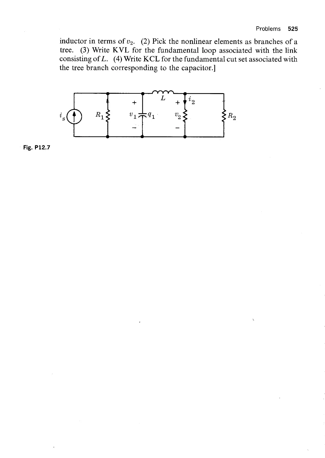
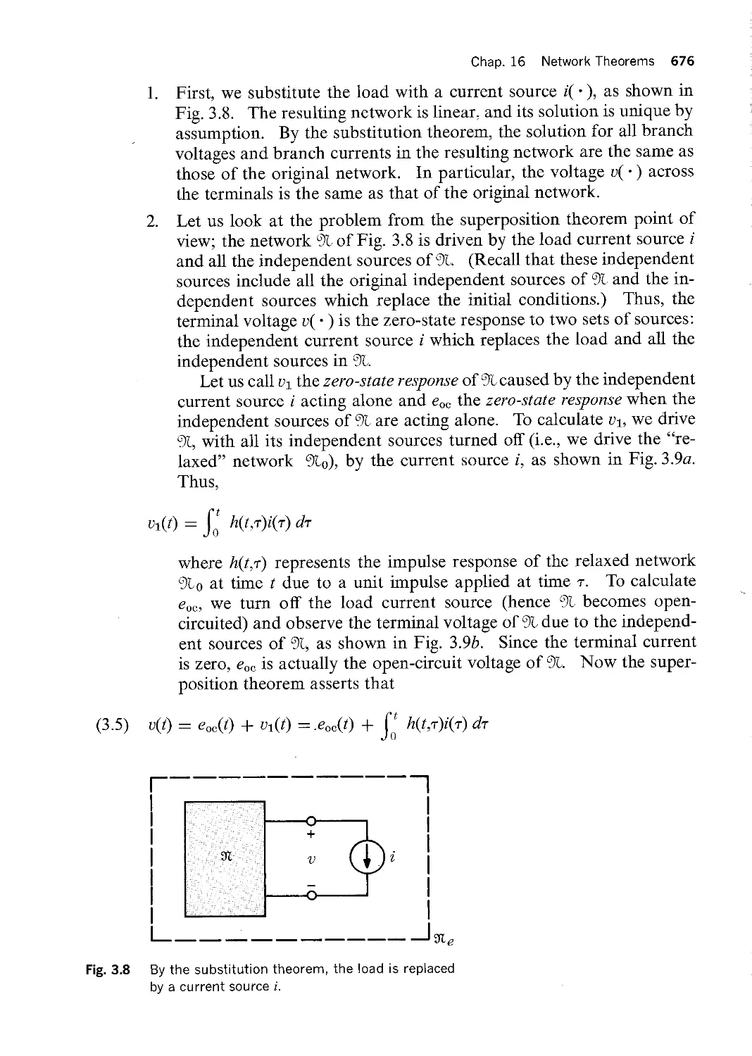
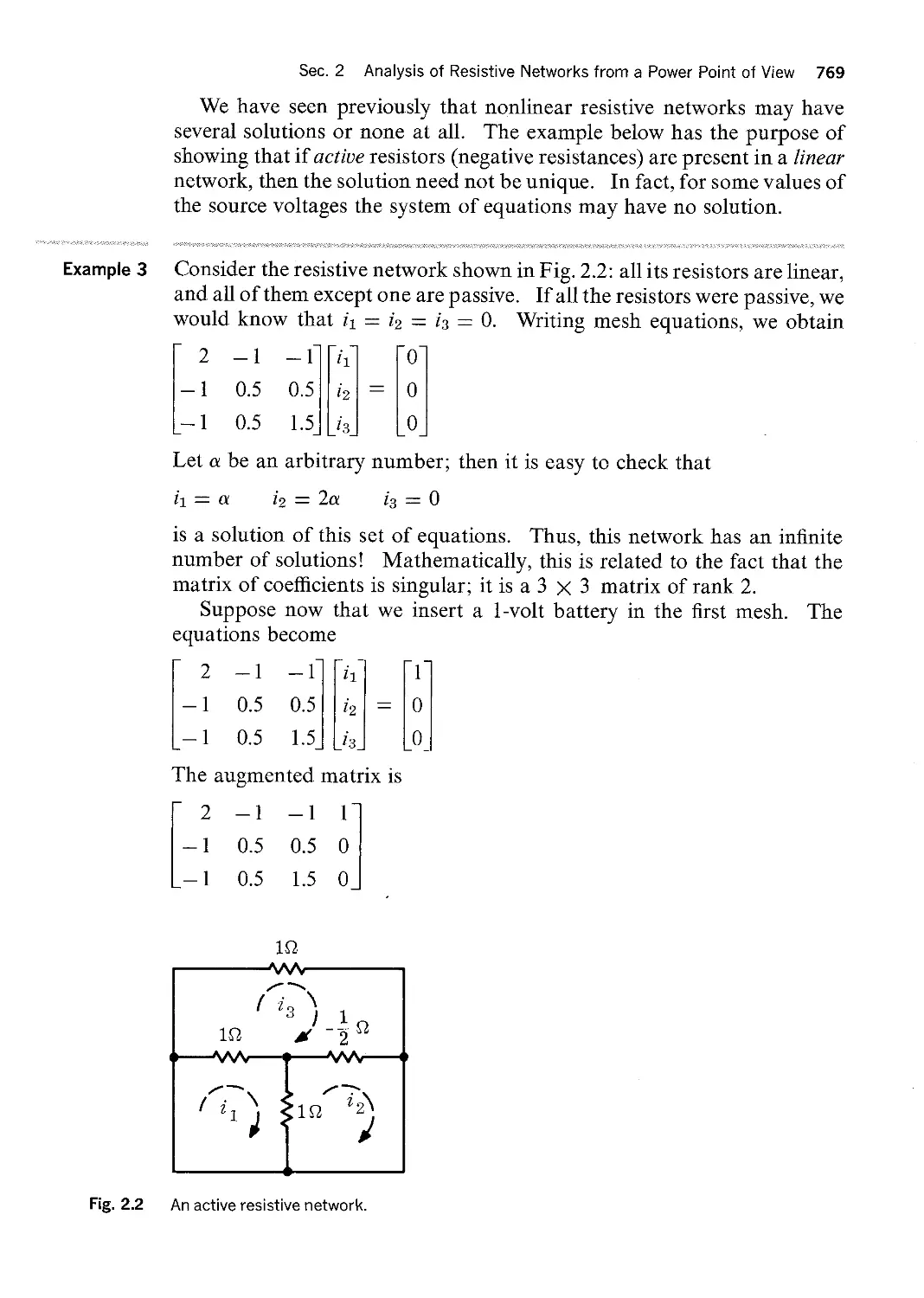
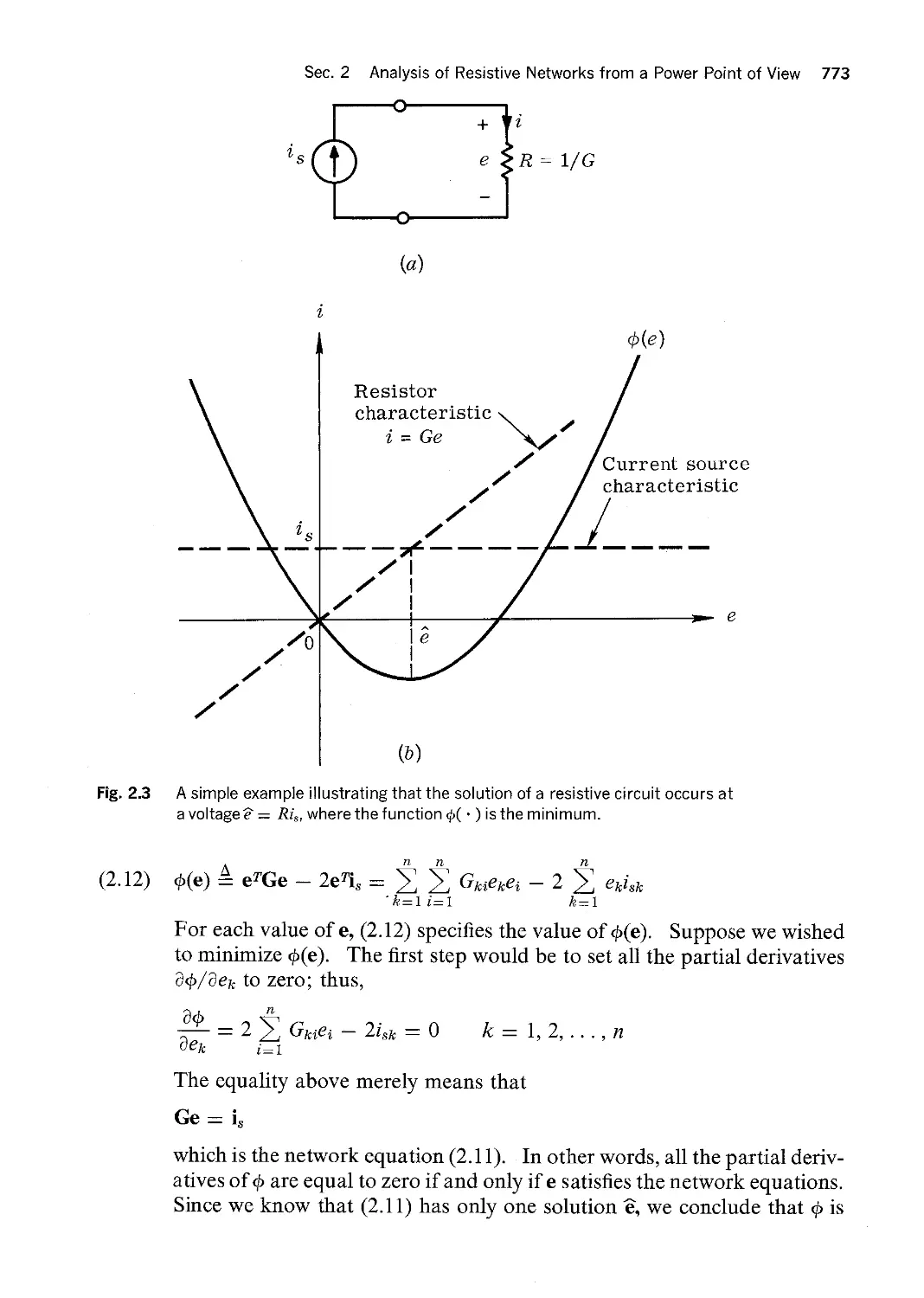
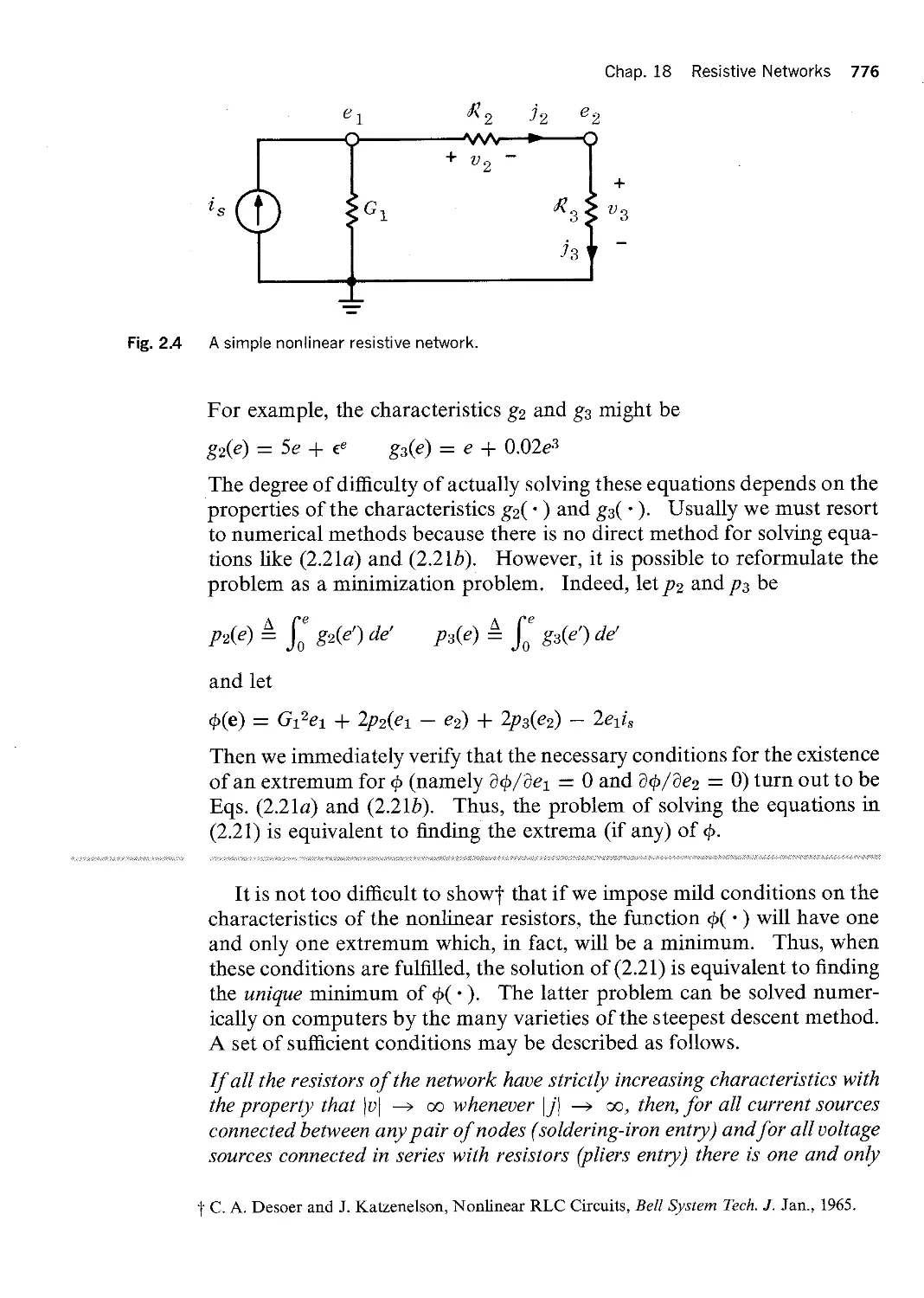
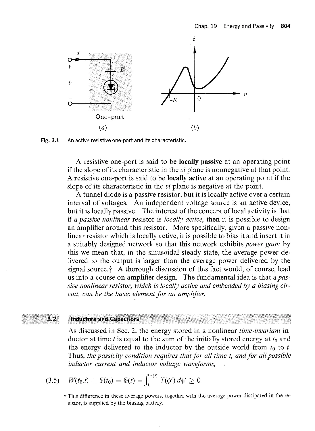
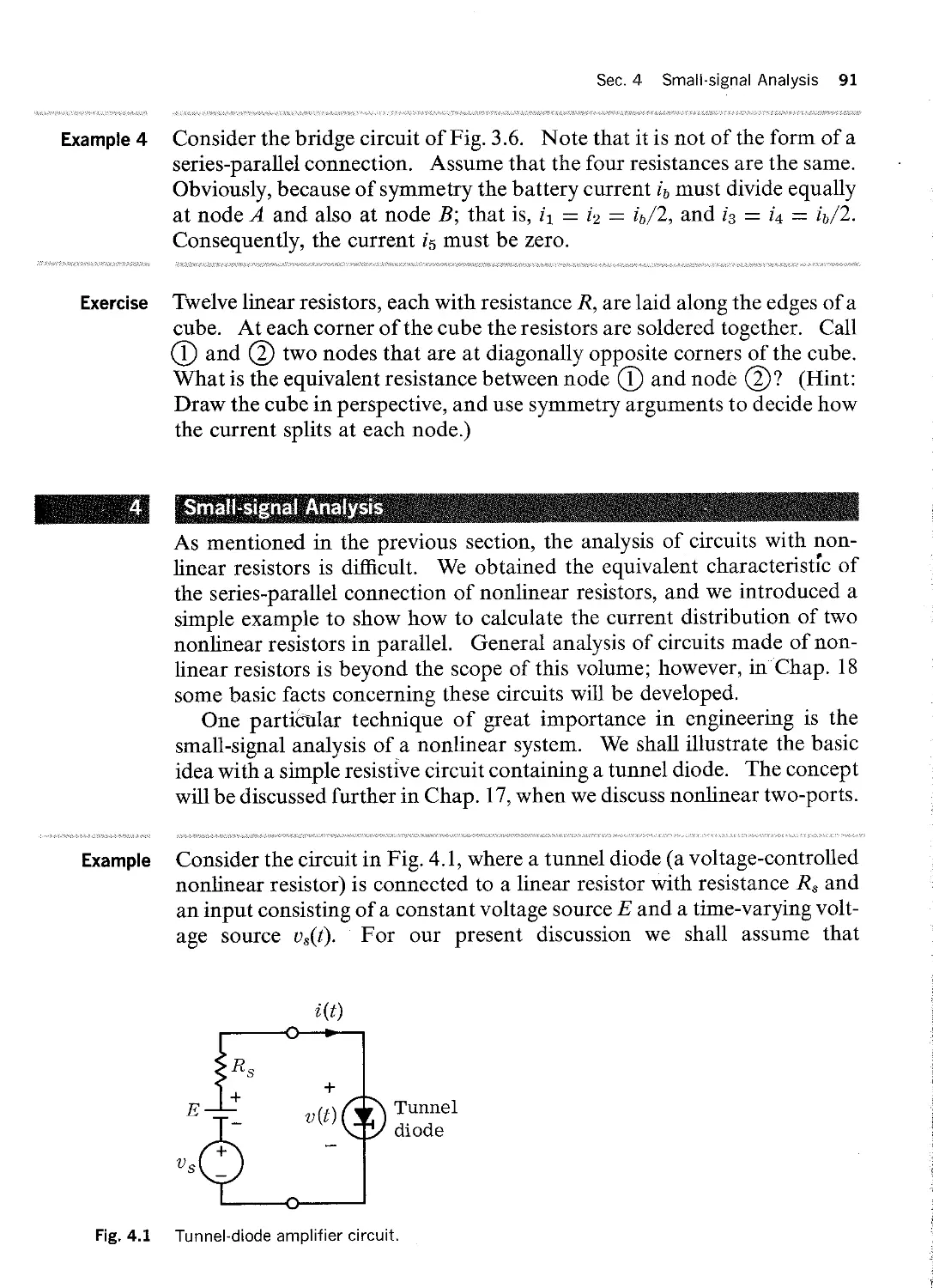
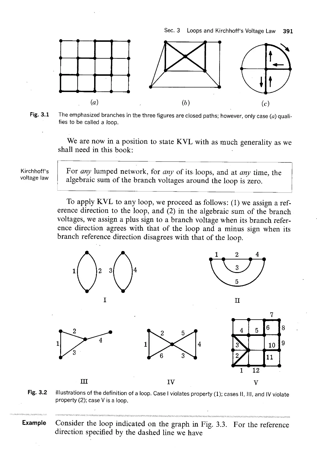
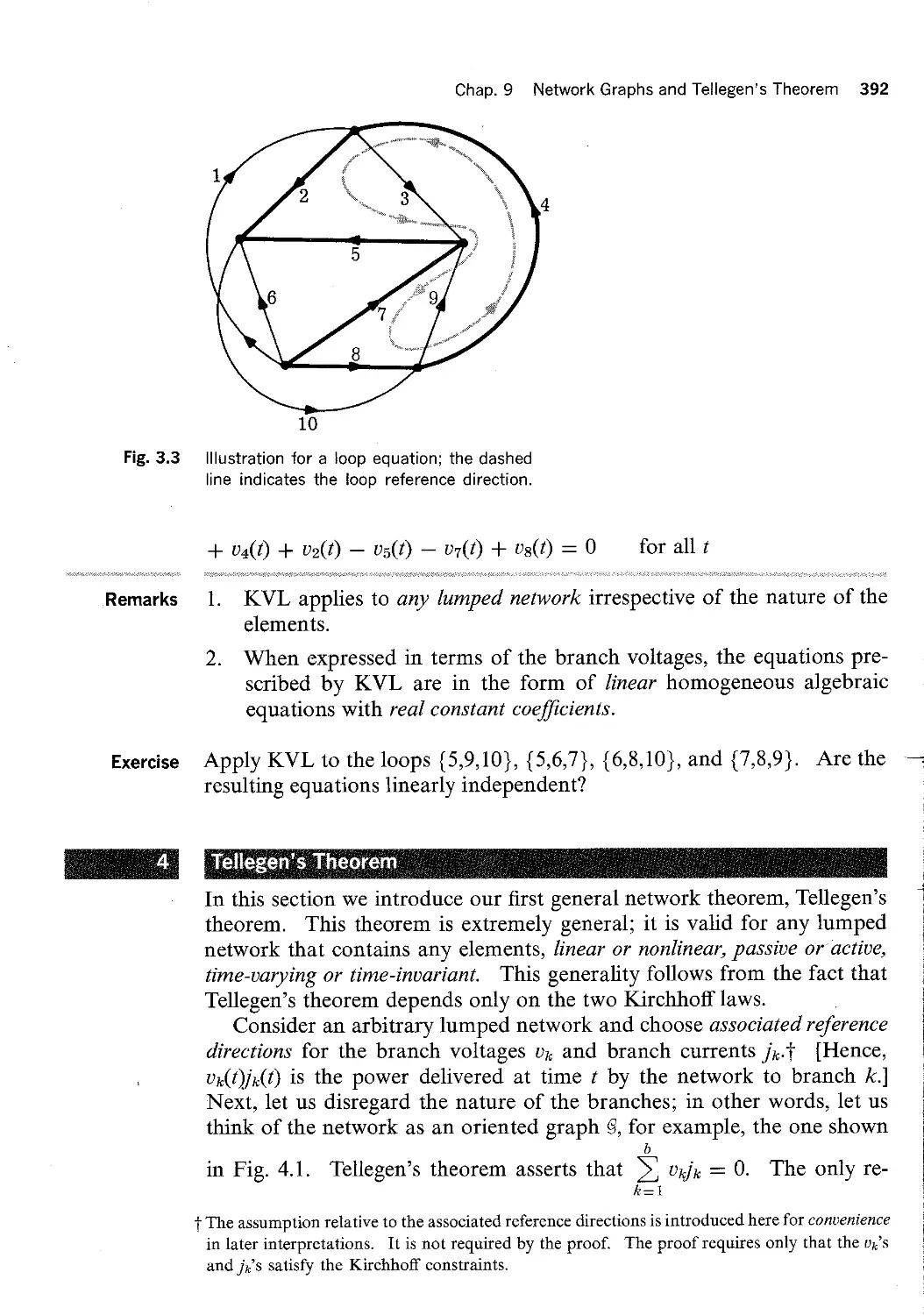
/


Автор: Desoer Charles A. Kuh Ernest S.
Теги: physics electrical engineering
ISBN: 07-016575-0
Год: 1969


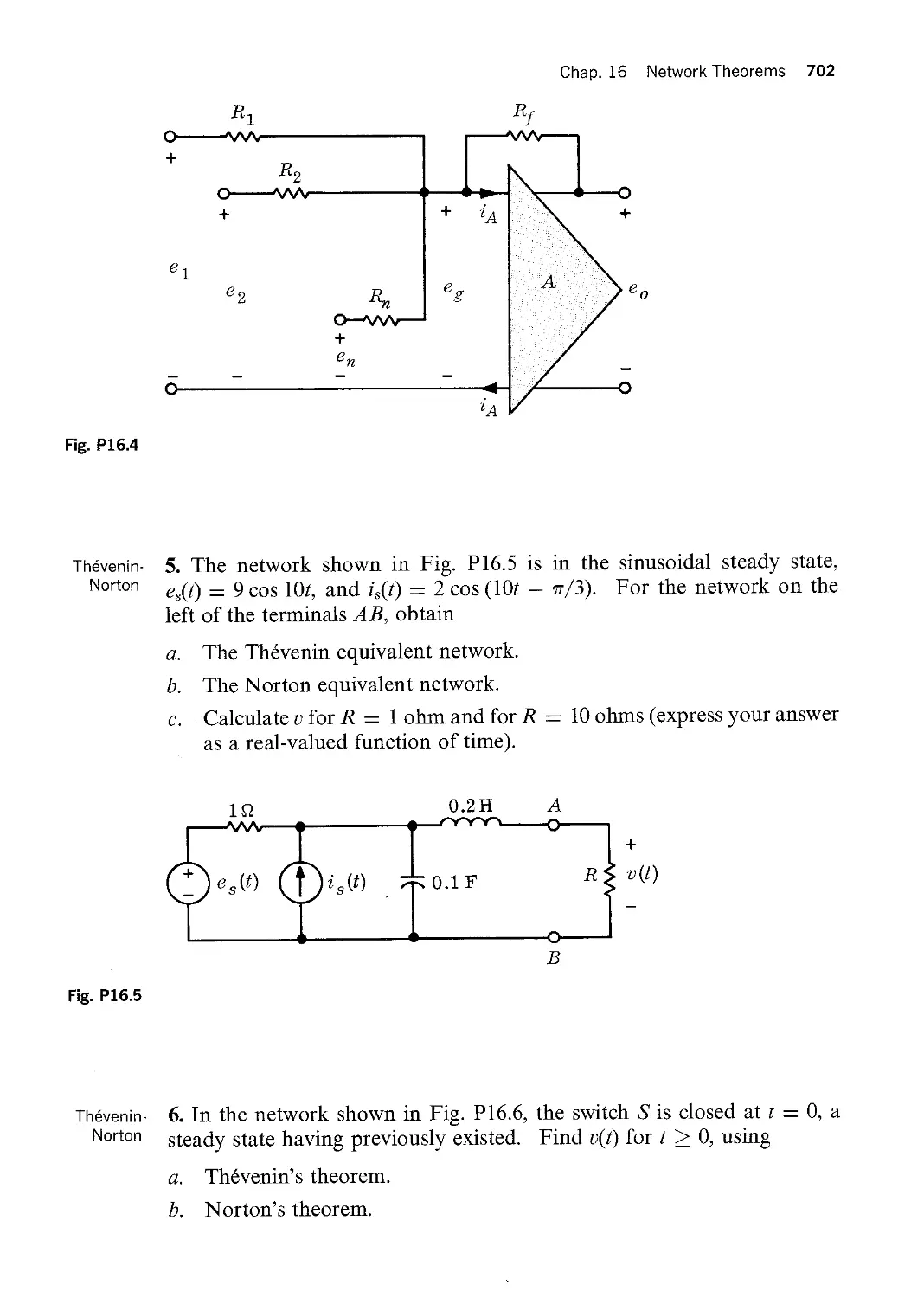
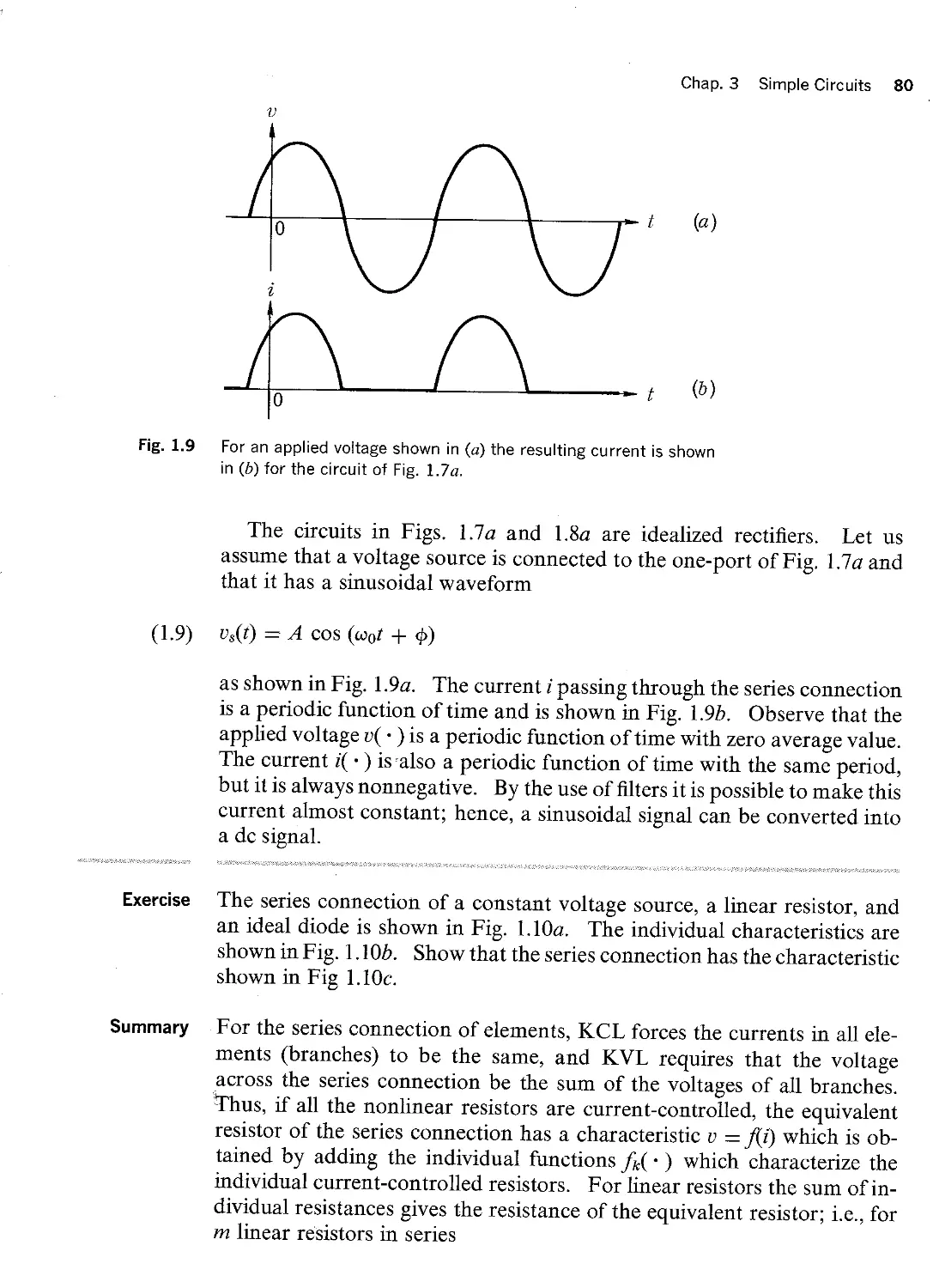
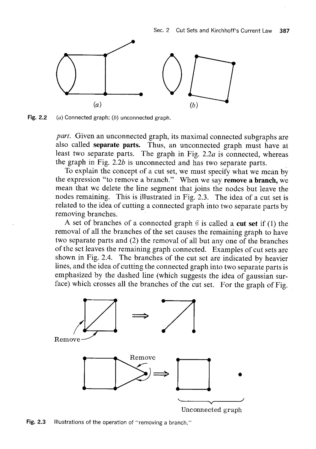
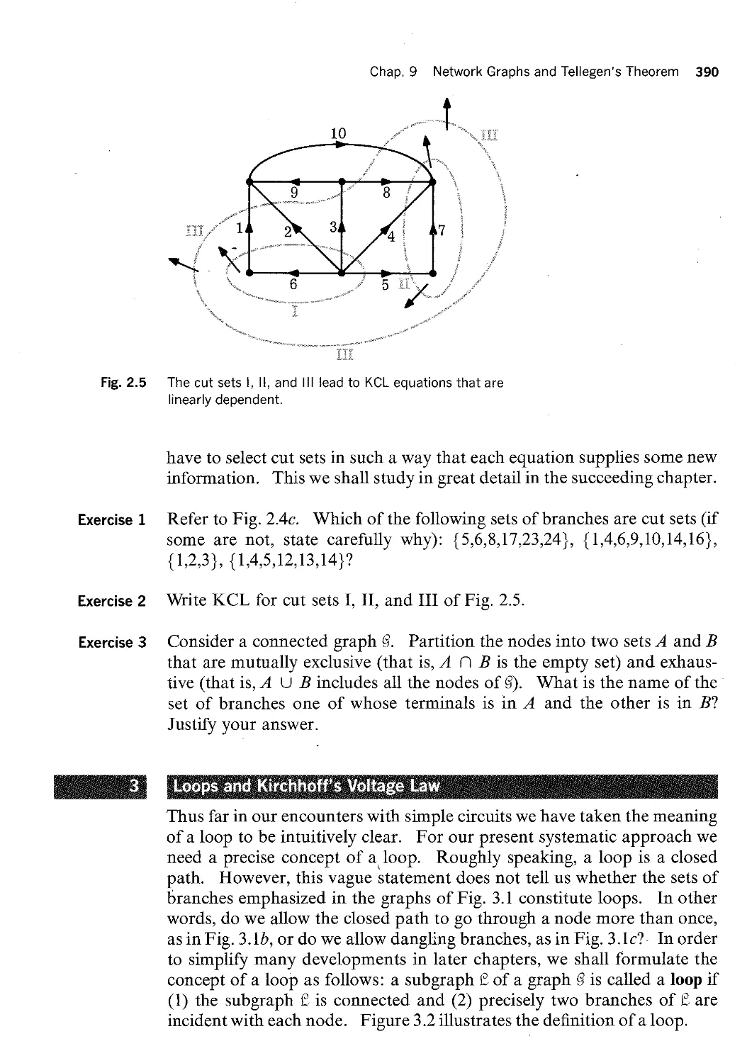
Текст
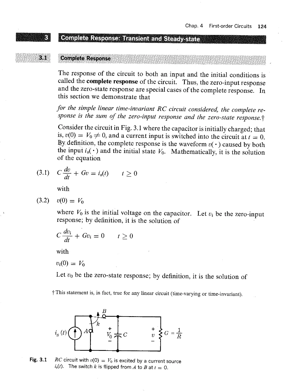
This chapter and the succeeding two are devoted to general methods of network
analysis. The problem of network analysis may be stated as follows: given the
network graph, the branch characteristics, the input (i.e., the waveforms of the
independent sources), and the initial conditions, calculate all branch voltages and
branch currents. ln these three chapters we shall consider only the formulation
of network equations. The methods of solution and the properties of the solu
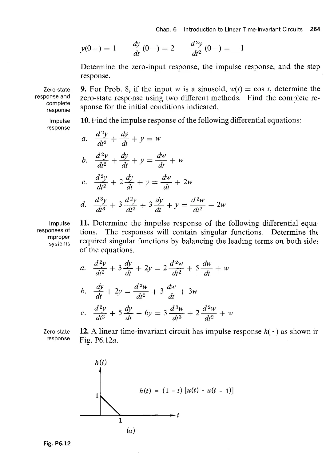
tions will be studied in Chaps. 13 to 16.
ln the present chapter we shall systematically develop node and mesh analysis.
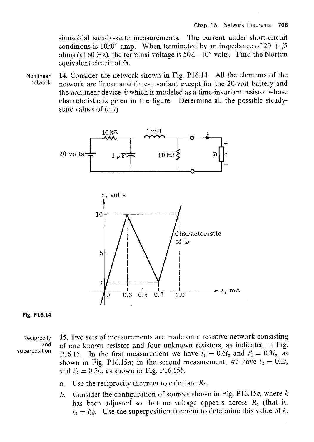
This systematic treatment is particularly important at present when computers
automatically perform the analysis of networks. Also from the results of these
systematic analyses we shall obtain the tools that will allow us to develop the prop
erties of these networks.
ln Sec. 1, we present source transformations that we shall use in all the follow
ing methods of analysis. ln Sec. 2, the consequences of Kirchhoff’s laws are ob
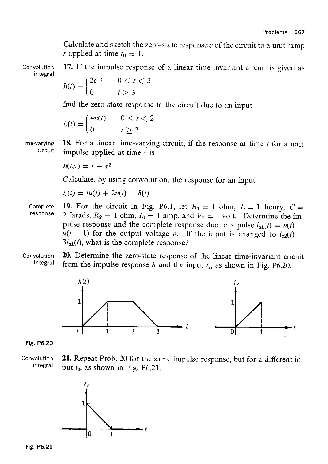
tained in the context of node analysis. Section 3 develops the systematic analysis
of linear time-invariant networks. Duality is developed in Sec. 4. Finally, mesh
analysis is presented in Secs. 5 and 6. Again, only linear time-invariant networks
are considered.
dU£•i=llIil1I=i(•1¥iiY=H`!?
In the general discussion of the problem of network analysis we assume
that the number and the location of independent sources are arbitrary as
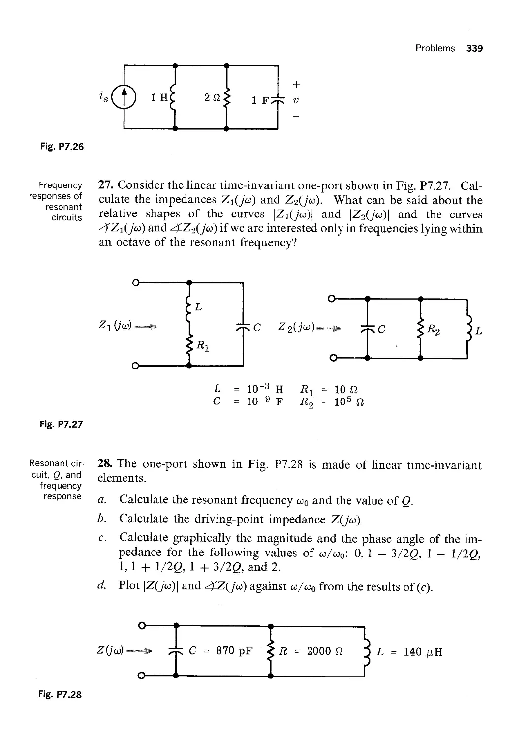
long as Kirchhoifs laws are not violated (ie., as long as no independent
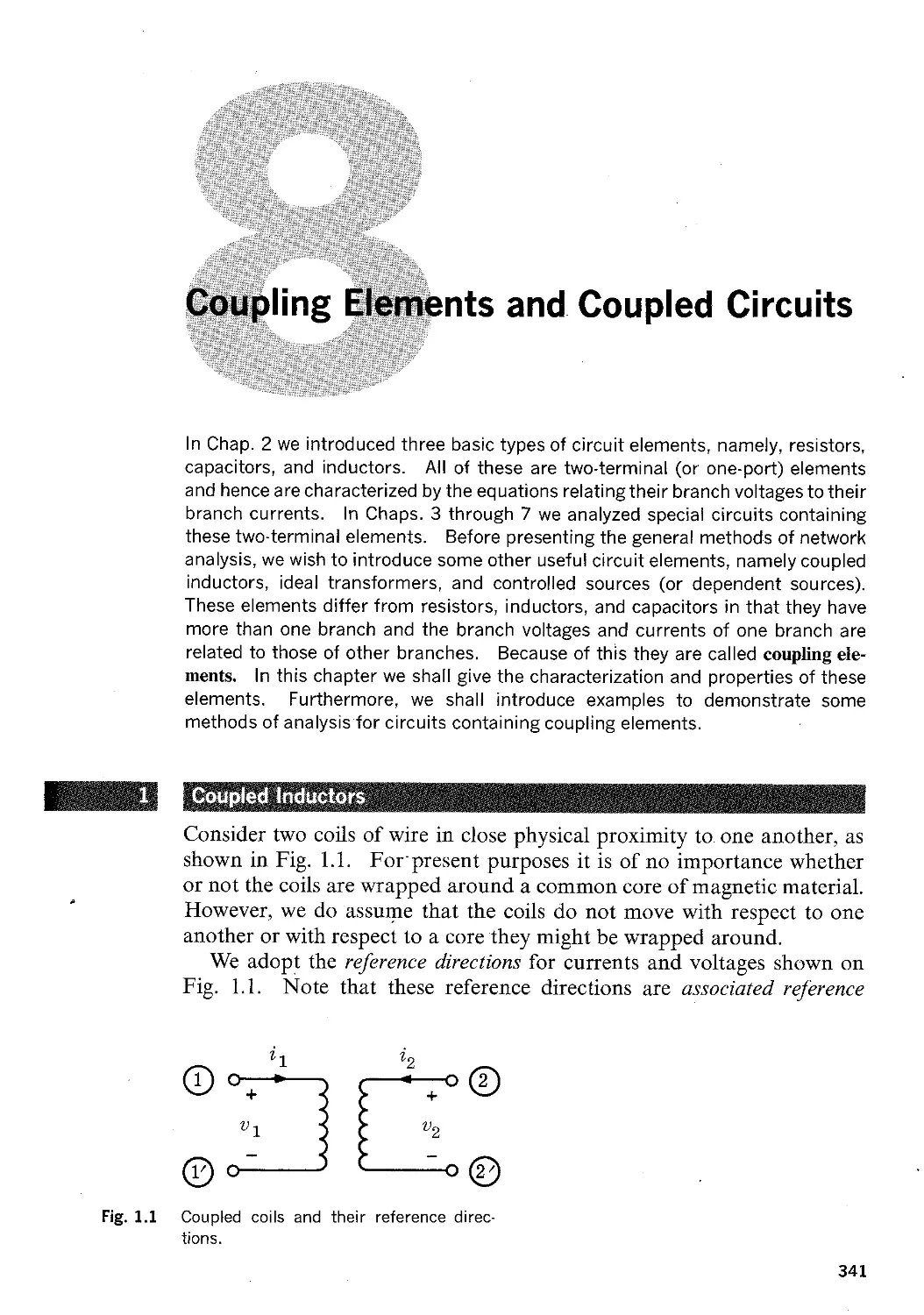
voltage sources form a loop and no independent current sources form a
cut set—for in either case the waveforms of these sources would have to
satisfy a linear constraint imposed by KVL and KCL, respectively).
To obviate separating the branches consisting only of sources from the
other branches, it is useful to introduce iirst two network transformations
that allow us to relocate sources in the network without affecting the prob
lem. These transformations can be used for both independent and de
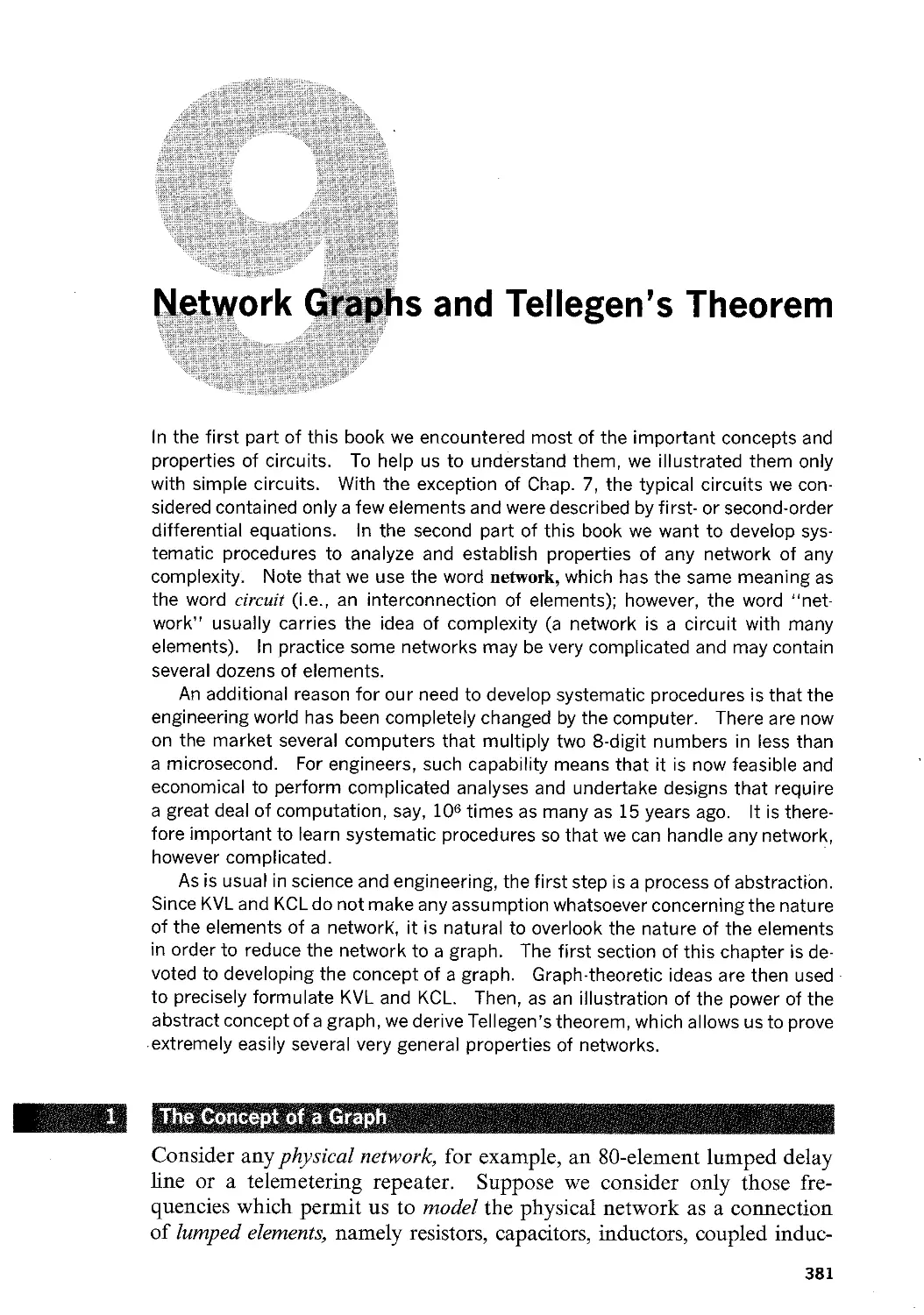
pendent sources. They are illustrated in Figs. 1.l and 1.2.
409
Chap. 10 Node and Mesh Analyses 410
16)
@i
E" @9 &
1Q) , Q)
+ n)l(¤ +
//i
//;\\
@k A
¤>°°( T
xl}
//;\\
' \ I \
I `\ I
Sec. 1 Source Transformations 411
(9}/ \\® CD x xx * \ x
Branch 4
1\ /2
,m\
(a)
,
\\ -7 {I
S
(6)
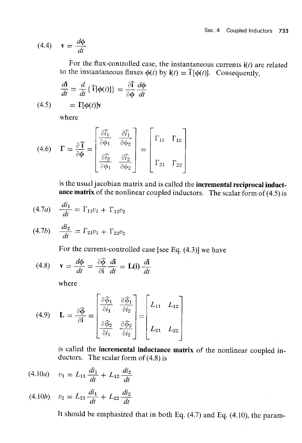
Fig. 1.2 Source transformation; a branch consisting of a current source alone is eliminated.
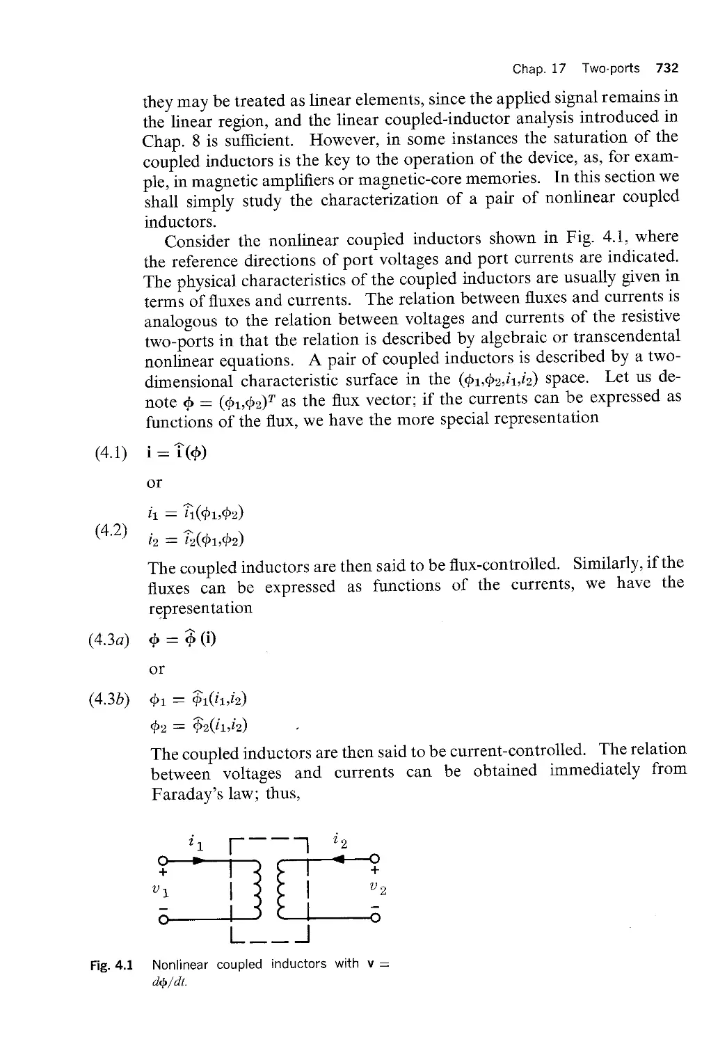
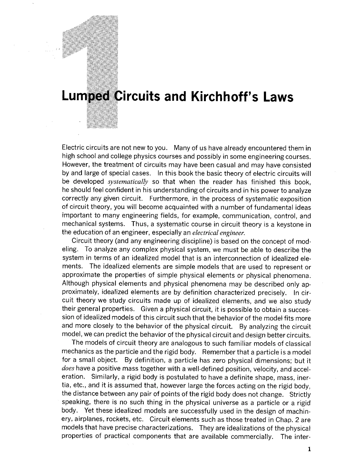
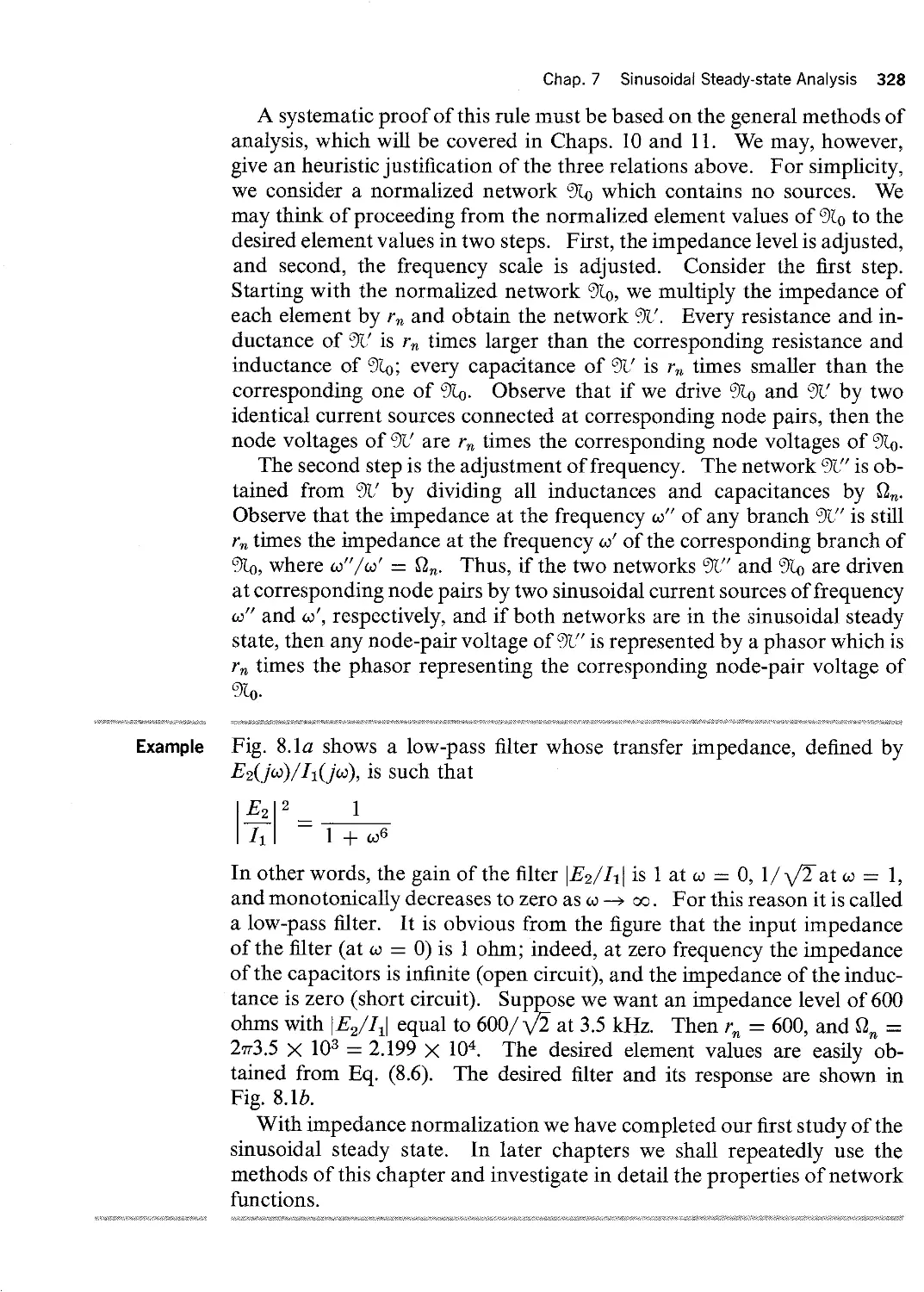
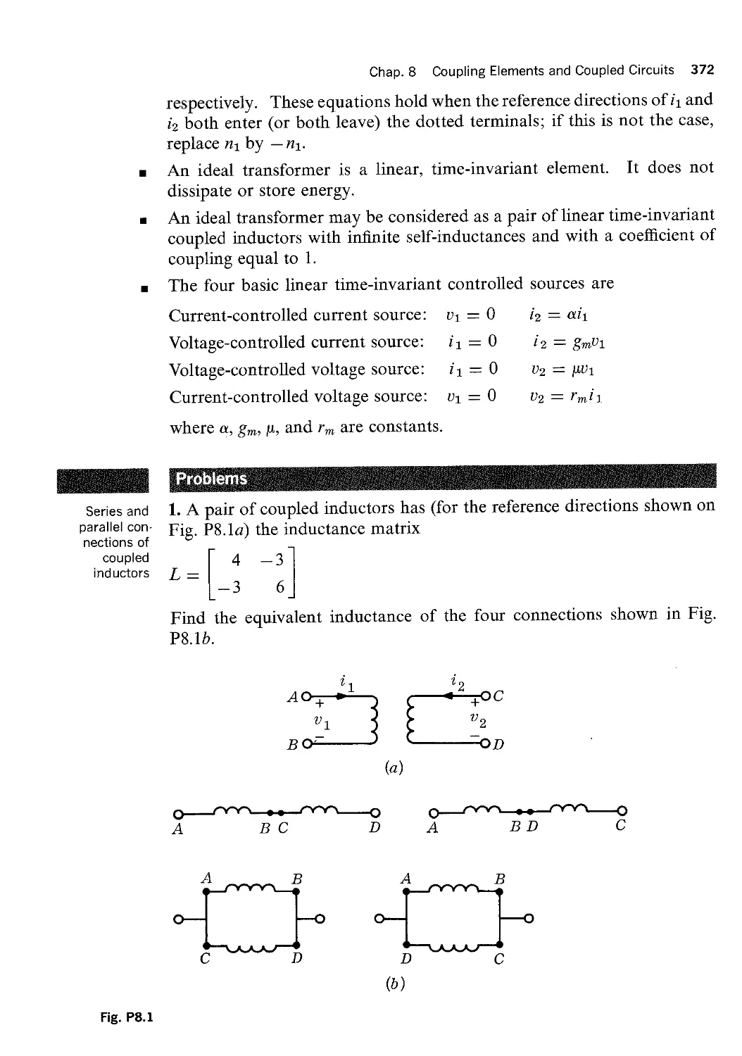
In Fi . l.la, branch l is a voltage source es which is connected between
nodes (E and Node @ is connected to node @ through branch 3
and to node @ through branch 4. If the current in branch l is of no inter
est to us, we can replace the circuit in Fig. l.la with its equivalent in
Fig. 1.lb. In the new circuit, branch l has been eliminated, and a new
node ® is introduced. This new node ® results from the merger of
nodes Q) and @ of the original circuit. To be equivalent, two sources es
must be inserted in branch 3 and branch 4 of the new circuit.
Showing that this transformation does not change the solution of the
problem is straightforward. We need only write the KVL equations for
all the loops containing branch 3 and all the loops containing branch 4 in
both networks. It is easily checked that the corresponding equations for
the two networks are the same. Also KCL applied to node ® is identical
to the sum of the equations obtained by applying KCL to node ® and to
node @ of the given network. Consequently, the KCL equations of
both networks impose equivalent constraints.
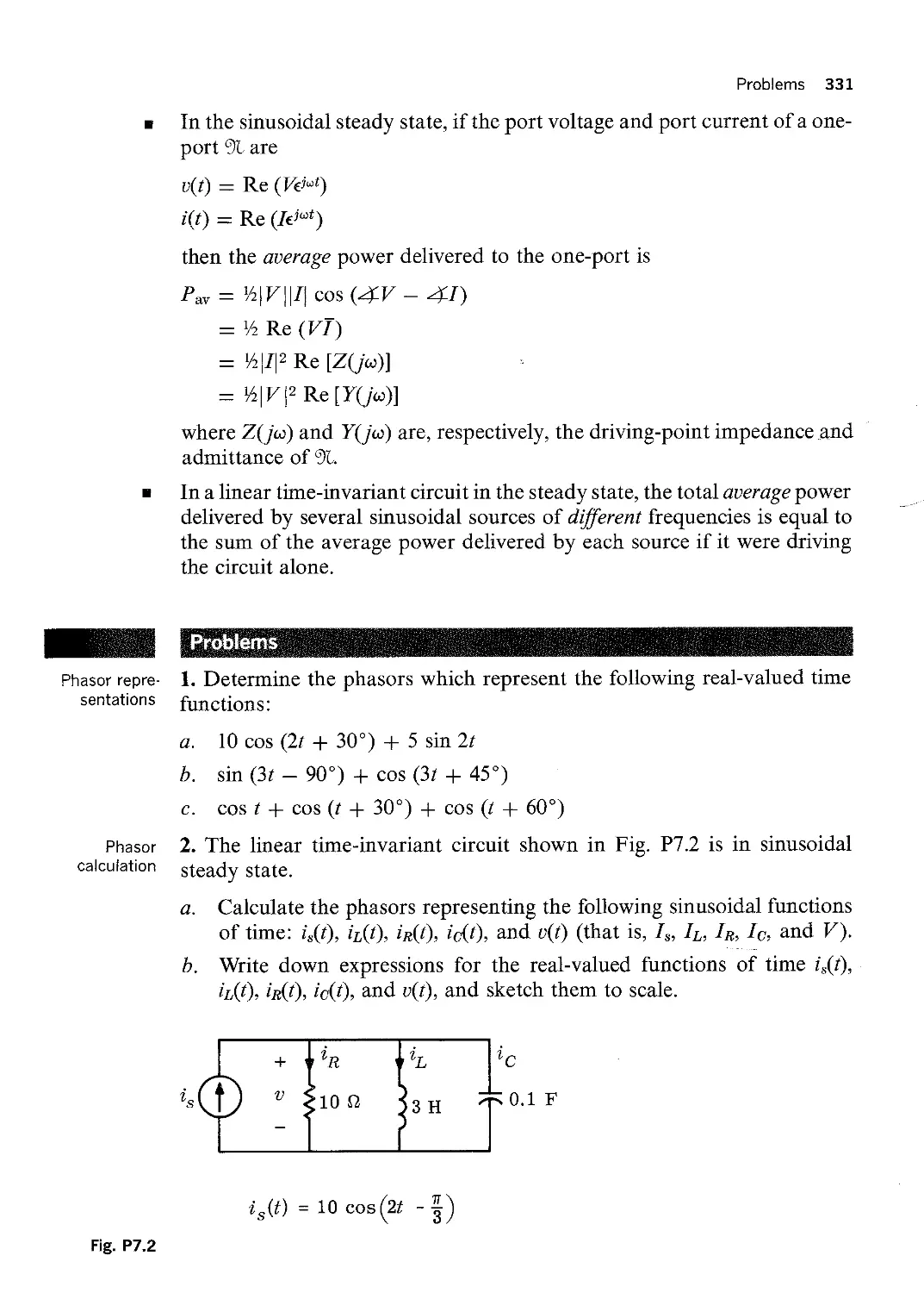
In Fig. l.2a, branch 4 is a current source is connected between nodes
(D and Nodes @ and @ are also connected to node @ through
branches l and 2, respectively. In Fig. l.2b we show the equivalent circuit,
where the current source in branch 4 has been removed; instead, two new
current sources is are connected in parallel with branches l and 2. That
this transformation does not change the solution of the problem can be
seen by writing the KCL equations for nodes ®, Q), and @ in both
networks. Clearly, the corresponding equations are the same.
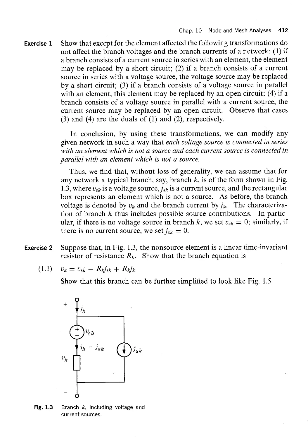
Exercise 1
Exercise 2
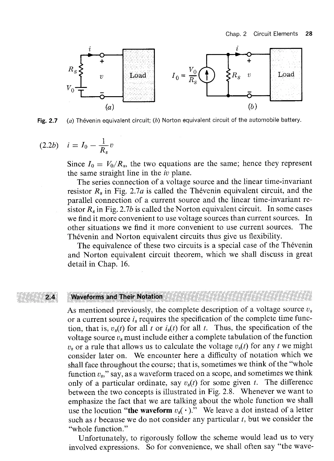
(1.1)
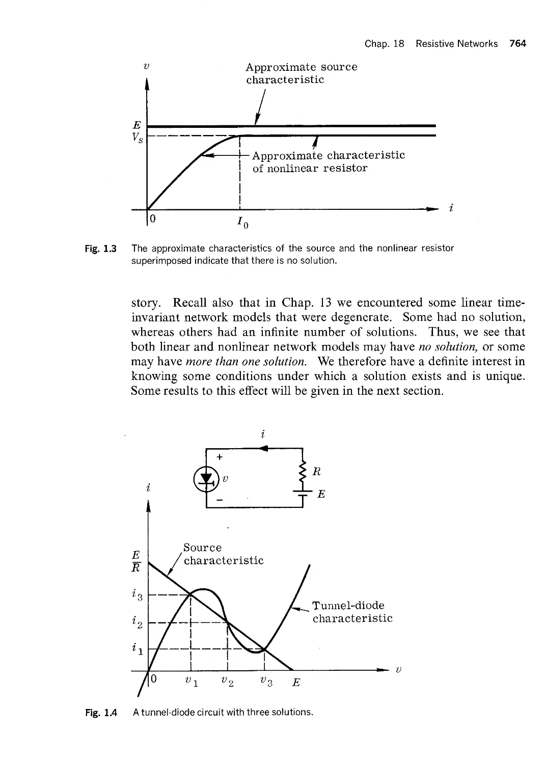
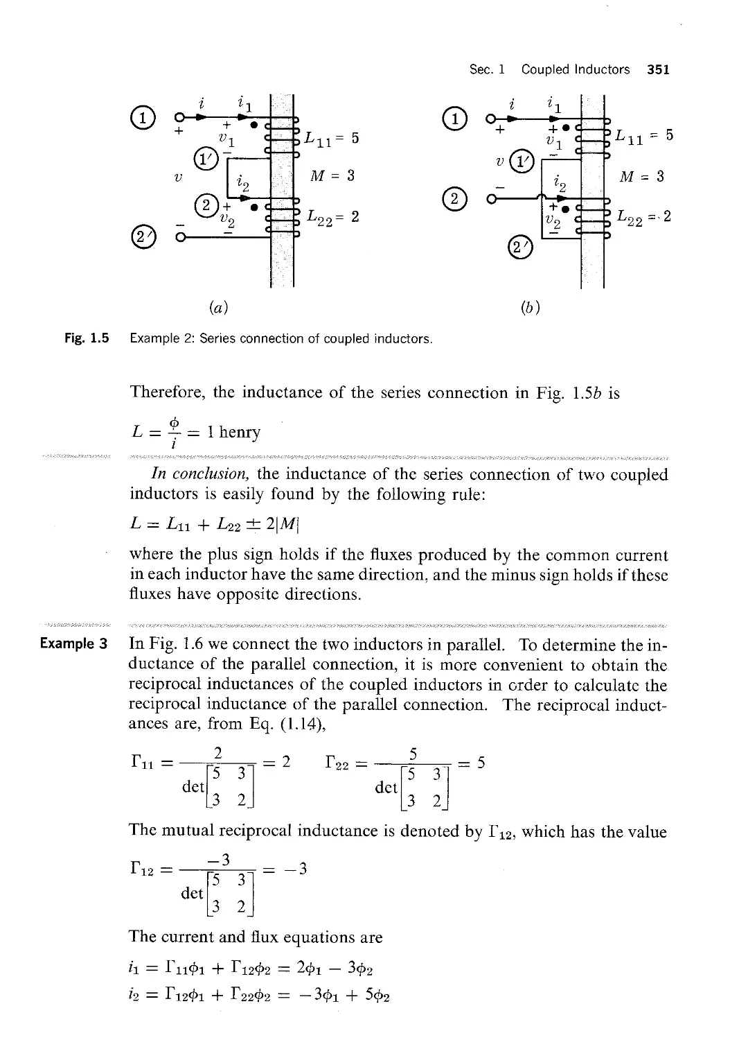
Fig. 1.3
Chap. 10 Node and Mesh Analyses 412
Show that except for the element affected the following transformations do
not affect the branch voltages and the branch currents of a network: (1) if
a branch consists of a current source in series with an element, the element
may be replaced by a short circuit; (2) if a branch consists of a current
source in series with a voltage source, the voltage source may be replaced
by a short circuit; (3) if a branch consists of a voltage source in parallel
with an element, this element may be replaced by an open circuit; (4) if a
branch consists of a voltage source in parallel with a current source, the
current source may be replaced by an open circuit. Observe that cases
(3) and (4) are the duals of (l) and (2), respectively.
In conclusion, by using these transformations, we can modify any
given network in such a way that each voltage source is connected in series
with an element which is not a source and each current source is connected in
parallel with an element which is not a source.
Thus, we find that, without loss of generality, we can assume that for
any network a typical branch, say, branch k, is of the form shown in Fig.
1.3, where vsk is a voltage source, js], is a current source, and the rectangular
box represents an element which is not a source. As before, the branch
voltage is denoted by vk and the branch current by jk. The characteriza
tion of branch k thus includes possible source contributions. In partic
ular, if there is no voltage source in branch k, we set vs;. : 0; similarly, if
there is no current source, we set js], = O.
Suppose that, in Fig. 1.3, the nonsource element is a linear time-invariant
resistor of resistance Rk. Show that the branch equation is
Uk = Usk — Rkjsk + Rkjk
Show that this branch can be further simplified to look like Fig. 1.5.
JI lvsk
jk — jsk ( hvjsk
Branch k, including voltage and
current sources.
Fig. 1.4
Exercise 3
(1.2)
Fig. 1.5
Sec. 1 Source Transformations 413
+ Wk
.. }"sk
+ ok I
“r ‘ "sk (lljsk
Branch k, including voltage and
current sources.
Suppose that, in Fig. 1.4, the nonsource element is a linear time-invariant
resistor of conductance Gk. Show that the branch equation is
jk =jsk — Gkvsk —i· Gkvk
Show that this branch can be further simplified to look like Fig. 1.6.
These two exercises illustrate useful equivalences. It is convenient,
though not necessary, in node analysis for all independent sources to be
current sources. Similarly, it is convenient, though not necessary, in loop
or mesh analysis for all independent sources to be voltage sources.
From now on we shall assume that in dealing with resistive networks
the branches are always ofthe form of Fig. 1.5 or Fig. 1.6, that is, a resistor
in series with a voltage source or a resistor in parallel with a current source.
Usk ` Rkjsk
A resistive branch with an equivalent
voltage source.
Fig. 1.6
Exercise 4
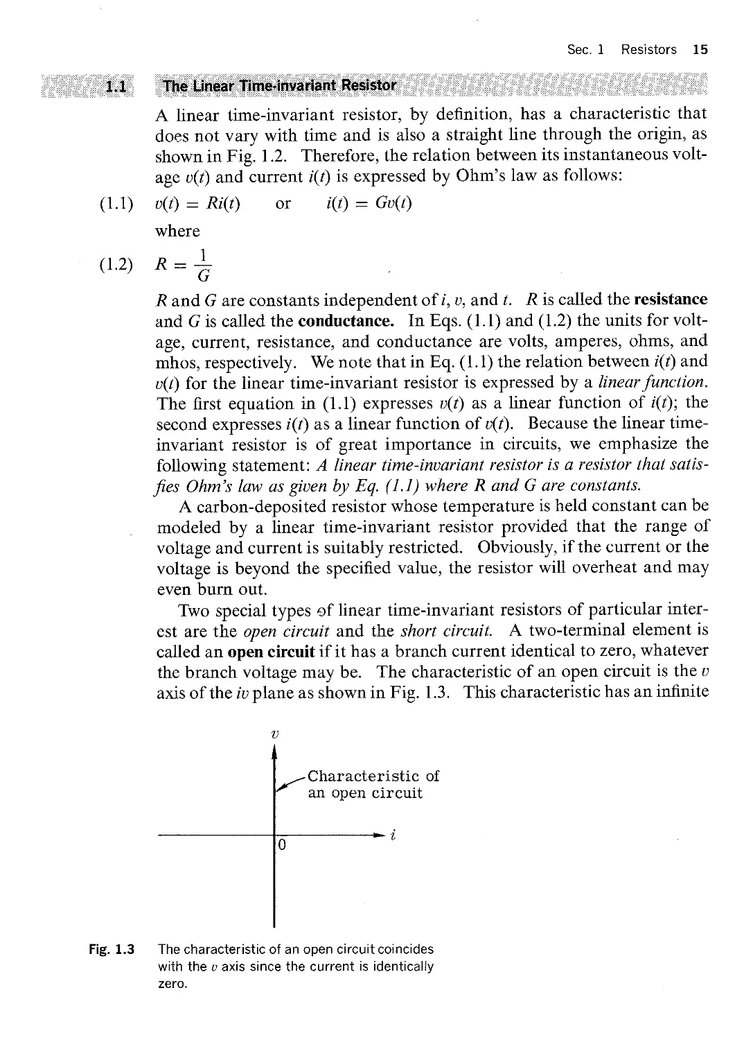
Fig. 1.7
\’*2.»1
Chap. 10 Node and Mesh Analyses 414
Gk ' Gkvsk
A resistive branch with an equivalent
current source.
In general networks, the resistor may be replaced by an inductor or a
capacitor.
Perform the transformation for the circuits in Fig. 1.7.
Exercises on source transformation.
uliriyinlu
•I·
Let us consider any network ‘?)l and let it have nt nodes and b branches.
Altogether there are b branch voltages and b branch currents to be deter
mined. Without loss of generality we may assume that the graph is con
nected, i.e., that it has one separate part only. (If the network were made
of two separate parts, we could connect these two separate parts by tying
them together at a common node.)
First, we pick arbitrarily a reference node. This reference node is usu
ally called the datum node. We assign to the datum node the label @ and
to the remaining nodes the labels ®, @, . . ., @, where n é nt — l.
J¢m¤ti¢sti¤¤$.i¤fiKcL
Let us apply KCL to nodes Q), @, . . . , @ (omitting the datum node)
and let us examine the form of the equations obtained. Typically, as in
Sec. 2 Two Basic Facts of Node Analysis 415
the case of node @ shown in Fig. 2.1, we obtain a homogeneous linear
algebraic equation in the branch currents; thus,
J4 + je — j7 Z 0
Thus, we have a system of n linear algebraic equations in b unknowns
jb, j2, . . . , jb. The iirst basic fact of node analysis is the following
statement:
Since the network €)L is connected the n linear homogeneous algebraic equa
tions inj1,j2, . . . ,j,,, obtained by appbring KCL to each node except the datum
node, constitute a set of linearbi independent equations.
Let us start by an observation. Consider the nb equations obtained by
writing KCL for each of the nb nodes of 9%. Let gk : O represent the
equation pertaining to node ®, k : 1, 2,..., nb. For the node @
shown in Fig. 2.1, the equation @3;, : 0 gives j4 -l- j6 — jb : 0. We assert
that E 5b reduces identically to zero. ln other words, if we add all the
kzi
nb KCL equations (written in terms of the branch currents jb, jg, . . . , jb),
all terms cancel out. This is obvious. Suppose branch 1 leaves node @
and enters node The term jl appears with a plus sign in 62 and a
minus sign in 63, and, since jl appears in no other equation, jl cancels out
in the sum. Since every branch of 9L must leave one node and terminate
on another node, all branch currents will cancel out in the sum. We con
clude that the nb equations obtained by writing KCL for each of the nodes of
the network {UL are linearbr dependent.
Let us now prove that the n linear algebraic equations gl : 0,
52 : O, . . . , @5,, : O are linearly independent. Suppose they were not;
i.e., suppose that these n equations are linearly dependent. This would
mean that, after some possibly necessary reordering ofthe equations, there
is a linear combination of the first k equation 51 : O, 52 : 0, . . . , {Sk : O
(k g n) with respective nonzero weighting factors al, a2, . . . , ak, which sums
identicalbr to zero. Thus,
@/*4
.7 6 7
Fig. 2.1 A typical node to illustrate KCL.
Chap. 10 Node and Mesh Analyses 416
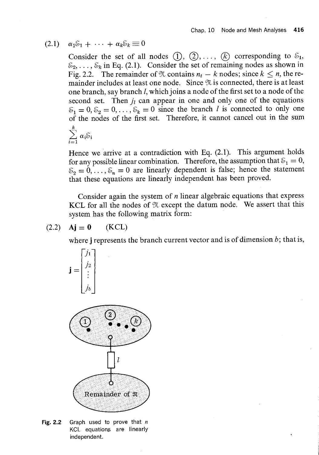
Consider the set of all nodes ®, @, . . ., @ corresponding to 551,
62, . . . , 55;, in Eq. (2.l). Consider the set of remaining nodes as shown in
Fig. 2.2. The remainder of Qt contains nt — k nodes; since k g n, the re
mainder includes at least one node. Since ‘?)tis connected, there is at least
one branch, say branch I, which joins a node of the first set to a node of the
second set. Then j; can appear in one and only one of the equations
551 = 0,52 : O, . . .,£5k : O since the branch I is connected to only one
of the nodes of the first set. Therefore, it cannot cancel out in the sum
2 04151
L:1
Hence we arrive at a contradiction with Eq. (2.l). This argument holds
for any possible linear combination. Therefore, the assumption that 81 = 0,
52 = 0,..., 55,1 = O are linearly dependent is false; hence the statement
that these equations are linearly independent has been proved.
Consider again the system of n linear algebraic equations that express
KCL for all the nodes of 9L except the datum node. We assert that this
system has the following matrix form:
(2.2) Aj : 0 (KCL)
where j represents the branch current vector and is of dimension bg that is,
Q1! GQ Q • _· Q
Remainder of SZ
Fig. 2.2 Graph used to prove that n
KCL equations are linearly
independent.
(2.3)
Remark
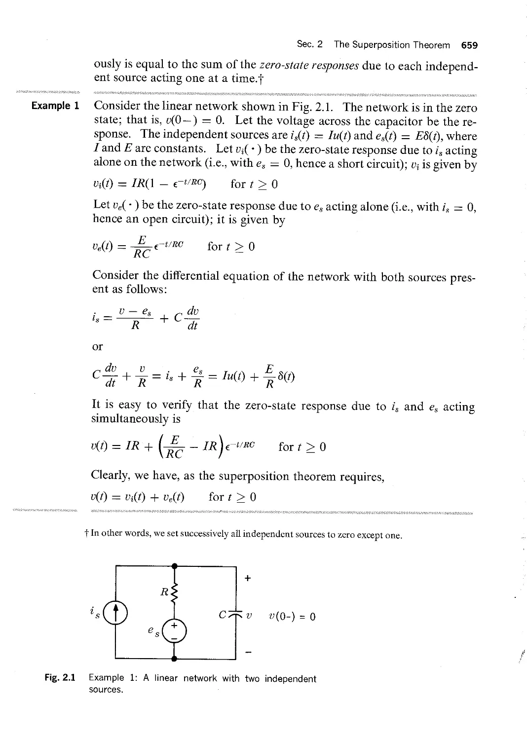
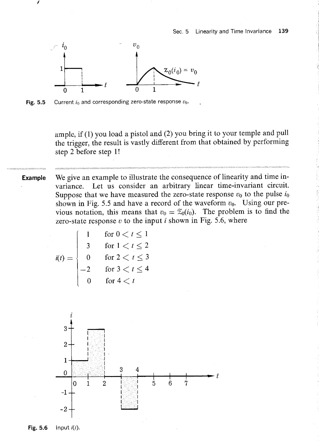
Example 1
Sec. 2 Two Basic Facts of Node Analysis 417
and whore A : (aug) is an n X b matrix dciinod by
1 if branch k leaves node ®
au, : { -1 if branch k enters node @
O if branch k is not incident with nodc @
Aj is therefore a vector of dimension n. This assertion is obvious since
when we write that the ith component of the vector Aj is equal to zero,
we merely assert that the sum of all branch currents leaving node @
is zero.
It is immediately observed that the rule expressed by Eq. (2.3) is iden
tical with the rule specifying the elements of the node—to-branch incidence
matrix Aa defined in the previous chapter. The only difference is that
Aa has nt : n -|- l rows. Obviously, A is obtainable from A., by deleting
the row corresponding to the datum node. A is therefore called the reduced
incidence matrix.
The fact that Aj : 0 is a set of n linearly independent equations in the
variables jl, j2, . . . , jb implies that the n X b matrix A has rank n. Since
we always have b > n, this conclusion can be restated as follows: the re
duced incidence matrix A is of full rank. This can be checked by Gauss
elimination.
Consider the graph of Fig. 2.3, which contains four nodes and five
branches (n, : 4, b : 5). Let us number the nodes and branches, as
shown on the figure, and indicate that node @ is the datum node by the
"ground” symbol used in the figure. The branch-current vector is
J Z] js
The matrix A is obtained according to Eq. (2.3); thus,
2 @ 4 @
Fig. 2.3 Graph for Examples 1 and 2.
1 1 O 0 O 0 O — I
Branch I 2 3 4
Thus, Eq. (2.2) states that
Aj :O -1
l 1 [O O
0r
]1+]2
]2 +]3 +]4
]4+]5
Chap. 10 Node and Mesh Analyses 418
Node
0 |~®
0 |~@
I |e—®
0 O 0 jg O -1 1 j4
which are clearly the three node equations obtained by applying KCL to
nodes ®, @, and In the present case it is easy to see that the three
equations are linearly independent, since each one contains a variable
not contained in any of the other equations.
Exercise 1 Verify that the 3 >< 5 matrix A above is of full rank. (Hint: You need only
exhibit a 3 X 3 submatrix whose determinant is nonzero.)
Exercise 2 Determine the incidence matrix Aa of the graph in Fig. 2.3. Observe that
A is obtained from Aa by deleting the fourth row.
Let us call el, eg, . . . , en the node voltages of nodes ®, @, . . . , @ meas
ured with respect to the datum node. The voltages el, e2, . . . , en are called
the node-t0-datum voltages. We are going to use these node-to—datum
voltages as variables in node analysis. KVL guarantees that the node-to
datum voltages are defined unambiguously; if we calculate the voltage of
any node with respect to that of the datum node by forming an algebraic
sum of branch voltages along a path from the datum to the node in ques
tion, KVL guarantees that the sum will be independent of the path chosen.
Indeed, suppose that a first path from the datum to node ® would give
Sec. 2 Two Basic Facts of Node Analysis 419
ek as the node-to-datum voltage and that a second path would give ei, ¢ ek.
This situation contradicts KVL. Consider the loop formed by the first
path followed by the second path; KVL requires that the sum of the
branch voltages be zero, hence ef, ; ek.
A somewhat roundabout but effective way of expressing the KVL con
straints on the branch voltages consists in expressing the b branch voltages
in terms of the n node voltages. Since for nontrivial networks b > n, the b
branch voltages cannot be chosen arbitrarily, and they have onbr n degrees
of freedom. Indeed, observe that the node—to—datum voltages el, e2, . . . , en
are linearly independent as far as the KVL is concerned; this is immediate
since the node-to-datum voltages form no loops. Let e be the vector
whose components are el, e2, . . . , en. We are going to show that the branch
voltages are obtained from the node voltages by the equation
V : ATB
where AT is the b >< n matrix which is the transpose of the reduced in
cidence matrix A defined in Eq. (2.3); v is the vector of branch voltage,
v1, 112,..., vb.
To show this, it is necessary to consider two kinds of branches, namely,
those branches which are incident with the datum node and those which
are not. For branches which are incident with the datum node, the branch
voltage is equal either to a node-to-datum voltage or its negative. For
branches which are not incident with the datum node, the branch voltage
must form a loop with two node—to-datum voltages, and hence it can be
expressed as a linear combination of the two node-to-datum voltages by
KVL. Therefore, in both cases the branch voltages depend linearly on
the node-to-datum voltages. To show that the relation is that of Eq. (2.4),
let us examine in detail the sign convention. Recall that uk is the
kth branch voltage, k : l, 2, . . . , b, and e, is the node-to-datum voltage
of node @, i : 1, 2, . . . , n. Thus if branch k connects the ith node to
the datum node, we have
U _ k _
e, if branch k·lez1ves node @
e, if branch k enters node Q)
On the other hand, if branch k leaves node @ and enters node (D, then
we have as is easily seen from Fig. 2.4
Uk Z 6; —— €j
Since in all cases vk can be expressed as a linear combination of the voltages
el, eg, . . . , en, we may write
U1I Icll €i2···€1n| l€i
U2I IC21 €22···€2nI I€2
Ubi |€b1 €b2···€zm| len
Fig. 2.4
(2.5)
Example 2
Chap. 10 Node and Mesh Analyses 420
QD ¤-——·———¤” CD + + Uk " + .
éi Qj
Calculation of the branch voltage uk in
terms of the node voltages ei and ei; uk :
Ei — Ei.
where the ckfs are 0, 1, or -1 according to the rules above. A little
thought will show that
1 if branch k leaves node @
ck, = I -1 if branch k enters node @
O if branch k is not incident with node @
A comparison of Eq. (2.5) with Eq. (2.3) shows immediately that cm ; 0,;,
for i : 1, 2, . . . , n and k : 1, 2, . . . , b. Therefore, the matrix C (whose
elements are the ckfs) is in fact the transpose of the reduced incidence
matrix A. Hence Eq. (2.4) is established.
For the circuit in Fig. 2.3,
V :l U3 6 : 82
U2 61 U4 6s
According to Eqf (2.5), we have
Branch
1 0 O I <—1
1 -1 O I +2
AT : I 0 l O I +3
O 1 -1 I %4
0 0 1 I <—— 5
Node (I) g &
Sec. 2 Two Basic Facts of Node Analysis 421
Thus, Eq. (2.4) states that
1 O O
v:ATe:|O 1 0e2
gf
U1 Z
U2 =
U3 :
U4 :
U5 :
II1 --1 OIIr61 O 1 -1 I I_€3I
0 0 1
61-62
62-63
These live scalar equations are easily recognized as expressions of the
KVL.
Summary Equations (2.2) and (2.4) give
Aj = 0 (KCL) v : ATe (KVL)
and are the two basic equations of node analysis. They are obtained from
the network graph and the two Kirchhoff laws, which make them in
dependent of the nature of the elements of the network. Eq. (2.2) ex
presses KCL and consists of n independent linear homogeneous algebraic
equations in the b branch currents jl, jg, . . . , jb. Equation (2.4) expresses
KVL and expresses the b branch voltages 01, vg, . . . , vb in terms of the n
node-to-datum voltages el, @2, . . . , en.
Obviously, to solve for the n network variables el, ez, . . . , en, we need
to know the branch characterization of the network, i.e., the b branch
equations which relate the branch voltages v to branch currents j. Only
in these branch equations does the nature of the network elements come
into the analysis. Thus, the remaining problem is to combine Eqs. (2.2)
and (2.4) with the branch equations and obtain n equations in n unknowns,
el, e2, . . . en. This requires some elimination. For nonlinear and time
varying networks the elimination problem is usually difficult, and we shall
postpone its discussion until later. However, for linear time-invariant
networks the branch equations can be combined with Eqs. (2.2) and (2.4),
and the elimination can easily be performed. We shall therefore treat
exclusively the linear time-invariant networks in Sec. 3.
Chap. 10 Node and Mesh Analyses 422
As an application of the fundamental equations (2.2) and (2.4), let us use
them to give a short proof of Tellegen’s theorem. Let vb, v2, . . . , vb be a
set of b arbitrariht chosen branch voltages that satisfy all the constraints
imposed by KVL. From these vb’s, we can uniquely deiine node-to-datum
voltages el, e2, . . . , eb, and we have [from (2.4)]
v : ATe
Let jj, j2, . . . , jb be a set of b arbitrarihr chosen branch currents that
satisfy all the constraints imposed by KCL. Since we use associated
reference directions for these currents to those of the vb’s, KCL requires
that [from (2.2)]
Aj : 0
Now we obtain successively
E vkjk Z vTi
kzi
= (AT€)Ti
= €T(AT)T.l
: eTAj
Hence, by (2.2)
vTj : 0
Thus, we have shown that ; vbjb : O. This is the conclusion of the
I:1
Tellegen theorem for our arbitrary network.
Let us draw some further conclusions from (2.2), (2.4), and (2.6). Con
sider j and v as vectors in the same b-dimensional linear space Rb. From
(2.2) it follows that the set of all branch—current vectors that satisjjz KCL
form a linear space: call it °\G. (See Appendix A for the definition of linear
space.) To prove this, observe that if jl is such that Aj] : 0, then
A(aj1) : aAj1 : 0 for all real numbers ag Ajl : 0 and Ajz : 0 imply that
Aji + A,l2 = AG1 + = 0·
It can similarly be shown that the set of all branch voltage vectors v that
satiw K VL form a linear space; let as call the space °\G».
Tellegen’s theorem may be interpreted to mean that any vector in °lG
is orthogonal to every vector of °\G]. In other words, the subspaces °\G and WG]
are orthogonal subspaces of Rb
We now show that the direct sum of the orthogonal subspaces W} and CSG;
is Rb itsehT In other words, any vector in Rb, say x, can be written uniqttehr
as the sum of a vector in WG], say, v, and a vector in °\G, say, — j.
To prove this, consider the graph specified by the reduced incidence
Fig. 2.5
Remark
(3. 1)
(3.2)
Sec. 3 Node Analysis of Linear Time-invariant Networks 423
Jk
lb (l)xk
Branch k is replaced by a 1-ohm resistor and a constant current
SOUYCG Xk.
matrix A. For k : l, 2, . . . , b, replace branch k by a l-ohm resistor in
parallel with a current source of xk amp (here x : (xl, x2, . . . , xl,) represents
an arbitrary vector in Rb); this replacement is illustrated in Fig. 2.5. Call
bill the network resulting from the replacement. As we shall prove later
(remark 2, Sec. 3.2), this resistive network QUL has a unique solution whatever
the values of the current sources xl, x2, . . . , xb. Note that the branch
equations read
V ; J —|— X
In other words, we have shown that any vector X in Rb can be written in
a unique way as the sum of a vector in 'lfy and a vector in WG. Hence, the
direct sum of °lfV and °\G is Rb
The subspaces °lQ and WV depend only on the graph. They are completely
determined by the incidence matrix, and consequently they are independ
ent of the nature of the branches and waveforms of the sources.
iTil'='I:\'iT¢`lK’I·?l»'=I€
In linear time-invariant networks all elements except the independent
sources are linear and time-invariant. We have studied in detail, but
separately, the branch equations of linear time-invariant resistors, capaci
tors, inductors, coupled inductors, ideal transformers, and controlled
sources. The problem of general node analysis is to combine these branch
equations with the two basic equations
Aj : 0 (KCL)
and
v : ATe `(KVL)
The resulting equations will, in general, take the form of linear simultane
ous dilferential equations or integrodifferential equations with n network
variables el, ez, . . . , en. The purpose of this section is to study the formu
(3 .3 41)
(3 .3 b)
(3.4)
Chap. 10 Node and Nlesh Analyses 424
lation of these equations and to develop some important properties of the
resulting equations. For simplicity we consider iirst the case in which
only resistors and independent sources are allowed in the network. In
this case the resulting equations will be linear algebraic equations. We
next consider the sinusoidal steady-state analysis of networks using
phasors and impedances. Finally, we consider the formulation of general
differential and integrodiiferential equations.
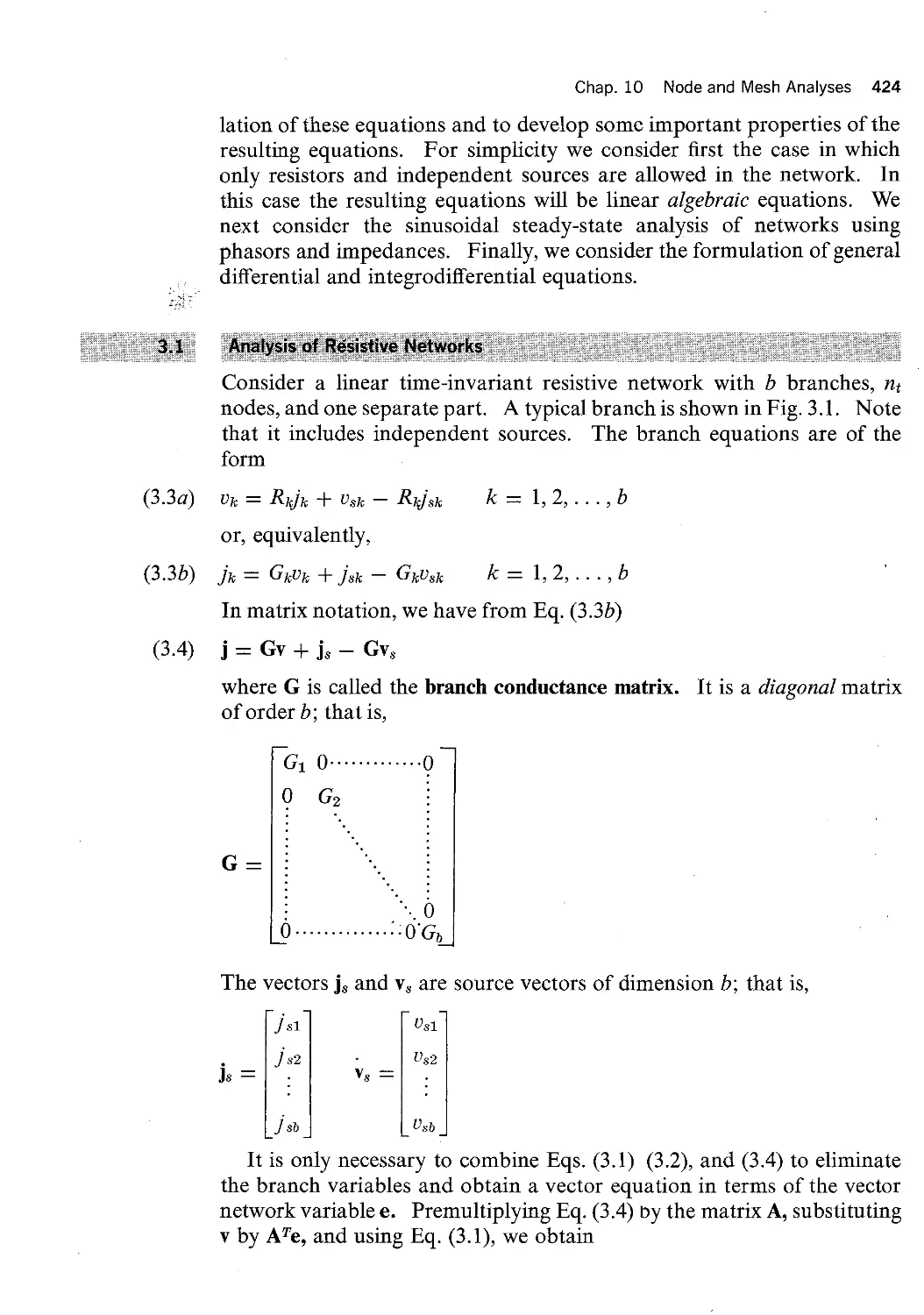
Consider a linear time—invariant resistive network with b branches, nt
nodes, and one separate part. A typical branch is shown in Fig. 3.1. Note
that it includes independent sources. The branch equations are of the
form
Uk=Rkjk+Usk_RlJsk l€=L2,···»b
or, equivalently,
jk=GkUk+j8k—GkUsk k=L2»··-rb
In matrix notation, we have from Eq. (3.3b)
j : Gv + js — Gvs
where G is called the branch conductance matrix. It is a diagonal matrix
of order bg that is,
G1 0 ............. O
G I
¥0`G;,
The vectors js and vs are source vectors of dimension b; that is,
Usl
j sl
Us2
, . j s2
Js Z · I Vs :
Usb
jsb
It is only necessary to combine Eqs. (3.1) (3.2), and (3.4) to eliminate
the branch variables and obtain a vector equation in terms of the vector
network variable e. Premultiplying Eq. (3.4) by the matrix A, substituting
v by ATe, and using Eq. (3.1), we obtain
Fig. 3.1
(3.5)
(3.6)
(3.7a)
(3.7b)
(3.8)
Sec. 3 Node Analysis of Linear Time-invariant Networks 425
+ Yjk
U. @2% Gfsk
ik ` kk
The kth branch.
AGATe -4- Ajs — AGvS : 0
or
AGATe ; AGVS — Ajs
In Eq. (3.6) AGAT is an n >< n square matrix, whereas AGVS and —AjS are
n-dimensional vectors. Let us introduce the following notations:
Yn é AGAT
is E AGVS - Ajs
then Eq. (3.6) becomes
Yné : is
The set of equations (3.8) is usually called the node equations; Ynris
called the node admittance matrix,·i· and is is the node current source vector.
The node equations (3.8) are very important; they deserve careful
examination. First, observe that since the graph specifies the reduced
incidence matrix A and since the branch conductances specify the branch
admittance matrix G, the node admittance matrix Ys is a known matrix;
indeed, Y,, é AGAT.
Similarly, the vectors vs and js, Which specify the sources in the
branches, are given; therefore, the node current source vector is is also
T We call Ys the node admittance matrix rather than the node conductance matrix even though we
are dealing with a purely resistive network. It will be seen that in sinusoidal steady-state
analysis we have exactly the same formulation; hence it is more convenient to introduce the
more general term admittance.
Example 1
Step 1
Step 2
Step 3
(3.9)
Fig. 3.2
Chap. 10 Node and Mesh Analyses 426
known by (3.7b). Thus, Eq. (3.8) relates the unknown n-vcctor e to the
known n >< n matrix Y,) and the known n—vcctor is. The vector equation
(3.8) consists of a system of n linear algebraic equations in the rz unknown
node-to-datum voltages el, ez, . . . , en. Once e is found, it is a simple mat
ter to {ind the b branch voltages v and the b branch currents j. Indeed, (3.2)
gives v : AT e, and having v, we obtain j by the branch equation (3.4); that
is,j : Gv -1- js — GV,.
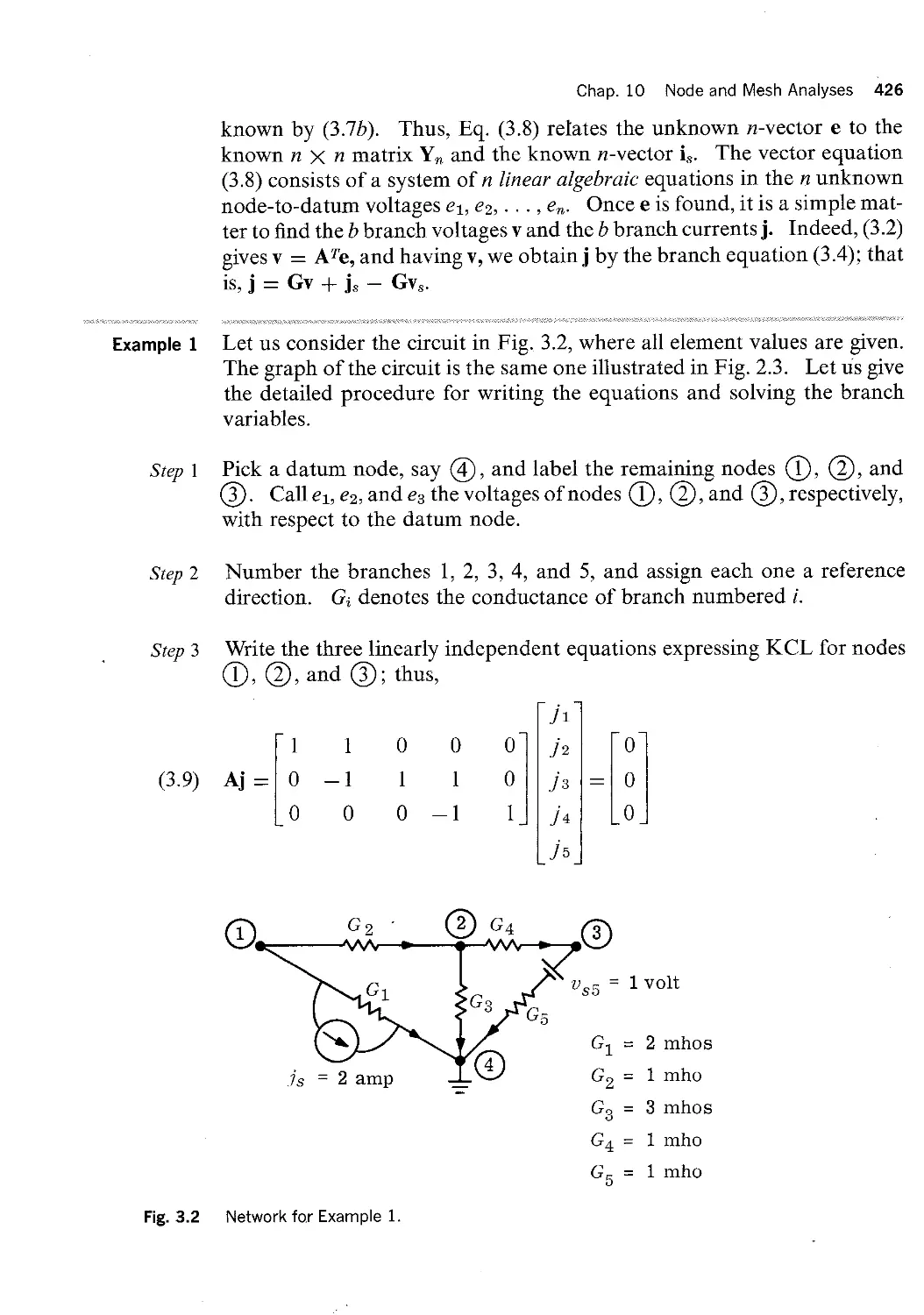
Let us consider the circuit in Fig. 3.2, where all element values are given.
The graph ofthe circuit is the same one illustrated in Fig. 2.3. Let us give
the detailed procedure for writing the equations and solving the branch
variables.
Pick a datum node, say @, and label the remaining nodes ®, @, and
®. Call el, eg, and eg the voltages of nodes ®, @, and ®, respectively,
with respect to the datum node.
Number the branches 1, 2, 3, 4, and 5, and assign each one a reference
direction. G, denotes the conductance of branch numbered i.
Write the three linearly independent equations expressing KCL for nodes
®, @, and @; thus,
Aj ;
1 1 0 0 O j 2 0 O -1 1 1 O jg ; 0 O O 0 -1 1 j 4 O
ez · ® et rs
v= 1 volt
n; 1 5G ,i—’ s
;- G5
V `jf L ls I 2 amp _@ G2
Network for Example 1.
2 mhos
1 mho
3 mhos
1 mho
1 mho
Step 4
(3.10)
Step 5
(3.1la)
(3.11b)
Step 6
(3.12a)
Sec. 3 Node Analysis of Linear Time-invariant Networks 427
Note that the reduced incidence matrix A is the same as in Example 1 cf
Sec. 2.1.
Use KVL to express the branch voltage uk in terms of the node voltages
ei; thus,
1 O O
V : ATB : I 0 1 O 62
1 —— 1 0 61 O 1 — 1 63
0 0 1
Write the branch equations in the form
i= Gv + js — Gvs
Thus,
jl 2 O 0 0 L2 O 1 0 O jg : O O 3 O
j.; 0 0 0 1 j5 O O 0 0
0IIv1I12||2000
0|Iv2|IO1|010 0
0i|v3I+{0;-{0 0 3 0
OIIv1Il0| |0001
1|Iv5lL0110000
For example, the fifth scalar equation of(3.1lb) reads
jg, : U5 —— 1
0|l0
0|l0
0lI0
0ll0
illi
Substitute into (3.11) the expression for v given by (3.10), and multiply the
result on the left by the matrix A; according to (3.9), the result is 0. After
reordering terms, we can put the answer in the form
Y,,e:iS
where
YWEAGAT
110 O 0IIO1000ll1—1 0
:10-11 lOIIOO300||O1O
0 0 O-1 1||00010||0 1-1
0 0 0 0 1IlO 0 1
(3.12b)
(3.12c)
(3.12d)
Step 7
(3.13)
(3.14)
(3.15)
Chap. 10 Node and Mesh Analyses 428
; -5 i -1
3 -1 O fi1 ;l 0 - 1 2
and
i,éAGv$-Aj8: O
- 2 { il 1
Thus, the node equation
3 — 1 O @1 — 2 li-1 5 -1;} {@2;|=|; Oi! O — 1 2 63 1
Solve Eq. (3.12d ) for e. The numerical solution of such equations is done
by the Gauss elimination method whenever n > 5. Formally, we may
express the answer in terms of the inverse matrix Y,,‘1; thus,
e : Y,f1 is zig0:-1
F9 2 1 -2 -17 ? 6 {H ]%{ jI 1 3 14 1 12
Once the node voltages e are found, the branch voltages v are obtained
from (3.10) as follows:
- 17
- 16
v : ATe : il -1
- 13
12
The next step is to use v to obtain the branch currents j by Eq. (3.11); then
we have
- 16
j:Gv-4-js-Gvszif -3
- 13
- 13
This completes the analysis of the network shown in Fig. 3.2; that is, all
branch voltages and currents have been determined.
(3. 16a)
(3. 1 6b)
Exercise
Example 1
(continued)
Sec. 3 Node Analysis of Linear Timeinvariant Networks 429
The step-by-step procedure detailed above is very important for two
reasons. First, it exhibits quite clearly the various facts that have to be
used to analyze the network, and second, it is completely general in the
sense that it works in all cases and is therefore suitable for automatic
computation.
ln the case of networks made only of resistors and independent sources
(in particular, with no coupling elements such as dependent sources), the
node equations can be written by inspection. Let us call ytk the (i,k) ele
ment of the node admittance matrix Y"; then the vector equation
Yné : is
written in scalar form becomes
yii )’12 ···)’1n|| 61] llsi
y21 y22···)’2n||€2| IIS2
ynl Ilsn
The following statements are easily verified in simple examples, and can
be proved for networks without coupling elements.
yi, is the sum ofthe conductances of all branches connected t0 n0de ®,‘
yi, is called the se@admittance of node
yi;. is the negative ofthe sum of the conductances of all branches connect
ing node ® and node ® ; yi;. is called the mutual admittance between
node @ and node
U we convert all voltage sources into current sources, then isk is the alge
braic sam of all source currents entering node the current sources
whose rq‘erence direction enter node ® are assigned a positive sign,
all others are assigned a negative sign.
Prove statements 1 and 2 above. Hint: Y,, : AGAT; consequently,
yn = E QMGMU = E (¤tt)2Gr
and
ya = 2 @uGji1kj
Note that (a,j)2 can only be zero or 1; similarly, away,) can only be zero
or — 1.
Consider again the network of Fig. 3.2. Let us, by inspection, write every
branch current in terms of the node voltages; thus,
J1;
/2;
J3:
J4:
J5;
Chap. 10 Node and Mesh Analyses 430
G1€1 + 2
G2(€1 — 62)
G2€2
G4(€2 — 63)
G5(€g -— 1)
In the last equation, we used the equivalent current source for branch 5,
as shown in Fig. 3.3. Substituting the above into the node equations, we
obtain
(G1 -4- G2)e1 — G2e2 : -2
Gzei -1- (G2 + Gs -1- G4)€2 — Giles = 0
G4€2 + (G4 + G5)€s = G5
By inspection, it is easily seen that statements l, 2, and 3 above hold for
the present case. Also if the numerical values for the Gk’s are substituted,
the answer checks with (3.12a).
Remarks 1. For networks made of resistors and independent sources, the node
admittance matrix YH : (yu,) in Eq. (3.8) is a symmetric matrix; i.e.,
yu, zyk, for i, k : l, 2,..., n. Indeed, since Y,, Q AGAT, then
Y,,T : (AGAT)T : AGTAT : AGAT : Y,,. In the last step we used
the fact that GT : G because G, the branch conductance matrix of a
resistive network with no coupling elements, is a diagonal matrix.
2. If all the conductances of a linear resistive network are positive, it is
easy to show that det (Y ,,) > Ofr Cramer’s rule then guarantees that
whatever is may be, Eq. (3.16) has a unique solution. The fact that
det (Y,,) > 0 also follows from Y,, : AGAT, where G is a b X b
diagonal matrix with positive elements and A is an n >< b matrix with
TSee Sec. 2.4, Appendix B.
+ 9 ®
G5 (T)G5vS5= lamp
Fig. 3.3 Branch 5 ot Fig. 3.2 in terms of current
SOUYC6.
Fig. 3.4
Exercise
33
(3.17)
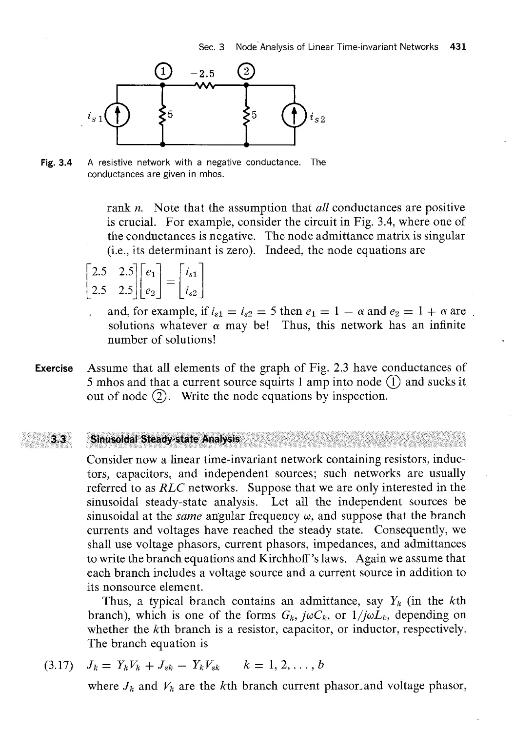
Sec. 3 Node Analysis of Linear Time-invariant Networks 431
CD -25 ®
MU) gil
5 (llisz
A resistive network with a negative conductance. The
conductances are given in mhos.
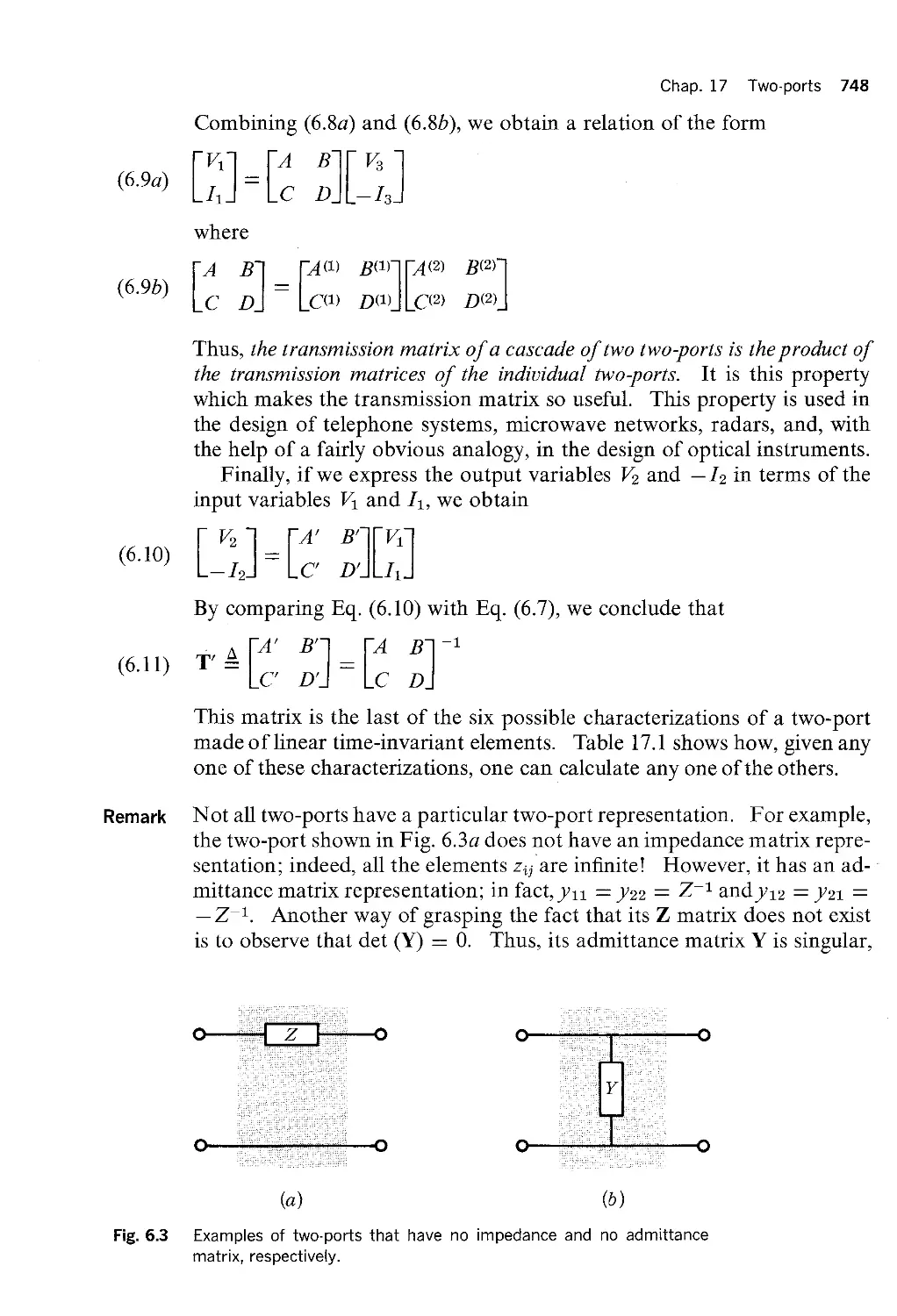
rank n. Note that the assumption that all conductances are positive
is crucial. For example, consider the circuit in Fig. 3.4, where one of
the conductances is negative. The node admittance matrix is singular
(i.e., its determinant is zero). Indeed, the node equations are
61 lsl 62 _ S2
and, for example, if isl : isz : 5 then el = l — ot and ez : l + at are
solutions whatever at may be! Thus, this network has an infinite
number of solutions!
Assume that all elements of the graph of Fig. 2.3 have conductances of
5 mhos and that a current source squirts l amp into node (D and sucks it
out of node Write the node equations by inspection.
Sinuscidai Sieadypstatet Analysis
Consider now a linear time-invariant network containing resistors, induc
tors, capacitors, and independent sources; such networks are usually
referred to as RLC networks. Suppose that we are only interested in the
sinusoidal steady-state analysis. Let all the independent sources be
sinusoidal at the same angular frequency w, and suppose that the branch
currents and voltages have reached the steady state. Consequently, we
shall use voltage phasors, current phasors, irnpedances, and admittances
to write the branch equations and Kirchhoff ’s laws. Again we assume that
each branch includes a voltage source and a current source in addition to
its nonsource element.
Thus, a typical branch contains an admittance, say Yk (in the kth
branch), which is one of the forms Gk, jwCk, or l/jwLk, depending on
whether the kth branch is a resistor, capacitor, or inductor, respectively.
The branch equation is
·lk=YkV}¢+JSk-Yklék k=L2..·-.b
where J k and V], are the kth branch current phasor. and voltage phasor,
(3.19)
(3.20a)
(3.20b)
Remark
Example
Chap. 10 Node and Mesh Analyses 432
and Jsk and IQ;. are the kth branch phasors representing the current and
voltage sources of branch k. In matrix form Eq. (3.17) can be written as
J : Y;,V -|- JS — Y;,VS
The matrix YI, is called the branch admittance matrix, and the vectors J
and V are, respectively, the branch—current phasor vector and the branch
voltage phasor vector. The analysis is exactly the same as that of the
resistive network in the preceding section. The node equation is of the
form
Y,,E : IS
where the phasor E represents the node-to-datum voltage vector, the
phasor IS represents the current-source vector, and Y., is the node admit
tance matrix. In terms of A and Yb, Y,, is given by
Y,, : AY,,AT
I, : AY;,V$ — AJ,
Consider on the one hand the steady-state analysis of an RLC network
driven by sinusoidal sources having the same frequency, and, on the
other hand, the analysis of a resistive network. In both cases node analy
sis leads to a set of linear algebraic equations in the node voltages. In the
sinusoidal steady—state case the unknowns are node-to-datum voltage
phasors, and the coeiiicients of the equations are complex numbers which
depend on the frequency. Finally, recall that the node-to-datum voltages
are obtained from the phasors by
e;,(t) = Re (Ek dai) k = l,2,...,n
In the resistive network case, the equations had real numbers as coeffi
cients and their solution gave the node—to-datum voltages directly.
If we had only networks without coupling elements, the inspection
method of the preceding section would suiiice. We are going to tackle an
example that has both dependent sources and mutual inductances. It will
become apparent that for this case the inspection method does not
suffice, and the value of our systematic procedure will become apparent.
After the example, we shall sketch out the general procedure.
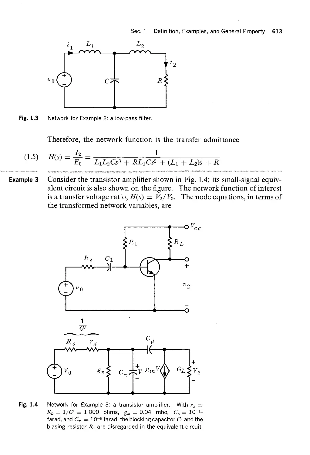
Consider the linear time-invariant network shown in Fig. 3.5. The inde
pendent current source is sinusoidal and is represented by the phasor I ;
its waveform is |I| cos (wt -1- 41). We assume that the network is in the
sinusoidal steady state, consequently, all waveforms will be represented
by phasors V, J, E, etc. Note the presence of two dependent sources.
The three inductors L3, L4, and L5 are magnetically coupled, and their
inductance matrix is
(3.21)
(3.22a)
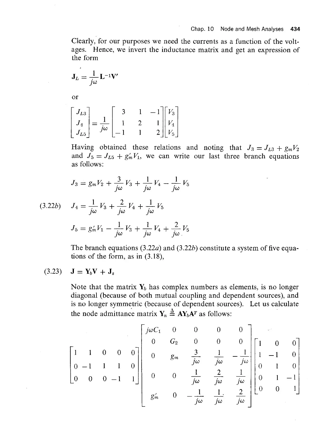
Sec. 3 Node Analysis of Linear Time-invariant Networks 433
Q), J2 ® J4 .,11}.. .® _
+Va" -1. + V4. ·
JLS
JL5
1(l)r1#¤1 gmr2<l> 1/32-. e' *. ir. <l>gM¤
Example of sinusoidal steady-state analysis when mutual magnetic coupling and dependent
SOUYCGS SVG pl'€S€I'1t.
L : -1 % -4
1 -1 1 {%] 1 —% %
First, to express Kirchhoi°1"s laws, we need the node incidence matrix A;
by inspection
A : 0 -1 1 1 o
1 1 0 0 0 { l O O O -1 1
Second, we need the branch equations. We write them in terms of
phasors; thus,
J1 :j0.>C1IG — 1
To write J 3, JL, and J 5 in terms of the Iéjs is not that simp1e; indeed the
inductance matrix te11s us on1y the relation between K, IQ, and I4; and
the inductor currents J L3, J4, and J L5 (see Fig. 3.5 for the definition of J L3
and JL5). Therefore,
V, :jwLJL
OI`
ig 1 -1 1 JL3 lrle rl lrl Vg 1 -% % JL5
Chap. 10 Node and Mesh Analyses 434
Clearly, for our purposes we need the currents as a function of the volt
ages. Hence, we invert the inductance matrix and get an expression of
the form
JL I +14-1V,
or
J L3 3 l —l IG, Ji Z L 1 2 1 iq JL, ]"’ -1 1 2 rg
Having obtained these relations and noting that J3 : J L3 + gmlé
and J5 : J L5 -1- ginlq, we can write our last three branch equations
as follows:
J3=gmlé+iT/E»,+$¥é.—J—l4·,
JLG JOJ JO.)
(3-22b) Ji Zim Jrla Jrla
JOJ JCU JO.)
L
J5=g.m--re,+lm+i1e
JO.) JO.} jid ,
The branch equations (3.22a) and (3.22b) constitute a system of five equa
tions of the form, as in (3.18),
(3.23) J : Y;,V + JS
Note that the matrix Y1, has complex numbers as elements, is no longer
diagonal (because of both mutual coupling and dependent sources), and
is no longer symmetric (because of dependent sources). Let us calculate
the node admittance matrix Y,, é AYbAT as follows:
j¢·.)C1 O 0 0 0
O G2 O O O I [-1 0 O
IIOOOH0
0-1110
§.L-Ll|l—l0
JT J; {°`°ll0 1 0
000—1 1llO O
, 0 gm
g g glp 1-1
1 1 _ 2 O 0 1
Jw Jw Jw
(3.24)
Systematic
procedure
Step 1
Step 2
(3.25a)
Sec. 3 Node Analysis of Linear Time-invariant Networks 435
yacl G2 0 0 0 1 I I 0 O
1 -1 O
4 3 — O
O - G - 2 + gm ja jw
0 1 0
2 O -2 -1 L | I O 1 -1
]°’ Jw JW .| { () () 1
jwC1 —I— G2 —G2 O
7 -3
G2+g 2 g +]w ]w|:Y"
-3 2
Jw ]°’
The right-hand term of the node equation, from (3.19) and (3.20b), is
AJ S since VS is identically zero. It is easily found to be a vector whose
iirst component is I (all the others are zero). Thus, the node equation is
j(.·.>C1 + G2 —G2 O
_ E I G2 + gm G2 — gm + 1
Jo`) jw E2 : O i .2. E3 0
tw tw
After substituting numerical values, we can solve these three equations
for the phasors E1, E2, and E3. Successively, we get V by
V : AYE
and J by (3.23).
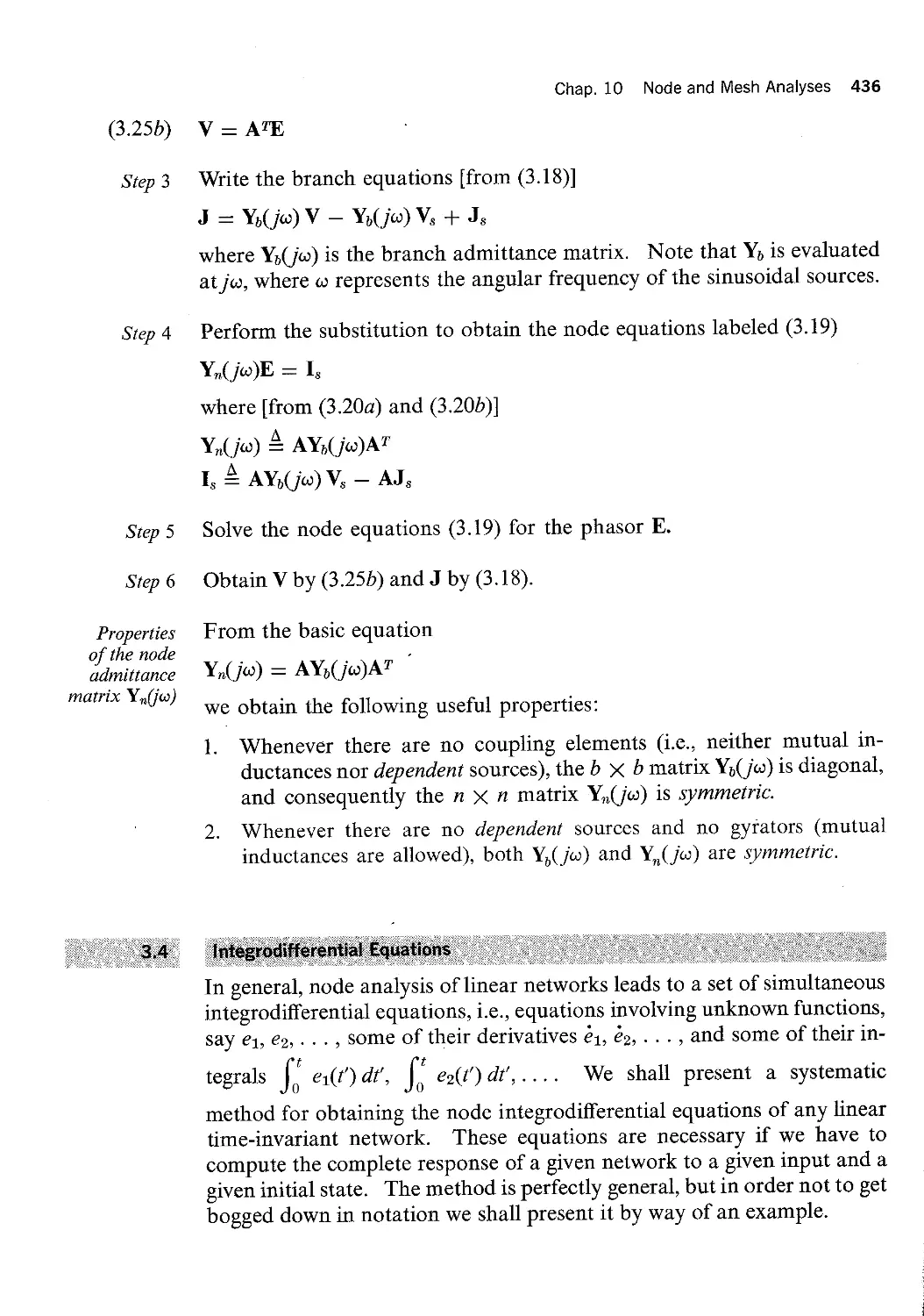
This example exhibits clearly the value of the systematic method;
obviously, it is hazardous to try to write Eq. (3.24) by inspection.
The detailed example above suggests a method for writing the sinusoi
dal steady-state equations of any linear time-invariant network driven by
sinusoidal sources of the same frequency. Note that the network may
include R’s, L’s, C ’s, mutual inductances, dependent sources, and inde
pendent sources. The steps are as follows:
Perform (if needed) source transformations as indicated in Sec. 1.
Write the requirements of Kirchhoff’s laws; thus,
AJ : 0
(3.25b)
Step 3
Step 4
Step 5
Step 6
Properties
0f the twde
admittance
matrix Y"(jw)
Chap. 10 Node and Mesh Analyses 436
V : ATE
Write the branch equations [from (3.18)]
J : Y;,(ja>)V — Y;,(jw) V, + JS
where Yb(jw) is the branch admittance matrix. Note that Yy, is evaluated
at jw, where w represents the angular frequency of the sinusoidal sources.
Perform the substitution to obtain the node equations labeled (3.19)
Y,,(jw)E : I,
where [from (3.20a) and (3.20b)]
Y»(j<»¤) é AYz»(j<»>)A’"
IS E AY,,(jw) V, — AJ,
Solve the node equations (3.19) for the phasor E.
Obtain V by (3.25b) and J by (3.18).
From the basic equation
Y,,( : AYb(jo.>)AT
we obtain the following useful properties:
1. Whenever there are no coupling elements (i.e., neither mutual in
ductances nor dependent sources), the b X b matrix Yb(jw) is diagonal,
and consequently the n >< n matrix Y,,(jw) is symmetric.
2. Whenever there are no dependent sources and no gyrators (mutual
inductances are allowed), both Yb(ja>) and Yn(jw) are symmetric.
In general, node analysis of linear networks leads to a set of simultaneous
integrodiiferential equations, i.e., equations involving unknown functions,
say el, e2, . . . , some of their derivatives el, éz, . . . , and some of their in
tegrals e1(t’) dt', e2(t’) dt’, .... We shall present a systematic
fj
f;
method for obtaining the node integrodifferential equations of any linear
time-invariant network. These equations are necessary if we have to
compute the complete response of a given network to a given input and a
given initial state. The method is perfectly general, but in order not to get
bogged down in notation we shall present it by way of an example.
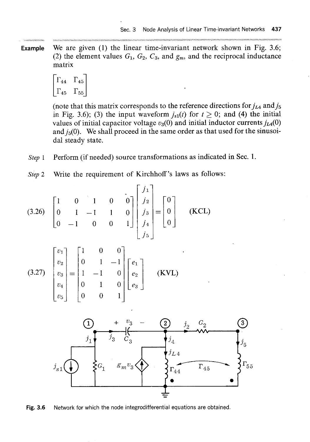
Example
Step 1
Step 2
(3.26)
(3.27)
Fig. 3.6
Sec. 3 Node Analysis of Linear Time-invariant Networks 437
We are given (1) thc linear time-invariant network shown in Fig. 3.6;
(2) the element values G1, G2, C3, and gm, and the reciprocal inductance
matrix
1144 F45 1145 rss
(note that this matrix corresponds to the reference directions for j L4 and jg,
in Fig. 3.6); (3) the input waveform jS1(t) for t 2 O; and (4) the initial
values of initial capacitor voltage v3(O) and initial inductor currents jL4(0)
and j5(0). We shall proceed in the same order as that used for the sinusoi
dal steady state.
Perform (if needed) source transformations as indicated in Sec. l.
Write the requirement of Kirchhoif’s laws as follows:
jsl
0 l
l —l
—l O
l O
O l
:Il —l
O 1
O O
1 0 J3 = 0 (KCL)
O O j2 O 0 l ji 0
O 62
1 61 O @3
+ .*13 — @ tz G2 ®
Ya CE,)
JL4
i) §Gi gM”3® tpl;/E? 2*5
Network for which the node integrodifferentiai equations are obtained.
Chap. 10 Node and Mesh Analyses 438
Note that the j;,’s, vk’s, and efs are time functions and not phasors. To
lighten the notation, we have writtenjl, jg, . . . , el, e2, . . . , etc., instead of
j1(l`),j2(Zi), . . . , CIC.
Step 3 Write the branch equations (expressing the branch currents in terms of the
branch voltages); thus,
ji = G1U1 + j $1
j 2 = G2U2
js = Calla
Noting that jL4 is the current in the fourth inductance and that ji; :
jy,4 — gmvg, we obtain the branch equation of the inductors as follows:
' I I I ' J4 = —§mU3 + I`44 U4(i)di/ —I· I`45 U5(l`)dZ + ]L4(0)
t IO
. · . J5 I I`45 JO U4(Z(/) dt, -I— I`55 U5(ZL/) dt, -I—
t JI]
lt is convenient to use the notation D to denote the differentiation operator
with respect to time; for example,
. D i I U3 U3
CZU3
dt
and the notation D‘1 to denote the deyinite integral · ; for example,
t I0
_ e, / U, - v4(t)dt
1 ¢ D I)
With these notations the branch equations can be written in matrix form
as follows:
j1I IGl O 0 0 0 IIv1I Ij,1
j2I I0 G2 0 0 0 IIv2I I0
(3.28) Ij3I:|0 0·C31> 0 0 IIv3I+I 0
j4I I 0 O -gm I`44D—1 F45D·1I I U4I |jL4(0)
j5I I O O O l`45D'1 l`55D‘1I I 05 I I j5(O)
Note that the matrix is precisely that obtained in the sinusoidal steady
state if we were to replace D by jw. Note also the contribution of the
initial state, the terms jL4(0) and j $(0) in the right-hand side. In the fol
lowing we shall not perform algebra with the D symbols among them
selves; we shall only multiply and divide them by constantsi
Tlt is not legitimate to treat D and D‘1 as algebraic symbols analogous to real or complex num
bers. Whereas it is true that D and D‘1 may be added and multiplied by real numbers (con
stants), it is also true that D D`1 92 D“1 D. Indeed, apply the first operator to a function thus,
Step 4
(3.29)
(3.30)
(3.31)
(3.32)
Sec. 3 Node Analysis of Linear Time-invariant Networks 439
Eliminate the v;,’s and j;,’s from the system of (3.26), (3.27), and (3.28).
If we note that they have, respectively, the form
Aj : 0
v : ATe
j = Yr(D) V + js
the result of the elimination is of the familiar form
AY;,(D) ATe : —AjS
or
Yt(D) e = is
Let us calculate for the example the node admittance matrix operator; thus,
Y,,(D) E`.- AYb(D) AT
1 0 l 0 0 I I 0 G2 0 0 0
; I 0 l — l l 0 I I 0 0 CBD 0 0
0 —l 0 0 III 0 0 —g,,, 1`44D‘1 l`45D‘
0 0 0 1`45D‘1 I`55Dr
1 0 0
0 l —l
1 — l 0
0 1 ` 0
0 0 l
G1 —I- C3D
— CBD
= I—CsD · gm G2 + Cal) + gm + I`44D`1 ·G2 + I`45D`
—G2 —I- 1145Drl G2 ‘I‘ 1*551)-1
D Dv: )rr) 4r:j(t)
%II)’I
where the last step used the fundamental theorem of the calculus. Now
D“1Df = flr) dr =JTr) IL =f(f) —f(0)
H
On the other hand, D and the positive integral powers ofD ean be manipulated by the usual rules
of algebra. In fact, for any positive integers m and n,
Dm Dr : Dmrn
a.nd for any real or complex numbers al, o42, ,81, ,82
(cqD" + B1)(a2Dm + B2) : a1a2Dm+" + a1,82D" 4- a2B1Dm -.¤- ,81,82
(3.33)
(3.34)
(3.35)
(3.36)
Remarks
(3.37)
Chap. 10 Node and Mesh Analyses 440
Therefore, for the present example, node analysis gives the following integ
rodiiferential equation:
G1 -{— C3D
CBD ·· gm CBD + G2 + gm + F44D_1 —G2 + 1-`4BD_1 62
-C3D 0 @1 -·G2 + Y45D`1 G2 + I`55D_1 63
= I ·fL4(0)
“" sl — j 5(0)
The required initial conditions are easily obtained; writing the cut—set law
for branches l, 4, and 5 we have
€1(0) = -,% [—jSi(0) — jL4(0) + gmUz(0) — j5(0)l
where all terms in brackets are known. Finally,
€2(0) : €1(0) — U3(O)
and
e3(0) = ez(0) —j5(0)/G2
l. Except for the initial conditions, the writing of node equations in the
integrodifferential equation form is closely related to that used in the
sinusoidal steady-state analysis. It is easily seen that if we replace
D by jw in Y,,(D), we obtain the node admittance matrix Y,,(jw) for
the sinusoidal steady-state analysis. Therefore, in the absence of
coupling elements, Y,,(D) can always be written by inspection.
2. Although the equations of (3.33) correspond to the rather formidable
name of "integrodifferential equations," they are in fact no different
than differential equations; it is just a matter of notation! To prove
the point, introduce new variables, namely fiuxes q52 and qby, defined by
<j>2(Z) Q €2(t') dll ¢3(1‘) é €3(t/) dt,
Clearly,
Dez = D2<Z>2 62 = D¢2 D`1€2 = 952
Example 1
Step 1
Fig. 3.7
Sec. 3 Node Analysis of Linear Time-invariant Networks 441
The system of (3.33) becomes
G1 + CBD
CSD?
Cal) — gm C3D2 + (G2 ·l· gm)D ·l· 1744 —G2D + T45 952
—G2D ·l- F45
0 el G2D —l- I`55 $3
I —]L4(O)
s1 — j $(0}
and the initial conditions are
e1(0) given by (3.34)
q32(0) : 0 see (3.37) <j32(0) : e2(0) given by (3.35)
¢»3(0) : 0 see (3.37) ql33(0) : e3(0) given by (3.36)
When the network under study involves only a few dependent sources, the
equations can be written by inspection if one uses the following idea: treat
the dependent source as an independent source, and only in the last step
express the source in terms of the appropriate variables.
7`
Let us write the sinusoidal stcady—state network of
Fig. 3.7.
Replace the dependent sources by independent ones, and call them JSF,
and JS5.
G) J2 i G2 ®
J1; + V2 _
I FQ (L) gmvi
•J* 1(f)v1»|~c1 gmV2<$> Qrg
Network including dependent sources.
Step 2
Step 3
Step 4
Example 2
Chap. 10 Node and Nlesh Analyses 442
Write thc equations by inspection as follows:
G2 -I-JOJC1 —-G2
-6 G+2 2
“4F3+F4 -24 E1 I jo: jo: Ez Z ··Js3 F4 F4 —l— F5 E3 ’_Js5
JO.} JCO
Express the dependent source waveforms in terms of the appropriate
variables as follows:
Js3 Z Z gm(E1 _ E2)
and
JS5 = $1%% = g{nE1
Substitute and rearrange terms; thus we have
G2 —|—jwC1
gm—G2 G2—gm+Li¥ —
J2 U E1 I ¥ E2 : 0 jw Jw E O rr rr + F5 3
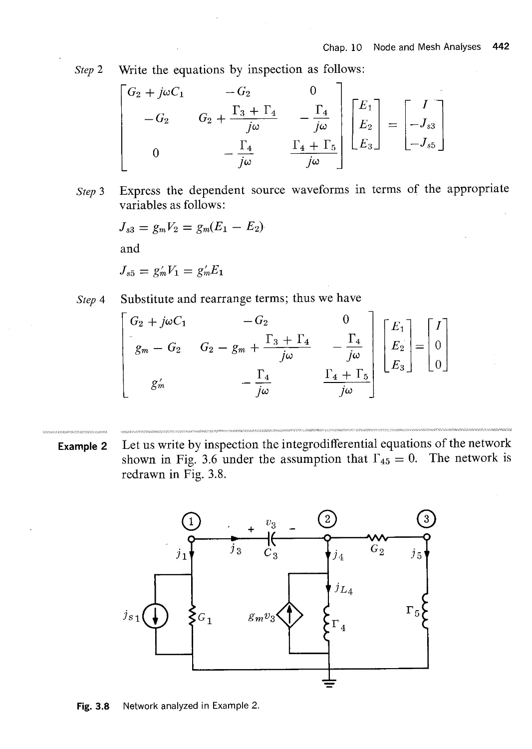
Let us write by inspection the integrodifferential equations of the network
shown in Fig. 3.6 under the assumption that I`45 : O. The network is
redrawn in Fig. 3.8.
@ · + tt - @
nl j3 éé lil G2 i5
JL4
MCD ie e~U3® EF
Fig. 3.8 Network analyzed in Example 2.
Fig. 3.9
Step I
Step 2
js 1( 4
Fig. 3.10
Sec. 3 Node Analysis of Linear Time—invariant Networks 443
JL
t. UL
L ( ,l)1L<<>>
Inductor L with
Inductor L with
no initial current.
initial current jL(0)
Useful equivalence when writing equations by inspection.
We must observe that the branch equations of inductors include initial
currents (see Fig. 3.9); thus,
. , . JLG) = Y Mt') df +1L(0)
t L
Thus, every inductor can be replaced by an inductor without initial cur
rent in parallel with a constant current source jL(O). After replacing the
dependent source gmvg by an independent source jsi, we have the network
shown in Fig. 3.10.
By inspection, the equations are
Gi —l· Cal)
Cal) G2 —l· T4D`1 + `CsD —G2 @2 = jS4 —jL4(O)
—CsD O 61 —j$1 —G2 G2 + IED`1 63 —js»(0)
Q) "` ` U3 · ` @
Network of Fig. 3.8 in which the initial currents have been replaced by constant current
SOUYCSS.
Chap. 10 Node and Mesh Analyses 444
Step 3 Express the dependent source waveform in terms of the appropriate var
iable as follows:
_js4 Z gmlla Z gm(€1 · 62)
Step 4 Substitute and rearrange terms; thus,
G1 + C3D
—CaD
—gm — CBD gm + G2 + 114DIl + C3]-) —G2 @2 Z -j1,4(O)
·—G2
O 61 _js1 G2 + F5D'1 @3 —j5(0)
In summary, it is easy in many instances to write the equations by in
spection. It is important to know that the systematic method of Sec. 3.1
and 3.3 always works and hence can be used as a check in case of doubt.
BI In
In this section we propose to develop the concept of duality which we shall
use repeatedly in the remainder of this chapter and in Chap. 11.
43% i.tii irPi€¤$t?€i?$iP%$§§?P}i&?¤¤¤S¥ferQ¤“¥<%*lM?$h€$
By the very deiinition of a graph that we adopted, namely, a set of` nodes
and a set of branches each terminated at each end into a node, it is clear
that a given graph may be drawn in several different ways. For example,
the three figures shown in Fig. 4.1 are representations of the same graph.
Indeed, they have the same incidence matrix. Similarly, a loop is a con
cept that does not depend on the way the graph is drawn; for example, the
branches L b, c, and e form a loop in the three figures shown in Fig. 4.1.
If we use the term "mesh" intuitively, we would call the loop bcef a
bp QD
11 d Vi
d _.®
b Q
t|\f It al Y ® lg
@' g '® ®
(a)
®,i\@
` g '® f Q
(6)
M \¤
@ Ie `
(C)
Fig. 4.1 The figures (a), (b), and (c) represent the same graph in the form of three different topological
graphs.
(cz)
Fig. 4.2 (a) Planar graph; (b) nonplanar graph.
(b)
Sec. 4 Duality 445
mesh in Fig. 4.lb, but not in Fig. 4.la or c. For this reason, we need to
consider graphs drawn in a specific way. When we do consider a graph Q
drawn in a way specified by us, we refer to it as the topological graph Q. For
example, the three figures in Fig. 4.l may be considered to be the same
graph or three different topological graphs.
A graph Q is said to be planar if it can be drawn on the plane in such a
way that no two branches intersect at a point which is not a node. The
graph in Fig. 4.2a is a planar graph, whereas the graph in Fig. 4.2b is not.
Consider a topological graph Q which is planar. We call any loop of
this graph for which there is no branch in its interior a mesh. For example,
for the topological graph shown in Fig. 4.la the loop f bce is not a mesh;
for the topological graph shown in Fig. 4.lb the loop fbce is a mesh. In
Fig. 4.lc the loop f bcc contains no branches in its exterior; it is called the
outer mesh of` the topological graph.
If you imagine the planar graph as your girl friend’s hair net and if you
imagine it slipped over a transparent sphere of lucite, then as you stand in
the center of the sphere and look outside, you see that there is no signifi
cant difference between a mesh and the outer mesh.
We next exhibit a type of network whose graphs have certain properties
that lead to simplification in analysis. Consider the three graphs shown in
Fig. 4.3a—c. Each of 'these graphs has the property that it can be parti
tioned into two nondegenerate subgraphs Q1 and Q2 which are connected
together by one node.? Graphs which have this property are called hinged
graphs. A graph that is not hinged is called unhinged (or sometimes, non
separable); thus, an unhinged graph has the property that whenever it is
partitioned into two connected nondegenerate subgraphs Q1 and Q2, the
subgraphs have at least two nodes in common. Determining whether a
graph is hinged or not is easily done by inspection (see Fig. 4.3 for
examples).
From a network analysis point of view, if` a network has a graph that is
hinged and‘if` there is no coupling (by mutual inductances or dependent
TBy nondegenerate we mean that the subgraph is not an isolated node.
Fig. 4.3
Counting
meshes
(4.1)
Chap. 10 Node and Mesh Analyses 446
/ / /t/
(cr)
gl Q2
(C)
(1;)
Unhinged graph
(Gl)
Examples of hinged graphs, (a), (b), and (c), and an unhinged graph, (d).
sources) between the elements of Q1 and Q2, the analysis of the network re
duces to the analysis of two independent subnetworks, namely the net
works corresponding to the graphs Q1 and Q2. Since Q1 and Q2 are con
nected together by one node, KCL requires that the net current flow from
Q1 to Q2 be zero at all times, so there is no exchange of current between the
two subnetworks. Also the fact that the two subnetworks have a node in
common does not impose any restriction on the branch voltages.
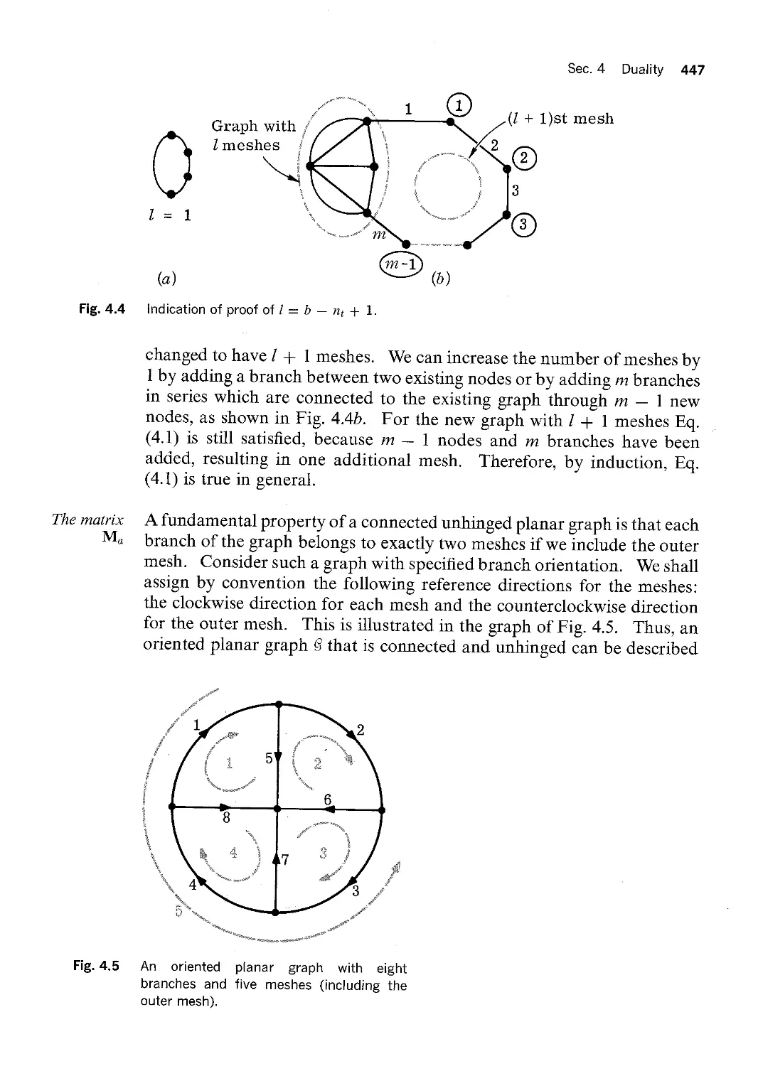
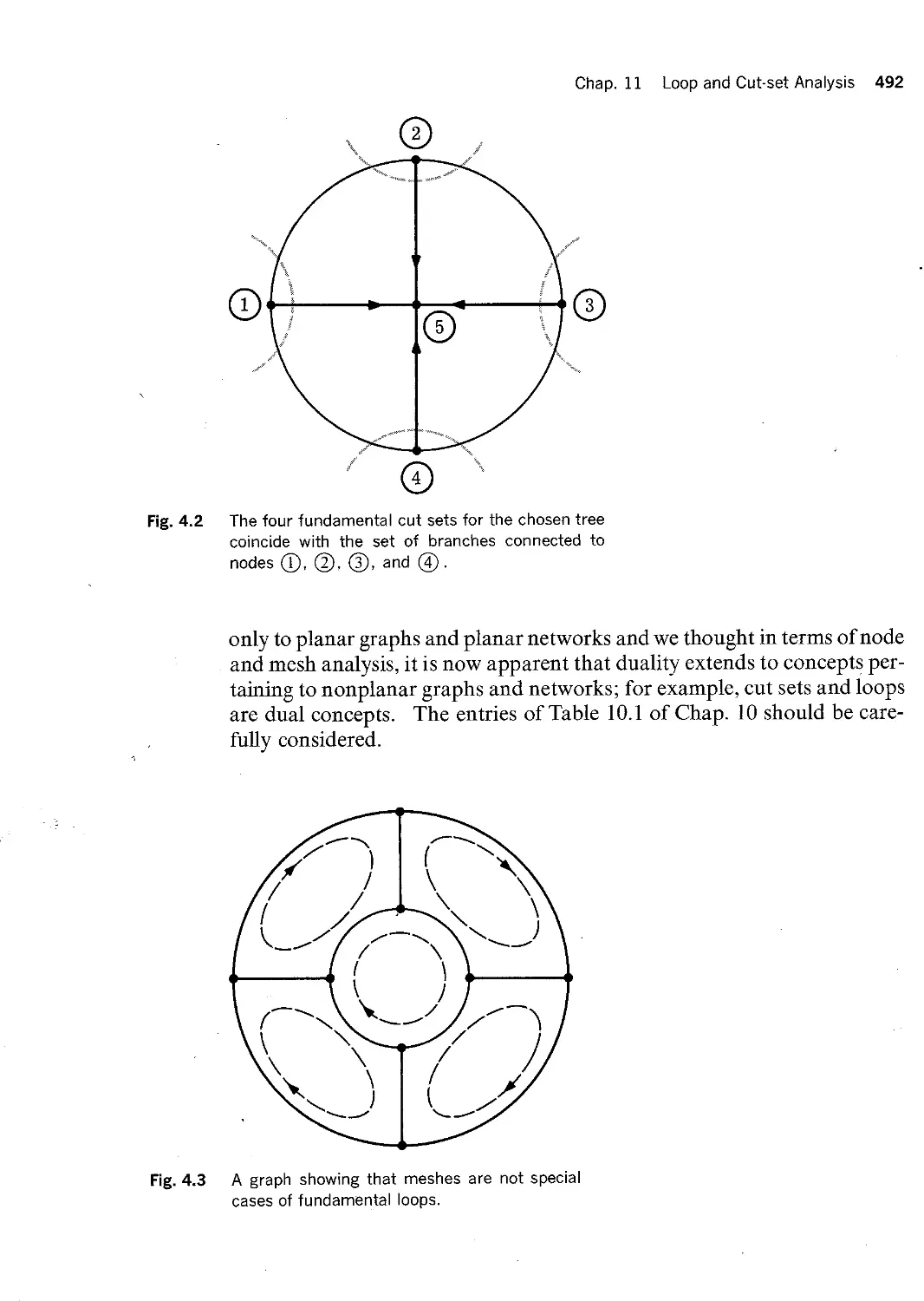
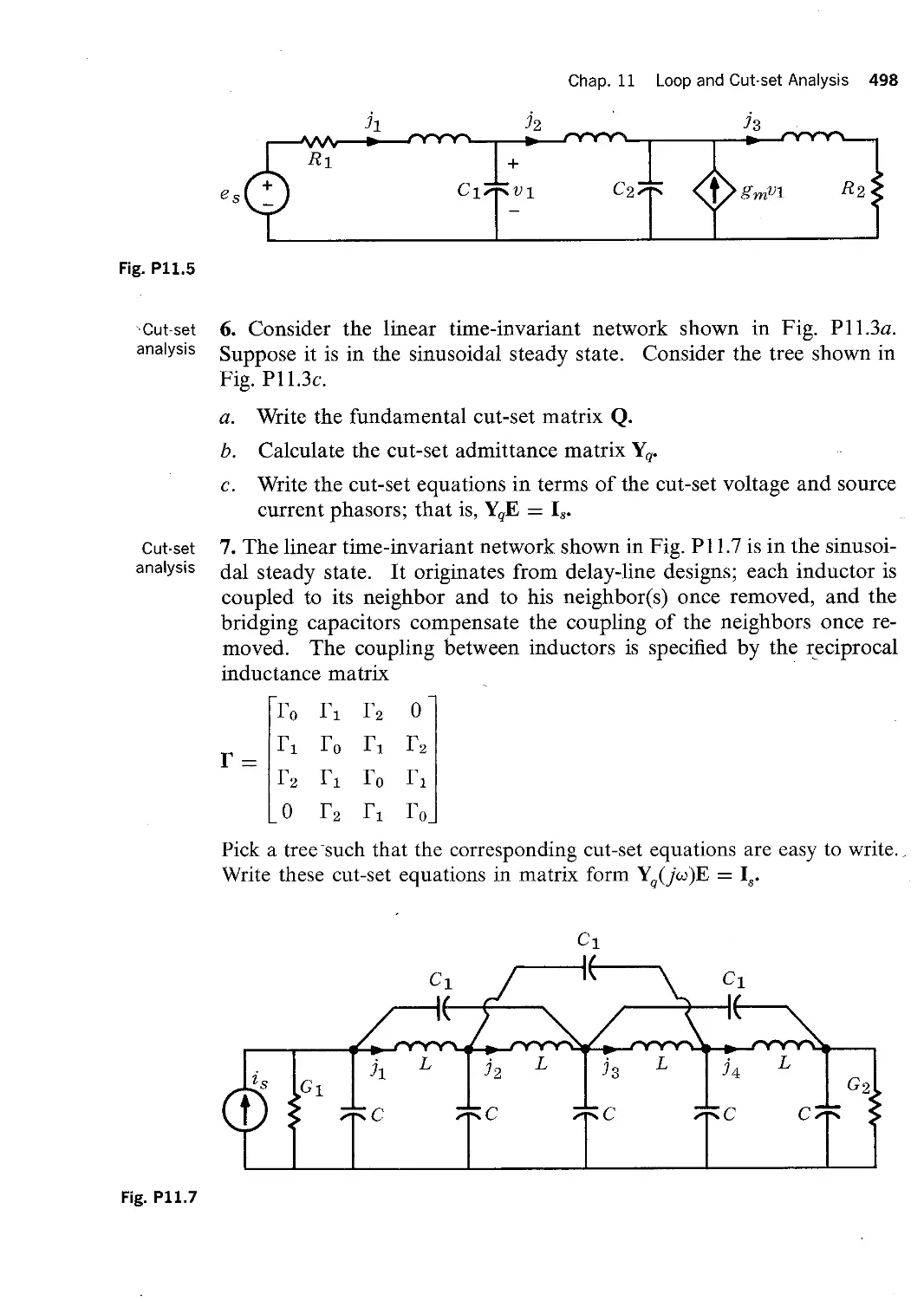
It is easy to see that for a connected unhinged planar graph the number af
meshes is equal t0 b — nt —l- 1 where b is the number of branches and nt the
number of nodes. The proof can be given by mathematical induction.
Let the number of meshes be I; thus we want to show that
Z Z b — TZ; -l— l
Consider the graph in Fig. 4.4a, where l : 1. Here it is obvious that
Eq. (4.1) is true. Next consider a graph which has l meshes, and we assume
that Eq. (4.1) is true. We want to show that (4.1) is still true if the graph is
Fig. 4.4
The matrix
Fig. 4.5
Sec. 4 Duality 447
.¢ff”NMM\ 1 ® h /·¤t~ ~(Z + 1)st mes
Graph with 3;
Zmeshes i
¥/Mk 2
r E K
3 X E `<~
Z = 1
.._ XX if ‘~·~·-....-~·"" G 'f
“·- M--rW2
(ce)
I (Z9)
Indication of proof of I : b — n, + 1.
changed to have Z -{- l meshes. We can increase the number of meshes by
1 by adding a branch between two existing nodes or by adding m branches
in series which are connected to the existing graph through m — 1 new
nodes, as shown in Fig. 4.4b. For the new graph with I -i- 1 meshes Eq.
(4.1) is still satislied, because rn — l nodes and m branches have been
added, resulting in one additional mesh. Therefore, by induction, Eq.
(4.1) is true in general.
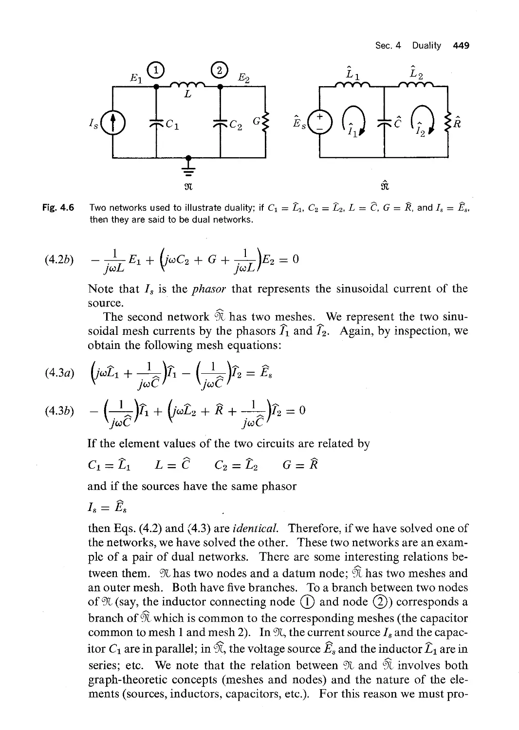
A fundamental property of a connected unhinged planar graph is that each
branch of the graph belongs to exactly two meshes if we include the outer
mesh. Consider such a graph with speciiied branch orientation. We shall
assign by convention the following reference directions for the meshes:
the clockwise direction for each mesh and the counterclockwise direction
for the outer mesh. This is illustrated in the graph of Fig. 4.5. Thus, an
oriented planar graph Q that is connected and unhinged can be described
J. { .¤`§”` .-“‘“o~N
,sf ' { é 5 it g .a
gg
~ `samwf I RM
é ’8 V al E \ at T fi
gQ E
. a AEs. >\ 3 gf
gxmva
>—»,,“<W%Mm“mmw¤w.a»¤¢’*
An oriented planar graph with eight
branches and five meshes (including the
outer mesh).
Chap. 10 Node and Nlesh Analyses 448
analytically by a matrix Ma. Let Q have b branches and l -1- l meshes
(including the outer mesh); then Ma is defined as the rectangular matrix of
I -4- l rows and b columns whose (i,k)th element mm is delined by
l if branch k is in mesh i and if their reference directions
coincide
mu, .-; i- l if branch k is in mesh i and if their reference directions do
not coincide
O if branch k does not belong to mesh i
For the graph shown in Fig. 4.5, b : 8, I + 1 : 5, andthe matrix Ma is
Meshes i 3
Branches
4 5 6 7 8
0 l O O — l
0 — l 1 O O
0 O — l l O
l O 0 — l l
5}-1-1-1-10 0 0 0
Observe that the matrix Ma has a property in common with the incidence
matrix Aa; that is, in each column all elements are zero except for one +1
and one - l. In the succeeding subsection the concept of dual graphs will
be introduced so that we may further explore the relation between these
matrices.
Before giving a precise formulation of the concept of dual graphs and
dual networks, let us consider an example. By pointing to some features
of the following example, we shall provide some motivation for the later
formulations.
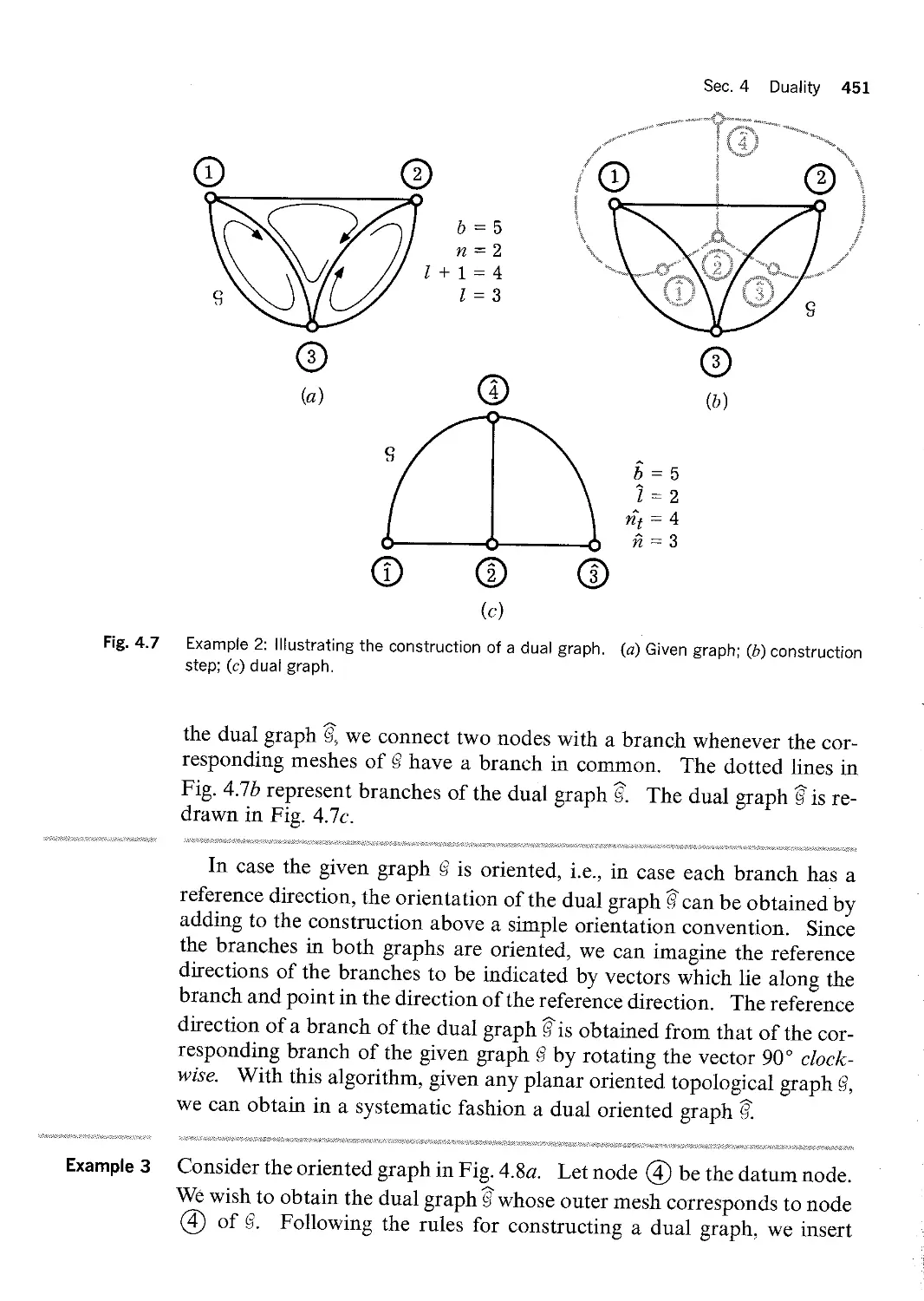
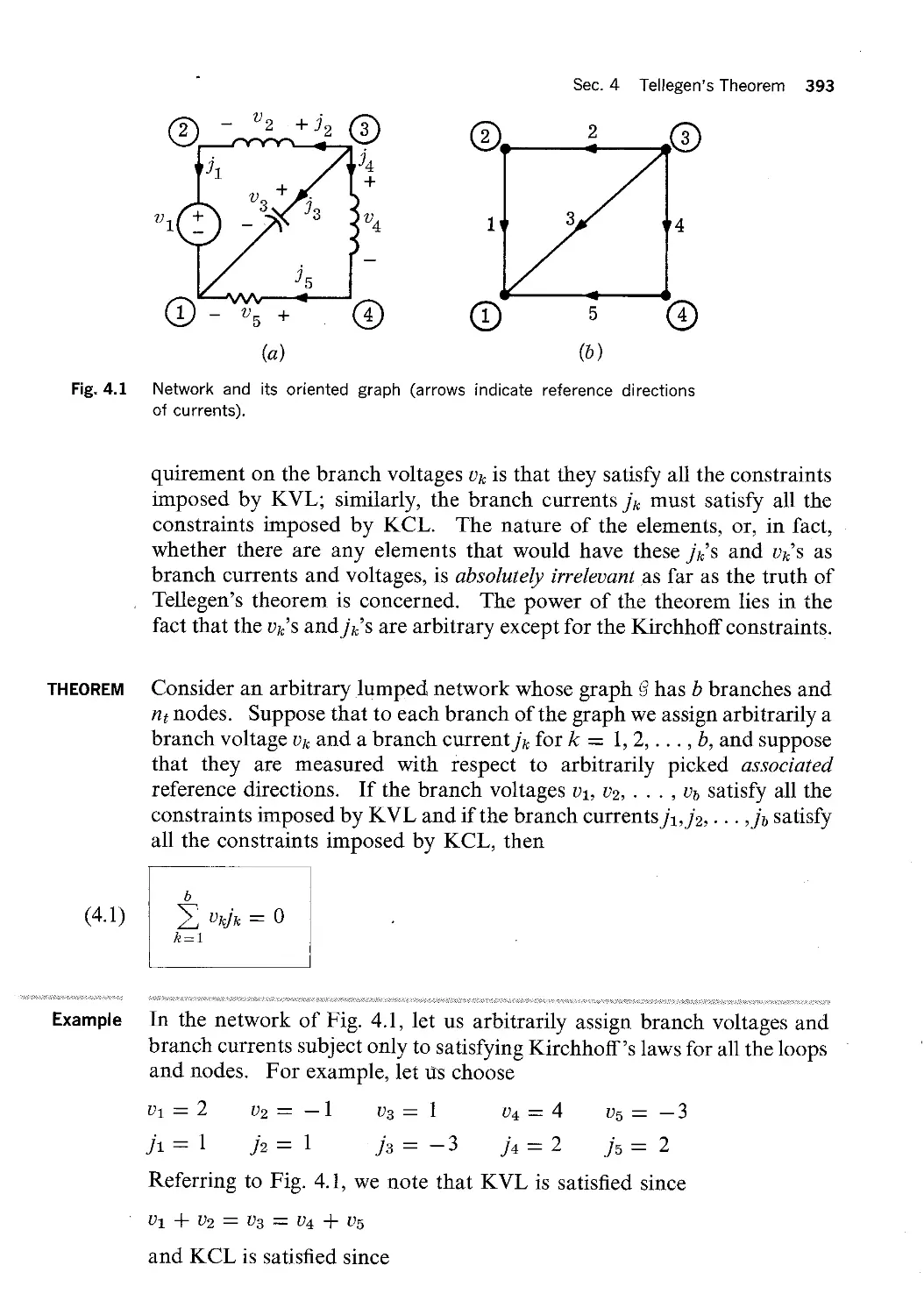
Example 1 Consider the linear time-invariant networks shown in Fig. 4.6. For sim
plicity we assume that the sources are sinusoidal and have the same fre
quency, and that the networks are in the sinusoidal steady state. In the
iirst network, say 9%, we represent the two sinusoidal node-to-datum volt
ages by the phasors E1 and E2. By inspection, we obtain the following
node equations:
(4.2a) joel + - E2 : IS
($
Fig. 4.6
(4.2b)
(4.3a)
(4.3b)
Sec. 4 Duality 449
L1 L2
Ei ® M-, @ E2
[(1) tc *¤ G? EC)- 6 ia S 'P 1 fl" 2 S
LIl T I2
"`
Two networks used to illustrate duality; if C1 : Z1, C2 : Z2, L : C, G : E, and I, : E,.
then they are said to be dual networks.
E . 1+ ]¢=>C2—l·G-l·+E2=0
l + ]o.>L
1 ]o.>L
Note that IS is the phasor that represents the sinusoidal current of the
source.
The second network fill has two meshes. We represent the two sinu
soidal mesh currents by the phasors K and Again, by inspection, we
obtain the following mesh equations:
A A
_ ]¢¤L1-l-kh- T]2=Es
A 1 A 1 io.>C iwC
1 _ A A 1 A
_ 1+ ]¢0L2+R+’"T§12—O
T t io.>C
jwC
If the element values of the two circuits are related by
CIZLI CZZEZ
and if the sources have the same phasor
IS Z ES
then Eqs. (4.2) and (4.3) are identical. Therefore, if we have solved one of
the networks, we have solved the other. These two networks are an exam
ple of a pair of dual networks. There are some interesting relations be
tween them. Qt has two nodes and a datum node; °E)t. has two meshes and
an outer mesh. Both have live branches. To a branch between two nodes
of 9L (say, the inductor connecting node Q) and node @) corresponds a
branch of Qt which is common to the corresponding meshes (the capacitor
common to mesh l and mesh 2). In GUL, the current source 18 and the capac
itor C1 are in parallel; in QN, the voltage source ES and the inductor I]1 are in
series; etc. We note that the relation between QL and We involves both
graph-theoretic concepts (meshes and nodes) and the nature of the ele
ments (sources, inductors, capacitors, etc.). For this reason we must pro
Chap. 10 Node and Mesh Analyses 450
cccd in two steps, iirst considering dual graphs and then deiining dual
networks.
We are ready to introduce the concept of dual graphs. Again we start
with a topological graph Q which is assumed to be connected, unhinged,
and planar.? Let Q have nt : n —|— l nodes, b branches, and hence,
I : b T n meshes (not counting the outer mesh). A planar topological
graph Q is said to be a dual graph of a topological graph Q if
There is a one—to—one correspondence between the meshes of Q (includ
ing the outer mesh) and the nodes of QZ
There is a one-to-one correspondence between the meshes of (includ
ing the outer mesh) and the nodes of Q.
There is a one-to-one correspondence between the branches of each
graph in such a way that whenever two meshes of one graph have the
corresponding branch in common, the corresponding nodes of the
other graph have the corresponding branch connecting these nodes.
We shall use the symbol `to designate all terms pertaining to a dual graph.
It follows from the deiinition that Q has b branches, l + l nodes, n
meshes, and one outer mesh. It is easily checked that if Q is a dual graph of
Q, then Q is a dual graph of Q. In other words duality is a symmetric relation
between connected planar, unhinged topological graphs.
ALGORITHM Given a connected, planar, unhinged topological graph Q, we construct a
dual graph Q by proceeding as follows:
l. To each mesh of Q, including the outer mesh, we associate a node of Q g
thus, we associate node ® to mesh l and draw node ® inside mesh
l; a similar procedure is followed for nodes @ , @ , . . . , including
node , which corresponds to the outer mesh.
2. For each branch, say lc, of Q which is common to mesh i and mesh j,
we associate a branch lc of Qwhich is connected to nodes @ and
By its very construction, the resulting graph Q is a dual of Q.
Example 2 The given planar graph is shown in Fig. 4.7a. There are three meshes, not
counting the outer mesh. We insert nodes G), ®, and ®, with one
node inside each mesh as shown in Fig. 4.7b. We place node @ outside
the graph Q because @ will correspond to the outer mesh. To complete
TThe concept of dual graph can be introduced for arbitrary planar connected graph. However,
for simplicity we rule out the case of hinged graph.
Sec. 4 Duality 451
V www M = 2 E. \ ~’°?€“§` / J "*·>=.,iiiiga.w
Z + 1 : 4
’/ b : 5 Q 1 : 3
(cz)
"WMWY%
»-"“%?r?`"“·~a
?rt"
2 tg; M_ Z `
E, QD ® 2
(c)
,_, www };;gWw hm,,
?i
in;2
b Z 5
Z 1 2
72} 2 4
ii = 3
(bl
Fig. 4.7 Example 2: lllustrating the construction of a dual graph. (a) Given graph; (b) construction
step; (c) dual graph.
the dual graph we connect two nodes with a branch whenever the cor
responding meshes of Q have a branch in common. The dotted lines in
Fig. 4.7b represent branches of the dual graph Q. The dual graph Qis re
drawn in Fig. 4.7c.
In case the given graph Q is oriented, i.e., in case each branch has a
reference direction, the orientation of the dual graph Q can be obtained by
adding to the construction above a simple orientation convention. Since
the branches in both graphs are oriented, we can imagine the reference
directions of the branches to be indicated by vectors which lie along the
branch and point in the direction of the reference direction. The reference
direction of a branch of the dual graph Qis obtained from that of the cor
responding branch of the given graph Q by rotating the vector 90° clock
wise. With this algorithm, given any planar oriented topological graph Q,
we can obtain in a systematic fashion a dual oriented graph QT
Example 3 Consider the oriented graph in Fig. 4.8a. Let node @ be the datum node.
We wish to obtain the dual graph Q whose outer mesh corresponds to node
@ of Q. Following the rules for constructing a dual graph, we insert
Q CD
W ‘· C
ax xg rf
M)
9 A
(C)
Chap. 10 Node and Mesh Analyses 452
/
f¤’ Y z
J
J A 2 ii m
ggr 3
g ,.d J5 ·
>»- ...,..» M A @6 ts- f
ZA @
Fig. 4.8 Example 3: Construction of oriented dual graph.
(b)
nodes ®, ® , andI@ inside meshes 1, 2, and 3, respectively, of Q, leaving
node 9 outside the mesh, as shown in Fig. 4.8b. To complete the dual
graph, branches are drawn in dotted lines, as shown in Fig. 4.8b, connect
ing the nodes of Qto correspond to the branches of Q. The reference direc
tions of the branches of Q are obtained by the method indicated above.
The dual graph is redrawn as shown in Fig. 4.8c. Care must be taken to
ensure that the branches of Q connecting the datum node correspond to the
outer mesh of Q. A moment of thought will lead to the following rule,
which gives the appropriate one-to-one correspondence. Since the datum
node, node @ in the example, must stay outside all dotted lines, when
placing node 9 of Qit is convenient to put it as far away as possible from
the datum node @, as shown in Fig. 4.8b.
Remarks
Exercise
(4.4)
Sec. 4 Duality 453
l. In general, a given topological graph Q has many duals. However, if
we specify the datum node of Q and specify that it has to correspond to
the outer mesh of Q, then the procedure described above defines a
unique dual graph. The branches which are connected to the datum
node in Q have corresponding branches which form the outer mesh
in Q.
2. The correspondence between the graph Q and its dual Q involves
branch versus branch, node versus mesh, and datum node versus
outer mesh. Furthermore, the incidence matrix Aa of the given graph
Q is equal to the matrix Ma of the dual graph Q.
Construct a dual graph Q of the oriented planar graph Q given in Fig. 4.5.
Write the KCL equations of the dual graph for all the nodes; that is,
A320
Show that the set of equations is identical to the KVL equations of the
given graph for all the meshes (including the outer mesh); that is,
Mav = 0
ln this discussion we restrict ourselves to networks having the following
properties: their graphs are connecteel planar, and unhingeaf and all their
elements are one-port elements. ln other words, we exclude coupled in
ductors, transformers, and dependent sources; we include independent
voltage or current sources, inductors, resistors, and capacitors. It is fun
damental to observe that the elements do not have to be linear and/ or
time-mvariant.
We say that a network {Ot is the dual 0f the network 9Lif (l) the topolog
ical graph Q of gt is a dual of the topological graph Q of ®L, and (2) the
branch equation of a branch of is obtained from its corresponding
equation of QL by performing the following substitutions:
U ——> q + 2,5
/
j + 1} q> + if
where v, j, q, and qb are the branch voltage, current, charge, and flux var
iables, respectively, for {UL, and 6,], Z}, and Z5 are the corresponding branch
variables for QR.
Requirement 2 of the definition means that a resistor of Qftcorresponds
to a resistor of 9L. Furthermore, a linear resistor of Qtwith a resistance of
K ohms corresponds to a linear resistor of Qt with a conductance of K
rnhos. Indeed, the branch equation of the resistor of €’)Lis v ; IQ; hence,
Chap. 10 Node and Mesh Analyses 454
that of the corresponding resistor of?)/>t1isj`: Ki?. Similarly, an inductor of
‘E% corresponds to a capacitor of 9%. Furthermore, a nonlinear time-vary
ing inductor of QL which is characterized by qb : f(i,t), where f( · , ·) is a
given function of two variables, will correspond to a nonlinear time-vary
ing capacitor of 9% which is characterized by 2} : j(’zZt). A voltage source
whose voltage is a function f( · ) will correspond to a current source whose
current is the same function j( - ). Also, the dual of a short circuit is an
open circuit; a short circuit is characterized by 11 : O, hence its dual is
characterized byf; 0, the equation for an open circuit.
It is easily checked that if gl is a dual network of ®"t, then 9% is a dual
network of €%; in other words, duality is a symmetric relation between
networks.
Example 4 Consider the nonlinear time-varying network ‘F% shown in Fig. 4.9a. The
inductor is nonlinear; its characteristic is (pl : tanh jl. The capacitor is
time-varying and linear; its characteristic is qg : (l —l- c‘l2)113. The out
put resistor is linear and time-varying with resistance 2 —|— cos t; its char
acteristic is z14 : (2 + cos ty);. The branch orientations are indicated in
the figure. Let the mesh currents be il and iz; then,
¢1= tanhjl
-f2 q3= 1+e 113
esli) = flf)© Q R2 {-U *i
R4 lf) = 2 + ¢<>S l
1 12 z YJ4
la)
+ U2 _
+ l G2 e R2 L+ +
A
A pf : 25 A ; A -.1 A 11 15 g ; tsl) fl)(Dv1 €l'P;tanhUg3 4 Gilt) 2+c0s¢
11l
Fig. 4.9 Example 4: lllustratlng dual networks.
lb)
A L — - L é
A -f2 ’> Ql)3 Z 1 + €
(4.5a)
(4.5b)
(4.6a)
General
propergz 0f
dual
networks
Exercise 1
Exercise 2
Sec. 4 Duality 455
]1:l1 ]2=ii—i2 j:s=j4=i2
The mesh equations read
1
. . tsl') —4’) · @§a + 44* · ’2)
O 1
. . . , , . 0 Z R2(l2 — Z1) + + + + COS
The dual network is easily found. First, the dual graph fi is drawn,
including the orientation; then each branch is filled with the appropriate
dual element as prescribed by requirement 2. The result is shown in
Fig. 4.9b. Let the node-to-datum voltages be @1 and @2. Then the branch
voltages are related to the node voltages by @1 : @1, @2 : @1 — @2, and
@3 : 64 : @2. The node equations give
1 d@1 A
A S I i ‘ G * A ’ (’) 4’) ? + 461 62)
cosha. at
$(0) I
_ A A A . i A O - G2(€2 — 61) —|- —I— _t2 €2(l)dl` —[— -1- COS l)€2(Z)
¢1+ €I)
where the conductance G2 is equal to the resistance R2. Observe that Eqs.
(4.6) are identical with Eqs. (4.5) except for the names of the variables.
il
The importance of dualitycannotoveremphasized. Its power is ex
hibited by the following general assertion. Consider an arbitrary planar
network QTL and its dual 9L Let S be any true statement concerning the be
havior of ®‘(. Let S be the statement obtained jiom S by replacing every
graph-theoretic word or phrase (node, mesh, loop, etc.) by its dual and every
electrical quantigr (voltage, current, impedance, etc.) by its dual. Then S is
a true statement concerning the behavior of ®l. In Table 10.1 we give a tabu
lation of pairs of dual terms. Some of these will be illustrated in later
chapters.
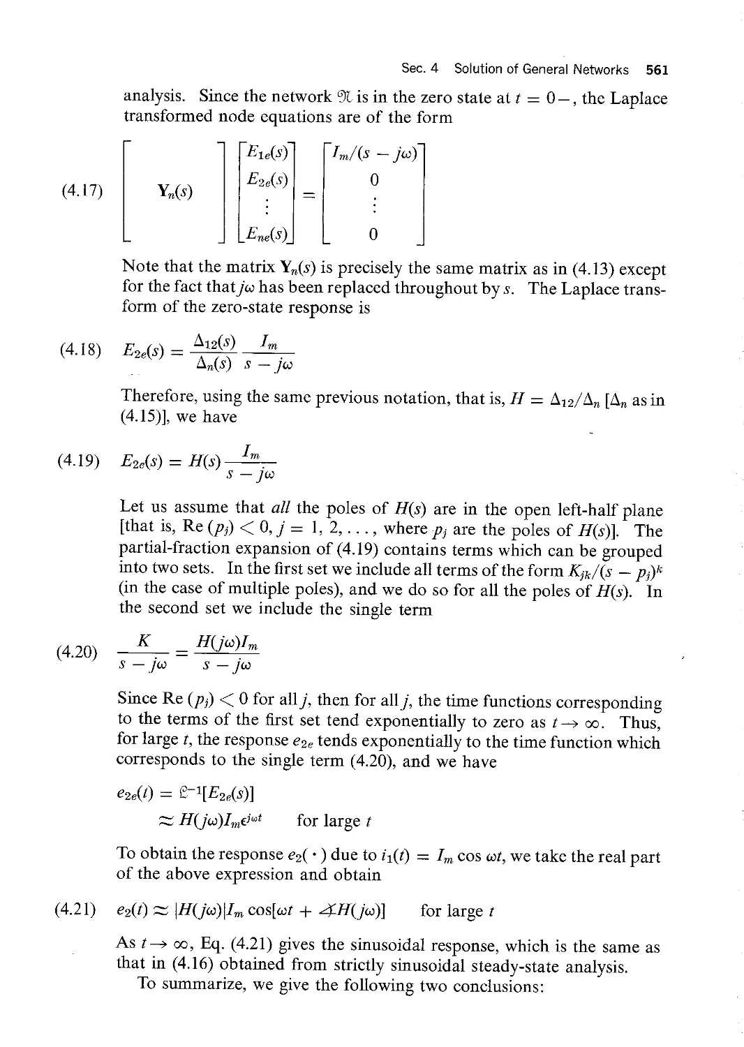
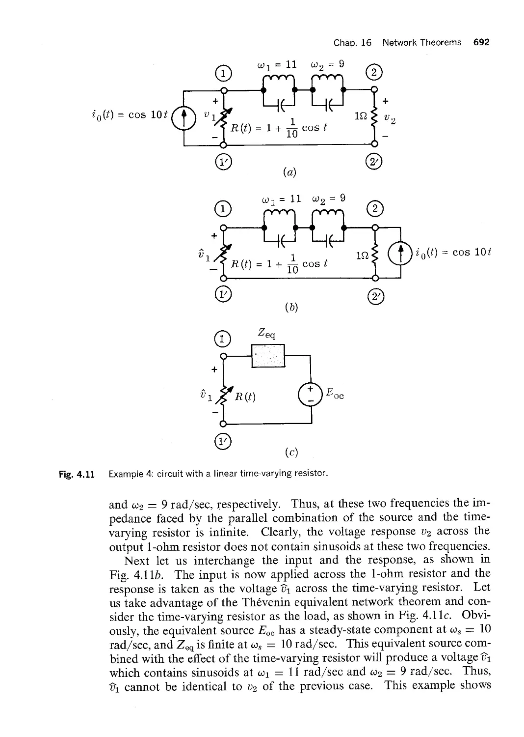
Consider the linear time-invariant RLC network @7, (without coupled in
ductors) shown in Fig. 4.10. Assume that its graph is planar and unhinged.
Suppose it is driven by a sinusoidal current source and is in the steady
state. Consider the dual network Qt. Show that the driving-point imped
ance Z11, of QL is for each w equal to the driving-point admittance K1, of QTL.
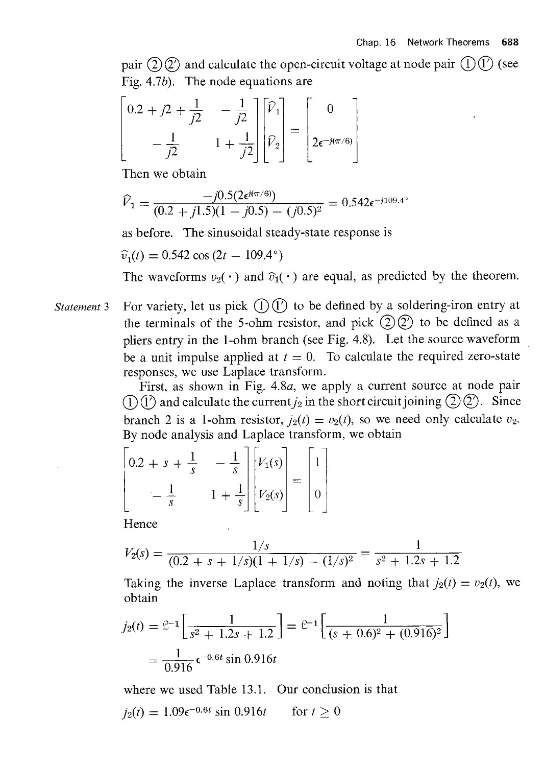
Consider the ladder network We shown in Fig. 4.11. The functions f1( ja),
j2(ja>) ,... , ]Q—,(jw) specify the impedances of the corresponding element
of QTL; the function fspeciiies the waveform of the source. Show that the
dual of ‘5L can be obtained (1) by replacing the current source of f(t) amp
Chap. 10 Node and Mesh Analyses 456
Table 10.1 Dual Terms
Types of properties S
Graph-theoretic Node
Cut set
propcrues
Datum node
Treo branch*
Fundamental cut set*
Branches in series
Reduced incidence matrix
Fundamental cut-set
matrix*
Graph-theoretic Node—to-datum voltages
and electric
Tree-branch voltages*
KCL
propertres
Electric
Voltage
Charge
properties
Resistor
Inductor
Resistance
Inductance
Current source
Short circuit
Admittance
Node admittance matrix
The asterisk is used to indicate terms that will be encountered in this
Mesh
Loop
Outer mesh
Link*
Fundamental loop*
Branches in parallel
Mesh matrix*
Fundamental loop
matrix*
Mesh currents
Link currents*
KVL
Current
Flux
Resistor
Capacitor
Conductance
Capacitance
Voltage source
Open circuit
Impedance
Mesh impedance
matrix*
and the next chapter.
by a voltage source of f(t) volts, (2) by replacing each series element
of We of impedance ]2(jw) by a shunt element of admittance ]Q(jw), and
(3) by replacing each shunt element of We of impedance ]Q(jw) by a
series element of admittance j(jw).
RLC
network
T if Q §
Z in
Fig. 4.10 Exercise 1: illustrating the dual of a driving-point
impedance.
f<¢)( T
Fig. 4.11 A ladder network @7..
m
alt*lrmi'I;
Sec. 5 Two Basic Facts of Mesh Analysis 457
Let us consider any network @L whose graph is connected, planar, and un
hinged. We assume that it has nt nodes and b branches; consequently it
has I : b — nt —l— l meshes, not counting the outer mesh. We label the
meshes l, 2, . . . , l and use the clockwise reference directions. The meshes
are the duals of the nodes, whereas the outer mesh is the dual of the datum
node. We shall employ the concept of duality to develop the two basic
facts of mesh analysis. Again it should be emphasized that the two facts
are independent of the nature of the network elements. Thus, the network
can be linear or nonlinear, time-invariant or time-varying.
Let us apply KVL to meshes 1, 2, . . . , I (omitting the outer mesh). As
seen in the example below (Fig. 5.l) each expression is a linear homogen
eous algebraic equation in the branch voltages. Thus, we have a system of
l linear homogeneous algebraic equations in the b unknowns 01, U2, . . . ,0;,.
The first basic fact of mesh analysis can be stated as follows:
The I linear homogeneous algebraic equations in 121, U2, . . . , U; obtained by
apphring KVL to each mesh (except the outer mesh) constitute a set of
I Iinearhz independent equations.
The proof of this statement can be given in the same manner as the
proof of the comparable statement in node analysis. We shall ask the
reader to go through corresponding steps. It is, however, quite easy to
use duality to prove the statement above: Denote by oi the network
dual to ‘?)L Apply KCL to all nodes of at except the datum node. If the
basic fact above were false, the first basic fact of node analysis would also
be false. Since the latter has been proved independently, it follows that
the first basic fact of mesh analysis is true.
Analytically KVL may be expressed by the use of the mesh matrix
(5.2)
Example 1
Fig. 5.1
Chap. 10 Node and Mesh Analyses 458
where M : (mw) is an l X b matrix defined below by Eq. (5.2). When
we write that the ith component of Mv is zero, we merely assert that the
sum of all branch voltages around the ith mesh is zero. Since this ith
component is of the form
E mikvk = O
kzi
wemusthavefori : 1,2,. . . ,landk : 1,2,.. .,b,
1 if branch k is in mesh i and if their reference directions
coincide
mi], : { - 1 if branch k is in mesh i and if their reference directions do
not caincide
O if branch k does not belong to mesh i
The basic fact established above implies that the mesh matrix M has a
rank equal t0 l.
Note that the mesh matrix M is obtained from the matrix Ma by deleting
the row of Ma which corresponds to the outer mesh.
l
Considertheof Fig. 5.1, graph of Fig. 2.3.
There are three nodes and five branches; thus, l ; 5 — 3 + 1 : 3. The
three meshes are labeled as shown. The branch voltage vector is
V I | U3
The mesh matrix, obtained from Eq. (5.2), is
gw; r”“*~—~I
, f . \. ,sY
jr if f R. . ¤.
j K \_74 \.,__;
. J Ml 2ri......» l 5
..-.,,.....
An oriented graph which is the dual graph of
that of Fig. 2.3.
M : 0 -1 1 1
1 1 0 0 0 0 0 - 1
T T T T
Branch 1 2 3 4
Sec. 5 Two Basic Facts of Mesh Analysis 459
Mesh
O +1 0 +2 l <———3
The mcsh equation is therefore
MV: O -1
I I 0 O
OI`
U1-T-U2
—U2 —I- U3 + U4
—U4+U5
0 0 O U2 0 1 1 0 U3 : O O — 1 1 U4 O
which are clearly the three mesh equations obtained from KVL for meshes
1, 2, and 3. The three equations are clearly linearly independent, since
each equation includes a variable which is not present in the other two.
Exercise Let A be the reduced incidence matrix of an oriented graph Q. Let NI be
the mesh matrix of the dual graph Q Show that A : lfl.
Let us call il, i2, . . . , il the mesh currents. For convenience let us assign
to each one a clockwise reference direction. First, let us observe that the
mesh currents il, i2, . . . , il are linearly independent as far as KCL is con
cerned. Since each mesh current runs around a loop, if mesh current ik
crosses an arbitrarily chosen cut set in the positive direction, it also crosses
the cut set in the negative direction and, hence, cancels out from the KCL
equation applied to that cut set. In other words, if we write KCL for any
cut set and express the branch currents in terms of mesh currents, every
thing cancels out, Thus, KCL has nothing to say about the mesh currents,
which makes them linearly independent as far as KCL is concerned.
The next step is to show that the branch currents can be calculated in
terms of the mesh currents by the equation
(5.3)
Example 2
Exercise 1
Exercise 2
Exercise 3
Summary
Chap. 10 Node and Mesh Analyses 460
j ; MTi (KCL)
where MT is the transpose of the mesh matrix M. Equation (5.3) means
that every branch current can be expressed as a linear combination of
mesh currents, and that the matrix which speciiies these linear combina
tions is the transpose of the mesh matrix defined previously. We shall ask
the reader to apply duality to the proof that v : ATe in order to justify
Eq. (5.3).
i(5 i
Consider the network whose graphis shown 5.1. It isobvious
that we can relate the branch currents and mesh currents as follows:
ji = Z1
_]2 = Z1 — 12
js = Z2
-/4 : Z2 —- Z3
js = ia
or
1 O O
j ; MTi ; | O l 0 i2
l — 1 0 il O l — l i 3
O 0 1
Express Kirchhoff ’s laws in the form of Eq. (5.1) and (5.3) for the graph
of Fig. 4.742.
Suppose that a network has a graph consisting of a large square divided
into 25 equal squares (live on a side). Suppose that you have a large
supply of zero-impedance ammeters. What is the minimum number of
ammeters required to measure all mesh currents? Where would you put
them?
Use deiinition (5.2) of mi;. to prove Eq. (5.3).
Equation (5.1)
and Eq. (5.3)
6,1
(6.l)
(6.2)
(6.3)
Sec. 6 Mesh Analysis of Linear Time—invariant Networks 461
j : MTi (KCL)
respectively, are the two basic equations of mesh analysis. Since the two
equations are obtained from the network graph (planar, connected, and
unhinged) and the two Kirchhoff laws, they are independent of the nature
of the elements of the network. Equation (5.1) expresses KVL and con
sists of a set of I linearly independent equations in terms of the b branch
voltages ul, v2, . . . , vb. Equation (5.3) expresses KCL and relates the b
branch currents jl, j2, . . . ,jl, to the lmesh currents il, i2, . . . , il. To
solve for the I network variables il, i 2, . . . , i Z, we need to know the branch
characterization of the network, i.e., the b branch equations which relate
the branch voltages to the branch currents. Only in these branch equa
tions does the nature of network elements come into the analysis. ln the
next section we shall treat exclusively linear time-invariant networks.
Nonlinear and time-varying networks will be considered later.
:Ti?i`!m§!'3
The mesh analysis of a linear time—invariant network requires a sequence
of steps which is the dual of that required for the node analysis of the dual
network ‘J`c, This will allow us to treat this material briefly.
sinusoidal.e,S:t¢¤dy&staiét1A¤a¤y$i$
Since the analysis of resistive networks is a special case of the sinusoidal
steady-state analysis, we treat only the latter.
Let {it be a linear time—invariant network with b branches and Ht nodes.
Let its graph Q be connected, planar, and unhinged. Let the sources be
sinusoidal and have all the same frequency w. Call J S and V8 the b-vectors
whose kth components are the phasors representing the sinusoidal sources
in the kth branch. Similarly, V and J are the b-vectors whose kth com
ponents are the phasors representing the branch voltage uk and the branch
current jk. Call I the Z-vector whose components are the phasors rep
resenting the mesh currents il, i2, . . . , il. Kirchhoif ’s laws give
MV ; 0 (KVL)
J I MTI (KCL)
The branch equations are
V = Zi(jw)J — Zi(jw)J8 + Vs _
The b >< b matrix Zl,(jw) is called the branch-impedance matrix. The
substitution gives
(6.4)
(6.5)
(6.6)
Example 1
(6.7)
(6.8)
Fig. 6.1
Chap. 10 Node and Mesh Analyses 462
(MZb(jw)MT)I : MZb(ja>)JS — MVS
or
Zm(jw)I : E8
where Zm(jw) is an I >< lmatrix called the mesh impedance matrix, given by
Zm(j°—’) = MZb(j<»)NW.
and Es, the mesh voltage source vector, is the Z vector given by
ES : MZ;,(jw)JS — MVS
Equations (6.4) are called the mesh equations of QR; they constitute a
system of Z linear algebraic equations (with complex coeflicients) in l un
knowns, the phasors representing the mesh currents I1, 12, ..., I l. The
solution of (6.4) specifies all mesh currents. Then the branch currents are
obtained by (6.2), and the branch voltages by (6.3).
Consider the linear time-invariant network 9i shown in Fig. 6.1. The
phasor K1 represents the sinusoidal voltage of the source; vS1(t) :
lQl| cos (wt -4- 4)Zl/Q1). By inspection,
M I
— 1 l 1 O 0 0 O - 1 1 l
Let the inductance matrix of the branches 3, 4, and 5 be
L ;
3 1 -1 1 4 2 -1 2 5
+ Y? - J4
2 F +.13 / ‘
3 SZ
J 5 w JL5
4V *2 2
r MQW 11 ;IT3
Network analyzed in Example 1.
Sec. 6 Mesh Analysis of Linear Time—invariant Networks 463
hence
(6.9)
K 3jo.> jon —jw J3 TQ : jw 4jw 2jw J4 V5 —jw 2jw 5jw JL5
lf we note that the current J 5 is related t0 J L5, the current into the inductor,
(6.10) JL5 : J5 - 415 : J5 — i-J2
we obtain the following branch equations:
O ai I3 O 0 Olm rm
V2. I0 E) 0 0 0||J2| [0
IGI:
J3|+l0
O 2 3jw jo: —jw
J4 I I 0
O 4 . . . — jon 4]0.> 2jw
J I I O 5
O -10 —jw 2jw _ 5jo.>
Using (6.5) and (6.6), we obtain the following mesh equations:
5-4-3jw-r,-i -3jo I1 Z K1 -16 — 3jw 16jw 12 ,0
Properties l .
ofthe mesh
impedance
matrix
If the network QL has no coupling elements, Z5(jw) is diagonal and
Z,,,(jw) is symmetric; that is, Zm(jw) : ZmT(jw) [this follows from
(6.5)].
Again, if 9L has no coupling elements, the mesh impedance Z,,,(jw)
can be written by inspection as follows:
a. Call zi, the diagonal element of Zm in the ith row and ith column.
zi, is the sum of all the impedances of branches in mesh i and is
called the self-impedance of mesh i.
b. Call z,k the (i,k)th element of Z5,. z,,, is the negative of the sum
of all the impedances of the branches which are in common with
meshes i and ki and is called the mutual impedance between
mesh i and mesh k.
If, using the Thévenin equivalent, we convert all sources into voltage
sources, then es], is the algebraic sum of all the source voltages in
mesh kx the voltage sources whose reference direction push the current
TThe fact that Zi].; is the negative of the sum of the impedances common to meshes i and k is a
consequence of the convention that all mesh currents are given clockwise reference directions.
Exercise 1
Exercise 2
Exercise 3
6.2s
Chap. 10 Node and Mesh Analyses 464
in thc kth mesh reference direction are assigned a positive sign, all
other voltage sources are assigned a negative sign.
4. In the case of resistive networks, if all resistances are positive, then
det (ZW,) > O. Cramer’s rule then guarantees that whatever the in
dependent sources may be, the mesh equations (6.4) have a unique
solution.
In case QL has coupling elements, the only general conclusions are that
Z;,(jw) is no longer diagonal and Z,,,(jw) is usually no longer symmetric.
Prove statements 2a and 2b. [Hint: Use (6.5) and (5.2)].
By inspection, write the mesh equations of the network shown in Fig. 6.1,
assuming that all mutual inductances and the dependent current sources
are set to zero.
Find a network with coupling elements which has a symmetric mesh im
pedance matrix. (Hint: Use symmetry.)
sgaiegroiisrieieritiariiqaaiians
Let us illustrate the general procedure for writing the integrodiH`erential
mesh equations. We choose a simple case so that we can concentrate on
the handling of initial conditions. The method, however, is completely
general.
Consider the linear time-invariant network shown in Fig. 6.2. We are
given the element values R3, C4, and or and the inductance matrix
Note that M is positive in view ofthe reference directions of jl and jz, which
enter the inductors through the dotted terminals. ln addition, we need
the initial charge on the capacitor or, equivalently, v4(0), and the initial
inductor currents j1(0) and j2(0). Finally, we need the input waveform
vs3( · ). To obtain the mesh equations, we proceed as follows:
3 j3 g_“I;'];_ jl g__i%___` j2
R 5é < 0* j 2
USB
_.. U4 ’l`C4 *
Fig. 6.2 Network used to illustrate the writing of integroditferential equations.
Step 1
(6.1 I)
Step 2
(6.12)
Step 3
(6.13)
Step 4
(6.14)
Sec. 6 Mesh Analysis of Linear Time—invariant Networks 465
We write KVL; thus, Mv : 0, and
1 0 -1 1 0 U2 0 U : 0 1 0 -1 1 3 0
We write KCL; thus, j ; MTi, and
ji I I I O
jg O l
i J3 = -1 11 I . 12 J4 1 — 1
J5 I I 0 I
We write the branch equations in matrix form as follows:
L D MD 0 0 O 1
. J1 I I O
MD L2D 0 0 0
. U2 J2 O O R 0 . U3 I: I 0 3 ? J3 `I` U
s3
0 0 -11125 0 125 12 O
We may think of this equation as being in the form
v : Z;,(D)j + v5
where, in this case, Z5 is a matrix whose elements involve the operators I
D and Dri.
We use (6.12) to eliminate the jk’s from (6.13); then we use (6.ll) to
eliminate the v;5’s from the resulting equation. Rearranging terms, we
obtain
MZ5(D)MTi Z -Mv5
or
: BS
where Zm(D) -2 MZb(D)MT is recognized as the mesh impedance matrix
operator. In this example, the matrix equation reads
(6.15)
(6.16)
Remark
(6.17)
Chap. 10 Node and Mesh Analyses 466
L D R 4 - .; · S - 1 + 5+C4D MD QD Hal IU5 v1(0)
MD R ~ -: 1. D R 4 · +<x 5 1 + 5+ lllzl I v4<0>
QD
QD
or, in scalar form,
1 r
di2 1 1·
di1 L
. . _ — R — ’ ’ M — — — ’ ’ 1 + 311 + C4 L + C4 fo 120)
= U53(Z) — v4(0)
di
di2
1 . _ . . M___ R j é / I i- t I / + a 511 l1(¢)d¢ + Lz + R5lz(¢) + l2(f)d¢
dt
dt
1 ¢ C4 L
1 1 C4 L
= v4(0)
This system of Eqs. (6.16) is a system of two integrodifferential equations
in two unknowns, i1(·) and i2(-). The required initial conditions are
i1(O), i2(0), and v4(0).
Any system of integrodifferential equations such as (6.16) can always be
put in the form of a system of differential equations by the introduction of
appropriate variables. Define the waveforms q1( ·) and q2( ·) by
q1(t) : i1(t/) dt' q2(t) : i2(z’) dt'
fof
Physically, q1(z) is the net amount of charge (in coulombs) that has passed
through R3 or L1 in the interval [0,t]. In terms of q1( ·) and q2( · ), the
integrodifferential system of (6.16) becomes a system of dgferential
equations,
L12]i + Rséi + %¢]i + — %6]2 Z U53(F) · U4(O)
+ R50¢Qli — ·,#q1 + Lzqa + Rsijz + %q2 = v4(0)
with the initial conditions
q1(O) : O q2(0) : 0 see (6.17)
Q1 I j1(O) @(0) = ]2(O)
In the node analysis, the n node-to-datum voltages e1, eg, . . . , 6,, are used
as network variables. By applying KCL to all the nodes except the datum
(CI)
(b)
(c)
<d>
Summary 467
node, we obtain n linearly independent equations in terms of branch cur
rents. For linear time—invariant networks, taking the branch equations
into account, the n equations can be written explicitly in terms of the
n node-to—datum voltages. In general, the resulting network equation
gives in matrix form
Y,,(D)e : is
Once e is determined, the b branch voltages can be obtained immediately
from
V : ATe
The b branch currents are then obtainable from the branch equations.
The writing of the node matrix equation in (a) can be done formally
using the step-by—step procedure and matrix multiplications. However,
for simple circuits which do not contain complicated coupling elements,
the node admittance matrix Y,,(D) as well as the source vector is can be
written by inspection. Frequently it is advisable to convert all voltage
sources into current sources before starting node analysis.
In mesh analysis the I mesh currents il, i2, . . . , il are used as network
variables, and I linearly independent equations in terms of branch voltages
are obtained by applying KVL to all the meshes except the outer mesh.
For linear time-invariant networks, taking the branch equations into
account, the I equations can be written explicitly in terms of the I mesh
currents. In general, the resulting mesh equation gives in matrix form
: 68
Once i is determined, the b branch currents can be obtained from
j : MTi
The b branch voltages are then obtainable from the branch equations.
Again, a step-by-step procedure can be used to write the mesh matrix
equation of (c); or in case the network does not include complicated
coupling elements, Z,,,(D) and es can be obtained by inspection. Fre
quently, it is advisable to convert all current sources into voltage sources
before starting mesh analysis.
Whereas node analysis is completely general, mesh analysis is restricted
to planar networks.
The two methods are dual to each other in the case of planar networks.
The natural question to ask is which is a better method. The answer de
pends on the given network. In node analysis there are n network
variables to be determined, whereas in mesh analysis there are Z network
variables. Thus, it is reasonable to say that if for a given graph the num
ber of nodes n —|— l is much smaller than the number of meshes I, the node
Chap. 10 Node and Mesh Analyses 468
analysis is preferable. lf it is the other way around, then the mesh analysis
is more advantageous. However, other factors must also be considered.
One crucial point deals with the number and kind of sources in the net
work. If all given sources (dependent and independent) are current
sources, node analysis probably is more convenient since one can often
write the node equations by inspection. On the other hand, if all given
sources are voltage sources, mesh analysis may be easier to use. Experi
ence will help you to decide one way or the other.
Two connected, unhinged, planar topological graphs are said to be dual
to each other if (1) there is a one—to-one correspondence between the
meshes of one (including the outer mesh) and the nodes of the other, and
vice-versa, and (2) there is a one-to-one correspondence between the
branches of each graph such that whenever two meshes of one graph have
a branch in common, the corresponding nodes of the other graph have the
corresponding branch connecting these nodes.
Two networks are said to be dual to each other if (l) the topological graph
of one is the dual of the topological graph of the other, and (2) the branch
equations of one are obtainable from the corresponding branch equations
of the other by performing the following substitutions:
v q —» {8
j —-> if <,l> Q Q`
The main facts of node and mesh analysis are tabulated in Table 10.2 in a
form that makes the duality of the two methods readily apparent.
Summary of Node and Mesh Analyses
Network
i, mesh currents
e, node-to-datum voltages
variables
Basic facts
Mv : 0 (KVL)
Aj : 0 (KCL)
j : MTi (KCL)
v ; ATe (KVL)
Linear
Branch equations
time
. . v : Rj + vs — Rjs
. . _| : Gv —l- js — Gvs
mvzmam
resistive
Network equations
networks
Zml : Gs
Yue = is
Zm 2 MRMT
Ys E AGAT
es é MRjs — Mvs
is E AGvs — Ajs
mverse
Incidence
matrices
Node analysis
Problems 469
QZ}?
1. a. Give the rank of the following matrices:
l A1:I
A3:
l O 1 0 1A:O -2 -2 2
0 2 -2 l l l 0 l l ] 2[ ] l -1 2 1 2 -l l O -2
3 1 O
4 7 9
6 2 O
3 2 7
b. Find the inverse of the following matrices:
% %
B 1 `
B 2 `
B O 1 0 — % -24 3 `
-1 3 2 -4
2 -2 1 -1 2 1
2. Are the following matrices possible reduced incidence matrices? In
each case ustify your answer.
-1 1
1 O
O -1
O 0
O 0
0 O
1 O
-1 1
0 O
O 0
O O 0 O O O O
O 0 -1 0 -1 O -1
O 0 0 O O 1 1
0 O 0 1 1·-1 0
0 -1 1 -1 0 0 0
0 -1 1 O 0 O O 0
1 O I I 1 1 0 1 0 O 1
0 - 1 - 1 O 1 O O - 1 O I I
[1 0]
2 0 I I O O O O 1 O -1
0 1 I I O -1 -1 O 0 1 O
3. Consider the linear time-invariant network shown in Fig. P10.3.
Using the reference directions shown, obtain the oriented graph of
the network.
Write the expression for KCL and KVL in matrix form (Aj : 0, and
V : ATC).
Assuming the sinusoidal steady state at frequency on and the source
phasor JS for the current source, write the node equations in matrix
form.
Fig. P10.3
Node analysis
Node analysis
Fig. P10.5
Node analysis
Node analysis
Chap. 10 Node and Mesh Analyses 470
J. T) §G1 #1*1
d. Assuming zero initial conditions, obtain the integrodifferential equa
tions of node analysis for the network shown.
4. Consider the linear time-invariant network shown in Fig. PlO.3.
ez. Obtain by inspection the node equations for the sinusoidal steady
state.
b. Obtain by inspection the node integrodiiTerential equations for the
case in which all initial conditions are zero.
5. Consider the linear time-invariant network shown in Fig. Pl0.5.
cz. Obtain the node integrodiiTerential equations by the systematic
method.
b. Assuming the sinusoidal steady state at frequency w, obtain the node
equations.
73 YM Us
J1 J 2
M
¢ • 4**L J1 I3
—L L2 »'~C R5; Us jS5
i gmU5® QR1 L1
Rl:R5:1OQ gWL=1mhO L1:1OH L2=M=1H CZIF
6. Repeat Prob. 5 with M : 0, using the shortcut method.
T7. Let the linear time-invariant network shown in Fig. PlO.7 be in the
sinusoidal steady state. An oriented graph of this network is shown in
Fig. PlO.7. Use node analysis to find all branch voltages and currents,
given e8(t) : cos lO6t.
Fig. P10.7
Node analysis
Fig. P10.8
Duality
Fig. P10.9
Problems 471
2 o
®._2_.®
1 nH
O 5 · MF
5+ +6
1 2 ME $0-M T 2
SW
@lT’—‘¤»» @
(b)
(cz)
8. Consider the linear time-invariant network shown in Fig. PlO.8.
cz. Assume it is in the sinusoidal steady state and write its node equations
by inspection.
b. Assume all initial conditions to be zero, and write the integrodiiferen
tial node equation.
2 C2
G3 <t>gmvi
#(1) G1? wel
9. Find the dual of the general resistive branch shown in Fig. Pl0.9. By
transforming the voltage source in the dual branch, show that the dual
€.( i
l ws
Chap. 10 Node and Mesh Analyses 472
takes the same form as thc original with é`S : —jS and : ——e8. (Hint:
If a voltage source appears in series with a current source, the voltage
source may be shorted out.)
Dual graphs l0gFor each of the topological graphs shown in Fig. Pl0.l0, give two
dillerent dual topological graphs.
61/ I \ d
1 3 4 21 b
A7} As
z»\ 1 xc
(C)
(b)
(cz)
Fig. P10.10
Dual networks. ($11. Given the nonlinear network ®Z, shown in Fig. P10.11, iincl a dual net
\work °E$`L (Be sure to specify gl completely.) The branch equations for
Fig. P10.11
Mesh analysis
Fig. P10.12
QL are
+ UR
vS(t) ; 2 coswti Q
12. The circuit shown in Fig. P10.12 is made of linear time-invariant ele
ments. Calculate the voltage 01.
uv ·¥ R5
E = 5 volts
Rl=R2=R4=R5=].Q
R3 = 2 Q
U1§R1 U2 2%
M Z 2
Mesh analysis
Fig. P10.13
Mesh analysis
Fig. P10.14
Mesh analysis
Problems 473
13. The network shown in Fig. P10. 13 is in the sinusoidal steady state with
angular frequency w = 2 rad/ sec.
a. Find the phasors [1 and 12.
b. What is the driving-point impedance seen by the voltage source?
1 • Lt`;
1i i L 2 $ R 2
Llzll/[:1H L2=2H R1:R2=1Q
14. The linear time-invariant circuit shown in Fig. P10.14 represents the
Maxwell bridge, an instrument used to measure the inductance L, and re
sistance R, of a linear time-invariant physical inductor. The measure
ment is made with the circuit in sinusoidal steady state by adjusting R1
and C until UA : UB (then the bridge is said to be "balanced"). It is im
portant to note that when balance is achieved, the current through the
detector D is zero regardless of the value of the detector impedance.
Show that when the bridge is balanced,
R R2 3
L, : R2R3C R, Z
GS = K sin wt
A — Hr L
15. Consider the linear time-invariant network shown in Fig. PlO.3.
a. Obtain the mesh matrix for this network.
b. Write KVL and KCL in matrix form.
Mesh analysis
Mesh analysis
Mesh analysis
Mesh analysis
Fig. P10.19
Node and
mesh analysis
Fig. P10.20
Chap. 10 Node and Mesh Analyses 474
c. Assuming the sinusoidal steady state at frequency w, use (a) and (b) to
obtain the mesh equations.
d. Assume the following initial conditions:
jL1(O) : 1 jL3(O) : O vC1(O) = 0 vC2(0) : l
Obtain the integrodifferential mesh equations.
16. Repeat (0) and (d ) of Prob. 15 by inspection.
17. Consider the linear time-invariant network of Fig. PlO.5.
a. Obtain the mesh matrix for this network.
b. Assuming the network is in sinusoidal steady state, write the mesh
equations.
c. Obtain, by the systematic method, the integrodifferential mesh equa
tions for zero initial conditions.
18. Repeat the previous problem using the shortcut method.
Write the mesh equations of the circuit shown in Fig. P10.19 using the
charge ql and q2 as variables. Indicate the necessary initial conditions.
At t: 0 the_ current in the inductor is I0, and the voltage across the
capacitor is I4).
L I0 + fg _
. |\ Z C
• R3
ql § R 2 q 2 . f Rz
m
H1 • 21 S +
20. For the linear time-invariant network shown in Fig. P10.20, which is
assumed to be in the sinusoidal steady state,
L2 I\ C
L1 i L2 Z 2 H
I/sl
R2 Rl:R2;3$`l
C = 4 F
Problems 475
Draw thc network graph; call it Q.
Draw thc dual graph; call it Q.
Obtain thc dual network; call it ‘i`JL.
Write the mesh equations for the given network and the node equa
tions of 9L.
Compare the equations in (al).
Dual networks 21. Consider the linear time-invariant network QL shown in Fig. Pl0.2l.
Find a dual network of 9%; call it
Assuming that the sinusoidal steady state has been reached, write by
inspection the mesh equations of 9L in terms of voltage and current
phasors; that is, Zml : ES, where Zm is the mesh impedance matrix,
I is the phasor which represents the mesh current vector, and ES is the
phasor which represents the mesh voltage source vector.
Assuming that the sinusoidal steady state has been reached, write by
inspection the node equations of in terms of voltage and current
phasorsg that is, Y,,E : IS, where Yn is the node admittance matrix, E
is the phasor which represents the node—to—datum voltage vector, and
IS is the phasor which represents the node current source vector.
Solve for the mesh currents of CZK and the node-to-datum voltages of @1
Give your results in the form of real functions of time.
q? R1
5 L1 Er .l..~ L2
S\—
Z? L1
Fig. P10.21
5 sin 32f volts
2 S2
i
ye;iw.$»w;;;;;;;¤;&;¤L;»s,$,
W
5*_g{‘i11i;é2é1?iws$%¤·;;;‘<;`;;vg;2@;&:1»;:4»: ¤?¢~=€¢;$L;¢`;i*iIi??%i“?£’¢#*‘ig¤5i;!*¤ii€i;:%?’g1e€5¤5;,
;_.
g;a;;¤;wm xx; 5 iS2"’~‘° vi:$?*?:?:.¢°i41Sw2?1~%;es:?:¤@
22i2521é@ W ?’?<%
if£Qi?%“§¥#¥YLsi;=¤¢;z¤;;¤zLz·#i
,A_ _, A , .5%If:@€“ie*¤’—`#;e=#¢~re»¤%;a&.§>’s%k¥¥z;?z¤¤;i;&A:%?;: §§;;€;*<&$F»iix;f;;ygw@;;¤2;&;2;;i¤;i4¤:r»,;gm;;;”,3
~=¤¢‘¤e$;m-¤»=·r ¢¤·=
mgA+$.&e;ii it».wS;2;ii12@$T£$i
$`,5¢:.£%i:S;iL€:7é=`§¤
In the previous chapter we have learned to perform systematically the node
analysis of any linear time-invariant network. We have also learned to perform
the mesh analysis for any such network provided its graph is planar. ln this chap
ter we brieflydiscuss two generalizations, or perhaps variations, of these methods,
namely, the cut—set analysis and the loop analysis. There are two reasons for
studying loop and cut-set analysis: first, these methods are useful because they
are much more flexible than mesh and node analysis, and, second, they use con
cepts and teach us points of view that are indispensable for writing state equations.
ln Sec. 1, we introduce some new graph-theoretic concepts and prove a funda
mental theorem. In Sec. 2, we study loop analysis, and in Sec. 3 we study cut—set
analysis. Section 4 is devoted to comments on these methods. ln Sec. 5 we
establish a basic relation between the loop matrix B and the cut-set matrix Q.
ti€luL=11ii€lIl1l=l•}K=lu[•lI¥‘l?¢`l•l1`I I iT=T•
ln order to develop this theorem we need to indicate precisely what we
mean by a tree. Let Q be a connected graph and T a subgraph of Q. We
say that Tis a tree of the connected graph Q if (l) T is a connected subgraph,
(2) it contains all the nodes of Q, and (3) it contains no l00ps.
Given a connected graph Q and a tree T, the branches of T are called
tree branches, and the branches of Q not in T are called links. (Some
authors call them cotree branches, or chords.)
A graph has usually many trees. ln Fig. 1.1 we show a few trees of a
connected graph Q. To help you understand the definition, in Fig. 1.2 we
show a few subgraphs (of the same graph Q) which are not trees of Q. To
emphasize the fact that complicated graphs have many trees, remember
that if a graph has nt nodes and has a single branch connecting every pair
of nodes, then it has nw-? trees. For such graphs, when nt : 5, there are
125 trees; when nt : 10, there are 108 trees.
Exercise Draw all possible trees for the graph shown in Fig. 1.3.
The following fundamental theorem relates the properties of loops, cut
sets and trees.
477
Fig. 1.1
THEOREM
Proof
Fig. 1.2
Chap. 11 Loop and Cut—se’c Analysis 478
2 1
1 / \2
1/ \ 2 1
41 16 41 161 4
4I Y I6
Graph g Tree T1 Tree T2 Tree T3 Tree T4
Examples of trees of graph Q.
Given a connected graph Q of nt nodes and b branches, and a tree T of Q,
There is a unique path along the tree between any pair of nodes.
There are nt — 1 tree branches and b — nt -1- 1 links.
Every link of T and the unique tree path between its nodes constitute
a unique loop (this is called the fundamental loop associated with the
link).
Every tree branch of T together with some links defines a unique cut
set of Q. This cut set is called a fundamental cut set associated with the
tree branch.
Suppose there were two paths along the tree between node (D and
node Since some branches of these two paths would constitute a
loop, the tree would contain a loop. This contradicts requirement 3
ofthe definition of a tree.
Let Tbe a tree of Q; then T is a subgraph of Q which connects all nodes,
and it therefore has nt nodes. If a node of Thas only one tree branch
incident with it, this node is called a terminal node of T. Since T is a
connected subgraph which contains no loops, it has at least two ter
minal nodes. Let us remove from the tree one of the terminal nodes
1 / \ 2
4I I6
Violates property (1) Violates property (2) Violates property (3)
Examples of subgraphs of Q which are not trees.
Fig. 1.3
COROLLARY
Fig. 1.4
Sec. 1 Fundamental Theorem of Graph Theory 479
A connected graph with four nodes and
six branches.
and its incident tree branch. The remaining subgraph must still have
at least two terminal nodes. Let us continue removing terminal nodes
and their incident tree branches until only one tree branch is left. This
last branch is incident with two nodes. Thus, we have removed one
tree branch for every node except for the last branch which was con
nected with two nodes. Since there were nl nodes, T must have had
nt — l branches. Since all branches of Q which are not in T are called
links, there are b — (nl — l) : b — nl -4- l links.
3. Consider a link ll which connects nodes (D and By part l, there
is a unique tree path between ® and This tree path, together
with the link Il, constitutes a loop. There cannot be any other loop
since the tree had no loop to start with.
4. Consider the branch bl of T as shown in Fig. 1.4. Remove bl from T.
What remains of T is then made up of two separate (connected) parts,
say Tl and T2. Since every link connects a node of T to another node
of T, let us consider the set L of all the links that connect a node of Tl
to a node of T2. It is easily verified that the links in L, together with
the tree branch bl, constitute a cut set. All links not in L cannot con
tribute to another cut set since each one of them with a tree path in
either Tl or T2 constitutes a loop.
The theorem can readily be extended to the case in which the graph
consists of several separate parts, as shown in the following statement.
Suppose that Q has nl nodes, b branches, and s separate parts. Let Tl,
T2, . . . , YQ be trees of each separate part, respectively. The set { Tl,
T2, . . . , T S} is called a forest of Q. Then the forest has nl — s branches,
Cut sety__\
” ‘
;" I )*\
,T ~\ 1
~ b \ {T xl ` / " ]._{\\/ ’
/\\\`\\ %//
Illustration of properties of a fundamental cut set.
Chap. 11 L00p and Cut-set Analysis 480
Q has b — nt + s links, and thc remaining statements of the theorem are
true.
Exercise Consider the graph Q of Fig. 1.1. List all the fundamental loops and all
the fundamental cut sets corresponding to tree T1. Repeat for trees T2, T3,
and T4.
QFTFI.:
2.11 {Tw¤iIBasicjfei;ts;
Consider a connected graph with b branches and nt nodes. Pick an
arbitrary tree T. There are n : nt — 1 tree branches andl ; b — n links.
Number the branches as follows: links iirst from 1 to l, tree branches next
from Z + 1 to b. Every link dennes a fundamental loop, i.e., the loop
formed by the link and the unique tree path between the nodes of that link.
This is illustrated in Fig. 2.1 in terms of a simple graph with b : 8, nt : 5,
H : 4, and [ : 4.
In order to apply KVL to each fundamental loop we adopt a rqference
direction for the [00p which agrees with the reference direction of the link
which defines that fundamental loop. This is shown in Fig. 2.1; for ex
ample, fundamental loop 1 has the same orientation as link 1, etc. The
KVL equations can be written for the four fundamental loops in terms of
the branch voltage as follows:
Looplz v1—v5-4-126:0
Loop2: 112-}-125-126-*,-v7—|-128:0
Loop3: v3—v6+u7+v8:O
Loop4: v.,—v6+u7:O
In matrix form, the equation gives
1 O 0 O -1 1 O O
0 1 0 O 1 -1 1 1
H°°pSll0 010 0 -1 1 1
O O O 1 O -1 1 O
it tree branches
zimks
Usl l0
U4l IO
Ural IO
Uel IO
More generally, if we apply the KVL to each one of the I fundamental
loops, we obtain a system of I linear algebraic equations in b unknowns
ul, 02, . . . , vb. The first basic fact of loop analysis is as follows:
Fig. 2.1
(2.1)
(2.2)
(2.3)
//V "
»1 I
/
\——--/
( (‘;·;;
(
\ \ \ 4+ \ \ \ `’
\ ·
\ \ \\_
K
Sec. 2 Loop Analysis 481
/- 2 / \N
{ \
\
3_ \ \ Links 1, 2, 3, 4
/,4-·—-x I Tree branches 5, 6, 7, 8
’ 3 /} /
/ /;/
4 /// /
.»? ZZ
-»/’ Z8
Fundamental loops for the chosen tree of a graph.
The l linear homogeneous algebraic equations in U], . . . , vb obtained by
apphring K VL to each fundamental loop constitute a set of l linearhr inde
pendent equations.
If we recall the convention that the reference direction of the loop agrees
with that of the link which defines it, we see that the system of equations
obtained from KVL is of the form
Bv : 0
where B is an l X b matrix called the fundamental loop matrix. Further
more, its (i,k)th element is defined as follows:
l if branch k is in loop i and their reference directions agree
bu, ; I- l if branch lc is in loop i and their reference directions do not
agree
O if branch lc is not in loop i
Since each fundamental loop includes one link only and since the orienta
tions of the loop and the link are picked to be the same, it is clear that if we
number the links l, 2, . . . , land the tree branches l + l, l -l- 2, . . . , b, the
matrix B has the form
B Z11F lloops
l % ___, · dn.
I links n tree
branches
where 1; designates a unit matrix of order I and F designates a rectangular
matrix of l rows and n columns. It is obvious that the rank of B is l, since B
includes the unit matrix 1; and has only l rows. Therefore, we have
established the fact that the l fundamental loop equations written in terms
of the branch voltages constitute a set of I linearly independent equations.
Exercise
(2.4)
(2.5)
(2.6)
(2.7)
(2.8)
Chap. 11 Loop and Cut-set Analysis 482
For the graph of Fig. 2.1, consider a loop E that is not a fundamental loop.
Show that KVL applied to loop E gives an equation which depends linearly
on the I equations based on the fundamental loops.
Turning now to KCL, we note that KCL implies that any current that
comes to a node must leave this node; therefore, we may think of the
branch currents as having been formed by currents around loops. Call
il, i2, . . . , i Z the currents in the I links of the tree T. We imagine each of
these currents flowing in its respective fundamental loop; thus, each tree
branch current is the superposition of one or more loop currents. More
precisely, we assert that
j ; BTi
where BT is the transpose of the fundamental loop matrix. To prove
Eq. (2.4), let us write it in the form j : Ci, where C is the appropriate
matrix of b rows and I columns which makes the equation true. We wish
to show that C : BT. Let us consider the branch currents. For those
branches which are links of the given tree, the link currents are identical
to the fundamental loop currents; that is,
k;1,2,...,l
The remaining branches belong to the tree; hence they are tree branches.
Each tree-branch current is a linear combination of the fundamental loop
currents. More specifically, the kth branch current can be written as
jk;2c;,,i, k;l+1,Z+2,...,b
1:1
where ck, is given by the following equation:
1 if branch k is in loop i and their reference directions agree
CH I l — 1 if branch k is in loop i and their reference directions do not
agree
O if branch k is not in loop i
It is obvious that Eq. (2.7) considers all branches, since for a link, branch
k is only in loop k, and their reference directions coincide; hence, as in
Eq. (2.5), all ck), : 1. Comparing Eq. (2.7) with Eq. (2.2), we conclude that
ck, : buf; hence, the matrix C : (ck,) as specified by j : Ci is the trans
pose of B; that is, C : BT. lf we partition the matrix BT in Eq. (2.4) ac
cording to whether a branch is a link or a tree branch, we obtain
· . l • _ T - ______ J ` B ' ‘ l
llwl
This equation will be useful for later applications.
Summary
Exercise 1
Exercise 2
Exercise 3
{2.2
Sec. 2 L00p Analysis 483
Let us consider our example of Fig. 2.1. We can write the following
equations according to Eq. (2.7):
J1:
J2;
J3;
J4;
J5;
J6;
/7;
JS;
-11+12
11—12·-13-14
12+13+14
12+13
In matrix fonn the equation is
/1 I i 1
J2 I I O
J3 I I O
J4 I I 0
J5 I _ I +1
J6] | l —1 -1 -1
Jil | 0 1 1 1
JSI I 0 1 1 O
KVL is expressed by Bv : 0, and KCL by j : BTi where i is the loop cur
rent vector. As a result of our choice of reference directions, the funda
mental loop matrix B is of the form (2.3). These equations are valid irre
spective of the nature of the branches.
Prove Tellegen’s theorem by using Eqs. (2.1) and (2.4).
Consider the graph Q of Fig. 1.1. Assign reference directions to each
branch. Determine B for the tree T1.
Mesh analysis is not always a special case of loop analysis; give an example
of a special case. (Hint: This will be the case if for each mesh current there
is one branch that is traversed by only that mesh current.)
In this section we shall restrict our consideration to linear time-invariant
networks. We shall introduce branch equations and obtain by elimination
(2.9)
(2.10)
(2.11)
(2.12)
(2.13)
Example
Chap. 11 Loop and Cut-set Analysis 484
I linear network equations in terms of the I fundamental loop currents.
For simplicity, we shall consider networks with resistors. The extension
to the general case is exactly the same as the generalization discussed in
Chap. 10.
The branch equations are written in matrix form as follows:
v : Rj + vs — Rjs
As before, R is a diagonal branch resistance matrix of dimension b, and
vs and js are voltage source and current source vectors, respectively.
Combining Eqs. (2.1), (2.8), and (2.9), we obtain
BRBTi ; -Bvs -1- BRjs
or
Zgi Z 08
where
Z, é BRBT es E —Bvs -|— BRjs
Z; is called the loop impedance matrix of order Z, and es is the loop voltage
source vector. The loop impedance matrix has properties similar to those
of the mesh impedance matrix discussed in the previous chapter. The
matrix Z; is symmetric. This is immediately seen once it is observed that in
Eq. (2.12) R is a symmetric matrix. Let us rewrite Eq. (2.11) as follows:
211 212 211I Ii1I I €’S1
221 222 221I I12I I es2
211 212 211I I Z1I I esl
Let us consider the network of Fig. 2.2. The graph of the network is that
of Fig. 2.1; hence the fundamental loop matrix has been obtained before.
The branch equation is
U1I IR1
IUS1I“I O
D21! R2
JZIIOIIO
J3 I I O I I O
j 0 O 4 I I
1 +
.I I J5 I O I 0
j6 I I O I I O
R1 Iljrl IOI I 0
RSI Ijsl I 9 I IRSJSS
Usl ( i
R6 I Rs
F 7 é R 4 agi
Fig. 2.2 Example of loop analysis.
/ ) j s 8
Sec. 2 Loop Analysis 485
Using Eq. (2.12), we can obtain the loop impedance matrix
Z; : BRBT
R1+R5+R6 —Rs—R6
—R6
—R6
R5—R6 R2+R5-l-R6+R7+Rs R6+R7+Rs R6+R7
R6 R6+R7+Rs R3—l—Re+R7+Rs R6+R7
—R6
The loop equations are
R6+R7
Ri+Rs·l·R6 —R5—R6
R6+R7 R4+R6—l—R7
—Ro
—R6
R5—R6 R2+R5—l—Ra+R7+Rs R6—l—R7—l-Rs R6·l-R7
R6 R6—l·R7+Rs Rs+R6—l-R7+Rs R6—l·R7
—R6
Re-’rR7
R6—l·R7 R4+R6-l—R7
ll I I _ Usl
i2 I I —Rsjss
iz I I - Rsjss
iii I I 0
Exercise Assume that the network shown in Fig. 2.2 is in the sinusoidal steady state
and that its kth branch has an impedance Z k(jw). In terms of phasors,
write the loop equations corresponding to the given tree.
It is clear that the analysis of a resistive network and sinusoidal steady
state analysis of a similar network are very closely related. The main
difference is in the appearance of phasors and impedances.
Exercise 1
Exercise 2
Exercise 3
iii;¥3;r1}
Chap. 11 Loop and Cut-set Analysis 486
The following properties of the loop impedance matrix Z;(jw) follow
from the relation
Zl(jw) : BZ;,(jw)BT
If the network has no coupling elements, the branch impedance
matrix Zb(jw) is diagonal, and the loop impedance matrix Z,(jw) is
symmetric.
Also, if the network has no coupling elements, the loop impedance
matrix Z;(jw) can be written by inspection.
a. The ith diagonal element of Zl(jw), 2,,, is equal to the sum ofthe
impedances in loop i ; z,, is called the self-impedance of l00p i.
b. The (i,k) element of Z,(jw), z,,,, is equal to plus or minus the sum
ofthe impedances ofthe branches common to loop i and to loop kg
the plus sign applies if, in the branches common to loop i and
loop k, the loop reference directions agree, and the minus sign
applies when they are opposite.
If all current sources are converted, by Théve11in’s theorem, into
voltage sources, then the forcing term es, is the algebraic sum of all the
source voltages in loop i : the voltage sources whose rderence direction
pushes the current in the ith loop reference direction are assigned a posi
tive sign, the others o negative sign.
If the network is resistive and if all its resistances are positive, then
Write in a few sentences the circuit-theoretic consequences of property 4.
Give an example of a linear time-invariant network made of passive ele
ments such that for some tree and some frequency wo, det [Z,(jwO)] : O.
Can you give an example which includes a resistor?
In the network of Fig. 2.2, pick the tree consisting of branches l, 2, 3, and 4.
Write the loop equations by inspection.
it ’ it `T 3 iiit` tiii
Cut-set analysis is the dual of loop analysis. First, we pick a tree; call it T.
Next we number branches; as before, the links range from 1 to l, and the
trees branches range from I + l to b. We know that every tree branch
defines (for the given tree) a unique fundamental cut set. That cut set is
made up of links and of one tree branch, namely the tree branch which
deiines the cut set. In Fig. 3.1 we show the same graph Q and the same
tree T as in the previous section. The four fundamental cut sets are also
shown.
Sec. 3 Cut-set Analysis 487
Cut set 1 (defined by
K tree branch 5)
,7 Q 2 ’N>\
“·m__h&_M|V0,_,s»#“
Mmm?
Cut set 2
M
A*-»,_“;
ff Cut set 3
VM »- M
3 5 ""“““”`““"W¢ Cut set 4
; R
¤"`3x}
,f§M@%“"°¤-~»»l¢“”Ww’F*/Vfwf xy,
fp"`;/
53»~“”
7 gwyty-n
Fig. 3.1 Fundamental cut sets for the chosen tree of a given graph.
Let us number the cut sets as follows: cut set l is associated with tree
branch 5, cut set 2 with tree branch 6, etc. By analogy to previous con
ventions, for each fundamental cut set we adopt a rq'erence direction for
the cut set which agrees with that of the tree branch defining the cut set.
Under these conditions, if we apply KCL to the four cut sets, we obtain
Cutsetl: jl-—j2—|-j5:O
Cut SCt 22 —j1
Cut set 3: —j2 —j3 —j4 -l-jy
Cutset4: —j2—j3—|—j8:O
In matrix form, the equation is
l -l 0 O l O
—l l l l O l
O —l -1 —l O O
0 —l .—l O O O
+j6=0
:0
0 O
O 0
1 O
O l
]3I I0
j4| l0
J5] IO
Jél IO
More generally, if we apply KCL to each one of the n fundamental cut
sets,we obtain a system of n linear homogeneous equations in b unknowns
j1,j2, . . . , jb. The iirst basic fact of cut—set analysis is summarized in the
following statement:
(3.1)
(3.2)
(3.3)
(3.4)
Chap. 11 Loop and Cut-set Analysis 488
The n linear homogeneous algebraic equations in jl, j2, . . . , jb obtained by
apphzing KCL to each fundamental cut set constitute a set of n linearhr in
dependent equations.
Recalling the convention of sign for cut sets, we see that the KCL equa
tions are of the form
Qi = 0
where Q is an n X b matrix defined by
l if branch lc belongs to cut set @ and has the same refer
ence direction
qu, : {-1 if branch k belongs to cut set @ and has the opposite
reference direction
0 if branch k does not belong to cut set ®
Q : [qw,] is called the fundamental cut-set matrix. As before we note that
it is of the form
Q :[ E ln ] ncutsets
l links n tree
branches
where E is an appropriate n X l matrix with elements -1, +1, 0, and 1,,
is the n X n unit matrix. Obviously, Q has a rank n since it includes the
unit matrix 1,,. Hence, the n fundamental cut-set equations in terms of
the branch currents are linearly independent.
Turning now to KVL, we note that each branch voltage can be ex
pressed as a linear combination of the tree-branch voltages. For con
venience, let us label the tree-branch voltages by el, e2, . . . , en. For the
example in Fig. 3.1, from KVL we obtain the following equations:
U1:U5_U6:e1_e2
U2: -U5+U6-U7-Us: -61+62-63-64
U3=U5—U7—Ug=€2—-63-64
U4:U6—U7:€g—€3
U5 I 61
U6 I €2
U7 = 63
Ug Z 64
By following the reasoning dual to that of the loop analysis, we can
prove the assertion of the second basic fact, namely
v : QTe
that is, the branch voltage vector is obtained by forming the product of the
cut—set matrix transposed and the tree-branch voltage vector.
Summary
Exercise 1
Exercise 2
(3.5)
(3.6)
(3.7)
(3.8)
Sec. 3 Cut-set Analysis 489
KCL requires that Qj = 0. KVL is expressed by v : QTe. As a result
of our numbering convention, the fundamental cut-set matrix Q is of the
form of (3.3). These equations are valid irrespective of the nature of the
branches.
Prove Tellegen’s theorem by using Eqs. (3.1) and (3.4).
Node analysis is not always a special case of cut-set analysis. Give an
example of such a non—special case.
In cut-set analysis KirchhoH"s laws are expressed by [see (3.1) and (3.4)]
Qi = 0
V : QTQ
These equations are combined with branch equations to form network
equations with the n tree-branch voltages el, eg, . . . , en as network
variables.
For the case of linear time-invariant resistive networks, the branch
equations are easily written in matrix form. Let us illustrate the proce
dure with a resistive network. The branch equations are written in matrix
form as follows:
j : Gv —|- js — Gvs
As before, G is the diagonal branch conductance matrix of dimension b
and j s and vs are the source vectors. Combining Eqs. (3.1), (3.4), and (3.5),
we obtain
QGQT€ Z QGVS _
or
Yqe : is
where
Yq 2 QGQT is é QGVS — Qjs
Yq is called the cut-set admittance matrix, and is is the cut-set cmrent
source vector.
In scalar form, the cut-set equations are
yii yiz yin||€i | =| isi
y21 }’22 )’2n||€2| |ls2
_y’VL1 · · · ynn j I e'/L I j Isn
Chap. 11 Loop and Cut-set Analysis 490
As before, we note that for sinusoidal steady—state analysis the cut-set
admittance matrix Yq has a number of properties based on the equation
Yq(j<») = QY»(f<»)QT
“ /
If the network has no coupling elements, the branch admittance
matrix Y;,(jw) isdiagonal, and Y,,(jw) is symmetric.
If there are no coupling elements,
a. The ith diagonal element of Yq(jw), y,,(jw), is equal to the sum of
the admittances of the branches of the ith cut set.
b. The (i,k) element of Yq(jw), yH,(jw), is equal to the sum of all the
admittances of branches common to cut seti and cut set k when,
in the branches common to their two cut sets, their reference
directions agree; otherwise, yu, is the negative of that sum.
If all the voltage sources are transformed to current sources, then isk is
the algebraic sum of all current sources in cut set kx the current sources
whose reference direction is opposite to that ofthe kth cut set reference
direction are assigned a positive sign, all others are assigned a negative
sign.
If the network is resistive and if all branch resistances are positive,
then det (Yq) > O.
Example Consider the resistive network in Fig. 3.2. The cut-set equations are
G2 I I 61 I I Glvsl
G1 + G2 + Gs 'G1 _ G2
G1"G2 G1+G2+G3+G4+G6 _G2_G3—G4 —G2—G3 I I 62I I_G1Us1
02-03-0. @+03+0.+07 02+03 ||¤3| | 0
G2_G3
G2+Gs Gz+Ga+GsI|€4| Ijss
{
X E `ls
x G \1
sx \ f 2 Xx `°"`**~ ..0 ¤·»¤""`rf fx
...,
y. !ifj»’N&
U+ R
S]. X G f— ‘·~.? 5 ai’§¤;i,w>»\4
\ i;G0 Gay ,f "
y lg
’\ N,,#’ y"L‘r
;,,...»R
i ·G4 G8J\\“‘“
{/) js8
Fig. 3.2 Example of cut-set analysis.
Sec. 4 Comments on Loop and Cut-set Analysis 491
{I l H$Ti`Il$5TER7
Both thc loop analysis and cut-sct analysis start with choosing a trcc for the
given graph. Since thc number of possible trees for a graph is usually
large, the two methods are extremely ilexible. It is obvious that they are
more general than the mesh analysis and node analysis. For example,
consider the graph of Fig. 4.1, where the chosen tree is shown by the em
phasized branches. The fundamental loops for the particular tree coincide
with the four meshes ofthe graph. Thus, the mesh currents are identical
with the fundamental loop currents. Similarly, as shown in Fig. 4.2, the
fundamental cut sets for the particular tree coincide with the sets of
branches connected to nodes (D, @, @, and If node @ is
picked as the datum node, the tree—branch voltages are identical with the
node-to—datum voltages. Thus, mesh analysis and node analysis for this
particular example are special cases of the loop analysis and cut-set anal
ysis. However, it should be pointed out that for the graph of Fig. 4.3, the
meshes are not special cases of fundamental loops ; i.e., there exists no tree
such that the live meshes are fundamental loops. Similarly, in Fig. 4.2, if
node @ is picked as datum node, there exists no tree which gives tree
branch voltages identical to the node—to-datum voltages.
As far as the relative advantages of cut-set analysis and loop analysis,
the conclusion is the same as that between mesh analysis and node anal
ysis. _ It depends on the graph as well as on the kind and number of sources
in the network. Foraexample, if the number of tree branches, n, is much
smaller than the number of links, I, the cut-set method is usually more
eiiicient.
It is important to keep in mind the duality among the concepts pertain
»ing to general networks and graphs. Table l0.l of Chap. 10 should be
studied again at this uncture. Whereas in our first study, duality applied
"
7\
r l
XZ
§\,/
\\__//
/' \
/ \
Fig. 4.1 Fundamental loops for the chosen tree
are identical with meshes.
i
Rh @
Nwlww
»M1”r-~.
’” (4} `
Chap. 11 Loop and Cut-set Analysis 492
Fig. 4.2 The four fundamental cut sets for the chosen tree
coincide with the set of branches connected to
nodes @, and
only to planar graphs and planar networks and we thought in terms of node
and mesh analysis, it is now apparent that duality extends to concepts per
taining to nonplanar graphs and networks; for example, cut sets and loops
are dual concepts. The entries of Table 10.1 of Chap. 10 should be care
fully considered.
/ \
x \ ` \
/ / \ ' \\
· / > \__,/ /‘\\\.,
/\
\' i
\ / \\ \// //
_ \ \ // / \\ / . /
x1
x } / ` \./ \./ ,
Fig. 4.3 A graph showing that meshes are not special
cases of fundamental loops.
THEOREM
(5.1)
(5.2)
Proof
(5.3)
Sec. 5 Relation Between B and Q 493
EWBTEPPJEYXEEIZFJETQIU
lf we start with an oriented graph Q and pick any one of its trees, say T, and
if we write the fundamental loop matrix B and the fundamental cut-set
matrix Q, we should expect to find a very close connection between these
matrices. After all, B tells us which branch is in which fundamental loop,
and Q tells us which branch is in which fundamental cut set. The precise
relation between B and Q is stated in the following theorem.
Call B the fundamental loop matrix and Q the fundamental cut-set matrix
of the same oriented Q, and let both matrices pertain to the same tree T;
then
BQT : 0 and QBT = 0
Furthermore, if we number the links from l to Z and number the tree
branches from I -|- l to b, then
B Z iFand Q Z -FT1,
[g l I
[; ,] 1
Before proving these facts, let us see what the first Eq. (5.1) means. This
equation tells us that the product of the I X b matrix B and the b X n
matrix QT is the I X n zero matrix. In other words, the product of every
row of B and every column of QT is zero. The second Eq. (5.1) is simply
the first one transposed ; the product of every row of Q by every column of
BT is zero.
Let the components of the vector e : [el, ez, . . . , e,,]T be arbitrary. Since
they are the tree—branch voltages of the tree T, the branch voltages of Q are
given by
V : QTe
In other words, whatever the n-vector e may be, this equation gives us a
set of b branch voltages that satisfies KVL. On the other hand, any time
a set of branch voltages vi, satisiies KVL, we have
Bv Z 0
(that is, these vk’s satisfy KVL along all the fundamental loops). Sub
stituting v, we obtain
BQTe : 0 for all e
Note very carefully that this equation means that given any n-vector e, if
we multiply it on the left by BQT, we get the zero vector! Observe that
the product BQT is an I X n matrix. This means that whenever we multi
ply any 11-vector e by BQT, we get the zero vector. For example if we
choose e : el é [l, 0, 0, . . . , 0]T, BQTe1 is easily seen to be the first col
(5.4)
Exercise 1
Exercise 2
Chap. 11 Loop and Cut-set Analysis 494
umn of BQT; hence, the first_column of BQT is a column of zeros. Sim
ilarly, if we choose e : ez E [0, 1, 0,..., O]7', we see that the second
column of BQT is a column of zeros, and so forth. Therefore, Eq. (5.3)
implies that the matrix BQT has all its elements equal to zero. Therefore,
Eqs. (5.1) are established. (The second equation is simply the iirst one
transposed.)
To prove (5.2), let us recall that we noted that Q was of the form
Q Z E Li
il
Therefore,
BQT ; 1,
[TT In }»
Using the fact that a product of matrices is performed as rows by columns
and noting that 1; has the same number of columns as ET has rows, we
conclude that
BQT:l;ET+Fl,,;ET—|-F :.-0
Hence,
ET : -F
and transposing,
E : —FT
Using this conclusion into (5.4), we see that
Q : -FT 1,,
[] I
Thus, the proof is complete.
The relation between B and Q expressed by (5.2) is extremely useful
since it means that whenever we know one of these matrices, we can write
the other one by inspection; or, even better, both matrices B and Q are
uniquely specified by the l >< n matrix F.
Verify that BQT : 0 for the graph of Fig. 3.1.
Prove the iirst equation (5.1) by referring to the definitions of B and Q.
Note that the (i,k) element of BQT is of the form
2 qtjbkj = qtkbkk + qut+z>bka+z)
that is, the sum has two nonzero terms.
Summary 495
In both the loop analysis and the cut-set analysis we lirst pick a tree and
number all branches. For convenience, we number the links first from
l to I and number the tree branches from I -|- l to b. Then we assign
branch orientations.
In loop analysis we use the fundamental loop currents il, iz, . . . , il as net
work variables. We write Z linearly independent algebraic equations in
terms of branch voltages by applying KVL for each fundamental loop.
In linear time-invariant networks, taking the branch equations into
account, the I equations can be put explicitly in terms of the I fundamental
loop currents. ln general, the resulting network equations form a system
of I integrodiiferential equations, in matrix form,
: ES
The solution of this system of linear integrodiiferential equations will be
treated in succeeding chapters. Once the fundamental loop currents i
are determined, the branch currents can be found immediately from
j Z BTi (KCL)
The b branch voltages are then obtainable from the b branch equations.
The cut-set analysis is the dual of the loop analysis. The n tree-branch
voltages el, e2, . . . , en are used as network variables, and 71 linearly inde
pendent equations in terms of branch currents are written by applying
KCL for all the fundamental cut sets associated with the tree. In linear
time-invariant networks the fl equations can be put explicitly in terms of
the n tree-branch voltages. In general, the resulting matrix equation is
Yq(D)e : is
Once e is determined, the b branch voltages can be found immediately
from
v : QTe (KVL)
The b branch currents are then obtainable from the b branch equations.
Given any oriented graph Q and any of its trees, the resulting fundamental
loop matrix B and the fundamental cut-set matrix Q are such that
BQT : 0 and QBT : 0
Furthermore,
1; Z 1, F; and Q Z -FTl,,n
I [g l}—»}».,.¤
I [l ]}ZZ,-¤ ',_,_»
I YI
I 11
Trees, cut
sets, and
Ioops
Fig. P1 1.1
Loop analysis
Chap. 11 L00p and Cut-set Analysis 496
The analogies between the four methods of analysis deserve to be
emphasized:
Y,,(jw) : AYb(jw)AT for node analysis
Z,,,(jw) : MZb(jw)MT for mesh analysis
Yq(jw) : QYb(jo.>)QT for cut-set analysis
Z;(jw) : BZb(jw)BT for loop analysis
Each one ofthe "connection" matrices A, M, Q, and B is of full rank.
um:
1. For the oriented graph shown in Fig. Pl l.l and for the tree indicated,
a. Indicate all the fundamental loops and the fundamental cut sets.
b. Write all the fundamental loop and cut-set equations.
c. Can you find a tree such that all its fundamental loops are meshes?
1 Tree :%,6,7,8,9}
2. Your roommate analyzed a number of passive linear time—invariant
RLC circuits. He found the loop impedance matrices given below.
Which ones do you accept as correct? Give your reasons for rejecting
any.
3 2 —l 2 l t 2 LJ i24i L3]
3 -1- j -2j 3 —j 5 7j {-2] 5 + 7]] [-j 2 il {6] 8 + 3j]
Loop analysis The linear time-invariant network of Fig. Pl 1.3a, having a (topological)
`graph shown in Fig. Pll.3b, is in the sinusoidal steady state. From `the
(topological) graph a tree is picked as shown in Fig. Pl l.3c.
Fig. P11.3
Loop analysis
Loop analysis
gm
J3 **2
L 1:
, _ 34 4 + E;
i
. .L. is ( T) R5? MCI
2 é;_ @6(l}gWM Ll
(a)
4 2
(C)
(b)
ez. Writo tho fundamental loop matrix B.
b. Calculate the loop impedance matrix Z;.
Problems 497
mhos
sin 2t amp
c. Write the loop equations in terms of voltage and current phasors;
that is, ZZI : Es.
4. Assume that the linear time-invariant network of Fig. Pl 1.3 is in the
sinusoidal steady state. Write the fundamental loop equations for the
tree indicated by the shortcut method. (First assume that the dependent
current source is independent, and introduce its dependence in the last
step.)
5. The linear time-invariant network shown in Fig. Pl 1.5 is in the sinusoi
dal steady state. For the reference directions indicated on the inductors,
the inductance matrix is
4 2 l 2 4 2 l 2 4
Write the fundamental loop equations for a tree of your choice.
Fig. P11.5
*Cut»set
analysis
Cut-set
analysis
Fig. P11.7
Chap. 11 Loop and Cut-set Analysis 498
Ci$vi C2;‘[`— <t>gmU1 R2
6. Consider the linear time-invariant network shown in Fig. Pll.3a.
Suppose it is in the sinusoidal steady state. Consider the tree shown in
Fig. Pll.3c.
ez. Write the fundamental cut-set matrix Q.
b. Calculate the cut-set admittance matrix Yq.
c. Write the cut-set equations in terms of the cut-set voltage and source
current phasors; that is, YqE : IS.
7. The linear time—invariant network shown in Fig. Pl 1.7 is in the sinusoi
dal steady state. It originates from delay—line designs; each inductor is
coupled to its neighbor and to his neighb0r(s) once removed, and the
bridging capacitors compensate the coupling of the neighbors once re
moved. The coupling between inductors is specified by the reciprocal
inductance matrix
To 1`1 T2 0
Fi To Ti Y2
F _
F2 F1 F0 Y1
Pick a tree such that the corresponding cut-set equations are easy to write.
Write these cut-set equations in matrix form Yq(jw)E = IS.
jl L Ijz L Ijg L lj;} L
F LG1
C C
Problems 499
Cut set arid 8. For a given connected network and for a fixed tree, the fundamental
'°°p mamx loop matrix is given by
1 O 0 l 0 O
B : I 0 1 O O 0 -1
0 0 l l -1 -l
a. Write, by inspection, the fundamental cut—set matrix which corre
sponds to the same tree.
b. Draw the oriented graph of the network.
¥ % $ € ’ iiiii 3 " “
L§i $
ll i
When the differential equations of a lumped network are written in the form
X : f(x,w,t)
(where x is a vector, say, with n components; w represents the set of inputs, and
t represents the time), we say that the equations are in the state form and that x
represents the state of the network. There are three basic reasons for writing the
equations in this form: (1) this form lends itself most easily to analog and/or digital
computer programming, (2) the extension of the analysis to nonlinear and/or
time-varying networks is quite easy (whereas this extension is not easy in the case
of loop, mesh, cut-set, or node analysis), and (3) in this form a number of system
theoretic concepts are readily applicable to networks.
In Sec. 1 we use examples to illustrate how state equations are written for
simple linear time—invariant networks. ln Sec. 2 we review and extend some per
tinent concepts of state. ln Sec. 3 simple time-varying and nonlinear networks
are treated. Finally, in Sec. 4 we give a general method ot writing state equations
for a broad class of linear time-invariant networks.
=1mn·|u=1m•
Consider the linear time-invariant network shown in Fig. 1.1. It has three
energy-storing elements: one capacitor C and two inductors Ll and L2.
Any response of this network is thus closely related to the behavior ofthe
capacitor voltage v and the inductor currents il and i2. If we wish to use
these variables for our analysis and also wish to write equations in the
state form,
(1.1) X = f(x,w,r)
we may choose U, il, and ig as the state variables; that is, we choose
X Z il
U i2
as the state vector. Note that in the vector differential equation (1.1), X,
501 _
Fig. 1.1
Step 1
Step 2
Step 3
Step 4
Chap. 12 State Equations 502
Z1 Z2
JC
UR R 1; 1
UR2g R2
eS( *
Network used to illustrate the writing of state equations; the tree branches
are emphasized.
the iirst derivative of the state vector, is expressed in terms of x itself and
the input w. We note that the quantities C(dv/dt), Ll(dil/dt), and
L2(di2/ dt) are currents in the capacitor and voltages in the inductors. To
evaluate C(dv/dt) in terms of the state variables and possibly the input,
we must write a cut-set equation; similarly, to evaluate Ll(dil/dt) and
L2(di2 / dt), we must write loop equations. This suggests that the capacitors
should belong to a tree and the inductors to the links. When these
suggestions are thought through and sorted out, we are led to the follow
ing procedure:
Pick a tree which contains all the capacitors and none of the inductors.
Such a tree is indicated in Fig. l.l by the emphasis on the tree branches.
Use the tree—branch capacitor voltages and the link inductor currents as
variables. In the example this means v, il, and il.
Write a fundamental cut-set equation for each capacitor. Note that in
these cut-set equations all branch currents must be expressed in terms of
the variables chosen in Step 2. For the capacitor, we obtain
C% Z -zl — i2
Write a fundamental loop equation for each inductor. Note that in these
loop equations all branch voltages (except independent sources) must be
expres sed in terms ofthe variables cho sen in Step 2. For the Hrst inductor;
L1§= —vR. —e$ + v
and in terms of the chosen variables il, i2, and U,
(1.3)
(1.4)
(1.5)
(1.6)
dil L ? 1
dz
Similarly,
dig L X 2
dz
Sec. 1 Linear Time-invariant Networks 503
—.R1i1 — €_; —l— U
for the second inductor,
—UR2 -1- U
—R2i2 —|- U
Thus, we obtain the following system of state equations:
dv C
zz;
dii L1
E
diz
L2 E
: -11 -12
: —R1i1 -|— U *· es
: —R2i2 -I- U
If we put the system in matrix form, we obtain
dv l 1 110 --lIU| I 0
$
? g
"“ I R1 1|·| N ll L_ I "i * ‘ 0 — vt i l'1+ ’ es
dru L1
dig 1 R2 . __ _ 0 _ _ 0 | |. ||12| I
,,L2
In terms of x, the state vector whose components are U, il, and i2, we note
that the equations have the form
X : AX -1- bw
where A is a constant 3 X 3 matrix, b is a constant vector, and w = es is
the scalar input. Both A and b depend only on the elements of the network
and on its graph. Equation (1.5) is a special form of the general state equa
tion (1.1) for linear time—invariant networks.
Let the initial state at t : O be specified by the three quantities v(O),
i1(0), and i2(0); that is,
X0 é X(0) = i1(0)
v(0) i2(O)
If the input waveform e$( · ) is given for all t 2 O, then for any tl > O, the
state at time tl is uniquely specified. Indeed, the theory of differential
equations teaches us that, given the initial conditions v(O), i1(0), and i2(0),
the forcing function eS( ·) uniquely determines the functions v( · ), i1( · ),
(1.7)
Example
Step 1
Step 2
Step 3
(1.8)
(1.9)
Chap. 12 State Equations 504
and i2( ·) for all t 2 O. Also obscrvc that each network variable can be
written as a function ofthe state and ofthe input. For example, the node
t0—datum voltage el is given by
610) : R1i1(Z) -I— 680) fOI' 3.11 Z
For linear time-invariant networks, if we let y be any output, we can
express y in terms of a linear combination ofthe state vector and the input
wrt Thus,
y : cTx + dow
where do is a scalar and c is a constant vector, both depending on the net
work topology and element values. Thus, el can be written in the above
form as
et = [0 R1 0] it + (Des
v i2
To further illustrate the procedure, consider the linear time-invariant net
work shown in Fig. 1.2. It has one input (the voltage source es), two in
ductors L1 and L2, and two capacitors C1 and C2. This network will
therefore require four state variables ilu, iL,, ucl, and vg,. We proceed as
follows:
We pick a tree which includes C1 and C2 and does not include L1 and L2.
Let us put R4 in the tree; consequently, the series connection of the voltage
source es and R2 is a link.
We identify the variables as the inductor currents ih and iL, and the
capacitor voltages UC, and vg,.
We write cut-set equations for the fundamental cut set defined by the
capacitors, recalling that we must express all currents in terms of {L1, iL,,
ucl, and UC,. Thus, we obtain
6{Ug
_ C1 j- : lL1
and
dv
. . C2 f = 11,1 + 11.2
T In certain cases, the output may also depend on the derivatives of the input w. These corre
spond to improper systems (see Chaps. 5 and 13).
Fig. 1.2
Step 4
(1.10)
Fig. 1.3
Sec. 1 Linear Time-invariant Networks 505
@1
Z * ' Z 3/ 61.1 L2? \ 4
R 4 2 UR 4
R3 ZR 1
R2 I `
+\¢.C1
00 1'J
@./1) 2*12 2
Network used in the example for writing state
equations.
We write loop equations for the fundamental loop defined by the inductors,
recalling that all the voltages must be expressed in terms of ih, im, ucl,
and 002. Thus, we have
di
Z -0121 — 001 — 002 — 011:5 + 011:.,
= —R1iL1 — 001 ·- 002 — R5(iL, + ir.2) —l· 01:4
In this case we notice that we are not as lucky as before, since UR, in the
right-hand side of the equation is not one of the state variables.
To express 11124 in terms of the chosen variables, we must solve the circuit
shown in Fig. 1.3 (note that in calculating 1;,24, we consider that the state
variables 1,,,, iL,, ucl, and vg, are known). Thus,
UR 2R 4 4
WL 1 2
Auxiliary network used to calculate 11,2, in terms of the chosen
variables.
(1.11)
(1.12)
(1.13)
(1.14)
(1.15)
(1.16)
(1.17)
Chap. 12 State Equations 506
U1z4(i + — ies Z —(iL1 + iL2)
or
_' . . "’** ‘ es R3 + R. R3 + R1 (ml + M)
Hence,
dilq Z Ugl UCZ (R] -1
ill _ + A4 E S
dt L1 L1 L1 1 L1 2 L1(R3 4- R4)
where
R R
R\_é R + A 5 R3 + R4
Similarly,
. . . ~L2—7 = —R2!L2 — U02 - R5(ZL1 -1- 11,2) + UR.,
g
and, after elimination of vm,
+ A4 e LS
_ L
dt L2 L2 1 L2 2 L2(R3 -1- R4)
Thus the state equations are
O 0 g
O | | vg. | | 0
$1
dligz L I I O O
W
4 C2 C2 11UC21O
+ Ae 1R4+RsS
,-1 -1 _R1-1-R -5 i{LI
dt L1 L] L1 L1
L1
diL2 L _ R _ R2 -1- R . A #110 -1|lL.11.
L2 L2 T
lf 1124 is the output, we note that it can be expressed in terms of the state
and the input es; indeed, from (1.11),
R R
R R
. . it R4(t) Z - ii-? zL1(t) - éi @(1) + §_2He.(z) ( for aut
We can express (1.16) in the standard form of Eq. (1.7) as follows:
UCI
U : R4
O O W A -—-L .1. l R3 -1- R4 Ra -1- R4 ih R3 -1- R4
1;,2
Remark
Example
(1.18)
(1.19)
(1.20)
Exercise
Sec. 1 Linear Time-invariant Networks 507
There is nothing sacred in the choice of inductor currents and capacitor
voltages as state variables. We could just as well have taken inductor
fluxes and capacitor charges. In fact, for the time—varying case there are
definite advantages in doing so. The situation is somewhat analogous to
that in particle mechanics where either positions and velocities or posi
tions and momenta may be chosen as variables.
Consider again the example of Fig. l.l. We note that
@10) : L1i1(t) 3.1'ld §I>g([) Z L2i2(l`)
and
q(t) ; Cv(t)
With these variables, namely q, <I>1, and <I>2, the cut-set equation becomes
· - - J. _ L ¢] — ¢1 ¢2
L1 L2
and the loop equations become
(131 Z % _ R1 % _ es
' - i _ R E 952 — 2
C L2
In matrix form,
l l
0 — — — — 0 II 4 I I
Ll L2
‘I’1i:i€ —O II°I’1I+I—1I€s
H
· L 1.\»2 (MI In O ·;II¢2I I 0
Looking at these state equations, we may say that the state at z‘ : 0 is
specified by the initial charge q(0) and the initial fluxes q51(O) and <I>2(0).
Indeed, with these three numbers and the waveform e8( · ), we can integrate
the differential equations and obtain (uniquely) q(t), qI>1(t), and <i>2(t) for
any t > 0.
Write the state equations for the linear time—invariant networks shown in
Fig. 1.4
a. Using currents and voltages as state variables
b. Using charges and fluxes
Chap. 12 State Equations 508
R C/lx ZS T Crlx L R Us T Q Cr" §Rg * ‘( ) *· E § ( > *
Fig. 1.4 Networks used to illustrate the concept of state.
•l1I•(=!•Xl•
ln the preceding examples, we have said "the initial state is speeyied by .
or "the state is given by .... " Why didn’t we say "the state is q(O), qb1(0),
and q>2(O)"‘? The reason is that strictly speaking the state is an abstract
concept that may be represented in many ways. As an analogy, think of
the number 2. It is also an abstract concept. When we think of it we may
picture the real line and the point in the middle of those with abscissa l
and 3. When we wish to represent it we may write the numeral 2; if we
were Romans, we would write the symbol ll. The computer, with its
binary arithmetic, insists on representing it by the symbol 10; sometimes
we may represent it by l + l, or by (1.41421 . . .)2, etc. All of these rep
resentations evoke in our minds the concept of the number 2.
Now that we understand the idea that the state may be represented in
many ways, we shall henceforth write, for short, "the state is 1 . .” and
remember that more precisely we mean "the state is represented by.
Let us give a precise definition of the concept of state.
A set of data qualifies to be called the state of a network if it satisiies the
following two conditions:
l. For any time, say tl, the state at tl and the input waveforms (speeyied
]$·om time tl on) determine uniquehz the state at any time t > tl.
2. The state at time t and the inputs at time t (and sometimes some of their
derivatives) determine uniquebr the value at time t of any network
variable.
We think of the state as a vector, and the components of the state are
called state variables.
ln the case of linear time-invariant networks if the state equation can be
written in the form
>k(t) : Ax(t) —|— bw(t)
then the vector X automatically satislies property l. Similarly, as soon as
any output y can be written as
Example 1
Exercise
Example 2
Fig. 2.1
Sec. 2 The Concept of State 509
y(t) : cTx(r) + dow
property 2 is also automatically satisfied.
Consider the parallel RC circuit driven by a current source i S (see Fig. 2.1).
If we use the voltage v as a variable, we have
Cl}(l`) —|- GU(t) : is(t) {Of I 2 O
or
z>(t) : — %v(t) + é- iS(t) my { 2 0
and
v(t) : v(O)e"*/RC -1- e‘<*—t’>/Rai (t”) df for t > O S _
ft i0 C
The voltage u(O) and the input i,( ·) uniquely specify v(t) for any t > 0.
Also, given v(t), any network variable is specified; thus,
iR(t) : Gv(t) q(t) : Cv(t)
Therefore, the voltage v across the capacitor qualifies to be called the state
of the RC circuit.
Verify that the charge q ofthe capacitor also qualifies to be called the state
of the RC circuit.
Consider the example of the previous section. Referring to Eq. (1.15), we
see that the set of data {vC,(t), vC,(t), iL1(t), iL,(t)} qualifies to be called the
state at time t of the network. Also note that if qq and qg denote
the charges on the capacitors and qq and qq denote the fluxes in the in
ductors, then the set of data {q1(t), q2(t), qb1(t), q>2(t)} also qualifies to be
called the state at timet of the network. Just as there are infinitely many
ways of representing the number 2, so there are infinitely many ways of
specifying the state of this network. For example,
{qw) + qw), qw) — qw), qw), qw) + 2qw)}
also specifies the state of this network.
ZR +
iS( T ) G; U
Network used in Example 1.
It is worth noting that, under very general conditions, the state of any
network? is specified by all the capacitor voltages (or charges) and all the
inductor currents (or fluxes). By any network, we mean any interconnec
tion of elements of the type described in Chaps. 2 and 8.
Sometimes some information in addition to the charges and fluxes is
necessary to specify the state. For example, if the network includes
switches, the switch position must be indicated. If there are inductors on
magnetic cores that exhibit significant hysteresis (say, as in computer
memories), then the condition of the magnetic core must be specified (see,
for example, Chap. 2, Fig. 4.4).
The concept of state is a very basic and fundamental concept which is
also found in the modern theories of control systems and sequential ma
chines. ln classical mechanics, the hamiltonian formulation of the equa
tions of motion constitutes a way of writing the state equations for the
dynamical system under consideration. The following fundamental idea
is behind the concept of state in all these fields.
Given the state ofthe system at time to and all the inputs (specyied from
time to on), the behavior ofthe system is completehz determined for all
Z > lg.
At present practically all the analyses of time-varying and nonlinear net
works use the state equations. As we shall see for the linear time-varying
case, the equations require little modification. For the nonlinear case, the
state equations are the most convenient for computations.
In this section we shall show, with the aid of a few examples, how to
write state equations for nonlinear time-varying networks.
3 3.1
Example 1 Let us consider the network shown in Fig. 3.1. Note that all the elements
(except the voltage source) are linear and time-varying. Their character
istics are given by
URN!) = R1(FURi(t)
¢1(’) Z L1(?)ii(Z)
(3.]) q(t) : C(t)v(t)
¢2(t) = L2(F)i2(i)
URN) = R2(?»1z2(t)
T ln Chap. l3, we shall prove this fact for linear time-invariant networks.
Fig. 3.1
(3.2)
(3.3)
(3.4)
(3.5)
Remark
Sec. 3 Nonlinear and Time-varying Networks 511
- $1 1,
+ $2
L1(1‘) 21 | zz 20)
R10)
’R1
H20)
C(t)
Linear time-varying network used in Example 1.
To write the equations of the network of Fig. 3.1, we pick the same tree
as before. We choose q, ol, and ¢2 as state variables and write a funda
mental cut-set equation for the tree-branch capacitor C(1) (remembering
to express all quantities in terms of the chosen variables q, qq, and q>2); the
result is
$0) = —i10) — i20)
_ ¢20) (120)
L10) L20)
We then write fundamental loop equations for each inductor as follows:
$10) = 000) — R10U1c20) - 620)
_ Q0) _ R10) _ — - $10) 6*20)
CU) L10)
and
$20) = 000) — R20UR20)
_ @ _ R20`) ` Ml
C0) L20)
Thus, in matrix form, we obtain
. l l 90) 0 — — — —I I
— 0) 0 L10) L20) q l `
l R10)
1 : — - L O 1 + -1 S 1 $i()' ICU) L10) ]|1».<)| | |e<)
R20)
2 <i> 1 — O - — (11 1) O all `C0) L20) 2( l l
The only difference between the equations of (3.5) (which pertain to the
linear timewarying case) and the equations of (1.20) is that the element
values, L1, L2, C, R1, and R2 are now known functions of time rather than
Chap. 12 State Equations 512
constants. Otherwise, the equations are exactly the same. This fact is
true in general. It is a consequence of our using the charges and fluxes as
state variables.
For the linear time—varying case, there are two signiiicant reasons for
using charges and iiuxes as state variables: (1) if we were to use inductor
currents and capacitor voltages, then the derivatives L(t) and C(t) would
appear in the analysis; and (2) as long as capacitor currents do not include
impulses, the capacitor charge is a continuous function of time [i.e., the
waveform q( · ) versus t does not have jumps]. Note that this is so even if
C(t) jumps from one constant value to another. Since q( · ) is continuous
and since q(t) : C(z‘)v(t) for all t, the waveform v( · ) exhibits a jump when
ever C( · ) jumps. Clearly, it is much simpler to solve for a q( ·) that is
continuous.
Exercise Assume that all the R’s, C’s, and L’s of the linear networks shown in Fig.
1.4 are time-varying. Write their state equations using charges and fluxes
as state variables.
Exercise For the same linear time-varying circuit as shown in Fig. 3.1 use capacitor
voltage and inductor currents as the state variables. Show that the state
equation is of the form (here, for simplicity, we have dropped the explicit
dependence on t, which should appear in each symbol)
dv I I C I
dz I I C C
L I I U I I 0
dll 1 R1 —I— L1 . ·— : L -· · 0 Z _1 L I IIIrI+I /1IeS
CUL1 L1
d’2I II
df I I L2
0 ·-—-—R2f“L2IIi2I I 0
Compare this matrix equation with that of (1.4). [Hint: Since L1(t) and
C(t) depend on time vL1(t) : il'? [L1(t)i1(z)], etc.]
3.2 Nonlinear- Case
We are going to write the state equations of two nonlinear networks. For
simplicity, we shall assume that these networks are time-invariant. From
Chap. 2, we recall that a nonlinear inductor is speciiied by its character
istic in the <piL plane (see Fig. 3.2a). Since we wish to use rp as a variable, let
us assume that the characteristic is described in terms of the function fl, as
in = /2015)
Fig. 3.2
Example 1
Step 1
Step 2
Step 3
Step 4
Sec. 3 Nonlinear and Time-varying Networks 513
il; =fL(<i>)
vo =fc(¢1)
(al
(bl
Typical characteristics of nonlinear elements.
Similarly, a nonlinear capacitor is specified by its characteristic in the qvg
plane (see Fig. 3.2b). We assume that its characteristic is given by
UC = fv(Q)
ln the case of resistors, it is sometimes convenient to have the voltage ex
pressed as a function of the current; at other times it is convenient to have
the current expressed as a function of the voltage. lt depends on the to
pology of` the network.
Let us assume that all elements of the network shown in Fig. 3.3 are non
linear. The characterization of each element is given in the figure. We
follow exactly the same procedure as before.
Pick a tree which contains all the capacitors and none of the inductors.
The tree is indicated in the figure.
Choose fluxes and charges as state variables. ln the present case, the
chosen state variables are q, ol, and og.
Write a fundamental cut—set equation for each capacitor. In each cut-set
equation, all branch currents must be expressed in terms of the chosen
state variables. Thus,
Q Z —l] — lg
fLi(<l)1) — fL2(<l>2)
Write a fundamental loop equation for each inductor. In each loop equa
tion, all branch voltages must be expressed in terms of the chosen state
variables. Therefore, we obtain
Fig. 3.3
(3.6)
Example 2
Chap. 12 State Equations 514
il :fL1(¢1) il i2 iz :fLg(¢2)
.7R2
]R ll +
fR1(jR1)
UC :fc(Q)
fR2(jR2)
In Example 1 we obtain the state equations of this nonlinear network; the tree
branches are emphasized.
<l’1=Uo-01:.-6%
f<>(q) ·fRi(fLi(<l>i)) — es
and
<l>2 = Uo — UR?
fc(q) · fm (fL2(<1>2))
Thus, if we exhibit the time dependence of the variables, the state equa
tions have the form
QU) = —fL.<¢i<r>) — fL.<¢2<r>)
<l$1(F) =fc(q(f)) — fRi(fL1(¢>1(t))) — €s(?)
<l>2(t) =f0(¢I(t)) · fR2(]Zz(¢2(t)))
It is fundamental to observe that if we know the element characteristics
[i.e., the functionsfL1( · ),fL,( · ), . . .], the state at time t [i.e., the three num
bers q(t), q>1(t), and 4>2(t)], and the input at time t [i.e., the voltage eS(t)],
then Eqs. (3.6) show us how to calculate the rates of change of the state
variables, q(t), qS1(t), and ¢2(t). It is precisely this calculation which is the
key step in the numerical integration of the differential equations of (3.6).
Let us develop another example in order to show that in some cases
the input may appear in the argument of a branch characteristic.
iii i
censigieitké iisgiigégi network shown 1;;i5ig[éQ4.}rQQQ1{;;QQ£éiig£ig§gig
shown in the figure. We shall see later that it is convenient to assume that
the characteristic of the first resistor is specified by
jR1 : fRi(URi)
and the characteristic of the second is specified by
UR2 = fR2(jzc2)
Steps l and 2 are obvious. In fact, there is only one possible tree; the state
variables are chosen to be q1, q2, and ¢.
Sec. 3 Nonlinear and Time-varying Networks 515
Step 3 We write cut-set equations for each capacitor. For the first capacitor,
q1 = —jR1 Z _fR1(UR1)
= ·f1ci(U01 + 002 —· es)
fr1[fvi(¢11) +fc2(€l2) — es]
For the second capacitor,
Q2 = Q1 — IL
`fR1[fC1(q1) + fC2(q2) _ esl `”
Step 4 We write the fundamental loop equations as follows:
<j> : Ugg — UR2
fv2(Q2) — fR2<fL<<i>>)
Thus, the state equations have the form:
€?1(’) Z ·fRilf¤i(q1(l‘)) +fv2(q2(’*)) * €s(’)l
@(0 = ·fRilf0i(¢11(t)) +f02(q2(t)) — €s(t)] ··fL(¢·(¥))
¤t><t> =f¤2(q2(¢)) — fR.lfL(¢»<t>)i
The same fundamental remark as made in Example l applies. If we know
the element characteristics [i.e., the functions fR,( - ), fL1( · ), fC,( · ), . . .],
the state at time t [i.e., the three numbers q1(t), q2(t), and qb(t)], and the in
put at time t [i.e., the voltage eS(t)], then the equations show us how to cal
culate the rates of change of the state variables q1(t), q2(t), and qS(t). It is
customary to visualize the state as a point in the three-dimensional space
with coordinates ql, q2, and <i>. This space is called the state space. Thus,
the state at time t and the input at time t specify the velocity of the state
at time t in the state space. The curve traced by the state as it moves in the
state space is called the state trajectory. For two-dimensional state spaces,
the state trajectory is easily exhibited (see, for example, Fig. 6.2 of Chap. 4).
7Rl vC1':fC1(¢i;) *q2
UR jR if R (UR ) lg 1 1 1
i L :fL(¢)
+ $fR2(jR2) 200:fc(¢1g)
2 2
Fig. 3.4 In Example 2 we obtain the state equations of this nonlinear network; the tree
branches are emphasized.
Chap. 12 State Equations 516
4| | State Equations for Linear Time-invariant Networks
In this section we develop a systematic method for writing the state equa
tions of linear time-invariant networks. For simplicity we shall restrict
ourselves to the case in which there are no capacitor-only loops and no
inductor-only cut sets. For the general case, the reader is referred to the
literaturet
Consider a linear time-invariant network whose graph is connected.
The elements are resistors, inductors, capacitors, and independent sources.
As stated, we assume that capacitors do not form a loop and inductors do
not constitute a cut set. The iirst step in the analysis is to select a tree;
however, for convenience we will pick what is called a proper tree. A tree
is called a proper tree if it contains all the capacitors in the network, but
no inductors. For networks without capacitor-only loops and inductor
only cut sets, a proper tree can always be found. Consider the capacitors;
since they do not form any loop, we can obviously include all capacitors as
tree branches. Since the inductors do not form any cut set, starting from
any node we can reach any other node in the graph without going through
an inductor; hence we can obviously assign all inductors to the links.
Once we have assigned all the capacitors to the tree, it is usually necessary
to add some resistors in order to complete the tree. We shall use an ex
ample to illustrate the procedure. A possible choice for a proper tree is
shown in Fig. 4.1. It includes the two capacitors (with capacitances Cb
and Cb) and four resistors (with conductances Gb, Gb, Gd, and Gb). The
three links are the inductors Lb and Lb and the series connection of Rb and
vo (counted as a single branch).
In general, it is convenient to partition the branches into four subsets,
namely the resistive links, the inductive links, the capacitive tree branches,
and the resistive tree branches. The KVL equations for the fundamental
loops are Bv : 0, or
(4.1) 1, i F---] Z 0
I [NYi1 Vg
where vbb, VL, vg, and vb; are subvectors representing voltages for the resis
tive links, inductive links, capacitive tree branches, and resistive tree
branches, respectively. The matrix B : [lb § F] is the fundamental loop
matrix corresponding to the tree shown in Fig. 4.1. For the present prob
lem we number the branches according to the partition of Eq. (4.1), i.e.,
resistive links first, inductive links next, then capacitive tree branches and
TE. S. Kuh and R. A. Rohrer, State Variable Approach to Network Analysis, Proc. IEEE,
53:672-686 (1965) (bibliography included).
ZILM 3’1-L5
1 Sp 6%% GG
vn/+\ 4
5$Cb
8gGe
Fig. 4.1 The emphasized branches constitute a proper
tree for the network.
resistive tree branches, as shown in Fig. 4.1 (including the orientations).
Equation (4.1) becomes
O 1 O { l 1 l O 1 —] I_.‘;I1-';()
1 0 0 0 0 0 0 0 1 O O 1 : O 1 0 1 l — l
where
VR I DRC — U() VL :
VC ;
UCa [DOJ
VG ;
ULQ LM]
URI;
URI;
DRE
Ugd
The KCL equations for the fundamental cut sets are Qj : 0, or
I JL
(4.2) [—F’:l..]I—-; -——— I = 0
(4.30)
(4.3b)
(4.3c)
(4.3d)
Chap. 12 State Equations 518
where j R, j L, jg, and jG are subvectors representing currents for the resistive
links, inductive links, capacitive tree branches, and resistive tree branches,
respectively. For the present example, we have
JR = JRC JL =
jba _ ]L2>
JR.
JEL
J0 = JG =
.]Re
JC'; _ JC;]
]Rd
Next we must introduce the branch equations. For convenience we as
sume that the independent sources located in links are voltage sources,
and the independent sources located in tree branches are current sources.
This certainly imposes no restriction on the method since it is easy to
transform independent voltage sources into current sources, and vice
versa. We write them in the following form with the new notations de
iined below:
VR Z RRJR + 61;
I L L · VL JL -l- €L
dt
• : • Jo Vc -1- lc
dt
JG Z GGVG + ia
The matrices RR, L, C, and GG are all branch parameter matrices that de
note, respectively, the link resistance matrix, link inductance matrix, tree
branch capacitance matrix, and tree-branch conductance matrix of the
network. The vectors eR, e L, ig, and ig represent the independent sources.
The reference directions used in writing Eqs. (4.3) are indicated in Fig. 4.2.
For the example in Fig. 4.1
RR I Rc L I
La 0
C Z
GG Z
Ca O O Cb
€RZ—U() eLZiC1"iG;0
(4.4a)
(4.4b)
(4.5a)
(4.5b)
(4.5c)
(4.5d )
Fig. 4.2
Clearly, the next problem is to combine the three sets of equations, i.e.,
the KVL equations in (4.l), the KCL equations in (4.2), and the branch
equations in (4.3). We must eliminate all variables which are neither state
variables nor sources.
Equations (4.1) and (4.2) can be rewritten as
VR _ F Vo _ FRC FRG VG VL VG FL0 FLG VG
JG I FT JR Z FRCT FLCT JR JG JL FRGT FLGT JL
where the matrix F has been partitioned into submatrices for convenience.
Combining Eqs. (4.3) and (4.4), we obtain
RRJR = _FRCVC —- FRGVG — €12
Ljir = "'FLCVC — FLGVG — €L
z
Civ.; = FROTJR + FLCTJL — ic
Gave = FRGTJR + FLGTJL — ia
Note that in Eq. (4.5) the only variables which are neither state variables
nor sources are jR and vG. They can be eliminated to obtain the state rep
resentation as follows (the proof is straightforward and is omitted):
+ YJR + WL
"G #G (WG UG ?G (WG
R KL PG
Link resistor Inductor Capacitor Tree-branch resistor
Typical branches with independent sources.
(4.6)
(4.7a)
(4.7b)
(4.70)
(4.7d )
(4.7e)
(4.7f)
Chap. 12 State Equations 520
d VC C 0 -1 —(y R Vg C 0 71 ig drjL_0L —acT—zjL 0L (BeR
The terms are defined as follows:
(H é FRUTGVIFRG
Z é FLGGAFLGT
W; FLGT · FR0T(R_1FRGRGF LGT
Q; RR + FRGRGFRGT RG = G07
Q é GG + FRGTGRFRG GR = RR7
A I —FRcT<R`1FRGRG
0 *FLGg_1
In our example,
FRG FRG Q _ _ _0_
at : RC + [0 O O 1]
G = I ub
O O O l l O l — l O l l — l
Gal ll
[0 O O 1]
Gd+Gc
‘!.·I=0
l O l -1] Gb
O l l —l
Gd+ GC
:Rc+Rd
`ll l 0
O 1
l 1
-1 —l
Since
R Rd
R R
d R .I. R .I. R .I. _. G 8 Rd + Rd E Rc + Rd
RcRd
RCRd
+ — R + R + t 6 Rc ‘I‘ Rd b 6 Rc ‘i‘ R
l O l l
d
€L=i0=iG=0 €R:`_UO FR0:0
Summary 521
for the term containing the input we only need to compute
FLGg_1FRGTG1€R, leads to
*<* I I 0
_(33I I ; I Rd I vo
BRI I Rc `I' Rd
€ . ’I I 12
Rc + Rd
The result checks with the result obtained previously.
The writing of state equations for networks containing coupling ele
ments can sometimes be done as in this section. For example, with
coupled inductors the inductance matrix becomes symmetric and non
diagonal. For networks containing dependent sources and ideal trans
formers the link resistance matrix and the tree-branch conductance matrix
become nondiagonal. For these cases the derivation of the cl0sed—form
representation becomes rather complicated. On the other hand, in most
practical instances the intuitive approach which we presented iirst works
line.
¤ A set of data qualiiies to be called the state of a network if it satisfies two
conditions:
l. For any time tl, the state at time tl and the inputs from tl on determine
uniquely the state at any time t > tl.
2. For any time t, the state at time 1 and the inputs at time t (and some
times some of their derivatives) determine uniquely every network variable
at time t.
networks
Time-varying
networks
Chap. 12 State Equations 522
The components of the state are called state variables.
For linear time—invariant networks, the state equation is usually of the
form (for a single input w)
X : AX -I· bW
and the output equation is of the form (for a single output y)
y ; cTx + dow
In some cases, derivatives of the input may appear in the state equation
and/ or the output equation.
Typically, the state variables are inductor currents and capacitor voltages.
For time—varying and nonlinear networks it is often preferable to use the
inductor fluxes and capacitor charges as state variables.
A systematic method that works in a large number of cases for RLC net
works is as follows: (l) choose a tree that includes all the capacitors and
none of the inductors, (2) choose fluxes and charges as state variables,
(3) write a fundamental cut-set equation for each capacitor (in each equa
tion express all branch currents in terms of the chosen state variables), and
(4) write a fundamental loop equation for each inductor (in each equation
express all branch voltages in terms of the chosen state variables). The
‘ state equations have the form
: f<X(t),W(t),t)
and any network variable y can be expressed as
y(¢) = g(X(i>,w(r>,W(r) ,-·-, Z)
ami?
1. Write the state equations
networks:
The network shown in Fig.
The network shown in Fig.
The network shown in Fig.
The network shown in Fig.
The network shown in Fig.
The network shown in Fig.
The network shown in Fig.
for the following linear time-invariant
PlO.3
Pl0.7
Pl0.8
PlO.ll
PlO.l9
PlO.20
Pl0.2l
2. Assume that all the linear elements of the networks listed below are
time-varying. Write the state equations of
Linear and
nonlinear
networks
Fig. P12.3
Linear and
nonlinear
networks
The network shown in F ig.
The network shown in Fig.
The network shown in Fig.
The network shown in Fig.
The network shown in Fig.
The network shown in Fig.
The network shown in Fig.
Problems 523
PIO.3
PIO.7
Pl0.8
P10.l1
P10.19
PlO.2O
P10.21
3. Write the state equations of the network shown in Fig. P12.3 for the
following situations:
All non-source elements are linear and tirne-invariant (use C1, C2,
C3, L4, 3Ild
All non-source elements (except the resistors R1, R3) are linear and
time-varying [these elements have characteristics specified by the
functions of time C1( · ), C2( · ), C3( · ), L4( · ), and L5( · )].
All non-source elements (except the resistors R1, R3) are nonlinear and
time-invariant [the element characteristics are ul : ]Q(q1), v2 = j§(q2),
Us = f2.(qs), i4 = j€i(<1>4), and is = k(¢s)l·
All non-source elements (except the resistors R1, R3) are nonlinear and
time-varying, and U1 :f1(q1,t), . . . , i5 :f5(¢5,z‘).
+ + (M _i+ + $5 _i+
) R1§ q1$U1 ‘i2$v2 q3*U3 §R
3
4. Consider the two versions (linear and nonlinear) of the time-invariant
circuit shown in Fig. Pl2.4. For each version write a set of state equations
using <l>1, (P2, q>3, q4, and q5 as state variables.
Linear version Nonlinear version
L1 Z l héllfy jl
L2 : 2 henrys jg : f§(¢g)
L3 : 5 henrys jg : f3(¢3)
C4 : l farad U4 : ]€i(q4)
C5 : 3 farads U5 = f5(q5)
R5 : 2 ohms R3 : 2 ohms
R7 : 3 ohms R7 : 3 ohms
Fig. P12.4
Nonlinear net
works, proper
tree
Fig. P12.5
Networks with
mutual
incluctances
Differential
equations for
nonlinear
network
Chap. 12 State Equations 524
74 YY1 “ W5 Us YV?
M T) 31*6 #4 ie $C5 P3 3Rr
The initial conditions are j1(O) : 2 amp, j2(O) : O, j3(O) = O, v4(O) : 4
volts, 125(O) : 6 volts, and the source is is ; 5 cos t amp.
5. Obtain for each of the nonlinear time-invariant networks shown in
Fig. P12.5 a set of state equations. Proceed in a systematic way; i.e., pick
a proper tree, write fundamental cut-set and fundamental loop equations,
perform whatever algebra is necessary, and finally indicate the initial state.
+ ] 2 + "4
» L U1; q2»'L”2 # C5 -4
R2 L 3
—l- 171
+ L3
J4_ —
6. Write the state equations for
rz. The network shown in Fig. Pl().5
b. The network shown in Fig. P10. 13
tanh (2vl)
2(q2 - 0.1:123)
2 SZ
1 H
2 F
2q.e(1/M12
1 Q
2 H
3 tanh (g $4)
3(jg, + 2j55)
Q; The nonlinear elements of the time-invariant network shown in Fig.
PI2.7 are specified by the following relations: i2 = Avg), and ql : $(111).
Knowing that the remaining components are linear, write two differential
equations with U1 and U2 as variables. [Hints: (1) Express the current in the
Problems 525
inductor in terms of v2. (2) Pick the nonlinear elements as branches of a
tree. (3) Write KVL for the fundamental loop associated with the link
consisting of L. (4) Write KCL for the fundamental cut set associated with
the tree branch corresponding to the capacitor.]
+ I L + V2
%( i) R1? ”1$"1 "2
The purpose of this chapter is to develop just enough of the method of the Laplace
transform to enable us to use it in the study of linear time·invariant networks. The
Laplace transform (with its close relative, the Fourier transform) is a fundamental
tool for studying linear time-invariant systems, for example, in electromechanical
systems (microphones, loudspeakers, electromagnetic transducers, etc.) or in
communication systems, where we study the properties of the interconnection of
networks, antennas, and propagation media. The Laplace transform is a vast sub
ject since so many engineering problems depend on its method and properties.
We shall only develop those properties which serve our present purposes; however,
the student will be exposed in other courses to other aspects of the Laplace trans
form, and will have an opportunity to obtain a comprehensive understanding of the
subject.
lt should be stressed that the Laplace transform is a very important and very
effective tool for studying linear time-invariant networks, but that it is almost use
less for time-varying and/or nonlinear networks. With the increasing importance
of nonlinear and time-varying networks the Laplace transform does not have the
overwhelming importance it used to have, say, 10 years ago. In those days, many
people had a hard time distinguishing between circuit theory and applications of
the Laplace transform.
We devote the first two sections of this chapter to a concise presentation of the
properties of the Laplace transform which are relevant to our purposes. ln Sec. 3
we show how the Laplace transform is used to solve a single linear differential equa
tion with constant coefficients, and we give special attention to the circuit-theoretic
conclusions implied by the analysis. ln Sec. 4 we develop important techniques
for solving systems of linear differential equations with constant coefficients; then,
in Sec. 5 applying the results of this analysis, we prove five general properties of
linear time-invariant networks. We alluded to some of these properties in our
study of simple circuits. These five general properties are extremely important for
electrical engineers, and we must understand them thoroughly. ln Sec. 6 we apply
the Laplace transform to state equations. In Sec. 7 we illustrate how sloppy model
ing of physical systems can produce puzzling degeneracies, and in Sec. 8 we bring
out the important property of uniqueness of solutions for linear time-invariant net
works composed of passive resistors, capacitors, and inductors.
527
Chap. 13 Laplace Transforms 528
Let us introduce the concept of a transform and justify its use with a very
familiar example. In the old days, when not all engineering offices had a
desk and/ or electronic computer, if an engineer had to multiply two num
bers, say a : 172,395 and b : 896,432, he might have used logarithms;
from
log ab ; log a + log b
he would get the logarithm of the product, and from the fact that there is a
unique number which has log ab as a logarithm, he would find the product
ab. The virtue of the method is that adding numbers is far easier than
multiplying them. Similarly, the Laplace transform reduces the solution
of linear dgferential equations to the solution of linear algebraic equations.
Instead of relating a positive number a to another real number log a, the
Laplace transform associates to a time function defined on the interval
[0,oo) another function which is defined in the complex frequency plane,
the s plane.
The importance of the Laplace transform arises also from other facts.
(1) Laplace transform theory uses the concept of network function. Since
network functions can be determined experimentally (in fact, with great
precision) by sinusoidal steady-state measurements, Laplace transforms
help us solve problems in terms of network functions, which are often
more convenient to deal with than, say, impulse responses. (2) The
Laplace transform exhibits the close relation that exists between the time
domain behavior of a network (say, as waveforms on the scope) and its
sinusoidal steady-state behavior.
As we said earlier, the key idea of the Laplace transform is that to a
time function f defined on [0,oo) it associates a function F of the complex
frequency s. The transform is constructed as follows: jft) is multiplied by
the factor 58**, and the resulting function of t, j(t)e‘S’, is integrated between
0— and oo, giving
LOG
f(t)e‘Stdt
Since the integral is definite (the limits 0- and oo are fixed), it does not
depend on t, but only on the parameter sg hence it is a function of the com
plex frequency s. Call F(s) the function defined by this integral; that is,
(1.1) y F(s) 2 j(z)e·S# dz
£)*
The integral on the right is called the defining integral. We say that F(s) is
the Laplace transform of j(t). The variable s is called the complex fre
Sec. 1 Definition of the Laplace Transform 529
quency. To distinguish F from ji we often refer to f as the "time function"
and to F as the "Laplace transform? We also write Eq. (1.1) in the form
Ffs) = @[1%)]
where fl is read "Laplace transform of.’
Remarks 1. Note that we use O- as the lower limit of integration. We do this to
emphasize the fact that if the time function f includes an impulse at
z :.— 0, the defining integral includes the impulse.
2. The integral (1.1) must be interpreted as a result of two limiting
OO I O—
operations:
_ . . jiz)e St dz Z lim lim Az)e·St dz
T I e—>() Teac —e
e>O
The limiting process e é O usually does not cause any trouble because
f is either identically zero for z < O or otherwise well behaved. The
limiting process T —> oo may cause trouble; as the interval of integra
tion becomes infinitely large, the net area under the curve ](t)e‘$* may
tend to infinity or tend to no particular value. The standard remedy
is to restricts to having a sufiiciently large positive real part so that the
weighting factor e‘Sl tends to zero sufficiently fast to make the integral,
i.e., the area, finite.
3. We shall use throughout capital letters to denote Laplace transforms.
Thus, the Laplace transforms of v(t) and j(t) are V(s) and J(s), respec
tively. Furthermore, since we need to deal with time function and its
Laplace transform simultaneously, the functional notation for the
Laplace transform, such as V( - ), is not used because we want to know
what is the independent variable of a function. The notation ( · ) does
not give us that information. Thus, even for a time function the func
tional notation, say v( · ), is not enforced; whenever we wish to em
phasize the independent variable t of a time function, we write the
voltage function v(t) as against its Laplace transform V(s).
Example 1 Let jfz) : u(t), the unit step; the defining integral then is
(1.2) u(t)c`$l dl : €`$t dt
00 J;)
oo L
Suppose we take s to be a positive real number, say 0 > 0. Then the
integrand of (1.2) is {rf, a decaying exponential. Clearly, the area under
a decaying exponential is finite. In fact,
-U. OO fw €_”tdZ=ii| ZA O-
0 0- U
where we used the fact that (with cr > 0) C¤f—> O as te oo. If s were a
(1.3)
Example 2
(1.4)
Remarks
Chap. 13 Laplace Transforms 530
negative real number, say —a (with a > 0), the integrand would be ettt, an
increasing exponential. Clearly, the area under such a curve is infinite. ln
other words, when s is real and negative, the integral (1.2) "blows up”; i.e.,
the defining integral (1.2) is infinite.
If the complex frequency s is of the form s = a -|- jw (where o and w
are, respectively, the real and imaginary parts of s) with 0 > O, the integral
(1.2) may be written
{<¤+i~>t dt : {Ut cos wt dt — {Ut sin wt dt
ji
j Li
ji
Since c > 0, in each integral the integrand is an exponentially damped
sinusoid; hence each integral is a well-defined number. For calculation
purposes it is better to use the exponential form as follows:
—<¤+‘»»>¢ 4 Z ;—.€_(°+mt OO € 7 t
OO f0—
`; —‘ f 0 —-(0—|-jw) 0- 0+joo OfU>
Therefore, we have shown that
B[u(t)] : L for Re (s) > O
Strictly speaking, the Laplace transform of u(t) is defined only for
Re (s) > 0. However, we consider the Laplace transform 1 /s to be a well
defined function for all values of s except s : 0 (indeed, when s : O, the
denominator is zero, and the expression 1/s has no meaning). This con
cept of enlarging the domain of the function is usually referred to as
analytic continuation.
Let az be any real or complex number. By definition, the Laplace trans
form of eat is given by
fie<tt: eatcst dz Z {<Sr¤>tdz
[]
€—(s—a)t [00
—(S — CZ) IO
Thus,
fi[e<tt] : i
for Re (s — a) > 0
s — a
Again, we shall regard the Laplace transform of eat, that is, the function
1/(s — a), as well defined for all s except s ; ez.
1. The two Laplace transforms calculated above (Eqs. 1.3 and 1.4) are
simple examples of Laplace transforms that are rational functions in s.
We call a rational function in s any ratio of polynomials in s. In these
Example 3
(1.5)
Example 4
Sec. 1 Definition of the Laplace Transform 531
two examples the numerator polynomial is the constant polynomial
with value 1. ln most of our applications the Laplace transforms will
turn out to be rational functions. We shall discuss rational functions
further in Sec. 3 and Chap. 15.
2. From a strictly logical point of view, the defining integral in Eq. (1.4)
defines the Laplace transform 1/(s — a) only for Re (s) > Re (a).
On the other hand, the expression 1/(s — rz) defines a function ofthe
complex frequency s for all values of s (except s : a, where the de
nominator is zero). Therefore, it is intuitively reasonable to consider
the Laplace transform 1/(s - a) as defined for all values of s except
s : a. This process of extension can be rigorously justified by the
technique of analytic continuation.
Let us give an analogous example from calculus. Consider the
power series 14-x-|-x2-|-x3+ -|-x"-|- This is a geo
metric series which converges for |x| < 1 and whose sum is 1/(1 — x).
Strictly, the series specifies a function only on the interval (-1, 1).
However, the expression 1/ (1 — x) defines a function for all x except
X Z l.
Let j(1) : 42; then
L 2 — 2 @6*2= c Stef d1 : e Sm dt
IL
[] LP
For any fixed value of s, however large, when 1 > |s|, the exponent 12 — st
will be monotonically increasing with 1, and the integrand e oo as 1—> oo.
Obviously, the integral "blows up." Thus, there is no value for s for which
(1.5) makes sense. We say that dz is not Laplace transformable, or that
the function elz has no Laplace transform.
Let f(1) : $(1); then
c`S"8(1)d1 : g 6(z)¤·S¢ dz : 8(1)d1 : 1
L
L4
j;)_
This is an example in which the defining integral has meaning for all real
and all complex values of s.
Throughout this chapter, we shall implicitly assume that all the func
tions we consider are Laplace transformable. It should be stressed that
this imposes no restriction on the important circuit—theoretic conclusions
of Sec. 5. These conclusions apply even to inputs of the form etz because
we are only interested in the properties of the response at jinite time. Sup
pose we want to calculate the response to, say, @2, at some time 11 (11 may
be as large as we wish, but it is fixed for the duration of this argument).
We only need to take as input the function
t I X )
42 forO§tgt1-|-1
O for t > tl + l
Chap. 13 Laplace Transforms 532
Clearly, the response at time tl of any network to j(t) will be the same as
its response to e". However, f(t) has a perfectly well-defined Laplace
transform. In conclusion, the very general results of Sec. 5 are not in
validated by the fact that some inputs might grow so fast as t——> oo that
they do not possess a Laplace transform.
=E¥§GI¤r·1·i=1¤1r=;.1•inm=1¤=i·1s=i•i=¤|1=1¤i~11•
We describe below only those fundamental properties of the Laplace
transform that are useful to our study of linear time-invariant networks.
Uniqueness is as fundamental as it is intuitively obvious. It means that
if a given function of the complex frequency s, say, F(s), is known to be the
Laplace transform of a time function, say f(t), and if some other time func·
tion g(t) also has F (s) as a Laplace transform, then the function g(t) differs
from j(t) trivially.
Suppose we take the unit step for f thus,
l for t > O
f(t):{O.5 fort:0
0 for t < 0
Then F(s) : l/s. Now, it is easy to verify that if we change onhz the
ordinate off at t : 0 and thus obtain (strictly speaking) a new function
g(t), for example,
l for t > O
g(t):{l fort;O
O for t < O
then @[g(t)] : 1/s. Obviously, for our purposes the difference between
f and g is trivial.
It is an important and deep fact of analysis that, except for those trivial
dyferences, a time function is uniquebt specyfed by its Laplace tranjorm.
Of course, it is understood that for negative t, the time function may be
arbitrary since the defining integral is for the interval [0, oo). Further
discussion on this comment will be given later.
Keeping this uniqueness property in mind, we should note again the
analogy with logarithms as follows:
(2. 1)
(2.2)
242
TH EOR EM
(2. 3)
Proof
Sec. 2 Basic Properties of the Laplace Transform 533
(t) uniquely I a uniquely 10G
fg
(r).@,F(S) | a@1Oa
jlg
This uniqueness property is fundamental to all applications of the Laplace
transform. Unfortunately, its proof is very complicated and would take
us too far astray.
We now know that the Laplace transform F(s) of a given time function
j(t) is uniquely defined by the defining integral. This fact is symbolically
represented by the notation
F(S) = fil/T0]
where fi[ ·] can be thought of as the operator · rst dt which maps a
LOG
time function into its Laplace transform. Conversely, given a Laplace
transform F(s), we know that (except for trivialities) there is a unique time
function f(t) over the interval [0, oo) such that (2.1) holds. This fact is
symbolized by
ffl) = @”1[F(S)l
This equation means f(t) is the inverse Laplace tranryform of F(s).
léinéétifye
The second most important property of the Laplace transform is that it is
linear. Consider the Laplace transformation fi[ ·] as a transformation
that can be applied to an extremely large class of time functions. To each
of these time functions the Laplace transformation assigns a function of s,
namely, the Laplace transform of the given time function. Therefore,
we can consider the Laplace transformation itself as a function which
maps time functions into their Laplace transforms. The linearity property
asserts that the Laplace transformation is a linear function. Referring to
the definition of a linear 'function (see Appendix A), we see that the
linearity can be stated as follows.
Let fl and fg be any two time functions, and let cl and c2 be two arbitrary
constants; then
@l€1f1(F) + €2J@(f)l = €1@lf1(i)] + €2@[f2(F)l
By definition the left-hand side is
@l¢if1(¢) + C2/@(0] = <“*[<¤1JH(¢) + ¢zJ%(¢)l df
Z {-S#C1)q(z) at + €S’c2§(z‘) dz
K
K
Application
(2.4)
(2.5)
Exercise
(2.6)
(2.7)
253;
Example 1
Example 2
Chap. 13 Laplace Transforms 534
because the integral of a sum is the sum of the integrals of each term. Re
calling that cl and c2 are constants, we may pull them out of the integral
sign, giving
E[C1f1([) —]- C2fé(Z)] I C1 e`$tf1(t) dt -]— C2 €_Stj€2([) dt
= ci@[fi(f)l + c2@l]3(f)l
Using the fact that @[61*] : 1/(s -— a), we obtain
[3 :;;i·pt L—·t:L__; L[COBB!] d +Em +
[]; 222s-j;22S+jp
hence
B t = [cos B]
S2 + B2
Similarly,
cpm Bt] Z te an - 6
M]
_ B
S2 + [B2
Show that
Q vii ; [e cos Bt] (S _ 002 + B2
Q at ° I P [e sin Bt] (S _ 002 + B2
The third most important property of the Laplace transformation is the
simple relation that exists between the Laplace transform of a function f
and the Laplace transform of its derivative df/dt. In order to clarify a
number of points let us consider some examples.
Consider l3[sin wt]. Differentiating the time function sin wt, we obtain
w cos wt for all t (see Fig. 2.1). We note that
Esin wt: l2[w cos wt] : w $5 : s E[sin wt]
[% ]
Consider as shown in Fig. 2.2. Differentiating this time func
tion, we obtain
di
sin wt
[sin wt] = w cos wi
Fig. 2.1 Time functions for Example 1.
dt
Sec. 2 Basic Properties of the Laplace Transform 535
[u(t) cos wt] ; @ cos wt + u(t) [—w sin wt]
dt
: 8(t) — wu(t) sin wt
This curve is also shown in Fig. 2.2. Then
W A l€— t t :1-—;——:E t t [u()c0sw]} 22 s22 s [u()c0sw]
d {dt
3+03S+w
dt
u(t) cos wt
[u(t) cos wt] = 6(2f) — wu(t) sin wt
6(t)
Fig. 2.2 Time functions for Example 2.
These examples suggest that the Laplace transform of df/dt is equal to
s times the Laplace transform of f However, this is not the casein general,
as we see by the next example.
Example 3 Consider the function
-1 for t < 0 fl!) =i eat for t > 0
A graph of the function f is given in Fig. 2.3. The Laplace transform of
f(t) is
°° - l — at st — T Q[j(t)]-L E E d»
S_a
Now referring to Fig. 2.3 and observing that JYO4-) — j(O—) : 2, we
obtain
dt
jy) : 28(z) + aaai
and
d a 2s — a Q ·* Z. 2 I m+
idtfi s — a s —— a
f(f)
gd)
Fig. 2.3 Time functions for Example 3.
Eat
Eat
DIFFEREN
TIATION
THEOREM
(2.8)
Proof
(2.9)
Example 4
(2.10)
Sec. 2 Basic Properties of the Laplace Transform 537
Let us modify the function f by setting its values to zero for t < 0. We
thus obtain a new function g defined by
0 for t < O
SU) =i eat for t > 0
Clearly,
@[80)] = Elf"] = @lf(f)l =
S _ a
However,
g(t) : 8(t) + aeat
dt
hence
d - 4.. - J. [Eg(t)l_l+s—a_s—a
The Laplace transform of dg/dt diifers from that of df/dt because the
magnitude of the jump in g at t : 0 is l, whereas that of f is 2.
These examples show that the Laplace transform of df/dt depends on
the magnitude of the jump at t : 0, that is, on f(0+) — f(O—). These con
siderations should make the following statement appear more natural:
: S @ir<z>1—m>—>
d
lt is crucial that when we calculate the derivative in (2.8), we insert the
appropriately weighted impulse whenever f has a jump; also, the deiining
integral of the Laplace transform starts at O- and thus includes the full
contribution of any impulse at the origin.
Integrating by parts, we have
£]-OO¢0’-S - »j°° OO as [dt -L_Ee ¢dt-j(r)¤ St 0- —L_y{t)(—s)e tdt
= SKf)<‘“ dt —f(0—) = S @[f(t)l —K0—)
£,Ci
Here again we use the fact that Re (s) is taken sufficiently large so that as
t—> OO,KZ)€_St—> O.
From B[8(t)] ; l we obtain
[O3[6<1)(t)] : s, ti[8<2>(t)] : s2, ..., ti[8<">(t)] : sn
Example 5
(2. 1 1)
(2.12)
Fig. 2.4
Chap. 13 Laplace Transforms 538
Let us calculate the impulse response of the linear time-invariant circuit
shown in Fig. 2.4, where e is the input and i is the response. The input
is e(t) ; 8(t), and, by definition of the impulse response, i(O—) : 0, since
the circuit must be in the zero state prior to the application of the impulse.
Let us use our previous notation and call h the impulse response. The
differential equation is
L% -l- Rh ; 6(t) h(0-) ; 0
Let us take the Laplace transform of both sides as follows:
fiL+ Rh: E[6(t)] ; l
[@ ] dz
By linearity (note that L and R are constants) the equation becomes
LQ — RB h = l + i 1
dh ] [ dt
Using the differentiation rule and the initial condition, we obtain
(Ls + R)@[h(t)] ; 1
since h(O-) ; 0. Thus,
L;
_ L - . €l"<’)l · Ls + R · L S + R/L
and hence
h(t) : —§ u(t)e‘<R(L>i for all t
It should be pointed out that the Laplace transform method only gives
solutions for t 2 O. The fact that a step function u(t) is used in (2.12) is
due to the physical fact that the response is zero before the application of
the impulse.
Linear time-invariant circuit for Ex
ample 5.
COROLLARY
Z4
INTEGRATION
THEOREM
(2.13)
Proof
Example 6
Example 7
Sec. 2 Basic Properties of the Laplace Transform 539
By repeated application of the differentiation theorem, we obtain the
following corollary.
[f‘2’(f)l = S2@lf(f)l — SRO-) —f‘1’(0—)
lf‘3’(¢)l = S3@If(f)l — S2f(0—) — ~v"1’(0—) —f‘2’(0—)
and, in general,
If‘">(f)l = S"@lf(f)l — S"‘W0—) — · -· — >fl"‘2’(0—) —f‘""’(0—)
lintegraii¤ifR¤lé?ri`
This property is the inverse of differentiation, but its precise interpreta
tion is important. The integration rule relates the Laplace transform of a
given function f to the Laplace transform of its integral j(t’) dt'. More
Kg
precisely, we have the following theorem.
`I / I l I? Kf)df — @If(¢)l
t L UO_l S
Note that we start integrating the function f at 0 — ; hence if f includes some
impulses at t : 0, their full contribution is included in the integral.
Again we integrate by parts as follows:
IE _fz’dt': f(t’) dt’e’S¢ dz
M}t_() ] ji [L)t_]
- [ f _ _ —s -;(I)I1I:j©)€ tdt
t QE OO °° L UO_]_Sl0_ L*( s)
The first term is zero. Indeed, for t = O —, the integral is zero; for t é eo
and with Re (s) sufficiently large, the exponential CHQ O fast enough to
make the whole term go to zero. Hence,
I I _ -8 _ 1 E_Kt)dt- _jTt)e ’dt - T£[yYt)]
" l °° U0] ?j;)
From `]0_ 6(t’) dt' : u(1) and fi[8(t)] : l, we conclude that IE[u(t)] ; l/s.
Integrating successively the unit step, we obtain
I I _ if I I _ I Q I _ Q u(z)dz-z zdz-dz
t `L)_
Q fog2 L)g23!
(2.15)
Example 8
Ex§m§1e
Chap. 13 Laplace Transforms 540
and
l
df : for any integer k —— l!
It iiL 0- kl (k |)
Consequently,
1 12 l ep] Z ? gl?] Z E
and
E —— for an inte ern — **+1 y g
il inl $
Let f( · ) be the rectangular pulse defined by
O z< 1
j(t) zl 1 1 g rg 3
O 3 < z
Then its Laplace transform is
Kt)€—st dt : fg €·st dt Z fj` 3 :
1
—s 1 s
waveform which is identical Let its
transform be F(s). Let us find the Laplace transform of the waveform
)@( · ) which is the waveform f( - ) delayed by r sec (here ·r > O). First, note
that u(ty(t) : j(t) for all t. Then, by definition of ]Q( - ),
yQ(t) : u(t — ry(t — ·r) for all t
and
B[f,(t)] : u(Z Z rmt — *r)€”$tdt
jg;
u(t’mt’)e‘S<*’+T> dt’
f°° 0..
: e’STt’)e‘S"’ dt' : c“$TF(s)
»Hif(
sm the Laplace nature Or prior
to t = 0-, when we are given F (s) and we want to calculate f(t) we may
take f (t) : 0 for t < 0. It is usually convenient to do so. With this inter
pretation we always have f (0-) : 0. In applying the differentiation rule,
we must not forget the impulses that may arise at the origin when the
resulting time function is differentiated.
Exercise 1
Exercise 2
Table 13.1
This concludes our brief survey of the properties of the Laplace trans
form. Of course, it has many other properties which are very useful for
some studies. However, we shall be able to get along with only the four
listed above and the convolution property that we shall derive later.
In Table 13.1 we give a list of Laplace transforms of some frequently
encountered time functions.
Derive (2.13) on the basis of (2.8). [Hint: Call g(t) the integral in the left
hand side of (2.13), find g(O—) and dg/dt, and apply (2.8)].
Verify the last four entries in Table 13.1.
Laplace Transforms of Elementary Functions
fw
Fw r<z>¤~ df
éji
6(r)
6*"’(f)
S" (M = L2 ,-·- )
M0)
E (n : 1,2 ,... )
in ( t
a real or (complex)
s + a
t" 1 areal or We t (complex)
l _ (s -|- 0)***1 (n _ L2, ` ' ')
_cos ,8z
sz J,. [B2
sin ,8t
S2 .L g2
s + or
_a { tcos Bt
(S + 002 + B2
1 S
aaai cos ,81 + @2 swf sin Bf
(S _;u; 3 B2
+ §
2 |K|F“’€0S (BF + 4K)
S .|. T$+ j,8
(3. 1)
(3.2)
Fig. 3.1
Chap. 13 Laplace Transforms 542
¤1i¤ii{•1n!·1•1t~1iu1•
One of the principal uses of the Laplace transform is solving linear integro
differential equations with constant coefficients. We shall describe the
method by way of examples.
Consider the linear time—invariant circuit shown in Fig. 3.1, where e is the
input and v is the output. Let us find its impulse response. The branch
equations are
f'
t Z % u0(t) Z vC(O—) J, in/) dt' UL Z
Q l;
% [Ot
Hence, by KVL,
—— ’ d ’ 0- : -1-11+ v(t) t -|~v0( ) e(t)
L dv l ¢ — — R dtRCI)
By definition of the impulse response, the circuit is in the zero state at 0-,
and the input is a unit impulse; that is,
vC(O—) : 0 iL(0—) = %u(0—) : O e(t) = 8(t)
Let h be the impulse response; we then have
L dh 1 v --— h -— h ’ d ’ : 8 Rdt+ +RCj,g (or <r>
with
h(O—) Z 0
Let us take the Laplace transform of both sides and put
H(s) Z Q[h(t)]
2
+ - F9- — +:9 — i
R 2 12
Linear time-invariant RLC circuit.
(3.3)
(3.4)
(3.5)
(3.6)
Remarks
Sec. 3 Solutions of Simple Circuits 543
Then
L dh 1 t —— —— h. —- h ’ d ’ ; 1 [R dz + s+ RC L- U) tl
By linearity we get
L dh 1 ¢ —E — H — .’ ’ ; R- ld,-l+ <S>+ Rcgllwdlli 1
Using the differentiation theorem and the integration theorem, and tak
ing into account the initial conditions, we obtain
1 —— H : 1 ‘°+s + (S)
L 1 —- l1zRCS]
or
H Z (S)
L s2 -4- (R/L)s -|- 1/LC
As in Table 5.l, with Q é wo/2a assuming Q > %, we put
and we obtain
R s H I (S)
L (s -|- oz)? —l— wd?
Referring back to Table l3.l, we conclude that
h(t) : u(t)e‘¤*’ cos wdt — sin wd:
5 (L
A ) wd
@
: u(t)e*¤t cos (wdt —|— qb)
0JdL
This answer, of course, agrees with our results of Chap. 5.
l. Suppose we had to calculate the sinusoidal steady-state response
(represented by the phasor V) to a sinusoidal input e(t) ; Em cos wt
(represented by the phasor E). We would use the phasor method and
obtain the following equation relating the unknown phasor V to the
phasor E :
1 1
. V V —— V : E J°° + +
RC jo
Hence
(3 . 7a)
(3 .7b)
(3 . 8)
(3 .9)
Chap. 13 Laplace Transforms 544
V R
E L (jw)2 4 (R/Lyra 4 1/LC
Equation (3.7a) gives the network function relating the input phasor E
to the response phasor V Comparing it with Eq. (3.4), we conclude
= HUM)
2. The method we have used so far to go from the Laplace transform (3.5)
to the corresponding time function is simply to look it up in the table.
In other words, we use our Laplace transform table in the same way
we use a table of logarithms. The procedure is perfectly legitimate
because the uniqueness property guarantees that if using any method
whatsoever we find a function f(t) whose Laplace transform is the given
function F(s), then j(t) is the time function we are looking for.
It is apparent that a more complicated problem would give a more com
plicated Laplace transform, i.e., a more complicated rational function in
s. Many such transforms will not appear directly in Laplace transform
tables. However, we can easily find the corresponding time function by
reducing the transform to simpler elements which do appear in our table.
There is a general method (which you may have already encountered
in calculus) for breaking up any rational function into simple components.
The method is called partialfraction expansion. Consider the following
rational function
P(s) bow 4 blswl 4 ·· ·_4 b,,,-1s 4 bm
HS) Z Z
Q(s) aes" + ais"‘1 + · · - + anis + an
where P(s) and Q(s) are polynomials in the complex frequency variable s
and the coefficients ao, al, . . . , an, bo, bl, . . . , bm are real numbers. A
rational function is specified completely by the two sets of real coeflicients
which deiine the numerator and denominator polynomials. On the other
hand, the polynomials can also be expressed in the factored form in terms
of their zeros. Thus, an alternate representation of F(s) is given by
Hrs — Zi)
F(s) Z K?
H ts — pi)
where Z4, i : l, 2, . . . , m, are the zeros of the numerator polynomial P(s),
and pj, j : l, 2, . . . , n, are the zeros of the denominator polynomial Q(s).
The z,’s are called the zeros of the rational function. The pfs are called the
Case 1:
Simple poles
(3.1 I)
Sec. 3 Solutions of Simple Circuits 545
poles of thc rational function.? Ifpj is a simple zero of tho denominator
polynomial Q(s), then pj is said to be a simple pole of the rational func
tion. Ifpk is a zero of order r of the polynomial Q(s), then pk is called a
multiple pole of order r.
The first step in the partial-fraction expansion is to put the rational
function into a proper form. We say that a rational function is proper if
the degree of the numerator polynomial is less than the degree of the de
nominator polynomial. If the given rational function F(s) is not proper,
ie., if the degree of P(s) is greater than or equal to that of Q(s), we divide
P(s) by Q(s) and obtain
P(s) A R(s)
FG) = L = P(S) +
Q(S)
Q<S)
In (3.10), P(s), the quotient, is a polynomial and R(s) is the remainder;
therefore, R(s) has a degree less than that of Q(s), and the new rational
function R(s)/Q(s) is proper. Since P(s) is a polynomial, the correspond
ing time function is a linear combination of 8, 30), Wl, etc., and can be de
termined directly from Table 13.1. We therefore go ahead with the new
rational function R(s)/Q(s) which is proper. In the remaining part of this
section we assume that all rational functions are proper.
The second step of the partial-fraction expansion is to factor the de
nominator polynomial Q(s) and obtain the poles of the rational function.
We shall consider three cases, namely simple poles, multiple poles, and
complex poles.
We start with a simple example as follows:
FG) I P(s) I s2 + 3s —l- 5
Q(S) (S + 1)(S + 2)(S + 3)
We claim that there are constants K1, K2, and K3 such that
S2 -|- 3S —|— 5 _ K1 K2 Kg
+ +
(s—|—l)(s—|—2)(s+3)_s·—|—l s—|-2 s-|-3
for all s (strictly speaking we should say for all s except at the poles, that
is, at s qé -1, # -2,and 95 — 3.) Let us clear the denominator in (3.11);
then
s2 —l— 3s + 5 : K1(s + 2)(s -1- 3)+ K2(s —l- l)(s + 3) + K3(s -4- l)(s -l— 2)
Since this equation must hold for all s, let us substitute successively
s : -1, s : -2, and s : -3. Clearly, we get
2 3s —|— 5 3 K Z Q I _ Z ]_5 1
(S 'l‘ "l' s:-1 2
T We assume that the numerator and denominator polynomials have no common factors.
(3.12)
(3.13a)
(3. 13b)
Proof
(3.14)
Chap. 13 Laplace Transforms 546
2 3s + 5 3 Z __ Z _3
K Z 2
(S +1>(S + 3) Z-2 -1
2 3s -|- 5 5 Lit, Z - Z 2.5
K Z 3
(s + l)(s -1- 2) ,Z_3 2
Hence
A
(S + 1)(S + 2)(S + 3)
1.5 -3 2.5 1 1 ___ li . is-5-1+s+2+s-|—3
: l.5e’* - 352* -|- 2.5c‘3I for Z 2 0
This example indicates a straightforward way of obtaining the partial
fraction expansion in the case in which all poles are simple. The coeffi
cients K1, K2, and K3 in Eq. (3.1 l) are called the residues of the particular
poles - l, -2, and -3, respectively.
There is a formula for computing the residue of an arbitrary rational
function F(s) at a simple pole: let the denominator polynomial of F(s) be
Q<S> - H (S — pa
where pj (j : l, 2,. . ., n) are simple poles of F(s). Then the partial
fraction expansion is of the form
'(S) Z .;L E S ·P¢
and the residue Kj of the pole pj is given by
IQ = (S — P¢)F(S)
_p_ 8- J
Multiplying on both sides of (3.1341) by the factor s - pj, we obtain
(S —pj)F(S> = IQ + (S -1n) $p'
5-1
Substituting s : pj in (3.14), we immediately obtain the formula in (3.l3b).
Note that in the simple example of (3.l l), the residues are indeed com
puted by means of the formula given in (3.l3b).
Case 2:
Multqale
poles
(3. 150)
(3. 15b)
Sec. 3 Solutions oi Simple Circuits 547
Suppose we were given
2 3s -|— 5 FG) Z
(s + 1)2(s + 2)
We claim that there are constants K12, K11, and K2 such that
s2+3s+5 K12 K11 K2
+ +
(s+l)2(s-l-2) (s-4-I)2 s+l s-|-2
for all s. Clearing the denominator, We obtain
s2 + 3s + 5 = K12(s + 2) + K11(s + 1)(s + 2) + K2(s + I)2
This equation must hold for all s; thus, substituting s ; -1 and s ; —2,
we obtain K12 and K2, respectively, as follows:
K]_2: *_·1·;s2+3S+5}
S + 2 $:*1 1
L&i` Z 2 I 3
K I 2
cs + nz ,;-2 1
Having found values for K12 and K2, we can take any convenient value
of s to get an equation for K11. Letting s : O, we obtain
5 Z 2K12 —|— 2Kll —|— Kg Z 9 —|— 2Kll
or
K11 I -2
Hence
[ Z @—fw
2 3s -|- 5 1 ] (s + l)2(s 4- 2)
3 —2 3 ] 1 ___ ? __ [(s+l)2 +s,—l—l+s-l-2
:. 3tc‘* — 2c’t —l— 3c`2* for t > O
Let us assume that the denominator of the rational function F(s) is the
polynomial
Q(s) = (s — pi)"1(s + p2)"2- · ·(s — p))'"
Thus, the rational function F (s) has a pole of order n1 at p1, a pole of order
n2 at p2, . . . , and a pole of order fly at p,. Clearly, if n is the degree of Q,
then
E Hi Z I’l
zzi
The rational function F(s) has a partial-fraction expansion of the form
(3. 16a)
(3. I 6b)
Example
Chap. 13 Laplace Transforms 548
Km
Kii K12
F(_g·);-....+.._...|. 4.;.;... S — (S — )2 (S — )"1
p1
P1 pl
K21 + K22 + + K2"?
2 S — pz (S — P2)
(S — pz)"2
Krm
Kd + Kr2 + +
(S — pS)"’
S — Pr (S — pS)2
Note that the first index i of the subscript to Ki, corresponds to the pole
pl, and the second index j corresponds to the order of the corresponding
denominator. In order to calculate the coefficients Kll, K12, . . ., Klm
associated with the pole pl, we consider the product of F(s) and (s — pl)”1,
namely,
(S — p1)"1F(S) = K11(S — p1)"1‘1 + K12(S — p1)"1—2 +
+ K1,SSl-1(S —]71) + Kiz-tl
F nr KM
+ (S — )”1 P1 E <s —pl>¤
Because the last double sum has (s — pl)"1 as a factor, if we evaluate
(S — P1)"SF(S)» (d/dS)[(S — p1)"1F(S)l ,·.·, (dwl/dS"*‘1>[(S —— p1)"1F(S)l at
s : pl, the last double sum contributes zero. Consequently, we obtain
successively,
Kim = (S — p1)"1F(S)
SZ[)1
Kiml-1 = i[(S — p1)"1F(S)l
wl
1<-:
l.n,S %i<s — p1>mF<S>1
wl
Find the partial-fraction expansion of
F : _ <S> (S + l)3s2
The function has two multiple poles ats : pl : —l (third order, nl : 3)
and at s ; pz ; O (second order, ng : 2). Thus, the partial-fraction ex
pansion is of the form
KKK
KK
11 12 ia 21 22 F Z *"** ‘*‘ *’_i"" ;* <S> T `2 TS T T 2
S+1(s+l)(S+1)S s
To calculate Kll, Kl2, and K13, we iirst multiply F(s) by (s + l)€"> to obtain
(0 + 1)3F(s) .:
Using (3.16b), we find
KB
02
d 1 I -2 K I ——— — I -j 12
ds S2 s:—1 s3 ls:~1
I 2
Sec. 3 Solutions of Simple Circuits 549
l KLI - L 6 I - 3 _ _
H I 2 dS2 S2 0:-1 2 S4 0::1
Similarly, to calculate K21 and K22, we nrst multiply F(s) by sz to obtain
S (sl (0 + 1)3
Using (3.l6b), we find
—‘ Z 1 I
K Z *··l 22 (0 + ng :0
K 'Z 22
d 1 I —- I *3
ds (0 + w3 :0
Therefore, the partial-fraction expansion is
1 3 2 1 3 1 F I *** I * **‘ * * * * (S) + + +
(0+ l)3s2 0+1 (0+ 1)2 (0+ 1)3 0 02
The corresponding time function is
J1:) : Q : 3e·¢ + 2te·¢ + -;- t2e“’ - 3 + t fort 3 0
Case 3; The two cases presented above are valid for poles which are either real or
CO
MPIEX complex. However, if complex poles are present, the coefficients in the
Poles
partial-fraction expansion are, in general, complex, and further simpli
fication is possible. First, we observe that F(s) in (3.8) is a ratio of poly
nomials with real coefficients; hence zeros and poles, if complex, must
occur in complex conjugate pairs. More precisely, if pl = cs +jw1 is a
pole, that is, Q1(p1) = O, then pl : 01 -jw1 is also a pole; that is,
Q1(]$1) : O. This is due to the fact that any polynomial Q(s) with real
coeflicients has the property that Q(s) ; Q(§) for all s.
Let us assume that the rational function has a simple pole at s : P1 :
cx +j/3; then it must have another pole at s : pg : pl : rx —j/9. The
artial-fraction ex ansion of F(s must contain the followin two terms: P P E5
(3.17)
(3.18a)
(3.18b)
(3.19)
Example
Chap. 13 Laplace Transforms 550
s — ex — j/3 s — or -5- j,8
Using formula (3.13b) for simple poles, we obtain
K1 = (S — vi —j/?)F(S)
_ s:ii+7l$
K2 : (s — or -l-j,8)F(s)
SZIMB
Since F(s) is a rational function of s with real coeiiicients, it follows from
(3.18a) that K2 is the complex conjugate of K1. Let us express K1 and K2
in polar form; then
K1 I €j4K1
K2 : K1 : €`j4Ki
The inverse Laplace transform of(3. 17) is
K1€<a+m>»> + Kzfra-vim Z |K1|€¤#[€j(Bf+4Ki) .1. (-f<##+4K¤
: 2[K1| eat cos (Bt + 4)CK1)
This formula, which gives the corresponding time function for a pair of
terms due to the complex conjugate poles, is extremely useful. Note that
it is only necessary to iind the complex residue K1 using (3.18a), since the
corresponding time function for both terms in (3.17) can be written im
mediately by means of (3.19).
Find the partial-fraction expansion of
2 3s -|— 7 F I __L`.L_ "’
l(S + 2)2 + 4l(S + 1)
__ K1 K1 Ka ‘T +
.»+2-j2S+2+j2 s+l
Using (3.18a), we have
K1 : (s -4- 2 —j2)F(s)
U $:22+32
s2 -l- 3s -1- 7
(S -l- 2 -l-j2)(S -l- 1)l.:-2+12
(-2 +j2)2 + $(-2 +j2) + 7
j4(—1 + J2)
: : %e799°
Similarly, we have for the real pole at s : —l
2 3s + 7 K Z 2 l Z 1 S
(s + 2)2 + 4 .;-1
Sec. 3 Solutions of Simple Circuits 551
The corresponding time function for F(s) can be written by inspection
using (3.19); thus,
f(t) : — $5% sin 2t -|- Ct for t 2 O
Note that the Hrst term in f(t) represents the time function corresponding
to the pair of complex conjugate poles.
Consider the same linear time-invariant circuit shown in Fig. 3.1. Let
the input e( · ) be an arbitrary waveform whose Laplace transform is E(s).
Let us calculate the zero-state response to e( · ). Repeating the previous
analysis and using the fact that all initial conditions are zero, we obtain
V — E S +1+ (S) ` (S)
£ L ) (RRCs
We can write
V : (S)
R s — [L s2 -1- (R/L)s + 1/LCl
(3.20) : H(s)E(s)
E (S)
Recall that in the sinusoidal steady-state analysis we deiined the network
function to be the ratio of the output phasor to the input phasor. We
also noted that the factor H (s) in Eq. (3.20) would be the network function
if s were replaced by jw. Since in Laplace transform theory we allow s to
take any value in the complex plane, we formally extend our definition as
follows: we call the ratio of the Laplace transform of the zero-state re
sponse to the Laplace transform of the input the network function. There
fore, the interpretation of Eq. (3.20) states that the Laplace transform of
the zero-state response is the product of the network function times the
Laplace transform of the input. Since this fact is of great importance we
restate it.
Laplace transform of ) _ <Network(Laplace transform
)" function
(3.21) l \the zero-state response of the input
Since the Laplace transform of a unit impulse is unity and since the
impulse response is a zero-state response, we obtain the following impor
tant fact.
Exercise
(3.22)
(3.23)
(3.24)
CONVOLUTION
THEOREM
(3.25)
(3.26)
Chap. 13 Laplace Transforms 552
E[h(t)] ; H(s)
that is, the Laplace transform of the impulse response is the network
function.
In Eq. (3.20) let R/L : 6, l/LC : 25, and e(t) : u(t)c‘t. Calculate the
corresponding zero-state response.
QThei.G¢$¥W6¥uii6tiYiT}?Q€6fé11i
From our previous knowledge of circuit theory we can obtain the basic
convolution theorem of the Laplace transform. Let us observe the follow
ing three facts.
1. We know that for linear time-invariant networks the zero-state re
sponse v( ·) can be obtained by calculating the convolution of the
input e( · ) with the impulse response h( · ); thus, from Eq. (4.4)
of Chap. 6 with to : 0, we have
. v(t) : h(t — 1·)e(a·) dr for t 2 0
¢
2. The Laplace transform of the impulse response is the network function
B[h(t)] ; H(s)
3. The Laplace transform of the zero-state response is the product of the
Laplace transform of the input times the network function as follows:
V(s) ; H(s)E(s)
These facts show that the Laplace transform of the convolution of two
functions is the product of their Laplace transforms. More formally,
we state the following theorem.
Let f1(t) and f2(t) have F1(s) and F2(s), respectively, as Laplace transforms.
Let fp, be the convolution of fl and f2; that is,
)€»,(t) é ff f1(t — ·r)j§(r) dr for Z 2 O
(
Then
F3(s) : F1(s)F2(s)
We deliberately indicate O- and 1+, respectively, as limits of integration
for the convolution of fl and JQ. We do this for the following reasons:
Sec. 3 Solutions of Simple Circuits 553
(l) if A( ·) has an impulse at the origin, then it must be included in the
computation of the convolution integral (3.25); (2) if A( · ) has an impulse
at the origin, f1(t- — 1-), as a function of ·r, has an impulse at 1- : t, and that
impulse must also be included in the computation of the convolution
integral.
Proof Let us prove it directly. For convenience, let A * A denote the convolution
integral. By definition, we have
Blfx *13] = E fi(¢ — -r)J3(-F) dt
Uf
—
_UO_j,(r - T))g(T)dT|€ wr
L
lf we recall that for our purposes we may take fl and A to be identically
zero when their arguments are negative, then for fixed t, f(t — 1-) is iden
tically zero for 1- > t. Hence we may replace the upper limit of integra
tion by oo; thus,
U >i< - OO OO rst -1 in ai - L_ li no — 1m<·r> dn dt
Using the fact that 68* : e‘S<i—*le‘ST and splitting the integrals we get
lilfi *;*3] = fz(t)€‘“ dr fi(¢ — t)<‘*""" df
O_ A(1-)erSr dr f1(}\)e‘S* d A
where A : t — ·r is the new integration variable. Therefore,
(327) Qlfi *J$l = Fi(S)F2(S)
where A * A represents the convolution of A and A.
Exercise Work out in complete detail the change of variables in the above
derivation.
Consider the linear time-invariant circuit shown in Fig. 3.2. Let us cal
culate the current i given that vC(()—) : 1 volt, iL(0—) :. 5 amp, and
e(t) : l2 sin 5t for t 2 0. The diiierential equation is
L+Ri+i(z’)dt’+vC(O—): e(t) fort;O
%%Lt_
iL(0—) = 5 amp
1 H i eo
Chap. 13 Laplace Transforms 554
e(¢) = 12 sm 5t 0.04 F; 1)C(0-)= 1 veit
for t 2 0
Fig. 3.2 Circuit used for the calculation of the complete response.
Let us take Laplace transforms of both sides; thus,
s2 + s -l- 1(s) : E(s) -|— LiL(0—) —
% (%
UC(O_)
Using the element values of L : l, R : 6, and C = 0.04, we obtain
_ s 5s — 1 3.28) lo) — —————, , E6) + ———,
(
(S + 3)+ 4(s + 3)+ 4,
= MS) + MS)
Laplace transform Laplace transform Laplace transform
of complete
I`€SpOI1S€
of zero-state of zero-input
I'€Sp0I1SC
I`€SpOI1S€
To emphasize the physical meaning of the complete response, we have
separated the above into two terms, one due to the input and the other
due to the initial conditions. Let us calculate the zero-state response.
We first obtain E(s) from the given input e(t) Z 12 sin 5l for t 2 0; thus,
60
E I ———·* (S) S2 _|_ 52
From (3.28), we have
60s·
I I °(S) [(5 + 3>2 + 42l<s2 + 52)
Using partial-fraction expansion, we write
OG) + + +
Where
5+3-j4S+s+j4S-js .¤+j5
K1 ; (s + 3 —j4)IO(s)| zjl.25 : l.25ef9
and
s:—3+j4
K3 : (s —j5)IO(s)l : -j : eri9°°
S:j5
Sec. 4 Solution of General Networks 555
The inverse Laplace transform is written by inspection using (3.19) as
follows:
i0(t) : {°f1[I0(s)] : 2.5é‘3t cos (4t -4- 90°) -4- 2 cos(5t — 90°)
; —2.5e‘3t sin 4t -4- 2 sin 5t for t > O
From (3.28), the zero—input response is
i)(t) : Q‘1[I4(s)] : 5e‘3l cos 4t — 4e‘3t sin 4t for t > 0
The complete response then is
K?) = i0(t) —l— EU)
: 553* cos 4t — 6.5e‘3t sin 4t + 2 sin 5t for t > 0
The last term in the right—hand side is the sinusoidal steady-state response;
the other terms form the transient response.
This example illustrates the general fact that the transient response is
contributed by both the initial state andthe sudden application of the
input sinusoid l2 sin 5t at t : O.
Exercise Consider the linear time-invariant circuit shown in Fig. 3.3. Its initial
state is given by vg(O—) : 2 volts and iL(0—) : 3 amp. Calculate the
complete response for the following inputs:
a. iS(z) ; 6 cos 7t
b. iS(t) : u(t)
c. i8(z) = 6(r)
d. i_.(z) : r(z)
Is the answer to (c) the time derivative of the answer to (b)? If not,
why not?
. 1 ..L zS(t)<T> $F”"UC
Fig. 3.3 Calculation of the complete response.
EI I·`Yi}f|Tl`G'lTIT
0.02H
In this section we show how the Laplace transform is used to solve sys
tems of linear integrodifferential equations with constant coeiiicients. We
(4.2)
Example 1
(4.3)
(4.4)
Chap. 13 Laplace Transforms 556
shall use this method to prove several important properties of linear time
invariant lumped networks.
In Chap. 10, Sec. 3.4, we used node analysis to write integrodilferential
equations for linear time—invariant networks. The node equations are of
the form
Y..(D)¢ = i + iL(0—)
where e is the node-to-datum voltage vector, i is the node current source
vector, Y,,(D) is the node admittance matrix operator, D : d/dt is the
differentiation operator, D‘1( · ) = ( · ) dt is the integration operator
and j L(O —) is the net contribution of the initial inductor currents. Equation
(4.1) is a set of simultaneous linear integrodifferential equations. It is easy
to see that when we take the Laplace transform of Eq. (4.1), we obtain the
following set of simultaneous linear algebraic equations:
Y,,(s)E(s) : I(s) + a
where E(s) and I(s) are, respectively, the Laplace transforms of e(t) and
i(t); that is, the components of E(s) and I(s) are, respectively, the Laplace
transforms of the corresponding components of e(t) and i(t). a is a vector
which includes contributions due to initial conditions. Y,,(s) is the node
admittance matrix in the complex frequency variable s. Let us pick a
specific example. Although this example involves only two equations
and two unknown functions, the reader should verify for himself that the
methods are perfectly general.
Consider the linear time—invariant circuit shown in Fig. 4.1. The input is
the current i, and the response of interest is the voltage ez. Using the node
voltages el and eg asl variables, we obtain the node equations
(C1 + Ca)§?€1 + (G1 + G3)€1 — C3?€2 + G3e2) =i
(?;,J
_C3e1 + 6361) + (C2 -l- C3)i,·€2
(g;
I I ' + (G2 -|— G3)€2 —}- T2 €2(t)dI Z O
t fo
Taking the Laplace transform of both sides and applying linearity, the
differentiation rule, and the integration rule, we end up with
(C1 + C3).? -|»— (G1 + G3) —(C3S —l- G3) E1(s) lll
(Cas —l- G3) (C2 + Cz)? + (G2 + Ga) + E2(·Y) O Q2
T = —l— {
Fig. 4.1
(4.5)
(4.6)
4.2
(4.7)
(4.8)
Sec. 4 Solution of General Networks 557
· .L .l. G1; C1,.I\el C2,|\ 1*2E Gziez
Three-node linear time-invariant circuit.
where E1(s), E2(s), and I(s) are the Laplace transforms of e1(t), e2(t), and
i(t), respectively, and
al : e1(O—)(C1 + C3) — e2(O—)C3
- L.!
a2(s) : —e1(O—)C3 + @(0-)(c2 + C3)
Note that Eq. (4.4) is in the form of Eq. (4.2).
lf mesh, loop, or cut-set analysis were used, we would get mesh, loop, or
cut-set equations, respectively. After the Laplace transform is taken, we
again end up with a set of simultaneous linear algebraic equations. Thus,
the remaining task is the solution of these algebraic equations.
The c¤£a¤:i¤r.eNr1s:h¤&r i
Let us consider the following set of simultaneous linear algebraic
equations:
Y,,(s)E(s) ; F(s)
where Y,,(s) is a given n X n matrix, say, the node admittance matrix,
E(s) is the 11-dimensional node voltage vector which is to be determined,
and F(s) is the given n-dimensional vector which represents the forc
ing function (including initial conditions). Obviously, the unknown vector
E can be written immediately in terms of the inverse matrix Y,,_1(s)
as follows:
EG) = Ylr1(S)F(S>
Thus, the complete solution of E involves no more than the determination
of the inverse of a given matrix. Nevertheless, to calculate the inverse of
a matrix, say, anything more than a 3 X 3 matrix, is not a simple ob. Since
(4.9)
(4.10)
Example -2
Chap. 13 Laplace Transforms 558
in most problems we are only required to iind one or two of the unknowns
in the vector E, we need not find the inverse matrix.
In discussing the cofactor method it is convenient to write (4.7) in the
following expanded form:
Yii Yiz YinlIEiI I Fr
Y21 Y22 Y2?] E2| IF2
Let us assume that we wish to determine the unknown E,. We iirst intro
duce the following notation: let A,,(s) é det Y,,(s) be the determinant called
the network determinant on the node basis. Let Aij be the cofactor of IQ);
that is, let A,) be (— l)7+t times the determinant of the matrix obtained by
deleting row i and column j of the square matrix Y,,(s). Now we need two
facts from the theory of determinants.
l. If we multiply each element of the jth column by its cofactor and add
the resulting n products, we obtain A,,(s), the network determinant.
In mathematical notation,
E Y,j(s)A,j(s) : A,,(s) for all s
i:1
2. If we multiply each element of the kth column (where k is any integer
different from j) by the cofactor of the corresponding element of the
jth column and sum the resulting n products, we obtain a polynomial
which is identically zero. In mathematical notation, whenever k qéj,
Q IQk(s)A,j(s) : O for all s
These facts imply that multiplying the first scalar equation of (4.9) by
AU(s), the second by A2j(s), . . . , the nth by A,,,(s), and by adding gives
4n(S)Ey(S) = gAk¢(S)Fk(S)
l
Thus, the unknown Ej(s) is given by
@*1 Ak1(S)F k(S)
Ej(s) :
MS)
This result is often referred to as the solution obtained from Cramer’s rule.
To illustrate the cofactor method, let us continue with the circuit of
Example l.
We consider the voltage E2(s) as the variable which we wish to determine.
From Eq. (4.4) we have
(4.1 1)
Remarks
(4. 12)
1 43
Sec. 4 Solution of General Networks 559
AMS) = (CIC2 + CZC3 -l- C3C1)S2
+ (GIC2 + Gice -l- GBC2 + G2C1 + G2Cs -l- G3C1)s
+ (Cirz + Cara + GIG2 + G1G3 -l- GZGB) + (G1 + Gs)
A12(S) Z Cas + G3
and
A22(~*) Z (C1 -l- C3)~V + G1 -l- Gs
The forcing functions are
F1(s) : I(s) -l- al
and
F2(S) Z @(5)
Using Eq. (4.10), we can write E2(s) in terms of, separately, the part due to
the input current source and the part which is contributed by the initial
conditions; thus,
_ A12(¤") I N(S) 2(S) ‘ (S) S
Axe Am
where
N(s) é A12(S)LI1 -l- A22(S)d2(S)
1. The first term on the right-hand side of (4. 1 1) is the Laplace transform
of the zero-state response, and the second term is the Laplace trans
form of the zero-input response; E2(s) is the Laplace transform of the
complete response. The remaining problem is to obtain the time func
tion e2(t). Observe that in (4.11), whenever I(s) is a rational function
of s, the complete response e2(t) can be obtained by partial-fraction
expansion.
2. In this example the current source i is the input, and the voltage e2 is
the output. Since the network function is defined as the ratio of the
Laplace transform of the zero-state response and the Laplace trans
form of the input (see Eq. 3.21), we have, from (4.11), the network
function
Al2(S) H Z ‘*·— <~*>
Airs)
which is a rational function.
Network;F¤¤ci:i¤nsjar1d`Sinusoidal»$téady.Staie
Suppose we were asked to {ind the sinusoidal steady-state response of the
network 9l shown in Fig. 4.2. Its input is the sinusoidal current i1(t) : Im
Fig. 4.2
(4.13)
(4.14)
(4. 15)
(4.16)
Chap. 13 Laplace Transforms 560
A general network with lnput current source il and output
voltage e2.
cos wt, and its output is the node-to-datum voltage @2. For purposes of
phasor analysis wc represent the input by the phasor I1 : Im (a real num
ber in the present case). The (unknown) output is represented by the
phasor E2. The node equations have the matrix form
E1 I I 11
E2 I I 0
. Y,,(]w)
En I I O
If we solve this set of equations by Cramer’s rule, we obtain
A12(j°¤) 2 1
Anvw)
where A12(jw) is the cofactor of the (1,2) element of Yn(jw), and A,,(jw) is
the determinant of Y,,(jw). The factor A12(jw)/A,,(jw) is a rational func
tion of w and, since it relates the input phasor 11 to the output phasor E2, it
is called a transfer impedance. It is a special case of a network function.
If, for simplicity, we write
. A12(_j0.)) < ~> é —+— J
Anya)
then the relation between the waveform e2( · ) and i1( · ) is
e2(z‘) : Re [H(jo,>)1,,,d~t] : |H(jw)|Im cos [wt + 4H(jw)]
Consider a related problem. Suppose {ill. is in the zero state at t : 0-,
and we switch on the input i1(t) : 1,,, cos wt at t ; 0-. The problem is to
calculate the response e2( · ). As usual, for simplicity, we shall perform
all calculations as if the input were 1,,,eW, and from the responset e2, we
take the real part. Let us use the Laplace transform and, as above, node
T The subscript e is used to remind us that the corresponding quantity relates to the exponential
input.
(4. 17)
(4. 18)
(4.19)
(4.20)
(4.21)
Sec. 4 Solution of General Networks 561
analysis. Since the network 9L is in the zero state at t : 0-, the Laplace
transformed node equations are of the form
E1,,(s)| I Im/(s —jw)
E G Yj,(s) I I 2 (S)
Ej,e(s)
Note that the matrix Yj,(s) is precisely the same matrix as in (4.13) except
for the fact that jw has been replaced throughout by s. The Laplace trans
form of the zero-state response is
A12(S) Im E Z 2"’(“°)
Ann) S — jw
Therefore, using the same previous notation, that is, H : A12/Aj, [Aj, as in
(4.15)], we have
EMS) = H(S)
s — jo
Let us assume that all the poles of H(s) are in the open left-half plane
[that is, Re (pj) < 0, j : 1, 2, . . . , where pj are the poles of H(s)]. The
partial—fraction expansion of (4.19) contains terms which can be grouped
into two sets. In the iirst set we include all terms of the form I<jk/ (s — pj)’°
(in the case of multiple poles), and we do so for all the poles of H(s). In
the second set we include the single term
K _ H(jw)Ij,,
s — jo s — jo
Since Re (pj) < 0 for all j, then for a11j, the time functions corresponding
to the terms of the first set tend exponentially to zero as t—> oo. Thus,
for large t, the response @2.,. tends exponentially to the time function which
corresponds to the single term (4.20), and we have
@260) = Q`1lE2e(S)l
z H(jw)Imel~’ for large t
To obtain the response e2( · ) due to i1(t) = Im cos wt, we take the real part
of the above expression and obtain
e2(t) z |H(jw)|I,,, cos[wt -|- 4)ZH(jw)] for large t
As I+ oo, Eq. (4.21) gives the sinusoidal response, which is the same as
that in (4.16) obtained from strictly sinusoidal steady-state analysis.
To summarize, we give the following two conclusions:
Remark
Exercise
PROPERTY 1
(5.1)
Chap. 13 Laplace Transforms 562
l. Provided that all the poles of H (s) have negative real parts, the zero-state
response to Im cos wt tends to the sinusoidal steady-state response
H(jw)|Im cos [wt + 4H(jw)].
2. The network function H (s) evaluated at s : jeu gives the ratio ofthe out
put phasor to the input phasor in the sinusoidal steady state at frequency w.
This last conclusion is extremely important because it relates the network
function to easily measurable quantities (amplitudes and relative phase
of the sinusoidal input and output). Thus, for example, if nothing is
known about the topology and element values of a linear time-invariant
network and only the input and output are measurable, it is still possible to
experimentally determine the network function.
Note that A,,(s) is usually a rational function, rather than a pohinomial in s.
Assume that all the elements of Y,,(s) have their poles in the open le)?-hah"
plane. Show that if all the zeros of A,,(s) are in the open left-hah' plane then,
whatever the initial conditions may be, the response to the sinusoidal input
Im cos cot approaches exponentially |H(jc.>)|1m cos [wt + 4H(ja>)] as t + oi.
iFlul31iFlIIIY?T?Y$l`E¥Y?¥-’E`
In this section we restate and prove live fundamental properties of linear
time-invariant networks. These properties have been encountered in the
study of simple circuits earlier in the book.
For any linear time—invariant network, the Laplace tranjorm of the com
plete response is the sum of the Laplace transform of the zero—state response
and the Laplace transform of the zero—input response. Also, by the linearigt
of Laplace transforms, the same holds for the corresponding time functions.
We have seen that this statement holds for the example of Sec. 4. To
show that it holds in general, consider an arbitrary linear time-invariant
network with a single input. We can always write node, mesh, loop, or
cut-set equations so that the input appears in only the iirst equation.
Specifically, let us use node analysis and let the variables be the node volt
ages el, e2, . . . ,e,,, and let ez be the desired response. After taking Laplace
transforms, we see that the equations are of the form
I(s) | [ al
O l @2
I Y,,(s) ||E(s)| : | . +
O I l an
Using Cramer’s rule, calling A12(s) the cofactor of the (1,2) element of the
node admittance matrix Y,,(s), and calling A,,(s) its determinant, we obtain
(5.2)
PROPERTY 2
PROPERTY 3
Sec. 5 Fundamental Properties of Linear Time-invariant Networks 563
E Ak2(S)ak
A12(S) /2:1 2(S) ‘ [ls) T
me
Aim
Laplace transform Laplace transform Laplace transform
of zero-state
of complete
of zero-input
I`€SpOl'1S€
ICSPOHSC
ICSPOHSC
Note that A12(s)/A,,(s) is a rational function and is (by definition) the net
work function relating the response E2 to the input I. The first term on the
right-hand side of (5.2) is the Laplace transform ofthe zero-state response
because, when all initial conditions are zero, all ak are zero, and the second
term in (5.2) drops out. Similarly, when the input is identically zero,
I(s) : 0 for all s, and the first term drops out; consequently, the second
term is the Laplace transform of the zero-input response.
Considering the first term of (5.2) and noting that the network function
A12(s)/A(s) is a rational function with real coefiicients, we state the follow
ing property.
The network function is, by definition, the function of s which, when multi
plied by the Laplace tranyform of the input, gives the Laplace transform of
the zero-state response. For any lumped linear time-invariant network, anyl
of its network functions is a rational function with real coejfcients.
The reason for specifically requiring the network to be "lumped" is that
for distributed networks network functions need not be rational functions.
In a number of examples we found that the initial conditions required
to specify uniquely the solution to a network problem were the initial
voltages across capacitors and the initial currents in the inductors. We
are going to use the Laplace transform to prove that this is true in general.
We express this property in the following statement.
For any linear time-invariant network, the initial conditions required to solve
for any network variable are completehz specwed by the initial voltages on the
capacitors and the initial currents in the inductors.
The idea contained in this assertion can also be expressed by saying
that the initial state of a linear time-invariant network is completely
specified by the initial voltages on the capacitors and the initial currents
in the inductors.
This is almost obvious. Consider a linear time-invariant network
made of resistors, capacitors, inductors, mutual inductors, and independ
ent and dependent sources. We are going to show that the very process
of writing down the Laplace transform equations requires all initial in
ductor currents and all initial capacitor voltages. Suppose we perform a
PROPERTY 4
P (5 .3)
PROPERTY 5
(5.4)
Chap. 13 Laplace Transforms 564
node or cut-set analysis; we then use voltages as variables. The initial
inductor currents appear as a result of expressing the inductor current as
a function of the inductor voltages; thus,
iL(t) ; I` vL(t’) dt' -4- iL(0—)
Lt
The initial capacitor voltages will appear when the Laplace transform of
the capacitor current is taken; thus,
dvc
. Z C ICU)
dt
hence
lC(s) : CsVC(s) — CvC(O—)
For mesh or loop analysis, the dual relations introduce in the Laplace
transform equations all the initial inductor currents and all the initial
capacitor voltages. Therefore, the Laplace transform of any network
variable is completely speciiied by the Laplace transform of the inputs
and the initial capacitor voltages and initial inductor currents.
For any linear time-invariant network the network function is the Laplace
transform of the corresponding impulse response.
Indeed, suppose we wanted to calculate the impulse response, i.e., the
voltage e2 due to the input i(t) : 8(t), given that the network is in the zero
state prior to the application of the impulse at the input. Then, all initial
conditions are zero, and the right-hand side of (5.l) reduces to the single
column vector (l, O, O, . . . , O)T. lf we call H(s) the Laplace transform of
the impulse response, we obtain from (5.2)
A12(s) H(s) : —
MS)
The left-hand side is the Laplace transform of the impulse response, and
the right-hand side is the network function. Therefore, Property 4 is
established.
For any linear time—invariant network the derivative of the step response is
the impulse response.
From (5.3), if we call 4(t) the step response, we get
Ai2(~Y) 1 @[4U)] —
AMS) S
Since the step response A(t) is, by definition, identically zero for t < 0, we
obtain, by the differentiation rule,
Remark
Example
(6.1)
(6.2)
Fig. 6.1
Sec. 6 State Equations 565
A12(S)
° — : B : —— : H : [2 h tS ul <s> [ <»>1
da l dt]
MS)
By the uniqueness of the Laplace transform we conclude that
da
h I (0
dl
When we use (5.6), it is understood that whenevera goes through a "jump,"
its derivative includes the corresponding impulse.
Property 5 is not true in the case of linear tirneazarying networks, or in
the case of nonlinear networks. (See Probs. 13 and 14.)
To be quite precise, throughout the discussion above we should have ruled
out the case where the determinant A,,(s) is identicalhz zero (i.e., zero for all
values of s). When this occurs, we say that we are in the degenerate case.
In such cases, the network may have no solution, or it may have infinitely
many solutions. It is physically obvious that degenerate cases occur as a
result of oversimpliiications in the modeling process; certain relevant
physical aspects of the problem have been overlooked. Examples of
degenerate networks will be given in Sec. 7.
State Equations
The Laplace transform applies equally well to state equations.
Consider the circuit shown in Fig. 6.1. For the element values shown, the
state equations read
QI lo at Ittl I t
dz
I +68
I , Q I I 1 — % v i O
dt
It is standard to write this equation in the form
X : AX —|- bw
1 H
ic 5
+ — mhos v % 1 F % 2
Example illustrating state equations.
Chap. 13 Laplace Transforms 566
Thus, in the present case, x : [i v]T is the state vector, w : es is the input,
and
A I
0 -1 L 1 b Z 1 — % O
Taking the Laplace transform of Eq. (6.1), we obtain
s 1 I(s) 1 i(0-) Z E(s)+ -1 s -1- % V(s) O u(O—)
where 1(s), V(s), and E(s) are, respectively, the Laplace transforms of i(t),
v(t), and eS(t). We could simply solve these two equations in two un
knowns. However, to exhibit the general formalism, let us multiply on
the left by the inverse matrix
s 1 *1 _ 1 s 4- % -1 -1 S + % MS) 1 S
where ¢(s) is the determinant of
s 1
-1 s -1- %
and is given by s2 -1- %s -1- 1. The result is
[S—| ILE {iii i ;(() (1 ll
Ms MS)
Ma MS)
“‘” 1 Slzl S S ll¤lE‘”*l S S Il <¤ > V(s ——— ; —— —— U —
MS) MS)
MS) MS)
Observe that the response is expressed as the sum of two terms; the first
one is the Laplace transform ofthe zero—state response, and the second one
is the Laplace transform of the zero-input response. For example, let the
initial state be the zero state; thus, i(O-) : v(0-) : O. Let es(t) : 8(t);
thus, E(s) : 1.
The response is obtained from (6.3) by taking the inverse Laplace
transform of
% -1 s + % 1(S)l li"- —- 1 f;
MS) MS) _
MS)
Va)! I L -L|l<>I I J
MS) MS)
MS)
(6.4)
(6.5)
(6.6)
(6.7)
(6.8)
(6.9)
(6.10)
(6.11)
Sec. 6 State Equations 567
Noting that ¢(s) : (s + 0.5)(s + 2) and using partial-fraction expansion,
we obtain
{U) %€—0.5¢ _ %€—2t
UU) %€—0.5»: _ %€r2t
In general, the output can be written as a linear combination of the
components of the state vector and the input. Let y be the output; then
in terms of standard notation we have
y : cTx -|- dow
where the vector c and the scalar do are constant. Suppose we say that
the output variable for our example is the current io in the capacitor; then
io:i—%v:[l —%]
{lil v
In terms of the notation of Eq. (6.5), this means
31'1d do I 0
l — %
Combining (6.4) and (6.6), we have the impulse response
jdt) I _%€—0.5¢ + %€~2¢
For general linear time-invariant networks with single input and single
output, we have the standard state equations
y : cTx -|- dow
Taking the Laplace transforms, we obtain
(sl — A)X(s) : bW(s) + x(O—)
Y(s) : cTX(s) -|- do W(s)
where X(s), Y(s), and W(s) are, respectively, the Laplace transforms of
x(t), y(t), and w(t). Multiplying on the left of (6.9) by (sl — A)‘1, we
obtain
X(s) : (sl — A)`1bW(s) -|- (sl — A)‘1x(O—)
Substituting (6.11) in (6.10), we obtain the Laplace transform of the out
put as follows
(6.12)
Remarks
(6.13)
(6.14)
(6.15)
Exercise
Chap. 13 Laplace Transforms 568
Y(s) : [cT(sl — A)r1b -|- d0]W(s) -4- cT(s1 — A)‘1x(0—)
Laplace transform Laplace transform of Laplace transform of
zero-input
of complete
zero-state response
1`€SpOI1S€
TCSPOIISC
1. Equation (6.12) should be compared with Eq. (5.2). We recognize that
the Laplace transform of the complete response is again the sum of
two terms. Note that if the network starts at zero state, x(()—) : 0,
the response is due to the input only, and thus, the iirst term on the
right-hand side of (6.12) is the Laplace transform of the zero-state
response. Similarly, if the input is set to zero; that is, W(s) : O for
all s, the response is due exclusively to the initial state x(O —), and we
thus conclude that the second term on the right-hand side of (6.12) is
the Laplace transform of the zero-input response.
2. Recall that the network function is, by definition, the ratio of the
Laplace transform of the zero-state response to that of the input.
Thus, the network function H (s) can be expressed explicitly in terms of
A, b, c, and do of the state equations as
H(s) : c"(s1 — A)f1b + do
3. To evaluate the inverse of the matrix sl - A, we need to find the deter
minant of sl — A. Let us denote it by tl/(s) Q det (sl — A). It is a
polynomial in the complex frequency variable s and is called the
characteristic polynomial of the matrix A. Then
(sl — A)·1 ; 4- N(s)
=l»<S)
where N(s) is a matrix with pohmomial elements. Equation (6.13) can
be written as
H(s) : L cTN(s)b -|- d 0
MS)
Thus, any pole of the network function H (s) is a zero of the character
istic polynomial ·,b(s). However, some zero of the characteristic poly
nomial may sometimes not be a pole because there may be a cancella
tion between the numerator polynomial cTN(s)b and the denominator
polynomial ¢(s).
Determine the network function specified by the input es and the output
ig in the circuit of Fig. 6.1.
Degenerate Networks
intuitively, we would expect that every linear time-invariant RLC network
has a unique solution in response to any set of initial conditions and any
Example 1
(7.1)
(7.2)
(7.3)
Fig. 7.1
Sec. 7 Degenerate Networks 569
set of independent sources. We shall give below some examples to show
that this is not the case in some limiting situations. We shall also see that
when a linear time—invariant network includes some dependent sources
or when it includes some negative resistance, it may happen that, for some
initial conditions and/or for some source distribution, the network has
no solution or more than one solution.
This is the simplest example of a passive RLCM network that has infinitely
many solutions. Consider the closely coupled inductors shown in Fig. 7.1.
The mesh equations are
4 sl lll lc
dt
di L Z
r 1 1 1 dr 1 s 1 6 9 i 0
dz
and suppose that
i1(0) : i2(0) ; 0
Note that the inductance matrix L is singular [that is, det (L) : 0]. This
is a direct consequence of the fact that the inductors are closely coupled.
It is easy to see that if we call a the vector (-3, 2)T, then La : 0. Con
sequently, if f(t) is any differentiable function with j(O) ; O,
i1(t) : -3j(z) and i2(r) : 2j(t)
constitute a solution of (7.1) which satisfies the initial conditions of (7.2).
This may seem an obvious contradiction to the uniqueness theorem of
differential equations (Appendix C, Sec. 4). However, in order to apply
the uniqueness theorem of the Appendix we must have the equations in
the normal form 5; : f(x, t). To bring Eq. (7.1) to the normal form, we
would have to multiply (7.1) by the inverse of L. However, L does not
have an inverse since it is singular; hence Eq. (7.1) cannot be written in the
normal form, and, consequently, the uniqueness theorem does not apply.
From a physical point of view, the trouble lies, of course, in that some
where in the modeling process the baby got thrown out with the bath
water. This point is demonstrated in the following exercise.
6 H
fl f\ ’2
4HS (QH
k = 1
Example of a degenerate network:
closely coupled inductors.
Exercise
Example 2
(7.4)
(7.5)
(7.6)
Fig. 7.2
Chap. 13 Laplace Transforms 570
Verify that, if the circuit shown on Fig. 7.1 is modiiied in any one of the
following ways, the circuit will have one and only one solution; (1) increase
any of the sefinductances by a positive amount (this models the ever
present leakage flux), (2) insert a linear resistor in any of the meshes, or
(3) insert a small capacitor in series with any of the inductors.
This example exhibits the kind of difliculty which may occur when a net
work includes both RLC elements and dependent sources, and when the
element values bear special relationships to one another. The node equa
tions for the circuit in Fig. 7.2 have the form
61 —l— 261 — 462 :f1
dt
n — ei + 2€2r:f2
gi
First note that if the second equation is multiplied by —2, the resulting
left-hand side is identical with that of the first equation; consequently, the
system (7.4) will have a solution if and only if
Ji = -2]%
In other words, unless the independent current sources have their wave
forms f1( · ) and )§( · ) related by Eq. (7.5), it is impossible to find branch
voltages and branch currents that satisfy the branch equations and
Kirchhoff ’s laws. Thus, whenever fl is not equal to -2jQ, Fig. 7.2 gives
an example of a linear time-invariant network that has no solution.
Now suppose that
h(t) ;y@(t) ; O for all t
and e1(O) : O. It is easy to verify (by direct substitution) that if g(t) is any
diiferentiable function satisfying g(O) : O, then
61(li) : 21Hd 62(I) : —l
constitute a solution of (7.4) when (7.6) holds and e1(0) : O. In this case
1 S2
it t
Mt) 3€2<t> la? 1F»¤~€1 aém <t><>-5¤< T > f2
Example of a degenerate network with dependent sources.
Exercise
Proof
(8. 1)
Sec. 8 Sufficient Conditions for Uniqueness 571
we have an infinite number of solutions. Again this is a case where the
modeling has gone astray.
Now if we take the Laplace transform of both sides of Eq. (7.4) we get
Y,,(s)E(s) : F(s)
The cause of these difficulties is that det [Y,,(s)] ; O for all s.
The qualification "for all s” is of crucial importance in this case; indeed,
det [Y,,(s)] is a polynomial in the complex variable s, and, therefore, it is
always possible to find some values of s at which det [Y,,(s)] takes the value
zero. On the other hand, the only way in which det [Y,,(s)] can be zero for
all s is for all its coefficients to be zero.
Calculate det [Y,,(s)] for each example above (verify that it is equal to zero
for all s).
These examples justify the following definition: a linear time-invariant
network will be called degenerate whenever the determinant of the system
of Laplace transform equations obtained from node, mesh, loop, or cut-set
analysis is equal to zero for all values of s. It is important to note that
degenerate networks are a consequence of oversimplifications in modeling.
Sufficient Conditions for Uniqueness
The first fact we wish to establish is the following: any linear time-invariant
RLC network, which has all its resistors with positive resistances, all its
capacitors with positive capacitances, and all its inductors with positive
inductances, has a unique solution in response to any set of independent
sources and to any initial state.
Since the conditions on the RLC elements amount to requiring them to
be passive, we can restate the result as follows:
Given any initial state and any set of inputs, any linear time-invariant network
made of passive R’s, L’s, and C ’s has a unique solution.
We base our proof on node analysis. In terms of Laplace transforms the
node equations have the form
Yt(S)E(S) = F (S)
where the right-hand side vector F(s) includes the contributions both of the
independent sources and the initial conditions. The solution will be
unique if it is not the case that det [Y,,(s)] : O for all s. In fact, we shall
show that whenever s is real and positive, det [Y,,(s)] qé 0. For purposes
of our proof let sl be any real and positive number. Consider the branch
admittance matrix Yb(s) evaluated at sl; it is a b X b matrix, Yl,(sl), which
is diagonal, and its elements are of the form G, Csl, and l/Lsl, where G,
(8.2)
(8.3)
(8.4)
(8.5)
Exercise
Chap. 13 Laplace Transforms 572
C, and L are positive numbers. Therefore, the diagonal matrix Yl,(sl) has
all its diagonal elements positive. Consider the node admittance matrix
Y,,(s) evaluated at sl; it is related to the branch admittance matrix by
Y,,(sl) ; AYl,(sl)AT
where the reduced incidence matrix A is an n >< b matrix which is of full
rank. For the purpose of a proof by contradiction, suppose that
det [Y,,(sl)] : 0. Then there exists a nonzero n—vector X such that
Y,,(sl)X : 0
Indeed, Eq. (8.3) represents a system of homogeneous linear algebraic
equations in xl, xg, . . . , x,,, and the determinant of the system is equal to
zero. If we multiply Eq. (8.3) by XT on the left, the result is equal to zero,
and we obtain successively
O ; XTY,,(sl)X : XTAYl,(sl)ATX
; (ATx)TYb(ATX)
Thus, if we deiine the b-vector z by z E ATX, we see that
zTYl,(sl)z I O
This new vector z qé 0 because X ak 0, and ATis of full rank. Now Eq. (8.5)
cannot hold because the real vector z qi 0, and Yl,(sl) is a diagonal matrix
with positive diagonal elements; in fact, (8.5) asserts that
Z )’u(S1)Zt2 2 O
Lzl
where not all the zfs are zero and each y,l(sl) is positive. This is a contra
diction. Consequently, we must have det [Y,,(sl)] gk O.
The result above can be extended to the case in which there are mutual
inductances. Precisely formulated, the result is as follows:
Suppose that {UL is a linear tinae—invariant RLCM network, such that all its
resistors have positive resistances, all its capacitors have positive capacitances,
all its inductors have positive inductances. Suppose further that every set of
coupled inductors has a positive dejinite inductance matrix. Under these
conditions, given any initial state and any set of inputs, the network @1 has a
unique solution.
This statement can be proved by using loop analysis and by using the fact
that for sl real and positive, the branch impedance matrix Zl,(sl) is a real
symmetric matrix that is positive definite.
Consider a linear time—invariant network such that Yl,(jw) : Gl, + jBl,(w),
where Gb is a matrix of real numbers, and Bl,(w) has real elements which
depend on w. Establish the following facts:
Summary 573
a. lf, for some fixed w, the real matrix Gb —|— B;,(w) is symmetric and posi
tive definite, then the node admittance matrix Y,,(jw) is nonsingular.
b. For any RC network made of positive resistances and positive capaci
tances and for all to > 0, Y,,(jw) is nonsingular.
c. For any RL network made of positive resistances and positive induct
ances and for all w > O, use loop analysis to show that the loop impedance
matrix Z;(jw) is nonsingular.
I The basic properties of the Laplace transform are those summarized in
Table 13.2. As with logarithms, the use of the Laplace transform is based
on the uniqueness property, namely, to one time function corresponds only
one Laplace transform, and conversely, to one Laplace transform cor
responds only one time function;
Table 13.2 Basic Properties ofthe Laplace Transform
Defining integral:
J
@[f(f)l é J;f(F)<`S‘di
Linearigt:
)
@l€1]€(F) + €2h(t)l = ¢‘1B[JHU)l + C2?/[f2(Z)l
where cl and c2 are arbitrary constants.
Dwrerentiations
Z stitoi —t<¤—>
d
(lf f has "jumps," df/dt includes corresponding impulses.)
Z s2@ir<»>1 — »r<<>—> —f‘1’<0—)
d 2
dZ S3@[f<¢)l — sv<<>—> — »~t·1><¤-> —t<2><0—> 3
g] dt
Integration:
» , , K f(¢)dF = @[f(f)]
tr 1 f0_;
C0nv0luti0n:
Denote the convolution of fl and f2 by fl * J3; that is,
+
(J9 *fz)(f) éJ€(¢ — GMT) dr for t 2 0
K
Qlfn *J3] = @[f1(f)]€[]$(i)]
FG)
Properties of
Laplace
transform
Chap. 13 Laplace Transforms 574
A network function of a linear time-invariant network is by definition the
ratio ofthe Laplace transform of the zero-state response and the Laplace
transform of the input.
When it is evaluated at s = jeu, the network function gives the complex
number H ( jw). It is the ratio of the output phasor and the input phasor in
the sinusoidal steady state at frequency oa.
The five fundamental properties of linear time-invariant networks are as
follows:
The complete response is the sum of the zero-state response and the
zero-input response.
Any network function is a rational function with real coefficients of
the complex frequency variable s.
Any network variable is completely speciiied by the input waveform,
the initial capacitor voltages, and the initial inductor currents.
Any network function is the Laplace transform of the corresponding
impulse response.
The derivative of the step response is the impulse response.
A linear time-invariant network is called degenerate if the determinant of
the system of Laplace transform equations is equal to zero for all values
of s.
A linear time-invariant RLC network with positive resistances, induct
ances, and capacitances has a unique solution for any given initial state
and for any set of input waveforms.
Him?
1. Find the Laplace transform of
a. 352i -|- 45* cos (3t -l- 4) -|- t5i (Note: The phase angle is in radians.)
b. tg — 2t —l- l
c. sinh bz
a'. 5*1** f(t), where li[f(t)] : F(s)
2. Given that l2[j(t)] : F (s), prove that
a. f3[f(at)] : (1/a)F(s/a), where a is a real positive constant.
b. Q[U(t)] : —(d/ds)F(s).
c. B[j(t — T)u(t — T)] : 5TSF(s), where T is a positive constant, and
Kt) : 0 for t < 0. Use this result to calculate the Laplace transform
of g(t) ; 5i -4- u(t — l)5<*·1> -{- 6(t — 2).
transform
Properties of
Laplace
transform
Complete
response
Fig. P13.5
Partial-fraction
expansion
Zero—input
response
Problems 575
3. Knowing that l3[e‘¢”] : 1/(s + rz), and that 2 sinh at : eat — Fai and
2 cosh at : eat 4- Fai, find
a. E[cosh az]
b. B[sinh at]
4. Calculate (first by direct integration, then by using Laplace transforms)
cz. e""c“"(*‘T) drr
K
b. JO cos wp- cos w2(t — 1-) dr
5. The linear time-invariant network shown in Fig. P13.5 is in the steady
state with switch S1 closed. Switch S1 is open at t : O. Find i1(t) and
vL,,(t) for t 2 0, given that V : 2 volts, L1 : L2 : 1 henry, and R1 :
R2 : 1 ohm.
+ UL2 — il
L2 R2 R
SIVX f = O
6. Find the inverse Laplace transform of the following by means of the
partialfmction expansion:
s2+6s+8
(S+1)(S+3>
s2-|-4s-|-3
S(s+2)(s+5)
s(s2 —l— 2)
b 54 + 5 '
s3+2s2+s+2
(S2+i)(S2+3)
s3 —|- 2s2 -4- 2s -|— 1
S2(S —l— l)2(S —l— 2)
h sg -l- 1 '
s‘*+3s3-4-4s2+3s-|-1 s2-1-2s+2
7. Using the Laplace transform method, determine the voltages v2(t) and
v2(t) for t 2 O for the circuit shown in Fig. Pl3.7, where j1(O) : 1 amp,
v2(O) : 2 volts, and 123(O) ; 1 volt.
Fig. P13.7
Complete
response
Fig. P13.8
Zero-input
response
Zero-state
response
Chap. 13 Laplace Transforms 576
0.25FzI-fig $2Sz 1Hév1 gmvlv 4Q$ O.5F7"<_ij;>,
gm Z 0.5 mho
8. The network shown in Fig. P13.8 is in the steady state with switch S
closed. Switch S is opened at 1 : O. Find the currents iL1(1) and iL,(t)
and the voltage v(1) for 1 2 0. Relate the values of 1L, and 1;,, at 0 + to their
values at O-. Explain physically.
so ‘>( S
ZL 1 Y ZL 2
ZH {5H
v=25vo1ts
5 rz 2 10 sz
9. Find the zero-input response [that is, v1(1) and v2(1), for 1 2 O] of the net
works in Fig. PI3.9 (page 577).
10. Calculate the zero-state response of the networks shown in Fig. PI3.9
when
cz. e1(1) : u(1) cos wt, and e2(1) : 8(t) [use u(1)c7¢~>* as input, and take the
real part ofthe answer].
b. 810) : UU), &I1d €2(l`) :
c. e1(1) : $(1), and e2(1) ; u(1)
Fig. P13.9
Complete
response
Fig. P13. 11
Problems 577
IQ
19
19 v1(O) = 1 volt
"i$1F U2*1F
v2(0> = ivoit
61( +
+ V2
(cz)
+ ig'
rx IH I 1 F lj
29 -*-12 6 + E 1 F"` 1 l(
109 0.2511 $
(6)
v1(O) = O 112 (O) : 2 volts j3(0) : 5 amp j4(O) = 2 amp
ll. a. The circuit shown in Fig. Pl3.ll is linear and time-invariant.
Write integrodifferential equations for the circuit using node-to-datum
voltages 01 and 02 as variables and knowing that v1(O-) ; y and
b. Determine I@(s), where I/§(s) ; E[v2(t)].
c. Let v0(t) : u(t) sin z‘, R1 ; R2 ; 1 ohm, L : 2 henrys, C : 2 farads,
gm = % mho, ·y : -2 volts, and p = 1 amp. Calculate v2(z‘) for
t 2 O. Write the answer as the sum of the zero-input response and the
zero—state response.
C #01 €m"1<l> R2; U2
v0<¢)
response
Fig. P13.12
Step and im
pulse
response of
linear time
varying
network
Fig. P13.13
Step and
impulse
response of
nonlinear
network
Fig. P13.14
Chap. 13 Laplace Transforms 578
12. The linear time-invariant circuit shown in Fig. P13.12 is in the steady
state with switch S closed. The switch opens at t = O. Find v1(t) for
tg 0, given that R1 ; R2 : 1 ohm, L : 1 henry, C : 1 farad, and
v(t) ; cost.
R1 y S
v(t)
C * U 1(¢)
13. Consider the linear network shown in Fig. Pl3.13; e is the input, q is
the response. Show that its impulse response is h(t) : u(t)/(t -|- 1), and
its step response is 4(t) : tu(t)/(t -1- 1). (Hence da/dt ;é hl This problem
shows that for linear time-varying networks we do not necessarily have
dri/dz : h, as in the time-invariant case.)
RU) = if + 1
q FIR 1 F
14. Consider the nonlinear time-invariant network shown in Fig. P13.14,
where e is the input, and UC is the response. Show that h(t) : (1 /RC)u(t)
and 41(t) : (1 — e””RU)u(t) (hence, da/dt 75 hl).
Ideal diode R
c x vc
Zerostate and
steady-state
response
Response of
feedback
amplifier
Fig. P13.16
Convolutions
C0nv0|uti0ns
Problems 579
15. Let A(s)/B(s) be the network function of a linear time-invariant net
work. Let the input be u(t) cos wt. Under what conditions [on the poly
nomials A(s) and B(s)] is the zero-state response identical to the sinusoidal
steady-state response? (To simplifyderivations, use em as the input.)
16. The linear time-invariant circuit shown in Fig. P13.16 is a simple feed
back ampliiier.
a. Determine the network function
E0(S) Ble0([)l H(S = —-——— : ——— )
EAS) @[€i(i)l
b. Determine the impulse response.
c. Determine the steady-state response for a sinusoidal input, ei(t) :
cos 2t.
19
2 9
1 sz
1 sz
1 sz
gmv 2
gm" 3
gmv 1
_ + .L .|. _L_ 84-} Us <i>»i~ §v2 <i> s évg <i> »» § €~
1 F
1 1*
gm = 1 mho 1 F
17. a. Calculate the Laplace transforms of f1(t) : u(t)e‘<” and AU) :
u(t)c‘b’.
Give an analytic expression valid for all t in (— oo,oo) of c%/dt and
ap/dt; calculate their Laplace transforms, and check the diiferentia
tion rule.
Calculate the convolution offl and
Calculate the Laplace transform of this convolution. ls it what you
expect?
18. For the same fl and fg as in the preceding problem,
a. Evaluate the convolution integral of fl and dk/dt.
b. Repeat d]§/ dt and f2.
c. Verify these calculations using Laplace transforms.
Impulse
response
Complete
response
Fig. P13.20
Complete
response
Chap. 13 Laplace Transforms 580
19. Calculate the impulse response of the following networks:
The network shown in Fig. Pl3.5 (input, V; response, il; switch S1
closed at all times)
The network shown in Fig. PI3.8 (input, v; response, ih; switch S
closed at all times)
The network shown in Fig. P13.7 (input, current source connected be
tween node ® and ground; response, vg,)
The network shown in Fig. Pl3.9 (input, voltage source el; response,
02; in case (a), e2(r) : 0, for all t)
20. Consider the linear time-invariant network shown in Fig. P13.20,
where the input voltage is e : 2 cos t volts when the switch S is in position
l, and e : 4 volts when the switch S is in position 2. The response of in
terest is the current i.
Calculate the sinusoidal steady—state response when S is left in posi
tion l.
Assuming the network is in the sinusoidal steady state (with S in posi
tion l) before t : 0, set up the mesh dilferential equations for t > 0,
indicating proper initial conditions, if the switch is thrown to position
2 &t I = O.
Calculate i(t) for t 2 0.
Compare i(0—) and i(O-|-), and explain physically.
i IQ
I (1) Q Q (2)
1 H g lo
2 cos1f(+) ‘-,|T4vo1ts
19 X 1 F
21. Consider the linear time—invariant network shown in Fig. Pl3.2l.
The switch S has been in position l sufficiently long so that the circuit is in
the sinusoidal steady state. At the instant t : O, the switch is thrown to
position 2.
a. Find the sinusoidal steady-state values of the current i1(t), i2(t), and
i3(t) fort < O.
Problems 581
b. Find the inductor currents and capacitor voltages at t = O- (that is,
immediately prior to the throwing of the switch to position 2).
c. Find the values of i1(t), i2(t), and i3(z‘) both att : O — and att : 0 -1-.
d. Set up the network equations and solve them to obtain i1(t), i2(t), and
i3(t) for t > 0.
(1) il
’ IQ i <2 <2>
2 cos 2t f+\ 19
2 volts
I H
Z 2 1 Q
1 F
1 F
1 H
M.~;.¤~¤r :,:x;‘&£§YY$` 11;:*zs¥::¢7g*¢ — ’’
r¤#:2éé¤$H¢;;$*.e#n;*Y.§=y$#®:&ze¤;e7L:¢>ié;:g5v.4§%
;“Q* I
Y~ =$?3`ii z:;; J ;;A;i;m;5.i;;,—¤_~ _;¤¤#;—;_¢~j;:* ¤`i’:“E“"$ gm www ~—~¤ ·“#—§;¤::;~ '°r ;;_a;g;;w, ~
V; ;§::<L;¥»2z ;
,;J2;% J? $*;,;&Li=iz;%$1Yié¥?~;—hs W3’:
;r;;~;A$;gx;yM;€g%# @’'`**7*`
$2=?5:¥?·L15;E.:*&%¢;;»?3 i~¤&Y ¢:”*?a%$`:®E;¤?*ééw&:¤e$`k%
“a:¤é‘1s7;s;;7?a:€EIfi;ié»>&%%Z&#“ 5Ly?Zw¤¤t$ ¥=i¤'`@:?*E5:*
f;xe
N ~¤::~»¢>vsea~
—;; wa
»¤;rr==,L $1,;% sq; "
%:é$;;e%i;€ws;
—¤.;
é¢is%m;;¤
i.;; :~, W ., .;,~;~,,A. LA~ W
ir., .
, Ar;s,~·—·;~z.»;$,.n::# ec N2, : ~ ,,ry;L.z¤v&::¤¢_;s;·##:»:»;é: S`.;:?@;@¥£s:,:m; wyfié —$%i?eéiw*¢ @::r~=*;;1®i:;tQ .é= ezmk m;A.» L=°*~ii¥i$%“*;é€$i;;;;&;s ¢I§“é,a:?Z:¢wy.a=`i#—~’ ~
V9 Q
This chapter is devoted to the study of the natural frequencies of linear time
invariant networks. In Chap. 5 we introduced the concept of natural frequency
in the case of second-order circuits. The definition was given in terms of
the characteristic roots of a second-order linear differential equation with constant
coefficients which described the second-order circuit under consideration. ln this
chapter we shall give a general definition of natural frequencies that is valid for any
linear time-invariant network. To be precise, we need to distinguish between two
concepts: the natural frequencies of a network variable, to be discussed in Sec. 1,
and the natural frequencies of a network, to be discussed in Sec. 3. Both are de
fined under zera-input conditions. These concepts are of paramount importance
for understanding the behavior of linear time-invariant networks.
We start by defining physically the concept of natural frequency of a network
variable. In order to calculate the natural frequencies of a particular network
variable we must obtain its "minimaI differential equation." For this purpose we
develop the elimination method. Finally, we relate natural frequencies to state
equations.
=H¥lk`lIli'=!·l|I=}:I•K’l¢)l¢‘lS(=1\'l'i·1iLI'l=l§l‘%1•1L=
We consider a linear time-invariant network QL, for example, any one of
those shown in Figs. 1.1 to 1.5. We set all its independent sources to zero;
i.e., all the independent voltage sources are reduced to a short circuit, and
all the independent current sources are reduced to an open circuit. We
set our attention on one network variable of ®t; it may be a branch voltage,
a node voltage, a branch current, or a loop current. In order not to prej
udice our thinking we call it x. Given the initial state of °E)L at t : O, the
corresponding zero-input response is a waveform x( · ), in general rep
resented by
(Ll) x(t) : K1e81l—|— Kgeszi + ··· for t 2 O
where the Kfs and sis are constants (possibly complex). The s,,’s depend
on the network topology and on the element values. The Kfs depend, in
addition, on the initial state. It will be increasingly apparent that the
583
(1.2)
Example 2
(1.3)
(1.4)
Fig. 1.1
Chap. 14 Natural Frequencies 584
numbers si are very important, and therefore, they deserve a name. We
shall say that sl is a natural frequency 0f the network variable x if, for some
initial state, the zero-input response x includes the term Klcsit. In other
words, for some initial state, K1 qé O, and Klesii appears in the expression
for the zero-input response of x.
Let us illustrate this definition by examples.
Consider the network shown in Fig. 1.1. Let v be the network variable of
interest. The differential equation for v is
dv C —
G : 0 dz + U
To the initial state v(O), the zero-input response is
v(t) : v(O)c`t/RC
Thus, — 1 / RC is the natural frequency of the network variable u.
i/RC
lf i were the network variable of interest, since i(t) : Gv(O)e‘
1/RC would also be the natural frequency of i.
Consider the parallel RLC circuit shown in Fig. 1.2, where C : 1 farad,
R : % ohm, and L : %s henry. From the equation
C0 +60 -l-0(z’)dz’+j(O-):0 0 0 0 L
iftL O
and its Laplace transform
1 · Cs + G + VC(s) : CvC(0—) — T]L(0—)
1 H)
we obtain
Cv (0-) —jr(0—) V Z LLL. cts)
Cs2 + Gs + 1/L
SUg(O—) —
(S + 3)2 + 42
The natural frequency of the network
variable u is —- 1/RC.
Sec. 1 Natural Frequency of a Network Variable 585
J G U L YJ c
G € L P C $ vc
Fig. 1.2 RLC network used in the calculation of
natural frequencies.
Using the partial-fraction-expansion technique, we obtain
DCU) Z
(_3 +j4)UU(Q_) _ jL(O_) €(—3-H4);
(— 3 — j4)vc(0 —) · MO ·) €(r3`j4)t
_j3
Thus, -3 + j4 and — 3 — j4 are the natural frequencies of vg. It is easy
to verify that jb, vL,jG, vG,jC, and vg have the same natural frequencies.
Example 3 Consider the same parallel RLC circuit shown in Fig. l.2, where C Z
l farad, R ; % ohm, and L : %¤ henry. The natural frequencies for the
network variable ug again are obtained from (1.4). In this case
0-) - jL(O —) V I svC(
which has a partial-fraction expansion
3vv(0—) — M0-) vc(0—)
-l—. —— s + 3
V = —————-— C(S) (s + 3)2
The inverse Laplace transform is
vC(t) : [- 3vC(0 — ) —jL(O —— )]te’3i + vC(O —)c5
Thus, — 3 is a natural frequency of UC. In view of the presence of the term
proportional to 163*, we say that — 3 is a natural frequency of ug of order 2.
Example 3 might suggest that the above definition of natural frequency
is defective. This is not the case. Indeed, if the natural frequency sl is of
an order higher than l (say 3, for purposes of discussion), then (1.1) would
become
XU) I K11€S1t + K12t€S1t —i— K13Z2€S1t —{— K2€S2t -}—
Now it is a fact that if there is some initial state for which K12 or KH, can be
made different from zero, then there are also initial states for which Ku ak
(1.5)
Example 4
Remarks
Chap. 14 Natural Frequencies 586
0. Therefore, in all cases we need only consider the factor of the pure ex
ponential em.
In the next section, we shall show that we can obtain a homogeneous
differential equation for the variable x,
which has the property that any zero-input response x of the network We
satisfies the differential equation (1.5), and any solution of (1.5) is the
zero-input response x corresponding to some initial state of @7o. Since no
differential equation of smaller order can have this property, it is called the
minimal differential equation of the network variable x. Suppose that this
equation were given to us; then from our knowledge of differential equa
tions, we would conclude that sl is a natural frequency of x if and only if
sl is a zero ofthe polynomial Q(s) [that is, if and only if Q(sl) : O]. If sl is
a zero of order na of the polynomial Q(s), then sl is said to be a natural
frequency of order m of the network variable x.
Suppose that the network variable of interest is a branch voltage v and that
its minimal differential equation is
(D5 -4- 2D4 -4- 2D3 + 2D2 -{- D)v : O
or
(D2 —{— l)(D + 1)2Dv : 0
Consequently, the zero-input response of v is of the form
v(t) I KIEH -l- K2€_jt —l— (K3 -|— K4[)€_t —l- K5
The natural frequencies of the network variable v are sl : jl, sz : —j1,
and sg, : sl : -1 (sg is a natural frequency of order 2), and sg, : O.
1. Ifsl : 0, as in the above example, the zero-input response may contain
a constant term. It is physically clear that this may occur in two
instances.
a. The network variable of interest is an inductor current, and this
inductor is in a loop made of inductors only. Since all these in
ductors are ideal, a constant current I may flow around the loop,
and no voltage will appear across any of the inductors since
L(a'I/dt) : O. For an example, see Fig. 1.3.
b. The network variable of interest is a capacitor voltage, and this
capacitor is in a cut set made of capacitors only. Since all the
capacitors are ideal, a constant voltage V may exist across each
capacitor of the cut set, and no current will flow through them
since C(dV/dt) : 0. Figure 1.3 also gives an example of this
second possibility.
Sec. 1 Natural Frequency of a Network Variable 587
Fig. 1.3 An example illustrating a dc circulating current in an induc
tor loop and a dc voltage across a capacitor cut set.
2. If we count a natural frequency of order m as m natural frequencies,
the number of natural frequencies of a network variable is equal to the
order of its minimal differential equation (or, equivalently, to the
degree of the corresponding characteristic polynomial). Physically,
the number of natural frequencies of a network variable is equal to the
minimum number of initial conditions necessary to specify uniquely
the response of that network variable.
In Example 1 we found that the natural frequency for the network
variable U, from Eq. (1.2), is -1/RC. We noted that this was also the
natural frequency for the current i, since i : GU, and thus, the minimal
differential equation for the current i has the same characteristic poly
nomial Q(s) : s -4- 1/RC. In Example 2 we also noted that the natural
frequencies for all the branch voltages and the branch currents are the
same. Is it then a general fact that for a given network, each network var
iable has the same set of natural frequencies? The answer is no. Let us
consider the following example.
example 5 The purpose of this example is to show that two network variables need
not have the same set of natural frequencies. Consider the network shown
in Fig. 1.4. Note that terminals @ and @ are left open-circuited. It
follows from our previous examples that U1 has j(1/ \/LICI) and
j(l/x/LIC,) as natural frequencies, whereas U2 has -1/RZCZ as the
natural frequency. In passing, let us observe that if we were to perform a
node analysis, we would easily verify that — 1/R2C2, —|—j(l/ x/LICI), and
-j(1/ \/LICI) are zeros of the network determinant, i.e., of det [Y,,(s)].
Fig. 1.4
Exercise
Fig. 1.5
2.1
Chap. 14 Natural Frequencies 588
L1? C 1'P U1
Given that the terminals @ and @ are left open-cir
cuited, the network variables ul and v2 have no natural
frequencies in common.
This particular fact will be discussed in Sec. 3, where we introduce the con
cept of natural frequencies of a network.
Consider the linear time-invariant network shown in Fig. 1.5. Show that
the natural frequencies of the variables el and e2 are — l and —— %, whereas
vg has only — % as a natural frequency.
@1 + ii? — @2
1 X 1
1 K 1
The network variables el and eg have -1 as a
natural frequency, whereas U3 does not.
¢!¤iI•hli’li=H;!•I•
In this section we develop a systematic procedure whereby, starting from a
system of integrodifferential equations which describes a network, we ob
tain the minimal differential equation of a specified variable.
Generai Remarks
The analysis of linear time-invariant networks leads to simultaneous linear
integrodiiferential or differential equations. Without loss of generality, we
may assume that we have to solve a system of linear dyferential equations.
Indeed, suppose we use mesh (or loop) analysis; then whenever we en
counter an integral like (1/ C)D‘1i(t), where C is the capacitance, i is the
Example 1
(2. la)
(2. lb)
(2.2)
Fig. 2.1
Sec. 2 The Elimination lVIethod 589
mesh (or loop) current, D : d/ dt, and Dr1( - ) : JO ( · ) dt, we can intro
duce the charge as variable
A fi . , d, QU) — 0 IU) {
and the term (l/C)D`1i(t) becomes (l/C)q(t). Similarly, in node (or cut
set) analysis we can introduce the flux as a variable
<l>(t) E U(Z’) dt'
¢ fo
where vis the node-to-datum (or tree-branch) voltage. Thus, we end up in
mesh (or loop) analysis with currents and/ or charges as variables, and in
node (or cut—set) analysis with voltage and/or fluxes as variables. Let us
start by considering a simple example to review the writing of network
equations.
In Fig. 2.1 we have a two-mesh linear time—invariant circuit. The initial
state is specified by the initial currents in the inductors,jl(0) and j2(O), and
the initial voltage across the capacitor, vC(O). Let us use the mesh currents
il and ig as network variables. The mesh equations are
(D -l- 6 -l- lOD‘1)il — lOD‘1i2 : es — vC(O)
i0D_1il + (10D -l- lOD`1)i2 : vC(O)
Note that the initial voltage across the capacitor has already been included
in the equations. Thus, we have a system of two simultaneous linear integ
rodifferential equations with constant coeflicients in the variables il and i2.
In matrix form the equations are
z' e ——v (O) Zm(D) i I S + c lg O vO(O)
where ZT,,(D) is the mesh impedance matrix operator. lf, on the other
R = 6 L1 = I
eS(_
il}C=$$vC iz} jL2=1O
Network for Example 1 with element values in ohms, farads, and henrys.
(2.3)
(2.4a)
(2.4b)
(2.5)
(2.6)
(2.7a)
(2.7b)
Chap. 14 Natural Frequencies 590
hand, we choose the mesh charges ql and qg as network variables, where
ql(Z) é il(t/) df c]g(t) é i2(Z") dif
fof
we obtain a system of two simultaneous linear dqferential equations with
variables gl and q2
(D2 —I— 6D + lO)q1 — lOq2 ; es — uC(O)
10ql -I— —I— I vC(O)
This is a system of two linear ordinary differential equations in two un
known functions ql and q2. In matrix form the equations are
e8 -0 (0) DZm(D) ql : + °` Q2 O Uc(O)
The differences between (2.2) and (2.5) are apparent. Whereas (2.2) repre
sents a system of integrodiiferential equations in terms of mesh currents,
(2.5) is a system of differential equations in terms of mesh charges.
Since the changing of variables from currents to charges and from volt
ages to fluxes is readily performed, we assume from now on that we have to
solve dyferential equations rather than integrodyferential equations. With
out prejudicing the case either in favor of loop (or mesh) or cut-set (or
node) analysis, we denote the n network variables by xl, x2, . . . , xn. The
system of l’l simultaneous linear diiferential equations resulting from our
analysis then takes the form
pii(D)><i + p].2(D)x2 + · · · + P1n(D)><}t =fi
}72i(D)Xi —|- ]722(D}X2 + · · · + ]?2n(D)Xn =f2
pm(D)x1 + pn2(D)x2 + · · · + pmt(D)xn : fn
where D : d/dt and the pi, (D) are polynomials in D of degree 2 at most.
The functions fl, fz, . . . ,f,, which appear in the right-hand side are forcing
functions contributed by independent sources and some of the initial
conditions. It is convenient to express this system (let us call it system 1)
in matrix form as
P(D)x = f
or
P11(D) P12(D) · · · PMD) I I Xi I I ./G
P2i(D) P22(D) · · · PMD) I I X2 I I JE
pn1(D) ' ‘ ' I I Xu I I fb
Sec. 2 The Elimination Method 591
where x : (xl, x2, . . . , x,,)T is a column vector whose components are the
unknown waveforms; P(D), whose entries are polynomials in D, is the
matrix of the system; and f : (y§,f2, . . . ,f,,)Tis the forcing functionvector.
For later reference, we write
(2.8) A(D) = det P(D)
and refer to A as the determinant of the system. It is important to note that
P(D) is a matrix whose elements are pohznomials in D and that in evaluat
ing det [P(D)] we treat D as an ordinary variable.
Remark It is important to point out that P(D) is related simply to the mesh imped
ance matrix operator Zm(D) in the case of mesh analysis. If charges in
stead of currents are used in mesh analysis, as in Example l, then P(D) E
DZm(D). Let us consider the determinant of the system, that is, A(s) :
det [P(s)]. It is then clear that the nonzero roots of A(s) ; 0 are identical to
the nonzero roots of the network determinant Am(s) é det [Z,,,(s)].
Similarly, if node analysis is employed, and fluxes instead of voltages are
used as variables, then P(D) : DY,,(D). Clearly, the nonzero roots of
A(s) é det [P(s)] are identical to the nonzero roots of the network deter
minant A,,(s) é det [Y,,(s)]. As a matter of fact it can be proven that for
any given network, if different methods of network analysis are used, the
corresponding network determinants have the same sets of nonzero roots;
that is, the nonzero roots of A,,,(s), A,,(s), A;(s) é det [Z,(s)] (the loop im
pedance matrix), and Aq(s) é det [Yq(s)] (the cut-set admittance matrix)
are all identical and are equal to the nonzero roots of A(s), the determinant
of the system of differential equations P(D)x : f.
g 2.2 sEquiva{enttSystéms..§
We wish to perform some operations on the system of (2.6) or (2.741) in
order to obtain the minimal differential equation pertaining to a particular
network variable, say xn. In doing so, we wish to be sure we do not intro
duce spurious solutions. In other words, if we start with system l of (2.7a);
that is,
and we end up with a system 2,
\
(2.9) l’(D)x Z r
we want to be sure that they have the same solutions. To be precise, we
introduce the notion of equivalent systems: the system of differential equa
tions, l, is said to be equivalent to system 2 if every solution of system l is a
solution of system 2, and if every solution of system 2 is a solution of sys
tem l.
Let us make an observation which will be useful later. It follows
(2.10)
(2.1 la)
(2.l lb)
(2.12)
Remarks
Chap. 14 Natural Frequencies 592
directly from this definition that if system l is equivalent to system 2 and if
system 2 is equivalent to some system 3, then system l is equivalent to sys
tem 3.
In order to make further progress we propose to transform the given
system l of (2.7a) into an equivalent system of the following form, called
system T :
j¤`11(D)Xi + [/?12(D)X2 +
+ jP`2n(D)Xn
j?`22(D)X2 —l
p\n—1,n~1(D)xn—1 ‘l' pn—1,n(D)-Xu
?M¤(D)Xn
In matrix notation, we have
f>(D)X Z f
or
2’\1n(D) I I Xi I I
j7`11(D) ?12(D)
EMD) I I X2 I I ji
0 p22(D)
O 0 p\n~l,n—1(D) p\n—1,n(D)
0 ?m»<D> I IMI {fi
Z fn—1
; fn
As before, 1/5(D) is the matrix (in the operator D) of the new system; its yth
element,j2`,j(D), is a polynomial in D whose degree may be greater than 2,
whereas fz (fi, E, . . . , ]§,)T is the forcing function vector of the new sys
tem. Again we define
A(D) : det [P(D)]
as the determinant (in the operator D) of the new system. For conven
ience we shall referlto the original system as system l and the new system
as system T (T, for triangular). For obvious reasons, system Tis said to be
in the triangular form. Note that in the last equation of system T all var
iables except xn have been eliminated. Thus, the last equation in system T
represents a single differential equation in the variable xy; and is the mini
mal differential equation of the variable xw.
l. Systems l and T above are equivalent. This means that every solution
of l is a solution of Z; and every solution of T is a solution of l. In
particular, the last component of any solution x of system l is a solu
tion of 2J\nn(D)Xn : f;,, and conversely any solution of the last equation
of system Y] namely,j2`,m(D)x,, : E,. is the last component of a solution
of system l. Thus,
(2.13)
Exercise
THEOREM
(2. 14a)
(2.14b)
(2.15)
Sec. 2 The Elimination Method 593
is the differential equation of least order in the variable x,, which is
satisfied by the nth component of all solutions of system l. For this
reason it is the minimal dyferential equation ofthe network variable x,,.
2. lt is important to note that the polynomialp`,,,,(D) and the function f,,,
which appear in the minimal differential equation of the variable xm
are uniquely determined (except possibly for a constant nonzero
multiplier). In other words, the polynomial jim, is independent of the
method used to analyze the network; it therefore describes some basic
properties of the variables xm. To see this, assume that in system l all
the inputs are equal to zero. The minimal differential equation of x,,
predicts all possible zero-input responses of x.,, (due to any initial state)
and none other. For example, if the equation has a solution Kes
(where K and sl are suitable constants), then there is an initial state
of the network which will have Kew as a response. Since all methods
of analysis predict the same responses, they must all lead, after
elimination, to the same minimal differential equation (except possibly
for a constant ncnzero factor).
3. The characteristic polynomial of the minimal differential equation of
the network variable x,, in (2.13) is ,6,,,,(s). Consequently, sl is a
natural frequency of the network variable x,, if and only if j2`,,,,(sl) : 0.
Using the notation of Eqs. (2.lla), (2.llb), and (2.12), show that A(D) :
p\11(D)?22(D) ‘ ‘ ‘
A systematic procedure for obtaining the minimal differential equation
is based on the following theorem.
Let the given system A be a set of n linear differential equations with con
stant coefficients,
@(1;):0 j:l,2,...,n
where
WX) é pj1(D)X1 + }?i2(D)X2 + · · · + p;n(D)Xn —
and x : (xl, x2, . . . , x,,)T is the unknown. Let
U”t(X) é MUAX) + M<D)Uk(X) kaéi
where na is a nonzero constant, M(D) an arbitrary pobznomial in D, and k
is any index different from i. Consider the system B obtained from the
system A by replacing onbz the ith equation of A, namely U, : O, by
U’$ : O. Under these conditions, the system A is equivalent to the system
Proof
(2.16)
(2.17)
(2.18)
Remarks
(2.19o)
(2.19b)
(2.20)
Chap. 14 Natural Frequencies 594
We shall give a direct proof based on the definition of equivalent systems.
For convenience we denote the equations of system B as follows:
U°§(x*):O j:1,2,...,n
where we use the symbol x* to denote a solution of system B. We show
first that any solution, say x, of system A is a solution of system B. Since
all equations of B are identical with those of A, except the ith equation, if
we substitute x in B, we obtain
U’§(x):U,(x):O j:1,2,...,i—l,i—|—l,...,n
Now we substitute x in the ith equation of system B; then by (2.15) we
obtain
: 7HUq;(X) -|- : O
where the last e ualit follows from 2.14 . Thus, we have (1 Y
U’§(x) ; 0 for allj
In other words, we have shown that every solution of system A is a solution
of system B.
Next we must show the converse: every solution x* of system B is a
solution of system A. As before, we iind immediately that
@(x*):() j:1,2,...,i—1,i—|—l,...,n
Therefore Uk(x*) : O because k gk i. From (2.15) we obtain
where the last equality follows from (2.16) and (2.18). Since m is a non
zero constont, U,(x*) : O. Thus, every solution to system B is a solution
to system A. Therefore, the two systems A and B are equivalent.
1. It is important to note that rn of Eq. (2.15) in the transformation is a
nonzero constant; otherwise the theorem does not hold.
2. Consider the matrix descriptions of the two systems
P*(D)x* — f* : 0
where
pTi(D) p’i2(D) · · · p’in(D)
p?'2r(D) pZi2(D) · · - pTm(D)
The transformation stated in the theorem is usually referred to as an
(2.21a)
(2.2lb)
Example 2
(2.2211)
(2.22b)
(2.23a)
(2.23b)
Sec. 2 The Elimination Method 595
elementary row transformation of the matrix of the given system. The
transformation can be expressed in the following matrix form:
P*(D) ; T(D)P(D)
i k
l l
l 0
O l
l 0
mO.M(D).O|ei
T(D);|0
l O
O 0
0 l
Since a product of matrices is performed row by column, it is clear
that (2.2la) and (2.2lb) predict that the matrices P(D) and P*(D)
differ only in the ith row. The operation T(D) amounts to multiplying
the ith row of P(D) by m and adding to it the kth row after it has been
operated by M(D). From the theory of determinants,
det [P*(D)] : det [T(D)] det [P(D)]
By expanding det [T(D)] successively by rows, we see that det [T(D)] ;
mg thus, det [P*(D)] : m det [P(D)], where m is a nonzero constant.
The following example illustrates the use of elementary row trans
formations.
fiiii
Considerliqsiand (2.4/2) of Example 1. Suppose we wish to
eliminate qg and obtain a single differential equation in ql. Let us denote
the two original equations by gl and 652 as follows:
gl: (D2 —i- -i— — I €S — vC(O)
522 — —|— + Z
By the theorem just proved we can obtain an equivalent system as follows:
5;* : {S1: (D2 + 6D + lO)q1 — lOq2 : es — vC(0)
8; ; 52 + (D2 + l)51: [-10 + (D2 -5- l)(D2 4- 6D + lO)]q1
= vc(0) + (D2 + Dies — vc(0)l
(2.24)
(2.25)
(2.26)
(2.27)
Remark
Chap. 14 Natural Frequencies 596
The system of (2.23) is in triangular form. The second equation contains
a single variable gl and is the minimal differential equation of the variable
gl; thus,
(D4 -4- 6D3 -{- llD2 -|- 6D)gl : (D2 + l)e,
The characteristic polynomial of this equation is of fourth degree, and the
natural frequencies of gl are 0, — l, -2, and -3. If we let gp be of any
particular solution of (2.24), then the solution for gl is of the form
¢]1(?) = K1 + K2€`t ·|· Ka€_2t + K4€T3t + ¢]p(f)
where Kl, K2, K3, and K4 are arbitrary constants to be determined from the
initial conditions. Note that the current il is related to gl by
[1 : Dqgl
From (2.24) we obtain the following minimal differential equation for the
variable il:
(D3 4,- 6D? + llD -|- 6)il : (D2 + l)eS
The natural frequencies for the network variable il are therefore -— l, -2,
and — 3; note that the number of natural frequencies for il is equal to the
number of energy-storing elements in the circuit.
It is customary to use the term "natural frequency" with a network variable
which is either a current or a voltage. If the charge or the flux is used as
a network variable, the zero-input response for that charge or iiux can be
obtained by integrating the corresponding zero-input response for the
current or voltage, respectively. Now if sl is a nonzero natural frequency
of a current i, then for some initial conditions the zero-input response i
will contain a term of the form Kew. The charge corresponding to that
current,
g(t) : i(1") dti
jx
will contain a term of the form (K /sl)e$1t. Thus, if sl is a nonzero natural
frequency of the current i, it is also a natural frequency of the charge g.
Similarly, if sl is a nonzero natural frequency of a voltage, sl is also a
natural frequency of the corresponding iiux. Now since Dg : i, the
differential equation of the charge is one order higher than that of the cur
rent; the characteristic polynomial of the charge includes an extra zero at
the origin. From a physical point of view, no extra physical initial con
ditions are required because the deiinition of g itself specifies the initial
condition, namely, g(O) :0 (see Eq. 2.3). Thus, the increased order of the
diiferential equation has no particular physical signiiicance.
*2.3
ALGORITHM
Szep 1
Step 2
Step 3
Step 4
Sec. 2 The Elimination Method 597
Ike HisminationleAlgorithm
We shall present an algorithm for obtaining an equivalent triangular sys
tem from a given system. The algorithm constitutes a proof that the trans
formation to triangular form can always be achieved by means of succes
sive elementary row transformations.
For convenience let us redefine the two systems again. We denote the
it variables by xl, x2, . . . , x,, and the n equations by 5;,, k : l, 2, . . . , n.
The given system l of linear differential equations is
gii p11(D)X1 +[712(D)X2 ·|· · · · -|·P1n(D)Xn ZA
52: ]721(D)X1 + P22(D)X2 + · · · + }72n(D)Xn =]3
gk: pk1(D)xr + pk2(D)xk + · · · + P1m(D)Xn Ifk
gn: pn1(D)x1 + pn2(D)-X2 + ' ' ' ‘l“ Zfn
where D denotes d/dt, the pi, are polynomials of degree 2 at most in D
with constant coefficients, and the L include contributions from the in
dependent sources and from some of the initial conditions. Let us denote
the equations of the equivalent triangular system by gk, k : l, 2, . . . , n.
The triangular system T of linear differential equations is
gl: p11(D)x1 + p12(D)x2 + p\13(D)x3 + · · · +l??`1ti(D)Xtt T-ji
]7`22(D)>€2 + P`2s(D)Xa + · · · + ,Y?\2n(D)Xn ZE
51;*1:
p\n—l,n—1(D)xn—1 ‘l' p\n—1,n(D)xn :fi;,—1
ln case one needs to calculate only one network variable, reorder, if neces
sary, the unknown functions xl, . . . , x,,, so that x,, is the network variable
of interest.
Examine the first column of the matrix P(D). If there is only one poly
nomial that is not identically zero, say, pkl, then interchange the first and
the kth equation, and go to Step 7; if not, go to Step 3.
Pick out of the first column the polynomial of least degree which is not
identically zero. Call lc the number of the row of this polynomial; then
the name of the polynomial of least degree is pkl.
Divide pkl(D) into each polynomial p,l(D) for all i yi/cg call q,l the
quotient of the division of pll by pkl, and call the remainder r,l. Hence,
Step 5
Step 6
Step 7
Example 3
Chap. 14 Natural Frequencies 598
pi1(D) — Z l'q;1(D) fOI` 3.11 IC
(Observe that the degree of each polynomial ru is at least 1 less than the
degree of p kl.)
Write the following equivalent system:
ga %
8éé
gk;
{; Ofc +1;
5%;
@1 · Q11(D)@k
52 · q21(D)gk
1:+1 — qk+1,1(D)gk
gn _
The iirst column of coefficients of the system (5l, gg, . . . , 65;,) is rll(D),
*'21(D)» - · - ,_Pk1(D)i · - · l i'n1(D)·
Repeat Steps 2 through 5 for this equivalent system.
After at most three such cycles, the system (now system l') is in the follow
ing form (we write PE because the present polynomial coeflicients are
possibly different from those of system l):
55*f: p*fl(D)xl -{-pj‘2(D)x2 4- - - - -4-p*l,,(D)x,, ;f;*‘
p“§2(D)x2 + · · · + p’§t(D)><t = f §
P’£2(D)X2 + · · ~ —l— ]Jl‘m(D)X» = fx
(System l' is equivalent to system l; that is, every solution of one is a solu
tion of the other, and vice versa.) Now, disregard the jirst equation. If
there is only one equation left, stop; if there is more than one equation left,
go to Step 2, and repeat Steps 2 through 7 for the remaining equations.
This algorithm reduces system l step by step to the triangular form and
can be readily programmed in a computer.
Consider the linear time-invariant network shown in Fig. 2.2. The initial
inductor currents jl(O) and j2(O) and the initial capacitor voltage v0(O) are
given. We wish to {ind the minimal differential equation of the network
variable jg, the current in the inductor L2. ln view of the graph of
the network under consideration we shall use mesh analysis. The mesh
currents il and i2 are indicated in Fig. 2.2. Since there is a capacitor in
mesh l, we shall use the capacitor charge ql as the mesh variable instead
of il. We have
Fig. 2.2
Step 1
Step 4
Steps 2 and 3
Step 5
Sec. 2 The Elimination Nlethod 599
EA jg A
11 ' + J
C2/FUC
With R1 : R2 : 1 ohm, C2 : 1 farad, L1 : 1 henry, and L2
2 henrys, the natural frequencies ofj2 are -1 and -%.
dql
. l1(Z) : -5 3,11d Z CvC(O)
The system of differential equations is
E51: (D2 -l- 2D -l- l)q1 — (D -l- l)i2 : O
52: —D(D -l- l)q1 -l- (3D -|— l)i2 : es
No reordering of the variables is necessary since the network variable of
interest is already in the last column.
Here k = 1, andp11(D) : D2 -|— 2D + l.
P21(D) — (—lD¤n(D) = D + I
Here q21(D) Z —l Ellld 7'21(D) Z D -|—
EQ2 Z gg — q21(D)g1 Z gg -|— 612 -|— -l— Z Gs
Since the first column is not yet in the desired form, we go back to Step 2.
We obtain successively [we call p§j(D) the coeflicients of the system
bi, 252, . . .]
lc:2 p21(D):D-l-l
qii(D) = D + I p' (D)—(D-l-l)(D-l-1):0 or H
/ rum - 0
The new system is
ESQ : 53 — (D -l- l)t52: 0 — (D -|— l)(2D -l- l)i2 : —(D -l— l)eS
@32 : 652:
: es
(D -|- l)q1 -l- 2D i2
Chap. 14 Natural Frequencies 600
By interchanging the order of the equations, we obtain the triangular form
(D -4- + i2 Z 6s
(2D? -4- 3D -4- l)i2 : (D -4- l)eS
Therefore, the minimal polynomial of the network variable iz is 2D? +
3D -4- 1, and the natural frequencies of i2 are —l and — %.
Exercise Consider the network shown in Fig. 2.2. Calculate the natural frequencies
of j2 for the case in which L2 : l henry, L1 : 4 henrys, C1 : l farad,
R1 : R2 : 2 ohms.
In conclusion, the elimination algorithm provides us with a systematic
technique for obtaining the minimal diiferential equation and the natural
frequencies of any network variable that we wish. Indeed, the zeros of the
polynomial j2`k,,(s) are the natural frequencies of xk.
az-m=m•1:=:.1•1r=|¤r=a1*.·L·
We now broaden our point of view and consider the linear time-invariant
network QTL as a whole. The main concept we wish to consider is that of
natural frequency of a network. We say that a number sk is a natural
frequency of the network Qt if sk is a natural frequency of some vcltage or a
natural frequency of some current in the network QTL. It will turn out that
in order to {ind the natural frequencies of a network we need not iind all
the natural frequencies of each voltage and of each current in the network.
Example The natural frequencies of the network of Example 5 in Sec. l are
the natural frequencies of the voltage vi, namely j(l/ 4/LICI) and
j(l/ 4/LICI), and the natural frequency of the voltage 02, namely
— l /R2C2.
Let us start by making two observations concerning R, L, C elements.
l. If sl 7é O and if sl is a natural frequency of a branch current, then it is
also a natural frequency of the corresponding branch voltage. The
reason is as follows: by assumption, for some initial state, the branch
current j will include the term Klesli, where K1 gk O. Depending on
the nature of the branches, the corresponding branch voltages will
behave as follows:
a. For a resistor, v : Rj, and v includes the term RK1eS1i
b. For an inductor, u : L(aj/dt), and v includes the term LK1s1eS1i.
c. For a capacitor, v : v(()—) + (l / C) j(t’) dt', and v includes
for
the term (l/C)K1(l/s1)e$1i.
THEOREM
Remarks
Pr00f
(3.1)
Sec. 3 Natural Frequencies of a Network 601
2. If sl ;é 0, and if sl is a natural frequency 0f a branch voltage, then it is
also a natural frequency of the corresponding branch current.
The reason for the qualification sl qi 0 is physically obvious. If a con
stant current Hows through an inductor, the voltage across the inductor
is identically zero; dually, if a constant voltage exists across a capacitor, the
current through the capacitor is identically zero. Therefore, the number
O may be a natural frequency of a branch current without being a natural
frequency of the corresponding branch voltage, and vice versa.
One important consequence of observations l and 2 is that in order to
find the nonzero natural frequencies of a network we may use any method
of network analysis that we like. Indeed, if sl 75 O and if sl is a natural
frequency of, say, some loop currents, it is necessarily a natural frequency
of any branch voltages of branches in that loop, and vice versa.
Let us now state the main result of this section.
The nonzero natural frequencies of any linear time-invariant network are
identical to the nonzero roots of the equation A(s) é det [P(s)] : O;
here, P(s) is the matrix of any system of differential equations which de
scribe the network.
l. Furthermore, since the nonzero roots of A(s) are identical to the non
zero roots of various network determinants A,,(s), Am(s), etc., we con
clude that nonzero natural frequencies of any linear time-invariant
network are identical to nonzero roots of any network determinant.
2. It is important to note that although sl is a natural frequency of a net
work, it is possible that some network variables do not have sl as a
natural frequency. This is shown by Example 5, Sec. l.
We have to show that the set of nonzero roots of det [P(s)] : O is identical
with the set of nonzero natural frequencies of the network. We proceed
in two steps.
1. We show that if sl 95 O and if det [P(sl)] : 0, then sl is a natural fre
quency of the network.
Since we are interested in zero—input responses, the network is de
scribed by a system of differential equations of the form?
P(D)X : 0
If we replace the differential operator D by the complex variable s, the
determinant ofthe resulting matrix P(s) is a polynomial in s. Suppose
that sl is a zero of this determinant; that is,
det [P(sl)] : 0
This means that the matrix P(sl) (whose elements are real or possibly
complex numbers) is singular. Consequently, the system of n linear
homogeneous algebraic equations in n unknowns zl, 22, . . . , 2,,
T To obtain dyferential equations with zeros in their right hand side, as Eq. (3.1), one may have
to use as variables q(t) ; q(O—) -4- fg_i(t’) dt' and ¢(t) : q>(O—) + f6_v(t’) dt'.
Chap. 14 Natural Frequencies 602
has at least one nonzero solution. Let y be one such nonzero solution.
y is a vector whose components are (real or complex) numbers, and
P(sl)y : 0.
· Consider now the waveforms specified by
yleslt
y2€slt yesltzl _ r fort2O
yneslt
From the fact that Dew : S1€S1t7 D2e$1t = sl2e$1*, . . . , it follows that
P(D)yeS1t : P(sl)ycS1t : 0 for all t 2 0. In other words, the wave
forms yew are solutions of the system of (3.1). Therefore, since y is a
nonzero vector, sl is a natural frequency of aH the network variables
yl, i : 1, 2, . . ., n for which yi 5:5 0. Ify, represents a voltage or a
current, sl, by definition, is a natural frequency of the network. Ify,
represents a charge or flux, since sl 75 0, sl is also a natural frequency
of the corresponding current or voltage, and hence a natural frequency
of the network.
2. We have to show that, conversely, if sl qé O and if sl is a natural fre
quency, then det [P(sl)] : 0.
If we take the Laplace transform of Eq. (3.l), we obtain
(3.2) P(s)X(s) : F (s)
where the components of F (s) are polynomials in s whose coefficients
involve the initial conditions. If we solve (3.2) by Cramer’s rule, we
see that each component of X(s) is a ratio of polynomials and that the
denominator polynomial is det [P(s)]. Therefore, by the partial-frac
tion expansion, in order that for some initial state, some component of
x(t) includes a term like Klesli we must have det [P(sl)] : O. There
fore, whenever sl is a natural frequency, det [P(sl)] : 0.
We conclude this section by commenting that the number of natural
frequencies of a network (including the origin) is no larger than the number
of energy-storing elements in the network. We give a physical argument
to justify this statement. The initial state of a network is specified by the
initial currents of all the inductors and the initial voltages across all the
capacitors. The initial state determines all the arbitrary constants in the
solution. Now, in the initial-state specifications there may be some con
straints imposed by Kirchhoif ’s laws; for example, the initial voltages on
capacitors which form a loop or the initial currents in inductors which
form a cut set must sum to zero. Thus, the number of independent speci
fications may be less than the number of energy-storing elements. There
Exercise
Fig. 3.1
(4.1)
(4.2)
Fig. 4.1
Sec. 4 Natural Frequencies and State Equations 603
fore, the number of natural frequencies in a network, or the number of
independent initial conditions needed to determine uniquely all the volt
ages and currents in the network, is no larger than the number of energy
storing elements in the network.
Perform a node and a mesh analysis of the network shown in Fig. 3.1.
Obtain for each case a system of differential equations. Compare the
behavior of their determinants at s = 0. Give a physical interpretation.
1 H
1 H
1 H
1 S2
1 F
1 F
Network to be analyzed by node and mesh analysis;
note the loop of inductors.
Natural Frequencies and State Equations
Let us consider the question of the natural frequencies of a network in the
light of the state equations. To be specific, consider the linear time
invariant network shown in Fig. 4.1. Following the standard technique,
we find the following state equations
lil — 1 0 — 1 U1 D2 I O — I l U2 ig 1 -1 . -4 ig
of the general form
X(t) ; Ax(t)
13 1 H
1822 IFFFU1
lpxoz {IQ
4 $2
The state equations of this network are given by Eq. (4.1).
(4.3)
(4.4)
(4.5)
Relation t0
eigenvectors
(4.6)
(4.7)
Chap. 14 Natural Frequencies 604
The state equations in (4.2) are actually a special case ofthe system ofthe
linear diferential equation
P(D)x : 0
where the matrix operator is
P(D) : D1 — A
The determinant of the system is
A(s) : det [P(s)‘] : det [sl — A]
Therefore, the natural frequencies of the network are the zeros ofthe poly
nomial A(s). In our example,
sl — A : O s + l —l
s —|— l O l { } —l l s —|— 4
and
A(s) : (s -4- l)(s + 2)(s —|— 3)
Therefore, the natural frequencies of the network are — l, -2, and -3.
Recalling basic facts from linear algebra, we see that each natural fre
quency, say, si, is an eigenvalue of A since
det [A - sil] : 0
Now to each eigenvalue st there is a (nonzero) eigenvector ui, that is, a
vector ui which satisfies the homogeneous algebraic equations
All; Z Sill;
In our example, it is easy to verify that we can associate to each eigenvalue
the following eigenvectors:
to sl
to sl
to sl
—l lll
-2 H2
-3 113
lil
lil
lil
To physically interpret the eigenvectors, suppose that the initial state is
x(O-) : u2. We assert that the zero-input response is then
Exercise 1
Exercise 2
Summary 605
X(l) : \1g€`2l
Indeed, by substitution in Eq. (4.2), we find
—2l12€_2t I (AH2)€A2t Z (—-2)l12€T2t
where we used (4.7). We therefore obtain the following interesting
conclusion:
If the initial State lies along the eigenvector uk then (1) the state trajectory
rernains along this eigenvector and (2) all network variables are proportional
to esti.
For the network shown in Fig. 4.l find the waveforms when the initial state
tl. : lll
b. : 112
c. x(O) ; ug
d. : (1]].11 -I- Olgllg —I·— Olgllg
(where al, ag, and ag are prescribed numbers).
For the network shown in Fig. 1.5, find an initial state such that all branch
voltages and all branch currents are proportional to
a. Cl
b_ €—(1/3)t
Let x be a network variable of a linear time-invariant network. The num
ber sl is said tobe a natural frequency of the network variable x if, for
some initial state, the zero-input response x includes the term Kles
The minimal differential equation of the network variable xk,
j2`kk(D)xk : fk, predicts all possible responses xk to any input waveform
and to any initial state.
The number sl is a natural frequency of xk if and only if jikk(sl) : O, that
is, if sl is a zero of the characteristic polynomial of its minimal differential
equation.
Given any system of differential equations describing the network in terms
of network variables xl, xg, . . . , xk, the elimination method is a system
atic procedure for obtaining the minimal differential equation of any of
these variables.
We say that sk is a natural frequency of the linear time-invariant network
9L if sk is a natural frequency of some voltage or of some current in 9L sk
Natural
frequencies
Fig. P14.1
Natural
frequencies
Fig. P14.2
Chap. 14 Natural Frequencies 606
may be a natural frequency of QL but not a natural frequency of some par
ticular network variable.
Let P(D) be the polynomial matrix of any system of differential equations
describing (DL, and let sl be a nonzero number. Then sl is a natural fre
quency of €Tcif and only if A(sl) : O, where A(s) : det [P(s)]. The set of
nonzero roots of A(s) : 0 is identical to the set of nonzero natural fre
quencies of QL
ami?
1. Find the natural frequencies of the network variables indicated on the
networks shown in Fig. Pl4.l.
1 F 1 F
· LQ +
19
1sR 1s2
IFK 1009
IH
(bl
(cr)
1*1*1 F gm ”1<T> 2 sz; 1 F$U2
(c)
2. Find the natural frequencies of the networks shown in Fig. Pl4.2.
5 1 H
1 F 4H
2 F
za
- 1Q ·'· 1 F ~<t> ém ém ée $ rr
(6)
(al
Fig. P14.2
(continued)
Equivalent
systems
Elimination
algorithm
Minimal
equation
Problems 607
m 1 F
2F {ut (')€S 22sz {1H
(C)
2 H
@1 ·\ 2 H
1H $21* 2Fx 1H{ }»1H :21* 2Fi 1H
(4)
(el
3. Given below arc thc differential equations representing two systems:
(D2 -4- 5D + 6)x ; e·2#
(D3 -l- 6D2 -l- 11D -l- 6)x ; -e·2*
Show that any solution of system l is a solution of system 2.
Given x(O) ; l, and x(0) : 2 as initial conditions for system l, find
suitable initial conditions for system 2 so that the solution of system 2
is also a solution of system l.
Find a solution of system 2 which is not a solution of system l.
4. Reduce the following systems to the triangular form:
D2-|-5D-l-7 D-l-5 3 X1 cri {D2-l-3D D2+D+l D+l}lCxz;*=[ 5 i D-|—2 D2-l-l 5D-l-2 xg l—<‘i
b. ( D + 2 —(D2 + D) u(t
(D-l-l) D2-l-2D-l-l X2 0
il Fil _ |i)]
2D -l- l l X1 Et l —l 2D + lilixzi Z l-l
5. Consider the linear time-invariant circuit shown in Fig. Pl3.20.
a. Find the minimal differential equation for the network variable i.
b. Compare the characteristic polynomial of its minimal differential
Natural
frequencies,
state
equations
Fig. P14.6
Natural
frequencies,
state
equations
Fig. P14.7
Chap. 14 Natural Frequencies 608
equation with the determinant of the system of Laplace transformed
equations.
6. The network shown in Fig. P14.6 is linear and time-invariant.
Find its natural frequencies.
Find an initial state such that only the smallest natural frequency is
excited.
Find how to locate (at t : O) l joule of energy in the network so that
the resulting (zero—input) response includes only the largest natural
frequency. (Specify the required initial voltages on each capacitor.)
1 Q
1 F PR 1 sz
1 Q Z 1 F
7. Repeat Prob. 6 for the network shown in Fig. Pl4.7.
1 H
1 H
1 Q
1 Q
1 Q
U
ln this chapter we consider, exclusively, linear time-invariant networks. Whereas in
Chap. 14 we were concerned primarily with zero-input responses, now we concen
trate on zero-state responses. Our purpose is to consider the main properties of
network functions. We shall show how a network function is related to the sinus
oidal steady-state response and to the impulse response. We shall then relate the
poles and the zeros of the network function to the network’s frequency response
and to its impulse response. We shall physically interpret the poles and the zeros
and show how they can be used in oscillator design. Finally, we shall derive the
symmetry properties of network functions.
émllon Kam · ¤1·. ‘¤‘ · ··=
In Chap. 7 we introduced the definition of network function exclusively for
sinusoidal steady-state responses. In Chap. l3 we extended this definition
to the general case in terms of the Laplace transform. Let us review the
extended definition. Consider a linear time-invariant network which con
tains a single independent voltage or current source as input with an
arbitrary waveform z1( · ). Let the zer0—state response be b( · ), where the
response is either a voltage across any two nodes of the network or a cur
rent in any branch of the network. We denote the Laplace transforms of
the input and zero—state response by
(l.la) A(s) ; t3[c1(t)]
and
(l.lb) B(s) : [i[b(t)]
Then the network function H(s) is defined as follows:
(l.2a) l Network function é
l3[1nput]
609
or
(1.2b) H(s)
B(s)
AG)
where s is the complex frequency
(1.3) s : 0 + jo.:
Chap. 15 Network Functions 610
and to is the real frequency (in radians per second).
This extended concept of the network function is much more general
than the one introduced for performing phasor calculations. First, the
extended concept considers the network function as a function of the com
plex variable s (rather than the purely imaginary variable jon). Second, it
relates the zer0—state response to any input (rather than relating the output
phasor to the input phasor). It is, however, also important to remember
that the network function only gives us a way to calculate the zero-state
response. In general, it is not sufficient to calculate the complete response.
There are many kinds of network functions. In Chap. 7 we introduced
the definition of the driving-point impedance of a one-port as the ratio of
the phasor which represents the sinusoidal steady-state output voltage to
the phasor which represents the sinusoidal input current. Since the driv
ing-point impedance is a special case of a network function, we can sim
ilarly extend the definition of the driving-point impedance function of a
one-port as the ratio of the Laplace transform of the zero—state voltage
response to the Laplace transform of the driving current. Clearly, the
driving-point impedances of the resistor, inductor, and capacitor are then
R, sL, and 1/sC, respectively, as shown in Fig. l.l. We can similarly de
fine the driving-point admittance function of a one-port as the ratio of the
Laplace transform of the zero—state current response to the Laplace trans
form of the input voltage. Obviously, the driving-point admittances for
the R, L, and C elements in Fig. l.l are 1/R, l/sL, and sC, respectively.
It is easy to show that the rules for combining impedances and admittances
are identical with those applicable in the sinusoidal steady state. For a
series connection of elements, we add the impedances of individual ele
ments to obtain the overall driving-point impedance. For a parallel con
nection of elements, we add the admittances of individual elements to
obtain the overall driving-point admittance. Often, by simple series and
parallel reduction we can compute the driving-point impedance of a com
plicated one-port. An important practical example is the ladder network.
The general methods of network analysis (mesh, loop, node, and cut-set)
can also be used directly in terms of impedances, admittances, and the
transformed voltage and current variables to yield a set of linear algebraic
equations. These equations can then be solved for the desired variables to
obtain the desired network functions. Thus, if we only wish to determine
the network function, we can bypass the writing of integrodiiferential
equations. Such analysis, which uses directly the transformed variables,
Sec. 1 Definition, Examples, and General Property 611
z Z
R§U=R¢
L§U:L-gg
iL(0·) = 0
T) C{v(¢) = é fti(¢/) dif Z :
0_
v(0-) = O
liv]
-<’[i]
liv]
·<’ii]
liv]
-C’[i]
=R
=SL
SC
Fig. 1.1 The driving-point impedances of Iineartime-invariantR, L, and C elements; note that
the inductor and the capacitor are in the zero state prior to the application ofthe
input i at t : O.
is often referred to as analysis in the "frequency domain,” in contrast to the
analysis with integrodifferential equations, which is called analysis in the
"time domain."
We shall encounter different types of network functions, depending on
the types of inputs and responses. Since the input and the response may
either be a current or a voltage, the network function may be a driving
point impedance, a driving—point admittance, a transfer impedance, a
transfer admittance, a transfer voltage ratio, or a transfer current ratio.
In the examples to follow we shall illustrate the ways of determining these
network functions. Even though each of the network functions mentioned
above has distinct properties, our concern in this chapter is to obtain some
general and broad properties of network functions. We leave the special
properties to an advanced course in network theory.
(1,4)
Example 2
Fig. 1.2
Chap. 15 Network Functions 612
Consider the usual parallel RC circuit driven by an independent current
source, as shown in Fig. 1.2. Let the voltage v be the zero—state response,
and let V(s) and I(s) be the Laplace transforms of v(t) and i(t), respectively.
Since G + sC is the driving-point admittance of the parallel RC circuit, we
find
V : -2-1 (S) (S)
G + SC
The network function is the driving-point impedance; thus,
V(s) l
H 1 I (S)
1(S) G + sC
Consider the low-pass lilter shown in Fig. 1.3. The input is the voltage
source eg, and the zero-state response is the current iz in the output resistor.
The network function in this case is a transfer admittance, H(s) : I2/E0,
where I 2 and E0 are, respectively, the Laplace transforms of i2(t) and e0(t);
the transfer admittance can be obtained easily by means of mesh analysis.
The mesh equations in terms of the transformed network variables are
M t h · t Z E0
(éla
Lit + (L + Lzs + R)I2 Z 0 Cs Cs
Note that in writing these equations we used the fact that the network was
in the zero state at time t : 0-. Solving for 12, we obtain
EO/Cs
I2 =
Cs
L ; is + Cs
1 1
— — ·L R Cs Cs + 2S +
L1L2Cs3 -l— RL1Cs2 -|— (L1 + L2)s —l— R
G <v
i<l> C
Network for Example 1: a parallel RC
circuit.
Fig. 1.3
(1-5)
Example 3
Fig. 1.4
Sec. 1 Definition, Examples, and General Property 613
i 1 L1
Network for Example 2: a low-pass filter.
Therefore, the network function is the transfer admittance
HN Z I
L 3 2 0 1L2Cs —|- RL1Cs ——l— (L1 —l— L2)s —l— R
Consider the transistor amplifier shown in Fig. 1.4; its small—signal equiv
alent circuit is also shown on the figure. The network function of interest
is a transfer voltage ratio, H (s) : I@/ I4). The node equations, in terms of
the transformed network variables, are
Vcc
R s C1
Rs Vx
+ .lf v<> G g V g -> 0 gr"; CMJ "Z l L V2
Network for Example 3: a transistor amplifier. With r,, :
RL : 1/G' : 1,000 ohms, gm : 0.04 mho, C, : 10*
farad, and C,,, : 10*9 farad; the blocking capacitor C1 and the
biasing resistor R1 are disregarded in the equivalent circuit.
General
propergr
(1 .7)
(1 .8)
Chap. 15 Network Functions 614
(G' -|- gw) -|— (C,, -|- C,,)s —C,,s V GK)
gm —- C,,s C,-Y —I— G1, TG O
The network function is found to be
H (S) :
(G'/ClT)[S — gm/C,]
S2 + [61./ C, + (G' + gl- + GL + gm)/Cwls + Gz(G’ + gw)/GTC,
For the typical set of element values shown in the figure,
— 4 X 10⁹ H : ]()6__ (S)
s2 + 1.43 >< 108s -4- 2 >< 1014
We have shown in Chap. 13, Sec. 5, that network functions are rational
functions of the complex frequency variable s with real coefficients. We
have checked this fact in the three examples above. This fact is true for
any lumped linear time-invariant network. Thus, we write, in general,
P(s) bosm + bls’”‘1 + ·· · + b,,—,-lS + bm
HG) Z I
Q(s) cos" + als"‘1 + · · · + an-ls + an
where P(s) and Q(s) are polynomials in the variable s and the coefficients
ao, al, . . . , 0,,, bo, bl, . . . , b,,, are real numbers. These coefficients are real
because each one is a sum of products of element values of resistors, in
ductors, and capacitors, etc., and these element values are specified by
real numbers. Thus, a network function is specified completely by the
two sets of real coefficients which define the numerator and the denomina
tor polynomials. Alternatively, Eq. (1.7) can be written in the factored
form as
H (S — Zi),
H (S ·· Pr)
where K is a (real) scale factor, 2,, i : 1, 2, . . . , m are called the zeros of
the network function, and p,, j : 1, 2, . . . , n are called the poles of the
network function. Thus, an alternate complete specification of a network
function is given by the m zeros (2l, 22, . . . , 2,,,), the n poles (pl, pg, . . . ,p,,),
and the scale factor K. Since the numerator polynomial P(s) and the de
nominator polynomial Q(s) have real coefficients, zeros and poles must be
real or occur in complex conjugate pairs. More precisely, if pl = al + jwl
is a pole; that is, Q( pl) : O, then pl : ol — jwl is also a pole, that is,
Q(pl) : 0. Similarly, if 22 : a2 + jwz is a zero; that is, P(22) : O, then
(1.10)
Exercise
Exercise
(2.1)
(2.2)
(2.3)
Sec. 2 Poles, Zeros, and Frequency Response 615
Z2 : o2 — jwg is also a zero; that is, P(Z2) : 0. These are immediate
consequences of the fact that any polynomial F(s) with real coeilicients
has the property that
F(s) ; F(s) for all s
or
F(o + jw) : F(o — ja) for all real o and w
Let H (s) have one zero and three poles. Let the zero be at s : 2 and the
poles at s ; -3, s : -1 ij2. Given also that H(0) : 1, express H(s)
as a rational function in the two forms shown in Eqs. (1.7) and (1.8).
Write the following rational function in factored form [i.e., as in Eq. (1.8)
above]:
2s2 — 12s -|— 16
(S) _ _s3-4-4s2+6s-i-3
RTTEXYIZSZPIY-?ET¥Il2‘JTiTf5IiTR'lK%`Yi'
In Chap. 13 we showed that substituting s for jw in the network function
H(s) gives H(jw), defined as the ratio of the phasors representing the
sinusoidal steady-state response and the corresponding sinusoidal input.
Thus, it is of particular importance to understand the behavior of a net
work function when s : jw and w varies from 0 to oo. In this way we can
visualize the sinusoidal steady-state properties from very low frequencies
to very high frequencies. Since for each fixed frequency w, H ( jw) is usually
a complex number, we represent it in its polar form,
H<j<»—¤) = lHUw)|<’4”““’
where |H(jw)| is called the magnitude and -)ZH(jw) is called the phase of
the network function at the frequency w. Whenever a network function
represents a transfer function, it is convenient to introduce the logarithmic
measure as follows:
®(jw) é ln H(jw) = ln |H(jw)| -5-j4)iH(jw)
The real part of the above expression is usually called the gain and is meas
ured in units called nepers. We denote the gain by a(w); that is,
a(w) 2 ln lH(jw)l nepers
Note that in Eqs. (2.2) and (2.3) we use natural logarithms. If we measure
the gain in decibels, we calculate
20 log |H(jo.>)| db
Example 1
(2.4)
(2.5)
Chap. 15 Network Functions 616
It is useful to remember that
1 neper : 8.686 decibels
The magnitude and phase of a network function are of paramount lm
portance, for they not only give the sinusoidal steady-state response at any
frequency, but also contain all the information for calculating the zero
state response due to an arbitrary input. From the practical point of view,
the curves of magnitude and phase vs. frequency are easily measured in
the laboratory; furthermore, they can be measured with great precision.
The combined information of magnitude and phase of a network function
for all w is usually referred to as the frequency response. In this section we
shall investigate the relation between poles, zeros, and the frequency
response.
The RC circuit of Fig. l.2 has a network function (see Eq. 1.4)
1 1/ C H I I (S)
G-4-sC s -|-1/RC
The numerator polynomial is equal to a constant for all s. Hence we say
that H (s) has no fnite zeros.? The denominator polynomial is zero when
s : -1/RC; that is, H(s) has a pole at s : -1/RC.
In order to consider the magnitude and the phase we write
. 1 1 H I t (W)
JCjw—(—l/RC)
1 1 1 _
. H Z (]w)|
C |jw — (-1/RC)| C \/wz + (1/RC)2
4H(jw) ; -tan‘1 wRC
From Eq. (2.4), we see that as w increases, |H(j¤.>)| decreases monotonically.
At direct current, H(O) : R, and for large oa, |H(j¢.>)| z 1/(mC). From
Eq. (2.5), 4H(O) : 0;· then ¢)iH(jw) decreases monotonically, and
4H(jw)» —90° as we oo. The frequency response is shown in Fig.
2.la. Let us now obtain these conclusions from s—p1ane considerations.
Refer to Fig. 2.1b, which shows the pole located ats : — l/RC; the com
plex number jw — (— 1 / RC ) represents the vector whose tqa is at the point
s : jw and whose origin is at the pole — l/RC. Hence
. - l _ fw r we M dl
is the length of the vector, and
1* Some authors find it convenient to introduce the concept of "zero at iniinity." lf H(s) behaves
for large |s| like K /sk (where K is a constant), they say that H (s) has a zero at infinigz of order k.
H (iw)
Sec. 2 Poles, Zeros, and Frequency Response 617
C ~/C02 + (1/RC)2
O 1
A H (iw)
. _45O}_____
—90°
1 I
i<l> R? ¤¥~
RC RC RC RC
w, rad/sec
—t ‘1 an o.>RC
(cv)
Im [S]
. ~1 / yu; - ET \//
7V 7 Rc
/ \ it- iw
x 1
\ ,. O 1 \ 45° I
RC \
xl . 1
‘J iw
(iv)
s plane
X: pole
Re ls]
Fig. 2.1 Network function for the parallel RC circuit. (a) Magnitude and phase curves; (b) interpreta
tion in terms of distances and angles on the s plane.
Example 2
(2.6)
(2.7)
(2.8)
(2.9)
Chap. 15 Network Functions 618
la - (~;é)l = tl
is the angle the vector makes with the positive real axis. Now from (2.4)
and (2.5)
H(jw)| : Ei and 4H(jw) : -01
Clearly, at w : O, H(0) : R, and 4)iH(O) : O; as a¤—> oo, ]H(jw)l Q 0,
and 4H(jw)+ —90°. Also, at to : l/RC, the vector jw — (—l/RC)
makes an angle of 45° with the real axis; consequently,
- _45<> F
- i H( (J RC ` \/Z 4 J RC
Therefore, as the point jw travels along the Im (s) axis, the changes in dl, the
length of the vector, and in 01, the angle of the vector, allow us to obtain
an interpretation of the shape of the magnitude and phase of H shown on
Fig. 2.la.
Consider the usual parallel RLC tuned circuit driven by a current source.
Let v, the voltage across the elements, be the zero-state response. Clearly,
from the circuit in Fig. 2.2 the admittance of the parallel connection is
Cs + G —|— l/Ls; hence
V : ———-%—— I 9 Cs + G +1/Ls (S)
H Z (S)
C s2 + (G/C)s + l/LC
s — O
C [S — (—·X +j<»¤d>llS — (-04 —j<»>d)l
where we have assumed that Q of the tuned circuit is larger than %, and
where we have used the notation of Table 5.1 (pages 222 and 223); that is,
oz é G/2C wd 2 \/wo? — rx? w02 E l/LC
The network function has one zero at s : O and has a pair of complex
conjugate poles at —-tx ijwd. From Eq. (2.7) we obtain
` - O “’
. , <·>:—— ·!.· . MI C |J<» — (—<>¢ +J<~>d)l|J<» — (—¤< —1<»—>d)
and
4H(j¤>) = 4(iw — 0) — 4lJw — (—<>< +j<—>d)l — 4lj<»> — <—<>< —j<»¤d)]
If we interpret (2.8) and (2.9) in terms of the lengths and angles of the
vectors shown in Fig. 2.2, we obtain
Fig. 2.2
(2.10)
(2.11)
Sec. 2 Poles, Zeros, and Frequency Response 619
Im [S]
d ZA- iw 1
s plane
-¤¢ + M %‘TI‘I‘!‘ Nd
I I In i(T)L? R? CM
!d’1l !`\‘?j1
R 6 [S1
-0, . , ,0
!l`\94
X: pole
oz zero
·J<¤d
-0; ·—]wd
Frequency response interpretation in terms ot poles and zeros ofthe network function
of a parallel tuned circuit.
. 1 H Z * (<¤)|
JC dldi
4H(jw) = cb; — 91 — 93
It is important to develop our intuition for relating the pole and zero loca
tions andthe gain and pliase curves. For example, by analyzing Eqs. (2.10)
and (2.11) and Fig. 2.2, we should be able to deduce the following facts:
H(0) ; 0.
For w > 0 and rn < wd, 4H(jw) z 90° (because the angles of the
vectors represented by dl, di will approximately cancel out).
H(jw)| will increase as oa increases and reach a maximum at about
oa z wd (because the denominator factor dl is the minimum).
Using the fact that for the case of Fig. 2.2 rx < wd, hence di 2 2wd
Whenjw : jwd,
. 1 (Od 1 l (]‘°")|
C 012wd 20iC G
Example 3
General case
Step I
Chap. 15 Network Functions 620
5. ¢)ZH(jwd) 2 0° (because Bl z 90°).
6. As w increases beyond wd, |H(jw)| decreases and tends to zero as
w—> oo; also 4)iH(jw)—> —90° as w+ oo. Indeed, when w > wd, the
two denominator factors dl and dl are proportional to w, and the
numerator factor is equal to w; hence |H(jw)| is proportional to 1 / w.
It is intuitively clear that the shape of the curves depends on the ratio
wd/ot, that is, on the Q of the tuned circuit, since Q é wo/204. For exact
curves see Figs. 3.2 and 3.3 of the next section.
The transistor amplifier in Fig. 1.4 has a network function (see Eq. 1.6)
H I 06 s — 4 X 10⁹ (S) 1
s2 -1- 1.43 X 10⁸s -1- 2 X 10¹⁴
There are two poles which are located on the negative 0 axis at
pl = -0.14 X 10⁷ pg : -14.16 X 10⁷
There is a finite zero on the positive cr axis at
Z1 : 4 X 10⁹
The magnitude and the phase are
. ~ 1600 + 10‘16w2 T (Ml ~ [4 -1- 2 X l0“12w2 -1- 10‘28w4
. _ l0‘9w _ 14.3 X l0‘7w .. i ____ _ 1 ____. 4H(]0J) - tan A tan 2 1O_142
_ w
The magnitude and phase curves are plotted in Fig. 2.3, where we used
a logarithmic scale for the frequency. The magnitude curve indicates that
the transistor circuit is a low-pass amplifier with a midband magnitude of
20 (or 20 log 20 : 26 db gain). The 3-db cutoff frequency is approxi
mately at w : \/ZX 106 rad/sec (or 226 kHz), where the magnitude is
20/ lé.
In general, we have a network function in the form of a ratio of polyno
mials with real coefficients as follows:
H(S) : boS";+ ‘ ‘ ' + bm-ls ‘1‘ bm
L(IOS + +an-1S+an
To obtain the frequency response, we proceed as follows:
Find the poles and the zeros. For convenience we call them pl, p2, . . . ,
and Z1, z2, . . . , respectively.
Sec. 2 Poles, Zeros, and Frequency Response 621
H (iw)
20
5 10 106 107 108
I‘8.d/SGC
A H(jw)
180°
— 180°
Fig. 2.3
Step 2
(2.12)
Step 3
105 106 107 108
rad/Sec
Frequency response of the transistor amplifier in Fig. 1.4.
Express each polynomial as a product of first-order factors. For example,
assume we have three zeros and four poles; the zeros Z2 and Z2 and the
poles pg and py, form complex conjugate pairs (see Fig. 2.4); we then obtain
bo (s — z1)(s — z2)(s — Z2)
HG) Z
- do (S c Pi)(S — mo — mts — P3)
Note the presence of the scale factor bo/ao.
Putting s : jo, and taking absolute values of both sides of Eq. (2.12), we
obtain the gain
Fig. 2.4
(2.13a)
(2,13b)
Chap. 15 Network Functions 622
Im [S]
d3¥’}L—jw
S plane
I 93// \·
II \
V di / I I I x 1
| \
Re [S]
P2 pl I i
dJI Z2!
x : pole
9 I I 3
- I \I
Q: zero
wé
interpretation of the magnitude and phase of the network function H(jw) [specified by
Eq. (2.12)] in terms of distances and angles on the s plane.
b `w—z 'w——z|]`w—Z vi 2 J 2
_ Z
avi UW ·P1|IJ<¤ ·P2||J¤¤ ·P31|J<¤ —P3
or, using the notations defined in Fig. 2.4,
b I l l' H · ` I Il} 1 2 2 Ow)
do d1d2d3de
If we take the logarithms of both sides of (2.13a) and (2.13b), we obtain
ct(w) : In
:1n|£| —|—ln|jw —z1| +111 |jw —z2] -|-lnijw —- Z2
Step 4
(2. 14)
General
conclusions
Sec. 3 Poles, Zeros, and Impulse Response 623
1¤IJ<» -121l - in ljw —1>2I -1¤ IJ<~> -1>3l —1¤IJ<~> -253
:1n|i| -{-lnll 4- h1l2 -9- l11l§ -111dl — lndz — lndg -1ndg
The advantage of using logarithms is that the gain for the network func
tion in decibels (or nepers) can be obtained by taking the sums and diifer
ences of the gains in decibels (or nepers) contributed by individual zeros
and poles.
Putting s
O1", usmg
; jo and taking the argument of both sides of Eq. (2.12), we have
: 4% + 4(jw - Z1)+ 4<.i¢~> — Z2) + 4(jw — Zz)
—4(j<¤ · Pi) — 4(jw · P2) — 4(jw · P3) — 4(jw · P3)
the notations of Fig. 2.4,
42+(<l>1+<1>2+<z>2>—<01+02+03+0é)
Equations (2.l3b) and (2.14) show that, given the poles and zeros and the
scale factor bo/ao, it is possible to calculate graphically the curve |H(jw)
and the curve 4H(jw) on the basis of measurements made on the s plane.
These graphical interpretations of the magnitude and phase curves lead
to some general ideas connecting pole-zero locations with gain and phase:
(1) in the neighborhood of a pole close to the jw axis, we expect the mag
nitude to have a local maximum and the phase to vary rapidly; (2) in the
neighborhood of a zero close to the jw axis, we expect the magnitude to be
small and the phase to vary rapidly. Hence we obtain the useful design
ideas of piling up the poles where the magnitude has to be large and piling
up the zeros where the magnitude has to be small. Formulas (2.13) and
(2.14) are extremely important for design purposes; they relate the poles
and zeros to the magnitude and phase of the network function. We shall
see in the next section that the behavior of the impulse response of the
network is also closely related to the location of the poles and the zeros.
•1I¢¥='HK=l&•?=£>=l¤I¤lml¤1¤lI»=i=l¤(=Fi•I•
In the previous section we saw how the knowledge of the pole and zero
locations allowed us by graphical means to deduce the shape of the mag
nitude and the phase curves of any network function. We propose now to
explore further these ideas and tie them to the behavior of the impulse
response.
Example 1
(3. 1)
(3.2)
Example 2
(3.3)
(3.4)
Chap. 15 Network Functions 624
We start by recalling that the inverse Laplace transform of a network
function is the corresponding impulse response
l?71[H(s)] : h(t)
We propose to consider the relation between pole and zero locations and
the impulse response. The best way to get hold of these ideas is to con—
sider simple examples.
We again consider the parallel RC circuit. As before,
l l H Z *‘ t(S)
t; C S + 1/RC
Consequently,
h(z) : %u(z)e·¢/RC
The magnitude curve and the impulse response are shown for RC : l
and RC : 0.5 in Fig. 3.1. From the figure we conclude that ( l) the closer
the pole is to the jw axis the narrower the 3-db bandwidth, and (2) the closer
the pole is to the jw axis, the longer it takes the impulse response to decay
to zero. Equivalently, the closer the pole is to the jw axis, the longer the
memory of the circuit.
We turn now to the parallel RLC circuit driven by a current source; as
usual, we take the voltage across the elements to be the response. Then
l s I
H I (S)
— · C s2 + (G/C)s -|- l/LC C s2 —l— 2ozs —l— wo?
and, for Q > %, we have
l
h(t) : z u(t)%c‘“i cos (wdt —l— q5)
where as usual
‘a
wd? é 0002 — cx? qs é sin1
From Eq. (3.4) we note two facts. (l) The distance between the pole and
the jw axis, oz, determines completely the rate of decay of the impulse re
sponse. The closer the pole is to the jo.: axis, the smaller the rate of decay;
if the pole were on the jw axis, there would be no decay, and if it were to
the right of the jw axis, the impulse response would be exponentialbz in
creasing! (2) The ordinate of the pole, wd, determines 2·zr/wd, the distance
between successive zero-crossings of the impulse response; the larger wd,
the higher the "frequency" of the impulse response. These facts are illus
trated by Figs. 3.2 and 3.3, where rx : 0.3 and wd : l, and or ; 0.1 and
.2 2
GJ O pj Q4
·—•N
IT N *" I 1 1
\ -1 /
\ ·/
\ / N
QH
V
E % Q:
~: sz.
*"‘ CQ
°°` [A1 I
§‘—F_1T‘[_ \ /
Ol" \+
11. 1
U iQ
iw —|—m
·—·IL> _LN
""`_f*N
"··—I—·-1
N m
Q I//
·—·I¤
T TOG
·-·I© _H_N
°‘?§
We %
¤. E-:77.
QE
X9
was ::1.
.L"D -1-·u>
0 cg
~·=’8·
ESE
gg
G.)3
Z0.
625
Hljwl
Mi)
Im [S]
$1 1
I s plane
-0.s’ I
Chap. 15 Network Functions 626
Re[s]
/ *2+ `1 X: p¤1€
O: zero
w 1.04 1 + 3 (1.04 _ 0,1 )
0.5 1 1.5 2 2.5
Q h(Z) =¥ u(i)e`O‘3t cos(2f + 0.292)
¥?··"’ " ’
L5 / 10 15 20
Z sec ’
w, rad/sec
Fig. 3.2 Network function for a parallel RLC tuned circuit; magnitude curve and impulse re
sponse with Q : 1.74.
H(jw)l
R —l— ——————
Sec. 3 Poles, Zeros, and Impulse Response 627
Im [S]
[`I S plane
..]_ |
—O.1"}
Re [S]
-1 xx pole
Q: zero
w 1.005 2 1+ 25 (1.005 ` 0 )
0 0.5 1.0 1.5 2 2.5
Mi)
1.005
w, rad/sec
_ Mi) T? u(t)6 O‘U cos(z‘ + 0.1)
t. sec
0 5 10 >L/if ' 25 \ I \ / /
/15
Fig. 3.3 Network function for a parallel RLC tuned circuit; magnitude curve and impulse re
sponse with Q : 5.025.
Chap. 15 Network Functions 628
wd : l, respectively. Note also that the closer the pole is to the jw axis,
the sharper the "peak" in the magnitude curve. When Q is larger than 5,
the 3-db bandwidth is approximately 2oz rad/ sec or or/or Hz.
In general, we may state the following. Isolated poles close to the
jw axis tend to produce sharp peaks in the magnitude curve.
The ordinate of the pole determines the location of the peak as well as
the "ringing frequency" of the impulse response. The distance of the
pole to the jw axis can be estimated by the fact that 2or z 3-db bandwidth
(in radians per second). This distance or also determines the rate of decay
of the impulse response.
¤¥=16=1t!•hl•ili£•u=1»=!=1r1·!·i=1L·
So far we have related the poles and zeros to the magnitude and phase
curves, and to the impulse response. We wish now to give physical inter
pretations. As before we assume we have a specific linear time-invariant
network, a specific input (say, an independent current source i), and a
specific zero-state response (say, the voltage vL across a designated node
pair).T Let H(s) be the network function relating this input and this re
sponse. Then
MS) @[vr(f)] (4.lo) H(s) : -— Z -Z
where
I(S) @[10)]
l_l(~’ · Z0 ]
(4.lb) H(s) Z gg Z Kg
H (S · P1)
Thus, 21, 22, . . . , 2,,, are the zeros, andpl, p2, . . . ,p,, are the poles of the
network function.
4{Ii Fotos
ln this subsection we wish to derive an important relation between the
poles of a network function and the natural frequencies of the correspond
ing network variable. In fact, we are going to show that any pole of a
network function is cz natural frequency ofthe corresponding (ouqaut) network
variable. For example, Eq. (4.lb) shows that P1 is a pole of H(s); the as
sertion above states that pl is a natural frequency of the node—pair voltage
T We use the subscript L to signify that 0;,, the output, is the voltage across the load on the network.
(4.3)
Example 1
Fig. 4.1
Sec. 4 Physical Interpretation of Poles and Zeros 629
UL. To prove the assertion, suppose that the network is in the zero state
at time O- and that the input current is 6(t). Since {i[6] : 1, the Laplace
transform of the output voltage is
UL(t) 2 lE."1[H(s)]
By Eq. (4.1b), the partial-fraction expansion of H(s) is of the form
: -L' Q S " Pl
where K, is the residue at the pole pl. Consequently,
UL(t) : )l KLM rg O
zzi
Now, observe that for t > 0, the input is identically zero; therefore, the
response waveform UL( ·) for t > 0 given by Eq. (4.3) can be considered
to be a zero-input response. In fact, it can be interpreted as being the
zero-input response due to the state at time 0+ in which the network
found itself as a result of the impulse. Since, for t > 0, Eq. (4.3) is the
expression of a zero-input response and since Kl sk 0,pl is a natural fre
quency of UL.
In fact, it can be shown that if the network starts in the zero state at
time 0- and is driven by an input waveform i( - ) over the interval [0,T]
(with the understanding that i is switched off for t > T), then the input
waveform may be so chosen that fort > T, UL(t) : Kew, that is, fort > T,
the output is purely exponential. We say that the natural frequency pl,
and only pl, has been excited by this particular input. We simply illus
trate it by an example.
Consider the linear time-invariant network shown in Fig. 4.1. Let us de
termine an input is over [0,1] such that the zero-state response is, for t 2 1,
e2(t) : eplt with pl being the pole nearest the origin. First, let us {ind the
transfer function H (s) : E2/1,. From the node equations
el émho 62
is( l
1 F 3% mhos
Linear time-invariant network used in Example 1.
Mrs -}- % - % El(s) 1 — % s -9- 2 E2(s) _ 0
Chap. 15 Network Functions 630
where the input is is taken to be a unit impulse, we obtain
Q
H I E I i/;._.: J. _ _ (S) 269) s2-|-4s+3 s+l s-{-3
Hence,
/10) = M(f)[¤"’ — <‘3’]
Second, let us take is(t) : Clet + C2e3t over [0,1] and zero elsewhere.
Then, using the convolution, we find that the zero-state response is, for
f2 L
e2(t) : Ft eTis(rr) dr —- e‘3t e3’is(r) dr
L1
L1
Our condition requires that the first integral be equal to l and the second
be zero. Upon substituting the assumed form for is, we have
3.194Cl -|- l3.40C2 ; 1
13.40Cl -}- 67.07C2 : 0
Therefore,
Cl ; 1.945 C2 ; -0.389
In conclusion, if
is(Z) :
1.9456 — 0.3896% 0 < t < l
then the zero-state response is
e2(t) : Fl for t 2 1
Z > l
Exercise Consider the network shown in Fig. 4.1.
a. Find the initial state such that the zero—input response is e2(t) : e
for t > 0.
b. Repeat with e2(z) ; {3** for t 2 0.
Example 2 The purpose of this example is to show that a node-pair voltage el may
have sl as a natural frequency, but that the driving-point impedance at
this node pair does not have a pole at sl. Consider the network shown in
Fig. 4.2. In order to write the state equations we pick a tree which in
cludes all capacitors and no inductors. The tree is shown in the figure.
Fig. 4.2
(4.4)
(4.5)
(4.6)
(4.7)
Sec. 4 Physical Interpretation of Poles and Zeros 631
iS( l ) el
IXU2
Linear time-invariant network analyzed in Exam
ple 2; the driving-point impedance seen at ter
minals is equal to 1 ohm for all s.
Writing the fundamental loop equation for the inductor and the funda
mental cut-set equation for the capacitor, we obtain
d' . gl l—21|la| li
+ l is
d I v gl l—1 OIIUZI 1
Taking the Laplace transform, we obtain
s—|—2 —l I(s) l i(O—) 1 Z IS(s) + I l s l@(s) l v2(0—)
rz. Let us calculate the zero-state response. By Cramer’s rule,
[ I L [ Z + [ i(S) 2 S(S) S(S)
(S + DS + 1
1
. V : L1 Z -1, 2(S) , S(s) (S)
(S + 1)S + I
In order to calculate the zero-state response el we observe that
g — .|. I 1 — 1
dt
or, in Laplace transforms,
E1(S) = (S + 1)1r(s)
Consequently, by Eq. (4.5),
1
E1(s) : %%T18(s) : IS(s)
_
Chap. 15 Network Functions 632
If we think of this equation in terms of the impedance Z1(s) seen at termi
nals ® ®, we note that (for zero-state responses)
.E]_(S) : Z1(S)Is(S)
Hence, on comparison with (4.7), the driving-point impedance
Z1(s) : l for all s
We note the very interesting fact that Z1(s), the drivingpoint impedance
seen at terminals ® ®, is equal to 1 ohm for all s. Algebraically, this is a
consequence of the cancellations which occurred in Eqs. (4.5), (4.6), and
(4.7). Physically, at very low frequencies, the capacitor is an open circuit,
and all the current flows through the RL combination. Since at low fre
quencies the impedance of the inductor is very small, the impedance seen
at (D ® should be close to l ohm. At very high frequencies the imped
ance of the capacitor is very low, the impedance of the inductor is very
high, and the same conclusion follows.
la. Let us calculate the zero-input response. Now I S(s) E O. By Cramer’s
rule applied to (4.4), we obtain
si1(O—) -|- v2(O—)
I Z _1(S) (S + D2
—‘ 0-)+ (S + 2)vz(0—) V Z ’1( 2(S) 2
(S + 1)
By partial-fraction expansion, we obtain
i1(t) Z —{- U2(O-—)]Z€_t -|- l1(O—)€_t fOI` I 2 0
v2(t) Z [-i1(O—) + o2(O—)]te’t + v2(O-—)e"’ for t 2 O
We see that the network variables il and og have — l as a natural frequency.
Consider now el. Since, in the present case, the network does not start
from the zero state, we have
E1(s) ; (s + l)I1(s) — i1(O—)
and, in fact, since we have zero input
_ —i1(0·) + U2(0·) ENS) _
s + l
Thus the zero-input response is
e1(t) : [—i1(O—) -|- v2(0—)]e*t for t 2 O
Thus — l is the natural frequency of el.
Let us stress that — l is the natural frequency of el and — l is not a pole
of Z1(s). This fact need not seem paradoxial, since natural frequencies are
properties of zero—input responses (i.e., responses to arbitrary initial states)
and network functions predict only zero-state responses.
In summary, we state that any pole of a network function is a natural
frequency of the corresponding (ouquut) network variable, but any natural
jiequency of a network variable need not be a pole of a given network func
tion which has this network variable as output.
In Chap. l4 we defined two concepts: natural frequencies of a network
and natural frequencies of a network variable. Recall that, by definition,
the natural frequencies of a network are the natural frequencies of any
voltage or any current in the network. We showed that the (nonzero)
natural frequencies of a network are the zeros of the determinant of the
system of equations obtained by any general method of analysis. Con
versely, we showed that each zero of the determinant is a natural frequency
of the network. The concept of natural frequencies is of paramount im
portance in understanding linear time-invariant networks; for this reason,
we shall explore further the relations between the natural frequencies of a
network and the poles of some typical network functions appropriately
defined for the network.
Since the natural frequencies of a network depend onbt on the network
topology and the element values, but not on the input, we can set all inde
pendent sources to zero when we consider the natural frequencies of a net
work. Note that when we set a voltage source to zero, we replace it by a
short circuit; when we set a current source to zero, we replace it by an open
circuit. We use the term imforced network to designate the network ob
tained from the given network by setting all its independent sources to zero.
Starting with the unforced network, we can apply appropriate inde
pendent sources to introduce various network functions. For example,
if an independent current source io is applied to the unforced network
shown in Fig. 4.3a, the driving-point impedance Z faced by the current
source is defined by
(4.8) zo) : I/E2 Z P@
MS) @[100)]
The poles of Z(s) are natural frequencies for the variable v, and hence are
natural frequencies of the network. Note that in applying the current
source we attach the terminals of the source to two nodes of the unforced
network. Thus, when the current source is set to zero by opening its con
nection, we recover the unforced network; i.e., the application of the cur
rent source does not alter the topology nor the element values of the un
forced network, and hence it does not alter its natural behavior. Similarly,
if an independent voltage source v0 is applied to the basic network shown
in Fig. 4.3b, the driving-point admittance Y faced by the voltage source is
defined by
V<S)
_ Z (S) ‘ z.,<S>
¤ + — —E;‘J— — 1
E I \
§ \ H-I z iii
i<>( T) irrmijzl [VE
iI
— -c ; J- — 4
(cr)
K _ {Z} _ 1
ew H-. Z li n \<;\ Z 5i i Z ‘
tr 3 ~¥
· Z
Chap. 15 Network Functions 634
# — { JF — VI
(1,)
Y( 2 —- S) VMS)
Fig. 4.3 Illustrations of (a) soldering-iron entry and (b) pliers entry to an
unforced network.
KS) @[i(i)] (4.9) Y(s) : T ; —-—
WS) @[1100)]
The poles of Y(s) are natural frequencies for the variable i and hence are
natural frequencies of the network. Note that in applying the voltage
source we break a branch of the unforced network and insert the voltage
source. Again, when the voltage source is set to zero by replacing it with
a short circuit, we recover the unforced network. To emphasize the two
distinct ways of applying independent sources to any unforced network,
we introduce the following descriptive terminology: soldering-iron entry
and pliers entry. By soldering-iron entry we mean that we enter the net
work by connecting the two terminals of a source to any two nodes of the
network. By pliers entry we mean that we enter the network by cutting
any branch ofthe network and connecting the two terminals of a source to
the terminals created by the cut. Clearly, we apply a current source only
by a so1dering—iron entry and a voltage source only by a pliers entry. In
this way we maintain the natural behavior of the unforced network.
We have shown that the set of natural frequencies of a network includes
all the poles of the appropriately defined driving-point impedances and
admittances of the network. In fact, we can also show that it is possible to
obtain all the natural frequencies of a network by calculating the poles of
all the impedance and admittance functions of the network. This fact has
to be related to the fact that all the (nonzero) natural frequencies of the
network can also be obtained by calculating the zeros of its network
determinant.
4.3 Y {Zews?
To interpret the physical meaning of a zero in a network function, let us
start with a simple case. Consider the ladder network shown in Fig. 4.4;
the ladder is driven by a current source, and v2 is the zero-state response.
Let the series-tuned circuit L2C2 resonate at w2, and let the parallel-tuned
circuit L3C3 resonate at wg. We assert that the network function H(s) :
V2(s)/1(s) relating the response v2 to the input i has a zero at s ; jw2 and
another zero at s : jw3.T Indeed, suppose we are in the sinusoidal steady
state at the frequency w2. Then the series resonant circuit L2C2 has a zero
impedance at that frequency; i.e., in the sinusoidal steady state at fre
quency w2, the voltage across AB is zero. Furthermore, since the imped
ance to the right of A’B’ is not zero at frequency w2, all the current will go
through the L2C2 series-tuned circuit, and none will reach the resistor R.
Hence 112 is also zero. Using phasor representation, we write
v2(t) : Re ( V2ef~¤t) i(t) : Re (Rim)
where U2 is the sinusoidal steady-state response and i is the sinusoidal in
put. Consequently, using the relation between the input phasor Y; the
response phasor V2, and the network function H(jwg), we obtain
it If m2 : wa, then H(s) has a double zero at s ; jw2.
A A’
. .l. M, Z0) rcre
‘ g3. W 2 C2 ’l`
§ B Br
Z (S)
C .J. C g 3 »~R¤2
Fig. 4.4 Example illustrating the zeros of a network function.
V2 Z 0
Chap. 15 Network Functions 636
Since the phasor Tis not zero, we conclude that
H(j¤¤2) = 0
Suppose now that we are in the sinusoidal steady state at frequency
wg. The impedance of the parallel circuit L3C3 is infinite at that fre
quency, and the impedance of the series circuit LZC2 is finite. Hence,
again all the current that flows through L1 will go through the L2C2 series
tuned circuit, and none will enter the L3C3 parallel-tuned circuit. Clearly,
V2 : 0, and, as before,
Consequently,
HUNB) : 0
The reasoning above exhibits an extremely important idea which is
basic to iilter design. To repeat it for emphasis, a parallel resonant circuit
in a series arm of the ladder inserts a zero of transmission at its resonant
frequency; a series resonant circuit in a shunt arm of the ladder inserts
a zero of transmission at its resonant frequency.
In practice, the designer often feels he cannot afford two reactive ele
ments for each series branch and for each shunt branch. ln such cases he
sometimes uses a ladder network made of series inductors and shunt ca
pacitors. It is important to intuitively understand that the resulting net
work shown in Fig. 4.5 is a low-pass filter. Indeed, at direct current
(on : O), all the current goes through the inductors directly to the load
resistor R. No current "leaks" through the capacitors, since they have
infinite impedance at w : O, and the inductors have zero impedance at
to ; 0. As long as w is small enough so that the impedance of each induc
tor is very small compared with that of the preceding capacitor (i.e., at
each node, mL < 1/mC), most of the current will still go through the in
ductors to the load resistor R. When w is very large, so that the imped
ance of each inductor is very large compared with that of the preceding
capacitor (i.e., at each node o.>L > l/mC) then, at each node, most of the
current goes through the capacitor, and only a very small fraction (of the
L 1 L2
- .1. J. J. Ki) tcl rc.? rc3 R? U2
Fig. 4.5 A low-pass filter which has a network function without finite
zeros.
Exercise
Exercise
Exercise
Fig. 4.6
Sec. 4 Physical Interpretation of Poles and Zeros 637
order of l/w2LC) goes through the series inductor. In conclusion, low
frequency signals go through the network with little attenuation and very
high—frequency signals suffer considerable attenuation before reaching the
load resistor. For these reasons such a network is called a low—pass filter.
Note also that, in contrast to the case of Fig. 4.4, the network with series
inductors and shunt capacitors does not block completely any purely sinus
oidal input; its transfer function has no iinite zeros.
Show intuitively that a ladder network made of series inductors and shunt
capacitors has a transfer function of the form
V HsZ i
A () Z hi; 1 s"-l-a1s"‘1+···+a,,
where n is the number of reactive elements, and K‘1 is the product of all
inductances and all capacitances. (Hint: Consider |H(jw)| when w is very
large; see how the current divides at every node between the series and
the shunt element.)
Give an intuitive explanation for the fact that a ladder network made of
series capacitors and shunt inductors is called a high-pass filter.
Generalizing this reasoning a little, we see that if a zero of the network
function is on the jw axis, it can be interpreted to mean that, in the sinus
oidal steady state at that frequency, the response is identically zero. It
turns out that if zl is any zero of the network function H (s) (not necessarily
on the jw axis) and if the input is u(t)ez1i, then there exists an initial state of
the network such that the complete response (to both that initial state and
that exponential input) is identically zero. In other words, with suitable
interpretation, it is correct to associate to a zero of a network function the
idea of zero transmission. This interpretation is illustrated by the follow
ing exercise (see also problem I6).
Consider the ladder network shown in Fig. 4.6. Since the parallel-tuned
circuit resonates at to : % rad/ sec, the network function H(s) :
3 H iL
° 2 3F +*9
- }1Q
_ _ 1 J-. + I\ z(t)-u(t)cos§t<T> ,I\2F 212
Dynamic interpretation of a zero of a network function; it e1(O) Z
v2(O) Z Oand iL(O) Z —%,then fortheinput shown above, e2(t) Z 0
for all t 2 O.
Chap. 15 Network Functions 638
E2(s)/1(s) has a zero at rn : % rad/ sec. Show that if e1(O) : O, v2(0) : 0,
and i L(O) : — % amp, then the response to i(t) ;- u(t) cos (t/ 3) amp is, for
all t 2 O, e1(t) ; % sin (t/3) volts and e2(t) : 0.
5 l | Application to Oscillator Design
In the design of oscillators we usually proceed as follows: first, we model
the active element_(transistor, tunnel diode, etc.) by a small-signal equiv
alent circuit; second, we embed the active element in a linear time-invar
iant network which we select either by experience or intuition; third, we
check whether the element values selected are going to sustain oscillations.
It is this last question that we shall examine in detail.
Suppose we propose to design a tunnel—diode oscillator based on the
configuration shown in Fig. 5.10. This coniiguration does not show the
Nonlinear
resistor
Tunnel diode
Zzlsl ZAS)
equivalent circuit
Slope: - 1/R0 /' `(
§@?§ 1
% 2
i
(al
l \l0 vo
‘”<> l\ l
(bl
Fig. 5.1 A tunnel-diode oscillator. (a) Equivalent circuit; (b) the vi characteristic of the
nonlinear resistor.
(5. I)
Method 2
Sec. 5 Application to Oscillator Design 639
biasing; the only elements shown are those essential in the analysis. In
the equivalent circuit representation of the tunnel diode, the resistor is
nonlinear and has the vi characteristic shown in Fig. 5. lb. For the purpose
of a small-signal analysis we may assume that the nonlinear resistor is
replaced by a linear resistor with negative resistance —R0. However, if
the voltage ud is beyond too as shown in the iigure, our small-signal ap
proximation is no longer valid, and we must use the non linear character
istic shown in Fig. 5.lb. In the following discussion, since we want to
iind out whether the oscillations will build up, we use small-signal analysis.
Let us consider ways in which we could check whether this small-signal
equivalent circuit can oscillate.
The straightforward method consists of writing the node equations in
their transform form as follows:
Y(s)E(s) : 0
where Y(s) is the node admittance matrix and E(s) is the column vector
whose elements are the Laplace transforms of the node voltages. Next we
calculate the zeros of det [Y(s)] to obtain the natural frequencies of the
network. The zero-input response of the network depends on the loca
tions of the natural frequencies of the network. Thus, if det [Y(sl)] : O,
sl is a natural frequency, and the node voltage vector contains a typical
term Klesli, where Kl is a vector with constant components which depend
on the initial state of the network. For sustained sinusoidal oscillation it
is necessary that the network have at least one pair of natural frequencies
on the jw axis at jwo. Indeed, if all the other natural frequencies are in the
open left-half s plane, the transient will die out, and the zero-input response
eventually becomes a sinusoid with angular frequency wo.
An alternate way for obtaining an oscillatory response is to have one or
more natural frequencies in the right-half s plane, that is, Re (sl) > 0.
We know that under this situation the node voltages grow exponentially.
In particular, when the voltage ud across the nonlinear resistor is beyond
vo, the small-signal approximation is no longer valid. We must then use
a nonlinear analysis of the circuit. The characteristic in Fig. 5.lb indi
cates that the voltage ud will saturate and will form a limit cycle; i.e., an
oscillation will result. In conclusion, the straightforward method con
sists of checking the determinant of (5.1) to see whether it has any zeros
in the closed right-halfs plane. However, if the answer turns out to be
negative, this method gives little suggestion as to how to modify the cir
cuit to get some of the natural frequencies to move into the right-half s
plane. For this reason, another method is also of interest.
Consider again Fig. 5.l and use small-signal analysis. In essence, we want
the tunnel diode to produce an oscillation in the tank circuit on the right
of terminals @ and . This will require a current i to flow from the
(5.2)
(5.3)
(5.4)
(5.5)
Fig. 5.2
Chap. 15 Network Functions 640
left part of the circuit to the right part. Calling Z; and Z, the correspond
ing impedances, we are led to think of the circuit of Fig. 5.l as if it were
the circuit shown in Fig. 5.2. Let us apply the method of Sec. 4.2 to cal
culate the natural frequencies; thus, we shall derive conditions for oscilla
tion. Using a pliers entry in the loop, we obtain the driving-point ad
mrttance
Y I (S)
Zio + Zl<s>
The poles of Y(s) are natural frequencies of the network. Obviously, if sl
is a zero of the denominator of Y(s) in (5.2), sl is a pole of the network
function Y(s) and hence is a natural frequency of the network. Thus, a
sufficient condition for oscillation is the following: given an appropriate
initial state, the current i in the linear equivalent circuit shown in Fig. 5.1 will
be oscillatory or growing exponentialbr the algebraic equation
Zl(s) -l- Z,(s) : 0
has one or more solutions in the closed right—ha@' s plane, in other words, the
loop impedance Z;(s) -l- Z,(s) has one or more zeros in the closed right-hay
s plane.
From a design point of view, Eq. (5.3) is very informative. Indeed,
suppose we would like to have an oscillation at frequency wo; we would
then split Zl(jw0) and Z,(jw0) into their real and imaginary parts and
obtain
lRz(j<»¤o) + Rl(f<»¤<>)l +jlXt(jwo) + Xi(jwo)l = 0
Hence we must have simultaneously
Ri(j<~>o) + Ri(j<¤0) = O
X;(jw0) -l- XT(jw0) : 0
§,..M,,.,..,... Y(g)
ZAS)
Zi<S>
Circuit illustrating a design method for linear
oscillators.
(6.1)
(6.2)
(6.3)
(6.4)
Sec. 6 Symmetry Properties 641
The second condition can always be satisfied. If X,(jw0) is too small for
(5.5) to hold, add an appropriate inductor in series with Z,; conversely, if
X,(jw0) is too large for (5.5) to hold, add a capacitor in series with Z,.
Equation (5.4) indicates directly whether or not the active device has a
sufficiently negative resistance to allow oscillations to occur with the par
ticular circuit chosen. Thus, this approach clearly indicates how the
embedding network has to be modified to obtain oscillations.
We return to the jw-axis behavior of a network function. We have seen
that any network function of any lumped linear time-invariant network
is a rational function; hence we write
b0S"” + b16"”_1 + · · · + b-15 + b
- _ mm (S) _ 6!0S" + d1S"_1 + · · · -l- an-is + an
where the coefficients ao, al, . . . , an, bo, bl, . . . , bm are real numbers. In
order to evaluate H at the frequency w, we put s : jw in (6.1) and collect
terms in the following way:
_ bm-2(U2 'l‘ bm—40—)4 'l' ' ‘ ‘l‘_jW(bm—1 _ bm—3w2 + ' ‘ L;
· _ HUM) —
4 . 2 (an — anczw + an-4w + ·· ·) + ]w(an`r — dneaw + ~··)
It is important to note that H(jw) is of the form
Enolynomial in wz] + jw[polynomial in wz]
HOOD) 2
[polynomial in wz] -|- jw[polynomial in wz]
Since all the coefficients of the polynomials involved are real, the numer
ator and denominator of (6.3) are neatly split according to their real and
imaginary parts.
Let us take the complex conjugate of (6.3); if we observe that the poly
nomials take real values whenever w is real, we obtain
[polynomial in wz] — jw[polynomial in wz]
HUM) Z
[polynomial in wz] — jw[polynomial in wz]
The interesting observation is that we would have obtained precisely the
same result if in (6.3) we replaced the variable w by — w. Indeed, a poly
nomial in wz does not change its value if w is changed into —w because
wzk : (—w)z’¤. Therefore, we have shown that, for all real w
H(i<») = H(—j<»)
Now, referring to the definition of the complex conjugate, we conclude
that for all real w
(6.5)
(6.6)
Exercise
Chap. 15 Network Functions 642
H(j<~>)| = |H(j<¤)I
RG lH<j¢~>)l = R6 [H(j<¤)l
1m[H(j¤»)i = —Im [H(j<¤)l 4H(j<») = —4H(i<»¤)
Consequently from Eq. (6.4), for all real w
R6 [H(j<»¤)] = R6 [H(—j<»¤)l |H(j<»¤)| = IH(—j¤¤)
Im [H(je.>)] : —lm [H( —jo.>)] 4)iH(jw) : —4)CH( —je.>)
These important conclusions may be stated as follows: the real part
Re [H(jw)] and the magnitude of a network function ]H(jw)] are even func
tions 0f oa; the imaginary part Im [H(jw)] and the phase of a network func
tion z)CH(jw) are odd functions of w.
This leads to the important practical conclusion that in order to display
the frequency response [i.e., the behavior of H (jo) on the whole jw axis] we
only need to plot Re [H(jw)] and Im [H(jw)], Of ]H(jw)| and ¢)CH(jw), for
w 2 0. The plots for no < O are readily obtained by using the symmetry
properties just established [see Eq. (6.6)].
Derive the symmetry properties given by Eq. (6.6) from H (s) ;
h(t)e‘$i dt. [Hint: Put s : jo; use the fact that the values of the im
IL
pulse response h( · ) are real numbers.] Discuss the relation between (6.6)
and Eq. (1.10) of Chap. 15.
Any network function of any lumped linear time-invariant network is a
rational function of s with real coefiicients. As a consequence, whenever
zeros and poles of network functions are complex, they occur in complex
conjugate pairs.
A network function can either be specified by its numerator and denom
inator polynomials or by its poles and zeros together with the scale factor.
There is a close relation between the pole and zero locations and the fre
quency response on the one hand, and the impulse response on the other
hand. For example, an isolated pole close to the je: axis produces a "peak"
in the magnitude curve; the 3-db width of the peak is twice the distance of
the pole to the jw axis. The 3-db width also determines the rate of decay
of its contribution to the impulse response. The location of the pole along
the jo.: axis determines the "frequency" of the oscillations in the impulse
response. Poles or zeros close to the jw axis cause the phase to vary rapidly
in their neighborhood.
Poles and zeros have interpretations in terms of the dynamics of the net
work. Ifpl, p2, . . . ,10,, are the poles of the network function H(s), then
they are natural frequencies of the corresponding response variable, and
the corresponding impulse response is a linear combination of the expo
nentials spit, i : 1,2, . . . ,n. For some initial states, the network variable
zeros
Fig. P15. 1
Problems 643
corresponding to H has a zero-input response which is purely exponential,
namely, ew, where k may be l, 2, 3, . . . , n. There are some special cases
where, for some initial state, the network variable has a zero-input re
sponse which is purely exponential, say, cpvt, where po is not a pole of the
network function.
Any natural frequency of a network is a pole of some network function.
In particular, starting with the unforced network, we can apply a current
source by means of a soldering-iron entry at any node pair of the network
and define a driving-point impedance and transfer impedances; we can
also apply a voltage source by means of a pliers entry in any branch of the
network and define a driving-point admittance and transfer admittances.
The poles of all of these network functions are the natural frequencies of
the network.
If zl is a zero of a network function, then initial states may be selected
so that the input u(t)ez1t produces a response which is identicalhz zero. It is
impossible to find such initial states if zl is neither a zero of the network
function nor a natural frequency of the network.
Given an appropriate initial state, some network variables of a linear time
invariant network will be oscillatory or will grow exponentially if and only
if the network has one or more natural frequencies in the closed right-half
s plane. In particular, if we consider a loop made of impedances Z ;(s) and
Z,(s), the loop current will be oscillatory or will grow exponentially if
the loop impedance Z ;(s) -1- Z,(s) has a zero in the closed right-half
s plane. We showed that the latter condition gives much design in
formation.
The symmetry properties of H(jw) are as follows: Re [H(jw)] and |H(jw)
are even functions of the real variable oa, whereas Im [H (jw)] and
4)iH(jw) are odd functions of w.
Hm?
1. Calculate the driving-point impedances of the linear time-invariant cir
cuits shown in Fig. P15.], and plot their poles and zeros on the complex
plane.
5 H
10 Q
1 H 2 2 S2
1 F
2 sz
(cl)
(C)
(bl
Fig. P15.1
(continued)
2 S2 X 2 F
(cl)
1 H
1 .2 Q
(Q)
2 F '\ 1 SZ 1 F 5
(gf)
Chap. 15 Network Functions 644
0 .2 H 4 1 H z 1 n
0.2 F $19
(f)
1 F-\/ *12 H
1 SZ
2 HE xm F
(h)
1 F
Poles and 2. Obtain expressions for the driving-point impedances Z (s) of the linear
Z€'°$
Fig. P15.2
tirne—invariant networks shown in Fig. P15.2. Indicate in terms of the
(cl)
(Q)
(b)
L < L
R < R
(f)
L 2 R 2 R $ C
(6)
R FR c
(d)
R x c
L 2 R < L { R
(g)
(iz)
graphical
evaluation
Fig. P15.3
Frequency
response
Fig. P15.4
Network func
graphical
evaluation
Problems 645
element values where the iinite poles and zeros may lie in the complex s
plane. Show that for networks (g) and (h), if R2 = L/ C, Z(s) : R for all s.
3. Consider the linear time-invariant circuit shown in Fig. Pl5.3 with
input is.
Calculate the driving-point impedance Z(s) é IQ/IS.
Calculate the transfer impedance H(s) é Vg/IS.
Plot the poles and zeros of H(s) on the complex plane.
Evaluate |H(j4)| and 4H(j4) graphically.
Suppose that iS(t) : 15 cos (4t — 30°) and that the network is in the
sinusoidal steady state. Write the expression for v2(t) as a real—valued
function of time.
é H
ZSk”1 &F$v2
T)
4. For the networks shown in Fig. P15.4, obtain expressions for the voltage
transfer functions G(s) : l@/ IQ. Plot the magnitude and phase of G(jw)
against w. Plot the locus of G(jw) as oa varies from O to oo on the complex
G plane. For network (b), show that if RIC1 : RZCZ,
<~*
> Ri—l-R2 ci+ C2 SSS S
L R2; [U2 U1(§>
R2 C2$’U2
(al
(b)
5. The transfer function H (s) has the pole-zero configuration illustrated in
Fig. Pl5.5. Given |H(j2)| : 7.7, and 0 < 4)iH(j2) < l80°,
a. Evaluate graphically H(j4).
Fig. P15.5
Network func
tion and
impulse
response
Zero-state
response
Chap. 15 Network Functions 646
_"l i4
s plane
Sli E l -1 T0
X : pole
Q: zero
J:--—I-j-1
b. Give |H(j4)| and ¢)fH(j4) in decibels and degrees, respectively.
6. a. The impulse response of a linear time-invariant network is
h(t) : u(t)(c`* 4- 26%)
Calculate the corresponding transfer function.
b. The transfer function of a linear time-invariant network is
Calculate its impulse response.
7. For each case below, H (s) is the network function, and e( · ) is the input;
calculate the corresponding zero-state response.
-ur
. H Z _;. a (S) s2 -|— 5s -|- 6
e(t) : 3u(t) sin 5I
Zer0—state and
steady-state
response
Fig. P15.8
Impulse
response and
functions
Frequency and
time response
b. H (s)
ev)
c. H (s)
Problems 647
s —l— 1 G,
s2 -1- s — 2
(1 + ¢)u(f>
(s2 + 25)
e(t) ; u(t) cos 5t
8. For the network shown in Fig. P15.8, let il, i2, and ig be mesh currents.
Let es and ig, be the input and response of the network, respectively.
cz. Find the network function H(s) : I 3/ ES.
b. Find the zero-state response when e,(t) : 35* cos 6t.
c. Find the steady-state response when eS(t) ; 2 -l- cos 2t.
1 sz 1 F 6 sz
1 H
_ e,r¤
2924H
i . /E5? /$$/25
1 S2
9. The impulse response of four networks can be written as
rz. h(t) : 6(z) -4- e·¤t sin (wz 4- 0)u(r)
-0, b. h(t):e *’l—1-—+-··u(t)
t2 14 t6 (i-E§)
c. h(t) : (%c`l — %ze‘3l -¤,- 3r)u(t)
d. h(t) 1 6’(r) + 8(z)
Find the corresponding network functions.
10. Consider the Hlter circuit shown in Fig. Pl5.10, where C1 ; 1.73
farads, C2 = C3 : 0.27 farad, L : l henry, R : 1 ohm.
a. Find the network function H(s) : I@(s)/I1(s).
b. Plot the poles and zeros of this network function.
c. Plot |H(jw)| versus oa (magnitude plot).
d. Plot 4CH(jo.>) versus w (phase plot).
functions
Fig. P15.11
Input, zero
state response
Operational
amplifier and
integrator
ll.
Chap. 15 Network Functions 648
.L " .l. T) "l` C1 C2 C2 'l` R g U2
Determine the impulse response of this filter.
Using impedance and frequency normalization, determine a filter
network which cuts off at about 4 MHZ and has a load resistor R of`
600 ohms (refer to Chap. 7, Sec. 8).
Consider the coupled circuit shown in Fig. P15.11, Determine
The driving-point impedance IQ(s)/I1(s).
The transfer impedance V§(s)/I1(s).
The transfer voltage ratio V§(s)/ IQ(s).
M = IH
I ) ( O
2 H { } 1 H
in xm
1F:‘,: 19;%
12. For three different networks, the following x(t), y(t) combinations are
obtained, where x is input, y is the output, and the network is initially in
the zero state.
a. x(Z) : 6(t) y(t) : [sinht —l— 2(cosht — l)]u(t)
b. x(t) = u(t) y(z‘) : (2e`* + sin 2t — 2)u(t)
c. x(t) : u(t)c‘t y(t) : (Cl sin t - e`2t cos 3t)u(t)
Find the transfer function of each network.
13. In the circuit diagrams shown in Fig. P15.13, A is a high-gain amplifier.
For purposes of a preliminary analysis, assume that the output voltage of
the amplifier, eo, is related to the input voltage eg by e0 : —Keg, where K
is a constant. Assume also that the input impedance of the amplifier is
so large that i0(t) : 0 for all t. Under these conditions, assuming that
the output terminals are open-circuited,
Fig. P15.13
Frequency and
time response
R1 I io
+ +
Gi 6g I A
(cl)
R [ it,
+ +
Qi Eg I A
TL' Z0
(b)
Problems 649
a. Find the transfer voltage ratio EO(s)/E,(s) for the two configurations
shown in Fig. Pl5.l3.
b. Assuming K to be very large, simplify the expression for E0(S)/Ei(S)
obtained in (a).
14. The magnitude frequency response for a network is sketched in Fig.
Pl5.l4. The function H(s) is assumed to be rational. The sketch is not
necessarily to scale, but,the following specifics should be noted:
H(jw)| is an even function of w
H(J0)| = I lH(j)| = 0 IH(j<><¤)| = O
a. In order to be compatible with the above data, what is the minimum
number of zeros that H (s) can have? What is the minimum number of
poles? Find an H(s) compatible with the above data.
b. Suppose that the network function H(s) has the minimum number of
zeros and simple poles at s : -1, -1 1 j and no other poles. Sup
pose that the zero-state response y due to some input x and corre
sponding to this H(s) is
y(t) : u(t)c"* — u(t)e`t cos t
Find this input x(t).
Fig. P15.14
Poles of
network
functions
Fig. P15.15
Zero oi net
work function
Chap. 15 Network Functions 650
H (fw)
-1 O 1
15. Consider a linear time-invariant network with two accessible terminals
® and ® (see Fig. Pl5.l5). Call Y(s) and Z(s) its driving-point admit
tance and driving-point impedance, respectively.
Suppose that the terminals ® and ® are short-circuited and that we
observe the current i through the short circuit. Is it true that if sl is a
pole of Y(s), then for some initial state we may observe i(t) : Kew
Justify.
Suppose that the terminals (D and ® are open-circuited and that we
observe the voltage v across the open-circuited terminals. Is it true
that if s2 is a pole of Z(s), then for some initial state we may observe
v(t) : Kew? Justify.
Work out the details for the circuit shown in Fig. Pl5.l5c.
@ 0.5 S2
1 F K Q 0.5 sz
Z (S)
Y(S)
(0)
(b)
(cz)
16. Suppose that a linear time-invariant network QL is described by the
following state equations
X : Ax —\- bw
y : CX
Problems 651
Call H (s) the network function which relates w and y. Let z be a zero of
H (s). Denote by y(t,x0,e”) the output at time t due to the input em applied
att : O, the network starting from state X0 at time 0. Calculate in terms of
A, b, c the initial state xo such that y(z‘,x0,ez*) : O for allt 3 0. [Hint: x0 :
(zl — A)—1b] and use the fact that
(sl — A)’1/(s — 2) : —(sI — A)‘1(zI — A)‘1 + (zl — A)‘1/(s — z)
In this chapter we shall study four very general and useful network theorems: the
substitution theorem, the superposition theorem, the Thévenin-Norton equivalent net
work theorem, and the recqarocigz theorem. The usefulness of these theorems lies
in that (1) they are applicable to very large classes 0f networks encountered in
practice and (2) their conclusions are very simple. This generality and simplicity
may be deceiving; often people do not perceive the breadth of application of these
theorems, or know precisely what they mean.
The principal assumption underlying all these network theorems is the unique
ness of the solution for the network under consideration. We discussed, in Secs. 7
and 8 of Chap. 13, the fact that for linear networks (with the exception of degen
erate cases) the solution is always unique for any given set of inputs and for any
given initial state. The substitution theorem is a very simple but general theorem
which holds for all networks with a unique solution. It can be applied to linear
and nonlinear networks, time-invariant and time-varying networks. The other
three theorems apply only to linear networks. Recall that a linear network, by
definition, consists of elements which are either linear or independent sources.
These independent sources are the inputs to the network. The superposition
theorem and the Thévenin-Norton equivalent network theorem apply to all linear
networks (time-invariant or time-varying). Thus, these networks may include
linear resistors, linear inductors, linear coupled inductors, linear capacitors, linear
transformers, linear dependent sources and independent sources. The reciproc
ity theorem applies to a more restricted class of linear networks; the elements
must be time-invariant, and they can not include dependent sources, independent
sources, and gyrators. A gyrator is a linear time-invariant two-port which we shall
define later.
ln presenting the four theorems we shall give first some motivation, then state
the theorem, and follow it with examples, remarks, and corollaries. We shall give
proofs at the end, so the reader can thoroughly digest and understand the precise
meaning of the theorem before worrying about its proof.
=x·1¤1•1-1iu4¤1¢:•1iI|it=t•
¥.?Fl1§é¤?éi§:ii;*1EX%iiiii$tez€§t.%lll@lleitiritétlisiftdit
The substitution theorem allows us to replace any particular branch of a
network by a suitably chosen independent source without changing any
653
THEOREM
Remark on
unIqu€r\€S$
Example 1
Chap. 16 Network Theorems 654
branch current or any branch voltage. The primary reason for the sub
stitution is that the substitute network is easier to solve than the original
one. With this idea in mind we are ready to state the theorem.
Consider an arbitrary network which contains a number of independent
sources. Suppose that for these sources and for the given initial condi
tions the network has a unique solution for all its branch voltages and
branch currents. Consider a particular branch, say branch k, which is
not coupled to other branches ofthe networki Let jk( - ) and vk( · ) be the
current and voltage waveforms of branch k. Suppose that branch k is
replaced by either an independent current source with waveform jk( ·) or
an independent voltage source with waveform vk( · ). If the modified net
work has a unique solution for all its branch currents and branch voltages,
then these branch currents and branch voltages are identical with those
of the original network.
Applying this theorem requires in principle that we check that the modi
fied network has a unique solution, i.e., that the specihed initial conditions
and the inputs determine uniquely all branch voltages and all branch cur
rents. For linear networks (time-invariant or time-varying) this is always
the case except for some degenerate cases (see Secs. 7 and 8 of Chap. 13).
In fact, we have shown that if a network consists of resistors, inductors,
and capacitors that are linear, time-invariant, and passive, then the initial
currents in the inductors, the initial voltages on the capacitors, and the
inputs determine uniquely all branch voltages and all branch currents.
The statement is still true when coupled inductors are present, provided
every set of mutually coupled inductors has an inductance matrix which
is positive definite.
Consider the circuit shown in Fig. l. la. The problem is to find the volt
age V and current I of the tunnel diode given E, R, and the tunnel-diode
characteristic (shown in Fig. l.lb). The solution is obtained graphically
in Fig. l.lb. According to the substitution theorem we may replace the
tunnel diode either by a current source I or by a voltage source V as shown
in Fig. 1.2. It is easy to see that in both cases the solutions are the same
as that obtained originally.
To illustrate the importance of the condition that the modined network
must have a unique solution, let us consider the voltage source E and re
sistor R of Fig. l.l as forming the branch k ofthe theorem. Let us replace
it by a current source I as shown in Fig. l.3a. The possible solutions of
the modified network are located at the intersection of the diode charac
teristic and the current source characteristic. Figure l.3b shows that there
are three possible solutions, namely (KJ), (@,1), and (V»,,I). Clearly,
T That is, branch k may not be a branch of a coupled inductor nor a branch of a dependent source.
(cr)
E/R
Sec. 1 The Substitution Theorem 655
V E
(b)
Fig. 1.1 A tunnel-diode circuit and its characteristic; the point (V,I) is the solution of the
circuit.
only one of these solutions can coincide with that of the given network.
Hence, as a tool for solving networks, the substitution theorem is eifective
only when the modified network has a unique solution.
The substitution theorem has many applications. ln Sec. 3 we shall use
it to prove the Thévenin—Norton equivalent network theorem. The sub
stitution theorem is particularly useful in the analysis of networks which
contain a single nonlinear or time-varying element. We shall now give a
simple application to illustrate the power of the theorem.
Example 2 Consider any linear time-invariant network which is in the zero state at
time zero and has no independent sources (see Fig. 1.4). We shall use the
frequency—domain characterizations of the network, i.e., network func
tions in terms of the complex frequency variable s. Assume that there are
two accessible terminals to the network which form a port. Let us apply
at time zero a voltage source eo to the port and let the response be
(M)
(6)
Fig. 1.2 The modified networks of Fig. 1.1a obtained by the substitution theorem. (rz) With
a current source I; (b) with a voltage source V.
Fig. 1.3
(1.1)
(1.2)
Fig. 1.4
Chap. 16 Network Theorems 656
Tunnel diode
characteristic
Current source
characteristic
0 V1 V2 V3
tb)
(rr)
Example showingthe importance of requiring that the modified network have a unique
solution; in the circuit of (rz), v has three solutions V1, V2, and V3.
the current i entering the port. Call EO(s) and 1 (s) the Laplace transforms
of e0(t) and i(t), respectively, as shown in Fig. 1.4a. The network function,
by definition the ratio of the Laplace transform of the response to that of
the input, is in this case the driving-point admittance
I Y(S) ; &
E0(S)
Next let us apply a current source-io to the port and let the response be the
voltage u across the port. Call I0(s) and V(s) the Laplace transforms of
i0(z‘) and v(t), respectively, as shown in Fig. 1.4b. The network function is
then the driving-point impedance
Z(s) Z K
I0(S)
The driving-point impedance is equal to the reciprocal of the driving-point
admittance; i.e.,
0 x
mo I I <> ( V
V = ZI0
I = YEO
(bi
ta)
An application of the substitution theorem showing that the driving-point im
pedance of a linear time-invariant network QLD is the reciprocal ofthe driving
point admittance ofthe same network; QJLO is in the zero state at t : O- and
contains no independent sources.
L2
Exercise
Fig. 1.5
Sec. 1 The Substitution Theorem 657
Z(‘)
Yo)
The proof of this relation can be made by standard loop and node analy
ses; however, it is lengthy. On the other hand, if we use the substitution
theorem, the conclusion is obvious. Let us consider the voltage source E0
in Fig. l.4a as the specific branch k of the theorem. Applying the theorem,
we replace the voltage source by a current source 10(s) : I(s), where I(s)
is the current entering the port in Fig. l.4a. The network after substitu
tion is shown in Fig. l.4b. The substitution theorem means that the volt
age across the port in Fig. l.4b must be the same as the voltage across the
port in Fig. l.4a; that is, V(s) : E0(s). Hence we conclude from Eqs. (l. l)
and (1.2) that Z(s) : I/Y(s).
?'?¤€*f;¤¥ ¥h$I`$i¥i*5¥i¥¤ii¤i¤ BGQFSTB
Let v1(·), v2(·), , vb(·) andj1(·),j2(·), . . . ,jb(·) be the branch
voltage waveforms and branch-current waveforms of the given network;
by assumption, these waveforms are the unique waveforms that satisfy the
KVL constraints, the KCL constraints, the initial conditions, and the
branch equations of the given network. Consider the case in which the
modified network is obtained by replacing the kth branch by a voltage
source which has the waveform vk( · ). We assert that these same branch
voltages and branch currents v1(-), v2(· ), . . . , vb(·) and j1(·), j2(·),
, jb( ·) constitute the solution (unique by assumption) of the modyied
network. Since the topology of the given network and the modified net
work are the same, the Kirchhoff constraints are the same. The initial
conditions are also the same for both networks. All branch equations are
the same except those of the kth branch. ln the modified network the kth
branch is a voltage source; hence the only constraint is that the branch
voltage be equal to the waveform of the source. However, the latter has
been selected to be v;,(·) itself. Hence the set of branch voltages and
branch currents {v,( · ),j,( · ), i : l, 2, . . . , b} satisfies all the conditions of
the modified network, and hence it is the unique solution of the modified
network. The proof for the case in which the kth branch is replaced by a
current source which has the waveform j;,(·) is entirely similar. The
reader should construct the argument for himself
The ladder network shown in Fig. 1.5 is in the sinusoidal steady state. The
fi,. ii- -E 2 - L4 t
gsf +
C1$ Cz$ C3;]‘\— 4uF* GOOSZSU0
A ladder network.
SUPER
POSITION
THEOREM
Chap. 16 Network Theorems 658
current iL has been measured to be l0 cos 3771 mA. Calculate the output
voltage 110. (If you use phasors, be sure to give your answer as a real
valued function of time.)
¤1=4¢•I•1»ciHI•11lI:I=1¤
The importance of the superposition theorem is hard to exaggerate, for it
is the foundation of many engineering systems in daily use, such as high
fidelity audio systems, telephone systems, broadcasting systems, analog
computer components, and numerous measuring instruments and tech
mques.
Roughly speaking, the superposition theorem means that, for a linear
network, the zero-state response caused by several independent sources is
the sum of the zero—state responses due to each independent source acting
alone. Let us illustrate this concept by a high-fidelity microphone
amplifier-loudspeaker system. lf we concern ourselves only with the
electric circuit aspects of it, we may think of the microphone as a voltage
source in series with an impedance; the output of the circuit is the current
in the driving coil of the loudspeaker. Suppose we want to amplify the
music produced by a violin and a piano. If superposition applies, the
response when both the violin and the piano play simultaneously is the
sum of the responses due to each one of them acting alone. lf superposi
tion did not apply, we would hear the sum of their respective responses
plus some "interaction." Imagine the effects that would then appear in
the case of a 140-piece orchestra! Because high-fidelity enthusiasts de
mand that a violin sound like a violin whether or not the piano is played
simultaneously, the designer of high-fidelity systems must make sure he
ends up with a linear system, for then he is assured that superposition
applies.
jrhébeeiigneniarké., ixampiésmiuetcdmisaaes
With this general picture in mind, we give the theorem’s precise formula
tion as follows.
Let °FJL be a linear network; i.e., let each of its elements be either an inde
pendent source or a linear element (linear resistor, linear inductor, linear
capacitor, linear transformer, or linear dependent source). The elements
may be time-varying. We further assume that 9% has a unique zero-state
response to the independent source waveforms, whatever they may be.
Let the response of at be either the current in a specific branch of 9%, or
the voltage across any specific node pair of @2,, or more generally any linear
combination of currents and voltages. Under these conditions, the zero
state response of @1- due to all the independent sources acting simultane
Sec. 2 The Superposition Theorem 659
ously is equal to the sum of the zero-state responses due to each independ
ent source acting one at a timefr
Example 1 Consider the linear network shown in Fig. 2.1. The network is in the zero
state; that is, v(O——) : O. Let the voltage across the capacitor be the re
sponse. The independent sources are is(t) : Iu(t) and es(t) : E8(t), where
1 and E are constants. Let v,( · ) be the zero-state response due to is acting
alone on the network (i.e., with es : 0, hence a short circuit); Us is given by
vs(t) : IR(l — crt/R6) for 1 2 O
Let vs( · ) be the zero-state response due to es acting alone (i.e., with is : O,
hence an open circuit); it is given by
vs(t) : %e`t/RC for t > O
Consider the differential equation of the network with both sources pres
ent as follows:
. U — es dv I — Cj Z8 +
or
R dz
'?
ci+ i Z is J, 2 Z 1141) + isp) dR "
r R
It is easy to verify that the zero-state response due to is and 6s acting
simultaneously is
Ur;) Z IR + - 1Re`t/RC rm 1 > 0
(% )
Clearly, we have, as the superposition theorem requires,
v(t) : u,(t) -|- vs(t) for t 2 0
iln other words, we set successively all independent sources to zero except one.
C? Y} U(O—) : O
Fig. 2.1 Example 1: A linear network with two independent
sources.
Chap. 16 Network Theorems 660
The superposition theorem is extremely general; it applies to all linear
networks, time-invariant or time-varying. There is no restriction on
the nature, on the waveforms, or on the location of the independent
sources. It is important to note that when a voltage source is set equal
to zero, it becomes a short circuit, and when a current source is set
equal to zero, it becomes an open circuit.
The superposition theorem can be expressed in terms of the concept
of the linear function. (Reread the definition of a linear function in
Appendix A, Sec. 2.3.) As in the statement of the theorem, we con
sider an arbitrary linear network 9%; its topology, its element values,
and its independent sources are specified. We assume that the wave
forms of the independent sources determine uniquely the waveform
of the zero-state response. Consider now the waveforms of the inde
pendent sources to be the components of a vector which we call the
vect0r—inpuz‘ waveform. Then the superposition theorem simply asserts
that the waveform of the zero-state response of a linear network is a
linear function of the vector-input waveform.
For example, suppose that there are only two independent sources;
a voltage source es and a current source is. The vector-input wave
form is then
€s( ° ) is( ‘)
Note that our notation emphasizes that the first component of the
vector is the waveform eS( · ), and the second component is the wave
form iS(-). Suppose that the response of interest is the branch
voltage waveform v( - ). Then the zero-state response v( · ) is a func
tion of the vector-input waveform
»< -> - f
e$( ·) ls( ' )
Let us show that if the function f is linear, then the superposition
theorem holds. We first note that
l“°’l—l““l ——l Ol iS( ·) O i8( ·)
Now, f is linear; therefore it is additive, and
<l“‘°’l> ”’”il€8(°)ll tfll O l> iS( ·) 0 ist ·)
Zero—state Zero—state Zero-state
response when : response when -9- response when
88 and is are €S acts alone is acts alone
turned on
Exercise
Example 2
Fig. 2.2
Sec. 2 The Superposition Theorem 661
For the example in Fig. 2.1 determine the linear function f which relates
the zero-state response v( ·) to the vector input [es( · ), is( · )]T. (ln this
connection see Example 4, Appendix A.)
3. One often sees the following statement: “In general superposition does
not appnz to nonlinear networks? Properly interpreted, this statement
is true. lf we consider all networks consisting of linear and nonlinear
elements, then the superposition theorem does not hold for all pos
sible locations, types, and waveforms of independent sources. How
ever, if there is a single nonlinear element in a network, we can often
choose two independent sources with appropriate waveforms and
locations so that superposition does hold. In other words, if a par
ticular network has all linear elements except for a few nonlinear ones,
it is possible to make superposition hold by careful selection of ele
ment values, source location, source waveform, and response. The
point is that we cannot guarantee superposition for all network to
pologies, and all choices of response. Let us illustrate these facts by
the following examples.
Consider the nonlinear circuit shown in Fig. 2.2. Let is be a dc current
source of 4 amp and es be a dc voltage source of 10 volts. Let the response
be the voltage v. For is acting alone, the response is v, ; 4 volts. For
68 acting alone, the response is vs : 0 (the ideal diode is reverse-biased).
For is and es acting simultaneously, the response due to both sources is
v : 0 (it is easy to check that with both is and es turned on the diode is still
reverse-biased). Hence, for these element values, source location, source
waveform, etc., the superposition theorem does not apply.
Consider next the sorne circuit, but with is : 10 amp and es ; — 10
volts. Then it is easy to show that 11, ; 10 volts, vs ; 5 volts, and v ; 15
volts. For these element values, source location, source waveform, and
choice of response, the superposition theorem applies. In the present
situation, the source waveforms are such that the diode is, in all three
cases, forward—biased; thus, the nonlinearity of the diode does not enter
the picture.
Ideal diode
2 Q
2 sz 2 U
D /]_
Example 2: A nonlinear circuit with
an ideal diode.
Example 3
Exercise
COROLLARY 1
Fig. 2.3
Chap. 16 Network Theorems 662
Balanced networks often furnish examples of nonlinear networks in which
a nonlinear element does not affect the application of the superposition
theorem. Consider the balanced bridge shown in Fig. 2.3. Let u be the
response. Since the bridge is balanced, it is clear that neither is nor es can
cause current to flow through the diode. Therefore, if v is the response,
the superposition theorem applies (as far as the sources Qs and is are con
cerned). lt should be stressed, however, that if the voltage source were
placed in series with the diode and the current source in parallel with it,
then the superposition theorem could not possibly hold for all source
waveforms. For one waveform the diode might be conducting; for the
other waveform and for their sum it might be reverse-biased.
Consider a series RLC circuit whose reactive elements are linear and time
invariant but whose resistor has a characteristic ol; : ai -l- ,8i2, where a
and ,8 are real constants. Let il be the zero-state response due to the volt
age source esl. Similarly, let ig be the zero—state response due to esg.
Show that il —l— i2 is not the zero-state response due to the input esl -l- esz.
(Hint: Write the mesh equation; express that il (iz, respectively) satislies
it when esl (esg, respectively) is the source. Add these equations and com
pare with the source voltage required to have il + i2 flow through the
mesh.)
Up to now the superposition theorem has been stated exclusively in
terms of the zero-state response of a linear network. Since the sinusoidal
steady state is the limiting condition (as té eo) ofthe zero-state response to
a sinusoidal input, it follows that the superposition theorem applies in par
ticular to the sinusoidal steady state. More formally, we state the follow
ing corollary.
Let QR be a linear time-invariant network; i.e., let each of its elements be
either an independent source or a linear element. Suppose that all the
independent sources are sinusoidal (not necessarily of the same frequency).
Then the steady-state response of 9% due to all the independent sources
1 SZ
BQS 1§2§ Ideal §1Q
diode
_ z S < T
1 tz
GSK i ) in
Example 3: A balanced bridge.
Sec. 2 The Superpositlon Theorem 663
acting simultaneously is equal to the sum of the sinusoidal steady-state
responses due to each independent source acting one at a time.
For linear time-invariant networks it is usually more convenient to use
the frequency-domain characterization. The superposition theorem can
then be stated in terms of network functions.
Example 4 Consider the linear time-invariant network shown in Fig. 2.4. The inputs
are the two independent sources el and i2, and the output is taken as the
voltage v across the resistor with resistance R2. More precisely, v is the
zero-state response to e1( ·) and i2( -) acting simultaneously on the net
work. Let V(s), E1(s), and 12(s) be the Laplace transforms of the wave
forms v, el, and i2, respectively. Then, the superposition theorem gives
V(s) : H1(s)E1(s) -1- H2(s)12(s)
The network function H1(s) is given by
V(s> H S : —— : 1( )
E1(s) 1250 l -1- (R1 + Ls)(G2 -1- Cs)
Note that in calculating H1(s), the current source i2 is set to zero.
Similarly,
. (S) _ V(s) _ R1 -1- Ls 2 _
]2(5) EE0 1 + (R1 + LSXG2 + CS)
Again in calculating H2(s), the voltage source el is set to zero.
This idea can be generalized to any number of inputs. Since it is im
portant in practice we state it formally as a corollary.
c0ROLLARY 2 Let @7cbe a linear time-invariant network. Let the response be the voltage
across any node pair or the current through any branch of Qt. More spe
R1 L
.L it C rr U ? R2 (T) Z
Fig. 2.4 Example 4: Illustration of the superposition theorem in terms
of transfer functions.
Chap. 16 Network Theorems 664
ciiically, call X (s) the Laplace transform of the zero-state response due to
all the independent sources acting simultaneously. Then
XCS) :2 Hi(S)1k(S)
where 1;s(s), k : l, 2, . . . , nt, are the Laplace transforms of the in inputs
and H ;s(s), lc : l, 2, . . . , nt, are the respective network functions from the
na inputs to the specified output.
2.2 l tPrdcf`§sfbét $ti§ev;31$siti¤ni.tThédrém>
Although the statement of the theorem allows any number and any
kind of independent sources, we shall for simplicity consider only two
sources: one voltage source es and one current source is. We assume that
es and is are applied at t : 0. Imagine then a network We consisting of
two independent sources es and is as inputs and linear (possibly time
varying) resistors, capacitors, inductors, and dependent sources. In prov
ing the theorem it is only necessary to consider as responses all the branch
currents and all the branch voltages of these linear elements, since any
node-pair voltage of 9L is a linear combination of branch voltages.
We shall consider the network CZK under three different conditions.
Condition 1 The voltage source es acts alone. In other words, the current source is set
to zero (i.e., replaced by an open circuit). To determine all branch volt
ages and branch currents, let us write the loop equations and solve for the
zero-state loop currents (due to the unique input es). Since the network
starts from the zero state and since the input es( ·) is specified, then by
the uniqueness assumption, all the loop currents are uniquely determined.
Given the loop currents, we can calculate all the branch currents by form
ing suitable linear combinations of loop currents. The branch equations
will give us all the branch voltages. Let us disregard the voltage source es
and call v§( · ), v§( · ),. . . , v§,( · ) andj§( • ),j§( · ), . . . ,j;§( · ) the branch volt
ages and branch currents thus calculated. These are branch voltages and
branch currents of all branches except the source. Note that (1) the sym
bols v§s( ·) and j;Q( · ), lc : l, 2, . . . , b, denote the whole waveform of the
voltage vis and current jg, respectively; (2) each one of these waveforms
are zero-state responses to es acting alone.
Condition 2 The current source is acts alone. Now the voltage source is set to zero (i.e.,
it is replaced by a short circuit). To determine all branch voltages and all
branch currents, let us write the node equations and solve them for the
node voltages. From these we obtain successively all branch voltages and
all branch currents. Denote them by vf( · ), vQ( · ), . . . , v’g( · ) and jQ ( · ),
jé’( · ), . . . ,jl;’( · ). Note that these symbols denote wavq'orms that are zero
Condition 3
Proof
(2. 1)
(2. 2)
Sec. 2 The Superposition Theorem 665
state responses to is acting alone. Again by the uniqueness assumption,
these waveforms are uniquely determined by the initial conditions and the
input is.
The voltage source es and the current source is act together. We have to show
that when es and is act simultaneously the resulting zero-state branch
voltages and branch currents are precisely the sum of the preceding ones.
Instead of calculating the response when both sources act on the network
we shall verify the following: (a) the branch-voltage waveforms u;Q( ·) -4
u4s’( · ) satisfy all KVL constraints; (b) the branch-current waveforms
j4Q( · ) -4- j,Q’( -) satisfy all the KCL constraints; (c) all the branch equations
are satisfied; and (a') the voltage waveforms v4Q( - ) + 11}; ( · ) and the current
waveforms j4Q( ·) -4- j§s’( ·) are equal to zero just prior to the application
of the inputs. Once these facts are established, it follows, by uniqueness,
that the waveforms v4Q( ·) + o§€’( · ), j4Q( ·) -4- j§,'( ·) are the zero-state re
sponses when both sources act simultaneously on the network.
a. First, consider the voltages. Around any loop, say loop i, which does
not include es, writing KVL around that loop gives an algebraic sum of
voltages of the form
E bskvjs : 0 for condition l
and
bskofj : 0 for condition 2
where bi]; is the (i,k) element of the loop matrix. Hence, by addition, we
conclude that, for all such loops,
E btk(Ui¢ + Util) Z 0
For any loop, say loop l, that includes the voltage source es we have
bysvjs : és for condition 1
b[kU];;/ : O for condition 2
Hence by addition, for all loops that include the voltage source es,
btk(vt + vi') = es
This equation expresses KVL for condition 3, since the voltage source is
turned on in condition 3. Equations (2.1) and (2.2) assert that the branch
voltage waveforms v§s( ·) -4- v§,’( ·) satityjz the KVL constraints around any
loop of
b. Second, consider the branch currents. By analogous reasoning we
see that for any node that is not connected to the current source is,
(2.3)
(2.4)
(2.5)
(2.6)
(2.7)
Chap. 16 Network Theorems 666
Z Gnwjit +/12/) = O
where nik is the (i,k) element of the reduced incidence matrix. For the
two nodes that are connected to the current source
E 01k(ji¤ +j12') 2 is
Thus, (2.3) and (2.4) assert that the branch-current wavq’0rmsj§,( · ) -1- ji,’( · )
satisjjr the KCL constraints about any node 0f‘f)l.
c. Third, consider the branch equations. If the kth branch is a resistor
(linear and, possibly, time-varying by assumption), we have
’ ; R " . Ugg) k(tyiC(7) for all t
/Uk (f) = Rk(?Uk U)
and, by addition,
vw) + vw) = Rw)ljw) + jt’<t)l for all t
For inductors,
vw) = §[LwUw)l
for all t
ww) = j,“§[Lw).1>2’(f)]
2
and, by addition,
vw) + vw) = j{Lw)[jw) + j¤2’(f)l} {Of all t
(If there were coupled inductors, the same manipulation would go through
except that the right-hand side would involve a sum over all the coupled
inductors.) For capacitors,
jw) = ;?[Cwf)vw)l
'
for all t
fw) = ·%[Cw)v§€(t)]
6
and, by addition,
jw) + jw) = -5% {Cw)lvw) + v»2’(f)l} fvf all I
Consider now the case of linear dependent sources. Suppose that branch 3
consists of a current source whose current depends on the branch voltage
ul. By assumption, all dependent sources are linear (though possibly
time-varying), hence, for conditions l and 2, we have, respectively,
{3;*) Z gm")";“) for 311;
J3 U) Z gm(t)U1(t)
Sec. 3 Thévenin-Norton Equivalent Network Theorem 667
By addition,
(2-8) jé(¢) + jé’(¢) = gm(i)[vi(i) + Ui'(¢)] f<>f all f
In other words, the current Wav€i`01‘mj§( · ) + j’§( · ) and thc voltage wave
form v§(·) + 1/{(·) satisfy the constraint imposed by the dependent
source. A similar reasoning obviously applies to dependent voltage
sources. Equating (2.5) and (2.6), and (2.7) and (2.8) shows that the
branch-voltage waveforms v§€( ·) -|- v;@’( · ) and the branch-current wavqorms
j§,( · ) + j},’( · ) satiryjz all the branch equations.
d. Finally, since the 0},, viy, jg, and j§{ are zero-state responses, we have
v§c(O—) : o§,’(O—) :j§,(0—) :j§,’(O—) : 0 for k : 1,2,. . .,b
hence
o§,(O—) —|— o;Q’(O—): 0 j§c(0—) —}—j§{(O—):O fork: 1,2,...,b
In other words, the waveforms v§,( ·) + v§,’( ·) and j§,( ·) —|— j§,( ·) are also
zer0—state responses.
Thus, if we put together all the partial conclusions, we conclude that
the branch-voltage waveforms v§,( ·) + v,Q’( -) and the branch—current
waveforms j§,( · ) + j§{( · ) satisfy (a) all KVL constraints, (b) all KCL con
straints, (c) all the branch equations, and (d) the initial conditions required
from zero-state responses. Hence by the uniqueness assumption, these
waveforms must be the zero-state responses to the sources e, and is acting
simultaneously.
Remark This proof illustrates the fact that the superposition theorem rests on four
fundamental facts.
KVL is expressed by linear homogeneous algebraic equations relating
branch voltages.
KCL is expressed by linear homogeneous algebraic equations relating
branch currents.
The linearity of the network elements implies that the branch currents
and the branch voltages are related by a linear function because all initial
conditions are zero.
The initial conditions corresponding to the zero state are expressed by
linear homogeneous equations
vk(O—):O jk(O—):0 k:l,2,...,b
•}n<•l•l1•
•)|;||;{:{•
The Thévenin—Norton theorem is a powerful tool in calculating the re
sponse of complicated networks. lt has added importance because it gives
a mental picture of any linear network as seen from any two of its termi
nals. It is a very general theorem; it applies to an extremely broad class
Linear
network { U
Arbitrary
load
Fig. 3.1 Circuit illustrating the conditions for application ot
the Thévenin-Norton equivalent network theorem.
Chap. 16 Network Theorems 668
of networks, and whatever the network, it gives an equivalent network of
the same form.
a. 1. anaemia,. Exampies. irlr Rematie; am: ecamiiary
The Thévenin-Norton network theorem considers the following situation:
a linear network WL is connected to an arbitrary load by two of its termi
nals, Q) and ®, as shown in Fig. 3.1. We assume that the only inter
action between @7s and the load comes from the current flowing through
terminals (D and In particular no other coupling (e.g., magnetic or
through dependent sources) is allowed between W, and the load. It is im
portant to stress the fact that we make no assumptions concerning the loacL·
it may be nonlinear and/ or time-varying. The network ®Lis only required
to be linear; it may include both dependent and independent sources. In
broad terms, the Thévenin-Norton theorem asserts that the terminal cur
rent waveform i( ·) and the terminal voltage waveform v( ·) will not be
affected if Gil is replaced by either a "Tl/tévenin equivalent network" or by a
“N0rt0n equivalent network. ’
The Thévenin equivalent network is shown in Fig. 3.2a. lt consists of
a two-terminal network QLO in series with a voltage source em,. The wave
form e0C( ·) of the voltage source is the open-circuit voltage of Qt, that is,
the voltage across the terminals ® and ® when the load is disconnected,
as shown in Fig. 3.2b. The voltage em, is caused by all the independent
sources of 9L and the initial state; it is measured with the polarity indicated
on the figure. The network @(0 is obtained from the network °DL by setting
all independent sources to zero (i.e., by replacing every independent volt
age source by a short circuit and every independent current source by an
open circuit) and by setting all the initial conditions to zero. Note that
dependent sources are left unchanged.
The Norton equivalent network is shown in Fig. 3 .3a. It consists of the
same two-terminal network 9% placed in parallel with a current source isc.
The waveform iSC( ·) of the current source is the short-circuit current of
Fig. 3.2
THEVENIN
NORTON
THEOREM
Fig. 3.3
Sec. 3 Thévenin-Norton Equivalent Network Theorem 669
I in
’ 0 ! I gcc
{ Thévenin
‘@ I z
Arbitrary EH I
800
load
E®
Q equivalent network i
(b)
(cl)
(zz) Thévenin equivalent network; (b) circuit defining the voltage source em, ofthe Thévenin
equivalent network; the subscript "oc" emphasizes that ece is an open-circuit voltage.
9L, that is, the current flowing in the short circuit which connects terminals
® and ®, as shown in Fig. 3.3b. The current is caused by all the inde
pendent sources of 9L and the initial state; it is measured with the polarity
indicated in the figure.
Let the linear network {Ut be connected by two of its terminals ® and ®
to an arbitrary load. Let ‘Dt consist of independent sources and linear
resistors, linear capacitors, linear inductors, linear transformers, and linear
dependent sources. The elements may be time-varying. We further as
sume that @1 has a unique solution when it is terminated by the load, and
when the load is replaced by an independent source. Let (ELO be the net
work obtained from Qt by setting all independent sources to zero and all
initial conditions to zero. Let eo., be the open-circuit voltage of {Ut ob
served at terminals Q) and ®, as shown in Fig. 3.2b. Let is., be the short
circuit current of Qt flowing out of ® into ® as shown in Fig. 3.3b.
Under these conditions, whatever the load may be, the voltage waveform
i®
il to fihi
U I lL¤ad I m I isc
' I I Norton
| equivalent network |
(M)
(bl
(a) Norton equivalent network; (b) the circuit defining current source isc of the Norton
equivalent network; the subscript "sc" emphasizes that isc is a short-circuit current.
Chap. 16 Network Theorems 670
11( · ) across ® and ® and the current waveform i( · ) through ® and®
remain unchanged when the network @2 is replaced by either its Thévenin
equivalent or by its Norton equivalent network.
Example 1 Consider the resistive circuit shown in Fig. 3.4a. We want to determine
the voltage across the tunnel diode. We can use the Thévenin theorem
and consider the tunnel diode as the load. First we determine the Théve
nin equivalent network of the one-port faced by the tunnel diode. By
inspection, the open-circuit voltage is given by
g — OC R1 —l· R2
, "oe
eoc
Req
R1 R3 {
R2 22 Load
(G)
Req {
(b)
U goo ud
(C)
Fig. 3.4 Example 1: a tunnel-diode circuit.
Sec. 3 Thévenin-Norton Equivalent Network Theorem 671
The network 9% is obtained by shorting out the battery; it is thus the series
combination of R3 with the parallel combination of R1 and R2. The
equivalent resistance is therefore
RR
i2 R : R —|— ——— Eq 3 Ri + R2
Given ece and Req, the Thévenin theorem asserts that v and i will remain
unchanged if we consider the circuit shown in Fig. 3.4b. With the nota
tions defined on the figure, the terminal characteristic of the Thévenin
equivalent network is
(3.1) v : em — Reqi
The circuit of Fig. 3.4b can be solved by plotting the characteristic (3.1)
on the same graph as the tunnel-diode characteristic. Any intersection
of the characteristics will give one solution of the problem. The plot is
shown in F ig. 3.40, and the solution is obvious.
Remarks l.
The Thévenin-Norton theorem is extremely general. No restriction
whatsoever has been imposed on the load except that its interaction
with % occur exclusively through the current and voltage at terminals
® and ®, and that WL terminated by that load have a unique solu
tion. The network ®”L must satisfy the same restrictions as in the
superposition theorem; this is natural since we shall derive the
Thévenin—Norton theorem from the superposition theorem.
The Thévenin-Norton theorem is important not only because it saves
steps in some calculations but also because it is a powerful intellec
tual tool. Given any linear (possibly time-varying) network ®t, as far
as any one of its terminal pairs ®, ® is concerned it behaves as if
it consisted of one voltage source em, in series with a "relaxed" net
work ®t0, or equivalently, as a "relaxed" network ®t0 in parallel with
a current source isc.
Since the "relaxed" network 9LO is obtained from Qt by reducing all
its independent sources to zero and setting all initial conditions to zero,
9Z,O could legitimately be referred to as the zero-input and zer0—state
equivalent network. (The term "zero-input" refers to the fact that all
independent sources are set equal to zero, and "zero state" refers to
the fact that all initial conditions are set equal to zero.) It is equiva
lent in the sense that filo, as seen from terminals @ and ®, is indis
tinguishable from 9L provided all the independent sources and all
initial conditions are set equal to zero.
]§i$Pé€i€¤lY.$C3$€$i-R
If the given linear network ®L is time-invariant it is more convenient to
use network function concepts. The Thévenin-Norton equivalent net
COROLLARY
(3.2)
Fig. 3.5
Chap. 16 Network Theorems 672
work theorem can be stated in terms of the driving-point impedance or
admittance of the "relaxed" network QULO.
Let the linear time-invariant network 9L be connected by two of its termi
nals, ® and ®, to an arbitrary load. Let EOC(s) be the Laplace trans
form of the open-circuit voltage eO,,(t) observed at terminals (D and ®,
that is, the voltage when no current flows into ‘)`t through Q) and
Let ISC(s) be the Laplace transform of the current iSC(t) flowing out of (D
and into ® when the load is shorted. Let Zéq : l/ Yeq be the impedance
(seen between terminals ® and ®) of the network obtained from Qt by
setting all independent sources to zero and all initial conditions to zero.
Under these conditions, whatever the load may be, the voltage V(s) across
(D and ® and the current 1(s) through ® and ® remain unchanged
when the network (ill is replaced by either its Thévenin equivalent network
or its Norton equivalent network, as shown in Fig. 3.5. Furthermore,
Eoc Z Zeqlsc
Formula (3.2) is easily verified by referring to the definitions of EOC
and ISC. Indeed, if we replace the load in Fig. 3.5a by a short circuit, the
current I becomes the short-circuit current ISC and (3.2) follows by KVL.
Q) ,
Z eq I mo
Load
OC \ _
wl
[SC(T) Ygql 210 I V I |Load
(6)
The Thévenin and Norton equivalent networks for linear
time-invariant networks.
Sec. 3 Thévenin-Norton Equivalent Network Theorem 673
Dually, if we replace the load in Fig. 3.5b by an open circuit, the voltage V
becomes the open-circuit voltage E0., and KCL gives
Isc Z YeqE0c
Multiplying this equation by Zgq and noting that Z€q(s) l{.,q(s) : l, we
obtain (3.2) again. The formula (3.2) is especially useful in computing
the Thévenin equivalent network in circuits with dependent sources.
Example 2 Consider the simple transistor amplifier shown in Fig. 3.6a. Its small
signal equivalent circuit is shown in Fig. 3.6b. We want to detennine the
amplilier voltage ratio l@/ W) and the output impedance (i.e., the imped
ance faced by the load resistor RL at terminals ® and ®). Let us obtain
the Thévenin equivalent network faced by RL. We shall calculate the
open-circuit voltage EOC and the short-circuit current ISC at terminals CD
and First, we convert the series connection of the voltage source T4)
and resistor rx into the parallel connection of a current source I4)/rx and
resistor rx. The open-circuit voltage EOC can be found from the circuit,
as shown in Fig. 3.7a. Using nodeanalysis, we obtain
Wi g, —|- s(C,, —l— C7,) —sC,, I6 _ T * ..’L‘ —sCL, + gm sCL IQ O
Bias
capacitor
C _ 1 BMS
Bias
capacitor
Bias
,l\ R1; I R2; resistor + + resistor
tw)
R U L L
VO Vw; cwélqvl gmt/1<l> RL; VL
(b)
Fig. 3.6 A simple transistor amplitier and its small-signal equivalent circuit;
the bias elements RL R2, C1, and C2 (being large by design) are
neglected in the smal|—signal equivalent circuit.
(3.3)
(3.4a)
Chap. 16 Network Theorems 674
rx? vn? cwellivl V2: EOC
wz 1
_ L A gf “ +
Vx 1/..
(w)
Q JI MQ) rx? M? Cmp <l
V gm 1
g = .L + .1 i
1/x vw
(6)
Example 2: derivation of the Thévenin and Norton equivalent networks.
Thus
gi + S(Cu + Ctr) K)/rx
I g — sC 0 E Z V : _ °° 2 ·
gt + qq. + cw) -.¤c,,
gm — sCu sC,.
{SC,. — gm)%/rx
S2C,.CW + SC..(g» + gm)
Next we compute ISC from the circuit in Fig. 3.7b. We iirst compute K
and obtain
M) l V Z ? * I
rt gt + s(C,. + CW)
The short-circuit current is therefore
(SC — gm)%/rt I : C — V : sc (S IL gm) 1
MCT + CH) _*_ gt
Thus the equivalent impedance in the Thévenin equivalent network is
Q.; Z S(C»¤ + C,.) + gt
Zeq I
__ Isc S2C;4CW + SC,u(gt 'l'
Sec. 3 Thévenin-Norton Equivalent Network Theorem 675
The voltage ratio of the amplifier is obtained next as follows:
3.4b V ; i ( ) L
Zeq + RL
Combining (3.3), (3.4a), and (3.4b), we have
Q I [(SC,r — gm)/rtl/[S2C,.CW + SC,.(gt + gm)]
to [s<Ca + Ct) + gt]/[S2CtCw + SC,.<gt + gm] + RL
SZCMCWRL + SCCW + C,. + C.gtRL + C,.gmRL) + gt
It is interesting to note that the network function relating VL to I4, has a
zero in the right-half plane; the network function is zero when s : gm/CM,
Alternate We obtained the impedance Zeq in Eq. (3.4a) by observing that it was the
met/wd ratio of EOC to ISC, and we had already easily computed them. In general,
the Thévenin equivalent impedance can always be obtained by (l) setting
to zero all the independent sources of QTL, (2) connecting a "test" current
source 1t(s) to terminals Cl) and ®, and (3) using node analysis to calcu
late V,;(s), the Laplace transform of the zero-state response to [t(s). Then
WS) = ZBq(S)1t<S)
For this case the node equations are
gt —|- s(C,, + C7,) —sC,, E1 O
_ sC,, —|- gm SCM IQ It
By Cramer’s rule,
(C + Ct.) V S) I [ (S) t( 2cc"
s... + sc,.<g. + gm)
The ratio Ié(s)/I,(s) is Z.,q(s). It gives the same result for Zeq as before.
§{Erbef$éf}'
F .
We shall prove only the Thévenin equivalent network theorem. The
Norton equivalent network theorem can be proved using the dual argu
ment. Referring to Fig. 3.1, let us first replace all initial conditions by
independent sources; we replace initial voltages across capacitors by
independent voltage sources placed in series with the capacitor, and {
we replace initial currents through inductors by independent current
sources placed in parallel with the inductor. Hence we shall be concerned
only with the zero-state response of the network. Let v( · ) and i( - ) be the
actual voltage and current at the terminals of the load as shown in Fig. 3.l.
The proof consists of three steps.
Chap. 16 Network Theorems 676
l. First, we substitute the load with a current source i( · ), as shown in
Fig. 3.8. The resulting network is linear, and its solution is unique by
assumption. By the substitution theorem, the solution for all branch
voltages and branch currents in the resulting network are the same as
those of the original network. ln particular, the voltage o( ·) across
the terminals is the same as that of the original network.
2. Let us look at the problem from the superposition theorem point of
view; the network 9L of Fig. 3.8 is driven by the load current source i
and all the independent sources of 9L. (Recall that these independent
sources include all the original independent sources of QTL and the in
dependent sources which replace the initial conditions.) Thus, the
terminal voltage v( - ) is the zero—state response to two sets of sources:
the independent current source i which replaces the load and all the
independent sources in ‘€)L.
Let us call ol the zero—state response of Qltcaused by the independent
current source i acting alone and eoc the zero-state response when the
independent sources of QL are acting alone. To calculate ul, we drive
QL, with all its independent sources turned off (i.e., we drive the "re
laxed" network QLO), by the current source i, as shown in Fig. 3.9a.
Thus,
U1(t) : h(t,*r)i(r) dr
where h(t,a·) represents the impulse response of the relaxed network
QTLO at time t due to a unit impulse applied at time ·r. To calculate
ece, we turn oiT the load current source (hence ®`t becomes open
circuited) and observe the terminal voltage of ‘DL due to the independ
ent sources of ‘?)L, as shown in Fig. 3.9b. Since the terminal current
is zero, eo., is actually the open-circuit voltage of We Now the super
position theorem asserts that
(3.5) u(t) : eOC(t) -|- o1(t) :,eOC(t) -|- h(z‘,v)i(n·) drr
I I “ » I U ( I ) Z
Fig. 3.8 By the substitution theorem, the load is replaced
by a current source i.
Fig. 3.9
Remark
Fig. 3.10
Sec. 3 Thévenin-Norton Equivalent Network Theorem 677
ER I gcc
m° I U1
(cv)
(zi)
The response to the circuit in Fig. 3.8 is, by the superposition theorem, the
sum of two responses, ul, due to the load current-source i only, and em, due
to the sources in Qt.
3. Now consider the Thévenin equivalent network shown in Fig. 3.10.
Writing the KVL equation for the mesh, we obtain
v(t) : e0C(t) + u1(z‘) : em, -|- h(t,r)i(r) dv
IH
which is exactly the equation in (3.5). Thus, we have shown that the
Thévenin equivalent network has the same terminal voltage v and
terminal current i as the given network 9L. Since at no point in the
derivation did we make any assumptions about the properties of the
load, the network @7. and its Thévenin equivalent network have the
same terminal voltage and currents for all possible loads.
The Thévenin-Norton theorem has just been derived from the superposi
tion theorem. We have previously remarked that the Thévenin-Norton
theorem stated that the zero-state response is a linear function of the vec
tor input. Let us then interpret the Thévenin-Norton theorem in terms
of linear functions. Assume, for simplicity, that all initial conditions have
been replaced by independent sources. Thus, the waveform v( · ) becomes
a zero—state response to the (enlarged) set of independent sources. Call
| I I I 310 *Iv1( I LoadI In
I Thévenin MOC I
quivalent network
Le_I
The Thévenin equivalent network of QTL.
Chap. 16 Network Theorems 678
s(·) the vector whose ith component se(·) is the waveform of the ith
independent source of QR. The network {Tee, shown in Fig. 3.8 and con
sisting of @7. terminated by the independent current source i, is a linear
network. Hence (by the superposition theorem) its zero-state response
v( ·) is a linear function of the vector input. Since Wte is driven by s( ·)
and i( · ), we have
vt ‘) = . fr< ‘ >
St ·) <ii>
where f is a linear function. This equation asserts that the waveform v( · )
is uniquely determined by the waveforms s( ·) and i( · ), that is, by the
vector input whose components are s1( · ), s2( · ), . . . , s,,( · ), i( · ). The
function f is linear, and therefore obeys the additivity property; hence,
from the vector equality
St ·> _ St ·) + 0 i( ·) _ 0 i( ·)
we conclude
U<·>=r
· 0 Sl) +r _ 0 it ·)
Now, f is the zero-state response of Gite when i( · ) : 0; hence it
S( ‘) O
is eee( · ). The second termf is the zero-state response of @`Ce
0 J) J
when s( · ) : O. Hence it is the voltage waveform that i( · ) would develop
across GRO; the voltage waveform is labeled 111( ·) in Fig. 3.9a. We con
clude that
Z U1(`) 'l' e0c(°)
which is precisely what the Thévenin equivalent network (shown in
Fig. 3.10) predicts.
$5i§§pl§é§§f$6#jofF§HéiIhéiranthr§E§6ivaié¤t.’Netw6rk$;ThébrHH‘ij*
One important practical problem in system or circuit design is the study
of sensitivity of the system or circuit with respect to changes in its com
ponents. Such changes may be due to manufacturing deviation, tempera
ture effects, or aging. The Thévenin theorem can be used conveniently
for such a study. For simplicity, let us consider a linear time-invariant
network which is in the sinusoidal steady state. Suppose that we know
the solution, and we wish to determine the change of the current in the
kth branch due to a small change in the impedance of the kth branch, as
shown in Fig. 3.11a. Let us denote the impedance of the kth branch by Z.
(3.6)
(3.7)
(3.8)
(3.9a)
(3.9b)
Fig. 3. 11
Sec. 3 Thévenin—Norton Equivalent Network Theorem 679
The Thévenin equivalent network is shown in Fig. 3.llb, with the kth
branch as the load. E0 and Zeq are, respectively, the open-circuit voltage
phasor and the equivalent impedance. The sinusoidal current of branch k
is represented by the phasor I ; this phasor is given by
1(Z,,q -4- Z) : EO
Let the kth branch be changed slightly so that the new impedance is
Z -4- BZ, and let I' : I -4- BI be the new Current, as shown in Fig. 3.llc.
Since the remainder of the network remains unchanged, we have the same
Thévenin equivalent network as before. Thus, the new current is given by
I’(Z.,q -4 Z -4- BZ) : (1 -4- BI)(Z,,q + Z -4- Bb Z Eg
Substituting (3.6) in (3.7), we obtain
IBZ+ B1(Z€q -4-Z) + 818Z:O
Since BZ is a small change, BI BZ represents a second-order term in (3.8)
and can be neglected. We therefore obtain
—I BZ BI Z —
Zgq -4- Z
or
BI ,_ -BZ
I " ZM, 4 Z
at I Load I Z IV
(kth branch)
ta)
I '= I + GI
Zeq
Zeq
Load I Z I V
Z + BZ
0 \
0\
(6)
(C)
Sensitivity study of a network using the Thévenin theorem; the impedance ot
branchkchanges tromZtoZ + BZ.
Fig. 3.12
Exercise 1
Fig. 3.13
Chap. 16 Network Theorems 680
SI
kth branch
Wo I
(W 162
Zeq
A proposed measurement procedure to study the
effect of a change in impedance SZ of branch k.
Thus, we have obtained a simple relation between SZ, the change in
the impedance Z, and SI, the change in the branch current I. More sig
nihcantly, this relation leads to a simple interpretation of SI; the change
in current, SI, is equal to the current that would flow if the any independ
ent source in the circuit were a voltage source I SZ with the polarity indi
cated in Fig. 3.12 (SZ is the change in the impedance and I is the current
that used to flow through Z). A moment of thought will indicate that
under this situation the measured voltages and currents in other branches
of the network are precisely the changes of voltages and currents caused
in the original network by the change SZ in the kth branch.
30°
Suppose that a generator has an internal impedance Zgq : 1,250eI
ohms and E0 : 100 volts. Its load is an impedance Z of 100 ohms. Cal
R1 I+
Ci n»<S>( i) Own <i>gmn §R2
wt ;
R1 I R2
LK CPF Vivi L
Networks for which the Thévenin and Norton equivalent networks must be found.
Sec. 4 The Reciprocity Theorem 681
culate (approximately) SI and S1/I when SZ : l0 ohms, SZ : 50exi3°°, °
and SZ : 50e730
Exercise 2 Find the Thévenin and Norton equivalent networks of the networks in
Fig. 3.13 (all the networks are in the zero state at t : O).
EI IIiIili{$1i!`i7IZiT•3lK'Ili`F5'
Reciprocity is a property that is encountered very often in physics; it
occurs in electrostatics, in mechanics, in acoustics, etc. Therefore, we
should not be astonished that it comes up in circuits. Roughly speaking,
when reciprocity applies to a physical system, the input and the output
can be interchanged without altering the response of the system to a given
input waveform. It is extremely important not only in the analysis and
design of systems but also in measurement techniques.
ln electric circuits reciprocity applies to a subset of all linear time
invariant networks. Applicable networks may have resistors, inductors,
coupled inductors, capacitors, and transformers; however, gyratarsj de
pendent sources, and independent sources are ruled out. We shall use the
symbol *?TtR to designate networks satisfying these conditions (the sub
script R stands for reciprocity).
As an example, consider a telephone link between two points A and B.
Suppose that the circuit includes only elements from the allowed list.
Note that since resistors are included in the allowed list, the circuit may
include negative-resistance ampliliers. On the basis of only this informa
tion, the reciprocity theorem allows us to conclude that the transmission
from A to B is identical with the transmission from B to A. It is obvious
that this fact greatly simplifies the design and the testing of the telephone
link.
Let €’)"cR be any network made of elements from the allowed list. The
reciprocity theorem concerns the zero-state response of ®"tR to either an
independent current source or an independent voltage source. This theo
rem allows considerable freedom in the way the independent source is
applied and in the way the response is measured. A simple way to visual
ize this freedom is the following: let us connect to QTLR two pairs of wires.
The iirst pair of wires will give us terminals (D and ®, and the second
pair will give us terminals @ and We may choose to connect either
or both pairs of wires to existing nodes of @11;,. This connection is called,
for obvious reasons, a soldering-iron entry. It is illustrated in Fig. 4.la.
We may also choose to connect either or both pairs of wires as follows: we
cut the lead of a branch and solder the wires to the terminals created by
the cut. This connection is called, for obvious reasons, a pliers entry. It
is illustrated in Fig. 4. lb. In stating the theorem, we shall connect a source
T The gyrator is a network element that will be defined in Example 5 below.
Fig. 4.1
4.1
RECIPROCITY
TH EOREM
Statement 1
Chap. 16 Network Theorems 682
Solder here /
B./J
Cut here\_
Solder here
(6)
(cz)
(a) lllustration of a soldering-iron entry—the wires are connected to existing nodes
of the network: (b) illustration of a pliers entry—the lead is cut, and the wires are
soldered to the open leads thus created.
to ® ® and measure either the open-circuit voltage across @ @ or
the current through a short circuit connected to @
Theorem; Examples; andkemarks
Since in the following we shall have to consider the current waveform in
a wire under two different sets of inputs and since the same reference di
rections are used in both cases, we shall use, say, jz for the current response
to the first set of inputs andjé (to be read ‘j2 hat") for the current response
to the second set of inputs. For voltages we use v1 and 731, etc. In short,
the network variables associated with the second set of inputs are distin
guished by the "hat" symbol ". We state the reciprocity theorem as
follows.
Consider a linear time-invariant network @@1; which consists of resistors,
inductors, coupled inductors, capacitors, and transformers only. QJLR is
in the zero state and is not degenerate. Connect four wires to @(1; thus
obtaining two pairs of terminals Q) ® and @
Connect a voltage source e0( · ) to terminals @ ® and observe the zero
state current response j2( ·) in a short circuit connected to ® @ (see
Fig. 4.2a). Next, comiect the same voltage source e0( · ) to terminals
C2) @ and observe the zero-state current response§( · ) in a short circuit
connected to ® The reciprocity theorem asserts that whatever the
t0p0l0gy and the element values 0f the network ‘5LR and whatever the wave
farm e0( ·) of the source,
j2(t) : j](t) for all t
Fig. 4.2
Statement 2
Statement 3
Remarks
Fig. 4.3
Sec. 4 The Reciprocity Theorem 683
J2 71
L )€0 I SIR
MR I @0
(6)
(6)
Statement 1 of the reciprocity theorem asserts that the waveformsj2( · ) and §( · ) are equal;
observe that the currentsjz andj are short-circuit currents and note the reference directions.
Connect a current source io to terminals ® ® and observe the zero-state
voltage response v2( · ) across the open-circuited terminals @ @ (see
Fig. 4.3a). Next, connect the same current source lg to terminals
and observe the zero—state voltage response ’131( · ) across the open-circuited
terminals ® ® (see Fig. 4.3b). The reciprocity theorem asserts that
whatever the topology and the element values of the network ®Z.R and what
ever the wavq”0rm i0( · ) of the source,
v2(t) : /1310) for all t
Connect a current source lg to terminals ® ® and observe the zero-state
current response j2( - ) in a short circuit connected to @ @ (see Fig. 4.4a).
Next, connect a voltage source e0 to terminals ® @ and observe the
zero-state response ’131(·) across the open-circuited terminals (see
Fig. 4.4b). The reciprocity theorem asserts that whatever the topology and
the element values of the network- WR, and whatever the waveform of the
source, i0(t) and e0(t) are equal for all t, then
@(1*) : j2(t) for all t
l. In Statement l, we observe short-circuit currents. The assertion says
{O I SER I U2
61 I MR I io
(6)
(6)
Statement 2 of the reciprocity theorem asserts that the waveforms v2( · ) and ’v1( · ) are equal;
note that v2 and vl are open-circuit voltages and note also the reference directions.
Fig. 4.4
Recqrrocigz
in terms of
functions
Statement I
Chap. 16 Network Theorems 684
ti I MR I €<>(i
IM I me
(6)
(cz)
Statement 3 ot the reciprocity theorem asserts that if the source waveforms iO( · ) and e0( ·)
are equal, then the zero-state responsesj2( · ) and @1( ·) are also equal; note the reference
directions.
that if the voltage source eo is interchanged for a zero-impedance am
meter, the reading of the ammeter will not change.
2. In Statement 2, we observe open-circuit voltages. The assertion says
that if the current source io is interchanged for an infinite-impedance
voltmeter, the readings of the voltmeter will not change.
3. In Statement l, the source and the meter are "zero-impedance" de
vices. In Statement 2, the source and the meter are "iniinite-imped
ance" devices. In Statement 3, for both measurements, there is an
"infinite impedance" connected to and a "zero impedance"
connected to ®
Since the reciprocity theorem deals exclusively with the zero-state re
sponse (including the steady—state response as te oo) of a linear time
invariant network, it is convenient to describe it in terms of network
functions. The equivalent statements which correspond to those stated
in the theorem in terms of network functions are given below.
Consider the two networks shown in Fig. 4.2. In Fig. 4.2a the input is a
voltage source ec, connected to terminal pair @®, and the response is
the short-circuit current j2. Call E0(s) and J2(s) the Laplace transforms
of eo and j2, respectively. We define the transfer admittance from (D ®
to as
A J2(s) )’21(S) = ——
E0(~")
In Fig. 4.2b, the input is the same voltage source eo connected to terminal
pair @@, and the response is the short—circuit current Using ob
vious notations, we define the transfer admittance from @ ® to ® ® as
A ]j(s) y12(S) = ;
E0(~*)
Sec. 4 The Reciprocity Theorem 685
The reciprocity theorem asserts that
y21(s) : y12(s) for all s
Szazemenr 2 Consider the two networks shown in Fig. 4Q. _In Fig. 4.3a the input is a
Statement 3
Example 1
Statement l
current source to applied to terminal pair @@5, and the response is the
open-circuit voltage U2 across terminal @ Let I0(s) and I@(s) be the
Laplace transforms of to and vg, respectively. We define the transfer im
pedance from to as
@(5) z (s) é —-— 21
I0(S)
In Fig. 4.3b, the input is the same current source io applied to terminal
pair @ @, and the response is the open-circuit voltage 7)} across terminal
pair ® We define the transfer impedance from @ ® to ® as
A I/1(S) Z12(S) ""
I0(S)
The reciprocity theorem asserts that
z12(s) I Z21(S) I`OI` HH S
Consider the two networks in Fig. 4.4. In Fig. 4.4a the input is a current
source io applied to the terminal pair ® ®, and the response is the short
circuit current jg. We define the transfer current ratio
J2(S) H,(s) é _.
I0(S)
In Fig. 4.4b the input is a voltage source eo applied to branch 2, and the
response is the voltage ’z31 across the node pair We deiine the
transfer voltage ratio as
V (S) Ha > é + S
E0($)
The reciprocity theorem asserts that
H1(s) : HV(s) for all s
The purpose of this example is to illustrate the full meaning of the reci
procity theorem and, in particular, that it applies to dc conditions,
sinusoidal steady state, and transients. We consider the network ‘2)LR
shown in Fig. 4.5.
Terminal pairs @ ® and @ ® are obtained by performing pliers
entries in the resistive branches with resistances of 5 and 1 ohm, respec
Fig. 4.5
Statement 2
Fig. 4.6
Chap. 16 Network Theorems 686
1 H
5 $2
1 F 1 S2
Network Qt]; used in Example 1.
tively. Let us apply a constant voltage source of l volt at and
measure the current j2 in the short circuit joining @ ® (see Fig. 4.6a).
Suppose that we wish only to investigate dc conditions. Since, at direct
current, the capacitor is an open circuit and the inductor is a short circuit,
we obtain, by inspection, that jg is a constant current of % amp. Next,
as shown in Fig. 4.6b, we apply the same voltage source across terminals
@ @ and calculate the currentf in the short circuit joining (D We
findj : % amp, as required by Statement l of the theorem.
For the sake of variety, let us now pick soldering-iron entries. The termi
nals Q), ®, @, and @ are shown in Fig. 4.7. In terms of network
1 H
1 S2
5 S2
1 F
e0 Z 1 volt
(cz)
1 H
1 Q
Branch 1 Z 5 S2
1 F
e0 = 1 volt
(6)
Network QLR is used to illustrate Statement 1 ot the reciprocity theorem under dc
conditions.
iiiv Y +
U;§5S`& *1F 1S2€vg
(al
1 H T +
¢7i§5o FIIKIF 1S2§62
lb)
Fig. 4.7 Network QLR is used to illustrate Statement 2 ot the reciprocity theorem under
sinusoidal steady-state conditions.
functions, Statement 2 states that the transfer impedance from node pair
®® to @ @ is equal to the transfer impedance from node pair @ ®
to ® This means in particular that the corresponding sinusoidal
steady-state responses to the same sinusoidal current source will be equal.
Let us verify this fact for the network shown in Fig. 4.5.
First, as shown in Fig. 4.7a, we apply a sinusoidal current source
i0(t) : 2 cos (2t —l— vr/ 6) at node pair (D ® and calculate the open-circuit
voltage at node pair Using phasor analysis, we write the node
equations as follows:
1 1
. . 0.2 2 —— - —- V 2 fr/6) +1 +I.lil lei
j2 j2
l l
— — l V 2 j2 T i i Zi i O
j
We obtain successively
j()_5(2€;(qT/6))
V _ _2 _
Thus, the sinusoidal steady-state response is
v2(t) : 0.542 cos (2t — l09.4°)
{mr/sy
(0.2 +jl.5)(l —j0.5) — (j0.5)2 — 1.20 +jl.40
: 0.542e·l1°9·‘*°
For the second experiment we apply the same current source to node
Chap. 16 Network Theorems 688
pair @ @ and calculate the open—circuit voltage at node pair (see
Fig. 4.7b). The node equations are
if
0.2+2+l —l 12 0
_ 1 .1. LL 1/2 1 2€·i(*rr/6)
Then we obtain
V I 1
J2 1_
I —·io9.4¤ (0.2 -1-jl.5)(1 —j0.5) — (j0.5)2 05426 j
as before. The sinusoidal steady-state response is
i»`1(1) : 0.542 cos (21 — l09.4°)
The waveforms 112( ·) and 751( ·) are equal, as predicted by the theorem.
Szazemenz 3 For variety, let us pick Q) ® to be defined by a soldering-iron entry at
the terminals of the 5-ohm resistor, and pick to be defined as a
pliers entry in the 1-ohm branch (see Fig. 4.8). Let the source waveform
be a unit impulse applied at 1 : 0. To calculate the required zero—state
responses, we use Laplace transform.
First, as shown in Fig. 4.8a, we apply a current source at node pair
Q) ® and calculate the current jg in the short circuit joining @ Since
branch 2 is a 1-ohm resistor, j2(t) : v2(1), so we need only calculate U2.
By node analysis and Laplace transform, we obtain
1 1
0.2+s-pg —?|\V1(s)| |1
--2 1+%||1é<s>| I0
Hence
_ IMS) T
1/s
(0.2 1 s + 1/s)(1+ 1/s) - (1/s)2 _ s2 -1- 1.2s + 1.2
Taking the inverse Laplace transform and noting that j2(1) : v2(1), we
obtain
. _ DU) Q
1 - 1 is? + 1.2s -1- 1.2ii i(s —1— 0.6)2 + (0.916)2i
;__ —0.61 ‘ ()_ 0.916c sin 9161
where we used Table 13.1. Our conclusion is that
j2(1) : l.09e’°·‘—” sin 0.9161 for 1 2 O
io : s< f
5 sz
A
1 F
Sec. 4 The Reciprocity Theorem 689
(cz)
1 H
1 H
igssz gl ) ;|‘=1F iz
lb)
1 S2 Z U2
1 S2
+ 560 = 6
Fig. 4.8 Network QLR is used to illustrate Statement 3 of the reciprocity theorem under transient
conditions.
For the second experiment, as shown in Fig. 4.8b, we apply a voltage
source eg with the same waveform (hence eo : 6) across @ @, and we
calculate the open—circuit voltage across node pair ® Using mesh
analysis, we obtain
and
l l A jj — F [ICS`) _ O g l -|- s -5- F I2(s) l
1 Z 1(S)
l/s
(5 -|- l/s)(s -|- l -l- l/s) — (l/s)2
Since ?i`1(t) :. 5?§(t), we have
I/1(S) Z
Z — (5.9+ l)(s—|— 1+ l/s)- l/s 5s?-l-6s-l-6
_ l
s2 -4- l.2s -l— 1.2
5
Chap. 16 Network Theorems 690
Recognizing this function of s to be the transform of j2(t), we use previous
calculations and conclude that
i31(t) : 1.0960-6* sin 0.916z for t 3 O
Thus, the two responses are equal, as required by the theorem.
Remark lt is important to observe that the class of linear networks allowed in the
reciprocity theorem is much more restricted than the corresponding class
allowed in the superposition and Thévenin-Norton theorems. Indeed,
no sources (either dependent or independent), no time-varying elements,
and no gyrators are allowed for the reciprocity theorem. Let us show by
counter examples that these restrictions are necessary.
Example 2 Consider the circuit shown in Fig. 4.9 with the notations deiined on the
iigure. The current source io is applied across node pair ® ®, and the
open-circuit voltage U2 is observed across node pair For i0(t) :
Iu(t), the zero-state response is
v2(t) : —R1gmR21(l — 5*/***202) for Z 2 O
If we interchange the source and the response, i.e., if we apply io across
MCD R1§“’1gmUiQ> R2? C2 M
(ai
1; A R c -1- zo 1§1gU§i> Z? Zi
m
(b)
Fig. 4.9 Example 2; circuit containing a dependent source.
Fig. 4.10
Example 3
Example 4
Sec. 4 The Reciprocity Theorem 691
Ideal diode
¢O(¢):u(¢)(‘|‘) mg m gvz
(G)
Ideal diode
z?1;1S2 ;1Sz (‘|‘)i0(z5):u(t)
(6)
Example 3: circuit with a nonlinear element.
node pair @@, and observe the open-circuit voltage across node pair
®®, we see that
@(1) : O for t 2 0
This example shows that when dependent sources are present, reciprocity
does not hold, in general.
Consider the circuit shown in Fig. 4.10, which includes a nonlinear ele
ment. Clearly, in Fig. 4.lOa we have v2(t) : ().5u(t). lf we interchange
the input andthe response as shown in Fig. 4.l0b, we get i](t) : 0. Thus,
when nonlinear elements are present, reciprocity does not hold, in general.
We shall discuss heuristically the case of a linear circuit which includes a
time-varying resistor, as shown in Fig. 4.lla. We shall show that reci
procity does not hold. Consider only the steady-state response of the
circuit to a sinusoidal current input i0(t) : cos l0t. Note that the time
varying resistor is in parallel with the current source and its resistance
varies sinusoidally; that is, R(t) : l -9- 0.1 cos t. The angular frequency
ofthe source is l0 rad/sec, and that ofthe resistor is l rad/ sec. The eifect
of this time variation is to create a steady-state voltage response ul which
contains both the sum and the diH`erence of the two frequencies fr that is,
wl : l0 -|- l = ll rad/sec, and m2 : lO — l : 9 rad/sec. In the circuit,
we see that there are two lossless tuned circuits tuned at wl : ll rad/sec
T Recall that 2 cos wlt cos wzt : cos (wl -l— wg)! -4- cos (wl — w2)t.
iO(t)=cos10f(f\ U1
Chap. 16 Network Theorems 692
wl = 11 w2 = 9
R(t)= 1+@cosz‘
(cv)
wl = 11 w2 = 9
IQ; U2
IQ Z = COS l\ |\ T _ (t)=1+%cos2f éwo
;TR
@3
(bl
U1/g_R(ZL) K
(C)
EOC
Fig. 4.11 Example 4: circuit with a linear time-varying resistor.
and (n2 ; 9 rad/ sec, respectively. Thus, at these two frequencies the im
pedance faced by the parallel combination of the source and the time
varying resistor is infinite. Clearly, the voltage response U2 across the
output 1-ohm resistor does not contain sinusoids at these two frequencies.
Next let us interchange the input and the response, as shown in
Fig. 4.1lb. The input is now applied across the 1-ohm resistor and the
response is taken as the voltage 7;] across the time-varying resistor. Let
us take advantage of the Thévenin equivalent network theorem and con
sider the time-varying resistor as the load, as shown in Fig. 4.11c. Obvi
ously, the equivalent source EOC has a steady—state component at ws ; 10
rad/ sec, and Zeq is finite at ws : 10 rad/sec. This equivalent source com
bined with the effect of the time-varying resistor will produce a voltage 61
which contains sinusoids at wl ; 11 rad/sec and m2 : 9 rad/sec. Thus,
61 cannot be identical to 02 of the previous case. This example shows
Remark
Example 5
Fig. 4.12
Sec. 4 The Reciprocity Theorem 693
that when time-varying elements are present, reciprocity does not hold,
in general. (See also problem 20.)
Any network which satisfies the reciprocity theorem is called a reciprocal
network. Using this concept, we see that the reciprocity theorem guaran
tees that any network made of linear time-invariant resistors, capacitors,
inductors, coupled inductors, and transformers is a reciprocal network.
It is also a fact that some linear time-invariant networks that contain de
pendent sources are reciprocal, whereas others are not.
Some texts suggest that all networks made of passive linear time-invariant
elements are reciprocal. This is false. To show this, we introduce a new
two-port element called a gyrator. By definition, a gyrator is a two-port
element (shown in Fig. 4.12) described by the equations
v1(t) : 0ii2(t)
U2(t) : —0ll1(Z)
or, in matrix form,
v1(t) 0 01 i1(z) U2(t) — —0i O l2(l)
In both equations, the number at is a constant and is called the gyration
ratio. From these equations it follows that the gyrator is a linear time
invariant element. It is linear because its branch voltages vl and v2 are
given by linear functions of its branch currents. Furthermore, from the
defining equations, it follows that the power delivered by the external
world to the gyrator is, for all t,
U1(f)i1(i) -l— v2(t)iz(f) = O
Thus, the gyrator neither absorbs nor delivers energy t0 the autside world.
It is worth noting that the ideal transformer also has these three properties.
However, in contrast to the ideal transformer, the gyrator as a network
element does not obey the reciprocity theorem. Hence, we say that
i L`, i @.4. _2_,.@
Symbolic representation of the gyrator;
the constant ex is called the gyration ratio.
Chap. 16 Network Theorems 694
the gyrator is not recqyrocal We check this fact as follows: we apply
Statement 2 of the reciprocity theorem to the terminals ®, ®, @, and
@ shown in Fig. 4.12. With il : 1 amp and i2 : O (a 1-amp current
source at and an open circuit at @@), we have U2 : —rx volts;
with i2 ; 1 amp and il : O, we have Ul : or volts. If the gyrator were
reciprocal, we would have Ul : U2. In conclusion, as far as linear time
invariant networks are concerned, passivity of every network element is
not suiiicient to guarantee that the network is reciprocal.
Exercise There has been a proposal to replace inductors by gyrators terminated by
capacitors. To understand it, suppose that the gyrator shown in Fig. 4.12
is loaded by a linear time-invariant capacitor C. Using the current and
voltage reference directions defined in Fig. 4.12, we have i2(t) :
C(dU2 / dt). Show that the equations relating Ul(t) to il(t) imply that the
loaded gyrator looks like a linear time-invariant inductor. What is the
value of its inductance?
S 1
We shall use Tellegen’s theorem to prove the three statements of the reci
procity theorem. .Observe that each of the three statements asserts that
two waveforms are equal. The first waveform is observed when the net
work is in the first condition, that is, the independent source is connected
to ® ®, and the observation is performed at ® The second wave
form is observed when the network is in the second condition, that is, the
independent source is at @@, and the observation is performed at
Q) Let us call ex and ,8 the branches joining Q) ® and @ Thus,
in the first condition, or is an independent source, and ,8 is either an open
circuit or a short circuit. ln the second condition, or is either an open cir
cuit or a short circuit, and 8 is an independent source. Altogether there
will be b + 2 branches, where b denotes the number of branches of the
given network @(.2. For the first condition, let us denote the Laplace
transforms of the branch voltages by K,,(s), @(.9), lQ(s), I@(s), . . . , %,(s),
and those of the branch currents by J,,,(s), J B(s), Jl(s), J 2(s), . . ., Jl,(s).
Similarly, for the second condition, the Laplace transforms are, for the
///
branch voltages, IZ,,(s), Ii,(s), Z(s), I/2(s), . . ., %(s), and for the branch
`\`
currents, f,,,(s), .7,l(s), .Yl(s), .Y2(s), . .. , .Yl,(s). Since, in each condition, the
Laplace transforms of the branch voltages and the branch currents satisfy
KirchhoiT’s laws, Tellegen’s theorem appliesfr ln fact, it asserts that
TTe11egen’s theorem was stated in Chap. 9 in terms of instantaneous voltages and currents. Ob
viously, it also holds for the Laplace transforms of the voltages and currents. Indeed, Telle
gen’s theorem follows directly from Kirchhoff ’s laws, and the Laplace transforms of the branch
voltages and branch currents also satisfy Kirchhoff’s laws.
(4.1)
(4.2)
(4.3)
(4.4)
(4.5)
Statement I
Fig. 4.13
Sec. 4 The Reciprocity Theorem 695
A b A
.. VZt<J)Jt(S) + %(S)JB(S) + E %¢(S)Jk(S) = 0
/2:1
and
K.(S)J¤(S) + %<S)Jp(S) + E TG<S)Jk(S) = 0
kzi
Note that for all branches we use associated reference directions. Let us
consider the terms under the summation signs. They are products of
voltages and currents of branches of the given network QTLR. By assump
tion, these branches are resistors, capacitors, inductors, coupled inductors,
and ideal transformers. If branch k is an inductor, capacitor, or resistor,
we have (no initial condition term appears because we consider only the
zero state response)
%a(s)Jk(S) = Zk(S)Jt(s)7}¢(S) = Jk(S)[Zk(S)fk(S)l = IZt(S)Jk(S)
where Zk(s) is the impedance of branch lc. If branches m and n are two
coupled inductors or are the branches of an ideal transformer, then it is
easy to show, by means of the branch equations of two coupled inductors
or those of an ideal transformer, that
Vm(S)J&»(S) + %t(S>Yn(S) = Vmtofmts) + i6t(s)Jt(s>
From Eqs. (4.3) and (4.4) we conclude that the indicated sums in Eqs. (4. l)
and (4.2) are equal; therefore,
I@(s)J,i(s) + %(s)Yp(S) = ¥Z(s)J...(s) + %(s)Jp(S)
This equation is very useful. Indeed, the three statements of the reci
procity theorem follow directly from it.
The two conditions corresponding to Statement l are shown in Fig. 4.13.
In the/\first condition, KQ) : E0(s), and IQ,(s) : 0. In the second condi
tion, IQ,(s) : E0(s), and V,,(s) : 0. Thus, from (4.5) we obtain
MS) = MS)
or, in terms of network functions,
+ +
VB = O A
+ I MR | JY ~ _ J,. WR B
W r 0
- wo
Ok
Conditions corresponding to Statement 1 of the reciprocity theorem.
.7Q,(s) I J y,(s)
E0(~') E0(5)
that is,
}’12(5) = }’21(5)
Chap. 16 Network Theorems 696
Statement 2 We refer to the conditions shown in Fig. 4.14. In the first condition,
J,,(s) : ——I0(s), and J ,,(s) : O. In the second condition ]};(s) : —10(s),
and .T,,(s) ;— 0. Thus, from (4.5) we obtain
@(5) = @(5)
or, in terms of network functions,
@(5) I @(5)
I()(S) 10(s)
that is,
Z12(5) = Z21(5)
Statement 3 We refer to the conditions shown in Fig. 4.15. In the Hrst condition,
J,,(s) : —I0(s), and IQ(s) : O. In the second, V;,(s) : E(s), and Ja(s) : O.
Thus, from (4.5)
@(5) I Jp(5)
1J¤(5) I0<5)
Consequently, if the source waveforms are the same, that is, E0(s) : I0(s),
then the output waveforms are equal; that is,
@(5) = Jt(5)
Interpreting _the previous equation in terms of the network functions, we
conclude that
HV(s) —.: H1(s)
This concludes the proof of the reciprocity theorem.
I0]. YZ
TMI me In
(et)
JB I O JO, : O
Fig. 4.14 Conditions corresponding to Statement 2 of the reciprocity theorem.
(b)
Y II0
rtl me Ii%(i
Remark
Exercise 1
Exercise 2
Summary 697
+ +
10 + d
E (s) ° ·
v Vs | MR | Jgtaivgs O mal MR
Je I `IO <a>
Ju r 0 <b>
Conditions corresponding to Statement 3 of the reciprocity theorem.
If we examine the proof of the reciprocity theorem, we note that the nature
of the branches entered the proof only when we wrote
%,(s) : Z;,(s)Jk(s) k : 1,2,. .. ,b
Therefore, the reciprocity theorem applies to any interconnection of
"black box" one-ports whose port voltage and port current are related by
an equation of the form %,(s) : Zk(s)Jk(s). The nature of the elements
inside the black boxes is irrelevant.
Let V(;v) 2 [EQ2, l@(s), . . . , %,(s)]Z and J(s) é [J1(s), J2(s), . . . ,Jb(s)]T
Define V(s) and J (s) similarly. Let Zb(s) be the branch impedance matrix
of the network ®`cR. Note that
; Vk(s)fk(s) : VT(s)j\(s) : [Zb(S)J(s)]T.T(s): J T(s)ZbT(s).T(s)
I:1
Show that the reciprocity theorem would still apply to GJZR if its branch
impedance matrix Zb(s) is a symmetric matrix.
Show that the reciprocity theorem would still apply to QLR if it has
time-varying resistors only. Hint: Follow the steps of the proof above,
but start with
U¤(fFL<f) + vp(f)E;(¢) + E vk(f)E¤<¢) = 0
k;i
and note that vk(t) : Rk(z)jk(t).
The four network theorems that have been presented are very important
because of their great usefulness. To help you keep their main features
in mind, let us describe their main conclusions.
Chap. 16 Network Theorems 698
The substitution theorem applies to any network, linear or nonlinear, time
varying or time-invariant. It considers a branch which is not coupled to
any other branch of the network. Roughly, it says that if any such branch
is replaced by an independent voltage source with the source waveform
equal to that branch-voltage waveform, then the resulting network will
have all its branch voltages and branch currents equal to those of the given
network. The same conclusion holds if the branch is replaced by a cur
rent source whose source waveform is equal to that branch-current wave
form. There is one condition which must be satisfied (and this condition
is particularly important in the case of nonlinear networks): both networks
must have a unique solution. If this is not the case, the only conclusion
possible is that one of the solutions of the modified network is equal to
one of the solutions of the given network; the $64,000 question then is,
which is which?
The superposition theorem applies to any linear network, time-invariant or
time-varying. It states that if a linear network is driven simultaneously
by a number of independent sources (called inputs), then its zero-state
response to these simultaneous inputs is equal to the sum of the zero-state
responses due to each input acting alone on the network. Let us note
that if in a particular problem the network does not start from the zero
state, one can always replace these initial conditions by appropriate inde
pendent sources.
The T hévenin—Norton theorem applies to any linear network 0L, time
invariant or time-varying. It says that if any linear network is connected
by two of its terminals to an arbitraiy load, then the voltage across the
load and the current into it are not changed if either of the following
replacements are made:
1. (Thévenin form) 0L is replaced by the series connection of a voltage
source e0C( ·) and a one—port 0tO; e0C( · ) is the open—circuit voltage of
(for the reference direction see Fig. 3.2b), and ®”t0 is obtained from
QZ. by setting all its independent sources and all its initial conditions to
zero (the dependent sources are left undisturbed!).
2. (Norton form) QTL is replaced by the parallel connection of a current
source iSc( ·) and a one—port Q10; iSc( · ) is the short—circuit current of
fit (for reference direction see Fig. 3.3b), and {ULD is obtained from
‘}t by setting all its independent sources and all its initial conditions to
zero.
The recqvrocigr theorem applies to any linear time-invariant network made
of resistors, inductors (including mutual coupling), capacitors, and trans
formers. Let and be terminal pairs obtained from @(1;
either by pliers entry or by soldering-iron entry.
Zero-state
response and
superposition
Problems 699
The reciprocity theorem can be stated in three ways.
Let a voltage source eO( ·) be connected to ® ®, and let the zero
state current response j2( ·) be observed in a short circuit connected
to ® Let the same voltage source e0( · ) be connected to @ @,
and let the zero-state current response ]}( ·) be observed in a short
circuit connected to (D ® (for reference directions, refer to Fig. 4.2).
Then, j2(t) : ]}(t) for all t.
Let a current source i0( ·) be connected to ®®, and let the zero
state voltage response 112( · ) be observed across @ Let the same
current source i0( ·) be connected to @@, and let the zero-state
voltage response 731( · ) be observed across ® ® (for reference direc
tions refer to Fig. 4.3). Then u2(t) : 71`1(z‘) for all t.
Let a current source iO( -) be connected to ®®, and let the zero
state current j2( · ) be observed in a short circuit connected to @
Let a voltage source e0( -) be connected to ®@, and let the zero
state voltage 61( · ) be observed across Q) ® (for reference directions
refer to Fig. 4.4). Under these conditions, if the waveforms i0( · ) and
e0( ·) are equal, then j2(t) : 7J`1(t) for all t.
A network that obeys the reciprocity theorem is called recqwmcal. Pas
sivity has nothing to do with reciprocity. There are linear time-invariant
passive networks that are not reciprocal. Any linear time-invariant
RLCM network (some elements of which may be active) is reciprocal.
There are special linear time-invariant networks which include dependent
sources which are reciprocal.
A gyrator is a linear, time-invariant two—port element that neither absorbs
nor delivers energy. The gyrator is an example of a passive element that
is not reciprocal.
ami?
l. Two sets of observations are made on a lumped linear time-invariant
network °E)"t, with terminal pairs AB, CD, and EF as indicated in Fig. Pl6.l.
In both instances. ®`t is in the zero state at time t : O. From the wave
forms shown in the figure, sketch to scale the voltage U3 appearing at the
terminal pair EF when the sources el and e2 are applied simultaneously
(as shown in the figure) where e1(t) : u(t) — u(t - 2), and e2(t) :
u(t -1) sin [(77/2)(l° — 1)].
Fig. P16.1
t €1( )
EQ+U1-QF
Zero state
at —i = 0
O 1 1 I 1 2
v1<¢>
5"‘
-.. I §;;>
1 4%-I--A-——>
1 2 3 4
e1( +
G20)
Chap. 16 Network Theorems 700
Eo+ vg —<pF
1 —I· ·· —— -3
@(1)
"‘ I @6
Zero state
at t = O
1 2 sx 4
6 + —————
2 ‘I'°`“`"I‘"I
1 2 3 \4
E Q+ 113 —Q F
Zero state
231 if = O
Steady-state 2. For the circuit shown in Fig. P 16.2, find the steady—state voltage v across
€F;°':‘;‘;?"d
;;;)_U I IOI']
the capacitor. Express your answer as a real—va1ued function of time.
Fig. P16.2
Nonlinear
network
Fig. P16.3
Operational
amplifier
Problems 701
1 Q 2 Q
SMLCTD 30.5H 71*1F (fvcosiit
3. In the network shown in Fig. Pl6.3, iL(O) : uC1(O) : uC2(O) : 0, i1(t) :
u(t)c‘*, and e1(t) : 3u(t) (note that there is an ideal diode in series with
the current source). Find v(t) for t 2 O. Can you use superposition in
this case? If so, why? The elements of the circuit have the values
L : %7 henry, C1 : 1% farads, C2 ; 1 farad, R ; R2 : 1 ohm, and
R1 : 15 ohms.
L fri R1
Ideal diode
ii < T} U? R
C2 itz
4. The operational amplifier given in Fig. Pl6.4 is a multiple-input
(el, 62, . . . , en), single-output (eo) circuit. The amplifier/1 is characterized
by the relation eo : —Keg, where K is a constant. Assume iA(t) : 0 for
all t and that the output terminals remain open circuited throughout.
ez. Use the superposition theorem to find E.,(s), the Laplace transform of
the output in terms of E1(s), E2(s), . . . ,E,.(s) and R1, R2, . . . , R2, Rf
and K, the amplifier gain.
b. Simplify the expression obtained in (ez) for the case in which K is very
large.
Fig. P16.4
Thévenin
Norton
Fig. P16.5
Thévenin
Norton
Chap. 16 Network Theorems 702
+ g/_1
R. i rg i A > @0
5. The network shown in Fig. P16.5 is in the sinusoidal steady state,
e8(t) ; 9 cos lOl, and iS(t) : 2 cos (l0t — or/3). For the network on the
left of the terminals AB, obtain
cz. The Thévenin equivalent network.
b. The Norton equivalent network.
c. Calculate U for R : l ohm and for R : l0 ohms (express your answer
as a real-valued function of time).
O .2 H A
1 gg
RS UU)
eS(t) ('[)iS(t) $ 0_1F
6. In the network shown in Fig. Pl6.6, the switch S is closed at t : 0, a
steady state having previously existed. Find v(t) for t 2 O, using
a. Thévenin’s theorem.
b. N0rton’s theorem.
Fig. P16.6
Thévenin
Norton
Fig. P16.7
Thévenin
Norton
Fig. P16.8
Problems 703
10Q I 10Q 1 H 1 H
100 vous
1092 1092 v(t)
7. The network shown in Fig. P16.7 is the equivalent circuit of a common
emitter transistor amplifier driving a nonlinear resistive load. Find
ez. The Thévenin equivalent network of the amplifier.
b. The output voltage 12.
1O0i1
1 999 | 10009
i +
U Z 2600i + 100i
10 VOHS 2 1Q
(ti, volts; i, amp)
8. Consider the small-signal equivalent network of a common-emitter
transistor shown in Fig. ·Pl6.8, where iS(t) : l0‘5 cos wt amp and
· .1. is QJ 1* ?“1 TCW Q? gmv 1
Thévenin
Norton
Fig. P16.9
Norton
Fig. P16. 10
Chap. 16 Network Theorems 704
rw ; 103 ohm gm ; 10‘1 mho
C., : 10*0 farad rc : 104 ohms
ro : 106 ohms w : 107 rad/sec
C0 ; 10*1 farad
Assuming a sinusoidal steady state exists, Hnd
a. The Thévenin equivalent of the network which lies to the left of ter
minals C and E.
b. The Norton equivalent.
9. The linear time—invariant circuit shown in Fig. P16.9 corresponds to a
simpliiied equivalent network for a transistor. Obtain the Thévenin and
Norton equivalent circuits with respect to terminals @ @, given R1
500 ohms, R2 : 10 kilohms, y Z 10**, and ,8 : 20.
i, ®
@,1 R,
MW wz
1)% §R2 U2
10. The network shown in Fig. P16.10 is in the zero state prior to the clos
ing of switch S1 at t : .0. Using the Norton equivalent network for the
1 H
1Q
iovoits
wi U I IROYC
Prcblems 705
circuit t0 the lcft of tcrmiiials ® and ®, calculate the vcltagc v(t) across
thc terminals ® and ® when the element in the box is
a. A resistor R : l ohm only.
b. A capacitor C : 1 farad only.
Thévemn 11. The linear time-invariant circuit shown in Fig. P l6.ll is in the steady
Fig. P16.11
Thévenin
Fig. P16.12
Norton
state. ln order to determine the steady-state inductor current i by means
of Thévenin’s theorem,
ez. Determine the open-circuit voltage vo., at terminals CD and ® when
the inductor is open-circuited.
b. Determine Zeq, the equivalent impedance which is faced by the
inductor.
c. Determine the steady—state current i.
212 1
1 F
V CD =1
IH
vS=cost<+) IQ; U1 <T>iS
12. The network QTL shown in Fig. P16.12 is made of linear time-invariant
resistors and batteries, where em, : 2 volts. \Vhen terminated by a re
sistor of l0 ohms, the voltage v at its terminals drops to l volt. Find the
Thévenin equivalent circuit for QTL.
R { v I 91
13. The network [ETL is made of linear time-invariant elements and sinu
soidal sources at a frequency of 60 Hz. All measurements reported are
network
Fig. P16. 14
Reciprocity
and
superposition
Chap. 16 Network Theorems 706
sinusoidal steady-state measurements. The current under short-circuit
conditions is l040° amp. When terminated by an impedance of 20 + j5
ohms (at 60 Hz), the terminal voltage is 50;- l0° volts. Find the Norton
equivalent circuit of 0L.
14. Consider the network shown in Fig. Pl6.l4. All the elements of the
network are linear and time-invariant except for the 20-volt battery and
the nonlinear device GD which is modeled as a time-invariant resistor whose
characteristic is given in the iigure. Determine all the possible steady
state values of (0, i).
10 ko 1 mH
:01 Iv
20 VON'?.-' 1 MF? 10140
0, volts
10}* _— 1-**
Characteristic
of ZD
it/···+ ··—· ·‘i 1
_ A hm
0 0.2 0.5 0.7 1.0
15. Two sets of measurements are made on a resistive network consisting
of one known resistor and four unknown resistors, as indicated in Fig.
Pl6.l5. In the Hrst measurement we have il : 0.6iS and ii : 0.3iS, as
shown in Fig. Pl6.l5a; in the second measurement, we have iz : 0.2iS
and ig ; 0.5iS, as shown in Fig. Pl6.l5b.
ez. Use the reciprocity theorem to calculate R1.
b. Consider the conhguration of sources shown in Fig. Pl6.l5c, where k
has been adjusted so that no voltage appears across R3 (that is,
i3 : ig). Use the superposition theorem to determine this value of k.
Fig. P16.15
Reciprocity
and
superposition
Problems 707
c. From thc value of lc obtained above, calculate ip, (: ig) in terms of is,
and hence determine R2 and R4.
d. Determine R3, using either measurement.
il R2 zi R4
’S(T) §R1 $1% im
(a)
Z2 R2 R4 ié
R1 §R3 ém (WS
(b)
i3 R2 zé R4
- RCT
R R · 1 ? 3 im (Wis
(rr)
16. Two sets of measurements are made on a resistive network consisting
of one known resistor and four unknown resistors, as indicated in Figs.
Pl6.l6a and b. Given R5 ; l0 ohms, IQ ; 0.9E, VQ : 0.5E, IQ ; 0.3E,
3Ild % :
Use the reciprocity theorem to determine R1.
Consider the network in the configuration shown in Pl6.l6c. Use
the superposition theorem to calculate the value of k for which no
current flows through R3 (i.e., for which % : Vg).
Determine the values of R2, R3, and R4. (Hint: Use the condition
set up in Fig. Pl6.l6c to calculate R2 and R4; then go back to either
of the two earlier sets of measurements to iind R3.)
R1 R2
E V1 g R2 Vi
(cl)
Rl R3
V2 Z R2 Vé
(b)
R1 R3
+ +
E V3 2 R2 Vg
(rr)
Fig. P16. 16
Chap. 16 Netw0rkThe0rems 708
kE
Review 17. Tho two-port shown on Fig. P16.17 contains linear time-invariant rc
sistors, capacitors, and inductors only. For thc connection shown in
Linear I·—0 +
time-invariant
W
RLC network
U 1 I I
H I U2 g 2 Q
(G)
Same
/ I mi U1 I1 network I HI vg g2$2 COS;
(6)
Fig. P16.17
Review
Fig. P16. 18
Review
Problems 709
Fig. Pl6.17a, if the voltage source vs is a unit impulse, the impulse re
sponses for t 3 0 are
v1(t) : 5(t) + e" + 5%
U20) : 2€—t ___ €—2t
What do you know about the natural frequencies of the network
variables ul and U2?
What do you know about the natural frequencies of the network?
Consider the connection shown in Fig. Pl6.l7b. The voltage source
vs has been set to zero, and a current source has been connected to the
output port. Is it possible to determine the steady-state voltages vi
and/ or vg? If so, determine vi and/ or ug; if not, give your reasoning.
18. The two—port GDL shown in Fig. Pl6.l8 is made of linear time-invariant
resistors, inductors, and capacitors. We observe the following zero-state
response (see Fig. Pl6.l8a):
lnput—current source: i1(t) ; u(t)
Response—short-circuit current: i2(t) : j(t)
where X ·) is a given waveform. Find, in terms of ji · ), the zero-state
response under the following conditions (see Fig. Pl6.l8b):
Input—voltage source: i2`2(t) : 8(z‘)
Response——open—circuit voltage: ’i?1(t) :
ii ( [1 sz rr
(ci)
is, | 1 at rr] ( j) az
(6)
19. The two-port We shown in Fig. Pl6.l9 is made of linear time-invariant
resistors, capacitors, inductors, and transformers. The following zero
state response is given:
Fig. P16. 19
Reciprocity
Fig. P16.20
Reciprocity
Chap. 16 Network Theorems 710
Mi) U1 II S Sl SHI U2
II =¤ 0 HI (T)
Input-—current source: i1(t) : 8(t)
Response—open-circuit voltage: v2(t) : 3e‘i + 5c" cos (500t — 30°)
rz. What do you know about the natural frequencies of the network varia
bles 01, 02, 61, and E2?
b. Ii`?} is a unit step, find the corresponding zero-state response 751.
c. If Y§(t) : cos 500t, find the sinusoidal steady-state voltage 731 as a
real-valued function of time.
20. Consider the RC circuit shown on Fig. Pl6.20. The sliding contact S
moves so that the resistance between S and ground is, for all t, given by
R(z‘) : 0.5 -1- 0.1 cos 2t ohms
Do the conclusions of the reciprocity theorem hold true for voltages and
currents at the ports (D ® and @ @?
1 F 1 Q é S ®
21. Use the reciprocity theorem to prove part (cz) of Problem ll of Chap.
17.
In the foregoing chapters we concerned ourselves with the following type of ques
tion: given a network and some inputs, how do we calculate the voltage or the cur
rent in one or more specified branches? In the process we obtained standard ways
of describing networks and derived general properties of specific classes of net
work. With this as a background let us think in terms of design problems. For
example, we might want to design a hi-fi system, a transcontinental telephone link,
or some measuring instrument. Let us take the hi-fi system as a specific case.
Suppose we have purchased an amplifier and the speakers; we have to design the
filter which will direct the low frequencies to the woofer and the high frequencies
to the tweeter. Suppose we have decided on a filter configuration, and we are
ready to calculate the voltages and currents in the filter. Clearly, to do so, we must
take into account the loading effects of the amplifier and the speakers on the filter.
At this stage of the problem we are not interested in what happens inside the ampli
fier or the speakers but only what happens at their terminals. lVlore precisely, the
only data we need is the Thévenin equivalent circuit of the amplifier and the input
impedance of the speakers. When we think in these terms, we mean that we are
only interested in the amplifier and the speakers as oneports, because we are only
considering their port properties. When engineers adopt this point of view they
often say, "For the filter design we treat the amplifier and the speakers as black
b0xes."
A two-port is simply a network inside a black box, and the network has only
two pairs of accessible terminals; usually one represents the input and the other
represents the output.
A good example of the use of two-port concepts in describing a fairly com
plicated subsystem is given by the repeater of the blastproof transcontinental
coaxial cable communication system. The repeater itself can be considered as a
two-port connected at each end to the coaxial cables. The repeater is obtained by
interconnection of smaller two-ports, as shown in Fig. 0.1. An overall system
analysis puts requirements on the repeater. Then by further analysis, experience,
and common sense, detailed requirements are obtained for each individual two
port. On the basis of these requirements the design of each two-port begins. lt
is for these reasons that the present chapter is devoted to two-ports.
We start by reviewing the characterization of various one-ports. By means of
711
coupling
Coaxial] network
cable
Chap. 17 Two—ports 712
Feedback
network
_ _ Amplifier
Repeater
Output
coupling
n€tWOrk [Coaxial
cable
Fig. 0.1 A typical repeater configuration for the transcontinental coaxial-cable communication system.
nonlinear resistive networks, we introduce the two-port problem. The small-signal
analysis is used as an intermediate step to specialize from the characterization of
nonlinear two-ports to linear time-invariant two-ports.
R‘17E';K"I¥'iI•l’i"F·!$'l7
When we use the expression "one-port" rather than "two-terminal net
work," we implicitly indicate that we are only interested in the external
characteristics of a network. In other words, the one-port is a black box,
meaning that when we think of one—ports, the only variables of interest
are the port voltage and the port current. Thus, a one-port is completely
described by all possible currents i( ·) through the port and the corre
sponding voltages v( · ) across the port, as indicated in Fig. l.la.
Given a linear network (i.e., by definition, a network whose elements
are either linear elements or independent sources) and a pair of terminals
of this network, we obtain a one-port. Clearly, such a one-port is char
acterized by the Thévenin equivalent network shown in Fig. l.lb. The
effect of independent sources and initial conditions is taken into account
(cz)
goo
Fig. 1.1 (a) Linear one-port; (b) its Thévenin equivalent network.
(bl
(1,1)
(1.2)
(1.3)
(1.4)
(1.5)
(1.6)
Sec. 1 Review of One-ports 713
by the voltage source ew. The network @10 is the relaxed network obtained
from QL by setting all initial conditions and independent sources to zero.
Let h(t,·r) be the impulse voltage response of the network @10 for a current
input; the one—port network 9% can then be characterized by the equation
U(t) : e0C(t) + h(l,r)i(r) dr I 2 O
Lt
lf the linear network is, in addition, time-invariant, the value of the zero
state response at time t to a unit impulse applied at time »r depends only on
t —- v-; it is denoted by h(t — ·r). Thus, for the time-invariant case, Eq.
(1.1) becomes
v(z‘) : e0.,(t) + h(t — 1·)i(r) dr t 2 O
Lt
and we can more conveniently use the frequency-domain characterization.
Let V(s), I(s), EOC(s), and Z(s) be the Laplace transforms of v(t), i(t), e(,c(t),
and h(t), respectively. Note that Z(s) is the driving-point impedance of
the one-port @(0. Then (1.2) becomes
V(s) Z E0¤(S) -|- Z(s)I(s)
Further simpliiication is possible if the network Qt does not contain inde
pendent sources and starts from the zero state. Under these conditions
E,,c(s) is identically zero, and the one-port is characterized by the driving
point impedance function Z(s), or in the time domain, by the impulse
response h(t). Recall that this impulse response is the zero-state voltage
response to an impulse of current. Equivalently, we can say that the
linear time-invariant relaxed one-port is characterized by its driving-point
admittance function Y(s), where
l I s Y(s) Z 2.. Z Q
(S) V(S)
The treatment of general nonlinear one-ports is very diiiicult and is
beyond the scope of this course. Simple nonlinear one-ports, such as
nonlinear resistors and nonlinear inductors, have been discussed in Chap.
2. In order to pursue the study of nonlinear resistive two-ports, we wish
to review briefly some nonlinear resistive one-ports. A nonlinear resistor
is completely described by its characteristic in the voltage—current plane.
If the resistor is voltage-controlled, the characteristic is described by a
functional relation
1 = g(v)
and if the resistor is current-controlled, the characteristic is described by
U :
where g( · ) and r( · ) represent single-valued nonlinear functions. , For
example, a tunnel diode is a voltage-controlled nonlinear resistor, whereas
Chap. 17 Two-ports 714
a pn-junction diode is a monotonic resistor and hence is both voltage
controlled and current-controlled. Their characteristics are shown in
Fig. 1.2. A linear resistor is a special case of a nonlinear monotonic re
sistor whose characteristic has a constant slope and passes through the
origin in the vi plane. A linear resistive one-port which includes independ
ent sources can be represented by the Thévenin or Norton equivalent net
work, as shown in Fig. 1.3. Its characteristic is given by
(ai
(bi
Fig. 1.2 Nonlinear resistive one-port characteristics. (a) Tunnel
diode; (b)pn junction diode.
Fig. 1.3
(1.7a)
(1.7b)
(1.70)
Sec. 2 Resistive Two-ports 715
Slope
G = %
- V O -1 Scl/ °
(cr)
U (T} $1%
;/goo
(bl
(C)
Linear resistive one-port. (a) Characteristic; (b) Thévenin
equivalent network; (c) Norton equivalent network.
U : Ri -|- EOC
i = GU — isc
where
600 Z Rise
•¤•1•
The two—port concept is an extension of the one-port concept. We call a
two-port any four-terminal network in which the four terminals have been
paired into ports and This means that for all t and for
all possible external connections at these terminals, the current entering
the network by terminal ® is equal to that leaving the network by ter
Chap. 17 Two-ports 716
minal ®, and the current entering the network by terminal ® is equal to
that leaving the network by terminal It is important to point out that
a four—terminal network is more general than a two-port. For example,
any network with terminals ®, ®, @, and @ is a four-terminal net
work. Clearly, KVL and KCL will require that (see Fig. 2.1)
i1(Z‘) —{— i1»(t) —|- i2(t) + i2»(f) : O
U11»(Z) -|- u21(t) — v22»(t) —- v2»1»(t) Z 0
for all t and all possible connections of the four-terminal network. This
four-terminal network will become a two-port only if we impose the addi
tional constraints that for all t
ii»(t) = —i1(i)
i2#(Z) : —ig(Z)
It is important to stress the distinction between a network and a two
port. By a network (or circuit) we mean an interconnection of network
elements; in a network we are free to measure any branch voltage or
branch current, and we may connect any current source to any node pair
or insert any voltage source in series with any branch. To solve a network
means to calculate all the branch voltages and all the branch currents.
When we adopt the two—port point of view, the only variables of interest
are the port variables; the only places we may connect independent
sources are the ports. In short, when we think of two—ports, we restrict
our interest to the four port variables ol, U2, il, and iz. Roughly speaking, if
we consider an ampliiier, we would say that the amplifier designer con
siders it as a network, whereas the engineer who uses it on his test bench
considers it as a two—p0rt.
U 1 1/
Z]_’
· D21 + ®
Z2'
U 2 2/
® ‘ "2/ 1/ + ®
Fig. 2.1 A four-terminal network.
Figure 2.2 shows a two-port. The port at the left is usually referred to
as the input port and has voltage vl and current il, whereas the port at the
right is usually referred to as the ougvutport and has voltage U2 and current
i2. Two-ports are completely characterized by all possible waveforms
il( · ), vl( · ), i2( · ), and u2( · ). The purpose of this chapter is to study the
various methods of characterizing and analyzing two-ports. Many con
cepts and techniques are direct extensions of those used for one—ports; in
particular, we have to go from scalar variables to vector variables, from
scalar functions to vector-valued functions, and from numbers to mat
rices. However, some additional concepts will also be required.
Besides the familiar two-port devices already mentioned in earlier
chapters, such as transformers, coupled inductors, and gyrators, there is
the important class of three—terminal devices which may be treated as
two-ports, such as transistors and vacuum tubes. Consider, for example,
the common-base transistor shown in Fig. 2.3. The base terminal (node
(3)) is connected to the input and the output by the short circuit ®
At node @, the base current il, is separated into il and ig, so that the two
terminals @ and ® at the input form the input port, and the two ter
minals @ and ® at the output form the output port; that is, the current
entering terminal ® is equal to the current leaving terminal ®, and the
current entering terminal Q) is equal to the current leaving terminal
@. Following the same scheme, we can form three different but related
two-port networks for altransistor by splitting, for example, the emitter
current into two parts and obtaining a common-emitter two-port tran
@ 22
Z 1 (BW Z 2
Fig. 2.3 A common-base transistor.
2 @
2.1
(2.241)
(2.2b)
(2.3a)
(2.3b)
(2.4)
Chap. 17 Two-ports 718
sistor configuration, or splitting the collector current into two parts and
obtaining a common-collector two-port transistor configuration.
We start our study of two-ports with the simpler case of resistive two-ports.
It should be recalled that the majority of physical devices behave like
resistive two-ports when operated at low frequency. A resistive two-port
differs from a general two-port in that for all time t its voltages at t are
related to its currents at t only, but are not related to either the derivatives
at t or the integrals up to tg in other words, a resistive two-port has no
memory.
A resistive two-port is characterized by its characteristic surface. This
characteristic surface is the generalization of the characteristic curve of
the resistive one—port. Whereas the one-port had only two pertinent var
iables, v and i, the two-port has four pertinent variables, ul, v2, il, and i2.
Consequently, the characteristic surface is a two—dimensional surface in a
four-dimensional space whose coordinates are ul, v2, il, and i2.
In some cases, the two-port is voltage-controlled; i.e., given the port
voltages, the port currents are uniquely specified. We can then write
i = g(V)
or
ii = gr(vi,v2)
i2 = g2(U1,U2)
These equations are similar to those of the voltage-controlled nonlinear
one-port of Eq. (1.5). In the current-controlled case, the port voltages can
be expressed in terms of the port currents, and we write
v : r(i)
or
vi = r1(i1¤i2)
U2 = F2(i1»i2)
These equations should be compared to Eq. (1.6). Sometimes we can use
a voltage and a current as dependent variables; for example,
U1 = h1(ii,U2)
i2 = h2(i1»U2)
These equations are referred to as a hybrid representation. For linear
two-port problems, it is a simple task to derive the relations among these
various characterizations and their corresponding equivalent circuit
models. The details will be treated in later sections.
221
(2.5a)
(2.5b)
(2.60)
Sec. 2 Resistive Tw0·p0rt$ 719
¤Te;é#¤i;1a¢zed Nb¤l i¤`éaiiIi&¤§sokfs
The first problem wc encounter in electronic circuits is determining the "
operating point" (also called "equilibrium point"). Typically, the prob
lem is as follows: given the battery voltages, the load, and bias resistors,
{ind the terminal voltages and currents of the transistor. Conceptually,
the problem can be visualized as follows: the transistor is considered to be
a nonlinear two-port, and the battery-resistor combinations are viewed as
linear resistive one-ports. The circuit is shown in Fig. 2.4a. We want to
determine the four unknown variables il, iz, ul, and U2. Clearly, the two
(battery-resistor) linear one-ports can be viewed as the Thevenin equiv
alent circuits of an linear one- orts which are connected to the in ut and Y P P
. . . output ofthe nonlrnear two-port, as shown rn Fig. 2.4b. Two simple mesh
equations written for the input and output ports give
U1 = E1 — Riii
U2 : Eg — Rgig
Let us assume that the nonlinear two-port is current-controlled; then
U1 I 7'1(HJ2)
Nonlinear
va g R2
two-port
(cz)
Linear
Nonlinear
Linear
0ne—port
two-port
one-port
(b)
Fig. 2.4 (a) A nonlinear two-port terminated into battery-resistor one-ports; (b) a nonlinear two
port terminated into general linear one-ports.
Chap. 17 Two-ports 720
The four equations (2.5a), (2.5b), (2.6a), and (2.6b) must be solved to obtain
the solution, i.e., the operating point. Unlike linear simultaneous equa
tions, nonlinear equations may have no solution, a single solution, or many
solutions. The condition for the existence and uniqueness ofthe solution
depends on the properties of the nonlinear functions r1 and r2. Simple
numerical and graphical means can often be used to obtain an approxi
mate solution. Fortunately, in most electronic circuit problems, one of
the nonlinear functions in Eqs. (2.6a) and (2.6b) contains only one argu
ment in its approximated form, and as a result, the solution can easily be
obtained graphically.
The problem that we have just outlined is usually referred to as the
analysis of the bias circuit.
2.3 I Incremental Mbdefandi (Small-signal! Anaiysis
In many applications of nonlinear devices, we are interested in the situa
tion where a "small" signal e1( · ) is superimposed with the battery E1 [that
is, }e1(z‘)| { E1 for all t], and we wish to calculate the currents due to e1.
The assumption that e1 is small leads to simplification, and the resulting
analysis is called the small-signal anabwsis. In Chap. 3 we illustrated the
small—signal analysis with a tunnel-diode amplifier circuit. The main
difference between the tunnel-diode amplifrer example and the following
treatment is that we are now dealing with two scalar functions in two var
iables, or equivalently, a vector-valued function.
It is helpful to consider first that the nonlinear problem of Fig. 2.4a has
been solved without the inclusion of the small-signal voltage e1. Let (IQ,
V2, 11, I2) be the solution of the problem with e1 : O; that is, (IQ, V2, 11,12)
satisfies (2.5) and (2.6). For convenience we call the solution (V1, IQ, I1, I2)
the "operating point" Q. With a small signal e1 inserted in series with the
battery E1, the new solution is, in effect, a small perturbation from the old
solution (IQ, I/2, I1, I2). Let (U1, 02, i1, i2) be the solution of the problem
with e1 qé O. Then
Ui=IG+5vi ii=Ii+6ir
02:%+602 i2=I2+6i2
where (801, 6112, Sil, 6i2) represents the small perturbation or the incremental
voltages and currents.
The mesh equations corresponding to (2.5) become
V1 + (SUI : E1 —|— 61 —— R1(11 —\—
(2.7b) V2 -1- 8112 : E2 — R2(I2 + 8i2)
Subtracting (2.5:1) from (2.7a) and (2.5b) from (2.7b), we obtain the equa
tions for the incremental voltages and currents as follows:
(2.8a)
(2.8b)
(2.90)
(2.9b)
(2.10a)
(2.1012)
(2.1la)
(2.11b)
Sec. 2 Resistive Two-ports 721
801 : 61 — R1 811
802 :· —R2
These two equations represent the constraints imposed by the battery
resistor one-port terminations.
Similarly, the two-port characterization [see Eqs. (2.6a) and (2.612)]
becomes
01 : M —|— 801 : l’1([1 -1- 811, 12 -1
U2 = I6 -1- 802 = 1'2(I1 + 611, I2 -1- 612)
Writing out the Taylor expansions of the right—hand sides, dropping all
terms higher than the first, and remembering that IQ : r1(11,12), IQ :
r2(11,12), we obtain, to a high degree of approximation,
801 Z -|
011 Q 012 Q
6112 = sa + 612
611 Q 012 Q
Note that the partial derivatives must be evaluated at the fixed operating
point Q. For instance, we differentiate the function r1 with respect to its
first argument i1 and then evaluate the derivative at (11,12).
In vector notation, Eq. (2.10) becomes
&:2&
where
071 01`1
Gr A 1 Zii1 8i2
07 2 07 2
Gil 612
is called the jacobian matrix.
The reader should pause and verify that what we have done here is a
generalization to two variables of the procedure we carried out in Chap. 3
for the case of the tunnel diode. In that case we approximated the tunnel
diode characteristic in the neighborhood of the operating point by its tan
gent to the operating point [see Chap. 3, Eq. (4.10)]. Here if we imagine
(as in Fig. 2.5) the surface v1 : r1(i1,i2) of (2.6a) in the three—dimensional
space with axes i1, i2, and 01, we see that we replace the surface in the
neighborhood of the operating point Q [with coordinates (11,12,I/1)] by its
tangent plane; indeed, Eq. (2.1041) gives the change in 8111 in terms of the
changes of the other two coordinates, 8i1 and 8i2. blt is intuitively clear
that, provided e1 is sufficiently small, 6i1 and 6i2 will also be small and the
Fig. 2.5
(2.12)
(2.13)
(2.14)
Chap. 17 Two-ports 722
Tangent plane
A/Surface
i t rr siiéé ,§ vi = ’”i(ii» iz)
3 , I
I
I
g ; / i , / ,
K X
........ 1. ...., ami .... i.....Mya,.M.}...a..?¢.,.., ,,.,. ..M....y
X . /
3 Y
Illustration of the equation 111 : r1 (11,12); the operating point i1 : 11, i2 : 12,
and 111 : V1; and the incremental resistance parameters r11 ; 6r1/8i1 and
F12 : G7';/612.
higher-order terms that we dropped from the Taylor expansions are, in
fact, negligible. Geometrically, in neighborhoods suificiently close to the
operating point Q, the tangent plane is almost indistinguishable from the
surface.
It is convenient to introduce "small-signal resistance parameters" r11,
F12, Fgl, and r22. They are defined as
@‘ kzi,2 j:1,2
1,,,:
81, 11,12
Since the values ofthe function rk are in volts and the values of the function
ij are in amperes, the ’r;,,’s are given in ohms. Since each partial derivative
is evaluated at (11,12), to be completely precise, we should say the rkfs are
the "small-signal resistance parameters at the operating point Q." With
Eq. (2.12), Eq. (2.ll) becomes
8U2 = 7'21 811 + F22 612
or, in matrix notation,
6v : R
The four resistance parameters (or, equivalently, the resistance matrix R)
describe completely the behavior of the resistive iwoyyort in the neighbor
Example
(2.15)
(2.16)
Sec. 2 Resistive Two-ports 723
hood of the operating point Q. The matrix R is called the incremental re
sistance matrix of the two-port about the operating point Q. In the next
section we shall illustrate these concepts with a transistor.
Suppose that a nonlinear resistive two-port is characterized by (in volts
and amperes)
U1 = i1(i2 + 0-U23)
U2 I il -{- -1- O.1i1)€i2
Let us calculate the incremental resistance matrix about the operating
point Q; 11 ; 1, and 12 : 3.
F11 : 5L?[i1(i2 -4- 0.li23)]| : I2 + 0.1123
Z1
[1,Ig
: 5.7 ohms
r12 : §-[i1(i2 -1- 0.li23)]| : 11 + I10.l(3I22)
[1-12
Z2
: 3.7 ohms
Similarly,
F21 : 1 -9- 0.162 : 3.0 ohms
P22 : -1- 0.l11)e’2 : Oh1'1'1S
The problem of determining the solution under the small-signal input
el is now reduced to solving the four linear simultaneous equations in
(2.8) and (2.13). These can be solved immediately. Eliminating 8111 and
8112, we obtain
(R1 + F11) 8i1 + F12 8i2.: 91
r218i1 + (R2 + F22) SF2 Z 0
From the solution of these equations, the (sma1l—signa1) output current and
voltage are readily obtained as follows:
·F21€1
8iZ Z
(R1 + F11)(R2 + r22) — F12F21
R2r21e1
M2 I
(R1 + F11)(R2 + F22) — F12F21
The incremental input variables 811 and 8111 can be obtained from (2.8).
As far as the incremental voltages and currents are concerned, we can
draw a linearized circuit as shown in Fig. 2.6.
Fig. 2.6
3éi
(3.la)
(3. Ib)
Chap. 17 Two-ports 724
6 i2
6 i 1
Linearized
two-port
5 U2 g R2
5 U 1
6V = R6i
Linearized circuit in terms ofthe incremental voltages and currents andthe
smaII—signaI input el.
=h¥ri¥=t§•}l0iQ=i11i*
In this section we will use a pnp transistor to illustrate various useful con
cepts and standard techniques in characterizing a nonlinear resistive
two-port.
CcmmomhzrseConfiguration
Consider the common-basepnp transistor shown in Fig. 3.1. The physical
device can be analyzed using a one-dimensional diffusion model to yield
the Ebers—Moll equationst
ie : c111(c”¢b’°’T — l) —|- a12(c”¢b/”T — l)
ic : a21(eM>/rr - 1) -4- a22(er¤b/UT - 1)
Here the aijs are constants, and UT is a parameter; From the form ofthe
Ebers-Moll equations, the transistor is a voltage-controlled two-port,
tSee D. O. Pederson, J. J. Studer, and J. R. Whinnery, "Introduction to Electronics Systems,
Circuits and Devices," McGraw-Hill Book Company, New York, 1966.
it The parameter UT is often called the thermal voltage. At room temperature it is approximately
25 mV. ln our analysis, we assume that UT is 21 constant.
Collector
Emitter
Ucb
Deb
b
Base
Fig. 3.1 Common-base pnp transistor.
Sec. 3 Transistor Examples 725
since the port currents can be expressed as (single-valued) functions of the
port voltages. (See Eq. 2.2.)
Recall that in the one-port case the equation could be represented by a
curve in the vi plane, as in Fig. l.2. As mentioned in the previous section,
if a corresponding representation for a nonlinear resistive two-port were
desired, we would have a characteristic surface in a four-dimensional space
whose coordinates were the port variables 11,,;,, vcb, ig, and ic. This is clearly
impractical. A practical way, which contains all the equivalent informa
tion of the two-port, is to use two graphs, each consisting of a set of char
acteristic curves. For example, one graph would have coordinates i., and
060 and use ud, as a parameter; the other graph would have coordinates ic
and ud, and use vg], as a parameter. The transistor characteristics given in
handbooks are simply variations of the above and are plotted in the most
revealing way to indicate the useful ranges of voltages and currents.
We now give an alternate to the Ebers-Moll equation which is used
more commonly in describing a transistor. Eliminating ucl, in (3.la) and
(3.1b), we obtain
(3.2a) ie + ¢xRi,, : 1,0(e’M>/W — l)
Similarly, eliminating 11,;,, we obtain
(3.212) apie -|- ic : 1C0(e°¤b/UT - l)
Note that the terms on the right-hand sides of the equations represent
currents in pn-junction diodes. 1,0 and 1,,0 are, respectively, the reverse
saturation current of the emitter-base diode with the collector open
circuited and the reverse saturation current of the collector-base diode
with the emitter open-circuited. The factor ap, (a positive number less
than unity) is the reverse short-circuit current ratiofr and ay (a positive
number usually in the range of 0.9 and 0.995) is the forward short-circuit
current ratio. It is a simple task to express the parameters 100,100, 1xR, and
ap in terms of the constants a,, of the Ebers-Moll equations in (3.1). Note
that the two equations can be put in a form such that ve], and ud, are ex
pressed explicitly in terms of logarithmic functions of ie and ic. Thus, the
two-port is current-controlled. However, the particular form in Eq. (3.2)
has the advantage that the equations have simple physical interpretations.
First, from the equations we can easily draw an equivalent circuit of the
common-base pnp transistor using pn-junction diodes and dependent cur
rent sources, as shown in Fig. 3.2. Second, the most common description
of a common-base transistor follows immediately from the equations in
(3.2). The two graphs are shown in Fig. 3.3. In the v_.,0i,, plane, ic is used
as a parameter. In particular, when ic is zero, the curve represents the
characteristic of a pn—junction diode. When sic is positive, ie is decreased;
thus, the collector current ic controls the emitter current ie. Similarly, in
1*The term "short—circuit current ratio" will be explained in Sec. 6.1.
Chap. 17 Two-ports 726
(IRZC
CMFZQ
Web
Ucb
Fig. 3.2 Equivalent circuit of a common-base pnp transistor.
i€,mA
1 2 3
:0
v€b,v01ts
:+1mA
:+2mA 71*
=+3mA "iJ"2
iC,mA
1 3
i = O F
vcb , volts
ze = +1 mA
ig = +2 mA
Ze = +3 mA
Fig. 3.3 Common-base pnp transistor characteristics. (After Searle etal.,
“Elementory Circuit Properties of Transistors} John Wiley & Sons,
Inc., New Yorlg 1964.)
Sec. 3 Transistor Examples 727
the vcbic plane, ie is used as a parameter, and its value controls the collector
current.
Finally, we wish to mention briefly the piecewise linear model of the
transistor using ideal diodes. The piecewise linear model is often useful
for analyzing the approximate behavior of a transistor circuit. If we as
sume that the diodes in Fig. 3.2 are ideal diodes, i.e., instead of having
exponential properties, they behave as a short circuit when forward
biased and an open circuit when reverse-biased, the graphical plots are
then in the form of straight-line segments, as shown in Fig. 3.4.
We have indicated various characterizations of the common-base tran
sistor configuration. All of them are useful for different reasons. The
lc : O
ig , mA
ze. = +1 mA . -0l
R tc = +2 mA
_ -2ozR tc = +3 mA
-3cuR
Z = O Q
Ze = +1 IHA
ic , mA
. -04 Ze = +2 mA F
2 ze = +2 mA ` "‘F
- 3ozF
veb, volts
vcb , volts
Fig. 3.4 Ideal piecewise linear diodepnp transistor characteristic in
the common-base configuration.
3.2
(3.3a)
(3.3b)
(3.4a)
(3.4b)
(3.5a)
(3.5b)
Fig. 3.5
Chap. 17 Two-ports 728
equivalent circuit helps us know the physical behavior of the device. The
nonlinear characterization equations are essential for precise analysis.
The graphical characteristics are important for numerical calculation and
for design purposes. The piecewise linear representation is useful for a
quick analysis and enables us to reduce a nonlinear circuit problem to a
simpler problem, one for which linear analysis suliices.
com murvemittri Canfiguratiun
ln most circuit applications, transistors are used in the common-emitter
configuration, as shown in Fig. 3.5. It is important to know that the char
acterizations of a common-emitter configuration can be readily obtained
from those of the common-base configuration. The port currents in the
common-emitter two-port of Fig. 3.5 are il, and ic; they are related to the
port currents of the common-base two-port according to
iz] = —(ie + ia)
lc = lc
The port voltages are vb, and 0,.,,; they are related to the port voltages of the
common-base two-port by
Une Z —Uez»
Uce Z Ucb _ Ueb
lf we substitute Eqs. (3.3) and (3.4) in (3.2), we obtain the relations
ib -l- — 0lR)iC I [g0(1 — €_vb€/UT)
ozpib -[- — (XF)iC Z 1c()(€(vC·"_m’€)/WT —
These two equations, even though they contain all the information of the
two—port, are not convenient to work with; indeed, Eq. (3.5b) contains
both port currents and both port voltages. We shall not attempt to
simplify these equations any further since the derivation is tedious and the
result is not particularly useful.
The most useful description for a common-emitter transistor two-port
is given by the following hybrid form:
v C 6
vb 6
Common-emitterpnp transistor.
Ubg Z h1(ib,l)ce)
(3.6b) ic : h2(ib,vC€)
The most commonly used graphical characteristics, given in Fig. 3.6, are
compatible with the equations in the hybrid form. The main reason for
using the hybrid representation is the convenience in measurement. Let
us take a look at the curves in the ubeiy, plane. Note that for veg negative,
the curves are in the third quadrant, and the input current il, and voltage
vb, are virtually independent of the output voltage vc,. In the normal
operating condition of a pup common-emitter transistor, both vm and ubc
are negative, and thus only the third quadrants of both graphs need to be
considered.
-20 MA
-40 uA
-60 ptA
-80 nA
In the following discussion we shall use the two graphs to
, IDA
0.2 -0.1 I 0.1 0.2 0.3
sl! 3
VI Hu
S
QIIQS
-4 -3 -2
-100 uA
vbg , volts
-0.05
-0.1
ic, mA
ib = 0
Fig. 3.6 Common-emitterpnp transistor characteristics.
-60 [VLA
-40 [1A
-20 [2A
veg, volts
Chap. 17 Two-ports 730
illustrate the determination of the operating point and the meanings of the
incremental hybrid parameters of a common—emitter transistor.
Consider the biased transistor circuit shown in Fig. 3.7. At the input
and the output two mesh equations describe the terminations of the two
port as follows:
Ube Z — mm — Rbib
(3.7b) vw : — Kc — Rcic
These equations can be superimposed on the curves of the common
emitter characteristics of Fig. 3.6 as straight lines (called load lines), as
shown in Fig. 3.8. The problem is to determine the operating point Q,
that is, the solution (Wm, iQE,1b,1C) of the problem in Fig. 3.7. Since the
input characteristic of the common-emitter two-port is relatively insen
sitive to the output port voltage vc., when vbe is negative, the intersection of
any characteristic curve with the load line gives approximately the values
of I/$,6 and I 1,, as shown in the figure. These values are then used to deter
mine VQE and Ic by means of the output characteristics in the vcgic plane.
An accurate value of TQ., and I I, can be found if we simply use the cut-and
try method, i.e., if we go back and forth successively a few times in the two
planes. For example, we may assume a value of vc, and find the intersec
tion of the characteristic in the input graph with the load line. Using the
value corresponding to this intersection, we locate a point in the output
graph and find that it is not quite on the load line. We next change the
assumed value of vw slightly and repeat the process. Finally, we obtain
the solution; i.e., we have a solution (I/§,.,,iQg,I;,,Ic) which sits on the load
lines for both the input graph and the output graph.
In the neighborhood of the operating point Q, (V§,,,,VQg,Ib,Ic) we can
use the small-signal incremental equations to describe the behavior of the
transistor two-port. Taking the incremental voltages and currents and
using Eqs. (3.6a) and (3.6b), we obtain the following linear equations:
(3.8a) 81;;,,, : 8i;, -|— Svc.,
Wy];
61;, Q BUCE Q
b $ Ubé
Fig. 3.7 A common-emitter transistor with biasing.
UCQ z RC
Vcc
Fig. 3.8
(3.8b)
(3.9)
Sec. 4 Coupled Inductors 731
_VV
'Vlyb Vbe
jb = () cc ee U
b E
UC Q
ib = -40 M1;}
ib = *80
F! Ib
Ji
I Z V `
vi I I it H—%
ui m b
U Q g Lb
Load lines for the biasing circuit of Fig. 3.7.
h . dh
. 6zC = 8zb + il 6vCg
(ill], Q EUC.; Q
The partial derivatives above are called the hybrid parameters of the in
cremental two-port model. They are denoted by hi, and evaluated at the
operating point according to the following equations:
dh dh hir = /112 = —%
EUC; I Q
gl;) Q
dh dh h21 = h22 = —i
61;, Q
GUM; I Q
More detailed discussion of the significance of these incremental two—port
parameters and their relations to other parameters will be given later in the
treatment of linear time-invariant two—ports.
Coupled lnductors
Up to this point we have considered only nonlinear resistive two-ports and
their small-signal analysis. General nonlinear two-ports will not be
treated in this book because they are too complicated. However, we wish
to introduce the characterization of a special nonlinear two-port which
stores energy, namely, the coupled inductor. It is well known that the
flux of an iron core "saturates” when the magnetomotive force becomes
large; therefore, an iron-core inductor is basically a nonlinear element.
Iron-core or ferrite-core coupled inductors are used in numerous applica
tions, for example, as transformers in power supplies, in Variacs, audio
ampliiiers, IF amplifiers, and magnetic amplifiers. For most applications
(4.1)
(4.2)
(4.3a)
(4.3b)
Fig. 4.1
Chap. 17 Two-ports 732
they may be treated as linear elements, since the applied signal remains in
the linear region, and the linear coupled-inductor analysis introduced in
Chap. 8 is sufficient. However, in some instances the saturation of the
coupled inductors is the key to the operation of the device, as, for exam
ple, in magnetic amplifiers or magnetic-core memories. In this section we
shall simply study the characterization of a pair of nonlinear coupled
inductors.
Consider the nonlinear coupled inductors shown in Fig. 4.1, where
the reference directions of port voltages and port currents are indicated.
The physical characteristics of the coupled inductors are usually given in
terms of fluxes and currents. The relation between fluxes and currents is
analogous to the relation between voltages and currents of the resistive
two-ports in that the relation is described by algebraic or transcendental
nonlinear equations. A pair of coupled inductors is described by a two
dimensional characteristic surface in the (¢1,q52,i1,i2) space. Let us de
note q5 = (¢i»<l>z)T as the flux vector; if the currents can be expressed as
functions of the flux, we have the more special representation
i = ri`(<i>)
or
ii = Yi(<l>1,¢2)
i2 2 ?é(¢1>¢2)
The coupled inductors are then said to be flux-controlled. Similarly, if the
fluxes can be expressed as functions of the currents, we have the
representation
¢=$®
or
$1 = $1(i1J2)
(P2 = $2(i1J2)
The coupled inductors are then said to be current-controlled. The relation
between voltages and currents can be obtained immediately from
Faraday’s law; thus,
% V""7 M
1 l i i | U2
L-_J
Nonlinear coupled inductors with v ;
dqa/dr.
(4.4)
(4.5)
(4.6)
(4.7cz)
(4.7b)
(4.8)
(4.9)
(4.10a)
(4. 10b)
Sec. 4 Coupled Inductors 733
dsb V —
Q
For the iiux-controlled case, the instantaneous currents i(z) are related
to the instantaneous iiuxes q>(t) by i(t) : i[q5(t)]. Consequently,
di _ 4 2 at da
_ E — d#‘l‘l’(’”I r az. dz
= I`[¢(F)]V
where
0E ei
— — F T 6/Y I @@1 @(152 I I 11 12
1-` I -1 1
it I 6%
F F 6¢1 @$2 I I 21 22
is the usual jacobian matrix and is called the incremental reciprocal induct
ance matrix ofthe nonlinear coupled inductors. The scalar form of (4.5) is
;
= Tirvi + I`12U2
6;
’2
= 112101 ·I— I`22U2
dz
For the current—controlled case [see Eq. (4.3)] We have
dqb @25 di . di
E —· Z — E L V (1)
dz ai dz dz
where
aq? 66
If ILM L2
8.; L I Z
H I @$2 @$2
Gll 812 I I 21 22
is called the incremental inductance matrix of the nonlinear coupled in
ductors. The scalar form of (4.8) is
d‘ d'
U1 : [411% + Liz;
d` d`
U2 = [#21% + L22§
It should be emphasized that in both Eq. (4.7) and Eq. (4.10), the param
Chap. 17 Two-ports 734
eters FH and Lil are usually nonlinear functions of (¢l,<i>2) and (il,i2),
respectively.
Example Suppose the characteristics (il and $2 in (4.3b) have the form
qbl : tanh (il —|— ig) —|— lO`2il
@2 : tanh (il + i2) + lO`2i2
The second term of the right-hand side represents the effects of the leakage
flux through the air. Suppose that the waveforms il( ·) and i2( ·) are
known; then the port voltages are given by
d E
U1(;):.:
` d' + ]()—2}@+___T_L_+..2
_ _ dz [cosh? [il(i) + z2(t)] dz cosh2 [zl(z) + z2(z)] dz
Zi : — Z —;-——— U20
dt cosh? [il(t) —|— i2(t)] dt I [cosh? [il(t) —|— i2(i)] dt
iY=2!iE1'&T•E!€liTiI:Y¤
•1¤m•¤·1·
10-2 — +
ln the present section and the next section, we consider two-ports which
may include energy-storing elements and dependent sources. We require,
however, all elements to be linear and iime—invariant,· for this reason, we
shall use Laplace transforms. We shall adopt throughout the reference
directions shown in Fig. 5.l. Thus, the waveforms ul( ·) and il( -) are
the port-voltage and port-current waveforms at port 1, and the reference
directions are such that vl(t)il(t) is the power (at time t) entering the two
port through port l. The notation and reference directions pertaining to
port 2 are similar. The Laplace transforms are denoted as usual by capital
letters, thus; we have Vl(s), l@(s), Il(s), and l2(s). Throughout Secs. 5 and
6 we assume that
1. All the elements in the two-ports are linear and time-invariant (in
particular, this excludes independent sources).
2. We calculate only zer0—state responses.
Linear
l V I1 time-invariant 2I V I m ml 1 l2 2
eements
(no independent sources)
Fig. 5.1 The two·p0rt is connected to networks Wl and 9%.2; the variables ot interest are IQ, %, Il,
Bild 12.
5i1
(5.1a)
(5. lb)
Fig. 5.2
Sec. 5 Impedance and Admittance Matrices of Two-ports 735
Let us consider the situation shown in Fig. 5.1. We note that there are
four unknowns of interest: IQ, I/Q, I1, and I2. We assert that the two-port
can impose only two (linear) constraints on these four variables. Indeed,
we can, by the substitution theorem, replace W1 and ‘5)Z2 by appropriate
independent sources. If both sources are voltage sources, then IQ and I@
are specified, and the corresponding 11 and I2 are determined by the given
two-port. Similarly, if both sources are current sources, then I1 and I2
are specified, and the corresponding IQ and IQ are determined by the given
two-port. Looking at the question from a different angle, we note that
since there are six ways of picking two elements out of a set of four ele
ments, there are six ways of characterizing the zero-state response of a
two-port composed of linear time-invariant elements. We shall start with
the impedance matrix characterization.
Th· {fipétiicircuit} piédanlié ;MairiX¥
Let us imagine the two-port driven by current sources, as shown in Fig. 5.2.
In other words, we use the Laplace transforms 11 and I2 as independent
variables, and we wish to calculate the Laplace transforms of the port volt
ages IQ and I/Q in terms of those of the currents. Since, by assumption,
the elements of the two-port are linear (and time—invariant) and since we
seek only the zer0—state response, the superposition theorem asserts that
Laplace transform of Laplace transform of
I/i(·$`) Z ( voltage at port l due + voltage at port l due
to I1 acting alone to 12 acting alone
By the definition of a network function, the first term is the product of a
suitable network function and I1(s). Call this network function z11(s).
Similarly, the second term may be put in the form z12(s)12(s). Thus, we
may write
IQ(s) I z11(s)I1(s) + z12(s)I2(s)
An analogous reasoning applied to port 2 introduces the network func
tions z21(s) and z22(s) and allows us to write
I@(s) Z z21(s)I1(s) -I- z22(s)I2(s)
Linear
time-invariant
V I1 ( I) 1
V [ 2 (T) 2
elements
(no independent sources) ]
A two-port driven by two current sources.
(5.2b)
Remark
Example 1
Physical
interpretation
Fig. 5.3
Chap. 17 Two-ports 736
In most ofthe equations below we shall not exhibit the dependence on s ofthe
voltages, the currents, and the network functions.
Rewriting the two equations above in matrix form, we obtain
V : ZI
where the matrix
Z I
Z 11 Z 12 Iii 21 Z22]
is called the open-circuit impedance matrix of the two-port. The imped
ances ZU are called the 0pen—circuit impedance parameters.
It is important to note that as a consequence of the substitution
theorem, Eqs. (5.la) and (5.lb) would still be valid if the two-port were
connected to arbitrary networks (as shown in Fig. 5.1) which supplied its
ports with the currents I1 and I2.
Let us calculate the open-circuit impedance matrix ofthe two-port shown
in Fig. 5.3. Since there are only two loops and since the two loop currents
11 and 12 are specihed, we obtain, by inspection
¥G(s)I ILIS + L L I I1i<s> Cs Cs
V ; L _; [ 2**) I I Cs ZS + Cs I I *5)
Note that in writing these equations, we had to take into account the fact
that the initial currents in each inductor and the initial voltage across the
capacitor were zero.
In the description of Z we use the qualification "open—circuit" because
each one of the zifs may be interpreted as an open-circuit impedance. In
deed, suppose port 2 is left open-circuited (hence I2 : O); then the input
impedance seen at port l is [see Eq. (5.1a)]
C 2 V2 (H12
lil T) V1 I
Q T@
A two-port for Example 1.
Fig. 5.4
(5.3a)
(5.3b)
(5.30)
(5.3d)
Sec. 5 Impedance and Admittance Matrices of Two-ports 737
G) ¤ +
<> @ +
Z 11
Z 22
z I _ 12 2\
_ \/ z 2 lll
An equivalent circuit of a tw0—p0rt in terms 0f the 0pen
circuit impedance parameters.
Z11 ;
ThUS, Z11
circuited.
Z21 Z
[2:0
is the driving-point impedance at port 1 with port 2 open
Under the same conditions, we conclude from Eq. (5.lb) that
[2:0
Thus, 221 is the forward open-circuit transfer impedance since it is the
ratio of the Laplace transform of the open-circuit voltage at port 2 to the
Laplace transform of the input current at port 1. Let us now have an open
circuit at port 1; then
Z22 `
12 lh:0
212 —
I2 l11;o
The impedance parameters Zij may be used in many ways. lt is possible
to draw several two-ports that obey Eq. (5.1). For example, Fig. 5.4
shows such a two-port. The interpretation of the Zij,S leads to an im
mediate verification of the fact that this two-port obeys Eq. (5.1). Another
equivalent circuit is the so—called Tequivalem circuit; it is shown in Fig. 5.5.
This equivalent circuit uses only one dependent source, but it is not as
general as the previous one since it implicitly assumes that terminals ®
and @ are at the same potential. In particular, if Z12 ; 221, the depend
ent voltage source vanishes; the two-port network is then representable in
terms of two-terminal impedances only. When 212 = 221, the two-port
is said to be reciprocal. The reciprocity theorem guarantees that if the
two-port is made of resistors, inductors, capacitors, and transformers, it is
a reciprocal two-port.
Fig. 5.5
Example 2
Fig. 5.6
Chap. 17 Two-ports 738
(Z 2 1 " Z 12) I 1
Q) <>—¢—|Zii- Zi2|—,—|¤22 - ¤12}—{ @
Z 12
The T equivalent circuit of a two-port.
As far as small signals are concerned, a grounded-base transistor at low
frequencies has the T equivalent circuit representation shown in Fig. 5.641.
Using a Norton equivalent network, we obtain an alternate equivalent
circuit which uses a dependent current source. It is shown in Fig. 5.6b.
Let us consider the two-port from a point of view which is the dual of the
one used previously. Now the port voltages IG and IQ are the independent
variables, and the port currents I1 and I2 are the dependent variables.
0.98 X 10⁶Q I 1
C 6 ’ 1 25 Q 1 MQ
600 Q
(G)
9.98 I 1
g 1 I Q
1 MQ
600 Q
(b)
T equivalent circuits of a low-frequency transistor model.
(5.4a)
(5.4b)
(5.5a)
(5.5b)
(5.6a)
(5.6b)
(5.60)
Sec. 5 Impedance and Admittance Matrices 0f Two-ports 739
Thus, we consider the situation in which the two-port is driven by voltage
sources, as shown in Fig. 5.7. Since the elements of the two-port are linear
and since we seek only the zero-state response, the superposition theorem
guarantees that each port current is the sum of the contributions due to
each voltage source acting alone; therefore, in terms of Laplace trans
forms, the equations have the form
MS) = yn(S)V1(S) + y1z(S)¥é(S)
MS) = y21(S)¥G(S) + yzz(S)¥é(S>
Using the matrix form and suppressing the dependence on s, we write
I : YV
where
Y Z
yu )’12 y21 y22
is called the short-circuit admittance matrix of the two—port, and the ad
mittances yu are called the short-circuit admittance parameters.
From Eq. (5.4a) the admittance yu can be interpreted by
yu 2 ni
Thus, yu is the driving-point admittance at port l when port 2 is short
circuited. Similarly,
- 2 y21 _
K l V2:O
is the forward transfer admittance, which is deiined under the condition
that port 2 is short-circuited. In applying (5.6b) note the reference direc
tions for I2 and V1; thus, for networks made of passive resistors in which
terminals ® and @ are connected to a common ground, yzl is a negative
number. From Eq. (5.4b) we obtain the following interpretations:
- 2 y22 _
% I V1:O
Linear
timednvariant
elements
(no independentisourcres) | .,·
Fig. 5.7 A two-port driven by two voltage sources.
Fig. 5.8
(5 .6d)
Example 3
Chap. 17 Two-ports 740
V22 I V2
V1 I V11
< l
V 2 1V1
9’12V2
An equivalent circuit of a tw0—p0rt in terms of the short-circuit admittance parameters.
and
- Q yl2 _
E I V1:O
The parameters y2; and yu are, respectively, the driving-point admittance
at port 2 and the reverse transfer admittance under the condition that port
1 is sh0rt—circuited.
The equivalent circuit based cn the short-circuit two-port parameters
is shown in Fig. 5.8. Note that two dependent current sources are used in
the figure. An alternate equivalent circuit using one dependent current
source is shown in Fig. 5.9. It is called the ar equivalent circuit. However,
it assumes implicitly that the terminals ® and @ are at the same poten
tial. In particular, if yu : ygl, the dependent current source vanishes;
the two-port is then said to be reciprocal.
A pentode in the common-cathode connection has the equivalent circuit
shown in Fig. 5.10. The short-circuit admittance parameters are easily
obtainable from their physical interpretations [Eqs. (5.6a) to (5-6d)] as
follows:
Y11 Z S(Cyk + Cyp)
}’22 Z S(Cpk + Cyp) I+ gp
‘Vi2
}’22+3’12
V2
V1 |9’11+3’i2
(Y2 1 ` y12)V1
Fig. 5.9 The yr equivalent circuit of a two-port.
Fig. 5.10
Relation
between
Z and Y
(5.7)
(5.8)
(5.9)
(5.10)
Fig. 5.11
Sec. 5 Impedance and Admittance Matrices of Two-ports 741
Cgp
Vg *Cgk
CP'? égp I?
gm Vg
The equivalent circuit of a pentode.
Y1? Z _SCy1¤
)’21 Z *‘SCyp + gm
It is easy to derive the relation between the 0pen—circuit impedance param
eters and the short-circuit admittance parameters by means of the two
matrix equations in (5.2) and (5.5). Clearly,
Z : YZ1 3Ild Y : ZZI
From the inverse relations of a nonsingular matrix, we obtain
Z1i=¥Z Z12=Z¥ Z21=¢2Z 222:2;
2
-212
-221
@1
_ _ _ _ yii — AZ y12 TZ y21 TZ )’22 A
where
Ay ; det [Y] and AZ : det [Z]
In many applications a two-port is connected to a generator and to a load,
as shown in Fig. 5.l l. The generator is represented by the series connec
RS i
l { ' V0
I I 1
Generator i
A terminated two-port.
Linear
time—invariant [ é VR
2 L
V1 elements
] (no independent sources) | —
Z 11
(5.1 la)
(5.1lb)
(5.1 lc)
(5.11d)
(5.12)
(5.13)
Exercise 1
Exercise 2
Exercise 3
Chap. 17 Two-ports 742
tion of a voltage source and a linear resistor with resistance R,. The load
is a linear resistor with resistance RL. We are interested in obtaining
(1) the driving-point impedance at the input port, i.e., the relation between
the current I1 and the voltage IQ, and (2) the overall transfer properties of
the terminated two-port, i.e., the relation between the output voltage IQ
and the source voltage IQ. Let the two-port be described by its open
circuit impedance parameters; i.e.,
IG = 21111 + 21212
IQ = Z2111 -|- 22212
The source and the load impose the following additional constraints on
the port voltages and currents:
IQ = —RLI2
It is a simple exercise to eliminate the variables I2 and IQ to obtain the
following useful formula of the driving—point impedance of the terminated
two-port:
V1 212221 Z I — I -- ——1 11 ' ZH
222 + R11
Similarly, eliminating I1, IQ, and 12 from the four equations in (5.11), we
obtain an equation relating IQ and IQ. The ratio IQ/ IQ is called the trans
fer voltage ratio and is given by
Z21RL
Vo (211 + Rs)(Z22 + RL) — 212221
Thus, given the open-circuit impedance parameters of a two-port and the
source and load impedances, we can calculate the driving-point impedance
and the overall transfer voltage ratio by using Eqs. (5.12) and (5.13).
Find the impedance matrix of the two-ports shown in Fig. 5.12. (Hint:
For Fig. 5.120 and d, assume that the ports are terminated by voltage
sources IQ and IQ, respectively; write three loop equations, use the third
loop equation to calculate 13 in terms of I1 and I2, and substitute in the
first two.)
Calculate the admittance matrix of the two-ports shown in Fig. 5.13.
(Hint: For Fig. 5.130, assume the ports are connected to current sources I1
and 12; write three node equations, solve the third one for K, and substi
tute the result in the first two.)
Which of the two-ports (in Figs. 5.12 and 5.13) are reciprocal?
R L
ta)
Sec. 5 Impedance and Admittance Matrices of Two-ports 743
L1 L2 Ls
V1 Rrg £mV1\#) R2; $C1
_L L 11 C2 O C4 I2 3 T Ia T
(c)
Fig. 5.12 Two-ports whose impedance matrix must be found.
Exercise 4 A two-port has the following impedance matrix
L g s -|- l s —|— 1 1 6 s —i— 1 s -|- 1
(6)
R R
I1 L 12
i (
(ci)
It is terminated as shown in Fig. 5.11, with RS ; 2 ohms and RL : 1 ohm.
a. Calculate the zero-state response 02 to a unit step.
b. If v0(t) : 10 cos (3t —|— 6()°), iind the sinusoidal steady-state output
voltage U2 (express your answer as a real-valued function of time).
C1$ C2
(cl)
V1 G1; (21* gmV1<l> G2; TZE C2
(c)
Fig. 5.13 Two-ports whose admittance matrix must be found.
(b)
Fig. 5.14
Exercise 5
5.1
(6. la)
(6.lb)
(6.2a)
Chap. 17 Two-ports 744
(cl)
(b)
Exercise to derive the T-or equivalence.
Let a reciprocal two-port network be represented by its T equivalent, as
shown in Fig. 5.14a. Derive its w equivalent, as shown in Fig. 5.14b; that
is, calculate the admittances YA, YB, and YC in terms of Za, Zh, and ZC.
Similarly, assuming the vr equivalent is given, obtain its T equivalent.
•}ii'E$IiVI'M'%7?TiIiE1?
The open-circuit impedance matrix and the short-circuit admittance
matrix relate the current vector and the voltage vector of a two-port. In
the former the currents I1 and I2 are the independent variables, whereas
the voltages V1 and V2 are the dependent variables. In the latter the volt
ages TG and V2 are the independent variables, whereas the currents 11 and
I 2 are the dependent variables. It is possible and often more convenient to
use a mixed set consisting of one current and one voltage as the independ
ent variables and the remaining parameters as the dependent variables. In
this section we shall give four descriptions of this kind. Each leads to a
new matrix which describes the two-port.
The Hybrid Matrices
The hybrid matrices describe a two-port when the voltage of one port and
the current of the other port are taken as the independent variables. Two
such descriptions are possible for a two-port. For the iirst one we use I1
and IQ as independent variables. As before, superposition allows us to
write
V1 = hllll —i- hizl/2
I2 = h2lI1 + h22%
or, in matrix notation
{TG] __ iihll hizlliliil I2 h21 [722 V2
(6.2b)
(6.3a)
(6.3b)
(6.30)
(6.3d)
Fig. 6.1
Sec. 6 Other Two-port Parameter Matrices 745
We define H by
_ H 1
[hu [112] hm hzz
The matrix H is called a hybrid matrix. It is straightforward t0 derive the
physical interpretatioris of the parameters hu as in the impedance and
admittance cases. The following results, which give both the physical
interpretations and the relations with the impedance and admittance
parameters, are easily derived:
hll Z
hlg Z
/121 ;
hgz Z
V2:0
I1 :0
V2:0
11:0
}’11
Z12
Z22
y21
yii
Z22
Note that hu has the dimension of an impedance, and /122 has the dimen
sion of an admittance. /112 is a reverse transfer voltage ratio, whereas /121
is a forward transfer current ratio. Since /121 is obtained with V2 : O, it is
usually called the short-circuit current ratio. Transistors are often char
acterized in terms of these hybrid parameters.
An equivalent circuit based on the hybrid matrix H is shown in
Fig. 6.l.
From Eqs. (6.3b) and (6.30) we can easily see that the condition for the
two—port to be reciprocal is that /121 ; —h]_2.
A second hybrid matrix can be defined in a similar way as follows:
h 1 i
Q) I h22 I V2 /2 l
\ 2 ii +
h 12V2
Ah equivalent circuit of a two-port in terms of the hybrid
parameters.
(6.4a)
(6.4b)
(6.5)
(6.6)
`$;2i
(6.7)
Chap. 17 Two-ports 746
11 = gum + g12I2
IG = $21% + $2212
or, in matrix notation,
[[1] _ G [V1] _ {$11 $12]I;%il I6 12 $21 $22 [2
It can bc chcckcd that
G I H_1
The two other conventional two-port parameters are called the trans
mission parameters. The transmission matrix relates the input variables
V1 and 11 to the output variables IQ and — 12. Note that the variable used
is -12 rather than I2. Again, superposition allows us to write the input
variables (IQ,11) in terms ofthe output variables (IQ, -12) by equations of
the form
l“l ll Bl ” l
We define
M T I
lt Bl C D
From Fig. 5.1, 12 is deiined as the current at port 2 which enters the two-port,
so -12 is the current at port 2 which leaves the two-port. The matrix T
is called the transmission matrix,. The parameters A, B, C, and D are called
the transmission parametersrf They are simply related to the open—circuit
impedance and short—circuit admittance parameters. (See Table 17.1).
The main use of the transmission matrix is in dealing with a cascade
connection of two-ports, as shown in Fig. 6.2. Assume that the transmis
sion matrices of the two-ports QUU and QU?) are known. As a result ofthe
TThe matrix T is also called the chain matrix.
12 -12
+ + + V1 l1 E)`C(U 2l V2 I1 $#2* 2I
Fig. 6.2 The cascade connection of two two-ports.
Table 17. 1
The tw0—p0rt
is reciprocal
Sec. 6 Other Two-port Parameter Matrices
Conversion Chart of Two-port Matrices*
Z11
Z21
Z22
Z21
Az
Z]1
Z21
Z21
Z22
Z12
Z12
Z22
Z21
Z22
Z11
Z21
Z11
Z12
Z22
Z12
Z11
Z21
Z22
Z21
Z12
Z11
Z12
Z12
Z22
Z22
Z12
Z11
Z11
Z12 = Z21
}’22
}’21
yu
)’2r
)’22
)’2r
}'12
yu
}’12
y22
r T' H 1 G
A AT D'
C C C*
1 D ATV
C C i Cr
D -AT Ar
g A
& _& C
}’21
}’21
yn
}’12
)’12
Y11
}'21
Y11
}’22
}’21
)’22
y2;
)’12
722
}’12
}’12
yu D
}’11
}’12
}’22
)’22
y12 = y21 »
C -ATi
D i A’
AT Cl
A D'
B A ATT
A - Dr
AT : l Ari
* All matrices in the same r0w are equal.
l AH h12
C' h22 /122
A' g —h21 1
C" h22 h22
1 hl;
hm
h21
hu
B' —AH
l/[21
h22
h21
h12
h22
h12
hu
h21
h22
h21
hu
hu
hu
h21
h21
hll
hl;
h12
h12
h22
hll
h12
S11
$21
S11
S22
S21
822
S21
811
S21
812
S11
S12
747
S12
S11
S11
S12
S22
S22
S22
S21
S21
S22
S12
S12
822 812
S21
S11
S21
h12 = —h21 812
811
812
822
821
connection, —I2 is both the current leaving ‘i7U1> and the current entering
(M2), and % is the output voltage of ®U1) as well as the input voltage of
®U2>; thus, with the notations of Fig. 6.2,
me
V AG) Bm V [IH ii rl [1 C(1) DU) _]2
<6-82
(2) i”i=i” B ii"’i _]2 C(2) D(2) -[3
(6.9a)
(6.9b)
(6.10)
(6.1 1)
Remark
Fig. 6.3
Chap. 17 Two-ports 748
Combining (6.8a) and (6.812), we obtain a relation of the form
11 _ C D -13 l“l lA Bl l 'it l
where
A B Am Bu) ,4<2> Bi?)
C DC(1) D(1)C(2> D<2>
[] I [$ii |;
Thus, the transmission matrix of a cascade of two twoports is the product 0f
the transmission matrices of the individual twoports. It is this property
which makes the transmission matrix so useful. This property is used in
the design of telephone systems, microwave networks, radars, and, with
the help of a fairly obvious analogy, in the design of optical instruments.
Finally, if we express the output variables IQ and -12 in terms of the
input variables IG and 11, we obtain
l tl lt' ”ll“l -12 _ C' D' 11
By comparing Eq. (6.10) with Eq. (6.7), we conclude that
. A T’ :
A' B' A B ; C' D' C D
This matrix is the last of the six possible characterizations of a two-port
made of linear time—invariant elements. Table 17.1 shows how, given any
one of these characterizations, one can calculate any one ofthe others.
Not all two-ports have a particular two-port representation. For example,
the two-port shown in Fig. 6.3a does not have an impedance matrix repre
sentation; indeed, all the elements 2,, are iniinitel However, it has an ad
mittance matrix representation; in fact, yu : y22 : Zrl and ylg : y21 :
Zrl. Another way of grasping the fact that its Z matrix does not exist
is to observe that det (Y) : 0. Thus, its admittance matrix Y is singular,
(6)
(cz)
Examples of two-ports that have no impedance and no admittance
matrix, respectively.
Exercise 1
Exercise 2
Exercise 3
Exercise 4
Fig. 6.4
Sec. 6 Other Two-port Parameter Matrices 749
and hence the matrix Y does not have an inverse. By Eq. (5.7) if such an
inverse existed, it would be the Z matrix.
Consider now the two-port shown in Fig. 6.3b; this two-port does not
have an admittance matrix representation, but it has an impedance matrix
representation.
Finally, consider the ideal transformer; its defining equations are (in
terms of Laplace transforms)
TG = MIG
Since it is impossible to express V as a function of I and vice versa, the ideal
transformer has neither an impedance matrix nor an admittance matrix
representation. It clearly has a hybrid matrix representation, namely,
12 _ —}’l O IQ l“l l ° "ll“l
Given this background the following fact is important. Suppose that
we are given any linear time-invariant network made of passive R’s, L’s,
C ’s, transformers, and gyrators, and suppose that we pick out two pairs of
terminals (D ® and @ @; then the resulting two-port has at least one
of the six matrix representations shown in Table 17.1, p. 747.
Find the transmission matrices and hybrid matrices of the two—ports
shown in Fig. 6.3a and b.
Use the result of Exercise 1 to calculate the transmission matrix of the
two-port shown in Fig. 6.4.
Use Eq. (6.5) to derive the physical interpretation of the g parameters.
Show that if a two-port is reciprocal (that is, zu : zu), then /121 : —h12
and AD — BC : 1.
Cas r
Ladder network.
Chap. 17 Two-ports 750
If port 2 is loaded by the impedance ZL, show that the driving-point im
pedance at pcrt 1 is given by
AZL -|— B Z1 I —·————*
CZL —f- D
The subject 0f this chapter is the characterization of two-ports. A two
p0rt is a four-terminal network subject to the restriction that the current
entering the two-port by terminal ® is always equal to the current leaving
it by terminal ®, and the current entering it by terminal @ is always
equal to that leaving it by terminal Terminals ® and ® constitute
the input port, and its corresponding port variables are ul and il. Ter
minals @ and ® constitute the output port, and its corresponding var
iables are U2 and i2. For reference directions, refer to Fig. 2.2. A two-port
is completely specified by the set of all its possible port-voltage and
port-current waveforms, that is, v1( · ), i1( · ), v2( - ), and i2( · ). Among the
four port variables 01, il, 02, and iz, the two-port imposes two constraining
equations, and the terminations impose two more equations.
Typical characterizations of nonlinear resistive two-ports are v : r(i) and
i = g(v). Such two-ports exhibit no memory. When a nonlinear resistive
two-port is terminated at both ports by dc sources and linear resistors, the
four port variables are constant and determine the operating point Q. In
practice the operating point is found graphically. In the neighborhood of
the operating point, the nonlinear two-port can be approximated by using
only the iirst—order terms in the Taylor expansions of the two-port equa
tions. This yields a "small-signal" linear model of the two-port; this
model is only valid in the neighborhood of the operating point. Thus if a
small-signal input is superimposed on the battery at the input port, the
port variables can be obtained by determining Hrst the operating point and
then the incremental port voltages and currents. These incremental var
iables are related by incremental impedance, admittance, or hybrid
matrices which are defined for this operating point. In this discussion all
networks were purely resistive.
Two nonlinear coupled inductors constitute a two-port which is character
ized by equations of the form i : i`(q>) for the ilux-controlled case, and
qs ; $(i) for the current-controlled case. For both cases we showed how
the port variables v and i are related.
I When a two-port is made of linear time-invariant elements (in particular,
with no independent sources) and when only the zero-state response is
sought, the two-port may be characterized by a two-port matrix. The ele
ments of such matrices are network functions. Each element is thus a
One-port
(smallsignal
equivalent)
Two-port
(small-signal
equivalent)
Fig. P17.2
Problems 751
rational function of s. The matrix Z, the open-circuit impedance matrix,
and Y, the short—circuit admittance matrix, relate the port-voltage vector
V to the port-current vector I. The elements zi, of the impedance matrix
are open—circuit driving—point and open—circuit transfer impedances of the
two-port. The elements yi, of the admittance matrix are short-circuit driv
ing-point and transfer admittances of the two—port. The zi, and yi, are
related because Z : Y‘1. The hybrid matrices relate a vector whose com
ponents are the voltage at one port and the current at the other port to the
vector whose components are the other port variables. The transmission
matrices relate the input port variables and the output port variables. The
transmission matrices are particularly useful for cascade connections of
two-ports. The relations between the six two-port matrices are given in
Table l7-l, page 747.
A two-port is said to be recqvrocal when zig : zu. To express this con
dition in terms of the other parameters, refer to Table l7.l.
B11?
1. For the current-controlled nonlinear resistor shown in Fig. Pl6.l4 find
the small—signal equivalent resistance when the bias current is
cz. 00.2 mA
b. 00.5 mA
c. 1.0 mA
2. The nonlinear resistive two-port shown in Fig. P17.2 is characterized
by the equations
U1 = —ii + if
U2 I + 3i1i2
Rl é + Nonlinear + g R,
U 1 resistive U 2
1-*- _ two-port
_ ._'ir E2
The two-port is terminated on each side by series connections of batteries
and linear resistors, as shown in the figure. Let E1 : 8 volts, E2 : 14
volts, R1 ; l ohm, and R2 : 4 ohms.
Chap. 17 Two-ports 752
Dctcmuinc thc operating point of thc nonlinear circuit; i.e., determine
the port voltages V} and VQ and the port currents 11 and I2 which
satisfy Kirchhoi ’s laws, the branch equations, and the two—port char
acterization. Do you think the circuit has a unique operating point?
If so, why?
Determine the incremental impedance matrix of the two—port at the
operating point obtained in (cz). Draw a small-signal equivalent cir
cuit of the two-port using resistors and dependent sources.
If a small—signal voltage el is superimposed with the dc battery E1 at
the input, compute the small—signal voltage ratio, i.e., the ratio ofthe
incremental voltage at the output port to the input incremental
voltage el.
Transistor 3. The circuit shown in Fig. Pl7.3b is the incremental model correspond
a"‘p"‘°'€"
ing to the common-emitter transistor amplifier shown in Fig. Pl7.3a.
rz. Determine the operating point Q ofthe amplifier shown in Fig. Pl7.3a.
Write KCL for the path consisting of RL, collector, emitter, and Re,
6 volts
RL = 1000 S-Z
C O? IbQ=20 MA IICQ
+ ( I`. /'ceQ
MQ l IeQ
S\
R6 = 100 SZ
(G)
V1 §R1 <l >gmV1 §R2 lé
Small-signal equivalent
(b)
Fig. P17.3
Fig. P17.3
(Continued)
Ic, mA
; 50 9
, 50 9
; 409 In
npn transistor
collector characteristic
/ gg ii lh '
0 1 2 3 4 5 6 7 8 9
Ib: UA
60
50
30
20
10
Problems 753
; =;0 0
5 X0 9
Base characteristic
1.. ’ °
VCE, volts
Independent
of IC
0| 0.1 0.2 0.3 0.4 0.5 0.6 0.7 0.8 0.9 1.0
Vbg, volts
matrix
Fig. P17.4
Two-port
matrices
Chap. 17 Two-ports 754
and use thc accompanying transistor characteristics to obtain ICQ,
KW, and VQMQ. (Observe that for determining the operating point,
Cc and C are open circuits, and we set es : O. Note also Im < ICQ.)
b. Write the two-port equations for the incremental circuit shown in
Fig. Pl7.3b in the form
V1 = hiili —i— [112%
I2 = hzili + hzzlé
From the accompanying curves and the dc operating point calculated
in (rz), determine the small-signal parameters R1, gm, and R2.
Suppose that the small-signal voltage source es operates at such fre
quencies that C and CC are short circuits. Write KVL for the RL
collector-emitter path and draw a line representing the possible values
IC- IQ. for various values of Ib; that is, draw the ac load line. (Assume
I b < Ic-)
lf the source phasor E$(jw) has a magnitude of 0.1 volt, determine
K : E,,(jw)/ES(jw) with respect to the operating point of I bg : 20 MA.
4. a. Obtain the two-port admittance matrix of the circuit shown in Fig.
Pl6.8 (the ports are BE and CE) in terms of the frequency oa.
b. Calculate the two-port impedance matrix of the network shown in
Fig. P17.4, between ports AE and DE.
1 H
C 1 Q D
Transistor
1 F
amplifier
of (a)
E E
5. Consider the linear time-invariant two—ports shown in Fig. Pl7.5. For
each of these two-ports, write 0ne of the following two-port matrices:
az. Impedance matrix
b. Admittance matrix
c. Hybrid matrix
d. Transmission matrix
Choose in each case the matrix easiest to calculate.
Fig. P17.5
Admittance
matrix
Problems 755
<a>
(1))
2 S2
1 sz 1 sz
• Lx"
3 Q
L1 5 k L2
<C>
<d>
0 (•
1 Q P 1 Q
3 gg
Ideal
(6)
m
Gyrator
(.2)
(hl
6. Consider a linear time-invariant two-port shown in Fig. Pl7.6. Zero-state
responses to a step—function current source at port l are measured in two
cases: (az) when port 2 is short-circuited and (b) when port 2 is terminated by
a 4-ohm resistor. From the measurements given below, determine the
short-circuit admittance matrix Y(s) of the two-port.
Ula : %u(t)[l — C3"?] 01;, : %u(t)[l — {W6]
iza : %u(t)[l — 63**/2] iz], : %4u(t)[1 — 671/6]
Fig. P17.6
Transmission
matrix
Fig. P17.7
Relations
between
matrices
Cascade
connection
Impedance
matrix
Chap. 17 Two-ports 756
aa
Mit) vt. I1
12b
4Q
u(f><f> vu, I1
7. Assume the two—ports shown in Fig. P17.7 are in the sinusoidal steady
state at frequency wg calculate the transmission matrix of each two-port.
1 H 1 H
1 H
1 F X 1 F
1 F
8. cz. Calculate Z in terms of Y.
b. Calculate Y in terms of Z.
c. Calculate T in terms of Z.
d. Calculate H in terms of T.
Refer to Table l7.l to check your answers.
9. Prove that a two-port obtained by the cascade connection of two ideal
gyrators is equivalent to an ideal transformer. Give the turns ratio of the
ideal transformer in terms of the gyration ratios of the gyrators.
10. Calculate the impedance matrix and the admittance matrix of the two
port shown in Fig. Pl7.lO (such a two-port is called a symmetric lattice).
Fig. P17. 10
Input imped
ance of a
terminated
two-port
Fig. P17.11
Problems 757
za ®
ll. The two—port @2, is driven by the generator G and is terminated by the
impedance Z L ; I6, 11, and IL are the Laplace transforms of the correspond
ing zero-state responses. The reference direction of IL is shown in Fig.
P17.1 l. The two-port ®`cis made of linear time-invariant elements.
G I V1
Generator
Zin
ez. Show that if 9Lis a reciprocal two—port, then
(QT Z Q 11 0zL
(Hint: Formulate the two-port equations using the transmission
matrix.)
b. Under the same conditions show that
@ : — ze; (Q)3 GZL2 I1
where C is the (2,1) element of the transmission matrix of 9L.
c. Your boss suggests that you design a two-port made of linear time
Network with
independent
sources
Impedance
ratios
Reciprocal
two-ports
Chap. 17 Two-ports 758
invariant resistors such that when it is loaded by RL, its input resist
ance Rm varies according to the following schedule:
RL, ohms Rm, ohms
100
300
150
340
200
420
Can you do it? If yes, design the network; if not, say why it cannot
be done.
12. Let QR be a two-port made of linear time-invariant elements and inde
pendent sources.
a. Show that the relations between V1, IQ, 11, and I2 can be written in the
form
Vi = 21111 + 21212 + E1
IG = 22111 + 222l2 + E2
b. Give a physical interpretation for E1 and E2.
13. Let QTL be a two-port made of linear time—invariant elements. Show
that
Z(at port 1; port 2 oc) _ Z(at port 2; port l oc)
Z(at port l; port 2 sc) _ Z(at port 2; port 1 sc)
(Hint: Relate these ratios to Z11)/11 : z22y22.)
14. The purpose of this problem is to justify a method for checking whether
a given two-port is a reciprocal two-port at frequency wo. Consider the
two situations shown in Fig. Pl7.l4. All measurements are sinusoidal
G I V1 II SZ III Z2 I I V2
V1 I I21 II SI HI V2 I G
Fig. P17.14
Y-A trans
formation
Fig. P17.15
A- Y trans
formation
Problems 759
steady-state measurements made at frequency wo; consequently IQ, V2, 11,
I2, Y1, IZ2, Y1, and E are the phasors representing the sinusoidal waveforms.
The impedances Z1 and Z2 and the internal impedance of the generator
are arbitrary, except that
Ii , Ii
I2 ’ E
Show that the /tw0—port is reciprocal at frequency wo if and only if
V111 + W12 = VIII + V2]2·
15. Show that the three-terminal circuits shown in Fig. P17.15 are equiv
alent if and only if
Y Y
Y ; ll b ab
Ya + Yb + Yc
and two similar formulas obtained by permuting the subscripts, viz.,
YY
b o Y Z “
n+n+m
YY
Y Z c a “
2+n+u
Yab
Yb C
Ya c
(Rule: The admittance of an arm of the A is equal to the product ofthe ad
mittance of the aajacent arms of the Y divided by the sum of Y ad
mittances.)
16. Refer to Fig. Pl7.15. Show that the conditions for equivalence can
also be expressed as follows:
Yabybc + Ybcyca + Ycayab
Y : a
Ybc
and two similar formulas obtained by permuting subscripts. (Rule: The
admittance of an arm of the Yis equal to the sum of the products of the A
admittances taken two at a time divided by the admittance of the opposite
arm of the A.)
In this chapter we shall discuss some important and interesting properties
of lumped resistive networks. We shall restrict our treatment to resistive net
works but we shall consider nonlinear as well as linear networks.t We shall
present three fundamental concepts. The first one is related to the relationships
between physical networks and network models and faces the question of the
existence and uniqueness of solution of a network. The second deals with the
nature of the solution of a resistive network and, in particular, its relation to power
dissipation. The third concept is the basic property of passive resistive networks
which states that the voltage gain and the current gain of such a network cannot
exceed 1 in absolute value.
•1n;s1¤ut·n:aw1»1a:|m»t·t:
In Chap. 2 we discussed briefly the problem of modeling. Given a physical
network, we use a network model to represent (approximately) its behavior.
Under proper physical environment, within the allowed tolerance of
engineering specifications, and assuming good judgment on the part of
the engineer who selects the network model, the model serves as a good
approximation for prediction and design. As an example, we usually
think of an attenuator pad (made of physical resistors) as a resistive net
work. The function of an attenuator pad is, of course, to reduce the signal
level but maintain its waveform. However, strictly speaking, an attenua
tor pad is not a resistive network. First, whenever there is a voltage differ
ence, there is an electric field and some electrostatic energy is stored;
second, the presence of a current implies some magnetic energy stored.
From a modeling point of view, these energies should be modeled by
capacitive and inductive elements. Thus, an attenuator pad is, strictly
speaking, not a purely resistive network. On the other hand, since the
capacitive and inductive effects in the usual operating frequencies are so
small, we can comfortably choose a resistive network model for analysis
and synthesis of the attenuator pad. When approximations are wisely
T General nonlinear networks are beyond the scope of this introductory book.
761
Chap. 18 Resistive Networks 762
made and when the physical network is judiciously built, the errors in
volved are so small that they have no practical consequences.
In nonlinear networks, because of the fact that the description of a
single nonlinear element involves a whole curve rather than a single num
ber (as in linear time-invariant elements), the modeling is far more difficult.
Often we find that a network model behaves much differently than the
physical network. This means that some important aspect of the physical
network is missing in the model.
To illustrate the point, consider the situation shown in Fig. 1.1. Sup
pose the internal resistance R ofthe source is small so that the voltage drop
across the source resistor is negligible compared to the source voltage E
for the values of the current i which we expect. Then, the vi characteristic
of the source is shown in Fig. 1.2a as a solid line and its approximate
characteristic is shown as a dashed line. Suppose that measurements of
the nonlinear load resistor yield a characteristic that saturates, and that as
i increases the slope becomes very small, making it seem reasonable to
take the slope to be zero for current values larger than, say, I0, as shown by
the dotted curve in Fig. 1.2b. Now if the source is connected to the non
linear resistor, as shown in Fig. 1.1, the same current will flow through
both elements, and their terminal voltage will be the same. Therefore,
an easy way of finding the actual voltage v and current i in the circuit is to
plot both characteristics on the same set of axes and find their intersection.
If we were to do this using the two approximate characteristics, as Fig. 1.3
shows, we would find that there is no intersection! A mathematician
would say, "The problem does not have a solution." Obviously, this is
physically absurd. We know that there is a solution to the physical prob
lem; the point is that our model (resulting from the approximations) has no
solution.
This example is, of course, trivial, and the remedy is obvious: fix up the
models of the source and the nonlinear resistor. On the other hand, when
we deal with problems so complicated that they have to be solved on com
puters, the diagnosis is not so easyfr For these reasons, it is useful to know
in advance whether or not a particular network model will have a solution,
and in case it has a solution, whether it is unique.
This example indicates that even though physical networks always have
at least one solution, there are nonlinear resistive network models which
have no solutions (ie., it is impossible to Hnd a set of branch voltages and
branch currents such that the two Kirchhoif laws and the branch equations
are satisfied). Furthermore, we have seen examples of nonlinear resistive
networks that have several solutions (i.e., the solution is not unique, or,
equivalently, there are several sets of branch voltages and branch currents
T Computers operate on the basis of "garbage in, garbage out." When we face a computer output
which is obviously garbage, it is often diiiicult to decide whether the error lies in the program
ming (i.e., the computer did not receive correct instructions), or in the data fed to the computer
(the computer worked on the wrong problem), or finally, in the model (this one hurts the most,
since the engineer started the garbage production!).
Source
Sec. 1 Physical Networks and Network Models 763
Nonlinear U H
resistor
Fig. 1.1 A nonlinear resistor is connected to a source.
that satisfy the two Kirchhoff laws and the branch equations). A simple
example is that of a suitably biased tunnel diode. The sets (vbig), (v2,i2),
and (v3,i1) shown in Fig. 1.4 are solutions. We should add that the model
used to represent a tunnel diode is rather primitive in that it neglects to
consider the combined diiiusion and depletion-layer capacitance of the
diode which makes the solution (v2,i2) unstable. This, however, is another
Approximate source
characteristic
Actual source
characteristic
(al
Actual characteristic of
nonlinear resistor
s I—··········r-——;i’“*····—1····— —*———
Approximate characteristic
I of nonlinear resistor
lb)
Fig. 1.2 Approximate and actual characteristics of (a) the source and (b) the non
linear resistor.
Approximate source
characteristic
Chap. 18 Resistive Networks 764
Approximate characteristic
of nonlinear resistor
Fig. 1.3 The approximate characteristics of the source and the nonlinear resistor
superimposed indicate that there is no solution.
story. Recall also that in Chap. 13 we encountered some linear time
invariant network models that were degenerate. Some had no solution,
whereas others had an infinite number of solutions. Thus, we see that
both linear and nonlinear network models may have no solution, or some
may have more than one solution. We therefore have a definite interest in
knowing some conditions under which a solution exists and is unique.
Some results to this effect will be given in the next section.
E Source
E / characteristic
13 l--
Z2 *__f__§___
l l "i
O U 1 U2 Us E
· Tunnel—d1ode
Fig. 1.4 A tunnel-diode circuit with three solutions.
characteristic
2.1
(2. 1)
Example 1
(2.2)
Sec. 2 Analysis of Resistive Networks from a Power Point of View 765
:YiHi'I~T¤¤iIi
•u;t~11¢•1¤rr|¥m¤lw·mim
In this section we would like to bring out some general facts concerning
linear and nonlinear resistive networks. The common features of the
presentation are its generality (there is no bound on the number of ele
ments constituting the network, nor is there any condition on the graph of
the network) and the key role played by the power dissqvation. We begin
our discussion with linear networks; we comment on direct methods of
solution of the network equations and then calculate the power dissipated
in a linear resistive network in terms of the loop resistance matrix and the
node conductance matrix. We use these results to establish the minimum
propergr.
i.inear‘NetworksnNla*clei of Passive Resistors
As a first step we would like to review several aspects of the problem of
solving a linear resistive network. Mathematically, the problem is to solve
a set of linear algebraic equations.
Consider a linear resistive network which has b resistors and I inde
pendent loops, and which is driven by a number of independent sources.
By loop analysis, we obtain loop equations of the form
Ri : G8
where i : (i1,i2, . . . , il)T is the loop current vector, R is the I >< I loop
resistance matrix, es : (esl, esg, . . . , eS;)T is the loop voltage source vector,
and its kth component esk is the sum of the source voltages in loop k. We
know that R is a real symmetric matrix. The system of equations (2.1) is
system of linear algebraic equations; therefore, by Cramer’s rule the solu
tion can be written in terms of determinants. Then
l1:%>i2=%>···'>il:
where A : det (R) and Ak is the determinant of the matrix obtained by re
placing the kth column of R by the right-hand side of (2.1). We shall see
later that if all the resistors are passive (i.e., all resistances are positive),
then A is always a positive number.
For the circuit shown in Fig. 2.1, the equations are
Ri —l— R2 —R2 —Ri ii €$i —R2 R2 + R4 —R4 i2 = O —Ri —R4 Ri + R3 + R4 is 0
Fig. 2.1
Remark
Power
disspated
(2.3)
Chap. 18 Resistive Networks 766
/`\
Ii l R\ 3 x
1 R4
`
’.\ / Tx b Z§Z
gslk1lR.2)
I Z g
Example of a linear resistive network.
—R1
R1 -l- R2 esl
-R1 O R1-l·R3+R4
Z2:
R1 + R2 —R2 ··R1
R2 R2 + R4 —R4
—R1 -·R4 R1 ·l· R3 + R4
R2R1 + R2R3 -l- R2R4 -1- R1R4
I 6 1
RIRZRS + R1RsR4 + R2RsR4
In principle, the equations of (2.1) can always be solved by determi
nants. In practice however, whenever the number of equations is larger
than four or five, the Gauss elimination method or any of its variants is
always used. Indeed, solving for all the currents by the Gauss elimination
method requires about I3 /3 multiplication operations, whereas evaluating
A requires at least I >< I! multiplications. For I : 10, the numbers turn
out to be about 350 and 36,300,000, respectively.
In the remainder of ‘this section, in order to simplify notation, we shall
assume that all voltage sources are constant voltage sources (batteries).
Consequently, the loop voltage source vector es is constant, and so are the
loop currents and the branch currents. Note that if es were a function of
time, then the system of equations of (2. 1) would have to be solved for each
t. All the results that follow are applicable to this case provided one keeps
track of the time.
Let us next calculate the power dissipated in the resistors. Let j :
(j1,j2, . . . ,jb)T be the branch current vector of the b resistors. The power
dissipated by the resistors is
P : E Rkjk2
1;%:1
(2.4)
(2.5)
(2.6)
Example 2
(2.7)
Sec. 2 Analysis of Resistive Networks from a Power Point of View 767
where Rb is the resistance of the kth resistor. We may write (2.3) in matrix
notation as follows:
R1 0 . . . 0 I I ji
O R2 . . . O I I J.2
_ _ _ p=[]2 J2 J2]
0 O . . . Rb I I jb
Let Rb be the branch resistance matrix; it is diagonal and Rb $ diag
(R1, R2, . . . , Rb). In terms of Rb, Eq. (2.3) may be written compactly as
P = jTRb.l
If now we recall the relation between the branch currents and loop cur
rents (j : BTi), we may rewrite (2.4) as
where B is the l >< b fundamental loop matrix. Observing that BRbBT é R
is the loop resistance matrix which appears naturally in the loop analysis,
we obtain
P ; i’Ri
Using the circuit of Fig. 2.l, we have
P = E RU? =li1 i2 i;».li —R2 R2 + R4 —R4 i2
kzl
1 + R2 —R2 —R1 iii —R1 —R4 R1 + R3 —i· R4 is
Completing the calculations, we obtain
P = (R1 + R2)i12 + (R2 + R4)i22 + (R1 + R2 —i- R4)i22
A dual analysis in terms of branch voltages and node-to-datum voltages
would give us the dual of (2.4) and (2.6). Let v : (ul, U2, . . . , vb)T be the
branch voltage vector and e : (el, e2, . . . , e,,)T be the node—to-datum volt
age vector. Note that n denotes the number of node-to-datum voltages.
The power dissipated is then
: vTGbv : GTGB
whgre Gb 2 diag (G1, G2, . . . , Gb) is the branch conductance matrix and
G : AGbAT is the node conductance matrix which appears in the node
analysis, where A is the reduced incidence matrix. We are now in a posi
tion to establish an important property.
THEOREM
Proof
COROLLARY 1
(2.8)
Proof
COROLLARY 2
COROLLARY 3
Chap. 18 Resistive Networks 768
The 100p resistance matrix R and the node conductance matrix G cf a
linear network made of passive resistors (i.e., all resistances are positive)
are positive definite matrices.?
The demonstration ofthe above property is immediate. We wish to prove
that for a passive resistive network, i;é0 implies that p : iTRi > O.
Since i is a fundamental loop current vector, i;é0 implies that some
branch current, say jk, is nonzero, since by assumption Ry, is positive,
Rm? > 0; hencep : E Rkjy,2 : i7'Ri > O. The prooffor the node con
kzi
ductance matrix follows from similar arguments.
The loop resistance matrix R and the node conductance matrix G of a
linear passive resistive network are nonsingular matrices; equivalently,
detR;éO and det G;é0
Suppose det R : O; then there would be a nonzero set of loop currents
i\ such that Ri` : 0, and consequently,
P = : 0
which contradicts the positive deiinite property of R.
Using well—known facts concerning systems of linear algebraic equa
tions (Cramer’s rule), we obtain immediately an important consequence
of (2.8).
Whatever the voltage sources may be, the loop equations
Ri Z 68
of a linear network made of passive resistors have one and only one
solution.
Whatever the current sources may be, the node or cut-set equations
G6 : is
of a linear network made of passive resistors have one and only one solu
tion; where the vector is is the node or cut-set current source vector, and
the kth component of is represents the total source current at the kth node
or cut set.
TBy definition, a positive definite matrix is a real symmetric matrix S such that for all vectors
x yé 0, the quadratic form xTSx > 0. For example, S é diag (1,1) is positive definite because
XTSX : xl? -4- x2?,whereas S' é diag (1,- 1) is not because xTS’x : xl? - x2?; this expression
is negative whenever xl : 0 and X2 7é 0.
We have seen previously that nonlinear resistive networks may have
several solutions or none at all. The example below has the purpose of
showing that if active resistors (negative resistances) are present in a linear
network, then the solution need not be unique. In fact, for some values of
the source voltages the system of equations may have no solution.
Example 3 Consider the resistive network shown in Fig. 2.2: all its resistors are linear,
and all of them except one are passive. If all the resistors were passive, we
would know that il : i2 : ig : 0. Writing mesh equations, we obtain
2 — 1 — 1 il 0 —l 0.5 1.5 ip, 0
Let a be an arbitrary number; then it is easy to check that
il Z Oi ig Z 2a ig Z O
is a solution of this set of equations. Thus, this network has an infinite
number of solutions! Mathematically, this is related to the fact that the
matrix of coefficients is singular; it is a 3 >< 3 matrix of rank 2.
Suppose now that we insert a l—volt battery in the first mesh. The
equations become
2 -1 -1 il 1- — 1 0.5 1.5 i3 0_
The augmented matrix is
2 -1 -1 l — 1 0.5 0.5 0 -1 0.5 1.5 0
IQ
/" z3 \ I
_; Q 1Q 1 2
x` xv
/ it D 19 1
$%
Fig. 2.2 An active resistive network.
2;2 i
THEOREM
Remarks
Proof
Chap. 18 Resistive Networks 770
Since the first, third, and fourth column are linearly independent, it follows
that the matrix is of rank 3. However, we know that whenever the aug
mented matrix and the matrix of coefficients have different rank, the sys
tem of equations has no solution. Therefore, there is no set of branch
voltages and branch currents that satisfy the Kirchhoff laws and the
branch equations!
¤f j*¤é*¤i¤ti¤¤i¢¤ :¤¤ne·~e
This section has two purposes: first, to derive an interesting property of
resistive networks and second, to show that the problem of solving a linear
resistive network is equivalent to minimizing an appropriately chosen
function.
The property we are going to establish is often stated informally as
follows: the current in a resistive network made of linear passive resistors
distributes itsey in such a way that the power disspated is minimum. As
stated this sentence suggests the following absurdity: if we were asked to
minimize the power iTRi, we would answer that the minimum occurs at
i : 0, because, R being positive definite, iYRi > O whenever i gk 0. This
is obviously not what is meant! A more precise statement is the following
theorem.
Consider a linear network Q made of passive resistors and independent
voltage sources. The minimum of the power dissipated in the resistors of
Q, i7Ri, subject to the condition that the source currents remain unchanged,
occurs at li, the only solution of the network equations.
l. To visualize the meaning of this statement, consider the network Q
analyzed by the loop method. Suppose the voltage sources have been
included only in the links; then only one loop current iiows through
each voltage source (since fundamental loops are chosen). Now, the
power dissipated in Q depends on all the loop currents. The statement
means that if the loop currents through sources are held constant and
if the other loop currents were allowed to change, then the power
dissipated in the resistors of Q is minimum when the currents in the
loops without sources have the values specified by the two Kirchhoff
laws and Ohm’s law.
2. This property of the power dissipated is very interesting from a philo
sophical point of view. However, in order to know the current
through the voltage sources we need to solve the network equations.
For this reason we shall reformulate the minimization problem in a
more useful fashion later on.
Consider a linear network made of passive resistors driven by independent
voltage sources. We use the same notation as in the previous sections.
Sec. 2 Analysis of Resistive Networks from a Power Point of View 771
Suppose that in the loop analysis we choose the tree so that the voltage
sources are included only in the links of that tree, and suppose that we
number the loop currents starting with the fundamental loops which con
tain no sources. The loop current vector i may be partitioned as (ilT, if)
where il represents loop currents that traverse fundamental loops without
sources and iz represents loop currents that traverse fundamental loops
with sources. Since the sources are in the links of the tree, each compo
nent of i2 is the current that goes through the corresponding voltage
source. The loop equations written for the fundamental loops have the
following form:
R11 R12 li Z 0 R21 R22 12 €s
where
R Z
R11 R12 R21 R22
is the loop resistance matrix. Since R is symmetric, Rll and R22 are
/`
symmetric, and Rlg : R2lT. Call (QT,i2T) the solution of (2.9). The
power dissipated in the resistors is given by
4\ 4. Q 4. 11 12 1
p(¤,¤)=i¤T¤’l 1 2 1 2
RRTa R12T R22 12
TITRIITI + T1TR12® + l2TR12Ti + igmzzlg
= TITRIIE + 2l1TR12E + i2TR22T2
Suppose now that we vary the loop currents in an arbitrary fashion but
subject to the condition that the source currents remain unchanged; that is,
il becomes il + 8il, and i2 remains as is. Note that 6il is arbitrary; it is not
required to be small. The power equation becomes
p(Tl + 611, T2) - Gl l silvnmdl + sm + 261 + silvklzz + izmzziz
or
//`//
(2.10) }J(T1 + 8i1,T2) = QYR11T1 + 2idTR12i2 + ETR22{2
-|- 28ilTRll'il -1- 28ilT R12/ié -4- 8ilT Rll 8il
We recognize the first three terms of the right—hand side of (2.10) to be
p(il,i§). The next two terms are
28i1T(R11T1 + R12l2) Z 0
where the equals sign follows from the first equation of (2.9). Hence
(2.10) becomes
\
[761 + 8i1>T2) = P(T1i2) + 6iiT R11 8ii
Chap. 18 Resistive Networks 772
Since the network is made of passive resistors, R11 is positive definite.
Hence, for all 8il ¢ 0, 8i1TR11 Si, > O. Consequently,
p(Yr + 6ii, E) > p(YiFz) fvr all 6ii ve 0
that is, the power dissipated in the resistors of Q for any loop currents
which are not the solution of the network is always larger than that for the
loop currents which are the solution of the network; hence, the stated mini
mum property is established.
i W!lBl¤$lZi¤§HP§1‘¤Pfl?i¥$itiF§h¤tlQ¤$
We now turn to the second task, namely, to show that the problem of solv
ing the network equations is equivalent to that of minimizing a well
selected function. For the sake of variety we use node equations in the
development; of course, we could just as well use loop equations. Since
we use node equations, it is more natural to assume that the network is
driven by current sources. This poses no problem, since a given network
driven by voltage sources can be changed into a network with equivalent
current sources. Let us illustrate the idea by a simple example.
Example 4 Refer to Fig. 2.3a. The unknown node voltage e can be found graphically
by locating the intersection between the current source characteristic
i : is, a constant, and the resistor characteristic i : Ge; these character
istics are shown by the dashed lines in Fig. 2.3b. lf, on the other hand, we
were to calculate the minimum of the function of e deiined by
q5(e) -3 Ge? — 2ise
we would find first
@ Z 2Ge — zi, : 0
de
Hence e : is/ G is the abscissa of the minimum, as shown in Fig. 2.3b.
Thus, the solution of the resistive cncuit occurs at e` : Ris, which also gives
the minimum of the function qb( · ).
Turning now to the general case, we consider as before a linear resistive
network with passive resistors driven by current sources. The node volt
ages satisfy the equation
(2.11) Ge : is
where G is the n X n node conductance matrix and is : (isl, isz, . . . , is,,)T
is such that isk is the source current entering the kth node, k : l, 2, . . . ,11.
Call E the unique solution of (2.11). Note the function qb( ·) defined by
Sec. 2 Analysis of Resistive Networks from a Power Point of View 773
(M)
Resistor
+ W
6 Q R Z 1/ G
characteristic . / \
Z = G6 `/
<2>(€)
/ /Current source
characteristic
.—-4+-1-l»——1··}44-·-·—I*—'·;Y*""';
/ I
/ I
/6 I\ I é
(b)
Fig. 2.3 A simple example illustrating that the solution of a resistive circuit occurs at
a voltage? : Rig, where the function q>( · ) is the minimum.
YL I1
A I CTGB —— 2eTiS Z E E Gmekei — 2 E Ekisk
'kzl zzi
kzi
For each value of e, (2.12) specifies the value of ¢(e). Suppose we wished
to minimize <l>(e). The first step would be to set all the partial derivatives
Zio/Ge], to zero; thus,
Z22;Gki€q;—2iSkZO k:l,2,...,n
@6% zzi
The equality above merely means that
Ge I is
which is the network equation (2.11). In other words, all the partial deriv
atives of qs are equal to zero if and only if e satisfies the network equations.
Since we know that (2.11) has only one solution 'é, we conclude that q> is
Remarks
MINIMUM
PROPERTY
Chap. 18 Resistive Networks 774
stationary at the point é` (that is, all its partial derivatives are zero at that
point). However, at that point, ¢ may have a minimum, a maximum, or a
saddle point. Let us verify that it is a minimum. Consider an arbitraryf
set of node voltages designated 'é -1- 8e; then
q>(’€ -1- 8e) ; (6 -1 8e)TG(’é -1- 8e) — 2(E -1- 8e)Ti,
or
¢(’é -1- 8e) ; ’éTGe — 2é`Ti, 1- 26eT G? — 26eTi, -1- 6eTG 6e
We recognize the first two terms on the right-hand side of (2.13) to be
<1>( E), as can be checked by referring to (2.12). Equation (2.1 l) implies that
the next two terms cancel out; that is,
28eT(G’e — is) ; 0
Thus, (2.13) becomes
¢>(’é -1- Be) : q>(’é) -1- 6eTG 8e
Since all the resistors of the network have positive resistances, G is positive
definite, and the quadratic fonn 6eTG 6e is positive for all Se gk 0;
consequently,
<1>('€ + 66) > @(/6)
whenever 6e 75 0. This means that rp is minimum at ’é. Note that it is not
just a local minimum; in fact, it is an absolute minimum. The above in
equality means that whenever e ;é 'é, q>(e) > qb(’é). Finally, observe that
<1>(’é): é`TGé` — 2é`TiS : —€TGé`
Thus,
<1>(’é) : ’eTGé` : power dissipated in the network
1. The dual deriyation, based on the loop equations Ri = es and on a
function ¤p(i) :· iYRi — 2iTe,, follows precisely the same steps. It is
left as an exercise to the reader.
2. It should be mentioned that the minimum property presented here is
an elementary example of many of the minimum principles in physics
and engineering.
We summarize the results in this section by the following statement.
Consider a linear network made of passive resistors and independent
sources. The problem of solving the network equations, either in terms of
node voltages,
T It is important to note that 6e is not required to be small.
(2. 15)
(2.16)
(2.17)
(2.18)
(2.19)
(2.20)
$2.4
Example 5
(2.21cz)
(2.21b)
Sec. 2 Analysis of Resistive Networks from a Power Point of View 775
Ge : is
or in terms of loop currents,
Ri : BS
is equivalent to that of minimizing the function
qb(e) é eTGe — 2eTiS
or the function
rp(i) E iTRi -— 2iTe,
respectively. More precisely, ¢(·) and r,b(·) attain onbz one minimum
which occurs at the unique solution 'é and respectively, of the network
equations; furthermore,
min <i>(e) : ¢(€) : -’éTGé`
= the negative of the power dissipated in the resistors
and
min Mi) = un = -T¤RT
: the negative of the power dissipated in the resistors
In the last three subsections we learned that, given any linear network
made of passive resistors, if an arbitrary set of voltage sources is inserted
in series with the branches and another arbitrary set of current sources is
inserted between node pairs, then the resulting network has one and only
one solution. The voltages and currents of the solution may be obtained
either by solving the equations directly or by minimizing a suitably
chosen function. We also learned in Sec. l that some nonlinear resistive
networks may have no solution or several solutions for some values of the
applied voltages or currents. We would like to consider now more care
fully the problem of solving nonlinear resistive networks.
To get a feel for the problem of solving nonlinear resistive networks, con
sider the simple circuit illustrated in Fig. 2.4. Suppose the nonlinear re
sistors % and @{6 are voltage-controlled and have characteristics given by
the functions jg : g2(v2) and jg : g3(v3). The node equations, using the
node—to-datum voltages el and ez as variables, are
Glel + g2(€1 — @2) Z is
g2(<-ri — ez) + g3(€z) = 0
fz 2 7 2 62
+ Z)2
Fig. 2.4 A simple nonlinear resistive network.
Chap. 18 Resistive Networks 776
Rs § Us
For example, the characteristics g2 and g3 might be
g2(e) : 5e -1- ee g3(e) : e —|- O.O2e3
The degree of difliculty of actually solving these equations depends on the
properties of the characteristics g2( · ) and g3( • ). Usually we must resort
to numerical methods because there is no direct method for solving equa
tions like (2.21a) and (2.21b). However, it is possible to reformulate the
problem as a minimization problem. Indeed, let pg and pg be
¤ 1 r M r 1 Me) = @(6 ) de Me) = g3(e ) de
E L
and let
E L,
$(6) Z G1261 —|— 2p2(€1 -· 62) —|- 2p3(6g) —· 261lS
Then we immediately verify that the necessary conditions for the existence
of an extremum for rp (namely Zio/Gel : 0 and oo/oez ; O) turn out to be
Eqs. (2.2la) and (2.21b). Thus, the problem of solving the equations in
(2.21) is equivalent to finding the extrema (if any) of <i>.
It is not too difficult to showt that if we impose mild conditions on the
characteristics of the nonlinear resistors, the function 4>( · ) will have one
and only one extremum which, in fact, will be a minimum. Thus, when
these conditions are fulfilled, the solution of (2.21) is equivalent to finding
the unique minimum of q>( · ). The latter problem can be solved numer
ically on computers by the many varieties of the steepest descent method.
A set of sufficient conditions may be described as follows.
I f all the resistors ofthe network have strictht increasing characteristics with
the propergr that lv| + oo whenever |jl + oo, then, for all current sources
connected between any pair of nodes (soldering-iron entry) and for all voltage
sources connected in series with resistors Qiliers entry) there is one and onhr
T C. A. Desoer and J. Katzenelson, Nonlinear RLC Circuits, Bell System Tech. J. Jan., 1965.
€3.1~
THEOREM
(3. 1)
Proof
Sec. 3 The Voltage Gain and the Current Gain of a Resistive Network 777
one set of branch voltages and branch currents that satiw the two laws of
Kirchho]j’ and the branch equations.
Note that thc characteristics of thc resistors need not go through the
origin; this allows series combination of batteries and monotonically in
creasing resistors. As a special case, the statement above means that any
network made of batteries, linear passive resistors, and ideal diodes will
have one and only one solution provided there is a resistor in series with
each ideal diode and each battery.
v!U=¥=1:l¤=U1l¢hI¤
vérrageftsaid;
We wish to establish the intuitively obvious fact that the voltage gain? of
any network made of linear passive resistors cannot exceed unity.; We
state it more precisely as follows.
Consider a linear network made of only passive resistors; i.e., all resist
ances are positive. Suppose that a voltage source es is connected between
two nodes ® and Then given any two nodes, say @ and ®, we
have
vz — vél S les
where v2 and vg denote the node—to-datum voltages of nodes @ and @,
respectively.
For simplicity, let es be positive, and let node ® be taken as datum node,
as shown in Fig. 3.l. Under these conditions we Hrst show that, for any
node ®, ok g es.
Consider the node-to-datum voltages of all the nodes. One of these
voltages is the largest one; call it vm, If the node with maximum voltage
vm,. is node ®, the assertion is proved. If not, suppose the node-to
datum voltage of node @ is equal to vmax. Consider the equation result
ing from applying KCL to node Since all resistors have positive
resistances, the currents in all the branches connected to node @ must
flow away from node @ . KCL requires that all branch currents for the
branches connected to node @ must be zero. Hence all nodes connected
to @ have the same voltage vmx as their node-to-datum voltage. Repeat
the argument for any one of these nodes and then to the nodes connected
T By "v0ltage gain” we mean here the ratio of an output voltage to an input voltage due to a volt
age source.
jj R. J. Schwartz, "A Note on the Transfer Voltage Ratio of Resistive Networks with Positive Ele
ments," Proc. IRE, 43(11): 1670 (1955).
Fig. 3.1
Remark
Fig. 3.2
Chap. 18 Resistive Networks 778
Linear, passive
resistive
€S (+
network
An arbitrary linear, passive resistive network is connected to
a voltage source at nodes @ and
to them, and so forth. Clearly, we must end up with node ® and con
clude that vmax : es. Thus, we have established that uk g es, for all k.
Consider now the minimum node voltage umm. A similar argument
shows that umm : O, since the node-to-datum voltage of node ® is 0.
Thus,
O_{vk$eS forallk
and
6s S vé _ U2 S es
which is equivalent to
vg — vél S les
Now each side of this last inequality is a voltage difference between two
nodes; hence each side is unaffected by the choice of datum node. Con
sequently, (3.1) is established.
It is crucial to note the importance of the assumption that all resistances
are positive. Consider the circuit shown in Fig. 3.2 where a — 1-ohm re
sistor is in series with a 2-ohm resistor. The voltages across the resistors
are, respectively, -1 volt and 2 volts for a l-volt source!
If we examine the proof of the theorem we note that we never used the
linearigz of the resistor characteristics. We used only two facts: (1) if the
_ — 1 volt Z = 1 amp +
— 1 $2
2 Q } 2 volts
E = 1 volt
An example of active resistive circuit.
Sec. 3 The Voltage Gain and the Current Gain of a Resistive Network 779
current is positive, the voltage drop across the resistor is positive; and
(2) if the current is zero, the voltage drop is zero. Hence, we may assert
that the voltage gain of a resistive network cannot exceed unigr even the
resistors are nonlinear, provided that their characteristics satisjr the con
dition that
v ; 0 for j : O
and
(3.2) vj > O forj qé O
A little thought will convince the reader that these conditions on the re
sistor characteristics are equivalent to saying that the characteristics must
go through the origin and must be inside the first and third quadrants.
Equivalently, the resistors must be passive; indeed, the power delivered
at time t to the resistor is v(ty(t), which is always 20.
Figure 3.3 shows typical nonlinear characteristics which satisfy these
conditions. The first one has the typical shape of a tunnel-diode charac
teristic and the second one that of a pn—j unction diode. On the other hand,
if a constant voltage source is connected in series with a diode, the con
ditions of (3.2) will not be satisfied; hence biased nonlinear resistors may
contribute voltage gain.
\`tri` i ii;
Intuitively, we expect that the current gain of a linear passive resistive net
work cannot exceed unityri In fact, this is still true when the network is
made of nonlinear resistors of the type considered above. These ideas
are stated precisely as follows.
T By "current gain" we mean here the ratio of an output current to an input current due to a cur
rent source.
1 mA I-, -....
O 0.5 wits
Fig. 3.3 Characteristics of tunnel-diode and pn-junction diodes; both are passive resistors.
Chap. 18 Resistive Networks 780
THEOREM Consider a network made of b nonlinear passive resistors. (The charac
teristic of each branch satishes the condition that, for j : 0, v : 0, and for
j 75 O, vj > 0.) Suppose a current source is is connected to the nodes ®
and ®; then none of the branch currents can exceed the source current.
More precisely,
j;s|g|is| k:l,2,...,b
Proof If the network is planar, this theorem follows from the preceding one by
duality. Indeed, the dual of a branch voltage is a branch current. For
linear resistors, this theorem also follows from the preceding one by the
reciprocity theorem. Consider the case of nonlinear resistors. Let us,
for the purpose of a proof by contradiction, assume that the current
through one branch is larger than is, say, jl > is. Consider this branch
and the operating point on its characteristic, as shown in Fig. 3.4. If we
were to replace this nonlinear resistor by a linear resistor whose character
istic goes through the operating point, all the branch voltages and branch
currents of the circuit would remain unchanged. Repeat the operation
with all nonlinear resistors. Then our assumption would mean that there
would exist a linear resistive network with positive resistances which would
have a current gain larger than l. However, we have just shown that this
is impossible. Hence, in the nonlinear circuit, we must have
jklglisl k:l,2,...,b
We may condense all the results of this section by the statement that
neither the voltage gain nor the current gain of a resistive network made of
passive resistors (linear or nonlinear) can exceed unigr.
This completes our study of nonlinear resistive networks. It is fasci
/ //l 0
Operating
point
Fig. 3.4 Characteristic of a nonlinear resistor and characteristic of a
linear resistor going through the same operating point.
Summary 781
nating to observe how the requirements of the Kirchhoif laws and some
simple requirements on the resistor characteristics lead to very general
properties.
An engineer must constantly keep in mind that his analyses and design
techniques are based on network models of physical networks. Sometimes,
as a result of unwarranted simplitications, the network model has prop
erties vastly different from that of the physical network.
As shown by examples, in some cases a nonlinear network model may
have no solution; in other cases it may have several solutions and even an
infinite number of solutions, even though the physical network has only
one solution.
Let QTL be a linear network made of passive resistors (positive resistances);
then QTL has the following properties.
l. Its loop impedance matrix R and its node admittance matrix G are
positive definite matrices (i.e., for all igé 0, iTRi > O, and for e # 0,
eTGe > O). This fact implies that det R gk 0, and det G qé O (equiv
alently, R and G are nonsingular; that is, R“1 and G‘1 are well
defined).
2. If Trepresents the actual loop currents and ’€ the actual node voltages,
then the power dissipated in the network ‘E)`tis given by
_p Z TTR? I ems
3. Whatever the sources may be, the loop equations
Ri = 68
and the node equations
G6 : is
have one and only one solution (this is obvious, since R and G are
nonsingular).
4. Suppose 9Lis driven by voltage sources only. Then the loop currents
can be found by minimizing the power dissipated, i7Ri, subject to the
condition that the currents of the voltage sources remain what they are.
5. The solution of the node equations of ®t, Ge : is, can be obtained by
minimizing the function
¢»(e) : eTGe — 2eTiS
The function <;>( · ) has a unique minimum at ’é, and
qs(@) : -’éTG’é : -power dissipated in Qt
resistive net
work analysis
Fig. P18.1
resistive net
work analysis
Chap. 18 Resistive Networks 782
6. The solution of the loop equations of QL, Ri : es, can be obtained by
minimizing the function
rb(i) : iTRi — 2iTeS
The function i,l»( · ) has a unique minimum at ri, and
Mi) : -i TRT : .-power dissipated in (JL
For a nonlinear resistive network, if all resistors have strictly increasing
characteristics with the property that |v| ——> oo whenever |j| —» oo, then,
for all current sources connected between any pair of nodes (soldering-iron
entry) and for all voltage sources connected in series with resistors (pliers
entry), the network has one and only one solution; more precisely, there is
one and only one set of branch voltages and branch currents that satisfy
Kirchholf ’s laws and the branch equations.
If a resistive network (linear or nonlinear) is made of passive resistors (i.e.,
the vi characteristic of each resistor lies in the iirst and third quadrants),
then any voltage gain and any current gain cannot be larger than l in ab
solute value.
HTH?
1. The middle resistor of the network shown in Fig. P18.1 is nonlinear; its
characteristic is
is U : ————
—-— 3 V1 + {a2
Calculate il and iz. (Hint: Replace the two resistor-battery combinations
by a Thévenin or Norton equivalent, and solve the resulting network
graphically.)
il 2 rz i 2 sz iz
Z3 Y +
7 volts
5 volts
2. For the network shown in Fig. Pl8.2, the characteristic of the nonlinear
resistor is given by
vg : tanh ig
Calculate el.
Fig. P18.2
Existence of
solution
Fig. P18.3
Uniqueness of
solution
Fig. P18.4
Problems 783
el + U3
3 sz I +
2 Q
7 volts
1-2 amp
3. Propose a resistor characteristic such that the circuit shown in Fig. P18.3
has no solution (specify the characteristic by a graph).
100 mA< T
4. Propose a resistor characteristic such that the current shown in Fig.
P18.4 has
a. A unique solution
b. Two solutions
c. An infinite number of solutions
1 ks!
10 volts
Uniqueness of 5. The characteristic of the nonlinear resistor Qtis given by (see Fig. Pl8.5) solution
i : 0.527 — (0 — 1.20) —|— (0 — l.20)3
Find the largest resistance R such that, whatever the battery voltage E may
be, the circuit has only one operating point.
Linear resis
tive network.
power calcula
tion, and the
minimum
property
Fig. P18.6
Minimum
property
Voltage gain
property
Dual circuit
and current
gain
Active resistive
network
Chap. 18 Resistive Networks 784
i, mA
O . 5 2 7 I- { —————
U, volts
1.2
6. For the linear resistive network shown in Fig. Pl8.6, determine the node
conductance matrix and show that it is positive definite. Determine all
branch currents and calculate the total power dissipation. Form the
function q>( ·) and show that it attains the minimum at the solution.
3 Q 1 S2
2amp(T5 §2SZ §2S2 §5Q <T)1amp
7. For the nonlinear network in Prob. l, determine the power dissipation.
Form the function t,b( ·) and show that it attains the minimum at the
solution.
8. For the nonlinear circuit in Prob. 5, where the battery E is the input and
u is the output, demonstrate that the voltage gain is always less than unity
for any positive resistance R.
9. What is the dual of the nonlinear circuit of Prob. 5? Demonstrate that
the current gain is less than unity for the dual circuit.
10. The linear resistive network in Fig. Pl8.l0 contains a dependent
current source.
Problems 785
Determine the value of gm for which the conductance matrix is
singular.
Under the above situation, what can you say about the voltages 01
and U2?
Consider the l-ohm resistor as the load; determine the power de
livered to the load and the power delivered by the source in terms of
gm. What must be the values of gm such that there is a power gain?
3 Q
@29 g»M<l> mévz
The concept of energy is one of the most important concepts of science and engi
neering. We first encountered it in Chap. 2 when we calculated the power de
livered to a two-terminal element and the energy stored in linear time-invariant in
ductors and capacitors. ln Chap. 7 we calculated, for the sinusoidal steady state,
the instantaneous power and the average power, and related the Q of a resonant
RLC circuit to the average energy stored and dissipated at resonance. Also, in
Chap. 9 we used Tellegen’s theorem and sinusoidal steady-state analysis to relate
Re [Z(jw)] to the average power dissipated and lm [Z(jw)] to 2w times GM - ESE,
the difference between the average magnetic energy stored and the average elec
tric energy stored. Thus, we have had many opportunities to observe the inter
relation between energy and other circuit-theoretic concepts.
So far, we have not discussed energy storage or energy balance of circuits with
time-varying elements. lt is, however, a very important subject. Suppose that we
think of an electric motor as a network element and that we select for it a very
simple network model. For example, the model involves two inductors, one rep
resenting the stator windings and the other representing the rotor windings; the
self- and mutual inductances of these inductors depend on the shaft position H
(see the highly idealized diagram of Fig. 0.1). Thus, as the shaft rotates at a given
speed, we have a pair of time-varying inductors. We know that when the shaft
angle 0 changes, either mechanical work is done to the outside world (in which
case we have a motor), or electric energy is transferred to the circuit from the out
side world (in which case we have a generator). Therefore, it is important to study
the behavior of the energy in time-varying networks.
ln Sec. 1 we shall consider an LC circuit whose capacitor is time-varying. In
this simple situation we can easily analyze the energy transfer and understand
how such a circuit can become unstable. ln Sec. 2 we shall study the energy stored
in nonlinear time-varying elements. Section 3 is devoted to the study of passive
one-ports with, in particular, the characterization of passive resistors, capacitors,
and inductors. Section 4 is a preparation section in which we show that a linear
time-invariant RLCM network driven by a single source ew can be made (by suit
able choice of the initial state) to have a complete response proportional to ew. ln
Sec. 5 we shall use this result to show that the driving-point impedance of any pas
sive one-port made of linear time-invariant elements must be a positive real func
tion. This result is the basis of practically all network synthesis. ln Sec. 6 we
shall use energy ideas to show that passive networks must be stable. Finally, in
Sec. 7 we shall use a parallel RLC circuit to show how a parametric amplifier can
exhibit current gain.
787
Chap. 19 Energy and Passivity 788
<\""y Field winding
my $8m%88
Rotor
winding
Q N Field winding
Fig. 0.1 Schematic diagram of an electric motor or generator.
w¤c.;¤}s•
The calculation of the energy stored in a time-varying capacitor and in a
time-varying inductor is definitely more subtle than that of the time
invariant case. The reason is that in order to change the capacitance of a
time-varying capacitor we move the plates of the capacitor; since there is
an attractive electrostatic force between the charges on the two plates, any
relative motion of the plates requires mechanical work. Depending on the
direction of motion, either the capacitor is receiving electric energy from
mechanical work or it transforms electric energy into mechanical workfr
Thus, a time-varying capacitor may receive energy both from the sources
in the electric circuit to which it is connected and from the agent which
moves the plates.
T;Descripii¤hL¤f;the?Btrcuit
To make these ideas more concrete, we consider a specific circuit, namely
the linear time-varying LC circuit shown in Fig. l.l. The inductor L is
time-invariant. The parallel—plate capacitor has a fixed plate and a mov
T Some electric motors have beeen built on this principle. However, they are very bulky com
pared with those using magnetic fields.
(1.1)
(1.2)
(1.3)
Sec. 1 Linear Time-varying Capacitor 789
able plate; therefore, the distance x between the plates can be varied. The
capacitance is
C Z iii
where A is the eifective area 0f the plates and e is the dielectric constant
ofthe medium. (We use the following units: A, in square meters; for free
space, so : 8.85 X 10⁻¹² coulz/newton—m2; x, in meters; C, in farads.)
If the plates are fixed and if, at time 2 : 0, a charge go is on the right
plate and no current Hows in the inductor, then for t 2 O the charge on the
right plate is given by
QU) Z qq COS OJQZ
where wo : l / V LC. Whenever the charge is nonzero, there is an attract
ive electrostatic force between the plates. This force is given in newtons
_ ·1 f— 2eA
To keep the moving plate from slamming into the Hxed one, we must bal
ance this force by applying to the moving plate an external force ji, of the
same magnitude but opposite direction, as shown in Fig. l.l. Note that,
irrespective of the sign of q, we must apply a force to the moving plate in
the direction of increasing x. Hence whenever we increase x (while q qé
O), we perform some mechanical work against the electrostatic f orces; this
work appears as energy in the circuit. Suppose for simplicity that at time
Fixed
p£at€ / Movable plate
%/ l’i
fe
Contact
O x x + dx
Fig. 1.1 LC circuit whose capacitor has a movable plate;
the outside forcejf, must be applied to the mov
able plate to prevent it from slamming into the
fixed plate.
(1 .4)
(1 .5)
Exercise
L2
Chap. 19 Energy and Passivity 790
to we suddenly increase the separation from x0 to xl; assume, in fact, that
the displacement of the plate is so fast that the charge q(z‘O) does not
change. The mechanical work done by the force applied to the moving
plate against the electrostatic attractive forces is
_ xl _ xl q2([O) _ qzvo) Wm -Lf(x)dx ..Ldx - (xl — x0)
O 0 28A 28A
since the charge q(tO) remains constant during the (instantaneous) dis
placement. The increase in electric energy stored is
~ 1 92(io) I 92(F0) 69 * 6 Z`- * _‘i * * tt- ml) EMO)
2 coal) 2 coco)
2 2 = %<>~ e Xa
Hence, as expected, the mechanical work Wm done against the attractive
electrostatic forces is equal to the increased energy stored.
Derive Eq. (1.3) from the basic laws of electrostatics. (Neglect fringing,
assume infinite planar plates, and calculate the force per unit area. Con
sider a test charge on one of the plates. The coulomb forces due to other
charges on that plate cancel out, and the resultant force on the test charge
is due exclusively to charges on the other plate.)
F-Pumping~Enérgy*inii1aihé-fftrcdit
Now that we have some feel for the mechanism whereby energy can be
pumped into the circuit, let us try to pump as much energy as possible into
the circuit per unit time. Clearly, to pump the maximum energy for a
given displacement, we should wait for q2(t) to reach a maximum; i.e., we
should wait for the maxima and the minima of q(t). In Fig. l.2a we show
the time variationlof q; the first maximum occurs at tl. Let us then pull
the plates apart from the separation x0 to the separation xl. As we have
seen, this process delivers energy to the circuit. Since we cannot pull the
plates apart indefinitely, we have to bring the movable plate back; we ask
ourselves how can we bring the plates back to separation xo and pump the
least energy 0ut of the circuit? Clearly, we should wait for q to be zero;
then the attractive electrostatic forces are zero, and we can bring back the
plates without receiving any work from the electrostatic forces. Thus, we
pull the plates back at time t2 since, as shown in Fig. l.2a, q(t2) : O.
Clearly, we can repeat the process indefinitely, as suggested by Fig. l.2.
In Fig. l.2c we show the value of C (t) versus t, and in Fig. l.2d we show the
total energy 5 stored in the circuit (E5 is all electrostatic when q2 is maxi
mum, for then i : 0 and the magnetic energy stored is zero. When q : O,
¤1(¢>
5 é \
(G)
5 i s
i E i
4 § ?
viz E
Sec. 1 Linear Time-varying Capacitor 791
O gig U5 Eby
Y E \E J6 i
?\z
Mi) 2
i E
; $
é $
i 3
€ §
i s i
1i————i
S 2
? i
g E Q 3
3 2 3 1
I 5
g x
¥ ?
§ 2
i i i i i i i
2 2 ; ;
5 ; 2 3 ; 2 i
; ; r g §
% S r 4
b ()
2 s 0 gil gig gig U4 gig gig %Z7
§ % S ( g g
CU) é 2 2 r 2 `
? i 2 2
A ? E 3 r r i
é ____ é ; é ;
; i g i i 1 i
= ‘ 2 ; T "§ i `
é
i ¢
i 2 E 2 1 2
(C)
0 it it gt it ’f it W- $1 g 2 3 4 5 6 ;7
8(z)
(rz)
E ‘ i
5 i
é 2
”
é
s A z [
i i 1
5 §
0 gil §t2 » U3 U4 $25 U6 Ur i °
i Z §
Fig. 1.2 Pumping energy into the LC circuit of Fig. 1.1; the waveform of charge, displacement, capaci
tance, and energy stored are plotted to scale. Note that at tl, tg, 15, ty, ..., the stored energy
é5(t) increases by 44 percent.
(1.6)
(1.7)
Exercise
Remark
1.3
Chap. 19 Energy and Passivity 792
5 is all magnetic). Since the circuit has no dissipation, 65 is constant, ex
cept at times 23, tg, t5, . . . when energy is pumped into the circuit.
Let us note in passing that at tl, t3, 15, . . . the voltage across the capac
itor jumps; indeed, for all t,
QU) = CU)vU)
Therefore, just before tg
QU:s—) = CUs—)vU3—) = C0UUa··)
and just after tg [since the charge has had no chance to leak through the
inductor, and hence q(t;-,+) : q(t3—)],
QU3+) = QUE-) = CUs+)UsU3+) = C1U([3+)
Hence
DUB +) Q
I > 1
v(t3 ——) C1
In other words, as shown in Fig. 1.2a the curve of q versus t is continuous;
however, the curve of v versus t exhibits jumps at tl, tg, t5, . . . , according to
the rule of (1.7). The charge waveform in Fig. 1.2a is not a sinusoid; the
amplitude grows from cycle to cycle since greater energy is obtained at the
same capacitance values.
Show that <‘5(t3 +)/é5(t3 —) : C0/C1.
Parallel-plate capacitors are used extensively for pumping energy in prac
tical electric circuits. These circuits are usually referred to as parametric
circuits. In practice, the capacitor is not mechanically varied but is made
of the depletion layer of a reverse-biased varactor diode; the pump changes
the bias and hence the width of the depletion layer. The varactor diode
is reverse-biased by a large dc voltage with a small ac voltage supplied by
an oscillator. The capacitor appears in the small-signal analysis as a
linear periodically varying capacitor. The analysis of parametric ampli
flers will be treated briefly in Sec. 7.
State-space Interpretation
From past experience we know that we might pick either the capacitor
voltage and inductor current or the charge and flux as state variables. In
the case of timebarying circuits whose elements vary discontinuously (as
the example shown in Fig. 1.20), the charge-flux choice is superior because
these state variables change continuously [see Eq. (1.7) for the voltage
discontinuity]. The reference directions are shown in Fig. 1.3; by inspec
tion, the state equations are
Fig. 1.3
(1.8)
(L9)
Case 1
Case 2
Exercise
1.4
(1.10)
Sec. 1 Linear Time-varying Capacitor 793
2 is U
at
- L @51 ’ "
at
State-space trajectory of the time-invariant LC circuit shown; scales
are so selected that the trajectory is circular.
da _ ¢
dt L
I _ A
dz C(z)
C (t) is constant and equal to CO. We choose to plot the state trajectory on
the qqb plane with scales so chosen that the trajectory is circular (see Fig.
1.3). The state moves along this trajectory in the clockwise direction.
Indeed, consider an arbitrary point on the trajectory in the jirst quadrant
(q > 0, ¢ > 0); then by (1.8) and (1.9), the flux is decreasing whereas the
charge is increasing.
C(t) is piecewise constant. Whenever q2(t) reaches a maximum, C(t) drops
from C0 to C1, and whenever q(t) : O, C(t) jumps up from C1 to C0.
In the qc plane (shown in Fig. 1.4), the state-space trajectory consists of
arcs of circles in the first and third quadrants [because then C(t) : C0] and
of arcs of ellipses in the second and fourth quadrants [then C(t) ; C1]. ln
theory, if these capacitance variations are maintained indefinitely, the
amplitudes of oscillation of q and rp increase indefinitely to iniinityg hence
the circuit is unstable. ln practice, the process ends by either dielectric
breakdown in the capacitor or melting of the coil wires.
Calculate t2 — tl and t3 — t2 (use data from Table 5.1).
Energy Balance
The energy stored in a linear capacitor at any time t is
@(1) Z %C(z)u2(z)
We can easily check this in two ways. first, we can calculate directly the
energy stored in the electrostatic field E using
Fig. 1.4
(1.11)
(1.12)
(1.13)
Chap. 19 Energy and Passivity 794
t "*‘ v = xi ( ) [ll cr 5 di
. _ dq ’ ·
{F
State-space trajectory for the time-varying LC circuit for which C(t) is given by Fig. 1.24-;
when C(t) : C1, the trajectory is an ellipse, and when C(t) : C0, the trajectory is circular
(because of the choice of scales).
ESE : fff %s|E|2 du
Second, by keeping.C lixed for all times after time t and connecting a linear
time-invariant resistor R in parallel with C, we can calculate the energy
delivered to R as follows:
ESE ; Ri2(z’) dz'
L
The rate of change of the energy stored is obtained from Eq. (1.10) as
d5 1 E
. = —C(¢)v2(¢) + C(¢)v(¢)v(¢)
dr 2
where we use the dot over C to denote the derivative of C. From a circuit
point of view, the capacitor voltage and current are related by
i(¢) = jlC(¢)v(¢)l = C(¢)v(¢) + C(f)*>(f)
(1.14)
(1.15)
(1.16)
(1.17)
Fig. 1.5
Sec. 1 Linear Time-varying Capacitor 795
Thus, the circuit delivers energy to the capacitor at the rate
pe(f) = i(¢)v(f) = C(f)v2(¢) + C(¢)v(¢)¢>(¢)
Hence from (1.13) and (1.14) we see that the capacitor receives energy at
the rate p€(t) and stores energy at the rate digg/df, and that
d5E 1
t — — ; — C t 2 t pe( ) Ov ( )
dt 2
We assert that this difference is the mechanical work done by the electro
static forces in the capacitor. Indeed, since these forces are attractive
(hence their reference direction is opposite to that of the velocity X), they
perform work at the rate
2 2 2 fx I _ L x Z _ L 2
2eA 2 2aA
For reference directions, refer to Fig. 1.5. Now since C : aA/x and
C/ C : -at/x, we obtain successively
1 X 1
. * Z * — C 2 _ Z —‘ C 2 x v U
f2 X 2
The result checks with (1.15). Therefore, we have veriiied in detail that
Mi) = $5% + pm)
where pm(t) is the rate at which mechanical work is done by the electro
static forces against the outside world. Thus the electric power delivered to
the capacitor is equal to the sum of the rate at which energy is stored and
the rate at which mechanical work is done against the outside world.
Fixed
Movable
lp ate
plate
\%
Velocity ok
O x
yi is the force applied to the movable plate by
the outside world to prevent it from slam
ming into the fixed plate; with the velocity at
measured with the reference direction indi
cated, the attractive electrostatic forces de
liver energy to the outside world at the rate
(2.1)
(2.2)
(2.3)
(2.4)
Fig. 2.1
Chap. 19 Energy and Passivity 796
Energy Stored in Nonlinear Time-varying Elements
The previous section has shown us why calculating the energy stored in
circuits which include time-varying elements requires care. Indeed, not
only do the voltage sources and the current sources deliver energy to the
circuit but also the mechanical forces that cause the elements to change
their values. We start by some general considerations.
Consider a one-port which may include nonlinear and/ or time-varying
elements. Let us drive the one-port by a generator, as shown in Fig. 2.l.
From basic physics we know that the instantaneous power entering the
one-port at time t is
PU) = v(¢)i(f)
and the energy delivered to the one-port from time to t0 t is
mm) Z pm) aw Z U(r)i(w) df
It V0
K 0
The energy delivered to the port may be dissipated into heat if the one
port is a passive resistor. It may also be stored in the elements if the one
port is an inductor or capacitor.
In Chap. 2 we used Eq. (2.2) to derive the energy stored in a nonlinear
time-invariant inductor. Let us review briefly the derivation. Consider a
nonlinear inductor whose characteristic is represented by the function Tas
follows:
i = 7i<1>)
Note that Tis the function which describes the inductor characteristic.
Since the inductor is time-invariant, the characteristic is a iixed curve; con
sequently, i`does not depend explicitly on t. The voltage across the induc
tor is given by Faraday’s law as follows:
d¢ U `”
E
The energy delivered by the generator to the inductor from to to tis then
i(2‘)
Generator I yy) I One—port
A one-port driven by a generator; the one-port
receives energy from the generator at the rate
v(z)i(z).
Sec. 2 Energy Stored in Nonlinear Time-varying Elements 797
.. _ I [ _ _ [ (25) Wie.!) = jh l(¢)v(¢()df —£Yl<i>(¢’)l—d¢’ — ?(<2>’)d¢
1 dqy fw) O W,,0,0,
Note that W(tO,t) is a function of the flux at the starting time to and at the
observing time t. If we assume that initially the flux is zero, that is,
¢(t0) : O, and if we choose the state of zero flux to correspond to zero
stored energy, then, recalling that an inductor stores energy but does not
dissipate energy, we see that the energy stored @3 must be equal to the en
ergy delivered by the generator from to to t, namely, W(t0,t), must be equal
to the energy stored; that is,
< > t
. (26) @[<1>(¢)l = W(foJ) = f ?(<1>’)d<l>’
i
Thus, if the characteristic of the inductor is given as in Fig. 2.2, the shaded
area gives the energy stored at time t.
The characteristic of a nonlinear time-varying inductor is given for each t
by a curve similar to that shown in Fig. 2.2, except that now the curve
changes as t varies. For simplicity, let us assume that at all times Z the
characteristic curve goes through the origin; thus, the inductor is in the
zero state when the ilux (or equivalently the current) is zero. We also
assume that at all times t the inductor is tlux—controlled; consequently, we
may represent the nonlinear timavarjying inductor by
(2-7) i = ?(<i>J)
Note that Yis now an explicit function of both gb and t. By analogy with
(2.6) we deline &<S[q5(t),t] by
(Mt)
Inductor characteristic
I \ . ’$ i Z = ¢l<1>(¢)l
0 frm}
Fig. 2.2 The energy stored in the nonlinear time—invariant inductor is equal to the
area indicated.
(2.8)
(2.9a)
(2.9b)
(2.10)
(2.11)
Fig. 2.3
Chap. 19 Energy and Passivity 798
A wl
. @i¢·(f)Jl = L ?(<i>’J) d¢’
Note that qb’ is the variable of integration and that t is considered a fixed
parameter during the integration process. The expression t5[q>(t),t] has the
same interpretation as in Fig. 2.2, provided the characteristic used is the
characteristic at time t.
We now show that 65 defined in (2.8) is indeed the energy stored in the
inductor at time t. For this purpose we conduct a "thought" experiment:
let us first freeze the characteristic of the inductor at time tg that is, for all
times later than t, the characteristic is the same as that at time t. Next we
connect a linear time—invariant resistor R across the inductor, as shown in
Fig. 2.3. Let us calculate the energy delivered by the inductor to the re
sistor during [t,oo). From KCL we have, for t' 2 t,
iR(¢’) = —iL(f’) = —?l<2>(f’)Jl
Note that tin (2.9a) is a jixed parameter, and t' in the interval [z‘,c>o) is the
time variable. From KVL we have
vw') = vL(¢’) = <l5(¢’)
As time t' approaches infinity, the circuit reaches its zero state; that is,
lim ¢(t’) : O. For brevity, we denote this limiting value by qb(oo).
t’·>oo
Furthermore, as t' » oo, i(t’) as well as ¢(t’) Q O. The energy dissipated
in the resistor is, from (2.9a) and (2.9b),
iR(¢’)vR(f’) df' = — ?l<1>(¢’)Jl<2$(¢’) df
L
<l><¤>¤) ' ’ Z‘ d ’ [W, ¤¢ . > ¢
( > w
= 8<l>’¢> dir
lo
Note that in (2.10) the time t in T[¢(t’),t] is a jixed parameter. The result in
(2.1 l) is the integral that we labeled 5 in (2.8). Since all the energy stored
in the inductor at time t has been dissipated in the resistor, we have shown
R Z UR
The resistor R dissipates, during
the interval (me), the energy
stored at time t in the nonlinear
time-varying inductor.
Sec. 2 Energy Stored in Nonlinear Time-varying Elements 799
that Eq. (2.8) is the expression for the energy stored in a nonlinear time
varying inductor at time 1.
2·.2; s $re¤&¤¤=w&·
Let us consider the nonlinear time-varying inductor as a one-port and con
nect it to a generator, as shown in Fig. 2.4. Let us calculate the energy
delivered to the inductor by the generator. From Eq. (2.2) we obtain
W(t0,t) : v(z")i(t’) df
t L
t ' x ‘\ x (2.12) = <i>(r)z[¢<¢’)J1d¢’
We are going to show that this expression can be rewritten in the form
(2.13) Wyo;) Z s[q>(z),z] - 8[qb(t0),f0l — @l¢(¢’>.r’1 df
§
The first two terms give the difference between the energy stored at time t
and the energy stored at time to. The third term
t 6 / / I LO W<‘5l<l>(¢ )J l df
is the energy delivered by the circuit to the agent which changes the char
acteristic of the inductor; thus, it is the work done by the electrodynamic
forces during the changes of the configuration of the inductor. To prove
the equality of (2.13), we first note that both sides are equal to zero when
t : t0. Therefore, if we show that their rates of change with respect to t
are the same, they will necessarily be equal for all t 2 to. From (2.12)
dW
- A (214) W = <i>(¢)l l<i>(f)Jl
To differentiate the first term in the right-hand side of (2. 13), observe that
5 is a function of qb and t, but that <j> itself is a function of tg hence by (2.8)
66 . 6@
U. - _ 59 I ._ ._ dz l¢(¢)J1 M <l>(T) + at
Nonlinear
Generewr | U Q time-varying
inductor
Fig. 2.4 A nonlinear time-varying inductor driven by a
generator.
(2.15)
(2.16)
(2.17)
(2.18)
(2.19)
Chap. 19 Energy and Passivity 800
?t¢<r>,r1qS (0 + ij; ®[¢<r>,r]
The derivative of the second term in the right—hand side of (2.13) is zero.
The derivative of the last term is
- L gg ’ [¢(f) fl
Gt
Combining the above with (2.15), we see that the derivative of the right
hand side of (2.13) is precisely that of the left-hand side as given by (2.14).
Therefore, we have shown that (2.13) is valid for all t.
For time-invariant inductors the energy stored does not depend ex
plicitly on time, and the last term in (2.13) is zero; hence the energy de
livered to a nonlinear time—invariant inductor from to to t is equal to the
diiference between the energy stored in the inductor at time z‘ and that
stored at time to.
For a linear time-varying inductor, we use a time-varying inductance
L(t) to describe its time-varying characteristic. Thus,
Z = (sb = -— ' ) ze)
From (2.8), the energy stored is
~ _ ¢<¢> <i>/ d , _ <1>2(’) ®[¢(f)Jl - fl¢· —
) LU) 2L(t)
and
1 ¢2(t)
U Gt [<1>(f)Jl 2 L20) (F)
Therefore, the energy delivered to the one-port by a generator from to
to t is
I <1>2(f) .1 <2>2(t0) ’ I <2>2(f’) · W , : —£ — — ——— L l / *0 0 2 L2 L(t) + fa 2 L2(t') (Z ) dt
g) 0
or, in terms of current i( · ),
WUOJ) = %L(f)i2(Z) — %L(¢o)i2(f<>) + L(f')i2(f’) df
%
where the term —L(t’)i2(t’) dz' is the energy delivered by the circuit to
Lt %
the agent which changes the characteristic of the time-varying inductor.
It is important to note that this last term depends both on the waveform
L( · ) and on the waveform i( · ).
The derivation of energy relations for capacitors goes along similar
lines. In fact, it follows the derivation for inductors by duality and is
therefore omitted. The results for both inductors and capacitors are
summarized in Table 19.1.
t (U $ N
EWS
G
·\G.) @4-¤
Z} O
»-· |q\1
QIQ
C\l *4 ·G—i(\|
5=<$’$ Tr?
E L_‘ 23% `5¤<:|| WX
;¥¤.¤··¤;
.;"g¤=é~®
§ E
E »·¤ 0 N D
CG L. Q4 (.8
FU I Q.)
>< »—. <¤ "L
‘“ C`}
vn G
N KS
r¤|~ cs
2*8
K? ] Q
MIN
+ Z Il
A E ¤
*0 8 kg
A ; N g
S 1 ··-<
§ 5
-8 ¤ "Q`, 0*5
xg é5·`§E' g¤1>,`©t,..<¤
g.;&§§€
¤.1 iw
.¤ 0
Q Ic
NID @61
E
W
m >»@
H ws: ·@#0
~ ¤ ~
N 8 •
.-JN
—i Y2 LM $5*
© I Q;
F _g A
$-4 A q)‘¢`¤
.£O
*6EQ
>»E6 %°2§
AQ-4
801
(3.1)
(3.2)
*34IS
(3.3)
Chap. 19 Energy and Passivity 802
@l*X'£!•HY53'¢F
In Chap. 2 we introduced the terms "passive resistor," "passive inductor,"
and "passive capacitor." The term "passive element" implies roughly
that the element absorbs energy. We now turn to one-ports. Recall that
when we think of a one-port, we have in mind a network made of an
arbitrary interconnection of lumped elements, and this network is put
(symbolically) in a black box with two of its terminals sticking out. These
two terminals constitute the port, and the one-port is the black box and its
two terminals. The point is that when we talk of one-ports, the only meas
urements allowed are those made at the port; hence, we can only talk
about the port voltage and the port current. In this section we give a
formal definition of a passive onezport and examine the characterization
of passivity for some typical elements.
Consider the one-port shown in Fig. 2.1, where v( ·) and i( ·) are the
port voltage and current, respectively. Either the voltage or the current
may be considered as the input of the one-port. Let us denote by é5(t0)
the energy stored in the one-port at time Z0. As before we denote by
W(Z0,t) the energy delivered by the generator to the one-port from time
Z0 to time Z; then
Wow) Z U(z*)i(w) dw
Lt O
A one-port QL is said to be passive if the energy
WUQJ) + @00) 2 0
for all initial time Z0, for all time Z 2 Z0, and for all possible input wave
forms. A one-port is said to be active if it is not passive.
From Eq. (3.2) passivity requires that the sum of the stored energy at
time Z0 and the energy delivered to the one-port from Z0 to Z be nonnegative
under all circumstances. The inequality must hold for all possible applied
inputs. In particular, it must hold for step functions, sinusoids, exponen
tials, or any arbitrary waveform. The inequality must hold for all time Z
and for any starting time Z0. Let us illustrate the significance of this
definition with some familiar two-terminal elements.
Resistors;
Consider a nonlinear time-varying resistor which is characterized for each
Z by a curve in the vi plane. Since a resistor does not store energy, we have
g([()) : O for all t0; the condition for passivity is reduced to
W(z0,0 Z in/)Z(w)dr 2 0
E
Sec. 3 Passive One-ports 803
Obviously, if the characteristic curve of a resistor stays in the first and
third quadrants of the vi plane for all times t, the integrand in (3.3), that is,
the instantaneous power entering the one-port, is always nonnegative;
then the energy delivered to the one-port is nonnegative at all t, for all to,
and for all inputs. Thus, if the characteristic of a resistor lies in the first
and third quadrants of the vi plane for all times t, the resistor is passive. It
is easily shown that if the characteristic is in the second or fourth quadrant
for any time interval, however small, the resistor is active. Assume that
during the interval (tl, tl -|- At) part of the characteristic lies in the second
or fourth quadrant. To be specific, suppose that during the interval
(tl, tl —|- At) the operating points corresponding to some fixed current io
lie inside the second or fourth quadrant. Then if during this time interval
we connect to the resistor a constant current source io, the energy delivered
by the current source to the resistor is
1+dt
(3.4) i0v(t’)dt’ < 0
£
where the inequality follows from the fact that the operating points are
inside the second or fourth quadrant. We have shown that if part of the
characteristic of a time—varying resistor lies in the second or fourth quad
rant, this resistor is not passive. Thus, if the resistor is passive, its charac
teristic must for all time be in the first and third quadrants. Collecting
the two conclusions, we state that a nonlinear tirne—varying resistor is passive
y’ and onhr its characteristic is for all time in the jirst and third quadrants.
It follows that independent voltage and current sources are active re
sistors, but germanium diodes and tunnel diodes, which have their charac
teristics passing through the origin of the vi plane and lying completely in
the first and third quadrants, are passive resistors. It is also obvious that
a resistive one-port formed by an arbitrary interconnection of passive re
sistors is passive. [To prove this we only need to apply Tellegen’s theorem
(see Sec. 3.3).] A passive resistive one-port can only dissipate energy,
whereas an active resistive one-port may supply energy to the device con
nected to it. Active resistive one-ports can be used as amplifiers. For
example, the series connection of a tunnel diode and a battery, as shown
in Fig. 3.la, forms an active one-port whose characteristics are shown in
Fig. 3.lb. ln Chap. 3, Sec. 4, we demonstrated that if we connect to this
active one-port a small-signal ac voltage source in series with a suitable
linear resistor, the average power delivered to the resistor is larger than
the average power delivered by the ac voltage source. Thus, the particular
active one-port of Fig. 3. la has the ability to amplyjr ac power under small
signal excitation. Not all active one-ports have this property; a constant
voltage source is an active resistor, yet it cannot be used to amplify an ac g
signal. To distinguish between active one-ports with and without this
amplification property we introduce the concepts of local activity and local
passivity.
One-port
(cr)
Chap. 19 Energy and Passivity 804
.E I O
Fig. 3.1 An active resistive one-port and its characteristic.
(6)
A resistive one—port is said to be locally passive at an operating point
if the slope of its characteristic in the vi plane is nonnegative at that point.
A resistive one—port is said to be locally active at an operating point if the
slope of its characteristic in the vi plane is negative at the point.
A tunnel diode is a passive resistor, but it is locally active over a certain
interval of voltages. An independent voltage source is an active device,
but it is locally passive. The interest of the concept of local activity is that
if a passive nonlinear resistor is localhr active, then it is possible to design
an amplifier around this resistor. More specifically, given a passive non
linear resistor which is locally active, it is possible to bias it and insert it in
a suitably designed network so that this network exhibits power gain; by
this we mean that, in the sinusoidal steady state, the average power de
livered to the output is larger than the average power delivered by the
signal sourcet A thorough discussion of this fact would, of course, lead
us into a course on amplifier design. The fundamental idea is that a pas
sive nonlinear resistor, which is localhr active and embedded by a biasing cir
cuit, can be the basic element for an amplbier.
{3.2 it lriduétorslahditihpaéiiora
As discussed in Sec. 2, the energy stored in a nonlinear time-invariant in
ductor at time t is equal to the sum of the initially stored energy at to and
the energy delivered to the inductor by the outside world from to to t.
Thus, the passivigr condition requires that for all time t, and for all possible
inductor current and inductor voltage wavq”orms,
<¢><¢> 4
, , (35) WCM) + @00) = @(0 =l(<1> ) d<i> 2 0
f0
it This difference in these average powers, together with the average power dissipated in the re
sistor, is supplied by the biasing battery.
(3.6)
(3.7)
(3.8)
(3.9)
Sec. 3 Passive One-ports 805
The condition can bc rcprcscntcd in terms ofthe area in the shaded region
of Fig. 2.2. Thus, for a nonlinear time-invariant inductor to be passive, its
characteristic (in the iqb plane) must pass through the origin and he in the
iirst and third quadrants in the neighborhood of the origin. Also, if the
characteristic of a nonlinear time-invariant inductor is monotonically in
creasing and lies in the iirst and third quadrants, it is passive. Unlike non
linear passive resistors, this is a suiiicient but not necessary condition.
Indeed, an inductor with a characteristic like the one shown in Fig. 3.2 is
passive as long as the net area (the difference of the shaded area and the
crosshatched area) is positive for all ol.
Let us now consider linear time-varying inductors. From Table 19.1
we know that
@(9 : %L(z)i2(z)
and
Woe:) + @00) : 60) + L<r’)i2<r’> df
§
Thus, the condition for passivity is
L(z‘)i2(t) —|— L(Z/)i2(Z') dt' 2 O
%£t
for all times t, for all starting times t0, and for all possible currents i( · ).
We assert that ez linear time-vaiying inductor is passive f and onhz y'
L(t) 2 0 and L(t) 2 0 for all t
First, if the two conditions in (3.9) are satisfied, the passivity condition
of (3.8) will hold for all t and all i( · ). Conversely, passivity implies both
Inductor
characteristic
i = i`(¢>)
Fig. 3.2 Characteristic of a time—invariant nonlinear in
ductor which is passive.
(3.10)
(3.11)
(3.12)
Chap. 19 Energy and Passivity 806
L(t) 2 0 and L(t) 2 0. Indeed, suppose for some time to, L(t0) < 0; then
putting t : to in (3.8), any i(t0) # 0 would make the left-hand side of (3.8)
negative, and hence would contradict the assumption of passivity. Sim
ilarly, if for some interval (to, tl), L < 0, and we choose a pulse-like current
waveform such that i(t0) : i(t1) : 0 but is nonzero in the interval (to, tl),
then the left-hand side of (3.8) with t : tl would again be negative, which
contradicts the passivity assumption.
Another way of demonstrating the fact that L(t) 2 0 is needed for pas
sivity is by considering the equation which characterizes a linear time
varying inductor, namely,
U : qi, Z %[L(t)i(t)]
; L(t) i + L(z)i(t)
dz
We may interpret the right-hand side of (3.10) as follows. The term
L(t)(di/ dt) gives the voltage at time t across a time—invariant inductor
whose inductance is equal to the number L(t). In the second term of (3. 10)
the voltage at time t is proportional to the current at time t; hence it can
be interpreted as the voltage across a linear time-varying resistor whose
resistance is equal to L(t). The series connection of these elements de
scribes the voltage-current relation of a linear time-varying inductor.
Clearly, if L(t) is negative, we have an active resistor; thus, it is necessary
that L(t) be nonnegative for the time-varying inductor to be passive.
The conditions for passivity of capacitors can be derived in a dual man
ner and are omitted. We shall simply state that a nonlinear time-invariant
capacitor is passive ana' onhr for all q
v<q*> dqr 2 0
§
(Here the function it describes the characteristic of the nonlinear capaci
tor.) A linear time-varying capacitor is passive and onhr
C(t) 2 0 and C(t) 2 0 for all t
Féséiiié
Consider a one-port formed by an arbitrary interconnection of passive
elements. Is this one-port passive? Intuitively, we expect an aiiirmative
answer. Let us prove it by means of Tellegen’s theorem.
Consider the one-port shown in Fig. 3.3. Let the one-port be driven
by a current source is, and let the voltage across the port be v. Note that
as far as the current source is concerned the voltage vis not in its associated
reference direction. Let there be b branches inside the one-port, and let
us assign to each of them associated reference directions; then Tellegen’s
theorem says that for all t
Fig. 3.3
(3.13)
(3.14)
(3.15)
(3.16)
(3.17)
Sec. 4 Exponential Input and Exponential Response 807
jk 9 +
’S ( T) U
A one-port which contains b branches is
driven by a current source is.
is(¢)v(¢) = E jk(¢)vz¤(f)
kzi
Let t5k(t0) be the energy stored in the kth element at to; then obviously, the
energy stored in the one—port at to is
@00) = @k(t0)
/2:1
By assumption, we know that every one of the b elements in the one
port is passive, i.e., that for all possible branch currents jk and branch
voltages 0;, and for all t, to
j,.(t’)u,,(z’) a’t’ -4- tS,,(z0) 3 O k : 1, 2 ,..., b
it
Hence, adding the b inequalities of (3.15), we obtain
;,L; jk(t’)vk(t’) dt' -|- g @(10) 3 0
/1
k
By Tellegen’s theorem the iirst term of the above equation is equal to
i._,(t’)v(t’) dt' : W(tO,t)
f
where W(t0,t) designates the energy delivered to the one—port by the cur
rent source during the interval [t0,t]. Substituting Eq. (3.14) and (3.17) in
(3.16), we obtain
WUOJ) + 6500) 2 0
which is the condition for passivity for the one-port. Thus, we have shown
that a oneport made 0f an arbitrary interconnection of passive elements is
a passive oneymrt.
Exponential Input and Exponential Response
Suppose we are given a linear time-invariant network driven by a single
independent current source i( - ). The source is connected at terminals
® and ®, and the port voltage is called el (see Fig. 4.1). Suppose
A S l,
Chap. 19 Energy and Passivity 808
Linear
inf) = Ile 0 u(t)( 1* ) @1 | time-mvariant
elements
Fig. 4.1 A one-port with linear time-invariant elements is driven by an exponential
current source.
i(t) : 1[eS¤¢u(r). We want to iind out whether it is possible to set up initial
conditions in the network such that the port voltage el is of the form
Elem for t 2 O. (ln these expressions, so, I, and E1 are constants, possibly
complex.) In other words, we want to fmd out whether we can suddenly
switch in, at t : 0, the exponential current new and get a voltage el that
is purely exponential. Since the response of the network will usually be of
the form
(where the s, are the natural frequencies of the network and the lc, are con
stants dependent on the initial conditions), the question amounts to asking
whether it is possible to set up initial conditions in the network such that
all the constants ki are zero.
Note that we do not want to put any restrictions on s0. For example, so
may be purely imaginary. If i(t) : A cos (wot — ep), we would solve the
problem for Ii : Ae‘?¢ and so : jwo, and at the end take the real part of
the answer. (To justify this procedure, see Chap. 7.) Also, so may be a
growing exponential [then Re (so) > O] or a decaying exponential [then
Re (so) < 0]. In the following, we take so to be possibly complex.
To answer the question, we must start by analyzing the problem. Let
us write the node equations, taking terminal ® as datum node. From
Sec. 4 of Chap. 10 the equations are of the form
(4.1) Y,,(D)e(t) ; i(t) + io
where Y,,(D) is the node admittance matrix with D ; d/dt, e(t) : [e1(t),
e2(t), . . . , e,,(t)]T is the node-to-datum voltage vector, i(t) : (EW, O,
O, . . . , O)T is the input, and io is a constant column vector which represents
the contributions of the initial currents in inductors. Initial voltages
across capacitors are specified separately as initial conditions. Our prob
lem is to solve for the complete solution of the node-to-datum voltage e1(t)
and show that with a suitable choice of initial inductor currents and ca
pacitor voltages, e1(t) is equal to Elesotg that is, as far as the input port is
(4.2)
(4.1’)
(4.20
Sec. 4 Exponential Input and Exponential Response 809
concerned, we can iind initial conditions such that the sudden application
of i(t) : Yiesoi does not create a "transient.’
We shall solve our problem by first calculating the constant vector
E such that e(t) : Ecsol is a solution of (4.1). Then by setting t : O, we
obtain all the node-to-datum voltages at t : O. These will determine the
required initial capacitor voltages. The initial inductor currents will then
be determined by referring to the branch equations and the network
topology.
We start with Eq. (4.1). For convenience, let us diiferentiate all the
scalar equations which have a nonzero component of io in their right-hand
sides. For simplicity, let us assume that the first component of io is zero,
so that the first equation is not diiierentiated in this process.? We then
get a set of equations of the form
M(D)e(t) ; i(t)
where M(D) is a matrix whose elements are polynomials in the operator D.
As an example, for the circuit shown in Fig. 4.2, Eqs. (4.1) and (4.2) have
the forms
(C1 + C2)D + G1 —C2D €1(i) ifw O
U Z +
(C1 —l— C2)D + Gi —C2D €1(F) *°"
C2D2 -4- C2D2 e2(t) O L
RL Z 2
Note that in (4.2’) we had to differentiate the second equation in order to
get rid of the initial current — iL,(O—) which appeared in the right-hand
side of the original node equation.
If this assum tion does not hold, we sim l have to re lace R b Sgi in all the follow- P P Y P Y
ing equations.
C2 +I L2
" is .L @680 M(¢)<l) el §G1 'PC1 g2§L2
Fig. 4.2 An example to illustrate an operation on the equations.
(4.3)
(4.4)
(4.5)
(4.6)
Let us go back to (4.2), and lct us write i(t) : Yew where T : (Y],
0, . . . , O)T. We try a solution ofthe form e(t) : Eesot where E is a constant
vector which we have to determine. Substituting and observing that
M(D)EeS¤’ : M(sO)EeS¤*, we obtain
`
M<s0>i2 : T
If det [M(s0)] qé 0;}* the matrix M(sO), whose elements are complex num
bers, is nonsingular, has an inverse, and
E : [M(S0)]_1I
In particular,
A A11(S0) A E I *-*1 1 l
4<S0>
where A(s0) : det [M(s0)], and AH(s0) is the cofactor of the (1,1) ele
ment of M(s0). Observe that if we had performed a sinusoidal steady
state analysis, we would have performed the same calculation (except that
so would have been replaced by jwo), and we would have recognized
A11(jw0)/A(jwO) to be Z(jwO), the driving-point impedance at terminals
Q) and Thus, using the extended definition of network functions, we
put
A11(5'0) _ Z ’ (S0)
MSO)
So far we have shown that any exponential solution of (4.2) is of the
form Eesvi, where E is given by (4.4). This solution specines all node volt
ages at t : 0. In particular, it specifies all initial capacitor voltages. It
also specifies all other branch variables except possibly some inductor
currents; indeed, since the node voltages are Eesot for t 2 O, all branch
voltages are specified, and the branch equations specify all resistor and
capacitor currents. Qnly the inductor currents are subject to some arbi
trarmess, since
JLG) = UN') df' + jL(0)
To specify the jL(O)’s, we proceed as follows. (1) If there are no loops com
posed only of inductors, we pick a tree that contains all the inductors.
Then each KCL equation applied to a cut set defined by an inductive tree
branch is one equation in one unknown, namely, jL(O) (since all other
branch currents are specified). This procedure specifies all the inductor
currents. (2) If there are loops composed only of inductors, we pick a tree
which includes as many inductors as possible and select all the link in
ductor currents to be zero at t : 0. We determine the other initial induc
T This requires that the network be nondegenerate.
Sec. 4 Exponential Input and Exponential Response 811
tor currents at t : 0 by the method used in (l). This again determines all
initial inductor currents.
Suppose we have calculated all these initial capacitor voltages and
initial inductor currents. [For ease of reference call them vC(O) and j L(0),
respectively]. Consider the following problem: at t : O- the initial con
ditions are given by vC(0—) and jL(O—); at t : 0 the current TeS<>iu(t) is
switched on. We assert that
e(t) : Eesvl : [M(s0)]*1Te$<>* t 2 O
is the resulting set of node voltages. Indeed, this set of node voltages
satisfies the differential equation (4.2), and by the process used to calculate
vO(0) and jL(O) it satisfies all the initial conditions. Therefore, we con
clude that given a nondegenerate linear time-invariant network (see Fig. 4.1)
driven by a single independent current source i(t) : ie$¤iu(t), there is a set
of initial capacitor voltages and initial inductor currents such that the port
voltage is
e1(t) : Z(s0)lQeS<>*’ for t 2 0
provided so is not a (complex) frequency at which the system determinant is
zero.
Let us make two observations. (1) Any complex frequency si at which
the system determinant is zero is a natural frequency of the network;
hence, provided so is not a natural frequency ofthe network, the node voltages
are
e(t) : Eesvi : [M(s0)]‘1IeS<>i for t > 0
(2) The driving-point impedance Z(s) is a rational function of s, and its
poles (i.e., the zeros of its denominator) are natural frequencies of the net
work. It may happen that so is a natural frequency of the network, but not
a pole of Z(s). Our proof may be extended to show that provided so is not
a pole of the drivingpoint impedance Z(s), the input voltage is
e1(t) 2 z(S0)1;a<Ȣ rar [ g 0
This last result is so important that it is worth repeating in complete detail.
Consider a nondegenerate linear time—invariant oneport which has no in
ternal independent sources and which is driven by the current source i(t) ;
ReS<>lu(t). Uso is any (complex) frequency which is not a pole ofthe driving
point impedance Z(s) ofthe oneport, then there is an initial state ofthe one
port such that the port voltage el (in response to the current i and that initial
state) is of the firm
e1(t) : Z(s0)Y}eS<>i for t 2 0
Remark lt is important to note that the same conclusion holds for the case in which
the one-port is driven by a voltage source e(t) : Eesvi and so is not a pole of
the drivingpoint admittance Y(s) of the one-port.
(5.2)
Example 1
Example 2
Example 3
Example 4
Remark
Chap. 19 Energy and Passivity 812
•H'¥¤5'5Ti¤t’lFGF1$'$I$
In this section we investigate a special class of passive one-ports, namely
those consisting of an arbitrary interconnection of passive linear time
invariant elements. We have just shown that if all the elements of a one
port are passive, the one-port itselfis passive. We wish now to take advan
tage of the fact that each element is, in addition, linear and time-invariant.
Clearly then, we can use network functions. We propose to characterize
the one-ports under consideration in terms of their driving-point imped
ances. To proceed in an orderly fashion, we must introduce the concept
of a positive real function. It is a very general concept with applications in
many fields. We need only concern ourselves with rational functions that
are positive real. We formulate, therefore, our definition for rational func
tions only.
A function F( ·) of the complex variable s is said to be positive real
F( · ) is a rational function of s with real coefficients
Re (s) > O implies that Re [F(s)] 2 0
Z1(s) : l/(l + s) is positive real. Indeed, Z1(s) is a rational function with
real coeflicients. Now let s : 0 + jw; then
_ . to ]
_ l _ l + 0 1(S)_
(1+a)-4-jo (1+a)2-4-o2 (1+¤)2-1-o2
Thus,
l -|- 0
R Z : ———-— O f O €l 1(S)l (l)22> 0T¤>
+G+w
l 0
. W Z I * Z * **‘ 2(S) s 02 -l- wg J 02 —|- w2
It is easily shown that Z2 is positive real.
1 1 ·· O. Z 1 — I S
· w * 3() l——s (l—0)2—l-w2 ](l—0)2+w2
Clearly, for 0 : 2, Re [Z3(s)] < 0, hence Z3 is not positive real.
Let Z4(s) : I/(l + i), where 5 is the complex conjugate of s. As far as
we are concerned, Z4 is not a positive real function because its denom
inator is not a polynomial in s.
It is important to note that the fact that F(s) is a rational function allows
us to state that if (5.2) holds, that is, Re [F(s)] 2 0 for all Re (s) > 0, then,
by continuity, Re [F(jo.>)] 2 O for all real or at which F(jw) is deiined.
THEOREM
Proof
(5.3)
(5.4)
(5.5)
(5.6)
(5.7)
(5.8)
Sec. 5 One-ports Made of Passive Linear Time—invariant Elements 813
Given the concept of positive real functions, we can state the following
theorem.
If a one-port is made of lumped passive linear time-invariant elements and
if it has a driving-point impedance Z(s), then Z(s) is a positive real
function.
Note that the second assumption is necessary because some passive
linear time—invariant networks do not have a driving-point impedance,
e.g., a two—winding ideal transformer whose secondary is open—circuited.
To start the proof, we note that the driving-point impedance satisfies con
dition (5.1); indeed, the driving-point impedance of such a one-port is a
rational function with real coefficients. It remains to prove that the driv
ing-point impedance satisfies (5.2). Let us restate the definition of a
passive one-port. Let &3(t0) be the energy stored in the one-port at time
to; then
W(t0,t) + @@0) : o(z’)i(z’) dz' + @(:0) 3 0
for all time 1, for all initial time to, and for all input waveforms. Here
W(t0,t) is the energy delivered to the one-port from to to t. We pick the
port current to be the input and the port voltage to be the response. Let us
choose a particular current input of the form
i(t) : Re ([€$0t)u(t —— tg)
where I and so are any fixed complex numbers and u(t) is the unit step
function. We have shown in the previous section that we can always
choose a suitable set of initial conditions for the one-port such that the
complete response (port voltage) is given by
v(t) : Re (Vcsvl) t 2 to
where the complex numbers V and I are related by
V Z Z(S())]
provided that so is not a natural frequency of the one-port. In (5.6), Z(s0)
is the driving-point impedance of the one-port evaluated at so. Let us
denote the initially stored energy associated with the set of suitable initial
conditions by 25(t0). Now we proceed to evaluate the integral W(t0,t).
First, we calculate the power entering the one-port for the current and
voltage, as given by (5.4) and (5.5). For t 2 O
p(t) : v(t)i(z) : |V||I |e2¤>i cos (wot + 4/1) cos (wot + 4/2)
where
V : II/Iefw I : IIICN2
and
(5.9)
(5.10)
(5.11)
(5.12)
(5.13)
(5.14)
Chap. 19 Energy and Passivity 814
S0 = 60 -1- ]<·=>0
Using standard trigonometric identities, we can put Eq. (5.7) in the form
PU) = %lVl1I|<2°°’1¢0S(¢i — ##2) + <><>S (2<»¤o¢ + ih + =P2)l
: % Re (e2¤<>tV1 -4- e2S<>*VI)
Using (5.6), we can express the instantaneous power in terms of the im
pedance Z(s0). Let
Z(S0) = [Z(S0)|<"’
Consequently by (5.6),
4)-V: abi =4Z(So) -|- 4)iI=<4> +¤P2
Then (5.10) becomes
p(t) : % Re [e2·*0*’|I |2Z(s0) -4- e2$<>’I2Z(s0)]
The energy delivered to the one—port from to to tis
W(t0,t) : p(z’) dt’
L;
I igc [€2U0t|]42 Z(S0) _4_ €2s4,t]2 Z(S0)
]t S0 tg
4 00
: I2c2¤<¤* tz -4- b cos (2wOt -4- y) 4 +
&]|[
where
R€1Z(So)l b |Z(S0)
I Un
y in (5.13) represents the phase angle which is contributed by Z(s0), 1,
and so; finally, the constant c is the preceding term evaluated at t0.
Let us consider the special case in which so is in the open right-half com
plex frequency plane; that is, 00 > 0. Then the right-hand side of (5.13)
consists of two terms: one that is exponentially increasing and one that is
constant term. As t increases indefinitely, the exponential term will
dominate any constant term. Thus, for W(t,t0) + E5(t0) to be nonnegative
for all t 2 0, the coeiiicient of the exponential term must be nonnegative;
that is,
cz -— b > 0
To see why we have a — b, consider large values of t for which
cos (2wOt + y) = —1 [typically, tk : (2kw — Y)/2wO wherekis an integer].
Going back to (5.14), we see that the condition a — b 2 0, together with
0'O > 0, implies
Sec. 5 One-ports Made of Passive Linear Time-invariant Elements 815
<5.i5> Rc [2001 2 ¤O @@ 2 0
Therefore, condition (5.2) is satisfied by the driving-point impedance.
Thus, we have shown that the driving-point impedance is positive real.
Remarks 1. We have shown that the driving-point impedance of any one-port
made of passive linear time-invariant elements is positive real. It
turns out that the converse is true. Given F(s), a rational function of
s which is positive real, then there exists a one-port, made of passive
linear time-invariant resistors, capacitors, and inductors, which has
F(s) as a driving-point impedance. In fact there are many ways of
designing such one-ports. The consideration of these matters would
lead us too far astray. However, it should be stressed that the above
theorem is the basic result of passive network synthesis; it is basic to
the design of filters, equalizers, delay networks, etc.
2. Let us note that the theorem implies by continuity the familiar result
Re [Z(jw)] 2 O for all w at which Z(jw) is delined
which had been established in Chaps. 7 and 9.
3. In the course of the derivation, we have obtained an important prop
erty of positive real functions. Indeed, if we rearrange (5.15), we
obtain
Re [Z(s0)] 00 5.16 ——t 2 e > 0 ( ’ ·
Z<s0>i iso
where the last inequality follows from the assumption that 00 > O.
Interpreting inequality (5.16) geometrically [by considering the com
plex numbers s0 and Z(s0) plotted in the complex plane], we conclude
that for all s0 in the right-half plane
450I 2 l¢)iZ(·$`0)
In other words, at any point s0 in the right-haf plane, the angle of a posi ·
tive real function is in absolute value n0 larger than the angle 0f s0.
4. Strictly speaking, we have only established (5.15) in the case where
00 > O and s0 is n0t a natural frequency 0f the oneport. Now if s0 is
a natural frequency of the one-port, s0 is a pole of the rational function
Z(s). By checking the behavior of Z in the neighborhood of the pole,
we can conclude that it is impossible for Z(s) to have a pole at s0 and
satisfy (5.15) at all points around this pole. Consequently, (5.15) for
bids Z(s) from having poles in the open right—half s plane. Let us re
mark that Z(s) may have simple poles on the ja axis. For example,
the driving-point impedance of the parallel LC circuit has simple poles
at i j 1 / y/LC.
Chap. 19 Energy and Passivity 816
In the discussion of the preceding sections we concentrated on the be
havior of one-ports. When we think in terms of one—ports, we do not con
cern ourselves with what is inside the one-port, provided the elements
are lumped. For example, it is perfectly possible to have active elements
in a network and still have the one-port of interest be passive, i.e., satisfy
ing the passivity condition [see Eq. (3.2)]. A typical example is the bal
anced bridge circuit of Fig. 6.l. This one-port has an input impedance
equal to l ohm for all complex frequencies no matter what the two
terminal element denoted by Z may be; in particular, Z may be a — l ohm
resistor, an active element.
6.1 x5=>assii:¥e.Networks:agussrawe.—Ne¢w¤rks
In this section we consider the behavior of a complete network, rather
than its behavior at a particular port. We say that a network is passive if
all the elements of the network are passive. We shall study a general prop
erty of passive networks in terms of the energy stored. In many engi
neering problems it is possible to derive a number of properties of a system
exclusively in terms of its energy. In particular, it is often possible to de
tect oscillation and instability in a system.
Exercise Restate the definitions of a passive network and a passive one—port. Give
a new example of a passive oneport which is not a passive network.
In Chap. 5 we used a linear time-invariant RLC tuned circuit to intro
duce the intuitive notions of stability, oscillation, and instability. We
I l 1.:/ \L. I 1
1 1 1 Q) •%l Z l®@ 1
I 1
1 1
Fig. 6.1 A one-port which behaves as a 1-ohm resistor
independently ot the nature of the element Z
in the box between node (D and node
Sec. 6 Stability ot Passive Networks 817
calculated the zero-input responses of an ordinary passive RLC tuned
circuit, a lossless LC tuned circuit, and an active negative—resistance tuned
circuit. We found the state-space trajectories for the three cases. In the
passive case, the trajectory reaches the origin as t tends to infinity; we then
called this circuit asymptotically stable. In the lossless tuned circuit, the
trajectory is a closed path; we called this circuit oscillatory. In the active
case, the trajectory may become unbounded and approach infinity as
te oo; we called this circuit unstable.
Stability is a vast subject. For our present purpose we wish to deal
exclusively with the stability of zero-input responses; in other words, the
networks under consideration contain no independent sources. Equiv
alently, we consider exclusively the unforced network, i.e., the network with
all independent sources set to zero. We shall treat passive networks, linear
as well as nonlinear, and we shall show that the energy stored in passive
networks in general has interesting properties; in particular, passive net
works cannot be unstable. Intuitively, this statement may be fairly obvious.
However, we wish to go through the derivation in order to bring out the
detailed assumptions and their consequences. For simplicity we will re
strict our treatment to time-invariant networks, even though the extension
to the time-varying case is not too difiicult.
First let us introduce the following definition: an unforced network is
said to be stable if for all initial states at time to the state trajectory
is bounded in the interval [topo).
Remarks l. Let us insist on the following exact meaning of the word bounded: that
the state trajectory is bounded in the interval [topo) means that, given
the trajectory in state space, we can find a faced finite number M such
that each component of the state vector is smaller than M during the
whole interval [topo); equivalently, for all t in [topo)
x,(t)|<M i:l,2,...,n
where x,(t) is the ith component of the state vector x(t). For example,
on [Opo) the functions ev and sin wt are bounded, but ei is not. Note
however that at is finite; indeed, for each instant of time t, the number
ci is finite. Of course, as t increases, ei increases without limit; this is
the reason ei is not a bounded function on [Opo).
2. The definition of stability allows the oscillatory responses (as in a loss
less tuned circuit).
$2* ;;¥P=·*$$¥i¢iwlféédiiétébiiittii
We consider a general nonlinear time-invariant RLC network (see Fig. 6.2).
There are no independent sources in the network. We assume that al
together there are in passive nonlinear inductors and n passive nonlinear
Fig. 6.2
(6.1)
(6.2)
(6.3)
(6.4)
(6.5)
Chap. 19 Energy and Passivity 818
L +
i im
Passive
resistive I j ·~ · 1
network
A general nonlinear time-invariant
network with m inductors and n
capacitors interconnected by non
linear resistors.
capacitors. They are connected to an arbitrary passive resistive network,
as shown in Fig. 6.2. The m passive inductors are assumed to be flux
controlled and are characterized by
d (iT
. as lk:lk(<]l>k) €kZ—--E kZl,2,...,}’}’l
dt
The n passive capacitors are assumed to be charge-controlled and are
characterized by
dq;
. v:" :— l:1,2,..., l UML) J1 H
dt
Let us calculate the energy stored in these elements. The magnetic energy
stored in the m inductors is
{QM = w $¢(¢l¤) d<l>i
E fkzl 0
The electric energy stored in the n capacitors is
, / gs = 2, Uz(qz) dqz
1% K12 L 2:1
The energy stored in the network is then
5 = {BM + 5E
We assume further that all these elements have the following properties:
(6.6)
(6.7)
(6.8)
(6.9)
(6.10)
(6.11)
(6.12)
Sec. 6 Stability of Passive Networks 819
EQMQ oo whenever one or more of the qbyfs tend to iniinity
{BEA eo whenever one or more of the qfs tend to infinity
These two properties are obviously satisiied in the case of linear inductors
and capacitors.
We shall now introduce the following vector notations:
lnductor—current vector: i : (il, i2, . . . , i,,,)T
Flux vector:
qb : (q51, <i>2, . . . , <j>m)T
Inductor-voltage vector: e : (el, ez, . . . , e,,,)T
Capacitor-voltage vector: v : (01, 02, . . . , v,,)T
Charge vector:
q : (qi, q2, . . . , q,,)T
Capacitor current vector: j = (jnjz, . · . ,jn)T
In vector notation the branch equations of the inductors and capacitors
are
i = ma e - gi
v : mq) j Z %
We will choose as the state vector of the RLC network
X :
q iii
and the state trajectory is then in an (m -1- n)-dimensional space with cpk,
k : l, 2,. . ., m, and q,,l : l, 2, . . . , n as the state variables. The energy
stored can then be written as
5[X(¢)] : @Mi<i>(t)] + @E[q(¢)]
""" T<<i>’> ·'d¢’ + j"“’ ma · dqr
j,
,
Equations (6.3) and (6.4) imply that if x ; 0, then
@[0] 2 &3M[0] -1- c'5E[0] ; O
The passivity requirement on the elements implies that for all t, for all
q5(z‘) and for all q(t),
?5[X(f)] = 6M[<i>(f)] + 5E[¢1(f)] 2 0
Taking the derivative with respect to time t, we obtain
{ti _ Q Q5)! d¢k { { BESE dg;
dt I; dt Q GQ; dt
(6.13)
(6.14)
(6.15)
Exercise
Chap. 19 Energy and Passivity 820
ITL 77.
= E iter + E jlvl
le:1 1:1
Since the resistive network is passive, the instantaneous power entering it
is nonnegative, that is (refer to Fig. 6.2),
E (—ik)€k + E (—j1)U1 2 0
1:1
k:1
or
ITL IL @$
:31161+; j1U1§O
k:i 1:1
Thus, the energy stored in the network is a nonincreasing function of time.
In other words,
5(t) 5 500) for all z 2 zo
Let us consider the consequences of the nonincreasing character of the
energy stored as far as a state trajectory is concerned. In view of (6.6), it is
impossible for any of the q>k’s or the qfs to become arbitrarily large.
Otherwise, either 5M or 5E (or both) would become arbitrarily large, and
the stored energy 5(t) would become larger than 5(to). This contradicts
(6.15). Consequently, all the ¢k’s and all the qfs remain bounded. Thus,
we have established the following general fact:
Any nonlinear passive time-invariant RLC network made 0fflux—c0ntr0lled
indactcrs and charge—c0ntr0lled capacitors is a stable network.
In many cases we can conclude that the state tends to the origin of the
state space as t-> oo. Intuition and Eq. (6.14) say that the energy stored
5 will decrease as long as the resistive network absorbs energy; in many
cases this process will force 5 to go to 0 as t—> oo. This will necessarily be
the case if each inductor is in series with a passive linear resistor and each
capacitor is in parallel with a passive linear resistor. The exercise below
suggests situations in which the state does not necessarily go to zero
as t—> 00.
The networks shown in Fig. 6.3 are passive, linear, and time-invariant.
In each case, lind capacitor voltages and inductor currents (that are not all
identically zero) which satisfy the network equations. [Hints: (a) Is there
a capacitor-only cut set? If so, what happens when all the capacitors of
the cut set have the same constant voltage? (b) Have you ever thought of
the dual of a capacitor-only cut set? (c) Observe that Z( j) : O and that
the series resonant circuit (in parallel with the 1-ohm resistor) also has a
zero impedance at or ; 1; iind then if the current i can be of the form
cos t.]
1 I C4
Sec. 6 Stability of Passive Networks 821
.l. ..|.. R1 #1* C1 ’|* C2 k L3 g R2
z C3
(cz)
Ls
R1 {L1 'T` C1 $C2 {L2 gR2
1 H
(iv)
0.8 F
0.2 F
(C)
Z (S)
1 H g 1 S2
1 F
Fig. 6.3 Examples of passive linear time-invariant networks in which the
energy stored does not necessarily reach zero as t Q oe.
Let us consider an important consequence ofthe fact that passivity implies
stability. In the particular case of passive linear timainvariant RLC net
works the fact that the stored energy E5 cannot be an increasing function of
time has implications on all network functions. To be specific, suppose we
consider a transfer impedance Zy(s); for example, we imagine the RLC
network driven by a current source at some node pair ®®, and the
response is the voltage across another node pair If the current
source applies an impulse at t : O and if the network is in the zero state at
t : 0——, the voltage which appears across will be equal to h(t),
Chap. 19 Energy and Passivity 822
where lz : B‘1[Zl(s)]. At 0-1-, just after the impulse, @(0-1-), the energy
stored, is finite; hence for all later t’s, @(1) g @(0-1-). lf ZT(s) has a pole,
say sl, in the open right-half plane [that is, Re (sl) > 0], then h(t) would
contain a term of the form klcsli, that is, an exponentially increasing
voltage. Intuitively, this exponentially increasing voltage can only appear
if the energy in the network is also exponentially increasing. Hence we
have a contradiction, since passivity requires that 5 be nonincreasing.
Therefore, the transfer impedance ZT(s) cannot have a pole in the open
right-half plane.
Similarly, if we had assumed that ZT(s) had a multiple pole on the jw
axis, say, a pole of order k 2 2 at jwll, then h(t) would contain a term of the
form Atk'1 cos (wllt—¢). Clearly, this term takes arbitrarily large values
as t increases, and again we have a contradiction, since passivity requires
that E5 be nonincreasing. Thus, we have shown that the transfer function
Z l(s) cannot have poles in the open right-half plane and that if it has a pole
on the jo axis, this pole must be simple. Clearly, this reasoning applies to
any network function, driving-point impedance or admittance, transfer
impedance or admittance, voltage or current ratio. Then we conclude by
making the following statement:
For any passive linear time—invariant RLC network, sl is a pale of any 0f its
netwarkfanctians, then Re (sl) g 0; and Re (sl) : 0, the pale sl is simple.
A similar reasoning shows that any natural frequency of a passive,
linear, time-invariant network must lie in the closed left-half plane, and
any jw-axis natural frequency must be simple.
7 1 1 Parametric Amplifier
In Sec. l we showed that by doing mechanical work against the electro
static forces acting on the plates of a charged capacitor, it is possible to
transfer energy from the outside world to the circuit. Intuitively, it would
seem that the same mechanism could be used to boost the power of a si
nusoidal signal. In fact, this can be done, and such amplifiers are called
parametric amplyiers. In this section we shall give an approximate anal
ysis of a very simple parametric amplifier. Our purpose is to illustrate the
approach to the problem and to show how our methods of circuit analysis
can be applied to practical problems.
The amplifier we are considering consists of a parallel RLC circuit (see
Fig. 7.l) driven by a sinusoidal current source at angular frequency wo.
The inductor L and the resistor of conductance G are linear and time
invariant. The capacitor is linear and time—varying. Although, in prac
tice, it consists of a reverse-biased varactor diode, we represent it as a
iixed capacitor C0 in parallel with a sinusoidally varying capacitor
of capacitance
Sec. 7 Parametric Amplifier 823
i(t)
J. G c vii) g LE 0/P
C(t)=2C1c0swpt
- jwt zS(t) = 2Re (Isc O)
Fig. 7.1
(7.1)
(7.2)
(7.3)
(7.4a)
(7.4b)
Y(iw)
A simple parametric amplifier circuit.
C(t) : 2Cl c0s wpt : Cleiwrl + C1e_7°>vt
Where 2Cl is the amplitude 0f thc capacitance variation and wp is the
angular frequency of the variation. It is called the pump frequency. We
assume that wp > wo. In the steady state the current i( · ) and the voltage
v( ·) of the time-varying capacitor have components at frequencies wo,
wo i wp, wo J; 2wp, wo 1 3wp, .... Now if the inductance L is so chosen
that it resonates with C0 at the signal frequency wo, then with a suitable
choice of the pump frequency wp and the Q of the tuned circuit, it turns out
that v( · ) and i( · ) consist mainly of a linear combination of two sinusoids
at wo and wp — wo.? A typical plot ofthe relative magnitude of the ordi
nates of the curve |Z(jw)| at wo, wp, wp — wg, and wp —|— wo is shown on
Fig. 7.2. For convenience we denote wl as the difference frequency (usu
ally called the idler frequency); thus, wl : wp — wl,. The approximation
that v( - ) and i( · ) contain only frequencies wo and wl simpliiies consider
ably the derivation to follow. Let us represent the steady-state voltage
v( · ) by its phasors V0 and K at frequencies wo and wl, respectively. Then
.; %€jw0f _I_ %€_jwOf + Vlejwll _|_ Z€"jwli
The current i( · ) in the time-varying capacitor is then
Z I()€j"°0t -|- T()€`j“’0t -l- Ilfjmlt —l- i1€`j°’1t
This voltage and current must satisfy the branch equation
‘ 1 : il C z z lf) i ()v()l
dp
By using Eqs. (7.1) and (7.2) in (7.3) and equating the phasors at fre
quencies wo and wl, we find that the phasors K), Vl, I0, and Il must satisfy
the equations
10 : j0.7()C1 V1
I1 : j0.>1C1V()
T The intuitive justification is that, at other frequencies, there is not enough impedance to develop
substantial voltages across (hence current through) the time-varying capacitors.
(7.5)
(7.6a)
(7.6b)
(7.7)
Chap. 19 Energy and Passivity 824
IZ I
JO wp-wo OSP wp+wO
Diagram showing the relation between the impedance Z(jw) of the
LCOG tuned circuit at wo, wp, wp — wo, and wp + wo.
Call Y(jw) the admittance at frequency w of the time-invariant circuit
made of G, L, and C0. Let also
Y0 é Y1 é
From KCL we obtain (see Fig. 7.1),
IS: Yowi-i·I0 at wo
0 : YIM + I1 at wl
The four equations in (7.4a), (7.4b), (7.6a), and (7.6b) have to be solved for
the four unknown phasors I0, 11, M), and IQ. Eliminating I1 and IQ in
(7.4a) and (7.4b) and using (7.6b), we obtain
10 ;j(A}0C1j(A)1C1%
or
IO —0Jgw1C12 —¢000.>1C12
Vb Y1 Y( ·]¢~>1)
Now 10/% is the apparent admittance of the time-varying capacitor at
frequency wo; call it YC(jwO). The equation above indicates that as far as
the signal frequency wo is concerned the time—varying capacitance C(t) has
an equivalent admittance YC(jw0) which is related to the admittance Yof
the time-invariant RLC circuit evaluated at frequency —w1. Moreover,
the negative sign in Eq. (7.7) indicates that this equivalent admittance rep
resents an active element. Thus, the total admittance faced by the current
source is
(7.8)
(7.9)
Summary 825
2 C1
Yr : Y¤(jw¤) + Y0 = Y0 - %
lf the output current is taken as I G through the resistor, we have the current
gain of the parametric amplifier as
G _— G
IS Y0 —- ‘·'·’O(’~}1C12/ Y1
Thus, the current gain depends on the values of the signal frequency wo,
the idler frequency wl, the amplitude of the capacitance variation 2Cl, and
the admittance (at wo and — wl) of the time-invariant tuned circuit. lf the
LGCO circuit resonates exactly at wl), then Y0 é Y(jw0) ; G. Since Yl
represents the admittance of a passive one-port at — wl, its real part is posi
tive. It is clear from (7.9) that an arbitrarily large current gain can be ob
tained with suitable design of the tuned circuit.
As mentioned earlier, a practical parametric amplifier employs a varac
tor diode which is actually a nonlinear capacitor. The value of CO and Cl
depends on the pump voltage. A typical parametric amplifier may have
Cl : 1 pF, C0 : 4 pF, G : l0‘4 mho, wo : 109 rad/sec, wl : 5 X 10⁹
rad/ sec, and a power gain of 20 db. The principal virtue of parametric
amplifiers is that they add very little noise to the signal they amplify. In
this respect, they are superior to vacuum—tube and transistor amplifiers.
Thus, we have demonstrated that an active time-varying circuit can be
used to amplify signals.
The concept of passivity is naturally related to the basic physical concepts
of energy and time. For a one-port, whether it is linear or nonlinear, time
varying or tin1e—invariant, we can define passivity in terms of the energy
delivered to the one-port. Let 8(t0) be the energy stored in the one-port
at time tl), and let W(t0,t) be the energy delivered to the one-port from time
to to t; then we say that the oneymrt is passive if @(10) -4- W(t0,t) is nonnega
tive for all possible input waveforms, for all initial time t0, and for all time
t 2 to. Based on this definition, we obtain the following important
conclusions.
1. A resistor is passive if and only if its characteristic in the vi plane is, for
all time, in the first and third quadrants.
2. A nonlinear time—invariant inductor is passive if and only if, for all qs,
the stored energy is nonnegative; that is,
ss Z f rw!) dar 2 0 for all a
i
Chap. 19 Energy and Passivity 826
A linear timc—varyi11g inductor is passive if and 011ly if L(t) 2 O and
L(t) 2 O for all time t.
3. A nonlinear time—invariant capacitor is passive if and only if, for all q,
the stored energy is nonnegative; that is,
E5 : ’U(q’) dq’ 2 O for all q
LQ
A linear time-varying capacitor is passive if and only if C(t) 2 0 and
C(t) 2 0 for all time t.
A one-port made of an arbitrary interconnection of passive elements is
a passive one-port.
If a one—port is made of lumped passive linear time-invariant elements
and if it has a driving-point impedance Z(s), then Z(s) is a positive real
function; that is, Z(s) is a rational function of s with real coeilicients,
and if Re (s) > O, then Re [Z(s)] 2 O.
n Passivity is closely related to stability. An unforced network (a network
with all independent sources set to zero) is said to be stable if, for all initial
states at time to, the state trajectory is bounded in the interval [10,00). A
network is said to be passive if all its elements are passive. Based on these
definitions, we showed that passive networks are stable. In the case of
linear time-invariant networks, this means that any natural frequency of a
passive network must lie in the closed left—half plane, and any jw—axis
natural frequency must be simple.
¤ Time-varying networks and time—varying circuit elements are useful in
many practical problems. If we assume that the time variation of a cir
cuit element is originated by mechanical means, we can study the energy
balance of the whole network and obtain simple relations between energy
dissipation, energy stored in the network, electric energy delivered, and
mechanical energy delivered by the network. In particular, for a parallel
plate time-varying capacitor, the electric energy stored at time t is
&$E(t) ; %C(t)v2(t)
The electric power delivered to the capacitor by the network is
p€(t) : i(t)u(t) : Cu2(z) + C(t)v(t)z>(t)
Mechanical work (against the outside world) is done by the electrostatic
force at a rate
p,,,(t) : —fx : %C(t)v2(t)
The energy balance yields
tw) = itat + pmt)
Linear
time-varying
capacitor,
energy
Linear
time-varying
capacitor,
energy
Linear time
inductor
Linear time
varying
elements
passivity
Nonlinear
elements
passivity
Passive net—
work vs.
passive one
port
Problems 827
We can design a simple parametric amplifier using a RLC tuned circuit
connected in parallel with a sinusoidally varying capacitor. A sinusoidally
varying capacitor is an active element. We demonstrated that an active
time-varying element can be used to amplify signals.
HE?
1. A voltage source v(t) : cos wt is connected to a linear time-varying
capacitor. The capacitance is C(t) : 2 -|- cos (wpt —|— tp), where the pump
frequency wp and the phase q> can be adjusted. Assume that the ratio w/ wp
is a rational number.
cz. Find wp and ¢» so that the average power delivered by the capacitor to
the source is maximum.
b. Where does the energy received by the source come from?
2. A voltage source v(t) : cos wt is connected to a linear time-varying
capacitor. This capacitor may take any value subject to the condition that
l g C(t) g 3. How should one vary the capacitance periodically so that
this constraint is satisiied and the maximum amount of energy is supplied
by the capacitor to the source over one period. Compare this energy with
that found in Prob. l.
3. A current source i(t) : sin wt is connected to a linear time-varying in
ductor with L(t) : 2 —|— cos (wpt —|— qb). Find the pump frequency wp and
the phase qb so that the average power delivered by the inductor to the
source is maximum. Assume that the ratio w/wp is a rational number.
4. In the expressions below, the symbols a and b denote constants that may
be positive or negative. State what conditions a and b must satisfy in order
that the corresponding element be active.
cz. A resistor with R(t) : a —|— b cos wpt.
b. A capacitor with C(t)·; a -5- b cos wpt.
c. An inductor with L(t) : a —|— b cos wpt.
5. Discuss whether the following nonlinear elements are passive or active:
a. A resistor specified by i : 02
b. An inductor specified by i : —q> -l- ¢3
c. A capacitor specified by q : U3
d. A resistor specified by i : v - 2122 + 03
6. a. The network shown in Fig. Pl 9.6 is linear and time-invariant. Is it
a passive network?
b. If we define terminals ® and ® as a port and consider the network
as a one-port, is the resulting bneport passive?
Appropriate
initial state for
exponential
response
Fig. P19.7
Properties of
positive real
function
Chap. 19 Energy and Passivity 828
1 Q
_ 1 F
-1 H > 1 rz
7. For the two circuits shown in Fig. P19.7, find the initial state at t ; O
which has the property that if i(t) : u(t)e*’, then all the voltages and all the
currents ofthe network are proportional to et. [Hint: Assume v2(t) : Act,
and calculate back to i(t), thereby adjusting the constant A.]
1 F 1/ 2 F
T) gl Q i2 S2 1 Q; U2
<¤>
-2
KT) la? Mite 2"1<l> IHE Em? 41**%
(6)
8. Given a linear time—invariant passive network and two of its nodes ®
and Call Z(s) the impedance seen at these nodes. J ustify the follow
ing properties of Z(s):
ez. Z(s) cannot have poles in the open right—halt` plane.
b. If Z(s) has a pole on the jw axis, that pole must be simple.
Test of positive
real functions
Properties of
positive real
functions
Properties of
positive real
functions
Passivity and
stability
Fig. P19.12
Stability
Problems 829
c. For all to where it is defined (i.e., except at jw-axis poles of Z),
R6 [Z(j¢=¤)l 2 0.
9. Are the following functions positive real? If not, say why.
sg —l- l a. -——
s — 1
b s2 + s -4- l d i i ” '
s -|- 1
10. Prove the following facts:
a. If Z1(s) and Z2(s) are positive real, so is Z1(s) + Z2(s).
b. If Z(s) is positive real, so is 1/Z(s).
ll. Give examples to show that if Z1(s), Z2(s), Z3(s), Z4(s), Z5(s), and
ZG(s) are positive real, then
cz. Z1(s) — Z2(s) need not be positive real.
b. Z3(s)Z.t(s) need not be positive real.
c. Z5(s)/Z6(s) need not be positive real.
12. The network shown in Fig. Pl9.l2 contains a linear capacitor and a
nonlinear resistor. Is the network passive? Is the circuit asymptotically
stable? Justify your answer.
i = gw)
13. Two lossless tuned networks are coupled together by means of a de
pendent source as shown in Fig. Pl9.l3. Is the network stable or unstable?
If we remove the dependent source and we couple the two tuned circuits
by an ideal transformer, is the new network stable or unstable?
Fig. P19. 13
Parametric
amplifier
Chap. 19 Energy and Passivity 830
1F
1H{ 1F$v <‘>gmv ?1H
14. A parallel RLC circuit, where the resistor is time-varying with con
ductance G(t) Z GO + 2Gl cos opt (where G0, G1, and wp are constants) is
driven by a sinusoidal current source.
a. Show that power amplification is possible only if 2Gl > G0. Justify
this conclusion by physical argument.
b. Carry out an approximate calculation similar to that in Sec. 7 to obtain
a sufficient condition for power amplification.
Lum; and Kirchhoff’s Laws
Electric circuits are not new to you. lVlany of us have already encountered them in
high school and college physics courses and possibly in some engineering courses.
However, the treatment of circuits may have been casual and may have consisted
by and large of special cases. In this book the basic theory of electric circuits will
be developed systernaticalbi so that when the reader has finished this book,
he should feel confident in his understanding of circuits and in his power to analyze
correctly any given circuit. Furthermore, in the process of systematic exposition
of circuit theory, you will become acquainted with a number of fundamental ideas
important to many engineering fields, for example, communication, control, and
mechanical systems. Thus, a systematic course in circuit theory is a keystone in
the education of an engineer, especially an electrical engineer.
Circuit theory (and any engineering discipline) is based on the concept of mod
eling. To analyze any complex physical system, we must be able to describe the
system in terms of an idealized model that is an interconnection of idealized ele
ments. The idealized elements are simple models that are used to represent or
approximate the properties of simple physical elements or physical phenomena.
Although physical elements and physical phenomena may be described only ap
proximately, idealized elements are by definition characterized precisely. ln cir
cuit theory we study circuits made up of idealized elements, and we also study
their general properties. Given a physical circuit, it is possible to obtain a succes
sion of idealized models of this circuit such that the behavior of the model fits more
and more closely to the behavior of the physical circuit. By analyzing the circuit
model, we can predict the behavior of the physical circuit and design better circuits.
The models of circuit theory are analogous to such familiar models of classical
mechanics as the particle and the rigid body. Remember that a particle is a model
for a small object. By definition, a particle has zero physical dimensions; but it
does have a positive mass together with a well-defined position, velocity, and accel
eration. Similarly, a rigid body is postulated to have a definite shape, mass, iner
tia, etc., and it is assumed that, however large the forces acting on the rigid body,
the distance between any pair of points of the rigid body does not change. Strictly
speaking, there is no such thing in the physical universe as a particle or a rigid
body. Yet these idealized models are successfully used in the design of machin
ery, airplanes, rockets, etc. Circuit elements such as those treated in Chap. 2 are
models that have precise characterizations. They are idealizations of the physical
properties of practical components that are available commercially. The inter
Chap. 1 Lumped Circuits and Kirchhoff’s Laws 2
connection of circuit elements forms a circuit. By means of idealized models we
analyze and design practical circuits.
There are two kinds of circuits: lumped circuits and distributed circuits. ln this
book we shall consider lumped circuits exclusively. We do this for two reasons.
First, lumped circuits are simpler to understand and to design; they are analogous
to mechanical systems made of a collection of interacting particles. Second, the
theory of distributed circuits can be based on that of lumped circuits. Indeed, a
distributed circuit may be considered as the limit of a sequence ot lumped circuits
in the same way that the equations of the string and the membrane can be con
sidered as the limit of systems of interacting particles when the number of particles
tends to infinity and the distance between particles goes to zero.
•}:.(•
Lumped circuits are obtained by connecting lumped elements. Typical
lumped elements are resistors, capacitors, inductors, and transformers.
We have encountered them in the laboratory, and we can see them in our
radio sets. The key property associated with lumped elements is their
small size (compared to the wavelength corresponding to their normal fre
quency of operation). From the more general electromagnetic field point
of view, lumped elements are point singularities; that is, they have negli
gible physical dimensions. In this way they are similar to a particle.
Lumped elements may have two terminals, as in a resistor, or more than
two terminals, as in a transformer or a transistor. For two—terminal
lumped elements, it can be shown that the general laws governing the
electromagnetic field, together with the restriction on physical size indi
cated above, imply that at all times the current entering one terminal is
equal to the current leaving the other terminal, and that the voltage differ
ence between the two terminals can be unambiguously defined by physical
measurements. Thus, for two-terminal lumped elements, the current
through the element and the voltage across it are well-defined quantities. For
lumped elements with more than two terminals, the current entering any ter
minal and the voltage across any pair of terminals are well defined at all times.
For the remainder of this book, any interconnection of lumped ele
_ ments such that the dimensions of the circuit are small compared with the
wavelength associated with the highest frequency of interest will be called
a lumped circuit.
As long as this restriction on the size of the circuit holds, Kirchhoff ’s
current and voltage laws (to be discussed in Secs. 3 and 4) are valid. This
restriction is a consequence of the fact that Kirchhoff ’s laws are approxi
mations of Maxwell’s celebrated equations, which are the general laws
of the electromagnetic field. The approximation is analogous to the fact
that Newton’s laws of classical mechanics are approximations to the laws
of relativistic mechanics. Even though they are approximations, the laws
of Newton and Kirchhoff can be applied to a large number of practical
.@
1 / Z2 '
6 c<¤ 1.
@ U3 ®
Fig. 1.1 A lumped circuit with six branches and
four nodes.
Sec. 1 Lumped Circuits 3
problems, which makes them of great theoretical and practical impor
tance.
To exhibit the implications of the restriction on size, consider the fol
lowing cases: (l) For an audio circuit the highest frequency may be
25 kHz, and the corresponding wavelength is A : (3 >< 108) / (25 X
103) m : 12 km :: 7.5 miles,t which is much larger than the size of a cir
cuit in a laboratory; (2) for a computer circuit, the frequency may be 500
MHz, in which case A : (3 >< 108)/(5 >< 108) : 0.6 m z 2 ft, and
consequently the lumped approximation may not be good; (3) for a micro
wave circuit, where A is anything between 10 cm and 1 mm, we shall en
counter cavity resonators, and we shall learn that Kirchhoff’s laws do
not apply in these resonators because they are operated at frequencies
whose wavelengths are of the same order of magnitude as the dimensions
of the cavity.
As we said before, a lumped circuit is by definition an interconnection
of lumped elements. In a lumped circuit the two-terminal elements are
called branches, and the terminals of the elements are called nodesf; Fig
ure l.l shows a lumped circuit which has four nodes (labeled Q), @, @,
and @) and six branches (labeled l, 2, 3, 4, 5, and 6). The voltage across a
branch (called branch voltage) and the current through a branch (called
branch current) are the basic variables of interest in circuit theory. Thus,
ip, is the branch current of branch 3, and 03 is the branch voltage of branch
3. To keep track of polarities, we arbitraribz assign a reference direction for
the current and a reference direction for the voltage. We devote the next
section to these reference directions.
T The symbol : means approximatehz equals.
jj Often we use the terms "node" and "terminal" interchangeably; later on the term node will
suggest the additional implication of a terminal at which several elements are connected.
Presently, we also use the terms "branch" and "element" interchangeably; the term branch
is somewhat more general.
Chap. 1 Lumped Circuits and Kirchhotfs Laws 4
Consider any two-terminal lumped element with terminals A and B as
shown in Fig. 2.1. It may be a resistor, inductor, or diode; its nature is of
no importance at present. To suggest this generally, we refer to the two
terminal element as a branch. It is of fundamental importance for an
engineer to be very precise concerning the meaning of the reference direc
tions of the branch voltage v and the branch current i. The reference di
rection for the voltage is indicated by the plus and minus symbols located
near the terminals A and B in Fig. 2.1. The reference direction for the
current is indicated by the arrow.
Given the reference direction for the voltage shown in Fig. 2.1, by con
vention the branch voltage v is positive at time t [that is, v(t) > O] whenever
the electrical potential of A at time t is larger than the electrical potential
of B at time t, with both potentials measured with respect to the same ref
erence. If we call these two potentials vA and vB, respectively, then
v(t) ; vA(t) — vB(t)
Given the reference direction for the current shown in Fig. 2.1, by con
vention the branch current i is positive at time t [that is, i(t) > O] whenever
(at time t) a net flow of positive charges enters the branch at node A and
leaves it at node B.
It is important to realize that reference directions may be assigned arbi
trarily, for they do not constitute an assertion of what physically happens
in the circuit. For example, it is only when the statement v(t) > 0 is
coupled with the reference direction for the voltage that we obtain an
assertion about the relative voltages of nodes A and B.
It is clear from the above that we may assign to a given branch an arbi
trary reference direction for the voltage and an arbitrary reference direc
tion for the current. In principle, these reference directions are independ
ent. It is customary to choose directions called associated reference direc
tions; the reference direction for the branch voltage and the reference
+ 7 z
A two-terminal lumped element (or a branch) with noclesA and B; the reference
directions for the branch voltage v and the branch current i are associated
Fig. 2.1 B reference directions.
Kirchh0ff’s
current
law
(3.1)
(3.2)
Remarks
Sec. 3 Kirchhoif’s Current Law (KCL) 5
direction for the current are said to be associated if a positive current
enters the branch by the terminal marked with a plus sign and leaves the
branch by the terminal marked with a minus sign. The reference direc
tions shown in Figs. 1.1 and 2.1 are all associated reference directions.
Recalling a basic fact from the physics courses, we note that if associated
reference directions are used, the product v(t)i(t) is the power delivered at
time t to the branch.
We turn now to the statement and detailed consideration of the basic
laws that apply to lumped circuits.
We shall first state Kirchho1f’s current law for a special case. Later we
shall broaden the concept and give a more general statement.
For any lumped electric circuit, for any of its nodes, and at any time,
the algebraic sum of all branch Currents leaving the node is zero.
In applying KCL to a particular node, we first assign a reference direc
tion to each branch current. In the algebraic sum, we assign the plus sign
to those branch currents whose reference direction points away from the
node; similarly, we assign the minus sign to those branch currents whose
reference direction points into the node. For example, in the circuit
shown in F ig. 1.1, KCL applied to node @ asserts that
i4(t) — i3(t) — i6(t) : 0 for all t
since the branch current i4 has a reference direction pointing away from
the node, whereas the branch currents ig and i6 have reference directions
pointing into the node. Similarly, for node Q) KCL asserts that
il(z) -4- i2(r) -4- i3(z) : O for all r
where the first term has to be assigned a minus sign because the reference
direction of the current il points into node In these introductory chap
ters Eqs. (3.1) and (3.2) will be referred to as node equations, i.e., equations
obtained from KCL at various nodes.
KCL is of extreme importance. Its simplicity and our familiarity with
it may hide some of its most important features. For emphasis we present
the following features of KCL.
1. KCL imposes a linear constraint on the branch currents. In other
words, Eqs. (3.1) and (3.2) are linear homogeneous algebraic equations
(with constant coeflicients) in the variables il, ig, i3, il, and i6.
Kirchhoffs
voltage
law
Example
Chap. 1 Lumped Circuits and Kirchh0ff’s Laws 6
KCL applies to any lumped electric circuit; it does not matter whether
the circuit elements are linear, nonlinear, active, passive, time-varying,
time-invariant, etc. (the precise meaning of these adjectives will be
given in later chapters). Another way of stating this idea is to say that
KCL is independent 0f the nature of the elements.
If we recall that the current through a branch measures the rate at
which electric charges flow through that branch, it is clear that KCL
asserts that charges do not accumulate at any node. In other words,
KCL expresses the conservation of charge at every node.
An example of a case where KCL does not apply is a whip antenna,
say, on a policernan’s motorcycle. Clearly, when the antenna is
transmitting, there is a current at the base of the antenna; however,
the current is zero at all times at the tip of the antenna. On the other
hand, it is a fact that the length of the antenna is about a quarter ofthe
wavelength corresponding to the frequency of operation; hence, the
antenna is not a lumped circuit. Therefore, we should not expect
KCL to apply to it.
m$.1*1•1mu=1m
In order to state KVL we must know what we mean by a loop. The pre
cise definition of a loop will be given in Chap. 9 when we introduce general
networks. Intuitively, a loop means a closed path. Thus, if we consider
a circuit as a bunch of branches connected at nodes, a path is formed by
starting at one node, traversing one or more branches in succession, and
ending at another node. A closed path is a path whose starting node is the
same as its ending node.
For any lumped electric circuit, for any of its loops, and at any time,
the algebraic sum of the branch voltages around the loop is zero.
In order to apply KVL we assign a reference direction to the loop. In
the algebraic sum expressing KVL, we assign the plus sign to the branch
voltages whose reference directions agree with that of the loop, and we
assign the minus sign to the branch voltages whose reference directions do
not agree with that of the loop.
Consider the circuit of Fig. 4.l.
a. KVL applied to the loop I, which consists of branches 4, 5, and 6,
asserts that
Fig. 4.1
(4.l)
(4.2)
Remarks
Sec. 4 Kirchhoff's Voltage Law (KVL) 7
~i5?E
tg}
U. ,,7 rh"`
f “ el ’ *\`°¤,
V I3I"3
_¢ 1,*/ 3 vat
fj 22 ` l
s,,,...r........,... ..,__l;
glvz
I fm M 2 {3;;; • Tmimwiw • (Mg? 2 U2 • + gt _ gx WE 4
—
Mfg s T
2%. El l +
+ i
X §
\ U 5 g5; 5 5 g gl
5 U U6 xnxE I I 5
x
(al
(6)
Example illustrating KVL; loops l and ll are indicated.
u4(t) -|— v5(t) — v6(t) : O fOI` 3.llZ
The reference direction selected for this loop (marked I) is shown in
Fig. 4.la. The reference directions of branches 4 and 5 agree with the
reference direction of loop I, whereas the reference direction of branch 6
does not agree with that of loop I; we therefore assign plus signs to 04 and
U5 and a minus sign to 06.
la. KVL applied to the loop ll, which consists of branches l, 4, 5, and 2,
asserts that
v1(t) + v4(t) 4- v5(t) - v2(t) Z 0 for aut
The reference direction for the loop (marked II) is shown in Fig. 4.lb.
In these introductory chapters, equations such as (4.1) and (4.2) will be
referred to as loop equations, i.e., equations obtained from KVL for vari
ous loops. For emphasis, we present the following features of this impor
tant law.
l. KVL imposes a linear constraint between branch voltages of a loop.
2. KVL applies to any lumped electric circuit; it does not matter whether
the circuit elements are linear, nonlinear, active, passive, time-varying,
time—invariant, etc. In other words, K VL is independent ofthe nature
0f the elements.
Chap. 1 Lumped Circuits and Kirchhoffs Laws 8
5T I I Wavelength and Dimension of the Circuit
T Sections and subsections with boxed headings may be omitted without loss of continuity.
(5.1)
(5.2)
Example
The purpose of this section is to discuss intuitively what happens when
the dimensions of a circuit become comparable to or even larger than the
wavelength associated with the highest frequencies of interest. Let
us examine this condition. Let d be the largest dimension of the circuit,
c the velocity of propagation of electromagnetic waves, A the wavelength
of the highest frequency of interest, and f the frequency. The condition
states that
dis of the order of or larger than A
Now »r é d/c is the time required for electromagnetic waves to propagate
from one end of the circuit to the other.; Since f A : c, A/c : 1 /f : T,
where Tis the period of the highest frequency of interest. Thus, the con
dition in terms of the dimension of the circuit and the wavelength can be
stated alternately in terms of time as follows:
1- is of the order of or larger than T
Thus, recalling the remarks concerning the applicability of KCL and KVL
at high frequencies, we may say that KCL and KVL hold for any lumped
circuit as long as the propagation time of electromagnetic waves through
the medium surrounding the circuit is negligibly small compared with the
period of the highest frequency of interest.
To get a feeling for? the importance of the conditions stated in (5.1) and
(5.2), consider a dipole antenna of an FM broadcast receiver and the
300-ohm transmission line that connects it to the receiver. lf we examine
the transmission line, we observe that it consists of two parallel copper
wires that are held at a constant distance from one another by some insu
lating plastic in which they are embedded. Suppose for simplicity that
the transmission line is inhnitely long to the right (see Fig. 5.1). If the
electromagnetic field is propagated at infinite velocity, then as soon as a
voltage is induced on the antenna, the same voltage appears simultane
ously everywhere down the line. To see what happens if the velocity of
propagation is not infinite but is 3 >< 108 m/ sec, suppose a 100-MHz sinus
oidal voltage appears at the antenna. Thus,
vA(t) ; I4, sin (2·n >< 108t)
where W) is a constant expressed in volts and t is expressed in seconds.
Consider what happens at B on the transmission line, say, 5 ft z 1.5 m
down the line. Since the velocity is 3 >< 108 m/ sec, the voltage at B is
il; The symbol é means equals by definition.
Sec. 5 Wavelength and Dimension ofthe Circuit 9
Dip01e antenna
/~··TT6'
A WQU A c
Transmission line
{UB
Fig. 5.1 . A dipole antenna connected to a transmission line.
delayed by 1.5 / (3 >< 108) : 5 >< lO‘9 scc, with respect to the voltage atA.
Thus,
U BU ) :
I4, sin (2vr >< l08)(t —— 0.5 X lO‘8)
K) sin (2·1r X 108t —— vt)
W) Sl1'1(2*7T X IOSZ`) : —UA(t)
and, at point B, the voltage at time t across the line is precisely the opposite
of that at point A ! The important fact is that the diiference between UA(t)
and UB(t) is due to the propagation time, which is not negligible in this case.
Indeed, the propagation time from A to B is 5 nsec (10-9 sec), and a full
period of the sinusoidal signal UA is 10 nsec.
lf we think in terms of wavelengths, we find that at 100 MHZ
}\ I E Z DE I 3 m
j 108
Thus, the distance from A to B is one-half of the wavelength.
Of course, if we were comparing UA and UU, where the point C is, say,
half an inch to the right of A, then the propagation time from A to C is
about 4 X 10*11 sec, and
UC(t) : K) sin (2w X l08)(t — 4 X 10-11)
; VQ, sin (2vr X 108t -— 0.025)
that is, the phase of UC lags behind that of UA by 0.025 rad ; 1.3°. Con
sequently, UA(t) z UC·(t) for all t.
Wavelength
calculation
KCL
Fig. P1.2
Chap. 1 Lumped Circuits and Kirchhoffs Laws 10
Kirchhoffs laws and the lumped-element model of a circuit are valid
provided that the largest physical dimension of the circuit is small com
pared with the wavelength corresponding to the highest frequency under
consideration. Under these conditions the voltage across any branch or
pair of nodes is well defined; also, the current entering any two-terminal
element through one terminal is well defined and is equal to the current
leaving it through the other terminal.
KCL states that for any lumped electric circuit, for any of its nodes, and at
any time, the algebraic sum of all the branch currents leaving the node is
zero.
KVL states that for any lumped electric circuit, for any of its loops, and at
any time, the algebraic sum of all the branch voltages around the loop is
zero.
Kirchhoff s laws are linear constraints on the branch voltages and branch
currents. Furthermore, they are independent of the nature of the
elements.
The reference direction of the branch voltage and the reference direction
of the branch current of an element are said to be in the associated refer
ence direction if a positive current enters the branch by the terminal
marked with a plus sign and leaves the branch by the terminal marked
with a minus sign. With associated reference direction, the product of the
branch voltage and the branch current is the power delivered to the
branch.
2517
1. An FM receiver is connected to its antenna by a piece of cable 2 m long.
Considering that the receiver is tuned to 100 MHz, can you say that the
instantaneous currents at the input of the receiver and at the antenna ter
minals are equal? If not, for what approximate cable lengths would they
be equal?
2. Some of the branch currents (in amperes) of the circuit shown in Fig.
Pl.2 are known, namely, il : 2, i3 ; 1, i7 : 2, and ig : 3. Can you
determine all the remaining branch currents with this information? Ex
plain. (Find the values of those that can be computed and indicate any
l1./ \.’2
f5\ /' fc
ig l9
KVL
KCL and KVL
Fig. P1.4
L00p
Fig. P1.6
Problems 11
additional data needed for those that you cannot compute.)
3. Suppose that in the circuit of Prob. 2 we use associated reference direc
tions for branch voltages and branch currents. We are given the following
branch voltages: ul : 113 : 06 : vg : l volt. Can you determine the
remaining branch voltages with this information? Explain.
4. In the circuit shown in Fig. Pl.4 we use associated reference directions
for the reference directions of the branch variables.
cz. Apply KCL to nodes Q), @, @, and Show that KCL applied
to node @ is a consequence of the preceding three equations.
b. If we call any loop which has no internal branch a mesh, write KVL
for the three meshes of the circuit shown. Write also KVL for loops
afe, abdjj acde, and bcfe. Show that these equations are consequences
of the preceding three mesh equations.
CD
Zb · ZC
¢\ Hid /1
5. In the circuit shown in Fig. Pl.4 list all possible loops.
i Z1
i 3 K I '
at 1 1
KCL
KVL
Fig. P1.7
KCL
KCL
Chap. 1 Lumped Circuits and Kirchh0ff’s Laws 12
6. The portion of the circuit in the dashed line (see Fig. Pl.6) can be con
sidered as a two—terminal element connected to the remainder of the cir
cuit 9% Is ia : ib? Prove your answer.
7. In the circuit shown in Fig. Pl.7, the following voltages are given in
volts: 01 Z l0, 02 .: 5, 04 ; -3, 06 : 2, 07 : -3, and 012 ; 8. Deter
mine as many branch voltages as possible.
+ IL
viz
- + I?1 ·‘ + i—:—1 · I ·· rji +
”1I1
UZIZ
"4|4
"2I3
11 8 9 --,,,+ t +L-——J,,Q — i +|——v(
1l
ILALJT
D10
8. In the circuit shown in Fig. Pl.7, the branch curesents are measured in
the associated reference directions. The followingcurrents are given in
amperes: il : 2, i7 : -5, i4 : 5, im : -3, and ig, : l. Is it possible to
determine the remaining branch currents? Determine as many as you
can.
9. In the circuit shown in Fig. Pl.7, the branch currents are measured in
the associated reference directions. Prove that
a+0+¤+u50
ir + ia-!-is+i10EO
-t. and I-I ma my
ln the course of our study of circuit theory we shall find ourselves using expres
sions such as "linear eIement,”’ "Iinear space," "Iinear circuit," "linear function,"
etc. ln order to understand these concepts we start by reviewing the most funda
mental ones, the concept of function and then the concept of linearfnnction.
There is a lot of clarity to be gained in engineering problems if one is familiar
with these more fundamental concepts. Once the concepts offnnciion and linear
function are understood (and this requires hard thinking), the remaining ones are
straightforward.
Most of your work up to the present has been with a special class of func
tions like polynomials, sines, cosines, and exponentials, which assign to
any real number another real number. The idea of a function is, how
ever, far more general. To develop this more general concept, let us
examine the following examples.
Example 1 The simplest and most familiar function is one defined by a polynomial.
Let
y : x -l- x2 -l- x3
For each real number x this equation defines a unique real number y. We
say that this equation defines a function which maps real numbers into
real numbers.
Example 2 Consider the three equations
yi = X1 + 3162 -l- 5963
831
(1)
Example 3
(2)
Appendix A Functions and Linearity 832
y2 : 3Xl —i— 2X2 —|·— 7)C3
)’3=X1+X2-I-5Xs
or, in vector form,
y : AX
X: xg y:y2 and A: 3 2 7
1 3 5 1 1 5
X1 yl X3 yg
Equation (1) assigns to each vector X a unique vector y. We say that
Eq. (1) defines a function which maps vectors into vectors.
Consider a periodic function with period T; suppose it is smooth enough
to have a Fourier series representation as follows:
FU) : Cn€jn2·7rt/T
HZ — OO
The Fourier coeHicients (. . . , c_1, 00, cl, . . .) are calculated in terms of the
function F by
— ifiw F(t)e`j"2""/T dt n — -1 O 1 * * · · · n 7 2 1 ·
c TL T O
Equation (2) associates to the function F and to each integer rz a complex
number cn. Considering all the Fourier coeilicients as a whole, we see
that Eq. (2) is a recipe that calculates, for any smooth periodic function F,
the sequence (. . . , c_1, 00, 01, . . .) of its Fourier coefficients. We say that
Eq. (2) defines a new function that maps any smooth periodic function F
into the set of all its Fourier coemcients (. . . , 0_1, 00, 01, . . .).
Let us extract from these examples the common features of the idea of
a function
There is u set (call it X) 0f elements. In the case of polynomials, X
was the set of all real numbers; in Example 2, X was the set of all
vectors of "space" geometry; in Example 3, X was the set of all smooth
periodic functions with period T
There is unother set (call it Y) 0f elements. For polynomials, Y was
the set of all real numbers; in Example 2, Y was the set of all vectors
of "space” geometry; in Example 3, Y was the set of all infinite se
quences of complex numbers (. . . , 0_1, 00, 01, . . .).
The function f assigns to each element x of X a unique element y of Y.
This particular element y is denoted by j(x), hence the notation
Example 4
(3)
Remarks
Sec. 1 Functions 833
y : f(x). We say that the function f maps the element x in X into the
element f (x) in X and f (x) is called the value of f at x. We sometimes
write x r-> f (x) to denote the function f and emphasize that f sends the
element x into the element f (x).
4. The set X is called the domain of the function f
It should be stressed that the generality and importance of the concept
of function lie in the fact that the sets X and Y are arbitrary. For instance,
the elements of X and Y may be functions themselves, as shown by the
following example from physics.
Consider the following problem in electrostatics. On an infinitely long
ribbon of nylon there is a charge distribution specified by the charge den
sity p($) coul/ m. We know that the electrostatic potential at the point of
abscissa x is given by
<€) dg
_ 1 + OO ¢>(Mx) _ 4·7re0 I-OO |x — S
The equation above defines a function; its domain is the set of all possible
charge densities p, and its range is the set of all potential distributions ¢.
Indeed Eq. (3) gives a rule for computing the unique ¢ associated to any
given p.
We are now ready to state the formal definition of a function.
iitt
Let f be a collection of ordered pairs (x, y) where the first element x belongs
to some arbitrary set X and the second element y belongs to another arbi
trary set Y. The collection f of ordered pairs is called a function if it has
the property that for each x in X there is a unique y in Y such that the pair
(x, y) belongs to the collection
The set X of all possible first elements is called the domain of the func
tion f We say that the function f is defined on X and takes its values in Y.
In other words, iff is a function and if the ordered pairs (x, y) and
(x,z) belong to the collection defining jf then y ; z.
1. It is important to perceive the difference between a function f and f(x),
its value at a point x. For example, consider the logarithm (base 10).
To know the function logarithm, we need a whole table consisting of
the collection of all ordered pairs (x, log x). However, to know log 2
we need only to remember the number 0.30103. In short, it is best to
recall that the definition of a function specifies a collection of ordered
pairs (x,j(x)) which we may think of as listed in a table. In the first
column of the table we list all the elements x of the domain; next to
each x we list in the second column f(x), the value of the function f at
Appendix A Functions and Linearity 834
that x. The function f is the whole table. The symbol j(x) donotcs
only the entry next to x.
Expressing the same idea in geometric terms for the case in which the
sets X and Y are the real hne, we think of the function f as being the
whole graph; Xx) is simply the ordinate corresponding to abscissa x.
In circuit theory, we encounter voltages (or currents, charges, etc.)
that change with time. We then think of them as functions of time.
When we want to emphasize that we are interested in the function, we
shall say the function v( · ) or the waveform v( · ) to emphasize that we
mean the whole graph (see also Example 4, Sec. 2, below).
Let f be a function which maps X into K or f is a mapping (or trans
formation or operator) of X into Y. Thus "function," "mapping,"
"transformation," and "operator" are synonymous terms. Which
term to use is a matter of tradition. It is often convenient to write
j( ·) instead off to emphasize the difference between f(x) and j( · ).
Stated again, f(x) is the value of the function f at x, whereas K · )—or
f— denotes the function itself, i.e., the collection of all ordered pairs
<><»f<><>>·
In some applications, such as nonlinear circuits, we encounter what
used to be called "multivalued functions,” which are rules that assign
several values to some or all of the elements in the function’s domain.
In modern parlance, the term "function" always means singlepalaed
function, and the term "multivalued function” is slowly being replaced
by "multivalued relation," or simply "relation.’
This section is mainly review, for it ties together in modern language a lot
of facts that you already know. However, in order to understand the con
cept of linear function we must agree on the meaning of linear space.
Roughly, a linear, space is obtained by combining a set of scalars with a
set of vectors and two operations, the addition of vectors and the multn2li—
cation of vectors by scalars.
Za2;1{; Sj-Sciaiafs
Technically, the set of scalars is required to be afield (here the word "field"
is a technical term of algebra). In engineering we encounter four fields:
(l) the set of all real numbers; (2) the set of all complex numbers; (3) the
set of all rational functions with real (or complex) coefficients; for example,
l -4- 2s -1- \/gs?
l + sf
Sec. 2 Linear Functions 835
(4) thc sct 0f binary numbers {0,1}. Over each 0f these sets the opera
tions of addition and multiplication (and their inverses, subtraction and
division) are defined in a well-known way. However, because each of
these sets constitutes a field, the rules for combining these operations are
identical.
Technically, if we wish to check whether or not a set of elements over
which two operations are defined qualifies as a set of scalars for some
vector space, we need only check the following nine axioms of a field.
Let F be a set of elements oz, B, y, .... For the set F to be called a field
it must satisfy the following axioms:
Associative law of addition. For all ev, ,8, y in F, or 4- (,8 + y) :
(vt + B) + v.
Commutative law of addition. For all a, ,8 in F, or + ,8 : ,8 + ot.
There is an element O in F such that O 4- or : oi, for every or in F. This
element O is called the additive identigz.
Additive inverse. For each element ot in F there is an element in F ,
called -04, such that or 4- (-41) : O.
Associative law of multqalication. For all ix, ,8, y in F, ot(,8y) : (a,8)y.
Commutative law of multqilication. For all et, B in F, ot,8 : ,8oz.
There is an element l ;é O in F such that la : or for every or in F.
This element l is called the multnilicative identigz.
Multqilicative inverse. For each or ¢ O in F, there is an element in F,
called ori, such that ozorl : aria : l.
Distributive law. For all ot, ,8, y in F, ¢x(B 4- Y) : ot,8 4- ay.
ln circuit theory we find use of the following fields of scalars: the real
numbers, the complex numbers, and the rational functions. ln the study
of computers and automata we shall encounter the field of binary numbers.
j ,,.., ,,,,,
A linear space is a collection of elements called vectors. The basic idea
associated with vectors is that they may always be combined linearly; i.e.,
they may be added to one another and multiplied by scalars. Some
authors use the redundant term linear vector space, or just vector space,
for the term linear space. We have encountered many linear spaces:
l. The set of all vectors x : (xl, x2, x3)T of "space" geometry.
2. The set of all n—tuples x : (xl, xg, . . . ,x,,)T where the xfs are real
numbers; this linear space is called R"
Appendix A Functions and Lincarity 836
The sct of all n-tuplcs x : (x1,x2, . . . , x,L)T whcrc thc xfs are complex
numbers; this linear space is called C"
The set 0f all periodic functions of period T.
The set of all solutions of the homogeneous differential equation
d2y/dt? -5- 3(dy/dt) -1- 2y : O. Recall that any such solution is of
the form
016* -|- c2e“2*
where 01 and 02 are any fixed real numbers.
6. Su ose that we excite a circuit with a volta e source and that we PP 5
. . consider the effect on the circuit of all possible waveforms of the
source. For such an investigation the set of all possible waveforms
e( -) constitutes a linear space; they can be added together or multi
plied by a scalar to form a new waveform.
Let us now introduce the formal definition of a linear space. V is
called a linear space over the field F and the elements of V are called
vectors, if the following axioms are satisfied:
l0.
To every x, y in V, the operation of addition defines a unique ele
ment X + y in V.
Forallx,y,zin V,x+ (y-9-2): (x-|-y)+z.
Forallx,yin V,x+y;y -|-X.
There is an element 0 in V such that x + 0 : x for all x in V This
element 0 is called the zero vector or the origin of the linear space V.
For each element x in V there is an element —x in V such that
X —|- (———X) : 0.
For each scalar ot in F and each vector X in V, the operation of scalar
multiplication defines a unique element oeX in V
For all oz, ,8 in F and for all X in V, (o4B)X : oi(,BX).
For all cx in Fand for X, yin V, o4(X + Y) = ocx -|- ay.
For all ot, ,8in Fand for all X in K (04 + B)X : ax + ,8X.
With l being the identity element of multiplication in F, for all
X in V, lx ; X.
It is easy to verify that the 10 axioms hold for all the linear spaces indi
cated in the beginning of the section.
The fact that the first four axioms of a field are identical with axioms
2 to 5 of a linear space is not an accident; it is a reiiection of the fact that
addition over a f1eld-and addition over a linear space are both required to
be commutative groups, which precisely means that they must satisfy the
axioms 2 to 5.
Sec. 2 Linear Functions 837
In order to define the concept of linear function we need to say what we
mean by the range of a function. Let the function f be defined by all its
ordered pairs (x, y), where x ranges over X , the domain of f We call range
off the set of ally in Y for which there is an x such that (x, y) belongs to
the collection defining If we think off as a table of all (x,j(x)), the
domain of f is the set of all first entries of the table, and the range of f is
the set of all second entries of the table.
We shall have to impose the requirement that the functions under con
sideration have a domain and a range which are linear spaces. This is
only a technical requirement so that given any xl, x2 in the domain and
scalars al, a2, the expressions zxlxl -4- QQXQ, ajxl) -|- a2j(x2) are meaning
ful; indeed, once the above requirements are satisfied, these expressions
amount to taking linear combinations of vectors.
A function f is said to be linear if
l. Its domain and its range are linear spaces over the same scalar field.
2. Homogeneinz propergz. For every x in the domain and for every
scalar rx, jfax) : ¢xj(x).
3. Additivigz pmpergz. For every pair of elements xl, x2 of its domain,
f(X1 + Xg) Zf(X1) —|-`KX2).
Remark Conditions 2 and 3 are equivalent to the single condition
2’. Superposition properzy. F or every pair of scalars al, d2 and for every
pair of vectors xl, x2 in the domain,
j(0clxl —l— ¢x2x2) Z OlU((X1) —{— Oty((Xg)
Let us prove that conditions 2 and 3 are equivalent to condition 2’.
cz. Suppose 2 and 3 hold; let us show that 2’ follows. We calculate
_f(0(1X1 + O{2X2) = ]I0¢1X1) + jl((X2X2)
where the equality follows by 3 once we observe that, since xl and x2
are elements of the linear vector space, so are exlxl and a2x2. By 2,
the right-hand side can easily be rewritten to obtain
j((X1X1 + 042Xz) = 0<1jlXi) —|· 0¢2flX2)
b. Suppose that 2’ holds; let us show that 2 and 3 follow. Let
al : 042 : 1; then 2’ becomes 2. Let a2 ; 0; then 2’ becomes 3.
This completes the proof.
Thus, to show that a function is linear, we may either establish that it
satisfies the superposition property (in the precise sense indicated above)
or that it satisfies both the additivity property and the homogeneity
property.
Exercise
Example 1
Example 2
Fig. 1
(4)
Appendix A Functions and Linearity 838
Let f( ·) be a linear function, mapping real numbers into real numbers;
show that f(O) : O. (Hint: Use the homogeneity property.)
Consider the function f whose graph on the xy plane is the straight line
through the origin defined by
y = f(>¤) = 2><
We assert that f is a linear function. Indeed,
f(ax) : 2ixx : a(2x) : aj(x) for all a and all x
and
yfxl -1- x2) : 2(x1 -1- x2) : 2x1 -1- 2x2 :f(x1) -1-j(x2) for all xl, x2
Slightly generalizing these calculations we observe that a function
whose domain and range are the set of all real numbers is a linear func
tion if and only if it is of the form y : kx, where k is a constant (that is,
where k is independent of x). Equivalently, a function is linear if and
only if its graph is a straight line through the origin of the xy plane. Note
that a function of the form y : kx -1- b, where b is a nonzero constant, is
not linear, since when x : 0, y : b qé O.
Suppose that the sliding contact of the rheostat shown on Fig. l is moved
back and forth so that the resistance between terminals A and B at time t
is (5 -1- cos t) ohms. The equation relating the instantaneous voltage v(t)
to the instantaneous current i(t) is
v(t) I (5 -1- cos t)i(t)
A i
Sliding contact
A linear time·varying resistor which is obtained
by moving the sliding contact of the rheostat
back and forth.
This equation may be viewed as defining a function
v(t) ;—f[i(t),t] : (5 + COS t)i(t)
Note that f has two arguments: the instantaneous value of the current i(t),
Example 3
Example 4
Fig. 2
Sec. 2 Linear Functions 839
and the time t. For each fixed t, Eq. (4) may be regarded as defining a
function associating to any real number i(t) the real number v(t); we de
note this function by f( ·, t). We assert that j( ·, t) is a linear function; i.e.,
for each fixed value of its second argument t, the function f in (4) is linear
with respect to its first argument. Additivity follows from the following
calculation:
f [HU) + iz(f)» fl = (5 + ¢<>Sf)li1(f) + i2(¢)l
: (5 + cos t)i1(t) + (5 + cos t)i2(t)
= f li1(f)Jl + f li2(f)Jl
Since for each fixed t this holds for all real numbers i1(t), i2(t), then f( ·, t)
is additive. Homogeneity is verified as follows:
f[ai1(t),t] : (5 —|— cos t)ai1(t) : ¢x(5 + cos t)i1(t) : otf[i1(t),t]
We shall see later that (4) describes the characteristic of a linear time
varying resistor.
Consider the function f whose domain and range is the vector space R"
(the set of all real n-tuples) defined by
f(X) : Ax
where A is a given n >< n matrix whose elements are real numbers. It is
immediate that f is a linear function, since
A(oqx1 —l- (X2X2) : OLIAXI —l- a2Ax2
for all real numbers al, a2 and for all n-tuples xl and X2.
This example shows precisely why we needed the general concept of func
tion and the general concept of linear function. Consider the circuit of
Fig. 2, where a voltage generator drives a linear time-invariant series RL
circuit. Suppose that at time t : O, the current through the inductor (of
inductance L) is zero and that from t : O on, the voltage generator applies
a voltage es across the terminals A and B of the circuit. Physically, it is
obvious that to each voltage waveform eS( · ) there results a unique current
waveform i( · ). It is crucial to observe that by the waveform eS( ·) we
A L t
Voltage Q S
generator _
A series RL circuit driven by a voltage generator.
Appendix A Functions and Linearity 840
mean the whole "curve" specifying the voltages eS(i) for all t 2 0; simi
larly, by the waveform i( ·) we mean the whole "curve" specifying the
current i(t) for all i 2 0. Technically, the waveforms eS( ·) and i( ·) are
real-valued functions whose domains are the time interval t€ [O,eo).T
Thus, we may think of the RL circuit shown as a device denning a function
f which assigns a (unique) current waveform i( · ) to each voltage waveform
eS( · ); therefore, we write i : j(e8). Later on in the book we shall show
that the value of i at time t, which is also the value at time t of the wave
form f(eS), and is hence denoted by the clurnsy notation []{eS)](t), is given by
i(t) : []ZeS)](i) : e‘<R/L><i*t'>e8(t’) dt' for all t 2 O
L)t%
The function f is completely defined since this equation gives for each t
the value of Kes) for any es.
We assert that the function f is linear. First, let us verify homogeneigz.
Let at be any real number. Let i be the response to the voltage waveform
es; that is, i : j(eS). Consider now the voltage waveform aes; then
mole )](l) Z 6-(ze/Litt-the (Zi) dt, S S
V LO L
By an obvious property of the integral—if all ordinates of a curve are
multiplied by rx, the area under the curve is multiplied by at-the right
hand side is
[f(v<€S)](t) = 04 <`(R/L>ltr¢’>eS(i’) dz'
LZ %
= ¢>¢[f(e8)l(f)
Since the last equality holds for all t, we conclude that
fide) = <>4f(€$)
for all real numbers at and waveforms es; that is, f is homogeneous. Physi
cally, this equation means that the current waveform due to the voltage
waveform ores is oi times the current waveform due to the voltage wave
form es.
Let us next verify additivinz. Call il the current waveform produced
by some voltage waveform el ; then il : j(el). More explicitly,
il(i) : [j(el)](t) : erm/L>ltr**’>el(t’) df for i 2 O
I i
Call i2 the current waveform produced by some voltage waveform e2; then
i2 : j(e2). More explicitly,
T The symbol [cz, b] means the set of all real numbers t such that a g t g b, whereas (a, b) means
the set of all t such that a < t < b. Thus [0,oo) means the set of all t such that O S t < eo.
i2(t) : [f(e2)](t) : c‘(R/L)(’“t’)e2(t’) dt' for t 2 0
I %
Sec. 2 Linear Functions 841
Consider now the current {1+2 produced by the voltage waveform el —|— ez;
in this case i1+2 : f(e1 —|— e2). More explicitly,
ii+2(¢) = [f(€1 + €2)i(¢) = €"R”L)“`i"[€r(f’) + <¢z(f’)] df' fm f 2 0
if %
Now writing this last integral as a sum of two integrals and using the two
previous equations, we obtain successively
i1+2(t) : €—<RrL><¢—r>€1(tr) df + €—<1crL><¢—r>€2(y) df
L %
= [f(€i)l(f) + lf(€2)l(¢)
= HU) + i2(F)
Lt %
Since the equations hold for all t 2 O, we have
l1+2 Zjzél -i- 62) IRE;) —|-j(€2) Z il -|— i2 for all 61, 62
Thus, the function f is additive. Physically, we observe that if i1( · ) and
i2(·) are, respectively, the currents produced by the voltage waveform
e1( · ) and e2( ·) acting alone on the circuit, then the current produced by
the voltage waveform e1( ·) -|- e2( · ) is i1( ·) —}- i2( · ).
Since f is homogeneous and additive, it is, by deiinition, a linear func
tion. In physical terms, provided i(O) : 0, the current waveform i( ·)
resulting from an applied voltage waveform eS( ·) is a linear function of
eS( · ).
and Determinants
The purpose of this appendix is to recall the basic definitions and the basic facts
concerning matrices and determinants.
1.1;;
A rectangular array of scalars is called a matrix. These scalars must, by
definition, be elements of a field. (Here the word feld refers to the
algebraic concept defined in Appendix A, Sec. 2. This concept of field
has nothing to do with the fields of physics.) In engineering we most often
encounter four fields of scalars:
l. The field of real numbers.
2. The field of complex numbers.
3. The field of rational functions with real or complex coeiiicients [for
example, (s —|— 1)/(s2 -|- 2s -|- 4)].
4. The field of binary numbers, more technically, the integers modulo 2.
Since scalars are by definition elements of a field, their rules of algebra are
precisely the same as the rules of the algebra of real numbers.
The rectangular array
all (112 ··· aln
921 (Z22 ··· a2n
aml am2 ‘ ‘ ‘ amn
is called a matrix of m rows and n columns. The scalar an is called the ele
ment of the ith row and jth column or the yth element of the matrix. We
shall use capital boldface letters, such as A, to denote matrices and the
843
JLZY;
Multqulica
tion of a
matrix by a
scalar
Addition 0f
matrices
Equaligr 0f
matrices
Multmlica
ti0n 0f
matrices
Remarks
12; 3 {ji;
Appendix B Matrices and Determinants 844
corresponding lowercase letters with subscripts, such as aii, to denote its
elements. Sometimes it is convenient to write A = (aii) to indicate that
the nth element of A is aii.
A matrix with m rows and n columns is referred to as an m X n matrix
(read "m by n matrix"). If` a matrix has n rows and n columns, it is said
to be a square matrix of order n. A matrix with one row and n columns
is called a row vector. A matrix with m rows and one column is called a
column vector. Two matrices are said to be of` the same size if and only if`
they have the same number of rows and the same number of columns.
If A is a matrix and c is a scalar (for example, a real or a complex number),
then cA is the matrix obtained by multiplying each element of` A by the
scalar c.
lf A and B are matrices ofthe same size, we define their sum A + B as the
matrix C with elements cii, such that cii : aii -|— bii for each i and j.
Two matrices A and B are equal if` and only if they have the same size and
aii : bii for each i and j.
If A is an m X n matrix, and B is an n X p matrix, then the product AB
is defined to be the m X p matrix C with elements cii given by
ciizglaiiibiii lZl,2,...,l’I’Z j:l,2,...,p
l
l. The sum A + B is not defined unless A and B have the same number
of rows and the same number of columns.
2. The product BA is not dejined unless m : p,
3. Usually BA 7% AB.
i r
If` A is a square matrix, then the elements of the form aii are called
diagonal elements. A matrix in which all elements except the diagonal
elements are zero is called a diagonal matrix. lf A and B are n X n diag
onal matrices, then AB : BA.
If, in a diagonal matrix A, aii : l for all i, the matrix is called the iden
tity (or unit) matrix; it is denoted by 1. lf A is any n X n matrix and I is
the n X n unit matrix, then A1 : lA.
lf aii : O for all i and all j, the matrix is called the zero matrix; it is de
Sec. 1 Matrices 845
110tcd by 0. lf A is any n >< n matrix and 0 thc zero matrix 0f order n, then
A + 0 : A.
lf A is a square n >< n matrix, and if there exists a square n X n matrix,
B such that
AB : BA ; 1
B is called the inverse of A and is denoted by A‘1. lf A has an inverse, A is
said to be nonsingular. It can be shown that if A is nonsingular, then its
inverse is unique. It can also be shown that A is nonsingular if and only
if det A gk 0. The calculation of A“1 will be detailed in Sec. 2.3.
THEOREM 1. If A and B are nonsingular n X n matrices, then
(AB)‘1 ; B‘1A‘1
2. If A, B, and C are nonsingular n X n matrices, then
(ABC)‘1 ; C‘1B‘1A"1
lf A is an m X n matrix, then the n X m matrix obtained by interchang
ing the rows and columns of A is called the transpose of A and is denoted
by the symbol AT
THEOREM l. IfA is an m X rz matrix and B is an n X p matrix, then
(AB)T ; BTAT
2. lf matrices A, B, C have dimensions such that the product ABC is
defined, then
(ABC)T : CTBTAT
ln the following, A, B, C, . . . denote n X rz matrices with elements in the
same field.
A:Bifandonlyifa,,:b,,fori: l,2,...,nandj: 1,2,...,n.
A -5- B : B + A; addition is commutative.
Distributiueproperga A(B + C) : AB -4- AC; (A -4- B)C : AC -4- BC.
Usually, AB gé BA; multiplication of matrices is not a commutative
operation.
A-4-0:0-4-A:A,forallA.
Al : lA : A, for all A.
The algebra of 11 X n matrices is substantialhz dferent from that of real
or complex numbers. The reason is that the class of Fl X I’l matrices does
not constitute a field. Consider the following facts:
2,51;
Evaluation
0f a
determinant
Appendix B Matrices and Determinants 846
l. ln general, multiplication is not commutative; for example,
l l l O _ l 2 O l O 2 O 2
l ~O l l _ l l O 2 O l O 2
2. If A 7é 0 (i.e., the matrix A is not the zero matrix; equivalently, not all
ai) are zero) then A does not necessarily have an inverse (in addition,
det A # 0 is required). For example,
A Z:
l O O O
does not have an inverse. Because there is no 2 X 2 matrix of real
numbers which when multiplied by A gives the identity matrix I.
3. In general, the cancellation law does not apply. This means that if
AB : AC, it does not follow that B : C. (ln order for this to fol
low, A must be nonsingular.) For example,
lOl2_lOl2_l2 O O O l _ O O 5 7 O O
We call a determinant a function whose domain is the collection of square
matrices (whose elements are scalars, i.e., elements of a field) and whose
range is the field of scalars. The determinant associated with the square
matrix A is denoted by det A. Thus, if A has real numbers as elements, det
A is a real number; if A has rational functions as elements, det A is a
rational function. We shall give below an inductive procedure for deter
mining the value of det A for any square matrix A.
The determinantassociated with the submatrix of A obtained by delet
ing its ith row and jth column is called the minor of the element ai, and is
denoted by Mi).
The cofactor A,) of the element ai) is defined by the relation
ii = (-1)*+lMu
Let A be an n X n matrix with n 2 2, then
l. detA : E aijAU fOI` Elllyj : l, 2, . . . , 71.
tzi
This formula is called the expansion of det A along the jth column.
Clearly, rule l defines inductively the determinant of an n X n matrix;
Sec. 2 Determinants 847
indeed, it expresses the determinant of an nt >< n matrix as a linear
combination of determinants of (n — 1) X (n — 1) matrices. It can
be shown that rule 1 is equivalent to rules 2 and 3 below.
2. det A : E aUAM for anyi : l, 2,. . . , n. This formula is called the
expansion 0f det A along the ith row.
3. det A : Ear am am . . . amn for all permutations il, ig, . . . , in, where
ei is +1 or -1 according to whether the permutation il, i2, . . . , in is
even or odd.
lf A, B are n >< n matrices, then
a. det AT ; det A.
b. det (AB) ; det A · det B.
Let k be an integer with 1 g k g n. If all the elements ofthe kth row
or of the kth column of the matrix A are zero, then det A ; O.
If the matrix A' is obtained from A by multiplying all elements of the
kth row (or of the kth column) by a scalar c and leaving all the other
elements unchanged, then
det A' z c det A
Remark A consequence of property 3 and the rule of multiplication of a matrix by a
scalar is that if A is an n X n matrix and c is a scalar, then
det (cA) ; c" det A
4. Let A be an n X n matrix. Suppose that the kth row of A is written as
a sum
(1kj:CZi€j-|—Cli;} j:l,2,...,I’l
Call A' and A" the matrices identical with A except that their kth rows
consist of aill, a§c2, . . . , aim and all, ak'; ,... , aigl, respectively.
Then
det A Z det A' + det A"
For example,
det 2+5 3+6 4+7 ;det2 3 4 +det 5 6 7
1 1 1 1 1 1 1 1 1 5 5 5 l 5 5 5 .5 5 5
5. The same result holds for the kth column.
Appendix B Matrices and Determinants 848
6. lf A' is obtained from A by interchanging two rows (or two columns),
then
det A' : — det A
7. lf A' is obtained from A by multiplying the kth row by the scalar c and
adding the result to the ith row where i 95 lc, then
det A' : det A
8. The same result holds for two columns.
O if k 7% j
( 9- 0~ L éiijfiik =i . . izi det A 1f k ; J
D. Ll· A- : glk ”°
0 if i 75 j
i [det A tri zj
In the definition of the determinant of a square matrix and in the statement
of the properties of the determinant, the assumption was made that all the
elements of the square matrix were scalars, i.e., elements of a field. In cir
cuit theory this is the case in the analysis of linear resistive circuits (where
the matrix elements are real numbers because they are resistances or linear
combinations thereof) and in the sinusoidal steady-state analysis of linear
time-invariant circuits (where the matrix elements are complex numbers
because they are impedances or linear combinations thereof). In writing
the differential equations of linear time-invariant circuits, we encounter
matrices whose elements are polynomials in the differential operator
D é d/dt. For example, we might have
D2 + 2D + 2 D -1- 1 D -9- 1 D2 + 5D + 7
The sum and products of polynomial operators are perfectly meaningful
(although the division of two polynomial operators leads to difficulties in
interpretation). The following can be verified.
The dqinition ofthe determinant of a square matrix and all the properties of
determinants listed above are still valid when the matrix elements are pohr—
nomials in the operator D é d/dt.
It is important to note that because polynomials in D do not constitute a
field, Cramer’s rule (stated below) is not applicable to such matrices.
2.3 *2 ( scramerrs Rate?
Let us now consider the system of n linear algebraic equations in n
unknowns
(1)
(2)
(3)
Application
(4)
coR0u.ARv
Example
Sec. 2 Determinants 849
6611961 + 6612962 + · · · + 661n96n = [91
021961 + 6622962 + · · · + 6627t96n = (92
anlxl + an2X2 + ‘ ' ' + drmxn : bn
We may write this system in matrix form
AX : b
where x and b are the column vectors with components (xl, x2, . . . , xn)
and (bl, bz, . . . , bn), respectively.
lf det A qi O, then the system of equations above has a unique solution
6611 661,k-1 br a].,k+1 dln
6621 662k-1 662 a2k+1 662nI ’ ’ k:l,2,...,n
zi- ’°" det A
66n1 66n,k-1 bn an,k+1 66mt
In other words, the numerator is the determinant of a new matrix obtained
from A by replacing the kth column with the column vector b. Using
fact (l) for the evaluation of a determinant, we get
§ bi/itk
% where Ai;. g cofactor of ay,
X]; :
Suppose det A 94 0; consider then
AA—1 : l
as a set of n systems of n linear algebraic equations, with one system for
each unknown column of A`1. Then Cramer’s rule implies that if ci) is the
element of the ith row and jth column of A`1, then
A ..
I2...}’l
Z,`]Z,,,
where A ji is the cofactor of up in A. Note that in (4) the subscripts of the
cofactor A H are those of ct) but in reverse order. An immediate con
sequence of (4) is the following corollary.
Let A be an n >< n nonsingular matrix. If A is a symmetric matrix (that is,
oi) : [lj) for all i and j ), then A‘1 is also a symmetric matrix.
Let
A Z
all 6612 a21 6622
Then,
AA I —
Appendix B Matrices and Determinants 850
022
-012
am _a12T I 011022 - 012021 011022 — 012021
A I-— (121 all,-I _ ` 011022 — 012021 011022 — 012021
The reader should verify that AA—1 : A‘1 A : l.
In the study of linear resistive networks, an extension of the celebrated
Hadamard inequality (clariiied by O. Taussky) is very useful.
THEOREM Let A : (ai,) be an n X n matrix with real elements. Assume the
following:
1. Each diagonal element is larger than or equal to the sum of the absolute
values of the other elements of the same row; that is,
diizgidiji {:1,2,..,71
jaei
2. The number of the inequalities in (5) that hold with an equal sign is at
mostn — l.
3. The matrix A cannot be transformed to the form
A11 A12 0 A22
by the same permutations of the rows and the columns, where All
and A22 are square matricestt Then
det A > O
THEOREM Let Z : (zi,) be an n X n matrix with complex elements. Assume the
following:
1. Each diagonal element is, in absolute value, larger than or equal to the
sum of the absolute value of the other elements of the same row;
that is,
‘i‘Condition 3, although often forgotten by many authors, is indispensable. Without it the
theorem is false. From a circuit theory point of view, if the equations are written in the usual
way, it is always satisfied for linear resistive networks (made of positive and negative resistors)
whose graphs are connected and unhinged.
(6) [z,,|g |z,j| i: 1,2,...,11
J:
jvei
Sec. 3 Linear Dependence and Rank 851
2. The number of inequalities in (6) that hold with an equal sign does not
exceed n — l.
3. The matrix Z cannot be transformed to the form
Zii Z12
by the same permutations of the rows and of the columns, where ZH
and Z22 are square matricesrf Then
det Z gk 0
•l’$i'¥l§iF¤H$E!’·3`7!‘iI:
ea»
A set of vectors X1, X2, . . . , Xk is said to be linearly dependent if there exists
a set of scalars cl, c2, . . . , ck nat all zero, such that
¢‘1X1+€2X2—l- +€kX1¤=0
The vectors xl, X2, . . . , Xk are also said to be linearly dependent. If a set
of vectors is not linearly dependent, it is said to be linearly independent.
In other words, the set of vectors X1, X2, . . . , Xk is linearly independent if
C1X1+C2X2+ 'l‘CkXk:0
implies
C1:Cg= :672:0.
lf this is the case we say that the vectors X1, X2, . . . , X2 are linearly inde
pendent.
12}
Consider a rectangular matrix A with m rows and n columns. Any matrix
obtained from A by deleting some rows and/or some columns is called
a submatrix of A. The number r is called the rank of A if (l) all l X lsub
matrices with l > r have a determinant which is equal to zero, and if (2) at
least one r >< r submatrix has a determinant which is different from zero.
{Condition 3, though indispensable for the truth of the theorem, is always fulfilled when the
network has a graph that is connected and unhinged and when the equations are written in the
usual way.
Appendix B Matrices and Determinants 852
Since the determinant of any matrix is equal t0 the determinant of its
transpose, the rank of A is equal t0 the rank of AT
The connection between the notion of linear independence and of rank
is covered next. Let the vectors xl, X2, . . . , xk have the following com
ponents:
X11;
X11 I I X12
X21 I I X22
X2k
X1=IXs1I X2=IX32I Xk=IXsk
xmk
xm2
xml
Let k g m: then the set of vectors xl, X2, . . . , xk is linearly independent if
and only if the m X k matrix X has rank lc, where
X11 X12 · · · Xik
X A IX21 X22 X2k
xml xm2‘ ' ' xmk
We may think of the n columns of the m X n matrix A as vectors (with
m components). If the rank of A is r, then (l) any subset made of r —I— l of
its column vectors is a linearly dependent set of vectors, (2) any subset
made of r + l of its row vectors is a linearly dependent set of vectors, and
(3) there is at least one set of r of its column vectors (or row vectors) which
is a linearly independent set. A connection between the notions of linear
independence, rank, and inverse of a matrix is given by the following
theorem.
THEOREM Let A be an n X n matrix. The following statements are equivalent:
Matrix A has an inverse; i.e., there is an n X n matrix, denoted by A1,
such that AA‘1 : A—1A : 1.
det A # 0.
The rank ofA : n.
The n columns of A form a set of 11 linearly independent vectors.
The n rows of A form a set of n linearly independent vectors.
A useful theorem on the rank of a product of matrices is the following.
THEOREM Let A and B be two square matrices of order n. Let p(A) and p(B) denote
the rank of A and B, respectively. Then
p(A) + p(B) — H S MAB) S min ip(A), p(B)]
F3:3°
(7)
THE0REM
(8)
Sec. 4 Positive Definite Matrices 853
In particular, if A is nonsingular,
MAB) Z MBA) : MB)
Observe that this theorem can be applied to the product of two rectangular
matrices. Indeed, adding suitable rows or columns of zeros will make the
matrices square and will affect neither their rank nor the rank of their
product.
isiiniééfiriiiiélébéndéntiqitétiéiis?*
Consider now the following system of m homogeneous linear algebraic
equations in n unknowns:
all-X1 + d12x2 + · · · + dinxn = O
amlxl + am2x2 ‘l‘ ' ' ' + amnxn : 0
These m equations are said to be linearly dependent if there are m constants
cl, cg, . . . , cm, not all zero, such that the first equation multiplied by cl, the
second equation multiplied by cz, . . . , and the mth equation multiplied
by cm sum to zero identicalbz. Referring to the definition of linearly inde
pendent vectors and considering the n coefficients of each equation as
defining a vector, we observe that the m equations above are linearly de
pendent if and only if the m row vectors of the coefiicient matrix are
linearly dependent.
Another way of expressing the idea of linear dependence is to observe
that if the m equations are linearly dependent, then some of the equations
may be expressed as a linear combination of some of the others; in other
words, some of the equations do not bring any information that is not yet
contained in some of the others. Thus, we may conclude this discussion
by stating the following theorem.
The system of Eq. (7) is linearly dependent if and only if the rank of the
m X n coefficient matrix (mj) is smaller than m. Also, the system is a
system of linearly independent equations if and only if the m >< n matrix
of coefficients has rank m; equivalently, this is true if and only if the m row
vectors of the coefficient matrix are linearly independent.
;&HHi"1'§•
Let A be a symmetric n >< n matrix with real elements. Given any vector
x ; (xl, x2, . . . , x,,)T with real components, we can form the quadratic
form
TL TL
xTAx Z E E llijxqgxj
izi jzi
Example 1
Example 2
DEFINITION
Appendix B Matrices and Determinants 854
l -2 L€t A : -2 l
Then
XTAX : xl? —I— x2? — 4x1x2
This quadratic form may be rewritten as
(X1 — X2)2 — 2)C1X2
Thus, for
X1 : XITAXI : -2
l 1
for
X2 :
XITAXZ : 6
l 1
and for
Xg :
X3TAX3 I O
l 2 -4- \/?
Depending on what the vector X is, the quadratic form takes positive, zero,
or negative values.
Let A :
2 l I5 il l l
Then
xTAx : 2x1? —|- x2? —I— 2x1x2
= (Xi + X2)2'+ X12
Clearly, in this case, whenever x : (x1,x2)T is not the zero vector, the
quadratic form takes positive values. This suggests the following defi
nition.
The symmetric n X n matrix A is said to be positive definite if x gé 0 im
plies XTAX > 0. If A is a positive definite matrix, the quadratic form
XTAX is said togbe a positive definite quadratic form.
It is immediately seen that a diagonal matrix with positive diagonal
elements is a positive definite matrix ; indeed, the corresponding quadratic
form is
XTAX Z E GMX;
i:i
There is a simple characterization of positive delinite matrices. We
call leading principal minor of order k the determinant of the submatrix
consisting of the frst lc rows and the jirst lc columns. The characterization
is given by the following theorem.
THEOREM A symmetric n X n matrix is positive deiinite if and only if all its leading
Example
principal minors are positive.
Thus, in order to check whether or not a symmetric n X n matrix is
positive dehnite, one has to calculate n determinants of respective order
l,2,...,n— l,n.
9 l 4 4 4 7
The leading principal minors are
9 det :26 and det l 3 4 :4
9 1 lil 3]
9 l 4 4 4 7
Hence the given matrix is positive definite.
In some cases, Theorem l of Sec. 2.4 is useful in checking that all lead
ing principal minors are positive.
(1)
(IH)
Example
Eq¤¤t·¤¤S
The purpose of this appendix is to summarize a number of basic facts concerning
differential equations. We give no proofs because these are available in modern
calculus texts. We hope that this collection of facts on differential equations will
be useful for ready reference.
€5%TiI=i$'l1‘l$1i‘¤Ti*l$il•1i‘1
iaeiinuiezisii.
We shall use throughout the notation y<"> for ally/dt". The differential
equation
y‘"’(f) —l- ¢11(f)y("`1’(F) —l- · · · —l- ¢¥n—1(f)y“*(f) + ¢1n(f)y(f) = b(f)
where the coefhcients a,( · ) and the forcing function b( ·) are known con
tinuous functions, is called a linear differential equation of order n. lf the
coefficients a,(t) are all constants, the equation is said to be linear with con
stant coeiiicients. If one or more of the coefficients are functions of time,
the equation is said to be linear with time-varying coeflicients. lf the forc
ing function b( ·) is identicalhz zero, Eq. (1) is said to be a homogeneous
linear differential equation of order n, and it gives
y‘")(¢) + ¤1(¢)y‘"‘”<¢) + ··· + an-i(¢)y‘1’(¢) + amy = 0
A function tb, which when substituted for y in the differential equa
tion (1), makes the left-hand side equal to b(t)f0r all t, is called a particular
solution of (l).
A function qb, which when substituted for y in the homogeneous equa
tion (IH) makes the left-hand side equal to zero for all t, is called a solution
of the homogeneous equation (1H).
Consider the equation
y‘2)(f) + 3y‘1’(¢) + 2y(¢) = 1
857
1.2
(2)
(3)
Pmpergz 1
Proof
Propergz 2
Appendix C Differential Equations 858
lt is easy to verify that ¢1(t) : 1 -4- est and i,b2(t) : 1 -4- 36*% are particular
solutions of this equation.
For the homogeneous equation
y‘2’(¢) + 3y‘1’(¢) + 2y<¢) = 0
it is easy to verify that, whatever the constants cl and c2 may be, the func
tion <4>(t) : cleft -4 c2e‘2l is a solution of the homogeneous equation.
These examples illustrate the fact that when no initial conditions are
specified, a linear differential equation has infinitely many solutions.
Before considering what additional conditions are required to make the
solutions unique, let us consider the relations between the solutions of (1)
and (1H).
1?r¤pértieslfBssed;4¤n -Linearity
The properties that we list below are all consequences of the fact that the
left-hand side of Eqs. (1) and (lH) can be considered as the result of apply
ing the differential operator
L(D,t) é D" -4- a1(t)D"‘1 4 · · - -4- a,,_1(z)D -4- a,,(t)
to the function y. (Here D is a shorthand notation for a'/dt.) Thus, Eqs.
(1) and (1H) may be written as, respectively,
L(D,t)y(t) : b(t) and L(D,t)y(t) : 0
The differential equations (1) and (1H) are justifiably called linear because
L(D,t) is a linear operator. Indeed, it is homogeneous. lf c is a constant,
then
L(DJ)l¢y(¢)l = ¢L(DJ)y(¢)
lt is also additive; thus,
L(D»¢)[ri(¢) + y2(¢)l = L(DJ)yi(¢) + L(DJ)y2(f)
Now we state the properties of the linear differential equations which are
based on linearity.
lf (pl and q52 are two solutions of the homogeneous equation (1H) and if el
and C2 are any constants, then clqbl -4- c2q52 is also a solution of the homo
geneous equation (1H).
For all t, we have
L(D,t)[e1<;>1(t) -4- e24>2(r)] : c1L(D,t)¢1(t) + c2L(D,z)4>2(t) ; O
lf ¢> is any solution of the homogeneous equation (1H) and gb is any solu
Proof
Propergz 3
Proof
Propergz 4
Proof
Exercise
Sec. 1 The Linear Equation of Order n 859
tion of the nonhomogeneous equation (l) (that is, gb is a particular solu
tion), then ¢ -|— (L is also a solution of the nonhomogeneous equation (l).
For all 1, we have
L(D-0[<i>(0 + =/#(0] = L(D»0¢(0 + L(D»0¤P(0 = O + @(0 = @(0
lf tpl and (L2 are solutions of the nonhomogeneous equation (l), then
¤/ri — (D2 is a solution of the homogeneous equation (lH).
For all t, we have
L(D,0[i/»i(0 — M0] = I-(D,0=l¤i(0 — L(D,0¢z(0 = @(0 — @(0 = 0
Suppose that in Eq. (1) the forcing function b( - ) can be written as a linear
combination of two other functions g1(·) and g2(·); that is b(-) :
c1g1( ·) -|- c2g2( · ), where cl and 02 are two constants. Let ip1( · ) and =.p2( ·)
be particular solutions of
L(DJ)*P1(() = g1(t)
I-(D,0¢2(0 = gz(0
respectively; then the function c1ip1( ·) + c2¢2( ·) is a particular solution
of (l); that is,
I-(DJ)[¢‘1¢1(F) + €21P2(i)l = €1g1(0 + <?2g`z(l‘)
For all t, we have
L(DJ)[<¤ix@i(0 + €2=P2(0l = L(D-0[¤i¤Pi(0l + L(D»0l¢2~l»z(0]
= @1-L(DJ)\!#1(0 + <?2L(DJ)¤P2(()
: c1g1(t) -1- c2g2(t) : b(t)
Verify the four properties based on linearity on the following equations:
=!»i(0 = <% =P2(0 = fi + {Si
<2> 4 (U 3 ; 8 t y ““ y + y ‘
i¤>r<1> - (mi - ee
¢1(1) : 1, t,b2(z) : 1 + 212 t2 (2)(t) — 2 <1>(1) -5- 2 (1) : 1 [ y W y
<i>1(0 = A <i>2(0 = 12
lil/1(Z) I l, 'Lp2(Z) I l —}— 51 t—l(2)t—t(1>1‘ 1:1 { ( >y O y ()+y(>
¢1(Z):€,,¢2(t):t
We know from experience that for any given forcing function b( · ) and any
given set of coefficients a1( · ), a2( · ), . . . , o,,( - ), Eq. (l) has an infinite num
Appendix C Differential Equations 860
ber of solutions. Additional requirements must be imposed in order to
make the solution unique. If` we select any time to and any set of n real
numbers ao, al, a2, . . . , a,,_1, then there is one and onbi one solution of
Eq. (1), call it tp, such that
<i>‘1)(f0) = (X1
(4) <i>(2)(?0) = Q2
<l$("`1)(i0) = Olnii
The equations in (4) are said to impose the initial conditions ao,
al, . . ., a,,_1 on the solution qb. Equivalently, the solution <l> is said to
satityjr the initial conditions ao, al, . . . , a,,_1 at to. Note that in order to
obtain uniqueness the number of initial conditions to be specified [as in
(4)] is equal to the order n of the differential equation.
It is possible to find systems of n solutions of (IH) qbl, <i>2, . . . , on such
that any solution qb of (lH) can be written as
¢·=€1<l$1+€2<i>2+ +6wPn
where the constants cl, c2, . . . Cn must be suitably chosen so that <i> satisfies
the initial conditions imposed on it. Such a system of solutions is called a
fundamental system of solutions. The functions qbl, <;l>2, . . . , on of a funda
mental system of solutions are said to be linearbi independent because it is
impossible to find n scalars cl, c2, . . . , cn, which are not all equal to zero,
such that
C1<i)1(t) + C2<i)2([) -l— - · - + Cn(i)"([) I 0 fO1° all Z
If rpg is any particular solution of` the nonhomogeneous equation (l)
and if tpl, qb2, . . . , qbn is a fundamental system of solutions of Eq. (lH), then
any solution of Eq. (l), say, tb, can be written as
¤P=€1¢1+¢‘2¢2+ +€n<l>n—l—i!¤0
where the constants cl, c2, . . . , Cn must be suitably chosen so that zli satisfies
the prescribed initial conditions. The solution ty above is called the gen
eral solution of the linear differential equation (1). It is "general" in the
sense that by particular choice of the constants cl, c2, . . . , cn it can satisfy
any set of initial conditions specified as in (4).
•1I|{•IQ=h!=I•
•1|P=wi•hl’.’lHil•£•hi·=i¤t=ml•i•1=
Let L(D) : D" + a1D"*1 -|- - - - -l— an, where L(D) is a polynomial of
degree n with constant coefficients. The homogeneous differential equa
tion can be written then as
(5H)
(6)
(7)
(8)
(9)
(10)
Sec. 2 The Homogeneous Linear Equation with Constant Coefficients 861
The algebraic equation in the variable s
L(s):s”+al.s“”’1+ -|-an:0
is called the characteristic equation of the differential equation (SH). The
roots of the characteristic equation are called characteristic roots.
s lisr
If the characteristic equation has n distinct roots sl, sg, . . . , sn, then the
functions
¢l(z) : ew, q>g(z) : ew, . . . , 4>,,(z) : esnt
constitute a fundamental system of solutions of (SH). Hence any solution
of (SH) may be written in the form
(t) : Clfglt + cge82’ + · · · -|- cgcsnt
where the constants cl, cg,. . ., Cn are appropriately chosen so that the
solution satisfies the prescribed initial conditions.
·is
If the characteristic equation has m distinct roots sl, sg, . . . , sm, where
rn < 11, and if the multiplicities of these roots are kl, kg, . . . , km, respec
tively, then
l. kl+kg+ -4-kmzn.
2. The rz functions
<1>i(t) = es", <i>z(l) = fem ,--·, <1>kl(¢) = ¢’°1‘1<8”
<l>kl+1(T) = fm) ¢1¤l+2(i) = ree, - · - , <i>kl+kg(Y) = Fkflfszt
¢»—k,,.+1(F) = €S’"'Z <l>»-km+2(i) = Ffsmb · - · 7 ¢m(T) = tk'"`1€S’”t
constitute a fundamental set of solutions of Eq. (SH); hence any solu
tion of Eq. (SH) can be written as a linear combination of the n solu
tions listed above. In other words, any solution of (SH ) can be written
in the form
¢,([) :P1(t)€slt +p2(t)€sgt + , . . +pm(t)€smt
wherepl, pg, . . . , pm are polynomials in the variable t of degree kl — l,
kg — l, . . . , km — 1, respectively. The coefficients of these poly
nomials must be chosen so that the solution satisfies the initial
conditions.
Remark
Case 1
(1 1)
(12)
(13)
Case 2
(14)
(15a)
(15b)
Appendix C Differential Equations 862
In applications, the coefficients of the characteristic equation are real
numbers; consequently, if sl % al + jwl is a characteristic root, so is
s2 E al — jwl. In such a case it is often convenient to use
ew cos wlt and em sin wlt
as solutions rather than e<¢¤+f~=1” and e<¤fi~1”, which were suggested by (7).
Il'C!)}`}TQ€}
Consider the equation
: €}‘t
a. lf L(A) 95 0 (that is, A is not a characteristic root), then
— ; t
is a particular solution of Eq. (ll). This is immediately verified by
substitution in (11).
b. lf A is a root of` order lc of the characteristic equation L(s) : O and if
p(t) is an appropriate polynomial in t of degree k, then
¤//0) = P(f)<”
is a particular solution of` Eq. (ll); the coefficients of p(t) can be
obtained by substitution of (13) in (11).
Consider the equation
L(D)y : A cos (wt —|- cp)
where A, w, and ¢ are constants.
If L(jw) 7Zi O and if 0 is defined by
L(j<¤) = |L(j¢~>)|<”
then
tp(t) ;$cos( t—|-qb — 0) '' °’
L(Jw)
is a particular solution of Eq. (14).
There is an alternate way of writing the particular solution (15a). Put
r,b(t) ; B cos wt + C sin wt
where the constants B and C are obtained by first, substituting (15b) into
Eq. (14), second, writing the right-hand side of (14) in the form
A cos¢»coswt —A sinqbsinwt
(150)
Case 3
(16)
Sec. 4 Nonlinear Differential Equations 863
and third, equating the coeflicients of cos wt and sin wt of both sides of
the resulting equation.
On the other hand, using well-known trigonometric identities, we can
rewrite Eq. (15b) as follows:
rb(t) : \/B2 -4- C2 cos (wt + tx)
where
cos¢x: and sina
Note that (150) is of the form (15a), hence
A /— ? Z B2 + C2
L<J<¤)
3.Hd Oi : (j) —
Ifjw is a root of order k of the equation L(s) : O and if p1(t) and p2(t)
are appropriate polynomials in t of degrees k, then
p1(t) cos wt -l- p2(t) sin wt
is a particular solution of Eq. (14). The coeiiicients of the polynomials pl
and pg can be obtained by substituting the above expression into Eq. (14)
and equating coehicients of like powers of t.
Consider the equation
I-(D)y = Jl!)
where f is a pohmomial in t of degree k. If L(0);é0, then there is a
polynomial p(t) of degree k which is a particular solution of Eq. (16). The
polynomial p can be found by substituting in (16) and equating coefficients
of like powers of t.
If O is a root of order m of L(s) : 0 and if p is an appropriate poly
nomial of degree k, then
tmpir)
is a particular solution of Eq. (16).
7ml'l'i!’£E‘¥I•liiI€!'1?l'i'ii“le?'lI¤Ki'lTE`1¥l’i
Given any lumped electric circuit and provided its elements have reason
ably well-behaved characteristics, the equations of the circuit can be writ
ten as follows:
Xi =f1(X1, X2, - · -, Xm Z)
X2 :f2(·x1¤ X2, · · - i Xu, F)
(17)
(IS)
4.1
(19)
(20)
Appendix C Differential Equations 864
X7! ;fH(x1> X2: · · · 7 x’I'l)7
or, in vector form,
: f[x(t),t]
Such a system of differential equations is said to be in the normal form.
Usually the variables xl, x2, . . . , xn can be taken to be capacitor charges
and inductor fluxes, or capacitor voltages and inductor currents (for
example, see Chap. 5, Sec. 5 and Chap. 12, Sec. 3). The presence of the
variable t as a variable in the right-hand side is caused by two possibilities:
the elements of the circuit are time-varying, or there are inputs that
depend on t.
In the following we shall describe the main existence and uniqueness
for n : 2; it is understood that it is still true for any positive integral value
of n. Thus, we consider the following system of two ordinary differential
equations in xl and x2:
>€1(¢) = h[xl(t),x2(f)Jl
X20) = fzl>¤1(F),x2(f),¢l
Flntarprefatigirrpf fhe*Eq¤&il¥?¤
The best way to get a feeling for the equations in (18) is to interpret them
geometrically in the xlxg plane. The two functions
f§(x1>x2¤t)
can be thought of as defining, for every point (xl,x2) at any time Z, the
velocity (xl,x2) of a particle. In other words, we can interpret the right
hand side of (18) as specifying a velocity field (see Fig. 1). The problem
of "solving” the equations of (18) may be stated as follows: given an arbi
trary point (xl°,x2°) and an arbitrary initial time to find the motion of a
particle, subject to the conditions that (1) at time to it starts at (xl°,x20),
and (2) at every instant of time t 2 to, the velocity of the particle is equal
to that prescribed by the field of velocities. Analytically, the motion of
the particle can be described by two functions §l( · ) and §2( · ) subject to
the conditions
€1(T0) = X10
g2(t0) = X20
5 z : it , r ,1: .1() f1[€1()€2() l for [ 2 to
€2(l) = ]izl€1(f)»€2(f)J]
The pair of functions (il, $2) is called a solution of the system of differen
tial equations (18). Because of (19) the solution (§l,§2) is said to satisfy
the initial condition xl0, x20 at time to.
Sec. 4 Nonlinear Differential Equations 865
(96-10: x20)
f1[€10), S2 0), ¢],f2 [$10), iz 0), ZF]
Fig. 1 Example of a field of velocities and the trajectory which starts from the point
(X1°,X2°)·
Geometrically, the functions gl and $2 may be thought of being the
parametric equations of a curve in the x1x2 plane; thus
X : g I 1 1() t 2 to
X2 I
This curve is called a trajectory, or more precisely, the trajectory which
starts from (x1°,x2°) at time to.
Remark If the functions A and A do not depend explicitly on t, then the field of
velocities can be computed once and for all; it is no longer necessary to
kee track of time when com utin a velocit at a articular oint in the P P E Y P P
xlxz plane.
So far we have imposed no restrictions on the functions A and We wish
now to state an often—quoted restriction—the Lqyschitz c0nditi0n—which
guarantees the existence and uniqueness of the solution. The following
Example
(21)
(22)
Fig. 2
Appendix C Differential Equations 866
example will show how a nice-looking equation may have several solutions
satisfying the same initial condition.
Consider the equation
MU) = 2v |><i(¢)l
(The absolute value sign is used to guarantee that we shall never take the
square root of a negative number.) Consider now solutions of Eq. (21)
satisfying the initial condition
x1(O) Z O
It is easy to verify that there are infinitely many solutions of (21) which
satisfy the initial condition (22). Indeed, the functions (pl and <p2, deiined
below, are solutions of (21) which satisfy (22); thus,
(pla) : 0 for t 2 O
and, with c being an arbitrary nonnegative number,
for O g t g c
(P 0) 2 _i2(t—c)2 forcft
These solutions are shown on Fig. 2. The reason for this infinitude of
solutions is due to the infinite jump in the slope of the right-hand side of
Two solutions of x : 2\/msuo
ject to x(O) : O; the curves (pl
and pz satisfy the same differ
ential equation and the same
initial conditions; observe that
c is an arbitrary nonnegative
number.
2,/ l xll
Fig. 3 The right-hand side of Eq. (21) plotted
versus xl; observe the jump in the slope
at X1 :
Sec. 4 Nonlinear Differential Equations 867
Eq. (21) when plotted against xl (see Fig. 3). Thissuggests that to guar
eantee uniqueness, we must impose smoothness conditions on the functions
JQ and j@; this is done by the Lipschitz condition.
The functions A and fg are said to satisfy a Lipschitz condition in a
domain D of the xlxg plane if there is a constant k such that, for all t
under consideration and for all pairs of points (x1,x2), (5c`1,5E2) in the
domain D,
h(X1,X2J) _ Ju Y1}/52J)] + ]]3(X1,X2J) — /@( 9/E1,)/$2J)
S kiixi — Y1] + IX2 — $$2]]
For instance, if the functions Zifl/Bxl, ofl/61:2, Gfg/Zixl, and Bp/Bx; are
continuous functions in D, then there is a constant lc for which the Lipschitz
condition is satisfied.
The key result may new be stated.
Suppose JQ and JQ satisyjz Lmschitz conditions. Let lg be an arbitrary instant
of time and (x1°,x2°) be an arbitrary point in the domain D; then there is
one and onbr one solution, say [x1(t),x2(t)], of (18) which satisfes the initial
condition
x1(t0) : X10
x2(t0) : X20
Geometrically, it means that given any initial instant to and any initial
state (x1°,x2°) in D, there is one and only one trajectory in D that satis
lies the differential equations (18). In circuit theory, these conditions
are always satisfied, provided the characteristics of the elements are
smooth. A detailed discussion of this question is the subject of more
advanced courses.
Index
Page references in boldface type indicate definitions.
Active element, 61
Active 0ne-port, 802
Additivity property, 23, 837
Admittance:
driving—p0int, 294, 610, 811
locus of, 306
mutual, 429
plane, 306
relation with impedance, 295, 655
self-, 429
(See also Impedance; Network func
tion)
Admittance matrix of two-port, 739
(See also Matrix)
Admittance parameters, 739
Amplitude:
of complex number, 270
of sinusoid, 272
Analysis:
cut-set, 486-494
loop, 480-486
mesh, 240-242, 299-304, 457-466
node, 238-240, 299-304, 414-444
nonlinear circuit, 109
first-order, 154-164
resistive, 775
second-order, 212-218
nonlinear networks, 512-515
state-variable, 196-207, 501-522
time-varying circuit: first-order,
154-164
second—order, 218, 219
state-equations, 510-512
Angle, 270, 272
Asymptotic stability, 210, 286, 820
Banclpass filter, 313
Bandwidth, 3-db, 315
Bilateral, 21
Bounded state trajectory, 817
Branch, 3, 382
current, 3
removal of, 387
voltage, 3
Cancellation, 568
Capacitance, 35
Capacitor, 34
characteristics of, 34
energy stored in, 56, 801
linear, 35
linear time-invariant, 35-39
linear time-varying, 39, 40, 788,
806, 822
nonlinear, 35, 41-43, 806
passive, 57, 806
time-varying, 35
Characteristic equation, 861
Characteristic polynomial, 179
Characteristic roots, 861
Circuit:
active seconcl—order, 207-211
distributed, 8, 9
double-tuned, 353-356
869
Circuit:
element, 13
(See also Element; Two-terminal
element)
linear, 109, 235
linear time-invariant, 235
lumped, 2, 3
nonlinear, 109
small-signal equivalent (see Small
signal analysis)
time-invariant, 109, 235
time-varying, 109, 235
two-terminal, 53
(See also Analysis; Linear time
invariant networks; Network)
Circuit element, 13
Close coupling, 346
Coefficient of coupling, 346
Cofactor, 846
method, 547
Complex frequency, 528
plane, 181
Complex number, 269-272
complex conjugate, 272
magnitude, 270
phase, 270
polar representation, 269
Conductance, 15
Conservation of complex power, 397,
398
Conservation of energy, 396, 397
Continued—fraction expansion, 298
Controlled source, 362-364
properties of, 368-370
Convolution integral, 251, 552
computation of, 254-261
derivation of, 248-252
Convolution theorem. 552
Index 870
Cut set, 387, 388
fundamental, 478
Cut-set analysis, 486-494
Damping constant, 179
Datum node, 414
Decibel, 314n., 616
Delta connection, 759
Determinant, 846
inequalities, 850
properties of, 847
of the system, 591
Differential equation, 857
constant coefficients, 857
existence and uniqueness, 859, 867
homogeneous, 857
linear, 857, 858
minimal, 586
nonlinear, 863-867
nth order, 242-247
particular solution, 857
time-varying coefficients, 857
Diode, ideal, 20
Domain, 833
Dot convention, 345
Double—tuned circuit, 353-356
Doublet, 33
Driving—point admittance (see Admit
tance)
Driving-point impedance (see Im
pedance)
Dual graphs, 450
Dual networks, 453
general property, 455
Duality, 219-225, 444-456
Coupled inductors, 341-356, 731-734
parallel connection of, 352
Ebers-lVloIl equations, 724
Effective value, 321
series connection of, 351
Cramer’s rule, 848
Eigenvalue, 604
Current, port, 53
Eigenvector, 605
Current gain of resistive networks, Elastance, 36
780
Element:
Current source:
active, 369
bilateral, 21
dependent, 363
independent, 26
coupling, 341
Element:
0f a matrix, 843
(See also One-port; Tw0—terminal
element)
Elementary row transformation,
594-595
Elimination algorithm, 597
Energy:
balance, 793, 797
in capacitor, 56, 801
conservation of, 396, 397
delivered, 54
in inductor, 58, 798
in inductors and capacitors, 801
relation to impedance, 401
relation to power, 54
stored, 55—58, 401, 402, 801
Entry:
pliers, 634, 681, 776
soldering-iron, 634, 681, 776
Equations:
mesh, 462
node, 425
Equilibrium point, 93
(See also Operating point)
Equivalent circuit:
Norton, 662
Thevenin, 27, 28, 38, 46, 668
calculation of 673-675
of transistor, 364, 726
of vacuum tube, 365
Equivalent one-ports, 73
Equivalent system, 591
fundamental theorem, 593
Farad, 35
Field, 835
Forest, 479
Frequency:
angular, 29, 272
complex, 528
resonant, 179
scaling of, 326-329
3-db cut off, 315
(See also Natural frequency)
Frequency response, 310-317, 616
from poles and zeros, 620
Index 871
Function, 833
linear, 837
rational, 530
versus value of a function, 833
Fundamental system of solutions, 860
Gain, 615
current, 779, 780
voltage, 777, 779
Gauss elimination, 766
Graph, 382
connected, 386
dual, 448, 450
fundamental theorem, 478
hinged, 445
oriented, 383
planar, 445
topological, 445
unhinged, 445
Gyration ratio, 693
Gyrator, 681, 693, 756
h parameters, 731
Henry, 44
Homogeneity property, 23, 837
Hybrid matrix, 745
Hybrid parameters, 731
l Hysteresis, 48-50
ldeal diode, 20
Ideal filter, 313-314
Ideal transformer, 356-362
multiple-winding, 360
Impedance:
driving-point, 292, 610, 811
angle of, 400-401, 815
locus of, 306
mutual, 463
of passive one-port, 813, 822
properties of, 398-402
relation to admittance, 655
scaling, 326-329
self-: of loop, 486
of mesh, 463
Impedance:
relation to step response, 145-147, convolution theorem, 552
of second~order circuits, 190-196 differentiation rule, 537
Incremental resistance matrix, 723 table of, 541
lnductance matrix, 347
characteristic of, 43
Index 872
l<irchhoff’s current law, 5, 388
transformation, using ideal trans- cut-set analysis, 488
former, 361
(See also Network function)
loop analysis, 482
mesh analysis, 457
Impedance matrix of two-port, 736 node 3¤F¤`lY$l$l 414
(See also Matrix)
Kirchhoff’s voltage law, 6, 391
Impedance parameters of two-port, CU’f·$€T GFIGIYSIS, 488
736
Impulse function, 31
Impulse response, 141
calculation, 141-149, 190-196
of first-order circuits, 141-154
loop analysis, 481
mesh analysis, 458
node analysis, 419
of nth~order differential equation, Ladder circuit, 298
245-247
Ladder network, 635
relation to network function, 564 - Laplace transform, 528
564
Incidence matrix, 385
reduced, 417
defining integral, 528
Incremental inductance matrix,
733
Inductance, 44
mutual, 342
reciprocal, 45, 349
self-, 342
incremental, 733
reciprocal, 348
Inductor, 43
integration rule, 539
linearity, 533
properties of, 532-539
table, 573
uniqueness, 532
L€r1Z’s law, 44
Limit cycle, 213
Linear dependence, 851
Linear function, 23, 837
additivity property, 837
homogeneity property, 837
superposition property, 837
Linear space, 836
energy stored in, 58, 798, 801 Linear time-invariant networks:
linear, 44
linear time-invariant, 44-47
linear time·varying, 47
nonlinear, 47, 48
passive, 58, 804
time-invariant, 44
degenerate, 571
examples of, 569, 570
general properties, 562-564
uniqueness, 571-573
(See also Network functions)
Linearly dependent:
Initial state, 196, 236, 563, 651 equations, 853
of RC circuit, 115
of RLC circuit, 183, 563
Input port, 717
Integral, defining, 538
Jacobian matrix, 721
Joule, 54
Jump phenomenon, 163
vectors, 851
Linearly independent, vectors, 851
Link, 477
Lipschitz condition, 867
Locally active, 804
Locally passive, 804
Loop, 390
fundamental, 478
impedance matrix, 484
Loop analysis, 480-486
Lossless case, 181, 182
Lossless two-port (see Gyrator;
Ideal transformer)
Lumped circuit, 2, 3
Lumped elements, 2
Magnitude, 270, 615
Match, conjugate, 324
Mathieu equation, 219
Matrix, 843
admittance, 739
branch admittance, 432
branch conductance, 424
branch impedance, 461
branch resistance, 767
chain, 746
node admittance, 425, 430, 436 Network function, 311
analysis, 240-242, 299-304, Normalization, 326-329
impedance matrix, 462
Index 873
Minimum property of resistive net
works:
linear case, 770, 774
nonlinear case, 776
Minor, 846
Mutual inductance, 342
dot convention, 345
sign of M, 343-345
Natural frequency:
of the network, 600, 601
of network variable, 584
of order m, 586
of passive network, 822
of an RC circuit, 113
relation to network functions, 628
of an RLC circuit, 179
Negative impedance converter, 370
cut-set admittance, 489, 490 Neper, 615
diagonal, 844
fundamental cut-set, 488
fundamental loop, 481
hybrid, 745
identity, 844
impedance, 736
inverse, 845
loop impedance, 484, 486
loop resistance, 767
mesh, 457
mesh impedance, 462
Network, 381
degenerate, 568, 571
determinant, 558
dual, 453, 455
passive, 816, 820, 822
reciprocal, 693
stable, 817, 820
unforced, 633
versus two-port, 716
node conductance, 768
nonsingular, 845
positive definite, 853
rank of, 851, 852
reduced incidence, 417
square, 843
of system, 591
transmission, 746
transpose of, 845
unit, 844
zero, 844
Mechanical analog, 225-227
Mesh, 445, 446
457-466
outer, 445
(See also Circuit; Linear time
invariant networks)
general properties, 562-564, 614,
822
symmetry property, 642
(See also Admittance; Impedance;
Pole; Zero of a network
function)
Network models, 761
Network variables, 73
Node, 3, 382
Node analysis, 238-240, 299-304,
414-444
Node equations, 5
Normal form equations, 212, 569
Norton equivalent network, 27, 28,
38, 46, 668
theorem, 669
Ohm, 15
Ohm”s law, 15
One-port, 53, 712
active, 802
equivalent, 73
passive, 802
Open circuit, 15
Operating point, 720
(See also Equilibrium point)
Oscillation, 207-209
conditions for, 639, 640
Output (see Response)
Output port, 717
Overdamped case, 180, 182
Parallel connection, 297
0* 9a¤9<=·*¤i9· 97-99
of lnductors, 100, 101
9* '9$‘?*°'$· 8¥T85
P9'9’T‘?“'° 9’“p"‘°‘9'i 822
Pargsmc €ff€°t‘ 90
__ Partlal-fractlon exansion544
Positive real function, 812
properties of, 815
Power:
average, 318
Index 874
superposition of, 320, 321
complex, 319
conservation of, 397, 398
dissipated, 766
minimum of, 770
instantaneous, 54, 318
maximum-transfer, 322-324
into a one-port, 54
relation to impedance, 401, 402
Pulse function, 30
iggiiagr)
gugfagiiqgg
paaiiiva iiaiiaiia, 854
Quality factor,
dl parallel mc circuit, 184, 222
l'€l3tlOll td bandwidth, 628
relation to energy, 325, 326
p, O, Series RLC Circuit, 222 Particular solution, 857, 862-863
phasor method, 274, 278-280
Passive capacitor, 57, 806
Passive inductor, 58, 805
Passive network, 816, 820, 822
Passive one—port, 802, 807
Passive resistor, 55, 803
Phase:
of driving-point impedance,
400-401
of network function, 615
of sinusoid§ 272
Phasor, 273
effective value, 321
Phasor method, 274
rr equivalent circuit, 740
Pole, 545
Ramp, 32
Rational function, 530
proper, 545
Reactance, 306
Reciprocal-inductance matrix, 348
incremental, 733
Reciprocal network, 693
Reciprocity theorem, 682
generalizations, 697
and passivity, 693
proof, 694
in terms of network functions, 684
Reference direction, 4, 5
associated, 5
Residue, 546
dynamic interpretation, 628 Resistance, 15
of a network function, 614, 822 Resistor, 14
and natural frequencies, 628, active, 55
633
of order r, 545
bilateral, 21
characteristic of, 14
of rational function, 545, 614 current-controlled, 20
simple, 545
Polynomial, characteristic, 586
Port, 53, 716
linear, 14
linear time-invariant, 15, 16
linear time—varying, 16-18, 803
Positive definite matrix, 768, 854 locally passive, 804
Index 875
Resistor:
Small-signal analysis, 91-95
m0n0t0nica||y increasing, 20
0f capacitor, 41-43
nonlinear, 14, 18-23
of resistive two-port, 720-724
passive, 55, 780, 803
Solution of differential equation, 857,
power dissipation in, 54
864
time—invariant, 14
fundamental system, 860
time-varying, 14
general, 860
voltage-controlled, 20, 775
particular, 857, 862-864
Resonance, 305
Source (see Current source; Voltage
Resonant circuit, 304-317
source)
Q of, 325-326
Source transformation, 409
summary, 316
Spurious solution, 591
Resonant frequency, 179, 305 Stability, 209-211, 286, 816-821
Response, 113, 236
(See also Oscillation, conditions for)
complete, 124, 206, 237, 254, 553 Stable network, 817, 820
exponential, 807
State, 508-510, 508
frequency, 310-317, 616
of a circuit, 236, 508
impulse (see Impulse response) initial, 196, 236, 563, 651
sinusoidal steady—state, 285, 559- (See also State vector)
562
State equations, 501-522
step (see Step response)
of linear time—invariant network
zero—input, 114, 237, 243, 563, 568 516-521
zero-state, 123, 236, 243-245, 563
568
calculation of, 551
Rms, 321-322
Root mean square, 321-322
Row transformation, 595
Scalars, 834
Scaling of frequency, 326-329
~ Scaling of impedance, 326-329
Separate parts, 387
Series connection, 296.
of capacitors, 96, 97
of inductors, 99, 100
of resistors, 74-81
Shift operator, 137-141, 138
Short circuit, 16
Short-circuit current ratio, 745
Singular functions, 245
Sinusoid, 29, 121, 272
amplitude, 29, 121, 272
effective value, 321
phase, 29, 121, 272
Sinusoidal steady state, 285, 559-562
superposition in, 287-289
Sinusoidal steady-state response, 285
(See also Response)
of nonlinear network, 212-215
512-515
of parallel RLC circuit, 197-201
of time-varying network, 219, 510
512
State space, 515
trajectory, 197, 202-205, 515, 794,
817
State variables, 198, 508
State vector, 198, 501
Steady state, 119, 127, 189
Step function, 29, 133, 134
Step response, 133
of first-order circuits, 149-154
relation to impulse response,
145-147, 564
of second-order circuits, 187-190
Subgraph, 383
degenerate, 383
Subharmonic response, 332
Substitution theorem, 654
applications, 654-657, 676
proof, 657
Superposition:
in sinusoidal steady state, 287-289
in terms of network functions, 663
of zero-state responses, 658
(See also Convolution integral)
Superposition method, 140
Two-terminal element:
Superposition theorem, 658, 677 time-invariant, 51
and linearity, 667
proof, 664
Susceptance, 305
System of simultaneous differential
equations, 590
time-varying, 61
table of, 52
(See also One-port)
Index 876
determinant of the system, 591 Underdamped case, 180, 182
equivalent System, 59]
T equivalent circuit, 738
Uniqueness of solutions, 654, 867
sufficient condition, 571-573
Unit impulse (see Impulse function)
feiiegen tneerem, 393, 422-423 Uplt Step ($96 stpp t¤p¢tl<>tt>
applications, 396-402, 807
Thévenin equivalent network, 27, 28, Vector 836 ’
38, 46, 668, 675
Thevenin-Norton theorem, 669
proof, 675
Cubset Current Source' 489
loop voltage source, 484
Hoge Current Source' 425
in terms of impedance, 672 Velocity of the state, 515
3_db bandwidth, 315
3-db cut-off frequencies, 315
3-db passband, 314
Time constant, 112
Vog
fséh 3 '
nOd€`tO`datum’ 418
t133-137 po"' 53
Time-invariance propery, _ _ _ Timgvarymg Capacitor, 35y 39, 40 Voltage gain of resistive networks, 777 Vltae Source:
Time—varying inductor, 47
og
Time-varying resistor, 14, 16-18 ;j€§°;§d€;* 5%;
Trajectory, 197, 515
bounded, 817
Transfer voltage ratio, 742
n(€n(* ` ’
Watt, 54
Transformer (see Ideal transformer) Waveform 28
Transient, 127, 189
Transistor, 724, 728
Transmission matrix, 746
property pf, 748
Wavelengtk 8 ’
v connection, 759
Transmission Pn"nVn€tsYs~ 746 y parameters, admittance parameters,
Tree, 477
proper, 516
properties of, 478
Tree branch, 477
Triangular form, 592
Two-port, 715
reciprocal, 737, 740, 747
terminated, 741, 757
Two—port matrices, 734
table of, 747
Two-terminal element, 13, 52
linear, 51
lumped, 2
nonlinear, 61
73g
2 parameters, impedance parameters,
736
Zero of a network function, 614
dynamic interpretation, 635, 651
finite, 616
at infinity, 616n.
Zero-input response (see Response)
Zero state, 123, 236
Zero—state response (see Response)
Zeros of rational function, 544, 614
Zeros of transmission, 637, 651
The components used to build lumped electric circuits are resistors, diodes, tran
sistors, ccuum tubes, capacitors, inductors, transformers, etc. Each component
is designed to make use of a primary physical property. Unfortunately, it is usu
ally impossible to build a physical component that exhibits only a primary property.
For examile, a resistor, being a two-terminal conducting body, transforms electric
energy irtoheat, and the voltage v(t) across its terminals depends only on the cur
rent i(t) through it. This physical picture is approximate because any current
creates some magnetic field; consequently, any resistor stores some energy in its
magnetic field. The stored energy is usually so small that it can be neglected in
analysis and design. Thus, it is only in an approximate sense that we can think
of a resistor in terms of a model that satisfies Ohm’s law. This approximate
modeling illustrates the fundamental fact that in order to analyze and design elec
tric circuits, we shall have to perform approximations and select appropriate
models, l icause to study in detail the physics ofthe majority of circuit components
is an almcrst impossible task. We are in the same position as the physicist who
can never describe accurately and completely the experimental setup he is using.
For example, he introduces the concept of a particle even though he knows that
every physical object has physical dimension. He also introduces the concept of a
rigid body even though he knows that every physical object exhibits elastic prop
erties. Similarly, in circuit theory we shall introduce ideal elements (in contrast to
physical components) that we shall refer to as circuit elements (or elements for
short). All these circuit elements will be lumped elements in the sense discussed
in Chap. 1. They are conceptual models in terms of which we shall interpret our
experimental results and design our practical circuits. ln this chapter we shall
define and discuss the properties of those circuit elements that have two terminals;
we call these elements tw0—terminal elements. In Chap. 8 we shall introduce addi·
tional circuit elements that have more than two terminals.
:E!3T§5`
In sophomore physics the only resistor that was considered was one that
satisfied Ohm’s law; i.e., the voltage across such a resistor is proportional
to the current flowing through it. In engineering there are many elec
tronic devices that do not satisfy Ohm’s law but have similar properties.
13
Chap. 2 Circuit Elements 14
Symbol for a resistor; note that the voltage reference direction and the current ret
Fig. 1.1 - 6 erence direction are associated reference directions.
These devices are used in increasing numbers in computer, control, and
communication systems. Therefore, it is important to approach the basic
circuit elements from a broader point of view. In this way we shall be
much better prepared to analyze and design the large variety of circuits we
are likely to encounter now and in the future.
A two-terminal element will be called a resistor if at any instant time t,
its voltage v(t) and its current i(t) satisfy a relation deiined by a curve in the
vi plane (or iv plane). This curve is called the characteristic of the resis
tor at time t. It specifies the set of all possible values that the pair of var
iables v(t) and i(t) may take at time t. The most commonly used resistor
is time-invariant; that is, its characteristic does not vary with time. A
resistor is called time-varying if its characteristic varies with time. In cir
cuit diagrams a resistor is drawn as shown in Fig. 1.1. The key idea of a
resistor is that there is a relation between the instantaneous value of the
voltage and the instantaneous value of the current. Typical characteristic
curves are shown in Figs. 1.2 to 1.4, Fig. 1.6, and Figs. 1.8 to 1.12.
Any resistor can be classified in four ways depending upon whether it is
linear or nonlinear and whether it is time-varying or time-invariant. A
resistor is called linear if its characteristic is at all times a straight line
through the origin. Accordingly, a resistor that is not linear is called
nonlinear. We turn now to a detailed study of these four classes of
resistors.
Slope R
Fig. 1.2 The characteristic of a linear resistor is at
all times a straight line through the ori
gin; the slope R in the iv plane gives the
value of the resistance.
I; 1—
(1.1)
(1.2)
Fig. 1.3
Sec. 1 Resistors 15
The>Li¤eat.$Ti¤iééifMirté¤i. Reeisigt
A linear time-invariant resistor, by definition, has a characteristic that
does not vary with time and is also a straight line through the origin, as
shown in Fig. 1.2. Therefore, the relation between its instantaneous volt
age v(t) and current i(t) is expressed by Ohm’s law as follows:
u(t) ; Ri(t) or i(t) : Gv(t)
where
R Z l
R and G are constants independent of i, u, and t. R is called the resistance
and G is called the conductance. ln Eqs. (1.1) and (1.2) the units for volt
age, current, resistance, and conductance are volts, amperes, ohms, and
rnhos, respectively. We note that in Eq. (1.1) the relation between i(t) and
v(t) for the linear time-invariant resistor is expressed by a linear function.
The first equation in (1.1) expresses v(t) as a linear function of i(t); the
second expresses i (t) as a linear function of v(t). Because the linear time
invariant resistor is of great importance in circuits, we emphasize the
following statement: A linear tin1e—invariant resistor is a resistor that satis
jies Ohrn’s law as given by Eq. (1.1) where R and G are constants.
A carbon-deposited resistor whose temperature is held constant can be
modeled by a linear time-invariant resistor provided that the range of
voltage and current is suitably restricted. Obviously, if the current or the
voltage is beyond the specified value, the resistor will overheat and may
even burn out.
Two special types of linear time-invariant resistors of particular inter
est are the open circuit and the short circuit. A two-terminal element is
called an open circuit if it has a branch current identical to zero, whatever
the branch voltage may be. The characteristic of an open circuit is the v
axis of the iv plane as shown in Fig. 1.3. This characteristic has an infinite
Characteristic of ’/
an open circuit
The characteristic of an open circuit coincides
with the u axis since the current is identically
ZGFO.
Fig. 1.4
Exercise
Chap. 2 Circuit Elements 16
Characteristic 0f
a short circuit
The characteristic of a short circuit coincides
with the i axis since the voltage is identically
ZGYO.
slope; that is, R : oo, and, equivalently, G : O. A two-terminal element
is called a short circuit if it has a branch voltage identical to zero, whatever
the branch current maybe. The characteristic of a short circuit is the i
axis ofthe iv plane as shown in Fig. 1.4. The slope ofthe characteristic is
zero; that is, R : O, and, equivalently, G : oo.
Justify the following statements by KirchhoiT’s laws:
cz. A branch formed by the series connection of any resistor Qt and an
open circuit has the characteristic of an open circuit.
b. A branch formed by the series connection of any resistor (Q, and a short
circuit has the characteristic of the resistor Qi.
c. A branch formed by the parallel connection of any resistor Qi, and an
open circuit has the characteristic of the resistor QR.
d. A branch formed by the parallel connection of any resistor QR and a
short circuit has the characteristic of a short circuit.
The characteristic of a linear time-varying resistor is described by the
following equations:
(1.3) v(t) : R(t)i(t) or i(z) : G(t)v(t)
where R(t) ; 1/G(t). The characteristic obviously satisfies the linear
property, but it changes with time. An illustration of a linear time
varying resistor is shown in Fig. 1.5. The sliding contact of the potenti
ometer is moved back and forth by a servomotor so that the characteristic
at time t is given by
(1.4) u(t) : (Ra -l- Rb cos 2wy7)i(t)
Fig. 1.5
Example 1
(1.5)
Fig. 1.6
Sec. 1 Resistors 17
"°”"'°“*=¤~x»b,,bK
;k(?A(»A"\x’%
/ * r .z·>._ `r r
x
\
b t§~-r”i"~~-.r S 5
M
Example of a linear time-varying re
sistor: a potentiometer with a slid
ing contact, R(z) : Rb + Rb cos 27:]%
where Rb, Rb, and f are constants and Rb > Rb > 0. In the iv plane, the
characteristic of this linear time-varying resistor is a straight line that
passes at all times through the origin; its slope, however, depends on the
time t. As time changes, the characteristic swings back and forth between
two lines with slope Rb — Rb and Rb —|— Rb, as shown in Fig. 1.6.
Linear time-varying resistors differ from time-invariant resistors in a
fundamental way. Let i(t) be a sinusoid with frequency fb; that is
i(t) Z A cos 27gqz
where A and A are constants. Then for a linear time—invariant resistor
with resistance R, the branch voltage due to this current is given by Ohm’s
law as follows:
by;}-— Slope Rb + Rb
ji /¥Slope Rb + Rb cos 2wft
{ . »~r“‘“”
J ,.t..»·
ff by ww
S1ope Rb — Rb
..»-“"W if
Characteristic at time r of the potentiometer of Fig. 1.5.
Fig. 1.7
(1.6)
(1.7)
Example 2
(1.8)
Chap. 2 Circuit Elements 18
Ideal switch
Model for a physical switch which has a resistance
R1 -4- R2 when opened and a resistance R1 when
closed; usually R1 is very small, and R2 is very large.
v(t) ; RA cos 2·n]Qt
Thus, the input current and the output voltage are both sinusoids having
the same frequency fl. However, for a linear time-varying resistor the
result is different. The branch voltage due to the sinusoidal current de
scribed by (1.5) for the linear time-varying resistor specified by (1.4) is
v(t) : (R., -}- Ry, cos 2ary9)A cos 27yQt
: R,,A cos 2·rryQt —|— cos 2·zr(f +f1)t -|- Qi cos 2·2r(f —jQ)t
We can see that this particular linear time-varying resistor can generate
signals at two new frequencies which are, respectively, the sum and the
difference of the frequencies of the input signal and the time-varying resis
tor. Thus, linear time-varying resistors can be used to generate or convert
sinusoidal signals. This property of linear time-varying resistors is re
ferred to as "modulation" and is of great importance in communication
systems.
A switch can be considered a linear time-varying resistor that changes
from one resistance level to another at its opening or closing., An ideal
switch is an open circuit when it is opened and a short circuit when it is
closed. A practical switch can be modeled in terms of an ideal switch and
two resistors, as shown in Fig. 1.7. A periodically operating switch that
opens and closes at regular intervals is a key component in digital com
munication systems.
Recall that a resistor that is not linear is said to be nonlinear. A typical
example of a nonlinear resistor is a germanium diode. For the pn
junction diode shown in Fig. 1.8, the branch current is a nonlinear func
tion of the branch voltage, according to
Z 1S(€qv(t)/kT _
Fig. 1.8 Symbol for a pn-junction diode and its characteristic plotted in the
vi plane.
Sec. 1 Resistors 19
where IS is a constant that represents the reverse saturation current, i.e.,
the current in the diode when the diode is reverse-biased (i.e., with v nega
tive) with a large voltage. The other parameters in (1.8) are q (the charge
of an electron), k (Boltzmann’s constant), and T (temperature in degrees
Kelvin). At room temperature the value of kT / q is approximately 0.026
volt. The vi-plane characteristic is also shown in Fig. 1.8.
Exercise Plot the characteristic of a typical pn-junction diode in the vi plane by
means of Eq. (1.8). Given IS Z IO"4 amp, kT/q z 0.026 volt.
By virtue of its nonlinearity, a nonlinear resistor has a characteristic
that is not at all times a straight line through the origin of the vi plane.
Other typical examples of nonlinear two-terminal devices that may be
modeled as nonlinear resistors are the tunnel diode and the gas tube.
Their characteristics are shown in the vi plane of Figs. 1.9 and 1.10. Note
Fig. 1.9 Symbol for a tunnel diode and its characteristic plotted in the vi
plane.
Chap. 2 Circuit Elements 20
Fig. 1.10 Symbol for a gas diode and its characteristic plotted in the vi plane.
that in the first case the current i is a (single-valued) function of the volt
age 0; consequently, we can write i : j(u). Indeed, as shown by the char
acteristic for each value of the voltage 0, there is one and only one value
possible for the currentri Such a resistor is said to be voltage-controlled.
On the other hand, in the characteristic of the gas tube the voltage v is a
(single-valued) function of the current i because for each i there is one and
only one possible value of 0. Thus, we can write v : g(i). Such a resistor
is said to be current-controlled. These nonlinear devices have a unique
property in that the slope of the characteristic is negative in some range of
voltage or current; they are often called negative-resistance devices and
are of importance in electronic circuits. They can be used in amplifier
circuits, oscillators, and computer circuits. The diode, the tunnel diode,
and the gas tube are time—invariant resistors because their characteristics
do not vary with time.
A nonlinear resistor can be both voltage-controlled and current
controlled as shown by the characteristic of Fig. l.l l. We can character
ize such a resistor by either i : f(v) or 0 : g(i) : f‘1(i), where g is the
function inverse to Note that the slope df/dv in Fig. l.ll is positive for
all vg we call such a characteristic monotonicalbz increasing. A linear re
sistor with positive resistance is a special case of such a resistor; it has the
monotonically increasing characteristic and is both voltage-controlled and
current-controlled.
To analyze circuits with nonlinear resistors, we often depend upon the
method of piecewise linear approximation. In this approximation non
linear characteristics are approximated by piecewise straight-line seg
ments. An often-used model in piecewise linear approximation is the
ideal diode. A two-terminal nonlinear resistor is called an ideal diode if its
‘lSee Sec. 1.2 of Appendix A.
Fig. 1.11
Exercise 1
Fig. 1.12
Sec. 1 Resistors 21
i = f (vi
A resistor which has a monotonically increasing char
acteristic is both voltage-controlled and current-con
trolled.
characteristic in the vi plane consists of two straight—1ine segments, the
negative U axis and the positive i axis. The symbols of the ideal diode and
its characteristic are shown in Fig. 1.12. When U < 0, i : 0; that is, for
negative voltages the ideal diode behaves as an open circuit. When
i > O, U : 0; that is, for positive currents the ideal diode behaves as a short
circuit.
At this point it is appropriate to introduce a distinct property of the
linear resistor that is not usually present in the nonlinear resistor. A re
sistor is called bilateral if its characteristic is a curve that is symmetric with
respect to the origin; in other words, whenever the point (U,i) is on the char
acteristic, so is the point (— U, — i). Clearly, all linear resistors are bilateral,
but most nonlinear resistors are not. It is important to realize the physical
consequence of the bilateral property. For a bilateral element it is not
important to keep track of the two terminals of the element; the element
can be connected to the remainder of the circuit in either way. However,
for a nonbilateral element such as a diode, one must know the terminal
designation exactly.
Indicate whether the characteristics of Figs. 1.2 to 1.4, Fig. 1.6, and Figs.
1.8 to 1.12 are bilateral.
v Y Ideal
Symbol for an ideal diode and its characteristic plotted in the vi plane.
Exercise 2
Example
Chap. 2 Circuit Elements 22
Draw a nonlinear resistor characteristic that is bilateral.
Let us introduce an example to illustrate the behavior of a nonlinear
resistor and, in particular, emphasize its difference with that of a linear
resistor.
Consider a physical resistor whose characteristic can be approximated by
the nonlinear resistor defined by
v zfi) : 50i + O.5i3
where v is in volts and i is in amperes.
a. Let 01, 122, and uy, be the voltages corresponding to currents il : 2 amp,
i2(z‘) : 2 sin 2w60t amp, and ig, : l0 amp. Calculate ul, 02, and vg. What
frequencies are present in U2? Let 012 be the voltage corresponding to the
current i1 + i2. Is 012 : 01 -9- 02‘? Let 02 be the voltage corresponding
to the current ki2, where k is a constant. Is 02 : k02?
b. Suppose we were considering only currents of at most l0 mA (milli
amperes). What would be the maximum percentage error in 0 if we were
to calculate 0 by approximating the nonlinear resistor by a 50-ohm linear
resistor':
Solution A11 voltages below are expressed in volts.
cz. 01:50X2-1-0.5X8: 104
02(t) : 50 X 2 sin 22r60t -1- 0.5 X 8 sin3 27r60t
; 100 sin 2*7760I -1- 4 sin3 2vr60l
Recalling that for all 0, sin 30 : 3 sin 0 - 4 sin3 0, we obtain
02(t) : 100 sin 22601 4,- 3 sin 271601 — sin 2·zr180z‘
; 103 sin 2·7r60t - sin 201801
02, = 50 X 10 + 0.5 X 1,000 : 1,000
Frequencies present in 02 are 60 Hz (the fundamental) and 180 Hz (the
third harmonic of the frequency of` i2).
U12 Z -1- ig) -1- -1- i2)3
Z -1- i2) -1- O.5(i]_3 -1- i23) -1- -1- i2)3i1i2
Z U1 -1- U2 -1- 1.5i]_i2(i1 -1- i2)
Obviously, 012 -,4 01 + 02, and the difference is given by
U12 — (U1 + U2) = }·5iii2(ii -1- i2)
Hence
Sec. 2 Independent Sources 23
v12(z) - [v1(t) 4- v2(t)] : 1.5 X 2 X 2 sin (2¢t60t)(2 + 2 sin 2w60t)
; I2 sin 2vr60t -4- l2 sin? 2·zr60t
: 6 -4- l2 sin 2vr60t — 6 cos 2·7rl2Ot
1112 thus contains the third harmonic as well as the second harmonic.
v§ : 50ki2 + 0.5k3i23 : k(50i2 -4- O.5i23) -4- 0.5k(k2 — l)i23
Therefore,
vg 7é kl)2
and
UQ — kv2 : 0.5k(k2 — l)i23 : 4k(k2 — I) sin3 2w60t
b. For iz 10 mA, u : 50 X 0.01 + 0.5 X (0.01)3 ; 0.5(1 -4- 10**).
The percentage error due to linear approximation equals 0.0001 percent at
the maximum current of 10 mA. Therefore, for small currents the non
linear resistor may be approximated by a linear 50-ohm resistor.
This example illustrates some major properties of nonlinear resistors.
First, it is seen that a nonlinear resistor can generate signals at frequencies
different from that of the input. In this respect it is similar to the linear
time-varying resistor discussed earlier. Second, a nonlinear resistor can
often be modeled approximately by using a linear resistor if the range of
operation is sufficiently small. Third, the calculations clearly indicate that
neither the property of homogeneity nor the property of additivity is satis
f1ed.‘4‘ In Appendix A we state that a function f is called homogeneous if
for every x in the domain and for every scalar <x,j(¢xx) : 4xf(x). A function
f is said to be additive if for every pair of elements xl, x2 of its domain,
j(x1 + x2) : j(x1) + j(x2). A function is said to be linear if (I) its domain
and its range are linear spaces, (2) it is homogeneous, and (3) it is additive.
Finally, a nonlinear resistor can again be classified according to
whether it is time-invariant or time-varying. For example, if a nonlinear
germanium diode is submerged in an oil bath whose temperature varies
according to a certain schedule, the germanium diode has the character
istic of a nonlinear time—varying resistor.
·{=i•I=§1I•I=lal¤l·T•
In this section we introduce two new elements, the independent voltage
source and the independent current source. We call voltage and current
sources independent to distinguish them from dependent sources, which we
shall encounter later. For convenience, however, we shall often use the
TSee Sec. 2.3 of Appendix A.
Chap. 2 Circuit Elements 24
terms "voltage source" and "current source" without the adjective "inde
pendent." This should not cause confusion because whenever we en
counter dependent sources we shall say specifically that they are
dependent.
ilte t
A two-terminal element is called an independent voltage source if it main
tains a prescribed voltage vs(t) across the terminals of the arbitrary circuit
to which it is connected; that is, whatever the current i(t) flowing through
the source, the voltage across its terminals is vs(t). The complete descrip
tion of the voltage source requires the specification of the function vs. The
symbols of the voltage source and the arbitrary circuit connected to it are
shown in Fig. 2.la. If the prescribed voltage Us is constant (that is, if it
does not depend on time), the voltage source is called a constant voltage
sourcet and is represented as shown in Fig. 2.lb.
It is customary and convenient to use reference directions for the
branch voltage and the branch current of an independent source that are
opposite from the associated rqference directions. Under these conditions
the product vs(t)i(t) is the power delivered by the source to the arbitrary
circuit to which it is connected (see Fig. 2.la).
From its definition, a voltage source has a characteristic at time t which
is a straight line parallel to the i axis with vs(t) as the ordinate in the iv
plane, as shown in Fig. 2.2. A voltage source can be considered as a non
linear resistor because whenever vs(t) 7é O, the straight line does not go
through the origin. It is a current-controlled nonlinear resistor because to
each value of the current there corresponds a unique voltage. It is time
varying if vs is not a constant, and it is time invariant if Us is a constant.
I f the voltage Us of a voltage source is identicalhz zero, the voltage source is
eyfectivehr a short circuit. Indeed, its characteristic coincides with the i
axis; the voltage across the source is zero whatever the current through it
may be.
t A constant voltage source is frequently referred to as a dc source or simply a battery.
Us U)
i(t)
(cr)
Arbitrary
circuit
(6)
Fig. 2.1 (a) Independent voltage source connected to an arbitrary circuit;
(la) symbol for a constant voltage source of voltage W,.
Fig. 2.2
Example
(2.1)
Sec. 2 Independent Sources 25
vS(f)
Characteristic at time 1 of a voltage
source. A voltage source may be com
sidered as a current-controlled nonlinear
resistor.
In the physical world there is no such thing as an independent voltage
sourcei However, certain devices over certain ranges of current approx
imate quite effectively a voltage source.
An automobile battery has a voltage and a current which depend on the
load to which it is connected, according to the equation
U : W) — Rsi
where U and —i are the branch voltage and the branch current, respec
tively, as shown in Fig. 2.3a. The characteristic of Eq. (2.1), plotted in the
iv plane, is shown in Fig. 2.3b. The intersection of the characteristic with
T The definition of the independent voltage source given above might be more precisely described
as an ideal independent voltage source. Some authors call our independent voltage source an
"ideal voltage source.” The adjective "ideal" is clearly redundant since all models are "ideal.’
Characteristic of the
VM automobile battery
Slo e -R` P s
’ v Auto
5 » Load battery T
(b)
(a)
Fig. 2.3 Automobile battery connected to an arbitrary load and its characteristic plotted in the
iv plane.
U I Load
Fig. 2.4 Equivalent circuit of the auto
mobile battery.
Chap. 2 Circuit Elements 26
the v axis is I4). I4) can be interpreted as the open-circuit voltage of the
battery, that is, the voltage across its terminals when i is zero. The con
stant RS can be considered as the internal resistance of the battery. Thus,
the automobile battery can be represented by an equivalent circuit that
consists of the series connection of a constant voltage source K, and a
linear time-invariant resistor with resistance RS, as shown in Fig. 2.4. One
can justify the equivalent circuit by writing the KVL equation for the loop
in Fig. 2.4 and obtaining Eq. (2.1). If the resistance RS is very small, the
slope in Fig. 2.3b is approximately zero, and the intersection of the char
acteristic with the i axis will occur far oif this sheet of paper. 1fRS ; 0,
the characteristic is a horizontal line in the iv plane, and the battery is a
constant voltage source as dehned above.
2.2: *C¤r€rehtl$burée
A two—terminal element is called an independent current source if it main
tains a prescribed current i8(t) into the arbitrary circuit to which it is con
nected; that is, whatever the voltage v(t) across the terminals of the circuit
may be, the current into the circuit is iS(t). Again we note the reference
directions used. The complete description of the current source requires
the specification of the function is. The symbol of a current source is
shown in Fig. 2.5.
At time t the characteristic of a current source is a vertical line of
abscissa iS(t) shown in Fig. 2.6. Thus, a current source may be considered
as a nonlinear time—varying resistor that is voltage-controlled.
M W ~ lA§?:;i?§y
.
Fig. 2.5 Independent current source con
nected to an arbitrary circuit.
Fig. 2.6 Characteristic ot a current source. A
current source may be considered as a
voltage-controlled nonlinear resistor.
Sec. 2 independent Sources 27
I f the current is is identicalbr zero, the current saurce is efectiuehr an open
circuit. Indeed, is : O implies that the characteristic coincides with the v
axis, and that the current through the device is zero whatever the voltage
across it may be.
2.3- JThéiiereiniiztii£ti1$tcii*£¤i1`Eti£siiia1e§1fi$$******5*
We have learned about the independent voltage source and the independ
ent current source. They are ideal circuit models. Most practical sources
are like the automobile battery illustrated in the previous example; i.e.,
they can be represented in the form of a series connection of an ideal volt
age source and an ideal linear time-invariant resistor Rsfr At this uncture
we iind it convenient to introduce an alternative but equivalent represen
tation of the automobile battery in terms of a current source.
If we consider the characteristic of the automobile battery plotted in
Fig. 2.3b, we may think of it either as representing a constant voltage
source V0 in series with a linear tirr&e—invariant resistor RS or as represent
ing a constant current source I0 : IQ/RS in parallel with a linear time
invariant resistor RS, as shown in Fig. 2.7.
We say that the two circuits shown are equivalent because they have
the same characteristic. Indeed, writing the Kirchhoif voltage law for the
circuit in Fig. 2.7a, we have
(2.2a) U : I4) — Rsi
Similarly, writing the Kirchhoif current law for the circuit in Fig. 2.7b, we
have
t Strictly speaking we should say "a linear time-invariant resistor with resistance RS." In circuit
diagrams such as that of Fig. 2.711 we usually designate a linear resistor by its resistance R8, and
for simplicity, we refer to it by saying "the resistor RS}
Chap. 2 Circuit Elements 28
U I Load I ¤»= QH) §RS U I I-Gad
V0?
(cz)
(6)
Fig. 2.7 (rz) Thévenin equivalent circuit; (b) Norton equivalent circuit ofthe automobile battery.
(2.2b) i : I0 — in
Since I0 : I4,/RS, the two equations are the same; hence they represent
the same straight line in the iv plane.
The series connection of a voltage source and the linear time-invariant
resistor RS in Fig. 2.7a is called the Thévenin equivalent circuit, and the
parallel connection of a current source and the linear time-invariant re
sistor RS in Fig. 2.7b is called the Norton equivalent circuit. In some cases
we find it more convenient to use voltage sources than current sources. In
other situations we find it more convenient to use current sources. The
Thévenin and Norton equivalent circuits thus give us flexibility.
The equivalence of these two circuits is a special case of the Thévenin
and Norton equivalent circuit theorem, which we shall discuss in great
detail in Chap. 16.
isYiW¤’!¢f6¥Yii$I$¤diTi*$i?¥N?¥$*i°“
As mentioned previously, the complete description of a voltage source US
or a current source is requires the specification of the complete time func
tion, that is, vS(t) for all t or iS(t) for all t. Thus, the specification of the
voltage source Us must include either a complete tabulation of the function
08 or a rule that allows us to calculate the voltage vS(t) for any t we might
consider later on. We encounter here a difiiculty of notation which we
shall face throughout the course; that is, sometimes we think of the "whole
function v$,” say, as a waveform traced on a scope, and sometimes we think
only of a particular ordinate, say vS(t) for some given t. The difference
between the two concepts is illustrated in Fig. 2.8. Whenever we want to
emphasize the fact that we are talking about the whole function we shall
use the locution “the waveform vS( · )." We leave a dot instead of a letter
such as t because we do not consider any particular t, but we consider the
"whole function."
Unfortunately, to rigorously follow the scheme would lead us to very
involved expressions. So for convenience, we shall often say "the wave
Sec. 2 Independent Sources 29
“)7g;)»»:>#“”'“’¤$*#»»¤;.,\ziK_`
¤%
ij, % if I ¤S(¢>| 0* Us V)
ww . T1me
~-»—~—»~»·»~”
,,, |0 zi
Fig. 2.8 This figure iliustrates the difference between the waveform vS( · ) and the num
The constant
T he sinusoid
The unit step
ber uS(t) which is the value assumed by the function vs at the instant t.
form cos ¢.>t" when we should have said "the waveformj( - ), where j(t) :
cos wt for all t.’
A typical use of the distinction between the concept of "whole func
ti0n" and the value assumed by a function at some time t is the following.
Consider a complicated circuit made of resistors, inductors, and capaci
tors and driven by a single current source is. Call vc the voltage across
one of the capacitors. We might state that the response v,,(t) (meaning
"the value of the response at time t") depends on the waveform iS( ·)
(meaning "the whole function if). We use this language to emphasize
that vC(t) depends not only on iS(t) (the value of i s at the same instant t) but
also on all past values of is.
rifiit
Let us now define some of the more useful waveforms that we shall use
repeatedly later.
This is the simplest waveform; it is described by
f(t) ; K for all t
where K is a constant.
To represent a sinusoidal waveform or sinusoid for short, we use the tradi
tional notation
j(t) : A cos (wt —i- rp)
where the constant A is called the amplitude of the sinusoid, the constant
w is called the (angular) frequency (measured in radians per second), and
the constant <i> is called the phase.T The sinusoid is illustrated in Fig. 2.9.
The unit step function as shown in Fig. 2.10 is denoted by u( ·) and is
defined by
fln problems, we usually give the phase in degrees because phasemeters and trigonometric tables express angles
in degrees. This is slightly inconsistent: in cos (2t + 90°) we have w : 2 rad/sec, t in seconds and ¢ in degrees.
So, for t : l sec, the argument of the cosine function is 2 rad/sec -1- 9()° = ll4.4° —i— 90°
(2.3)
The pulse
Chap. 2 Circuit Elements 30
A cos (wt + tp)
7T ¢ + sec
zw w
.»M“““@
».
Km
in I0
rw"°‘~·»e.w,e$·»*“
E
Period = sec
A sinusoidal waveform of amplitude A and phase q>.
u(l) :
O for t < O 1 for t > 0
and its value at 2 : O may be taken to be 0, %, or 1. For the purposes of
this course it does not matter. However, when using Fourier or Laplace
transforms, u(O) : % is preferable. Throughout this book we shall use
the letter u exclusively for the unit step.
Suppose we delayed a unit step by to sec. The resulting waveform has
u(t — to) as an ordinate at time t. Indeed, for t < to, the argument is nega
tive, and hence the ordinate is zero; for t > tg, the argument is positive,
and the ordinate is equal to l. This is shown in Fig. 2.l l.
We shall frequently have to use a rectangular pulse. For this purpose we
define the pulse function pA( -) by
MU)
Fig. 2.10 The unit step function u( · ).
Fig. 2.11
(2.4)
(2.5)
The unit
impulse
(2.6)
Fig. 2.12
Sec. 2 Independent Sources 31
uu — :0)
Ol to
The delayed unit step function.
0 t < O
pA(z):{% ()<t<A
0 A < t
In other words, [JA is a pulse of height 1/A, of width A, and starting at
t : 0. Note that whatever the value of the positive parameter A, the area
under pA( ·) is l (see Fig. 2.12). Note that
; for all {
The unit impulse 8( · ) (also called the Dirac delta function) is not a func
tion in the strict mathematical sense of the term (see Appendix A). For
our purposes we state that
for t sk O
60) =
. singular at t : O
and the singularity at the origin is such that for any Q > 0
pA U)
A l I
OI A
A pulse function pA( · ).
Fig. 2.13
(2.7)
(2.8)
(2.9)
(2.10)
Remarks
Chap. 2 Circuit Elements 32
60)
A unit impulse function 8( - ).
6(z) dt : 1
Intuitively, we may think of the impulse function 8 as the limit, as
A » O, of the pulse pA. This fact will be used frequently. Physically we
may think of 8 as representing the charge density of a unit point charge
located at t : 0 on the t axis.
From the definition of 8 and u we get formally
u(t) Z (str) dw
and
gg - 5 Z <r>
dt
These two equations are very important and will be used repeatedly in
later chapters. The impulse function is shown graphically in Fig. 2.13.
Another frequently useful property is the sfting propergz of the unit
impulse. Let f be a continuous function. Then
jtiysg) at Z fw)
fg
for any positive §.
This is easily made reasonable by approximating 8 by pA as follows:
f(t)8(t) at Z lim f(t)pA(t) dz
fi -5
(tt AZ0 —$
. Z * d mt
A 1 mti
JTO)
l. Related to the unit step function is the unit ramp r( · ), defined by
Fig. 2.14
(2.1 1)
(2.12)
(2.13)
(2.14)
(2.15)
(2.16)
Exercise 1
Sec. 2 Independent Sources 33
¢*(¢)
in--
0| 1
A unit ramp function r( · ).
r(r) Z m(z) for all z
The waveform r( ·) is shown in Fig. 2.14. From (2.3) and (2.11) we
can show that
r(t) Z away
[fm
and
% = um
2. Closely related to the unit impulse function is the unit doublet 8’( · ),
which is defined by
for tqé 0
<‘$’(¢) =
. singular at t Z O
and the singularity at t : 0 is such that
8(t) Z sm dw
Km
and
d6(f) _ 8, — U)
dt
The symbol for a unit doublet is shown in Fig. 2.15.
Sketch the waveforms speciiied by
cz. 3u(t) — 3u(t — 2)
iv. 5p0.1(t) *é._3P0.1(¢ — Ol) + 2P0.2(f — 3)
c. r(t) — u(t — 1) — r(t — 1)
Fig. 2.15 A doublet §’( · ).
<5’(t)
Chap. 2 Circuit Elements 34
Exercise 2 Express sin t and 3 sin (2t -|— l) in the standard form for the sinusoid (here
the phase is given in radians).
•?=Mk(•
Capacitors are used in electric circuits because they store electric charges.
The element called a capacitor is an idealized model ofthe physical capac
itor, for example, a parallel-plate condenser. A physical capacitor is a
component which, in addition to its dominant property of storing electric
charge, has some leakage (usually a very small amount). A two-terminal
element is called a capacitor if at any time t its stored charge q(t) and its
voltage v(t) satisfy a relation defined by a curve in the vq plane. This curve
is called the characteristic of the capacitor at time t. The basic idea is that
there is a relation between the instantaneous value of the charge q(t) and
the instantaneous value of the voltage v(t). As in the case of the resistor,
the characteristic of the capacitor may vary with time. Typically, the
characteristic would have the shape shown in Fig. 3.1. The characteristic
of nearly all physical capacitors is monotonically increasing; that is, as v
increases, q increases.
Fig. 3.1 Characteristic of a (nonlinear) capacitor
plotted on the uq plane.
Fig. 3.2
(3. 1)
(3.2)
Sec. 3 Capacitors 35
+ PFU) UU) <1<¢>
Symbol for a capacitor.
In circuit diagrams a capacitor is represented symbolically as shown in
Fig. 3.2; note that we shall always call q(t) the charge at time t on the plate
to which the reference arrow of the current i(t) points. When i(t) is posi
tive, positive charges are brought (at time t) to the top plate whose charge
is labeled q(t); hence the rate of change of q [that is, the current i(t)] is also
positive. Thus, we have
. aq t : — l( )
dt
In this equation currents are given in amperes and charges in coulombs.
From Eq. (3.1) we obtain the branch-voltage and branch-current charac
terization of a capacitor using the specified charge-voltage relation.
A capacitor whose characteristic is at all times a straight line through
the origin of the uq plane is called a linear capacitor. Conversely, if at any
time the characteristic is not a straight line through the origin of the uq
plane, the capacitor is called nonlinear. A capacitor whose characteristic
does not change with time is called a time-invariant capacitor. lf the char
acteristic changes with time, the capacitor is called a time-varying
capacitor.
Just as in the case of resistors, we have a four—way classification of
capacitors, depending on whether they are linear or nonlinear and time
invariant or time-varying.
From the definition of linearity and time invariance, the characteristic of
a linear time—invariant capacitor can be written as
q(t) : Cv(t)
where C is a constant (independent oft and v) which measures the slope of
the characteristic and which is called capacitance. The units in Eq. (3.2)
are coulombs, farads, and volts, respectively. The equation relating the
terminal voltage and the current is
(3.3)
(3.4)
(3.5)
Exercise 1
Exercise 2
Chap. 2 Circuit Elements 36
. dq dv l dv I I C; I —····— '(I)
dz at s dr
where S : Cel, and is called the elastance. Integrating (3.3) between 0
and t, we get
_ . , , v(t) - v(O) —|— z(t ) dt
1 t C fo
or, in terms of the elastance S,
v(t) : v(O) + S i(r’) dz'
K
Thus, a linear time-invariant capacitor is completely speciiied as a circuit
element only if the capacitance C (the slope of its characteristic) and the
initial voltage v(0) are given.
It should be stressed that Eq. (3.3) defines a function expressing i(z‘) in
terms of dv/dt; that is, i(t) : f(dv/dt). It is fundamental to observe that
this function f( · ) is linear. On the other hand, Eq. (3.4) defines a function
expressing v(t) in terms of v(O) and the current waveform i( ·) over the
interval [0,1]. It is important to note that only if v(0) : O, the function
defined by (3.4) is a linear function that gives the value of v(t), the voltage
at time t, in terms of the current waveform over the interval [0,t]. The
integral in (3.4) represents the net area under the current curve between
time 0 and tg we say "net area” to remind ourselves that sections of the'
curve i( - ) above the time axis contribute positive areas, and those below
contribute negative areas. It is interesting to note that the value of v at
time t, v(t), depends on its initial value v(0) and all the values of the current
between time O and time tg this fact is often alluded to by saying that
"capacitors have memory?
Let a current source i,(t) be connected to a linear time-invariant capacitor
with capacitance C and v(O) : O. Determine the voltage waveform v( · )
across the capacitor for
a. iS(t) : u(t)
b. i,(z) : 6(z)
C. iS(2‘) : A COS (wi -|— cp)
Let a voltage source vS(t) be connected to a linear time-invariant capacitor
with capacitance C and v(O) : O. Determine the current waveform i( · )
in the capacitor for
a. uS(t) ; u(t)
b. vS(z‘) ; 8(Z)
c. vS(t) = A cos (wt -|— qb)
Sec. 3 Capacit6l:§f 37
ft
Example A current source is connected to the terminals of a linear time—invariant
capacitor with a capacitance of 2 farads and an initial voltage of v(O) :
% volt (see Fig. 3.3a). Let the current source be given by the simple
waveform i( ·) shown in Fig. 3.3b. The branch voltage across the capac
itor can be computed immediately from Eq. (3.4) as
. , , r ; - — — z dz v() + l( )
1 1 ff 2 2 O
and the voltage waveform v( · ) is plotted in Fig. 3.3c. The voltage is — %
volt for t negative. At t : O it starts to increase and reaches % volt at
t : l sec as a result of the contribution of the positive portion of the cur
rent waveform. The voltage then decreases linearly to —% volt because
of the constant negative current for l < t < 2, and stays constant for
tg 2 sec. This simple example clearly points out that v(t) for t 2 0
depends on the initial value v(O) and on all the values of the waveform
i( ·) between time O and time t. Furthermore it is easy to see that u(t) is
not a linear function of i( -) when 12(O) is not zero. On the other hand if
the initial value v(0) is zero, the branch voltage at time t, v(t), is a linear
function of the current waveform i( · ).
Exercise Assume that the current waveform in Fig. 3 .3b is doubled in value for all t.
Calculate the voltage v(t) for t 2 O. Show that linearity is violated unless
U(O) Z O.
+ iw)
i(t)( f ) v(t)7';<2F
(ai
z, amp
2 Li '
i
o il
i -2I i_...i
0, volts
li.--
(6)
OI / 1 \ :2
(C)
Fig. 3.3 Voltage and current waveform across a linear time-invariant capacitor.
t, sec
Z, sec
i(¢)
J- _ v(t) C4` MO) : VO
(al
v(t)
Chap. 2 Circuit Elements 38
i(¢)
Uncharged
at t ; ·r E : V0
(b)
Fig. 3.4 The initially charged capacitor with v(0) : I4) in (a) is equivalent to the series con
nection of the same capacitor (which is initially uncharged) and a constant voltage
source E : I4, in (b).
Remarks l. Equation (3.4) states that at time t the branch voltage v(t), where
t` 2 0, across a linear time-invariant capacitor is the sum of two terms.
The first term is the voltage v(0) at t : O, that is, the initial voltage
across the capacitor. The second term is the voltage at time t across a
capacitor of C farads if at t : O this capacitor is initially uncharged.
Thus, any linear time-invariant capacitor with an initial voltage v(0)
can be considered as the series connection of a dc voltage source
E z v(O) and the same capacitor with zero initial voltage, as shown in
Fig. 3.4. This result is very useful and will be repeatedly used in later
chapters.
2. Consider a linear time—invariant capacitor with zero initial voltage;
that is, v(0) : O. lt is connected in series with an arbitrary independ
ent voltage source vS(t) as shown in Fig. 3.5a. The series connection
is equivalent to the circuit (as shown in Fig. 3.5b) in which the same
capacitor is connected in parallel with a current source iS(t), and
ve)
i(¢)
1 t
050)
* . __ vS(t) -7,-% zS(2f’) di'
(cz)
W)
~<¢> (T)¢,<¢> $c
dv
. _ zS(t) —C-H?
(bl
Fig. 3.5 Thévenin and Norton equivalent circuits for a capacitor with an independent source.
(3.6)
(3.7)
(3.8)
Exercise
(3. 9)
Sec. 3 Capacitors 39
dv 8
i Z : C lS( )
The voltage source v,(t) in Fig. 3.5a is given in terms of the current
source iS(t) in Fig. 3.5b by
. , vS(t) Z zS(t’)dt
l 1* F L
The results in Fig. 3.5a and b are referred to as the Thévenin and the
Norton equivalent circuits, respectively. The proof is similar to that
of the resistor case in Sec. 2.3. In particular, if the voltage source Us
in Fig. 3.5ais a unit step function, by Eq. (3.6) the current source is in
Fig. 3.5b is an impulse function C8(t).
3. Consider Eq. (3.4) again at instant t and at instant t -1- dt; by subtrac
tion we get
w
to + at) - va) Z é fza!) ar
Let us assume that i(t) is bounded for all t; that is, there is a jinite con
stant M such that |i(t)1 g M for all t under consideration. The area
under the waveform i( · ) over the interval [t, t -1- dt] will go to zero as
dté 0. Also from (3.8), as dt + 0, v(t -1- dt) + v(t), or stated in an
other way, the voltage waveform v( ·) is continuous.
We can thus state an important property of the linear time-invariant
capacitor: U the current i( ·) in a linear time—invariant capacitor remains
bounded for all time in the closed interval [0,T], the voltage v across
the capacitor is a continuous function in the open interval (0,T); that is, the
branch voltage for such a capacitor cannot jump instantaneousht from one
value to a dyjferent value (as in a step function) as long as the current remains
bounded This property is very useful in solving problems in which pulses
or step functions of voltage or current are applied to a circuit. Applica
tions of this property will be illustrated in later chapters.
Prove the statement in Remark 2.
If the capacitor is linear but time-varying, its characteristic is at all times
a straight line through the origin, but its slope depends on time. There
fore, the charge at time t can be expressed in terms of the voltage at time
t by an equation of the form
QU) = C(t)v(¢)
where C( ·) is a prescribed function of time that specifies for each t the
Fig. 3.6
(3.10)
(3.1 1)
Exercise
Chap. 2 Circuit Elements 40
Moving p1ate
Fixed plate
With the moving plate driven mechanically, this capacitor
becomes a time-varying capacitor.
slope of thc capacitor characteristic. This function C( ·) is part of the
specification of the linear time-varying capacitor. Equation (3.1) then
becomes
dq dv dC
. t : —— : C I —— ; I lt) (>+ dv()
dt dtt
A simple example of a linear time—varying capacitor is shown in Fig.
3.6, where a parallel—plate capacitor contains a iixed and a moving plate.
The moving plate is driven mechanically in a periodic fashion. The ca
pacitance of this periodically varying capacitor may be expressed in a
Fourier series as
C(t) : CO -1- gCk cos (Zwjkt -l- qbk)
l
where f represents the frequency of rotation of the moving plate.
Periodically varying capacitors are of great importance in the study of
parametric amplifiers. A different type of periodically varying capacitor
will be mentioned in the next section.
Consider the circuit shown in Fig. 3.7. Let the voltage be a sinusoid,
u(t) : A cos wlt, where the constant wl : 2wfl is the angular frequency.
Let the linear time-varying capacitor be speciiied by
CU) Z C0 + C1 COS 3wlZ
where C O and C1 are constants. Determine the current i(t) for all t.
i(t)
v(t) ` ( `
Ctvfl
Fig. 3.7 A linear time—varying capacitor is driven
by a sinusoidal voltage source.
3.3
Example
(3.12)
Fig. 3.8
Sec. 3 Capacitors 41
The Nb¤!in2a{ aCa§a¤&¤r a`
A varactor diode is a device used in many modem communication systems
as a key circuit component of parametric ampliiiers, oscillators, and sig
nal converters; the varactor diode can be modeled essentially by a non
linear capacitor. An accurate model of transistors also includes a non
linear capacitor. In high-speed switching applications the effect of the
nonlinear capacitor is often of great significance. The analysis of circuits,
which include nonlinear elements is, in general, much more difficult than
that of linear circuits. In nonlinear analysis various techniques exist, each
suitable for a special situation. Among them and probably the most use
ful is the so-called small-signal anabzsis. We shall introduce this main
concept in the following example.
Consider a nonlinear capacitor specihed by its characteristic q : f(v) (see
Fig. 3.8). Let us assume that the voltage 0 is the sum of two terms, as
shown in Fig. 3.9. The first term U1 is a constant voltage applied to the
capacitor by the biasing battery (it is often called "dc bias"), and the sec
ond term 02 is a small varying voltage. For example, 02 might be a small
voltage in an input stage of a receiver. Using a Taylor series expansion,
we have
9 =f<U) =Kv1 + vz)
~ Q
Skip? e in
¢Z:JC(U1 + Uzll. ____
qi =f("1)l____;
O vi I
Ul + U2
Characteristic
61 = f (·)
Characteristic ot the nonlinear capacitor and the small-signal approxi
mation about the operating point (v1,yTv1)).
Fig. 3.9
(3.13)
(3.14)
Chap. 2 Circuit Elements 42
"2(UK Q
U * v1 = f (v)
A nonlinear capacitor is driven by a voltage v
which is the sum of a dc voltage ul and a small
varying voltage v2(z).
In Eq. (3.12) we neglected second-order terms; this introduces negligible
errors provided v2 is suiiiciently small. More precisely, 02 must be suffi
ciently small so that the part of the characteristic corresponding to the
abscissa ul + v2 is well approximated by a straight-line segment passing
through the point (v1,f(v1)) and having slope . The current i(t) from v
,,1
Eq. (3.1) is
E EE2
K,) Z Z l dz dv .,1 dr
The equation is of the form
if
im : <¤<».>
Note that ul is a constant. Thus, as far as the small-signal 02 is concerned,
the capacitance C(u1) : is a linear time-invariant capacitance and is
v .,1
equal to the slope of the capacitor characteristic in the uq plane at the op
erating point, as shown in Fig. 3.8. Hence, the capacitance depends on
the dc voltage vi.
If the nonlinear capacitor is used in a parametric amplifier, the voltage
U1 is not a constant; however 02, which represents the time-varying sig
nal, is still assumed to be small so that the approximations used in
writing (3.12) are still valid. We must then modify the above analysis
slightly.
The voltage across the capacitor is u1(t) -l- v2(t). Consequently, the
charge is
qtt) = f(vi(¢) + v2<¢))
Since v2(t) is small for all t, we have
q(t) :f(v1(t)) + il v2(t)
dv iw)
(3.15)
(3.16)
Exercise
Sec. 4 Inductors 43
Let
qw 4 f<»r<z>>
The charge q1(t) can be considered to be the charge due to u1(t). The re
maining charge q2(t) é q(t) — q1(t) is given approximately by
920) = L U20) i
dvmm
This charge qg is proportional to U2 and can be considered as the small
signal charge variation due to 02. Since ul is now a given function of`
time, can be identified as a linear time—varying capacitor C(t), where
U vita
C(t) ; . Therefore, we have demonstrated that a nonlinear capac
U ¤a<t>
itor can be modeled as a linear time—varying capacitor in the small-signal
analysis. This type of analysis is basic to the understanding of parametric
amplifiers.
Given a nonlinear capacitor characterized by the equation
q : l —— 6T"
determine the small-signal capacitance C that is defined by of (3.16)
U1
for
a. vl ; 10 volts
b. v1(t) ; 10 + 5 cos wlt
Let v2(t) : 0.1 cos 10 wlt, and determine the approximate capacitor cur
rent due to 02 for both cases.
¤l|{•§i•
lnductors are used in electric circuits because they store energy in their
magnetic fields. The element called an inductor is an idealization of the
physical inductor. More precisely a two—terminal element will be called
an inductor if at any time tits flux ¢(t) and its current i(t) satisfy a relation
defined by a curve in the i¢· plane. This curve is called the characteristic
of the inductor at time t. The basic idea is that there is a relation between
the instantaneous value of the flux qb(t) and the instantaneous value of the
current i(t). In some cases the characteristic may vary with time. In cir
cuit diagrams an inductor is represented symbolically, as shown in Fig.
4.1. Since in circuit theory the fundamental characterization of a two
terminal element is in terms of voltage and current, we need to relate the
Fig. 4.1
(4.1)
4.14T
Chap. 2 Circuit Elements 44
Mt)
v(t)
Symbol for an inductor.
Hux and thc branch voltage. The voltage across the inductor (measured
with the reference direction indicated in Fig. 4.1) is given by Faraday’s
induction law as
[ : v()
dt
where v is in volts and <l> is in vvebers.
Let us verify that (4.1) agrees qualitatively with Lenz’ law, which states
that the electromotive force induced by a rate of change of flux will have a
polarity such that it will oppose the cause of that rate of change of flux.
Consider the following case: The current i increases; that is, di/dt > O.
The increasing current creates an increasing magnetic Held; hence the flux
<;> increases; that is, dgb/dt > O. According to (4.1), u(t) > O, which means
that the potential of node A is larger than the potential of node B; this is
precisely the polarity required to oppose any further increase in current.
The four-way classification of inductors, according to whether they are
linear or nonlinear, time—invariant or time-varying, is similar to that of
resistors and capacitors. An inductor is called time-invariant if its char
acteristic does not change with time; an inductor is called linear if at all
times its characteristic is a straight line through the origin of the io plane.
THELinéérifiiiiééiévériéniiiiiliiduvi¤f
By definition the characteristic of the linear time-invariant inductor has an
equation of the form
(4.2) <l>(t) : Li(t)
where L is a constant (independent of t and i) and is called the inductance.
The characteristic is a fixed straight line through the origin whose slope is
L. The units in this equation are webers, henrys, and amperes, respec
tively. The equation relating the terminal voltage and current is easily
obtained from (4.1) and (4.2). Thus
(4.3)
(4.4)
(4.5)
Exercise 1
Exercise 2
Remarks
Sec. 4 inductors 45
di
Z L UU)
dz
Integrating Eq. (4.3) between 0 and 1, we get
. _ . , , z(t) .. z(O) -|- v(1)d1
L 2 L L)
Let l` é Lvl, and let l` be called the reciprocal inductance. Then
i(1) : i(0) -|- l` v(z") d1'
K
ln Eqs. (4.4) and (4.5) the integral is the net area under the voltage curve
between time O and time 1. Clearly, the value of i at time 1, i(t), depends on
its initial value i(O) and on all the values of the voltage waveform v( - ) in
the interval [0,1]. This fact, as in the case of capacitors, is often alluded to
by saying that "inductors have memory.’
In considering Eq. (4.4) it is important to note that a linear time
invariant inductor is completely specified as a circuit element only if the
inductance L (the slope of its characteristic) and the initial current i(O) are
given. We shall encounter this important fact throughout our study of
circuit theory.
It should be stressed that Eq. (4.3) defines a linear function expressing
the instantaneous voltage v(t) in terms of the derivative of the current
evaluated at time 1. Equation (4.4) defines a function expressing the in
stantaneous current i(1) in terms of i(O) and the waveform v( · ) over [0,1].
lt is important to note that only if i(0) : O is the function defined by Eq.
(4.4) a linear function which gives the value of the current i at time 1, i(1), in
terms of the voltage waveform 12( · ) over the interval [0,1].
Let a current source iS(1) be connected to a linear time-invariant inductor
with inductance L and i(O) : O. Determine the voltage waveform v( ·)
across the inductor for
cz. iS(1) : u(t)
b. i$(1) : 8(L`)
Let a voltage source vS(1) be connected to a linear time—invariant inductor
with inductance L and i(O) : O. Determine the current waveform i( · ) in
the inductor for
0. vS(1) ; u(1)
B. v,(1) Z sq;)
c. vS(1) : A cos wt, where A and w are constants
l. Equation (4.4) states that at time 1 the branch current i(1) (where
1 2 O) in a linear time-invariant inductor is the sum of two terms.
i(t)
i(t)
Chap. 2 Circuit Elements 46
vg) L iw) : [ UU) [ L Zero initial gl O 0< l) $ t
(cz)
(6)
curren
Fig. 4.2 The inductor with an initial current i(O) : 10 in (a) is equivalent to the parallel
connection of the same inductor with zero initial current and a constant current
source I0 in (b).
The first term is the current i(0) at t : O, that is, the initial current in
the inductor. The second term is the current at time t in an inductor
L if, at t : O, this inductor has zero initial current. Thus, given any
linear time-invariant inductor with an initial current i(O), we can con
sider the inductor as the parallel connection of a dc current source
IO : i(O) and the same inductor with zero initial current. See Fig. 4.2.
This useful result will be encountered often in later chapters.
2. Consider a linear time—invariant inductor with zero initial current;
that is, i(0) : O. lt is connected in parallel with an arbitrary current
source iS(t) as shown in Fig. 4.341. The parallel connection is equiva
lent to the circuit shown in Fig. 4.3b where the same inductor is con
nected in series with a voltage source v,(t) and
4.6 U I : L
di S
The current source iS(t) in Fig. 4.341 (in terms of the voltage source in
Fig. 4.3b) is
ill?)
Um (iysm gr
. 2S(t)= vS(t’)dt’
f
(a)
vit)
i(i)
dg vS(t)=L—é?
(FJ)
vS(¢)
Fig. 4.3 The Norton (a) and Thévenin (b) equivalent circuits for an inductor with
source.
(4.7)
4;2
(4.8)
(4.9)
Example
Sec. 4 Inductors 47
iS(t) I u,(i’) di'
L ft L 0
The results in Fig. 4.3a and b are referred to as the Norton and
Thévenin equivalent circuits, respectively. In particular, if is in Fig.
4.3a is a unit step function, the voltage source Us in Fig. 4.3b is an im
pulse function L6(t).
3. Following reasoning similar to that used in the case of capacitors, we
may conclude with the following important property of inductors: U
the voltage v across a linear time—invariant inductor remains bounded
for all times in the closed interval [0,t], the current i is a continuous
function in the open interval (0,t); that is, the current in such an inductor
cannot jump instantaneously from one value to a different value as
long as the voltage across it remains bounded.
e
If the inductor is linear but time-varying, its characteristic is at all times a
straight line through the origin, but its slope is a function of time. The
flux is expressed in terms of the current by
<i>(t) = L(t)i(f)
where L( · ) is a prescribed function of time. Indeed, this function L( · ) is
a part of the specification of the time-varying inductance. Equation (4.1)
becomes
di dL
. Z : L Z — * Z v() ()+1()
dtd[
The?Nu¤|in&3ri;l¤d¤ct¤r
Most physical inductors have nonlinear characteristics. Only for certain
specified ranges of currents can inductors be modeled by linear time
invariant inductors. A typical characteristic of a physical inductor is
shown in Fig. 4.4. For large currents the flux saturates; that is, it increases
extremely slowly as the current becomes very large.
Suppose the characteristic of a nonlinear time-invariant inductorcan be
represented by
q5 : tanh i
Let us calculate the voltage across the inductor, where the current is sinus
oidal and is given by
Fig. 4.4 Characteristic of a nonlinear inductor.
i(t) : A cos wt
The flux is thus
q£>(t) ; tanh (A cos wt)
By (4.1) we have
d . dodi
l [ : — [ : —— —- U( ) dl` ig) dt
d tanh il dA cos wt
di I wg) dll
I —
. —— —A Z cosh? (A cos wt) ( OJ Sm w )
We conclude that
t I _A sm wt U( ) w
cosh? (A cos wt)
Chap. 2 Circuit Elements 48
Thus, given the amplitude A and the angular frequency w of the current,
the voltage across the inductor is completely specified as a function of
time.
4.4; ‘YHrsi¤¢¤sirs$;
A special type of nonlinear inductor, such as a ferromagnetic-core induc
tor, has a characteristic that exhibits the hysteresis phenomenon. In terms
of the current-Hux plot, a hysteresis characteristic is shown in Fig. 4.5.
Assume that we start at the origin in the i¢ plane; as current is increased,
the flux builds up according to curve 1. If the current is decreased at the
Fig. 4.5 Hysteresis phenomenon.
Sec. 4 lnductors 49
¢1l“""_"‘??;(i1,<i>1)
O / i4
point (i1,q51), the flux follows curve 2 rather than retracing curve l. As the
current reaches the point — i2, the flux Hnally becomes zero. If the current
is increased at the point (—i3, — q>3), the flux follows curve 3 and becomes
zero as the current reaches a positive value at ii.
Our formal definition of the inductor as a circuit element does not in
clude the case of physical inductors that exhibit the hysteresis phenom
enon since a characteristic shown in Fig. 4.5 is not, strictly speaking, a
curve. To our best knowledge there is no effective way of describing the
general hysteresis phenomenon. Nevertheless, we show in the example
below how, by suitable idealization and for certain types of current wave
forms, it is easy to determine the terminal voltage across an inductor that
exhibits hysteresis.
Example Let us assume that a nonlinear inductor has an idealized hysteresis char
acteristic such as is shown in Fig. 4.6. Assume that the operating point at
time 0 is atA on the characteristic, where i : O and q5 ; -1, and that the
current waveform is that shown in Fig. 4.7a. The voltage across the in
ductor is to be determined. We should emphasize that when we use the
idealized characteristic, we assume that when }i| > 3, the iiux is constant.
When |i| < 3, the flux may take two values for each i, depending upon
whether the current is increasing or decreasing. Using the given current
waveform, we may easily plot the curve giving gb as a function of time (see
Fig. 4.7b). The differentiation of the function <;b(t) thus obtained gives the
voltage across the inductor; the result is shown in Fig. 4.70. This kind of
idealization and calculation is in common use in the analysis of magnetic
amplifiers and some computer circuits.
-3 1
gb, webers
I./·2 -1 IO 1/2 3
s§~~"“”i
-~~~r-® AT—1 f
z, amp
Fig. 4.6 Characteristic of an inductor which exhibits hysteresis.
z, amp
Chap. 2 Circuit Elements 50
____ _ -Z} I- 4 8\ 12 /16 20 24
<i>, webers
1 PWMMW
" 3
11, volts
I I
11
9 \i
9 11
{ {
(rz)
(b)
(C)
17
i?
-...-..1.......11..
I I
17 19
25
1*, sec
l—» t, sec ‘
Fig. 4.7 Waveform of i, qa, and v for the nonlinear inductor whose hysteresis characteristic is shown
in Fig. 4.6.
Sec. 5 Summary of Two-terminal Elements 51
In this brief section we would like to bring together some of the concepts
that are common to all the circuit elements we have considered thus far.
These elements are resistors, independent sources, capacitors, and
inductors.
All are two-terminal elements. Resistors and independent sources are
characterized by a curve on the iv plane, capacitors by a curve on the uq
plane, and inductors by a curve on the iqb plane. In each case the curve is
called the characteristic 0f the two-terminal element at time t. The char
acteristic specifies the set of all possible values that the pair of variables
(appropriate for that two-terminal element) may take at time t.
If we consider the four-way classification, we can see that we have used
the following concepts:
l. A two-terminal element will be called linear if its characteristic is at
all times a straight line through the origin; equivalently, the instan
taneous value of one of the variables is a linear function of the instan
taneous value of the other.
2. A two-terminal element will be said to be time-invariant if its char
acteristic does not change with time. Consequently, a two-terminal
element will be called linear time—invariant if it is both linear and time
invariant; by definition, this means that its characteristic is a iixed
straight line through the origin, and the characteristic is completely
specified by a single number, its slope.
In Table 2.1 the analytic expressions specifying the characteristic and
the equations relating the voltage to the current are given for each of the
elements. As we mentioned earlier, usual physical capacitors have a vq
characteristic that is monotonically increasing; therefore, the instanta
neous value of the charge q(t) can always be expressed as a (single-valued)
function of the instantaneous value of the voltage v(t). Thus, the capacitor
characteristic can always be put in the form q : j(u) if the capacitor is
time-invariant, and in the form q(t) : f(u(t),t) if the capacitor is time
varying. If we exclude the hysteresis phenomenon, we can make similar
comments for inductors; their characteristic can always be put in the form
qb = Ki) for the tirne—invariant case, and in the form q>(t) : f(i(t),t) for the
t1me—vary1ng case.
For resistors the situation is more complicated. Refer to Fig. 1.9, and
observe that the characteristic of a tunnel diode can be represented by an
equation of the form i : jfv), where f is a (single-valued) function; indeed,
for each value of the voltage 12 the characteristic allows one and only one
value for the instantaneous current i. Such a resistor is called voltage
controlled. On the other hand, if we refer to Fig. l.l0, we observe that the
characteristic of a gas tube has the property that for each value of i there is
one and only one value of v allowed by the characteristic; we then have
~@\~¤
;» i ; "O i : Z gv 2 E2 gf
E1>:3 ::,— 3/81;/ . °’°E>?
1-4:;;, s$~<s|;-¤1
“ ¤_,H::__)
-*22.*;; A¤.¤¢
.¤ _¤ 1:
‘*"·
@4/\,_, 1*-~,_, —Q/.;E;N ` A —I—
Im ~CH:<s;1II
~<
] Q5 ;€/\ ¤’>;© Q ¤<z
.>;
5 7, ~¤|`¤
Q $4 54* 1 /xt}/·\¢-g—/;\ G
é/¤¤»-x " E \~rs_‘~.E¢C`L-—
Q! QUCKV
§‘~¤ . ¥¤’.= %§i;~$5*®|@
/..`¤ °'*’¥¤S
nll H
I lg Ilég
fav-<
— »-\ 4 zczyq 3*/AO;
¤U>»<?¢
I ~ N rx
‘~ my
€<:<:L¤
ivy ,M©>
II1||
{wx;
G? xx
\.z 3 ¤~ ·~
¤ N `¤|`¤
§’\ '\
Q x./ I D D
;;;;S>¥`~¤
FL) `¤|¤
ll \l
f /\ /\
;$¤
$§%1`€
iw D
11 11
‘%|~`S,
hhs
+
11 1
§ Q
*S|`~§.
;/` G
%§"~sI=·s
11 11
E<'~` Q
*5 *:
*%|~‘S
§§T$
۩@~ 1ӡ
i<`¤
1 11
2QQ
1¥¥
A 2E
1 _ +
1§`*·1`E 6
24 *4 M
11 11 1
VL 40.%*. ei ·I*" "B §~%`1% +~1g~¤1 La
.Q-< ;’O H 11 L ’
(<©-~+ LE ¤ +
52
Sec. 6 Power and Energy 53
U : f(i), where f is a (single-valued) function. Such a resistor is called
current-controlled. Some resistors are neither current-controlled nor volt
age—controlled, for example, the ideal diode. If v : O, the current may
have any value, provided it is normegative (hence, it cannot be a voltage
controlled resistor); if i : O, the voltage may have any value provided it is
nonpositive (hence, it cannot be a current-controlled resistor). A linear
resistor is both voltage-controlled and current-controlled provided
0 < 1R! < <><>
il IQEWZETGIHEE
In physics we learned that a resistor does not store energy but absorbs elec
trical energy, a capacitor stores energy in its electric iield, and an inductor
stores energy in its magnetic field. In this section we shall discuss power
and energy from a viewpoint that is most convenient for lumped circuits.
In our study of lumped circuits we have thus far concentrated our atten
tion on two-terminal elements. We now want to take a broader view.
Suppose that we have a circuit, and from this circuit we draw two wires
which we connect to another circuit which we call a generator (see Fig.
6.1). For example, the circuit we start with may be a loudspeaker that we
connect to the two terminals of the cable coming from the power amplifier;
the power amplifier is then considered to be a generator. We shall call the
circuit we are considering a two-terminal circuit since, from our point of
view, we are only interested in the voltage and the current at the two ter
minals and the power transfer that occurs at these terminals.
In modern terminology a two-terminal circuit is called a one-port. The
term oneport is appropriate since by port we mean a pair of terminals
of a circuit in which, at all times, the instantaneous current iiowing into
one terminal is equal to the instantaneous current flowing out of the other.
This fact is illustrated in Fig. 6.1. Note that the current i(t) entering the
top terminal of the one-port We is equal to the current i(t) leaving the bot
tom terminal of the one-port @1,. The current i(t) entering the port is called
the port current, and the voltage u(t) across the port is called the port volt
age. The port concept is very important in circuit theory. When we use
the term one—port, we want to indicate that we are only interested in the
port voltage and the port current. Other network variables pertaining to
elements inside the one-port are not accessible. When we consider a net
4 +
Generator | v(t) One—port
i(z‘)
Fig. 6.1 Instantaneous power entering the one·port Qtat
time r is p(t) : v(t)i(t).
Chap. 2 Circuit Elements 54
work {Tc as a one-port, then as far as we are concerned, the port is a pair of
leads coming out of a black box. The box is black because we are not
allowed to see what is inside! With this concept in mind it is clear that
resistors, independent voltage sources, capacitors, and inductors are sim
ple and special examples of oneports consisting of a single element.
It is a fundamental fact of physics that the instantaneous power entering
the oneport is equal to the product of the port voltage and the port current
provided the reference directions of the port voltage and the port current
are associated reference directions, as indicated in Fig. 6.1. Let p(t) denote
the instantaneous power (in watts) delivered by the generator to the one
port at time t. Then
(6-1) i PU) = v<¢>i(¢>
where o is in volts and i is in amperes. Since the energy (in joules) is the
integral of power (in watts), it follows that the energy delivered by the gen
erator to the one-port from time to to time t is
(6.2) i W(t0,t) E p(t’) dt' : o(t’)i(t’) dt'
it O
t LO
Since a resistor is characterized by a curve in the oi plane (or io plane), the
instantaneous power entering a resistor at time t is uniquely determined
once the operating point (i(t),o(t)) on the characteristic is speciiied; the
instantaneous power is equal to the area of the rectangle formed by the
operating point and the axes of the iv plane, as shown in Fig. 6.2. If the
Second quadrant if First quadrant
v(t>
Third quadrant
0 t<t>
<i<t>, vw)
Fourth quadrant
Fig. 6.2 The power entering the resistor at time t is u(t)i(t).
Sec. 6 Power and Energy 55
operating point is in the first or third quadrant (hence, iv > O), the power
entering the resistor is positive; that is, the resistor receives power from the
outside world. If the operating point is in the second or fourth quadrant
(hence iv < O), the power entering the resistor is negative; that is, the re
sistor delivers power to the outside world. For these reasons we say that
a resistor is passive if for all time t the characteristic lies in the Hrst and
third quadrants. Here the first and third quadrants include the i axis and
the v axis. The geometrical constraint on the characteristic of a passive
resistor is equivalent to p(t) 2 0 at all times irrespective of the current
waveform through the resistor. This is the fundamental property of pas
sive resistors: a passive resistor never delivers power to the outside world. It
is easy to see that a germanium diode, a tunnel diode,T an open circuit, a
short circuit, and a linear time-invariant resistor with R 2 0 are passive
resistors.
A resistor is said to be active if` it is not passive. For example, any volt
age source (for which Us is not identically zero) and any current source (for
which is is not identically zero) is an active resistor since its characteristic
at all time is parallel to either the i axis or the v axis, and thus it is not re
stricted to the first and third quadrants. lt is interesting to note that a
linear resistor (either time-invariant or time-varying) is active y' and onbr g'
R(t) is negative for some time t. This is so because the characteristic of a
linear resistor is a straight line passing through the origin, and the slope is
equal to the resistance R; thus, if R < O, the characteristic lies in the sec
ond and fourth quadrant. It follows that if a current is driven through the
resistor (say, by a current source) when R(t) < O, the resistor will deliver
energy to the outside world at the rate of |R(t)|i2(t) watts. It is true that one
seldom finds a physical component that behaves as a linear active resistor
as defined above. However, the model of a linear active resistor is im
portant because a nonlinear resistor such as a tunnel diode behaves as a
linear active resistor in the small-signal analysis. This will be explained in
the next chapter.
Gi? .s`t
Let us apply Eq. (6.2) to calculate the energy stored in a capacitor. For
simplicity we assume that it is time-invariant, but it can be nonlinear;
Suppose that the one-port of Fig. 6.l, which is connected to the gen
erator, is a capacitor. The current through the capacitor is
T A tunnel diode has its characteristic in the first and third quadrants hence is a passive element.
We shall see in Chap. 3 that it can be used as an amplifier only if an external active element is
connected to it. In practice, this is done by using a bias circuit containing a battery.
jjThe energy stored in time-varying inductors and capacitors requires more subtle considera
tions; its calculation will be treated in Chap. 19.
(6.3)
(6.4)
(6.5)
(6.6)
Fig. 6.3
Chap. 2 Circuit Elements 56
IO
dz
Let the capacitor characteristic be described by the function 7z`( · ), namely
U = U`(Q)
The energy delivered by the generator to the capacitor from time to to tis
then
o» — U( )l( — U Q1 Q1 We r) — rf naw — c( )d
,0 ft
WO, fw)
To obtain Eq. (6.5), we lirst used Eq. (6.3) and wrote i(t’) dt' : dql accord
ing to (6.3), where ql is a dummy integration variable representing the
charge. We used (6.4) to express the voltage v(t’) by the characteristic of
the capacitor, i.e., the function 71`( · ) in terms of the integration variable ql.
The lower and upper integration constants were changed accordingly from
Z0 to q(t0) and from t to q(t). Let us assume that the capacitor is initially
uncharged; that is, q(t0) : O. It is natural to use the uncharged state of
the capacitor as the state corresponding to zero energy stored in the capac
itor. Since a capacitor stores energy but does not dissipate it, we conclude
that the energy stored at time t, 8E(t), is equal to the energy delivered to
the capacitor by the generator from to to t, W(tO,t). Thus, the energy
stored in the capacitor is, from (6.5),
(F)
@120) = f U`(Q1) dQ1
f
In terms of the capacitor characteristic on the uq plane, the shaded area in
Fig. 6.3 represents the energy stored [note that on this graph q is the ordi
nate and v is the abscissa; thus the integral in (6.6) represents the shaded
area above the curve]. Obviously, if the characteristic passes through the
(UU), ¢1<¢>)
¤1(f)i
O v(2‘)
\€Characteristic
22 = 0(Q)
The shaded area gives the energy stored at
time t in the capacitor.
(6.7)
(6.8)
6.3
(6.9)
(6.10)
(6.11)
Sec. 6 Power and Energy 57
origin of the uq plane and lies in the first and third quadrant, the stored
energy is always nonnegative. A capacitor is said to be passive if its stored
energy is always nonnegative. For a linear time—invariant capacitor, the
equation of the characteristic is
q : Cv
where C is a constant independent of t and v. Equation (6.6) reduces to
the familiar expression
C. _ mg _1q2(z)_lC2 I ¤>E(¢) — fo dqi — ? — 2 U (Z) x
CZ
Accordingly, a linear time-invariant capacitor is passive if its capacitance
is nonnegative and active if its capacitance is negative. An active capac
itor stores negative energy; that is, it can deliver energy to the outside. Of
course, it is not physically realizable. However, it is possible to obtain a
negative capacitance within a small operating range and a narrow fre
quency band by means of a suitably designed electronic circuit.
We shall see in Chap. 19 that a linear time-varying capacitor may be
active even if its C(t) is positive for all t.
Energy:Stcred1itfTima·invariant.linducturs
The calculation of theenergy stored in an inductor is very similar to the
same calculation for the capacitor. As a matter of fact, if in the preceding
derivation we simply change variables (i.e., change i into v, q into ¢, and v
into i), we obtain the results for an inductor. This procedure, an aspect of
the method of duality, is of great importance in circuit theory. Duality
will be studied in great detail later.
For an inductor Faraday’s law states that
{ : v()
dt
Let the inductor characteristic be described by the function · ); namely,
i = WP)
Let the inductor be the one-port that is connected to the generator in
Fig. 6.1. Then the energy delivered by the generator to the inductor from
I0 to t is
, _ , , _ WUOJ) = UU )l(f)d¢ = @1) d<l>i
¢><¢) LW O
z L f)
To obtain (6.11), we used Eq. (6.9) and wrote v(t’) dz" : d<l>1, where the
(6.12)
(6.13)
(6.14)
Fig. 6.4
Chap. 2 Circuit Elements 58
dummy integration variable qbl represents flux. Equation (6.10) was used
to express current in terms of flux. The procedure is similar to the deriva
tion of (6.5). Suppose that initially the flux is zero; that is, <i>(t0) : 0.
Again choosing this state of the inductor to be the state corresponding to
zero energy stored, and observing that an inductor stores but does not
dissipate energy, we conclude that the magnetic energy stored at time t,
5M(t), is equal to the energy delivered to the inductor by the generator from
to to t, W(t0,t). Thus the energy stored in the inductor is
gM(Y) I Z(<i>1) d<i>i
L
In terms of the inductor characteristic on the iqb plane, the shaded area in
Fig. 6.4 represents the energy stored. Similarly, if the characteristic in the
i¢ plane passes through the origin and lies in the iirst and third quadrant,
the stored energy is always nonnegative. An inductor is said to be
passive if its stored energy is always nonnegative. A linear time-invariant
inductor has a characteristic of the form
ii) : Li
where L is a constant independent of t and i. Hence Eq. (6.12) leads to the
familiar form
(P1 1 9520) 1 w
· a rz -4 :————:—L2t MO l 10
f0 Li2L 2
Accordinglyga linear time-invariant inductor is passive if its inductance is
nonnegative and is active if its inductance is negative.
<¢<¢>, ¢<r>>
<D(¢)
0 mi)
Characteristic i = {Ob)
The shaded area gives the energy stored at time t in the
ind uctor.
Sec. 7 Physical Components versus Circuit Elements 59
As mentioned at the beginning of this chapter, the circuit elements which
we have defined are circuit models which have simple but precise char
acterizations. These circuit models are the analogs to the particle and the
rigid body of the physicist. These circuit models are indispensable in both
analysis and synthesis of physical circuits and systems. However, we must
realize that physical components such as physical resistors (to be distin
guished from model resistors), diodes, coils, and condensers, which we
have in the laboratory or use in practical circuits, can only be approxi
mated with our circuit models. Engineering is not a precise subject like
mathematics; therefore, it is important and necessary to use approxima
tion in almost all problems. The crucial thing is to know the right model
ing and to use valid approximations in solving problems.
In this section we shall give a brief discussion of the modeling problem
for some commonly used physical components. Many physical compo
nents can be modeled more or less exactly by their primary physical func
tions. For example, a parallel-plate condenser under normal operation
(to be explained) can be modeled as a linear time-invariant capacitor. At
low frequencies a junction diode can be considered as a nonlinear resistor
and can then be approximated by the combination of an ideal diode and
linear resistors. However, in using these components we must understand
under what conditions the model is valid and, more importantly, under
what situation the model needs to be modified. In the following we shall
discuss three principal considerations that are of importance in modeling
physical components.
Range of Any physical component is specified in terms _of its normal range of oper
0P€””i°” ation. Typically the maximum voltage, the maximum current, and the
maximum power are almost always specified for any device. If in a circuit
the voltage, current, or power exceed the specified value, the component
cannot be modeled in its usual way and may actually be destroyed when so
used.
Another commonly specified range of operation is the range of fre
quencies. For example, at very high frequencies a physical resistor can
not be modeled only as a resistor. Strictly speaking, whenever there is a
voltage difference, there is an electric field ; hence, some electrostatic
energy is stored. Similarly, the presence of current implies that some
magnetic energy is stored. At low frequencies these effects are negligible,
and hence a physical resistor can be modeled as a single circuit element,
a resistor. However, at high frequencies a more accurate model will in
clude some capacitive and inductive elements in addition to the resistor.
Thus, to model one physical component, we use two or more circuit ele
ments. By specifying the frequency range we know that within the range
the physical resistor can be modeled only by, say, a 100-ohm resistor.
eject
Parasitic
qfect
Yjipical
element
size
Chap. 2 Circuit Elements 60
Resistors, diodes, and almost all circuit components are temperature
sensitive. If they are used in an environment where temperature changes,
their characteristics are time-varying. Semiconductor devices are also
very sensitive to temperature changes. Circuits made up of semiconduc
tor devices often contain additional circuit schemes, such as feedback,
which counteract the changes due to temperature variation.
Probably the most noticeable phenomenon in a physical inductor, in addi
tion to its magnetic field when current passes through, is its dissipation.
The wiring of a physical inductor has a resistance that may have substan
tial effects in some circuits. Thus, in modeling a physical inductor we
often use a series connection of an inductor and resistor. Similarly, a
junction diode at high frequency must be modeled by the parallel connec
tion of a nonlinear resistor and capacitor. The need for the capacitor is
caused primarily by the charge storage at the junction. We have already
mentioned that a practical battery is not an (ideal) voltage source. How
ever, a model that includes the parasitic resistive effect can be used to ap
proximate the external behavior.
Engineers must use their experience and common sense in choosing
physical components. For example, high-quality coils having negligible
dissipation are available, but they may be economically unfeasible in a
particular design. Instead, one must use a more complicated circuit with
cheaper components to achieve the same purpose.
In summary, it is important to appreciate the difference between a cir
cuit element that is an idealized model, and a physical component that is a
real-life object. We must know the assumptions under which models are
derived to represent physical components. However, in this book our
principal aim is to develop the theory of circuits made up with models. It
is even more important to know that only through modeling are we able to
develop precise methods of analysis, concrete theorems, and deep under
standing of physical circuits and systems.
At this juncture we shall mention briefly the size of element values that
are encountered in practice. For resistors the commonly used range of
values varies from a few ohms to megohms, the accuracy of specification
depending on the particular application. For a precise physical experi
ment we may want to measure resistances to a few tenths or hundredths of
an ohm. On the other hand, in designing a biasing circuit for an audio
amplifier a 10 percent precision requirement on the resistors is usually
suflicient.
The useful range of values for capacitors varies from a few picofarads
(10*2 farad) in the case of parasitic capacitances of an electronic device
to microfarads (10** farad). A practical inductor ranges from micro
henrys in the case of the lead inductance of a short wire to a few henrys in
power transformers.
ln the examples treated in this book we consistently use round and
simple figures, such as a resistor of l0 ohms, a capacitor of l farad, and an
inductor of % henry. It is important to know that these numbers do not
correspond to practical numbers of physical elements. The purpose for
using these numbers is, of course, to help us focus our attention on the
ideas and the methods rather than on complicated numerical evaluations.
In Chap. 7 we shall give a brief discussion of element normalization, which
is useful in analysis and design of circuits. By means of element normal
ization we can design a practical circuit by carrying out all our calculations
in "normalized" values such as l farad or 0.7 henry. This procedure has
the further advantage of reducing the effect of round-off errors in numer
ical calculations.
Circuit elements are ideal models that are used to analyze and design cir
cuits. Physical components can be approximately modeled by circuit
elements.
Each two-terminal element is defined by a characteristic, that is, by a
curve drawn in an appropriate plane. Each element can be subjected to a
four-way classiiication according to its linearity and its time invariance.
An element is said to be time-invariant if its characteristic does not change
with time; otherwise it is called tiine—vaiying. A two-terminal element is
said to be linear if, for each i, its characteristic at time t is a straight line
through the origin; otherwise, it is called nonlinear.
A resistor is characterized, for each t, by a curve in the iv (or vi) plane. An
independent voltage source is characterized by a line parallel to the i axis.
An independent current source is characterized by a line parallel to the
v axis.
A capacitor is characterized, for each t, by a curve in the vq plane. An
inductor is characterized, for each i, by a curve in the iqb plane.
A aneyvort (or two-terminal circuit) is formed by two terminals of a circuit
if the current entering one terminal is equal to the current leaving the other
terminal at all times. When using the term "one-port," we are interested
in only the port voltage and the port current. The insiantaneouspower en
tering the one-port is given by p(t) : v(t)i(t). The energy delivered to the
one-port from time lg to time t is given by W(t0,i‘) : v(t’)i(t’) dt'.
Lt 0
Circuit elements may also be classified according to their passivity. An
element is said to be passive if it never delivers a net amount of energy to
the outside world. An element which is not passive is said to be active.
In the linear time-invariant case, resistors, capacitors, and inductors are
passive if and only if R 2 0, C 2 0, and L 2 0, respectively.
Property of non
linear resistor
Character
ization of
resistors
Waveforms
Waveforms
Chap. 2 Circuit Elements 62
The magnetic energy stored in a linear time-invariant inductor is
1 . 1 ¢2 F : -. L 2 ; -— °M I
2 2 L
The electric energy stored in a linear time-invariant capacitor is
l l 2
q5 : — C 2 : —— E U
2 2 C
HTH?
1. Suppose that the nonlinear resistor GR has a characteristic specified by
the equation
v : 20i -4- i2 + %1’3
a. Express v as a sum of sinusoids for
: COS (Ulf —l— 2 COS wgf
b. If wz : 2wl, what frequencies are present in v?
2. The equations below specify the characteristics of some resistors. In
dicate whether they are linear or nonlinear, time-varying or time-invariant,
bilateral, voltage-controlled, current—controlled, passive or active.
a. v+lOi:O i—l—3v;lO
b. v:(cos2t)i+3 g. i;2-l-coswt
c. z:e"*
h. i;ln(v+2)
_ '2 d· "—’
r. z:U+(cOS2z)
e. i ; tanh v
3. Plot the waveforms specihed below:
38(t — 2)
h. 3p2(t)
60) — 60 — 1) + 60 — 2) i· 1>m0 — 2)
u(2t)
j. em cos t
u(t) cos (2t —l- 60°)
k. u(t) — 2u(t — l)
u(-1)
I. r(z) sin z
u(3 — 2t)
m. u(t)ev2t sin (t — 90°)
u(t)<`
4. Give functional representations for the waveforms given in Fig. P2.4.
(See pages 64 and 65.)
invariant
ind uctor and
capacitor
Linear time
invariant
inductor and
Linear resis
tors and sources
Fig. P2.7
Power
Power and
energy
Problems 63
5. Assuming that the waveforms given in Fig. P2.4 are branch currents,
sketch on graph paper the branch voltages when
cz. the element is a linear time-invariant inductor of l henry.
b. the element is a linear time—invariant capacitor of l farad [v(O) = 0].
6. Assuming that the waveforms given in Fig. P2.4 are branch voltages,
sketch on graph paper the branch currents when
cz. the element is a linear time-invariant inductor of 2 henrys [i(O) : 0].
b. the element is a linear time-invariant capacitor of 2 farads.
7. Determine the voltages across the linear resistors for each of the three
circuits shown in Fig. P2.7.
3 S2
2volts(+5 239 amp 2volts(
i> <T>1amp
(6)
(cv)
3 S2
2vo1ts<l;) gm (T>1amp
(C)
8. For the three circuits in Fig. P2.7 calculate the power dissipated in each
resistor. Determine where this power comes from by calculating the con
tribution due to the voltage source and that due to the current source.
9. The branch voltage and the branch current of an element are measured
with respect to associated reference directions, and they turn out to be (for
all t)
UZ cos 2t izcos (2t—|—45°)
Determine and plot the power delivered to this element. Determine the
energy delivered to the branch from z : 0 to 1 ; l0 sec.
Fig.P2.4
f(¢)
‘ I I I
Ol 1 2 3
f(f)
fab/,
7
w’I
(cz)
0| 1 2 3
f (i)
1 I 1% I
I
(b)
OI 1 2 3
f(¢>
,»*°'@&%
2 Ig
(C)
(d)
I
E!
:°»
,»~* ;»
Chap.2 Circuit Elements 64
f(f)
"Eif' ‘‘‘‘ FT ‘‘‘’ $#1 ‘*—— @1
g { ff!
pf ¥ sy' A*";? A1? { W I xp?
R1.==| f N { if 1
if 11 Wy
0I 1 2 3 4
f (f)
1I==»»%,
JCU)
% m
\L¢`%.
1 _T ·-wh, hvwvm
(Q)
ik 4 E6
xjyj@@1;%
ff X {
(f)
1 X2
Problems 65
~m*¢
#*7y
-1 0 2 5;ag
f(¢)
<<a
%§
§¤;;y¢» § 1
*11 _wx¤ WJ
% 1 jg,
(11)
%"···11. * f’
may mW
fx? ¤%
g€*%%z1
if
Afg
dww
x i**······***·*·**—*)>f
Linear time
invariant RLC
elements
Fig. P2.10
Chap. 2 Circuit Elements 66
10. The circuit shown in Fig. P2.10a is made up 0f linear time-invariant
elements. Calculate 0R, UL, and vc for t> O, and then sketch the cor
responding waveforms for each of the following input currents (given in
amperes):
a. i(z) : 0.2 cos 21 4
(
b. i(z) : e·’/2
c. i( · ) is given as shown in Fig. P2.lOb.
d. i( ·) is given as shown in Fig. P2.lOc.
?U
+_iL__.. + R
L `R ` | +
C we
rm ( f
L =5H, R = 1082, C =O.1F
Note: vC(O) = 0
(cz)
i(f)
ml
i I
I 1
13Y75Y,·'t
0246
(6)
(c)
Lineartime-invari- ll. In the linear time-invariant circuit shown in Fig. P2.ll the voltage ant lC iit
R-crcuvS(t) and the current iS(t) are given by vS(t) : A cos wt and is : Be- th
W$°“'°"’$
(where A, B, rx, and oa are constants); calculate vL(t) and iC(t).
ZC H “2
L15 UL
Fig. P2.11
inductor,
linear approxi
Small-signal
inductance and
capacitance
Nonlinear
inductor
Linear time
inductor
Fig. P2.15
Problems 67
12. Suppose that an inductor has the characteristic
qs ; 10r2(l — i2)i
a. Calculate the voltage across the inductor if the current (in amperes) is
i(t) : 2 X l0r2 cos 2¢r60t
b. Suppose that the application under consideration requires l percent
components; i.e., the tolerance on element values is 1 percent. Within
this tolerance can you consider the inductor above as linear if the typical
current is
i(t) : 2 X l0‘2 cos 2vr60z
13. a. A nonlinear time-invariant inductor has a characteristic given by
qb : 10*2 tanh i -i- 10-4i
Plot the value of the small—signal (linear) inductance versus the bias
current.
b. A nonlinear time-invariant capacitor has a characteristic given by
q ; ] _ Qrivi
This equation is only valid for v larger than a few tenths of a volt. Plot the
value of the small—signal (linear) capacitance vs. the bias voltage.
14. The io characteristic of a given inductor fits very closely the function
4) : B tanh ori
where rx: 102 amp‘1 and [3 :10* weber. By using a suitable approxima
tion, calculate the voltage resulting from the simultaneous flow of sinus
oidal and constant currents (im, and [dc, respectively) as specilied by each
pair below:
rz. [dc : 16 X 10-3 amp, i,,C(z) : l0‘4 sin 107t amp
b. [dc : -4 X 10—3 amp, i,,C(t) : 10‘4 sin 107t amp
15. Through a linear time-varying inductor, whose time dependence is
specified by the curve shown in Fig. P2.15, ilows a constant current i(t) :
I0 amp (I0 a constant and — oo < t < -l- oo). Calculate and sketch v(t).
L(t)
i(t)
vw { L<¢>
0 T
in linear
capacitor
Fig. P2.16
Power and
energy stored
in iinear
inductor
Chap. 2 Circuit Elements 68
16. The current i(·) specified by the curve shown in Fig. P2.16 flows
through a linear time-invariant capacitor with capacitance C : 2 MF.
Given vC(O) : O, calculate and sketch for t 2 O the voltage vO(t), the in
stantaneous power delivered by the source p(t), and the energy stored in
the capacitor @E(t).
i(z`),amp
my
1 X 10”2..L..
}2OO 500 ,——J | t, usec UP(t);l'.\ C
O
L ‘2'
-2 X 10\ __
17. A linear time-invariant inductor with inductance L : 10 n1H operates
in a circuit that constrains i L(t) to the time dependence shown in the graph
of Fig. P2.17. Calculate and sketch for t 2 0 the voltage vL(t), the instan
taneous power delivered by the source p(t), and the energy stored in the
inductor E5M(t).
1L (r), mA
3+ ···· 1: "
Mi)? L
2+ / I
It / l
.,_l..L....» i - 1 2 3 , nsec
Fig. P2.17
Nonlinear 18. The voltage v(t)de1ined by the curve shown in Fig. P2.18 is applied to a
I gK'§"T"a"a‘;t time—invariant parallel RLC circuit which has each component specified
G amen S
Fig. P2.18
by a characteristic curve. Given iL(O) : O, calculate and sketch the cur
rents iL(t), iC(t), and iR(t).
v(t)
+2 l- -———
+1+ / a
tLC WR
+ _f++
· z' LK 6 78 f W;) UEQL TTC ”£*?R
q, coul
2 1 I/I
qb, webers
+2+--
+1+ / Q
01 2 3 vcvo s Twl 012 1L amp
-+-1
l/ fz
—··· -3
11R, volts
-3 —2 -1 I i amp ?’iR’
· Z0 1 2 2
···1=1
N { I- ¤ ng
70
*§·°
gm .£.‘
,__:*~O
Nm QQ)
OAs..·—< m gw <>
>•-·
®&4www;
mgm ¤g‘¤§3
.O *-*:1:
II ,0
A i Y2
Q
\/I
II § $:\/IE
€‘¤£¤E€
'~© /'\
I ·—< O .
>< : N
`
§g§s L‘*
»¤;¤¤Jg ¤·¤
.`¤§.°:
.3¤
%¤
U$-*.55;-45
,..Nq_,¤ $-<<A.¤-av-1 '** g ·-<§£€¤ ¤>
OY"°D¤><¤E¤
H>>» ~ M25 bb-cs
,`mjig/QESE
F;
Problems 71
Modeling 19. A set of unknown two-terminal circuit elements (resistors, capacitors,
inductors, and sources) is being tested for specification. A sample of the
test sheets corresponding to four components is presented in Table P2.l9.
Determine the characteristic of each component.
¤ n :i1~L“; ,. le Gi
ln Chap. 1 we introduced the two Kirchhoff laws for lumped circuits and empha
sized the fact that these laws do not depend on the nature of the circuit elements.
Rather, they constitute linear constraints on the instantaneous values that the
branch voltages and branch currents can take. Since these constraints depend
only on the way the circuit elements are connected, they are referred to as
topological constraints.
ln Chap. 2 we studied the properties of two-terminal circuit elements in detail.
Each branch in a given circuit is characterized by its branch relation, that is, the
relation between the branch voltage and branch current. The topological con
straints and the branch relations for all the branches in a circuit describe the cir
cuit completely. The circuit analysis problem is to determine all branch currents
and branch voltages of the circuit.’r These voltages and currents will be called
network variables. The many fundamental concepts and basic methods that are
useful in solving the circuit analysis problem are the principal subjects of this text.
ln this chapter we shall present some introductory ideas and techniques for
analysis of simple circuits. These circuits are made of only one kind of circuit
element; that is, they contain only resistors, inductors, or capacitors.
lt is convenient to introduce the concept of equivalence in the following dis
cussion. We say that oneqzorts are equivalent qc their characterizations in terms ofthe
port voltage andport current are identical. ln the preceding chapter we have already
discussed the simple forms of the Thévenin and Norton equivalent circuits in order
to convert voltage source into current source and vice versa. Those equivalent
circuits are special cases of equivalent one-ports. We shall derive more general
equivalent one-ports in this chapter. The term equivalent is used frequently to
signify the fact that different circuits have the same electric characterization in
terms of pertinent voltage and current variables. Often we use the term equivalent
branches; then the pertinent variables are the branch voltage and the branch
current.
t Of course, in many cases we want to know only certain branch voltages and currents, or some
linear combinations of branch voltages and currents.
73
Example 1
(1.1)
(1.2)
Fig. 1.1
Chap. 3 Simple Circuits 74
ml1[=¥•il!•lel¤klH>}=iMi•
The meaning of a series connection of circuit elements is intuitively clear.
We have already discussed in the previous chapter the series connection of
a resistor and a voltage source. In this section we shall give a more gen
eral treatment of a series connection of resistors.
Consider the circuit in Fig. l.l, where two nonlinear resistors @{1 and @,2
are connected at node B. Nodes A and C are connected to the rest ofthe
circuit, which is designated by 9L The one—port, consisting of resistors €Pt1
and @{2, whose terminals are nodes A and C, is called the series connection
ofresistors @1 and @2. For our present purposes the nature of qc is of no
importance. The two resistors €Pt1 and QR? are speciiied by their character
istics, as shown in the iv plane of Fig. l.2. We wish to determine the
characteristic of the series connection of @,1 and 6%;, that is, the character
istic of a resistor equivalent to the series connection.
First, KVL for the mesh ABCA requires that
U : U1 —l- U2
Next, KCL for the nodes A, B, and C requires that
l : Z1 Z1 : lg I2 : l
Clearly, one of the above three equations is redundant; they may be sum
marized by
ll : [2 : l
Thus, Kirchhoif ’s laws state that @1 and Qi); aretraversed by the same cur
rent, and the voltage across the series connection is the sum of the volt
ages across éltl and Qi/2. Thus, the characteristic ofthe series connection is
easily obtained graphically; for each iixed i we add the values of the volt
ages allowed by the characteristics of Qt; and @,2. The process is illustrated
in Fig. 1.2. The characteristic thus obtained is called the characteristic of
the resistor equivalent to the series connection of@t1 and GL;. Observe that
ta
atl?} B
The series connection of €Pt1
and et;.
Fig. 1.2
(1.3)
(1.4)
Sec. 1 Series Connection of Resistors 75
Series connection
of R1 and JZ2
1 2 A 1
Series connection of two resistors @11 and @12 of
Example 1.
in this example QH2 is a linear resistor, and @.1 is a voltage-controlled non
linear resistor; i.e., the current in Qtl is specified by a (single—valued) f`unc
tion of the voltage. In Fig. 1.2 it is seen that if the current is io, the
characteristic of @1 allows three possible values for the voltage; hence, @1
is not current—controlled. It is interesting to note that the series connec
tion has a characteristic that is neither voltage-controlled nor current
controlled.
In the above example we obtained the characteristic of` the series con
nection of two resistors graphically by adding the corresponding voltages
across the resistors for the same current. Analytically, we can determine
the characteristic of the resistor that is equivalent to the series connection
of two resistors @{1 and @2 only if both are current-controlled. Current
controlled resistors @,1 and @{2 have characteristics that may be described
by equations of the form
U] U2
where the reference directions are shown in Fig. 1.1. ln view of Eqs. (1.1)
and (1.2) the series connection has a characteristic given by
U =f1(il) +J3(iz)
= f1(i) + Mi)
Therefore, we conclude that the two-terminal circuit as characterized by
the voltage—current relation of Eq. (1.4) is another resistor specified by
(1.50)
(1.5b)
(1.6)
Example 2
Fig. 1.3
Chap. 3 Simple Circuits 76
U zyxl)
where
f(i) :fr(i) +j$(i) for all i
Equations (1.5a) and (1.5b) show that the series connection of the two
current-controlled resistors is equivalent to a current-controlled resistor
Qt, and its characteristic is described by the function f ( · ) delined in (1.5b);
this characteristic is shown in Fig. 1.3.
Using analogous reasoning, we can state that the series connection of m
current—controlled resistors with characteristics described by Uk : fk(ik),
k : 1, 2, .. ., in, is equivalent to a single current-controlled resistor whose
characteristic is described by v : Ki), where f(i) : E fk(i) for all i. If, in
kzi
particular, all resistors are linear; that is, uk ; Rkik, lc : 1, 2, . . . , rn, the
equivalent resistor is also linear, and o ; Ri, where
R Z Z 1a,,
kzi
Consider the circuit in Fig. 1.4 where in voltage sources are connected in
series. Clearly, this is only a special case of the series connection of rn
current—controlled resistors. Extending Eq. (1.1), we see that the series
combination of the in voltage sources is equivalent to a single voltage
source whose terminal voltage is o, where
Series connection
of Rl and R2
Series connection of two current-controlled resistors.
Fig. 1.4
(1.7)
Example 3
Fig. 1.5
Sec. 1 Series Connection of Resistors 77
”
©§>r VVL
Z} I E Uk
k=1
Series connection of voltage sources.
U Z E Uk
k:1
Consider the series connection of m current sources as shown in Fig. 1.5.
It is seen immediately that such a connection usually violates KCL; in
deed, KCL applied to nodes B and C requires that il : i2 : ig :
Therefore, it does not make sense physically to consider the series connec
tion of current sources unless this condition is satisfied. Then the series
connection of m identical current sources is equivalent to one such current
SOLIICC.
Htl
The series connection of current sources
can be made only if il : i2 : : im.
Fig. 1.6
Example 4
(1.8)
Example 5
Chap. 3 Simple Circuits 78
UIZRI
Slope Rl
(a)
(6)
.-Z ·;
(cr)
(vi)
Series connection of a linear resistor and a voltage source.
Consider the series connection of a linear resistor R1 and a voltage source
02, as shown in Fig. 1.6a. Their characteristics are plotted on the same iv
plane and are shown in Fig. 1.6b. The series connection has a character
istic as shown in Fig. 1.6c. In terms of functional characterization we
have
0:01-|-v2:R1i—|-U2
Since R1 is a known constant and 02 is known, Eq. (1.8) relates all possible
values of v and i. It is the equation of a straight line as shown in Fig. 1.6c.
In Fig. 1.6d we plot the characteristic in the (—i)v plane; we recognize
the characteristic of the automobile battery discussed in Chap. 2, Sec. 2,
where the opposite to the associated reference direction was used for the
battery.
Consider the circuit of Fig. 1.7a where a linear resistor is connected to an
ideal diode. Their characteristics are plotted on the same graph and are
shown in Fig. 1.7b. The series connection has a characteristic as shown in
Fig. 1.7c; it is obtained by reasoning as follows.
Slope R1
Ideal diode
(al
Sec. 1 Series Connection of Resistors 79
Ideal
diode
(C)
Slope R1
Fig. 1.7 Series connection of an ideal diode and a linear resistor. (a) The circuit; (b) the characteristic
of each element; (c) the characteristic of the series connection.
First, for positive current we can simply add the ordinates of the two
curves. Next, for negative voltage across the diode the ideal diode is an
open circuit; hence, the series connection is again an open circuit. The
current i cannot be negative.
To illustrate that an ideal diode is not a bilateral device, suppose we
turn it around as shown in Fig. l.8a. Following the same reasoning, we
obtain the characteristic shown in Fig. l.8b.
(Q)
Ideal
diode
Slope R1
(bl
Fig. 1.8 The series connection is analogous to that of Fig. 1.7 except that the diode
is reversed. (rz) The circuit; (b) the characteristic of the series connection.
Fig. 1.9
(1.9)
Exercise
Summary
Chap. 3 Simple Circuits 80
if (cv)
y (Z?)
For an applied voltage shown in (zz) the resulting current is shown
in (b) for the circuit of Fig. 1.7a.
The circuits in Figs. l.7a and l.8a are idealized rectiiiers. Let us
assume that a voltage source is connected to the one-port of Fig. l.7a and
that it has a sinusoidal waveform
U8(t) : A cos (wot -l— cp)
as shown in Fig. 1.9a. The current i passing through the series connection
is a periodic function of time and is shown in Fig. l.9b. Observe that the
applied voltage 11( · ) is a periodic function of time with zero average value.
The current i( - ) is also a periodic function of time with the same period,
but it is always nonnegative. By the use of filters it is possible to make this
current almost constant; hence, a sinusoidal signal can be converted into
a dc signal.
The series connection of a constant voltage source, a linear resistor, and
an ideal diode is shown in Fig. l.lOa. The individual characteristics are
shown in Fig. l.lOb. Show that the series connection has the characteristic
shown in Fig l.lOc.
For the series connection of elements, KCL forces the currents in all ele
ments (branches) to be the same, and KVL requires that the voltage
across the series connection be the sum of the voltages of all branches.
Thus, if all the nonlinear resistors are current-controlled, the equivalent
resistor of the series connection has a characteristic v : j(i) which is ob
tained by adding the individual functions j,( ·) which characterize the
individual current-controlled resistors. For linear resistors the sum of in
dividual resistances gives the resistance of the equivalent resistor; i.e., for
m linear resistors in series
<—· Ideal diode
(6)
Sec. 2 Parallel Connection of Resistors 81
U Y Ideal diode
- T _ V3
(ci)
Resistor,
slope R1
Battery
(C)
Slope R1
Fig. 1.10 Series connection of a linear resistor, an ideal diode, and a battery. (rz) The connection;
(b) the individual characteristics; (c) the overall characteristic.
R Z E 12,,
ker
where Rk is the individual resistance and R is the equivalent resistance.
;E!¥lll”Jl•{¥Yl`li"f$!•T¤i'f?l‘l‘lil:l’§I¥?¥`
Consider the circuit in Fig. 2.l where two resistors @{1 and Qt; are con
nected in parallel at nodes A and B. Nodes A and B are also connected to
the rest of the circuit designated by 9L. The exact description of €’)Lis of no
importance for our present purposes. Let the two resistors be specified by
their characteristics, which are shown in Fig. 2.2 where they are plotted
on the vi plane. We want to iind the characteristic of the parallel connec
tion of @11 and @2. Thus, Kirchhoif ’s laws imply that @{1 and @2 have the
same branch voltage, and the current through the parallel connection is
the sum of thegcurrents through each resistor. The characteristic of the
parallel connection is thus obtained by adding, for each fixed v, the values
ofthe current allowed by the characteristics of @{1 and Qt;. The process is
illustrated in Fig. 2.2. The characteristic thus obtained is that of the re
sistor equivalent to the parallel connection.
Fig. 2.1
(2.1)
(2.2)
(2.3a)
(2.3b)
Fig. 2.2
Chap. 3 Simple Circuits 82
i A
Z1 V2
+ I +
QTL I o
"1 2 J? 1 U2 2% 2
Parallel connection of two resistors.
Analytically, if @,1 and Gl); are voltage-controlled, their characteristics
may be described by equations of the form
ii = gi(v1) i2 = g2(v2)
and in view of Kirchhoff ’s laws, the parallel connection has a character
istic described by
i= il + i2 = §1(U) + g2(U)
In other words the parallel connection is described by the function g( · ),
defined by
i = g(v>
where
g(o) : g1(u) + g2(z2) for all 0
Extending this result to the general case, we can state that the parallel
connection of in voltage—controllea' resistors with characteristics ik : gk(vk),
i Parallel connection
of R1 and R2
Characteristics of dt], and @.,2 and of their
parallel connection.
(2.5)
Example 1
(2.6)
Example 2
Example 3
(2.7)
Fig. 2.3
Sec. 2 Parallel Connection of Resistors 83
k : l, 2, . . . , rh, is equivalent t0 a single voltage-controlled resistor with
characteristic i : g(v), where g(v) : E gk(v) for all v. If, in particular,
k:}
all resistors are linear, that is, ik : Gkvk, k : 1, 2, . . . , m, the equivalent
resistor is also linear, and i : Gu, where
G : E ck
k:l
G is the conductance of the equivalent resistor. ln terms of resistance
value
E Gk
ki].
or
R k:i Rk
As shown in Fig. 2.3, the parallel connection of m current sources is equiv
alent to a single current source Whose source current is
i: Z ik
kzl
The parallel connections of voltage sources violates KVL with the excep
tion of the trivial case where all voltage sources are equal.
The parallel connection of a current source il and a linear resistor with
resistance R2 as shown in Fig. 2.4a can be represented by an equivalent
resistor that is characterized by
i .—: -i1 -4- gv
Eq. (2.7) can be written as
li ('lllz (TML E ti= it
i) Z k=l
Parallel connection of current sources i : E ik.
k:l
Fig. 2.4
(2.8)
Example 4
Summary
Chap. 3 Simple Circuits 84
111 = i1R2
v ( i V1 E R2 E zz
lb)
(cl)
Equivalent one-ports illustrating a simple case of the Thévenin and
Norton equivalent circuit theorems.
v : i1R2 -4- iR2
The alternative equivalent circuit can be drawn by interpreting the voltage
v as the sum of two terms, a voltage source ul : i1R2 and a linear resistor
with resistance R2, as shown in Fig. 2.4b. This equivalence, which was
also discussed in Chap. 2, Sec. 2, represents a special case of the Thévenin
and Norton equivalent circuit theorem and is extremely useful in circuit
analysis.
The parallel connection of a current source, a linear resistor, and an ideal
diode is shown in Fig. 2.5a. Their characteristics are shown in Fig. 2.5b.
The equivalent resistor has the characteristic shown in Fig. 2.5c. Again it
should be pointed out that for an ideal diode the current is not a function
of the voltage. However, we can use physical reasoning to obtain the re
sulting characteristic; that is, for v negative the characteristic of the equiv
alent resistor is obtained by the addition of the three curves. For ig
positive the ideal diode is a short circuit; thus, the voltage v across it is
always zero. Consequently the parallel connection has the characteristic
shown in Fig. 2.50.
For the parallel connection of elements, KVL requires that all the voltages
across the elements be the same, and KCL requires that the current
through the parallel connection be the sum of the currents in all branches.
For nonlinear voltage-controlled resistors the equivalent resistor of the
parallel connection has a characteristic i : g(v) which is obtained by add
ing the individual functions g;,( ·) which characterize each individual
voltage-controlled resistor. For linear resistors the sum of individual con
ductances gives the conductance of the equivalent resistor. Thus, for rn
linear resistors in parallel, we have
G Z Q G,.
kzi
Fig. 2.5
Example 1
(3.1)
Sec. 3 Series and Parallel Connection of Resistors 85
21 ( L yl §R2 ¥ Ideal diode
(al
Slope G2
Ideal diode
Slope G2 i
i
\Curr·ent source
(C)
tb)
Parallel connection of a current source, a linear resistor, and an ideal diode. (a) The cir
cuit; (b) the characteristic of each element; (c) the characteristic ofthe parallel connection.
where Gk is the individual conductance and G is the equivalent conduc
tance.
'§I:£TE`ll¥`5I•G$`iTi¥-Tii¥l’5T¥l’?iII{§i‘lZ~§iT
Consider the circuit in Fig. 3.l, where a resistor Qt, is connected in series
with the parallel connection of @2 and Qty,. The problem is to determine
the characteristic of the equivalent resistor.
If the characteristics of QRI, QHJZ, and Qty, are specified graphically, we need
iirst to determine graphically the characteristic of @t*, the resistor equiv
alent to the parallel connection of €Pt2 and @,3, and second, to determine
graphically the characteristic of QR., the resistor equivalent to the series con
nection of QM and Gl? The necessary steps are shown in Fig. 3.l.
Let us assume that the characteristics of Qt; and @{3 are voltage
controlled and specified by
ig Z g2(v2) 3.Ild ig Z g3(U3)
where g2( ·) and g3( ·) are single-valued functions. The parallel connec
tion has an equivalent resistor @t*, which is characterized by
Fig. 3.1
(3.2)
(3.3)
(3.4)
Fig. 3.2
+YZl
"1€R1
++i2 ’ ih-E
Uzijez KSQUB Z U
Chap.3 Simple Circuits 86
L)
z* E v ZR
Series-parallel connection of resistors and its successive reduction.
i* = g<v*)
where i* and 0* are the branch current and voltage of the resistor @t* as
shown in Fig. 3.1. The parallel connection requires the voltages 02 and vg
to be equal to 11*. The resulting current i* is the sum of iz and i3. Thus,
the characteristic of @1* is related to those of QQ and @3 by
g<v*> = gz<v*> + g3(v*) fer all v*
Let g2( · ) and g3( · ) be specified as shown in Fig. 3.2a. Then g( - ) is ob
tained by adding the two functions.
The next step is to obtain the series connection of gpbl and @l*. Let us
assume that the characteristic of @{1 is current-controlled and specified by
U1 = HG1)
Voltage
Current g
Current
Voltage
f<·) =J2(·)+g·1<·)
gl-) =g2<·)+g3<·)
(bl
(cv)
Example 1: the series-parallel connection of resistors.
(3.5)
(3.6)
(3.7)
Exercise
Sec. 3 Series and Parallel Connection of Resistors 87
where f1( · ) is a single-valued function as shown in Fig. 3.2b. The series
connection of qpbl and €Pt* has an equivalent resistor Qt, as shown in Fig. 3.1.
The characteristic of QR as specified by
U = f (i)
is to be determined. Obviously the series connection forces the currents
il and i* to be the same and equal to i. The voltage 0 is simply the sum of
01 and 0*. However, in order to add the two voltages we must first be able
to express 0* in terms of i*. From (3.2) we can write
U"‘ = 8*0*)
where g‘1( · ) is the inverse of the function g( · ). For our present exam
ple, the inverse function g*1( ·) is plotted on the current-voltage plane of
Fig. 3.2b directly from the function g( · ) on the voltage-current plane of
Fig. 3.20. This is easily done by inverting the curve g( · ) to form the mir
ror image with respect to the straight line that passes through the origin
and is at an angle 45" from the axis. Thus the series connection of @11 and
@t* is characterized by f( ·) of (3.5), where
f (i) : ]Q(i) + g‘1(i) for all i
This is also plotted in Fig. 3 .2b. Thus, the crucial step in the derivation is
the question of whether g‘1(-) exists as a single-valued function. lf the
inverse does not exist, the reduction procedure fails; indeed, no equiva
lent representation exists in terms of single-valued functions. One simple
criterion that guarantees the existence of such a representation is that all
resistors have strictly monotonically increasing characteristics. For ex
ample, linear resistors with positive resistances are monotonically increas
ing. The equivalent resistance of @0 for the circuit in Fig. 3.1, assuming
that all resistors are linear, is
R I R __; 1 * 1/R2 + 1/R3
where R1, R2, and R3 are, respectively, the resistances of QM, @02, and %.
The circuit shown in Fig. 3.3 is called an inhnite-ladder network. All re
sistors are linear; the series resistors have resistances Rsgeand the shunt
resistors have resistances Rp. Determine the input resistance R, that is,
the resistance of the equivalent one—port. Hint: Since the ladder consists
of an infinite chain of identical sections (a series RS and a shunt Rp), we can
consider the first section as being terminated by an infinite chain of the
very same sections. Thus, the input resistance R will not be changed if the
iirst section is terminated by a resistor with resistance R.
Up to now we have dealt with the problem of determining the charac
Fig. 3.3
Example 2
(3.8)
(3.9)
Chap. 3 Simple Circuits 88
RS RS RS
R—» Rp; Rp; Rp
An infinite ladder consisting of linear resistors. RS is called the series re
sistance, and Rp is called the shunt resistance. R is the input resistance,
i.e., the resistance ofthe equivalent one-port.
teristics of a resistor equivalent to that obtained by a series, parallel, or
series-parallel connection of resistors. ln circuit analysis we are often in
terested in iinding out the voltages and currents at various locations in a
circuit when sources are applied. The following examples will illustrate
how to solve these problems.
Consider the simple circuit, shown in Fig. 3.4, where @1 and @2 are
voltage-controlled resistors characterized by
il I 6 —i— U1 -i— U12 3.11d ig Z 302
10 is a constant current source of 2 amp. We wish to determine the cur
rents il and i2 and the voltage 0. Since v : U1 : U2, the characteristic of
the equivalent resistor of the parallel combination is simply
1 : 11 + 12
;6+v+v2+3v;6-;—4v+v2
To obtain the voltage v for i : 10 : 2 amp, we need to solve Eq. (3.9).
Thus,
02 + 40 + 6 ; 2
or
i ( > 22 O T
(R12 U 1
U2 Z @2
Fig. 3.4 Example 2: parallel connection of resistors and a current
source.
(3.10)
Exercise
Example 3
Sec. 3 Series and Parallel Connection of Resistors 89
v : -2 v0lts
Since v : 01 : vg, substituting (3.10) in (3.8), we obtain
il : 8 3HlP
and
i2 : -6 amp
Determine the power dissipated in each resistor and show that the sum of
their power dissipations is equal to the power delivered by the current
source.
In the ladder of Fig. 3.5, where all resistors are linear and time-invariant,
there are four resistors shown. A voltage source of I4, : 10 volts is
applied. Let RS : 2 ohms and Rp ; l ohm. Determine the voltages vu
and vb.
We iirst compute the input resistance R of the equivalent one-port that
is faced by the voltage source I4). Based on the method of series-parallel
connection of resistors we obtain immediately a formula similar to Eq.
(3.7) ; thus
R : R —|- S
I/Rp + l/(RS + Rp)
l _ 2
___ + 1 + %
: 2% ohms
Thus, the current il is given by
1 ” ‘ ‘ P
R 2% 11
The branch voltage ul is given by
Q
ul : Rsil : volts
ll
{2 RS
il RS
tri- I+ * U2" |+
RPM
rn'? R¤$”“
Fig. 3.5 Example 3: a ladder with linear resistors.
Exercise 1
Exercise 2
Fig. 3.6
Chap. 3 Simple Circuits 90
Using KVL for the first mesh, we obtain
11,, : K) — ul : Evolts
l l
Knowing va, we determine immediately
i_. ua _3%i_g2_- “
am P
Rs-|-Rp3 ll
From Ohm’s law, we have
vb : R,,i2 : Q volts
ll
Thus, by successive use of Kirchhoff’s laws and Ohrn’s law we can
determine the voltages and currents of any series-parallel connection of
linear resistors. For nonlinear resistors the problem is more complex, as
evidenced by possible difficulties such as the necessity of iinding the in
verse of a function (as in Example l) and obtaining solution of a polyno
mial equation (as in Example 2).
For the infinite ladder of Fig. 3.3, determine the ratio RS/Rp such that each
node voltage is half of the preceding node voltage.
Suppose we want to design a iinite ladder, say, a chain consisting of l0
sections with the ratio of RS and Rp found in Exercise l; how do we termi
nate the chain so that the property described in Exercise l holds?
For resistive circuits that are not in the form of series-parallel connec
tion, the analysis is again more complex. We shall give general methods
of analysis for circuits with linear resistors in Chaps. 10--and ll. However,
it is useful to introduce an example of the non-series-parallel type that we
can solve at present by simple physical reasoning.
Z1/ \i2
RD 35
i3\ / Z4
Example 4: a symmetric bridge circuit.
Example 4
Exercise
Example
Fig. 4.1
Sec. 4 Small-signal Analysis 91
Consider the bridge circuit of Fig. 3.6. Note that it is not of the form of a
series-parallel connection. Assume that the four resistances are the same.
Obviously, because of symmetry the battery current il, must divide equally
at node/1 and also at node B; that is, il ; i2 : il,/2, and ig : i4 ; il,/2.
Consequently, the current i5 must be zero.
Twelve linear resistors, each with resistance R, are laid along the edges of a
cube. At each corner of the cube the resistors are soldered together. Call
® and @ two nodes that are at diagonally opposite corners ofthe cube.
What is the equivalent resistance between node CD and node @? (Hint:
Draw the cube in perspective, and use symmetry arguments to decide how
the current splits at each node.)
As mentioned in the previous section, the analysis of circuits with non
linear resistors is difficult. We obtained the equivalent characteristic of
the series—parallel connection of nonlinear resistors, and we introduced a
simple example to show how to calculate the current distribution of two
nonlinear resistors in parallel. General analysis of circuits made of non
linear resistors is beyond the scope of this volume; however, in "Chap. 18
some basic facts concerning these circuits will be developed.
One particiiilar technique of great importance in engineering is the
small-signal analysis of a nonlinear system. We shall illustrate the basic
idea with a simple resistive circuit containing a tunnel diode. The concept
will be discussed further in Chap. 17, when we discuss nonlinear two-ports.
Consider the circuit in Fig. 4.1, where a tunnel diode (a voltage—controlled
nonlinear resistor) is connected to a linear resistor with resistance R, and
an input consisting of a constant voltage source E and a time-varying volt
age source uS(t). ‘ For our present discussion we shall assume that
i(Z“)
J Tunnel ` UU)
diode
Tunne|—dlode amplifier circuit.
Fig. 4.2
(4.1)
(4.2)
(4.3)
Chap. 3 Simple Circuits 92
Slope:
Di ode
characteristic
i = g(v)
" ``“' ‘r~-....__,_A__,/ Slope:
dvlm
V0 \ E
Tunnel-diode characteristic and characteristic of the remaining circuit.
u8(t)| < E for all t, which means that the time-varying voltage is at all
times much smaller (in absolute value) than the dc source. In practical
application the time-varying source corresponds to the signal, and the dc
source is called the bias. The problem is to determine the voltage v(t) and
the current i(t) for the tunnel diode shown in Fig. 4.1.
Let us use Kirchhoif ’s laws and the branch equations of all the elements
in the circuit to obtain the necessary equations. First, KCL implies that
each element of the circuit of Fig. 4.1 is traversed by the same current i(t).
Next, KVL applied for the mesh gives
E + vS(t) : RSi(z‘) + v(t) for allt
Let the characteristic of the tunnel diode be described by
i = g(v)
The characteristic is plotted on the vi plane in Fig. 4.2. Combining (4.1)
and (4.2), we have
E + v8(t) : RSg[v(t)] —|- v(t) for all t
This is an equation in which v(t) is the only unknown. Since it holds for
all t, Eq. (4.3) should be solved for each t, and the unknown function v( - )
would be obtained point by point.
Before proceeding to the solution of (4.3), we take advantage of the fact
that the input is the sum of two terms, namely the dc source E and the
time-varying source v8(t). The solution of the problem can be more easily
Step 1
(4.4)
(4.50)
(4.5b)
Step 2
(4.6a)
(4.6b)
Sec. 4 Small-signal Analysis 93
obtained by considering first the dc source only. After the solution to the
dc problem is found, we then include the time-varying source and analyze
the whole problem by means of small-signal analysis.
vS(t) ; O for all t. The independent voltage source Us in Fig. 4.l becomes a
short circuit. KVL gives
E — Rsi : U
The tunnel diode is described by its characteristic according to (4.2). The
two equations, (4.2) and (4.4), have two unknowns, v and i. We solve the
problem graphically. In Fig. 4.2, the straight line labeled D is the locus of
all points (v,i) that satisfy Eq. (4.4). Similarly, the tunnel-diode character
istic is the locus of all points (v,i) that satisfy Eq. (4.2). Hence any point
(v,i) that lies both on the line of D and on the tunnel-diode characteristic
has coordinates (v,i) that satisfy Eqs. (4.2) and (4.4). Thus, every inter
section of D and the characteristic gives a solution of the system described
by Eqs. (4.2) and (4.4). In the present situation, there is only one solution 44
(%,I0), as indicated in Fig. 4.2. Thus, (%,I0) satisfies Eqs. (4.2) and (.);
that is,
E "‘ RSIO Z VI)
and
I0 = g(VE»)
(I/{,,10) is called the opemtingpoint. We now proceed to the whole problem.
The voltage Us is not identically zero. The equations describing this
situation are
E -5- vS(t) — RSi(t) : v(t) for all t
and
i(t) : g[v(t)] for all t
For each t, the locus of all points (u(t),i(t)) that satisfy (4.6a) is a straight
line parallel to the line D in the vi plane of Fig. 4.2. This line is above D if
vS(t) > O and below D if vS(t) < 0. The locus of all points (v(t),i(t)) that
satisfy (4.6b) is the tunnel-diode characteristic that remains fixed in time.
Therefore, any point (v(t),i(t)) that lies on both the straight line and the
characteristic satisfies (4.6a) and (4.6b). In short, the intersection deter
mines the solution. Thus, Eqs. (4.6) can always be solved graphically.
We have assumed that |v._,(z‘)| < E for all t. Small-signal analysis is an
approximate method of solution which is valid as long as \vS(t)| is small.
The first step is to write the solution (v(t),i(t)) as the sum of two terms.
Thus,
(4.7a)
(4.712)
(4.8)
(4.9)
(4.10)
(4.ll)
(4. 12)
(4.13)
Chap. 3 Simple Circuits 94
UU) = Wi —I— MU)
Kt) I Io + HU)
Note that (@10) is the operating point, i.e., the solution when vS(t) : O.
Since vS(t) is assumed small, the solution (v(t),i (t) ) lies in the neighborhood
of ( %,I0); thus, v1(t) and i1(t) can be considered as a perturbation from the
dc solution (V0,10). This perturbation is caused by the small-signal source
vS(t). Let us now determine v1(t) and i1(t) for all t.
First, consider the tunnel-diode characteristic i : g(v). Using Eq.
(4.7a) and (12), we have
I0 + Mt) = gm + v1(¢>i
Since v1(t) is small by assumption, we can expand the right-hand side of
(4.8) by Taylor’s series and take only the Hrst two terms as an approxima
tion. Thus,
10 + ir(¢) Z g(%) + ?| vr(t)
U VO
Substituting (4.512) in (4.9), we obtain a simple equation for i1(t) and
v1(t). Thus,
· ~ 2. l1(Z) ~ lv1(t)
du vo
The term ?| is the slope of the tunnel-diode characteristic curve at the
U V )
operating poini(%,I0), as shown in Fig. 4.2. Let us designate
él é G Z
dv V0 R
and call G the small-signal conductance ofthe tunnel diode at the operating
point (%,I0). Note that G is negative. Thus, to the small-signal source vs
the tunnel diode is a linear active resistor since as far as Us is concerned the
resistor characteristic of the tunnel diode has an "origin" at (%,I0), and the
characteristic in the neighborhood of ( I/{,,10) is that of a linear resistor with
negative resistance. Thus,
{10) Z Gl)1(I) OI` v1(t) : Ri1(t)
In order to calculate v1(t) and i1(t) we must first go back to our original
KVL equation, i.e., Eq. (4.6a), and combine it with Eqs. (4.7a) and (4.712).
We obtain
E + USO) — Rsilo + i1(¢)] = K) + vi(¢)
Using the information of (4.5a), which relates 10 and I4), we obtain the
following equation relating i1(t) and v1(t):
Fig. 4.3
(4.14)
(4.15)
(4.16)
Sec. 4 Small-signal Analysis 95
ill?)
R S +
Ulu) 2 R
Us(t)
Small-signal equivalent circuit.
vS(t) - RSi1(t) : v1(t)
Equations (4.12) and (4.14) constitute a system of two linear algebraic
equations in two unknowns v1(t) and i1(t) and can be solved easily. Since
G in (4.12) is a constant, (4.12) describes the branch equation of a linear
time-invariant (active) resistor. Equation (4.14) represents simply the
KVL equation for a circuit shown in Fig. 4.3. This circuit is called the
small—signal equivalent circuit [about the operating point (%,IO)] of the
tunnel—diode circuit of Fig. 4.1. From (4.12) and (4.14) we calculate easily
the solution
i1(t) Z ._jS$)
RR
and
RvS(t)
_ . _ v1(t) - Rz1(t)
RS + R
In the present situation R : 1 / G, and G is negative; hence v1(t) can be
made much larger than vS(t) by an appropriate choice of R8. The varying
voltage v1(t) across the diode is then much larger than the applied voltage
vS(t). Since the time-varying currents in the voltage source Us and the
resistor R are the same, the signal power delivered to the resistor has been
amplified. Actually the circuit in Fig. 4.1 is a simple tunnel-diode am
plifier. The dc source and the resistance RS, which constitute the "biasing
circuit," determine the operating point (%,I0) according to Eqs. (4.5a) and
(4.5b). The slope of the tunnel diode at the operating point, that is, the
small-signal equivalent conductance G, and the value of RS determine
R/ (R + RS), the amplification factor of the ampliiier.
Of course, the analysis is highly simplified since it neglects all parasitic
elements (such as the parasitic capacitor) of the tunnel diode. However, it
does illustrate how the basic laws can be applied to solve some interesting
problems.
f5; 1%<
(5.1)
(5.2)
(5.3)
(5.4)
(5.5)
(5.6)
Chap. 3 Simple Circuits 96
=i•2¢i¤4t&•}é·1¢1Il1I•!¤£•·Hr
The scrics and parallel connections of pure capacitors or pure inductors
can be treated in a similar fashion to those of resistors. For simplicity we
shall illustrate this fact with linear time-invariant cases.
Consider the series connection of capacitors as illustrated by Fig. 5.1. The-»
branch characterization of linear time-invariant capacitors is
U,.(i) I U,.(0) + i,.(w) dw
é jg
Using KCL at all nodes, we obtain
ik(z) : i(z) k Z 1, 2 ,..., m
Using KVL, we have
vm = E »k<¢>
k: l
At z ; 0
U(0) Z Q U,.(0)
/2:1
Combining Eqs. (5.1) to (5.4), we obtain
u(z) : v(0) + — z(r’) dz'
agi Ck fo
Therefore the equivalent capacitor is given by
1 % 1
C 1;*1 Ck
Z2 "`?
4: ia
1 .1 it `C
C ka Ck
2 12 _ + _|_ | : U rn C
v (0) = 2 vk *69)
k=1
i + I m U2; ’` C
Im
Fig. 5.1 Series connection of linear capacitors.
(5.7)
(5.8)
Exercise
,Y?5;2i
(5.9)
(5.10)
Sec. 5 Circuits with Capacitors or inductors 97
We state, therefore, that the series connection of nt linear z‘ime—invariani
capacitors, each with value Ck and initial voltage vk(0), is equivalent to a
single linear time-invariant capacitor with value C, which is given by Eq.
(5.6), and initial voltage
U<0> : E wm)
iii
If we use elastance instead of capacitance, that is, Sk : l / Ck, then
Eq. (5.6) becomes
s Z E sk
tai
which means that the elastance of the linear time-invariant capacitor,
which is equivalent to the series connection of in linear time-invariant
capacitors with elastances Sk, k : 1, 2, . . . , m, is equal to the sum ofthe
in elastances. Thus, elastance serves the same role for the capacitor as
resistance does for the resistor.
Compute the total energy storedin the capacitors for the series connection
and compare it with the energy stored in the equivalent capacitor.
For the parallel connection of na capacitors we must assume that all ca
pacitors have the same initial voltages, for otherwise KVL is violated at
t : 0. It is easy to show that for the parallel connection of rn linear time
invariant capacitors with the same initial voltage vk(O), the equivalent ca
pacitor is equal to
C : E Ck
kai
and
v(0) = vk(0)
This is shown in Fig. 5.2.
+1 +
J. .L J. - "1#1~Ci ”2q~Cg ••• "m»·pCm= v #C C=g,Ck
1
v(O)= vk(0) le: 1, 2, 3, . . ., rn
Fig. 5.2 Parallel connection of linear capacitors.
Fig. 5.3
Example
(5.11)
(5.12)
(5.13)
(5.14)
Chap. 3 Simple Circuits 98
Ideal switch
*1 I//l\ C
C 1;; V1
V2 FF C2
The parallel connection of two capacitors with different voltages.
Let us consider the parallel connection of two linear time-invariant capac
itors with different voltages. In Fig. 5.3, capacitor 1 has capacitance C1
and voltage IQ, and capacitor 2 has capacitance C2 and voltage IQ. At
t: 0, the switch is closed so that the two capacitors are connected in
parallel. What can we say about the voltage across the parallel connec
tion right after the closing of the switch?
First, from (5,9) we know that the parallel connection has an equivalent
capacitance
C : C1 + C2
Att : 0- (immediately before the closure ofthe switch) the charge stored
in the two capacitors is
Q(0—) = Q1(0—) + Qz(0—)
= CNG + C2I@
Since it is a fundamental principle of physics that electric charge is con
served, at t : 0+ (immediately after the closure of the switch)
Q(0+) = Q(0—)
From (5.11) through (5.13) we can derive the new voltage across the par
allel connection of the capacitors. Let the new voltage be V; then
CV = CNG ·l- C2l/E
or
V : Cilé + Czlé
C1 + C2
Physically, we can explain the phenomenon as follows: Assume V] is larger
than IQ and C1 is equal to C2; thus, att : 0—, the charge Q1(0—) is bigger
than Q2(0 — ). At the time when the switch is closed, t : 0, some charge is
dumped from the first capacitor to the second instantaneously. This im
plies that an impulse of current flows from capacitor l to capacitor 2 at
t : 0. As a result, at t = 0+, the voltages across the two capacitors are
equalized to the intermediate value V required by the conservation of
charge.
Exercise
(5.15)
(5.16)
This phenomenon is analogous to the collision of two particles of dif
ferent mass ml and mz with velocities 01 and U2, respectively. Before the
collision, the momentum is mlvl + m2v2; after the collision the momen
tum is (ml -|- m2)u. Since momentum is conserved, the velocity v after
collision is given by
WiiU1 + Wi2U2
mi + W12
This equation is analogous to Eq. (5.14).
Compute the total energy stored in the capacitors before and after the
close of the switch. lf the two energy values are not the same, where did
the energy diiference go? This question will become clear after we study
Chap. 4.
The series connection of m linear time-invariant inductors is shown in
Fig. 5.4. Let the inductors be speciiied by
UkZLk§ik k=l,2,...,l’}’l
and let the initial currents be ik(O). Using KCL at all nodes, we have
izik k:l,2,...,l’I’l
Thus, at t : 0, i(O) ; ik(O), k : l, 2, . . ., m. KCL requires that in the
series connection of m inductors all the initial value of the currents through
the inductors must be the same. Using KVL, we obtain
U 1 5 L 1
L = L Tgk
11L
23z _ g l — 1 : 11 L
_ _ z(0)= tl,(0) le: 1, 2, 3, . . ., m
+ L im
vm2Lm
Fig. 5.4 Series connection of linear inductors.
(5.17)
(5.18)
(5.19)
(5.20)
(5.21)
Remarks
(5.22)
Fig. 5.5
Chap. 3 Simple Circuits 100
U Z E Uk
kzl
Combining Eqs. (5.15) to (5.17), we have
Z L E U gi " dt
Therefore, the equivalent inductance is given by
L Z E Lk
lc;]
We conclude then that the series connection of na linear tirne—inoariant in
aluctors, each with inductance Lk and initial current i(0), is equivalent to a
single inductor of inductance L : E Lk with the same initial current i(0).
h:1
We can similarly derive the parallel connection of linear time—invariant
inductors shown in Fig. 5.5. The result is simply expressed by the follow
mg equations:
L kzl Lk
and
i<<>> Z E i.<<>>
/2:1
1. If we define reciprocal inductance Pk é 1/Lk, k : 1, 2, . . . , m, (5.20)
states that the equivalent reciprocal inductance T` of the parallel con
nection of in linear time-invariant inductors each with reciprocal in
ductance I`], is the sum of the rn reciprocal inductances. Thus,
r Z E rk
k:]
The reciprocal inductance thus plays the same role for an inductor as
conductance does for a resistor.
21 [` iz
L1 51,*2 ••• 7) A-: A- 2
L k1Lk
Parallel connection of linear inductors.
(5.23)
Table 3.1
Series-parallel
connection of
linear resistors
Problems 101
2. For the parallel connection of inductors, the analog of conservation
of charge is the conservation of Hux. For linear time-invariant induc
tors the total Hux in m inductors is
<Z> I E Lklk
1e:i
where Lk and Ik are, respectively, the inductance and the instanta
neous current of the kth inductor.
In a series connection of elements, the current in all elements is
the same. The voltage across the series connection is the sum ofthe volt
ages across each individual element.
In a parallel connection of elements, the voltage across all elements is the
same. The current through the parallel connection is the sum of the cur
rents through each individual element.
Table 3.1 summarizes the formulas for series and parallel connections
of linear resistors, capacitors, and inductors.
Series and Parallel Connection of Linear Elements
Series connection Parallel connection
Type 0f
elements
of m elements of m elements
Resistors
R : resistance R : E Rk
G : conductance
kzi
Capacitors
C Z
C : capacitance S : E Sk
k=1
S : elastance
Inductors
L : induotance
l` :
l` : reciprocal r L : E Lk
,*:1
inductance
EYE}?
E Gr
k:l
E Ck
k:l
E Pk
k:l
1. The ladder circuit shown in Fig. P3.l contains linear resistors with re
sistances as specified on the figure. What is the resistance of the one-port
seen at terminals Q) and @7
Analysis of
linear resistive
circuit
Characteriza
tion and
equivalent
circuits of
resistive one
port
Fig. P3.3
Resistive one
port
Fig. P3.4
Solution of
resistive circuit
Chap. 3 Simple Circuits 102
3 S2
4 $2
2 Q
1 S2
5 Q
2. A constant voltage source of 10 volts is applied to thc one-port of Fig.
P3,]. Detennine all thc branch currents.
3. For thc circuit shown in Fig. P3.3
Determine the characteristic of the one—port ® ®, that is, the equa
tion describing the one-port in terms of the port voltage and the port
current.
Plot the characteristic in the vi plane;
Draw the Thévenin equivalent circuit.
Draw the Norton equivalent circuit.
3 S2
U 2 S2
3 volts
4. For the circuit shown in Fig. P3.4, repeat (ez), (b), (0), and (d) of Prob. 3.
‘ 1 Q B o——£—»w~
2 Q
1 ) 2 amp
5. If the two one-ports in Fig. P3.3 and P3.4 are connected back to back as
shown in Fig. 3.5, what is the resulting voltage U? If the terminal ® is
Resistor
s0urce—di0de
circuit
Fig. P3.6
Diode circuit
Synthesis of
resistive
circuit
Fig. P3.8
Problems 103
connected to terminal Q) and the terminal ® is connected to terminal
@, what is the voltage u?
6. Describe analytically and graphically the vi characteristic of the circuit
shown in Fig. P3.6, where D is an ideal diode.
R = 10 Q
10 volts
7. Suppose that the connection of the diode D in Fig. P3.6 is reversed.
Describe analytically and graphically the characteristic of the new circuit.
8. Find a circuit which is formed by the parallel connection of a resistor, an
ideal diode, and a current source, given that it must have the vi character
istic shown in Fig. P3.8.
z, amp
Oi 1
v, volts
Solution of
resistive
circuit
Fig. P3.9
Synthesis of
resistive circuit
Fig. P3.10
Series and
parallel con
nection of
nonlinear
resistors
Chap. 3 Simple Circuits 104
9. Fig. P3.9 shows the circuit of Prob. 8 connected to the series connec
tion of a constant voltage source of 2 volts and a resistor of 2 ohms. De
termine the current through the voltage source and the power delivered to
the circuit.
2 S, G) ,
Circuit of
2 me
Fig. Pas
10. Design a resistive one-port with linear resistors, ideal diodes, and inde
pendent sources that has the vi characteristic shown in Fig. P3.10,
2, amp
12, volts
I / I0 2
ll. Suppose we are given two resistive elements, the vi characteristics for
which are shown in Fig. P3.ll.
a. Find the vi characteristic of the series connection of these two
elements.
b. Find the vi characteristic of the parallel connection of these two
elements.
Fig. P3.11
Small-signal
equivalent
circuits
Fig. P3.12
Symmetrical
circuit
Problems 105
1, amp
-10
E1ement2
i\ Element 1
It 172 3 4 sei U’V°S
12. In the circuit shown in Fig. P3.12, the gcrmemium diode has a vi char
acteristic as follows:
i : IS(eq°*/W — 1) IS : 0.05 mA; kT/q z 0.026 volt
The signal source ul is a sinusoid
ul : l0‘3 sin 2vr60t volts
Determine the small-signal equivalent circuits for biasing voltages I4) :
0.1, 0, and -0.1 volts, respectively.
13. For the circuit shown in Fig. P3.13, determine the currents in all the
resistors. (Hint: Can you {ind the solution of this circuit by using
symmetry?)
1 S2
2 Sz
2 sz
mi M? (t)2amp ém
Fig. P3.13
circuit
Fig. P3.14
Solution of
nonlinear
resistive circuit
Fig. P3.15
Chap. 3 Simple Circuits 106
14. Determine the current i inthe circuit shown in Fig. P3. 14.
1 sz
1 Q \q_ 1 sz
10 volts
1 S2
1 S2
1 S2
1 Q
1 Q
15. The circuit shown in Fig. P3. 15 contains two nonlinear resistors and a
current source. The characteristics of the two resistors are given in the
iigure. Determine the voltage v for
d. ls
b. is
C. ls
1 amp
10 amp
2 cos t amp
. v tS( l) I *1
11; amp
22, amp
Y)’VO1tS
Z}, volts
Solution of
nonlinear
resistive
circuit
Switching in
of capacitors
Switching in of
inductors
Connection of
nonlinear
inductors
Problems 107
16. Replace the current source i S in the circuit shown in Fig. P3.15 by the
series connection of a voltage source vs and a linear resistor with a resist
ance of 2 ohms. Determine the voltage v for
a. vs ; l volt
b. vs : 10 volts
c. vs : 2 cos tvolts
17. We are given three isolated linear time-invariant capacitors with ca
pacitances l, 2, and 3 farads and initial voltages l, 2, and 3 volts, respec
tively. The three capacitors are simultaneously connected in parallel by
means of instantaneous switching. What is the resulting voltage across
the parallel connection? Calculate the electric energy stored in the capac
itors before and after the connection.
18. Two linear inductors with inductances l and 2 henrys and currents 2
and l amp, respectively, are switched to a series connection. What is the
resulting current? Calculate the magnetic energy stored in the inductors
before and after the connection.
19. The characteristics of two nonlinear inductors are specified by the cor
responding qbi curve as shown in Fig. P3.l9. At t : 0, no current iiows
through the inductors. Plot the characteristic ofthe connections shown in
the figure.
- -2 -1 ‘ · Z1
U1
-——— l—1
Fig. P3.19
nonlinear
capacitors
Fig. P3.20
Chap. 3 Simple Circuits 108
20. The characteristics of two nonlinear capacitors are specified by the
corresponding qu curve as shown in Fig. P3.20. At t : 0, the charge on
each capacitor is zero. Plot the characteristics of` the connections shown
in the figure. Determine the energy stored in each connection when the
voltage across the connections is — l, l, and 2 volts.
Q) + I 11--1 U Q2 -2 -1 = U 1 UQ 2
Q + I U qi 1
I 1
[@3
I ®
G) ® ® ®
Q) ®
· · » ·
ln the previous two chapters we studied in detail the three basic types of circuit ele
ment and analyzed some simple circuits. We considered series and parallel con
nections of circuit elements of the same kind. We showed in examples how to ob
tain equivalent one-ports and how to find their solutions. ln these examples we
used both graphical and analytical approaches. ln either approach we needed only
algebraic operations; differential equations are not involved in the solution of cir
cuits with one kind of element, no matter how complicated these circuits may be.
ln this chapter we shall analyze circuits with more than one kind of element; as
a consequence, we shall have to use differentiation and/or integration. We shall
restrict ourselves to circuits that can be described by first-order differential equa
tions; hence, we give them the namejirst-order circuits. As a starting point we shall
analyze a circuit that contains a linear time·invariant resistor and capacitor. We
shall use this simple example throughout the chapter to introduce some basic facts
concerning linear time-invariant circuits and systems. First, we shall present the
concepts of the zero-input response, the zero-state response, and the complete
response, along with a review of solutions of linear nonhomogeneous differential
equations. We shall then review the step and impulse functions and show how to
find the step and impulse responses. The treatment of higher-order circuits, that
is, circuits described by a higher-order differential equation, will be covered in later
chapters. Finally, simple nonlinear and time-varying first-order circuits will be
treated briefly at the end of this chapter. Our purpose is mainly to introduce sim
ple but useful techniques that are effective for solving circuits with time-varying
and nonlinear elements, and thereby to point out the differences between these
circuits and circuits containing linear and time-invariant elements.
To simplify a number of descriptions in the remainder of this book, we adopt the
following terminology. A lumped circuit is said to be linear if each of its elements is
either a linear element or an independent source. Similarly, a lumped circuit is
said to be time-invariant if each of its elements is either a time-invariant element or
an independent source. Thus, the elements of a Iiricar time-invariant circuit are
either linear time-invariant elements or independent sources. Similarly, a circuit
containing one or more nonlinear elements that are not independent sources is
called nonlinear. A circuit containing one or more time-varying elements that are
not independent sources is called time-varying. The reason why independent '
sources are considered separately will become clear later on.
109
(1.1)
(1.2)
(1.3)
(1.40)
(1.4b)
Chap. 4 First-order Circuits 110
•!!11•1'iI{@H€
iaaeiiiicsigR¤eg;¢¢::g;pai;m;=igirgqax
111 the circuit of Fig. 1.1, the linear time-invariant capacitor with capaci
tancc C is charged tc a potential 14) by a constant voltage source. At ill
t : O the switch kl is opened, and switch k2 is closed smutaneousy.
Thus, the charged capacitor is disconnected from the source and con
nected to the linear time—invariant resistor with resistance R at z‘ : O. Let
us describe physically what is going to happen. Because of the charge
stored in the capacitor (QU : C V0) a current will ilow in the direction spec
iiied by the reference direction assigned to i(t), as shown in Fig. l.l. The ill b
charge across the capacitor will decrease gradually and eventually we
come zero; the current i will do the same. During the process the electric
energy stored in the capacitor is dissipated as heat in the resistor.
Let us use our knowledge of circuit theory to analyze this problem.
Restricting our attention to t 2 O, we redraw the RC circuit as shown in d
Fig. 1.2. Note that the reference directions for branch voltages and
branch currents are clearly indicated. VO, along with the positive an
negative signs next to the capacitor, specifies the magnitude and polarity
of the initial voltage. Kirchhoif ’s laws and topology (the parallel connec
tion of R and C) dictate the following equations:
KVL:
vC(t) : vR(t) t 2 0
KCL: ( iC(t) —|- iR(t) ;- 0 t 2 0
The two branch equations for the two circuit elements are
Resistor: UR = RiR
d
. . Capacitor: lg : C —§ and vO(O) Z K,
or, equivalently,
Ug([) : W) + A- ig(t/) dt,
It C 0
k2 gr
kl R/»
i(zf)
E = Wi "-1% NO) = Vb $C
Fig. 1.1 A charged capacitor is connected to a resistor (kl opens and
k2 closes at z : O).
Fig. 1.2
(1.5)
(1.6)
(1.7)
(1.8)
Sec. 1 Linear Time-invariant First-order Circuit, Zero-input Response 111
{owl + + li]? (r)
vc (O) = V0* vc (L`) vR(t)
An RC circuit, vG(O) : I4,.
In Eq. (1.4a) we want to emphasize that the initial condition of the capac
itor voltage must be written together with ig: Cdvg/dt; otherwise, the state
of the capacitor is not completely specified. This is made obvious by the
alternate branch equation (1.4b).
We have four equations for the four unknowns in the circuit, namely,
the two branch voltages vg and UR and the two branch currents ig and iR.
A complete mathematical description of the circuit has been given, and we
can go on to solve for any or all of the unknown variables. Suppose we
wish to find the voltage across the capacitor] Combining Eqs. (1.1) to
(1.4a), we obtain, for t 2 O,
0%:iC: 4,,: -%: -% and uC(0): Vb
or
@@
C-4-:0 t>O and uC(0):I&, _
dz R
This is a first-order linear homogeneous diiferential equation with con
stant coeliicients. Its solution is of the exponential form
vC(t) : Kew
where
S0 Z “
RC
This is easily verilied by direct substitution of Eqs. (1.6) and (1.7) in the
differential equation (1.5). In (1.6) K is a constant to be determined from
the initial condition. Setting t : O in Eq. (1.6), we obtain vC(O) ; K 2
V0. Therefore, the solution to the problem is given by
UGO) : I/@6*1/RCW I 2 O
It is important to note that in Eq. (1.8), vC(1) is specified for t 2 0 since for
negative 2 the voltage across the capacitor is a constant, according to our
original physical specification. Yet Eq. (1.8), without the qualification of
t 2 0, gives an exponential expression even for negative t. The voltage
UC is plotted in Fig. 1.3 as afunction of time. Of course, we can immedi
(1.9)
(1.10)
(1.11)
Exercise
Chap. 4 First-order Circuits 112
UC (Z)
t/T
vC(t) : Voe `T =RC
0.368 V - --i4r§ Oi
0.0184 V0
0
2 T 3 T 4 T
The discharge of the capacitor of Fig. 1.2 is given by an exponential curve.
ately obtain the other three branch variables once vc is known. From Eq.
(1.4a) we have
dog W)
. t:C—:——`<1/ROV t>0 ICO E
dz R
From Eq. (1.2) we have
iR(t) : —iC(t) : i§e‘<1/1**0)* t 2 0
From Eq. (1.3) we have
vR(t) : v0(t) : V[;€`(1/RCW I 2 O
These curves are plotted in Fig. 1.4.
Show that the light line in Fig. 1.3, which is tangent to the curve vg at
t : 0+, intersects the time axis at the abscissa T.
Let us study the waveform vC( · ) more carefully. We say that the volt
age across the capacitor decreases exponentially with time, as shown in
Fig. 1.3. Since exponential curves and simple RC circuits occur very often
in the everyday life of electrical engineers, it is important to know their
properties precisely. An exponential curve can be characterized by two
numbers, namely, the ordinate of the curve at a reference time, say t : 0,
and the time constant T, which is defined by f(t) : j(0)c`i/T. In the curve
of Fig. 1.3 we have K0) : I4, and T : RC. It is convenient to remember
some simple facts about the exponential curve. Assume that I4) : 1; that
is, vC(O) : lg at Z Z TQ vC(T) : €'lZO.368, and at I: 42; vO(4T) :
e·‘* Z 0.0184. Thus, at a time equal to the time constant, the exponential
curve reaches approximately 37 percent of the starting value, and at four
times the time constant, the exponential curve reaches approximately 2
percent of the starting value.
Sec. 1 Linear Time-invariant First-order Circuit, Zero-input Response 113
Remark The term so : -1/T : — 1/RC in Eqs. (1.6) and (1.7) has a dimension of
reciprocal time or frequency and is measured in radians per second. It is
called the natural frequency of the circuit. The concept of "natural fre
quency" is of great significance in linear time-invariant circuits, as will be
illustrated in later chapters.
Exercise Recall that the unit of capacitance is the farad and the unit of resistance is
the ohm. Show that the unit of T : RC is the second.
In circuit analysis we are almost always interested in the behavior of a
particular network variable called the response (it is sometimes called the
output). Recall that a network variable is either a branch voltage, a branch
current, or a linear combination of branch voltages and branch currents.
A network variable can also be a charge on a capacitor or a flux in an in
ductor. In the present example, the response could be any of the curves
in Figs. 1.3 and 1.4. Usually the responses are due to either independent
ic (fl
iR (Z`}
UR (il
Fig. 1.4 Network variables ig, il;. and UR plotted against time for 1 3 O.
Chap. 4 First-order Circuits 114
sources that we consider as inputs or to the initial condition, or to both. In
the present example, there is no input, and the response is due to the initial
voltage of the capacitor; therefore, we call this response the zero-input
response. In general we give the name zero-input response to the response
of a circuit with no applied input. This zero-input response depends on
the initial condition and the characteristics of the circuit. The zero-input
response of the simple RC circuit is an exponential curve; it is completely
specified by the natural frequency so : — 1 / RC and the initial voltage I4,.
1·2r tWei1Hl=<Ré€i$?t¤ril*v=li4i=*¤?Y¤i#‘<>¤¤
The other typical iirst—order circuit is the RL circuit. We shall study its
zero—input response. As shown in Fig. 1.5 for t < O, switch kl is on ter
minal B, kg is open, and the linear time-invariant inductor with inductance
L is supplied with a constant current 10. At t : O switch kl is flipped to
terminal C, and kg is closed. Thus, for t 2 O the inductor with initial cur
rent I0 is connected to a linear time-invariant resistor with resistance R.
The energy stored in the magnetic Held as a result of Ig in the inductance
decreases gradually and dissipates in the resistor in the form of heat. The
current in the RL loop decreases monotonically and eventually tends to
zero.
We can similarly analyze this circuit by writing Kirchhofl"s laws and
the branch equations. For this purpose we redraw the circuit for t 2 O, as
shown in Fig. 1.6. Note that the reference directions of all branch volt
ages and branch currents are clearly indicated. KCL says ill : -iL, and
KVL states UL — UR .-: O. Using the branch equations for both elements,
that is, UL : L(diL/dt), iL(0) : I0, and UR : Rill, we obtain the following
differential equation in terms of the current iL:
. . (1.12) LE-+RzL:0 t;O zL(O):IO
’<>( T
A B
Fig. 1.5 For t < O, switch kl connects terminal A to terminal B, and kl is open;
therefore, for r < 0, the current I0 goes through the inductor L. At
z : O, switch kl is flipped to C, ancl switch kg closes; the current
source is then shorted on itself and the inductor current must now go
through the resistor R.
Sec. 1 Linear Time-invariant First-order Circuit, Zero-input Response 115
RY _
_ Y °L
iL(O) = [0
iL(¢)
Z/LU)
Fig. 1.6
(1.13)
(1.14)
0.36810]-——*»{
OI ' T I
_R[m€—<R/Lit
-10R
An RL circuit with iL(O) : I0 and the waveforms fort 3 O.
This is a first-order linear homogeneous differential equation with con
stant coeiiicients; it has precisely the same form as the previous Eq. (1.5).
Therefore the solution is the same except for notation:
iL(t) : 1061R/Lit t 2 O
where L/ R : T is the time constant and so é —R/L is the natural fre
quency. The current iL and the voltage UL are plotted in Fig. 1.6.
For the RC circuit and the RL circuit considered above, the zero-input
responses are, respectively,
v(t) : %e"t/RC t(t) : 10€·<R/LW z g O
The initial conditions are specified by VE] and I0, respectively. The num
bers W, and I 0 are also called the initial state of the RC circuit and of the RL
circuit, respectively. Now if we consider the way in which the waveform
of the zero-input response depends on the initial state, we reach the
following conclusion:
Far first-order linear tirne—invariant circuits, the zero-input response c0n—
sidered as a waveform defined for 0 S t < oo is a linear function ofthe ini
tial state.
Let us prove this statement by considering the RC circuit. We wish to
show that the waveform v( · ) in Eq. (1.14) is a linear function of the initial
state VO. It is necessary to check the requirements of homogeneity and
Chap. 4 First-order Circuits 116
additivity for the function (see Appendix A, Sec. 2.3). Homogeneity is
obvious; if the initial state is multiplied by a constant k, Eq. (1.14) shows
that the whole waveform is multiplied by k. Additivity is just as simple.
The zero-input response corresponding to the initial state V6 is
v’(t) : V()e`i/RC t 2 0
and the zero—input response corresponding to some other initial state
I4? is
v’”(t) : V(Q’<—’*/R0 t > O
Then the zero-input response corresponding to the initial state V6 + KQ is
(V6 + [/g’)€rt/RC I 2 0
This waveform is the sum of the two preceding waveforms. Hence, addi
tivity holds. Since the dependence of the zero-input response on the ini
tial state satisfies the requirements of homogeneity and additivity, the
dependence is a linear function.
Remark This property does not hold in the case of nonlinear circuits. Consider the
RC circuit shown in Fig. 1.7a. The capacitor is linear and time-invariant
and has a capacitance of l farad, and the resistor is nonlinear with a
characteristic
ig Z URS
The two elements have the same branch voltage v, and expressing the
branch currents in terms of U, we obtain from KCL
c%+iR:%+U3:0 Um): I4,
Hence
dv
If we integrate between O and t, the voltage takes the initial value I4) and
the final value v(t); hence
1 l
_ _ + _ I
or
2[v(¢)]2 2W
Wi —— T > O
I : — ;( ) v() l + 2%%
This is the zero-input response of this nonlinear RC circuit starting from
the initial state K) at time O. The waveforms corresponding to Vb : O.5
and I4) : 2 are plotted in Fig. l.7b. It is obvious that the top curve (for
VQ) ;— 2) cannot be obtained from the lower one (for I4, : 0.5) by multi
v(f)
2.0
1.5
0. 5
Sec. 1 Linear Time—invariant First-order Circuit, Zero-input Response 117
$4) = 2
VO = 0.5
22 {T C = 1 F ZR 2 UR
(al
3
gy? + 22= O
UU) Z _i
(6)
1 + 2 T4) _ Z
Fig. 1.7 Nonlinear RC circuit and two of its zero-input responses. The capacitor is linear with
capacitance C : 1 farad, and the resistor characteristic is iR : vB3.
plying its ordinates by 4. Clearly the zero-input response is not a linear
function of the initial state. From an experimental point of view, this is
very important. Suppose we have in our laboratory notebook the scope
picture of the zero-input response of a first-order circuit, say, for IQ ; l.
lf the circuit is linear, the ordinates of the zero-input response for any ini
tial state, say, I4) : k, are simply k times the ordinates of the recorded
curve. In the nonlinear case we have to go back to the laboratory or solve
again the differential equation for the initial condition W) : k.
Let us consider a familiar mechanical system that has a behavior similar to
that of the linear time—invariant RC and RL circuits above. Figure 1.8
Fig. 1.8
(1.16)
(1.17)
Chap. 4 First-order Circuits 118
mr) v(0) ·= VO
B1; (friction forces)
A mechanical system which is described by a first-order
differential equation.
shows a block of mass M moving at an initial velocity I4, at t : 0. As time
proceeds, the block will slow down gradually because friction tends to
oppose the motion. Friction is represented by friction forces that are al
ways inthe direction opposite to the velocity 0, as shown in the figure. Let
us assume that these forces are proportional to the magnitude of the veloc
ity; thus, f : Bv, where the constant B is called the damping coefficient.
From Newton’s second law of motion we have, for t 2 O,
M% Z -BU pro) I 14,
Therefore,
u(t) : I/})e‘<B/Mlt t 2 0
where M /B represents the time constant for the mechanical system and
B/M is the natural frequency.
‘iEEi¥§i{$¤F
In the circuit of Fig. 2.1 a current source is is switched to a parallel linear
time-invariant RC circuit. For simplicity we consider first the case where
the current is is constant and equal to I. Prior to the opening of the switch,
the current source produces a circulating current in the short circuit. At
t : O, the switch is opened and thus the current source is connected to the
RC circuit. From KVL we see that the voltage across all three elements is
the same. Let us designate this voltage by v and assume that v is the re
sponse of interest. Writing the KCL equation in terms of v, we obtain the
following network equation:
3/k :l<c Rév
is<¢>=1
Fig. 2.1 RC circuit with a current-source input. Att : O, switch
k_is opened.
(2.1)
(2.2)
(2.3)
(2.4)
(2.5)
Fig. 2.2
Sec. 2 Zero-state Response 119
C%-\—%TU:iS(Z‘):I {20
where I is a constant. We assume that the capacitor is initially uncharged.
Thus, the initial condition is
Before we solve Eqs. (2.1) and (2.2), let us figure out what will happen
after we open the switch. At t ; 0+ , that is, immediately after the open
ing of the switch, the voltage across the capacitor remains zero because, as
we learned in Chap. 2, the voltage across a capacitor cannot jump abruptlye
unless there is an infinitely large current. At t : 0+, since the voltage is
still zero, the current in the resistor must be zero by Ohm’s law. Therefore
all the current from the source enters the capacitor at t : 0+. This im
plies a rate of increase of the voltage specified by Eq. (2.1); thus
dv l I
dt i()+ C
As time proceeds, v increases, and 0/R, the current through the resistor,
increases also. Long after the switch is opened, the capacitor is com
pletely charged, and the voltage is practically constant. Then and there
after, a’u/ dt 2 O. All the current from the source goes through the resistor,
and the capacitor behaves as an open circuit; that is,
U : RI
This fact is clear from Eq. (2.1), and it is also shown in Fig. 2.2. The circuit
is said to have reached a steady state. It only remains to show how the
whole change of voltage takes place. For that we rely on the following
analytical treatment.
The solution of a linear nonhomogeneous differential equation can be
written in the following form:
U Z Uh -l- Up
where Uh is a solution of the homogeneous differential equation and up is
22(2f)
5 //
z _ Slope.
_ C
Initial and final behavior ofthe voltage across the capacitor.
(2.6)
(2.7)
(2.8)
(2.9)
(2.10)
Exercise 1
Fig. 2.3
Chap. 4 First-order Circuits 120
any particular solution of the nonhomogeneous differential equation. Of
course, Up depends on the input. For our problem the general solution of
the homogeneous equation is of the form
Uh : K1€$°t S0 Z — %
C
where K1 is any constant. The most convenient particular solution
for a constant current input is a constant
Up :
since the constant R1 satisfies the differential equation (2.1). Substituting
(2.6) and (2.7) in (2.5), we obtain the general solution of (2.1):
v(t) : K1e‘<1/RW + RI t 2 O
where K1 is to be evaluated from the initial condition specified by Eq. (2.2).
Setting t : 0 in (2.8), we have
Thus,
K1 : -R1
The voltage as a function of time is then
v(t) : Rl(1 —- e“(1/RW) Z 2 0
The graph in Fig. 2.3 shows the voltage approaching its steady-state value
exponentially. At about four times the time constant, the voltage is within
2 percent of its final value RI.
Sketch with appropriate scales the zero-state response of the circuit of
Fig. 2.1 with
at. I : 200 mA, R : 1 kfl (103 ohms), and C ; 1 1uF (10‘6 farad).
b. I : 2 mA, R : 50 ohms, and C : 5 nF (10‘9 farad).
UU)
0.05121
0.02RI ...i.n. ............. ..+4(..-..W M.
RI
0.63 RII-- - ~·~
0 T 2.T za T 4 T
Voltage response for the RC circuit due to a constant source I as
shown in Fig. 2.1, where v(O) : O.
Sec. 2 Zero-state Response 121
Exercise 2 Discuss the capacitor charging in the circuit of Fig. 2.1 from an energy
point of view. More precisely,
a. Calculate and sketch the waveforms pS( ·) (the power delivered by the
source), pR(·) (the power dissipated by the resistor), and t5O(·), (the
energy stored in the capacitor).
b. Calculate the efficiency of the process, i.e., the ratio of the energy
eventually stored in the capacitor to the energy delivered by the source
that is, p,(t) dt.
{Lic ]
We consider now the same circuit but with a different input; the source is
now given by a sinusoid
(2.11) iS(t) : Al COS (wt -1- <i>l) t 2 O
where the constant Al is called the amplitude of the sinusoid and the con
stant w is called the (angular) frequency. The frequency is measured in
radians per second. The constant gbl is called the phase. Let us proceed
immediately to the solution; the physical interpretation will be given in
the next section. First, the solution of the homogeneous differential equa
tion is of the same form as before [see Eq. (2.6)], since the circuit is the
same except for the input. Thus, we need only fmd a particular solution
for the sinusoidal input. The most convenient particular solution of a
linear differential equation with a constant coefficient for a sinusoidal
input is a sinusoid of the same frequency. Thus, Up is taken to be of the
form
(2.12) vp(t) : A2 cos (wt + q52)
where A2 and <1>2 are constants to be determined. To evaluate them, we
substitute (2.12) in the given differential equation, namely,
C%?- -1- %Up : A1 COS (wi -1- (P1)
We obtain
CA2w sin (wt -1- qb2) -1- %A2 cos (wt -1- q32)
; Al cos (wt -1- $1) for all t 2 0
Using standard trigonometric identities to express sin (wt -1- <t>2), cos
(wt -1- <1>2), and cos (wt + wl) as a linear combination of cos wt and sin wt,
and equating separately the coefiicients of cos wt and sin wt, we obtain the
following results:
(2.14)
(2. 15)
Exercise
(2.16)
Chap. 4 First-order Circuits 122
A1 A Z ?
(I/R)2 + (MC)?
and
@2 I @1 — t3H_1
Here tarrl wRC denotes the angle between 0 and 90° whose tangent is
equal t0 o.>RC. This particular solution and the input current are plotted
in Fig. 2.4. A more general and more elegant derivation of this particular
solution will be given in Chap. 7.
Derive Eqs. (2.14) and (2.15) in detail.
The general solution of (2.13) is therefore of the form
v(t) : K1e`(1/ROV + A2 cos (wt —|— <i>2) t 2 O
is (zi)
gr1
E 1
UPU)
; i
4
g
{ 5 0 .*1
Q F
gi
iis#g
.._...
_ tl = i[tan`1o.>RC - q5l]
Fig. 2.4 Input current and a particular solution for the output voltage of the RC cir
cuit in Fig. 2.1.
Fig. 2.5
(2.17)
(2.18)
(2.19)
Sec. 2 Zero-state Response 123
22(t)
/`\_/UP
\4
""-I-__-_
O1 \\*x
// \ J
k\ \\ 1/ U/
h x 4
Voltage response of the circuit in Fig. 2.1 with v(O) : O and iS(r)
A1 cos (wz -5- qq).
Setting t ; O, we have
I K1 -1- A2 COS $2 Z O
that is,
K1 : —Ag COS (bg
Therefore, the response is given by
v(t) : —A2 cos ozevil/RW -1- A2 cos (wt -|- (pz) t 2 O
where A 2 and ¢2 are defined in Eqs. (2.14) and (2.15). The graph of v, that
is, the zero-state response to the input A1 cos (wt + gbl), is plotted in
Fig. 2.5.
In the two cases treated in this section we considered the voltage v as
the response and the current source is as the input. The initial condition
in the circuit is zero; that is, the voltage across the capacitor is zero before
the application of the input. In general, we say that a circuit is in the zero
state if all the initial conditions in the circuit are zeroti The response of a
circuit, which starts from the zero state, is due exclusively to the input. By
definition, the zero-state response is the response of a circuit to an input
applied at some arbitrary time, say, to, subject to the condition that the cir
cuit be in the zero state just prior to the application of the input (that is, at
time to-). In calculating zero—state responses, our primary interest is the
behavior of the response for t 2 to. For this reason we adopt the follow
ing convention: The input and the zero-state response are taken to be
identically zero for t < t0.
1* We shall prove in Chap. 13 that a linear time-invariant circuit is in the zero state if the initial
voltages across all capacitors and the initial currents through all inductors are zero.
UHTHFJZNIFKTF
·•·11=·xr·
Chap. 4 First—0rder Circuits 124
The response of the circuit to both an input and the initial conditions is
called the complete response ofthe circuit. Thus, the zero-input response
and the zero-state response are special cases ofthe complete response. In
this section we demonstrate that
for the simple linear time—invariant RC circuit considered; the complete re
sponse is the sum of the zero-input response and the zero-state responsei
Consider the circuit in Fig. 3.1 where the capacitor is initially charged; that
is, v(O) : Vb 7+ O, and a current input is switched into the circuit att : 0.
Ely definition, the complete response is the waveform v( · ) caused by both
the input i8( ·) and the initial state W). Mathematically, it is the solution
of the equation
(3.1) C?-+Gv:iS(t) t2O
with
(3.2) o(0) ; K,
where W) is the initial voltage on the capacitor. Let vi be the zero-input
response; by definition, it is the solution of
do
+ U'!]
dt
with
vi(0) I Vb
Let UO be the zero-state response; by definition, it is the solution of
·tThis statement is, in fact, true for any linear circuit (time—varying or time-invariant).
l + + 1 ¢S<¢><f)A<f\ i{,,—|,;c v§G=§
Fig. 3.1 RC circuit with v(O) : H) is excited by a current source
i8(t). The switch k is flipped from A to B at 1 : O.
@
Sec. 3 Complete Response: Transient and Steady-state 125
C+Gv0:i,(t) t20
dz
with
v0(O) Z O
From these four equations we obtain, by addition,
Ciwr + vo) + G(vi + vo) = i$(¢) fz 0
and
v»r(0) + v0(0) = W)
However these two equations show that the waveform v,( · ) 4- uO( ·)
satisiies both the required differential equation (3.1) and the initial condi
tion (3.2). Since the solution of a differential equation such as (3.1), sub
ject to initial conditions such as (3.2), is unique, it follows that the com
plete response v is given by
UU) = vr(¢) + v0(¢) ¢ 2 0
that is, the complete response vis the sum of the zero-input response U., and
the zero-state response 00.
Examples If we assume that the input is a constant current source applied at t : O,
that is, is : I, the complete response of the circuit can be written imme
diately since we have already calculated the zero-input response and the
zero-state response. Thus,
UU) = UN) + U0(F) Z 2 O
From Eq. (1.8) we have
UA;) Z %€—(1/RC)i [ 2 0
and from Eq. (2.10) we have
uO(z‘) : RI(1 - cou/ROV) t 2 O
Thus the complete response is
(3.3) v(z‘) : %er<1/RCE + RI(1 — 50/RCW)! t 2 O
Complete Zero—input Zero-state
ICSPOHSC ICSPOHSC U; 1`€SpO1'1S€ UO
The responses are shown in Fig. 3.2.
Of course, from a purely computational point of view, the calculation
F ig. 3.2
Remark
Exercise
(3.4)
Chap. 4 First-order Circuits 126
RI-}- 4\ ———-— T
___ ____ __ ,2 E.» i.
& ' U >( O
/ ' \ \ vi
i-—-—-—-=-·»` ` * — — i
Zero-input, zero-state, and complete response of the simple RC circuit.
The input is a constant current source I applied at t : O.
of the complete response requires only the solution of a nonhomogeneous
differential equation with specified initial conditions; the decomposition
into the zero-input response and the zero-state response may not be nec
essary. On the other hand, taking a physical point of view, it is extremely
interesting to note that the complete response is the sum of the zero-state
response (due to the input only) and of the zero-input response (due to the
initial conditions only). This decomposition is a fundamental result of
linear circuit theory and, in fact, of linear system theory.
We shall prove in Chap. 6 that for the linear time—invariant parallel RC
circuit the complete response can be explicitly written in the following
form for any arbitrary input is:
U([) I [g)€—¢/R0 _,_ €—(¢ — tl)/noisy) df
Ké
Complete Zero-input Zero-state
IGSPOHSC
ICSPOIISG ICSPOHSE
By direct substitution show that the expression for the complete response
given in the above remark satisfies Eqs. (3.1) and (3.2).
eeetiie — iixii
issassrreeii
In the previous example we can also partition the complete response in a
different way. The complete response due to the initial state I4, and the
constant current input I in Eq. (3.3) is rewritten as follows:
v(t) : (I4, - RI)e‘<1/RCW + RI t 2 0
Complete Transient Steady
state
ISSPOHSC
The first term is a decaying exponential as represented by the shaded area,
i.e., the difference of the waveform u( ·) and the constant RI in Fig. 3.2.
Sec. 3 Complete Response: Transient and Steady-state 127
For very large t, the first term is negligible, and the second term dominates.
For this reason we call the first term the transient and the second term the
steady state. In this example it is evident that transient is contributed by
both the zero-input response and the zero-state response, whereas the
steady state is contributed only by the zero-state response. Physically, the
transient is a result of two causes, namely, the initial conditions in the cir
cuit and the sudden application of the input. If the circuit is well behaved
as time goes on, the transient eventually dies out. The steady state is a
result of only the input and has a waveform closely related to that of the
input. For example, if the input is a constant, the steady—state response
is also a constant; if the input is a sinusoid of angular frequency w, the
steady-state response is also a sinusoid of the same frequency. In the ex
ample of Sec. 2.2 the input is is : A1 cos (wt + qq); the response [as seen
in Eq. (2.19)] has a steady-state portion A2 cos (wt -|- qb2) and a transient
portion —A2 cos q>2e‘i1/RW. A more thorough discussion of the tran
sient and the steady state will be given in Chap. 7.
Exercise The circuit shown in Fig. 3.3 contains a 1—farad linear capacitor and a
linear resistor with a negative resistance. When the current source is
applied, it is in the zero state at time t : O, so that for t 2 0, is : 1,,1 cos wt
(where Im and w are constants). Calculate and sketch the response v. Is
there a sinusoidal steady state? Explain.
Remark It is interesting to note that with sinusoidal input it is sometimes possible
to eliminate the transient completely by choosing a particular time for the
application of the input. We shall illustrate this fact with the same exam
ple as appeared in Sec. 2.2. Recall the problem was to find the zero-state
response of an RC circuit to the input currentA1 cos (wt -|- q>1). The solu
tion of the problem was expressed in Eq. (2.16) in terms of a constant K1,
which was to be evaluated from the given initial condition. Clearly, if K1
were zero, there would be no transient, and vin Eq. (2.16) would be a pure
sinusoid. In Eq. (2.17) it is seen that K1 depends on the initial voltage
across the capacitor as well as on the value of the input waveform att : 0;
in fact, K1 : 0 if and only if q>2 : i9()°. Physically this means that the
zero-state response contains no transient if at t : 0 the steady-state volt
age across the capacitor A2 cos q>2 is equal to the initial voltage across the
is < f ) ir E]: U §- 1 sz
Fig. 3.3 Exercise on steady state. Note the circuit
contains a resistor with negative resistance.
(3.5)
(3 .6)
(3.7)
Fig. 3.4
Chap. 4 First-order Circuits 128
capacitor v(O). Equation (2.15) implies that for q>2 to be t90°, the input
phase <l>l must be picked to be t90° + tan‘1 wCR. We may conclude this
discussion by saying that if at t : 0 the capacitor voltage is speciiied, the
sudden application of a sinusoidal current source will introduce a transient
unless the sinusoidal input is adjusted to a suitable amplitude and phase
angle so that the steady—state portion of 0 at time t : 0 is equal to the spec
ified initial voltage.
Problems involving the calculation of transients occur frequently in cir
cuits with switches. Let us illustrate such a problem with the circuit shown
in Fig. 3.4. Assume that the capacitor and the resistors are linear and
time-invariant, and that the capacitor is initially uncharged. For t < O
switch kl is closed and switch k2 is open. Switch kl is opened at t : 0
and thus connects the constant current source to the parallel RC gircuit.
The capacitor is gradually charged with the time constant Tl = RlC.
Suppose that at t : Tl, switch kg is closed. The problem is to determine
the voltage waveform across the capacitor for t 2 0. We can divide the
problem into two parts, the interval [0,Tl] and the interval [Tl,<>o). First,
we determine the voltage in [O, Tl] before switch kg closes. Since v(0) : 0
by assumption, the zero-state response can be found immediately. Thus,
{ S O
v(t) : _ Rl1(l — c "/T1) 0 g t g Tl
At i V: Tl
v(rl) : R1]l
(l) e
which represents the initial condition for the second part of our problem.
For t > Tl, since switch k2 is closed, we have a parallel combination of C,
Rl, and R2; the time constant is
T2 I C
( RIR2 > R1 + R2
.L . R T) We l~ C U % 1
A simple transient problem. The switch kl is opened at z : O; the
switch k2 is closed att : Tl é RlC.
RlR2
R1 + R2
0| ji
Sec. 4 The Linearity of the Zero-state Response 129
/ X Time constant T1
Fig. 3.5 Waveform of voltage for the circuit in Fig. 3.4.
Time constant T2
and the input is I. The complete response for this second part is, for
I 2 T1,
(gg) UU) Z R1](1 __ l>€—(t~ min + _B.&?.](l _ €—<t~ Ti)/Tg) ; 2 T1 R1 + R2
E
The waveform v( ·) is plotted in Fig. 3.5.
€ETi'iFE}Ii Z2.
It is a fact that the zero-state response of any linear circuit is a linear func
tion ofthe input; that is, the dependence of the waveform of the zero-state
response on the input waveform is expressed by a linear function. Note
that any independent source in a linear circuit is considered as an input.
Let us illustrate this fact with the linear time-invariant RC circuit that we
studied (see Fig. 4.1). Let the input be the current waveform iS( - ), and let
the response be the voltage waveform v( · ). We are going to show the
following in detail:
The zer0—state response of the linear time-invariant parallel RC circuit
(shown in Fig. 4.1) is a linear function of the input; that is, the dependence of
the zer0—state response waveform 0n the input wavq'0rm has the prapergr 0f `
additivigr and homogeneigr.
c 22 2 R = g
Fig. 4.1 Linear time-invariant RC circuit with input is
and response U.
(4.1)
(4.2)
(4.3)
(4.4)
(4.5)
(4.6)
(4.7)
(4.8)
Chap. 4 First-order Circuits 130
l. Let us check additivity. Consider two input currents il and i2 that are
both applied at to. Note that by il (and also i2) we mean a current
waveform that starts at to and goes on forever. Call vl and v2 the cor
responding zero-state responses. By definition, vl is the unique solu
tion of the differential equation
E
C+ Gul : il(z) t 3 to
dt
with
U]_(Z0) : O
Similarly, v2 is the unique solution of
lg
Cig- + GU2 : i2(z‘) t2 to
dz
with
U2(t0) : O
Adding (4.1) and (4.3), and taking (4.2) and (4.4) into account, we see
that the function ul -|- v2 satisfies
C i-(vl + v2) -5- G(vl + u2) : il(z) + i2(t) t 3 to
with
Ui(i0) + U2(t0) Z O
Now, by definition, the zero—state response to the input il -|- i2 applied
at t ; to is the unique solution of the differential equation
0% + Gy = il(z) + i2(z) t 3 to
with
)’(t0) = 0
By the uniqueness theorem for the solution of such differential equa
tions and by comparing (4.5) and (4.6) with (4.7) and (4.8), we arrive
at the conclusion that the waveform vl( ·) -1- v2( ·) is the zero-state
response to the input waveform il( ·) -4- i2( · ). Since this reasoning
applies to any input il and any i2 applied at any time to, we have shown
that the zero-state response 0f the RC circuit is a function 0f the input,
which abeys the additivigr prapergr.
2. Let us check homogeneity. We consider the input il (applied at to)
and the input kil, where k is an arbitrary real constant. By definition,
Sec. 4 The Linearity of the Zero-state Response 131
the zero-state response due to il satisfies (4.1) and (4.2). Similarly, the
zero-state response due to kil satisfies the differential equation
(4.9) 0% + Gy Z kilo) rg to
with
(4.10) y(z0) : O
(4.11)
(4.12)
The %0
operazor
(4.13)
(4.14)
By multiplying (4.1) and (4.2) by the constant k, we obtain
C§(ko1) + G(kv1) : ki1(t) t 3 to
with
kU1(l`0) : O
Again, the comparison of the four equations above, together with the
uniqueness theorem of ordinary differential equations, leads to the
conclusion that the zero-state response due to kil is kvl. Since this
reasoning applies to any input waveform i1( · ), any initial time to, and
any constant k, we have shown that the zero—state response of the RC
circuit is a function of the input, which obeys the homogeneity property.
The zero-state response, being both an additive and homogeneous func
tion of the input is, therefore, by the very definition of linear function, a
linear function of the input. Thus our assertion is proved.
The linearity of the zero-state response can be expressed symbolically by
introducing the operator 2,0. For the RC circuit shown in Fig. 4.1, let
%t0(i,) denote the waveform of the zero-state response of the RC circuit to
the input waveform i,( • ). The subscript to in $0 is used to indicate that
the RC circuit is in the zero state at time to and that the input is applied at
to. Therefore, the linearity of the zero-state response means precisely the
following:
l. For all input waveforms i1( · ) and i2( • ) (defined for t 2 to and taken
to be identically zero for t< to), the zero-state response due to the
input i1( · ) + i2( - ) is the sum of the zero-state response due to i1( ·)
alone and the zero-state response due to i2( · ) alone; that is,
fiztfii + iz) = %i0(ii) + @002)
2. For all real numbers ot and all input waveforms i( · ), the zero-state re
sponse due to the input oti( · ) is equal to ot times the zero-state response
due to the input i( · ); that is,
%¢0((Xi) : (xiiioo)
Chap. 4 First—0rder Circuits 132
Remarks 1. If thc capacitor and rcsisior in Fig. 4.1 arc linear and timevarying, the
diifcrcntial equation is, for t 2 to,
(4.15) i[C(z)v(z)] + G(z)u(z) : iS(z)
dz
The zero-state response is still a linear function of the input; indeed,
the proof of additivity and homogeneity would require only slight
modifications. This proof still works because
[C(¢)vi(f)l + é [C(f)vz(¢)l = i {C(¢)[vi(f) + v2(f)l}
The following fact is true although we have only proven it for a spe
cial case. Consider any circuit that contains linear (time-invariant or
time-varying) elements. Let the circuit be driven by a single inde
pendent source, and let the response be any branch voltage or branch
current. Then the zero-state response is a linear function of the input.
The proof depends on the general analysis of networks (and will be
presented in Chap. 6). For example, the linear RL circuit shown in
Fig. 4.2 with the source voltage es as input and the current iR as re
sponse has the property that its zero-state response iR( ·) is a linear
function of the input eS( • ).
It is easy to see from the proof of the simple linear RC circuit above
that the complete response is not a linear function of the input (unless,
of course, the circuit starts from the zero state). Let us go back to the
proof and note that if the circuit is in an initial state VZ) 94 O, that is,
v1(tO) : I4, in Eq. (4.2) and v2(t0) : K) in Eq. (4.4), then in Eq. (4.6)
[v1(t0) -9- v2(t0)] : 2%, which is not the specified initial state. This
emphasizes again the important fact that initial conditions, together
with the differential equation, characterize the input-response relation
of a circuit. In Chap. 6 we shall show that the complete response of
any linear circuit can be written explicitly in terms of the input wave
form and the zero-input response; the latter depends only on the ini
tial conditions.
Exercise The purpose of this exercise is to show that if a circuit includes nonlinear
elements, the zero-state response is not necessarily a linear function of the
L + +zR
s\ ..
UR > R
Fig. 4.2 Linear RL circuit with input eg
and response iR.
Sec. 5 Linearity and Time invariance 133
input. Consider the circuit shown in Fig. 4.2, but let the resistor be non
linear with the characteristic
UR = dim + Gain
where al and ag are positive constants. Show that the operator Eigo does
not possess the additivity property.
:k'ilWBm•lI!•|l=lm’t=1dt2
In Chap. 2 we classiiied circuit elements according to whether they were
linear or nonlinear, time-varying or time-invariant. In the previous sec
tion we demonstrated in a simple case that for linear circuits, the zero—state
response is a linear function of the input; we noted also that this holds for
both time-varying and time-invariant circuits. In this section we shall
bring out the differences between responses of circuits with time-invariant
elements and circuits with time-varying elements. These will help us
understand the significance of time invariance.
Up to this point, whenever we connected an independent source to a cir
cuit, we used a switch to indicate that at a certain time t : 0 the switch
closes or opens, and the input starts acting on the circuit. An alternate
description of the operation of applying an input starting at a speciiied
time, say t : 0, can be supplied by using a step function. For example, a
constant current source that is applied to a circuit at t : O can be repre
sented by a current source permanently connected to the circuit (without
the switch) but with a step-function waveform plotted in Fig. 5.1.
Thus, for t< O, i(t) = 0, and for t> 0, i(t) : 1. At t ; 0 the current
jumps from O to 1.
We call the step response of a circuit its zero—state response to the unit
step input u( · ); we denote the step response by 4. More precisely, i1(t) is
the response at time t of the circuit provided that (l) its input is the step
i(t) = Ia(i)
Fig. 5.1 Step function of magnitude 1.
Fig. 5.2
(5. 1)
(5.2a)
(5.2b)
(5.20)
Chap. 4 First-order Circuits 134
Mi)
R ·i— ———·——·— ;
J. (z) c R M T IU g
Time constant T = RC
Step response of simple RC circuit.
function u( · ) and (2) the circuit is in the zero state just prior to the applica
tion of the unit step. As mentioned before, we adopt the convention that
4(t) ; 0 for t < 0. For the linear time-invariant RC circuit in Fig. 5.2 the
step response is, for all t,
4(t) : u(t)R(l — z_0/RCW)
Note that the presence of u(t) in Eq. (5.1) makes it unnecessary to indicate
as before that the result is true only for t 2 0.
Our purpose is to focus now on a fundamental property of linear time
invariant circuits. We start with an intuitive discussion and continue with
a formal description of the time-invariance property.
Consider any linear time-invariant circuit driven by a single independ
ent source, and pick a network variable as a response. For example, we
might use the parallel RC circuit previously considered. Let the voltage
U0 be the zero-state response of the circuit due to the current source input
ig starting at t : O. In terms of the operator EZ;) we have
U0 é ?Z0(i0)
The subscript O of the operator EE0 denotes specifically the starting time
t ; 0. Thus, vo is the unique solution of the differential equation
d
. c& + Guo Z z0(t) tg 0
dz
with
v0(O) `: O
In solving (5.2b) and (5.20), we are only interested int 2 O. By a previous
convention, we assume iO(t) ; O and vO(t) : 0 for t< O. Suppose that
without changing the shape of the waveform i0( · ), we shift it horizontally
so that it starts now at time 1-, with r 2 O (see Fig. 5.3). The new graph
(5.3)
(5.4a)
(5.4b)
(5.40)
(5.5)
Sec. 5 Linearity and Time Invariance 135
defines a new function i,( · ); the subscript T represents the new starting
time. Obviously from the graph, the ordinate of i, at time r -1- tl is equal
to the ordinate of io at time I1; thus, since tl is arbitrary,
i,.(’T + tl) : i()(Z1) fOI` all Z1
If we set t : r -|- tl, we obtain
i t — T t > T O( ) _
i-(Z) =
Z < T
Consider now UT, the response of the RC circuit to in given that the cir
cuit is in the zero state at time O; that is,
v- -3 %(i-)
More precisely, 0, is the unique solution of
C §vT(f) + GU-(f) = i-(f) f 2 0
with
UT(0) : O
Intuitively, wehgxpect that the waveform UT will be the waveform UO
clvshifted by T. indeedjhe circuit is time-invariant; therefore, its response
to iT applied at time Tis, except for a shift in time, the same as its response
to io applied at time t : 0. This fact is illustrated in Fig. 5.4.
For students who desire a more detailed reasoning we proceed with the
following proof in two steps.
l. On the interval (0,T), UT is identical to zero; indeed, UT E 0 satisfies
Eq. (5.4b) for 0 g t g T (because iT E O on that interval) and the ini
tial condition (5.4c). Since UT E O on O g t g T, it follows that
UT(*T) : O
{unt
_ _ 2. Now we must determine UT for t 2 T. In this task we use Eq. (5.5) as
our initial condition. We assert that the waveform obtained by shift
Af1r¤p!..; \i~;"?`;’;T§
¤ 1 Ol T
il T + il
Fig. 5.3 The waveform iT is the result of shifting the waveform [0 by
T SBC.
Chap.4 First-order Circuits 136
Z0 (io)
Z0(iT)
Fig. 5.4 Illustration ofthe time-invariance property.
ingp0by'_·r satisfies Eq. (5.4b) for t 2 1- and Eq. (5.5). To prove this
\
ibt us verify that the function y, defined by y(t) Q v0(t — ·r),
satisfies the differential equation (5.4b) for t 3 »r and the initial condi
tion (5.5).
Replacing t by t — T in Eq. (5.2b), we obtain
(5.6a)
(5.6b)
Example
Remarks
Sec. 5 Linearity and Time lnvariance 137
C§[U0(I — T)] —|- Gv0(t — T) : i0(t — T) : i,(t) Z 2 T
or, by definition,
Cilyfdl + GW) = i-(f) f 2 T
which is precisely Eq. (5.4b) for t 2 T. The initial condition is ob
viously satisfied since
)/('T) E v0(t — T)| ; v0(O) ; O
f;‘*r
In other words, the function y(t) 2 vO(t — T) satisfies the differential
equation (5.4b) for t 2 T and the initial condition (5.5). This fact, to
gether with 11, E O on (0,T), implies that the waveform vo sh$ed by T is
EQU.), the zero-state response to iT.
If i0(l`) : II/l(l`), thC1'1
v0(t) : u(t)RI(l — Ft/RG) for all t
and the zero—state response to i,(t) : iO(t — T) = 1u(t — T) is
vT(t) : u(t — T)RI(l — {lift)/RC) for all t
l. The reasoning outlined above does not depend upon the particular
value of T 2 0, nor does it depend upon the shape of the input wave
form io. In other words, for all T 2 O and all io, €Z0(i,) is identical with
the waveform ?Z0(i0) shifted by T. This fact is called the time-invariance
propergr of the linear time—invariant RC circuit.
2. It is crucial to observe that the constancy of C and G was used in argu
ing that Eq. (5.6) was simply Eq. (5.2b) in which t — T was substituted
for Z.
The*saTTr.fl¤pé¢éi¢k.T.£
The idea of time invariance can be expressed precisely by the use of a shw
operator. Let j( · ) be any waveform defined for all t. Let QT, be an opera
tor which when applied to f yields an identical waveform, except that it
has been delayed by T; the shifted waveform is called )Q( ·) and its ordi
nates are given by
jQ(t) : j(t — T) for all t
In other words, the result of applying the operator 5, to the waveform f is a
Chap. 4 First-order Circuits 138
new waveform denoted by QT; such that the value at any time z of the new
waveform, denoted by (‘2TJ")(z), is related to the values of f by
(?TJ)(t) : Kt — ·r) for all t
In the notation of our previous discussion we have QTJ : f,. The operator
‘iT, is called a shift operator; some authors call it a translation operator. It
is a very important fact that a shift operator is a linear operator. Indeed,
it is additive. Thus,
‘l(f+ g) = ‘JJ+ Eg
that is, the result of shifting f -4- g is equal to the sum of the shifted f and
the shifted g. It is also homogeneous. lf rx is any real number and f is any
waveform,
@',[af] ; aqf
that is, if we multiply the waveform f by the number a and shift the result,
we have the very same waveform that we would have had if we iirst shifted
f and then multiplied it by a.
Let us use the shift operator to express the time-invariance property.
As before let %(i0) be the response of the circuit to the input io provided
that the circuit is in the zero state at time 0. Previously, we used v0(t) to
denote the value of the zero-state response at time t [see Eq. (5.2a)]. The
reason that 3Z0(i0) is used now is to emphasize the dependence of the zero
state response on the whole input waveform i0( ·) and to emphasize the
time at which the circuit is in the zero state. It is very important to keep in
mind that %(i0) is the whole waveform, not its value at time t. With these
notations the time-invariance property demonstrated above can be written
as
(5.7) ‘?T,[‘Z0(i0)] : €Z0[6J,i0] for all inputs io and for all r 2 O
Although we have only proved (5.7) for a circuit with a linear time
invariant resistor and capacitor in parallel, it is, in fact, valid for any linear
time-invariant circuit, for any input i, and for any r 2 0. Equation (5.7)
states the time-invariance property of linear time—invariant circuits. It
will play a key role in the derivation of the convolution representation of
the zero-state response in Chap. 6.
Remark The time-invariance property as expressed by (5.7) may be interpreted as
that the operators OJ, and 20 commute; i.e., the order of applying the two
operations is immaterial. Although you have seen many operations that
commute (addition of real numbers, addition of matrices, etc.), there are
many that do not (the multiplication of n X n matrices, for example). It
is a remarkable fact that the operators 65, and 20 commute for linear time
invariant circuits, because in the large majority of cases if the order of two
operations is interchanged, the results are drastically different. For ex
Sec. 5 Linearity and Time Invariance 139
Z0(i0) Z vo
1; ...;...4 0 1
O 1
Fig. 5.5 Current io and corresponding zero-state response vo.
ample, if (1) you load 21 pistol and (2) you bring it to your temple and pull
the trigger, the result is vastly diiferemt from that obtained by performing
step 2 before step l!
Example We give an example to illustrate the consequence of linearity and time in
variance. Let us consider an arbitrary linear time-invariant circuit.
Suppose that we have measured the zero-state response 00 to the pulse io
shown in Fig. 5.5 and have a record of the waveform 00. Using our pre
vious notation, this means that UO : %0(i0). The problem is to find the
zero-state response v to the input i shown in Fig. 5.6, where
l for O < t g l
3 for l < t Q 2
i(t):{ 0 for2<t_§3
2 for 3 < t g 4
0 for 4 < t
O 1
Fig. 5.6 input i(t).
Q 5 6 7
Chap. 4 First—0rder Circuits 140
M W;
The observation is that thc given input can bc rcprcscntcd as a linear
combination of io and multiples of io shifted in time. The piocess is illus
trated in Fig. 5.7; the sum 0f the three functions shown is i. It is obvious
from the graphs of i and io that
i : io + 3€Y1(i0) — 2‘I3(i0)
Now call v the zero-state response due to i; that is,
v = 200)
: ?Z0[iO -9- 3?T1(i0) — 2€l3(i0)]
By the linearity of the zero-state response we get
U = %0(i0) -i- 3%0[°»Ti(i0)l · 2%0[[’—ls(i0)l
and by the time-invariance property
U = Y0(i0) + 3q1[%0(i0)] — 2°~Ts[20(i0)l
Since
U0 = $$0%)
U I UO —|— 3§l—1(U()) — 2q3(U0)
or
v(t) : v0(z‘) -|— 3v0(t — l) — 2v0(z‘ — 3) for t 2 O
Remark The method used to calculate 0 in terms of 00 is usually referred to as t£%€i>\,
superposition method. It is fundamental to realize that we have to inilo e
the time-invariance property and the fact that the zero-state response is a
linear function of the input.
·2Us(i0}
35100)
3+ its
01
01
O 1 2 i
Fig. 5.7 Decomposition of i in terms of shifted pulses.
Fig. 5.8
Exercise
Sec. 6 impulse Response 141
-l- tS<f>c:1»I~ R = 2§22
(ev)
Rm
0 1 2
(Z1)
(a) A simple linear RC circuit; (b) time-varying resis
tor characteristic.
Consider the familiar linear time—invariant RC circuit shown in Fig. 5.8a;
is is its input, and v is its response.
a. Calculate and sketch the zero-state response to the following inputs:
3 0<tg0.5
l 0<tg0.5
0 0.5 < t g 2
_ O I : ll
O l f : I2 l *0.5 2 < t g 2.5
0 2.5 < t
0 0.5 < t
b. Suppose now that the resistor is time-varying but still linear. Let its
resistance be a function of time as shown in Fig. 5.8b. Suppose we were
to calculate the response of this circuit to the input il; may we still use the
method discussed previously? If not, state briefly why.
'H\'iR%l:&§$F
The zero-state response of a time-invariant circuit to a unit impulse ap
plied at t : 0 is called the impulse response of a circuit and is denoted by h.
More precisely, h(t) is the response at time t of the circuit provided that
(1) its input is the unit impulse 6 and (2) it is in the zero state just prior to.
the application of the impulse. For convenience inlater formulations we
First method
(6.1)
(6.2)
Chap. 4 First-order Circuits 142
shall dciinc h t0 bc zero for t < 0. Since the calculation of impulse re
sponse is of great importance to electrical engineers, we shall present three
methods.
We approximate the impulse by the pulse function pw In order toiobtain
a first acquaintance with the impulse response, let us calculate the impulse
response of the parallel RC circuit shown in Fig. 6.1. The input to the cir
cuit is the current source is, and the response is the output voltage v. Since
the impulse response is defined to be the zero-state response to 8, the im
pulse response is the solution of the differential equation
dv
C — G : 8 + v U)
dt
with
U(O —) Z O
where the symbol 0- designates the time immediately before t : 0.
We have to distinguish between 0- and O-1- because of the presence
of the impulse on the right-hand side of (6.1). At time t : O an iniinitely
large current goes through the circuit for an infinitesimal interval of time.
The situation is analogous to the golf ball sitting on the tee and being hit by
the club at t : O; it is obviously of great importance to distinguish be
tween the velocity of the ball at 0- just prior to being hit, and its velocity
at 0+ just after being hit.
Equation (6.2) states that the circuit is in the zero state just prior to the
application of the input. In order to solve (6.1) we run into some difli
culties since, strictly speaking, 8 is not a function. Therefore, the solution
will be obtained by approximating unit impulse 8 by the pulse function
pm computing the resulting solution, and then letting A Q 0. Recall that
pA is defined by
0 for t < 0
pA(t) :{% for O < t < A
0 for A < t
and it is plotted in Fig. 6.2. The first step is to solve for hA, the zero-state
- .1.. MT) R? U
Fig. 6.1 Linear time-invariant RC circuit.
Fig. 6.2
(6.3a)
(6.3b)
(6.4a)
(6.4b)
Sec. 6 Impulse Response 143
i %= . I
Pulse function pA( · ).
response of the RC circuit to p A, where A is chosen to be much smaller than
the time constant RC. The waveform hA is the solution of
dh1 1
A _ C--|-hA..K 0<z<A
Wi
dh1
A C + A I >
dz R
with hA(0) Z O. Clearly, l/A is a constant; hence from (6.3a)
hA(t) : %(1 — cri/R0) O < t < A
and it is the zero-state response due to a step (1/A)u(t). From (6.3b), hA
for t > A is the zeroeinput response that starts from hA(A) at z : A; thus
hA(z) : hA(A)e—<*‘¤>/RC t > A
The total response hA from (6.4a) and (6.4b) is shown on Fig. 6.3a. From
(6.441)
hA(A) : $(1 - ere/R
Since A is much smaller than RC, using
x2 x3
Am _
we obtain
h A :5[A_L(.é_)2 °( l A RC zz RC +
L _ ;(AA) . . cil 2l RC +
Similarly, from (6.4a) for A very small and O < t < A, expanding the expo
nential function, we obtain
Chap. 4 First-order Circuits 144
hg(A)}——————;W;,e»T;%iiw`l `\Time constant RC
yy l %v"“
e“»~» 11 f,a¤*\hA 1 —~».,.,_mm%“L~*m A
1 1 "`yf7
(a)
h ,r.1 .? .,.w”"`M
Njlg if h i A,»r*'°!
rigr f /1
,.. yr 1 ea. ; r I *<».,~,,M*¤~~...,°’~··¤.
dLw,.,,_a,¤<#.n»»‘•‘
ywagwwwi
gi‘+"
/1;¤.yi;\·-¤."‘*·1~—».
Bf%;_%,_}_k ,__%_W gf I l i ‘r-—»‘”e-~»»I.'Y7“°”"“*1~—»~f;`“..°;“;‘1‘1e—~~a»»»»z¤~»»t......
0i 1 1 A : 1
4 2
(lv)
Fig. 6.3 (11) Zero—state response of pA; (b) the responses as A —> O.
1 1
h 1 Z -- . . . 0 1 A 10 + < <
C A
Note that the slope of the curve hA over (0,A) is l / CA. This slope is very
large since A is small. As A —+ 0, the curve hA over (0,A) becomes steeper
and steeper, and hA(A) Q l / C. In the limit, hA jumps from 0 to l / C at the
instant 1 ; 0. For 1 > 0, we obtain, from (6.4b),
hw) A é €—111zc
As A approaches zero, hA approaches the impulse response h as shown in
Fig. 6.3b. Recalling that by convention we set h(1) : 0 for 1 < O, we can
therefore write
(6.5) h(1) ; u(1)-jtfi/RU for all 1
The impulse response h is shown in Fig. 6.4.
The above calculation of h calls for two remarks.
Fig. 6.4
Remarks
Relation
between
impulse
response and
step response
Fig. 6.5
Sec. 6 Impulse Response 145
Time constant : RC
Impulse response ofthe RC circuit ot Fig. 6.1.
l. Our purpose in calculating the impulse response in this manner has
been to exhibit the fact that it is a straightforward procedure; it re
quires only thc approximation of 6 by a suitable pulse, here pA. The
only requirements that pA must satisfy are that it be zero outside the
interval (0,A) and the area under pA be equal to lg that is,
s L pA(t) at I 1
It is a fact that the shape of pA is irrelevant; therefore, we choose a
shape that requires the least amount of work. We might very well
have chosen a triangular pulse as shown in Fig. 6.5. Observe that the
maximum amplitude of the triangular pulse is now 2/A; this is re
quired in order that the area under the pulse be unity for all A > 0.
2. Since 8(t) : O for t > 0 (that is, the input is identically zero fort > 0),
it follows that the impulse response h(t) is, for t > 0, identical to a
particular zero—input response. We shall use this fact later.
We wish now to establish a very important relation between the step re
sponse and the impulse response of a linear time-invariant circuit. More
precisely we wish to show that the following is true:
The impulse response of a linear time-invariant circuit is the time derivative
of its step response.
0i A A
A triangular pulse can also be used to approximate the impulse.
(6.7)
Fig. 6.6
Chap. 4 First-order Circuits 146
Symbolically,
h ; 3:% or equivalently 4(t) : h(t’) dt'
We prove this important statement by approximating the impulse by the
pulse function pA. Let hA be the zero—state response to the input pA; that is,
hA é QOUJA)
As A —> O, the pulse function pA approaches 6, the unit impulse, and /1,,,
the zero-state response to the pulse input, approaches the impulse re
sponse /1. Now consider pA as a superposition of a step and a delayed step
as shown in Fig. 6.6. Thus,
PA : %[u(t) — u(t -— A)] : iu —l- ilthu
By the linearity of the zero-state response, we have
arpa : %(gu + ig mu)
- L _ 1 6* - %(~) + %(Jru)
A A
Since the circuit is linear and time-invariant, the EE, operator and the shift
operator commute; thus,
A I I
0 I A
(ci)
— J u
OI I
1 I I
(bl
(C)
The pulse function pA in (zz) can be considered as the sum of a step function in (b) and a
delayed step function in (c).
(6.8) %0(‘IAu) : 6JA%O(u)
Let us denote the step response by
A 2 20(tt)
Sec. 6 Impulse Response 147
Equations (6.7) and (6.8) can be combined to yield successively
h.\%%(pt) : it-gate
L
hA(t) : -t(t) — lt(t — A)
A A
————M) T 40 Q- A) for all t
Now with A ——> O, the right-hand side becomes the derivative; hence
· 1 1 Z gg MZ) h(t)
d 4
dt
Remark The two equations in (6.6) do not hold for linear time-varying circuits; this
should be expected since time invariance is used in a key step of the deriva
tion. Thus, for linear time-varying circuits the time derivative of the step
response is not the impulse response.
Second method We use h : do/ dt. Again considering the parallel RC circuit of Fig. 6.1,
we recall that its step response A is given by
h(t) : u(t)R(l — {(1/RW)
If we consider the right-hand side as a product of two functions and use
the rule of diiferentiation (uv)’ : u’v + uv', we obtain the impulse
response
h(t) : 6(t)R(l — e‘<1”R°`>t) -|- %u(t)e‘(VR°'”
The first term is identically zero because for t 0, 8(t) : O, and for t : O,
l — e‘(1/Emi = 0.T Therefore,
h(t) : iq u(t)€"(1/ROV
N t;y(,i;¥;,; Lgt CM, P; PMP.,
· This result, of course, checks with the previously obtained result in (6.5).
Third method We use the differential equation directly. We propose to show that lz de
fined by
h(t) : { u(t)e*"/RO for all t
+.—\s a rule replace right away expressions like f(t)5(t) by f(0)5(t), and expressions like f(t)8(t — tr) by f(·r)6(t — or).
(6.9)
(6.10)
(6.11)
(6.12)
Fig. 6.7
Chap. 4 First-order Circuits 148
is the solution to the differential equation
C§(v) + Gu : 8 with v(0-) ; 0
‘
In order not to prejudice the case, let us call y the solution to (6.9).
Thus, we propose to show that y : h. Since 6(t) ; 0 for t > 0 andy is the
solution of (6.9), we must have
y(t) : y(0+)C”RC for t > 0
This is shown in Fig. 6.7a. Since 8(t) ; 0 for t < 0 and the circuit is in the
zero state at time 0-, we must also have
y(t) ; 0 for t < 0
This is shown in Fig. 6.7b. Combining (6.10) and (6.11), we conclude that
y(z) : u(t)y(0+)c‘t/RC for all t
It remains to calculate y(0-|—), that is, the magnitude of the jump in the
curve y at t : 0. In order to do this we use the known fact that
du(t)
5 I (0
dt
From (6.12) and by considering the right-hand side as a product of func
tions, we obtain
ii/RC
U) = 6(¢)y(0+)<‘"'°“’ + M(¢)y(0+)%<
dt
In the first term, since 6(t) is zero everywhere except at t : 0, we may set
t to zero in the factor of 8(t); thus
%(¢) = 6(¢)y(0+) + M(f)y(0+)7,é<"”R"
y (0 +>
y (O +) E — t/RC
(b)
(cl)
Impulse response for the parallel RC circuit. (41) y(t) for t > 0; (b)y(t) for t < O.
Remark
(6.13)
Example 1
(7.1)
Sec. 7 Step and Impulse Responses for Simple Circuits 149
Substituting in (6.9), we obtain
6(¢)Cy(0+) — M(f)y(0+)G<"””°` + GM(¢)y(0+)<"’”"° = 60)
After cancellation the only term that remains on the left-hand side is
Cy(0+)6(t); since it must balance the term 8(t) in the right—hand side, we
obtain y(0+)C : 1; equivalently,
M0 +) =
Inserting this value of y(0+) into (6.12), we conclude that the solution of
(6.9) is actually h, the impulse response calculated previously.
We have just shown that the solution of the diiierential equation
C§(v)+ Gu: 8 with u(0—) :0
for t > 0 is identical with the solution of
C£(v)+ Gv:0 withv(0+);
for Z > 0. This can be seen by integrating both sides of (6.9) from
t : 0- to t Z 0+ to obtain
Cv(0+) — Cv(0—) + G v(t’) dt' : 1
Kt
Since v is finite, G v(t’) dt' : 0, and since v(0—) : 0, we obtain
fOO_+
In Eq. (6.13) the effect of the impulse at t : 0 has been taken care of by the
initial condition at t ; 0+.
•!¢`l!!*Iluhlilhiili(=}~"l•{•l|L‘i=¥·*li•lI·`ll|•l•
Let us calculate the impulse response and the step response of the RL cir
cuit shown in Fig. 7.1. The series connection of the linear time-invariant
resistor and inductor is driven by a voltage source. As far as the impulse
response is concerned, the differential equation for the current i is
L%+Ri;8 i(0—):0
If we confine our attention to the values of t > 0, this problem is equiva
Fig. 7.1
(7.2)
(7.3)
(7.4)
Chap. 4 First-order Circuits 150
h(¢)
Ll mt) =%u<¢> e·”T T =é
11S( +
(ol)
(6)
Mi)
U Sl —
(C)
(rz) Linear time-invariant RL circuit; vs is the input and i is the response; (b) impulse response;
(c) step response.
lent to that of the same circuit with no voltage source but with the initial
condition i(0-5-) = l/L; that is, for t > 0,
di
. . L— R : 0 0 : + 1 l( +)
dt
The solution is
i(t) Z h(z) = +u(z)e·<R/M
The step response can be obtained either from integration of (7.3) or
directly from the differential equation
40) = %u(Y)(l — <`(R”L”)
The physical explanation of the step response of the series RL circuit is
now given. As the step of voltage is applied to the circuit, that is, at 0-4-,
the current in the circuit remains zero because, as we noted earlier, the
current through an inductor cannot change instantaneously unless there is
an infinitely large voltage across it. Since the current is zero, the voltage
across the resistor must be zero. Therefore, at 0+ all the voltage of the
voltage source appears across the inductor; in fact gl ; l/L. As time
0+
increases, the current increases monotonically, and after a very long time,
Example 2
(7.5)
(7.6)
Sec. 7 Step and Impulse Responses for Simple Circuits 151
the current becomes practically constant. Thus, for large t, di / dt z O; that
is, the voltage across the inductor is zero, and all the voltage ofthe source
is across the resistor. Therefore, the current is approximately l / R. In the
limit we reach what is called the steady state and i : 1/R. We conclude
that the inductor behaves as a short circuit in the steady state for a step
voltage input.
Consider the circuit in Fig. 7.2, where the series connection of a linear
time-invariant resistor R and a capacitor C is driven by a voltage source.
The current through the resistor is the response of interest, and the prob
lem is to Hnd the impulse and step responses. The equation for the current
i is given by writing KVL for the loop; thus
i(t’) dt' -1- Ri(t) : vS(t)
g
Let us use the charge on the capacitor as the variable; then (7.5) becomes
E. R Ei _ + — Us(Z‘)
C dt
t A)
4(t) I %u(t) 6 "lf/T
T = RC
i R
\ 1 \\
s\ _
R O.377—*—··—‘T‘
`R \\
(U)
(a)
mz)
REC
(C)
Fig, 7.2 (a) Linear time-invariant RC circuit; us is the input and i is the response; (b) step response;
(c) impulse response.
N
Q u
§
¤§ B
¥
g \~"¤1~
·~
·—<|L> _ ,F¢ Q` \;·_~ =
!_/
5 c S R
·-·IU
© »
rmx ,0 S A' s \ ’! I xl
Q "" I0 5 " "’<;g@¤m;W#@ G QZ I M i Q G, I
Gt`, EE
E
+ a n
+ Q n
~
M
1 i Elmwgzhmh
gf
; ··*|U "IU
QI
0
SUT
(3
iL>‘ 2¤:|
ZT
W1
..¤ · `M AE
g
E
; gé
¤•
aa KD
E 9
9 V! ;
xx 2 * ¤dI>—1
HIL) I
3 II »
+
I
°¤I I ¤ \`£ I
w / I A
mI°
·é<’
"¤¥`| ·:‘”;I °= IMI “ I._»I,;I °‘ I3·
W 2*
l "'UE
E 2
¤ I·—I¤>%
3 8 + * + +I I ¤2§* I
.wéxi
;_\
-~‘“
‘
152
/ N 0
xii %
s 2: N
N 3
z ` `
§ | 1 A
MIMO
.—n¤ I I
+ I I
Q
·-·I¤ / I $3
, V *0
*"“
H'? I~I°<I
i ,-$
W` 3*-IQ I
PNN
··I~ I“
é I I
2
·—¤~ I
ws I
I I
I ~?\ a
I°< I
HM \G I
ET I
§ W
% I I
I / I Z N " " 3/
e i A5 I \ I "Im
I ,..I¤:| | f
·—<I€¤I
HIHm; IO L3°*,i.II“’§“"“I° I-·I¤:I°
Ii ; E
Qi ”g
v-4IQj
3
Il I O I + I Iw
gv
ss¢* |+; ® ~•¤ _:`
§9
;_§I·•_§; I¤I·§ + I ®
N I va
*.N I hq
H I II 'N - vm ® ,-` ··~>
F I ?W—I"“v
+·>-¤¤:I—<+·
i¤%*I+'
vn "`
gz'- ww
153
Chap. 4 First-order Circuits 154
Since we have to find the step and impulse responses, the initial condition
is q(0—) : O. If Us is a unit step, (7.6) gives
qA(t) : u(t)C(l — ft/RC)
and by differentiation, the step response for the current is
Q(t) : ,4(t) : %u(t)ez*/RC
If v, is a unit impulse, (7.6) gives
950) = % u(l)€7l/RC
and, by differentiation, the impulse response for the current is
L ll
i,(r) : h(z) : 8(t) — u()k"i/RC Z
sR RC Q
We observe that in response to a step, the current is discontinuous at
t : 0; g,(O-4-) : l/R as we expect, since at t : O there is no charge (hence
no voltage) on the capacitor. In response to an impulse, the current in
cludes an impulse of value l/R, and, for t > 0, the capacitor discharges
through the resistor.
The step and impulse responses for simple iirst-order linear time—invar—
iant circuits are tabulated in Table 4.1.
¢lH•
Up to this point we have analyzed almost exclusively linear t1me—1nvar1ant
circuits. We have studied the implications of the linearity and of the time
invariance of element characteristics as far as the relation between input
and output is concerned. In this section we shall iirst summarize the main
implications of linearity and of time invariance of element characteristics.
Next we shall consider examples of circuits with nonlinear and of time
varying elements to demonstrate that without linearity and time invar
iance these main implications are no longer true.
In our study of first—order circuits we have seen that if the circuits are
linear (time-invariant or time-varying), then
l. The zero-input response is a linear function of the initial state.
2. The zero-state response is a linear function of the input.
3. The complete response is the sum of the zero-input response and of the
zero-state response.
We have also seen that if the circuit is linear and tirne—invariant, then
1. %[‘3T(i)l = ‘3T[%(i)l T 2 0
Sec. 8 Time-varying Circuits and Nonlinear Circuits 155
which means that the zero-state response (starting in the zero state at
time zero) to the shifted input is equal to the shift of the zero-state re
s onse startin also in the zero state at time zero to the ori inal in ut. P S S P
2. The impulse response is the derivative of the step response.
For lime-varying circuits and nonlinear circuits the analysis problem is iii %; Q
. . 2Mi ; . in general difficult. Furthermore there exists nolgeneral method of anal
ysis except numerical integration of the differential equations. Conse
quently, we shall give only simple examples to point out techniques that
may be useful in simple cases. Our main emphasis is, however, to demon
strate certain properties of the solutions.
Example 1 Consider the parallel RC circuit of Fig. 8.1, where the capacitor is linear
and time-invariant with C = 1 farad and the initial voltage at t : 0 is
l volt. The zero—input responses are to be determined for the following
types of resistor:
a. A linear time-invariant resistor with R : l ohm
b. A linear time-varying resistor with R(t) : l / (1 + 0.5 cos t) ohm
c. A nonlinear time-invariant resistor having a characteristic iR : UR2
Solution a. The solution has been discussed before and is of the form
v(z) : rt 1: 2 O
b. The diiferential equation is given by
dv
and
_ +(l-|-0.5cost)v-0 rg0
U(O) Z l
The equation can be put in the following form
dv
. ; -(l —l— 0.5 cos t) dt
Integrating the right-hand side from zero to t and the left-hand side from
v(0) : l to u(t), we obtain
’U(O)=1Z·|‘Z1F
UR=U
Fig. 8.1 Illustration of the zero-input responses of a simple RC circuit.
1.0
oaaiixil
0.5
0.25
(C)
%i£ (0)
0 1 2 3 · 4
Chap. 4 First-order Circuits 156
<¤> ~<¢> e ei
(b) UU) I 6-if-O.5SiI1Z'
L (C) W) Z Q
Fig. 8.2 Zero-input responses for three different types of resistors.
ln v(t) ; -(t -4- 0.5 sin t)
or
UU) = €—t—0.5sint { 2 0
c. The differential equation is nonlinear and is given by
iii 2 — 0 > 0 + v - z _
dt
and
The equation can be solved again by separating the variables and integrat
ing both sides as
"""d@- ; - i »- - 1-dz-:
()fl 62U(t)L
or
I Z $ > O v( ) t + I r _
The three results are plotted in Fig. 8.2 for comparison.
Example 2 Consider the same circuit as given in the previous example with v(0) : 0.
For the same three cases as above, we want to calculate the unit step re
sponse due to a current source connected in parallel.
cz. The step response for the linear time-invariant RC circuit is
U(t) ; u(t)(l — c`i)
b. The diiTerential equation is given by
dv
dt
+ (l -|- 0.5 cos t)v : u(t) v(0) : 0
Sec. 8 Time-varying Circuits and Nonlinear Circuits 157
0.2
Linear time-varying
Linear time—invariant
O1234567891011121314
Fig. 8.3 Step responses of two RC circuits. In both cases the capacitor is linear and time-invariant;
the resistor is linear and time—varying (dark curve) or linear ancl time—invariant (light curve).
We cannot integrate the impulse response to obtain the step response be
cause of the time-varying resistor. The solution can be obtained by means
of a step-by-step calculation using a computer, and is plotted in Fig. 8.3
along with the step response obtained in (rz) for the time-invariant case.
Note that for t > 2, the response is asymptotic to a periodic function, and
we can say that the circuit has reached a steady-state behavior. For t < 2
the circuit is undergoing a transient. The steady-state part contains a con
stant term and a periodic term with angular frequency ro : l. The
periodic term is caused by the constant current input and the sinusoidal
variation of the time-varying resistor. This example indicates the main
difference between a linear circuit with time-invariant elements and a
linear circuit with a time—varying element; that is, for a step input the
steady—state solution for the time-invariant case contains only a constant
term but for the time-varying case it contains a constant term and, in
addition, a periodic term.
Let us use this example to illustrate the fact that for time-varying cir
cuits the shifting property no longer holds. Consider two other inputs as
given by
ist!) = 2
MU — L) [ u(t — W)
In the iirstwséiftuation the input waveform jumps from zero to unity at vi
t : vw/2, whereasihthe second situation it jumps att : vr. The zero—state
responses are plotted in Fig. 8.4. Let vw/2 and 0,, be the zero-state re
sponses for the two cases, respectively, and let UO be the zero-state response
for the original example due to the unit step input u(z‘). The figure shows
Chap. 4 First-order Circuits 158
, g Q Z l i ? t
r
.0 c,.,..,,...“.....·.a.»···~§-~···~-·····~·w~¤»:V§»~~~···~··r**°**°**~*‘§ [ E i g
% i i E é S , MMVW - M. W iiii ,M,m i,uii W i
M
s é
"rr/2
2
·" 2 i ”" ““` KP ”`“ `i T I UO/i 21 d5 é f Q
v
g il. §—i+(1+O.5cost)v =u(t—r)i g i ' T
E j dt e ¥ = .~..~-·-·-·~·..··...3~,,. w.,,...a,W.,,;t,)~r,,N.._...,,.... ,.?W..»WaM,.u....?
1 t 9
K l M0 = Ot 2 ;
E E i l 4 s w § % 2 % 5
g § , t
0 2 4 6 8 10 12 14 16 18 20
Fig. 8.4 Plots of three responses to step inputs; the waveforms v..(-) and vw/2(·) cannot
be obtained from the waveform v0( · ) by a time shift.
clearly that the two new responses cannot be obtained by shifting the re
sponse vo in time; in symbols
UW/2 7é (577/2UO
and
vw ee ffwvo
where fi is the shift operator.
c. The differential equation is
dv
dz
—|— 02 : u(z‘) v(0) : 0
5 i 2
g
Asymptote v = i/2 i i g é _ 11(t) ; i/2u(t) tanh x/Z2? g
ASig¤gg>te}» = 1 E
%_ ___
’
22(L`) = Mt) tanh t i
§ E % %
M ”‘t‘“ W Mrsr f”r’“e
g
0 0.5 1.0 1.5 2.0 2.5 3.0
Fig. 8.5 Zero-state responses of an RC circuit with nonlinear resistor to iS(z) Z u(t) and
iS(z) Z 2u(z).
usr 3
Sec. 8 Time-varying Circuits and Nonlinear Circuits 159
Zdv 4
Fig. 8.6 A simple circuit with apwjunction
diode and a linear time-invariant
capacitor.
The solution can be obtained b se aratin the variables and inte ratin Y P E 8 8
C _ both sides. Thus,
U dif ¢ ———-— = fi) l — iz`? fo
or
U : u(t) tanh t
dll
Similarly, if the input were ku(t) where k is a constant, the zero-state re
sponse would be
v : \/F u(t) tanh \/Ft
The plots for lc : 1 and 2 are shown in Fig. 8.5. Clearly, the homogeneity
property is not satisfied; indeed, the ordinates of the second curve are not
always twice as large as the corresponding ordinates of the first curve.
rw wi m`
r _ Example 3 The purpose of this example is to demonstrate the usefulndss and sim
plicity of the piecewise linear analysis method in electronic circuits. Fig
ure 8.6 shows a voltage source Us connected to a linear time-invariant
capacitor C in series with a pn-junction diode. The voltage source has a
waveform that is a rectangular wave, as shown on Fig. 8.8. We wish to
T6' Z A
2 R2
/ I O
VQ1 Z
+ _ T Ud ~ nw “° U4 ER] ERZ S
Ideal diodes
Fig. 8.7 Piecewise linear approximation of the pn-junction diode characteristic.
Chap. 4 First-order Circuits 160
2r Sr 4r 5r
t/T
VO(1 — 6-1) O 5 ti T (charging)
U (ZL) _ c ‘ - - l VO€ (t T)/T2 T 5 if 2T (discharging)
2r 3r 4·r 51*
€`t/T1 0$f<t
vm- d ‘ - - { -t/6 “ T)/T2 Ts¢< 2T
Vo0
i 1 / ZT
3·r
I 4 i / T
Fig. 8.8 Waveforms of voltages us, vc, and ud. Note: vs : vc -4- ud. The capacitor is completely
charged or discharged at the end of each halt cycle.
determine the waveforms vC( · ) and vd( - ). We settle for an approximate
solution because the closed—form solutions are too complicated. We use
piecewise linear analysis; we approximate the diode characteristic by two
straight-line segments starting at the origin, as shown on Fig. 8.7. For
positive voltages the approximating line segment has slope G1, and for
negative voltages the approximating line segment has slope G2. Suppose
that the value of C is such that the two time constants T1 : RIC and
T2 ; R2C have the property that T1 < r and T2 < a-, where 2·r is the period
of the rectangular waveform vs, which is shown on Fig. 8.8. As a conse
Sec. 8 Time-varying Circuits and Nonlinear Circuits 161
quence, at the end of each half cycle the capacitor is practically completely
charged or completely discharged. The waveforms of the voltages across
the capacitor and the diode are shown in Fig. 8.8.
Next, assume that T1 and T2 are of a magnitude comparable to T. Then
in alternate half cycles, the capacitor is neither completely charged nor
discharged. However, as time proceeds, the response, say the voltage
across the capacitor, will reach a steady state as shown in Fig. 8 vP;3!M_A#§Sxl}1l1€
that att : 0, the response has reached a steady state. It is straughtforward
to calculate the voltages V} and IQ that characterize the steady-state be
havior and are defined in the iigure. The waveforms for the response in
the charging half cycle and the discharging half cycle are, respectively,
v1(t) : V1 -|- (V0 — IQ)(l — e"’/T1) O S t g T
and
v2(t) : I@e‘(I"Tl/T2 T g t g 2T
Clearly, at t : T
vi(t) = Vé = IG + (Wi — @(1 — Fmt)
and at t : 2T
U2(2T) : V1 : %E_T/T2
I gt/,5
I w
\\ I
"
i ~\ { I I i~`_ I
2T 3T 4T
\ \ i
I ` ~ \ _ _I I`
` ~ ` - I I TI 2T: 3T%"'---47}
/
Fig. 8.9 Voltage waveforms in the steady state. The capacitor is neither completely charged
nor discharged at the end of each half cycle.
Chap. 4 First-order Circuits 162
Solving for IQ and IQ from the two equations, we have
1 _ (wr/T1
IG _ W) 1 _ 6-7/new/E
1 Q G--/Tik--/T2
(
_ IG " IQ 1 _ €—T/T1€—T/T2
Of course, the degree to which the results of the piecewise linear analysis
\ approximate the actual response depends upon the degree to which the
piecewise linear approximation of the diode characteristic is a good model
for its nonlinear characteristic.
Example 4 Let us consider the zero-input response of the parallel RC circuit shown in
Fig. 8.10a. The capacitor is linear and time-invariant and has a capaci
tance C and an initial voltage M). The resistor is time-invariant but non
linear; its characteristic is shown in Fig. 8.10b. Note that the nonlinear
resistor is current-controlled; that is, the branch voltage UR is a single
valued function of the branch current i R. Thus
(8.l) UR :f(iR)
However, since for some voltages several dilferent values for the current
are allowed by the characteristic, the inverse function does not exist. We
wish to determine the zero-input response due to the initial voltage Vb.
As usual we use Kirchhoff ’s laws and the branch equations to obtain a
dilferential equation in terms of some network variable in the circuit. We
proceed by writing
ZC ZR
I V0
(cz)
ig —l-· ig : O
UR : Ug
6l IC
(bl
B/ I
IB IA
Fig. 8.10 (a) An RC circuit where the capacitor is linear and time—invariant and the resistor is non·
linear and time-invariant with the characteristic shown in (b); V0 is the initial voltage on
the capacitor.
Sec. 8 Time-varying Circuits and Nonlinear Circuits 163
. . Capacitor branch: lg ; C
dlig
Combining the above three equations, we have
(8.2) C? + iR Z 0
Had we been able to express iR in terms of UR, we would have obtained a
differential equation in UR. However, since the resistor, as characterged
tjaby Fig. 8.10b, is not voltgge-controlled, this is impossible to fgfiievé. In
the following we shall afierhpij to solve the circuit by reasoning physically.
Suppose that at t : O, the initial voltage is I4). This corresponds to point
A on the characteristic of the nonlinear resistor in Fig. 8.10b. Thus, the
initial current fiowing in the resistor is I A. As time increases, the capacitor
discharges through the nonlinear resistor. Both the voltage UR and the
current i R decrease according to the characteristic curve of the resistor and
at a rate specified by Eq. (8.2). When point B is reached, a dilemma
appears. Had the voltage and current followed the characteristic curve,
Eq. (8.2) would have been violated. This is clear since the voltage v R would
increase after point B has been reached, which implies that dUR/ dt is posi
tive; but riR is also positive. Consequently, (8.2) cannot be satisfied. The
only possible conclusion is as follows: When point B is reached, UR : IQ,
and iR : IR; the voltage will remain at IQ, but the current jumps instan
taneously to IU, which corresponds to point C on the characteristicj This
instantaneous change of current is referred to as a jump phenomenon.
After point C is reached, the voltage and current will follow the character
istic curve once again until the origin is reached. The waveforms for UR
and iR are shown in Fig. 8.ll.
We should comment that the jump phenomenon frequently occurs in
electronic circuits. Actually, it is indispensable in compgijterlieircuits.
i
xIn a later chapter we shall see that if we modify the circuit 'slightlyby intro
ducing a small inductance in series with the resistor, we shall be able to
write the differential equation. The solugqiprk to the modified circuit will
not have an abrupt jump, but it will be a smooth curve with a very rapidly
varying portion. Physically, the small inductance may represent the lead
inductance of the connecting wire.
Exercise Let the nonlinear resistor in Fig. 8 . 10a be voltage-controlled; that is, i R =
g(UR), where g is a (single-valued) function. Determine the zero—input
response of the voltage due to an initial voltage V0. Write the appropriate
differential equation, and discuss physically what happens.
T The voltage across the capacitor cannot jump instantaneously. For the capacitor voltage to
jump, an infinitely large current is required; clearly, the resistor is not capable of supplying such
a current.
Fig. 8.1 1
Chap. 4 First-order Circuits 164
V1l` __’‘‘ I
IBF ‘_”`‘ °
[cl- ————‘‘ i
Voltage and current waveforms for the parallel RC circuit of
Fig. 8.10.
A lumped circuit is said to be linear if each of its elements is either a linear
element or an independent source. A lumped circuit is said to be time
invariant if each of its elements is either time-invariant or an independent
source.
The zero-input response of a circuit is defined to be the response ofthe cir
cuit when no input is applied to it; thus, the zero-input response is due to
the initial state only.
The zero-state response of a circuit is defined to be the response of the
circuit due to an input applied at some time, say to, subject to the condition
that the circuit be in the zero state just prior to the application of the input
(that is, at time to-); thus the zero—state response is due to the input only.
The step response is defined to be the zero—state response due to a unit
step input.
The impulse response is defined to be the zero-state response due to a unit
impulse.
Zero-inpu
response,
energy calcu
lation
Fig. P4.1
Steady—sta¥e
response and
zero-input
response
Problems 165
For linear first-order circuits (time-invariant or time-varying) we have
shown that
1. The zero-input response is a linear function of the initial state.
2. The ggzro-state response is a linear function of the input waveform.
3. The complete response is the sum of the zero-input response and the
zero-state response.
For linear time-invariant first-order circuits we have shown that
l. The zero-state response to the shifted input is equal to the shift of the
zero-state response to the original input:
‘fTT[%(io)l = %[‘li0]
2. The impulse response is the derivative of the step response:
at - _ , , h ; YZ or equivalently 4 (t) - _h(t ) dt
t w
The step and impulse responses for iirst-order circuits are tabulated in
Table 4.1 (see pages 152 and 153).
27317
1. The circuit shown in Fig. P4.1 is made of linear time-invariant elements.
Prior to time 0, the left capacitor is charged to W) volts, and the right capac
itor is uncharged. The switch is closed at time O. Calculate the following:
The current i for t > O.
The energy dissipated during the interval (0,T).
The limiting values for t+ oo of (1) the capacitor voltages ul and 02,
(2) the current, (3) the energy stored in the capacitor and the energy
dissipated in the resistor.
Is there any relation between these energies? If so, state what it is.
VVhat happens as R —> O?
R i
T I + C i = O C fh U2
2. The switch S in Fig. P4.2 is closed until the steady state prevails, and
then it is opened. Assuming that the opening occurs att : O, find i(z‘) and
v(t) for t > O.
Initial cond?
tion, transient,
and steady
state
FiE>\P4.3
response
Fig. P4.4
Linearity of the
zero-state
response
Chap. 4 First-order Circuits 166
10vo1ts;
2H Bggvw
i(¢) |
3. In the circuit shown in Fig. P4.3, thc switch is caused to snap back and
forth between the two positions A and B‘at regular intervals equal to L/R
sec. After a large number of cycles the current becomes periodic, as shown
in the accompanying plot. Determine the current levels I1 and I2 charac
terizing this periodic waveform.
+ I . B
4. Let the circuit given in Fig. P4.4 be linear and time—invariant. Let es be
a unit impulse. Find the zero-state response i.
5. The purpose of this problem is to illustrate the important fact that al
though the zer0—st¢1te response of a linear circuit is a linear function of its
input, the complete response is not. Consider the linear time-invariant cir
cuit shown in Fig. P4.5.
1 mH io
Fig. P4.5
Pulse response
Fig. P4.6
Completé
response and
transient due
20 a sinusoidal
input
Problems 167
a. Let i(O) : 2 mA. Let il and iz be the responses corresponding to volt
ages el and eg applied by the voltage source es. The voltages el and ez
are grven as
el ;- 10 volts for t 2 O
ez ; 30 volts for t 2 0
Plot il and ig as functions of t. ls it true that i2(t) = 3il(t) for all
r > O?
b. Consider now the zero-state responses due. to el and ez; call them il
and iQ. Plot il and il as functions of t. Is it true that i§(t) : 3il(t) for
all t > 0?
6. A pulse of voltage of 10 volts magnitude and 5 psec duration is applied
to the linear time-invariant RL circuit shown in Fig. P4.6. Find the cur
rent wavefor1ni( · ), and plot it for the following sets of values of R and L:
d. ,R:20hH1S,L:
b. R:2ohms,L= 5ptH
c. R;2ohms,L:2ptH
1 0 volts I--:
0 5 lzsec
7. Consider the linear time-invariant circuit shown on Fig. P4.7. Let
vC(0) : 1 volt.
If the sinusoidal voltage es : 30 cos 2vr >< 103t volts is applied at
t : 0, calculate and sketch i(t) for t 2 0.
Suppose we have control over the phase <l> of the generator voltage; is
there a value of q5 such that the input 30 cos (2w >< 103t J.- cp) does not
cause any transient? If so, what is an appropriate value of q>?
1 p;F i
C g 2 ks)
Hg. P4.7
steady-state
response due
to a constant
input
Fig. P4.8
Pulse
resp0nses\and
an elementary
design prob
lem
Fig. P4.9
Chap. 4 First—order Circuits 168
8. Consider the linear time-invariant circuit shown in Fig. P4.8, At t ; O
a constant voltage source of l0 volts is applied to the circuit. Find all
branch voltages and all branch currents at t : 0 and at t : oo, given
i1(0) ; 2 amp and 114(O) ; 4 volts.
11 L
R2 = I SZ
`L : 1 H
H 3 4 10volts‘.L 1 pl A
C C:O·5F
R1 = 2 Q
9. The zero-state responses 111, 112, and vp, of three linear time-invariant one
ports @@1, (502, and {UL?. to the same input current i are shown in the Fig. P4.9.
Knowing that these circuits can be described by first-order diiferential
equations, propose a circuit topology and appropriate element values.
1, amp
. ’U· gy; . ZC T) J l 1
0 1 2
j Z 1: 2: 3
112, volts
U1 , volts
2 l- ————
I, --
K >T¤ 0.8 sec
r ZL & 0 1 2 0 1 2 t
113 , volts
O_5l___L‘ `T M 2 sec
I ( 2 -]j— f, SGC
-0.5+--
Complete re
sponse, power,
and energy
Fig. P4.1O
Nonlinear Rl.
circuit
Fig. P4.11
Complete
response
Fig. P4.12
Corn Iete
respcgpse,
sinusoidal
steady state
Problems 169
10. The source shown in the linear time—invariarrt circuit of Fig. P4.1O
delivers current according to the equation i(t) : 5r(t) mA. Knowing that
v(O) ; - 5 volts, calculate and sketch the voltage v(t), the power delivered
by the source, p(t), and the energy stored in the circuit, &5(t), for t 2 0.
+ R = 20,000 $2
_ _L
ll. a. Given the circuit shown in Fig. P4.11, where L : l0 mH, R ;
100 ohms, and D is a nonlinear time-invariant resistor defined by
i : IS(e<W/kT — l) amp, where IS : 1()‘6 amp and kT/q : 0.026
volt, write the differential equation for the current i.
b. Is the voltage across the resistor R at time t : 0 sufficient to estab
lish the initial condition?
R D, , i
+ U _
· 12. The circuit shown in Fig. P4. l2 is linear and time-invariant. Knowing
that i(0) = — l0 mA,
Calculate and sketch the current i for t > 0.
Identify the zero-state response and the zero-input response from the
solution obtained in (a).
LL
500 Q
10 mH
8 volts
Does a steady state exist for the solution obtained in (cz)? If there is
one, indicate what it is.
13. Solve the preceding problem for a value of R : — 500 ohms.
Wavef0r¤¥$
and shifted
waveforms
Fig. P4.14
Transient and
steady state
Fig. P4.15
Chap. 4 First-order Circuits 170
14. The function f is speciiied by the graph of Fig. P4.l4.
41. Deiine the function f by appropriate mathematical expressions for the
intervals (— oo,O), (0,1), (1,2), (2,3), and (3,00).
b. Graph the functions gl, g2, g3, and g4, which are defined from f by
$10) = f(—¢) $30) =f(—3 — f)
820) =f(2 — I) 84(0 = ·4f(t -7)
for all Z.
1-I- ···· ·i·*i
0iY1e 2: 3 4 ' i
-1+-;
15. Consider the linear time-invariant circuit shown in Fig. P4.l5. The
voltage source is an oscillator delivering a voltage
2 sin lO3t volts for t > O
eS(t) :
for Z < O
Knowing that i(O) : 2 mA, calculate and sketch the current —i for t 2 0.
Assume now that the voltage delivered by the oscillator is
sin (103t -1- ¢>) volts for t 3 0
U) es _
{2 0
for t < 0
where the phase angle ¢ can be adjusted to any desired value. Given
i(0) : 2 mA, is there any value of qb for which a transient does not occur
(i.e., steady state takes place at t : O)? If so, give an appropriate value
for gb.
R = 100 SZ
L = 0.2 H
Problems 171
Saw respqnse 16. The zero-state response v 0f a linear time-invariant RC circuit t0 a unit
Em the t'm€`
step 0f current is v(t) : u(t)2(1 — ft). Sketch with reasonable accuracy
ml
igsgsti the zero-state response t0 a current having the Waveform i( (see Fig.
g
P4.16).
{ I
I I I 1
Oi 1 2 3 :4 5
Fig. P4.16
Piecewise\ 17. Find the exact solution for the voltage u(t) resulting from the discharge
EHBET 3ppl'OXl
mation
Fig. P4. 17
stepxqd
impulse
responses
of a linear capacitor C through a nonlinear resistor QL The capacitor and
the resistor are time-invariant, the latter being characterized by the vi curve
given in Fig. P4.l7. (Hint: For |v| > 2 volts, the resistor Qi. is equivalent
to a combination of linear resistor and voltage source, and for |v| < 2, 6% is
equivalent to a 2-k/S2 resistor. Compute the part of the response when
v > 2 volts and when v < 2 volts.)
i, xrbml
c #32 v
· -4-3-2-1
I rn
C = 10 pF
22(O) = 5 volts
.... J ·
Z),VO1tS 1 2 3 4 5
18. Consider the linear time-invariant series RL circuit driven by a voltage
source as shown in Fig. P4.l8.
a. Calculate the zero-state response i to a unit step of voltage.
b. Calculate and sketch the zero—stateo response hA(t) to an input voltage
pA for values of A : 0.5, 0.2, and .0.05 sec.
c. Determine the unit impulse response h.
Chap. 4 First-order Circuits 172
`\ d. With regard to the solution of (c), explain the discontinuity ofthe cur
rent through the inductor at time t ; O.
R = 5 Q
L = 5 H
Fig. P4.18
N¤niine§¤¥__jQ:_AVConsider the nonlinear circuit shown in Fig. P4. 19. The voltage source
circuit
Fig. P4.19
Linear timé
varying circuit
Fig. P4.20
es is the input, and the capacitor voltage vg is the response. The resistor
and the capacitor are linear and time-invariant.
a. Calculate the impulse response and the step response.
b. Show that the derivative ofthe step response is not equal to the impulse
response.
R Ideal diode
esl
C 'T UC
20.4Consider the linear circuit shown in Fig. P4.20; the resistor is time
varying. Its resistance at time tis R(t) : t -1- l, and the capacitor is time
invariant with the capacitance of l farad. The input is the voltage source
es, and the response is the capacitor charge q.
a. Calculate the impulse response and the step response.
b. Show that the derivative of the step response is not equal to the impulse
response.
R(t) = if + 1
esl ` ) C
Problems 173
Relation be\2l§ A linear time-invariant circuit has an impulse response h as shown in
tween the Fla. P4.2l. Find the step response of the circuit at times
impulse re·
sponse and
the step
response
Fig. P4.21
Linear time
varying circuit
Fig. P4.22
Complete
response
Cl. I : l
b. Z : OO
1l.l..\-
Height 1/2i
l '\ • • •
• • •
]_ 2 3 • • • * _I_ 1 • • •
22. The circuit in the Fig. P4.22 is linear and time-varying. Show that the
zero-state response is a linear function of the input and that the zero-input
response is a linear function of the initial state.
i(¢) L(i)
R(t)§v(f)
z»S(it)f;
23. For the linear time-invariant circuit shown in Fig. P4.23, the input is a
unit step applied at time t : O. The initial conditions are vC(O —) : l volt
and iL(O—) : 2 amp. Find the output voltage response v( · ), t 2 O.
Fig. P4.23
Nonlinear
circuit
Fig. P4.24
Piecewise
linear analysis
of nonlinear
network
Fig. P4.25
Piecewise lin
ear analysis of non
linear network
Chap. 4 First-order Circuits 174
UC $· C ; {F R = 2 S2
MVK T ) 4L
R = 2 SY L = 1 H
24. For the circuit shown in Fig. P4.24, calculate the ramp response v( · ),
that is, the response v due to an input iS(t) : r(t) with v(0) : O. Is the step
response for the circuit the derivative of the ramp response?
Ideal diode
2 Q
1 FXD
25.The circuit shown in the iigure contains a linear capacitor that is
charged at t : O with v(O) : 3 volts. The nonlinear resistor has a vi char
acteristic as shown in Fig. P4.25. Determine the waveform 11( ·) and the
time it takes for the voltage to reach l volt.
z, amp
2h··—x ———— ’—
v.|. xml F
l 1r—/——l———¥ l
{ { §
lt ‘ 0 1 2 2 ”’ VO S
26. For the circuit given in Fig. P4.25, the resistor characteristic is changed
Y to that of FigTP4.26. Determine the waveform v( · ) if v(O) : 2 volts.
Fig. P4.26
Linear time
varying circuit
Fig. P4.27
Problems 175
z, amp
3l— —————
2F——
i \ {
L 1 —-—-——
. 7:
;
4-——» v, volts O 1 2
27. Consider the linear time-varying circuit shown in Fig. P4.27. The
sliding contact S is moved up and down in a sinusoidal fashion, so that as
long as the terminals @ and @ are left open-circuited we have the
relation
v2(t) l + cos wt
U]_(I) 2
A current source is connected to terminals ® and ®, and the open
circuit voltage is observed across terminals @ and If the current
source applies at a unit impulse of current at time 1-, calculate the volt
age h21(t,¢) observed across @ Assume v1(·r——) : 0.
Now connect the current source to terminals @ and @, and observe
the open-circuit voltage across terminals ® and If the current
source applies a unit impulse of current at time r, calculate the voltage
h12(t,»r) across the terminals @ and Assume v1(·r—) : O.
Sketch for t 2 ~r, the waveforms h21(t,0), h21(t,0.5), h21(t,l), h12(t,0),
h12(Z,O.5), 31'ld h12(Z,l).
i $1F 1o>'S
|’CU|t$
`’* ’
ln Chap. 4 we studied first-order electric circuits in detail and encountered both
linear and nonlinear circuits. We studied linear circuits and calculated their com
plete response, zero—input response, and zero-state response. We established
that for linear circuits the zero-input response is a linear function of the initial state
and that the zero-state response is a linear function of the input. These facts are
valid for general linear networks and will be proven in Chap. 13. In this chapter
we shall study second—order circuits. We shall use a simple parallel RLC(resistor—
Inductor-capacitor) circuit to illustrate the calculation of the zero—input response
and the zero-state response. We shall also encounter a new way of describing a
circuit, the state-space method. We shall apply this method not only to linear cir
cuits, but also to nonlinear circuits.
gnlllnll l¤1lFlIF-lilli
!Z•El¢l•!“I¥{H •X*11H=
In Fig. 1.1 we have a parallel connection of three linear time-invariant and
passive elements: a resistor, an inductor, and a capacitor. Their branch
equat1ons are
UR I OI` ig I GUR
di
Fig. 1.1 Parallel RLC circuit; the three elements are linear
time-invariant and passive.
1 t
l, . . (1.lb) UL : LW zL(O) : I0 or iL(t) : I0 -|- T [H vL(t’) dt'
Z + Y C
'L + 1 L
vC(0) = V6 zL(0) = I0
2 + i R
177
(Llc)
(1.2)
(1.3)
(1.4)
(1.5)
(1.6)
(1.7)
Chap. 5 Second-order Circuits 178
. . U0(t) : I4) -|— zC(t’) dt' or lg = C % UG(0) : W,
1 F fo!
where R, G, L, and C are positive numbers representing, respectively, the
resistance, conductance, inductance, and capacitance. I0 represents the
initial current in the inductor, and Vb represents the initial voltage across
the capacitor. UR, UL, UC, i R, i L, and ig are the six network variables. Prom
KVL we have
Ug Z UR I UL
and from KCL we have
ic + in + in Z 0
Altogether we have six equations, three in (1.1), two in (1.2), and one in
(1.3). This leads us to expect that the six unknown network variables can
be uniquely determined. ln fact, our development will show that they are
indeed uniquely determined.
The problem is to pick the most convenient variable, write the most
convenient equation in terms of that variable, solve for that variable, and
then calculate the remaining live variables. One way is to use the capac
itor voltage UO as the most convenient variable. Using Eqs. (1.1) to (1.3),
we obtain the following integrodifferential equation in terms of the
voltage UC:
+ GUC —}— I0 + —-Ug(Z°/)dZ/ Z O
gif;
and
Uc(O) = Wi
Once the voltage UC is obtained, the live other network variables can be
found from Eqs. (1.1) and (1.2). An alternate approach is to choose the
inductor current i L as the variable. If we use the branch equations for the
capacitor and resistor, we obtain from Eq. (1.3)
c% + GUR + tL I 0
Since in (1.2) UC ; UR : UL, the above equation becomes
C -i— GUL -|- iL I O
Now we use the branch equation for the inductor to obtain the following
second-order differential equation with il, as the dependent variable:
LC — GL — ; O + + 'L
azz di
(1.9)
(1.10)
(1.11)
(1.12)
(1.13)
Sec. 1 Linear Time-invariant RLC Circuit, Zero-input Response 179
The necessary initial conditions are
iL(0) Z I0
and
UL(0) vC(O) E)
: : : dt L . L L
The differential equation (1.7) with initial conditions (1.8) and (1.9) has a
unique solution il, Once the current iL is obtained, we can find the iive
other network variables from Eqs. (1.1) and (1.2). Let us proceed to solve
for iL from Eqs. (1.7) to (1.9). Since no source is driving the circuit, the
response ill is the zero-input response.
For convenience in manipulation let us define two parameters a and
(.00 3S
2C \/ LC
The parameter a is called the damping constant, and the parameter wo (in
radians per second) is called the (angular) resonant frequency. wo : 2vrj{,,
wherefo (in hertz) is the resonant frequency of the inductor and the capac
itor. These two parameters oz and wo characterize the behavior of the RLC
circuit. Dividing Eq. (1.7) by LC, we obtain
d 2 ' a' ' . £+2cx£-}- w02zl,:
This is a second-order homogeneous differential equation with constant
coefficients. The characteristic pohmarnial for this differential equation is
s2 —|— 2as —|— wo?
Note that both a and wo? are positive because we assumed that G, L and
C are positive. The zeros of the characteristic polynomial are called the
characteristic roots or, better, the natural frequencies of the circuit; they are
a —|— OL d
:-aix/a2—o.>¤2:
—0l — Old
s 1}S2
where
(Xd E `\/OI2 — 0002
The form of the zero-input response of the circuit depends upon the
relative values of a and wo. According to the relative values of a and wo,
we can classify the zero—input response into four cases: overdamped, crit
ically damped, underdamped, and lossless. The first three cases give
(1.14)
(1.15)
(1.16)
Fig. 1.2
Chap. 5 Second-order Circuits 180
waveforms i L( · ) that are some forms of damped exponentials, whereas the
last case corresponds to a sinusoidal waveform.
l. Overdamped (04 > 400). The two natural frequencies sl and s2 are real
and negative. The response is the sum of two damped exponentials
iL(l‘) Z [(16811: -l— kg€S2t
where the constants kl and k2 depend on the initial conditions.
2. Critically damped (ev = wo). The two natural frequencies are equal
and real; that is, sl ; sl ; -04. The response is
iL(z) = (k + k’zr)e·
where k and k’ are constants that depend upon the initial conditions.
3. Underdamped (04 < wo). The two natural frequencies are
complex conjugate (sl : -04 -l— jwd, and sz : -04 — jwd, where
(.·.)d2 é 0002 — 042). The response is of the form
iL(t) = kewi cos (wdt -l- 0)
where k and 0 are real constants that depend upon the initial condi
tions. A typical plot of the waveform i L( - ) is shown in Fig. 1.2, where
ke ·°‘t cos (wdzf + 9)
in
Period I 0;
N 2%.
RM ke · °"i envelope
2 ii`2 `°"
"`·-M
»»·*""`W¤wW»
{www': W
”`Mi
..4-»~s·
ff \ —ke ‘ °‘t envelope
Waveform iL( · ) for the underdamped case (04 < wo) of the parallel RLC circuit.
( 1 . 17)
Exercise
Evaluation
of arbitrary
constants
Sec. 1 Linear Time-invariant RLC Circuit, Zero-input Response 181
the light exponential curves are called the envelopes. Note that the
peaks of the waveform decrease in amplitude according to the damped
exponential envelopes.
4. Lossless (a : O, hence G : 0). The two natural frequencies are
imaginary (sl : jam, and sz : -jw0). The response is
lL(Z) : [C COS (0.J()l` —|—
where k and 0 are real constants that depend upon the initial
conditions.
It can be easily shown by direct substitution that Eqs. (1.14) to (1.17)
are the general solutions of the homogeneous differential equation in
(1.11). In each case the two arbitrary constants are to be determined from
the given initial conditions in Eqs. (1.8) and (1.9). The evaluation of the
arbitrary constants from the given initial conditions is straightforward.
The four cases can also be classified in terms of the natural frequencies,
i.e., the two roots sl and s2 of the characteristic polynomial of the differ
ential equation. Since natural frequencies can be real, complex, or imag·
inary, it is instructive to locate them in the complex plane, called the
complex jiequency plane. In the complex frequency plane (s plane), the
horizontal axis represents the real part, and the vertical axis represents the
imaginary part. The four cases are illustrated in Fig. 1.3, where the loca
tion of the natural frequencies is plotted in the s plane on the left, and the
corresponding waveform iL( · ) is plotted on the right. The significance of
the complex frequency plane will become clearer in Chap. 13 when the
Laplace transform is introduced. However, it should be recognized now
that the locations ·of the natural frequencies in the complex frequency
plane dictate the form of the response.
The solution of the homogeneous differential equation (1.11) for the un
derdamped case can also be written as
Z k1€S1t -l— kgiszt
where sl, s2, kl, and k2 are complex numbers, and
The bars denote the complex conjugate. Derive Eq. (1.16) from the above,
and show that
k Z 3.Hd 0 Z 4kl
Let us consider the overdamped case. The current i L is given by (1.14) as
il,(t) : klesit -l- kzeszt
We wish to determine the constants kl and k2 from the initial conditions
Im s
s plane
*·—-•—f—' Re s s$
l 2
Im s
s plane
—@——l···' Re s s- $
l 2
= - cu
Im s
T"] Jwd
s plane
t;'——*Re s
&“i·jw
Im s
JCUO
s plane
Re s
(cr)
(b)
(0)
(cl)
Chap. 5 Second-order Circuits 182
Fig. 1.3 Zero-input responses of the parallel RLC circuit classified according to the locations of
natural frequencies on the left and the waveforms on the right. (a) Overdamped
(u > wo); (b) critically damped (tx : wo); (c) underdamped (tx < wo); (d) lossless (tx : O).
specified in Eqs. (1.8) and (1.9). Evaluating iL(t) in (1.14) at t : O, we
obtain
(1.18) iL(O) :: kl -l- k2 : I0
(1.19)
(1.20)
(1.21)
(1.22)
(1.23)
(1.24)
(1.25)
Exercise 1
Exercise 2
(1.26)
(1.27)
Exercise 3
Sec. 1 Linear Time-invariant RLC Circuit, Zero-input Response 183
Differentiating (1.14) and evaluating the derivative at t : 0, we obtain
i;
(O) = klsl + k2·$'2 Z
a
Solving for kl and kg in Eqs. (1.18) and (1.19), we obtain
k Z 1
I 141 —..(- - 1 ) S1 — S2 L S2 0
and
k 2 2
I 141 ;(- - 1 ) S2 - sl L S1 0
Substituting kl and k2 in (1.14), we obtain a general expression of the cur
rent waveform i L( - ) in terms of the initial state of the circuit, i.e., the initial
current I0 in the inductor and the initial voltage I4, across the capacitor.
Thus,
{Sli _, (Sgt + L S €S2i _ S (Sli ( ) (1 2 )
S1_S2
i [ ; Qt L() (S1_S2)
The voltage UC across the capacitor can be calculated from il, since uc : UL
étfld UL : L Tl1l.1S,
UC([) ; #..(S1€8it .. $26820 + ((S2t _ (Sit)
S1 — S2
S1 — S2
Similarly, we can derive, for the underdamped case, the inductor current
and the capacitor voltage as
iL(t) : Jem sin wdt -|- IOe‘“"( cos wdt -4- sin wdt
0.JdL
i ) (Od
2
vC(t) : %e‘¤t(cos wdt — L sin wdt) — £@—10e""i sin wdt
Prove the formulas in Eqs. (1.24) and (1.25).
Show that for the lossless case the inductor current and the capacitor volt
age are given by
iL(t) = 4 sin wot -1- IO cos wot
(DOL
v0(t) : I4) cos wot — w0LI0 sin wot
Given 10 ; 1 amp and I4, : 1 volt, determine the zero-input responses
and plot the waveforms iL( ·) and vC( -) vs. t for each of the following
parallel RLC circuits:
Energy and
the Q factor
(1 .28)
cl. R:
b. R:
C. R:
Chap. 5 Sec0nd·0rder Circuits 184
1 ohm, L : 1 henry, and C : 1 farad
1 ohm, L : 4 hcnrys, and C : Mi farad
oo, L : 4 homys, and C : 1 farad
It should be noted that the lossless case is actually a limiting case of the
underdamped case. lf we let R approach infinity (rx : O), the damped
oscillation becomes a sinusoidal oscillation with angular frequency wo.
Recall that the initial state is given by the initial current I 0 in the inductor
and the initial voltage I4) across the capacitor at t : O. Thus, the initial
stored energy is the sum of %L1O2 (in the magnetic field) and %C%2 (in
the electric field). Let us consider the underdamped case. As time pro
ceeds, the energy is being transferred back and forth from the capacitor
to the inductor. Meanwhile the resistor dissipates part of the energy into
heat as the oscillation goes on. Thus, the total energy left in the electric
and magnetic fields gradually diminishes. For R = co, the current in the
resistor is always zero, and there is no energy loss; hence we have a sus
tained oscillation,
Note that the parameter wo is related to the frequency of the damped
oscillation, wd : \/wo? — a2, whereas the parameter a determines the rate
of exponential decaying. The relative damping in a damped oscillation is
often characterized by a number Q, defined by
n & JL R
Q g Z Z Z
201 G w0L \/W
Q can be considered as a qualigz factor of a physical resonant circuit. The
less damping, the larger Q. Note that for the parallel RLC circuit, to
decrease the damping, we must increase the resistance. A lossless resonant
circuit has zero damping or infinite Q. In Chap. 7 we shall show that Q
can be related to the ratio of energy stored and average power dissipated
per cycle.
The four cases we have studied can also be classified according to the
value of Q. The overdamped case has a Q < %, the critically damped
case has a Q : %, the underdamped case has a Q > %, and the lossless
case has a Q : eo. In Fig. 1.4 the values of Q are related to the locations
of the natural frequencies in the four cases.
The lossless case (a : 0, R : co, and Q ; eo) is an ideal case, for a
physical inductor always has some dissipation. Thus, in practical passive
circuits Q : oo cannot be found, which means that a sinusoidal oscillation
due only to the initial state is, in fact, impossible to achieve. In Sec. 4 we
shall show that if some active circuit element is employed in addition to a
lossy L and C, we can obtain sustained oscillation.
Fig. 1.4
Exercise
(2.l)
Sec. 2 Linear Time-invariant RLC Circuit, Zero—state Response 185
Im s
·¤+¤¤~g,{§?w<> S plane
Jwd
Q Z 0.70% I I
I \ I
. . Circle of radius wO\_/ I \ I
I *\ I I
I I / I nt
4_5 I \
|`O’ \
Re s
I I0
I I
Q : 0.4 \ I
I
I I
Q : 0.707
——— ‘J¢¤ f
- rr M `if ar
Locus ofthe natural frequencies of the four cases; in the characteristic equation
s2 —I- 2as -I- wo? : s2 I- (wo/Q)s -I- M2 : O. The resonant frequency wo : 1/ I/LC
is kept constant, and Q varies. This corresponds to a circuit with L and C fixed
and R varying.
In practical lumped circuits, a Q of the order of few hundred is available.
To get a feeling of the meaning of Q, assume that Q > l, and show that the
amplitude of the damped oscillation decreases to 4.3 percent of its initial
value after Q periods.
'·7E"1?€Iii'lR3'3·!=
We continue with the same linear time—invariant parallel RLC circuit to
illustrate the computation and properties of the zer0—state response. Thus,
we are now in the case in which the initial conditions are zero and the input
is not identically zero; in the previous section, the input was identically
zero and the initial conditions were not all zero.
Indeed, by zero-state response we mean the response of a circuit due to
an input applied at some arbitrary time to, subject to the condition that the
circuit is in the zero state at to —. We say to- rather than to to emphasize
the fact that immediately prior to the application of the input, the initial
conditions (current in the inductor and voltage across the capacitor) are
zero.
KCL for the circuit of Fig. 2.l gives
Z0 ·I· IR —I· 11, = is
Fig. 2.1
(2.2)
(2.3)
(2.4)
(2.5)
(2.6)
(2.7)
(2.8)
Chap. 5 Second-order Circuits 186
tc YzR Y 2L
tsl T ) vc $€ SR QL
Parallel RLC circuit with current source as
input.
Following the same procedure as in Sec. 1, we obtain the network equa
tion in terms of the inductor current ih. Thus
d 2iL dih
. . LC —— LG; ; z t > 0 , + +1L lS()
dtdt
and
iL(O—) : 0
dill
0* Z * Z O ( ) T
dt
The three equations above correspond to Eqs. (1.7), (1.8), and (1.9) of the
previous section. The differences are that previously the input was zero
and the initial conditions were nonzero and presently the forcing function
is iS(t) as in (2.2) and the initial conditions are zero, as given by (2.3) and
(2.4). We remember that the solution of a linear nonhomogeneous differ
ential equation with constant coeflicients is the sum of two terms; that is,
ZL = in + lp
where ih is a solution of the homogeneous differential equation, that is,
Eq. (2.2) with is : 0 and ip as a particular solution of the nonhomoge
neous differential equation. For our problem, ih has been calculated in
the previous section since it is the zero-input response; recall that it con
tains two arbitrary coefficients. Except for the critically damped case, ih
can be written in the form
ih Z klislt —{— k2€S2t
Of course if the natural frequencies are complex, then
S2 Z E1 I —0i —j0.>d 3.Hd kg Z kl
and ih can also be written as
ih(t) : 2|k1|é"” cos (wdt —l— 4kl)
On the other hand, ih, depends upon the input. It is convenient to pick
ip to be a constant if the input is a step function and to be a sinusoid if the
input is a sinusoid.
In the remainder of this section we shall calculate only the step response
e 2:1
(2.9)
(2.10)
(2.11)
(2.12)
(2.13)
(2.14)
(2.15)
(2.16)
(2.17)
Sec. 2 Linear Time-invariant RLC Circuit, Zero-state Response 187
and the impulse response. The calculation ofthe zero-state response for a
sinusoidal input will be given in Chap. 7 and that for arbitrary inputs in
Chap. 6.
An important property of the zero-state response for a linear circuit is
that it is a linear function ofthe input. We shall not go through the proof
now since it is similar to that of the first-order circuits and was done in
Chap. 4.
Sférisiiéépeiirié
Let us calculate the step response ofthe parallel RLC circuit shown in Fig.
2.1. By definition the input is a unit step, and the initial conditions are
zero; hence, from Eqs. (2.2) to (2.4) we have
L ***·" I LC -|- G -|- 1L u(t)
dp dt
@(0) = 0
0 Z O ( ) i
dt
The most convenient particular solution of (2.9) is
ip(t) : l for t 2 O
Therefore, the general solution is of the form
iL(t) : kleslt -|- k2eS2t + l
if the natural frequencies are distinct, and
iL(z) Z (k + k’z)er¤¢ + 1
if they are equal; Let us determine the constants kl and k2 in (2.13) using
initial conditions (2.10) and (2.11). At t : O, Eqs. (2.10) and (2.13) yield
Diiferentiating (2.13) and evaluating the derivative at tz O, we obtain
g
(O) Z k1S1 + k2S2 = O
t
Solving the two equations above for kl and k2, we have
kl : L 3.Hd kg ; —-j
S1 — S2
S1 — S2
T Since there is no impulse in Eq. (2.9), there is no need to make the distinction between 0
and O 4-.
The unit step response is therefore
(2.18) iL(t) : (szesll — slew) + l |u(t)
S1 — S2
Chap. 5 Second-order Circuits 188
In the underdamped case the natural frequencies are complex; thus,
S1 ] S2
_ : -01 ;l:]wd
or, in polar coordinates (see Fig. 2.2),
51 } S2
. Z woexytvr/2+q:)
where
\S1l I {S2] Z \/CK2 —-l- wdz 0.70 3,1'1d Q5 Z {3.117
(2.20)
The first term of (2.l8) can be expressed as follows:
S1 — S2
(SZESN: _ Slcszr) Z o_,0€—a¢(€;(wd¢»w/2—¢> _ €~;(wd¢—w/2~a))
Im s
Zjwd
; -ex¤t2sin wdt — — gb
(¥j (Z ) 2]b.Jd 2
Z - &€-M COS (ad; - q)
ll _ s plane S ix--- Jwd
l<»6f<¤>
-ozl IO
$2$‘—- -l-j wd
R 6 S
Fig. 2.2 Representing natural frequencies sl and sz in
terms of rectangular and polar coordinates,
we write
Z _a i fwd Z woixarqr/2+4), wo Z \/wd? _‘_ az,
sin qs : rx/wo, cos q> : wd/wo, and tan qs : rx/wd.
Fig. 2.3
(2. 2 1)
(2.22)
Physical
interprelzztion
Sec. 2 Linear Time-invariant RLC Circuit, Zero-state Response 189
Envelope
lL 1 + Q e-Od
\.I- —- ·"— *"‘ "' w
o — l OZ
.iL(i) = 1 · @6 c0S(wdt‘ Q5)
(6)
0 (ct)
Step responses for the incluctor current ofthe parallel RLC circuit. (a) Overdamped;
(b) underdamped.
The unit step response becomes
iL(t) : _ €~~# COS (adr - qs) + 1 pta)
[i"i(Od.,
Typical plots of the step response for the overdamped and the under
damped cases are given in Fig. 2.3.
It is instructive to separate the step response into two parts; the term
that is either a damped exponential or a damped sinusoid represents the
transient, and the constant term equal to unity is the steady state. In both
cases, the current il, starts at zero and reaches unity as t : oo.
The voltage across the capacitor of the parallel RLC circuit can be
determined immediately by calculating LdiL/ dt. Thus,
; L (€$it ,_ €8gl)u([)
S1 -— S2
and for the underdamped case
. oC{t) : u(t) Cal sin wdt
L \/;@ C wd
These are plotted in Fig. 2.4, In this case the steady State is identically
zero. Eventually all the current from the source goes through the induc
tor, and since the current is constant, the voltage` across the inductor is
identically zero.
With the parallel RLC circuit in the zero state, a constant current source is
applied in parallel to the circuit. Clearly, the voltage across the capacitor
and the current through the inductor cannot change instantaneously, so
they stay at zero immediately after the input is applied. This implies that
initially the current in the resistor must also be zero, since the voltage
vR(()) ; vC(O) ; O. Thus, at t ; O all the current from the source goes
through the capacitor, which causes a gradual rise of the voltage. At
t : 0+ the capacitor acts as a short circuit to a suddenbr applied finite con
stant current source. As time progresses, the voltage across the capacitor
Fig. 2.4
Exercise
5 2.2
(2.24)
(2.25)
(2.26)
Chap. 5 Secondprder Circuits 190
- ut
UGG) Z E Sill
b w T Q3 é slope
-Olt
< Envelope\6C w
/ii E d
\ J; __
O "\ /2U
\l; slope
wd wd
(bl
(cz)
Step responses for the capacitor voltage of the parallel RLC circuit.
increases, and the current will flow in both the resistor and inductor. After
a long time the circuit reaches a steady state; that is,
g I 0 d 2iL I O
dt2
dz
Hence, according to Eq. (2.2), all current from the source goes through the
inductor. Therefore, the voltage across the parallel circuit is zero because
the current in the resistor is zero. At t : oo the inductor acts as a short cir
cuit to a constunt current source. The currents through the capacitor, re
sistor, and inductor are plotted in Fig. 2.5 for the overdamped case
(Q < %)
For the parallel RLC circuit with R : l ohm, C ; l farad, and L : l
henry, determine the currents in the inductor, the capacitor, and the
resistor as a result of an input step of current of l amp. The circuit is in
the zero state at t : ()—. Plot the waveforms.
lmp¤¥se¥,Resp0nse
We now calculate the impulse response for the parallel RLC circuit. By
definition, the input is a unit impulse, and the circuit is in the zero state at
0- ; hence, the impulse response iL is the solution of
d 2iL
. LC ; LG— ; 8 t + + ZL ()
dt, dt
iL(0—) ;— O
O- : O ( )
— dt
Since the computation and physical understanding of the impulse re
sponse are of great importancein circuit theory, we shall again present
First method
(2.27)
Fig. 2.5
Sec. 2 Linear Time-invariant RLC Circuit, Zero—state Response 191
several methods and interpretations, treating only the underdamped case,
that is, the circuit with complex natural frequencies.
We use the differential equation directly. Since the impulse function 8(t)
is identically zero for t> 0, we can consider the impulse response as a
zero—input response starting at t : 0+. The impulse at Z : 0 creates an
initial condition at t : 0-4-, and the impulse response for t > 0 is essen
tially the zero-input response due to that initial condition. The problem
then is to determine this initial condition. Let us integrate both sides of
Eq. (2.24) from t : 0- to t : 0-3-. We obtain
d
‘”
LC h 0 LC L 0 LG' · w( +) — _) + @(0+) — LGZL(O_)
iL(Z/) df, : l
i
Rc slope
Zero slope
Plots of ic, iR, and iL due to a step
current input for the parallel RLC
circuit (overdamped case, Q < %).
(2.28)
(2.29)
(2.30)
(2.31)
(2.32)
Remark
Chap. 5 Second-order Circuits 192
where the right-hand side is obtained by using the fact that
aw dr Z 1
Q- f0_
We know that iL cannot jump at 1 : O, or equivalently, that iL is a con
tinuous function; that is,
iL(t’) dz' : 0 and iL(0+) : iL(()-)
foii
lf it were not continuous, diL/dz would contain an impulse, d 2iL/dt? would
contain a doublet, and (2.24) could never be satisfied since there is no
doublet on the right-hand side. From (2.27) we obtain
di], diL l l
_ O Z ._ _ _ Z __ dt(+) dt(0 )+LC LC
As far as t > O is concerned, the nonhomogeneous differential equation
(2.24), with the initial condition given in (2.25) and (2.26), is equivalent to
LC — LG - ; 0 + + ZL
dz2 dz
with
@(0+) I O
and
_ 0 Z __ dz ( J") LC
Fort g O, clearly, i L(t) is zero. The solution of the above is therefore
g
iL(r) : u(t) gewi sin wd:
The waveform is shown in Fig. 2.6a. Note that (2.32) can also be obtained
from the zero-input response of (1.24) for a given initial state IO : 0 and
V0 : l / C.
Consider the parallel connection of the capacitor and the current source is.
In Chap. 2 we showed that the parallel connection is equivalent to the
series connection of the same capacitor and a voltage source vs, where
' / / vS(t) : _zS(z)dt tg 0
1 E L
Thus, for an impulse current source, the equivalent voltage source is
(l/C)u(t). Fort < 0, the voltage source is identically zero, and for t > O,
the voltage source is a constant l / C. The series connection of an un
charged capacitor and a constant voltage source is equivalent to a charged
capacitor with initial voltage l / C. Therefore, the impulse response of a
Direct
subsziruzwn
(2.33)
(2. 34)
Sec. 2 Linear Time·invariant RLC Circuit, Zero-state Response 193
y M
{L iL(t) = E-g[sin wdzf
Envelope E {Oli
’/
Z
Ol gy \ /1 .’
W/YE E E
/' wd wd wd
(al
wt
vC(t) = \-acos (wdt + 4;)
2 /g $3
fwd l >·x~
\ _ if
Oi
’/
gidy Envelope—\{O"?
/gi; g
d
(b)
Impulse response of the parallel RLC circuit tor
the underdamped case (Q > %).
parallel RLC circuit due to a current impulse in parallel is the same as a
zero-input response with vC(O+) : l / C. These equivalences are illus
trated in Fig. 2.7.
Let us verify by direct substitution into Eqs. (2.24) to (2.26) that (2.32)
is the solution. This is a worthwhile exercise for getting familiar with ma
nipulations involving impulses. First, i L as given by (2.32) clearly satisfies
the initial conditions of (2.25) and (2.26) ; that is, iL(0-) : 0 and
(di],/dt)(0—) : O. It remains for us to show that (2.32) satisfies the differ
ential equation (2.24). Diiferentiating (2.32), we obtain
E
: 8(t)e‘w’ sin wdt-1- FM cos (wd! + ¢)
) JEEwd
@ (@ dt wd
Now the first term is of the form 6(tMt). Since 6(t) is zero whenever t qé O,
we may set t : 0 in the factor and obtain 8(ty(O); however j(O) : 0.
Hence the first term of (2.33) disappears, and
E ; f COS (wd! +
dt wd
Chap. 5 Second-order Circuits 194
ew = ¤<¢>( T) tc ¥L €R
(vi)
C §
*L {R
_ urn (+5 ¤$(¢> - —,~ . t
(6)
2 1+ t |
ve(0+)=F‘‘C {L 2R
’T i
(cl
Fig. 2.7 The problem of determining the impulse response of a
parallel RLC circuit is reduced to that of determining the
zero-input response of an RLC circuit. Note that the
parallel connection ofthe capacitor and the impulse cur
rent source in (rz) is reduced to the series connection of
the capacitor and a step voltage source in (b) and is
further reduced to a charged capacitor in (c).
Differentiating again, we obtain
dz- 3 ZL E
4
_ : 6(t) - cos qs — u(t) gem sin (wdt -4- 2¢) '
dlz (Od
(2.35) ; w026(t) — u(t) 3-(Le*¤i[sin (wdt + ¢) cos qb + cos (wdt -1- ep) sin tp]
Substituting Eqs. (2.32), (2.34), and (2.35) in (2.24), which is rewritten be
low in terms of wo and rx,
1 di 2 2 di
. 7%+ %* +1L = $(0 wg dt (.00 dl
we shall see that the left-hand side is equal to 8(t) as it should be; Thus,
(2.36)
Second method
Exercise
Physical
interpretalion
Fig. 2.8
Sec. 2 Linear Time-invariant RLC Circuit, Zero-state Response 195
we have verified by direct substitution that (2.32) is the impulse response
ofthe parallel RLC circuit.
Show that the impulse response for the capacitor voltage of the parallel
RLC circuit is
vC(t) = u(t) Fei cos (wdt -|— ¢)
\/EE C wd
The waveform is shown in Fig. 2.6b.
We use the relation between the impulse response and the step response.
This method is applicable only to circuits with linear time-invariant ele
ments for it is only for such circuits that the impulse response is the
derivative of the step response.
Show that the impulse responses for iL in Eq. (2.32) and vg in Eq. (2.36)
are obtainable by diiferentiating the step response for iL in Eq. (2.21) and
vc in Eq. (2.23).
Let us use the pulse input iS(t) : pA(t) as shown in Fig. 2.8a to explain
the behavior of all the branch currents and voltages in the parallel RLC
circuit. Remember that as A A O, pulse [JA approaches an impulse, and
the response approaches the impulse response. To start with, we assume
A is iinite and positive, but very small. From the discussion of the step
is = QA
dvc
. ic: C E
LL-!
CI
é,Slope : @
O A
(U)
(cz)
L t
- - ZL ·· L f0UC(t/) dt!
. ZR:§
LL- il
2Lo
t?*f Tii‘>—‘" —rL—-¤ A ¢
¤
(e)
(C)
` (ci)
Physical explanation of impulse response ot a parallel RLC circuit; pA is the
input pulse; the resulting vc, iv, {R, and iL are shown.
Chap. 5 Sc-1cond—0rder`Circuits 196
response, we learned that at t : 0+ all current from the source goes into
the capacitor; that is, i0(O+) : i,(O—|-) : 1/A, and iR(O+) = iL(0+) : O.
The current in the capacitor forces a gradual rise of the voltage across it
at an initial rate of (dv0/dt)(0—|—) : i0(O -5-)/ C : l / CA. Since our primary
interest is in a small A, let us assume that during the short interval (0,A)
the slope of the voltage curve remains constant; then the voltage reaches
1/C at time A, as shown in Fig. 2.8b. The current through the resistor is
proportional to the voltage v0, and hence it is linear in t (see Fig. 2.8d).
The inductor current, being proportional to the integral of 0;,, is parabolic
in t (see Fig. 2.8e). The current through the capacitor remains constant
during the interval, as shown in Fig. 2.8c. Of course, the assumption that
during the whole interval (0,A) all the current from the source goes through
the capacitor is false; however, the error consists of higher-order terms
in A. Therefore, as A + O the error becomes zero. Going back to Fig.
2.8a, we see that as A Q 0, is becomes an impulse 8, v0 undergoes a jump
from 0 to l / C, i0 becomes an impulse 3, iR undergoes a jump from 0 to
l/RC, and iL is such that iL(0—) : iL(O-9-) : (diL/dt)(O—) : O and
(diL/dt)(0-4-) : l/LC. Finally, as A6 O, from KCL we see that
i0(O—|—) : —iR(O—|—) — iL(0-|-) ;
RC
Note that these conditions check with those found earlier by other
methods, as in (2.31).
¢H=¤»-‘i¤?=I•·I=!:\•1~l{¤?¢
The analysis carried out in the previous sections was a straightforward
extension of the method used for first-order circuits; that is, pick one
appropriate variable (iL in the case above), and write one differential equa
tion in this variable. Once this equation is solved, the remaining variables
are easily calculated. However, there is another way of looking at the
problem. It is clear that the zero—input response is completely determined
once the initial conditions of the inductor current 10 and of the capacitor
voltage % are known. Thus, we are led to think of 10 and % as specifying
the initial state of the circuit; and the present state (iL(t),v0(t)) can be ex
pressed in terms of the initial state (10,%). In other words, we may think
of the behavior of the circuit as a trajectory in a two-dimensional space
starting from the initial state (10,%), and for every t the corresponding
point of the trajectory specifies iL(t) and v0(t).
We may legitimately ask why we need to learn this new point of view.
The reason is fairly simple. First, it gives a clear pictorial description of
the complete behavior of the circuit, and second, it is the only eifective
way to analyze nonlinear and time—varying circuits. In these more general
cases, to try to select one appropriate variable and write one higher-order
(3.1)
(3.2)
(3.3)
Sec. 3 The Statespace Approach 197
differential equation in terms of that variable leads t0 many unnecessary
complications. Thus, we have a strong incentive to learn the state-space
approach in the simple context of second-order linear time-invariant
circuits. A further advantage is that computationally the system of equa
tions obtained from the state-space approach is readily programmed for
numerical solution on a digital computer and readily set up for solution
on an analog computer. A more detailed treatment of the state-space
approach will be given in Chap. l2.
aeti ii?
Consider the same parallel RLC circuit as was illustrated in Sec. 1. Let
there be no current source input. We wish to compute the zero-input re
sponse. Let us use iL and vg as variables and rewrite Eqs. (1.lb) and (1.6)
as follows:
dt L UU I —
a;)C%
:—iL—%U(;< {20
1t
The reason that we write the equations in the above form (two simulta
neous first-order differential equations) will be clear later. The variables
UC and iL have great physical significance since they are closely related to
the energy stored in the circuit. Equations (3.1) and 3.2) are first-order
simultaneous differential equations and are called the state equations of
the circuit. The pair of numbers (iL(t),vC(t)) is called the state ofthe circuit
at time t. The pair (iL(O),vC(O)) is naturally called the initial State; it is
given by the initial conditions
iL(0) Z I0
UC(O) Z K)
From the theory of differential equations we know that the initial state
specified by (3.3) defines uniquely, by Eqs. (3.1) and (3.2), the value of
(iL(t),vC(t)) for all tg 0. Thus, if we consider (iL(t),oC(t)) as the co
ordinates of a point on the iL-vg plane, then, as t increases from 0 to oo,
the point (iL(t),uC(t)) traces a curve that starts at (10,%). The curve
is called the state-space trajectory, and the plane (iL,vC) is called the state
space for the circuit. We can think of the pair of numbers (iL(t),vC(t)) as
the components of a vector x(t) whose origin is at the origin of the co
ordinate axes; thus, we write
id?)
XU) :
UCU)
Chap. 5 Second-order Circuits 198
The vector x(t) is called the state vector or, briefly, the state. Thus, x(t)
is a vector deiined for all t 2 O in the state space. Its components, the
current il, through the inductor and the voltage vg across the capacitor,
are called the state variables. Knowing the state at time t, that is, the pair
of numbers (iL(t),vC(t)), we can obtain the velocity of the trajectory
((diL/dt)(t),(dvC/dt)(t)) from the state equations (3.1) and (3.2).
Example 1 Consider the overdamped, underdamped, and lossless cases of the parallel
RLC circuit. Let the initial state be I0 ; 1 amp and I4) ; 1 volt.
a. Overdamped. R : 3 ohms, L : 4 henrys, and C : %z farad (a : 2,
and wo ; Thus, the natural frequencies are sl : -1 and s2 : -3.
From Eqs. (1.22) and (1.23), we obtain
iL(t) : %s(c‘t — {gi) -1- %(—e‘3t -|- 3+:*)
and
: l%e‘t — %c‘3*
vC(t) : %(—e`t -|- 3e‘3i) + 6(e‘3t — Ft)
: —l%e"’ -|- l%c‘3t
The waveforms are plotted in Fig. 3.la. Next we use t as a parameter,
and plot for each value of t the state (iL(t),v0(t)) in the state space, i.e., the
plane with iL as abscissa and vc as ordinate. The result is shown in Fig.
3.1b. Note that the trajectory starts at (1,1) when t : O and ends at the
origin when t : oo.
b. Underdamped. R ; 1 ohm, L .—; 1 henry, and C : 1 farad (a : 15,
wo : 1, and wd : \/3/2). From Eqs. (1.24) and (1.25) we have
iL(;) Z {rt/2cgs z 4- \/3sin t
g)
and
(%§
: 2e-i/2 cos t — 60°
(g)
vC(t) Z E-Mess yr - \/§ Sm i;
g)
: 25*/2 cos—\Tt + 60°
(%)
The waveforms are plotted in Fig. 3.2a, and the trajectory is plotted in
Fig. 3.2b. Note that the trajectory is a spiral starting at (1,1) and terminat- F
ing at the origin.
c. Lossless. R : oo ohms, L : % henry and C : 1 farad (a : O, and
wo : 2). From Eqs. (1.26) and (1.27) we have
Sec. 3 The State-space Approach 199
0.5
O 1 2 3 4 5
0.62 1 2 3 4 5
(a)
t=0
0.5 I1
OI\f=¤0
1+ \¢=2
2} ¢=1
zt=0.62
(b)
Fig. 3.1 Overdamped parallel RLC circuit. (u) Waveforms for iL and vg;
(b) state trajectory.
uf
M kw
$"°"“~·
~.
.
Oi 1 2 3% 4
%._\%
1L i``ii
i »~ .1.
,
0| \ 1 2 3
1l ———— 11 = 0
(cl)
1 7 2 ' ’L
(6)
Chap.5 Second-order Circuits 200
%...-.1- 1101 2 * iiii - 11.» 5 ·~-~1 é t
, ,,,,
Fig. 3.2 Underdamped parallel RLC circuit. (a) Waveforms for iL and 1:,;; (b) state
trajectory.
1 l.\ 7T 7T 371
4 2 4/ TT
Sec. 3 The State-space Approach 201
4l- 7T Tl / 3Tr
rf O
(cr)
UC
t = 0, Tr,
— 1I 0I l1
(b)
4 » 2 / » 4 \7T
Fig. 3.3 Lossless parallel LC circuit. (a) Waveforms for iL and vc; (b) state trajectory.
iL(1) : cos 21 + 2 sin 21 : 2.24 cos (21 — 63?5)
and
vC(1) : cos 21- 1/2 sin 21 : 1.12 cos (21 -|— 26E’5)
The waveforms and the trajectory are plotted in Fig. 3.3a and b. Note in
this case, the trajectory is an ellipse centered at the origin, which indicates
that the zero-input response is oscillatory.
ieM=mrxigspat»¤z¤ti¤¤
In tenns of state variables, Eqs. (3.1) and (3.2) may be written in the matrix
form as follows:
@
(3.4) I Axrz) 1; 0
dr
and
(3.5)
(3.6)
(3.7)
(3.8)
(3.9)
3.3
Chap. 5 Second-order Circuits 202
x(O) : X0
where
A é r l G
C C
and
X : °
[0 a
The matrix equations (3.4) and (3.5) are very similar to the scalar equation
i
: ax x(O) : x0
f
The scalar equation has the well—known solution x(t) ; eaixo. Similarly,
the matrix equation has a solution
x(t) : cAtxO t 2 O
where cAi is a matrix that depends upon t and A. Geometrically speaking,
it maps the initial—state vector xo into the state vector x(t) at time t. In
fact, just as the ordinary exponential eat is given by the power series (valid
for all t)
eat: 1 +ai+2§+—”§{3
the matrix eAi is given by the power series (valid for all t)
€At:I+At+A2£+A3£+ 2! 3!
where I is the unit matrix. In this last series, each term is a matrix; hence
eA’* is also a matrix. Each element of the matrix eAi is a function of t. It is
important to observe that (3.9) represents a linear function that maps the
vector xo (the initial-state vector) into the vector x(t)(the state vector at
time t). Though we shall not go further into the representation and calcu
lation of cAi, the idea that the vector equation (3.9) generates the whole
state-space trajectory is important.
Approximate Mefhcdtfortthe Calculaticm of the .Traject0ry
With reference to Eqs. (3.4) and (3.5), we may view Eq. (3.4) as defining,
for each t, the velocity (dx/dt)(t) along the trajectory at the point x(t) of the
state space. In particular, given the initial state x(O), Eq. (3.4) gives the
initial velocity of the state vector (dx/dt)(O). We may use a simple step
(3.10)
(3.11)
(3.12)
(3.13)
(3.14)
Example 2
Sec. 3 The State-space Approach 203
by-step method to compute an approximation to the trajectory. This
method is based on the assumption that if a sufiiciently small interval of
time At is considered, then during that interval the velocity dx/ dt is ap
proximately constant; equivalently, the trajectory is approximately a
straight-line segment. Thus, starting with the initial state x0 at time O, we
have
dx
0 : A ( ) X0
dt
and, since we assume the velocity to be constant during the small interval
(O,At),
x(At) S: X0 -4- ۤ(O) At : XO -4- Axo At
For the next interval, (At, 2 At), we again assume the velocity to be constant
and calculate it on the basis of the approximate value of x(At) given by
(3.11). Thus,
(At) : Ax(At)
dt
hence
x(2 At) z x(At) + Ax(At) At
We continue to calculate successive approximate values of the state
x[(k -4- 1)At] z x(k Az) 4 Ax(k Az)Az k : 0,1,2 ,..., N
: (I + At A)x(k At)
This process can be easily programmed on a digital computer. In fact, it
can be shown that the successive approximate values x(At), x(2 Az), . . . ,
x(N At) calculated in this manner tend to the exact points of the exact tra
jectory if At—> 0. ln practice, the value of At that should be selected de
pends (1) on the number of significant figures carried in the computation,
(2) on the accuracy required, (3) on the constants of the problem, and
(4) on the length of the time interval over which the trajectory is desired.
Once the trajectory is computed, the response of the circuit is easily ob
tained since it is either one component ofthe state or a linear combination
of them.
Let us employ the method to calculate the state trajectory of` the under
damped parallel RLC circuit in Example 1. The state equation is
@
dr _ 0 1 xl dxz _ —l — l Xg
dt
Chap. 5 Second-order Circuits 204
and the initial state is
X1(O) _ 1 .XZ2(O) _ 1
Let us pick At : 0.2 sec. We can use (3.11) t0 obtain the state at At; thus
0.2 1 O 1 1 1.2 x1( ) : + 0.2 : x2(O.2) 1 -1 -1 1 0.6
Next the state at 2 At is obtained from (3.13), and we obtain
x1(0.4) 1.2 0 1 1.2 1.32 x2(0.4) 0.6 -1 -1 0.6 0.24
From (3.14) we can actually write the state at (k + 1) Az in terms of the`
state at k At as
(k At) X
X : [(k 1 At] + )
1 0.2 -0.2 0.s
Figure 3.4 shows the trajectory as a continuous curve and the points com
puted with At : 0.2 sec. lf we had used At : 0.002 sec, the points com
puted by repeated application of Eq. (3.14) would all be on the trajectory.
:"Z
t= 2.80*
A¢=0.2
@:0.4
9::0.6 LL
Qz:0.8
Qt = 1
f1f=1.2
t ZW i"i‘ s·~»~....»·s??’: 1.4
,WW_.
_ t = 2,00* ZL = 1.6
Fig. 3.4 State trajectory calculation using the step—by-step method for Ex
ample 2 with At : 0.2 sec.
Exercise
Remark
(3.15)
(3. 16)
(3.17)
3.4
Sec. 3 The State—space Approach 205
Compute the state trajectory by using
a. At : 0.1 sec
b. At : 0.5 sec
Comment on the results.
lf we consider a parallel RLC circuit in which the resistor, inductor, and
capacitor are nonlinear but time-invariant, then, under fairly general as
sumptions concerning their characteristics, we have equations of the form
d' j
d
. . Z Arma) { - nmci
(j
where the functions fl and J2 are obtained in terms of the branch
characteristics.
It is fundamental to note that the general method of obtaining the ap
proximate calculation of the trajectory still holds; the equations are
dX(’)
- { — (X<¢))
dt
and the equations corresponding to (3.11) and (3.13) are now
x(Az‘) 2 X0 -4- f(x0) At x(2At) z x(At) -4- f(x(At)) At
Examples will be given in Sec. 5.
State .Equaticns.ar1d scammers-inespanse
If the parallel RLC circuit is driven by a current source, as in Fig. 2.1, the
state equations can be similarly written. First, the voltage across the
parallel circuit is the same as if there were no source. We obtain, as in
Eq. (3.1),
·
J To
Next, for the KCL equation we must include the eifect of the current
source. Thus, an additional term is needed in comparison with Eq. (3.2),
and we have
QIUC 1 . G is
_ ‘ ’L UC T
dz c c C
The initial state, the same as given by Eq. (3.3), is
iL(0) : I0
(3.18)
(3.19)
(3.20)
(3.21)
(3.22)
(3.23)
(3.24)
Chap. 5 Second-order Circuits 206
. If we use the vector x to denote the state vector, that is, x : ,
in UC
the state equation in matrix form is
dx
: Ax b + W
dz
and the initial state is
10 T4)
In (3.18)
A I i l G
C C
and
bw Z 1 lis
O C
The matrices A and b depend upon the circuit elements, whereas the input
is denoted by w. Equation (3.18) is a first-order nonhomogeneous matrix
differential equation and is similar to the first—order scalar nonhomo
genous linear differential equation
i
: ax + bw
i;
The solution of this scalar equation, satisfying the specified initial con
dition x(0) ; xo, is
x : eatxo + c**(""')bw(t’) dt'
Ll
Note that the complete response is written as the sum of two terms. The
first term, eat xo, is the zero-input response, and the second term, which is
represented by the integral, is the zero-state response. Similarly the
matrix equation (3.18) has the solution
X Z €AtX0 + €A4t—¢/)bW(t/) dy
Lt
The iirst term, cAixo is the zero-input response, and the second term, which
is represented by the integral, is the zero-state response. The proof of
(3.24) will not be given here; however, the form of (3.24) is worth noting.
Sec. 4 Oscillation, Negative Resistance, and Stability 207
Again, the expression depends upon the evaluation of eA". The ap
proximate method of calculating x, as given in Sec. 3.3, is applicable.
EI IiR}‘llE‘iii?¥li'll}f!'i¥'ii’{'Z$II?€
·|>·u»=1•
In previous sections we studied the linear time-invariant parallel RLC
circuit in great detail. The solutions for the underdamped case were
derived explicitly. Of particular concern in this section is the lossless case,
which has an oscillatory zero-input response. We shall study the prop
erties of such a circuit and, moreover, give some specific physical
considerations.
The lossless parallel LC circuit can be considered as a special case of
the underdamped circuit with R : oo (or G : 0, at ; O, Q : oo). The
formulation of differential equations, in terms of the capacitor voltage or
the inductor current, and state equations is no different from that of the
underdamped circuit. Moreover, the zero-input response and the zero
state response can be obtained directly from the responses of the under
damped case by setting at : O and aid ; wo : 1/ Let us review
some of these results. The natural frequencies of the lossless circuit are
s : ijwo, wo : 1/ t/LC. The zero-input response is a sinusoid with the
same angular frequency wo. This fact was illustrated in Example l of
Sec. 3. The state trajectory is an ellipse, as shown in Fig. 3.3b, which im
plies that the zero-input response of a lossless circuit is in sustained
oscillation. The initial stored energy in the capacitor and/or in the in
ductor is being transferred back and forth endlessly.
Let us consider next the zero-state response. Referring back to
Sec. 2, we recall that the impulse response of a lossless LC circuit is a
sinusoid with angular frequency wo. The step response also contains a
sinusoidal part with the same frequency. As a matter of fact, if the circuit
is in the zero state at time O and any input is applied during an interval
[0,T ] (where Tis any time later than zero) and set to zero after Z then the
response beyond time T is of the form K sin (wot + 0), where the
amplitude K and the phase 0 depend on the input.
The lossless LC circuit is called a resonant circuit or a tuned circuit.
The word "tuned" implies that the frequency of oscillation is tuned to a
given number JQ) : wo/2vr by adjusting the element value of either the
capacitor or the inductor. If the physical circuit were such that its physical
inductor and its physical capacitor were identical with our models of
linear time-invariant inductor and capacitor, we would have a "linear
oscillator" that oscillates at the angular frequency wo. Clearly, physical
components are not identical with our circuit models. As mentioned in
Chap. 2, a physical inductor always has a certain amount of dissipation and
should be modeled by a series connection of an inductor and resistor.
Thus, in practice, a physical tuned circuit (by itself) is not an oscillator
Chap. 5 Second-order Circuits 208
and behaves as an underdamped circuit, provided that the dissipation is
small enough. For tuned circuits, Q’s of several hundred are attainable
in practice. With superconductors, an infinite Q is attainable, in principle.
To obtain an oscillator, we need to compensate for the dissipation
present in any physical tuned circuit. The obvious means is to introduce
some negative resistance to the circuit so the net effect will be again loss
less. A typical oscillator can often be thought of as consisting of a
physical tuned circuit connected to a resistor with negative resistance.
This is illustrated in Fig. 4.l. We have discussed in Chap. 2 the small
signal negative-resistance property of a tunnel diode. We shall see that
it is also possible to obtain negative resistance by means of feedback in
a transistor circuit. These negative resistances are all approximations;
that is, over certain ranges of voltages or currents and perhaps over certain
frequency bands, the devices behave like linear time-invariant resistors
with negative resistances. Nevertheless, the model of a linear time
invariant active resistor is useful, and we shall use it to analyze the be
havior of some simple second-order circuits. A clear understanding of
these circuits will be useful in the study of nonlinear circuits.
Next, let us consider the linear time-invariant parallel RLC circuit, as
shown in Fig. 4.2, where the resistor has a negative resistance (R < 0 and
G < 0). The characteristic polynomial for the circuit is s2 -|- 2us + moz,
where or : G/2C is negative. wo is, as before, equal to l/x/LC. The
natural frequencies of the circuit are the characteristic roots, which can be
written in the form
S1 ]$2
; {al i \/or? — wo?
since rx < O. \/042 — 0302 is either purely imaginary or real, in which case
it is smaller than |¢x|. Thus, the natural frequencies are located in the right
half of the complex frequency plane. We shall study the zero-input re
sponse and make the following classifications:
Physical
tuned circuit
with dissipation
Negative
resistance
Fig. 4.1 A simple linear oscillator which comprises a
physical tuned circuit and a negative resist
ance.
C { L
Fig. 4.2 Parallel RLC circuit.
Sec. 4 Oscillation, Negative Resistance, and Stability 209
G, negative
l. |a| < wo; the two natural frequencies are complex conjugate (sl ;
|¢x| -|- jwd, and sz : |a| — jwd, where wd2 : wl-,2 — 042). The response
is then
kelelt cos (wdt —l— 0)
where k and 0 are constants that depend on the initial conditions.
2. |a| > wo; the two natural frequencies sl and s2 are real and positive.
The response is a sum of two increasing exponentials
klcslt _j_ k2€s2t
where iq and kg depend on initial conditions.
In both cases the responses contain growing exponential factors; hence,
as time passes, the responses become arbitrarily large. The procedure for
determining the waveforms for i L and vc is exactly the same as for the case
in which the resistance is positive. In Figs. 4.3 and 4.4, plots of vg versus t,
iL versus t, and the state trajectory of a case (|a| < wo) are given for the
initial state vC(0) : l and iL(O) : l.
It is important to understand these responses. The linear resistor with
negative resistance is an active element that delivers energy to the inductor
and capacitor instead of dissipating energy as in the passive resistor.
Thus, without any input, the responses can grow after they are started by
the initial energy in the inductor and/ or the capacitor. As we have men
tioned, the linear active resistor is only a model that approximates the be
havior of some device over specified ranges of voltages and currents. As
the voltages and currents grow beyond these ranges, the calculations no
longer represent the actual physical behavior of the circuit. In most in
stances we must consider the nonlinear characterization of the device and
modify the mathematical result obtained under linear approximation.
The actual physical behavior could end up with a nonlinear oscillation, as
will be shown in the next section, or in other cases some of the compo
nents in the circuit cannot tolerate the excessive current and eventually
burn out.
Let us come back to our linear analysis. Consider both the cases of
passive and active linear resistors together. We can divide the zero-input
responses of the parallel RLC circuits into three categories.
Case 1 The natural frequencies are in the ley?—ha@'plane,· that is both natural fre
Chap. 5 Second-order Circuits 210
quencies sl and sg have negative real parts. This includes the overdamped,
critically damped, and underdamped cases in Sec. 1. Because of the
damped exponential factor, the zero-input response approaches zero as
te oo. In the state space, for any initial state the trajectory reaches the
origin as te oo. We say that such a circuit is asymptoticalhz stable. The
state trajectories of Figs. 3.lb and 3.2b are typical examples. Since the
concept of asymptotic stability is extremely important, we repeat it: a
circuit is said to be asymptotically stable if for any initial state and for zero
input the trajectory in state space remains bounded and tends to the
origin as ie co. The boundedness requirement is important only for
certain special nonlinear circuits.
Case 2 The natural frequencies are on the imaginaiy axis; that is, sl and sz have
zero real parts. sl ; j2·rrfO, and s2 : -j 2·nfl. This is the lossless case.
0 2 4 6 8 10 12 14 16 18 20 22 24
O 2 4 6 8 1012 141618 202224
Fig. 4.3 Plots of il, and vc for the parallel RLC circuit of Fig. 4.2. Note the active resistor.
We assume that ltxl < wo.
25:11; t|55 i
Sec. 5 Nonlinear and Time-varying Circuits 211
Z = 5.0I f = O
1 1 I i x ¢= 10-2i {it uml i it = 0.8
Zf=12.5
Z? = 13.5
Z? = 3.5 I I ti 1 izf= 1.5I/ytz,75
pr Q 9.5`\l\l£ ‘.@
-2 -1
zi = 8.5
1 2
Fig. 4.4 State trajectory of the RLC circuit of Fig. 4.2.
The zero-input response is sinusoidal with frequency fo. In the state space
the trajectory is an ellipse centered on the origin. We call the circuit
oscillatory.
Case 3 The natural frequencies are in the right—ha@’_plane,· that is, sl and s2 have
positive real parts. This corresponds to the negative-resistance situation.
The zero-input response becomes unbounded as t—» oo. In the state
space the trajectory reaches inlinity as t —> co. We call the circuit unstable.
A typical example is the trajectory of Fig. 4.4. The associated waveforms
of iL and vg are shown in Fig. 4.3.
In Chap. 4 when we treated lirst-order nonlinear and time-varying circuits,
we discovered that we could sometimes solve these problems analytically.
In addition to showing simple analytical solutions, our main emphasis in
Chap. 4 was to demonstrate that the linearity property did not hold for
nonlinear circuits and the time-invariance property did not hold for time
varying circuits. In second—order nonlinear and time-varying circuits
there are analytical methods for some very special types of circuits; there
are also various graphical methods that can be used advantageously for
wider classes of circuits. In the literature there are many special equations
and methods such as the van der Pol equation, the Mathieu equation, the
Dufiin equation, the isocline method, and the Liénard method. We shall
(5.2)
Example 1
Fig. 5.1
Chap. 5 Second-order Circuits 212
not present these conventional methods here. First of all, they are
specialized subjects and are clearly beyond the scope of this book.
Secondly, in the age of digital computers these special equations and
methods have somewhat lost their signiiicanceg it is cheaper and it makes
more engineering sense to solve the best model known rather than to make
rough approximations to fit the problem into the mold of another problem
whose solution is known.
Our purpose in this section is, iirst, to explain the physical behavior of
some nonlinear circuits and, second, to demonstrate carefully the writing
of differential equations of nonlinear circuits. The equations that are
most convenient for numerical computation are the systems of two first
order differential equations (rather than a single second-order ordinary
diiferential equation). In the linear case these equations are called state
equations,- whereas in the nonlinear case, they are called equations in the
normalform; that is,
= f(X,¢,w)
dt
where x represents a vector whose components are selected network
variables (voltages, currents, charges, and iluxes), w represents the input,
and f is a vector-valued function. Equation (5.1) is a generalization of the
linear state equation
: Ax bw +
dz
which we discussed in Sec. 3. As mentioned previously, the step—by-step
integration method can be used for numerical work. The following two
examples illustrate these points.
Consider the parallel RLC circuit as shown in Fig. 5.1, where the inductor
and capacitor are linear and time-invariant; the resistor is a nonlinear
device and has a characteristic as given in the iigure. The nonlinear
characteristic might in some cases be approximated by a polynomial
such as
ic Y iz i Y ZR
( ) 8 U _
... C rr L S U
Nonlinear oscillator with a nonlinear resistor whose characteristic
is the curve shown in vi]; plane.
(5.3)
(5.4)
(5.5)
(5.6)
(5.7)
Sec. 5 Nonlinear and Time-varying Circuits 213
g(v) 2 —¢xv + ,8123
where ix and ,8 are two constants to lit the curve in Fig. 5.l. First,
the voltage 0 can be related to the inductor current by
dljj U
. ld ) °
dz L
Next, writing the KCL equation for the circuit, we have
lc Z — IL — ZR
or
dv _ it g<v) _ "` ”(O)‘V°
dzcc
Combining Eqs. (5.4) and (5.5), we have the equation in normal form as
follows:
d di X I
:
· dt Idvi I ZL gw
dz I I C C
with the initial state
: : : X0
i (O) I L 0 v(0) W)
Given the initial state xo, the numbers L and C, and the characteristic
g( · ), we can find the solution by means of the step-by-step method de
scribed in Sec. 3. Starting with the given initial state x(0) : X0 in (5.7), we
compute the state at time At, x(At), by Eq. (3.17). Thus,
x(At) 2 x(O) -I— f(xO) At
We continue with
x(2At) 2 x(At) -|- f [x(At)] At
Thus, the trajectory can be drawn in the state space, i.e., the iLv plane. In
Fig. 5.2 we present two such trajectories. The iirst one, which is shown
in Fig. 5.2a, has the initial state
X I 0
; W) 1
Note that as t increases, the trajectory approaches a closed curve called
the limit cycle. This implies that after some time the zero-input response
of the nonlinear circuit is arbitrarily close to a periodic motion; that is,
Chap. 5 Second-order Circuits 214
i = 13.1
2 0
’ = 6**
¢ = 13.9
t = 7.2
L5 i = 5.8
f = 0.7
1.0
t; 0
0.5
I: 0
I I 0 f= 12l—l—l—
i= 5.3
-0.5
i= 4.6
B -1°0 ¢= 11.3
t = 4.1
1 5 f= 10.8
t : 3.3
-2.0
-2.5 -2.0 -1.5 -1.0 -0.5 O 0.5
2.0
1.5
1.0
0.5
-0.5
-1.0
-1.5
-2.0
(a)
1f= 6.1
t= 12.8
t= 5.2
f= 11.9
i= 4.6
¢= 11.3
¢·= 3.7
¢=8.2
f=9.2
is- 1.'&.I FV.: 14-9
t= 2.0
i= 8.8
i= 15.8
¢= 2.4
f= 92
.- 2`}8 V Z= 15.9
1.0 1.5 2.0 2.5
/ OQ V0 =2.07
I6 =1.15
69
.W; ; g_ 13.6 i 1 7
¢= 1.2
¢= 8.0
i= 14.7
§= 8.5
2 = 15. W I I f ¢= 1.7
f = 3.1`I§>L It = 15-9
i= 2.3
-2.0 -1.5 -1.0 -0.5 0 0.5 1.0 1.5 2.0 2.5
(b)
Fig. 5.2 Trajectories of the nonlinear oscillator of Fig. 5.1; for both initial conditions the
same limit cycle is reached.
Remark
Piecewise
linear
approxzmatzan
Sec. 5 Nonlinear and Time-varying Circuits 215
both waveforms iL( ·) and v( ·) eventually become periodic functions of
time. In Fig. 5.2b we start at a different initial state
X0 Z
[10] [1.15] ; I4) 2.07
It is interesting to note that in this case the trajectory approaches the same
limit cycle from the outside as t increases.
It should be pointed out that there are distinct diilerences between the
zero-input response of a linear circuit and the zero-input response of a
nonlinear circuit. In the linear parallel LC circuit (lossless case), starting
with an arbitrary initial state, we reach sinusoidal oscillation immediately.
Moreover, the amplitudes of the oscillation for iL and v depend on the
initial state. In the nonlinear case oscillation is reached only after a
transient elapses, and the oscillation in this example does not seem to de
pend on the initial state.
Let us explain the physical behavior of the circuit, based on the piece
wise linear approximation of the characteristic of the nonlinear resistor.
In Fig. 5.3a we divide the range of voltage across the resistor into three
regions. In region l, that is, where — eo < v g —E1, the characteristic of
the nonlinear resistor is approximated by the straight line of positive
slope l/R1, which intersects the iR axis at ordinate I1. Thus, in region l,
the nonlinear resistor can be replaced by the parallel connection of a
linear resistor of positive resistance R1 and a constant current source I1.
This replacement is shown in the equivalent circuit of Fig. 5.3b. In region
2, that is, where —E1 < v < E2, the characteristic of the nonlinear re
sistor is approximated by the straight line through the origin with negative
slope — l/R0, as shown in Fig. 5.3a (note that R0 > 0). Thus, in region 2,
the nonlinear active resistor can be replaced by a linear resistor of negative
resistance R0. This replacement is shown in the equivalent circuit of
Fig. 5.3c. In region 3, that is, where E2 < v < eo, the characteristic of
the nonlinear resistor is approximated by a straight line of positive slope
l/R2, which intersects the iR axis at ordinate -12 (note that I2 > 0).
Thus, in region 3, the nonlinear resistor can be replaced by the parallel
connection of a linear resistor of positive resistance R2 and a constant
current source 12. This replacement is shown in the equivalent circuit of
Fig. 5.3d. Depending on the voltage across the nonlinear resistor, one of
the three approximate equivalent circuits in Fig. 5.3 must be used.
Since we are familiar with the analysis of second—order parallel linear
RLC circuits, we can easily determine the characteristics of the circuit in
the three separate regions of the nonlinear resistor. The problem is then
to determine what happens to the circuit at the boundary of two regions.
Suppose that the initial state is ij, : O and v : 2, which is assumed to be
Slope =
-E 1 / 1
Chap. 5 Secondcrder Circuits 216
Region 1 Region 2 Region 3
+ VL l +
(cv)
(b) Region 1
Slope =
S ; \ = ;. / i Slope RO
+ YZL +
.1.. [Ki) rib rv
-¤<><vS—E
—E$v$E
12
(0) Region 2
+ YZL Je +
I ӤR2
E2 S 1) < oo
(d) Region 3
Fig. 5.3 Piecewise linear approximation ofthe nonlinear oscillator.
2}%**0
in region 2. The parallel linear RLC circuit can be analyzed (as in the
previous section), where the resistor is linear and active. The trajectory
for the linear circuit starts at (0,2) moves away from the origin, and
is supposed to reach infinity as t—> co since the circuit is unstable. How
ever, at some time tl the trajectory reaches a point where v(t1) : —E1 or
E2, and the negative-resistance approximation is no longer valid. As the
trajectory passes the point (v(t1),iL(t1)), we are either in region l or region
3, and we need to use the combination of the linear passive resistor and
the constant current source to represent the device. The circuit is then
Sec. 5 Nonlinear and Time-varying Circuits 217
switched from thc picccwisc linear approximation of Fig. 5.30 to Fig. 5.3b
or d, depending upon whether o(11) is equal to —E1 or +E2.
Let us assume that the actual voltage waveform is shown in Fig. 5.4.
At z : O, the device is in region 2, and at t : tl, the voltage reaches —E1.
Thus, for t> tl the device is in region 1; we have to use the circuit
2.0
1.5
E2: 1.0
-0.5
-E1:-1.0
-1.5
-2.0
Region 3
Region 2
ti I tz
1 I 1
1 I i
1 1
1· i 1
Region 1
0 2 4 6 8 10 12 14 16 18 20 22 24
2.0
1.5
1.0
0.5
-0.5
-1.0
-1.5
-2.0
0 2 4 6 8 10 12 14 16 18 20 22 24
Fig. 5.4 Waveforms of v and iL for the approximation shown in Fig. 5.3; here E1 : E2 : 1 volt.
Example 2
(5.8)
(5.9)
(5.10)
(5.11)
(5.12)
(5.13)
Fig. 5.5
Chap. 5 Second-order Circuits 218
in Fig. 5.3b and compute the complete response with initial state given
by (v(t1),iL(t1)), where v(t1) : —E1. The response can be computed
easily with the linear equivalent circuit in Fig. 5.3b; it is shown in Fig. 5.4
in terms of v and i L plotted vs. time. At t : t2 the voltage is v(t2) : -E1
once again. For r> t2 the device is back to region 2 operation. The
equivalent circuit of Fig. 5.30 must then be used. Therefore, we compute
the response of the active circuit in Fig. 5.3c with the initial state given
by (u(t2),iL(t2)), where u(t2)J_; -E1. The device will next enter region 3 "
operation and then com)e“back to region 2. Continuing this process, the
waveforms of voltage and current eventually reach a steady state, that is,
a periodic behavior as shown in the figure. In the state space we call the
portion of the trajectory that is a closed curve the limit cycle.
Let us consider the linear parallel LC circuit in Fig. 5.5, where the
capacitor is time-invariant but the inductor is time-varying. The KCL
equation is
ZL + Z0 = ls
Let us use the llux as the network variable; then
- ¢([) { I lL( )
LU)
dl? U ·
E
For the linear time-invariant capacitor we have
. dv I C-—— ’¤
dr
Combining the four equations, we obtain a second—order linear differential
equation with <;> as the dependent variable; thus
d 2qb qb
. C ——-— 4 : I , + ISO
dtLU)
If L(t) is a periodic function of the form
L { : ( )
a + b cos colt
ZL Y + We
’$ (T) LGF); U kc
Linear time·varying circuit; the ca
pacitor C is time-invariant but the
inductor L(t) is time-varying.
(5.14)
(5.15)
(5.16)
(5.17)
641
Sec. 6 Dual and Analog Circuits 219
where a and b are constants with b < a, Eq. (5.12) has the form of
the celebratedequation of Mathieu. It can be shown that if wl is chosen
appropriately, an oscillation with exponentially increasing amplitude ap
pears in the circuit. This phenomenon is called parametric 0sci/lation.
The energy of the increasing oscillation is supplied by the agent that varies
the inductance. ln the early days of radio, alternators were used to supply
the varying inductance of the oscillator. A more detailed treatment of
this is given in Chap. 19.
Let us now consider the same circuit from the state-space point of view.
Let us use the capacitor charge q and the inductor flux <l> as the dependent
variables. Combining Eqs. (5.8) and (5.9), we have
Z - _ ¢’ · — + ISO)
dt L(t)
Combining Eqs. (5.10) and (5.11), we have
a’<l> _ q
dr C
ln matrix form, we have
S(t)
dt
O _; ¢1 -L(t) q 1 _ Ir}:l 4- zL 0 tp 0 (P c
with the initial state
Wl] _ Q <i>(0) <I>`
The equations can again be solved numerically by using the step-by-step
integration method.
¤1'!'E`l@I':!`i¥¤`ll`5'¥£
Duality
Up to now we have considered linear, nonlinear, time-invariant, and time
varying second-order circuits, but we have restricted ourself to the parallel
RLC-circuit configuration. Let us consider another simple example, the
series RLC circuit. Its behavior is closely related to that of the parallel
RLC circuit.
Consider the circuit in Fig. 6.1, where a series connection of a linear
time-invariant resistor, inductor, and capacitor is driven by a voltage
source. The analysis is similar to that of the parallel RLC circuit. We
Fig. 6.1
(6. 1)
(6.2)
(6.3)
(6.4)
(6.5)
(6.6)
(6.7)
(6.8)
Chap. 5 Second-order Circuits 220
R L C
+12R — + 22—+}é—
L,
Usi I
Series RLC circuit with a voltage source
input.
wish to determine the complete response, that is, the response to both the
input and the initial state. First we need to derive a differential equation
in terms of a convenient network variable. For each of the three branches,
the branch voltage and current are related by their branch equations. The
current variables must satisfy the KCL constraints; that is,
IL Z IR I lg
while the voltage variables must satisfy the KVL constraint
UL + UR + U0 Z Us
Therefore, in terms of the mesh current (denoted by iL), we have the fol
lowing integrodifferential equation:
d'
. . , , L—é£+RzL —|- V0 lL([)d[ Z Us
l t IO
C
with
iL(0) : I0
lt is then possible to solve for il, from (6.3) and (6.4). However, if the
voltage vg is considered as the variable of interest, the equation becomes a
second-order differential equation. lt is only necessary to substitute the
branch equations
d
. , .
1 »r
in (6.3). The second-order differential equation is
d 2Ug dug
LC ——— RC — ; + + vc Us
dt2 dt
with initial conditions
U0(O) Z Wi
and
dug I0 ()
._ I ._. Z .. dz ( ) C C
Equations (6.6) to (6.8) specify completely the capacitor voltage for all I
t > 0.
We can easily recognize the similarity between the analysis of the series
RLC circuit and that of the parallel RLC circuit. As a matter of fact, if
we introduce some consistent changes in notation, we may end up with
identical equations. We may have noticed already, from Eqs. (6.6) to (6.8),
that the capacitor voltage in the series RLC circuit plays the same role as
the inductor current in the parallel RLC circuit [see Eqs. (1.7) to (1.9)].
Thus, the solution of the series RLC circuit may be obtainable from the
solution ofthe parallel RLC circuit if appropriate transcriptions are used.
In the following examples we illustrate this concept, which is usually re
ferred to as dualigz. A more general treatment will be given in Chap. 10.
Example 1 Consider the parallel linear time-invariant RLC circuit of Fig. 6.2. We
wish to compare it with the series RLC circuit of Fig. 6.1. To distinguish
between the notations and symbols for the series and for the parallel cir
cuits, we use "hats" (Y) to designate all parameters and variables for the
parallel circuit.
For instance, writing the KVL equation for the series circuit, we obtain
Us = UL ·l· UR + Uc
U, I L+ Ri + timer + agro)
g é fj
Similarly, writing the KCL equation, we obtain
lg = ll ·l— la + lit
t
r, I G.? + Gear %Li¤`(t’)dt’ + mo)
`
Suppose now that L : C, R : C, C : Z, and vC(0) ; @(0). Then the
two equations have the same coefficients; they differ only in notation.
Consequently if, in addition, i(0) : @(0) and uS(t) : i§(t) for all t 2 0, the
responses are identical; that is, i(t) : i;`(t) for all t 2 0. The two circuits
are said to be dual. ln particular, both circuits have identical impulse
responses and step responses. A tabulation of the zero-input responses
of each circuit is given in Table 5.1.
is < T ) A
A l +
?.. ZL
A ) v
Fig. 6.2 Parallel RLC circuit with a current source input.
+ g N
%L“~> sb
1 MN
M2
3 + ff ·
-|¥> M
€I%‘
wlw
EL ¤
rg KH
222
2 QIJ
.¤
.¤ 2
2 Q ;@P3 ¤..
·‘s
g a
Q <lI QH
w OJ
... Q =~
5
B ,: <II <"
O 0 G ·: 3
:as
§|%
+
Ei K N
1|~s §
§
1 ¤.. Uk)
U E Q I
if €l£
E “'
_,: m
2 Q
·.: zé Ln {Q up O" O °’ 3
<u ,-*5 <ll Q"
5 ,,2 oz §
LJ "I 5
`jl
sl?
QI!
W:
fix
Mla?
MII:
»3|§
U Q ?§I_9
—!—
Hg__ I
€? 3
dfw ;>5’
§‘¤
U
¤I€@
`G· {L Ku
¤ srs
.5]. E ¤|¤
w Qcb
y§ ` z?
§I§
OT'. sis
-§ ?s¥é
\/ gw?
;?|§
$13
$ ’s
§
§
OID ~ 2
sl?
ll 13
223
+’U Z f - i
Us" ·
LU)
Chap. 5 Second-order Circuits 224
{ = f(@)t +
Fig. 6.3 Two dual circuits; note that the resistors are nonlinear.
1;
Example 2 Two circuits need not be linear and timainvariant in order to be dual.
Consider the two circuits of Fig. 6.3. The linear time-varying inductor
ofthe first circuit is characterized for each t by the slope of its characteristic
L(t); similarly, the linear time-varying capacitor of the second circuit is
characterized by C(t). The nonlinear resistor of the first circuit is charac
terized by the function f ( ·) whose graph is the resistor characteristic
plotted as 0 versus i ; the nonlinear resistor of the second circuit is charac- `
terized by the same curve provided the characteristic is plotted as lversus
YE (note the interchange of current and voltage). In other words, the two
resistors have characteristics described by the same curve, provided that
the first characteristic is plotted on the iv plane and the second is plotted
on the iiiplane. If the current through the first resistor is i, the voltage
across it is f (i); if the voltage across the second resistor is ia`, the current
through it is f (U). For the series circuit we have, from KVL,
(,{ . . usc) = E iL<r>l<r>l + fom)
For the parallel circuit we have, from KCL,
A LZ " A A 180) = E lC<f)v(¢)l + f (U (O)
Suppose that L(r) ; C(t) for every Z 2 0. The two equations have the
same form, and the two circuits are called dual. Consequently if the initial
states are the same [i(0) : ’z3(O)] and if the inputs have the same waveform
[vS(t) : i;(t), for all t 2 O], the responses are identical; that is, the wave
form of i( · ) defined for t 2 O is identical to the waveform of i2`( · ) defined
for t > O.
Let us examine these two examples and observe that there are many
one-to-one correspondences between them. A KVL equation of one cir
cuit corresponds to a KCL equation of the other; a mesh of one of them
corresponds to a node of the other. The following gives typical dual terms:
KVL
Current
Mesh
Sec. 6 Dual and Analog Circuits 225
KCL
Voltage
Node together with the set of
branches connected to it
Elements in series Elements in parallel
Inductor
Resistor
Voltage source
Capacitor
Resistor
Current source
It is important to observe that some of these correspondences relate
to properties 0f the graph, whereas others pertain to the nature of the
branches. Therefore, in the formulation of duality we must introduce the
notion of dual graphs. A thorough treatment of this subject will be given
in Chap. 10. At the present we only wish to stress the fact that the concept
of duality is of great importance in circuit theory. Many circuits can be
understood without a detailed analysis if the properties of a dual circuit
are known. We shall take advantage of the duality concept from time to
time throughout the text.
6.2 `ifvlechanicale.ar;id#Ele1=tricaI Analpg
ln classical mechanics we have encountered simple harmonic motion,
damped oscillation, and exponential damping similar to what we have
studied so far in this course. Let us review the basic mechanical elements
and the formulation of equations in mechanical systems, and observe the
analogy with electric circuits.
Example 3 Consider the mechanical system in Fig. 6.4 in which a block with mass M
is tied to the wall by a spring with spring constant K. The block is driven
by a force designated JQ. The contact surface between the block and
ground has a friction force that retards the motion of the block; at every
instant of time it is opposite to the velocity. The equation of motion can
be written by means of a free-body diagram, as shown in Fig. 6.4. Let fl;
be the force applied by the spring to the block, and let fg be the friction
Spring K
Friction B
7 fa
Fig. 6.4 Mechanical system and its free-body diagram.
(6.9)
(6.10)
(6.11)
Chap. 5 Second-order Circuits 226
force; then the net force to accelerate the block is fs — fl; — fg, equal to the
derivative of the momentum according to Newton’s law. Thus,
£ — fK · fa = j MU
if
where v is the velocity in the direction of the force fs. It is well known that
the friction force is a function of the velocity denoted by fB( · ), whereas the
elastic force is a function of the displacement x denoted by fK( · ). Let us
rewrite Eq. (6.9) in the following form:
1% = fdr) + fB(v> + j MU
We now consider a parallel connection of a resistor, an inductor, a capac
itor, and a current source is. We can write the KCL equation
is = iL(<Z>) + i1a(lJ`) + é C7}
where Ciiis the charge in the linear capacitor and <j>(t): $(0) -1-i:`(t’) dt'
fof
is the flux for a nonlinear inductor. iL( • ) and i R( · ) represent, respectively,
the current in the inductor as a function of flux and the current in the resis
tor as a function of voltage. In the mechanical system, U : dx/dt is the
velocity, and x : x(O) -9- v(t’) dt' is the displacement. lf, in addition,
fof
fs : is,fK : iL,fB : ils, and M : C, the two equations are identical, and
we call the parallel RLC circuit the electric analog of the mechanical sys
tem. ln the analog circuit, the circuit variable?} (the voltage) behaves the
same way as the mechanical variable v (the velocity). The concept of
analogy is similar to that of duality, except that ordinarily analogy implies
only a dynamic equivalence between two systems whereas duality implies,
in addition, a topological relation. The notion of analogy is often useful
for explaining and understanding many physical phenomena since, de
pending on their experience and education, people are invariably more
familiar with one type of system than another. As pointed out, the con
cept of analogy is not restricted to linear time—invariant systems. The
following summarizes the analogous variables and elements:
Electric circuits
Mechanical systems
Current is
Force
Velocity v
Voltage ii
Flux ¢
Displacement x
Inductor
Spring
Friction
Resistor
Mass
Capacitor
Summary 227
In particular, if the three basic elements are linear and time-invariant, we
have the following familiar analogous relations:
Electric circuits
Mechanical systems
Mass f: M%
Capacitor i : cg
Conductor i : Gi?
Friction f : Bu
Spring jtr) = f(0) + K ln vo') df Inductor za) Z i(0) + ao') dw
{K
This set of analogous quantities is not the only one possible. ln par
ticular, if instead of relating the mechanical system to the parallel RLC
circuit we had related it to the series RLC circuit, we would have obtained
a different set of analogous quantities. For instance, the voltage Us would
correspond to the force JQ, andthe current i would correspond to the
velocity v.
The zero-input responses of second-order linear time-invariant passive
RLC circuits fall into four cases, as shown in Table 5.l (see pp. 222-223).
The zero—input responses of a linear time-invariant parallel RLC circuit
can be expressed in terms of state trajectories plotted on the i Luc plane with
t as a parameter. The state of the circuit at time t is the vector
i (f) L
. . . . x(t) é and the initial state is the vector x(0) :
i 0 L( ) . v¤(0)
vat!)
The second-order time-invariant parallel RLC circuit (passive and active)
can be further categorized according to the location of natural frequencies
and the nature of the state trajectories, as shown in Table 5.2.
Classification of Linear Time-invariant Parallel RLC Circuits
Parallel RLC circuit Passive: G ; { > O Lossless: G ; { : O Active: G Z { < O
Right-half s plane
Location of natural Left-half s plane jw axis
frequencies
State trajectories Asymptotically Oscillatory Unstable
stable
The state—space approach is most useful for the analysis of nonlinear and
time-varying circuits. The equations are of the form x : f(x,w,t) where
Calculation
with exponen
Natural
frequencies
Q factor
Q factor
Determination
of arbitrary
constants from
the initial
conditions
Step and
impulse
responses
Chap. 5 Second-order Circuits 228
X is the state and w is the input. The solution can be obtained by means of
the step-by—step calculation.
The concept of dual circuits is based on the fact that the equations describ
ing dual circuits have the same form.
If a mechanical system is the analog of an electric circuit, then they are
both described by equations which have the same form.
E?
1. Using the notation of Sec. l, show that
€—‘”" cos wd! : —w0<'°” sin (wdt + <;5)
dt
Cat sin wdt : woewt cos (wdt + ¢)
dt
2. Suppose that the natural frequencies of a linear time-invariant circuit
consist of one of the following sets:
(Jl. S1 Z -2,52 Z 3
b. S1 : S2 : -2
C. S1:j2,S2:
d. 51:2-]-j3,S2:2—j3
Give the general expression for the zero-input responses in terms of real
valued time functions.
3. Given an RLC circuit with a Q of 500, how many periods need one wait
to have the envelope of the zero—input response reduced to l0 percent,
l percent, and 0.l percent of its peak value during the first period? (Give, in
each case, an answer to the nearest % period.)
4. Consider two linear time-invariant RLC circuits. The first one is a par
allel circuit with element values R', L, and C, and the second one is a series
circuit with element values R, L, and C. If the two circuits must have the
same Q, what is the relation between R and R'? What happens when
Q + oo'?
5. Given a linear time—invariant parallel RLC circuit with wo : l0 rad/sec,
Q : %, and C : l farad, write the differential equation and determine the
zero-input response for the voltage UC across the capacitor. The initial
conditions are vC(0) : 2 volts and iL(0) : 5 amp.
6. For the parallel RLC circuit in Prob. 5, let the input be a current source
is connected in parallel. Determine the step response and the impulse
response for the voltage UC.
Sinusoidal
steady-state
response,
transient, and
complete
response
Transient
elimination
Solution of
differential
equations
Solution of
matrix
differential
equations,
state
trajectories
Impulse re
sponse and
change of
source
Step response
and ramp
response
Linea rity of
zero-state
response
Problems 229
7. Connect at current source is in parallel with the RLC circuit in Prob. 5.
Let the current be iS(t) : u(t) cos 2t. Determine the zero-state response
and the transient response.
8. For the parallel RLC circuit in Prob. 5, let the input be a current source
i$(t) : u(t) cos 2t connected in parallel. Determine the complete response
for the initial conditions vC(O) : 2 volts and iL(0) = 5 amp. Indicate
clearly the transient part and the steady—state part. Demonstrate that the
complete response is the sum ofthe zero—input response of Prob. 5 and the
zero—state response of Prob. 7.
9. Connect a current source is in parallel to the RLC circuit in Prob. 5. Let
iS(t) : u(t) cos 2t. Is it possible to choose the initial conditions so that
there is no transient? If so, determine the required initial conditions; if
not, justify your answer.
10. Solve the following diferential equations:
‘
a. %+2.%+x:.-2r x(o):1;%(o):
@
1). %+3%+2x:s x(0):1;%(o):
6
x(O):0;%(0):
c. @{4-xzcost
4. %;i+%+x: zur;) x(0):0;%(o):
ll. Solve for the following matrix differential equations by the method of
successive approximation and plot the state trajectories:
dx _ Z O X X<>
1] l.
1 0 dt ls 2l
dx -é Z O x XU
1] l»1
1 2 dt il Ol
12. Given a linear time-invariant parallel RLC circuit with (:.30 ; 1 rad/ sec
and Q : 10: the input is a voltage source connected in series with the in
ductor. Determine the impulse response for the voltage vg across the
capacitor. (Hint: Use Norton’s equivalent circuit.)
13. For the circuit in Prob. l2 determine the step response and the ramp
1`CSPOHSC.
14. Given a linear time-invariant parallel RLC circuit. The zero-state
response to the sinusoidal input il(t) : u(t) cos 2t is given by
v1(t) : e" + 2e‘2l + cos (2t —l— 60°) t 2 O
equation, and
state trajectory
Fig. P5.15
State trajectory
of nonlinear
circuit
approximate
integration
Chap. 5 Second-order Circuits 230
The complete response to the sinusoidal input i2(t) : 3u(t) cos 2t when the
circuit starts from a certain initial state is
v2(t) : —€t —|— 35% + 3 cos (2t —|— 60°) t 2 O
Determine the complete response to the sinusoidal input i3(z) : 5u(t)
cos 2t if the circuit starts at the same initial state.
15. The circuit shown in Fig. P5.15 islinear and time—invariant.
a. Write the differential equation with ug as the dependent variable, and
indicate the proper initial conditions as functions of iL(0) and vU(O).
(Hint: Write a node equation for node @ and a mesh equation for iL,
using vg and iL as variables.)
R1 @
L Uc $ C g R 2
Rl = 4 Q L = 1 H
R2 = 2 Q C = 5 F
Calculate the zero-input response iL( · ) and uC( · ).
Write the zero-input response as a state vector x( · ) : and plot
· .
the state trajectories x1( ·) and x2( ·) corresponding to x1(0) :
l {2}
and x2(0) :, plotting ij, along the abscissa and UC along the
-2 { 2 ]
ordinate.
Does the trajectory x1( ·) have any special property? Which other
trajectories, if any, have a similar property?
16. The nonlinear time—invariant RLC circuit in Fig. P5.l6 has compo—
nents specified by iR : ¢xuR, q : Bug + YUC3, and qI> : 8iL, where 01 :
2 mhos, ,8 : l farad, y : % farad/voltz, and 8 : % henry. The source
drives the circuit with voltage e(t) : sin (0.5t) volt, and at time t : O the
voltage across the capacitor vC(0) : 2 volts and the current through the
inductor iL(0) : -2 amp. Write the state equation for the circuit using
Fig. P5.16
Formulation of
differential
equations,
energy
Fig. P5.17
Nonlinear cir
cuit and
equations in
normal form
energy
Fig. P5.18
Problems 231
x zas state vector, and plot the state-space trajectory using succes
lt lL]U0
sive straight-line approximations; that is, x[(n —l- 1) At] zz x(n At) -l
x(n At) At with At : 0.2 sec and n : 0, 1, . . . , 10. Plot vg and iL as func
tions of time.
zR tL
€( i) "C¥ feb
17. zz. For the circuit shown in Fig. P5. 17 set up the differential equations
for v1(t) and v2(t).
b. Let E§(t) : %[v12(t) —|— v22(t)]; show that d5(Z)/dt g 0 for all Z.
+ U1 —
1 Z I? U2
18. a. Write the differential equation for the nonlinear time-invariant cir
cuit given in Fig. P5.18, using q and qb as variables, where the in
ductor characteristic is given by iL : qb -l- ¢i>3 (rp is the flux) and the
capacitor characteristic is given by UC : 2q (q is the charge).
b. At time to let the flux and the charge have the values oo and qi), respec
tively. What is the energy stored in the circuit?
c. At time Ig let q : 0 and <l> : 2. What is the maximum value of q(t)
for tg to? (Hint: Is there any energy dissipation in the circuit?)
terization and
state trajectory
Fig. P5.19
response,
complete response,
and sinusoidal
steady state
Chap. 5 Second-order Circuits 232
. . . . . 19. Use x : as the state vector for a lmear t1me-mvamant senes RLC
lb U 0
circuit as shown in Fig. P5.l9. The only data available from measure
ments taken of this circuit are the time derivatives ofthe state vector at two
diiferent states, namely,
:2:atx:Iand $;:atx:
| _}l sl {-1] L·5l I
l ul_I l-1sl lzl L wl Lil
Determine the element values R, L, and C.
Calculate the derivative of the state vector at x : by two
3 Ll
methods. First, use the equation 5; : Ax, and second, equate the un
known derivative to an appropriate linear combination of the given
derivatives.
Calculate the slope dug/diL of the state-space trajectory at x :
3 [O} .
L R lL + lj? ·
20. The circuit shown in Fig. P5.2O is made of linear time-invariant ele
ments. The voltage es is the input, and UC is the response. The element
values are R1 : 2 ohms, R2 : 3 ohms, L : l henry, C : 0.25 farad.
Calculate the impulse response h.
Calculate the complete response to the input eS(z) : ·u(t) and the initial
state iL(()) : 2 amp, uC(O) : 1 volt.
Calculate and sketch the sinusoidal steady state for vg, i L, and 11,;,, to the
input es : 5 cos 2t. Give the results as real-valued functions of time.
L l 9 l R
Fig. P5.20
Lossless cir
cuit, state
trajectory
Fig. P5.21
Negahve
resistance and
zero-input
response
Duai circuit
Mechanical
analog and
dual circuits
Nonlinear
circuit and
differential
equation in the
normal form
Fig. P5.25
Problems 233
21. Consider the linear time-invariant LC circuit shown in Fig. P5.2l.
Before time t : O the switch is open, and the voltages across the capacitors
are U1 : l and 02 : 4 volts. The switch is closed at time t ; O and re
mains in this condition for a time interval of 271 sec. The switch is opened
at t : 271 sec and remains open thereafter. VVhat are the values of 01 and 02
for t > 271 sec? Sketch the state trajectory in the iL0C plane (00 ;
02 -5- 01). What can be said about the energy stored in the circuit before
time t : O and after time z : 271 sec? (Hint: Analyze the consequences of
the particular choice of time interval.)
. if = 2ir ZL L \$F
t = O | +
1*Ci
C2$ U2
L=2H cl =c=4F
2
22. The resistance R2 in the circuit in Fig. P5.l5 is changed to — 2 ohms.
rz. What are the natural frequencies of the circuit?
b. If iL(0) : l amp and 0C(O) : l volt, determine the zero-input re
sponses iL( ·) and vC( · ).
c. Plot the state trajectory.
23. Draw a circuit that is the dual of the circuit in P5.l5, and specify all
element values.
24. For the mechanical system in Fig. 6.4 draw two electric circuits that are
electric analogs to the mechanical system.
25. The circuit in Fig. P5.25 is a typical tunnel—diode oscillator circuit.
We model the diode as a resistor with a characteristic specified by ip :
g(0D). Write the differential equation in normal form with iL and 00 as
variables.
L 7; L
+ I ZD
U C X c
In the previous two chapters we studied first-order and second-order circuits and
developed many basic concepts and techniques. ln this chapter we shall first
summarize some of the important results and then make a few generalizations.
We shall give a preliminary treatment of node analysis and mesh analysis for linear
time-invariant circuits. lt will be shown that the result of these analyses leads to
an input-output description in terms of an nth-order linear differential equation
with constant coefficients. A method of calculating the impulse response from
the nth·order differential equation will be presented. We shall then consider re
sponses to arbitrary inputs. The convolution-integral representation will be care
fully derived, and the computation of the convolution integral will be illustrated
with examples.
•i`§¥l1Ti¥ l'a`2$i?
ln Chap. 2 we introduced three basic circuit elements, namely, the resistor,
the capacitor, and the inductor. For each element we gave a four—way
classification: linear or nonlinear, time-invariant or time—varying.
To facilitate our later formulations, we shall recall our four-way
classification of circuits. Any circuit with the property that each of its
elements is either a linear element or an independent source is called a
linear circuit. Similarly, any circuit with the property that each of its ele
ments is either a time-invariant element or an independent source is called a
time-invariant circuit. Consequently, a linear time-invariant circuit is a cir
cuit with the property that each of its elements is either a linear time-invar
iant element or an independent source. Obviously, if a circuit is not linear,
it will be called a nonlinear circuit; if a circuit is not time-invariant, it will
be called a time-varying circuit.
ln these definitions the independent sources must be treated separately
because (l) The voltage across a voltage source and the current of a current
source play a role in the analysis that is different from that of the network
variables of other elements, and (2) all the independent sources are non
linear and time-varying elements (for example, a sinusoidal voltage source
235
Chap. 6 Introduction to Linear Time-invariant Circuits 236
may be considered as a nonlinear time-varying resistor since its charac
teristic is, for each t, a horizontal line in the iv plane whose ordinate is a
sinusoidal function of time; that is, its characteristic is a straight line that
does not go through the origin all the time).
Furthermore, it should be emphasized that the set of all voltages across
independent voltage sources and all currents through independent current
sources is referred to as the set of inputs of the circuit. Thus, a circuit con
taining only one independent source is called a single—input circuit.
In this chapter we shall consider only single-input-single-output cir
cuits, that is, circuits containing only one independent source and having
only one variable (the output) that needs to be calculated. The input is
the waveform of either an independent voltage source or an independent
current source; this waveform may be a constant, a step function, an im
pulse, a sinusoid, or any arbitrary function of time. The output, which
may also be called the response, is either a particular branch voltage, a
particular branch current, a linear combination of some branch voltages
and branch currents, or the charge on a capacitor or the flux of an inductor.
For all the lumped circuits that we shall consider in this text, we shall
be able to write a differential equation or a system of differential equations
that will allow us to calculate all the branch voltages and all the branch
currents of the circuit.
ln order to calculate the unique solution of the system of differential
equations, we must know the inputs as well as the initial conditions. The
particular way in which these initial conditions will be expressed depends
upon the way in which the differential equations are written. In par
ticular, we shall show in Chap. 13 that it, at the initial time, all the
capacitor voltages and all the inductor currents are known, the required
initial conditions are uniquely specified.
We shall give the narne of state of a circuit at time t0 to any set of initial con
ditions that, together with the inputs, uniquehr determines all the network
variables ofthe circuit for all t 2 Z0.
From the previous statements, we see that the state of a circuit at some
time to can always be taken to be the set of all capacitor voltages and all
inductor currents at time t0. The state that corresponds to having all ini
tial conditions equal to zero is called the zero state. For linear circuits, if all
the inputs are zero and if the circuit is in the zero state, all network var
iables remain equal to zero forever after. When the input is applied at
some time 10, the set of initial conditions at time to required to uniquely
determine all network variables is called, according to the previous defi
nition, the state at time to; for brevity it is also called initial state. The
word "initial" refers to the fact that it is the state of the circuit when the
input is applied.
We give the name zero-state response to the response (output) of a
circuit to an input applied at some arbitrary time t0, subject to the condi
Sec. 2 Node and Nlesh Analyses 237
tion that the circuit be in the zero-state just prior to the application of the
input (that is, at Z0-). Zero-input response is defined as the response of
a circuit when its input is identically zero. Clearly, the zero-state response
is due only to the input; similarly, the zero-input response is due to the
initial state only. lt is the response of the circuit due to the energy initially
stored in it. Complete response is defined as the response of a circuit to
both an input and the initial state.
In previous chapters we established the properties of linear time
invariant circuits of the first and second order; we shall see later that these
properties also hold for any linear time-invariant or time-varying circuit.
For linear circuits (tinie-invariant or time-varying)
l. The complete response is the sum of the zero-input response and the
zero-state response.
2. The zero-state response is a linear function of the input.
3. The zero-input response is a linear function of the initial state.
•2•l=·l¢m•
ln Chap. 3 we analyzed simple resistive circuits that were of the form of
series and parallel connections of elements, and we obtained equivalent
circuits. In Chaps. 4 and 5 we dealt with circuits containing resistors, in
ductors, and capacitors. The circuits had simple topology; they either
contained only a single loop so that a single—loop equation (KVL) charac
terized the behavior of the circuit, or they had only two nodes so that a
single-node equation (KCL) characterized the behavior of the circuit.
For circuits with complex topology we need to develop general and sys
tematic methods of network analysis, which we shall do in Chaps. 9
through l2. ln this section we shall employ a circuit slightly more com
plicated than those in Chap. 5 to illustrate two basic methods of network
analysis: node analysis and mesh analysis.
We start with the simple circuit shown in Fig. 2.l. The input is the
current source is, and the output is the voltage 112 across the resistor with
iL (O) = I O
Mt) Ré <>%=~<><°>; in R2?)2
Fig. 2.1 A simple example illustrating the node analysis and the
mesh analysis. The current source is is the input, and the
voltage vg is the output.
Chap. 6 Introduction to Linear Time—invariant Circuits 238
resistance R2. The initial state is given by 112(O) : I4) and 1'1,(O) : I0; their
reference directions are indicated in the figure.
2.1 Node Analysis
The first step of node analysis is to count the number of nodes of the cir
cuit. ln the present case there are three nodes labeled @, @, and @
(see Fig. 2.2, which is Fig. 2.l redrawn to emphasize the nodes).
Clearly, we can define three nodeymir voltages between nodes, namely,
1113, 1123, and 1112. They turn out to be the branch voltages for the branches
connecting the nodes (D and @, @ and @, and ® and @, respec
tively. From KVL the sum of voltages in any loop must be zero. Thus,
KVL implies a linear constraint among the three node-pair voltages. For
CX3.11'1pl€, W€ set U13 I U1 3.Hd U23 Z U2, WC have U12 Z U1 — U2. IH
general, we pick a particular node as a reference node (sometimes called
datum node or ground and indicated by the symbol é`). We then call the
voltages from all the other nodes to the reference node n0de.110#ages (or
node-to-datum voltages). ln the present case, with ® as the reference
node, the node voltages are 111 and 112. Clearly, all other node-pair voltages
can be expressed in terms of the node voltages 111 and 112 by means of KVL.
Thus, in general, if a circuit has n -1- l nodes, there are n node voltages to
be determined because once they are known, any node-pair voltages and,
in particular, branch voltages can be found immediately. ln the above
we have used only Kirchhoff’s voltage law. We must, in addition, use
Kirchhoff ’s current law and the branch equations in order to be able to
calculate all branch voltages and branch currents and, in particular, to
calculate the desired response.
Let us consider the implication of Kirchho1T’s current law in this cir
cuit. We can, of course, write three node equations for nodes ®, @,
211 M +
C [\` 2 3112
x)Rf
Fig. 2.2 The circuit in Fig. 2.1 is redrawn to empha
size the node labeling, which is the first step
of node analysis.
(2.1)
(2.2)
(2.3)
(2.4)
(2.5)
Sec. 2 Node and Mesh Analyses 239
and However, it is obvious that one of the three equations will be
redundant; indeed, adding any two of these equations yields the third,
possibly except for a factor of — 1. Thus, for this three-node circuit, KCL
yields only two independent node equations. In an (rz + 1)-node circuit,
it is not difficult to show that there are n independent node equations (this
will, in fact, be shown in Chap. 10). To save time, instead of explicitly
writing the node equations in terms of branch currents, we shall use
branch equations and express the currents directly in terms of branch
voltages. Also we shall express all branch voltages in terms of node
voltages. The net result is that we obtain two equations for the two un
known node voltages. Therefore, we shall be able to solve for all or any of
the node voltages.
Let us proceed to write the two node equations for our example, keep
ing in mind the relation vm ; ul — 02 and all the branch equations of the
elements. Using KCL, for node ® we have,
d 1
, . 0%+%+10 .-ff; rv. —»2>d¢ = ism
and for node @,
I0 4-%},) (02 — v1)dt’ -1-%%: O
The additional given initial condition is
v1(O) Z W)
Equations (2.1) and (2.2) are the two node equations in which only the
two node voltages 01 and U2 appear as variables. Equation (2.3) is an
initial condition required to specify a unique solution to (2.1) and (2.2).
The aim of our problem is to obtain a differential equation with 02 as
the dependent variable. A systematic method will be given in Chap. 13
for obtaining a single differential equation from a set of simultaneous in
tegrodiiferential equations. In the present case, the simplest way is to
add (2.1) and (2.2) first to yield
dv) U1 U2 . C ’·; * _; Z S T T ’
dt 12, R2
Diiferentiating (2.2), we have
1 l 1 0,02
L _ _ _._ Z O L U2 L U1 T R9 dr
or
U -- U + 1 _ 2 R0 df
(2.6)
(2.7)
(2.8)
(2.9)
Exercise
2..2
(2. IO)
Chap. 6 Introduction to Linear Time-invariant Circuits 240
DiHerentiating (2.5), wc have
6{U1 CZIUZ l L dzllg
dz dt I R2 dz?
The diiferential equation for U2 is then obtained by substituting (2.5) and
(2.6) in (2.4); thus,
LC
d2Ug ( L ) CZIUQ ( R2) . — R C — — 1 — : R9 S dt2+ 2 ·i-R1 d[—i- +R1U2 J
The initial conditions required to uniquely determine the solution of (2.7)
can be obtained from Eq. (2.3) and the original equations (or their
equivalents) by substituting t : Oi From (2.2) we obtain
l}g(O) Z Rglg
and from (2.5) we have
d R 2
(0) = { [U1(0) · U2(O)l = $0% · R2I0)
62
F or the circuit of Fig. 2.2, obtain the differential equation relating ul and
is. Be sure to specify also the initial condition necessary to specify the
solution uniquely.
Mesh Anaiysis
An alternative procedure for analyzing a general network depends on the
writing of mesh equations. Let us redraw the circuit in Fig. 2.l by using
the Thévenin equivalent circuit of the parallel combination of is and the
resistor. The new circuit is shown in Fig. 2.3 and
Us I Rlis
T Assume that is is not an impulse or other singular function. lf is includes an impulse at t : O,
care is required; we may integrate the equations from z ; 0+ to t : 0+ to obtain the new ini
tial condition at 0+.
ii C9 - E
Z
,---7- \12}2 —-—— §—` +i2
\ if Z1 I C i z2 }
I rc
· SH2
I ’ l l
vS=R1¢$(t)‘
Fig. 2.3 The circuit in Fig. 2.1 is redrawn for mesh analysis. Note that the current
source in Fig. 2.1 has been replaced with the voltage source by means of
Thévenin’s equivalent circuit.
(2.11)
(2.12)
(2.13)
(2.14)
(2.15)
(2.16)
(2.17)
Sec. 2 Node and Mesh Analyses 241
Let us designate the current in mesh 1 (which contains us, Rl, and C ) by il
and the current in mesh 2 (which contains C, L, and R2) by i2. The actual
branch currents of the source Us and the resistor Rl are il, whereas the
branch currents of the inductor L and the resistor R2 are iz. The branch
current of the capacitor is the algebraic sum of the two mesh currents,
il — il. This can also be seen by using KCL at node
Next we apply KVL to the meshes. In the expressions for KVL we
express the branch voltages explicitly in terms of il and i2 by means of
branch equations. Thus, for mesh 1 we have
Rlil —l- W) -l- -—_— —- dt, Z vS(t)
g
and for mesh 2
L%§—l—R2i2—V0+(i2·i1)dZ/:0
%f)t
//
The additional given initial condition is
i2(O) Z I0
Equations (2.11) and (2.12) are the mesh equations of the circuit; only the
two mesh currents il and i2 appear as variables. Equation (2.13) is an ini
tial condition required to uniquely specify the solution. To obtain the dif
ferential equation with the output variable 02, we need only to rind the
diiferential equation for i2. The simplest way is to add (2.11) and (2.12)
to yield
d '
. . Rrli + L? + R2l2 = Us
Q
or
BgUs
j - __ _ j + 1 ‘ 2
Rl dz Rl Rl
Differentiating (2.12), we have
L ·· R * * — ·* Z + 2 + 0
an dt c c
Substituting (2.14) in (2.15) we obtain
d2i2 ( L )di2 < R2). vs LC —— R C — -— 1 — ; — an + 2 +Rl dt+ +Rl'2 Rl
The initial conditions are obtained from (2.13); that is,
Z 10
and from (2.12) by setting t : O and obtaining
Fig. 2.4
(2.18)
(2.19)
(2.20)
(2.21)
Exercise
(3.1)
Chap. 6 Introduction t0 Linear Time-invariant Circuits 242
R1 9
DJ +
L{ R2 ZU2
Circuit for exercise 0n node analysis and mesh analysis;
vs is the input, and vg is the response.
0 ; — V — R I ( ) ( 0 2 0)
dt L
Since 112 ; Rgig and vs : Rlis, the cquations in terms of U2 and is are
. LC-—+ Rc —- 1 -:1z 2 + + + U2 21S
d2U2 L dUg R2 ()()dtz R1 dt R1
and the initial conditions arc
U2(O) : Rglg
dl)2 R2
O : — V — R I ( ) ( 0 2 0)
dt L
This simple example has illustrated the general fact that, given any
single-input single—output linear time-invariant circuit, it is always possible
to write a single diierential equation relating the output to the input. Of
course, the more complicated the circuit, the more work is involved. How
ever, as we shall see in Chaps. 10 and 13, for such circuits there are system
atic methods of obtaining the simplest differential equation relating the
output to the input.
Use node analysis and mesh analysis to write the differential equation for
the voltage vg in the circuit shown in Fig. 2.4.
·m=m·
7!TiH•1T§i’¤'¢'il:l§%T¥1¥53iie’€i§T¤'i¥I'1'iii'B$i'¥$¤ll
For single—input single-output linear time-invariant circuits in general, the
relation between input and output can be expressed by an nth-order linear
diferential equation with constant coeiiicients; thus,
d"y d"‘1
dmw dm·1w
, - Q . . . Z 5 ( gp 1. . . . 5 + Gi ,n_1 + + any o dtm -1- 1 dtm,1 -1- -1- mw
dm dl
where y represents the output and w the input. The constants al, az, . . . ,
an and bo, bl, . . . , bm depend on the element values and the topology ofthe
circuit. The initial conditions are?
T As we shall see later, this is strictly true only if the term dmw/dim does not include the impulse
function 6(t) or any of its derivatives.
Sec. 3 Input-Output Representation (nth-order Differential Equation) 243
dy drrly
O ,— 0 , . . . , —; O y() dif) d,,,_,()
The differential equation is obtained from Kirchhoff equations and from
branch characterizations with node or mesh analysis as illustrated in the
previous section. The initial conditions are obtained from the given initial
state of the circuit and the network equations. The general method of
writing nth-order differential equations and the determination of the initial
conditions will be discussed in Chaps. 10, ll, and 13. At the present we
wish to assume that the input-output relation has been expressed in (3.1),
and we now proceed with the discussion of various types of responses.
3..1 y. A iléro-inp¢1t,Respdnse
The zero-input response is the response of the circuit when the input is
identically zero. Accordingly, the right-hand side of (3.1) is identically
zero; in other words, the differential equation is homogeneous. The char
acteristic polynomial of this differential equation is the nth-degree poly
nomial in s
S" —i— diS”`1 —i- + élnwis + an
and the zeros of this polynomial, si, i : 1, 2, . . . , n, are called the natural
frequencies ofthe network variable y. It is well known that if all the natural
frequencies are distinct, the solution of the homogeneous equation is
given by
(3.2) y(t) : kiesri
I:
_ where the constants ki are determined from the specified initial conditions.
lf some of the natural frequencies coincide, Eq. (3.2) must be modified to
include powers of t in the representation, as discussed in Appendix C.
For example, if sl is a zero of the characteristic polynomial of order 3,
Eq. (3.2) would contain klesli + kztesli -4- k3t2e81i.
—i.. 3..2 Zero-statekesponse
The zero-state response for the variable y in Eq. (3.1) is, in general, of the
form (again assuming that all natural frequencies are distinct)
(3-3) y(f) = kifsii +yp(t)
Z:
where yp is any particular solution of (3.1) and depends upon the input w.
The n constants ki are specified by the requirement that all initial condi
tions y(0—), dy/dt (O-), . . . , a'”‘1y/dt"‘1 (O-) be zero; that is, the circuit
must be in the zero state just prior to being hit by the input.
(3.4)
(3.5)
Chap. 6 Introduction to Linear Time-invariant Circuits 244
iiii
Consider thc shown in Fig. vs is thcinput, and thcrcsistor
current i is thc output. Just prior to thc application of the input, thc ca
pacitor is unchargcd. From t : 0 on, thc input vS(t) : Vm cos tis applied;
equivalently, we may use the step function u( -) and put vS(t) : u(t)Vm
cos t, for all t. From KVL we obtain
Ri(t) 4. i(t’) dt' ; u$(t) ; u(t)Vm cos t
L fl C 0
or
di l dv R—* * . I J + I
dz C dz
Note that (3.5) is in the form of (3.1). Let us calculate the right-hand side
of (3.5). Thus
dvs
: Vmfk cos t -1- V,,,u(t)i cos t : Vm 8(z) — Vmu(t) sin t
dz
dz dz
The presence of Vm 6(t) in the right-hand side of (3.5) will cause the current
i to be discontinuous at t : 0. Indeed, for the left-hand side of (3.5) to
balance the impulse Vm 6(t) of the right-hand side, R(di/dz) must include
the impulse Vm 8(t); hence i will include the term (Vm/R)u(t), which is a
step function. Physically, this is easily explained. Since the voltage wave
form v8( · ) is bounded, the voltages across the capacitor C and the resistor
R are bounded; consequently, the current is also bounded, and, finally, the
charge and voltage across C are continuous. Thus, vC(O—) : vC(O+),
and, by KVL, uR(0-|-) : vS(O-9-) — vC(O+) : VW,. In other words,
. O I vR(0+) Z 1/-,,1 Z( +)
R R
Thus, we see that even though just prior to turning on the voltage source
vs (that is, at O-) the initial condition is zero, i(O-) : O; it turns out that
at Z : O -|- the initial condition is not zero but depends on the input!
It is also important to point out that the term yp in (3.3) is any particular
solution, that is, by definition, any solution which satisfies the nonhomo—
geneous differential equation (3.1). Some particular solutions are more
T. VS
Fig. 3.1 A simple RC circuit.
Sec. 3 Input-Output Representation (nth-order Differential Equation) 245
convenient than others. For step input, yp is chosen to be a constantgf for
a sinusoidal input, yp is chosen to be a sinusoid ofthe same frequency; and
for an input which is a polynomial in t, yp is chosen to be a polynomial in t
ofthe same degree (see Appendix C). In the next chapter we shall give a
detailed discussion of the case in which the input is sinusoidal.
=|¥’¤¤¤?$éot¤é5P¤5$é
The calculation of the impulse response is somewhat delicate because the
right—hand side of (3.1) includes impulses and derivatives of impulses. In
this subsection we shall use an example to illustrate the calculation ofthe
impulse response directly from the differential equation. In Sec. 4 we shall
show that the determination of the zero—state response for an arbitrary
input depends only on knowledge ofthe impulse response. It is therefore
of paramount importance to feel comfortable with the impulse response
and to understand the method used to calculate ity
We propose now to show how one can obtain the impulse response
directly from the differential equation (3.1):
(W) + g1y(7V1) + . . . .|.. gn); ; b0w(m) + b1W(m`1) + . . . ..|. bmw
with initial conditions
(3.6) y(O—) : y<1>(O—) ; y<2>(O—) ; . . . ;y<"·1i(O-) ;
For simplicity in notation we have used the superscript W to represent
d"/dt", etc. Clearly, if the input w is a unit impulse, the right-hand side
includes the impulse function and its successive derivatives. The succes
sive derivatives of the impulse function are sometimes called singular
functions. Formally, we have
du
dz
d8
dz
d5<1>
dz
d3(n>
dt
8 and 8(z’) dt'
6<1> and 6<1>(t’) dt'
so and It 6<2>(w)aw
6<¤+1> and 6<#+1>z’) dr
(
u(Z)
60)
6(1)(l)
8(n)(l`)
ing the singular functions of the right-hand side by singular functions of
fIf the degree m is larger than the degree n in the differential equation, then for a step input, yp
must include, in addition to a constant, an impulse and some of its derivatives. This will be
explained later.
(3.7)
(3.8)
Example
(3.9)
Chap. 6 introduction to Linear Time-invariant Circuits 246
the left-hand side of (3.1). Since in (3.1) w(t) : 8(t), the highest-order
singular function ofthe right-hand side is Nm), andthe behavior ofthe im
pulse response h will depend on the relative magnitudes of m and n.
n > m (the proper case). The impulse response h does not include any
singular functions, but dnh/dw includes Sim), as required by (3.1).
n : m. The impulse response h will include an impulse, bO8 [here, bo
is the coefficient of wm) in (3.1)].
n < m. The impulse response h will include more than one singular
function, and the weighting coeilicient assigned to each singular func
tion is easily obtained by balancing both sides of the equation.
In the following discussion we shall restrict ourself to the case of n > m
(the proper case). Recall that the impulse function 8(t) is, by definition,
identically zero for t > O. Clearly, the successive derivatives of the im
pulse, that is, the singular functions, have the same property. Thus, for a
unit-impulse input, the right-hand side of (3. 1) is identically zero for t > O;
consequently, as far as t > 0 is concerned, the impulse response is iden
tical to a zero-input response. The singular functions on the right—hand
side of (3. 1) essentially specify the initial conditions at t = O +, that is, the
conditions immediately after the irnpulse is applied. These conditions are
h(0+), h‘“(0+) .---, h‘"`”(0+)
Therefore, as far as t > O is concerned, we may express the impulse re
sponse h in the same form as the solution of the homogeneous equation in
terms of n arbitrary constants ki. Assuming that all characteristic roots of
(3.1) are distinct, we have
h(z) : k,eSt¢ z> O
L:
Since, by convention, h(t) : O for t < O, and since h does not include any
singular function, we may write (for all t)
h(t) :E k,e$tu(t)
Il <§zzi
The remaining task is to substitute (3.8) in the differential equation (3.1)
and evaluate n constants lc,. However, care must be taken in differentiat
ing singular functions.
Suppose that the differential equation relating the response y to the input
w of a given circuit is
d 2d
y y aw 4 — 3 : — 2 + +y + W
— dt2dt47
Let us find the impulse response h of this circuit. Note that in Eq. (3.9)
Sec. 4 Response to an Arbitrary Input 247
n : 2 and m : l; hence, it is a proper case. Consequently, the impulse
response does not contain any singular function. The characteristic
roots of the differential equation (3.9) are sl : — l and sz : — 3. There
fore, we may express the impulse response as
(3.10) h(t) : (klfl -4- k2e`3’*)u(t)
Diiferentiating h once, we obtain
h(1)(t) : (klc`t -4- k2e‘3t) 8(Z) -4- (-—kle`t — 3k2c‘3’)u(t)
: (kl 4- k2) 8(t) -4- (—kl€" —— 3k2e`3*)u(t)
Differentiating it once again, we obtain
]’l(2)(Z) Z (kl -4- kg) 6(1)(Z) -4- (—kl — —4— (kl€_t -4- 9kg€r3t)I»l(l`)
Substituting w : 8(t) and y : h(t) in Eq. (3.9), we have
h<2>(z) 4- 4h<1>(z) 4 3h(z) : (kl -4- kg) 6<1>(z) -4- (3kl -4 k2)3(z)
: 8(1)(t) -4- 28(t)
We now equate the coefficients of 6(1>(t) and those of 6(t); thus,
kl -4- kg Z l
and
3kl —4— kg : 2
Therefore, the constants kl and k2 turn out to be
kl Z % 3.1'1d kg I %
Therefore, the impulse response is, from (3.10),
h(2‘) : %(e"’ -4- e‘3t)u(t)
Exercise Determine the impulse responses for the variable y, which is characterized
by the following differential equations,
§ -4- 2y : w
2 6
% + g- + y = % +
%%
-4-6%+11-4-6y:%-pw
EI Ii `¢Y¥l'EI:Y?iT¥fET¥*Il'£‘l¥
We know now how to calculate the impulse response of a linear time
invariant circuit. We shall show in this section that the impulse response
Chap. 6 Introduction to Linear Time-invariant Circuits 248
of such a circuit can bc uscd t0 calculate thc zcro-state response to any
arbitrary input. Linearigz and time invariance are the two crucial proper
ties used in the derivation.
2141; ceaerivaiiansrcithecunvssiutiqnxtaiegraio
Wc propose to calculate the zero—state response v( -) of a linear time
invariant circuit to an input iS( · ). We assume that the input is applied at
time to and that the circuit is in the zero state at to; thus we may consider
iS(t) : O fOI` t < I0.
The problem is to calculate v(z‘), the response v at time t, for any t > io,
assuming that we know the impulse response h of the circuit. As a iirst
step let us approximate the input is in the following manner. As shown in
Fig. 4.1, divide the interval (t0,t) in a large number, say n, of small equal
intervals of duration A. Call the subdivision points tl, Z2, . . . , tk,
@+1,..., [7,-1. ThIlS, Z1 -—·— Z0 Z Z2 — Z1 I :l`k+1—ZkZ
Consider the step approximation isa to the curve is such that the ordinate
of the approximating curve iS,,( · ) at the abscissa t' is given by
Mio) to S il < fi
i$(F1) I1 S il < f2
(4.1) iSa(i’) ;
l / l$(Fk) tk S F < fkti
iS(fn-i) @-1 S Fi < in = f
Note specifically that i’ denotes any time in the interval [to;]. The relation
of the waveform iSa( - ) to the given waveform iS( ·) is shown in Fig. 4.1.
It is clear that (for a wide class of inputs) as n Q oo (hence as A » 0), the
diiference between the response of the circuit to iS( ·) and to iS,l( ·) also
goes to zero (this can easily be shown to be the case for any piecewise con
tinuous is).
Observe that the step approximation im may be considered as a sum of
rectangular pulses, as shown in Fig. 4.2; all pulses have the same width A
rw
2 i 1
Tjmg { tk tk+1 tml Z
Z0 fl Z2
Fig. 4.1 Approximating is by iss, which is a succession of pulses of equal duration.
Q01)
is
is(t2)
i5(t3)
Z0 it fg i 3
(Q)
Sec. 4 Response to an Arbitrary Input 249
isa (tl)
iS(t0)pA(t’ — t0)A <-A—>
to li
<-A->
(bl
[0 ti lf 2
(C)
¢S<¢i>z>A<¢’ — vi M
<-A—a»
(dl
is(t2)pA (tl _ t2>A
Fig. 4.2 The approximating function iw in (a) can be interpreted as the
sum of rectangular pulses in (b), (c), (d), etc.
but diifer in height and position along the time axis. Recall that in Chap.
2 we defined the pulse function pA as
O z' < 0
pA(t’):{% O<t’<A
O A < z'
If we shift this pulse function pA to the right by tk, we obtain the shifted
pulse function represented by
Chap. 6 Introduction to Linear Time-invariant Circuits 250
O t' Q tk
pA(z’-1,,):}} zk<z’<rk+A
\//l0 zk+Agz’
Representing is,,(t’) in terms of the shifted pulse functions, we obtain
iSG(Z’) : iS(t0)pA(t’ — l0)A + iS(t1)pA(t’ — [QA
(4-2)
+ iS<r2>pi<¤’ — rm + -·- + iS<rk>pi(z’ — rm
+ - -· + iS(rn-1)pi(r’ — rn-i)A
Since the circuit is linear, the zero-state response (at time t, the observa
tion time) to im is the sum of the zero-state responses (at time t) to the
pulses iS(rO)pA(z’ - z0)A, iS(z1y>A(r/ - z1)A ,..., iS(r,,_1)pA(z’ - z,H)A.
Therefore, the problem reduces to finding the zero-state response (at time
t) ofthe circuit to one such pulse, say the (lc -4- l)st pulse iS(tk)pA(t’ — tk)A.
lf we call hA( · ) the zero-state response ofthe circuit to pA( · ), then, invok
ing linearity and time invariance, we conclude that the zero-state response
at the observation time t to the pulse iS(tk)pA(t’ — tk)A is iS(tk)hA(t — tk)A.
The argument of hA is t — tk because the pulse pA(t’ — tk) is applied at
time tk. Therefore, at the time of observation, which is called t here, only
t — tk sec have elapsed since the pulse has been applied. Repeating this
reasoning for each of the pulses of (4.2), we get the zero-state response due
to iS,,( ·) as follows:
is(Z())hA(f — Z0)A -|- iS(Z1)hA(t — [QA
+ + iS(tk)ht(t — tk)A + + iS(Zn-1)/mt — tn-i)A
n—l
: E is(tk)hA(Z — tk)A
(4.3)
rio
The next step is to make n —> oo; since t — to is iixed and t — to : nA, as
né oo, A Q O. Now as A Q O, the following events occur:
The step approximation iS,,( ·) becomes the actual input iS( · ).
The zero-state response to i,,,( ·) becomes the zero-state response to
iS( · ), namely, v( · ).
The zero-state response hA( ·) to pA( · ) becomes the impulse
response h.
The sum in (4.3) becomes an integral; in other words,
v(t) ; t,(t’)h(t - z’)dt’ for t 3 to
Lt
This equation gives, for any t 2 to, the zero-state OMZPMZ voltage at time t
caused by the input current is applied at time to.
(4.4)
COROLLARY
Remarks
Sec. 4 Response to an Arbitrary Input 251
The calculation ofthe zer0—staz‘e response of any linear time-invariant cir
cuit tqan "arbitrary" input reduces to
l. The determination of the impulse resp0nse /1
2. The calculation of the integral
. h(z - z’)zS(z’) dz' Z u(z) for z 3 :0
f L
where to is the instant at which the input is is applied. An integral of
this type is called a convolution integral.
As a direct consequence of (4.4) it follows that the waveform v( · ), the
zero-state response 0f cz linear time—invariant circuit to an “arbitrary" input,
is u linear function of the input waveform iS( · ). (See the definition of a
linear function in Appendix A and Example 4 of Sec. 2.3 in that appendix.)
Each new value of t at which we wish to find the output voltage v(t)
requires a new integration because the integrand also depends upon t.
Note that we start integrating at to, the instant at which the circuit is in
the zero state; also note that the upper limit of the integral is t, the
instant at which we want to calculate v. We must not integrate be
yond t because the values taken by the input current after t do not
affect the response at time t.
Let us consider again the reason why we stated that the zer0—state
response at time t due to an impulse applied at tk is a function of
t — tk. In general, we might write h(t,tk); that is, the response is a
function of two variables, t the instant of observation and tk the in
stant at which the impulse is applied. Now let us recall that the cir
cuit is time—inuariant, which means that for any T the results of an
experiment performed now are identical to those obtained from the
same experiment performed T sec later. In particular, the zero—state
response at time t due to an impulse applied at time tk is equal to the
zero—state response at time t —|- Tdue to an impulse applied at tk -|- T.
Thus,
h(z,tk) : h(t + T, tk + T) for all T
Since this equation holds for all T, the number h(t,tk) is uniquely de
fined by the difference t — tk. Hence, we are justified in writing it in
the form h(t — tk).
4. It is interesting to note that since the calculation of the zero-state re
sponse by (4.4) does not use the differential-equation representation
of lumped circuits, it follows that if by some method one knows the
Chap. 6 Introduction to Linear Time—invariant Circuits 252
impulse response of a distributed linear time—invariant circuit, then
(4.4) can be used to calculate its zero-state response to any input.
4.2 iaxamptnr a Commlutiuuilntegrat inlPhysics
We have probably already encountered the convolution integral in
physics. Suppose we have a taut nylon thread on which we have sprayed
some electric charges, say, the belt of a Van de Graaff generator. Suppose
we wish to calculate the electrostatic potential at the point x of the thread
due to a continuous charge distribution with charge density p as shown in
Fig. 4.3. The charge contained in the small interval (x', x' -l- Ax’) is
p(x’) Ax', where p(x’) is the charge density at x’ in coulombs per meter and
Ax' is the length of the interval in meters. lf this charge were l coul, the
potential at x would be l/(4·ne0lx - x’l). (Note the use of the absolute
value of x — x’, which is necessary since the distance between two points
is a positive number.) Now we use the fact that the potential at a point is
a linear function of the charge. By the homogeneity property, the contri
bution to the potential at x of the charge p(x’) Ax' is
p(x’) Ax'
4·2re0|x — x’
Usin the additivit ro ert and oin to the limit, we obtain the S Y P P Y S g
x' dx'
_ 1 potentia
<4.5> <i><><> : f+°° Le —oo 4'7T8()[X — X
For convenience let h(r) : l/(4w20|Fl), Where r represents the distance.
Then (4.5) may be written in the form
[ q>(x) : h(x — x’)p(x’) dx
+ OO LOG
The interpretation of the function h is as follows: h(r) is the potential
created by a unit charge at a distance r from the charge. The convolution
integral must here be carried from — oo to -|- oo because any charge on the
AI`€8- D(x”) 4%/
x’ + Ax’
p Charge density
Fig. 4.3 Electrostatic-potential illustration of the convolution integral.
Sec. 4 Response to an Arbitrary Input 253
taut thread, whether it is to the left or to the right of the point x, contrib
utes to the potential at x.
4.3 (Comments ¤nLinear Time-varying Cirwits
So far we have calculated the impulse response of linear time—invariant
circuits. The concept of the impulse response applies also to linear time
varying circuits. By definition, the zero-state response to a unit impulse
is called the impulse response. Consider, as an example of a linear time
varying circuit, a linear amplifier whose gain is varied slowly in time.
Thus, the zero-state response to a unit impulse applied at 11, that is,
6(t — 11), will not be the same as the zero-state response to a unit impulse
applied at some later time 12, that is, 8(t — 12); this is because the gain of
the amplifier at time 11 and shortly thereafter is different from the gain at
time 12 and shortly thereafter. Consequently, in denoting the impulse
response, we must keep track of the instant at which the impulse is
applied. In the case under discussion, the impulse response might be
similar to that shown in Fig. 4.4. In general, h(t,1-) denotes the zer0—state
response at time t due to a unit impulse applied at time 1.
For linear time-varying circuits, it can be shown that the zero—state re
sponse is a linear function of the input. ln fact, using the properties of
homogeneity and additivity, we can show that the zero-state response t0 an
"arbitrary" input is applied at time to is given by
(4.6) v(t) : l1(t,t’)i8(t’) dt' t 2 lg
it
If we compare the above formula with (4.4), we see that the only dif
ference is that the impulse response is now a function of two variables t
and t' rather than a function of the difference t — t'.
Similarly, in the electrostatic problem, if say, the dielectric constant zz is
a function of x’, the potential at x would be given by the formula
I / I q>(x) : g(x,x )p(x ) dx
+ fg ww
where g(x,x’) is the potential at x contributed by a unit point charge at x'.
l1(t, T1 )
rgme T2 )
Time
Fig. 4.4 Impulse responses of a time-varying circuit. In the first
case a unit impulse is applied at time 11; in the second
case it is applied at time 12.
4.4
(4.7)
Exercise 1
Exercise 2
(5.1)
Chap. 6 Introduction to Linear Time-invariant Circuits 254
The Complete Response
ln Chap. 4 we proved that for a linear time-invariant first-order RC circuit,
the complete response is the sum of the zero-state response and the zero
input response. As a matter of fact, for any linear circuit, time-invariant
or time-varying, the statement is still true. A general and complete proof
of the statement will be given in Chap. 13. Let us for the present simply
state the fact in terms of the following equation;
Mt) = Z0) + v(f)
or
y(t) : z(t) + h(t,t’)w(t’) dz' for t 2 to
z LU
where z is the zero-input response, v is the zero-state response, w is the
input, and y is the complete response. From Eq. (4.7) it is clear that the
complete response is a linear function of the input onbz the zero-input re
sponse is identicalbr zero.
Suppose that in the circuit of Fig. 2.1, the inductor L and the resistor R2
were removed. Let is be the input, and let vg be the response. Give the
expression for vC(t), the complete response of the circuit to is, and the ini
tial capacitor charge I4).
Remove the capacitor C from the circuit of Fig. 2.1. Consider iL as the
response, and give the expression for iL(t), the complete response of the
circuit to is, and the initial inductor current 10.
g_u}»}i{£]jlohlaglsojntpuiupulnuj E
ln the previous section we have shown that the zero—state response U of a
linear time—invariant circuit to an arbitrary input i s( · ) applied at time lg is
given by the convolution integral
v(t) ; li(t — t’)is(t’) clt’ for all t 2 to
(‘ 0
where li is the unit—impulse response. Thus, given the impulse response h,
we can determine u(t) for t 2 to due to is( · ) applied at to by performing the
integration in (5.1). In this section we shall use several examples to illus
trate the computation of the convolution integral. However, first let us
derive two simple but useful results.
l. Suppose that the input is is a unit impulse applied at tl > to; that is,
is(t) ; 8(t — tl). We wish to show from (5.1) that the response v is
given by h(t — tl). From (5.1) we have
(5.2)
(5.3)
(5.4)
(5.5)
(5.6)
(5.7)
Sec. 5 Computation of Convolution Integrals 255
v(z) Z h(z - z’)6(z’ Z z1)dz’ for it > zo
Lt
From the definition of the impulse function, we know that 8(t’ Z tl) is
identically zero except at t' : tl; at the point t' : tl, 8 is singular with
the property li 6(t’ — t1)dt’ : l. We can therefore replace (5.2) by
Li
v(t) Z h(t — t’)6(t’ — t1)dt’
!1+ L
where tl — and tl -1- denote the time immediately before and immedi
ately after tl, respectively. Now for lumped linear time-invariant cir
cuits, la is a continuous function on (O, oo); therefore we can write
v(t) : h(t — 11) 5(t’ — t1)dt’ : h(z — 21) for 1 > 0
Ll1+
Thus, the convolution integral has the important property that (for t >
Z1 > {0)
h(t — t’)6(t’ — t1)dt’ : h(t — tl)
it
Eq. (5.4) may also be considered to be a direct consequence of the
linearity and the time invariance of the circuit. Since, by definition,
h(t) is the zero-state response at time t to an impulse applied at O, time
invariance implies that if the impulse is applied at tl, the zero-state
response will be the same waveform but shifted by tl sec; in other
words, it is h(t — tl) [as predicted by (5.4).]
2. The convolution integral of (5.l) can be written in another form by
introducing a change of variable. Let t — z' : a-, a new dummy var
iable; then z’ : t — -r, and —dz’ : da-. The lower integration limit, in
terms of the new variable, becomes ·r : t — 10, and the upper inte
gration limit becomes »r : O. Therefore,
u(t) : h(r)iS(z - ·r)(—d1·)
Lf,
m
Z h(a-)iS(t Z mit
fo
Since r and z‘” are dummy integration variables, we can write (5.5) in
terms of t' again in order to compare it with (5.1). Thus,
5"°
u(t) Z h(z’)iS(t Z w) dw rm z g to
f;
Therefore, if to : 0, (5.l) and (5.6) both have the same integration
limits; that is, from O to t,
_ _ h(t — z’)zS(t’) dt' ; h(t')zS(t~ — t') df for t 2 O
t fo
t L
Example 1
(5.8)
(5.9)
Example 2
Chap. 6 Introduction to Linear Time-invariant Circuits 256
It is interesting to note in (5.7) the symmetric role that the input and
impulse response have in the convolution integral. In computations
one can often take advantage of this symmetry, as illustrated by the
following examples.
Let the input be a unit step function and the impulse response be a tri
angular waveform, as shown in Figs. 5.la and 5.2a. We wish to determine
the step response using the integrals in (5.7). We begin by calculating the
first integral in (5.7), namely,
. U(t) : h(t — Z’)zS(t’) dt' fort 2 O
r fo
Figure 5.la gives the graph of the impulse response. It is repeated on
Fig. 5.lb, where the variable has been relabeled t' instead of t. Figure
5.lc shows h(—t”) versus t'; note that this graph is the mirror image of the
preceding one with respect to the ordinate axis. Figure 5.ld shows
h(t - t') plotted versus t'; note that t is a constant (in the figure t : l).
Note also that the waveform of Fig. 5.ld is obtained by shifting that of
Fig. 5.lc by t sec to the right. Figure 5. le gives the graph of the integrand
of (5.8), the product of the step function iS(t’), and h(t — Z'). The area
under this graph gives v(t) for t ; l.
Let us run through the calculation of the second integral in (5.7),
namely,
. u(t) ; 1S(t — t’)h(t’) dt' fOI` t 2 O
r J;)
We start by plotting i S versus t' (Fig. 5.2b). Then we plot its mirror image
with respect to the ordinate axis, namely, iS(-Z') versus t'. We shift the
whole graph by t sec, thus obtaining iS(t — t') versus t’ (see Fig. 5.2d). We
then plot the product of the impulse response h(t”) and iS(t — t') (see Fig.
5.2e). The area under this graph gives us v(t) for t : l. Clearly, the re
sults obtained in both cases are the same.
In Fig. 5.3, we have sketched the plots used to evaluate the integral in
(5.9) for t : 0, l, 2, and 3.
Determine and sketch the zero-state response for the input and impulse
response given in Fig. 5.4a. We have
iS(t) .-: u(t) — u(t — l)
h(r) : e"*u(t)
Clearly, the response v(z‘) is zero for t negative. Fort 2 O we use
v(t) ; h(t — z’)i,(z’) df
Mt)
OI 2
hdr)
(cv)
Ol 2
hw,)
-2 0
hg _ tx)
-1 0| zi: 1
(cz)
(6)
(C)
iQ(f’)h(f— V)
0] ls Z 1
(6)
Sec. 5 Computation of Convolution Integrals 257
Fig. 5.1 Example to illustrate the evalua
tion ofa convolution integral using Eq.(5.8).
The calculation is performed fort ; 1.
isa)
iS(2f’)
¢S( )
7;S(t ‘ ZW)
Ol 1
(“)
(b)
(C)
(dl
QU · f’)h(f¥)
ol if = 1
(2)
Fig. 5.2 Exampletoillustratethe
evaluation of a convolution inte
gral using Eq. (5.9).
iS<0—t’)
¢S(1 - M
¢S(2 - M
zS(2 -zi/)
Chap. 6 Introduction to Linear Time-invariant Circuits 258
is(i ‘ Z")h(V)
2 i\ Mw
f = O
Area : O
/ 1 2
hy!) 2
1 2
h(¢/)
- 1 2
Mw)
1 2 3 O
v(f)
2+___2
3/§i‘f§
7
I
0 i 2 3
1 2
¢=1
AI’€3.=%
Z=2
Area:2
1 2
f=3
AI‘€&=2
1 2
Fig. 5.3 Example 1: Illustration of convolution calculation.
iS(¢)
Ol 1
h(i — T) 1l7|—{
ol is 1
; (T) S
Sec. 5 Computation of Convolution integrals 259
<¤>
For O g t< 1, since i$(t) ; 1, we have
UU) = e`“""> dt' : 1 — eat
—1---
1_ riémi - T) € /i
OI 1 is
Fig. 5.4 Example 2 ot a convolution integral.
ff
Mr)
im)
1%
lL /€_t
(6)
v(i)
0l 1
For t 2 1, since i$(t) : 0, we only need to integrate up to t : 1. Thus,
v(t) : e`(t‘t') dt' : (c — l)e"*
L1
The graphical interpretation of these two steps and the response are
shown in Fig. 5.4b.
Example 3 Determine the zero-state response for the input and impulse response
given in Fig. 5.5a. We have
iS(t) ; u(z) sin wt
h(r) ; u(z) — u(t — 1)
For Z < O
UU) = O
We use the graphical method to evaluate the convolution integral. For
0 < 2 < 1
v(t) : sin arf df : $(1 — cos wt)
For 1 < t
mt)
sin rri
Chap. 6 introduction to Linear Time-invariant Circuits 260
Mt)
ol 1l 72 ' t ol 1 ' '5
Mi)
(cz)
OI 1 1.5 2 2.5 2 3:5 4
(U)
Fig. 5.5 Example 3 of a convolution integral.
v(t) : sin ·zrt’ dt' : é[cos ar(t — 1) — cos wt]
Lil
: — i cos nt
The result is shown in Fig. 5.5b. Note that the response is sinusoidal after
the transient which extends over the interval O gt g l has disappeared.
Example 4 Determine the zero-state response for the same input as that in Example 3.
The impulse response is a rectangular pulse which lasts 2 sec, as shown in
Fig. 5.6a. Thus,
iS(t) ; (sin vrt)u(t) h(t) : u(t) — u(t — 2)
For t < 0,
v(t) Z 0
For O g t g 2 (see Fig. 5.6b),
v(t) : sin ·zrt’ df : é(l — cos art)
L)!
Fig. 5.6
Summary 261
h(t)
mz - T)
1I /
; { [ \ I/sin 77*r
| I t
0| 2
,4 0 1 r /2 \s
LL — 2 _1
(bl
(cz)
i h(z` — T) vi )
sin 1r*r 5 .|____
rr I
2 T r
01V t 2 0 1 2
l\'1
is - 2
(dl
(c)
Example ofthe calculation of a convolution integral. (a) The impulse
response; (b) the calculation for O g r g 2; (c) the calculation for
2 g z; (d) the output.
For 2 g t (see Fig. 5.60),
u(t) : sin m' dt' = i[cos vr(t — 2) — cos wt] : 0
LQ
The response v( ·) is shown in Fig. 5.6d. Note that the response is iden
tically zero for t 2 2. In fact, for t 2 2, the zero-state response can be
interpreted as a sinusoid of amplitude zero.
This chapter, in contrast to the previous ones, deals mainly with tech
niques useful in analyzing linear time-invariant circuits. The three prin
cipal ones are (1) the node and mesh analysis, (2) determination of the
impulse response for nth-order diiferential equations, and (3) the calcu
lation of the convolution integrals.
Node analysis of a circuit with n + l nodes is based on writing Tl KCL
equations at n nodes in terms of a set of n node-pair voltages.
Mesh analysis of a network with m meshes is based on writing m KVL
equations for the m meshes in terms of m mesh currents.
For a single-input, single-output, linear time—invariant circuit, we obtain
an nth-order linear diiferential equation with constant coefficients for the
output variable by manipulating the equation of the mesh or node
analysis.
Node analysis
Fig. P6.1
Mesh analysis
State equa
tions
Node analysis
Chap. 6 Introduction to Linear Time-invariant Circuits 262
The impulse response of a proper nth—order diiferential equation is of the
form
h(z) : u(t)k,eSi#
H <2 > Z:
where si, i : 1, 2, . . ., n, are the n distinct zeros of the characteristic
polynomial.
For linear time-invariant circuits, the zero-state response v to any input
is applied at to is equal to the convolution of the input is applied at to with
the impulse response h. Thus,
UU) : h(t — t/)iS(t/) dt" fO1‘ t 2 to
Lt 0
For all t > O
ht t’)‘z’dt’—‘ ’ht’dt’ (— lS() - i$(f—¢)()
f{O
fiO
till?
1. For the circuit shown in Fig. P6.1, use the node analysis to obtain the
differential equation in terms of the voltage v, given the initial conditions
: I0 Ellld vC(O) :
L iL
+ | +
@(1*) ER1 C;i~"+~ R2? U
2. For the circuit in the preceding problem, transform the current source
to an equivalent voltage source, and then use the mesh analysis to obtain
the differential equation in terms of the voltage o.
3. Give the state equations for the circuit in the preceding problem. Use
v and il, as state variables.
4. Write the node equations for the linear time-invariant circuit shown in
Fig. P6.4. Determine the diiferential equations for the voltages ol and og.
Indicate the needed initial conditions for each case in terms of vU(O) and
iL(0).
Mesh analysis
State equations
Initial condi
tions and
impulse
excitation
Fig. P6.7
Zero-input
response,
impulse
response,
and step
response
Problems 263
1 F
+ J; —
2 S2 2 Q
ZH 152iUz
1Q§U1
5. Repeat the preceding problem using mesh analysis.
6. Write the state equations for the circuit of Fig. P6.4.
7. Consider the linear time—invariant RLC circuit shown in Fig. P6.7.
Let h be the current in the inductor corresponding to is : 5 and h(0-) :
dh/dz (0-) ; 0.
cz. Evaluate (in terms of R, L, and C) h(O+) and dh/dt (0+).
b. Show directly (by checking the initial conditions and substituting in
the diiferential equation) that
_ 1L(r) Z h(t - z’)i,(z’) dz' for z 3 0
t L
is the zero—state response to is.
. .l. rS< T) tc iii SL
8. Given the differential equation of a linear time-invariant circuit,
d 3y d 2y dy d Zw
— 4; 5 — 2 : - 3 3+ 2+ +y 2+W
dtdzdzdz
The initial conditions are
Zer0·state
response and
complete
response
Impulse
response
Impulse
responses of
nmproper
systems
Zero-state
response
Fig. P6.12
Chap. 6 Introduction to Linear Time-invariant Circuits 264
y(0-):l %(O-):2 $(0-): -l
Determine the zero-input response, the impulse response, and the step
response.
9. For Prob. 8, if the input w is a sinusoid, w(t) : cos t, determine the
zero—state response using two different methods. Find the complete re
sponse for the initial conditions indicated.
10. Find the impulse response of the following differential equations:
d2d
y y _ ”‘ 2 + +y‘W
dzdz
d2y dy dw
_ F + dt + y ` dz +
d 2dd
y y w . - 2—— : - 2 C 2+ -ky + W
dzdtdz
d 3d 2dd 2
y y y w d. *" "'"; é Z +3+3+y +2w
dz3dz2dzdz2
ll. Determine the impulse response of the following differential equa
tions. The responses will contain singular functions. Determine the
required singular functions by balancing the leading terms on both side:
of the equations.
d 2w dw
d 2y dy
_ “· w+3a?+2y·2az?+5w+W
dy d 2w dw
+y 2+3+3W
dtdzdz
d 3w d 2w
d 2y dy
. —— 5— 6 : - 2- C dz2+ dz+y 3dz3+ dzzfw
12. A linear time—invariant circuit has impulse response h( ·) as shown ir
Fig. P6.l2a.
h(z)
h(z) = (1 — i) [u(i) — u(i - 1)]
(al
Fig. P6. 12
(continued )
Zero-state
response
Problems 265
a. Find the step response 4( · ).
b. If the system is in zero state at O-, find the response due to the wave
formf shown in Fig. P6.l2b.
f (lf)
2 | {Y1
‘ I
1 3% 2
{ {
O 1 2
(6)
13. Sketch accurately the zero-state response for the following cases with
out using convolution integrals (see Fig. P6.l3); h denotes the impulse re
sponse of the linear time-invariant circuit under consideration; i denotes
the input.
h(¢>
(a) ms)
10k-
0| 0.1 0.2 " 0l 1
mr)
tb) mr)
60 - 1)
0 1 l 0 1 ’ l
(c) Mt)
mr)
1_|_____
0| 1 2\ 3 / 4 " 0
- 106(t— 1)
Fig. P6.13
(continued)
Convolution
integral
Step response
and pulse
response
Fig. P6.15
Ramp
response
Chap. 6 Introduction to Linear Timeinvariant Circuits 266
(d) i(t) as in (c) Mt)
T so - 4)
au) our - 2) 60: - 6)
(§ &¤»
JE. K?
»”%¤a.. my ' { “‘*
§§§g I
t 2 4 6
14. Repeat Prob. 13 by the use of the convolution integral.
15. The zero-state response h of a network to a unit impulse of current in
put is graphed in Fig. P6.l5.
Calculate and sketch the zero-state response to a unit step input,
i(t) : u(Z).
Calculate and sketch the zero-state response to pulses i(z‘) : 5ApA(t)
for values ofA : 0.2, l, and 5 sec.
Suppose that by redesign of the circuit with available components we
can modify h to have any shape provided that
(1) h(t) : O for all t < 0
(2) 0 g |h(t)| g 5 for all t 2 0
(3) hm dz Z 1
ff
Given this constraint, what shape would you choose for h if you wished to
have the step response of the modiiied circuit reach its steady state in the
shortest possible time?
it-
0 1 2 3
16. The impulse response of a linear time-invariant circuit is specilied by
;— r ll > 0 h(r);!1+z OM"
0 for all t < 0
integral
Time-varying
circuit
Complete
response
Convolution
integral
Fig. P6.20
Convclution
integral
Fig. P6.21
Problems 267
Calculate and sketch the zero-state response U of the circuit to a unit ramp
r applied at time to : 1.
17. lf the impulse response of a linear time-invariant circuit is given as
2 "’ O < Z 3 6 - <
h(t) zi O I > 3
iind the zero—state response to the circuit due to an input
4 t O < I 2 ”() _ <
iso) : i O t > 2
18. For a linear time-varying circuit, if the response at time t for a unit
impulse applied at time ·r is
h(t,a·) ; t — *1*2
Calculate, by using convolution, the response for an input
i,(z) : tu(t) —l— 2u(t) — 8(Z)
19. For the circuit in Fig. P6.1, let R1 : 1 ohm, L : 1 henry, C :
2 farads, R2 ; 1 ohm, I0 ; 1 amp, and V}, : 1 volt. Determine the im
pulse response and the complete response due to a pulse iS1(t) : u(t)
u(t — 1) for the output voltage v. If the input is changed to iS2(t) :
3i,1(t), what is the complete response?
20. Determine the zero-state response of the linear time-invariant circuit
from the impulse response h and the input is, as shown in Fig. P6.20.
Mt)
1 l- ---7
ll- -
1 1 1 1
01 1 2 3
0 1 t
21. Repeat Prob. 20 for the same impulse response, but for a different in
put is, as shown in Fig. P6.21,
O 1 t
Impulse
response,
complete
response, and
convolution
Fig. P6.22
Chap. 6 Introduction to Linear Timeinvariant Circuits 268
22. Consider the linear time-invariant series RLC circuit with input es and
response i, as shown in Fig. P6.22a.
a. Calculate and sketch the impulse response.
1 |\ H 2 Q 0. 2 F
esl L
0 1 2 3 4 5
(5)
(wl
b. Write down an expression that would permit you to calculate the com
plete response for any given input voltage es applied at z‘ : O, and for
any initial state iL(O) : I0 and vC(0) : I4).
c. Calculate and sketch the complete response for 10 : l amp, V0 :
l volt, and es as shown in Fig. P6.22b.
¤ - Steady-state Analysis
Sinusoidal waveforms play an important role in science and engineering. In elec
tric circuits the frequencies of sinusoids of interest may vary from a few hertz
(cycles per second) to kilohertz, megahertz, and gigahertz. We are all familiar
with the 60-Hz sinusoidal current used in power transmission and in the home. In
the laboratory we have used sinusoidal signal generators and detectors covering
several frequency ranges. As electrical engineers, we know that sinusoidal wave
forms are bread and butter in our professional life because, as we shall see later, if
we know the response of a linear time—invariant circuit to any sinusaial we know,
in principle, its response to any signal. It is therefore important to learn the most
efficient means of dealing with sinusoids.
ln Chap. 4 we introduced examples in which we calculated the response of
simple circuits to sinusoidal inputs. The method used to determine a particular
solution was straightforward yet extremely clumsy. ln this chapter we shall de
velop a much simpler and more elegant method, which is based on the idea of
representing a sinusoid of a given frequency by a complex number.
:¤‘¤T§i’l¥El•f€Ti?l1`l!$$YI¤D1'E¥liT€
1..1 Yliieseriptianrrgt Complex Numbers
Let us first summarize some principal facts about complex numbers. 1 Let
z be a complex number, and let x and y be its real part and its imaginary
part, respectively. We then have
(1.1) z : x —l—]y
where j : w/ — 1. We may also write O if 2 I rl
Re (Z) ; X I1'1’1(Z) ; y
where Re (· · -) means "real part of . . ." and Im (· - ·) means "imaginary
art of .... i’ The ri ht-hand side of E . 1.1 is called the rectan ular P S Cl S
coordinate representation ofthe complex number z. The polar representa
tion of the complex number z is
269
(1.3)
(1.4)
(1.5)
(1.6)
Remark
Chap. 7 Sinusoidal Steady-state Analysis 270
z : Izlejg
whcrc |z| is called thc magnitude or amplitude 0f z, with a value
Zi Z (X2 _*_y2)1/2
and 0 is called the angle or phase of z, with a value
0 = l&I1_1X
Sometimes we write 42 for the angle 0. In terms 0f |z| and 0, we have
x:|zlc0s0 y:|z|sin0
These facts are illustrated in Fig. 1.1, where the complex number 2 is
associated with the point which has Re (2) and Im (2) as coordinates.
Note that the phase 0 is measured from the x axis to the vector which starts
from the origin and ends at the point 2.
The angle 0 is restricted to the interval [0,2ar) or (—vr,vr].’l‘ As a conse
quence, 0 is uniquely defined by x andy. In calculating 0 by Eq. (1.5), we
should keep in mind that if we know tan 0, the angle 0 is not uniquely de
iined in [0,271). For example, tan 26.6° : 0.5; but tan 206.6° also equals
T [0,2vr) denotes the interval 0 g 0 < 2w; (-vmr] denotes the interval —·rr < 0 g wr.
Im (Z) = ll
Z = x + yy
1st quadrant
2d quadrant
X20
xio
zplane
i lz! I
y 2 ()
y 2 ()
Re (,2) = x
zl cos 0 [0
4th quadrant
3d quadrant
x 2 0
x S 0
y S O
y S O
Fig. 1.1 Complex number and polar representation. Any complex number 2 corresponds to a point
in the 2 plane; it can be characterized by either its real and imaginary parts or its magnitude
and phase.
Exercise 1
Exercise 2
Exercise 3
1.2
Addition
M ultiplicd
tz0n
Exercise
Sec. 1 Review of Complex Numbers 271
0.5. In order to uniquely determine 0 we must consider the signs of Re (2)
and Im (z), which specify the quadrant of the complex plane in which z lies.
Sketch tan 0 versus 0 for 0 g 0 < 277.
Express in polar form the following complex numbers: 1 -1- jO.5, 1 -|— l0,
l—j2, —l -|-j2, and —l —j3.
Express the following complex numbers in rectangular form (that is, z :
x -|-yy): 5ei30°, 5ei150°, l0e‘i‘*5°, lOef240°, and 2d18°“
¤psrgu¤¤s.wsiue C¤mpIex.Numbers
The rules of operation of complex numbers are identical with those of real
numbers, provided one uses the fact that j2 : -1. The rules are iden
tical because the real numbers and the complex numbers obey the axioms
of a field (see Appendix A, Sec. 2.1). Let
Z1 = xi +]y1 = Izrlem
Zg = xg +]yg = Izglem
be two complex numbers. The operations of complex numbers are de
iined as follows:
zi + zg = (xi + jyi) + (xg + jyg)
= (Xi + X2) +j()’1 +)’2)
2122 = (x1 +J)’1)(><2 +])’2)
= (xixg -}*1)/2) +j(X1y2 + X2)/1)
and in terms of their polar representations
2122 Z |21|€j01|22|€j02
; |Z1I|Z2‘(i(9i+02)
Show that
21 _ (XIXZ +y1)’2) +j(··X1)’2 + Xzyi)
xg? + yg2
and
Z
1 Z E.1€iwi—·9g>
22 {Z2
Complex
conjugate
Exercise
2.1
(2.1)
MAIN
TH EOREM
Example 1
Chap. 7 Sinusoldal Steady-state Analysis 272
Given the complex number z : x + yy, we say that the complex number
x — jy, denoted by Z, is the complex conjugate of z. It is easy to see that
ifz : |z\a7", then
Z : IZIETN
and
Z-I-ZZ2.X 2-2:2])/
More importantly,
zi : }z|2 : x2 -l-y2
and
><=%(Z+?) y=§<Z——Z>
Evaluate
le WH0 fp) and 24300 - {-M50
J5(i - J1)
and express the answers in terms of both the polar and the rectangular
coordinates.
·um:i•
'¢'fE!?E‘l¥l•I7¤lliFl’i"'l!
The Representation of a Sinusoicl by a Phaser
We have defined a sinusoid of angular frequency w to be any function of
time t defined on (— <>o,oo) and of the form
Am cos (wt + qs)
where the real constants Am, w, and <;> are called the amplitude, the angular
frequency, and the phase of the sinusoid, respectively.
The purpose of the development to follow is to establish the following
important theorem.
The algebraic sum of any number of sinusoids of the sarne angular
frequency, say w, and of any number of their derivatives of any order is
also a sinusoid of the same angular frequency w.
Consider the function ji · ) defined for all t by
j(t) = 2 cos (2t + 60°) — 4 sin 2t + §2 sin 2t
(2.2)
(2.3)
Example 2
Sec. 2 Phasors and Ordinary Differential Equations 273
Note that f is the sum of two sinusoids and the derivative of a third one;
each of these sinusoids has the same angular frequency w : 2 rad/sec.
The main theorem asserts that the function f can be represented by a single
sinusoid with the same angular frequency. Checking this fact by direct
expansion of the cosine term, we obtain
f(Z) : 2 cos 2t cos 60° — 2 sin 2t sin 60° — 4 sin 2t -9- 4 cos 2z‘
: cos2t— \/?sin2t — 4sin2t-9- 4cos2t
:5cos2t—(4-9- \/$sin2t
1 4 +
: (/52 -9- (4 -9- \/T)? cos (2t -9- tan‘
%-3
: 7.6 cos (2t -9- 48.8°)
which is of the form given in Eq. (2.1).
The proof of the main theorem will be given at the end of this subsec
tion. First, we wish to discuss the implication of the main theorem. It
suggests that we could treat sinusoids by algebraic methods. First, ob
serve that a sinusoid with angular frequency w is completely specified by
its amplitude Am and its phase gb. Thus, we are led to the idea of represent
ing the sinusoid by the complex number A é A,,,cf¢. Note that Am :
A| is the magnitude of the complex number A, and gb : 4)iA is the phase.
More precisely, the sinusoid x(t) é Am cos (wt + qb) is represented by the
complex number A E A,,,e7¢ and, conversely, given the complex number
A : Amei¢ and the angular frequency w, we may recover the sinusoid as
follows:
x(t) : Re (Adm)
Indeed,
Re (Aciwf) : Re (A,,,ei<~f+¢>)
: Re [Am cos (wt + ep) +jA,,, sin (wt -9- ¢)]
: Am COS (wt -l·- : XU)
Note that in the last step we used the fact that Am, w, t, and <9> are real num
bers. The complex number A, which represents the sinusoid Am cos
(wt -9- gb), is called, for convenience, the phasor representing the sinusoid.
By definition, the phasor A is given by A : A,,,e7¢.
Let u(t) : \/2 110 cos (2vr60t -9- or/3) volts; then the phasor representing
the sinusoid is
A : i/2 110e7(””3>
that is,
Chap. 7 Sinusoidal Steadystate Analysis 274
Remarks 1. It should be stressed that the knowledge of the phasor representing
a sinusoid determines the amplitude and the phase, but not the fre
quency. Thus, it is important, when performing calculations with
phasors, to keep in mind the frequency of the phasors.
2. Alternately, if we specify a sinusoid by a sine function rather than by a
cosine function, we have
y(t) : Am sin (wt —|— qb)
fédgiég
Then a phasor representation A é A,,,<l¢ works as well. However, we
must recover the sinusoid from the following equation:
y(t) : Im (Adm'?)
In this book we shall use exclusively the real-part representation.
3. On the complex plane let us graph the function Adel. The coordi
nates of the complex number Aster are
x(t) : Re (Adel) y(t) : Im (Adel)
We may think of x(t) as the projection on the x axis of the point Adm,
which rotates on the circle of radius Am at an angular velocity of on
rad/ sec in the counterclockwise direction, as shown in Fig. 2.1. Thus,
Adel may be called a rotating phasor. Similarly, the projection on the
y axis of the point Aciet gives y(t).
The phasor representation of sinusoids is used mainly in the computa
tion of a particular solution of ordinary linear dgferential equations with
real constant coeyjicients when the forcing function is a sinusoid. In other
words, the differential equation is of the form
040%+ a1% -4- + ana? 4- anx :Amcos (wt -•- tp)
where a0,a1, . . . ,ot,,, Am, w, and o are real constants. Indeed, according to
the theorem stated above, if we substitute a sinusoid of angular frequency
w for x in the left-hand side, then the left-hand side will also be equal to a
sinusoid of frequency oa. This is precisely what the right-hand side re
quires. Therefore, the only real problem is to calculate the amplitude and
phase of the sinusoid that is the particular solution. To do so we shall use
phasors, and the method is called the phasor method.
Instead of plunging directly into calculations, we shall carefully exhibit
three lemmas that explain why the phasor method works.
LEMMA 1 Re [- · -] is additive and homogeneous. In other words, let 21 and 22 be any
complex-valued functions of the real variable t, and let a be a real number;
then additioigr means
Fig. 2.1
(2.40)
(2.4b)
LEMMA 2
Sec. 2 Phasors and Ordinary Differential Equations 275
tz tb y
y(t) Z Im (Aejwt)
comilex + {Am Sm (wil J, (1,)
num er
Am Simp
t = 0, complex
H \`|'A __:= ` { =..,._ ·=5‘‘ ’‘‘‘ §number A
Am c0s?{wtl§+ 93) [0 A,,,Lé§c0s§{ OI f1
§Angu1a.r
mqmf gvelocity w
(a) g
¤ E
LWJ ·-4
(C)
(b)
Representation of the rotating phasorAef~*. (a) Aeiat may be considered as a vector rotating
counter clockwise with angular frequency w; (b) its projection on they axis; (c) its projection
on the x axis.
Re [z1(t) —|— Z2(Z)] : Re [z1(t)] + Re [zz(t)]
and homogeneity means that
Re [ctz1(t)] : or Re [z1(t)]
for all such functions Z1 and zz, all real numbers ot, and all values oft. The
two conditions (2.4a) and (2.4b) are equivalent to
Re [oqz1(t) —|— o4zzz(t)] Z (X1 [210)] + (X2 Re [Z2(l`)]
for all real numbers oc; and az and all complex-valued functions Z1 and zz.
The proof is simple. It is omitted because it follows directly from the
use of the rectangular representation of z1(t) and zz(t).
Let A be a complex number whose polar representation is Ame7¢; that is,
Am é |A| and q5 é 4A. Then
(2-5)
LEMMA 3
(2.6)
Proof
(2.7)
(2.8)
chap. 7 sinusoidal steady-stare Analysis 276
Re Adm: Re Aeiwi: Re (jwAqi~¢)
if- () ) dz dz
Lemma 2 teaches us two facts: The operations of taking the real part and
differentiating commute (Re and d/dt commute), and d/dt applied to
Aefwt amounts to the multiplication of Adel by jw.
Let us calculate the left-hand side of Eq. (2.5). We obtain
Re (Aeiwt: Re (Amd<~t+¢>)
3 ) %
= ilflm ws (wr + ¢>]
Z -wAm sin (wt -4- <;>)
: Re (jwAmef<~¢+¢>)
: Re (ja>Aef~t)
= R€A‘“"
i$)
Let A and B be complex numbers, and let w be an angular frequency.
Under these conditions, the statement
Re (Adm'?) : Re (Bam) for all t
implies that A : B, and conversely A : B implies
Re (Acid) : Re (Bam) for all t
The proof is divided into two parts. For the first part let us assume that
Re (Adm) : Re (Bam) for all t
We have to show that the complex numbers A and B are equal. Let us
exhibit the real and imaginary parts of A and B as follows:
AEA,-{-jAi BéB.+jBi
Consider iirst the case of t : 0. Since ei~*|,;:0 : l, Eq. (2.7) implies
Re (A) : Re (B)
which means that
A, : B.
Next let t : wr/2w. Thus, @*},;:7,/2.,, : j, and Eq. (2.7) becomes
Re (jA) : Re (jB) or Re (jA, — Ai) : Re (jBT — Bi)
hence
Pr00f 0f the
main theorem
Sec. 2 Phasors and Ordinary Differential Equations 277
A, : B,
Finally, Eqs. (2.8) and (2.9) mean, by the definition of equality of complex
numbers, that A : B.
Let us next prove the converse. The assumption is now that A : B,
and we must show that
Re (Adel) : Re (Bdel) for all t
This is immediate since A : B implies that
Adel : Bdel for all t
and hence
Re (Adel) : Re (Bdel) for all t
For simplicity let us consider a particular case of three sinusoids
x(t) E A,,, cos (wt -9- <j>1) : Re (Adel)
y(t) E B,,, cos (wt -|- (pz) : Re (Bdel)
z(t) E Cm cos (wt + og) : Re (Cdel)
Thus,
A E A,,,d¢1 : A, +jA,
B é B,,,d¢2 : B, + jB,
C 2 C,,,d¢3 : C, -|—jC,
where A, B, and C are the three phasors which represent the sinusoids
x, y, and z, respectively. Let us calculate x(t) + y(t) -|— (d/dt)z(t). Call
this sum E(t); then
E(t) : Re (Adel) + Re (Bdel) + é Re (Cdel)
By Lemma 2, the third term may be written as
Re (jwCdel)
Using Lemma l, we get
EU) = Re KA + B +j<~>C)<l“l]
Therefore E( · ) is a sinusoid of angular frequency w. Also, E( · ) is of the
form Re (Sdel), where
S : S,,,d4S : S, -|-jS,
is the phasor which represents the sinusoid E( · ). The complex number S
is determined by S : A + B + jwC, according to Lemma 3. The last
equation implies the following: If we consider real and imaginary parts, we
get
Exercise 1
Exercise 2
(2.10)
(2.1 1)
Chap. 7 Sinusoidal Steady-state Analysis 278
S,:A,-|-B,—40C,
St=At+Bt+wC¢
Sm : \/(A4 + BT — <»C;)2 + (A4 + Bt + <»CT)2
A· —l- B· -|- mC S Z t 41 Z ’L T 4 an
A, + B, - 00,
where the 4S lies in the quadrant chosen according to the rule stated
previously.
Clearly, we can extend the proof to the sum of any number of sinusoids
of the same frequency and to the sum of any number of their derivatives of
any order.
Using standard trigonometric formulas, show that
Am cos wt + Bm sin wt : \/Am? -}- Bm? cos (wt — q>)
where <j> is determined by tan ¢ : Bm/Am, and the quadrant in which qb
lies is specified by
A - B cos <{> = -—4”———— sin ep : —@
AHF + Bm
Aw? + Bm?
Derive the same result using phasors.
7iiewiiééfiéiiof`§5é;§4Phh$ér~M§1h0¤s,té-Difiemntiai Equations
As mentioned in the beginning of this section, the phasor method is the
most convenient method for obtaining a particular solution of a linear
differential equation with real constant coeiiicients when the forcing func
tion is a sinusoid. Consider the equation
040%+ + -{- 04,,,1% + Olnx :Amcos (wt -|- ¢)
where (X0, 041, . . . , Ol", Am, 40, and ¢> are real constants. Introducing
phasors, we set
A é A,,,ei¢ and X E Xmcw
Substituting in the differential equation x(t) by Re (Xejwt), we get, suc
cessively,
Otg Re (Xeiwt) -1- - · · + Gln Re (Xefwt) : Re (Adm)
By Lemma l, we may write
Re (040Xej~*) -4- - · · -1,- Re (tXnX€j“t) : Re (Aelwt)
din
(2. 12a)
(2.12b)
(2. 13a)
(2. 13b)
Remark
(2.14)
(2.150)
Sec. 2 Phasors and Ordinary Differential Equations 279
and, by Lemma 2, applied repeatedly, we obtain
Re [¢x0(jw)"Xe7°”] —|— · · · + Re (¢x,,Xe7°”) : Re (Acjwl)
Using Lemma l again, we have
RG {l<>¢¤>(f<»¤)" + <><1(j<»)"‘1 + ··· + at-r(j<») + ¤»lX¤’°”} = R6 (AW)
Lemma 3 gives the algebraic equation for X as follows:
[0c0(jo.>)” + ¢x1(jo.>)"‘1 —|— · · · + ¢x,,_1(jw) + a,,]X : A
or
X =
. . _ . ¤<0(]<¤)" + ¤<r(]w)" 1 + · - - + v¢n-r(/w) + an
Hence, the magnitude is
Xm I
l(¢¥n — vin-2w2 + · · -)2 —i— (<xn-rw — <1n-3<v3 + · · ·)2]1”2
EVC1'1 p0W€1‘S of w
Odd powers of 4,;
and the phase is
_ _ -1 v¢n-rw — v¢a-3w* + `* _ "’ tan 2
va — an-ZW+
where the angle represented by tan‘1 ( -) lies in the quadrant chosen ac
cording to the rule stated previously.
Equation (2.l2a) can be solved for X and gives the answer given by Eq.
(2.12b) provided that w is such that
<>c0(jw)" + <xr(jw)"* + · · · + vcnarjw + an #0
If this polynomial is equal to zero for the value of w under consideration,
jw is a natural frequency, and, consequently, a particular solution of the
form tA cos (wt —l— <i>) Should be considered (see Appendix C, Sec. 3.2).
The preceding development can clearly be generalized to a linear time
invariant circuit with a single input w and a single output y, as described
by the following differential equation:
dn d —1
dm dm—1
{+arT%+ +any=b0—g%+brE£—+ +bmw
dtl
where :11,112, . . . , an and bo, bl, . . . , bm are real numbers. If the input is a
sinusoid given by
w(t) : Re (Adm) : |A| cos (wt —|— q5)
where
(2.15b)
(2.16a)
(2.16b)
(2.17)
Example 3
(2.18)
(2.19)
(2.20)
Fig. 2.2
Chap. 7 Sinusoidal Steady-state Analysis 280
A é lAIel¢
then a particular solution of Eq. (2.14) is of the form
y(t) : Re (Bam) : |B| cos (wt -l- gb)
where
B é |B|ei=/»
The relation between the input expressed in terms of phasor A and the
portion of the output (particular solution only) expressed in terms of
phasor B can be obtained from the following equation:
l(j¢~>)" + ¤1(j¢·¤)"`1 + + MB = lbo(j<¤)'" + b1U¢¤)'”`1 + · ·· + bmlfi
Equation (2.17) is obtained directly from Eq. (2.14) by replacing the kth
derivatives 0f w(t) with (jo.>)’°A, for k : O t0 nt, and by replacing the kth
derivatives 0fy(t) with (jw)’°B, for k : 0 to n. Thus, in essence the deter
mination of a particular solution as expressed by Eq. (2.16) is immediate
from Eq. (2.17). We only need to manipulate complex numbers to put the
solution in the form of Eq. (2.16a).
Consider the linear time-invariant series RLC circuit shown in Fig. 2.2.
Let the input be the sinusoidal voltage source
eS(t) : Re (Eder) : |E| cos (wt -|- q>)
Let the output variable be the voltage across the capacitor. Then the dif
ferential equation is, for all t,
d2vC(t) a’vC(t)
L * *‘ I C -|- RC -}— vC(t) eS(t)
dp
dt
and a particular solution is of the form
vU(t) : Re (Vgelwl) : |VC| cos (wt -l- tb)
The relation between the output phasor VC, which is to be determined, and
the input phasor E, which is known, is as follows:
[LC(jo.>)2 -|- RC(jw) -|- 1] VC : E
‘\ tt) + QS
- J- i - V i = |E]c0s(wl° + gb) (//l`UC() ICICOS (CU + Lp)
Series RLC circuit in sinusoidal steady state.
(2.21)
3.1
(3.1)
(3.2)
Example 1
Sec. 3 Complete Response and Sinusoidal Steady-state Response 281
Note that Eq. (2.20) is obtained from Eq. (2.18) by replacing eS(t) with
E and the kth derivatives of uC(t) with (jw)'°VC. Thus,
— VC ‘
1 - mrc + jwRC
Hence the magnitude and phase of VC are
VCI Z
2 2 2 1/2 [(1- w LC) + (¤~=RC)l
_ _ _1 o.>RC `*°"’° tan
1—o.>2LC
The solution vO(t), expressed as a real function of time, is then readily ob
tained from Eq. (2.19).
$THT¥1¤El: l·`fl1TYE!?¥FHl~`i£?·F{¢i'K'£a?$Z€Ii(5¥$¥¥1?
Complete Response
A linear time-invariant circuit with sinusoidal input has a complete re
sponse of the form
y(t) : y;,(t) -4- y,,(t) for all z
where the particular solution chosen, y,,( · ), is a sinusoid of the same fre
quency as the input, and y;,( · ) is a solution of the homogeneous differen
tial equation. Assuming that all natural frequencies of the circuit are
distinct (i.e., the characteristic polynomial has no multiple zeros), we have
yh([) Z kiesit
where s, are the natural frequencies and ki are the arbitrary constants to
be determined by the initial conditions. The particular solution y,,( · ) is
easily obtained using the phasor representation of a sinusoid, according to
the method shown in the previous section. This decomposition of the
complete response is illustrated by the following example.
Consider the series RLC circuit of Fig. 3.1. The input is the sinusoidal
voltage source eS( · )which is applied att : 0. The output is the capacitor
voltage waveform vO( · ). Let us illustrate the calculation of the complete
response with the following specifications:
e$(t) : u(t) cos 2t
C : 1 farad R : % ohms L : % henry
iL(O—) ; 10 : 2 amps vC(0-) ; V0 : 1 volt
Fig. 3.1
(3.3)
(3.4)
(3.5)
(3.6a)
(3.6b)
(3.7)
Chap. 7 Sinusoidal Steady-state Analysis 282
aio L :5 R :5
es (25) = u(i) cos 22f( I
C : 1*% (t)
Series RLCcircuit illustrating the calculation of a complete response.
The initial state is specified by iL(O—) ; 2 and vC(O-) : 1.
Note the presence of the unit step function u( · ) as a factor in the expres
sion for es. The factor is necessary to describe the fact that the input es is
applied at z : O; that is, e._,(t) ; O for t< O.
First we review the writing of the differential equation and the deter
mination of the necessary initial conditions. From KVL we have
d' I
. L % + RzL(t) + vO(t) : eS(t)
Since the current iL is also the current through the capacitor, we have
. dvC(t) Z = C — lL( )
dt
Hence, Eq. (3.3) becomes
d 2vC dug
LC — RC— I 1
or, upon insertion of the numerical values,
l d2v3 du
C g _- - — ; t cos 2t 2 azz +2 dz +”" "O
The initial conditions are
vC(O-) ; l volt
and
dvC(O—) iL(0—) .-——- ; -7 : 2 volts sec /
dr C
Equations (3.5) and (3.6) describe completely the output UC. The com
plete solution can be obtained readily. The characteristic polynomial is
%s2 -|- %s + l, and the natural frequencies are sl : —l and s2 : -2.
Therefore, the solution to the homogeneous equation is of the form
vh(t) : k1€_t —l- k2€_2t
The most convenient particular solution is of the form
(3.8)
(3.9)
(3.10)
(3.11)
Sec. 3 Complete Response and Sinusoidal Steady-state Response 283
v,,(t) : Re (Ve72’) : {V1 cos (21 -1- tb)
where Vrepresents the phasor of the output variable and is called the out
put voltage phasor. Let us also represent the input, in terms of the
voltage phasor E, as
e,(t) = Re (Eefm) : cos 21
with E : 160. The voltage phasor Vis found immediately from Eq. (3.5)
according to the rule stated in the previous section [substituting the kth
derivative of vc by (jw)'°V]. Thus,
[%(jw)2 + %(jo.>) -1- 1]V : E
or
V Z l
lwogé + j%w
With on : 2
Z 0.316e‘tl°8·4°
_ 1
From Eq. (3.8) we obtain the particular solution
u,,(t) : 0.316 cos (2t — 108.4°)
The complete solution is
UGO) = UN) + Uplt)
: klert + k2e*2* -9- 0.316 cos (2t — 108.4°)
The constants kl and kg are next determined from Eqs. (3.6a) and (3.6b).
From (3.6a) and (3.11)
vC(0) : 1 : kl -|- kg + 0.316 cos (—108.4°)
or
kl —l— kg Z
From Eqs. (3.6b) and (3.11)
6;);
(0) : 2 : —kl — 2k2 — 0.316 >< 2 sin (—108.4°)
or
kl + 2k2 I —
Therefore,
kl Z and kg Z
The complete solution is
Chap. 7 Sinusoidal Steady—state Analysis 284
(3.12) vO(t) : 3.6e"l + 2.5e`2" + 0.316 cos (2t — lO8.4°)
The sketch of vC(t) is shown in Fig. 3.2. Note that the complete response
can be meaningfully separated into two components, namely the transient
and the steady state. The transient is identical to uh of Eq. (3.7), whereas
the steady state is the up of Eq. (3.10). Note that for t > 4 sec, the com
plete response is essentially the sinusoidal steady-state response.
Remark In some simple circuits it is possible to choose the initial state so that the
sinusoidal steady—state response is reached immediately after the input is
applied; in other words, the transient term is identically zero. The way
to choose the initial state for this particular purpose depends on two facts
(see Chap. 2, Secs. 3 and 4): (l) the voltage across a capacitor can
UC (Z5)
2;3 .6€-t
; / 2 L Zia
/ Complete response
0 \,.~’°`/AwwwMM~W"N“mw\`t`~\\ WZ · ’i"i” '
»... 2 ./4 }\ 6
-1 L yy? _2_5€-2t
0.316 cos (2t - 108.4°)
Sinusoidal steady state
Fig. 3.2 The complete response vO( · )(shown by a heavy solid line) is the sum of the sinusoidal steady
state (light solid line) and the transient terms (dotted lines).
Exercise 1
Exercise 2
32
(313)
Fundamental
Theorem 0f
Sinusoidal
Steady State
Sec. 3 Complete Response and Sinusoidai Steady-state Response 285
not change instantaneously if the current is bounded, and (2) the current
in an inductor cannot change instantaneously if the voltage is bounded.
Let the inductance L in Fig. 3.1 be zero. Thus, we have a series RC cir
cuit. Determine the initial voltage vC(O—) across the capacitor for which
no transient exists after the input es is applied.
Consider the circuit in Fig. 3.1 with L : % henry, as in Example l. Is it
possible to choose the initial state iL(0—) and vC(O—) such that no tran
sient exists after the input es is applied? lf so, determine the initial state.
$i¤¤$¤id¤i.$¥é$¢Y*$i€¥¤»iB¢$P§$$¢si s
Let us consider an arbitrary linear time—invariant circuit driven by a single
sinusoidal source. Suppose we are interested in a particular network
variable, say, y. The response y to the sinusoidal input and to the speciiied
initial state is of the form
y(t) : klew + kzeszt 4- - - - + knesnt ei- Am cos (at + tb)
where, for simplicity, we have assumed that the natural frequencies are
simple, kl, kg, . . . , kn are constants which depend on the initial state, and
the amplitude Am and the angle ip of the particular solution can easily be
determined by the phasor method.
The following observation is extremely important. Suppose that all
the natural frequencies lie within the open left—half complex frequency
planet Then, in Eq. (3.13), the terms klcsli, k2eS2t, . . . , knew tend 'to zero
as t—» oo; equivalently, as té oo, y(t) becomes arbitrarily close to the
sinusoid An, cos (wt + ip). This allows us to state the following very
important fact:
Consider an arbitrary linear time-invariant circuit driven by a single sinusoidal
source. U all the natural frequencies are in the 0pen l¢-hah" plane, then,
irrespective of the initial state, the response will become sinusoidal as t + oo.
This sinusoidal response is called the sinusoidal steady-state response. The
sinusoidal steady-state response can easihz be calculated by the phasor method.
In Example 1, as we have seen, the sinusoidal steady state is described
by the phasor Vin Eq. (3.9), and the sinusoidal steady-state response is
given by the particular solution obtained by the phasor method; that is,
v,,(t) : Re (Wim).
On the basis of the above considerations, we can adopt the following
language, as we did in Chap. 5. When a linear time-invariant circuit has
all its natural frequencies in the open l¢-haylplane we say that the circuit
Jr The open left-half plane consists of the left half of the complex plane with the imaginary axis
excluded. In other words, the open left—half plane includes all points with negative real parts.
Remark
Example 2
Example 3
Chap. 7 Sinusoidal Steady-state Analysis 286
is asymptotically stable. If one or more of its natural frequencies are in
the open righrhay plane, we say that the circuit is unstable. Thus, any
zero-input response of an asymptotically stable circuit approaches zero as
té oo. For unstable circuits, we can only state that for most initial states,
the zero-input response —-> oo as té oo.
Thus, the important conclusion is that for asymptoticalbz stable circuits
driven by a single sinusoidal input, whatever the initial state may be, any
network variable tends to the corresponding sinusoidal steady state as
t—» oo. We refer to this fact by the statement "asymptotically stable cir
cuits have a sinusoidal steady-state response}
If the circuit has natural frequencies which are purely imaginary besides
those which are in the open left-half plane, the steady-state response can
sometimes still be defined. To understand this remark, we need to review
the solution of differential equations that contain purely imaginary char
acteristic roots and multiple characteristic roots. Let us use the following
two examples to illustrate two different situations.
Let the characteristic polynomial of a differential equation be of the form
(S2 _,_ (OO2)2 Z S4 _l_ 2pS02S2 _|_ (004
The characteristic roots are sl : sz ; jwo and sg ; sl : -jw0. The
solution of the homogeneous differential equation is of the form
y;,(z‘) : (kl + k2t)d~<>’ -|- (ky, -|- k4t)e‘l~=¤i
which can also be expressed in terms of cosines as
yh(t) Z K1 COS (OJOK —l- (lh) —|- Kzt COS (OJOZL -l— $2)
where Kl, K2, qil, and rpg are real constants. Clearly, as t increases, yh(t)
will take on arbitrarily large values, showing that the circuit is unstable.
In the complete solution y : yp -|- yp, yp is negligible in comparison with
yh for large t. From this example we conclude that if a circuit has multiple
natural frequencies that lie on the imaginary axis, it is unstable, and it does
not have a sinusoidal steady-state response.
Let the characteristic polynomial of a differential equation be of the form
s2 + wo?. The characteristic roots are sl = jwo and sz : —jw0. Let the
forcing function be a sinusoid of angular frequency w with w 7é wo. Then
the complete solution is of the following form:
YU) = yw) + mr)
where
yh(t) : kleiwot + k2e‘7~¤*’
: Kcos (wot -1- cp)
Sec. 3 Complete Response and Sinusoidal Steady-state Response 287
with K and qb real constants, and where the particular solution obtained
by the phasor method is of the form
yp(t) : B cos (wt + nb)
with B and tp real constants. Note that yh is oscillatory and hence cannot
be considered as the transient of the complete response. Yet the term yp
is a sinusoid with the same frequency as the input and can thus be deiined
as the sinusoidal steady-state response, even though the complete re
sponse contains another sinusoid at a different frequency. This type of
sinusoidal steady-state response can be detected by a suitably tuned
receiver.
On the other hand, if the angular frequency no of the input coincides
with wo, the complete response will contain a term At cos (wt + 0) and
will become arbitrarily large as t increases; hence, the steady-state re
sponse does not exist. From this example we conclude that if the circuit
has an imaginary natural frequency, say at jwo, which is a simple zero of
the characteristic polynomial, and if the angular frequency w of the input
sinusoid is not equal to wo, then the sinusoidal steady-state response is
well defined.
To summarize, a linear time—invariant circuit whose natural frequencies
are all within the open le]? hah' of the complex frequency plane has a sinusoi·
dal steady-state response when driven by a sinusoidal input. lj in addition,
the circuit has imaginary natural frequencies that are simple and these are
dgjferent from the angular frequency of the input sinusoid, the steady-state
response also exists.
The sinusoidal steady-state response always has the same frequency as the
input and can be obtained most ejjicienthz by the phasor method
Remark For linear timeparying circuits or nonlinear circuits the steady-state re
sponse (if it exists) to a sinusoidal input is usually not sinusoidal. It may
include many sinusoids, even sinusoids with frequencies equal to a frac
tion of that of the input (see, for example, Probs. 3, 4, and 5 of this
chapter).
343 ,$uperposiii¤rtin the Steady State
Consider a situation in which a linear time-invariant circuit with all its
natural frequencies in the open left-half plane is driven by two sources
with dgferent frequencies. For example, this would be the case when an
audio amplifier boosts a single note played by, say, a iiute; the sinusoids
are the fundamentals and the harmonics of the flute.
In order to perform the analysis easily, let us consider the series RLC
circuit of Fig. 3.3. The differential equation is
Alm cos (coli + $1) (f
Azmcos Qvzf + $2) KI
Chap. 7 Sinusoidal Steadystate Analysis 288
L R
C 712 v
Fig. 3.3 Series RLC circuit driven by two sinusoidal voltage sources.
d 20 d
v (3.14) LCE;-,L RCE -|- 0 : A1,,, cos (0.:1t + qb1) + A2", cos (wit + oi)
where the input voltages have amplitudes A1,,, and Aim, frequencies m1 and
wz, and phases q51 and $2, respectively. The solution is of the form
0,, -|- 01,, where 0;, is the solution of the homogeneous equation. To obtain
a convenient particular solution 0,,, observe that if 0,,1 is the particular
solution computed by the phasor method when the sinusoid A1",
cos (w1t -1- <j>1) alone drives the circuit, and if 0,,2 is the corresponding solu
tion when Am cos (wzt -|- qbz) alone drives the circuit, then 0,, :
0,,1 + 0,,2. Indeed, by the definition of 0,,1,
d 2 d
LC? + 120% + 0,,1 Z .4,,,, cOS(ii1z + ii,)
and, by the definition of 0,,2,
2
L<i%%2 + RC? + ii,2 Z 4,,,, COS (W2; + ii,)
Hence, by addition
LC%<vii + Uiz) + RC§(vii + viz) + (vii + viz)
Z Alm COS (colt -|— (#1) —l— Agm COS (wg! + $2)
from which we conclude that 0,,1 + 0,,2 is a particular solution of Eq. (3.14).
Using the results of phasor analysis, we see that
(315) vi(f) = Km COS (wir + <i>i + 01) + Vim cos (wz! + <i>z + 92)
where
[gm€i<vi+¢i> é
and
%m€5(02+,i2) Q
1 — @12LC -{-jw1RC
l — o.>22LC +jw2RC
Observe that in the denominators of these two expressions, we used the
frequencies wl and m2, respectively. We must use the frequency of the
appropriate sinusoidal input. It is important to observe that whatever the
initial conditions may be, as t —> oo, the voltage v becomes arbitrarily close
to the value of up given by Eq. (3.15). The waveform vp( ·) is called the
steady state and not the sinusoidal steady state, since the sum of two sinu
soids of different frequencies is not a sinusoid.
Note the important fact that the steady state resulting from the two in
put sinusoids is the sum of the sinusoidal steady states that would exist if
each input sinusoid were acting alone on the circuit. Even though this
result was proved only for the RLC circuit of Fig. 3.3, it is not difficult to
see that the same method of proof could be applied to any linear time
invariant circuit.
EI l•§TiT•H¤‘ii§¥§lf?i1$*§XiE'!iT¤{'¥?IiTiI;\'¢
In the previous two sections we demonstrated that the sinusoidal steady
state response can be simply obtained by using the phasor representation
of a sinusoid. We also learned that in determining the sinusoidal steady
state response we need only to solve an algebraic equation rather than a
diiferential equation. Instead of adding, subtracting, or differentiating
sinusoids, we can add or subtract complex numbers which represent them.
In this section we shall explore further properties of the phasor representa
tion of sinusoids and develop the important concepts of impedance and
admittance. We shall see that when we only need to know the sinusoidal
steady-state response of a linear time-invariant circuit, we can bypass the
formulation of differential equations. Instead we can obtain the necessary
linear algebraic equations directly from a network in terms of phasors,
which represent the input, the output, and other network variables.
4.1 Phaser Reiatitms;:t0re.Gireueit earements
The voltage-current characterizations of simple circuit elements were
studied in detail in Chap. 2. For linear time—invariant circuit elements, if
we are only interested in the sinusoidal-state response, we can give a char
acterization in terms of the phasor representation of voltages and currents.
In this subsection we shall derive the characterizations for the three basic
elements: resistors, capacitors, and inductors. In each case let us assume
that the element under consideration is connected to a linear time-invar
iant circuit, as shown in Fig. 4.1, and that the circuit is in sinusoidal steady
state with angular frequency w. Let the sinusoidal steady-state branch
voltage and branch current for the element be
Fig. 4.1
(4. 1)
(4.2)
Resistor
(4.3)
(4.4)
Capacitor
(4.5)
(4.6)
Chap. 7 Sinusoidal Steady-state Analysis 290
Linear
time
_ i(t) : Re(1e]wt)
invariant
Element under
. circuit in Ivy): Re (VEJM) I 41/ _ _ consideration
sinusoidal
steady state
A linear time—invariant circuit in sinusoidal steady state drives the
element under consideration.
v(t) : Re (Vkiei) : |V| cos (wt -l- 4V)
and
i(t) : Re (Ida'?) : |I| cos (wt + 41)
We wish to obtain the relation between the voltage phasor V and the cur
rent phasor I for each of the three elements.
A linear time-invariant resistor with resistance R or conductance G ;
l /R is characterized by
v(t) I Ri(t) i(t) Z Gu(t)
To obtain the relation between the voltage phasor and the current phasor,
we substitute Eqs. (4.1) and (4.2) in Eq. (4.3). Using Lemma 3 of Sec. 2,
we obtain
V : RI 1 : GV
Although the resistance and the conductance of a resistor are always
real numbers, the voltage phasor V and the current phasor I are usually
complex. numbers It is instructive to plot the voltage phasor and the cur
rent phasor in a complex plane as shown in Fig. 4.2b. Since R is a real
number, the complex numbers V and I are collinear and must have the
same angle; that is, 41 : 4V. The voltage and current waveforms are
shown in Fig. 4.2c. They are said to be in phase to each other; that is, they
cross the time axis at the same time and reach their maxima and minima
simultaneously.
A linear time—invariant capacitor with capacitance C is characterized by
. dv 2 C—— I
dt
Using the phasor representations of i and 0 as in Eqs. (4.1) and (4.2) and
substituting them in (4.5), we obtain
1 : jwCV or V : i?]
i
Inductor
(4.7)
(4. 8)
Fig. 4.2
Sec. 4 Concepts of Impedance and Admittance 291
In deriving (4.6), we have employed Lemma 2 of Sec. 2 (that is, d/ dt ap
plied to WM amounts to the multiplication of VEM by jw). In Eq. (4.6), be
cause of the factor jw, the current phasor I and the voltage phasor Vdiffer
by an angle of 90° when plotted on a complex plane, as shown in Fig. 4.3b.
The current phasor leads the voltage phasor because I : jwCV, 41 :
90° + 4V. In Fig. 4.30 the current and voltage waveforms are plotted,
and the current waveform leads the voltage waveform by one-quarter
cycle.
It should also be pointed out that, unlike the resistor case, the rela
tion between the current phasor and the voltage phasor depends on the
angular frequency w.
A linear time-invariant inductor with inductance L is characterized by
di 1 L — U
dr
As in the capacitor case, we obtain the following relations between the
current phasor and voltage phasor (for an inductor):
V : ` LI I : —l V Jw
jo.>L
i(¢) = Re(1ej"”) Im
L_ mear '—0 +
V = R1
time
invariant
_ circuit in Ivlt) ; Re (Vdwt) gg
sinusoidal
ZIV RG
steady state
(cz)
(b)
—>l AV i<— \\\__,z’<7Qg(g) ;@
v(t) = I VI cos (wt + ZIV)
(ci
Sinusoidal steady-state characterization of a linear time-invariant resistor.
Fig. 4.3
4.2
(4.9)
(4.10)
(4.1 1)
Chap. 7 Sinusoidal Steady—state Analysis 292
Im
t(t) : Re(1€l“*)
w
a `I
Z R€(V€]wt)
(cz)
(b)
vu) - lvl CGS (M1 av)
/l/y
\ I \ / \ \ /
\\|O\ /
\x [ [ \)x
\
`/
Ul) = coC]VI cos (wt + AV + 90°)
(C)
Sinusoidal steady—state characterization of a linear time—lnvariant capacitor.
In this case the current phasor lags the voltage phasor by 90°, which means
that the current waveform lags the voltage waveform by one-quarter
cycle. These phasors are illustrated in Fig. 4.4b and c. Also, as in the
capacitor case, the relation between the voltage and current phasors is
dependent on frequency.
SDéfihiiizéér-iuiiliiipedancé and Adréiittahce
The discussion of phasor relations for circuit elements can be extended to
general one-ports with linear time-invariant elements. Consider the cir
cuit in Fig. 4.5a, where the one-port ‘Dt is formed by an arbitrary intercon
nection of linear time-invariant elements. The input is a sinusoidal cur
I`€I1t SOl1I`C€ Ell 31'1gl1l&1' f1`Cql1€1'1Cy 0.). Thus,
iS(t) : Re (lselwl) : |I8| cos (wt -1- 418)
Let the sinusoidal steady-state voltage response be
v(t) : Re (WW) : |V1 cos (wt -1- 4V)
We deiine the driving-point impedance of the oneport QTL at the angular
frequency on (or simply impedance) to be the ratio of the output voltage
phasor V and the input current phasor I S; that is,
V
Z(jw) é
(4. 12)
(4.13)
(4.14)
Sec. 4 Concepts of Impedance and Admittance 293
Thus, thc magnitude and the phase of thc impedance are related t0 the
magnitudes and the phases 0f the voltage phasor and the current phasor
according to the relations
Z(jw)| ; and 4Z(jw) ; 4V — 418
In terms ofthe impedance the output voltage waveform is given by
v(t) : |Z(jw)[|I$\ cos (wt + 4Z(jw) -1- 478)
This equation leads to extremely important conclusions which are basic
to any interpretation of impedance calculations. Thus,
If the 0116-port 9L has Z(jw) as a driUingy20int impedance and its input
current is |1S[ c0s (wt —|— 41 S) then, in the sinusoidal steady state, its part v0lt
age is a sinusoid 0f amplitude \Z(jo.>)||lSl and 0f phase 4V :
4Z(jw) + 4IS
In other words, to obtain the amplitude of the sinusoidal voltage, we
multqahz the amplitude of the current by the magnitude of the impedance
(evaluated at the appropriate frequency), and to obtain the phase of the
sinusoidal voltage, we add to the phase of the current the phase 4Z(jw)
of the impedance (also evaluated at the appropriate frequency).
In Fig. 4.5b the input is a sinusoidal voltage source:
vS(t) : Re (Kem) : cos (wt —|— 4%)
Im
i(f) = Re<Iejwt)
\w {V
AV ——~R€
- W i =R W L U( ) G (VE ) Q
t \ /900
(ci)
(b)
Y
i(;t) : L} cos (wi + AV - 90°)
_\{/ /,`\
// \ 1/ \\
t / 0 \\1 \\
\ /
v(t) = IVI c0s(wl + AV)
(c)
Fig. 4.4 Sinusoidal steady-state characterization of a linear time-invariant inductor.
Fig. 4.5
(4.15)
(4.16)
(4. 17)
Remark
(4.18)
(4.19)
Chap. 7 Sinusoidal Steadystate Analysis 294
One -po1·t with
iS(;) Z R6 ([8 Ejwf) U(;) = R€(V€iw¢) I linear time
invariant
elements
(al
mt) : Re(Iej"‘°t)
One—po1·t with
linear time
USG) Z R€(VS€J<»·>’)
invariant
elements
(b)
The one-port 9L, made of linear time-invariant elements, is connected to a si
nusoidal current source in (a) and to a sinusoidal voltage source in (b).
and the sinusoidal steady—state response is the current i, given by
i(t) : Re (lem) : ll] cos (wt —|— 41)
We define the driving-point admittance of the onegaort We at the frequency oa
(or simply admittance) to be the ratio of the ouqaut current phasor I and the
input voltage phasor V8; that is,
I
Y(jw) 4
Thus, the magnitude and phase of the admittance Y(jw) is related to the
magnitudes and the phases of the voltage phasor and current phasor
according to the relations
Y(jw)| ; % and 4Y(jw) : 41 — 4iQ
If the voltage source of Fig. 4.5b is adjusted so that its phasor IQ becomes
equal to the output voltage phasor V of Fig. 4.5a, it is expected that the
current response phasor I in Fig. 4.5bis equal to the current source phasor
18 in Fig. 4.5a. Thus, from (4.11) we have
From (4.16), we have
(4.20)
(4.2 1)
Exercise
Sec. 5 Sinusoidal Steadystate Analysis of Simple Circuits 295
From Eqs. (4.18) and (4.19), it is clear that for all w
Y(J¤~>)
and
: -—- Z ; - Y (J¤>)l IYUMN 4 (Jw) 4 (iw)
A rigorous proof of this reciprocal relation between Z and Y will be given
in Chap. 16.
Give in words the rule which gives the amplitude and phase of the current
in terms of that of the voltage and Y(jw).
From the above deiinitions of impedance and admittance, we can ob
tain immediately the impedances and admittances of the elements R, L,
and C:
Angular frequency m Z (impedance) Y(admittance)
Resistor with
G _ A _ “
resistance R
Capacitor with
. Jwc
jwc
capacitance C
Inductor with
. L fw
inductance L
. ]<¤L
•1x·m¤»1r=i»=t·v¤m=u=r;i¤r=uu-is¤x•ia-iim·
Kirchhoif ’s laws state that at any instant of time the algebraic sum
of certain branch voltages or the algebraic sum of certain branch currents
is zero. If we are only interested in the sinusoidal steady state and if we
only need to deal with sinusoidal waveforms of the same frequency, we
can write the equations in terms of phasors rather than in terms of the
sinusoids themselves. Thus in the sinusoidal steady state Kirclzhojjws equa
tions can be written directbz in terms of voltage phasors and current phasors.
For example, let a mesh equation be of the form
vi(¢) + v2(t) + v3(t) = 0
Let each voltage be a sinusoid with the same angular frequency w. Then
we have
Chap. 7 Sinusoidal Steady-state Analysis 296
Vlm cos (wt -4- q>1) + Em cos (wt -4- <4>2) -4- mgm cos (wt -4- qbg)
: Re (Hem) -4- Re (T@eW) + Re (%,e7<=”’)
: Re [OQ -4- IQ -4- %_)ef<Ȣ] : O
From Lemma 3 of Sec. 2 we can immediately write an equivalent equation
in terms of the voltage phasors IQ, IQ, and %; thus,
%+%+%=0
Of course, knowing the phasor and the frequency oa, we can always obtain
the sinusoidal functions of time. For example, if a voltage phasor is given
by V at an angular frequency w, the sinusoidal function is simply
v(t) : Re (Veiwi) : Vm cos (wt + qb)
where
V E Vme7¢
Similarly, we can write node equations in terms of current phasors.
We first consider the series and parallel connections. In Fig. 5.l we have
circuit elements connected in series. In the sinusoidal steady state at a
given frequency eo, each element is characterized by an impedance. Writ
ing a KCL equation at each node, we see immediately that the currents are
the same for all elements; in terms of phasors,
11:12: :1,,:1
Using KVL with the phasor representation of voltages, we have
V : TG + T6 + + VL.
Since
+ '1 - + '2 — + vn - [I[
[ 1 2 Z1 Z2 - - - - Zn
Z(jw) = Z Zi (iw)
i=1
Fig. 5.1 Impedances in series.
Fig. 5.2
Exercise 1
Exercise 2
Exercise 3
Sec. 5 Sinuscidal Steady-state Analysis 0f Simple Circuits 297
+ Ill * [ZY * l
V IQ IVI IY2 IV2
‘ I · I
Y(jw)= E Eljwl
i=1
Admittances in parallel.
IQ:ZiIi i:1,2,...n
wc have
Z(]w) = Z¢(j<¤)
E In} +
I ll/W
where Z : V/I is the impedance of the one-port shown in Fig. 5.1.
Similarly, in Fig. 5.2 we have simple circuit elements connected in
parallel. Each element is characterized by its impedance or admittance.
Using KVL, we have
VII IQ: ··· I
Thus, all branch voltages are the same. Using KCL, we have
1:11+12+ +1n
Since
1i:lQIQ i:l,2,...n
we have
YUM) = Yl(j¢~>)
L:
where Y : 1/ V is the admittance of the one-port shown in Fig. 5.2.
Determine the driving-point impedances as functions of w for the one
ports shown in Fig. 5.3.
Plot the magnitude and phase versus w for each of the impedances.
Assuming that a current source is is connected to each of the one-ports,
determine the steady-state voltage responses (across nodes ® and @)
for
a. 18 : cos t
b. is : cos 2t
Chap. 7 Sinuscidal Steady-state Analysis 298
rl 1 F
4 H
3 H
2 Q
1 Q
1 F
I
1H< 22S-Z 2Fr|\ 219
3Hj
Fig. 5.3 The driving·p0int impedances of the one-ports are to be determined.
We can obviously analyze more complicated circuits by alternatively
combining elements in series and in parallel. For example, the circuit
in Fig. 5.4 is usually referred to as a ladder circuit. The driving-point im
pedance can be expressed by the form
(5.1) Z : Z1 +
1 Y2 —i- —
Z3 + é
Y4 + j
It can be rewritten as follows:
ZZ
Z1 +
1 Y2 +
Z5 3 +
$/425
Z1 +
1 + Y4Z5
Y2 +
Z5 _‘_ Z3(l + Y4Z5)
Z (1 .i. Y4Z5) Y[
Z1+
l+y4Z5.i.25
Z)]_I_Z5+Z3(l-I-Y45 YZZ5 + Y2Z3(l + Y4 5 Ziil + Y4Z5T
YZ )] YZ5 —i- Y2[Z5 + Z3(1 J" 4 5 + 4
Equation (5.1) is called a continuedfwction expansion. This expansion is
useful in the synthesis of circuits.
Fig. 5.4
Exercise
Fig. 5.5
Sec. 5 Sinusoidal Steady-state Analysis of Simple Circuits 299
Z —> I Y2
A simple ladder network.
Determine the driving-point impedances for the one-ports shown in
Fig. 5.5.
4 H
1 $2 1 $2
2 F
3 sz
1 F K 1 F
(6)
(cr)
The driving-point impedances for the one-ports are to be determined.
From the above examples we see that in analyzing networks formed
by series and parallel connections of circuit elements, we only need to
combine elements in series by adding the impedances of all branches in
series and combine elements in parallel by adding the admittances of all
branches in parallel. Since driving-point impedance is simply the recip
rocal of driving-point admittance, we can be flexible in choosing either
impedance or admittance, according to which is most convenient in a
particular situation. In the parallel combination of Fig. 5.2 we choose
admittance; in the ladder network shown in Fig. 5.4 we deal alternately
with impedances and admittances.
Sieié iese
For linear time-invariant circuits which are not in the form of a series
parallel connection of circuit elements, we can use the two general
methods of network analysis, namely, the node analysis and the mesh
analysis. First, we wish to emphasize again that we are dealing with the
sinusoidal steady—staz‘e ananzsis onbr. Thus, we may use voltage phasors,
current phasors, impedances, and admittances in writing KCL and KVL
equations. The resulting equations are linear algebraic and can be solved
by means of Cramer’s rule. We shall give two examples to illustrate the
methods.
Example 1
(5.2)
(5.3)
(5.4)
Fig. 5.6
Chap. 7 Sinusoidal Steady-state Analysis 300
ln the circuit in Fig. 5.6 let the input be the current source
iS(t) ; 10 cos (2t + 30°)
We wish to determine the sinusoidal steady-state voltage 03 across the
2-ohm resistor.
We shall use node analysis. Let us pick the datum node as shown in
the figure and denote the node-to-datum voltages v1, 02, and vp,. Since
there are altogether four nodes in the circuit, we can write three KCL
equations. Thus, the three node—to-datum voltages constitute the three
unknowns that can be determined from the three KCL equations. Be
fore proceeding to the writing of these equations, we wish to define the
current source phasor IS, which represents the source waveform iS( · ), and
the three voltage phasors IQ, I6, and Vg, which represent the three sinusoi
dal steady—state voltages U1, U2, and vg, respectively. From (5.2) we have
i,(t) : Re (I,ei2**) : 10 cos (2t -|— 30°)
or
18 E 10ei30°
Note that the angular frequency is w : 2 rad/ sec. Let the voltage phasors
be defined by the following equations:
v1(t) : Re (Hem)
v2(t) : Re (léem)
v3(t) : Re (léem)
Recall that to obtain a current phasor, we multiply the voltage phasor
by the admittance of the element. For example, let the current in the
Q F ic
CD I I Q @ is ®
isi T) ISZZU1
2 H 2% ZQSUS
Example 1: Sinusoidal steady-state analysis based on the node
method.
Sec. 5 Sinusoidal Steady-state Analysis of Simple Circuits 301
inductor be iL, which is represented by the current phasor IL. If VQ is
given, IL can be obtained by
IL= YLlé=$V§=g—V2
7
Similarly, let the current in the capacitor be ig, which is represented by
the current phasor IO. Noting that the voltage across the capacitor is
01 — 03, we obtain, in terms of phasors,
Iv = YGUG — W:) =j<¤C(lG — WJ =j4(lG — V5)
Following this scheme, we can express all branch-current phasors in terms
of the phasors of node-to-datum voltages.
We then write the KCL node equations at the three nodes in terms of
the three node—to—datum-voltage phasors. Thus, at node one
Vi+j4(lG— %)+(TG— l@)=IS
at node two
Vé+(%—¥G)+(¥@— ¥é)=0
and at node three
%%+j4(Ié— lG)+(%,— Vé)=0
Rearranging the equations, we obtain
(2 —l—j4)K — VE —j4lG = IS
Vi+2+I@—%=0
($)J4
—j4¥6— 1é+(%+j4)%=0
These results form a set of three linear algebraic equations with complex
coefficients. The desired voltage phasor IG, can be obtained by means
of Cra1ner’s rule. Thus,
V_ 3
2 + j4 -1 18
-1 2 4- —§ O
-j4 -1 0 l_ 2-|-j8
2-|-j4 -1 -j4 |_6+j11.25
-1 2 -i- 4- -1
-j4 -1 % + j4
Since IS : lOeI30°
% : 6.4567440
Chap. 7 Sinusoidal Steady-state Analysis 302
Thus, the sinusoidal steady-state voltage output is
vg(t) ; 6.45 cos (2t -|- 44°)
Example 2 We wish to use the mesh analysis to solve the same problem. First, we
convert the current source into a voltage source by means of the Norton
equivalent circuit. The resulting circuit is shown in Fig. 5.7, and the
voltage source is
v,(t) : l0(cos 2t + 30°)
Thus, the phasor representing Us is
Vg. : 106300
In mesh analysis we use mesh currents as network variables. These
currents are il, ig, and ig, as shown in Fig. 5.7. The phasor representations
for il, ig, and ig are defined by
il(z‘) : Re (Ilem)
i2([) Z Re (12621:)
ig(t) : Re (Igcm)
We shall write mesh equations by means of KVL in terms ofthe phasors
ll, Ig, I g, and VQ. First, we need to express all branch-voltage phasors in
terms of the mesh-current phasors Il, I2, and Ig. To achieve this, we
multiply the branch-current phasors by the branch impedances. For ex
1 Q
2 F
+ I\ _
1 S2
Z1 2H§Z’L Z3 l 2rz§v3
1 Q vs +
Fig. 5.7 Example 2: The same circuit as in Fig. 5.6 except that the
current source has been replaced by an equivalent voltage
source to facilitate the mesh analysis.
Sec. 5 Sinusoidal Steady-state Analysis of Simple Circuits 303
ample, the voltage phasor VC for the capacitor is equal to (l/j4)I3.
Similarly, the voltage phasor IQ for the inductor is equal to j4(I1 — I3).
The KVL equations in terms of the mesh-current phasors are written
next. Thus, for mesh 1
11 -l- (I1 — I2)'i'_j4(I1 — Is) = Vs
for mesh 2
-12 -l- (I2 — I3) + (12 — 11) Z 0
and for mesh 3
213 -l- (I3 - 13) -l-j4(I3 - I1) : 0
The three equations are linear algebraic. After rearrangement we obtain
(2 -4-j4)11 - I2 -j4I3 = Ig
I1+2—l—I2··Is=O
(L)J4
-j4I1 - I3 -|- (3 -|-j4)I3 : 0
We solve for I3 by means of Cramer’s rule. Thus,
1 Z 3
2 + j4 -1 IQ
-1 2 -5- { O
- ‘4 -1 O l 2 -l- j8 -i{ ; —-{ V; "
2 +j4 -1 -j4 | 12 +j22.5
-1 2 -1- { -1
-j4 -1 3 + j4
Since TQ : lOe13°° and W, : 213, we have
% : 6.45€j44¤
or
u3(z) ; 6.45 cos (2t -l- 44°)
The answer, of course, checks with that obtained by node analysis.
Exercise 1 Write the mesh equations for the ladder circuit shown in Fig. 5.8. The cir
cuit is assumed to be in the sinusoidal steady state.
Exercise 2 Solve for the sinusoidal steady-state voltage 03 across the l—ohm resistor.
Fig. 5.8
Exercise 3
Exercise 4
63:
Chap. 7 Sinusoidal Steady-state Analysis 304
3 Q
2 Q
IF
2F$ 1Q§v2
v3:c0s2t
A ladder circuit in sinusoidal steady state.
Change the voltage source to a current source, and write the node equa
tions in terms of phasors.
Solve for the sinusoidal steady-state voltage 02 based on the node analysis.
We shall use a resonant circuit to further illustrate the sinusoidal steady
state analysis, with the concepts of phasor, impedance, admittance, and a
new notion, that of network function. We shall give various graphical rep
resentations to demonstrate many properties of resonant circuits. These
graphical methods will be useful for sinusoidal steady-state analysis of
more complex circuits.
Two types of resonant circuits, the parallel resonant and the series res
onant circuit, are important in applications. We shall analyze the par
allel RLC resonant circuit of Fig. 6.l. The series resonant circuit is the
dual of the parallel resonant circuit. Since we have discussed brieily the
concept of duality, a detailed treatment of series resonant circuits will be
omitted. However, for reference, the results for both circuits are sum
marized in Table 7.l page 316.
Consider the resonant circuit of Fig. 6.l, which is driven by a sinusoidal
current source
Ic l ’LL ’R l +
· _ · .i- co — Re<r.-w>lt) rr rc 5L (55 V
Fig. 6.1 Parallel resonant circuit.
(6.1)
(6.2)
(6.3)
Admittance
and imped
ance planes
(6.4a)
(6.4b)
Fig. 6.2
Sec. 6 Resonant Circuits 305
iS(t) : Re (lseiwt) : |I$| cos (wt —|— 4IS)
The admittance of the one—port at the angular frequency w is
Y ` :. G ' C (Jw) +J°’ +
POL
. l Z G ( c - -) + J w wL
Thus, the real part of Y(jw) is a constant, and the imaginary part is a func
tion of w. The imaginary part 0f an admittance is called the susceptance
and is denoted by B; thus,
B Z- ·- (w) mC
OSL
The susceptance is a function of w and is plotted in Fig. 6.2 versus w. At
the frequency fo : wo/(2rr) : 1/(2·n i/LC) the susceptance is zero, and
the circuit is said to be in resonance; the frequency fg is called the resonant
frequency. The significance of the word "resonance" will be discussed
later in this section.
Equation (6.2) shows that the admittance is a function of the angular fre
quency ¤.>. Splitting Eq. (6.2) into its real and imaginary components, we
obtain
Re [Y(jw)] : G
Im[Y(jw)] : B(o.>) : o.>C —
mL
The characteristic behavior of the admittance I/(jo) may be described
€F7©?7*' °’
/ Z A
Q wL
Susceptance plot of the parallel resonant
circuit; B(w) versus w. Note that at the
angular resonant frequency wo ; 1/y/LC
rad/sec, and B(w0) : O.
Chap. 7 Sinusoidal Steady-state Analysis 306
graphically. For each fixed w, we may plot Y(jo.>) as a point in the complex
plane called, in this case, the admittance plane. As w varies, the point
Y(jw) varies, and Eqs. (6.4o) and (6.4b) constitute the parametric equa
tions of the curve traced by Y(j<..>) (see Fig. 6.3). This curve is called
the locus of Y. Since in the present case the abscissa G is a constant, the
locus is a straight line parallel to the imaginary axis which intersects the
real axis at G. The distance from Y(jw) to the origin is equal to the mag
nitude |Y(j¤.>)|. The angle from the real axis to the line joining the origin
to Y(jw) is the phase 4)CY(jw). Since lm [Y(jw0)] = 0, Y(jw0) : G.
Thus, at resonance (av : wo), the admittance is minimum, and its phase is
zero. It is interesting to note that the admittance of` the parallel resonant
circuit at resonance is equal to the admittance of the resistor alone; that is,
the inductor and capacitor combination behaves as an open circuit.
Exercise Consider a parallel resonant circuit with L = 1 henry, C : 1 farad, and
R : 100 ohms. Plot the locus of Y. In particular, plot the points cor
responding to to : 0, 0.30, 0.995, 1.00, 1.005, 1.30, and co rad/sec.
The impedance of` the parallel resonant circuit is
. 1 1 Z I ·· I ·T (JM)
_ (65) T
1 Z
Y(jw) G -1- jB(w) G + j(wC — 1/a>L)
G . +]
—B(w)
G2 -1- B2(w) G2 -1- B2(u>)
Similarly, the impedance can be plotted in a complex impedance plane.
From Eq. (6.5) we have
Imlyl
0, Z ,,0 Admittance plane
1YI /
Y(jw) = G +j<wC —&
1 we = M0 ‘
OI I G
w increasing
(.0 = O
Fig. 6.3 Locus of Y in the admittance plane.
Rem
(6.6b)
Exercise 1
Exercise 2
(6.7)
Phasar
diagram
(6.9)
(6.lO)
Sec. 6 Resonant Circuits 307
R Z ' = —— —
and
—B(o.>)
. ,_, mi (J<~>)] (w)
G, + Bm)
The imaginary part of an impedance is called the reactance and is usually
denoted by X(w). Equations (6.6a) and (6.6b) can be regarded as para
metric equations of a curve in the impedance plane; this curve is called
the locus of Z.
Plot the locus of Z for the parallel RLC circuit with L : 1 henry, C ; l
farad, and R : 100 ohms.
Prove that the locus of Z of any parallel RLC circuit is a circle in the com
plex impedance plane. The center is located at (1 /2G, 0), and the radius is
l /2G, as shown in Fig. 6.4. Hint: The equation of the circle is given by
°( _ ai + m · E ha1iD®iVY
The significance of resonance will be clear if we examine either the
locus of Yin Fig. 6.3 or the locus of Z in Fig. 6.4. As a function of w, the
magnitude of the impedance, |Z(jw)|, starts at zero for w = 0, increases
monotonically, and reaches a maximum at resonance (w : wo). At reso
nance, the reactance X (wo) is zero, and Z(jw0) is said to be purely resistive.
For oa > wo, |Z(jw)| decreases monotonically and tends to zero as w + oo.
Physically, at resonance all the current from the current source goes
through the resistor, andthe currents in the inductor and capacitor add to
zero. At low frequencies (w < 400) most of the current goes through the
inductor, and at high frequencies (w > wo) most of the current goes
through the capacitor.
Let us now consider the phasors of the branch voltages and the branch
currents. First the voltage phasor Vis given by
V : Z1,
Let the current phasors for the resistor, inductor, and capacitor branches
be IR, IL, and IU, respectively. Then
IR:GV 1L:@V IC:jwCV
Clearly,
IR + IL + Ic = IS
mz) mw)
w mcreasmg
Chap. 7 Sinusoidal Steady-state Analysis 308
Impedance plane
— -4
+1 G + ]wC
w = w
<
R€(Z)
2G G
w increasing
Fig. 6.4 Locus of Z in the impedance plane.
To illustrate the above relations, let us specify the following:
iS(t) : cos t : Re (lseit)
that is,
IS : leio amp w : l rad/sec
Let the element values be given by
R : l ohm L : % henry C : 1 farad
The admittance of the resonant circuit at the angular frequency w : l
rad/sec is (in mhos)
Y(jl) : 1 -1-j(l — 4) : l —j3 : \/We‘i71·6°
Thus, the impedance is (in ohms)
ZUU I I _L€j71.6°
Y<11> x/W
and the voltage phasor is (in volts)
V : Z(jl)1S : ——§;—ei71·6°
\/6
From Eq. (6.9) with w : l, we have (in amperes)
[R : j_E;71.6¤ IL Z h €—j18.4° IC I €j1G1.6°
E
The phasors of voltage V and currents are plotted in Fig. 6.5. It is seen
that IR —|- IL + Ig Z IS.
Next let us apply a sinusoidal input at the resonant frequency wo :
1/ \/LF : 2 rad/ sec. Let the input be
Im V
Ic l/\
Complex plane
60 \ I • \\ S R ’ G
0| <Z -1a.4° ,/
IL + IC`\l_
Fig. 6.5 Plots ot voltage and current phasors in a
complex plane (IS is the source current).
is(t) : cos 2t : Re (Isel-2*)
that is,
Is = lelo amp to : 2 rad/sec
Sec. 6 Resonant Circuits 309
The input has a frequency equal to the resonant frequency of the circuit.
The admittance is seen to be
Y(j2) : 1 mho
Thus, the phasor voltage is
V : l volt
and
IR : 1 IL : 2e‘f9°° Ig : 2€j9O°
in amperes. The phasors are plotted in Fig. 6.6. It is interesting to note
that the branch currents in the inductor and capacitor have magnitudes
Im
Complex plane
0 . I= 1V
I R S I.
Re
Fig. 6.6 Plots of voltage and current phasors
at resonance.
Chap. 7 Sinusoidal Steady-state Analysis 310
twice as large as the input current. This is not surprising, since Eq. (6.10)
is an equation with complex numbers; in the present case, IL and Ig are,
respectively, »—90° and +90° out of phase with I,.
It is also interesting to observe the effect of the resistance to the overall
behavior of the resonant circuit. For example, if the I-ohm resistor in the
case given above is replaced by a resistor of 250 ohms while the inductor
and capacitor remain unchanged, the resonant frequency is still 2
rad/ sec, and
Y(j2) : 4 X 10⁻³ mho or Z(j2) ; 250 ohms
Hence, with the same input current, that is, IS : l amp, we get
V ; 250 volts
Ig :j5OO : 500el9°° amp
[L : -j500 : 50O€'l9O° EIIIIP
IR : l amp
We can think of these currents and voltages as follows: A huge current of
500 amp flows through the LC loop and the l-amp current from the source
goes through the resistor. In fact, at res0nance the ratio of the magnitude
of the current in the inductor (or capacitor) to the magnitude of the source
current is equal to the quality factor Q of the resonant circuit; that is,
[Li O
_ l _ Q ‘
1,| |IS
Because of this phenomenon caution is required when measuring cur
rents and voltages of a resonant circuit. For example, in a series resonant
circuit with an input voltage source of just a few volts in amplitude, the
voltage across the inductance or capacitance may have an amplitude of
several hundred volts!
Remark In all the discussions of this section, we considered exclusively the sinu
soidal steady state, where all the branch voltages and all the branch cur
rents vary sinusoidally with time at the same frequency. For example,
when we say that, at resonance Q > l, the inductor current is very large
compared with the source current, we in fact mean that the amplitude of
the sinusoidal inductor current is very large compared with the amplitude
of the source current. In fact, at resonance, these two currents are 90° out
of phase; when one of them is maximum, the other is zero.
5.21 Nétwitk~F¤fi€fi€i*»?Ff€§ii€*i°Ys R¤$P¤¤$°
We are still considering the parallel RLC circuit shown in Fig. 6.1. Let us
assume now that the actual output of interest for the resonant circuit is the
(6.1 1)
(6.12)
(6.13)
(6.14)
(6.15)
Remark
Sec. 6 Resonant Circuits 311
steady-state current in the resistor, iR(t) : Re (I Rem). The input is still
given by the sinusoidal current source iS(t) : Re (lsciwt). We define a
network function to be the ratio 0f the output phasor t0 the input phasor.
Let us denote the network function by H; then the network function H
evaluated at jw is given by
IR GV
. . l (M 1, 1, (M 1 + jzaqwc - 1/wL)
1 + jQ(w/we — wo/w)
where
A wo
Q °`°° °°°
za
N/To
Observe that network functions usually depend on the angular frequency
eu, as is the case for H in (6.11). The magnitude of the network function
H is
(/°’)| Z [1 _,_ Q2(w/wo _ wo/w)2]1/2
and its phase is
4)iH(jw) : -—tan‘1 Q—(i — 2
(9) (,00 (4)
with
— % S 4H(j¤>> S
The two parameters Q and wo characterize completely the network func
tion H. In Fig. 6.7 we plot the magnitude and phase of H versus w/wo
with Q as a parameter. The two sets of curves, i.e., the magnitude and the
phase versus oa, are extremely useful since they give all the needed informa
tion for any resonant circuit at all frequencies. To find the sinusoidal
steady-state response iR due to the input is : Re (lseiwt), we need only find
the magnitude and phase of H(jw) from the sets of curves. Since IR ;
H(jw)IS,
tR(t) : Re [H(jw)ISe7~t]
= |H(j<»¤)|lIs| COS [wi + 418 + 4HU<¤)l
l. The driving-point impedance and admittance are special cases of the
general concept of network functions. If we compare Eq. (6.15) with
Eq. (4.13), we notice that the same rule applies in determining the
sinusoidal steady-state output waveform from the sinusoidal input
waveform and the network function.
Chap. 7 Sinuscidal Steady-state Analysis 312
|HUw)\
0.8
2 Q : T2
Fig. 6.7
Exercise
Frequency
response
0.6
,62 = 2
0.4
Q : 10
0.2
1 2
AH (iw), degrees
90
: 10 Q
60
30/\ Q=2
t §11;2 3 OJ 1 _ O Q = Z wr
-30
-60
-90
0 1
Frequency response of resonant circuits.
2. The sets of curves in Fig. 6.7 are also valid for the series resonant cir
cuit shown in Fig. 6.8. It is only necessary to use the corresponding
definition for Q; that is, Q é w0L/RS (see Table 5.1). The network
function for a series circuit is deiined by H : VR/ IQ.
Let the current source input be specified by iS(t) : cos 2t. Determine the
current phasors I R in the parallel RLC circuits specified by COO : l rad/ sec
and Q : %, 2, and l0, respectively. (Hint: Use Fig. 6.7.)
Since H ( jw) contains all the needed information concerning the sinusoi
dal steady-state response, we call the curves of the magnitude and phase
(6.16a)
(6.16b)
(6.160)
Fig. 6.8
Sec. 6 Resonant Circuits 313
of H(j¢.>) (versus w or log oa) the frequency response of the circuit for that
specified input and output (1 S and IR, respectively, in the case of parallel
resonant circuits). In order to obtain a physical interpretation of the
frequency response, we shall consider the sinusoidal steady-state response
of the circuit for several values of the frequency. As above, let IS(jw) be
the phasor representation of the input current at the angular frequency w.
Then the output phasor, which represents the sinusoidal steady-state re
sponse at the angular frequency w, is I R( jeu), and from the definition of the
network function,
1R(j<») = H<j¢~>)1$(j<»¤)
Thus, the magnitude of the output phasor is related to the magnitude of
the input phasor by
!R(j<»)i .= |H(jw)Ii1S(j<»>
Similarly, the phase of the output phasor is related to the phase of the
input phasor by
4IR(]¤>) = 4H(j<») + 4IS(]<»>)
In particular, if H(jw) : 1, the output phasor is identical to the input
phasor; if H(jw) : O, the output phasor is zero. For the resonant circuit,
Eq. (6.11) shows that the network function H is equal to 1 at the resonant
frequency and is zero at w : O and oo. Therefore, we say that a resonant
circuit passes signals at the resonant frequency but stops signals at zero
and infinite frequencies. At other frequencies, the magnitude and phase
are modified according to the curves of Fig. 6.7. Thus, in the immediate
neighborhood of the resonant frequency, input signals get through with
only a slight reduction in magnitude and a slight change in phase. At
low frequencies (w < wo) and at high frequencies (w > wo), the output is
considerably reduced in magnitude. Because of this fact, we call a
resonant circuit a bandpass jilter. Only signals with frequencies in the
neighborhood of the resonant frequency are not "filtered out" by the
resonant circuit. The shapes of the magnitude and phase curves of a
resonant circuit depend on the quality factor Q. A higher Q produces a
narrower passband. An ideal bandpass filter has a magnitude curve as
L C
Rs g VR
.; ) Vg
Series resonant circuit with wo
1./\/LC, and Q :w0L/R,.
IH (jwll
I I I
I I
I I
I I
Chap. 7 Sinusoidal Steady-state Analysis 314
Fig. 6.9 Magnitude curve for an ideal bandpass filter.
shown in Fig. 6.9. Ideally, all signals inside the passband pass with no
change in magnitude and phase; outside the passband, the output is uni
formly zero. However, the magnitude curve of Fig. 6.9 is not physically
realizable. For a practical filter circuit (such as a resonant circuit) the
passband can be defined in various ways. The most commonly used
definition is the 3-db passbandfr which means that at the edges of the pass
band, |H(jw)I is 1/ \/2 of the passband’s maximum value. From Eq. (6.13)
the maximum magnitude of |H(jw)| occurs at w : 400, and is equal to 1.
Setting |H(jw)| : 1/\/Z we have
H(j<»¤)| =
or
[1 + Q2(<»/we - wo/<¤)2l‘/2 x/Y
2 Z Z I Q
A my ((00 (.0
Solving for positive values of to in terms of Q, we obtain
]
(6.17) Ji: /1 -I-iii
4Q 2Q
T The abbreviation db stands for decibel. Voltages and currents can be expressed in decibels
according to the formula
Voltage] ; 20 log voltage
in decibels
in volts
(and similarly for currents). The transfer function H, being a ratio of currents is also expres
sible in decibels as follows:
H(jw)II : 20 10g|H(jw)
in decibels
Since in the present case, H(jwO) : 1, at wo the transfer function is O db and 0°. Since 20 log
(1/\/2) 2 —3, if for some frequency wl, |H(jw1)| is -3 db, it means that
H ‘ 1 E Z Z Z 0.707
H(/wcll \/5
(6.18)
(6.19)
(6.20)
(6.21)
Sec. 6 Resonant Circuits 315
Calling wl and w2 the two positive solutions we obtain
wzwl : w02 and w2 — wl : wo/Q
ln the case of large Q (Q > 1), using
1 +x:1+—+
x/%§
we obtain
Q- z 1 1 A
wo 2Q
We can thus define the passband as the band from wl to w2, where
t71:777,1-7»7:~71+f0rQ>1
(i) 2Q
(L) 2Q
The frequencies
- 2 - li fl · 277 and fz · 277
are called the 3-db cutoff frequencies, whereas Q — fl : Af is called the
3-db bandwidth and is given in hertz by
A Z _ Z Ei Z m Z n Z Fi f JE fi
27T 2·nQ Q 7T
For oo > Q > 1 /2 we labeled the natural frequencies
_ : —0l jjwd
S1 { ]S2
where
wo (X Z 7
and
7—-— 1 (7OdZ (.O02—(X2;(,0()
In Fig. 6.10, the complex frequency plane is shown along with the mag
nitude curve to indicate many interesting relations among the locations
of natural frequencies at rx t jwd, the resonant frequency wo, the band
Chap. 7 Sinusoidal Steady-state Analysis 316
width wg - wl, and the cutoff frequencies wl and wg. Figure 6.10 is drawn
for a case in which Q is large. With Q > l, by dropping terms in 1/Q2,
we obtain from Eqs. (6.19) and (6.21) the relations
wd Z (.00 (.01 Z (00 —— Oi 602 Z 0.30 -|— (X
For convenience we summarize the principal results of parallel and
series resonant circuits in Table 7.l.
Table 7.1 Sinusoidal Steady-state Properties of Resonant Circuits
1 1 iiyw Wiii WW
Parallelresonant circuit
Selies Fes0r1a¤fcirCUil
’$(l‘) Ye ’FC lL 3** TGC) Z·’
2
R
Qgg:(_,0CR:L:
20i
°‘ Z are
i’
(.00L
H(ja)éi· YUM): ’ ’
RH(j¤>)
L C
gmyrér/141
Qjz2(X Rs Rs
“ I E
H(jw)é@- Z(jw): V ’
A 1 A m wo _ Q _
x/ZC 201
11(4'lw) :.
l HQ lx - w.->
BSW?
. HUM)
If Q > % (underdamped case), the natural frequencies are -—uz ijwd, where
wd é ~,/wo? — 412 :w0\/1-·— l/EQ2. IfQ > 1, wd: wg.
3-db angular cutoff frequencies
wlfzwo —d:000l
(
wziv->0+¤=wol +-2
I (5)
3-db angular bandwidth Aw : wz —· wl : Za : % rad/sec
¤f=f2 —fl = Q Hz
Complex Jiu I (ibm
frequency w
plane Ol
g w
·oz -I- jwd o 1
awd J;
{ l I wi
jd 0
_ I · Ol ‘ jwd x
ta)
Sec. 7 Power in Sinusoidal Steady State 317
I i _ I
{ l I
I s I
, . . I I E i
I F I I I I l F A {
wl wo wz
Aw~*Passband
i··—i
(bl
in 1·ad/ sec
Fig. 6.10 (rz) Natural frequencies in the complex frequency plane and the corresponding passband for
a high-Q resonant circuit; (b) magnitude curve (for Q > l, Aw z wo/Q),
•i I- in I~1*i=1¤I• vnu:
In Chap. 2 we calculated the instantaneous power entering a one-port at
time t and the energy delivered to a one-port from to to t. With reference
to Fig. 7.1, the instantaneous power entering the one-port 9% is
(7.1) p(t) :2 U(l)i(Z)
and the energy delivered to Qt in the interval (to;) is
(7.2) W(z‘0,t) : p(t’) dt'
In this section we shall use the above equations to calculate the power and
the energy in the sinusoidal steady state.
Generator
UU)
i(Z‘)
Fig. 7.1 The one-port Qtis made of linear time-invariant elements. The
port voltage is v(t), and its port current is i(t).
—7. 1
(7.3a)
(7.3b)
(7.4u)
(7.4b)
(7.5)
(7.6a)
(7.6b)
Fig. 7.2
Chap. 7 Sinusoidal Steady-state Analysis 318
Instantaneous, Average,. and Complex Power
Suppose that in the sinusoidal steady state, the port voltage of the one
port ‘i)t is
v(t) : Vm cos (wt + 4V) : Re (I/EW)
where
Ve 1/,,,614V 1/,, Z it/|
Suppose that its port current is
i(t) : 1,,, cos (mt + 41) : Re(1e1~>¢)
where
1 é 1,,.,e/ef] 1,,, I {1
Then from Eq. (7.1), the instantaneous power entering ®t. is
PU) = v(¢)i(¢)
: V,,,1,,, cos (wt + 4V) cos (wt + 41)
; %V,,,1,,, cos (4V — 41) + %V,,,1,,, cos (2wt + 4V + 41)
The current i, the voltage 11, and the instantaneous power p are plotted on
Fig. 7.2. The first term in the power expression of Eq. (7.5) is a constant,
whereas the second is a sinusoid with angular frequency 2m. If we cal
culate the average power over one period T : 2·rr/w, the second term
will always equal zero (since the average of any sinusoid over any integral
number of its periods is zero). Hence, labeling the average power with
PAV, we get
1 T
A I I Pa., - T fp(t) dt
o
hence
Pa., : %V,,,1,,, cos (4V — 41)
v(f)
PU) Z U(t)i(7f)
/\
/`\
/ A
” A
/ / ,1
- / I{
Pa"
7_`\“7`_Y//r' \`~
/ ¤j`\\;>
Y,/\\ }
\`%
/
x
i(t) X \_ /
\ / \z
1 \/
Sinusoidal steady-state current and voltage waveforms and instantaneous and average
[DOWGI'.
Remarks
(7.70)
(7.7b)
Sec. 7 Power in Sinusoidal Steady State 319
The angle 4V — 41, which is the argument ofthe cosine in Eq. (7.6b),
is the phase diiference between the voltage sinusoid and the current
sinusoid. Since V ; Z1, 4V — 41 : 4Z. 4V — 41 is also the
angle of the impedance of the one-port under consideration. There
fore, it is possible to change the average power received by a one-port
by changing the angle of the impedance while keeping the magnitude
of the impedance constant.
Pm, is the average over one period of the instantaneous power p( ·)
entering the one-port. A typical graph of p versus time is shown in
Fig. 7.2. In most instances the one-port 9% contains only passive ele
ments; i.e., all resistances, capacitances, and inductances are positive.
Consequently, the inductors and the capacitors store energy, and the
resistors dissipate energy. By the principle of conservation of energy,
in the sinusoidal steady state the average power entering the one-port
QR must be nonnegative (20). The fact that the average power is
greater than or equal to zero does not imply that p(t) 2 O for all t. As
shown in F ig. 7.2 the instantaneous power p(t) may be negative over
some intervals of time in each period.
The easiest way to calculate the average power delivered to the one
port (BL is to proceed as follows. In the sinusoidal steady state, we
define
E %V1
as the complex power delivered to the one-port Qt. Here we used the
overbar to denote the complex conjugate. Then
: %| V||1|c7(4V—4I)
: %)V||1| cos (4V — 41) -|-j%|V||1| sin (4V — 41)
By Eq. (7.6), the real part ofthe complex power P is the average power
Pa`, : :
4. Let Z(jw) and Y(jw) be, respectively, the driving-point impedance
and the driving-point admittance of the one-port at frequency oa.
Since V : Z1 and 1 : YV, Eq. (7.7a) becomes
Fav = %U|2 R6 [Z(j<¤)l = WVI2 R6 [Y(j<»)l
Eq. (7.7b) leads to an important conclusion. Suppose the one-port is
made of passive elements. Then it is intuitivelyiobvious that Pm must
be nonnegativefr Thus, the driving—p0int impedance Z and the driving
point admittance Y of any one-port made of passive elements satisfy
the inequalities
T This will be proved in Chap. 9.
(7.8a)
(7.8b)
7;;%
Chap. 7 Sinusoidal Steady-state Analysis 320
Rc [Z(jw)] 2 0 Rc [Y(jo.>)] 2 O for all w
Or from Eq. (7.6), cos (4V — 41) 2 0, which is equivalent t0
4Z(jw)| g 90° |4Y(jw)\ g 90° for all oa
Equations (7.8a) and (7.Sb) are so important that they will be derived
by a different method in Chap. 9.
Adiiitixié Averag§<Pqwér
Let @1 be a one-port made of an interconnection of linear time-invariant
elements. Suppose the one-port QL is driven by an input which is the sum
of several sinusoids at dferent frequencies, and suppose that the one-port
is in the steady state; then each sinusoidal input produces a sinusoidal output
at the same frequency, and the output consists of a sum of sinusoids.
Suppose that the input current is
Z [lm COS (wlf -|— il/1) -|- Igm COS (wgl + lil/2)
and that the input impedance is a known function Z(jw); then, in the
steady state
UU) = I1mIZ(]<»>1)I COS [wi? + $1 + 4Z(j¢~>1)]
—l— COS [OJZZL —l- Il/2 —|—
For simplicity we shall write v(t) in the form
v(t) = Km cos (wl! -4- cpl) -4- lém cos (wl! + ¢>2)
where
451 é abi + 4Z(]°¤1)
<l>2 é il/2 + 4Z(j¢¤2)
The instantaneous power entering the one-port ®l is
(7,9) p(t) : v(t)i(t) : %V1ml1m COS (<i>l —— ¢l) -4- %V§m]2m COS (gbl — 412)
+%%mI1m COS (2w1i + ¢1 + ¤l»1)
—l— %%mI2m COS (2wgt + (bg —I— $2)
+ %V1m12m COS [(wl —l- wl): —l— 951 —l- I!/2]
COS [(031 — (,Og)Z -|— (bl — tl/2]
+%V2mI1m COS [@91 + W2)! + RDI + <l>2]
+%IémI1m 005 [(¢~>1 — ¢~>2)F + Hbl — <l>2l
Equation (7.9) shows that the instantaneous power is n0t the sum of the
instantaneous power due to the currents at (U1 and wg acting alone. In
deed, the sum consists only of the iirst four terms of the right-hand side
Sec. 7 Power in Sinusoidal Steady State 321
of Eq. (7.9). On the other hand, the average powert is the sum of
the average power at wl and the average power at wz. In fact, once averag
ing has been accomplished, only the first two terms of the right-hand side
remain. In other words, in the steady state, superposition holds for the
average power provided the frequencies are different.
Exercise Show, by an example, that if two sinusoidal sources have the same fre
quency and deliver power to the same linear time-invariant circuit, the
average power delivered by both sources acting together is not necessarily
equal to the sum of the average power delivered by each source acting
alone. Call Z the driving-point impedance of the circuit at the frequency
of interest.
YZ35 rEf1‘¤i;ii?¤2;<¥¢`iB<#¤’€5!¥¤3t¥*$¢t¤¤fé§zV$i**¤*4t
Consider the sinusoidal steady-state response of a linear time-invariant
resistor with resistance R. From Eq. (7.1),
p(t) : v(t)i(t) : Ri2(t) : RIW,2 cos? (wt +
The average power is, from Eq. (7.6) or (7.7),
Pm, : %I,,,2R : %I,,,Vm
Let us define the effective value of a sinusoidal waveform to be its amplitude
or peak value divided by Thus,
V m
i (7-10) Jer: é % Ka é
T The calculation ofthe average of the right-hand side of Eq. (7.9) is not always a trivial matter.
Consider the case in which a single sinusoid is present [Eq. (7.5)]; in that case, the right-hand
side is a periodic function, and T é 2vr/w is its period. So the average power Pm, is given by
(7.6a). The situation of Eq. (7,9) is simple if the frequencies wl and wz are harmonically related;
i.e., if there are integers nl and nz such that nlwz : nzwz. Consider the least common multiple
of nz and nz, and call it n. Let pz é n / nl and pz é n/nz; pl and pz are integers. Then sinusoids
of frequencies wl, wz, wl + wz, and wl — wz have a common period E : pl (271/wl) :
pz(2·n/ wz). Therefore, the right-hand side of (7.9) is periodic over the period 7}. It is therefore
calculated by Eq. (7.6a), in which T is replaced by T C, and the results stated in the text follow
immediately. If the frequencies wl and wz are not harmonically related (for example, if wl
l rad/sec and wz : \/Trad/sec), then the right-hand side of Eq. (7.9) is not a periodic function,
and (7.6a) cannot be applied. The concept of average power can still be defined by a limiting
process as
A · _; +T d Pa`, - 2T f_T PO`) {
The results stated in the text follow directly from this modified definition. It requires, however,
some lengthy calculation.
(7.11)
(7.120)
(7.12b)
(7.13)
(7.14)
7.4
Chap. 7 Sinusoidal Steadystate Analysis 322
then
Pav : Igff R Z Ieffuaff
For example, the common domestic line voltage is 110 volts effective,
which corresponds to an amplitude of l10\/2 volts. Similarly, many
voltmeters and ammeters give readings in terms of effective values. To
obtain the amplitude, or peak value, we have to multiply the effective value
by
For a nonsinusoidal but periodic waveform, the effective value can be
defined in terms of the following integrals:
1/2
1,,, é iti
LT2() d]
1/2
Vigff é U[z
2() d]
where i( · ) and v( · ) are periodic functions with period T. The significance
of the definitions (7.12a) and (7.12b) is that the average power delivered by
a periodic function to a resistor with resistance R is equal to
Pav Z 13rrR Z % Z [Girl/Qtr
This is clear since Paw, by the definition given in Eq. (7.6), is
_ _ . Pa, - p(t) dt - U({)l(Z) dt
L T T L)
1 T T L)
_ 1 T . _ 1 T v2(z‘)
Comparing Eq. (7.12) with (7.14), we obtain immediately Eq. (7.13). In
Eq. (7.12) the effective values are defined in terms of the square root of the
mean of the squares of the voltage and current values; hence the name
"root-mean-square” value.
Ihearérnon{haisMaxirhumQP¤wqr..Transf¤r
A problem of great practical importance is illustrated by Fig. 7.3. In this
circuit, ZS represents a given passive impedance, and IQ is the phasor rep
resenting the given sinusoidal voltage source at angular frequency w.
Thus,
vS(t) : Re (Kem)
The impedance ZL represents a passive load impedance whose value must
be selected so that the average power entering the load impedance ZL (in
the sinusoidal steady state) is maximum. For example, we might wish to
VS( I
Fig. 7.3 A circuit illustrating power transfer from
a source to a load.
Sec. 7 Power in Sinusoidal Steady State 323
design the iirst stage of a radar or radio telescope. The voltage source Us
represents the incoming electromagnetic wave, and the impedance Z8 is
the impedance of free space, the cables, waveguides, etc., leading to the
iirst stage. The problem is to select the best input impedance ZL for the
iirst stage so that as much power as possible is fed to that stage.
load impedance ZL0 is equal to the complex conjugate of ZS, that is ZM = ZS.
Proof All the calculations that follow involve impedances at the angular fre
quency eo of the source. To simplify the notation, we shall write ZL for
ZL be . In terms of the current hasor I, the avera e ower delivered to J P S P
ZL IS
Pm, : %|I|2 Re (ZL)
Since
[ Z Ji
Zs + ZL
it follows that
1 Re Z pav : _ Iréiz LLQ
2 lzs ‘l" ZL
Letting the real and imaginary parts of Z, and ZL be RS, RL, XS and XL,
respectively, we have
P : i V 2 ev I SI
2 (RL + RS)? + (XL + XS)2
Here IQ, RS, X S are given and RL and XL have to be chosen to maximize
Pm,. Since the reactance XL can either be positive or negative, we can
choose XL : -X, so that the term (XL -4- XS)2 in the denominator be
comes zero. For example, let Z8 be the series connection of a resistor and
an inductor with an inductance of l henry, and let w : 2 rad/sec. Then
X S : wL : 2 ohms. The required XL is — 2 ohms, which can be realized
by a capacitor of % farad. With this choice of XL, Pa., becomes
(7.15)
(7.16)
(7.17)
(7.18)
(7.19)
(7.20)
Chap. 7 Sinusoidal Steady-state Analysis 324
1 RL
Pav : "` V 2 t"'“ 2 I SI (RL + RS)2
We must now determine the optimum RL. Taking the partial derivative of
Pa,. with respect to RL, we obtain
BPLV _ 1 II/2 (RL + — 2(RL -|- RS)RL _ LII/I2 R32 .. RL?
_
2 S (RS + RL)4
IBRL — 2 ‘° (RL + R8)4
For optimum Pav, we set ZBPLV/BRL equal to zero. Thus, we find from (7.16)
that RL = RS since RL 3 0 because ZL is assumed to be passive. The
maximum power is, from (7.15),
2
IHBX Pm, :
and is attained when
ZL0 Z Rs : Zs
When this condition is satisiied, we say that the load impedance is
conjugately matched with the source impedance or, for short, that the load
is matched to the source.
Equation (7.17) gives the maximum average power delivered to the
load. It will be interesting to compare it with the average power delivered
by the source. Clearly, the average power delivered by the source is given
PS : %|I|2 Re (ZS -1- ZL)
Under the conjugately matched condition of (7.18),
I - K - Ir _ —
ZL0 + Zs 2R.s
Thus, Eq. (7.19) becomes
1 IVQI2 IVQIZ
P : ——--2R : S S
2 4RS2 4RS
We may deiine the ejiciency of the circuit as the ratio of the average power
delivered to the load and the average power delivered by the source.
Comparing Eq. (7.17) with Eq. (7.20), we find the eiliciency of the con
jugately matched circuit is 50 percent. For radars and radio telescopes this
fact is of no importance because the energy in the incoming electromag
netic wave would be lost if it were not absorbed by the first stage. For
power engineers the situation is reversed. The energy delivered by the
source costs money, and power companies are extremely interested in
eiiiciency; they want to deliver as much ofthe average power they produce
to the load (i.e., the customer). Consequently, large alternators are never
conjugately matched.
135
(7.21)
(7.22)
(7.23)
(7.24)
(7.25)
(7.26)
(7.27)
Sec. 7 Power in Sinusoidal Steady State 325
We shall give an energy interpretation of the quality factor Q of a resonant
circuit. For the parallel resonant circuit shown in Table 7.1 (page 316),
E
Q é 3 : (AOCR
2a
If V is the voltage phasor at resonance, we can write
%C I V12
_ Q ‘ "’° %GlV12
The denominator %G|V]2 is the average power dissipated in the resistor
at resonance. To interpret the numerator, recall that in Chap. 2 we
showed that the electric energy stored in a linear capacitor is
t5E(t) : %Cvg2(t)
and that the magnetic energy stored in a linear inductor is
gM(Z) : %LiL2(t)
For the resonant circuit at resonant frequency, the voltage across the
capacitor is
vO(t) : Re (Vciwvt) : |V| cos (wot -9- 4V)
and the current in the inductor is
iL(t) Z Re amI cos (ao; + 4V - 90°)
) %
: L SlI1 (MOI —|—
OJOL
The total stored energy is, from Eqs. (7.22) to (7.25),
5(Z) : é5E(z) + GMU)
1 Wiz
— ` C 2 2 V L ' 2 -7 COS 1
Since o>02 ; 1/(LC ),
E5(t) ; %C|V|2
Thus, at resonance, the total energy stored is constant, meaning that the
total stored energy 5(t) does not depend on t. From Eq. (7.21) we can
interpret Q as follows: at resonance
energy stored
Q _ W _ 0
average power dissipated in the resistor
This formula also holds for the series RLC circuit at resonance.
Exercise
(7.28)
(8.10)
(8. lb)
(8. lc)
(8.20)
(8.2b)
(8.3)
(8.4)
Chap. 7 Sinusoidal Steady-state Analysis 326
Show that for the parallel RLC circuit, at resonance
_ 277 energy stored _
energy dissipated in one cycle
Note that at resonance the period of all waveforms is 2vr/wo sec.
impedance and Frequency Normalization
The resonant circuits we studied in Sec. 6 have three parameters, namely
resistance, inductance, and capacitance. Such resonant circuits are
usually used as iilters. A typical design problem might read as follows:
Design a series resonant circuit with impedance level Z0 (i.e., the im
pedance at resonance), resonant frequency wo, and a 3-db bandwidth Aw,
where Z0, wo, and Aw are assigned numerical values. Let us use Table 7.l
to write down the relations between the specilied items and the element
values L, R, and C for the series resonant circuit. We find
Impedance level : Z0 ; R
Angular resonant frequency : wg :
\/T
R
3-db bandwidth : Aw ; Q ;
To iind L, we use (8.lc), and obtain
R L Z —·
Aw
To find C, we use (8.lb), and obtain
Ao.: C Z 3
w02R
There is an alternate design procedure which is usually preferred by
experienced designers. This procedure starts with the design of a normal
ized series resonant circuit, i.e., a series resonant circuit with an impedance
level equal to 1 ohm, an angular resonant frequency equal to l rad/ sec,
and a 3-db bandwidth
Aw l
0->0 Q
Let LO, R0, and CO be the element values of the normalized circuit. From
Eqs. (8.10) and (8.2) we have
RO Z 1 LO Z Q C0 I
To obtain the element values of the desired circuit, we have to make two
(8.5a)
(8.5b)
(8.50)
(8.60)
(8.6b)
(8.60)
Sec. 8 Impedance and Frequency Normalization 327
adjustments. First, change the impedance level to Z0, and then change
the resonant frequency to w0. It can be shown that the desired resistance
is obtained by multiplying R0 by Z0; the desired inductance is obtained
by multiplying Lg by Z0/w0, and the desired capacitance is obtained by
multiplying C0 by l/(Z0w0). Thus, we end up with
R I Z0
L Z _QZ0 I E
(OO Aw
C : .2 I &
Qwozo Zo¢¤02
The final results, of course, agree with Eqs. (8.1) and (8.2).
There are two reasons for the popularity of normalized designs. First,
if an engineer has in his files a normalized design of a bandpass filter (of
special desirable characteristics), he has at his finger tips the element
values of any such bandpass filter with any impedance level and with any
center frequency. The second reason is the well-known plague of num
erical computations. It is far easier to add, subtract, multiply, and divide
numbers whose values are within an order of magnitude of unity. Further
more the roundoff errors which always occur in numerical calculations
are much less severe. Circuits encountered in practice often exhibit re
sistances in the hundreds of ohms, capacitances in the picofarads, induct
ances in the microhenrys, and frequencies in the megahertz. It turns out
that by impedance and frequency normalization these element values
can usually be brought to within an order of magnitude of unity, making
otherwise long and tedious computations relatively simple.
Let us state the general rule that has to be applied in order to obtain the
desired R, L, and C element values of an arbitrary network from the nor
malized element values R0, L0, and C0 of the normalized network . Let rn
be the impedance normalization factor; more precisely, let
A desired impedance level
F " _
impedance level of normalized design
Let $2,, be the frequency normalization factor; more precisely, let
A desired typical frequency
typical frequency of normahzed design
Then, the desired element values are given by
R Z FHRO
L Z Q L0
Co C Z
rnszn
A systematic proof of this rule must be based on the general methods of
analysis, which will be covered in Chaps. 10 and ll. We may, however,
give an heuristic justification of the three relations above. For simplicity,
we consider a normalized network Q10 which contains no sources. We
may think of proceeding from the normalized element values of Q10 to the
desired element values in two steps. First, the impedance level is adjusted,
and second, the frequency scale is adjusted. Consider the first step.
Starting with the normalized network Q10, we multiply the impedance of
each element by r,, and obtain the network QU. Every resistance and in
ductance of QU is rn times larger than the corresponding resistance and
inductance of Q10; every capacitance of QU is rn times smaller than the
corresponding one of Q10. Observe that if we drive Q10 and QU by two
identical current sources connected at corresponding node pairs, then the
node voltages of QU are rn times the corresponding node voltages of Q10.
The second step is the adjustment of frequency. The network QU’ is ob
tained from QU by dividing all inductances and capacitances by $2,,.
Observe that the impedance at the frequency w" of any branch QU' is still
1*,, times the impedance at the frequency w' of the corresponding branch of
Q10, where ta"/of : $2,,. Thus, if the two networks QU' and Q10 are driven
at corresponding node pairs by two sinusoidal current sources of frequency
w" and to', respectively, and if both networks are in the sinusoidal steady
state, then any node-pair voltage of QU’ is represented by a phasor which is
rn times the phasor representing the corresponding node-pair voltage of
Example Fig. 8.la shows a low-pass filter whose transfer impedance, defined by
E2(j¢.>)/11(jw), is such that
E2 | 2 1
I1 I l —|— (06
ln other words, the gain of the filter |E2/11| is 1 at w ; 0, 1/ \/2at w : 1,
and monotonically decreases to zero as w é oo. For this reason it is called
a low-pass filter. lt is obvious from the figure that the input impedance
of the filter (at to : 0) is 1 ohm; indeed, at zero frequency the impedance
of the capacitors is infinite (open circuit), and the impedance of the induc
tance is zero (short circuit). Sup ose we want an impedance level of 600
ohms with }E2/I1| equal to 600/ J2 at 3.5 kl-lz. Then rn = 600, and (Zn :
2713.5 >< 103 : 2.199 >< 104. The desired element values are easily ob
tained from Eq. (8.6). The desired filter and its response are shown in
Fig. 8.lb.
With impedance normalization we have completed our first study of the
sinusoidal steady state. In later chapters we shall repeatedly use the
methods of this chapter and investigate in detail the properties of network
functions.
Fig. 8.1
Summary 329
1.333 H
+ 1
1.5 F
22 1/or ----
1 T) 1
0.5 Fl 1 S2
O 1 1*ad/ sec
la)
36.37 mH
+ 600
0.1138 uF _L E % < 2 600/J? —————
f ) 11
0.0379 uFT 600 Q _
0 21r >< 3500 rad/Sec
(b)
Low—pass filter illustrating impedance and frequency normalization. (a) Normalized design;
(b) actual design.
A sinusoidal waveform (with angular frequency w),
x(t) : Am cos (wt -1- qb)
can be represented by a phasor
A E Ame7¢
according to
x(t) : Re (Adm) : Re (Amel(¤>"+¢))
Conversely, given the phasor A : A,,,cl¢ and the angular frequency oa, we
can determine uniquely the sinusoidal waveform x( · ); thus,
x(r) : Re (Aew)
: Am cos (wt -4- q5)
F or linear time-invariant circuits, if the natural frequencies are all in the
open left half of the complex frequency plane, the circuit is said to be
asymptotically stable.
For asymptotically stable linear time-invariant circuits, the sinusoidal
Chap. 7 Sinusoidal Steadystate Analysis 330
steady-state response is defined as the response to a sinusoidal input as
t—> eo. The sinusoidal steady state is independent of the initial state of
the circuit. The sinusoidal steady-state response has the same frequency
as the sinusoidal input.
The network function of a linear time-invariant circuit in sinusoidal steady
state is defined as the ratio of the ouanitphasar to the input phasor.
KCL and KVL can be written down directly in tenns of phasors.
The driving-point impedance Z of a one-port with linear time-invariant
elements is the network function corresponding to a current source input
and voltage response. Thus, it is the ratio of the output-voltage phasor to
the current-source phasor.
The driving-point admittance Y of a one-port with linear time-invariant
elements is the network function corresponding to a voltage source input
and current response. Thus, it is the ratio of the output—current phasor to
the voltage-source phasor.
The driving-point admittance Y of a one-port QTL. is the reciprocal of the
driving-point impedance Z of QL.
The driving—point impedances and admittances for the basic circuit ele
ments are as follows:
YUM)
Z(jw)
Resistor
Inductor
jwL
ML
jwC
Capacitor
jwc
The impedance of a series connection of one-ports is the sum of the im
pedances of the individual one-ports. The admittance of a parallel con
nection of one-ports is the sum of the admittance of the individual
one-ports.
Given the network function H(jw) : V0/IS, if the input is the sinusoidal
waveform iS(t) : |IS| cos (wt + qb), then the sinusoidal steady-state re
sponse is
v<>(f) = |H(j<»)||!sI GOS W + <1> + 4H(j<¤)l
that is, the amplitude of the output is obtained by taking the product of the
magnitude of the network function and the amplitude of the input. The
phase of the output is obtained by adding the phase of the network func
tion and the phase of the input.
The curves of magnitude and phase versus w are called the frequency re
sponse of a circuit for a specified input and output.
Phasor repre
sentations
Phasor
calculation
Fig. P7.2
Problems 331
In the sinusoidal steady state, if the port voltage and port current of a one
port % are
v(t) : Re (WM)
i(t) = Re (lem)
then the average power delivered to the one-port is
Pm, : %|Vl|Il cos (4V — ¢)ZI)
; %|I|2 Re [Z(jw)]
: %|Vl2 Re [Y(jw)]
where Z(jw) and Y(jw) are, respectively, the driving-point impedance and
admittance of 9L.
In a linear time-invariant circuit in the steady state, the total average power
delivered by several sinusoidal sources of dyferent frequencies is equal to
the sum of the average power delivered by each source if it were driving
the circuit alone.
SYM
1. Determine the phasors which represent the following real-valued time
functions:
a. 10 cos (2t -1- 30°) -1- 5 sin 2t
b. sin (32 — 90°) -1- cos (3t -1- 45°)
c. cos t -1- cos (t -1- 30°) -1- cos (t + 60°)
2. The linear time-invariant circuit shown in Fig. P7.2 is in sinusoidal
steady state.
a. Calculate the phasors representing the following sinusoidal functions
of time: iS(t), iL(t), iR(t), iC(t), and v(t) (that is, IS, IL, I R, IC, and V).
b. Write down expressions for the real-valued functions of time iS(t),
iL(t), iR(t), iC(t), and v(t), and sketch them to scale.
+ { ZR WL I ic
· .l. ZSU`) U $10 o 33 H @0.1 F
iS(t) = 10 cos(2t —
Nonlinear
resistor and
harmonics
Nonlinear
capacitor and
subharmonics
Fig. P7.4
Linear time
varying
resistor
Fig. P7.5
Phasor and
differential
equations
Chap. 7 Sinusoidal Steady-state Analysis 332
3. Let v be the voltage across the nonlinear resistor whose characteristic is
U :
Calculate the voltage 0 when a current i : 0.0l cos 37725 flows through the
nonlinear resistor (express the result as a sum of sinusoids). What fre
quencies are present in the output?
4. Consider the nonlinear time-invariant subharmonic generating circuit
shown in Fig. P7.4, The inductor is linear and the capacitor has a
characteristic
Ug : %sq —l- %vq3
a. Verify that for an input es ; %4 cos tvolt, a response q(t) : cos (t/3)
coul satisfies the differential equation. (Note that the charge oscillates
at 0ne—third of the frequency of the source.)
b. Calculate the current through the source for the charge found in (a).
L = 1 H
@8 (t)
5. Consider the linear time-varying circuit shown in Fig. P7.5. Calculate
the voltage v when a current iS(t) : l0‘2 cos [2w60t + (vr/ 6)] amp
Hows through the circuit. (Express the result as a sum of sinusoids.)
L = O.1 H
a(l) U
R(t) = 50 + 10 cos 2rr300t Q
6. Find the steady-state solutions of the following diiferential equations:
a. ég + 3% +10x Z COS (2; + 45°)
d gx d 2x dx · b. — 6 — ll -— 6 ; 2 + + + X Sm';
dt34rZdt
Differential
equations,
complete
solution, and
sfeadystate
solution
imaginary
natural fre
quencies and
steadystate
response
Fig. P7.8
Driving-point
impedance
Problems 333
LX Q — i 12 c. -l—4—|—x- -|- cost
() dt2dtdt
7. Find the complete solution of the following differential equations.
Indicate whether the steady-state solution exists for each case.
—.d2" fbi — a. --x
(i 1) dl-}
2 dZ2|dt+cost /
dx
O- : l — O- : - ><( ) ( ) 1
dt
d 2x dx · + -1-x sin t
dig dt
dx
0- : l — O- : 2 ><( ) ( )
dt
c. % -|- x : cos 2t
dx
- ; l -- 0- : 0 ><(0 ) < )
dt
d 2x
d. W + X Z COS [
dx
— : l —- 0- : O >¢(0 > ( )
dt
6. @9-3%+2x:c0sz
dx
xt ) ( )
dt
8. The circuit shown in Fig. P7.8 is made of linear time-invariant elements.
The input is es, and the response is vg. Knowing that eS(t) : sin 2t volts,
and at time t : 0 the state is iL : 2 amp and ug : l volt, calculate the
complete response.
0.5 H ZL
esl Q
O. 5 F FF UC
9. The circuit shown in Fig. P7.9 has linear and time—invariant elements.
Fig. P7.9
Superposition
in the steady
state
Fig. P7.10
Complete
response and
sinusoidal
steady state
Fig. P7.11
Chap. 7 Sinusoidal Steady-state Analysis 334
a. Determine the driving-point impedance Z(jw).
b. Calculate the value of the impedance for values of ra : O and l
rad/ sec. (Express the impedance as a magnitude and an angle.)
c. Explain by physical reasoning the value of the impedance for to : 0
and oo : oo.
1 $2
0.5 F
Z "““r"‘%
4 Q
2 H
10. For the circuit of Fig. P7.10, given that iS(t) : l -|— 2} cos 2t for all t,
determine the steady-state voltage v.
tS(r:>(f) m§ ipziaa
11. Let a sinusoidal voltage eS(t) : 3 cos lO6t volts be applied at time
t : 0 to the linear time—invariant LC circuit shown in Fig. P7.] l.
a. Given i(0) ; l mA and v(O) ; O, calculate and sketch i(r) for t 2 0.
b. Suppose we have control over the phase gb ofthe generator voltage es;
that is, suppose e$(t) : 3 cos (lO6t + Q5). Find the appropriate value
of tp, if any, such that the response is of the form
1 uH
1 uF
€S( L
and steady
state response
Fig. P7.12
Sinusoidal
steady—state
response
Fig. P7.13
Network func
tion and
steady-state
response
Fig. P7.14
Problems 335
i(t) : l0‘3 cos 106t + A sin 1061
where A is some constant.
12. Consider the linear time-invariant LC series circuit shown in Fig.
P7.12, where the input is a sinusoid, eS(t) : Em cos (t + sb). Set up the
differential equation for v(t), and show that the voltage vis not of the form
v(t) : Re (Refi), where Vis the phasor representing v(t). Explain.
+ v —
.;|·_\ 1 F YZ
1 H
13. Given, for all t,
e(t) ; 50 sin (l0t + or/4)
i(t) : 400 cos (10t + vv/6)
Find suitable elements of the linear, time—invariant circuit shown in Fig.
P7.13, and indicate their values in ohms, henrys, or farads.
e(f)( f
14. The circuit shown in Fig. P7. 14 is linear and time-invariant, and is in the
sinusoidal steady state. Find, in terms of R and C, the frequency on at
which U2(t) lags 45° behind e1(t). Find the amplitude of v2(t) at that
frequency.
U2$C
e1(t) = cos wt
Phasor
diagram
Fig. P7.15
Series connec
tion of
impedance
Fig. P7.16
Frequency
response
Impedance and
admittance
|0ci
Ladder circuit
and network
functions
Chap. 7 Sinusoidal Steady—state Analysis 336
15. Assuming vC(z) : cos 2t, construct a phasor diagram showing all volt
ages and currents indicated (see Fig. P7.l5). Find the sinusoidal steady
state voltage e1(t). (Express it as a real-valued function of time.)
2 Q 1 H
il + URI- + UL
' J. 2 S2 UC ap t F $
ei i ;
lc Y iR
16. Determine the driving—point impedance Z(jw) of the circuit shown in
Fig. P7.l6. If a sinusoidal voltage source vS(t) ; l0 cos 2t is applied to the
one—port, determine the port current in the sinusoidal steady state.
1 F
1 S2 1 H
Z t"“”“`““‘“°°
1 o
17. Plot the magnitude and phase ofthe driving-point impedance Z(jw) of
the circuit in Fig. P7.16 versus w. If a current source i8(t) = l + cos t +
cos 2t is applied to the one-port, determine the steady-state port voltage.
18. Determine the real and imaginary parts of the impedance Z(jw) ofthe
circuit in Fig. P7.l6. Determine and plot the susceptance as a function of
on. Plot the loci of impedance and admittance of the one-port.
19. For the ladder circuit shown in Fig. P7.l9,
Determine the driving point admittance Y(jw).
Calculate the steady-state current il due to the sinusoidal voltage
source es(t) ; 2 cos 2t.
Determine the transfer admittance Y21(jw) : 12/ES where I2 and ES
are phasors which represent the sinusoidal current i2 and sinusoidal
voltage es, respectively.
Calculate the steady-state current iz.
Fig. P7.19
Driving-point
admittance
and suscep
tance plot
Fig. P7.20
Dual circuit
Mesh analysis
Fig. P7.22
Problems 337
2 H
Z 1 1 S2
1 F
6 ` ;sr‘r~~ SK } r
1 F é 1 Q
20. Determine the driving-point admittance Y(jw) of the lossless circuit
shown in Fig. P7.20. Plot the susceptance versus w. If a sinusoidal volt
age source es : cos wt is applied to the one-port, what can you say about
the current il for w : 0, l, 2, and oo?
YWMF
2 2 H 1 H
1 F
21. Determine the dual circuit of the circuit shown in Fig. P7.20.
22. Determine the sinusoidal steady—state current in the inductor and the
sinusoidal steady-state voltage across the l—farad capacitor for the circuit
shown in Fig. P7.22. The input voltage source is eS(t) : cos 2t.
1 F
1 S2 K 4 F
H2.! N 1 sz
1 H
Driving—p0int
impedance and
power
Fig. P7.24
Phasor
energy, and
power
Fig. P7.25
Impedance,
time response,
and
superposition
Chap. 7 Sinusoidal Steady-state Analysis 338
23. Change the series connection of the voltage source and the resistor
in the circuit of Fig. P7.22 to the parallel connection of a current source
and a resistor. Use node analysis to determine the sinusoidal steady-state
current in the inductor and the sinusoidal steady-state voltage across the
1-farad capacitor.
24. a. Find the input impedance Zm(jw) at the frequency eo.
b. If the input voltage is 10 cos wt and the circuit is in the sinusoidal
steady state, what is the instantaneous power (as a function of time)
into the circuit? (See Fig. P7.24.)
1 H X1 F
Zim www
io Zio
25. The series RLC circuit shown in Fig. P7.25 is made of linear time
invariant elements.
Calculate by the phasor method the sinusoidal steady-state response i
to es : sin wt volts for values ofw : 2.0, 2.02, and 2.04 rad/sec. Give
each result as a real-valued function of time.
Calculate the energy stored in the capacitor ESE and in the inductor
5M as functions of time for w ;- 2.00, 2.02, and 2.04 rad/ sec.
Calculate the average power dissipated in the resistor for on : 2.00,
2.02, and 2.04 rad/sec.
1 H 0.04`¤0.é§F
eS( +
26. The elements of the circuit shown in Fig. P7.26 are linear and time
invariant. Calculate and sketch the steady-state voltage v as a function
of time, given is : 2 sin t + cos (3t -1- vv/4). Explain the basic idea of
your method of solution.
Frequency
responses of
resonant
circuits
Fig. P7.27
Resonant cir
cuit, Q, and
frequency
response
Fig. P7.28
Problems 339
MT) IH? mi 1 1% YQ
27. Consider the linear time-invariant one-port shown in Fig. P7.27. Cal
culate the impedanoes Z1(jw) and Z2(jw). What can be said about the
relative shapes of the curves |Z1(jw)| and |Z2(jw)| and the curves
4Z1(j¢.>) and 4Z2(jw) if we are interested only in frequencies lying within
an octave of the resonant frequency?
Z1(iw)»»-~·»e—
C Z2(jo.>)»·~»»»w akg §R2 QL
L = 10·¢iH Rl = 10sz
c :10-9F R., = 105o
28. The one-port shown in Fig. P7.28 is made of linear time-invariant
elements.
Calculate the resonant frequency wo and the value of Q.
Calculate the driving-point impedance Z(jw).
Calculate graphically the magnitude and the phase angle of the im
pedance for the following values of w/wo: O, 1 — 3/2Q, l — l/2Q,
1,1 -4- l/2Q, l -|- 3/2Q, and 2.
Plot |Z(jw)| and 4Z(jw) against w/wo from the results of (c).
Z(iw)-·w»»®¤ ;,':c:a70pF ;R=2000$2 jL:140pnH
Phasor dia
gram and
power
Fig. P7.29
Bandwidth of
resonant cir
cuit, design
Fig. P7.30
Chap. 7 Sinusoidal Steady-state Analysis 340
29. The circuit shown in Fig. P7.29 is operating in the sinusoidal steady
state. It is determined that ua : 10 cos (1000t —|— 60°) and vb : 5 cos
(IOOOZ — 30°). The magnitude of the impedance of the capacitance at
this frequency is 10. Determine the impedance Z(jl000) of the one—p0rt
network 9L and the average power delivered to @1.
5%
Usl L
30. cz. Shown in Fig. P7.30 is the resonance curve [|Z(jw){ in ohms versus
oa in rad/ sec] of a parallel RLC circuit. Find R, L, and C.
b. The same resonance behavior is desired around a center frequency
of 20 kHz. The maximum value of |Z(jw)| is to be 0.l MS2. Find
the new values of R, L, and C.
o
LvjvE
9.9 10 10.1
ling and Coupled Circuits
In Chap. 2 we introduced three basic types of circuit elements, namely, resistors,
capacitors, and inductors. All of these are two-terminal (or one-port) elements
and hence are characterized by the equations relating their branch voltages to their
branch currents. In Chaps. 3 through 7 we analyzed special circuits containing
these two~terminal elements. Before presenting the general methods of network
analysis, we wish to introduce some other useful circuit elements, namely coupled
inductors, ideal transformers, and controlled sources (or dependent sources).
These elements differ from resistors, inductors, and capacitors in that they have
more than one branch and the branch voltages and currents of one branch are
related to those of other branches. Because of this they are called coupling ele
ments. ln this chapter we shall give the characterization and properties of these
elements. Furthermore, we shall introduce examples to demonstrate some
methods of analysis for circuits containing coupling elements.
•2¤l•H=·I¤lm•Hl•i(•
Consider two coils of wire in close physical proximity to. one another, as
shown in Fig. 1.1. Forpresent purposes it is of no importance whether
or not the coils are wrapped around a common core of magnetic material.
However, we do assume that the coils do not move with respect to one
another or with respect to a core they might be wrapped around.
We adopt the reference directions for currents and voltages shown on
Fig. 1.1. Note that these reference directions are associated rq’erence
CD ¤:
:<> @
Fig. 1.1 Coupled coils and their reference direc
tions.
341
Chap. 8 Coupling Elements and Coupled Circuits 342
directions for each coil. They assert nothing whatsoever about the actual
direction of current iiow or about the relative voltages of the terminals.
The reference directions are only necessary to keep track of the signs of
the quantities which represent the actual phenomena.
For the record let us note that if we have some ferromagnetic material
in the magnetic circuit of the two coils, then when the currents are
suliiciently large, the relations between the fluxes ¢l and (pg and the cur
rents il and i2 are no longer linear. In this case the equations have the
following form:
¢1 = f1(i1J2) <l>2 = f2(i1J2)
where fl and JQ are nonlinear functions of the currents il and iz. By Fara
day’s law
%%%6f1di2
,,1::+
dz Bil dr atl di
d<i>2 _g’;@Gfzdiz
U _ _'_ 2 _ T
dz gil dz atl dt
It should be stressed that the four partial derivatives are functions of il
and iz. Obviously, when we have such nonlinear iiux-current equations,
the problem is quite complicated. We shall not consider further nonlinear
coupled coils until Chap. l7.
gill-if ixéraéfétiiéiiééefdfiiliiééii!Ti¤¤¢?i¤Y#*i¤*i*e$¤¤¤léd.l*i=¥¤¢f¤¤‘$
Let us assume that we have a pair of linear time-invariant coupled in
ductorstl Since the inductors are linear, each flux must be a linear func
tion of the currents; since the inductors are time-invariant, the coeiiicients
of these linear functions must be constants (i.e., they do not depend ex
plicitly on time). Thus, we can write
¢1(t) = L11i1(F) + Miéi2(f)
4>2(z) ; M2lil(i) -4- L22i2(i)
where the constants Lll, L22, M l2, and M 21 do not depend on the time t
nor on the currents il and i2. Lll is the self-inductance of the inductor
® ® and L22 is the self-inductance of the inductor @ Ml2 and
Mzl are called the mutual inductances for the coupled inductors Q) ®
and @ All are measured in henrys when the currents are expressed
in amperes and the fluxes are expressed in webers. In physics we learned
T We use "inductors" rather than "coils" to indicate that we are dealing with circuit models. Coils
designate physical components which usually include a certain amount of energy dissipation
and stray capacitance. Coils can be modeled with a combination of inductors, resistors, and
capacitors.
(1.1)
(1.2)
(1.3)
(1.4)
(1.5)
(1.6)
Remark
Sign of
mutual
inductance
Sec. 1 Coupled Inductors 343
from energy considerations that the two mutual inductances are always
equal; that is, M12 : M21. If we call M their common value, we can
W1`1t€
¢1 = Liiir + Miz
@2 = Mir + L22i2
It follows immediately from the Faraday law equations above that
dil diz
: L ———- M — U1 11 dl + dt
dil di2 U2 -l— 22
dt dt
In the sinusoidal steady state, if we represent the sinusoidal voltages
ul and v2 and currents il and i2 by their corresponding phasors VQ and I6
and 11 and I2, respectively, the equations become
V1 :j0.)L1111
V2 ZjwMI1 —{-jwligglg
where w is the angular frequency.
Although the self-inductances Lu and L22 are always positive numbers,
the mutual inductance M can be either positive or negative depending
on the winding of the coils.
The sign of the mutual ·inductance M can only be decided by careful con
sideration of the physical situation and the reference directions. Suppose
we leave the second inductor @ @ open-circuited; that is, i2 is identi
cally zero. Equations (1.2) and (1.4) become
(P2 : Mil
and
I M— U2
dr
If an increasing current enters terminal ® of inductor 1, then dil/dt > O,
and the sign of v2 is clearl that of M since v2 = M(di1/dt). For example,
it may be that terminal é of inductor 2 is observed to be at a higher po
tential than terminal ln that case, our reference direction implies
that U2 > 0; hence M > O. Thus, the sign of M depends both on the
physical situation and on the reference directions selected.
Let us consider now the problem of determining the sign of M from
an energy viewpoint. We are given a specific pair of coupled inductors
together with reference directions for both the currents and the voltages
(see Fig. 1.2). We assume that the magnetic permeability of the core is
Chap. 8 Coupling Elements and Coupled Circuits 344
much larger than that of the free space; under this condition almost all the
magnetic energy is stored in the core. We wish to decide on the basis of
this data whether M in Eqs. (1.3) and (1.4) should be positive or negative.
We shall reach a decision rule by considering the magnetic energy
stored when il > O and i2 > O. In physics we learned that if H is the
magnetic field vector at some point P in the magnetic core, then
(u/2)|H|2 dv is the magnetic energy stored in an element of volume dv
which includes the point P, where ,u is the permeability of the core. Sup
pose that by the use of appropriate generators we have constant positive
currents il and i2 flowing. Let Hl be the magnetic field due to il only, and
let H2 be the magnetic field due to i2 only. Then the magnetic energy
stored in dv is
” 1
Hl J, Ella du Z |F1l|2 + ml-H2 + 12|2ap
%|F)
where Hl · Hg denotes the scalar product of the two vectors Hl and H2.
In the equation, (,u/ 2)|H1|2 dv is the magnetic energy stored due to the cur
rent il only, and (lu/2)|H2|2 dv is the magnetic energy stored due to the cur
rent i2 only; then the term pHl - H2 dv is the magnetic energy stored due to
the presence of both il and i2. Thus, if Hl · H2 is positive (that is, if the
angle between the magnetic fields Hl and Hg is less than 90° in absolute
value, giving it a positive cosine) the energy stored in dv when il and i2
flow simultaneoushr is larger than the sum of the energy stored in dv when
each il and i2 flow alone. For example, in Fig. 1.2 the right-hand rule
indicates that Hl and H2 have the same direction; hence the energy stored
in dv when both il and i2 flow is larger than the sum of the energies when
they flow alone.
Let us next calculate the energy stored not by considering the field, but
by considering the circuit. Suppose, for simplicity, that il(0) : 0 and
i2(O) : O; hence from Eqs. (1.1) and (1.2) the fiuxes are zero at t : O, and
there is no energy stored at t : 0. The energy stored is a function of the
instantaneous values of the currents il and i2, and we write the energy
. H . Z1 I 41...33... . I tz G
+ QT
U1
- A n
1-; +
H3 U2
Fig. 1.2 Illustration of the determination of sign of M.
Sec. 1 Coupled lnductors 345
stored at time t as 5§[il(t),i2(t)]. The associated reference directions imply
that vl(t)il(t) is the instantaneous power delivered by the external world
to the inductor at terminals ® and ®, and v2(t)i2(t) is the instantaneous
power delivered by the external world to the inductor at terminals @ and
@. Therefore,
' ' / ' I / ' / I @[1i(¢),1z(t)l = [vi(f )1i(f ) + U20 )12(f ll df
t L,
From Eqs. (1.3) and (1.4), we obtain
- . . . . . . ®[Zl(l),l2(Z)] Z intl+ M ll+ Z2 + LM dw
d` d` d` d ` K [; (?
Since il(O) and i2(O) are assumed to be zero, we get
(1.7) &$[il(t),i2(t)] : %Lllil2(t) + Mil(t)i2(t) -4- %L22i22(t)
This relation may be rewritten as follows:
(1.8) &3(il,i2) : §(il,O) -|- Mili2 + &5(O,i2)
where E5(il,O) is the energy stored when i2 : 0 and a current il flows in
inductor 1, and &S(O,i2) is the energy stored when il : O and a current iz
flows in inductor 2. We conclude from Eq. (1.8) that if il and i2 are posi
tive and if M > 0, the total energy stored is larger than the sum of the
energy stored when the current il ilows alone and when the current i2 flows
alone, respectively. We have therefore justified the following rule to de
termine the sign of M :
Let us consider a pair of coupled inductors and assign reference directions for
the currents and voltages such that the power delivered to the inductors by
the external world is vl(t)il(t) + v2(t)i2(t). (This is guaranteed by the asso
ciated reference directions.) K a current of 1 amp flows in each inductor
along the rqference direction and the energy stored under these conditions
is larger than the sum of the energies stored when each 1-amp current flows
alone, then the mutual inductance M is positive.
Dots are often used in circuit diagrams as a convention to indicate the
sign of M. The convention is as follows:
First, use associated reference directions for each inductor. Second assign
one dot to one terminal of each inductor so that M is positive when the refer
ence directions of il and ig both enter (or leave) the windings by the dotted
terminals.
In the situation shown in Fig. 1.2 for the given reference direction of il and
i2, the mutual inductance M is positive, and a pair of dots should be placed
either at terminals CD and @, or at terminals ® and
Chap. 8 Coupling Elements and Coupled Circuits 346
For linear time-invariant two-winding coupled inductors, we need three
parameters Lll, L22, and M to characterize the relations between the cur
rents and fluxes. We know that the self—inductances Lll and L22 are al
ways positive, whereas the mutual inductance M can be either positive or
negative. The ratio of the absolute value of the mutual inductance to the
geometric mean of the two self-inductances is a measure of the degree of
coupling. Thus, we define the coefficient of coupling of two-winding
coupled inductors by the equality
M k é J;
\/L11L22
The coefficient lc is a nonnegative number which is independent of the ref
erence directions selected for the inductor currents. lf the two inductors
are a great distance apart in space, the mutual inductance is very small, and
k is close to zero. lf the two inductors are tightly coupled, such as is the ~xv—~¤=~» tv
».l t . ,. case when two windings are wound) on the same core, most of the magnetic
flux is common to both inductors, and k is close to unity. We shall show,
by examining the equations for the energy stored in the inductors, that the
coefficient of coupling k delined above is always less than or equal to unity.
If it is equal to unity, we say that the inductors are closely coupled.
Let us examine the expression for the energy stored given by Eq. (1.7).
We shall use the algebraic technique of completing the squares; thus,
g(i1»i2) = %L11i12 + Mi1i2 -l— %L22i22
1 M . )2 1 ( M2 —L — — L — ——— 2 2 1111-PLHZ2 +2 22 LH Z2
Note that the term [il -4- (M /Lll)i2]2 is always nonnegative for any il and
i2. Recall the energy g(il,i2) stored in the coupled inductors must be non
negative for any choice of il and i2. It follows then that L22 — M2/Lll
must be nonnegative.· The proof is by contradiction. Let us assume that
L22 — M 2/Lll is negative, and let us choose, for example, i2 ; 1 and
il I —M/LII; lh€H —l- (M/L11)i2]2 V3.I11Sl'1€S, (Lg; — M2/L11)i22 is
negative, and we arrive at the absurdity that t5(—M/Lll, 1) < O. Con
sequently, we have the condition
L — i- > O 22 _
Lu
This is equivalent to L11L22 2 M 2, or
(1.9) k ;
M -L— < 1
V L11L22
In summary, energy considerations require that a pair of linear coupled
1.3
(1.10a)
(1.10b)
(1.10c)
Fig. 1.3
Sec. 1 Coupled Inductors 347
inductors have positive self-inductances and a coeiiicient of coupling
smaller than or equal to unity.
Multiwindingrinductprs and Their-rlrnd¤ctan¢ré Matrix
If more than two linear time—invariant inductors are coupled together, as
shown in Fig. 1.3, the relation between currents and iluxes is given by a set
of linear equations as follows:
(151 = Lllil + L12i2 -1- Lisis
(P2 = Lziii -1- L22i2 -1- Lzsis
$3 = Lsiii + Lsziz + Lssia
In Eq. (1.10a), LH, L22, and L33 are self-inductances of inductors 1, 2, and
3, respectively. L12 : L21, L23 : L32, and L13 : L3, are mutual induct
ances; more precisely, L12 represents the mutual inductance between in
ductor l and inductor 2. It is sometimes more convenient to write Eq.
(1.10a) in the matrix form as
Q5 : Li
where gb is called the ilux vector, i the current vector, and L is a square
matrix called the inductance matrix. Thus,
*15: 952 i= i2 L: L21 L22 L23
<l>1 ii Lii L12 Lis <l>3 is Lar Laz Las
The inductance matrix L has its order equal to the number of inductors.
Since the inductors are time-invariant, the elements of L (the L,fs) are
constants. ln terms of voltages, we have a voltage vector v related to i by
+ Q1 Z2
U1 : d¢ 1
d U2 I $2
dt
dt
d UQ Z $3
dt
Three-winding inductors.
(1.1 1)
Example 1
Exercise
(1.12)
Fig. 1.4
Chap. 8 Coupling Elements and Coupled Circuits 348
di I L-- v
dt
Since the inductance matrix L is always symmetric (L12 : L21, etc.), a set
of three—winding coupled inductors is characterized by six parameters
rather than by nine parameters. The signs of the mutual inductances L12,
L13, and L23 can be determined by checking the direction of induced mag
netic field.
Figure 1.4a shows three inductors wound on the same iron core. Let us
choose the reference directions of the voltage and currents for the three
pairs of terminals as shown. We can determine the direction of the mag
netic field caused by positive currents flowing in each inductor by the right
hand rule. For example, the arrow marked H1 indicates the direction of`
the magnetic field caused by a positive current i1 while iz ; i3 : 0. As
shown in the figure H1 and H2 have the same direction, but H3 has the
opposite direction; thus, L12 is positive while L13 and L23 are negative.
ln the three-winding coupled inductors of Fig. 1.4b determine the signs of
the mutual inductances L12, L13, and L23.
lt is useful to define a reciprocal inductance matrix according to
l` é L‘1
With this definition Eq. (1.10b) becomes
i : Ftp
For example, the scalar equations for two-winding coupled inductors in
terms of the elements of reciprocal inductance matrix are
+ il
22 +
U1 X x U2
— H - . / Z. In
} Y]-[2 +
i i + +
U1 ie
1 2 ir;
` I
i3 Ha
+ vg
(cv)
lb)
Examples of coupled three-winding inductors.
(1.13)
(1.14a)
(1.14b)
(1.15a)
(1.15b)
Remark
1.4
Sec. 1 Coupled Inductors 349
ii = F11¢1 + 1112(P2
i2 = 1_`21¢1 -1- F22¢2
where, from the relation of an inverse matrix or from Cramer’s rule,
L22 L11 li Z *¥ F Z *
H det L 22 det L
and
—L12
T I F I 12 21 det L
where det L denotes the determinant of the inductance matrix L. The TU
are called reciprocal inductances. In terms of voltages, Eq. (1.13) becomes
i1(t) : 1`H v1(z’) dt' -4- F12 u2(z’) dt' -4- i1(0)
K
t2(;) I r2, u1(t’) dw + r22 U2(w) dr + z2(0)
K
(
These equations express the inductor currents at any time t in terms of the
voltages and the initial currents. For this reason, in node analysis the
reciprocal inductance matrix is more useful than the inductance matrix.
In the sinusoidal steady state, the current phasors I1 and I2 can be
written in terms of the voltage phasors IQ and V2 as follows:
I
11 = ii m + & w
JO) JO.}
l` T
12 : i M + Ji re
JQ) JO.}
where on is the angular frequency.
As a final thought it should be stressed that the inductance matrix by itself
does not completely specify the behavior of the branch voltages and cur
rents. In order to write circuit equations correctly we must know both the
inductance matrix and the reference directions of the inductor currents.
The reference directions of the voltages follow from our previous conven
tion that when we use associated reference directions, v1(t)i1(t) -4
v2(t)i2(t) is the power delivered by the external world to the inductors.
Series and Parallel Cmmectitms ¤rc¤upz¤u inductars
We now turn our attention to the problem of calculating the equivalent
inductance of two coupled linear inductors connected in series or in
parallel.
Chap. 8 Coupling Elements and Coupled Circuits 350
Example 2 Figure 1.5a shows two coupled inductors connected in series. To deter
(1.16)
mine the inductance between terminals ® and ®, let us Hrst determine
the sign of the mutual inductance. From the chosen reference directions
of the two currents il and iz, we see that the magnetic Helds Hl and Hz
due to il and iz, respectively, are in the same direction, which mal<es,M
positive. (The dot convention may also be used. Since both il and iz
enter their respective inductors at the dotted terminals, M is positive.)
From the current and flux equations, we have
¢1 Z Lllil + M12 Z 511 —l- 312
<l>2 Z M11 + L2212 Z 311 —l- 212
where the inductances are expressed in henrys. Since the two inductors
are connected in series, KCL requires that
l : ll : lz
KVL requires that v : vl —l- uz. Faraday’s law states that ul : delul/dz
and uz : dduz/dt. Thus, if q5 is a flux such that v : do/dz, we obtain
d<l’ 11<l>1 , 61952
dz dz ' dz
lf initially the iluxes are zero, by integration we obtain
*15 Z <l>1 —l- <l>2
and by Eq. (1.16)
qb : 8Zl —l- 5iz :13i
Therefore, the inductance of the series connection is
L : ; 13 henrys
Suppose that we connect the two inductors as shown in Fig. 1.5b; terminal
® of the first inductor is now connected to terminal @ of the second. To
determine the inductance of the series connection between terminals ®
and @, we observe by KCL that
I : ll : -12
KVL requires that U : vl — uz. Since ul : d<l>l/dz and uz : ddwz/dz and
letting v ;— dqb/dt, we obtain
1191) d<l>1 d¢2
_ dz dz dz
Again we assume that the initial iiuxes are zero; on integrating, we
obtain
<l5Z<l>1—¢2Z2i1+i2=1
_ U1 — 5
Uvlinllil/[:3
+ • E 2
_
2’) 0;;
(cz)
Fig. 1.5 Example 2: Series connection ot coupled inductors.
Sec. 1 Coupled Inductors 351
® .4. .;.• L : 5 U
® 11
1
— |i2I|M=3
(6)
. . U2 :`2
Therefore, the inductance of the series connection in Fig. l.5b is
L ; : l henry
In conclusion, the inductance of the series connection of two coupled
inductors is easily found by the following rule:
L : L11 —l- L22 j
where the plus sign holds if the fluxes produced by the common current
in each inductor have the same direction, and the minus sign holds if these
fluxes have opposite directions.
Example 3 In Fig. 1.6 we connect the two inductors in parallel. To determine the in
ductance of the parallel connection, it is more convenient to obtain the
reciprocal inductances of the coupled inductors in order to calculate the
reciprocal inductance of the parallel connection. The reciprocal induct
ances are, from Eq. (1.14),
5 3
de
t 3 2
5 3
de
t 3 2
The mutual reciprocal inductance is denoted by F12, which has the value
3 I *3
-F Z 12 5 3
de
t 3 2
The current and flux equations are
ii = F11¢’1 + I`12¢2 = 2<l>1 — 3952
i2 = 1112951 + I`22¢2 Z ··3<l>i + 5<i>2
Chap.8
Yo-" ` °
U1 @1
M:
U2 @1*2 :
Coupling Elements and Coupled Circuits 352
Fig. 1.6 Example 3: Parallel connection of coupled
inductors.
Referring to Fig. 1.6, we see that KVL requires that
o1(t) : o2(t) for all t
If we assume that i1(0) : q>1(0) = O and i2(O) : q>2(0) : O, by integration
of the voltages we obtain
4>1(z) : q>2(t) for all t
Calling <l> the common value of @1 and qhz, from the flux—current relations
we have
i=ii·l·i2= —¢1+2¢2=¢•
Therefore, the inductance of the parallel connection of Fig. 1.6 is
L : : 1 henry
In conclusion, the reciprocal inductance of the parallel connection of
two coupled inductors is given by the following rule:
Y = Fir —l— P22 i ZIF12
where the plus sign holds if the iluxes produced by each inductor current
(caused by the common voltage v) have opposite directions, and the minus
sign holds if these fluxes have the same direction.
Exercise Compute the inductances of the circuits shown in Fig. 1.7a and b. The
inductance matrix for the three-winding coupled inductors is
L : -1 3 l
10 — 1 2 2 1 5
Fig. 1.7
1.5
(1.17)
Fig. 1.8
Sec. 1 Coupled lnductors 353
ii! 22L is
(rz)
(6)
Series and parallel connections of three-winding coupled inductors.
Double-tuned Circuit
A very useful circuit used in communication systems is the double-tuned
circuit of Fig. 1.8. We shall give a simpliiied analysis of this circuit to
demonstrate how node analysis of a circuit with coupled inductors
proceeds and to review the steady-state concepts of Chap. 7.
The two parallel resonant circuits are magnetically coupled. Let us
assume for simplicity that the two resonant circuits are identical. The
inductance matrix of the coupled inductors is given by
L M 1 k I L I M L k 1
where k is the coeflicient of coupling and M is positive (see the data in
Fig. 1.8). In node analysis it is _more convenient to use the reciprocal in
ductance matrix
{1 M ’2 @
+ Vol Vo° { $° llcIGl+
l
z 2
v 1 .l. -'— 1 V IS<l>1 $1%:; ac QL lL Cr Rza? 2
Double-tuned circuit.
(1.18)
(1.19)
(1.200)
(1.20b)
(1.2141)
(1.21b)
(1.22)
Chap. 8 Coupling Elements and Coupled Circuits 354
I_ _ L_1 _ _ _
1 l —k (1 — k2)L —k 1
If we assume that the input is a sinusoid
iS(t) : Re (1 Sem)
then the sinusoidal steady-state output is a voltage v2(t) of the form
v2(t) : Re (Iédwt)
We are interested in determining the sinusoidal steady—state response for
all wg that is, we wish to determine the network function
In steady-state analysis we use phasor representation for all the branch
currents and voltages. The relation between current phasors and voltage
phasors for two—winding coupled inductors are simply, from Eqs. (1.5),
(1.6), and (1.9),
IQ =jc0L1I1 ZJLOLII
w :jwM]1 -l—j0..>L212 -—l—j(:JL1g
where IQ and I/§ are the voltage phasors across the two resonant circuits,
and I1 and 12 are the current phasors in the inductors. In terms of recip
rocal inductances, using Eqs. (1.15b) and (1.18), we obtain
I : 4- l` V L I` V ; LLL - kV 1 iw 11 1 + iw 12 2 jwL(1_k2)(lG 2)
I —; L l` V J- I` V ; — —k V 2 iw 121+iw 222 jwL(1_k2)( K+ 2)
In the steady-state node analysis, we choose the two node voltage phasors
V1 and VQ as the network variables and write KCL equations in terms of
current phasors at the two nodes ® and At node (D, we have
[G1 —l— [01 —l- I1 = Is
where
IG, : GK [C1 ;jo.>CIQ
and I1 is given by Eq. (1.21a). In terms of the voltage phasors, we have
V Z 1 2 S
. G c +]°’ +
1 k ——.—]V - -—-— jam — ka) 1 jam - ka)
At node @ we have
I2-l-1g2—|-IGZZO
(1.23)
(1.24)
(1.25)
(1.26)
(1.27)
(1.28)
(1.29)
(1.30)
Sec. 1 Coupled Inductors 355
where
[C2 [G2 Z
and 12 is given by Eq. (1.21b). In terms of voltage phasors, we have
k [ . 1 ] ———— V G C ——— V : O jwL(1— k2) 1 + +]°° +jwL(1 - k2) 2
Therefore, we have two linear algebraic equations (1.22) and (1.23) with
complex coeiiicients in two unknowns V1 and IQ. The output voltage
phasor IQ can be solved immediately by Cramer’s rule in terms of the
input current phasor IS. However, because of the symmetry in the circuit
and the equations, a simpler method is available. Let us define two new
variables
2V+=Vi+IQ 2V-=IG-VE
or
IQ:V++V_ V2:V+-V_
Adding Eqs. (1.22) and (1.23), we obtain
G +]‘°C +
1 I jwL(1-|- k)l t 2
Subtracting (1.23) from (1.22), we obtain
. G +f‘°C +
1 _ IS ;;mTalV~ · 5
Equations (1.26) and (1.27) are exactly in the form of the equations for
two single RLC parallel resonant circuits with inductances equal to
L(1 -1- k) and L(1 — k), respectively. Since the output voltage phasor
IQ : V+ — V_, it can be considered as the difference of two output
phasors of two different single resonant circuits which are uncoupled.
Let us introduce the resonant frequencies and quality factors for the
two single resonant circuits to simplify our results. Let
2 Z ;t 0, 2 I `
LC(1 -5- k)
LC(1 — k)
where w+ < w-, Let
Q+ : o.>+CR Q_ : o.>_CR
Then it follows from (1.26) and (1.27) that
V = LISR +
_ 2 1 + ]Q+(°J/°°+ _ °·’+/W)
and
Fig. 1.9
(1.31)
(1.32)
(1.33)
Chap. 8 Coupling Elements and Coupled Circuits 356
lH<Jw>l
w+ w_
A typical magnitude plot of a double-tuned circuit.
V_ : LISR
_ 2 1 +JQ-(w/w- — w-/w)
The output voltage phasor is therefore
V : il R 2 S
_ l 2 il +]Q.,.(w/w+ - w+/w) l —|-]Q_(w/o.>_ -— ¢t>_/oa)
and the network function is
V2 1
. H( (,0) = —— : —R J
_ _ IS 2 I_l -}—]Q+(w/w+ — w+/oa) l +]Q_(w/w- — w_/oa)
The network function of Eq. (1.33) can further be simplified if the quality
factors Q., and Q- are much larger than unity and if the coefiicient of
coupling is small. However, we shall not go into the derivation of sim
plified formulas. We only wish to point out that the double-tuned circuit
can provide a broader bandwidth than that of the resonant circuit which
we treated in the previous chapter. A typical magnitude curve |H(jw)
is shown in Fig. 1.9. The peaks correspond to approximately w+ and w_
of the two single RLC resonant circuits defined in Eq. (1.28).
The ideal transformer is an idealization of physical transformers available
on the market. With respect to such physical transformers, the ideal
transformer is characterized by three idealizations: (1) the ideal trans
former does not dissipate energy, (2) it does not have any leakage iiux,
which means that the coefficient of coupling is equal to unity, and (3) the
self-inductance of each winding is infinite. The ideal transformer is a very
useful model for circuit calculations because with a few additional ele
ments (R, L, and C) connected to its terminals it can be made to represent
fairly accurately the terminal behavior of physical transformers.
Sec. 2 ldeal Transformers 357
Let us show heuristically how the ideal transformer would be obtained
by winding two coils on a magnetic core as shown in Fig. 2.l and by having
the magnetic permeability pi of the core become infinite. We assume that
the coils have neither losses nor stray capacitance. To simplify the follow
ing considerations, let us adopt reference directions for the currents so
that the mutual inductance is positive. If the magnetic permeability of
the core material were infinite, then all the magnetic field would be con
strained to the core and any line of magnetic induction which links a turn
of coil l would link each and every turn of coil 2. Thus, if <l> is the flux
through a one—turn coil located anywhere on the core and if nl and n2 are
the number of turns of coils l and 2, respectively, then the total flux qbl and
oz through coils l and 2 respectively, are
<i>1 = H1<i> and @52 = n2<i>
Since ul : dqbl/dt and 112 : dog/dt, we have
v t n (2.1) | y I ;
U20) H2
for all times t and for all voltages vl and vg.
Consider now the calculation of ip in terms of the rnagnetomotiveforce
(mmf ) and the magnetic reluctance Qt. Similar to Ohm’s law for a linear
resistor, the reluctance Qi relates the magnetomotive force and the flux
qi according to
mmf : Qlqb
ln view of our assumption concerning the choice of reference directions
for the currents il and i2, the mmf is nlil + ngig, and hence
Fliii + nziz = @~<i>
Now if the permeability gi is made infinite, €P, becomes zero since the re
luctance is inversely proportional to ,u. Clearly,
4501 •
Fig. 2.1 A transformer obtained by winding two coils on
a common core.
(2.2)
Remarks
(2.3)
Fig. 2.2
Chap. 8 Coupling Elements and Coupled Circuits 358
fill; + Ylglg Z O
or
_ H2
l2(l) H1
for all t and for all currents il and i2.
Equations (2.1) and (2.2) are taken to be the defining terminal equations
of the ideal transformer. Thus, whenever we use the expression two
winding ideal transformer, we shall mean a two-port device whose voltage
current equations are (2.1) and (2.2). Note, in particular, the minus sign
in (2.2). On circuit diagrams, ideal transformers are represented by the
symbol shown in Fig. 2.2.
1. Since Eqs. (2.1) and (2.2) can be interpreted as linear functions express
ing vl in terms of 02 and il in terms of il, respectively, and since the
coellicients nl and n2 are independent of time, the ideal transformer is
a linear time—invariant circuit element.
2. From (2.1) and (2.2),,for all currents and voltages and for all t,
Ul(l)ll(l`) —l— v2(t)i2(t) Z O
Thus, at all times the sum of the power inputs through each port is
zero; no energy is stored, and no energy is dissipated. Whatever
power Hows into the transformer through one terminal pair Hows out
through the other terminal pair. These facts are often indicated by
saying that an ideal transformer is a lossless element without energy
storage, hence it is memoryless. Note that capacitors, inductors, and
pairs of inductors with mutual coupling (even when k : 1) are also
lossless elements, but ones which d0 store energy.
3. From (2.1) the voltage vl across coil 1 does not depend on il or on iz;
it depends only on 02. Similarly, from (2.2) the current il depends
Z1 Ideal Z2
4 ° { } ° V+
W1 I H2
Ideal transformer, by defini
tlOI'l, vl/v2 : nl/i’L2,3l1dil/ig :
712/ H1.
Sec. 2 Ideal Transformers 359
only on iz and is independent 0f 01 and 112. In particular, if we were t0
try to measure the self-inductance of inductor I (hence with inductor
2 0pen—circuited and thus iz : O), then Eq. (2.2) requires that i1(t) : O
identically, whatever might be the voltage ul applied to inductor 1.
This fact implies that the sefinductance 0f each inductor 0f an ideal
transformer is injinite.
4. In addition to having infinite seltiinductances, a two-winding ideal
transformer is a pair of inductors with coeiiicient of coupling k ; 1.
The energy stored for coupled inductors may be written as (see
Eq. 1.7)
<°5(i1, iz) = %(L11i12 + 2\/L1iL22 i1i2 + L22i22)
—KZL— — 1 w/L L i i I é-—L11L22 ) 11 22 1 2
= %(\/L11i1 + \/L22 i2)2 + (k — l)\/L11L22i1i2
As a consequence of Eq. (2.3), E5 is identically zero for an ideal trans
former; hence
(2.4) k : l
and
_ _ \/L22
\/ L11
Note that the last equation agrees with (2.2) since LH and Lzz are
proportional to 1112 and nzz, respectively.
As a consequence of our choice of reference directions, Eqs. (2.1) and
(2.2) have the signs indicated. If we choose reference directions as
shown in Fig. 2.3 (note that iz leaves the winding by the dotted ter
minal), the equations read
W1 11 H2
F12 12 H1
*1 rdeai l2
• Z2 ··
nl: nz
Fig. 2.3 Ideal transformer, in view ofthe dot loca
tion, U1/U2 : —}’lj_/712, and il/i2 Z H2/H1.
Chap. 8 Coupling Elements and Coupled Circuits 360
Fig. 2.4 Mechanical analog of an ideal transformer,
U1/U2 Z -6111/dg, andfi/fig Z dg/dl.
6. The ideal transformer is the electrical analog of a mechanical lever
which would be made of a frictionless pivot and a massless, infinitely
rigid rod (see Fig. 2.4). Clearly, under such assumptions, the rela
tions between the forces f and velocities v are
f1(’) __ dz Uiit) _ di
f2([) di U2(t) dz
The absence of friction corresponds to the absence of dissipation of
energy in the ideal transformer. The infinite rigidity of the rod cor
responds to the assumed absence of stray capacitance in the ideal
transformer; and the masslessness of the rod corresponds to the ab
sence of magnetic energy stored in the ideal transformer.
7. As a final comment, we should point out that it is possible to consider
multiple-winding transformers. For example, consider the single
core three-winding transformer of Fig. 2.5. Its equations are
v v v l
. . . zizi I’l1l1+}’Z2l2-|—I’l3l3:O
711 H2 H3
Again this three—winding single-core ideal transformer is a linear time
invariant Zossless element without energy storage.
W2 Z2
+ U2 Ideal `
Z1 is
+ + ol vg
"1 "B
Fig. 2.5 A three-winding ideal transformer.
2.2
(2.5)
(2.6)
Exercise 1
Fig. 2.6
Sec. 2 Ideal Transformers 361
Impedance—.changing Properties
l. Consider a resistive load with resistance RL which is connected on the
secondary winding of an ideal transformer as in Fig. 2.6. The input
resistance is
R_ _ LH *
2 _ (Mi/M2)v2 _ U2 ) . * . ‘ . I1 "(n2/n1)l2 H2 -12
However,
U2 = _RLi2
Therefore,
Rm : R,
2 (2) 772
2. Let us consider the sinusoidal steady-state behavior of the linear time
invariant circuit shown on Fig. 2.7. The load is a one-port of imped
ance Z L( jw),
t “ <’“)2( ”I <'“)2 t · 0.) : -— : — ————- : —— Z 0.) m(.] ) I1 H2 __ I2 H2 L(,] )
Equations (2.5) and (2.6) have an interesting interpretation; that is,
ideal transformers change the apparent impedance of a load and can be
used to match circuits with different impedances. For example, the input
impedance of a loudspeaker is usually about 8 ohms, too small an imped
ance for a direct connection to many ofthe vacuum tube or transistor driv
ing amplifiers with, say, output impedance of SOO ohms. If a transformer is
placed between the output of the power amplifier and the input of the
loudspeaker and the turns ratio is selected to compensate for the imped
ance ratio between the amplifier output and the loudspeaker input, then
the amplifier has an appropriate impedance to drive the loudspeaker. The
required turns ratio is nl/nz : t/SOO/8 : 10.
Show that (2.5) and (2.6) would still be valid if the dotted secondary ter
minal were the bottom one instead of the top one as shown in Fig. 2.7.
Z1 Ideal U2
Q °{ P ° I +
Ri¤—* U1
U2 ;RL
rtl : wz
Input resistance of a terminated ideai trans
former, with Rm : (nl/n2)2RL.
Fig. 2.7
Exercise 2
3.1
Fig. 2.8
Chap. 8 Coupling Elements and Coupled Circuits 362
lr wear Iz
+ ° { r ° +
Zt¤_’ Vi
V2 |zL
nl : nz
Input impedance of a terminated ideal trans
former, with Zm : (nl/n2)2ZL.
Consider the circuit in Fig. 2.8, where an ideal transformer is connected
to two linear time—invariant inductors with inductances La and Lb as
shown. Prove that the two-port is equivalent to a pair of coupled in
ductors with the following inductance matrix:
La + Lb Elm
Q Lb (nf H1 H1
This exercise establishes the important fact that coupled inductors can be
replaced by inductors without couplings and an ideal transformer.
•i|H{•l¥I1{•I*~I•
Characterization of Four Kinds of Controlled Source
Up to this point we have encountered only independent voltage sources
and current sources. Independent sources constitute the inputs of the
circuit. In this section we shall introduce another type of source called
a controlled source or dependent source. A controlled source is indispen
sable in the modeling of electronic devices such as transistors. By
definition, a controlled source is an element having two branches, where
branch 2 is either a voltage source or a current source, and branch l is
ll ,5fL Ideal
• < y • +
nl : n2
A two-port which is equivalent to a pair of
coupled inductors.
Sec. 3 Controlled Sources 363
cithcr an open circuit or a short circuit. The waveform of thc sourcc in
branch 2 is a function of thc voltage across thc open circuit (branch 1) or
a function of the current through the short circuit (branch 1). In other
words, the source in branch 2 is controlled by a voltage or a current of
another branch, namely branch l. There are, ofcourse, four possibilities,
which are shown on Fig. 3.1, where the diamond—shaped symbols rep
resent the controlled sources. In Fig. 3.la and b the sources in branch 2
are current sources; their currents depend, respectively, on the current
in branch 1, which is a short circuit, and the voltage in branch 1, which is
an open circuit. These controlled sources are called currennconzrolled
current source and voltage-controlled current source, respectively. In Fig.
3.lc and d the sources in branch 2 are voltage sources; their voltages de
pend, respectively, on the voltage in branch 1, which is an open circuit,
and the current in branch 1, which is a short circuit. These controlled
sources are called voltage-controlled voltage source and current-controlled
voltage source, respectively.
The four kinds of controlled sources are characterized by the equations
shown in the figures. The four proportionality constants a, gm, tt, and rm
in Fig. 3.1 represent, respectively, a current ratio, a transfer conductance,
a voltage ratio, and a transfer resistance. Thus, we have
U1 Z O I U2
wil —
(cr)
Q) U2
_ W1
(0)
il = O iz
1} U2
_ gmvi
(zi)
U1 = O l U2
7/me `1 "
(tt)
Fig. 3.1 Four types ot controlled sources; since the factors oc, gm, _u, and Fm are constant,
these controlled sources are linear time—invariant elements. (a) vl : O, i2 : ail,
current-controlled current source; (b) il : O, i2 : gmvl, voltage-controlled current
source; (c) il : O, U2 : pwl, voltage-controlled voltage source; (d) ul : O, vg
rmil, currenbcontrolled voltage source.
(3.1)
Chap. 8 Coupling Elements and Coupled Circuits 364
Current—controlled current source: oi :
Voltage—controlled current source: gm :
Voltage-controlled voltage source: lu. :
Current-controlled voltage source: rm ;
These controlled sources, as specified by Eq. (3.1), where rx, gm, ,u., and
Fm are constants, are linear time—invariant elements. A nonlinear con
trolled source would have a characterization such as iz : f(i1), where
f( ·) is a nonlinear function. A linear time-varying controlled source
would have a characterization such as ig : ¢x(t)i1, where ¢x( ·) is a given
function of time. Linear time-varying controlled sources are useful in
representing some modulators. However, for simplicity, only linear
time-invariant controlled sources will be considered here. Electronic
devices such as transistors and vacuum tubes in small-signal linear opera
tion can be modeled with linear resistors, capacitors, and a linear con
trolled source, such as those shown in Fig. 3.1. A typical small-signal
equivalent circuit of a grounded-emitter transistor is shown in Fig. 3.2, and
a low-frequency linear equivalent circuit of a triode is shown in Fig. 3.3.
Thus, the small-signal analysis of electronic circuits is reduced to the
analysis of linear circuits with RLC elements and controlled sources.
Remarks The reasons for using different symbols for independent and dependent
sources are the following:
1. Independent sources play a completely different role from the de
pendent sources. Independent sources are inputs, and they represent
signal generators; i.e., they represent the action of the external world
on the circuit. Independent sources are nonlinear elements (usually
time-varying) since their characteristics are lines parallel to the v axis
Base
Emitter
Collector Base
Collector
at Q} wi
Emitter
Fig. 3.2 Small-signal linear equivalent circuit of a grounded-emitter transistor using a
voltage-controlled current source.
Fig. 3.3
3.2
Example 1
(3.2)
Sec. 3 Controlled Sources 365
Plate
Grid
+) W1
Cathode
Vacuum-tube triode equivalent cir
cuit using a voltage-controlled volt
8gG SOUTCG.
or the i axis of the vi plane. Dependent sources are used to model
phenomena that occur in electronic devices. Dependent sources
represent the coupling between one network variable in branch l to a
network variable in branch 2. Typical dependent sources are those
given in Fig. 3.1. The sources shown in Fig. 3.l are four—terminal
linear time—invariant elements.
2. Linear circuits may contain both independent and dependent sources;
however, dependent sources must be linear, whereas independent
sources are not linear.
3. In the Thévenin and Norton equivalent network theorems (Chap. 16),
the dependent sources play a completely different role from the inde
pendent sources.
Examptes of CircguitAnalysis
In circuit analysis, controlled sources are treated like independent sources
when the circuit equations are written. This will be illustrated by the fol
lowing two examples.
Consider the simple circuit shown in Fig. 3.4. The controlled source in
this circuit is a voltage—controlled voltage source, where ® ® and
@ @ represent its two branches, and is specilied by
U2 Z |U,U]_
Let the input be the independent voltage source vs, and let the output be
the voltage vL across the resistor with resistance RL. Since there are two
meshes, we can write two mesh equations with mesh currents il and ig as
variables. The two equations are
Fig. 3.4
(3.3)
(3.4)
(3.5)
(3.6)
(3.7)
Remarks
Example 2
(3.8)
Chap. 8 Coupling Elements and Coupled Circuits 366
® @ .L?%
RL? UL
KQ U _, R1 1 - L2 Z wi
Example 1: a simple circuit with a controlled source.
(RS + R1)i1 : Us
(R2 —l· RL)i2 = U2
Since the controlled source is specified by Eq. (3.2), we can rewrite Eq.
(3.4) as follows:
(R2 + RL)i2 I ILLU1 I [_LR1i1
Therefore, Eqs. (3.3) and (3.5) are two linear algebraic equations in two
unknown currents il and i2. They can be solved immediately; from (3.3)
Z1 Z j— Rs ‘l' R1
Substituting (3.6) in (3.5), we obtain
i2 : HUSRI
(RS + R1)(R2 + RL)
Therefore, the output voltage is
R R U ; R { Z ;U'U8 1 L L L L
(1%+ Rim + Ra
l. lf the constant ,u is large and the resistances are suitably chosen, the
output voltage UL can be much larger than the input voltage vs, in
which case the circuit represents a simple voltage amplifier.
2. The circuit in Fig. 3.4 contains two meshes which are not connected.
The controlled source serves as the coupling element between mesh
1 and mesh 2 or between the input and the output.
Consider the circuit in Fig. 3.5. The controlled source in the circuit is a
voltage-controlled current source, where and represent
its two branches, and is specified by
Z2 = gmvi
We wish to obtain the differential equation that relates the input current
(3.9)
(3.10)
(3.11)
(3.12)
(3.13)
Fig. 3.5
Sec. 3 Controlled Sources 367
source is and the voltage ul. Let us use node analysis and designate the
two node voltages by ul and 112. The two node equations are
d d — Givi + C1-; + C
= ls
d — . —l· G2U2 = ·-i2
In Eq. (3.10) the current ig can be substituted with gmvl according to Eq.
(3.8). Thus, Eq. (3.10) becomes
d _ . + G2U2 + gmvi = O
I
Equations (3.9) and (3.11) constitute a system of two linear dilferential
equations in ul and 02 with constant coefficients. Let us take advantage
of the fact that the derivative term is identical (except for sign) in both
equations; adding (3.11) to (3.9), we obtain
d
. (G1 + gm)U1 —l· Chg — ls Z —G2U2
Differentiating (3.12) and substituting dv;/dt in (3.9), we obtain the re
quired differential equation in ul. Thus,
d2U1 G1 —l· gm + G2 G2dvi GIGZ
() dt? + cl + 02 dz + 0,02
+ _G.2.-j
C1 dt C1Cg
The necessary initial condition can be found easily from the given in
formation; that is, v1(0) ; V1, and v2(0) : %. To find (dv1/ dt)(0), we set
t : 0, in Eq. (3.12) and obtain
d l }
. (0) Z ’lls(O) — Gzlé · (gm + 61)%]
C;a
Q) 92 @
112 QGZ
G1§C19|;221
Z2 = g mU1T _
Example 2: a simple circuit with a controlled source which is
analyzed using node analysis.
343
(3.14)
(3.15)
Fig. 3.6
Chap. 8 Coupling Elements and Coupled Circuits 368
With these two initial conditions it is an easy matter to calculate the solu
tion of Eq. (3.13) for any given is and then to substitute the result in Eq.
(3.12) to obtain 02.
Other Properties of Controlled Sources
As mentioned in Sec. 3.1, the controlled sources shown in Fig. 3.1 are
linear time—invariant elements. They are coupling elements because they
relate the voltages and currents of two different branches. Since the
equations which characterize the controlled sources (see Fig. 3.1) are
linear algebraic equations with voltages and currents as variables, con
trolled sources can be considered as two-port resistive elements. Since
we use associated reference directions, the instantaneous power entering
the two-port is
PU) = U1(F)i1(F) + U2(F)i2(F)
Since branch 1 or the input branch is either a short circuit (01 : 0) or an
open circuit (il : 0), the instantaneous power for all four kinds of con
trolled source is
P(¢) = vz(f)i2(¢)
Let us connect branch 1 of a voltage-controlled current source to an in
dependent voltage source 111 and connect branch 2, the output branch, to
a linear resistor with resistance R2. This is shown in Fig. 3.6. In view
of the reference directions for v2 and iz, Ohm’s law gives
U2 Z -1gRg
Substituting Eq. (3.15) in (3.14), we obtain
PU) = —i22(F)R2
Therefore, the instantaneous power entering the two-port is always
negative; in other words, the controlled source delivers power to the re
e<i> rgm"1<l> U2 $**2
A circuit illustrating that controlled sources may
deliver energy to the outside world; consequently,
they are active elements.
Exémple 3
(3.16)
(3.17)
(3.18)
Fig. 3.7
Sec. 3 Controlled Sources 369
sistor R2 at the rate R2i22(t) watts. Hence by controlling the input voltage
v1 of the circuit in Fig. 3.6, we can have the independent voltage source
deliver any amount of energy to the load R2. Recall that in Chap. 2 we
defined a passive element as an element that cannot deliver energy to the
outside world. Since a controlled source can be considered as a two-port
resistive element and since it may deliver energy to the outside world, it
is an active element.
In the previous section we have seen that a circuit consisting of a con
trolled source and passive resistors can amplify voltages. Let us give one
more example to demonstrate another interesting possibility arising from
the use of controlled sources.
Consider the sinusoidal steady-state analysis of the simple circuit in Fig.
3.7. The controlled source is represented by the two branches (D ® and
The impedance ZL is connected in parallel with the branch
The input is the independent current source; its current is rep
resented by the phasor IS. Let us {ind the input impedance Zi,. that is
faced by the input source.
Using KCL at nodes ® and @, we have
The input impedance is therefore
V ZI
LL Z' Z — I m
Is IS
Combining Eqs. (3.16) and (3.17), we have
Zh-1 : —- 0l)ZL
It can be seen that if the parameter oz is 2, then Eq. (3.18) indicates that
ZL, is equal to the negative of ZL. Thus if ZL represents the impedance
of a passive one—port, ZL, : —ZL represents the impedance of an active
one-port. In Chap. 7 we showed that a necessary property for the driving
( 11 ® @ IL
’Sl ”"‘“`i° t ~li’ 2**"’~’.1t<l> t`t v IZL
I) t
Zin
Example 3: a two·port formed by a controlled source.
Fig. 3.8
(3.19)
Exercise
Chap. 8 Coupling Elements and Coupled Circuits 370
U1 ii E U2
A negative-impedance converter
which is formed by a controlled
source.
point impedance ZL to be passive is Re [ZL(jw)] E O for all w. Since
Zi., : —ZL, Re [Zm(jw)] g 0, and hence Zi., is the impedance of an active
one-port when oi : 2. Then the two-port inside the dotted square in Fig.
3.7 is called a negative impedance converter. A negative impedance con
verter is a two-port device which has the property that the input imped
ance is equal to the negative of whatever impedance is connected at the
output port. As a matter of fact, the negative impedance converter is
itself a two-port coupling element. If we redraw the circuit of Fig. 3.7
inside the shaded square, as shown in Fig. 3.8 with ct : 2, and if we re
deiine the currents and voltages as shown in the iigure, then the character
ization of a negative impedance converter is
U1 Z U2 ll : Z2
As we have seen in Chaps. 2 and 5, a negative resistance is an active
element. This point is stressed again in the following exercise. It has been
used in the design of amplifiers and in some cable communication systems.
Consider the circuit shown in Fig. 3.9.
a. Calculate the power delivered by the generator, the power received
by the negative resistance, and the power received by the load resistance
when es is a constant. equal to l0 volts.
b. Repeat the problem when eS(t) : 10 cos wt (calculate both the in
stantaneous power and the average power).
c. What can you say about the energy flow in the circuit?
50-Q A + — 50 S2 +
ei; (ill. i
vL 2 1.00 Q
Load
Generator
Fig. 3.9 Exercise showing that the negative resistance delivers power to the load.
Summary 371
Typical coupling elements are coupled inductors, ideal transformers, and
dependent sources. Coupling elements consist of more than one branch
and have more than two terminals, usually four. They are defined by the
equations relating their branch voltages and their branch currents.
The equations denning a pair of linear time-invariant coupled inductors
are
dil di2
: L — M —— U1 11 dt + dt
d` d`
U2 = M -6% + L22 E
To complete the specification, the initial currents i1(O) and i2(O) are
required.
The energy stored in a pair of linear time—invariant coupled inductors is
given by
@(iiJ2) = %L11i12 + Miriz + %L22i22
If these inductors are passive, the self-inductances Lu and L22 are posi
tive, whereas M may be either positive or negative. The magnitude of M
is related to the coeiiicient of coupling k, which is defined by
k é A
\/ Li 1L22
Passivity requires that O g k g 1.
Linear time-invariant inductors may be described in terms of the induct
ance matrix L. Thus,
di I L— V
dz
They may also be described in terms of the reciprocal inductance matrix
I`. Thus,
i(t) : i(0) + I` v(t’) dt’
fof
It is always the case that
l` : L‘1
The defining equations of a two-winding ideal transformer are
U1([) _ H1 _ —i2(t)
U20) H2 i1(t)
where nl and nz are the number of turns in the first and second windings,
Series and
parallel com
nections of
coupled
inductors
Chap. 8 Coupling Elements and Coupled Circuits 372
respectively. These equations hold when the reference directions of il and
i2 both enter (or both leave) the dotted terminals; if this is not the case,
replace nl by -111.
An ideal transformer is a linear, time-invariant element. It does not
dissipate or store energy.
An ideal transformer may be considered as a pair of linear time-invariant
coupled inductors with infinite self-inductances and with a coeilicient of
coupling equal to l.
The four basic linear time—invariant controlled sources are
Current-controlled current source: ul : 0 i2 : ail
Voltage-controlled current source: il : O {2 : gmul
Voltage-controlled voltage source: i l ; 0 v2 : pvl
Current-controlled voltage source: ul ; O 02 : rmi l
where ex, gm, p., and rm are constants.
tim?
1. A pair of coupled inductors has (for the reference directions shown on
Fig. P8.la) the inductance matrix
L I
4 — 3 — 3 6
Find the equivalent inductance of the four connections shown in Fig.
P8.lb.
(cz)
A B c D A B B c
A _ _ _ B
(6)
Fig. P8.1
Sign 0f M,
series and
parallel
connections
Fig. P8.2
Sign of M,
equivalent
inductance
Fig. P8.3
matrix, equiv
alent two-ports
Problems 373
2. Sketched in Fig. P8.2 is the physical arrangement of inductor windings
on a common core. Each self-inductance is 2 henrys, and each mutual
inductance has the absolute value of l henry. Compute the net inductance
of circuits (a) to ( ln the sketches (a), (b), etc., the arrows indicate the
direction of the reference arrow of each winding.
1 2 3 4
(cv)
1 2 3 4
(6)
1 2 3 4
(0)
3“4
1 3
an 1 3 /’\/'
<>6
<1> 1 Tb- —<>··
2 4
3. The magnetic coupling between two linear time-invariant inductors is
provided by a core as shown in Fig. P8.3, The values of the self-induct
ances are Lu : 2 henrys and L22 : 3 henrys, and the mutual inductance
is M : l henry.
Calculate the e uivalent inductance between terminals ® and @
when ® and é are tied together.
Calculate the e uivalent inductance between terminals ® and @
when ® and é are tied together.
Suggest a procedure for measuring the mutual inductance between
windings using only an inductance bridge.
@<>—l.lQmET¤@
LII?. 2l—l-l2MEl—l-l5 Jr L22
4. The inductors in the circuits shown in Fig. P8.4 are linear and time
invariant.
Fig. P8.4
Mesh analysis
Fig. P8.5
Node analysis
Chap. 8 Coupling Elements and Coupled Circuits 374
il gafc Lb·Lc @2
M*J JL +
L C U 2
La Q {Lb vg U1
• l l • T t
(ul
(bl
il ,_];é,_ xdeai _ fz
Lb U2
· • K H • N :
nl.·n2
(cl
Obtain the inductance matrix for each circuit.
Show that if LC : M, circuits (a) and (b) have the same inductaricc
matrix.
How should LQ and nl /112 bc related with La and M so that circuits (cz)
and (0) have the same imductance matrix?
5. The circuit shown in Fig. P8.5 is in sinusoidal steady state, where the
input is a voltage source eS(t) : cos (2t + 30°). Determine the steady
state currents il and iz.
1 Q ii • Ali
: O M 1H\\.
2 Q
1 H
6. Write the node equations for the circuit shown in Fig. P8.6. If iS(t) :
cos t, determine the sinusoidal steady—state voltage v2(t).
Fig. P8.6
Reciprocal
inductance
matrix
Fig. P8.7
Energy stored
ideal transform
er and equivalent
two-ports
Fig. P8.9
Problems 375
2 F
M = 1 H
1Q§ 3H; $1H ZSZSU2
7. Given the circuit shown in Fig. P8.7, determine the steady—state currents
i1(t), i2(t), and i3(t) for the given current source input iS(t) : sin t. The
inductance matrix for the three coupled inductors is
L ; 2 4 - l
5 2 l l -1 2
HY Z2! is
8. In the circuit of Prob. 7, assume that is is a constant current source and
il : 2, i2 : l, and ig : -3 amp. What is the energy stored in the
inductors?
9. Find an expression for R2 such that the two—ports shown in Fig. P8.9
are equivalent.
Z_1 _ __ wear iz _ _ il ideai iz
+ R1’L}° + +'L,J•Rz
U2 U1
121:1/12
wlznz
changing
property of
ideal trans
former,
average
power
calculation
Fig. P8.10
Defining equa
tions of ideal
transformer
Fig. P8.11
Driving-point
and transfer
properties of
ideal
transformer
Chap. 8 Coupling Elements and Coupled Circuits 376
10. The circuit shown in Fig. P8.10 is linear and time-invariant.
Find Z(jw) when aa' and bb' are not connected.
With aa’ and bb' connected, assuming that all branch voltages and
currents are sinusoidal with the same frequency as that of es, {ind il
when R1 : 2 ohms.
Find the value of R1 that allows the maximum average power to be
dissipated in R.
i2(¢) Ideal R 1
d a/
+ L' ’J +
1 H
es (U
1Q *1F< <—Z(7w) ”2{ }"1
= cos if
b bf
1 : 2
ll. a. Determine the equivalent resistance of the one-port shown in
Fig. P8.] 1.
b. Repeat the problem when points a and a' are connected by a short
circuit.
2 Q
ll Ideal Z2
• | | •
1 S2
a a'
2 : 1
l2. For the circuits shown in Fig. P8.12, calculate [using (a)] the imped
ances
Z11(jw) : and Z21(jw) :
Fig. P8.12
Driving·p0int
and transfer
properties of
coupled
inductors
Problems 377
and [using (b)] the impcdanccs
Z22Uw) I 3Hd Z12(jO.J) Z
where IQ and % are phasors that represent the sinusoidal output voltages
v1(t) and u2(t), respectively, and 11 and I2 are phasors that represent the
sinusoidal input currents i1(t) and i2(t), respectively. Note that in (cz), ter
minals @ and @ are left open-circuited, and in (b) terminals ® and
QQ are left open—circuited.
HL rdeai
f1( 1 ) Vi 1:22 2F
n : 1
(rz)
?_H__ rdeai
V1 1 oz 2 F
nz 1
(6)
292 Vg
m§ V2 (D12
13. Consider a pair of linear time—invariant i
their inductance matrix (see Fig. P8.l3).
a. §`how thy the drying-point impedance
nductors characterized by
Z1O(jw) (seen at terminals
Q) and QD with é) and Q open)Aand the_driving-point impedance
and Q
Z20(jw) (seen at with Q) and ® open) satisfy
Z10(j‘·") _ Z20(j“)
L11 L22
b. Show that
Z1S</M) Z2;/M)
L11 L22
where Z18(jw) is the input impedance seen at terminals ® and ®
with @ and @ short-circuited, and Z2S<j(»\}) is the input impedance
seen at @ and @ with Q) and ® short-circuited.
Fig. P8.13
Transistor
amplifier
Fig. P8.14
Vacuum-tube
amplifier
Fig. P8.15
Dependent
sources
Chap. 8 Coupling Elements and Coupled Circuits 378
{J 5%
14. Figure P8. 14 shows the small-signal equivalent circuit of a simple tran
sistor ampliiier; V1, I1, IQ, and T4) are phasor representations of sinusoids
of frequency w.
ez. Calculate the driving—point impedance Zm(jw) : IQ/I1.
b. Calculate the transfer voltage ratio H(jw) : I@/ K).
I1 Vx
V1 *3 CL <l> R §r qs V 2 2
Vof +
gm V
15. Figure P8.l5 shows a vacuum—tube amplifier circuit and its small
signal equivalent circuit. Calculate the voltage ratios lG,/ K, and Hj K) in
terms of the given resistances and the constant li.
V1 <+) /J~Vi
I/0( f l 7.
+ R Lgt/L
RK2Vk
16. The circuit in Fig. P8.l6 represents an alternate model of a transistor
amplifier at low frequencies. Determine the voltages 121 and vg.
Fig. P8.16
Dependent
source and
network
function
Fig. P8.17
Ideal trans
former and
dependent
sources
Problems 379
vS( +
+) wz
17. For the circuit shown in Fig. P8.17 determine the network function
H (jon) é I@/ M), where IQ and VO are phasors that represent the sinusoidal
voltages v2(t) and v0(z), respectively.
1 F
IQ
132H <T>3v1 2S2§71g
18. A two-winding ideal transformer with turns ratio nz l can be modeled
by two dependent sources. Based on the defining equations of the ideal
transformer and the dependent sources, determine an appropriate model
for the ideal transformer which uses two properly chosen dependent
sources.
and Tel|egen’s Theorem
ln the first part of this book we encountered most of the important concepts and
properties of circuits. To help us to understand them, we illustrated them only
with simple circuits. With the exception of Chap. 7, the typical circuits we con
sidered contained only a few elements and were described by first- or second-order
differential equations. In the second part of this book we want to develop sys
tematic procedures to analyze and establish properties of any network of any
complexity. Note that we use the word network, which has the same meaning as
the word circuit (i.e., an interconnection of elements); however, the word "net
w0rk”’ usually carries the idea of complexity (a network is a circuit with many
elements). In practice some networks may be very complicated and may contain
several dozens of elements.
An additional reason for our need to develop systematic procedures is that the
engineering world has been completely changed by the computer. There are now
on the market several computers that multiply two 8-digit numbers in less than
a microsecond. For engineers, such capability means that it is now feasible and
economical to perform complicated analyses and undertake designs that require
a great deal of computation, say, 106 times as many as 15 years ago. It is there
fore important to learn systematic procedures so that we can handle any network,
however complicated.
As is usual in science and engineering, the first step is a process of abstraction.
Since KVL and KCL do not make any assumption whatsoever concerning the nature
of the elements of a network, it is natural to overlook the nature of the elements
in order to reduce the network to a graph. The first section of this chapter is de
voted to developing the concept of a graph. Graph-theoretic ideas are then used
to precisely formulate KVL and KCL. Then, as an illustration of the power of the
abstract concept of a graph, we derive TeIIegen’s theorem, which allows us to prove
extremely easily several very general properties of networks.
=l!*§•lrl•i=l•tl~1l>=l¢1i=l•
Consider any physical network, for example, an 80-element lumped delay
line or a telemetering repeater. Suppose we consider only those fre
quencies which permit us to model the physical network as a connection
of lumped elements, namely resistors, capacitors, inductors, coupled induc
381
Chap. 9 Network Graphs and TelIegen’s Theorem 382
tors, transformers, dependent sources, and independent sources. From
now on when we say "the network QTL under consideration" we mean this
lumped—parameter model. In this chapter the network 9% may be linear or
nonlinear, active or passive, time—varying or time-invariant. We shall
investigate the ways of expressing the constraints imposed on branch
voltages and branch currents by KCL and KVL. Since KirchhoiT’s laws
do not depend on the nature of the elements, it is natural to disregard the
nature ofthe elements. To do so, we replace each element ofthe network
QTL by a branch (represented by a line segment), and at the ends of each
branch we draw black dots called nodes (some authors use the word "edge"
for branch and the word "vertex” or “junction" for node). The result of
this process is a graph. Two examples are shown in Fig. l.l. In Fig. l.lb,
even though the two inductors are mutually coupled, the graph does not
indicate the magnetic coupling M since M pertains to the nature of the
branches of ‘E7L and is not a property of the graph of 9%.
More precisely, by the word graph we mean a set of nodes together with
a set of branches with the condition that each branch terminates at each
end into a node.
Observe that the dehnition of the graph includes the special case in
which a node has no branch connected to it, as shown in the graph of Fig.
1.2a. Observe also that since each branch terminates at each end into a
node and since these nodes are not required to be distinct according to our
definition, a graph may include a sefloop, i.e., a loop consisting of a single
branch (see Fig. 1.2b). In this book we shall not encounter such graphs,
Network ETL (Q)
Network ETL
(1))
Fig. 1.1 Networks and their graphs. (a) Graph with four nodes and five branches; (b) graph with
two separate parts, five nodes, and seven branches.
@ (cv)
(C)
Sec. 1 The Concept of a Graph 383
(6)
Fig. 1.2 (a) Graph with an isolated node; (b) graph which contains a self-loop; (c) a
somewhat more complicated graph.
although they appear in engineering work, for example, in How graphs.
Suppose we have a graph Q in mind. We then say that Q1 is a subgraph
of Q if Q1 is itself a graph, if every node of Q1 is a node of Q, and if every
branch of Q1 is a branch of Q. In other words, given the graph Q, we can
obtain Q1 by deleting from Q some branches and/ or some nodes. In Fig.
1.3 Q1, Q2, Q5, Q1, and Q5 are subgraphs of Q. Note that Q5 consists of only
one node, and is called a degenerate subgraph.
Throughout the following discussion we shall adopt reference direc
tions for branch voltages and branch currents that are called associated;
i.e., the arrowhead thatlspeciiies the current reference direction always
points toward the terminal labeled with a minus sign for the voltage refer
ence direction. The branch voltage and current of the kth branch will be
denoted by uk and jk as shown in Fig. l.4’r. Since in this chapter we always
use assaciated reference directions, we need only indicate the arrow speci
fying the reference direction of the current, and we omit the plus and
minus signs for the voltage reference direction.
Given a network {UL with a specified reference direction for each of its
branches, the process of abstraction described above leads to a graph
whose branches have reference directions. Such a graph is called an
oriented graph. For example, Fig. 1.5 shows a network with reference
TFrom now on we shall usually use the letter j (as in j1, jg, . . . ,jk) to designate branch currents; the
letter i will usually designate loap currents or mesh currents.
2 CD §
Chap. 9 Network Graphs and TeiIegen’s Theorem 384
9 ( 2
i ®
Fig. 1.3 Graphs Qi, Q2, Q3, G4, and Q5 are subgraphs of Q.
é ® ® k
i é •
§ G)
gs
directions and the corresponding oriented graph. We think of an
oriented graph as a set of nodes together with a set of oriented branches,
where each branch terminates at each end into a node. For example, we
may number the nodes and the branches of the graph as shown in Fig. 1.5.
+ Uk
Uk { jk
Fig. 1.4 Associated reference directions for an ele
ment and for a branch.
Sec. 1 The Concept of a Graph 385
CD 1 @ 4 @
A YB +5
GD 6 G)
Fig. 1.5 Network and its oriented graph.
We say that branch 4 is incident with node @ and node Q), branch 4
leaves node @ and enters node
From an analytical point of view we may describe the oriented graph of
Fig. 1.5 by listing all branches and nodes and indicating which branch is
entering and leaving which node. This is conveniently done by writing
down a matrix. Suppose that the oriented graph is made up of b branches
and nt nodes. Suppose also that we number arbitrarily all the branches
and all the nodes of this graph. We call the node-to-branch incidence
matrix Aa a rectangular matrix of nt rows and b columns whose (i,k)th
element au, is dehned by
1 if branch k leaves node ®
ark : { -1 if branch k enters node Q)
O if branch k is not incident with node @
Since each branch leaves a single node and enters a single node, each
column of the matrix Aa contains a single +1 and a single -1, with all
other elements equal to zero. The incidence matrix of the graph in
Fig. 1.5 is
®| 1
® |—l
n,nodes{ ®I O
GD I 0
b branches
3 4 5
O 0 O
1 — 1 0
O l — 1
O O l
@ I 0 -1 -1 0 0 -1
Thus, given any oriented graph, it is a simple matter to number its
branches and nodes and to write down the resulting incidence matrix Aa.
Conversely to any nt X b matrix with the property that each one of its
columns contains a single + 1, a single -1, and zeros, we can associate an
Chap. 9 Network Graphs and Te|legen’s Theorem 386
oriented graph of b branches and nt nodes. In computer work, the inci
dence matrix is the standard method used to describe the interconnection
of the elements.
Exercise Draw an oriented graph corresponding to the following incidence matrix:
— l l l l O
O 0 0 — l O Arr ; i
l — l O 0 — l
0 O — l O 1
=l¤l•l•1li•m:l•
In order to be able to express KCL systematically and without hesitation
for any network, we now develop the concept of cut set. Roughly speak
ing, KCL states that the algebraic sum of all the currents leaving a node is
equal to zero. Intuitively then, if we were to partition the nodes of a net
work into two sets by a closed gaussian surfacet so that one set of nodes is
inside the surface and the other outside (see Fig. 2.1), then KCL implies
that the sum of the currents leaving the gaussian surface is zero. In many
cases, the collection of all the branches that cross the gaussian surface will
be called a cut set.
In order to make precise this intuitive idea we must proceed step by
step and distinguish between connected and unconnected graphs.
We say that a graph is connected if there is at least one path (along
branches of the graph and disregarding branch orientations) between any
two nodes of the graph. By convention, a graph consisting of only one
node is connected. A connected graph is also said to be of one separate
T We use the word "gaussian" to suggest the analogy with the closed surface used in Gauss’ law,
which states that electric·flux out of the closed surface is equal to the charge enclosed.
Me, _,,...»»~’“°"
iGaussian
Ssurface
Fig. 2.1 The gaussian surface which leads intuitively to the concept of
cut set.
(cr)
Sec. 2 Cut Sets and Kirchhotf’s Current Law 387
Fig. 2.2 (a) Connected graph; (b) unconnected graph.
(6)
part. Given an unconnected graph, its maximal connected subgraphs are
also called separate parts. Thus, an unconnected graph must have at
least two separate parts. The graph in Fig. 2.2a is connected, whereas
the graph in Fig. 2.2b is unconnected and has two separate parts.
To explain the concept of a cut set, we must specify what we mean by
the expression "to remove a branch." When we say remove a branch, we
mean that we delete the line segment that joins the nodes but leave the
nodes remaining. This is illustrated in Fig. 2.3. The idea of a cut set is
related to the idea of cutting a connected graph into two separate parts by
removing branches.
A set of branches of a connected graph Q is called a cut set if (1) the
removal of all the branches of the set causes the remaining graph to have
two separate parts and (2) the removal of all but any one of the branches
ofthe set leaves the remaining graph connected. Examples of cut sets are
shown in Fig. 2.4. The branches of the cut set are indicated by heavier
lines, and the idea of cutting the connected graph into two separate parts is
emphasized by the dashed line (which suggests the idea of gaussian sur
face) which crosses all the branches of the cut set. For the graph of Fig.
Remove
Remove
Unconnected graph
Fig. 2.3 Illustrations of the operation of "removing a branch!
Fig. 2.4
Kirch h0ff's
current law
Chap. 9 Network Graphs and TeIIegen’s Theorem 388
6 h/ i§\
2 7; ®
Cut set
(al
19
3 y I5
18 20 6 i 15 . PN
22
8 1'7 24 9 I 16 hx]
25
29 26
11 ly 14
Cut set
28
13
b ( )
12
cut set
(c)
Examples of cut sets; the branches of the cut set are indicated by heavier lines.
2.4b, we see that the set of branches connected to node (D is a cut set be
cause an isolated node constitutes a separate part.
In case the graph Q has s separate parts, a cut set is defined to be a set of
branches such that (1) the removal of all the branches of the set causes the
remaining graph to have s + l separate parts, and (2) the removal of all but
any one of the branches of the set leaves the remaining graph with s sep
arate parts. With the concept of a cut set well established we can now
state KCL with great generality:
For any lumped network, for any of its cut sets, and at any time, the
algebraic sum of all the branch currents traversing the cut—set
branches is zero.
Example 1
Example 2
Example 3
Remarks
To apply KCL, we proceed as follows: (I) we assign a reference direc
tion to the cut set, namely, from the inside to the outside of the gaussian
surface that defines the cut set, and (2) in obtaining the algebraic sum, we
assign a plus sign to the branch currents whose reference direction agrees
with that of the cut set and a minus sign to the branch currents whose
reference direction is opposite to that of the cut set.
For the cut set shown in Fig. 2.4a, KCL gives
j1(t) —j2(l°) ·-{-j3([) Z O fOI` all Z
For the cut set shown in Fig. 2.4b, KCL gives
j1(l`) —j3(l) Z 0 I`O1` 3.ll I
Kirchhoif ’s current law, as stated above, is a direct consequence of the
node law stated in Chap. l. Indeed, if we sum all the expressions of KCL
applied to the nodes inside the gaussian surface, we obtain the cut-set law.
The branch currents of branches joining two internal nodes cancel out!
This is easily veriiied in the following example.
Let us consider again the cut set shown in Fig. 2.4a. The node laws give
= O
Node ®Z +ji
+]5 ·—]e
Node @: —j2 —j5 —`j7
Node @:
-4-jg
-j8;O
Node @:
—|—j6 —}—j7 :0
Sum: j1*j2”l'j3:O
and this equation is the cut-set equation.
l. KCL applies to any lumped network irrespective of the nature of the
elements.
2. When expressed in terms of branch currents, the equations pre
scribed by KCL are in the form of linear homogeneous algebraic equa
tions with real constant coeyjicients.
Let us end this section with an observation. Suppose we apply the
Kirchhoif law to the cut sets I, II, and III shown in Fig. 2.5. It is obvious
that by adding the equations relative to cut sets I and II we obtain that of
cut set III; the three equations are linearly dependent. In other words, the
third equation did not supply any information not contained in the preced
ing ones. Therefore, in our general theory of network analysis we shall
Fig. 2.5
Exercise 1
Exercise 2
Exercise 3
Chap. 9 Network Graphs and Te||egen’s Theorem 390
10
" it
. 8 zl
1+ A 3+ A +7 i
is \%’°*·—{6
5 jig
¤ _,,¤*“’4; {ji
The cut sets l, Il, and III lead to KCL equations that are
linearly dependent.
have to select cut sets in such a way that each equation supplies some new
information. This we shall study in great detail in the succeeding chapter.
Refer to Fig. 2.4c. Which of the following sets of branches are cut sets (if
some are not, state carefully why): {5,6,8,l7,23,24}, {l,4,6,9,lO,l4,l6},
{1,2,3}, {l,4,5,l2,l3,l4}?
Write KCL for cut sets I, II, and III of Fig. 2.5.
Consider a connected graph Q. Partition the nodes into two sets A and B
that are mutually exclusive (that is, A O B is the empty set) and exhaus
tive (that is, A U B includes all the nodes of Q). What is the name of the
set of branches one of whose terminals is in A and the other is in B?
Justify your answer.
Thus far in our encounters with simple circuits we have taken the meaning
of a loop to be intuitively clear. For our present systematic approach we
need a precise concept of a_ loop. Roughly speaking, a loop is a closed
path. However, this vague statement does not tell us whether the sets of
branches emphasized in the graphs of Fig. 3.l constitute loops. In other
words, do we allow the closed path to go through a node more than once,
as in Fig. 3.lb, or do we allow dangling branches, as in Fig. 3.lc?e In order
to simplify many developments in later chapters, we shall formulate the
concept of a loop as follows: a subgraph {B of a graph Q is called a loop if
(l) the subgraph B is connected and (2) precisely two branches of E are
incident with each node. Figure 3.2 illustrates the delinition of a loop.
Fig. 3.1
Kirchh0ff’s
voltage law
Fig. 3.2
Sec. 3 Loops and Kirchhoff’s Voltage Law 391
(cz)
(b)
(C)
The emphasized branches in the three figures are closed paths; however, only case (a) quali
fies to be called a loop.
We are now in a position to state KVL with as much generality as we
shall need in this book:
For any lumped network, for any of its- loops, and at any time, the
algebraic sum ofthe branch voltages around the loop is zero.
To apply KVL to any loop, we proceed as follows: (l) we assign a ref
erence direction to the loop, and (2) in the algebraic sum of the branch
voltages, we assign a plus sign to a branch voltage when its branch refer
ence direction agrees with that of the loop and a minus sign when its
branch reference direction disagrees with that of the loop.
1 2 4
il l2 Bl l4
6 8 4 l 5 I l
2 5
INI I 10 I9
6 3
2/ I I11
1 12
III
IV
Illustrations of the definition of a loop. Case I violates property (1); cases ll, lll, and IV violate
property (2); case V is a loop.
Example Consider the loop indicated on the graph in Fig. 3.3. For the reference
direction specified by the dashed line we have
Fig. 3.3
Remarks
Exercise
Chap. 9 Network Graphs and Tei|egen’s Theorem 392
”““““”
f~\\
2 K._xM 3\wx \4
W ~u§%mmM¤A E
,~"‘/ g
h a{E
{ 9
8 “Wf°i
10
Illustration tor a loop equation; the dashed
line indicates the loop reference direction.
—|— v4(t) -1- v2(t) — v5(t) — v7(t) + v8(t) : O for all t
l. KVL applies to any lumped network irrespective of the nature of the
elements.
2. When expressed in terms of the branch voltages, the equations pre
scribed by KVL are in the form of linear homogeneous algebraic
equations with real constant coefcients.
Apply KVL to the loops {5,9,10}, {5,6,7}, {6,8,10}, and {7,8,9}. Are the
resulting equations linearly independent?
=$d:hl·lI1K=X•
In this section we introduce our first general network theorem, Te]legen’s
theorem. This theorem is extremely general; it is valid for any lumped
network that contains any elements, linear or nonlinear, passive or active,
timeparying or time-invariant. This generality follows from the fact that
Tellegen’s theorem depends only on the two Kirchhoil laws.
Consider an arbitrary lumped network and choose associated rqerence
directions for the branch voltages ok and branch currents jk.? [Hence,
v;,(tyk(t) is the power delivered at time t by the network to branch k.]
Next, let us disregard the nature of the branches; in other words, let us
think of the network as an oriented graph Q, for example, the one shown
in Fig. 4.1. Tellegen’s theorem asserts that E okjk : O. The only re
1.;:1
T The assumption relative to the associated reference directions is introduced here for convenience
in later interpretations. It is not required by the proof. The proof requires only that the o;,’s
and jk’s satisfy the Kirchhoff constraints.
Fig. 4.1
THEOREM
(4.1)
Example
Sec. 4 Te|iegen’s Theorem 393
5* ` U2 + ’2 (3
® 2 G) •————<——;•
1 Z, + ./ l I
U./i\ 3—1(’3 lv
1+ 3,/ H
C Y ‘ Y CD - U5 + t @ CD 5 QD
(bl
(cr)
Network and its oriented graph (arrows indicate reference directions
of currents).
quirement on the branch voltages vk is that they satisfy all the constraints
imposed by KVL; similarly, the branch currents jk must satisfy all the
constraints imposed by KCL. The nature of the elements, or, in fact,
whether there are any elements that would have these jyjs and vk’s as
branch currents and voltages, is absolutehw irrelevant as far as the truth of
Tellegen’s theorem is concerned. The power of the theorem lies in the
fact that the v;,’s and jk’s are arbitrary except for the Kirchhoff constraints.
Consider an arbitrary lumped network whose graph Q has b branches and
nt nodes. Suppose that to each branch of the graph we assign arbitrarily a
branch voltage uk and a branch current jk for k : l, 2, . . . , b, and suppose
that they are measured with respect to arbitrarily picked associated
reference directions. If the branch voltages ul, vg, . . . , vb satisfy all the
constraints imposed by KVL and if the branch currents jl, jz, . . . ,j;, satisfy
all the constraints imposed by KCL, then
E vkjk Z O
k:1
In the network of Fig. 4.1, let us arbitrarily assign branch voltages and
branch currents subject only to satisfying Kirchhoif ’s laws for all the loops
and nodes. For example, let us choose
111:2 U2:—l Ugzl U4:4 U5:—3
Referring to Fig. 4.1, we note that KVL is satisfied since
U1“l`U2:U3:U4'l'U5
and KCL is satisfied since
Proof 0f
Tellegen ’s
theorem
(4.3)
Chap. 9 Network Graphs and Tellegerrs Theorem 394
j1=j2 j4=js ji—\—j3+j5:0
To check Tellegen’s theorem, we calculate
kzi
It is of crucial importance to realize that the branch voltages ul, U2, . . . , vb
are picked arbitrarihz subject only to the KVL constraints. Similarly, the
branch currents jl, jz, . . . ,j;, are picked orbitrorihw subject only to the KCL
constraints.
For example, suppose 751, @2, . . . ,75;, and H,§, . . . ,]?, are other sets of
arbitrarily selected branch voltages and branch currents that obey the
same KVL constraints and the same KCL constraints. Then we may
apply Eq. (4.l) to the i1`k’s and theffs and obtain
Z an I 0
kzl
However, we can do the same to the ok’s andjijs and obtain
E U ° : O "j'°
}z:l
and, also to the 7J`k’s and jk’s and obtain
E Gkjk = O
kzi
Let us assume, for simplicity, that the graph Q is connected and has no
branches in parallel; i.e., there exists only one branch between any two
nodes. The proof can be easily extended to the general casert We first
pick an arbitrary node as a reference node, and we label it node Thus,
el : 0. Let ea and ep be the voltages of the ath node and ,8th node, re
spectively, with respect to the reference node. It is important to note that
once the branch voltages (ol, v2, . . . ,12;,) are chosen, then by KVL the
node voltages el, . . . , ea, . . . , ep, . . . are uniquely specified. Let us assume
that branch k connects node @ and node Q?) as shown in Fig. 4.2, and
let us denote by jay, the current flowing in branch k from node @ to node
Q3). Then
Ukjk = (ea — €t:)ja¤
Obviously, vg], can also be written in terms of jpa, the current from node
@ to node @, as
Ukjk = (ep · €¤)j¤»t
T If there are branches in parallel, replace them by a single branch whose current is the sum of the
branch currents. If there are several separate parts, the proof shows that Eq. (4.1) holds for
each one of them. Hence it holds also when the sum ranges over all branches of the graph.
Fig. 4.2
(4.4)
(4.5)
Sec. 4 Tei|egen’s Theorem 395
Branch le
5) <>——·——%" Uk `
<>® +
+ ju;
An arbitrary branch, branch k, connects node
@ and node @; the branch currentjk is also
designated as jab. or —jj,,,.
Adding the above two equations, we obtain
Ukjk Z %l(€a · epyap + (ep — €¤)lB¤]
Now, if we sum the left-hand side of Eq. (4.4) for all the branches in the
graph, we obtain
E vkjk
ker
The corresponding sum of the right-hand side of Eq. (4.4) becomes
é E E (ea — ecym 1 B1
0:::
where the double summation has indices ex and ,8 carried over all the nodes
in the graph. The sum leads to the following equation:
E vkjk Z é E E (ea _ 6/Eye/3
k:]. 01:1 B:1
Note that if there is no branch joining node @ to node @, we set
j,,B : jp, : 0. Now that Eq. (4.5) has been established, let us split the
right—hand side of (4.5) as follows:
Tl
· 1 m rw I I T7-:1 Us · Uklk Z 5 E @(21ap) " 5 2 6/?( ELM?) .1:1 5*:1 5:1 a:i
lg;]
For each iixed cu, E j,,,,, is the sum of all branch currents leaving node @.
For each fixed ,8, E ja,} is the sum of all branch currents entering node
0z:l
@. By KCL, each one of these sums is zero, hence,
E U]Jk I O
1;:1
Chap. 9 Network Graphs and Tellegerrs Theorem 396
Thus, we have shown that given any set of branch voltages subject to KVL
only and any set of branch currents subject to KCL only, the sum of the
products vkjk is zero. This concludes the proof
Exercise 1 Suppose that starting from the reference node and following a certain path
to node @, we obtain (by adding appropriate branch voltages) for its
node potential the value ea. Show that if following another path we were
to obtain a potential ef, 7% ea, then the branch voltages of these two paths
would violate KVL.
Exercise 2 Consider an arbitrary network driven by any number of sources of any
kind. Let u1(t), v2(t), . . . , vb(t) and j1(t), j2(t), . . . ,jb(t) be its branch voltages
and currents at time t. If ta and tb are arbitrarily selected instants of time,
what can you say about
E Uk(f¤)]k(F2»)
kzi
:‘i7THUEHF
Considering an arbitrary network, we have, with the notations of
Tellegen’s theorem,
E ok(ty;,(t) : O for all t
kzi
Since vk(ty;,(t) is the power delivered at time t by the network to branch k,
the theorem may be interpreted as follows: at any time t the sum of the
power delivered to each branch of the network is zero. Suppose the net
work has several independent sources; separating in the sum the sources
from the other branches, we conclude that the sam of the power delivered by
the independent sources to the network is equal to the sum of the power ab
sorbed by all the other branches ofthe network. From a philosophical point
of view, this means that as far as lumped circuits are concerned, KVL and
KCL imply conservation of energy.
Let us brieiiy look into the interpretation of this conservation of energy
as far as linear time—invariant RLC networks are concerned. The power
delivered by the sources is the rate at which energy is absorbed by the
network. The energy is either dissipated in the resistors at the rate
R;Jk2(t) for the kth resistor, or it is stored as magnetic energy in inductors
[%Lkjk2(t)] or as electric energy in capacitors [%Ckv;,2(t)]. When ele
ments are time—varying (as in electric motors and generators or in para
metric amplifiers), the discussion is much more complicated and is dis
cussed in Chap. 19.
Sec. 5 Applications 397
Remark Te1legen’s theorem has some rather astonishing consequences. For ex
ample, consider two arbitrary lumped networks whose only constraint is
to have the same graph. In each one of these networks, let us choose the
same reference directions and number the branches in a similar fashion.
(The networks may be nonlinear and time-varying and include inde
pendent sources as well as dependent sources.) Let v;,,jk be the branch
voltages and currents of the iirst network and 71),,]}, be corresponding
branch voltages and currents of the second. Since the vk’s and i2`k’s satisfy
the same set of KVL constraints and since thejfs and the jk’s satisfy the
same set of KCL constraints, Tellegen’s theorem guarantees that
b 1;
A E vkjk I E Z O
kzl kzl
and
A ‘ Z ° Z 0 i i Ukjk Ukjk
kzl kzl
Note that whereas the first two are expressions of the conservation of
energy, the last two expressions do not have an energy interpretation be
cause they involve voltages of one network and currents of another.
»i..
Consider a linear time-invariant network. For simplicity let it have only
one sinusoidal source in branch 1, as shown in Fig. 5.1. Suppose that the
network is in the sinusoidal steady state. For each branch (still using
associated reference directions), we represent the branch voltage ok by
the phasor Vk and the branch current jk by the phasor J k. Clearly,
IQ, IQ, . . . , I6, and J1, J2, . . . , J 1, satisfy all the constraints imposed by KVL
and KCL. However, the conjugates J1, J2, . . . ,J;, also satisfy all the KCL
constraints; therefore, by Tellegen’s theorem
(5.1) E ami, Z 0
kZi
Since I6 is the source voltage and J1 is the associated current measured
with respect to the associated reference direction, %V}J1 is the complex
power delivered to branch 1 by the rest of the network, and hence —— % IQ J1
is the complex power delivered by the source to the rest of the network.
We rewrite Eq. (5.1) as follows:
mai, Z E mai,.
kZ2
Clearly, the above can be generalized to networks with more than one
source. Thus, we state the theorem of conservation of complex power as
follows.
Fig. 5.1
THEOREM
<i5 }3
(5.2)
Chap. 9 Network Graphs and Te|legen’s Theorem 398
J2 + V2 — //
J4 \
+ _L \`
Vi( +
J3 + Vs _ ,/
Linear time-invariant network inthe sinus
oidal steady state; the Ws and the Lys are
phasors which represent the sinusoidal
voltages and currents.
Consider a linear time-invariant network which is in the sinusoidal steady
state and which is driven by several independent sources that are at the
same frequency (see Fig. 5.2). Let us pull out all the independent sources
as shown and denote the rest of the network by QZ,. Then the sum of the
complex power delivered by each independent source to the network ‘3Tcis
equal to the sum of the complex power received by all the other branches
of 9L.
rser=raarr#Fsa`rra¤a1=it¤ss.s¤erm-ws¤g»p¤r¤ee1mp¢¤a¤¢es
The conservation-of-complex-power theorem can be used to derive many
important properties of driving-point impedances. With reference to
Fig. 5.3, let us consider the driving-point impedance Zi,] of the linear time
invariant one-port @1 which contains only resistors, inductors, capacitors,
and/ or transformers. Let the network Qfcbe driven by a sinusoidal current
source at an angular frequency w. Let the source current be represented
by the phasor J1. Let the voltage, measured in the associated reference
direction of the source, be represented by the phasor V1. Clearly,
V1 Z —J1Zjn(`j6J)
Let the branches inside °D"c be numbered from 2 to b, and let the branch
phasor currents and branch impedances be denoted by J k and Zk, k = 2,
3, . . . , b. Let P denote the complex power delivered to the one-port by
the source. Using Tellegen’s theorem, we obtain
P : -%I/ijl : %Zm(jw)|J1
: { Z mil : g Q Zko¤»>|Jk
azz kzg
Fig. 5.2
Case I
Fig. 5.3
Sec. 5 Applications 399
V1( +
LiH€&I’
V ( ·r 2 ‘
time-invariant
RLC
network
Jk( T Wk
Theorem of conservation of complex power.
If wc take thc real part of Eq. (5.2), wc obtain Paw, the average power de
livered by the source to 9%, and
Pa., : %.Re[Zm(jw)]|J1]2 :. $2 Re [Zk(jw)]|Jk
/2:2
Note that all these impedances are evaluated at the same angular fre
quency w, which is the angular frequency ofthe source. Let us study the
implications of Eq. (5.2) for the following cases.
Resistive networks made of branches all having positive resistances:
Then in Eq. (5.2) all the Zk’s are positive real numbers. Consequently,
Zm, the in ut resistance, is a ositive real number. In this case, Zm does P P
not depend on the angular frequency w. Consequently, the input im
pedance of a resistive netwark made of positive resistances is a positive
resistance.
J 1( l ll/1
+ Fla
iwwl Va
E I —
Z° Linear time—invariant
m RLC one~port
Properties of driving-point impedance Zm(j0.J).
Case 2
Case 3
Case 4
(5.3)
Case 5
Chap. 9 Network Graphs and TeI|egen’s Theorem 400
RL networks made of branches all having either positive resistances or
positive inductances: Then Zk is either a positive real number or a purely
imaginary number of the form jwLk, where to > O and Lk > 0. Hence,
from Eq. (5.2),
Re [Zm(jw)] 2 0 and Im [Z,,,(_jw)] 2 0 for all on 2 0
or equivalently,
0 g 4)CZi¤(jw) g 90° for all to 2 0
Thus, we have shown that at any positive angular frequency io, the driving
point impedance of a linear time—invariant RL network made of positive re
sistances and positive inductances has a phase angle between 0 and 90°
RC networks made of branches all having either positive resistances or
positive capacitances: A similar reasoning shows that at any positive
angular frequency w, the driving—point impedance of a linear time—invariant
RC network made of positive resistances and positive capacitances has
a phase angle between 0 and —90°
Lossless networks made of capacitors, inductors (including coupled in
ductors), and/or ideal transformers: In Chap. 8, Sec. 2, we stated that
coupled inductors can be replaced by inductors without coupling and an
ideal transformer. Thus, inside the one-port QTL we can assume that all
branches are either positive inductances, positive capacitances, or ideal
transformer windings. Because ideal transformers neither dissipate
nor store energy, the sum E I/QJ], over all the branches with ideal
transformers is zero; therefore, ideal transformers contribute nothing
to the sum in Eq. (5.2). The other terms are either of the form jwLk |J k
or (1 /jwCk)|Jk|2; in either case, they are purely imaginary. Therefore,
Re [Zm(jw)] : 0 for all w
or equivalently,
4iZm(_jw) : i90° for all w
Hence we arrive at the conclusion that at any angular frequency ca, the
drivingpoint impedance of a linear time—invariant network made of inductors
(coupled or uncoupled), capacitors, and ideal transformers is purehz
imaginary; i.e., it has a phase angle of either -90 or -|—90°
RLC networks with ideal transformers having all branches with either
positive resistances, positive inductances, positive capacitances, and/or
ideal transformer windings: As in case 4, the ideal transformers do not
contribute anything to the sum in Eq. (5.2). The other terms are either of
the form Rk|Jk|2, jwLk|J;,|2, or (1 /jwC;,)|Jk|2. Therefore, each term
Sec. 5 Applications 401
Z k|J ,,12 is either a positive number or an imaginary number. Hence, Zh, is
a complex number with a real part that is larger than or equal to zero and
an imaginary part that may be of either sign. Therefore, we conclude that
at any angular frequency w, the drivingyvvint impedance of a linear time-in
variant RLC network (which may include ideal tranjarmers) has a nan
negative real part; equivalenthr, it has a phase angle between — 90 and -1- 90°
that is,
(5.4) Re [Z1,,(jw)] 2 0 for all w
or equivalently,
90° g 4)iZ,,,(jw) g 90° for all oa
We consider again a linear time—invariant RLC network driven by a single
sinusoidal current source (see Fig. 5.3). Again assuming that the network
is in the sinusoidal steady state and using the previous notation, we can
write the complex power delivered by the'source to the network as follows
(see Eq. 5.2):
P Z %Zin(j"·’)|J1|2 Z é E Zm(jw)l]m
rn:2
l 1 . l l :— R,J,2 — LJ2 — ¢—J ng I I +;Jwk|1¤| +§|z
2
2]wCl
where we write out as separate sums the terms corresponding to resistors,
inductors, and capacitors. Exhibiting the real and imaginary part of P,
we obtain
. 1 1 1 Z 1 _ _ _ __ __ J (5.5) P n Z R,|J,|2 + 2],.11.,,11,.12 g 1 ,
% 4
) 2 4 w2Cl1
Now we have seen that in the sinusoidal steady state the average (over one
period) of Rg,2(t) is
%Rt|Jt
Similarly, the average of %L,,jk2(t) is
%LklJkl2
and the average of %C,v,2(t) is
r·c,1n12 = il IJ,12
4 002C;
Thus, the iirst term of Eq. (5.5) is the average power dissipated in {UL (de
noted by Pav), and the two terms in the parentheses are, respectively, the
(5.6)
THEOREM
Exercise 1
Exercise 2
Exercise 3
Exercise 4
Exercise 5
Chap. 9 Network Graphs and Te|iegen’s Theorem 402
average magnetic energy stored 5M and the average electric energy stored
SE. Therefore, Eq. (5.5) can be rewritten as
. 2P 4` 5 — E5 Zin(]w) Z av ”l' [](’—)(2 M E)
¢]]_|
It should be stressed (l) that |J1| is the peak amplitude of the sinusoidal
input current, (2) Pav, 5M, and 5E are, respectively, the average power dis
sipated, the average magnetic energy stored, and the average electric en
ergy stored, and (3) these three averages are obtained by averaging over
one period of the sinusoidal motion. Thus, we have established the
following result.
Given a linear time-invariant RLC network driven by a sinusoidal current
source of one ampere peak amplitude and given that the network is in the
sinusoidal steady state, the driving-point impedance seen by the source
has a real part that is equal to twice the average power dissipated and an
imaginary part that is 4w times the dilference between the average mag
netic energy stored and the average electrical energy stored.
Write the equation expressing the conservation of complex power for the
network of Fig. 4.1
a. in terms of branch-voltage phasors and branch—current phasors
b. in terms of branch impedances and branch currents
Prove Case 3 of Sec. 5.3 in detail.
Consider the following time-invariant circuits: the series RL, the parallel
RC, the series LC, the parallel LC, the series RLC, the parallel RLC. In
each case find the frequency (if any) at which 4Z(jw) :.- O, 45, -45, and
90°.
An RLC network is in the sinusoidal steady state and is driven by a single
source delivering the current j1(t) : 7 cos (377t — 30°) amp; given that
the average power dissipated in the resistors is 10 watts, what can you say
about the impedance faced by the source at the frequency of 60 Hz?
Show that any two-terminal network obtained by interconnecting any
number of passive two-terminal elements is passive.
The networks under study are connections of models of physical elements.
These models are resistors, capacitors, inductors, coupled inductors, ideal
From network
to graph
Problems 403
transformers, and dependent and independent sources. By assigning
associated reference directions to the branch voltages and branch currents
and by disregarding the nature of the elements, we obtain an oriented
graph Q. Once the branches and nodes of Q are numbered, there is a one
to-one correspondence between the graph Q and its incidence matrix Aa.
The nt X b matrix Aa is such that au, : l or — l, depending on whether
branch k leaves or enters node @; au, : 0 if branch lc is not incident with
node
By cut set of a connected graph, we mean a set of branches such that (l) the
removal of all branches of the set causes theremaining graph to have two
separate parts, and (2) the removal of all but any one of the branches of the
set leaves the remaining graph connected.
By KCL, for any lumped network, for any of its cut sets, and at any time,
the algebraic sum of all the currents in the cut-set branches is zero.
Given a graph Q, B is called a loop if (1) Bis a connected subgraph of Q and
(2) precisely two branches of B are incident with each node of li.
By KVL, for any lumped network, for any of its loops and at any time, the
algebraic sum of all the branch voltages around the loop is zero.
The two Kirchhoff laws hold irrespective of the nature of the elements.
When expressed in terms of branch currents (KCL) or branch voltages
(KVL), they give linear algebraic equations with real constant coeyjicients.
Tellegen’s theorem applies to any lumped network. Given its oriented
graph, if we assign to its branches arbitrary branch voltages ul, U2, . . . , vb
subject only to the constraints imposed by KVL, and arbitrary branch
currents jl, jg, . . . ,jb subject only to the constraints imposed by KCL, then
gUkjk I 0
1
From this theorem we proved that
. 2P V -4- 4` 55 — 5 ZiH(`]w) I 3 }]w(2 M E)
Jil
where |J1| is the "peak" input current, and all the averages are taken over
one period of the sinusoidal steady-state motion at frequency w.
IMT?
1. For the networks shown in Fig. P9.] lind the node-to-branch incidence
matrix. The numbers shown refer to the branch number. [For simplicity,
associate one branch to the series (or parallel) connection of two or more
elements.]
Fig. P9.1
Incidence
Incidence
matrix and cut
sets
Chap. 9 Network Graphs and Tei|egen's Theorem 404
(cz)
(b)
2. Draw an oriented graph whose node-to-branch incidence matrix Aa is
given by
Aa I I 0
1-1
0-1
0 O
O 0 O O
0-1 -1 1
0-1
0 O
0 0 0
1 0 0
0 0 -1
0 1 0
0 0 O
O 0
0 0
0 -1
0 0
1 0
1 1
O 0
0 O
0 O
0 0
0 -1
1 0
O O-1 -1 1
3. Consider the oriented graph shown in Fig. P9.3
ez. Write the node-to-branch incidence matrix.
I5. Specify which of the following sets of branches are cut sets and ustify
your answer: {1,9,5,8}, {1,9,4}, {6,8}, {1,9,4,7,6}, or {3,4,5,6}.
Fig. P9.3
Cut sets
and KCL
Fig. P9.4
Loops and KVL
Problems 405
1 1 \ 2
3/ 4\ I5 \6
5} 7 GD 8
4. Consider the oriented graph shown in Fig. P9.4.
a. Write equations corresponding to the cut sets indicated.
b. Are these cut—set equations linearly independent?
2 <&w,w"IV
”"&Wi
..M......i|»N"‘““"3
~»——....%
s»»»~r·~·~·» III
_“_|w
.m·>·~<<»~·¤¤~"°°°"`|'°°°"°‘~¢.sYA s¢¢~""I°°°`°""”*¤¤¤»
5 \0’M>*I
\
i i
5. Consider the graph shown in Fig. P9.5. Are the loop equations cor
responding to loops abc, bdyf cdc, aqf cehj and bcgi linearly independent?
Justify your answer.
Chap. 9 Network Graphs and Teilegervs Theorem 406
Kirchhoffs 6. For the networks shown in Fig. P9.6, assign arbitrary branch voltages
TE? $2
and branch currents subject only to KVL and KCL constraints. Verify
théimm the conclusion of Tellegen’s theorem.
Fig. P9.6
1/2+ V
theorem
Fig. P9.7
Te|Iegen’s
theorem
Problems 407
7. The network ®L shown in Fig. P9.7 is made of n — 2 linear time-invar
iant resistors. Voltage and current measurements were taken for two
values of R2 and the input. The measurements are tabulated in the figure.
Determine the value @2.
fz with R2
i I R2§Z}Z sz I +) v1(—
=1S2 WithR2=2Q
4 volts U1
1 amp Z1
1 VO].t [U2
6 volts
1.2 amp
8. Suppose that (as in Sec. 5.4) a sinusoidal current source drives a linear
time-invariant RLC network with the current j1(t) : J1 cos wt, where J1
is a (real) constant which will not vary as we change the frequency. Con
sider now the sinusoidal steady-state for several values of to including w :0.
Thus the branch—voltage and branch-current phasors are functions of w:
J k( jw), V], (jon). So are the average magnetic and electric energy stored
gM(<.O) 2l1'1d
(I) Show that
: 4t<®M<<i>> » gram
w) w:O
(Note that Re[Zm(jw)] is an even function of w).
(II) In case, the network is LC (no resistors), show that
Jig = 4[<’5M(¤~>) + @E(<»)l
(HINT: Apply Tellegen’s Theorem to the .7,,, and to , Vi.; add
((%)0.)
the results.)
theorem
Fig. P9.9
Measurements
and properties
of RLC
networks
Chap. 9 Network Graphs and TeI|egen’s Theorem 408
9. Consider the sinusoidal steady-state measurements performed on a
linear time-invariant RLC network, shown in Fig. P9.9, In both instances
the same voltage source is used (same frequency and same phasor). Show
that JQ : J2. (Hint: Show that E12 -|- I/it/1 : IQJZ .4- [All,)
(1) (ml (I
Ji) IU) W2)
\ {
Vn:0 {/;:0
Vzzt/ig
Vlztg
10. Your technician measures the driving-point impedance (or admittance)
at a iixed frequency wo of a number of linear time-invariant networks
made of passive elements. In each case, state whether or not you have any
reasons to believe
RC network:
RL network:
RLC network:
LC network:
RLC network:
RLC network:
his results (in ohms or in mhos).
Z:
Z;
Y;
Z:
Z:
Z;
Whenever you accept
5 + j2
5 — j7
2 — j3
2 4- j3
——5 — jl9
_j7
a measurement as plausible, assume wo : I
rad/ sec, and give a linear time-invariant passive network which has the
specified network function.