/


Текст
Numerical Prefixes Used in the Text
pi co (p) = 10- 12
nano (n) = 10- 9
micro (fl) = 10- 6
milli (m) = 10- 3
kilo (k) = 10 3
meg (M) = 10 6
For example, pF = picofarad or 10- 12 F.
For example, ns = nanosecond or 10- 9 s.
For example, flV = microvolt or 10- 6 V.
For example, mA = milliampere or 10- 3 A.
For example, kW = kilowatt or 10 3 W.
For example, MHz = megahertz or 10 6 Hz.
Greek Letters Used in the Text
alpha ex
beta (3
delta 0, Ll
theta e
lambda A
mIcron fl
pI 7r
sIgma \'
0, J....J
tau T
phi cP
pSI 'I'
omega O,W
Item (Symbol)
Time (t)
Electric charge (q)
Energy or work (\v)
Voltage (v)
Currcnt (i)
Power (p)
Resistance (R)
Conductance (G)
Capacitance (C)
Inductance (L)
Mutual inductance (M)
Frcquency (f)
Angular frequency (w)
Impedance (Z)
Admittance (Y)
Reactance (X)
Susceptance (B)
Magnetic flux (cP)
Flux density (B)
Magnctomotive force (mmf)
Intensity of magnetic field (H)
Units
Unit (Symbol)
second (s)
coulomb (C)
joule (1)
volt (V)
ampere (A)
watt (W)
ohm (0)
siemens (S)
farad (F)
henry (H)
henry (H)
hertz (Hz)
radians per second (rls)
ohm (0)
siemens (S)
ohm (0)
siemens (S)
weber (Wb)
tcsla (T)
ampere turns (AT)
ampere/meter 0 r ampere turns/meter
(A/m or AT/m)
LINEAR
CIRCUIT
ANALYSIS
S,MADHU
Professor of Electrical Engineering
Rochester Institute of Technology
With contributions from
R. Unnikrishnan
Professor of Electrical Engineering
Rochester Institute of Technology
LINEAR
CIRCUIT
ANALYSIS
It
Prentice Hall
Englewood Cliffs, New Jersey 07632
Library of Con/vess Catalol(inl(-in-Pub/ication Data
MADHU. SWAMINATHAN.
Linear circuit analysis
Bibliography: p.
Includes index.
I. Electric circuits. Linear. 2. Electric networks.
I. Unnikrishnan. R. II. Title.
TK454.M224 1988 621.319'2 87-14398
ISBN 0-13-536673-9
Editorial/production supervision: Mary Jo Stanley
Interior design: Kenny Beck
Cover and chapter opening design: Christine Gehring-Wolf
Cover photo: FPG/Chris Simpson
Manufacturing buyer: Cindy Grant
PSpice":'" is a registered trademark of
MicroSim Corporation. Laguna Hills, California
II
(Q 1988 by Prentice-Hall, Inc.
A Division of Simon & Schuster
Englewood Cliffs, New Jersey 07632
All rights reserved. No part of this book may be
reproduced, in any form or by any means,
without permission in writing from the publisher.
Printed in the United States of America
10 9 8 7 6 5 4 3 2
ISBN
0-13-536673-9
Prentice-Hall International (UK) Limited. London
Prentice-Hall of Australia Pty. Limited, Sydney
Prentice-Hall Canada Inc., Toronto
Prentice-Hall Hispanoamericana, S.A., Mexico
Prentice-Hall of India Private Limited. New Delhi
Prentice-Hall of Japan. Inc.. Tokyo
Prentice-Hall of Southeast Asia Pte. Ltd., Singapore
Editora Prentice-Hall do Brasil, Ltda., Rio de Janeiro
To
my children
and
my brother
CONTENTS
Preface XIX
A Note on Notation for Voltages and Currents XXIII
CHAPTER 1
BASIC CONCEPTS, COMPONENTS, AND LAWS
OF ELECTRIC CIRCUITS
1-1 Basic Units and Definitions 2
1-1-1 Potential Difference (Voltage) 2
1-1- 2 Electric Current 2
1-1-3 Electrical Power and Energy 4
1-2 Voltage 7
1-2-1 Voltage Polarity Notation 8
1-2-2 Ideal Voltage Sources 9
1-3 Current 10
1-3-1 Ideal Current Sources 10
1-4 Power Delivered and Power Received 11
1-5 Classification of Circuits 13
1-5-1 Lumped and Distributed Circuits 13
1-5-2 Linear and Nonlinear Circuits 14
1-5-3 Time-variant and Time-invariant Circuits 17
vii
1-6 Resistance 20
1-6-1 Ohm's Law 20
1-6-2 Power Dissipated in a Resistor 21
1-6-3 Nonlinear Resistors 21
1-6-4 Effect of Temperature 23
1-7 Circuit Diagram Conventions 23
1-8 Kirchhoff's Laws 23
1-8-1 Kirchhoff's Voltage Law (KVL) 24
1-8-2 Kirchhoff's Current Law (KCL) 28
1-9 Voltage and Current Sources 32
1-9-1 Determination of the Voltage Source Model 34
1-9-2 Determination of the Current Source Model 36
1-9-3 Conversion between the Models of a Source 38
1-9-4 Dependent Sources 41
I-lOAn Overview of Circuit Analysis 42
] -11 Summary of Chapter 43
Answers to Exercises 44
Problems 45
CHAPTER 2
SERIES AND PARALLEL CIRCUITS 56
2-1 The Series Circuit 56
2-1-1 Voltage Dividers 59
2-1-2 Series Circuits with Multiple Sources 62
2-2 The Parallel Circuit 65
2-2-1 Current Dividers 68
2-2-2 Parallel Circuits with Multiple Sources 71
2-3 Duality 74
2-4 Series and Parallel Circuits with Dependent Sources 74
2-4-1 Model of an Amplifier 76
2-5 Series-Parallel and Ladder Networks 78
2-5-1 Series-Parallel Reduction Method 78
2-5-2 Ladder Network Procedure 82
2-6 Circuit with A Nonlinear Component 88
2-7 Summary of Chapter 90
Answers to Exercises 91
Problems 93
CHAPTER 3
NODAL ANALYSIS 103
3-1 Network Topology-Choice of Independent Voltages 104
3-2 Principles of Nodal Analysis 106
3-2-1 Resistors in Nodal Analysis 107
3-2-2 Nodal Equations 108
3-2-3 Standard Form of Nodal Equations 113
viii
Contents
3-2-4 Nodal Equations for Circuits with Voltage Sources ] 18
3-2-5 Circuits with Dependent Sources 125
3-3 Algebraic Discussion of Nodal Equations 130
3-3-1 Nodal Conductanc Matrix 130
3-3-2 Cramer's Rule and the Solution of Nodal Equations 133
3-3-3 Circuits with Dependent Current Sources 136
3-3-4 Transfer and Driving Point Resistances 139
3-4 Operational Amplifiers 144
3-4-1 Symbol of an Op Amp 145
3-4-2 Analysis of the Inverting Op Amp Circuit 146
3-4-3 Approximate Model of an Op Amp 148
3-5 The Noninverting Op Amp Circuit 149
3-6 The Summing Op-Amp Circuit 151
3-7 Summary of Chapter 153
Answers to Exercises 154
Problems 157
CHAPTER 4
METHODS OF BRANCH CURRENTS,
LOOP, AND MESH ANALYSIS 168
4-1 The Method of Branch Currents 168
4-1-1 DC Analysis of a Transistor Circuit 173
4-1-2 Operational Amplifiers 176
4-1-3 Circuits Containing Current Sources 177
4-2 The Concept of Loop Currents 180
4-3 Network Topology-Choice of Independent Loop Currents 181
4-3-1 Number of Independent Currents 182
4-3-2 Selection of Independent Closed Paths 183
4-3-3 Relationship of Branch Currents to Loop Currents 183
4-4 Principles of Loop Analysis 184
4-5 Mesh Analysis 189
4-6 Standard Form of Loop and Mesh Equations 191
4- 7 Circuits with Linear Dependent Voltage Sources 195
4-8 Circuits Containing Current Sources 197
4-8-1 Circuits with Linear Dependent Current Sources 199
4-8-2 Mesh Analysis of Circuits with Current Sources 201
4-9 Duality 203
4-10 Mesh Resistance Matrix 205
4-10-1 Application of Cramer's Rule to the Solution of Mesh Equations 207
4-10- 2 Circuits Containing Dependent Voltage Sources 209
4-10-3 Loop Resistance Matrix 211
4-10-4 Driving Point and Transfer Conductances 213
4-11 Summary of Chapter 216
Answers to Exercises 216
Problems 220
Contents Ix
CHAPTER 5
NETWORK THEOREMS 230
5-1 Thevenin' s Theorem 231
5-1-1 Procedure for Finding a Thevenin Equivalent Circuit 232
5-2 Norton's Theorem 238
5-2-1 Conversion between Thevenin and Norton Equivalent Circuits 242
5-3 Maximum Power Transfer Theorem 244
5-4 The Superposition Theorem 247
5-5 Reciprocity Theorem 250
5-6 Proofs of Theorems 253
5-6-1 Proof of Thevenin' s Theorem 253
5-6-2 Proof of the Superposition Theorem 255
5-6-3 Proof of Reciprocity Theorem 256
5-7 Summary of Chapter 256
Answers to Exercises 257
Problems 257
CHAPTER 6
CIRCUITS CONTAINING CAPACITORS
AND INDUCTORS 264
6-1 Properties and Relationships of a Capacitor 264
6-1-1 Current through a Capacitor 265
6-1- 2 Energy Stored in a Capacitor 267
6-1-3 Voltage Continuity Condition 267
6-2 Properties and Relationships of an Inductor 267
6-2-1 Duality between Capacitance and Inductance 268
6-2-2 Energy Stored in an Inductor 269
6-2-3 Current Continuity Condition 269
6-3 Equations of Simple RC and RL Circuits 270
6-3-1 Solution of a First-Order Linear Differential Equation 271
6-3-2 The Step Function 271
6-3-3 Step Responses of a Series RC Circuit 273
6-3-4 Discussion of the Step Response of the Series RC Circuit 275
6-3-5 Time Constant and Rise Time 277
6-3-6 Step-by-Step Procedure for the Solution of RC Circuits
with a Step Input 278
6-3-7 Discussion of the Pulse Response of an RC Circuit 281
6-3-8 Change of Conditions in an RC Circuit 283
6-4 Step Response of a Parallel RC Circuit 286
6-5 Step Response of RL Circuits 288
6-5-1 Discussion of the Step Response of an RL Circuit 289
6-5-2 Time Constant of a Series RL Circuit 290
x
Contents
6-6 Zero Input and Zero State Response of First-Order Circuits 295
6-7 Step Response of a Second-Order Circuit 297
6-7 -1 Zero Input Response of a Series RLC Circuit 298
6-7-2 Zero State Response of an RLC Circuit (Step Input) 305
6-8 Integrating Op Amp Circuit 307
6-9 Summary of Chapter 308
Answers to Exercises 309
Problems 311
CHAPTER 7
SINUSOIDAL STEADY STATE-TIME
DOMAIN ANALYSIS 318
7 -1 Importance of Sinusoids in Circuit Analysis 318
7-2 Basic Definitions and Relationships of Sinusoidal Functions 319
7-2-1 Phase Angle 320
7-2-2 Phase Difference between Two Signals 322
7-2-3 Decomposition of a General Sinusoidal Signal 323
7-2-4 Combination of Sinusoidal Functions 324
7-3 Voltage, Current, and Power in Single Components 326
7-4 The Series RL Circuit-Time Domain Solution 329
7-5 The Series RC Circuit-Time Domain Solution 331
7-6 The Parallel GLC Circuit-Time Domain Solution 332
7-7 Instantaneous and Average Power in AC Circuits 334
7-7-1 Average Power 335
7-8 RMS Values of Time-Varying Signals 338
7-8-1 RMS Value of a Sinusoidal Voltage 339
7-9 Summary of Chapter 340
Answers to Exercises 341
Problems 342
CHAPTER 8
PHASORS, IMPEDANCE,
AND ADMITTANCE 347
8-] Complex Exponential Functions 347
8-2 The Phasor Concept 350
8-2-1 Phasors and Sinusoidal Forcing Functions 352
8-3 The Series RL Circuit under Complex Exponential Excitation 354
8-4 Analysis of Circuits in the Sinusoidal Steady State:
Procedure Using Phasors 356
Contents
xi
8-5 Impedance, Resistance, and Reactance 360
8-5-1 Impedance of Single Elements 362
8-5-2 Series Circuits 363
8-5-3 Impedance Triangles and Phasor Diagrams 367
8-6 Admittance, Conductance, and Susceptance 369
8-6-1 Admittance of Single Elements 371
8-6-2 Parallel Circuits 372
8-6-3 Admittance Triangles and Phasor Diagrams 375
8-6-4 Relationships between Impedance and Admittance Components 377
8-7 Simple Equivalent Circuits 378
8-8 An Impedance Bridge 380
8-9 Power in the Sinusoidal Steady State 381
8-9-1 Power Factor 382
8-9-2 Apparent Power and Reactive Power 384
8-9-3 Modification of Power Factor 386
8-9-4 Complex Power 389
8-10 Summary of Chapter 391
Answers to Exercises 392
Problems 395
CHAPTER 9
NETWORKS IN THE SINUSOIDAL
STEADY STATE 402
9-1 Networks with Single Sources 402
9-2 Networks with Multiple Sources 408
9-3 Nodal Analysis 408
9-3-1 Nodal Analysis in the Presence of Voltage Sources 412
9-4 Loop and Mesh Analysis 417
9-4-1 Loop and Mesh Analysis in the Presence of Current Sources 422
9-5 Transfer Functions of a Network 426
9-5-1 Frequency Response Characteristics of a Transfer Function 428
9-5-2 Complex Exponential Driving Functions and the Concept of
Negative Frequency 430
9-6 Transfer Functions from Mesh Impedance Matrices 433
9-7 Network Theorems 437
9-7-1 Thevenin's Theorem 437
9-7-2 Norton's Theorem 440
9-7-3 Maximum Power Transfer Theorem 443
9-7-4 The Superposition Theorem 447
9-7-5 The Reciprocity Theorem 450
9-8 Summary of Chapter 453
Answers to Exercises 454
Problems 456
xii
Contents
CHAPTER 10
MAGNETIC CIRCUITS, COUPLED COILS
AND THREE-PHASE CIRCUITS 472
10-1 Basic Relationships of Magnetic Fields 472
10-2 A Basic Magnetic Circuit 475
10-2-1 Reluctance of a Magnetic Circuit 477
10-3 Principles of Analysis of Magnetic Circuits 478
10-3-1 Determination of mmf for Specified Flux 479
10-3-2 Determination of Flux for Specified mmf 481
10-4 Magnetically Coupled Coils 485
10-4-1 Polarity of Mutually Induced Voltages 486
10-4-2 Coefficient of Coupling 487
10-4-3 Voltage Components in Coupled Coils 487
10-4-4 Dot Polarity Notation 489
10-4-5 Coupled Coils in Series 491
10-4-6 Coupled Coils in Parallel 491
10-5 Analysis of Circuits with Coupled Coils 492
10-6 Energy Stored in Coupled Coils 494
10-7 The T Equivalent Circuit for Coupled Coils 497
10-8 Transformers 499
10-8-1 The Ideal Transformer 499
10-8-2 Impedance Transformation Using Ideal Transformers 504
10-9 Three-Phase Systems 505
10-9-1 Double Subscript Notation 505
10-9-2 Balanced Three-Phase Sources 507
10-9-3 Y Connected Load 509
10-9-4 Delta Connected Load 512
10-10 Power in Three-Phase Circuits 515
10-10-1 Use of Wattmeters in Measuring Power 517
10-11 Summary of Chapter 520
Answers to Exercises 521
Problems 523
CHAPTER 11
RESONANT CIRCUITS 528
11-1 Resonance in a Parallel GLC Circuit 528
11-1-1 Properties of the Parallel Resonant Circuit 532
11-1-2 Energy Considerations 534
11-2 Bandwidth of the Parallel GLC Circuit 539
11-2-1 Definition of Bandwidth 539
11-3 The Two-Branch Parallel RLC Circuit 544
11-3-1 Application of Tuned Circuits 549
Contents
xiii
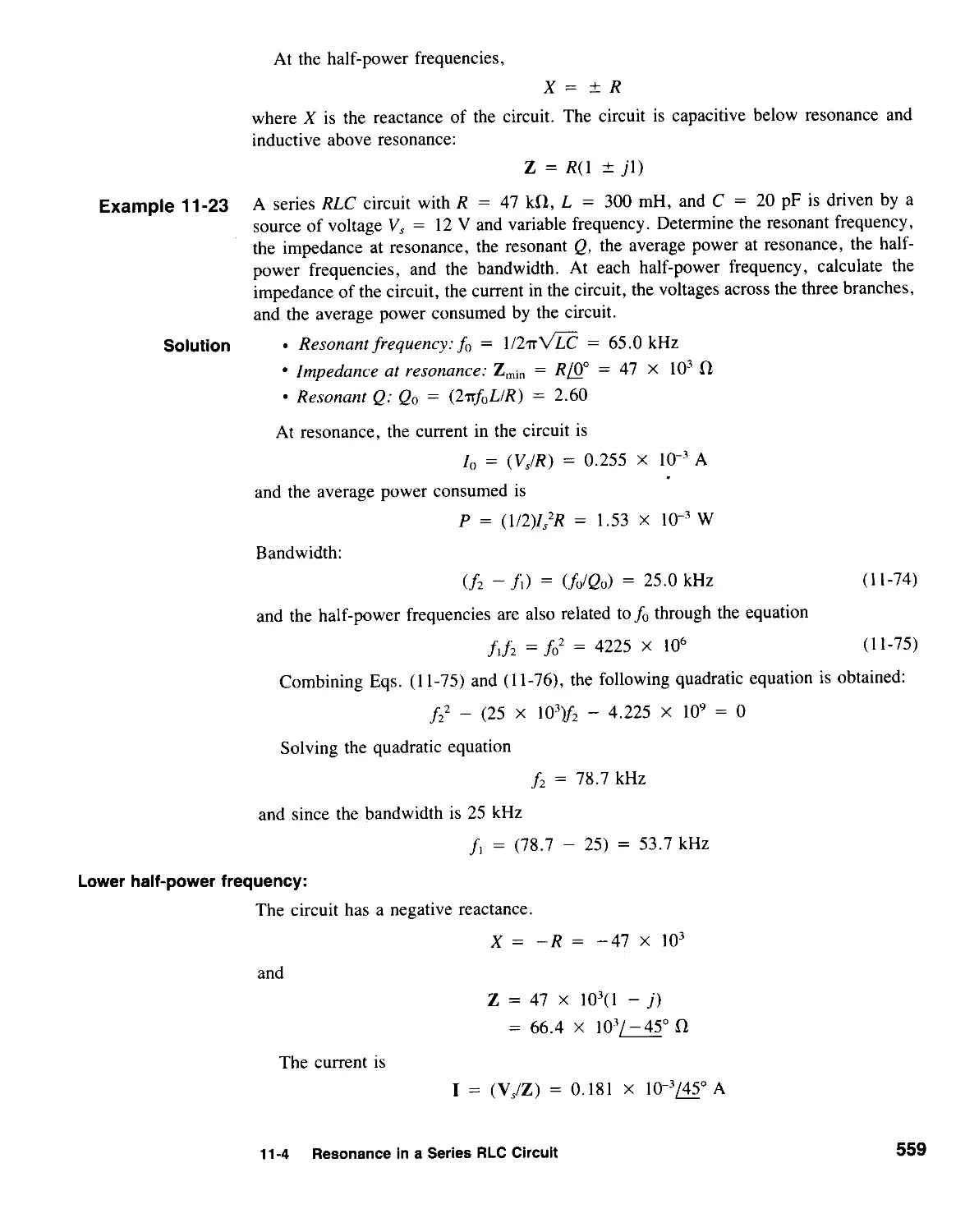
11-4 Resonance in a Series RLC Circuit 551
11-4-1 Energy Considerations in a Series RLC Circuit 554
11-4-2 Resonant Q of a Series RLC Circuit 555
11-4-3 Bandwidth of a Series Resonant Circuit 557
11-5 Reactance/Susceptance Curves of Lossless Networks 561
] 1-6 Summary of Chapter 566
Answers to Exercises 566
Problems 568
CHAPTER 12
COMPLEX FREQUENCY
AND NETWORK FUNCTIONS 573
12-1 The Concept of Complex Frequency 573
12-2 Impedance and Admittance in the Complex Frequency Domain 575
12-2-1 Analysis of Circuits in the Complex Frequency Domain 576
12-3 Critical Frequencies of a Network Function 578
12-3-1 Poles and Zeros of Network Functions 579
12-4 Frequency Response and Bode Diagrams 582
12-4-1 Amplitude Response Diagrams 583
12-4-2 Phase Response Diagrams 589
12-4-3 Bode Diagrams for H(s) with a Single Zero 590
12-4-4 Bode Diagrams of a Network 592
12-5 Complex Frequency Viewpoint of Resonance 598
12-5-1 Magnitude and Angle of a Driving Point Function 598
12-5-2 Response of a Tuned Circuit 600
12-5-3 Movement of Zeros of Y(s) as a Function of Qeo 601
12-5-4 Variation of Y(s) as a function of s 602
12-6 Summary of Chapter 606
Answers to Exercises 607
Problems 608
CHAPTER 13
TWO-PORTS 614
13-1 Basic Notation and Definitions 615
13-2 Open-Circuit Impedance Parameters (Formal Derivation) 6]6
13-3 Open-Circuit Impedance Parameters of a Two-Port 619
13-4 Use of the z Parameters in the Analysis of a Two-Port System 623
13-5 Models of a Two-Port Using z Parameters 624
13-5-1 Model of a Reciprocal Two-Port 624
13-5-2 Models of a Nonreciprocal Two-Port 626
13-6 Short-Circuit Admittance Parameters of a Two-Port 629
xiv
Contents
13-7 Models of a Two-Port Using y Parameters 632
13-8 Relationship between z and y Parameters 635
13-9 The Hybrid Parameters 636
13-9-1 Determination of the h Parameters of a Two-Port 637
13-10 Model of a Two-Port Using h Parameters 642
13-10-1 Analysis of a Two-Port System Using h Parameters 643
13-11 Relationship between hand z Parameters 644
13-12 Transmission or ABCD Parameters 646
13-13 Interconnection of Two-Port Networks 646
13-13-1 Parallel Connection of Two-Ports 646
13-13-2 Cascaded Connection of Two-Ports 649
13-14 Balanced and Unbalanced Two-Ports 653
13-15 Summary of Chapter 653
Answers to Exercises 654
Problems 656
CHAPTER 14
NONSINUSOIDAL SIGNALS-
FOURIER METHODS 661
14-1
14-2
14-3
Fourier Series Representation of a Periodic Signal 661
14-1-1 Determination of the Fourier Series Coefficients 663
14-1- 2 Effect of Waveform Symmetry on Fourier Series 668
Steady State Response of a Circuit with Periodic Input 673
14-2-1 Average Power in a Circuit with Periodic Input 675
14-2-2 RMS Value of a Periodic Signal 678
Exponential Fourier Series 679
14-3-1 Determination of the Coefficients ek 679
14-3-2 Relationships between Exponential and
Trigonometric Forms of Fourier Series 681
Steady State Response of a Circuit Using Exponential Fourier Series
Frequency Spectra of Periodic Signals 685
14-5-1 Amplitude and Phase Spectra 685
14-5-2 Power Spectrum 686
Minimum Mean Square Error Property of Fourier Series 689
Nonperiodic Signals: The Fourier Transform 690
14-7-1 Energy Density Spectrum of a Signal 693
14-7-2 Properties of the Fourier Transform 695
The Inverse Fourier Transform 699
Response of Linear Networks to Nonperiodic Signals 701
Response of a Linear Network to Arbitrary Signals 702
14-10-1 Representation of an Arbitrary Signal by Means
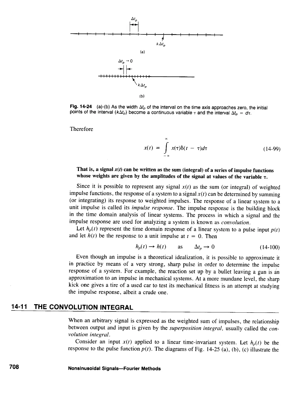
of Impulse Functions 703
14-10-2 The Impulse Function 705
683
14-4
14-5
14-6
14-7
14-8
14-9
14-10
Contents
xv
14-11 The Convolution Integral 708
14-11-1 Evaluation of the Convolution Integral 711
14-11-2 Fourier Transform of Convolution 717
14-12 Response of a Linear System 720
14-13 Limitations of the Fourier Transform 721
14-14 Summary of Chapter 721
Answers to Exercises 723
Problems 725
CHAPTER 15
LAPLACE TRANSFORMATION 734
15-1 The Laplace Transform 735
15-1-1 Region of Convergence for the Laplace Transform 735
15-1-2 Causal Signals and Systems 738
15-2 Use of Laplace Transforms in Analysis of Linear Networks 741
15- 2-1 Some Properties of the Laplace Transform 741
15-2-2 Current Voltage Relationships in Basic Circuit Components 743
15-2-3 Analysis of a Linear Network 745
]5-3 Determination of the Inverse Laplace Transform 748
15-3-1 Procedure for Finding the Partial Fraction Expansion of F(s) 750
15-4 Step-by-Step Procedure for Analysis of Networks
Using Laplace Transforms 759
15-5 Initial Value and Final Value Theorems 768
15-6 Convolution Theorem 769
15-7 Role of Critical Frequencies in the Response of Networks 769
15-8 An Overview of Network Analysis 770
15-9 Summary of Chapter 772
Answers to Exercises 772
Problems 774
APPENDIX A Computer-Based Problems 781
APPENDIX B Determinants and Matrices 785
B-1 Determinants 785
B-2 Minors and Cofactors of a Determinant 786
B-3 Laplace's Expansion of a Determinant 787
B-4 Cramer's Rule 787
B-5 Matrices 789
APPENDIX C Complex Numbers
and Complex Algebra 791
xvi
Contents
APPENDIX D SPICE Program for Circuit
Analysis 797
D-l Introduction 797
D-2 Types of Analysis 798
D-3 Input Format 798
D-4 Circuit Description 799
D-5 Title, Comment, and .END Statements 799
D-6 Element Statements 800
D- 7 Linear Dependent Sources 801
D-8 Independent Source Functions 802
D-9 Control Statements 804
D-IO Examples of SPICE applications 808
APPENDIX D SPICE Program for Circuit
Analysis 797
D-l Introduction 797
D-2 Types of Analysis 798
D-3 Input Format 798
D-4 Circuit Description 799
D-5 Title, Comment, and .END Statements 799
D-6 Element Statements 800
D-7 Linear Dependent Sources 801
D-8 Independent Source Functions 802
D-9 Control Statements 804
D-I0 Examples of SPICE applications 808
BIBLIOGRAPHY 811
ANSWERS TO EVEN-NUMBERED PROBLEMS 813
INDEX 827
Contents
xvii
PREFACE
l:e analysis of electric circuits and networks is a fundamental tool of the electrical
engineering student, since it provides the foundation for the study of linear systems,
electronic circuits, power systems, control systems, and communication systems. A strong
background in methodical circuit analysis is essential for intelligent and successful design,
as well as for using the computer for the analysis of complex networks. The aim of this
text is to present a reasonably rigorous treatment of the methods of circuit analysis and
their applications, it is intended for use by sophomores and juniors in electrical engi-
neenng.
With the growing need for accommodating a wide variety of important technical areas
in an electrical engineering program, there has been an unavoidable trend toward curtailing
the time allotted to teaching circuit analysis. As a result, faculty usually find it difficult
to devote enough time in the classroom to working a sufficient number of examples and
drilling the student in the various topics in circuit analysis. The difficulty has been
exacerbated in many colleges and universities by large class sizes. I have tried to alleviate
the problem by including numerous worked examples, as well as a large number of
exercise problems in each chapter. A seetian at the end of eaeh ehapter provides nat anly
the final answers ta the exercise prablems, but alsa apprapriate intermediate steps ta
help students eheek their wark. The intermediate steps should help reassure students
whose final answers are incorrect even though they have applied the principles correctly.
Each chapter also includes 30 to 50 homework problems organized by sections within
the chapter; the final answers to roughly 50 percent of these problems are provided at
the end of the book. A combination of the worked examples, exercise problems with
xix
intermediate steps and answers, and the large number of chapter-end problems should
help students develop a strong working background in the principles and procedures of
circuit analysis.
The general mathematical background expected of the student is a year of differential
and integral calculus. There are some optional sections in Chapters 3 and 4 and some
later chapters requiring a knowledge of the theory of determinants (especially Cramer's
rule) and basic matrix notation. Students lacking a background in the use of determinants
and basic principles of matrix notation will find it helpful to study the summary of the
relevant information provided in Appendix B. First- and second-order linear differential
equations are encountered in Chapter 6, and the necessary steps for solving them (by
using an assumed solution) are presented in that chapter. A knowledge of complex numbers
and complex algebra is essential for Chapter 8 and the chapters that follow. A summary
of the basic concepts and rules of complex numbers and complex algebra is presented in
Appendix C.
Motivation is an important problem in teaching circuit analysis. Since circuit analysis
is usually taught when the students have not been exposed to other electrical engineering
subjects (except probably digital systems and microprocessors), they are overwhelmed
by the steady flow of information with very little clue about what to do with it. I have
tried to address this problem by providing examples of circuits from electronics (biasing
calculations, small signal analysis, and pulse response, as well as operational amplifiers)
and communications (filters and bandwidth considerations of communication systems).
The op amp, with its simple approximate model, provides an attractive and convenient
tool for illustrating the use of circuit analysis in practical electronic circuits. It is first
introduced in Chapter 3 (on nodal analysis) and revisited periodically in later chapters,
where its linear applications are discussed.
The degree and manner in which students use the computer at this point in their
program vary widely. At this early level, it is more important for the student to grasp
the principles and methods of circuit analysis by focusing on circuits of moderate com-
plexity rather than simply obtaining the final answers by means of a computer. Never-
theless, it is desirable to give the student the opportunity to write programs in FORTRAN
or BASIC as an adjunct of a course (or courses) in circuit analysis. With this end in
view, a set of computer-based problems is provided in Appendix A.
When the student has progressed sufficiently in circuit analysis, it becomes appropriate
to use commercially available software packages to study complex circuits of practical
importance. A summary of SPICE is provided in Appendix D for this purpose. Since
there is a proliferation of personal computers on campuses, an adaptation of SPICE,
called PSpiee/ f '1; created by MicroSim Corporation for use with the personal computer,
should prove attractive to many students and professors. Prentice Hall also publishes A
Guide to Cireuit Simulation and Analysis Using PSpiee@by Paul Tuinenga. The hardcover
edition includes a student version of the PSpice program. A paperback edition of the text
only is also available.
The order of treatment of the topics of circuit analysis follows classical lines. The
treatment of circuits containing only resistors and sources is presented first, since such
circuits need only the algebra of real numbers and variables and permit the student to
concentrate on the principles and methods of circuit analysis without worrying about
more involved mathematical manipulations. Chapter 1 deals with basic definitions im-
portant in the study of lumped, linear, and time-invariant circuits, Ohm's law, and
Kirchhoff's laws. Simple circuit configurations are discussed in that chapter. Chapters
xx
Preface
2, 3, 4, and 5 develop the methods of circuit analysis for networks containing resistors
and dependent and independent sources. Chapter 6 discusses the properties and relation-
ships of capacitors and inductors and the time-domain determination of the step response
of first- and second-order circuits. The classical (time domain) approach to the sinusoidal
steady state response of circuits is covered in Chapter 7. Chapter 8 introduces the concepts
of phasors, impedance, and admittance, and deals with series and parallel configurations.
The analysis of more general circuits in the sinusoidal steady state is discussed in
Chapter 9 by modifying the information already presented in Chapters 3, 4, and 5. Chapter
10 discusses the principles of magnetic circuits, magnetically coupled coils, and balanced
three-phase circuits. Parallel and series resonance is studied in Chapter 11 by using
impedance and admittance concepts. A discussion of reactance/susceptance curves of
loss less networks is also included in that chapter. Complex frequency is introduced on
an ad hoc basis in Chapter 12 as an important tool in the study of the frequency response
characteristics of driving point and transfer functions of networks. Bode diagrams of
circuits with simple poles and zeros are dealt with in detail in that chapter. Resonance
is revisited by using vectors in the complex frequency plane to illustrate the link between
sinusoidal steady state response, natural response, and the use of complex frequency.
Chapter 13 discusses two-port networks and their analysis by using z, y, and h pa-
rameters. The ABeD parameters are introduced by means of exercise problems in that
chapter. The appropriate characterization pf some of the interconnections of two-ports
are also presented in Chapter 13. Chapters 14 and 15 extend the analysis of networks to
other than sinusoidal signals. The discussion in Chapter 14 starts with the use of Fourier
series for periodic signals and is then extended to the use of Fourier transforms in the
case of nonperiodic signals of finite duration. The use of convolution for finding the time
domain response of a network to an arbitrary signal is also presented in that chapter.
Laplace transform is presented in Chapter 15 as an extension of the Fourier transform
by using complex frequency to provide convergence of the transform. The use of Laplace
transform in the analysis of circuits is also studied in that chapter. It concludes with an
overview of circuit analysis as presented in this text.
The material in this book could be covered comfortably in a one-year sequence in
circuit analysis without any omissions. In my school, we find it possible to cover Chapters
1 through 13 in two academic quarters by skipping a small portion of the material in
those chapters. The material in Chapters 1 through 9 would fit the one-semester course
in circuit analysis taught in a number of colleges and universities. Such coverage will
provide the student with the essential background in circuit analysis needed for courses
in electronics and linear systems that normally follow the course in circuit analysis.
A solution manual for use by faculty is available from the publisher. The solution
manual provides complete solutions to the problems in the 15 chapters, the computer-
based problems in Appendix A, and also several sample problems solved by using SPICE
(or PSpice).
The writing of this book has been a long project, and I have been helped along the
way by a substantial number of people. Even though I cannot thank everyone of them
individually, I do wish to express my sincere appreciation to the following reviewers,
whose constructive and careful criticisms have contributed significantly to the final man-
uscript: Professors Elizabeth Koster, Arthur Dickerson, Charles Nelson, Peter Scott, and
Sidney Shapiro. My colleague, Unnikrishnan, was instrumental in the starting of this
project, and the material in Chapter 10 is based on his contributions. I also wish to thank
Preface
xxi
another colleague, David Perlman, whose notes on SPICE have been useful in writing
Appendix D. I have had the good fortune of working with two of the most patient and
understanding editors: Tim Bozik and Bernard Goodwin. Their continued faith in this
book has been a strong driving force. Finally, I cannot fully express how grateful I am
to my wife lanice, who had serious doubts that this book would ever be finished, patiently
put up with portions of the manuscript strewn over various parts of the house for months,
and accepted my excuses for not doing a number of things.
S. Madhu
Rochester, New York
xxii
Preface
A NOTE
ON NOTATION
FOR VOLTAGES
AND CURRENTS
e following notation is used to represent voltages and currents:
Lawerease letters explicitly written as funetians of time, vet) and i(t), denote time-
varying voltages and currents, respectively. Often the explicit dependence is not shown,
and the functions are written simply as v or i.
Upperease letters V and I denote parameters that are constant in time-varying voltages
and currents. Examples are the constant value of a voltage or current in the case of dc
(Chapters 1 through 6), and the amplitude of a sinusoidal voltage or current in the case
of ac (Chapter 7 and those that follow).
In Chapters 1 through 5, the networks are purely resistive, and their analysis is not
affected by whether the voltages and currents are constants or time-varying. In these
chapters, lower- and uppercase letters are used interchangeably.
Lawerease letters in boldfaee, vet) and i(t), denote eomplex time-varying funetions,
usually complex exponential functions (Chapter 8 and those that follow).
Upperease letters in baldfaee, V and I, are used for phasors representing sinusoidal
voltages and currents (Chapter 8 and those that follow). The boldface is sometimes omitted
(e pecially in the later chapters), however, when the context is sufficient to indicate that
the voltages and currents are phasors (with magnitude and angle). The same comment
applies to letters used to represent impedances and admittances: boldface is not always
used when the context indicates that the quantity has both magnitude and angle.
xxiii
LINEAR
CIRCUIT
ANALYSIS
CHAPTER 1
BASIC CONCEPTS,
COMPONENTS, AND LAWS
OF ELECTRIC CIRCUITS
Electrical components (e.g., resistors, coils, capacitors, and batteries) are familiar to
us from a study of electricity and magnetism in physics. An electric cireuit is an inter-
connection of electrical components for performing some function. The term eleetrie
network usually refers to a rather complex electric circuit, but the terms cireuit and
network are used interchangeably. As one progresses through the study of electric circuits
and networks, a point is reached where the interest is no longer on the structural details
of the network but on how it behaves when excited by a particular source of electrical
energy. In such cases, the term eleetrieal system is used.
The aim of cireuit analysis is the evaluation of quantities, such as voltages, currents,
and power, or ratios of such quantities in a given circuit. Synthesis of networks, on the
other hand, deals with the methodical design of networks to satisfy specified input-output
characteristics. A strong understanding of analysis forms the foundation for intelligent
and efficient synthesis.
Procedures used in circuit analysis are built on basic laws rooted in certain physical
principles. These principles govern the behavior of the components and the constraints
imposed by their interconnections. The underlying laws of circuit analysis are only a few
in number; they are fairly simple to state and understand. The actual application of the
laws to the methodical analysis of circuits, however, leads to a variety of systematic
techniques to be presented in this text.
The purpose of this chapter is to introduce the basic concepts of electric circuits, some
of the electrical components, and some of the basic laws of circuit analysis.
1
1-1 BASIC UNITS AND DEFINITIONS
The three basic physical quantities of a physical system are mass (measured in kilograms,
abbreviated kg), length (measured in meters, abbreviated m) and time (measured in
seconds, abbreviated s). A fourth basic quantity, the eleetrie eharge, is needed when the
physical system also contains electrical components. The symbol for electric charge is
q. and it is measured in eoulambs (abbreviated C). Special names are given to the units
of various quantities in electrical systems (usually in honor of pioneering scientists); but
all these units can be expressed in terms of the four basic units: kilograms, meters,
seconds, and coulombs.
1-1-1 Potential Difference (Voltage)
An electric field exists in the neighborhood of an electric charge or a collection of electric
charges. Since the electric field exerts a force on any electric charge placed in it, work
has to be performed (that is, energy has to be expended) to move the electric charge from
one point to another in the electric field. The work needed to move a pasitive electric
charge of I coulamb ( + 1 C) from a point A to a point B in an electric field is defined
as the potential differenee between those two points.
The potential difference represents the change in potential energy of a unit positive
charge between two points.
The unit of potential difference is the valt (abbreviated V). It follows from the above
definition that I volt equals I jaule/eoulamb, where energy is measured in joules. Since
the unit for potential difference is volts, the phrase valtage between twa points is commonly
used to denote the potential difference between two points.
Example 1-1 The potential energy of an electron is found to change by 1.2 x 10-- 16 1 when it moves
between two points. Calculate the voltage between the two points.
Solution Magnitude of electronic charge = 1.6 x 10- 19 C
Work done in moving the electron = 1.2 x 10- 16 1
Therefore, the voltage between the two points is 1.2 x 10- 16 /1.6 x 10- 19 = 750 V
.
The term electromotive farce (abbreviated emf) is often used when the voltage is due
to a source of energy such as a battery or a generator.
In referring to the voltage between two points A and B, it is often convenient to use
one of the points, say A, as a referenee. This permits the comparison of potentials at
different points in a circuit using the potential at point A as a common basis. In such
cases, the term voltaRe at paint B is used to represent the potential differenee between
the point B and the referenee paint A.
It is important to note that a voltage is always measured between two paints. Even
when the phrase "voltage at a point" is used, it actually means the voltage between that
point and some reference point.
1-1-2 Electric Current
Current flow in a material is due to the motion of free electric charges under the influence
of an external force acting on the material. Current carriers can be negatively charged
(e.g.. free eleetrons in metals and semiconductors) or positively charged (e.g., holes in
semiconductors). When the flow of free charges is due to an external electric field, an
2
Basic Concepts, Components, and Laws of Electric Circuits
electron moves in a direction opposite to the vector representing the electric field, whereas
a hole moves in the same direction as that vector.
The conventional direction of positive current is always taken as that in which a free
positive charge would flow under the influence of an external force. Therefore, when
there is a motion of electrons, the direction of positive current is opposite to the direction
of motion of the electrons.
The current through a cross section of a material is defined by the time-rate of ehange
af eleetrie eharge through that section. That is, if q is the electric charge, which varies
with time t, then the resulting current i is given by
. dq
1=-
dt
The unit of current is the ampere (abbreviated A). One ampere represents a rate of
flow of 1 eaulomblseeond.
(1-1)
Example 1-2 The electric charge in a cross section of a material is found to vary with time as shown
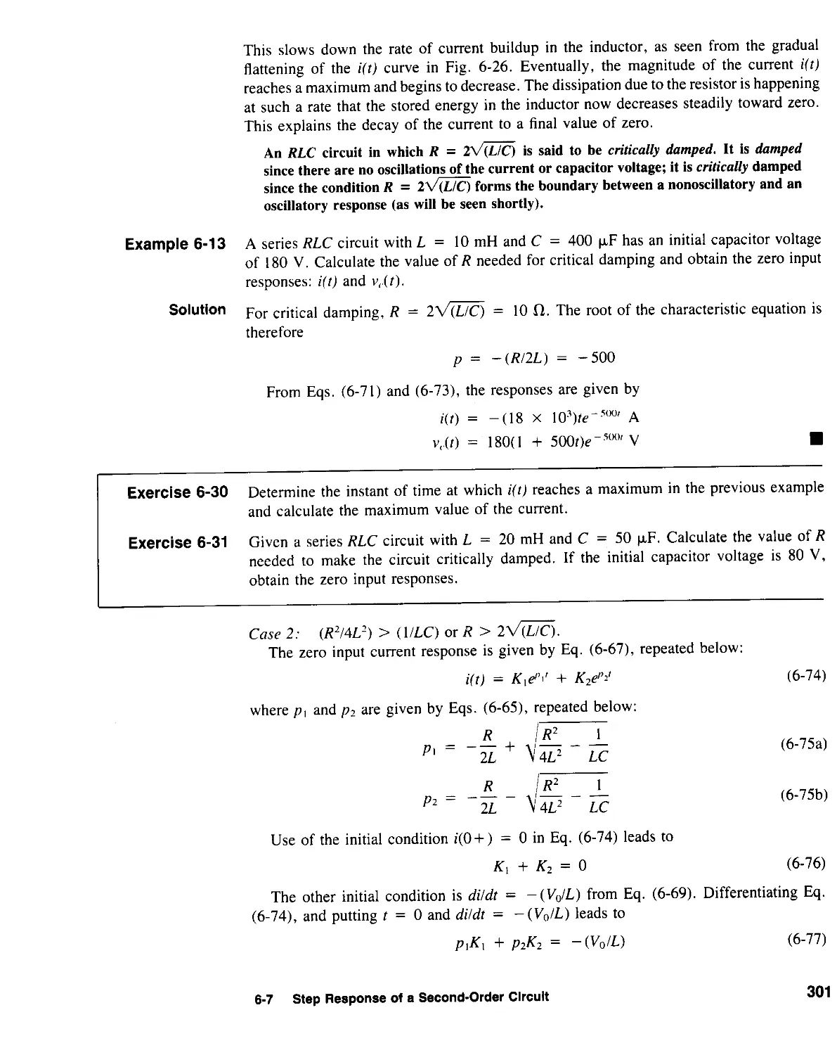
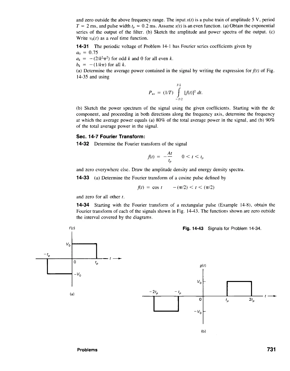
in Fig. 1-I(a). Determine and sketch the current i(t).
t 10
q (e)
16
(a)
2.5
-
0 4 8 12 16
-
t
i(A)
Fig. 1.1 Charge and
current waveforms for
Example 1-2.
-2.5
t(s)-
(b)
Solution Since the graph of q(t) is in the form of straight-line segments in this example, dqldt is
evaluated from the slopes of the different segments. The segments in Fig. 1-I(a) have
slopes of +2.5 and -2.5 alternately. Therefore,
i(t) = { 2.5 A when q(t) has a positive slope
- 2.5 A when q(t) has a negative slope
The waveform of the current i(t) is shown in Fig. 1-I(b).
.
Example 1-3 The electric charge in a cross section of a material varies according to the equation
q(t) = Q(} cos Bt C
where Qo and B are constants. Determine the current i(t) through that section.
1.1 Basic Units and Definitions
3
Solution
dq
dt
-QoB sin Bt A
.
Exercise 1-1 * The variation of electric charge in a cross section of a material is of the form shown in
Fig. 1-2. Determine and sketch i(t).
'1C)5
o 2
4 6
t (s)
Fig. 1-2 Charge waveform for Exercise 1-1.
Exercise 1-2 The electric charge in a cross section of a material is found to vary according to the
equation
q(t) = Qoe- pt C
where Qo and p are positive constants. Determine and sketch i(t).
L
1-1-3 Electrical Power and Energy
Power is the rate at which work is done. Consider an elementary charge dq moving from
point A to point B in a time interval dt, and let the potential difference between A and
B be v. Then the work done on the charge dq is
since i
dw = v dq = v(i dt)
dqldt. Then the power is given by
dw
p = dt
(1-2)
vi
(1-3)
The unit of power is the watt (abbreviated W). One watt equals 1 jaulelseeand. It can
be verified that the product (volts X amperes) has the dimensions of joules/second.
In general, the voltage v and the current i vary with time. The quantity p given by
Eq. (1-3) represents the instantaneous power in the circuit and varies as a function of
time. It is, therefore, preferable to write Eq. (1-3) in the form
pet) = v(t)i(t)
(1-4)
explicitly showing the dependence on time.
Example 1-4 The voltage across an electrical component is a constant at 15 V, and the current through
it is a constant at 6 A. Calculate the power in the component.
*Answers to the exercises, along with some intermediate steps where appropriate, will be found at the end of
the chapter.
4
Basic Concepts, Components, and Laws of Electric Circuits
Solution Since the voltage and current are constant, the power is also a constant and equals
(15x6)=90W. .
Example 1-5 The voltage across a circuit is given by
v(t) = 12 cos lOOt V
and the current through it is
i(t) = 5 cos lOOt A
Determine pet). Sketch vet), and p(t).
Solution p(t) = v(t)i(t) = 60 cos 2 lOOt
= 30 + 30 cos 200t
where the formula cos 2 X = (l + cos 2X)/2 has been used.
The sketches of v(t), i(t), and p(t) are shown in Fig. 1-3. It is seen that pet) varies
continuously between a minimum of zero and a maximum of 60 W. The average value
of pet) is 30 W. .
o
t (5)____
-5 A
-12 V
p(t) (W)
60
30
t (5)_
Fig. 1-3 Sinusoidal
current, voltage, and
power waveforms.
o
Exercise 1-3 The voltage across an electric circuit is a constant at 12 V, and the current through it is
given by
i(t) = (10 + 5 cos 20t) A
Determine and sketch pet).
1-1 Basic Units and Definitions
5
Exercise 1-4 The voltage across a component is
v(t) = 10 cos 50t V
The current through the component is equal to dvldt. Obtain the expression for p(t).
Energy in electric circuits is the work done in moving a charge between two points
with a potential difference between them. Energy is either delivered to or received by a
component. Since power equals the derivative of energy, energy equals the integral af
pawer. The energy delivered or received by a component at time t is therefore given by
w(t) = Ip(t)dt
(1-5)
The unit of energy is jaules (abbreviated J).
The energy delivered to or received by a component in the time interval (0, t) is given
by
w(O,t) = !:p(u)du
(1-6)
where u is a dummy variable of integration. The energy in a component at any time t
can then be considered as the sum of two parts:
Energy at time t = (Initial energy in the component at t = 0)
+ [Energy delivered or received in the time interval (O,t)]
The integral in Eq. (1-5) can then be written as
wet) = w(O) + L'P(U)dU
(1-7)
where w(O) is the initial energy in the component.
Example 1-6 Determine the energy delivered at time t to the component of Example 1-4. Assume that
w(O) = O.
Solution Since power p is a constant at 90 W,
w(t) = w(O) + L' 90du
90t J
The energy delivered increases linearly with time.
.
Example 1-7 The voltage across and the current through a component are given by
v(t) = Vue-PI V
and
i(t) = loe- PI A
where V"' I,,, and p are constants. Obtain an expression for the energy delivered to the
component in the interval (O,t).
Solution First obtain the expression for the power p(t).
pet) = v(t)i(t) = V u l o e- 2P [ W
The energy delivered in the interval (O,t):
6
Basic Concepts, Components, and Laws of Electric Circulta
w(O,t)
L (U)dU = LVJoe-2Pudu
-(l/2p)Vol o (e- 2pt - 1)
.
Exercise 1-5 The voltage across a component is a constant at 12 V, and the current through it is a
constant at 7.5 A. Calculate the energy delivered to the component at t = 3 s, assuming
the energy is zero at t = O.
Exercise 1-6 Power companies measure energy in kilowatt-hours (kWh), which is the product of power
in kilowatts and the number of hours over which the power is used. Calculate the equivalent
of 1 kWh in joules.
Exercise 1-7 The voltage across and the current in a component are given by vet) = (lOt - 8) V and
i(t) = 15 A (constant), respectively. Determine and sketch the instantaneous power pet).
Calculate the energy consumed in the intervals (a) (0,8 s) and (b) (8 s,12 s).
1-2 VOLTAGE
Voltages in an electric circuit can be constant at all times (or at least during the interval
of observation), or vary as a function of time, as shown in Fig. 1-4.
Voltages that are constant at all times are referred to as direet-eurrent or de voltages.
Time-varying voltages are classified according to whether they have repetitive or non-
repetitive waveforms, or whether their waveforms are deterministic or nondeterministic.
Such classifications of time-varying voltages will be discussed in Chapters 7 and 14.
Voltages in an electric circuit can be observed on an oscilloscope or measured by a
voltmeter. The so-called de voltmeter measures the average value of the voltage taken
over a certain time interval. When the voltage remains constant, its average value equals
the constant value. In the case of time-varying voltages, the average value gives only
one important parameter of the voltage. Another important parameter is its roat-mean-
square, or rms, value. The rms value of a time-varying voltage is the square roat of the
Fig. 1-4 (a) Constant
and (b, 0) time-varying
VOltages.
vItI
1, =1
t
vItI
Va
o
t_
t-
(a)
(b)
t
vItI
t-
(e)
1.2 Voltage
7
average (or mean) value of the square of the voltage. This may appear at first to be a
complicated way of measuring voltage, but it actually is the natural form of response of
certain voltmeter mechanisms. The 110 V specification of the household and laboratory
power supply in the United States is the rms value of the available voltage.
1-2-1 Voltage Polarity Notation
The potential energy of a unit positive charge situated in an electric field varies, in general,
from one point to another. Given two points in an electric field, therefore, the potential
at one of those points is, in general, higher than the other. (Whenever potentials at
different points are compared with one another, all patentials are measured with respect
to the same referenee paint.) In circuit diagrams, the fact that one terminal of a component
is at a higher potential than the other is indicated by placing plus and minus polarity
marks at the component's terminals, as illustrated in Fig. 1-5(a).
Fig. 1-5 Reference
polarity marks for a volt-
age. (a) v, = VA - VB.
(b) Circuit for Example
1.8.
A o----e=J----o B
+ v,
P Q
--- ---
+ V x -
(al
(b)
The polarity marks in Fig. 1-5(a) mean that the voltage VI across the component is
given by
VI = VA - VB
(1-8)
where VA and VB are the potentials at points A and B, respectively. Voltage VI can be
positive, zero, or negative, depending on whether the potential at terminal A, respectively,
is greater than, equal to, or less than the potential at terminal B.
In circuit problems, it is usually not known beforehand which terminal of a component
is actually at a higher potential than the other. It is customary to arbitrarily choose one
terminal of the component as the positive reference and the other becomes the negative
reference.
Then the voltage across the component is equal to potential at the terminal chosen as
the positive reference minus the potential at the terminal chosen as the negative ref-
erence.
The value obtained from the above relationship can be positive, zero, or negative.
Example 1-8 The component shown in Fig. 1-5(b) is part of a circuit. For each of the following pairs
of values of potential at P and Q, calculate the voltage V X '
(a) Vp = 8 V; VQ = 5 V. (b) Vp = -5 V; vQ 1 V.
(c) Vp = 2 V; vQ = 2 V. (d) Vp = -7 V; vQ = 5 V.
Solution In all cases, v, is calculated from the equation:
V x = Vp - vQ
(a) V x = 3 V (point P is 3 V higher than point Q)
(b) V x = -6 V (P is 6 V lower than Q)
(c) v, = 0 V (P and Q are at the same potential)
(d) v, = - 12 V (P is 12 V lower than Q)
.
8
Basic Concepts, Components, and Laws of Electric Circuits
Flg.1-6 Components
for Example 1-9.
a o----[:=J----o b
+ v,
e o----[:=J----o d
+ V 2 -
e f
- V 3 +
Va = -10V; v,=8V
v2= 5V; vd -12V
V e = 10 V; V 3 = -7 V
(al
(bl
(el
Example 1-9 Circuit components are shown in Fig. 1-6. The reference polarity marks, the voltage
across the component, and the potential at one terminal are given in each case. Calculate
the potential at the other terminal.
Solution Resist all temptation to guess. Write an equation for each case and solve it.
(a) VI = Va - Vb. VI = 8 V; Va = -10 V. Therefore, Vb = - 18 V.
(b) Vz = V c - Vct. Vz = -5 V; Vct = -12 V. Therefore, V c = -17 V.
(c) V3 = Vf - V e . V3 = -7 V; V e = 10 V. Therefore, Vf = 3 V. .
Exercise 1-8 Calculate the voltage V t in each of the components shown in Fig. 1-7. Values of potential
at the terminals are shown.
P Q
12V . -12V
- V x +
(a)
V s
x . -5.4V
+
V2 = -9 V
(bl
M V
-4.3V x
+
v3=-1.4V
A v
-8V X
+
v, = -20 V
(e)
(d)
V .....r----l D
x 22V
+
V 2 = 16 V
(e)
Fig. 1-7 Components for Exercise 1-8.
1-2-2 Ideal Voltage Sources
A source of electrical energy (for example, a battery) is used to supply power to a
component or an arbitrary circuit connected to it, that is, to a laad.
When the energy source has the property that the voltage across its terminals is in-
dependent of the current supplied by it to the load, it is called an ideal voltage source.
The symbol for an ideal voltage source is shown in Fig. 1-8(a), where v, denotes the
voltage available across the terminals of the source. An ideal voltage source is shown
connected to a load in Fig. 1-8(b). The voltage VL across the load is not affected by how
large or small the load current i L is.
If the voltage V s has a constant value at all times, then a plot of v., as a function of
the current i L is a horizontal straight line, as shown in Fig. 1-8(c).
1-2 Voltage
9
Fig. 1-8 Ideal voltage
source. (a) Symbol for
the ideal voltage source.
(b) Voltage V s is not af-
fected by the load cur-
rent h. (c) Case of a
constant (or de) voltage
source.
1-3 CURRENT
v,
i L
---
V L
1=
o 'L
v,
(a)
(b)
(e)
As a practical matter, however, the voltage across the terminals of an energy source
does not remain independent of the current supplied by it. In circuit analysis, nonideal
voltage sources are represented by models, which will be considered later in this chapter.
The current through a component in an electric circuit is indicated by an arrow, repre-
senting the assumed direetian of current flow, as shown in Fig. 1-9. There also exists a
voltage with reference voltage polarities (plus and minus), leading to the two situations
shown in the figure:
I. Current flows through the component in the plus-to-minus direction
2. Current flows through the component in the minus-to-plus direction
The term associated referenee polarities is useu when the current direction is chosen
to be in the plus-ta-minus direction of reference voltage polarities.
tit i
+
+
v
v
Fig. 1-9 Current direction in a component. Associated reference polarities
are shown in part (a).
1-3-1 Ideal Current Sources
(al
(b)
10
An energy source with the property that the current supplied by it is independent of
the voltage across its terminals is called an ideal current source.
The symbol for an ideal current source is shown in Fig. 1-10(a), where i, represents the
current supplied by the source. An ideal current source is shown connected to a load in
Fig. 1-IO(b). The current i L in the load is not affected by how large or small the voltage
VL across the load is.
If the current i, supplied by the source has a constant value at all times, then a plot
of i L as a function of the load voltage VL is a horizontal straight line, as shown in Fig.
1-IO(c).
As a practical matter, however, the current supplied by an energy source is not
independent of the voltage across the load connected to it. In circuit analysis, non ideal
current sources are represented by models, which will be considered later in this chapter.
Basic Concepts, Components, and Laws of Electric Circuits
Flg.1-10 Ideal current
source. (a) Symbol for
the ideal current source.
(b) Current is is not af-
fected by the load volt-
age VL. (c) Case of a
constant (or dc) current
source.
V L
i L
C
o
(a)
(b)
(e)
1-4 POWER DELIVERED AND POWER RECEIVED
The instantaneous power associated with a component is given by Eq. (1-9):
p(t) = v(t)i(t)
(1-9)
Since there is an assignment of valtage referenee palarities and direetion for the current
through a component, two distinct cases are possible as shown in Fig. 1-9:
1. Current direction is from the plus to the minus terminal of voltage polarities (as-
sociated reference polarities)
2. Current direction is from the minus to the plus terminal of voltage polarities
Consider first the situation in Fig. 1-9(a), where the current is chosen flowing from
the positive reference terminal to the negative reference terminal (associated reference
polarities). Let both the voltage and current be positive. Then, positive current carriers
are flowing from a higher to a lower potential while negative current carriers are flowing
from a lower to higher potential. That is, carriers are moving in the direetian af the foree
due to an electric field set up in the component by an external agent (such as an electric
generator). Therefore, work is being done by the external agent, and the component is
reeeiving electrical energy from the external agent.
If, in a component, the eurrent direetian isfram the plus terminal ta the minus terminal
(that is, associated reference polarities are used), then the product vi at any instant of
time t represents the pawer reeeived by the component at that instant of time.
Consider now the situation in Fig. 1-9(b), where the current is flowing from the negative
reference terminal to the positive reference terminal. This is exactly the opposite of the
previous case. That is, current carriers are moved through the component in appositian
to the faree due to an electric field. Therefore, work must be done by the component
itself, and it is delivering energy to some other component or circuit.
If, in a component, the current direction isfrom the minus terminal to the plus terminal,
then the product vi at any instant of time t represents the pawer delivered by the component
at that instant of time.
The two cases can be summarized:
· vi = power reeeived by a component if the direction of current is from the plus
ta the minus terminal of voltage polarities (associated reference polarities).
. vi = power delivered by a component if the direction of current is from the minus
ta the plus terminal of voltage polarities.
Example 1-10 In each of the cases shown in Fig. 1-11, calculate the power delivered or received by
the component.
1.4 Power Delivered and Power Received
11
Fig. 1-11 Circuits for
the power calculations
of Example 1-10.
v = 10 V
+ - i=3A
v = 15 V
+ i = -3 A
v=-15V
+ i = -3 A
v=8V
+ - i=4A
(a)
(b)
Ie)
Id)
Solution In Fig. I-II (a) and (b), the current direction is from plus to minus voltage polarities.
Therefore, the product vi represents the power received in these two cases.
(a) vi = 30 W. The component is reeeiving 30 W.
(b) vi = (15)(-3) = -45 W. The component is reeeiving -45 W.
In Fig. I-ll(c) and (d), the current direction is from minus to plus voltage polarities.
Therefore, the product vi represents the power delivered in these two cases.
(c) vi (- 15)( - 3) = 45 W. The component is delivering 45 W.
(d) vi = 32 W. The component is delivering 32 W. .
The last example shows that the product vi is negative in some instances. Negative
values of vi should be interpreted as follows: reeeiving - X watts is equivalent to delivering
+ X watts; and delivering - X watts is equivalent to reeeiving + X watts.
Example 1-11 The voltage across a component is v = 12V (constant at all times), and the current
(whose direction is from the plus to the minus terminal of voltage polarities) is given by
i(t) = (8 + 10 sin 4'iTt) A
(a) Determine the instantaneous power pet) received by the component. (b) Sketch p(t)
as a function of time for 0 < t < 0.75 s. (c) Calculate the maximum and minimum values
of power received by the component. (d) Make use of the symmetry of the plot of pet)
to estimate the average value of the power received by the component.
Solution (a) Instantaneous power:
p(t) = v(t )i(t) = (96 + 120 sin 4'iTt) W
Since the given current direction is from plus to minus voltage polarities, p(t) represents
the power reeeived by the component at time t.
(b) The plot of p(t) for the interval 0 to 0.75 s is shown in Fig. 1-12. Note that the
power received by the component is positive for part of the interval and negative for part
of the interval.
Fig. 1-12 Waveform for the power received in Example 1-11.
216
p(t) (W)
96
o
t (0)
12
Basic Concepts, Components, and Laws of Electric Circuits
(c) The power received has a maximum value of 96 + 120 = 216 Wand a minimum
value of 96 - 120 = -24 W.
(d) From the symmetry of the waveform, the average value of power received (the dashed
line) is 96 W. .
Exercise 1-9 Determine for each case of Fig. 1-13 whether the component is receiving or delivering
power, and calculate the value of the power.
v, = 110 V
',= 6.2 A
(a)
Vb = 25 V
+
o------CJ----o
----
ib = 25 mA
v, = 7.5 V + i, = 10 A
+
V d = 15 V
+
o------CJ----o
-
id =9 A
(b)
(d)
Fig. 1-13 Circuits for Exercise 1-9.
lei
Exercise 1-10 It is given that each of the components of Fig. 1-14 is delivering +20 W of power.
Calculate the value of the missing quantity (voltage or current) for each case, including
the proper sign for each answer.
+
ia
+
ib
+' =7A
+ id = 3 A
Fig. 1-14 Circuits for
Exercise 1-10.
Va = 8 V
Vb = -6 V
V c
V d
(a)
(b)
lei
(d)
1-5 CLASSIFICATION OF CIRCUITS
Circuits are classified into different categories: lumped or distributed, linear or nonlinear,
and time-variant or time-invariant. The analysis techniques to be presented in this text
will be confined to lumped, linear, time-invariant cireuits. Such a group covers a large
number of networks of practical importance and interest. Even though the methods
developed in this and the following chapters do not directly apply to other classes of
networks, they nevertheless serve as an essential foundation for developing analysis
methods for other types of networks.
1-5-1 Lumped and Distributed Circuits
Consider a taut string with one end fastened to a fixed point and the other end excited
by some force. The resulting disturbance travels along the string in the form of a wave
with an associated wavelength. The displacement and velocity at any point at a given
instant of time depends on the position of the point on the line. In an analogous manner,
electrical energy propagates in the form of electromagnetic waves (with the velocity of
light). For example, the current and voltage on a power transmission line at any point at
a given instant of time depends on the position of the point on the line. The current
entering one end of the line is not necessarily equal to the current leaving at the other
1.5 Classification of Circuits
13
end, and the voltage can be measured at an infinite number of points along the line. Such
components are called distributed eampanents. Networks partly or wholly made up of
distributed components are called distributed networks. The analysis of distributed net-
works requires the use of the theory of electromagnetic waves and is outside the scope
of this book.
In principle, all circuit components are distributed components, since electrical energy
takes a finite nonzero time to propagate through any component. From a practical view-
point, however, when the physical dimensions of a component are much smaller than a
quarter-wavelength of the waves propagating through it, the following approximating
assumptions are made. The dependence of current and voltage on distance are neglected.
A single value of current in the component and a single value of voltage across the
component are defined for the entire component at a gi ven instant of time. This is analogous
to a body of small dimension in a mechanical system, where a single value of displacement
and a single value of velocity is used for the entire body at a given instant of time.
A component in which it is possible to specify a single value of current and a single
value of voltage for the whole component at a given instant of time is called a lumped
component; a circuit made up entirely of lumped components is called a lumped circuit.
The criterion for a lumped component approximation is that the physical dimensions
be much less than 11./4, where A is the wavelength, given by A = elf, where c is the
velocity of light (3 x 10 8 m/s), andfis the frequency of the electrical energy.
A component of length 2 cm, for example, can be treated as a lumped component
when 2 cm <:g 11./4. Mueh less than is often taken to mean 10 pereent or smaller. In the
present case, then, we take 11./4 = 20 cm = 0.2 m, or A = 0.8 m. This leads to a fre-
quency f = ciA = 3.75 X 10 8 Hz, which is a very high frequency indeed. Note that
even the 2 c cm-Iong component has to be treated as a distributed component at frequencies
above 3.75 X 10 8 Hz.
Exercise 1-11 The frequency of electrical energy in power systems in the United States is 60 Hz. Estimate
the maximum length of a transmission line that can be treated as a lumped circuit.
All components mentioned in the preceding sections were (tacitly) assumed to be
lumped components, and the discussion in this textbook is confined to lumped circuits.
Lumped circuits are analyzed by means of Kirchhoff's laws (to be introduced later in
this chapter), without having to solve electromagnetic wave equations.
1-5-2 Linear and Nonlinear Circuits
Scaling Property
An electrical component is said to have the sealing property if it satisfies the following
condition.
If forcing function XI(t) -,> response YI(t),
then forcing function kx I (t) -,> response ky I (t) where k is any constant.
The forcing function is either a voltage or current applied to the element (by a source),
and the response is either a voltage or current caused by the forcing function.
14
Basic Concepts, Components, and Laws of Electric Circuits
For example, suppose
50 cos lOOt V - 12 cos lOOt A
is a component with the scaling property. Then
5 cos lOOt V-I. 2 cos lOOt A
Additive Property
An electrical component is said to have the additive property if it satisfies the following
condition.
If forcing function Xl - response Yt(t),
and forcing function xz(t) - response Y2(t),
then [XI(t) + X2(t)] - [Yl(t) + Y2(t)]
The forcing functions can be voltages or currents, and the response functions can also
be voltages or currents.
For example, suppose
current lOe- 51 A _ voltage 2.5e- sl V
and
current 3 cos 377t A - voltage 12 cos 377t V
in a component with the additivity property. Then
current (lOe 51 + 3 cos 377t) - voltage (2.5e- sl + f2 cos 377t)
A component that possesses both the scaling and additive properties is said to be linear.
A circuit made up entirely of linear components is a linear circuit.
Example 1-12 The voltage-current relationship of an electrical component is
di
v =
dt
(1-10)
Determine if the component is linear.
Solution Sealing Conditian Suppose a current i l in the component produces a voltage VI' Then,
from Eq. (1-10),
di l
dt
Now, change the current to kil' Then, using Eq. (1-10),
VI =
(1-11)
V = de:: d = k ( ; )
or, from Eq. (1-11),
V = kv,
It is seen that if i l - Vb then ki l - kv l for the given component. Therefore, the scaling
condition is satisfied.
1-5 Classficatlon of Circuits
15
Additive Canditian Suppose a current ia produces a voltage Va and a current ib produces
a voltage Vb in the component. Then from Eq. (1-10),
dia
v =-
a dt
and
di b
Vb =-
dt
(1-12)
Now let the current in the component be ia + ib' Then Eq. (1-10) leads to
d(i a + i b )
dt
V =
dia di b
+
dt dt
or, from Eq. (1-12),
V = Va + Vb
Thus, if ia Va and ib Vb,
then ia + ib Va + Vb
Therefore, the additive condition is satisfied by the component.
Since both the scaling and additive conditions are satisfied, the component is linear.
.
Example 1-13 Test the linearity of a device whose voltage-current relationship is given by
i = av + bv 2
(1-13)
where a and b are constants.
Solution Sealing Conditian Let VI ill Then, from Eq. (1-13),
i l = aVI + bVl2
(1-14)
Now change the voltage to kv l . Then, from Eq. (1-13),
a(kvl) + b(kv l )2
kavi + k2bvl2
(1-15)
It is seen, from Eqs. (1-14) and (1-15), that
i * ki l
Therefore, the scaling condition is not satisfied by the given device, and the device is
not linear. Note that once the scaling condition fails, it is not necessary to check the
additive condition to prove that the device is nonlinear. .
Exercise 1-12
The voltage current relationship of a component is given by V f i dt. Test the component
for linearity.
Exercise 1-13
The voltage-current relationship of a component is given by i v(dvldt). Test the com-
ponent for linearity.
16
Basic Concepts, Components, and Laws of Electric Circuits
Principle of Superposition
The two aspects of linearity, scaling and additivity, are usually combined into a single
statement as follows. If the response of a component due to the weighted sum of a number
of forcing functions is the weighted sum of the responses due to each forcing function
acting alone on the component, then the component is linear. That is,
if XI Yb X2 Y2, . . . , X n Yn
where the x's represent the forcing functions and the y's the response functions, and
alxl + a2X2 + . . . + anX n alYI + a2)l2 + . . . + a,;yn
where the a's are all constants, then the component is linear.
Conversely,
if a component is linear, then its response to a weighted sum of several forcing functions
is a weighted sum of the responses due to each forcing function acting alone on the
component.
This last statement is known as the principle af superpasitian and plays a pivotal role
in the analysis of linear circuits and systems.
The principle of superposition leads to straightforward methods of analysis of linear
circuits. The methods of circuit analysis presented in this text will be confined to linear
circuits (except for the discussion of the graphical analysis of a simple nonlinear circuit).
As a practical matter, all electrical components and devices exhibit a certain degree of
nonlinearity. Since the analysis of nonlinear circuits and systems is complicated, time-
consuming, and often impractical, it becomes necessary to use idealized linear models
in circuit analysis. It should be remembered that such idealization frequently leads to
results that do not match laboratory measurements with 100 percent accuracy (especially
if the models have not been developed carefully for a given device), and some adjustments
and refinements are necessary in practical design.
1.5.3 Time.variant and Time-invariant Circuits
If the result of shifting the forcing function applied to a component by a time interval is
to simply shift the response by the same time interval, then the component is said to be
time-invariant. That is,
if forcing function x(t) response y(t),
then forcing function x( t - to) response y( t - to)
in a time-invariant component, as shown in Fig. 1-15.
A circuit made up entirely of time-invariant components is called a time-invariant
cireuit.
Example 1.14 The voltage-current relationship of a component is given by
( di(t»)
v(t) = L ---;;r
(1-16)
where L is a constant. Show that it is time-invariant.
1-5 Classification of Circuits
17
x It)
v(f)
Yo
Xo
o
o
x(t)
vItI
Yo
Xo
o to
o
Fig. 1-15 Time invariance. A shift in forcing function simply shifts the response.
Solution Let a current i,(t) produce a response v.(t). Then
( dil(t»)
v,(t) = L
(1-17)
Now consider a current i 2 (t) obtained by shifting il(t) by to. That is,
i 2 (t) = il(t - to)
and let the resulting response be V2(t). Then, from Eq. (1-16),
( di 2 (t»)
V2(t) = L
= L( dil(td to» )
( 1-18)
Using the substitution t - to = u and dt = duo the right-hand side of Eq. (1-18)
be\:omes
L( di U» )
But, from Eq. (1-17)
L( di U» ) Vl(U)
Vl(t - to)
(1-19)
Comparing Eqs. (1-18) and (1-19),
V2(t) = VI (t - to)
18
Basic Concepts, Components, and Laws of Electric Circuits
Therefore, the only effect of a shift in the forcing function by to is a shift in the response
by to also. The component is time-invariant. .
Example 1-15 Suppose the voltage-current relationship of a component is given by
( dV(t»)
i(t) = t ---:it
(1-20)
Is the component time-invariant?
Solution Let voltage Vl(t) produce a response il(t). Then from Eq. (1-20),
( dVl(t»)
il(t) = t ---:it
(1-21)
Now consider a voltage V2(t)
from Eq. (1-20),
VI (t - to), which produces a response i 2 (t). Then,
t( dV; t) )
t( dVl(td; to» )
Substituting u = (t - to) and du = dt, the right-hand side of Eq. (1-22) becomes
i 2 (t )
(1-22)
(u + to) ( dV U» ) = u( dV U» ) + t o ( dV U» )
The first term in the above expression gives i I (u) = i I (t - to) from Eq. (1-21). There-
fore,
. ( ) . ( ) ( dVI(t - to» )
12 t = 11 t - to + to dt
Since iit) is not equal to il(t - to), the component is not time-invariant.
.
Exercise 1.14 If a component's voltage-current relationship is given by
v(t) = K f i(t) dt
where K is a constant, is the component time-invariant?
It is important to note that the terms time-variant and time-invariant refer to properties
of eamponents and eireuits. They should not be confused with time-varying signals and
eonstant signals. The response of a time-invariant eompanent to a time-varying signal
will, in general, vary with time. When the applied signal is shifted by to, however, the
shape of the response does not change, but the response is shifted by to.
Equations governing the behavior of lumped, linear, time-invariant circuits are, in
general, ordinary linear differential equations with constant coefficients. The solution of
such equations is straightforward. The methods of basic circuit analysis are, therefore,
confined to lumped, linear, time-invariant circuits.
1-5 Classification of Circuits
19
1-6 RESISTANCE
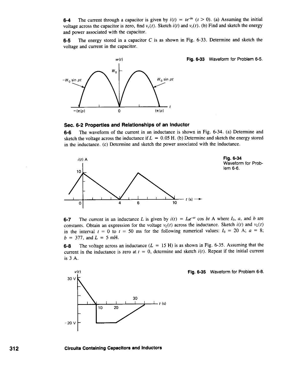
1-6-1 Ohm's Law
-----
i(t)+ R
v(t)
(a)
-f---
+ R i(t)
v(t)
(b)
Fig. 1-17 Ohm's law:
(a) v = Ri when the
current direction is as-
signed from plus to mi-
nus, and (b) v = - Ri
when the current direc-
tion is assigned from mi-
nus to plus.
The current flowing in a conductor depends on the voltage across its terminals. If v is
the voltage (in volts) and i is the current (in amperes), then the ratio R = vii is called
the resistanee of the conductor. The unit ofresistance is the ahm (denoted by the symbol
!l). One ahm equals 1 volt/ampere. A conductor with resistance is called a resistar, and
its symbol is shown in Fig. 1-16.
v
I
------
o
R
VI/II'v
+ -
v
o
(a)
Fig. 1-16 (a) Symbol and
(b) characteristic of a linear resistor.
(b)
The plot of current versus voltage in a linear time-invariant resistor is a straight line
passing through the origin as shown in Pig. 1-16(b). The resistance R of a linear time-
invariant resistor is a constant independent of the current through it or the voltage across
its terminals. (Unless otherwise stated, linear time-invariant resistors are assumed in the
following discussion.)
Current flows from a higher to a lower potential in a conductor, and the normal current
direction is from the plus terminal to the minus terminal of voltage polarities in a resistor,
as indicated in Pig. l-l7(a). With such a choice, the voltage and current in a resistor are
related through Ohm's law.'
v(t) = Ri(t)
Ohm's law
(1-23)
In some analysis problems, however, the current in a resistor may be assigned a
direction from the minus terminal ta the plus terminal of voltage polarities, as indicated
in Fig. 1-l7(b). (Such a situation occurs fairly routinely in electronic circuit analysis.)
Noting that a current i(t) flowing in one direction is equivalent to a current - i(t) in the
opposite direction, Ohm's law for the situation shown in Fig. 1-l7(b) becomes
vet) = - Ri(t)
(1-24 )
The distinetion between the twa situatians in Fig. 1-17 is very impartant and must be
carefully abserved in writing equatians for resistars.
Example 1-16 Calculate the voltage or current (whichever is not given) for each resistor shown in Fig.
1-18.
20 Basic Concepts, Components, and Laws of Electric Circuits
+
R,; 15 n v,
+
R 2 ;Sn v 2 ;40V
+
R 3 ;2n v 3
R 4 ;12n v 4 ;20sin377t V
j
;,; 6 A
t ;2
;3; 15 eos 100t At
t ;4
(a)
Ib)
Fig.1-18 Resistors for Example 1-16.
(c)
(d)
Solution First, decide which of the two equations, Eq. (1-23) or (1-24), applies in each case.
(a) Current from plus to minus. VI = Rli l = 90 V.
(b) Current from minus to plus. V2 = - Rzi z . Therefore, i 2 = - 5 A.
(c) V3 = - R3i3 = - 30 cos 100 tV.
(d) V4 = R4i4' and i4 = 1.67 sin 377t A. .
Exercise 1-15 Calculate the voltage or current (whichever is not given) for each resistor shown in Fig.
1-19.
Fig. 1.19 Resistors
for Exercise 1-15.
+ v,
-----
25 n ;,; 2 A
v 2 ; 30 V
- j
7 o . 5n
2
v 3 ; SO V
+
4n
'3
v 4
-----
15 n ;4; 4e t A
(a)
(b)
Ie)
(d)
1-6-2 Power Dissipated in a Resistor
A resistor receives power from a source of electrical energy and dissipates it in the form
of heat. It does not store energy, nor can it deliver power to another component. Since
p(t) = v(t)i(t) [Eq. (1-9}], the power dissipated in a resistor is given by
pet) = R[i(t)f = [v(t)fIR
(1-25)
Example 1-17 Calculate the power dissipated in each of the resistors of Example 1-16.
Solution Using Eq. (1-25), (a) p = 540 W, (b) p = 200 W, (c) p 450 cos 2 lOOt W, and (d)
p = 33.3 sin 2 377t W. .
Exercise 1-16 Calculate the power dissipated in each of the resistors of Exercise 1-15.
1-6-3 Nonlinear Resistors
A resistor whose current-voltage relationship does not satisfy Ohm's law is a nonlinear
resistor. Typical graphs of the characteristics of nonlinear resistors are shown in Fig.
1-20.
The resistance of a nonlinear resistor varies as a function of current (or voltage). The
device whose characteristic is shown in Fig. 1- 20(b) has the additional property that its
1-6 Resistance
21
-1
Fig. 1-20
Characteristics of
nonlinear resistors.
Exercise 1-17
22
v
limA)
l(mA)
(a)
6
4
-----
v IV)
v (V)
-1
-0.5
-2
Ib)
(e)
resistance values are low (in the order of tens of ohms) when v > 0 (first quadrant of
the graph) and very high (in the order of several thousand ohms) when v < 0 (third
quadrant). Such a device is said to be nanohmie or reetifying.
In order to use linear circuit analysis methods on a nonlinear resistor, it is necessary
to replace it by one or more linear models. A common approach is to approximate the
current-voltage characteristic by means of straight-line segments, as indicated in Fig.
1-20(c). Note that the resistance of each straight-line segment is a constant and valid for
a particular range of voltage values.
The graph of Fig. 1-21 shows the current-voltage relationship of a nonlinear resistor. It
is called a pieeewise linear resistor. Determine its resistance values for the different ranges
of voltage values. I (A)
20
10
v (V)
20
-20
Fig. 1-21 Piecewise approximation of a nonlinear
resistor characteristic for Exercise 1-17.
Basic Concepts, Components, and Laws of Electric Circuits
1-6-4 Effect of Temperature
In any resistor, the power dissipation due to the flow of current causes the temperature
to increase (in proportion to i 2 ), which leads to a change in the resistance, except in the
case of resistors made up of certain special alloys. In some materials, the resistance
decreases as temperature increases, and in others, the resistance increases as temperature
increases. Thus, the resistance of any resistor is affected by the flow of current. Most
resistors are, therefore, nonlinear. When linear resistors are used in circuit analysis, they
are approximate models of real resistors. The error introduced by such an approximation
will depend on the material of which the resistor is made. For example, the resistance
of molded-carbon composition resistors used in laboratory circuits varies by no more than
a specified percentage (5 or 10 percent) from the nominal value if the power rating is
not exceeded. Treating such resistors as linear usually leads to results of acceptable error
margins.
Two other components commonly used in electric circuits are capacitors and induetors,
which are discussed in Chapter 6.
1-7 CIRCUIT DIAGRAM CONVENTIONS
Components such as resistors and energy sources are shown by specific symbols in a
circuit diagram, and connecting wires (assumed to have zero resistance) are shown by
lines. A dark dot at the junction of two or more conductors denotes the presence of an
electrical connection between the conductors at the junction, as shown in Fig. 1-22(a).
The absence of an electrical connection at a crossover is usually indicated by the absence
of a dark dot, as shown in Fig. 1-22(b), but other conventions are also used, as shown
in Fig. 1-22(c).
--c::::J-
(a) (b) (e)
Fig. 1-22 (a) Dark dot at the intersection of two lines indicates an electrical connection.
(b) Absence of a dark dot indicates no connection. (c) Absence of an electrical connection is
also shown by a crossover.
1-8 KIRCHHOFF'S LAWS
Circuit analysis involves the determination of the values of the currents and voltages in
a circuit set up by a forcing function or by some initial stored energy or a combination
of the two. These values are governed by a number of constraints, some of which are
due to the manner in which the components are interconnected in a circuit. Two fun-
damentallaws of circuit analysis, Kirehhaff s valtage law (KVL) and Kirchhaff s eurrent
law (KCL), derived from the properties of electric fields dictate the constraints imposed
by the interconnection of the circuit components. Kirchhoff's laws are valid for any
lumped eireuit whether linear or nonlinear, time-variant or time-invariant. The discussion
1.8 Kirchhoff's Laws
23
in this and the following chapters, however, are confined to lumped, linear, and time-
invariant circuits with only an occasional discussion of some simple nonlinear circuit.
1-8-1 Kirchhoff's Voltage Law (KVL)
An electric field has the eanservative property, namely the work in moving an electric
charge around a closed path in the field is zero. Kirchhoff's voltage law states the above
property in terms of voltages in a circuit:
the algebraic sum of the voltages around a closed path in an electric circuit is zero.
The two key terms in the statement of KVL are c1ased path and algebraie sum afvaltages.
A c1ased path in an electric circuit is any path that starts at some point in the circuit
and returns to that point after traversing a number of components. A closed path is
indicated by a looping arrow, as shown in Fig. 1-23(a). Note that a closed path can jump
across several components or even across an open pair of terminals (Path 3 in Fig.
1-23(a».
Now, suppose a unit positive charge is moved clockwise around the closed path shown
in Fig. 1-23(b). When the charge is moved from the higher-potential terminal to the
lower-potential terminal of a component (that is, from the referenee pasitive ta the
referenee negative terminal), it lases a potential energy equal to the voltage across the
component. For example, a unit charge moving across component # 1 in the direction of
the path in Fig. 1-23(b) would lose VI joules. On the other hand, when a unit positive
charge is moved from the lower-potential terminal to the higher-potential terminal of a
component (that is, from the referenee negative ta the referenee pasitive (erminal) , it
gains a potential energy equal to the voltage across the component. For example, a unit
charge moving across component #2 in the direction of the path in Fig. 1-23(b) would
gain Vz joules. The losses and gains in the potential energy of a unit charge moving across
the components in a closed path must be subtracted and added, respectively, to determine
the net change in its potential energy. The resulting algebraie sum of the voltages in the
closed path must be zero, since the work done in moving a charge through a closed path
in an electric field is zero (conservative property of the electric field).
The following sign eanventian is used in writing KVL equations.
FIg.1-23 Closed paths
in a circuit.
+
V3
Path 2
V 6
Path 3
+
V 4
V s
(a)
(b)
24
Basic Concepts, Components, and Laws of Electric Circuits
. If the direction of path is from plus to minus across a component, that voltage is
added in the KVL equation.
. If the direction of path is from minus to plus across a component, that voltage is
subtraeted in the KVL equation.
The algebraic sum of the voltages in a closed path, obtained by using the above
convention, is then equated to zero.
For the closed path in Fig. 1-23(b), the direction of the path is from + to - in v),
V4, and V6 , and from - to + in V2, V3, and Vs. Therefore, the KVL equation becomes
VI - V2 - V3 + V4 - Vs + V6 = 0
Example 1-18 Write the KVL equations for the three closed paths in the circuit of Fig. 1-24.
Path 1
v 7 v s
+
[ 1
Path 3
..
+
v2
Path 2
v, v6
FIg.1-24 Closed paths
for the KVL equations for
Example 1-18.
V3
v 5
Path 1
Solution Path 1:
VI - V7 - Vg + V6 + Vs - V3 = 0
Path 2: VI - V2 + V6 + Vs - V3 = 0
Path 3: (Note the eauntercloekwise direction of this path)
- V2 + V7 + Vg = 0
.
Example 1-19 Calculate the voltage Vg in the circuit of Fig. 1-25(a).
Solution Two closed paths are available for this calculation, as shown separately in Figs. 1-25(b)
and 1-25(c). (Both should give the same answer for V8')
The KVL equation of the closed path in Fig. 1-25(b) is
- VI - V2 - Vs + V6 + Vg - V7 + V4 0
which gives (after substituting the numerical values)
Vg = -100 V
1.8 Kirchhoff's Laws
25
V 2 = 50 V
+
V 5 = 100 V v6 = 200 V
+ +
V 2 = 50 V v 5 = 100 V v6 = 200 V
+ + +
+
v, = 100 V
v, = 100 V
VB
+
v 4 = 200 V
+
v 7 = 50 V
+-
v 4 = 200 V
+
v 7 = 50 V
(al
(bl
V 5 = 100
+
V 6 = 200
+
v, = 50 V
+
+
VB
Fig. 1-25 Circuit for
Example 1-19. Voltage
VB can be calculated by
using either the path in
part (b) or in (c).
+
v 7 = 50 V
(e)
The KVL equation of the closed path in Fig. 1-25(c) is
V3 - Vs + V6 + VB - V7
o
which also gives VB = - 100 V.
.
Since the actual polarities of voltages across the components in a circuit are not always
known beforehand, they are usually assigned arbitrarily. If the assigned polarities match
the actual polarities in a component, then the answer will be a positive voltage. If the
assigned polarities do not match the actual polarities, then the answer will be a negative
voltage. as in the preceding example. It is not necessary, however, to go back and reassign
polarities in such cases; the answer is left as a negative value.
Exercise 1-18 Write the KVL equation for the closed paths shown in Fig. 1-26(a).
Exercise 1-19 Obtain an expression for the voltage marked V x in terms of Va. . . . , V" in Fig. 1-26(b).
Exercise 1-20 In each of the circuits shown in Figs. ]-26(c) and (d), evaluate the voltage marked V,.
Open Circuit
A pair of terminals is said to be apen eircuited when there is an open gap between them,
which represents an infinite resistance. Current through an apen-eireuited pair of terminals
is zero (except when an infinite voltage is applied across the terminals). The valtage
across an apen eireuit is, in general, nat zero.
26
Basic Concepts, Components, and Laws of Electric Circuits
+ V 2 _
+ V 5 _
_ VB +
+
V 7
V,
+ V s -
(a)
V 2 = 20 V
+
V 3 15 V
+
V, = 10 V
+
+
v 7 = 62 V
+
VB = 51 V
(e)
V 2 90 V
+
v,=175V
V x
+
+
v 3 35 V
+
v 4 = 80 V
(d)
Fig.1-26 Circuits for Exercises 1-18, 1-19, and 1-20.
1.8 Kirchhoff's Laws
_ Vb +
_ V c +
+ +
V x V e
(b)
+
V 4 = 17 V
V 5 3 V
+
+
27
v2 14V v3 7V
+ +
(a)
v 2 14 V v 3 7 V
+ +
+ t +
Open v, 8 V v DC
circuit L
+ +
V s 30 V v 4 19 V
(b)
v, 8 V
Fig. 1-27 Calculation
of the open-circuit
voltage for Example
1-20.
V s 30 V V 4 19 V
Example 1-20 Calculate the voltage across the open circuit in Fig. 1-27(a).
Solution First, label the voltage across the open circuit as Va, and assign reference polarities
(arbitrarily) as shown in Fig. 1-27(b). Next write a KVL equation around the closed path
that includes the open circuit:
- VI + V2 - V3 + V ac + V4 - Vs = 0
(Note that the path jumps across the open circuit and V"' is included to account for the
voltage due to the jump.)
Therefore, v"c = 12 V. .
Exercise 1-21 Calculate the voltage across each open circuit shown in Fig. 1-28. Use the polarities
already assigned.
Vb = 15 V
+
v DC
V c 75 V
+
+
V d 60 V
+
V , 9 V
, 1
v DC
j
+ +
V6 6 V V s 20 V
(b)
V3 7 V
va = 45 V
V 4 13 V
+
v, ' 30 V
+
v e 90 V
(a)
Fig. 1-28 Circuits for Exercise 1-21.
Note that the only restriction in using KVL is that the circuits be lumped circuits; no
restriction is imposed about the linearity or time invariance of the components.
1-8-2 Kirchhoff's Current Law (KCL)
The law of conservation of electric charge states that throughout any process occurring
within a system, the algebraic sum of the electric charges within the system does not
28
Basic Concepts, Components, and Laws of Electric Circuits
Nodes
(a)
(b)
Fig. 1-29 Nodes in a
circuit. A node is often
shown spread out as in
part (b) so as to avoid
clutter.
Nodes
(el
change. Since currents involve flow of charges, Kirchhoff's current law restates the charge
conservation principle in terms of currents in a circuit:
The algebraic sum of the currents at a node in an electric circuit is zero.
The key terms in the statement of KCL are nade and algebraie sum of the eurrents.
The terminals of a branch in a circuit are called nades, as shown in Fig. 1-29(a), and
KCL applies to any node in a circuit. When many branches meet at a common node, a
single node is often shown spread out in order to avoid clutter in the circuit diagram, as
shown in Fig. 1-29(b).
Consider the portion of a circuit shown in Fig. 1-29(c), with currents assigned to the
branches, where some currents are entering and others are leaving the node. A distinction
must be made between them by using appropriate algebraie signs and this leads to the
"algebraic sum" referred to in the statement of KCL.
The following sign eonventian will be used in writing KCL equations.
. A current leaving a node is written with a pasitive sign.
. A current entering a node is written with a negative sign.
The algebraic sum of the currents at a node, obtained by using the above convention,
is then equated to zero.
The KCL equation of the node in Fig. 1-29(c) is
ia - ib + i, + id 0
1-8 Kirchhoff's Laws
29
'3
--
CD
1 2
'3
---.----
"
14
lal
'x t
Fig. 1-30 Circuits for the KCL equations for
(a) Example 1-21 and (b) Example 1-22.
(bl
Example 1-21 Write a KCL equation for each node in the circuit of Fig. 1-30(a).
Solution Node J:
Example 1-22
Solution
i 2 + i I + i3
o
Node 2:
-i l + 14
IS = 0
Node 3:
is
i6
i3
o
Nade 4:
-12
14 + 16 = 0
It is found that the equation for nade 4 is equal to the negative sum of the other three
equations. That is, the equation for node 4 is a linear eombination of the other three
equations, and node 4 is, consequently, not an independent node. A formal discussion
of the independence of nodes in a circuit is presented in Chapter 3. .
Determine the current ix in terms of the other currents in Fig. 1- 30(b).
The KCL equation for the given node is
- i l - i 2 + i3 ix + i4 0
Therefore,
Ix -i, 12 + i3 + i4 .
Exercise 1-22
Exercise 1-23
Exercise 1-24
30
Write the KCL equations of nodes 1, 2, and 3 in the circuit of Fig. 1-31(a). Verify that
the KCL equation of node 4 is equal to a linear combination of the equations of the other
three nodes.
Obtain an expression for current ix in the circuit of Fig. 1-31 (b) in terms of the other
currents.
Evaluate current ix in the circuit of Fig. 1-31(c).
Basic Concepts, Components, and Laws of Electric Circuits
-
tie
o
(a)
Fig. 1-31 Circuits for (a) Exercise 1-22,
(b) Exercise 1-23, and (c) Exercise 1-24.
(b)
i2 ; 5 A
Ix
---
1 3 ; 13 A
----
(c)
Short Circuit
A shart eireuit is said to exist across a pair of terminals connected by a wire of zero
resistance. The valtage acrass a short eireuit is zera (unless an infinite current is forced
through it). Even though the voltage is zero across a short circuit, the current through it
is, in general, not zero.
Example 1.23 Calculate the current through the short circuit between points A and B in the circuit of
Fig. 1-32.
Solution The KCL equation at node A:
- i l
i 2
which leads to
isc
i 1 ; 7.5 A
---
o
i ; 4 A
4--
13 + Is, + 14
o
-2.5 A
.
1.8 Kirchhoff's Laws
31
" = 5.5 A
----
'4 = 12.5 A
----
'3
/
/
/
Fig. 1-33 Circuits for
Exercise '-25.
,
,
,
h
" t
la)
Ib)
Exercise 1-25 Determine the current labeled is, in each circuit of Fig. 1-33.
(a)
Ib
-
(b)
Fig, 1-34 KCL is also
applicable to the cur-
rents at the terminals of
a circuit or a device.
Since the actual directions of currents in the branches of a circuit are not always known
beforehand, they are usually assigned arbitrarily. If the assigned direction matches the
actual direction in a branch, then the answer will be a positive current. If the assigned
direction does not match the actual direction, then the answer will be a negative current,
as in the previous example. It is not necessary, however, to go back and reassign current
directions in such cases; the answer is left as a negative value.
In the preceding examples and exercises, KCL has been applied to junctions of in-
dividual branches in a circuit. KCL can also be applied to more general situations, as
indicated in Fig. 1-34.
In Fig. 1-34(a), the shape may represent a portion of a more complex circuit or a
multi terminal device. If the four paths in the diagram are the only external connections
to the shape, then the KCL equation
- i I - i z + i3 + i4 = 0
is valid. An example of such a situation occurs in bipolar junction transistors and other
electronic devices. Figure 1-34(b) shows the symbol of a bipolar transistor with the
relevant currents, and the three currents are related by the KCL equation:
ie - ib - i, = 0
Note that the only restriction in applying KCL in a circuit is that it should be a lumped
circuit; no restriction is imposed about the time invariance or linearity of the individual
components.
The following sections will discuss the use of Kirchhoff's laws in the development of
models of nonideal sources.
1-9 VOLTAGE AND CURRENT SOURCES
32
ideal voltage and current sources were discussed in Sections 1-2 and 1-3, respectively.
The voltage across the terminals of an ideal voltage source is independent of the load
current drawn from it, and the current through the terminals of an ideal current source
is independent of the voltage across a load connected to it. Sources available in practice
do not, however, behave like ideal voltage or ideal current sources: that is, the voltage
Basic Concepts, Components, and Laws of Electric Circuits
Fig. 1-35 Models of a
non ideal source. (a)
Nonideal source with a
load. (b) v-i character-
istic of the non ideal
source. (c) Voltage
source (Thevenin)
model. (d) Current
source (Norton) model.
and current available at their terminals vary with the load. For example, the voltage of
the battery in an automobile decreases noticeably when the engine is being started.
Concept of Equivalent Circuits
The analysis of a circuit is often facilitated by the use of equivalent eireuits (or madels
made up of circuit components). Thll:r is, a device (such as a transistor), a component
(such as a nonideal source), or even a subnetwork (i.e., a portion of a network) is replaced
by a circuit that exhibits the same terminal eharaeteristies as the original device, com-
ponent, or subnetwork. If the equivalent circuits are properly developed for a given
situation and carefully used, then the results obtained by utilizing them will fit the original
circuit. Equivalent circuits and models are encountered at various points in this and the
following chapters.
Care should be exercised in using an equivalent circuit, since it is usually developed
or specified with respect to a set of terminals:
The equivalent circuit in any situation is valid only up to a set of terminals and ceases
to be valid beyond those terminals.
This point is further elaborated in Subsection 1-9-3 for the case of models of non ideal
sources.
Models of Nonideal Sources
Consider a non ideal source represented by a black box with a variable load resistance,
as shown in Fig. 1-35(a). The arrow through the resistance denotes a variable component.
Voltage Vab is the terminal valtage and ia is the terminal eurrent of the source. If, as
shown in Fig. 1-35(b), the terminal voltage varies linearly with the terminal current as
the load is varied, then there are two possible models for the source. The validity of
V ab
o
ia
+ -
ia
Non.ideal :{
source V ab /,
-
G)
o
(a)
(b)
,---------l
I R I
I '
I
I
I
I
I
I
I
I
I
I I
L_________-1
i---------- l 0
I I
I
I ---+
I '.
I
R L I i, R, V ab R L
I
I
I
I
I I G)
L___________J
o
1--+
I 'a
I
I
I
I
I
'---v----'
+ V 1 -
v,
V ab
G)
(c)
(d)
1-9 Voltage and Current Sources
33
these models is based on Thevenin's and Norton's theorems, which are discussed In
Chapter 5.
I. Valtage Sauree Madel. In the voltage source model, an ideal voltage source v, is
in series with resistor R" as shown in Fig. 1-35(c). In a series connection, the
components are connected in such a way that the same current flows through them.
2. Current Souree Madel. In the current source model, an ideal current source i., is
in parallel with a resistor R" as shown in Fig. 1-35(d). In a parallel connection,
the components are connected in such a way that the same voltage appears across
them.
(The models in Figs. 1-35(c) and (d) are often referred to as the Thevenin model and
the Norton madel. respectively.)
The resistor R, represents the internal resistanee of the source. Internal resistance is
just a concept used to model the given source; the source may not actually contain an
internal component identifiable as a resistor. Note that if R, = 0, the voltage source
model becomes an ideal voltage source and Vab = v, independent of the load current. If
R, = OC, then the current source model becomes an ideal current source and ia = i,
independent of the load voltage. Thus, ideal sources are special cases of non ideal sources.
In the following discussion, it will be assumed that a given source has ajinite. nanzero
internal resistance.
1-9-1 Determination of the Voltage Source Model
The KVL equation relating the different voltages in the model of Fig. 1-35(c) is
- v, + VI + Vab = 0
(1-26)
But. VI
R,iu (Ohm's law). Therefore, Eq. (1-26) becomes
Vab = V s - Rsiu
(1-27)
where V, and R, are constants. Equation (1-27) describes a straight line on a graph with
Va" as the ordinate and iu as the abscissa, as shown in Fig. 1-36(a).
The intersections of the straight line with the two axes are V s on the vertical axis,
obtained by putting ia = 0 in Eq. (1-27), and vjR s on the horizontal axis, obtained by
putting Vab = 0 in Eq. (1-27).
V ab
Fig, 1-36 Measurements for the determination of the voltage source model.
R,
fa = 0
-----
o
+
R,
o
v,
V ab = V s
+
v,
V ab = v,/2 R L
I.
-0
o
(al
(b)
(e)
34
Basic Concepts, Components, and Laws of Electric Circuits
Now, consider apen eireuiting the terminals a-b of the source, as shown in Fig. 1-
36(b). Then,
ia = 0 due to the open circuit
which makes the voltage across Rs O. Therefore,
Vab = V s under the open circuit condition
Thus,
V s in the voltage source model = open-circuit voltage measured
across the load terminals
(I-28a)
The basic principle in finding the resistance R., is that if the voltages across R, and R L
are made equal (by a proper choice of RLJ, then R, and Rio should be equal also (by
Ohm's law). When the above condition occurs, the voltage v., is split equally between
R., and R L . Therefore, connect a load resistance R L to terminals a-b and vary its value
until the voltage Vab becomes exactly one-half af the apen-eireuit valtage as shown in
Fig. 1-36(c). When this condition occurs, Eq. (1-27) shows that
R L = R,
Therefore,
Rs = the value of R L needed to make the load voltage across a-b one-half of the
open-circuit voltage (I-28b)
The voltage source model of a non ideal source is thus given by Eqs. (I-28a) and
(I-28b).
Example 1-24 The terminal voltage of a battery (with an open-circuit voltage of 12 V) reduces to 6 V
when a resistance of 5 n is connected to its terminals. (a) Obtain the voltage source
model of the battery. (b) Calculate the current flowing through a short circuit placed
between the battery terminals. (c) Sketch the graph of the terminal voltage as a function
of the terminal current.
Solution (a) The model consists of V s = 12 V in series with R., = 5 n, as shown in Fig. 1-37(a).
Fig. 1-37 Model and load line for Example 1-24. V ab (V)
15
R, = 5 n
0)
R, = 5 n
ia
-
ia (A)
v, = 12 V
v, = 12 V
4t
o
(a) (b)
(e)
1-9 Voltage and Current Sources
35
(b) When a-b are short circuited, as shown in Fig. 1-37(b), ia = viRs = 2.4 A.
(c) The graph is a straight line drawn by joining the point at Vab = V s = 12 V on the
vertical axis to the point at ia = vsIRs = 2.4 A, as shown in Fig. 1-37(c). .
Exercise 1-26 A load resistance of 120 n reduces the terminal voltage to 12 V of a source whose open-
circuit voltage is 24 V. (a) Draw the model of the source. (b) Sketch the graph of the
terminal voltage against the terminal current. (c) Calculate the current when the load
terminals are short circuited.
1-9-2 Determination of the Current Source Model
The KCL equation of the model in Fig. 1-38(a) is given by
Vab
Rs
which describes a straight line on a graph with ia as the ordinate and Vab as the abscissa,
as shown in Fig. ]-38(b).
But i,
- is + i l + ia = 0
(I-29a)
vablRs by Ohm's law, and Eq. (I-29a) becomes
ia
is
(I-29b)
The points of intersection of the straight line with the two axes are: is on the vertical
axis [obtained by putting Vab = 0 in Eq. (1-29b)] and Rsis on the horizontal axis [obtained
by putting ia = 0 in Eq. (1-29b)].
Fig. 1-38 Measurements for the determination of the current source model.
ia
t i,
V ab
-----------l ia
1---
I
--_________J
36
+
R,
V ab
Load
(a)
(b)
fa::: a
---
t i,
V ab
R L
+
t i,/2
+
t ia i,/2
R,
V ab = Rsis
R,
(e)
(d)
Basic Concepts, Components, and Laws of Electric Circuits
If terminals a-b are open circuited, as shown in Fig. 1-38(c), then ia
(I-29b) leads to
o and Eq.
Vab = Rsis
open-circuit voltage
(1-30)
The current source model for a given source is obtained by using the same two
measurements used for the voltage source model. The open-circuit voltage of the given
source is measured. Then the load resistance is adjusted until the voltage across it is
exactly one-half of the open-circuit volt e. Under this condition, Eq. (1-30) leads to
Vab = Rsi,l2
which means that the current through Rs is i/2 and the current through R L is also i)2,
as is shown in Fig. 1-38(d). Therefore, R L = Rs when the load v ltage is one-half the
open-circuit voltage.
Then, Eq. (1-30) gives
is in the current source model = (open-circuit voltage of the source)/R s
Example 1-25 The open-circuit voltage of a source is 18 V. The terminal voltage reduces to 9 V when
the load resistance is 5 kil. (a) Obtain the current source model. (b) Sketch the graph of
the terminal current as a function of the terminal voltage. (c) Calculate the current that
would flow in a short circuit across the terminals of the given source.
Solution (a) The internal resistance of the source is 5 kil. Since the open circuit voltage is 18 V,
i, = 18/(5 X 10- 3 ) = 3.6 mA. The model is shown in Fig. 1-39 (a).
(b) The graph is a straight line joining the point is = 3.6 mA on the vertical axis with
the point R.i, = 18 V on the horizontal axis, as shown in Fig. 1-39 (b).
(c) A short circuit from a to b, as shown in Fig. 1-39 (c), makes the voltage Vab = O.
Since the voltage across Rs is zero, no current flows in Rs. Therefore, the current in the
short circuit = is = 3.6 mA. .
ia (mAl
o
R, = 5 kQ
(0
Flg.1.39 Model and
load line for Example
1-25.
(a)
(b)
(e)
o ia=is
ti=o t It
R, = 5 kQ v ab = 0
V ab (V)
20
(0
Exercise 1-27 The open-circuit voltage of a source is 24 V and a load resistance of 470 il reduces the
load voltage to 12 V. (a) Obtain the current source model. (b) Sketch the graph of the
terminal current as a function of the terminal voltage.
An examination of the two models of a non ideal source shows that the eurrent flawing
in a short eireuit across the source terminals equals i, in the current source model and
1-9 Voltage and Current Sources
37
v)R, in the voltage source model. Therefore, the following two relationships are also
useful in setting up the models.
i, in the current source model = short-circuit current of the given source
and
R, in either model = (open-circuit voltage)/(short-circuit current)
Making a short-circuit measurement on a given source is usually not feasible, since
it may permanently damage the source. The preferred experimental procedure is to adjust
R L to give one-half the open-circuit voltage.
Exercise 1-28 The open-circuit voltage and short-circuit current of a source are given as 12 V and 0.3 A,
respectively. Obtain the two models of the source.
1-9-3 Conversion Between the Models of a Source
R,
v,
lal
38
Depending on a given problem, one model is found to be more convenient than the other.
Conversion of one model to the other is therefore necessary in some problems.
Consider the two models of a non ideal source, as shown in Figs. 1-40(a) and (b). The
value of the internal resistance is the same in both cases, but it is connected in series
with the voltage sauree and in parallel with the eurrent sauree.
Now consider an arbitrary load resistance R L connected to the two models, as shown
in Figs. 1-40(c) and (d).
For the voltage source model, the KVL equation is
- V s + VI + Vab = 0
which leads to, after using Ohm's law,
(R, + RL)ia V,
and
Vab = RLia = lRd(RL + Rs)]v,
(1-31 )
For the current source model, the KCL equation is
- i, + i J + ia = 0
Fig,1-40 Conversion between the models of a source. Models in parts (a) and (b) are equivalent
if V s = Rsis.
a a
+ v, - 0 I.
+=Jt
R, + t i. i, t
v. b R L R, v. b R L
Rs V s
b
b
o
Ib)
Ie)
(d)
Basic Concepts, Components, and Laws of Electric Circuits
which leads to, after using i l = vablRs and ia = vablRL,
( RLRs ).
v = I
ab (R s + R L ) s
Equating Eqs. (1-31) and (1-32), it is seen that
(1-32)
V s = Rsis
"is = v,IRs
(1-33)
and
Equation (1-33) permits the determination of is if V s is known and viee versa.
Example 1-26 Convert each of the voltage source models in Figs. 1-41(a) and (b) to an equivalent
current source model. "
Solution (a) The internal resistance is Rs = 15 n. The source current is v,lRs = 5 A. The equiv-
alent current source model of Fig. 1-41(a) is shown in Fig. 1-41(c).
(b) The internal resistance is Rs = 10 n. The source current is v,lRs = 12 A. The
equivalent current source model of Fig. 1-41(b) is shown in Fig. 1-41(d). .
Rs = 15.11
V s = 75 V
(a)
Fig. 1-41 Source
conversions for
Example 1.26.
Example 1-27
Solution
Fig. 1.42 Source
conversions for
Example 1-27.
(a)
o
o
-+-
V s = 120 V
o
is = 12 A
Rs = 15.11
Rs = 10.11
o
(b)
(e)
(d)
The direction of the current in the current source must be carefully determined and
clearly indicated in the diagram of the converted model. The direction of the current in
the equivalent current source is determined by matching the directions of he current in
a short circuit placed across the terminals a-b in the two models.
Convert each of the current source models in Figs. 1-42(a) and (b) to an equivalent voltage
model.
(a) The internal resistance isRs = 0.1 n. The source voltage isR,is = 2.5 V. The voltage
source model of Fig. 1-42(a) is shown in Fig. 1-42(c).
(b) The internal resistance isRs = 11 n. The source voltage isRJ,
source model of Fig. 1-42(b) is shown in Fig. 1-42(d).
110 V. The voltage
.
o
o
Rs =0.1 .11
Rs = 11 .11
o
o
Rs = 11 .11
@
Rs =0.1 .11
V s = 2.5 V
V s = 110 V
@
is = 10 A
G)
(b)
(e)
(d)
1.9 Voltage and Current Sources
39
The polarity marks on the voltage source must be carefully determined and clearly
indicated in the diagram of the voltage source model. The polarities are determined by
matehing the voltage polarities on an open circuit across the terminals a-b in the two
models.
Exercise 1-29 Convert each source model in Fig. 1-43 to the other form.
G)
Important Points to Note in the Conversion Procedure
I. The conversion procedure depends on the presenc/e of a finite nonzero internal
resistance Rs. If Rs = 0 in the voltage source model (the case for an ideal voltage
source), or Rs = 00 in the current source model (the case for an ideal current source),
the conversion procedure will lead to indeterminate results. Therefore, if the given
source is ideal, then it eannat be converted to the other form.
2. Equivalence between the two source models is valid only outside the terminals a-b
of the source. That is, the two models yield identical results for any and all cal-
culations outside the dashed lines in Fig. 1-44. For any calculations inside the
dashed lines, the two models will, in general, yield different results. For example,
suppose both models are open-circuited so as to make ia = O. Then the power
delivered by V s [as shown in Fig. 1-44(a)] is zero since it supplies no current,
whereas the power supplied by is [as shown in Fig. 1-44(b)] is Rsi" since the current
is would flow through R" and the two results are seen to be quite different.
Care should, therefore, be taken to use equivalent circuits only within valid circuit
boundaries.
V ab
r--------,
I
I
I
I
: + i. R.
I
I
I
I
I
L________-.J
ia
-
a
,..--------,
I I
I
I
I
I
I
I
I
I v.
I
I
I
L_______.J
ia
-
a
+
+
Fig. 1-44 The two models yield the same
results for any connections made to the
terminals a-b. The equivalence is not valid
inside the dashed lines.
V ab
b
b
(a)
(b)
40
Bulc Concept., Components, and Laws of Electric Circuits
1-9-4 Dependent Sources
If the voltage of an ideal voltage source in a circuit is independent of the voltage or
current in another branch, then it is called an independent voltage source. A similar
definition is valid for an independent current source. Ideal source components in the
models of batteries and generators are examples of independent sources.
A dependent (or controlled) source, on the other hand, has the property that its voltage
or current is dependent on the voltage or current in another branch of the circuit.
Dependent sources arise in the models of active devices such as transistors and electronic
circuits. For example, a bipolar junction transistor has three terminals (emitter, base, and
collector) with a current associated with each terminal, and the collector current can be
expressed as a specific fraction of the emitter current. This dependence of the collector
current on the emitter current leads to a dependent current source in the model of a bipolar
junction transistor.
A dependent source is represented by a diamond shaped symbol, as shown in Fig. 1-
45. As shown in the diagrams, a dependent source is a voltage source or a current source,
and the quantity that controls the voltage or current of a dependent source is a voltage
or current in another branch. When the voltage or current in a dependent source is related
to the controlling voltage or current by a constant that does not vary with time, which
is the case in all four circuits of Fig. 1-45, the source is a linear. time-invariant dependent
source, which is the only kind that will be discussed in this and the following chapters.
Fig. 1-45 Linear dependent sources. (a) Dependent current source controlled by the voltage
in a branch. (b) Dependent current source controlled by the current in a branch. (c) Dependent
voltage source controlled by the voltage in a branch. (d) Dependent voltage source controlled
by the current in a branch.
+ Va _
ib
-
k,v a A
l k2 i b A
(a)
(bl
id
-
k3 V c V
k4id V
+
V c
(el
(d)
1.9 Voltage and Current Sources
41
'x
-----
t klx A R3
Ix
-----
R3
+
kR3'X V
FIg. 1-46 Conversion between dependent current and
voltage source models.
Except for the fact that their voltage or current is controlled by what is happening
somewhere else in a circuit, dependent sources are analyzed in the same manner as
independent sources. For example, the conversion procedure of source models applies
to dependent sources also. An example of such a conversion is shown in Fig. 1-46.
1-10 AN OVERVIEW OF CIRCUIT ANALYSIS
The primary aim of circuit analysis is to determine the response of a circuit to a given
forcing function. The forcing function is a voltage or current applied to a circuit, and
the response is a voltage or current at some part of the circuit. But circuit analysis serves
other important purposes as well. It forms the basis of network theory, which is a study
of the behavior of general networks. Some basic concepts of network theory are presented
in later chapters. The ultimate aim of circuit analysis can be considered to be netwark
synthesis, that is, the design of a netwark to meet a set of specifications about the input
and output. Methods of synthesis will not, however, be considered in this book.
Even though it would be desirable to develop methods of circuit analysis applicable
to all types of circuits, the mathematical complexity of analyzing distributed, nonlinear,
or time-variant networks makes it necessary to restrict our attention here to lumped,
linear, time-invariant circuits.
Since it is usually convenient to proceed from simple cases to difficult cases in a
gradual manner, we start with the simplest type of circuit problems: circuits made up of
resistors and driven by sources of constant voltage or current. Algebra is the only math-
ematical tool needed for the analysis of such circuits, and we can concentrate on the
basic principles and procedures of circuit analysis without complicated mathematics.
The addition of energy storage elements such as inductors and capacitors leads to
ordinary linear differential equations with constant coefficients describing the circuits.
Again, we start with the simple case of such circuits driven by sources of constant voltage
or current before considering time-varying forcing functions.
Among the wide variety of time-varying forcing functions, the sinusoidal function
42
Basic Concepts, Components, and Laws of Electric Circuits
(that is, a voltage or current described by a sine or cosine function of time) occupies a
most important position. Because of its importance, a great deal of attention will be
devoted to the analysis of circuits driven by sinusoidal sources. The response of circuits
to sinusoidal forcing functions are governed by ordinary linear differential equations with
constant coefficients. Since the solution of such equations tends to be tedious, an alter-
native method is developed in which differential equations are transformed to algebraic
equations with complex coefficients.
From sinuosoidal forcing functions progress is made to more general forcing functions,
where a periodic function can be expressed as the sum of sinusoidal components and this
sum is known as a Fourier series. Fourier analysis in conjunction with the principle of
superposition permits the analysis of circuits driven by periodic non sinusoidal functions.
When forcing functions are not periodic, several methods of analysis are available.
One is convolution, which is a statement of the principle of superposition in the form of
an integral. Convolution permits the analysis of a circuit in the time domain and is
applicable even when the forcing function cannot be expressed in a convenient mathe-
matical form. In the case of forcing functions that are of finite duration, circuits can also
be analyzed by Fourier transforms that are modifications of the Fourier methods for
periodic functions. It is found, however, that Fourier transforms have certain limitations
and are not applicable to all forcing functions of interest. A more versatile method of
attack is provided by Laplace transforms, which permit the analysis of circuits under a
wide variety of forcing functions in both the time domain and the frequency domain.
The principle of superposition will be seen to form the foundation on which the structure
of linear circuit analysis is built. In fact, the difficulty in analyzing nonlinear circuits
directly is their failure to obey the principle of superposition.
1-11 SUMMARY OF CHAPTER
Potential difference (or voltage) between two points in an electric field is the work required
to move a positive unit charge between the two points. The unit of potential difference
is the volt: 1 V = 1 joule/coulomb. Voltage reference polarity marks (+ and -) are
necessary to indicate the reference positive and reference negative terminals of a com-
ponent.
Electric current is defined as the rate of change of electric charge across a section of
a material. The direction of current is taken as that in which free positive charges would
flow under the influence of an electric field.
Power is the rate of doing work. If v is the voltage across and i the current through
a component, then p = vi represents the instantaneous power. When p varies as a function
of time, the root-mean-square (rms) value is usually specified. A component can deliver
or receive power.
The product vi represents te power received by a component if the current is flowing
from the reference positive to the reference negative terminals of a component. (Such an
assignment of voltage polarities and current direction is referred to as associated reference
polarities. )
The product vi represents the power delivered by a component if the current is flowing
from the reference negative to the reference po itive terminals of a component.
An ideal voltage source has the property that its terminal voltage is independent of
the current supplied by it to a load. An ideal current has the property that its terminal
current is independent of the voltage across a load connected to it. Energy sources in
practice are non ideal and their models are considered in Chapter 2.
1-11 Summary of Chapter
43
Components and circuits can be classified in different ways. The treatment in this
book will be limited to lumped, linear, time-invariant circuits. Circuits with physical
dimensions much smaller than a quarter wavelength of the signals are considered lumped.
Linearity is defined by the principle of superposition: the response of the circuit to a
weighted sum of forcing functions is given by the weighted sum of the responses to the
individual forcing functions. Time invariance implies that a shift of the forcing function
in time causes a shift in the response by the same interval without affecting the shape or
form of the response. Kirchhoff's laws are used to analyze lumped, linear, time-invariant
circuits. Other types of circuits usually required more sophisticated techniques that are
outside the scope of this text.
The voltage across and a current through a conductor are related by Ohm's law: v = Ri.
A linear resistor has the property that its resistance R is a constant independent of the
current through it. Almost all practical resistors are nonlinear. Linear approximations are
used, however, in order to apply linear circuit analysis techniques.
The two basic laws on which circuit analysis is founded are Kirchhoff's voltage law
(KVL) and Kirchhoff's current law (KCL). KVL states that the algebraic sum of the
voltages around a closed path in an electric circuit is zero. KCL states that the algebraic
sum of the currents at a node in an electric circuit is zero.
The sign convention used for KVL is add a voltage if the direction of the path is from
the positive reference polarity to the reference negative polarity, and subtract a voltage
if the direction of the path is from the negative reference polarity to the positive reference
polarity. The algebraic sum of all the voltages in any closed path obtained by using the
above convention is equated to zero.
The sign convention used for KCL is add a current if the current is leaving the node,
and subtract a current if it is entering the node. The algebraic sum of all the currents at
any node obtained by using the above convention is equated to zero.
A nonideal source, in which the terminal voltage varies linearly with the terminal
current (as the load is varied) may be represented by one of two models: the Thevenin
model, consisting of an ideal voltage source in series with a resistance, or a Norton
model, consisting of an ideal current source in parallel with a resistance. The two models
are determined by making two measurements: an open-circuit measurement and finding
the load resistance that reduces the load voltage to one-half the open-circuit voltage.
Either model is converted to the other by using some simple conversion formulas.
A dependent source is one whose voltage or current is controlled by the voltage or
current in another branch of the circuit. Dependent sources occur in models of active
devices such as transistors.
Answers
to Exercises
44
I Wherever appropriate, some intermediate steps are given below to help you check your work.]
1.1 i = 2.5 A (0 < t < 2); i = 0 A (2 < t < 4); i = - 2.5 A (4 < t < 6);
i = 0 A (t > 6).
1-2 i = - (pQo)e- P [.
1.3 p = ]20 + 60 cas 20t W.
1.4 i = - 500 sin 50t A; p = - 5000 sin 50t cas 50t W.
1-5 w = 270 J.
1-6 3.6 x 10 6 J.
1-7 (a) 3840 J and (b) 5520 J.
Basic Concepts, Components, and Laws of Electric Circuits
1-8 (a) - 24 V; (b) - ]4.4 V; (c) - 2.9 V; (d)]2 V; (e) 6 V.
1-9 (a) Delivering 682 W; (b) receiving 625 mW; (c) receiving 75 W; (d) receiving 135W.
1-10 (a) vaia = - 20 W, ia = - 2.5 A; (b) vbib = + 20 W, ib = - 3.33 A;
(c) vcic = +20 W, V C = 2.86 V; (d) vdid = -20 W, Vd = -6.67 V.
1-11 '1\14 = 1.25 x 10 6 m. Maximum length = 1.25 x IO s m.
1-12 The element is linear since both scaling and additive properties are satisfied.
1-13 The element is nonlinear since it fails the scaling test.
1-14 The element is time-invariant since i(t - to) results in v(t. to)'
1-15 (a) 50 V; (b) -60 A; (c) 20 A; (d) - 60e-[ A.
1-16 (a) 100 W; (b) ]800 W; (c) ]600 W; (d) 240 e- 2 [ W.
1-17 Resistance = I1s]ope.R = oo(v< -20V);R = 3n(-20<v< -5V);
R = 0.5 n (- 5 < v < 0 V); R = 2 n (0 < v < 10 V);
R = ] n (10 < v < ]5 V); R = 0 (v > ]5 V).
1.18 Pathl: -VI + V2 + V3 + V4 = O. Path 2: ,-V4 - V3 + Vs - V6 - V7 - VB = O.
Path 3: - V9 - VIO - V7 - VB = O.
1-19 V x = - Va - Vb - V c + Vd - Vel
1-20 (a)v x = -VI + V2 + V6 - V7 = -] Vorv x = -V3 + V4 - Vs = -] V;
(b)v x = -VI + V2 + V4 - V3 = -40V.
1-21 (a)v oc = -Va - Vb + V c + Vd + V e + Vf = ]95 V; (b)v oc = -VI - V2 + V3 - V4
+ Vs + V6 = O.
'-22 Nodel: -ia + ib - ic - i h = O. Node2:ic + ie + id - ig = O. Node3:ih + if
+ ig = O. (Node 4: ia - ib - ie - id - if = 0, which is also the negative sum of the equations
of nodes ], 2, 3.)
1-23 ix = ia - ib + ic - ie + id.
1.24 ix = - i l - i 2 + i3 - i4 + is = ] A.
1-25 (a) ].5 A and (b) i l + i 2 + i3 or i l + i 2 - i4 - is.
1-26 (a) Mode]: 24 V in series with ]20 n. (b) Straight line cuts the horizontal axis at 0,2 A
and the vertical axis at 24 V. (c) i = v)R s = 0.2 A.
1-27 (a) Mode]: 51.]-mA source in parallel with 470 n. (b) Straight line cuts the horizontal
axis at 24 V and the vertical axis at 5 I.] mA.
1-28 Voltage source mode]: ]2-V source in series with 40 n. Current source model: 0.3-A source
in parallel with 40 n.
1-29 (a) 20-A source in parallel with 25 n. Current in the source directed from terminal a to
terminal b. (b) 120-A source in parallel with 6 n. Current in the source directed from terminal
b to terminal a. (c) 80-V source in series with 20 n. Positive polirrity at terminal a.
(d) 3- V source in series with 200 n. Positive polarity at terminal b.
PROBLEMS
Sec. 1.1 Basic Units and Definitions
1-1 The work needed to move a positive charge of 0.25 C from point A to point B in an electric
field is 20 J, (a) Calculate the potential difference between the two points. (b) Calculate the work
done in moving an electron between the two points. (Magnitude of electronic charge = 1.6 x 10- 19 C.)
Problems
45
1-2 The potentia] difference between two points A and B is 250 V with A at the higher potential.
(a) Calculate the change in potentia] energy of an electron as it goes from B to A. (b) Does its
potential energy increase or decrease?
1-3 The flow of charge in a materia] is given by q(t) = te- I C for t > O. (a) Obtain an expression
for the current i(t) for t > O. (b) Draw a neat sketch of q(t) and i(t) on the same graph.
1-4 The variation of the electric charge in a section of a materia] is as shown in Fig. 1-47.
Determine and carefully sketch the current i(t).
q(t) Ie)
15
t (5)
° 6 12 18
Fig. 1-47 Variation of electric charge for Problem 1-4.
1-5 A piece of material has a uniform distribution of free charges moving at a constant (average)
velocity. Let p denote the charge density (i.e., charge per unit volume in C/m 3 ) and u the velocity.
(a) Consider an elementary section of length in the direction of motion of the charges and
assume that the charge in that section takes Ilt to move out of the section. Show that by letting
and Ilt - 0, the current in the material is given by i = Apu, where A is the area of cross
section of the material. The above expression is of particular importance in the study of semicon-
ductor devices. (b) If the number of free electrons in a circular copper wire of diameter 2 x 10- 3 m
is 8.5 x 1031/m 3 , calculate the velocity of the electrons for i = ] A. How does this velocity
compare with that of light at which electromagnetic energy travels?
1-6 The voltage across a component is a constant at ] 2 V. The current in it is
i(t) = ]5 - ]5 sin 27Tt A. (a) Determine the instantaneous power pet) and sketch it in the interval
(0, I s). (b) Calculate the energy received by the component in the interval (0.5, ] s).
1-7 The voltage across a component is vet) = KIt V and the current in it is i(t) = K 2 e-[ A,
where K, and K 2 are constants. Obtain the expression for the energy wet) assuming w(O) = O.
1-8 The pulse train produced by a transmitter has a maximum power level Po, as shown in Fig.
] -48. The duration of each pulse is 5 fLS and the period T = 0.] ms. (I fLS = 1O-{> sand
] ms = ] 0- 3 s.) The energy contained in each pulse is 2 J. (a) Calculate the value of Po'
(b) Calculate the average power of the pulse train, where the average power is defined as the area
of each pulse divided by the period T.
t
pIt)
r--- 0 . 1 ms1
--1 51'S
-
-T
Po
r
° T 2T t-
Flg.1-48 Pulse train for Problem 1-8.
1-9 The voltage vet) and current i(t) in a component are as shown in Fig. ]-49. (a) Sketch the
power p(t). (b) Determine the total energy received by the component.
46
Basic Concepts, Components, and Laws of Electric Circuits
v(t) (V)
50
0
-50
i(t) (A)
10
5
0
2 4 6
-5
-10
t (s)
t (s)
Flg.1-49 Voltage and current in a component for Problem 1-9.
Sec. 1-2 Voltage
1-10 The voltages VA, VB, and Vc in Fig. ]-50 are measured with reference to a common ground.
(a) Write expressions for VI and V2. (b) If VA = 15 V, Vc = 15 V, and V2 = - 34 V, calculate VI
and VB.
v,
v 2
c
1+
VA VB V c
\V
1
Flg.1-50 Circuit for Problem 1-10.
1-11 Calculate the voltage across each of the components in Fig. ]-5]. Use the reference polarities
already assigned. The voltages at different terminals are shown.
v,
A B
30V 10V
v 2
C + D
-30v 10V
v 3
E + - F
30V -10V
Fig. 1-51 Components for Problem 1-11.
v 4
G + H
-30V -10V
Problems
47
Fig. 1-52 Circuit for
Problem 1-12.
1-12 Obtain expressions for the voltages at points P, Q, R, and S (with reference to ground) in
terms of voltages v" V2, V3, and V4 in the circuit shown in Fig. ]-52.
1-13 Calculate the work done in moving an electron from point P to point Q in the circuit for
Fig. ]-53.
Sec. 1-4 Power Delivered and Power Received
1-14 Calculate the power received or delivered by each component in Fig. ]-54. State in each
case whether power is received or delivered.
VA = 10 V
V 2
V,
-:-
o
V, = 80 V
+ c:=J -
o
i, =5 A
p
V, = 80 V v 2 = 150 V
+ +
V 4 = 20 V
Flg.1-53 Circuit for Problem 1-13.
t i3 = 5 A
i4 = 5 A
--
V p = -70 V
o
t i 2 = 5 A
Va = -30 V
o
c=J
V 3 = 110V
VB = -10 V
(a) (b)
Fig. 1-54 Components for Problem 1-14.
(e)
(d)
1-15 If a current of ] 6 A flows from terminal P to ground through the various components in
the circuit for Problem ]-13 (Fig. ]-53), calculate the power in each component and state if it is
received or delivered.
1-16 The voltages and currents in the circuit of Fig. ]-55 are VI = ]OOV,V2 = -50V,V3 = 75 V,
V4 = 225 V; i l = -7 A, i 2 = ]3 A, i3 = - 6 A. (a) Calculate the power delivered or received
by each component and state in each case if power is delivered or received. (b) Verify that the
total power received equals the total power delivered in the circuit. (This result is valid only for
complete circuits and not for portions of a circuit. A forma] statement of the above result is known
as Tellegen's theorem.)
1-17 The voltage and current across a component (with associated reference polarities assigned)
are given by vet) = 50 cos 201Tt V and i(t) = 3 sin 201Tt A. Determine and carefully sketch the
power received by the component in the interval (0, 0.2 s). What is the average value of the power?
48
Basic Concepts, Components, and Laws of Electric Circuits
i 1 + v 1 _
----
V 4
+
V 2
+
V 3
Flg.1.55 Circuit for Problem 1-16.
Sec. 1-5 Classification of Circuits
1-18 The conductor ribbons used for interconnecting various printed circuit boards in a persona]
computer have lengths in the order of 0.] m. Determine the maximum frequency for which they
can be treated as lumped elements.
1-19 Test the linearity of the component whose current-voltage relationship is given by
d 2 i
v =-
dt 2
1-20 The voltage-current relationship of a component is given by
v = V o + Ri
Where V o and r are constants. Test the component for linearity. Draw a graph of the voltage as a
function of the current. Note that eve1} though the graph is a straight line. the component does not
satisfy the linearity property. (When such components are analyzed, a mode] is used in which the
constant term Va is represented by a constant voltage source and the Ri term by a linear resistor.)
1-21 It was (tacitly) assumed that in the component of Exercise ]-]2 the initial voltage is zero.
Suppose there is an initial voltage Va, so that the voltage-current relationship becomes
v = r(u)du + V o
Test the linearity of the component. (In analysis, this nonzero initial condition is treated by using
a model similar to the one mentioned in the previous prob]em.)
1-22 The forcing voltage functions and the corresponding current responses of a certain linear
circuit are
vet)
vet)
10 V i(t)
cos lOt i(t)
20 A
2 cos lOt - 5 sin lOt
Determine the response i(t) by using the principle of superposition when the forcing function
is (a) vet) = 13.2 + 5 cos lOt V; (b) v(t) = -8 + 2 cos lOt V; and
(c) vet) = -]] - 2.56 cos lOt.
1-23 Test the time-invariance of the components whose voltage-current relationships were given
in Problems 1-20 and 1-21.
1-24 The forcing-current function on a linear time-invariant circuit is given by
i(t) = { A
t < 0
t > 0
Problems
49
as a series combination of an idea] voltage source and a linear resistor. Set up the models and
indicate the range of current values for which each mode] is valid.
Sec. 1-7 Kirchhoff's Voltage and Current Laws
1-29 Write the KVL equations for the closed paths indicated in each of the circuits of
Fig. ]-58.
Fig. 1.58 Circuits for Problem 1-29.
/------------------ ----------------,
( Path 3 \
I I
I I
I + I
I I
I I
I I
I I
I I
I I
I __________ ___________ I
: ( + .....----------.... 'i + t
I va 1 Path 1 v f I Path 2 I v g I
IT.... I I I
I \ -------- I I
I ....___________ ___________/ I
I I
I I
I I
I + I
I + V k - V h I
\, )
,---- --- ---- --- --- --- ---------'- ------_/
(a)
V c
Va
+
-- -....
/ ....
I \
I I
+ Path 1 t
I I
\ I
.... /
-- --
\
I
I
I
I
I
I
I
I
t
I
I
I
I
I
I
I
J
/
V d
+
+
+
V.
(b)
Problems
51
+
v. = 25 V
+
v, = 62 V
v, = 100 V
+
V 2 = 80 V
+
v 3 =120V
+
+
V y
V 7 = 13 V
+
V 2 = 17 V
+
VB = 41 V
+
+
+ Lla -
+
V s = 85 V
+
vB = 30 V
(a)
V x
+
+
V s = 91 V
(b)
V y
+
v8 113V
Flg.1-59 Circuits for Problem 1-30.
1-30 Evaluate the voltages labeled V x and V y in the circuits shown in Fig. ]-59.
1-31 In the network of Fig. ]-60, (a) obtain an expression relating the voltages Va, Vb, V" and
Vd; (b) if Va = 100 V, Vd = 100 V, and Vin 300 V, calculate V o , Vb, and V C '
+
V,"
52
+ Vb -
Fig. 1.60 Network for Problem 1-31.
+
V o
Basic Concepts. Components, and Laws of Electric Circuits
(a)
1-32 Using suitable closed paths, calculate the voltage across and the power delivered by each
of the three current sources in Fig. ]-61.
V 2 = 35 V
+
V 3 = 11 V
+
V e = 27 V
+
+
v, = 75 V
V d = 12 V
Ie = 11 A
+
+
V s = 53 V
+
V s = 61 V
Fig. 1-61 Circuit for Problem 1-32.
1-33 (a) Write the KCL equations for nodes ],2, and 3 in the circuit of Fig. 1-62. (b) Show
that the equation for the remaining node can be expressed as a linear combination of the three
equations of part (a).
Id
----
CD
Flg.1-62 Circuit for Problem 1-33.
1-34 In each of the cases shown in Fig. ]-63, determine the value of current ix'
Fig. 1-63 Circuits for Problem 1-34.
[E7mA 7 A ___ ---- 4;t
ix
____ 15mA t5 A t3 A Ix
(b)
(e)
Problems
53
Fig, 1-64 Circuit for
Problem 1-35.
Fig. 1-65 Circuit for
Problem 1.36.
Fig. 1-66 Source
models for Problem
1-38.
i, = 20A
54
1-35 Evaluate currents iI, i 2 , i 3 , and i4 in the circuit of Fig. ]-64.
i,
----
i 2
---
i. = 7 A
-
i3
...--
1-36 Determine the current in and the power supplied by each of the three voltage sources in the
circuit of Fig. 1-65.
id = 9 A
i 1
--
ib = 7 At
+
v 1 = 17 V
t i3
i c = 3A t
t i .=12A
t i. = 5 A
ia = 10 A
v 3 = 8 V
+
v 2 = 19 V
+
i 2
if = 20A
---
Sec. 1-8 Voltage and Current Sources
1-37 The open-circuit voltage of a nonidea] source is ] 4 V. It is found that a load resistance of
24 n reduces the terminal voltage to one-fourth of the open-circuit voltage. Obtain (a) the voltage
source model and (b) the current source model.
1-38 For each of the source models shown in Fig. ]-66, obtain the equivalent source model of
the other type. Include diagrams of the models showing the source voltage polarities or current
directions as appropriate.
p
p 0
+ 0 -
v, = 80 V
\11M
R, = 20 n
0 0
p
R, = 25 n
(c)
i, = 120A
R, =6 n
p 0
- 0+
\11M
R, = 200 n
o
o
Q
v, = 30 V
(a)
(b)
(d)
Basic Concepts, Components, and Laws of Electric Circuits
1-39 The graphs in Fig. ]-67 show the results of measuring the terminal voltage versus the
terminal current for two circuits. The voltage polarities and current direction used in the measure-
ments are as shown in the figure'. For each case, obtain the two source models, including diagrams
showing the voltage polarity marks and current directions.
jab
+
Fig, 1.67 Terminal voltage versus terminal current for two
circuits of Problem 1-39.
Nonideal
source
V ab
(a)
V ab (V)
iab (A)
(b)
V ab
jab
(-10 A, -8 V)
(c)
Problems
55
CHAPTER 2
SERIES AND PARALLEL
CIRCUITS
l:e two fundamental laws of circuit analysis, Kirchhoff's voltage law (KVL) and
Kirchhoff's current law (KCL) were discussed in Chapter 1. As stated earlier, Kirchhoff's
laws are valid for any lumped cireuit whether linear or nonlinear, time-variant or time-
invariant. The discussion in this and the following chapters is, however, confined to
lumped, linear, and time-invariant circuits, with only an occasional discussion of some
simple nonlinear circuits. The application of Kirchhoff's laws to circuits containing certain
configurations of resistors are presented in this chapter. The analysis of circuits studied
does not involve the solution of simultaneous equations; and the absence of algebraic
manipulations makes it possible to concentrate on the fundamental properties of electric
circuits.
As an illustration of the application of the analysis techniques to some practical en-
gineering situations, the model of an electronic amplifier and its analysis are also discussed
in this chapter. The model is used as the basis of introducing the operational amplifier,
which is a versatile and commonly used circuit in electronic design. The operational
amplifier is revisited in Chapters 3, 4 and 6.
The simplest circuit that can be solved by applying KVL, KCL, and Ohm's law is
one made up of resistors in series or in parallel. The solution of series circuits is discussed
first.
2-1 THE SERIES CIRCUIT
56
Two branches are in series if they are physically connected so that the same current
flows through them regardless of what makes up those two branches.
A series circuit contains a single closed path made up of components in series and a KVL
equation is written for that closed path. A series circuit containing only resistors and
v,
o
+ v, -
+ V 2 -
l: R3
I,
----
,.[JR'
R,
R 2
V 4 +
I,
-
R4
(a)
Fig. 2.1 (a) Series circuit and (b) its equivalent circuit.
(b)
voltage sources is analyzed by using Ohm's law in combination with the KVL equation.
Consider a series circuit driven by a single voltage source v., as shown in Fig. 2-1(a).
There is only one current i 1 in the circuit. Voltage polarities are assigned to the resistors
so that it flows from the higher potential (plus) terminal to the lower potential (minus)
terminal in each resistor. (This is the "associated reference polarities" defined in Chapter
1.)
As stated in Chapter 1, the convention for writing the K VL equation for a closed path
is
Add a voltage if the path is from plus to minus and subtract if the path is from minus
to plus.
Following the direction of the current in Fig. 2-1(a), the KVL equation is
- V s + VI + V2 + V3 + V4 = 0
which leads to
VI + V2 + V3 + V4 = V s
(2-1)
Each voltage term on the left side of Eq. (2-1) is replaced by an Ri product by using
Ohm's law.
Rli l + R 2 i l + R3 i l + R4 i l = V s
or
i I
V s
(2-2)
(R I + R 2 + R3 + R 4 )
which is solved for i 1.
It is possible to set up a simple circuit, as shown in Fig. 2-I(b), so that the current
in it it = v,lRTis the same as in the original circuit shown in Fig. 2-1(a). Then the circuit
of Fig. 2-1(b) is said to be equivalent to that of Fig. 2-1(a). It follows from Eq. (2-2)
that the relationship between Figs. 2-1(a) and (b) is
R T = Rl + R 2 + R3 + R4
(2-3)
Therefore,
the total resistance of two or more resistors in series is equal to the sum of the individual
resistances,
and
the current in a series circuit is the ratio of the applied voltage to the total resistance.
2-1 The Series Circuit
57
+
R, 10n R 2 20 n
+ + v 2
v,
r J +
v 3 R3 30 n
i.
4
- v 5 + - V. +
R5 50 n R. 40 n
v, 100 V
Fig. 2-2 Circuit for Ex-
ample 2-1.
Example 2.1 Calculate the current ia and the voltage across each resistor in the circuit of Fig. 2-2.
Solution The total resistance of the circuit is
R T = RI + R 2 + R3 + R4 + Rs
150 n
Therefore,
ia = vsIRT = 100/150 = 0.667 A
The voltages across the resistors are (using Ohm's law) VI = Rlia
V; V = 20.01 V; V4 = 26.68 V; and Vs = 33.35 V.
6.67 V; V2
13.34
.
If the five voltage values are added, the sum should equal V S ' The actual sum is 100.05
(instead of 100.00) and the discrepancy is due to the round-off errar in calculating ia.
This situation occurs in almost all problems, of course. Trying to minimize this error by
retaining a large number of significant digits in numerical answers is absurd, however,
since such accuracy cannot be matched in the usual laboratory measurements. As a general
rule, three significant digits are retained in numerical answers in this text, letting the
round-off error fall where it may.
Exercise 2.1 Calculate the current and the voltage across each resistor in each of the circuits of Fig.
2-3.
Fig. 2.3 Circuits for
Exercise 2-1.
v, 350 V
R, 20 n O -
R'025U L '.
R 2 15 H
:J
R. 30 n
R3 50 n
(a)
R, = 2 n R, 5n R 2 16 n
ib t
v, 200 V R3 8 n v, 12 V
R 2 0.5 n R3 6 n R. 13n
(b) (e)
58
Series and Parallel Circuits
Example 2-2 Given that the 5-0 resistor in the circuit of Fig. 2-4 consumes a power of 80 W (constant),
determine the voltage V s of the source, the power dissipated in each of the other resistors,
and the power supplied by the source.
R, = 16,Q
" ?
'VIM.
R 2 = 13,Q
1" ,0 5 "
R. = 6,Q
Fig. 2-4 Circuit for Example 2-2.
Solution The power consumed by a resistor is given by
p = i 2 R
Since p = 80 Wand R = 5 0, i = 4 A.
The total resistance of the circuit is 40 O. Therefore, V s = 160 V.
The power dissipated by the resistors are 256 W (in R 1 ), 208 W (in R 2 ), and 96 W
(in R 4 ).
The power supplied by the voltage source is
Ps = vsi = 640 W
This should equal the sum of the powers dissipated by the four resistors in the circuit.
.
Exercise 2-2 If the 5-0 resistor of Fig. 2-4 is to dissipate 160 W, recalculate the results of the previous
example.
Exercise 2-3 The power supplied by the voltage source in the circuit of Fig. 2-5 is 600 W. Determine
the value of Rx.
Exercise 2-4 If the value of each resistor in the circuit of Fig. 2-5 is multiplied by a factor of N, what
is the effect on the power supplied by v s ?
Exercise 2-5 If the source voltage in Fig. 2-5 is multiplied by a factor of N, what will be the effect
on the power dissipated in each resistor compared with the results of Exercise 2-3?
R, 9,Q
,,0200V ?
R 2 = 7,Q
--l
Fig. 2.5 Circuit for Exercises 2-3 to 2-5.
2-1-1 Voltage Dividers
A special case of a series circuit is two resistors in series. Such a circuit divides the
applied voltage in proportion to the two resistances and is known as a valtage divider.
For the voltage divider shown in Fig. 2-6, the current in the circuit is
i = v,/(RI + Rz)
2-1 The Series Circuit
59
+ The voltage across R I is
i I
t (R I : RJv S
}:' VI = Rli
R,
and the voltage across R 2 is
} :v 2 . ( R 2 )
Vz = R 2 1 =. V s
R 2 Rl + Rz
(2-4a)
(2-4b)
Equations (2-4a) and (2-4b) are known as voltage divider formulas. The voltage divider
formula states that the voltage across each resistor equals the ratio of that resistance to
the total resistance.
Fig. 2-6 Voltage
divider. Also, the ratio of the voltages across the resistors in Fig. 2-6 is given by
VI RI
Vz R 2
and, for unequal resistances, the larger valtage appears across the larger resistanee.
Example 2-3 Two resistors, RI = 100 nand Rz = 400 n, are in series with a total voltage VT = 50
V across them. Calculate the voltage across R I,
Solution
VI = [RI/(RI + Rz)]v s = (100/150) x 50 = 10 V
.
The following example illustrates the use of a voltageAlivider in the measurement of
voltages using a certain kind of voltmeter.
Example 2-4 The basic mechanism of an analag de valtmeter is called the D'Arsanval movement.
which has a resistance Rm' as shown in Fig. 2-7(a). It is quite delicate and the maximum
value of V m that can be safely applied to the mechanism is of the order of tens of millivolts.
(1 mV = 10- 3 V.) When a voltage VT > V m is to be measured, the voltage across the
mechanism is limited by placing a resistance Rl in series with it, as shown in Fig.
2-7(b). Obtain an expression for Rl in terms of Rm' V m , and VT' CalculateRI when Rm = 50
n, V m 50 mV, and VT = 100 V.
+
Vm
o---#IINv---O
Rm
V m
+ -
R, Rm
..
+
V r
..
(a)
(b)
Fig. 2-7 Voltmeter for Example 2-4.
Solution: From the voltage divider formula, Eq. (2-4),
( Rm )
v - V
m - Rm + Rl T
Therefore,
When Rm = 50 n, V m
kn = 10 3 n.)
Rl = Rm[(vTlv m ) - 1]
50 X 10- 3 V, and VT = 100 V, R 1
10 5
100kn. (l
.
60
Series and Parallel Circuits
Exercise 2-6 Calculate the voltage V2 in each of the circuits in Fig. 2-8.
R, = 15 n
v, = 48 V
+
v 2 R 2 =3n
R, =8n
R 2 = 24 n
+
v, = 10 V
+ v 2
(a)
Fig. 2-8 Circuits for Exercise 2-6.
(b)
Exercise 2-7 If the D' Arsonval movement of Example 2-4 is placed in series with a 5-kn resistor,
what is the maximum voltage VT that can be measured by the voltmeter?
Useful Approximations
When one of the resistances is mueh larger than the other in a voltage divider, the total
resistance can be taken as approximately equal to the larger resistance and the smaller
resistance neglected. That is, if in Fig. 2-6,
RI » Rz, then R T = Rt + Rz = Rl
/
where the symbol = means appraximately equal to. Also, the voltage across the larger
resistance = the total voltage.
The voltage across the smaller resistance is not zero, however; it is simply much
smaller than the total voltage. The above approximation is useful for making rough
calculations (especially in electronic circuits). The question is, of course, how to define
"much larger than." This depends upon the allowable margin af error, which may be as
high as 10 percent in calculations involving electronic devices. In such cases, approxi-
mations are permitted if one resistor is ten or more times larger than the other. In circuit
analysis problems, however, the allowable margin of error varies with the instructor.
Example 2-5 Consider the results obtained in the voltmeter example, Example 2-4. Calculate the total
resistance, the voltage across each resistor when the smaller resistance is neglected, and
the error (percent) introduced by the approximation.
Solution Neglecting the 50 n due to Rm'
. Total resistance R T = RI = 100 kn (100.05 kn is the exact value)
. Voltage across RI = VT = 100 V (99.95 V is the exact value from [Rl/(R l + Rm)]vT)
. Voltage across Rm: V m = (Rm/RT)v( = 0.05 V (0.04998 V is the exact value)
· Percent error = 100 x (error/exact value) = 0.05 percent for all three cases .
Exercise 2-8 Consider the voltmeter circuit of Exercise 2-7. Calculate the total resistance, the voltage
across each resistor, and the error introduced when the smaller resistance is neglected,
2-1 The Series Circuit
61
Va
-
i
R,
Vb
i
-
+
R3
V s = Va - Vb + V c -- V d
RT R,+R2+R3
+
V c
V d
(a)
(b)
Fig. 2-9 (a) Series circuit with multiple sources. (b) Equivalent circuit.
2-1-2 Series Circuits with Multiple Sources
Consider a series circuit with more than one voltage source, as shown in Fig. 2-9(a).
Choosing a direction for the current i as indicated, the KVL equation of the closed path
in the circuit is
Va + R)i + Vb + R 2 i - V e + Vd + R3i = 0
The above equation is rewritten by keeping the Ri products on the left side and moving
the source terms to the right side (since the source voltages are usually specified quantities).
(R l + R 2 + R 3 )i = -Va - Vb + V e - Vd
(2-5)
It is seen that the resistances can be summed to a single resistance. The source voltages
are added algebraically to obtain a net source voltage acting on the circuit, as shown in
Fig. 2-9(b). The rest of the procedure is exactly the same as for a series circuit with a
single voltage source.
Example 2-6 (a) Calculate the current in the circuit of Fig. 2-1O(a). (b) Calculate the voltage between
points A and B.
Rc = 70 112
62
o
o
+
Va = 240 V
+
+ Ra i
.
Va = 240 V
+
Ra = 40 112
Ra = 40 112
i
c------- \
" Closed I
", path :
V x '........ I
" t
Vb = 80 V
+
-
[
Vb = 80 V
+
+
V c = 470 V
Rb = 90 112
(a)
(b)
Fig. 2-10 Circuit for Example 2-6.
Solution (a) The KVL equation is
- Va + Rai - Vb + Rbi + V e + Rei 0
Series and Parallel Circuits
which gives
(R a + Rb + Rc)i = Va + Vb - V c
Therefore, i = -150/200 = -0.75 A.
(b) Label the voltage between points A and B as V x and assign reference polarities. Write
a KVL equation for a closed path obtained by starting from B, going over to A across
V x and returning to B through the components of the circuit. One such path is shown in
Fig. 2-IO(b), and its KVL equation is
- V x - Va + Rai - Vb = 0
which gives
V x = -240 + (40)(-0.75) - 80 = -350 V
.
Exercise 2-9 Verify the value of V x obtained in Example 2-6 by using the other available closed path.
Example 2-7 Determine the voltage VAB in the circuit of Fig. 2-11(a).
R, 0
- r
i
R 2
+
V. VAS
+ L
Vb
i R 1 i
-+ -
-------I- +
( Closed \ 1
I I
I path I
I I
+ I I I
V. I I : VAS
I I I L
I 0 1
I I
l t
'---------t-
o
(a)
Fig. 2-11 Circuit for Example 2-7.
(b)
Solution First solve for the current i.
The KVL equation is
- Va + Rd + R 2 i + Vb = 0
which gives
i = (va - vb)/(R 1 + R 2 )
(2-6)
There are two possible closed paths for calculating VAB. One choice is shown in Fig,
2-11(b) and its KVL equation is
- Va + R I i + V AB = 0
which leads to, after substituting for i from Eq. (2-6),
VAB = Va - Rli = (R 2 v a + R1Vb)/RT
where R T = Rl + R 2 .
.
2-1 The Series Circuit
63
.
Exercise 2-10 Verify the expression for v AB obtained in the previous example by using the other available
closed path.
Exercise 2-11 Calculate the current in each of the circuits shown in Fig. 2-12.
-i- R ,=2n
V. = 10 V
Vb = 3 V
R 2 = 1.5 n
(a)
o
Vb = 75 V
+
R, = 25 n
v d =175V
(e)
Flg.2.12 Circuits for Exercise 2-11.
R = 12 n i vb = 12 V
1 + _
V. = 80 V
R 2 = 24 n
V c = 30 V
+
@
R3 = 18 n
(b)
V c = 150 V
o
R 3 =2.5n
Vb = 80 V
(d)
Exercise 2-12 Calculate the voltage between points A and B in each of the circuits of Exercise 2-11,
with A chosen as the positive reference.
Exercise 2-13 Determine the value of the source voltage V x in Fig. 2-13 so as to make Vso
R, = 27 n
Vb = 170V
Va = 80 V
R 2 = 13 n
Flg.2-13 Circuit for Exercise 2-13.
64
Series and Parallel Circuits
150 V.
v c =150V i
+
+
R 3 =50,n V so
+
V x
2.2 THE PARALLEL CIRCUIT
Two branches are in parallel if they are physically connected so that the same voltage
appears across them regardless of what makes up those two branches.
A circuit in which all the components are connected in parallel across one pair of nodes
is called a parallel cireuit. The number of independent nodes in a circuit is one less than
the tatal number af nades (a statement that will be established in Chapter 3). Thus, there
is only one independent node in a parallel circuit and a KCL equation is written for one
of the two nodes. A parallel circuit containing only resistors and current sources can be
solved by using Ohm's law in combination with the KCL equation.
Consider a parallel circuit driven by a single current source in as shown in Fig. 2-
14(a). The voltage VI is common to all the branches. A current is assigned to each resistor
flowing from the higher to the lower potential terminal of VI (associated reference po_
larities).
I, 13 I. J+
I, R, R 2 R3 R. V,
G, G 2 G 3 G. 1-
(al
+ I
G r v,
- !
(b)
Fig. 2-14 (a) Parallel circuit and (b) its equivalent circuit.
As discussed in Chapter 1, the KCL equation for the upper node is written using the
convention: add if a current leaves the node and subtraet if a current enters the node.
- is + i l + i 2 + i3 + i4 = 0
which leads to
i l + i 2 + i3 + i4 = i,
(2-7)
Each current on the left side of Eq. (2-7) is replaced by a ratio of the form viR by
using Ohm's law. Using ratios such as viR tends to make the algebra somewhat messy.
It is therefore convenient to introduce the parameter eonduetanee.
Conductance is defined as the reciprocal of resistance and denoted by the symbol G.
The unit of conductance is the siemens (abbreviated S). (The old unit for conductance
was "mho," which can still be found in some textbooks.) Thus,
G
1
R
(2-8)
2-2 The Parallel Circuit
65
and if R is in ohms, then G is in siemens. Ohm's law then assumes the alternative form
v = (I1G)i
Equations (2-9) and (2-7) lead to
or
i = Gv
(2-9)
GIVI + G2Vl + G3Vl + G4Vl = I.,
where G k = 1 IRk (k
Therefore,
1, 2, 3, 4).
is
VI
(G l + G z + G 3 + G 4 )
which is solved for VI.
The given circuit can be replaced by a simple circuit, as shown in Fig. 2-14(b),
provided the voltage VI = islGT in it is the same as in the original circuit of Fig. 2-14(a).
That is, the circuit of Fig. 2-14(b) is equivalent to the original circuit if
G T = G l + G 2 + G 3 + G 4
(2-10)
The total conductance of two or more resistors in parallel equals the sum of the individual
conductances,
and
the voltage across a parallel circuit is the ratio of the applied current to the total
conductance.
Example 2-8 Calculate the voltage VI and the current in each resistor in the circuit of Fig. 2-15.
is = 10 A
i 2
i3 r4
R, = 10
R3 = 4
R4 2 R5 = 1
i5 t +
v,
-
Fig.2-15 Circuit for
Example 2-8.
Solution The individual conductances are G I
and G s = 1 S.
The total conductance is
0.1 S, G 2
0.2 S, G 3
0.25 S, G 4
0.5 S,
G T = G I + G z + G 3 + G 4 + G s = 2.05 S
Therefore,
VI = islGT = 4.88 V
The currents through the individual resistors are (by using Ohm's law) i I
A. i 2 = 0.976 A, i3 = 1.22 A, i4 = 2.44 A, and is = 4.88 A.
VIG I
0.488
.
The five currents should add up to is = 10 A (within the limits of round-off error).
Exercise 2-14 Calculate the voltage across and current in each resistor in each of the circuits of Fig.
2-16.
66 Series and Parallel Circuits
R, = 311
R 2 =1.511
R3 = 6 11
R. = 0.5 11
(a)
is = 10 A
G, = 3 S
G 2 = 1.5 S
G 3 = 6 S
G. = 0.5 S
Flg.2-16 Circuits
for Exercise 2-14.
(b)
Fig. 2-17 Circuit for
Example 2-9.
Example 2-9 Given that the 5-0 resistor in the circuit of Fig. 2-17 consumes a power of 80 W (constant),
determine the current is supplied by the source, the power dissipated by each resistor,
and the power supplied by the source.
Solution The power consumed by a resistor is given by
p = v 2 /R = v 2 G
Since p = 80 Wand R = 50, v = 20 V.
The total conductance of the circuit = 0.375 S. Therefore, is = vG T = 7.5 A.
The power dissipated by the resistors are (by using p = v 2 G): 80 W (for R.), 40 W
(for R 2 ), 20 W (for R 3 ), and 10 W (for R 4 ). The power supplied by the source is vis = 150
W.
R,=4011
R 2 = 20 11
R3 = 10 11
R. 5 11
Exercise 2-15 If the 5-0 resistor of Fig. 2-17 is to dissipate 160 W, recalculate the results of Example
2-9.
Exercise 2-16 The power supplied by the current source in Fig. 2-18 is 600 W. Determine the value
of Rx.
Flg.2-18 Circuit
for Exercise 2-16.
R 2 = 5 11
R, = 1011
Rx
2-2 The Parallel Circuit
67
2-2-1 Current Dividers
Fig. 2-19 (a) Current
divider. (b) Current flow
through the current di-
vider.
68
A special case of the parallel circuit is two resistors in parallel. Such a circuit divides an
applied current into two parts in inverse proportion to the two resistances and is called
a eurrent divider (analogous to the voltage divider). Even though a current divider is a
special case of a number of conductances in parallel, it is usually more convenient to
analyze it in terms of resistanees rather than conductances. For the circuit shown in Fig.
2-19(a), the total conductance is
By using R
G T = G 1 + G 2
1/G, the above equation is rewritten as
1/R T = 1/R l + 1/R z
which leads to
RlRz
R T =
Rl + R 2
(2-11)
The total resistance of two resistances in parallel equals the ratio of the product to the
sum of the two resistances.
iT
-
ti1 i2
R T - R ,
R ,
R 2
R 2
,
(al
(b)
Remember that the (product/sum) rule applies only to twa resistors in parallel. It does
not apply to three or more resistors in parallel.
It is important to keep in mind that in any parallel combination of resistors, the total
resistance is always less than the smallest of the individual resistances.
The KCL equation of the circuit of Fig. 2-19(b) is
iT = i 1 + i z
(2-12)
The voltages across Rl and R 2 must be equal to each other (due to the parallel con-
nection). Therefore,
R1i l = R 2 i 2
(2-13)
Equations (2-12) and (2-13) lead to
i - ( Rz ) iT
I - Rl + Rz
(2-14a)
and
i z
( Rl: RJ IT
(2-14b)
Series and Parallel Circuits
Equations (2-14a) and (2-14b) are known as current divider farmulas. Note that the
denominator is the same (R l + Rz) in both formulas. Also, the current through either
branch is proportional to the resistance of the other braneh.
For unequal resistors, the larger eurrent flows through the smaller resistar. (This is
to be expected since the Ri products of the two branches must be equal.)
Example 2-10 Calculate (a) the total resistance and (b) the current in each resistor of Fig. 2-20.
i, R = 40 n
- ,
I = I
----;- R 2 =60n
2
0_
o
i, = 20 A
Flg.2-20 Circuit for Example 2-10.
Solution Using Eqs. (2-11), (2-14a), and (2-14b),
R T = R)Rz/(R) + Rz) = 24 0
i) = [Rz/(R) + Rz)]i s = 12 A
i z , = [Rl/(R) + Rz)]i s = 8 A
Note that the two currents add up to is = 20 A and the voltage across each resistor is
480 V. .
Example 2-11 Determine the value of Rx in Fig. 2-21 so as to make the total resistance 100 O. Calculate
the current in each resistor if a current of 16 A is fed to the circuit.
I,
-
I, 1 2
R T =100n Rx 800n
Fig. 2.21 Circuit for Example 2-11 .
Solution From Eqs. (2-15),
100 = 800R)(800 + Rx)
which, when solved, gives Rx = 114 O.
Using the current divider formulas and a total current of 16 A,
current in 800-0 resistor = [Rxf(R x + 800)](16) 2 A
current in Rx = [800/(R x + 8(0)](16) = 14 A
(An alternative procedure is to first find the voltage across the circuit, 16 X 100 = 1600
V, and then use Ohm's law for each resistor.) .
2-2 The Parallel Circuit
69
iT
--
r T
R 2 = 9 n
i, = 0.5 A
R T --- R,=50n
R 2 = 18 n
R T --- R,=16n
1,
R, = 30 n
Rx
(a)
(b)
Fig. 2-22 Circuits for Exercises 2-17 to 2-19.
(c)
Exercise 2-17 Calculate the total resistance of the circuits of Figs. 2-22(a) and (b).
Exercise 2-18 Calculate the current in each resistor of the circuits of Fig. 2-22(a) and (b) when the total
current is 100 A.
Exercise 2-19 If the current source in Fig. 2-22(c) delivers 50 W of power to the circuit, evaluate Rx.
The current divider principle is used in the measurement of currents using certain types
of ammeters, as discussed in the following example.
Example 2-12 The D'Arsonval movement (introduced in Example 2-4) is also the basic mechanism of
de ammeters. The movement can withstand a current i m which is of the order of a few
mA, If a current iT > i m is to be measured, then it is necessary to limit the current in
the movement by providing a parallel resistor (known as a shunt resistor) R I as shown
in Fig. 2-23. Obtain an expression for Rl in terms of Rm' i m , and iT' Calculate RI when
Rm = 50 n, i m = 2 mA, and iT = 10 A.
i,
-
R, (Shunt)
iT i m Rm iT
-- --
Fig. 2-23 Ammeter for Example 2-12.
Solution Using the current divider formula,
i m = [Rl/(R l + Rm)]i T
or
R I = Rmim/UT - i m )
For the given numerical values, RI = 0.01 n.
Note that the current through the meter movement is only 2 mA (or 0.002 A) compared
with the current of 9.998 A in R 1. Since the current in R I is much greater than that in
Rm' it is to be expected that R I is very small in comparison with Rm. .
70
Series and Parallel Circuits
Exercise 2-20 If the D'Arsonval movement of Example 2-11 is placed in shunt with a 5 x 10- 3 -0
resistor, calculate the maximum current that can be measured by the ammeter.
Useful Approximations
When one of the resistances is mueh larger than the other in a current divider, the total
resistanee can be taken as approximately equal to the smaller resistance and the larger
resistance ignored. That is, if in Fig. 2-19,
RI » R2' then R T = R 2
Also, the current in the smaller resistance = the total current.
The current in the larger resistance is not zero, however; it is simply much smaller
than the total current. The above approximation is useful in making rough calculations.
The "much larger than" is normally taken as "ten or more times larger than" in electronic
circuits, which leads to a maximum error of 10 percent.
Example 2-13 For the ammeter of Example 2-12, calculate the total resistance and the current in each
resistor when the larger resistor is ignored, and calculate the error (percent) introduced
by the approximation.
Solution Neglecting the 50 0 due to Rm'
. Total resistance = RI = 0.01 0 (0.009998 n is the exact value)
. Current in R I : i l = iT = 10 A (9.998 A is the exact value)
. Current in Rm: i m = [R/(R i + Rm)]i T = (R/Rm)i T = 0.002 A (or 2 mA) (1.9996
mA is the exact value)
. Error = 0.02 percent in all three cases .
Exercise 2-21 Repeat the calculations of Example 2-13 for the ammeter circuit of Exercise 2-20.
2-2-2 Parallel Circuits with Multiple Sources
Consider a parallel circuit with more than one current source as shown in Fig. 2-24(a).
Assign polarities to the voltage v across the circuit. The KCL equation of node 1 is
ia + Glv + ib + G 2 v - i,+ G 3 v + id = 0
Keeping the Gv products on the left side and moving the source terms to the right side,
the equation becomes
(G l + G 2 + G 3 )v = - ill - ib + i, - id
It is seen that the conductances can be added to give a single conductance. The source
currents are added algebraically to obtain a net current feeding the circuit, as shown in
Fig. 2-24(b). The rest of the procedure is exactly the same as for a parallel circuit with
a single current source.
2-2 The Parallel Circuit
71
Example 2-14
Solution
72
CD
+ I
G, G 2 G 3 v
- 1
8
(a)
+
G T =G,+G 2 +G 3
(b)
Fig. 2-24 (a) Parallel circuit with multiple sources and its (b) equivalent circuit.
(a) Calculate the voltage across the circuit of Fig. 2-25(a). (b) Calculate the current ip.
(a) The KCL Equation is
or
-is + Glv - ia + G 2 v + ib+ G 3 v 0
is + ia
ib
(G I + G 2 + G 3 )v
Therefore,
Fig. 2-25 Circuit for Example 2-14.
G, = 2 5
o
ip
---
Serle. and Parallel Circuit.
v = 35/6.5
5.38 V
o
G 3 = 1.55
-----
Ip
+1
v
J
G 2 = 3 5
(a)
G 2 v
G 3 v
G 2
(b)
(b) Write a KCL equation using the branches to the right of point P. Figure 2-25(b) shows
the currents in those branches.
- ip + Gzv + ib + G 3 v = 0
Therefore, ip = 34.2 A.
.
Exercise 2-22 Recalculate the current ip in Example 2-14 by using branches to the left of point P.
Example 2-15 Given that the current in G 3 is i3
60 A in the circuit of Fig. 2-26, evaluate the current
Ix.
Fig. 2-26 Circuit for
Example 2-15.
Solution The voltage across G 3 (and all the other branches as well) is v
The KCL equation is
G, = 15 S
G 2 16 S
iJ = 60 A
G J =5S i b =120A
i 3 /G 3
12 V.
- ia + Glv + G 2 v + Ix + G 3 v - ib
o
Therefore, ix = 48 A.
.
Exercise 2-23 Calculate the voltage across each of the circuits shown in Fig. 2-27.
G, = 4 S
G 2 = 12 S
G, = 2 S
G 2 = 6 S
IX
--
(a)
Fig. 2-27 Circuits for Exercise 2-23.
(b)
Exercise 2-24
In each circuit of Exercise 2-23, evaluate the current ix.
Exercise 2-25
Determine the value of the conductance G x in Fig. 2-28 so as to make iq = 15 A.
Fig. 2-28 Circuit for
Exercise 2-25.
iq = 15 A
--
G, = 4 S
@
G 2 = 6 S
G x
ib = 12 A
2-2 The Parallel Circuit
73
2-3 DUALITY
A careful review of the discussions of series circuits in Section 2-1 and parallel circuits
in Section 2-2 shows a strong similarity between the various relationships and properties
of the two types of circuits.
For example, the total resistance of a number of resistanees in series is equal to the
sum of the resistanees. whereas the total conductance of a number of eonduetanees in
parallel is equal to the sum afthe eanduetanees. In fact, if the statements and relationships
of Section 2-1 on series circuits were rewritten by replacing valtage by eurrent. eurrent
by valtage. and resistanee by eanduetanee, then the resulting paragraphs would lead to
the corresponding statements and relationships in Section 2-2 on parallel circuits. The
problems at the end of the chapter covering Sections 2-1 and 2-2 also show this similarity.
That is, even though the geometrical structure and tools of analysis of series circuits
and parallel circuits are quite different, the relationships and properties of one connection
can be readily transformed to those of the other by methodically interchanging voltage
with current, resistance with conductance, and series connection with parallel connection.
This correspondence between the two types of circuit configuration is called duality.
Quantities such as voltage and current form dual pairs. The following is a summary of
dual pairs:
voltage current
resistance conductance
series connection parallel connection
open circuit short circuit
The above is only a partial list and some other dual pairs are encountered in later
chapters.
Duality not only exhibits a symmetry in circuit theory but is a useful concept as well.
Theorems derived for a series configuration, for example, lead to theorems that are valid
for a parallel circuit, and the results obtained from the analysis of some general series
circuits can be used in the study of dual parallel circuits. Such applications of the principle
of duality are presented in Chapters 4, 5, 6, 8, 9, 11 and 12.
2-4 SERIES AND PARALLEL CIRCUITS WITH DEPENDENT SOURCES
Dependent sources were introduced in Chapter 1; they have the property that their voltage
or current is controlled by a voltage or current in a branch in another part of the circuit.
Models of electronic devices include dependent sources so as to account for the terminal
properties of the devices. The analysis of circuits containing dependent sources uses the
same principles and procedures as those containing only independent sources, as illustrated
by the following examples.
Example 2-16 Determine the current in the circuit of Fig. 2-29.
Solution It is advisable to first set up the relationship - for the voltage controlling the dependent
source: v I across resistor R I,
VI
Rli l
(2-15)
74
Series and Parallel Circuits
R, R 2
+
v,
Kv, (V)
+
v,
Fig. 2-29 Series circuit with a dependent source for Example 2-16.
The KVL equation is
-V s + Rli l + R 2 i l + KVl
o
(2-16)
Substitute for VI from Eg. (2-16) in Eq. (2-15).
[Rl (l + K) + R 2 ]i l V s
Therefore,
V. I
II
RI (l + K) + R 2
.
Example 2-17 Find the voltage across the dependent source in the circuit of Fig. 2-30.
i 2
+
i. +
G, =0.55
G 2 = 0.2 5 v
t Ki 2 (A) = 0.4i 2 A
Fig. 2-30 Parallel circuit with a dependent source for Example 2-17.
Solution Set up the relationship for the current controlling the dependent source.
i 2 = G 2 v = 0.2v A
The KCL equation is
- ia + Glv + G 2 v - Ki 2 0
Therefore,
Glv + G 2 v - K(0.2v) ia
which gives
0.62v = 10
or
V = 16.1 V
.
2-4 Series and Parallel Circuits with Dependent Sources
75
R,; 20 n
8i, IV)
+
----.-
i,
+
v, ; 100 V
R 2 ; 30 n
(a)
i. ; 15 A t
G,; 0.01 S
t 0.2V, (A)
+ i b ; 5 A
1+
G 2 ;0.005S v,
(b)
Fig, 2-31 (a) Circuit for Exercise 2-26. (b) Circuit for Exercise 2-27.
Exercise 2-26 Determine the current in the circuit of Fig. 2-31(a).
Exercise 2-27 Determine the voltage in the circuit of Fig. 2-31(b).
2-4-1 Model of an Amplifier
An amplifier is a circuit that receives an input voltage and produces an output voltage of
a larger amplitude than the input. For our purposes, it is sufficient to think of an amplifier
as a "black box" with a pair of input terminals and a pair of output terminals, as shown
in Fig. 2-32(a). VI and i l are the input voltage and current, and V2 and i 2 are the output
voltage and current (across a load not shown in the diagram). One of the models used
to represent an amplifier is shown in Fig. 2-32(b). R; represents the input resistanee of
the amplifier. (The model used in the discussion is usually referred to as the valtage
eontrolled voltage sauree madel. Other models are also used for an amplifier in electronics
textbooks.) The electronic devices in the amplifier circuit cause the input voltage v! to
be multiplied by some factor A and this is represented by the dependent voltage source
AVI. The resistor R" represents the autput resistanee of the amplifier.
Now connect a signal source v, in series with a resistor R, to the input terminals of
the amplifier and a load resistance R L to the output terminals, as shown in Fig. 2-32(c).
Note that the circuit is made up of two separate series paths; the only link between them
is through the dependent source. The amplifier circuit is analyzed by writing the KVL
equations of the two closed paths.
Input Side:
-v s + Rsi! + R;il
o
76
Series and Parallel Circuits
i, i 2 (To load) i, r - - - - - - - - - --, i 2 (To load)
----- - ----.-
I 0
+ + + Ro I +
+ I
I
Amplifier Rj v, Av, (V) I
v, V 2 v, I v 2
I
I
I
I 0
L__________...J
(a) (b)
R, Ro i 2
----.-
------.-
i,
+ +
+ }v, +
v, Rj Av, IV) v 2 R L
(e)
Fig. 2-32 Model of an amplifier.
which leads to
i 1
V s
(2-17)
Rs + R;
Output Side: The voltage controlling the dependent source is Vh which is given by
VI = R;il
(2-18)
where i I is given by Eq. (2-17). The KVL equation for the output side is
-Av} + Roi2 + Rd2 = 0
which, in conjunction with Eq. (2-17), gives
/2 = ARdl/(Ro + Rd
(2-19)
AR;v s
(2-20)
(Rs + R;)(Ro + R L )
V2 = R L i 2
(2-21)
Equations (2-17) through (2-21) are used to solve for any desired quantities in the amplifier
circuit.
Exercise 2-28 Use the equations derived above to find the voltage gain V2/Vs of the amplifier.
Exercise 2-29 Exercise 2-28 can be solved more efficiently by using the voltage divider formulas on
the input and output sides of Fig. 2-32(c). Show the solution.
2.4 Series and Parallel Circuits with Dependent Sources
77
R, = 2.5 kD. Ro = 3 kD. '2
---
---
"
t + + + +
V, R, = 1.5 kD. v, 20v, (VI v 2 R L = 7 kD.
Fig. 2-33 Circuit for Exercise 2-30.
Exercise 2-30 Analyze the amplifier circuit shown in Fig. 2-33. Evaluate the following: (a) vz/v s and
(b) iz/il'
We will return to the model of the amplifier at various points in the text. It is important
to note that even though the active devices and the circuits in actual amplifiers are generally
complicated, the circuit set up by using appropriate linear models are solvable by using
the principles of linear circuit analysis.
2-5 SERIES-PARALLEL AND LADDER NETWORKS
Progressing from strictly series and strictly parallel circJ.lits, we next consider circuits
with resistors connected in series and parallel driven by a single source. Two methods
are available for their analysis.
1. The circuit is reduced by starting at the branch farthest from the source and using
successive series and parallel combinations of the resistors. The reduction leads to
a simple equivalent circuit (one source and one resistor). This circuit is solved and
the result is then used to evaluate the currents and voltages in the original circuit
by reversing the steps used in the reduction. This procedure is known as series-
parallel reduction of a network.
2. The analysis is started by assuming the current to be 1 A (or the voltage to be 1 V)
in the branch farthest from the source. The currents and voltages in the other
branches conforming to the above assumption are then calculated by using KVL,
KCL, and Ohm's law and moving toward the source, one branch at a time. The
principle of linearity is then invoked to find the actual currents and voltages in the
circuit. This method is known as the ladder network procedure.
2-5-1 Series-Parallel Reduction Method
The procedure of series-parallel reduction is best illustrated through an example. Consider
the circuit of Fig. 2-34(a).
Starting with the branch farthest from the source, resistors R I and R 2 are in series.
These are added to a single resistance Ra = R 1 + Rz and the circuit reduces to that
shown in Fig. 2-34(b). Ra is now in parallel with R3 and they are combined to a single
resistance Rb leading to the circuit of Fig. 2-34(c). The succeeding steps with the relevant
resistances are shown in Figs. 2-34(d) to (t). The final circuit contains a resistor Re in
series with the source. Re is the total resistance seen by the source. The current supplied
by the source is is = v,lRe.
78
Series and Parallel Circuits
R6 R4 R 2 R6 R4
"' ITTl R,", ITlJ R'
(a)
R6 R4
"' fTl ",
R6
Rs
(e)
(d)
Fig. 2-34 Series-parallel reduction of a circuit.
Rc
(b)
R6
",[JR.
V s
R.
(e)
(f)
Example 2-18 Determine the total resistance seen by the source and the voltage across it in the circuit
of Fig. 2-35(a).
Solution The successive reductions are shown in Figs. 2-35(b) through (e). The total resistance
seen by the source is 7.5 n and the voltage across it is 10 X 7.5 = 75 V. .
Fig, 2-35 Circuit for Example 2-18.
Rs = 1.0
R6 = 30 .0
R4 = R 2 =
90.0 40.0
(a)
Rs R 3 =2n
j, un R'''R' 8''
(b)
Rs = 1 .0
is
9 + 1 = 10.0
R41110
R6 = 9 .0
R -
6 -
30.0
(d) (e)
2-5 Series-Parallel and Ladder Networks
R3 = 2 .0
R, = 10.0
Rs
is
R6 R 4 =90n
R3 + B = 10.0
(e)
R T = 10 II R6 = 7.5 .0
(f)
79
Fig. 2-36 Circuit for
Example 2-19,
Example 2-19
Solution
80
R 2 = 6 n
R4 = 15 n
Ra = 1 n
Ra = 4 n
R 1 =4n
Rs = 1 n
R3 = 10 n
R7 = 20 n
v, = 10 V
(a)
R4
Ra
R,
Rrl -10n
R3 = 10 n
+
R7 = 20 n
Rb = 5 n
v,
(b)
R4 = 15 n
Ra = 1 n
R,
R, = 5 n
+
Rd = 4 n
v,
(e)
R, = 10n
R, = 10n
R" 20 2
R =4 2
y
+ R, =5n
+
v, = 10 V
v,
(d)
(e)
Determine the power supplied by the lO-V source in Fig. 2-36(a).
This circuit has two sections, one on either side of the source. Each section is reduced
separately at first as shown in the diagrams of Figs. 2-36(b) to (c). Then the two resistors
Re and Rf in Fig. 2-36(d) are in parallel and combined into Rg as shown in Fig. 2-36(e).
RR is in series with Rs.
. Total resistance: R T = Rs + Rg = 14 0
. Current from the source: is = vsIRT = 0..714 A
. Power delivered: vsis = 7.14 W .
Serle. and Parallel Circuits
R,=18S2
R4 = 4 S2
+
R,=6S2
+
"., = 15 V
R 2 = 24S2
RJ = 36 n
R3 = 45 n
"., = 200 V
R2=9 2
(al
(b)
R, = 05 n
" = 25 A t R4 = 1.5 n
RJ = 1 n
o
R 2 =3kn
"., = 50 V
R4 = 1.5 kS1
Rs =0.6 n
R,=2kS2
R 5 =1.5kS1
R 2 = 075 n
RJ = 5 kn
Ie)
Fig. 2-37 Circuits for Exercise 2-31.
(dl
Exercise 2-31 Calculate the total resistance and the power supplied by the source in each of the circuits
of Fig. 2-37.
Determination of the Branch Currents
If the aim of the analysis is to find the currents in some or all the branches of the circuit,
then it is necessary to retrace a path through the intermediate steps of reduction. The
branch currents (and voltages) are usually calculated by using the current and voltage
division equations.
As an example, Fig. 2-3g shows the calculation of branch currents in the circuit of
Fig. 2-34, which was reduced earlier by series-parallel combinations. Current i., splits
into is and i, given by
IS
( Rc ).
Rs + Rc Is
( Rs ).
Rs + Rc Is
ic
Current i. splits into i3 and ia given by
( Ra ).
R3 + Ra I,
( R 3 ; RJ i(
All the branch currents in the circuit of Fig. 2-34 are now known.
13 =
ia
2-5 Series-Parallel and Ladder Networks
81
R6
R6
+
+
15
Ie
v,
Rd
v,
R5
Re
(a) (b)
I, Rs Ie R4 la
- - -
+ 15 13
v, R5 R3 Ra
Ie)
Fig. 2.38 Calculation of branch currents by current division.
Example 2-20 Determine the currents in all the branches of the circuit of ,Fig. 2-39(a).
Solution Figures 2-39(b) through (e) show the reduction of the circuit to a single resistance. Figures
2-39(e) through (h) show the calculations of the branch currents by retracing the reduction
steps. Current division has been used in each step. Figure 2-39(h) shows the original
circuit with the values of the branch currents. .
Exercise 2-32 Evaluate the branch currents in the circuits of Fig. 2-37.
In applying series-parallel reductions, it is important to start from a point farthest from
the source and work tawards the source. The source branch remains unaffected throughout
the reduction. In some circuits, the resistance seen from a pair of terminals is to be
calculated and the source cannot be explicitly shown. In such cases, the required resistance
is what would be seen by a source if it were connected to the terminal pair.
The series-parallel reduction procedure is efficient when the quantities to be determined
are those associated with the source itself: the resistance seen by the source, the current
or voltage of the source, and the power supplied by the source. When the currents in
individual branches are to be determined, the procedure tends to be inefficient and tedious.
The ladder network procedure is more convenient in such cases.
2-5-2 Ladder Network Procedure
Networks in which the configuration of branches is alternately vertical and horizontal
resemble a ladder and are called ladder netwarks.
The principle underlying the ladder network procedure is as follows. Suppose the
currents and voltages in a network driven by a source v; have been determined. What is
the effect on those values if the source v; is replaced by one with voltage v, = Kv;?
82
Series and Parallel Circuits
00 N
!I "
r:c' "
r:c
<t
N r:c M C1l
r:c M <t
II <t
cC <t t <t
II 00
<t _
0 <t <t
00 t <0 c:i
II <0 LO
r:c'" r:c" 8 c:i
> " II ---
0 '-" "
;? r:c'" r:c <t r:c"
"," II
,-'" '" ,-
'" r:c
r:c E!
r:c'" t <t
cC
0
M
" r:c ",:'"
r:c" <t ci
7:t C\l
cC N
+
'-" Q)
"," Ci
:9' t E
to
><
w
0 .E
..... +
II
0 '" "," '5
cC r:c
<t (3
00
N CD
" C')
" N N
------ 00 Q
0 II
<t "," r:c M <::' u::
"
N r:c N 0
CO') <t <t
" <t t <D
r:c M r:c" N LO
<t N c:i
II " "
" ,-' ..
r:c "
,-'"
-
0 - 0
00 00
" 0 II
<t r:c" <t ..... .. :2
II r:c'" <t r:c
0 r:c'" '" <t
r:c'" ..... r:c r:c
00
" t II
r:c'" '" <t ,-'"
r:c t ---
-'0 "
'- '"
r:c
","
<t > cC
0 r:c
cC 0
<t
,,: t
+ '-"
+
,:
2-5 Series-Parallel and Ladder Networks
83
Since the network is linear, the current and voltage in each branch change by a factor
K = v/v.;.
Exercise 2-33 Return to the circuits of Fig. 2-37 and replace the source in Fig. 2-37(a) by a 115- V
source and the source in Fig. 2-37(c) by a 15-mA source. Determine the new values of
branch currents and voltages by using the multiplication factor K. Verify the new results
by direct calculations on the circuits.
The ladder network method starts by suppasing that the value of the current (or voltage)
in the branch farthest from the source as 1 A (or I V). Since the given source V s cannot
conform to the above supposition (except of course by accident), an unknown source
v; is used in place of v s . Starting with the branch where a unit current or voltage was
assumed, KCL, KVL, and Ohm's law are used as appropriate and we move step by step
towards the source. This leads to a set of values of branch currents i;t and voltages v;'
(where n = I, 2, 3, . . . denotes the different branches) and a source voltage v;. This
means that
if the circuit were driven by a source v;, then the branch currents and voltages are
given by i and v obtained in the above calculations.
If, on the other hand, the circuit were driven by the original source v" then the
branch currents and voltages i and v should be multiplied by the factor
K = vsfv;
Even though the above statements have been made in connection with a voltage source
driving the circuit, the principle is equally valid when the given circuit is driven by a
current source. The factor is then is/i;.
The ladder network procedure is illustrated by the following example.
Example 2-21
Solution
Determine the voltages and currents in the circuit of Fig. 2-40(a).
The circuit is shown redrawn in Fig. 2-40(b) after assigning currents and voltages. An
unknown source voltage v; has replaced the given voltage source. Assume i; = I A.
Voltages v; and v are calculated by using Ohm's law:
v; = Rli; = 1 V
and
v = R 2 i; = 2 V
The voltage across R J is (from KVL) the sum of the voltages across R I and R 2 :
v = v; + v = 3 V
The current in RJ is obtained by Ohm's law:
i = v /RJ = 0.75 A
The current in R4 is (from KCL) the sum of the currents in RJ and R 2 :
i = i; + i = I. 75 A
The procedure continues in the above manner. The voltage or current in a branch is
calculated at each step by using Ohm's law, KVL, or KCL, depending on the available
information at that point.
84
Series and Parallel Circuits
Fig. 2.40 Ladder net-
work of Example 2.21.
R 6 ; 12 n
+
v, ; 100 V
R6;12n
+ '
v 6
+
v;
5.9AR 6 ;12n
---
+
+ -
70.9 V
29.1 vI
100V
R 4 ; 8 n
R 2 ; 2 n
Rs; 10 n
R3 ; 4 n
R,; 1 n
(al
R ; 8 n i
4 __
- I + v
(
v ] R S ;10n
R ; 2 n ,;
2 _____
+ ,-
V 2
- i
V { R 3 ;4n
R,; 1 n
(b)
R 4 ;8n 2.99A
R 2 ;2n 1.71 V
-1)
I + -
t1.28A +{
R3 ; 4 n 1.71 A R, ; 1 n
---
I + -
t 24 V
2.91 A +{
Rs; 10 n 5.13 V_
(e)
v = R4i = 14 V
V = V + v) = 17 V (KVL)
is vs/Rs = 1.7 A
i; i + i = 3.45 A (KCL)
v = R6i; = 41.4 V
v; = v + v = 58.4 V (KVL)
If v; = 58.4 V, then the voltages and currents in the circuit are those calculated above.
But the given voltage source is V s = 100 V. Therefore, the branch voltages and currents
must be multiplied by the factor
K = vslv; = 100/58.4 = 1.71
Figure 2-40(C) shows the given circuit with the currents and voltages when driven by
the 100- V source. The total resistance seen by the source can also be calculated.
R T = vslis = 100/5.90 = 16.9 n
.
2-5 Series. Parallel and Ladder Networks
85
There is no need to retrace the reduction steps in the ladder network procedure (in
contrast to the series-parallel reduction procedure). Also, it is usually not necessary to
write each intermediate step explicitly as was done in the last example. The calculations
can be done directly on the circuit diagram and the problem solved without writing
numerous equations.
Even though an assumption of unit eurrent in a branch was the starting point of the
last example, it is equally valid to start by assuming a unit voltage in a branch, which
may be more convenient in some problems.
In some problems, the source voltage or current is not specified and the objective is
to determine the ratia of the voltage or current in some branch to the source voltage or
source current. Such a ratio does not depend on the actual value of the source voltage
or current. For instance, it can be verified that the ratios i;/v; and i/v, are equal to each
other in Example 2-21.
Exercise 2-34 Determine the branch currents and voltages in the circuit of Fig. 2-41 by using the ladder
network procedure.
R6 = 3 Q
R4 2 Q
R 2 1.5 Q
R3 = 0.8 Q
R, = 2.1 Q
R 5 =1.2Q
R3 0.75Q
R, 0.5 n
+
v, 180V
Fig. 2-41 Circuit for
Exercise 2-41.
Exercise 2-35 Use the ladder network procedure in the circuit of Fig. 2-39(a).
Example 2-22 Use the ladder network procedure in the circuit of Fig. 2-42(a) and determine v)v,.
Solution The circuit extends to both sides of the source. It is necessary to start by assuming a
current (or voltage) in both resistors Rd and R4 (farthest from the source). If both the
currents (or voltages) are assumed to have a value of unity, the result is two different
values of v: (one from the left half and the other from the right half), which would lead
to a conflict. It is therefore necessary to assume a current of 1 A (or voltage of I V) in
one of the two resistors and an unknawn current of x A (or voltage of x V) in the other.
Since v)v, is asked for in the present problem, start by assuming
v;, = I V
and
i = x A
The ladder network procedure is used separately on the two sections of the network until
point P (which is where the two halves of the circuit meet) is reached.
Right Half:
From Fig. 2-42(b): v;,
IV
i; = 2 A
v = R3i; = 3 V
I
V2
v + v;, = 4 V
i
V 1R2 = 8 A
R;i = 2.0 V
i
i + i; = 10 A
v;
v v; + v = 6.0 V
86
Series and Parallel Circuits
Rc = 3 n
Ra = 2 n
Rd = 2 n
Rb = 4 n
R 1 = 0.2 n
R 3 =1.5n
R 2 =0.5n
+
R 4 =0.5n }V a
v,
(a)
+
o R 1 =0.2n
R 3 = 1.5n
v
v;
V c +
Va + i 0
ti Rc = 3 n
,;J R. 2n
i Ra = 2 n +
+
v; Rb = 4 n v
(e)
Fig. 2-42 Circuit for Example 2-22.
Left Half:
From Fig. 2-42(e): i = x A
+ v; - + '----y---J_
I ' v
+'2
,;+{ R, O.5n
+
va R 4 =0.5n
(b)
i = 2.25x
----
i = 10 A
---
+
v: -
R, =3n }/J;
R, = 3n
v
+
+
v;
v,
(d)
V = Rdi = 2x V
v; = R(i = 3x V
V = V;. + V = 5x V
if} vb/R h = 1.25x A
i i + i = 2.25x A
v = R i = 4.5x V
v = v + v = 9.5x V
The two values of v , 6.0 V and 9.5x V, must be equal to each other since KVL
dictates the voltage at P to have a unique value for a given source. Therefore,
9.5x = 6.0
or
x = 0.632 A
2-5 Series-Parallel and Ladder Networks
87
This means that if the voltage across R4 is 1 V (as assumed), then the current in Rd must
be 0.632 A. A similar comment applies to the other branch currents and voltages in the
left half of the circuit.
Now consider the branch containing the source, as shown in Fig. 2-42(d):
.,
Is
i + i J = 2.25x + 10 = 11.4 A
since x = 0.632
v; v + Rsi; = 40.3 V
Therefore, v; = 40.3 V when v = IV, or
valv s = v /v;= 1/40.3 = 2.48 X 10- 2
.
[
Exercise 2-36 Determine the branch currents and voltages of the circuits in Fig. 2-37(c) and (d) by
using the ladder network procedure.
If the series-parallel reduction procedure is compared with the ladder network pro-
cedure, the former is efficient when only the quantities associated with the source terminals
are of interest. When the aim of the analysis is to find the currents and voltages elsewhere
in the circuit, the ladder network procedure is far more efficient since it leads to the
desired results in a single series of calculations.
2-6 CIRCUIT WITH A NONLINEAR COMPONENT
A nonlinear series circuit is considered in this section to show that its solution requires
a different approach from the linear series circuit.
The device labeled NL in Fig. 2-43(a) is nonlinear, that is, the current versus voltage
for the device is not a straight line passing through the origin. The relationship between
its voltage V n and current in is given by the eharaeteristic eurve of Fig. 2-43(b). Suppose
it is desired to solve for the values of V n and in when V s and Rs are given.
Any solution to the circuit must satisfy:
1. The deviee eonstraint; that is, any pair of values (v m in) must give a point on the
device characteristic in order to be a valid solution
2. The KVL equatian of the closed path is
- V s + Rsin + V n 0
which is rewritten as
in
V s V n
(2-22)
Rs Rs
Equation (2-22) describes a straight line, called the load line, as shown in Fig. 2-
43(c), on a set of axes with in as ordinate and V n as abscissa. It has a slope = - llRs.
The load line joins point vJR. on the vertical axis [obtained by putting V n = 0 in Eq.
(2-22)] to point V s on the horizontal axis [obtained by putting in = 0 in Eq. (2-22)]. The
load line is a graphical representation of the constraint due to KVL in the given circuit.
88
Series and Parallel Circuits
R,
v,
NL
(a)
in
in
in
V n
Vi>
V n
Load line whose
slope = -1/ R,
/
a
(b) !G) (d)
Flg.2-43 (a) Circuit with a nonlinear component (NL). (b) Characteristic of the nonlinear device.
(c) Load line. (d) Intersection of load line and device characteristic.
The point of interseetion of the load line with the device characteristic, as shown in
Fig. 2-43(d), satisfies the device constraint since it lies on the device characteristic and
the KVL constraint since it lies on the load line. Therefore,
the coordinates of the point of intersection give the values of V n and in for the circuit.
Example 2-23 Find the voltage across the nonlinear device and the current in the circuit of Fig. 2-44(a)
for the following values ofv s : (a) 6 V, (b) 2 V, and (c) -4 V. The device characteristic
is shown in Fig. 2-44(b).
Solution Three load lines are needed since three different values of V s are given. Draw each load
line by joining the point at V s on the horizontal axis to the point at v/Rs = 0.05v s on the
vertical axis, as shown in Fig. 2-44(c). Find V n at the intersection of each load line with
the device characteristic.
(a) V s = 6 V and 0.05v s = 0.3 A. The point of intersection is at VII = 3.5 V and
ill = 0.125 A.
(b) V s = 2 V and 0.05v s = 0.1 A. VII = 1.5 V and ill = 0.025 A.
(c) v, = -4 V and 0.05v s = -0.2 A. VII = - 2.5 V and ill = -0.075 A. .
Exercise 2-37 Suppose V s in the circuit of the last example is kept fixed at 3 V. For each of the following
values of R" determine the voltage across the nonlinear device and the current in the
circuit: (a) 10 0, (b) 15 0, and (c) 25 0.
2.6 Circuit with a Nonlinear Component
89
R, 20 Q
v,
in IAI
V n
lal
in IA)
V n IV)
Ibl lei
Fig. 2-44 (a) Circuit, (b) device characteristic, and (c) load lines for Example 2-23.
2-7 SUMMARY OF CHAPTER
In a series combination of resistors, the total resistance equals the sum of the individual
resistances, and the current is obtained by dividing the voltage applied to the circuit by
the total resistance. A voltage divider is a special case of a series circuit made up of two
resistors in series. The voltage across each resistance equals the ratio of that resistance
to the total resistance multiplied by the applied voltage. When one resistance is much
larger than the other, the total resistance can be taken as approximately equal to the larger
resistance and the applied voltage is essentially across the larger resistance.
In a parallel combination of resistors, the total conductance equals the sum of the
individual conductances, and the voltage is obtained by dividing the current applied to
the circuit by the total conductance. A current divider is a special case of a parallel circuit
made up of two resistors in parallel. The current in each resistance is proportional to the
resistance of the other branch. The larger current flows through the smaller resistance.
When one resistance is much larger than the other, the total resistance can be taken as
approximately equal to the smaller resistance and the applied current flows essentially
through the smaller resistance.
Duality is the correspondence between parameters and relationships in circuits. The
following are dual pairs: current and voltage, resistance and conductance, series con-
nection and parallel connection, open circuit and short circuit. Duality is useful in ex-
tending the results obtained for one circuit configuration to the dual configuration.
Circuits with dependent sources are analyzed in the same manner as those with only
independent sources. Dependent sources occur in the model of electronic devices and
90
Series and Parallel Circuits
circuits. One possible model of a basic amplifier uses an input resistance and a dependent
voltage source in series with an output resistance. When a signal source is connected to
the input and a load resistance is connected to the output, the amplifier circuit consists
of two series circuits.
A circuit made up of both series and parallel combinations of resistors and driven by
a single source can be analyzed either by a series-parallel reduction procedure or by a
ladder network procedure. In the series-parallel reduction procedure, the resistances are
combined alternately in series and in parallel until the circuit reduces to a single source
connected to a single resistance. The determination of the individual branch currents and
voltages requires the retracing of the steps used in the reduction process and applying
the current division formula. In the ladder network procedure, an initial assumption is
made about the voltage or current in the branch farthest from the source. KCL, KVL,
and Ohm's law are used repeatedly to obtain the values of the currents and voltages in
all the branches consistent with the initial assumption. Then the concept of linearity is
invoked to find the branch currents and voltages for the specific value of the source
voltage or current driving the given network. The ladder network has the advantage that
the retracing of steps (needed in the reduction procedure) is not required.
Answers
to Exercises
2-1 Rr = ]40 nand ia = 2.5 A. Voltages across the resistors are 50 V, 37.5 V, 125 V, 75
V, and 62.5 V. (b) Rr = 10.5 nand ib = ]9.05 A. Voltages across the resistors are 38.1 V,
]5204 V, and 9.52 V. (c) Rr '= 40 nand i, = 0.30 A. Voltages across the resistors are 1.5
V, 4.8 V, 1.8 V, and 3.9 V. /
2-2 i = 5.66 A; Rr = 40 n; V s = 226 V. Power dissipated by the resistors are 513 W, 416
W, ]60 W, and ]92 W. Power delivered by v, = 1279 W.
2-3 is = 3 A; Rr = 66.7 n; R, = 50.7 n.
2-4 Current decreases by a factor N. Power supplied by the source also decreases by a
factor N.
2-5 Current increases by a factor N. Power increases by a factor N".
2-6 (a)v2 = 8 V and (b) V2 = 30V.
2-7 Vr = 5.05 V.
2-8 Rr = RJ = 5000 n. Vr = R]i = 5 V. Error is 0.99 percent.
2-9 v, = -Ki - v, - Rbi = -350 V.
2-10 VAB = (Rzv" + Rlvb)/(R] + Rz).
2-11 (a) i = (Vb - va)IR r = -2 A. (b) i = (va - VI> + v,)IR r = 1.82 A.
(c) i = (-Va + Vb + V, + vd)/R r = ]4 A, (d) i = (VI> - va)IR r = 0.8 A.
2-12 (a) VAB = Va + Rzi = Vb - R]i = 7 V. (b) VAH = Rli + VI> + R"i = Va - R i + v,
= 77.5 V. (c) VAB = Va - V" - V, = I'd - R]i = -175 V. (d) VAil = +R"i + R i - V"
= -Va - Rli = -66V.
2-13 i = 3A. v, = Va - VI> + V, - Rri = -2IOV.
2-14 (a) V = 3.16 V. Currents are 1.05 A, 2.10 A. 0.526 A, and 6.32 A. (b) v = 0.909 V.
Currents are 2.73 A, 1.36 A, 5045 A, and 0.455 A.
2-15 V = 28.3 V and i, = 10.6 A. Powers dissipated are 20 W. 40 W. 80 W, and 160 W.
2-16 V = 12 V; G r = 4.17 S; R, = 0.258 n.
2-17 (a) 13.2 n and (b) 5.76 n.
Answers to Exercises
91
2-18 (a) 26.5 A and 73.5 A. (b) 36 A and 64 A.
2-19 i, = 3.33 A. R)(R, + R I ) = 0.513.33. R, = 5.30 D.
2-20 I'm = 100 mV and iT = 20.002 A.
2-21 R, = RI = 5 X 10.- 3 D (exact value is 4.9995 x 10- 3 D). iT = i l
is 20.002 A). Error is 0.01 percent.
2-22 i" = i, _. Glv + ia = 34.2 A.
2-23 (a) 0.375 V and (b) - 1.5 V.
2-24 (a) ix = ia - Glv = h + G 2 v = 6.5 A.
(b) i, = -Glv - i" = -i b + ic + Gzv = -5 A.
2-25 I' = (i" - ih)/G, = 0.5 V. G,v = - iq + ia - Glv. G, = 2 S.
2-26 i l = l'/(RI + R, - 8) = 2.38 A.
2-27 VI = (- i h + ia)/(G I + G, + 0.2) = 46.5 V.
2-28 Voltage gain = ARRdW, + R;)(R o + Rd.
2-29 I', = AIR,/(RI + Ra)J[R,I(R, + R,)]v" which gives the same expression for voltage gain
as in Exercise 2-41.
20 A (exact value
2-30 i l = 0.25 x 10'] V s ; Vi = 0.375 V s ; Vl = 5.25 V s ; i z = 0.75 X 10- 3 V s . Voltage gain
= 5.25. Current gain = 3.0.
2-31 (a) R, = 3204 D; i, = 00463 A; P = 6.94 W. (b) R T = ]5.25 D; is = ]3.] A;
P = 2623 W. (c) Rr = 0.293 D; V S = 7.32 V; P = ]83 W. (d) R T = 6.88 kD; i, = 7.27
mA; P = 0.364 W.
2-32 (The subscripts of the curre,m symbols here match those of the resistors in Fig. 2-37.)
(a) i, = i l = 00463 A; i 2 = 0.278 A; i3 = 0.]85 A. (b) is = i4 = ]3.1 A; i l = i 2 = 9.82
A; i, = 3.28 A. (c) i l = 7.90 A; i 2 = 4.5] A; i3 = 3.39 A; i4 = 4.89 A; is = 12.2 A.
(d) i, = i, = 7.27 mA; i 2 = 2.73 mA; i4 = 4.54 mA.
2-33 (a) Multiply all currents and voltages in the answers to Exercise 2-32(a) by the factor
1 ]5!rs = 7.67. (b) Mu]tiply all currents and voltages in the answers to Exercise 2-32(c) by the
factor 15 x 10- 1 /25 = 6 x 10- 4 .
2-34 The same notation scheme as in Example 2-21 is used in the answers to this and the next
two Exercises. Assume i; = I A. Then v; = 0.5 V; V2 = ].5 V; v; = 2 V; i3 = 2.67 A;
i = 3.67 A: I' = 7.33 V; Vs = 9.33 V: is = 7.78 A; i = 1104 A; v = 34.3 V; v = 43.6;
i = 20.8 A: i: = 32.2 A; voltage across R, = 25.8 V; v: = 69.4 V. Multiply all the above
voltage and current values by the ratio = 180/6904 = 2.59 to get the results for the given 180-V
source.
2-35 Assume i; = ] A. Then vi = V2 = 10 V; i 2 = 0.25 A; i] = 1.25 A; v] = 15 V;
I' = 25 V: i = 0.3]2 A; is = 1.56 A; Vs = 21.9 A; v = 46.9 V; i = 0.670 A; i = 2.23 A;
v = 8.93 V; v; = 55.8 V. Multiply all the above voltage and current values by the ratio
100/55.8 = 1.79 to get the results for the given ]OO-V source.
2-36 (a) Right Half: Assume is = I A. Then v = Vs = 0.6 V; i = 004 A; i = 104 A;
l'{,= 0.6 V. Left Half: Assume i 2 = x. Then \'2 = v] = 0.75x V; i] = 0.75x A; ii = 1.75x A;
v; = O.875x V; vp = 1.625x V. x = 0.369; i; = 0.646 A; i; = 2.05 A. ]n the above answers,
use x = 0.369 where appropriate, and also mu]tiply aU the voltage and current values by the ratio
25/2.05 = 12.2 to get the results for the given 25-A source. (b) Right Half: Assume is = I
mA. Milliamperes are used since the product of ] mA and] kD gives] V, which is rather
convenient. I's = 1.5 V; v = 1.5 V; vp = 3 V. Left Half: Assume i; = ] mA. V2 = 2x V; V2
= 3x V; vp = 5x. x = 0.6; ii = 0.6 mA; i: = 1.6 mA; v] = 8 V; v; = ] I V. Use x = 0.6
92
Series and Parallel Circuits
where appropriate and also multiply all the above voltage and current values by the ratio 50/]] = 4.54
to get the results for the given 50- V source.
2-37 (a) v" = 2.5 V and i" = 0.06 A. (b) v" = 2.3 V and i" = 0.05 A. (c) v" = 2.] V
and i" = 0.04 A.
PROBLEMS
Sec. 2-1 The Series Circuit
2-1 Determine (a) the total resistance, (b) the current supplied by the source, and (c) the voltage
labeled V x in each of the circuits shown in Fig. 2-45.
-'-- R,=13n R 2 = 31 n R3 = 15 n I Rb
----
+ . ,. R,'510 · 1 R.
v, = 100 V V X R.
-1 v.
Rb
(a) (b)
Fig. 2.45 Circuits for Problem 2-1.
2-2 If the power supplied by the voltage source in the circuit of Fig. 2-46 is 75 W, determine
(a) the value of Rx and (b) the power dissipated by each of the resistors.
R3 = 3 n
R4 = 13 A
R 2 = 7 n
Rx
R, =5n
v, = 50 V
+
Fig. 2-46 Circuit for Problem 2-2.
2-3 If the voltage across the resistor R3 in the circuit of Fig. 2-47 is 3.6 V, determine the voltage
across each of the other resistors and the voltage V S '
R,=1.2kn R 2 =4.7kn R 3 =2kn
R 4 =12kn
v,
Fig. 2-47 Circuit for Problem 2.3.
2-4 A source with V s = ] 10 V is available. It is necessary to use a voltage divider to provide
a voltage of 6.3 V to some load resistance. Design the voltage divider. Assume that the maximum
power that can be dissipated by available resistors is 0.5 W.
Problems
93
2-5 A voltmeter with a multiple range of voltages to be measured can be designed by using a
D' Arsonval movement and severa] resistors as indicated in Fig. 2-48. The value placed next to
each contact position in the diagram represents the maximum voltage to be measured for that
position. ]f the resistance of the movement is 40 n and the maximum voltage it can safely withstand
is 80 m V, determine the values of the resistors.
R ,
Mova ble
switch
250 V
R 2
.
+
Rm
RJ
Vm
+
v,
Fig. 2-48 Circuit for Problem 2-5.
2-6 The voltage across two resistors R I and Rz in series is ] 2 V. For each of the following
values of the ratio RzlR I, find the error introduced in the value of the voltage across R 2 if approximate
calculations are made by neglecting the smaller resistance: (a) 0.0], (b) 0.2, (c) 2, and (d) 2000.
2-7 Consider the circuit shown in Fig. 2-49, where the load resistance R L is variable, and the
source voltage V s and the resistance Rs remain fixed. (a) Obtain' an expression for the power P L
dissipated in the load resistance in terms of Vs. Rs. and R L . (b) By evaluating the derivative dPddR L
and equating it to zero, obtain an expression for the value of R L at which P L becomes a maximum,
and (c) obtain an expression for the maximum value of PL.
R,
v,
R L
Flg.2-49 Circuit for Problem 2-7.
2-8 Obtain expressions for the circuit current and the voltage across each resistor in the circuit
of Fig. 2-50.
R ,
Va
RJ
Vb
+
R 2
+
Fig. 2-50 Circuit for Problem 2-8.
V c
94
Series and Parallel Circuits
+
Va
i, = 25 A
2-9 Determine the voltage V x in each of the circuits shown in Fig. 2-5].
R,
Vb
V = 85 V
+
R, = 16 n R 2 = 28 n
+
+
.
V x
R,=80n R 2 =190n
V c V x v 2 = 90 V
V, = 125 V
R4 = 36 n
+
+
R4
V d
(a)
(b)
Fig. 2-51 Circuits for Problem 2-9.
(e)
2-10 If the voltage v o , in the circuit of Fig. 2-52 is ]00 V, calculate the value of the source
voltage Vb.
R 2 = 2.85 n
R, = 15n
+
Vb
t
v oc
J
+
Va 32 V
R4 9 n
Flg.2-52 Circuit for Problem 2-10.
Sec. 2-2 The Parallel Circuit
2-11 Determine (a) the total conductance, (b) the voltage across the source, and (c) the current
ix in each of the circuits shown in Fig. 2-53.
I x
ix
G, = 6 S
G 2 = 13 S
G 3 17 S
G, = 4 S
G 2 = 7 S
i, 24 A
G 3 = 9 S
G 4 = 5 S
la)
(b)
Fig. 2-53 Circuits for Problem 2-11.
2-12 If the power supplied by the current source in the circuit of Fig. 2-54 is 75 W, determine
(a) the value of G x and (b) the power dissipated in each resistor.
G,=0.5S
G 4 = 0.9 S
G x
G 2 = 0.1 S
Flg.2-54 Circuit for Problem 2-12.
Problems
95
2-13 If the current in the conductance G 3 in the circuit of Fig. 2-55 is 3.6 A, determine the
current in each of the other conductances and the source current is.
G , = 5 mS
G 2 = 3 mS
G J 2 mS
is
t
Fig. 2-55 Circuit for Problem 2-13.
2-14 A current source with is = 20 mA is avai]able. It is necessary to use a current divider to
provide a current of 5 mA to some load resistance. Design the current divider. Assume that the
maximum power that can be dissipated by the available resistors is 0.5 W.
2-15 An ammeter with a multiple range of currents to be measured can be designed by using a
D' Arsonval movement and several resistors, as shown in Fig. 2-56. The value next to each contact
position in the diagram represents the maximum current to be measured for that position. If the
resistance of the movement is 40 n and the maximum current it can safely withstand is 5 mA,
determine the values of the resistors.
R ,
iT
--
R 2
iT
--
RJ
i m
-----
Rm
Fig. 2-56 Circuit for Problem 2-15.
2-16 The current through a paralle] combination of two resistors R 1 and R 2 is 8 A. For each of
the following values of the ratio R 2 IRJ, find the error introduced in the value of the current in R 2
if approximate calculations are made by neglecting the larger resistance: (a) 0.0], (b) 0.2, and (c)
2000.
2-17 Consider the circuit shown in Fig. 2-57, where the conductance G L is variable, and the
source current is and the conductance G s remain fixed. (a) Obtain an expression for the power P L
dissipated in G L in terms of i" G" and G L . (b) By equating the derivative dPddG L to zero,
obtain an expression for the value of G L at which P L becomes a maximum, and (c) an expression
for the maximum value of PL'
is
G s
G L
Fig. 2-57 Circuit for Problem 2-17.
96
Series and Parallel Circuits
2-18 Obtain expressions for the voltage across the circuit and the current in each conductance
for the circuit of Fig. 2-58.
G,
G 2
Flg.2-58 Circuit for Problem 2-18.
2-19 Determine the current ix in each of the circuits shown in Fig. 2-59.
, x
---
G, 0.5S
G 2 0.4 S
G 3 0.2 S
(al
R, 2.5 kD.
iT
-
-
ix
iT
-----
i 2 5 mA
---
R2 4.7kD.
(b)
Fig, 2-59 Circuits for Problem 2-19.
2-20 If the current is, for the circuit of Fig. 2-60 is to bc 30 A, calculatc the value of the source
current i h .
ia 15 A
G a 2 S
ib
G b 5 S
t i,c
Fig. 2-60 Circuit for Problem 2-20.
Problems
97
2-21 Each circuit shown in Fig. 2-61 can be converted to a series circuit by changing the current
source in parallel with a resistance into an equivalent voltage source in series with a resistance.
(a) Determine the current i l after performing such a conversion. (b) Determine the power supplied
by the two voltage sources Vh and V,. (c) Return to the original circuit and determine the voltage
across the current source and the power supplied by it.
Vb = 80 V
Rb = 15 Q
+
Ra = 25 Q Rb = 16 Q
v b =150V
---+-
i,
V c = 120 V
---+-
i,
fa = 10 A
R" = 5 n
Rc = 20 Q
ia = 30 A
--
V c = 65 V
+
Rc = 5 Q
Fig. 2-61 Circuits for
Problem 2-21.
la)
(b)
2-22 Each circuit shown In Fig. 2-62 can be converted to a parallel circuit by changing the
voltage source in series with a resistance into an equivalent current source in parallel with a
resistance. (a) Determine the voltage VI. (b) Determine the power supplied by the two current
sources i" and il>. (c) Return to the original circuit and determine the current in the voltage source
and the power supplied by it.
ii, = 17 A
r-
Ra = 9 l
WI/I.
6)
Rb = 6 n
6)
+
V c = 135 V
Rb = 12 Q
Rc = 15 Q
ia = 13 A
Ra = 8 Q
R c =16Q t i b =17A
V c = 300 V
(9
(9
Fig. 2-62 Circuits
for Problem 2-22. la)
Ibl
Sec. 2-3 Circuits with Dependent Sources
2-23 For each of the circuits shown in Fig. 2-63, determine (a) the current in the circuit and (b)
the power delivered by the dependent source.
Fig. 2-63 Circuits for
Problem 2-23.
R,
R 2
Vb
+
R, R 2 i,
-
+ '---y'-
V x
+
+
Kv x (V) V,
---+-
I,
+
Va
R3
KI, (V)
+
la)
(b)
98
Series and Parallel Circuits
Fig. 2-64 Circuits for
Problem 2-24.
Fig. 2.65 Circuits for
Problem 2-25.
Fig. 2.66 Circuit for
Problem 2-26.
Fig. 2.67 Circuit for
Problem 2-27.
2-24 For each of the circuits shown in Fig. 2-64, determine (a) the voltage across the circuit and
(b) the power delivered by the dependent source.
+
V"{ G a
G b
la
(al
I,
G,
G 2
t I,
Ib)
2-25 Each circuit shown in Fig. 2-65 can be converted to a series circuit by changing the dependent
current source in parallel with a resistance into an equivalent dependent voltage source in series
with a resistance. Determine the current in each circuit after performing such a conversion.
R 2
R3
la)
I,
R =
,
1511
- '-v-' +
V x
v, = 10 V
R 2 = 5 n
(b)
2.26 The circuit shown in Fig. 2-66 can be converted to a parallel circuit by changing the
dependent voltage source in series with a resistance into an equivalent dependent current source
in parallel with a resistance. Determine the voltage across the circuit after performing such a
conversion.
Ix
Klx (V)
t la
t Ib
G a
G b
2-27 The circuit of Fig. 2-67 shows a model of a transistor amplifier, slightly more complicated
than the one discussed in the text. (This model is the same as the hybrid parameter model to be
introduced in Chapter ]3). Note that the input side can be analyzed as a series circuit and the output
side as a parallel circuit. Obtain an expression for (a) the current i l . (b) the voltage V2. and (c) the
ratio v2Iv,.
R,
K,v 2 (V)
v,
Problems
G 2
+
G L } V 2
99
Sec. 2-4 Series-Parallel and Ladder Networks
2-28 Calculate the total resistance seen by the source and the current supplied by it in each of
the circuits shown in Fig. 2-68.
R,=sn R 3 =1.75n R 6 =3n
+
"s = 100 V
R 2 = 4 n
R4 = 9 n
R 5 =12n
R7 = 11 n
R4 = 3 n
la)
R7 = 5 n
Rg = 5 n
R3 = 1 n
Rs = 2 n
R,,=12n
R, = 2 n
R 2 =2n
Re = 3 n "s = 100 V
R'2=lsn
Fig. 2-68 Circuits for
Problem 2-28. (b)
2-29 Determine all the branch currents in the circuits of Problem 2-28.
2-30 Use the ladder network procedure in each of the' circuits of Problem 2-28 to determine the
branch currents.
2-31 Determine the branch currents and voltages in the circuit of Fig. 2-69 when it is driven by
a voltage source V s = 100 V. What are the answers if the given circuit is driven by a current source
is = ]00 A?
Fig. 2-69 Circuit for
Problem 2-31.
's
_ R,=ln R 4 =ln R 6 =ln
:. }=r=r:1 0 2n
2-32 Start by assuming that VIO = ] V and Vg = Y V in the circuit of Fig. 2-70, work toward
the source. and calculate all the branch currents and voltages in the circuit. Be sure to determine
the value of y and use it in the appropriate voltages and currents.
Fig. 2-70 Circuit for
Problem 2-32.
R3
R7
R,
+
R5
+
"g Rg
+
", = 10 V
R4
Ra
R 2
Re
+
"10 RlO
All resistors
are 5 n
100
Series and Parallel Circuits
2-33 A slide-wire resistance, or rheostat (shown in Fig. 2-7]), is used as a voltage divider in
laboratory experiments. It consists of a coil of wire wound uniformly over an insulating cylinder
with a sliding contact C on the coil. The resistance between any two points on the coil is assumed
to be proportional to the distance between those two points. Assume that the total resistance between
points A and B is 20 kil. If VAB = ] 10 V and the contact C is one-fourth of the way down from
A, determine the voltage between C and B for the following two cases: (a) no load is connected
and (b) R L = 5 kil. A]so, calculate (c) the position of the contact so as to have 55 V across a 5-
kil load.
+ .0
@)
J + I
V CB
0f -1
R L
Fig. 2-71 Circuit for Problem 2-33.
2-34 For the circuit of Fig. 2-72(a), obtain an expression for the voltage VL across R L .
If the voltage across R L is to be rpeasured by a voltmeter [connected in parallel with RL' as shown
in Fig. 2-72(b)], the finite resistance Rv of the voltmeter introduces an error in the measurement,
since it alters the given circuit. Obtain an expression for the voltage vI. measured across the load
with the voltmeter connected.
Define percent error by 100 [(VL - vDlvLJ. Obtain an expression for the percent error.
Suppose an error of 10 percent in the measurement of the voltage VL is permissible. Obtain an
expression for Rv in terms of R L and Rs for a 10 percent error.
If Rs = 10 kil and R L = 15 kil, calculate Rv for a IO-percent error.
Fig. 2-72 Circuits for Problem 2.34.
Rs
V S R L } L
(a)
Rs
Voltmeter
V S R L R. f;
(b)
Problema 101
2-35 For the circuit of Fig. 2-73, points A and B are required to be at the same voltage (with
respect to a common reference node) so that if a resistance were connected between the two points,
no current would flow in it. Obtain a relationship between the four resistances R I, R2' R 3 , and R4
to satisfy the above condition.
R,
R,
R 2
+
v,
o
o
R4
R3
(9
Fig. 2-73 Circuit for Problem 2-35.
102
Series and Parallel Circuits
CHAPTER 3
NODAL ANALYSIS
T:e analysis of circuits, in general, requires writing and solving a set of simultaneous
equations. These equations are mathematical expressions of Kirchhoff's laws and voltage-
current relationships applied to the circuit and its components. Except in special config-
urations, such as those considered in Chapter 2, which did not require a set of simultaneous
equations for their solution, systematic procedures are necessary to select the proper set
of independent variables and write the equations of a given circuit. Two such systematic
procedures are provided by nodal analysis (discussed in this chapter) and loop and mesh
analysis (presented in Chapter 4).
In a circuit where the number of branches is B. there are 2B unknown quantities: B
branch currents and B branch voltages. This does not mean, however, that the circuit
needs a set of 2B simultaneous equations in 2B unknowns because the voltages and
currents are not all independent of one another. For example, if the current in a resistor
is known. the voltage across it is also known through Ohm's law. Also, if the voltages
across all but one of the components in a closed path are known, then the voltage across
the remaining component can be calculated by using Kirchhoff's voltage law. Similarly,
if the currents in all but one of the branches meeting at a node are known, the current
in the remaining branch can be calculated by using Kirchhoff's current law. Thus, the
number of independent voltage and current variables in a circuit with B hranches is not
necessarily equal to 2B.
A result from the theory of determinants states that a system of n equations in n
unknoll'ns gives a unique set of values of the unknowns if and only if the n unknowns
form (In independent set. Thus, the choice of an independent set of variables in a circuit
forms the first important step in analysis.
103
One choice of independent variables for a circuit uses the voltages at the nodes of a
circuit measured with respect to a common reference node. Such a choice leads to I/odal
(/Iwl.\'sis.
3-1 NETWORK TOPOLOGY-
CHOICE OF INDEPENDENT VOLTAGES
The number of independent branch voltages and currents in a circuit depends on the
manner in which the various components are interconnected to form the circuit and not
on what are the individual components. For example, in a series circuit. there is only a
single independent current variable regardless of what the actual components in the circuit
are. Therefore. it is important to concentrate on the geometry of'intercol/I/ectiol/ of the
components or topology of the network for selecting a set of independent variablcs in a
network.
The topological aspects of a circuit are displayed by the graph of the circuit in which
the branches are shown simply as lines connected in the same configuration as in the
given circuit (without showing the actual component in each branch).
An example of a circuit and its graph is shown in Fig. 3-1.
Let
and
B = number of branches
N = number of nodes
in a given circuit. For example. B = 9 and N = 6 in the graph of Fig. 3-I(b).
A subset of the branches of the graph. called a tree. is first chosen. so as to satisfy
the following two conditions:
(]) the tree should not have any closed paths, and (2) it should be possible to go from
any node in the graph to any other node by striking a path through the branches of
the tree.
It is possible to draw several different trees for a given graph. Figures 3-I(c) and (d)
show two possible trees for the graph of Fig. 3-1 (b). Any branch chosen to form a tree
is referred to as a tree-branch.
@
Fig. 3-1 A network, its graph, and two possible trees.
o
o
@
0 @ 0
3 6 6 CD
9 CD @ 0 9 @
(a) (b) (e) (d)
104 Nodal Analysis
To form a tree. it takes one branch to connect the first two nodes and then an additional
branch to connect each successive node. Therefore, it takes N - I branches to form a
tree; that is. if T = number of tree-branches in a graph. then
T = N-I
Exercise 3-1 For each circuit shown in Fig. 3-2, draw the graph. For each graph, draw several trees.
8 0 @ 0
2
3 4 5 6
+ +
t
@
(a)
(b)
Fig. 3-2 Circuit for Exercise 3-1.
Kirchhoff's voltage law makes it possible to express the voltage between any two
nodes (called a node-pair voltage) in a graph as the algebraic sum of voltages across the
set of tree-branches between the two hodes. For example, the voltage between nodes P
and Q in Fig. 3-I(c) is given by the algebraic sum of voltages across the tree-branches
numbered 1.2. and 6. Similarly, the voltage between nodes Rand S in Fig. '3-I(d) is
given by the algebraic sum of voltages across the tree-branches I, 4. 5, 6. and 9.
Since a tree is set up so that there is a path made up of tree-branches from anyone
node to any other node, it follows that all the nade-pair volta/?es of a circuit are knol\'n
if the volwf?es across all the tree-branches are known.
Exercise 3-2 For each tree set up in Exercise 3-1, list the branch voltages that should be (algebraically)
added to express the voltage between nodes A and B indicated in the given circuits.
Let
n = number of independent node-pair voltages
in a circuit. Imagine a short circuit placed across a tree-branch so as to make the voltages
at the two terminals of that branch equal. This would reduce the number of independent
node-pair voltages in the circuit by one to n - I. If the short circuiting were continued
to the other tree-branches, each short circuit would reduce the number of independent
node-pair voltages by one at a time. Eventually. if short circuits were placed across all
the tree-branches. the number of independent node-pair voltages would be reduced to
zero. since all the nodes would now be at the same voltage.
Therefore, the number of independent node-pair voltages in a circuit equals the number
of tree-branches. or
n=T=N- I
3.1 Network Topology-Cholce of Independent Voltages
105
The above conclusion can also be reached by the following alternative argument. Suppose
the number of independent node-pair voltages n is less than T. Then it would be possible
to reduce the number of independent node-pair voltages to zero by short circuiting just
n branches. But this is not possible since T - n tree-branches would remain without
short circuits across them and hence with nonzero node-pair voltages. On the other hand,
assume the number of independent node-pair voltages n to be greater than T. This would
imply that even after all the tree-branches were short circuited, there would still be n - T
nonzero node-pair voltages. This is clearly impossible since the circuit has been reduced
to nothing by shorting all the tree-branches. Therefore, n = T = N - I.
Exercise 3-3 Consider the circuit of Fig. 3-3 with five nodes. Let Vjk denote the voltage between nodes
j and k (where j. k = 1, 2, 3, 4, and 5) with j taken as the positive reference. Verify
that there are only four independent node-pair voltages by expressing VI2 as an algebraic
sum of V2J, V34, V45, and V51.
CD
V 34
Fig. 3-3 Circuit for Exercise 3-3,
The above discussion shows that one approach to the analysis of a circuit is to write
a set of II = N - 1 equations with n node-pair voltages as the unknowns to be solved.
In nodal analysis, one node of the circuit is selected as a reference or datum node.
Then the voltages at all the other nodes measured with respect to the datum node become
a set of independent node-pair voltages.
Exercise 3-4 In the circuit of Exercise 3-3, choose node 3 as the reference node. Denote the node-to-
datum voltages by VI, V2' V4, and V5' Express the following node-pair voltages in terms
of the above node-to-datum voltages: (a) V14, (b) V25, (c) V51> and (d) V.12'
The topology of a circuit is discussed again in Chapter 4 for choosing a set of inde-
pendent current variables in a circuit. The present discussion is devoted to nodal analysis.
3-2 PRINCIPLES OF NODAL ANALYSIS
The variables used in nodal analysis are node-to-datum voltages (called simply nade
vO!tlIKes), which are voltages at the nodes of a circuit measured with respect to a common
reference point. The reference point is usually chosen as a node in the given circuit, but
it can also be taken outside the circuit. However, the number of independent nade vO!tlIKe.\'
106
Nodal Analysis
in a cireuit is always one less than the total number of nades. regardless of where the
reference is selected.
In some circuits, the reference node may already be specified, as indicated by a ground
symbol or the label REF. If a reference node is not prescribed, anyone of the nodes in
the given circuit can be chosen as the reference.
When the reference node is chosen within the circuit, its voltage becomes the zero
base, and nodal equations are written for all the other nodes.
Kirchhoff's current law is the primary tool in nodal analysis.
The currents at each independent node are algebraically added and equated to zero.
The currents in each equation are then separated into two groups:
I. Those due to sources
2. Those due to components with known current-voltage relationships
Since the discussion in this chapter is limited to circuits with only resistors (besides
sources), the current-voltage relationships of the second group are Ohm's law equations,
thus introducing node voltages into the equations.
The above procedure leads to a set of n equations with n unknown node voltages. The
equations are then solved for the node voltages in terms of the known source quantities.
3.2.1 Resistors in Nodal Analysis
Fig. 3-4 Resistor
in nodal analysis:
;, = G,(v. - Vb)'
First consider Ohm's law as it should appear in nodal analysis. Suppose the voltages at
the terminals of a resistor R I are Va and Vb (measured with respect to some reference node)
as shown in Fig. 3-4(a). Let the current in RI be i l taken in the direction a to b and the
voltage be VI [Fig. 3-4(b), where assoeiated reference polarities* have been used}. The
Ohm's law equation is
i 1 = v/RI
(3-1 )
Algebraic manipulations in nodal analysis are found to be more manageable if conduct-
ances are used instead of resistances. Using G 1 = 1/ R J, Eq. (3-1) becomes
i 1 = GIVI
(3-2)
But, in Fig. 3-4(b),
o R, 0
0 \ /0
o
8
VI Va - Vb
0 I, R, 0
0 V'M 0
+ v, -
(a)
(bl
* Associated reference polarities (defined in Chapter I) assign the direction of current in a component from the
reference positive to negative voltage polarities.
3-2 Principles of Nodal Analysis
107
and Eq. (3-2) hecomes
II
GI(\',,-\'h)
L -3)
Exercise 3-5 Choose the current in RI in the above discussion as i; in the direction b to a. Choose
voltage v; using assoeiated reference polarities. Obtain an expression for i; similar to
Eq. (3-3).
Equation (3-3) and the equation obtained in Exercise 3-5 show that
if the two terminals of a resistor have node voltages Vj and Vk, then
current in the directionj to k = G(Vj - Vk)
where G is the conductance of the resistor.
Exercise 3-6 Write the expressions for the currents in the various branches shown In Fig. 3-5. The
voltage at the node labeled REF should be treated as zero.
G a
o
CD
-
i 1
-
[2
. I G 3
13 t
G 4 t i4
G s
o
-
is
8
CD
Fig. 3-5 Circuit for Exercise 3-6.
3-2-2 Nodal Equations
Consider the circuit shown in Fig. 3-6. The reference node has already been picked, and
the voltages at the other nodes are denoted by Vj, where j = 1, 2, 3 is the number
labeling each node. All node voltages are measured with respect to the REF node.
Assign currents to the resistors with directions chosen arbitrarily as shown in Fig. 3-
6(b). Write KCL equations at the three nodes. (Recall the convention introduced in Chapter
I:
minus sign for currents entering and plus sign for currents leaving a node.)
Nade J:
-I a + II + 12
!J + Ib = 0
(3-4)
Nade 2:
13
Ib + 14 + is
ic
o
(3-5)
108
Nodal Analysis
ib
Q)
CD
ia
G,
G 2
G 4
G 5
ic
G 3
G e
o
8
(a)
ib
Q)
CD
Q)
o
CD
VIM. 0
G 3
G 3 (V , - V 2 )
G 3
(e)
ia
G 4
ic
G,
G 2
G 5
Q) V 2 - v, CD
,---A-,
G e 0 VIM. 0
G 3
0 8 G 3 (V 2 - v , )
(d)
(b)
Fig. 3-6 Development of nodal analysis: (a) Given circuit, (b) arbitrary assignment of branch
currents, (c) node 1: current leaves node 1 through branch G 3 , and (d) node 2: current leaves
node 2 through branch G 3 .
Node 3:
ia - i 1 - i 2 - i6 = 0
(3-6)
In order to work toward a standard farm of nodal equations (to be defined shortly),
move the terms due to the eurrent sourees in the equations to the right-hand side.
Nade 1: i I + i 2 i3 ia ib (3-7)
Node 2: i3 + i4 + is ib + ic (3-8)
Nade 3: - i l 12 16 la (3-9)
3-2 Principles of Nodal Analysis 109
Each term on the left-hand side of an equation represents the eurrent through a resistor
and is rewritten as the product of a conductance and the difference between two node
voltages. That is,
io G 6 (0 - v,)
Note (once again) that the voltage at the reference node is treated as zero.
Substitution of the above expressions into Eqs. (3-7), (3-8), and (3-9) and some
rearrangement leads to the following equations:
II G,(v, V3)
i3 G,( V2 VI)
i5 G 5 ( V2 0)
12
G 2 (VI
Gi V 2
V3)
14
0)
Node 1:
G,(v, - v,) + G 2 (VI - v,) + G 3 (VI - vz)
la
In
(3-10)
Node 2:
G 1 (V2 - VI) + G 4 (V2 - 0) + G 5 (V2
0)
in + i.:
(3-11 )
Node 3:
G,(v, - v,) + G 2 (v, - VI) + G o (V3 - 0) = - ia
(3-12)
The last three equations are the nodal equations of the given circuit. These equations
have the following features:
I. In each equation, the right-hand side terms together represent the net current entering
that node from all the current source branches connected to that node.
2. Each term on the left-hand side of an equation represents a current leaving that
node through a conductance branch connected to that node.
For example, consider the current in the conductance G 3 connected between nodes I
and 2. In Eq. (3-10) for node I, the current in G 3 appears as G,(VI - V2), that is, as a
current leaving nade 1 through G, [Fig. 3-6( c)]; but in Eq. (3-11) for node 2, the current
in G, appears as G, (V2 - VI)' that is, as a current leaving nade 2 through G, [Fig. 3-
6(d)].
Thus each nodal equation is of the form
Sum of currents leaving the nade through the different conductances connected to
that node = Net current entering the nade due to sources connected to that node
Therefore, the general procedure for writing the equatian af nade j is as follows.
Right-hand side: Form the algebraic sum of currents due to the sources connected to
node j, using a plus sign for a source current entering the node and a minus sign for a
source current leaving the node.
Left-hand side: Form the sum of currents leaving node j through the resistors connected
to node j. Each term will be of the form G ik (Vi - vd, where k denotes any other node
linked to node j by the conductance G ik .
Example 3-1 Write the nodal equations of the circuit in Fig. 3-7.
Solution Node 1: For the right-hand side, the current is ia - in because source current ia enters
node I and in leaves node 1.
For the left-hand side, the current leaving node I through G I is GI(VI - 0) = G,VI;
through G z is Givi - 0) = Gzv,; and through G 3 is G,(VI - V2)'
11 0 Nodal Analysis
G,
t
;c
Fig. 3-7 Circuit for Example 3-1.
The equation for node 1 is, therefore,
GIVI + GZVI + G 3 (VI - V2) = ia
By a similar argument, equations for nodes 2 and 3 are
in
(3-13)
G 3 (Vz - vd + Gs(vz
G4V3 + G S (V3
V3) + G 6 (vz
vz) + G 6 (V3
V3)
vz)
in
ic
(3-14)
(3-15)
ic
Equations (3-13) through (3-15) form the set of nodal equations of the given circuit.
Note that every term on the left-hand side of each equation has the physical signifieanee
of a current leaving that nade. Consider G s connected between nodes 2 and 3, for example.
The current leaving node 2 through G s is G s ( V2 - V3) and this is the term due to G s in
the equation for nade 2. The current leaving nade 3 through G s is G s ( V3 - vz) and this
is the term in the equation due to G s for node 3. Similar statements are valid for the
terms due to G 3 and G 6 . .
Example 3-2 Determine the power supplied by each of the current sources in the circuit of Fig:. 3-8.
;b 10 A
Fig. 3-8 Circuit for Example 3-2.
-+-
CD
G 2 =0.2S
REF
;a = 20 A t
G , = 0.1 S
G.=0.3S
G 3 = 0.2 S
o
3-2 Principles of Nodal Analysis
111
Solution In order to calculate the power associated with each current source, it is first necessary
to determine the voltage across it. Write the nodal equations.
Node J: G,( VI - V2) + G 2 VI = ia - i h
or 0.3vl - 0. lv 2 = 10 (3-16 )
Node 2: G I (V2 - VI) + G3V2 + G4V2 -la
or -O.lvl + 0. 6V 2 -20 (3-17)
Equations (3-16) and (3-17) form the set of nodal equations of the gIven circuit.
Solving the two equations,
VI = 23.5 V
and
V2 = -29.4 V
. Voltage across the ia source = VI - V2 = 52.9 V
. Power delivered by the ia source = ia( VI - V2) = 1058 W
. Voltage across the i h source = VI = 23.5 V
. Power received by the i h source = ihvi = 235 W
.
Exercise 3-7 Calculate the current and the power dissipated in each resistor of Example 3-2. Verify
that the algebraic sum of all the powers (including the sources and the resistors) in the
circuit is zero.
Exercise 3-8 Write the nodal equations for the circuit of Fig. 3-9(a).
(2)
Fig. 3-9 (a) Circuit for Exercise 3-8 and (b) circuit for Exercise 3-9.
'b = 15 A
G b = 0.2 S
'a = 20 A t
G a = 0.01 S G e = 0.05 S
t 'e = 10 A
CD
G 7 = 7 S
(a)
REF
(b)
112
Nodal Analysis
Checking Your Work:
It is possible to verify the correctness of answers to a problem in nodal analysis by
evaluating all the branch currents (even when they are not specifically asked for) and
checking whether KCL is satisfied at all the nodes.
Exercise 3-9 Use nodal analysis and determine the currents in all the branches for the circuit of Fig.
3-9(b).
Exercise 3-10 Write the nodal equations and calculate the voltages for the circuit of Fig. 3-10.
6)
G 2 4 S
CD
fa 25 A
G, 2S G3 3S
fb 15 A
REF
Flg.3-10 Circuit for Exercise 3-10.
3-2-3 Standard Form of Nodal Equations
It was seen in Example 3-2 and Exercises 3-7 and 3-9 that after setting up the nodal
equations by means of the procedure outlined in the previous section, it was necessary
to collect the coefficients of the different voltages in each equation before solving the set
of equations.
When the coefficients of the different voltages are collected (and simplified where pos-
sible) and the voltage terms on the left-hand side are written in the same order in all
the equations (that is, VI term followed by V2 term followed by VJ term. . . ), the nodal
equations are said to be in standard form.
For example, the nodal equations in Eqs. (3-10) through (3-12) for the circuit of Fig.
3-6 have the standard form:
Node J:
(G, + G 2 + G 3 )v, - G3V2 - (G l + G 2 )V3
ia
ib
(3-16b)
Node 2:
-G,VI + (G, + G 4 + G S )V2
i h + ic
(3-17b)
Nade 3:
- (G, + G 2 )v, + (G 1 + G 2 + G n )V3
- ia
(3-18)
Exercise 3-11
Write the nodal equations of Example 3-1 and Exercise 3-8 in standard form.
3-2 Principles of Nodal Analysis
113
It is possible to write the standard form of the nodal equations of a circuit directly
(without going through the intermediate steps outlined in Subsection 3-2-2) when the
sources contained in the circuit are all independent eurrent saurees.
For this. first examine Eqs. (3-16) to (3-18).
An examination of the equations shows that the eoeffieient af vi in the equation for
node j (where) = I, 2, 3) is the positive sum af all the conduetanees meetinR at
nade ).
For example, the coefficient of V2 in the equation for node 2 is G 3 + G 4 + G" the
positive sum of all the conductances meeting at node 2.
Equations (3-16) through (3-18) also have the property that the eaefficient of Vk (where
k = I. 2, 3) in the equation for nade) 0/= k) is the negative sum af the canductances
cannected between nades) and k.
For example, the coefficient of V3 in the equation for node I is -(G 1 + G 2 ), which
is the negative sum of the conductances connected between nodes 1 and 3.
The general validity of the above features of the coefficients in the standard form of
nodal equations can be established as follows.
Let G ik be a conductance connected between nodes) and k in a circuit. Then the term
due to G ik in the equation for node) is
G ik ( Vi - Vk) = GikVi - GikVk
(3-19)
Therefore, the coefficient of Vi in the equation for node i due to the presence of G 1k
is +G 1k . Every conductance connected to node) appears as a (positive) coefficient of Vi
in the equation for node).
Equation (3-19) also shows that the coefficient of Vk in the equation for node j due to
the presence of G ik connected between the two nodes is - G ik . Every conductance
connected between nodes} and k similarly appear as a (negative) coefficient of Vk in the
equation for node}.
The rules for writing the standard form of nodal equations are
. The coefficient of Vi in the equation for node} = the positive sum of all con-
ductances connected to node}.
. The coefficient of Vk in the equation for node} (k 0/= ) = the negative sum of all
conductances directly connected between nodes} and k.
If there is no conductance directly connected between nodes} and k, then the coefficient
of Vk in the equation for node} is zero. For example, in Eq. (3-17) for node 2, the
coefficient of V.J is zero because there is no conductance directly connected between nodes
2 and 3 in Fig. 3-6.
The above rules permit the writing of the standard form directly in circuits where all
the sources are independent current sources. Writing the standard form of nodal equations
of circuits with other types of sources (e.g., dependent current sources) usually needs
some steps in addition to the application of the above rules.
Example 3-3 Write the nodal equations for the circuit of Fig. 3-11 in standard form.
Solution The right-hand side of each equation is the net eurrent entering that nade.
114 Nodal Analysis
G 3
G.
G 1
ia
CD
id G}
8
I
@
--
Fig. 3.11 Circuit for Example 3-3.
The left-hand side is set up by using the rules stated above for the coefficients of the
voltages.
Node 1 Equatian: Source current ia is leaving node 1. Therefore,
right-hand side = - ia
The coefficient of VI is the positive sum of all the conductances (GJ, G 2 , G}, and G 4 )
connected to node 1. The coefficient of V2 is the negative sum of the conductances (G}
and G 4 ) connected between nodes 1 and 2. The coefficient of V} = 0 because there is
no conductance directly connected between nodes I and 3.
The equation for node I is, therefore, given by
(G I + G 2 + G} + G 4 )VI - (G} + G 4 )V2
- ia
(3-20)
The equations of the other two nodes are written by using a similar argument.
Nade 2:
- (G 3 + G 4 )VI + (G 3 + G 4 + G 6 + G 7 )V2 - (G 6 + G 7 )v}
= ia - in + iu
(3-21 )
Nade 3:
-(G 6 + G 7 )V2 + (G s + G 6 + G 7 )V3 = ic - iu
(3-22)
Equations (3-20), (3-21), and (3-22) are the nodal equations of the given circuit in
standard form. .
Nodal equations will be expected to be put in standard form beyond this point even
when not so stated explicitly.
3-2 Principles of Nodal Analysis
115
..,.
Exercise 3-12 Write the nodal equations for each of the circuits shown in Fig. 3-12.
-
ib = lOA
--
G 3
CD
G 2 = 0.1 S
o
CD
o
ia = 10 A
ic = 10 A
G,=0.05S
G 3 = 0.1 S
REF
(a)
(b)
Flg.3-12 Circuits for Exercise 3-12.
(e)
Example 3-4 Determine the currents in and the power supplied or received by each of the branches
for the circuit shown in Fig. 3-13.
Fig. 3.13 Circuit for Example 3-4.
CD
G, 0.2S
s
G 2 =0.5S
G 3 = 0.3 S
o
G.=O.4S
CD
116
Nodal Analysis
Solution The nodal equations are
Nade 1: (G I + G 2 )VI - G2V2 = ib
or 0.7v, - 0. 5V 2 = 20 (3-23)
Nade 2: -G 2 VI + (G 2 + G 4 )V2 - G 4 V 3 - ia
or -0.5v, + 0.9 V2 - OAV3 -10 (3-24)
Nade 3: -G4V2 + (G 4 + G 3 )V3 - ib
or - OAV2 + 0. 7V 3 -20 (3-25)
Equations (3-23) through (3.25) are solved for the voltages and the solution is
v, = ]2.3 V
V2 = -22.7 V
V3 = -41.6 V
(The negative values of V2 and V3 indicate that the voltages at nodes 2 and 3 are lawer
than the voltage at the reference node by 22.7 and 41.6 V, respectively.)
Voltage across each conductance = difference between the voltages
at its two terminals
Figure 3-14 shows the numerical values of branch voltages (with reference polarities).
Then the currents are calculated by using i = Gv (Ohm's law). The values of the currents
are also shown in Fig. 3-14.
The power dissipated by each conductance is calculated by using any of the following
relationships: v 2 G, PIG, or vi. The values of power dissipated are
. 30.2 W in G" 612 W in G 2 , 519 W in G 3 , and 143 W in G 4 .
. The ib source delivers (VI - v3)i b = 1078 W.
. The ia source delivers (0 - V2) ia = 227 W.
Since this is a complete circuit, the total power delivered (by the two sources) must
equal the total power dissipated by the four resistors (within round-off error). .
Flg.3-14 Circuit for Example 3-4 showing the branch voltages and branch currents.
+1 _ 9
G,=O.2S
+
41.6 V
+
35 V_{
G 4 =OAS
0 9
'-y--'
+ 18.9 V -
Ei!9
3.2 Principles of Nodal Analysis
117
Exercise 3-13 Use nodal analysis and determine the power delivered or received by each component in
the circuit of Fig. 3-15(a).
CD G2 2.5S (3)
G, 2 S
G 3 4.2 S
8
;a)
G, O.5S
G 2 1.5 S
(3)
G3 2.5S
8
(b)
Flg.3-15 (a) Circuit for Exercise 3-13 and (b) circuit for Exercise 3-14.
Exercise 3-14 If the voltage at node 1 in Fig. 3-15(b) is given as 20 V, calculate the source current ix.
3-2-4 Nodal Equations for Circuits with Voltage Sources
The circuits used in the discussion of nodal analysis up to this point contained only current
sources. The currents due to such sources appear directly in the nodal equations. When
ideal voltage sources are present in a circuit, they introduce a constraint between the
voltages at a pair of nodes. The nodal analysis of circuits with voltage sources, therefore,
requires some adjustment of the procedure discussed in the previous subsection.
The voltage across an ideal voltage source is usually specified, and it provides a
relationship between the voltages at the two terminals of the source. Such an equation
is a statement of the dependenee between the two voltages and leads to a reduction of
the number of unknown independent node voltages. On the other hand, since the current
supplied by a voltage source is a variable depending on the circuit connected to it, the
current through a voltage source becomes an additional unknown quantity.
Consider the circuit shown in Fig. 3-16. One terminal of the ideal voltage source has
been chosen as the reference node. (The wisdom of such a choice will become apparent
soon.) Note that the junction of the two branches Va and Ra is chosen as a node. There
are three independent nodes as indicated.
118
Nodal Analysis
@
G c
(1)
G a
+
CD
G b
ib t
G d
id t
Va
8
Fig. 3-16 Circuit with voltage sources in nodal analysis.
The presence of the ideal voltage source Va gives a relationship between the voltage
at node 1 and the reference node voltage: VI - 0 = Va. That is,
VI = Va
Since the source voltage Va is usually known, VI also becomes a known quantity. This
reduces the number of unknawn independent voltages to two (that is, Vz and V3). There
is no need to write an equation for node 1, and equations are written only for nodes 2
and 3.
This saving of labor has resulted from choosing the reference node at one terminal of
the ideal voltage source.
Equations for nodes 2 and 3 are written by using the procedure already discussed in
the previous subsection.
Since VI
- GaVI + (G a + G b + Gc)vz - G c V 3 = - ib
Va, a known quantity, the Gav a term is moved to the right-hand side.
Node 2:
Nade 3:
(G a + G b + G c )V2 - G c V 3 = Gav a - ib
-Gcvz + (G c + G d )V3 = id
(3-26)
(3-27)
Equations (3-26) and (3-27) are solved for the voltages Vz and V3 in terms of Va> i a ,
and id'
Example 3-5 Determine (a) the current supplied by the voltage source Vb and (b) the power delivered
by the current source ic in the circuit of Fig. 3-17(a).
Solution Choose the reference node at one terminal of the source Vb and number the other nodes
as indicated in Fig. 3-17(b). Note that the bottom line is node 4.
Then
VI = 0 - Vb = - Vb = - 150 V
Write equations for nodes 2, 3, and 4.
Nade 2:
-GbVI + (G a + G b + G c )V2-G c V 3 -G a v 4
ia
3-2 Principles of Nodal Analysis
119
G c 0.3 S
Vb 150 V
Gf 0.25S
G h 0.35 S
1 21
102.1 V vb 150V6
CP +S - cp - 0+ Y
E G b -0.2S
(
Ge 0.15S
(al
(e)
G c 0.3 S
(2) E
vb 150V
o G b 0.2 S
G e 0.15 S
7.4V-{ t ic 15A
+
G h 0.35 S
o
o (42!
Ibl
(dl
Fig.3-17 Circuit for Example 3-5: (a) Given circuit, (b) assignment of reference node and node
voltages. (c) calculation of current in the Vb source, and (d) calculation of voltage across the ic
source.
which, after substituting VI = - 150 V and the numerical values of the conductances,
leads to
0.6vz - 0.3V3 - 0.1 V4 = -10
Node 3: - G c V 2 + (G c +G,+G h )V3 - G h V 4 - ic
or -0.3vz + 0.9V3 - 0. 35v 4 -5
Nade 4: -Gavz - G h V 3 + (G a + G d + G e + G h )V4 -Za + ic
or - 0.1 Vz - 0.35v3 + 0.65v4 -5
(3-28)
(3-29)
(3-30)
Solving Eqs. (3-28) through (3-30), the voltages are
Vz = -47.9 V
V3 = -48.7 V
V4 = -41.3 V
(a) Referring to Fig. 3-17(c), the current supplied by the source Vb is iZI, which is also
the current in G b .
i 21 = G b (V2 - VI) = 0.2( -47.9 + 150) = 20.4 A
(b) Referring to Fig. 3-17(d), the power delivered by the current source ic is
vcic = (V4 - v3)i c = 111 W
.
120
Nodal Analysis
Exercise 3-15
Exercise 3-16
Exercise 3-17
Calculate the power delivered by the current source ia and the power dissipated in G c in
the circuit of Example 3-5.
Use nodal analysis and determine the currents in all the branches of the circuit shown in
Fig. 3-18(a).
Choose the terminal common to the sources Va and Vb as the reference node in Fig. 3-
18(b). Find the power delivered by each of the three sources.
Vb = 100 V
+
G a = 0.2 S
ic = 10 A
G b = 0.05 S
ia = 20 A
(a)
G a = 0.4 S
G b = 0.3 S
+
Vb = 50 V
Va = 100V
ia = 10 A
G c = 0.2 S
(b)
Flg.3-18 (a) Circuit for Exercise 3-16 and (b) circuit for Exercise 3-17.
Consider now the circuit of Fig. 3-19. The reference node has been chosen at one
terminal of one of the ideal voltage sources, and the other nodes are numbered as shown.
The voltage source Va places a constraint on the node voltage VI:
VI = (va - 0) = Va
The voltage source V c places a constraint on the node voltages V3 and V4:
(3-31)
V4 - V3 = V c
or
V4 = V3 + V c
(3-32)
Thus, even though there are four independent node voltages in the given circuit, Eqs.
(3-31) and (3-32) reduce the number of unknawn independent node voltages to two.
On the other hand, it becomes necessary to introduce a current i, in the voltage source
branch in order to apply KCL at nodes 3 and 4. (Note that a KCL equation cannot be
written for either node 3 or node 4 without introducing the current i, in the voltage
3-2 Principles of Nodal Analysis
121
G b
ib
-
Va
8
V c
Fig,3-19 Circuit with voltage sources in nodal
analysis. The current ix in the V c source must be
included in the. equations for nodes 3 and 4.
source.) The current ix is an additional unknown quantity in the circuit. The direction of
the current ix is chosen arbitrarily, as indicated in Fig. 3-19.
Write equations for nodes 2, 3, and 4.
Node 2:
-GaVI + (G a + G b + G c )V2 - GcV3 = -lb
Using VI Va IEq. (3-31)J and moving the Va term to the right-hand side, the equation
for node 2 becomes
(G a + G b + GJ V 2 - G c V 3 = -lb + Gav a
(3-33)
Node 3:
-GcV2 + GcV3 = -i x
Since i, is an unknown quantity, it is moved to the left-hand side, and the equation for
node 3 becomes
-GcV2 + GcV3 + ix = 0
(3-34 )
Node 4:
G d V 4 = ix + id
Using Eq. (3-31), the last equation becomes
GdV3 + Gdv c = it + ict
The Gdv c term is moved to the right because V c is a known quantity, and the i, term
is moved to the left because ix is unknown. The equation for node 4 becomes
G d V 3 - ix = id - Gdv c
(3-35)
122
Nodal Analysis
Equations (3-33) through (3-35) are solved for V2, V3, and ix. These values, in conjunction
with Va and V c are then used to determine any branch current or voltage in the given
circuit.
Example 3-6 Determine the current supplied by the voltage source Vb in the circuit of Fig. 3-20 through
nodal analysis withaut changing the reference node assignment already given.
G b = 0.2 5
G)
Vb = 50 V
+
(3) G d =01 5 CD
---
ix
G a = 0.5 5
G c = 0.3 5
G e = 0.45
ic = 20 A
(3
Fig. 3-20 Circuit for Example 3-6.
Solution Constraint due to the ideal voltage source Vb:
V2 - VI = Vb
or
V2 = VI + 50
(3-36)
Choose a current ix through Vb. Equations for nodes 1,2, and 3 are written by referring
to Fig. 3-20.
Nade l:
That is,
(G a + Gb)Vl - G b V 2
0.7vl - 0.2V2
ia ix
lO-i x
The last equation leads to (after using Eq. (3-36) and some manipulation)
0.5vl + ix = 20
(3-37)
Nade 2:
- GbVl + (G b + G c + G d )V2 - G d V 3
i,
Using Eq. (3-36) and rearranging the terms,
O.4Vl - 0.1 V3 - ix = - 30
(3-38)
Nade 3:
-GdV2 + (G d + G c )V3 = ic
which gives, after using Eq. (3-36),
-0. ]v. + 0.5V3 = 25
(3-39)
Equations (3-37) through (3-39) are the set of nodal equations. Their solution gives
ix = 22.8 A
which is the current in the Vb source.
.
3-2 Principles of Nodal Analysis
123
Exercise 3-18 Determine all the branch currents in the circuit in Example 3-6.
Exercise 3-19 Redo Example 3-6 and Exercise 3-17 by shifting the reference node to the positive terminal
of the Vh source.
Exercise 3-20 Determine the node voltages, branch currents, and the power delivered by the sources
for the circuit of Figs. 3-21(a) and (b). Note that the values given are resistanees and
not conductances.
Exercise 3-21 Using the reference node already assigned, determine the node voltages and the branch
currents for the circuit of Fig. 3-21(c).
va 100V
R, 5 n
fc 12.5A
Vb 50 V
(al
Va 50 V
+
vb 100V
+
R, 10 n
R5 20 n
R3 5 n
R4 2 n
(b)
R, 2 n
fa 10 A
s
R3 20 n
(e)
Fig. 3-21 (a) and (b) Circuits for Exercise 3-20 and (c) circuit for Exercise 3-21.
124
Nodal Analysis
Summary of Procedure for Nodal Analysis of Circuits with Voltage
Sources:
Unless some restrictions are imposed by the statement of the problem, choose the
reference node at one terminal of an ideal voltage source.
Write relationships between node voltages at the terminals of ideal voltage sources
in terms of the source voltages. These constraints are used to reduce the number of
unknown independent node voltages.
If it is necessary to write the equation for a node at the terminal of an ideal voltage
source, assign a current through that source as a new unknown quantity and treat this
current in the same manner as a source current when writing the nodal equation.
Use the constraints due to the ideal voltage sources and reduce the number of
equations to be solved to equal the number of unknown independent node voltages plus
the number of unknown currents through the ideal voltage sources.
Alternative Methods:
There are two other procedures besides the one discussed above that are also useful in
the nodal analysis of circuits with voltage sources.
In one procedure, ideal valtage sourees with series resistars are replaced by ideal
eurrent saurees with parallel resistars by using the conversion rules discussed in Chapter
I. (This procedure is discussed in Problem 3-20 at the end of the chapter.) The conversion
procedure is inapplicable, however, to any ideal voltage source not in series with a
resistor.
The other procedure uses the concept of the so-called "supernode," which will not be
discussed in this text. It is described in the literature.
3-2-5 Circuits with Dependent Sources
The concept of dependent voltage and dependent current sources, which appear in the
models of active devices such as transistors, was introduced in Chapter 2. The value of
the voltage of a dependent voltage source (or the current in a dependent current source)
is determined by the voltage or current in another branch. In a linear dependent voltage
source, there is a linear relationship between the voltage of the source and the parameter
that controls the voltage. Similarly, in a linear dependent current source, the source
current and the parameter controlling it are related linearly. The procedures of nodal
analysis discussed in the preceding sections can be directly extended to circuits containing
linear dependent sources.
In writing nodal equations, terms due to dependent sources are treated in the same
manner as those due to independent sources.
The following examples illustrate the analysis of circuits with dependent sources.
Example 3-7 The circuit of Fig. 3-22 has a dependent source whose current KVI is controlled by the
voltage at node 1. (K is a constant.) Write the nodal equations.
Solution Node I:
Nade 2:
(G, + G 2 )VI - G Z V2
-G 2 VI + (G 2 + G,)V2
l.,.
-Kvl
(3-40)
(3-41)
3-2 Principles of Nodal Analysis
125
Fig. 3-22 Circuit with a CD CD
dependent source for G 2
Example 3-7.
+
v , G , t Kv , (A) G 3
8
The VI terms on both sides of Eq. (3-41) are combined and placed on the left-hand
side.
(K - G 2 )VI + (G 2 + G 3 )vz = 0
The nodal equations of the given circuit are given by Eqs. (3-40) and (3-42).
(3-42)
Example 3-8 The circuit of Fig. 3-23 is the model of an amplifier (known as the common-collector
bipolar transistor amplifier). The portion of the circuit shown within the dashed lines is
an approximate model of the transistor, whereas the remainder of the circuit shows
connections made to the terminals of the transistor.
Determine (a) the voltage gain (V2/Vl), and (b) the current gain (ia/is).
CD
,----------------,
I I
+ is
I
I
I
I
I
I
I
I
I
L________
G
3
I
I
I
I
I
I
I
I
I
_______...J
ib t
G ,
G 2
o
Fig. 3-23 Circuit for
Example 3-8.
iot G 4
-:-
Solution The model contains a dependent source whose current is controlled by the current i h in
the G 3 branch. Since i h is not an independently specified parameter of the circuit, first
write an equation for i h using Ohm's law and the voltages at the two terminals of G 3 .
Nade 1:
Nade 2:
(G I + G z + G 3 )VI - G 3 V 2
is
(3-43)
(3-44)
(3-45)
ib
G 3 (VI - V2)
Kib
126
Nodal Analysis
Since ib is not an independently specified quantity, use Eq. (3-43) in Eq. (3-45) to
eliminate ib.
-G 3 V l + (G 3 + G 4 )V2 = KG 3 (VI - vz)
Collecting coefficients, the equation for node 2 becomes
- (K + I)G 3 vl + [(K + I)G 3 + G 4 ]vz = 0
(3-46)
The nodal equations of the given circuit are given by Eqs. (3-44) and (3-46), which
are repeated:
(G) + G z + G 3 )Vl - G3Vz = i.,
-(K + I)G 3 v) + [(K + l)G 3 + G 4 ]vz = 0
(a) Valtage Gain: Solve the nodal equations for VI and Vz to evaluate the ratio VZ/Vl'
The determinant .1 of the system of Eqs. (3-44) and (3-46) is given by
.1 = (G l + G z + G 3 )[(K + I)G 3 + G 4 ] - (K + l)G
= (G) + Gz)[(K + l)G 3 + G 4 ] + G 3 G 4 (3-47)
The node voltage VI is given by
1 I is
VI = 0
-G 3 I
(K + I)G 3 + G 4
Therefore,
VI = (l/.l)[(K + I)G 3 + G 4 ]i s
where .1 is the determinant given by Eq. (3-47).
Similarly, the node voltage V2 is given by
(3-48)
Vz = (l/.l)(K + I)G 3 i.,
From Eqs. (3-48) and (3-49),
(3-49)
V2 (K + I)G 3
VI [(K + I)G 3 + G 4 ]
which is the voltage gain of the amplifier.
(b) Current Gain: The current iu in G 4 is given by
io = G4Vz
= (l/.l)(K + I)G 3 G 4 i.,
Therefore,
iulis = (l/.l)(K + I)G 3 G 4
(K + I)G 3 G 4
(G l + Gz)[(K + I)G 3 + G 4 ] + G 3 G 4
which is the current gain of the amplifier. .
3-2 Principles of Nodal Analysis
127
Exercise 3-22 Obtain an expression for the current i h , which controls the dependent source current, in
the circuit of Example 3-8.
Exercise 3-23 Write the nodal equations for the circuit of Fig. 3-24(a) and determine the voltage V2.
Exercise 3-24 The circuit of Fig. 3-24(b) is the model of an amplifier known as the common-emitter
bipolar transistor amplifier. Note that the only link between the input side and the output
side is through the dependent source. Obtain an expression for the voltage gain V2 1v l'
G2 0_5S
.
.
21b (A)
CD
G 3 = 0.5 S
+ Ib
--+-
Ib
G,=0.5S
Ie = 10 A
G,
G 2
t Klb (A)
G L
Input side
Output side
7
(al
REF
Ib)
Fig. 3-24 (a) Circuit for Exercise 3-23 and (b) circuit for Exercise 3-24.
Example 3-9 Determine the resistance seen by the source i, in the circuit of Fig. 3-25.
CD
G 1 = 0.1 S
CD
I, +
Ix+_
v g \ OAv g (V)
G, 0.2S +
-0
G 4 = 0.02 S
G 3 = 0.05 S
7
Fig. 3-25 Circuit for Example 3-9.
Solution The resistance seen by source (, is given by VIii,. The voltage VI is obtained here by
nodal analysis.
128 Nodal Analysis
There are three independent nodes in the circuit, as shown in the figure, and the
dependent voltage source places a constraint between the voltages at nodes 2 and 3.
V3 - V2 = O.4v R
But the voltage v g controlling the dependent source voltage is given by
(3-50)
V R = VI - V3
(5-51)
so that Eq. (3-50) becomes
V3 - V2
O.4(VI - V3)
or
-0.4vl - V2 + l.4v3 = 0
(3-52)
Equation (3-52) is a relationship between the three voltages due to the presence of the
dependent source.
Equatian far Nade 1:
(G s + GI)VI - G I V 2
i,.
which gives (after substitution of numerical values)
0.3vl - 0.1 V2 = i,
(3-53)
To write equations for nodes 2 and 3, it is necessary to introduce a current i, in the
O.4v R source, as shown in Fig. 3-25.
Equatianfar Nade 2:
-GIVI + (G I + G 4 )V2 = -i,
Substituting numerical values and moving i, term to the left-hand side, we have
- 0.1 VI + 0.12v2 + i, = 0
(3-54)
Equatian far Nade 3:
which becomes
G 3 V 3
1.,
0.05V3 - i, = 0
(3-55)
There are four unknowns, the three node voltages and the current in and four equations,
Eqs. (3-52) through (3-55), which are repeated:
- O.4VI - V2 + l.4v" 0
0.3vl
0.1 V2
i.\"
- 0.1 VI + 0.12v2 + i,
0.05Vl i,
The solution of the above equations gives
VI = 4.08i,
The resistance seen by the current source is, therefore,
VIii, = 4.08 n
o
o
.
3-2 Principles of Nodal Analysis
129
Exercise 3-25 Determine the ratio v,/i, for the circuit shown in Fig. 3-26(a).
Exercise 3-26 Determine the resistance seen by the current source shown in Fig. 3-26(b).
G c
CD G 2 = 2 S CD
---
ix
G d i, + G , =O.5S t 3i x (A) G 3 = 1.5S
CD
G b
0)
i, +
+
G, v ,
CD
+
Kv,IV)
8
8
(b)
(a)
Fig. 3-26 (a) Circuit for Exercise 3-25 and (b) circuit for Exercise 3-26.
3-3 ALGEBRAIC DISCUSSION OF NODAL EQUATIONS*
The application of the theory of determinants to nodal analysis leads to some general
results of circuit theory. Some aspects of such an application are discussed in this section.
The principles developed here are useful in the proof of several important theorems of
circuit theory in later chapters. A knowledge of matrix notation and the basic theory of
determinants is assumed in this section. A brief review of the theory of determinants is
prcscnted in Appendix C.
3-3-1 Nodal Conductance Matrix
First. consider circuits in which all the sources are independent current sources. For such
circuits, the coefficient of Vk in the equation for node k is the positive sum of all the
conductances meeting at node k. and the coefficient of Vi in the equation for node k is
thc negative sum of the conductances linking nodes j and k.
The nodal canductance matrix of the circuit is the (n X n) array of the set of coef-
ficients of the voltages on the left-hand side of the nodal equations (in standard form).
The 11 rows of the matrix correspond to the n nodal equations and the n columns to the
n voltages.
The nodal conductance matrix of the circuit of Example 3-3, whose nodal equations
were given by Eqs. (3-20) through (3-22), is
[ GI + G 2 + G, + G 4 -(G, + G 4 )
[g] = -(G 3 + G 4 ) (G, + G 4 + G 6 + G 7 )
o -(G 6 + G 7 )
o ]
-(G 6 + G 7 )
(G s + Go + G 7 )
*Seetion 3-3 can be omitted without loss of continuity.
130
Nodal Analysis
Exercise 3.27 Write the nodal conductance matrices for the circuits of Exercises 3-11 and 3-12.
The nodal conductance matrix of a circuit with n independent nodes is of the general
form:
gll gl2 !?Ij !?III
g21 g22 !?2i !?211
[g] !?kl !?k2 !?ki gkll
gill !?1I2 g'lJ !?WI
The first subscript of each element in the matrix denotes the row and the second
subscript the column of the matrix in which that element is found. That is, gkj (where k
and j are any integers 1, 2, 3, . . . , n) is the element in the kth row and the jth column
of the matrix.
The elements in the kth row (k = 1, 2, 3, . . . ,n) are the coefficients of the voltages
in the equation for node k. The elements in the jth eolumn (j = I, 2, 3, . . . , n) are
the coefficients of the voltage Vi in the different nodal equations.
Consider, for example, the following nodal conductance matrix:
[ GI +'G2 + G 3 -G 3 -(G I + G 2 ) ]
[g] = / - G 3 G 3 + G 6 0
-(G I + G 2 ) 0 G I + G 2 + Go
The elements in the first row, gll = G I + G 2 + G 3 ,!?12 = -G 3 ,gl3 = -(G I + G 2 )
are, respectively, coefficients of the voltages VI, V2, and V3 in the equation for node 1.
The elements in the third column of the matrix, !?u = - (G 1 + G 2 ), !?23 = 0,
!?33 = G I + G 2 + Go) are coefficients of the voltage v, in the equations for nodes I,
2, and 3, respectively.
Exercise 3.28 For the nodal conductance matrices obtained in Exercise 3-27, (a) list the following
elements: gl" !?22' !?23, and !?31; (b) list the coefficients of the voltages in the equation
for node 3; (c) list the coefficients of V2 for the different nodes.
The elements of the nodal conductance matrix of a circuit containing only independent
current sources and conductances are seen to have the following properties.
I. The element gkk (where k = ], 2, 3, . . . , n) is the positive sum of all the con-
ductances meeting at node k. This follows from the rule established in Subsec. 3-
2-3: the coefficient of Vk in the equation for node k is the positive sum of all the
conductances meeting at node k.
2. The element gki (where k and j can assume any integer values between I and n.
but k *- j) is the negative sum of the conductances linking nodes k and j. This
follows from the rule established in Subsec. 3-2-3: the coefficient of the voltage Vj
in the equation for node k is the negative sum of the conductances linking nodes j
and k.
3-3 Algebraic Discussion of Nodal Equations
131
3. The elements gjk and gkj U =Fk) are equal. That is, the element in thejth row and
kth column is the same as that in the kth row and jth column. This follows from
the fact that the coefficient of Vj in the equation for node k and the coefficient of
Vk in the equation for node j are both equal to the negative sum of the conductances
linking nodes j and k.
Passive and Active Networks:
A resistor is said to be passive if the power dissipated by it, the product vi, is always
positive. That is, a passive resistor cannot deliver power to another component. The
resistance (vii) of a passive resistor is always positive. In Chapter 6, two other passive
components, the passive capacitor and passive inductor are introduced. A circuit made
up entirely of passive components is called a passive eireuit.
If the ratio vii for an element were negative, indicating a negative resistance, then the
power vi = Ri 2 received by it would also be negative. That is, a negative resistance
would deliver power to other components. A component with a negative value of resistance
is called an aetive resistor. Besides negative resistances, ideal voltage and current sources
are aetive components also since they can deliver power to other components. Circuits
containing one or more active components are called aetive circuits.
The circuits discussed in the present section belong to the class of passive circuits
driven by independent current sources. We have seen that, in such circuits, the nodal
conductance matrix has the property:
gjk = gkj
The nodal conductance matrix of a passive circuit (driven by independent current sources)
is symmetric about the principal diagonal.
As will be seen later in this chapter, dependent sources can introduce voltage coef-
ficients in nodal equations, which violate the property gjk = gkj' That is, the nodal
conductance matrix of an active circuit may not be symmetric.
The nodal conductance matrix of passive circuits in which all the sources are inde-
pendent current sources is written directly by inspection of the circuit by using the three
properties discussed earlier.
Example 3-10 Write the nodal conductance matrix of the circuit in Fig. 3-27.
Flg.3-27 Circuit for Example 3.10.
G.
G f
e
132
Nodal Analysis
Solution: Since the given network contains only independent current sources and conductances,
the nodal conductance matrix is written by inspection. These are three independent nodes
in the circuit and, consequently, the conductance matrix has three rows and three columns.
The elements of the first row are
gll positive sum of all conductances meeting at node
G a + G b + G c
gl2 negative sum of the conductances linking nodes I and 2
-G b
gl3 negative sum of the conductances linking nodes I and 3
-G c
The other elements of the matrix are obtained in a similar manner. The matrix is given
by
[ Ga + G b + G c
[g] = -G b
-G c
-G b
G b + G c + G d
-G c
-G c ]
-G c
G c + G c + G f
The matrix is seen to be symmetric. For example, g 12 = g21 = - G b .
.
Exercise 3-29 Write the nodal conductance matrix of each of the circuits shown in Fig. 3-28.
G 3 = 3 S
CD
G 4
(3)
CD
(3)
G 2 2 S G 5 = 2 S
G 4 = 4 S
o
G,
G 5
G s
G, = 1 S
G 6 = 1 S
8
8
(b)
(a)
Fig. 3-28 Circuit for Exercise 3.29.
3-3-2 Cramer's Rule and the Solution of Nodal Equations
Cramer's rule from the theory of determinants sets up a procedure for the systematic
solution of a system of n independent equations in n unknowns. Apart from its use in
the systematic solution of a set of n simultaneous equations, Cramer's rule plays a more
important part in circuit theory: it facilitates the derivation of a number of general results
and theorems.
3-3 Algebraic Discussion of Nodal Equations
133
Consider a system of nodal equations given by
gllVI + g12 V 2 + + glnvn i I
g21 V I + gn v 2 + + g2n V n i 2
gnlVI + gn2 V 2 + + gll/lV Il = ill
The solution of such a system of equations by using Cramer's rule involves the
following steps:
1. Evaluate the determinant of the nodal conductance matrix: Ilgll.
gll gl2 glj gin
g21 g22 g2j g2n
Ilgll gkl gk2 gkj gkn
gnl gn2 gnj g/l11
2. To find the value of the voltage vi (where j is any integer between 1 and n), the
jth column of the nodal conductance matrix is replaced by the currents iJ, i 2 , . . . ,
in from the right-hand sides of the equations and the determinant of the matrix so
obtained is divided by Ilgll.
That is,
jth column
gll g12 i I gin
g21 g22 i 2 g2n
1
V - Ilgll i k
J gkl gk2 gkn
gnl gn2 In gnn
(3-56)
Let
A kj = cofactor of the kth row and jth column
That is, A kj is the determinant obtained after deleting the kth row and jth column of the
nodal conductance matrix. Using Laplace's expansion about the jth column of the nu-
merator determinant in Eq. (3-56) (and letting k = 1, 2, . , n), the expression for
the voltage at node j becomes
Vi = (I/llgll)(A Ii I + A2i b + . . . + Ajii i + . . . + A' iin)
(3-57)
or
I n
vi = k 1 Ak/k
(3-58)
Equation (3-58) is the general expression for the solution of the nodal equations of a
circuit with n independent nodes. In Eq. (3-58),
134
Nodal Analysis
Example 3-11
Fig. 3-29 Circuit for
Example 3-11 .
Ilgll = determinant of the nodal conductance matrix of the given circuit
Aki = cofactor of the kth row and jth column of the nodal conductance
matrix
i k = the net current entering the kth node due to independent current
sources connected to that node
Determine the nodal voltages in the circuit of Fig. 3-29 by using Cramer's rule in the
form of Eq. (3-58).
CD
+ i 2 20 A
G e 2 S
i,=30A t
G 2 3 S
s
Solution The nodal equations of the circuit are
i3 = 10 A
7Vl - V2 - 3V3 -30
-VI + 5V2 - 2V3 20
- 3V l - 2V2 + 6V3 = 10
The determinant Ilgll is given by
Ilgll
7
-1
-3
-3
-2
6
-1
5
-2
G, = 1 S
o
119
Using Eq. (3-58) with n
3, the node voltages are given by
V
.I
(l/llgll) L Akiik
k=1
(l/llgll) (A Ii I + A 2j i 2 + A 3 ;iJ)
The voltage at node 1 is given by
VI = (lIllgll)(A ll i J + A 21 i 2 + A 31 i 3 )
3-3 Algebraic Discussion of Nodal Equations
(3-59)
135
The cofactors AI), A 2J , and A 31 are given by
1-; - I I -1 -3 A 31
All = A 2l =(-I) -2 6
Therefore,
All 26 A 21 12 A 31 17
Equation (3-59) then gives
-I -3
5 -2
VI = -3.11 V
The voltages at the other two nodes are found by a similar procedure.
V2 = 3.95 V
and
V3 = 1.43 V
.
Exercise 3-30 The nodal equations of a circuit are given by
16vI 6 V2
-6vl + 12v2
4V3
10
-10
o
-4v,
+ 8V3
Evaluate the three nodal voltages by using Cramer's rule.
3-3-3 Circuits with Dependent Current Sources
The preceding discussion (of a nodal conductance matrix and the use of Cramer's rule
for solving nodal equations) is readily extended to cover circuits with dependent current
sources, that is, to active circuits. The only difference is that the nodal conductance
matrix of such circuits cannot always be written directly by inspection. It is usually
necessary to first write the nodal equations and manipulate them to obtain the standard
form before writing the nodal conductance matrix.
Example 3.12 Obtain the nodal conductance matrix of the circuit shown in Fig. 3-30.
Solution The given circuit has a dependent source. The current i, controlling its current is given
by
i,
G 4 (VI - V2)
(3-60)
Fig. 3-30 Circuit for
Example 3-12.
G 3
CD
G.
o
-
ix
G,
G 2
G 5
t Kix (A)
G 6
136
Nodal Analysis
The nodal equations are given by
Node 1:
(G I + G Z + G 3 + G 4 )VI - (G 3 + G 4 )VZ = ia
(3-61 )
Nade 2:
- (G 3 + G 4 )VI + (G 3 + G 4 + G 5 + G 6 )V2
-Ki,
Substituting for i, from Eq. (3-60), the last equation becomes
- [G 3 + G 4 (l - K)]vl + [G 3 + G 4 (l - K) + G 5 + G 6 ]V2 = 0 (3-62)
Equations (3-61) and (3-62) are the nodal equations of the given circuit. The nodal
conductance matrix is
[g] = [GI + G 2 + G 3 + G 4 -(G 3 + G 4 ) ]
- [G 3 + G 4 (l - K)] G 3 + G 4 (l - K) + G 5 + G 6
It is seen that gl2 = - (G 3 + G 4 ), and g21 = - [G 3 + G 4 (l - K)]; the matrix is
not symmetric.
Exercise 3-31 Obtain the nodal conductance matrix of each of the circuits shown in Fig. 3-31.
CD
G,=0.2S
(3)
2ix (A)
ix
G 2 =0.5S
G 3 = 0.4 S
G 4 = 0.3 S
G s = 0.25 S
e
(a)
G,
CD
G 2
o
G 3
e
G 4
(b)
Fig. 3-31 Circuits for Exercise 3-31.
Except for the lack of symmetry in the nodal conductance matrix of an active circuit,
the treatment of the matrix of such a circuit follows exactly the same procedure as that
of passive circuits. For example, Cramer's rule [as given by Eq. (3-58)] is useful for
solving the nodal equations.
It is necessary, however, to pay particular attention to the order of the subscripts of the
cofactors because Ajk *' A kj , in general.
3-3 Algebraic Discussion of Nodal Equations
137
Fig. 3.32 Circuit for CD CD
Example 3.13. G J
-
iJ
G, G 2 G 4 t KiJ + ia
-:"
Example 3-13 Determine (a) the nodal voltages in the circuit of Fig. 3-32 by using Cramer's rule and
(b) the resistance seen by the current source ia.
Solution The current controlling the dependent source is given by
Nade 1 Equatian:
i] = G 2 (vl - V2)
(G I + G 2 + G])VI - G]V2 = 0
(3-63)
(3-64)
Node 2 Equatian: -G 3 VI + (G] + G 4 )V2 = -Ki] + ia
Substituting for i 1 from Eq. (3-63), the equation for node 2 becomes
(K - l)G]VI + [G] (l - K) + G 4 ]V2 = ia
(3-65)
Equations (3-64) and (3-65) are the nodal equations of the given circuit. The nodal
conductance matrix is
[g) = [ G l + G 2 + G 3
-G] (l - K)
-G] ]
G] (l - K) + G 4
(a) The determinant of the nodal conductance matrix is
Ilgll = (G I + G 2 )[G] (l - K) + G 4 ] + G]G 4
Using Eq. (3-58),
(3-66)
Vi = (l Illgll)(A Iji, + A 2j i 2 )
where i,
o and i 2
ia for the given circuit. Therefore,
VI = A 21 Uligii
= G]Ullgll
and
V2 = Ania
= (G I + G 2 + G 3 )i.lllgll
(b) The resistance seen by the current source ia is
V2 (G I + G 2 + G])
La IIgll
where Ilgll is given by Eq. (3-66). The determinant Ilgll depends on the factor (I - K)
and Ilgll can be negative for a sufficiently large K. Then the ratio v 2 /i a becomes negative.
138
Nodal Analysis
That is, the resistance seen by the source becomes negative. A situation like this was
also encountered in Exercise 3-26. It is, therefore, possible to "create" a negative resistance
by using an active device (whose model contains a dependent source) in a circuit. .
Exercise 3-32 Determine the voltage ratio V2/VI in each of the circuits of Exercise 3-31 (see Fig. 3-31).
The emphasis on the solution of nodal equations by using Cramer's rule in the preceding
discussion should not lead the reader to conclude that Cramer's rule is the preferred
method for solving all nodal equations. In fact, the equations of the previous example
could be readily solved by noting that V2 = 2vI from Eq. (3-64) and using this fact in
Eq. (3-65). The purpose of stressing Cramer's rule, on the other hand, is to facilitate the
theoretical developments in the following section and the proof of theorems to be presented
in Chapter 5.
3-3-4 Transfer and Driving Point Resistances
Consider a linear circuit (which may contain linear dependent sources) with n independent
nodes, which contains no independent sources. Such a network is called a relaxed, or
dead, network. Assume a relaxed linear network contained in the black box of Fig. 3-
33(a), where leads are shown attached to the nodes of the circuit for the purposes of
connecting external independent sources to make the circuit spring it into action.
Suppose a single independent current source is connected between node r and the
reference node as indicated in Fig. 3-33(b). The leads to the other nodes are left open
as shown. Under the single-source connection, the net saurce eurrent entering any node
(except node r) is zero. That is, in the equation for the voltage Vj in the Cramer's rule
formula of Eq. (3-58), repeated here,
v = (I1llgll) LAkiik
.I
k
i k { when k 01= r
when k = r
Fig. 3-33 (a) Relaxed i,
network with multiple 0
nodes. (b) Network fed 0
by a single current
source.
(3)
Relaxed Relaxed
linear linear
network network
CD 0 CD
(0)
(a)
(0)
(b)
3-3 Algebraic Discussion of Nodal Equations
139
Therefore, Eq. (3-58) reduces to
Vj = (l/llgll)(Arir)
j = 1, 2, . . ., n
(3-65)-(3-58a)
where Arj is the cofactor of the rth row andjth column of the nodal conductance matrix.
Equation (3-58a) gives the voltage at any node (with respect to the reference node) when
the circuit is driven by a single current source connected between any node r and the
reference node. The ratio of the voltage at any node to the source current at node r leads
to two situations: the transfer resistance and the driving point resistance.
Transfer Resistance:
The ratio of the voltage at any node .i to the source current i r is obtained from Eq. (3-
58a)
_ Arj
i r - Ilgll
(3-66)-(3-65a)
The ratio vjli r is called the transfer resistance from node r to node j.
The transfer resistance is a measure of the effect at some node j due to a current source
connected to some other node r of a circuit. Transfer resistances are of importance in
the study of amplifiers and communication circuits. For example, suppose it is required
to find the output voltage of an amplifier when an input current signal is applied. Equation
(3-65a) shows that such a determination requires only a knowledge of the nodal con-
ductance matrix of the circuit.
Example 3-14 Write the nodal conductance matrix of the circuit in Fig. 3-34. Determine the transfer
resistance (a) from node 2 to node 3 and (b) from node I to node 2.
4S
0)
@
8
Flg.3-34 Circuit for Example 3-14.
Solution The nodal conductance matrix is written by inspection.
[g] = [-
-4
The determinant IIgll is found to be
-1
5
-2
-4]
-2
7
jlgll = 145
(a) The transfer resistance from node 2 to node 3 is given by
v,/i 2 = (A 23 /1Igll)
140
Nodal Analysis
where
A23 = -1 I
8
-4
-1 I = 20
-2
Therefore, V3/i2 = 20/145 = 0.1380.
(b) The transfer resistance from node 1 to node 2 is given by
V2/il = A 12 /llgll
where
A I2 = -1 I
-1
-4
-2
7
15
Therefore, v 2 /i I
15/145
0.]030.
.
Exercise 3-33 Determine the other four transfer resistances of the circuit in Example 3-14. Note that
the symmetry of the matrix [g] leads to equality between pairs of transfer resistances.
Example 3-15 Obtain the nodal conductance matrix of the circuit shown in Fig. 3-35, and determine
(a) the transfer resistance from node 2 to node I and (b) from node I to node 2.
Kv, (A)
Fig. 3-35 Circuit for Example 3-15.
CD
G 2
CD
G,
G 3
s
Solution Since there is a dependent source in the circuit, we start by writing the nodal equations:
Node 1:
(G I + G 2 )VI - G2V2 = KVI
or
(G I + G 2 - K)vl - G2V2 = 0
(3-67)
Node 2:
-G 2 VI + (G 2 + G 3 )V2 = -Kvl
or - (G 2 - K)vl + (G z + G.1)Vz = 0
(3-68)
3-3 Algebraic Discussion of Nodal Equations
141
From Eqs. (3-67) and (3-68), the nodal conductance matrix is
[g] = [G I + G 2 - K -G 2 ]
- (G 2 - K) G 2 + G 3
The determinant of the matrix is found to be
Jlgil = G I G 2 + G 1 G 3 + G 2 G 3 - KG 3
(3-69)
(a) The transfer resistance from node 2 to node I is given by
vl/i 2 = A 2 /llgll
= G 2 /11gl1
where Ilgll is given by Eq. (3-69).
(b) The transfer resistance from node 1 to node 2 is given by
V2/ i l = AI2/Jlgll
= (G 2 - K)/lIgll
where /Ig/l is given by Eq. (3-69).
Note that since the nodal conductance matrix is not symmetric, the transfer resistance
from node 1 to node 2 is not the same as from node 2 to node I. .
Exercise 3-34: Obtain the nodal conductance matrix of each of the circuits shown In Fig. 3-36 and
determine all possible transfer resistances.
G, = 0.35 S
0) G 2 = 0.15 S (0 G 4
0
Kv, (A)
0 --- 0)
G 3 = 0.25 S G, G 2
G 3 G 5
G s = 0.05 S
G 7 = 0.65 S 0
@)
(a) (b)
Fig. 3-36 Circuits for Exercise 3-34.
When the conductance matrix of a circuit is symmetrie (the case of passive circuits),
Arj = A jr
and
transfer tesistance from node r to node j = transfer resistance from node j to node r
142
Nodal Analysis
+
o
i, +
v,
Relaxed
linear
network
s
Fig. 3-37 Driving point resistance at node r = vr/i r .
Driving Point Resistance:
Consider the case where j = r in Eq. (3-66). That is, the voltage is measured at the
same node as the one driven by the current source [Fig. 3-37]. Then Eq. (3-66) becomes
V r Arr
- --
i r Jigil
(3-70)
The ratio vrli r is the effective resistance seen by the current source connected between
node r and the reference node. It is, therefore, called the driving point resistance of the
circuit with respect to nod r.
/
When a current source is applied to a terminal designated as the input terminal, the
driving point resistance seen by the source is referred to as the input resistanee. When
a current source is applied to a terminal designated as the output terminal of the circuit,
the driving point resistance seen by the source is referred to as the autput resistanee. In
Chapter 5, the driving point resistance seen from a designated pair of terminals of a
circuit will be referred to as the Thevenin resistanee.
Example 3-16 Determine the three driving point resistances of the circuit of Example 3-14.
Solution The driving point resistance seen from node 1 is
vl/i l = AlI/11g11
where
All
1-;
-;\
31
so that
vl/i\ = 31/145 = 0.214 n
The driving point resistance seen from node 2 is
v2/i2 = A 22 /11gl1 = 40/145 = 0.276 n
The driving point resistance seen from node 3 is
v3/i3 = A33 / 11gl1 = 39/145 = 0.269 n
.
3-3 Algebraic Discussion of Nodal Equations
143
That is, if the given circuit were viewed from node 1, it would be equivalent to a
single resistance of 0.214 n. Similarly if viewed from node 2, it would be equivalent to
a single resistance of 0.276 n; from node 3, a single resistance of 0.269 n. _
Example 3-17 Determine the input and output resistances of the circuit of Example 3-15.
Solution The input resistance is the driving point resistance seen from node 1, and is given by
All (G 2 + G 3 )
IIgil Ilgll
The output resistance is the driving point resistance seen from node 2, and is given
by
Azz (G I + G z - K)
I/gil Ilgll
From Eq. (3-69),
Ilgil
G I G 2 + G I G 3 + G Z G 3 - KG,
-
Exercise 3-35 Obtain the nodal conductance matrix of the circuit shown in Fig. 3-38, which is the model
of a common-emitter transistor amplifier. (a) Determine all the transfer resistances. (b)
Determine the input and output resistances of the amplifier.
CD
G,
o
CD
V 2 : { G 2
Input
terminals
G,
G 3
G L Output
terminals
Fig. 3-38 Circuit for
Exercise 3-35.
7
The preceding discussion shows that the driving point and transfer resistances of a
relaxed linear circuit can be determined once the nodal conductance matrix of the
circuit is known. The procedure involves a calculation of the appropriate cofactor and
dividing it by the determinant of the conductance matrix.
The nodal conductance matrix and the use of Cramer's rule thus provide a systematic
and efficient approach to the determination of driving point and transfer resistances of a
circuit.
3-4 OPERATIONAL AMPLIFIERS
It is worthwhile at this point to consider some circuits of practical importance and apply
nodal analysis to them. In order to apply the analysis techniques developed to this point,
however, we have to restrict ourselves to circuits containing only resistors and sources.
144
Nodal Analysis
Even though such a restriction may appear to be severe, it so happens that the models
of many circuits in electronics need only resistors and dependent sources. This is illustrated
by the model of an amplifier discussed in Chapter 2 and in the examples presented earlier
in this chapter. This particular class of amplifier is known as an aperational amplifier.
usually abbreviated ap amp.
The model of an amplifier (used in Sec. 2-4) contains three components: the input
resistanee R, the output resistanee Ro, and a dependent voltage source Av;, where A is
the valtage gain o( the amplifier. The three parameters R;, Ro. and A can be either
determined experimentally for a given amplifier or obtained from theoretical considera-
tions of devices such as transistors. It should be stressed that electronic devices are
inherently nonlinear and the models used in analysis are only linear appraximatians to
the characteristics of actual electronic devices or circuits. Also, there are several levels
of approximation (and corresponding linear models), depending upon the type of signal
applied to the amplifier, the degree of accuracy desired, and the type of computational
facilities employed.
Consider fl resistance R F connected between the output side and the input side of the
model of an amplifier, as shown in Fig. 3-39(a).
R F serves as a link between the output and input sides and feeds back information from
the output side to the input side. Hence, it is called a feedback resistance.
The circuit of Fig. 3-39(a) is thus a model of a feedbaek amplifier circuit. Specially
designed feedback amplifiers are commercially available in which the gain A is made
extremely large (of the order 10 6 ), the input resistance R; is also made extremely large
(of the order 10 6 fl and much higher in some cases), whereas the output resistance Ro is
made extremely small (of the order 100 fl). Such amplifiers are called operatianal
amplifiers because they were originally designed for performing mathematical operations
like addition, subtraction, and integration. With the advent of integrated circuits tech-
nology, op amps have become a standard component in a wide variety of electronic
circuits. R F
R F
1- - - - - - - - - - -- - - -,
0 1 0 0
I Ro I
+
I
1 I
I v, R; AV i V o v;
I I
1+ I v 0
I +
@ I I G) @ 1°
L _ _ _ _ _ _ _-=-_ _ _ _ _ _ - __J -:-
(a) (b)
Fig. 3-39 (a) Amplifier model with feedback. (b) Symbol of an op amp with feedback.
3-4-1 Symbol of an Op Amp
The portion of the op amp enclosed by the dashed lines in Fig. 3-39(a) is symbolically
shown as a large triangle with two input terminals and one output terminal, as shown in
Fig. 3-39(b). The feedback resistor R F is shown externally connected to the terminals of
the op-amp symbol.
3-4 Operational Amplifiers
145
The input terminal marked with a minus sign is called the inverting input terminal and
the one marked with a plus sign is called the noninverting input terminal.
In order to see the basis for this labeling, let P and Q denote the inverting and non inverting
terminals, respectively. Then, the input voltage to the op amp is defined by
Vi = vQ - Vp
(3-71)
and the output in Fig. 3-39(b) is given by
V o = AVi = A(vQ vp)
= -Avp + AVQ
It is seen in the above equation, that the term due to a voltage applied to P is multiplied
by a minus sign, that is, it is inverted by the amplifier. On the other hand, the term due
to a voltage applied to Q is multiplied by a plus sign, that is, it is not inverted by the
amplifier. Consequently, P is called the inverting input terminal and Q the noninverting
input terminal.
The minus and plus signs on the op-amp symbol do not mean that only a negative
signal should be connected to terminal P or only a positive signal connected to terminal
Q. In actual practice, any signal can be connected to one or the other or both terminals,
depending upon the particular application.
3-4-2 Analysis of the Inverting Op Amp Circuit
v,
146
Consider a voltage signal V s in series with a resistance Rl connected to the inverting input
terminal of the op amp, while a noninverting input terminal is connected to ground, as
shown in Fig. 3-40(a). The circuit configuration in Fig. 3-40(a) is called the inverting
op-amp circuit.
R F
(G F )
R F
R,
(G l )
R,
o
(Go)
Ra
(2)
--
;,
(GL)
R L
(G i )
R i
v,
Vi
V; { R L
+
(a)
(b)
Fig. 3-40 (a) Inverting op-amp circuit. (b) Inverting op-amp circuit with the op amp replaced
by a model.
In order to find the voltage gain volv s and the input resistance of the amplifier, replace
the op amp by its model, as shown in Fig. 3-40(b). The nodal equations are
Nade J:
VI = V s
(3-72)
Nade 2:
-G,v, + (G, + G; + G F )V2 - GFV4 = 0
Nodal Analysis
which, in combination with Eq. (3-72), leads to
(G I + G; + G F )V2 - GFV4
G1v.,
(3-73)
Nade 3:
V3 = AVi = - Av 2
(3-74)
Node 4:
-GFV2 - GoV3 + (G F + Go + G L ) V4 = 0
which, in combination with Eq. (3-74), leads to
(AGo - G F )V2 + (G F + Go + G L ) V4 = 0
(3-75)
Equations (3-73) and (3-75) are to be solved for V2 and V4. The determinant of the
system of two equations, Eqs. (3-73) and (3-75), is, after some manipulation,
Ilgll = (G l + G;)(G F + Go + G L ) + GF[(A + I)G o + Gd
The voltage V2 is given by
(3-76)
V2 = Gt(G F + Go + GL)vJllgll
(3-77)
and the output voltage V o is given by
V o = V4 = - GI(AG o - GF)v.Jllgll
The voltage gain is given by
(3-78)
V s
Gt(AG o - G F )
Ilgll
(3-80)
V o
The input resistance of the amplifier is defined by
R in = v2 /i l
(3-81 )
where i I is the current supplied by V,. Since i I is the current through G J, the expression
for i I is
i l = (v, - V2)G I
(3-82)
Equations (3-80) to (3-82) lead to
(G F + Go + Gd
R- =
In Gi(G F + Go + G L ) + GF[(A + I)G o + Gd
(3-83)
Exercise 3-36 An op amp has the following specifications: G i = 10- 6 S, Go = 10- 2 S, and A = 2 X 10 5 .
Calculate the voltage gain and the input resistance of the inverting op-amp circuit when
G 1 = 10- 3 S, G F = 10--4 S, and G L = 10- 3 S.
Exercise 3-37 In typical op-amp circuits, G i GJ, Go G F , and Go G L . Use these criteria and
obtain approximate expressions for the determinant Ilgll, the voltage gain, and the input
resistance of the inverting op-amp circuit. Use the numerical values of Exercise 3-36 in
the approximate expressions, and compare the results with those calculated in Exercise
3-36.
3-4 Operational Amplifiers
147
Exercise 3-38 The ILA741 is a commercially available op amp very popular with electronic designers.
Its input resistance is given by the manufacturer as 2 MO and its output resistance as 75
O. Using a factor of 100 to define "much greater than," determine the maximum value
of R I and the minimum values of R F and R L to satisfy the conditions stated in Exercise
3-37.
3-4-3 Approximate Model of an Op Amp
The last two exercises show that certain valid approximations can be made in practical
op-amp circuits.
I. The value of G i of a practical op amp is small enough to be neglected in comparison
with G s . Therefore, G i can be taken as zero or R i = 00 in the op-amp model of
Fig. 3-39.
2. The value of Go of a practical op amp is very large compared with G F or G L .
Therefore, Go can be taken as infinity or Ro = 0 in the op-amp model of Fig. 3-
39.
The op-amp model resulting from the above two approximations is shown in Fig. 3-
41 (a). The op amp in the approximate model presents an apen eireuit at its input terminals.
This means that
the input currents (shown as i) and i)' in the diagram) to the op amp are zero. The op
amp draws no input current.
It is also seen that, in the approximate model, the output voltage V o of the op amp is
identieally equal to A Vi'
Thus the output voltage depends only upon the gain A and the input voltage Vi; it is
independent of the load resistance R L .
Because of this lack of dependence of the output voltage on the load resistance, it is
customary to omit the load resistance in op-amp circuit diagrams.
Fig. 3-41 (a) Approximate model of an op amp. (b) Inverting op-amp circuit with the op amp
replaced by an approximate model.
R F
CD R, CD
CD
+
+
v,
v,
AV j
R L
+
-:"
-:"
(b)
148
Nodal Analysis
(A third approximation, namely, the gain A of the op amp is infinite. is also frequently
used in electronics. This leads to the so called ideal ap amp. We will, however, use the
approximate model of Fig. 3-39 with a finite gain A.)
Analysis of the Inverting Op-Amp Circuit Using the Approximate
Model:
When the approximate op-amp model is used in the inverting op-amp circuit of Fig. 3-
40, the resulting circuit is as shown in Fig. 3-41(b). Nodal analysis of that circuit leads
to the following expressions (the same as those obtained in Exercise 3-37):
V" AG 1 (3-84)
V S G 1 + G F (1 + A)
R in R F (3-85)
(l + A)
Exercise 3-39 Write the nodal equations of the circuit of Fig. 3-4](b) and derive Eqs. (3-84) and (3-
85).
Exercise 3-40 In practical op amps, the gain A is of the order of 10 5 or higher, so that A 1 and
AG F G 1 . What is the effe<;t of this approximation on Eqs. (3-84) and (3-85)?
The approximate model of the op amp is used in the following discussion because it
saves a great deal of work and the results obtained are sufficiently accurate for all practical
purposes.
3-5 THE NONINVERTING OP AMP CIRCUIT
A signal can be applied to the noninverting input terminal of an op amp instead of the
inverting input, as shown in Fig. 3-42(a). Such a configuration is known as the nonin-
verting ap-amp eireuit. Note that the feedback resistor R F is still connected between the
inverting input and the output terminals. Since the op amp is assumed to have infinite
input resistance and draws no input current, it is necessary to have resistor R I connected
between the inverting input and ground so as to provide a path for current flow through
R F . Replacing the op amp by its approximate model leads to the equivalent circuit shown
in Fig. 3-42(b).
The nodal equations for the circuit of Fig. 3-42(b) are:
Nade 1.- (G l + GF)VI -. G F V 2 = 0
Node 2.- V2 = AVj
Nade 3.- V3 = v.,.
Also,
(3-86)
(3-87)
(3-88)
V
I
V3 - VI
v, - VI
(3-89)
3-5 The Nonlnvertlng OP-AMP Circuit
149
R F
(G F )
R F
v,
(G,)
R,
CD
0)
v,
R L
0)
+
+
....
v,
AV i
(G L )
R L
....
(a)
(b)
Fig. 3-42 (a) Noninverting op-amp circuit. (b) Noninverting op-amp circuit with the op amp
replaced by an approximate model.
Equations (3-86) through (3-89) lead to
[G, + GF(A + 1)]v, = AGFv s
or
VI = AGFv,l[G l + GF(A + 1)]
From Eqs. (3-89) and (3-90),
(3-90)
Vi V s - VI
(G l + GF)v,l[G, + GF(A + 1)]
The voltage gain is given by
(3-91 )
volv s = Av;lv s
A(G I + G F )
[G l + GF(A + 1)]
(3-92)
The input resistance of the noninverting op amp is infinite because the current supplied
by the signal source is zero.
Exercise 3-41 Calculate the voltage gain of the noninverting op-amp circuit when G I
S, and G L = 10- 3 S. Assume A = 2 X 10 5 .
10- 3 S, G F = 10--4
Exercise 3-42 What is the effect on Eq. (3-92) when the gain A becomes sufficiently large as in Exercise
3-40?
A comparison of the voltage gains of the inverting and non inverting op-amp circuits
leads to the following observations: .
150
Nodal Analysis
1. The voltage gain of the inverting op-amp circuit is negative, whereas that of the
noninverting op-amp circuit is positive. That is, the polarity of the output voltage
is the same as the signa] V s in the noninverting op-amp circuit, but opposite to the
input signal in the inverting op-amp circuit.
2. The voltage gain of the inverting op-amp circuit can have any magnitude between
zero and infinity, whereas the voltage gain of the noninverting op-amp circuit has a
minimum value of 1.
Exercise 3-43 Establish the above-mentioned property about the range of voltage-gain magnitudes of
the two op-amp circuits.
Exercise 3-44 For each set of values given, calculate (a) the voltage gain and (b) the input resistance
for an inverting op-amp circuit and a noninverting op-amp circuit. (i) G I = 10- 3 S,
G F = 9 X 10- 3 S, A = 10 3 . (ii) G I = 9 X 10- 3 S, G F = 10- 3 S, A = 10 3 . (iii)
G, = G F = 10-4 S, A = 10 3 .
3-6 THE SUMMING OP-AMP CIRCUIT
It was mentioned earlier that the op amp was originally designed to perform certain
mathematical operations such as addition, subtraction, differentiation, and integration.
We will consider here the addition of two or more signals through the use of a summing
op-amp circuit. Differentiation and integration are discussed in Chapter 6. Consider three
voltage signals, ViI, ViZ, and Vi3, applied to the inverting input terminal of an op amp
through resistors R.. R2' and R3' respectively, as shown in Fig. 3-43(a). The output of
the circuit is equal to the negative weighted sum of the inputs. To prove this, replace the
op amp by its approximate model, leading to the equivalent circuit of Fig. 3-43(b).
The equation for node 1 is
-GIVil - G z V i2 - G 3 V i3 + (G 1 + G 2 + G 3 + GF)VI - GFV2 = 0
Using Vi = - VI and Vz = AVi = -Av.. the equation for node] is rewritten as
[GF(A + 1) + G 1 + G 2 + G 3 ]VI = GlVil + GZVi2 + G3Vi3
Fig. 3-43 (a) Summing op-amp circuit. (b) Summing op-amp circuit with the op amp replaced
by an approximate model.
R , R F (G,) R, (G F ) R F
R 2 (G 2 ) R 2
+ Va + (2) 0
V i1 R3 (G 3 ) R3
V i1
- V i2 -=- V i2 (G L )
Vi AV j
v i3 R L v i3 R L
+
....
....
(a)
(b)
3-6 The Summing OP-AMP Circuit
151
or
VI =
GF(A + 1) + G l + G 2 + G 3
and the output voltage is given by
GtViI + GZViZ + G 3 V i3
V o = Vz = -Avi
-A(GIViI + G2Vi2 + G 3 V i3)
GF(A + 1) + G 1 + G z + G 3
The expression for the output voltage is of the form
V o = - (KiViI + K2ViZ + K 3 V i3)
(3-93)
where Kh Kz, and K3 are constants given by
KI = AGl/[GF(A + 1) + G I + G 2 + G 3 ]
K 2 = AGzI[GF(A + 1) + G 1 + G z + G 3 ]
K3 = AGi[GF(A + 1) + G I + G z + G 3 ]
The output voltage of the given op-amp circuit is, therefore, the negative weighted
sum of the three inputs.
Proceeding in a similar manner, the output voltage of a summing op-amp circuit with
k input signals, Vii, Vi2, . . . ,Vik applied to the inverting input terminal through resistors
R I, Rz, . . . , Rb respectively, is given by the expression
V o = - (K1ViI + K2ViZ + . . . + KkVik)
where
K
J
AG j
GF(A + 1) + G 1 + G z + . . . + G k
Exercise 3-45 Determine the output voltage in terms of the input voltages in a summing op-amp circuit
if RI = 10 kn, Rz = 2 kn, R3 = 20 kn and R F = 20 kn. Assume A = 2 x IOS.
Exercise 3-46 Suppose the three inputs to a summing op-amp circuit are given as Vii = 0.08 V, ViZ = 0.02
V, and Vi3 = -0.12 V. R F = 100 kn. Given that Rl = 5 kn and R 2 = 10 kn, find
the value of R3 so as to make the output voltage equal zero. Assume A = 2 X 10 5 .
If the resistors in a summing op-amp circuit are chosen so that R I = R 2
then the output becomes
Rb
V o -K(vil + ViZ + . . . + Vik)
where
AG 1
K=
G 1 + GF(A + 1)
The output then equals the negative sum of the inputs multiplied by a scale factor K.
152
Nodal Analysis
Exercise 3-47 Obtain a relationship for G F in terms of G I and A in order to make the scale factor K 1.
Modify the expression for the case where A is sufficiently large.
The above analysis shows that it is possible to choose the feedback resistor so as to
obtain the negative sum of two or more input signals applied to a summing op-amp
circuit. If it is desired to obtain the positive sum of the input signals, then the output of
the summing amplifier is applied to an inverting op-amp circuit with a voltage gain of
- 1 as indicated in Fig. 3-44. The output V o is then the positive sum of the input signals.
The op amp finds numerous applications in electronic circuits where signals have to
be added or subtracted, or the weighted sum of a set of signals is desired. For example,
threshold logic circuits can be designed so that the output can be made to switch from a
low value to a high value (or viee versa), depending upon the weighted sum of several
inputs. The problems at the end of the chapter consider several op-amp circuits. Op-amp
circuits are also discussed in Chapters 4 and 6.
R R
V i1 R
R
V i2 R
R V o
V i3
-=-
-=-
Fig. 3-44 Obtaining an output equal to the positive sum of the inputs by using a second op
amp with a gain of - 1.
3-7 SUMMARY OF CHAPTER
The first step in the analysis of a circuit is the choice of a complete set of independent
variables, which may be a set of branch currents or voltages. The topology of a network
is the tool for selecting a set of independent voltage variables or currents. In studying
the topology of a network, the geometry of connections of its branches is first represented
in the form of a graph. A tree is a subset of the graph, providing a path from any node
to any other node through its branches but with no closed paths. Tree-branches correspond
to a set of independent node-pair voltages that can be used for writing a set of independent
equations. The number of independent node-pair voltages in a circuit is exactly equal to
the number of tree-branches, which is one less than the total number of nodes.
Nodal analysis uses a set of independent node-to-datum voltages (that is, voltages
between the nodes of the circuit and a common reference node) as the variable. One of
the nodes in the circuit is chosen as the reference node and KCL equations are written
for the remaining nodes. Nodal equations are expressions of Kirchhoff's current law,
where the current through each resistive branch is written as the product of a conductance
and the difference between the node voltages at the terminals of the branch. Solution of
the nodal equations gives the node voltages. Once the voltages at all the nodes are known,
it is possible to determine the current in any branch and other quantities of interest in the
given circuit.
3-7 Summary of Chapter
153
The left-hand side of the standard form of the equation for node k contains the terms
involving the node voltages: the coefficient of voltage Vk is the sum of all the conductances
meeting at node k; the coefficient of Vj U oF k) is the negative of the sum of the
conductances linking nodes j and k. The right-hand side of the equation is the algebraic
sum of the currents due to sources meeting at node k: a source current entering the node
is added and a source current leaving the node is subtracted. If dependent sources are
present, they are treated as if they were ordinary current sources in setting up the equations.
Some manipulations are then necessary to obtain the standard form of the equations.
When a circloUt contains voltage sources, a judicious choice of the reference node often
leads to a significant reduction in the computations.
The application of the theory of determinants to nodal equations leads to the concept
of the nodal conductance matrix whose elements are the coefficients of the voltages in
the form of a matrix. The nodal conductance matrix of networks containing resistors and
independent sources (but no dependent sources) can be written by inspection of the circuit.
The matrices of such networks are symmetric about the principal diagonal. For networks
containing dependent sources, it is necessary to first write some of the equations explicitly
and rearrange terms before writing the matrix. The matrices of such networks are, in
general, not symmetric.
The application of Cramer's rule to the nodal conductance matrix leads to the concepts
of driving point resistance and transfer resistance. The driving point resistance represents
the total resistance seen looking in from any specified node,of the network. The transfer
resistance is a measure of the effect of a current source connected to a node to the voltage
at a different node. The determination of the driving point and transfer resistances of a
circuit is systematic once the nodal conductance matrix of the circuit is known.
An operational amplifier is a specially designed, commercially available amplifier with
certain special properties: extremely high input resistance, extremely low output resis-
tance, and extremely high gain. The inverting op-amp circuit has an output opposite in
polarity to the input and a gain whose magnitude lies in the range zero to infinity. The
noninverting op-amp circuit has an output of the same polarity as the input and a gain
of magnitude greater than I. The summing op-amp circuit has an output equal to the
(negative) weighted sum of the input signals, with the weights being controlled by resistors
in series with the signal sources.
Answers
to Exercises
154
3-1
3-2
and 7,
See Fig, 3-45. The trees shown here may not all be the same as the ones you set up.
(a) Tree I: branches I. 5, and 8. Tree 2: branch 4. Tree 3: branch 4. Tree 4: branches 3
(b) Tree I: branches 1 and 4. Tree 2: branches I and 5. Tree 3: branches 2,3. and 6.
3-3 VI" = -V23 - V34 - V4S - VSI.
3-4 (a) VI4 = VI - V4; (b) V2S = V2 - Vs; (c) VSI Vs - VI; (d) V32 = - V2'
3-5 ii' = GI(Vh - va)'
3-6 i" = G,,(I', - I'Jl; i l = GI(v, - VI); i, = G,(V3 - V,); i, = G.1 V ,;
I.. = G..( \'.. - 1'.,); and i, = - G,v,.
3-7 279.8 W in G I ; 11004 W in G 2 ; ]72.9 Win G 3 ; and 259.3 W in G 4 .
3-8 Node I: 3vI - 2V2 - V4 = 10. Node 2: -2vI + 16v2 - 4V3 - 7V4 = O.
Node 3: -41', + 91'., = -10. Node 4:-vl - 7V2 + ] 4V 4 = 10.
3-9 Node I: 0.21vI - 0.2V2 = 35. Node 2: -0.2vl + 0.25v2 = -10. VI = 540 V and
1', = 392 V, Branch currents are: 29.6 A in 0.2 S; 504 A in 0.0] S; and 19,6 A in 0.05 S.
Nodal Analysis
4
8
. .
2
5
4
C
2
7
(a)
(b)
Fig. 3-45 Possible
trees for the answer
to Exercise 3-1 .
3-10 Node I: 6v, - 4V2 = -25.
Node 2: -4vl + 71'2 = 15. VI = -4042 V and V2
-0.385 V.
3-11 (a) Node I: (C , + C 2 + C 3 )V, - G,V2 = ia- ih'
Node 2: -G,v, + (C:; + Co + C 6 )V2- (Co + C,,)v, = i h i,.
Node 3: -(Co + C 6 )V2 + (C 4 + Co + C 6 )v, = i,. (b) See answer to Exercisc 3-8.
3-12 (a) 0.15v, - 0,]V2 = 20; -O.lv, + 0.2V2 = O. (b) (C I + C 2 + G,)I'I - G,V2 - C,I':;
= ia; -G,VI + (C" + C o )V2 = ih; -CIVI + (C , + C 4 )v, = -(, - ih'
(c) (C , + G, + C 4 + G" + C 2 )V, = -ia - in - i,.
,
3-13 Node equations: 4.51'1 - 2.51'2 = -10; -2.51'1 + 6.7v2 = -15.
V, = -4.37 V and V2 = -3.87 V. ia delivers 43.7 W; i h delivers 58.0 W. Powers dissipated:
38.2 W in C I ; 0.625 W in C 2 ; and 62.9 W in G,.
3-14 i, = 35 A.
3-15 Voltage across the ia source = 6.6 V (bottom terminal positive). Power received = 132
W. Voltage across C, = 0.8 V (left side positive). Power dissipated = 0.192 W.
3-16 v, = 100 V and V2 = 40 V. Branch currents: 12.0 A in C a ; 8.0 A in the 100-V source;
and 2.0 A in G b .
3-17 VI = 100 V; V2 = 50 V; and v, = 72.2 V. Current through the Va source = : 1.1 A; it
delivers] 110 W. Current through the Vb source = 6.66 A; it receives 333 W. ia source delivers
722 W.
3-18 2.8 A in Ca; 10 A in C b ; 13.3 A in C,; 0.52 A in G d ; and 19.8 A in C,.
3-19 (a) VI = -50 V. Node 2 (bottom): 1.2V2 - 0041', = -55.
Node 3 (extreme right): -OAv2 + 0.51', = 20. V2 = -44.3 V; V3 = 4.54 V; and i, = 22.8 A.
(b) Node 1 (bottom): VI = -50 V. Node 2 (extreme left): V2 = 50 V and v, = 22.2 V. Other
ans wers are the same as for Exercise 3-17.
3-20 (a) With the bottom node as reference, node I at the left of the Vh source and numbering
the remaining nodes counterclockwise, VI = -50. Node 2: 0.51'2 - 0.251', = -17.5.
Node 3: -0. 2V 2 + 0.21', - i" = O. Node 4: -0.05\'2 + 0.31', + i" = 17.5 A. where i" is the
current in the Va source (right to left). Va delivers 933 W; Vh delivers 334 W; i, deli vcrs 958 W.
Power dissipated: 435 W in G , ; 143 W in G 2 ; 178 W in C 3 ; and 1475 W in G 4 . (b) Choose the
node common to Va and Vb as reference. Node I is at the negative tcrminal of I'a; node 2 is at the
positive terminal of Vb; node 3 is at the bottom left; and node 4 is at the bottom right. V, = - 50
V and 1'2 = 100 V. Node 3: 1.05 v, - 0.71'4 = -5. Node 4: -0.71', + 0.751'4 = -5.1'3 =
- 24.4 V and 1'4 = - 2904 V. Va delivers 128 W; i, delivers 294 W; and \'h delivers 647 W. Power
dissipated: 65.5 W in C I ; 149 W in C 2 ; 5 W in G,; 12.5 W in C 4 ; and 837 W in Co.
Answers to Exercises
155
3-21 Number the nodes clockwise starting at top left. V3 = (v, + 80). Node J: 0.75v, - 0.5 V 2
+ i h = -10. Node 2: -0.583v, + 0.583v2 = 6.66. Node3:0.]33v, - 0.0833v2 - i h
= - 10.7. where i h is the current in the Vh source (from top to bottom). v, = - 46.7 V; V2 = - 35.2
V; v, = 33.3 V; i h = 7042 A. Branch currents: 11.7 A in G 4 ; 5.75 A in G I ; and 1.66 A in G 3 .
3-22 ib = (G 3 G.Jllgll)i s '
3-23 Node J: 2vI - 0.5V2 = 10. Node 2: - 1.51'., + V2 = 10. V2 = 28 V.
3-24 Node 1: (G, + G 2 )1', = is. Node 2: GLV2 = -Ki h . v2lv, = -K(G 2 /Gd
3-25 Node I: (G a + Gb)v, - G b V.1 = i,. Node 2: V2 = Kv,. Node 3: - GhVI - G,V2
+ (G b + G, + G d )V3 = O. v,li, = (G b + KGc)/llgll, where Ilgll = (G a + G b )
(G h + G, + G d ) - Gb(G b + KG c ).
3-26 i, = 2(1'2 - 1'1). Node J: 2.5v, - 2V2 = (,. Node 2: 4v, - 2.5v2 = O. v, = -1.43i,.
Input resistance = 1',/i, = - IA3fL Yes, the resistance is negative. This is a possibility in circuits
with dependent sources.
3-27 Use the answers given above for Exercises 3-]] and 3-]2.
3-28 N/A below denotes "not applicable." (a) gl' = G, + G 2 + G 3 ; 3; 0.]5; G I + G 2 + G 3 :
G, + G 2 + G, + G. + G s . gn = G 3 + G s + G 6 ; ]6; 0.2; G 3 + G s ; N/A.
g2' = -(G s + Go); -4; N/A; 0; N/A. g3' = 0; 0; N/A; -G,; N/A.
(b) OVj, -(G s + G o )V2. (G. + G s + G 6 )V3; Ov" -41'2, 9V3, OV4; N/A; -G,v,.
01'2. (G, + G.)1'3. (c) -G 3 , (G.1 + G s + G 6 ), -(Go + G 6 ); -2, ]6, -4, -7; -0.],0.2;
-G,. G 3 + G s . 0: NlA.
3-29 (a) [G' + G 2 + G 3 + G 4
-G 4
-G 4 ]
G 4 + G s + G 6
(b)
[ -
-3
-2
8
-2
-3]
-2
6
3-30 v, = 00455 V; V2 = -0.606 V; and 1'.3 = 0.227 V
3-31 (a) [0.7 -0.2 0] (b) [GI + G 2 + G 4
-0.2 1.7 0 -G 2
o -0.8 0.25
3-32 (a) \', = lA8ia; V2 = 0.174i a ; V3 = 0.557i a ; v2lv, = 0.]]8.
(b) VI = (G 2 + G, - K)/llgll; V2 = G 2 /11gll; V21v, = [G 2 /(G 2 + G 3 - K)].
3-33 v,li, = O. ]52 n. v,/i 2 = 0.103 n. v,/i 3 = O. ]52 n. v2/i3 = 0.138 n.
3-34 (a) [1.2 - 0.5 - 0.25 ]
-0.5 I.] -0.05
-0.25 -0.05 0.95
Transfer resistances: I to 2 (or 2 to ]) 0.524 n; I to 3 (or 3 to 1) 0.322 n; and 2 to 3 (or 3 to 2)
0.198 n.
(b) [G'; G 2
-K
-G 2 ]
G 2 + G,1 - K
o
G 3 + G 4
-G 4
o ]
-G 4
G 4 + Go
IIKII = (G, + G 2 )[(G, + G 4 )(G4 + Go) - G 4 2 ].
Transfer resistances: V21i, = -KGs/llgll; v3/i! = KG 3 /11gll; v,/i 2 = 0; v3/i2 = G 4 (G,
v,/i, = 0; 1'2/i3 = G 4 (G I + G 2 )/llgll.
3-35 [G' + G,
-G,
o
It!?11 (G, + G,)[(G,
+ G 2 )1llgll;
-G, 0]
G I + G 2 0
K G 3 + G 2
+ G 2 ) (G, + Gd - G,2].
156
Nodal Analysis
Transfer resistances: v J /i 2 = v2/il = G I (G 3 + GLJ/llgll;v l /i 3 = 0; v2/i3 = 0; v 3 /i J = -KGl/llgll;
v 3 /i 2 = -K(G s + GJ)/llgll. Driving point resistances: R in = (G I + G 2 )(G3 + GLJ/llgll;
Rout = lIe G 3 + G 2 ).
3-36 Gain = - 10 and R in = 0.056 n.
3-37 Ilgl/ = GolG I + (A + ])G f ]. v,/v, = -AGJ/[G I + (A + I)G f ]. R in = I/Gf(A + I).
Gain = - 10; R in = 0.05 n.
3-38 R J < 20 kil. R f > 7.5 kn; and R L > 7.5 kn.
3-39 Noda] equation (G I + G f )V2 + AGFV2 = Glv, leads to the desired results.
3-40 v,Jv s = -(GJ/G F ). R in = O.
3-41 Gain I I.
3-42 Gain (G I + GF)/G f .
3-43 Gain can be made zero by making G I = 0 in the inverting op-amp circuit. As G I increases
to large values, the gain approaches -A. ]n the noninverting op amp, the gain is I when G I = O.
As G J increases to large values, the gain approaches +A.
3-44 (i) Gain = - 0.]]] and R in = 0.1]] n for the inverting connection; gain = 1.11
and R in = :xl for the noninverting connection. (ii) Gain = -8.9] and R in = 0.999 n
for the inverting connection; gain = 9.90 and R in = :xl for the noninverting connection.
(iii) Gain = -0.998 and R in = 9.99 n for the inverting connection; gain = 2.00; and R in :xl
for the non inverting connection.
3-45 V o = - (2vil + IOvi2 + Vi3).
3-46 R] = 6.67 kn.
3-47 G F = G J .
PROBLEMS
Sec. 3-1 Network Topology-Choice of Independent Voltages
3-1 For each of the circuits shown in Fig. 3-46, (a) draw the graph, and (b) draw three trees.
3-2 For the graph of the circuit in Fig. 3A6(a), (a) draw a tree containing the branches labeled
A, C. E, G, and H; (b) make a list of the tree-branches whose voltages should be algebraically
added to obtain the node-pair voltages: (i) 1 and 4; (ii) 2 and 6.
Fig. 3-46 Circuits for
Problems 3.1 and 3.2.
o
0)
CD
(a)
Problems
o
(b)
157
Fig, 3-47 Graph for
Problems 3-3, 3-4, and
3-5.
Fig. 3-48 Circuit for
Problem 3-7.
158
3-3 In the graph shown in Fig. 3-47, denote the voltage across each branch by Vj, where) = A,
B,. ., L are the letters associated with the branches in the diagram. The reference voltage
polarities are as shown in the diagram. Set up a tree consisting of branches labe]ed A, B, D, E,
F, H, and 1. Write an expression in the form of an algebraic sum of tree-branch voltages for each
of the following node-pair voltages: (a) Nodes ] and 4, with node ] taken as reference positive;
(b) nodes 5 and 7, with node 5 taken as reference positive; (c) nodes 1 and 8, with node I taken
as reference positive.
F +
CD +
G C
@ -
H
+
D
0+
+
B
-0
VA
A
E
+0
+ +
L
-0
0- +@
3-4 Repeat the work of the previous problem for the graph in that problem using a tree comprising
branches labeled I, 1, K, L, B, C, and D.
3-5 ]n the graph of Fig. 3-47, choose node 8 as the datum (reference) node. Write the voltages
at the other nodes with respect to the datum node in terms of the tree-branch voltages in the tree
set up in Prob]em 3-3.
3-6 Repeat the work of Problem 3-5 using the tree set up in Problem 3-4.
Sec. 3-2 Principles of Nodal Analysis
3-7 The numerical value shown next to a node in each of the resistors shown in Fig. 3-48 is
the voltage at that node with respect to a reference node. Calculate the current in each resistor.
5 G , ;2S 6 J) G 2 ;O.5S @
= 0
Nodal Analysis
i 2
G 3 ;1.5S
i4
G 4 ;O.OlS
0
3-8 The diagrams in Fig. 3-49 show severa] partial circuits. The connections to node ] are
complete, however. For each circuit shown, assign a current to each conductance branch. Write a
KCL equation at node]. Rep]ace each current in the equation (except the source current) by the
product of the relevant conductance and the difference between node voltages, and obtain an
expression relating the source current to the node voltages and conductances.
(£) G 1 /NOde 1
@
o
G 3
,
, ,
'
I' V
10
I
,
G 4
Ie
/
/0
I',
'0
I
I
CD
e
(a)
Fig. 3-49 Circuits for Problem 3-8.
G s
(bl
3-9 Write the nodal equations for each of the circuits shown in Fig. 3-50. (It is assumed that
the equations are to be put in standard form in this and future problems.)
Fig. 3-50 Circuits for Problem 3-9.
o
0)
G 3 : 6 S
e
(2)
G,: 2 S
o
G s : 0.2 S
--
Iv
(a)
(b)
Problems
159
Fig. 3-51 Circuit for
Problems 3-10, 3-11,
and 3-12.
Fig, 3-52 Circuit for
Problem 3-13.
160
3-10 Use nodal analysis and determine (a) the currents in all the branches and (b) the power
delivered or received by each component in the circuit shown in Fig. 3-51. (c) Verify that the total
power received equals the total power delivered in the circuit.
CD
o
o
e
--
ib = 5 A
3-11 Suppose the reference node in the circuit of Problem 3-10 is chosen at what was originally
designated node I. What will be the new values of the node voltages, the branch currents, and the
power quantities obtained in the previous Problem 3-1O? Arrive at your answers without redoing
the problem.
3-12 The circuit of Fig. 3-51 has been set up in the ]aboratory. The voltage at the node designated
as reference (in Problem 3-10) is measured with respect to a meta] chassis and found to be 13 V.
What will be the values of the voltages at the other nodes (with respect to the metal chassis)? What
will be the values of the branch currents and the power quantities calculated in Problem 3-10'1
Arrive at your answers without redoing the problem.
3-13 Determine the nodal voltages in the circuit of Fig. 3-52. The result should be put in the
form of a ratio of polynomials involving the conductances.
ic
o
e
Nodal Analysis
3-14 Use nodal analysis and determine the ratio v2/ia in the circuit shown in Fig. 3-53.
CD G 2 0
i. t
G,
G 3
G 4
8
Flg.3-53 Circuit for Problem 3-14.
3-15 It is known that the ib current source in the circuit of Fig. 3-54 delivers a power of 300 W
to the circuit. Use nodal analysis and determine all the branch currents.
---
i. 10 A
G 3 = 0.4 S
G 4 = 0.6 S
G 2 = 0.2 S
id = 15 A
ic = 10 A
Fig. 3-54 Circuit for Problems 3-15 and 3-16.
3-16 Suppose the power delivered by the ib current source in the circuit of Problem 3-15 is zero.
Use nodal analysis and determine all the branch currents.
3-17 The conductance G a in the circuit of Fig. 3-55 is known to dissipate a power of 100 W.
Evaluate the current ia (which may be positive or negative) and the node voltages. If there is more
than one correct solution, find all solutions.
Fig. 3-55 Circuit for Problem 3-17.
G d = 0.25 S
G. = 2 S
G e =O.l S
G f = 0.4 S
Problems
161
Subsec. 3-2-4 Circuits Containing Voltage Sources
l-t
3-18 Use nodal analysis and determine the current supplied by the voltage source in the circuit
of Fig. 3-56. Choose a reference node so as to reduce the amount of computations.
G a =0.5S
Vb = 40 V
+
G b = 2 S
G c =0.2S
G e = 0.3 S
G d = 5 S
Fig. 3-56 Circuit for Problems 3-18, 3-19, and 3-21.
3-19 In the circuit of Problem 3-]8, choose. the node at the bottom as the reference node. Write
the new set of nodal equations and recalculate the result asked for in Problem 3-] 8.
3-20 Use nodal analysis and find the power delivered by each of the sources in the circuit of
Fig. 3-57.
Va = 80 V
+
Ra = 5 Q
Rb = 10 Q
ib = 20 A
Rd = 4 Q
Re = 2 Q
Fig. 3-57 Circuit for Problems 3-20 and 3-22.
3-21 It was mentioned in the text that an alternative procedure is available for the nodal analysis
of circuits containing voltage sources. ]n Chapter 2, the conversion of a voltage source in series
with a resistance by a current source in parallel with a resistance was discussed. Using that conversion
procedure. it is possible to change a circuit containing voltage sources (and current sources) to one
that contains current sources on]y. Do this for the circuit of Problem 3-] 8. Choose the node at the
bottom as the reference node and write the equations for the various nodes. Solve the equations
for the node voltages. Return to the original diagram (Fig. 3-56) and calculate the current supplied
by the voltage source. Note that this procedure is not fully applicable if the circuit contains one
or more voltage sources without a series resistance.
3-22 Repeat the work of Problem 3-20 using the procedure outlined in the previous problem.
162
Nodal Analysis
Subsec. 3-2-5 Circuits Containing Dependent Sources
3-23 Write the natlal equations of each of the circuits shown in Fig. 3-58.
G) G b G9 G) G c G9 G d (V
Ly--J
+
--+-
ix
ib
ia
G a
G c
8
la)
Fig. 3-58 Circuits for Problem 3.23.
V x
ia
G a
G b
ib
8
(bl
3-24 Use nodal analysis and determine the node voltages and branch currents in the circuit shown
in Fig. 3-59.
8v x (A) G d = 4 S
t ia = 10 A G c = 0.8 S
G c = 0.1 S
8
Fig. 3-59 Circuit for Problem 3-24.
3.25 Use nodal analysis and determine the conductance i)v) seen by the current source is in each
of the circuits shown in Fig. 3-60.
Fig. 3-60 Circuits for Problem 3-25.
G) ib
l)
t is G, = 2 S
0)
8
lal
Problems
G. = 5 S
CD G 2
G 5 = 2 S
G,
Kv,lAI
G 3
is
8
(b)
163
3-26 The circuit shown in Fig. 3-6] is the mode] of an amplifier (called the common-base bipolar
transistor amplifier). Use nodal analysis and determine (a) the voltage ratio v2lvJ, (b) the current
ratio i 2 /i" and (c) the resistance vIlis seen by the current source. (d) Remove the current source
and reconnect it between node 2 and the ground node. Determine the resistance v 2 /i s seen by the
current source in the new position.
G 3
CD
Kib (A)
---.,
G,
G 2
b
':'
Fig. 3-61 Circuit for Problem 3-26.
o
b
G 4
3-27 Repeat the work of Problem 3-26 on the circuit shown in Fig. 3-62.
G 4
CD
o
h
is
G,
G 2
Kic (A)
CD
G 3
G 5
h
":"
Fig. 3-62 Circuit for Problem 3.27.
Sec. 3-3 Algebraic Discussion of Nodal Analysis
3-28 Write the nodal conductance matrix of each of the circuits shown in Fig. 3-63.
Fig. 3-63 Circuits for Problem 3-28.
o
(a)
164
Nodal Analysis
G c
8
o
(b)
3-29 The nodal conductance matrices of two circuits are given. Set up a circuit that will match
each of the given matrices.
(a)
[ IO
-4
-2
-4
9
-]
-2]
-]
3
(b)
[G' G,
o
G 3 + G 4
-G 3
o ]
-G]
G 4 + G 5
3-30 Use Cramer's rule and detem1ine the node voltages for the circuits whose conductance
matrices are given in Problem 3-29, when the following current sources are connected: i l = IO A
(between node] and ground) and i 2 = ]5 A (between node 2 and ground).
3-31 Obtain the nodal conductance matrix of each of the circuits shown in Fig. 3-64.
G f
G.
CD
G 2
CD
CD
--
;2
G 1
CD
G 1
G e
8
(a)
8
(b)
Fig. 3-64 Circuits for Problem 3-31.
3-32 The nodal conductance matrices of two circuits are given.
diagram that can give rise to that matrix.
(a) [GI + G z - G 2 ] (b)
(K - G 2 ) G 2 + G 3
]n each case, set up a circuit
[ ] -: =;]
-2 -3 7
3-33 For the circuit shown in Fig. 3-65, (a) set up the nodal conductance matrix. Use Cramer's
rule to evaluate (b) the node voltage V2 and (c) the driving point resistance at node I when a current
source i, is connected between node] and the reference node.
Fig. 3-65 Circuit for Problem 3-33.
G,
o
G,
CD
. ...
G 1 G,
G 2
CD
8
Problems
165
Fig. 3-66 Circuit for
Problem 3-34.
Fig. 3-67 Circuit for
Problem 3-37.
(2)
G ,
Input
166
3-34 Repeat the work of Problem 3-33 for the circuit sh6wn in Fig. 3-66.
G , 0 G,
(2)
G,
o
CD
G ,
G 2 G 2
8
3-35 Determine the transfer resistance (a) v3/i2 from node 2 to node 3 and (b) v2/i3 from node 3
to node 2 in the circuits whose conductance matrices were given in Problem 3-29.
3-36 Determine the transfer resistance (a) v,/i 2 from node 2 to node] and (b) v2/i, from node
to node 2 in the circuits whose conductance matrices were given in Problem 3-32.
3-37 Determine the ratio V 2 /i l in the circuit shown in Fig. 3-67.
G) G 3 = 6 S
CD
+ V x -
G 4 = 0.5 S
G, = 2 S
t i,
o
G 2 = 3 S
-=-
3-38 Determine the three driving point resistances of each of the circuits in Problem 3-29.
3-39 Determine all possible driving point resistances of each of the circuits in Prob]em 3-32.
3-40 Determine the input and output resistances of each of the circuits shown in Fig. 3-68.
Fig. 3-68 Circuits for Problem 3-40.
CD
o
G,=2S GJ
Kib (A)
G 3
---
o
G)
----..-
ib
G 3 =1.5S
---
ib
G 2
G 4
Input
Output
G 2 = 0.5 S
G 4 = 0.15 S
8
8
(a)
(b)
Nodal Analysis
Sec. 3-4 Operational Amplifiers
(The approximate model of the op amp should be used in solving the following problems.)
3-41 The gain of an op amp is A = i0 6 . For each of the following sets of values, calculate the
voltage gain and the input resistance of the inverting op-amp circuit: (a) G 1 = 0.0] S, G F = IO- s
S, and G L = 0.] S; (b) G 1 = 0.0] S, G F = 10-- 2 S, and G L = 10 S.
3-42 ]n the circuit of Fig. 3-40, replace V s by a short circuit. Remove R L and connect a current
source iT in its place. Determine the resistance seen by the current source. This is the output
resistance of the inverting op-amp circuit.
3-43 A signa] source that generates 20 mY and has an internal resistance of 500 kfl is connected
to the inverting input of an op amp (with the noninverting input grounded). A = 10 6 . Determine
the value of the feedback resistor R F needed to produce an output of 5 V.
Sec. 3-5 The Noninvertlng Op-Al11p Circuit
3-44 Repeat the work of Problem 3-4] for the non inverting op-amp circuit.
3-45 Repeat the work of Prob]em 3-42 for the circuit of Fig. 3-42.
3-46 Repeat the work of Problem 3-43 if the signa] source is connected to the non inverting input
terminal of the op amp (with the inverting terminal connected to ground through a resistance
RI = the resistance of the source).
3-47 Obtain an expression for the output voltage of the op-amp circuit of Fig. 3-69.
R F
R 1
V o
Va
R L
-::-
-=-
Fig. 3-69 Circuit for Problems 3-47 and 3-48.
3-48 Repeat Problem 3-47 by using the following procedure: first calculate the component of V o
if only Va is present (with Vb replaced by a short circuit), then calculate the component of V o if only
Vb is present (with Va replaced by a short circuit), and add the two components so obtained to get
the total output voltage. (This is an application of the principle of superposition.)
Sec. 3-6 The Summing Op-Amp Circuit
3-49 In a summing op-amp circuit (using an op amp with A = IO S ), R F = ]00 kfl. Determine
the values of the resistors R I, R2' and R3 so that the output is V o = - (]. 25 Vii + Va + 0.75 v i3)'
3-50 Consider the three signa] sources (along with the resistors) of Fig. 3-43 connected to the
noninverting input terminal of the op amp instead of the inverting input. Assume that the inverting
input is connected to ground through resistor R4. Obtain an expression for the output voltage of
the op-amp circuit so obtained.
Problems
167
CHAPTER 4
METHODS OF BRANCH
CURRENTS, LOOP,
AND MESH ANALYSIS
1e method of nodal analysis discussed in Chapter 3 uses a set of independent node-
pair (or node-to-datum) voltages in a circuit as the unknown quantities and the equations
are based on Kirchhoff's current law. An alternative procedure is to choose a set of
branch currents as the unknown quantities and write equations based on Kirchhoff's
voltage law. In the methad af braneh eurrents, a separate current is assigned to each
branch of the circuit and then the necessary set of independent equations is written using
Kirchhoff's voltage law around a set of independent closed paths. The method of branch
currents is effective for simple circuits, but it loses its effectiveness in even moderately
complex circuits. The reason is the lack of a methodical choice of independent closed
paths or branch currents in the circuit. Loop analysis, on the other hand, is based on a
methodical choice of independent currents around closed paths (or loops) in a circuit.
Mesh analysis is a special form of loop analysis, in which the meshes of the network
form the closed paths of currents. Both loop analysis and mesh analysis provide systematic
approaches to circuit analysis in the same manner as nodal analysis. The methods of
branch currents, loop analysis, and mesh analysis are presented in this chapter.
4-1 THE METHOD OF BRANCH CURRENTS
168
It is possible to assign an independent set of branch currents in simple circuits through
a step-by-step application of Kirchhoff's current law at successive nodes. KVL equations
are then written around the requisite number of closed paths. The equations are then
solved for the currents in the various branches of the circuit. Such a procedure is called
the methad af braneh eurrents. Even though it is not as systematic as loop analysis and
R,
+
V.
R,
-
[,
// - -"
I \
I :
I I
I I
+ I I
I I
v. I Path 1 I
I I
I I
I I
I
I I
I I
I
-4--_/
i,
-
R3
R 2
+
V c
+
Vb
V d
+
Rs
R6
(a)
CD
t i 2
R3
-
(/, - i 2 )
/----------,
/ \
i \
I I
I Path 2 t
I I
I I
\ I
" /
+
V c
i3 R4 v d
--- +
o
t i ,-i 2 +i 3
Path 3
R6
(3)
Fig. 4-1 Assignment of branch currents and closed paths for the method of branch currents.
(b)
mesh analysis, it is found to be particularly useful in a number of problems of practical
interest such as, for example, dc analysis of transistor circuits.
Consider the circuit in Fig. 4-I(a). Start at any branch (say R I ), and assign a current
i I to it. Follow i I to node I, where two new branches are encountered. Assign a current
i 1 to one branch (say R 1 ). With the use of KCL at node I, the current in the other branch
(R,) then becomes (i, - i 2 ). Follow the current i 2 to node 2, where two new branches
are encountered: a current i3 is assigned to one branch (R 4 ) and the current in the other
branch is written as i 2 - i, by using KCL at node 2. At node 3, there are three branches
and the currents in two of these are already specified: i, in one and i, - i 2 in the other.
KCL at node 3 gives the current in R6 as i, - i 2 + i,. Finally, at node 4, the currents
4-1 The Method of Branch Currents
169
in all three branches are already specified and these currents satisfy KCL at that node.
Node 4, therefore, merely serves as a point of verification of the currents already assigned
in the circuit.
The assignment of branch currents in the given circuit is shown in Fig. 4-1(b). Since
no new current symbols were introduced except when necessary, and the current in a
branch was expressed in terms of those already assigned whenever possible, the set of
branch currents chosen by the above procedure forms an independent set. Since there are
three independent branch currents, i J, i z , and i 3 , in the circuit, a system of three equations
is needed. These equations are obtained by using KVL around three closed paths in the
circuit.
The closed paths used for writing the KVL equations should be independent of one
another so as to have a system of independent equations. The following procedure is
used in the selection of an independent set of closed paths * .
The first closed path is chosen arbitrarily. Each successive closed path after that must
include at least one branch that is not a member of the closed paths already selected.
Also, the total number of closed paths must be exactly equal to the number of independent
branch currents determined earlier.
A set of three closed paths satisfying the above criteria for the present example is
shown in Fig. 4-I(b).
In writing the KVL equation for a closed path, the following convention (already
introduced in Chapter 2) is used:
If the direction of the path is from plus to minus across a component, add the voltage
in the KVL equation.
If the direction of the path is from minus to plus across a component, subtract the
voltage in the KVL equation.
The current direction in a resistor is from the positive to the negative voltage reference
polarities (associated reference polarities). Therefore, if the direction of the path eoincides
with the direction of current in a resistor, then the path goes from plus to minus and the
"RJ" product due to that resistor must be added; if the direction of the path appases the
direction of current in a resistor, then the "RJ" produce due to that resistor must be
subtracted.
The KVL equations for the paths in Fig. 4-1(b) are given by
Path 1:
-Va + Rji l + R 2 i z + Vb + R 5 (iz - i 3 ) = 0
(4-1 )
Path 2:
- Vb - R 2 i z + R 3 (i1 - i z ) + V, - Vd - R4i3
o
(4-2)
Path 3:
R4 i 3 + Vd + R 6 (il - i z - i 3 ) - R 5 (i2 - ;3) = 0
(4 3)
Equations (4-1) to (4-3) form a complete set of branch current equations of the given
circuit and can be solved for iJ, i z , and i3. Once these three currents are known, it is
possible to calculate the currents and voltages in any branch of the circuit.
The choice of branch currents or closed paths is clearly not unique and different sets
of independent branch currents can be assigned and different sets of closed paths selected
for a circuit. This is illustrated in the following exercise.
*Refer to E. A. Guillemin, Introductory Circuit Theory (Chapter 1, Section 7) (New York: John Wiley, 1953).
170
Methods of Branch Currents, Loop, and Mesh Analysis
Exercise 4-1 In the circuit of Fig. 4-1 (a), assign branch currents ia (left to right) in R t. i h (left to right)
in R J , and ic (downward) in Rs. Label the currents in the other branches in terms of the
above three currents. Choose closed path 1 through Va, Rt. R J , V n R6' and back to Va.
The other two paths are the same as those indicated in Fig. 4-1(b). Write the set of branch
current equations for this set of closed paths and assignment of branch currents.
Exercise 4-2 Three branch currents have already been specified for the circuit shown in Fig. 4-2.
Assign appropriate currents to the other branches, and write a complete set of branch
current equations.
Rs
V d
+
--
1 2
/--------- - - --------,
I \
I Path 2 I
\ /
,------ -- - -......- - - - ---- -_/
R 2
R4
+
V e
t I,
t 13
/---,
R, / \
, \
+ t Path 1 t
\ J
va \ I
'- ,
+
/----------.......
/ \
( \
t Path 3 t
\ I
Vb \ /
.....----------/
R5
+
V c
Fig. 4-2 Circuit for Exercise 4-2.
Example 4-1 Determine (a) the current in each resistor and (b) the power received or delivered by each
voltage source in the circuit shown in Fig. 4-3(a) on page 172.
Solution The assignment of branch currents is shown in Fig. 4-3(b). There are three independent
branch currents. Three closed paths are selected, as shown in Fig. 4-3(b).
Equatian of Path 1.'
R1i l - Va + R 4 (i l - i z ) - Vb + V c + R 2 (i1 - i z - i 3 ) = 0
By substituting numerical values, collecting coefficients, and moving the voltage source
terms to the right-hand side, the above equation becomes
45i l - 35i z - 20i J = 200
(4-4)
Equation of Path 2:
Vb - R 4 (i l - i z ) + R6iz - Rsi3 0
which leads to
- 15i l + 45i z - 25i 3
-150
(4-5)
4-1 The Method of Branch Currents
171
Fig. 4-3 Circuit for Ex-
ample 4-1. (a) Given
circuit. (b) Assignment
of branch currents and
closed paths.
172
R3 = 5 n
+
v d = 50 V
(a)
R3 = 5 n
----
;2 + ;3
+
V d = 50 V
(b)
Equation af Path 3:
-R 2 (i,
12 - i 3 ) - v, + R5i3 + Vd + R 3 (i2 + i,)
o
which leads to
-20i l + 25i 2 + 50i 3 = 0
Equations (4-4) to (4-6) are solved for iJ, i 2 , and i3. It is found that
(4-6)
i l = 5.17 A
i 2 = -0.366 A
i3 = 2.25 A
The currents in the various resistors are i l = 5.17 A in R I : i l - i 2 -i, = 3.29 A in
R 2 : ;2 + i, = 1.88 A in R3: i l - i 2 = 5.54 A in R4: i 1 = 2.25 A in R5: and
i 2 = - 0.366 A in R6'
Methods of Branch Currents, Loop, and Mesh Analysis
The power associated with the voltage sources are Vail = 517 W (delivered by Vu);
vh(i l - i 2 ) = 831 W (delivered by Vh); vc(i l - i 2 - i 3 ) = 164 W (received by v,.); and
vd(i 2 + i 3 ) = 94 W (received by Vd). .
Exercise 4-3 Write a set of branch current equations for the closed paths indicated in the circuit of
Fig. 4-4(a). Note that currents have already been assigned to two of the branches.
Exercise 4-4 Determine the currents i 1 and i 2 in the circuit of Fig. 4-4(b).
V d ; 50 V
R,;lon +
;,
R 1 --
R 2
V c
R 2 ; 5 n
+
v a ;100V
".------......-
( Path 2
I
+
R. r---P;th'---1
: I
I G I i
+ t I I
I I
I J
---------
--------- ----\
I
I
I
I
I
I
I
I
I
I
J
-----------_./
R3
;1
--
Vb; 75 V
+
R 3 ; 15 n
Va
V d
R.; 20 n
Vb
V c ; 75 V
+
;2
(a)
(b)
Fig. 4-4 Circuits for Exercises 4-3 and 4-4.
4-1-1 DC Analysis of a Transistor Circuit
The method of branch currents is particularly suitable for the determination of the dc
voltages and currents in a transistor circuit, as illustrated by the following example.
Example 4-2 For the transistor in the circuit of Fig. 4-5(a), assume (as a first-level approximation) that
the current Ic is related to the current I h through a constant :
Ic = /h
(4-7)
Assume that the dc level of the voltage V he is given. The three currents h, I" and Ie
satisfy KCL:
Ie - I h - I, = 0
(4-8)
since the transistor can be considered as a node. [Refer to Fig. 2-13(b) in Chapter 2.]
The voltages V ch and V ce and the current Ic are to be determined.
(a) Assign a set of branch currents to the circuit. (b) Choose the necessary number of
closed paths and write the KVL equations to solve for the branch currents. Avoid paths
involving V ch and V ce since they are not known. (c) Solve the equations and obtain an
expression for I h . (d) Determine the voltages V ch and V ce for the following numerical
values: Rl = 10 kO, R 2 = 90 kO, Re = 1 kO, Rc = 4 kO, = 50; V cc = 15 V,
and V he = 0.7 V.
4-1 The Method of Branch Currents
173
174
R 2
R,
1 ,
--
I"
-------
(--------
I
t Rc
--- ;;_2- \
I
+
I
I
I
I
I
I
I
I
I
-=- V cc
R 2
ilI"
1 , - ill"
Ib
-------
+
-=-V cc
+
+
Vb. II
Te
{__t_ ...\
I \ Vb. I (il + 1 )I b
t ''-,- +
I " -
I Path 1 ...
\.-------1 Re
R ,
R.
-=-
-
1 , (iJ+ 1)I b
-:-
(a)
(b)
I, - illb
illb
Rc
Rc
illb
+ +
V c . -=- V cc
(iJ + 1)I b
R.
R 2
+
(e)
Flg.4-5 Transistor circuit for Example 4-2. (a) Given
circuit. (b) Assignment of branch currents and closed
paths. (c) Calculation of V cb . (d) Calculation of V cc .
':'"
(d)
Solution (a) The three currents I b , I" and Ie are related through Eqs. (4-7) and (4-8). From Eq.
(4-7),
I, = I3lb
Equation (4-7) combined with Eq. (4-8) leads to
Ie = (13 + l)l b
(4-9)
Thus, I,. and I, can both be expressed in terms of I b , and there is only one independent
current among the three associated with the transistor.
Methods of Branch Currents, Loop, and Mesh Analysis
Let I I be the current supplied by the battery V ce. The currents in all the branches of
the given circuit are expressed in terms of II and h, as shown in Fig. 4-5(b). There are
only two independent currents in the circuit.
(b) KVL equations for two closed paths are necessary to solve for the two currents I I
and I h. Neither of these closed paths should involve the voltages Vh and V'('l which are
unknown. Two closed paths are shown in Fig. 4-5(b), one of which includes the voltage
V he (whose value is assumed to be given).
(c) The KVL equations of the two closed paths are
Path I:
RI[lI - ( + 1)lhJ - Re< + l)h - V he
o
which leads to
RIll - [( + 1)(R I + Re)J/h = V he
(4-10)
Path 2:
- V ee + Rz(l\ - /h) + RI[/I - ( + 1)l h J = 0
which leads to
(R) + R 2 )/1 - [ Rz + ( + I)Rd l h = V ee
Equations (4-10) and (4-11) are solved for I h. It is found that
RIV ee - (R I + RZ)Vhe
I h ;;=
RIR2 + ( + I)R e (R I + Rz)
(4-11 )
(d) Using the numerical values in the expression for I h ,
I h = 1.33 X 10-- 5 A
or 13.3 microamperes. By substituting the above value of h and the numerical values in
Eq. (4-11), it is found that
I I = 8.18 X 10-- 4 A
or 0.818 mA.
To find V,h, choose a closed path that includes that voltage. Such a path is shown in
Fig. 4-5(c), and the KVL equation for that path is
V'h - R 2 (l1 - h) + R,( /h) = 0
which yields
V'h = 11.0 V
To find Ve, choose a closed path that includes that voltage. Such a path is shown in Fig.
4-5(d), and the KVL equation for that path is
Va + Re( + 1)l h - V ee + R..( h) = 0
which yields
V,e = 11.7 V
This last value could also have been obtained by going around the transistor and writing
the K VL equation
V he + Vh - V,e = 0
.
4-1 The Method of Branch Currents
175
Exercise 4-5 In the circuit of Example 4-2, calculate the power supplied by the battery and the power
dissipated in each resistor. Calculate the power dissipated by the transistor, which is the
difference between the power supplied by the battery and the total power dissipated by
the resistors.
Exercise 4-6 The circuit of Fig. 4-6 shows a slightly modified version of that in Example 4-2. Using
the numerical values given earlier, calculate the current lb and the voltages Y,." and V""
R 2
+
+
Ib
-
V ce
+
-=- v cc
R,
Re
Fig. 4-6. Circuit for Exercise 4-6.
4-1-2 Operational Amplifiers
Operational amplifier circuits were analyzed in Chapter 3 using nodal analysis. The
following example illustrates the use of the method of branch currents in the analysis of
op-amp circuits.
Example 4-3 The inverting op-amp circuit is shown in Fig. 4-7(a). Obtain the expression for the voltage
ratio vjv,.
Solution Branch currents i l and i L are assigned to the circuit, as shown in Fig. 4-7(b). By writing
a KVL equation for the closed path consisting of v" R), and Vi, the expression for Vi,
Fig. 4-7 (a) Inverting op-amp circuit for Example 4-3 and (b) its equivalent circuit.
R F
R F
v,
Rl
;1 - i L
-
R L } o
--. -
I,
' L
+
V s
Vi
Av,
R L
+
':"
-=
(a)
(b)
176
Methods of Branch Currents, Loop, and Mesh Analysis
which controls the voltage of the dependent source, is
VI = Rli l - V,
(4-12)
The KVL equation for the path v" R I , R,., and AVi is
R1i l + RFi j = v, - AVi
which becomes, after using Eq. (4-12),
IRI(l + A) + Rrli l = v,(l + A)
Therefore,
II
1',(1 + A)
RI(l + A) + R,
(4-13)
The output voltage is given by
v" = R,J,.
and the K VL equation for the path A V;, R, gIves
v" = R,il. = AI';
By using Eqs. (4-12) and (4-13). it is found that
t',
AR,
RI(l + A) + R,
(4-14)
V(J
which is the desired result.
When the gain A is sufficiently large, Eq. (4-14) reduces to
V" _ _ R F
V S RI
which is a commonly used formula for inverting op-amp circuits.
.
Exercise 4-7 Using G = IIR. show that the equation for the voltage ratio obtained in Chapter 3 for
the inverting op-amp circuit is identical to Eq. (4-14).
4-1-3 Circuits Containing Current Sources
When a circuit contains a current source. the current supplied by it is a known quantity
and consequently chosen as onc of the branch currcnts. It is important to remember that
the voltage across a current source is /lot l/ k/lo\\'/l (jill/mirY. Thcreforc, it is advisable to
avoid including the branch with a current source as part of a closed path whenever possible.
The following cxamplc illustrates thc proccdure.
Example 4-4 Determine thc current supplied by the 1'(> source in the circuit of Fig. 4-8(a).
Solution The circuit contains a dcpendent current source. The current due to the dependent source
and the currcnt controlling it are already specified. By using KCL at node I. the current
in R I is (K + 1 )i 2 . By denoting the current in R4 by i 4 , KCL at node 2 gives the current
through R, as i4 - Ki 2 . The circuit of Fig. 4-8(b) shows the assignment of branch currents.
4-1 The Method of Branch Currents
177
+
Va
178
R,
R 2
Ki 2 (A)
R, Ki 2 (A)
...- ...-
(K + 1)i 2 r4 _ _ L
----- R4
I \ I \
+ I I I t
I I R 2 R3 I
Va I I
I Path 1 I Path 2 +
+ I I I
vb I L I I Vb
I I I I
\ I \ )
.....---/ '-- - ---
(b)
Ki 2 (A)
---
+
v.
R 2 R3
L i4-Ki2
(e)
R3
L
(a)
Fig. 4-8 Circuit for Example 4-4. (a) Given circuit. (b) Assignment of branch currents and
closed paths. (c) Calculation of voltage across the current source.'
Since there are two independent current variables, i 2 and i 4 , KVL equations for two
closed paths are needed. The two closed paths chosen are indicated in Fig. 4-8(b) and
the resulting KVL equations are
Path 1:
-Va - RI(K + l)i 2 - R 2 i 2 = 0
Collecting coefficients and moving Va to the right-hand side, the above equation becomes
- [(K + I)R I + Rz]i z = Va
(4-15)
Path 2:
- R 3 (i4 - Ki z ) + Vb - R4i4 = 0
Collecting coefficients and moving Vb to the right-hand side, the above equation becomes
KR3i2 - (R 3 + R4)i4 = - Vb
(4-16)
Equations (4-15) and (4-16) are the two equations to be solved. From Eq. (4-15),
i 2 =vJ[(K + l)R I + R 2 ]
(4-17)
By combining Eqs. (4-16) and (4-17), it is found after some manipulation that
-KR 3 v a + [(K + I)R, + R 2 ]Vb
(R 3 + R 4 )[(K + I)R. + R 2 ]
i4 =
which is the current supplied by the Vb source.
.
Suppose that in the above circuit it is required to find the voltage across the Ki 2 source.
Then a voltage, say v x , is assigned to that branch and KVL is written around a closed
Methods of Branch Currents, Loop, and Mesh Analysis
path that includes that source, as indicated in Fig. 4-8(c). The KVL equation for the
closed path is
V< + R 3 (i 4 - Ki 2 ) + R 2 i 2 = 0
which is solved for v<.
Exercise 4-8 Obtain the expression for v< using the equation given above.
Exercise 4-9 Use the method of branch currents to determine the resistance vTli T seen by the voltage
source VT in each of the circuits of Fig. 4-9.
5i 2 (Al
R = 8 n i 2
2 _
---
!.!-- R,
V T
KiT (A)
R 2
R3 = 17 n
+
V T
Fig. 4-9 Circuits for
Exercise 4-9.
(al
(b)
Summary of the Method of Branch Currents
Start with a current i. in some branch, proceed to each of the nodes in succession, and
split the current at each node. Use KCL as appropriate at each node to express a branch
current in terms of those already specified, and introduce a new current symbol only
when necessary. By a careful use of this procedure, it is possible to arrive at a set of
independent branch currents.
Choose a set of closed paths, equal in number to the number of independent branch
currents. In selecting closed paths, each should include at least one branch not included
in those already selected.
In writing the KVL equation for a closed path, add the voltage across a component
if the path goes from plus to minus. Subtract the voltage if the path goes from minus
to plus. In the case of resistors, add the Rl product if the path direction coincides with
the current direction, and subtract if the path direction opposes the current direction.
Take advantage of the presence of a current source by using its current as one of the
branch currents. It should be kept in mind that the voltage across a current source is an
unknown quantity when writing the KVL equation of a path that includes the current
source.
The disadvantage in the method of branch currents is the lack of a systematic approach
to the assignment of independent branch currents and the selection of independent closed
paths to fit the set of branch currents assigned to the circuit. There is a need to make a
number of judgments both in the assignment of branch currents and the selection of closed
paths, which becomes cumbersome in even moderately complex circuits. As will be seen
4-1 The Method of Branch Currents
179
in the following discussion, the methods of loop analysis and mesh analysis provide a
systematic approach to the assignment of currents and selection of closed paths in a
circuit.
4-2 THE CONCEPT OF LOOP CURRENTS
Fig. 4-10 Concept of
loop currents. The cur-
rent i, - i 2 in R" in part
(a) is treated as the dif-
ference between two
component currents i,
and i 2 in part (b), leading
to the two loop currents
in part (c).
180
Consider the circuit shown in Fig. 4-1O(a) with branch currents assigned as shown.
Consider the current through the Rb branch. Even though there is only a single current
through Rb denoted by i l - i 2 , it is possible to imagine that there are two separate eurrent
eampanents i l and i 2 in Rb flowing in appasite directions [as indicated in Fig. 4-IO(b»),
so that the net current in Rh is i I - i 2 . It then becomes possible to use two eireulatory
ar laap eurrents i l and i 2 in the circuit, as indicated in Fig. 4-IO(c). It is apparent that
the current in a branch is not actually made up of two (or more) physically distinguishable
loop current components. But, such a separation is conceptually feasible and leads to a
systematic procedure for assigning currents to a circuit.
The current in any branch of the circuit of Fig. 4-IO(c) can be expressed in terms of
the two loop currents it and i 2 : current in Ra = iJ, current in Rb = i l - i 2 , and current
in R, = i 2 . The above idea is readily extended to more complicated circuits. That is, in
a given circuit, it is possible to choose a set of loop currents in such a manner that the
current in any branch can be expressed as the algebraic sum of loop currents.
Ra
Rc
----
I,
----
i 2
i, t i 2
+
i, - i 2 f Rb
+
Rb
Va
V c
Vb
Vb
+
+
(al (b)
Ra Rc
i, 1 2
Rb
+ +
Va V c t
Vb
+
(e)
Methods of Branch Currents, Loop, and Mesh Analysis
Exercise 4-10 Several circuits are shown in Fig. 4-11 with loop currents already specified. For each
circuit, express the current in each branch as the algebraic sum of the loop currents.
is
i.
ib
ic ' 2
)
CJ
if
i 2
id (
i3
i 2
ie
id
(a)
(b)
Fig. 4-11 Circuits for Exercise 4-10.
4-3 NETWORK TOPOLOGY-CHOICE OF INDEPENDENT
LOOP CURRENTS
The selection of a set of independent loop currents is based on the concepts of network
topology introduced in Chapter 3, where the graph of a network and the selection of a
tree were defined.
The graph simply shows the interconnection of the branches of a circuit but not the
actual components in each branch. A tree is a subgraph satisfying two conditions: (a)
there should be no closed path in a tree, and (b) it must be possible to strike a path
from any node to any other node through the tree-branches.
The tree forms the basis for establishing the independence of node-pair voltages in a
circuit. The graph of a circuit and one possible tree are shown in Figs. 4-12(a) and (b).
Links in a Graph:
Now, consider the branches of a graph not used in the formation of a tree as, for example,
branch numbers 3, 4, 8, and 9 in Fig. 4-12(a).
Branches not used in setting up a tree are called links.
Suppose, in a given graph,
N total number of nodes
B total number of branches
T number of tree-branches
L number of links
Then the number of tree-branches is given by
T = (N - 1)
4-3 Network Topology-Choice of Independent Loop Currents
181
3
(a)
(e)
(b)
6
2}
(c)
6
ie
(d)
ic
id
(9)
Fig. 4-12 Choice of independent loop currents. (a) Graph of a circuit. (b) A possible tree.
(c) to (f) Loop currents set up by individual links. (9) Complete set of loop currents.
7
--------
9
(f)
as was shown in Chapter 3. Of the B branches, T have been used in the tree, and the
remaining branches must be the links. Therefore,
L = (B - T) = (B - N + 1)
(4-18)
If any of the links from the graph of a circuit were added to the tree, it would immediately
create a closed path and consequently facilitate the flow of a current (a loop current).
This is illustrated by Figs. 4-12(c) through (t), where each circuit shows the closed path
and the loop current set up by adding a link to the tree of Fig. 4-12(b).
Exercise 4-11
Calculate the number of links in the graph of each circuit of Exercise 4-10.
4-3-1 Number of Independent Currents
The number of independent currents in a circuit equals the number of links in its graph.
The proof of the above statement is as follows:
First, note that the addition of each link to a tree sets up a closed path and facilitates
the flow of a current independent of the presence of any other link. Consequently, there
must be at least as many independent currents in a circuit as there are links in its graph.
182
Methods of Branch Currents, Loop, and Mesh Analysis
Next, assume that the number of independent currents is greater than the number of
links in the graph. This would imply that even after removing all the links, at least one
more current would still flow in the circuit. This leads to a contradiction because the
removal of all the links leaves behind a tree with no closed paths, making it impossible
for a current to flow. Therefore, the number of independent loop currents eannat be
greater than the number of links in the graph.
Since there must be at least as many independent currents as the number of links, and
the number of independent currents cannot be greater than the number of links, it follows
that
the number of independent currents in a cireuit is exaetly equal to the number or links
in its graph.
[The above rule verifies (in retrospect) the correctness of the number of independent
branch currents in the circuits analyzed by the method of branch currents as discussed
in Sec. 4-1.]
4-3-2 Selection of Independent Closed Paths
The loop current established by placing a link on a tree depends for its existence only
upon that link and not any other link: remove that link and the loop disappears. Therefore,
the procedure of setting up a tree and placing links on the tree, one at a time, also
establishes a set of independent laaps for the currents besides giving the correct number
of independent current variables. The paths described by these loops form a set of
independent closed paths for writing KVL equations.
The complete set of independent loop currents for the graph of Fig. 4-12 [using the
tree of Fig. 4-11 (b)] is shown in Fig. 4-12(g).
The selection of a complete set of independent loop currents for a given circuit is not
unique because it is possible, in general, to set up two or more trees for a given graph.
Each tree leads to a different set of loop currents for the circuit. It should be remembered
that the number of independent loop currents remains the same for a given circuit,
however, and is given by Eq. (4-18).
Exercise 4-12 Consider the circuit of Fig. 3-7 (in Chapter 3). Calculate the number of independent loop
currents. Set up several different trees. For each tree, show the paths of the independent
loop currents.
4-3-3 Relationship of Branch Currents to Loop Currents
Since the loop currents chosen by the procedure described above form a complete set of
independent currents, it must be possible to relate the current in each branch to the loop
currents. Given a tree for a graph, each link sets up its own loop current and there is no
other loop current involving that link. Consequently, the branch current in any link is
equal to the loop current set up by that link. On the other hand, a tree-branch is, in
general. common to the closed paths set up by different links. Therefore, there are two
or more loop currents in a tree-branch, and the net eurrent in eaeh tree-braneh is the
algebraie sum af the laap eurrents flawing through it.
4-3 Network Topology-Choice of Independent Loop Currents
183
The relationships between the branch currents in the circuit of Fig. 4-12 and the loop
currents are given by
ia = i I + i 2 ib i I + i 2 ic = i3 + i4
id = i4 ie i 2 if = - i l
ill = -1\ - i 2 + i3 + i4 i h = i3 i k - i 2 + i4
Exercise 4-13 For each set of loop currents obtained in Exercise 4-12, write the relationships between
the branch currents and the loop currents.
Exercise 4-14 Show that the currents given in each circuit of Exercise 4-10 (Fig. 4-11) form a complete
set of independent loop currents by setting up the tree from which those loop currents
were established and adding the links one at a time.
4-4 PRINCIPLES OF LOOP ANALYSIS
The discussion in the previous section shows that the procedure for selecting a set of
independent loop currents is
I. Draw the graph of the circuit.
2. Set up a tree.
3. Add one link at a time to the tree and delineate the corresponding loop current.
The loop currents chosen in the above manner have the following properties:
I. They form a complete set of independent current variables for the circuit.
2. The closed paths described by the loops are independent of one another.
3. The current in any branch equals the (algebraic) sum of the loop currents.
Because of the above properties, it is possible to determine the currents in all the
branches of a circuit by solving a set of KVL equations around the loops with the loop
currents as the current variables. The resulting method of analysis is called loop analysis.
The basic principles for writing the KVL equation for a loop are the same as those
for the method of branch currents.
Traverse a closed path by following the loop current that delineates each loop, and
set the algebraic sum of the voltages around the loop equal to zero.
Add the voltage across a component if the direction of the path is from the plus to
minus voltage polarities of the component. Subtract the voltage across a component if
the direction of the path is from the minus to plus voltage polarities of the component.
Equate the algebraic sum to zero.
As for the resistors in a loop, there can be more than one loop current through a
resistor and the net current is the algebraic sum of the loop currents through it. The
following convention leads to a consistent rule for adding the voltages across resistors
in a loop: If the net eurrent is always evaluated in the direetian of the laap far whieh
the equation is being written, then the path direetian eoineides with the direetian af the
184
Methods of Branch Currents, Loop, and Mesh Analysis
net eurrent. Then the valtage in a resistanee, given by the RI produet, (resistanee times
net eurrent), is always added in the KVL equatian.
Example 4-5 For the circuit shown in Fig. 4-13(a), a set of loop currents has already been chosen
using the tree (shown in solid lines) and links (shown in dashed lines) in Fig. 4-13(b).
Write the loop equations.
R,
R3
Va
Link 2
____L_
I
:"""-Link 1
R.
((;,
i 2
)
+
Rs
V c
V.
( i3
-------
Link 3
(
.
i3
+
R7
+
Rg
(b)
V d
lal
Fig.4-13 (a) Circuit for Example 4-5. (b) Tree and links to fit the given set of loop currents.
Solution Laap I is in the direction of i I. First consider the resistors.
Resistar R I has two loop currents, both in the direction of Loop 1. Therefore,
Net current in Rl in the direction of Loop 1 = i l + i 2
and
Voltage term for RI = +RI(i1 + i 2 )
Resistar R 2 has only one loop current, and
Voltage term for R 2 = + R 2 i I
Resistor R6 has three loop currents, i J and i 2 in the direction of Loop I and i3 in the
opposite direction. Therefore,
Net current in R6 in the direction of Loop I = i I + i 2 - 13
and
Voltage term for R6 = +R 6 (i, + i 2 - i 3 )
The KVL equation for Loop 1 is, therefore, given by
-Va + R1(i1 + i 2 ) + R 2 i l - Vb + R 6 (i1 + i 2 - i 3 ) = 0
The above equation is rewritten by maving the voltage souree terms ta the right-hand
side:
RI(i1 + i 2 ) + R 2 i l + R 6 (i1 + i 2 - i 3 ) = Va + Vb
(4-19)
4-4 Principles of Loop Analysis
185
Laap 2 is in the direction of i 2 .
Net current in Rl in the direction of Loop 2 = i 2 + i l and the voltage term for
Rl = +R l (i2 + i l )
Current in R3 = i 2 and the voltage term for R3 = + R3i2'
Current in R4 = i 2 and the voltage term for R4 = + R4i2'
Net current in R5 in the direction of Loop 2 = i 2 - i3 and voltage term for
R5 = + R 5 (i2 - i 3 )
Net current in R6 in the direction of Loop 2 = i 2 + i l - i3 and voltage term for
R6 = +R 6 (i2 + i l - i 3 )
The KVL equation for Loop 2 is, therefore, given by
-Va + R l (i2 + it> + R3i2 + R4i2 + R 5 (i2 - i 3 ) + V c + R 6 (i2 + i 1 - i 3 ) = 0
which is rewritten (by moving the voltage source terms to the right-hand side) as
R l (i2 + i l ) + R3i2 + R4i2 + R 5 (i2 - i 3 ) + R 6 (i 2 + i l - i 3 ) = Va - V c (4-20)
Laap 3 is in the direction of i3' Using the same argument as for the other two loops,
the KVL equation for Loop 3 is given by
R 6 (i3 - i 1 - i 2 ) - V c + R 5 (i3 - i 2 ) + V e + RBij + Vd + R7i3 = 0
which is rewritten as
R 6 (i3 - i 1 - i 2 ) + R 5 (i3 - i 2 ) + R B i 3 + R7i3 = V c - V e - Vd
Equations (4-19) to (4-21) are the loop equations of the given circuit.
(4-21)
.
The loop equations of a circuit have the following features:
1. In the equation for each loop, the right-hand side is the algebraic sum of terms due
to source voltages and represents the net increase in potential due to the sources in
the loop.
2. Each term on the left-hand side represents the voltage across a resistor due to the
net current in the resistor in the direction of the loop. Thus, the left-hand side
represents the total decrease in potential due to the resistors.
Thus, each loop equation states that the total decrease in potential in the loop due to
all the resistors in it equals the total increase in potential in the loop due to the sources
in it.
The above discussion is readily extended to the case of a general network, leading to
the following procedure for writing the loop equation for loop j in a network.
Right-Hand Side: Form the algebraic sum of voltages due to the sources present in loop
j. Use a plus sign if the loop goes from minus to plus thraugh the souree and a minus
sign otherwise.
Left-Hand Side.' Add the RI product due to all the resistors present in the loop. For
each resistor, the current is taken as the net current through the resistor in the direetian
af laop j.
186
Methods of Branch Currents, Loop, and Mesh Analysis
R, i3 R5
i 2 +
v.
Vb
+ R6 V d
V. + i3
R3 =
R7
V C
R4 i 2
i3 V,
(al
--r----
Link 3
i 2
Link 1
__1-
0J
i3
(b)
Example 4-6
Fig. 4.14 (a) Circuit for Example 4-6. (b) Tree and links to fit the given set of loop currents.
Solution
For the circuit shown in Fig. 4-14(a), a set of loop currents has been selected by using
the tree and links shown in Fig. 4-14(b). Write the loop equations.
Using the procedure outlined earlier, the loop equations are
Laop 1:
R 3 Ul - i z ) + R6 i l + R 7 U\ - i 2 + i 3 ) = - V c - Vd + vJ
Loap 2.'
R 3 Uz - i l ) + R 7 Uz - ;\ - i 3 ) + R 5 (i z - ;3) + Rzi z = v, - vJ + V e - Vb
Laap 3:
R l ;3 + R 5 U3 - i z ) + Ri i 3 - i 2 + i l ) + R4 i 3 = Va - v e + vJ .
Exercise 4-15 Consider the circuit of Fig. 4-13 (of Example 4-5). Set up a tree so that the links are
provided by the Rh R4' and R5 branches. Write a set of loop equations for the resulting
configuration of loop currents.
Exercise 4-16 Consider the circuit of Fig. 4-14 (of Example 4-6). Set up a tree so that the links are
provided by the R3' R5, and R7 branches. Write a set of loop equations for the resulting
configuration of loop currents.
Example 4-7 Determine the power supplied by each of the sources in the circuit of Fig. 4-15. Loop
currents have already been assigned.
Solution The loop equations are given by
Loop 1:
RlU\ + ;z) + Rzi l
Va - Vb
4-4 Principles of Loop Analysis
187
R, 10 n
R3 20 n
;2
+
u
R 2 15 n
Va 150 V
+
V c 50 V
Vb 50 V
+
Fig.4-15 Circuit for Example 4-7.
which (after collecting coefficients) leads to
(R) + R 2 )i l + R l i 2
which (after substituting numerical values) gives
25i) + lOi 2 = 100
Va - Vb
(4-22)
Laap 2:
which leads to
RI(i1 + i 2 ) + R3i2 = Va + V,
lOi l + 30i 2
200
(4-23)
Solving Eqs. (4-22) and (4-23),
i l = 1.54 A
and
i 2 = 6.15A
The current in the Va source is i l + i 2 , and the power supplied by it is Va(il
1154 W.
The current in the Vb source is iJ, and the power received by it is Vbil
The current in the V . source is i 2 , and the power supplied by it is V e i2
+ i 2 )
77 W.
308 W.
Cheeking Yaur Answers:
Choose a closed path that was not used as one of the loops in solving the problem and
see if KVL is satisfied. .
Exercise 4-17 Calculate the power dissipated by each resistor in the circuit of Example 4-7. Verify that
the total power dissipated in the circuit equals the total power supplied to it.
Exercise 4-18 For the circuit shown in Fig. 4-16, verify by setting up a tree that the set of loop equations
shown is a complete independent set. Use loop analysis and determine the power supplied
by each source and dissipated by each resistor.
Fig.4.16 Circuit for
Exercise 4-18.
R, 10n
Vb 50 V
+
R 2 20 n
va 100V
;2
R3 15n (0
R4 25n \ "'J
V c 100V
+
+
188
Methods of Branch Currents, Loop, and Mesh Analysis
(al
(b)
/' ----- "
I \
I G G) I
I I
I I
I I
I I
I I
I
I G) G) I
I I
I I
\ 1
\ " ..- /
-----
(e)
9
eC08
/'
""'\
\.
/
Id)
Fig.4-17 Mesh currents.
4-5 MESH ANALYSIS
When a network has a graph that is mappable on the surface of a sphere, there exists an
alternative approach to the selection of independent current variables and closed paths.
If the term network is taken as analogous to a net (such as a fishing net), then the analogy
can be extended by using the term meshes for the apen spaees in the network.
Consider the graph of Fig. 4-17(a). By choosing the tree of Fig. 4-17(b), the resulting
loops coincide with the meshes, as shown in Fig. 4-17(c). The set of mesh currents is
simply one choice of loop currents in this circuit. Therefore, the mesh currents form a
complete set of independent current variables for the circuit of Fig. 4-17(a).
On the other hand, consider the mesh currents in the graph of Fig. 4-17(d). They also
form a complete set of independent current variables even though we cannot find a tree
that will lead to a set of loops coincident with the meshes of the network.
Circuits whose graphs can be drawn on a plane (without any crossovers) or on the
surface of a sphere have the property that the mesh currents form a complete set of
independent current variables.
The above property is based on the fact that "a sufficient (though not necessary)
procedure to insure the independence of closed paths is to select them successively in
such a way that each additional path involves at least one branch that is not part of any
of the previously selected paths."* It can be seen that the above condition was satisfied
by the mesh current assignments of Fig. 4-17(d).
Therefore, it is possible to choose the meshes as closed paths (which is only possible
if the graph is mappable on a plane or on the surface of a sphere) and the mesh currents
as the current variables in the analysis of some circuits. The procedure of analyzing a
circuit by writing KVL equations for the meshes with mesh currents as the variables is
known as mesh analysis.
Since the only difference between loop analysis and mesh analysis is the method of
choosing the current variables and closed paths, the steps in mesh analysis are the same
as those in loop analysis. There is a minor difference:
there are only two mesh current components in any branch common to two meshes,
whereas in loop analysis it is possible to have even three or more loop current components
in a branch common to two loops.
*Refer to E. A. Guillemin, Introductory Circuit Theory (Chapter I. Section 7) (New York: John Wiley, 1953).
4-5 Mesh Analysis
189
FIg.4-18 Circuit for
Example 4-8.
Example 4-8
Solution
R 2
R5
R6
R7 8 V c
+
Vb
,.8 :: 8
Write the mesh equations for the circuit of Fig, 4-18,
Using the same procedure as in loop analysis, the mesh equations are
Mesh 1:
R1i l + R 2 i l + R 3 (i1 - i 2 ) + R 4 (il - i 2 ) = Va
Mesh 2.'
R 3 (i2 - i l ) + R 4 (i2 - i l ) + R 6 (i2 - i 3 ) + Rii 2 - i 3 )
Vb
Mesh 3:
R 7 (i3 - i 2 ) + R6(i3 - i 2 ) + R5i3 = V c - Vb
.
Example 4-9 Determine the power supplied by each of the voltage sources in the circuit of Fig. 4-19.
(Pay careful attention to the directions of the mesh currents.)
Solution The mesh equations are
Flg.4-19 Circuit for
Example 4-9.
190
Mesh 1.'
R1i l + Rii l + i 2 )
- Va + Vb
or
25i l + 15i 2 = - 50
(4-24)
Mesh 2:
R 2 (i2 + i l ) + R3i2 + Rii 2 - i 3 )
Vb
or
15i l + 70i 2 - 25i 3 = 150
(4-25)
Mesh 3:
R 4 (i 3 - i 2 ) + R5i3 = - V c
R, 10n
R3 30 n
R5 20 n
R 2 15 n
",."n 8
+
> 200VC)
Vb 150VU
V c 50 V
Methods of Branch Currents, Loop, and Mesh Anllllysis
or
- 25i z + 45i 3
Solving Eqs. (4-24) to (4-26),
-50
(4-26)
i) = -3.94 A
i z = 3.23 A
i3 = 0.683 A
· Power delivered by Va is vi - id = 788 W,
· Power delivered by Vb is vb(i) + i z ) = -106 W.
· Power delivered by V c is v c ( - i 3 ) = - 34.2 W.
.
Exercise 4-19 Write the mesh equations of the circuits in Figs. 4-13 and 4-14 (refer to Exercises 4-14
and 4-15).
Exercise 4-20 Write the mesh equations of the circuit in Fig. 4-20(a), solve them, and find the power
delivered or received by each component in the circuit.
Exercise 4-21 Determine the ratio vjv s in the circuit of Fig. 4-20(b) by using (a) mesh analysis and (b)
the ladder network approach.
R, = 10n
R 2 8 n
R, = 10n
R 2 = 15 n
+
n
R 3 =2n n
+ Vb = 50 V l'2...J
+
V c = 120 V
+
V. = 10 V
v, = 100 V
R3 = 20 n
R4 = 15 n
+
V o
(a)
Fig. 4-20 (a) Circuit for Exercise 4-20 and (b) circuit for Exercise 4-21.
(b)
4-6 STANDARD FORM OF LOOP AND MESH EQUATIONS
The standard form of loop and mesh equations are obtained by (a) collecting the
coefficients of the different currents in the equation (and simplifying where possible)
and (b) writing the current terms on the left-hand side in the same order in all the
equations (that is, i 1 term followed by i z term followed by i3 term . . . ).
Example 4-10 Write the standard form of (i) the loop equations for the loop currents indicated in the
circuit shown in Fig, 4-21(a) and (ii) the mesh equations of the circuit shown in Fig. 4-
21(b) on page 192,
Solution (i) The loop equations are
Loop 1:
Rli) + Rz(i) - i z ) + R 3 (i) - i z - i 3 )
va - Vb
or
(R) + Rz + R 3 )i l - (R z + R 3 )i z - R3 i 3
Va - Vb
(4-27)
4-6 Standard Form of Loop and Mesh Equations
191
R,
+ 8 R 2
+
Vb
R3
R.
1 2
R, R.
+ 8 R 2 8
V c Va + V c
+ Vb +
R3 R5
L /3
R6 V d
+
(b)
R5
L i3
R6
V d
+
(a)
Fig. 4-21 Circuit for Example 4-10. (a) Loop analysis. (b) Mesh analysis.
Loap 2:
Rz(i 2 - i l ) + R4 i 2 + R 6 (i 2 + i 3 ) + R 3 (i2 + i3 - i l )
Vb + V c + Vd
or
- (R 2 + R 3 )i l + (R 2 + R4 + R3 + R 6 )i 2 + (R 3 + R 6 )i 3
Vb + V c + Vd (4-28)
Laap 3:
R 3 (i3 + i 2 - i l ) + Rsi3 + R 6 (i2 + i 3 ) Vd
or
- R3iJ + (R 3 + R 6 )i 2 + (R 3 + Rs + R 6 )i 3 = Vd
Equations (4-27) to (4-29) are the loop equations of the circuit in standard form.
(ii) The mesh equations are
(4-29)
Mesh J:
RJi l + R 2 (iJ + i 2 ) + R 3 (iJ - i 3 )
Va - Vb
or
(R I + R 2 + R 3 )i J + R 2 i 2 - R3i3 = Va - Vb
(4-30)
Mesh 2.'
R4i2 + R 2 (i 2 + i l ) + R S (i2 + i 3 ) = - V c - Vb
or
R 2 i l + (R 4 + R 2 + Rs)i2 + Rsi3 = - V c - Vb
(4-31)
Mesh 3:
R6i3 + R 3 (i3 + i l ) + R s (i3 + i 2 ) = Vd
or
- R3il + Rsi2 + (R 3 + Rs + R 6 )i 3 = Vd
(4-32)
Equations (4-30) to (4-32) are the mesh equations of the given circuit in standard
form. .
192
Methods of Branch Currents, Loop, and Mesh Analysis
The standard form of the loop and mesh equations of the circuit in the preceding
example have the following features. Even though the term loop is used in the following
statements, they are equally valid for mesh equations also.
1. Coefficient of ij in the equation for loop j is the positive sum of all the resistances
present in loop j.
For example, the coefficient of i l in the equation for loop 1 is the sum of the
resistances present in loop 1.
2. Coefficient of i k in the equation for loop j (k 4= j) is the sum of the resistances in
the branches common to loops j and k.
The sign of the coefficient is pasitive if loop currents ij and i k flow in the same direction
through the common branch.
The sign of the coefficient is negative if loop currents ij and i k flow in opposite directions
through the common branch.
For example, the coefficient of i 2 in the equation for loop 1 is the positive sum of the
resistances common to loops I and 2 because i, and i 2 are flowing in the same direction,
whereas the coefficient of i3 in the equation for loop I is the negative of the resistance
common to loops 1 and 3 because i l and i3 are flowing in opposite directions.
The above observations are valid for any network eantaining anly independent valtage
saurees and resistars, as seen from the following argument. Let Rjk be a resistance common
to loops j and k. Then the RI product due to Rjk in the equation for loop j is
R jk ( ij + h) = Rikij + Rikik
if ij and i k are in the same direction through R jk ; and
R ik ( ij - i k ) = Rjkii - Rjkik
(4-33a)
(4-33b)
if ij and i k are in opposite directions through Rik'
Therefore, the coefficient of ij in the equation for loop j due to the presence of Rjk is
+ Rik' Every resistance present in loop j appears as a positive coefficient of ij in the
equation for loop}. Thus, the coefficient of ij in the equation for loop j is the positive
sum of all the resistances present in loop j.
Equation (4-33a) also shows that when the currents ij and i k are in the same direction
through Rjb the coefficient of i k in the equation for loop} due to Rik is + Rjk' Thus, if i k
and ij are in the same direction in the branch(es) common to loops} and k. the coefficient
of i k in the equation for loop j is the positive sum of all resistances common to loops j
and k.
Similarly, Eq. (4-33b) shows that if ij and i k are in opposite directions in the branch(es)
common to loops} and k, then the coefficient of i k in the equation for loop} is the negative
sum of all the resistances common to loops} and k.
In the case of mesh analysis, it is generally convenient to choose all currents circulating
clockwise (or all counterclockwise). Then the coefficient of i k in the equation for mesh
} is always the negative sum of the resistances common to meshes j and k.
The above statements facilitate the writing of the standard form of the loop equations
of a circuit directly, when the circuit contains only independent voltage sources and
resistors. For circuits containing current sources or dependent sources, some additional
rearrangement of terms is usually needed.
It will be assumed from this point onward that all loop and mesh equations are to be
put in standard form whether or not explicitly stated.
4-6 Standard Form of Loop and Mesh Equations
193
Exercise 4-22 Write the loop equations for Exercises 4-15 and 4-16 in standard form.
Exercise 4-23 In the circuits of Exercises 4-15 and 4-16, choose mesh currents (all clockwise), and
write the mesh equations in standard form.
Example 4-11 For the circuit shown in Fig. 4-22(a), (a) find the values of the loop currents, and (b)
determine the voltage between points A and B,
Solution (a) The loop equations are
Laap 1.'
(R l + R 2 + R 3 )i) - R3i2 + R)i 3
Va - Vb
or
6i) - 3i 2 + i3 = 50
(4-34)
Fig.4-22 (a) Circuit for Example 4-11. (b) Calculation of VAS.
;3
R5 = 5 n
o
V d = 100 V
+
Rs = 6 n
R 2 = 2 n
V c = 50 V
+
R,= 1 n
R3 = 3 n
;3
;,
@
+
Vb = 50 V
;2
R4 = 4 n
;3
(a)
;3
--
R5 = 5 n
o
R 2
r
VAS
1-
@
+
..........
;,
R,= 1 n
Va = 100 V
Vb = 50 V
(b)
194
Methods of Branch Currents, Loop, and Mesh Analysis
Laap 2.'
- R3 i , + (R 3 + R 4 )i 2 + R4 i 3 = Vb - V c
or
- 3i, + 7i 2 + 4i 3 = 0
(4-35)
Laap 3:
Rli, + R4i2 + (R l + Rs + R6 + R 4 )i 3
Va - V c
or
i l + 4i 2 + 16i 3 = 0
Solving Eqs. (4-34) to (4-36), it is found that
(4-36)
i, = 12.0 A
i 2 = 6.48 A
i3 = -2.37 A
(b) To find the voltage between points A and B, consider a portion of the circuit that
includes the two points and a set of branches between them, as shown in Fig. 4-22(b),
and write a KVL equation:
-VAB - Rsi3 - R,(il + i 3 ) + Va - Vb = 0
Therefore, VAB = 52.2 V.
.
Exercise 4-24 Solve Example 4-11 by using mesh analysis.
Exercise 4-25 Determine the power supplied by each of the voltage sources in the circuit of Fig. 4-
23(a).
Exercise 4-26 If it is given that i,
20 A in the circuit of Fig. 4-23(b), determine the value of V X '
Va = 75 V
+
Va = 100 V
+
V,
R3 = 7 n
R, = 10n
R3 = 20 n
R, =2n
R 2 = 6 n
+;, = 20 A
Vb = 125 V
+
(b)
;2 V c = 55 V
(a)
Fig. 4-23 (a) Circuit for Exercise 4-25 and (b) circuit for Exercise 4-26.
4-7 CIRCUITS WITH LINEAR DEPENDENT
VOLTAGE SOURCES
When a circuit contains a linear dependent voltage source, the procedure involves the
same steps as those used in the previous discussion.
4-7 Circuits with Linear Dependent Voltage Sources
195
R,
R, v g K g R, v g
R3 t ;1 t ;2
+ +
R 2 V, R 2
(a)
(b)
Fig.4-24 (a) Circuit for Example 4-12. (b) Calculation of v g controlling the dependent source.
Example 4-12 Determine the currents i l and i 2 in the circuit of Fig. 4-24(a).
Solution It is first necessary to obtain a relationship for the parameter controlling the dependent
voltage source, which is v g . Consider a portion of the circuit containing V g and relevant
branches, so that a KVL equation can be written. Such a portion is shown in Fig. 4-
24(b). Writing a KVL equation for the closed path B to A through v g , R" v" and R2'
- V s + Rsit + v g - R 2 i 2 = 0
Therefore,
V g = V s - Rsil + R 2 i 2
(4-37)
The loop equations are
Loop J:
Rsil + Rli l + R 3 (i1 + i 2 )
V s
which (after collecting coefficients) gives
(R s + Rl + R 3 )i l + R3i2 = V s (4-38)
Loap2: R 3 (il + i 2 ) + R 2 i 2 = -Kv g (4-39)
Substituting for v g from Eq. (4-37) into Eq. (4-38), and rearranging terms,
(R 3 - KRs)il + [R 3 + R 2 (l + K)]i 2 = - Kv s (4-40)
Equations (4-39) and (4-40) are solved for i l and i 2 . It is found that
(R 3 + R 2 )(l + K)v s
II r II
II =
and
i 2
[R 3 (l + K) + KRdv s
II r II
where
II r II = (R s + Rt + R3)[R3 + Ril + K)] - R3(R3 - KRs)
.
196
Methods of Branch Currents, Loop, and Mesh Analysis
Exercise 4-27 If the voltage across R3 in the circuit of Example 4-12 is denoted by Va, determine the
voltage ratio volv s in that circuit.
Exercise 4-28 Write the loop equations for the circuit of Fig. 4-25(a) using the R I and R 2 branches as
links. Determine the power supplied by the KV2 source.
Exercise 4-29 Determine the input resistance Rio
vs/i l in the circuit of Fig. 4-25(b).
R,
R 2
i,
---
v 2 +
R 1 =100n
+
+
R 2 = 50 n
v,
KV 2 (V)
R3
v,
+
+
20i, (V)
R3 = 75 n
(al
(b)
Fig. 4-25 (a) Circuit for Exercise 4-28 and (b) circuit for Exercise 4-29.
4-8 CIRCUITS CONTAINING CURRENT SOURCES
Consider a circuit containing one or more current sources. The presenee of a eurrent
saurce in a braneh makes the eurrent in that branch a known quantity. Thus, each current
source reduces the number of unknown independent current variables by one. It is possible
to exploit this feature by ehoosing the current souree branch as a link in assigning a set
of loop eurrents to the eircuit. Then the loop current defined by that link becomes a
known quantity and it is therefore not necessary to write an equation for that loop. As a
simple example of the use of the above idea, consider the circuit shown in Fig. 4-26(a).
By choosing the current source branch as a link, as shown in Fig. 4-26(b), the resulting
set of independent loop currents for the circuit is obtained, as shown in Fig. 4-26(c).
Then iI, being equal to i b , is a known quantity and it is not necessary to write an
equation for loop I. The equation for loop 2 is
Using i l
Rail + (R a + R b )i 2 = Va
i b , Eq. (4-35) can be solved for i 2 :
i 2 = (va - Raib)/(Ra + R b )
(4-41)
R.
Fig. 4-26 (a) Circuit with a current source in loop analysis. (b) Choosing the current source
branch as a link reduces computational effort. (c) Resulting set of independent loop currents.
,
C J \
() I
I 0
I v.
I
I
I
'"
la) (b) (e)
4-8 Circuits Containing Current Sources 197
Rz = 5!2
R 1 = 15!2
R3 = 8!2
, ---- ,
\ /
\ /
\ /
\ /
y
)
V d = 100 V
(
+ i b =20A
+ ic = 15 A
+
v. = 70 V
+
(a)
(b)
Rz = 5!2
R,= 15!2
R3 = 8!2
i3
+
i,
+ V15A
i 2
+
V. = 70 V
V d = 100 V
(e)
R,
R3
--
;1 - ;3
----+-
i Z + i3
V d
Fig. 4-27 (a) Circuit
for Example 4-13. (b)
Current source branches
chosen as links. (c) Loop
currents. (d) and (e)
Calculation of voltages
across the current
sources.
+
V.
(d)
(e)
Example 4-13 Determine the power supplied by each of the sources in the circuit of Fig. 4-27(a).
Solution A tree is set up, as shown in Fig. 4-27(b), so as to make the two current source branches
act as links, and the resulting set of loop currents is shown in Fig. 4-27(c). Then,
i l ib = 20 A
and
i z ic = 15 A
There remains only one unknown independent current variable, i3' The equation for loop
3 is
-R1i l + R3i2 + (R 1 + Rz + R 3 )i 3 = Va - Vd
which leads to, after using i 1
20 A, i 2 = 15 A, and the other numerical values,
28i 3 = 150
or i3 5.36 A.
198
Methods of Branch Currents, Loop, and Mesh Analysis
Power supplied by the Va source = V a (i3 - it) = -1025 W.
Power supplied by the v d source = v d( - i3 - i 2 ) = - 2036 W.
(The negative values of power mean that the Va and Vd sources are actually reeeiving
1025 Wand 2036 W, respectively, from the other sources.)
In order to calculate the power supplied by the ib source, it is necessary to calculate
the voltage across it. For this, label the voltage across the current source Vb, and choose
a closed path, including the current source and appropriate branches, as shown in Fig.
4-27(d). The KVL equation for the closed path is
-Vb + Rt(il - i 3 ) + Va = 0
which gives Vb
290 V. Therefore,
Power supplied by the ib source
Vbib
5792 W
A similar procedure with the ic source [Fig. 4-27(e)] gives
Power supplied by the ic source = vcic = 3943 W
.
Exercise 4-30 Determine the value of V c using KVL in the closed path shown in Fig. 4-27(e), and verify
the value obtained for the power supplied by the ic source.
Exercise 4-31 The voltage across the ib source in the circuit of Fig. 4-27(c) can also be determined by
the alternative closed path R'2' R3' Vd, and ib. Verify the results obtained earlier using
this closed path.
Exercise 4-32 Calculate the current in the resistor R L in the circuit of Fig. 4-28 by using loop analysis.
Only one loop equation is needed.
Va 100 V
+
R L = 8
R, = 10
v c =150V
+
Fig. 4-28 Circuit for Exercises 4-32 and 4-33,
Exercise 4-33 Determine the power supplied by the current source in the circuit of Exercise 4-32.
4-8-1 Circuits with Linear Dependent Current Sources
The analysis of a circuit with linear dependent current sources follows exactly the same
steps as the previous example.
Example 4-14 Determine the ratio vjv s in the circuit of Fig. 4-29(a).
Solution A eareful seleetion af links leads ta signifieant simplication in the analysis af the given
eireuit. By ehaasing the dependent sauree braneh as a link, the eurrent in that souree
beeames ane of the laap eurrents.
4-8 Circuits Containing Current Sources
199
R, R3
+
+
+
t R L Va
Kv x (A)
V S R 2 V x
(a)
R 1 R3
8 + +
v, V X R 2 ;2 t Kv x ;3 R L Va
(b)
(e)
Flg.4-29 (a) Circuit for Example 4-14. (b) Selected tree. (c) Loop currents.
The voltage V x across R 2 controls the current source. Choosing the branch with R 2 as
a link makes V x a function of a single loop current, which provides some computational
advantage.
The voltage V o is defined across the resistor R L . Choosing the branch with R L as a link
makes v 0 a function of a single loop current, which also provides some computational
advantage.
The tree that conforms to the above choice of links is shown in Fig. 4-29(b), and the
circuit with the resulting set of loop currents is shown in Fig. 4-29(c).
i 2 = Kv x
and, since V x = R 2 i h
i 2 = KR 2 i)
(4-42)
Since i 2 is related to i l by Eq. (4-42), there are only two unknown independent currents,
i. and i 3 , and equations are written for loops 1 and 3.
Laap 1:
(R l + R 2 )i. + R.i2 + R l i 3 = V s
which, on using Eq. (4-36), becomes
(R. + R 2 + KRlR2)il + Rli3 = V s
(4-43)
Loop 3: Rli l + (R I + R 3 )i 2 + (R) + R3 + R L )i 3
which, on using Eq. (4-43), becomes
[R] + KR 2 (R I + R 3 )]i l + (R I + R3 + R L )i 3 = v,
V s
(4-44)
Equations (4-43) and (4-44) are the loop equations (in standard form) of the given
circuit. Solving them for i 3 ,
200
Methods of Branch Currents, Loop, and Mesh Analysis
13
R 2 (l - KR 3 )v s
(R I + R 2 )(R 3 + R L ) + R IR 2 ( I + KRd
and, since Va = R L i 3 , the ratio vjv s is given by
V s
R L R 2 (1 - KR 3 )
(R l + R 2 )(R 3 + R L ) + R 1 R 2 (l + KR L )
.
Va
Exercise 4-34 Determine the ratio V2/Vs in the circuit of Fig. 4-30(a).
Exercise 4-35 Determine (a) the input resistance vs/i, and (b) the voltage ratio v"/v, in the circuit of
Fig. 4-30(b).
Exercise 4-36 Choose links carefully so as to minimize the amount of computation and determine the
power delivered by the dependent current source in Fig. 4-30(c).
R 1
+
+
R,
I,t r
+
v, R 2 t KI, (AI R L
L
-:-
(b)
131 3 (A)
v,
KV 2 (AI t
V 2 R 2
(al
R 2 = 5 n
R3 = 7 n
-----
13
t la = 12 A
R, =3 n
t Ib = 9 A
v c =108V
+
Fig. 4-30 (a) Circuit for
Exercise 4-34. (b) circuit
for Exercise 4-35. and (c)
circuit for Exercise 4-36.
(el
4-8-2 Mesh Analysis of Circuits with Current Sources
Consider now the case when a branch with a current source has not been chosen as a
link in a circuit with one or more current sources. This happens especially when one
routinely uses mesh analysis and the current source is in a branch common to two meshes.
4-8 Circuits Containing Current Sources
201
Such a procedure makes the analysis of a circuit significantly more complex by increasing
the number of equations to be solved. The following example and exercises illustrate the
computational disadvantage of using mesh analysis in circuits with current sources.
Example 4-15 Determine the voltage across the resistor R4 in the circuit shown in Fig. 4-31(a) by using
mesh analysis.
R, 10n
R 2 15 A
+
8 i,'lOA I
()
Vb 75 V
-8
R4 = 5 n
va 100V
(a)
R, 10n
R 2 15 n
+
V
is 10 A
+ 8R3 25n
t :x i 2
Vb 75 V
-V
R4 5 n
va 100V
(b)
Fig. 4-31 (a) Mesh analysis of a circuit with a current source. The voltage v, across the current
source in part (b) must be included in the equations for meshes 1 and 2.
Solution The current is in the current source leads to the following relationship between the mesh
currents i l and i 2 .
i 2
11
is
lOA
or
i 2 = (i l + 10) A
(4-45)
The above equation does reduce the number of unknown independent current variables
by one. But the voltage across a current source is not a known quantity and, consequently,
introduces a new unknown denoted by the symbol V x in Fig. 4-31(b). The voltage V x must
be included in the equations for meshes 1 and 2. Thus, there are three unknown inde-
pendent variables in the circuit, iJ, i 3 , and V n and a system of three equations is needed.
(Note that with a careful choice of laap eurrents instead of mesh currents, the problem
needs only two loop equations. The complexity of solving a set of simultaneous equations
increases geametrieally with the number of equations and it is advisable to use an approach
that requires the smallest number of equations to be solved.)
202
Methods of Branch Currents, Loop, and Mesh Analysis
The mesh equations of the circuit are as follows:
Mesh J: Treat V x like the voltage across a source in writing the equation.
Rli l = Va - V x
Move the unknown quantity V x to the left-hand side. Using the given numerical values,
the above equation becomes
lOi 1 + V x = 100
(4-46)
Mesh 2:
(R z + R3)i z - R3i3 = V x + Vb
Move the unknown quantity V x to the left-hand side and use Eq. (4-45) to replace i 2 by
it + 10. Using the given numerical values, Eq. (4-46) then becomes
40i l - 25i 3 - V x = - 325
(4-47)
Mesh 3.'
- R3iz + (R 3 + R 4 )i 3 = - Vh
which gives, after using Eq. (4-45) and the numerical values,
-25i l + 30i 3 = 175
Solving Eqs. (4-46) to (4-48), it is found that
i3 = 3.57 A
Therefore, the voltage across R4 = R4i3 = 17.9 V.
(4-48)
.
Exercise 4-37 In Example 4-15, determine the power delivered by the current source.
Exercise 4-38 Choose a set of loop currents for the circuit of Example 4-15 so that only two loop
equations are needed for solving the circuit. Solve the equations and find the voltage
across R4'
Exercise 4-39 Repeat Exercise 4-34 by using mesh analysis.
Exercise 4-40 Repeat Exercise 4-36 by using mesh analysis.
4-9 DUALITY
The concept of duality was introduced in Chapter 2 (Section 2-5-3) and the following
dual pairs were discussed in connection with series and parallel circuits.
current voltage
resistance conductance
series connection parallel connection
short circuit open circuit
Duality.also applies to analysis methods based on nodal, loop, and mesh equations.
For example, note that Kirchhoff's voltage law equates the algebraic sum of voltages
4-9 Duality
203
araund a closed path to zero, whereas Kirchhoff's current law equates the algebraic sum
of eurrents at a node to zero. Thus,
KVL and KCL are a dual pair
Also, since KVL is written for a closed path and KCL for a node,
clased path is the dual of a nade
Consider a system of nodal equations for a set of independent nodes for some circuit. If
the voltage variables in the equations are replaced by currents and conductance symbols
by resistances, the resulting system of equations should correspond to the loop or mesh
equations of a circuit that is the dual of the given circuit. Therefore, it would appear that
the dual of a system of nodal equations is a system of loop or mesh equations.
When nodal equations are written with node-to-datum voltages as the independent
variables (as in Chapter 3), then their dual is a set of mesh equations of a circuit with
all mesh currents circulating in the same direction (all clockwise or all counterclockwise).
The validity of the above statement is established by comparing the features of nodal
equations and mesh equations. In nodal analysis, the coefficient of voltage Vj in the
equation for node} is the sum of all the conductances connected to node}. The coefficient
of the voltage Vk in the equation for node} is the negative sum of the conductances
common to nodes} and k. In mesh analysis, the coefficient of current ij in the equation
for mesh} is the sum of all the resistances connected in mesh}. The coefficient of the
current h in the equation for mesh} is the negative sum of the resistances common to
meshes} and k (provided that all currents are circulating in the same direction). Therefore,
if the nodal equations of a circuit are transformed by using duality, the resulting equations
are the mesh equations of the dual circuit. The converse is also true: if the mesh equations
of a circuit are transformed by using duality, the resulting equations are the nodal equations
of the dual circuit. Note that the dual of a node is a mesh rather than an arbitrary closed
path. An example of a dual pair of circuits is shown in Fig. 4-32.
Fig. 4-32 Dual pair of circuits. Mesh equations of part (a) are the duals of the nodal equations
of part (b).
G,
Vb R4 CD G 2 0 ic 0
--+-
v. :] Rs i. t G 3 + ib G 4 G s
8
(a) (b)
204
Methods of Branch Currents, Loop, and Mesh Analysis
Exercise 4-41 Show that the two circuits of Fig. 4-32 are a dual pair by writing the equations.
Exercise 4-42 Consider the nodal equations given by Eqs. (3-13) to (3-15) in Chapter 3. Replace v by
i. i by v, and G by R in the equations. Draw the diagram of the circuit described by the
resulting mesh equations.
In the general case of loop analysis, on the other hand, the coefficient of current i k in
the equation for loop j can be pasitive ar negative even if all loop currents are circulating
in the same direction. (Refer to the equation for loop 2 in the circuit of Example 4-9.)
Therefore, if the nodal equations of a circuit are transformed by using duality, the resulting
equations need not represent the general loop equations of a dual circuit (except that
mesh equations are a special case of loop equations). Thus, a system of loop equations
and a system of nodal equations are not necessarily duals of each other. It so happens,
however, that the dual of a general system of loop equations is a set of KCL equations
written by using nade-pair valtages (that is, voltages defined between pairs of nodes
without reference to a datum node). Such a procedure was not discussed in this chapter
and the interested student should refer to the literature on network theory.
Based on the above discussion (and Chapter 2), the following table of dual pairs is
obtained.
current voltage
resistance conductance
node-to-datum voltage mesh current
node-pair voltage loop current
series connection parallel connection
short circuit open circuit
It should be stressed that each of the above pairs represents mutual duals: each item
in a pair is the dual of the other. Equations. expressions, and general results of a linear
network are applicable to its dual by using the transformations listed above. This approach
is used at various points in this text for proving certain properties and theorems.
4-10 MESH RESISTANCE MATRIX
When duality is applied to the algebraic discussion of nodal analysis in Section 3-3
(Chapter 3), the corresponding properties and relationships of mesh analysis are obtained,
as shown in the following summary:
The mesh resistance matrix of a circuit is the arrangement of the coefficient of the mesh
currents in the mesh equations of the circuit (in standard form) in the form of an n X n
matrix, with n rows corresponding to the n mesh equations and n columns corresponding
to the n independent mesh currents.
4-10 Mesh Resistance Matrix
205
R 2
R5
R,
..........
R3 R6
C R. 8 R7 8
Fig. 4-33 Illustrative
circuit for a mesh re-
sistance matrix.
The mesh resistance matrix of the circuit in Fig. 4-33 is given by
r
+ R 2 + R3 + R4
-(R 3 + R 4 )
o
-(R J + R 4 )
R J + R4 + R6 + R7
-(R 6 + R 7 )
o ]
-(R 6 + R 7 )
Rs + R6 + R7
.
Exercise 4-43 Write the mesh resistance matrices of the circuits of Exercise 4-22.
For a circuit with n independent mesh currents and containing anly independent voltaxe
saurces and resistanees (that is, a passive circuit driven by independent voltage sources),
the mesh resistance matrix is of the general form
rll rl2 rlj rl n
r21 rn r2j '211
rkl rk2 rkj rkll
rnl rill 'nj r"ll
The elements in the kth raw (k = 1,2,3,. ., n) are the coefficients of the currents
in the equation for mesh k. The elements in the jth ealumn U = I, 2, 3, . . . , 11) are
the coefficients of the current ij in the different mesh equations.
Exercise 4-44 In the mesh resistance matrices obtained in Exercise 4-43, (a) list the following elements:
rib rn, r2J, and r11; (b) list the coefficients for the currents in the equation for mesh 3;
and (c) list the coefficients for i 2 for the different meshes.
The elements of the mesh resistance matrix of a passive circuit driven by independent
voltage saurees have the following properties:
1. The element rkk (k = 1,2,3, . . . , n) is the positive sum of all the resistances in mesh
k.
The element rkj (k andj can assume any integer values between 1 and n, but k '* j) is the
negative sum of the resistances common to meshes k and j. Note that all mesh currents
must circulate in the same direction for this property to be valid. 3.
rkj = rjk; that is, the matrix is symmetric about the principal diagonal.
206
Methods of Branch Currents, Loop, and Mesh Analysis
The above properties of the mesh resistance matrix of a passive circuit driven by
independent voltage sources make it possible to write the mesh resistance matrix by
inspection.
Write the mesh resistance matrix for the circuit of Fig. 4-34.
R3
Rs
R,
Flg.4-34 Circuit for Example 4-16.
Solution The mesh resistance matrix is given by
[ RI + R 2
-R 2
o
-R 2
R 2 + R J + R4
-R 4
o ]
-R 4
R4 + Rs + Ro
.
Exercise 4-45 Write the mesh resistance matrix for each of the circuits shown in Fig. 4-35.
R,
R 2
R,
Rs
,.
.'
0
R3 R4
C <J
R7
R3
/'
L i3
R 2
C R4 C Rs
'-----./
..
Rs
R7
R B
Fig. 4-35 Circuits for
Exercise 4-45.
(a)
(bi
4-10-1 Application of Cramer's Rule to the Solution of Mesh Equations
Consider a system of mesh equations given by
rl1i l + rl2 i 2 + + rlji, + + rl"i" VI
r21 i I + r22 i 2 + + r2/i + + '2 H l" V2
rkl i I + rk2 i 2 + + rk/i + + 'k."l" Vk
rllll, + r ll 2 i 2 + + '''/; + + '""i" VII
4-10 Mesh Resistance Matrix 207
where the voltage term on the right-hand side of each equation represents the net increase
in potential difference around that mesh due to voltage sources.
Let IIdl denote the determinant of the mesh resistance matrix [r]. Then the mesh current
ij U = 1, 2, 3, . . . , n) is given by
Ij = (l/llrll)[Aijvl + Azjvz + . . . + Ajivj + . . . + Alljvj]
(4-49)
II
L Akjvk
k 1
Ilrll
where
A kj = cofactor of the kth row and jth column of the
mesh resistance matrix.
Vk the net increase in potential difference in
mesh k due to the voltage sources in it.
Ilrll the determinant of the mesh resistance matrix.
Example 4-17 Use Cramer's rule to determine the mesh currents in the circuit of Fig. 4-36.
Solution The mesh equations are
Mesh I:
(R I + Rz + R 3 )i l - Rzi z - R3 i 3
Va - Vh
or
21i) - 7i z - 9i 3 = 50
(4-50)
Mesh 2:
- Rzi l + (R z + Rs + R 4 )i z - Rsi3 = V,
or
-7i, + 21i z - IIi3 = 125
(4-51)
Mesh 3:
-R3 i l - Rsi2 + (R s + R3 + R 6 )i 3 = -V, + Vh
Fig. 4-36 Circuit for
Example 4-17.
R, = 5 n
Va 100V
+
(
)
I,
R 2 = 7 n
Vb = 50 V
+
R3 9 n
R4 = 3 n
c
R;O"00
R6 = 8 n
V c = 125 V
+
208
Methods of Branch Currents, Loop, and Mesh Analysis
or
-9i l - lli z + 28i 3
The mesh resistance matrix is given by
[ 21 -7 -9]
[r] = -7 21 -11
-9 -11 28
-75
(4-52)
The determinant of the matrix [r] is found to be
Ilrll = 5348
The different cofactors of the determinant are
All I 21 -111 = 467 A I2 1-7 -111 295
- 1] 28 -9 28
AI3 1- 7 21 1 = 266 A 21 = A lz = 295
-9 -11
A 22 I 21 -91 = 507 A Z3 121 -71 294
-9 28 = - -9-11
A 31 = A I3 = 266 A 32 = An = 294
A33 = I 21 -71 = 392
-7 21
.
Using Cramer's rule [Eq. (4-49»),
i l = (l/llrll)(AllVI + A21V2 + A 31 V 3)
where VI = 50 V, V2 = 125 V, and V3 = -75 V from the right-hand sides of Eqs. (4-
50), (4-51), and (4-52).
i 1 7.53 A
i z (lIIlrll)(A IZ V I + A 22 v 2 + A 32 v 3)
10.5 A
i3 (1 Illrll)(A 13 V I + A23v2 + A 33 v 3)
3.86 A
Exercise 4-46 Use Cramer's rule and determine the mesh currents in the circuit for Exercise 4-24.
4-10-2 Circuits Containing Dependent Voltage Sources
The use of the mesh resistance matrix and Cramer's rule in the analysis of a circuit applies
also to circuits containing dependent voltage sources. The main difference, however, is
that the mesh resistance of such circuits cannot be written completely by inspection. It
is necessary to write the mesh equations and then manipulate them into the standard form
before writing the mesh resistance matrix.
4-10 Mesh Resistance Matrix
209
The mesh resistance matrix of an active network (that is, a network containing de-
pendent sources) is, in general, nat symmetrie about the principal axis; that is,
r;k -# rkj
The lack of symmetry makes the cofactors Ajk and AI9 different from each other, and
special care must be taken about the arder of subseripts in the cofactor terms of Eq. (4-
43) when using Cramer's rule.
Except for the additional steps needed for obtaining the mesh resistance matrix and
the possible lack of symmetry in such a matrix, the treatment of the mesh resistance
matrix of an active circuit follows exactly the same procedure as passive circuits.
Example 4-18 For the circuit shown in Fig. 4-37, (a) obtain the mesh resistance matrix, and (b) determine
the voltage ratio volvo where Va is the voltage across R L .
+
R, v x { R 2 Kv x (V)
RLfv o
i 2
+
v, R3
Fig. 4-37 Circuit for Example 4-18.
Solution (a) Since the circuit contains a dependent source, we start by writing the mesh equations.
The parameter controlling the voltage of the dependent source is given by
V x = Rzi l
(4-53)
The mesh equations are
Mesh 1:
(R I + Rz + R 3 )i l - R 3 i z = V s
(4-54 )
Mesh 2:
- R3 i , + (R 3 + RL)i z = - Kv x
which becomes, after using Eq. (4-53) for v. and rearranging terms,
(KR 2 - R 3 )i l + (R 3 + Rdi2 = 0
The mesh resistance matrix is obtained from Eqs. (4-54) and (4-55):
[ Ri + Rz + R3 - R3 ]
KRz - R3 R3 + R L
(b) The voltage Va is given by
(4-55)
Va = RLi z
and i z is obtained by using Cramer's rule.
210
Methods of Branch Currents, Loop, and Mesh Analysis
The determinant of the mesh resistance matrix is
(R) + R 2 + R 3 )(R 3 + R L ) + R 3 (KR z - R 3 )
(R I + Rz)(R3 + R L ) + R 3 (R L + KR 2 )
Using Eq. (4-43) for Cramer's rule, the current i 2 is given by
Iidl
(4-56)
i z = (l/llrll)(A 12 vl + A 22 v 2)
where VI = V., and V2 = 0 from the right-hand sides of Eqs. (4-54) and (4-55). The
cofactors are
A I2 = -(KR 2 - R 3 )
and
A 22 = RI + Rz + R3
so that
i 2 (R 3 - KR 2 )vJllrll
The voltage ratio v)v, is given by
V o
V,
R L (R 3 - KR 2 )
(R I + Rz)(R3 + R L ) + R 3 (R L + KR 2 )
.
Exercise 4-47 Find the current supplied by the source V s in the circuit of Fig. 4-38(a).
Exercise 4-48 Use mesh analysis and determine the voltage ratio vzlv.\ in the circuit of Fig. 4-38(b).
v,
Ki, IV)
R,
+ '-y----1 -
v,
+ +
v, K,v 2 IV)
R 2
R,
R3
-----
i,
R 2
K 2 v,IA)
+
v 2 { R3
+
+
+
-:-
la)
Ib)
Fig.4-38 la) Circuit for Exercise 4-47 and Ib) circuit for Exercise 4-48.
4-10-3 Loop Resistance Matrix
Attention was focused on the mesh resistance matrix in the above discussion in order to
make use of the duality between nodal conductance matrices and mesh resistance matrices
and transfer the results obtained in Chapter 3 to this chapter. It is also possible to write
a laop resistanee matrix for a network and apply the relationships and discussion of the
preceding sections to the analysis of a network using loop resistance matrices.
Example 4-19 For the system of loop currents shown in the circuit of Fig. 4-39, (a) obtain the loop
resistance matrix, and (b) determine the ratio vJil when RI = 2 n, R 2 = 4 n, R3 = 8
n, R4 = 7 n, and Rs = 9 n.
4-10 Mesh Resistance Matrix
211
R 1 R3 R5
-
i,
0 R4
+ GJ
v, R 2 + i3
Ki 1
Fig. 4-39 Circuit for Example 4-19.
Solution (a) The given circuit contains a dependent source. The parameter controlling the source
is i l .
The loop equations are
Laop 1:
(R l + R 2 )i l - R 2 i 2 - R2 i 3 = V s
(4-57)
Laap 2:
- R 2 i 1 + (R 2 + R3 + R 4 )i 2 + (R 2 + R 3 )i 3
-Ki l
which, after moving the - Ki l term to the left, leads to
(K - R 2 )i. + (R 2 + R3 + R 4 )i 2 + (R 2 + R 3 )i3 = 0
(4-58)
Loap 3:
- R 2 i) + (R 2 + R 3 )i 2 + (R 2 + R3 + Rs)i3 = 0
(4-59)
The loop resistance matrix is obtained from Eqs. (4-57) to (4-59):
[r] = [ :2 2 R 2 + 2 + R4 R 2 -:2 R3 ]
- R 2 R 2 + R3 R 2 + R3 + Rs
(b) On using the numerical values, the loop resistance matrix becomes
[r] = [ ;
-4
-4
-419
12
-4]
12
21
The determinant is
IIrll = 36K + 1274
The current i, is given by [from Cramer's rule, Eq. (4-49)]
i l = (l/llrll)(Allvl + A 21 V 2 + A 31 V 3)
where VI = V s and V2 = V3 = 0 from the right-hand sides of Eqs. (4-57) to (4-59).
Therefore,
I,
A IIV s 255 V,
IIdl 36K + 1274
and
v/il = 0.141k + 4.997
.
212
Methods of Branch Currents, Loop, and Mesh Analysis
Exercise 4-49 Write the loop resistance matrix of the circuit shown in Fig. 4-40(a), and determine the
power delivered by each of the two voltage sources.
Exercise 4-50 Write the loop resistance matrix of the circuit shown in Fig. 4-40(b), and determine the
current il'
R, = 15 n R3 = 7 n R, R3
v. = 100 V L R 2 = 9 n GJ Vb = 150 V V s i, R 2 8
(a) (bi
Fig. 4-40 (al Circuit for Exercise 4-49 and (b) circuit for Exercise 4-50.
4-10-4 Driving Point and Transfer Conductances
Consider a relaxed linear network (that is, one containing no independent sources) with
m independent loop currentS and a loop resistance matrix [r] inside a black box, as
indicated in Fig. 4-41(a). (The following discussion is also valid for mesh currents and
the mesh resistance matrix.) Two branches, labeled p and j, .have been extended outside
the box in the diagram for purposes of external connections and measurements. An opening
is made in branch p and a voltage source v p is connected, as shown in Fig. 4-4l(b).
Since there is only one independent voltage source, v p in loop p, the net voltage due
to the voltage sources in loop k from Cramer's rule, Eq. (4-49) is given by
Vk = 0
except when k = p
Then the current in loop j is, from Eq. (4-49),
i; = (Apjvp)/llrll
(4-61 )
where A pj is the cofactor of the pth row and rth column of [r].
Equation (4-61) gives the current in loop j due to the presence of a voltage source in
loop p in a circuit.
Fig. 4-41 Driving point and transfer conductances of a relaxed network.
Branch p Branch j
V p
(al
(b)
4-10 Mesh Resistance Matrix
213
Transfer Conductance:
The ratio of the current ij in loop j due to a voltage source v p in loop p is called the
transfer conductance from loop p to loop j.
From Eq. (4-61),
!J... _ A pj
v p - Ilrll
(4-62)
The transfer conductance from one loop to another is a measure of the effect in a loop
due to a voltage source placed in a different loop. The transfer conductance is a useful
tool in the analysis and design of electronics and communication circuits.
Driving Point Conductance:
The ratio of the current ij in loop j due to a voltage source placed in the same loop is
called the driving point conductance with respect to loop j,
By making p = j in Eq. (4-56), it is seen that
il. _ Ajj
vi - Ilrll
(4-63)
The driving point conductance with respect to any loop is the effective conductance
seen by a voltage source placed in that loop.
Equations (4-62) and (4-63) permit the determination of the transfer and driving point
conductances of a circuit whose loop (or mesh) resistance matrix is known.
Example 4-20 For the circuit shown in Fig. 4-42, determine (a) the loop resistance matrix for the set
of loop currents shown, (b) the driving point conductance with respect to loop 1 and the
transfer conductance from loop 1 to loop 3, (c) the driving point conductance with respect
to loop 3 and the transfer conductance from loop 3 to loop 1.
l
R, R3
,.
C +
R 2 'x ' 2
-
R4
Klx (V)
Fig. 4-42 Circuit for Example 4-20.
Solution (a) Since the circuit contains a dependent source, we start by writing the loop equations
to obtain the loop resistance matrix.
The current controlling the dependent source is
ix = i,
214
Methods of Branch Currents, Loop, and Mesh Analysis
Exercise 4-51
R,
Laap 1:
(R I + R 2 )i l + R l i 2 = 0
Loap 2:
Rli l + (R I + R 3 )i 2 - R3i3 = - Ki,
which becomes, after using ix = i l
(R t + K)i t + (R I + R 3 )i 2 - R3i3 = 0
Loap 3:
- R3 i 2 + (R 3 + R 4 )i 3 = 0
The loop resistance matrix is, from Eqs. (4-64) to (4-66),
[ RI + R 2
[rJ = R, + K
o
RI
RI + R3
-R 3
o ]
-R
R3 + 4
The determinant of the loop resistance matrix is found to be
Ilrll = R l R 3 (R 2 + R4 - K) + R I R 4 (R 2 - K) + R 2 R,R4
(b) The driving point conductance with respect to loop 1 is
i l All
- =- =
RlR3 + RIR4 + Rfi4
Ilril
VI Ilrll
The transfer conductance from loop I to loop 3 is
!2 = A I3 = _ R 3 (R I + K)
VI Ilril IIrll
(c) The driving point conductance with respect to loop 3 is
!2 = A33 = Rt(R3 - K) + RIR2 + R2R3
V3 IIdl Ilrll
The transfer conductance from loop 3 to loop 1 is
11 A 31
V3 Iidl
RlR3
Ilrll
(4-64)
(4-65)
(4-66)
(4-67)
.
For each of the circuits shown in Fig. 4-43, set up the loop resistance matrices and
determine all possible driving point and transfer conductances.
R3 R,
I -
L_ R,
F
R 2
la) Fig. 4-43 Circuits for Exercise 4-51.
(b)
4-10 Mesh Resistance Matrix
K/, IV)
+
R3
;"1
'-----/
215
4-11 SUMMARY OF CHAPTER
Two methods of analysis of circuits were developed and discussed in this chapter.
The method of branch currents applies KVL and KCL directly to the analysis of a
circuit. A set of independent branch currents is chosen by proceeding to each node in
succession and deciding at each node whether a new current variable has to be introduced.
A set of independent closed paths is chosen by including a new branch in each successive
path. KVL equations are written for the closed paths and these can be solved to determine
all the branch currents. Even though the method of branch currents is not as systematic
as the methods of nodal and loop (or mesh) analysis, it is a useful and effective procedure
for simple circuits. It is found to be particularly effective in the dc analysis of electronic
circuits.
Loop analysis is based on the concept of circulating currents: the current through a
branch can be split into two or more component currents for the purposes of analysis,
with each current component circulating through a loop. Network topology provides a
systematic method of obtaining a set oJ independent loop currents. Mesh analysis uses
the meshes of a network that is mappable on a plane or on the surface of a sphere as the
independent loops. In either case, KVL equations are written for the loops (meshes) and
their solution leads to the determination of the currents in the branches of the network.
When a network contains current sources, a judicious choice of loops permits a consid-
erable savings in computation.
Mesh analysis is the dual of nodal analysis. The result obtained by using the theory
of determinants in nodal analysis can be directly converted to mesh analysis by using
duality. Driving point and transfer conductances can be defined either on a mesh analysis
basis or a loop analysis basis, and they can be determined from a knowledge of the mesh
resistance or loop resistance matrix of the network.
One of the questions that arises when solving a given circuit problem is what is the
"best" method of attack? Even though there is no precise answer to the above question,
it is important to examine which method, if any, requires fewer equations to solve, since
the computational complexity of a system of equations increases geometrically with the
number of equations.
Answers
to Exercises
216
4-1 -v" + Rli" + R3ih + v, + R 6 (ia - i,) = O. -Vb - R 2 (ia + R3 i h + v, - Vd
- R 4 (ia - i h - i,) = O. R4(ia - i" - iJ + Vd R 6 (ia - iJ - Rsi, = O.
4-2 - Va + R\i\ + R 2 (i\ - i 2 ) + R3i3 + VI, = O. R6 i 2 - Vd - V e - R 4 (i1 - i 2 - i 3 )
- R 2 (i\ - i 2 ) = O. -Vb - R3 + R 4 (i1 - i 2 - i 3 ) + V e + Rs(i\ - i 3 ) + V, = O.
4-3 (R 2 + RJ)i l - (R 4 + R 2 + R 3 )i 2 = v" - v, + Vd.
(R\ + R 2 + R.,)i\ - (R 2 + R 3 )i 2 = -v" - v, + Vd.
4-4 - 30i\ + 15i 2 = 75 and ]5i\ + 20i 2 = O. i l = - 1.82 A and i 2 = 1.36 A.
4-5 R I : 104 x 10 4 A, 1.96 X 10⁻⁴ W; R 2 : 1.53 x 10⁻⁴ A, 2.11 X 10- 3 W:
R,: 6.65 x 10 4 A, 1.77 X 10- 3 W; and Rc: 6.78 x 10⁻⁴ A, 4.60 X 10 4 W.
Power supplied by V cc = ]2.3 X 10- 3 W. Power dissipated by the transistor = 7.76 x 10- 3 W.
4-6 V'" = ]4.3 V and V,b = ]3.6 V.
4-7 Verification.
Methods of Branch Currents, Loop, and Mesh Analysis
i. C
(KR;?4 - R2R3 - R 2 R 4 )v a - [(K + l)R I + R 2 ]R 3 v b
(R 3 + R 4 )[(K + I)R 1 + R 2 ]
4-9 (a) R in = R, + (K + ])R 2 and (b) ]4.2 n.
4-10 (a) ia = i, + i 2 ; ib = i 2 ; i, = i,; id = -i, - i 2 + i 3 ; ie= -13; If = -i 2 + i3.
(b) ia = i l + i 2 ; ib = i 2 ; ic = - i,; id = i, + i 2 - i 3 ; ie = - i 2 + i 3 ; if = i3.
4-8
v =
x
4-11 (a) N = 4; B = 6; T = 3; L = 3. (b) N = 5; B = 7;
T = 4; L = 3.
4-12 Six independent loop currents. See Fig. 4-44.
Fig. 4-44 Answers to Exercises 4-12 and 4-42.
ic
C0
i k
i.
i k
i4
i4
if
i6
i4
t i6
i6
(a) (b)
R 2
V C
R, 0 R3 OR;-O
R4
+ +
va Vb
R6
(e)
Answers to Exercises
217
4-13 Answers will vary depending on your answers to Exercise 4-]2.
4-14 Verification.
4-15 Loop I: (R I + R 2 + R 6 )i l - (R 2 + R 6 )i 2 - R6i3 = Va + Vb.
Loop 2: - (R 2 + R 6 )i l + (R 2 + R3 + R4 + Rs + R7 + R 6 )i 2 - (R 6 + Rs + R7)i3
= - Vh - V e - Vd.
Loop 3: - R6il - (R 6 + Rs + R 7 )i 2 + (Rs + Rs + R7 + R6)i3 = V, - V e - v".
4-16 Loop I: (R I + R 2 + R3 + R 4 )i l - R 2 i 2 + (R I + R 2 + R 4 )i 3 = Va - Vb + V,.
Loop 2: - R 2 i l + (R 2 + Rs + R 6 )i 2 - (R 2 + R6)i3 = Vb - V e + Vd.
Loop 3: (R I + R 2 + R 4 )i l - (R 2 + R 6 )i 2 + (R I + R 2 + R6 + R7 + R4)i3
= Va - l'h - Vt! + vr.
4-17 592 W in R I ; 35.6 W in R 2 ; and 756 W in R3.
4-18 Loop I: 60i l + 20i 2 = 150. Loop 2: 20i l + 30i 2 = 250.
i l = 0.357 A and i 2 = 8.57 A. Va delivers 857 W;
Vi" 411 W; I'" 821 W. Dissipated: 734 W in R I ; ]349 W in R 2 ; 1.91 Win R 3 ; 3.19 W in R4.
4-19 (a) (R I + R 2 + R 6 )i l - Rsi2 - R6i3 = v" + Vb. -R 2 i l + (R 2 + R3 + R4 + Rs)i2
- Rsi3 = Vb - V,. -R6il - Rsi2 + (R 6 + Rs + Rs + R7)i3 = C, - V e - Va.
(b) (R I + R 2 + R, + R 4 )i l - R 2 i 2 - R3i3 = V" - Vb + V,.
-R 2 i l + (R 2 + Rs + Ro)i2 - Roi3 = Vb - V e + V".
-R,il - Roi2 + (R, + Ro + R 7 )i, = -V, - Va + VI'
4-20 12i l - 2i 2 = -40; -2i l + lOi 2 = -70; i l = -4.66A; i 2 = -7.93 A; v" receives
46.6 W; V" receives 164 W; v, delivers 952 W. Dissipated: 2]7 W in R I ; 503 W in R 2 ;
21.5 W in R3.
4-21 30i l - 20i 2 = 100; - 20i l + 50i 2 = O. v"Iv, = 0.273.
4-22 See answers to Exercises 4-] 5 and 4-] 6.
4-23 (a) (R I + R 2 + Ro)i l - R 2 i 2 - R6i3 = Va + Vi,. -R 2 i l + - Rsi3 = -V" - V,.
-Roil - Rsi2 + (R o + Rs + R7 + Rs)i3 = V, - V e - V".
(h) (R I + R 2 + R3 + R 4 )i l - R 2 i 2 - R3i3 = V" - v" + V,.
- R 2 i l + (R 2 + Rs + Ro)i2 - Roi, = Vb - V, + Va.
-R,il - Rth + (R, + R6 + R7)i, = -V,-V" + VI'
4-24 6i l - 3i 2 - 2i, = 50; -3i l + 7i 2 = 0; -2i l + ]3i 3 = -50. i l = 9.60 A; i 2 =
4.12 A; i3 = -2.37 A; VAB = 52.2 V.
4-25 25i l + lOi 2 = 200; 10i l + 30i 2 = 20. i l = 8.92 A; i 2 = -2.3] A. 496 W delivered
by V,,; 1115 W delivered by Vb; ] 26 W delivered by V,.
4-26 Assign i 2 to R,. 8i l + 2i 2 = 100; 2i l + % = (225 - v,l. V x = 455 V.
4-27 1',,11', = R 3 [R 2 (1 + K) - KRI]/llrll.
4-28 i l = vJIRI(I + K)]. i 2 = Kv s /[(1 + K)(R 2 + R 3 )]. Power supplied by KV2 is
- v,2K(R 2 + R3 + KRI)/[(I + K)2R I (R 2 + R 3 )].
4-29 170i l - 50i 2 = v,; -70i l + ]25i 2 = O. i l = 7.04 v, mA. R in = ]42 n.
4-30 - v, + R,(i2 + i 3 ) + v" = O. v, = 263 V. Power = 3943 W.
4-31 - v" + R2i, + R 3 (i2 + i 3 ) + v" = O. Vb = 290 V.
4-32 i l = -i" = -20 A; (R I + Rdi2 = -V"
+ v, + Rli". i 2 = 13.9 A.
4-33 Voltage across i" source = 38.9 V. Power received = 778 W.
4-34 i l = KV2 = KR 2 i 2 ; Rli l + (R I + R 2 )i 2 = V,. v2lv, = R 2 /(R I + R 2 + KR I R 2 ).
218
Methods of Branch Currents, Loop, and Mesh Analysis
4-35 R in = R] + R 2 ; vjv, = -KRd(R] + R 2 ).
4-36 Choose the three branches with current sources as links. i] = i" = 12 A; i 2 = ii, = 9
A; i4 = -13i 3 . Loop 3 Equation: -R]i l + (R I + R 2 )i 2 + (R] + R 2 + R,)i, - R2 i 4 = V,.
Voltage across current source = R 2 (i] + i 2 - i 4 ) = 108 V. Power delivered = 1264 W.
4-37 Voltage across the current source = ]27 V. Power delivered = 1272 W.
4-38 i l = -i, = -10 A. Loop 2: 50i 2 - 25i 3 = 275. Loop 3: -25i 2 + 30i] = -75.
Voltage across R4 = 17.9 V.
4-39 Voltage across current source; v, = V2. Mesh I: R]i l + v, = V,. Mesh 2: R 2 i 2 = V,.
Expression for v2lv, is the same as in Exercise 4-34.
4-40 Denote the voltage across the i" source by VI>. Mesh I: i l = i" = 12 A. Mesh 2: 73i, + VI>
= -36. Mesh 3: 7i.1 - VI> = 108. i, = 0.900 A. Same answer for power as in Exercise 4-36.
4-41 Equations show duality.
4-42 See Fig. 4-44(c).
4-43 (a) [R] + !!k 2 + R"
-R b
-R 2
R 2 + R3 + R4 + R,
-R,
-R"
-R,
R" + R, + R7
+ RJ
(b) [R'
+ R 2 + R3 + R4
-R 2
-R.1
-R 2
R 2 + R, + R"
-R"
-R 3 ]
-R"
R, + R" + R7
4-44 (a) rl] = (R] + R 2 + R,,), (R I + R 2 + R] + R 4 ); r22 = (R 2 + R, + R4 + R,).
(R 2 + R, + R,,); r2) = -R" -R,,; r31 = -R". -R]. (b) -R". -R,. (R" + R, + R7 + RR);
-R" -R b , (R, + R6 + R 7 ). (c) -R 2 , (R 2 + R, + R4 + R,), -R,; -R 2 ,
(R 2 + R, + Ro). - R".
(a) [R' + R3 + R6
4-45 -R 6
-R,
-R"
R6 + R4 + R7
-R 4
= ; ]
R] + R 2 + R, + R4
(b) [R3 + R 2 + R4 + R7 -R 4 -R2]
-R 4 R4+ R ,+RR -R,
-R 2 -R, RI+R,,+R,+R2
4-46 Ilril = 401. Cofactors of column I are 91, 39. and 14. i] = 9.60 A. Cofactors of column
2 are 39, 74, and 6. i 2 = 4.12 A. Cofactors of column 3 are 14.6. and 33. i, = - 2.37 A.
4-47 Ilrll = R]R 2 + RIR3 + R 2 (R 3 - K). i] = (R 2 + Rd/llr/I.
4-48 R]i] + K]R.1i2 = V,; K2R]i] + (R 2 + R,)i 2 = O. Ilrll = R](R 2 + R,) - K]K 2 R]R,.
V2/ V , = -K 2 R]Rillrll.
4-49 r I; 2 J.
Ilr/I = 303. i] = -9.74 A. i 2 = 0.825 A. Power delivered: 82.5 W by V,,; 1337 W by VI>.
4-50 Ilrll = (R] + R, - K)(R 2 + R,)-RlR3 - K); i l = (R 2 + R,)vJIIrII.
4-51 (a) Ilr/I = R]R 2 + R]R, + R2R,. (R 2 + R,)/Ilr/I. (R] + R,)lllrll. -R.1 / llrll.
(b) Ilr/I = R]R 2 + RIR, + R 2 (R, - K). (R 2 + R,)/llrll. (R I + R3 - K)/lIrll. -R , /llrll.
(K - R.1)/IIr/I.
Answers to Exercises
219
PROBLEMS
Sec. 4.1 The Method of Branch Currents
4-1 In the circuits of Fig. 4-45, some branch currents have already been assigned. Label the
remaining branch currents in terms of those already given, and write a set of branch current equations
for each circuit.
Fig. 4-45 Circuits for Problem 4-1.
R5
V d
+
--------
/ ,
\ Path 4 / I
..... ...k
- - -- --
i, R, i3 R4
- -----
i2
i4
/ "- V c
I \ R, / ..... / .....
I \ / "- / "
+ f I \ + I \
: Path 1 f \ I \
va I Path 2 \ I Path 3 I R5
I
\ I \ I \ I
\ \ I \ I
I Vb "- "- /
\ I ..... R3 ..... .#'
, /
(a)
R, = 10 S1.
R 2 = 10 S1.
--,
......--......
GI
R6 = 40 S1.
/
I
: Path 2
\
\
.....
"
\
\
I
I
V c = 100 V
Va = 100 V
I
I
I
\
"
.....
"-
\
Path 1 I
I
I
+
+
Rs = 40 S1.
R7 = 40 S1.
t i3 / ..... i4 t
/ ,
+ I \ I \ +
I \ I \
Vb = 100 V \ Path 3 I Rs = 40 S1. \ Path 4 I v d = 100 V
\ / \ I
I
, "
.....
R3 = 10 S1.
R4 = 10 S1.
(b)
220
Methods of Branch Currents, Loop, and Mesh Analysis
4-2 For each of the circuits shown in Fig. 4-46, determine (a) all the branch currents. (b) the
power delivered by each voltage source, and (c) the voltage between the points A and 8 (with A
as reference positive).
R, = 3 n
R 2 = 6 n
o
Fig. 4-46 Circuits for Problem 4-2.
7 i3
R3 = 9 n
Vb = 18 V
+
Va = 12 V
+
R4 = 2 n
o
--
'2
Rs = 7 n
(al
Va = 10 V
Ra = 5 n
R L = 20 n
Ra = 5 n
o
(b)
4-3 Determine the current lh and the voltages marked V,,, and V". in the transistor circuit shown
in Fig. 4-47. Equations (4-7) and (4-8) in the text (Example 4-2) are valid for the transistor.
I,
---
Fig. 4-47 Circuit for Problem 4-3.
Re = 4 kn
R, = 8.5 kn
1b
-
V eb +
dJ Ie +
V ee
+
-=- V cc = 12 V
+
Vb"
- le
R 2 = 1.5 kn
Re = 0.5 kn
Problems
221
4-4 The circuit shown in Fig. 4-48 is used as part of differential amplifiers. The box marked
V/J can be treated as some device whose voltage is a known quantity. Again, Eqs. (4-7) and (4-8)
in the text are valid for the transistor. Obtain an expression for i, in terms of 13, the resistances,
and the voltages labeled Vhe and Vo. If 13 ;» I, it is possible to make
i. = VEER2/[R3(R2 + R I )]
Determine the relationship that must be satisfied by Vo and Vhe for the above equation for i, to be
valid.
'e
'b
--
R,
"
--
+
Va
R 2
II
V EE +
Fig. 4-48 Circuit for Problem 4-4.
4-5 Analyze the non inverting op-amp circuit discussed in Sec. 3-5, Chapter 3, using the method
of branch currents.
4-6 Analyze the summing op-amp circuit discussed in Sec. 3-6, Chapter 3, using the method
of branch currents.
4-7 Determine the value of the current i L in the circuit of Fig. 4-49.
R,=10kn
R 2 = 8 kn
-
"
'0
--
+
v a =1.5V
R 3 =5kn
R4 = 4 kn
-:'
-:'
'L R L =2kn
-:'
Fig. 4-49 Circuit for Problem 4-7.
4-8 Use the method of branch currents in the circuit of Fig. 4-50, and determine the power
delivered or received by each of the components.
222
Methods of Branch Currents, Loop, and Mesh Analysis
R3 = 9 n
R, = 5 n
R 2 = 7 n
+
Va = 75 V
t ib = 12 A
R. = 15 n
Fig. 4-50 Circuit for Problem 4-8.
4-9 For the circuit of Fig. 4-51, it is required to make the voltage between points A and B
equal zero. Determine the value of the current supplied by the (. source. What effect does the
resistance R, have on the circuit?
Ra = 4 n
Va = 80 V
+
o
Rb = 6 n
v b =120V
+
o
Rc
ic
--
Fig. 4-51 Circuit for Problem 4-9.
4-10 For the circuit of Fig. 4-52, determine the power delivered or received by each component.
Determine the range of values of R L in terms of Vh and ia for Which the power delivered by the
voltage source becomes negative; that is, it receives positive power.
+
Vb
R L
Fig. 4-52 Circuit for Problem 4-10.
Sees. 4-2 and 4-3 The Concept of Loop Currents, Network Topology-
Choice of Independent Loop Currents
4-11 The relationships between a set of independent loop currents and the currents in the individual
branches of a network can be set up in the form of a table, called the tie set schedule. In the tie
set schedule, a row is set up for each loop current (il. i 2 , . . . ) and a column for each branch
current (i", i". . . . ). Each element in the table is a + ], - I, or 0, depending on whether the loop
current is going in the same direction as, opposing, or not related to the particular branch current.
Problems
223
For example. the tie set schedule of the loop eurrent assignment in Fig. 4-12(g) in the text is as
shown below.
ia h i, id i, if ig i h i k
i l +1 +] 0 0 0 -] -] 0 0
i z +1 +] 0 0 +1 0 -] 0 -]
i3 0 0 +] 0 0 0 +] +] 0
i4 0 0 +] +] 0 0 +] 0 +]
Each row of the tie set schedule shows the relationship of a loop current to the various branch
currents. whereas each column shows the relationship of a branch current to the various loop
currents. The tie set schedule can also be used to test the independence of the loop currents chosen
for a given circuit. If a row in the tie set schedule can be expressed as a linear combination of the
other rows. then the loops given by the tie set schedule do not form an independent set.
For the circuit shown in Fig. 4-53, set up the tie set schedule for each of the following cases:
(a) Branches d, e. f. g. and h chosen as links. (b) Branches a. d. e. g. and i chosen as links.
(c) Mesh currents chosen as the independent variables.
is
ib
'e
i h
Fig. 4-53 Circuit for Problem 4-11 .
4-12 A set of loop currents has been assigned in the graph of Fig. 4-54. Write the tie set schedule
and show that the row for the loop current i I can be written as an algebraic sum of the elements
in the other three rows. The given choice of loop currents is, therefore, not an independent set
even though the number of loop currents is correct.
Fig. 4-54 Circuit for Problem 4-12.
is
-" "- if /--........
"-
I i4 t i 2
i, I
I I ib
I I
i9
ie
id I
i3 I
I
I
\ / '- -"
"- - [h
ie
224
Methods of Branch Currents, Loop, and Mesh Analysis
Sec. 4-4 Principles of Loop Analysis
4-13 For the circuit shown in Fig. 4-55. write a set of loop equations for each of the following
cases: (a) R 2 . Rd. R'H and R, are chosen as links; (b) R". Rh. Rd. and R, are chosen as links; (c)
RI' RI' R,. and Rh are chosen as links.
R,
+
R. R, GJ R 2
Vb V c C
+ Rb + +
Rc Rm
V,
Rd
+ R3 i3 Rx
Fig.4-55 See Problems 4-13.4-17. and
4-30.
Fig. 4-56 Wheatstone's bridge circuit for
Problems 4-14 and 4-18.
4-14 The cireuit in Fig. 4-56 is known as Wheatstone's bridge, which used to measure the value
of an unknown resistor (R, in the circuit). When the resistors RI' R 2 . and R, are adjusted until there
is no current through the resistor R"" the bridge is said to be balanced. Determine the relationship
between the resistors RI' R2' R" and R, when the bridge is balanced, and obtain an expression for
R, in terms of the other three resistors. How does the value of R, or R", affect the relationship
obtained?
4-15 For the circuit of Fig. 4-57, use loop analysis and (a) determine the power supplied by each
voltage source, (b) the voltage between points A and 8 (with A as reference positive). and (c) the
voltage between points 8 and C (with 8 as reference positive).
Fig. 4-57 Circuit for Problems 4-15 and 4-19.
Vb = 50 V
+
o R 3 =4n
@
R4 = 8 n
+
c
+
v a =100V
V c = 50 V
i 2
R, =2n
R 2 = 3 n
R5 = 7 n
o
Rs = 9 n
[3
..
J
R] = 17 n
Problems
225
4-16 Determine the current i, in the circuit of Fig. 4-58 when (a) the terminals A to Bare open-
circuited and (b) when the terminals A to B are short-circuited. Also, in part (a). determine the
open-circuit voltage across A to B, and in part (b). determine the current in the short circuit from
A to B.
Ra 0
v,
Fig. 4-58 Circuit for @
Problem 4-16. Ra
4-17 Write the mesh equations for the circuit in Problem 4-13.
4-18 Solve the Wheatstone bridge problem (Problem 4-14) by using mesh analysis.
4-19 Solve the circuit given in Problem 4-15 by using mesh analysis.
4-20 The resistor configurations shown in the two circuits of Fig. 4-59 are equivalent to each
other in the sense that the current supplied by each of the three voltage sources is the same in both
circuits. The configuration in Fig. 4-59(a) is known as a delta network. whereas that in Fig. 4-
59(b) is known as a wye (or star) network. Obtain the relationships that permit the determination
of the resistances in the equivalent wye network for a given delta network and vice versa.
Vb
Vb
+
---
Ib
Ib
Ra
h
L
+
d
+
+
V c
Va
V c
Va
R3
Fig. 4-59 Delta-wye
transformation for
Problem 4-20.
(a)
(b)
4-21 Determine the value of i, in the circuit of Fig. 4-60.
Fig, 4-60 Circuit for
Problem 4-21.
R, 5 n
R3 5 n
R5 5 n
+
Ix t
R4 15 n
va 100V
R 2 15 n
+
Re 15 n
Klx (V)
226
Methods of Branch Currents, Loop, and Mesh Analysis
4-22 Determine the voltage v, in the circuit of Fig. 4-61.
Rl
R 2
t ix
+
v,
K,v 3 (V)
t K2ix IA)
R3 };
Fig. 4-61 Circuit for Problems 4-22 and 4-31.
4-23 (a) Determine the ratio vjv, in the circuit shown in Fig. 4-62. (b) Modify the given circuit
by replacing the source v, by a short circuit and the resistor R, by a voltage source 1'/. Determine
the resistance seen by VI in the modified circuit.
K 2 i 2 (AI
-
+ i't L +
v, R, t K,i, (A) R 2 va R3
Fig. 4-62 Circuit for Problem 4-23.
4-24 Determine the power delivered or received by each component in the circuit of Fig. 4-63.
Determine the range of values of R" in terms of Va and i, for which the power delivered by the
current source is negative. that is. the current source receives positive power.
Rb
'.0"
Fig. 4-63 Circuit for Problem 4-24.
4-25 Determine the value of i, due to the current source so that the voltage across R I is zero in
the circuit of Fig. 4-64.
Fig. 4-64 Circuit for Problem 4-25.
R 2 = 4 n
va = 80 V
+
R, =5 n
R3 = 2 n
R4 = 8 n
Problems
227
4-26 Determine the voltage labeled Va in the circuit of Fig. 4-65.
R
R
2R
+
Va 2R
ic
Fig. 4-65 Circuit for Problem 4-26.
4-27 Determine the power delivered by each of the four sources in the circuit of Fig. 4-66 by
using (a) the method of branch currents, (b) nodal analysis, (c) loop analysis in which the current
source branches are chosen as links, and (d) mesh analysis.
ib = 15 A
--
R, 2 n
R3 = 10 n
+
R 2 = 4 n
t ic = 5 A
+
V. = 80 V
Vb = 80 V
Fig.4-66 Circuit for Problem 4-27.
Sec. 4-9 Duality
4-28 Set up the dual networks for the networks analyzed (using nodal analysis) in Problem 3-9
of Chapter 3.
4-29 Set up the dual network for the one analyzed (using nodal analysis) in Example 3-5 of
Chapter 3.
4-30 Set up the dual network for the one analyzed (using mesh analysis) in Problem 4-13.
4-31 Set up the dual network for the one analyzed (using mesh analysis) in Problem 4-22.
Sec. 4-10 Mesh Resistance Matrix
4-32 Write the mesh resistance matrix of the circuit shown in Fig. 4-67. Use Cramer's rule and
determine the values of the mesh currents when each resistance is IOn and a 100- V source IS
placed in series with R I.
4-33 Write the mesh resistance matrix of the circuit for Problem 3-28 in Chapter 3.
4-34 Obtain the mesh resistance matrix of the circuit shown in Fig. 4-68.
4-35 In the circuit of Problem 4-32, assume that each resistor is 10 n. Make an opening in the
R; branch and insert a voltage source V3' Determine the driving point conductance and the transfer
conductances between meshes 3 and I and between meshes 3 and 2.
4-36 For the circuit of Problem 4-35, insert a voltage source VI in series with R I (after removing
the source in the R; branch). Determine the driving point and the two possible transfer conductances.
228
Methods of Branch Currents, Loop, and Mesh Analysis
R,
Fig. 4-67 Circuit for Problems 4-32, 4-35. and 4-36,
R 2
R4
R,
:]
R3
KV 5 (AlJ
+
V 5 {
R,:]
R6
Fig. 4-68 Circuit for Problems 4-34 and 4-37,
4-37 In the circuit of Problem 4-34, use the following numerical values: R I = R 1 = R5 = R6
= 15 D and R 2 = R4 = 20 D. (a) Insert a voltage source VI in series with R] and determine the
driving point conductance and the transfer conductance llh']. (b) Remove the VI source. Insert a
voltage source Vl in seri'es with R6 and determine the driving point conductance and the transfer
conductance i]/v3'
4-38 Write the mesh resistance matrix of the circuit of Fig. 4-69. Determine the driving point
conductance with respect to mesh I, the driving point conductance with respect to mesh 2,
the transfer conductance from mesh I to mesh 2, and the transfer conductance from mesh 2 to
mesh I.
Fig. 4-69 Circuit for Problem 4-38.
R,
Ki, (V)
R3
+
-
"C
R 2
;,)
Problems
229
230
CHAPTER 5
NETWORK THEOREMS
The methods of nodal and loop analysis discussed in the previous chapters provide a
standard and routine approach to the analysis of networks. There are, however, many
situations where the analysis of a network is more effectively and efficiently done by
using theorems derived from the general properties of linear networks. They serve as an
attractive alternative (and a more efficient approach) to the analysis of networks in certain
special situations. Network theorems also provide a special insight into the response of
networks and lead to a better understanding of network theory. The discussion in this
chapter addresses theorems used most frequently in the solution of circuit problems:
Thevenin's and Norton's theorems, maximum power transfer theorem, superposition
theorem, and reciprocity theorem. The discussion in this chapter (as in previous chapters)
is restricted to resistive networks containing independent and linear dependent sources.
The use of theorems in other types of networks is discussed in Chapters 6 and 9.
Cases occur in which one portion of a network remains fixed while the other portion
is variable, and the aim of the problem is to determine the currents and voltages in the
variable portion of the circuit. A typical example is a circuit in which only the load
resistance is varied. In such cases, it is possible to replace the fixed portion of the circuit
by a simple equivalent circuit by using Thevenin's or Nartan's theorem. The use of the
simple equivalent circuit greatly reduces the quantity and complexity of computations
needed to analyze the given circuit. A question related to the above situation is to maximize
the power being transferred from the fixed portion of the circuit to the load and the answer
is provided by the maximum power transfer theorem.
The currents and voltages in the branches of a circuit being driven by two or more
sources can be determined by using the superpositian thearem. This theorem facilitates
the solution by evaluating the response of the circuit under the influence of each of the
sources acting individually and then suitably adding the responses so obtained. Super-
position is an indispensable tool for analyzing circuits driven by a mixture of sources
(as, for example, sources of different frequencies). Superposition is also the basis for the
derivation of a general approach (called eanvalutian) to the analysis of networks subjected
to arbitrary signals. Convolution is discussed in Chapter 14.
It is possible to transfer the results obtained for the response of one branch in a circuit
when driven by a source in another branch to the converse situation where the response
branch and source branch are interchanged. Such a transfer is made possible by means
of the recipracity thearem.
The use of the above theorems is restricted to lumped linear networks. In addition to
the above constraint, the reciprocity theorem requires the additional condition that the
circuit be passive.
The early sections of this chapter concentrate on understanding the implications of the
various theorems and their applications in circuit analysis. The praafs of the theorems
based on the algebra of loop resistance matrices are presented at the end of this chapter
(Section 5-6).
5-1 THEVENIN'S THEOREM
Consider a network in which the currents and voltage in a particular portion are of interest.
This is indicated in Fig. 5-1(a), where the "load circuit" denotes the portion of the network
under observation and the "fixed circuit" inside the black box represents the remainder
of the network. It is assumed that the fixed circuit is a lumped linear circuit made up of
resistors, linear dependent sources, and independent sources. No such constraint is placed
on the load circuit. The objective is to replace the fixed circuit with a simple equivalent
circuit consisting of a voltage source VTh in series with a resistor RTh as shown in Fig.
5-1(b).
A
Fixed
circuit
r--------l
I
I
I R Th
: V Th
I
I
I
L________J
A
B
B
(a)
(b)
Fig. 5-1 (a) Fixed linear circuit and (b) its Thevenin equivalent.
Equivalence here implies that the current and voltage in the load circuit are the same
whether the load is driven by the original fixed circuit or by the equivalent circuit.
For example, it is possible to replace the portion of the specific network shown enclosed
by dashed lines in Figure 5-2(a) by the simple series equivalent circuit within the dashed
lines in Fig. 5-2(b). The currents and voltage in the load circuit are the same whether
they are determined by using the original network of Fig. 5-2(a) or the equivalent network
of Fig. 5-2(b). The circuits within the dashed lines in either diagram are equivalent as
far as any external connections made to the terminal pair A-B are concerned. The
equivalence ceases to be valid once we go inside the dashed lines.
5-1 Thevenln's Theorem
231
,---------------------------l
I - +
I
I
I
I
I
I
I
I
I
I I B
L___________________________
,---------;
I
I RTh
I
I V Th
I
I
I
L_______--.J
A
B
(b)
(a)
Fig. 5-2 Illustrating the concept of a Thevenin equivalent circuit. (a) Original network.
(b) Thevenin equivalent.
Statement of Thevenin's Theorem
Given a network of linear elements and sources, the voltages and currents in any general
load connected to a terminal pair A-B of the network can be determined by replacing
the network by an equivalent circuit consisting of a voltage source in series with a
resistance.
The voltage VTh of the source in the equivalent circuit is equal to the voltage that
would appear across the terminal pair A-B if those terminals were apen-eireuited.
The resistance RTh in the equivalent circuit is the total resistance seen laoking inta the
network from the terminal pair A-B, when the independent sources in the network have
been made inactive. (Such a network is called a relaxed network.)
Certain important points should be noted in the above statement:
I. The lumped linearity restriction affects only the portion of the network being re-
placed by a Thevenin equivalent. The restriction does not extend to the load. As
a practical matter, however, if the load is not a lumped linear circuit, then the
solution of the problem (after replacing the fixed circuit by its Thevenin equivalent)
is, in general, difficult.
2. A Thevenin equivalent is defined with respect to a speeified pair af terminals of a
network. The equivalent circuits obtained by looking in from different terminal
pairs of a network are different from one another.
5-1-1 Procedure for Finding a Thevenin Equivalent Circuit
The statement of Thevenin's theorem and the steps in its proof (presented in Section 5-
6) lead to the following procedure for finding the Thevenin equivalent circuit as seen
from a terminal pair of a (lumped linear) network.
The load is removed and set aside. In some cases, the load may already be absent
from the given circuit.
The Thevenin voltage is defined as the voltage across the open-circuited terminal pair
A-B. The terminals A-B are therefore open-circuited and the voltage across them is
calculated by appropriate analysis.
The Thevenin resistance is defined as the total resistance looking in from the terminal
pair A-B of the relaxed circuit. A relaxed circuit (also called somewhat morbidly a "dead
circuit") should contain no independent sources. Therefore, the given circuit is first made
relaxed by disabling all the independent sources. An independent valtage sauree is
232
Network Theorems
Fig. 5-3 Using a test
source to find R Th of a
relaxed circuit with de-
pendent sources.
disabled by replacing it with a short circuit so as to make the voltage zero. An independent
eurrent souree is disabled by replacing it with an apen circuit so as to make the current
zero. Dependent saurees, if any, are left untauehed. The total resistance looking in from
the terminals A-B of the relaxed circuit gives the Thevenin resistance.
In circuits that do not contain any dependent sources, the Thevenin resistance is usually
calculated by series and parallel combinations of resistances.
In circuits that contain dependent sources, however, the presence of such sources
precludes the calculation of Thevenin resistance by series and parallel combinations. In
such cases, the usual procedure is to connect a test source, as indicated in Fig. 5-3, and
determine the ratio vr!i T to find the Thevenin resistance. The Thevenin resistanee of
networks eontaining dependent sourees may be negative in some eases. It is, therefore,
critically important to keep track of the polarities of voltages and directions of current
in the determination of the Thevenin resistance.
A
Relaxed
network
V T
Test
source
B
Note that the direction of the current iT in the test source in Fig. 5-3 is from the negative
to the positive terminals of the source.
The following examples illustrate the determination of the Thevenin equivalent circuit.
Example 5-1 Obtain the Thevenin equivalent as seen from the terminals A-B of the circuit in Fig. 5-
4(a).
Fig. 5-4 (a) Circuit for
Example 5-1. (b) Cal-
culation of VTh. (c) Cal-
culation of R Th .
Ra Rc V c A
- +
+ Rb
va + R L
Vb
B
(a)
Ra Rc V c
+ 0 Rb
Va +
Vb
B
(b)
5-1 Thevenln's Theorem
Ra
.. .,
Rc
A
Rb
---RTh
B
(c)
233
Solution The load resistor R L is first removed and set aside.
Determinatian of VTh: Figure 5-4(b) shows the circuit with terminals A-B open-cir-
cuited. There is only a single current it. given by
i l = (va - vb)/(R a + R b )
(5-1)
In order to find the voltage VTh, choose a closed path that includes the terminals A-
B and write the KVL equation. (Note that the voltage across Rc = 0, since there is no
current through it.)
- VTh + V c + Rbil + Vb = 0
which leads to, after using Eq. (5-1),
Rbv a + Ravb
VTh = V c +
Ra + Rb
Determinatian af R Th : Figure 5-4(c) shows the relaxed circuit (obtained by replacing
the voltage sources by short circuits). Since the circuit does not contain any dependent
sources, the resistance looking in from A-B is obtained by series-parallel combinations,
and
(5-2)
R Th = R, + (R a II R b ) (5-3)
RaRb
= R, +
Ra + Rb
Equations (5-2) and (5-3) define the Thevenin equivalent as seen from the terminals
A-B of the given circuit. .
Exercise 5-1 Obtain the Thevenin equivalent of the circuit of Fig. 5-5 as seen from the terminal pair
A-B.
Exercise 5-2 For the circuit shown in Fig. 5-5, obtain the Thevenin equivalent as seen from the terminal
pair C-D.
Exercise 5-3 For the circuit shown in Fig. 5-5, obtain the Thevenin equivalent as seen from the terminal
pair E-F.
0R , =10n @
R 2 = 5 n
+
Vb = 100 V
+
v c =100V
+
Va = 100 V
@
o
Fig. 5-5 Circuit for Exercises 5-1, 5-2, and 5-3.
234
Network Theorems
Vb = 50 V
+
o
Rb = 2 n
PL
i.= lOA t
R. = 5 n
Rd = 4 n
R L
Rc = 10n t ic =40A
o
(a)
(2)
8-
o
+
G b =0.5S
i. = 10 A t
G. = 0.2 S
G d = 0.25 S
V Th
G c = 0.1 S t ic = 40 A
o
0)
0)
(b)
Rb = 2 n
o
R Th =2.03n 0
+
Ra = 5 n
Rd = 4 n
R Th
Rc = 10 n
V Th = 110.1 V
R L
Fig, 5-6 (a) Circuit for
Example 5-2. (b) Cal-
culation of VTh. (c) Cal-
culation of R Th . (d) Cal-
culation of h.
o
o
(e)
(d)
Example 5-2 Calculate the current h in the circuit of Fig. 5-6(a) for the following values of R L :
(a) 2 n, (b) 1 n, and (c) 5 n.
Solution Since only one branch in the circuit is varied, an efficient approach is to first replace the
rest of the network by a Thevenin equivalent as seen from the terminals of R L .
Remove the resistor R L and set it aside.
Determinatian af VTh: Figure 5-6(b) shows the circuit with terminals A-B open-cir-
cuited. By choosing the negative terminal of Vb as the reference and numbering the other
5.1 Thevenln's Theorem
235
nodes as indicated, the voltage vTh across terminals A-B is
VTh = V2 - V3
(5-4)
The nodal equations of the circuit are
Node J:
(G a + Gb)Vl - G a V 3 = ia
or
0.7vl - 0.2V3 = 10
(5-5)
Node 2.'
V2 = 50 V
Nade 3:
- GaVI + (G d + G c )V2 + (G a + G d + G c )V3 = - ia
i"
which becomes, after using V2 = 50 V and substituting numerical values,
- 0.2vI + 0.55v3 = - 32.5
Solving Eqs. (5-5) and (5-6) for V3,
V3 -60.1 V
(5-6)
Therefore, from Eq. (5-4),
VTh = V2 - V3 = 110.1 V
Determination of R Th : The relaxed circuit [Fig. 5-6(c)] is obtained by replacing the ia
and ic sources by open circuits and the Vb source by a short circuit. The Thevenin resistance
is the resistance seen from the terminals A-B (obtained by series-parallel combination):
R Th = Rc II [R d II (R a + R b )] = 2.03 n
The Thevenin equivalent circuit is shown in Fig. 5-6(d) with the load resistance R L
restored to its original position. The current i L is given by
'L = vTh/(R Th + Rd
(a) For R L = 2 n : h = 27.3 A,
R L = 5 n : i L = 15.7 A.
(b) for R L = 1 n 'L
36.3 A, and (c) for
.
Exercise 5-4 In the circuit of Example 5-2, use a value of R L
as seen from the terminals of Ra.
8 n and obtain the Thevenin equivalent
Example 5-3 Obtain the Thevenin equivalent as seen from the terminals A-B in the circuit of Fig. 5-
7(a).
Solution Determination of VTh: The terminals A-B are already open. Nodal analysis can be used
for finding VTh. Labeling the nodes, as shown in Fig. 5-7(b), the Thevenin voltage is
VTh = V3
The voltage controlling the dependent source is
V x = V2 - V3
(5-7)
236
Network Theorems
R, = 0.5 n
R 2 = 1 n
+ V x -
+
o
v,
R, = 0.25 n
t Kv x (A)
R 3 =0.2n
o
(a)
0) G, =25 o G 2 = 15 A 0
+ V x -
+
v, G, =45 t Kv x (A) G 3 = 5 5
(2) G, = 2 5 0 G 2 = 1 5 0
+ V x -
G, = 45
"l t
t Kv x (A)
G 3 = 5 5
e
B
e
(e)
(b)
Fig.5-7 (a) Circuit for Example 5-3. (b) Calculation of VTh. (c) Calculation of R Th .
The nodal equations are
Nade 1:
VI = V s
Nade 2:
-GsVI + (G 1 + G 2 + G s )V2 - G2V3 = 0
or
7V2 - V3 = 2v,
(5-8)
Nade 3:
-G2V2 + (G 2 + G 3 )V3 = -Kv,
which leads to, after using Eq. (5-7),
(K - l)v2 + (6 - K)V3
Solving Eqs. (5-8) and (5-9),
o
(5-9)
VTh = V3 =
2(K - l)v,
(6K - 41)
(5-10)
Determination af R Th : Note that the dependent souree is retained in forming the relaxed
version of the circuit [Fig. 5-7(c)]. The presence of the dependent source makes it
impossible to find R Th by using only series and parallel combinations. A test source is
inserted at terminals A-B as indicated and
RTh = v3 /i T
(5-11)
5-1 Thevenin's Theorem
237
It is seen that VI
o in Fig. 5-7(c) and the equations for the other two nodes are
Nade 2.'
7V2 - V3 = 0
(5-12)
Nade 3.' (K - l)v2 + (6 - K)V3
Solving Eqs. (5-12) and (5-13),
iT
(5-13)
V3
R Th =
iT
7
n
6K
(5-14)
41
The Thevenin equivalent as seen from the terminals A-B of the given circuit is defined
by Eqs. (5-10) and (5-14). .
Exercise 5-5 For the circuit shown in Fig. 5-8(a), determine the Thevenin equivalent as seen from the
terminals A-B.
Exercise 5-6 For the circuit shown in Fig. 5-8(b), determine the Thevenin equivalent as seen from the
terminals C-D.
A R, R 2 = 5 n
+ v 2 - - V x +
R3 @
R3 = 20 n
+
KV 2 (V) v, v, = 100 V @ Kv x (V)
B
(a)
(b)
Fig. 5-8 (al Circuit for Exercises 5-5 and (b) Circuit for Exercise 5-6.
5-2 NORTON'S THEOREM
Norton's theorem is the dual of Thevenin's theorem. By replacing voltage by eurrent.
resistanee by eonduetanee, and open cireuit by short cireuit in the statement of Thevenin' s
theorem of Section 5-1, the following statement is obtained:
Given a network made up of linear elements and sources, the voltages and currents in
any general load connected to a terminal pair A-B of the network can be determined
by replacing the network by an equivalent circuit consisting of a current source in
parallel with a conductance.
The current iN of the source in the equivalent circuit is equal to the current that would
appear across the terminal pair A-B if those terminals were shart-eireuited. The con-
ductance G N in the equivalent circuit is the total conductance seen laaking inta the network
from the terminal pair A-B when the independent sources in the network have been made
inactive.
238
Network Theorems
Fixed linear
network
,---------,
I
I
I
I
I G N
I
I
I
L________-'
A
A
Fig. 5-9 (a) Fixed lin-
ear circuit and (b) its
Norton equivalent.
B
B
(a)
(b)
The Norton equivalent is illustrated in Fig. 5-9. Current iN in Fig. 5-9(b) is the current
that flows from A to a if a short circuit were placed across the terminals A-B in Fig.
5-9(a). Conductance G N is the conductance seen from the terminals A-B when the
independent sources in the fixed network of Fig. 5-9(a) have been made inactive.
The comments made earlier immediately after the statement of Thevenin's theorem
are valid for Norton's theorem also.
Procedure for Finding a Norton Equivalent Circuit
Given a network for which it is desired to find the Norton equivalent as seen from a
specified terminal pair A-B, remove whatever is connected between A and B and set it
aside.
Determinatian af iN: Place a short circuit across the terminals A-B and determine the
current flowingfrom A to B through the short circuit. This gives iN in the Norton equivalent.
Determinatian af G N : Make the network relaxed by replacing all independent valtage
saurees by shart eireuits and all independent eurrent sourees by open cireuits. Determine
the conductance seen looking in from terminals A-B (remember to remove the short
circuit across A-B). This gives G N in the Norton equivalent. In the case of circuits with
no dependent sources, the Norton conductance is usually found by series and parallel
combinations of resistors, but when the circuit contains dependent sources, it is necessary
to use a test source at the terminals A-B and calculate the resistance seen by the test
source by nodal or loop analysis.
A comparison of the steps to determine the Norton conductance with those for the
Thevenin resistance shows that
the Norton conductance G N and the Thevenin resistance R Th are simply reciprocals of
each other.
That is,
G N = llR Th
Example 5-4 Determine the Norton equivalent of the circuit of Fig. 5-10(a) as seen from the terminals
A-B.
Solution Determinatian af iN: R L is removed and a short circuit is placed across the terminals
A-B leading to the circuit shown in Fig. 5-IO(b). The current in the short circuit is the
sum of the current in G 3 (= G 3 v s ) and the current through the dependent source. That
IS,
iN = G3V2 + Kv x
5-2 Norton's Theorem
239
CD 0
R, + R3 G, G 3 t Kv x (A)
V X { 0 + 0
R 2 R4 0 V X G 2 G 4
+
v, v, G 3 V 2 iN Kv x
R L
0 8 0
(a) (b)
CD
o
G, G 3
+
V X G 2 G 4
CD +
v r {
8
(e)
Fig. 5-10 (a) Circuit for Example 5-4. (b) Calculation of iN. (c) Calculation of G N .
but, referring to Fig. 5-IO(b),
V, V2
Therefore,
iN = (G 3 + K)V2
and V2 has to be expressed in terms of v, so as to obtain an expression for iN in terms of
V,.
The nodal equations of the circuit are
Nade J:
VI = V,
Nade 2:
-GIVI + (G l + G 2 + G 3 )V2 = 0
(G I + G 2 + G 3 )V2 = Glv,
(5-15)
or
That is,
V2
GlV,I(G I + G 2 + G 3 )
(5-16)
240
Network Theorems
and Eq. (5-16) leads to
GI(K + G 3 )V,.
IN =
G l + G 2 + G 3
(5-17)
Determinatian af G N : The relaxed circuit is shown in Fig. 5-IO(c). A test source has
been inserted between terminals A-B because the relaxed circuit contains a dependent
source. The Norton conductance G N is given by
G N = i T lv 4
(5-18)
Note that
V x
V2
(5-19)
as before.
The equations for nodes 2 and 4 are
Node 2:
(G l + G 2 + G 3 )V2 - G3V4 = 0
(5-20)
Nade 4:
- G3V2 + G3V4 = iT + Kv,
which becomes, after using V x = V2 from Eq. (5-19),
- (K + G 3 )V2 + G3V4 = iT
(5-21 )
Solving Eqs. (5-20) and (5-21) for V4,
(G I + G 2 + G 3 )i T
V4 =
G 3 (G j + G 2 - K)
and, from Eq. (5-18),
G 3 (G I + G 2 - K)
G N =
G I + G 2 + G 3
The desired Norton equivalent is defined by Eqs. (5-17) and (5-22).
(5-22)
.
Exercise 5-7 Determine the Norton equivalent of the circuit of Fig. 5-11 as seen from the terminals
A-B.
Fig. 5-11 Circuit for Exercise 5-7.
R,
R 2
v,
Kv, (V)
+ '--y---J -
+
v,
o
5-2 Norton's Theorem
241
Exercise 5-8 For the circuits specified in Exercises 5-1 through 5-3, determine direetly the Norton
equivalents.
Exercise 5-9 Repeat the work of Exercise 5-8 for the circuits specified in Exercises 5-5 and 5-6.
5-2-1 Conversion between Thevenin and Norton Equivalent Circuits
Since the two theorems, Thevenin's and Norton's, are related to each other by duality,
it is possible to obtain the Thevenin equivalent from the Norton equivalent and vice versa.
It was already pointed out that the Norton conductance and Thevenin resistance are mutual
reciprocals, that is,
GNRTh = 1
(5-23)
Consider a fixed network [Fig. 5-12(a)] replaced by its Thevenin equivalent as seen
from the terminal pair A-B [Fig. 5-12(b)]. The two systems are equivalent as far as the
terminal pair A-B is concerned. Therefore, the Norton source current can be found by
placing a short circuit across A-B in either Fig. 5-12(a) or in Fig. 5-12(b). If a short
circuit is placed across the terminals A-B in Fig. 5-12(b), the current in the short circuit,
iN, is given by
iN = vThlRTh
(5-24 )
Equations (5-23) and (5-24) permit the conversion of one equivalent circuit to the
other and the conversion procedure is shown diagrammatically in Fig. 5-13.
The conversion between Thevenin and Norton equivalents (Fig. 5-13) is identical to
the conversion between the voltage source and current source models discussed in Chapter
2 (Subsection 2-6-1). Thus, the Thevenin-Norton theorems provide the theoretical basis
Fig, 5-12 Short circuit
current in terms of the
Thevenin equivalent of
a fixed linear network.
o
,--------,
I
I
I RTh
I
I v Th
I
I I
I I
L________
o
Fixed linear
network
o
o
(a)
V Th
(b)
RTh 0
iN
0
(c)
242
Network Theorems
,.
RTh
V'Rn :
(a)
RTh = RN
-
+ 'n R.'.
Fig. 5.13 Conversion between Thevenin and
Norton equivalent circuits.
(h)
for the source conversion presented in Chapter 2 and also explains the names 'Thevenin
model" and "Norton model," used for the voltage source and current source models,
respectively.
Prom Eq. (5-24),
R Th
VTh
iN
(5-25)
That is, the
Thevenin resistance of a network as seen from a terminal pair A-B is the ratio of the
open-circuit voltage across A-B to the short-circuit current from A-B.
This relationship provides an alternative approach to the determination of the Thevenin
resistance (or Norton conductance) of a network.
Exercise 5-10 Use the results of Exercises 5-1, 5-2, 5-3, 5-5, 5-6, 5-8, and 5-9 to verify the above
statements regarding the conversion between Thevenin and Norton equivalent circuits.
In using Thevenin's and Norton's theorems, it should be remembered that the equivalent
circuits are useful only for calculations pertaining to the load network. They are of no
use in determining the currents and voltages in the branches of the fixed network that
they have replaced.
Thevenin's (or Norton's) theorem is an obvious labor-saving device in networks where
a branch (or a portion of the circuit) is variable. There are also situations that may not
involve variable networks, where Thevenin's and Norton's theorems are useful in letting
us concentrate on one portion of the network while essentially ignoring the remainder of
the network. In any circuit, it is always worth asking whether Thevenin's or Norton's
theorem can either simplify the calculations or give some insight into the behavior of
those portions of particular interest in the given circuit. When properly used, these two
theorems are extremely useful tools in the study of a wide variety of network problems.
As an example, consider the circuit containing a nonlinear device, as shown in Pig.
5-14(a). If it is required to find the voltage across (or the current in) the nonlinear device,
5-2 Norton's Theorem
243
li L
+
V L
(a)
i L
+ +
V L
V L
R Th A
V Th
B
(b)
(e)
Fig. 5-14 Application of Thevenin's theorem to a circuit with a nonlinear component.
then a Thevenin equivalent is first obtained for the portion of the circuit excluding the
nonlinear device, as indicated in Fig. 5-14(b). As discussed in Chapter 2, the circuit is
then solved by drawing a load line: the load line intersects the VL axis at VTh and the i L
axis at vThlRTh and has a slope of - llR Th [Fig. 5-14(c)]. The coordinates of the point
of intersection of the load line with the device characteristic give the voltage across and
the current in the nonlinear device.
Exercise 5-11 Suppose a Norton equivalent is used to replace the circuit in Fig. 5-14(a) except for the
nonlinear device. Draw the relevant load line by using the parameters of the Norton
equivalent.
5-3 MAXIMUM POWER TRANSFER THEOREM
One of the most important considerations in electronics and communication systems is
to maximize the power transferred from a given network (or system) to a load. As an
example, the resistance of a loudspeaker to be connected to an amplifier should be selected
so as to transfer the maximum power from the amplifier to the speaker. In the case of
loads connected to lumped linear networks, the problem of maximum power transfer is
attacked conveniently by replacing the network by a Thevenin equivalent.
244
Network Theorems
P L
A
Fixed linear
network
B
0 RL
(a) (b)
1------, I L A
I I-
I I +
I I
I V Th I v L R L
I I
I I
Fig. 5-15 Maximum I
power transfer from a I I B
fixed linear network to L______
a variable load. (c)
In the circuit of Fig. 5-15(a), let the black box contain a lumped linear circuit that is
fixed in its eamposition, while the load R L is a variable resistance. As R L varies, the
power delivered to it by the fixed circuit varies, as shown in Fig. 5-15(b): the power
delivered is zero when R L is zero, increases at first as R L increases, reaches a maximum
for some value of RL' and then decreases toward zero as R L becomes infinite. The value
of R L for which the power delivered to the load is a maximum is given by the maximum
pawer transfer thearem.
The maximum power transfer theorem for resistive networks states that the power trans-
ferred to a variable load resistance by a fixed lumped linear network is a maximum
when the load resistance is equal to the Thevenin resistance as seen from the terminals
of the load resistor.
The maximum power transferred to the load is v Th 2 /4R Th , where VTh and RTh make
up the Thevenin equivalent circuit of the fixed circuit.
To prove the above theorem, replace the fixed circuit by its Thevenin equivalent, as
shown in Fig. 5-15(c). The power delivered to R L is then
v L 2 1R L
VTh 2R L
(R L + R Th )2
The condition to be satisfied for P L to be a maximum when R L is the variable is
P L
(5-26)
dPddR L = 0
Differentiating Eq. (5-26) with respect to RL' it is found that dPddR L
R L = R Th
o when
(5-27a)
Substitution of R Th for R L in Eq. (5-26) leads to
P Lemax) = VTh 2/4R L
(5-27b)
5-3 Maximum Power Transfer Theorem
245
Rl = Ion
R3 = 12 n
R5 = 2 n
+
v, = 100 V
R 2 = 8 n
R. = 4 n
R L
(a)
RTh = 5.22 n
+
V Th = 8.70 V
R L =5.22n
rig. 5-16 (a) Circuit for
Example 5-5. (b) Thev-
enin equivalent.
(b)
Example 5-5 Determine the value of the load resistance to be connected to the circuit of Fig. 5-16 so
as to transfer maximum power from the circuit to the load. Also calculate the value of
the maximum power transferred.
Solution The Thevenin equivalent of the given circuit as seen from the terminal pair A-B is shown
in Fig. 5-16(b). Therefore,
R L = 5.22 n
is the load resistance needed for maximum power transfer.
When R L = 5.22 n, the power delivered to it is 3.62 W.
When the load resistance is made equal to the Thevenin resistance seen from the load
terminals, the load is said to be matched to the network. Matching is an essential
condition whenever maximum power is to be transferred from a fixed network to a
variable load resistance.
Under matched conditions, the two resistances R Th and R L are equal and consume
equal amounts of power. That is, one-half of the total power generated by VTh is consumed
by RTh' leaving only the other half to the load. Thus, the efficiency of power transfer is
only 50 percent under matched conditions. This low efficiency is the price to pay when
the aim is to transfer as much power as possible from a given circuit to the load and the
given circuit is fixed and cannot be casually altered by the user. Matching the load to the
circuit is an important consideration in electronics and communication circuits, but is not
an economical practice in the case of power systems. In power systems, an attempt is
made to reduce the Thevenin resistanee to a much smaller value than the load resistance
so as to increase the efficiency of power transfer. .
246
Network Theorems
Exercise 5-12 Determine the value of R L for maximum power transfer in the circuit of Fig. 5-17, and
calculate the maximum power dissipated in the load.
2v 1 (V)
+ R 2 = 8 n
is = 10 A t
] R,"'"
R3 = 5 n
R L
Fig. 5-17 Circuit for
Exercise 5-12.
Exercise 5-13 Restate the maximum power transfer theorem in terms of the parameters of a Norton
equivalent circuit.
Exercise 5-14 A black box is known to contain a fixed resistive network. A load R L is connected to the
terminals of the black box and adjusted so as to maximize the power dissipated in it. The
maximum power dissipated is 400 W. When R L is adjusted to one-half of its value needed
for maximum power transfer, the valtage across it is 10 V. Determine the Thevenin and
Norton models of the circuit.
5-4 THE SUPERPOSITION THEOREM
The principle of superposition is the cornerstone of the theory of linear networks and
systems. In fact, as stated in Chapter 1, the testing of the linearity of a network or system
is through the principle of superposition. Besides serving as a computational tool in circuit
analysis, the theorem also leads to some general results of importance in the analysis and
design of linear systems. Superposition may not always be the most efficient tool for
purely resistive circuits driven by constant voltage (or current) sources. On the other
hand, it is an indispensable tool in circuits driven by different types of sources (such as,
for example, sinusoidal sources of different frequencies). The superpasitian thearem is
applicable to any linear network (including those containing linear dependent sources).
The superposition theorem states that
the current or voltage associated with a branch in a linear network equals the sum of
the current or voltage components set up in that branch due to each of the independent
sources acting one at a time on the circuit.
For example, the current i L in R L in the circuit of Fig. 5-18 can be written as the sum
i L = i La + i Lb + he
Fig. 5-18 Illustration of
the superposition theo-
rem.
i L
=1)
+
Va
t ib
t ic
R L
5-4 The Superposition Theorem
247
where h" is the current component in R L when Va alone is present in the circuit, i Lh is
the current component in R L when ib alone is present in the circuit, and i L , is the current
component in R L when ic alone is present in the circuit.
Remember that in making a source inactive, a voltage source is replaced by a short
circuit and a current source by an open circuit.
Example 5-6 Determine the voltage VI in the circuit of Fig. 5-19(a) by using the superposition theorem.
R. = 1 n Rc = 3 n R. Rc
+ E, + ,,]
v. = 10 V Rb = 2 n t 1b = 20 A V c = 20 V v. Rb
+
Fig.5-19 (a) Circuit for
Example 5-6. (b), (c),
and (d) Calculation of
components of v,.
(a) (b)
R. Rc R. Rc
,,] Rb t 1b ,:{ Rb V c
+
(e) (d)
Solution The components of the voltage VI due to each of the three sources acting individually
are first calculated and then added (algebraically) to obtain the total voltage VI.
Case I: Only V" is active while i h is replaced by an open circuit and V c by a short
circuit, as shown in Fig. 5-19(b). The voltage VI" across Rb is obtained by using voltage
division.
Via
vjRbllR,)
Ra + (RhIIR,)
5.46 V
Case 2: Only i h is active while V" and V c are replaced by short .circuits, as shown in
Fig. 5-19(c). The voltage Vlb across Rh is given by
Vlh = ih/(G" + G h + G,) = 10.9 V
Case 3: Only V, is active while V" is replaced by a short circuit and i h by an open
circuit, as shown in Fig. 5-19(d). The voltage Vie across Rb is given by
- vc(RaIIRb) V c = _ 3.63 V
Vie = R, + (R"IIR h )
The total voltage VI across Rh is, therefore,
VI = VI" *' Vlh + VI,
12.73 V
.
248
Network Theorems
R, Kv x (V) R, Kv x . (V)
+ +
+ + + i3
+
v. V X R 2 R3 + ib Va V xa R 2 i3 R3
(a) (b)
R, e 0)
+
KV xb (V)
+
v xb R 2 R3 t ib
Fig. 5-20 (a) Circuit for
Example 5-7. (b) and (c)
Calculation of compo-
nents of ;3.
CD
(e)
Example 5-7 Find the current i3 in R3 in the circuit of Fig. 5-20(a) by using superposition.
Solution Case 1: Voltage Va is acting alone. Current ib is replaced by an open circuit. The
dependent source is left in place. Referring to Fig. 5-20(b),
V xa = R 2 i.
(5-28)
Laap 1:
(R l + R 2 )i l + R l i 3a
Va
(5-29)
Laap 2:
Rli l + (R I + R 3 )i 3a
Va + Kv w
which becomes, after using Eq. (5-28),
(R l - KR 2 )i l + (R I + R 3 )i3a
Solving Eqs. (5-29) and (5-30),
Va
(5-30)
R 2 (K + l)v a
i -
3a - RlR3 + R2 R 3 + R l R 2 (K + 1)
(5-31)
Case 2: Current ib is acting alone. Voltage Va is replaced by a short circuit. The
dependent source is retained. Referring to Fig. 5-20(c) and using nodal analysis,
Nade 1:
VI = KVxb
But, Vxb
- V2 and the above equation becomes
VI = -KV2
(5-32)
Nade 2:
-G 3 VI + (G I + G 2 + G 3 )V2
- ib
5-4 The Superposition Theorem
249
which leads to, after using Eq. (5-32),
-i b
V2 =
G 1 + G 2 + G 3 (K + 1)
The current i3b in R3 is given by
i3b G 3 ( VI - vz)
Since, from Eq. (5-32), VI = - Kvz,
-G 3 (K + l)v2
G 3 (K + l)i b
G I + G 2 + G 3 (K + 1)
R I R 2 (K + l)i b
RlR3 + RzR3 + RiRz(K + 1)
By combining Eqs. (5-32) and (5-33), the total current i3 in R3 of the given circuit is
i3b
(5-33)
. RiK + 1)(v a + Rli b )
13 =
RIR3 + R2R3 + RlRz(K + 1)
.
Exercise 5-15 In the circuit of Example 5-6, calculate the current ic through R by superposition.
Exercise 5-16 Use superposition to determine the voltage V o in each of the circuits shown in Fig. 5-21.
R 2 = 15 n
Va = 100 V
+
+
Ra
Rb
Va
R, = 10n
"l, 20"
i b =10A +
+
+
Va
Vb
Fig. 5-21 Circuits
for Exercise 5-16.
(a)
(b)
5-5 Reciprocity Theorem
The reciproeity thearem is valid for passive linear networks (that is, linear networks that
do not contain dependent sources) and permits the transfer of the result obtained for one
branch of a circuit due to a source in another branch to the reciprocal situation when the
response branch and source branch are interchanged. Consider the two situations shown
in Fig. 5-22, where both black boxes contain the same relaxed passive linear network.
In Fig. 5-22(a), the voltage at node k due to a source ij connected between node j and
the reference node is measured. In Fig. 5-22(b), the voltage at node j due to a source i k
250
Network Theorems
(2) CD (2) CD
+ +
Passive Passive
linear network V k v, linear network
-:"
-:"
-:"
-:;-
Fig. 5-22 Reciprocity
theorem: ijlvk = iklv J .
(a)
(b)
connected between node k and the reference node is measured. The reciprocity theorem
states that
i/Vk = h/vi
Similarly, in the situations shown in Figs. 5-23(a) and (b), the reciprocity theorem states
that
V)ik = vk/ij
An important restriction of the reciprocity theorem is that it applies anly to the ratio af
a valtage ta a eurrent or the ratio af a eurrent to a valtage. It does not apply to the ratio
of two voltages or the ratio of two currents.
V J
Passive
linear network
t I k i k t
Passive
linear network
Vj
Fig. 5-23 Reciprocity
theorem: v/i k = vk/i,.
(al
(b)
Example 5-8 Verify that the ratio of the voltage V3 to the source current i I in the circuit of Fig. 5-
24(a) equals the ratio of the voltage VI to the source current i3 in the circuit of Fig. 5-
24(b).
Solution The ladder network procedure is used to evaluate V3/il in Fig. 5-24(a) and vl/i 3 in Fig.
5-24(b), and the details are shown in the diagrams. It is seen that both ratios equal 0.238.
.
A combination of reciprocity and superposition often provides a useful tool in circuit
analysis and measurements, as illustrated by the following example.
Fig.5-24 Circuits for Example 5-8. (a) Calculation of v3lij. (b) Calculation of v j li 3 .
0 8
V 3 1 V
(Assumed)
r:\ lA 2A CD
\2.; --- \...::...::J --- 3
4.2 A
-
4.2 A t e
2n
I 4n
to.6 A
3n
0.2 A
v, 1 V I 2 n I
(Assumedl t 1 A 1 A t
4n I
2.2At
I j t
In
5n
In
3n
5n
t 13
3.4 A
REF
(a)
(b)
5-5 Reciprocity Theorem
251
v 2 .=15V
V 2b = 40 V
-:-
-:-
-:-
(a)
(b)
Fig. 5-25 Combination
of reciprocity and su-
perposition for Example
5-9.
v,
-:-
(e)
-:-
Example 5-9 Two sets of measurements are made on a passive linear network, as indicated in Figs.
5-25(a) and (b). Calculate the voltages VI and V2 in the arrangement of Fig. 5-25(c).
Solution Use of Reeipraeity: From Fig. 5-25(a), v2a1i la = 1.5. Therefore, in Fig. 5-25(b),
Vlhli2h = 1.5 by reciprocity.
We now have the following information:
When a current source i l is connected to node 1 (with no source at node 2),
vlali a = 20/10 = 2, and v.Jja = 15/10 = 1.5. That is,
Via = 2ia
and
V2a = 1.5i a
When a current source i 2 is connected to node 2 (with no source at node 1), Vlhlih 1.5
and V2hlih = 40110 = 4. That is,
VII> = 1.5il>
and
V21> = 4il>
Use af Superpasitian: For the situation shown in Fig. 5-25(c), the voltages are obtained
by adding the components when each current source is acting alone.
VI
V2
Via + VII>
V2a + V2h
2ia + 1. 5i l>
1.5i b + 4i b
32.5 V
67.5 V
.
Exercise 5-17 Show that the reciprocity theorem is not valid for the circuit shown in Fig. 5-26(a).
Fig. 5-26 (a) Cir-
cuit for Exercise 5-
17, and (b) circuit for
Exercise 5.18 and 5-
19.
Kv x
CD
+
o
R, =2n
R3 = 12 n
A
B
+
V x R
R 2 = 4 n
A'
B'
la)
(b)
252
Network Theorems
Exercise 5-18 Verify the reciprocity theorem for the circuit of Fig. 5-26(b) by (a) connecting a voltage
source between the terminals A-A' and calculating the current in a short circuit across
B-B' and (b) connecting a voltage source between the terminals B-B' and calculating
the current in a short circuit across A-A'.
Exercise 5-19 Use the results of Exercise 5-18 and superposition to find the branch currents in the circuit
of Fig. 5-26(b) when a 100-V source is connected between A-A' and a 75-V source is
connected between B-B'
5-6 PROOFS OF THEOREMS
The proofs presented here assume familiarity with the algebraic treatment of nodal and
loop analyses in Chapters 3 and 4.
5-6-1 Proof of Thevenin's Theorem
Consider an arbitrary load connected to a fixed linear network, as shown in Fig. 5-27(a).
The equivalent situation (using Thevenin's theorem) is shown in Fig. 5-27(b). The ob-
jective is to determine the expressions that relate VTh and R Th to the parameters of the
fixed linear network in Fig. 5 27(a).
For the system in Fig. 5-27(b),
i L = (VTh - vL)/R Th
(5-34)
Let the system in Fig. 5-27(a) be described by a set of n loop equations with currents
i" i 2 , . . . , in> and let
in
i L
(5-35)
Fig. 5.27 (a) Fixed linear network and (b) its Thevenin equivalent. (c) Load replaced by a
source VL.
A
A
+
V Th
Fixed linear
network
B
I
I
I
I
L_______--1
(a)
(b)
r----------,
I I
I
I
i L
---
V Th
V L
I
-______---J
(e)
5-6 Proofs of Theorems
253
that is, the load branch is taken as the link defining the loop current in. Then the loop
equations of the system in Fig. 5-27(a) will be of the form
rIll) + rl2 i 2 + + rlni n VI
r2)i 2 + r22 i 2 + + r2n i n V2 (5-36)
rn1i) + r n 2 i 2 + + r nnin V n - VL
where the load voltage VL is directly included in the last equation because the relationship
between VL and i L (= in) is not specified. It is important to note that the load network
is fully covered by the term VL in the last equation, and, therefore, none of the coefficients
on the left-hand sides of the above set of equations depend on the load network.
The current in is given by (using Cramer's rule):
rll rl2 rlln-I) VI
1 r21 r22 rln-I) V2
in Ilrll
rnl r n 2 rnl n -I) V n - VL
Laplace's expansion of the numerator determinant of the above expression about the
nth column leads to
in = (I/llrll)[Alnvl + A2nv2 + ... + Ann(v n - VL)]
(5-37)
where Ajk is the cofactor of the jth row and the kth column and Ilrll is the determinant of
the coefficients of the currents in Eq. (5-36). Equation (5-37) can be rewritten in the
form (after some manipulations)
L , (AjAnn) V j ] - VI
Ilrll/Ann
(5-38)
In
Since in
i L , a comparison of Eqs. (5-34) and (5-38) shows that
VTh
!. (A j,,/Ann)vj
j 1
(5-39)
and
RTh
H
(5-40)
Ann
First consider the expression for R Th . Neither Ilrll nor Ann in Eq. (5-40) includes any
term due to the load network. Therefore, RTh does not depend on the load network and
it must be removed before calculating R Th . The expression A",/Ilril is (from the discussion
in Chapter 4) the driving point conductance seen from the nth link of the network when
the network contains no independent sources. Therefore, Ilrll/Ann is the driving point
resistance seen looking into the fixed network of Fig. 5-27(a) when the fixed network
does not contain any independent sources. Thus, R Th is the driving point resistance seen
254
Network Theorems
from the terminals of the load network after removing the load network and making the
fixed network relaxed.
Now consider Eq. (5-39) for VTh' It is necessary to show that this is the voltage
appearing across the terminals A-B if they are open-circuited. Since the load network is
completely arbitrary, it is convenient to represent it by a fictitious source of voltage V L
delivering a current i L , with the relationship between VL and i L being arbitrarily dictated
by the original load network. This is only a eoneeptual source and does not alter the
voltages and currents in the given system. The modified system is as shown in Fig. 5-
27(c). Now let the voltage VL be varied until the current i L become identically equal to
zero so as to stimulate an open-circuit conditional cross A-B. The voltage VL needed to
make i L = 0 must equal the open-circuit voltage across A-B. Making in = i L = 0 in
Eq. (5-38), the open-circuit voltage across A-B is
VL = L (Aj)Ann)vj
j 1
(5-41 )
which is the same as the expression for VTh in Eq. (5-39). Thus, the voltage of the
Thevenin source is equal to the open-circuit voltage appearing across the load network
terminals when those terminals are open-circuited.
Note that the only assumption made in the above proof is that the fixed network be
linear. It may contain linear dependent sources.
5-6-2 Proof of the Superposition Theorem
Consider a general linear network with n independent node voltages VI, V2, . . . , Vn,
driven by current sources i), i 2 , . , in. It was shown in Chapter 3 that the voltage Vk
at the kth node is given by
Ak i .
.1.1
j=1
Ilgll
(5-42)
Vk
where Ilgll is the determinant of the nodal conductance matrix, and Ajk is the cofactor of
the Jth row and kth column of that matrix.
Suppose only one current source i r is left active while all the others are disabled (by
replacing them with open circuits). Let Vkr be the component of the voltage of node k
when only i r is active. Then, from Eq. (5-42),
Arkir
Vkr = W
If the process of keeping only one current source active at a time is repeated by making
r = 1, 2, 3, . . . in succession, then the components of Vk due to the single-source
connections are given by Eq. (5-43), with r = 1,2,3,. . . . A comparison of Eqs. (5-
42) and (5-43) shows that the total voltage at node k when all the sources are simulta-
neously active is given by
(5-43)
Vk = Vkl + Vk2 + . . . + Vkn
which is the statement of the superposition theorem: the total voltage at a node is the
sum of the components of that node voltage due to each source acting independently on
the network.
5-6 Proofs of Theorems
255
The above argument is readily extended to a network containing voltage sources of
current sources or a combination of both types.
It should be noted that the only assumption made in the above proof about the network
is that it should be linear. It may contain linear dependent sources.
5-6-3 Proof of Reciprocity Theorem
It was seen in Chapter 3 that the nodal conductance matrix of a passive linear network
is symmetric about the principal diagonal. That is,
gjk = gkj
U=I=k)
Therefore, the cofactors Ajk and A kj are also equal. Now, if the network is driven by a
current source ij connected between node j and the reference node and the resulting
voltage at node k is Vb then
Vklij = Ajklllgil (5-44)
where Ilgll is the determinant of the nodal conductance matrix. On the other hand, if the
network is driven by a current source i k connected between node k and the reference
node, the resulting voltage Vj at node j is given by
V/ik = Akjlllgil
(5-45)
For a passive network, Ajk = A kj and the two ratios v,Ji j and V/ik given by Eqs. (5-
44) and (5-45) are equal.
Note that both passivity and linearity are required for reciprocity to be valid.
5-7 SUMMARY OF CHAPTER
It is possible to replace a linear resistive network as seen from a specified pair of terminals
by a Thevenin equivalent circuit consisting of a voltage source in series with a resistance.
The given circuit may contain linear dependent sources. The voltage of the Thevenin
source is equal to the open-circuit voltage across the specified terminal pair and the
Thevenin resistance is the resistance seen looking into the network from the terminal
pair. For networks without dependent sources, the Thevenin resistance is usually deter-
mined by series/parallel combinations of resistances for networks. When linear dependent
sources are present, a test source is applied to the terminal pair and the resistance presented
to the source is calculated by some suitable analysis procedure.
The Norton equivalent circuit is the dual of the Thevenin equivalent. The current
source in a Norton equivalent equals the current through a short circuit placed across the
specified terminal pair. The Norton conductance is simply the reciprocal of the Thevenin
resistance.
In the case of a variable load resistance attached to a network that is fixed in its
composition, maximum power is transferred from the network to the load when the load
resistance is equal to the Thevenin resistance seen from the load terminals. Then the load
resistance is said to match the fixed network. The maximum power transferred to the
matched load is vTh2/4RTh'
256
Network Theorem's
The total current or voltage associated with a branch in a linear circuit can be determined
by superimposing the contributions from the individual sources acting on the circuit one
at a time. Superposition is an important and fundamental concept in the study of linear
networks and systems.
The ratio of the voltage at a node to the current fed to another node is unaffected by
the interchange of the source node and the response node. A similar statement is valid
for the ratio of the current in a branch due to a voltage source in another branch. Reciprocity
applies only to passive linear networks (that is, networks without any dependent sources).
Answers
to Exercises
5-1 VTh = 200 V and R Th = 6.2] n.
5-2 VTh = -5.27 V and RTh = 24.7 n. (The negative sign in the value of VTh means that
terminal D is actually at a higher voltage than terminal C.)
5-3 VTh = 133 V and RTh = ] 1.7 n.
5-4 VTh = 75.2 V and RTh = 4.10 n.
5-5 VTh = v,Rz/(R 2 + R 3 ). RTh = [RIR2 + RIR, + R,(R 2 - KR I )l/(R 2 + RJ).
5-6 VTh = (1500 - 500K)/(30 - 5K). RTh = 225/(30 - 5K) n.
5-7 iN = v,(R 2 + KR I )IR I R 2 (1 - K). G N = (R 1 + R 2 )IR I R 2 (1 - K).
5-8 The Norton source currents are iN = 32.2 A, - 0.213 A, and 1104 A. The Norton con-
ductance values are the reciprocals of the Thevenin resistances already calculated.
5-9 The Norton source currents are iN = v,R 2 /[R 1 R 2 + R 2 R J + RIR.,( I - K)] and
(1500 - 500K)1225. G N is the reciprocal of RTh already determined.
5-10 Source conversion formulas lead to the desired answers.
5-11 T.he load line intersects the h axis at iN and the VL axis at iN/G N . Its slope is - G N .
5-12 VTh = ]5.8 V and R Th = 3.68 n. R L = 3.68 n. Power dissipated in R L = ]7.0 W.
5-13 Use duality on the statement of the maximum power transfer theorem in the text.
5-14 VTh = 30 V and RTh = 0.5625 n.
5-15 Current components are 1.82 A, 3.64 A, and 5.45 A. i, = 10.9 A.
5-16 (a)v o = (Ravb + Rbva)/(R a + R b ). (b) Components are 4404 V and ]] I V. V O = 156 V.
5-17 vz/il = Rand v 1 /i 2 = (I - K)R. (Note that if K = O. then reciprocity is present.)
5-18 UVI = i/v2 = 0.05.
5-19 ]6.2 A in RI' ]6.9 A in R2' and 0.625 A in R3.
PROBLEMS
Sec. 5-1 Thevenin's Theorem
5-1 Obtain the Thevenin equivalent of the network in Fig. 5-28 with refcrence to each of the
following pairs of terminals: (a) A-B, (b) C-D, and (c) E-F.
Problems
257
@)
@)
CD
CD
R 2 = 10 n
R4 = 30 n
R6 = 20 n
Va = 80 V
+
v b =50V Rs=5n
+
o V d = 150 V
R3 = 5 n
V c = 80 V
+
o
Fig. 5-28 Circuit for Problem 5-1 .
5-2 Obtain the Thevenin equivalent of the network in Fig. 5-29 as seen from the terminals A-B.
R,
V,
A
B
R,
Fig. 5-29 Circuit for Problems 5-2 and 5-6.
5-3 (a) Obtain the Thevenin equivalent of the network in Fig. 5-30 as seen by R L and use the
equivalent circuit to determine the ratio v"lv,. (b) Verify your result by using nodal analysis on the
given network.
R 2
R,
+
i,
+
V,
R,
t Ki,
R L Va
Fig. 5-30 Circuit for Problems 5-3 and 5-6.
5-4 Determine the input resistance R in of the network in Fig. 5-31.
Fig. 5-31 Circuit for Problem 5-4.
R 2 =8n
A
V x +
R,n
R, =4n
Kv x (A)
R3 = 2 n
B
258
Network Theorems
5-5 Obtain the Thevenin equivalent of the op-amp circuit shown in Fig. 5-32 as seen from the
output terminal and ground. Use the approximate modcl for thc op amp.
R F
Va
Va
--
-:-
1
Fig. 5-32 Circuit for Problem 5-5.
Sec. 5-2 Norton's Theorem
5-6 Determine the Norton source current in the circuits of Problems 5-1. 5-2. and 5-3 directly.
Verify that RTh = vTh/i N .
5-7 Dctermine the Norton equivalent of the circuit shown in Fig. 5-33.
Rp
J1 v g
Rg +
0
+
v g
v, Rx --
0
Fig. 5-33 Circuit for Problem 5-7.
5-8 For the circuit of Fig. 5-34, (a) determine the open-circuit voltage across A-B. (b) determine
the short-circuit current from A to B. and (c) obtain the Thcvenin and Norton equivalent circuits
as seen from A-B.
i, = 9 A
R 2 = 4 n
R4 = 2 n
A
R, 8n
R3 = 6 n
R5 = 4 n
B
Fig. 5-34 Circuit for Problem 5-8.
5-9 When the terminals A-B of a black box containing a resistive network are short-circuited,
the current form A to B is 6 A. The short circuit is removed and a source of 80 V in series with
a resistance of 20 n is connected between A and B (with the positive terminal at A). The voltage
across A-B is then 100 V. Determine the Thevenin and Norton equivalents of the network in the
black box.
Problems
259
Fig. 5-35 Circuit for
Problem 5-10.
Flg.5-36 Circuit for
Problem 5-11.
5-10 The component labeled NL in the circuit of Fig. 5-35 is a nonlinear element whose voltage-
current relationship is given by VL = i L 2 . Determine the values of VL and i L .
R 2 = 20 n
0.1v. (A)
i L
--
-----
+
+
NL
V L = if
R 3 =5n v.
v. = 50 V
Sec. 5-3 Maximum Power Transfer Theorem
5-11 ]n the circuit of Fig. 5-36, determine the value of R L for maximum power transfer and
calculate the maximum power dissipated in R L .
R 1 6 n
V d = 70 V
+
R3 = 30 n
R 2 = 10 n
R. = 60 n
i. = 15 A t
+
R L
+
Vb = 80 V
v c =120V
5-12 ]n each of the circuits of Fig. 5-37, the variable resistor is indicated by an arrow through
the resistor symbol. In each case, determine the value of the variable resistor so that maximum
power is dissipated in the load resistor R L .
Fig. 5-37 Circuits for R.
Problem 5-12. ,. 'V'M f ' f R'
V. R L
(a) (b)
Rb
i. R. R L i. Ra R L
260
(e)
(d)
Network Theorems
5-13 In the circuit of Fig. 5-38, the source (v, in series with R,) is to be matched to the circuit
from the input side. At the same time, the load resistance R L is to be matched to the circuit from
the output side. Obtain expressions for R, and R L in terms of R. Determine the power supplied by
V s and the power dissipated in R L under the above conditions.
R,
,--------------,
I I
I 2R 2R I
V s
R
R L
I I
L______________--1
Flg.5-38 Circuit for Problem 5-13.
5-14 Consider a source V s in series with Rs (with both v, and R.s fixed in their values) feeding a
variable load R L . Write an expression for the efficiency given by the ratio PdP" where P L is the
power dissipated in the load, and P, is the power supplied by V,. Draw a graph showing the variation
of P.., P L , and PdP s as a function of R L (with all three plots on the same set of axes). What is the
value of R L for which each of the three quantities becomes a maximum?
Sec. 5-4 Superposition Theorem
5-15 Determine the voltage marked v o , in the circuit of Fig. 5-39 by using superposition.
+ -
v DC
Ra = 10 n
Rb = 20 n
Vb 50 V
Rd = 4 n
+
+
v a =100V
V c = 80 V
V d = 40 V
Flg.5-39 Circuit for Problem 5-15.
5-16 Determine the short-circuit current marked i" in the circuit of Fig. 5-40 by using super-
position.
Fig. 5-40 Circuit for Problem 5-16.
R
ia t
R
2R
2R
t ic
+
Vb
Problems
261
5-17 Determine the voltage V o in the circuit of Fig. 5-4] by using superposition.
Kix (V)
+
+
ia = 10 A t
15n
V o
ix
Vb = 200 V
Fig. 5-41 Circuit for Problem 5-17.
5-18 Obtain a relationship for the source voltage Vb in terms of ia, in K, and R so that the voltage
V2 is zero in the circuit of Fig. 5-42.
R
KV 2 (A)
---
6)
R
ia t
+
t ic
Vb
8
Fig. 5-42 Circuit for Problem 5-18.
Sec. 5-5 Reciprocity Theorem
5-19 Verify the reciprocity theorem for the network shown in Fig. 5-43 by finding (a) the ratio
vJ/i l when a current source i l is connected to node ], and (b) the ratio v l li 3 when a current source
i3 is connected to node 3.
Fig. 5-43 Circuit for Problems 5-19 and 5-20.
2R 2 CD 2R 2
CD 0 0
2R, 2R,
R 2 R,
262
Network Theorems
5-20 Verify the reciprocity theorem for the network of Problem 5-] 9 by finding (a) the ratio i l lv3
when a voltage source V3 is connected between node 3 and ground and i I is the current through a
short circuit between node] and ground, and (b) the ratio i)vl when a voltage source VI is connected
between node] and ground and i3 is the current through a short circuit between node 3 and ground.
5-21 Four terminals are available for a passive linear network, as indicated in Fig. 5-44. Mea-
surements are made by connecting a current source of (, = ] A to a single node at a time (with
the other terminal of the current source grounded). The following data are obtained. Current source
atnodel:vl = 90V,V2 = 30V,andv3 = -IOV.Currentsoureeatnode2:v2 = 60V,and
V3 = ] 5 V. Current source at node 3: V3 = 40 V. Determine the three node voltages when three
current sources are connected to the network (simultaneously): i l = 10 A to node I, i 2 = - 10
A to node 2, and i3 = ]5 A to node 3.
CD
CD
o
7
Fig. 5-44 Circuit for Problem 5-21.
5-22 A three-port network is shown in Fig. 5-45. The network can be described by the set of
three equations:
VI rlli l + rl2 i 2 + r\3i3
V2 r21 i l + r22 i 2 + r23 i 3
V3 r31 i l + r32 i 2 + r33 i 3
where the parameters rjk need to be determined.
. i 2 1
" t
-
+
v,
+
V 3
...-
[,
-
i3
Fig. 5-45 Circuit for Problem 5-22.
Measurements are made yielding the following data: With VI = 100 V and V2 = V3 = 0, it is
found that i l = 10 A, i 2 = -10 A, and i3 = -4 A. When V2 = 100 V and VI = V3 = 0,
12 = ]2 A and i3 = 7 A. When V3 = 100 V and VI = V2 = 0, i3 = 9 A.
For a passive linear network, determine the values of the parameters rjk'
If the network is linear but not passive, can the parameters be determined from the given
information? Explain.
Problems
263
..
CHAPTER 6
CIRCUITS CONTAINING
CAPACITORS
AND INDUCTORS
Capacitors and inductors have the ability to store energy in the electric and magnetic
fields, respectively, and this property makes them useful components in electrical circuits
and systems. The voltage and current in inductors and capacitors are related through
derivatives (or integrals). Consequently, the KVL and KCL equations of circuits that
contain inductors or capacitors or both are differential equations rather than algebraic
equations. When the capacitors and inductors are linear and their values are time-invariant,
the differential equations are found to be ordinary linear differential equations with
constant coefficients. The determination of the response of circuits containing inductors
or capacitors or both, therefore, requires the solution of ordinary linear differential equa-
tions with constant coefficients.
After a brief discussion of capacitors and inductors (which the student is assumed to
have studied in a physics course), this chapter concentrates on circuits containing a single
capacitor and resistor (first-order RC circuits) subjected to a constant voltage or current
source. The procedure used for the RC circuits is then extended to the analysis of circuits
containing a single inductor and resistor (first-order RL circuits) subjected to a constant
current or voltage source. The chapter concludes with a treatment of circuits containing
a capacitor, an inductor, and a resistor (second-order RLC circuits).
6-1 PROPERTIES AND RELATIONSHIPS OF A CAPACITOR
264
A capacitor consists of two electrodes separated by an insulating medium called the
dielectric.
In a linear capacitor, the electric charge q on the electrodes is proportional to the voltage
v across the capacitor;
that is
q = Cv
(6-1)
where C is the capacitance. The unit of capacitance is farads (abbreviated F): 1 farad
equals 1 coulomb/volt. Practical capacitors have capacitances in the order of microfarads
(l JJ.F = 10- 6 F) or picofarads (l pF = 10- 12 F).
6-1-1 Current through a Capacitor
Current is the rate of change of an electric charge and, from Eq. (6-1), the current through
a capacitor is given by
i(t) = dq/dt = d(Cv/dt) = C(dvldt)
(6-2)
where C is assumed to be a time-invariant constant. For Eq. (6-2) to be valid, the reference
polarities of the voltage v and the direction of the current i must be as shown in Fig. 6-
1 (associated reference polarities were introduced in Chapter 1).
i(t) C
0-11
+ -
vItI
o
Fig. 6-1 Voltage-current relationship of a capacitor.
Note that when the voltage across a capacitor is a constant, dvldt = 0 and i = O.
Therefore the eurrent thraugh a eapaeitar is zero when the valtage aerass it is a eanstant.
Given the current i(t) in a capacitor, the voltage across it is given by
v(t) = (l/C) fi(t)dt (6-3)
which follows from Eq. (6-2). The use of the indefinite integral leads to an arbitrary
constant whose value can be found if the voltage across the capacitor is known at a
specified instant of time. If the voltage at some instant of time t = to is known to be
v (to) , then Eq. (6-3) leads to
v(t) = (l/C) r i(u)du + veto)
J/O
(6-4)
where u is a dummy variable. Frequently, the voltage across the capacitor is known at
the beginning of the time of observing its response-that is, at t = O. Then Eq. (6-4)
leads to
vet) = (l/C) J: i(u)du + v(O)
(6-5a)
If the capacitor is initially uncharged, then v(O) = 0, and
v(t) = (l/C) J: i(u)du
[initially uncharged capacitor]
(6-5b)
Example 6-1 The voltage waveform v(t) across a capacitor (C
Determine and sketch i(t).
250 pF) is shown in Fig. 6-2(a).
6-1 Properties and Relationships of a Capacitor
265
v(t) (V)
i(t) A
t(s)-
o
,
1 3 5
-
t(s)_
2.5 X 10- 8
-100
-2.5 X 10 8
(a)
(b)
Fig. 6-2 Voltage and current waveforms for Example 6-1.
Solution Since v(t) is made up of straight line segments, the derivative dvldt is readily determined
by using their slopes in this example. The current waveform i(t) obtained by multiplying
the slopes by C is shown in Fig. 6-2(b). .
Example 6-2 The current in a capacitor is given by i(t) = foe-PI(t > 0), where fo and p are constants.
Obtain an expression for the capacitor voltage vet) for t > 0, given that vet) = Vo at
t = O.
Solution From Eq. (6-5a)
v(t)
(l/C) L i(u)du + v(O)
(lIC) L foe-pudu + Vo
(JolpC)(l - e- PI ) + Vo
.
Exercise 6-1 If the voltage across a capacitor is given by vet) = At + B, where A andB are constants,
determine and sketch the current waveform.
Exercise 6-2 The voltage across a 30 pF capacitor is as shown in Fig. 6-3. Sketch i(t).
Fig. 6-3 Waveform for Exercise 6-2.
v(t) V
10 4
o
t(s)__
-10 4
Exercise 6-3 The current in a capacitor (C = 500 pF) is given by i(t) = 20 cos 10 3 t A. Determine
the voltage across the capacitor if it is given that vet) = 50 V at t = O.
266 Circuits Containing Capacitors and Inductors
6-1-2 Energy Stored In a Capacitor
The charge on the electrodes of a capacitor sets up an electric field, and the work done
in charging a capacitor is stored as energy in its electric field. In order to obtain a
relationship for the energy stored, consider the power relationship:
p(t)
v(t)i(t)
dv(t)
v(t)C--;jf
(6-6)
Now
d[v(t)f
-
dt
dv(t)
2 v(t)-
dt
Therefore, Eq. (6-6) becomes
p(t) = [! C[V(t)]2]
dt 2
(6-7)
The energy w(t) stored in the capacitor is related to power through the equation
dw(t)
pet) =-
dt
(6-8)
Comparing Eqs. (6-7) and (6-8), the energy stored in a capacitor at any instant of time
t is given by
w(t) = (l/2)C[v(t)f
(6-9)
Exercise 6-4 Obtain an expression for the energy stored in a capacitor (C = 150 pF) if the voltage
across it is given by v(t) = (lOt - 5) V. Evaluate the energy at t = 0, and at t = 15 s.
Calculate the instant of time at which the energy is zero. Calculate the energy gained or
lost in the interval (0 to 1 s).
6-1-3 Voltage Continuity Condition
Consider the energy wet) in a physical system as a function of time. If there were
discontinuities in the graph ofw(t) as a function of time, then the derivative dwldt = pet),
the power, at those points would be infinite. A discontinuity in energy is therefore possible
if and only if an infinite amount of power is available. Therefore, in any physical system
where infinite power is not available, energy must be a eantinuaus function of time. Since
the energy stored in a capacitor is directly proportional to the square of the voltage, the
continuity of energy leads to the valtage eantinuity eanditian for a capacitor:
The voltage across a capacitor must be a continuous function of time (except when
an infinite amount of power is available).
6-2 PROPERTIES AND RELATIONSHIPS OF AN INDUCTOR
Current flowing through a conductor sets up a magnetic field in the region surrounding
the conductor, and there is a magnetic flux linking the conductor. If the current varies
with time, then the magnetic flux also varies with time, and a voltage is induced in the
6-2 Properties and Relationships of an Inductor
267
i(t) L
vItI = L(di/dt)
(a)
conductor proportional to the rate of change of the magnetic flux. This is the phenomenon
of eleetromagnetie induetian. Devices (usually in the form of coils) specifically designed
to exploit electromagnetic induction are called induetars and are denoted by a coil as
shown in Fig. 6-4.
In a linear inductor, the magnetic flux linkage is proportional to the current;
i(t) that is
-
vItI = -L(di/dt)
(b)
Fig. 6-4 Voltage-cur-
rent relationships of an
inductor: (a) Using as-
sociated reference po-
larities. (b) Using the
Lenz's law viewpoint.
Note that the two are
equivalent.
l\J=Li
where L is called the eaeffieient af self-induetion, or simply the induetanee. The unit of
inductance is henries (abbreviated H). The voltage due to electromagnetic self-induction
is then given by
vet) = d'JIldt = L[di(t)ldt]
(6-10)
where it has been assumed that L is a time-invariant constant. Associated referenee
polarities as shawn in Fig. 6-4(a) must be used in arder far Eq. (6-10) ta be valid. Note
that the voltage across an inductor is zero when the current through it is a constant.
In physics textbooks, the relationship between self-induced voltage and the current in
an inductor is usually given in the form of Lenz' slaw:
v(t) = - Ldi(t)ldt
with a minus sign present in the equation. The Lenz's law equation corresponds to the
inductance acting as a sauree delivering power vi, with the generated voltage vet) appasing
the change in the current in the coil; see Fig. 6-4(b). When associated reference polarities
are used, as shown in Fig. 6-4(a), the inductance is reeeiving power vi. The change from
"delivering power" to "receiving power" is taken into account by changing the minus
sign in Lenz's law to the plus sign in Eq. (6-10).
6-2-1 Duality between Capacitance and Inductance
A comparison of the voltage-current relationship of a capacitor as in Eq. (6-2), and that
of an inductor, as in Eq. (6-10), shows that
eapaeitanee and induetanee are duals
of each other, since replacing v by i and i by v in one equation leads to the other. The
duality between inductance and capacitance will be used here to extend the discussion
of the capacitor to the case of the inductor.
Duals of Eqs. (6-3), (6-4), (6-5a), and (6-5b) lead to relationships useful in finding
the current in an inductor when the voltage vet) is given.
268
i(t) = (IlL) J v(t)dt
= (IlL) r v(u)du + i(to)
)'0
(6-11a)
(6-1Ib)
when the value of the current is known at some instant of time to. When the initial value
of current (at t = 0) is known, the relationship becomes
i(t) = (IlL) L ' v(u)du + i(O)
(6-11 c)
Circuits Containing Capacitors and Inductors
and when the initial current is zero
i(t) = (IlL) 1: v(u)du
[initial zero current]
(6-11d)
Exercise 6-5 The current in an inductance (L = 5 mH) is as shown in Fig. 6-5. Determine and sketch
the voltage across the inductance.
Fig. 6-5 Current i(t)
for Exercise 6-5.
a
15 A
-15 A
Exercise 6-6 The voltage across an inductance L is given by vet) = Voe - pl where V o and p are constants.
Determine the current in the inductance if it is given that i(t) = 0 at t = O.
6-2-2 Energy Stored in an Inductor
The work done in setting up the magnetic flux in an inductor is stored as energy in its
magnetic field. The energy stored in the magnetic field of an inductor is given by
w(t) = (l/2)L[i(t)j2
dual of Eq. (6-9)
(6-12)
Exercise 6-7 Derive Eq. (6-12) for the energy stored in an inductor.
Exercise 6-8 Obtain an expression for the energy stored in an inductor (L = 0.1 H) if the current in
it is given by i(t) = lOe- 2 [ A. Evaluate the energy at t = 0, and at t = 0.5 s. Calculate
the energy gained or lost in the interval (0 to 1 s).
6-2-3 Current Continuity Condition
The energy stored in an inductance is a eontinuaus function of time (unless an infinite
amount of power is available). The energy stored in an inductor is proportional to the
square of the current, and the continuity of energy leads to the eurrent eantinuity eandition
far an induetar:
The current in an inductor must be a eantinuous function of time (unless an infinite
amount of power is available).
This condition is the dual of the voltage continuity condition of a capacitor.
6-2 Properties and Relationships of an Inductor
269
6-3 Equations for Simple Rc and RL Circuits
Fig. 6-6 Simple RC
and RL circuit configu-
rations. Circuits in (a)
and (d) are a dual pair.
Circuits in (b) and (c)
are a dual pair.
270
In general, electric circuits are made up of resistances, capacitances, and inductances,
and their responses are determined by using Kirchhoff's laws and the different methods
of analysis discussed in earlier chapters. We start with simple circuits containing a
resistance and a capacitance, or a resistance and an inductance.
R --.!...- R
v, (t)
L
+
ia
V R
c
i, (t)
G
V c
v,
(a)
(b)
(e)
i,
G
L}
(d)
The KVL equation of a series connection of a resistance R and a capacitance C driven
by a voltage source vs(t), shown in Fig. 6-6(a), is given by
vc(t) + VR(t) = vs(t)
which becomes, after using Eq. (6-3) and Ohm's law
(l/C) fi(t)dt + Ri(l) = v,(t) (6-13a)
It is convenient to differentiate once through the equation to get rid of the integral.
Equation (6-13a) then becomes
diet) dv (t)
i(t) + RC- = C
dt dt
(6-13b)
For the parallel circuit shown in Fig. 6-6(b), the KCL equation is
ic(t) + iG(l) = is(t)
which, after using Eq. (6-1) and Ohm's law, leads to
dv(t) G 1
--;;r + Cv(t) = C is(t)
(6-14)
The equations of the series RL and parallel GL circuits in Figs. 6-6(c) and (d) are
written by using duality:
di(t) R 1
- + -i(t) = -v (t)
dt L L s
dv( t) di,( t)
vet) + GL- = L-
dt dt
dual of Eq. (6-14)
dual of Eq. (6-13)
Circuits Containing Capacitors and Inductors
The four equations obtained above belong to the category of ordinary linear differential
equations with constant coefficients. Since the highest derivative in each equation is of
the first order, they are differential equations of the first order, and the four circuits
described by them are called first-arder eireuits.
6-3-1 Solution of a First-Order Linear Differential Equation
The detailed discussion of the solution of first-order linear differential equations is pre-
sented in standard mathematics texts on differential equations. A brief summary of the
steps is presented here for the special case of a constant forcing function. The general
procedure is to assume a suitable solution, with some coefficients whose values must be
determined.
Given the differential equation
dxldt + px(t) = F
(6-15)
where p and F are known constants, the general solution is assumed to be of the form
x(t) = Kle- PI + K 2
(6-16a)
where KI and K 2 are constant coefficients to be determined.
To determine the value of K2' the expression for x(t) in Eq. (6-16a) and dxldt obtained
by differentiating Eq. (6-16a) are substituted in the given differential equation, Eq. (6-
15). This leads to
K 2 = F
so that Eq. (6-]6a) now reads
x(t) = K.e- pI + F
(6-16b)
The constant Kl is then evaluated by using a known initial condition, usually the value
of x(t) at t = 0, in Eq. (6-16b). Suppose x(t) = Xo at t = O. Then putting t = 0 and
x(t) = Xo in Eq. (6-16b)
Xo = KI + F
or
K. = (X o - F)
and the final expression for x(t) becomes
x(t) = (X o - F)e- PI + F
which is the solution of the given differential equation.
Example 6-3 Find the solution of the differential equation
dxldt + 0.5x(t) 20
(6-16c)
given the initial condition x(O) = 6.
Solution Since the steps involved in the solution of a first-order differential equation are straight-
forward, it is convenient to proceed step by step, rather than plug the given numbers into
a formula. The genera] solution is
x(t) = K 1 e- O . 5t + K 2
6-3 Equations for Simple RC and RL Circuits
271
and
dxldt = -0.5K l e- 051
Substitution of x(t) and dxldt in the original differential equation gives
K 2 = 2010.5 = 40
so that
x(t) = K\e- o . 5t + 40
Putting t = 0 in the last expression and using the given initial condition x(O)
found that
6, it is
Kl = [x(O) - 40] - 34
Therefore, the solution of the given equation is
x(t) = - 34e- 05t + 40
.
Exercise 6-9 Find the solution of the differential equation
di/dt + 2i(t) 40
if i(O)
-4A.
6-3-2 The Step Function
As we noted earlier, the discussion in this chapter will be confined to the behavior of
circuits subjected to a constant forcing function. Consider a circuit in a black box, as
shown in Fig. 6-7(a), to which is applied a constant voltage source VB' The source begins
to act upon the circuit at t = 0 by means of a switch that closes at t = O. Then the input
voltage Vi to the circuit jumps from 0 to VB instantaneously at t = 0, as indicated in Fig.
6-7(b). Such a function is called a step funetion. A unit step funetian, u(t), shown in
Fig. 6-7(c), is defined by
u(t) = {
t < 0
(> 0
Note the presence of the discontinuity at ( = O.
A step function that is zero until t = 0 and VB for t > 0 is written as VBu(t):
{ 0 «0
VBu(t) = VB ( > 0
Fig. 6-7 (a) Circuit with constant voltage source. (b) A step function. (c) A unit step function.
t;O
VB
Circuit
V'C
t
o
u(t)
1
o
(a)
(b)
(c)
272
Circuits Containing Capacitors and Inductors
which is the function in Fig. 6-7(b). For practical purposes, a step function is simply a
representation of a constant source made active at t = O.
6-3-3 Step Responses of a Series RC Circuit
The differential equation of a series RC circuit driven by a voltage step VBu(t), as shown
in Fig. 6-8(a), is
Ri(t) + (l/C) fi(t)dt = VBu(t) (6-17)
The responses of interest are the current i(t) in the circuit and the voltage vc(t) across
the capacitor. Suppose we wish first to find the response v,(t). The voltage vc(t) and the
current i(t) are related by these equations:
vc(t) = (l/C) fi(t)dt and i(t) = C[dvc(t)ldt]
After using Eqs. (6-18) and some manipulations, Eq. (6-17) becomes
dVcCt) 1 1
-;jf + RC vc(t) = RC VBU(t)
(6-18)
(6-19)
Consider first the interval t > 0:
t> 0: u(t)
and Eq. (6-19) becomes
dvc(t) + v .(t) = V
dt RC' RC B
which is of the form of Eq. (6-15), with p = (lIRC) and F = (l/RC)VB' Its general
solution is, from Eq. (6-16a)
(6-20)
vc(t) = K l e-(I/RCII + K 2
(6-21)
Substituting Eq. (6-21) in Eg. (6-20), we find that
K 2 = VB
so that the solution becomes
vc(t) = K,e-(I/RC) + VB
(6-22)
Initial Condition
The constant Kl is determined by making use of a known initial condition. Assume that
the capacitor had no charge before t = O. That is
vc(t) = 0
when
t < 0
(6-23)
At t = 0, the applied voltage to the circuit jumps to VB and activates the circuit. But the
valtage eantinuity eanditian for the capacitor demands that the voltage vc(t) remain
continuous and not undergo any instantaneous changes. Therefore, immediately after
t = 0, an instant that may be called t = 0 +, the voltage v c(t) will still be zero. That
IS
vc(t) = 0
at
t = 0+
(6-24)
Equation (6-24) gives the initial condition to be used for evaluating KI in Eq. (6-22).
6-3 Equations for Simple RC and RL Circuits
273
Putting t = 0+ and vc(O+) = 0 in Eq. (6-22), we find that
KI = -VB
Eq. (6-22) then becomes
vc(t) = VB - VBe-UiRC)
(t > 0)
(6-25)
which is the voltage across the capacitor in the interval t > O.
Therefore, the voltage across the capacitor is given by
vc(t) = { VB - VBe-tiRC)
t < 0
t> 0
which may be written more compactly as
vc(t) = VB(l - e -tIRC)U(t)
The current i(t) in the RC circuit is obtained by using the equation
i(t) = C[dvc(t)ldt]
(6-26)
Therefore
i(t) = { VBIR)e-tiRC
t < 0
t> 0
(6-27a)
or
i(t) = (VBIR)e-tiRCu(t)
The graphs of v,(t) and i(t) are shown in Fig. 6-8(b).
(6-27b)
Example 6-4 A step voltage vs(t) = 150 u(t) is applied to a series RC circuit with R = 40 kD and
C = 50 fl-F. Assume that the initial voltage on the capacitor is zero. (a) Write the
differential equation of the circuit in terms of the capacitor voltage v,(t). (b) Obtain
expressions for v,(t) and i(t). (c) Evaluate vJt) and i(t) at t = 2 s. (d) Determine the
time taken for the capacitor to charge up to 140 V.
Solution (a) The differential equation in terms of the current i(t) is
Ri(t) + (l/C) i(t)dt = v,(t)
or
40 X 10 3 i(t) + 2 X 10 4 i(t)dt = 150u(t)
Using i(t) = C[dvc(t)/dt], the differential equation becomes
dvc(t)ldt + 0.5v,(t) = 75
(b) The general solution is of the form
vJt) = K j e- O . 5 [ + K 2
Using Eq. (6-29) in (6-28), K 2 = 150, so that vc(t) = K l e- 05t + 150.
Using the initial condition vc(O) = 0 in the last equation, Kl = - 150.
Therefore
(t> 0)
(6-28)
(6-29)
v,(t) = [150 - 150e- 05 []u(t) V
(6-30)
274
Circuits Containing Capacitors and Inductors
and
i(t) = C[dvc(t)ldt) = 3.75 X 1O- 3 e- o . 5t A
(t > 0)
(6-31)
(c) The values of vc(t) and i(t) at t = 2 are obtained by substituting t = 2 in Eqs. (6-
30) and (6-31): V c = 94.8 V and i = 1.38 X 10- 3 A
(d) If V c = 140 V at t = t h then Eq. (6-30) becomes
140 = 150 - 150e- 05tl
which gives t l
- 2 In (10/150) = 5.42 s.
.
Exercise 6-10 A 5000 pF capacitor in series with a 470 k!l resistor is driven by a source vs(t) = 120u(t) V.
If the capacitor has no initial charge, obtain the expressions for vc(t) and i(t) for t > O.
Exercise 6-11 If the initial voltage v c(O) = 50 V (instead ofzero) in the circuit of the previous exercise,
obtain the expressions for vc(t) and i(t).
Exercise 6-12 A series RC circuit is excited by a source V s = 25u(t) V. The capacitor has no initial
charge. If it is given that i(t) = 6.25 A at t = 0 + and that vlt) = 12.5 V at t = 100 ms,
determine the values of Rand C.
6-3-4 Discussion of the Step Response of the Series RC Circuit
Voltage Buildup in a Capacitor
Let us examine the response of a series RC circuit to a step voltage from a physical point
of view; see Fig. 6-8(a). The voltage across the capacitor is assumed to be zero when
t < O. At t = 0, the voltage VB is applied to the circuit.
i WBIR) T
R ---- V c
c} ;(t)
VB
VBu(t)
Flg.6-8 (a) Series RC
circuit under step input. a
(b) Step response of a
series RC circuit. (a) (b)
The voltage continuity condition of the capacitor requires that V c = 0 at t = 0 + . The
condition of the circuit at t = 0 + is as shown in Fig. 6-9(a). Using KVL around the
closed path at t = 0 +
VR = VB
and
i = (vRIR) = (VB/R)
at t = 0+
The current jumps up instantaneously from zero at t < 0 to (VBIR) at t = 0 +. (Note
that the continuity condition need not be met by the eurrent through a eapacitor.)
The current (VBIR) flows through the capacitor and starts charging it. As the charge
on the capacitor builds up, vc(t) increases and VR(t) decreases, since VR + V c = VB, a
6-3 Equations for Simple RC and RL Circuits
275
R / = (Ve IR ) R /=0
+ '---y----J - + '---y----J -
V R = VB {", V R = 0 cE "",
VB
t = 0+ t = 00
(a) (b)
Flg.6-9 Snapshots of a series RC circuit at (a) t = 0 +, and (b) t = ce.
constant. The decrease in VR is accompanied by a smaller charging current i(t). The
smaller charging current slows down the rate of charge buildup in the capacitor, as can
be seen by the gradual reduction of the slope of the vJt) curve in Fig. 6-8(b). The
variation of the capacitor voltage vJr) and i(t) depends upon the exponential term e -liRe
in Eqs. (6-26) and (6-27).
As the capacitor voltage increases and eventually becomes equal to the applied voltage
VB, as shown in Fig. 6-9(b), the voltage VR across the resistor becomes zero. Since
VR = 0, i = (vRIR) = 0, and no further charging takes place. The capacitor voltage
stays constant at VB'
The state of affairs where the capacitor voltage has reached a constant value and no
further charging occurs is referred to as the steady state of the circuit.
The steady state occurs when the exponential term e- t / RC becomes zero, which occurs
theoretically at t = 00. From a practical point of view, however, the exponential term
becomes negligibly small when t = 5RC (e- 5 < 0.01), and the steady state may there-
fore be assumed ta start at t = 5RC.
The exponential term - VBe-[/RC appearing in the expression for vJt) in Eq. (6-26)
has a value of - VB at t = 0 and approaches zero exponentially as t increases. Because
of its temporary existence, this term is called the transient eampanent of the capacitor
voltage. The voltage across the capacitor for t > 0, given by Eq. (6-26), is thus seen to
be the sum of two components: a transient component - VBe-[/RC which goes to zero as
t 00, and a steady state component VB which is a constant. Similarly, the current in
the circuit is a sum of a transient component (VBIR(e- t / RC , and a steady state component
which is zero in the present circuit.
The transient component is also called the natural respanse of the circuit. It represents
the manner in which the passive components (R and C) would respond ifleft to themselves.
Because of the energy storage and voltage continuity properties of the capacitor and the
energy dissipation in a resistor, the circuit dictates the manner in which the voltage and
current will vary in it, and this gives rise to the natural response term. The shape and
form of the natural response depend only upon Rand C. The applied voltage source
affects only the magnitude of the natural response term at t = 0: VB for the voltage and
(VBIR) for the current.
The steady state components of the capacitor voltage and current represent the response
forced upon the circuit by the applied voltage source: the steady state components are
constant, since the applied voltage is a constant. The steady state component represents
the fareed respanse of the circuit.
276
Circuits Containing Capacitors and Inductors
6-3-5 Time Constant and Rise Time
By expressing the resistance R and the capacitance C in terms of the basic dimensions
(charge, mass, length, and time), it is possible to show that the praduet RC has the
dimensians af time. It is called the time eonstant of the RC circuit and denoted by the
symbol 7. Then the exponential term may be written as e -/IT, where 7 = RC s.
Consider the expression for the voltage across the capacitor:
v,(t) = V n (1 - e- t / T )
At t 7, the value of v, becomes
v, = V B (1 - e- I) = 0.632 VB
The time constant is therefore the time taken by the capacitor in a series RC circuit
driven by a step voltage to reach 63.2 pereent of the final (steady state) value.
As we mentioned earlier, the circuit is assumed to have reached the steady state after
5 time eanstants.
Figure 6-IO(a) shows the variation of v,(t) for two circuits with the same steady state
voltage, but different time constants: 7, > 72. The circuit with the larger time eanstant
takes langer to reach steady state.
The speed with which the capacitor reaches stea state thus depends upon the time
constant: A larger time constant leads to a slower response.
When the capacitor voltage in an RC circuit is observed in the laboratory through an
oscilloscope, it is not easy to pinpoint the instants of time where the capacitor voltage
starts from zero and where it has reached steady state. The measurement of the time
constant by using the time at which the capacitor voltage reaches 63.2 percent of is final
value becomes difficult. A more convenient parameter is the 10 to 90 pereent rise time
(usually referred to simply as rise time), t R , as shown in Fig. 6-IO(b).
Rise time is defined as the time taken for the capacitor voltage to increase from 0.1 VB
to 0.9V B .
By evaluating the instants of time at which v, = 0.1 VB and v,
26), the formula for rise time is found to be as follows:
t R = 2.2RC
0.9V B in Eq. (6-
(6-32)
t
Fig.6-10 Speed of charging of a capacitor: (a) Larger time constant means slower charging.
(b) Definition of rise time.
V c
V c
VB
T 2
VB
0.9 VB
0.632 VB
0.1 VB
t -----
o T 2
T,
o t, t 2
f--tR
(a)
(b)
6-3 Equations for Simple RC and RL Circuits
277
That is, the rise time equals 2.2 time eanstants. The time constant is known once the
rise time is known.
Exercise 6-13 Using Eq. (6-26), evaluate the time t l at which vc(t) = 0.1 VB and the time t z at which
vc(t) = 0.9V B . Determine the rise time t R = (tz - t l ) and verify Eq. (6-32).
Exercise 6-14 Determine the rise time for an RC circuit with R = 100 kO and C = 50 pF.
Exercise 6-15 An RC circuit is to reach steady state in 0.025 s. Find its time constant and rise time.
6-3-6 Step-by-Step Procedure for the Solution of RC Circuits with a Step Input
The discussion about the transient component, steady state component, and time constant
presented in the previous section shows that when a series RC circuit is driven by a step
voltage, the response may be obtained by using the following steps:
1. Write an expression of the form: (transient term + steady state term) = K.e-(/T + K 2
for the complete response, where the time constant T = RC.
2. Evaluate the steady state term K 2 by examining the circuit when the capacitor voltage
has reached a constant value and the current through the capacitor is zero.
3. Use the initial condition in the expression for the complete response to find K.. The
initial condition is obtained by inspecting the circuit at t = 0 + and applying the
voltage continuity condition to the capacitor voltage. Remember that there is no
continuity condition for the capacitor current.
4. In the case of circuits containing a single capacitor but not in the form of a series
RC circuit, first obtain the Thevenin equivalent, as seen from the capacitor terminals,
and then use the steps above.
The following examples illustrate the application of this procedure to RC circuits.
Example 6-5 The circuit shown in Fig. 6-11(a) contains a voltage source Va which remains constant
at 150 V for all t (t > - 00) and a step voltage source VB( t) = 200 u (t) V which becomes
active at t = O. Determine the voltage vc(t).
Solution Note that the condition of the circuit changes at t = 0 by the activation of the source
VB' Therefore, the response is considered in two parts: the interval t < 0 when only the
Va source is active, and the interval t > 0 when both sources are active.
Interval t < 0: In this interval, VB(t) = 0, and the circuit is as shown in Fig. 6-11(b).
Replace the circuit by a Thevenin equivalent, as seen from the capacitor terminals; see
Fig. 6-11(c). Since the Va source has been active in the circuit since t = -00, the circuit
must have reached a steady state by the time t = O. Therefore, the capacitor voltage
must equal the source voltage:
V,(O-) = 112.5 V
Next consider t > O. The circuit is now as shown in Fig. 6-11(d). Again, replace the
circuit by a Thevenin equivalent, as seen from the capacitor terminals in Fig. 6-11 (e).
278
Circuits Containing Capacitors and Inductors
R. = 500 n
+
-=- V. = 150 V
Rb = 1500 n
+
-=- V. = 150 V
Rb = 1500 n
Rc = 750 n
R. = 500n
C = 500 I1F };
+
VB = 200u(t) V
(a)
(b)
RTh = 1125 n
Co 500" E R.=500n Rb = 1500 n Rc = 750 n
v Th = 112.5 V + +
-=- V. = 150 V VB = 200 V TC =50011 F
(e) (d)
RTh = 1125 n V c
+ C 0500" F 112.5 V T
100
v Th = 162.5 V 162.5 V
50
t(s)
0 2 3 4
(e) (f)
C = 500 I1F
Fig. 6-11 (a) Circuits for Example 6-11. (b) and (c): Interval t < O. (d) and (e): Interval t> O.
(f) Capacitor voltage.
The time constant of the circuit is T = RC = (1125 X 500 x 10- 0 )
Therefore, the response v,(t) is of the form
vc(t) = K l e-[/O.5025 + K 2
Evaluate the constant K 2 by using the steady state condition:
steady state value of v,(t) as t + 00 = 162.5 V
Therefore K 2
162.5 V, and Eq. (6-33) becomes
vc(t) = Kle- U8[ + 162.5
0.5625 s.
(6-33)
(6-34)
KI is evaluated by using the initial condition. The initial value of V c is
vc(O +) = v,(O -) = 112.5 V (due to voltilge continuity). Putting t = 0 and V c = 112.5
in Eq. (6-34), 112.5 = KI + 162.5, or KI = -50.
Therefore, Eq. (6-34) becomes
V,(t) = -50e- usl + 162.5
(t> 0)
6-3 Equations for Simple RC and RL Circuits
279
The voltage across the capacitor in the given circuit is given by:
{ 112.5 V t < 0
Vc(t) = _ 50e- U81 + 162.5 V t > 0
The variation of the capacitor voltage as a function of time is shown in Fig. 6-11 (t).
.
Exercise 6-16
Exercise 6-17
(Discharge of a
capacitor)
Use the expressions for vc(t) obtained in the example above and do the following: (a)
Obtain the expressions for the current in R.. (b) Use the results of part (a) to obtain the
expressions for the voltage at the top node of the circuit in Fig. 6-11(a). (c) Use the
results of part (b) to obtain the expressions for the voltages across Ra and Rb. (d) Use
the results of part (c) to obtain the expressions for the currents supplied by the two voltage
sources.
The voltage applied to a series RC circuit is given by VBu( - t) where
{ I t < 0
u( - t) = 0 t > 0
Obtain the expressions for the capacitor voltage and capacitor current for all t, and sketch
the two responses.
Example 6-6
Pulse Response
of a Series RC
Circuit
The response of an RC circuit to a rectangular pulse is important in electronics and
communication systems, since a large number of signals of practical interest are in the
form of rectangular pulses. Consider the rectangular pulse shown in Fig. 6-12(a) applied
to the RC circuit of Fig. 6-12(b). Assuming that v,(O -) = 0, determine the voltage and
current response of the RC circuit.
t 0
v R I R i
b,_ GeE De
o t p L-J L3
R
De
(a) (b) (e) (d)
Flg.6-12 Pulse response of an RC circuit. The rectangular pulse in (a) is applied to the circuit
in (b). (c) The circuit in the interval 0 < t < t p . (d) The circuit in the interval t > tpo
Solution Since there is a change of conditions in the circuit at t = 0 and at t = t p , the response
is considered in the two intervals: 0 < t < t p and t p < t < 00.
280
Interval 0 < t < t p : The situation during the interval 0 < t < t p is as shown in Fig.
6-12( c): a step voltage is applied to a series RC circuit. From Subsection 6-3-3
vc(t) = Vm(l - e-[jRC) (0 < t < t p ) (6-35)
and
i(t)
(VmIR)e-[jRC
(0 < t < t p )
Circuits Containing Capacitors and Inductors
Note that the circuit has no way of knowing beforehand that the input will be reduced
to zero at t = t p , and therefore it responds as if the voltage will remain at V m for all
t> O.
Interval t p < t < 00: The situation for the interval t > t p is as shown in Fig. 6-12(d).
The capacitor starts with an initial voltage given by Eq. (6-35) evaluated at t = t p , and
discharges toward zero. Since the steady state value is zero, the expression for vcCt) in
this interval is of the form
vc(t) = Kle-'IRC
(6-36)
where the value of Kl is determined by using the value of V c at t = t p + (which is the
initial condition for this interval). Due to the voltage continuity condition
v c(tp +) = v J t p - )
and from Eq. (6-35)
vc(tp -) = V m(l - e-lpIRC)
Using Eq. (6-37) in Eq. (6-36) with t = t p ,
(6-37)
Kle-lplRC = Vm(l - e-lpIRC)
which leads to
Kl V m(elplRC - 1)
so that Eq. (6-36) becomes
v c(t) = V m( elplRC - l)e -IIRC
(t> t p )
(6-38)
The capacitor current in the interval t > t p is obtained from Eq. (6-38)
i(t) C[dvjdt]
-(VmIR)(e-[pIRC - l)e- 'IRC
(t > t p )
(6-39)
Collecting the various expressions obtained, the pulse response of the series RC circuit
is given by
vc(t)
{ Vm(l - e-[IRC)
V m( elplRC - l)e -IIRC
{ (VmIR)e-'IRC
-(VmIR)(e[pIRc - l)e- 'IRc
0< t < t p
t> t p
0< t < t p
t> t p
.
i( t)
6-3-7 Discussion of the Pulse Response of an RC Circuit
Electronic amplifiers and communication networks have the same effect on an input pulse
as an RC circuit. Consequently, the output pulse of such systems is of the same form as
the voltages in an RC circuit subjected to a pulse input. The discussion of the preceding
example can be used to determine how well the output of an amplifier resembles the
input pulse.
The diagrams of Fig. 6-13 show the output pulse (voltage across the capacitor) in a
series RC circuit for three different cases:
6-3 Equations for Simple RC and RL Circuits
281
o t p = 507
v sr -------, V m
I I
I v I
I C I
o t p = 7 2t p
v'r------,
I I
I I
I I
I I
I V c I
I
o t p = 0.027
,
2t p
].< l
(a)
(b)
(e)
Fig. 6-13 Effect of time constant on pulse response: (a) Slight rounding off occurs when the
time constant is very small compared with pulse duration. (b) The pulse is recognizable when
the time constant = pulse duration. (c) The pulse is indistinguishable when the time constant
is very large compared with pulse duration.
I. Pulse duration is much larger than the time constant: t p = 50 T.
2. Pulse duration = time constant.
3. Pulse duration is much smaller than the time constant: t p = (T/50).
In all cases, the output voltage starts from zero at t = 0, charges up to a certain value
at the end of the input pulse, and then discharges toward zero.
When the input pulse duration is large compared with the time constant, as shown in
Fig. 6-]3(a), the output reaches a constant value (equal to the amplitude V m of the input
pulse) long before the input pulse disappears. When the input pulse returns to zero, the
output voltage decreases from V m to zero. The output pulse is a rounded-off versian af
the input pulse. As the duration of the input pulse is made even longer in comparison
with the time constant RC, the rounding off of the output pulse is less pronounced, and
it begins to resemble the input pulse more closely. The voltage continuity condition of
the capacitor makes it impossible for the output to resemble the input pulse exactly (with
its discontinuities at t = 0 and t p ), but it is possible to make the output voltage reasonably
faithful to the input when the input pulse is of extremely long duration compared with
the time constant.
When the duration of the input pulse equals the time constant, as shown in Fig. 6-
13(b), the output voltage reaches a value of 0.632V m at the end of the input pulse. The
output does not resemble the input, but it is possible to detect the presence of a pulse.
Chaasing a time eonstant equal ta the duratian af the input pulse is therefare used as
an aceeptable rule af thumb in same RC cireuits through whieh pulses are transmitted.
When the duration of the input pulse is much smaller than the time constant, as Fig.
6-13(c) shows, the output voltage reaches only a small fraction of V m at t = t p and then
discharges from this small value toward zero. The presence of a pulse in the output is
hardly noticeable in this case. In fact, if several pulses were applied in quick succession
to the RC circuit, the output would be in the form of a small ripple instead of a series
of distinguishable pulses.
The discussion shows that when pulses are transmitted through a capacitive network
with the output taken across the capacitor, it is necessary to make the pulse duration
much larger than the time constant of the circuit to produce an output that is a reasonable
facsimile of the input pulse.
The time constant of an RC circuit will also be encountered later in the discussion of
the frequency response of RC networks; it will be seen to be closely related to the
bandwidth of the RC circuit.
282
Circuits Containing Capacitors and Inductors
Exercise 6-18 Use the expressions for the current i(t) in the RC circuit driven by a pulse input to find
the voltage VR across the resistor. Sketch VR(t) for the three cases: (a) t p = 50T; (b)
t p = T; (c) t p = 0.02T. Discuss the resemblance between VR and the input pulse in the
three cases.
6-3-8 Change of Conditions in an RC Circuit
Circuit conditions may change before the steady state is reached in an RC circuit. An
example is the RC circuit with an input pulse whose duration is comparable to the time
constant. The principles of analysis of such circuits are exactly similar to those used
earlier in this section. It is, hawever, neeessary to write a different expression for eaeh
interval and evaluate the eanstants in the expressians by using the steady state value and
initial eonditian apprapriate to eaeh interval.
Example 6-7 Obtain the expression for the voltage vc(t) in the circuit of Fig. 6-14(a) if the switch S
remains closed until t = 0.5 s and then opened. Assume that v, = 0 at t = 0 - .
FIg.6-14 (a) Circuits for Example 6-7. (b) Thevenin equivalent for 0 < t < 0.5 s. (c) Thevenin
equivalent for t > 0.5 s. (d) Capacitor voltage.
R 2 = 3 kn
RTh = 3.53 kn
+
V c C = 250 IlF
R 3 =12kn
+
v Th = 70.6 V
C = 250 Il F } :C
R 1 = 5 kn
+
Va = 100u(t) V
(al
V c IV)
80
60
R Th = 4.8 kn
40
V Th = 60 V C=250 Il F}:c
20
(bl
--
".'"
".
"
,.
,.
T = 1.2 s
t (s)
o
0.5
1.0
1.5
2.0
2.5
3.0
(e)
(d)
6-3 Equations for Simple RC and RL Circuits
283
Solution There are two intervals of interest: 0 < t < 0.5 sand t > 0.5 s.
Interval 0 < t < 0.5 s: The switch shorts out R 2 . Replace the circuit by a Thevenin
equivalent, as seen from the capacitor terminals:
R Th = (R I IIR 3 ) = 3.53 k!1
and
VTh = valRARI + R 3 )] = 70.6 V
The resulting Thevenin equivalent is shown in Fig. 6-14(b). For this circuit
time constant T = 0.883 s
and the response is of the form
Vc(t) = K l e-[/0883 + K 2
The constant K 2 is evaluated by using the steady state value of V n which is 70.6 V. (Note
that the circuit cannot foresee the change in circuit conditions and consequently will go
toward the steady state voltage given by the present circuit conditions.) Therefore
K 2 = 70.6
Therefore,
V,(t) = Kle-t/O.883 + 70.6
The constant KJ is evaluated by using the initial condition in the expression for Ve'
initial condition: vc(O +) = vc(O -) = 0 (given)
Therefore
Kl -70.6
so that
V,(t) = 70.6(1 - e- I13 [) V
(0 < t < 0.5)
(6-40)
Interval t > 0.5 s: The open switch makes R 2 a part of the circuit. Again, replace the
circuit by a Thevenin equivalent, as seen from the capacitor terminals:
RTh (R I + R 2 )IIR 3 = 4.8 k
VTh v a [R3/(R, + R 2 + R 3 )] = 60 V
The resulting circuit is shown in Fig. 6-14(c). For this circuit
time constant T = 1.2 s
and the response is of the form
vAt) =. K 3 e- til . 2 + K4
The constant K4 is given by the steady state value of VC' which is 60 V, so that
vc(t) = K 3 e-[/12 + 60
(6-41 )
284
Circuits Containing Capacitors and Inductors
For the initial condition for this interval, the voltage continuity condition requires the
value of V c at the instant just after opening the switch to equal the value of v, at the
instant just befare opening the switch. That is, V c at t = 0.5 s obtained from Eq. (6-40)
should be the same as V c at t = 0.5 s in Eq., (6-41). From Eq. (6-40)
v, = 30.5 V
at
t = 0.5 s
and this is the initial condition for the interval t > 0.5. Putting t
V in Eq. (6-41)
0.5 sand V c
30.5
30.5 K 3 e- O . 5 {i.2 + 60
or K3 -44.7 V. Therefore
v,(t) = -44.7e- 0833 [ + 60 (t> 0.5)
The voltage across the capacitor in the given circuit is therefore given by
{ 70.6(l - e- 113 [) V 0 < t < 0.5 s
v,(t) = -44.7e-0833t + 60 V t> 0.5 s
The graph of vA t) is shown in Fig. 6-14( d). Charging is at a slower rate in the interval
t > 0.5 s due to the larger time constant in that interval. .
(6-42)
Exercise 6-19
Exercise 6-20
Use the expressions for v, obtained in the example above and find (a) the current through
R 3 ; (b) the current through the capacitor; (c) the current in the resistor R 2 ; and (d) the
current in the resistor R ,.
Suppose that, in the circuit of Example 6-7, the switch is open in the interval 0 < t <0.5
s and then closed. Obtain the expressions for v,(t) and the various currents mentioned
in Exercise 6-19.
Example 6-8
(Basic Automatic
Exposure
Control Circuit)
The circuit of Fig. 6-15 represents a basic automatic exposure control circuit for a camera.
The resistor Rp is a photosensitive resistance that varies as a function of the incident light
intensity. If P denotes the intensity of light (measured in lumens), then it is possible to
write
Rp = A - B Log P
where A and B are constants. The switch is at position I until t = 0 and is assumed to
be charged to VB' At t = 0, the switch is moved to position 2 by the operator of the
R, CD 0)
v. n
c
Flg.6-15 Basic automatic exposure control
circuit for Example 6-8.
To shutter
Rp control
mechanism
Incident
light
6-3 Equations for Simple RC and RL Circuits
285
camera. This action also activates an electromechanical system in the camera and opens
the shutter. The capacitor discharges through Rp and when its voltage reaches 0.2 VB,
the electromechanical system closes the shutter.
Obtain an expression for the time of exposure as a function of the light intensity.
Solution When the switch is moved to position 2 at t = 0, the capacitor discharges through RI'
and
V,(t) = VBe-t/Rpc
The shutter closes at t = t l when v, = 0.2 VB. Therefore
tl - (RpC) en (vjV B ) = - (RpC) en (0.2)
1.61R p C
The time of exposure is therefore
t l = 1.61R p C = 1.61C(A - B Log P)
For example, suppose A = 10 4 and 8 = 9 X 10 3 (when P is measured in lumens) for
a certain resistor RI" and let C = 5 fJ.F. Then the expression for the exposure time
becomes
t = 8.05(10 - 9 Log P) ms
If the light level is low with P = 1 lumen, tl = 80.5 ms (or 1/12 s). If the light level
is bright with P = 10 lumens, t l = 8.05 ms (or 1/120 s). The exposure time decreases
as the light level increases. Of cours , the actual exposure control systems used in modern
cameras are far more sophisticated than the circuit in this example, but the underlying
principle is the same.
Exercise 6-21 Suppose the initial voltage on the capacitor in the exposure control circuit is only 0.8 VB
due to weak batteries, and the shutter still closes when the capacitor voltage reaches 0.2
VB. Obtain the new expression for the exposure time and find its numerical values for
P = I and 10 lumens.
6-4 STEP RESPONSE OF A PARALLEL Rc CIRCUIT
The principles developed for the step response of a series RC circuit are also applicable
to simple parallel RC circuits. The time constant is T = RC; the voltage continuity
condition is applied to the capacitor voltage to obtain the initial condition; and the steady
state value of the response is determined by making the capacitor current equal to zero.
The response is in the same form as before:
Kle-I/T + K 2
where K 2 is the steady state value and KI is determined by using the initial condition on
the complete expression.
Actually, regardless of whether a circuit containing a single capacitor is in the form
of a series RC circuit, a parallel RC circuit, or any other configuration, a convenient
approach would be to replaee the eireuit by a Thevenin equivalent as seen fram the
286
Circuits Containing Capacitors and Inductors
eapaeitar terminals. and use the procedures developed in the previous sections of this
chapter.
Example 6-9 Determine the voltage vc(t) in the circuit of Fig. 6-16(a). Note that the battery VB is
active for all t > - x
VB = 150 V
+ II -
R 2 = 20 n
+
ia = 10u(t) A
R, = 10 n
C = 1000 I'F
V c
R3 = 60 n
lal
VB = 150 V
+ II -
R 2 = 20 n
R Th =20n
V Th = -33.3 V
R, = 10n
V c : {
R3 = 60 n
C = 1000 I'F
Ibl
Ie)
Fig.6-16 (a) Circuit for Example 6-9. (b) Interval t < O. (c) Thevenin equivalent for t > O.
Solution Interval t < 0: The circuit is in a steady state, since the VB source has been active for a
long time. The current due to the current source is
ia(t) = 10 u(t) = 0
when
t < 0
so that the circuit assumes the form shown in Fig. 6-16(b). The voltage across the capacitor
is found to be
V c = -100 V
at
t = 0-
Interval t > 0: The Thevenin equivalent as seen from the capacitor terminals is
VTh
[66.7u(t) - 100] = - 33.3 V
20 n
(t > 0)
R Th
The resulting circuit is as shown in Fig. 6-16(c).
. Time constant = RThC = 0.02 s
. Initial condition vc(O +) = vc(O -) = - 100 V
. Steady state value of V c = - 33.3 V
The capacitor voltage is therefore given by
v,(t) = (-66.7e- 1tO02 - 33.3) V
.
6-4 Step Response of a Parallel RC Circuit
287
Exercise 6-22 A circuit consists of the parallel combination of a current source iit) = 50u(t) A, a
capacitor C = 5000 pF, and a resistor R = 20 n. It is given that the voltage across the
capacitor is 500 V at t = 0 -. Determine (a) the voltage across the capacitor; (b) the
current through the capacitor; and (c) the current through the resistor, all as functions of
time for t > O.
Exercise 6-23 Determine the voltage ve(l) in each of the circuits of Fig. 6-17.
VB = 180 V
+ III -
+
R, 12n.
R 2 = 8 n.
C = 250!1F
V c
R3 = 20 n.
(a)
C = 10!1F
"--y--l
+
V c
R 2 = 4 n.
ia 15u(t) A t
R , =2n.
t = 20!1S
+
Fig. 6-17 Circuits
for Exercise 6-23.
Vb = 20u(tl V
(b)
6-5 STEP RESPONSE OF RL CIRCUITS
Consider a series RL circuit driven by a step voltage function, as shown in Fig. 6-18(a).
The differential equation for the circuit is, since VL(t) = L[di(t)/dt],
di (t)
L- + Ri(l) = VB
dt
(t> 0)
Fig. 6-18 (a) Series RL Circuit under step input. (b) and (c): Step response of a series RL
circuit.
....!.-- R
t
t
V L
+
VBu(t) v
(VB/RI
VB
t_
L
0.632 (VB/R)
0.368V B
t=(L/R)
t_
(a)
(b)
t=(L/R)
(e)
288
Circuits Containing Capacitors and Inductors
which is rewritten in the form
di(t) R VB
- + - (i(t) = -
dt L L
(6-43)
Comparing the last equation with Eq. (6-15), the general solution is of the form
i(t) = Kle- CR / L )[ + K 2
(6-44)
Substitution of i(t) and dildt from Eq. (6-44) in Eq. (6-43) gives
K 2 = (VBIR)
leading to
i(t) = Kje-CR/Ll( + (VBIR)
(6-45)
The constant Kl is evaluated by using the initial condition i(t) at t 0 in Eq. (6-45).
Assuming that i = 0 in the interval t < 0 and using the current eantinuity eanditian
i(O) = 0
which, when substituted along with t = 0 in Eq. (6-45), leads to
KI = -(VBIRT
The response of the series RL circuit to a step input is therefore
i(t) = (VBIR)[I - e- CR1L )[] u(t)
(6-46)
The graph of the current in the circuit as a function of time is shown in Fig. 6-18(b).
It is seen that the current starts at zero at t = 0 and builds up gradually to a final value
of (VBIR).
The voltage across the inductance is given by
VL(t = L[di(t)ldt]
(6-47)
= VBe-CRIL)(
and the graph of the voltage is shown in Fig. 6-18(c). The voltage across the inductor
is seen to jump instantaneously from zero to VB at t = 0 and then decay toward zero.
There is a strong similarity between the current buildup in an inductor and the voltage
buildup in a capacitor discussed earlier. Similarly, there is a strong similarity between
the behavior of the voltage in an inductance and the current in a capacitance. These
similarities are to be expected because of the duality between an inductor and a ca-
pacitor.
6-5-1 Discussion of the Step Response of an RL Circuit
The current through the the circuit is zero just before t = O. At t = 0, the voltage VB
is applied to the circuit. Due to the current continuity condition of an inductance, i = 0
at t = 0+. Since i = 0, the voltage across R, VR = 0 at t = 0+ and, by KVL, the
voltage across the inductance VL = VB. The situation at t = 0 + is shown in Fig. 6-
19(a).
The voltage across the inductance causes a current to flow, and the current i(t) increases
from zero. As i(t) increases, VR increases and VL decreases. The reduction in VL causes
6-5 Step Response of RL Circuits
289
VB
i = (VBIR)
V L = 0
VB
r=o+
L } L = VB
+ L-.r--' -
V R = VB
+L-.r--' -
V R = 0
t = 0+
t = 00
(a)
(b)
Flg.6-19 Snapshots of the series RL circuit at (a) t = 0 + and (b) t = 00.
a reduction of the rate at which the current builds up in the inductor, which explains the
gradual reduction in the slope of the curve of i (t) in Fig. 6-18.(b).
Eventually, the current i(t) increases to a point where VR = 'V B , as shown in Fig. 6-
19(b). At this point
VR =. VB
and
VL
o
and the current in the circuit is
= (VBIR) = a constant
Since the current through the inductance is a constant, the voltage across it is zero. This
situation corresponds to the steady state: the current in the inductance is a constant, and
the voltage across it is zero.
6-5-2 Time Constant of a Series RL Circuit
The exponential term e (RIL)[ appearing in i(t) and VL(t) starts at 1 at t = 0 and decays
toward zero as t increases. The rate at which the exponential term decreases is seen to
depend upon the quantity (RIL). By using the basic dimensions (mass, length, time, and
charge) for resistance R and inductance L, it is possible to show that the ratio (UR) has
the dimensions of time (seconds). The quantity (UR) is called the time canstant of the
RL circuit. That is
T = (UR)
(6-48)
The larger the value of the time constant, the longer it takes for the current to build up
to the steady state value. Theoretically, it takes an infinite amount of time for the circuit
to reach the steady state. As a practical matter, however, the time to reach the steady
state is taken as 5 time eonstants.
Determination of the Step Response of an RL Circuit
The step response of a circuit containing a single inductance and any combination of
resistances is obtained by using the following procedure (similar to that used in the case
of RC circuits.)
I. If necessary, first use Thevenin's theorem to reduce the circuit to a series RL circuit.
2. Write the response in the form: (transient component + steady state component)
= K.e- m + Kz where the time constant T = (LlR).
3. Evaluate Kz by using the steady state value of the response. For this, take the current
in the inductor as a constant and the voltage across it as zero.
290
Circuits Containing Capacitors and Inductors
4. Eva]uate the constant KI by using the initial condition. Initial condition is determined
in terms of the current through the inductance and using the current continuity
condition. KI is evaluated by substituting the initial condition in the complete re-
sponse.
The following examples illustrate the procedure.
Example 6-10 The source VB in the circuit in Fig. 6-20(a) has been active since t = -x. Obtain the
expressions for (a) the current iL(t) in the inductance and (b) the voltage VL(t) across the
inductance. (c) Determine the instant of time at which the current in the inductance is
75 percent of its steady state value.
Fig.6-20 (a) Circuit for Example 6-10. (b) and (c): Circuits, interval t < O. (d) and (e): Circuits,
interval t > O. (f) Graph, current in the inductor.
R, =6 n
R3 = 4 n
R, =6 n
R3 = 4 n
+
va = 20u(t) V
r L
R 2 =12n
iL
L = 0.01 H
+
L = 0.01 H
V B =10V V B =10V
(a) (b)
R,=6n R 3 =4n
RTh = 8 n
V Th 3.33 V
+
L = 0.01 H
Va = 20 V
L=0.01H
VB = 10 V
(e)
(d)
i L
RTh = 8 n
2.09 A
V Th = 16.7 V
L = 0.01 H
I
I
I
I
I
I
I
I
Or=1.25ms
t-
(e)
(f)
6-5 Step Response of RL Circuits
291
Solution Interval t < 0.' In this interval, only the VB source is active, and the circuit is as shown
in Fig. 6-20(b). Replace the circuit as seen from the terminals of the inductor by a
Thevenin equivalent, as shown in Fig. 6-20(c). The circuit is in the steady state at t = 0 - :
VL = 0 and
i L = 0.417 A
at
t = 0-
(6-49)
Interval t > 0: The circuit in this interval is as shown in Fig. 6-20(d). Replace the
circuit as seen from the terminals of the inductor by a Thevenin equivalent, as shown in
Fig. 6-20(e). The current iL(t) can be written in the form
h(t) = K\e- tIT + K 2
(6-50)
Time eonstant: T = (LiR Th ) = 1.25 X 10- 3 s
Steady state: VL = 0, VR = VTh, and h = (vTh/R) = 2.09 A.
The expression for h(t) now reads
h(t) = Kle-SOOt + 2.09 A
(6-51 )
Initial eandition: iL(O+) = iL(O-) = 0.417 A
Putting t = 0 and i L = 0.417 in Eq. (6-51), we find that
Kl = -1.67
Therefore, the current i L in the given circuit is described by
'() {0.417A (t<O)
lL t = -1.67e- soo [ + 2.09 A (t> 0)
(6-52)
(b) The voltage across the inductance is obtained from
VL(t) = Lldi(t)/dt]
= 13.3e- SOO [ V
(c) Seventy-five percent of the steady state current is (0.75 x 2.09)
the instant at which i L = 1.57, then from Eq. (6-52)
1.57 = - 1.67e- Soo [' + 2.09
1.57 A. If t' is
which gives
t' = -(l/800) tn (0.311)
1.46 X 1O 3 S
The graph of il.(t) is shown in Fig. 6-20(f).
.
Exercise 6-24
Obtain the expression for h(t) in the circuit of Example 6-10, shown in Fig. 6-20(a), if
the locations of the two sources are interchanged.
Exercise 6-25
(Current Decay
in an Inductor)
The input to the RL circuit of Fig. 6-21(a) is as shown in Fig. 6-21(b). Determine and
sketch iL(t).
292
Circuits Containing Capacitors and Inductors
t
R
°
-
i
v,
vo
t-
v,
L
(a)
(b)
Fig. 6-21 Circuit and input for Exercise 6.25.
Exercise 6-26 The current in an inductor is 10 A at t = 0 and made to decay through a resistance. If
the current has decreased to 5 A in 12 ms, determine the time constant.
Example 6-11 Determine h(t) anq i 2 (t) in the circuit of Fig. 6-22(a), where the switch S remains closed-.
until t = 0.25 s and then opened. Assume i L = 0 at t = 0 - .
Solution A solution for iL(t) is first obtained, which is then used for finding i 2 (t). Since there is
achangeofcircuitconditionsatt = 0.25 s, there are two intervals of interest: 0 < t < 0.25
sand t > 0.25 s.
;...:0.25 5
Fig.6-22 (a) Circuit for Example 6-11. (b) Interval 0 < t < 0.25 s. (c) Interval t > 0.25
s. (d) Current and voltage in the inductor.
R3 = 15 n
r L t i 2 RTh = 4 n l't iL R Th =10n
p
+ L = 1 H R 2 = 20 n V Th = 8 V L = 1 H V Th = 5 V L = 1 H
10u(t) V
(a)
(bl
(e)
t
i L (A)
t
v 2 (V)
0.5
°
0.25
0.5
t(5)___
t (5)___
1.5
-0.5
(d)
(e)
6-5 Step Response of RL Circuits
293
Interval t < 0.25 s: The closed switch shorts out the resistor R3' Replace the circuit
by a Thevenin equivalent, as seen by the inductor shown in Fig. 6-22(b).
Time canstant: T = (UR Th ) = 0.25 s. The current iL(t) is of the form
h(t) = Kle-tIO.15 + K 2
The constant K 2 is given by the steady state value. In the steady state, VL
i L = (vThIRTh) = 2.0 A
(6-53)
o and
Therefore, Kl
2 and Eq. (6-53) becomes
iL(t) = Kle 4t + 2 A
K I is determined by using the initial condition
(6-54)
Using i
iL(O+) = iL(O-) = 0
Oat t = 0 in Eq. (6-54)
(given)
K, -2
and Eq. (6-54) leads to
i L (t)
-2e- 4 [ + 2 A
(t < 0.25 s)
(6-55)
Interval t > 0.25 s: The circuit now includes the resistor R3. Replace the circuit by a
Thevenin equivalent, as seen from the inductor terminals; see Fig. 6-22(c):
Time Canstant: T = (UR' Th) = 0.1 s. The current iL(t) is of the form
iL(t) = K3e-t10I + K4
(6-56)
In the steady state for this interval, VL = 0 and i L = (v/ ThIR' Th) = 0.5 A. Therefore
K4 = 0.5
and Eq. (6-56) becomes
iL(t) = K 3 e- lOt + 0.5 A
(6-57)
The value of K3 is found by using the initial condition for this interval, which occurs
at t = 0.25 s. Due to the current continuity condition for an inductor, the value of i L at
t = 0.25 s given by Eq. (6-55) from the previous interval will be the same as il. at
t = 0.25 given by Eq. (6-57). From Eq. (6-55)
IL = 2(1 - e- I ) = 1.26 A at t = 0.25 s
Substituting i L
1.26 and t = 0.25 in Eq. (6-57), we find that
K3 = 9.26
Therefore, the expression for iL(t) becomes
iL(t) = 9.26e- lOt + 0.5 A
(t > 0.25)
(6-58)
294
Circuits Containing Capacitors and Inductors
The current through the inductance in the given circuit is therefore given by
. {- 2e- 4 [ + 2 A (t < 0.25 s)
IL(t) = 9.26e- lO [ + 0.5 (t > 0.25 s)
Returning to Fig. 6-22(a), we see that the current iit) is given by
i 2 (t) = vL(t)IR 2
Using VL(t) = L[di(t)ldt], we find that
. {0.4e- 4 [ (t < 0.25 s)
lit) = -4.63e-lOt (t > 0.25 s) (6-60)
The curves of i L and i 2 are shown as functions of time in Figs. 6-22(d) and (e). The
current through R 2 shows a reversal of direction after t = 0.25 s. At t = 0.25 s, the
current in the inductor is ] .26 A, which is greater than its final steady state value of
0.5 A. The energy stored in the inductor is unloaded through the resistor R 2 . The decrease
in current accompanying the reduction of energy causes the voltage VL to become negative.
This results in the reversat of current in R 2 . .
(6-59)
Exercise 6-27 Obtain expressions for the current in and the voltage across the inductor in the circuit of
Fig. 6-23. Assume i L = 0 at t = 0-.
R, = 4n
R3 = 6 n
i(t) +
v, = 20u(t) V
R 2 = 16 n
L = 0.1 H
Fig. 6-23 Circuit for Exercise 6-27.
Exercise 6-28 A rectangular voltage pulse of amplitude V m and duration t p is applied to a series RL
circuit. Assuming the current through the inductor is zero at t = 0 -, determine the
current h(t). Sketch iL(t) for the following cases: (a) t p = 20(L/R); (b) t p = (L/R); (c)
t p = 0.05(L/R).
6-6 ZERO INPUT AND ZERO STATE RESPONSE
OF FIRST-ORDER CIRCUITS
The circuits discussed to this point in the chapter have a single inductor or a single
capacitor, along with a combination of resistors. Such circuits are called first-order
cireuits, since their response involves the solution of a first-order differential equation.
In the preceding sections, the response of a first-order circuit was separated into two
components: a transient component and a steady state component. The complete response
may also be viewed as consisting of two components called the zero input respanse and
the zero state respanse.
The zero input response of a first-order circuit is defined as the response when there is
no external forcing function acting on the circuit.
6-6 Zero Input and Zero State Response of First-Order Circuits
295
For a series RL circuit, the zero input current response is obtained by solving the differential
equation
dirt)
L- + Ri(t) = 0
dt
(6-61 )
Thus the zero input response is the eomplementary funetion of the general solution of
the differential equation. Therefore, the zero input response is given by
i(t) or vet) = Koe-t17
where T is the time constant of the circuit. The value of Ko in the zero input response is
immediately evaluated by using the initial condition. (This is different from the manner
in which the coefficient of the transient term was evaluated in the preceding sections.)
Therefore, Ko is simply the value of the current or voltage at t = 0 + .
The zero input current response of a series RL circuit (with an initial current 10 in the
inductance) is
i(t) = Ioe-tRILII
and the zero input voltage response of a series RC circuit (with an initial voltage V o
across the capacitor) is
vet) = Voe-[IRC
The zero state response of a first-order circuit is defined as the response when the circuit
has zero initial energy stored,' that is, the initial current is zero for an inductor and
initial voltage is zero for a capacitor.
The zero state current response of a series RL circuit driven by a source vi t) is the
solution of the differential equation
dirt)
L- + Ri(t) = v,(t)
dt .
under the stipulation that i
the zero state response is
o at t = O. When v..(t) = VBu(t), a step voltage source,
i(t) = (VBIR)[I - e-tRILII]
is
The zero state voltage response of a series RC circuit driven by a step voltage VBu(t)
vet) = VB(l - e- IIRC )
The zero state response of a first-order circuit is, in general, given by
i(t)
or
vet) = K,...(l - e- 1/7 )
where K,... is the steady state value of the response and T is the time constant.
The complete response of a first-order circuit can be written as
Complete response = zero input response + zero state response
In the case of a first-order circuit subjected to a step voltage function, the complete
response is given by
296
Circuits Containing Capacitors and Incfuctors
i( t)
or
vet) = Koe- tlT + K,sO - e- tIT )
zero input
response
zero state
response
Example 6-12 The initial voltage on the capacitor in the circuit of Fig. 6-24 is given as v, - 50 V.
Determine the voltage vcCt) by finding the zero input and zero state responses.
R = 470 n
v, = 250u(t) V
C = 50MF }
Fig. 6.24 Circuit for Example 6-12.
Solution Time constant: T = 0.0235 s.
The zero input response is given by v,(t) = _50e-WO.02J5) V.
The zero state response is given by (since the steady state voltage on the capacitor is
250 V: vcCt) = 250[1 - e-(tI002J5)j V.
The complete response is
vc(t) = _50e-It/O.(235) + 250[1 - e-[([I00235)]
which reduces to
vc(t) = 250 - 300e-[IO.02J5 V
This is the same result obtained by using the procedure outlined in Section 6-3. .
Exercise 6-29 The voltage applied to a series combination of R = 470 nand L = 15 mH is given by
150 u(t) V. If the initial current in the inductor is given as 0.2 A, determine the current
response of the circuit by finding the zero input and zero state responses.
The advantage of using the zero state and zero input responses for finding the response
of a circuit is that the problem is split into two simpler problems.
6-7 STEP RESPONSE OF A SECOND-ORDER CIRCUIT
A circuit in which a resistance, capacitance. and inductance are in series (or in parallel)
is described by a second-order differential equation; that is, the highest derivative is of
second order. Such a circuit is called a seeond-arder eircuit. A capacitor stores energy
in its electric field, and the energy is proportional to the square of the current; an inductor
stores energy in its magnetic field, and the energy is proportional to the square of the
voltage. The presence of the two different types of energy storage elements in a second-
order circuit leads to some interesting and even unexpected results. For example, it is
possible to have a response in the form of sinusoidal oscillations even though the circuit
is driven by a constant forcing function.
6-7 Step Response of a Second-Order Circuit
297
V c
V c
Va
Va
R L C
j
+ '-v--'_ i + '-v--'
V R V L + V c -
t=O l
o
o
(a)
(b)
(e)
Fig. 6.25 (a) Zero input response of an RLe circuit. The response may be a steady decay,
as in (b), or oscillatory, as in (c).
6-7-1 Zero Input Response of a Series RLC Circuit
Consider a series RLC circuit, as shown in Fig. 6-25(a), in which the capacitor has an
initial voltage V o and the inductor has an initial current of zero. The switch is closed at
t = O. When the switch is closed, a current starts to flow in the circuit due to the initial
stored energy from the capacitor. Eventually all the available energy is dissipated in the
form of heat by the resistor. Therefore, in the steady state, the current in the circuit and
the voltage across the capacitor must be zero. The manner in which the current in the
circuit and the voltage across the capacitor voltage reach a steady state value of zero
depends upon the relative values of R, L, and C. In some circuits, the capacitor voltage
monotonically decreases to zero and the current in the circuit starts from zero, builds up
to a maximum, and then decays monotonically to zero, as indicated in Fig. 6-25(b). In
other circuits, the capacitor voltage and the current in the circuit undergo oscillations (of
diminishing amplitudes) before becoming zero, as indicated in Fig. 6-25(c).
With the current direction chosen as shown in Fig. 6-25(a), the differential equation
of the circuit is
dirt) 1 f
L- + Ri(t) + - i(t)dt = 0
dt C
After differentiating once, the above equation becomes
d 2 i(t) R dirt) I.
7 + L dt + Ld (t) = 0
(6-62)
which is a homogeneous differential equation whose solution is of the form
i(t) = KeP[
(6-63)
where K and P are constants to be determined.
Substitution of Eq. (6-63) and derivatives obtained from Eq. (6-63) in (6-62) leads to
the equation
p2 + (RIL)p + (lILC) = 0
(6-64)
which is known as the eharaeteristie equatian of the series RLC circuit. The quadratic
equation (6-64) has two roots, PI and P2, given by
298
Circuits Containing Capacitors and Inductors
PI
R
-- +
2L
I R Z I
'.J 4U LC
(6-65a)
and
(6-65b)
P2 =
R I R Z 1
2L '.J 4L z LC
Depending upon the relative values of R, L, and C, the quantity within the square root
may be positive, zero, or negative. The three possible cases are:
Case I: (R z /4L 2 ) = (lILC). Then PI = pz = - (RI2L).
Case 2: (R z /4U) > (l/LC). Thenpi andp2 are both real, but different from each other.
Case 3: (R z /4L z ) < (lILC). Then PI and pz are complex conjugates of each other.
In Case (l)' the solution in Eq. (6-63) has to be modified to the form
i(t} = (Kit + Kz)e-(RIZLlr
(6-66)
In Cases (2) and (3), the solution in Eq. (6-63) has to be modified to the form
i(f) = KjeP 't + K 2 e P2 [
(PI =1= P2)
(6-67)
In both Eqs. (6-66) and (6-67), KI and Kz are coefficients to be determined from the
initial conditions. Two initial conditions are required, since there are two undetermined
coefficients. The two initial conditions available are:
i(O + )
v,.(O+ )
i(O -) = 0
v,(O-) = Va
(current continuity in inductor)
(voltage continuity in capacitor)
(6-68)
Instead of using the second initial condition (on vel directly, it is more convenient to
find the initial value of dildt by using that condition. At t = 0 + , i = O. and therefore
VR(O +) = 0 also. The KVL equation of the circuit in Fig. 6-25(a) is
VR + VL + v" = 0
which leads to (at t = 0 + ):
VL(O+) = -v,(O+) = - V o
and since VL(t) = L[di(t}ldtJ, the initial value of the derivative dildt is
dildt = (vdL) = - (VoIL)
at
t = 0+
(6-69)
Eqs. (6-68) and <,6-69) are the two initial conditions to be used in the determination
of KI and Kz in Eqs. (6-66) and (6-67).
Case I: (R z /4L z )
Eq. (6-66):
(lILC) or R = 2 V(L/C) . The zero input current response is, from
i(f) = (Kit + Kz)e- (RIZ/.)t
(6-66)
Using the initial condition, Eq. (6-68), i(O +) = 0, in Eq. (6-66)
Kz = 0
6-7 Step Response of a Second-Order Circuit
299
and Eq. (6-66) becomes
i(t) = Klte-fRI2L)[
(6-70)
In order to use the initial condition in Eq. (6-69), dildt
differentiate the expression for i(t) in Eq. (6-70):
dildt = K,e-rRI2L)[ - (RI2L)Klte-rR/2L)'
- (Vol L) at t = 0 + ,
Putting t
o and dildt = - (vaiL), we find that
K, = -(VoIL)
so that the solution for i(t) becomes
i(t) = -(VoIL)te-rR/2L)[
(6-71 )
The negative sign in the expression for i(t) arises as follows: The capacitor has an
initial voltage V o with reference polarities, as indicated in Fig. 6-25(a). When the switch
closes, the capacitor discharges through Rand L and its voltage v, decreases. Therefore,
dv)dt is negative, and the current i(t) = C(dv(./dt) is negative also.
The voltage across the capacitor is obtained by using
vJt) = (l/C) L[i(U)du + V o
(6-72)
From Eqs. (6-71) and (6-72), we find that
v,(t) = Vol 1 + (RI2L)t]e - rR/2L)[
(6-73)
The graphs of v,(t) and the magnitude of the current i(t) are shown in Fig. 6-26. The
magnitude of the current at first increases, reaches a maximum, and then decays to zero.
The capacitor voltage decays monotonically to zero.
Va
Fig. 6-26 Zero input response curves in a
o critically damped RLe circuit.
The zero input response of the circuit for the case R = 2 Y (UC) can be interpreted
as follows. At t = 0 +, the current in the circuit is zero due to the current continuity
condition in the inductor, and the voltage across the capacitor is V o due to the voltage
continuity condition in the capacitor. Since i(O +) = 0, the voltage across the resistor is
also zero at t = 0 + and, from KVL, the voltage across the inductor VL(O +) has a
magnitude of V o . This voltage across the inductor causes a current to flow. As the current
in the inductor builds up, energy is stored in its magnetic field. The current flows through
the resistor as well, and some energy is dissipated in the form of heat. Thus part of the
initial stored energy from the capacitor is transferred to the magnetic field of the inductor,
and part of it is dissipated by the resistor. The presence of a voltage across the resistor
due to current flow causes a reduction in the voltage, and hence dildt across the inductor.
300
Circuits Containing Capacitors and Inductors
This slows down the rate of current buildup in the inductor, as seen from the gradual
flattening of the i(t) curve in Fig. 6-26. Eventually, the magnitude of the current i(t)
reaches a maximum and begins to decrease. The dissipation due to the resistor is happening
at such a rate that the stored energy in the inductor now decreases steadily toward zero.
This explains the decay of the current to a final value of zero.
An RLC circuit in which R = 2Y (LlC) is said to be critically damped. It is damped
since there are no oscillations of the current or capacitor voltage; it is critically damped
since the condition R = 2 Y (LlC) forms the boundary between a nonoscillatory and an
oscillatory response (as will be seen shortly).
Example 6.13 A series RLC circuit with L = 10 mH and C = 400 f1F has an initial capacitor voltage
of 180 V. Calculate the value of R needed for critical damping and obtain the zero input
responses: i(t) and v,(t).
Solution For critical damping, R
therefore
2 Y(L/C) = 10 n. The root of the characteristic equation is
P = -(RI2L) = -500
From Eqs. (6-71) and (6-73), the responses are given by
i(t)
vJt)
- (18 X 10 3 )te - 500[ A
180( I + 500t)e - 500[ V
.
Exercise 6-30 Determine the instant of time at which i(t) reaches a maximum in the previous example
and calculate the maximum value of the current.
Exercise 6-31 Given a series RLC circuit with L = 20 mH and C = 50 f1F. Calculate the value of R
needed to make the circuit critically damped. If the initial capacitor voltage is 80 V,
obtain the zero input responses.
Case 2: (R 2 /4L 2 ) > (lILC) or R > 2 Y(L/C) .
The zero input current response is given by Eq. (6-67), repeated below:
i(t) = Kle N + K 2 e"o'
(6-74)
where PI and P2 are given by Eqs. (6-65), r epeated be low:
R I R 2 I
PI = - 2L + \j 4L 2 LC
I R 2 ]
\j 4£1 LC
(6-75a)
pz =
R
2L
(6-75b)
Use of the initial condition i(O+) = 0 in Eq. (6-74) leads to
KI + K 2 = 0
(6-76)
The other initial condition is di/dt = - (voIL) from Eq. (6-69). Differentiating Eq.
(6-74), and putting t = 0 and di/dt = - (VoIL) leads to
PIKI + pzKz = - (VoIL)
(6-77)
6-7 Step Response of a Second-Order Circuit
301
The solution of Eqs. (6-76) and (6-77) gives
KI = -K z =
V u
L(pl - pz)
(6-78)
The zero input current response is therefore
V o
i(t) = [e"" - e""]
L(pl - pz)
where PI and pz are given by Eqs. (6-75).
The voltage across the capacitor is given by
v,(t) = (l/C) L'i(U)dU + V o
V o
(Ple P / - pze P1 ')
PI - P2
The zero input responses are shown graphically in Fig. 6-27. The behavior of the
circuit is seen to be quite similar to the critically damped case, and the explanation of
the behavior follows the same general argument presented earlier. The damping of the
responses due to the dissipation of energy in the resistor is faster here than in the critically
damped case.
(6-79)
(6-80)
A series RLC circuit in which R > 2 (Lie) is said to be overdamped, since it offers more
damping than the critically damped circuit.
o
Fig. 6-27 Zero input response curves in an overdamped RLC circuit.
Example 6-14 A series RLC circuit with R = 500, L = 5 mH, and C
capacitor voltage of 10 V. Obtain the zero input responses.
Solution First check the damping in the circuit. For eritical damping
R = 2 Y(L/C) = 400
12.5 f.LF has an initial
and the given value of R is higher than 40 O. Therefore, the circuit is overdamped.
The values of PI and P2 are, from Eqs. (6-75), PI = - 2000 and pz = - 8000.
The zero input responses are, from Eqs. (6-79) and (6-80)
and
i(t) 0.333(e- SOOO ' - e- 2OOO ,) A
V,(t)
I3.3e- soOO [ - 3.33e- zoou [ V
.
302
Circuits Containing Capacitors and Inductors
Exercise 6-32 Repeat the work of the example above for the circuit with R
C = 50 f..lF. vc(O) = 10 V.
1O0!1, L
20 mH,
Exercise 6-33 Determine the instant of time at which the current i(t) of Example 6-14 reaches a maximum,
and calculate the maximum value of the current.
Case 3: (R 2 /4e) < (lILC) , or R < 2 Y(L/C) . In this case, the quantities under the
radical sign in the expressions for PI and P2 in Eqs. (6-65) are negative. Therefore, PI
and P2 are eomplex. It is convenient to rewrite the expressions for P I and P2 by using
/ = -1.
PI
- + j L - ::2
(6-81a)
and
P2 = - - j L
R 2
4e
(6-81b)
If we let
ex = (RI2L)
(6-82)
and
(3
Y (lILC) - (R 2 /4e)
(6-83)
then
PI
-ex + j(3
(6-84)
and
P2 = -ex - j(3
Then the zero input current response is, from Eq. (6-67),
(6-85)
i(t) = K l e-(a- j [3)[ + K 2 e-<a+ j [3)[
(6-86)
Use of the initial condition i(O +) = 0 in Eq. (6-85) gives
Kl + K 2 = 0
(6-87)
The other initial condition is dildt = - (VaiL) from Eq. (6-69). Differentiating Eq.
(6-86), putting t = 0 and di/dt = -(VaiL) in the derivative, leads to:
- (ex - j(3)K, - (ex + j(3)K 2 = - (VaiL)
Solving Eqs. (6-87) and (6-88)
K, = - K 2 = - (Va 12 j(3L)
(6-88)
(6-89)
The zero input current response of the circuit is therefore
i(t) -(V a I2j(3L) [e-<a- j [3)t - e- ca + j [3)tj
Va -a1 (e j [3[ - e- j [3[)
- (3L e 2j
(6-90)
6-7 Step Response of a Second-Order Circuit
303
By using Euler's identity:
e j6 - e- j6
2} sin e
Eq. (6-90) becomes
i(t) = -(VoI L)e-a' sin t
where a and are given by Eqs. (6-82) and (6-83).
The voltage across the capacitor is obtained from the relationship
vc(t) = (l/C) L'i(U)dU + V o
(6-91 )
Using a table of integrals, we find that (after a fair amount of manipulation)
vc(t) = (VoI vLC)e-a' cos [ t - arc tan (a/ )] (6-92)
The graphs of vc(t) and the magnitude of i(t) are shown in Fig. 6-28. Both the current
in the inductor and the voltage across the capacitor aseillate. instead of monotonically
reaching a steady state value of zero. The amplitudes of the oscillations decrease (at the
rate of e- a ,), and eventually both V c and i reach a value of zero.
A circuit in which R < 2 Y(L/C) is said to be underdamped or oscillatory.
Va
Fig. 6.28 Zero input response curves in an underdamped RLC circuit.
Example 6-15 A series RLC circuit with R = 2 n, L = 10 mH, and C = 400 f.LF has an initial ca-
pacitor voltage of 200 V. Find the zero input responses.
Solution First, check the damping in the circuit. The value of R for critical damping is
R erit = 2 Y(LlC) = 10 n
Since R = 2 n in the given circuit, the circuit is underdamped.
The values of a and are given by Eqs. (6-81) and (6-82) and found to be
a = 100
Therefore, from Eq. (6-92)
i(t) -40.8e- lOo , sin 490t A
and
= 490
304
Circuits Containing Capacitors and Inductors
and from Eq. (6-93)
vc(t)
204e- IOO / cos (490t - 11.so) V
.
Exercise 6-34 Repeat Example 6-15 when R
are the same as before.
0.5 n and the other elements and initial capacitor voltage
Exercise 6-35 An inductance of 16 mH and a capacitance of 400 pF are in series with a resistance R.
Find the maximum value of R that will permit an oscillatory response.
Exercise 6-36 Consider a series LC circuit. Modify the results obtained in the discussion above to fit
this circuit. Sketch i( t) and vJ t). Note that (a) the oscillations remain constant in amplitude;
(b) i(t) is a maximum when v,(t) is a minimum; and (c) vc(t) is a maximum when i(t) is
a mInimum.
The oscillatory behavior can be explained by noting that the resistance in the circuit
is smaller than the value for critical damping. The rate at which the resistor is dissipating
available energy is slower than for a critically damped circuit. The result is that there is
an excess of energy available to permit a cantinuaus exchange of energy between the
magnetic field of the inductor and the electric field of the capacitor. As the energy in the
inductor decreases (due to a decreasing current), the energy in the capacitor increases
(causing the capacitor voltage to increase). Similarly, as the energy in the capacitor
decreases (due to a decreasing voltage), the energy in the inductor increases (causing an
increase in the current). This continuous exchange is responsible for the oscillations. The
amplitudes of the oscillations diminish because the resistor is dissipating a certain amount
of energy in each cycle, making a smaller amount of energy available for exchange
between the fields of the inductor and capacitor in successive cycles. Eventually all the
available energy is dissipated by the resistor, the oscillations die down, and the current
and the capacitor voltage become zero.
The persistence of the oscillations depends upon e- a /: the larger the value of a, the
faster is the decay of the oscillations.
If a = 0; that is, when the circuit has zero resistance, the oscillations will be at a constant
amplitude and last indefinitely. As the resistance increases (for a given L and C), the
attenuation increases and the oscillations die down at a faster rate. When the resistance
reaches the value given by 2 Y(LlC) , the resistor dissipates available energy at such a
rate that oscillations cannot get started. This is, of course, the case of critical damping.
6-7-2 Zero State Response of an RLC Circuit (Step Input)
A qualitative discussion of the response of a series RLC circuit (with no initial energy
stored) to a step input voltage will be presented here. The detailed mathematical steps
are quite similar to those in the discussion of the zero input response.
Consider the circuit shown in Fig. 6-29(a). The initial state of the circuit is zero: that
is, v,(O) = 0 and iL(O) = O. At t = 0, when the voltage VB becomes active, the current
in the circuit and the voltage across the capacitor both increase. In the steady state, the
voltage across the capacitor becomes a constant and equal to VB, and the current in the
6-7 Step Response of a Second-Order Circuit
305
R L
V c (t)
--
i(t)
Vsu(t) v
(a)
o
(e)
o
T
(b)
V c (t)
t
o
(d)
Fig. 6-29 (a) Step input to an RLC circuit. Zero state response curves: (b) Critical damping.
(c) Overdamping. (d) Underdamping.
circuit becomes zero. The manner in which the voltage v,(t) and the current i(t) approach
the steady state pends upon the relative values of the elements R, L, and C.
When R = 2 (L/C), the circuit is eritically damped. The current increases from zero
to a maximum value and then decays monotonically toward zero. The capacitor voltage
increases from zero monotonically toward the final value of VB' The response of the
critically damped circuit is as shown in Fig. 6-29(b).
When R > 2 Y(L/C) , the circuit is averdamped. The response is similar to that of a
critically damped circuit, except that the rate at which the capacitor voltage builds up is
slower in this case. Figure 6-29(c) shows typical curves of i(t) and v,(t) for an overdamped
circuit.
When R < 2 Y(L/C) , the circuit is underdamped and exhibits an aseillatory response.
As Fig. 6-29(d) shows, the current increases at first and then oscillates about the value
of zero before settling down to the steady state value of zero. The capacitor voltage
increases to VB and shoots past that value. Then it oscillates about the value VB before
settling down to the steady state value of VB. The amplitudes of the oscillations of i(t)
diminish between successive cycles, and the rate at which they decay depends upon
e-"[, where ex = (RI2L).
The zero state behavior of the RLC circuit is thus seen to bear a strong resemblance
to the zero input response.
A question of practical interest is whether it is desirable to have an oscillatory or a
nonoscillatory response in a second-order circuit. Oscillatory response has the disadvan-
tage that it takes a certain length of time for the circuit to reach the constant values of
the steady state. If the resistance is much smaller than that required for critical damping,
the oscillations persist for a large number of cycles, and this may be undesirable in a
given circuit.
306
Circuits Containing Capacitors and Inductors
Another disadvantage of the oscillatory response is the presence of the overshoot: The
capacitor voltage becomes higher than VB by an amount determined by the level of damping
in the circuit. On the other hand, the overshoot of the oscillatory response has an ad-
vantage. The rate at which the capacitor voltage first increases from zero toward VB is
faster than in a critically damped or overdamped circuit. That is, the initial speed of
respanse of the eireuit is faster when the eireuit is underdamped. leading ta a smaller
rise time. Some circuits are made faster by means of a small amount of underdamping.
In such cases, the value of a is chosen so as to make the oscillations die down within
one cycle.
6-8 INTEGRATING OP AMP CIRCUIT
The voltage-current relationship of a capacitor makes it possible to design an op amp
circuit to perform mathematieal integratian of functions of time. Consider the circuit
shown in Fig. 6-30(a) in which a capacitor is used as the feedback link between the input
and the output of the op amp.
c
V o
R
c
+
Avi(t) R L volt)
R L
.".
-=-
-=-
(a) (b)
Fig. 6-30 (a) Integrating op amp circuit and (b) its equivalent circuit.
The equivalent circuit of the integrator is shown in Fig. 6-30(b), where the op amp
has been replaced by the ideal model.
The equations are:
Ri(t)
i( t)
v,(t)
V,(t) + v;(t) (using KVL)
C[dvJt)ldt]
- Viet) - Vo(t)
= AVi(t)
(6-93)
(6-94)
(6-95)
(6-96)
Vo(t)
If we combine the four equations above, the following equation is obtained:
RC(A + I) dvo(t) I
A - Avo(t) = v,(t)
(6-97)
In practical op amps, the gain A is very much larger than I, so that (A + I )IA = I
and (l/A) = O. With these approximations, Eq. (6-97) becomes
dvo(t)
-RC - = v,(t)
dt
6-8 Integrating OP Amp Circuit
307
or
vo(t) = - (lIRC) J vs(t) dt
(6-98)
The output of the circuit in Fig. 6-30(a) is therefore proportional to the integra] of the
input and the circuit performs integration.
From the discussion above and that in Chapter 3, we can see that op amp circuits
perform the following operations on a signal: (a) multiplication by a scale factor using
the inverting op amp circuit; (b) summing of two or more signals using the summing op
amp circuit; and (c) mathematical integration of a signal using the integrating op amp
circuit. It is therefore possible to set up a network of op amps (with capacitors and
resistors) to solve a system of simultaneous differential equations. Such a network is
called an analog eomputer. Therefore, the response of a linear system may be studied
in real time by means of analog computers.
6-9 SUMMARY OF CHAPTER
The current through a capacitor is proportional to the rate of change of the voltage across
it. When the voltage across the capacitor is a constant, the current through it is zero.
Energy is stored in the electric field of a capacitor and is given by (l/2)Cv 2 . Since energy
in a finite physical system must be continuous, the energy stored in a capacitor is a
continuous function of time, and consequently the voltage across a capacitor must be a
continuous function of time unless an infinite amount of power is available.
An inductor is the dual of a capacitor. The voltage across it is proportional to the rate
of change of the current through it. When the current in an inductor is a constant, the
voltage across it is zero. Energy is stored in the magnetic field of an inductor and is
given by (1I2)LP. Energy in an inductor is a continuous function of time, and consequently
the current in an inductor is a continuous function of time unless an infinite amount of
power is available.
The energy storage property and the voltage continuity condition of a capacitor dictate
the manner in which the voltage across a capacitor varies. When a series RC circuit is
excited by a step input voltage, the capacitor voltage is found to have two components:
a transient component (or natural response term), which exponentially decays tow d
zero, and a steady state component that remains constant at all times. The rate of decay
of the transient component depends upon the time constant RC. The larger the time
constant, the slower the decay of the transient component. The time taken for the capacitor
voltage to increase from 10% of its final value to 90% of its final value is called the rise
time. The rise time equals 2.2 time constants.
The analysis of a simple RC series circuit can be done by examining the initial value
and the steady state value of the capacitor voltage and calculating the time constant RC.
The initial condition for the capacitor voltage is obtained from the voltage continuity
condition. The steady state value of the capacitor voltage (with a step input) is obtained
by noting that the capacitor voltage is constant, and the current through it is zero in the
steady state. These principles are applied to a more complicated circuit (containing a
single capacitor) by first reducing it to a series RC configuration through Thevenin's
theorem.
When a rectangular pulse of duration t p is applied to a series RC circuit, the output
pulse measured across the capacitor is a rounded-off version of the input pulse when the
pulse duration is very large compared with the time constant of the circuit. When the
308
Circuits Containing Capacitors and Inductors
pulse duration is short compared with the time constant, it becomes difficult to distinguish
the presence of a pulse in the output.
The behavior of the current in an RL circuit is quite similar to that of the voltage in
an RC circuit. The time constant is given by (L/R). The initial condition for the current
in the inductor is evaluated by using the current continuity condition. The steady state
value of the inductor current (for a step input) is obtained by noting that the current in
an inductor is a constant and the voltage across it is zero in the steady state. Thevenin's
theorem is used to reduce complicated circuits containing a single inductor to a series
RL configuration.
The terms zero input response and zero state response are used in the analysis of
systems containing capacitors and inductors. For a first-order circuit, the zero input
response (capacitor voltage or inductor current) is an exponential term whose exponent
is - (tIT), where T is the time constant and the coefficient of the exponential term is the
initial value of the capacitor voltage or inductor current. The zero state response (for a
st.ep input) consists of a constant term equal to the steady state value of the capacitor
voltage or inductor current and an exponential term with an exponent - (tIT) and coef-
ficient equal to the steady state value of the capacitor voltage or inductor current.
The response of a second-order RLC circuit may be oscillatory or nonoscillatory,
depending upon the relative values of R, L, and C. When R < 2 Y(L/C) , the circuit is
underdamped and has an oscillatory response; that is, the response oscillates about the
steady state value before settling down to the steady state. The amplitude of the oscillations
decreases from one cycle to the next at a rate determined by e - (RI2L It. In such circuits,
the rate at which the resistor dissipates the energy is small enough to permit a continuous
exchange of energy between the capacitor and inductor, causing the oscillations. When
R > 2 Y(L/C) , the circuit is overdamped and the response is nonoscillatory. In such
circuits, the rate at which the energy is being dissipated by the resistor is so large that
there is no exchange of energy between the inductor and the capacitor, but only a gradual
decay of stored energy.
The use of a capacitor in the feedback path from the output to the inverting input of
an op amp leads to an integrating circuit. Such a circuit is useful for mathematically
integrating a given signal.
Answers
to Exercises
6-1 i(t) = CA, a constant.
6-2 i(t) = 3 x 10- 5 A (0 < t < 0.0] s); 0 (0.01 < t < 0.02 s); - 3 x 10- 5 A (0.02 < t < 0.04).
6-3 v,(t) = (4 x JO?) sin 1000f + 50 V.
6-4 w(t) = (75 X 1O- 12 )(lOt - 5)2 J. 1.88 X 10- 9 J at t = 0; 1.58 x 10- 6 J at t = 15 s;
] .875 X 10- 9 at t = ] s. Energy change from t = 0 to t = ] s is zero.
6-5 v(t) = 2.5 V (0 < t < 0.03); -0.938 V (0.03 < t < 0.1] s);
-2.5 V (0.]] < t < 0.]4 s); 0.938 V (0.14 < t < 0.22).
6-6 i(t) = (VoILp)(I - e- P ') = (d/dt).
6-7 pet) = i(Ldildt) = (d/dt)(a/2).
6-8 wet) = 5e-4[ J. 5 J at t = 0,0.677 J at t = 0.5 s, 0.0916 J at t = ] s. Loses 4.9] J from
t = 0 to t = ] s.
6-9 i(t) = - 24e- 2 ' + 20 A.
Answers to Exercises
309
6-10 v,(t) = 120 - 120e--42bt V; i(t) = 2.55 X lO--4e--42bt A.
6-11 v,(t) = 120 - 70e--426[ V; i(t) = 1.49 xlO--4e--426[ A.
6-12 At) = 25(1 - e-[IT). (tIlT) = 0.693, where tl = 100 ms. T = 144 ms; R = 4 n;
C = 36 X 10- 3 F.
6-13 t l = 0.1054 T; t2 = 2.303 T; tR = 2.198 T or 2.2 T.
6-14 1.1 x 10 5 s.
6-15 T = 5 ms; tR = ]] ms.
6-16 i,(t) = 0(t<0);4A5 X 1O- 2 e- 178 [A(t>0),vl(t) = 1]2.5V(t<0);(l62.5 _ 16.6e178[)
V (t > 0). i h (downward through R b ) = 0.075 A (t < 0); -(0.025 + 0.0] I ]e- 178 [) A (t > 0).
ia (downward through Ra) = -0.075 A (t < 0); (0.025 - 0.0332e- 178 [) A (t > 0).
6-17 v, = VB (t < 0); VBe-tIRC (t > 0). i(t) = 0 (t < 0); -(VBIR)rtIRC (t > 0).
6-18 VR = Vme-/fT (0 < t < t p ); - V m (e[pIT -]) e-[IT (t > t p ).
6-19 dt) = 0.02e- 113 [ A (0 < t < 0.5 s); 0.0093Ie-<l833[ A (t> 0.5 s). i 3 (t) = (vcfR])
= 0.00588(1 - e 113[) A (0 < t < 0.5 s); (0.005 - 0.00372 e -0 833 [) A (t > 0.5 s). i 2 (t) =
o (t < 0.5 s); (0.005 + 0.0055g e -O. 833 [) (t > 0.5 s). il(t) = (0.00588 + 0.014Ie-11J[)
(t < 0.5 s); (0.005 + 0.0055ge- 083 ][) A (t > 0.5).
6-20 v,(t) = 60(1 - e-0 833 [) V (t < 0.5 s); (70.6 - 88Ae- 113t ) (t > 0.5 s). i,(t) = 0.0125e-<J83][
A (t < 0.5 s); 0.025e- 1I3t A (t > 0.5 s). i3 = 0.005(1 - e00833t) A (t < 0.5 s); 0 (t >0.5 s).
(0.00588 - 0.00737e- 1I3t ) A (t > 0.5 s). i 2 (t) = (0.005 + 0.0075 e -0 833 ,) A (t < 0.5 s); 0 (t
> 0.5 s). il(t) = (0.005 + 0.0075e- 0833 [) A (t < 0.5 s); (0.00588 + 0.0] 76e- 11J [) A (t > 0.5 s).
6-21 t l = 1.39 T; 69.3 ms for P = ]; 6.93 ms for P = 10.
6-22 vAt) = (1000 - 500e- 107t ) V; iJt) = 25e- 107t A.
6-23 (a) t < 0 Thevenin equivalent: -145 V in series with 3.87 n. v,(O) = 145 V.
t > 0: Thevenin equivalent: -87.] V in series with 3.87 n. v,(t) = -(87.1 + 57.ge-I() 4') V.
(b) t < 20 IJ..I': Thevenin equivalent: 10 V in series with 6 n. v,(t) = ]0(1 _ e- 167 x 104, V.
v, at t = 20 IJ.S is 2.83 V. t> 20 IJ.s: Thevenin equivalent: 30 V in series with 2 n.
v, = (30 - 73.8e. 5 x 10 4 ,) V.
6-24 t < 0: Thevenin equivalent: 6.67 V in series with 8 n. h(O -) = 0.833 A. t > 0: Thevenin
equivalent: 13.3 V in series with 8 n. h(t) = (1.66 - 0.827e- 8OO [) A.
6-25 (VoIR)eIRILlt.
6-26 17.3 ms.
6-27 t> 0: Thevenin equivalent: ]6 V in series with 9.2 n. h(t) = 1.74e- 92 [ A. VL(t) = 16e- 92 ' V.
6-28 0 < t < t p : iL(t) = (VmIR) (I - e- t "). At t = tL, h = (VmIR) (I - e-[/T).
t> t,,: h(t) = (VmIR)(I - e- t / T ) e-U-[plIT.
6-29 Zero input response: h(t) = 0.2e- 3 . 13 X 10 4 [) A.
Zero state response: idt) = 0.3]9(1 - le)-3.13 x 10 4 , A.
4
Totalresponse:h(t) = (0.3]9 - 0.]1ge- 3 . 1J x IO[)A.
6-30 i ma . = ]3.2 mA occurs at t = 2 ms.
6-31 R"i' = 40 n. i(t) = - 4000te- 2OOOt A. v,(t) = 80(1 + ] OOOt)e- 118lO [ V.
6-32 R > R"i' = 40 n. PI = -209; P2 = -4791. i(t) = 0.109(e- 4791 ' - e- 209 ,) A.
v,(t) = (-OA56e- 4791 ' + 1O..46e- 209 [) V.
6-33 Maximum occurs at t = (P2 - pil/f.n(P l /p2) = 2.3] x 10- 4 s. lima.1 = O. ]57 A.
6-34 ex = 25; 13 = 49904. i(t) = -40e- 25t sin 499At A.
v,(t) = 200e- 25 [ cos (499At - 2.87°) V.
310
Circuits Containing Capacitors and Inductors
6-35 R < ]2.6 k n.
6-36 ex = O. PI j/VLC. P2 = - jlVLC. i(t)
tlVLC.
- Vo Y(CIL) sin tl\I'LC. v,(t)
V o cos
PROBLEMS
Sec. 6-1 Properties and Relationships of a Capacitor
6-1 The waveform of the voltage across a capacitor is shown in Fig. 6-31. (a) Determine and
sketch the current in the capacitor if C = ]50 pF. (b) Determine and sketch the energy stored in
the capacitor. (c) Determine and sketch the power associated with the capacitor.
200
100
-100
Fig. 6-31 Waveform for
Problem 6-1.
-200
vc(t) v
o
t (ms)
6-2 The voltage across a capacitor is given by
vJt) = V m (1 + m cos At) sin Bt
wherc V m , m, A, and B are constants. Determine the current in the capacitor.
6-3 The current through a capacitor (C = 1600 f.LF) is as shown in Fig. 6-32. Assuming the
voltage across the capacitor to be zero at t = 0, determine v,(t) and sketch it. Repeat if the voltage
v, = -]5 V at t = O.
i(t) A
6
4
2
0 t (s)
5 10
-2
-4
Fig. 6-32 -6
Waveform for
Problem 6-3.
Problems
311
6-4 The current through a capacitor is given by i(t) = te- bl (t > 0). (a) Assuming the initial
voltage across the capacitor is zero, find vc(t). Sketch i(t) and vc(t). (b) Find and sketch the energy
and power associated with the capacitor.
6-5 The energy stored in a capacitor C is as shown in Fig. 6-33. Determine and sketch the
voltage and current in the capacitor.
w(t)
Fig. 6-33 Waveform for Problem 6-5.
-(rrlp)
o
(rrlp)
Sec. 6-2 Properties and Relationships of an Inductor
6-6 The waveform of the current in an inductance is shown in Fig. 6-34. (a) Determine and
sketch the voltage across the inductance if L = 0.05 H. (b) Determine and sketch the energy stored
in the inductance. (c) Determine and sketch the power associated with the inductance.
i(t) A
Fig. 6-34
Waveform for Prob-
lem 6-6.
o
4
6
10
t (5) ----+-
6-7 The current in an inductance L is given by i(t) = loe- al cos bt A where 10, a, and bare
constants. Obtain an expression for the voltage VL(t) across the inductance. Sketch i(t) and VL(t)
in the interval t = 0 to t = 50 ms for the following numerical values: 10 = 20 A; a = 8;
b = 377, andL = 5 mHo
6-8 The voltage across an inductance (L = ]5 H) is as shown in Fig. 6-35. Assuming that the
current in the inductance is zero at t = 0, determine and sketch i(t). Repeat if the initial current
is 3 A.
v(t)
30 V
Fig. 6-35 Waveform for Problem 6-8.
t (5)
-20 V
312
Circuits Containing Capacitors and Inductors
6-9 The voltage across an inductance is given by vet) = e- iti . That is, vet) = e[ when t < 0
and e-[ when t > O. (a) Determine and sketch i(t). (b) Determine the energy and power associated
with the inductance.
Sec. 6-3 Step Response of RC Circuits
6-10 Find the solution of the differentia] equation dx(t)ldt + IOx(t) = 250 if it is given that
x(O) = ]00.
6-11 Solve the differentia] equation of the previous problem if it is given that dxldt = - 10 at
t = O.
6-12 (a) Solve the differentia] equation di(t)ldt + Ai(t) = 0 where A is a constant, given that
i(O) = 10. (b) Solve the differential equation di(t)ldt + Ai(t) = B where A and B are constants,
given that 1(0) = O. (c) Show that the sum of the two expressions obtained in parts (a) and (b) is
a solution to the differential equation given in part (b) when the initial condition is i(O) = 10.
6-13 Determine the responses vc(t) and i(t) of a series RC circuit (R = ]00 0; C = 250 fLF)
driven by vs(t) = ]20u(t) V if vc(O) = - ]20 V.
6-14 A series RC circuit is driven by vs(t) = 25u(t) V. Given that i(O) = 2 mA, v..(O) = 4 Y,
and v, = 10 V at t = 80 ms, determine the values of Rand C.
6-15 A step voltage v,(t) = ]50u(t) V is applied to a series RC circuit with C = 500 fLF. Given
that the energy stored in the capacitor is 20 mJ at t = 0 and 60 mJ at t = 16 s, determine the
time constant of the circuit.
6-16 Determine the currents il(t) and i 2 (t) in the circuit of Fig. 6-36.
R,=10kn
R 2 = 40 kn
Flg.6-36 Circuit for Problem 6-16.
--
;2
C = 50fJF
+
-=- V. = 100 V
+
Vb = 150u(t) V
R3 = 10 kn
6-17 Assume that the circuit in Fig. 6-37 is in the steady state before t = O. The switch is closed
at t = O. (a) Obtain the expression for v,(t) for t > O. (b) Obtain the expression for the current
supplied by the Vb source.
R,=1.2Mn R 2 =4.7Mn
Fig. 6-37 Circuit for Problem 6-17.
C=100fJF
Vb =
100 V
6-18 Determine the voltage v..(t) and the current il(t) in the circuit in Fig. 6-38.
R
C
R
Flg.6-38 Circuit for Problem 6-18.
V. = Vou(t)
+
R
Problems
313
6-19 Determine the voltage vAt) in the circuit in Fig. 6-39.
R,
Flg.6-39 Circuit for Problem 6-19.
V 8 u(t)
+
V x R 2
R3
c
V e
6-20 The pulse train shown in Fig. 6-40 is applied to a series RC circuit. Draw neat and scaled
sketches of vAt) and VR(t) for each of the following cases: (a) RC = 10 ms; (b) RC = 100 ms.
Discuss the results.
lJLllV
v,t)
t (ms)
o 50 150200
Fig. 6-40 Pulse train for Problem 6-20.
6-21 ]n the circuit of Fig. 6-41, the switch is off until t = 0, moved to position I at t = 0, and
then moved to position 2 at t = 10 ms. Determine and sketch the voltage across the capacitor.
R, 2r1. CD
s
c 1500 IlF
Fig. 6-41 Circuit for Problem 6-21.
+
-=- V 8 12 V
o
R 2 3 rI.
6.22 The initial voltages on the capacitors in Fig. 6-42 arc v,]
the expressions for Vel. V,2. and i(t) for t > O.
80 V and Vel
120 V. Obtain
ilt)
R 2.5 krl. ___
v.M.
Fig. 6-42 Capacitors for Problem 6-22.
t o t
-=- V 8 100 V
-T
Vel ICl 100 IlF
V e2 i C 2 400 IlF
6-23 Consider a parallel circuit consisting of a current source i,(t) = lou(t)A. a conductance G,
and a capacitance C. Assume that the initial voltage on the capacitor is zero. Set up the differential
equation for the voltage v(t) across the parallel combination by using KCL. Solve the differential
equation using the steps outlined in Subsection 6-3-1.
Sec. 6-5 Step Response of RL Circuits
6-24 A series RL circuit is driven by a voltage source vit) = IOOu(t) V. If it is given that the
maximum current in the circuit should be 50 mA and that the current should reach 20 mA at t = 10
ms. find the values of Rand L.
6-25 A series RL circuit (with L = 10 mH) is driven by v,(t) = 250u(t) V. The initial energy
stored in the inductance is 2 J. The current is 25 A at t = 2 T. Obtain an expression for i(t).
314
Circuits Containing Capacitors and Inductors
6-26 Determine iL(t) in the circuit of Fig. 6-43.
R, = 200 n
Fig. 6-43 Circuit for Problem 6-26.
+
R 2 = 8 n
Va = 30ult) V
k
t ib = 200 mA
R3 = 60 n
L = 5 mH
6-27 Assume that the circuit of Fig. 6-44 is in the steady state of t = 0 - . At t = O. the switch
is closed. (a) Obtain an expression for h(t). (b) Obtain an expression for the current supplied by
the VB source.
R, = 5 n
R 2 = 10 n
Fig. 6-44 Circuit for Problem 6-27.
t i B
L = 1.5 mH
t = 0
+
-=- VB = 100 V
6-28 Determine the currents il-(t) and il(t) in the circuit of Fig. 6-45.
i, R = 50 n
-'
R2 100n
Fig. 6-45 Circuit for Problem 6.28.
Va = 100u(c) V
+
25i, V
+
+
Vb = 200 V
6-29 Determine the currents h(t) and il(t) in the circuit of Fig. 6-46.
i,
-
Fig. 6-46. Circuit for Problem 6-29.
R, = 50n
R 2 = 16 n
+
Va = 150ult)
t i L
t 20i, A
R3 = 24 n
L = 10 mH
Problems
315
6-30 A rectangular pulse of amplitude V m and duration t p is applied to a series RL circuit. Assume
that i(t) = 0 at t = O. Obtain expressions for h(t) and VL(t). Sketch the two waveforms for each
of the following two cases: (a) t p = (L/8R) and (b) t p = (8L/R).
6-31 Consider the expression h(t) = loe- UiT ) , which describes the decay of current in an in-
ductance with an initial current 10. (a) Show that a tangent to the curve drawn at t = 0 intersects
the time axis at t = T. (b) If i = I, at t = t, and i = h at t = t2, obtain an expression for
(t2 - t 1 ) in terms of II. h. and T.
6-32 When the current in the coil in the circuit of Fig. 6-47 reaches a value of 12.5 mA, the
magnetic field set up in the coil makes the contacts close. Assuming the initial current to be zero,
the contacts are to close 15 ms after the switch S is moved to the ON position. The maximum
current in the circuit should not exceed 30 mA, Determine the values of Rand L.
R
Fig. 6-47. Circuit for Problem 6-32.
1
-=- 120 V
L
Sec. 6-6 Zero Input and Zero State Response of First Order Circuits
6-33 Given a seriesRC circuit (R = ]5oon, C = 500 floF) driven by a voltage source v,(t) = 20u(t)
V. If the initial voltage on the capacitor is 25 V, determine: (a) the zero input responses i(t) and
1',(1); (b) thc zero state responses; and (c) the total responses by using the results of (a) and (b).
6-34 Given a parallel RC circuit (R = ] 500 n, C = 500 floF) driven by a current source i,( t)
= 30u(t) mA. If the initial voltage on the capacitor is 25 V, determine (a) the zero input responses
\',(t) and i,(t); (b) the zero state responses; and (c) the total responses by using the results of (a)
and (b).
6-35 The initial current in a series RL circuit (R = 470 n, L = 15 mH) is 30 mA. The circuit
is driven by a voltage source v, = 100u(t) V. Determine (a) the zero input responses i(t) and
\'f(t): (b) the zero state responses; and (c) the total responses by using the results of (a) and (b).
6-36 The initial current in the inductance in a parallel RL circuit (R = 470 n, L = 15 mH) is
30 mA. The circuit is driven by a current source l,U) = 0.2u(t) A. Determine (a) the zero input
responses iLlI) and VL(t); (b) the zero state responses; and (c) the total responses using the results
of (a) and (b).
Sec. 6-7 Step Response of Second-Order Circuits
6-37 (a) The initial conditions of a circuit made up of L = 0.5 Hand C = 0.002 Fare: i(t) = 5
A and I',(t) = 80 V. Determine the zero input responses i(t) and v,(t). (b) Suppose a resistance
R equal to one-half that needed for critical damping is placed in series with Land C. Determine
the zero input responses i(t) and v,(t).
6-38 The initial voltage on the capacitor in a series RLC circuit (with L = 0.25 Hand C = 100
floF) is 75 V. and the initial current is zero. For each of the following values of R, obtain the
expressions for the zero input response. Draw neat sketches of i(t) and vC<t) for the following
cases: (a) R = 10 n; (b) R = ]00 n; (c) R = 1000 n.
6-39 The data obtained for the zero input response of an underdamped series RLC circuit are as
follows: 1',(0) = 100 V; the first positive peak of ve(t) is ]22 V and occurs at t = 150 ms. The
316
Circuits Containing Capacitors and Inductors
zero crossings of the curve occur at intervals of ] .05 s. Determine the values of R. L. and C. Write
the expressions for i (t) and v,(t).
6-40 The peak value of the zero input response i(t) of a critically damped series RLC circuit is
given as 50 A, occurring at t = 25 ms. If the initial voltage on the capacitor is 500 V imd the
initial current is zero, determine the values of R. L. and C. Write the expressions for the zero input
responses.
6-41 The characteristic equations of several series RLC circuits are given below. ]n each case,
assume that v,(O) = ]00 V, and i(O) = 2 A. Obtain the expressions for the zero input responses
i(t) and vc(t) in each case. (a) p2 + 25 = 0; (b) p2 + 8p + 25 = 0; (c) p2 + 8p + ]6 = 0;
(d) p2 + 8p + ]5 = O.
6-42 The zero input response of a circuit made up of a conductance G. an inductance L. and a
capacitance C in parallel can be obtained by using the principle duality, along with the results
obtained in the text for the series RLC circuit. (a) Write the characteristic equation. (b) Determine
the relationship of G. L. and C for critical damping. (c) Write the expressions for the zero input
responses v(t), iJt), and h(t) for these three cases: overdamped, critically damped, and under-
damped.
Sec. 6-8 Integration Using Op Amps
6-43 The signal v,(t) shown in Fig. 6-48 is fed to an integrating op amp circuit. Sketch the output
waveform for (a) R = 10 k n, C = 10 f.l.F; (b) R = I.M n, C = I f.l.F.
v, (t)
5vh 11
Uilt(Sl-
o 0.3 0.7 1
6-44 An integrating op amp circuit can also be built by replacing the resistor R in Fig. 6-30(a)
by an inductance L and the capacitor in Fig. 6-30(a) by a resistor R. Obtain the equation for the
output vo(t) in terms of the input v,(t) and show that when the gain A is very large compared with
], the circuit acts as an integrator. (This configuration is not used in practice, since an inductance
has several disadvantages: weight, limited linear range, and inability to fabricate in integrated
circuit, IC form.)
6-45 The network in Fig. 6-49 shows an analog computer set up to solve a differential equation
involving the variable x(t). The functionf(t) is a forcing function assumed to be known. Set up
the equation for f(t) in terms of x(t) and its derivatives.
Fig. 6-48 Circuit for Problem 6-43.
C 1 = 1liF
Fig. 6-49 Network for Problem 6-45.
f(tl
Rs = 1 Mn
R 2 = 1 Mn
x(t)
R3 = 100 kn
C 2 = 1li F
R 4 =50kn
Problems
317
CHAPTER 7
SINUSOIDAL STEADY
STATE-TIME
DOMAIN ANALYSIS
The preceding chapters focused on the response of circuits to constant forcing functions.
Signals of practical importance and interest, however, do not stay constant, but vary with
time. Even though there is a wide variety of time-varying signals, the sinusoidal signal
(that is, a signal described by a sine or cosine expression) occupies a special place in
circuit analysis. Sinusoidal signals are usually referred to as alternating eurrents, abbre-
viated ae, and circuits driven by such signals are called ae eireuits.
The analysis of ac circuits requires the solution of a set of differential equations.
Solution of differential equations in the time domain is performed through classical
procedures for solving ordinary linear differential equations, and this method is the topic
of the present chapter. It will quickly become apparent, however, that the classical
approach is time-consuming, cumbersome, and painful, except in the case of simple
circuits. Fortunately, there is a more efficient method using complex algebra and the
concept of phasors, which we develop in the next chapter.
7-1 IMPORTANCE OF SINUSOIDS IN CIRCUIT ANALYSIS
318
There are several reasons why the sinusoidal signal is of special significance in the analysis
of circuits subjected to time-varying forcing functions.
1. The voltages generated by alternators in power systems and by most of the com-
mercially available generators have an essentially sinusoidal waveform. Therefore,
the use of sinusoidal signals in analysis covers most practical situations.
2. Certain mathematical properties of a sinusoid make it a convenient function to work
with. (a) The addition of two or more sinusoidal functions of the same frequeney
results in a single sinusoidal function of that frequency. (b) The operations of
differentiation and integration do not affect the sinusoidal nature of the function;
they only lead to a shift in time and a change in amplitude. (c) The sinuoidal
function is closely related to the complex exponential function, which leads to a
simplification of the analysis procedures.
3. It was shown by Fourier that a periodic function may be expressed as the sum of
a number of components, each of which is sinusoidal. It is therefore possible to
determine the response of a circuit to a periodic nonsinusoidal forcing function by
extending the techniques developed for sinusoidal forcing functions.
The practical relevance, mathematical convenience, and potential for extension to
other time-varying signals are the reasons for choosing the sinusoidal signal as the ideal
vehicle to study the response of circuits to time-varying signals. In the words of Guillemin,
the sinusoid is "the one that shall forever be king and ruler within the realm of network
theory."
7-2 BASIC DEFINITIONS AND RELATIONSHIPS
OF SINUSOIDAL FUNCTIONS
A sinusoidal waveform as shown in Fig. 7-l(a), is described by the equation:
fie) = A cos e
(7-1)
where e is measured in radians. In the case of time-varying signals, the angle e varies
in proportion to the time t. That is
e = wt
(7-2)
where w is called the angular velaeity or angular frequeney. measured in radians/seeafid
(abbreviated rls). A sinusoidal signal is therefore described by:
f(t) = A cos wt
(7-3)
where A is the amplitude or peak value of the signal.
The waveform repeats itself after every T seconds, and T is called the periad. The
replica of the signal that is repeated every period is called a eycle. Since the angle e
described in one cycle is 21T radians, Eq. (7-2) leads to the following relationship between
the period T and the angular frequency w:
T = (21T/w)
(7-4)
The number of cycles completed each second is known as the frequeney, f. of the
signal. The unit of frequency is the hertz (abbreviated Hz). Since the time taken per cycle
is T. the frequency f and period T are related by
f = (liT)
(7-5a)
and, from Eqs. (7-4) and (7-5a)
w
21Tf
(7-5b)
7-2 Basic Definitions and Relationships of Sinusoidal Functions
319
7-2-1 Phase Angle
320
____One cycle ---1
A
e radians ---
t = !
w
---
(a)
t
f (t)
A
t-
(b)
Fig. 7-1 Sinusoidal waveforms.
Equations (7-5 a and b) lead to the following alternative expressions for a sinusoidal
signal:
f(t) = A cos (2'Trt/T)
f(t) = A cos (hft)
(7-6a)
(7-6b)
Normally, an expression of the form in Eq.(7-3) is commonly used for a sinusoidal
signal.
The peak value of the signal in Fig. 7-I(a) was chosen as occurring at t = O. In the
usual case, the peak value may occur at any arbitrary instant of time t l , as indicated in
Fig. 7-I(b), and the expression for such a signal is given by Eq. (7-3), with t replaced
by (t - td:
f(t) = A cos w(t - tl)
= A cos (wt - <1»
(7-7)
Sinusoidal Steady State-Time Domain Analysis
where
<p = wt I radians (7 -8)
is called the initial phase angle of the function. Since w (2'ITIT), an alternative expres-
sion for the initial phase angle is
<p = (2'ITt/T) radians (7-9)
Note that, since w is in radians per second, the quantity (wt) in Eqs. (7-3) and (7-6)
through (7-7) is always in radians. The phase angle <I> given by Eq. (7-8) or (7-9) is also
in radians. Common practice, however, condones the use of degrees for the phase angle,
since we have a "physical feel" for angles measured in degrees. Therefore, the phase
angle will usually be expressed in degrees. Be careful in numerical calculations, however;
remember that (wt) always yields radians.
Example 7-1 For each of the sinusoidal waveforms shown in Fig. 7-2, find the peak value, period,
frequency, and angular frequency, and write an expression.
t___
(a)
Fig.7-2 Waveforms for Example 7-1.
t
dO
t__
(bl
Solution Wavefarm (a): Peak value = 15 V, T = 10 ms,f = 100 Hz, w = 200 'IT = 628 rls.
Since the peak value occurs at t = 2 ms, the phase angle is, from Eq. (7-10)
<p = 2Tr(2/10) = OA'IT radians
which corresponds to 72°. The expression for vJt) becomes
vJt) = ]5 cos (628t - 72°) V
Wavefarm (b): Peak value = 3 mA; T = 60 ms, since it takes 15 ms for a quarter of
a cycle;f = 16.7 Hz; w = 377 rls. Since the peak value occurs at t = -12 ms, the
phase angle is, from Eq. (7-10)
<I> = 2'IT( - 12/60) = - o A 'IT radians = - 72°
The expression for the waveform is
ih(t) = 3 cos (377t + 72°) mA
.
7-2 Basic Definitions and Relationships of Sinusoidal Functions
321
Exercise 7-1: For each of the waveforms shown in Fig. 7-3, find the peak value, period, frequency,
and angular frequency, and write an expression.
t
i(t)
15mA
t
v(t)
40 V
t (ms)----
t (ms)----
(a)
Flg.7-3 Waveforms for Exercise 7-1.
(b)
The instant of time at which the positive peak occurs is used for determining the phase
angle of a sinusoidal signal. Since a sinusoidal signal has an unlimited number of positive
peaks, however, the phase angle can have more than one value. That is, since
A cos (wt + 4» = A cos (wt + 4> + 2mr)
where n is any integer, the phase angle is given by (4) + 2mr) also. It is convenient,
however, to choose the positive peak closest to the origin as the basis of the phase angle
to keep the magnitude of 4> within 180°.
7-2-2 Phase Difference between Two Signals
When two signals of the same frequeney do not have their peak values occurring at the
same instant of time, a phase angle differenee or simply phase differenee is said to exist
between them. Consider two signals
aCt) = A cos (wt + 4>a)
and
bet) = B cos (wt + 4>b)
The phase difference between the two signals is defined as (4)u - 4>,,) or (4),, - 4>,J:
If 4>a > b' then aCt) is said to lead bet) by ( a - b)' If a < b' then a(t) is said to
lag behind bet) by ( b - a).
Example 7-2 (a) Given the two signals v(t) = 100 cos (lOOOt + 45°) V and i(t) = 15 cos (lOOOt + 13°)
A, the phase difference between them is (45 - 13) = 32°. vet) leads i(t) by 32°. i(t)
lags behind vet) by 32°.
(b) Given two signals il(t) = 8 cos (500t - 60°) A, and i 2 (t) = 19 cos (500 t + 36°)
A, the phase difference is [36 - (-60)] = 96°. il(t) lags behind i 2 (t) or iz(t) leads il(t)
by 96°. ·
322 Sinusoidal Steady State-Time Domain Analysis
Example 7-3 Calculate the phase difference between i(t) = 20 cos (700t + 10°) A, and vet) = 18
sin (700t + 70°) V.
Solution Note that one expression is a cosine while the other is a sine. It is necessary first to put
both expressions in the same form: both must be cosines or both must be sines before
trying to calculate the phase difference. Convert v(t) to a cosine expression.
The rule for converting a sine expression to a easine expression is subtract 90°. That
IS,
sin X cos (X - 90°)
v(t) 18 cos [700t + (70° - 90°)]
18 cos (700t - 20°) V
Since i(t) = 20 cos (700t + 10°), the phase difference between vet) and i(t) is 30°, with
i(t) leading. .
Remember that phase difference is meaningful only when signals of the samefrequeney
are being compared.
As we mentioned in connection with phase angle, the phase difference between two
signals can have more than one value due to the multiplicity of instants of time at which
positive peaks occur. Again, it is convenient to choose the instants of peaks closest to
one another to prevent angles from becoming inconveniently large in numerical com-
putations.
Exercise 7-2 Given vet) = 100 cos (50t + 36°) V. Write an expression of a current i(t) with an
amplitude of 15 A and leading v(t) by 70°.
Exercise 7-3 find the phase difference between every possible pair of the following set of signals. In
each case, state which signal is leading.
VI(t) 100 cos (lOt - 20°) V; V2(t) = - 100 cos (lOt + 160°) V;
V3(t) = 10 sin (lOt + 45°) V; v 4( t) = - 50 sin lOt V.
7-2-3 Decomposition of a General Sinusoidal Signal
A sinusoidal signal of the form
J(t) = A cos (wt + 4»
(7-lOa)
can be decomposed as the sum of the" two terms, a cosine and a sine term, to the form
J(t) = Pc cos wt + P, sin wt
(7-lOb)
where
Pc = A cos 4>
and
P, = -A sin 4>
(7-11)
(Note the minus sign for Ps.) The validity of the relationships in Eq. (7-11) is established
by expanding the expression in Eq. (7 -lOa) and comparing it with the expression in (7-
lOb).
Decomposition of the form Eq. (7-1 Ob) is necessary when combining sinusoidal func-
tions for the resultant signal.
7-2 Basic Definitions and Relationships of Sinusoidal Functions
323
Example 7-4 Given VI(t) = A cos (wt + <Pa) and V2(t) = B cos (wt + <Pb), write an ex.pression for
vet) = [VI(t) + vz(t)] in the form (C cos wt + D sin wt).
Solution vet) = (A cos <Pa + B cos <Pb) cos wt - (A sin <Pa + B sin <Pb) sin wt
A sinusoidal signal described by
A sin (wt + <p)
has the decomposition
Qc cos wt + Qs sin wt
where
Qc = A sin <P
and
Qs = A cos <P
(7-12) .
Example 7-5 In the arrangement shown in Fig. 7-4, il(t) = 10 cos (200t + 30°) A, iz(t) = 5 COS
(200t- 70°), and i 3 (t) = 15 sin (2oot + 25°) A. Express iit) in the form [II cos 200t
+ /2 sin 200t].
Solution Using KCL, i4 = i l - i z + i3
i 4 (t) = (8.66 cos 200t - 5 sin 200t)
+ (-1.71 cos 200t - 4.70 sin 200t)
+ (6.34 cos 200t + 13.6 sin 2oot)
(13.3 cos 200t + 3.90 sin 200t) A
Fig.7-4 Circuit config-
uration for Example 7-5.
»
/2 '4
.
Exercise 7-4 Given/J(t) = 10 cos lOOt andfz(t) = 12 cos (lOOt - 40°), find get)
and express it in the form (A cos lOOt + B sin lOOt).
[II (t) + h(t) I
Exercise 7-5 The source voltages in the series connection of Fig. 7-5 are given by VI(t) = 100 cos
377t V, vz(t) = 100 cos (377t + 120°) V, and V3(t) = 100 cos (377t - 120°) V.
Calculate the total voltage vs(t) and put it in the form (VI cos 377t + V z sin 377t).
v,
V 2
V 3
+
I:
v,
I
Fig. 7-5 Series connection for Exercise 7-5.
7-2-4 Combination of Sinusoidal Functions
Consider the addition of two sinusoidal components, P cos wt and Q sin wt. Let
P cos wt + Q sin wt = A cos (wt + <p)
The relationships between A, <P, P and Q are given by
(7-13)
324
Sinusoidal Steady State-Time Domain Analysis
A
y (pZ + Q2)
(7-14)
and
<l> = arc tan ( - QIP)
(7-15)
Nate the minus sign in the expression far cPo
In numerical calculations, note that the value of <l> obtained by using Eq. (7-15) may
not always place <l> in the correct quadrant, since the ratio of (- QIP) is involved. For
example, the value of <l> obtained from Eq. (7-15) will be the same whether P = 3 and
Q = - 4, or P = - 3 and Q = 4.
The general rule for determining the correct angle <l> is as follows:
If P is positive in Eq. (7-13), then Eq. (7-15) yields the correct value of «I» directly.
If P is negative in Eq. (7-13), then the angle obtained from Eq. (7-13) has to be
shifted by 180° by adding or subtracting 180°.
Note that addition of 180° and the subtraction of 180° are equivalent operations.
Exercise 7-6 Prove the rule for the determination of the correct angle <l>. For this, study the effect
of changing the angle <l> in the expression A cos wt + <l> by 180° on the expansion
(P cos wt + Q sin wt).
Example 7-6 If VI(r) = 100 cos 1500t V and V2(t) = 70 sin 1500t V, find vJ(t) = [VI(t) + vz(t)]
and express it in the form V m COS (1500t + <l» V.
Solution Using Eq. (7-14) with P = 100 and Q = 70, V m = Y (l002 + 70 z ) = 122 V.
From Eq. (7-15), <l> = arc tan (-70/100) = -35°. Since P 100 is positive, the
angle obtained is the correct angle. Therefore
V3(t) = 122 cos (l500t - 35°) V
.
Example 7-7 Given il(t) = -30 cos (l90t + 45°) A and i 2 (t) = -40 sin 190t A, express their sum
i3 in the form 1m cos (l90t + <l».
Solution It is first necessary to decompose il(t) into a cosine and a sine term before adding iz(t)
to it.
i I (t) = - (21. 2 cos 190t - 21. 2 sin 190r)
Therefore,
i 3 (t) il(t) + iz(t)
- 21. 2 cos 190t - 18.8 sin 190t
Using Eq. (7-14) with P = -21.2 and Q = -18.8, 1m = Y (21.2 2 + 18.8 z )
28.3.
The angle given by Eq. (7-15)is<l> = arctan(l8.8/-21.2) = -41.6°. ButP = -21.2,
which is negative. Therefore, the correct value of <l> = (-41.6 + 180)° = 138.4°, and
i 3 (t) = 28.3 cos (l90t + 138.4°) A
.
7-2 Basic Definitions and Relationships of Sinusoidal Functions
325
Exercise7-7 Givenvl(t) = lOcos 150tV,andv2(t) = 15 sin 150tV, determine (a) Va = (VI + V2);
(b) Vh = (VI - V2); (c) V c = (- VI + V2) and (d) Vd = (- VI - V2)' In each case, the
final expression should be of the form V m cos (l50t + <fl).
Exercise 7-8 Givenil(t) = IOcos(50t + 60 0 )A,iit) = -lOcos50tA,andi,(t)
A, determine i, = i l + i 2 + i3'
10 cos (50t - 60°)
7-3 VOLTAGE, CURRENT, AND POWER
IN SINGLE COMPONENTS
We start with the voltage-current relationships of the basic passive electrical components
and the relationship for power in the discussion of the response of electric circuits in the
sinusoidal steady state.
Resistance
For a resistor,
V(l) = Ri(l)
If the voltage across a resistor is
V(t) V m COS wt
then the current in the resistor is
i(t) (Vm/R) cos wt
Refer to Fig. 7-6(a).
The phase difference between the voltage and current in a resistor is zero; that is, vet)
and i(t) are in phase with each other.
The instantaneous pawer received by a resistor is
p(t) = v(t)i(t) = (Vm2/R) cos 2 wt
By using the formula
cos 2 X = (l12)(l + cos 2X)
the expression for pet) becomes
p(t) = (Vm 2 / 2R ) (l + cos 2wt)
The power consumed by the resistor R varies from a maximum of (V m2/R) to a minimum
of zero, and is non-negative at all times. The average value of power is (V m 2 /2R).
Capacitance
For a capacitor
i(t) C[dv(t)/dt]
If the voltage across a capacitor is:
V(t) V m cos wt
326
Sinusoidal Steady State-Time Domain Analysis
V m 1 m
2
V m
..........p(t)
o
t---
1m
(a)
o
t---
V m
- Vm1m
-1 m
(b)
V m
1m
V m 1 m
2
t-
(e)
Fig. 7-6 Current, voltage, and power waveforms in (a) a resistance; (b) a capacitance; and
(cl an inductance.
7-3 Voltage, Current, and Power in Single Components
327
then the current in the capacitor is
i(t) = - (wCV m) sin wt = (wCV m ) cos (wt + 90°)
Refer to Fig. 7-6(b).
The current in a capacitor leads the voltage by 90°,
The instantaneous power received by a capacitor is
pet) v(t)i(t) = - (wCV m 2) cos wt sin wt
= - (wCV m 2/2) sin 2wt
where the formula
cos x Sin X = (1/2) sin 2x
has been used.
The power pet) varies sinusoidally at twice the frequency of the. voltage or current.
The pawer reeeived by the eapacitar aver anyone eycle is pasitive far half a eycle (when
the valtage is inereasing) and negative far half a eycle (when the voltage is deereasing).
The average value of the power received by a capacitor is zero.
Inductance
Since inductance is the dual of capacitance, the principle of duality is used to extend the
results obtained for a capacitor to the case of the inductor. (The results 'may also be
obtained directly.)
If the current in an inductor is
i(t) = 1m cos wt
then
v( t) (wLI m) cos (wt + 90°)
Refer to Fig. 7 -6( c).
The voltllge in an inductor leads the current by 90°.
The power received by an inductor is given by
p(t) = - (wLIm 2/2) sin 2wt
which varies sinusoidally at twice the frequency of the voltage or current. The pawer
reeeived by the induetor is positive during ane half of eaeh eycle (when the eurrent is
inereasing) and negative during the ather half af eaeh eycle (when the eurrent is de-
creasing). The average value of the power received by an inductor is zero.
Exercise 7-9 The current through a resistance R = 15 n is i(t) = 14.1 cos 5t A. Draw neat sketches
of the voltage and power over the interval 0 to T.
Exercise 7-10 The voltage across a capacitance C = 50,..,F is vet) = 20 cos lOt V. Draw neat sketches
of the current and power over the interval 0 to T.
Exercise 7-11 The current in an inductance L = 16 mH is i(t) = 25 cos 400t A. Draw neat sketches
of the voltage and power over the interval 0 to T.
328 Sinusoidal Steady State-Time Domain Analysis
7-4 THE SERIES RL CIRCUIT-TIME DOMAIN SOLUTION
R
Flg.7-7 Series RL cir-
cuit under sinusoidal
excitation.
L
As we saw in Chapter 6, the application of Kirchhoff's laws to a circuit containing
inductors and capacitors leads to differential equations. We also saw that the general
solution of the differential equation consisted of two components: a transient component
(or natural response), and a steady state component (or forced response). The discussion
in this and most of the following chapters will be restricted to the steady state eamponent
(or forced response); we will ignore the transient component. The reasons for the restriction
are (l) The steady state response is of interest in a large number of problems of practical
importance; and (2) the determination of the complete response is analytically cumbersome
without the use of Laplace transform (which will be presented in the final chapter).
Consider a circuit made up of a resistance R and an inductance L in series driven by
a sinusoidal voltage source (Fig. 7-7). The KVL equation for the circuit is
di
L- + Ri = V s
dt
(7-16)
In sOme cases the current i(t) may be given, and it is desired to find the voltage V,;
in other cases the voltage V s is specified, and it is desired to find the current i(t).
When i(t) is given and vs(t) is to be determined, i(t) is substituted in the left-hand
side of Eq. (7-16) and some manipulations lead to a single expression for vs(t), as
illustrated by Example 7-8.
Example 7-8 The current in a series RL circuit with R = 9 nand L = 6 mH is i(t)
A. Determine the voltage VT across the series combination.
Solution The KVL equation of the circuit is
(6 x 1O- 3 )(dildt) + 9i = VT
i(t) 8 cos 2000t and dildt = - (16 X 103) sin 2000t
8 cos 2000t
Therefore
VT = - 96 sin 2000t + 72 cos 2000t
120 cos (2000t + 53. n V
.
15 nand L
8 mH when
Exercise 7-12 Determine the voltage across a series combination of R
the current i(t) = 4 sin 500t A.
Classical Solution of the Differential Equation
When the voltage v,(t) applied to a series circuit is specified and we want to find i(t), it
becomes necessary to solve a differential equation for the steady state response.
Linear operations (such as addition, multiplication by a constant, differentiation, and
integration) do not change the sinusoidal nature of a signal or its frequency, as we saw
in the preceding sections of this chapter. Consequently, the steady state response of a
linear circuit driven by a sinusoidal forcing function may safely be assumed to be sin-
usoidal at the same frequency as the forcing function. Therefore, the classical procedure
for solving the differential equation of a linear circuit starts by assuming a sinusoidal
7-4 The Series RL Circuit-Time Domain Solution
329
response of the same frequency as the forcing function, with an amplitude and phase
angle that are to be determined.
For the series RL circuit driven by
vs(t) V m cos wt (7-17)
Eq. (7-16) becomes
di
L - + Ri
dt
V m cos wt
(7-18)
Assume a solution of the form
i(t) = 1m cos (wt + <1»
(7-19)
where 1m and <1> are unknown quantities to be determined, or of the form
i(t) = A cos wt + B sin wt
(7-20)
where A and B are unknown coefficients to be determined.
The form in Eq. (7-20) is somewhat preferable for the present discussion. To evaluate
the coefficients A and B, substitute the expression in Eq. (7-20) and its derivative in Eq.
(7 -18). This step leads to
-(wLA) sin wt + (wLB) cos wt + RA cos wt + RB sin wt = V m cos wt (7-21)
For Eq. (7-21) to be valid for all values of time t, it is necessary for the coefficients
of cos wt on both sides of the equation to be equal and for the coefficients of sin wt to
be equal to each other.
Equating the coefficients of cos wt on both sides of Eq. (7-21)
LB + RA = V m
Equating the coefficients of sin wt on both sides of Eq. (7-21)
-LA + RB = 0
(7-22)
(7-23)
Equations (7-22) and (7-23) are solved for A and B, and it is found that
A = RV m /(R 2 + w 2 L 2)
(7-24)
and
B = LV m /(R 2 + w 2 U)
Therefore, the expression for i(t) in Eq. (7-20) becomes
i(t) = lYm/(R2 + w 2 U)] (R cos wt + wL sin wt)
Using Eqs. (7-14) and (7-15), the expression above is rewritten in the form of a single
sinusoid with a phase angle
(7-25)
i(t) = lYm/ Y (R2 + w 2 L2)] cos (wt - arc tan wLlR)
(7-26)
which is the response of a series RL circuit to a sinusoida l forcing func tion.
The amplitude or peak value of i(t) is given by lYm/ Y (R2 + w 2 U)] and the current
lags behind v,(t) by arc tan wLiR. Both the amplitude and phase angle are seen to depend
upon the frequency as well as the element values. The waveforms of v,(t) and i(t) are
shown in Fig. 7-8.
330
Sinusoidal Steady State-Time Domain Analysis
'"
'" = arc tan (wLIR)
v, (t)
t _____
Fig. 7-8 Current and voltage
waveforms in a series RL circuit.
Once the current i(t) in the series circuit is determined, other quantities such as the
voltage across the resistance or inductance can be found by using appropriate relationships.
For example, the voltage across the inductance i s given by
VL(t) = L(dildt) = [wLV m/ V (R2 + w 2 L 2)] cos (wt - arc tan wLiR -L 90°)
Exercise 7-13
Derive the expression for vdt) given above.
Exercise 7-14
For each of the following sets of values for a series RL circuit driven by a sinusoidal
source of amplitude 100 V, determine the amplitude and phase angle of the current and
write the expression for i(t).
(a) R = 30 n. C = 40 f.LF, w = 1000 rls.
(b) R = 30 n, C = 40 f.LF, w = 250 rls.
(e) R = 100 n, C = 40 f.LF, w = 1000 rls.
(d) R = 30 n, C = 200 f.LF, w = 1000 rls.
Exercise 7-15 find the values of Rand L in a series RL circuit to make the amplitude of the current
equal to twice the amplitude of the voltage and the current lag behind the voltage by 36°
at a frequency of 159.2 Hz.
Exercise 7-16 Consider a parallel combination of a conductance G and a capacitance C driven by a
sinusoidal current source i,.(t) = 1m cos wt. This is the dual of the series RL circuit
discussed earlier. Use the principles of duality and modify the expressions obtained for
the series RL circuit to obtain the corresponding expressions for the parallel GC circuit.
7-5 THE SERIES Rc CIRCUIT-TIME DOMAIN SOLUTION
The determination of the steady state response of a series RC circuit follows exactly the
same lines as that of a series RL circuit. The KVL equation of a series RC circuit driven
by a source V. I = V m cos wt is
Ri + (l/C) fidt = V m cos wt
(7-27)
7-5 The Series RC Circuit-Time Domain Solution
331
Consider the integral fidt. which will normally give rise to an arbitrary constant. The
arbitrary constant is ignored (or taken as zero) in sinusoidal steady state solutions, since
the steady state response will be a pure sinusoid, and a constant term does not belong in
such a solution. The solution of Eq. (7-27) is (and Exercise 7-17):
i(t) = [Vm rVR 2 + l/w 2 C 2 ] cos [wt + arc tan (l/wRC)] (7-28)
The current in the series RC circuit is seen to lead the applied voltage by arc
tan (l/wRC).
Exercise 7-17 Assume a solution of the form i(t) = (A cos wt + B sin wt) for Eq. (7-27). Use steps
exactly similar to those in the solution of the series RL circuit and derive Eq. (7-28).
Exercise 7-18 Obtain the expression for the voltage across the capacitor in the series RC circuit.
Exercise 7-19 For each of the following sets of values for a series RC circuit driven by a sinusoidal
source of amplitude 100 V, determine the amplitude and phase angle of the current and
write the expression for i(t).
(a) R = 30 n, C = 40 f.IoF, w = 1000 rls.
(b) R = 30 n, C = 40 f.IoF, w = 250 rls.
(c) R = 100 n, C = 40 f.IoF, w = 1000 rls.
(d) R = 30 n, C = 200 f.IoF, w = ]000 rls.
Exercise 7-20 The current in a series RC circuit with R = 12 nand C = 20 f.LF is i(t) = 6 cos 10 4 t A.
Determine the voltage across the resistance, the capacitance, and the series combination.
Exercise 7-21 Find the values of Rand C in a series RC circuit such that the phase angle between the
current and the voltage is 29° and the amplitude of the current is one-third of the amplitude
of the applied voltage. w = 10 3 rls.
7-6 THE PARALLEL GLc CIRCUIT-TIME DOMAIN SOLUTION
The steady state response of first-order circuits (RL and RC) was discussed in the preceding
section. Consider now a second-order circuit: a conductance G. an inductance L, and a
capacitance C in parallel and driven by a current source, as indicated in Fig. 7-9. The
KCL equation of the circuit is
dv 1
C- + Gv + - f vdt = 1m cos wt
dt L
(7-29)
Assume a solution of the form
vet) = P cos wt + Q sin wt
Substitution of vet), its derivative, and its integral in Eq. (7-29) leads to
[ GQ + P ( L - Wc) ] sin wt + [GP + Q ( wC - L ) ] cos wt = 1m cos wt
(7-30)
332
Sinusoidal Steady State-Time Domain Analysis
G C} :Vltl
Fig. 7-9 Parallel GLe circuit under
sinusoidal excitation.
Equating the coefficients of cos(wt) on both sides of Eq. (7-30) gives
GP + (wC - l/wL)Q = 1m
and equating the coefficients of sin wt on both sides of Eq. (7-30) gives
-(wC - l/wL)P + GQ = 0
Solving Eqs. (7-31) and (7-32)
P = Glm
G 2 + (wC - l/wL)2
(7 -31)
(7-32)
and
(wC - l/wL)l m
Q=
G 2 + (wC - l/wL)2
(7-33)
Therefore, the solution of the differential equation becomes
vet) =
G 2 +
1m
cos (wt + 4»
_ )2
wL
(7-34)
(WC
where
4> =
wC
- arc tan
l/wL
G
(7-35)
The phase angle 4> may be positive, zero, or negative (that is, the voltage may lead,
be in phase with, or lag behind the current), depending on the relative values of w, L,
and C.
Exercise 7-22 A parallel GLC circuit with G = 0.5 S is driven by a current source is = 12 cos 16t A.
For each of the following cases, determine the amplitude and phase angle of the voltage
across the circuit. State which of the two quantities, voltage or current, leads in each
case. (a) L = 0.125 H, C = 0.0625 F; (b) L = 0.0625 H, C = 0.0625 F; (c) L
0.0625 H, C = 0.03125 F.
Exercise 7-23 Repeat the work of the previous exercise when is is changed to 12 cos 8t A.
The principle of duality is used to modify the solution of a parallel GLC circuit driven
by a sinusoidal current source and obtain the solution of the series RLC circuit driven by
a sinusoidal voltage source.
Exercise 7-24 Modify the expressions obtained for the parallel GLC circuit to obtain the expression for
the current in a series RLC circuit driven by V m cos wt.
7-6 The Parallel GLC Circuit-Time Domain Solution
333
Exercise 7-25 Repeat the work of Exercise 7-22 for a series RLC circuit with R
= 12 cos 16t V.
2 fl driven by v,
For a general circuit with n independent voltage or Current variables, it becomes
necessary to solve a system of n simultaneous differential equations. The solution starts
by assuming a set of n solutions (for the n variables), with each solution containing two
unknown quantities: amplitude and phase. Substitution of the assumed solutions in the
system of differential equations leads to a set of 2n simultaneous equations that must be
solved to obtain the amplitudes and phases of the n independent variables. It is not difficult
to imagine the amount of work involved, and the numbing tediousness of such an endeavor.
Fortunately, however, there is an easier method of attack to solve circuits in the sinusoidal
steady state, and such a method will be presented in the next chapter.
7-7 INSTANTANEOUS AND AVERAGE POWER
IN Ac CIRCUITS
Power is one of the most important quantities in electronic and communication systems,
as well as electric power systems. The design of such systems often centers on the
transmission of power from one point to another. An important question in ac' circuit
analysis is the definition and measurement of power.
We discussed instantaneous power pet) for individual components in Sec. 7-3. Consider
now the general case of instantaneous power across an arbitrary combination of circuit
components under sinusoidal excitation. Let the black box of Fig. 7-IO(a) contain an
arbitrary network of resistances, capacitances, and inductances, and let the voltage vet)
and the current i( t) associated with the black box be
vet) = V m cos (wt + e) v
and
i(t) = 1m cos (wt + <t» A
where V m and 1m are the amplitudes (or peak values), ahd e and <t> are the initial phase
angles of the voltage and current, respectively.
The instantaneous power reeeived by the circuit in the black box is then given by
Flg.7-10 Power in sinusoidal steady state. pet) < 0 implies that the circuit is receiving negative
power (or delivering positive power). (a) Black box. (b) Waveform of pet).
t
pIt)
i(t)
-
t_
+
vItI
(a)
(b)
334
Sinusoidal Steady State-Time Domain Analysis
pet) v(t)i(t)
Vm1m cos (wt + 8) cos (wt + <1»
Using the trigonometric identity
(cos X)(cos Y) = (112) [cos (X + Y) + cos (X - Y)]
the expression for pet) is rewritten in the form
pet) = (Vm1mI2) cos (2wt + 8 + <1» + (Vm1ml2) cos (8 - <1»
(7-36)
The instantaneous power pet) is seen to consist of two components. The component
expressed by the first term in Eq. (7-36) is a time-varying sinusoidal function whose
frequency is twice that of the voltage or current. The second term in pet) is a constant
at all times. The constant value depends upon the peak values of the voltage and current,
as well as the phase difference between the voltage and the current.
The waveform of pet) is shown in Fig. 7-IO(b). One can see that pet) is positive for
a part of each cycle and negative for the remainder of the cycle. When pet) is positive.
the pawer reeeived by the eireuit in the blaek bax is positive. and there is a flaw afpawer
into the blaek box. When pet) is negative. the pawer reeeived by the eireuit in the blaek
bax is negative, and there is a flow of pawer aut af the blaek bax. The outward flow of
power is possible due to the presence of energy storll,ge elements (inductors and capacitors)
that deliver part or all of their stored energy during a portion of each cycle.
For the special case, 8 = <1>, that is, when the voltage and current are in phase (which
implies a purely resistive circuit in the black box), the constant term in pet) becomes
(Vm1mI2). In such a situation, pet) in Eq. (7-36) has a minimum value of zero, and pet)
is always non-negative. Therefore, there is a flow of power into the black box at all times
only when the circuit is purely resistive.
7-7-1 Average Power
The measurement of power in an ac circuit by an indicating instrument is difficult, since
it varies as a function of time. It is more convenient to use the average value of power
in practical measurements.
Average power is defined as the mean value of pet) over an internal of T seconds (where
T is the period of the sinusoidal voltage or current).
One of the reasons for using average power is that a wattmeter (of the analog type
used for measuring power) responds to average power. A wattmeter consists of a mech-
anism that responds to a torque proportional to the product of the currents in two coils,
the potential coil and the current coil (see Fig. 7-11). The current in the potential coil is
proportional to the voltage vet), while the current in the current coil equals i(t). The torque
is therefore proportional to the product pet) = v(t)i(t). The inertia of the meter mechanism,
however, makes it difficult for the meter needle to track the time-varying torque, and it
comes to rest at a position determined by the average value of the torque or the average
value of p(t). Thus, with proper connections, the wattmeter reading equals the average
power received by a circuit.
The average power is defined by
P av (liT) L T p(t) dt
7-7 Instantaneo\.ls and Average Power In AC Circuits
335
v(t)
+
r------------,
l:t I
I I
I I
I I
I I
I I
I
I
I :t
I +
I v
I -
Current coil
I Potential coil
I
I
I 1--- Wattmeter
L___________--l
R
Fig. 7-11 Basic wattmeter mechanism.
Using Eq. (7-36) for pet) in the last equation, and noting that the integral of cas (2wt
+ 6 + <1» over the interval 0 to T is zero, the average power is found to be
Pay = (Vm1mI2) cos (6 - <1»
(7-37)
That is, the average power received by an electric circuit is:
Pay = (1/2)(voltage amplitude) x (current amplitude)
x (cosine of the phase difference between the voltage and current)
Example 7-9 The voltage in Fig. 7-IO(a) is vet) = 100 cos 500t V, and the current is i(t) = 24 cos
(500t + ( 1 ) A. For each of the following values of 6" plot the instantaneous power pet)
and calculate the average power: (a) -120°, (b) 60°, (c) 0°, (d) 90°, (e) 120°.
Solution The instantaneous power received by the circuit in the black box is
pet) 2400 cos (500t) cos (500t + 6d
1200 cos (IOOOt + 6d + 1200 cos 6 1
and the waveforms are shown in Fig. 7-12.
The average power is given by
Pay = 1200 cos 6 1
(a) 6 1 = -120°: Pay = -600 W. (b) 6 1 = 60°: Pay = 600 W.
(c) 6 1 = 0°: Pay = 1200 W. (d) 6, = 90°: Pay = O. (e) 6 1 = 120°: Pay = - 600 W.
The negative values of average power in cases (a) and (d) mean that the given circuit
delivers (on the average) 600 W to some components connected to the input of the black
box. Case (c) corresponds to a purely resistive circuit, and the average power is seen to
have the highest value for this case. Case (d) represents a purely capacitive circuit (since
the current is leading the voltage by 90°), and the average power is zero. This means
that the circuit is delivering as much energy as it returns in each cycle. .
336
Sinusoidal Steady State-Time Domain Analysis
t t
pIt) pIt)
t --+-
t --+-
0
-600W
(al (b)
t
p(t)
211 ms
(e)
(d)
t
pIt)
600W
t --+-
(e)
Flg.7-12 Power waveforms for Example 7-9.
Exercise 7-26 Given that v(t) = 800 cos 377t V and i(t) = 20 cos (377t + e 2 ) in Fig. 7-IO(a), find
the instantaneous power p(t) and calculate the average power when e 2 equals (a) 30° and
(b) 150°.
Exercise 7-27 If v(t) = 150 cos 200t V and i(t) = 80 cos (200t + e 3 ) in Fig. 7-IO(a), determine the
value of e 3 for each of the following cases: (a) The circuit in the black box reeeives an
average power of ] 500 W. (b) The circuit in the black box delivers an average power of
4000 W.
Power in an ac circuit will be discussed again in Chapter 8 from a different perspective.
7-7 Instantaneous and Average Power In AC Circuits
337
7-8 RMS VALUES OF TIME-VARYING SIGNALS
In the case of power, its average value is convenient from the viewpoint of measurement.
In the case of sinusoidal voltages and currents, the average value is zero (since the integral
of a sinusoidal function over a period is zero) and is consequently not useful. A better
measure is the root mean square value, abbreviated rms value. Voltmeters and ammeters
(of the analog type) are calibrated to read the rms value of a sinusoidal signal. Even
though the term rms value has been introduced here in connection with sinusoidal signals,
it applies to any periodic signal (as well as to a wide variety of other types of signals).
The rms value of a voltage (or current) is defined on the basis of the average power
received by a resistor. Consider a periodic voltage vet) applied to a resistor R. The average
power dissipated in the resistor is
Pay
(lIT) L T (V 2 IR)dt
(lIR)[(l/T) L T V 2 dt]
(7-37)
Suppose the same amount of average power is to be dissipated in R by applying a
constant voltage Va to it. The power dissipated is a constant at (V a 2 IR), and the average
power equals the constant value. Therefore,
(Va2IR) = (lIR)[(l/T) L T V 2 dt]
or
Va = (lIT) L T V 2 dt
(7-38)
Since Va produces the same average power as vet), it is called the effeetive value of
vet). The quantity under the square root sign is seen to be the mean square value of the
voltage v(t). Consequently, Va is referred to as the root mean square or rms value of
vet), and denoted by V rms :
V rms = (liT) L\2dt
(7-39)
Note that the integration may be taken over any interval spanning one period-such
as, for example, from - (T/2) to (TI2), and need not always be (0 to T). If i(t) is used
in Eq. (7-39) instead of vet), the resulting expression yields the rms value of a periodic
current.
Example 7-10 Determine the rms value of vet) shown in Fig. 7-13.
v(t)
V m
Fig.7-13 Triangular waveform for Example 7.10.
o
t-
338
Sinusoidal Steady State-Time Domain Analysis
Solution The first step is to describe the voltage over a period of T seconds by means of an
expression.
v( t) = (VmlT)t
(0 < t < T)
Using Eq. (7-39)
V nn/ (I IT) (T v 2 (t )dt
Jo
(liT) LT( V n /IT2)t 2 dt
(lIT) (V[/IT 2 )(T'/3)
( lI3)V,,,2
Therefore,
V rms
Vn/V3 = O.577V m
.
Exercise 7-28 Determine the rms value of the voltage shown in Fig. 7-14. Note that two separate
expressions are needed to describe v(t) over one period: one expression valid from 0 to
T/2, and the other valid from TI2 to T.
v(t)
50 V
o 5
t-
-40 V
Fig. 7-14 Voltage for Exercise 7-28.
Exercise 7-29 Determine the rms value of the voltage of Exercise 7-28 if the positive portions are erased.
Exercise 7-30 Determine the rms value of the voltage of Exercise 7-28 if the negative portions are
erased.
7-8-1 RMS Value of a Sinusoidal Voltage
The rms value of a sinusoidal signal
v(t) = V m cos (wt + 6)
is given by
V rms = [(lIT) L T V m 2 cos 2 (wt + 6) dt]1/2
The integral is evaluated by using the trigonometric identity
cos 2 X = (1/2)(1 + cos 2X)
7-8 RMS Values of Time-Varying Signals
339
and the result is
V rms = V m /Y2 = 0.707V m
The rms value of a sinusoidal voltage (or current) is 0.707 times the peak value.
The commonly available ac power in the United States has a frequency of 60 Hz
(w = 120'Tl' = 377 rls) and a nominal rms value of 110 V. Its peak value is therefore
(110/0.707) = 156 V, and it is described by the expression 156 cos 377t.
Exercise 7.31 Perform the integration needed to obtain the result given in Eq. (7-40).
In ammeters and voltmeters constructed on what is known as the eleetradynamameter
principle, the deflection of the needle is due to the torque between two current-carrying
coils. When both coils carry the same current, the torque is a function of i 2 and the meter
deflection is proportional to the mean square value of the current. The scale is calibrated
to read the square root of the mean square-that is, the rms value. In such meters, the
reading will represent the rms value of any signal applied to it. There are other meters
in which the electrodynamometer principle is not used, and the reading on the so-called
rms scale in such meters may be valid only for sinusoidal signals.
7-9 SUMMARY OF CHAPTER
The sinusoidal signal is an important type of time-varying signal because of its availability
and its mathematical properties. Among the mathematical properties is its relationship to
complex exponential functions, which makes it possible to introduce the concept of phasors
(to be discussed in Chapter 8). Phasors permit the solution of the differential equations
of a circuit by converting them to algebraic equations.
The quantities of interest in a sinusoidal signal are the peak value (or amplitude), the
period, the frequency, and the initial phase angle. Sinusoidal voltages (or currents) of
the same frequency can be combined into a single sinusoidal function with an amplitude
and phase angle. The time delay between two sinusoidal signals of the same frequency
is expressed in the form of a phase difference between them.
The voltage and current in a resistor are in phase with each other. The ratio (voltage
amplitudelcurrent amplitude) equals the resistance. The instantaneous power received by
a resistance is always non-negative.
The voltage and current in a capacitor are 90° out of phase, with the current leading.
The ratio (voltage amplitudelcurrent amplitude) equals (l/wC). The instantaneous power
received by a capacitance is positive for one-half of each cycle and negative for the other
half, and the net power consumption over a complete cycle is zero. This is due to the
energy storage property of a capacitor: the capacitor receives energy when the voltage
increases and delivers energy when the voltage decreases, and the two cancel each other
in a complete cycle.
Inductance is the dual of capacitance. The current in an inductor lags the voltage by
90°, and the ratio (voltage amplitudelcurrent amplitude) is (wL). The instantaneous power
received by an inductance is positive when the current is increasing and negative when
the current is decreasing. The net power consumption over a complete cycle is zero.
One method of determining the steady state sinusoidal response of a circuit is through
the classical method of solution in the time domain. A sinusoidal solution with unknown
340
Sinusoidal Steady State-Time Domain Analysis
Answers
to Exercises
amplitude and phase angle is assumed, and the two unknowns are evaluated by substituting
the assumed solution in the differential equation. The process is time-consuming except
for simple circuits, since each independent variable gives rise to a sinusoidal expression
with two unknowns.
The instantaneous power received by a circuit varies with time, and consists in general
of two components: a constant component, and a component that varies sinu!>oidally at
twice the frequency of the voltage or current. The constant term depends upon the
amplitudes of the voltage and current, as well as the cosine of the phase difference
between the voltage and current.
A verage power is commonly used in measurements and equals one-half of the product
of voltage amplitude, current amplitude, and the cosine of the phase difference between
voltage and current. For a given set of amplitudes of voltage and current, the average
power is a maximum when the voltage and current are in phase, and zero when the
voltage and current are 90° out of phase.
The rms (or root mean square) value is commonly used to specify currents and voltages
in ac circuits. The rms value of a voltage is the constant value of voltage that would
cause a resistor to dissipate the same amount of power as a sinusoidal voltage. It is
evaluated by taking the average of the square of the signal and then taking the square
root. For a sinusoidal voltage, the rms value is 0.707 times the amplitude.
7-1 (a) 1m = ]5 mA, T = 48 ms,f = 20.8 Hz, w = 13] r/s.
i(t) = 15 cos (l3lt + 120°) mA. (b) V m = 40 V, T = 24 ms,f = 41.6 Hz, w = 262 rls.
v( t) = 40 cos (262t - 300°) or 40 cos (262t + 60°) V.
7-2 i(t) = ] 5 cos (50t + 106°) A.
7-3 VI and V2 are in phase; VI leads V3 by 25°; V4 leads VI by 110°; V4 leads V.1 by 135°.
7-4 g(t) = 19.2 cos lOOt + 7.71 sin lOOt.
7-5 v,(t) = O.
7-6 When the angle is changed by ]80°, P and Q both change in sign. The ratio (PIQ) remains
the same. When P > 0, the angle must be in the first or fourth quadrant. When P < 0, the angle
must be in the second or third quadrant.
7-7 (a) Va = ]8.0 cos (]50t - 56.3°) V; (b) Vb = ]8.0 cos (l50t + 56.3°) V;
(c) V, = 18.0 cos (l50t - ]24°) V; (d) 18.0 cos (l50t + 124°) V.
7-8 i, = (5 - 10 + 5) cos 50t + (- 8.66 + 8.66) sin SOt = O.
7-9 v(t) = 2]2 cos 5t V; p(t) = 149] + ]49] cos lOt W.
7-10 i(t) = - 0.0] sin lOt A; p(t) = - 0.1 sin 20t W.
7-11 v(t) = - ]60 sin 400t V; p(t) = -2000 sin 800t W.
7-12 v(t) = 62.] sin (SOO t + ]4.9° ) = 62.] COS (500t - 75.]°) V.
7-13 VL(t) = -(wLV m rVR 2 + w 2 U ) sin [wt - arc tan (wL/R)]
= (wLV m / Y R 2 + w 2 U) cos [wt - arc tan (wL/R) - 90°].
7-14 (a) i(t) = 2 cos (lOOOt - 53.]°) A; (b) i(t) = 3.16 cos (250t - 1804°) A;
(c) i(t) = 0.928 COS (IOOOt - 21.8°) A; (d) i(t) = 00494 cos (IOOOt - 8]S) A.
7-15 (R 2 + w 2 U)! = 0.5. (w L/R) = tan 36° = 0.726. R = OA04!l; L = 0.294 mHo
7-16 v(t) = (Im/ Y C2 + W 2 C 2 ) c os lwt - arc tan (wC/C)],
i(t) = (wCl m / Y C 2 + W 2 C 2 ) cos [wt - arc tan (wC/C) - 90°].
7-9 Answers to Exercises
341
7-17 Equating coefficients of cos wt: RA - (BlwC) = V m . Equating coefficients of
sin wt: RB + (A/wC) = O. A = V m w2RC2/(w2R2C2 + I); B = - V m wC/(w 2 R 2 C 2 + J).
This leads to Eq. (7-28).
7-18 v, = Vm/[wC Y R 2 + J/w 2 C 2 ] cos [wt + arc tan (l/wRC) - 90°]
7-19 (a) i = 2.56 cos (lOoot + 39.8°) A; (b) i = 0.958 cos (250t + 73.3°) A;
(c) i = 0.970 cos (I00Qt + 14°) A; (d) i = 3.29 cos (lOOOt + 9046°) A.
7-20 v(t) = 7 8 cos (I04 t - 22.6°) V.
7-21 yI'j{! + (lIw 2 C 2 ) = 3. (lIwRC) = tan 29° = 0.554. R = 2.6211. C = 688 fJ..F.
7-22 v(t) = 17.0 cos (I6t - 45°) V. v(t) = 24 cos (I6t) V; v(t) = 17.0 cos (16t + 45") V.
7-23 v(t) = 17.0 cos (8t + 45°) V; v(t) = 7.59 cos (8t + 71.6°) V;
v(t) = 6.59 cos (8t + 74°) V.
[ ( I )]
V wL--
7-24 i(t) = '" cos wC
, ( I) 2 wt - arc tan
R" + wL - -C R
w
7-25 (a) i(t) = 5.37 cos (16t - 26.6°) A; (b) i(t) = 6 cos 16t A;
(c) i(t) = 5.37 cos (] 6t + 26.6°) A.
7.26 p(t) = 16 x 10-' cos (377t) cos (377t + 112) = 8000 cos (754t + 8 2 ) + 8000 cos fI,.
(a) Puv = 6928 W. (b) -6928 W.
7.27 (a) 75.5". (b) ]32°.
7.28 V rm } = (1I]0)[f7>100t' dt + f7> 1 600 dt]. V n ", = 34.9 V.
7-29 28.3 V.
7.30 2004 V.
7.31
.., .., T
V rn ,,- = (V",-/T) fo [(112) + (1/2) cos (2wt + 8)] dt = V,/12. V rmv = O.707V",.
PROBLEMS
Sec. 7-2 Basic Definitions and Relationships for Sinusoidal Functions
7-1 Given: il(t) = 10 cos (5t + 30°) A and i 2 (t) = 50 sin (5t + 30°) A. Draw neat and
carefully scaled sketches of i l and i 2 to the same scale on a single graph sheet. Show exactly two
cycles. Obtain the graph of i3 = i l + i 2 from the plots (using point by point addition). Write an
expression for ij(t) from the graph obtained.
7-2 Given v(t) = 10 cos (3000t - 30°) V. (a) Calculate the frequency of v(t) in Hz. (b) Write
an equation for a current of amplitude 1.5 A and lagging behind v(t) by one-sixth of a cycle.
7-3 A sinusoidal function is known to have an amplitude of 20 V. At t = 0, v(t) = - 10 V.
At t = 0.5 ms, v(t) = + 10 V. Write an expression for v(t). Choose the smallest frequency that
will fit the data. ]s there more than one solution?
7-4 Two sinusoidal currents of the same frequency, i l and i 2 , have amplitudes 20 A and] 6 A,
respectively. At t = 0, il(t) = 20 A and i 2 (t) = -8 A. At t = 2 ms, il(t) = 10 A, and
i 2 (t) = - 16 A. The frequency is known to be less than ]00 Hz. Find the expressions for i](t)
and i 2 (t).
342
Sinusoidal Steedy State-Time Domain Analysis
7-5 Determine the phase angle between each of the following pairs of functions. In each case,
state which is leading. (a) v(t) = 30cos (lOOt + 75°) V, i(t) = 40cos (lOOt + 15°) A.
(b)i](t) = -20cos(200t + 75°)A,i 2 (t) = lOcos (200t - ]5°)A.
(c) Viet) = 20 sin (40t + 10°) V, V2(t) = lOcos (40t - 10°) V.
7-6 Express each of the following functions in the form [P cos wt + Q sin wt]. with P and Q
reduced to single numbers. (a) v](t) = 120 cos (lOOt - 150°) V; (b) i 2 (t) = 30 sin (450t +
60°) A; (c) v,(t) = [30 cos (50t - 75°) + 25 sin (SOt - 36.9°)[ V.
7-7 Determine the phase angle between va(t) and Vb(t) in each of the following cases:
(a) vit) = [-10 cos 40t + 10 sin 40t] V; Vb(t) = 20 sin (40t + 4SO) V.
(b) va(t) = [10 cos (30t - 60°) + ]5 cos (30t + ]5°)] V; Vb(t) = 20 sin 30t V.
7-8 ]n each of the following cases, determine V3 = (VI - V2). Simplify the expression to the
form V m cos (wt + <1» in each case.
(a) VI(t) = 20cos ]OOtV. V2(t) = 30 sin 100tV.
(b) VI(t) = -10 cos (200t - 45°) V. vit) = 20 sin 200t V.
(c) VI(t) = 10 cos (300t - 120°) V. V2(t) = -10 cos 300t + 10 sin (300t - 30°) V.
7-9 ]n the arrangement shown in Fig. 7-]5, it is given tha : il(t) = 100 cos 200t A;
i 2 (t) = 50 sin 200t A; i3(t) = 80 cos (200t - 60°) A. Find i,(t) and express it in the form
1m cos (200t + 8).
t ;2 (tl
;, (t) ;3 (tl
--- -
L(tl
Fig. 7-15 System for Problem 7-9.
7-10 ]n the system shown in Fig. 7-]6, a signa] is passed through a phase-shifting network, ana
the output of the phase shifter is added to the original signal. ]f v(t) = A cos wt: (a) obtain an
expression (simplified as far as possible) for the amplitude of the output vo(t) of the system;
(b) obtain an expression (simplified) for the phase angle <I> of the output of the system; (c) determine
the values of the phase shift <I> for which the output amplitude is a maximum and a minimum.
VIti
Flg.7.16 System for Problem 7-10.
V o (tl
Problems
343
Sec. 7-3 Voltage, Current and Power in Single Components
7-11 The voltage across a resistor, R = 10 n, is given by v(t) = ]4]04 cos (377t) V. Write
the expression for the current and the instantaneous power p( t). What are the minimum and maximum
values of the voltage, current, and power?
7-12 The maximum value of the instantaneous power in a resistor, R = 25 n, is to be 500 W.
The duration of each cycle of p(t) is 30 ms. Obtain the expressions for the voltage and current.
What is the average power?
7-13 The average power consumed by a resistance is 300 W. The voltage across it has a peak
value of ]56 V and the frequency is 60 Hz. Obtain the expressions for the current i(t) and instan-
taneous power p(t); p(t) should be in the form of a constant term plus a sinusoidal term. Calculate
the maximum power consumed by the appliance.
7-14 The voltage across a capacitor, C = ]200 pF, is v(t) = ]2 cos (5 x ](6) V. Obtain the
expressions for the current i(t) and the instantaneous power p(t) in the capacitor. What are the
minimum and maximum values of the voltage, current, and power?
7-15 The current through a capacitor, C = 50 IJ.F, is i(t) = 2.5 cos (5000t) A. Obtain the
expressions for the voltage v(t) and the instantaneous power p(t) in the capacitor. What are the
minimum and maximum values of the voltage, current, and power?
7-16 The maximum value of power in a capacitor, C = 25 IJ.F, is 50 W. The duration of each
cycle of power is 0.25 ms. Obtain the expressions for the voltage, current, and instantaneous
power.
7-17 Obtain the expression for w(t), the energy stored in a capacitor in the sinusoidal steady
state. Draw a neat sketch of w(t). ]f the maximum value of energy in a capacitor is 0.5 J and the
peak value of the voltage is 50 V, calculate the capacitance and write the expressions for v(t), i(t),
and p(t). Assume w = 1000 rls.
7-18 The current in an inductor, L = ]5 mH, is i(t) = 4 cos (500t) A. Determine the voltage
v(t) and the instantaneous power p(t) in the inductor. What are the maximum and minimum values
of the voltage, current, and power?
7-19 The maximum value of power in an inductor, L = 25 mH, is 50 W. The duration of each
cycle of power is 0.25 ms. Obtain the expressions for the voltage, current, and instantaneous power.
7-20 Repeat problem 7-] 7 for an inductor. On the same graph, show w( t) for the inductor as
well as the capacitor.
7-21 Consider a resistor, an inductor, and a capacitor. Let the current in each case be 1m cos
(wt + <1» A. Discuss the effect of each of the following changes on the instantaneous power (its
peak value, frequency, and constant component) for the three elements. Treat each change as being
independent of the others. (a) The amplitude of the current is increased by a factor of K\. (b) The
frequency of the current is increased by a factor of K 2 . (c) The phase angle of the current is shifted
by a value of <1>1. Present the results in a tabular form.
7-22 Repeat the previous problem when the voltage v(t) is given as V m cos wt and the changes
pertain to v(t).
Sees. 7-4, 7-5, 7-6 Time Domain Solution of Simple Series and Parallel Circuits
[Note: In all problems. the final result must be reduced to a single sinusoidal term of the form A
cos (wt + cP).]
7-23 The current i(f) in a series circuit made up of R = 25 n, L = 0.2 H, and C = 8 IJ.F is
given as i(t) = 20 cos (SOOt) A. Determine the voltage across the series circuit.
7-24 The voltage v(t) across a parallel circuit made up of G = 0.] S, L = 0.02 H, and C
= 10 IJ.F is given as v(t) = 100 cos 2000t V. Determine the total current in the circuit.
344
Sinusoidal Steady State-Time Domain Analysis
7-25 In a series RLC circuit, it is given that the voltage across the capacitor is v,(t) = V cm cos
wt V. Obtain an expression for the total voltage vsCt) across the circuit.
7-26 Consider a parallel combination of a conductance G and an inductance L driven by a current
source is = 1m cos wt. Set up the differentia] equation for the voltage vet) across the circuit. Assume
a solution of the form vet) = [P cos (wt) + Q sin (wt)]. Determine the values of P and Q. Write
the final expression for vet). Verify your result by using duality on the series RC circuit discussed
in Sec. 7-5.
7-27 A series combination of Land C is driven by a voltage source vsCt) = V m COS (wt). Set up
the differentia] equation for the current i(t) in the circuit. Assume a solution of the form i(t) = P
COS wt + Q sin wt) and determine the values of P and Q. Write the final expression for i(t). Obtain
the expressions for vc(t) , the voltage across the capacitor, and VL(t), the voltage across the inductor.
Draw neat sketches of v" v e , and VL on the same set of axes.
7-28 In solving the differential equation of a series RL circuit, an alternative form of the assumed
solution is i(t) = 1m cos (wt + 4». Substitute this solution in the differential equation and evaluate
1m and 4> by equating the coefficients of cosine terms on both sides and the sine terms on both
sides. This form of assumed solution gives the amplitude and phase angle direct]y.
7-29 A resistance R = 30 n is in series with an inductor L. The applied voltage to the series
combination is vet) = ]00 cos (628t) V, and the resulting current has an amplitude of 2 A.
Determine the value of L. Write the expression for i(t).
7-30 The voltage across a parallel combination of a conductance G and capacitance C is vet)
= 32 cos (l5t") V and the total current to the circuit is i(t) = ]2.5 cos (l5t + 36.9°) A. Determine
the values of G and C.
7-31 A series RLC circuit with R = ]2 n, L = 25 mH, and C = 400 f.lF is driven by a voltage
source V s = ]00 cos (wt) V. Determine the value of w for each of the following cases: (a) V s leads
the current in the circuit by 60°; (b) V s is in phase with the current; (c) V s lags behind the
current by 30°.
7-32 A parallel GLC circuit with G = 0.25 S, L = 25 mH, and C = 400 f.lF is driven by a
current source is = ]00 cos wt. Determine the value of w for each of the following cases: (a) is
leads the voltage across the circuit by 60°; (b) is is in phase with the voltage; (c) is lags behind
the voltage by 30°.
7-33 Let ve(t) be the voltage across the capacitance in a series RC circuit and let v,(t) be the
total voltage across the circuit. If the phase angle between v, and V s is 45° at w = wo, obtain the
relationship between wo, R, and C. Is V e leading or lagging behind v, at wo? Calculate the ratio of
the amplitude of V e to the amplitude of V s at (a) w = Wo; (b) w = IO Wo; (c) w = 0.1 woo
ec. 7-7 Instantaneous and Average Power
7-34 The voltage applied to a series RL circuit with R = 20 nand L = ]5 mH is vet) = 60
COS (25OOt) V. Obtain the expression for the instantaneous power pet) and write it as the sum of
a constant term and a sinusoidal term. What is the value of average power in the circuit?
7-35 Repeat the work of the previous problem for a series RC circuit with R = 20 nand C
= 40 f.lF.
7-36 The average power received by a circuit is 500 W. The applied voltage has an amplitude
of 250 V. For each of the following cases, determine the amplitude of the current in the circuit
and write the expression for pet).
(a) The voltage leads the current by 30°; (b) the current leads the voltage by 30°;
(c) the voltage is in phase with the current.
7-37 Consider a series RL circuit with an applied voltage v,(t) = V m cos wt. Write the expression
for the instantaneous power in each of the two individual elements in the form of a constant term
Problems
345
plus a sinusoidal term. Show that the total average power received by the circuit equals the sum
of the average power consumed by the resistance and the average power consumed by the inductance.
Sec. 7-8 RMS Value of Time Varying Signals
7-38 Determine the rms value of each of the signals shown in Fig. 7-17.
v(r)
t
(a)
i(t)
Ib)
Fig. 7-17 Signals
for Problem 7-38.
7-39 The waveform shown in Fig. 7-18 is the output of a half-wave rectifier. Determine its rms
value. How does this value compare with that of a regular sinusoidal signal?
/ V m sinwt
v(t)
(\ f\ ( ,_
o
T
2
T
Fig.7-18 Waveform
for Problem 7-39.
7-40 Show that the average power received by a circuit with v(t) = V m COS (wt) V and i(t)
= 1m cos (wt + <1» A can be written in the form (VrmJrms cos <1».
7-41 An electronic voltmeter is designed so that it senses the positive pcak value of the applied
signal, and its scale is calibrated to read (0.707 x peak value) so that the scale reading will give
the correct rms values for sinusoidal signals. Suppose the meter reading is 75 V. For each of the
following cases, calculate the true rms value of the signa]; (a) The signal is a pure sinusoid.
(b) The signal is a half-wave rectified sinusoid as in Fig. 7-]8. (c) The signal is a de voltage.
346
Sinusoidal Steady State-Time Domain Analysis
CHAPTER 8
PHASORS, IMPEDANCE,
AND ADMITTANCE
l:e previous chapter showed that the classical solution of the differential equations of
circuits under sinusoidal excitation becomes quite laborious, except in the case of simple
circuits. Not only does the effort of solving a set of simultaneous differential equations
become enormous, but the significance of the results gets buried in the details of analysis.
In this chapter, we develop a more efficient and convenient approach using the concept
of phasors.
Euler's theorem provides a relationship between sinusoidal functions and complex
exponential functions and permits the replacement of sinusoidal function by equivalent
complex exponential functions. This replacement leads to a phasor representation of
sinusoidal voltages and currents. The ph as or concept permits the conversion of linear
differential equations to simultaneous linear algebraie equations. The simultaneous equa-
tions involve complex numbers and are therefore more cumbersome than those involving
only real numbers. Nevertheless, they are definitely easier to solve than a set of simul-
taneous differential equations!
The use of phasors in sinusoidal steady state analysis leads to the concepts of impedance
and admittance, which are analogous to the resistance and conductance encountered in
purely resistive circuits. The methods of analysis and the network theorems developed
in earlier chapters for purely resistive networks can be readily modified for the sinusoidal
steady state analysis of circuits containing capacitors and inductors as well as resistors.
8-1 COMPLEX EXPONENTIAL FUNCTIONS
The Maclaurin's series expansion of the exponential function e< is given by
eX = 1 + x + (x 2 /2!) +...+ (xn/n!) +...
(8-1)
347
If the variable x is replaced by the complex quantity* (8), then Eq. (8-1) becomes
e j6 = 1 + j8 + (8)2/2! + (j8)3/3! + . . . + (j8t/n! +...
Using the relationship l = - 1, the last series is rewritten in the form
e j6 = [I - (8 2 /2!) + (8 4 /4!) - (8 6 /6!) +...]
+ j[8 - (8 3 /3!) + (8 5 /5!) - (8 7 /7!) + ...] (8-2)
Reference to a mathematical handbook shows that the two parts of the series in Eq.
(8-2) represent the Maclaurin's series for the trigonometric functions (cos 8) and (sin 8),
respectively. Thus Eq. (8-2) leads to the identity:
d 6 = cos 8 + j sin 8
which is known as Euler's thearem. A similar procedure leads to the identity:
e - j6 = cos 8 - j sin 8
(8-3a)
(8-3b)
A combination of Eqs. (8-3a) and (8-3b) gives the following two relationships:
(e j6 + e- j6 ) = 2 cos 8
(8-4a)
and
(e j6
e- j6 ) = 2j sin 8
(8-4b)
The relationships in Eqs. (8-4a) and (8-4b) permit the writing of a real sinusoidal function
as the sum or difference of complex exponential functions.
If the notation Re[ ] is used to denote the operation "take the real part of the quantity
within the brackets," then it follows from Eqs. (8-3a) and (8-3b) that
Re[e j6 ] = Re[e- j6 ] = cos 8 (8-5)
If the notation Im[ ] denotes the operation "take the imaginary part of the quantity
within the brackets," then it follows from Eqs. (8-3a) and (8-3b) that
Im[e j6 ] = sin 8 (8-6)
and
Im[e- j6 ] = - sin 8
(8-7)
Eqs. (8-3) through (8-7) are also valid when 8 is a function of time. If 8 is replaced
by (wt), for example, the above equations become
e jW [ = cos wt + j sin wt (8-8)
(e jw1 + e -jWI) 2 cos wt (8-9)
(e jW [ - e -jwI) 2j sin wt (8-10)
Re[e.!.jw,] cos wt (8-11)
Im[e .!.jW[] .::I:: sin wt (8-12)
Eq. (8-3) through (8-12) are constantly used in ac circuit analysis as well as the analysis
of linear systems. One must be fully familiar with their use, as illustrated by the following
examples.
* A brief summary of the algebra of complex numbers is presented in Appendix B.
348
Phasors, Impedance, and Admittance
Example 8-1 Evaluate Re[(a + jb)e- je [] where a, b, and e are real quantities.
Solution First, expand the expression in brackets and reduce it to a single complex quantity.
(a + jb)e -jet = (a + jb)( cos et - j sin et)
= (a cos et + b sin et) + j(-a sin et + b cos et)
Taking the real part
Re[(a + jb)e- jct ] = a cos et + b sin et
.
Example 8-2 Determine Im[Kleixe-jBt] where k), X, and B are real quantities.
Solution K,ejXe- jB [ = K,e- j (8[ - X)
= Kdcos (Bt - X) - j sin (Bt - X)]
Therefore
Im[K,ejXe-jBI] = -K I sin (Bt - X)
.
Example 8-3 Givenf(t) = K 2 cos (K 3 t + 8il, expressf(t) in the form Re[AejW[j, where A is a eomplex
quantity.
Solution From Eq. (8-11)
K 2 cos (K 3 t + 8 1 )
Re[K 2 e j (K3[ + HII]
Re[ (K 2 ejH I )ejK 3 t ]
Re[Ae jwt ]
where A = K 2 e iH and w = K3'
.
Example 8-4 Expressf(t) = 3 cos lOt + 4 sin lOt in the form Re[Ae jBI ] where A is a complex number
and B is a real number.
Solution First reduce f(t) to the form of a single cosine term with a phase angle by using the
procedure presented in the previous chapter:
f(t) 5 cos (lOt - 53.1°)
Re[5e j ('Ot - 531°)] from Eq. (8-11)
Re[ (5e -i53.lo)eiIO[J
Therefore A = 5e - j53.1, and B = 10.
.
In complex exponentials, angles such as 53.1° in the previous example should be
expressed in radians to be consistent with the quantity (lOt) which is in turn radians. As
we noted in Chapter 7, however, the use of degrees is an accepted practice in electrical
circuits.
Exercise 8-1 Reduce each of the following quantities to a single real number: (a) Re[ (I 0 + jlO)e j50I ].
(b) Re[(lO - jl0)e- i50 [J. (c) Im[(lO + jlO)e i50 1]. (d) Im[(10 - jlO)e- i50t ].
8-1 Complex Exponential Functions
349
Exercise 8-2 Evaluate the real and imaginary parts of each of the following expressions: (a) (3 + j4)(jeJ 2t ).
(b) (- 3 + j4)( - I - j)ei(lOt + 45).
Exercise 8-3 Express each of the following functions in the form Re[Ae iB [] where A is a complex
number and B is a real number. (a) fl(t) = 100 cos (60t - 30°); (b) fit) = (86.6 cos
60t + 50 sin 60t); (c) f,(t) = (50 cos 60t + 86.6 sin 60t)
8-2 THE PHASOR CONCEPT
The three parameters that describe a sinusoidal voltage or current are amplitude, phase
angle, and frequency. When a linear circuit is driven by one or more sinusoidal sources,
all at the same frequency, the amplitudes and phase angles of the currents and voltages
will differ from one branch to the next; but all the voltages and currents will be at the
single frequency dictated by the forcing functions. The description of a circuit's response
must therefore give the amplitude and phase angle of each current and voltage. The
frequency need not be listed separately for each quantity, since it is the same throughout
the circuit. It is therefore possible to set up a notation that focuses on the amplitudes and
phase angles of currents and voltages while ignoring the frequency (which needs to be
specified once in each problem). Such a notation leads to the concept of phasors.
To develop the concept of phasors, consider an arrow length of V m' at an angle of 6
at t = 0, rotating at an angular velocity of Ul r/s. as shown in Fig. 8-1(a). The arrow
may be viewed as the graphical representation of a complex number of magnitude V m
and angle 6: V mei6. As the arrow rotates, it assumes new angles given by (Ult + 6), as
shown in Fig. 8-1(b), and it is described by [Vm ev6 + iwtl] = [Vmei6]eiWI.
Let
v = V m e i6
(8-13)
Then a complex function
vet) = Ve iwt
(8-14)
describes the arrow at any time t. The horizontal projection of the rotating arrow gives
the real part of vet):
Re[v(t)]
Re[Ve iw [] = Re[Vmei6eiw[]
V m cos (Ult + 6)
(8-15)
Fig. 8-1 A sinusoidal
voltage can be treated
as (a) the real or (b) im-
aginary part of a com-
plex exponential func-
tion. (cl Phasor repre-
sentation.
1m
1m
1m
t=O
I
I
I IIf't = 0
v m I ;'
I ;'
wt ,A"
I
;' tp I
o '---v----'
V m CDS (wt + tp)
Re
o
Re
Re
o
(a)
(b)
(C)
350
Phaaora, Impedance, and Admittance
Fig. 8.2 Examples
of voltage and cur-
rent phasors.
That is, a physically realizable voltage function, V m COS (wt + 9), may be thought of as
the real part of a complex voltage function vet) described by a rotating arrow of magnitude
V m and an initial phase angle 9.
Instead of showing the position of the rotating arrow at different instants of time, it
is sufficient to show the arrow in its initial position and imply that it is rotating at the
rate of w radians per second, as in Fig. 8-1(c), which is a snapshot of the rotating arrow
at t = O.
The complex coefficient V = V mej6 of vet) in Eq. (8-14) is called a phasor. The phasor
V m ej6 contains explicit information about the amplitude and the initial phase angle of
vet).
Only the frequency is missing, since, as we noted at the beginning of this section, the
frequency is a constant throughout the circuit, it needs to be listed only once as a single
parameter for the entire circuit. A complex voltage function v(t) can therefore be rep-
resented by a phasor V with a magnitude V m and an angle e.
A similar argument leads to the current phasor I = I m ei 9 , which is the representation
of a complex current function i(t) = Iei W [.
The diagrams of Fig. 8-2 show several examples of voltage and current phasors. Each
phasor is described by a complex number and represents a complex time function vet)
or i(t).
Let us summarize the discussion: A complex (voltage or current) exponential function
of time is represented by a complex number called a phasar, which is the value of the
complex function at t = O. The phasor describes the complex function completely except
for the frequency, which must be specified separately.
Given a phasor, the corresponding complex exponential function is obtained by mul-
tiplying the phasor e jw1 .
1m
1m
7.
Re Re
0
(a) (b)
1m 1m \w
SA
0 Re 0 Re
i = 8e i ""
;:
(e)
(d)
8-2 The Phasor Concept
351
8.2-1 Phasors and Sinusoidal Forcing Functions
Eq. (8-15) shows that the real part of a complex voltage or current exponential function
gives a physically attainable sinusoidal driving function described by a easine term with
a phase aflgJe. The imaginary part of a complex exponential function also gives a physically
realizable sinusoidal function described by a sine term with a phase angle. That is
Re[v(t)] = V m cos (wt + 6)
(8-16)
and
Im[v(t)] = V m sin (wt + 6)
(8-17)
where v«) is defined by Eqs. (8-13) and (8-14). Thus any given sinusoidal forcing function
can be expressed as either the real part or the imaginary part of a complex exponential
forcing function.
The standard convention used in circuit analysis is to express a sinusoidal forcing function
as the real part of a complex exponential forcing function, as in Eq. (8-16).
Example 8-5 find the complex exponential forcing function whose real part corresponds to each of
the following sinusoidal forcing functions. (a) VI(t) = 10 cos 50t V. (b) i 2 (t) = 10
sin 50t A. (c) v,(t) = (10 cos 50t + 10 sin 50t) V. (d) i 4 (t) = 30 sin (lOOt + .60°) A.
Solution (a) VI(t) = Re[lOe j50t ]. Therefore, VI(t) = lOe j50t V. (b) iit) must be first
expressed as a cosine term. Subtract 90° to go from sine form to cosine form. Then
iit) = 10 cos (50t - 90°) = Re[lOej(50[ - 90°)]. Therefore h(t) = lOe j (50t - 90°) A.
(c) V3(t) = (10 cos 50t + 10 sin 50t) = 14.14 cos (50t - 45°) = Re[ 14. 14e j (50[ -
45°)]. Therefore, v,(t) = 14.14ei(501 - 45°) (d) i 4 (t) = 30 sin (lOOt + 60°) 30 cos
(lOOt - 30°) = Re[30ej(I()()[ - 30°)]. Therefore, i 4 (t) = 30e j (100t - ,OO)A. .
Exercise 8-4 Find the complex exponential forcing function whose real part is given by (a) VI(t)
= - 10 cos 80t V; (b) V2(t) = 8 sin (l90t - 75°) V; (c) i,(t) = (3 cos 80t - 4 sin 80t)
A; (d) i 4 (t) = (- 3 cos 80t - 4 sin 80t) A.
Since a sinusoidal function is related to a complex exponential function, it may be
represented by the phasor that corresponds to the complex exponential function. Using
Eqs. (8-13) and (8-]4) in Eq. (8-16), a sinusoidal forcing function is written as
V m cos (wt + 6) = Re[v(t)] = Re[(Vmej6)ejw[] (8-18)
The sinusoidal voltage function [V m COS (wt + 6)] is then represented by the phasor
(Vme j o). A similar comment is valid when a sinusoidal current function is used.
That is, given a sinusoidal forcing function (voltage or current), its phasor representation
is a complex quantity of magnitude equal to the amplitude and an angle equal to the
phase angle of the given function.
Remember that the phasor is a natatian for representing sinusoidal functions of time;
it is not identical to the sinusoidal forcing function. A phasor is a eamplex number,
whereas a sinusoidal forcing function is a realfunetian aftime. The link between a phasor
and a sinusoidal function is a complex exponential function, as expressed by Eq. (8-18).
352
PhaSOfS, Impedance, and Admittance
The quiek eonversian process between a sinusoidal function and its phasor represen-
tation is as follows:
Actual Function
vet) = V m cos (wt + fl)
i(t) = 1m cos (wt + <1»
Phasor Re p resentation
V = Vme jB
I = Imej<l>
Note that the actual function must be in the form of a single easine term with a phase
angle; that is, in the form A cos (wt + a), for use with the conversion formulas.
Example 8-6 Obtain the phasor representing each of these forcing functions: (a) il(t) = 10 cos .
(377t - 50°) A. (b) V2(t) = 80 sin 500t V. (c) i 3 (t) = (8 cos lOt + 13 sin IOt)A.
Solution (a) il(t) = 10 cos (377t - 50°) is represented by II = We -j50° A. (b) V2(t)
= 80 sin 500t = 80 cos (5OOt - 90°) is represented by V 2 = 80e- j90 ° V. (c) iit)
= (8 cos lOt + 13 sin lOt) = 15.3 cos (lOt - 58.4°) is represented by 13 = 15.3e-/ 584 °
A. .
Exercise 8-5 Obtain the phasors corresponding to the following,forcing functions: (a) v,,(t) = - 100
cos 40t V. (b) Vb(t) = -100 sin 40t V. (c) (t) = (-100 cos 40t + 100 sin 40t)
A.
Example 8-7 Determine the sinusoidal functions represented by the following phasors: (a) V I
V. (b) Iz = (-4 + j8) A. (c) 13 = [(3 - j7)(lOe/ 30 o)] A.
(d) V 4 = [(4 + j5) - (3 + j8)] V.
l00e.i 45 °
Solution
The formal derivation involves the use of Eq. 8-18. Multiply the phasor by e iw1 , simplify
the product, and then take the real part. The quick conversion formulas listed earlier can
also be used.
(a) va(t) = Re[l00e.i45°e.iwl] = Re[100e.i(wI + 45°)] = 100 cos(wt + 45°) V.
(b) iz(t) Re[( -4 + j8)e.i w, ] = Re[8.94 e/(wl + 116°)] = 8.94 cos (wt + 116°) A.
(c) i 3 (t) = Re[(3 - j7)(lOe/ 30 )e/ w [] = Re[(76.2e-/368°)e/wI]
= 76.2 cos (wt - 36.8°) A.
(d) vit) = Re[(l - j3)e/ w' ] = Re[3.16e-/7160ejw,] = 3.16 cos(wt - 71.6°).
.
Exercise 8-6
Determine the time functions represented by the following phasors: (a) VI = l00e- j60 °
V. (b) 1 2 = (-5 - j8.66) A. (c) V 3 = [(5 + j8.66)(l00e-/6(Jo)] V. (d) 14 = je/ 45 A.
Phasors are helpful in the addition and subtraction of sinusoidal functions of the same
frequeney. The time functions are first converted to phasors; the phasors added or sub-
tracted; and the resultant phasor is then converted back to a time function. Note that
manipulations (addition, subtraction, multiplication, and division) using philsors are valid
only when they represent currents and voltages of the same frequeney. With currents and
voltages of different frequencies, manipulations using phasors are meaningless; the com-
plete complex exponential function must be used in such cases.
8-2 The Phasor Concept
353
Example 8-8 If il(t) = 10 cos (220t + 36.9°) A and i2(t) = 20 cos (220t - 90°), determine i3
= i l + i 2 .
Solution The phasor representations of the two currents are II = lOej36.9° = (8 + j6) A, and
1 2 = 20e- j90 ° = - j20. Therefore
13 = II + 1 2 = (8 - j14) = 16.1e- 60 ° A
and
i 3 (t) = 16.1 cos (2oot - 60°) A
.
Exercise 8-7 Given v\(t)
100 cos (377t + 75°) and vit) = (30 cos 377t - 40 sin 377t), find their
sum, V3'
Exercise 8-8 The voltages in a three-phase power system are given by Va = 311 cos 377t V, Vb = 311
cos (377t + 120°) V, and V, = 311 cos (377t - 120°) V. Show that the sum of the
three voltages is zero.
Forms of Writing a Phasor
There are three forms of writing a phasor:
. Exponential form: Ae j8
. Polar form: A
. Rectangular form: (A cos e + jB sin e)
The polar form is almost the same as the exponential form: the angle is written as angle
o in the polar form and as an exponent (jO) in the exponential form. The polar form is
the most widely used notation in ac circuit analysis. The rectangular form is necessary
for addition and subtraction of phasors.
8-3 THE SERIES RL CIRCUIT UNDER COMPLEX
EXPONENTIAL EXCITATION
The concept of phasors allows considerable simplification in the sinusoidal steady state
analysis of circuits. The simplification is due to the use of complex exponential functions
as forcing functions, instead of sinusoidal forcing functions. With complex exponential
forcing functions, differentiation and integration are replaced by multiplication and di-
vision by (jw), so that the differential equation becomes a linear algebraic equation that
can be readily solved. The use of complex exponential forcing functions in sinusoidal
steady state analysis will be illustrated first by means of the series RL circuit.
Consider a series RL circuit driven by a complex exponential function
v s( t) = V mej(W[ + 8) = [V mej8]e.iwI
(8-19)
Let v,(t) be written in the form
where
V.,(t) = V s e jw1
tJ1
V s = Vmej"'1
(8-20)
is the phasor coefficient of v,(t).
354
Phasors, Impedance, and Admittance
The differential equation of the RL circuit becomes
di .
Ri + L- = V e Jwt
dt s
(8-21 )
Since the circuit is driven by a complex exponential function, the steady state response
will also be a complex exponential function at the same frequency as vs(t), but with some
phasor coefficient Is. Assume a solution of the form
i(t) = Ise jwt
(8-22)
where the magnitude and angle of the phasor Is are to be determined. Differentiating Eq.
(8-22)
[di(t)/dt] = (jw)Ise jW [ = (jw)i(t)
(8-23)
That is, the process of differentiatian is equivalent ta multiplieatian by the faetor ljw)
for a complex expanential funetian.
When Eqs. (8-22) and (8-23) are used, the differential equation (8-21) transforms to
RIsei wt + (jw)Llsei wt = V sei wt
which is an algebraic equation. Solving the equation for Is
Is = V,/(R + jwL)
and the solution of the differential equation Eq. (8-22) becomes
(8-24)
i(t)
V s jwt
e
R + jwL
(8-25)
or
V m .
i(t) = eAwt+\l+<l»
v' R 2 + w 2 L 2
(8-26)
where <I> = arc tan - wLiR.
Eq. (8-26) gives the complex exponential current response of a series RL circuit when
driven by the complex exponential voltage vs(t) in Eq. (8-19). Now, consider the same
circuit driven by vt(t), the complex conjugate of vs(t). That is
v (t) = V m e- j (wI+6)
(8-27)
Using the same procedure as before, the complex current response of the circuit is
found to be i*(t), the complex conjugate of i(t):
V m .
i*(t) = e- J (w[+6+q,1
v' R 2 + w 2 £2
where the angle <I> is still given by arc tan (- wLlR).
Now if the circuit is driven by the sum of the two functions vir) and v (t), superposition
dictates that the response will be the sum of the two responses i(t) and i*(t). That is,
(8-28)
forcing function = [v,(t) + v (t)]
then
response
[i(t) + i*(t)]
(8-29)
8-3 The Series RL Circuit under Complex Exponential Excitation
355
But
[vs(t) + v!(t)] = 2Re[v s (t)]
(8-30)
and
[i(t) + i*(t)] = 2Re[i(t)]
Therefore, it follows from Eq. (8-29) that if
forcing function = Re[vs(t)]
(8-31 )
then
response = Re[i(t)]
(8-32)
For the case of vs(t)
V me(W! + 6),
Re[vs(t)] = V m cos (wt + e)
(8-33)
The real part of i(t) in Eq. (8-26) is found to be (after a fair amount of manipulation):
Re[i(t)] = V 2 V m 2 cos (wt + e + <1»
R + w U
(8-34)
The expression in Eq. (8-34) is the same as that obtained in the previous chapter through
the classical time domain solution of the series RL circuit.
The procedure shows that for a complex exponential forcing function, the differential
equation of a series RL circuit becomes an algebraic equation. The response of the circuit
is a complex exponential function obtained by solving the algebraic equation. When the
circuit is driven by the real part afthe eamplex expanentialfareingfunetion, the response
is the real part of the eamplex exponential respanse. It is possible, then, to find the
response of a series RL circuit to a sinusoidal forcing function by first obtaining the
response to a complex exponential function and then taking the real part of the response.
Exercise 8-9 Consider a circuit containing a conductance G = 2 S in parallel with a capacitance
C = 0.005 F driven by a current source is(t). Set up the differential equation for the
voltage vet) across the circuit. Let is(t) = lOeJ2501 A. Assume a solution of the form
vet) = V me250!. Solve the resulting algebraic equation for the phasor V m and write the
expression for vet). Take the real part of v(t) and verify the result by using the classical
time domain procedure presented in Chapter 7.
Exercise 8-10 Repeat the work of the previous exercise when an inductance of L = 0.0] H is added
in parallel to G and C.
8-4 ANALYSIS OF CIRCUITS IN THE SINUSOIDAL STEADY
STATE: PROCEDURE USING PHASORS
The discussion of the previous section can be extended to a general linear circuit in the
following way. Let the circuit be driven by a sinusoidal forcing function
fs(t) = A cos (wt + e)
(8-35)
and it is required to find the response get). Let feet) be a complex exponential function
356
Phasora, Impedance, and Admlttancl
selected so that
fsU)
Re[f.(t)]
(8-36)
Then fee t) will be of the form
feU) = (F e)( e jW [)
(8-37)
where Fe is the phasor associated with the given forcing function. That is
Fe = Ae-'6
Let the response of the circuit, when driven by feU), be given by
g.( t) = Be.i wt
(8-38)
(8-39)
where B is a complex coefficient whose magnitude and angle are to be determined. B is
the phasor associated with the response function geU). When ge<t) is substituted in the
differential equation of the circuit
each [dg(t)/dt)] is replaced by (jw)Be jW [
(8-40)
and
each f g( t )dt is replaced by (1 Ijw)Be jwI
(8-41)
The differential equation becomes an algebraic equation to be solved for B. B will be
a function of the circuit elements and the angular frequency w. Once B is determined,
the response ge<t) is known.
When the given circuit is excited by a complex exponential forcing function r:U), the
complex conjugate of feU),
r:U) = Ae-j6e-jwt
the complex exponential response will be g U):
g U) = B*e- jwI
where B* is the complex conjugate of B in Eq. (8-39).
These relationships and the principle of superposition lead to the following table:
Forcing Function
Response Function
fe (t) = (Ae J6 )e JW[
fe * (t) = (Ae J6 )e JWI
[fe(t) + f..*(t)]
= 2A cas (wt + 6)
A cas (wt + 6)
ge(t) = Be Jw1
g,.*(t) = B*e cIW [
[ge(t) + ge* (t)] = 2Re [ge(t)] = 2Re [Be Jw1 ]
Re[ge(t)] = RelBe iw1 ]
The discussion shows that the real part of the complex response to a complex forcing
function gives the response of the circuit to the real part of the complex forcing function.
The response of a linear circuit to a sinusoidal forcing function can therefore be
determined by first obtaining the response to a complex forcing function and then taking
the real part of the complex response. This procedure is summarized in Fig. 8-3. The
key to the procedure is that the ph as or serves as a tool which transforms a differential
equation into an algebraic equation. This transformation technique is used frequently in
the analysis of linear circuits and systems. The phasor method is only one of several such
8-4 Analysis of Circuits In the Sinusoidal Steady State
357
transformation procedures; others such as Laplace and Fourier transformations will be
introduced in later chapters.
As we will see shortly, not all the steps shown in Fig. 8-3 are required for the solution
of every problem. In fact, the solution usually involves only the operations in the two
boxes on the right side of the diagram. But the theoretical justification of the procedure
involves the operations in all four boxes.
Time domain differential
equation with sinusoidal
forcing function
Replace forcing function
by a phasor. Replace the
response function by a
phasor. Replace
fr ( ) by [jw( ) J
Replace f ( ) dt by
[ ( lJ
/w
Solve the complex
algebraic equation for
the response phasor.
Put responsephasor in
exponential form.
Multiply the response
function bye/wI and
take the real part of
the product. The result
is the response function
in the time domain.
Fig. 8-3 Phasor method of finding the response of a circuit in the sinusoidal steady state.
Example 8-9 A series circuit consisting of Ll = 0.2 H, Rl = 100, L 2 = 0.3 H, C = 0.0025 F, and
R 2 = 150 is driven by a voltage vs(t) = 100 cos 25t V. Determine the current i(t) in
the circuit.
Solution The differential equation of the circuit is
LI(di/dt) + Rli + L 2 (dildt) + (l/C) J idt + R 2 i = 100 cos 25t (8-42)
The phasor corresponding to the given vs(t) is 100ei°° = 100. The complex forcing
function is therefore lOOei 25t . Using the symbol ie to denote the response to the complex
forcing function, Eq. (8-42) is rewritten as
(L I + L2)(dieldt) + (R l + R 2 )i e + (l/C) J ie dt = 100e j25 [
The response ie(t) is one of the form
(8-43)
ie(t) = Bei 25t
In Eq. (8-43), replace (diefdt) by (j25)Be j25t and Jiedt by (l/j25)Be j25t . Then Eq. (8-
43) becomes
(j25)(L I + L 2 )Bei 25 [ + (R I + R 2 )Bei 25 [ + (l/j25C)Bei 25t = 100ej25t
which reduces to
[(R I + R 2 ) + j25(L l + L 2 ) + (lIj25C)]B 100
or
B
100
(R I + R 2 ) + j25(L I + L 2 ) + (l/j25C)
358
Phasors, Impedance, and Admittance
Substituting the numerical values of the components, and using (II})
pendix B), the last equation becomes
B 100/(25 + }12.5 - }16)
100/(25.2 1 -7.97 °) = 3.97el 7 . 97 °
The response iAr) is therefore
ie(t) = Bei 25 / = 3.97ei(25' + 797°)
Taking the real part, the response i(t) to the original sinusoidal forcing function is
-} (see Ap-
i(t) = 0.0397 cos (25t + 7.97°) A
.
Exercise 8-11 Determine vet) in a circuit whose differential equation is given by
O.I(dv/dt) + 2 J vdt = 10 cos 8t
by using the phasor approach.
Exercise 8-12 Determine i(t) in a circuit whose differential equation is given by
150 Jidt + 20i + 5(dildt) = 80 cos(4t + 45°)
by using the phasor approach.
The procedure using phasors leads to the response as a function of time in two steps:
I. Calculate the phasor representation of the response.
2. Convert the phasor response to the time function representation of the response.
Compare the two results:
Phasar Representatian: B
its angle.
IBlej<l> where IBI is the magnitude of the phasor and <I> is
Time Funetion Representation: Re[Be iwI ] = Re[IBlei<l>e jW '] = IBI cos(wt + <1»
For instance, the phasor representation in Example 8-9 was 3.97e i7 . 97 ° and the time
function was 3.97 cos(25t + 7.97°).
The phasor form of the response provides the same information as the time function,
except for the frequency. As we noted in Sec. 8-2, the frequency is a single fixed quantity
in the circuit and needs to be specified only once. Thus, the phasor representatian af the
respanse is suffieient for all praetieal purposes, and it is nat neeessary ta write the time
funetian explicitly eaeh time. This is the general practice followed in ac circuit analysis:
the forcing function and the response are left in the form of phasors, and the corresponding
time functions are usually omitted (unless specifically asked for). Note, however, that in
the case of circuits driven by sources of different frequencies, the combination of the
responses due to the different sources should not be done with phasors, but must be done
with the eamplete time funetians.
8-4 Analysis of Circuits In the Sinusoidal Steady State
359
8-5 IMPEDANCE, RESISTANCE, AND REACTANCE
I,e 1wr
-
+
V,e iwt
Linear
network
Fig. 8-4 Impedance is
the ratio of the complex
exponential voltage to
the complex exponen-
tial current.
Since the use of phasors in sinusoidal steady state analysis leads to algebraic equations,
the ratio (voItage/current) in a circuit leads to an expression involving complex quantities.
This leads to the concept of impedance and a version of Ohm's law applicable to ac
circuits. These enable us to analyze a circuit directly with phasor equations (using steps
like those used for purely resistive circuits), thus bypassing the need to write the differential
equations of a circuit.
Consider the circuit contained in a black box (see Fig. 8-4). Let the complex exponential
voltage VI(t) be given by Vle jW [ and the complex exponential current il(t) by Ile/W[.
Impedance is defined as the ratio of the complex exponential voltage function to the
complex exponential current function. That is, if Z denotes impedance, then
Z = (V I ejW[11,e jw ,)
or
Z = (Villi)
where V I and I, are phasors. That is,
voltage expressed as a phasor
Z =
current expressed as a phasor
Note that impedance is the ratio af twa eamplex exponential time functians. or of two
phasars. Impedance is not the ratio of two sinusaidal time functions.
The unit of impedance is ohms.
In the general case, voltage and current phasors are complex quantities. Their ratio,
Z, is therefore also a complex quantity, and its magnitude and angle are given by the
relations:
magnitude of impedance
(magnitude of the voltage phasor)/(magnitude of the current
phasor)
(angle of voltage phasor) - (angle of current phasor)
angle of impedance
In Example 8-9, the voltage phasor was 100e jO ° V and the current phasor was
3.97e j797 " A. The impedance of the circuit is therefore
Z (100e jO "/3. 97e j797 )
25.2e- j79T
which is more commonly written Z = 25.2 / - 7.97° n. The magnitude of Z IS
(100/3.97) = 25.2 n and the angle of Z is (0 - 7.97) = -7.97°.
Exercise 8-13 Determine the impedances of the circuits in Exercises 8-9 through 8-12.
360
Based on the definition of impedance, the relationship between voltage and current in
the sinusoidal steady state is
If V =
V = ZI
IVILft, I = I/I , and Z
Ivl = Izll/I
(8-45)
(Ohm's law of ac circuits)
IZI&, then
and e = <J> + ex
(8-44)
Phaaora, Impedance, and Admittance
Example 8-10 Determine the current I in the following cases: (a) V = 100 / - 30° V, Z = 5 /45° n;
(b) v(t) = 80 cos (lOOt - 75°) V, Z = 13 /-60° n.
Solution (a) I = (V/Z) = (lOOW) /(-30 - 45° ) = 20 /-75° A. (b) The voltage V must
first be expressed as a phasor. V = 80 /75° V. Therefore, I = (80/13) /(75 + 60t
= 6.15 /135° A. ·
Exercise 8-14 In each set of values given here, find the value of the missing item (voltage, current, or
impedance). (a) vet) = 100 cos 50t V; i(t) = 25 cos (50t - 90°) A. (b) V = 48 / - 36.9°
V; Z = 5 /53.1° n. (c) i(t) = 3.25 cos 500t A; Z = 8 /-20° n.
The rectangular form of an impedance is written as
Z = R +)X
(8-46)
where
R. the real part of Z, is called the resistanee
and
X, the imaginary part, is called the reaetanee
The unit of reactance is ohms, the same as for resistance. Note that the standard
convention for the rectangular form of Z is always R plus )X. The reactance X may be
positive or negative.
For example, if Z = (2.02 /8S ) = (2 + )0.299) n, then the resistance R = 2n
and the reactance X = 0.299 n. On the other hand, if Z = 8.3 / -40° = (6.36 - )5.34)
n, then the resistance R = 6.36 n and the reactance X = - 5.34 n.
If Z is written in polar form,
Z = Izlfu
then Izi and ex are related to R and X through the equations
Izi = Y R 2 + X 2 and ex = arc tan (XIR)
R = Izi cos ex and X = Izi sin ex
These relationships are conveniently displayed by using a triangle called the impedanee
triangle. which is shown in Fig. 8-5.
Fig. 8-5 Impedance triangles: (a) inductive circuit, (b) capacitive circuit.
R
IZI
x
R
(a)
(bl
8-5 Impedance, Resistance, and Reactance
361
Exercise 8-15
Determine the resistance and reactance of each of the impedances calculated in Exercise
8-13.
8-5-1 Impedance of Single Elements
Resistor
If v(t) = v'n cos wt is applied to a resistor R. the equation Ri(l)
v'n cos wt becomes
RI = V
where V
VmlJE.. Then the impedance is
Z = (VII) = RIJr.. = (R + jO)
The impedance of a resistor is therefore simply its resistance.
Inductor
If v(t) = V m COS wt is applied to an inductance L, the equation L(di/dt)
transforms to
V m cos wt
(jwL)I V
and the impedance is
Z (VII) = jwL
or
Z = 0 + jwL = wL /90°
The impedance of an inductor contains only a positive reactance component:
x = wL
The reactance of an inductance increases linearly with frequency, being zero at
f = 0 and infinity atf = x. The current in an inductance lags behind the voltage by 90°
at all frequencies.
Capacitor
When vet) = v'n cos wt is applied to a capacitance C, the equation (lie) Jidt v(t)
transforms to
(l/jwC)I V
and the impedance is
Z = (VII) = I/jwC = -j(llwC)
since (1Ij)
- j. An alternative form of writing the impedance of a capacitance is
Z = 0 - j(l/wC) = (lIwC) / - 90°
The impedance of a capacitor contains only a negative reactance component.
x = -(l/wC)
362
Phasors, Impedance, and Admittance
Resistance Reactance Impedance
R
R + 10
R 0
L
0+ IwL
0 wL 0+1 (- C )
c
----II--
0 1 = 0 - 1 ( c )
wC
Fig. 8-6 Impedance, resistance, and reactance of single elements.
The reactance of a capacitance decreases as frequency increases: infinity atf = 0 and
zero at f = x. The current in a capacitance leads the voltage by 90° at all frequencies.
Figure 8-6 shows the three elements, with information on impedance, resistance, and
reactance.
Exercise 8-16
Calculate the impedance of an inductance L = 5 mH at (a) f = 60 Hz; (b) f = 100 kHz;
(c) f = ] 80 MHz. Write your answers in polar and rectangular forms.
Exercise 8-17
Repeat the calculations of Exercise 8-16 for a capacitance C = 50 I-1F.
8-5-2 Series Circuits
Consider a series connection of components, as shown in Fig. 8-7, and let the voltages
across the components be VI(t), V2(t), . . . , v,,(t), all of which are sinusoidal functions
of the same frequency. Then the total voltage v,(t) will also be sinusoidal at the same
frequency. The K VL equation of the circuit is
v.,(t) = VI(t) + V2(t) + . . . + v,,(t)
(8-47)
When complex exponential forms of the voltages are used, Eq. (8-47) becomes
V,eiwI = Vleiw[ + V2eiwI + . . . + V"e iwt
which reduces to
v, = VI + V 2 + . . . + V"
(8-48)
Fig. 8-7 A series connection of impedances.
+ V ,
+ v 2 -
+ V o -
z,
Z2
Zo
""
+
v,
363
8-5 Impedance, Resistance, and Reactance
Eq. (8-48) is the phasor form of Eq. (8-47). If I is the (phasor) current in the circuit,
then the voltages across the individual components are written as ZI products, and Eq.
(8-48) becomes
v, = Z,I + Z21 + . . . + ZitI
= (Z, + Z2 + . . . + ZIt)1
(8-49)
The current I is obtained in phasor form by solving Eq. (8-49). Since phasor forms of
voltages and currents provide sufficient information (except for frequency), the solution
is usually left in ph as or form.
This discussion shows that a series circuit may be analyzed by writing the KVL equation
directly in phasor form, as in Eq. (8-48), replacing the voltages across the individual
components by ZI products, and then solving for the current as a phflsor. But note that
this procedure utilizes only the boxes on the right side of Fig. 8-3, and that the time
domain is not explicitly used.
Example 8-11 If three impedances ZI = (10 + jlO)D, Z2 = (5 - j5)D, and Z3 = (10 - j25)D are
in series and the voltage vi t) = 100 cos 377t is applied across them, calculate the current
in the circuit and the voltage across each impedance.
Solution The phasor form of the applied voltage is V, = 100flL V and the equation of the ..circuit
IS
(Z, + Z2 + Z3)1 = V,
where I is the current (in phasor form). Substituting the numerical values, the last equation
becomes
(25 - j20)1 100
or
100 100
I (25 - j20) (32.0 1 -38.7°)
3.12 /38.7° A
The current has an amplitude of 3. 12 A and leads the voltage by 38.7°, which means
that the circuit is effectively capacitive.
The voltages across the individual impedances are given by
. VI
· V 2
. V 3
ZII
Z2 1
Z3 1
(14.1 /45° )(3.12 /38.7° ) = 44.2 /83.7° V
22.1 /-6.3° V
84.0 /-29S V
The three voltages should add up to 100flL (within roundoff error).
The time function forms of the answers are:
. i(t) = 3.12 cos (377t + 38.7°) A
. VI(t) = 44.2 cos (377t + 83.7°) V
. V2(t) 22.1 cos (377t - 6.3°) V
. V3(t) = 84.0 cos (377t - 29S) V
.
364
Phasors, Impedance, and Admittance
Exercise 8-18 Three impedances, ZI = (10 + jO)O, Z2 = (0 + j30)O, and Z.l = (0 - jlO)O, are
in series, and the total voltage across them is v(t) = 25 cos lOOt V. Calculate the current
in the circuit and the voltages across the individual impedances. Write the answers in
phasor and time function forms.
Exercise 8-19 Two impedances ZI = (10 /30° ) and Z2 = (10 / - 60° ) are in series. If the voltage across
Z I is given as VI = 25 / - 90° V, find the current in the circuit, the voltage across Z2,
and the total voltage across the circuit.
Discussion of the Series Circuit
Let us return to Eq. (8-49). The total impedance ZT of the circuit defined by the equation
V, = ZTI
is seen to be
ZT
(Zl + Z2 + . . . + Z,,)
(8-50)
Therefore,
Total impedance of a series connection of impedances = sum of the individual imped-
ances.
This result is like the series connection of resistances obtained in earlier chapters. If R T
is the total resistance and X T the total reactance of the circuit; that is,
ZT = R T + jX T
then
Rr = sum of the resistance components
and
X T = sum of the reactance components
of the individual impedances.
When the components connected in series are explicitly given as single elements (R,
L. and C), the impedances of the individual elements are written using Fig. 8-6, and then
the total impedance is calculated.
The voltage across any individual impedance Zk in a series circuit is
V k = Zk I
and
(Vk/VJ = (ZkIZT)
(8-51 )
which is the valtage division relationship for series ac circuits.
Example 8-12 A resistor R. an inductance L, and a capacitance C are in series. Determine the total
impedance, resistance, and reactance. Find the frequency at which the total reactance of
the circuit is zero.
8-5 Impedance, Resistance, and Reactance
365
Solution The impedance is given by
Z = R + jwL - j(1/wC) = R + j(wL - I/wC)
The resistance of the circuit is R and the reactance is
x = (wL - 1/wC)
which may be positive, zero, or negative depending upon whether wL is greater than,
equal to, or less than (1/wC).
The reactance is zero when
wL 1/wC
or
w=
1/vLC
.
Example 8-13 Determine the current and the voltages marked V h V 2, and V J in the circuit of
Fig. 8-8.
+
(
v,
"-
+
V 2
..
R, = 20 n
L, = 40 mH
R 2 = 30n
C = 8!lF
--
I
+
v, = 100 [30 0 V "v
+
V 3
L 2
25 mH
w = 10 3 rls
Fig. 8-8 Circuit for Example 8-13.
Solution The total impedance of the circuit is
ZT = RI + jwL! + R 2 - j(l!wC) + jWL2
(R, + R 2 ) + j(wL I + wL 2 - 1/wC)
(50 - j60)
78.1 /-50.1°
The current in the circuit is
I (VsIZ T ) = (100 /30° )/(78.1 /-50.1° )
1.28 /80.1° A
The voltages V I, V 2, and V, are given by
VI (R I + jwLI)I = (20 + j40)(1.28 /80.n
57.2 /144° V
V 2 [R 2 - j(1/wC)]I (30 - jI25)(1.28 /80. n
16 4/3.59° V
V, = jwL21 = j25(1.28 /80.1 0 ) 32 /170° V
366
Phasors, Impedance, and Admittance
Note that the voltage V 2 has a higher amplitude than the applied voltage. Such a
situation is possible in ac circuits when both inductors and capacitors are present in the
same circuit. The three voltages should add up to 100LlQo V. .
Exercise 8-20 A series RLC circuit contains R = 50, L = 0.4 H, and C = 0.0125 F, and the applied
voltage is 100L!L V. Determine the total impedance, reactance, resistance, and the current
in the circuit for (a) w = 5 rls; (b) w = 20 rls; (c) w = 14.14 rls. Discuss the variation
of the calculated quantities as a function of frequency.
Exercise 8-21 Three impedances ZJ, Z2' and Z3 are in series with a voltage vir) = 100 cos 500t
applied across the series connection. Determine the current in the circuit and the voltage
across each impedance for each of the following cases:
(a) ZI is a 100 resistor; Z2 is a 20 mH inductor; Z3 is a 100 f.LF capacitor.
(b) ZI (30 + )40)0; Z2 = (10 - )30)0; Z3 = (10 - )10)0.
(c) ZI = 10 /60° 0; Z2 = 20 /30° 0; Z3 = 5 / - 30° O.
Exercise 8-22 Two impedances are in series. The voltage across ZI is 200 /75° V, and the voltage across
the series connection is V T = 100 /15° V. find the voltage across Z2'
8-5-3 Impedance Triangles and Phasor Diagrams
Even though the analysis of a circuit is usually performed through algebraic equations
and expressions, it is often convenient to use graphic representations as computational
aids. Graphical representations of impedance, called impedance triangles, and diagrams
showing the relative magnitudes and phase angles of voltages and currents, called phasor
diagrams, are frequently used in connection with the analysis of series circuits.
As Fig. 8-5 shows, an impedance triangle is a right-angled triangle whose horizontal
side represents the resistance of a circuit. The vertical side represents the reactance of
the circuit: it is upward for an inductance (since the angle of the impedance of an
inductance is + 90°) and downward for a capacitance (since the angle of the impedance
of a capacitance is - 90°). The hypotenuse represents the impedance of the circuit: Its
length is the magnitude of the impedance, and its angle with the horizontal is the angle
of the impedance.
for a series circuit made up of a number of different components, the impedance
triangle is obtained by drawing a horizontal line for each resistor and a vertical line for
each inductance and capacitance. The lines are then added vectorially to obtain the total
impedanc of the circuit. Fig. 8-9 shows an example of an impedance diagram.
The impedance triangle is useful in studying the qualitative effect of varying one of
the parameters in the circuit on the impedance. For example, the variation of the impedance
of a series RLC circuit as a function of frequency is illustrated by the impedance triangles
in Fig. 8-10. The diagrams show the general manner in which the reactance, the mag-
nitude, and the angle of the impedance change with frequency. Such qualitative obser-
vations provide an insight into the behavior of certain circuits, as we will see in later
chapters.
8-5 Impedance, Resistance, and Reactance
367
R 2
Fig, 8-9 Impedance triangle of a series circuit.
XL
R
XL
XL
R,Z
(XL + Xc) <0
w<
vTt
Xc
XL + Xc = 0
1
w=-
yTC
Xc
R
Xc
(a)
(b)
(e)
Fig. 8-10 Impedance triangles of a series RLe circuit at different frequencies: (a) reactance
< 0 when w < 1/VLC; (b) reactance = 0 when w = lIVLC; and (c) reactance> 0 when w
> lIvLC.
Exercise 8-23 Draw the impedance triangles of the circuits of Examples 8-12 and 8-13.
The relationship between the current and the voltage phasors in a circuit is graphically
displayed by means of a diagram similar to the impedance triangle. Each phasor is drawn
as a vector, with length proportional to the magnitude and angle equal to the angle of
the phasor. Such a diagram is called the phasar diagram. The phasor diagram for Example
8-13 is shown in Fig. 8-11.
Fig. 8-11 Phasor diagram for Example 8-13.
368
Phasors, Impedance, and Admittance
Whenever possible, it is advisable to choose the current in a series circuit as the
horizontal reference in a phasor diagram, since the current is the same in all the com-
ponents. When the current in a series circuit is used as the horizontal reference, phasor
and impedance diagrams can be obtained one from the other by merely relabeling the
lines of the diagram.
Example 8-14 Draw the ph as or diagram showing the current and the voltages in the circuit of Fig. 8-
12(a).
Flg.8-12 (a) Circuit of
Example 8-14 and (b) its
phasor diagram.
+ v,
L,
v 2 v 3
+ - +
R 2 c 3
v,
v 1
v 5
+
+
R. v.
L5
I
- v 5 +
(a)
(b)
Solution Using the current as the horizontal reference, the vol rages across the individual components
are drawn as vectors: horizontal for each resistance (since voltage is in phase with current),
vertically upward for each inductance (since voltage leads current by 90°), and vertically
downward for each capacitance (since voltage lags current by 90°). The lines are then
added vectorially to obtain the total voltage in the circuit. The phasor diagram is shown
in Fig. 8-12(b). ..
Exercise 8-24 A series circuit consists of R = 100, L = 0.05 H, and C = 0.05 F, driven by a source
V, = 100 V. Draw the phasor diagram of the circuit for the following values of w: (a)
10 rls, (b) 20 rls, and (c) 40 rls.
8-6 ADMITTANCE, CONDUCTANCE, AND SUSCEPTANCE
v
The admittance of a circuit is defined as the ratio of the current phasor to the voltage
phasor.
If I is the current in a component and V the voltage across it, as indicated in Fig. 8-
13, then its admittance Y is given by
--L.-
+
Linear
network
Y
I
V
(8-52)
Fig. 8-13 Admittance
is the ratio of the phasor
current I to phasor volt-
age V.
The unit of admittance is the siemens (5).
A comparison of the defining equations of admittance and impedance shows that
Y = l/Z and Z = I/Y
The impedance and admittan e of a circuit are reciprocals of each other.
Since admittance and impedance are complex quantities, their magnitudes and angles
satisfy the following relationships:
8-6 Admittance, Conductance, and Susceptance
369
magnitude of admittance
angle of admittance
reciprocal of the magnitude of impedance
negative of the angle of the impedance
Exercise 8-25
Calculate the admittances of the circuits whose impedances are gIven by: (a) Z"
= 5 1 - 30° n. (b) Zb = (3 + j4) n. (c) Z, = lO e i25 n.
Exercise 8-26
In each of the following sets of values, determine the admittance of the circuit. (a) V"
= 100L!L V; Ia = 10 1 -45° A. (b) Vb(t) = 100 cos (50t + 75°) V; ib(t) = 500 cos
(50t - 15°) A. (c) Amplitude of V c = 60 V; amplitude of Ie = 25 A; current leads
voltage by 63°.
The rectangular form of the admittance of a circuit is written as
Y = G + jB
where
G Re[Y] is the eanduetanee
and
B = Im[Y] is the suseeptanee
The units of conductance and susceptance are siemens, just as for admittance.
The susceptance B may be positive or negative: B > 0 for a capacitive circuit, and
B < 0 for an inductive circuit.
Note that the standard form of writing Y in rectangular form is always G plus jB,
where B may be pasitive or negative.
For example, an admittance given by Y = 0.850 1 - 50° S = (0.546 - jO.65 I ) S has
a conductance = 0.546 S, and susceptance = -0.651 S.
Exercise 8-27
Find the conductance and susceptance of each of the circuits in Exercises 8-25 and 8-
26.
Example 8-15
The impedance of a circuit is given by
Z = R + j(wL - l/wC)
Determine its conductance and susceptance.
Solution The admittance of the circuit is
I
Y=
Z
I
R + j(wL - l/wC)
The real and imaginary parts of this function are found by rationalizing-that is. by
multiplying both the numerator and the denominator by the eamplex eanjugate af the
denaminator. This process makes the denominator a real expression without changing
the original function. Then the admittance becomes
Y
R - j(wL l/wC)]
R 2 + (wL - l/wC)2
370
Phasors, Impedance, and Admittance
Therefore,
G
Re[Y]
R
R 2 + (wL - IlwC)2
and
B
Im[YI
- (wL - l/wC)
R 2 + (wL - l/wC)2
Note that
1. The eanduetanee is a functian af frequeney in this example, even though the
resistance R of the given impedance is a constant.
2. G is not simply equal to (lIR).
That is, the term eanduetanee is nat simply the reeipracal af resistance. as it was in
purely resistive circuits. The possibility of confusing the term conductance with the
reciprocal of a resistance instead of treating it as the real part of an admittance does exist,
and it is important to watch out for it. .
8-6-1 Admittance of Single Elements
Resistor
For a resistor
Y = G = (1IR)
For a single pure resistance, the conductance is indeed the reciprocal of the resistance.
Inductor
Since Z = jwL for an inductance, the admittance is
Y = l/jwL = - j( l/wL) = w L/ - 90 °
The admittance of an inductance is a pure (negative) susceptance given by
B = - (l/wL)
The susceptance of an inductor is infinity at w = 0 and decreases with frequency to a
value of zero at w = ex
Capacitor
For a capacitance, Z
(lziwC), and hence
Y = jwC = wC flit
The admittance of a capacitance is a pure (positive) susceptance given by
B = wC
The susceptance of a capacitor is zero at w = 0 and increases linearly with frequency
to a value of ex at w = ex
8-6 Admittance, Conductance, and Susceptance
371
Exercise 8-28 Determine the admittance (in both rectangular and polar forms) of an inductance of
L = 15 mH at the following frequencies: (a) 50 Hz. (b) 10 kHz. (c)16 MHz. What is
the value of the susceptance in each case?
Exercise 8-29 Determine the admittance (in both polar and rectangular forms) of a capacitance C
= 250 pF at the following frequencies: (a) 10 Hz, (b) 10 kHz. (c) 10 MHz. What is the
value of the susceptance in each case?
Table 8-1 summarizes the expressions for the impedance and admittance of single
elements.
TABLE 8-1
Element
z
y
R
R + jO= R LJlo
+ jO = L.!L
R R
L
o + jwL = wL d!L
o - j = I -90 0
wL wL
o
o
o - j I -90 0
wC wC
0+ jwC = wC d!L
8-6-2 Parallel Circuits
Use of Duality
The defining equations for impedance and admittance are
v = ZI
1= YV
Since each relationship can be obtained from the other by replacing voltage by current,
current by voltage, impedance by admittance, and admittance by impedance, it follows
that
Impedanee and admittanee are a dual pair.
Comparing the two relationships
Z = R + jX
Y = G + jB
it follows that
Resistanee and eonduetanee are a dual pair.
and
Reaetanee and suseeptanee are a dual pair.
372
Phasors, Impedance, and Admittance
Y2
+
v
Fig. 8-14 A parallel connection of admittances.
The principle of duality will be used here to study a parallel circuit by modifying the
results already obtained for a series circuit.
Consider a parallel combination of admittances Y), Y 2, . . . Y n' as shown in Fig. 8-
14, with a driving function Is = Imei<t>. The total admittance seen by the source is
Y T = Y I + Y 2 + . . . + Y n
Therefore,
total admittance of a parallel connection of admittances = sum of the individual
admittances
The result is analogous to the parallel connection of conductances obtained in earlier
chapters. If G T is the total conductance and B T the total susceptance of the circuit-that
IS,
Y T = G T + JB T
then
G T = sum of the conductance components
and
B T = sum of the susceptance components
of the individual admittances.
The magnitude and angle of the admittance are given in terms of G T and B T by the
following relationships:
IYTI
Arg Y T
V G} + B}
arc tan (BTIG T )
Example 8-16 Determine the voltage across and the branch currents in the circuit of Fig. 8-15.
Flg.8-15 Circuit for Example 8-16.
+
I,
1 2
13
I.
Is
1,=10L600A +
R,= 5n
C 2 = 0.02 F
L3 = 0.1 H
R. = 4 n
C s = 0.04 F
v
w = 20 ,Is
8-6 Admittance, Conductance, and Susceptance
373
Solution Total admittance
Y T = Y I + Y 2 + Y} + Y 4 + Y s
G I + jwC 2 - j(l/wL}) + G 4 + jwC s
(1/5) + jO.4 - jO.5 + (1/4) + jO.8
(0.45 + jO.7) = 0.832 /57.3° S
Voltage across the circuit:
v = (I)Y T )
IO
0.832 /57.3°
= 12.0 /2.7° V
The branch currents are:
II = GIV = 2.4 /2.7° A
1 2 = jwC 2 V = 4.8 /92.7° A
13 = -j(l/wL})V = 6.0 /-87.3° A
14 = G 4 V = 3.0 /2.7° A
Is = jwCsV = 9.6 /92.7° A
.
Exercise 8-30 Repeat the analysis of the circuit in Fig. 8-15 by keeping the element values same as in
Example 8-16 for the following values of w: (a) 10 rls. (b) 30 rls.
Exercise 8-31 Analyze the circuit of Fig. 8-15 when the value of the inductance is changed to 0.01 H,
with the values of the other elements and frequency the same as in Example 8-16.
Exercise 8-32 Analyze the circuit of Fig. 8-15 when the value of the capacitance C s is changed to 0.8
F, with the values of the other elements and frequency the same as in Example 8-16.
Example 8-17 Determine the voltage across the parallel combination and the current in each admittance
of the circuit in Fig. 8-16.
Fig, 8-16 Circuit for Example 8-17.
I, 1 2 +
Is 4- Y, Y2 Y3 V
I, = 10 / 45° A Y, = 3 + i4
Y2 = 5 - i7
Y3 = 0 + i3
374
PhaBorB, Impedance, and Admittance
Solution Y.,. Y I + Y 2 + Y 3 = (8 - jO) 8L[' S
I, 10 /45°
V - = 125 /45° V
Y T 8L[' .
II YIV 6.25 /98° A
1 2 YzV 10.8 1-9.7° A
13 Y 3 V 3.75 /135° A .
Exercise 8-33 Determine the current in each admittance and the voltage across the parallel combination
of three admittances Y b Y 2 , and Y 3 , driven by I., = 10 /45° A for each of the following
cases: (a) Y I is a IOn resistor; Y 2 is a 150 f.LF capacitor; Y 3 is a 10 mH inductor.
(b) Y I = (2 - j4) S; Yz = (4 - j2) S; Y., = (5 + j5) S. (c) Y I =.10 /-30° S;
Yz = 1O /-60 0 S;Y 3 = 1O /90 0 S.
Exercise 8-34 If the current in Y z in the parallel combination of two admittances Y I and Y 2 is to be
IOflL A, calculate the current in Y I and the total current in the parallel circuit for each
of the following cases: (a) Y I = (0.05 + jO.l) S; Y 2 = (0.05 - jO.I) S. (b) Y I
= (3 + j4) S; Y 2 = 4 /-90° S. (c) Y I = 2 /53.1° S; Y 2 = 8 /36.9° S.
8-6-3 Admittance Triangles and Phasor Diagrams
The admittance triangle is the dual of the impedance triangle: Its horizontal side rep-
resents the conductance, its vertical side the susceptance, and its hypotenuse the ad-
mittance. The vertical side is directed upward for a capacitance and downward for an
inductance.
Examples of the admittance triangle are shown in Fig. 8-17.
L
G
(al
G
B
(b)
Flg.8-17 Admittance triangles: (a) capacitive circuit (b) inductive circuit.
Exercise 8-35 Draw the admittance triangles of the circuits of Examples 8-16 and 8-17.
The phasor diagram for a parallel circuit shows the currents in the various branches
and the voltage across the parallel combination. The phasor diagram of the circuit of
8-6 Admittance, Conductance, and Susceptance
375
Fig.8-18 Phasor diagram for
Example 8-17.
Example 8-17 is shown in Fig. 8-18. Whenever possible, the voltage phasor should be
chosen as the horizontal reference, since the voltage is the same for all the branches.
Example 8-18 Draw the phasor diagram showing the branch currents and the voltage across the circuit
of Fig. 8-19(a).
t I,
1 2
P3
14
t 15
+
I,
c,
G 2
L3
G 4
C 5 V
(a)
1 2
I,
v
13
15
14
Ib)
Fig.8-19 (a) Circuit for Example 8-18 and
(b) its phasor diagram.
Solution Vectors are drawn to represent the different branch currents, using the voltage as the
horizontal reference. Note that the current ph as or for an inductance is vertically dawnward.
since the current lags the voltage by 90° in an inductance. The current phasor for a
capacitance is vertically upward. since the current leads the voltage by 90° in a capacitance.
The phasor diagram is shown in Fig. 8-19(b). .
376 Phasors, Impedance, and Admittance
Exercise 8-36 Draw the phasor diagrams of the circuits in Exercises 8-30 and 8-31.
Exercise 8-37 A resistance R = 2D, an inductance L = 0.05 H, and a capacitance C = 0.05 Fare
in parallel and driven by a current source 1, = 10 A. Draw the phasor diagram of the
circuit for the following values of w: (a) 10 rls. (b) 20 rls. (c) 40 rls.
8-6-4 Relationships between Impedance
and Admittance Components
If a circuit has an impedance Z and admittance Y given by
Z = R + jX
and
Y = G + jB
then using the formula
Y = l/Z
the following relationships between (R, X) and (G, B) are obtained:
R -X
G R 2 + X 2 B -. R 2 + X 2
G -B
R G 2 + B 2 X G 2 + B 2
(8-52)
The important point to note in these relationships is that
the resistanee and eonduetanee of a cireuit are, in general. funetians of frequeney.
That is, even though a physical resistor has a constant value of resistance, the real part
of the impedance or admittance of a circuit in which the resistor is used may vary with
frequency.
As an example, consider a series RL circuit. The impedance of the circuit is
Z = R + jwL
and its admittance is
Y =
R + jwL
The four components-resistance, reactance, conductance, and susceptance-are given
by
G(w)
R(w) = R X(w) = wL
R
B(w)
R 2 + w 2 L 2
-wL
R 2 + w 2 L 2
Note that the conductance is not simply the reciprocal of the resistance; nor is the
susceptance the reciprocal of the reactance. Fig. 8-20 shows how the four components
vary with frequency.
8-6 Admittance, Conductance, and Susceptance
377
t
R 1
o
t
1
,,- W----'-
o
t
(l/R)
w-
o
w_
o w = R/L
v- w -
Fig.8-20 Resistance, reactance, conductance, and
11 susceptance of a series RL circuit as functions of
I frequency.
Exercise 8-38
Three circuit elements, R = IOn, L = 0.05 H, and C = 800 jJ..F are available. Calculate
the resistance, reactance, conductance, and susceptance for each of the following cases:
(a) The three elements are in series at w = 100 rls. (b) The three elements are ill series
at w = 500 rls. (c) The three elements are in parallel at w = 100 rls. (d) The three
clements are in parallel at w = 500 rls.
8-7 SIMPLE EQUIVALENT CIRCUITS
A linear time invariant circuit enclosed in a black box, as shown in Fig. 8-21 (a). may
be treated as a single impedance or admittance and replaced by a simple equivalent circuit:
either a resistance and reactance in series, see Fig. 8-21 (b), or a conductance and sus-
ceptance in parallel, see Fig. 8-2I(c). For a given value of frequency, the element values
of the equivalent circuit are uniquely determined. Such simple equivalent circuits are
frequently used to replace portions of a larger network, thus simplifying the analysis of
the larger network.
A series equivalent of a given circuit is obtained by first finding its impedance, separating
the impedance into real and imaginary parts, and calculating the values of the resistance
and reactance elements.
A parallel equivalent of a given circuit is obtained by first finding its admittance,
separating the admittance into real and imaginary parts, and calculating the values of
the conductance and susceptance elements.
Fig, 8-21 Series and parallel equivalents of a circuit.
A
A 6-R
Linear
circuit W.JII X G
A' (b)
A'
(a) lei
378
Phasors, Impedance, and Admittance
Example 8-19
Solution
Example 8-20
Solution
The two circuits obtained are equivalent to the given circuit and consequently to each
other. Remember that the equivalence is valid only at ane frequency (unless the element
values are in the form of algebraic expressions that are functions of frequency).
Given that the input voltage to a black box with two terminals is V, = 100LlQo V at w
= 500 rls and the resulting current is l, = 8 / - 33.1 0 A, obtain (a) a simple series
equivalent, and (b) a simple parallel equivalent of the circuit in the black box.
(a) Series Equivalent
Z
R
(V.lIJ
7.5 n
12.5 t = (7.5 + jlO) n
and X = 10 n.
Since X > 0, an inductance is needed with a value of L = (Xlw) = 0.01 H.
(b) Parallel Equivalent
Y (I)V,) = 0.08 / - 53.1 0 = (0.048 - jO.064) S
G 0.048 Sand B = -0.064 S.
Since B < 0, an inductance is needed with a value of L
The two equivalent circuits are shown in Fig. 8-22.
- (I/wB)
0.031 H.
.
G = 0.048 S
(R = 20.8 n)
L =0.031 H
Flg.8-22 Series and parallel equivalents of the circuit for E;xample 8-19.
Obtain a series equivalent of the circuit shown in Fig. 8-23(a) at the following values of
w: (a) 100 rls. (b) 400 rls. (c) 1000 rls.
The admittance of the given circuit is
Y T = G" + j(wC" - I/wL,,)
2 + j(5 x 10- 3 w - 8001w)
Flg.8-23 (a) Circuit for Example 8-20. (b), (c), (d): Series equivalents at different frequencies.
Note that both resistance and reactance are different at different frequencies.
! R, c 05 n 1 ',0 '" m' t c, 0 "'0 ' F
(a)
w = 400 rls
(e)
Ft.= 0.092iin C' 15.15 10 3 F
w=1000rls
R
w = 100 rls
(bl
(d)
8-7 Simple Equivalent Circuits
379
(a) w 100 rls: Using w = 100 rls, the value of Y T becomes
Y T = (2 - j7.5) = 7.76 /-75.1 ° S
Therefore, the impedance of the circuit is
ZT = (I/Y T ) = 0.129L1.U° = (0.0331 +jO.124)n
The senes equivalent consists of a resistance R = 0.0331 n and an inductance L
= (0.124/100) = 1.24 mH, as Fig. 8-23(b) shows.
(b) w = 400 rls:
Y T = (2 + jO) S
ZT = (0.5 + jO) n
The series equivalent is simply a resistance R = 0.5n, as shown in Fig. 8-23(c).
(c) w = 1000 rls:
Y T = (2 + j4.2) = 4.65 /64S S
ZT = 0.2]5 /-64S = (0.0926 - jO.194) n
The series equivalent consists of a resistance R = 0.0926 n, and a capacitance C
= -(1/1000 x 0.194) = 5.15 x 10- 3 F, as Fig. 8-23(d) shows. .
Exercise 8-39 The sets of values of Y., and 1. , given below are from measurements made at the terminals
of a black box known to contain a linear network. For each set of values, obtain a simple
series equivalent and a simple parallel equivalent of the circuit in the black box. (a) V,
100 /-10 ° V; Is = 4 /-60 ° A; w = 500 rls. (b) Same V, and I, as in (a), but
w = 100 rls. (c) Y., = 100 / - 45 ° V; Is = 1O 0 A; w = 377 rls. (d) V,
10 0 V; I, = 100 / -45 ° A; w = 377 rls.
Exercise 8-40 A resistance R = 100 n and a capacitance C = 50 fJoF are in series. Obtain a parallel
equivalent circuit at the following frequencies: (a) 100 Hz. (b) 500 Hz.
Exercise 8-41 Add an inductance L = 4 mH in series with the elements of the circuit in the previous
exercise (8-40). Repeat the calculations.
8-8 AN IMPEDANCE BRIDGE
The notion of simple equivalent circuits discussed in Sec. 8-7 is useful in the measurement
of impedance by means of a bridge circuit like that shown in Fig. 8-24, where Z, is an
unknown impedance. The elements R h R2' c,., and R, are precision components. R I and
R 2 are fixed in value, while R" and c,. are adjustable and calibrated components. The
components R,. and c,. are adjusted until the voltage V" = O. When V" = 0, I" = 0,
The null condition is detected by a pair of earphones or a galvanometer. The bridge is
said to be balanced when the null condition is achieved.
V" = 0 implies that Va = V,
Using voltage division, the relationships for Va and V, are
380
Phaaora, Impedance, and Admittance
cv v,
+T
Va
T
V x
Rp
+
C p
Fig. 8.24 (a) Imped-
ance bridge. (b) Parallel
equivalent of the un-
known impedance Zx.
(a)
(b)
Va
V,Z,.
Z,. + RI
V. = V,Z,
.\ Zx + R 2
(8-53 )
(8-54)
When Va
V, (null condition), Eqs. (8-53) and"(8-54) lead to the equality
Z,R2 = Z,RI
(balanced bridge equation)
Therefore, the unknown impedance Z, is given by
Z, = (R 2 IRilZ,
If a parallel equivalent is to be obtained for the unknown impedance, as Fig. 8-24(b)
shows, then
Rp = (R 2 IR I )R,
and
C p = (R 2 IR I )C
Since (R 2 IR il is a constant, it simply acts as a scale factor between RI' and R,. and
between C t > and C. This is the reason for first finding the parallel equivalent circuit.
Once the parallel equivalent is found, it also leads to the series equivalent of the unknown
impedance.
Analysis will show that the bridge of Fig. 8-24(a) will not balance if the reactance of
the unknown impedance is positive. A modification will be needed for such situations;
see Problem (8-48).
Exercise 8-42 Given R I = I DOn, R 2 = 250n in the bridge circuit, the null condition occurs when R,
= 50n and C, = 10 fJ..F at a frequency of f = I kHz. Obtain the parallel and series
equivalents of the unknown impedance.
8-9 POWER IN THE SINUSOIDAL STEADY STATE
The concepts of instantaneous power and average power were discussed in Chapter 7,
where it was shown that if
v(t) = v'n cos (wt + 8)
and
i(t) = 1m cos (wt + <1»
8.9 Power in the Sinusoidal Steady State
381
then the instantaneous power is given by
p(t) = (l/2)Vmlm[cos (6 - <1» + cos (2wt + 6 + <1»]
while the average power, which is the constant term in the expression for p(t), is given
by
Pay = (l/2)Vn.Im cos (6 - <1»
(8-55)
That is, given a circuit with voltage V = V m@ and current ImL.!i!., the average power is
given by Eq. (8-55).
It is sometimes convenient to use the rms values of voltage and current instead of the
peak values. Using the relationships V rms = (VmlY2) and Irms (lmlY2) obtained in
the previous chapter, Eq. (8-55) becomes
Pay = VrmJrms cos (6 - <1»
(8-56)
When V m and V rms are in volts, and 1m and Irms are in amperes, the average power given
by Eqs. (8-55) and (8-56) is in watts.
In the solution of problems, pay careful attention to whether the given values of voltages
and currents are peak values-in which case Eq. (8-55) should be used--or rms values-
in which case Eq. (8-56) should be used. Unless otherwise stated, the given values of
voltages and currents in this and the following chapters should be treated as peak values.
8-9-1 Power Factor
For a given V m and 1 m , the highest value of average power is (V m l m I2) obtained when (ll
- <1» = 0 and cos (6 - <1» = 1 in Eq. (8-55). This situation pertains to a circuit
containing only resistors, since the voltage and current are in phase in such circuits. For
any other circuit, the average power is smaller by a factor of [cos (6 - <1»]. The quantity
[cos (ll - <1»] is therefore called the power faetor of a circuit. That is,
power factor (or pf) = cosine of the angle between the voltage and current.
The formula for average power becomes
average power = (1/2)( V m)(lm)(power factor)
(8-5'7)
The minimum value of power factor is - I (when the phase angle between voltage
and current is 180°), and its maximum value is + 1 (when the voltage and current are in
phase).
For a single impedance or admittance,
power factor = cosine of the angle of the impedance or admittance.
This statement follows from the fact that the angle between the voltage and current
phasors for an impedance or admittance equals the angle of the impedance or admittance.
Since a cosine is an even funetian of its argument; that is, cos X = cos ( - X), the
power faetor will be the same whether the eurrent is lagging behind the voltage ar leading
the valtage by a certain angle. The terms eurrent leading and eurrent lagging should be
used to distinguish between the two cases.
Example 8-21 A voltage V = 100n!t V is applied to an impedance Z
average power received by the impedance.
5 / - 53.1 ° n. Calculate the
382
Phasors, Impedance, and Admittance
Solution
I
(V/Z)
20 .1_r A
Using Eq. (8-55),
Pay = (1/2)(100)(20) (cos 83.1°) = 120W
.
Example 8-22 A circuit has a power factor of 0.75 (current leading) and consumes an average power
of 1000 W when the voltage across it is 90 V (rms) at a frequency of 60 Hz. Obtain a
simple series and a simple parallel equivalent for the given circuit.
Solution Using Eq. (8-56),
Pay = VrmJrms (power factor)
Irms = 1000/(90 x 0.75) = 14.8 A
The magnitude of the impedance is therefore
IZI = (90/14.8) = 6.08 !1
The angle of the impedance is the angle of the power factor. Since it is specified that
the current is leading, the circuit must be eapaeitive, and the angle of the impedance
must be negative.
impedance angle = - arc tan 0.75 = - 41.4°
and
Z = 6.08 / - 41.4 ° = (4.56 - j4.02) !1
and the admittance is
Y = (l/Z) = 0.164 /41.4 ° = (0.123 + jO.108) S
The two equivalent circuits are shown in Fig. 8-25.
.
G = 0.123 S (8.13 Q)
Fig. 8-25 Equivalent
circuits for Example 8-
22.
R = 4 56 Q C = 660 /-IF
C = 286 /-IF
.Exercise 8-43 A voltage 100LQO V is applied to an impedance Z. Calculate the power factor and the
average power consumed by the impedance when (a) Z = (8 + j8)!1;
(b) Z = (9 + j8l)!1; (c) Z = (8 - j8)!1; and (d) Z = (81 - j9)!1.
Exercise 8-44 A current 10LQo A is fed to an admittance Y. Calculate the power factor and the average
power consumed by the circuit when (a) Y I = (0.3 + JOA) S and (b) Y 2 = (004 -
jO.3) S.
Exercise 8-45 The average power consumed by a circuit is 1500 W when the applied voltage is 100 V
at w = 1000 rls. For each of the following values of power factor, obtain a simple series
and a simple parallel equivalent of the circuit. (a) pf = 0.5 (current lagging). (b) pf =
0.8 (current leading).
8-9 Power In the Sinusoidal Steady State
383
8-9-2 Apparent Power and Reactive Power
LJ app
P,
O!
Pav
(a)
Pav
(b)
Fig. 8-26 Power tri-
angles; horizontal side
= average power, ver-
tical side = reactive
power, hypotenuse =
apparent power, angle
= power factor angle.
Example 8-23
Solution
384
The average power is of practical importance, since it is the power measured by wattmeters
and forms the basis of the charges paid by a consumer to a power company, for example.
From the point of view of the power-generating system, however, it is not enough to
consider only the average power, since the power factor of the load affects the current-
carrying capacity of the system for a given transmission voltage. For a given voltage and
average power demand, a load with a smaller power factor requires a larger current. The
equipment used in the generation, transmission, and distribution of power must be de-
signed on the basis of the current demand, 1m or Irm" of the load for a given voltage V m
or V rms . The product (VrmJrms), called apparent power, thus forms an important speci-
fication of all such equipment. If P app denotes the apparent power, then
Papp = (VrmJrms) = (l/2)Vm I m
(8-58)
The name valt-ampere (abbreviated VA) is used for the units for apparent power to
distinguish it from average power. (Generically, the product of volts and amperes leads
to watts, but different names are used for different power quantities in ac circuits for
purposes of distinction.)
The average power and apparent power are related by the equation
Pay = Papp cos Ci
(8-59)
where cos Ci is the power factor. The last relationship is shown graphically by means of
a pawer triangle with Papp as the hypotenuse and Pay as the horizontal side; see Figs. 8-
26(a), (b).
The vertical side of the power triangle represents another possible component of power
called reaetive pawer or P r:
P
(8-60)
Pr = Papp sin Ci
The name valt-ampere-reaetive (abbreviated VAR) is used for reactive power to dis-
tinguish it from the other two power quantities, apparent and average power. Reactive
power may be positive or negative, depending upon whether Ci is positive or negative.
If the angle Ci in Eq. (8-60) is the angle by which the valtage leads the eurrent, then a
pasitive reactive power represents an induetive circuit and a negative reactive power a
capacitive circuit. It is generally safer, however, to specify the magnitude of reactive
power and state whether the current is leading or lagging.
A circuit with a power factor of 0.8 (current leading) consumes a reactive power of 1000
V AR when a voltage of 120 V at 60 Hz is applied. Calculate the element values of (a)
a series equivalent circuit and (b) a parallel equivalent circuit.
The angle for a power factor of 0.8 has a magnitude of [arc tan 0.8] = 36.9°. Set up a
power triangle with 1000 V AR as the vertical side and an angle of 36.9°, as shown in
Fig. 8-27(a). (It does not matter whether the vertical side is drawn upward or downward.)
Then
Pr
Papp =
sin Ci
1000
0.6
1667 VA
Using Eq. (8-58), Papp
(l/2)Vm I m,
Phasors, Impedance, and Admittance
Fig. 8-27 Power
triangles for Example
8.23
36.9°
1333W
(a)
R = 5.40n
R = 3.45 n C = 1023 I1F
f-------<>
C = 36911F
(b)
{el
I = 2Papp
m V m
2 X 1667
= 27.8 A
120
(a) The angle of the impedance is - 36.9° (since current is leading) and
Iz/ = (Vm/Im) = (120/27.8) = 4.32 n
Therefore,
Z = 4.32 / - 36.9 = (3.45 - j2.59) n
The series equivalent consists of a resistance of 3.45 n and a capacitance whose
reactance is - 2.59 n. Since w = 377 rls,
C = 1/(377 x 2.59) = 1023 IJoF
Thus R = 3.45 nand C = 1023 IJoF in the series equivalent, shown in Fig. 8-27(b).
(b)Y = (l/Z) = 0.233 2/36.9 ° = (0.185 +jO.139)S.Theparallelequivalentconsists
of a conductance of 0.185 S and a capacitance whose susceptance is 0.139 S. Since w
= 377 rls,
C = (0.139/377) = 369 IJoF
The elements of the parallel equivalent circuit are R = (1/0.185)
= 369 IJoF, as Fig. 8-27(c) shows.
5.40 nand C
.
Exercise 8-46 Determine the apparent power and reactive power in the circuits of Exercises 8-43 and
8-44. Draw the power triangle in each case.
Exercise 8-47 Calculate the elements of (a) a simple series equivalent, and (b) a simple parallel equivalent
of the circuit for each of the following sets of data. f = 60 Hz.
8-9 Power In the Sinusoidal Steady State
385
(i) V m = 90 V. Papp = 1800 VA. Pay = 400 W. Current lagging.
(ii) 1m = ]6 A. Pay = 4 kW. Pr = 1.5 kVAR. Current leading.
(iii) Papp = 5 kVA. pf = 0.9 (current lagging). 1m = 125 A.
8-9-3 Modification of Power Factor
For a given value of apparent power, the amount of average power consumed decreases
as the power factor decreases. It is desirable, especially in power systems, to have a
power factor as close to unity as possible to increase the average power delivered to the
load for a given apparent power.
The power factor of a circuit is increased by moving the angle of the impedance (or
admittance) of the circuit closer to zero; that is, reducing the magnitude of the angle
of the impedance (or admittance).
Such a reduction is accomplished by decreasing the magnitude of the reactance of an
impedance or susceptance of an admittance. The customary procedure is to place an
inductance or capacitance in parallel with the existing load so as to reduee the magnitude
af the susceptanee of the circuit to a desired level. (The power factor can also be modified
by placing an inductance or capacitance in series with a circuit. But the parallel connection
is preferable, since adding a component in parallel to a given circuit is more convenient
in a power distribution system.)
Consider a circuit with the admittance
Y, G I + jB 1
The power factor of Y I is given by
pfl = arc tan (B I/G I )
Choose a capacitance or inductance with a susceptance B 2 opposite in sign to B, and
let
Y 2 = jB 2
When Y 2 is connected in parallel with Y" the total admittance is
Y T = G I + j( B I + B 2)
and the new power factor is
PiT = arc tan [(B l + B 2 )/GI1
(8-61 )
Since B I and B 2 are opposite in sign,
IBI + B21 < IBd
and
piT> pfl
Equation (8-61) is used to calculate the value of B 2 to meet the new power factor specified.
Example 8-24
Solution
A reactive element is to be added in parallel to the circuit of Example 8-23 to increase
the power factor to 0.95. Determine the value of the reactive element.
The admittance of the circuit in Example 8-23 is
Y I = (0.185 + jO.139) S
386
Phasors, Impedance, and Admittance
which has a positive susceptance (capacitive). An inductance L must be added in parallel
to increase the power factor. Let the new admittance be
Y T = 0.185 + JB T
where
B T = (0.139 - I/wL)
The power factor of Y T is to be 0.95; therefore, the angle a of Y T must satisfy the
equation
cos a = 0.95
There are two possible values of a: + 18.2° and -18.2°, as indicated in Figs. 8-28(a)
and (b).
Br > 0
B, 0.139
B, 0.139
}
}B' <0
G = 0.185
la}
Fig. 8-28 Power factor modification for Example 8-24.
Case 1: a = + 18.2°. B T > O. (BTIGd = tan 18.2° = 0.329. B T = 0.0608 S.
Therefore,
(b)
(l/wL) = 0.0782
or
L = 1/(377 x 0.0782) = 33.9 mH
The circuit is still capacitive in this case, and the power factor is 0.95, with current
leading.
Case 2: a = - 18.2°. B T < O. (BriG,)
S. Therefore, from Eq. (8-62),
tan (-18.2°) = -0.329. B T = -0.0608
(l/wL) = -0.200
or
L = 1/(377 x 0.2) = 13.3 mH
The circuit is inductive in this case and the power factor is 0.95 with current lagging.
Even though both answers are correct, the 13.3 mH might be preferable because of ill
smaller value.
Exercise 8-48
For each circuit of Exercise 8-47, calculate both possible values of a shunt element in
order to increase the power factor to 0.95.
Industrial loads in a power distribution system use a large number of induction motors,
resulting in a lower power factor with current lagging. The improvement of the power
factor using actual shunt capacitors is usually impractical, since very large capacitors are
8-9 Power in the Sinusoidal Steady State
387
needed. A more practical solution is to use a special type of motor called a synehronous
mator that operates as either an inductive load or a capacitive load, depending upon the
field excitation levels. Synchronous motors are useful not only for increasing the power
factor, but also for driving loads as motors. The term synehranous eandenser is used for
synchronous motors used to improve the power factor of a system.
Example 8-25 A manufacturing plant is rated at 4000 kW at a power factor of 0.5 (current lagging).
Determine the V AR specifications of a synchronous motor to be added in parallel to the
system to change the power factor to 0.75 (current lagging). Assume that the apparent
power rating of the synchronous motor is given as 3000 kV A.
Solution Set up a power triangle for the original system: 4000:(W as the horizontal side, and an
angle of (arc cos 0.5) = 60°; see Fig. 8-29(a). The reactive power (vertical side) is found
to be 4000 tan 60° = 6928 kV AR.
Fig. 8-29 Power tri-
angles for Example 8-
25. (a) Original system.
(b) Synchronous mo-
tor. (c) Modified system.
6928 kVAR
P,
Q,
3000kVA
(b)
14000 + P,)
(c)
4000kW
(a)
Let P, (in kW) and Q, (in kVAR) denote the average and reactive power components
of the synchronous motor. The power triangle of the synchronous motor is shown in Fig.
8-29(b).
p/ + Q/ = 3000 2
(8-62)
The power triangle of the modified system will have an angle of (arc cos 0.75) = 41.4°.
Its horizontal side equals (4000 + Ps) and its vertical side equals (6928 - Q,), as
indicated in Fig. 8-29(c). Therefore,
6928 - Qs = tan 41.4° = 0.882
4000 + Ps
(8-63)
Equations (8-62) and (8-63) are to be solved for Ps and Qs. A combination of the two
equations leads to the following quadratic equation:
1.78P; - 5998P s + 2.56 x 10 6 = 0
There are two possible values:
Ps = 501 kW
and
Ps = 2872 kW
Therefore, there are two solutions: (a) Ps = 501 kW, Qs = 2958 kVAR; and (b) P,
2872 kW and Qs = 867 kV AR. The solution Ps = 501 kW, Qs = 2958 kV AR is
preferable, since the total apparent power of the system is considerably smaller than in
the other case. ·
388
Phasors, Impedance, and Admittance
t. efei:S£ , mJHlctik'T.rnn !pla.":ltiJi&ma(b;atill'}'ax:l 0'1. k:W ,v.'-iJ hap()we:-f1icP3T-of0. :( QUITent I'aggif,gh"
A,-=:-syr$hmm)lj ' motorJrlltsig u"Uf- natc t 'aO'p.1Jw :elfacWYL.orU.i5-:-(€i!I n;m Letiding.f i-f-;
aGdOOflrr.paraliut(illh:e:'pbmt tQjll<m:a:S€.lht.fuv. f;a-Ulpow-eFfa€JOfn ((fQJ:fS'({lurr.tLl)lll<1ggijig) '-_
iDctoll1Jiil1C' tlre:;tot::'<ilta iWRgf;::pg-we;.""lrre li$;>J,'ipm,'er,' aooi partto!l:l(l"'e-foDf:ifuOrIDQQj fLed!-
SYStBRC.
a '. OO/'f ffio; 61awe"l
Th '!'p()w€:r::::briangUi,- used,jjl 'pHx:e<ilin -di soui>"jon. s gg S't-S-"tlR'''p-osSc_HI1 fity '11hIDi th() =
a¥-e agi':"p0 ilijir,ii bc.rtfi@uo:hr:o}.ag,'frf(,;.Y:eaLl)u"'!Tndr:therea:b$Av;-e]J fUi'bhe::imaf;'j E&ry--
1i!11111111111111111111111111111111111111111Ihtil...............................Ii.I;1111111111111111111111111111III II IIIIII .. l.
part oL:a :c:mJJpJe:>; qumtitY.:ref)reSen W-lt}Hh.m kyp01ellUse:.- Tfrls-'viewpointr i Si ta- tiTe:
d@fiiiitioittJf:"jjijjn-iilex powe!:;'
m."l iiuili lf:;o."'mp.:le:cpv," eF"=. '='ap-p sIlt' powe:ro
.g v!T.iC' offiplcx. ,w;,;!;,;.'" =P0\.H./;8Ja.'cilltJ(mgle::;;
MiJr :<i.m3'1fYJ.lt-'6i !i')::':"DVV - ='f.l ;,'/R i,:e>rdlt -I-=f'i'i! IN-.i. -,DJ(L s,'.ng \ 6IJJ--<tr'-Jt.'i!tt"!.1 1" r"
ir&oh1l:;;;: Lg)i0" :-til:: ¥ we:!i);i"3_ d:lbj1_r
Ji I1Tt::ll--=l.i{£.LV 1 J 4.M1-- {
( )I)
o mce"i*';'the-cumptex conjugate of I;"is given by-l* =-';"l..::::.JJ!., it follows that
P comp = (l/2)VI*
(8-65)
The relationships among average power, reactive power, and complex power are given
by
Pav
RelPcump]
(112)Re[VI*]
(l/2)lm[VI*]
(8-66)
(8-67)
(8-68)
Pr
ImlPcomp]
Pav + iPr
P comp
The concept of complex power is particularly useful in theoretical analysis, since it
permits the use of all three power components (apparent, average, and reactive) in a
combined analytical form. For example, it is possible to show that
The total complex power in a network = sum of the complex powers of the individual
components.
Therefore,
The total average power = sum of the average powers. The total reactive power =
sum of the reactive powers of the individual components.
But
The total apparent power =/:: sum of the individual apparent powers.
(The proof of these statements is the topic of Problem 8-57.)
Example 8-26 Determine the complex power, the average power, and the reactive power in each of the
following cases: (a) VI = 100 / - 36.9 ° V, II. = 1 6/16.2 ° A. (b) V2(t) = 156 cos 377t,
i 2 (t) = 12 cos (377t - 45°) A. (c) V 3 = 12 /-60 ° V, 13 = 5 /-60 ° A.
8-9 Power in the Sinusoidal Steady State
389
Solution (a) V I
100 /-36.9 ° V. 1 1 * :: 16 /-16.2 ° A.
P comp = (1/2)(100 /-36.9 °)(16- /16.2 °)
(480 - j640) VA.
Pay = RelPcomp] = 480 W. Pr = ImlPcomp] = - 640 VAR. (In complex power notation,
a minus sign for reactive power indicates eurrent leading.)
(b) Put V 2 and 1 2 in phasor form first. V 2 = 156L t V. 1 2 = 12 / -45 ° A. 1 2 * = 12
o A. Therefore,
800 / - 53.1 °
P comp = 936 0 = (662 + j662) VA.
Pay = 662 W. Pr = 662 VAR.
(In complex power notation, a plus sign for reactive power indicates current lagging.)
(c) P comp = 30lSt = (30 + jO) VA. Pav = 30 W. Pr = O. .
Example 8-27 Two loads are connected in parallel across a 220 V, 60 Hz source. Load I consumes an
average power of 4000 Wand a reactive power of 3000 V AR (current leading). Load 2
consumes a complex power of 9000L2 t VA. (a) Determine the total average power, the
total reactive power, and the total apparent power in the circuit. (b) Obtain a simple
series equivalent of the circuit.
Solution (a) The complex power in load I is
Pcompl = (4000 - j3000) V A
The total complex power in the circuit is therefore
P comp = (4000 - j3000) + 9000L2!t
(8500 + j 4794) = 9758 /29.4 ° V A
. Total average power = 8500 W
. Total reactive power = 4794 V AR (current lagging)
. Total apparent power = 9758 V A
. Power factor = 0.871 (current lagging)
(b) Since PCl'mp
in the circuit is
9758 /29.4 ° VA and V = 2201St, and P comp
(VI* 2, the current
1 = 88.7 /-29.4 ° A
Therefore.
Z = 2.48 /29.4 ° = (2.16 + j1.22)
The series equivalent consists of R = 2.160, and L = 3.23 mHo
.
Exercise 8-50 Repeat the calculations of the previous example (for the same applied voltage and fre-
quency) in the case of the following sets of loads connected in parallel. (a) Load I: P comp
= 1900 / - 30 ° V A; Load 2: P comp = 2400LJ!t VA. (b) Load I: 400 W at 0.9 pf (current
lagging); Load 2: 800 W at unity pf.
390 Phasors, Impedance, and Admittance
Exercise 8-51 A voltage of 150 V is applied to each of the following impedances. In each case,
calculate the complex power, average power, reactive power, apparent power, and
power factor. (a) Zl = 50 / - 36.9 ° O. (b) Z2 = 30 / - 90° O. (c) Z3 = 48 /63.5" O.
(d) Z4 = 1.51.St O.
Exercise 8.52 A current of 15 A is sent through each of the following admittances. In each case,
calculate the complex power, average power, reactive power, apparent power, and power
factor. (a) Y I = 0.02 /36.9 ° S. (b) Y 2 = 30BSt S. (c) Y 3 = 0.195 /-45 ° S.
(d) Y 4 = 100 /-90 ° S.
8.10 SUMMARY OF CHAPTER
A real sinusoidal forcing function can be expressed in terms of complex exponential
forcing functions by means of Euler's theorem. A phasor is a complex quantity with the
magnitude and angle of the complex exponential forcing function and represents the
corresponding sinusoidal function. The differential equation of a circuit excited by a
complex exponential forcing function transforms into an algebraic equation, since dif-
ferentiation and integration are replaced by multipli ation and division by the factor (jw).
The solution of the algebraic equation gives the complex exponential response of the
circuit. When the circuit is excited only by the real part of a complex exponential function,
the response is only the real part of the complex exponential response obtained by solving
the algebraic equation. The solution of circuits in the sinusoidal steady state is expedited
by using phasors for voltages and currents and replacing derivatives and integrals of
voltages and currents by (jw) and (l/jw), respectively. The resulting phasor responses
contain all the essential information except the frequency.
The impedance of a circuit is given by the ratio of a voltage phasor to a current phasor.
The version of Ohm's law for ac circuits is: The product of a current phasor and complex
impedance equals the voltage phasor. The real and imaginary parts of an impedance are,
respectively, its resistance and its reactance. The reactance may be positive (an inductive
circuit) or negative (a capacitive circuit). The impedance of a resistor is simply its
resistance; of a capacitor, it is (l/jwC) or - j(l/wC); of an inductor, it is (jwL).
The total impedance of a series connection of impedances is the sum of the individual
impedances. The voltage across each individual impedance is proportional to that imped-
ance. Graphic representations of the components of art impedance (the impedance triangle)
and the voltages in a series circuit (phasor diagrams) are useful visual aids in the study
of a circuit.
Admittance is the dual of impedance, conductance the dual of resistance, and sus-
ceptance the dual of reactance. Susceptance is positive for a capacitive circuit and negative
for an inductive circuit. Admittance and impedance are mutual reciprocals, and the product
of a voltage phasor and complex admittance gives the current phasor in a circuit. In
general, conductance, resistance, susceptance, and reactance of a given circuit are all
functions of frequency.
Given a circuit, it is possible to find a simple series equivalent circuit (a resistance in
series with a reactance element) or a simple parallel equivalent circuit (a conductance in
parallel with a susceptance element). It is important to remember that the total admittance
8-10 Summary of Chapter
391
and total impedance of the two equivalent circuits are mutual reciprocals at a specific
frequency.
The average power in the sinuosidal steady state is given by the product of the rms
value of the voltage, the rms value of the current, and the cosine of the angle between
them. The cosine of the angle between voltage and current in a circuit is the power factor.
The average power consumed by a circuit is at a maximum when the power factor is I
and zero when the power factor is zero. For single impedances and admittances, the
power factor angle is the same as the angle of impedance or admittance.
Apparent power is the product of the rms voltage and rms current in a circuit, and is
a measure of the capacity of the power source needed to feed a circuit of an arbitrary
power factor. Reactive power is the vertical component of a power triangle.
The power factor of a circuit can be changed by adding a suitable reactance element
in series or parallel with the circuit; the shunt connection is preferred. The aim of the
parallel addition is to reduce the magnitude of the effective susceptance of the circuit.
In industrial systems, a synchronous motor is used as a capacitive load to achieve power
factor correction.
Complex notation for power uses the average power as the real component, and the
reactive power as the imaginary components (with a negative sign for current leading the
voltage). The magnitude of the complex power equals the apparent power, and its angle
is the power factor angle. In a circuit, the average power, the reactive power, afld the
complex power in the individual components are added to obtain the totals of those
quantities. The total apparent power, however, is not equal to the sum of the individual
components of apparent power (except when the circuit is purely resistive or purely
reactive).
Answers
to Exercises
392
8-1 Write each complex coefficient in the form Ae j6 first. (a) 14.14 cos (50t + 45°).
(b) 14.]4 cos (50t + 45°). (c) 14.14 sin (50t + 45°). (d) - ]4.]4 sin (50t + 45°).
8-2 (a) 5ej12f+143 I". Real part: 5 cos (2t + ]43.1°). Imaginary part: 5 sin (2t + ]43.1°).
(b) 7.07e J (Wf+45+ 1269'-135'). Real part: 7.07 cos (lOt + 36.9°).
Imaginary part: 7.07 sin (lOt + 36.9°).
8-3 (a) A = 100e _)30'. B = 60. In (b) and (c), reduce the expression first to a single cosine
term. (b) A = 100e -j3If. B = 60. (c) A = 100e -j60'. B = 60.
8-4 See comment in answer to Exercise (8-3). (a) lOe j (So[-ISO') V. (b) 8eJ,190,-165', V.
(c) 5e j (SO[+53 I') A. (d) 5 e .l 180 [+ 1269') A.
8-5 (a)I OO/]80 0V. (b)100L2!tV. (c)14] A/-135 °A.
8-6 (a) 100 cos (wt - 60°) V. (b) 10 cos (wt - 120°) A. (c) 1000 cos wt V.
(d) cos (wt + 135°) A.
8-7 V 1 = [(25.9 + j96.6) + (30 + j40)]. V3(t) = ]47.6 cos (377t + 67.7°) V.
8-8 Verification.
8-9 V", = 10/(2 + jl.25) V. v(t) = 4.24 cos (250t -32°) V.
8-10 V", = 10/(2 + jl.25 - jOA). v(t) = 4.6]e J (250[-23) V.
8-11 V = IOjjO.55. v(t) = 18.2 cos (8t - 90°) V.
8-12 I = 80illo/(20 - j]7.5). i(t) = 3 cos (4t + 86.2°) A.
8-13 0042 4/-32 ° n. 00461 /-23 n. 1.82 /-90 ° n. 26.6 /-41.2 ° n.
Phasors, Impedance, and Admittance
8-14 (a) (l00L!tI25 /-90 0) = 4 /-90 ° n. (b) 9.61Jst A. (c) 26 /-20 ° V.
8-15 (R, X): (0.36, -0.225); (00424, -0.180); (0, - 1.82), (20, -17.5).
8-16 (a)jI.88 = I. 88L.2Q° n. (b)j3]42 = 3]42L.2Q° n. (c)j5.66 x 10 6 = 5.66 X 10 6 L2Qo n.
8-17 (a) -j53 = 53 /-90 ° n. (b) -jO.03]8 = 0.0318 /-90 ° n. (c) -jl.77 x 10- 5
= 1.77 x lO- s /-90 ° n.
8-18 I = 1.12 / -6304 ° A. Voltages: ] 1.2 / -6304 °,33.6 /26.6 °, ] 1.2 / -15304 ° V.
8-19 I = 25 / - ]20 ° A. V 2 = 25 / - ]80 ° V. V T = 3504 / - ]35 ° V.
8.20 (a) Z = ]4.9 / -70.3 ° n. R = 5n. X = - ]4n. 1= 6.71 /70.3 ° A. (b) Z = 6040 /38.7 °
n. R = 5n. X = 4n. I = 15.6 / - 38.7 ° A. (c) Z = 51st n. R = 5n. X = O. I = 20lst A.
8-21 (a) 7.07132° A, 70.7132° V, 70.7 /]35° V, 141.4 / -45 ° V. (b) 21st A, 100LlDo, V,
63.2 /-71.6 ° V, 28.2 /-45 ° V. (c) 3.20 /-31.3 ° A, 32.0 /28.7 ° V, 64L..=..U° V, 1 6/-61.3 ° V.
8-22 173 / -75 ° V.
8-23 (a) Horizontal side = R. Vertical side = ( wL - ). (b) Horizontal side = 50n. Vertical
side = 60n (downward). wC
8-24 See Fig. 8-30(a).
8-25 (a) 0.2/]],0 S. (b) 0.2 / - 53.] ° S. (c) o. ] / - 25 ° S.
8-26 (a) 0.] /-45 ° S. (b) 5 /-90 ° S. (c) 0.397/!(l° S.
8-27 (G. B): (0. ]73, 0.1), (0.12, -0.16), (0.0906, 0.0423), (0.0707, -0.0707), (0, -5),
(0.180, 0.354).
8-28 (a) -jO.212 = 0.2]2 /-90 ° S. (b) -j1.06 x 10- 3 = 1.06 x 10- 3 /-90 ° S.
(c) - j6.63 X 10- 7 = 6.67 X 10- 7 / - 90 ° S.
8-29 (a) jl.57 X 10- 8 = 1.57 X W- 8 L2Qo S. (b) jl.571 x 10- 5 = 1.57 X 1O- 5 L2Qo S.
(c) jO.0157 = 0.0157L2Qo.
8-30 (a) 0.602 / -41.6 ° S; ]6.6 /10] .6 ° V, 3.32 /10] .6 ° A, 3.32 /]9] .6 ° A, 16.6L.!.L2° A,
4.] 5L..!.QL2° A, 6.64 /] 91.6 ° A. (b) 1.54illo s, 6A9L.=...U° V, 1.30L.=...U° A,
3.89illo A, 2.17 / - 103 ° A, I. 62L.=...U° A, 7. 79/J1° A.
8.31 3.82 /-84 ° S, 2.62 /]44 ° V, 0.524 /144 ° A, 1.05 /234 ° A, 13.] 0 A, 0.655 /144 ° A,
2. ] /234 ° A.
8-32 15.9 /8804 ° S, 0.629 /-2804 ° V, 0.]26 /-2804 ° A, 0.252 /61.6 ° A, 0.3]5 /-11804° A,
0.157 /-2804 ° A, 10.] /61.6 ° A.
8-33 (a) 0.289 / -69.7" S, 34.6 /1 ]4.7 ° V, 3046 /1 ]4.7 ° A, 1.63 / -155.3° A, ] 1.0 /24.7" A.
(b) 11.0 / -5.2 ° S, 0.906 /50.2 ° V, 4.05 / - ]3.2 ° A, 4.05 /23.6 ° A, 6040 /90.2 ° A.
(c) ]4. ]4L.::...!l° s, 0.70712St V, 7.07/]],0 A, 7.071!t A, 7.07 /]50 ° A.
8-34 (1 1 11 2 ) = (Y 1 /Y2). (a) II = 10 /126.8 ° A. Ir = 8.96 /6304 ° A. (b) 11 = 12.5L.L4lJ.° A. Ir
= 7.5L2Qo A. (c) II = 2.5 /16.2 ° A. h = 1204 /3.2 ° A.
8-35 (a) Horizontal side = 0045 S. Vertical side = 0.7 S (upward). (b) Horizontal side = 8 S.
8-36 See Fig. 8-30(b).
8-37 See Fig. 8-3 I.
8.38 Listing of answers is (R, X), (G, B) in all four cases: (a) (10, -7.5), (604 x 10- 2 ,4.8
X 10. 2 ). (b) (10, 22.5), (1.65 x 10- 2 , - 3.7] X 10- 2 ) (c) (4. I. 4.92), (0.1, -0. ]2)
(d) (0.716, - 2.58), (0.], 0.36).
8-39 (a) 16.ln in series with 3804 mH; 38.9n in parallel with 6504 mHo (b) ]6.]n in series
with 0.192 H; 38.9 n in parallel with 0.327 H. (c) 265 f.LF. (d) 26.5 mHo
Answers to Exercises
393
V L = 4.94 V
\V" 19.8V
I = 9.89 A j
8.50 V s = 100 V
(a)
1= 10 A
V L = 10 V
.1
V R =V s =100V
V e = 10 V
(b)
l }
V R =98.9V V L =19.8V
V e =4.94V
V=16.6V
(d)
Fig. 8-30 Answers for Exercises 8-24 and 8-36.
V = 6.33 V
1" 316A /
w = 10 ,Is
Ie = 10 A
(Ie+IL)=O
I R = Is = 10 A
(a)
(b)
Fig. 8-31 Answer for Exercise 8-37.
394
Phasors, Impedance, and Admittance
V = 20
(e)
(1 2 + 1 3 ) = 1.72 A
-13°
V = 6.49 V
(e)
(IL + Ie) = 9.5 A
Is = 10A ____
I R =3.16A le=12.7A
\
V = 6.33 V
(e)
8-40 (a)] 100, 4.6 J.LF. (b) 1000, 0.202 J.LF.
8-41 (a) 1090,4.3 "",F.. (b) 1000,0.5]5 H.
8-42 Z, = (11.5 - )36.])0. Series: 11.50,404] J.LF. Parallel: ]250,3.99 J.LF.
8-43 (a) 3]2 W, 0.707. (b) 6.75 W, 0.]10. (c) 3]2 W, 0.707. (d) 61.1 W, 0.994.
8-44 (a) 60 W, 0.6. (b) 80 W, 0.8.
8-45 (a) I = 60 / - 60 ° A. Series: 0.8340, 1044 mHo Parallel: 3.330, 1.92 mHo
(b) I = 37.5 /36.9 ° A. Series: 2. ]30, 625 J.LF. Parallel: 3.330, 225J.LF.
8-46 441.3 VA, 3]2 VAR; 6]04 VA, 61.0 VAR; 441.3 VA, 3]2 VAR; 61.5 VA, 6.72 VAR;
100 VA, 80 VAR; 100 VA, 60 VAR.
8-47 (i) I = 4 0/-77.2 ° A. Series: 004980, 5.8] mHo Parallel: 10.20,6.]3 mHo
(ii) V = 3]2.5 /-36.9 ° V. Series: ]5.60,226 J.LF. Parallel: 24040, 81.7 J.LF. (iii) V = 8 0/25.8 °
V. Series: 0.5760, 0.740 mHo Parallel: 0.7090, 3.9 mHo
8-48 (i) Add C. Be = 0040] or 00465 S. C = 1063 J.LF or 1234 J.LF. (ii) Add L. B L = 1.732
X 10- 2 or 40428 x 10- 2 S. L = ]53 mH or 59.9 mHo (iii) Add C. Be = ]. ]44 or 0.2]6.
C = 3034 J.LF or 573 J.LF.
8-49 Plant: 10 4 kW; 0.75 kVAR. Motor: Qs = - 1.732P,. Total: (-1.732P, + 0.75 x 10⁴)/
(P, + 104) = +0.329. Ps = 0.77] X 10 4 kW or 0.204 X 10 4 kW. Total: 1.77] x ]0 4 kW,
0.585 X 10 4 kVAR (current leading), 1.865 x 10 4 kVA. Or, 1.204 X 10 4 kW, 0.396 kVAR
(current lagging), 1.267 x WI kVA. .
8-50 (a) 37]5 W, 250 VAR, 3723 VA. 60490,1.15 mHo (b) 1200 W, 194 VAR, 1216 VA.
19.70, 8.39 mHo
8-51 (a) 225 /-36.9 ° VA, ]80 W, 135 VAR, 225 VA, 0.8. (b) 375 /-90 ° VA, 0 W, 375
VAR, 375 VA, O. (c) 234 /63.5" VA, 105 W, 210 VAR, 234 VA, 0.446. (d) 75oo1!X VA,
7500 W, 0 VAR, 7500 VA, I.
8-52 (a) 5625 /-36.9 ° VA, 4498 W, -3377 VAR, 5625 VA, 0.8. (b) 3.75 / -90 ° VA, 0 W,
3.75 VAR, 3.75 VA, O. (c) 76.9ill.° VA, 54.4 W, 5404 VAR, 76.9 VA, 0.707.
(d) 1.]25 /-90 ° VA, 0 W, 1.125 VAR, 1.125 VA, O.
PROBLEMS
Sec. 8-1: Complex Exponential Functions
8-1 Evaluate each of the following and simplify the result as far as possible.
(a) 1(3 - )4)(lOLlQO)(e i3 0X
(b) RelA 2 -;-IAI2] where A = a + lb.
(c) Imaginary part of the expression in (b).
8-2 ]f V I = (-7.07 - )7.07), evaluate and sketch
(a) VI(t) = RelV 1 e i2OO [J.
(b) V2(t) = ImlVleiI200[+1TI3I].
(c) V3(t) = Re[Vlei200U-00041].
8-3 Given X = (-4 - )9) and Y = 11.2 /105° , evaluate and simplify the following.
(a) (X - )Y). (b) ImlXe- i (JOO[+2601]. (c) RelXe iIlX1 ,] + ImlYe-iIlX1I].
8-4 Evaluate each of the following functions, where A = (p + )q); p. q. r. and b are real
numbers. Simplify the result as far as possible.
(a) fl(t) = Ae ib [ + A*e- ib [.
(b)f2(t) = IAle 1bl + !A*le- ib [.
Problems
395
(c)h(t) = A (b[+r) + A*e- J (b1+r).
(d)f4(t) = IAeJrle Jb [ + IA*e-Jrle- Jb [.
8-5 Write the complex exponential function whose real part is:
(a) gl(t) = 10 cos lOOt - 8 sin lOOt. (b) g2(t) = 10 cos lOOt - 20 cos (lOOt + 90°).
(c) g3(t) = 30 cos (lOOt - 36.9°) + 40 sin (]OOt - 53.]°).
8-6 Write the complex exponential function whose imaginary part is given by: (a) hl(t) == ]f)
sin 500t + 20 cos 500t. (b) h2(t) = 10 cos (500t + 53.1°) + 10 sin (500t + 53.]°).
(c) h 3 (t) = - 10 cos 500t - ]5 sin 500t.
8-7 If X = Ixl and Y = IYI , evaluate and simplify: (a) (XeJwI)(Y*e-JwI). (b) (XeJwI)/(YeJwI).
(c) [Re(XY*)](e JW [ + e- JW [). (d) Re[(X*Y)(eJW/ - e- JW [)]
Sec. 8-2: Phasors
8-8 Write the phasor representations of: (a) v(t) = 10 cos (lOOt + 30°) + 10 sin lOOt V.
(b) i(t) = 10 cos (lOOt + 30°) + Re [5e J !(lOl] + 1m []5e J (lOOI+45°)].
8-9 Write the sinusoidal functions represented by each of the following phasors. Assume the
period T = 10 ms for each signal. (The final answer must be a single cosine function.)
(a) VI = lOe J 6O' + 20e J30 °. (b) V 2 = (IOLlQO)(30 - j40) + (-]2 + j5).
(c) V 3 = [(30 + j40)(lOOe J90 )] -;- (50 - j50).
8-10 If il(t) = 2 cos lOOt A, i2(t) = 2.828 cos (lOOt - 45°) A, and i3(t)
= 5 cos (lOOt + 90°) A, evaluate (the final answer must be a single cosine function.of time):
(a) ia = (i l + i 2 + i 3 ) (b) ib = (il + i 2 - i 3 ) (c) ic = (il - i z - i 3 ).
8-11 Determine the complex quantity X in each of the following equations. Write the final answer in
the form IXle J6 . (a) ( 101 - 30 0)(30eJlOOI) + X = (I30L2 n (b) [(lOlliO) + (3 + j4)] (351+500)
= X[e J35 []. (c)[(l 0/36.9 °) + ( 10/-36.9 °)] = X*.
Sees. 8-3, 8-4: Complex Exponential Excitation and Use of Phasors:
8-12 In a certain network, it is found that when the input is vs(t) = 4e J (31+1l'/6) V, the resulting
current is i(t) = 0.5e J (3[-OI1l'). (a) Find the current when the input is va(t) = ] 6e J (31 + 1l'14) V.
(b) Find the voltage needed to produce the current ib(t) = 2 sin (3t - 60°) l'\.
8-13 When the input current to a network is is(t) = lOe J40t A, the output voltage is found to be
vo(t) = 30e j (40[-600) V. Determine the output voltage in the following cases: (a) Input ia(t) ==
1Oe-)40t A. (b) Input ib(t) = 10 cos 40t A. (c) Input i,(t) = 10 sin 40t A. (d) Input id(t) = 10
cos (40t + 60°) + lOe J40I .
8-14 A resistor R = 470, a capacitor C = 120 J.LF, and an inductor L = ]4 mH are in series
with a voltage source v,(t) = ]60 cos 377t V. (a) Write the differential equation of the circuit.
(b) Assume the forcing function to be vit) = ]60e J377 [, and a suitable complex exponential current.
Substitute the assumed solution and forcing function in the differentia] equation. (c) Evaluate the
complex exponential current. (d) Repeat the steps (b) and (c) for a forcing function ]60e- J377I . Write
all the steps. (e) Combine the results of parts (c) and (d) to find the current in the original circuit.
8-15 Repeat the. work of the previous problem if the three elements are in parallel across a current
source is(t) = 20 cos ]500t A. In parts (b), (c), and (d), use forcing functions that correspond to
the given source current.
8-16 Given the differentia] equation (d 2 i1dr2) + 2(dildt) + i = 5 cos (2t + 30°), transform the
equation to algebraic form by using phasors. Solve for the phasor I. Write the solution i(t) of the
given equation.
8-17 Given the differentia] equation v(t) + 0.05(dvldt) + 400 I v(t)dt = 10 cos lOOt, transform
the equation to algebraic form by using phasors. Solve for the phasor V. Write the solution v(t)
of the given equation.
396
Phasors, Impedance, and Admittance
8-18 A resistance R and a capacitance C are in parallel across a current source i,(t). (a) Write
the differentia] equation relating the voltage vet) across the circuit to i,(t). (b) Transform the
equation by using phasors when i,(t) = loCOS wt. (c) Solve the equation for the voltage V. (d) If
it is given that v(t) = 2 COS (lOt - 30°) V when i,(t) = 5 cos lOt A, calculate the values of R
and C. (e) Find the voltage v(t) if i,(t) = 5 cos,50t A for Rand C found in (d).
8-19 An inductor L and a capacitor C are in series across a voltage source v,(t) = Vmcos wt.
Set up one differential equation that relates the voltage VL across the inductanee to the source
voltage V,. Transform the differential equation to an algebraic equation by using phasors. Solve
the equation and determine VL(t).
8-20 An inductor L and a capacitor C are in parallel across a current source i,(t) = Imcos
(tI2y1'L(;). Set up one differential equation that relates the current h in the induetance to the source
current. Transform the differential equation to an algebraic equation by using phasors. Solve the
equation and determine h(t).
[In the following problems, answers pertaining to voltages and currents should be left in phasor
form unless otherwise specified.]
Sec. 8-5 Impedance and Series Circuits
[Impedance triangles and phasor diagrams will often be helpful in solving these problems.]
8-21 In each of the sets of values given below, one item (vo]tage, current, or impedance) is
missing. Eva]uate the unknown quantity. (a) v(t) = l00.cos (500t + 20°) V. i(t) ]2.5 cos
(500t - 60°) A. (b) v(t) = 100 COS (500t - 60°) V. Z = (30 - j40)n. (c) i(t) = ]2.5 cos
(500t + 36.9°) A. Z = (5 + j]2)n.
8-22 A resistor R = 47n, an inductance L = 25 mH, and a capacitance C = 625 IJ.F are in
series. Determine the impedance, resistance, and reactance of the circuit at the following values
of w: (a) 10 rls. (b) 100 rls. (c) 10 3 rls. (d) 10 4 rls.
8-23 A resistor R = 25n is in series with an inductance L = 50 mH and a capacitance C. w
= ] 000 rls. Determine the value of C for each of the following cases: (a) reactance X of the circuit
= 20n; (b) X = - 20n; (c) angle of the impedance is + 45°; (d) angle of the impedance is - 45°.
8-24 A series circuit consists of Rl = l5n, C 1 = 10 IJ.F, LI = 0.2 H, R 2 = lOn, C 2 = 40
IJ.F. (a) If the current i(t) through the circuit is given as 20 cos 500t A, determine the voltage
across each element and the total voltage. (b) Find the value of w at which the total voltage is in
phase with the current. (c) Find the value of w at which the total voltage leads the current by 45°.
(d) Find the value of w at which the total voltage lags behind the current by 45°.
8-25 The voltage V 2 in the circuit of Fig. 8-32 is found to be 100LQQo V at w = 2 rls. Calculate
the current I and the voltages VI and V s .
R,=1on L,=10H
+
+
\/ ,
+{
R 2 =1on
v 2
_ T C=O.l F
V s
o
Fig. 8-32 See Problem 8-25.
8-26 A resistance R and capacitance C are in series with a voltage V s across them. (a) Determine
the frequency w at which the phase angle between the current I in the circuit and V s is 45° and
Problems
397
evaluate the current I at that frequency in terms of V s and R. (b) Determine the frequency at which
the amplitude of the current is one-half of that in part (a) and evaluate the current at that frequency.
8-27 A resistor R = 4700 is in series with an inductance L and a capacitance C. The applied
voltage is V s = l2LQ:: V at w = 1000 rls. It is found that the amplitudes of the voltages across
Land C are equal to each other and 25 times as high as the applied voltage. Calculate the values
of Land C.
8-28 An impedance Z, is in series with a capacitance C whose reactance is - 100. The voltage
across the capacitance is found to be vc(t) = 5 cos (1000t - 30°) V and the voltage across the
series combination is v s ( t) = 10 cos (lOOOt + 60°) V. (a) Determine the va] ue of C. (b) Determine
the value of Zx and obtain a simple series equivalent.
8-29 An inductance of L = 0.02 H is in series with an impedance ZI. The current in the circuit
i(t) = 20 cos (200t + 6) A, the voltage across ZI is v,(t) = ]00 cos (200t + <1» V, and the
voltage across the series combination is vs(t) = ]00 cos 200t V. Determine the values of the angles
6 and <1>.
8-30 The impedance of a circuit is found to have a magnitude of IZd = ]000 at w = 100 r/s.
A capacitance of C = 100 IJ..F is connected in series with ZI and it is found thaI the magnitude
of the new impedance is IZ21 = 500. Determine ZI and obtain a simple series equivalent.
8-31 Measurements were made in a laboratory (which did not have an oscilloscope) on a circuit
made up of a resistance R I = ] 0 0 in series with a coil that has a resistance R L and an inductance
L. Only the amplitudes of the voltages were measured (at w == 1000 rls) and found to .be: total
voltage = ] 25 V, voltage across R I = 50 V, and voltage across the coil = ] 03 V. Phase angles
were not measured. Determine the values of R L and L.
Sec. 8-6: Admittance and Parallel Circuits
[Admittance triangles and phasor diagrams will often be helpful in solving these problems.]
8-32 ]n each of the sets of values given below, one item (voltage, current, or admittance) is
missing. Evaluate the unknown quantity. (a) v(t) = 100 cos (500t + 20°) V. i(t) 12.5 cos
(500t - 60°) A. (b) v(t) = ]00 cos (500t - 60°) V. Y = (30 - j40) S. (c) i(t) = 12.5 cos
(500t + 36.9°) A. Y = (5 + j]2) S.
8-33 A resistor R = 470, an inductance L = 25 mH, and a capacitance C = 625 fJ.F are in
parallel. Determine the admittance, conductance, and susceptance of the circuit at the following
values of w: (a) 10 rls. (b) 100 r/s. (c) 10 3 r/s. (d) 10 4 rls.
8-34 A resistor R = 250 is in parallel with an inductance L = ] 0 mH and a capacitance C. w
= 1000 rls. Determine the value of C for each of the following cases: (a) susceptance B of the
circuitisO.OI S;(b)B = -0.0] S;(c)angleoftheadmittanceis +45°; (d) angIeofthe admittance
is -45°.
8-35 A parallel circuit consists of R, = ]50, C I = 10 fJ.F, L, = 0.2 H, R 2 = 100, C 2 = 40
fJ.F. (a) ]f the voltage v(t) across the circuit is given as 20 cos 500t V, determine the current in
each element and the total current. (b) Find the value of w at which the voltage is in phase with
the total current. (c) Find the value of w at which the voltage leads the total current by 45°.
(d) Find the value of w at which the voltage lags behind the total current by 30°.
8-36 Determine the resistance, reactance, conductance, and susceptance of the circuits described
by the following data: (a) A series combination of 100, 25 mH, and 500 fJ.F at w = 377 rls.
(b) A parallel combination of the elements in part (a). (c) Input voltage V = 10 01 - 30 ° V produces
an input current of I = 5 01 - 100 ° A. (d) The current has an amplitude 5 times as high as the
input voltage and leads the input voltage by 53.] 0.
8-37 The current 1 2 in the circuit of Fig. 8-33 is found to be 101 - 30 ° A at w = 12 rls. Calculate
the currents II and Is and the voltage V.
398
PhaaOfa, Impedance, and Admittance
Is
-----
i,f I 2r
R,=lOn R 2 =10n
C = 0.025 F
L = 0.4 H
Fig, 8-33 See Problem 8-37.
8-38 A resistance R and the capacitance C are in parallel with a current Is through the combination.
(a) Determine the frequency w at'Yhich the phase angle between the current Is in the circuit and
V is 4SO and evaluate the voltage V at that frequency. (b) Determine the frequency at which the
amplitude of the voltage is one-half of that in part (a) and evaluate the voltage at that frequency.
8-39 A resistor R = OA70n is in parallel with an inductance L and a capacitance C. The applied
current is Is = ]2lst A at w = 1000 rls. It is found that the amplitudes of the currents in Land
C are equal to each other and three times as high as the applied current. Calculate the values of L
and C.
8-40 An admittance Y x is in parallel with a capacitance C whose susceptance is 0.25 S. The
voltage across the capacitance is found to be ve(t) = 5 cos (1000t - 30°) V and the total current
in the parallel combination is is(t) = 10 cos (1000t + 60°) V. (a) Determine the value of C.
(b) Determine the value of Y, and obtain a simple parallel equivalent.
8-41 The admittance of a circuit is found to have a magnitude of Iy d = 100 S at w = ] 00
rls. A capacitance of C = 0.8 F is connected in parallel with Y h and it is found that the magnitude
of the new admittance is Iy 21 = 50 S. Determine Y 1.
8-42 A resistance R = 600n is placed in parallel with a capacitance C. Determine the value of
C so that atf = I kHZ, the input impedance is given by Z = (400 + jX), where X is not specified.
Sec. 8-7: Simple Equivalent Circuits
8-43 Measurements are made at the terminals of a black box, and the following data are obtained.
For each case, obtain (a) a simple series equivalent circuit, and (b) a simple parallel equivalent
circuit.
(i) V, = 5 0/ -45 ° V. Is = 4mo A. w = ]000 rls.
(ii) Same y., and I, as in part (a), but w = 200 rls.
(iii) V s = ]50illO V. Is = 300 (-30 ° A. w = 1000 rls.
(iv) Same V, and I, as in part (iii), but w = 200 rls.
8-44 A resistance R. a capacitance C, and an inductance L are in series. Obtain expressions for
the conductance and susceptance of the circuit.
8-45 A conductance G, a capacitance C, and an inductance L are in parallel. Obtain expressions
for the resistance and reactance of the circuit.
8-46 A resistance R = lOOn is in series with a capacitance C = 1500 fLF. (a) Determine the
frequency at which the susceptance of the circuit is 0.005 S. (b) Determine the frequency at which
the conductance = one-half of the susceptance. (c) Determine the conductance and susceptance
of the circuit at the frequency calculated in (b).
8-47 A resistance R = ] oon is in parallel with a capacitance C = 1500 fLF. (a) Determine the
frequency at which the magnitude of the reactance of the circuit is 50n. (b) Determine the frequency
at which the resistance equals the magnitude of the reactance. (c) Determine the conductance and
susceptance at the frequency calculated in (b).
Problems
399
Sec. 8-8: Impedance Bridge
8-48 Show that the bridge in the circuit of Fig. 8-24 cannot balance if the reactance of the
unknown impedance is positive. Make the necessary modification to permit the use of the bridge
circuit for measuring an unknown impedance with a positive reactance.
Sec. 8-9: Power
8-49 Determine the average power and power factor for the circuits for which the following data
are available. (a) V s = ] 00/-30 ° V. Is = ]2.5illo A. (b) V s = 100 /-60 ° V. Z = (10 + j]6)
n. (c) t = ] 00/ -60 ° A. Y = (3 + j4) S.
8-50 When a voltage of ]00 V at w = 200 rls is applied to a series RL circuit, the voltage across
the inductance L is found to have an amplitude of 50 V, and the average power consumed by the
circuit is 200 W. Calculate the values of Rand L.
8-51 When a current of 10 A at w = 50 rls is fed to a parallel RC circuit, the average power
consumed by the circuit is 400 W at a power factor of 0.8. Calculate the values of Rand C.
8-52 A voltage V s = lOOL!t V at w = 100 rls is applied to a series connection of an impedance
ZI and an inductance L. The angle of the impedance Z, has a magnitude of 45°. The average power
delivered by the source is 1000 W at a power factor of unity. Determine the values of L and the
impedance Z,.
8-53 For each of the circuits specified in Problem 8-49, determine the apparent power anti reactive
power.
8-54 For each of the circuits specified in Problem 8-49, determine the value of the reactive
element to be connected in parallel with it so as to change the power factor to 0.90. Assume
w = 377 rls. Calculate both possible values in each case.
8-55 An industrial load is rated at 500 kVA and consumes an average power of 300 kW. Assume
the load to have a net positive reactance. (a) If the applied voltage is 220!!t V, obtain a simple
series equivalent circuit for the load. (b) If a pure reactive load with a reactive power of 100 kVAR
(current leading) is connected in parallel with the load, determine the values of the apparent power,
average power, and reactive power of the combination. (c) Obtain a simple series equivalent of
the combination.
8-56 A factory has a total load of 500 kW at a power factor of 0.7 (current lagging). The applied
voltage is 220 V. Determine the average power and reactive power components of a '. mchronous
motor to be added in parallel to the factory load so as to change the power factor to 0.05. Assume
that the synchronous motor is operating at a power factor of 0.75 (current leading).
8-57 Consider a parallel connection of admittances Y!. Y 2, . . . ,Y n with a voltage y, applied
across it. Let Is be the current supplied to the circuit. Write an expression for the complex power
in each branch in terms of its admittance and V s . Write an expression for the total complex power
in terms of Is and V s . Show that the total complex power equals the sum of the complex powers
in the individual branches and a similar statement is true for the total average power and for the
total reactive power. Why is a similar statement not valid for the total apparent power?
8-58 Two impedances Z, and Z2 are in series. Z, consumes] kW with a power factor of 0.5
(current leading), while Z2 consumes 2 kW with a power factor of 0.75 (current lagging). The
voltage across Z2 has an amplitude of ]00 V. (a) Write the complex power in Z" .z2, and the
series combination. (b) Determine the total average power, power factor, reactive power, and
apparent power in the circuit. (c).Obtain a simple series equivalent of the circuit at w = 377 rls.
8-59 Two impedances, Z, and Z2, are in parallel. Z, consumes] kW with a power factor of 0.5
(current leading). The apparent power in Z2 is 3 kV A and the voltage across the circuit has an
400
Phaaora, Impedance, and Admittance
amplitude of 250 V. The power factor of the parallel combination is given as 0.75 (current leading).
Determine the complex power for each of the impedances and the parallel combination.
8-60 Redo Problem 8-54, using the complex power notation.
8-61 Redo Problem 8-55, using the complex power notation.
Problems
401
CHAPTER 9
NETWORKS IN THE
SINUSOIDAL STEADY STATE
We saw in the last chapter that, in sinusoidal steady state analysis using phasors,
impedance and admittance performed a function exactly analogous to resistance and
conductance in resistive circuits with constant forcing functions. This analogy is applicable
not only to the KVL and KCL equations of simple circuits (as was done in the last
chapter), but also to the more systematic equations of a network using nodal, loop, and
mesh analysis. It is simply a matter of using Z instead of Rand Y instead of G in the
development shown in Chapters 3 and 4. The equations in sinusoidal steady state are
somewhat more cumbersome due to the complex coefficients, and the results are more
complicated (and more interesting) than in purely resistive circuits driven by a constant
forcing function. But the principles and procedures of analysis are exactly the same in
both types of circuits.
This chapter discusses the applications of circuit analysis methods to the sinusoidal
steady state. Instead of repeating all the material developed for circuit analysis in Chapters
3, 4, and 5, a brief review of the relevant principles and procedures will be presented
here at appropriate points, along with a number of illustrative examples.
9-1 NETWORKS WITH SINGLE SOURCES
402
When a network consists of passive elements (resistors, capacitors, and inductors) driven
by a single source, it is analyzed in most cases by using either of the following methods.
1. Series-parallel Combinations: Series and parallel combinations of impedance and
admittances are used to reduce the network to a single impedance. Voltage and
current divisions can then be used to solve for the currents and voltages in individual
branches.
2. Ladder Network Method: An assumption is made about the voltage or current in a
suitably selected branch of the circuit. Voltages and currents in the remaining
branches are found by successive steps involving KCL, KVL, and voltage-current
equations. Linearity is then invoked to find the currents and voltages in the various
branches of the circuit for the given forcing function.
The following examples illustrate the application of these methods to circuits driven
by sinusoidal sources.
Example 9-1 Series-parallel Reduction
Determine the currents in all the branches of the network shown in Fig. 9-l(a).
Solution The steps in the reduction of the network are shown in Fig. 9-I(b), (c). Note that Y and
Z are used interchangeably, depending upon whichever is convenient.
The total admittance is seen to be
Y r = Y I +
1
Z2 +
Y.1 + Y 4
Y I Z 2 (Y.1 + Y 4 ) + Y I + Y.1 + Y 4
Z2 (Y.1 + \'4) + I
The voltages and currents are found by retracing the steps in Fig. 9-1, and using
voltage and current divisions as appropriate.
Fig. 9-1 Series-parallel reduction (Example 9-1).
1 2
---
t 1 1
V2 (Z2)
t 13
t 14
I,
V1 (Z,)
V3 (Z3)
V4 (Z4)
(a)
1 2 1 2
--- ---
t I, V2 (Z2) t I,
+ + +
V, (z,) V 1 1
I, V, (z,) V, V3 + V4 V 2 I, z2+-
(V3 + V4)
(bl
(e)
9-1 Networks with Single Sources
403
Example 9-2
Solution
Fig. 9.2 (a) Circuit for
example 9-2. (b)-(d)
Reduction of network.
C,- 0.05 F
,-
I,
Is t
VI = (I,IY T) II = V1Y I = I.. (Y/Y T )
1 2 = VI (Y 3 + Y 4 ) I,
Z2 + Y T [Z2 (Y 3 + Y 4 ) + 1] .
Y 3 + Y 4
[1/(Y 3 + Y 4 )] 1
V 2 1 VI I
Y T [ZI (Y 3 + Y 4 ) + I]'
Z2 + Y 3 + Y 4
13 = V 2 Y 3 =
Y 3 I
Y T [Z2(Y 3 + Y 4 ) + 1] s
Y 4 I
Y T [Z2 (Y 3 + Y 4 ) + I] S
.
1 4 = Y 4 V 2 =
Series-parallel Reduction
Determine the branch currents in the circuit of Fig. 9-2(a).
The steps in the reduction are shown in Figs. 9-2(b), (c), and (d).
ZI = RI - }(l/wC I ) = 5 - }5 n
Y 2 = (l/R 2 ) + } (wC 2 ) = 0.5 + } 0.25 S
Z3 = }WL2 + (l/Y 2 ) = 1.6 + } 1.2 n
Y 4 = (l/ZI) + (l/Z3) = 0.5 - } 0.2 S
ZT = R3 + (l/Y 4 ) = 2.224 + } 0.6896 n
L 2 - 0.5 H
I,
---
L 2 - 0.5 H
-
1 2
R3 - 0.5 n
C 2 - 0.0625 F
1st R 3 -O.5n
R,-5n
+
'V v, -100LQ: v
Zl Z, - (5 - i5)
404
13
----
1 2
14
R 2 - 2 n
Z, z, - (5 - i5)
Y Y2 - 0.5 + iO.25
+
w - 4 r/s
'V V s - 100 V
(a) (b)
I, 1 2
- -
Is t R3 - 0.5 n
Is t R3 - 0.5 n
+
Z3 Z3 - 1.6 + i1.2
+
Y4 Y4 - 0.5 - iO.2
"v V s - 100 V
'V Vs-l00 V
(e)
(d)
Networks In the Sinusoidal Steady State
Exercise 9-1
Fig. 9-3 Circuits for
Exercise 9-1 .
Exercise 9-2
Fig. 9-4 Circuits for
Exercise 9-2.
The current supplied by the voltage source V, is
I, = (V/Z T ) = 42.96 / -17.2 ° A
The branch currents are found by using current division and KCL and going backward
through the diagrams of Fig. 9-2.
II
Z3 °
Z Is = 11.28 /49.6 A
3 + Zj
1. 1 - II = 33.72 - j 21.29 = 39.88 / - 32.3 ° A
R 2
R 2 _ j(1/wC 2 ) 1 2 = 17.83 LlLlo A
1 2 - 13 = 18.45 - j 30.5 = 35.65 / - 58.8 ° A
.
1 2
13
14
Determine the total impedance seen by the source and the average power delivered by it
in each of the circuits of Fig. 9-3.
L = 0.5 H
R = loon
w = 100 rls
L = 0.5 H
C = 50 I'F R = 100 n
C = 50 I'F
I, = 10[[' A
,= 100 Dr v
w = 400 rls
(a)
(b)
L = 0.5 H
L = 0.5 H
R = lOOn
I, = 10 [[' A
C = 50 I'F R = 100 n
w = 300 rls
(e)
(d)
Determine all the branch currents in each of the circuits of Fig. 9-4.
L 2 = 20 mH
v, = 100[[' V
R 2 = 2 n +
R, =2n
'V
t I,
t 1 2 -r:-
.--
I,
t I,
t 1 2
I, t
+
C, = 0.01 F
L,=50mH
1 e ,. 0.05 F I C2 = 0.05 F C 3 = 0.05 F J
_ __ w = 10 rls _
'V V, = 100 LY'... v
w = 20 rls
(al
(b)
9-1 Networks with Single Sources
405
Example 9-3
ladder Network Method
Determine the currents and the voltages in the circuit of Fig. 9-5.
I, 20 LQo A
V 3 C 0.1 F V 2 C 0.1 F V,
I4 12 I,
13
R 2n R=2n R = 2 n
Fig. 9-5 Ladder net-
work for Example 9-3.
w = 4 rls
REF
Solution Assume II
1 A. Then V I = 2 V.
V 2 V I + I I [- j(l / wC)] = 2 - j 2.5 V
1 2 (V 2 /R) = I - j 1.25 A
13 II + 1 2 = 2 - j 2.5 A
V 3 V 2 + 13 (-j/wC) = -1.125 - j 7.5 V
14 (V 3 /R) = -0.5625 - j 3.75 A
Is = 14 + 13 = 1.438 - j 5 = 5.203 1 -74 ° A
Since the given current source is 20/Sl.. A, linearity requires that all the currents and
voltages obtained must be multiplied by the ratio:
given value of Is °
. = 3.844 /74
value of Is obtamed when II = 1 A
The values of the branch currents and voltages in the given circuit are therefore:
II = 3.84113.° A; VI = 7.69 !JjO V; V 2 = 12.3 122.7 ° V;
1 2 = 6.15 122.7 ° A; V 3 = 29.2 /-24S V;I 4 = 14.6 124S A
.
Example 9-4 ladder Network Method
Redo the circuit of Example 9-2 by using the ladder network procedure.
Solution Refer to Fig. 9-6 for the currents and voltages assigned.
Fig. 9-6 Circuit for
Example 9-4 (same
circuit as in Example
9-2).
C, = 0.05 F V 3
L 2 = 0.5 H
V 2
Ix Id t
Ie
Ib
la
R3 = 0.5 n
Rl = 5n
+
C 2 = 0.0625 F
R 2 = 2 n
v,
w = 4 rls
REF
406
Networks In the Sinusoidal Steady State
Assume III
I A. Then V 2 = 2 V.l h = V 2 (jWC 2 ) = jO.5 A
Ie = III + I h = I + j 0.5 A
V 3 = jwL 2 !, + V 2 = I + j 2 V
Starting from the left, assume the current through R I to be I,. Then
(9-1)
V J = Ix [RI - j(l/wC,)] = (5 - j 5) I,
(9-2)
Equating the two values of V J from Eqs. (9-1) and (9-2):
Ix = -0.1 + j 0.3 A when III = I A
Id = Ix + Ie = 0.9 + j 0.8 A
V s = RJl d + V J = 1.45 + j 2.4 = 2.804 /58.9 ° V
Since the given voltage V s = 100 1St V, linearity requires that all the currents
and voltages obtained above must be multiplied by (100 Lst -;- 2.804 /58.9 °) = 35.66
/ - 58.9 °.
Therefore, the branch currents in the given circuit are:
la = 35.7 /-58.9 ° A; I h = 17.8 Ll!J.0 A; Ie
Id = 42.9 / -17.3 ° A; Ix = 11.3 149.5" A.
39.9 /32.3 ° A
.
Exercise 9-3 Use the ladder network method to determine the branch currents in each of the circuits
shown in Fig. 9-7.
Fig. 9-7 Circuits for Exercise 9-3.
L=2H
L = 2 H
L=2H
-
Is
I3
P4
1 2
I,
+
v, = 100 LOa V 'V
W = 2 rls
C = 0.5 F
C = 0.5 F
C = 0.5 F
(a)
L = 0.5 H
L = 0.5 H
L = 0.5 H
-----.-
Id Ie
Ib
Ia
R = 2 rl ... 1, = 20 LOa A
W = 4 rls
R=2rl
R=2rl
(b)
9-1 Networks with Single Sources
407
9-2 NETWORKS WITH MULTIPLE SOURCES
When a network contains two or more sources, all at the same frequency, all the voltages
and currents in it are represented by phasors of the same frequency, and voltages and
currents in such a circuit can be manipulated completely in terms of phasors. The circuit
is then analyzed by using impedances and admittances in nodal, loop, or mesh analysis.
If a network contains sources of different frequencies, the principle of superposition
is employed for its analysis. The sources are separated into groups, each of which operates
at the same frequency. The response of the network to each group of resources is found
by using phasors of a single frequency, impedance, and admittance. Then the individual
responses are transformed to real sinusoidal functions of time and combined to obtain
the total response.
The number of independent node voltages and independent loop currents in a circuit
are determined by using the topological principles discussed in Chapters 3 and 4.
Exercise 9-4 For each of the circuits shown in Fig. 9-8, draw the graph, set up three trees for each
graph, and for each tree, set up the independent loops.
'mf'
+
t
+
1---1
L--H-- (b)
(a) Fig. 9-8 Circuits for Exercise 9-4.
9-3 NODAL ANALYSIS
As we discussed in Chapter 3, there are n independent node voltages in a network with
(n + I) nodes. One of the nodes is chosen as the reference node, and nodal equations
are written for the remaining n nodes.
Consider an arbitrary node as shown in Fig. 9-9, where the voltages Vb V 2 . . . are
measured with respect to the reference node REF. Writing KCL at node I in the same
form as presented in Chapter 3:
L currents leaving node 1 through the admittanees
= L souree currents entering node I
The equation for node 1 in Fig. 9-9 is
Y I (VI - V 2 ) + YiV I - V 2 ) + Y 3 (VI - V 3 ) + Y 4 V I + YSV I
III - Ih
408
Networks In the Sinusoidal Steady State
Ib
REF
Fig. 9-9 Portion of a circuit for nodal equations.
When the coefficients of the different voltages are collected together, the equation
above becomes
(Y I + Y 2 + Y 3 + Y 4 + YS)V I - (Y 2 + Y 3 )V 2 - Y 3 V 3 = 1([ - II>
I
The coefficient of V I is the sum of all the admiijances connected to node I, the
coefficient of V I is the negative sum of the admittances linking node 2 with node 1, and
the coefficient of V 3 is the negative of the admittance linking node"with node I. These
properties of the coefficients in a nodal equation can be generalized:
In the equation for node j in a network, the coefficient of V j will be the sum of all the
admittances connected to node j and the coefficient of V k , k '* j, will be the negative
sum of the admittances linking node k with node j.
Example 9-5 Write the nodal equations of the circuit shown in Fig. 9-10.
Flg.9-10 Circuit for Example 9-5. Note that the elements in the shaded box are in series and
that their impedances must be added.
I.
( . 1 .
z= R 2 - J-)
we,
CD
o
r------------'-
i C, R 2
I
I I
L_______________
L,
G)
C 2
R,
(G,)
R3
(G 3 )
L 2
R4
(G 4 )
REF
9-3 Nodal Analysis
409
Solution Using the rules for writing nodal equations discussed above, the equations of the various
nodes are:
Nade 1:
(c,
. I
-J- +
wLI
R 2
_lj ) VI - ( - jw ) V2
wC,
I V 3
R 2 - j-
wC 1
Ia
Node 2:
( - jw ) VI + (G3 + jwC 2 - j w ) V 2 - jWC 2 V 3
o
Node 3:
. 1
-J- +
wL 2
1. I ) V 3
R 2 - J-
wC 1
-1([
1 VI - jWC 2 V 2 + (G4 + jwC 2
R 2 - j-
wC I
.
Example 9-6
Set up the nodal equations of the circuit shown in Fig. 9-11. Note the presence of a
dependent source.
CD
C 2
CD
+
I, +
V, G,
t KV, A
G 3
L4
REF
Fig. 9.11 Circuit for Example 9-6.
Solution The nodal equations are:
(G I + jwC 2 ) VI - jWC 2 V 2
+ (G3 + jwC 2 - j ) V 2
WL4
In the last equation, the voltage V I appears on the right side because of the dependent
source. Move it to the left side, where it belongs.
Is
-jWC 2 V I
-KV ,
(9-3)
(K - jWC 2 )V 1 + (G3 + jwC 2 - j ) V 2 = 0
WL4
(9-4)
Equations (2) and (4) are the nodal equations of the given circuit.
.
410
Networks In the Sinusoidal Steady State
Exercise 9-5 Set up the nodal equations of each of the circuits shown in Fig. 9-12.
o
L,
CD
c,
R,
REF
(a)
CD
KV 2
CD
I, : 20 [Q0 A
w: 4 rls
-
+
V 2
L,: 0.25 H
c,: 0.125 F
L 2 : 0.25 H
REF
(b)
CD
R,: 0.1 n
o
Ia : 50 [Q0
(e)
Flg.9-12 Circuits for Exercise 9-5.
9-3 Nodal Analysis
Ib
t I b :l0[Q°A
411
Exercise 9-6 Determine the voltage at node 2 of each circuit in Fig. 9-13.
(2)
Is; 100LJr A
w; 40 rls
L,; 5 mH
c,; 0.05 F
L 2 ; 2.5 mH
c 2 ; 0.1 F
G)
REF
(a)
L 3 ; 5 mH
Is; 100 &0 A
w; 40 rls
G)
(2)
L 2 ; 2.5 mH
c 2 ; 0.1 F
L,; 5 mH
REF
(b)
L 3 ; 5 mH
L,; 5 mH
2V,A
L 2 ; 2.5 mH
G)
c 2 ; 0.1 F
Fig. 9-13 Circuits
for Exercise 9-6.
REF
(e)
9-3-1 Nodal Analysis in the Presence of Voltage Sources
The principles of nodal analysis of a circuit containing one or more voltage sources are
the same as those discussed above, but some modification is necessary in the procedure
because of the voltage sources. The following methods can be used for such circuits:
1. If the voltage source is in series with an impedance, then it can be converted to a
current source in parallel with an admittance. The principle of source conversion is
analogous to that used for purely resistive circuits and is shown in Fig. 9-14. Nodal
equations are written for the modified circuit.
412
Networks In the Sinusoidal Steady State
V,
+
I, = (V,/Z,)
-?+-
Fig. 9.14 Source conversion. Zs is the same in both models
and V s = Zsls.
2. A judicious choice of the reference node can lead to the reduction in the number of
independent unknown nodal voltages and eliminate the need to write the equation
for a node at either terminal of a voltage source.
The following examples illustrate the procedures.
w = 4000 rls
c, = 2500 /IF
Z,
A
B
Example 9-7 Use nodal analysis and determine the voltage V 2 in the circuit of Fig. 9-15(a).
Flg.9.15 (a) Circuit
for Example 9-7. (b)
Circuit after conversion
of the voltage source
to a current source.
9.3 Nodal Analysis
Ie = 10 o A
:t-
o
V b =4L<t v
o
L 2 = 50 /lH
c, = 2500 /IF
R 3 =0.2n E2
REF
(a)
Ie = 10 o A
Ib = 20 / -90 0 A
o
L 2 = 50 mH
o
G 3 = 5 S
REF
(b)
413
Solution The Vb - L 2 combination is replaced by a current source in shunt with an admittance:
Vb
Ib = -;-- = - j20 A
}wL z
The modified circuit is shown in Fig. 9-15(b) with the admittance values of the different
components. The nodal equations are as follows:
Nade 1:
Node 2:
j 5 V I + j 5 V 2 = (10 + j 10)
j 5 VI + (5 - j 5) VI = - j 10
The solution of the two equations above leads to
V 2 = 2 /-53.1 ° V
.
Exercise 9-7 Determine the voltage at node 2 for the circuit shown in Fig. 9-16.
G) C,=0.2F 0
L, = 0.5 H
R,=O.4n
R 2 = 0.8 n
"" v, = 100 L.Q0 V
REF
w = 5 rls
Flg.9-16 Circuit for Exercise 9.7.
Exercise 9-8
Use nodal analysis and determine the average power supplied by the lOA source in Fig.
9-17.
w = 10 3 rls
V. = 40 L.Q0 V
+
250J.lF
R, =4n
L, = 4 mH
R 2 = 4 n
Fig. 9-17 Circuit for Exercise 9-8.
Example 9-8 Determine the average power supplieq by the voltage source Va in the circuit of Fig. 9-
18.
Solution In order to calculate the average power supplied by the voltage source, it is necessary to
find the current II supplied by it, which is also the current through Z4. Therefore,
II = (VI - V 2 )Y4
(9-5)
414
Networks In the Sinusoidal Steady State
Zl = 10 + jO
Zl
CD
Z2=0+j10
Z2
CD
Va = 100 LSt V 'V
Z3 Z3 = 10 - jlO
..t- Ie = -j10A
Fig. 9-18 Circuit for Example 9-8.
REF
With the reference node as given, the voltage at node 1 becomes a known quantity.
VI = Va = 100L t
Equatianfar Nade 2:
-Y 4 V I + (Y 4 + Yz + Y 1 )V 2 - (Yz + YI)V, = 0
(0.1 + jO.l)V 2 - (0.1 - jO.l)V, = j20 (9-6)
Equatianfar Nade 3:
-(YI + Yz)V z + (Y I + Yz + Y 3 )V 3 = Ie
-(0.1 - jO.l)V 2 + (0.15 - jO.05)V,
Solving Eqs. (9-6) and (9-7) for V z
V 2 = 55.4 /33.7 ° = (46.1 + j30.7) V
-jlO
(9-7)
Using Eq. (9-5), the current supplied by the source Va is
II = 12.4 /60.3 ° A
Therefore, the average power supplied by the source Va is
Pa = (1/2)(100 X 12.4 X cas 60.3°) = 307 W
.
Exercise 9-9 Make a judicious choice of the reference node in each of the circuits of Fig. 9-19(a),(b)
and determine the power delivered by each of the sources in the circuit.
Exercise 9-10 Calculate the average power supplied by each of the sources in the circuit of Fig. 9-
19(c).
Exercise 9.11 Determine the average power delivered by each of the sources in the circuit of Fig. 9-
19(d).
9-3 Nodal Analysis
415
Fig.9-19 Circuits
for Exercises 9-9.
9-10. and 9-11.
v. = 10 Dr. v
+
R, = 0.5 n
c, = 0.04 F
Ib = 15 Dr. A
L , =10mH
w = 50 ,Is
(a)
L,=0.05H
C,=0.15F
V b = 10 V
w = 20 ,Is
I. = 10 Dr. A
R,=0.5n
Is = 10 Dr. A
(b)
Z2
Z4 = 3 + jO
+
v. = 100 V 'V
Z3=0-j4
Ib = 25 Dr. A
--
(e)
R, = 0.5 n
V. = j100 V
Vb=100 V
R 2 =0.5n
(d)
416
Networks In the Sinusoidal Steady State
The general discussion of nodal analysis through a nodal conductance matrix and the
concepts of driving point and transfer resistances of Chapter 3 is directly translated for
sinusoidal steady state by using admittance in place of conductance.
9-4 LOOP AND MESH ANALYSIS
Loop and mesh analysis of a network in the sinusoidal steady state consists of the selection
of an independent set of loops or meshes, which are defined by a set of loop currents or
mesh currents, and the setting up of an equation for each loop or mesh to satisfy Kirchhoff's
voltage law. Each term in a loop equation or mesh equation will be in the form of a
voltage--either a voltage due to an independent source, or the product of an impedance
and a current. The procedure in loop and mesh analysis in the sinusoidal steady state is
again exactly similar to that used in purely resistive circuits driven by constant voltage
sources and discussed in Chapter 4.
Consider a loop in an arbitrary network as shown in Fig. 9-20. The KVL equation is
written in the form:
algebraic sum of the voltages in the impedances in the loop
= algebraic sum of the voltages due to the sources in the loop
using the same rules as discussed in Chapter 4.
For loop I shown in Fig. 9-20, the KVL equatim1 is
ZI(I, + Iz) + ZZ(lI + 1 2 ) + Z3(11 + 1 2 ) + Z411 + Z,(II + 1 2 - 1 3 ) = Va - VI>
When the coefficients of the different currents are collected together, the equation
becomes
(Z, + Zz + Z3 + Z4 + Zs)11 + (ZI + Z2 + Zs + Z3)1z - Z,I3 = Va - VI>
The coefficient of 1 I in the equation for loop I is the sum of all the impedances
connected in that loop, the coefficient of Iz is the pasitive sum of the impedances common
to loops 1 and 2, and the coefficient of 13 is the negative of the impedance common to
loops 1 and 3.
Fig, 9-20 Portion of a circuit for loop equations.
Z2 23
1 2
Z,
o
Z5
r
l 3
9-4 Loop and Mesh Analysis
417
These properties of the coefficients of the loop currents in a loop equation can be made
more general:
In the equation for loop j in a network, the coefficient of Ij will be the sum of all the
impedances connected in loop j,' and the coefficient of Ik' k :/= j, will be either the
positive or negative sum of the impedances common to loopsj and k, where a positive
sum is used when Ik and Ij flow in the same direction in the common branch, and a
negative sum is used when the currents Ik and Ij flow in opposite directions through
the common branch.
Example 9-9 Write the loop equations of the network shown in Fig. 9-21.
13
La
Rc
Rd
C a
o c.()
Vb
13
Fig, 9-21 Network for Example 9-9.
Solution: Loop I:
( R + R - j )1 - (-j )1 + Ra l }
a d wC b I wC b 2
Va
Loop2:
-( - jw J II + (Re - jW a - jw J l2 + Rel3
-Vb
Laop3:
RaIl + Rel2 + (R a + R + Re + jwLa)l} = Va - Vb
Pay close attention to the coefficient of 1 2 in the equation for loop 1, and the coefficient
of II in the equation for loop 2. In both cases, it is -Z, where Z, is the impedance of
. .
Example 9-10
For the network shown in Fig. 9-22(a): (a) Draw the graph; (b) set up a tree using the
branches with the capacitors in them; (c) set up the resulting loop currents; and (d) write
the loop equations.
Solution: The graph, the required tree, and the set of loop currents are all shown in Figs. 9-
22(b),(c),(d).
The loop equations are:
418
Networks in the Sinusoidal Steady State
R 2 =5n L,=10mH
C, = 100 !.IF
+
R3 = 15 n
w = 10 3 rls
R,=lOn
V.= 100 V "v
(b)
C 3 = 400 !.IF
+
L3 = 5 mH
V c = 100 /30 0 V
"v
(a)
(el
R 2 =5n L,=10mH
C,= lOO !.lF
I,
o
I,
R3 = 15 n
R,= 10n
+
V.= 100 V
w=10 3 rls
C 2 = 500 !.IF
R4 = 2 n C 3 = 400 !.IF
r
13
)
L3 = 5 mH
+
V c = 100 /30 0 V
(d)
Flg.9-22 (a) Circuit for Example 9-10. (b) Graph of the circuit. (c) Assigned tree. (d) The loop
currents conforming to the tree.
Laap 1:
( RI
+ (-j
wC I
+ R 2 + jwLI - j- + RJ - j- + R4 - j )II
wC I wC 3 wC 2
+ R3 - jW J + R4)I2 - ( - jW 3 + R4 - jw J I.,
Va
which becomes
(32 - j4.5)I l + (17 - jI2.5)I 2 - (2 - j4.5)I J
100 1.S1 0
(9-8)
9-4 Loop and Mesh Analysis
419
Laap 2:
( -j + R3 - j + R4)11 + (jWL 2 - j
wC I wC 3 wC l
+ R3 - j + R4)1z
wC 3
( -j + R4)13 = -Vb
wC 3
which becomes
(17 - jI2.5)11 + (17 + j37.5)l z - (2 - j2.5)1 3
-j80
(9-9)
Loop 3:
( .1 .1) (
- -j- + R4 - j- 11 - R4
wC 2 wC 3
. 1 )
- j- Iz
wC 3
( . 1 . I
+ -j- + R4 - j-
wC 2 wC 3
-v,
+ jWL 3 )13
which becomes
- (2 - j4.5)l l - (2 - j2.5)1 2 + (2 + jO.5)1 3 = - 100L2!t
Eqs. (9-8), (9-9), and (9-10) are the required loop equations.
(9-10)
.
Exercise 9-12
Exercise 9-13
For the network in the example above, set up a tree so as to make the branches with the
capacitors the links. Write the resulting loop equations.
For the network in the example above, set up the mesh currents and write the resulting
mesh equations.
Example 9-11
Solution
420
For the circuit shown in Fig. 9-23(a), determine the transfer function (Va I V,) by loop
analysis.
Since the voltage of the dependent source is controlled by the current In it is desirable
to choose the R 2 branch as a link. The choice of loop currents is shown in Fig. 9-23(b),
and the resulting loop equations are as follows:
Loop 1: (R I + Rz)ll + Rllz = V s
Laap2: (R I - K)II + (RI + R3 - j )Iz - R3 1 3 = V s
wC 1
Loap3: K II - R312 + (R 3 + jwL I )1 3 = 0
Using the numerical values given, the equations become:
Laapl:
Laap2:
201 1 + 101 2
V s
(10 - K)II + (20 - jlO)1 2
101 3
y,
Networks In the Sinusoidal Steady State
R, = 10n
c, = 100 pF
+
R3 = 10 n
+
R 2 = 10 n L,o lOmH} V"
KIx V
Ix + R 1
'V V,
w = 10 3 rls
(a)
+
Flg.9-23 (a) Circuit for Example 9-11.
(b) Set up for loop analysis.
I,
V, 'V
R 2
Ix
Loap3:
KII - 101 2 + (l0 + jlO)I 3
The last three equations are solved for h It is found that
I _ 100 + jlOK
3 - 3000 + j( 1000 + lOOK)
and the output voltage is
V o = jwL 3 I 3 = jlOI 3
I
Therefore, the transfer function is
V o [ (lOOK - jIOOO) ]
V s = - 3000 + j( 1000 + lOOK)
Exercise 9-14: Determine the ratio V o I V s of the circuit shown in Fig. 9-24.
Fig. 9-24 Circuit for Exercise 9-14.
R, = 5n
KIt V
+
-
I,
+
Va
R 2 = 15 n
R3 = 20 n
9-4 Loop and Mesh Analysis
C 1
1 2
(b)
o
} + Va
L,
KIx V
+
.
421
9-4-1 Loop and Mesh Analysis in the Presence of Current Sources
The principles of loop and mesh analysis of a circuit containing current sources are the
same as those discussed above, but some modification is necessary in the procedure
because of the current sources. The following methods can be used for such circuits.
1. If the current source is in parallel with an admittance, it can be converted to a
voltage source in series with an impedance. The principle of source conversion is
like that used for purely resistive circuits and is shown in Fig. 9.14. Loop equations
are written for the modified circuit.
2. A judicious choice of loops can lead to the reduction in the number of independent
unknown loop currents and eliminate the need to write the equation for a loop
involving the current source.
The following examples illustrate these procedures.
Example 9-12 Set up the two mesh equations needed to analyze the circuit of Fig. 9-25(a) after performing
a source conversion.
V x V x
+ R 2
+ R 2
C,
C,
R, Rl
t KVxA L I, 1 2
+ +
V,
jwLKV x V
L
(a)
(b)
Flg.9-25 (a) Circuit for Example 9-12. (b) Mesh currents after source conversion.
Solution A conversion of the dependent current source to a dependent voltage source leads to the
circuit of Fig. 9-25(b). The voltage V x that controls the dependent sources is given by:
V x = - ( - j C )11
(9-11 )
The mesh equations are:
Mesh]:
( RI - j )ll - R l 1 2
wC l
-v.,
(9-12)
Mesh2:
-RIll + (R l + R 2 + jwL)1 2
V s - jwL K V x
which becomes, on using Eq. (9-11) for V x ,
- (Rt + L; )II + (R I + R 2 + jwL)I 2
V s
(9-13)
422
Networks In the Sinusoidal Steady State
Equations (9-11) and (9-13) are the two mesh equations needed to analyze the given
circuit. .
Exercise 9-15 After a source conversion in each of the circuits, as shown in Fig. 9-26, write the mesh
equations for the circuit.
L,
L 2
-to
Ia
c,
R 2 R3
R,
Vb
+
'V
(a)
L,=100mH
R 2 = 10 n
+
L 2 = 50 m
v,
w = 200 rls
+
Va = 100 L.!r' V 'V
c, = 500!lF
'V Vb = j80 V
+
(b)
Fig. 9-26 Circuits for Exercise 9-15.
Example 9-13 Use loop analysis to find the average power supplied by the current source Ib in the circuit
of Fig. 9-27(a).
Solution It is desirable to choose the Ib branch as a link. The tree and the choice of loop currents
are shown in Figs. 9-27(b),(c). The loop current 1 2 = lOL!t A. There is no need to write
all equation for loop 2.
Laap J:
(RI - jW 1 + jwL I + R2)11 + (jwL I + R 2 )1 2 - RJ J
which becomes on using the numerical values and 1 2 = 10,
Va
(15 - j35)l l - 51 3 = (50 - j50)
(9-14)
Laap 3:
-R 2 1 1 - R 2 1 2 + (R2 - j )13 = j90
wC 2
9-4 Loop and Mesh Analysis
423
C, = 250l'F
L, = 0.05 H
C 2 = 500 I'F
V. = 100 L.Q': V "v
+
7
R,=lOn
+
Ib = 10 L.Q': A
R 2 = 5 n
"v V c = j90 V
w= 100r/5
(a)
(b)
C,= 250 I'F
L, = 0.05 H
C 2 = 500 I'F
V a = 100LJ;LV "v
1 2
13
"v V c = j90 V
(c)
Flg.9-27 (a) Circuit for Example 9.13. (b) Tree chosen to make Ib a link; (c) resulting loop
currents.
which becomes on using the numerical values and 1 2 = 10,
- 51 1 + (5 - }20)1 3 = (50 + }90)
The solution of Eqs. (9-14) and (9-15) leads to
II = 1.172 mo A
(9-15)
. Voltage across Ib source Va - (R I - j ) I I
wC I
(71.6 + j39.1) = 81.6 /28.6 ° V
. 1
. Average power supplIed by Ib = - x 81.6 x 10 X cos 28.6
2
= 358.2 W
.
Suppose the circuit in the example above is tackled through mesh analysis (see Fig.
9-28). An additional unknown quantity, the voltage V x across the current source I b , is
introduced in order to write the KVL equations for meshes 1 and 2. Also, the two mesh
currents II and 1 2 are related through the current Ib:
1 2 - II = Ib = 10
424
Networks in the Sinusoidal Steady State
C,; 250J,lF
L,;0.05H
C 2 ; 500 J,lF
+
D
I b ; 10 LOa A
1 2
Rd
'\, V c ; j90 V
R,; 10D
w; 100 r/s
+
Va; 100 LOa V '\,
Fig. 9.28 Mesh analysis of the circuit for Example 9-13. The voltage V x across the current
source is an additional unknown appearing in the equations.
The three mesh equations are:
Mesh]: (RI - j )11 = Va V, or (10 - j40)11 + V, = 100
wC,
Mesh2: (R 2 + jwL I )1 2 - R2 1 3 V, or (5 + j5)1 2 - 51 3 - V, = 0
Mesh 3: -RJ2 + (R2 - j )13 = V, or - 51 2 + (5 - j20)1 3 = j90
wC 2
There are four equations in four unknowns to be solved. Clearly, a great deal of work
is saved by a suitable choice of loop currents, as we saw in the earlier solution.
Exercise 9-16 Determine the voltage across the current source in each of the circuits shown in Fig. 9-
29.
Fig. 9-29 Circuits for Exercise 9-16.
C; 10 3 F
R; 10D
Va ; j50 V
L ; 0.1 H
la)
Va; 100 LOa V
+
Ib ; j5 A
R 2 ; 20D
w; 100r/s R,; 10H
L,; 0.1 H
L 2 ; 0.2 H
(b)
9-4 Loop and Mesh Analysis
425
Exercise 9-17 Determine the input impedance Zin of each of the circuits shown in Fig. 9-30.
L,=O.OlH
L 2 = 0.04 H
V. = 100 LO° V 'V
L3 = 0.02 H
R=8n
w = 200 rls
Zin
(al
L,=O.OlH
L 2 = 0.02 H
V. = 100 LO° V 'V
4V, V
w = 200 rls
Zin
Fig. 9-30 Circuits for Exercise 9-17.
The general discussion of mesh analysis through the mesh impedance matrix and the
concepts of driving point and transfer conductances of Chapter 4 is directly translated
for sinusoidal steady state by using impedance in place of resistance. An application of
the mesh impedance matrix in sinusoidal steady state will be found in Sec. 9-6.
9-5 TRANSFER FUNCTIONS OF A NETWORK
The ratio of the voltage or current in some branch (the response branch) to the voltage
or current of a source in another branch (the source branch) is called the transfer
function of a network.
For networks with sinusoidal signals, such ratios are funetians af frequeJley, and the
variation of the magnitude and phase angle of a transfer function with frequency has
important practical applications. Transfer function analysis is used to predict the range
of frequencies that will be transmitted with little or no attenuation and the range that will
be attenuated significantly by a given network such as an amplifier. Conversely, the
frequency characteristics to be met by a network may be specified, and a network designed
to meet those specifications. The determination of the transfer functions and some of
their properties will be discussed in this section. A further treatment of transfer functions
in terms of the complex frequency will be presented in Chapter 12.
426
Networks In the Sinusoidal Steady State
If V s and Is denote the voltage and current in the source branch, and V L and I L those
in the response branch, there are four possible transfer functions: VdV" IdV." VdI...
and IdIs. The voltage transfer functions VdV s and IdIs are dimensionless; IdV., is a
transfer admittanee. and V dIs is a transfer impedanee.
The general symbol for a transfer function is H(jw). Recall that frequency appears in
sinusoidal analysis in the form of (jw) or (lljw) in impedances and admittances. When
such terms in an expression are manipulated, powers of (jw) appear in the resulting
expressions; hence the parameter (jw) is used in the notation H(jw).
Example 9-14 Determine the voltage transfer function VdV, of the network shown in Fig. 9-31.
Rs L
--- pc I L +1
Is
+ +
V s '\, V c C R L V L
-l
Fig. 9.31 Circuit for Example 9-14.
Solution Using the ladder network approach, start by assuming V L
expressions are obtained.
V L
I L
1. Then the following
V e
llR L
(R L + jwL)
R L
- w 2 LC + jwCR L
R L
(l - w 2 LC) + jwCR L
R L
Ie
Is
R L + Rs(l - w 2 LC) + jw(R,RLC + L)
R L
Therefore, the voltage transfer function is (since V L is assumed to be I):
V L
V s
V s
R L
[R L + Rs(l - w 2 LC)] + j[w(R,RLC + L)]
.
Exercise 9-18 Obtain the expression for the current transfer function IdI, of the network in the example
above.
Exercise 9-19 Assume that, in the network of the example above, R L = Rs = 511, L = 0.1 H, and C
= 4 X 10- 3 F. Suppose the input source voltage and frequency are: (a) 10 V at w = 5
rls; (b) 10 V at w = 50 rls; (c) 10 V at w = 500 rls. For each of these cases, determine
the output voltage phasor.
9-5 Transfer Functions of a Network
427
Exercise 9-20 Determine the voltage transfer function VdV s and the current transfer function Idl, of
the network shown in Fig. 9-32.
L
+
I L
+
I,
v,
c
c
R v L
Fig. 9-32 Network for Exercise 9-20.
9-5-1 Frequency Response Characteristics of a Transfer Function
Since a transfer function is a complex quantity, it has a magnitude IH(jw)1 and a phase
6(jw). That is,
H(jw) = IH(jw)le)O()W)
Since H(jw) is in the form of a ratio of polynomials, the most convenient method of
finding the magnitude and phase functions is through the following formulas.
IH(jw)1 (magnitude of the numerator polynomial)
-7- (magnitude of the denominator polynomial)
8(jw) = I(angle of the numerator polynomial) - (angle of denominator polynomial)]
Plots showing the variation of the magnitude and. phase of a transfer function with
frequency are calledfrequeney respanse characteristics. There are two components of a
frequency response:
( I) Variation of IH(jw)1 as a function of frequency, called the amplitude respanse.
(2) Variation of 8(jw) as a function of frequency, called the phase respanse.
A typical set of frequency response curves is shown in Fig. 9-33. The frequency
response of a network (when the appropriate transfer function is considered) provides a
powerful tool for the study of the behavior of the network when the input signal contains
a band of frequencies. Conversely, the first step in the design of a network for the
processing of a signal is the determination of the desired frequency response.
I H(fwll
Fig. 9-33 Frequency response curves.
(a) Amplitude response. (b) Phase response.
o (fw)
w
t::"
o
o
428
Networks In the Sinusoidal Steady State
I H(jw) I
e (jw)
--1IRC
w
"
0.707 - - - - I
I
0.5 I
I
I
I
I
o 11RC
o
-30 0
-45 0 ----
-90 0
w
lal
(b)
(c)
Fig, 9-34 A low-pass filter and its frequency response characteristics.
Example 9-15 Determine and sketch the frequency response of the network shown in Fig. 9-34(a) when
the transfer function of interest is V o IV"
Solution The transfer function is given by
H(jw)
- j(llwC)
R - j(llwC)
1
(l + jwRC)
The amplitude response is given by
IH(jw)1
v' (1 + w 2 R 2 C 2 )
and the phase response is given by
6(jw) = - arc tan wRC
The frequency response plots are shown in Figs. 9-34(b) and (c). The physical message
in the two plots is important and should be understood. Suppose, for the sake of con-
venience, the input V s has an amplitude of 1 V and a phase angle of 0° at all frequencies.
As the frequency is increased (starting at de), the amplitude response shows that the
amplitude of the output voltage decreases monotonically. At low frequencies, the am-
plitude of the output is roughly equal to the amplitude of the input. At high frequencies,
the amplitude of the output decreases and approaches zero. Thus the network transmits
low-frequency signals with only a small degree of attenuation, while it suppresses high-
frequency signals and acts as a low-pass filter. The phase response shows that the output
voltage is in phase with the input at de. As frequency increases, the output voltage lags
behind the input voltage, with the angle of lag increasing as the frequency increases. In
the limit of infinite frequency, the phase angle becomes 90°.
The frequency response sketches, especially the amplitude response, serve as a visual
guide to the behavior of the network as the frequency of the input signal is varied over
all possible values. .
Exercise 9-21 In the circuit of the previous example, define a transfer function H(jw) = V RIV,,, where
V R is the voltage across the resistance R. Determine and sketch the corresponding fre-
9-5 Transfer Functions of a Network
429
quency response. Discuss the behavior of the circuit when the output is taken across R
rather than C.
Exercise 9-22 Suppose a series combination of Rand L is to be used to obtain a low-pass filter. Set up
the proper configuration, determine the relevant transfer function, and verify by means
of frequency response sketches that the circuit is indeed performing as a low-pass filter.
9-5-2 Complex Exponential Driving Functions and the Concept
of Negative Frequency
When the forcing and response functions are to be studied in the real time domain, it
becomes necessary to introduce the complex conjugate H*(jw) of the transfer function.
This leads to the concept of negative frequency, as we will show in the following
discussion. Consider the input to a linear network given by the complex exponential
function
v s(t) = Ae iw [
(9-16)
As noted in Chapter 8, the differential equations of the network become algebraic equa-
tions. When the resulting algebraic equations are solved for vo(t), the result win be of
the form
vo(t) = H(jw)[Ae iw []
(9-17)
Remember that the form of Eq. (9-17), in which a function of time is given directly as
the product of a transfer function and another function of time, is valid if and only if
the functions are complex exponential/unctions oftime, and not real sinusoidal functions.
To find the response of the network to a real sinusoidal voltage, it is necessary to
consider an input vs*(t), the complex conjugate of vs(t), as well as v,(t) itself. v,,*(t) is
given by
vs*(t) = A*e-/ W [
(9-18)
and the corresponding output is the complex conjugate of vo(t) in Eq. (9-17):
vo*(t) = H( - jw)A*e- iwt
(9-19)
sInce
H*(jw) = H( - jw)
(9-20)
Then, since a real sinusoidal input is given by the sum of the two inputs v, and v, *,
the output will be the sum of the two responses Vo and vo* given by Eqs. (9-17) and (9-
19).
Exercise 9-23 Let A = IAIe/6 and H(jw) = IHlei<J> in the analysis above. Show that the sum of the
expressions in Eqs. (9-17) and (9-19) is a real sinusoidal function of time and write it in
the form of a single cosine term with a phase angle.
430 Networks In the Sinusoidal Steady State
That is,
if real sinusoidal functions are to be considered in a network, then the time domain
solution requires the inclusion of two terms: one involving the transfer function H(jw),
and the other its complex conjugate H*(jw) = H( - jw).
Therefore, the transfer function H(jw) itself, in a sense, tells us only half the story, and
it is necessary to include its counterpart H( - jw) to find the response of networks in the
time domain.
Since H( - jw) is obtained from H(jw) by replacing w by - w, the frequency w assumes
both positive and negative values! Clearly, it is not possible to generate a sinusoidal
voltage of frequency - 1 kHz, for example, in the laboratory. So what does this negative
frequency mean? It is simply a mathematical necessity: the complex conjugate response
functions for a pair of complex conjugate input functions need to be added to produce a
real sinusoidal function. The two response functions are related to the two input functions
by a pair of transfer functions, one evaluated for positive values of wand the other for
negative values of w.
Example 9-16 Consider the transfer function of a network
H 'w = Va = 12jw + 6
(J) V, -4w 2 + '14jw + 8
Obtain the output of the network when the input is (a) v,(t)
20e-ci 5r V; and (c) v,(t) = 40 cos 5t V.
20e j 5' V; (b) vt(t)
Solution
(a)
Val (t)
[(j60 + 6)/( - 100 + j70 + 8)]20e j5 [
(60.3ej84.3/116ejI43)20ej5r
1O.4e j (5[-58.4°)V
[ - j60 + 6)/( - 100 - j70 + 8)]20e -j5[
(60.3e-j84.3/116e-jI43)20e-j5r
1O.4e- j (5[-58.4°) V
(b)
Val *(t)
(c) Since
V,(t) 40 cos 5t = 20(e j5r + e-/ 5r )
the output is
Vo(t) vodt) + VOI*(t)
20.8 COS (5t - 58.4°) V
.
Exercise 9-24 Determine the output of the network of the previous example when the input IS
v, = 10 cos 2t V using complex exponential components of the given input.
Exercise 9-25 Repeat the previous exercise when the input is 10 sin 2t V.
When negative frequencies ale used, the frequency response curves should be extended
to negative frequencies also. Since
H( - jw) = H*(jw)
(9-21 )
9-5 Transfer Functions of a Network
431
it follows that
IH( -jw)1
IH(jw)/
(9-22)
and
angle of H( - jw) = - [angle of H(jw)]
(9-23)
The last two equations are used in plotting frequency response curves that extend into
negative as well as positive frequencies. The frequency response curves corresponding
to those in Figs. 9-33 and 9-34 are shown redrawn in Fig. 9-35, where negative frequencies
are included.
Fig. 9-35 Frequency response characteristics of Figs. 9-33 and 9-34 with negative frequencies
included. Note the even symmetry in the amplitude response and the odd symmetry in the
phase response.
t
<p(/W)
t
I H(jw) I
a
w
a
w__
(a)
(b)
OIL)
t
I HI/w) I
90 0
w--+-
(-lIRC)
o (lIRC)
w
-90 0
(e)
(d)
432
Networks In the Sinusoidal Steady State
Even and Odd Symmetries of the Frequency Response Curves
The frequency response curves in Fig. 9-35 are seen to have certain features:
The amplitude response is an even function of W; that is, the portion of the curve on
the left side of the origin is a mirror image of that on the right side. This is a general
property that arises from Eq. (9-22), which states that IH( - jw)1 = IH(jw)l.
The phase response is an odd function of W; that is, if we rotate the left portion by
180 0 about the origin as pivot, it coincides with the right portion. This is also a general
property due to Eq. (9-23), which states that [angle of H( - jw)] = - [angle of H(jw)].
Strictly speaking, negative frequencies should be included in the discussion of transfer
functions and frequency response diagrams. As a practical matter, however, the frequency
response of networks (such as filters) can be studied by using only the positive frequency
axis, as we did in the previous section. This is an accepted practice. We will see in
Chapter 11 that Bode diagrams (a graphic tool for studying the frequency response of
certain circuit configurations) are customarily drawn anly for positive frequencies.
9-6 TRANSFER FUNCTIONS
FROM MESH IMPEDANCE MATRICES
For a relaxed linear network (that is, a network wtthout any independent sources), a
knowledge of the mesh or loop impedance matrix is sufficient for finding the transfer
function between a response branch and a source branch.
Suppose it is required to find the transfer function
H(jw) = (V m/Vk)
where V m is the voltage across a load impedance ZL in mesh m and V k is a voltage source
placed in mesh k of a network (see Fig. 9-36). The matrix form of the mesh equations
of the network is:
ZII ZIZ Zim Zlll II 0
Z21 Z22 Z2m Z211 1 2 0
Zkl ZZk Zkm Zkll Ik V k
ZIII ZZII Znm Zlln III 0
where the only nonzero element in the voltage matrix on the right-hand side is V k -
The current 1m in mesh m is given by Cramer's rule:
A km
1m = Vk
(9-24)
V k
Fig. 9-36 Relaxed linear network
driven by a voltage source.
Linear
network
ZL } m
9-6 Transfer Functions from Mesh Impedance Matrices
433
where
A km cofactor of the element Zkm of the mesh impedance matrix
and
Ilzll = the determinant of the mesh impedance matrix
The voltage V m across the load is given by
V m = ZLl m
and
AkmZ L
H(jw) = V m/Vk =
(9-25)
A similar procedure yields any other transfer function when the mesh impedance matrix
is known.
Example 9-17 A network is shown in Fig. 9-37 with an assignment of mesh currents. Determine the
voltage transfer function, V)V." when a voltage source V s is inserted in series with L 2 .
L, L 2
fR' t c} ,
Fig. 9-37 Circuit for Example 9.17.
Solution The mesh impedance matrix is written directly by inspection, since no dependent sources
are present.
[ RI + jwLI
[z] = -R I
o
-R I
RI + R 2 + jWL2
-R 2
o ]
-R 2
R 2 - jlwC
The determinant of the above matrix is found to be
IIzll = (l/jwC)[ - jw 3 LIL2R 2 C
- w 2 (LIL2 + R I R 2 L 2 C + R I R 2 L I C)
+ jw(RIL2 + RILl + R 2 L I ) + R l R 2 ]
The voltage source is in mesh 2, and the output voltage is due to the current in mesh 3.
An
Vs
R 2 (R I + jwLI)
= IIzll V s
13
The voltage transfer function is
434
Networks In the Sinusoidal Steady State
H(jw)
VJV s
- j(l/wC)I 3 /V s
R IR2 + jwLIR2
- jw 3 L,L2R 2 C - w 2 (LIL2 + R l R 2 L 2 C + R I R 2 L l C) + jw(RIL2 + RILl + R 2 L I ) + RIR2
.
Exercise 9-26 Determine the transfer function Vo/V s of the network shown in Fig. 9-38 for each of the
following cases: (a) A voltage source V s is interested in series with the resistor RI and
the output voltage V 0 is measured across the capacitor C. (b) A voltage source y, is
inserted in series with the resistor R 2 and the output voltage is measured across the resistor
RI'
R,
R 2
0)
L8
c
Fig. 9-38 Circuit for Exercise 9-25.
Once the relevant transfer function is determined for a given network, the output phasor
for any given input phasor at a specified frequency can be calculated. Therefore,
the transfer function contains all the essential information about a network as far as
its input/output terminal behavior is concerned.
In fact it is possible to think of the network as a sort of a black box with a pair of input
terminals and a pair of output terminals, as in Fig. 9-39, with a specified transfer function.
This blaek diagram approach is commonly used in the analysis of linear systems.
I in lout
-;:;-+- -
+ +
Linear
V in network V out
H(jw)
-;.,
Fig. 9-39 Block diagram of a network.
Example 9-18 Determine the transfer function V jV, of the network shown in Fig. 9-40. Evaluate the
output voltage for the following cases: y, is a sinusoidal voltage source of 100 V amplitude
and angular frequency: (a) 0.2 r/s. (b) 2 r/s. (c) 20 r/s.
R, = 2 n
L 4H
K1x = 41x V
Flg.9-40 Circuit for Example 9-18.
v,
8
C= F 8
Ix
+
R L =6n }_v L
9-6 Transfer Functions from Mesh Impedance Matrices
435
Solution The mesh impedance matrix of the network is obtained by writing the mesh equations
and moving the voltage of the dependent source to the left side in the equation of mesh
2. It is found to be
[z] = [ Rs - j(l/wC)
-K + j(l/wC)
+ j(l/wC) ]
K + R L + j(wL - 1/wC)
which becomes, after using the given numerical values
- [ 2 - j(2/w) j(2/w) ]
[z] - _ 4 + j(2/w) 10 + j(4w - 2/w)
The output voltage V L is given by
V L = R L I 2
RLAI2
= -W Vs
and
. 12(jw) + 6
H(}w) = 4(jW)2 + 14(jw) + 8
w = 0.2 r/s: H(j0.2) = (6 + j2.4)/(7.84 + j2.8) = 0.776 12.2 °
V o = 77.6 /2.2 ° V
w = 2rls:
H(j2) = (6 + j24)/( - 8 + j28) = 0.847 / - 30 °
V o = 8.49 1-30 ° V
w = 20rls:
H(j20) = (6 + j240)/( - 1592 + j280)
V o = 14.8 1-81.4 ° V
0.148 / - 81.4 °
.
Exercise 9-27 Find the transfer function VoII, in the circuit shown in Fig. 9-41. Evaluate the output
voltage when the input current is a sinusoid of amplitude lOA and angular frequency:
(a) 10 r/s. (b) 100 r/s. (c) 1000 r/s.
R = 0.H2
C = 0.1 F
L = 1 mH }+V o
Fig. 9-41 Circuit for Exercise 9-27.
Transfer functions will be discussed again in Chapter 12, where the ideas developed
in this chapter will be extended by using complex frequency.
436
Networks In the Sinusoidal Steady State
9-7 NETWORK THEOREMS
The theorems presented in Chapter 5 for resistive networks can be translated to the
sinusoidal steady state by using impedances and admittances instead of resistances and
conductances. There are no significant new aspects to Thevenin's and Norton's theorems
in the sinusoidal steady state. The maximum power transfer theorem, on the other hand,
becomes more elaborate, since it is possible to vary one or more of the following com-
ponents of the load impedance: real part, imaginary part, magnitude, or angle. The
principle of superposition becomes more interesting and important than in the case of
constant voltage and current sources and is an indispensable tool for analyzing circuits
driven by sources of different frequencies. The proofs of the theorems are exactly like
those presented in Chapter 5 and will not be repeated here.
9-7-1 Thevenin's Theorem
Thevenin's theorem for networks in the sinusoidal steady state can be stated as follows:
Given a network made up of linear components and sources, the voltages and currents
in any general load connected to a terminal pair A-B of the network can be determined
by replacing the network by an equivalent circuit consisting of a valtage sauree in series
with an impedanee. The voltage of the source in the equivalent circuit is equal to the
voltage that would appear across the terminal pair A-B if those termir.als were open-
circuited. The impedance in the equivalent circuit is the impedance of the network, as
seen from the terminal pair A-B after the network is relaxed.
Finding the Thevenin Equivalent
1. Open-circuit the terminals A-B (unless they are already given in the form of an open
circuit) and determine the voltage across A-B. This requires setting up a suitable
set of equations and solving them.
2. Make the network relaxed by deactivating all the independent sources (but leave the
dependent sources as they are). Determine the total impedance as seen from the
terminal pair A-B. In networks without dependent sources, this can usually be done
by series and parallel combinations. In networks with dependent sources, it is nec-
essary to use a test source and determine the impedance seen by that source by
using proper analysis procedures. The Thevenin impedance of networks with de-
pendent sources may contain a negative resistance component.
Example 9-19 Determine the Thevenin equivalent of the circuit in Fig. 9-42(a) as seen from the terminals
A-B.
Solution Determination of V Th : Choosing a current I as shown, the KVL equation is
(10 + jl5 + 15 - j25)1 = 100 1St
which gives
I = 3.72 /21.8 ° A
The Thevenin voltage V Th is the voltage across A-B: V AB in Fig. 9-42(a). The KVL
equation for V AB is
V AB - 50 f}S20 + 101 - 100 1St 0
9-7 Network Theorems
437
R, 10n
wL, 15n
[l
+
r ' -5n
50mOV
+ A
VAS
R 2 15 n
100& V 'V
25n
wC 2
8
(al
Rl 10 n
WL, 15n
(1!wC,)
T 5n
A
R 2 15 n
25n
wC 2
8
(b)
V Th 74.8 /28.9° V 'V
8
ZTh 9.14 / -44.2 0 A
(e)
Flg.9-42 (a) Circuit for Example 9-19. (b) Calculation of Thevenin voltage. (c) Calculation of
Thevenin impedance.
which leads to
V Th
V AB
74.8 /28.9 ° V
Determinatian af ZTh: The relaxed network is shown in Fig. 9-42(b). The Thevenin
impedance can be determined by series-parallel combinations.
ZTh -}5 + [10 II (15 - }IO)J
9.14 /-44.2 ° n
The Thevenin equivalent circuit is shown in Fig. 9-42(c).
.
438
Networks In the Sinusoidal Steady State
Exercise 9-28 Determine the Thevenin equivalent circuit of the network shown in Fig. 9-43 as seen
from (a) terminal pair A-B; (b) terminal pair C-D; (c) terminal pair E-F.
Fig. 9-43 Circuit for
Exercise 9-28.
o L=15mH @
+
Va = 100 tJJ° V 'V
w=10 3 rls
I b =5LQOA t
V c = j100 V
+
'V
@
CD
C = 200l1F
R=5n
@
o
Example 9-20 Determine the Thevenin equivalent of the network in Fig. 9-44(a) as seen from terminal
pair A-B.
Fig. 9-44 (a) Circuit
for Example 9-20. (b)
Calculation of Thev-
enin voltage. (c) Calcu-
lation of Thevenin
impedance.
R,
C
+
+
R 2 } v,
t KV,
V,
(a)
I, = G, V,
G, G) C
+
G 2 V,
KV, t
REF
(b)
G,
G)
c
G 2 t KV,
(e)
9-7 Network Theorems
o
R3
R4
o
CD 0
G 3
0
CD
+
G 3 It t V,
e
439
Solution First remove the resistance R4 in order to open-circuit the terminals A-B. The resulting
circuit is shown in Fig. 9-44(b). The voltage source model has been replaced by a current
source model and the elements relabeled to facilitate nodal analysis.
Determination af V Th :
Nade 1:
Nade2:
(G) + G 2 + jwC)V I - jwCV z
- jwCV I + (G 3 + jwC)V z
l,
-KV 1
(9-26)
which is rewritten as
(K - jwC)V I + (G 3 + jwC)V 2 = 0
(9-27)
The determinant of this system of equations is found to be
= (G I + G Z )G 3 + jwC(G I + G 2 + G 3 + K)
The voltage V 2, which is V Th in the present case, is then found to be
(-K + jwC)l,
V Th = V z =
(G I + G Z )G 3 + jwC(G I + G 2 + G 3 + K)
(9-28)
Determination af ZTh: The relaxed network is shown in Fig. 9-44(c). Since there is a
dependent source, a test source I[ has been added. Then
ZTh = Vz/I[
Nadel:
Nade2:
(G I + G z + jwC)V I - jwCV z
(K - jwC)V I + (G 3 + jwC)V z
o
I,
(9-29)
(9-30)
Solving for V z
ZTh = V II = _ (G 1 + G z + jwC)
2' (G I + G Z )G 3 + jwC(G, + G 2 + G 3 + K)
.
Exercise 9-29 Determine the Thevenin equivalent of the circuit shown in Fig. 9-45 as seen from (a)
the terminal pair A-B; (b) the terminal pair C-D; and (c) the terminal pair E-F.
fA\ L ; 15 mH f6\ Vb; i100 V 10
\.:J \..:J _ +________
'V
+
@
CD
Va; 100 LSlo V 'V
w; 10 3 ,Is
21 0 t
C; 200 J,LF
R;5n
Fig. 9-45 Circuit for
Exercise 9-29.
@)
CD
9-7-2. Norton's Theorem
Nartan's theorem is the dual af Thevenin' s thearem. Instead of a voltage source in series
with an impedance, the Norton equivalent contains a current source in parallel with an
admittance. Given a fixed linear network with an arbitrary load, as indicated in Fig. 9-
440
Networks In the Sinusoidal Steady State
o
o
1Ntt
o
(b)
Fig. 9-46 Norton equivalent.
Fi ed linear
network
o
(a)
46(a), the Norton equivalent as seen from the terminal pair A-B consists of a current
source IN in parallel with an admittance Y N , as indicated in Fig. 9-46(b). The current IN
is equal to the current that would flow from A to B through a short circuit placed across
A-B. The admittance Y N is equal to the admittance seen from the terminal pair A-B.
The Norton equivalent circuit can be obtained from the Thevenin equivalent circuit
for a given terminal pair by using the relationships
IN = V Th
ZTh
and
Y N ZTh
(9-31 )
(9-32)
Example 9-21 Determine the Norton equivalent circuit of the network in Fig. 9-47(a) as seen from the
terminal pair A-B.
Solution A short circuit is placed across the terminals A, B, as indicated in Fig. 9-47(b). The
short circuit current is given by
IN = II - h
(9-33)
V s 100 1St
- = (12 - j ]6) A
RI + jwL 3 + j4
81 1 = (96 - j 128) = (56 _ j 8) A
R3 - jl/we 2 - j2
Therefore, the short circuit current IN is, from Eq. (9-33),
II
1 2
IN = (II - 1 2 ) = (-44 - j 8) = 44.7 /-170 ° A
which is the current for the Norton source.
.
To determine the admittance Y N , the network is made relaxed and a test source used
as indicated in Fig. 9-47(c). We need to calculate the ratio V)I[.
I, 1 2 - II (9-34)
V[
--
3 + j4
The KVL equation for the other loop is
II =
(- 0.12 + jO. ]6)V[
(9-35)
(2 - j2)I 2
V[ + 81 1
9-7 Network Theorems
441
R, 3n L 4mH
c 500 {.IF
--
I,
+
o
R3 2 n
v, 100 L.Q0 V 'V
w 103rls
R 2 10 n
o
81, V
(a)
R, 3n L 4mH
c 500 {.IF
--
I,
---
1 2
+
V, 100 L.Q0 V
o
R3 2 n
IN t
o
81, V
(b)
R, 3n L 4mH
c 500 {.IF
-
I,
h
T
R3 2 n
+
'V V,
81, V
(e)
Fig. 9-47 (a) Circuit for Example 9-21. (b) Calculation of Norton current. (c) Calculation of
Norton admittance.
which becomes, on using Eq. (9-35),
(2 - j2)l z
(0.04 + j1.28)V[
Therefore
Iz = (-0.31 + jO.33)V,
From Eqs. (9-34), (9-35), and (9-36)
I[ = [( -0.31 + jO.33) - (-0.12 + jO.16)]V[
(9-36)
442
Networks in the Sinusoidal Steady State
so that
Y N = I;V[ = (-0.19 + }0.17) S
Note that the real part of the admittance is negative, which is possible due to the presence
of the dependent source. The Norton equivalent circuit is shown in Fig. 9-47(c).
Exercise 9-30 Obtain the Norton equivalent of the network of the example above, as shown in Fig. 9-
47(a), as seen from the terminals of (a) the capacitor C; (b) the inductor L.
Exercise 9-31 Determine the Norton source currents direetly in the circuits of Fig. 9-45. Show that in
each case, the relationship IN = V N/Z Th is satisfied.
Exercise 9-32 A linear circuit is inside a black box with two terminals A-B available for making
measurements. When a short circuit is placed across the terminals, the short circuit current
is found to be 2 0/ - 30 ° A. If, after removing the short circuit, an impedance of 4
n is connected between A and B, the voltage across that impedance is found to be
20/Jt V. Determine the Thevenin and Norton equivalents of the circuit in the black box.
9-7-3 Maximum Power Transfer Theorem
Consider a fixed linear network connected to a variable load impedance Z/. as indicated
in Fig. 9-48(a). It is necessary to determine the value of Z/. in terms of the parameters
of the fixed network such that the average power consumed by Z/. is a maximum.
Fixed linear
network
V Th
Fig. 9-48 Maximum power
transfer from a fixed linear
network to a variable load.
(b)
(a)
The fixed linear network is replaced by its Thevenin equivalent, as seen from the load
terminals, as in Fig. 9-48(b). If
ZTh = R Th + }X Th and ZL = R L + jX L
then the average power consumed by the load can be written as
P L = It(rms)R L
(9-37)
where htrms) is the rms value of the current in ZL.
V Th
I L =
(R Th + RJJ + }(X Th + XJJ
The magnitude of I L is given by
I I IVThl
I L = V(R Th + R L )2 + (X Th + X/Y
9-7 Network Theorems
443
so that Eq. (9-37) leads to
P L
1 iVThl2RL
2 (R Th + R/Y + (X Th + X L )2
(9-38)
When we want to maximize the value of P L , the question is: what are the variables?
Since the impedance has two parts, R L and XL, either of which can be varied with certain
constraints imposed, the maximization of P L has to be considered for different cases.
Even though a number of cases can be visualized, we will confine ourselves to the
following two.
Case J: Both R L and XL can be varied over any range of values, and each independently
of the other. This is the most flexible situation of a variable load.
Case 2: Only the magnitude of the impedance; that is, the quantity Y RE + Xl, can
be varied, but not the angle. This means that the ratio XdR L remains fixed. This is an
important practical case. In a number of situations, the load may be a pure resistance,
which means that the angle of the load impedance is fixed at 0°, whereas the magnitude
R L can be varied. And in the case of loads which are coils, the ratio of the inductance
to resistance is usually a constant, again corresponding to the case of a fixed angle of
the impedance.
Case J: R L and XL are both variable, each independently of the other.
In order to maximize P L in Eq. (9-38) under this condition, it is necessary to have
aP L
- = 0
aR L
and
aP L
- = 0
aX L
When (apdaRd is zero, the resulting condition is found to be
Rth - Rl + (X Th + Xd 2 = 0
When (aPdaXd is zero, the resulting condition is found to be
(X Th + XL) = 0
(9-39)
Therefore, it is necessary to make
X Th = -XL
which makes Eq. (9-39) give the condition
RTh = R L
(9-40)
Therefore, in order ta transfer maximum pawer from a fixed linear network to a
variable laad impedance with bath its real part and imaginary part variable and inde-
pendent (){ each ather, the laad impedanee must be the eamplex canjugate ()f the Thevenin
impedance seen from the terminals of the load impedance.
ZL = Zih (9-41)
Examining the above result, we can see that when XL is made to cancel X Th , the total
reactance of the network with the load is made zero. This makes the power factor seen
by the Thevenin source equal to 1, which is the highest power factor that can be obtained.
The power factor has been made as high as possible in order to increase the average
444
Networks In the Sinusoidal Steady State
power supplied by the source. Once the reactance of the circuit is reduced to zero, the
situation reverts to the case of purely resistive networks. For such networks, it is necessary
to make the load resistance equal to the Thevenin resistance for maximum power transfer.
When the condition in Eq. (9-41) is satisfied, the maximum average power delivered
to the load becomes
IV Th l 2
PL(max) = 8R Th
(9-42)
where Iv Thl represents the amplitude of the voltage of the Thevenin source. An alternati ve
form of Eq. (9-42) is obtained by using VTh(rms) = IV Th !tV2:
V 2
P _ Th(rms)
L(max) - 4R Th
which is identical to the expression obtained for purely resistive networks in Chapter 4.
Example 9-22 Suppose a load impedance with variables R L and XL is connected to the terminals of the
network in Fig. 9-42 (Example 9-19). Determine the load impedance for maximum power
transfer and the maximum power consumed by the load.
Solution In Example 9-19, the Thevenin equivalent of the network was given by
V Th = 74.8 /28.9 ° V
ZTh = 9.14 /-44.2 ° n
Therefore, the desired value of the load impedance is
ZL = Zih = 9.14 / + 44.2 ° = (6.55 + j6.37) n
The maximum average power delivered to the load is, from Eq. (9-42),
74.8 2
P - = 107 W
L(max) - 8 x 6.55
.
Case 2: Only the magnitude of the load impedance is variable, and its angle is held
constant.
Since the angle of ZL is a constant, the ratio
XdR L = a constant
Therefore, we can write
XL = KR L
where K is a constant.
Then the expression for the average power, Eq. (9-38), becomes
1 IV Th l 2 R L
P L = - 2 2
2 (R Th + Rd + (X Th + KR L )
and it is necessary to make dPddR L = 0 for maximum PL'
Differentiating Eq. (9-43) with respect to R L and equating the derivative to zero leads
to
(9-43)
(R Th + R L )2 + (X Th + KR L )2 - 2R L (R Th + R L ) - 2KR L (X Th + KR L ) = 0
9-7 Network Theorems
445
which leads to
RI + K 2 RI = R}h + X}h
(9-44)
Since XL = KRL' the left side of Eq. (9-44) can be recognized as IZLI2 while the right
hand side is IZThI 2 .
Therefore, the eondition for maximum power transfer when only the magnitude of the
load impedanee ean be varied, but not its angle, is
IZLI = IZThl
(9-45)
In the special case when the load is a pure resistanee, the eonditian for maximum
power transfer becomes
R L = IZThI
since R L = IZLI here. The maximum power transferred to the load in the present case
will not be as large as it was when both the magnitude and angle of the load impedance
were allowed to vary, since the overall power factor is not unity when the angle of the
load impedance cannot be varied.
Example 9-23 Suppose a load impedance with a fixed angle of e but variable magnitude is used in the
network of Fig. 9-42 (Examples 9-19 and 9-22). Determine the value of the load impedance
for maximum power transfer. Discuss the effect of the angle e on the maximum power
transferred.
Solution Since
ZTh = 9.14 / -44.2 ° n
for the network under consideration, the condition to be satisfied is
Izd = 9.14 n
so that
ZL = 9.141] n
for maximum power transfer.
As the angle e is given different (fixed) values, the maximum average power transferred
to the load is zero when the angle e is - 90°. It increases as e increases toward zero. At
e = 0, which corresponds to a purely resistive load, the maximum average power
transferred is 89.2W. When e is increased further, the highest maximum average power
is reached when it equals + 44.2° (as is to be expected), and then it decreases again,
reaching a value of zero at + 90°. .
Exercise 9-33 The Thevenin equivalent of a circuit as seen from the load terminals consists of V Th =
35 /160 ° V and ZTh = 50f]!t n. Determine the load impedance for maximum power
transfer and the power consumed by the load when (a) the real and imaginary parts of
the load are independently adjustable, and (b) when the load is a resistance.
Exercise 9-34 Consider a load resistance R L connected to the terminal pairs given in the circuit of
Exercise 9-28. Determine the value of R L for maximum power transfer.
446 Networks In the Sinusoidal Steady State
9-7-4 The Superposition Theorem
The superposition theorem states that the response of a linear circuit to an input which
is a sum of component functions is equal to the sum of the responses of the circuit to
the individual components of the input. Superposition has already been used in this chapter
in the section on transfer functions to find the response of a network to an input which
was the sum of complex exponential functions.
In using superposition in the sinusoidal steady state, the response of the network to tbe
individual components of the forcing function are determined by using phasors, imped-
ance, and admittance. The response to each input component is then written as a time
function, either as a complex exponential function (if the component is a complex
exponential function), or as a real sinusoidal function (if the component is a real
sinusoidal function). The responses are added in the time domain to obtain the total
response.
Example 9-24 The current source in the circuit of Fig. 9-49 produces a current i,(t) given by
is(t) = 10 + 20 cos 2t + 30 cos (4t - 30°) A
Determine the voltage va(t) across the capacitor.
G 1 S
L 0.5 H
+
C = 0.5 F vo(tl
Fig. 9-49 Circuit for Example 9-24 (use of superposition).
Solution The admittance of the circuit is given by
Y = G + j( : + wC )
and the voltage V 0 at any frequency is given by
Va = I,IY
where I, is the phasor representation of the component of the current at the frequency
under consideration. Consider each of the three frequencies present in the current i.,(t).
I. DC: Y - joo
Va = 0 (dc component)
2. w = 2rls:
Y
Va
1 + jO S
20lit V
Vo(t) 20 cos 2t V
3. w=4rls:
Y
I + jl.5 = 1.80 /56.4 ° S
16.7 /-86.4 ° V
16.7 cos (4t - 86.4°) V
Va
va(t)
9-7 Network Theorems
447
Therefore, the total output voltage is given by
vo(t) = 20 cos 2t + 16.7 cos (4t - 86.4°) V
.
Example 9-25 The input to the circuit shown in Fig. 9-50 is specified as
v s(t) = 50 + 50 cos 1000t + 50 cos 3000t V
Determine the output voltage vo(t).
L = 0.5 H
V,(t)
R=1000n
C = 5!.lF
Fig. 9-50 Circuit for Example 9-25 and Exercise 9-35.
Solution The relevant transfer function is
H(jw)
V o
= - =
V s
Z2
ZI + Z2
where
Z\ = jwL
and
Z2
[R II - j(l/wC)]
R
+ jwRC
Therefore
H(jw)
R
R(l w 2 LC)
(1000 - 2.5
+ jwL
1000
x 10- 3 w 2 )
+ jO.5w
Now consider each of the three components of the input voltage.
DC: The transfer function is
H(jw)
so that the output component becomes
V o = 50 V
w 1000: The transfer function becomes
1000 °
H(jw) = = 0.632 / - 162
-1500 + j500
448
Networks In the Sinusoidal Steady State
so that the output component becomes
vo(t) = 31.6cos (lOOOt - 162°)V
w = 3000: The transfer function becomes
H 'w _ 1000
(j ) - - 21500 + j 1500
0.0464 / - 176 °
so that the output component becomes
vo(t) = 2.32 cos (3000t - 176°) V
The total output voltage is given by
vo(t) = 50 + 31.6 cos (lOoot - 162°) + 2.32 cos (3000t - 176°) V .
The situation in the last example is encountered in practical electronic circuits. Tran-
sistors require dc power in order to function in the desired manner in amplifiers. The
usual practice is to convert available ac power into dc by reetijication (that is, the removal
of the negative half cycles of the sinusoidal waveform, or by flipping them over so that
they become positive half cycles also). But a rectified 06inusoid has a dc component as
well as sinusoidal components at different frequencies. In order to eliminate, or at least
suppress as much as possible, the sinusoidal components, a circuit of the type in Fig. 9-
50 is used. The amplitudes of the different components of the input are equal to one
another, but in the output voltage, the components at 1000 r/s and 3000 rls have been
significantly attenuated. As we will see in the following exercise, the two sinusoidal
components can be suppressed even further by a suitable selection of the values of the
circuit elements.
Exercise 9-35 In the circuit of Fig. 9-50, change L to 5 Hand C to 50 j.LF. If the input is
vs(t) = 31.8 + 50 cos 377t + 21.2 cos 754t V
determine the output voltage. Compare the relative amplitudes of the 60 Hz and 120 Hz
components in the output and input using the dc component as the basis of comparison.
Exercise 9-36 Determine the current supplied by the source in the circuit of Fig. 9-5] if
v,(t) = 100 + 80 cos 500t + 40 cos 1000t V
i(t)
R=5n
-
v, (t)
L = 7 mH
C = 250 IlF
Fig. 9-51 Circuit for Exercise 9-36.
9-7 Network Theorems
449
We will see in Chapter 14 that a periodic signal can be written as the sum of sinusoidal
components, and we will use superposition again in circuit analysis in that chapter. When
signals are not periodic, the principles of superposition is restated in the form of an
integral called the eanvalution integral.
9-7-5 The Reciprocity Theorem
The reciprocity theorem states that, in a passive linear network, the ratio of the current
response in one branch to a forcing voltage function in another remains unaffected
when the source branch and response branch are interchanged.
That is, in the situation shown in Figs. 9-52 (a) and (b), the ratio IkNm equals ImNk'
The theorem is also valid for the ratio of the voltage response in one branch to a forcing
current function in another. In Figs. 9-52 (c) and (d) the ratios Vmll k and VJlm are equal
to each other.
As we noted in Chapter 5, the theorem does not apply to the ratio of response current
in one branch to the forcing current in another, or response voltage in one branch to the
forcing voltage in another.
Branch m Branch k Branch m Branch k
Passive Passive
linear I. linear V.
V m bilateral bilateral
network network
(a) (b)
CD e
Passive + + Passive
linear V. V m linear I.
bilateral bilateral
network network
-;:- -;:- -;:- -;:-
(c) (d)
Fig. 9-52 Reciprocity theorem. (a)-(b): (I.N m ) = (ImNk)' (c)-(d): (Vk/lm)(Vm/l k ).
Example 9-26 In the circuit of Fig. 9-53(a): (a) Connect a current source of current 11 between node 1
and the reference node and calculate the ratio Vii I; (b) connect a current source of current
1 2 between node 2 and the reference node and calculate the ratio V 1/12 Note that in each
part, only one current source is active. The results should verify the reciprocity theorem.
Solution (a) Referring to Fig. 9-53(b) we see that
V 2 = R 2 V
R 2 + jwL I
450
Networks In the Sinusoidal Steady State
CD
L @
R 1 R 2
e
(a)
CD L @
', 1 ,nR, ,
s
(b)
L
;, n R , '+ l'
8
(e)
Fig. 9-53 Reciprocity theorem (Example 9-26).
and
R l (R 2 + jwL)
VI = II
RI + R 2 + jwL
V 2 = RIR2
II RI + R 2 + jwL
(b) Referring to Fig. 9-53(c), we have
VI
RI V
RI + jwL 2
and
V 2 = R I (R 2 + jwL) 1 2
RI + R 2 + jwL
9-7 Network Theorems
451
so that
VI RIR2
1 2 RI + R 2 + jwL
We see that V 2/11 is equal to V /1 2 , thus verifying the reciprocity theorem. .
Exercise 9-37 Verify the reciprocity theorem in the circuit of Fig. 9-54 by: (a) cutting into branch A,
inserting a voltage source Va into the opening, and calculating the ratio Ib/V a; and (b)
cutting into branch B, inserting a voltage source Vb into the opening, and calculating the
ratio I)V b. In each situation, only one voltage source is active.
Branch A
Branch B
"" R, R 2 I
l' ltl
Fig. 9-54 Circuit for Exercise 9-37.
The combination of the reciprocity theorem and the principle of superposition is useful
in the analysis of linear networks, as illustrated by the following example.
Example 9-27 The box in Fig. 9-55 contains a passive, linear, bilateral network. When a current source
II = 1/Sl A is connected between node 1 and the reference node, the nodal voltages V 2
and V 3 are given by
V 2 = 16L=..3.!t V
and
V 3 = 28 V
Solution
Determine the voltage V I (at node 1) when two current sources are connected to the
network, as follows: A source of current 12.5 / - 90 ° A is connected between node 2 and
the reference node and a source of current 15 /45° A is connected between node 3 and
the reference node. (No source is connected between node 1 and the reference node.)
Consider first the case when only a single current source of current 1 2 = 12.5 / - 90 ° A
is connected between node 2 and the reference node.
Using the reciprocity theorem and the principle of superposition, the contribution to
the voltage V I from the 1 2 source acting alone becomes
Fig. 9-55 Use of reci-
procity and superposi-
tion (Example 9-27).
V l /1 2 = V 2 /l l = 16 /-30°
o
so that
VI
(16 / - 30 °)(12.5 1 - 90 °)
200 / -120 ° V
CD
o
8
due to the source 1 2 ,
Consider next the case when only a single current source of current 13
is connected between node 3 and the reference node.
Then
15 /45° A
V/1 3 = V 3 /1 1 = 28 /75°
452
Networks In the Sinusoidal Steady State
so that
VI = (28 /75° )(15 /45° ) = 42 0/120° V
Therefore, the total voltage at node 1 (when both current sources are connected si-
multaneously) is, by the principle of superposition,
V 1 200 / - 120° + 420 /120°
363 /148° V .
Exercise 9-38 Suppose in the network of the previous example that the following additional piece of
information is provided. With a single current source II = lL!tA, the voltage at node I
is found to be VI = 100L2!t V. Suppose there are three current sources, I), 1 2 , 1 3 ,
connected, respectively, between nodes 1,2,3 and the reference node. IfI l = 20 / -120°
A and 1 2 = 4 0/ - 90 ° A, determine the value of 13 such that the total voltage at node 1
is 100L!r V.
9-8 SUMMARY OF CHAPTER
The analysis of circuits in sinusoidal steady state uses the same procedures as those for
the resistive networks discussed in Chapters 2, 3, and 4. The main difference is that
impedances are used instead of resistances, and admittances instead of conductances.
Voltages and currents are used in their phasor forms. Series parallel combination and
reduction of a network to a single impedance or admittance is possible for circuits driven
by a single forcing function. The ladder network approach is especially effective when
the currents and voltages in several or all of the branches of a circuit are to be determined.
Networks with multiple sources are analyzed by means of nodal, loop, or mesh analysis.
Again the steps are exactly like those used in resistive networks. Even though the steps
are not new, the results obtained in sinusoidal steady state are interesting because of their
variation with frequency.
Transfer functions of a network are ratios of a response function (voltage or current
in some branch) to a source function (voltage or current due to a source placed in another
branch). Once the appropriate transfer function is known, the response to any complex
exponential or sinusoidal signal can be readily determined. The frequency dependency
of transfer functions is an important factor in the analysis and design of filters and other
communication circuits. The curves showing the variation of the magnitude and phase
of a transfer function as a function of frequency constitute the frequency response char-
acteristics of a network. Frequency response curves are convenient and useful visual aids
in studying the behavior of a network for signals of different frequencies.
When the forcing function is in the form of a complex exponential forcing function,
the response of a network may be written as the product of the appropriate transfer
function and the forcing function. For real sinusoidal inputs, it is necessary to add two
complex conjugate response functions. This leads to the mathematical concept of negative
frequencies.
Transfer functions of a network can be obtained by direct analysis or from the mesh
or loop impedance matrix or the nodal admittance matrix. The transfer function is related
to the ratio of an appropriate cofactor and the determinant of the matrix. Matrix repre-
sentations of a system of equations of a network are therefore powerful tools in circuit
analysis.
9-8 Summary of Chapter
453
Answers to
Exercises
454
Thevenin's and Norton's theorems permit the reduction of a complicated network to
a simple series or a parallel equivalent circuit made up of a source and an impedance.
The equivalents and the procedures for finding them ar:e exactly like those presented in
Chapter 5. The maximum power transfer theorem leads to different choices of load
impedance, depending on the constraints placed upon the variation of the load impedance.
When there is complete freedom in choosing the load impedance, maximum power is
transferred when the load impedance is the complex conjugate of the Thevenin impedance
seen looking in from the load impedance. When only the magnitude of the load impedance
can be varied (but not its angle), the load impedance magnitude must equal the magnitude
of the Thevenin impedance.
Superposition is a more interesting and useful principle for time-varying inputs than
for constant inputs. It is essential in finding the response of a circuit when it is simul-
taneously subjected to sources of different frequencies. The individual responses can be
obtained by using phasors, impedances, and admittances; the sum of the response functions
in the time domain gives the total response. The reciprocity theorem is exactly like the
case of resistive circuits.
9-1 (a) Zr = 160.7 /82.r n. Pav = 3.95 W. (b) Y r = 1.6] x 10- 2 /-82.9 ° S.
Zr = 62.] /82.9 °n. Pav = 384 W. (c) Y r = 1.08 x 1O- 2 /73,jO S. Zr = 92.2 /-73,jO n.
Pav = 1309 W. (d) Zr = 70.7 /-45 °n. Pav = SO W.
9-2 (a) Zr = - jO.850n. Branch currents are: j] ]8, - j29A, j]47 A.
(b) Zr = 4/-53.] On. Branch currents are: 25LTI..:..r, ]1.2 /26,jO , ]5.9 /7],jO A.
9-3 (a) With I A assumed in the capacitor at right, V s = j7 V. Ratio to multiply all values
= - jI4.3. Branch currents are (from right to left): - j]4.3, j42.9, j28.6, - j71.5, - j42.8 A.
(b) With I A assumed in the resistor at right and x in the resistor at left, x = 2.12fjl,° A.
I, = 4.3 /35,jO A. Ratio: 4.65 / - 3S,jO . Branch currents are: 4.65 / - 3S,jO , 6.58 0, 10 04/ - 8.9 °,
9.86 0 A.
9-5 (a) Node J: Ijw(C I + C 2 ) - j(]/wLt)]V] + (j/wL])V 2 = -Ia. Node 2: (jlwLI)V]
+ IG I - j(l/wL I »)V 2 = Ib.. (b) Node J: -jV] - KV 2 = 20. Node 2: (K - jO.5)V 2 = -10.
(c) Node J: (10 - j9.9)V I - IOV 2 = -j50. Node 2: -10(1 - K)V] + 10(1 - K)V 2 = 50.
Node 3: IO(K - j])V I + IOKV 2 + (10 - jlO)V 3 = O.
9-6 (a) Equations: -j3V] = -100. -j6V 2 = 100. V 2 = j]6.7 V. (b) Equations: -j8V I
+ j5V 2 = -100. j5V] - j]]V 2 = ]00. V 2 = j4.76 V. (c) Equations: (- j8)V] + j5V 2
= - 100. (-2 + j5)V] - j] ]V 2 = ]00. V 2 = 5.65 V.
9-7 After source conversion, equations are: (2.5 + jO.6)V] - JV 2 = O. - jV]
+ (1.25 + jO.2)V 2 = -j80. V 2 = 49.] /-93.9 ° V.
9-8 After source conversion, equations are: (0.25V I - jO.25V 2 ) = jlO. - jO.25V ]
+ (0.25 + jO.25)V 2 = o. V 2 = 17.9 /153 ° V. Pav = 40.6 W.
9-9 (a) VI = 10 V. V 2 = (17.5 - jlO) V. ]32 W. la = 35.4 /81.9 ° A. 24.9 W.
(b) VI = 10 V. V 2 = (IS - j5) V. V 3 = 10 V. Ib = 21.2 1- ]35 ° A. 25 W. 50 W. -75 W.
9-10 Node voltages (with left node chosen as reference) are: 100 V, 85.1 1- 98.1 ° V, 80 / - 36.9 °
V. Source Va: current = 35.2 /- ]9.9 ° A; power delivered = ]655 W. Ib receives 800 Wand Ie
delivers 950 W.
9-11 Source Va: current = 72] /33.7° A. Delivers 20 kW. Source Vb: current = 412 /- ]4 ° A.
Delivers 20 kW.
9-12 Loop J: (15 + j58)11 + (15 + j60)1 2 + (15 + jlO)1 3 = (100 + j80).
Loop 2: (15 + j60)1I + (17 + j62.5)J 2 + (15 + j]5)1 3 = (1304 + j30).
Loop 3: (15 + jlO)11 + (15 + j]5)1 2 + (30 + j5)1 3 = (1304 - j50).
Networks In the Sinusoidal Steady State
9-13 Mesh 1: (15 + j58)11 - j501 2 + hI3 = (100 + j80). Mesh 2: -j501 1 + (17 + j37.5)h
- (2 - j2.5)1 3 = - j80. Mesh 3: j21 1 - (2 - j2.5)1 2 + (2 + jO.5)1 3 = - loomt.
9-14 Equations: 201 1 - 151 2 = V,. (K - ]5)1 1 + (35 - j20)1 2 = O.
VjV, = (300 - 20K)/[(l5K + 475) - j400].
9-15 (a) Mesh 1: [R I + R 2 + j(wL I - IIwC1)]11 - R 2 1 2 = -jwLlla. Mesh 2: -R 2 1 1
+ (R 2 + R3 + jwL 2 )1 2 = - Vb. (b) Mesh 1: (2ooK + jlO)1 1 + j]0I 2 = 100.
Mesh 2: (-200K + j]O)11 + 101 2 = j80.
9-16 (a) V, = ]46 /- ]64 ° V. (b) Currents in the inductors are: (7.5 - j2.5) A and (2.5 + j2.5)
A. V, = ]27L!Ql° V.
9-17 (a) Equations: j]41 1 - j41 2 = 100. - j]21 1 + (8 + j]2)1 2 = O. Zin = 11.4 /80.7 °n.
(b) Equations: (2 + j2)11 - 21 2 = Va. - (2 + j8)11 + (2 + j4)1 2 = O. Zin = 2 /143 °n.
Note the negative resistance, which is due to the dependent source.
9-18 (ldIl,) = 1/[(1 - w 2 LC) + jwCRd.
9.19 (a) 5 /-5.74 ° V. (b) 4.47 /-6304 ° V. (c) 0.1 /- ]68 ° V.
9-20 (VdV,) = RI(-w 2 LC+jwL + R).
(ldlJ = II[ - jw'(RLC 2 ) - w 2 (LC) + jw(2RC) + I J.
9-21 H(jw) = jwRC/( I + jwRC). IHI is 0 at w = 0 and I as w x. It acts as a high pass
fi Iter.
9-22 H(jw) = RI(R + jwL).
9-23 Sum = 21AIIHIcos (wt + e + <1».
9-24 Response components: 8Age J12 [ - 299°) and 8.4ge J12[ - 299°).
Total response = ]7.0 cos (2t - 29.9°) V.
9-25 Using the components from the previous exercise, response = 17.0 sin (2t - 29.9°) V.
9-26 Elements of the mesh impedance matrix are: (R I + jwL), - jwL, - jwL. and
(R 2 + jwL - jl/wC). (a) H(jw) = jwL/[ -w 2 LC(R 2 +R I ) + jw(CR 1 R 2 + L) + Rd.
H(jw) = -w 2 LCR 1 /[same denominator as in part (a)J.
9-27 H(jw) =jI03w/[-w 2 (10 4 ) +jw(O.OI) + I]. (a) 0.101 /-84.2° V. (b) ILQoV.
(c) 0.101 /-84 ° V.
9-28 (a) 167 mo V, 3.54 / - 45 °n; (b) 128.2 1 - 82.1 ° V, 4. 74 /18A o n; (c) I 46L!..!Q° V. - j7 .5n.
9-29 (a) I" = 6.329 /162 ° A, V Th = 158 /34.7 ° V, ZTh = 1.581 /- ]8A o n.
(b) I" = 3.123 /-38.r A, V Th = 110.7 /-83.6 ° V, ZTh = 1.66 /6.34 °n.
(c) Note that the dependent source is dead for the calculation of V Th , but not for the calculation
of ZTh' V Th = 112LllT V. ZTh = - j22.5n.
9-30 (a) IN = 33.5L=...l.!.Q° A; Y N = 0.253 /-99.5" S.
(b) IN = 34.5 /123 ° A, Y N = 0.345 /124 ° S.
9-31 (a) IN = ]ooQUo A. (b) IN = - j66.6 A. (c) IN = 4.96 / - 153 ° A.
9-32 Start with a Norton model. IN = 2 0/ - 30 ° A (given). Y N = (IN - ILJ/V L = 0.775 1 - 22.7 °
S. V Th = 25.8 /-7.3 ° V. ZTh = 1.29 /22.r n.
9-33 (a) ZL = 50 /-80 0 n. P L = 35.3 W. (b) R L = 50 n. P L = 5.22 W.
9-34 (a) 3.54n. (b) 4.74n. (c) 7.5n.
9-35 At 377 rls: VjV, = (52.9 /-87 °)/(1832 /89.9 °). At 754 rls: VjV, = (26.5 /-88.5 °)/(3743
1.2!1 0 ). v,,(t) = [31.8 + 1.44 cos (377t - 176.9°) + 0.15 cos (754t - 178.5")] V.
9-36 At 500 rls, Zin = 7.98 /51.2 °n. At 1000 r/s, Zin = 1O.6 /-61.8 °n.
i(t) = [20 + 10 cos (500 t - 51.2°) + 3.78 cos (lOoot + 61.8°)1 A.
Answers to Exercises
455
9-37 1/(R I + R 2 + jwCR I R 2 ).
9-38 VI = 0'](0)1 1 + (1 6/-30 °)1 2 + (28illO)h 13 = (2034 JI30 0)/( 28 illO)
72.6illO A.
PROBLEMS
Fig. 9-56 Circuit for
Problem 9-1 .
C,: 0.01 F
\ L l :0.15H
0---1
C 2 : 0.02 F
Fig. 9-57 Circuits for
Problem 9-2.
Fig. 9-58 Circuits for
Problem 9-3.
Sec. 9-1 Networks with Single Sources
9-1 Determine the current supplied by the source and the voltage across the inductance in the
circuit shown in Fig. 9-56.
C: 0.02 F
+
R: 0.1 n
V L L: 0.2 mH
V,: 10 eos400t V
9-2 Determine the total impedance Zin of each of the circuits shown in Fig. 9-57.
Use w = 10 rls.
L 2 :O.5H
C 3 : 0.04 F
L,: 1 H
t
R 2 : 5 n
o
c,: 0.1 F
Z i n .-----...
R,: 20n
R3: 1 n
R4: 4 n
C 2 : 0.2 F
L 2 :O.15H
Zm
(a)
(b)
Z" TcTcl R
R:5Q
C: 0.05 F
(e)
9-3 (a) Write the expressions for the input impedances Zl and Z2 in the circuits shown in Fig.
9-58, (b) Obtain the expressions for the rea] part and the imaginary part of the two impedances.
(c) Calculate ZI + Z2.
L : H
'.J3
C 2 : v'3 F
-
C, : v'3 F
R 2 : 1 n
R,: 1 n
-
Z, Z2
456 Networks in the Sinusoidal Steady State
9-4 (a) Determine the impedance Zin of the circuit in Fig. 9.59 at w = 1000 rls. (b) ]f Zin is
to be increased by a factor of 25 (with frequency remaining at 1000 rls), calculate the new values
of the individual elements in the circuit. (c) Returning to the element values in part (a), calculate
the values of the elements in the circuit so as to have the same impedance as in part (a) at a
frequency of w = 5000 rls.
R, = 2 n
L, = 2 mH
Z III ------..
R 2 = 3 n
c= 125!.lF
L 2 = 4 mH
Fig. 9-59 Circuit for
Problem 9-4.
9-5 Assume V 2 = ]LQo V in the circuit of Fig. 9-60. (a) Determine the resulting voltages VI
and V s (as a fuhction of the element values and w). (b) Write the expressions for the magnitude
and phase of the voltage VI. (c) Calculate the phase angle between VI and V 2 when RIC I = R 2 C 2 .
+
C,
V s vI
+
R, C 2 } V 2
Fig. 9-60 Circuit for Problem 9-5.
9-6 In the circuit of Fig. 9-6], it is given that (a) wRC = 2 and (b) V 2 leads VI by 45°. Use
a ladder network approach and determine the reactance (wL) in terms of R.
L
+
+
is
R v 2
c
R V ,
Fig. 9-61 Circuit for Problem 9-6.
9-7 Determine all the branch currents in the circuit of Fig. 9-62. The values given in the diagram
are impedances.
-j n
Fig. 9-62 Circuit for
Problem 9-7.
2n
4n
j4 n
n
-j n
-jl n
Problems
457
9-8 In the circuit of Fig. 9-63, Load] consumes 30 kW of average power at a power factor of
0045 (current lagging) and load 2 consumes 30 kW of average power at a power factor of ]. The
amplitude of the voltage V L is given as 1000 V. Determine the value of: (a) V s ; (b) the total
impedance seen by V s ; (c) the total average power supplied by V s and the corresponding power
factor.
=0.5 + j4n
+
V L
Fig. 9-63 Circuit for Problem 9-8.
9-9 Given that 13 = 10 1 - 60 ° A, determine V s in the circuit of Fig. 9-64.
Zl =10 n
Fig. 9-64 Circuit for Problem 9-9.
9-10 A resistance R = ] on is in series with an unknown impedance Zx. A voltage V s of amplitude
]50 V is applied to the series combination. In making measurements, the phase angle information
was unfortunately overlooked, and only the amplitudes of the voltages were recorded: voltage
across R = ] 00 V and voltage across Zx = 80 V. Determine the value of the unknown impedance
Z, (both magnitude and angle).
9-11 The box marked X in the circuit of Fig. 9-65 contains a pure reactance (L or C). The input
impedance at w = 1000 rls is to be (]50 + jO)n. Determine the value of R, the nature of the
element in X. and its value (in henries or farads).
Zin
L = 0.3 H
Flg.9-65 Circuit for Problem 9-11.
Sec. 9-3 NOdal Analysis
9-12 ]n the circuit of Fig. 9-66: (a) redraw the circuit showing single boxes between the various
nodes. with each box having a single admittance value in it. (b) Write the equations for nodes I
458
Networks In the Sinusoidal Steady State
Fig. 9-66 Circuit for R 2 = 2 n
Problem 9-12. CD 0
c = 0.25 F
R, n L = 0.1 H R3 = 0.5 n
REF
and 2. Set up the coefficients of the equations in a matrix form (this is the nodal admittance matrix).
The idea of redrawing a given circuit with single admittance boxes between various nodes is an
advisable first step in solving nodal analysis problems. It helps minimize the probability of errors.
9-13 Repeat the work of the previous problem for the circuit shown in Fig. 9-67.
Ib
Z3 = 0.8 n
o
Z4 = jO.4 n
CD
-f
o
Ie
Z2 = 0.12 + jO.16 n
...
Is l'
Z, = 0.3 Dill" n
=0.16 - jO.12 n
REF
Flg.9-67 Circuit for Problem 9-13.
9-14 Determine the node voltages VI and V 2 in the circuit of Fig. 9-68.
Fig. 9-68 Circuit for Problem 9-14.
v,
KV,V
+
L
R
+
c}v,
REF
Problems
459
9-15 Convert the Va - LI combination in Fig. 9-69 to a current source in parallel with an
admittance. Write the nodal equations and set up the nodal admittance matrix. Determine the
voltages VI and V 2 .
C = 0.1 F
L,=0.05H (2) R,=5n @
V. = 100 &:. v
w = 10 rls
+
L 2 = 0.05 H
R 3 =0.3n
+
L3 = 0.05 H
Ib = 10 &:. A
REF
Fig. 9-69 Circuit for Problem 9-15.
9-16 Determine the average power delivered by each of the sources in the circuit of Fig. 9-70.
Z, = 10n
Z2=-jl0n
Z3 = 10 + jl0 n
V. = 100 &:. V
'" V8=100 V
Ie = (10 - jlO) A
+
Fig. 9-70 Circuit for Problem 9.16.
9-17 Obtain an expression for the voltage V I in the circuit of Fig. 9-7].
Fig. 9-71 Circuit for Problem 9-17.
KV 2
V, L 2 V 2
0 0
C 2
I. i C, L,
8
460
Networks In the Sinusoidal Steady State
9-18 Determine the input admittance in the circuit of Fig. 9-72.
YF
+
-
Yin
G, v,
gm v, A t
Flg.9-72 Circuit for Problem 9-18.
9-19 Calculate the value of Ia in the circuit of Fig. 9-73 so that the node marked A is at the same
potential as the reference node.
Ia
--
@
R, =411
Is = 10L. t A t
C,=500"F
C 2 = 1000 "F
R 2 = 2 11
w = 10 3 ,Is
8
Fig. 9-73 Circuit for Problem 9-19.
Sec. 9-4 Loop and Mesh Analysis
9-20 ]n the circuit of Fig. 9-74: (a) Redraw the circuit showing single boxes in the various meshes
or loops. with each box having a single impedance value in it. (b) Write the equations for meshes
I and 2. Set up the coefficients of the equations in a matrix form (this is the mesh impedance
matrix). The idea of redrawing a given circuit with single impedance boxes in the various meshes
or loops is an advisable first step in solving mesh or loop analysis problems. It helps minimize the
probability of errors.
Fig. 9-74 Circuit for Problem 9-20.
R,= 311
L=0.1H R 3 =211
v' Q
R 2 = 5 11
'00.25" f)
+
"v v 2
w 10 rls
Problems
461
9-21 Repeat the work of the previous problem for the loop currents in the circuit shown of Fig.
9-75.
R,=5n C,=0.02F
L3 = 1.2 H C 3 = 0.02 F
+
CF
1 2
VB ""
L 2 = 1.2 H
w = 10 rls
c. = 0.02 F
L.=1.2H
R 2 = 5 n
J
c
+
C s = 0.02 F
Fig. 9-75 Circuit for Problem 9-21.
9-22 Determine the currents II and 1 2 in the circuit of Fig. 9-76.
R= 10n C=400!,F
I,
1 2
+
VB = 50 LQo V ""
t 31,
L = 6 mH
w = 10 3 r/s
Fig. 9-76 Circuit for Problem 9-22.
9-23 Convert the 1<1 - L I combination in Fig. 9-77 to a voltage source in series with an impedance.
Write the mesh equations and set up the mesh impedance matrix. Determine the current II and 1 2 .
Fig, 9-77 Circuit for Problem 9-23.
Vb = 100 LQo
+
L 2 =0.15H
--
I,
1 2
C, = 0.1 F
I B = 75 LQo A
L, = 0.05 H
C 2 = 0.5 F
w = 10 rls
R, 5 n
462
Networks In the Sinusoidal Steady State
9-24 Determine the average power delivered by each of the sources in the circuits of Fig. 9-78.
V c = 100 /-30 ° V
Z3 = -1'10 n
Z, = (3 - 1'4) n
--..
Ib = 10 LJillo A
I. = 10 L.!t A t
Z2 = 1'10 n
Z4 = (2 + 1'2) n
Fig. 9-78 Circuit for Problem 9-24.
9-25 Obtain an expression for the current II in the circuit-of Fig. 9-79.
1 ,
---
L ,
1 2
---
C 2
KI 2 V
Fig. 9-79 Circuit for Problem 9-25.
9-26 Determine the input impedance the circuit of Fig. 9-80.
Fig. 9-80 Circuit for Problem 9-26.
R,
KV , V
+
'--y---J
+ V , -
Zin
Z,
ZL
Problems
463
Fig. 9-81 Circuit for
Problem 9-27.
Fig. 9-82 Circuit for
Problem 9-28.
Fig. 9-84 Circuits for
Problem 9.31.
L, = H
+
v,
464
9-27 Calculate the value of Va in the circuit of Fig. 9-81
are equal to each other.
L, = 0.01 H
so that the currents in loops 2 and 3
C = 0.01 F Vb = 100 L.Q0 V
+
R 2 =0.5n
L'
+
()
1 2
Va '"
R, =4n
w 100 rls
9-28 Determine the volta,ge V, in the circuit of Fig. 9-82: (a) by using nodal analysis, and (b)
by using loop analysis.
R,= 2n
L = 0.5 H
+
+
Va = 5 cos 3t V
C = 0.5 F
V c
ib = 2 sin 3t A
R 2 = 4 n
9-29 The current source Ib in the circuit of Fig. 9-83 is known to deliver an average power of
90 W with a power factor of 0.5 (current leading). Determine the voltage Va.
Z2 = (1 + /2) n
R 2 = 3 n
+
R, = 5 n t Ib = 1.5 L.Q0 A
'" Va
X 2 = 4 n
Fig, 9-83 Circuit for
Problem 9.29.
9-30 Interchange the positions of the two sources Ib and Va in the circuit of the previous problem
and determine the new value of Va.
Sec. 9-5, 9-6 Transfer Functions
9-31 Determine the transfer function V(/V i for each of the circuits of Fig. 9-84.
L 2 = H R = 2 n R = 2 n R = 2 n
+
L = i H Va
+
+
C = i F
R= n
2
L = i H
L = i H
L = H
Va
Vi
(a)
-=-
(b)
Networks In the Sinusoidal Steady State
9-32 Determine the transfer function IjV, in the circuit of Fig. 9-85.
c
c
+
t 10
v,
R
R
R
Fig. 9-85 Circuit for Problems 9-32 and 9-34.
9-33 The transfer function VoIV s of a network is given by
-w 2 + j4w + 2
-w 2 + j9w + ]
Determine the output function voCt) for each of the following inputs: (a) Vi = 30 V (a constant).
(b) Vi = 30e- j4 rV. (c) Vi = 30ei l41 + 45°) V. (d) Vi = 30 cos (4t + 45°) V.
(e) Vi = 30 sin 4t V.
9-34 Consider the circuit of Problem 9-32, with R = 2 n, C = 0.8F.
(a) Determine io when the input is
V I = 10 + lOei 21 + 1Oe'4[ V
(b) Write io when the input is
V2 10 + lOe- j2r + lOe-ci 4r V
(c) Write io when the input is
V2 = 10 + 10 cos 2t + 10 cos 4t V
9-35 When the input to a network is Vi(t) = lOe- j (40[ + 75°) V, the output is found to be vo(t)
= 2. 5 e- jl 401 - 369°) V. (a) Calculate the value of the transfer function H(j40), its magnitude and
phase. (b) Find the input viet) needed to produce an output of 100 cos 40t V.
9-36 Determine the amplitude function IH(jw)1 and phase function 8(jw) for each of the following
functions.
- w 2 + 9jw + 10
(a) H(jw) =
- w 2 + 3jw + 2
(b) H(jw) = 1000(jw + I)(lOOOw + j])
w + jlOoo
j30w + 30
(c) H(jw) = _ IOw2 + j30w
9-37 ]n the circuit of Fig. 9-86: (a) Determine the transfer function V 2 /V 1 . (b) Determine the
R, = 5 n
Fig. 9-86 Circuit for Problem 9-37.
+
+
R 2 =2n
V 2
Problems
465
frequency at which the phase of H(jw) is a maximum. The answer must be a single number.
(c) For the frequency calculated in (b), calculate IH(jw)l.
9-38 (a) Determine the transfer function V 2 /V 1 of the circuit in Fig. 9-87. (b) Plot the amplitude
response and phase response of the circuit.
L = 0.25 H
+
+
V, C=0.5F= R=2n V 2
Fig. 9-87 Circuit for Problem 9-38.
9-39 Repeat the work of the previous problem for the circuit of Fig. 9-88.
R,= 2n
+
+
v,
R 2 =0.5n
L, = 3 H
C, = F
Va
Fig. 9-88 Circuit for Problem 9-39.
9-40 For each of the transfer functions given below, sketch the frequency response (both amplitude
and phase) characteristics.
. IOO(jw + I)
(a) H(jw) = -w + j2w + 4
5
(b) H (jw) = (jw)(l + jw)(2 + jw)
9-41 (a) Determine the transfer function Vo/Is in the circuit of Fig. 9-89. (b) Find the output
when the input is i,U) = Ioe -j(t/vLC). (c) Sketch the amplitude response of the circuit.
L
+
I, t
C
R Va
Fig. 9-89 Circuit for Problem 9-41.
9-42 (a) Determine the transfer function V 2 /V 1 of the circuit shown in Fig. 9-90. (b) Plot the
amplitude response. (c) Evaluate the output phasor for an input of ]LQo V at the following values
of w: (i) (5IRC); (ii) (2IRe); (iii) (lIRC); (iv) (l/2RC); (v) (l/5RC).
466
Networks In the Sinusoidal Steady State
R
KV , V
+
+
+
V , "v
R
C V 2
Fig. 9-90 Circuit for Problem 9-42.
9-43 The mesh impedance matrix of a network is given as
[ 00 + jlO)
[Z] = 0
o
-j4
(8 - j8)
5
l]
For each of the following situations, determine the transfer function IdY" where I L is the current
in the mesh designated as the load mesh and y, is the voltage of the source: (a) y, in mesh I, and
mesh 3 taken as the load mesh; (b) V, in mesh 3, nd mesh I taken as the load mesh;
(c) V, in mesh 2. and mesh 3 taken as the load mesh.
9-44 Given the nodal admittance matrix [y] of a linear network with no independent sources,
obtain an expression in terms of the appropriate cofactor for the transfer function V mil; where V m
is the voltage at node m and I; is a current source connected to node j. Apply this expression to
the circuit of Fig. 9-37 (used in Example 9-] 7), choosing the bottom node as reference, and the
node at left of LI as node I and that at right of L 2 as node 2. Find the following transfer functions:
V 2 /1 1 and V/1 2 .
9-45 ]n the circuit of Fig. 9-37, insert a dependent current source in parallel with R 2 . The current
in the source is given by KV I, where V I is the voltage at node ]. Recalculate the transfer functions
V 2 /1 1 and V I /1 2 for this case.
Sec. 9-7 Network Theorems
9-46 Obtain the Thevenin equivalent of the circuit shown in Fig. 9-91 as seen from (a) the
terminals of R L and (b) the terminals of C.
Fig. 9-91 Circuit for Problems 9-46 and 9-51.
9
C = 0.1 F
II
L,=0.05H
R,=5n
V.=10LQOV"v
W = 10 rls
l' Ib = 10LQo A
L 2 = 0.05 H
L3 = 0.05 H
+
R L =0.3n
Problems
467
9-47 Determine the Thevenin equivalent of the circuit shown in Fig. 9-92 as seen from the
terminals A-B.
L,=0.8H
o
o
V.= 10LSt v "v
W = 5 rls
R 2 = 2.n
L 2 = 0.8 H
R3 = 2 n
C = 0.1 F
Fig. 9-92 Circuit for Problem 9-47.
9-48 Determine the Thevenin equivalent of each of the circuits shown in Fig. 9-93 as seen from
(a) the terminal pair A-A' and (b) the terminal pair B-B'.
L, = 2 H
R,=4n
KI, V
+
I,
R 2 = 4 n
o
o
+
R3 = 5 n
V. = 2 /...Q0 V "v
W = 2 rls -
R4 = 2 n
C = 0.25 F
@
(a)
C = 0.4 F
o @
o
R 2 =0.5n
I, = 10 /...Q0 A t
w 2 rls
V { R,=0.5n
KV, V
L3 = 0.625 H
L 2 = 0.25 H
+
@
(b)
Fig. 9-93 Circuit for Problems 9-48 and 9-52.
9-49 Determine the Thevenin impedance of the circuit shown in Fig. 9-94 as seen from (a) the
terminal pair A-A' and (b) the terminal pair B-B'.
468
Networks In the Sinusoidal Steady State
-
I,
R
KI, V
Fig. 9-95 Circuit for
Problem 9-50.
o
+
L
V,V "V
o
L
@
Fig. 9-94 Circuit for Problem 9-49.
o
9-50 Determine the Thevenin impedance of the circuit shown in Fig., 9-95 as seen from the
terminal pair A-B.
9-51 Determine the Norton source current directly in the circuit of Problem 9-46 for each terminal
pair specified.
9-52 Determine the Norton source current directly in the circuits of Problem 9-48.
9-53 Measurements are made at the terminals of a black box containing a network. The open
circuit voltage is measured to be ]20 0 V. When a load impedance ZL = (30 + j40)O is
connected to the terminals, the voltage across the load is .measured to be 8 01 - 30 ° V. Obtain the
Thevenin and Norton equivalent circuits of the network in the black box.
9-54 Measurements are made at the terminals of a black box. When a load impedance of
(10 + jlO)O is connected to the terminals, the current in it is found to be 1.56 /-81.3° A. When
a load impedance of (10 - jlO)O is connected to the terminals, the current in it is found to be 2L
-66.9 ° A. Obtain the Thevenin and Norton equivalents of the network in the black box.
9-55 Determine the value of the load impedance for maximum power transfer to the load in the
circuits of Problem 9-48 when the load is fully adjustable.
9-56 (a) Determine the values of R and X in the circuit shown in Fig. 9-96 to maximize the
power dissipated in R. Calculate the power dissipated in R. (b) Suppose the angle of the load
impedance is fixed so as to make (XIR) 0.5. Redo part (a) for this case.
21 2 V
CD
R, = 2 Q
+
v, = 100 Lilo V
w=10 3 r/s
R 2 = 4 Q
C = 250 IJ.F
P2
Fig. 9-96 Circuit for Problem 9-56.
9-57 Consider a load impedance whose magnitude is fixed, while its angle ex can assume any
value between - 90° and + 90°. Obtain the relationship between the load impedance and the
Thevenin impedance for maximum power transfer.
9-58 A series LC circuit is driven by a voltage v,,(t) = V o + VI cos (t/2'VLC)
+ V 2 cos (2tIVLC) V. Obtain an expression for the current i(t).
9-59 A series RC circuit is driven by a voltage source vs(t) = V o + VI cos (tIZRC)
+ V 2 cos (tIRC) + V 3 cos (2tIRC) V. Obtain expressions for the voltage v,(t) across the capacitor
and VR(t) across the resistor.
Problems
469
9-60 A parallel RC circuit is driven by a current source ilt) = 10 + II cos (t/2RC) + 1 2 cos
(tIRC) + h cos (2tIRC) A. Obtain expressions for the current ic(t) in the capacitor and iR(t) in
the resistor.
9-61 The voltage V s from the source in the circuit of Fig. 9-97 is given by vs(t) = 30 + 50 cos
377t + 25 cos 754t V. Determine the output voltage vo(t).
Rs = 500n
L = 100mH
V s (t)
C = 50 /.IF
C = 50 /.IF
Fig. 9-97 Circuit for Problems 9-61 and 9-62.
9-62
= 10
9-63
R L = 1 kn } o
Replace the voltage source in the circuit of the previous problem by a current source i,( t)
+ 10 cos 500t + 10 cos lOOOt A. Determine the output voltage vo(t).
Determine the currents in all the branches of the circuit shown in Fig. 9-98.
L,=0.2H
Va = 10 cos5t V
R,= 2n
Fig. 9-98 Circuit for Problem 9-63.
C = 0.1 F
ib = 10 cas 10t A
R 2 = 3 n
9-64 Determine the voltage V,(t) across the capacitor in the circuit in Fig. 9-99.
Ll = 7.82 mH
L 2 = 7.82 mH
i. = 10 cas W o t A
W o = 1000 r/s
Fig. 9-99 Circuit for Problem 9-64.
C = 40/.lF
'---v---'
+ V c
R L = 10n
9-65 Determine the output voltage of the operational amplifier circuit shown in Fig. 9-100 when
v,,(t) = 10 cos lOOOt V and Vb = 20 cos 2000t V. Use the approximate model of the op amp
discussed in Chapter 3.
470
Networks In the Sinusoidal Steady State
C = 0.05 IlF
R = 10 kn
R = 10 kn
V o
+
'" Va
-:-
-:-
Fig. 9-100 Circuit for Problem 9-65.
9-66 The following data are available for the network in the box of Fig. 9-54 (Example 9-27 of
the text). When a source i,(t) = lOe)50f A is connected between node I and ground. the resulting
node voltages are: 1'1(t) = 25e)ISOf - 3ln V, V2(t) = 4e/ 150f + 'n V, and v,(t) = IOe),50[ + bOO) V.
When a current source i 2 (t) is connected to node 2, the voltage at node 2 is found to have twice
the amplitude of i 2 and lags 40° behind i 2 (t), while the voltage at node 3 is found to have the same
amplitude as i 2 (t) and is in phase with it. When a current source i 3 (t) is connected to node 3. the
input impedance seen by it is measured to be (30 + j40)!l. Assume that only one source is active
in each of the above sets of measurements and that all of them operate at w = 50 rls. Determine
the node voltages when the following three sources are simultaneously connected to the network:
i,(t) = 20 cos (50t + 45°) A, i 2 (t) = 30e)150f -75°) A, and i 3 (t) = 25e/ 50f A.
Problems
471
CHAPTER 10
Magnetic Circuits,
Coupled Coils,
and Three-Phase Circuits
l:e magnetic field set up by a current in a structure made up of magnetic materials
plays an important part in many practical applications. For example, the magnetic re-
cording of a signal (as in tape recorders) depends upon the conversion of a varying
electrical signal to varying magnetization levels of the recording medium (the magnetic
tape). Conversely, the reproduction of a signal from a magnetic tape depends upon the
conversion of the varying levels of magnetization on the tape into varying voltage levels.
The analysis of a structure of magnetic materials used in such systems is possible (to a
certain degree of approximation) by using principles similar to those used in electric
circuits, and such structures are therefore calied magnetie eireuits. In this chapter, we
develop the principles of analysis of magnetic circuits.
When the magnetic field set up in a coil due to a time-varying current links the wires
of another coil, there is a voltage induced in the latter coil. This is the phenomenon of
mutual induetion. The two coils are said to be magnetieally eaupled. Mutual induction
is the underlying mechanism in transformer action. We discuss analysis of circuits with
coupled coils and the principles of linear transformers in this chapter.
Three-phase networks are commonly used in electric machines, power systems, and
networks. The balanced three-phase system has some special relationships because of the
particular amplitude and phase angle distribution between the component voltages. We
also treat balanced three-phase systems in this chapter.
10-1 BASIC RELATIONSHIPS OF MAGNETIC FIELDS
472
A detailed treatment of the basic relationships of magnetic fields can be found in any
standard physics text. Here, we present just a brief overview.
Flux and Flux Density
The space surrounding a magnet or current-carrying conductor is the site of a magnetic
field, and the magnetic field is represented by lines of induction, or magnetic flux lines.
The unit of flux is the weber (abbreviated Wb). In the case of a conductor in which a
magnetic field is set up by a uniformly wound coil, as indicated in Fig. IO-l(a), the
direction of the flux lines is determined by using the right-hand rule:
if the fingers of one's right hand are curled around the conductor in the direction of
the current flow, then the flux is in the direction of the thumb.
For the sake of convenience, the flux is assumed to be uniformly distributed through the
core of the coil. At the two extremities of the coil, however, there is a spreading of the
flux lines, known as the fringing effeet. which should be included in calculations involving
the neighborhoods of the extremities. In a core in the form of a toroid (or doughnut), the
flux lines are assumed to be uniformly distributed along concentric circles, as indicated
in Fig. 1O-1(b).
Fig. 10-1 Magnetic flux due to electric current. (a)-(b) Flux direction is determined by the right-
hand rule. (c)-(d) Relationship between flux and flux density.
Diameter 2r
</> .
qJJJJff /
la)
Diameter 2r
-
I
Ib)
B
Area,- Bn tl
dA
Area
dA
(c)
:
f'lux lines
(d)
10-1 Basic Relationships of Magnetic Fields
473
The magnetic field is characterized by a vector B called the flux density. The unit of
flux density is the tesla (abbreviated T). One tesla corresponds to one weber per square
meter. The magnetic flux d<l>, shown in Fig. 1O-1(c), passing through an elementary area
dA of the magnetic field, is related to the flux density B by the equation
d<l> = BndA
where BII is the component of the vector B perpendicular to the element dA. If the element
dA is perpendicular to the flux density vector B as shown in Fig. 1O-1(d), then
d<l> = BdA
(10-1 )
For example, the flux passing through any section in the middle of the core in Fig. 10-
I(a) or the toroid in Fig. 1O-1(b) is B(7Tr 2 ), where B is the flux density in the core. One
important problem is how to determine the flux when the current I is known, and vice
versa.
Magnetic Field Intensity
For an isotropic material, a vector H, called the magnetie field intensity, is defined by
means of the relationship
B = J..LH (10-2)
where J..L is called the magnetie permeability of the material. The unit of magnetic field
intensity is the ampere per meter (Aim), as we will see from Ampere's law. For a vacuum,
the permeability equals the permeability eanstant J..La:
J..Lo = 47T X 10- 7 tesla-meter/ampere.
The relative permeability of any material J..Lr is defined by
J..Lr = (J..L/J..Lo)
( 10-3)
An alternative form of Eq. (10-2) is
B = J..LoJ..LrH
( 10-4)
The relative permeability of a ferromagnetic material (such as iron) is not a constant,
but depends upon the flux density itself. In such cases, the graph showing B as a function
of H (called the magnetizatian eurve) is not a straight line, but is of the form shown in
Fig. IO-I(e). We can see that, for a given magnetic intensity, the material with the higher
permeability has the higher flux density. The relative permeability of materials other than
ferromagnetic ones can be taken as I.
Ampere's Law
Consider a magnetic field set up by a current I in a conductor. Let dl be an element of
a closed path in the magnetic field, as shown in Fig. 1O-2(a). Then H.dI is the product
of the component of the magnetic field intensity in the direction of the path and the length
of the element dl. The line integral around the closed path is fH.dI.
Ampere's law states: '
pH.dI = I
When the conductor carrying the current I is in the form of a coil of N turns, as in
Fig. 10- 2(b), then each turn of the coil contributes a current I to the equation for Ampere's
474
Magnetic Circuits, Coupled Coils, and Three-Phase Circuits
/
/ /
/ /
dl
I
I
I
/ /
I I
(a)
Flux lines
y;
/
Closed path
Closed path
(bl
Fig. 10-2 Ampere's law. For coils with N turns as in (b), the product NI is used in Ampere's
law.
law, and the product Nl represents the number of ampere turns associated with the path
of integration. Then Ampere's law becomes
H.dl = Nl
(10-5)
The product (N/) is called the magnetomative faree. abbreviated mmf and measured
in ampere turns (abbreviated AT). Equations (10-1) through (10-6) provide the tools for
the solution of problems in magnetic circuits.
10-2 A BASIC MAGNETIC CIRCUIT
Consider a toroid with a ferromagnetic core, as shown in Fig. 10-3. A coil of N turns
carrying a current I is wound closely and uniformly over the toroid. The flux lines are
assumed to be uniformly distributed in the core in the form of concentric circles. Choosing
a circular path of radius R in the middle of the core, the magnetic field intensity vector
H is tangential to the path at all points, and the integral in Ampere's law becomes
H.dl = HI
Mean path length = 2rrR
I
---
---
I
10-2 A Basic Magnetic Circuit
Fig. 10-3 A basic magnetic
circuit-the toroidal core.
475
where I is the length of the circular path and equals (27!'R), and Ampere's law becomes
H(27!'R) = NI
or
H = NII27!'R
(10-6)
If /.l is the permeability of the core, then the flux density B in the core is, from Eq.
( 10-2),
/.lNI
B=fJJf=-
27!'R
The flux <l> in the core is, from Eq. (10-1),
<l> = B(7!'r 2 )
which leads to
<l> = (fJNII27!'R)7!'r 2
/.lr 2
= 2i(Nl)
(10-7)
Equation (10-7) permits the calculation of the magnetic flux due to a given mnif NI if
the dimensions and composition of the toroid are known. Conversely, the mmf required
to set up a specified magnetic flux in the toroid is also determined by using Eq. (10-7).
Example 10-1 Determine the magnetic flux set up in a toroidal core of mean radius 0.05 m and area of
cross section 2 x 10- 4 m 2 due to a current of 2.5 A in a coil of 2000 turns wound closely
on the toroid. Assume that the core material has a relative permeability of 1.
Solution mmf = NI = 5000 AT
Choosing a circular path of radius R = 0.05 m,
length of path I = 27!'R = 0.314 m
magnetic field intensity H = (NI/I) = 15.9 x 10 3 ATlm
flux density B = /.lJ! = (471' x 10- 7 )(15.9 X 10³) = 0.02 T
flux <l> = B x area of cross section = 0.02 x 2 x 10- 4
= 4 X 10- 6 Wb .
Exercise 10-1 Calculate the flux in the toroid of the example above if the core material has a relative
permeability of I-lr = 2400.
Exercise 10-2 Calculate the current needed to establish a flux of 20 x 10- 6 Wb in the core of Example
10-1 (with th relative permeability of the core equal to 1).
Exercise 10-3 For a given mmf in the core, how will each of these changes affect the flux established
in the core: (a) The radius of the toroid is doubled; (b) the area of cross section of the
toroid is doubled; (c) the relative permeability is doubled.
476 Magnetic Circuits, Coupled Colis, and Three-Phase Circuits
10-2-1 Reluctance of a Magnetic Circuit
In the case of a magnetic circuit with a core permeability f.L through the entire core, a
magnetic path of length I, area of cross section A, and an mmf of NI AT,
intensity of the magnetic field H = (Nl/I)
flux density B = flll = (f.L/I)(N/)
and
flux Q> = BA
(N/)
or
(N/) = ( )Q>
(10-8)
It is possible to create an analogy between a magnetic circuit and an electric circuit
by thinking of the magnetic flux being analogous to electric current and the magnetomotive
force (N/) as analogous to electromotive force (or voltage). The relationship between the
mmfand flux, Eq. (10-8), is seen to be similar to Ohm's law for a resistance. Consequently,
Eq. (10-8) is called the Ohm's law of magnetie eireuits.
The quantity (l1f.LA) in Eq. (10-8) plays the same part as resistance in an electric circuit
and is called the reluetanee of the magnetic circuit.
reluctance = (II f.LA)
( 10-9)
Then Eq. (l 0-8) states that
mmf = (reluctance)(flux)
Example 10-2 Determine the reluctance of the magnetic circuit shown in Fig. 10-4.
1 4
a
_I Mean path
T
b
1
r------------
I
I
I
I
I
I
I
I
I
L______
I
I
I
I
I
I
I
I
I
____--1
Area c 2
Fig. 10-4 Magnetic circuit for Example 10-2.
Solution Assume that the flux in the core is uniformly distributed so that the mean magnetic path
can be taken as that shown by the dashed lines. Then the length of the path is
I = 2(a + b)
10-2 A Basic Magnetic Circuit
477
and the area of cross section of the core is
A = e 2
Therefore
reluctance
I
flA
2(a + b)
l-Le 2
.
Exercise 10-4 Calculate the reluctance of the toroid in Example 10-1 and the toroid in Exercise 10-1.
Exercise 10-5 If the dimensions of the core in Example 10-2 are: a = 0.10 m, b = 0.08 m, e = 0.02
m, and the relative permeability of the core is I-Lr = 2500, calculate (a) the flux established
by a coil of 500 turns carrying a current of 250 mA; and (b) the current in a 500-turn
coil needed to establish a flux of 0.05 Wb.
10-3 PRINCIPLES OF ANALYSIS OF MAGNETIC CIRCUITS
The magnetic circuits considered in the previous examples were simple circuits with a
single path of the same material. Magnetic circuits of practical interest usually consist
of more than one path or have cores made up of two or more materials, or a combination
of both. The analysis procedure is similar to that used for electric circuits, except that
instead of Kirchhoff's voltage law, Ampere's law is used.
Consider the magnetic circuit shown in Fig. 10-5. Even though the flux is the same
through the circuit, the flux densities are different in different sections due to the different
cross-sectional areas. The values of the magnetic intensity H are therefore also different
in the different sections. In such a case, the integral in Ampere's law, pH.dI, is replaced
by a summation of the products of H and path lengths of the different sections. The
Fig. 10-5 Magnetic circuit in which the integral of Ampere's law is replaced by a summation
of (HI) products.
Mean path
N turns
H,
I" la .I , ------------ '\ 1
,----------' 1- I, .1
I Ha I
. t H 2 G
I I t
I I
I I
I
lL_ :___ H, _-- --t 1
1---16 -- - --- -- - - 1 4 ----1
15
478
Magnetic Circuits, Coupled Colis, and Three-Phase Circuits
Ampere's law equation for the circuit in Fig. 10-5 is
HILI + Hzlz + ... + Hnln = NI
(10-10)
which is analogous to the KVL equation of a series resistive circuit.
For a general magnetic circuit, equations similar to Eq. (10-10) are set up in a manner
similar to the KVL equations of an electric circuit. These equations are solved in con-
junction with equations of the form B = fJJf in order to determine the flux in the core
due to a given mmfor the mnifneeded to establish a specified flux. There are some serious
difficulties in carrying out this task, however. The relationship
B = fJJf
might lead one to think that the permeability I.\. of a material is a constant and the graph
of B versus H is a straight line. Unfortunately, the B versus H curve of a ferromagnetic
material is not a straight line, as is evident from the typical curve shown in Fig. 10-6.
In problems where the flux in the circuit is specified and one needs to find the mmf
needed to establish the flux, the magnetization curve is used to find the value of the
magnetic intensity H corresponding to the known value of flux density B. The solution
of equations like Eq. (10-10) is fairly straightforward in such cases.
The reverse of this type of problem-that is, where the mmf is known and the flux is
to be determined-is more complicated. In some cases, it is possible to draw a load line
(similar to that used in electric circuits with a nonlinear element) and solve the problem
graphically. In other cases, it is necessary to use trial and error.
0.5
.--+--
.... V "-
./ Cast steel
/'
7
7
I
II
7 - - "'"
7 ./ ..... Cast iron
./ ",."
/ ./
I ./'
V
1.5
1.0
i-
ce
o
1000 2000
H Ampere turns/m
3000
Fig, 10-6 B.H curves of cast steel and cast iron.
10-3-1 Determination of mmf for Specified Flux
The method of determination of the mnif needed to establish a specified flux in a magnetic
circuit is illustrated in the following example.
10-3 Principles of Analysis of Magnetic Circuits
479
Cast steel
1=6A
.---+-
,-------------------,
I I
I
t
I
L
2 mm
t
LL
J
I
I
I
I I
L__________---------
I-
0.2 m
.1
la)
Core
Air gap
.\
t
/""
Flux
t Airgap
'J
(b)
Fig. 10-7 (a) Magnetic circuit with an air gap (Example 10-3). (b) Fringing of flux at the air
gap.
Example 10-3 Determine the number of turns of coil needed in the magnetic circuit of Fig. 1O-7(a) in
order to establish a flux of <!> = 5 mWb in the air gap. The core material is cast steel.
The area of the cross section equals 49 X 1 o-4m 2 .
Solution When magnetic flux passes through an air gap, there is a tendency for the lines to diverge,
as shown in Fig. 1O-7(b). This fringing increases the effective cross-sectional area of the
air gap. The fringing effect is ignored when the width of the air gap is very small compared
with the length of the path in the ferromagnetic material.
The flux has the same value in the ferromagnetic core and in the air gap. Ignoring the
fringing effect, the flux density also has the same value in the ferromagnetic core and
the air gap.
B = (<!>IA) = (5 x 10- 3 /49 X 10- 4 ) = 1.02 T
If the intensity of the magnetic field in the core is denoted by He and that in the air gap
by H", then Ampere's law leads to
HcI, + Hala = NI
(l 0-11)
where
I,
length of the path in the core
0.6 m
and
fa
length of the air gap
0.002 m
480
Magnetic Circuits, Coupled Colis, and Three-Phase Circuits
so that Eq. (10-11) becomes
0.6H e + O.OO2H u = NI
(10-12)
Using the magnetization curve of cast steel from Fig. 10-6, the intensity in the core
H" when B = 1.02 T, is found to be
He = 800 ATlm
Since the permeability of air is /-La, the intensity in the air gap, Hu, is found from the
equation (using /-La = 41T X 10- 7 ):
Hu = (BI/-La) = 8.12 X 10 5 ATlm
Therefore, Eq. (10-12) leads to
NI = 2104 AT
and, since I = 6 A, N = 351 turns.
Note that the portion of the mmf in the ferromagnetic core is HJ = (0.6 X 800) =
480 AT, while that in the air gap is Hula = (0.002 X 8.12 X 105) = 1624 AT. The
mmf drop in the air gap is considerably larger than that in the ferromagnetic core, even
though the length of the magnetic path in the air gap is much smaller than that in the
ferromagnetic material. This is due to the fact that the-reluctance of an air gap is much
higher than that of a ferromagnetic core. .
Exercise 10-6 Suppose the air gap width is 2.5 mm in the core of Exercise 10-5. Recalculate the results
of that example.
Exercise 10-7 Introduce an air gap of width 3 mm in the core of Exercise 10-]. Calculate the mmf
needed for a flux of 9.6 mWb.
Exercise 10-8 Repeat Exercise 10-7 with the air gap width reduced to half its previous value.
10-3-2 Determination of Flux for Specified mmf
The examples and exercises in Sec. 10-3-1 dealt with the determination of the mmfneeded
to establish a specified flux in a magnetic circuit with different values of H in different
sections. Now consider the reverse problem: Given a magnetic circuit in which the mmf
is known and the flux has to be determined, Ampere's law equations similar to Eq. (10-
10) are set up. They need to be solved for the different intensities H in those equations.
Suppose the structure is such that the flux is <!> throughout the circuit. The flux densities
in different sections should first be expressed in terms of <!> and the areas of the sections.
But since B is not linearly related to H, it is not easy to introduce the flux densities into
the Ampere's law equations.
Graphic Analysis Using Load Line
Consider the magnetic circuit set up by a ferromagnetic toroid with an air gap of width
la. Let the length of the path in the ferromagnetic core be I,. If the fringing in the air
gap is ignored, then the flux <!> in the circuit and the flux density B are the same throughout
10-3 Principles of Analysis of Magnetic Circuits
481
the circuit. If H, is the intensity in the ferromagnetic core with a path length I" and Hll
is the intensity of the air gap,then the Ampere's law equation is
H), + Hala = NI
(10-13)
where NI is the mmf due to a current I flowing through N turns of a coil. Using Hll
(Blj.Lo), Eq. (10-13) becomes
(Blj.LO)/a + H,I, = NI
or
Nlj.Lo j.Lo/c
--H,
la la
Eq uation (10-14) represents a straight line on a two-dimensional plane with B as
ordinate and H, as abscissa. The straight line may be called the laad line in analogy with
the load line in electric circuits.
B
(10-14)
The load line intersects the horizontal He axis at (NIlI e ) and the vertical B axis at (NIJ.tol
la), and its slope is - (J.tolelI.).
The load line is shown in Fig. 10-8. The intersection of the magnetization curve and the
load line gives the value of Band H, that will satisfy the load line equation and the
magnetization curve of the material of the core.
Be
( NI/lo o )
ia .
Load line slope =
/loOie
ia
( : )
He
Fig. 10-8 Graphic analysis of a magnetic circuit.
Example 10-4 A magnetic circui t of the form shown in Fig. 10-7 has the following data: I, = 1. 2 m;
I" = 0.001 m; area of cross section = 0.01 m 2 . NI = 1000 AT. Determine the flux in
the core. The core material is cast steel.
Solution The equation of the load line is
B (j.Lr/VIIU - (j.LoUlll)H,
1.26 - 0.ODI5H,
The load line intersects the H axis at (1.26/0.0015) = 840 ATlmeter and the B axis
at 1.26 T, as shown in Fig. 10-9. The intersection of the magnetization curve and the
load line is found to be: H = 420 A Tim and B 0.65 T. The flux density in the core
is therefore 0.65 T, and the flux is 6.5 mWb. .
482
Magnetic Circuits, Coupled Coils, and Three-Phase Circuits
8 (T)
1.26
o
420
H (AT)
Fig. 10-9 Solution for Example 10-4.
Exercise 10-9 Determine the flux established in the magnetic circuit of the previous example for an
mmf of 1200 AT.
Exercise 10-10 Return to Example 10-4, and change the air gap width to 0.002 m. Recalculate the flux
in the circuit.
Trial and Error Procedure for the Determination of Flux
When the magnetic circuit contains two or more nonlinear components (due to two or
more different ferromagnetic materials), a load line cannot be drawn, and the problem
must be solved by trial and error. A trial value of the flux is selected first, the flux density
is calculated, the values of H in the different sections are found from the magnetization
curve, and then the Ampere's law equation is checked. If the equation is not satisfied,
a different trial value of flux is selected and the process repeated until the Ampere's law
equation is satisfied within a specified percentage of error (e.g., 5 percent). Even though
there is no prescribed rule for the initial trial value of the flux, it is a good idea to assume
initially that the total applied mmf is across the portion with the highest reluctance (or
lowest permeability). In a magnetic circuit with an air gap, for example, the mmf is
initially assumed to be across the air gap. The procedure is illustrated in the following
example (10-5).
Example 10-5 Determine the flux (within an error of 5 percent in the Ampere's law equation) set up
by 1000 AT in the core of the magnetic circuit shown in Fig. 10-10. Use the magnetization
curves given in Fig. 10-6 for the two materials.
10-3 Principles of Analysis of Magnetic Circuits
483
Cast steel
Cast steel
Cast iron
I.
Cast steel
Flg.10-10 Magnetic circuit for Example 10-5.
Solution Since there are two nonlinear components in the circuit due to the two different ferro-
magnetic materials, a load line cannot be used, and it is necessary to use a trial and error
procedure.
path length in cast steel: II = 2.3 m
path length in cast iron: 1 2 = 0.5 m
Ampere's law equation: Hili + H 2 / 2 = NI
or
2.3H I + 0.5H 2 = 1000
(10-15)
Trial 1: Assume that the mmf of 1000 AT is across the portion made up of cast iron,
since it has the lower permeability. Then H 2 1 2 = 1000, or H 2 = 2000 ATim. From the
magnetization curve of material II, B 2 = 0.58 T. Since the flux and flux density are the
same in both sections of the circuit, BI = 0.58 T and, from the magnetization curve for
cast steel, HI = 350 ATim. Then the left side of Eq. (10-15) becomes
2.3H I + 0.5H 2 = 2.3(350) + 0.5(2000) = 1805
which is quite a bit higher than the value of 1000 needed to satisfy Eq. (10-15).
Trial 2: Try a value of H 2 smaller than the previous value of 2000. Let H 2 = 1400
ATlm for cast iron. Then B 2 = 0.51 T from the curve for cast iron. BI = B 2 = 0.51
T. Therefore, HI 300 ATlm from the curve for cast steel. The left side of Eq. (10-
15) becomes
2.3(300) + 0.5(1400) 1390
and Eq. (10-15) is not satisfied.
Trial 3: Try a value of H 2 = 950 AT/m. Then B 2 = Bl = 0.38 T, and HI = 220
ATim. The left side of Eq. (10-15) adds up to 981, which is only 1.9 percent less than
the desired value of 1000. Therefore, the final approximate value of flux density is B
0.38 T, and the flux is 3.8 mWb. .
484
Magnetic Circuits, Coupled Coils, and Three-Phase Circuits
Exercise 10-11 Switch the two materials in the magnetic circuit of the previous example and recalculate
the flux.
Exercise 10-12 Make the length of each section in the magnetic circuit of the previous example 1.4 m
and calculate the new value of flux.
10-4 MAGNETICALLY COUPLED COILS
Fig. 10-11 Mutually
induced voltages in
coupled coils. (a) Cur-
rent in coil 1 induces a
voltage in coil 2. (b)
Current in coil 2 in-
duces a voltage in coil
1. (cHd) Determination
of the polarities of the
induced voltage V2.
In Chapter 6, we discussed the phenomenon of self-induction and introduced the coefficient
of self-induction (or inductance). In self-induction, we are interested in the voltage induced
in a coil due to a time-varying current in that coil. There is also an induced voltage in
one coil when there is a time-varying current in another coil.
Consider two coils (coil 1 and coil 2) placed near each other. If there is a current in
coil 1, then the magnetic flux surrounding it also links the turns of coil 2. If the current
in coil 1 varies with time, then the time-varying magnetic flux induces a voltage in coil
2. Similarly, if there is a time-varying current in coil 2, it induces a voltage in coil 1.
This phenomenon is called mutual induetion:
A time varying current in one coil induces a voltage in another coil when there is a
linking of magnetic flux between the coils. Just as in the case of self.induced voltage,
mutually induced voltage is proportional to the rate of change of magnetic flux causing
it.
That is, if il(t) is the current in coil 1, as Fig. 1O-11(a) shows, then the voltage V2(t)
i, (t)
-
i 2 (t)
--
--M 21 ------
.-----M'2 ---0..-
"I {
CD 0
(a)
(b)
i,
-
1rr=
'c
i,
---
2
i 2
---
(e)
(d)
10-4 Magnetically Coupled Colis
485
induced in coil 2 due to the current in coil 1 is proportional to dil(t)ldt, and the relationship
for V2 is given by
di l(t)
vz(t) = M 21 -
dt
(10-16)
where M 2I is called the coefficient of mutual induction (or simply mutual inductance) of
coil 2 with respect to coil 1.
Similarly, the voltage VI induced in coil 1 due to a current in coil 2, as Fig. 1O-1l(b)
shows, is given by
di 2 (t)
VI(t) = M lz -
dt
(10- I7)
where M I2 is the mutual inductance of coil 1 with respect to coil 2. We will see in Sec.
10-6, on energy in coupled coils, that
M lz = M Zl
Therefore, a single symbol M is used for both M I2 and M 21 so that Eqs. (10-16) and (10-
17) become, respectively,
dil(t) (10-18)
vz(t) = M-
dt
and
di 2 (t) ( 10-19)
VI(t) = M-
dt
The unit of mutual inductance is the henry, the same as for self-inductance L.
10-4-1 Polarity of Mutually Induced Voltages
The polarity of the mutually induced voltages in a pair of coupled coils is determined by
using the principle that the induced voltage must be in such a direction as to oppase the
current that causes it. (This is similar to Lenz's law for self-induction).
Consider a current i l in coil 1 inducing a voltage Vz in coil 2. Suppose there is a closed
path on the side of coil 2, as indicated in Fig. 1O-11(c). The induced voltage Vz should
generate a current i 2 in coil 2 in such a direction as to set up a flux <l>z opposing the flux
<1>1 set up by i l . Therefore, we assign a direction to i 2 by taking a flux direction opposing
the flux due to i l and using the right-hand rule. This gives the direction of i z shown in
Fig. 1O-11(d). Since coil 2 acts as a valtage sauree. the current i z must be directed from
the negative reference terminal to the positive reference terminal of Vz in coil 2; this
determines the direction of Vz.
Therefore, the polarity of Vz is chosen as follows:
Determine the direction of a current i 2 in coil 2 needed to set up a flux that will oppose
the flux due to i.. Place the positive polarity mark of V2 on the side of the coil through
which i 2 leaves coil 2.
A similar set of steps leads to the determination of the polarity of VI induced in coil
due to a current in coil 2.
The procedure requires a knowledge of the winding directions of the coils on a
486
Magnetic Circuits, Coupled Coils, and Three-Phase Circuits
core, which is not always convenient to show in circuit diagrams. A more convenient
notation, called the dot palarity natation, is commonly used and will be presented in
Sec. 10-4-4.
Equations in the Sinusoidal Steady State
In the sinusaidal steady state, the derivative dldt is replaced by jw, so that Eqs. (10-]8)
and (10-19) can be rewritten in the form
V z = jwMII
and
VI = jwMI 2
where V j, V 2, 11, and Iz are phasors.
10-4-2 Coefficient of Coupling
A parameter called the eaeffieient af coupling, denoted by k. is defined for a pair of
coupled coils:
M
k=-
YLlLz
The value of k lies in the range 0 ,;:;; k ,;:;; 1. (The proof of this statement will be
presented in Sec. 10-6.) The coupling coefficient is a measure of the tightness of coupling:
The closer k is to 1, the tighter the coupling. Note that, since k ,;:;; I, Eq. (10-22) leads
to the inequality
(10-20)
M Z ,;:;; LtLz
(10-21)
Exercise 10-13 Calculate the mutual inductance between two coils whose inductances are 10 mH and 25
mH when the coefficient of coupling is (a) 0.1, (b) 0.5, and (c) 0.9. What is the maximum
value of M that can be attained for the two coils?
10-4-3 Voltage Components in Coupled Coils
Consider now the situation in Fig. 1O-12(a) where both coils are carrying current. There
are two components of voltage in coil 1: a self-induced voltage jwLII I due to the current
in itself, and a mutually induced voltage jwMI 2 due to the current in the other coil.
Depending upon the relative directions of the windings of the two coils and the magnetic
flux, the two components may be additive or subtractive. That is, the total voltage across
coil 1 is of the form
VI = jwLIII ::!:: jwMlz
( 10-22)
where a choice has to be made for the sign ::!::. Similarly, the total voltage across coil 2
is
V 2 = jwLzlz ::!:: jwMI I
(10-23)
Suppose the relative winding directions of the two coils are as shown in Fig. 1O-12(b).
Consider the flux set up in the core by each of the currents II and Iz acting separately:
<1>1 due to II and <l>z due to Iz. The two fluxes are in the same directian through the core
10-4 Magnetically Coupled Coils
487
--1.- <1>, <1>2 -b-
I, r=<1>,
I, 1 2 -
M + +
GC + +
V, V 2 V, V 2
<1>2
(a)
(b)
(e)
Fig. 10-12 (a)-(c): Determination of the sign of the mutually induced voltage term in KVL
equations of coupled coils.
and are additive. In such a case, the mutually indueed valtage and self-indueed voltage
are alsa additive. The :!: signs in Eqs. (10-22) and (10-23) are therefore replaced by
plus signs.
On the other hand, in the situation shown in Fig. 1O-12(c), the fluxes due to the two
currents are in apposite direetians and are subtraetive. In this case, the mutually indueed
voltage and self-indueed valtage are also subtraetive. The ::t signs in Eqs. (10-22) and
(10-23) are therefore replaced by minus signs.
If the winding directions are known, it is therefore possible to determine whether the
self-induced and mutually induced voltage components should be added (if the fluxes aid
each other) or subtracted (if the fluxes oppose each other).
Example 10-6 Let the currents in the coils shown in Fig. 1O-12(b) be given by il(t) = K,e- P [ and iit)
= K 2 (1 - e- p1 ) where K), K2' and p are constants. Obtain the expressions for VI(t) and
V2( t).
Solution Since the given currents are not sinusoidal, phasors cannot be used. The fluxes due to
il(t) and i 2 (t) in Fig. 1O-12(b) aid each other; therefore, the self-inductance term and
mutual inductance term in each coil are added.
di,(t) di 2 (t)
v,(t) = L I - + M-
dt dt
-pLIKle- P [ + pMK 2 e- pt
-p(LlK l - MK 2 )e- P [
Similarly
V2(t) = -p(L 2 K 2 - MK,)e- P [
.
Example 10-7 Let the currents in the coils shown in Fig. 1O-12(c) be given by il(t) 100 cos 377t A
and i 2 (t) = 50 cos (377t + 45°) A. If LI = 20 mH, L 2 = 50 mH, and M = 30 mH,
determine the voltages v I (t) and V2(t) across the two coils.
Solution The problem may be solved either directly in the time domain or by using phasors.
Using phasors:
II = 100LQo A
1 2 = 50ffio A
and
w = 377 rls
488
Magnetic Circuits, Coupled Colis, and Three-Phase Circuits
Since the fluxes due to the two currents in Fig. 1O-12(c) oppose each other, the mutual
inductance term is subtracted from the self-inductance term. Therefore
VI = jWLll. - jwMI2 = j754 - j566ffiO
= (400 + j354) = 534 /41S V
and
V 2 = jwl212 - jwMI l = j942ffiO - j1131
= - 666 - j465 = 812 / - 145 ° V
The voltages in the two coils are therefore
VI(t) = 534cos(377t + 41S)V
and
V2(t) = 812 cos (377t - 145°) V
.
Exercise 10-14 If the currents in the two coils in Fig. 1O-12(b) are il(t) = (Kit + K 2 ) A and i 2 (t)
= - (lIt) A, obtain the expressions for the voltages across the coils.
Exercise 10-15 Verify the results of Example 10-7 by working directly in the time domain.
Exercise 10-16 Two coupled coils have these data: L I = 0.1 H, L 2 = 0.4 H, M = O. 15 H (coupling
additive), w = 100 rls. When VI = 1000L{t V, II = 50L3..6...2° A. Calculate V 2 .
10-4-4 Dot Polarity Notation
In order to determine whether the self- and mutual inductance terms should be added or
subtracted, the relative winding directions must be known. Showing the winding directions
in circuit diagrams, however, is not always convenient, so a special notation called the
dat palarity eonvention is used instead.
Consider the two coils shown in Fig. 1O-13(a). A dot mark is placed on each coil, as
follows:
I, L
-. '
M
L 1 2
2._
0
v,
0 @
V 2
@
.
, I
I,j J I
o 0
0 0
"\ \ II
v v v .
t 1 2
@ @
(b)
L, I; L 2
(e)
I L,
5
------
Is L 2
(a)
(d)
Flg.10-13 Dot polarity notation. (a) Currents entering the dotted terminals set up an additive
flux in the core. (b)-(c) Mutual inductance term adds to the self-inductance term if currents enter
similarly marked terminals. (d) Mutual inductance term subtracts from the self-inductance term
if currents enter dissimilarly marked terminals.
10-4 Magnetically Coupled Coils
489
Suppose currents are chosen through the two coils such that the fluxes due to the two
currents add. A dot mark is placed at the points where the currents enter the two coils.
Once the dots have been assigned, the winding directions need not be shown, and the
coils are shown instead with the dot assignments as indicated in Fig. 1O-13(b). Even
though currents were chosen in a particular direction so as to assign dots, it does not
mean that, in analyzing a given circuit, current directions must always be chosen in the
same manner. Currents are chosen in any arbitrary manner, and the following rules are
used in writing the equations.
If the currents in two coupled coils are chosen (or assigned) so that they both enter the
dotted terminals, as in Fig. lO-13(b), then the dot convention states that the fluxes due
to them will aid each other. The mutual inductance term is therefore added to the self-
inductance term in this case.
The same rule applies if the currents are chosen so that they both leave the dotted terminals,
as in Fig. JO-13(c). The voltages across the two coils in Fig. 1O-13(b) or (c) are given
by:
VI = jWLlII + jwMI2
V 2 = jwL2Iz + jwMI I
If the currents in two coupled coils are chosen (or assigned) so that one enters the dfJtted
terminal of a coil and the other enters the undotted terminal of the other coil, the fluxes
will oppose each other. The mutual inductance term is subtractedfrom the self-inductance
term in this case.
The voltages across the two coils in Fig. 1O-13(d) are given by:
VI = jWLIII - jwMI 2
V z = jwLzIz - jwMI I
Exercise 10-17 Place a dot at the appropriate terminal of coil 2 in each arrangement of Fig. 10-14.
Flg.10-14 (a)-(b) Coils for Exercise 10-17
CD
CD
@
o
@
o
@
@
(a)
(b)
490
Magnetic Circuits, Coupled Coils, and Three-Phase Circuits
I, L I, L
___.1 ___.2
o 'WG' '- 'WG'
+ - M + -
V 1 V 2
o
I, I,
___ . L, ___ L2.
+ M.-K+
V, V 2
.
V r
(a)
(bl
+
Flg.10-15 Coupled coils in series. The two connections lead to a determination of M.
10-4-5 Coupled Coils in Series
Consider the series connection of two coupled coils as shown in Fig. 1O-15(a). Assuming
sinusoidal steady state, the voltage V r across the series combination is given by
V r = VI + V z
= UWLll1 + jwMIl) + UwLzII + jwMI I )
= jw(L, + L 2 + 2M)l l
(10-24)
If the series combination of the two coupled coils in Fig. 1O-15(a) is replaced by a
single equivalent inductance L eq , so that
V r = jwLeql1
(10-25)
then, by comparing Eqs. (10-24) and (10-25),
Leq = (L I + Lz + 2M)
(10-26)
Now suppose one of the coils is reversed, leading to the situation shown in Fig. 10-
15(b). Then the voltage V r' is given by
Vr' = jw(LI + Lz - 2M)11
and the equivalent inductance for this connection is
Leq' = (L I + Lz - 2M)
(10-27)
Subtracting Eq. (10-27) from (10-26)
Leq - Leq' = 4M
or
M = (Leg - Leg')/4
( 10-28)
Thus the mutual inductance between two coils can be determined by measuring the
equivalent inductances Leq and Leq'.
Exercise 10-18 The total inductance of two coils is measured to be 13 mHo If one of the coils is reversed,
the total inductance is found to be 18 mHo If the inductance LI of one coil is known to
be 5 mH, calculate the inductance of the other coil, the mutual inductance, and the
coefficient of coupling between the two coils.
10-4-6 Coupled Coils in Parallel
Consider two coils connected in parallel, as shown in Fig. 10-16. Choose two braneh
eurrents II and 1 2 and two closed paths, as shown. Since V r is the voltage across Lh
10-4 Magnetically Coupled Coils
491
(I, + 1 2 )
-
+
t 1 1 t 1 2
. ....--M-.....
V T
L,
L 2
Fig. 10-16 Coupled coils in parallel;J
V T = jwLll 1 + jwMI 2
Since V T is also the voltage across L2'
V T = jwMI I + jwL 2 1 2
Solving Eqs. (10-29) and (10-30)
( 10-29)
( 10-30)
11
j(L 2 - M)V T
w(M 2 - L l L 2 )
( 10-31)
and
1 2 = j(L 12 - M)VT
w(M - L l L 2 )
(10-32)
The total current supplied by V T is
Ir = II + 1 2
jVT(L l + L 2 - 2M)
w(M 2 - L l L 2 )
( 10-33)
and the equivalent inductance is
V T
L =-
eq jwIr
LIL2 - M 2
LI + L 2 - 2M
(10-34 )
Exercise 10-19 Reverse the coil L 2 in Fig. 10-16. Obtain the expression for the new equivalent inductance.
10-5 ANALYSIS OF CIRCUITS WITH COUPLED COILS
Loop or mesh analysis is applied to circuits with coupled coils using the same principles
as any other circuit, with the only difference being that there are two voltage eampanents
to be included for each coil and that the addition or subtraction of the mutual inductance
term is decided by means of the dot polarity notation.
Consider, for example, the circuit shown in Fig. 10-17. Mesh currents are assigned
as shown. Note that the current II enters the dotted terminal of coil Ll while 1 2 leaves
the dotted terminal of coil L 2 . The mesh equations are
Mesh]:
Rill + UwLIII - jwMl 2 ) = V s
or
(R I + jwLI)11 - jwMI2 = V s
(10-35)
492
Magnetic Circuits, Coupled Colis, and Three-Phase Circuits
R,
M
+
I,!/\ .
(0L, L 2 G) R L
v,
t 1 2
Fig. 10-17 Mesh analysis of circuit with coupled coils.
Mesh2:
R L I 2 + (jWLJ2 - jwMI I ) = 0
or
-jwMI I + (R L + jwL 2 )1 2 = 0
( 10-36)
Eqs. (10-35) and (10-36) are the mesh equations of the given circuit and can be solved
for II and 1 2 .
Note that, in the example above, the two voltage components across each coil were
written together at first and an additional step was taken to collect the coefficients. This
approach is recommended to avoid possible errors in sign for mutual inductance terms
in KVL equations of circuits with coupled coils.
Example 10-8 Write the mesh equations for the circuit of Fig. 1O-18(a).
Solution It is convenient to identify the branch current through each inductance (in terms of the
mesh currents). This makes it easier to determine the sign of the mutual inductance
terms for the coils.
Redraw the diagram as shown in Fig. 1O-18(b), where the current through LI is taken as
(I I - 1 2 ) entering the dotted terminal and the current in L 2 is 1 2 entering the undotted
terminal. Then the voltage across coil Ll is
VI = jwLI(11 - 1 2 ) - jwMI2
= jwLII I - jw(L I + M)1 2
(10-37)
The voltage across coil L 2 is
V 2 = jwL 2 1 2 - jwM(11 - 1 2 )
= - jwMII + jw(L 2 + M)1 2
(10-38)
Fig, 10-18 (a) Circuit for Example 10-8. (b) Using branch currents in setting up the mesh
equations.
R,
R L
R,
R 2
+
00
L 2
v,
L 2
v,
(a)
(b)
10-5 Analysis of Circuits with Coupled Colis
493
Equatian far Mesh 1:
RIll + VI = V r
Substituting for VI from Eq. (10-37) and collecting coefficients, the equation for mesh
1 becomes
(R I + jwLI)11 - jw(L I + M)1 2 = V r
(10-39)
Equation for Mesh 2:
- VI + R 2 1 2 + V 2 = 0
Substituting for V I and V 2 from Eqs. (10-37) and (10-38), and collecting coefficients,
the equation for mesh 2 becomes
- jw(L I + M)l l + [R 2 + jW(LI + L 2 + 2M)]1 2 = 0
Equations (10-39) and (10-40) are the mesh equations for the given circuit.
(10-40)
.
Exercise 10-20 Write the mesh equations of each of the circuits shown in Fig. 10-19.
Ll L 2 Rl
R 2
G) R1G) R 2
L 2
(a)
(b)
Flg.10-19 Circuits for Exercise 10-20.
Exercise 10-21 Determine the voltage ratio (V 2 /V s ) in the circuit shown in Fig. 10-20.
v, n "
R }:,
Fig. 10-20 Circuit for Exercise 10-21.
10-6 ENERGY STORED IN COUPLED COILS
The energy stored in the magnetic field of a pair of coupled coils has components due
to the self-inductance of each coil and the mutual inductance between them. The energy
stored in each coil is given by
wet) = f v(t)i(t)dt
If L I and L 2 are the inductances of two coils with a mutual inductance of M. and the
currents in the coils are il(t) in Ll and i 2 (t) in L2' then the total energy in the two coils
at any time t is given by
494
Magnetic Circuits, Coupled Coils, and Three-Phase Circuits
wet) = !:V\(U)il(u)dU + f: v z(U)i 2 (U)dU
(10-41)
where u is a dummy variable. It has been assumed for the sake of convenience that the
initial stored energy w(O) = O.
Let M Zl denote the coefficient of mutual induction from coil 1 to coil 2 and M 12 the
coefficient of mutual induction from coil 2 to coil 1. (The aim of the present development
is to prove that M 12 = M 21, to justify the use of a single symbol M for M 12 and M ZI. a
pair of coupled coils.)
Assuming that the mutual induetanee term adds to the self-induetanee term, the voltage
in coil LI is
dil(t) di 2 (t)
Vl(t) = LI---;Jt + M12---;Jt
(10-42)
and the voltage in coil L 2 is
diz(t) dil(t)
vz(t) = L 2 - + M 2l -
dt dt
(10-43)
Consider an instant of time to at which the current in coil Ll is II and the current in
coil Lz is Iz, and it is desired to determine the energy at t = to.
Suppose the following experiment is performed. Both coils start with zero current at
t = O. At first i z is maintained at zero while i l increases from zero to II over the interval
o < t < t I. Then i \ is maintained constant at II while i 2 increases from zero to I z over
the interval t l < t < to.
Interval 0 < t < t l : Since iz(t) and [diz(t)ldt] are both zero, Eqs. (10-42) and (10-43)
become
dil(t)
Vl(t) = LI---;Jt
dil(t)
vz(t) = MZ1---;Jt
Using the above equations for VI and V2 and the fact i 2 = 0, the energy stored in the
system during this interval is, from Eq. (10-41),
1 '1 dil(t)
L l - il(t)dt
a dt
(l/2)L l i l Z I8
(1/2)L l I I 2
w(O, t l )
(10-44)
since il(il) = II'
Interval t l < t < to: Since il(t) = II. a constant, [dil(t)ldt] = 0 in this interval, and
Eqs. (10-42) and (10-43) become
diz(t)
VI(t) = Mlz---;Jt
diz(t)
V2(t) = L 2 -
dt
10-6 Energy Stored in Coupled Colis
495
Using the equations above, the energy stored in the system during this interval is,
from Eq. (10-41),
f '° diz(t) f'° diz(t),
wet], to) = M lz - d Ildt + L 2 - d 12(t)dt
1, t 1, t
Note that in the first integral, II is a constant and is theref05e taken outside the integral,
leading to
w(t" to) = IIMlziz(t)I: + (l/2)L z i/I:':
= M l zl l / 2 + (l12)Lzl/
( 10-45)
since iz(to) = 1 2 and iz(tl) = O.
The total energy in the system at t = to is given by
w(to) = w(O, t l ) + wet], to)
and, from Eqs. (10-44) and (10-45),
w(t o ) = (l12)L I I,2 + (l/2)L z i/ + MlzllI z
(10-46)
The total energy has components due to self-induction LI and L2' which are of the
form (l/2)LP, and a component due to mutual induction of the form MlzllI z .
Now suppose the building up of the currents from zero to II and Iz was done in the
following manner: The current i l is maintained at zero while i z increases from zero to 1 2
in the interval 0 < t < t I; then the current i z is maintained at I z while i I increases from
zero to II in the interval t l < t < to. Then the total energy of the system will have the
expression
w(to) = (l/2)Ll i 2 + (l/2)Lzl/ + M 21 I I h
( 10-47)
Since the total energy in the system at t = to as given by the two equations (10-46)
and (10-47) must be the same, it follows that
M 2I = M IZ
and a single symbol is therefore used to denote the mutual inductance between a pair of
coils.
In general, the total energy at any time t in a pair of coupled coils where the mutual
inductance term adds to the self inductance terms is
w(t) = (112)L 1 [i,(t)]2 + (l/2)L 2 [i2(t)]2 + Mi l (t)i 2 (t)
(additive M term) (10-48)
Exercise 10-22 Derive Eq. (10-47).
Now consider the total energy in a pair of coils in which the mutual inductance term
subtraets from the self-inductance term. The energy stored in the system at any time t
can be obtained by replacing M in Eq. (10-48) by -M.
w(t) = (l/2)L I [iI(t)f + (l/2)L 2 [i2(t)f
- Mi l (t)i 2 (t) (subtractive M term) (10-49)
The total stored energy in the system must be non-negative for all t and regardless of
496
Magnetic Circuits, Coupled Calls, and Three-Phase Circuits
whether i l and i z are individually positive or negative. The expressions for wet) in Eqs.
(10-48) and (10-49) are said to be in quadratie form. The necessary and sufficient
conditions for the quadratic forms in Eqs. (10-48) and (10-49) to be positive are:
LI 0
Lz 0
LILz M Z
Using the coefficient of coupling defined earlier,
k = M/ Y(L l L 2 )
it can be seen that if LILz M Z , then
k 1
that is, the maximum value of the coefficient of coupling is unity.
Exercise 10-23 The currents in a pair of coupled coils (L I = 0.2 H, L 2 = 0.3 H, and M = 0.15 H)
are given by i1(t) = e-0 5t A and iz(t) = 0.2t A. Determine the energy stored in the
system at t = 2 s if (a) the mutual inductance term adds to the self-inductance term, and
(b) the mutual inductance term subtracts from the self.inductance term.
Exercise 10-24 Repeat the previous exercise if the coefficient of coupling is changed to 0.3 with Ll and
Lz having the same values as before.
10-7 THE T EQUIVALENT CIRCUIT FOR COUPLED COILS
It is possible to replace a pair of coupled coils in a circuit by an equivalent circuit made
up of three uneaupled coils in the form of a T. The coils in the equivalent circuit are nat
magnetieally eaupled to one another, and this offers an advantage in writing its equations.
Fig. 10-21 shows pairs of coupled coils and their T equivalent circuits. The equivalences
(L,-M) (L 2 -MI
L,
CD
o
CD
Fig. 10-21 Coupled 0
coils and their T equiv-
alent circuits.
L 2
M
o
o 0
o
(a)
(L , + MI
(L 2 + M)
o
L,
o
CD
@
CD
L 2
@
@
@
(b)
10-7 The T Equivalent Circuit for Coupled Colis
497
between the circuits of Fig. 1O-21(a) and (b) and between those of Fig. 1O-21(c) and (d)
are independent of the current directions and voltage polarities chosen.
Exercise 10-25 For the two circuits in Fig. 1O-21(a), choose currents III 1 2 in the coils and assign voltages
V I and V 2 across the coils. Write KVL equations for the circuits and establish their
equivalence.
Exercise 10-26 Repeat the work of the previous exercise for the two circuits in Fig. 1O-21(b).
The use of the T equivalent circuit is illustrated by the following example.
Example 10-9
Determine the input current II and the output voltage V 2 of the circuit shown in Fig. 10-
22(a). The coefficient of coupling between the coils is 0.6, and the angular frequency is
500 rls.
R,=15n0
M
.A
@
L,=40mH
L 2 = 70 mH
+
v, = 100& v ""
R L = 30 n
@
w = 500 rls
R 2 = 10 n
(a)
(L, - M)
R,= 15n 0 =8.3mH
(L 2 - M)
=38.3mH 0
+
G)
G)
R L = 30n
M=
31.7 mrl
v, = 100& V ""
w = 500 rls
R 2 = 10 n
(b)
Flg.10-22 (a) Circuit for Example 10-9. (b) Modified circuit using T equivalent for the coupled
coils.
Solution Since LI = 40 mH, L 2 = 70 mH, and k = 0.6
M = 0.6 \/ (40)(70) = 31.7 mH
Replace the coupled coils by their T equivalent, as shown in Fig. 1O-22(b). Choose mesh
currents as shown, and write the mesh equations.
498
Magnetic Circuits, Coupled Calls, and Three-Phase Circuits
Mesh 1:
[Rl + jw(LI - M) + jwM + R 2 ]/1 - UwM + R 2 )I z
V s
or
(25 + j20)I l - (10 + jI5.9)I z = 100
(10-50)
Mesh 2:
- (R 2 + jwM)I l + [Rz + jwM + jw(L z - M) + Rdlz = 0
or
-(10 + jI5.9)II + (40 + j35)I 2
Solving Eqs. (10-50) and (10-51),
11 3.72 /-30.3 ° A
Iz 1.31 / -13.7 ° A
o
(10-51)
and
V 2 = RLIz
39.3 / -13.7 ° V
.
Exercise 10-27 Verify the results of the example above by solving it ithout using a T equivalent circuit.
Exercise 10-28 Two coils Ll and Lz, with a coefficient of coupling k, are in parallel (with dots on the
top terminals of the two coils) and driven by a current source Is. Set up the T equivalent
circuit for the coupled coils. Use nodal analysis and find the total inductance seen by the
current source.
Exercise 10-29 Reverse one of the coils in the previous exercise and recalculate the total inductance seen
by the current source.
10-8 TRANSFORMERS
One of the most important uses of a pair of coupled coils is for transfarming an available
voltage (or eurrent) level ta a different voltage (or eurrent) level. Therefore, a pair of
coupled coils is referred to as a transfarmer. The analysis of the preceding sections dealt
with coupled coils having finite values of inductance and coupling coefficients less than
1. Such circuits are called linear transfarmers. since their analysis uses the procedures
of linear circuits.
When the two inductances are made to approach infinity and the coefficient of coupling
becomes equal to 1, the voltages across the two coils and the currents in the two coils
are found to be proportional to the number of turns in the coils. Such a transformer is
known as an ideal transfarmer. Even though no practical transformer is completely ideal,
it is possible to develop models for a practical transformer using an ideal transformer and
other components such as inductances and resistances.
10-8-1 The Ideal Transformer
Consider two coupled coils wound on a ferromagnetic core. The following assumptions
are made for an ideal transformer.
10-8 Transformers
499
Assumptian 1: The permeability of the core is infinite. The flux set up in the core
depends upon the permeability of the ferromagnetic material. As the permeability in-
creases, the current needed in either coil to set up a given flux in the core decreases. In
the limit where the permeability beeomes infinite, the eurrent needed to set up 'a given
flux beeames zero. Since the inductance of a coil is given by the ratio (flux linkagel
current), an infinite permeability means that the inductance of the coil is also infinite.
That is
Lt = L 2 = 00
It will be assumed, however, that the ratia L l /L 2 is finite.
Assumptian 2.' The coupling between the two coils is so complete that the coefficient
of coupling equals 1. This means that
M = YL I L 2
and M is also infinite, since LI and L 2 are infinite.
Consider the pair of coupled coils in Fig. 10-23. The equations are
jwLllt - jwMI2 VI (10-52)
-jwMIl + jwL212 -V 2 00-53)
+ +
v, L, L 2 v 2
Fig. 10-23 Development of the ideal transformer.
Solving Eqs. (10-52) and (10-53)
V 2 = -L 2 1 2 + Mil
VI LIII - MI 2
Using the condition M = YL I L 2 in the equation above, the expression for the mag-
nitude of the voltage ratio reduces to
I I =
Solving Eqs. (10-52) and (10-53) for 11 and 1 2 , the ratio 1 2 /1 1 becomes
(10-54)
Using the condition M =
1 2 V 2 L l - VIM
II - V l L 2 + V 2 M
YLtL2 ' the magnitude of the current ratio is found to be
(10-55)
I I =
which is the inverse of the ratio for V 2/V I.
Note that the magnitude of the voltage ratio given by Eq. (10-54) and the magnitude
of the current ratio given by Eq. (10-56) are not affected if one of the coils is reversed.
(10-56)
500
Magnetic Circuits, Coupled Coils, and Three-Phase Circuits
Now, consider the relationship of the inductance of a coil to the number of turns in
its winding. The inductance L of a coil with N turns is given by
L = N dljJ
dt
where 1jJ, the flux linkage, is related to the flux <I> by IjJ = N<I>. Therefore,
d<l>
L = f{2-
dt
When two coils have a coupling coefficient of 1, then the flux linking each coil also
links the other coil completely. In such a case,
2d<l>
LI = N I -
dt
( 10-57)
and
1d<l>
L 2 = N 2 -
dt
(10-58)
where N I and N 1 are the values of the number of turns in Ll and L1' respectively.
Using Eqs. (10-57) and (10-58) in Eqs. (10-54) mld (10-55),
I \ N 2
N l
and
I I = N I
N 1
(10-59)
(10-60)
Therefore, the magnitude of the voltage ratio IV 2 1V 1 ! equals the turns ratio (NJN 1 ) in
an ideal transformer. Remember that the higher voltage is across the coil with the
larger number of turns.
The magnitude of the current ratio 11 2 /1 1 1 equals the turns ratio (N 1 /N 2 ). The higher
current is across the coil with the smaller number of turns.
Equations (10-59) and (10-60) also lead to the condition
IVIIII = IV 2 1z!
(10-61 )
That is, the instantaneous power in the two coils is equal, and there is no loss of power
in the ideal transformer.
One of the coils (usually the one on the input side) of the ideal transformer is called
the primary eail, and the other is called the seeandary eail.
Voltage Polarities and Current Directions
Equation (10-55) shows that when Viand V 2 are positive, II and 1 2 are also positive in
the coils of Fig. 10-23. This leads to the following statement about the current directions
and voltage polarities of an ideal transformer:
Voltage Polarities: If the voltages across the coils of an idea] transformer are chosen
with their positive references at the dotted terminals of the two coils, the two voltages
will be in phase with each other.
10-8 Transformers
501
Current Directions: If the currents in the coils of an ideal transformer are chosen so
that one of them is entering the dotted terminal of a coil and the other is leaving the
dotted terminal of the other coil, the two currents will be in phase with each other.
Figure 10-24 shows several different cases, in all of which V 2 and VI are in phase
with each other and 1 2 and II are in phase with each other.
I, = 5 LlQ." A 15: 1
___ Ideal
1 2
---
I, = 5 LlQ." A
---
15: 1
Ideal
1 2
---
+
+
+
+
.
v, = 100 V
V 2 V,=100 V
V 2
.
I,=10MA 1:4
___ Ideal
1 2
-
I, = 10M A 1:4
___ Ideal
+
+
+
+
.
Fig. 10-24 Examples
of the ideal trans-
former.
V,
V2=80 V
V,
V2=80 V
.
Example 10-10 Determine the current supplied by V s and the voltage across the resistor R L in the circuit
of Fig. 10-25(a). The quantity a denotes the turns ratio (N l IN 2 ).
a: 1 a: 1
R, Ideal Rl Ideal
. I . x:-
+
V, V 2
+ +
V, '" R L V, '" R L
R 2 R 2
(a) (b)
Flg.10-25 (a) Circuit for Example 10-10. (b) Assignment of voltages and currents for analysis.
Solution Assign voltages and currents in the coils of the ideal transformer as shown in Fig. 10-
25(b). Note that VI and V 2 are chosen with their positive references at the dotted terminals,
and the currents are chosen with a current entering the dotted terminal of one coil and a
current leaving the dotted terminal of the other coil. Then
V 2 V _ VI
or 2 -
VI a a
and
1 2 1 2 all
= a or
II
(10-62)
(10-63)
502
Magnetic Circuits, Coupled Colis, and Three-Phase Circuits
The mesh equations of the circuit are
Mesh J:
(R I + R 2 )I l - RzIz = (V, - VI)
which becomes, after using Eq. (10-63),
[RI + Rz(1 - a)]Il + VI = V,
(10-64)
Mesh 2:
-RzIl + (R z + RdIz = V 2
which becomes, after using Eqs. (10-62) and (10-63),
[Rz(a - 1) + aRdII - (l/a)V 1 = 0
Solving Eqs. (10-64) and (10-65),
(10-65)
V,
II =
RI + Rz(l - a?) + aZRL
which is the current supplied by V,.
The current through R L is Iz, given by
Iz = all
aV,
RI + Rz(l - a? +. aZRL
and the voltage across R L is
Va = RLIz
aRLV,
RI + R 2 (l - a)Z + a 2 RL
.
Exercise 10-30 If, in the circuit of Example 10-10, the dot in one of the coils is moved to the other
terminal of that coil, what will be the new expressions for II and Va? Try to answer this
without actually going through the analysis. Would it make a difference which coil has
the dot shifted?
Exercise 10-31 Determine the voltage V z in the circuit of Fig. 10-26(a) when (a) the terminals 2-2' are
shorted, and (b) a resistance of R L = 250 is connected to the terminals 2-2'.
Exercise 10-32 Find the current I, supplied by the source in the circuit of Fig. 1O-26(b).
Fig. 10-26 Circuits
for Exercises 10-31
and 10-32.
15: 1
Ideal
V s = 110& V '"
o
R 1 = 10n
R 1 = 20 n
Is
} 2= 12& V
. +
CD
(al
(b)
10-8 Transformers
503
10-8-2 Impedance Transformation Using Ideal Transformers
We saw in the discussion of maximum power transfer theorems (Chapters 5 and 9) that
it is desirable to match the load impedance to the Thevenin impedance of the network.
In a number of practical situations, however, the available range of load impedance may
not fit the matching condition. For example, the output resistance of an amplifier may
be in the order of kilohms, while the resistance of a loudspeaker is around 8 ohms. The
ideal transfarmer has the property of ehanging the impedanee level af a network and is
useful in praviding matehing between a netwark and a load.
Consider the circuit shown in Fig. 1O-27(a), where a load resistance ZL is connected
to the secondary coil of an ideal transformer with turns ratio a: 1. It is desired to determine
the impedance Zin seen from the primary side.
V 2 = ZLl z
all and Eq. (10-66) becomes (VIla)
Zin = (Villi) = aZZL
That is, the effective impedance seen from the primary side is a 2 times the impedance
connected as the load on the secondary side. Thus the ideal transformer is useful for
transforming a given impedance to another value.
The quantity Zin = aZZL is called the refieeted impedanee seen from the primary side.
A procedure similar to the one above will show that when a load impedance ZL is
connected to the primary side, as in Fig. 10-27, the reflected impedance seen from the
secondary side is (1la Z )ZL'
But V z
(V/a) and Iz
(10-66)
ZL(all)' Or
In general, when a load impedance ZL is connected to either coil of an ideal transformer,
the reflected impedance seen from the other coil equals ZL multiplied by the square of
the turns ratio. It is convenient to remember that the reflected impedance is larger than
the actual ZL when seen from the coil with the larger number of turns.
Fig.10-27 (a) Imped-
ance transformation
using an ideal trans-
former. (b)-(c) Re-
flected impedances.
Zin --.....
+
V ,
.
a: 1 1 2
Ideal
OZ,
I,
I,
-
--
+
a 2 Z L
Z,n1 = a 2 Z L _ V,
(al
(b)
a:l
Ideal
Z, 0 'v: Z,", IZ,1o'I
(e)
504
Magnetic Circuits, Coupled Colis, and Three-Phase Circuits
Exercise 10-33 Show that the impedance labeled Zin2 in Fig. 10-27 (c) equals (lla 2 )ZL'
Exercise 10-34 An ideal transformer has a primary to secondary turns ratio of 24: 1. If an impedance Zl
= (3 + }4) is connected to the primary side, determine the reflected impedance seen
from the secondary side. If the impedance is connected to the secondary side (instead of
the primary), determine the reflected impedance seen from the primary side.
Exercise 10-35 A resistance of 16 n is available. If it is necessary to transform it to a 5 kn resistance,
what is the turns ratio of the transformer needed? Should the 16 n be connected to the
side with the larger coil or the smaller coil?
The impedance transformation property of an ideal transformer is useful in matching
a load impedance to a given network, as is evident from the preceding exercises. The
use of a transformer for matching is not without disadvantages, however. A practical
transformer has losses and nonlinearities. Therefore, it may not fully meet the idealizing
assumptions made earlier.
10-9 THREE-PHASE SYSTEMS
In the generation, transmission, and distribution of power, it is common practice to use
three sinusoidal voltages of equal amplitude, but differing in phase by 120 0 from each
other. Such a system is known as a three-phase system. There are polyphase systems
with other than three phases, but the three-phase system is the most commonly used.
Three-phase systems have certain advantages over single-phase systems. For a given size
frame, a three-phase motor or generator has a greater power capacity than a single-phase
unit. A polyphase motor has a uniform torque, whereas most single-phase motors have
pulsating torques. Rectification (that is, conversion of ac to dc) of three-phase ac voltages
yields an output with considerably less ripple than the rectification of single-phase ac
voltages.
10-9-1 Double Subscript Notation
It is convenient to use a special notation, called the dauble subseript notation, using two
subscript symbols in the analysis of three-phase systems.
In the case of a voltage, the first subseript identifies the pasitive referenee terminal.
That is, if a and b are two terminals of an element, as in Fig. 1O-28(a), the symbol V ab
denotes the voltage across the element with terminal chosen as the positive reference.
Note that a reversal of the subscripts reverses the voltage; that is,
V ba = - V ab
Consider now a situation with several elements connected, as shown in Fig. 1O-28(b).
The equation for the voltage V ad is given by
V ad = V ab + V bc + V cd
The pattern of the subscripts in the last equation should be noted carefully: the path is
from a to b, b to e, and e to d, and the subscripts appear in the same order. Because of
this pattern, it is not always necessary to mark the polarities of voltages in a circuit.
10-9 Three-Phase Systems
505
+ V. b
- Vb. +
V ab
-lb.
o ---l.b 0
,
+
y
V. d
lal
(b)
Example 10-11
Solution
Fig.10-28 Double subscript notation for
(e) voltage and current.
Determine the voltages Va" V da , and Val' in the arrangement of Fig. 1O-28(c).
To go from a to e (for finding Va,), the path is from a to band b to e. Note that V ab
- 100LQo in the diagram. Therefore,
Va, = V ab + Vb, = (-100LQO) + (l00 0)
= -29.3 +j70.7 = 76.5@oV
100 V
100&V
50 LillL V
To find Vel,,, it is necessary to start at d and finish at a. Therefore, paying careful
attention to the order of subscripts and the voltages in the diagram,
Vela = Vel, + V'b + V ba = (-50L2!t> + (-100 0) + (lOOLQO)
= 29.3 - j120.7 = 124.2 1 -76.4 ° V
Val' = V ab + Vb, + V,eI + V dl'
- 100LQo + 100 0 + 50!.2S! - 50llSl
-72.6 + j95.7 = 120.1 /127.2 ° V
Val' could also have been found by using V ac found earlier and V,eI and Veil" .
It is important to realize that the basic principle is still Kirchhoff's voltage law; the
double subscript serves only to make the application of the law more systematic.
Exercise 10-36 Determine the voltages V bel and V l'c in the arrangement of Fig. 10-28.
Exercise 10-37 Given that Val> = 100LQo V and Vb, = 100 / - 120 ° V in a circuit, determine the voltage
Va,"
506 Magnetic Circuits, Coupled Coils, and Three-Phase Circuits
A double subscript notation is also used for currents. If an element has terminals a
and b, then a current lab denotes the current through the element in the direction a to b.
That is, the first subseript identifies the assumed starting point af the eurrent. Note that
lab = - I ba
10.9.2 Balanced Three-Phase Sources
A balaneed three-phase source consists of three voltages of equal amplitude but separated
in phase by 120°. There are two connections of a three-phase source, the Y connected
source, as in Fig. 1O-29(a), and the delta connected source, as in Fig. 1O-29(b).
a
b
n
b
V m l-120°
c
c
(a) (b)
van V cn
V m
a
V ao
o
t
V m
(c)
(d)
Fig. 10-29 Balanced three-phase sources: (a) Y connected. (b) Delta connected. (c) Phasor
diagram of Y connected source. (d) Voltage waveforms.
In the Y connected source, the terminal labeled n is called the neutral point. The line to
neutral voltages in Fig. 1O-29(a) are Van = VmfJt; Vim = V"' / - 120 °; V(// = V m /l20 ,
where V m is the amplitude of each of the three voltages. Use of the above expressions
of the three line to neutral voltages will show that
Va" + Vb" + V('// = 0
10-9 Three-Phase Systems
507
The term phase valtage is also used to refer to the line to neutral voltages. The voltages
between any two of the three lines a, b, e is called line to line voltages or simply line
voltages. The three line to line voltages of a Y connected source also form a balanced
set, as the following exercise shows.
Exercise 10-38 Obtain the values of the following line to line voltages in the Y connected source of Fig.
1O-29(a). (a) V ab , (b) Vb" and (c) V ca . Reduce your result to a single phasor in each
case and show that the three voltages form a balanced set. Verify that the three voltages
add to zero.
In the delta connected source, shown in Fig. 1O-29(b), the line to line voltages are
V"IJ = V ,!St; Vb, = V/n / -120 °; V,a = V/n /120 °, where V/n is the amplitude of each of
the three voltages. Use of the above three expressions for the line to line voltages will
show that
V ab + Vb, + V,a = 0
The phasor diagram of the Y connected source is shown in Fig. 1O-29(c). If the three
voltages in the Y connection are expressed as sinusoidal functions of time, then
van(t)
V m cos (wt)
V m cos (wt 120°)
V m cos (wt + 120°)
Vbn(t)
v,n(t)
and these are shown in Fig. 1O-29(d). It is seen that van(t) attains its peak value first, Vbn
second, and v,1l third. This sequence repeats itself. The sequence in which the three
voltages attain their peaks is called their phase sequence and denoted by a-b-e.
Phase sequence can be determined directly from the phasor diagram also: If the phasors
in Fig. lO-29(c) are imagined to be rotating counterclockwise, then the order in which
the phasors will be seen is: a-b-c-a-b-c. . .; hence the phase sequence is a-b-c.
When the three voltages in a three-phase source do not meet the conditions of equal
amplitude and 120° phase difference, the source is an unbalaneed three-phase source.
Circuits with unbalanced three-phase sources are analyzed by routine techniques of ac
circuit analysis (see Chapters 8, 9, and 10). Circuits driven by balanced sources have
special formulas and relationships that simplify their analysis considerably.
The relationship between the line to neutral voltages and line to line voltages is most
conveniently remembered by means of an equilateral triangle with lines drawn from the
vertices to the center, as shown in Fig. 10-30. The vertices are marked a, b, e and the
c Fig. 10-30 Voltage triangle for a balanced three-phase system.
a
b
508
Magnetic Circuits, Coupled Coils, and Three-Phase Circuits
center represents the neutral point n. The sides of the triangle represent the line to line
voltages and the lines from the vertices to the center represent the line to neutral voltages.
Note that
lline to line voltagel = V310ine to neutral voltage)1
The load connected to a three-phase source may be balanced or unbalanced and
connected in the form of a Y or a delta. A balaneed laad consists of three identieal
impedances connected in the form of a Y or a delta. Balaneed laads lead ta speeial
formulas and relatianships. as will be seen in the following discussion.
10-9-3 Y Connected Load
A Y connected load fed by a balanced three-phase source is indicated in Fig. 1O-31(a).
The neutral point of the source is connected to the center of the load, thus leading to a
three-phase, faur-wire system. The voltage across each load is directly equal to a line to
neutral voltage, and the load currents are given by
Ian (VanIZ a )
I hn (VhnIZ b )
1m (VjZ,)
( 1O-67a)
( 1O-67b)
(lO-67c)
Equations (10-67) are valid whether the load in the three-phase, four-wire system is
balanced or not (assuming that an unbalanced load does not upset a balanced source).
a
Ian
Ia
b
Z a:
n
---
Inn'
Van
E-
c
---
Ien
(a)
(b)
Fig. 10-31 (a) Y connected load. (b) Phasor diagram.
Balanced Load
When Za = Zb = Ze = ZL (for a balanced Y connected load), the three currents have
equal amplitude lVanlZLI and a phase difference of 120° between them.
Figure 10-31 (b) shows the phasor diagram of voltages and currents in the balanced Y
connected load.
10-9 Three-Phase Systems
509
The average power consumed by each load is the same, since the amplitudes of the
voltages and currents are equal in the three impedances. The power factor angle being
equal to the impedance angle is also the same for all three. The average power consumed
by eaeh laad is given by
Pay = (112)lVllllcos e
(10-68)
where IVI is the amplitude of the line to neutral voltage, III the amplitude of the line
current, and e is the angle of each impedance.
The tatal average pawer eansumed by the laad is three times that af eaeh load.
Example 10-12 A balanced Y connected source (phase sequence a-b-e) with Van = 100LQo V is connected
to a balanced load ZL = 50 /-36.9 °, as indicated in Fig. 10-32(a). (a) Determine the
currents in each of the load impedances. (b) Draw the phasor diagram showing the voltages
and currents. (c) Calculate the average power consumed by each load and the average
power consumed by the total load.
a
Z. = ZL
I bn
t Iao
a
b
c
Zb = ZL
+
V en
+
v bn
+
Ze = ZL Van
n
Inn
-
n
(a)
(b)
Ie
1.
V ao
Fig. 10-32 (a) Circuit for Example 10-12.
(b) Source voltages. (c) Phasor diagram.
(c)
Solution (a) The three line to neutral voltages are shown in the partial ph as or diagram of Fig. 10-
32(b), where V un is the reference voltage (as given) and the other two phasors are drawn
by using the given phase sequence a-b-e.
The currents are:
lUll (V,,,/ZL) (1QOL!t> -:- (50 1 -36.9°) 2 /36.9 ° A
I hll (VhIlIZ L ) 2 / - 83.1° A
1"11 (V,.,/Zd 2 /156.9 ° A
510 Magnetic Circuits, Coupled Coils, and Three-Phase Circuits
(b) The phasor diagram is shown in Fig. 1O-32(c).
(c) Using Eq. (10-68), the average power consumed by each load is
Pay = (l12)IVIWcos 6)
= (l/2)(l00)(2)(cos 36.9°)
80 W
Total average power consumed by the load is 240 W.
.
Exercise 10-39 Repeat the work of the example above if the phase sequence of the supply voltages is
reversed to a-e-b.
Exercise 10-40 Calculate the currents and the average power in a balanced, Y connected load with ZL
= IOffio fl if Van = 11OL2 t V and the phase sequence is a-b-e.
Exercise 10-41 A balanced three-phase source delivers an apparent power of 9 kVA and an average
power of 6 kW to a balanced, Y connected load. If the line to neutral voltage of the
source is 500 V, determine the magnitude and angle of each load impedance.
Current in the Neutral Wire
In the system where a balanced, Y connected load is fed by a balanced, Y connected
source, the three line currents Ian' Ib", and I,,, are, from Eq. 10-67,
Ia" = Va"/Z L , Ib" = Vb"/Z L , Ic" = VcnlZ L
and since (Van + Vb" + V,n) = 0 for a balanced source, it follows that
Ia" + Ib" + Ic" = 0
This means that the current I",,' in the fourth wire (neutral wire connecting the neutral
of the source to the center of the load) in the circuit of Fig. 10-31 or Fig. 1O-32(a) is
identieally equal to zero for a balaneed load. The calculations and results for a balanced
load will be the same whether the neutral wire is present or not.
This conclusion does not apply to an unbalanced load, as will be seen from the following
example.
Example 10-13 The impedances in the circuit of Fig. 10-32 (used in Example 10-12) are: Za = (5 +
jI5)fl, Zb = (15 - j25)fl, and Zc = j60 fl. Determine the current I"n' through the
neutral wire.
Solution The three load currents are:
Ia" (Va"/Z a ) = (lOOLSn/(l5.8 /71.6 °) = 6.33 /-71.6 ° A
Ib" (VbnIZ b ) = (10 01-120 °)/(29.2 /-59.0 °) = 3.42 /-61 ° A
I,,, (Vc"/ZJ = (l00 /120 0 )/(60L2Sn = 1.67 1lSl0 A
Using KCL at the central node of the load
I",,' = - (la" + Ib" + I,,,) = - (5.10 - 'j8.16) A = 9.6 2/122 ° A .
The results obtained above will change if the neutral wire is removed. The analysis
10-9 Three-Phase Systems
511
of an unbalanced three-wire load (that is, without the neutral wire) is done by using
routine techniques such as mesh analysis.
Exercise 10-42 Determine the average power consumed by each of the loads in Example 10-13 and the
total average power in the load.
10-9-4 Delta Connected Load
Figure 10-33(a) shows three impedances connected in the form of a delta fed by a balanced
three-phase source. The currents in the three impedances depend upon the line to line
valtages rather than the line to neutral voltages (which was the case in a four-wire, Y
connected load). For the directions shown, the branch currents are
lab (V ablZa)
I bc (Vb)Zb)
Ica = (VcalZJ
Equations (] 0-69) are valid whether the load is balanced or not.
For a balanced delta-connected load, the three branch currents have equal amplitudes
= lVablZI and differ in phase by 120° from one another.
(l0-69a)
(l0-69b)
(10-69c)
The phasor diagram of voltages and currents is shown in Fig. 1O-33(b) with Va" chosen
as reference. The average power consumed by eaeh laad is the same and is given by
P av = (l 12) IVJ/I cos e
( 10-70)
where IVLI is the amplitude of the line ta line voltage, III is the amplitude of the branch
current and e is the angle of the impedance.
The tatal average pawer eansumed by the load is three times that eansumed by eaeh
impedance.
b
V ab
+
V ab
a
lab
c
la}
Ib)
Fig. 10-33 (a) Delta connected load. (b) Phasor diagram.
Example 10-14 Let each of the impedances in Fig. 1O-33(a) be ZL = (30 - j40)O and let Va"
= 173fSt V (phase sequence a-b-e). Determine the branch currents, the average power
consumed by each branch, and the total average power consumed by the load.
512 Magnetic Circuits, Coupled Coils, and Three-Phase Circuits
Solution The three line to line voltages are shown in the partial phasor diagram of Fig. 1O-33(b).
The branch currents are
lab (VabIZ L ) = (173L!t>1(50 /-53.1 °) = 3.46 0 A
I be (VbclZL) = (173 /-120 °)/(50 1-53.1 °) 3.46 /-66.9 ° A
lea 3.46 /173.1 ° A
The average power consumed by each branch is
Pave = (112)(173)(3.46) cos 53.1°
and the total power is 539.2 W.
179.7 W
.
Exercise 10-43 Determine the branch currents and the average power consumed by the load in the network
of the previous example if ZL = (5 + j15) n.
Exercise 10-44 A three-phase source with line to line voltage of 300 V delivers a total apparent power
of 10 kVA and an average power of 0.95 kW to a balanced, delta-connected load. Calculate
the magnitude and angle of each load impedance.
When the line to neutral voltages of a three-phase source are given instead of the line
to line voltages needed for using Eqs. (10-69), some initial computations are necessary
to obtain the line to line voltages. Such computations are made systematic by the equilateral
triangle introduced in Fig. 10-30.
Orient the triangle so that the lines from the vertices to the center conform to the given
line to neutral voltages. Then the sides of the triangle provide both the amplitude and
the phase of the line to line voltages.
Example 10-15 If the voltage from line a to the neutral in a three-phase source is Vall = 100L!t V (phase
sequence a-b-e), calculate the line to line voltages of the source.
Solution The vertex a of the equilateral triangle is situated so that the line from the center n to
the vertex a is at 0°. Then Vall has an angle of 0°. Choose the other vertices on the basis
of the given phase sequence. Remember that the phasors are rotating eountercloekwise
about n as the pivot. The triangle is shown in Fig. 10-34. Each side of the triangle is
related to the length of a line from the vertex to the center by a factor of V3 or 1.732.
Fig. 10-34 Voltage triangle for Example 10-15.
Y3 (100) = 173.2 V
c
a
b
10-9 Three-Phase Systems
513
From the diagram, the line to line voltages are
V ab = 173.2/]St V
Vb, = 173.2 /-90 ° V
V,a = 173.2 /150 ° V.
.
Exercise 10-45 Suppose the phase sequence of the example is changed to a-e-b. Set up the triangle, and
calculate the line to line voltages.
Exercise 10-46 The line to line voltage in a three-phase source is given as V ab = 500Lit V. Calculate the
three line to neutral voltage phasors if the phase sequence is (a) a-b-e, and (b) a-e-b.
Example 10-16 A source is connected to a balanced delta as shown in Fig. 10-35 with ZL = (5 + j12)
n. Use the voltage triangle of the previous example (Fig. 10-34). Determine the branch
currents and line currents marked on the diagram.
Ia
a
I,
13
ZL
b
Ib
ZL
t 1 2
ZL
Ie
c
Fig. 10-35 Circuit for Example 10-16.
Solution The branch currents are calculated by using the appropriate voltage from the triangle.
Careful attention must be paid to the given directions of the current and the corresponding
angles of the voltages.
II lab = (Vu"lZd = (173.2mt) -7- (13 /67-4 °) = 13.3 1 - 37.4 ° A
1 2 I'b = (V,blZd (173.2L2!n -7- (13 /67.4 °) = 13.3 /22.6 ° A
I, la, = (Va)ZL) (173.2 /-30 °) -7- (13 /67.4 °) = 13.3 /-97.4 ° A
The line currents are obtained by using KCL at the different nodes:
Ia = II + 13 = 23.0 1-67.4 ° A
Ib = - II - 1 2 = 23.0 /173 ° A
I, = 1 2 - 13 = 23.0 /52.6 ° A
.
514
Magnetic Circuits, Coupled Colis, and Three-Phase Circuits
Exercise 10-47 Change the phase sequence to a-e-b in Example 10-16 and recalculate the currents.
10-10 POWER IN THREE-PHASE CIRCUITS
As we have already seen in several examples and exercises, the total power in a three-
phase load can be calculated by calculating the power in each load impedance and then
adding them. This comment applies to the average power and to the reaetive pawer in
all loads, but it does not apply to the tatal apparent pawer for unbalaneed loads.
For balanced loads, the total apparent power, the total average power, and the total
reactive power are all three times th" corresponding power component in each load.
In the case of balaneed laads, it is possible to relate the total average power in a three-
phase load directly to the line to line voltage and the line current. Such an expression is
useful, since the line to line voltage and line currents are often directly measured or
specified in a system.
Let IvLNI be the amplitude of the line to neutral voltage, and Ihl be the amplitude of
the line current. Let the angle of each impedance in a balanced, Y connected load be e.
Since the load is Y connected, the average power con umed by each impedance is
Pay = (112)IVLNllhl(cos e)
and the total average power consumed by the load is
P T = (3/2)iVLNllhl(cos e)
If iVLd is the line to line voltage, then
iVLLI = Y3 iVLNI
from the voltage triangle of Fig. 10-30. Therefore,
P T = (Y3I2)IVdlhl(cos e)
(1O- l)
The same expression can be derived for a delta connected load. Therefore,
Total average power in a balanced load = (Y3I2)
x (amplitude of the line to line voltage)
x (amplitude of the line current) x (angle of each impedance)
An alternative version of the formula is in terms of the rms values of voltages and
currents. Since the rms value is (1/v2) times the amplitude (or peak value), the total
average power is given by
P T = Y3iVLLRMSlhRMSI(cos e)
(10-72)
As is the practice in the rest of the text, valtages and eurrents given are to be treated
as peak values unless otherwise stated.
Note very carefully that the angle e is the angle of each impedance and nat the angle
between the line to line voltage and the line c'urrent.
Example 10-17 Calculate the total average power delivered by a three-phase source with line to line
voltage of 500 V to each of the following balanced, Y connected loads with ZL equal to:
(a) (30 + jO)O; (b) (30 + ;72)0; (c) (30 - jI2.5)0.
10-10 Power in Three-Phase Circuits
515
Solution Since only the amplitudes of the line currents need be determined, it is not necessary to
worry about actual phase angles. For the Y connected load,
voltage across each load = (line to line voltage) -;- Y3
= (500/1.732) = 288.7 V
Therefore, the current in each load, which is also the line current in the Y connected
load, is
h = (288.8 -;- IZLI)
(a) ZL = (30 + jO) = 30lSt O. h = 9.62 A.
Average power P T = (Y3/2)(500)(9.62)(cos 0°) = 4167 W.
(b) ZL = (30 + j72) = 78.0 /67.4 ° O. h = 3.70 A.
P T = CV3/2)(500)(3.70)(cos 67.4°) = 616 W.
(c) ZL = (30 - jI2.5) = 32.5 / - 22.6 ° O. h = 8.88 A. P T = 3551 W. .
Example 10-18
Solution
Repeat the calculations of the example above if the loads are delta connected.
Since the voltage across each branch is the line to line voltage, the amplitude of the
branch currents are IVLLIZ L I. The average power in each load can be calculated and
multiplied by 3 to get the total average power. For a delta connected balanced load, this
procedure is simpler than using Eq. (10-71).
(a) ZL = 30LQoO. Branch current = (500/30) = 16.7 A.
P T = 3 x (1/2)(500)(16.7) cos 0 = 12.5 kW.
(b) ZL = 78 /67.4 °. Branch current = (500/78) = 6.41 A.
P T = 3 x (1/2)(500)(6.41) cos 67.4° = 1848 W.
(c) ZL = 32.5 / - 22.6 °. Branch current = (500/32.5) = 15.4 A.
P T = 3 x (112)(500)(15.4) cos 22.6° = 10.6 kW.
Comparing the results of this example with those of the previous example, we see
that the same impedance in a delta connection consumes three times the average power
of the Y connection. .
Exercise 10-48 Calculate the total average power consumed by a balanced, Y connected load when the
line to line voltage is 2300 V if ZL is equal to: (a) (20 + j20)O. (b) (50 - j80)O.
(c) (80 + jO)O.
Exercise 10-49 By what factor will the answers change if the given voltage in the previous exercise is
the value of the line to neutral voltage (instead of line to line)?
Exercise 10-50 Calculate the total average power consumed by a delta connected load when the lin.e to
line voltage is 1000 V if ZL equals: (a) (60 + jO)O. (b) (10 + j90)O. (c) (90 - jlO)O.
Exercise 10-51 By what factor will the answers change if the given voltage in the previous exercise is
the value of the line to neutral voltage (instead of line to line)? How does this change
compare with that in Exercise 1O-49?
516 Magnetic Circuits, Coupled Colis, and Three-Phase Circuits
Apparent and Reactive Power in Balanced Loads
For balanced loads, since the total apparent power equals three times the apparent power
of each impedance, the following expression is valid:
total apparent power = (v3/2)IV LL llhl
Similarly, the total reactive power can be written as
total reactive power = (v3I2)IV LL llhl(sin 6)
where 6 is once again the impedance angle.
The expressions above are not valid for unbalanced loads.
Exercise 10-52 Calculate the total apparent and total reactive power in Exercises 10-48 and (10-50).
10-10-1 Use of Wattmeters in M asuring Power
The wattmeter, which uses the principle of the electrodynamometer (based on the torque
between two coils carrying current), was discussed in Chapter 7 in connection with the
definition of average power. There are :t marks on th two coils in a wattmeter. When
the wattmeter is connected to some arbitrary load, as in Fig. 1O-36(a), let
v w = voltage across the potential coil with the + as the positive reference
Iw = current in the current coil from the + terminal to the other terminal
and
(V w, Iw) = angle between the voltage V wand the current Iw defined above (l 0-73c)
(10-73a)
(10-73b)
Fig. 10-36 (a) Connection of the coils of a wattmeter for measuring power. (b) Use of three
wattmeters for measuring power in a three-phase Y connected load.
To load
b
Iw
---
Current
coil
I
:!:
_ V w +
\pot:ntial
coil
:!:
:!:
:!:
(a)
(b)
10-10 Power in Three-Phase Circuits
517
Then
wattmeter reading = (l/2)IVwlllwl[cos (V w , Iw)]
(10-74)
Pay careful attention to the connections of the :t polarity marks of the instrument and
the definitions of the voltage V wand the current Iw in Eqs. (10-73). When using a two
wattmeter seheme for measuring three-phase power (to be discussed below), the reading
of a wattmeter can be legitimately negative and must be calculated or recorded as a
negative value. To make sure that the reading is legitimately negative and not the result
of errors in calculation or connections, it is critical to pay careful attention to the polarity
of V wand the direction of the current Iw as defined in Eqs. (10-73).
The use of three wattmeters for measuring the power in athree-phase Y connected load
is indicated in Fig. 1O-36(b) where the neutral point of the load serves as the common
reference for all three potential coils. Equation (10-74) shows that each wattmeter measures
the average power of the particular load branch to which it is connected, and the sum of
the three readings will give the total average power. The connection is valid for both
balanced and unbalanced Y connected loads.
Since the three wattmeter arrangement requires the presence of a common point in the
load, it is not convenient for delta connected loads.
Two Wattmeter Method
The method of using two wattmeters for measuring average power in a three-phase load
is useful for almost all types of three-phase loads: balanced or unbalanced, Y or delta
connected. (The only exception is in a four-wire unbalanced load). In this method, two
wattmeters are connected in a three-phase circuit by choosing any ane af the lines as the
camman referenee far the patential eaits. The eurrent eoits are conneeted in series with
the other twa lines as well as the :t terminals of the potential coils. A typical arrangement
is shown in Fig. 10-37. The following discussion will show that
total average power in the load = algebraic sum of the readings of the two wattmeters
Fig. 10-37 Use of two wattmeters for measuring power in a three-phase load.
w,
Ia
a -
:!:
ZL
b
13
Ie
C -
:!:
W 2
518
Magnetic Circuits, Coupled Coils, and Three-Phase Circuits
If we look at the three load impedances, the total average power is, in terms of complex
power notation,
P T = (1/2)Re[V ab I I * + V b ,I 2 * + V,al3*]
Now, since (V ab + Vb, + V,a) = 0 (by KVL),
V,a = -(V ab + Vb,)
Also, the line currents Ia and I, are related to the branch currents:
( 10-75)
(10-76)
Ia = (II - 1 3 )
and
I, = (1 3 - 1 2 )
(10-77)
Using Eqs. (10-76) and (10-77) in Eq. (10-75), it can be shown that
P T = (l/2)Re[V ab I a * + V'b I ,*)
which is rewritten as
P T = (l/2)[IV ab III a l cos (Vab,1a) + IV'bIII, cos (V'b,I,))
(10-78)
If we look at the wattmeter connections, their readings are
PH'I = (l/2)IV ab III a l cos (Vab,Ia)
(10-79)
and
PH'2 = (l/2)IV'bIII,.1 cos (V'b'l,)
A comparison of Eqs. (10-78), (10-79), and (10-80) shows that
(10-80)
the algebraic sum of the two wattmeter readings equals the total average power consumed
by the load.
Note that the only assumption made in the derivation above is that the sum of the
three branch currents must be zero. No assumption is made about the load being balanced.
It is quite possible (and not at all uncommon) to have the angle in either Eq. (10-79)
or Eq. (10-80), but not in both, greater than 90°, in which case that partieular wattmeter
reading will be negative, and it is important to use the algebraie sum of the two meter
readings to find the total average power.
Example 10-19 Calculate the wattmeter readings in Fig. 10-37 if the line to line voltage V ab = 500L!t
V, the phase sequence is a-b-e. and each impedance is ZL = (10 + j60)ll (Delta). Verify
by direct calculation that the total average power consumed by the load equals the algebraic
sum of the two wattmeter readings.
Solution The voltage triangle is set up as shown in Fig. 10-38. The branch currents are:
II VablZ L = (500L!t> -;- (60.83 /80S )
8.22 /-80S A = (1.351 - j8.108) A
1 2 V b,ZL = (500 1 - 120 °) -;- (60.83 /80S )
8.22 1 - 200S A = (-7.699 + j2.879) A
13 V,ulZL = (500 /120 °) -;- (60.83 /80S )
8.22 /39S A = (6.346 + j5.224) A
10-10 Power in Three-Phase Circuits
519
c
b
Fig.10-38 Voltage
triangle for Example
10-19.
The line currents through the currents coils of the wattmeter are:
I"
(II
(1 3
1 3 )
1 2 )
(-4.995 - jI3.33) = 14.24L=l1..Q° A.
(14.04 + j2.345) = 14.24 /9.48 ° A.
I,
a
The voltage across the potential coil of wattmeter I is V"b = 500LQo V and the current
through its current coil is Ia = 14.24L.=..ll!t A. Therefore,
V Bb
reading of wattmeter 1
(1/2)(500)(14.24)(cos 110°)
-1247 W
The voltage across the potential coil of wattmeter 2 is V cb = 5001 Lfit V (from Fig.
10-38), and the current in its current coil is I, = 14.24 /9.48 ° A. Therefore,
reading of wattmeter 2 = (1/2)(500)(14.24)[cos (60 - 9.48)] = 2263 W
The total average power in the load is
P T = (2264 - 1247) = 1017 W
The average power in each branch impedance is:
(1/2)(500)(8.22) cos 80S = 339.1 W
and the total average power in the load is (3 x 339.1) = 10 18 W, which checks with
the value obtained from the wattmeters. .
Exercise 10-53 Calculate the wattmeter readings of the previous example if the load is Y connected and
find the total average power. Verify the result by adding the values of the individual
average power.
Exercise 10-54 Calculate the wattmeter readings of Example 10-19 if the phase sequence is reversed to
a-e-b.
10-11 SUMMARY OF CHAPTER
520
Magnetic circuits are structures of magnetic materials serving as paths fpr magnetic flux
in devices based on the interaction of electric and magnetic fields. By using linear
approximations, we can analyze such circuits in a manner similar to electric circuits.
When the flux is known, the flux density is first calculated. The intensity of the magnetic
field H is then found by using the permeability of the material. Since the permeability
of ferromagnetic materials is not a constant, it is necessary to use a magnetization curve
(8 versus H) to find H. The product of H and the length of a section gives the mmf for
the section. Ampere's law is used in magnetic circuits leads to: sum of the mmfcomponents
around a closed path = O. The equation is used to find the mnifto be provided by a coil
(or coils) placed in the magnetic circuit. The solution of the reverse problem presents
difficulties because of the nonlinearity of ferromagnetic circuits; in this case, either a
graphic procedure or a trial and error approach is used.
When two current coils are placed so that the magnetic flux of one links the other,
there is a mutually induced voltage due to electromagnetic induction. The coefficient
of coupling is a measure of the tightness of the coupling (maximum being I when
Magnetic Circuits, Coupled Coils, and Three-Phase Circuits
M = YL\L 2 and minimum being 0 when M = 0). In analyzing a circuit with coupled
coils, the voltage across each coil is the algebraic sum of the self-induced voltage and
the voltage(s) induced in it due to the current(s) in other coil(s). A dot polarity notation
is used to guide the determination of the relative signs of the voltage components in a
coil. If the current causing the self-induced voltage in a coil and the current causing the
mutually induced voltage in that coil enter similarly marked terminals in the two coils,
the mutual term and the self-induced term add to each other.
Coupled coils form the basis of transformer action. Ideal transformers have the property
that their voltage ratio equals the turns ratio, and the current ratio is the reciprocal of the
turns ratio. There are no losses in the ideal transformer. One of the applications of an
ideal transformer is in the transformation of impedance levels for matching a load to a
given network in order to attain maximum power transfer.
Three-phase systems are important in the generation, transmission, and distribution of
electric power. The three voltages in a balanced three-phase source have equal amplitudes
and a phase difference of 120° between each pair of voltages. The line to line voltages
are also balanced, and the amplitude of the line to line voltage is Y3 times the amplitude
of the line to neutral voltage. The source may be connected as a Y or a delta. The load
may be balanced (all three load impedances identically equal to one another) or unbal-
anced. The load may be connected in the form of a Y or a delta. In the case of balanced
loads, the currents in the different branches and lines have special relationships which
help simplify the analysis. For a balanced, delta connected load, the amplitude of each
line current is Y3 times the amplitude of each branch current.
The total average power consumed by a three-phase load is the sum of the average
powers in each of the three impedances. For a balanced load, the three impedances
consume the same amount of power, and the total is three times the power in the individual
branches. The total average power is also given by the formula: (Y3/2)(amplitude of the
line to line voltage)(amplitude of the line current)(angle of each impedance). Average
power is measured in the laboratory by using a two wattmeter method. The algebraic
sum of the readings of the wattmeter gives the total average power.
Answers
to Exercises
10-1
10-2
10-3
10-4
10-5
10-6
10-7
10-8
10-9
10-10
10-11
10-12
10-13
10-14
9.6 mWb.
Nf = 2.5 x 10 4 AT.
(a) Hand <jJ decrease by a factor of 2. (b) B not affected. <jJ doubles. (c) Band <jJ double.
(a) 1.25 x ]0 9 . (b) 5.21 x IO s .
(a) 4.36 x 10⁻⁴ Wb. (b) 28.6 A.
Nf = (347 x 0.3575) + (8.67 x IO s x 0.0025) = 2292 AT.
Nf = 1.2 x 10 5 AT.
Nf = 6.23 x 10 4 AT.
B = 1.51 - 1.5] x H)-W,. 7.77 mWb.
B = 0.628 - 7.54 x IO-4H,. 4.3 mWb.
H 2 = 400, HI 110. B = 0.]8 T. 1.8 mWb.
H 2 = 530. HI ]50. B = 0.25 T. 2.5 mWb.
(a) 1.58 mHo (b) 7.90 mHo (c) 14.2 mHo Max M = ]5.8 mHo
VI = LIKI + M/t z . V2 = -Lzlt 2 + KIM.
Answers to Exercises
521
10-15 Verification.
10-16 }101 1 + }]5I z = lOoo.l z = 90.7 /-107 ° A. V z = 3053 /-8.67 ° V.
10-17 (a) dot on terminal D. (b) dot on terminal H.
10-18 M = 1.25 mHo L 2 = 10.5 mHo
10-19 L,.q = (LiLZ - M 2 )1(LI + Lz + 2M).
10-20 (a) (R I + }wLilII - (R i - }wM)l z = V,.
- (R I - }wM)l i + (R I + Rz + }wL 2 )l z = O. (b) (R 1 + }wLi)l i -
}w(L I - M)lz = V,. - }w(L I - M)l i + [Rz + }w(L I
+ Lz - 2M)]lz = O.
10-21 Equations: }W[(Li + Lz + 2M)l i - (L z + M)lz]
= V,. - }w(L z + M)l i + (R + }wLz)lz = O. (V 2 /V,) = Uw(L z + M)R]IUwR(L i
+ Lz + 2M) - wZ(LiL z - M 2 )].
10-22 Steps exactly similar to the discussion preceding the exercise.
10-23 (a) IV = O.le' + 0.006t Z + 0.03te0 151 = 0.0596 J. (b) 0.0155 1.
10-24 0.0429 J. 0.0267 J.
10-25 Verification.
10-26 Verification.
10-27 (25 + }20)11 - (10 + }15.8)l z = 100. - (10 + }15.8)11 + (40 + }35)1 2 = O. Answers
same as in Example 10-9.
10-28 (L I - M) in parallel with (L z - M) and the combination in series with M.
L,.q = (LILz - MZ)/(L 1 + L 2 - 2M).
10-29 (LiL z - MZ)/(L 1 + Lz + 2M).
10-30 Replace a by - a.
10-31 (a) V, - 15V z + V z = O. V z = 7.86 V. (b) -14R 1 I 1 + 15 V 2 = V,.
(l4R i + 15RLlIJ = V 2 . V Zh = 7.55 V.
10-32 I, = - 6h Mesh 2: V z + Rllz + 0.2V z = O. I, = 8.64 A.
10-33 ZL = (aVz)/(lz/a).
10-34 (a) (5.21 + }6.94) X 10- 3 0 (b) (1728 + }2304)0.
10-35 Ratio 17.7:1. Side with the fewer turns.
10-36 V,,,, = V,,, + V,,, = 140 159.6 ° V. V"' = V"" + V", = 5 01-30 ° V.
10-37 10 01 - 60 ° V.
10-38 V,d' = V"" + V"" = 1.732V",LlQo V. V,,, = 1.732V", I-90 ° V.
V,,, = 1.732V" ,/150 ° V.
10-39 Interchange the values of V,,,, and V,,, and those of I,,,, and I", in the steps of Example 10-
12. Powcr valucs are the same as before.
10-40 1,,,, = IIBlo A. I,,,, = 11 1-75 ° A. I,,, = 11 /165 ° A. 1283 W.
10-41 3 kVA and 2 kW per impedance. Current in each impedance = 12 A. pf = (2/3).
Z = 41.7 1+ 411.2 ° H. Insufllcient data to choosc the sign.
10-42 Z,,: 99.9 W. Z,,: 88.1 W. Z,: 0 W. Total: 188 W.
10-43 I"" = 10.9 /-71.6 ° A. I", = 10.9 /16804 ° A.
I,,, = 10.9 /4804 ° A. Po, = 892.8 W.
522
Magnetic Circuits, Coupled Coils, and Three-Phase Circuits
PROBLEMS
10-44 Apparent power per branch = 3.333 kVA. Branch current = ]2.2 A. pf = 0.095.
Z = 13.5 1+84.5" n.
10-45 Interchange vertices band c in Fig. 10-34. Va" = 173.2 /-30 ° V.
VI" = 173.2L2 t V. V,a = 173.2 /-150 °.
10-46 (a) Va" = 288.7 /-30 ° V. Vim = 288.7 /-150 ° V.
V,,, = 288.L2 t V. (b) Change the signs of the angles in part (a).
10-47 II = 13.3 1-9704 ° A. 1 2 = 13.3 /-15704 ° A.
I, = 13.3 1 - 3704 ° A. Ia = 23.0 1 - 67.3 ° A. I" = 23.0 152.6 ° A.
I, = 23.0 /173 ° A.
10-48 Line to neutral voltage = 1328 V. (a) III = 47.0 A. P = 66.1 kW. (b) III 14.1 A.
P = 14.9 kW. (c) III = 16.6 A. P = 33.1 kW.
10-49 Each value of average power will increase by a factor of 1.732.
10-50 (a) III = 16.7 A. P = 25.0 kW. (b) III = 11.0 A. P = 1.82 kW. (c) III 11.0 A.
P = 16.4 kW.
10-51 Values increase by a factor of 1.732.
10-52 93.5 kVA. 66.1 kVAR; 28.0 kVA. 23.8 kVAR; 33.1 kVA. 0 kVAR; 25 kVA. 0 kVAR:
16.5 kVA. 16.2 kVAR; 16.5 kVA, 1.82 kVAR.
10-53 Wattmeter I: Ia = 4.75 1-IIOS A. Va" = 500LQo V. Reading = -415.9 W.
Wattmeter 2: I, = 4.75 0 A. V,,, = 500L2 t V. Reading" = 755.3 W.
Total power = 339 A W.
10-54 Wattmeter I: Va" = 500LQo V. Ia = 14.24 /-50S A. Reading = 2264 W.
Wattmeter 2: V,,, = 500 1-60 ° V. I, = 14.24 /-170.4 ° A. Reading = -1241 W.
Total power = 1023 W.
Sees. 10-1, 10-2, 10-3 Magnetic Circuits
10-1 A toroidal core made of cast steel has a mean radius of 0.06 m and an area of cross section
3.2 x 10 J m 2 . (a) Calculate the mmf needed to establish a flux of 4 mWb in the core. (b) Calculate
the reluctance of the circuit.
10-2 For the toroidal core of the previous problem: (a) Calculate the flux resulting from a coil
of 400 turns carrying a current of 3 A. (b) Calculate the reluctance of the circuit. ]s the reluctance
different from the previous problem? Should it be different? Discuss.
10-3 Repeat Problem ] 0-] if the toroidal core is made up of a nonmagnetic material.
10-4 Repeat Problem 10-2 if the toroidal core is made up of a nonmagnetic material.
10-5 A toroidal core made of cast steel has a mean circumference of 1.2 m and a cross sectional
area of 4 x 10--4 m 2 . A coil of 600 turns is wound on the core, and the current in the coil is 6 A.
(a) Determine the flux in the core. (b) Calculate the width of an air gap to be cut radially in the
core if it is desired to limit the flux in the core to 0048 mWb.
10-6 A rectangular core of the form shown in Fig. 1O-7(a) is made of cast iron. The width of
the air gap is 1.5 mm. The length of the path in the ferromagnetic material is 0.8 m. The area of
cross section is 50 x 10--4 m 2 . Calculate the current in a coil of 1200 turns to establish a flux of
2.5 mWb in the core. Ignore the fringing effect.
10-7 For the magnetic circuit of the previous problem, calculate the flux established if the
current in the coil is ] A.
10-8 Repeat the calculations of the previous problem if the material of the core is cast steel
instead of cast iron.
Problems
523
Z",__
524
Sees. 10-4 to 10-8 Coupled Coils and Ideal Transformers
10-9 If v,(t) = 100 cos 200t V in the circuit of Fig. 10-39, determine the current i 1 (t) if
(a) the switch S is open and (b) the switch S is closed.
+
R, = 10n
M = 40mH
--
I,
Fig. 10-39 Circuit for Problem 10-9.
L 2 = 50 mH
r S
10-10 For each of the circuits shown in Fig. 10-40, write the mesh or loop equations using the
currents already assigned. Use phasors and impedances.
L,
8 0) R3
(a)
R, L, R 2 C
.
0) 1 2
L 2 R3
(b) Fig. 10-40 Circuits for Problem 10-10.
10-11 Determine the input impedance of each of the circuits shown in Fig. 10-41. Do not use
T equivalent circuits for the coupled coils.
R
L 2
Fig. 10-41 Circuits for Problem 10-11.
(a)
M
. L,,- ""'" L 2 .
R
. L,
L 2
c
Zin -----.....
Z;Il
R
c
c
(b)
(e)
Magnetic Circuits, Coupled Coils, and Three-Phase Circuits
M = 1.5 H
EE 0
V. l00V'" R, 20n
w= 10r/s 0
(a)
M = 1.5 H
L l =2H R,=10n L 2 =4H
v.. ,00v rn R ,.20n
w = 10 r/s
(b)
Fig.10-42 Circuits for Problem 10-12.
10-12 Determine the Thevenin equivalent circuit as seen from the terminals A-B of each of the
circuits shown in Fig. 10-42. Do not use T equivalent circuits for the coupled coils.
10-13 ]n Fig. 10-23, let LI = 0.1 H, L 2 = 0.25 H, and M = 0.15 H. Connect a source y,
= 5/St V at w = 100 rls across LI and a load R L = 250 across Lz. (a) Determine the energy
stored in the circuit at t = 10 ms. (b) Reverse the polarity of one of the coils and recalculate the
energy of part (a).
10-14 Repeat the work of the previous problem if the coefficient of coupling is changed to 0.3
(with LI and L 2 having the same values as before).
10-15 Repeat the work of Problem 10-] I after replacing the coupled coils by their T equivalent
circuits.
10-16 Repeat the work of Problem 1O-12 after replacing the coupled coils by their T equivalent
circuits.
10-17 An ideal transformer is designed to convert] 10 V to 12 V. (a) If a resistance of 200 is
connected as a load to the low voltage side with 110 V applied to the high voltage side, calculate
the average power supplied by the] 10 V source. (b) If the 20 0 resistor is connected to the high
voltage side with ] 2 V applied to the low voltage winding, calculate the average power supplied
by the 12 V source.
10-18 A voltage source y, = 100LQo with a series impedance of Z, = (30 + j40)0 is availab]e.
The V, - Z, combination is connected in series with one winding of an ideal transformer, while
a load resistance of 20 0 is connected to the other winding. For each of the following cases,
calculate the current supplied by V, and the average power delivered by it: (a) Turns ratio = 1:2.5
with the load on the side with the larger number of turns. (b) Turns ratio = 2.5: I with the load
on the side with the fewer turns.
10-19 A voltage source y, = ]2LQo V in series with an impedance Z, = (10 - j90)0 is
connected to the side o"f an ideal transformer with N I turns. A load impedance ZL is connected to
the side with N z turns. For each of the following cases, determine ZL for maximum average power
transfer to the load and the maximum average power received by the load.
Problems
525
Fig, 10-43 Circuit for
Problem 10-20.
R, 12 n
+ t I,
v, 100 V '"
Fig. 10-44 Circuits for
Problem 10-21,
526
(a) (N i /N 2 ) = 5. Both the resistance and reactance of ZL can be varied independently.
(b) (N i /N 2 ) = 5. ZL is a resistance.
(c) (N i IN 2 ) = 0.1. Both the resistance and reactance of ZL can be varied independently.
(d) (N i /N 2 ) = 0.1. ZL is a pure reactance.
10-20 Determine the input impedance Zin of the circuit shown in Fig. ]0-43. The transformer is
ideal.
C
N,
. \
Z",_ Ideal
. J
N 2
R
10-21 Determine the current supplied by the source V, in each of the circuits of Fig. 10-44.
R4 5 n
R 2 2 n
41
Ideal
.
R, 20 n
R3 15 n
+
12
Ideal
2 '1
Ideal
t I,
R3 0.5n
v, 100 V '"
(al
(b)
Sees. 10-9, 10-10 Three Phase Systems
10-22 The voltage V,;n in a balanced three-phase power supply is given by Vall = 230LQo V and
the phase sequence is a-b-c. Calculate the following voltages (a) Va'" (b) Va<' (c) V"II' (d) V,a.
(e) V,,,.
10-23 Repeat the work of the previous problem if the phase sequence is reversed to a-c-b.
· 10-24 A balanced Y connected load with ZL = (20 - j60)f! is connected to a three-p.hase source
with Va" = 550LQo V and phase sequence a-b-c. (a) Calculate the three line currents la, I,,, and
1,. (b) Calculate the average power received by each impedance. (c) Calculate the total average
power delivered by the source.
10-25 Repeat the work of the previous problem if the impedances are connected in the form of
a delta.
10-26 Three identical impedances Zi are connected in the form of a Y to a three-phase balanced
source. ]f the load is to be replaced by a balanced delta connected load (each of impedance Z2),
how is Z2 related to Zi if the line currents remain the same in both cases? Derive your answer.
Magnetic Circuits, Coupled Coils, and Three-Phase Circuits
10-27 A three-phase balanced source with Van = 250LQo V feeds a Y connected load with the
center of the load tied to the neutral point of the source. ]f Za = (40 - )60)0, Z"
= (60 - )40)0, and Z, = (100 + )100)0, determine: (a) The three line currents. (b) The average
power received by each impedance. (c) The total average power delivered by the source.
10-28 A three-phase balanced source with Van = 250LQo V feeds a delta connected load with
Z"h = (40 - )60)0, Z", = (60 - )40)0, and Z,a = (100 + )100)0. Determine (a) the three
line currents; (b) the average power received by each impedance; (c) the total average power
de Ii vered by the source.
10-29 A balanced three-phase source with V n " = 220L2 t V feeds an unbalanccd load consisting
of ZI = (5 + jI5)!!, Z2 = (15 + )15)!!. Z.1 = (15 + j5)!!. The impedances are connected in
the form of a Y with ZI connected to line a. Z2 to line h. and Z, to line ('. Determine (a) the
current in each impedance: (b) the three line currents; (c) the average power received by each
impedance: and (d) the total average power for each of the following cases: (i) phase sequence
a-h-c. (ii) phase sequence a-coho
,
1 0-30 Rep at the work of the previous problem if the three impedances are connected in the
form of a delta: Zl between lines a and h. Z2 between hand c, and Z3 between c and a.
10-31 A balanced three-phase system with line to line voltage of 325 V (frequency 60 Hz) delivers
a total average power of 24 kW to a balanced load. The power factor of each impedance is 0.75
(current lagging). (a) Determine a simple series equivalent circuit for each impedance, assuming
the load to be Y connected. (b) Calculate the total apparent power supplied by the source. (c)
Calculate the total reactive power supplied by the source. .
. 10-32 A balanced three-phase system with line to neutral voltage of 400 V (frequency 50 Hz)
delivers a total apparent power of 30 kVA and a total average power of 15 kW to a balanced
inductive load. (a) Obtain a simple parallel equivalent circuit for each branch of the load, assuming
the load to be delta connected. (b) Determine the value of a reactance element that should be placed
in parallel with each load to increase the power factor to 0.75 (current lagging). (c) Calculate the
total apparent and total average power supplied by the system to the modified load.
10-33 Repeat the work of the previous problem, if the load is Y connected.
10-34 Two wattmeters are connected as follows in a balanced three-phase system. Wattmeter I:
current coil in series with line a, + terminal of potential coil to line a and the other terminal of
the potential coil to line C. Wattmeter 2: current coil in series with line h, + terminal of potential
coil to line b. and the other terminal of the potential coil to line c. Assume a balanced. delta
connected load with each impedance IZLIL!Z011 and Van = VmLQo V. (a) Obtain the expressions for
the readings of the individual wattmeters. (b) Show that the algebraic sum of the two meter readings
is the sum of the total average power consumed by the circuit. (c) Calculate the range of values
of the angle e for which one of the wattmeters will show negative values. (d) When will the
readings of the two wattmeters be equal?
10-35 A balanced three-phase source with Val} = 600LQo V feeds a balanced delta connected
load with ZL = 20 01 -75 ° 0. Two wattmeters are connected with current coils in series on lines
band c and the common connection of the potential coils on line a. Calculate the individual
wattmeter readings when the phase sequence is (a) a-b-c, and (b) a-cob.
10-36 Three unequal loads are connected to form a delta and fed by a balanced three-phase
source with line to line voltage of 320 V. The data are: load Zah consumes 10 kW at unity power
factor; load ZI" consumes 20 kW at a powerfactor of 0.7 (current lagging); and Z", consumes 15
k W at a power factor of 0.7 (current leading). Two wattmeters are connected as stated in Problem
10-34 (with phase sequence a-b-c). Calculate (a) the individual wattmeter readings. (b) The total
average power consumed by the load. (c) The total reactive power consumed by the load. (d) The
total apparent power consumed by the load.
Problems
527
CHAPTER 11
RESONANT CIRCUITS
Networks containing both inductors and capacitors exhibit some interesting frequency
response characteristics. For example, they present a negligibly small attentuation to
signals over a band of frequencies and essentially suppress signals outside that band. The
frequency response characteristics of such networks lead to a variety of practical appli-
cations.
Since the energy stored in the magnetic field of an inductance depends upon the current
in the inductance, and the energy stored in the electric field of a capacitance depends
upon the voltage across the capacitor, a mutual exchange of energy is possible in a circuit
containing both inductors and capacitors. When the resistance of the circuit is zero or
close to zero, the exchange of energy between the magnetic field of the inductance and
the electric field of the capacitance continues for long periods of time in the form of
oscillations at a particular frequency. The phenomenon whereby the exchange of energy
between the two fields reaches an optimum condition is known as resananee. The prop-
erties of a circuit at resonance form the basis of frequency selective networks.
We develop resonance and the properties of resonant circuits in this chapter using
phasors and sinusoidal steady state analysis. We discuss resonance again in terms of
complex frequency in Chapter 12.
11-1 RESONANCE IN A PARALLEL GLc CIRCUIT
528
Consider a parallel combination of a conductance G, inductance L, and capacitance C
driven by a current source of variable frequency-see Fig. ll-l(a).
The admittance of the circuit is
B
G
L
c
Va
o
w_
+
(al
(b)
I Va I
y
w
w
o
o
(,."':0
(e)
Id)
Fig.11-1 (a) Parallel GLC circuit driven by a variable frequency source. Frequency dependence
of (b) susceptance, (c) admittance, and (d) voltage across the circuit.
Y = G + jB
(11-1)
where G is a constant and B is a function of frequency given by
B = (we - l/wL)
(11-2)
Consider the variation of B with frequency.
At w = 0, wC = 0, (l/wL) = 00 and B = - 00. As w increases, wC increases,
(l/wL) decreases, and B increases. At some frequency, wo, called the resonantfrequeney,
B becomes 0. That is, at w = Wo,
B = (woC - l/woL) = 0
which gives the expression for the resonant frequency:
1
Wo = vLC
(11-3)
As frequency increases above wo, wC continues to increase and (l/wL) continues to
11-1 Resonance in a Parallel GLC Circuit
529
decrease, so that B continues to increase. The variation of the susceptance as a function
of frequency is shown in Fig. 11-I(b).
Now consider the magnitude of the adm ittance If I . From Eq. (11-1),
If I = V G 2 + B 2
Therefore, If I is always ;;. G. It starts at 00 at W
increases. At resonance, B = 0 and
o and decreases as frequency
Ifl = G at w = Wo
(11-4)
that is, Ifl has its minimum value of G at resonance. As frequency increases above wo,
I fl increases and - 00 as w _ oc.
Figure II-I( c) shows the variation of If I as a function of frequency.
At resonance, B = 0 and
Y = G + jO = GfSl
(11-5)
Now consider the voltage V o across the circuit.
V o = IsIY
Assuming t to have the same amplitude at all frequencies, IVol is inversely proportional
to IYI. As shown in Fig. 11-I(d), it starts at zero at w = 0, increases, reaches a maximum
value of IVGI at wo, and then decreases to zero. Note that since the angle of Y is zero
at resonance, V o and Is are in phase at resonance.
If we collect the pieces of information in the preceding discussion, we have:
I
Resonant frequency: Wo = \ILC rls
or
(11-6)
Io
I
Hz
2TI\ILC
At resonance,
susceptance B
admittance Y
voltage V o
V o is in phase with t.
A direct application of the property of maximum output voltage at resonance is illus-
trated in the following example.
o
G (minimum)
(IJG) (maximum)
Example 11-1 The source in the circuit of Fig. 11-1 produces a current containing several frequencies
of equal amplitude:
ill) = 0.10 + 0.10 cos 1000t + 0.10 cos 2000t + 0.10 cos 3000t
(a) Design a parallel GLC circuit to pass the w = 2000 rls component more freely than
the other components, if it is given that G = 0.001 Sand L = 50 mHo
(b) Repeat the calculations if G is changed to 2 x 10- 4 S.
Solution (a) Since the voltage is a maximum at resonance, the resonant frequency of the circuit
must be set at 2000 rls. The required value of C is, from Eq. (11-3),
530 Resonant Circuits
1
c=-
W0 2 L
=5xlO- 6 F
or 5 !J.F. The admittance of the circuit at any frequency is
Y = 0.001 + j(5 x 1O- 6 w - 201w) S
(11-7)
and
V o = (I/Y) = (O.l/Y)
(11-8)
since the amplitude of the given current is 0.1 A for all the components.
Consider the different frequency components of the input current:
w = 0 (de): Y = - joo and V 0 = 0
w = 1000 rls: From Eqs. (11-7) and (11-8),
Y = (0.001 - jO.015) = 0.015 / - 86.2 ° S
V o = (O.l/Y) = 6.67 /86.2 ° V
w = 2000 rls: From Eqs. (11-7) and (11-8),
Y =0.001 S
V o = (O.I/Y) 100LQo V
w = 3000 rls.' From Eqs. (11-7) and (11-8),
Y = (0.001 + jO.00833) = 0.00839 /83.2 ° S
V o = (O.l/Y) = 11.9 L-83.2 ° F
The total output voltage is therefore,
vo(t) = 6.67 cos (1000t + 86.2°) + 100 cos 2000t + ] 1.9 cos (3000t - 83.2°)
The 2000 rls component in the output is 15 times as high as the 1000 rls component
and 8.4 times as high as the 3000 rls component. The resonant circuit has thus significantly
attenuated the components at other than the resonant frequency.
(b) G changed to 2 X 10-- 4 S. From Eq. (11-3), G has no effect on the value of the
resonant frequency. C = 5 !J.F as before, and the admittance of the circuit at resonance
is given by
Y = 2 X 10- 4 + j(5 x 1O- 6 w - 201w) S
and the output voltage is again given by Eq. (11-8).
Consider the different frequencies of the input current.
(11-9)
w = 0: Y = -joo and V o = 0 as before.
w = 1000 rls: Y = (2 X 10- 4 - jO.015) = 0.015 / - 89.2 ° S
V o = 6.67 /89.2 ° V
11-1 Resonance in a Parallel GLC Circuit
531
w = 2000 rls: Y = 2 X 10- 4 S
Va = 500L t V
w = 3000 rls: Y (2 X 10- 4 + j83.3 X 10-4)
Va 12 /-88.6 ° V
83.3 X 10- 4 /88.6 ° S
The total output voltage is
vo(t) = 6.67 cos (1000t + 89.2°) + 500 cos 2000t + 12 cos (3000t - 88.6°)
The amplitude of the component at 2000 rls is seen now to be 75 times as high as
that at 1000 rls and 42 times as high as that at 3000 rls.
The-smaller value of G has resulted in a more efficient suppression of the components
at the unwanted frequencies. It will become evident in the discussion that this is to be
expected for the given set of values. .
Exercise 11-1 A parallel GLC resonant circuit is known to have a resonant frequency of 10 4 rls,
C = 50 nF, and its admittance at resonance is 10-- 4 S. Determine the values of Land
G.
Exercise 11-2 Suppose the current source in a parallel GLC circuit produces the current
i,(t) = 0.01 cos (5 X 10 3 t) + 0.01 cos 10 4 t
Given that C = 100 nF, choose the values of Land G so that (a) resonance is at
5 X 10 3 rls and the amplitude of the component in the output voltage at 5 X 10 3 rls is
50 times as high as the other component; (b) resonance is at 10 4 rls and the amplitude
of the component in the output voltage at 10 4 rls is 50 times as high as the other component.
11-1-1 Properties of the Parallel Resonant Circuit
The minimum admittance of the parallel resonant circuit depends only upon G, and not
upon Land C.
When G = 0 in the circuit, Y min = 0, and the circuit presents an open eireuit to the
source. As we will see shortly, this does not mean that the current in each individual
branch is zero. It only means that the source supplies no current to the circuit at resonance
when G = O. The explanation for this rather startling situation is based on the exchange
of energy between the electric field of the capacitance and the magnetic field of the
inductance.
Consider a parallel GLC circuit driven by a voltage source V s as shown in Fig. 11-
2(a). Let the current supplied by the source be Is and the currents in the three branches
be I G , I L , and Ie. Then
Is
Is
VsY or V s = y
GV, = G( )
1 I t
- jwL V, - jwL Y
(11-10)
IG
(II-II)
I L
(11-12)
532
Resonant Circuits
I L Ie
+
------
I 0
I L
Ie -IL
L
c
v, '"
G
L
c
w= W o
(a)
(b)
-----
I, 0
,- - - - - - - - - - - - - -l
I I
I I
: I L Ie -I L :
I I
I I
I Lei
I I
I I
I I
I I
I
I I
L _ _ _ _ _ _ _ _ _ _ _0_ _ J
+
V, '"
w::::: W o
y O
z::::: 00
(e)
Fig. 11-2 Current distribution in a parallel resonant circuit. I L and Ie are equal in magnitude
but 180 0 out of phase.
Ie = (jwC)Y,
t
jwC-
y
(11-13)
where Y is given by Eqs. (11-1) and (11-2).
At resonance, Y = G and, from Eq. (11-1])
Ie = t
(11-14)
Since
Ie + I L + Ie = Is
Eq. (11-14) leads to the following constraint between I L and Ie:
I L + Ie = 0
(I ]-15)
Eqs. (11-12), (II-D), and (11-15) show that I L and Ie are not individually equal to
zero, but their sum is zero at resonance.
Therefore,
at resonance, all the current supplied by the source goes through G, while the currents
in Land C exactly cancel each other. If G = 0 (that is, a parallel LC circuit), there
would be no path through which the source current could flow, and consequently there
would be no current supplied by V s'
These situations are shown in Figs. 11-2(b) and (c).
11-1 Resonance in a Parallel GLC Circuit
533
Example 11-2 In Fig. 11-2(a), assume that v., = 100 V and is operating at the resonant frequency of
the circuit. L = 40 mH, C = 900 pF. Evaluate the branch currents and t for the following
values of G.' (a) 10 S, and (b) 0.1 S.
Solution The resonant angular frequency is given by
Wo = l/YLC = 1.67 x 10 5 rls
At resonance,
Y L = - j(l/woL) = - j1.5 X 1O 4 S
Y, = j(woC) = jl.5 X 10- 4 S
The currents in the inductance and capacitance are not affected by the value of G.
They are:
I L = YLV, = -j1.5 X 10- 2 A
Ie = y,v, = j1.5 x 10- 2 A
Note that I L and Ie are equal in magnitude but 180 0 out of phase so that they cancel
each other.
The current in G and the total current I, are given by
Is = Ie = GV,
since
I L + Ie O.
(a) G = 10 S: I., = Ie = 1000L t A
(b) G = 0.1 S: Is = Ie = IOLQo A
Note that the current in the inductance and capacitance remain the same in both cases,
while the current supplied by the voltage source decreases in proportion to the value of
G. .
Exercise 11-3 Calculate the branch currents and the current supplied by the voltage source in a parallel
resonant circuit, as in Fig. 11-2(a), with G = 0.01 S, L = 50 mH, and C = 250 pF,
if v., = 100 V operating at the resonant frequency. Repeat the calculations if G = O.
11-1-2 Energy Considerations
The energy stored by the capacitor in its electric field and by the inductor in its magnetic
field play an important part in the behavior of a resonant circuit. The resistive element
G does not store energy, but dissipates it in the form of heat. At resonance, there is an
exchange of energy between the inductor and the capacitor: As the energy in one of them
increases, the energy in the other decreases. The source is needed to provide energy only
to the dissipative element G. If G = 0, then the source need not supply any energy,
which explains why it supplies no current. The exchange of energy between Land C will
continue for an indefinitely long time even if the source is removed in such a case
(assuming that the inductor and capacitor are ideal elements with no losses).
Let the voltage v,(t) of the source in the circuit of Fig. 11-2(a) be at the resonant
frequency:
534
Resonant Circuits
vs(t) = V m cos wot
(11-16)
The energy stored in the capacitor is given by
Wc(t) = (l/2)Cv/
or
Since V c
Wc(t) = (l12)CV m 2 cos 2 wot
v.,. Therefore, the energy in the capacitor is
CV 2
W c( t) = --.!!!.... (I + cos 2 wot)
4
(11-17)
( 11-18)
The energy stored in the inductor is given by
WL(t) = (l12)Li L 2
(11-19)
The phasor I L is given by
V, V,
I L = - = -'- 1-90 °
jWoL woL
so that the time domain form of i L becomes
V m
idt) = - cos (wot - 90°)
woL
v'n .
= - Sin wot
woL
(11-20)
Substitution of Eq. (11-20) in Eq. (11-19) leads to
V m 2 . 2
WL(t) = -2 2 Sin wot
woL
V 2
= (I - cos 2wot)
4Wo2L
(11-21)
But from Eq. (11-3),
woL = (l/woC)
so that Eq. (11-21) becomes
CV 2
WL(t) = --.!!!.... (I - cos 2wot)
4
(11-22)
The tatal energy stored in the inductor and capacitor becomes, from Eqs. (11-18) and
(11-23)
WL + We = (1/2)CV m 2
(11-23)
That is,
the total energy stored in the two elements Land C remains a constant at all times.
The two energy components and the total stored energy are plotted in Fig. 11-3.
11-1 Resonance in a Parallel GLC Circuit
535
1 CV2
2 m
t_
o
I To 121
To
Fig. 11-3 Energy stored in a parallel resonant circuit.
Example 11-3 If G = 0.5 S, L = 10 mH, C = 4 pF in a parallel GLC circuit connected to a voltage
y, = 16 V at the resonant frequency, obtain the expressions for the energy stored in the
inductor and the capacitor.
Solution The resonant angular frequency is
Wo = l/vLC
5 X 10 6 rls
The voltage across the capacitor is
Vc = 16 cos (5 x 10 6 t) V
so that the energy stored in C is
We (l/2)Cv,2
(112)(4 X 10- 12 )[256 cos 2 (5 X 10 6 t)]
2.56 x 10- 1 °[1 + cos (10 7 t)] ]
The current in the inductance is given by
i L = 3.2 X 10⁻⁴ sin (5 X 10 6 t) A
and the energy stored in L becomes
WL (l/2)LiI
(1/2)(10 x 10- 3 )[10.24 x 10- 8 sin 2 (5 x 10 6 t)]
2.56 x 10- 1 °[1 - cos (l07t)] ]
The energy stored in C varies from a maximum of (5.12 X 10- 1 °) ] to a minimum of zero.
The same is true for the energy stored in L. The total energy stored in Land C is equal
to (5.12 x 10- 10 ) ] for all t. .
Exercise 11-4 Repeat the calculations of the previous example (a) if G were doubled to its previous
value; (b) if L were doubled to its previous value; (c) if C were doubled to its previous
value. In each case, assume that only that particular change has been made, and the other
element values are the same as in the previous example.
536 Resonant Circuits
The curves of Fig. 11-3 show that as the energy in the electric field of the capacitance
increases, that in the magnetic field of the inductance decreases, and vice versa. When
one is a maximum, the other is a minimum. The two fields feed each other alternately,
and since neither of them loses any energy, the total remains a constant. If there were
no resistive element in the circuit, there would be no dissipation of energy at all and no
need for any external source of energy. The exchange of energy between the inductor
and capacitor could go on forever (at least in theory) and become self-sustaining.
When a resistive element is present in the circuit, it dissipates energy that must be
provided from the voltage source. The average power P dissipated by the conductance
G is given by
P = (1/2)GV m 2
(11-24)
and as the conductance increases, the power dissipated increases also.
Exercise 11-5 Calculate the average power dissipated by the circuits of Example 11-4 and Exercise
11-4.
Quality Factor Q
The ratia of the total stared energy to the average power dissipated by the circuit is a
measure of the energy-storing quality of the circuit. A quality faetar Q is defined for a
resonant circuit by the equation
(21T)(total energy stored)
Q = (energy dissipated per cycle)
The energy dissipated per cycle is given by
PTo
where P is the power dissipated in G, as in Eq. (11-24), and To = (21T/wo) is the period
of the voltage and current in the circuit at resonance.
The value of Q at resonance, called the resonant Q, denoted by Qo, for the parallel
resanant GLC eireuit. is obtained from Eqs. (11-23), (11-24), and (11-25):
(11-25)
woC
Qo=-
G
(11-26)
The higher the value of Qo, the smaller the amount of energy dissipated per cycle for a
given total of stored energy..
Qo is an important factor in the study of resonant circuits.
Example 11-4 A parallel GLC circuit is resonant at fo = 1.59 X 10 3 Hz with Qo
current is
20. The input
is(t)' = 40 cos 10 4 t A.
(a) If L = 20 mH, calculate the values of G and C. (b) Calculate the total energy stored
in Land C. (c) Calculate the average power and the energy dissipated per cycle. (d)
Calculate the ratio of the amplitudes of the currents in the different branches to the source
current.
11-1 Resonance in a Parallel GLC Circuit
537
Solution (a) Using Eg. (11-6) for 10, the value of C is given by
1
C = = 0.5 fLF
(2'ITlofL
Using Eq. (11-26) for Qo,
WoC
Qo
which corresponds to a resistance of 4 kil.
(b) At resonance,
G
2.5 X 10⁻⁴ S
V o = (I.JG) = 1.6 x 10 5 V
Ther fore, the maximum value of the voltage is 1.6 x 10 5 V. From Eq. (11-23), the
total energy stored in the circuit is
(We + WL) = (l/2)CV m 2 = 6400 J
This is the total energy stored in the circuit at any instant of time.
(c) The average power in the circuit is given by
P = (l/2)V02G = 3.2 x 10 6 W
The energy dissipated per cycle is
(11-27)
We = PTo
where To is the period at resonance and is given by
To = (2'ITlwo) = (2'IT x 10-4) S
Therefore,
We = 2011 J
Equation (11-25) could also have been used to find We.
(d) The currents in the three branches are
I c =I,=40A
= = 1.6 X 10 5
I L
jWoL j200
Ie = - I L = j800 A
(1]-28)
-j800 A
The ratio of the branch currents to the source current is
IIGI1sI 1
Ihl/,I llel 1,1 = 20
The last ratio has the same value as the Q of the circuit; this is not a coincidence, as
wi II be shown by Exercise 11-7. .
Exercise 11-6 The Qo of a parallel GLC circuit has a value of 20 at its resonant frequency of ] 2.5 kHz.
If G = 0.01 S, calculate the values of Land C.
Exercise 11-7 Show that the ratio II,W,I in a parallel GLC circuit at resonance equals Qo.
538 Resonant Circuits
11-2 BANDWIDTH OF THE PARALLEL GLc CIRCUIT
Example 11-1 showed that the effect of a resonant circuit is different on the different
frequency components of an input current. If a parallel GLC circuit is fed by a current
source containing different frequency components (all of which have the same amplitude),
the component of the output voltage at the resonant frequency has the largest amplitude.
Look at Fig. 11-I(d): there is a successive diminution of amplitude of the output voltage
components on either side of the resonant frequency. The amplitudes of the voltage
components at frequencies sufficiently far from resonance become negligibly small in
comparison with that at the resonant frequency. The range of frequencies over which the
amplitude of the output component remains significant compared with the resonant com-
ponent represents the useful bandwidth of the circuit. The rate at which the amplitudes
of the components roll off on either side of resonance and hence the bandwidth of the
circuit depends directly upon the value of Qo of the circuit.
11-2-1 Definition of Bandwidth
Fig.11.4 Variation of
average power with
frequency in a parallel
resonant circuit and
the definition of
bandwidth.
The useful bandwidth of a resonant circuit is defined in terms of the average power
consumed by the circuit. Consider a parallel GLC circuit fed by a current source of
variable frequency. Assume that the amplitude of th current is kept the same at all
frequencies. The average power consumed by the circuit is due to the conductance G and
is given by
P = (l/2)IV o I 2 G
(11-29)
where V o is the voltage across the circuit, whose magnitude is given by
I v I l!J
o Ivl
IVI = VG 2 + (we - I/wLf
(11-30)
(11-31 )
Combining Eqs. (11-29), (11-30), and (11-31), we obtain an expression for P. The
variation of P as a function of frequency is shown in Fig. 11-4. The maximum average
power P max occurs at resonance and is given by
t
p
p
m"
+
G C V o
p
2 max
f--
o
f, fo f 2
la)
Ibl
11-2 Bandwidth of the Parallel GlC Circuit
539
Pmax
(1/2)IV O (reslI 2G
11,12
2G
(11-32)
where VO,re,) = Itl/G is the voltage at resonance.
There are two frequencies, fl and 12, called the half-power frequeneies. at which the
average power is one-half of that at resonance.
The rule for the definition of useful bandwidth is that the power output of a circuit
may be treated as significant provided it is greater than or equal to one-half the maximum
power, The bandwidth of a resonant circuit is therefore the range between the two
half-power frequencies II and 12' That is,
bandwidth = (12 - II) Hz
(11-33)
The bandwidth of a resonant circuit is often defined in terms of deeibels. The ratio of
two power quantities in a network is customarily expressed in decibels (dB):
power ratio in dB = 10 Log (power ratio)
(11-34)
When the power ratio has a value of one-half, the corresponding dB value is:
10 Log(0.5) = - 3.01 dB
which is usually taken as - 3 dB. That is, the pawer at either half-power frequeney is
3 dB less than that at resananee. The two half-power frequencies are therefore referred
to as the - 3 dB frequeneies. and the bandwidth is called the - 3 dB bandwidth.
Determining Half-power Frequencies
Equations (11-29) through (11-32) are combined to give the relationship
P G 2
Pmax = IYl2
(11-35)
At the two half-power frequencies, fl andh, P = 0.5P max , and Eq. (11-35) leads to
the equation
Since Y
IYl2 = 2G 2 (11-36)
(G + jB), IYl2 = (G 2 + B 2 ), and Eq. (11-36) leads to the condition
B 2 = G 2
or
B = :!::. G
(11-37)
From Eq. (11-2), the susceptance B is
B = (wC - l/wL)
and from Eq. (11-37),
(wC - l/wL) = :!::. G
(11-38)
at the two half-power frequencies fl and h.
Since B > 0 above resonance, using +G in Eq. (11-38) leads to the determination
of the upper half-pawer frequeney 12, and since B < 0 below resonance, using - G in
Eq. (1 ] -38) leads to the determination of the lower half-pawer frequeney fl'
lt is convenient to remember that the admittanee triangle has an angle of - 45° at II
and + 45° at f2' as indicated in Fig. 11-5.
540
Resonant Circuits
B
G
(a)
(b)
Fig. 11-5 Admittance triangles at the half-power frequencies: (a) w < Wo (b) w > woo
The solution of Eq. (11-38) leads to this expression:
G G2 1
W W =+-+ -+-
h 2 - 2C 4C 2 LC
(11-39)
with the minus sign chosen for WI and the plus sign for W2.
The bandwidth of the resonant circuit in radians per second is, from Eq. (11-39),
bandwidth = (W2 - WI) = GIC rls (11-40)
Since the resonant Q of the circuit is given by
Qo = woC/G
Eq. (I I -40) also leads to
bandwidth
Wo
= - rls
Qo
= fa Hz
Qo
(l1-41a)
(lI-4Ib)
The bandwidth of a resanant cireuit is therefore inversely praportional to its resonant
Q.
The product of the two half-power frequencies is equal to .M; see Exercise 11-9. That
IS,
(fd2) = f02
(11-42)
The resanant frequency is the geametric mean of the twa ha(rpower frequencies.
For computational purposes, it is convenient to remember the two formulas:
Differenee: (/2 - fl) = (!r)Qo)
Product: (fil2) = Jil 2
( 11-42a)
(l1-42b)
These two simple relationships form the basis of calculating the half-power frequencies
and the bandwidth and make it unnecessary to remember a number of complicated
formulas.
Example 11-5 A parallel GLC circuit with G = 0.05 S, L = 20 mH, and C = 45 f.LF is driven by a
current source of amplitude 25 A and variable frequency. Determine the resonant fre-
quency, the admittance at resonance, the resonant Q, the average power at resonance,
11-2 Bandwidth of the Parallel GLC Circuit
541
the half-power frequencies, the bandwidth, the admittance, the voltage across the circuit,
the currents in the three branches, and the average power at each half-power frequency.
Solution . Resonant frequeney: Wo = l/YLC = 1054 rls, or fo = 168 Hz.
. Admittanee at resananee: Y = G = 0.05 S.
. Resanant Q: Qo = woC/G = 0.949.
· Average pawer at resananee: Pmax = Itj2/2G 6250 W.
· Half-pawer frequeneies: Using fd2 = f02,
fil2 = 2.822 X 10 4
(11-43)
and U2 - fl)
UoIQo) gives
bandwidth = (f2 - fl) = 177 Hz
Equations (11-43) and (11-44) are combined into a single equation:
(11-44)
[f2 - (2.822 x 10 4 /f2)] = 177
which leads to the quadratic equation
Jl - 177f2 - 2.822 X 10 4 = 0
If we solve the quadratic equation above, we find that
f2 = 278 Hz
and, using Eq. (I ]-44),
fl = 101 Hz
At the lawer half-power frequeney (fl = 101 Hz):
Y = G(I - jl) = 0.0707 ffio S
V o = IsIY = 354ffio V
The branch currents are
Ie VolG = 17.7ffio A
I L VoljwL = 27.8 1 - 45 ° A
Ie = Vo(jwC) = 10.1 /135 ° A
The average power consumed by the circuit is
P = (l12)IV o I 2 G = 3125 W
which is one half of P maXl as expected.
At the upper half-pawer frequeney: The values obtained for the lower half-power
frequency are readily modified for the upper half-power frequency: Y = 0.0707 ffio S.
V o = 354 / -45 ° V
Ie 17.7 I - 45 ° A
I L 10.1 / -135 ° A
Ie = 27.8ffio A
P = 3125 W
542
Resonant Circuits
V o = 500 V
V o
IG = Is = 25 A
I L
I c =23.7A
I L = 23.7 A
fa)
(b)
(e)
Fig. 11-6 Phasor diagrams for Example 11-5: (a) at resonance; (b) at the lower half-power
frequency; and (c) at the upper half-power frequency.
The phasor diagrams at the resonant frequency and the two half-power frequencies are
shown in Fig. 11-6. .
Exercise 11-8 For a circuit with G = 0.01 S, L = 10 mH and C
of the previous example. Use t = 25/!l A.
100 pF, repeat the calculations
Exercise 11-9 Show that fd2 = f02 for a parallel GLC circuit.
Exercise 11-10 Design a parallel GLC circuit with C = 1200 pF, to have resonance at 30 kHz and a
half-power frequency at (a) 20 kHz; (b) 29.5 kHz.
Exercise 11-11 Given a parallel GLC circuit with G = 10- 3 S and bandwidth of 2400 Hz, determine L
and C when (a) the upper half-power frequency is at 3200 Hz, and (b) the lower half-
power frequency is at 3200 Hz.
Summary of Relationships of a Parallel GLC Circuit
Driven by a Current Source Is
1
. Resonant frequency: Wo = , rls
vLC
. Resanant Q: Qo = woC/G.
. Admittanee at resananee: Y min = G + jO.
. Braneh eurrents: Ie = 1, and I L + Ie = O.
. Average pawer: P = 11.,1 2 /2G.
. Half-power frequeneies fl and fz satisfy the following equations: (fz
= (foIQo) and (fdz) = foz.
or
I
fo = , Hz.
2'TT V LC
- fd
At the half-power frequencies, G = IBI, where B is the susceptance of the circuit.
The admittance triangle has an angle of - 45° below resonance and + 45° above
resonance.
11.2 Bandwidth of the Parallel GLC Circuit
543
Voltage across the circuit at either half-power frequency is (1/Y 2), or 0.707 times
the voltage at resonance.
11-3 THE TWO-BRANCH PARALLEL RLc CIRCUIT
Fig.11-7 (a) Two-
branch parallel reso-
nant circuit and (b) its
approximate parallel
GLC equivalent circuit.
544
The parallel circuit with three parallel branches G, L, and C assumes the availability of
a pure resistance, a pure inductance, and a pure capacitance. Even though such an
assumption is somewhat justifiable for a resistance and capacitance (except at extremely
high frequencies), practical coils do not have zero resistance. Coils are modeled by an
inductance L in series with a resistance R L .
Parallel resonant circuits in practical applications (such as radio receivers) use a coil
and a capacitor in parallel, as indicated in Fig. 11-7, where R L represents the resistance
of the coil and L its inductance. Cil'Cuits of the form in Fig. 11-7 are called two-branch
parallel resonant circuits and also tuned eireuits or tank eireuits. The general analysis of
tuned circuits in and around their resonant frequency becomes rather messy unless certain
approximations can be made. The aim of the approximations is to convert the two-branch
parallel circuit to an equivalent three-branch GLC circuit to make use of the relationships
already derived for GLC circuits.
R L
y----+-
c
y --- G 1/Q;o R L
L
c
lal
Ib)
The following assumptions are made:
I. The analysis is restricted to a range of frequencies in the neighborhood of the
resonant frequency.
2. In the range of frequeneies in the neighborhood of the resanant frequency. the
reactance of a coil wL is assumed to be mueh greater than its resistance. That is,
(wL/Rd 1
(11-45)
The section on series resonance in this chapter shows that the resanant Q of a coil
(when a coil is taken by itself) is defined by
woL
Qco = R L
(11-46)
so that the condition in Eq. (11-45) can also be expressed as
Qco I
(11-47)
in the neighborhood of the resonant frequency.
Resonant Circuits
The admittance of the circuit of Fig. 11-7 is given by
1
+ jwC
R L + jwL
After rationalizing the denominator of the first term, the last equation becomes
y=
R L - jwL
2 2 0 + jwC
R L + w L"
R L - jwL
+ jwC
w 2 U(R L 21w 2 U + 1)
The assumption in Eq. (11-45) permits the approximation
(R L 2 Iw 2 L 2 ) + 1 = 1
y
(11-48)
(11-49)
in the neighborhood of the resonant frequency. When this approximation is used in Eq.
( II-50), it becomes
y=
R L - jwL
+ jwC
w 2 L 2
or
y = (Rdw 2 U) + j(wC - IIwL)
(II-50)
which is of the same form as the admittance of a parallel GLC circuit, as shown in Fig.
11- 7 (b), provided that
R L
G=-
w 2 L 2
(II-51 )
Equation (11-51) is combined with Eq. (11-46) to provide the alternative expression
for G:
G=
Qn?RL
(11-52)
Note that the resistanee of the branch labeled G in the equivalent circuit has a value of
Roy = (IIG) = Q,}R,.
(11-53)
That is. the resistance in the equivalent circuit may be very high due to the factor Q,},
even though the resistance R L of the coil itself is small.
Based on the discussion above, a two-branch tuned circuit (a coil with inductance L
and resistance R L in parallel with a capacitance) is replaced by an equivalent three-
branch paralle] GLC circuit with G = I1Qc}RL and Land C having the same values
as in the given circuit. The equivalent circuit is then analyzed by means of the formulas
derived earlier for the parallel GLC circuit. The results obtained are acceptably ac-
curate, provided (a) the analysis is confined to the neighborhood of the resonant fre-
quency (that is, within the useful bandwidth of the circuit), and (b) the resonant Q of
the coil is much greater than 1.
In order to determine how high Q of the coil should be, rewrite the approximation in
Eq. (11-49) in the form
11-3 The Two-Branch Parallel RLC Circuit
545
(l/Q,}) + I
For an error of 10%, Eq. (II-54) requires that
Q,} > 10 or Qco > 3.2
(II-54)
For an crror of 1%, condition (II-55) leads to
Q,,, > 10
Thcrefore, the minimum value of Qco needed to justify the use of the equivalent GLC
circuit will depend upon the tolerable error. A minimum value of 5 for the resonant Q of
Ihe coil is a convenient number to use.
Example 11-6 A coil with an inductance of 10 mB and resistance of 250 is connected in parallel with
a capacitance of 50 pF, as Fig. 11-8(a) shows. (a) Obtain the equivalent parallel GLC
circuit assuming a sufficiently high resonant Q for the coil. (b) Determine the resonant
frcquency and the admitt'dnce at resonance. Verify the assumption made in part (a).
R L = 25 n
C = 50 pF
G=
O;ORL
L = 10 mH
C = 50 pF
L = 10 mH
lei
Ibl
Fig. 11.8 (a) Circuit for Example 11-6 and (b) its parallel GLC equivalent.
Solution Under thc assumption of high Q for the coil, the equivalent parallel circuit is of the form
shown in Fig. ll-8(b). Note that G cannot yet be determined, since Qco is not known
until the resonant frequency is calculated.
Resonance occurs at
w() = I/YLC
= 1.41 x 10 6 rls
or 0.225 MHz. The resonant Q of the coil is
Qco wOL/R L
566
which validates (in retrospect) the high Q assumption. The value of G in Fig. 11-8(b)
becomes
G IIQ,}R L
1.25 X 10- 7 S
(which corresponds to a resistance of 8 MO). At resonance,
Y = G = 1.25 X 10 7 S
.
546
11-2 Resonant Ciruits
Exercise 11-12 Suppose a current source of 25 f-LA at the resonant frequency feeds the circuit of the last
example. Determine the currents in the three branches of the equivalent circuit. Also
determine the current in the coil of the original circuit.
Exercise 11-13 Find a value of the capacitance to produce at resonance at 2.25 kHz when connected in
parallel with the coil of Example 11-6. Repeat the calculations of Example 11-6 and
Exercise 11-12 for this situation.
Bandwidth Calculations
Once the equivalent GLC circuit has been obtained for a given (high Q,o) tuned circuit,
the formulas (11-41a) and (11-42) lead to the bandwidth and the half-power frequencies.
Exercise 11-14 Show that for a tuned circuit and its equivalent GLC circuit the resonant Q of the coil
(Qco = wuLl R L ) is equal to the resonant Q of the GLC circuit (Qo = woC/G).
The result of the exercise above shows that either Qo defined by Eq. (11-26) or Q,o
defined by Eq. (11-46) may be used in bandwidth calculations. Be careful, however,
since additional branches may be placed in parallel wirh a tuned circuit in certain appli-
cations.
Example 11-7 A two-branch tuned circuit is made up of a coil with L = 50 mH and R, = 470n in
parallel with a capacitance C = 400 pF. Determine (a) the resonant frequency, assuming
that the resonant Q of the coil is sufficiently high; (b) the half-power frequencies and the
bandwidth of the tuned circuit; (c) the admittance of the circuit at each half-power
frequency.
Solution (a) Assuming high Q for the coil, the resonant frequency is
Wo = IIVLC = 2.236 X 10' rls (35.59 kHz)
The resonant Q of the coil is therefore
Qco = wOL/R L = 23.8
which justifies the high Q assumption. The G in the equivalent GLC circuit is given by
G = IIQ,}R L = 3.76 X 10- 6 S
(b) The half-power frequencies are obtained by using
bandwidth = (12 - II) = (jo/Qo)
1495 Hz
and
Ilh = fc/ = 1.267 X 1O'!
The last two relationships lead to the quadratic equation:
II 2 + I 495/'1 - 1.267 X 1O'! = 0
which gives
II
3.485 X 10 4 Hz
or
34.85 kHz
11.3 The Two-Branch Parallel RLC Circuit
547
Since the bandwidth is 1495 Hz, the upper half-power frequency is
h = 36.35 kHz
For high Q circuits, the resanant frequeney is at the eenter of the useful bandwidth, as
is the case in the calculations above.
(c) At the half-power frequency, IBI = G. That is
IBI = 3.76 x 10- 6
Therefore, the admittance is
Y 3.76 X 10- 6 (l ::t jl)
5.32 x 10- 6 / ::t45 ° S
where the plus sign is used at f2 and the rQinus sign at fl'
.
Exercise 11-15 Determine the admittance of the tuned circuit of the previous example direetly (that is,
without using the equivalent GLC circuit) at the two half-power frequencies obtained in
that example.
Exercise 11-16 Repeat the calculations of Example 11-7 if the capacitance is changed to 4000 pF.
Example 11-8 A parallel circuit consists of a resistance R = 10 kn, C = 1500 pF, and a coil whose
inductance L = 40 mH and resistance R L = 80n, see Fig. 11-9(a). Determine (a) the
resonant frequency assuming that the resonant Q of the coil is sufficiently high; (b) the
half-power frequencies and the bandwidth of the given circuit.
R L 80 n
R = 10 kn
C = 500 pF
R = 10 kn
G , = 2.995115
L = 40 mH
C = 500 pF
L = 40 mH
(a)
(bl
Fig. 11-9 (a) Circuit for Example 11-8 and (b) its parallel GLC equivalent.
Solution (a) Assuming the Q of the coil to be sufficiently high, the resonant frequency is
fo = 1/(21TvLC) = 20.55 kHz
Resonant Q of the coil = Q,o = woL/R L = 64.6, which justifies the initial assumption.
The coil is replaced by an equivalent parallel combination of an inductance L = 40
mH and a conductance
G I = l/Q,}R L = 2.995 X 10- 6 S
and the equivalent circuit is shown in Fig. 11-9(b).
(b) The bandwidth is controlled by the resonant Q of the whole eireuit in Fig. ll-9(b).
548
Resonant Circuits
Because of the additional resistance R = 10 kf!, the resonant Q of the circuit is nat the
same as that of the coil.
The total conductance G T of the circuit is
G T = G + G I = 1.03 X 10- 4 S
and the resonant Q of the eireuit is
Qo = WOC/G T = 1.88
Even though the Q of the circuit is small, the replacement of the given coif by an equivalent
parallel combination of Land G 1 is still valid, since such an equivalence depends anly
upon the Q of the coil.
The equations for the determination of the half-power frequencies are:
h - f1 = (foIQo) = 1.093 x 10 4 Hz
and
fdl = f02
The resulting quadratic equation is
N - 1.093 x 1O:t2 - 4.223 10 M 0
4.223 X 10 M
Therefore,
f2 26.72 kHz
and
fl
15.80 kHz
The bandwidth is 10.92 kHz.
.
Exercise 11-17 Change the resistance R in the previous Example to 100 kf! and repeat the calculations.
Exercise 11-18 Find the new value of R in the circuit of Fig. 11-9(a) for which the bandwidth of the
circuit would be 100 kHz.
11-3-1 Application of Tuned Circuits
In communication circuits, the tuned circuit is used as a filter that transmits the resonant
frequency or a range of frequencies centered at its resonant frequency while suppressing
the other frequencies from an input signal. As a specific example, certain amplifiers
(called class C amplifiers) produce a series of pulses of the form shown in Fig. 11-IO(a),
and a tuned circuit is used to produce an output voltage that is nearly sinusoidal.
Fourier analysis (discussed in Chapter 14) shows that the periodic pulse train in Fig.
11-IO(a) contains components at dc,fo, 2fo, . . . , kfo, . . . , where};) = (liTo) is called
the fundamental frequeney. A sinusoidal voltage at one of the frequencies can be produced
by using a tuned circuit resonant at that frequency, as indicated in Fig. 11-IO(b).
The tuned circuit presents a high impedance to the input component at the resonant
frequency, and a much lower impedance to the other components. Consequently, the
output voltage of the circuit will consist essentially of the resonant frequency component.
11-3 The Two-Branch Parallel RLC Circuit
549
Fig.11-10 The tuned
circuit in (b) is used as
a filter to pass a single
frequency component
of the input current in
(a).
i,
-.-
i, t
L
R L
c
t-.-
To
2To
(a)
(b)
Example 11-9 Let i,( t) of Fig. 11-IO(a) be given by
i,(t) = 0.225 + 0.409 cos (21T x 10 3 )t+ 0.300 cos (41T 10 3 t) + 0.159 cos (61T x 10 3 t) mA
Solution
Fig. 11.11 Equivalent
GLC circuit for
Example 11-9.
550
The current i, is the input to a tuned circuit, as Fig. I1-10(b) shows.
(a) If L = 400 mH and R L = 2500, determine the value of C so that the circuit resonates
at I kHz.
(b) Obtain the expression for the output voltage vo(t) of the circuit. Compare the amplitudes
of the components at dc, 2 kHz, and 3 kHz with respect to that at I kHz in the output.
. Resonant frequency fo = 1000 Hz.
. Resonant Q of the coil: Q,,, (21Tf o L/Rd
(2 x 10 3 X 400 x 10- 3 /250)
10.0
High Q approximation is therefore applicable, and the given circuit is replaced by the
equivalent GLC circuit of Fig. II-II, where
G = (l/Q,}R L ) = 3.96 x 10- 5 S
G 3.96 x 10 5 S
63.3 nf
(a) Using the formula for resonant frequency, the value of Cis
C = 1/(21Tfo)2L = 63.3 nF
(b) The principle of superposition is used for finding the output voltage. The output
voltage at any frequency is given by
V o = (lJY)
where l, is the amplitude of the current. The admittance Y is given by
Y G + j(wC - I/wL)
= 3.96 x 10-- 5 + j(63.3 x 1O- 9 w - ] )
400 X 1O- 3 w
Resonant Circuits
. DC: Y = -jx
V o = 0
. J kHz: Y = 3.96 X 10- 5 S
V o = (0.409 x 1O- 3 1Y) = 10.3 V
. 2 kHz: Y = (3.96 X 10- 5 + j5.96 X 10- 4 ) = 5.98 X 1O-4 0 S
V o = (0.3 X 1O- 3 /Y) = 0.502 / - 86 ° V
. 3 kHz: Y
V o
3.96 X 10- 5 + jl.06 X 10-' = 1.06 X IO-' o S
(0.159 X 1O- 3 /Y) = 0.150 / - 88 ° V
therefore, the output voltage is given by
vo(t) 10.3 cos (2 X 10't) + 0.502 cos (4 X 10 3 t - 86°) + 0.150 cos (6 X lO't - 88°)
In the output, the amplitude of the I kHz component is 10.3 V, while the 2 kHz and
3 kHz components are, respectively, 0.502 V and 0.150 V. In the input current. the
amplitudes of the different components are fairly close in value, while the output has a
much stronger component at I kHz than at the other frequencies. The tuned circuit
essentially filters out all but the I kHz component of lhe input.
The filtering can be made even more pronounced by selecting a coil with a much
higher Q,,, than the one used here, but it will cause a corresponding reduction in the
bandwidth of the circuit. In radio communication circuits, the ability of the circuit to
filter out unwanted frequencies (its selectivity) as well as the bandwidth are both important
factors. Therefore, a very narrow bandwidth may not always be desirable. .
Exercise 11-19 It is possible to design a tuned circuit to act as a frequency multiplier (called a harmanic
generatar). For instance, the circuit of the last example can be tuned to a frequency of
3 kHz instead of I kHz to make the output have a strong component at 3 kHz and relatively
small components at the other frequencies. Redesign the circuit to do this and determine
the output voltage vu( t). Compare the amplitude of the 3 kHz component with the others.
11-4 RESONANCE IN A SERIES RLc CIRCUIT
The phenomenon of resonance also occurs when a resistance, inductance, and capacitance
are connected in series, as shown in Fig. 11-12(a).
Since a series RLC circuit driven by a voltage source is the dual of a parallel GLC
circuit driven by a current source, the discussion of resonance in the series RLC circuit
(properties as well as relationships) is based on the principle of duality. When using
duality,
. Replace G by R.
. Replace L by C and C by L.
. Replace current by valtage and va/rage by current (that is, i by v and v by i).
. Replace impedanee by admittance and admittance by impedanee (that is, Y by Z
and Z by V).
11-4 Resonance in a Series RLC Circuit
551
Fig, 11-12 (a) Series
resonant circuit. Fre-
quency dependence of
(b) impedance and (c)
current.
552
R
c
W
-+
L
(al
W o
Ibl
The following relationships and properties are obtained for the series RLC circuit.
Resonant frequency:
I
w --
o - Vi7:
I
10 = 27rVi7:
[dual of Eq. (11-6)1
( II-55)
or
which turns out to be the same as for the parallel GLC circuit. The impedance of the
circuit is a minimum at resonance:
Zmin = R
ldual of Eq. (11-4)]
( II-56)
The current in the circuit is a maximum at resonance:
Imax = V/R
(II-57)
The variation of Izi and III with frequency are shown in Fig. 11-12(b).
When the resistance R = 0 in a series RLC circuit, the circuit has an impedance of
zero at resonance; that is, the circuit appears as a shart eircuit to the source. The current
supplied by a voltage source at the resonant frequency is infinitely large in such a case.
Consider a series RLC circuit driven by a current source as shown in Fig. 11-13, and
let V, be the total voltage across the circuit. Then the voltages across the components
are:
V R RY, [dual of Eq. (II-II)] ( II-58)
Z
V c jV, [dual of Eq. (11-12)J (II-59)
wCZ
V L jwLV, [dual of Eq. (11-13)] (11-60)
Z
where
Z = R + j(wL - l/wC)
is the total impedance of the circuit. The total voltage across the circuit is
V, = V R + V L + V,
(11-61 )
At resonance,
Z=R+jO
Resonant Circuits
VR+VL 1':-Vc-1
R
c
+
.
V s
-+-
Is
Fig. 11-13 Voltage components in a series resonant circuit.
and
V R
v,
(11-62)
Therefore, Eq. (11-61) leads to
V c + V L = 0
[dual of Eq. (11-15)]
(11-63)
Therefore, the voltages across C and L exactly cancel each other at resonance. If the
resistance R were made equal to zero (series LC circuit), the voltage across the current
source would become zero, even though there is a nonzero voltage across each individual
component.
Example 11-10 A resistance R = 250 is in series with an inductance L = 50 mH and a capacitance C.
(a) Choose C to give a resonant frequency of Wo = 10 4 rls.
(b) Determine the impedance of the circuit at resonance.
(c) If a current source at the resonant frequency and amplitude 16 A is applied to the
series circuit, determine the voltage across each of the three components. Verify that the
voltages across the inductance and capacitance cancel each other.
(d) If the circuit is driven by a voltage source
V,(t) = 10 + 10 cos (0.5 X 10 4 t) + 10 cos 104 t + 10 cos (2 x 10⁴ t ) V
determine the current (,(t) supplied by the source.
Solution (a) Using Eq. (II-55),
C = l/(wo 2 L) = 200 nF
(b) Impedance at resonance: Zmin = R = 250
(c) Using Eqs. (II-58), (11-59), and (11-60), the voltages across the individual elements
are
V R = RI = 400flt V
V c = - [j(l/wC)]I = 8000 / - 90 ° V
V L = jwLl = 8000L2 t V
V L and V, are seen to have the same amplitude, but are 180 0 out of phase. Thus they
add up to zero as expected. (d) The current at any frequency is given by
I = VjZ
11-4 Resonance in a Series RLC Circuit
553
where
Z = R + j(wL - I/wC)
= 25 + j(50 x IO- J w - 5 x 10 6 /w)
. DC: Z = -jx
and
I = 0
. w = 0.5 X 10⁴: Z = 25 - j750 = 750 /-88 ° n
I = (lO/Z) = 0.0133 0 A
. w = 10 4 rls: Z = 25 + jO = 25/St n
I = (lO/Z) = O.4L!t A
. W = 2 X 10 4 rls: Z
I
25 + j750 = 750 0 n
(IO/Z) = 0.0133 /-88 ° A
The total current supplied by the source is
i,(t) = 0.0133 cos (0.5 x 10 4 t + 88°) + 0.4 cos 104t -
+ 0.0133 cos (2 x 10⁴ t - 88°) A
Even though the amplitudes of the different frequency components of the input voltage
are equal, the component at the resonant frequency is much larger in the current than the
components at the other frequencies. The circuit can therefore be used as a filter by taking
the output across the resistor. .
Exercise 11-20 A series RLC circuit with C = 5000 pF resonates at 2.5 x 10 4 rls and its impedance at
resonance is 470n. Determine the values of Rand L.
Exercise 11-21 The RLC circuit of Exercise 11-20 is driven by a voltage source
v,(t) = 50 + 50 cos 5000t + 50 cos (2.5 X 10 4 t) + 50 cos (5 x 10⁴ t ) V
Obtain the expression for the current (lO produced by the source.
Exercise 11-22 A current source of lOA operating at resonant frequency is connected to a series RLC
circuit with R = 80n, L = 250 mH, and C = 500 f-lF. Determine the voltage across
each branch and the current source. Repeat the calculations if R = O.
11-4-1 Energy Considerations in a Series RLC Circuit
Consider a series RLC circuit connected to a current source (,(t) given by
ilt) = 1m cos Waf
Using duality on the results of the parallel GLC circuit, the expressions for the energy
stored in Land C are given by
w/(t)
w,( t)
(L/;,/4)(I + cos 2wat)
(L/ .I4)(I - cos 2wat)
[dual of Eq. (11-18)]
[dual of Eq. (11-21)]
(11-64)
(11-65)
554
Resonant Circuits
WL + We = (1/2)LI m 2
[dual of Eq. (11-23)J
(11-66)
The total energy stored in a constant at all times, as in the parallel GLC circuit. The
waveforms of energy stored in Land C. and the total energy, are exactly similar to those
for the parallel GLC circuit.
Example 11-21 A series RLC circuit with R = 120, L = 500 mH, and C = 250 !J..F has a current I,
= 0.4 A at the resonant frequency. Write the expressions for the energy stored in L. C.
and the circuit as a function of time.
Solution Resonant frequency: Wo = 1/YLC = 89.4 rls. The current in the circuit is given as 0.4
A. Therefore,
iL(t) = 0.40 cos 89.4t A
and the energy stored in the inductance is
WL(t) = (1/2)L[i L (t)j2
= (1/2)(500 X 10- 3 )(0.4 cos 89.4t)2
= 0.02(1 + cos 179t) J
The voltage across the capacitor is
v c = I( - j1/wC)
17.9 1 - 90 ° V
which leads to
V,(t) = 17.9 sin 89.4t V
and the energy stored in the capacitor is
we(t) = (1/2)C[v,(t)J 2
= (1/2) (250 x 10- 6 )(17.9 sin 89.4t)2
= 0.02(1 - cos 179t) J
Total energy stored = 0.04 J.
.
Exercise 11-23 Repeat the calculations of the previous example when (a) R = 500, L = 500 mH, C
= 250 !J..F. (b) R = 250, L = 250 mH, C = 250 !J..F. (c) R = 250, L = 500 mH,
C = 125 !J..F. Also, calculate the average power dissipated in the circuit.
Exercise 11-24 The total energy stored in a series resonant circuit is found to be 0.1 J when the current
in the circuit is at the resonant frequency of 377 rls and has an amplitude of 0.25 A.
Determine the values of Land C.
11.4.2 Resonant Q of a Series RLC Circuit
The resistance in a series RLC circuit dissipates a certain amount of energy every cycle,
and this energy must be supplied by the source connected to the circuit. The average
pawer dissipated by the resistance is given by
P R = (1/2)Rl m 2
(11-67)
11-4 Resonance in a Series RLC Circuit
555
where / m is the amplitude of the current is and energy dissipated per cycle is
PRTo = (2'IT /w o)PR
(11-68)
since the period
To = (2'IT/wo)
The Qo of a series resonant circuit is defined by the same relationship as in the parallel
GLC circuit:
Qo = (2'IT)(energy stored)/(energy dissipated per cycle)
From Eqs. (11-66), (11-67), and (11-68), the expression for the resonant Q is given
by
woL
Qo =-
R
[dual of (11-26)]
(11-69)
Recall that the ratio (woLIR) was used as the Qo of a coil in the discussion of the two-
branch tuned circuit. In the case of a series RLC circuit, the Qo of the coil is also the Qo
of the circuit.
Example 11-22 A series RLC circuit has a resonant frequency of 10 4 rls, L
is driven by a voltage source
20 mH, and Qo
8. It
vs(t) = 80 cos 10 4 t V
(a) Determine the values of Rand C. (b) Calculate the total energy stored in the circuit.
(c) Calculate the average power and the energy dissipated per cycle. (d) Calculate the
ratio of the amplitudes of the voltages across the individual branches to the voltage across
the circuit.
Solution (a) Using Eq. (11-69)
R
(woL/Qo)
250
Using Eq. (II-55),
C = l/(wo 2 L)
0.5 f-LF
(b) At resonance, the current in the circuit is
I, = V/R = (80/25) = 3.2 A
Therefore, the maximum value of the energy stored in the inductance is
WL(max) = (l/2)Ll/ = 0.102 J
which is also the total energy stored in the circuit.
(c) The average power dissipated in the resistor is
P R = (l/2)/,2R = 128 W
and the energy dissipated per cycle is, from Eq. (11-68),
WR = (2'IT/wo)PR = 0.08 J
(The value above could also have been obtained by using the definition of Qo.)
556
Resonant Circuits
(d) The voltages across the individual branches in the circuit are:
V R = RI., = V, = 80L t V
V L = j(woL)I.I = 640L2 t V
V, = - j(l/woC)I, = 640 / - 90 ° V
Therefore
IV R /V.lI = 1
and
IVdv.ll = IV,IV, I = 8
The voltage across the inductance (or capacitance) is larger than the applied voltage
by a factor equal to Qo, which is a general result; see Exercise I 1-26. .
11-4-3 Bandwidth of a Series Resonant Circuit
Fig. 11-14 Definition
of bandwidth in a
series resonant circuit
and the impedance
triangles at the half-
power frequencies.
Exercise 11-25 The Qo of a series RLC circuit has a value of 12, and its resonant frequency is 25 kHz.
If R = 50n, determine the values of Land C.
Exercise 11-26 Show that the ratio IVdv.ll in a series RLC circuit is equal to Qo at resonance.
The bandwidth of a series resonant circuit is defined as the difference between the two
half-power frequencies II and 12:
bandwidth = (/2 - II) Hz
Consider a series RLC circuit driven by a voltage source V.I(t) and let/v be the amplitude
of the current at resonance. Then the amplitude of the current at II or fz is UufY2) =
0.707/ 0 ; see Fig. 11-14(a). At the two half-power frequencies, II andfz, the reactance
t
1 I I
10
f> fo
10
VI
R
Ib)
f-
o
f, fo f 2
lal
11.4 Resonance in a Series RLe Circuit
f < fo
R
x
lei
557
of the circuit is related to the resistance by
X= i:.R
[dual of Eq. (11-37)]
(11-70)
Above resonance, (wL) > (1/wC) and X > O. Therefore, the plus sign is used in Eq.
(11-70) to find the upper half-power frequency. Below resonance, (wL) < (1/wC) and
X < O. Therefore, the minus sign is used in Eq. (11-70) to find the lower half-power
frequency fl'
Since resistance and reactance are equal at the half-power frequencies, the angle of
the impedance is i:.45° at the two half-power frequencies, as indicated in the impedance
triangles of Fig. 11-14(b) and (c).
Using
X = (wL - l/wC)
and Eq. (11-70), the relationships fo r WI and W 2 are
w w = + !i + I +
1 ,2 - 2L \j 4L 2 LC
with the plus sign yielding the value of f2 and the minus sign the value of fl.
The resonant frequency is the geometric mean of the two half-power frequencies: that
ldual of Eq. (11-39)]
(11-71 )
IS,
f1f2 = f02
(11-72)
Also, from Eq. (11-71),
R
bandwidth = - Hz
2'ITL
and, since Qo = (2'ITf o LoIR)
fo
bandwidth = (/2 - fl) = - Hz
Qo
which is exactly the same equation as for the parallel GLC circuit. The bandwidth of the
series RLC eireuit is inversely propartional to the Qo of the cireuit.
(11-73)
Summary of Relationships of a Series RLC Circuit
Driven by a voltage source V s
1
. Resanant frequeney: fo = 2'ITvlI; Hz
woL
. Resonant Q: Qo = -
R
. Impedance at resananee: Zmin = R + jO
. Braneh valtages at resonanee: V R = V s and
\v s l 2
. Average pawer: P = -
2R
V L + V, = 0
The two half-pawer frequeneies satisfy the equations:
f1l2 = f02
and
(12 - fil = fo
Qo
558
Resonant Circuits
At the half-power frequencies,
x ;= :i:. R
where X is the reactance of the circuit. The circuit is capacitive below resonance and
inductive above resonance:
Z ;= R(1 :i:. jl)
Example 11-23 A series RLC circuit with R ;= 47 kn, L ;= 300 mH, and C ;= 20 pF is driven by a
source of voltage V s ;= 12 V and variable frequency. Determine the resonant frequency,
the impedance at resonance, the resonant Q, the average power at resonance, the half-
power frequencies, and the bandwidth. At each half-power frequency, calculate the
impedance of the circuit, the current in the circuit, the voltages across the three branches,
and the average power consumed by the circuit.
Solution . Resanant frequeney: fo ;= l/21TvLC ;= 65.0 kHz
. Impedanee at resananee: Zmin ;= RISl ;= 47 X 10 3 n
. Resanant Q: Qo = (21Tf o L/R) ;= 2.60
At resonance, the current in the circuit is
10 ;= (VsIR) ;= 0.255 x 10- 3 A
and the average power consumed is
P ;= (1/2)I/R
1.53 X 10- 3 W
Bandwidth:
(f2 - fl) ;= (foIQo) ;= 25.0 kHz
(11-74)
and the half-power frequencies are also related to fo through the equation
fd2 ;= f02 ;= 4225 X 10 6
(11-75)
Combining Eqs. (11-75) and (11-76), the following quadratic equation is obtained:
N - (25 X 10 3 )f2 - 4.225 X 10 9 ;= 0
Solving the quadratic equation
f2 78.7 kHz
and since the bandwidth is 25 kHz
fl ;= (78.7 - 25)
53.7 kHz
Lower half-power frequency:
The circuit has a negative reactance.
X ;= -R
-47 X 10 3
and
Z 47 X 103(1 - j)
66.4 x 10 3 / -45 0 n
The current is
I
(V,IZ)
0.181 X 1O- 3 ffio A
11-4 Resonance in a Series RLC Circuit
559
Fig. 11-15 Phasor
diagrams for Example
11-23.
I
f = f,
f = f 2
(a)
(b)
The amplitude of the current is seen to be 0.707 times the current at resonance.
The voltages across the three branches are
V R = RI = 8.50 0 V
V L (jwIL)I = 18.3 /135 0 V
V, -j(l/wIC)I = 26.8 /-45 0 V
and the corresponding phasor diagram is shown in Fig. 11-15(a).
Upper half-power frequency:
. Z = 47 X 103(l + j) = 66.4 X 10 3 1 ffiO 0
. I = 0.181 x 10- 3 / -45 0 A
. V R = 8.50 / -45 0 V
. V L = 26.8ffio V
. V, = 18.3 / -135 0 V
and the phasor diagram is shown in Fig. 11-15(b).
The average power consumed by the circuit at either half power frequency is
P = (l/2)WR = 0.770 X 10- 3 W
which is one-half of that at resonance.
.
Exercise 11-27 Change the value of R to 4700 in the previous example and repeat all the calculations.
Exercise 11-28 In Example 11-23, keep Rat 47 kO, but change Land C so that the bandwidth is one-
tenth of the value obtained in that example while the resonant frequency is the same as
before. Recalculate the half-power frequencies.
Exercise 11-29 In the circuit of Example 11-23, determine the total energy stored and the energy dissipated
per cycle at resonance. Use the value of Qo to verify your answer.
In the discussion of parallel resananee, we discussed the two-branch parallel (tuned)
circuit at length. The dual of such a circuit is a pure inductance in series with a parallel
560
Resonant Circuits
RC branch. Such a circuit is of no practical significance, however, since it calls for a
coil with zero resistance.
11-5 REACTANCE/SUSCEPTANCE CURVES
OF LOSSLESS NETWORKS
The analysis of circuits other than simple parallel or series connections of R, L, and C
is quite cumbersome, and it is difficult to get a sense of the behavior of such circuits at
resonance. The difficulty is alleviated, however, in the case of circuits containing only
inductances and capacitances. Since none of the stored energy is lost in such circuits
(due to zero resistance), they are called lass less cireuits. Lossless circuits offer certain
advantages in analysis and design, and consequently are useful in the initial phase in the
design of passive filters. Adjustments and refinements are then made to account for the
inevitable losses in practical coils.
The chief advantage of a lossless circuit is that all its impedances and admittances
have only an imaginary component. The algebraic manipulation of purely imaginary
quantities is considerably easier than those with both real and imaginary parts. Diagrams
showing the variation of the reactance or susceptance as a function of frequency, called
reaetanee/suseeptanee eurves, are useful for studying the response of lossless circuits.
Critical Frequencies of a Lossless Network
At resonance, a parallel Le circuit has an admittance of zero since G = 0, while a series
LC circuit has an impedance of zero since R = O. The behavior of a loss less network is
thus characterized by an infinite suseeptanee (zero reactance) or zero suseeptanee (infinite
reactance) at certain values of w determined by the structure of the circuit and element
values.
Frequencies where the impedance or admittance of a network passes through zero or
becomes infinitely large are known as criticalfrequencies. More specifically, frequencies
at which an impedance (or admittance) is zero are called the zeros of the impedance
(or admittance), and those at which an impedance (or admittance) becomes infinite are
called the poles of the impedance (or admittance).
A more formal discussion of critical frequencies, poles, and zeros of impedance and
admittance functions will be presented in the next chapter. The informal definition given
here for critical frequencies is sufficient for studying reactancelsusceptance curves of
loss less networks. The next chapter shows that critical frequencies provide the key to the
behavior of a network. Reactancelsusceptance curves are useful in the qualitative obser-
vation of critical frequencies of lossless networks.
Properties of Reactance/Susceptance Curves
The reactance of a single inductance is
X wL
and its susceptance is
B = -(l/wL)
Figures 11-16(a) and (b) show the reactance and susceptance curves of a single inductance.
11-5 Reactance/Susceptance Curves of Lossless Networks
561
B
t
x 0 -w
t (
0 _w
la) (b)
X
t B
t
o
w
(el
Idl
Fig.11-16 Reactance and susceptance curves of single elements: (a)-(b) inductance;
(c)-(d) capacitance.
For a single capacitance,
x = - (lIwC)
and
B = wC
and its reactance and susceptance curves are shown in Figs. ll-16(c) and (d).
The reactancelsusceptance curves of the single elements are seen to have a positive
slope; that is,
dX
->0
dw
and
dB
->0
dw
(11-76)
which is a general property of the reactancelsusceptance curves of loss less networks.
Reactancelsusceptance curves in the discussion here will all be seen to have a positive
slope.
At the critical frequencies of a loss less network, reactancelsusceptance curves pass
through zero or become infinitely large (- oc; or + oc; in the diagrams). Poles where a
reactancelsusceptance curve becomes infinite are indicated by placing small crosses on
the w axis and zeros where a curve passes through zero are indicated by placing small
circles on the w axis.
For a lossless network, the impedance and admittance are of the form
Z = jX
and
Y = jB
Using Z
( l IY), the susceptance and reactance of a lossless network are related to each
562
Resonant Circuits
other through the equations:
B = -(l/X)
or
x = -(lIB)
(11-77)
When B = 0, X -00, and when X = 0, B -oc.
Thus the pales af a reaetanee eurve are the zeros of a suseeptanee eurve, and the
zeros af a reaetanee eurve are the poles of a suseeptanee eurve. This property is seen
to be valid in the curves of Fig. 11-16.
Reactance/Susceptance Curves of an LC Circuit
Now consider a series LC circuit, as in Fig. 11-l7(a). The total reactance is the sum of
the reactances of the individual components. Therefore, the reaetanee eurves of the
components are added to obtain the reactance curve of the circuit, as indicated in Fig.
11-l7(b). The following critical frequencies are present: a pole at w = 0, a pole at w
= oc, and a zero at w = w00 (wo is, of course, the resonant frequency of a series LC
circuit and can be calculated. But the primary aim in using reactancelsusceptance curves
is not the specific locations of the critical frequencies, but their locations with respect to
one another.)
The susceptance curve of the series LC circuit is obtained by using Eq. (11-77):
B = - (1 IX) and is shown in Fig. I1-17(c). The critical frequencies are: a zero at w =
0, a pole at Wo, and a zero at w = oc. Note that the "poles and zeros reverse their roles
between reactance and susceptance.
L C
1-
(a)
x
'"'
XL /./.
'v/
// IX L + Xci
or "
B
I
I
I
I W
iT
o
(b)
lei
Fig. 11.17 A series LC circuit and its reactance/susceptance curves.
Exercise 11-30 Draw the reactancelsusceptance curves of a parallel LC circuit. Examine the effects of
duality.
11-5 Reactance/Susceptance Curves of Lossless Networks
563
The following rules lead to sketching the reactancelsusceptance curves of more com-
plicated networks:
(a) All the curves have a positive slope.
(b) Both w = 0 and w = oc are critical frequencies, since capacitances and inductances
have zero or infinite reactance at those frequencies.
(c) Reactances add when components or branches are in series, while susceptances add
when they are in parallel.
(d) The conversion of reactance to susceptance and vice versa involves a negative
reciprocal relationship.
(e) The poles and zeros of a reactance curve reverse their roles in a susceptance curve,
and vice versa.
Remember too that since the object here is a qualitative study, the exact locations of
the poles and zeros are not important; only their relative distribution is.
The reactancelsusceptance curves of two lossless networks are shown in Figs. 11-18
and 11-19. For the network in Fig. 11-18(a), the susceptance curve of the LIC I branch
is drawn first, using Fig. 11-17(c). The susceptance curve of the L 2 branch is also drawn,
from Fig. ] 1-17(b). The two susceptances are then added to obtain the total susceptance
Ba of the given network. The Ba curve is converted to a reactance curve Xa by using X
= - (lIB).
The series of steps for obtaining the reactancelsusceptance curves of the network of
Fig. 11-19 are similar to those used for Fig. 11-18.
Fig. 11-18 A loss less circuit and its reactance/susceptance curves.
L, c,
B.,. :r=
B
o
Overall
Ba
Ib)
564
Resonant Circuits
lal
x
o
w
Ie}
C 2 r -- C,
<>------1
Bb' X b - L 2 L,
I
L__
Ba' Xa of Fig. 11-18
x
o
Ib)
la}
B
o
w
Bb
Fig. 11-19 A lossless circuit and its reactance/susceptance curves.
(e)
Exercise 11-31 Draw the reactancelsusceptance curves of the circuits shown in Fig. 11-20.
C,
Ba,xa
L 2
C 2
Bb,Xb
la)
Fig.11-20 Circuits for Exercise 11-31.
L,
L 2
C 2
(b)
The reactance/susceptance curves obtained above show that at a pole, the curve to the
left of a pole goes up to + x, while the curve to the right of the pole starts at - IX and
goes upward. This is a result of the positive slope constraint mentioned in Eq. (11-76).
A consequence of the positive slope constraint of the reactancelsusceptance curve of a
loss1ess network is that the pales and zeros of the impedanee or admittanee af a lassless
11-5 Reactance/Susceptance Curves of Lossless Networks
565
netwark alternate with eaeh ather an the waxis. The converse is also true: if all the poles
and zeros of an impedance or admittance function alternate on the w axis, then the function
can be realized by means of a lossless network.
11-6 SUMMARY OF CHAPTER
Answers
to Exercises
566
A circuit containing both inductance and capacitance exhibits resonance at a frequency
determined by the values of the elements in the circuit. At resonance, the energy storage
in the inductance and capacitance reach an optimal level.
In the case of a parallel GLC circuit, resonance occurs when fa = 1 1(21TvLC). The
susceptance of the circuit is zero; the admittance is a minimum and equals G. The total
current in the circuit is in phase with the voltage across the circuit. The currents in L
and C are equal in magnitude but 180° out of phase with each other, thus adding up to
zero. The source does not notice the presence of the inductance and capacitance. The
energy stored in L or C varies sinusoidally with a frequency equal to twice the input
frequency. When the energy in L increases, that in C decreases; and when the energy in
L decreases, that in C increases. The total energy stored in Land C remains constant at
all times. The source is needed only to providethe energy being dissipated in the resistor.
The energy storage quality of a circuit is measured by the factor Q. A higher value of
Q at resonance implies that a smaller energy is dissipated per cycle in the circuit.
The bandwidth of a resonant circuit is defined as the difference between its two half-
power frequencies (or - 3 dB frequencies). The bandwidth is inversely proportional to
Q(). The resonant frequency is the geometric mean of the two half-power frequencies. At
either half-power frequency, the magnitude of the susceptance equals the conductance,
and the admittance triangle has a 45° angle.
A more practical circuit than the parallel GLC is the two-branch parallel circuit, also
called the tuned circuit. The two-branch parallel circuit is conveniently analyzed by means
of an equivalent parallel GLC circuit when the resonant Q of the coil is sufficiently high
( 5).
The series RLC circuit is the dual of the parallel GLC circuit, and the principles of
duality permit the modification of the statements for the parallel GLC to the series RLC
circuit. The series RLC circuit has a minimum impedance and zero reactance at resonance.
Reactancelsusceptance curves of lossless circuits are useful in the study of resonant
circuits more complicated than simple series and parallel structures. The basic principles
involved in sketching the curves are these: The reactance of an inductance and the
susceptance of a capacitance vary linearly with frequency; reactance and susceptance of
a given element or loss less circuit are negative reciprocals of each other; the slopes of
reactance and susceptance curves are all positive. The frequencies at which reactancel
susceptance curves pass through zero are called the zeros of the reactance or susceptance
function, and the frequencies at which they go to infinity are called the poles of the
function. Poles and zeros together represent the critical frequencies of the reactance or
susceptance function. For lossless networks, poles and zeros alternate on the w axis.
11-1
11-2
G =
0.2 H. 10 4 S.
L = 004 H. (O.OI/G)
1.5 x 10 5 S.
5010.01 rV G" + 8 2 ], where 8
7.5 X 10⁻⁴ S.
Resonant Circuits
11-3 (a) I, = I A. I L = 0.707 x 10 -4/-90 ° A. I.. = -I L . (b) I, = O. Other two currents,
same as before.
11-4 (a) Same resonant frequency and same energy stored. (b) I L = 2.26 x 10 4 /-90 ° A.
WL(t) = 2.56 x 10- 10 (1 - cos7.07 x lOot) 1. w..(t) = 2.56 x 10 10(1 + cos7.07 x loot) 1.
(c) I L = 4.52 x 10⁻⁴ /-90 ° A. WL(t) = 5.12 x 10- 10 (1 - cos 7.07 x lOot) 1.
wAt) = 5.]2 x 10- 10 (1 + cos 7.07 x 10 6 t) 1.
11-5 64 W, 128 W, 64 W, 64 W.
11-6 63.7 f.lH, 2.55 f.lF.
11-7 1,11, = (jwoCVJ/C,GVJ. Hence the result.
11-8 fo = 159 kHz. Y min = 0.01 S. Qo = 0.01. V o = 2500 V. Pmax = 3.125 X 10 4 W.
Bandwidth = ]5.9 MHz. Half-power frequencies: 1.59 kHz, ]5.9 MHz. At the lower half-power
frequency: Y = 1.414 x 10- 2 /-45 ° S, V o = 1768M2° V, Ie = 17.68M2° A, I L = 17.68 /-45 °
A, I, = 1.768 x 10- 3 /135 ° A, P = 1.563 X 10 4 W. At the upper half-power frequency,
Y = 1.4]4M2° S, V o = 1768 /-45 ° V, Ie = ]7.68 /-45 ° A, h = 1.768 x 10- 3 /- 135 ° A,
I.. = ]7.68M2° A, P = 1.563 X 10 4 W.
11-9 Use Eq. (1]-39).
11-10 L = 2304 mHo (a)f2 = 45 kHz. (woC/G) = 1.2. G = 1.89 X 10 4 S. (b)f2 = 30.5
kHz. (woC/G) = 29.8. G = 7.59 X 10- 6 S.
11-11 (a) fl = 800 Hz. Qo = 0.667. C = 66.3 nF. L = 0.149 H. (b) fz = 5600 Hz.
Qo = 1.76. C = 66.3 nF. L = 21.3 mHo
11-12 Ie = 25 X 10-6 A. V o = 200 V. I L = 1.42 x 10 2 /-90 ° A. I. = -I L . Since Qo is
extremely high, the value of I L in the original circuit is the same as in the equivalent circuit.
11-13 C = 0.5 f.lF. G = 1.25 X 10 3 S. Currents: 25 x 1O- 6 LQo A, 1.41 x 10⁻⁴ /-45 ° A,
1041 x IO-4M2° A.
11-15 (a) Y r = (3.98 X 10⁻⁶ - )9.12 X 10- 5 ) + )8.76 x 10 5 S
= (3.98 x 10-°) - )3.62 X 10⁻⁶) S. (b) Y r = (3.66 X 10⁻⁶ + )3.91 x 10°) S.
11-16 fo = ]1.3 kHz. Qo = 7.53. Bandwidth = 1495 Hz.f2 = ]2.03 kHz. II = 10.54 kHz.
Y = (3.76 + )3.78) x 10- 5 S.
11-17 Qo = ]4.9. fl = ]9.87 kHz. f2 = 21.25 kHz.
11-18 Qo = 0.206. Add G = 3.10 X 10⁻⁴ S, or 3.22 kn in parallel.
11-19 C = 7.036nF. Q", = 30.2. G = 4.4 X 10 6 S. vo(t) = 1.16cos(21T x 10.1( + 89.3°)
+ 2.72 cos (41T x 10 3 ( + 87.7°) + 36.] COS (61T x 1O.1().
11-20 L = 0.32 H. R= 470n.
11-21 i.(t) = 1.30 x 10 3 cos (5000t + 89.3°) + 0.106 cos (2.5 x 1041)
+ 4.17 x 10 3 cos (5 x 10⁴ t - 88°) A.
11-22 8904 rls. Voltages: 800LQo V. 224L2.Q° V. 224 /-90 ° V. When R 0, total voltage is
zero. V L and V.. same as before.
11-23 (a) W/ and w, are the same as in Example 11-21. PH = 4 W.
(b) li'/ = 0.01 (I + cos 253t) 1. w.. = 0.0] (I - cos 253t) 1. PH = 2 W.
(c) \\'L = 0.02 (I + cos 253t) 1. w.. = 0.02 (I - cos 2531) 1. PH = 2 W.
11-24 Use Eq. (11-66). L = 2 H. C = 2 f.lF.
11-25 3.82 mHo 10.6 nF.
11-26 V L = )woL(V,IR). Hence the result.
Answers to Exercises
567
11-27 fo = 65 kHz. Zmax = 4701.!t n. Qo = 261. P = 0.]53 W. Bandwidth = 0.249 kHz.
.12 = 65.1 kHz. fl = 64.86 kHz. At the lower half-power frequency: Z = 664.7 I-45 °.
I = 1.8 X 1O-2 0 A. Voltages: 8A84 0, 2210 /135° , 22 10/-45 ° V. P = 0.0766 W. At the
upper half-power frequency: Z = 664.7 0 n. I = 1.8 x 10- 2 1 -45 ° A. Voltages: 80484 1 -45 °,
2201 0, 2208 - 135 ° V.
11-28 Qo = 26..12 = 66.27 kHz.fl = 63.77 kHz.
11-29 P R = 1.53 X 10- 3 W. WR = 2.36 X 10- 8 J. Total energy = 9.76 x 10- 9 J.
11-30 See Fig. 11-21(a).
11-31 See Figs. ] ]-2](b) and] ]-2](c).
(a)
w
Fig, 11-21 Answers for Exercises 11 -30 and 11-31.
(b)
PROBLEMS
w
w
Ie)
Sec. 11-1 Resonance in a Parallel GLC Circuit
11-1 A conductance G = 0.0] S, an inductance L = 50 mH, and a capacitance C = 250 fl.F
are in parallel. Calculate (a) the resonant frequency, (b) the admittance at resonance, (c) the
admittance at onc-half the resonant frequency, and (d) the admittance at twice the resonant fre-
quency.
11-2 A conductance G = 0.5 S is in parallel with a capacitance C = 5000 nF. (a) Calculate
the value of L needed to make the GLC circuit resonate at 100 kHz. (b) Calculate the current in
cach branch if the circuit is fed by a current source Is = IOLQo A at resonant frequency.
11-3 A conductance G = 10- 3 S, a capacitance C = 500 nF, and an inductance L = 500 mH
are in parallel and fed by a current source:
ut) = 0.20 + 0.20 cos 2000t + 0.20 cos 4000t A
Determine the voltage across the circuit and the current in each branch.
11-4 The circuit of the previous problem is fed by a voltage source:
vi t) = 25 cos ] OOOt + 20 cos 2000t + 15 cos 3000t V.
Determine the current in each branch and the total current.
11-5 Design a parallel GLe resonant circuit to meet the following specifications: resonant
frequency jll = 2800Hz; minimum admittance = 00470 S; angle of the admittance = 60° at 3600
Hz.
568
Resonant Circuits
11-6 (a) Design a parallel GLC circuit resonant at 10 4 rls so as to have a minimum admittance
of 0.0] S. At resonance, the current through the inductance should be 50 times as large as the
current supplied by the source. (b) Let is = 0.02 cos 10 4 t A. Write the expressions for the energy
stored in the inductance and the capacitance at resonance. (c) Calculate the maximum stored energy.
11-7 Design a parallel GLC circuit to have a resonant frequency of 50 kHz and a minimum
admittance of 0.040 S. The admittance has a magnitude of 0.] S at 100 kHz.
11-8 Consider the current I, through the capacitance in a parallel GLC circuit fed by a current
source. (a) Determine and sketch the variation of 11el and Arg Ie as a function of frequency.
(b) Obtain an expression for the frequency at which 11,1 reaches a maximum value.
11-9 Repeat the work of the previous problem for the current 1 L through the inductance in a
parallel GLC circuit.
11-10 ]n radio receivers, tuning is done by varying the capacitance. Assume that the input current
source to a parallel GLC circuit has a given frequency of fo while the capacitance is varied.
(a) Obtain an expression for Co (in terms of the circuit elements and the frequency./;) when the
circuit is at resonance. (b) Determine the value of the capacitance at which the voltage across the
circuit is 50 percent of the voltage at resonance for a given input current amplitude 10. The final
expression for C should be in terms of G. L. and woo
11-11 Given: a parallel GLC circuit with G = 0.25 S, L = 50 mH, and C = 1200 fJ..F, driven
by a current source Is = 2.5 A operating at the resonant frequency. Calculate (a) the admittance
of the circuit; (b) the voltage across the circuit; (c) the current in each of the three branches;
(d) the energy stored in L; (e) the energy stored in C; (f) the energy dissipated per cycle in the
circuit; and (g) the resonant Q.
11-12 The following data are available for a parallel GLC circuit at resonance: maximum energy
stored = 10- 3 J; resonant frequency = 250 kHz; resonant Q = 6.25; voltage across the circuit
= ]50 cos wot V. (a) Determine the values of G, L, and C. (b) Calculate the current in each
branch. (c) Write the expressions for the energy stored in L and in C. (d) Calculate the energy
dissipated per cycle by the circuit.
11-13 Design a parallel GLC circuit to meet the following specifications: resonant frequency
= 625 kHz, maximum stored energy = 10- 5 J at resonance, minimum admittance of the circuit
= 0.025 S, current through G at resonance = 150 mA.
11-14 The concepts of normalized frequency and normalized admittance are useful in comparing
parallel resonant circuits with different values of Qo. The normalized admittance Y n is defined by:
Y" = (Y/G), where Y is the actual admittance of a parallel GLC circuit. The normalized frequency
w" is defined by: W n = (wlwo) where w is any arbitrary frequency. Write the expression for Y"
and show that it can be reduced to the form
Y" = ] + JQo(w" - I/w n )
Determine and sketch the variation of IY"I and Arg (Y,,) as a function of normalized frequency for
the following values of Qo: (i) 0.1. (ii) J .00 (iii) 10.
Sec. 11-2 Bandwidth of a Parallel GLC Circuit
11-15 ]t was shown that the resonant frequency is the geometric mean of the two half-power
frequencies. Show that for a sufficiently high value of Qo, the resonant frequency may be taken
as the arithmetic mean of the two half-power frequencies. Then the two half-power frequencies
will be symmetrical with respect to the resonant frequency (on a linear scale). Find the minimum
value of Qo for which the approximation above is valid if the tolerable error is ] percent. Note:
This approximation (with ] percent error) may be used wherever applicable in the following
problems.
Problems
569
11-16 (a) Calculate the bandwidth and the half-power frequencies of a parallel GLC circuit with
G = 0.0 IS, L = 500 mH, and C = 50 fJ..F. (b) Calculate the admittance at resonance. (c) Calculate
thc admittance at the two half-power frequencies.
11-17 Given: a parallel GLC circuit resonant at 250 kHz withG = 10-4 Sand L = 20 mHo
Calculatc (a) the value of C; (b) the bandwidth; (c) the half-power frequencies; (d) the frequencies
at which the admittance has an angle of + 30°.
11-18 (a) Design a parallel GLC circuit to have a resonant frequency of 250 kHz, a bandwidth
of 25 kHz, and a maximum impedance of 5 kn. (b) Calculate the half-power frequencies.
(c) Calculate the total energy stored at resonance if is(t) = 0.5 cos wot mA. (d) Calculate the
energy dissipated per cycle at resonance.
11-19 Obtain expressions for the energy stored in L and in C at the two half-power frequencies
in a parallel GLC circuit. Calculate the total energy stored in the circuit at the two half-power
frequences. Calculate the maximum stored energy at the two half-power frequencies and find its
relationship to the maximum stored energy at resonance.
11-20 Show that the property that the resonant frequency is the geometric mean of the two half-
power frequencies means that on a logarithmic frequency scale, the two half-power frequencies
will be symmetrical with respect to the resonant frequency.
11-21 A parallel GLC circuit has a bandwidth of 10kHz and upper half-power frequency at 955
kHz. The magnitude of the impedance at the upper half-power frequency is 500n. Determine the
values of G. L, and C.
11-22 A parallel GLC circuit consists of G = 5 X 10- 6 S, L = 0.625 mH, and C = 40 pF.
(a) Calculate the bandwidth and the half-power frequencies. (b) Calculate the resistance that must
be placed in parallel with the given circuit in order to increase the bandwidth to 120 percent of
the value obtained in part (a). The resonant frequency is the same as before.
11-23 (a) The two half-power frequencies of a parallel GLC circuit are 20 kHz and 320 kHz. If
the maximum impedance of the circuit is lOOn, determine the values of G, L. and C. (b) It is
desired to shift both half-power frequencies upward by 5 kHz. What modifications should be made
to accomplish this? Keep the modifications as simple as possible, rather than redesigning the whole
circuit.
Sec, 11-3 The Two-Branch Parallel RLC Circuit
11-24 A coil with resistance R L = 20n and inductance L = 50 mH is in parallel with a capacitance
C = 500 nF. (a) Calculate the resonant frequency assuming the coil to have a high Q(). (Check
your assumption.) (b) Draw the equivalent parallel GLC circuit. (c) ]f the circuit is driven by a
current source I, = 50LQo mA, calculate the current through the capacitance and through the coil
of the orixil1al circuit. (d) Calculate the bandwidth and the half-power frequencies.
11-25 Repeat the work of the previous problem if the resistance of the coil is reduced to Ion.
11-26 Design a tuned circuit to have a resonant frequency of ] 280 kHz, a bandwidth of 10kHz,
and a maximum impedance of 5 x 10 3 n. Be sure to provide the values of the resistance and
inductance of the coil. Calculate the half-power frequencies.
11-27 A coil with a resistance of 200n and inductance 100 mH is used in a tuned circuit.
(a) Calculate the value of C needed to have resonance at 25 kHz. (b) Calculate the impedance of
the circuit at resonance. (c) Calculate the current in the coil and in the capacitance if an input
current of 5 mA at resonant frequency is applied to the circuit. .
11-28 Thc coil in a tuned circuit has a resistance of 50 and an inductance of 50 mH. Capacitance
C = 1.2 fJ..F. (a) Calculate the resonant frequency assuming high Qo. (b) Calculate the error
introduccd in using Eq. (I ]-49) by the Q of the coil at resonance. (c) Calculate the lower half-
power frequency (by using the equivalent parallel GLC circuit). (d) Calculate the value of Q of
570
Resonant Circuits
the coil at the resonant frequency and the error introduced by it in using Eq. (11-49). (e) If the
error introduced in part (d) is greater than 10 percent, find the lowest frequency at which the
equivalent parallel GLC circuit can be used in the analysis with an error of no more than 10 percent.
11-29 Design a tuned circuit to act as a filter with the following specifications: it is to have a
maximum output voltage when the input current has a frequency of 100 kHz with an impedance
of 20 kn at that frequency. At SO kHz and at 200 kHz, its impedance must be no more than 2
kn. Calculate the output voltage vo(t) when the input to the filter is
i,(t) = 1.2 + 1.2 cos Crr x 10 5 t) + 1.2 cas (21T X 105t) + 1.2 cas (41T X 105t) mA
11-30 Consider a coil with resistance R L and inductance L in parallel with a capacitance C. with
no assumptions made about the value of Q of the coil. (a) Write the expression for the admittance
YoI' the circuit. (b) Determine the frequency at which IYI is a minimum. (c) Determine the frequency
at which the angle of Y is zero (that is, B = 0). (Note that these two frequencies coincide in a
parallel GLC circuit.)
Sec. 11-4 Resonance in a Series RLC Circuit
11-31 A resistance R = lOOn, an inductance L = SO mH. and a capacitance C = 2S0 I-lF arc
in series. Calculate (a) the resonant frequency; (b) the impedance at resonance; (c) the impedance
at one-half the resonant frequency; and (d) the impedance at twice the resonant frequency.
11-32 A resistance R = 2n is in series with a capacitanee C = SOOO nF. (a) Calculate the value
of L needed to make the circuit resonate at 100 kHz. (b) Calculate the voltage across each branch
if the circuit is fed by a voltage source V, = IOL!t V at resonant frequency.
11-33 Design a series RLC resonant circuit to meet the following specifications: resonant fre-
quency if) = 2800 Hz: minimum impedance = 470n; angle of the impedance = 60° at 3600 Hz.
11-34 (a) Design a series RLC circuit resonant at 10 4 rls so as to have a minimum impedance
of loon. At resonance. it is found that the voltage across the inductance is SO times as large as
the voltage of the source. (b) Write the expressions for the energy stored in the inductance and the
capacitance when l\(t) = 10 eos 10 4 1 V. (c) Calculate the maximum stored energy.
11-35 Design a series RLC circuit to have a resonant frequency of SO kHz and a minimum
impedance of 400n. The impedance has a magnitude of 1000n at 100 kHz.
11-36 Consider the voltage V, across the capacitance in a series RLC circuit. (a) Determine and
sketch the variation of Iv,l and Arg V, as a function of frequency. (b) Obtain an expression for
the frequency at which IV,I reaches a maximum value.
11-37 Given: a series RLC circuit with R = 0.2Sn, L = SO mHo and C = 120(J I-lF driven by
a current source V, = 2S0 V operating at the resonant frequency. Calculate (a) the impedance of
the circuit. (b) the voltage across each component. (c) the energy stored in L. (e) the energy stored
in C, (f) the energy dissipated per cycle in the circuit, and (g) the resonant Q.
11-38 The following data are available for a series RLC circuit at resonance: maximum energy
stored = ]()-J J; resonant frequency = 2S0 kHz; resonant Q = 6.25; voltage across the circuit
= ISO V. (a) Determine the values of R. L, and C. (b) Calculate the voltage across each component.
(c) Write the expressions for the energy stored in L and in C. (d) Calculate the energy dissipated
per cycle by the circuit.
11-39 Design a series RLC circuit to meet the following specifications: resonant frequency
= 62S kHz, maximum stored energy = 10 5 J at resonance, minimum impedanee of the circuit
= son, voltage across R at resonance = 150 V.
11-40 (a) Calculate the bandwidth and the half-power frequencies of a series RLC circuit with
R = son, L = SOO mH, and C = SOO nF. (b) Calculate the impedance at resonance. (c) Calculate
the impedance at the two half-power frequencies.
Problems
571
11-41 Gi ven a series RLC circuit resonant at 250 kHz with R = 10 4 0 and L = 20 mH. Calculate
(a) the value of C: (b) the bandwidth; (c) the half-power frequencies; (d) the frequencies at which
the impedance has an angle of + 30°.
11-42 (a) Design a series RLC circuit to have a resonant frequency of 250 kHz, a bandwidth of
25 kHz, and a minimum impedance of 5 kO. (b) Calculate the half-power frequencies. (c) Calculate
the total energy stored at resonance if vs(t) = 10 cos wat V. (d) Calculate the energy dissipated
per cycle at resonance.
11-43 A series RLC circuit has a bandwidth of 10 kHz and upper half-power frequency at 955
kHz. The magnitude of the impedance at the upper half-power frequency is 5000. Determine the
values of R. L. and C.
Sec. 11-5 Reactance and Susceptance Curves of Lossless Networks
11-44 Draw the reactance and susceptance curves of the loss]ess networks shown in Fig. 11-22.
L ,
L 2
C 2
C 2
C ,
L3
C 3
L3
lal
(b)
Fig. 11-22 Lossless networks for Problem 11-44.
11-45 An inductance LI and a capacitance C 1 are in series. Sketch the reactance/susct,;ptance
curves of the L I C I branch and label the pole frequency as W \. ]f a susceptance 8 2 is added in
parallel with the L\C I branch, a zero will be introduced. ]f the zero is to be at a frequency < WI,
should 8 2 be > 0 or < O? ]f the zero is to at a frequency> WI, then should 8 2 be > 0 or < O?
Calculate the values of L\, C lo and 8 2 for the following two cases: (a) Susceptance function is to
have a zero at 100 rls and a pole at 200 rls. (b) Susceptance function is to have a pole at 100 rls
and a zero at 200 rls. In each case, are there other zeros and poles? Where are they?
572
Resonant Circuits
CHAPTER 12
COMPLEX FREQUENCY
AND
NETWORK FUNCTIONS
I n the last several chapters, we discussed the steady state analysis of networks driven
by sinusoidal signals. It is necessary to consider a more general type of signal in order
to extend the discussion of network response. We do this through the concept of complex
frequency, which is introduced on an informal basis in this chapter (the formal treatment
appears in Chapter 15). Complex frequency signals cover sinusoidal and exponential
signals as well as constant voltages and currents.
Network functions are ratios of the response in a branch of the network to the forcing
function applied in that branch or some other branch of the network. An example of such
functions is the transfer function (where the excitation is applied to one branch and the
response is observed in another), which was discussed in Chapter 9. Driving point
functions are obtained when the response of interest is in the same branch as the one in
which the forcing function is applied.
The concept of complex frequency introduces the concept of network functions. This
chapter will present the importance of critical frequencies in the study of network behavior.
One of the important applications of critical frequencies is in the development of Bode
diagrams of the frequency response of certain circuits. Bode diagrams are useful graphic
aids in the analysis and design of amplifiers.
12-1 THE CONCEPT OF COMPLEX FREQUENCY
In Chapter 6 we noted that the complete response of a network to a forcing function
consists of two parts: the natural respanse and the farced response. The form of the
natural response is governed by the passive components in the network: for example,
573
the response may decay exponentially, or oscillate with decaying amplitude. The form
of the forced response, on the other hand, is dictated by the forcing function itself: a
sinusoidal forcing function, for example, produces a sinusoidal response.
Consider the zero input response of a linear circuit; that is, the circuit has an initial
energy and a switch is closed at t = 0, causing a current to flow in the circuit. The
equation governing the circuit's response is a homogeneous linear differential equation
with constant coefficients. The solution of such an equation is known as the eomplementary
funetion and represents the natural response of the network. The complementary function
is assumed to be of the form
j(t) = Ke st
(12-1 )
where K and s are constants. When the assumed solution is substituted in the differential
equation, the derivatives are replaced by a multiplication by s and integrals by (1 Is). The
differential equation becomes an algebraic equation in s, called the eharaeteristie equation
of the circuit. The roots of the characteristic equation describe the form of the natural
response of the circuit.
For some circuits, such as RL and RC circuits, the roots of the characteristic equation
are found to be negative real numbers. For other circuits, such as underdamped RLC
circuits, the roots turn out to be complex numbers of the form
S = IT + jw (12-2)
where
IT real part of s (12-3)
w imaginary part of s (12-4)
Depending upon the nature of the roots of the characteristic equation, the zero input
response of a passive network may be a decaying exponential or an oscillatory function
with a decaying amplitude. For example, when the characteristic equation has a single
pair of complex conjugate roots sand s*, given by
s = IT + jw
and
s* = IT - jw
the responsef(t) in Eq. (12-1) assumes the form
fU) = Kle st + KI*es*t
(12-5)
As we will see in the following exercise, this expression can be written in the form of
a sinusoid with decaying amplitude:
fU) = AeO't cos (wt + e)
where A and e depend upon KI and K I *.
(12-6)
Exercise 12-1 Use Eq. (12-2) for sin Eq. (12-5) and let KI
e in Eq. (12-6) in terms of a and b.
(a + jb). Obtain expressions for A and
574
Complex Frequency and Network Functions
The expression in Eq. (12-6) represents a general response function. Specific functions
are obtained from it by assigning suitable values to IT and w in the expression for
s = IT :!:: jw.
Response is a constant.' This corresponds to (J' = w = 0 and fit) = A cos 6, a
constant for all t.
Response is an exponential function: This corresponds to w = 0 (but (J' '* 0) and
fit) = (A cos 6)eO'I.
Response is a sinusoidal function of constant amplitude: This corresponds to (J' = 0
(but w '* 0) and fit) = A cos (wt + 6).
It is possible to cover the different response functions in a linear network by using
the single symbol s. The cases here are valid for forced response functions also, when
the forcing functions are constants, exponential functions, or sinusoids, respectively.
If we compare Eq. (12-6) and the definition of sin Eq. (12-2), the angular frequency
w of the sinusoid is seen to be the imaginary part of s. Since one component of s is a
frequency, it is convenient to think of s itself as a generalized frequeney, which is called
the eamplex frequeney. (The real part IT of s does not represent an actual frequency, since
it leads to an exponential function of time of the form Ae<TI which does not oscillate. But,
since IT is part of a complex frequency, it may also be thought of as a frequency. It is
usually referred to as the neper frequeney.)
12-2 IMPEDANCE AND ADMITTANCE IN THE COMPLEX
FREQUENCY DOMAIN
Consider a series RL circuit driven by a eomplex exponential voltage
VI(t) = Ke'[
where K and s are, in general, complex quantities, and the complex frequency s is used
instead of (jw), as was done in Chapter 8.
The differential equation of the circuit is
L(dildt) + Ri = VI(t) = Ke\[
(12-7)
where i(t) represents the eamplex response function. The steady state solution of Eq.
(12-7) is of the form
i(t) = loe"
where 10 is the complex coefficient to be determined.
Then
(12-8)
di
dt
si(t)
( 12-9)
so that Eq. (12-7) becomes
(Ls + R)i(t) = VI(t)
(12-10)
The quantity (Ls + R) acts like an impedance function that relates the applied voltage
to the resulting current. It is therefore possible to define
Z(s) = Ls + R
(12-11)
as the impedance of a series RL circuit for complex frequency.
12-2 Impedence and Admittance in the Complex Frequency Domain
575
To extend the discussion of the simple RL circuit to the general case consider a circuit
driven by a complex exponential function
f(t) = Foest
where s is the complex frequency and Fo is, in general, a complex coefficient. Then the
steady state response is also a complex exponential function of the form
get) = Goe'[
where Go is a complex coefficient to be determined. Differentiation and integration of
the response function lead to:
dg(t)
dt
s[g(t)]
and
f g(t )dt
]
-[g(t)1
s
It follows that:
Differentiation in the time domain transforms to multiplication by s in the complex
frequency domain, and integration in the time domain transforms to division by s in
the complex frequency domain.
o
R
'VW'o.
These transformations are applied to the voltage-current relationships of single elements
excited by forcing functions of complex frequency s, leading to the following expressions
o for the impedance and admittance of single elements:
Z=R
1
y = -
R
L
Resistars:
Inductars:
Capacitars:
Z(s) = R
Z(s) = Ls
Z(5) = (l/Cs)
Yes)
Yes)
Yes)
( l/R)
(IlLs)
Cs
(12-12)
(12-13)
(12-14)
Z = Ls
1
y =-
Ls
o
c
II
o
These relationships are also shown in Fig. 12-1 for convenience. Note that the rela-
tionships in Eqs. (12-12) through (12-14) and in Fig. 12-1 assume zero initial stored
energy in inductors and capacitors, since they were obtained from a consideration of the
steady state response.
The impedance and admittance relationships in the complex frequency domain are
exactly similar to those obtained by using phasors in sinusoidal steady state analysis. The
difference is that when using phasors, the forcing functions involve terms of the form
e;W[, whereas in complex frequency analysis, the forcing functions involve terms of the
form e". Thus s appears in the impedance and admittance expressions instead of (jw).
Z= y=Cs
Cs
Fig. 12-1 Impedance
and admittance of
single components as
functions of s.
12-2-1 Analysis of Circuits in the Complex Frequency Domain
The methods of analysis developed in Chapters 8 and 9 (series and parallel combinations,
nodal analysis, mesh and loop analysis, and network theorems) are applicable to the
analysis of circuits in the complex frequency domain by using the impedance and ad-
mittance relationships in the complex frequency domain. The importance of using complex
576
Complex Frequency and Network Functions
frequencies, however, is not just the availability of another technique for network analysis,
but the introduction of the concept of critical frequencies of network functions.
Example 12-1 For the network shown in Fig. 12-2, determine (a) Zin(.I') = (V/!;) and (b) H(s) = VoIV j .
R 2 = (5/41 Q
R, = 12 Q
+
2 in ---... Vi
C 2 = (1/101 F
R3 = 7 Q
+
C 3 = (1/141 F Va
Fig. 12.2 Circuit for
Example 12-1.
Solution Let Z2 denote the parallel combination of C 2 and R 2 and Z3 the parallel combination of
R3 and C 3 .
Then
ZinCS) = RI + ZI(S) + Zis)
and
H(s) = Z3/Zin
Z1(S) = [l/(C 1 S) IIR 1 ]
R 1
R 1 C 1 .1' +
50
5s + 40
Z3(.I')
R3
R 3 C,s +
14
s + 2
60.1'2 + 720s + 1620
(a) ZII1(s) = RI + Z1 + Z3 = ?
5s- + 50s + 80
70s 1 + 700s + 1120
(b) H(.I') = Z3/ Z in = 60s3 + 840s1 + 3060s + 3240
.
Exercise 12-2 For each of the networks shown in Fig. 12-3, determine (a) the input impedance ZinCS);
(b) the input admittance Yin (s), and (c) the transfer function H (.I') = VO/V i .
Fig. 12-3 Networks C = 12 F
for Exercise 12-2. L, 2 H C. 0 ' F
.J 4
+ +
+ +
V, C, '" } V, Vi e l "" F C, c'" } Va
(a) (b)
12-2 Impedence and Admittance in the Complex Frequency Domain
577
12-3 CRITICAL FREQUENCIES OF A NETWORK FUNCTION
Driving point and transfer impedances and admittances as well as ratios of voltages and
currents in different branches of a network are called network funetions. When analysis
is done in the complex frequency domain, the network functions are functions of s. The
standard form of writing a network function is a rational funetion; that is, as a ratio of
polynomials with real coefficients and the powers of s being integers. It is customary to
normalize the numerator and denominator polynomials by making the coefficient of the
highest power of S equal to unity.
That is, if F(s) is a network function, then it is written in the form:
Sill + alll-ls",-1 +
F(s) = K
s" + h,,_ IS" 1 +
+ al s + au
+ hiS + b o
(12-15)
whcre K is a constant.
For instance, the standard form of the function H(s) of Example 12-1 IS
7 S2 + IOs + 16
H(s) = -
6 S3 + 14s 2 + 5 I s + 54
Since a network function F(s) is complex, it has a magnitude IF(s)1 and phase 6(s).
Thcir plots as a function of s are useful in studying the complex frequency response of
thc network. But s is a complex quantity in which both (J' and ware independently
variable. Consequently, it will take three-dimensianal plots to show the variation of IF(s)1
and 8(s). Such plots are usually done by means of suitable computer software, and we
arc not interested in them here.
The purpose of this discussion is to focus on those values of s that highlight the
behavior of the network: those values of s for which the function F(s) is zero, and those
values of s for which the function F(s) becomes infinite. For example, the impedance
function Z(s) of a network may become zero at some values of s, causing the network
to act like a short circuit at those values. Similarly, the network acts like an open circuit
for those values of s that make Z(s) infinite. Examples of these situations were seen in
the reactance/susceptance curves of Chapter 11.
The values of s at which the network function reaches the two extreme values (0 and
x) are called its eritieal frequencies. A knowledge of the critiealfrequencies of a network
function is not only helpful in predicting the behavior of the network, but is, in fact,
sl ffi('iellt to descrihe the netwark funetion (except for a constant multiplying factor).
Consider the function F(s) given by Eq. (12-15). Suppose the roots of the numerator
and denominator polynomials are found by equating each polynomial to zero and using
appropriate formulas or computer routines. Let the roots of the numerator polynomial be
denotcd by Sl' ,\'2, . . . and the roots of the denominator polynomial by Sa, Sh, . . . Then
F(.I) in Eg. (12-15) can be written in the form:
(s - SI)(S - S2)(S - S3)'
(s - sa)(s - Sh)(S - scl.
(12-16)
Not all the roots of either polynomial need to be distinct; that is, one or more of its
roots may be repeated. Also, if any of the roots are complex, they must occur in complex
conjugate pairs. since all the coefficients of the polynomials are real.
578
Complex Frequency and Network Functions
Example 12-2 Write the network functions of Example 12-1 in the form of Eq. (12-]6).
Solution (a) To find the roots of the numerator polynomial of ZinCS), solve the equation:
S2 + 12s + 27 = 0
Roots of numerator polynomial: - 3 and - 9.
Similarly
S2 + 10s + 16 = 0
gives the roots of the denominator polynomial: - 2 and - 8.
Therefore
12(s + 3)(s + 9)
ZinCS) = (S + 2)(s + 8)
(12-17)
(b) The roots of the numerator polynomial of H(s) are: - 2, - 8.
To find the roots of the denominator polynomial, the equation to be solved is:
S3 + 14s 2 + 5 I s + 54 = 0
Recall that in Example 12-1, the polynomial above was obtained by multiplying (60s 2
+ 720s + 1620) by (s + 2). Therefore, s = - 2 is a root of this polynomial, and the
other two roots are found by solving the quadratic equation
60s 2 + 720s + 1620 = 0
or
S2 + 12s + 27 = 0
and the roots of this equation are - 3 and - 9. Thus the roots of the denominator
polynomial of H(s) are -2, -3, and -9. Therefore
7 (s + 2)(s + 8)
H(s) = -
6 (s + 2)(s + 3)(s + 9)
7 (s + 8)
6 (s + 3)(s + 9)
.
Exercise 12-3 Put the functions obtained in Exercise 12-2 in the form of Eq. (12-16).
12-3-1 Poles and Zeros of Network Functions
The zeros of a network function F(s) are defined as those values of s for which
F(s) = O. Since F(s) = 0 whenever the numerator is zero, the zeros of a network
function are given by the roots of the numerator polynomial.
For instance, the zeros of ZinCS) in the previous example are s = - 3 and s = -:- 9,
while H(s) has a zero at s = - 8.
The poles of a network function pes) are defined as those values of s for which
F(s) = x. Since F(s) = x whenever its denominator becomes zero, the poles of F(s)
are given by the roots of its denominator polynomial.
12-3 Critical Frequencies of a Network Function
579
In the previous example, the poles of ZinCS) are given by s = - 2 and - 8, while
those of H(s) are at s = -3 and -9.
The picturesque name "pole" arises from the following analogy. Suppose a rubber
sheet is stretched over the complex frequency plane to illustrate a network function. When
the function becomes infinite, it would be necessary to insert a pole at that point to make
the altitude of the rubber sheet very great; hence the name pole.
The poles and zeros of a network function represent the two extreme behaviors of a
network: becoming infinitely large or becoming nothing. At first it may appear that, being
extreme conditions, they should be of little interest, but they are actually the lifeblood
of a network function.
Once the poles and zeros of a network function are known, the function is specified
completely except for a constant multiplicative factor.
For instance, suppose the critical frequencies of an impedance function are: zeros at
s = - 3 and - 9, and poles at s = - 2, - 8. Then it is possible immediately to write
the ratio of two polynomials by using factors (s + 3) and (s + 9) in the numerator and
the factors (s + 2) and (s + 8) in the denominator. This gives the function
(s + 3)(s + 9)
F(s) -
(s + 2)(s + 8)
which is seen to be the same function as Zin of Example 12-2 except for the multiplicative
factor of 12. Thus Zin is specified completely by its poles and zeros (except for a mul-
tiplicative factor). A constant factor attached to a network function simply represents a
seale faetar or gain which is easily accommodated by multiplying the elements of a
network by appropriate scale factors.
Exercise 12-4 Write the network function for each of the following sets of critical frequencies. Note
that a pole or zero at infinity may not be explicitly specified. In each case, write the final
expression in the form of Eq. (12-15).
(a) Zero at s = - I. No finite poles.
(b) Pole at s = -4. No finite zeros.
(c) Zeros at s -I, -5; poles at s = 0, -3, - 7.
(d) Zeros at s 0, s = zj3. Poles at s = zjl, zj5.
(e) Zeros at s (2 z j3); poles at s = 0, (3 z j4).
Note too that a network function owes its importance and usefulness to the presence
of poles and zeros. Otherwise the network function will be a plain, uninteresting constant
that does not change under any conditions. To quote Van Valkenburg:* "Without poles
and zeros, the three dimensional representation of the network function becomes a tedious
expanse of mathematical desert-absolutely flat. But add a few poles and a few zeros
and we have a land of spectacular peaks (elevation: x) and beautiful springs (elevation:
0)."
Since poles and zeros completely describe a network function (except for a gain
constant), the reason for calling them "critical frequencies" is apparent.
*M. E. Van Valkenburg, Network Analysis. Englewood Cliffs, NJ: Prentice Hall, 1955.
580
Complex Frequency and Network Functions
L, = 2 H
L 2 = 6 H
R,=4
R 2 = 3
R3 = 12
Fig. 12-4 Circuit for Example 12-3.
Example 12-3 Determine the critical frequencies of the input impedance of the network shown in Fig.
12-4.
Solution The expression for Z;(s) is obtained first, and then the critical frequencies are determined
by factoring the numerator and denominator.
Starting from the right end of the network and proceeding toward the input, we obtain
the following impedance components:
Za = L 2 s + R3 = 6s + 12
1 1 1 I
Y b -+- - +
R 2 Za 3 6s + 12
2s + 5
6s + 12
1 6s + 12
Z, LIS + = 2s +
Y" 2s + 5
4s 2 + 16s + ]2
2s + 5
1
y +-
I RI Z,
1 2s + 5 S2 + 6s + 8
- + 4s 2 4(S2 + 4s + 3)
4 + 16s + ]2
Therefore, the input impedance is given by
4(S2 + 4s + 3)
Z =
m s2+6s+8
The roots of the numerator polynomial are: - I, - 3. The roots of the denominator
polynomial are - 2, - 4.
. Zeros of Z;(s): s =
. Poles of Z;(s): s
-1, - 3
-2, -4
.
Cheeking Yaur Work:
Eva]uate the final expression for the network function obtained in a problem at (a) s
= 0 (de) and (b) s = x (infinite frequency) and see whether the values given by F(s)
at these two extreme frequencies match those obtained by inspecting the circuit. Treat
inductances as short circuits and capacitances as open circuits for dc, and use the
opposite situation for s = :xl.
12-3 Critical Frequencies of a Network Function
581
Even though checking does not guarantee the correctness of the expression for F(s),
it at least decreases the probability of error.
In the circuit of the previous example, the expression gives Z(O) = (12/8) = 1.5,
and an inspection of the circuit at dc shows three resistors (40, 30, and 120) in parallel,
which also leads to 1.50. At s = oc, the expression gives Z(oc) = 4, and an inspection
of the circuit at infinite frequency shows only the resistor R I = 40, since the inductances
are open circuits.
Exercise 12-5 Determine the critical frequencies of the input impedance function of each of the networks
shown in Fig. 12-5.
R 2 4 n
R, 3 n
R, 10n R2 5n
c F
5
T e , if
Zb -----
Za-
o
L 2 5 H
(al
(b)
C2 0.01F
L 2 0.5 H
zc
(e)
Fig. 12-5 Networks for Exercise 12-4.
The concept of critical frequencies opens up a wide field of topics dealing with the
analysis and synthesis of networks. In this chapter we discuss transfer functions and
frequency responses of certain useful networks, as well as the study of a resonant circuit
from the viewpoint of complex frequency.
12-4 FREQUENCY RESPONSE AND BODE DIAGRAMS
Since critical frequencies of a network function provide sufficient information for writing
the function, they are useful in the study of the frequency characteristics of transfer
functions of networks in the sinusoidal steady state. For some simple circuits, it is possible
to sketch the frequency response characteristics quickly from a knowledge of the critical
frequencies by means of Bade diagrams.
Bode diagrams show the variation of a magnitude of a transfer function in decibels and
the phase of a transfer function as functions of the logarithm of frequency.
582
Complex Frequency and Network Functions
12-4-1 Amplitude Response Diagrams
Consider a transfer function H (s) with a single pole at .I' = - su, where Su is a constant.
Then
I
H(s) = - (12-18)
S + Su
where the multiplicative constant is taken as unity for the time being.
To study the behavior of the network in the sinusoidal steady state, the complex
frequency variable s is replaced by (jw), and Eq. (12-18) becomes
H(jw)
( 12-19)
JW + So
whose magnitude is given by
IH(jw)1 =
V w" + So 1
( 12-20)
In networks with wide bandwidths (on the order of kHz or more), it is difficult to
make a meaningful plot of the frequency response on linear graph paper, since there will
be a congestion of data points at low frequencies. If. on the other hand, a logarithmic
scale is used for frequency, it is possible to accommodate a wide bandwidth, and the
spacing between frequencies is more manageable.
Computations involving gains of an amplifier are also easier when the gains are
expressed in the decibel (or dB) unit. The use of dB is particularly advantageous in the
design of multistage amplifiers. Voltage gains in dB of multiple stages are added, while
voltage gains as ratios have to be multiplied.
The conversion of a va/tage (or current) gain A to its dB value is given by the formula
A in dB = 20 Log A
(12-21)
where the logarithm is to base 10. For example, a voltage gain of 500 corresponds to
(20 Log 500) = 53.98 dB.
The frequency response of the transfer function of a network is plotted on semilog
graph paper, where the frequency is plotted on the logarithmic (horizontal) axis and the
dB values on the linear (vertical) axis.
Applying the formula of Eq. (12-21) to IH(jw)1 in Eq. (12-20)
IH(jw)ldB = -10 Log (w 2 + Su 2) (12-22)
High-Frequency Asymptote
First, consider the range of high frequencies defined by w Su. (The term "much greater
than" is generally interpreted as "greater by a factor of 10 or more" in numerical com-
putations.) Then the term (su") may be ignored in comparison with w 2 in Eq. (12-22),
and
IH(jw)ldB = - 10 Log w 2 = - 20 Log w
Consider a semilog graph where
(12-23)
x = Log w
(l2-24a)
12-4 Frequency Response and Bode Diagrams
583
is the abscissa and
y = IH(jw)ldB
(l2-24b)
is the ordinate. Then Eq. (12-23) assumes the form
y = -20x (12-25)
Equation (12-25) describes a straight line. That is, a plot of IH(jw)1 in dB as a function
of Log w, as given by Eq. (12-23), is a straight line. The straight line is called the high-
frequeney asymptate; see Fig. 12-6(a).
In Eq. (12-24), y = 0 when x = O. Using Eq. (12-23), this corresponds to IH(jw)1
being 0 dB when w = Iris.
High-frequency
asymptote
-20 log So
/
H igh- frequency
asymptote
Low-frequency
?mPlote
I H(;wl I dB
I HI/wi I dB
X 1 log w , Log 10 w , (x 1 + 1)
Logw-
(al
Log So
Iw So)
Logw_
(b)
t
I H(;w) I dB
o
-20
-10
-30
w 0.1S o
w 0.5S o w So w 2S o
w (log scalel__
w 10S o
(c)
Fig. 12.6 Amplitude response diagram of a single pole transfer function: (a) high-frequency
asymptote; (b) low- and high-frequency asymptotes; (c) actual response curve obtained by using
three data points near the corner frequency.
584
Complex Frequency and Network Functions
The slope of the straight line is, from Eq. (12-25), - 20. That is, if x increases by a
value of I, Y changes by - 20. Consider two frequencies, WI and lOw), as in Fig.
12-6(a). Then the values of x corresponding to these are
XI Log WI
X2 Log 10Wl = 1 + Log WI = 1 + XI
Thus an increase in the value of X by 1 corresponds to an increase in the value of W
by a factor of 10. Therefore, the slope of - 20 in Eq. (12-24) means that y = IH(jw)ldB
decreases by 20 dB for every tenfold increase in frequency; that is, the slope of the
straight line in Eq. (12-23) is therefore stated as - 20 dB per deeade.
At high frequencies-that is, frequencies higher than the pole frequency by a factor
of 10 or more-the plot of IH(jw)ldB versus Log w is a straight line (called the high-
frequency asymptote) of slope - 20 dB per decade.
Exercise 12-6 Consider two frequencies WI and 2wI and calculate the loss in dB of the high-frequency
asymptote between those two. This result is also used to specify the slope of the high-
frequency asymptote: - 6 dB per octave, where the term "octave" stands for a doubling
of the frequency.
Low-Frequency Asymptote
Next consider the range of low frequencies defined by w So. (The "much less than" is
generally interpreted as "less than 10 percent" in numerical computations.) Then the term
w 2 may be ignored compared with (s6) in Eq. (12-20), so that Eq. (12-22) becomes
I(H(jw)ldB = - 10 Log s(/
- 20 Log So (12-26)
which is a constant; see Fig. ]2-6(b).
Therefore, at law frequencies,-that is, frequencies less than the pole frequency by
at least a factor of IO-the amplitude response is a horizontal straight line (called the
lawjrequeney asymptote) at - 20 Log So dB.
The point of intersection of the high-frequency and low-frequency asymptotes obtained
by equating Eqs. (12-25) and (12-23) is given by
w = So
That is, the two asymptotes intersect at the pale frequeney.
The term eorner frequeney or breakfrequeney is commonly used for the pole frequency,
since a straight line seems to turn a corner or break at that frequency
The graph made up of the low- and high-frequency asymptotes is, of course, not a
true representation of the amplitude response of the given transfer function at all fre-
quencies. But at frequencies less than 10 percent of the break frequency and at frequencies
higher than ten times the break frequency, the asymptotic plot coincides with the actual
amplitude response. The only region where the actual plot significantly varies from the
asymptotic plot is in the range between one-tenth of the break frequency and ten times
the break frequency. This portion of the amplitude response is sketched by using a few
data points obtained from Eq. (12-22), as follows:
First, consider the break frequency: w = So in Eq. (12-22).
12-4 Frequency Response and Bode Diagrams
585
lH(jw)ldB = - 10 Log (2s5) = - 10 Log 2 - 20 Log So = - 3.01 - 20 Log So
Taking the - 3.01 dB as - 3 dB for convenience, the actual amplitude response is 3 dB
belaw the low-frequeney asymptate at w = So.
Two more data points are usually sufficient to draw the actual curve in the region
between (O.ls d ) and (lOso).
At twice the break frequency, w = (2s o ):
IH(jw)ldB = 10 Log (5s5)
10 Log (5) - 20 Log So
-7 - 20 Log So
which is 7 dB below the law-frequeney asymptote.
At one-half the break frequency, w = 0.5s o :
- 10 Log (I. 25s5)
- 10 Log (1.25) - 20 Log So
-1 - 20 Log So
which is I dB belaw the law-frequency asymptate.
The procedure for drawing the amplitude response of a transfer with a single pole is
summarized below.
IH(jw)ldB
Given
H(s) =
s + So
1
1
or H(jw) = .
JW + So
(12-27)
mark the vertical axis of a semilog paper in dB. Mark the horizontal (logarithmic) axis
in w in rls. The logarithmic scale takes care of the Log in Log w.
I. Starting at the low-frequency end of the graph, draw a horizontal straight line at
- 20 Log So dB. This is the low-frequency asymptote.
2. The break frequency is at w = So on the low-frequency asymptote. Draw a downward
straight line with a slope of - 20 dBldecade or - 6 dB per octave, whichever is
convenient. This is the high-frequency asymptote.
3. Mark the following data points:
1 dB below the low-frequency asymptote at (s0l2).
3 db below the low-frequency asymptote at So.
7 dB below the low-frequency asymptote at (2s o ).
4. Draw a smooth curve through the data points and make the curve merge with the
low-frequency asymptote at (solIO) and with the high-frequency asymptote at (lOso).
This curve gives the amplitude response, as shown in Fig. 12-6(c), of the single-pole
transfer function.
Nate an Units: Theoretical expressions use w, the angular frequency in rls, whereas
laboratory measurements and practical specifications are usually in terms of frequency f
in Hz. The pracedure for drawing the amplitude respanse is exactly the same whether
r/s or Hz is used. The only difference is in labeling the horizontal axis of the graph paper;
Use rls or Hz, depending upon the statement of the problem.
586
Complex Frequency and Network Functions
Example 12-4 Sketch the amplitude response of the transfer function:
I
H(s) = s + 40
Solution Law-frequeney asymptote: Starting at some low frequency, draw a horizontal straight line
at -20 Log 40 = -32 dB.
The break frequency is at w = 40 rls (given by the pole at s = - 40).
High-frequeney asymptote: Starting at the break frequency of 40 rls, draw a straight
line downward with a slope of - 20 dB/decade. That is, at w = 400 rls, which is ten
times the break frequency, the straight line will pass through ( - 32 - 20) = - 52 dB,
which is 20 dB lower than the value of - 32 at the break frequency.
Mark the following three data points: 1 dB below the low-frequency asymptote at
(40/2) or 20 rls; 3 dB below the low-frequency asymptote at 40 rls; and 7 dB below the
low-frequency asymptote at (2 x 40) or 80 r/s.
Join the three data points by a smooth curve and extend the curve in both directions
to merge with the low-frequency asymptote at (40/10) = 4 r/s and with the high-frequency
asymptote at (40 x 10) = 400 r/s. The resulting curve (Fig. 12-7) is the amplitui
response of the given transfer function.
I H(/w) I dB
3 dB
-30 32 dB
-40
-50
-60
-70
Fig. 12.7 Amplitude 4 8 20 40 80 200 400
respon e curve for
Example 12-4. w (log scalel -
Exercise 12-7 Sketch the amplitude response of the following transfer functions: (a) H(s)
(b) H(s) = lI(s + 0.1).
lI(s + 100).
Effect of a Constant Factor on the Amplitude Response Diagram
Consider a transfer function:
K K
H(s) = or H(jw)
s + So jw + So
(12-28)
12-4 Frequency Response and Bode Diagrams
587
which is different from that in Eq. (12-27) by the constant factor K. When converted to
dB units, Eq. (12-28) becomes
IH(jw)ldB = 20 Log K + 20 Log [1I(jw + so)] (12-29)
The second term is exactly the same form as in Eq. (12-27). The first term has a
constant value of 20 Log K dB for all values of wand has the effeet of shifting the
amplitude respanse due to the second term in Eq. (12-27) by 20 Lag K dB.
Example 12-5 Determine the transfer function H(s) = (VoIV,) of the circuit shown in Fig. 12-8(a) and
sketch the amplitude response.
+
+
Va
(al
I H{jwll dB
o
OdB
-10
-20
-30
w (log scale) _
(b)
Fig. 12-8 (a) Circuit for Example 12-5; (b) the amplitude response of its transfer function.
Solution
IICs
Transfer function H (s) = I I
R + (1 Cs) RC s + (1 RC)
There are two terms: a constant factor (1IRC) and a single pole term lI(s + liRe).
The amplitude response of the single pole term is obtained by using the same steps as
in the previous example: break frequency at - (IIRC), low-frequency asymptote of value
- 20 Log (IIRC) and the three data points: I dB below the low-frequency asymptote at
w = (1/2RC), 3 dB below the low-frequency asymptote at w = (IIRC), and 7 dB below
the low-frequency asymptote at w = (2IRC).
588
Complex Frequency and Network Functions
The constant factor of (lIRC) introduces a uniform shift of 20 Log (1IRC) on the
amplitude response obtained above. The final curve is shown in Fig. 12-8(b). Note that
the low-frequency asymptote has now shifted to 0 dB. .
Since the RC circuit in Example 12-5 presents no attenuation (0 dB) at low frequencies
but large attenuations at high frequencies, it serves as a law pass filter (LPF). At the
break frequency of the transfer function, the loss is - 3 dB. (Recall the use of - 3 dB
in the definition of bandwidth of a resonant circuit discussed in Chapter 11.) The frequency
at which the response is down by - 3 dB is defined as the eutaff frequeney af the filter:
cutoff frequency = (I1RC) rls
The amplitude response of any low pass filter made up of a single resistance in series
with a single capacitance will have the same shape and form as in Fig. 12-8(b). The only
difference will be the location of the cutoff frequency as determined by the specific values
of Rand C.
Exercise 12-8 A low pass filter is to have a cutoff frequency of 10 kHz (note the units!). Sketch its
amplitude response in the range 0.1 kHz to 1000 kHz. If R = 10 kn, determine the
value of C.
12-4-2 Phase Response Diagrams
The phase response of the transfer function of Eq. (12-19) shows the variation of the
angle e(jw) of H(jw) as a function of Log w. From Eq. (12-19)
When w
e(jw) = - arc tan (w/so)
So, that is at the break frequency,
e = -arc tan 1 = -45°
( 12-30)
At low frequencies, w so. the value of e is approximately zero. At high frequencies,
w P so, the value of e is approximately - 90°.
Therefore, an approximate phase response curve is drawn by setting up the following
straight-line segments: a straight line at 0° at frequencies less than one-tenth of the
break frequency, a straight line at - 90° at frequencies higher than ten times the break
frequency, and a straight line going from 0° at (O.Is o ) to -90° at (lOso).
The asymptotic plot is shown in Fig. 12-9(a). Note that the horizontal coordinate is Log
w, as in the amplitude response graph.
The actual phase response departs from the asymptotic plot and is drawn by selecting
a few data points obtained from Eq. (12-29), as follows
At w = O.ls o , 6 = -arc tan 0.1 = -6°. Similarly, the angle is -26.5° at (0.5s o );
- 63.4° at (2s o ); and - 84° at (10s o ).
The actual phase response is shown in Fig. 12-9(b).
The set of two curves, IH(jw)/dB and e(jw), as a function of Log ware known as
Bode diagrams. The asymptotic plots used as a first step in obtaining the actual plots are
called the idealized Bode plots.
12-4 Frequency Response and Bode Diagrams
589
t
o (jwl w (log scalel_
0.15 0 105 0
0°
-30°
-60 0
_90° 105 0
(al t
Ii iJwl
Fig. 12.9 Phase
response diagram
of a single pole
transfer function:
(a) asymptotes at low
and high frequencies;
(b) actual response
curve obtained by
using four data points.
0 0
6/ - 26.5°
-30 0
-60 0
84
-90 0
0.15 0 0.25 0 0.55 0 So 25 0 55 0 105 0
w (log scale)______
(b)
Exercise 12-9 Draw the phase response curves of the functions in Exercise 12-6 and the low pass filter
of Example 12-6.
12-4-3 Bode Diagrams for H(s) with a Single Zero
The Bode diagrams for the transfer function with a zero at s = - so:
H(s) = (s + so) or H(jw) = (jw + so) (12-31)
are drawn by using steps similar to those of the transfer function with a pole at s = - so.
The amplitude response of Eq. (12-31) is given by
IH(jw)ldB = 10 Log (w 2 + S02) (12-32)
which differs from Eq. (12-22) only by a sign. Therefore, the low-frequency asymptote
is + 20 Log So, and the high-frequency asymptote has a pasitive slope of 20 dB/decade
starting at the break frequency w = So. The curve between O.ls o and IOs o is above the
590
Complex Frequency and Network Functions
t
! HiJwl ! d"
lOd"
Slope = +20 dB/decade
20 log 50 dB
------_.-/
0.15 0
25 0
105 0
w lIog scalel-
(a)
t
i! (fwl
90°
60°
0.15 0 0.25 0 0.55 0 50 25 0
55 0 105 0
30°
0°
Flg.12.10 Bode
diagrams of a single
zero-transfer function.
w (log scale)-
(b)
law-frequeney asymptate by the values listed in connection with Eq. (12-27). The am-
plitude response is as shown in Fig. 12-10(a).
The phase response is given by
8(jw) = + arc tan (wlso)
which also differs from the phase function of Eq. (12-30) by a sign. Therefore, the phase
response is made up of a low-frequency asymptote at 0° (w < 0.1 so), a high-frequency
asymptote at + 90° (w > 10 so), and a straight line joining the two asymptotes from
O.ls o to IOs o . The curve between O.ls o and IOs o is obtained by using the positive coun-
terparts of the values listed for Eq. (12-30). The phase response diagram is as shown in
Fig. 12-IO(b).
Exercise 12-10 Draw the Bode diagrams of each of the following transfer functions: (a) H(s) = s. (b)
H(s) = (lIs). Do these by using the appropriate values of So in the transfer functions
already discussed.
12.4 Frequency Response and Bode Diagrams
591
12-4-4 Bode Diagrams of a Network
When a transfer function has more than one critical frequency, the Bode diagram is
drawn by taking each critical frequency separate]y, setting up the corresponding Bode
diagram, and then adding them.
When the critical frequencies are sufficiently separated from one another on the waxis
(that is, two successive critical frequencies are different by a factor of 10 or more), the
curve in the region of a critical frequency does not affect the curve in the region of the
next critical frequency. In such cases, the asymptotes are added directly, and the curves
near the critical frequencies are sketched in after the addition. An example of such a
transfer function is presented in Exercise 12-10.
When the critical frequencies are not sufficiently far apart, then point by point addition
of the individual diagrams is needed to obtain the overall diagram.
Example 12-6 The circuit of Fig. 12-11(a) shows a high pass filter (HPF). Determine the transfer function
H(s) = (VI/V,) and sketl;h the Bode diagrams.
Fig. 12-11 (a)-(f) A high pass filter and its Bode diagrams (Example 12-6).
C
:T+
vo
dB
Slope" 20 dBldecade
o dB
w = 1
3 dB
-20 log (lIRCldB
----,
dB
Slope == -20 dB/decad
lal
(bl
lei
H{jw) :<11::1
20
90°
(J due to zero at S = 0
/
60°
-10
30"
(0. llRCI (0.5IRCI 121RCI (1OIRCI
w (log scale)-----..-
w (log scale) --+--
Idl
lei
w Hog scale).--..
lO.l/RCI 1O.51RCI 121RCI (1OIRCI
0"
-30"
-60"
-90"
If)
w {log scale)
(gl -
592
Complex Frequency and Network Functions
Solution Transfer function:
R
H(s) = R + (l/Cs)
s
s + (IIRC)
which has a zero at s = 0 and a pole at s = - (IIRC).
The amplitude response for the zero at s = 0 was obtained in Exercise 12-9(a) and
repeated in Fig. 12-11 (b). The amplitude response for the pole at - 1 I RC is shown in
Fig. 12-11 (c). The two component diagrams are added to obtain the total amplitude
response shown in Fig. 12-11(d). A similar procedure is used for the phase diagram
shown in Figs. 12-ll(d), (e), (f). .
Exercise 12-11 Draw the Bode diagrams of the transfer function
1
H(s) -
(s + 1O)(s + 200)
Example 12-7 For the network shown in Fig. 12-12(a), determine H(s), and plot the Bode diagrams.
Fig. 12-12 (a)-(k) Network for Bode diagrams for Example 12-7.
R , = 100n
+
+
R 2 = 20 n
v. "
V O
C2 1000!.lFL
(al
o
0.5
2
5
I
10 20
I
50 100 200
500
I w(r!s)_
15.7 dB
t
I HUw) I
(Fig 12-12 cont.)
594
Complex Frequency and Network Functions
Solution
0 2 5 10 20 50 100 200 500
W (rlsl
t -30 0 Phase response of
II (jw) 1
s + 6.1
-60 0
-90 0 Ii)
0 2 5 10 20 50 100 200 500
w(rls)-
-30 0
t Phase response of
-60 0 1
s + 164
IIl;w)
-90 0
(jl
30°
t 0°
II (jwl
-30 0
Total phase response
w(rlsl-
Ik)
H(s)
2z
2 1 + 2 2
where
2, RI 2000
-
RIC,s + s + 20
2z RzCzs + 1 20(s + 50)
Czs s
Therefore
H( SZ + 70s + 1000
s) =
SZ + 170s + 1000
The critical frequencies of H(s) are:
. Zeros at: - 20, - 50
. Poles at: -6.1, -164
The Bode diagrams of the amplitude responses for the two zeros are shown in Figs.
12-12(b) and (c), and those for the two poles are shown' in Figs. 12-12( d) and (e). Unlike
the previous exercise, where the critical frequencies were sufficiently isolated from each
12-4 Frequency Response and Bode Diagrams
595
other, those in the present example are close enough that point by point addition must
be used around each critical frequency in combining the four plots to obtain the total
response, see Fig. 12-12(f).
The Bode diagrams for the phase response are shown in the remaining diagrams of
Fig. 12-12:(g)-(k). .
Exercise 12-12 Determine H(s) = VoIV s for the circuits shown in Fig. 12-13. Plot the Bode diagrams.
R , = 1 kn
R , = 1 kn
+ + + +
C = l/iF C 2 = l/iF
V, R 2 = 1 kn V o v, R 2 = 1 kn V o
(a)
Fig. 12-13 Circuits for Exercise 12-11.
Exercise 12-13 The gain of an amplifier can be written in the form
10 4
(s + 20)(s + 20 X 104)
(b)
A(s) =
Sketch its amplitude response.
The discussion and examples show that when the poles and zeros of a network are of
the form s = - So, where So is a real number, the frequency response is drawn by a
careful use of low-frequency and high-frequency asymptotes. The frequency response is
thus drawn quite quickly, without a great deal of computation. Bode diagrams are useful
tools in the design of amplifiers and control systems because of the simplicity with which
they can be sketched. This is particularly so when the critical frequencies are sufficiently
separated from each other so that it is not necessary to draw the actual curve in the region
of each critical frequency. The following example illustrates the application of Bode
diagrams in a multistage amplifier.
Example 12-8 The gain of a three-stage amplifier is given by
A(s) =
10 21
(s + 105)(s + 2 x 10⁶)(s + 2 x 10⁷)
This amplifier is modified by the addition of a network whose transfer function is given
by
O.l(s + 105)
HI(s) =
(s+ 0.1 X 10⁵)
so that the overall transfer function of the modified network becomes H(s) = A(s)H I(S).
Sketch the asymptotic (amplitude response) Bode plots of the gain of the amplifier.
the added network, and the combination.
596
Complex Frequency and Network Functions
Solution: The Bode diagrams of the functions A(s) and HI(s) are shown in the diagrams of Fig.
12-14(a) and (b).
Fig.12-14 Bode diagrams for Example 12-8.
I H(jw) I dB
60
48 dB
a
40
20
-20
-40
10' 10 6 2Xl0 6 10 7 2Xl0 7 10 8 W
10 3 10 5
lal
I H,(jwll
60
40
20
a
-20
-40
w
10 3 10'
(bl
I Hljw) I
60
48 dB
40
20
a
-20
-40
w
10 3 10'
Icl
12-4 Frequency Response and Bode Diagrams 597
The transfer function of the modified network is
H(s) = A(s)H1(s)
10 20
(S + 0.1 x 10 5 )(s + 2 x 10 6 )(s + 2 x 10⁷)
and the resulting Bode diagrams are shown in Fig. 12-14(c).
The purpose of the network added to the amplifier is to stabilize the amplifier against
oscillating at a fixed frequency. Unfortunately, further discussion of this topic is beyond
the scope of this text. .
12-5 COMPLEX FREQUENCY VIEWPOINT OF RESONANCE
The concept of complex frequency is applicable to driving point network functions also,
and as an exmaple of such an application, resonance (which was discussed in Chapter
II) will be treated here from the viewpoint of complex frequency. The complex frequency
approach will provide certain insights into the behavior of resonant circuits and a link
between their natural responses and a forced response in the sinusoidal steady state.
Chapter 6 showed that the natural respanse of an RLC circuit is oscillatory when the
value of the resistance in the circuit is less than the critical value: R = 2vIJC. Under
sinusoidal excitation, the fareed (ar steady state) respanse of the circuit is always os-
cillatory, of course; but the properties of the resonant circuit are significantly affected by
the relative values of R, L, C, and the frequency, as we saw in Chapter II. A relationship
must therefore exist between the forced response of an RLC circuit under sinusoidal
excitation and its natural response. The use of complex frequency permits the study of
the complete response of the circuit without restricting it to a specific type of forcing
function, and consequently provides a more complete picture of the behavior of resonant
circuits than the sinusoidal steady state approach.
12-5-1 Magnitude and Angle of a Driving Point Function
The frequency dependence of the amplitude and phase of a certain type of network function
was examined by means of Bode diagrams in Sectiron 12-4. An alternative way of
examining the magnitude and phase of a network function is by sketching veetors in the
camplex frequeney plane.
In the complex freuqency or s plane, the horizontal axis represents (]', the real part of
s, while the vertical axis represents w, the imaginary part of s; see Fig. 12-15(a).
Fig. 12-15 (a) Complex frequency plane. (b) Pole-zero diagram.
w
w s plane
X
--+=
a
" -2 -1 0
0 X -1 -
(a) (b)
598
Complex Frequency and Network Functions
The locations of the poles and zeros of a function are shown in the s plane by means
of small crosses and small circles, respectively. For example, the function
S + 2
Z(s) = S2 + 2s + 2
S + 2
(s + 1 + j)(s + 1 - j)
has a zero at s = - 2 and poles at s = - (l - j) and - (l + j). Its pole-zero diagram
is shown in Fig. 12-15(b).
Consider a network function
At any point s
(s - SI)(S - S2)
(s - sa)(s - Sb)
sp in the complex plane, the value of F(s) is given by
F(s)
F(sp) = (sp - SI)(Sp - S2)
(sp - sa)(Sp - Sb)
If P is the location of S = sp in the S plane, then each term in F(sp) is represented by a
vector drawn from the corresponding critical frequency to the point p. as shown in Fig.
12-16. Then the magnitude of F(sp) is given by multiplying and dividing the vector
lengths:
Ip I Pllp 2 pI
IF(sp)1 = IpapllpbPI
while the angle of F(sp), denoted by Arg F(sp), is given by the sum and difference of
the vector angles (measured from the real axis):
Arg F(sp) = (6 1 + 6 2 ) - (6 a + 6 b )
Fig. 12-16 Using the pole-zero diagram to estimate the magnitude and phase of a transfer
function.
w
P
a
P b
12-5 Complex Frequency Viewpoint of Resonance
599
The magnitude and angle of a network function at any specified value of the complex
frequency S can therefore be evaluated graphically by drawing vectors from the poles
and zeros in the s plane and then using the following relationships:
magnitude of a function = (product of the lengths of the vectors from the zeros to the
given point) divided by (product of the lengths of the vectors
from the poles to the given point) (l2-33a)
(sum of the angles of the vectors from the zeros to the given point)
minus (sum of the angles of the vectors from the poles to the given
point) (l2-33b)
The importance of the graphic approach does not lie in the actual evaluation of F(s) at
specific values of s; in fact, such an evaluation might be cumbersome in practice. The
important advantage of the graphic approach is its ability to show the manner in which
a given function varies without the need for detailed calculations and plots.
angle of a function
12-5-2 Response of a Tuned Circuit
The tuned circuit made up of a coil (with inductance L and resistance R) in parallel with
a capacitance C will be used as the vehicle for discussing the use of pole-zero diagrams
in the complex frequency plane to study the response of a resonant circuit.
The admittance of the tuned circuit is given by
Yes)
1
+ Cs
Ls + R
C[S2 + (RIL)s + (lILC)]
[s + (RIL)]
Using Q"o to denote the resonant Q of the coil
Q,o = (wo LlR)
and
w0 2 l/LC
the expression for Y(s) becomes
C[S2 + (wofQ"o)s + (0 2 )]
Yes) =
[s + (wofQ"o)]
Yes) has a single pole at s = - (wofQco)'
The zeros of Y(s) are the solution of the quadratic equation
S2 + (WofQCf,)S + w0 2 = 0
(12-34)
given by
Wo 1
Sj. S2 = - - ::+: Wo -----:2 - 1
2Qco 4Q"o
(12-35)
Depending upon whether (2Q"o) is < 1, = l, or > 1, there are three possible cases:
(I) If (2Q"o) < 1; that is, Q"o < (1/2), the zeros are real and distinct. (2) If (2Q,.,,) = I;
600
Complex Frequency and Network Functions
that is, Q", = (112), the zeros are real and equal to each other. (3) If (2Q",) > 1; that
is, Q", > (1/2), the zeros are a complex conjugate pair.
12-5-3 Movement of Zeros of yes) as a Function of Qco
Consider the locus of the zeros and poles of Yes) in the s plane as Q,.o is varied while
the resonant frequency Wo is kept constant.
Starting with Qco = 00, the zeros are
Sl' SI = jwo
That is, they are both purely imaginary and lie on the vertical axis in the s plane: points
A and B in Fig. 12-17.
C Ar WO
X
/
/
I
,
F Ef H
\
\
'\
"-
..
D....... -w
BI 0
a
Fig.12.17 Locus of the critical frequencies of a tuned circuit.
Now if Q,o is decreased but kept greater than (1/2) at first, the zeros become complex
conjugates given by
Sl. S2 = -(wo/2Q,o) ::!:: jwo[ V I - (I/4Q,})]
The zeros move away from the vertical axis along a semicircular path-points C and D
in the sketch. The semicircular shape of the path is established by noting that the distance
OC (or OD) is given by
locI2
wo 2
4Qc}
wo z
z( 1)
+wo 1-
4Q,o
which is a constant.
Eventually, Q", decreases to a value of (1/2), making
Wo
Sl = S2 = - -
2Qco
and the two zeros now coincide at the point E.
If Q", is decreased further, the zeros remain on the negative real axis, points F and
H move away from each other as Qco decreases. When Qco = 0, SI = 0, and Sz = x.
The movement of the pole is confined to the negative real axis for all values of Qco:
it starts at the origin when Qco = x and moves away from the origin as Qco decreases.
In terms of the terminology introduced in Chapter 6, when the zeros are on the vertical
12-5 Complex Frequency Viewpoint of Resonance
601
axis or on the semicircular path in Fig. 12-17, the circuit is underdamped. The natural
response of the circuit is oscillatory due to the imaginary part Wo of the zeros. When the
zeros coincide at point E, the circuit is critieally damped. The circuit is overdamped
when the zeros occur on the negative real axis.
Exercise 12-14 Given: a tuned circuit with L = 50 mH and C = 20 J.1F. Sketch the locus of the zeros
and pole of the admittance function by considering values of R starting at 0 and increasing
in steps of 20 Oltp to 2000.
12-5-4 Variation of Y(s) as a Function of s
The magnitude and angle of the admittance function of a tuned circuit can be studied by
using vectors and the relationships in Eqs. (12-32) and (12-33). Consider the variation
of 1 Y(s)1 and Arg Y(s) for a fixed set of element values in the circuit (which makes the
pole and zeros fixed also). For any given value of s = sp (point P in Fig. 12-18)
I I - Ip l Pllp 2 pI
Y(sp) - Ip aPl
(12-36)
and
Arg Y(sp) = (e l + e 2 ) - e a
( 12-37)
As s assumes different values, the variation of the magnitude and angle of Yes) are
studied by examining the vectors and using Eqs. (12-36) and (12-37). As a case of special
interest, the variation of Y(s) for sinusoidal driving functions is studied by moving the
point P along the (jw) axis, since a sinusoidal driving function is obtained from e'l by
making s = jw.
The point P may be chosen on the jw axis either abave or belaw the origin. Conse-
quently, the plots showing the variation of the magnitude and angle of Y(s) will include
both positive and negative values of w. That is, negative frequencies should be included
in the study of the variation of Yes).
Variation of IY(s)1
For small values of Q",; that is, (4Q,/) 1, the approximate locations of the zeros of
Y(s) are at 0 and - (wo/Qco) , while the pole is at - (wolQ,o)' Thus one of the zeros and
the pole coincide, making the vectors P 2 P and PaP essentially equal to each other; see
Fig. 12-18(b). Then
IY(sp)1 = IpIPI
As P starts from 0 and moves along the jw axis in either direction, PIP begins at a small
value (= IIR,J and increases monotonically. Therefore, IY(s)1 has a minimum value at
.I' = 0 (that is, dc excitation) and shows a continuous increase as w increases. Resonance
as such is not observed when Q", of the coil is very law.
As Q,o is increased (but still low), the pole no longer coincides with one of the zeros,
but it stays sufficiently close to a zero so that the monotonic variation of IY(s)1 persists.
The response of the circuit does not show a clearly identifiable resonance; see Fig. 12-
18(c).
602
Complex Frequency and Network Functions
P
W
P,
W
I vis) I
a
---
W ____
a
o
11/R L )
o
P 2
(al Ib!
W I v(s!1
W I vis) I
P
11/R L !
(J
a Pa P " P 2 0
P, P 2 P , 0
0
w___
0
(e! (d)
W
W W o
P
P 11/R L ) ----
--
(J (J
0 0
P 2 W
0
0 W o
(e) If!
W---
W
Fig.12-18 Magnitude of the admittance function of a tuned circuit estimated from its pole-zE:ro
diagram. The Q of the coil starts at a very low value in (b) and increases successively to a very
high value in (f).
When Q", increases to a value of 0.5, the two zeros of Yes) occur at -w() while the
pole is at - 2wo; see Fig. 12-18(d). Then
IYI = Ip 1 PI2
lpapl
which starts at (I1R L ) when s =:= a and increases monotonically as we move along the jw
axis. Again resonance is not observed, but the curve of IYI remains rather flat for a range
of frequencies near s = O.
When Q,o increases beyond 0.5, the zeros become complex conjugates; see Fig. 12-
12-5 Complex Frequency Viewpoint of Resonance
603
18(e). The value of IYI starts at (1IRd at s = a (dc excitation) and at first decreases to
a minimum and then increases again. When Qco is small (but> 0.5), the frequency at
which IYI is a minimum cannot be clearly pinpointed. That is, resonance is not sharp for
low Q circuits.
When Q", is much greater than 0.5, the zeros of Y(s) are at approximately
Wo .
- -:!: JWo
2Q,o
and they are quite close to the jw axis, as Fig. 12-18(f) shows. The behavior of IY(s)1
when s is in the neighborhood of Wo in this case is of interest. When the point P is in
the neighborhood of wo, the two vectors P 2 P and PaP do not show significant variation;
that is, they remain substantially at the same values as when P is at Woo But the vector
PIP shows a dramatic variation, becoming quite small when P is at Wo and increasing
significantly when P is moved away from Wo in either direcition. The admittance thus
reaches a minimum value when P is at Wo and the resonant behavior is limited to a very
small range of frequencies centered at Wo; that is, the resonance is quite sharp. As Q,."
is increased, the resonance becomes sharper and the variation of the admittance is rapid
around the frequency of resonance. In the limit Qco x, the zeros of Y(s) are on the
jw axis at jwo while the pole is at the origin. The minimum value of IYI is zero in this
case.
Now consider the sinusoidal steady state behavior as seen in the complex frequency
plane in comparison with the transient analysis of Chapter 6. When the circuit is aver-
damped. Q,,, < 0.5, the natural response of the circuit shows only an exponential decay,
and it is now clear that the sinusoidal steady state response does not exhibit any resonant
behavior when Q,,, < 0.5. When the circuit is underdamped, Q", > 0.5, the natural
response is oscillatory, with decaying oscillations. The rate of decay of oscillations
depends upon the value of (RIL). When the Qco of the circuit is small, (RIL) is large
and the oscillations die down more rapidly than when Q", is high. The sinusoidal steady
state response displays resonance in such cases, but the resonance is not sharp for small
values of Q",.
The sharpness of resonance is thus related to the rate at which the natura] oscillations
decay in the circuit: the sharper the resonance, the slower the rate of decay of the
natural oscillations.
Exercise 12-15 Examine the behavior of the impedance Z(s) of a series RLC circuit using the complex
frequency plane.
Variation of the Angle of yes)
Return to Eq. (12-37). The angle of Yes) is given by
Arg Yes) = 8 1 + 8 2 - 8u
where 8 1 , 8 2 and 8u are. respectively, the angles of the vectors PIP. P 2 P. and PuP in
Fig. 12-19(a).
For very low values of Q,O' the pole is quite close to one of the zeros, as Fig. 12-
19(a) shows, and their angles essentially cancel each other. Therefore
Arg Yes) = 8,
604
Complex Frequency and Network Functions
w Arg vlsl
90°
a
Pa P 2 P, 0
w
0
lal
w Arg y(sl
P
-----
°a
a
Pa P 2 P, 0
w
0
(bl
w Arg v(sl
P
90°
a
Pa
P 2
W
0
(e)
w Arg vis)
90°
a 0 w
p. 0
°2
P 2 -90 0
(dl
Fig. 12-19 Phase of the admittance function of a tuned circuit estimated from its pole-zero
diagram. The Q of the coil starts at a very low value in (a) and increases successively to a very
high value in (d).
12-5 Complex Frequency Viewpoint of Resonance
605
As w increases (P starts from the origin and moves up), the angle of Yes) increases
monotonically from 0 toward 90°.
If Q", is increased to a somewhat larger value (but still less than 0.5), the situation is
as shown in Fig. 12-19(b). Again the angle due to one of the zeros is not much different
from the angle due to the pole, and they essentially cancel each other. The angle of Y(s)
equals 8 1 and increases from 0 to 90° monotonically as P moves up along the jw axis.
It can be seen that the angle increases more slowly for higher values of Qco of the coil.
When Q", is increased above 0.5 so as to make the zeros complex, the monotonic
increase of the angle of Y(s) persists at first when the zeros are still far removed from
the vertical axis, as in Fig. 12-19(c). But as Qco is increased and the zeros move closer
to the jw axis, Fig. 12-19(d), the situation becomes interesting. The angle 8 2 from the
lower zero to point P remains relatively large throughout (80 to 90°). The angle 8u from
the pole starts at 0 and increases continuously toward 90°, rapidly at first and then
more slowly. Note that 8 2 > 8a and (8 2 - 8a) > 0 for all positions of P on the ver-
tical axis above the origin. The angle 8 1 from the upper zero starts at a large negative
value when P is at the origin, increases toward zero (which occurs when P is directly
opposite the location of the zero), and then becomes positive. When P is between the
origin and the position directly opposite the upper zero, the total angle of Yes) is negative,
since the negative value of 8, dominates the positive value of (8 2 - 8a). As P moves
above the position directly opposite the upper zero,the total angle of Y(s) becomes positive
since 8 I and (8 2 - 8a) are both positive.
As point P starts from the origin and moves along thejw axis, the angle of Yes) starts
at zero, becomes negative, and decreases at first and then increases. It becomes zero
again when P is in the neighborhood of the position directly across the upper zero and
then increases toward 90°.
Now consider a very high value of Qo for the coil. The zeros of Yes) will then lie
essentially on the jw axis at jwo, while the pole will be almost at the origin. The angle
8 I from the upper zero to the point P will be approximately at - 90° or + 90° depending
upon whether P is below or above woo The angle 8 2 from the lower zero to the point P
will be essentially a constant at + 90° as P moves along the positive portion of the vertical
axis. The angle 8a from the pole to the point P will be essentially a constant at + 90° as
P moves along the positive portion of the jw axis. Thus the angles 8 2 and 8u cancel each
other, and the angle of Yes) equals 8,: +90° above Wo and -90° below woo (This case
is not shown in the figures.)
The diagrams of Fig. 12-19 show the variation of Arg Yes) for positive frequencies.
To have a complete picture it is necessary to add the portion of the curves for negative
frequencies, which is obtained in each case by using the fact that the argument is an odd
function of w.
The use of the complex frequency plane provides a means of examining the behavior
of a circuit's frequency response qualitatively and also reveals the interrelationship be-
tween the natural response and the sinusoidal steady state response of a circuit.
12-6 SUMMARY OF CHAPTER
The use of a complex function of the form Ke S [ where K and s are complex quantities
enables us to represent different types of forcing and response functions that are constant,
exponential, or sinusoidal by an appropriate choice of the exponent s. s is called the
complex frequency with a real part IT and an imaginary part w. When both IT and ware
606
Complex Frequency an Network Functions
Answers
to Exercises
zero, the function is a constant; when w = 0 (but not a), the function is an increasing
or decreasing exponential function; and if a = 0 (but not w), the function is sinusoidal.
Complex frequency plays a part similar to the quantity }w in sinusoidal steady state
analysis using phasors.
When a complex forcing function Kest acts on a circuit, differentiation and integration
transform to multiplication and division by s and the differential equations of the circuit
reduce to algebraic equations in s. Impedances and admittances are defined in terms of
s and the principles of circuit analysis developed in earlier chapters are applicable in the
complex frequency domain.
The values of s at which a network function becomes zero are called the zeros of the
function, and the values of s at which the function becomes infinite are called the poles
of the function. If the poles and zeros of a network function are known, then the function
is completely specified except possibly for a constant multiplying factor; hence these are
called the critical frequencies of the function.
Bode diagrams are used to sketch the frequency response of networks in which the
critical frequencies are all negative real. The amplitude response shows the variation of
IH(jw)/dB versus Log w. For a transfer function with a single pole or a single zero, the
amplitude response is drawn by sketching the low-frequency and high-frequency asymp-
totes. Data points are added at and near the break frequency to obtain the actual amplitude
response. For a transfer function with two or more poles or zeros, the component plots
can be added, since multiplication is transformed to addition by the introduction of. the
logarithm in the definition of the decibel. The phase response is also obtained by sketching
asymptotes at low and high frequencies and adding several data points at and near the
break frequency. Bode diagrams are useful in the study of filter networks and amplifiers.
Vector diagrams drawn in the s plane are useful for a qualitative study of the behavior
of network functions. The magnitude of the function is related to the product and ratio
of the lengths of the vectors, and the phase of the function to the sum and difference of
the angles of the vectors. The behavior of the two-branch parallel resonant circuit (tuned
circuit) studied in this fashion shows the close relationship of the natural response of the
circuit to the sinusoidal steady state response of the circuit. A high Q coil leads to an
oscillatory natural response (with slowly decaying oscillations) and a sharp resonance.
A very low Q coil leads to a nonoscillatory natural response and a steady state response
that does not exhibit resonant characteristics. Qualitative analysis of this type is possible
for other circuits.
12-1 fit) = 2 V (a 2 + b 2 ) em cas [Olt + arc tan (bla)].
12-2 (a) Z(s) = 5(S3 + 0.267s)/(s2 + 0.25). yes) = 0.2 (S2 + 0.25)1(S3 + 0.267s). H(s) =
L 3 .\'/Z(s) = 0.6(S2 + 0.25)/(s2 + 0.267). (b) Z(s) = 5(S2 + 1)/(s3 + 4.75s). yes) = 0.2 (S3
+ 4.75s)/(S2 + I). H(s) = S2/(S2 + I).
12-3 (a) Z(s) = 5s(s + jO.517) (s - jO.5 I 7)/(.\' + jO.5)(s - jO.5).
(b)Z(s) = 5(s + j)(s - j)ls(s + j2.]8)(s - j2.]8).
12-4 (a) F(s) = (s + I). (b) F(s) = tI(s + 4). (c) F(s) = (S2 + 6.1' + 5)/(s3 + IOs 2
+ 2Is). (d) (S3 + 9s)/(s4 + 26s 2 + 25). (e) (S2 + 4.1' + 13)/(s3 + 6s 2 + 25s).
12-5 (a) Z" = 3(S2 + 4.92s + 2.5)/(.1'2 + 1.25s). Zeros at -0.576, -4.34. Pole at 0, - 1.25.
(b) Z" = 3.33(s + I). Zero at -I. No finite poles.
(c) Z, = 0.25 (S4 + 220s + 4000)/(.1'3 + ] IOs). Poles at 0, :!::jIOA9. Zeros at :!::j4A7, :!::jI4. ]4.
12-6 Loss of 6 dB in an octave.
Answers to Exercises
607
12-7 (a) Low-frequency asymptote: - 40 dB. Break at 100 rls. High-frequency asymptote passes
through -40 dB at 100 rls and -60 dB at 1000 rls. (b) Low-frequency asymptote: +20 dB.
Break at O. I rls. High-frequency asymptote passes through + 20 dB at 0.1 rls and 0 dB at Iris.
12-8 C = 1.59 nF. Shape same as Fig. 12-8(b).
12-9 (a) Asymptotes: 0° up to 10 rls, - 90° above 1000 rls. and a straight line joining 0° and
-90° between 10 rls and 1000 rls. (b) Asymptotes: 0° up to 0.01 rls. -90° above I rls. and a
straight line joining 0° and - 90° between 0.0 I rls and I rls. (c) LPF: 0° up to 1000 Hz. - 90°
above 10 5 Hz. and a, straight line joining 0° and - 90° between 10 3 and 10 5 Hz.
12-10 (a) Upward straight line for all w. Slope: 20 dB/decade. Passes through 0 dB at Iris.
(b) Downward straight line for all w. Slope - 20 dB/decade. Passes through 0 dB at Iris.
12-11 1/(.1' + 10): Low-frequency asymptote: -20 dB. Break frequency 10 rls. High-frequency
asymptote passes through - 20 dB at 10 rls and - 40 dB at 100 rls. 11(.1' + 200): Low-frequency
asymptote: - 46 dB. Break frequency: 200 rls. High-frequency asymptote passes through - 66 dB
at 200 rls and - 86 dB at 2000 rls. Overall: Asymptotes: - 66 dB up to 10 rls; - 20 dBldecade
from 10 rls to 200 rls; - 40 dB after 200 rls. Data points for curve near the break frequencies:
- 67 dB at 5 rls. - 69 dB at 10 rls, -73 dB at 20 rls. - 87 dB at 100 r/s. -79 dB at 200 rls.
and - 99 dB at 400 rls.
12-12 (a) H(s) = (s + 10(0)/(s + 2000). Asymptotes: Horizontal at - 6 dB up to 1000 rls.
upward at + 20 dBldecade from 1000 to 2000 rls. horizontal at 0 dB above 2000 rls. Data
points: - 5 dB at 500 rls. - 4 dB at 1000 rls, - 2 dB at 2000 rls, + I dB at 4000 rls.
(b) H(s) = 1000/(s + 2000). Diagram same as a low pass filter: -6 dB at low frequencies. brcak
at 2000 rls.
12-13 10 4 gives a constant 80 dB. 11(.1' + 20): low-frequency asymptote at -26 dB. brcak at
20 rls, and high-frequency asymptote - 20 dB/decade. lI(s + 20 x 1( 4 ): low-frcqucncy asymptote
at - 106 dB. break at 20 x 10 4 rls, and high-frequency asymptote - 20 dB/decade. Overall: low-
frequency asymptote - 52 dB up to 20 rls, downward slope - 20 dBldecade from 20 rls to 20 x
10 4 rls. and - 40 dBldecade aftcr 20 x 10 4 rls. Data points: - 53 dB at 10 rls. - 55 dB at 20
rls. -59 dB at 40 rls. -133 dB at 10 x 10 4 rls, - ]35 dB at 20 x 10 4 rls, and -139 dB at 40
x 10 4 rls.
12-14 Locus of zeros: Circle of radius 1000 units. Critical damping at R = 100 n.
12-15 2(.1') = Lis" + (RIL)s + IILC]ls. Zeros of 2(s) are exactly the same as the zeros of Y(s)
of the tuned circuit discussed in the text. Pole at s = O. Response exactly similar to the tuned
circuit for largc Q; at low Q there is a very flat resonant behavior.
PROBLEMS
Sees. 12-1, 12-2 Complex Frequency, Impedance, and Admittance
12-1 Expressj(t) = Kte'l[ + K"e'"' in the form of a rcal time function in each of the following
cases (simplify your result as far as possible):
(a) Kt = K" = 4. .\] = .\'" = O.
(b) K] = K" = 4. .1'1 = +3LQo and s" = 3 /180 °.
(c) K] = (3 - )4). K" = K]*. .1'] = )6. s" = -)6.
(d) K] = (3 - )4). K" = K]*. .1'] = -5 + )6. .1'" = .1']*.
12-2 Write each of the following functions in the form of a term (or sum of terms) involving
Ke\l.
(a)f](t)
(c)j (t)
10 cos (lOOt + 30°).
10 cosh 3t.
(b),h(t) = 10e 5, sin (377t + 75").
(d)j (t) = 10 sinh 3t.
608
Complex Frequency and Network Functions
C, = F
r
Z",_ v
Z.- V. R F
/,
V ,11 ...............
--
/,
V,n----"'"
12-3 For each of the networks shown in Fig. 12-20, obtain the input impedance 2(s).
R 2 = 1 r2
Fig. 12-20 Networks for Problem 12-3.
C 2 = 2 F
R3 = -k r2
(a)
C
+
R,=2r2 L 2 =3H
+
C = F}:
3 3 0
Zo- J r"; F f' "(l+
(b)
K/, (V)
+
RF
C
+
R, t I,
Z,n---" VI
(el (d)
12-4 For each of the networks shown in Fig. 12-21. obtain the input admittance Y(s).
Fig. 12-21 Networks for Problem 12-4.
L3 = 0.5 H
(al
L 2 = H
R 2 = r2
(e)
Problems
L, = 1.5 H
--
1,
R 2 =4r2
R,=2r2} +
Va
L, = 2 H -
C 2 = 0.2 F
',c e HE
Y In ---..
C, = 0.5 F
L 2 = 0.25 H
(bl
2/ , (V) 3R
+
--
1, + V 2 -
C=6F R,",+ Vin ----..- R t KV 2 (AI cF
(d)
609
12-5 For each of the networks of Problem ]2-3, obtain the transfer function H(s) = Vo/V i .
12-6 For each of the networks of Problem ]2-4, obtain the transfer impedance (Vol/]).
Sec. 12-3 Critical Frequencies of Network Functions
12-7 Determine the critical frequencies of each of the impedance functions obtained in Problem
12-3.
12-8 Determine the critical frequencies of each of the admittance functions obtained in Problem
12-4.
12-9 Determine the critical frequencies of each of the transfer functions obtained in Problem
12-5.
12-10 Determine the critical frequencies of each of the transfer impedances obtained in Problem
12-6.
12-11 A coil with an inductanee L and resistance R is in parallel with a capacitance C. The input
impedance 2(.1') has poles at .I' = - (a + jb) and - (a - jb). Determine the values of Land C in
terms of the constants a. b. c. and R.
12-12 Two impedances 2 1 and 2 2 are known to have the following critical frequencies. 2]: Zeros
at.\ = O. -3. -5. and poles at s = -I, -4. and -10.2 2 : Zeros at .I' = 0, -I, -3.5. -5.
and poles at.l" = - 0.5. - 3. - 4. What information can you provide about the critical frequencies
of 2(.1") obtained by (a) connecting the two impedances in series. and (b) connecting the two
impedances in paralic!')
12-13 It was stated in Chapter I] that (a) the poles and zeros of the impedance or admittance
of a loss less network are all confined to the jw axis, and (b) that the poles and zeros alternate.
Also.l" = 0 is always a critical frequency. Consider two loss less networks 2] and 2 2 .2] has zeros
at.\ = O. and.l" = j:j4 and poles at s = j:j2 and .I' = j:j8. 2 2 has zeros at s = j:j2, .I' = j:j4
and poles at .I' = O. .I" = j:j3. (a) What is the behavior of 2] at infinite frequency? (b) What is
the behavior of 2 2 at infinite frequency? (c) Sketch the pole-zero patterns of 23 obtained by connecting
2] and 2 2 in series. (d) Sketch the pole-zero pattern of 24 obtained by connecting 2 1 and 2 2 in
parallel. In parts (c) and (d). certain critical frequencies can be determined exactly, only a region
of location can be determined for the others.
12-14 Suppose an impedance function 2(s) and the corresponding network with all element values
are given. State how each R. each L. and each C will be affected in the following cases. (a) The
impedance function is multiplied by a constant K. (b) The frequency for which the given circuit
element values arc valid is changed by a factor of N.
12-15 Determine the transfer function (VoN,) of the op amp circuit shown in Fig. 12-22. Use
the approximate model of the op amp from Chapter 3.
C 2 R 2
R,
Va
.,...
Fig, 12-22 Op amp circuit for Problem 12-15.
12-16 Repeat the previous problem for the op amp circuit of Fig. 12-23.
610
Complex Frequency and Network Functions
C 2
r
R 2
Va
V,
Fig. 12-23 Op amp circuit for Problem 12-16.
12-17 Determine the transfer function of the op amp circuit shown in Fig. 12-24. Show that if
the gain A of the op amp is infinitely large, then the given network acts as an integrator: V o is
proportional to (V;ls).
R,
R 1
-:-
Va
V,
R,
R,
I C
Fig,12-24 Op amp circuit for Problem 12-17.
Sec 12-3 Frequency Response and Bode Diagrams
12-18 Draw the Bode diagram (amplitude response) of each of the following transfer functions.
(a) I
His) s + 100
(b) Hb(s) s
s+100
(c) ]
HJs) (s + 100)2'
(d) S2
HJs) (s + 100f'
12-19 Draw the Bode diagram of the phase of each of the transfer functions in Problem 12-] 5.
12-20 Draw the Bode diagram of the amplitude response of each of the transfer functions given
below.
(a)
IOOO(jw + ])(j100 w + ])
(j1O w + ])(10 + jw)
1000ljw
(b) (I + IOljw)(lOO + Iljw)
12-21 Three identical amplifier stages, each with a gain of A. are cascaded together so that the
overall gain is A3. ]f
A(s)
10 6 s
(s + 20)(s + 50 x 103)
Problems
611
(a) Sketch the Bode diagrams (amplitude response) of a single stage. (b) Sketch the Bode diagram
(amplitude response) of the three-stage amplifier. (c) In the three-stage configuration, there is a
range of frequencies (called the midband) over which the gain remains constant. What is the value
of this constant gain? (d) Estimate the two frequencies at which the gain is 3 dB less than the
midband gain. The bandwidth of the amplifier is the difference between the two - 3 dB frequencies.
12-22 Repeat the previous problem if the gain of each stage of the amplifier is modified to
lOBs
A(s) = (S + 2000)(s + J04)
12-23 An idealized Bode plot consists of the following straight-line segments: a straight line at
- 20 dBldecade from w = 0 to w = ] rls, a horizontal straight line at - 20 dB from w = Iris
to w = 30 rls, a straight line at - 20 dBldecade from = 30 rls to 300 rls, and a straight line at
-40 dBldecade for all w > 300 rls. Write the expression for H(jw) and obtain H(s).
12-24 An amplifier has the idealized Bode diagram shown in Fig. ]2-25(a). (a) Write the transfer
function HI(s). (b) The transfer function Hi(jw) is multiplied by a function H 2 (jw) so that the
idealized Bode diagram of the product function H3(jW) is as shown in Fig. ]2-25(b). Obtain the
idealized Bode diagram of H 2 (jw) and write the transfer function H 2 (s).
t
t
IH,(Jw)l dB
I H 3 (Jw) I dB
100 dB
100dB
10 3 rls
lQ6 rls
100 rls
lQ6 rls
w lIog scale) ---
w lIog scale) ---
(a)
Fig. 12-25 Bode diagram for Problem 12.24.
(b)
12-25 Sketch the Bode diagrams (amplitude and phase response) of the following two transfer
functions:
HI(s) =
s + b
s + a
and H 2 (s) =
s + a
s + b
Assume that a = lOb. How are the plots of the two functions related to each other?
12-26 The transfer function of a network is given by
J07
H(s) -
(s + loo)(s + 3000)
Use Bode diagrams and estimate (a) the phase angle of the function when IH(jw)ldB is 0 dB. (b)
The value of IH(jw)ldB when the phase angle is - ]35°.
12-27 Repeat the previous problem (a) if the given transfer function is modified by adding a zero
at s = 0, and (b) if the given transfer function is modified by adding a pole at s = O.
12-28 An amplifier has a voltage gain of J03 at w = O. The poles of the voltage gain are at 250
kHz, ] MHz, and 2 MHz. There are no finite zeros. (a) Sketch the amplitude and phase response
612
Complex Frequency and Network Functions
Bode diagrams. (b) Estimate the phase angle when the amplifier gain is 0 dB. (c) Estimate the
gain of the amplifier when the phase angle is - ]80°. (d) The amplifier is cascaded with a network
of transfer function HI(jw) so that the resultant transfer function is the product H(jw)H1(jw).
H1(jw) has a zero at 500 kHz and a magnitude of - 20 dB at w = O. Repeat parts (a), (b), and
(c).
Sec 12-4 Complex Frequency Viewpoint of Resonance
12-29 A conductance G = 0.5 S, an inductance L = 2 H, and a capacitance C = 0.25 Fare
in parallel. Determine the input admittance yes). Sketch the pole-zero diagram on the s plane.
Obtain its frequency response characteristics, IY(jw)1 and Arg Y(jw) , as the frequency is varied
from 0 to Cf.J by using vectors in the sp]ane.
12-30 The transfer function of a resonant circuit is given by
. ]OO(s + 0.5)
H(jw) = (S2 + 2s + 40])
Use vectors in the s plane to estimate the magnitude and angle of the above transfer function at
w = 0 and w = 20. Sketch the variation of the magnitude and phase of the transfer function as
w varies from 0 to 200 rls.
12-31 (a) A series RLC circuit has a maximum impedance of 50 n, a resonant frequency of 300
Hz, and a bandwidth of 200 Hz. Obtain its pole-zero pattern. (b) Repeat the problem if the data
pertain to a parallel connection of G. L, and C.
12-32 (a) The critical frequencies of the impedance of a series resonant circuit are given by:
zeros at s = -(5 + j50), -(5 - j50) and a pole at s = O. Assume L = lH. Determine its
resonant frequency, resonant Qo, bandwidth, the values of Rand C. (b) Repeat the problem if the
data pertain to the admittance of a parallel GLC circuit.
12-33 The use of vectors in the s plane to study the frequency characteristics of a network is not
restricted to resonant circuits. Consider a network with a resistance R in series with an impedance
ZI. Study the variation of the magnitude and phase of ZT = (R + ZI) for the following cases:
(a) Z 1 is a parallel combination of a resistance R and a capacitance C. (b) Z 1 is a parallel combination
of a resistance R and an inductance L.
Problems
613
614
CHAPTER 13
TWO-PORTS
1e discussion of nodal and loop analysis in Chapter 9 showed that a knowledge of the
nodal admittance or loop (or mesh) impedance matrix of a relaxed network is sufficient
for analyzing the network; it is not necessary to know the detailed configuration of the
network elements. In the general case, it is possible to provide access to different branches
of the network by attaching terminals to a pair of nodes or by cutting into branches that
form the links of the network. Each such access forms a part of entry into the network.
A network with n ports of entry is called an n-port. For example, the determination of
Thevenin's and Norton's equivalents pertain to one-ports, since there is one pair of
terminals through which we look into the network in such cases. Note that the Thevenin
or Norton equivalent is sufficient for determining the voltages and currents in any branch
or circuit connected externally to the one-port.
A large number of networks of practical interest and importance have two ports of
entry. An amplifier, for example, has a pair of input terminals (the input port) and a pair
of output terminals (the autput part). Such networks are called two-ports. There are four
variables of interest in a two-port; the current and voltage at the input port and the current
and voltage at the output port. The response of a two-port is studied by using parameter
matrices that express the interdependence of these four variables. The actual configuration
of elements is of no interest to anyone making only external connections to the two-port.
For example, the user of a given amplifier needs to know only an appropriate parameter
matrix in order to analyze the relationship between any external connections at the input
and output ports, and does not need to worry about the detailed composition of the
amplifier network.
The common occurrence of two-ports in modeling electronic devices, electronic cir-
cuits, and communication networks and systems makes it important to study them in
some detail. The attractive feature of two-port theory is that the network is viewed simply
as a black box described by certain parameter matrices. We can concentrate on the four
variables (currents and voltages at the two ports) and any external connections to the
two-port.
13-1 BASIC NOTATION AND DEFINITIONS
Consider a general network with four terminals arbitrarily attached to it, as indicated in
Fig. 13-1(a). To view the resulting four-terminal network as a two-port, it should be
possible to divide the four terminals into two sets of terminal pairs in such a way that
the current entering one terminal in each pair leaves through the other terminal of that
pair. For example, if the current entering terminal P equals the current leaving terminal
Q, and the current entering terminal R equals the current leaving terminal S-that is, if
ip + iq = 0
and
i r + is = 0
(13-1 )
in Fig. 13-I(a), then the terminal pair PQ form one port and the terminal pair RS form
the other port, and the network is a two-port.
0 I, 1 2
- ---
+0--- +
General t t
CD v, Two port V 2
network t t
-
I, - 0---
iq --- -
@ I, 1 2
(a) (b) (e)
Fig. 13-1 Two-port representation. (a) A four-terminal network. (b) A four-terminal network
with two terminals connected together. (c) Notation for voltages and currents in a two-port.
Exercise 13-1 In the diagram of Fig. 13-1(a), what conditions must be satisfied by the four currents in
order to treat the network as a two-port with P-R as one port and Q-S as the other?
Note that when conditions of the form in Eq. (13-1) are satisfied, there are only two
independent currents. Thus a two-port is characterized by having only two independent
currents.
Networks with four terminals, of which two are connected by a short circuit as shown
in Fig. 13-1(b), occur frequently in models of electronic circuits. The presence of the
common node reduces the number of independent currents to two in such networks, and
they are always classified as two-ports.
The block diagram representation of a two-port is shown in Fig. 13-1(c), where VI
and I I denote the voltage and current at the input port, and V 2 and 1 2 those at the output
port. The network in the black box is assumed to consist of linear components (including
13-1 Basic Notation and Definitions
615
linear dependent sources), but no independent sources. The standard convention is to
choose both the currents I I and 1 2 entering the positive voltage reference terminals at the
input and output ports to introduce symmetry in the analysis of two-ports.
The four quantities of interest in a two-port are the input voltage VI, the input current
II, the output voltage V 2 , and the output current 1 2 . Note that the only access to the
network in the two-port is through the two ports, and the only quantities in the network
available for observation are the two currents and two voltages II> 1 2 , VI> and V 2 .
It is possible to express any two of the four variables, VI> II, V 2 , and 1 2 as linear
functions of the other two variables. (The validity of this statement will be established
in Section 13-2 for one choice of independent variables.) Each choice of two independent
variables gives rise to a different two-port parameter matrix useful for analyzing any
linear system made up of the two-port and any external connections made to it. The
different parameter matrices are related, since all express relationships between and among
the same four variables. Therefore, given one parameter matrix, any other parameter
matrix can be readily determined.
Four of the possible choices of independent variables and the names of the corre-
sponding sets of two-port parameters are given here.
I. Open-eireuit impedanee parameters. The current II and 1 2 are selected as the in-
dependent variables, and the voltages V 2 and VI are then expressed as functions of
II and 1 2 . The parameters that appear in the resulting equations are called apen-
eircuit impedanee, ar z, parameters.
2. Short-eireuit admittanee parameters. The voltages VI and V 2 are chosen as the
independent variables, and the currents II and 1 2 are then expressed as functions of
VI and V 2 . The parameters appearing in the resulting equations are called shart-
cireuit admittanee, ar y, parameters.
3. Hybrid parameters. The input current II and the output voltage V 2 are selected as
the independent variables. The output current 1 2 and the input voltage V l are then
expressed as functions of 1 2 and V 2 . The parameters appearing in the resulting
equations are called hybrid, ar h, parameters. These parameters are particularly
important to the analysis of transistor amplifiers.
4. Transmission parameters. The output voltage and current V 2 and 1 2 are chosen as
the independent variables, and the input voltage and current VI and II are then
expressed as functions of V 2 and 1 2 . The parameters appearing the resulting equations
are called transmission, ar ABCD, parameters. These parameters are particularly
useful in the analysis of general communication networks and transmission lines.
Other choices of independent and dependent variables are available, but the four sets
listed here are those most commonly used in network analysis.
13-2 OPEN-CIRCUIT IMPEDANCE PARAMETERS
(FORMAL DERIVATION).
Consider a general linear relaxed network to which two terminal pairs are attached, as
shown in Fig. 13-2. Two current sources have been added to excite the network into
action. If there are n independent nodes in the network, then the general set of nodal
'The analysis presented in Section 13-2 may be skipped by any reader not interested in the formal derivation
of the parameters; one may continue with Section 13-3 without loss of continuity.
616
Two-Ports
(0
General
linear
network
Fig. 13.2 Development of the open-circuit impedance parameters of a two-port.
equations will be of the form
[y][V] [I]
where
[y] the nodal admittance matrix (defined in Chapter 9)
[V] a column matrix whose elements are the nodal voltages V h V 2 , . . .'vn
[I] a column matrix with II in the first row, 1 2 in the second row, and all
other elements zero.
The solution of the set of equations (13-2) le ds to
1
VI = fIYij (A III I + A 2l 1 2 )
(13-2)
and
1
V 2 = fIYij (Adl + A 22 1 2 )
(13-3)
where
A ij the cofactor of the ith row and jth column of [y]
and
Ilyll = determinant of [y]
Using matrix notation, Eqs. (13-2) and (13-3) are rewritten in the form:
[ VI] _ [All/llYll
V 2 - A 12 / 1 lYl I
A21/11yll] [II]
A 22 /llyll 1 2
(13-4)
Let
Z
1./
Aj;
Ilyll
(i,j = 1,2)
(13-5)
so that Eq. (13-4) becomes
[ ]
[ ZII
Z21
Z12] [II]
Z22 1 2
(13-6)
13-2 Open-Circuit Impedance Parameters (Formal Derivation)
617
The set of equations represented in Eq. (13-6) is known as the open-eireuit impedanee
parameter equatians. The four parameters 21), 212, 221, 222 are called the apen-eireuit
impedanee parameters or simply the 2 parameters of the two-port. The matrix consisting
of the four 2 parameters is called the 2 parameter matrix. (As we will see in Section 13-
3, determination of the 2 parameters involves open-circuit measurements or calculations;
hence the name apen-eireuit impedance parameters.)
Example 13-1 Obtain the 2 parameters of the network shown in Fig. 13-3.
Solution The nodal admittance matrix of the network is written by inspection.
REF
Fig. 13-3 Network for
Example 13-1.
[ YI + Y 2
[y] = -Y 2
-Y,
-Y 2
Y I + Y 2
-Y I
-Y I ]
-Y,
2Y 1 + Y 2
The determinant of [y] is given by
Ilyll Y 1 Y 2 (2Y 2 + Y,)
The cofactors Aij are given by
All = A 22
AI2 = A2'
YT + 3Y I Y 2 + n
(Y I + y 2 )2
The 2 parameters are obtained by using Eq. (13-5) and the 2 parameter matrix is found
to be
[ YT + 3Y I Y 2 + Y
__ Y I Y 2 (2Y 2 + Yd
[2]
(Y, + y 2 )2
Y, Y 2 (2Y 2 + Yd
(Y I + Y 2 f
Y I Yi2Y 2 + Y I )
YT + 3Y'Y 2 + Y
Y I Y 2 (2Y 2 + Y 1 )
In this example 211 = 222 and 212 = 221. The equality of 212 to 221 is a general property
of reeiproeal networks, since the nodal admittance matrix of such a network is symmetrical
and A 12 = A 21 . The equality of 211 to 222 is not a general property, however, but is due
to the physieal symmetry of the given network, which presents the same configuration
when viewed from either port. .
Exercise 13-2 Obtain the 2 parameter matrix of the network shown in Fig. 13-4 by using the same
procedure as in Example 13-1.
618
o
Fig. 13-4 Network for Exercise 13-2.
Y,
REF
Two-Ports
The use of the nodal admittance matrix to obtain the Z parameter matrix is usually
rather time-consuming. A more convenient method is discussed in the next section.
13-3 OPEN-CIRCUIT IMPEDANCE PARAMETERS
OF A TWO-PORT
The open-circuit impedance parameters (or the z parameters) of a two-port are denoted
by ZII, Z12, Z21, and Z22 and are defined by the set of equations:
VI z'l/l + Z12/"
V 2 = Z21 / 1 + z22 / "
(l3-7a)
(l3-7b)
where the voltages and currents are as indicated in Fig. 13-5(a).
1,
-----
1 2
---
1,
-----
1 2 = 0
-.-
1, = 0
---.-
1 2
-
+
+
v,
V 2
v,
V 2
+
+
+
+
v,
V 2
(a)
(b)
(e)
Fig.13-5 (a)-(c) Determination of the z parameters of a two-port by open-circuit calculations.
One procedure for determining the Z parameters is by means of two sets of open-
circuit measurements on the network: open circuit at the input port and open circuit at
the output port.
Open Circuit at the Output Port
As Fig. 13-5(b) shows, the network is driven by a source at the input port, with the
output port open-circuited and 1 2 = O. When 1 2 is made equal to zero in Eqs. (13-7),
they reduce to
VI = zll/l
and
V 2 = Z21 / 1
The equations above lead to the following relationships:
Zll
(VIllI) when 1 2
(V2111) when 1 2
o
o
( 13-8a)
(l3-8b)
Z21
Eqs. (l3-8a,b) lead to the determination of Zil and Z21 by imposing an open circuit
(either in actuality or on paper) at the output of the two-port and evaluating the ratios
(VIII,) and (V 2 11 1 ), respectively.
Open Circuit at the Input Port
Repeating the steps with the input port open-circuited, as in Fig. 13-5(c), we obtain the
following relationships:
Z12
(V I 11 2 )
( V 2 11 2 )
when II
when II
o
o
( 13-9a)
(l3-9b)
Z22
13.3 Open-Circuit Impedance Parameters of a Two-Port
619
Eqs. (13-9a,b) lead to the determination of ZI2 and Z22 by imposing an open circuit
(either in actuality or on paper) at the input of the two-port and evaluating the ratios
(V I I1 2 ) and (V 2 Ih), respectively. Note that for recipraeal networks, ZI2 = Z21'
Since the Z parameters of a two-port can be determined by means of open-circuit
measurements or calculations, they are called open-eireuit impedance parameters. The
four relationships in Eqs. (13-8) and (13-9) also lead to the following specific names of
the individual parameters:
. Z II open circuit input impedanee
. Z 12 open-circuit farward transfer impedanee
· Z21 open-circuit reverse transfer impedanee
. Z22 open-circuit autput impedanee
Note that the z parameters determined by open-circuit calculations are valid for use with
any input and output connections made to the two-port.
When a given circuit contains no inductances or capacitances, the open-circuit imp ed-
anee parameters become open-circuit resistanee parameters, and the symbol r may be
used with appropriate subscripts.
Example 13-2 Determine the z parameters of the two-port shown in Fig. 13-6(a). Assume that the coils
are not mutually coupled.
L, L 2
O :T O
: r v;
L , L 2
O;, Tr o
:' J, if" :
L, L 2
: ' C T :
(a) (b) (e)
Fig. 13-6 (a) Network for Example 13-2. (b) Calculation of Zl1 and Z21 by open-circulating the
output. (c) Calculation of Z,2 and Z22 by open-circuiting the input.
Solution Open-eireuit the Output Port: [Fig. 13-6(b)]
VI
j(wLI - l/wC)
II
and
. II
V 2 = -J wC
Therefore,
Zll
VI
I,
when 1 2 = 0
and
= j( wLI - w l c )
V 2
Z2' = - when 1 2 0
II
1
-j-
we
620
Two-Ports
Open-eireuit the Input Part: [Fig. 13-6(c)]
1 2
V 2
j(WL2 - l/wC)
and
VI
. 1 2
-J-
wC
Therefore,
Zl2
V,
1 2
when II
o
. 1
-J-
wC
and
V 2
when I, = 0
1 2
= j( wL 2 - w l c )
The z parameter matrix of the given two-port is
Z22
[z] = [j(WL I - l/wC)
- j(l/wC)
- j(l/wC) ]
j(wL 2 - l/wC)
Since the given network is reciprocal, ZI2 = Z2l.
.
Example 13-3 Determine the z parameters of the two-port shown in Fig. 13-7(a).
Fig. 13-7 (a)-(e) Determination of the z parameters of a network with a dependent source
(Example 13-3).
/, R = 4 n
----- '
R 2 = 2 n
/2
----
+
+
/, R 1 = 4n R 2 = 2 n 1 2 = 0
----- ----
+
t
V, R3 = 3 n V 2
(b)
/2
----
v,
R3 = 3 n
V 2
(a)
/, = 0
__ R 1
R 2 = 2 n
v,
O.6V 2
R3 = 3 n
V 2
+
(e)
13-3 Open-Circuit Impedance Parameters of a Two-Port
621
Solution Open-eireuit the Output Port: [Fig. 13-7(b)] The equations of the circuit in Fig. 13-
7(b) are
II = h + 0.6V z
V z = R 3 h = 3/ 3
and
VI = Rill + (R z + R3)/3 = 4/ 1 + 5/ 3
These three equations lead to
VI = 5.79/ 1
and
V z = 1.07/ 1
Therefore,
ZII = 5.790
and
ZZI = 1.070
Open-eireuit the Input Port: [Fig. 13-7(c)] The equations of the circuit in Fig. 13-7(c)
are
14 = 0.6V z
V z = R 3 (l2 - 1 4 ) = 31z - 3/ 4
VI = - Rz/4 + R 3 (lz - 1 4 ) = 3/ 2 - 5/ 4
The three equations lead to
VI = - 0.2141 z
and
V z
1.071 2
Therefore,
ZIZ = -0.2140
and
Z22
1.070
The Z parameter matrix of the given two-port is
[ ] = [5.79
Z 1.07
-0.214J
1.07
.
Exercise 13-3 Determine the Z parameters of the two-ports shown in Fig. 13-8.
Fig. 13-8 Two-ports for Exercise 13-3.
(2)
R.
o
CD R. 0
Rb = 2R.
Rb = 2R.
(b)
Rb
(a)
622
Two-Ports
Exercise 13-4 Determine the Z parameters of the two-ports shown in Fig. 13-9.
CD CD CD 4V l (V) CD
R,;2 n + R 2 ; 8 n
---+- +
1 ,
R 3 ; 4 n v, R,;4n +
(a)
(b)
Flg.13-9 Two-ports for Exercise 13-4.
13-4 USE OF THE z PARAMETERS IN THE ANALYSIS
OF A TWO-PORT SYSTEM
When a two-port such as an amplifier is used in practice, it is customary to connect a
signal source with a series impedance to the input port and a load impedance to the output
port, as indicated in Fig. 13-10. The resulting network represents a two-port system and
is analyzed by using the z parameter equatiqns (13-7) in conjunction with additional
constraints imposed on the system by the connections made to the input and output ports.
The connection of the signal source and its impedance at the input port in Fig. 13-10
leads to the following equation:
VI = V, - ZJI
(13-10)
The presence of the load impedance at the output port leads to the following equation:
V z = -ZLl z
(13-11 )
The system must satisfy Eqs. (13-7), (13-10), and (13-11). Equations (13-7a) and (13-
10) are combined into the single equation:
(ZII + Z,)/I + zlzlz = V,
and Eqs. (13-7b) and (13-11) are combined into the single equation:
ZZl/1 + (Z22 + Zd/2 = 0
(13-12)
(13-13)
Solving Eqs. (13-12) and (13-13),
(Zzz + ZL)V,
II =
[(Zll + Z,)(zzz + ZL) - ZI2 Z 2I]
(13-14)
1 2 =
[(ZlI + Z,)(Z22 + Zd - ZI2 Z 2d
- ZZI V,
(13-15)
These expressions form the basis for determining any desired quantities in the two-
port system.
13-4 Use of the z Parameters In the Analysis of a Two-Port System
623
Exercise 13-5 Determine the ratio (V 2 IV,) and the input impedance Zi = (Villi) in the two-port system
of Fig. 13-10.
Z,
/,
--.-
/2
--
t +
v,
L
t +
V 2
-
ZL
Fig. 13-10 A two-port system.
Exercise 13-6 Connect a load resistance R L = 3D to the output port in the two-port of Example 13-3
and determine the input resistance R i = (Villi) by (a) using the z parameter equations
and (b) by using circuit analysis principles directly.
Exercise 13-7 Connect a signal source V s with a resistance Rs = 40 and a load resistance R L 30
to the two-port of Example 13-3. Determine the voltage ratio (V 2 /V s )'
Exercise 13-8 Each of the two-ports of Exercise 13-4 is the two-port in the system of Fig. 13-1 I. For
each case, write the system equations, solve them, and determine the ratios (V 2 1lil and
(/2 1l I).
(0
02
R. = 4 n
V 2
Fig. 13-11 A two-port system for Exercise 13-8.
13-5 MODELS OF A TWO-PORT USING z PARAMETERS
Even though the analysis of a two-port system is performed by using equations of the
form (13-12) and (13-13), it is often convenient to use a model or an equivalent circuit,
since a model provides a convenient visual aid for remembering the equations. The model
of a two-port using z parameters is in the form of a T network, and different models are
obtained for reciprocal networks (those without dependent sources) and nonreciprocal
networks (those containing dependent sources).
13-5-1 Model of a Reciprocal Two-Port
For a reciprocal two-port,
Zl2 Z21
624
Two-Ports
so that the Z parameter equations become
ZIl/l + Zl2 / 2
Z12 / 1 + z22 / 2
VI
V 2
(13-16a)
(13-16b)
Now consider the T network shown in Fig. 13-12(a). The mesh equations of the T
network are
(2 1 + 2 2 )/ 1 + 2 2 1 2 = VI (13-17)
2 2 / 1 + (2 2 + 2 3 )/ 2 V 2 (13-18)
(2) Z, Z3 CD
+ +
I - -- I
[, [2
V , V 2
I
t
(a)
(2) (Zl1 - Z12) (Zn - Z 12) CD
(b)
Fig. 13-12 T equivalent of a reciprocal two-port.
A comparison of Eq. (13-16) with (13-17) and (13-18) shows that
ZII = (2 1 + 2 2 )
ZI2 = 2 2
Z22 = (2 2 + 2 3 )
(13-19)
(13-20)
(13-21)
Solving the last three equations, we see that the components in the T equivalent network
are related to the Z parameter of the two-port through the equations:
(Z22 - zd
(13-22)
(13-23)
(13-24)
(ZII - zd
2 1
2 2
23
ZI2
The T equivalent of a reciprocal two-port (described by its Z parameters) is of the
form shown in Fig. 13-12(b).
13-5 Models of a Two-Port Using z Parameters
625
Example 13-4 The z parameter matrix of a two-port at w
500 rls is given by
[z] = [ _ t }1
Obtain its T equivalent network.
Solution Since Zl2 = Z2h the two-port may be treated as reciprocal, and Eqs. (13-22), (13-23),
and (13-24) can be used for finding the T model.
-1 + }IJ
-}2
ZI (ZII - Z12) = (6.5 - }1)0
Z2 ZI2 = (- 1 + }1)0
Z3 (Z22 - Z12) = (1 - }3)0
The T equivalent network is shown in Fig. 13-13.
.
o
R, 6.5n
VIM,
XC1 ln
R3 1 n
XC2 3n
I
o
R2= ln
XL 1 Q
Fig. 13-13 T equivalent of the network for Example 13-4.
Exercise 13-9 Obtain the T equivalents of the two-ports of Exercise 13-3.
Exercise 13-10 Determine the z parameters of the T networks shown in Fig. 13-14.
o R, 10n
R 3 =15Q 0
o
L
c
I
o
o
R 2 = 20 Q
R
Fig. 13.14
T networks for
Exercise 13-1 O.
(al
(b)
13-5-2 Models of a Nonreciprocal Two-Port
For a nonreciprocal network, Z12 is not equal to Z21, and the T equivalent of Fig. ]3-
12(b) is not valid. It becomes necessary to use dependent sources in the models in order
to take into account the inequality between Zl2 and Z21. Two different models are possible
626
Two-Ports
for a nonreciprocal network: one using two dependent sources, and the other using only
one dependent source.
The Two-Source Model
The two-source model is simply a network made up of two subnetworks, each of which
is a direct representation of the z parameter equations:
ZIJI + Z12 / 2
Z2l/1 + Z22 / 2
VI
V 2
(13-25)
(13-26)
The terms zIi2 and Z21/1 in the two equations are accounted for by using dependent
voltage sources, as shown in the model of Fig. 13-15.
(0
Zl1
Z22
CD
-
1,
-
1 2
Fig. 13-15 Two-source z parameter model of a nonreciprocal two-port.
It is evident that the two-source model is not particularly imaginative.
The One-Source Model
In order to develop the one-source model of a nonreciprocal two-port, rewrite Eq. (13-
25) in the form
(ZII - z12)/1 + zd/l + 1 2 ) = VI
This equation leads to the partial model shown in Fig. 13-16(a). Note that this is the
same as the left side of the model of the reeiproeal two-port.
The ZI2 branch in the partial mode of Fig. 13-16(a) is common to the two meshes and
will give rise to the term zd/l + 1 2 ) in the equation of mesh 2 of that model. Such a
term is, however, missing from the z parameter equation for mesh 2 [Eq. (13-26)]. This
Flg,13-16 Development of the one-source z parameter model of a nonreciprocal two-port. (a)
Input side same as for the reciprocal T equivalent. (b) The complete T equivalent of a nonre-
ciprocal two-port.
Z11 - Z12 (0 (Z21 - Z,2)1 , CD
+
+ + +
------ -
1, 1 , 1 2
V , V , V 2
(a)
Ib)
13-5 Models of a Two-Port Using z Parameters
627
deficiency is rectified by adding and subtracting the term Zl2(ll + 1 2 ) from Eq. (13-26),
which becomes
Z21 / l + z22 / 2 + zd/l + 1 2 ) - zd/l + 1 2 ) = V 2
or
zd/l + 1 2 ) + (Z22 - zd/2 + (Z21 - Z12)/1 = V 2
The second term in the last equation leads to a branch of impedance (Z22 - zd in
mesh 2 of the model. The third term of the last equation is taken care of by introducing
a dependent valtage sauree (Z2l - ZI2)/ l , which is controlled by the current II. The
complete model of a nonreciprocal two-port using one dependent source is shown in Fig.
13-16(b). It is useful in the analysis of two-port systems.
Example 13-5 The z parameter matrix of a bipolar junction transistor in the common base configuration
is given by
[r] = [ere + rb)
(arc + rb)
rb ]
(r e + rb)
where r" rb, r, and a are device constants that are specified (or can be determined). (a)
Draw the one-source model of the transistor. (b) Connect a signal source V, with a
resistance Rs and a load resistance R L to the model. Determine the voltage ratio (V 2 IV,).
Solution (a) The one-source model is obtained by referring to Fig. 13-16(b) and is shown in Fig.
13-17(a).
(b) The two-port system is as shown in Fig. 13-17(b). The mesh equations of the circuit
in Fig. 13-17(b) are
Mesh 1:
(R s + re + rb)/ l + rbl2
V s
Mesh2:
(rb + are)/I + (rb + re + R L )/ 2
o
Solving the two mesh equations, we find that
(rb + arJV,
1 2 =
(R. I + re)(R L + rb + rJ + rbrc( 1 - a) + rbRL
Flg.13-17 (a) T equivalent of the bipolar transistor for Example 13-5. (b) Model of the amplifier
circuit.
1,
-
'.
'c
O<'c/l 1 2
+ ---
R,
'.
'c
O<'c l ,
+
+
+
v,
'b
V 2
v,
'b
R L
+
t
r
--
1 2
(a)
(b)
628
Two-Ports
and, since V 2 = -Rd2, the voltage ratio (V 2 IV s ) is given by
V 2 - RL(rb + ar,)
V s (R, + re)(R L + rb + r,) + rbrJ 1 - a) + rbRL
Exercise 13-11 Set up the T equivalent of a two-port whose z parameter matrix is given by
(a) [ 10
-5
]
(b) [(3 + j4)
-j5
(3 j4)]
Exercise 13-12 Obtain the T equivalents of the two-ports of Exercise 13-4.
Exercise 13-13 Obtain the one-source z parameter model of the network shown in Fig. 13-18.
CD R , =10rl
CD
+
+
-
1 ,
O.2V 2 IVI
R 2 =20rl
V 2
+
Fig.13-18 Network for Exercise 13-13.
Exercise 13-14 The two-port of Exercise 13-13 is fed by a signal source V, in series with a resistance
R" = 20 and drives a load resistance R L = 50. Determine the ratio (V 2 IV,).
13-6 SHORT-CIRCUIT ADMITTANCE PARAMETERS
OF A TWO-PORT
By choosing the voltages VI and V 2 in a two-port as the independent variables, it is
possible to express the currents II and 1 2 as functions of the two voltages through the
equations
ylIV I + YI2V2 = II
Y2I VI + Yn V 2 = 1 2
(13-27a)
(13-27b)
The parameters Yij (i. j = 1, 2) are called the short-cireuit admittanee parameters or
simply the Y parameters of the two-port. The Y parameters represent the dual of the z
parameters, and duality is used to modify the discussion of z parameters to apply to the
Y parameters. For this, replace V by I, I by V. and z by y; and open circuit by short
circuit.
Here is a summary of the results obtained.
13-6 Short-Circuit Admittance Parameters of a Two-Port
629
/2
------
/,
--
t +
V,
+ -
V 2 0
v, 0
t +
V 2
+ -
(a)
(1:»
Fig. 13-19 Determination of the y parameters from short-circuit calculations.
Determination of the y Parameters from Short-Circuit Measurements
Shart-Cireuit the Output Port (V 2 = 0):
Yll = (/IIV I )
Y2l = (/2 IV I)
[Fig. 13-19(a)]
when V 2 = 0
when V 2 = 0
Short-Cireuit the Input Port (VI = 0):
YI2 = (/11V 2 )
Y22 = (hIV 2 )
[Fig. 13-19(b)]
when VI = 0
when VI = 0
For reciprocal networks,
YI2 = Y21
Example 13-6 Determine the Y parameter matrix of the two-port shown in Fig. 13-20(a).
Solution Short-Cireuit the Output Part: [Fig. 13-20(b)] The KVL equations of the circuit in Fig.
13- 20(b) are
II + 1 2
--VI
G I
II + 1 2 1 2
-+-=KV 1
G l G 2
(13-28)
(13-29)
Solving Eqs. (13-28) and (13-29),
II = [G I - G 2 (K - 1)]V1
and
1 2 = (K - I)G 2 V I
Therefore,
Yll = (/IIV I ) when V 2 = 0
= [G I - G 2 (K - 1)]
Y2I = (/2 1V 1) when V 2 = 0
=G 2 (K - 1)
630
Two-Ports
1, G 2 KV, (V) 1 2 1, G 2 KV l (V) 1 2
---- + - ---- + -
+ + -
+ (I,+12) 1 2 U 13 = 0
I V 2 = 0
V, G, G 3 V 2 V, G, G 3 } V=O
I
I
I
I
(a) (b)
I, G 2 KV, 0 1 2
---- + -
---- +
U 1 0 1,
I
V,=O{ G, G 3 V 2
I
(I,+121
(e)
Fig.13-20 (a) Two-port for Example 13-6. (b) Calculation of ¥" and ¥2' by short-circuiting the
output. (c) Calculation of ¥'2 and ¥22 by short-circuiting the input.
Shart-Cireuit the Input Part: [Fig. 13-20(c)] The dependent source is dead, since the
controlling voltage VI has been made zero by the short circuit. The KVL equations are
II + Iz
= V z
G 3
and
II
G 2
V z
Therefore,
Y12
(lIIV 2 ) when VI
-G z
(lzIV 2 ) when VI
(G 2 + G 3 )
o
Yz2
o
The y parameter matrix of the given two-port is
l ] = [G 1 - G 2 (K - 1)
Y Gz(K - I)
-G 2
G z +
GJ
.
13-6 Short-Circuit Admittance Parameters of a Two-Port
631
Exercise 13-15 Determine the Y parameters of the two-ports in Exercises 13-3 and 13-4 by using short-
circuit calculations.
Analysis of a Two-Port System Using y Parameters
When a current source Is with a shunt admittance Y s is connected to the input port and
a load admittance- Y L is connected to the output port, the resulting two-port system (Fig.
13-21) can be analyzed by using the y parameter equations in conjunction with the
constraints imposed at the input and output ports by the external connections.
1,
-
1 2
----
+
+
YL
V ,
V 2
Fig. 13-21 A two-port system.
The connection of the source Is and admittance Y s at the input port leads to the following
constraint between VI and 11:
II = Is - YIV I
(13-30)
and the connection of the load admittance leads to the following constraint between V 2
and 1 2 :
1 2 = -Y L V 2
Eqs. (13-30) and (l3-27a) are combined into a single equation:
(YII + Ys)VI + YI2 V 2 = Is
and Eqs. (13-31) and (13-27b) are combined into a single equation:
Y21 VI + (Y22 + YdV 2 = 0
(13-31)
( 13-32)
(13-33)
Solution of Eqs. (13-32) and (13-33) leads to VI and V 2 and any other desired quantities
in the two-port system.
Exercise 13-16 Obtain the expression for the transfer function (V 2 11,) of the two-port system of Fig.
]3-21.
13-7 MODELS OF A TWO-PORT USING Y PARAMETERS
The Y parameter description of a two port is useful in arriving at an equivalent circuit
(or model) of the two-port in a manner exactly like the model obtained by using the z
parameters. The equivalent circuit is in the form of a 1T network, since the 1T network is
the dual of the T network. There are separate models for the reciprocal and nonreciprocal
networks, and these are set up by using the principles of duality on the T equivalents
already obtained. The resulting models are shown in Fig. 13-22.
632
Two-Ports
CD
-Y'2
CD
1,
-Y12
1 2
----
+
+
(Y22 + Y'2)
v,
(Y22 + Y'2)
t !Y2' - Y'2)V' (A) V 2
(a)
(b)
Fig. 13-22 'IT equivalents of (a) a reciprocal two-port and (b) a nonreciprocal two-port.
Example 13-7
Solution
Obtain the 11' equivalent of the two-port of Example 13-6.
Using the results of Example 13-6 and the diagram of Fig.
assumes the form shown in Fig. 13-23.
13-22(b), the 11' equivalent
.
(2)
G 2
CD
(G, - KG 2 ) G 3
Fig. 13-23 'IT equivalent of the two-port for Example 13-7.
Example 13-8
The y parameter matrix of a two-port is given by
-0.6]
2.1
[ [ 1.5
y] = 0.25
Solution
(a) Obtain the 11' equivalent of the two-port.
(b) A current source Is in shunt with a resistance of 811 is connected to the input port
and a load resistance of 411 is connected to the output port. Determine the input resistance
R; = (VillI) and the voltage ratio (V21V1) of the resulting two-port system.
(a) The 11' equivalent is obtained by referring to Fig. 13-22(b) and is shown in Fig.
13-24(a).
(b) The two-port system is shown in Fig. 13-24(b). The nodal equations of the circuit in
Fig. 13-12(b) are
Nade I:
(Y s + Y l + Y 2 )V1 - Y 2 V 2 = Is
or
Nade2:
1.625V I - 0.6V 2 = I,
- Y 2 V I + (Y 2 + Y 3 + Y L )V2 = -0.85V I
(13-34 )
13-7 Models of a Two-Port Using y Parameters
633
CD
V2 = 0.6 S
CD
V,=0.9S
V3=1.5S
t 0.85V, (A)
(a)
CD
V2 = 0.6 S
CD
I, t
V,=0.125S
V,=0.9S
V3 = 1.5 S
VL = 0.25 S
REF
(b)
Fig. 13-24 (a) 1T equivalent of the network for Example 13-8. (b) Two-port system using the
equivalent.
or
0.25V I + 2.35V 2 = 0 (13-35)
Solving Eqs. (13-34) and (13-35), we find that
VI = 0.5921, V and V 2 -0.06301, V
The current I I is given by
II = I, - y,vl = 0.9261,
so that the input resistance becomes
R i = (VIllI) = (0.592/0.926) = 0.6390
The voltage ratio
(V 2 IV l ) = (- 0.06310.592) = - 0.106
(The negative sign means that V 2 is 180 0 out of phase with Vj. As I., increases, VI
increases, but V 2 decreases.) .
Exercise 13-17 Set up the 'iT equivalent networks of the two-ports in Exercise 13-1S.
Exercise 13-18 Obtain the 'iT equivalent of the two-port shown in Fig. 13-25.
634 Two-Ports
I,
--+-
1 2
-
+
+
V, G, O.lS
+ 51, (AI
G 2 = 0.2 S V 2
t-
Fig. 13-25 Two-port for Exercise 13-18.
Exercise 13-19 Connect a signal source Is in shunt with G.\ = 0.4 S to the input port and a load G L =
0.8 S to the output port of the network in the previous exercise. Determine the current
ratio (/2/IJ and the input conductance (/IIV 1 ).
13-8 RELATIONSHIP BETWEEN z AND Y PARAMETERS
Since a given two-port can be described by a z parameter matrix or a y parameter matrix,
if one matrix is known, it is possible to obtain the other. The z parameter matrix and y
parameter matrix are the inverses of each other. To establish this, consider the matrix
equation of a two-port in terms of the z parameter matrix [zJ.
IzJ[I] = [V]
(13-36)
Premultiplying both sides of the equation by [zt 1 of the matrix Iz],
[zr l [zJ[I] = lzt l [V]
which leads to
[lJ = [zt 1 [VJ
(13-37)
Comparing Eq. (13-37) with the y parameter matrix equation of the two-port
[y][VJ = [I]
we see that
[yJ = [zt l
(13-38)
It follows that
[z] = lyr 1
( 13-39)
Thus the z parameter matrix and y parameter matrix are mutual inverses, and matrix
inversion procedures are used to find one matrix when the other is known. The relationships
between the two are summarized here:
Determinatian of {y] When {z] Is Known:
l Z22
[y] = M
Z21
I/zil
where liz/I is the determinant of the matrix [z].
i: 1
Ilzl/ J
13-8 Relationship between z and y Parameters
635
Determinatian af [z] When [y] Is Known:
[z] = [ I
YZI
Ilyll
where IlYll is the determinant of the matrix [y].
I ]
Ilyll
Exercise 13-20 Obtain the y parameter matrix of each of the z parameter matrices given below:
(a) [1
- ]
(b) [(3 + j4)
(4 - j6)
-j6]
j9
Exercise 13-21 Determine the y parameter matrix of each of the two-ports in Exercises 13-3 and 13-4
by using matrix inversion.
Exercise 13-22 Determine the z parameter matrix of the network in Exercise 13-18 by matrix inversion.
13-9 THE HYBRID PARAMETERS
Linear models of electronic devices are used in analyzing the response of an electronic
circuit to a time-varying signal. The linear model of a device may be obtained by treating
it as a two-port and finding a set of two-port parameters (e.g., the z and the y parameters)
to describe its behavior. In Example 13-5, the z parameter matrix of a common base
transistor was used. Measurement of the z and y parameters of a bipolar junction transistor
presents some practical difficulties, however; a set of parameters, called the hybrid or h
parameters, is found to be preferable for modeling the transistor.
The input current II and the output voltage V z are selected as the independent variables
in the h parameter description of a two-port. The input voltage VI and the output current
Iz are then written as functions of II and V 2 . The h parameters are denoted by h ij (i, j
I, 2). The h parameter equations of a two-port are
hlll l + h 12 V Z = VI
h 21 / 1 + h 22 V z = Iz
(l3-40a)
(l3-40b)
Consider the dimensions of the different parameters. To be dimensionally consistent,
each term in Eq. (l3-40a) must have the dimensions of a voltage:
hli/ l is a voltage h ll is in ohms
h 12 V 2 is a voltage h lz is dimensionless
Similarly, each term in Eq. (13-40a) must have the dimensions of a current:
hZl/ l is a current h Zl is dimensionless
h 22 V 2 is a current h 22 is in siemens
636
Two-Ports
Thus one of the four parameters is in ohms, one is in siemens, and the other two are
dimensionless. The name hybrid is therefore quite apt for these parameters.
13-9-1 Determination of the h Parameters of a Two-Port
The h parameters of a two-port may be determined by means of open-circuit and short-
circuit measurements or calculations on the network. The output is shart-circuited for
finding h ll and h Zh while the input is open-circuited for finding h lz and h 22 .
Open-Cireuit the Input Port, Making II = 0: Apply a source at the output port, as in
Fig. 13-26(a).
/, = 0
/2
-
-
+
V ,
(a)
/2
-
V 2
V 2 =0
+
V ,
(b)
Fig,13.26 Determination of the h parameters: (a) open circuit at the input for finding h '2 and
h 22 ; (b) short circuit at the output for finding h " and h 21 .
Since II = 0, the h parameter equations (13-40) reduce to
VI = hlZV Z
and
1 2 = h 2z V z
The parameters h 1z and h 22 are then given by
h 12
h Z2
(VIIV z ) when II = 0
(/zIV z ) when II = 0
(13-41)
(13-42)
Shart-Cireuit the Output Part, Making V z = 0: Apply a source at the input port, as
in Fig. 13-26(b).
Since V 2 0, the h parameter equations (13-40) reduce to
VI = hllI I
and
Iz = hZlI I
The parameters h 11 and h 21 are then given by
13-9 The Hybrid Parameters
h ll
h 21
(VillI) when V z = 0
(/zIII) when V z = 0
(13-43)
(13-44)
637
Thus the h parameters can be determined by means of two tests: open-circuiting the input
port and short-circuiting the output port and using Eqs. (13-41) through (13-44).
The relationships for the four h parameters in Eqs. (13-41) through (13-44) lead to
the following specific names for the individual h parameters:
. h ll short-circuit input impedance
· h 12 open-circuit reverse voltage ratio
. h 21 sh0l'!.-circuit forward current gain
. h 22 open-circuit output admittance
An alternative set of subscripts is commonly used for h parameters of bipolar transistors:
hi for h ll , h r for h 12 , hi for h Zh and ho for h zz . These new subscripts arise, respectively,
from the terms input, reverse, forward, and output appearing in the names listed above.
A second subscript is also added to indicate the particular connection in which the
transistor is used, For example, the symbols hi., h", hi" and hoe are used for the
transistor in the common emitter connection.
We will use the symbols for the h parameters with numerical double subscripts in this
chapter.
Example 13-9 Determine the h parameters of the two-port in Fig. 13-27(a).
(£)
R,
R3
CD
1 , = 0
R,
--
R3
v,
R 2
V 2
v,
R 2
V 2
+
-+
1 2
+
1 2
(a)
(b)
R ,
R3
+
R 2
1, + 1 2
V 2 = 0
1,
v,
(e)
Fig. 13-27 (a)-(c) Determination of the h parameters of the two-port network for Example
13-9.
Solution Open-Cireuit the Input Part (II
0): [Fig. 13-27(b)] The KVL equations are
VI = R 2 I 2
and
V 2 (R 2 + R)I 2
638
Two-Ports
Therefore,
h l2 = (V I IV 2 ) when II = 0
R 2
R 2 + R3
h 22 = (/21V2) when II = 0
R 2 + R3
Shart-Cireuit the Output Part (V 2 = 0): [Fig. 13-27(c)] The KVL equations are
(R I + R 2 )/1 + R 2 / 2 = VI (13-45)
and
Ril + (R 2 + R 3 )/ 2 = 0
Solving Eqs. (13-45) and (13-46), we find that
(R 2 + R 3 )V1
RlR2 + RlR3 + R2R3
(13-46)
II
and
-R 2 V I
1 2 =
Rt R 2 + Rt R 3 + R2 R 3
Therefore,
h 1l = (VIllI) when V 2 = 0
(R 1 R 2 + RIR3 + R 2 R 3 )/(R 2 + R 3 )
h 21 (/2111) when V 2 = 0
- R 2 /(R 2 + R 3 )
The h parameter matrix of the given two-port is
[h] =
[ RIR2 + RlR3 + R2R3
R 2 + R3
-R 2
R 2 + R3
R 2 ]
R 2 R3
R 2 + R3
The two-port in the examples above was a reciprocal network, and we can see that
h l2 = -h 21
This is a general property of reciprocal two-ports, as we will prove in Sec. 13-11. .
Example 13-10 Determine the h parameters of the two-port shown in Fig. 13-28(a).
Solution Open-eireuit the Input Part (II = 0): [Fig. 13-28(b)] The three nodal equations are:
Nadel: (G l + G 2 )VI - G 2 V 3 = 0
13-9 The Hybrid Parameters
639
CD G 2 = 2 S 0 G 3 = 10 S CD CD G 2 = 2 F CD G 3 = 10 S CD /2
-
-
/, = 0
+
G, = 0.667 S t 2V, (A) G 4 = 4 S G, = 0.667 S t 2V, (A) G 4 = 4 S V 2
REF
(a) (b)
CD G 2 = 2 S CD G 3 = 10 S
/, t
G, = 0.667 S t 2V, (A)
V 2 = 0
REF
(e)
Flg.13-28 (a)-(c) Determination of the h parameters of the two-port network for Example
13-10.
which becomes
2.667V I - 2V 3 = 0
(G 3 + G 4 )V2 - G 3 V 3 = /2
(13-47)
Nade2:
which becomes
14V 2 - IOV 3 = /2
(13-48)
Node 3:
-G 2 V I - G 3 V 2 + (G 2 + G 3 )V3
2V j
which becomes
-4V 1 - IOV 2 + 12V 3 = 0
( 13-49)
Solving Eqs. (13-47) through (13-49), we find that
VI = 0.289/ 2 and V 2 = 0.347/ 2
Therefore,
h l2 = (V I IV 2 ) when /1 = 0
= (0.289/0.347) = 0.833
h 22 (/2IV2) when /1 = 0
= 2.89 S
640
Two-Ports
Output Port Short-cireuited (V 2 = 0): [Fig. 13-28(c)] The two nodal equations are:
Nade 1:
(G l + G 2 )V1 - G 2 V 3 = 1 1
which becomes
2.667V l - 2V 3 = 1 1
(l3-S0)
Nade3:
-G 2 V I + (G 2 + G 3 )V3 = 2V l
which becomes
-4V I + 12V 3 = 0
Solving Eqs. (13-S0) and (13-51), we find that
(13-51)
VI = O.SO/I
and
V 3 = 0.167/ 1
The current /2 is given by
/2 = -G 3 V 3
-1.67/ 1
Therefore,
h 21 (/2 / /1) when V 2 = 0
- 1.67
h ll (VillI) when V 2 = 0
= o.son
The h parameter matrix of the given two-port is
[h] = [ 0.375
-1.25
0.833J
2.89
.
Exercise 13-23 Determine the h parameter matrix of each of the two-ports of Exercises 13-3 and 13-4.
Exercise 13-24 Determine the h parameter matrix of each of the two-ports shown in Fig. 13-29.
CD R, 0
-- CD G, CD
I, +
t KV 2 (A) G 2 V 2
KI, (V)
(a)
(b)
Fig. 13-29 Two-ports for Exercise 13-24.
13-9 The Hybrid Parameters
641
Exercise 13-25 The equations of a two-port are given by
lOll - 8/ 2 VI
- 4/ 1 + 12/ 2 V 2
Obtain the h parameter equations of the two-port.
13-10 MODEL OF A TWO-PORT USING h PARAMETERS
The h parameter description of a two-port leads to an equivalent circuit for a two-port
(similar to the case of models obtained with z and y parameters). The h parameter model
is a literal translatian of the h parameter equations to two subnetworks linked through
two dependent sources, as shown in Fig. 13-30(a).
Eq. (l3-40a) is in the form of a KVL equation:
hll/ i + h l2 V 2 = V j
The input side of the model is therefore a series connection of a resistance h II (to account
for the term hil/ j ) and a dependent voltage source h 12 V 2 .
Equation (13-40b) is in the form of a KCL equation:
h 21 / j + h 22 V 2 = 1 2
The output side of the model is therefore a parallel combination of a conductance h 22 (to
account for the term h 22 V 2 ) and a dependent current source h 2l / l .
It is interesting to note that the h parameter madel af a twa-part is the same whether
the two-port is reeiprocal ar nat. That is, two dependent sources are necessary in the
Fig. 13-30 (a) h parameter model of a two-port (the same model is used for both reciprocal
and nonreciprocal two-ports). (b) A two-port system using the h parameter model.
h" n
/2
-
v,
h'2 V 2 (V)
t h 2 ,/, (A)
+
+
+
h'Z2 S
V 2
(a)
R,
h,!
/2
-
-
I,
+
+
+
v,
h'2 V 2 (V)
t h 2 ,/, (A)
h'Z2 S
V 2 G L
(b)
642
Two-Ports
model even for reciprocal networks. In the case of reciprocal networks, h l2
but this does not help simplify the model.
-h 21 ,
13-10-1 Analysis of a Two-Port System Using h Parameters
A two-port system in which a signal source V, and an impedance Z, are connected to the
input port and a load impedance ZL is connected to the output port is shown in Fig. 13-
30(b).
The structure of the two portions of the system in Fig. 13-30(b) is such that it is
convenient to use a mesh equation for the input side and a nodal equation for the output
side.
Input Side:
(Z, + hld/, + h l2 V 2 = V,
Output Side:
h 2 ,/1 + (h n + YdV 2 = 0
( 13-52)
( 13-53)
Equations (13-52) and (13-53) provide the basis for the analysis of a two-port system
using h parameter equations.
Example 13-11 The h parameter matrix of a bipolar junction transistor is given by
[h] = [2500
50
2 x 0 10 _ 4 ]
A signal-source V, with a resistance Rs = 500n is connected to the input port and a load
resistance R L = 25 kn is connected to the output port. (a) Set up the h parameter model
of the system. (b) Determine the ratio (V 2 /V,).
Solution (a) The h parameter model of the system is shown in Fig. 13-31.
(b) Input Side Mesh Equatian:
(R, + hll)/1 V s
which leads to
3000/ 1
v,
(13-54)
Output Side Nadal Equatian:
h 21 / 1 + (h n + G L )V2 0
Fig. 13-31 Analysis of a bipolar transistor amplifier using the h parameters for Example
13-11.
R. = 0.5 X 10 3 n hI! = 2.5 X 10 3 n
o
1 2
-
v,
h 22 =2X10. 4 S
= (5000nl
G L =0.4XlO. 4 S
(25 X 10 3 m
-------
I,
+
REF
13-10 Model of a Two-Port Using h Parameters
643
which leads to
50/ 1 + 2.4 x IO-4V 2 = 0
Solving Eqs. (13-54) and (13-55), we find
V 2 = -69.4V s
(13-55)
and therefore,
(Vz/Vs) = -69.4
.
Exercise 13-26 Determine the input impedance Z; = (V,III) and the transfer function (l21I I) of the two-
port system shown in Fig. 13-30.
Exercise 13-27 Calculate the ratio (lzi I d in the system of Example 13-11.
Exercise 13-28 (a) Obtain the h parameter model of the network shown in Fig. 13-32.
(b) Connect a resistance of R L = 20 fl to the output port and determine the input resistance
R; = (Villi)'
CD R,=1on
R4 =2on CD
+
+
--
I,
-
1 2
R 2 = 15 n
101, (V)
+
v,
V 2
R3 = 2 n
Fig. 13-32 Network for Exercise 13-28.
13-11 RELATIONSHIP BETWEEN hAND z PARAMETERS
If the z or y parameters of a two-port are known, then the h parameters of a two-port
can be determined. Conversely, given the h parameters, the z or y parameters can be
determined.
Consider the h parameter equations:
hl,/, + h lZ V 2 = V,
h 2 ,/ 1 + hnV z = 1 2
(13-56)
( 13-57)
These equations are manipulated to resemble the z parameter equations. Equation (13-
57) is easily put in the form of a z parameter equation by a rearrangement of terms:
V 2 = - (h 2l Ih n )/1 + (1lh 22 )/ 2
( 13-58)
644
Two-Ports
Comparing Eq. (13-58) with the Z parameter equation,
V 2 = Z21 / 1 + z22 / 2
we see that
Z21
- (h 2 /h n )
( 13-59)
and
Zn = (1lh n )
(13-60)
Equation (13-56) is changed to the form of a standard Z parameter equation by com-
bining it with Eq. (13-58) and some manipulations. The resulting equation is
hllh n - h l2 h 21 h l2/ 2
VI = II +
h 22 h n
Comparing the last equation with the z parameter equation
VI = zll/l + zli2
we see that
Zll
h1lh n - h l2 h 21
h n
(13-61 )
and
h l2
ZI2 =
h n
( 13-62)
The Z parameter matrix, in terms of the h parameters, is therefore given by
[Z]=[
h n
h 21
h n
h12 ]
h n
I
h n
where II h II is the determinant of the h parameter matrix.
Note that for a reeiproeal network, ZI2 = Z21, and when this condition is applied to
the matrix above, it leads to
h l2 = -h 21
(for reeiprocal networks)
which was found to be the case in Example 13-9.
Exercise 13-29 Obtain the Z parameters of the two-ports of Exercise 13-24 by using the conversion
procedure outlined above.
Exercise 13-30 Derive the equations needed to determine the y parameters when the h parameters are
known.
Exercise 13-31 Obtain the y parameters of the two-ports of Exercise 13-24 by using the conversion
procedure of Exercise 13-30.
13-11 Relationship between hand z Parameters
645
13-12 TRANSMISSION OR ABeD PARAMETERS
In the caseaded interconnection of two-ports (where the output of each two-port is
connected to the input of the next two-port), as well as in transmission lines, it is
convenient to express the input variables as functions of the output variables; that is, VI
and II are expressed as functions of V 2 and 1 2 . The parameters in this system of equations
are denoted by the symbols A, B, C, D, and the equations are
AV 2 - BI 2 = VI
eV 2 DI 2 = II
or, in matrix form
[ ] [ - ] [ II]
The exercises that follow are intended to provide a discussion of the determination,
properties, and uses of the ABCD parameters.
Exercise 13-32 The ABCD parameters of a two-port can be determined by two tests: open-circuit and
short-circuit of the output port. Obtain the relationships for the parameters based on such
tests.
Exercise 13-33 Determine the ABCD parameters of the two-ports in Exercises 13-3 and 13-4.
Exercise 13.34 Obtain the relationships that lead to a determination of the ABCD parameters when the
z parameters of a two-port are known.
Exercise 13-35 Use the results of the previous exercise to show that (AD - BC)
networks.
I for all reciprocal
13-13 INTERCONNECTION OF TWO-PORT NETWORKS
When the design of a two-port leads to a rather complex structure, it is advisable to break
the design down into simpler two-ports. A suitable interconnection of the simpler two-
ports is sought to meet the specifications of the complex two-port. Two commonly used
interconnections are the parallel connection of two-ports and the easeaded connection of
two-ports.
13-13-1 Parallel Connection of Two-Ports
The parallel connection of two-ports requires that the voltages VI and V 2 of each two-
port are, respectively, equal to the voltages VI and V 2 of the other two-ports. In addition,
an important condition must be observed: the parallel connection must not alter any of
the original networks.
An example of impraper parallel connection of two-ports is shown in Fig. 13-33(a).
Note that the bottom branch of the T network is a short circuit, and this shorts out the
646
Two-Ports
r
V 1
V 2
(a)
l'
1
--
l'
2
--
2
(b)
Fig. 13.33 Parallel connection of two-ports: (a) an improper connection; (b) a proper
connection.
bottom branch of the lattice. In such cases, an isolating transformer is inserted to provide
a proper parallel connection.
The general parallel connection of a pair of two-ports is indicated in Fig. l3-33(b),
where the presence of a common ground between input and output for both two-ports
ensures a proper parallel connection.
13-13 Interconnection of Two-Port Networks
647
The parallel connection of two two-ports in Fig. 13-33(b) is equivalent to a two-port
whose y parameter matrix is the sum of the Y parameter matrices of the individual two-
ports. To establish this, let the Y parameter equations of two-port I be given by
I; = Y;IV; + Y;2V
I = Y IV; + Y 2V
and those of two-port 2 by
1'( = Y'(IV'( + v" V"
. 12 2
I = Y lv't + Y 2V
( 13-63a)
(l3-63b)
( 13-64a)
(l3-64b)
The parallel connection of the two-ports imposes the following constraints:
VI
V 2
v;
V'(
( 13-65)
(13-66)
(13-67)
(13-68)
V
V
II = I; + 1'(
1 2 = I + I
Equations (13-63) through (13-68) are combined to obtain
II (Y;I + y'(I)V1 + (Y;2 + y'(2)V 2
1 2 (Y I + y dV2 + (Y 2 + Y 2)V2
Therefore, the Y parameter matrix of the parallel combination is given by
[ 'J = [(Y; 1 + y','il
Y ( I " )
. Y21 + Y2I
(Y;2 + y'(2)]
(Y 2 + Y 2)
The result for the parallel connection of two two-ports is readily extended to cover
the general case of n two-ports in parallel:
the y parameter matrix of the parallel connection is the sum of the y parameter matrices
of the individual two-ports.
Example 13-12 The parallel combination of two T networks, known as a twin-T network. is shown in
Fig. 13-34(a). Obtain its Y parameter matrix.
Solution The two component T networks are shown separately in Figs. 13-34(b) and (c). The Y
parameter matrices of the individual networks are found to be:
[ ,'1 = [ 0.0667
.\ -0.0167
-0.0167]
0.0067
[ "J = [-jO.0667
Y jO.133
jO.133 ]
- jO.0667
The y parameter matrix of the twin- T network is therefore
[ '1 = [(0.0667 - jO.0667)
y (-0.0167 + jO.133)
(-0.01167 + jO.133)]
(0.0067 - jO.0067)
.
648
Two-Ports
j5 n
j5 n
(2)
12n
12 n
0)
l'
12n
l'
12n
+
+
j10n
4n
v,
4n
V 2
(a) Ib)
J" j5 n j5 n J"
1 2
------- -
+ + t
V, T -j10n V 2
1 - - 1
(e)
Fig, 13-34 (a), (b) Determination of the y parameter matrix of a twin T network.
Exercise 13-36 The network of Fig. 13-35 can be treated as the parallel combination of a pair of two-
ports. Obtain its)' parameter matrix.
-jlO n
I -j10n
o -- 0
Fig, 13-35 Network for Exercise 13-36.
13-13-2 Cascaded Connection of Two-Ports
When the output port of one network is connected to the input port of the following
network, as indicated in Fig. 13-36, the networks are said to be cascaded. Cascading of
multiple stages occurs often in electronics and communication systems. Since the output
variables of one stage become the input variables of the next, the ABeD parameters are
found to be particularly effective in dealing with cascaded two-ports.
Let the ABCD equations of network N' be given by
[ V;] [AI B'] [ V ]
I; C' D' -/
(13-69)
13-13 Interconnection of Two-Port Networks
649
J' J' r r
1 2 1 2
-- - -- ---
I + +
V' N' V' V" N" V"
1 2 1 2
- - - -
FIg. 13-36 Cascaged two-ports.
and those of N" by
[ V';] = [A" B"] [ V ]
r; c" D" -/
(13-70)
The cascaded connection imposes the following constraints:
[ V ] [v';]
-/ r;
Therefore, Eqs. (13-69) and (13-70) lead to
[ V ] = [VI;] = [A" B"] [ V ]
-/ r; C" D" -/
(13-71 )
and
[ V;] [A' B'] [ V ]
I; C' D ' -/
= [A' BI] [A" B"] [ V ]
C' D' C" D" -/
Therefore.
the ABCD parameter matrix of the cascaded connection of two two-ports is the product
of the ABCD parameter matrices of the individual two-ports.
The result can readily be extended to the general case of n two-ports connected in cascade.
Example 13-13 The model of an amplifier is of the form shown in Fig. 13-37(a), where R; = input
resistance of the amplifier, Ro = output resistance of the amplifier, and gill = transcon-
ductance of the amplifier device. (a) Determine the ABCD parameter matrix of the
amplifier. (b) Two amplifier stages are cascaded together. The values of the parameters
of stage I are: R j = 5kD, Ro = 4kD, and gill = 50 mS. The values of the parameters
of the second stage are: R; = O.lkD, Ro = 8kD, and gm = 40 mS. Determine the ABCD
parameters of the cascaded connection. (c) The cascaded connection is connected to a
load resistance of R L = IOkD. Determine the voltage gain, current gain, and input
resistance of the system.
650 Two-Ports
V;
R;
+
+
Ro
V o
(a)
I,
-
10 0
----
: R'! 'mv't f R. :
(b)
I;
-
10
-
: R'! t,m v , f : v.co
(e)
Fig.13.37 (a) Amplifier for Example 13.13. (b)-(c) Determination of the ABeD parameters.
Solution (a) The ABCD parameters are determined by using the open-circuit (10 = 0) and short-
circuit (V o = 0) calculations on the output port. The two cases are illustrated in Fig. 13-
37(b) and (c).
From Fig. 13-37(b)
V o = - gmRo V ;
and
I; (V;lR i )
so that, by using the results of Exercise 13-32
A = - (llgmRo)
C = -(lIgmRoR;)
From Fig. 13-37(c)
10 = gmVi
and
I
I
(V;lR;)
so that by using the results of Exercise 13-32
B = -(llgm)
D = -(llgmRj)
The ABCD parameter matrix of the amplifier can be written as
- (11 R R) [Ri RoR i ]
gm 0 I I R
o
13-13 Interconnection of Two.Port Networks
651
where the factor ( - gmRoR;) -I multiplies every element of the matrix.
(b) The ABCD parameter matrices of the two stages are:
Stage 1:
[ 5 X 10 3 20 X 10 6 ]
( - 10 - 6) 1 4 X 10³
Stage 2:
(-3.125 X 10⁻⁵)[100 0.8 X 10 6 ]
1 8 X 10 3
The ABCD parameter matrix of the easeaded eambinatian is
(10-6 X 3. ]25 X 10-5) [5 XI 10 3 20 X 10 6 ] [100 0.8 X 10 6 ]
4 X 10 3 1 8 X 10 3
5.125 ]
1.025 x 10- 3
= [6.41 X 10- 4
1.28 X 10- 7
(13-72)
(c) The addition of the load resistance introduces the constraint
1 2 = - (V 2 /R L )
which modifies the ABCD parameter equations:
VI = AV 2 - BI 2 = (A + :J V 2
(13-73)
and
11 = CV 2 - DI 2 = -(CR L + D)I 2
(13-74)
Using the values of the parameters from the matrix (13-72) in Eqs. (13-73) and (13-
74)
VI = 1.154 X 10- 3 V 2
and
11 = 2.305 X 10- 3 1 2
which leads to
(V 2 /Vd = 867
(Uld = 434
and
R in
(VI/II)
5 X 10 3 fl
.
Exercise 13-37 Interchange the two stages of the prevIOus example and recalculate the answers of
part (c).
652 Two-Ports
13-14 BALANCED AND UNBALANCED TWO-PORTS
Two-ports can be classified as balanced or unbalanced on the basis of the following
conditions. If a horizontal center line can be drawn through the two-port in such a way
as to make the two halves mirrar images of each other, the two-port is said to be balaneed.
An example of the balanced two-port is the symmetrical lattice (Fig. 13-38).
Any two-port that does not satisfy the condition for a balanced two-port is an unbal-
anced two-part. A sufficient condition for a two-port to be unbalanced is that there be a
camman ground between the input and autput parts. All the two-ports we have discussed
in this chapter, with the exception of the symmetrical lattice, are unbalanced two-ports.
An example of a two-port which is unbalanced but does not have a common ground
between the input and output ports is the unsymmetrieallattice. Common usage, however,
permits the assumption of a common ground between the input and output ports when
we refer to unbalanced two-ports.
Whether or not a two-port is balanced does not affect the definitions and results derived
in this chapter. Also, almost all important networks, especially those used in electronic
circuits, are unbalanced two-ports.
13-15 SUMMARY OF CHAPTER
A two-port model of a network views the network as a black box with two terminal pairs,
one of which may be considered the input port and the other the output port. The
relationships between the voltages and currents are written in terms of different sets of
parameter matrices. Two-port parameters of a network permit the analysis of a system
without paying attention to the details of the network inside the black box.
In the open-circuit impedance (or z) parameters, the two voltages are expressed as
functions of the two currents. One method of determining the z parameters is by means
of measurements or calculations when the input port and the output ports are open
circuited, one at a time. The z parameters are useful for analyzing a two-port system
(which includes a signal source and a load). The z parameter description of a two-port
leads to a T network model for a reciprocal two-port (with the property Zl2 = Z21) and
a T network with a dependent voltage source for a nonreciprocal two-port. The models
are useful in the analysis of two-ports to which external connections are made.
The short-circuit admittance (or y) parameters are the dual of the z parameters. The
two currents are expressed as functions of the two voltages. Short-circuit measurements
or calculations permit the determination of the y parameters. The model of a reciprocal
network (Y12 = Y21) is a 1T network, while the model of a nonreciprocal network is a 1T
network that includes a dependent current source. The Y and z parameter matrices of a
two-port are mutual inverses.
13-15 Summary of Chapter
653
Hybrid or h parameters express the input voltage and output current as functions of
the input current and output voltage. One of the parameters (hi Il is an impedance, another
(h n ) is an admittance, and the other two are ratios of voltages (hd or currents (h zl ).
Hybrid parameters are particularly important in the analysis of amplifiers using bipolar
junction transistors. An open-circuit test at the input and a short-circuit test at the output
permit the determination of the h parameters of a two-port. For a reciprocal network, h ZI
= - h 12. The h parameter model of a two-port is a literal translation of the equations
for a circuit diagram.
The ABeD or fransmission parameters express the input voltage and current as functions
of the output voltage and current in a network. They are important in communication
and power networks and particularly convenient in cascaded networks. The determinant
of the ABCD parameter matrix of a reciprocal network has a value of I.
When several two-ports are interconnected, the overall description of the combination
can be expressed in terms of the two-port parameters of the individual network. For a
parallel connection of two-ports, the sum of the individual y parameter matrices gives
the y parameter matrix of the combination. For a cascaded connection of two-ports, the
product of the ABCD parameter matrices gives the ABCD parameter matrix of the com-
bination. Such properties are useful not only in analysis, but also in design, where a
complicated two-port can be synthesized by using simpler component two-ports.
Answers
to Exercises
654
[Matrices in answers are given below in the form of a list of elements starting with the first row.
NOTE: Several ( l the exercises depend upon the results of earlier exercises. Save your solutions
to all exercises until the chapter is finished.]
13-1 i , > + i r = iq + i, = O.
13-2 Elements of the nodal admittance matrix are: Y I . - Y I . - Y I . (Y I + Y 2 ). The elements of
the: parameter matrix are: (Y I + Y 2 )IY I Y 2 , (lIY 2 ), (lIY 2 ), (lIY 2 ).
13.3 (a) (R a + R h ), R 'H Rb, Rh' (b) 1.2R,,, O.8R a . 0.8R a , 1.2Ra.
13-4 (a) When /2 = O. VI = 8/ 1 and V 2 = 6/ 1 , When II = O. V 2 = VI = 4/ 2 . The 2 parameter
matrix is: 8. 4, 6. 4. (b) When h = O. VI = 4/ 1 and V 2 = 20 II. When II = O. VI = 4/ 2 and
V 2 = 28/ 2 . The z parameter matrix is: 4, 4. 20. 28.
13-5 (V)V.) = ZLz2J/(denominator same as in Eqs. (13-]4) and (13-15).
ZIO = :11 - ZI2221/(222 + ZLl.
13-6 RIO = 5.85 n.
13-7 V 2 /V, = 0.0801.
13-8 (a) Equations: (12/ 1 + 4/ 2 ) = 0; (6/ 1 + 4h) = V 2 . (V 2 11 1 ) = -6. (l2111! = -3.
(b) Equations: (8/ 1 + 41 2 ) = 0; (20/ 1 + 281 2 ) = V 2 . (V 2 11 1 ) = -36; (l2111! = -2.
13-9 (a) Given circuit is already in the form of a T (with one limb zero). (b) Elements of
the T are: OAR,,, 0.8R a , OARa.
13-10 (a) Elements are: 30, 20, 20, 35 n. (b) Elements are: (R + jwL), R. R, (R - j/wCl.
13-11 (a) Elements of the Tare: 5 n, 5 n, lOll V. and 4 n. (b) Elements of the Tare:
(3 + j4) n. O. - j5/ 1 V, (3 + j4) n.
13-12 (a) Elements of the Tare: 4 n, 4 n, 2/ 1 V, 0 (b) 0,4 n, 16/ 1 V. 24 n.
13-13 Elements of the z parameter matrix are: 9.6, 4, - 2,20 n. Elements of the Tare: 5.6 n.
4 n, 6/ 1 V. 16 n.
Two-Ports
13-14 Equations: (11.6/ 1 + 4/ 2 ) = V,. (- 2/] + 251z) = O. V 2 /V, = - 0.0336.
13-15 (a) Elements of the y matrix are: (lIRa), - (liRa). - (lIRul. (R" + Rh)IR)?h' (b) When
V 2 = 0, V] = (2/3)R)1 and h = -(2/3)/]. Elements of the y matrix are: (3/2R,,). -(lIR,,),
-(IIR,,). (3/2R a ). (c) When V 2 = 0, h = -1.5/], VI = 2/]. When V] = O. V z = -2/].
V z = 61] + 4/ 2 . Elements of the y matrix are: 0.5, -0.5. -0.75, I S. (d) When V z = 0,
VI = RI(I] + h). -R](li + h) - R z /2 = 4V I . When V] = 0, the dependent source is dead.
I] = -I z , V z = Rzh. Elements of they matrix are: 0.875, -0.125, -0.625,0.125.
13-16 (VzII-l = - yz]/[(y]] + Y-l(Y22 + YLl - Y]zYzd.
13-17 The first two networks of Exercise 13-] 5 are already 1T networks. (c) Elements of the
1T network are: 0, 0.5 S. 0.5 S. -0.25V] A. (d) Elements of the 1T network are: 0.75 S. 0.125
S. 0 S, -0.5V] A.
13-18 Y matrix: 0.], 0, 0.5. 0.2 S. 1T network same as the given circuit.
13-19 (hlfs) = 0.8. (I]/V]) = 0.5 S.
13-20 (a) 0.0870. 0.0652, -0.0217, 0.109. (b) II zII = j51. y matrix: 0.176. 0.118,
(0.118 + jO.0784). (0.0784 - jO.0588) S.
13-21 Answers same as in Exercise 13-] 5(a) and (b).
13-22 z matrix: 10,0, -25,5.
13-23 (a) h matrix: Ra, \, -], (lIR h ). (b) h matrix: (2/3)R". (2/3), -(2/3). 0.833IR". (c)
When V z = O. Iz = - 1.5/], VI = R]/]. When I] = O. V z = V] = R 3 h.
h matrix: 2. I, -1.5,0.25 S. (d) When V z = O. RI/] + Rllz = VI' R]/I + (R I + Rz)lz =
-4V]. When I] = 0, V] = R]/ 2 . V z = (R] + Rz)lz + 4V]. h matrix: 1.14 n, 0.143, -0.714.
0.0357 S.
13-24 (a) When V z = O. current in Rz = (K/]IR z ). V] = R]/]. When I] = 0, the dependent
source is dead. V] = V z = Rzl2. h matrix: R], \, (K - Rz)IR z , (lIRz). (b) When V z = O. the
dependent source is dead. VI = I]/G]. h = -I]. When I] = O. V z = (lz - KVz)/G z .
V] = V z - (KVzIG I ). h matrix: (l/G]), (G] - K)/G], - \, (G z + K).
13-25 h matrix: 7.33 n, - 0.667, 0.333,0.0833 S.
13-26 Equations: (R, + hi Ill] + h]zV z = V,. hz]/] + (h zz + GdV z = O.
(Iz//I) =h z ]Gd(h z2 + G L ). (V)/il = [(R, + h]])(h 22 + GJJ- h]zh z 1l/(h zz + GLl.
13-27 8.33.
13-28 (a) When V z = O. (R] + Rz + R 3 )/] + RJ/z = V]. RJ/] + (R 3 + R 4 )/z = 1011. When
I] = O. V] = R1/z. V z = (R 1 + R4)lz. h matrix: 27.7 n. 0.0909. 0.3636, 0.0455 S.
(b) [RIll (lIh zz )] = 10048 n. V 2 = -3.811]. V] = 27.7 I] + 0.0909 V z . R] = 2704 n.
13-29 (a) z matrix: (R I + Rz - K). R2' (Rz - K). Rz. (b) z matrix: (G I + Gz)/IG](K +
Gz)l. (G I - K)/[G](K + G z )]. II(K + G z ), I/(K + G 2 ).
13-30 y matrix: IIh]]. -h]zll1]], hz/h]].11 h II Ih]].
13-31 (a) y matrix: IIR]. -IIR], (K - Rz)IR]Rz. (R] + Rz - K)IR]R z . (b) y matrix: G],
(K - Gil. -G I . (G] + G z ).
13-32 A = (v]lVz)I'2 (). B = -(v]lIz)lv2 II. C = (lI/V z )'2 (). D = -(l]ll z )lv 2 II.
13-33 (a) When 1 2 = 0, VI = (R" + Ri,)/I. V 2 = R,,/]. When V 2 = 0, VI = R,,1I' 1 2 = -I].
ABCD matrix: (R" + Ri,)IR'H R", (IIR h ). 1. (b) When Iz = O. VI = 1.2R"II, V 2 = 0.8R,Ji, When
V z = 0,1 2 = -0.667R,,1] , VI = 0.667R,JI' ABCD matrix: 1.5. Ro. (1.25IR,,), 1.5. (c) When
1 2 = 0, V] = 8/), V z = 6/]. When V 2 = 0,1 2 = -1.51], VI = 2/ 1 . ABCD matrix: 1.333. 1.333
n. o. ]67 S. 0.667. (d) When 1 2 = 0, V] = 4/], V z = 20/]. When V 2 = 0, I] = 0.875V].
Iz = - 0.625V]. ABCD matrix: 0.2, 1.6 n. 0.05 S, 104.
Answers to Exercises
655
13-34 ABCD matrix: (ZI/Z21l, ( II z II Iz 21 ), (l/z 2 1l, (Z22/z21).
13-36 Treat the -jlO branch and ground line as two-port I and the remaining T as two-port 2.
y matrix of I:jO.\, -jO.\, -jO.\,jO.1. y matrix of2: -jO.0667,jO.133.jO.133. -jO.0667. y
matrix of combination: jO.0333, - jO.033, - jO.033, jO.0333.
13-37 ABCD matrix of the combination: 4.06 x 10- 5 . 0.162. 4.06 x 10- 7 . 1.62 X 10⁻¹.
(Vllld = 1.76 x 10 4 . (hili) = - 176. R in = 100 n.
PROBLEMS
Sees. 13-3, 13-4, 13-5 Open Circuit Impedance Parameters
13-1 Determine the z parameters of each of the circuits shown in Fig. 13-39.
R3 = 6 r2
R4 = 6 r2
R
c
R
2
... .
, R 2 = 4 r2 Rs = 4 r2 2
R, = 2 r2 R6 = 2 r2
" 2'
-
L
" 2'
(a) (bl
Fig. 13-39 Circuits for Problem 13-1.
13-2 Determine the z parameters of each of the circuits shown in Fig. ]3-40.
R 2 =0.5r2
Fig.13-40 Circuits for Problem 13-2.
2
R, =2 r2
KV,A t
R3 = 0.4 r2
l'
2'
(a)
R, =2 r2
R 2 = 3 r2
\",
V x
---------
2
R3 = 4 r2
R4 = 5 r2
KV x V
2'
"
(b)
656
Two-Ports
Fig. 13-41 Lossless
twin T network for
Problem 13-5. , .
13-3 Determine the z parameters of the symmetrical lattice network of Fig. 13-38.
13-4 A two-port network is described by the set of equations:
V 2 = K)V) + Ki)
1 2 = K 3 V) + K 4 1)
Obtain the z parameters of the network in terms of the Ks.
13-5 A 10ssIess twin T network is shown in Fig. ]3-41. Determine its z parameters.
c
c
L
L
2
c
2'
L
13-6 Obtain the T equivalent of each of the two-ports of Problem 13-1.
13-7 Obtain the T equivalent (one-source model) of each of the two-ports of Problem 13-2.
13-8 Obtain the T equivalent of the symmetrical lattice of Problem 13-4.
13-9 A gyrator is a two-port element whose symbol is shown in Fig. 13-42(a). with the governing
relationships: VI = K1e, and V e = KI I where K is a constant. The gyrator is analogous to the ideal
transformcr but is nonreciprocal. A gyrator is connected as shown in Fig. 13-42(b). Determine the
T equivalent of the connection.
R,
1,
--
1 2
--
1
Gyrator R 2
2'
2
+
K
----.-
2
+
v,
"
V 2
Fig. 13-42 Gyrator
connection for Problem
13-9. "
Fig. 13-43 (a) Net-
work and (b) system
for Problem 13-10.
+
v,
R, =0.5 n
"
wL = 2.5 n
2'
(a)
(b)
13-10 (a) Obtain the T equivalent of the network shown in Fig. 13-43(a). (b) The network is
used in the system shown in Fig. 13-43(b). Determine (i) the voltage ratio (V)V.) and the output
impedance. (i.e.. the Thevenin impedance as seen from the output port).
4V,
+
2
R s =0.5n I
R 2 = 2 n V 2 v, :
2'
(a) (b)
JR'02n :,
Problems
657
Fig. 13-44 Circuit for
Problem 13-14,
Fig. 13-45 T and 1T
equivalent for Problem
13-15.
Fig. 13-46 Circuit for
Problem 13-16,
658
Sees. 13-6, 13-7, 13-8 Short-Circuit Admittance Parameters
13-11 (a) Determine the y parameters of the two-ports of Problem ]3-] by direct short-circuit
calculations. (b) Set up the equivalent 1T network in each case.
13-12 (a) Determine the y parameters of the two-ports of Problem 13-2 by direct short-circuit
calculations. (b) Set up the equivalent 1T network (one source model) in each case.
13-13 Obtain the 1T equivalent of the symmetrical lattice,
13-14 Obtain the one-source model of (a) the equivalent T and (b) the equivalent 1T of the circuit
shown in Fig. 13-44.
R 2 = 4 n
2
R, =5n
+ Ix
+
WI x A t
R3 = 2 n
l'
2'
2V 2 V
13-15 A two-port has the T equivalent and the 1T equivalent shown in Fig. 13-45. (a) Obtain the
relationships for Y", Y". and Y, in terms of 2 1 . 2 2 . and 2.1, (b) Obtain the relationships for 2 1 , 2 2 .
2, in terms of Y", Y/" and Y" These two sets of equations are usually referred to as the delta-liTe
and wye-della conversion formulas.
Zl
Z3
Y a
l'
2'
2
2
Y e
2'
l'
13-16 The circuit of Fig. 13-46 is called the hybrid-1T model of a bipolar junction transistor.
(a) Determine the y parameters of the transistor. (b) Determine the input admittance when a load
RI = 10 kn is connected to the output terminals, and g"b' = 0.02 S. g/"" = 4 X 10- 4 S. g""
= 2 X 10- 5 S. gee = 2 X 10- 5 S, and gm = 4 X 10- 2 S.
gbb
gb'e
+
Vb'. gb'e gee.
2
l'
2'
Sees. 13-9, 13-10, 13-11 Hybrid Parameters
13-17 Determine the h parameters of the two-ports of Problem 13-1 directly by using appropriate
short- and open-circuit calculations,
Two-Ports
13-18 Determine the h parameters of the two-ports of Problem 13-2 directly by using appropriate
short- and open-circuit calculations.
13-19 Determine the h parameters of the symmetrical lattice.
13-20 (a) Determine the h parameters of the circuit in Problem 13-14. (b) Draw the h parameters
model of the circuit. (c) Connect a current source /, with a shunt resistance of R, = 5n at the
input port and a load resistance of R L = 2n at the output port. Calculate the current ratio (/ Ilj).
13-21 (a) Determine the h parameters of the model of the transistor in Problem 13-16. (b) Connect
a load resistance R L to the output terminals and determine the input impedance of the resulting
circuit.
13-22 A bipolar junction transistor has the following specifications: hI! = 2.5 kn. hl = O. h 1
= 50. and h = 2 X 10⁻⁴ S. A signal source V, with a series resistance of R, = 2.5 kf1 is
connected to the input side and a load resistance R L = 5 kn is connected to the output side.
Calculate (a) the voltage gain (V /VJ and (b) the current gain (fz!ld.
13-23 An ideal negative impedance converter (NIC). Fig. 13-47(aL has the property:
Zm = (Vllld = -ZL. (a) Obtain a set of h parameters of the NIC. Verify that the h parameters
satisfy the condition Zin = -ZL. (b) Use the set of h parameters to analyze the arrangement in
Fig. 13-47(b) and obtain a relationship between Z, and ZO'
+
+
1, 1 2
----.-
+ +
Z, V, Ideal V 2 Zo
NIC
(b)
1,
-----
1 2
---
Zin"""- V,
Ideal
NIC
V 2 ZL
(al
Fig.13-47 Ideal NIC systems for Problem 13-23.
13-24 Derive the formulas for converting the y parameter matrix of a two-port to its h parameter
matrix. Verify your formulas by trying them on the two-ports of Problems 13-12 and 13-]8.
13-25 Derive the formulas for converting the z parameter matrix of a two-port to its h parameter
matrix. Verify your set of formulas by proving it to be the inverse of the matrix that gives z
parameters in terms of the h parameters (derived in the text).
Sec. 13-12 ABeD Parameters
13-26 Determine the ABCD parameters of the two-ports in Problem 13-1.
13-27 Determine the ABCD parameters of the two-ports in Problem 13-2.
13-28 Derive the formulas that permit the (a) determination of the h parameters from ABCD
parameters and (b) the determination of the ABCD parameters from the h parameters.
13-29 A signal source V in series with a resistor R, is connected to the input port of a network,
and a load resistance R L is connected to the output port. If the two-port is described by its ABCD
parameters. obtain the expressions for the following: (a) the voltage ratio (V /VJ; (b) the current
ratio (/ /ld; (c) the input resistance (Vjll l ).
13-30 A set of parameters. which will be called the EFGH parameters here. can be defined for
a two-port by the equations:
V
I
EV j - Fl i
GV j - Hl j
Problems
659
(a) Write a set of relationships to determine the EFGH parameters in terms of appropriate open-
and short-circuit measurements or calculations.
(b) Determine the relationships that permit the conversion of the ABCD parameters to the EFGH
parameters.
(c) Verify if (EH - FG) = I for a reciprocal network.
(d) Determine the EFGH parameters of the two-port in Problem 13-]4.
13-31 Repeat Problem 13-29 by using the EFGH parameters defined in Problem 13-30.
Sec. 13-13 Interconnection of Two-Ports
13-32 Figure 13-48 shows two interconnections of two-ports. In each case. (a) discuss which
parameters are most convenient to describe the overall system and (b) determine the parameters of
the overall network in terms of the selected parameter matrices. Assume that the interconnections
do not alter the parameters of the original networks.
1, I, 1 2
-----
+ + + + + + +
V' N, V' N, V'
1 1 2
1 2
----
+
V, V 2 V, V 2
1, 1 2
--- ----
+ + + +
V" N 2 V" N 2 V"
1 1 2
(a) (b)
Fig. 13-48 Interconnections of two-ports for Problem 13-32.
13-33 In the case of two cascaded networks. derive the overall EFGH parameter matrix in terms
of the EFGH matrices of the individual two-ports.
13-34 Assume that hi" = h"" = 0 for two networks. A and B. Designate the parameters of
network A by an additional subscript a and those of network 8 by an additional subscript h. The
two networks are cascaded. with network A being fed by a voltage source V, with a series resistance
R, and a load Rl connected to the output of network B.
(a) Obtain the ABCD parameters of each of the two networks and use them to determine the voltage
gain of the cascaded connection.
(b) Use the h parameter models directly and determine the voltage gain of the cascaded connection.
660
Two-Ports
CHAPTER 14
NONSINUSOIDAL
SIGNALS-
FOURIER METHODS
We have focused on sinusoidal signals up to this point in the analysis of circuits not
only because of their common occurrence in practice and mathematical convenience, but
also because they serve as building blocks for periodic nonsinuoidal signals. Periodic
signals can be decomposed into a sum of sinusoidal components, called Faurier series,
and the response of the network can be determined for the individual sinusoidal com-
ponents by using the methods discussed in the preceding chapters. The principle of
superposition is then used to find the response of the network to the general periodic
signal. F aurier transfarms ( or Fourier integrals) permit the extension of the method of
Fourier series to nonperiodic signals of finite duration. When the response of networks
to arbitrary signals is to be determined, the approach is to slice the signal into rectangular
pulses of infinitesimally short duration. The principle of superposition is then applied in
the form of an operation called eonvolutian. Fourier series, Fourier transforms, and
convolution are the subject of this chapter.
14-1 FOURIER SERIES REPRESENTATION
OF A PERIODIC SIGNAL
For the purposes of analysis, it is desirable to express an arbitrary signal f(t), defined
over an interval (a, b) in the form
f(t) = PI<PI(t) + P2<P2(t) + . . . + Pk<Pk(t) + . . .
(14-1 )
where the component functions <Pk(t) are some familiar functions, and the coefficients Pk
are selected so that the series on the right side of Eq. (14-]) eanverges to ,f(t). The
661
determination of the coefficients Pk is straightforward if the component functions satisfy
the arthaganality eanditian:
h
J { o when m 0/= n
<1>m(t)<1>,,(t)dt = some nonzero constant when m = n
(14-2)
When f(t) is a periodic signal defined over the interval (0, T), one possible choice of
the component fu ction is
<1>k(t) = cos (2'TrktlT)
since it satisfies the orthogonality condition over the interval (0, T). When cos (2'TrktIT)
is used for <1>k(t) in Eq. (14-2)
T
J cos (2'TrmtlT) cos (2'TrntlT)dt =
o
{ o when m 0/= n
(TI2) when m = n
(14-3)
See Exercise 14-1. A similar statement is valid for the component function sin (2'TrktlT).
Exercise 14-1 Verify Eq. (14-3) by using the trigonometric identity
(cos X)(cos Y) = (l/2)[cos (X + Y) + cos (X - Y)]
and performing the indicated integration.
Exercise 14-2 Show that the function cos [(2'TrktlT) + 6)j, where 6k is an arbitrary angle, also satisfies
the orthogonality condition.
The Fourier series expansion of a periodic signal fit) with period T uses sines and
cosines as the component functions:
fit) = ao + [ak cos (kwt) + b k sin (kwt)]
k 1
( 14-4)
where (10, ak and b k (k = I, 2, . . . , n, . . .) are coefficients to be determined and
w = (2'Tr/T) = hf
(14-5)
where f = (I IT) is called the fundamental frequeney of the signal.
The Fourier series expansion is seen to consist of a constant (or dc) term all and a
number of sinusoidal components whose frequencies are multiples of the fundamental
frequency j. The frequencies 2j, 3j,... are called, respectively, the second,
third, . . . harmonic components of the signal. The kth harmonic is given by the sum
[ak cos (kwt) + b k sin (kwt)]
which can also be expressed as a single cosine term with a phase angle by using the
procedure discussed in Chapter 7.
662
Nonsinusoidal Signals-Fourier Methods
Exercise 14-3 Let d k cos (kwt + 8 k ) represent the kth harmonic component of a periodic signal. Write
the equations relating d k and 8k to the coefficients ak and b k .
Exercise 14-4 A signal is known to have the Fourier series
vet) = 6 + (4.7 cos 200t - 1.18 cos 400t +
+ (6.47 sin 200t + 4 sin 400t + . . .
(a) What is the fundamental frequency of the signal? (b) Write each component (fun-
damental frequency and second harmonic) in the form of a single cosine term with a
phase angle. (c) What are the amplitudes of the fundamental frequency and the second
harmonic components?
14-1-1 Determination of the Fourier Series Coefficients
The expressions for the coefficients in Fourier series are obtained by using the orthog-
onality properties of the sine and cosine functions. The interval ( - T/2, T12) is used in
the following discussion, since it will be seen to offer some theoretical advantages over
the interval (0, T).
Determination of ao
Consider the average value of j(t) defined by
Ti2
average value of j(t) = (I/T) f j(t)dt
-Tl2
Using Eq. (14-4)
T;2
average value of Jet) = (lIT) [ f
-Tl2
T/2
au dt + J 2: [ak cos (kwt)dt + bksin (kwt)dtl
Tl2 k
(14-6)
Assuming that the series converges uniformly over the interval ( - T/2, T/2), the infinite
series in Eq. (14-6) is integrated term by term. Each term in the infinite series is periodic
and goes through k complete cycles in the interval ( - T12, T/2). Therefore, the integrals
due to the sine and cosine terms in the infinite series will all lead to zero, and the only
term remaining is due to the constant term ao:
T!2
au = J f(t)dt
- TO.
(14-7)
Thus the constant term ao in the Fourier series expansion equals the average value of
j(t) taken over a period, which is given by Eq. (14-7). An alternative expression is
ao = (I/T) [area under j(t) for one period]
( 14-8)
since the integral ofj(t) represents the area under the signal. If a signalf(t) is observed
through a dc ammeter or voltmeter, the meter reading will equal its average value: hence
ao is called the de eamponent of f(t).
14.1 Fourier Series Representation of a Periodic Signal
663
Determination of the Coefficient am
The value of am, for any integer m (=1= 0), is obtained by using the formula
Tr2
am = f f(t) cos (mwt)dt
- T/2
(14-9)
that is, f(t) is multiplied by cos (mwt), the product integrated over a period, and the
result divided by (T/2) in order to determine the coefficient of the cosine term of the mth
harmonic. '
Proof of Formula in Eq. (14-9): Consider the integral
Tr2
/2 = f fit) cos (mwt)dt
-T/2
m=l=O
which becomes after using Eq. (14-4)
T/2
/2 = f [ao cos (mwt)dt + L ak cos (kwt) cos (mwt)dt +
-T/2 k
L b k sin (kwt) cos (mwt)dt]
k
(14-10)
T/2
Since m =1= 0, the term f [ao cos (mwt)]dt in Eq. (14-10) equals zero.
-T/2
From Eq. (14-3),
Tl2
f { 0 when k =1= m
L ak cos (kwt) cos (mwt)dt =
am (T/2) when k = m
k -T/2
Therefore, in the series of terms
T/2
L f akcos (kwt)cos (mwt)dt
k -T/2
in Eq. (14-10), the only surviving term will be am (T/2). For example, if a7 is being
evaluated, then in the series of terms L f ak cos (kwt) cos (7wt)dt, all terms except
k
k = 7 will be zero, while the k = 7 term will result in a7(T/2).
A procedure similar to the one used in Exercise 14-1 will show that
T/2
f b k sin (kwt) cos (mwt)dt = 0
-T/2
for all k (including k = m).
Thus, when the integrals in Eq. (14-10) are evaluated for any specific value of m, the
result will be
/2 = a m (T/2)
664
Nonsinusoldal Signals-Fourier Methods
or
am = (2/T)/z
which proves the formula in Eq. (14-9) for the evaluation of am.
Determination of b m
The value of b m , for any integer m, is obtained by using the formula
T;Z
2 J .
b m = T l(t) Sin (mwt)dt
-T!Z
(14-11 )
That is, l(t) is multiplied by sin (mwt), the product integrated over a period, and the
result divided by (T/2) in order to determine the coefficient of the sine term of the mth
harmonic.
The proof of the formula follows steps similar to those used in connection with am.
Exercise 14-5 Use the trigonometric identity
[(sin X)(cos Y)]
(1/2)[sin (X + Y) + sin (X - Y)]
and show that
T!2
J b k sin (kwt)cos (mwt)dt = 0
-T/2
for all k, including k = m
Exercise 14-6 Use the trigonometric identity
[(sin X)(sin Y) = (1/2)[cos (X - Y) - cos (X + Y)]
and the result of Exercise 14-5 to derive the formula for b m in Eq. (14-11).
Compare the formulas for au and am, and note that the multiplying factor is (liT) in
au and (21T) in am. Thus au is not obtained by putting m = 0 in the formula for am.
A frequently used relationship in the evaluation of Fourier coefficients is
wT = 27T
(14-12)
Example 14-1 The waveform of a half-wave rectified sinusoid (i.e., a sinusoidal signal in which the
negative half-cycles have been removed by means of a rectifier) is shown in Fig. 14-1.
Obtain its Fourier series.
Solution Describe the function over the interval ( - T/2, T/2).
{ Va cos wt
let) =
o for the remainder of the interval
-T/4 < t < T/4
( - T/2, T/2)
14-1 Fourier Series Representation of a Periodic Signal
665
t
fIt)
Va
t-
3T
4
"! 0
4
T
4
3T
4
Fig. 14-1 Half-wave rectified sinusoid of Example 14-1.
Determil/ation of ao: From Eq. (14-7)
Ti4
ao (I /T) J Va cos wtdt
-T;4
(VoIwT)[sin (wT/4) - sin (-wT/4)]
since wT = 21T and (wT/4) = (1T/2) from Eq. (14-]2).
(V a /1T)
Determil/atiol/ af a",: From Eq. (14-9)
T;4
a", = (2/T) J Va COS (wt) cos (mwt)dt
-T;4
Using the trigonometric identity cited in Exercise 14-1
T;4 T;4
a", = (Vol2T)[ J cos (m + 1) wt dt + J cos (m - I) wt dt]
-m -m
= V o [ sin [em + 1)1T/2] + sin [em - 1)1T/2] ]
1T (m + 1) (m - I)
(14-13)
If m = I is used in Eq. (14-13), the second term in it leads to the indeterminate ratio
(0/0). Therefore, a, cannot be determined from Eq. (14-13) and needs to be determined
by returning to Eq. (14-9) with m = 1. Deferring that evaluation for the present, let us
consider the other values of m.
If m is an add number (but oF 1), both sine terms in Eq. (14-13) become zero.
Therefore
a", = 0 when m = 3, 5, 7, 9, . .
If m is an even number
sin [em + 1)1T/2]
{ -I when m = 2, 6, 10, . . .
= + 1 when m = 4, 8, 12, . . .
and
{ + 1 when m
sin [m - 1)1T/2] =
-I when m
2,6,10, . . .
4,8, ]2, . . .
666
Nonsinusoldal Signals-Fourier Methods
Therefore, after some manipulation of the terms in Eq. (14-13), the expressions for
am (m :/= 1) are found to be
2V o
+ when m
'IT(m 2 - 1)
2,6, 10, . . .
(14-14)
(14-15)
am
2V o
2 when m = 4, 8, 12, .
'IT(m - I)
Now consider the coefficient al' Using m = I in Eq. (14-9)
1'/4
al (2/T) J V o cos 2 (wt)dt
-T/4
or
al = (Vo/2)
The coefficients for am are given by Eqs. (14-14), (14-15), and (14-16).
(14-16)
Determination af b m : From Eq. (14-11)
1'/4
b m = (2/T) J V o cos (wt) sin (mwt)dt
-T/4
Using the trigonometric identity cited in Exercise 14-15, the integral leads to
b m = 0 for all m
The Fourier series of the givenf(t) does not contain any sine terms. The Fourier coefficients
of the half-wave rectified sinusoid are therefore
ao =
(Vo/'IT)
(Vo/2)
o for odd values of m (except m = I)
2V o
+ when m = 2, 6, 10, .
(m 2 - 1)
2V o
when m = 4, 8, 12, .
(m 2 - I)
o for all m
al =
am
b =
m
If we write out the first few coefficients of the series,
f(t)
(Vo/'IT) + (Vo/2)cos (wt) + (2V o /'IT) [(1/3)cos (2wt)
- (1/1S)cos (4 wt) + (1/3S)cos (6 wt) - (1/63)cos (8wt) + . . .J
.
Exercise 14-7 Obtain the Fourier series of the pulse train shown in Fig. 14-2(a).
Exercise 14-8 Figure 14-2(b) shows a half-wave rectified sinusoid with a different choice of origin from
14-1 Fourier Series Representation of a Periodic Signal
667
l n
-T
'\ vI (\ (
o
T
4
3T
4
T
(b)
v(tl
vvrn
TOT T
2 2
Ie)
Fig,14.2 Pulse train and sinusoids for Exercises 14-7, 14-8, and 14-9.
Fig. 14-1. Obtain the series for this waveform by using an appropriate shift in time in
the series obtained in Example 14-1.
Exercise 14-9 Figure 14-2(c) shows a full-wave rectified sinusoid. Obtain its Fourier series by combining
the results of Example 14-1 and Exercise 14-8.
14-1-2 Effect of Waveform Symmetry on Fourier Series
If the waveform of a signal possesses certain symmetrical features, then some of the
coefficients in its Fourier series expansion are found to be zero. For instance, the absence
of the sine terms in the half-wave rectified sinusoid in Example 14-1 was due to the
symmetry of the waveform (as we will show here). Symmetry properties of waveforms
are useful in reducing the amount of computation in evaluating Fourier coefficients.
668
Nonsinusoidal Signals-Fourier Methods
Even and Odd Symmetry
Even Funetians: If t is replaced by - t in the expression for f(t) and does not affect
the function, then f( t) is an even function. That is
f(t) is even iff(t) = f( - t)
Some examples of even functions are cos (mwt), t 2 , It!, and a constant.
(14-17)
Visually, if the portion of the waveform to the left of the vertical axis is a mirror image
of the portion to its right, then the waveform has even symmetry.
The half-wave rectified sinusoid of Fig. 14-1 is seen to have even symmetry.
Odd Funetians: If t is replaced by - t in the expression for f(t) and the result is a
multiplication of the original function by (-1), thenf(t) is an odd function. That is
f(t) is odd if f( - t) = - f(t)
(14-18)
Some examples of odd functions are sin (mwt) and t J .
Visually, if the given function is rotated through 180 0 by using the origin as pivot and
the rotated function coincides with the original function, then J(t) has odd symmetry.
The even and odd symmetries lead to the following properties of Fourier coefficients.
(The proof of some of the properties will be presented later in this section.)
Even Symmetry: The Fourier coefficients b m of an even function are zero for all m. All
sine terms will be absent from the series.
For an even function, the coefficient am is given by the expression [which is an
alternative choice to the general formula for am in Eq. (14-9)]
T/2
am = 2 [ J f( t) cos (mwt) dt]
o
(14-19)
Therefore, it is sufficient to deal withf(t) over the half period (0, T/2).
Odd Symmetry: The Fourier coefficients am of an odd function are zero for all m
(including m = 0). All cosine terms and the eonstant term will be absentfram the series.
For an odd function, the coefficient b m is given by the expression [which is an alternative
choice to the general formula for b m in Eq. (14-11)]
Ti2
b m = 2[ J f(t) sin (mwt)dt]
o
(14-20)
Therefore, it is sufficient to deal with f(t) over the half period (0, T/2).
Proaf That b m = 0 Far an Even Funetion: Consider the integral in Eq. (14-11) for b m
Ti2
J f(t) sin (mwt)dt
-T/2
14-1 Fourier Series Representation of a Periodic Signal
669
The product f(t)sin (mwt) is an odd function, since J(t) is even and sin (mwt) is an
odd function. The integral of an odd function is an even function. That is
fl(t) sin (mwt)dt = an even function
and the value of an even function will be the same at the upper limit (T/2) as at the lower
limit ( - T/2). Therefore, b m = 0 for all m.
A similar argument is used to establish the property that am = 0 for the odd functions.
Note that odd symmetry of a function is changed by the presence of the constant term
(which itself is an even function). Therefore, it is advisable to check the odd symmetry
after removing the dc component from a given function.
Example 14-2 Determine the Fourier series of the periodic signal shown in Fig. 14-3.
t-
Flg.14-3 Waveform for Example 14-2.
Solution The waveform has odd symmetry, as can be verified by rotating the signal through 180 0
about the origin and seeing that it coincides with the original signal. Therefore,
am = 0 for all m (including m = 0)
From Eq. (14-11), the description of the function over the half period (0, T/2)is
f(l) u
T
O<t<-
4
T T
-<t<-
4 2
From Eq. (14-20)
[ Ti4 T/2
b m = f * sin (mwt )dt + f (2
o D4
Using the integral
- ¥) sin <mwt)dt]
f t sin (mwt)dt
t 1
-- cos (mwt) + 2'2 sin (mwt)
mw mw
it is found after a fair amount of manipulation,
8 (m1T)
b m = 2'2 sin -
m1T 2
670
Nonslnusoldal Signals-Fourier Methods
That is
{ 0 when m is even
b m = + 8/m 2 'IT 2 when m = 1, 5, 9, .
-8/m 2 'IT 2 when m = 3,7,11, . .
Therefore, the Fourier series of the given signal is
f(t) = (8/'IT 2 )[sin (wt) - (1/9) sin (3wt) + (1/25) sin (5wt) - ...] .
Exercise 14-10 Use the symmetry property and obtain the FoUrier series of the waveform shown in Fig.
14-4(a).
Exercise 14-11 Use the symmetry property and obtain the Fourier series of the waveform shown in Fig.
14-4(b).
fa (t)
n
Va
n
t_
-T
o T
4
T
(al
fb (t)
Va
2
-T 0 T T
2
- - Va I..-
-
t --.-
2
(b)
Fig. 14-4 Waveforms for Ex-
ercises 14-10 and 14-11.
Half Wave Symmetry
A signal is said to have half-wave symmetry if it satisfies the condition:
f(t + D = -f(t)
(14-21)
14-1 Fourier Series Representation of a Periodic Signal
671
t ---
t___
(a)
(el
Original signal
,
,
,
,
,
,
t ___
o ,
,
(b)
(d)
Fig. 14-5 (a) A waveform with half-wave symmetry when shifted by T/2 and folded coincides
with the original waveform as in (b). (c) A waveform without half-wave symmetry does not satisfy
the above property as shown in (d).
That is, if the signal is shifted by T/2 in either direcion, the shifted signal beeomes a
mirror image of the original signal about the horizontal axis. Figure 14-S shows examples
of signals with and without half-wave symmetry. The waveform of Fig. 14-5(a) has half-
wave symmetry, which is made evident by Fig. 14-5(b), while the signal of Fig. 14-5(c)
does not have half-wave symmetry, as is made evident by Fig. 14-5(d).
A signal with half-wave symmetry does not eantain any even harmanies. That is, am
and b m are zero for all even values of m. To prove this statement, note that
{ cos (kwt) when k is even
cos [kw(t + T/2)] = cos (kwt + k7r)
- cos (kwt) when k is odd
{ sin (kwt) when k is even
sin [kw(t + T/2)] = sin (kwt + hr) =
- sin (kwt) when k is odd
Write the series for j(t) shifted by T/2 and separate the k = even terms and k odd
terms. Then
j(t + T/2) = au + 2: [ak cos (kwt) + b k sin (kwt)]
k even
- 2: [ak cos (kwt) + b k sin (kwt)] (14-22)
k odd
Compare the series in Eq. (14-22) with the series for [-j(t)]:
-j(t) = - au - 2: [ak cos (kwt) + b k sin (kwt)]
k J
(14-23)
672
Nonslnusoidal Signals-Fourier Methods
For a signal having half-wave symmetry,
j(t + T/2) = - Jet)
and the series in Eqs. (14-22) and (14-23) must be equal to each other, which means that
any terms that are different between the two series must be equated to zero. This leads
to the conditions: ao = 0, and ak = 0 and b k = 0 when k is even.
Half-wave symmetry does not lead to any reduction in the computational work needed
to find the Fourier series of a signal. It is useful, however, in checking the results obtained
for those signals having half-wave symmetry.
One important distinction between half-wave symmetry and the other two symmetries
(even or odd) is that if a signal has half-wave symmetry, a shift in the origin of the
waveform will not destroy such a symmetry. On the other hand, even and odd symmetry
depend upon the location of the origin and can be removed by shifting the origin.
14-2 STEADY STATE RESPONSE OF A CIRCUIT
WITH PERIODIC INPUT
The steady state response of a circuit driven by a periodic signal is determined by using
the principle of superposition and the Fourier series expansion of the signal. That is, the
circuit is analyzed separately for each of the sinusoidal components in the Fourier series:
Each individual harmonic component is first converted to a phasor, and the desired
response for that harmonic component is found by using phasors, impedance. and ad-
mittance. Since phasors of different frequencies are involved, the individual responses
are first converted to time functions and added in the time domain to get the total response
of the circuit. The procedure is illustrated by Example 14-3.
Example 14-3 The source current i, in the circuit of Fig. 14-6 has the Fourier series:
i,.(t) = 7.5 - 2.03 cos lOOt - 0.225 cos 300t - 3.18 sin lOOt
- 1.59 sin 200t - 1.06 sin 300t - 0.796 sin 400t A
Determining the output voltage vo(t).
G =0.15
C 250,F [",
Fig. 14-6 Circuit for Example 14-3.
Solution Since the series contains both sine terms and cosine terms, each harmonic component
should first be expressed in the form of a single cosine term with a phase angle.
Using the identity (refer to Chapter 7):
ak cos (kwt) + b k sin (kwt) = V (ar + br) cos Ikwr + arc tan (-bk/adJ
the given series becomes
i,(t) = 7.5 + 3.77 cos (lOOt + 122°) + 1.59 cos (200t + 90°)
+ 1.08 cos (300t + 102°) + 0.796 cos (400t + 90°) A
14-2 Steady State Response of a Circuit with Periodic Input
673
Note that every term is written as a eosine to facilitate conversion to a phasor: A cos
(wt + 6) ALfl.
For the given circuit, the admittance at any particular frequency is
Y = G + j(wC - l/wL)
= 0.] + jr2.5 x 1O 4w - (lO/w)]
and the output voltage at that frequency is given (as a phasor) by
V o = (IJY)
(14-24)
( 14-25)
Each phasor Va is then converted to a sinusoidal time function.
The procedure is quite systematic (though tedious), as shown below.
DC Component of Output: For dc, the inductance acts as a short circuit, and
V o = 0
Fundamental Frequeney Campanent of Output: (w
100 r/s)
. Input: is = 3.77 cos (lOOt + 122°)
. Ph as or Is = 3.77 /122 ° A
. Admittance: Y = 0.1 + jr2.5 x 10- 4 X 100 - (10/100)] from Eq. (14-24)
= (0.1 - jO.075) = 0.125 / - 36.9 ° S
. Output Phasor: V o = (IJY)
3.77 MO
O. 125 I - 36.9 °
= 30.2 /158.9 ° V
. Output time function: Va = 30.2 cas (lOOt + 158.9°) V
Second Harmonie Camponent: (w = 200 r/s)
. is 1.59 cos (200t + 90°)
. Is = 1.59/JJ1" A
. Y = (0.1 + jO) = O.ILQo S
. V o = 15.9L2Q0 V
. Vo = 15.9 cas (200t + 90°) V
Third Harmonic Campanent: (w = 300 r/s)
. Is 1.08 /102 ° A
. Y (0.1 + jO.0417) = 0.108 /22.6 ° S
· V o 10 /79.4 ° V
. V o 10 cos (300t + 79.4°) V
Fourth Harmonic Component: (w = 400 r/s)
. Is 0.796L2Q0 A
. Y = (0.1 + jO.075) = 0.125 /36.9 ° S
674
Nonslnusoldal Signals-Fourier Methods
. Va 6.37 j53.1 °V
. va 6.37 cos (400t + 53.1°) V
Total Output:
vo(t) = 30.2 cos (lOOt + 159°) + 15.9 cos (200t + 900)
+ 10 cos (300t + 79.4 0 ) + 6.37 cas (400t + 53.1 0 ) V .
The circuit of Example 14-3 is used in certain types of amplifiers to produce an output
that is close to a pure sinusoid even though the input is not a sinusoid. By choosing the
resonant frequency of the circuit equal to the frequency of the desired sinusoidal output
and making the Q of the circuit high, the output is very close to a pure sinusoid with
very little distortion. Exercise 14-12 illustrates such an application.
Exercise 14-12 Use L = 0.1 H, C = 1000 fLF, and G = 0.01 S in the circuit of Fig. 14-6 and the
same current i, as before. Recalculate the output voltage. Compare the amplitudes of the
various harmonics to that of the fundamental frequency component in the input current
and the output voltage.
In Section 14-4, the analysis of a circuit for a periodic input will be performed by
using the complex exponential form of Fourier series and complex exponential forcing
functions. In such cases, the responses for the different harmonic components are in the
form of complex exponential time functions and may be added directly. But when complex
exponential Fourier series and complex exponential time functions are not used, the
component responses are in the form of phasors and must be converted to time functions
before being added, as was done in the last example.
14-2-1 Average Power in a Circuit with Periodic Input
Let the voltage and current in a circuit be given by
v(t) = V de + 2: V k cos (kwt + 8d
k J
( 14-26)
and
i(t) = Ide + 2: Ik cos (kwt + k)
k J
(14-27)
where V k and h are the amplitudes of the kth harmonic components of the voltage and
current, and 8k and k the corresponding phase angles. Vue and I ue are the average values
or the dc components of the voltage and current.
The instantaneous power received by the circuit is given by
p(t) = v( t )i(t)
( 14-28)
which is also an infinite series. As in the sinusoidal steady state, the average power
14-2 Steady State Response of a Circuit with Periodic Input
675
received by the circuit is of practical importance. The average power Pay (see Chapters
7 and 8) is defined by
1
Pay = -
T
Tt2
J p(t)dt =
-Tl2
TI2
J v(t)i(t)dt
-T12
(14-29)
When Eqs. (14-26) and (14-27) are substituted in Eq. (14-29), the integrand is the
product of two inIinite series. The integration of the product of two infinite series might
at first appear to be a formidable task. Fortunately, the various product terms in the
integrand fit into several categories, each of which is readily integrable. Note that the
expression for average power in Eq. (14-29) is made up of terms of the following forms.
TI2
PI = J Vdeldedt
-T12
T/2
Pz J Vdeh cos (kwt + <!>k)dt
-T12
TI2
P, J IdeV k COS (kwt + 8 k )dt
- Tl2
Tt2
P 4 J Vkh cos (kwt + 8 k ) cos (kwt + <!>k)dt
-Tl2
Tt2
Ps J VmI II cos (mwt + 8m) cos (nwt + <!>1I)dt (m "4= n)
- 7'12
In P 2 , P" and P 4 , k can be any integer I, 2, 3, . . . In P s , m and n are integers (m.
n = I, 2, 3, . . . ), but m "4= n.
If the indicated integrations are performed in the above expressions, it is found that:
PI VdJde
Pz 0 for all k
P 3 0 for all k
P 4 (1/2)Vkh cos (8 k - <!>k) for each k
Ps 0 for all m and n, m "4= n
Therefore, the only terms that survive in Eq. (14-29) after performing the integrations
are those due to P I and P 4, Therefore
ex Vkh
Pay = VdJde + - cos(8 k - <!>k)
k I 2
( 14-30)
The term VdJ de represents the power due to the dc component of the voltage combining
with the dc component of the current. This can be thought of as the average power due
to the dc components. For each k. the term
676
Nonslnusoidal Signals-Fourier Methods
Vkh
2 cos (6 k - <h)
represents the average power due to the kth harmonic component of the voltage combining
with the same harmonic component of the current. There is no contribution to average
power due to the combination of any harmonic component of voltage with a different
harmonic component of current. This arises from the orthogonality property of the com-
ponent functions in Fourier series, mentioned in Section 14-1.
The average power received by a circuit driven by a periodic nonsinusoidal signal is
therefore the sum of the average power contributions from each harmonic component of
the voltage (including dc) combining with the same harmonic component of the current
(including dc).
Example 14-4 The voltage and current associated with a circuit are given by
v(t) = 20 + 17.3 cos 200t + 9.43 cos (400t + 60°) + 10 cos 600t V
and
i(t) = 10 + 5.21 cos (200t - 30°) + 3.16 cos (400t - 2S0) + 10 cos 600t A
Determine the average power received by the circuit.
Solution The contribution from each component of voltage and current is calculated first.
DC Companent: P = (20)(10) = 200 W
Fundamental Frequeney Camponent.' (w = 200 r/s). Amplitude of voltage = 17.3 V,
amplitude of current = S.21 A, and phase angle between voltage and current = 30°.
P = (0.S)(17.3)(5.21) cos 30° = 39.0 W
Seeond Harmanie Component: (w = 400 r/S). Amplitude of voltage = 9.43 V, am-
plitude of current = 3.16 A, and phase angle between them = (60 + 2S) = 85°.
P = (0.5)(9.43)(3.16) cos 85° = 1.30 W
Third Harmanie Companent: (w = 600 r/s). Amplitude of voltage
of current = 10 A, and phase angle between them = 0°.
10 V, amplitude
P = (0.5)(10)(10) = SO W
The total average power received by the circuit is
Pay = (200 + 39.0 + ] .30 + 50)
290.3 W
.
Exercise 14-13 The voltage and current associated with a network are given by
v( t) = 100 + 100 cos 500t + 30 cos 1500t V
and
i(t) SO + 50 cos (500t - 4S0) + 30 cos (1500t - 90°) A
14-2 Steady State Response of a Circuit with Periodic Input
677
Determine the average power received by the circuit.
Exercise 14-14 Calculate the average power received by the circuit in Example 14-3.
Exercise 14-15 In the circuit of Exercise 14-12, calculate the average power due to each harmonic
component as a percentage of the total average power to see the dominant effect of the
fundamental frequency component.
Case of a Single Resistance as Load
In communication systems, it is customary to assume the load to be a single resistance
(and I ohm is often used as the standard load). If a periodic voltage v(t) is applied to a
resistor R, then the current i(t) = [v(t)/R]. In Eq. (14-30), the phase angles are all zero,
fole = (VolJR), and f k = (V)R) for all k. The average power fed to a single resistance
R by a periodic signal is therefore
Pay = (I/R)[V ol / + 2: (Vk /2)1
k 1
(14-31 )
For the standard load of 1 ohm,
7 x VI
Pay = V:ie + 2: -
k I 2
(14-32)
In communication systems, the quantity in Eq. (14-32) is often referred to simply as
the pawer eantained in a periodie signal.
Exercise 14-16 Determine the average power fed to a I ohm load by the voltage given In Example
14-4.
14-2-2 RMS Value of a Periodic Signal
The RMS (root mean square) value of a voltage was defined in Chapter 7, and it was
found that the average power received by a resistance R is given by
V 2
P =
av R
(14-33)
Comparing Eqs. (14-31) and (14-33), we see that the rms value of a periadie voltage
vet) is given by
I 2 ex VI
V rms = Vue + 2: -
k I 2
(14-34)
Exercise 14-17 Calculate the rms value of the half-wave rectified sinusoid by using its Fourier series
obtained in Example 14-1 and a handbook of mathematical tables.
678 Nonsinusoidal Signals-Fourier Methods
Exercise 14-18 Calculate the rms value of a full-wave rectified sinusoid by using its Fourier series obtained
in Exercise 14-9.
14-3 EXPONENTIAL FOURIER SERIES
The form of Fourier series using sine and cosine terms (the form used in the preceding
sections) is called the trigonametrie form of Fourier series. An alternative form uses
complex exponentials instead of trigonometric functions, and such a series is referred to
as the exponential form of Fourier series. The exponential form has certain theoretical
advantages, as we will see shortly.
The exponential form of Fourier series is written as
f(t) = L ek ejkw [
k = x
(14-35)
where the coefficients ek are, in general, complex. The exponential and trigonometric
forms of the series are related through Euler's formulas
e+ jkw [
= cos (kwt) + j sin (kwt)
1 .k
- [el wI + e-:ikwI]
2
(14-36a)
cos (kwt)
(14-36b)
l. k .k
sin (kwt) = 2J lei w[ - e-: I WI]
In the exponential form of the series, the kth harmonic component of the signal is
represented by two terms: one involving e jkw [ and the other involving e-: ikw [.
(14-36c)
14-3-1 Determination of the Coefficients Ck
Consider the integral
I
TI2
f f( t )e-: 1mWI dt
-Tl2
(14-37)
where m is any integer (positive, zero, or negative). Using the series for f(t) from Eq.
(14-35) in Eq. (14-37)
TI2
I = J IL ekejkw[]e -jmw[ dt
-Tl2
Tl2
L J ekej(k-m)wI dt
-T12
(14-38)
where uniform convergence of the series has been assumed.
14-3 Exponential Fourier Series
679
When k = m, the term of interest in Eq. (14-38) is
T/2
J emdt = emT
-T/2
(14-39)
When k -4= m, the terms of interest in Eq. (14-38) are of the form:
Ti2
f ekej(k - m)wt dt
-T/2
1 [e.i<k - mlWI] 1 2
'(k) T/2
J - m w
1 . k . k
[ell -m)7'I - e-}( -m)7T]
j(k- m)w
since (wT) = 2'TT. The value of the last expression is zero. Therefore, the integral [ in
Eq. (14-38) becomes
[ = emT
or
T;2
C m
T I J
f(t)e-}I>IW[dt
(14-40)
- T/2
which leads to the determination of the coefficient em for any value of m (positive, zero,
or negative).
Note that there is only a single formula for the coefficients of the exponential Fourier
series, whereas there were three different formulas for the coefficients of the trigono-
metric series.
Example 14-5 Obtain the exponential form of FOUlier series for the half-wave rectified sinusoid (Fig.
14-1).
Solution The function J(t) is described by
J(t) = Va COS (wt)
-T/4 < t < T/4
It is more convenient to use J(t) in the exponential form
Va. .
J(t) = _[e lwt + e- lwt ]
2
-T/4 < t < T/4
From Eq. (14-40)
em
T/4
(VoI 2T { J ej(l-m)wt dt +
-T/4
T/4
J e - j(l + m)wt dt]
-T/4
Va [ej(l-m)WI e-j(l +m)wt]T/4
=- +
2T j(1-m) j(1+m) -T/4
which reduces (after some manipulations) to
680
Nonslnusoldal Signals-Fourier Methods
V o [2 . (1 - m)1T 2 . (1 + m)1T]
e =- -sin +-sln
m 41T 1 - m 2 1 + m 2
Using the identity sin [(1 ::t m)1T/2] = cos (m1T/2), the expression becomes
e = V o cos ( m1T )
m (1 - m 2 )1T 2
m *- ::tl
Note that when m is odd, but *- ::t I, em = O. If m = ::t I is used in the above
expression, it becomes (0/0) which is indeterminate. Therefore, Eq. (14-40) is used
directly with m = I to find CI:
TI4
el = ; [J dt +
-T/4
TI4
J e ;2W[dt]
-T/4
which yields
VO[T I . .]
el = 2T '2 - j2w (e -J7r - e/ 7T )
V o
4
Similarly it can be shown that when m
-1,
e-l
V o
4
Therefore, the exponential Fourier series of j(t) is given by
f(t) = V o ( e/ w1 + e -/W[) + i [ V o ] cos k1T e;kw[
4 k _ % (1 - k 2 )1T 2
k*l
The series contains no odd harmonics except k = 1.
.
Exercise 14-19 Obtain the exponential form of Fourier series of the waveform of Exercise 14-7, as shown
in Fig. 14-2(a).
Exercise 14-20 Consider the half-wave rectified sinusoid of Fig. 14-2(b). Obtain the coefficients of the
exponential series for this waveform by introducing a suitable shift in time t in the series
obtained in Example 14-S.
14-3-2 Relationships between Exponential
and Trigonometric Forms of Fourier Series
We should expect that the coefficients of the exponential series and those of the trigo-
nometric series must be related. To show this, equate the expression of the mth harmonic
of a periodic signal given in the trigonometric form
am cos (mwt) + b m sin (mwt)
(14-41 )
14-3 Exponential Fourier Series
681
with its exponential form:
e mejmwt + e _ me - jmw[
(14-42)
Using Euler's identities, Eq. (14-36), we obtain the following relationships:
am = (em + e- m )
b m = j(e m - c- m )
(14-43a)
(14-43b)
and
em = (am - jb m )/2
e -m = (am + jb m )/2
( 14-44a)
(14-44b)
The coefficients am and b m in the trigonometric series are real for a real function f(t).
Therefore, (em + cm) in Eq. (14-43a) must equal a real quantity. Therefore, em and C m
must be eamplex eonjugates. That is
em
e -m*
(14-45a)
This means that
kml = k -ml
( 14-45b)
( 14-45c)
angle of em = - angle of e- m
Equations (14-43) have the alternative forms:
am = 2Re[e m J and b m
-2Im[e m J
Exercise 14-21 Verify that Eqs. (14-44) and (14-45) are satisfied by the coefficients obtained in Examples
14-1 and 14-5; and in Exercises 14-7 and 14-19.
The amplitude and phase angle of the mth harmonic, using the coefficients em and
Cm, are obtained by using Eq. (14-44):
amplitude of the mth harmonic
phase angle of the mth harmonic
Y am" + b m 2 = 2lcml (14-46a)
arc tan (-b,,/a m ) = angle of (em) (14-46b)
Exercises 14-22 The Fourier series of a periodic signal is given by
0.667 . t
f(t) = £.J e Jnw
n= -x 1 + jmr
(a) Determine the amplitude and phase angle of the nth harmonic. Calculate their values
for the specific cases: n = 1, 2, and 3. (b) Determine the coefficients an and b n of the
trigonometric form of the series.
682
Nonslnusoldal Signals-Fourier Methods
14-4 STEADY STATE RESPONSE OF A CIRCUIT USING
EXPONENTIAL FOURIER SERIES
The procedure for finding the steady state response of a circuit with a periodic input using
the trigonometric series was discussed in Section 14-2. A similar procedure is used when
the exponential form of the series is available. In fact, the use of the exponential series
offers a certain economy in analysis, as will be seen in the following discussion.
Let the input voltage to a linear circuit be
Vi(t) = 2: ekeJkwI
k= -x
(14-47)
and let the desired response be the output voltage vo(t).
Denote the transfer funetian between the output and input voltages by H(jw):
H(jw) = VO(jw)/Vi(jw)
(14-48)
Then, if the input voltage is a single term of the exponential series:
v ik( t) = e /(EJkwI
the corresponding output voltage will be
Vok(t) = H (jkW)ckeJkw[
(14-49)
Note that Vok in the last equation is a complex exponential function, and not a real
function of time. When the input is given by the series in Eq. (14-47), the output will
be the sum of terms of the form in Eq. (14-49). That is, the total output of the circuit
will be
k=x;
Vo(t) = 2: Vuk (t) = 2: H(jkw)ekeJkwI
(14-S0)
k= -x
k= -x
Even though each of the terms in the summation is not a real function of time, the
total output vo(t) is a real function, as will be proved shortly. The advantage of using
the exponential series is that the output function is obtained directly by using the transfer
function and Eq. (14-49), and it is not necessary first to convert each component to a
real time function, as was done in connection with the trigonometric series.
Example 14 6 A periodic pulse train is applied to a series RC circuit, as shown in Fig. 14-7. The Fourier
series of the pulse train is given by
Vs(t) 2: VskeJkwI
k= -x
where
V sk
Ad sin (kwd/2)
T (kwd/2)
Determine the output voltage vo(t).
14-4 Steady State Response of a Circuit Using Exponential Fourier Series
683
t
V,(t)
Flg.14-7 (a) Circuit for
Example 14-6. (b) Input
to the circuit.
+
A
d
I I
R
v, (t)
c
Va
-T
o
T
(a)
(b)
Solution The transfer function H(jw) is
H( ') V,(jw)
)W =-
V,(jw)
Z,
(R + Z,)
1
+ jwRC
The transfer function at the different harmonics is obtained by using kw in the above
expression:
H(jkw)
1
+ jkwRC
The output vo(t) is given by
vo(t) = L H(jkw)Vsk ejkw [
k= -x
I Ad sin (kwdl2)k
v,(t) = L - e J wI
k -x (1 + jkwRC) T (kwd/2)
which is the desired result.
.
The amplitude and phase angle of any particular harmonic in the output voltage are
determined by using Eqs. (14-46).
Exercise 14-23 A voltage vet) whose Fourier series is the same as that given in Exercise 14-22 is applied
to a series RL circuit. Obtain the series for the voltage across the inductance L.
Exercise 14-24 A resistance R = 20 in parallel with a capacitance C = 0.0159 F is fed by a current
source is whose Fourier series is given by
is(t) = L ej207rkl A
k -x 1 +)k
(a) Obtain the series for the current i,(t) in the capacitor. (b) Evaluate the amplitude and
phase of each of the first three harmonics of i,.
684
Nonslnusoidal Signals-Fourier Methods
14-5 FREQUENCY SPECTRA OF PERIODIC SIGNALS
The distribution of frequencies in a signal is often the most important piece of information
needed for the design of filters, amplifiers, and communication networks. Even though
it is possible to observe the waveform of a signal in the laboratory by means of an
oscilloscope, it is difficult to make sense out of the time domain displays of most practical
signals. More useful are diagrams (or displays) showing the amplitudes, phase angles,
and power in the different frequency components of a signal. Such diagrams are known
asfrequeney speetra. or more specifically as amplitude speetra. phase speetra, and power
speetra. Since a periodic signal contains components at discrete frequencies (dc, fun-
damental frequency, and the various harmonics), its frequency spectra are made up of
vertical lines at those specific frequencies; that is, they are line spectra.
14-5-1 Amplitude and Phase Spectra
The amplitude spectrum of a periodic signal shows the values of the magnitudes of the
coefficients of the exponential series, ICkl, and the phase spectrum shows the angles of
the coefficients of the exponential series, Ok' for different values of kw where w is the
fundamental frequency.
For example, if the coefficients of the Fourier series of a signal are given by
1
e -
k - 1 + jk7r
then its amplitude spectrum shows the values of
Ickl = V (1 + e7'i 2 )
and its phase spectrum shows the values of
8k = -arc tan k7'i
Fig. 14.8 (a)-(b) Am- The two spectra are shown in Fig. 14-8.
plitude and phase spec-
tra of a periodic signal. I c k I
Ii k
0.303 0.303
0.106 0.106
0.079 0.157 0.157 0.079
0. 64 It I I I I I' 0.064
I w
8rr 6rr 2rr 0 2rr 6rr 8rr
T T T T T T
(a)
90° t- 72.30 83.9° 86.4°
- 2rr
T
0 2rr 6rr 8rr
T T T
-72.3°
-86.4° -83.9° t- -90 0
w
(b)
14-5 Frequency Spectra of Periodic Signals
685
Properties of Amplitude and Phase Spectra
I. Spectral lines extend over positive as well as negative frequencies, for reasons
discussed in Chapter 9 in connection with the frequency response of transfer func-
tions.
2. The amplitude spectrum has an even symmetry; that is, the lines at kw and - kw
have the same height. This follows from the fact that since ek and Ck are complex
conjugates, their magnitudes must be the same.
3. The phase spectrum has an add symmetry; that is, the line at kw has the same length
but directed opposite to the line at - kw. This follows from the fact that since Ck
and Ck are complex conjugates, their angles must be equal in value but opposite
in sign.
4. The amplitude and phase spectra are useful for calculating the amplitude and phase
angle of each of the harmonies. From Eq. (14-46)
amplitude of the kth harmonic = 2hl
Therefore, the amplitude of any harmonic is the sum of the heights of the two lines
corresponding to that harmonic in the amplitude spectrum.
phase of the kth harmonic = angle of ek
Therefore, the phase angle of the kth harmonic is given by the line at kw in the phase
spectrum.
Exercise 14-25 Draw the amplitude and phase spectra of the half-wave rectified sinusoid. Use the spectra
to determine the amplitudes and angles of the fundamental component and the fourth
harmonic.
Exercise 14-26 Draw the amplitude spectra of the input and output voltages of Example 14-6, when A
= 25 V, d = (Tl5), w = 100 r/s, and RC = 0.005 s.
Exercise 14-27 Repeat the work of the previous exercise on the circuit and input given in Exercise 14-
23. Use w = 100 r/s, R = 20n, and L = 0.1 H.
14-5-2 Power Spectrum
The average power received by a I ohm load when a periodic signal v(t) is applied to it
forms the basis of the power spectrum. It was shown in Section ]4-2 that the average
power in a I ohm load is
? x V/
Pay = V dc - + L -
k I 2
(14-51)
where V dc is the dc component and V k is the amplitude of the kth harmonic component
of the voltage vet). Using the coefficients of the exponential series
amplitude of the kth harmonic: V k = 2lckl
686
Nonsinusoidal Signals-Fourier Methods
and
V dc eo
so that Eq. (14- 5 1) becomes
Pay
eo 2
x 1
+ L 2: (4hI 2 )
k 1
eo 2 + L 2lekl2
k 1
or using the property that hi
Ie-kl, the expression for the average power becomes
Pay eo 2 + L {[h1 2 + Ie _kI2l}
k 1
L Iekl2
(14-52)
k= -x
The power spectrum consists of lines of height ICkJ2 at all possible integer values of k
(positive, zero, and negative).
Figure 14-9 shows the power spectrum of the signal whose amplitude spectrum was shown
in Fig. 14-8(a).
From Eq. (14-52), we see that
power in the kth harmonic
sum of the heights of the two lines at + kw
and - kw in the power spectrum
( 14-53a)
and
total averagc powcr in a signal
sum of the heights of all the lines
in the power spectrum
( 14-53b)
Fig. 14.9 Power spectrum of a periodic signal.
I c k I 2
w
14-5 Frequency Spectra of Periodic Signals
687
t
f(t)
I em I 2
0.25
0.0411
t_
w-+-
-211
-11
o
11
211
-5
-1 0
5
(a)
(bl
Fig. 14-10 (a) A triangular waveform and (b) its power spectrum.
Example 14-7 The coefficients of the exponential Fourier series of the triangular waveform of Fig. 14-
lO(a) are given by
{ 0.5 k = 0
ek = 0- (2/12'IT 2 ) when k is odd
o when k is even
Sketch the power spectrum of the signal. Calculate the average power contained in the
dc component and each of the first three odd harmonics.
Solution The power spectrum is shown in Fig. 14-IO(b), where the heights of the lines equallckl 2 ;
0.25 at dc, and (4/k 4 'IT 4 ) for all odd values of k. Since the signal does not contain any
even harmonics, there are no lines in the power spectrum for those harmonics.
power in the dc component = eo 2 = 0.25 W
power in the fundamental component = 2(0.0411) = 0.0822 W
power in the third harmonic = 2(5.07 X 10- 3 ) = 1.01 X 10- 3 W
power in the fifth harmonic = 2(6.57 X 1O 5) = 1.31 X 10- 4 W .
Exercise 14-28 Draw the power spectrum of the half-wave rectified sinusoid.
Exercise 14-29 Draw the power spectrum of the output of the circuit in Exercise 14-26.
Exercise 14-30 Draw the power spectrum of the output of the circuit in Exercise ] 4-27.
One of the important applications of the power spectrum is to determine the bandwidth
of a system needed to transmit a specified percentage of the total power in a signal.
Theoretically, the power spectrum extends to all discrete frequencies from - 00 to + 00,
and the system must respond equally to all harmonics. This is an impractical expectation,
since the bandwidth of such a system must be infinite. From a practical viewpoint,
however, most of the power in a signal is usually concentrated in the first few harmonics.
The power spectrum of the triangular wave (in Example 14-7) shows that almost all of
688
Nonslnusoldal Signals-Fourier Methods
its power is concentrated in the first three harmonics, and a bandwidth of three times the
fundamental frequency is acceptable for that signal. Therefore, the bandwidth of a com-
munication system is usually determined on the basis of being able to transmit a specified
large percentage (90 to 95 percent) of the total power contained in the signal. Then the
lines of the power spectrum are added (starting at dc and proceeding in both directions)
until the desired percentage is reached, and the number of harmonics included in the
computation determines the bandwidth.
14-6 MINIMUM MEAN SQUARE ERROR PROPERTY
OF FOURIER SERIES
Theoretically, a periodic signal can be reconstructed by combining the dc component and
an infinite number of harmonic components (with the proper amplitudes and phase angles).
From a practical viewpoint, it is necessary to limit the number of harmonics in analysis
to a finite number N. A signal obtain d by using a finite number of harmonics is called
the Jruneated signal and denoted by f(t) and the error introduce by truncation is [f(t)
- f(t)]. It is found that the mean square error betweenf(t) andf(t), defined by
T/2
1 J -
T [f(t) - f(t)f dt
-T/2
is a minimum when the coefficients of the truncated series f(t) are those given by the
Fourier series. Therefore, the use of Fourier coefficients ensures that the mean square
error due ta truneatian is a minimum, compared with the choice of other series expansions
possible for a periodic signal.
The minimum mean square error is not always the most desirable criterion, however.
As an example, consider the reconstruction of a rectangular pulse [Fig. 14-II(a)] from
its Fourier series. When only a small number of harmonics is used, the reconstructed
pulses exhibit oscillations, as indicated in Fig. 14-ll(b). As more harmonics are included,
the ripples do not disappear; they get closer together and attenuate more rapidly. Even
if all the infinite harmonics are used, there is a vertical line representing a 9 percent
overshoot at each discontinuity. This peculiar behavior at a discontinuity of a signal is
Fig, 14-11 (a) A rectangular pulse train. (b) Pulse train
reconstructed by using a finite number of its harmonics.
J I I L ,_
(a)
nn
I I I
I :,.. I :
--v v- -v v--
(b)
14-6 Minimum Mean Square Error Property of Fourier Series
689
known as the Gibbs phenamenan. There are other types of series expansions for a periodic
signal which do not exhibit the Gibbs phenomenon; the interested reader is referred to
the literature.
14-7 NONPERIODlc SIGNALS: THE FOURIER TRANSFORM
When a signal is not periodic, the Fourier series formulas will not lead to a description
of the signal valid for all values of time. An extension of the approach used with Fourier
series is possible for signals of finite duration (such as, for example, single pulses or
groups of pulses).
Consider a single rectangular pulse of width t p . It is possible to think of the pulse as
being part of a periodic pulse train, except that the period T = x; that is, the next pulse
never appears. The Fourier analysis of the pulse is performed by letting the period T
approach infinity in the Fourier series of a periodic pulse train.
For a pulse train of period T and pulse width t p , as in Fig. 14-12(a), the coefficients
Fig, 14-12 (a) A pulse train and (b) its amplitude spectrum. As T increases, the envelope of
a plot of (CkT) is unaffected but the lines get closer together, as shown in (c) and (d).
-T
o
((piT) = (1/3)
(a)
T
2T
t
C k T
/' ,ot p
\
I
I \
I \
I \
I \
I \
0
f ----
-1/T 1/T
(e)
t
CkT
va t p
\
\
-+-l t p I-+-
V o
( V o /3)
0.41 (V o /3)
f
-liT 1/T
(b) (d)
690 Nonslnusoidal Signals-Fourier Methods
of the exponential Fourier series are given by
Vot p sin (kwtjT)
ek =-
T (kwt,,/T)
(14-54)
The amplitude spectrum of the pulse train is shown in Fig. 14-12(b). The spacing
between the lines equals the fundamental frequency (I/T). Suppose t p is kept constant
while the period T is increased. As T increases, the spectral lines move closer together.
At the same time, their heights decrease also, since ek is proportional to (UT). If T
approaches infinity (so as to simulate a single pulse), the spacing between the lines
approaches zero so that the spectrum becomes a continuous curve. But ek approaches
zero so that the spectrum reduces to nothing! To avoid this difficulty, consider a modified
spectrum which shows the quantity (ekT) rather than ek. As T approaches infinity, ekT
can have a finite value even though ek itself becomes zero. From Eq. (14-54)
[ Sin (kwtjT) ]
ek T = (Vot p ) (kwt,,/T)
(14-55)
When ekT is plotted as a function of frequency, a line spectrum is again obtained with
line spacing = (l/T). The height of the line at dc is (Vot,,), independent ofT. The envelope
of the spectral lines is of the form [(sin Xl/X] where X = (kwtjT). As T increases, the
lines get closer together while the shape of the envelope of the spectrum is unaffected.
Figures 14-12(c) and (d) show the spectrum for two different values of T. As T _ x,
the spacing between the lines becomes zero and the spectrum becomes a continuous curve
given by the envelope. Therefore the amplitude spectrum of a single rectangular pulse
is a continuous curve, with the height of the curve varying in the form [(sin X)/X].
To put this discussion on a formal basis, let the fundamental angular frequency of a
periodic signal be denoted by
2-rr
w() =-
T
( 14-56)
The formula for the coefficient ek is
T/2
('k = T I f
j(t)e -jkf:J.wo[ dt
( 14-57)
T12
where (k w(» has been used instead of w to emphasize that only discrete frequencies
(multiples of wo) are relevant for periodic signals, while the symbol w denotes a con-
tinuous variable. From Eq. (14-57)
Ti2
(ekT) = f j(t)e-jkf:J.W()[ dt
-T12.
Using T = (2-rr/ wo), the last equation becomes
Ti2
2-rr C k f .
- = j(t)e-Jkf:J.wot dt
Wfl
. -Ti2
(14-58)
As T- X, Ck and wo both approach zero, but their ratio is finite. The ratio (eJ wo)
IS a function of the angular frequency and will be denoted by F(jw). As T _ x,
14-7 Nonperiodic Signals: The Fourier Transform
691
Example 14-8
Fig. 14-13 (a) A rec-
tangular pulse and (b)
its amplitude density
spectrum; Example 14-
8.
692
AWn = 0 and the product (kAwo) becomes the continuous variable w. Thus Eq. (14-58)
becomes
F(jw) = J f(t)e- jW [ dt
(14-59)
Equation (14-59) is known as the (farward) F aurier transfarm of the funetion f(t).
The quantity F(jw) is analogous to the coefficient ek of a periodic signal, but the units
of ek are volts, while the units of F(jw) are volts/(radians/second) whenf(t) is a voltage.
Therefore a plot Of I F(jw) I as a function of frequency is called the amplitude density
speetrum. Note that the limits of integration are - 00 and + 00 in F(jw) instead of - T/2
and T/2. Because of the infinite limits on the integral, the functionf(t) must satisfy the
condition
J I f(t) I dt < x
(14-60)
in order for F(jw) to exist.
The following statement summarizes the discussion:
Given a signal J(t) with the property that J I J(t I dt is finite, the signal has a Fourier
transform F (jw) defined by
F(jw) = J f(t)e- jwt dt
(14-61)
F(jw) represents the amplitude density of the signal J(t); that is, a plot of I F(jw) I
shows the distribution of amplitude per unit of angular frequency as a function of w
in the signal.
Obtain the Fourier transform of the rectangular pulse shown in Fig. 14-13(a). This is a
formal verification of the earlier qualitative discussion of the rectangular pulse.
t
I F(fw) I
w
Va
I
-t p /2 0 t p /2
t
(a)
(b)
Nonslnusoldal Signal&-Fourler Methods
Solution The signal is described by
J(t)
V o
( - t,,/2 < t < t,,/2)
From Eq. (14-61)
F(jw)
'1
-1,,/2
1,,1 2
V o -J'WI
Voe- jwl dt = -- e
jw 1,,/2
(2V o /w)sin (wt,,/2)
It is customary to introduce the function [(sin X)/X], since it is a well-known (and
ubiquitous) function in signal analysis. Therefore, the last expression is written in the
form
. [ Sin (wt,,/2) ]
F(jw) = (Vot p ) (wt,,/2)
The amplitude density spectrum of the rectangular pulse is shown in Fig. 14-12(b).
Exercise 41-31 Given
vet) = { o sin (100 'TTt)
(0 < t < 0.01 s)
for all other t
Determine the Fourier transform of v(t). (Using complex exponentials to represent the
sine will be helpful.)
14-7-1 Energy Density Spectrum of a Signal
Before proceeding with a detailed discussion of the Fourier transform and introducing
the inverse Fourier transform, which transforms FUw) to J(t), it is worth studying the
significance of the Fourier transform in signal analysis. That is, what kind of insight can
be gained by examining the Fourier transform of a given signal? To address this question,
it is more convenient to examine the energy density speetrum of a signal, rather than its
amplitude density spectrum.
The energy supplied to a 1 ohm resistor by a voltage v(t) is referred to as the normalized
energy of the signal v(t) and is given by
w = J [v(t)f dt
(14-62)
It is possible to show, by using the convolution theorem presented at the end of this
chapter, that
J [v(tf dt = 2 J I V(jw) 1 2 dw
(14-63)
where V(jw) is the Fourier transform of v(t). Therefore, Eq. (14-62) assumes the form
14-7 Nonperiodic Signals: The Fourier Transform
693
w
J I V(jW) 1 2 dw
21T
(14-64)
The equation states that if I V(jW) 12/21T is plotted as a funetion af w, the total area
under the eurve gives the normalized energy af the signal v(t).
For example, the plot of I VUw) 12121T of a rectangular pulse (from Example 14-8) is
shown in Fig. 14-14. The total area under the curve gives the total normalized energy
contained in the re\:tangular pulse.
t
1 I F(jw) 1 2
21T
w
-21T/t p -w 2 -w, 0 w, w 2 21T/t p
Fig. 14-14 Energy density spectrum of a rectangular pulse. The total shaded area gives the
energy content of the pulse in the frequency band w, to W2.
Since the area under it represents energy, the function I VUw) 12/21T is called the energy
density funetion and a plot of the energy density as a function of frequency is called the
energy density speetrum.
The area under the energy density spectrum in the two shaded portions (- W2, - WI)
and (W., (2) of Fig. 14-14 taken together represents the energy contained in the signal
in the band of frequencies WI < W < W2.
Thus the square of the magnitude of the F aurier transform af a signal provides infarmation
abaut the energy eon tent of the signal over different bands ( f frequeneies. It gives an
indication of the distribution of energy in a signal as a function of frequency.
The energy density spectrum is a useful aid in determining the bandwidth needed to
transmit a signal (analogous to the use of the power spectrum for a periodic signal). For
example, in the transmission of a rectangular pulse, a common rule of thumb is to use
the band of frequencies between the first zero crossings, shown shaded in Fig. 14-15(a).
Consider two pulses with different widths t p and t;, (tp < t;,), whose energy density spectra
are shown in Figs. 14-14(b) and (c). Using the rule of thumb mentioned earlier, we see
that
(bandwidth needed for transmitting the narrower pulse)
> (bandwidth needed for transmitting the wider pulse)
694
Nonslnusoidal Signals-Fourier Methods
t
1 I F(jwll 2
27T
1 1 F(jw) 1 2
27T
w__
w.......
-27T/t p
o
27T/t p
o
(b)
27T/t p
(a)
1 I F(jw) 1 2
27T
w----
-27T/t p '
o
27T/t p '
(e)
Fig. 14-15 Energy density spectrum of a rectangular pulse. The bandwidth (27T/t p ) , shown by
the shaded area in (a), contains a large portion of the total energy in the pulse. (b)-(c) The
bandwidth of the pulse is inversely proportional to the pulse duration.
As the pulses to be transmitted in a communication system becomes narrower, the
bandwidth of the system must become wider.
This discussion gives a general idea of the importance of Fourier transform as a tool
in signal analysis.
14-7-2 Properties of the Fourier Transform
Effects of Even and Odd Symmetry
The Fourier transform of a signal is, in general, a complex quantity, except in the case
of signals with even or odd symmetry.
14-7 Nonperiodic Signals: The Fourier Transform
695
If/(/) is an even function of I, then F(joo) is a rea] function of 00, and for such functions,
Eq. (14-61) assumes the alternative form
F(joo) = 2 f f(t) cos wt dt
o
( 14-65)
If ft.1) is an odd function of t, then F(joo) is a pure imaginary function of 00 and for
such functions, Eq. (14-61) assumes the alternative form
F(jw) = - j2 f f(t) sin wt dt
o
(14-66)
The proof of the last two statements is based on the properties of even and odd functions
and Euler's theorem. Using
e- jwt = cos wt - j sin wt
Eq. (14-61) becomes
F(jw)
J f(t) cos wt dt - j f f(t) sin wt dt
-in
(14-67)
If f(t} is even, then the productf(t) sin (wt) is an odd function and the integral of any
odd function between - ex; and + ex; equals zero. The product f(t) cos (wt) is an even
function and the integral from - ex; to + ex; of an even function equals twice the integral
from 0 to ex;. Therefore
F(jw) = 2 f f(t) cos wt dt
o
if f(t) is even
which establishes Eq. (14-65). A similar argument will show the validity of Eq. (14-66).
Whenf(t) is neither even nor odd, FUw) is complex, with both a real and an imaginary
part.
Example 14-9 Obtain the Fourier transform of the signal shown in Fig. 14-16.
t
f(t)
t ____
-1
o
Fig. 14-16 Pulse for Example 14-9.
Solution The function is described by
f(t)
I t I
- 1< t < 1
696
Nonslnusoldal Signals-Fourier Methods
Therefore f( - t) = f(t), and it is an even function. Using Eq. (14-65),
I
F(jw) = 2 J t cos wt dt
a
[ t sin wt I ] I
2 - + 2coswt
w w 0
[ sin WI]
2 - + - (cos w - I)
W w 2
.
Exercise 14-32 In the previous example, show by actual integration that
I
J f( t) sin wt dt = 0
-I
Exercise 14-33 Find the Fourier transform of the signal shown in Fig. 14-17.
sin wot
t
Fig. 14-17 Pulse for Exercise 14-33.
Differentiation and Integration in the Time Domain
The operations of differentiation and integration of a signal in the time domain transform,
respectively, to operations of multiplication and division by jw in the frequency domain.
This is, of course, the same as in the case of complex exponential forcing functions
discussed in Chapter 8.
Consider a functionf(t) whose Fourier transform is FUw). Then
F(jw) = J f(t)e jW[ dt
(14-68)
Let l' (t)
[df(t)/dt). The Fourier transform of f'(t) is given by
[f'(t») = J f'(t)e jwt dt
(14-69)
where 2F[ ) denotes Fourier transform of the function in brackets.
14-7 Nonperiodic Signals: The Fourier Transform
697
Example 14-10
Solution
698
Equation (14-69) is evaluated by using integration by parts. Let
u = e- jW [
and
dv = f'(t)dt
so that
du = - (jw)e- jw1
Then Eq. (14-69) becomes
and
v = f(t)
g; [f'(t)] = f(t)e- jW [ I x + J f(t)(jw)e-jW[]dt
(14-70)
If the Fourier transform F(jw) exists for the given functionf(t), then, from Eq. (14-
60),
J I f(t) I dt < 00
which can be satisfied if and only if I f(t) I has decayed to a value of zero at t = - 00
and t = + 00. Therefore, the first term in Eq. (14-70) is zero at both limits and
g; [f(t)] = (jw) J f(t) e- jW [ dt
which leads to
g; [f'(t)] = (jw)F(jw)
(14-71)
Thus, the effeet af differentiating f(t) in the time domain is equivalent to multiplying
its Faurier transfarm by (jw).
A similar procedure shows that
7f [[ fix)dx ]
1
= -:-F(jw)
JW
(14-72)
where x is a dummy variable.
That is, the effeet af integrating f(t) in the time domain is equivalent to dividing its
Faurier transfarm by (jw).
Determine the Fourier transform of the signal shown in Fig. 14-18(a). Use the result to
find the Fourier transform of the signal in Fig. 14-18(b).
By inspection, the function fa(t) is an even function described by
t
!oCt) {:
O<t<p
P
t
+-
P
-p < t < 0
Nonslnusoldal Signals-Fourier Methods
t
fa (t)
I
fb (t)
lip
p
t____
-p 0
t ____
-p
o
p
(a)
-(lip)
(b)
Fig.14-18 (a) A pulse and (b) its derivative. (Example 14-10).
Using Eq. (14-65)
I'
F'/jw) = 2 I [I - J cos (wt)dt
2. I" 2[t.
= - Sin wt 0 - - - Sin wt
w P w
2
= - (I - cos pw)
pw 2
I J"
+ -:; cos wt
w- ()
The function fh(t) in Fig. 14-18(b) is obtained by differentiating .t;[(t). Since
dfa(t)
dt
fh(t)
Fh(jW)
'2
(jwlFa(jw) = L (1 - cos pw)
pw
.
Exercise 14-34 Verify by direct evaluation the expression obtained for Fh(jW) in the previous example.
14-8 THE INVERSE FOURIER TRANSFORM
The transformation of the time domain representation of a signal to its frequency domain
representation is performed through the (forward) Fourier transform. The reverse trans-
formation-that is, from the frequency domain representation of a signal to its time
domain representation-is accomplished through the inverse Fourier transfarm. The
development of the relationship for the inverse Fourier transform starts with a periodic
signal and extends its period T to infinity (exactly similar to the development of the
forward Fourier transform).
14-8 The Inverse Fourier Transform
699
The exponential Fourier series of a periodic signal f(t) is given by
f(t)
L eke)k/:>.wo'
k= -x
(14-73)
where Ck is given by the formula
TI2
('k=T l f
f(t)e - )kt!.wO[ dt
(14-74)
-TI2
where dwo = (2Tr/T) as in Eq. (14-56).
The aim is to obtain a formula for f(t) in terms of other quantities.
Combining Eqs. (14-73) and (14-74)
T12
f(t) = i [.!. f f(u)e-)kt!.wou du]eikt!.wol
k -x T
- T12
(14-75)
where u is a dummy variable of integration. Eq. (14-75) leads to
TI2
f(t) = i dwo [f f( u)e -)kt!.woudU] e./kt!.wo[
k -x 2Tr
-T12
(14-76)
Now, let T ---+ x. Then dwo becomes the differential (dw), kdwo becomes the con-
tinuous variable w, and the summation becomes an integral. Therefore, Eq. (14-76)
becomes
x
f(t) = 2 [[ f(u)e-)wudu ] eiW[dw
(14-77)
The quantity within brackets is recognized as F(jw), and Eq. (14-77) becomes
If.
f(t) = - F(jw)e JWI dw
2Tr
(14-78)
The Fourier transform pair is thus given by the following equations. Time domain to
frequency domain (forward transform):
F(jw) = f f(t)e -)W[ dt
( 14-79)
Frequency domain to time domain (inverse transform):
1 f .
f(t) = 2Tr F(jw)e./ W [ dw
(14-80)
The two transform relationships are seen to be quite similar to each other. The dif-
ferences between them are: ( I ) the presence of the factor ( 1 /2Tr) in the inverse relationship,
700
Nonsinusoldal Signals-Fourier Methods
and (2) the change in sign of the exponent in the two equations. (The term "Fourier
transform" without any qualifying adjective is normally used to denote the forward Fourier
transform, while the qualifying adjective "inverse" is always used to refer to the inverse
Fourier transform. In the literature, the factor (I/27T) is occasionally found associated
with the forward Fourier transform, in which case it is absent from the equation of the
inverse Fourier transform. It is therefore important to check the notation used by a
particular author.
The determination of the inverse transform is not always a simple problem, since the
integral in Eq. (14-80) cannot always be expressed in closed form.
14-9 RESPONSE OF LINEAR NETWORKS
TO NON PERIODIC SIGNALS
The Fourier transform pair is useful in finding the response of a linear network or system
to a nonperiodic input signal. Since the operations of differentiation and integration in
the time domain become multiplication and division by jw in the frequency domain, the
differential equations of the network become algebraic equations. The situation is exactly
like the sinusoidal steady state analysis under complex exponential forcing functions.
Concepts of impedance, admittance, and transfer functions are therefore applicable in
connection with nonperiodic inputs as well. The procedure for the solution of a linear
network problem consists of (a) replacing the signal f(t) by its Fourier transform; (b)
using impedance, admittance, or appropriate transfer functions as needed to find the
response in the frequency domain; and (c) using the inverse Fourier transform to
find the response as a function of time. As was the case in sinusoidal steady state analysis,
the last step is not always carried out. We illustrate the procedure in Example 14-11.
Example 14-11 A rectangular pulse of amplitude 1 V and duration t p is applied to a low pass filter whose
transfer function is given by
1
H(jw) =
I + j(w/wo)
where Wo is the bandwidth (that is, the frequency at which the transfer function has a
magnitude of 0.707). Determine the output of the filter.
Solution The Fourier transform of the rectangular pulse is given by (refer to Example 14-8):
sin (wtj2)
VJjw) = t p
(wtj2)
(14-81 )
The output transform is
Vo(jw) = H(jw)vJjw)
sin (wtj2)
= t
p (wt p /2)
I
[I + j(w/wo)J
Since the magnitude of H(jw) decreases as frequency increases, the magnitude of
Vo(jw) decreases as frequency increases also. At w = 0, 1 V o 1 = 1 Vi I. At w = wo, the
cutoff frequency, 1 H(jw) I = 0.707 and I V o 1 = 0.7071 Vi I.
14-9 Response of Linear Networks to Nonperlodlc Signals
701
If the time domain representation of the output is desired, then the inverse transform
is applied to Vo(jw):
vo(t) = J Vo(jw)e jW [ dw
2'IT
(14-82)
This is not an easy integral to evaluate (and not given In standard handbooks of
integrals). But it is possible to show that
{ I - e- wot
vo(t) = (I - eWO') e-wo(l-,p)
0< t < t p
t> t p
The sketch of vo(t) is shown for different values of the quantity (wot p ) In Fig.
14-19. .
Vi
y-----
I
I
I
I
I
I
watp = 2
watp = 8
watp = 16
Va
Va
o
t p
t___
t___
t --+-
o
o
t p
Fig. 14-19 Output of a low pass filter for different values of the product (pulse duration x
bandwidth): the larger the product, the more faithful is the output to the input.
Relationship of Filter Bandwidth to Its Time Domain Response
Compare the filter outputs in the last example for the different values of the product:
(bandwidth x pulse duration) = (wot p ). When (wot p ) 1, the output pulse is seen to
resemble the input very closely. This corresponds to the filter having a large bandwidth
for a given pulse duration. When (wot p ) = I, the output pulse is a rounded-off version
of the input pulse. That is, much of the energy at high frequencies is lost by transmission
through the filter. As (wot p ) becomes smaller, the rounding off becomes more pronounced.
For a given pulse duration, therefore, the bandwidth of the filter must be sufficiently wide
to maintain a reasonable fidelity of the output to the input.
Looking at the speed af respanse of the filter (that is, the rate at which the output rises
from 0 to I at t = 0 and drops from 1 to 0 at t = t p ), the response is faster when the
filter has a large bandwidth for a given pulse duration.
14-10 RESPONSE OF A LINEAR NETWORK
TO ARBITRARY SIGNALS
The discussion up to this point has dealt with methods of analysis of linear networks
under periodic forcing functions and nonperiodic signals that are Fourier transformable.
When the input signal to a system is not Fourier transformable, the Fourier transform
method is not adequate and other methods are needed. One of them, called eonvolution,
involves computations directly in the time domain and will be discussed in this chapter.
Another method involves the use of Laplace transform, which is an extension of the
concept of Fourier transform to cover a wider variety of signals; it will be discussed in
Chapter 15.
702
Nonslnusoidal Signals-Fourier Methods
14-10-1 Representation of an Arbitrary Signal by Means
of Impulse Functions
The tool available for the analysis of a linear network is, of course, the principle of
superposition. In order to use superposition, a signal x(t) must first be expressed as a
sum of simpler component functions. And the component functions must be such that
the response of a linear system to each of them can be determined. Narrow rectangular
pulses are found to be suitable component functions to start with.
Fig. 14-21 Pulse func-
tion occurring at (a) t =
o and (b) t = t,. Height
of pulse = reciprocal of
its width.
pIt)
Il/iltp)h
LLt_
o Mp
(a)
pit - t,)
1 1 /ilt p + n
ULt_
t, t, + ilt p
(b)
Staircase Approximation
It is possible to chop up a signal x(t) into narrow rectangular pulses so that the given
signal is approximated by the "staircase" function x(t), as in Fig. 14-20. The error due
to the approximation approaches zero as the width of each pulse approaches zero.
(t)
Fig. 14-20 Staircase ap-
proximation of a signal.
In order to describe a staircase function formally, first define a pulse funetion pet),
Fig. 14-21 (a), whose height and width are mutual reciprocals so as to make the area
under the pulse always equal to I. That is
p(t) { it"
o < t < D.tl'
( 14-83)
for all other t
and
p(t )D.tl' = I
0< t < D.tl'
(14-84)
A shifted pulse function starting at t = t l , as in Fig. 14-21(b), is described by
p(t - t,) { it,
t l < t < (tl + D.tl')
(14-85)
for all other t
The pulse function (shifted as needed) is used as a narrow window through which we
can peek at any portion of a given signal. By moving the window across the signal we
get to see the whole signal, a small portion of it at a time.
The whole signal is reconstructed by adding these segmented views, as follows.
Consider an arbitrary signal x(t), as in Fig. 14-22(a). Subdivide the time axis into a
large number of narrow intervals of width D.tl" as in Fig. 14-22(b), set up a rectangular
14-10 Response of a Linear Network to Arbitrary Signals
703
Pu Ise height
= x(kAt p )
t _
t__
(a)
(e)
t
X(k
--}l-t-
kAt p
(b)
(d)
Fig. 14-22 (a) An arbitrary signal. (b) Time axis chopped up into small intervals of width tit p .
(c) Approximation to the signal by a series of pulse functions. (d) A single pulse from the staircase
approximation.
pulse in each interval with pulse height equal to the value af x(t) at the beginning of that
interval, as in Fig. 14-22(c).
A single pulse at t = ktJ.t p , as in Fig. 14-22(d), is given by
x(ktJ.t p ) [p(t - ktJ.tp)tJ.t p ] (14-86)
In Eq. (14-86)
pet - Mt p ) ° except where ktJ.t p < t < (k + l)tJ.t p
from Eq. (14-85). Also
[p(t - ktJ.tp)tJ.t p ] ktJ.t p < t < (k + 1) tJ.t p
from Eq. (14-84).
Therefore, the expression in Eq. (14-86) is equal to x(ktJ.t p ) when ktJ.t p < t < (k + 1)
tJ.t p and zero for all other t. That is, the expression in Eq. (14-86) covers up the given
signal except for the narrow portion between ktJ.t p and (k + 1 )tJ.t p visible through the
pulse window.
Each pulse of the staircase approximation of the given signal is therefore given by an
expression of the form in Eq. (14-86), with k = . . . , - n, . . . , 0, . . . , II. . . . ,
and the stairease approximation x(t) is given by
let) = x(ktJ.tp)p(t - ktJ.tp)tJ.t p
k= -x
(14-87)
What has been accomplished so far is to synthesize an arbitrary signal by the sum of
eamponent pulses as a first step in the application of superposition to the analysis of a
linear system. The error between x(t) and x(t) approaches zero as tJ.t p approaches zero.
704
Nonslnusoldal Signals-Fourier Methods
That is, the actual signal x(t) is given by
lim
x(t) = at __ 0 £.J x(katp)p(t - katp)at p
P k=-x
(14-88)
14-10-2 The Impulse Function
When the width of the pulse p(t) defined by Eq. (14-83) approaches zero, it becomes an
impulse funetion. A unit impulse, denoted by 8(t), has the rather unusual property of
being zero everywhere except at t = 0 and having an infinite amplitude at t = O. It is
represented symbolically by a vertical arrow of unit height at t = 0; see Fig. 14-23(a).
WI
I
J
A8(1 - 1,1
LJ: tren 9 th = A
1___ 0 1___
I,
(b)
(a) A unit impulse ll(t). (b) Impulse of strength A occurring at t = tl.
(al
Fig. 14-23
That is
8(t) = {
t*'O
t = 0
( 14-89)
and the area under a unit impulse is defined as being equal to unity. That is
f 8(t)dt =
( 14-90)
More specifically
[
[ 8(x)dx = {
t < 0
t> 0
(14-91)
Eq. (14-91) shows that the integral af a unit impulse is a unit stepfunctian. Conversely,
the derivative of a unit step funetion is a unit impulse.
When an impulse encloses an area of arbitrary value A, it is written as IA8(t)]. The
quantity A is called the strength or weight of the impulse. Eqs. (14-90) and (14-91) then
become:
f A8(t)dt = A
( 14-92)
and
I
[ A8(x)dx = {
t < 0
t > 0
( 14-93)
14.10 Response of a Linear Network to Arbitrary Signals
705
An impulse of strength A occurring at t
IA6(t - t l »), and has the properties:
t), as in Fig. 14-23(b), is written as
J A6(t - tl)dt = A
(14-94)
and
J A6(x - tIldx = {
t < t l
t> t l
(14-9S)
The product of a function f(t) and a unit impulse at t = to is [f(t) 6(t to)]. It is
zero except at t = to. At t = to, the product is an impulse whose strength equals f(to).
Therefore
J f(t) 6( t - to)dt = f(to) J 6( t - to) dt = f(to)
(14-96)
since J 6(t - to)dt = I.
Eq. (14-96) is known as the sifting thearem.
The value of a signal fit) at any given instant time to is sifted out by means of a unit
impulse occurring at t = to.
The sifting property of the impulse function is useful in representing a signal f(t) as a
summation of impulse functions.
Example 14-12 Evaluate
(a) J f(t) 6(t) dt and (b) J f(t) 6(t - 2) dt for each of the following functions.
(i) f(t) = e- jOSt (ii) f(t) = 10 cos (t/5).
Solution In each case, the value of the integral is obtained by evaluating the given function at the
instant of occurrence of the impulse.
(i) J e- jOs [ 6(t)dt = e- jO = I.
J e- jOSt 6(t - 2)dt = e- jl
(0.540 - )0.842).
(ii) J 10 cos (t/S)6(t)dt = 10 cos 0 = 10.
706
Nonslnusoldal Signals-Fourier Methods
J 10 cos (t/S)o(t - 2)dt = 10 cos (2/5)
9.21.
.
Exercise 14-35 Evaluate the integrals
(a) J f(t)o(t + l)dt and (b) J f(t)o(t - I )dt for each of the following functions.
(i)f(t) = 20 sin (t/2). (ii)f(t) = -lOt + 5.
A unit impulse is obtained as the limiting case of certain specially defined functions.
For example, consider the pulse function pet) defined in the previous section
p(t) = { 61/ tlt p )
o < t < tlt p
for all other t
In the limit tlt p 0, p(t) becomes zero everywhere except at t = O. At t 0, it
has an infinite amplitude, but the total area enclosed by it is still I. Thus
o(t) = { Jim p(t) (14-97)
tp 0
Similarly, a pulse function occurring at t = t l leads to
o(t - t J ) = { lim p(t - t l ) (14-98)
tp 0
Exercise 14-36 Sketch the function
f(t) = ae- al u(t)
a>O
for different values of a> O. Show that it becomes a unit impulse in the limit (1/a) = O.
Representation of a Signal x(t) as a Sum of Impulse Functions
Consider the staircase approximation of Eq. (14-88) for a given signal
x(t) = lim [x(ktltp)p(t - ktltp)tlt p ]
!!.[p o k!!.tp -x
where the index of summation is in terms of (ktlt p ).
Figure 14-24(a) shows the time axis divided into intervals of width tlt p . Refer to Fig.
14-24(b). As tlt p approaches zero
ktlt p T, a continuous variable
tlt p dT
p(t - ktlt p ) o(t - T)
(summation over ktlt p ) integral J ( ) dT
14-10 Response of a Linear Network to Arbitrary Signals
707
H
I I
k!!.t p
(a)
!!.t p --> 0
-1r-
11111111111\11111
k!!.t p
(b)
Fig. 14-24 (a)-(b) As the width tit p of the interval on the time axis approaches zero, the initial
points of the interval (ktit p ) become a continuous variable T and the interval tit p = dT.
Therefore
x(t)
J x(T)3(t - T)dT
(14-99)
That is, a signal x(t) can be written as the sum (integral) of a series of impulse functions
whose weights are given by the amplitudes of the signal at values of the variable T.
Since it is possible to represent any signal x(t) as the sum (or integral) of weighted
impulse functions, the response of a system to a signal x(t) can be determined by summing
(or integrating) its response to weighted impulses. The response of a linear system to a
unit impulse is called its impulse respanse. The impulse response is the building block
in the time domain analysis of linear systems. The process in which a signal and the
impulse response are used for analyzing a system is known as convolution.
Let hp(t) represent the time domain response of a linear system to a pulse input pet)
and let h(t) be the response to a unit impulse at t = O. Then
hp(t) h(t)
as
dt p 0
(14-100)
Even though an impulse is a theoretical idealization, it is possible to approximate it
in practice by means of a very strong, sharp pulse in order to determine the impulse
response of a system. For example, the reaction set up by a bullet leaving a gun is an
approximation to an impulse in mechanical systems. At a more mundane level, the sharp
kick one gives a tire of a used car to test its mechanical fitness is an attempt at studying
the impulse response, albeit a crude one.
14-11 THE CONVOLUTION INTEGRAL
When an arbitrary signal is expressed as the weighted sum of impulses, the relationship
between output and input is given by the superpositian integral, usually called the eon-
valutian integral.
Consider an input x(t) applied to a linear time-invariant system. Let hp(t) be the
response to the pulse function pet). The diagrams of Fig. 14-25 (a), (b), (c) illustrate the
708
Nonslnusoldal Signals-Fourier Methods
Input Linear Output
x(t) system vItI
x(t) vItI x(t) vItI
Ap(t)
A /'
pIt) I!J.t p
1 /
-
ts.t p
----.- ----.-
0 I!J.t p 0 0 I!J.t p 0
(a) (b)
t t
x(t) vItI
------+-
t_
o
kMp
o
(e)
Fig. 14.25 (a) A linear time-invariant system. (b), (c) Effect of changing the amplitude and
shifting the input pulse on the response of a linear time invariant system.
effect of changing the amplitude or position of a pulse input to a linear time invariant
system, and the diagrams of Fig. 14-26 (a), (b), (c) show the case where at p - O.
Input Output
p(t) - hp(t)
Ap(t) - Ahp(t)
Ap( t - kat p ) - Ahp(t - kat p ) (14-101)
Using Eq. (14-88), the expression for a signal in terms of pulse functions is
x(t) = lim x(katp)p(t - katp)at p
tJ.tp-->o ktJ.tp=-x
which is rewritten in the form
x(t) = Jim [x(katp)at p ] pet - kat p )
tJ.tp-->O ktJ.t p = - x
(14-102)
Each term in the series is a pulse function occurring at t = kat p and of amplitude
[x(katp)at p ]. From Eq. (14-101), the output of the system to such an input is
14-11 The Convolution Integral
709
Input
xlt)
Linear
system
O"""'
ylr)
x(t)
y(t)
,'>It I Yo
/ -------
0 0
(a)
x(t) y(t)
AIi(t)
/
t -+-
--
o
o
(bl
xltl
y(t)
Ayo
-------
t_
AIi(t - kt:.tpl
/
o
ktJ.t p
o
ktJ.t p
(e)
Fig. 14-26 The diagrams here are parallel to the corresponding diagrams of Fig. 14-25 and
show the effect of changing the strength and shifting an input impulse on the response of a
linear time invariant system.
[xC k tp) tp]hp( t - k tp)
(14-103)
Considering the whole input x(t), the output y(t) is then given by using superposition
and Eq. (14-103)
y(t) = lim L [x(k tp) tp]hp(t - k tp)
t>.[p o kt>.[p -x
(14-104)
As discussed in connection with Eq. (14-99), when t p 0, k tp T, tp dT, and
hp(t - k tp) h (t - T) and Eq. (14-104) becomes
710
Nonsinusoldal Signals-Fourier Methods
yet) = f x(T)h(t - T)dT
(14-105)
Equation (14-IOS) is called the eanvolutian integral; eanvalving means "twisting,"
and it will be seen that the use of Eq. (14-105) requires a twisting or folding over of the
impulse response function. The convolution integral is a statement of the superposition
principle for a general input x(t) to a linear time-invariant system with an impulse response
h(t). The notation [x(t)0h(t)] is used to denote the convolution of x(t) and h(t):
yet) = [x(t) 0 h(t)] = f x(T)h(t - T)dT
(14-106)
The time domain response of a linear time-invariant system to any input signal may
be obtained by using convolution, provided the impulse response of the system is known.
The output of the system at any given (or specified) value of time t is found by integrating
the product x( '1') and h (t - '1') over all T. In the calculations, therefore, t acts as if it were
a constant; that is, t is simply a specific point arbitrarily chosen on the 'I' axis as the time
of observation of the output. In order to find the output for all t. it is necessary to consider
different values (or ranges of values) of t, and for each value (or range of values) of t,
the integral has to be evaluated separately.
Exercise 14-37 Show that the convolution integral can also be written in the form
yet) = f X(t - T)h(T)dT
(14-107)
This result shows that either of the two functions, x(t) or h(t), can be selected for shifting
and folding, while the other remains fixed.
14-11-1 Evaluation of the Convolution Integral
The actual evaluation of the integral in Eq. (14-106) or (14-107) needs a certain amount
of care, as will become painfully evident shortly. The saying "A picture is worth a
thousand words" is particularly true in the application of convolution; it is important (in
fact, vital) to draw a series of diagrams for the solution of convolution problems.
Examine the various items in the convolution integral. The variable of integration is
T. This dictates that all diagrams must use 'I' as the horizontal coordinate (abscissa).
Therefore,
the first step is: draw diagrams of X(T) and h(T); that is, as functions of T.
X(T) is one of the terms in the integral of Eq. (14-106). The second term in the integral
is h(t - '1'). In order to obtain h(t - T)
Shift h(T) by a distance t along the T axis to get h(T - t). Fold the shifted function
h(T - t) backward about a vertical line at T = t. The resulting function is h(t - T).
Several examples of the shifting and folding operation are shown in Fig. 14-27.
14-11 The Convolution Integral
711
L\
Shift by t
--
",-"
t t + 7, t + 7 2
I
Fold about t
I
I
I
I
7_
7_
a
7, 7 2
7
t-7 2 t-7,
(a)
h(7) h(7 - t)
Shift I
-- I
I
I
7_ I 7
a t
Fold about t
7
(b)
, ""ll
a 7 1 7 2 7 3
Shift
--
hIt - 7)
/l_ ,
7--
,I
t t + 7, t + 7 2 t + 73
I
Fold about t
I
I
I
I
I
t - 7 3 t - 7 2 t - 7, t
7
"'- 'D
(e)
Fig. 14-27 (a)-(e) Examples of shifting and folding a given h(T),
712
Nonslnusoidal Signals-Fourier Methods
Exercise 14-38 For each of the functions h(t) shown in Fig. 14-28, draw a sketch of (a) h(S - T) and
(b) h( -2 T), both as functions of T.
h, (t)
h 2 (t)
h3 (t)
10
5
o(t) oU - 2)
o
2
4
(a)
o
2
4
6
8
o
2
(e)
(b)
Fig. 14-28 Functions for Exercise 14-38.
In the evaluation of the integral in Eq. (14-106), X(T) is defined by the given input
signal. As we saw in the last exercise, the term h(t - T), however, assumes different
positions on the T axis for different values of t.
That is, X(T) remains fixed while h(t - T) moves on the T axis, as illustrated in Fig.
14-29(a)-(g) for a sample set of functions.
Note that the intersection of X(T) and h(t - T) and the limits of integration for T vary
from one situation to the next.
Fig. 14-29 (a)-(g) In evaluating the convolution integral, one of the functions remains stationary
while the other one moves to different positions along the Taxis.
: , :bL,
o 4 0 3 5
hit r)
x(rl
lal
(bl
lei
hit - d",
x{r)
h(t - r)
x(r)
([ -31 0 -2 (r -51 0 0
(dl (el
: , : ,
0
([ - 51 = 3 Ir - 51 0 6
(fl (gl
14-11 The Convolution Integral 713
The intersection of X(T) and h(t - T) and the limits of integration in Eq. (14-106) for
different ranges of values of t are best determined by a series of diagrams similar to
those in Fig. 14-29. Trying to evaluate the convolution integral without the help of such
diagrams is like touring a strange land without a good map.
Example 14-13 Given the impulse response of a linear time-invariant system
h(t) = 5e- 2 'u(t)
The input x(t) is _a rectangular pulse of amplitude 3V in the interval (0, 4). Determine
the output yet) of the system.
1. Draw the input x and the impulse response h as functions of T [Fig. ]4-30(a)].
2. Draw the function h(t - T) as a function ofT. This involves shifting h(T) by t and
then folding the shifted function backward about the vertical at t. The result is
shown in Fig. 14-30(b). The shifted and folded function is given by
Solution
x(r)
3 ,
o
4
714
h(t - T) = 5e- 2 (1-T) T < t
3. Starting with a large negative value of t, move h(t - T) and examine how the
intersection between that curve and X(T) changes. It is seen that there is no inter-
Fig. 14-30 Convolution of (a) a rectangular pulse and an exponential function (Example 14-
13). (b)-(d) show the diagrams needed to evaluate the convolution. (e) Output waveform.
h(r)
5
xlr)
5
o
(a)
t 0
4
(b)
5
Interval of
/" integration
hit - rl
0<t<4
-x(r)
Interval of
/ integration
hit - r)
5
3
o
4
o
4
(e)
(d)
y(t)
7.5
t-
o
4
Ie)
Nonslnusoidal Signals-Fourier Methods
section of h(t - T) and X(T) when t < 0 in this example. This condition persists
until t = O.
When t > 0, the situation changes at first to that shown in Fig. 14-30(c). The
curves intersect over the interval (0, t), which is shaded in the diagram. This situation
is vlliid when 0 < t < 4.
When t > 4, the situation changes, as shown in Fig. 14-30(d). The two curves
intersect over the interval (0, 4), which is shaded in the diagram. This situation is
valid for all t > 4.
Therefore, there are three regions af values of t to be considered in the present
example: t < 0, 0 < t < 4, and t > 4.
4. In each of the regions identified in step 3, form the product of X(T) and h(t - T)
and integrate over the range of values of T, as defined by the shaded portion of the
diagram.
Region 1: t < 0
x(T)h(t - T) 0
Therefore, yet) = 0 when t < O.
Regian 2: 0 < t < 4
x(T)h(t - T)
(3)[Se- 2U - 7 )j
O<T<t
y(t) f 15e- 2 (1-7) dT = 15e- 2 [ f e 27 dT
o 0
7.5(1 - e- 2t )
0<t<4
Region 3: t > 4
x(T)h(t - T)
(3)[5e- 2U - 7 )j
0<T<4
4
yet) f ISe- 2U - 7 ) dT
o
4
15e- 2 [ f e 27 dT
o
7.5e- 2 [(e 8 - I) t > 4
The output of the system is, therefore, described by the following set of equations.
{ o t<O
y(t) = 7.5(1 - e- 2 [) 0 < t < 4
7.5e- 2 [(e 8 - I) t > 4
Figure 14-30(e) shows the output. .
Exercise 14-39 Repeat the calculations of the previous example when the input pulse occurs in the interval
( - I, 3) with the same amplitude as before.
14-11 The Convolution Integral
715
Exercise 14-40 A rectangular pulse of amplitude 10 V occurring in the interval (0, 4) is applied to a
system with h(t) = Se 2l when t < 0, and 0 when t > O.
Determine the output.
Recall that, in Exercise 14-37, we showed that the convolution integral can also be
written in the alternative form
y(t) = J x(t - T)h(T)d T
(14-107)
Therefore, the output of a system may also be determined by shifting and folding the
input x while the impulse response h(T) remains fixed.
Example 14-14 is a reworking of Example 14-13 by using Eq. (14-107).
Example 14-14
Solution
See Example ]4-13 for the statement of this problem.
The impulse response:
h(T)
Se- 2T T > 0
and
o for T < 0
and the input is
X(T) = 3
0<T<4
and
o everywhere else
The diagrams of Fig. 14-31 (a)-(c) show x(t - T) for different regions of t of interest:
t < 0; 0 < t < 4; and t > 4.
Region 1: t < 0
y(t) = 0
Fig. 14-31 (a)-(c) An alternative evaluation of the convolution. h(T) remains stationary while
xU - T) is moved.
x(t - T)
5
5
0<t<4
3
t<O
3
T
t - 4
o
t - 4 0
(a)
(b)
t>4
hIT)
x(t - T)
I
T
o t - 4
(e)
716
Nonsinusoidal Signals-Fourier Methods
Regian 2: 0 < t < 4
y(t)
J (3)(Se- 27 )dr
o
7.S(1 - e- 2 [)
0<t<4
Regian 3: t > 4
yet) J (3)(Se- 27 )dT
1-4
-7.S(e- 2 (t-4) - e- 21 ) = 7.5e- 21 (e 8 - 1)
The three expressions for yet) are fortunately seen to match those obtained in the
previous solution to this system problem. .
Exercise 14-41 Redo Exercises 14-39 and 14-40 by using Eq. (14-107).
14-11-2 Fourier Transform of Convolution
The convolution integral provides a rigorous basis for using the procedure already em-
ployed in the analysis of linear systems when subjected to a Fourier transformable signal.
This is a result of the property:
convolution of two functions in the time domain transforms to a multiplication of their
Fourier transforms.
Fourier Transform of an Impulse Response
The Fourier transform of a unit impulse is given by
S'[8(t)] = J 8(t)e- jw1 dt = e- jO
1 for all w
That is,
S'[8(t)] = 1, a constant at all frequencies
Let the input to a linear system be
(14-108)
Vl(t) = 8(t)
and the output be denoted by V2(t). If h(t) is the impulse response of the system, then
from convolution
vir) = f h(T)8(t - T) dT
h(t)
(14-109)
where the sifting theorem, Eq. (14-96) has been used.
14-11 The Convolution Integral
717
The transfer function of the system is defined by
H( ') Vz(jw)
JW =-
Vl(jW)
where V 2 (jw) and VI (jw) are the Fourier transforms of the input and output, respectively.
If VI(t) = 8(t), then VI(jw) = 1 from Eq. (14-108).
The transfer function of a linear system may therefore be determined by driving the
system with a unit impulse and observing the output in the frequency domain. When
VIUw) = 1, we have
H(jw) = Vz(jw) = Vz(jw)
Vl(jw)
9F[h(t)]
from Eq. (14-109). Therefore,
The transfer functioD of a linear system is the Fourier transform of its impulse response.
Fourier Transform of Convolution
Letf(t) and g(t) be two functions whose Fourier transforms are given by FUw) and GUw).
Then their convolution is given by
[J(t) 0 get)]
J j(:r)g(t - 7)d7
Taking the Fourier transform of [J(t) 0 get)]
9Flf(t) 0 g(t)] = J J [J(7)g(t - 7)]e- jW [dtd7
(14-110)
Integrating first with respect to t by using the substitution
(t - 7) = X
Eq. (14-110) becomes
9Flf(t) 0 get)]
x x
i f(7{ i g(x)e-jwxdx }-jW d7
= G(jw) J j(7)e- jwT d7
(14-111)
since G(jw) is the Fourier transform of g(t).
Equation (14-111) leads to
9F[J(t) 0 g(t)
x
G(jw{ i j(7)e-jw d7]
= G(jw )F(jw)
(14-112)
since F(jw) is the Fourier transform of f(t).
718
Nonsinusoldal Signals-Fourier Methods
Therefore,
[f(t) @ get) = F(jw)G(jw)
(14-113)
That is,
Convolution in the time domain multiplication in the frequency domain.
Example 14-15 Given fit) = e-a[u(t) and get) = e-b[u(t) , determine the Fourier transform of their con-
volution: (a) by first evaluating the convolution integral and finding its Fourier transform,
and (b) by evaluating the individual Fourier transforms and using Eq. (14-113).
Solution (a) Let
e(t) [f(t) @ g(t)]
Referring to Fig. 14-32
e(t) = 0 for t < 0
Fig. 14-32 Convolution for Example 14-15.
fIt)
g(t)
t---
t-
o
o
T__
o
o
14-11 The Convolution Integral
719
and, for t > 0,
e(t) = J e-a(t-T) e- In dT
o
e- b [ - e- af
t> 0
a - b
The Fourier transform of e(t) is obtained by using the identity:
;1' [e - "f U ( t)]
a + jw
Therefore,
[e(t)] 1 [ _ ]
(a - b) b + jw a + jw
1
[e(t)] = (a + jw)(b + jw)
(b) The Fourier transforms of f(t) and g(t) are:
I
(a + jw)
[a(t)]
[b(t)]
1
(b + jw)
and, from Eq. (14-113),
[a(t)] [b(t)]
1
(a + jw)(b + jw)
The two results are seen to be the same.
.
Exercise 14-42 Two rectangular pulsesf(t) and g(t) are shown in Fig. 14-33. Evaluate their convolution
e(t) and its Fourier transform C(w). Show that C(w) = F(w)G(w).
g(t)
6tl,
o 4
f(t)
4Q,
o 6
Fig. 14.33 Pulses for Exercise 14-42.
14-12 RESPONSE OF A LINEAR SYSTEM
If v,(t) is the input to a linear system with an impulse response h(t), then its output in
the time domain is given by
V2(t) = [h(t) 0 VI(t)]
which leads to, from Eq. (14-113)
720
Nonslnusoldal Signals-Fourier Methods
V 2 (jw) = H(jw)Vl(jw)
(14-114)
The Faurier transform of the autput of a linear system is the produet af the Fourier
transforms of the input and the impulse response.
The response of a linear system may therefore be determined in the time domain by
using the convolution integral or in the frequency domain by using the transfer function.
When the analysis is performed in the frequency domain, the output is obtained in the
frequency domain also. If the response in the time domain is desired, it is necessary to
use the inverse transform, which may not always be easy.
Whether convolution or transfer function offers the better approach to a problem
depends upon a number of factors. The most important consideration is perhaps whether
the desired solution is in the time or frequency domain.
14-13 LIMITATIONS OF THE FOURIER TRANSFORM
In this chapter we have shown that the Fourier transform is an effective tool in the analysis
of linear systems, provided the input signal has a Fourier transform. The utility of Fourier
transform arises from the fact that many signals are in the form of the sum (or integral)
of component functions of the form e jwt . When such a signal is the input to a linear
system, the output is determined readily by using Eq. (14-114).
As stated earlier, a signal must satisfy the condition
J Ifit)ldt < 00
(l4-llS)
in order to have a Fourier transform. When a signal does not satisfy the condition in Eq.
(l4-IIS), it is still possible in some cases to obtain a Fourier transform by using an
indirect approach. An example is the unit step function, which does not satisfy the
condition in Eq. (14-1 IS); however, its Fourier transform can be determined by starting
with the function e- at and letting a O. Such an indirect approach does not work in all
cases. Many signals do not have a Fourier transform, and it becomes necessary to make
some suitable modifications to widen the area of applicability. The result is the Laplace
transform, discussed in the next chapter.
14-14 SUMMARY OF CHAPTER
A periodic signal can be expanded as an infinite series using component functions. An
expansion in which the coefficients of the component functions are selected so as to
minimize the mean square error between the series representation and the actual signal
is the Fourier series.
The given signal is written as a sum of a constant term (the dc component), a fun-
damental frequency term, and terms involving all the harmonics of the fundamental
frequency. The series involves either sines and cosines (the trigonometric form) or complex
exponential functions (the exponential form). The coefficients of the series in either form
are determined by the use of suitable integral formulas. The fundamental frequency and
each harmonic are represented by two terms in the series: a sine and a cosine term in the
trigonometric series, and two exponential terms in the exponential series. Given either
form of the series, the other form is obtained by means of suitable conversion formulas.
14-14 Summary of Chapter
721
The exponential form has theoretical advantages over the trigonometric form, and it
permits extension to the case of nonperiodic signals.
Symmetry of a signal leads to certain special features of the series expansion. For an
even function, the trigonometric form contains no sine terms, while the coefficients of
the exponential form are all pure real. For an odd function, the trigonometric form contains
no dc component or cosine terms, while the coefficients of the exponential form are all
pure imaginary. A signal with half-wave symmetry is found to contain no even harmonics.
Symmetry properties are useful in saving computational labor and checking the results.
The response of a circuit to a periodic signal uses the Fourier decomposition and the
principle of superposition. When using the trigonometric form, the response of the circuit
to each individual harmonic component of the input is determined by employing techniques
of ac steady state analysis; the individual responses are converted to sinusoidal time
functions and then added. When using the exponential form, the response is obtained by
using impedance, admittance, or transfer function and adding all the complex exponential
response functions.
A plot of the magnitudes of ek as a function of frequency is known as the amplitude
spectrum. It is a line spectrum and extends to both positive and negative frequencies.
Negative frequency is not a realizable parameter in the real world, but it is a mathematical
necessity since the complex exponential representation of a real sinusoid requires a
combination of e jkw1 and e- jkw1 . The amplitude of each harmonic component in a signal
is given by the sum of the heights of the two lines at that harmonic in the amplitude
spectrum. The phase spectrum is a plot of the angle of ek, and the power spectrum is a
plot of Ickl2 as a function of frequency. The power in any harmonic component is the
sum of the two lines for that harmonic in the power spectrum. The total power is the
sum of all the lines in the power spectrum.
For nonperiodic signals for which the area contained by their magnitude is finite, the
discrete series changes to a continuous function, and the relationship is called the Fourier
transform. The Fourier transform represents the amplitude density (that is, volts per radians
per second in the case of a voltage signal) of the signal. The energy density spectrum
obtained by squaring the magnitude of the Fourier transform (and divided by 2'TT) displays
the energy distribution as a function of frequency in a signal. It is like the power spectrum
of a periodic signal in its significance. Symmetry of a signal leads to special features of
its Fourier transform. For an even function, the Fourier transform is a pure real function,
while for an odd function, the Fourier transform is pure imaginary.
Differentiation and integration of a function in the time domain are equivalent to
multiplication and division, respectively, of the Fourier transform by jw. This property
provides the basis for using impedance, admittance, and transfer functions in the deter-
mination of the response of a network.
The transformation of the frequency domain representation of a signal to its time
domain representation uses the inverse transformation integral. The integral is not always
easy to use, however, since it cannot always be evaluated in closed form.
An arbitrary signal may be expressed as the integral of component functions, each of
which is an impulse function of strength equal to the amplitude of the given signal. The
response of a network to a unit impulse input gives the impulse response. Using super-
position with the response of the network to each of the weighted impulses leads to the
operation of convolution in the time domain. Convolution permits the determination of
the response of a network when the input and the impulse response are available. The
Fourier transform of the convolution of two functions equals the product of the Fourier
722
Nonslnusoldal Signals-Fourier Methods
Answers
to Exercises
transforms of the two functions. The transfer function of a network is the Fourier transform
of its impulse response.
Signals which do not have the property that the area enclosed by their magnitude is
finite do not possess a Fourier transform. A modification of the component function tl W1
leads to the Laplace transform.
14-1 The integral splits into two terms, each of which completes an integral number of complete
cycles in the interval (0, T) when m 1= n. When m = n, one of the terms is a constant. This leads
to Eq. (14-3).
14-2 f(t) = (cos 8) cos (2Trkt) - (sin 8) sin (2Trkt). Since cos (2Trkt) and sin (2Trkt) are
orthogonal and cos 8 and sin 8 are constant s, fit) is also orthogonal.
14-3 From Chapter 7, d k = V ak2+ b k 2 . 8k = arc tan (-bklak)'
14-4 (a) 200 rls (or 31.8 Hz). (b) 8 cos (200t - 54°) V, 4.17 cos (400t - 106°)V. (c) 8 V,
4.17 V.
14-5 The integral splits into two sine terms, each of which integrates to zero in the interval
( - T12. T/2).
14-6 The integral splits into two cosine terms. each of which integrates to zero when m 1= n.
When m = n. one of the terms is a constant, leading to the formula for b m .
14-7 ao = (AI3). am = (AlmTr) sin (ZTrmI3). b m = (AlmTr)[1 - cos (ZTrmI3)].
fit) = A[0.333 + 0.276 cos (wt) - O. ]38 cos (2wt) + 0.0688 cos (4wt) +. . . + 00477 sin
(wt) + 0.239 sin (2wt) + 0.119 sin (4wt) +. . .]. Note that the signal does not contain any
harmonics that are multiples of (3w).
14-8 New signal get) = f(t - TI2). The cos (mwt) terms become cos (mwt - mTr). The only
difference between the series for g(t) andf(t) is a change in sign of the coefficient of thefundamenta/
frequency component.
14-9 Series = (2VulTr) + (4VulTr)[(l/3) cos (2wt) - (11]5) cos (4wt)
+ (1135) cos (6wt) - (1/63) cos (8wt) +. . .]
14-10 Even function. b m = 0 for all m. ao = (V o /2). am = (2V,,ImTr) sin (mTr/2). am = 0 for
all even m, (2VoImTr) form = ],5,9,..., and -(2V o lmTr) form = 3,7, II,...
14-11 Odd function. am = 0 for all m. b m = (V,,ImTr)(I - cos mTr). b m = 0 for all even m.
b", = (2V,,ImTr) for all odd m.
14-12 Y = [0.0] + J(IO- 3 w - IO/w). Y = O.OILQo S at w = 100 rls, O. ]5 0/86.1 ° at 200 rls,
0.267 0 at 300 rls, and 0.375 /88S at 400 rls. vo(t) = 377 cos (lOOt + 122°)
+ 10.6 cos (200t + 4°) + 4.04 cos (300t + ]4°) + 2.12 cos (400t + IS) V.
14-13 Pas = (100 X 50) + (112)[(100 X 50)cos (4SO) + (30 X 30) cos (90°)] = 6768 W.
14-14 Average power components are: 45.5 W, 12.6 W, 4.98 W, 2.03 W. Total average power
= 65.] W.
14-15 Average power components are 71] W, 0.588 W, 0.0761 W, 0.0221 W. Total = 711.7
W. Power in the resonant frequency component is 99.9% of the total power.
14-16 Pas = 20 2 + (112)[17.3 2 + 9043 2 + 10 2 ] = 644 W.
14-17 V rn ,,2 = (Vo /Tr2) + (Vo2/8) + (2V,,2/Tr 2 ) L []/(4P - I)]. V rms = 0.5V o .
k = 1
14-18 V rm / = (4V 0 2 /Tr 2 ) + (8V o 2 /Tr 2 ) L [1I(4k 2 - I)]. V nm = 0.707V o .
k=1
Answers to Exercises
723
14-19 Ck = -(Alj27rk)(e- i2 'rrk/3 - ]) = (Alk7r) sin (k7r/3)e- jk 'rr/3. Note that Co = A13.
14-20 g(t) = f(t - TI2). e-jkw(l - TI21 = (cos k7r)e ikw[. For even k, the coefficients are the same
for both series. When k = ], C) = - V o /4 in t he present waveform.
14-22 (a) Amplitude = 1.334 rV (I + n 2 7r 2 ) Angle = -arc tan (n7r). Amplitudes of the first
three harmonics are: 00405, 0.210, and O. ]41. Angles of the first three harmonics are: -72.3°,
- 81 0, - 84°. (b) a" = 1.334/(1 + n 2 7r 2 ). b" = 1.334n7r/(l + n 2 7r 2 ).
14-23 HUkw) = jkwL/(R + jkwL). vo(t) = L [j0.667kwL/(R + jkwL)(I + jk7r)]e1 kwI .
k -x
14-24 l = RI,I(R - jllkooC). ic(t) = L [4/(3 + j(2k - l/k)]ei k20 'rr[ A. Amplitudes of the
k= -x
first three harmonics are: 2.53 A, 1.74 A, 1.25 A. Angles of the first three harmonics are: -18.4°,
-4904°, -62.1°.
14-25 Heights of lines in the amplitude spectrum: 0.3]8V o at dc and then proceeding in both
directions: 0.25V o , 0.106V o , 0.02]2V o , 0.00909V o , . . . Phase spectrum: 0° at the first, second,
sixth, tenth. . . harmonics, and ]80° at the fourth, eighth, . . . harmonics.
14-26 Input spectrum: Line heights are: 5, 4.68, 3.78, 2.52, 1.17,0, . . . Output spectrum: 5,
4.19,2.67, ]04,0.523,0, . . .
14-27 Input spectrum: 0.667, 0.202, 0.105, 0.0704, 0.0529, . . . Output spectrum: 0, 0.090,
0.074, 0.0586, 0.0473, . . .
14-28 0.10IV o 2, 0.0625Vl, 1.12 x 1O- 2 V o 2 ,4A9 X ] Q-4V 0 2 , . . .
14-29 25, 17.6,7.12, 1.96,0.274 W.
14-30 0,0.0082,5.50 x 10- 3 ,3043 X 10'-3,2.24 X 10- 3 W, 1.55 X 10- 3 W.
14-31
F(}w)
= V o [ e-j1'rr-0.0)WI -] e-j('rr+o.O)wl - I J
P j(1007r - (0) + j(lOO7r + (0)
[(1007rV o )/(l04 7r 2 - oo2)](e-jOOlw + I)
14-33 Odd function.
FUw)
'l sin (7r - 00/(00) sin (7r + w/Wo) J
-J -
(000 - (0) (000 + (0)
_ j( 27rOO ) l Sin (7rOO/Wo) J
000 2 - 00 2 (7rwlwo)
14.35 (a)f( - I): -9.59, ]5. (b)f( + I): 9.59, -5.
14.36 Area under the curve = I. As a 00, height 00, and width O. Hence the function
approaches the unit impulse in the limit a 00.
14-37 Use (t - T) = U, T = (t - u), dT = -duo Careful about the two limits. Result follows.
14-38 See Fig. 14-34.
14-39 t < -I: y(t) = O. - 1< t < 3: y(t) = J ]5e- 2 (1-T) dT = 7.5(1 - e- 2 (1+)I).
-I
t> 3: y(t)
J 15e 2 (1-T) dT = 7.5e- 21 (e 6 - e- 2 ).
-)
724
Nonslnusoidal Signals-Fourier Methods
10
h 1 (r) h 1 (t - r) h 1 (5 - r) h 1 (-2-r)
shifted by
t 5 - 5- 5
r-.- r r r
t t + 2 t + 4 t - 4 t - 2 t 1 3 5 -6 -4 -2
"FOld here to get h 1 (t - r)
h 2 (r)
' r = :' _ T
t t+4 t+6 t+8 t-8 t-6 t-4
'" Fold here to get h 2 (t - r)
h 2 (t - r)
_(l :O h 2 (5 - r)
r-.-
-3 -1 5
r ____
{ ] O
h 2 (-2-r)
h 3 (t - r)
h 3 (5 - r)
lL
r__
r
r
-10 -8
-6
-2
(t - 2) t
3
5
-4 -2
Fig. 14-34 Solution for Exercise 14-38.
14-40 t > 4: y(t) = O. 0 < t < 4: yet)
4
J 50e2(' T) dT
,
4
25(1 - e 2 (1-8). t < 0: J50e 2 (1-TI
o
dT = 25e 2 '(1 - e- 8 ).
14-41 (a)l < -]: y(t) = O. -I < t < 3: y(t)
1+ ]
J 15e- 2T dT = 7.5(1 - e- 2 (1+]). t> 3:
°
yet)
[+ ]
J 15e 2T dT
t-J
7.5e- 2 [(e 6 - e- 2 ). (b) t < 0: yet)
J 50e 2T
[-4
25e 2 [(1 - e-- 8 ). 0 < t
o
< 4: y(t) = J 50e 2T dT
[-4
25(1 - e]2[-8). t > 4: yet)
O.
PROBLEMS
Sec. 14-1 Fourier Series Representation of a Periodic Signal
14-1 Determine the coefficients ao, am, and b m of the Fourier series for the signal shown in Fig.
]4-35. Evaluate the coefficients up to m 5. Write out the series showing the numerical values
through the fifth harmonic.
v(t)
Fig. 14-35 Series for Problem 14-1.
/
V lL ,_
,
-T/2
o
T/2
T
2T
Problems
725
14-2 A periodic function is given by f(t) = e-[ (0 < t < I). T = I s. Repeat the work of
Problem 14-1 for this.
14-3 Obtain the Fourier series of the following functions. (Hint: Try using well-known trigo-
nometric formulas rather than formulas for am and b m .)
(a) j;,(t) = cos 2 1000t.
(b) Ji,(t) = 8 sin 50t sin lOOt cos 250t.
(c)f(t) = 10[1 + cos (2000t)] cos (15 X 10 4 t)
14-4 The Fourier series of a periodic signal is given by
% {-20 20 }
f(t) = L -k 2 2 cos 200krrt - -k sin (200hrt) .
k 1 7T 7T
(a) Calculate the period of the waveform. (b) Determine the amplitude and phase of the kth
harmonic. (c) Write the third and fifth harmonics in the form of a single sinusoidal term with a
phase angle.
14-5 The output voW and input vJ(t) of a nonlinear device are related by
vo(t) = V; + v?
]f the input to the device is v;(t) = 10 cos 800t + 5 cos ]600t, obtain the Fourier series of vo(t).
14-6 (a) Determine the Fourier series of the signal shown in Fig. 14-36(a). (b) Use the results
obtained in part (a) to obtain the series for the signal shown in Fig. 14-36(b). (c) Use the results
obtained in the previous parts to obtain the series for the signal shown in Fig. ]4-36(c).
v, (t)
11 11
Va
11
t_
-T
o O.3T
T
(a)
"" 'J\ Vl\. [\
-T -O.3T 0 T
t ---..
(b)
V
O.3T
(e)
Fig. 14-36 Signals for Problem 14-6.
726
Nonsinusoldal Signals-Fourier Methods
14-7 The Fourier series of the waveform shown in Fig. ]4-37(a) is given by
fit) = 0.5 + 0.637 cos t - 0.2]2 cos 3t + 0.127 cos 5f - 0.0909 cos 7t +
Use the above series and obtain the series for the signal g(t) shown in Fig. ]4-37(b). (Do not obtain
the series for g( t) by using the formulas of Fourier coefficients directly.)
" "\ !\ /\
t -----.-
-T
-T/4 0 T/4
T
(a)
" ''/\ 1\ 6
-T
t -----.-
o
T/2
T
(b)
Fig.14-37 Waveform for Problem 14-7.
14-8 Figure ]4-38 shows a portion of a cycle of a periodic functionj(f). (a) Sketch the remainder
of the cycle so that there is no de component in the signal. (b) Sketch the remainder of the cycle
so that the series expansion does not have any cosine terms. (c) Sketch the remainder of the cycle
so that the series does not have any sine terms. (d) Sketch the remainder of the cycle so that the
even harmonics are absent from the series expansion.
f(tl
!'i
10
t_
o
T/4
T/2
T
Fig, 14-38 Cycle portion for Problem 14-8.
14-9 For the waveform shown in Fig. 14-39, (a) choose a set of axes so that the function has
even symmetry and (b) choose a set of axes so that the function has odd symmetry. In each case,
evaluate the appropriate coefficients of the third and fourth harmonics (only).
Problems
727
Fig. 14-40 Circuit for
Problem 14-10.
Fig. 14-41 Circuit for
Problem 14-11.
728
15
o
-15 -
Fig. 14-39 Waveform for Problem 14-9.
Sec. 14-2 Steady State Response of a Circuit with Periodic Input:
14-10 A periodic voltage v(t) whose Fourier series is given by
v,(t) = ]5 + 31.8 cos 500t - 15.9 cos ]500t + 0.106 cos 2500t
is applied to the circuit shown in Fig. ]4-40. Obtain the expression for the voltage vo(t).
L = 50 mH
+
V j
= 50 n }
+
C =911F
Va
14-11 The input to the circuit shown in Fig. ]4-4] is a half-wave rectified sinusoid of amplitude
100 V and fundamental frequency 60 Hz (or 377 rls). Determine the amplitudes of (a) the de
component, (b) the fundamental frequency component, and (c) the second harmonic component of
the output voltage vo(t).
R,=300n
L,=0.3H
+
+
V j
C, = 10 I1F
Va
R 2 =500n
14-12 A periodic voltage vi t) given by
v,( t) = 50 + 30 cos ] OOOt + ] 5 cos 2000t + 10 cos 3000t V
is applied to a series RLC circuit with R = 500f!. Determine the values of Land C so that the
component of the current in the circuit at 2000 rls is in phase with the corresponding input voltage
component and the amplitude of the voltage across the capacitor at that frequency is 45 V. Also,
obtain the expression for i(t) in the circuit.
14-13 A periodic current is(t) given by
i,(t) = 10 + 3.5 cos 500t - 1.75 cos 1000t + 0.875 cos ]500t - 5 sin 500t + 2.5 sin 1500t
- 1.25 sin 2000t
is applied to a parallel combination of G = 0.1 Sand C = ]00 fJ.F. Obtain the expression for the
voltage across the circuit.
Nonsinusoidal Signals-Fourier Methods
14-14 Determine the average power consumed by the circuit in Problem ]4-]2.
14-15 Determine the average power consumed by the circuit in Problem ] 4-13.
14-16 Determine the rms value of each of the functions of Problem ]4-3.
14-17 The voltage applied to a circuit is
V s = ]00 + 70.7 cos 400t + 25 cos ]5OOt V
and the resulting current is
is = 50 cos (400t - 60°) + 10 cos (l500t + 25°) A.
(a) Determine the rms value of the voltage V S ' (b) Determine the rms value of the current (" (c)
Determine the average power delivered to the circuit.
Sec. 14-3 Exponential Fourier Series:
14-18 Obtain the exponential form of the Fourier series of the signal in Problem 14-1 directly.
14-19 Obtain the exponential series for the signal in Problem ]4-2 directly.
14-20 A periodic voltage is given by
3
vet) = L 4 e Jk (2001-0 125,,)
k -x + k 2 -rr 2
(a) Calculate the period of the signal. (b) Calculate the de component of v( t). (c) Calculate
the amplitude and phase angle of the first three harmonics.
14-21 Convert the series of Problem 14-4 to the exponential form.
14-22 A periodic voltage is given by
vet) = 17.8 cos (lOOOt + 93.4°) + 25 cos (3000t + ]53.7°) + 9.29 cos (50oot + 21.8°) V.
Obtain the exponential series for the signal.
14-23 The coefficient Ck of the exponential Fourier series of a periodic signal is given by
Ck = [00432/(1 + j3. ]4k)]e- j k,,14.
Determine ak and b k of the trigonometric form of the series.
Sees. 14-4, 14-5 Steady State Response and Frequency Spectra:
14-24 A periodic voltage whose coefficients Ck are those given in Problem ]4-23 is applied to
the circuit of Problem 14- ]0. Determine the output voltage vo(t) in the form of a complex exponential
series. Use w = 500 rls. Calculate the amplitude and phase of the first three harmonics of the
output.
14-25 A periodic sawtooth current waveform is described by i(t) = 5(t1T) A in the interval (0,
T). Assume a fundamental frequency of 100 rls. The current is fed to a parallel circuit with
R = 0.250 and L = ] .25 mHo Obtain the series for the current in the inductance. Calculate the
output voltage at the following frequencies: 100 rls and 300 rls.
14-26 Sketch the amplitude and phase spectra of the signal in Problem 14-] 9.
14-27 Sketch the amplitude spectra of the input current and the current in the inductance of the
circuit in Problem ]4-23.
14-28 The amplitude and phase spectra of a periodic signal are shown in Fig. 14-42. (a) Sketch
the power spectrum. (b) Calculate the total power content of the signal (standard load of I ohm).
(c) Write the trigonometric series for the signal.
Problems
729
I C. I
0.75
0.566 0.566
0.5
0.239 0.25
0.162
0.119
0.0963
0.239
0.162
0.119
0.0963
0.0796
0.0796
w_
10"
T
2" 0 2"
T T
10"
T
(a)
Arg C.
180° -
-
78° 83°
_ 57.5°
I 0
f-
-180°
w____
(b)
Fig. 14.42 Amplitude and phase spectra for Problem 14-28.
14-29 The coefficients Ck of the Fourier series of a periodic voltage signal are given by
j2k
c--
k-]-j2k
(a) Sketch the amplitude spectrum, and (b) sketch the power spectrum for a fundamental frequency
of 100 rls. (c) The voltage is fed to a low pass RC filter with cutoff frequency at 300 rls. Sketch
the amplitude and power spectrum of the output voltage of the filter.
14-30 The transfer function of an idea/low pass filter is given by
H(jw) = lOe j(w/104)
- 10 4 < w < 10 4
730
Nonslnusoldal Signals-Fourier Methods
-t p
and zero outside the above frequency range. The input x(t) is a pulse train of amplitude 5 V, period
T = 2 ms, and pulse width t" = 0.2 ms. Assume x(t) is an even function. (a) Obtain the exponential
series of the output of the filter. (b) Sketch the amplitude and power spectra of the output. (c)
Write vo(t) as a real time function.
14-31 The periodic voltage of Problem ]4-] has Fourier series coefficients given by
ao = 0.75
ak = - (2Ik 2 Tr 2 ) for odd k and 0 for all even k.
b k = - (l/kTr) for all k.
(a) Determine the average power contained in the signal by writing the expression for f(t) of Fig.
14-35 and using
T/2
Pay = (lIT) J Lf(t)]2 dt.
- T/2
(b) Sketch the power spectrum of the signal using the given coefficients. Starting with the de
component, and proceeding in both directions along the frequency axis, determine the frequency
at which the average power equals (a) 80% of the total average power in the signal, and (b) 90%
of the total average power in the signal.
Sec. 14-7 Fourier Transform:
14-32 Determine the Fourier transform of the signal
At
f(t) = --
t p
O<t<t"
and zero everywhere else. Draw the amplitude density and energy density spectra.
14-33 (a) Determine the Fourier transform of a cosine pulse defined by
f(t) = cos t
- (Tr/2) < t < (Tr/2)
and zero for all other t.
14-34 Starting with the Fourier transform of a rectangular pulse (Example 14-8). obtain the
Fourier transform of each of the signals shown in Fig. ] 4-43. The functions shown are zero outside
the interval covered by the diagrams.
fIt)
Fig. 14-43 Signals for Problem 14-34.
Va
t----
o
t p
g(tl
-Va
Va
t---
(a)
-Va
o
t p
2t p
(b)
Problems
731
Fig. 14-44 Triangular
pulses for Problem 14-
35.
732
14-35 Determine the Fourier transform of a trianguar pulse with two different choices of origin,
as shown in Fig. 14-44. Verify that IF(jw)1 is the same in both cases.
f(rl
,_ A ,_
-d/2 0 d/2 0 d
14-36 Given a signal x(t) = 5e- lU [ u(t): (a) determine and sketch its energy density spectrum;
(b) calculate the frequency at which the energy density is one-half of its largest value; and (c)
calculate the total energy contained in the signal.
14-37 Given that 2F[f(t)] = F(jw), prove the following theorems:
(a) 2F[.f{t)e Jwd ] = F[j(w - wa)]
(b) 2FIJ(t)cos (wot)] = (I/2){F[j(w - wa)] + FU(w - wa)]}
(c) The amplitude density spectrum of a signal.f{t) is given as being equal to 20 volts/radiansl
second in the interval - 10 < w < 10 and zero outside that band of frequencies. Sketch the
amplitude density spectrum of j(t) cos 5t.
14-38 A function f(t) has the Fourier transform:
F(jw) = lOe-[OOllwj-l arc tan (O,OlwIJ for all w.
(a) Obtain an expression for the magnitude IF(jw)l. (b) Sketch the amplitude density spectrum
IF(jw) I versus w, Indicate significant values on your sketch. (c) Obtain an expression for the
phase function Arg [F(jw)]. (d) Sketch the phase spectrum. Indicate significant values on your
sketch.
Sec. 14-8 Inverse Fourier Transformation:
14-39 The Fourier transform of a signal.f{t) is given by
] '3
F(jw) = -eel '"
I + jw
I
Given that the inverse Fourier transform of ----:- is e-[u(t) and the result of Problem 14-37.
I + JW
determine /It). Simplify it as far as possible.
14-40 The Fourier transform of a signal f(t) is given by
e- J3w ).
F(jw) = K. a constant in the intervals - Wh < w < - W a and w" < w < Wh
and zero for all other w. Determinef(t) by using Eq. (14-40).
Sec. 14-9 Analysis of Linear Networks:
14-41 A signal j(t) has the Fourier transform
]
F(jw) = ----:- for all w.
4 + JW
The signal is passed through a low pass filter with a cutoff at 4 rls. Calculate the energy contained
in (a) the input signal, and (b) the output signal.
14-42 A voltage pulse v( t) = [u(t) - u(t - I)] V is applied to a series RC circuit with R =
O.SH and C = I F. (a) If the output voltage is taken across the capacitor, determine Vc(jw). (b)
If the output voltage is taken across the resistor, determine VR(jw) , (c) On a single graph sheet.
draw neat and informative plots of the amplitude density spectra of the input, the voltage across
the capacitor. and the voltage across the resistor. all to the same scale.
Nonsinusoidal Signals-Fourier Methods
Sees. 14-11 Convolution:
14-43 Let f(t) be a single cosine pulse defined by
fit) = COS 7ft
- 0.5 < t < 0.5 s.
Determine the convolution of f(t)
(a) with itself
(b) with g(t) = [u(t + 0.5) - u(t - 0.5)] and
(c) with g(t) = e- 2I u(t).
14-44 Let f(t) be a single symmetric triangular pulse with a peak value of 5 at t = 0 with a
slope of + 5 when -] < t < 0, and a slope of - 5 when 0 < t < ]. f(t) = 0 outside the interval
( - ], I). Determine the convolution of f(t) with a periodic train of unit impulses L 5( t - nT)
for the following values of the period T: (a) T = ].5 s. (b) T = 2 s. (c) T = 3 s.
14-45 The impulse response h(t) of a linear network is given by
h(t) = -t
0< t < I
and zero for all other t. The input to the network is a unit step function. Determine the output vo(t)
of the network.
14-46 The impulse response h(t) of a linear network is given by
{ ( -2t + 3)
h(t) = 6- 0.5t + 1.5)
0< t < I
l<t<3
for all other t
The input to the network is the ramp function tu(t). Determine the output y(t) for the
following speeijie values of t: (a) t = 0.5 s. (b) t = 2 s. (c) t = 4 s.
14-47 If
fit) = (-0.5t + I)
0<t<2
and zero for all other t, and
get) = 45(t) + 25(t - ]) + 5(t - 2),
find the convolution r(t) = [f(t) (!:g(t)]. Obtain the result by (a) shiftingf(t), and (b) shifting g(t).
14-48 (a) Obtain the transfer function H(jw) of a low pass filter with R = 20 and C = 0.5 F.
(b) Determine the impulse response h(t). (c) If the input to the filter is a rectangular pulse of unit
amplitude in the interval (0, ]), obtain the output by using convolution.
14-49 Repeat the work of the previous problem when the output is taken across R in the filter.
14-50 When the input to a linear network is a rectangular pulse v;(t) = [u(t - ]) - u(t - 3)],
the output is found to be vo(t) = lO[u(t - 4) - u(t - 8)]. Determine the transfer function H(jw)
of the network. Sketch the magnitude and phase of H(jw).
Problems
733
734
CHAPTER 15
LAPLACE
TRANSFORMATION
T he methods of network analysis of the preceding chapters permit us to analyze linear
networks under various types of forcing functions: constant voltage or current, sinusoidal
signals, periodic nonsinusoidal signals, nonperiodic signals that have Fourier transforms,
and time domain analysis using convolution in the case of arbitrary signals. Our discussion
dealt primarily with the steady state (forced) response of linear networks rather than their
complete (natural and forced) response, except in a few simple cases (RL and RC circuits
under constant forcing functions). Convolution yields the complete response, of course,
and the response obtained through Fourier transforms also includes both the natural and
forced response components.
Even though convolution leads to the complete response in the time domain for arbitrary
signals, analysis in the frequency domain offers certain advantages, such as the concepts
of transfer functions and critical frequencies, which are powerful tools in the study of
networks and their synthesis. The complex frequency introduced informally in Chapter
12 provided the appropriate frequency domain in the case of arbitrary signals.
The discussion of Fourier transforms showed that the condition to be satisfied by a
signal (to have a Fourier transform) is the finite area condition: the area enclosed by If(t)1
must be finite. In order to extend the idea of Fourier transform to a wider variety of
signals, the finite area condition needs to be modified. The real part a of the complex
frequency s = (a + jw) permits the modification of the finite area condition and makes
it applicable to a large variety of signals. The transformation obtained by using the complex
frequency is called Laplaee transfarmatian, which converts functions of time to functions
of complex frequency. Laplace transformation exists for almost all signals of practical
interest.
Important properties and basic applications of Laplace transformation in network anal-
ysis will be presented in this chapter. It will also provide a rigorous foundation for the
concept of complex frequency introduced in Chapter 12.
1 1 THELAPLAcETRANSFORM
The Fourier transform description of a signal uses the component function e- jW [, which
has the drawback that it does not converge when t - 00 or t + 00. Consider the
function e-: iw1 multiplied by e- rrl , where a is real. The product (e-<TI)( e-: iw1 ) may be made
to converge when t 00 or t - 00 by choosing an appropriate range of values of a.
The product (e-<T[)( e-: iw [) is denoted by e- S [, where the variable s is defined by
s = (a + jw).
(IS-Ia)
That is,
a = Re(s)
and
w = Im(s)
(I5-1b)
The variable s is called the eomplex frequeney. Note that e- jW [ is a special case of e-.I1
when s = jw or a = O. Consider the integral of the forward Fourier transform with jw
replaced by the new variable s. Then
F(s) = J f(t)e- H dt
(1S-2)
F(s) is called the Laplaee transform of f(t). The lower limit of the integral in Eq. (1S-2)
is - x, since a function f(t), in general, exists for all t ( - 00 < t < (0).
In most practical systems, however, the instant at which a system is subjected to a
forcing function f(t) is taken as t = O. The system does not respond to f(t) until f(t) is
applied to it at t = O. Such systems are called eausal systems and the signalf(t) is called
a eausal signal. The lower limit in Eq. (1S-2) is zero for causal signals. That is,
F(s) = J f(t)e-s/dt
o
(causal signals)
(1S-3)
Even though Eq. (1S-3) is only a special case of (1S-2), it is customary to refer to the
relationship in Eq. (1S-2) as the two-sided (or bilateral) Laplace transform, whereas Eq.
(1S-2) for causal signals is referred to as the ane-sided (or unilateral) Laplace transform.
The one-sided Laplace transform is usually called simply the Laplace transform without
any qualifying adjective, since causal signals are commonly used in circuit analysis. The
existence and nature of the transform function F(s) itself are not uniquely controlled by
whether a signal is causal or not. Therefore, the adjective "bilateral" provides just a
distinction to the definition of the signal f(t) in the time damain.
15-1-1 Region of Convergence for the Laplace Transform
In order for a functionf(t) to have a Laplace transform F(s), it is necessary to satisfy the
condition
15-1 The Laplace Transform
735
J If(t)e-S[ldt < 00
(lS-4)
which leads to the condition
J lfit)[e-o-[ dt < 00
(1S-S)
since Ie-HI = e-'". Even if If(t)1 itself does not vanish at the two extreme limits t = ::+::: 00,
it is possible to find an appropriate range of values of a so that the condition in Eq. (IS-
S) is satisfied for a given signal.
The range of values of (J' for which the condition in Eq. (15-5) is satisfied defines a
region of convergence in the complex frequency plane over which the Laplace transform
of the given fit) exists.
There are functions that do not have a region of convergence, and such functions do not
have a Laplace transform anywhere in the s plane. Fortunately, almost all signals of
practical interest do have a Laplace transform.
Example 15-1 Determine the Laplace transform of
j(t) = eat u(t)
where a is a constant (positive or negative). Identify the region of convergence of the
transform.
Solution Using Eq. (1S-3), sincefit) = 0 for t < 0,
F(s) J eat u(t) e- st dt
o
J eta-sit dt
o
(1S-6)
s - a
The condition to be satisfied for convergence is, from Eq. (1S-S):
J If(t)le-o- t dt < 00
That is,
J e(a - 0-)[ dt < 00
(15-7)
which is satisfied if the exponential function e(a-o-)[ decays to zero at t = 00. Therefore,
the region of convergence is given by
736
Laplace Transformation
w
a>O
a
o
1 8
I
I
I
I
I
I
I
Fig. 15-1 Regions of convergence
of the Laplace transform of eatu(t). (a)
a < O. (b) a > O.
(b)
(a - u) < °
or
u>a
The regions of convergence for the two cases a < 0, and a > 0 are shown in Fig.
IS-I (a) and (b). When a < 0, the Laplace transform exists in the entire right half of
the s plane as well as a portion of the left half; when a > 0, the transform exists only
over a portion of the right half of the plane. When a > 0, the given function has a Laplace
transform, but does not have a Faurier transform. .
Exercise 15-1 Determine the Laplace transform of a unit step function u(t) and the region of convergence
of the transform.
Exercise 15-2 Repeat the previous exercise for a step in the third quadrant: j(t) = - u( - t).
Exercise 15-3 Find the Laplace transform of a rectangular pulse of unit amplitude in the interval ( - b,
b) on the time axis. Identify the region of convergence.
The example and exercises show that the region of convergence for the Laplace
transform of a function is, in general, a strip in the s plane whose sides are parallel to
the vertical axis. In some cases, the strip occupies the entire s plane; in other cases, it
occupies only a portion of the s plane. An example of a function that does not have a
region of convergence for its Laplace transform is
J(t) = e hltl
where b is a positive constant, as Fig. IS-2 shows.
15-1 The Laplace Transform
737
fIt)
o
Fig. 15-2 f(t) = e 1bll does not have a region of convergence for its
Laplace transform.
15-1-2 Causal Signals and Systems
Causal signals and systems were mentioned earlier in connection with Eq. (1S-3). Phys-
ically realizable systems have the property that they do not produce a response to a signal
until that signal is applied; that is, the signal acts as the cause, and the response of the
system is the effect. Such systems are known as eausal systems. Any signal that corre-
sponds to the impulse response of a causal system is defined as a causal signal. Accepted
common practice, however, is to refer to any signal whieh is identieally zero for t < 0
as a causal signal.
It is usually convenient (especially when making observations or measurements) to
define the particular instant of starting the observations or measurements as t = 0. Even
if the system has already been under the influence of some forcing functions before t =
0, the effect of the earlier forcing functions is taken into account by means of the energy
stored in the inductors and capacitors at t = ° - . It is therefore no loss of generality to
concentrate on the response of linear systems to causal signals, and Eq. (1S-3) is used
for finding the Laplace transform. That is,
F(s) = f f(t)e-"dt
o
( IS-8)
In certain circuits, there may be a change of conditions occurring at the instant t =
0; for example, a switch may be closed at t = 0, activating a source at that instant. In
such cases, the lower limit of Eq. (15-3) is taken as t = 0 -.
The region of convergence for the Laplace transform of a causal signal lies to the right
of a vertical line in the s plane; that is, a > ao.
A function that satisfies the condition
limf(t)e-<T o [ = °
when a > a()
( 15-9)
[ X
is said to be of exponential order a(), and for such functions the Laplace transform has
a region of convergence given by a > ao.
Iff(t) is not an exponentially increasing function, then the region of convergence is
the entire right half of the s plane, and part of the left half of the plane as well, depending
upon the actual form of f(t).
If{(t) is an exponentially increasing function of the form e lll , where a > 0, then the
region of convergence is to the right of the vertical line at a = a.
There are functions (t[ for example) for which the region of convergence does not
exist, but such functions are of only theoretical interest and have no practical significance.
It may be safely assumed that, for any causal signal, the Laplace transform has a region
of convergence in the right half of the complex frequency plane.
738
Laplace Transformation
Example 15-2 Determine the Laplace transform of the rectangular pulse
f(t) = u(t) - u(t - to)
where to is a positive constant. Find the region of convergence.
Solution Using Eq. (IS-3),
F(s) = f [u(t) - u(t - to))e-S[ dt
o
(1S-IO)
Since u(t - to)
o for t < to, and I for t > to, Eq. (15-10) becomes
F(s) f e-S[dt - f e-S[dt
o '0
- e -I[ I; + e - s[ [
I
-[I - e-S'O]
s
The condition to be satisfied for convergence is
f [u(t) - u(t - to)]e-<TI dt < 00
o
Since the term [u(t) - u(t - to)) is zero at t = 00, the condition is satisfied for all values
of IT > O. The region of convergence is the entire right half of the s plane. .
Example 15-3
Solution
Determine the Laplace transform of fit) = (cos bt)u(t), where b is a real constant.
F(s) = f (cos bt)e-S[ dt
o
Using Euler's theorem,
F(s) f [e'b' + e-jb']e-S'dt
o
x x
[f e-(s-jb)1 dt + f e-(I+jb)[ dt]
o 0
1 [ 1 I ]
="2 (s - jb) + (s + jb)
S
S2 + b 2
The region of convergence is again the entire right half of the plane.
.
15-1 The Laplace Transform
739
Exercise 15-4 Determine the Laplace transform of each of the following functions: (a) e-U[u(t), where
a is a real positive constant. (b) (sin bt)u(t), where b is a real constant. (c) o(t - to).
The Laplace transforms of a number of functions are listed in Table IS-I.
Table 15-1 Laplace Transform Pairs and Properties of Laplace Transforms
f(t)
5(t)
u(t)
F(s)
s
t"
,u(t)
n.
e-< lI u(t)
sn+ I
s + a
tne-ur
u(t)
n.
Icos (bt)]u(t)
Compare with the
transform of (t"/n!)
Isin (bt)]u(t)
(s + a),,+1
s
S2 + b 2
b
S2 + b 2
s + a
(s + a)2 + b 2
b
(s + a)2 + b 2
a,F(s) + a2G(s)
e-'IO F(s)
F(s - a)
aF(as)
F(s)G(s)
sF(s) - f(O - )
Compare with the
transform of cos bt
Compare with the
transform of sin bt
Linearity
Time shift
Effect of
multiplying by e af
Scaling in time
Convolution
Differentiation
[e a[cos (bt)]u(t)
[e"[sin (bt)]u(t)
alf(t) + a2g(t)
fit - to)
f(t)e a [
fitla)
fit) @ g(t)
( d;:» )
J f(f)dt
J fit)dt
o
(I/s)[F(s) +
J fit)dt 10-]
(I/s)F(s)
Indefinite
integral
Definite
integral
740
Laplace Transformation
15-2 USE OF LAPLACE TRANSFORMS IN ANALYSIS
OF LINEAR NETWORKS
The use of Laplace transforms in network analysis follows the same general steps as that
of Fourier transforms. But the method of Laplace transform leads to the complete response
of circuits (with and without zero initial conditions) subjected to any signal of practical
importance.
Laplace transforms convert ordinary linear differential equations into algebraic equa-
tions in the variable s. Concepts of impedance, admittance, and transfer functions are
again used in the analysis of a network, except that they are functions of s instead of jw.
The response of a network appears as a function of s and may be left in that form or
transformed to the time domain by using the inverse Laplace transformation.
15-2-1 Some Properties of the Laplace Transform
To apply the Laplace transform to circuit analysis, it is first necessary to examine some
of its important properties.
Multiplication by a Constant
If ;£If(t)] = F(s), then
;£[af(t)] = aF(s)
(1S-11)
where a is a constant. The notation;£[ ] denotes "Laplace transform of the function in
brackets." The proof of Eq. (1S-11) is straightforward and will not be presented here.
Transform of a Derivative
Let F(s) = ;£[f(t)]. Consider the functionf'(t) = df/dt. The transform off'(t) is given
by
;£[1' (t)]
J f'(t)e- st dt
o
Using integration by parts,
x
;£[f'(t)] = fit)e- S [ I x + sf f(t)e- st dt
o 0
The term f(t)e- st becomes fiO) at the lower limit. Since F(s) exists (in the region of
convergence), fit)e- S [ goes to zero at t = 00. The integral in the second term is F(s).
Therefore,
;£[f'(t)] = -f(O) + sF(s)
where f(O) represents the initial value of the function fit). In the case of functions with
a discontinuity at t = 0 (for example a unit step, or [e-atu(t)]), the initial value is taken
at t = 0 -. In general then
[f'(t)] = sF(s) - f(O-)
(1S-12)
15-2 Use of Laplace Transforms in Analysis of Linear Networks
741
For the special case f(O -) = 0,
[f'(t)] = sf(s)
whenf(O -) = 0
(lS-13)
Thus differentiation in the time domain is equivalent to multiplication by s in complex
frequency domain (except for including the initial value of the function)
Exercise 15-5 Use the result obtained in Eq. (lS-12) and determine the Laplace transforms of the second-
order derivative Q,f f(t).
Exercise 15-6 Assuming the Laplace transform of (cos bt) u(t) derived in Example IS-3, determine the
Laplace transform of sin bt u(t) using Eq. (lS-12).
Transform of a Definite Integral
Consider the definite integral I feu) duo
o
[j feu) dUJ
o
x t
J I [feu) du] e- st dt
o 0
Again, by using integration by parts,
. t t x
[I feu) dUJ = - e-S[ J feu) du I: + J f(t)e-\[ dt
000
(lS-14)
o
At the lower limit t = 0, the integral I feu) du in the first term becomes J f(u)du
o 0
and equals zero. Also, since the function fit) has a Laplace transform (in the region of
convergence), the value of the first term in Eq. (lS-14) goes to zero at t = 00. Thus the
first term disappears, and the second term becomes [F(s)ls].
Therefore,
[I ' ] F(s)
flu) du =
o
(IS-IS)
For definite integrals, integration in the time domain becomes a division by s in the
complex frequency domain.
Exercise 15-7 Assuming the transform of cos bt u(t) determine the transform of sin bt u(t) using Eq.
(IS-IS).
Transform of an Indefinite Integral
The transform of an indefinite integral is given by
742
Laplace Transformation
[f ] F(s) 1 f
;£ f(t)dt = W + f(t)dt I t 0-
(1S-16)
15-2-2 Current Voltage Relationships in Basic Circuit Components
The relationships of the three basic elements, R, L, and C, in terms of Laplace transforms
lead to impedance and admittance as functions of the complex frequency s.
Resistance
The relationship in the time domain is
vet) = Ri(t)
Taking the Laplace transform of both sides and using Eq. (1S-11)
V(s) = R/(s)
where V(s) = ;£[v(t)] and /(s) = ;£[i(t)]. For a resistor
V(s) = R
/(s)
Refer to Fig. lS-3(a).
Inductance
The relationship for an inductance in the time domain is
di
v(t) = L-
dt
Taking the transform of both sides and using Eqs. (1S-II) and (15-12)
V(s) = L[s/(s) - i(O -)]
= Ls/(s) - Li(O-)
(1S-17)
Note that the initial eondition of the inductance is present in the form of the term
Li (0 - ), which is the flux linkage in the coil at t - 0 -. It is convenient to use a model
for an inductance, as in Fig. IS-3(b), where a voltage source is used to represent the
term Li(O - ).
In some cases, it is more convenient to use the equation
. 1 J
let) = L vet) dt
for an inductance. Taking the transform on both sides and using Eqs. (1S-11) and (1S-
16)
V(s) i(O-)
/(s) = - +-
Ls s
(1S-18)
and the corresponding model is shown in Fig. lS-3(c). The two circuits of Figs. lS-3(b)
and (c) are seen to be equivalent to each other; one is the Thevenin model, and the other
the Norton model.
15-2 Use of Laplace Transforms in Analysis of Linear Networks
743
0 0 0
- ')- + -
i(t) l(s) i(t) l(s) l(s)
+ + +
v(t) R -+- V(s) R v(t) -+- Vis) 1 t ilO-1 A
L or V(s)
Ls s
LiIO-) V
0 0 0
(a) (b) (e)
0 0 0
1 + 'pI, ')
Cs
J v(t) -+- V(s) or V(s) Cs t CvIO-1 A
v(O-) V
s
0 0 0
(d) (e)
Flg.15.3 Transform equivalent circuits of single elements. The sources in the models account
for the initial energy stored in the element.
In the case of an inductance with no initial stored energy, i(O - )
17) becomes
0, and Eq. (1S-
V(s) = LsI(s)
or
V(s)
- =Ls
I(s)
(zero initial energy)
(1S-19)
The inductance is simply an impedance Ls in the s domain, when the initial energy = O.
Capacitance
By using duality on the relationships obtained for an inductance, the transformed rela-
tionships for a capacitance are
I(s) v(O -)
V(s) = - +
Cs s
(15-20)
744
Laplace Transformation
and
/(s) = CsV(s) - Cv(O-)
and the models are shown in Figs. IS-3(d) and (e).
For a capacitor with no initial stored energy
(1S-21)
1
V(s) = -/(s)
Cs
or
V(s)
/(s) Cs
The capacitor is simply as an impedance (lies) in the s domain, when the initial energy = O.
(zero initial energy)
(1S-22)
Exercise 15-8 Show that the voltage current relationship in the time domain for a capacitance leads to
Eqs. (1S-20) and (1S-21). Do each one independently.
When complex frequency was introduced informally in Chapter 12, the impedances
of the three basic circuit components were found to be R, Ls, and (1/Cs). (A tacit
assumption was made about the initial conditions being zero in the previous treatment.)
We now see that those impedance relationships are justified by the properties of Laplace
transformation. Other concepts introduced in that chapter, such as poles and zeros of
network functions, also have their theoretical basis in Laplace transformation.
15-2-3 Analysis of a Linear Network
Using the previous section, we can replace each of the three basic circuit elements by
an equivalent model in the s domain. Now consider a simple series RLC circuit with
some arbitrary forcing function vet) applied at t = 0; see Fig. IS-4(a).
R
L
R
Li(O
Ls
+
--
i(t)
-----
[Is)
+
+
1
Cs
v(t)
C
VIs)
vc(O-)
(a)
(b)
Flg.15-4 (a) Series RLC circuit under arbitrary excitation and (b) its transform equivalent.
The differential equation of the circuit is
di 1
L- + Ri + - J i dt = v(t)
dt C
15-2 Use of Laplace Transforms In Analysis of Linear Networks
745
When Laplace transformation is applied to both sides, each term on the left side is
replaced by the corresponding expressions in Eqs. (1S-17) and (IS-20). The differential
equation changes to
1 [/(S) v(O-)]
LsI(s) - Li(O-) + RI(s) + - - + - = V(s)
C s s
where V(s) = .;E[v(t)] and is obtained by referring to Table IS-I. Equation (1S-23) leads
to
(1S-23)
V(s) + Li(O-) - v(O-)
I(s) -
Ls + R + l/Cs
Instead of writing the differential equation and then replacing each term by the cor-
responding transform, it is more convenient to replace the elements of the given circuit
by their equivalent series or parallel models from Fig. IS-3. The equations of the resulting
circuit are then written directly in the s domain by using KVL, KCL, nodal, loop, or
mesh analysis. The transform equivalent of the series RLC circuit is as shown in Fig.
IS-4(b) and its KVL equation will be exactly the same as Eq. (1S-23).
Example 15-4 Determine the current I(s) in the circuit shown in Fig. IS-5(a). Assume that the circuit
is in zero initial state.
Solution Replace each element of the circuit by its transform equivalent. Since the initial condition
is given as zero, the sources in the models for the inductance and capacitance are absent.
Fig. 15-5 (a) Circuit for Example 15-4 and (b) its transform equivalent.
R,=3S1 L , =1.5H L 2 =2.5H
+
C'O']
c 2 = 1 F
lO,4t u (t) V
(a)
R, =3S1
L,s = 1.5s 1. 2 s = 2.5s
-
[Is)
+
=.!
C:' 0:1
c 2 s
10
s+4
(b)
746
Laplace Transformation
The forcing function is replaced by its transform, obtained from Table IS-I. The resulting
transformed circuit is shown in Fig. 15-5(b). The KVL equation is
[R l + LIS + Lzs + (lIC I s) + (l/C 2 s)]I(s)
10
s + 4
or
10
(3 + 4s + 2Is)I(s) = -
s + 4
Therefore
IOs
l(s) -
- (s + 4)(4s z + 3s + 2)
.
Example 15-5 In the circuit shown in Fig. 15-6(a), assume that V c = IS Vat t = 0-. Determine the
voltage Vc(s).
o
o
+
'Ou(t) A t
G =0.55
C=4F
V e (t)
'SO A t
G = 0.55
Cs = 4s
t CV e (0-) = 60 A
o
o
(a)
(b)
Fig. 15-6 (a) Circuit for Example 15-5 and (b) its transform equivalent.
Solution The transformed circuit is shown in Fig. IS-6(b). A parallel model for the capacitance
permits analysis through a single KCL equation:
10
(G + CS)Vc(s) = - + CVc(O-)
s
That is,
10
(0.5 + 4s)VC<s) = - + 60
s
or
Vc(s)
60s + 10
s(4s + O.S)
.
Exercise 15-9 Obtain the current l(s) in each of the circuits shown in Fig. IS-7(a) and (b). Assume
there is an initial current of 5 A in the inductance. The capacitor voltage is zero at
t = 0-.
15-2 Use of Laplace Transforms In Analysis of Linear Networks
747
R 5n
L 0.5H
--------
I
-------
I
+
+
5e- 21 V
C = 0.2F
3 cas 5t u(t) V
C = 0.02F
(a)
Ib)
G =0.25
L = 0.2H
+T
V o
-1
3 cas 5t u(t) A t
L = 0.2H
C = 0.2F
T
1
(c)
(d)
Flg.15-7 Circuits for Exercises 15-9 and 15-10.
Exercise 15-10 Obtain the voltage Vo(s) in each of the circuits shown in Fig. 15-7(c) and (d). Assume
there is an initial current of 2 A flowing downward in the inductance and 4 V in the
capacitance, with the polarity indicated.
15-3 DETERMINATION OF THE INVERSE
LAPLACE TRANSFORM
The response of a network is obtained as a function of the complex frequency by using
the Laplace transform approach. In many cases, the complex frequency description of
the response is sufficient for studying the behavior of a network. In other cases, it is
necessary to transform the response to the time domain by means of an inverse Laplace
transfarmation. The integral formula for the inverse Laplace transform is obtained by
replacing jw by s in the formula of the inverse Fourier transform of Chapter 14. The
evaluation of the resulting integral, however. requires a knowledge of contour integration
in the complex plane. Instead of contour integration (which is outside the scope of this
book), the method presented here will be to use a table of Laplace transforms. The
procedure covers all the functions listed in Table IS-1 and thus includes almost all the
important forcing and response functions.
Consider a function F(s) given by
pes)
Q(s)
where pes) and Q(s) are polynomials in s and are of the form
F(s)
Sll + all _ IS Il - 1+ . . . + als + ao
where an - I, an - 2, . . . . ai, ao are real constants. A function F(s) that is the ratio of
two polynamials in s is called a rational function. By factorizing the denominator poly-
748
Laplace Transformation
nomial Q(s) with each factor of the general form (s + b)m, where m is an integer, it is
possible to expand F(s) into a sum of terms of the form
K
(s + b)m
(lS-24)
where the values of K are to be determined. Terms of the type in Eq. (lS-24) are called
partial fraetions.
For example, consider the function
5s + 6
F(s) = S3 + 4s 2 + 5s + 2
The factorized form of the denominator is
(s + 1)2(s + 2)
Therefore, the partial fraction expansion of F (s) is given by
Ss + 6
(s + 1)2(s + 2)
KI K 2 K3
+ +
(s + 1)2 (s + 1) (s + 2)
where KI' K2' and K3 have to be chosen to satisfy the last equation.
Table 15-1 shows that the expression in Eq. (15-24) is the Laplace transform of the
following expression:
K
tm-Ie-btu(t)
(m - I)!
Conversely, the expression in Eq. (IS-2S) is the inverse transform of the partial fraction
in Eq. (15-24).
(15-25)
It follows, then, that if a rational function F(s) is expressed as the sum of partial
fractions, it is possible to write the inverse transform of F(s) as a sum of the inverse
transforms of the partial fraction terms.
Example 15-6 Obtain the inverse Laplace transform of
F s) _ 2s + 10
( - (s + 4)(s + 6)
Solution The denominator is already factorized, and the given function is found to have the partial
fraction expansion
1 1
F(s) =-+-
s + 4 s + 6
(A routine procedure for finding the partial fraction expansion of a rational function will
be presented below.)
From Table 15-1
1
;£-1_ = e-alu(t).
s + a
where ;£-1 denotes "the inverse Laplace transform of." Therefore, the inverse transform
of the given function is
15-3 Determination of the Inverse Laplace Transform
749
f(t) = e- 4 [u(t) + e- 6t u(t)
[e- 4 [ + e- 6 []u(t)
.
Example 15-7 Determine the inverse transform of
F(s)
16s + 80
(s + 2)z(s + 6)
Solution The partial fraction expansion of F(s) is found to be
12 1 1
F(s) = + - --
(s + 2)2 s + 2 s + 6
Refer to Table 15-1:
fit)
(l2te- Zt + e- z [ - e- 61 )u(t)
.
Exercise 15-11 Given the function
F(s)
4s + 16
(s + 5)(s + 1)
put it in the form
KI
F(s) -
(s + 5)
+
K 2
(s + 1)
Evaluate KI and Kz by expanding the second expression and equating it to the first. Write
the function f(t).
Exercise 15-12 Given the function
F(s)
4s + 16
s(s + 2?
put it in the form
KI Kz K3
F(s) = - + +
s (s + 2)z (s + 2)
Evaluate KI' Kz, and KJ using the same procedure as in the previous exercise. Write the
function f(t).
15-3-1 Procedure for Finding the Partial Fraction Expansion of F(s)
Consider a rational function F(s) given by
F(s) = Pes)
Q(s)
where pes) and Q(s) are polynomials, all of whose coefficients are real. Assume that the
order of pes) is less than that of Q(s); that is, the highest power of s in the numerator is
less than the highest power of sin Q(s). If this is not the case, the numerator polynomial
750
Laplace Transformation
is first divided by the denaminator polynamial until a ratio P(s)IQ(s) is obtained, with
the property that P( s) is af a lower order than Q( s).
In order the expand F(s) into a sum of partial fractions, it is first necessary to find the
factors of the denominator polynomial and write that polynomial in the form
Q(s) = (s - SI)(S - sz) . . . (s - S/l)
where s), Sz, . . . , S/I are the roots of Q(s).
Some or all of the roots of Q(s) may repeat themselves in the factorized form of Q(s);
that is, they are of a multiple order. If a root Sj appears as a factor (s - sY in Q(s),
where k is an integer, then the root is of order k.
Poles of F(s)
The poles of a function F(s) were defined in Chapter 12 as those values of s for which
the function assumes a value of 00. When F(s) is expressed as the ratio [P(s)/Q(s)], the
value of F(s) is infinity whenever Q(s) = O. Therefore, the roots of Q(s) are poles of
F(s), and the partial fraction expansion of F(s) is about its poles. A kth order root of
Q(s) becomes a kth order pole of F(s). Poles due to roots which are not of multiple order
are called simple poles of F(s).
Suppose F(s) has some complex poles. A complex pole by itself will lead to complex
coefficients in the polynomial Q(s). But all the coefficients of the polynomials in a rational
function F(s) must be real. All the coefficients of Q(s) will be real if and only if each of
its complex factors is rationalized by the presence of the complex conjugate of that factor,
since the product of two complex conjugate factors has only real coefficients. It follows,
then, that any eomplex pales af F(s) must aeeur in eomplex eonjugate pairs.
There are two different cases to be considered for developing the rules of partial
fraction expansion: (I) All poles of F (s) are simple, and (2) F (s) has one or more multiple
poles.
Case 1: All Poles of F(s) Are Simple
The function F( s) is then of the form
F(s) =
(s - SI)(S
pes)
S2) . . . (s - S/l)
where each root Sj is distinct from the others.
Then
F(s)
Kl
(s - s,)
+
Kz
(s - S2)
+
+
K
}
(s - Sj)
+ .. . +
K/I
(s - S/l)
(15-26)
The constants K), Kz, . . . , Kj, . . . , K/I are called the residues of the function F(s)
at the corresponding poles. If both sides of Eq. (1S-26) are multiplied by (s - Sj), then
KI(s - Sj) K/I(s - Sj)
(s - Sj) F(s) = + . . . + Kj + . . . + (1S-27)
(s - Sl) (s - S/I)
If both sides of Eq. (1S-27) are evaluated when S = si' then, except for the term Ki'
all the other terms on the right side disappear. That is
(s - si)F(s)I,=,j = K i
(1S-28)
15-3 Determination of the Inverse Laplace Transform
751
Therefore, the residue at any simple pole Sj of F (s) is obtained by finding the value of
theproduct[(s - Sj)F(s)] at that pole.
Example 15-8 Expand each of the following functions of s into a sum of partial fractions.
s + 12
(a) FI(s) = (s + 4)(s + 6)
S2 + 3s + 1
(b) F 2 (s) = 3 4 2 3
s +- s + S
Solution (a) The denominator of F1(s) is already factorized, and the poles are at s
s = - 6. Therefore, the partial fraction expansion is
-4 and
s + 12
(s + 4)(s + 6)
KI
(s + 4)
K 2
+
(s + 6)
Equation (15-28) is used to calculate the residues.
Residue at s = -4:
KI
s + 121
(s + 4)F I (s)ls = -4 = - = 4
s + 6 s=-4
Residue at s - 6:
s + 121
K 2 = (s + 6)F I (s)ls = 6 = -
- s + 4 ,=-6
-3
Therefore
4
FI(s) = (s + 4)
3
(s + 6)
and the inverse transform of FI(s) is
fl(t) = (4e- 4 [ - 3e- 6t )u(t)
(b) The denominator of Fis) is factorized
Q(s) = S(S2 + 4s + 3)
= s(s + 1)(s + 3)
The poles are at s = 0, s = - 1, and s = - 3. Therefore
S2 + 3s + 1 KI K 2 K3
=-+-+-
s(s + 1)(s + 3) s s + 1 s + 3
The residues are evaluated by using Eq. (1S-28).
Residue at s = 0:
S2 + 3s + 1 I
KI = sF 2 (s)I, 0 = (s + 1)(s + 3)] ,=0
1
3
752
Laplace Transformation
Residue at s -1:
I)Fz(s)IF -I S2 + 3s + t -I 1
K 2 = (s + -
s(s + 3) 2
Residue at s = -3:
(s + 3)F2(S)I' -3 S2 + 3s + 11, -J I
K J = -
s(s + 1 ) 6
Therefore
F(s) (1/3) + (1/2) + (1/6)
s (s + 1) (s + 3)
and
J(t)
[(1/3) + (l/2)e-[ + (l/6)e- Jt ]u(t)
.
Exercise 15-13 Return to Exercises 15-11 and IS-12 obtain the partial fraction expansions by using Eq.
(15-28).
Exercise 15-14 Determine the partial fraction expansion and the inverse transform of each of the following
functions:
2s + 16
(a) S2 + 7s + 6
4s
(b)-
S2 - 4
Example 15-9 Determine the inverse transform of the function
S2 + 2s + 4
F(s) -
- S2 + Ss + 6
Solution The numerator is not lower in order than the denominator in the given function. Therefore,
first divide the numerator by the denominator to obtain
-3s - 2
F(s) = 1 + 2 S 6
s + s +
The second term is expanded in partial fractions leading to
-3s - 2
(s + 2)(s + 3)
KI
(s + 2)
K 2
+
(s + 3)
Residue at Pale s - 2:
Kt
- 3s - 21
- 4
s + 3 F-2
Residue at Pole s = - 3:
K 2
-3s - 2 1
s + 2 F-3
7
15-3 Determination of the Inverse Laplace Transform
753
Therefore
F(s)
4
1 +
(s + 2)
7
(s + 3)
and
fit) = 3(t) + [4e- 2t - 7e- 3t ]u(t)
.
Exercise 15-15 Determine the inverse transform of each of the following functions.
3s 2 - 6
(a) S2 + 6s + 8
s2+6s+9
(b) S2 + 3s + 2
Complex Conjugate Poles
If F (s) has eamplex eanjugate poles that are not of multiple order, the procedure for
finding the residues at those poles is exactly the same as for simple real poles. The
residues at a pair af eamplex eonjugate pales are eomplex eanjugates of each other, as
shown below.
Consider a function with poles at s = - (a + jb) and - (a - jb) so that
F(s) = pes)
(s + a + jb )(s + a - jb)
Kl K 2
+
(s + a + jb) (s + a - jb)
The residues are calculated by using Eq. (1S-26).
Residue at s = -(a + jb).'
Kl (s + a + jb)F(s)ls -(a + jb)
= S +P s jb I F -(a+jb)
= p(s)ls -(a+jb)
( - j2b)
Residue at s
-(a -jb):
K 2 = (s + a - jb)F(s)ls -(a-jb)
_ p(s)ls= -(a-jb)
(j2b)
Since P(s) is a polynomial with real coefficients, the values of P(s) at the complex
conjugate quantities s = - (a - jb) and s = - (a + jb) will also be complex conjugates.
Thus the numerators for KI and K 2 are complex conjugates. The denominators are seen
to be complex conjugates also. Therefore
KI = K 2 *
754
Laplace Transformation
This property helps reduce the work in the calculation of residues when there are complex
conjugate poles.
Example 15-10 Expand the function
2s + 7
F(s) -
- (s + 4)(S2 + 6s + 25)
into partial fractions and find its inverse transform.
Solution The poles of F(s) are at s = -4, -(3 + j4) and -(3 - j4). Therefore
KKK
F(s) = 1 + 2 + 3
(s + 4) (s + 3 + j4) (s + 3 - j4)
where K 2 and K3 are complex conjugates.
Residue at s = -4:
KI = (s + 4)F(s)IF-4
2s + 7 I
= S2 + 6s + 25 F - 4
= - (1/17) = - 0.0588
Residue at s = -(3 + j4):
K 2 = (s + 3 + j4)F(s)I., (3+j4)
2s + 7 I
= (s + 4)(s + 3 - j4) ,= -(3+j4)
1 - j8
= 0.0294 + jO.243
-32 - j8
Residue at s
K 2 .
- (3 - j4): K3 will be directly evaluated here to verify the value of
K3 = (s + 3 - j4)F(s)l, -(3 - j4)
2s + 7 I
= (s + 4)(s + 3 + j4) s = -(3 - j4)
1 + j8 = 0.0294 _ '0.243
-32 + j8 }
which verifies the correctness of K 2 .
F(s) = 0.0588 + 0.0294 + jO.243 + 0.0294 - jO.243
(s + 4) (s + 3 + j4) (s + 3 - j4)
and
f(t) = [-0.0588e 4[ + (0.0294 + jO.243)e(-3 - j4)t + (0.0294 - jO.243)e(-3 + j4)[]U(t)
15-3 Determination of the Inverse Laplace Transform
755
The two complex conjugate terms in the function must be simplified to obtain a real
function of time. For this, consider the last two terms inj(t):
(0.0294 + jO.243)e(-3 - j4)t + (0.0294 - jO.243)e(-3 + j4)t
e-3t(0.2448ej83.lo e- j4 [ + 0.2448e-j83.lo e j41 )
e- 3 [[0.2448e-j(4[ - 83.1"; + 0.2448ej(4t - 83.1°)]
e- 3t [0.2448 x 2cos(4t - 83.1°)]
since the sum of two complex conjugate terms equals twice the real part of either term
and Re[ee' CW 1+Hlj = cos(wt + e).
Therefore
jet) = -0.0588e- 4 [ + 0.490e- 3 [cos(4t - 83.1°)
.
Example 15-11 Find the inverse transform of
F(s)
II S2 - 28s + 27
(S2 + 9)(S2 + 2s + 2)
Solution The poles of F(s) are at s = -j3, +j3, -(1 + j), and -(1 - j).
Therefore
F(s)
KI
(s + j3)
+
K 2
(s - j3)
+
K3
+
(s + I + j) (s + I - j)
K4
The residues KI and K 2 will be complex conjugates of each other, and the residues
K, and K4 will be complex conjugates of each other.
Residue at s. = - j3.'
KI
(s + j3)F(s)ls -j3
lls2 - 28s + 27 I
(s - j3)(S2 + 2s + 2) s -j3
-72 + j84
-36 + j42
K 2 = K I * = 2
2
Residue at s
- (1 + j).'
K3 (s + 1 + j)F(s)ls _(I + j)
11s2 - 28s + 27 I
(S2 + 9)(s + 1 - j) F-(l+j)
55 + j50 2
= - + j3.5
4 - j18
K4 = K 3 * = - 2 - j3.5
Therefore
F(s)
2
(s + j3)
2 ( - 2 + j3.5) ( - 2 - j3.5)
+ + +
(s - j3) (s + 1 + j) (s + 1 - j)
756
Laplace Transformation
and
fit) [2e- j3t + 2e+ j3t + (-2 +j3.S)e(-1 -j)t + (-2 -j3.5)e(-1 +j)t]u(t)
[2(e- j3t + e j3t ) + e-t(4.03ejI200e-jl + 4.03e-jI200ejt]u(t)
[4 cos 3t + 8.06e- t cos (t - 120 0 )]u(t) .
Exercise 15-16 Determine the inverse transform of each of the following functions.
40s 2 + 20
(a)
(s + 2)(S2 + 2s + 5)
2Ss 2 + 40s
(b) (S2 + 4)(S2 + 16)
Case 2: F(s) Has a Multiple Order Pole
Consider a function F(s) given by the partial fraction expansion
Am Am-I AI
F(s) = + I + . . . +
(s - Sl)m (s - SI)m- (s - Si)
( lS-29)
When the m partial fractions are added, there is a single common denominator (s - Sl)m
and the result will be of the form
F(s)
Pes)
(s - Sl)m
(15-30)
where P(s) is a polynomial in s.
Conversely, a function of the form in Eq. (1S-30) will, in general, have a partial
fraction expansion of the form in Eq. (1S-29), with the possibility that one or more of
the constants Aj may be zero. Therefore, an mth order pole of F(s) will, in general, give
rise to m residues, some of which may be zero.
Multiplication of both the expressions in Eqs. (1S-29) and (1S-30) by (s - Sl)m leads
to
Am + Am _ ,(s - Si) + . . . + AI(s - Sl)m - I = Pes) = (s - si)mF(s)
(1S-31)
Therefore
Am = p(s)ls 'I = [(S - Sl)m F(s)]I,\ = 'I
(1S-32)
which gives the value of the residue Am.
Next, differentiate Eq. (15-31) once with respect to s:
d
Am _ i + 2Am _ 2(S - s,) + . . . + (m - I)A I (s - SI)m - 2 = - [(s - silmF(s)]
ds
When the last equation is evaluated at S = SI, all terms on the lefthand side, except
Am _ I, become zero and
d
Am-I = ds [(s - silmF(s)]I, = SI
which give the value of the residue Am - 1.
15-3 Determination of the Inverse Laplace Transform
757
If we proceed in a similar manner, we obtain the following general result:
1 d r
Am-r = - - [(s - sdmF(s)]I, "
r! ds r
where r = 0, I, 2, 3, . . . , m - 1. (O! = 1.)
To summarize the discussion: if a function F(s) has a pole of order mat s = s), then
the partial fraction terms due to such a pole will be
Am ' Am - I Am - r A I
F(s) = + I + . . . + + . . . +
(s - S I )m (s - s d m - (s - S I)m - r (s - s d
Am is given by the value of (s - SI)mF(S) at s = SI' Differentiate the product (s -
s,)",F(s). After each differentiation, evaluate the derivative at s = Sl' The value of the
rth derivative at s = s" divided by r!, gives the residue Am-n where r = 1, 2, . . . ,
(m - 1).
The inverse transfurm of each partial fraction term is then given by (see Table 15-
1):
;;e-Il Am-r J
(s - SI)'"-r
A t m - r -/ -.\']1
= m-r e u(t)
(m - r - I)!
Example 15-12 Find the inverse transform of
F(s)
S2 + 8
(s + 2)3
Solution Partial fraction expansion:
A3 A 2 Al
+ +
(s + 2)3 (s + 2)2 (s + 2)
Product function (s + 2?F(s) = (S2 + 8)
Residues:
F(s)
A3 = (S2 + 8)1, -2 12
A 2 = [.:{(S2 + 8)]1 = -4
ds , -2
Al = [ d: (S2 + 8)] I = I
2.ds , -2
Therefore,
12
F(s) =
(s + 2)3
4
+
(S+2)2 (s+2)
The inverse transform of the given function is
J(t) = [6t 2 e- 2 [ - 4te- 2 [ + e- 2 []u(t)
Example 15-13 Find the inverse transform of
.
F(s)
S3 + 2S2 + I
(s + I)(s + 3?
758
Laplace Transformation
Solution Partial fraction expansion:
F( ) _ KI + A3 + A 2 + AI
s - (s + 1) (s + 3)3 (s + 3)2 (s + 3)
Residue KI at s -1:
= S3 + 2S2 + 1 I I
KI = - = 025
(S+3)3 ,=-14 .
The product function needed for the residues at the multiple order pole is
S3 + 2S2 +
(s + 3)3 F(s) =
s + 1
Residues:
A3 S3 + 2S2 + I I = 4
s +-] s -3
A 2 = !!...- S3 + 2S2 + 1 I
ds s + 1 F-3
= 2S3 + 5s 2 + 4s - 1 \
(s + 1)2 ,= _ 3
22
-- = -55
4 .
I d 2S3 + 5s 2 + 4s
A ---
I - 2 ds (s + 1)2
11 I (3)
= - - = 075
F -3 2 2 .
The partial fraction expansion of the given function is therefore
0.25 4 5.5 0.75
F(s) = + - +
(s + 1) (s + 3)3 (s + W (s + 3)
The inverse transform of the given function is
f(t) = [0.25e -( + 2t 2 e - 31 - 5 .5te - 3( + O. 75e - J[]u(t)
.
Exercise 15-17 Determine the inverse transform of each of the following functions.
2s
(a) (s + 5)2
2s - 3
(b) s(s + 5?
15-4 STEP-BY-SYEP PROCEDURE FOR ANALYSIS
OF NETWORKS USING LAPLACE TRANSFORMS
The discussion in the last section leads to the following step-by-step procedure for using
Laplace transform in the analysis of linear networks. (The steps are followed by examples
of the procedure.)
15-4 Step-By-Step Procedure for Analysis of Networks Using Laplace Transforms 759
Step I: Replace the independent sources in the network by their transform equiv-
alents by referring to Table 15-1.
voltage source: v(t) replaced by V(s)
current source: i(t) replaced by I(s)
Dependent saurees are essentially left alone except for changing the voltage and
current symbols to uppercase letters that are functions of s.
Step 2: Replace each capacitor and inductor by an equivalent transform model from
Fig. 15-3. Use a 'Series or parallel equivalent circuit as appropriate for the problem. Initial
conditions are either given or have to be determined for finding the models. If the data
of the problem are clearly insufficient to determine the initial conditions, they may be
taken as zero.
Step 3: Write equations using s as the variable for the network obtained in Step 2.
The principles involved in writing equations are exactly the same as in steady state ac
circuit analysis. Solve the equations for the desired response quantities. If the aim of the
problem is only to find the responses in the complex frequency domain, this step (step
3) completes the solution of the problem.
Step 4: If it is desired to find the responses in the time domain, then expand the
response function F(s) = P(s)/Q(s) into a sum of partial fractions. For this, find the
poles of F(s) by solving the characteristic equation
Q(s) = 0
Set up a sum of partial fractions corresponding to the poles of F(s). Remember that a
multiple pole of F(s) of order m will initially generate a set of m different partial fractions.
Evaluate the residues at the poles of F(s) by using the steps given above. Write out the
partial fraction expansion form of F(s).
Step 5: By referring to Table 15-1, write the inverse transform of each partial fraction
term obtained in step 5. In the ease af funetions F(s) with eamplex eonjugate poles,
manipulate the inverse transform funetion until it is simplified to the farm of a real time
funetion.
Example 15-14 A series RC circuit, as in Fig. 15-8(a), is driven by a step input. Assuming zero initial
charge on the capacitor, determine the current i(t) and the voltage vc(t) across the ca-
pacitor.
R R
- -
i(r) I(s)
v.u(t) v c } ;(t) Va } c(SI
Cs
Fig. 15-8 (a) Circuit for
Example 15-14 and (b)
its transform equivalent. (a) (b)
Solution The circuit is redrawn by using
;,e [Vau( t)] Va
S
760 Laplace Transformation
for the source and the capacitor by an impedance (l/Cs) since there is no initial charge.
The resulting circuit is shown in Fig. IS-8(b). The KVL equation is
1 Va
R + -/(s) = -
Cs s
which leads to
There is a single pole at s
from Table IS-I.
I(s) _ (VJR)
s + I/RC
- (l/RC) , and the inverse transform i(t) is obtained
V
i(t) = -!!.e - tiRe u(t)
R
The voltage across the capacitor is found by integrating i(t) and dividing by C, or by
means of the relationship
1
VC<s) = Cs I(s)
Va 1
RC s(s + I/RC)
There are two poles: s
to be
0, and s = - I/RC. The partial fraction expansion is found
Va [RC RC ]
V,(s) = RC ----; - (s + 1/RC)
Therefore
vc(t)
Va(l - e-IIRC)u(t)
.
Exercise 15-18 Determine the voltage across the inductance VL(t) in each of the circuits shown in Fig.
IS-9. Assume a zero initial energy storage.
R
c
Vault) v
+
Vault) V
+
L } v (t)
+
+
L
V L (t)
la)
(b)
Fig. 15-9 Circuits for Exercise 15-18
Example 15-15 In the RC circuit of Fig. 15-8(a) of Example 15-14, assume that the capacitor has an
initial voltage of X volts (with the top terminal positive). Determine the current i(t) and
the capacitor voltage vc(t).
15-4 Step-By-Step Procedure for Analysis of Networks Using Laplace Transforms 761
R
-- + t
lIs) 1
+ Cs
Vault) V c (s)
li.v - J
s
vclt) i(t)
t t
Va (Va - X)/R
x
o
RC
2RC
3RC
(a)
(b)
Fig. 15-10 (a) Transform equivalent circuit for Example 15.15. (b) Time-domain response
curves.
Solution The circuit is redrawn as shown in Fig. 15-IO(a) by replacing the capacitor with a transform
model, using Fig. 15-3.
The KVL equation is
(R + s ) l(s)
Va X
s s
which leads to
1 Va - X
l(s) - -
R s + I/RC
There is a single pole at s
from Table 15-1.
- (l/RC) and the inverse transform is found directly
V - X
i(t) = a e- t / RC u(t)
R
The voltage transform across the capacitor is
1 X
V,(s) = -l(s) + -
Cs s
Va - X ]
RC s(s + I/RC)
Va (Va - X)
S (s + I/RC)
X
+-
s
Therefore
vc<t) [Va - (Va - X)e-t/RC]u(t)
[Va(l - e- t / RC ) + Xe-t/RC]u(t)
The graphs of the current and the capacitor voltage are shown in Fig. IS-IO(b). .
762
Laplace Transformation
Exercise 15-19 Repeat the work of Exercise IS-18 if the inductance (in each circuit) had an initial current
of i(O -) = 5 A. The capacitor has no initial charge.
First-order circuits under constant forcing functions (as in the preceding examples and
exercises) were discussed in Chapter 6. The only difference is that instead of solving
differential equations in the time domain (as was done in Chapter 6), the present procedure
uses algebraic equations in the complex frequency domain and inverse Laplace transform.
The method of Laplace transforms is less cumbersome than the time domain solution of
differential equations. Even in the case of circuits that could be solved by using phasors
or Fourier transforms, the method of Laplace transform has a clear advantage when there
is an initial energy storage in the circuit elements and the circuit is subjected to causal
signals. This advantage is due to the fact that nonzero initial conditions of circuit elements
are systematically included in their transform models. In addition, the Laplace transform
method yields expressions for the complete response of networks, rather than just the
steady state response, as is the case when phasors are used. The following examples
demonstrate the advantages of the method of Laplace transform.
Example 15-16 Determine the voltage vc(t) in the parallel circuit of Fig. 15-ll(a), if the capacitor has
an initial voltage vc(O -) = V o .
Fig. 15-11 (a) Circuit for Example 15-16. (b) Its transform equivalent. (c) Output voltage
waveform.
VetS)
+
10 eos wt A
G
C ve(t)
Ios
s2 + w 2
G
Cs
CV o A
la)
7
(b)
.
I
V e
va
t--
Ie)
15-4 Step-By-Step Procedure for Analysis of Networks Using Laplace Transforms 763
Solution From Table IS-I, the Laplace transform of the forcing function is
10.1'
:£ [1 0 cos (wt)] = 2 2
.I' + w
The capacitor is replaced by its parallel equivalent from Fig. IS-3, since the circuit
is best suited for a nadal equation. The transformed circuit is shown in Fig. 15-11 (b).
The KCL equation for VJs) is
(G + Cs)VJs)
Ios
CV o +
S2 + w 2
which leads to
_ {Q . s + Va
V,(s) - 2 2
C (s + G/C)(s + w ) (s + G/C)
(1S-34)
Consider the term
s
T(s) -
- (s + G/C)(S2 + w 2 )
Since (S2 + w 2 ) = 0 has the roots s = - jw and + jw, T(s) becomes
.I'
T(s) =
(s + G/C)(s + jw)(s - jw)
KI K 2
+ +
(s + G/C) (s + jw)
K3
(s - jw)
Residue at s = - G/C:
KI (.I' + jW) S - jw) 1,= -GIC
-(G/C) -GIC
(G 2 /C 2 ) + w 2 (G 2 + W 2 C 2 )
Residue at s - jw:
K 2
s I
(s + G/C)(s - jw) s= -jw
-Jw
(- jw + G/C)( - 2jw)
C
2(G - jwC)
Residue at .I'
+ jw:
K, (s + G/ \(s + jw) I s +jw
+jw C
(+jw + G/C)(+2jw) 2(G +jwC)
K, = Ki could have been used instead. Equation (1S-34) becomes
764
Laplace Transformation
[ loG 1 10
Vc(s) = (G 2 + oiC 2 ) (s + G/C) + '2 (G - jwC) (s + jw)
10 1 1 V O ]
+- +
2 (G + jwC) (s - jw) (s + G/C)
Taking the inverse transform
vc<t) = [v - loG ]e-(GICJ/
o G2 + W 2 C 2
( 1 . 1 . )
+ (/012) . e- JwI + . e+ Jw /
G - JWC G + JWC
The terms involving d w / and e- jw / in Eq. (IS-3S) are combined and simplified to get
a real sinusoidal function of time. Let
(1S-3S)
(G + jwC)e- jw / + (G - jwC)e+ jw /
x(t) = G2 + W 2 C 2
1
G 2 + W 2 C 2 [2G cos wt + j C( - 2j sin wt)]
1 .
G 2 + w2Cl2G cos wt + 2 C sm wt)
2
cos [wt - arc tan (wC/G)]
Y G 2 + W 2 C 2
The voltage VI(t) of Eq. (15-3S) is therefore
[ V _ loG ]e-(GleJI +
o G2 + W 2 C 2
Y G2 W2C2 COS [ wt - arctan w ]
vc(t) =
Check to make sure that the initial condition is satisfied: vc(t) = V o at t = O.
The voltage waveform is shown in Fig. 15-11(c). The response consists of an expo-
nentially decaying component and a sinusoidal component. Note that the exponential
term is not strictly due to the initial charge on the capacitor; there would be an exponentially
decaying term even if V o = O. An adjustment of the initial phase angle is necessary to
eliminate the exponentially decaying term.
If this problem had been solved using phasors, the initial condition could not have
been included. Also, the solution would have yielded only the steady tate component
(the sinusoidal term) of the response. .
Exercise 15-20 A parallel combination of L = 10 mH and G = 0.1 S is driven by a current source is(t)
= 20 cos 1000t. Assume that the initial current in the inductance is zero, and determine
the voltage vo(t) across the circuit for t > O.
Example 15-17 Determine the current iL(t) and the voltage vc(t) for t > 0 in the circuit shown in Fig.
15-12(a). The 20u( - t) V source provides 20 V until t = 0 and then becomes zero. The
lOu(t) A source becomes active at t = O.
15-4 Step-By-Step Procedure for Analysis of Networks Using Laplace Transforms 765
L = 0.5H R 2 = 10 n i L (0-) R 2 = 10 n
--+-
-
i L (t)
+ +
20u(-t) V R, = 5 n + 10u(t) A V c C = O.lF 20 V R, =5 n V c (0--)
t = 0-
(a)
i L (0-)/5 =
5
L R 2 (2)
--+- =
i L
+ Ls
R, t 10u(t) C t IL (5) G, = 0.2S 10 t
V c
(b)
G 2 =0.lS
Cs = 0.1 s
CVc(O-) = 2 t
REF
(c)
(d)
Fig. 15-12 (a) Circuit for Example 15-17. (b) Determination of initial condition. (c) Circuit after
t = 0, and (d) its transform equivalent.
Solution In order to determine the initial conditions, consider the circuit at t = 0 -. A steady
state dc condition exists: the voltage across the inductance is zero (short circuit) and
current in the capacitor is zero (open circuit), as shown in Fig. 15-12(b). Therefore
iL(O-) = 4 A
and
vc(O-) = 20 V
For t > 0, the circuit is as shown in Fig. 15-12(c), where the 20 V source has been
replaced by a short circuit, since its voltage becomes zero at t = O.
The circuit elements are replaced by their transform equivalents, as indicated in Fig.
15-12( d). Parallel equivalents have been used for the inductor and capacitor in order to
use nodal analysis. The nodal equations are
(G I + G 2 + S )VI(S) - GzVz(s)
iL(O-) - 10
S
(lS-36)
and
-GZVI(s) + (G z -I-- CS)V2(S) = Cv,(O-)
( IS-37)
After substituting the numerical values, the last two equations become
(0.3 + D Vl(S) - 0.1 Vz(s)
-O.IVI(s) + (0.1 + O.ls)Vz(s)
6
S
(lS-38)
(lS-39)
2
766
Laplace Transformation
Solving Eqs. (15-38) and (1S-39), we find that
- (O.4s + 0.6)
0.03s z + 0.22s + 0.2
0.4 (s + 1.5)
0.03 SZ + 7.33s + 6.667
- 13.33(s + I.S)
(s + 1.064)(s + 6.270)
Vl(S)
(15-40)
which has the partial fraction expansion
-1.116 -12.21
Vl(S) = +
(s + 1.064) (s + 6.270)
Taking the inverse transform
VI(t) = -(1.116e- IOM [ + 12.21e- 6270I )u(t)
The current iL(t) is given by
iL(t) = - f vl(t)dt
(15-41)
where the minus sign is due to the relative directions of the current i L and VI in the
inductance. Substituting Eq. (1S-40) in Eq. (1S-41), performing the integration, and using
iL(O -) = 4, we find
iL(t) = -2.18e- IoM ! - 3.89Se- 6 . 271 + 10
As t 00, i L = 10 A, which checks with the steady state condition in the circuit of
Fig. IS-12(c). The expression for iL(t) could also have been obtained by first getting
h(s) from the expression for Vl(S) in Eq. (1S-40) and then finding iL(t).
The voltage Vz(s) is, from Eqs. (15-38) and (1S-39),
0.6s + 3.4
V 2 (s) = 0.03s z + 0.22s + 0.2
0.6 (s + S.667)
0.03 (S2 + 7.333s + 6.667)
20 (s + S.667)
(s + 1.064)(s + 6.270)
which has the partial fraction expansion
17.68 2.32
Vb) = (s + 1.064) + (s + 6.270)
Therefore
Vz(t) = (17.68e-1.064[ + 2.32e- 6270I )u(t)
which is the voltage across the capacitor. The initial condition is verified: V2(0) = 20 V.
As t 00, the expression for vz(t) goes to zero, which checks with the steady state
condition in Fig. 15-12(c). .
15-4 Step-By-Step Procedure for Analysis of Networks Using Laplace Transforms 767
Exercise 15-21 In the previous example, h(s) can be found from Eq. (15-40) for VI(S). Apply KCL at
the leftmost node 1 in Fig. IS-12(c) carefully to obtain an expression for h(s). Obtain
iL(t) by using inverse transform on IL(s).
Exercise 15-22 Mesh analysis can be used in the circuit of the previous example by converting the 10
A source and the resistor R I into an equivalent voltage source and series resistor config-
uration. Do this and determine the current h(t) and the voltage vc(t) for t > O.
15-5 INITIAL VALUE AND FINAL VALUE THEOREMS
It is not always necessary (or even desirable) to invert the response function F(s) of a
network and obtain the corresponding fit) in the time domain. It would be convenient,
however, to check the solution by examining its values in the time domain at t = 0 and
at t = 00, since the values of fit) at these two extreme instants of time can usually be
obtained by inspecting the circuit. Voltage continuity in a capacitor and current continuity
in an inductor are used to determine the response of the circuit at t = O. The steady state
response of the circuit is used to find the value of the response at t = 00. The values of
f( t) at t = 0 + and t = 00 may be determined directly from F( s) without using inverse
transform by means of two theorems: the initial value theorem and the final value thearem.
The assumptions in both theorems are:
1. fit) and its first derivative f' (t) have Laplace transforms.
2. fit) = 0 when t < O.
3. fit) contains no impulses or higher-order singularities at t = O.
Initial Value Theorem
The value 01 fit) at t = 0 + is given by
f(0+) = Jim [sF(s)]
(15-42)
S -+ x
For example, let F(s) = l/(s + a) then [sF(s)] = siCs + a), which equals 1 as s
00. This is to be expected, sincef(t) = e-atu(t) in this case andf(O+) = 1.
Final Value Theorem
The value of fit) as t 00 is given by
Jim fit) = Jim [sF(s)]
t...... ::c S ...... 0
(1S-43)
Again, if F(s) = lI(s + a), then [sF(s)] = s/(s + a)
checks with f( t) = e - at becoming zero as t 00.
o when s
0, which
Exercise 15-23 Consider the expressions of the responses in Examples 15-1S, IS-16, and IS-17 in the
complex frequency and time domains and verify the initial and final value theorems.
768 Laplace Transformation
15-6 CONVOLUTION THEOREM
The convolution theorem stated in Chapter 14 in terms of Fourier transformation is readily
modified for the case of Laplace transformation by replacing (jw) by s. That is, if Lf(t)l
F(s) and [g(t)l = G(s), then
lf(t) 0 g(t)l
For example, suppose the transfer function
F(s)G(s)
H(s) = V 2 (s)
VI(S)
of a network is known. The impulse response h(t) is the inverse transform of H(s), and
h(t) is found by using the method of partial fraction expansion on H(s). Given an input
signal VI(t), the response V2(t) is then obtained by using convolution:
V2(t) = h(t) 0 VI(t)
Thus there are two methods of finding the response of a linear network in the time
domain: (1) Determine the response as a function of s using Laplace transform and invert
the function to obtain the time domain response. (2) Find the impulse response by using
inverse Laplace transform on the transfer function and use convolution.
The principles and applications of convolution in terms of Laplace transform are exactly
the same as those discussed at the end of Chapter 14. The only difference is that the
determination of the inverse Laplace transform through partial fraction expansion is more
methodical for causal systems than finding the inverse Fourier transform.
15-7 ROLE OF CRITICAL FREQUENCIES IN THE
RESPONSE OF NETWORKS
Poles and zeros of network functions were discussed in Chapter 12, and we pointed out
that if the critical frequencies are known, then the function is completely specified (except
for a possible constant multiplicative factor). We also pointed out that the natural response
of a circuit (such as a resonant circuit) is dictated by the location of its critical frequencies
in the complex frequency domain. Not only does Laplace transform provide the theoretical
basis for the concept of critical frequencies, but it also brings some new insight into the
behavior of networks by including critical frequencies of forcing functions side by side
with those of network functions. One example of the implications of Laplace transform
on network theory will be discussed here.
Let the forcing function F(s) in a network and the desired response function G(s) be
related by an appropriate network function H(s), which may be an impedance, admittance,
or a transfer function. If F(s) and H(s) are known, then
G(s) = H(s)F(s)
Suppose the poles of H(s) are given by s,,, Sh, . . . , and the poles of F(s) are given
by s), S2, . . . . If get) is the inverse transform of G(s), then get) will be of the form
get) = Kae.\'af + Khes/,r + . . . + K1e. "lf + K 2 e" 2f + . . .
The terms KaeSa[, Khe Shf , . . . due to the poles of the network function represent the
natural respanse of the network, while the terms Kle" I [, K 2 e '2 [, . . . due to the poles of
15-7 Role of Critical Frequencies in the Response of Networks
769
the forcing function represent the foreed respanse of the network. It is important to
remember that the shapes and farms af the natural response eompanents are completely
determined by the pales of the netwark funetian. Any effect of the forcing function on
the natural response components is limited to their amplitudes. Similarly, the shapes and
farms af the fareed response eomponents are completely determined by the pales af the
foreing functian, and any effect of the network function on them is only on their ampli-
tudes.
Now consider two possible network situations: Hl(s) and Fl(s) pertain to network 1
and H 2 (s) and F2 ) pertain to network 2. Let the response G(s) be the same in both cases.
G(s) = H1(s)Fl(s) = H 2 (s)F 2 (s)
Also, let
poles of H 2 (s) of network 1
poles of F 2 (s) acting on network 2
and
poles of F1(s) of network 1 = poles of H 2 (s) of network 2
Then the natural response components of network 1 will become the forced response
components of network 2, while the forced response components of network 1 will become
the forced response components of network 2.
That is, an exchange of the poles between a networkfunction and a forcing function
has no effect on the shape and form of the complete response!
As an example, consider a series RL circuit subjected to a sinusoidal voltage. The
complete response of the circuit will contain an exponential term of the form e a [ (a < 0)
due to the pole of the admittance of the circuit, and a sinusoidal term due to the complex
conjugate poles of the forcing function. Now, the same sort of response is obtained by
applying an exponential forcing function of the form eat to a series LC circuit.
Therefore, we conclude that it is possible to trade the critical frequencies of circuits
and forcing functions without changing the nature of the complete response. The fact
that circuits with widely different configurations can be made to produce the same response
has important implications in the synthesis of networks.
The insight ga!ned in the preceding discussion was clearly the result of using Laplace
transform to determine a circuit's response.
15-8 AN OVERVIEW OF NETWORK ANALYSIS
If we start with a set of two basic laws, Kirchhoff's voltage law and Kirchhoff's current
law, and voltage-current relationships of different circuit components, the techniques of
circuit analysis require the solution of algebraic equations for purely resistive circuits.
The equations become linear differential equations with constant coefficients when the
circuits include inductors and capacitors.
For circuits driven by sinusoidal sources of a single frequency, the use of phasors
converts the differential equations to linear algebraic equations with complex coefficients.
The validity of the notion of phasors rests on the use of complex exponential driving
functions. The use of complex exponential functions and phasors leads to concepts of
impedance and admittance. Complex driving functions also give rise to complex response
functions, but the response due to real sinusoidal functions is obtained by taking the real
parts of the complex response functions.
no
Laplace Transformation
The treatment of networks in the sinusoidal steady state is made more general by
addressing the frequency response and transfer functions of networks. The concept of
eomplex frequeney is found to be useful in dealing with transfer functions. Complex
frequency s is defined by s = (a + jw). Complex frequency allows us to examine the
response of a network through its critical frequencies (poles and zeros). The critical
frequencies form the very core of networks: the goal of network design is to realize a
specified set of poles and zeros of the appropriate network function.
When the forcing function is nonsinusoidal but periodic, Fourier series is used in the
analysis. A periodic forcing function is expanded as an infinite series, each of whose
terms is a sinusoidal function of time. The frequencies of the sinusoidal terms are integral
multiples of the fundamental frequency of the periodic signal. A combination of Fourier
series and the principle of superposition facilitates the analysis of networks driven by
periodic forcing functions. The study of Fourier series also leads to the concept of
frequency spectra depicting the amplitudes (and phase relationships) of the different
harmonics in a signal. The response of a system in the frequency domain is often studied
by comparing its output frequency spectrum with the input frequency spectrum.
Single pulses or signals of finite duration may be viewed as the limiting cases of
periodic signals with a period of infinity. For such signals, the discrete Fourier series
becomes the Fourier integral or transform, and the frequency spectrum becomes a con-
tinuous curve. The signal is now expressed as the sum of an infinitely large number of
components of the form e- jwt , where w can take any value on from - 00 to + 00, instead
of only discrete values, as in periodic signals. The response of a system to an input pulse
is obtained by using the transfer function of the system and the Fourier transform of the
input signal.
The analysis techniques used in sinusoidal steady state and periodic and non periodic
signals deal almost exclusively with the frequency domain. It is possible, of course, to
convert the results to the time domain, but the procedure usually requires extra work. In
order to determine the response of a network directly in the time domain, the principle
of superposition has to be extended to cover arbitrary signals. Such an extension leads
to the operation of convolution: The output of a linear network is found by convolving
the input and the impulse response of the network. Convolution of two functions in the
time domain is equivalent to multiplication of their Fourier transforms in the frequency
domain (and their Laplace transforms in the s domain). This property of the convolution
integral also provides the theoretical justification for the technique used in frequency
domain analysis of a linear network: the use of the product of the transform of the input
and the transfer function to obtain the transform of the output.
The fact that not all signals of practical importance have Fourier transforms makes it
necessary to modify the function e- jwt used in Fourier integrals to a function of the form
e- H , s being the complex variable: s = a + jw. The complex frequency s introduced
earlier in connection with frequency response and transfer functions without any rigorous
justification is now found to have a rigorous mathematical basis. The use of the function
e- st as the building block of signals leads to the Laplace transformation.
Almost all causal signals of practical interest are found to possess a Laplace transform
(within a region of convergence), and a larger class of signals have a Laplace transform
than a Fourier transform. This makes the Laplace transform a more versatile tool in
network analysis. Laplace transformation permits the conversion of linear differential
equations to linear algebraic equations. This is exactly like sinusoidal steady state analysis
with phasors, except that Laplace transform is not restricted to sinusoidal signals or steady
state response. It permits the determination of the complete response (the sum of the
15.8 An Overview of Network Analysis
771
natural and forced responses) of networks under a variety of forcing functions. As the
discussion in Section 15-6 indicates, Laplace transform and critical frequencies playa
vital role in network theory, and particularly in network synthesis.
The methods of Fourier and Laplace transforms are applicable to all linear systems;
that is, any system (electrical as well as nonelectrical) whose behavior is controlled by
a set of linear differential equations. Such an extension forms the basis of the study of
control and communication systems, as well as of a number of other electrical and
mechanical systems.
15-9 SUMMARY OF CHAPTER
The limitations of Fourier transform are due to the use of the component function e-/ W !
that does not converge at t = - x or at t = + x. These limitations are overcome in
Laplace transformation, where the component functions are e-", where s is the complex
variable (a + jw). The region of convergence of the Laplace transform of a function is
a vertical strip in the s plane. The region of convergence for a causal signal is a portion
or all of the right half of the s plane. Some functions have a Laplace transform even
though they do not have a Fourier transform. Almost all practical causal signals have a
Laplace transform.
Differentiation in the time domain transforms to a multiplication by s and integration
in the time domain to a division by s in the complex frequency domain (except for the
inclusion of initial conditions). The basic elements of electric circuits, R. L. and C. have
transform equivalents that are useful in circuit analysis in the s domain. Concepts of
impedance, admittance, and transfer function are valid in the s domain.
When the desired response of a circuit is in the time domain, inverse Laplace transform
is used. The formal determination of the inverse Laplace transform of a function of s
involves contour integration in the s plane. For the vast majority of problems in networks,
however, a procedure using partial fraction expansion and a table is sufficient for finding
the inverse transform.
The analysis of a circuit is performed by setting up an equivalent circuit with transform
models of the elements of the circuit, using the same sort of approach as in sinusoidal
steady state analysis (except that s is used instead of jw) and solving for the desired
response. The time domain response (if required) is obtained by partial fraction expansion
to find the inverse transform. The time domain response obtained in this manner includes
the natural response and the forced resppnse; that is, it is the complete response.
The values of the response at t = 0 and t = x in the time domain can. be calculated
by using the initial and final value theorems without finding the response function in the
time domain by inverse transform.
Since the Laplace transform approach combines the critical frequencies of network
functions and forcing functions, it is useful in gaining some insight into general properties
of networks.
Answers
to Exercises
15-1
15-2
15-3
15-4
(lis). Region of convergence: a > O.
(lIs). Region of convergence: a < O.
(e h ' - e-h')/s. Region of convergence: all a.
-S10
(a) lI(s + a). (b) bl(s2 + b 1 ). (c) e .
n2
Laplace Transformation
15-5 s2F(s) - sfiO-) - 1'(0-).
15-6 Use sin bt = -(llb)(dldt)(cos bt). Answer same as in Exercise ]5-4(b).
15-7 Use sin bt = bf cos bt dt. Answer same as in Exercise] 5-4(b).
15-8 Use v, = (IIC)Jidt and Eg. (15-]6) for the series mode\. Use i = C(dvJdt) and Eg. (15-
12) for the parallel mode\.
15-9
5 I s
(a) l(s) = s + 2 . (5 + 51s) (s + I )(s + 2)
(b) I(s) [2.5 + 3S/(S2 + 25)]/(0.5s + 50/s)
= 5(S3 + 1.2s 2 + 25s)/(S2 + 100)(s2 + 25).
15-10 (a) Vo(s) = [1I(s + 1)2 - 2Is]/(0.2s + 51s) = - lO(s2
+ 1.5s + 1)/(s + 1)2(s + 25). (b) [3sl(s2 + 25) - 21s + 0.8)]/[(5Is)
+ 0.2s] = 4(s" + 1.25s 2 + 25s - 62.5)/(s2 + 25)2.
15-11 (K] + K 2 ) = 4; (K] + 5K 2 ) == 16. K] = ]; K 2 = 3.
i(l) = (e- ' + 3e-[)u(t).
15-12 (K] + K 3 ) = 0; K] = 4; (4K I + K 2 + 2K 3 ) = 4. KI = 4. K 2 = 4.
K.1 = -4. f(t) = (4 - 4te- 21 - 4e- 2 [)u(t).
15-13 Same answers as in (15-11) and (15-12).
15-14 (a) Poles are at s = - I, - 6. Residue at pole at s = - I: 2.8. Residue at pole at
s = -6: -0.8. j,,(t) = (2.8e-[ - 0.8 e -O[)u(t). (b) Poles are at s = -2, +2. Residue = 2 at
either pole. Ji,(t) = (2e- 21 + 2e 2 [)u(t).
15-15
3 18s + 30 3 21 3
(a) - S2 + 6s + 8 = - s + 4 + s + 2
fa(t) = 35(t) - 21 e-4l u (t) + 3e- 2I u(t)
] 4
--+-
s+2 s+1
fb(t) = 5(t) - e- 2I u(t) + 4e-[u(t)
15-16 (a) Residue at pole at s = -2: 36. Residue at pole at s = -(I + j2): (2 - j21).
Residue at pole at s = - (I - j2): (2 + j21). fit) = [36e- 21 + 42.2e-Icos (2t
+ 84.6°)]u(t) (b) Residue at pole at s = - j2: (1.6 - j2.08). Residue at pole at s = + j2: (1.67
+ j 2.08). Residue at pole at s = - j4: (- 1.67 + j4.17). Residue at pole at s = + j4: (- 1.67
- j4.17).f(t) = [5.33 cos (2t + 51.2°) + 8.98 cos (4t - ]12°)]u(t).
15-17
3s + 7
(b) I + =
S2 + 3s + 2
10 2
(a) - (s + 5)2 + s + 5
fit) = (- IOte- 5 [ + 2e- 51 )u(t).
0.024 2.6 0.12 0.024
(b) -- + + +
s (s + 5)3 (s + 5)2 (s + 5)
fit) = [- 0.024 + (l.3f + 0.12t + 0.024)e- 51 ]u(t).
-(RILII
15-18 (a) VL(s) = [LsI(Ls + R)](Vafs). VL(t) = Vae .
(b) VL(s) = [LsI(Ls + I1Cs)](Vafs). VL(t) = Va COS (tIVLC).
Answers to Exercises
773
PROBLEMS
15-19 (a) Vds) = LsI(s) - Li(O-) = (Va - 5R)/(s + RIL). VL(t)
= (Va - 5R)e- IR1L )lu(t). (b) VL(s) = LsI(s) - Li(O-) = (VaS - Ir/C)/(s2
+ I/LC). VL(t) = [Vacos trVLC - 5ViJC sin tIVLC]u(t).
15-20 yes) = G + (IlLs) = (O.]s + ]oo)ls. Vo(s) = 200s 2 /(s2 + 106)(.1' + 1000).
Residue at pole at s = - 1000: 100. Residue at pole at s = - j]ooO: (50 - j50). Residue at pole
at .I' = + jIOOO: (50 + j50). vo(t) = []41.4 cos (Ioo0t + 45°) + 100e- IOOO/ ]u(t) V.
15-21
4.1'2 + 56.1' + 66.67
h = (4/.1') - (VtlLs) = .. ] 063) 6 27)
.\(.\ +. (s + .
= (10/.1') - 2.II/(s + 1.063) - 3.896/(s + 6.27), which gives the same expression as
Eq. (15-42).
15-22 Mesh equations: (0.5s + 5)/ 1 - 51 2 = (2s + 50)ls; and -51 1 + [(15s + 10)/.1']/ 2
- (70Is). Expression for II(s) will be the same as in Exercise ]5-21. 1 2 (s) = - (25s + 4)/(7.5s 2
+ 55.1' + 50). Final expressions same as in Example ]5-] 7.
F(t)
-4
o
-5
774
Sec. 15-1 Laplace Transformation
[Whenever a function of' .I' [is to be determined. it should be simplified to a ratio of polynomials].
15-1 Starting from the basic relationship of the Laplace transform, (a) determine the Laplace
transforms and (b) the regions of convergence of the following functions. Show all steps (do not
use Table 15-1).
(a)fl(t) = e"lti
(b) j (t) = cosh at u(t)
(c) !1(t) = cos (t - to) u(t - to)
15-2 Starting from the basic relationship of the Lap]ace transform, determine the Laplace
transforms of the functions shown in Fig. ]5-13. The functions exist only in the interval shown.
f(t)
f(t)
K
A
t -----+-
5
t_
4
t-
o
t p
o
(a)
(b)
(e)
Fig. 15-13 (a)-(c) Functions for Problem 15-2.
15-3 (a) Show that if .;e[f(t)u(t)] = F(s), then .;e[f(t - to)u(t - to)] = e->loF(s). (b) A staircase
functionj(t) consists of (an infinie number of) ascending steps, each of which is one unit high and
has a width of T seconds. Such a staircase function can be expressed as the sum of unit step
functions starting at different instants of time. Write such a sum. Assume the transform of u(t) and
Laplace Transformation
the result obtained in part (a) to obtain the Laplace transform of the staircase function. Use a
mathematical handbook to sum the series obtained in the solution.
Sec. 15-2 Use of Laplace Transform in Analysis of Linear Circuits
15-4 Obtain the Laplace transforms of the following functions. Use appropriate transforms and
theorems from Table 15-1 instead of starting from the basic relationship for Laplace transform in
each case.
(a) flU) = It cas (4t)Ju(t.
(b)h(t) [te][ cas (4t)]u(t).
(c)jj(t) lcos bU - 5)]u(t - 5).
(d)j4U) ( )tt cos (4t)]u(t).
(e) Nt) = [A cas (Bt + D)]u(t).
15-5 Transform each of the following differential equations to algebraic equations in .I and
obtain an expression for yes).
(a) 3 ( dY ) + v = e 'u(t). Initial condition: v(O) = ].
dt - .
(b) ( d ey 2 ) + 2( d Y ) + v = e ][cos 4t. ]nitial conditions: v(O) = - 2. v'(O) = 4.
dt dt' '.
15-6 In the circuit of Fig. l5-l4(a). VtU) = sin lOt V. and in Fig. 15-l4(b). 1'2(t) = e 10[.
Assume zero initial cnergy storage. Obtain an expression for the current as a function of.l' in each
circuit. If C = 0.05 F. determine the values of Rand L so that the currents in the two circuits are
equal to each other.
R
L
-
i,(t)
-
i 2 (t)
+
+
V, !tl
c
V 2 (t)
c
(a)
(b)
Fig.15-14 (a), (b) Circuits for Problem 15-6.
15-7 In the circuit of Fig. 15-15. the switch is at position A for , < 0 (for a long time). At
, = O. it is moved to position B. Obtain an expression for 1(.1') for the interval, > O.
Fig.15-15 Circuit for Problem 15-7.
n 0
v, = 100V -=- 0
R 2 = 20 iJ.
i
-
R, = 10 iJ.
L = 0.5H
Problems
775
15-8 Assuming that the initial current is zero in the two inductances, obtain expressions for
II(s) and lis) in the circuit of Fig. ]5-]6 for the interval t > O.
R3 = 10 n
" It)
+
R 2 = 10 n
'2 1t )
R, = 10n
+
v, = 100u(t) V
L 2 = 0.5H
L, = 2H
Flg.15-16 Circuit for Problem 15-8.
15-9 Determine the impedance Z(s) and admittance yes) for each of the networks shown in Fig.
15-17.
Flg.15-17 Networks for Problem 15-9.
L 2 = 4H
C,
R, L, c}
(b)
L3 = 5H
+
R, L,
+
r r E Z Vi
(a)
z__ V,
o
L, = 2H
'-v---'
+ Va -
C 2 = 0.25F
C 3 = 0.2F
.
+
Vi
t
z
(e)
776
Laplace Transformation
15-10 Determine the transfer function H(s)
18 (from the previous problem).
v oIV; in each of the networks shown in Fig. 15-
i,(tl Ioe a'ult) t
cE
R
Flg.15-18 Circuit for Problem 15-18.
Sec. 15-3 Determination of the Inverse Laplace Transform
15-11 Obtain the inverse Laplace transform of each of the following functions.
(s - 2)
(a) (s + 2)
(b) (s + 2)
(s - 2)
(s - 1)(.1' - 2)
(c)
(s + I)(s + 2)
15-12 Obtain the inverse Laplace transform of each of the following functions.
(7s + 2)
(a)
(.1'3 + 3s" + 2s)
6s 2 + 22.1' + 18
(c) , ,
s + 6.1'- + ]].1' + 6
S3 + 3s 2 + 3s +
(b) S(S2 - 9)
15-13 Obtain the inverse Laplace transform of each of the following functions.
.I'
(.I' + 3)
(b) ,
(.1'- + 4.1' + 9)
(a)
(S2 + 9)(S2 + 16)
.1'3 + 3
(c) ,
(s + I)(s - + 4)
15-14 Obtain the inverse Laplace transform of each of the following functions.
s" - .I' + 1
(a)
.1'2(.1' + I)
I
I
(b) ,
(s + 1)(.1' + 2)-
\,1
(d) (.I'" If
(c)
.I'-'(S2 - I)
15-15 For the expressions yes) obtained for the differential equations in Problem 15-5, find the
corresponding time functions.
15-16 Determine the current i(t) in Problem ]5-7.
15-17 Determine the currents il(t) and i 2 (t) in Problem 15-8.
Sec. 15-4 Step-by-Step Procedure of Network Analysis
15-18 Assume that the capacitor is initially uncharged in the circuit of Fig 15-18. Determine
vcCt) for t > O.
15-19 A resistance R and a capacitance C are in a series and driven by a voltage source
,,(t) = V", cos (wt + 8)u(t). Assuming the capacitor to be initially uncharged, determine the value
of the phase angle 8 so as to eliminate the exponentially decaying term (the transient or natural
response term) in the response.
Problems
777
15-20 Determine the voltage VL(t) in the circuit of Fig. ]5-] 9, if the initial current in the inductance
is 5 A (in the downward direction).
R, = 30 n
V s = 100 u(t) V
R 2 = 10 n
L 02+
+
Flg.15-19 Circuit for Problem 15-20.
15-21 ]n the circuit of Fig. ]5-20, the switch K is open for an indefinite period of time before
it is closed at t = O. Determine the expression for the capacitor voltage v,(t) for t > O.
t=O
R, = 5 n
L,=0.05H
Is = 20 A +
R 2 = 10 n
c, = 20 jJF
Fig. 15-20 Circuit for Problem 15-21.
15-22 ]n the circuit of Fig. 15-21, there is an initial voltage of VI = 2 V on C), and the initial
voltage on C 2 is zero. The switch is closed at t = O. Determine the voltages VI(t) and V2(t).
t 0
,L=
"' :r' omF c, - O.OO5F T "'
Fig. 15-21 Circuit for Problem 15.22.
15-23 Find the input impedance Z(s) of the circuit shown in Fig. 15-22. For what value of gm
can the circuit be replaced by a resistance? What is the value of the resistance?
R,
r
Z15) - - v,
L c
Fig. 15-22 Circuit for Problem 15-23.
778
Laplace Transformation
15-24 A rectangular pulse Vt(t) = [u(t - a) - u(t - b)] where a and b are constants is applied
to a linear network and the output is found to be V2(t) = A[u(t -a - to) - u(t-b - to)], where
to is a constant. Determine the transfer function H(s) = V 2 (s)/V t (s).
15-25 The response of a linear network to a unit step is found to be get) = (t + 3e- 5 [)u(t).
Determine the response of the network for an input fit) = JOe- 3 [u(t).
15-26 The impulse response h(t) of a network is given by h(t) = [u(t) - u(t - n] where T is
a constant. Determine the output for each of the following inputs.
(a) x(t) = B(t) + B(t - T12) + B(t - 2n.
(b) x(t) = B(t) + u(t - n.
(c) x(t) = cos (2-rrtln in the interval (0, n and zero everywhere else.
15-27 When the forcing function on a network is a unit impulse voltage B(t), the resulting current
is found to be i(t) = 4e- 2 [ + 3e- 2 [cos 8t A. Determine (a) the impedance Z(s) of the network, (b)
its poles and zeros, and (c) the current in the circuit if a unit step voltage is applied to it.
15-28 When a unit step current is fed to the terminals of a network, the resulting voltage is found
to be v(t) = 3 cos 2t + 2 sin 3t V. Determine (a) the impedance Z(s), and (b) the admittance yes)
of the network.
Sec. 15-5 Initial and Final Value Theorems
15-29 For each of the functions given below, (a) calculate the initial and final values of fit) by
using the initial and final value theorems; (b) verify your answers by finding j(t) using inverse
transform.
s + a
( i) F(s) -
(s + b)(s + c)
s + 4
(ii) F(s) = S2 + 8s + 25
Sec. 15-6 Convolution
15-30 Prove the convolution theorem: 5£[fit)C!)g(t)] = F(s)G(s), where F(s) = 5£[fit)], and G(s)
= 5£[g(t)].
15-31 (a) Obtain the transfer function H(s) = V 2 (s)IV t (s) of a series RL circuit where the output
voltage is measured across the resistor. (b) Determine h(t) by using inverse Laplace transform.
(c) Obtain V2(t) by using convolution when the input is Vt(t) = [u(t) - u(t - L/R)]. (d) Verify
your result by first finding V 2 (s) and then V2(t) by inverse Laplace transformation.
15-32 Repeat the work of the previous problem when the output is taken across the inductor.
Sec. 15-7 Critical Frequencies in the Response of Networks
15-33 A series RC circuit (R = 50 nand C = ] 50 floF) is driven by a voltage source
v,(t) = lOe- 21 cos 500tu(t) V. A series RLC circuit which will produce the same response as the
given RC circuit is to be designed. Determine the values of R. L. C and the forcing function to be
applied to the series RLC circuit.
15-34 Consider two networks. Network ] is a parallel RL circuit with L = 50 mH and driven
by a current source it(t) = 5 sin 4000tu(t) A. Network 2 is a parallel LC network with L = 50
mH and driven by a current source i 2 (t) = loe- 20 [ A. The voltages across the two networks are to
be identical. Determine the values of 1 0 , R. and C and obtain the expression for v(t) across each
circuit.
15-35 A series RLC circuit with zero initial energy is driven by a source v,(t) = V mCOS tu(t). (a)
Obtain the expression for the current I(s) in the circuit. (b) Assuming L = I H, find Rand C so
that the critical frequencies of I(s) are: zero at s = 0, poles at - (I ::t jl), (0 ::t jl). (c) Find i(t)
for the critical frequencies specified in part (b). (d) Consider a series LC circuit (with R = 0)
Problems
779
driven by a voltage source vs'(t). Determine the capacitance C and vs'(t) so that the current I(s)
has the same critical frequencies as specified in part (b).
15-36 For the network shown in Fig. ]5-23, let H(s) = [Vo(s)IVi(s)]. (a) Find the element values
so as to have the poles of H(s) at (-0.383 :!:: jO.924) and (-0.924 :!:: 0.383). (b) Determine the
impulse response h(t).
L , L 2
+
+
v,
C ,
G 2
R = 1 n Va
Fig. 15-23 Network for Problem 15-36.
780
Laplace Transformation
APPENDIX A
COMPUTER-BASED
PROBLEMS
[The following is a selection of problems suitable for solution by means of computer programs
using FORTRAN.]
A-1 (Simpson's rule for evaluating an integral)
The integral of a function f(t) between two limits tl and t2 represents the area enclosed by f(t)
between those limits. Simpson's rule uses the following approach to evaluate the integral: The total
interval (t I, t2) is divided into N smaU subintervals of width 2w. Let tk denote the beginning of the
J.1h subinterval. The segment of f(t) in each interval is then approximated by an expression of the
form
fit) "" A + Bt + Ct 2
where
A = f(tk)
B = [- 3f(tk) + 4f(tk + w) - f(tk + 2w)]2w
C = [f(tk) - 2f(tk + w) + f(tk + 2w)]/2w 2
Then the area of each segment of f(t) in the interval (tk> tk + 2w) becomes
area of each segment = (wI3)[f(tk) + 4f(tk + w) + f(tk + 2w)] (A-])
and the total area under f(t) in the interval (tt. t2) is obtained by summation of the expression in
Eg. (A-I) over all possible k. A computer program can be written in which the expression in Eg.
(A-I) is evaluated for different values of k (by means of a DO loop) and the results added
successively.
781
Consider a component whose voltage-current relationship is given by
i = 10-6 e ,3K.6V) A
(v> 0)
with
v = te-[ V
0<t<IO.1
Write a program to evaluate the total energy dissipated by the component using Simpson's rule.
Evaluate the energy by choosing (a) N = 50, and (b) N = 100.
A-2 (Gauss's elimination method for solving a set of simultaneous equations)
The solution of a set of simultaneous algebraic equations can be found by a systematic procedure
due to Gauss (instead of using Cramer's rule). Consider, for example. the set of three equations:
aJIXI + G]2 X 2 + a I3X" b l
Q21 X 2 + (l22 X 2 + a23 X J b 2
a3]x] + Q.U X 2 + a 1J ,r' = b"
where alk and b l (j, k = I. 2. 3) are all known constants and x" (/1 = I. 2. 3) are to be evaluated.
Gauss's procedure consists of setting up an augmented matrix consisting of the coefficients a Ik and
a fourth column consisting of bl:
[ all
a21
a.lI
a12 a]3 b']
an a23 b 2
a:Q a.1J b 3
Then. by multiplying an appropriate row by a suitable constant and adding it to the other rows,
the set of equations is reduced to the form:
XI + a;2 x 2 + a;3 x J
X2 + I
a2JXJ
X3
b;
b
b
which is readily solved for the three unknowns:
X]
b; - a;2 (b
a 3b ) - a;3b ;
X2 (b 2 - a "b;);
x, b
Thc following example illustrates the procedure:
Given the set of equations
3xI + 5X2 + 2x, - I
9x, + 3X2 - x, = 5
2x] + X2 - 4x, = - 15
the augmented matrix is:
M I
n ;
2
-I
-4
-I]
-I;
Divide the first row by 3 so as to make a ] I
I. This leads to
M, [i
1.67
3
I
0.667
-I
-4
- .333]
-15
782
Computer-Based Problems
Multiply the elements of the first row of M 2 by - (9/1) and add to the corresponding elements
of the second row so as to make a21 = O. Multiply the elements of the first row by M 2 by - (21
I) and add to the corresponding elements of the third row so as (0 make a3 I = O. This leads to
M3 = [ _ 1 : 7 _ : 7 - : 3]
o - 2.34 - 5.33 - 14.33
Multiply the elements of the second row of M3 by - (- 2.341 - 12.0) and add to the corresponding
elements of the third row so as to make a32 = O. This leads to
M, [i 1.67 0.667 -0.333]
- ]2.0 -7.00 8.00
0 -3.96 -15.89
Then.
-3.96 x 3 -15.89 or X3 4.01
- 12r 2 - 7X3 8 or X2 -3.01
XI + 1.6 7x 2 + 0. 667x 3 -0.333 or XI 2.02
Write a computer program to carry out the necessary operations ofGauss's elimination procedure
for (a) a system of three simultaneous equations, and (b) a system of four simultaneous equations.
Use your program for the three equations on the example used above. Use your program for the
four equations to solve the following set:
2xI - 4X2 + 5X2 + 6 X 4 21.32
-4xI + IOx2 + 7 X 3 8 X 4 -66.04
5xI + 7X2 + 2X3 - IOx4 - 28.55
6xI - 8X2 - IOx3 + 12 x 4 76.37
A-3 (Resistive ladder networks)
Ladder networks of the form in Fig. 2-40 (Chapter 2) lend themselves to analysis by a recursive
formula. and a computer program can be set up to solve for the branch cum:nts and voltages.
Consider a ladder network with n resistors and use the same scheme for numbering the resistors
as in Fig. 2-40. Let v, be the voltage across resistor R, and h the current in R i . Then thl' relevant
equations are:
VI = I. i l = (l'IIR I ). i 2 = i l . 1'2 = R 2 i 2 . \'.1 = \'2 + \'1. i, =- (V1,Rd . .
The general forms of the above equations become:
I, (v,IRd when k is odd
I,
i, _ I + i, -
when k i l'Vl'n
l',
V, _ + \',
when k i, (llid
l',
R,h
when k j, even
Set up a computer program for evaluating the recur,ive equatilln' and finding the voltages and
currents of a ladder network. Use your program and analyte the clrc'uits of Figs. 2-40, 2-41, and
2-69.
A-4 (Resistive ladder networks)
Modify the program of the previous prohlem for case, 01 the type in Fig. 2-42 and analyze that
circuit using your program,
A-5 (Circuit with a nonlinear clement)
Consider a circuit with a voltage ,ourcl' \'" a re,i,tor RI' and a nonlinear device NL series. Let the
Computer-Based Problems
783
nonlinear device have the voltage-current relationship
i = lo(e bV - I) A
where v is the voltage across, i is the current in NL (using associated reference polarities), and /0
and b are device constants. The operating point of the nonlinear device (that is, the value of v and
i that will satisfy the circuit constraints and the characteristic of the device) can be obtained by
means of a tria] and error procedure. Set up a program for such a procedure. Use your program
to analyze a circuit in which /0 = 10--6 A, b = 38.6 vole l , Rl = lOOn, and v, assuming values
from - 5 to + 5V in increments of 0.2 V.
A-6 (Ladder network with impedances)
Modify the ladder network program of Problem A-3 to cover the case when the branches are
impedances (instead of resistances). Use your program on the circuits of Figs. 9-5, 9-57, and
9-59.
A-7 (Pu]se response of an RC circuit)
Consider a series RC circuit driven by a rectangular voltage pulse: v, = V o (0 < t < t p ). Write a
program to determine and plot (a) the voltage acrossC, and (b) the voltage across R. Use your
program on a circuit with V o = 10 V and the ratio (RClt p ) starting at 0.02 and having geometric
increments of 5 (that is, 0.02, 0.], 0.5, . . . )' to 62.5.
A-8 (Pulse response of an RC circuit)
Modify the program of Problem A-7 for the case of the input being a group of pulses (each of
width t p and with an interval of t p between successive pulses): v, = V o (0 < t < t p ) and (2t p < t
< 3t p ) . . . and zero everywhere else.
A-9 (Fourier series)
The coefficients of the Fourier series of a periodic signal can be determined by using a summation
in place of the integra] relationships for the coefficients. For this, chop up each period T into N
subintervals of width (TIN). Let a periodic function Jet) be approximately represented by pulses
of height f(kT/N) , k = 0, ],2, . . . Then the coefficients of the Fourier series are given (approx-
imately) by
N-l
a o (]/T) f(kTln)
k O
N-I
am (2IT) f(kT/n) cos (27T mkln)
k O
N-l
b m = (2fT) f(kTln) sin (27T mkln)
k O
Set up a program to compute the coefficients using these formulas. Apply the program to determine
the Fourier series for the periodic function described by
{ Vmsinwt 0.]T<t<0.3T
Vet) = 0.95]Vme-U-0.3T)11.66T 0.3T < t < ]']T
A-10 (Gibbs phenomenon)
Write a program to plot the truncated Fourier series made up of the de component and the first N
harmonics of a periodic rectangular pulse train: vet) = V m ( - TI2 < t < Tl2) and zero for the rest
of each period. Plot the series for N = 5; 10, and 50.
A-11 Write a computer program to evaluate the convolution of two functions f(t) and get). The
integral itself is to be evaluated by using Simpson's rule (see problem A-]). Make sure that the
program includes the establishment of the lower and upper limits of T and the proper ranges of
values of t. Use your program for the cases: (a) f(t) = e- aluU ); g(t) = e- bluU ), and (b) f(t)
[u(t) - u(t - 2)] and get) = cos 7Tt (0 < t < 2), and zero everywhere else.
784
Computer-Based Problems
APPENDIX B
DETERMINANTS
AND MATRICES
T his appendix presents a summary of the basic principles and relationships needed for
using determinants and matrices in circuit analysis. The discussion is informal and only
those items needed directly for the material discussed in several chapters of this textbook
are presented here. More formal and complete treatment can be found in the literature.
B-1 DETERMINANTS
Even though determinants are usually thought of as a tool for solving numerical equations,
they have more important applications in circuit theory. The theoretical properties of
certain aspects of determinant theory lead to the development of some general results in
circuit analysis, and this is the primary reason for our interest in the theory of determinants
in circuit analysis.
Determinants of the Second Order
A second-order determinant contains two rows and two columns and written in the form
IIDdl = la ll a 12 \
a21 a22
(B-1 )
The value of the determinant in Eq. (B-1) is
IIDdl = (alla22 - a12 a 21)
(B-la)
For example,
I 2 -3\
-4 -5
[2(-5) - (-3)(-4)]
-22
785
B-2 MINORS AND cOFAcTORS OF A DETERMINANT
For determinants of order higher than 2, evaluation is systematically done by using their
cofactors. Consider a determinant of order n:
all a12 alk al n
a2l a22 a2k a2n
IID211 (B-2)
ajl aj2 aik akn
ani a n 2 ank ann
where aik is the element in the jth row and kth column.
The minar M jk of any element ajk is defined as the determinant remaining after the
jth row and kth column are deleted from the original determinant. For example, M 32 is
the minor of the element a32 and is obtained by deleting the third row and the second
column of the original determinant.
The cofaetor Ajk of any element ajk of the determinant in Eq. (B-2) is defined by
Ajk = (-I)j + kM jk (B-3)
That is, the eafaetar af any element is the minor of that element multiplied by a sign
given by (_l)j+k.
The cofactor of the element a32, for example, is
A 32 = -M 32
since (- 1)3+2
- I, while the cofactor of the element al3 is
Au = M I3
since ( I) 1+ 3 = + I.
As an example, consider the determinant
10 -4 -9
D3 = -8 7 6
2 5 13
Various minors and co factors of the determinant D3 are listed below.
M 21 = 1-; -91 A 2l = (-I) 1-; -91
13 13
M33 1 10 -;1 A33 (+1) 1 -;1
-8
1 -8 71 1- 87 1
Mu = 2 5 A I3 = (+ 1) 2 5
Each of the cofactors is evaluated by using the formula in (B-1 a):
A 21 = 7
A33 = 38
Au = -54
786
Determinants and Matrices
B-3 LAPLACE'S EXPANSION OF A DETERMINANT
The value of a determinant may be found by using Laplaee's expansion, which states
that the determinant equals the sum of the products of the elements of any row (or column)
and their cofactors.
That is, the determinant D 2 in Eq. (A-2) can be expanded about its jth row and written
as
IIDzl1 = aj1A ji + ajzA jz + . . . + ajkAjk + . . . + ajnAjn
or it can be expanded about its kth column and written as
IID211 = alkAlk + aZkAzk + . . . + ajkAjk + . . . + ankAnk.
For example, the determinant
10 -4 -9
IID311 -8 7 6
2 S 13
can be expanded about any row or any column. Some possible expansions are shown
below.
Expansion about the First Row:
\ 7 6\ \-8 6\ 1-8 71
IO( + 1) S 13 - 4( - I) 2 13 - 9( + I) 2 5
10(91 - 30) + 4( -104 - 12) - 9( -40 - 14) = 632
IID311
Expansion about the Third Column
IID311 = -9(+1) I- I +6(_l)ll
= -9(-40 - 14) - 6(SO + 8) +
- 1 + 13( + I) I
13(70 - 32) = 632
- I
The computational advantage of Laplace's expansion is that the value of a given
determinant is found through the evaluation of lower order determinants. Laplace's ex-
pansion is used frequently in circuit analysis for writing a determinant in the form of a
series of terms, each of which is the product of an element of the determinant and the
cofactor of that element.
B-4 CRAMER'S RULE
Consider a system of n equations in n unknowns XI, Xz, . . . , Xn:
allXI + a12 x Z +
a21xI + an X 2 +
+ alnX n = YI
+ aznx n = Yz
(B-4)
anlXI + a,12 x Z +
+ aw,xl/= Yn
8-4 Cramer's Rule
787
The solution of the equations is given by Cramer's rule. Let Iiall be the determinant
of the coefficients on the lefthand sides of the equations:
all alZ alk GIn
aZI aZZ aZk aZ n
Iiall ajl ajZ ajk ajn
ani Gill ank ann
The value of the unknown Xk in Eq. (B-4) is then given by the following procedure.
Replace the coefficients in the kth column of the determinant Iiall by the quantities YI,
Y2, . . . 'Yn from the righthand side. Calling the newly formed determinant the "modified
determinant," Cramer's rule states that
Xk =
(modified determinant)
Ifall
(B-S)
Laplace's expansion of the numerator of Eq. (B-5) leads to
Xk =
yIA 1k + Y2 A zk + . . . + YnAnk
Iiall
or
1 n
Xk= j AjkYj
where A Ik> AZk' . . . , Ank are the cofactors of the kth column of the determinant. That
is, in order to determine a particular unknown Xk, the cofactors of the kth column are
multiplied by the corresponding quantities Y from the righthand side, and the product
divided by the determinant lIall.
Equation (B-6) is used frequently in several of the chapters in this text.
As an example, consider the set of equations:
(B-6)
gllVI + gl2 V 2 + g13V3 = 11
g21 V I + g22 V 2 + gZ3 V 3 = Iz
g31 V I + g32 V 2 + g33 V 3 = 13
where the gs are known coefficients, IJ, I z , and 13 are known quantities, and the unknowns
(B-7)
are VI, Vz, V3.
Then
1 3
VI = j AjlYj
1
= [AliI} + Azll z + A 31 / 3 ]
where IIgll is the determinant of the coefficients of the lefthand side of Eqs. (B-7) and
AI I (j = I, 2, 3) are the cofactors of the elements of the first ealumn of the determinant
/lgil.
788
Determinants and Matrices
B-5 MATRICES
Similarly
1 3
Vz = W j AjzYj
1 3
V3 W j A j3 Yj
A matrix is an array of elements arranged in the form of m rows and n columns, in
general. The matrix notation and definitions permit the representation of equations and
their solutions in a methodical form. .
An n x n matrix contains n rows and n columns. The matrix of the coefficients of
Eq. (B-4) is written as
all al2 alk al n
a21 an aZk aZ n
[a] ajl ajZ Qjk ajn
ani anz ank am,
A eolumn matrix contains a single column. For example, the quantities Y in Eqs. (B-
4) have the column matrix representation
YI
Y2
Yj
Yn
Sum of Two Matrices
The sum of two n X n matrices is defined as an n x n matrix each of whose elements
is the sum of the corresponding elements of the two given matrices.
[ all a12] [b ll biZ] = [(all + b ll ) (alz + bd]
a21 an + b ZI b Z2 (aZI + b 2 d (a22 + b 2Z )
Product of Two Matrices
The product of two matrices [A][B] is defined when the number of columns in [A] is
equal to the number of rows in [B]. The order of multiplication is important: [A][B] is
not in general equal to [B][A]. If
[A][B] = [C]
8.5 Matrices
789
then the element Cjk of the product matrix is obtained by multiplying the elements of Jth
row of IA] by the corresponding elements of [B] and adding these products.
ejk = ajlb lk + aj2b2k + . . . + ajnbnk
For example
[ all aloJ [b ll b l2 J = [allbll + al2 b 21 a ll b l2 + a l 2 b 22 J
a21 a2 x b 21 b 22 a21bll + a22 b 21 a21 b l2 + a22 b 22
A system of equations as in Eq. (B-4) has the matrix representation
[A][X] = [Y]
where IA] is an 1/ x n matrix whose elements are the coefficients ajb (j, k = I, 2,
3, . . . , 1/), IX] is a column matrix whose elements are XI, X2, . . , X n , and IYI is a
column matrix whose elements are YI, Y2, . . . , Yn'
Inverse of a Matrix
Given a matrix [A], the inverse of the matrix (if it exists) is denoted by IAI I and has
the property
[A)[Ar l = IA]-I[A] = [I]
where III is called the unit matrix. The elements on the principal diagonal of the unit
matrix II] are all equal to I, while all the other elements in it are zero.
In order for the inverse to exist, the given matrix must have a nonzero determinant.
Since only second-order matrices are used in Chapter 13, the following formula for
inverting a second on;I 5 matrix is sufficient for our purposes:
[A] = [all a l2 J [Atl [(/ 22/ 1I a ll al2/11allJ
a21 a22 a21/11all all/liall
The procedure for finding the inverse of a higher-order matrix can be found in the
literature.
790
Determinants and Matrices
APPENDIX C
COMPLEX NUMBERS
AND
COMPLEX ALGEBRA
An informal discussion of some of the important properties and rules of operation
involving complex numbers is presented here. A more formal and complete treatment of
complex variables can be found in the literature.
A complex number Z is an ordered pair of real numbers A and B which is commonly
written in the form
Z = (A + jB)
(C-I)
where A is called the real part of Z and B is called the imaginary part of Z. The symbol
j is used to designate the imaginary part* of a complex number. The quantity j satisfies
the relationship
F = -I
(C-2)
The form of the complex number in Eq. (C-l) is called its rectangular farm. Note
that the symbol j is not part of the definition of the imaginary part, but only an indicator
of the imaginary part. The notation Re[ ] is used to denote "take the real part of the
quantity within the brackets" and Im[ ] to denote "take the imaginary part of the quantity
within the brackets." In Eq. (C-l)
Re[ZI = A and Im[Z] = B
Addition and Subtraction of Two Complex Numbers
The sum of two complex numbers (A + jB) and (C + jD) is defined by
(A + jB) + (C + jD) = (A + C) + j(B + D)
(C-3)
"The symbol i is used in mathematics and physics to designate the imaginary part of a cumplex quantity. It is
more convenient to use the symbol j in electrical engineering, however. since the symbol i normally denotes
current in an electric circuit.
791
Note that the
real part of the sum = sum of the real parts
and the
imaginary part of the sum = sum of the imaginary parts
Examples:
(3 + j4) + (- 5 + j23)
(3 + j4) (-5 + j23)
-2 + j27
(3 + j4) + (-1)( - 5 + j23)
(3 +j4) + (-5 -j23) = 8 -j19
Product of Two Complex Numbers
The product of two complex numbers (A + jB) and (C + jD) is defined by
[(A + jB)(C + jD)l = (AC - BD) + j(AD + BC)
where the relationship / = - 1 of Eq. (C-2) has been used. That is, multiplication of
two complex quantities in rectangular form is done in the same manner as in the algebra
of real numbers, with the exception that / is replaced by - 1. Note that
Re[(A + jB)(C + jD)] = (AC - BD)
and
Im[(A + jB)(C + jD]
(AD + BC)
Examples:
(3 + j4)( -5 + j23) = -107 + j49
(3 + j4 )(3 - j4) = 25 + jO
(3 + j4)(4 + j3) = 0 + j25
Multiplication is often more convenient when the complex numbers are in exponential
(or polar) form. The discussion of division will be deferred until after the exponential
form has been introduced.
Graphic Representation of a Complex Number
The ordered pair (A, B) representing a complex number is represented by a point on a
plane, called the eomplex plane, where the horizontal axis is chosen as the "real part
axis" and the vertical axis as the "imaginary part axis." The real part of the complex
number is the abcissa and the imaginary part of the complex number is the ordinate.
With such a representation, it is possible to go one step further and identify the complex
number with a veetor emanating from the arigin and terminating at the point (A, B).
Graphic representations of several complex numbers are shown in Fig. C-l.
The length of the vector is called the magnitude (or modulus) and the angle made by
the vector with the real axis is called the angle (or argument) of the complex number.
Given a complex number
Z = A + jB
792
Complex Numbers and Complex Algebra
1m (A, B)
Re
I
I
I
1 5
I
I
I
(12, -5)
Fig. C-1
the relationships between its magnitude, argument, real part, and imaginary part are given
by
Izl
8
A
B
YA 2 + B 2
Arg Z = arc tan (BIA)
Izi cos 8
Izi sin 8
(C-4a)
(C-4b)
(C-Sa)
(C-Sb)
Examples: Given X = - 3 + j4. Re ferring to Fig. C-l,
Ixl = Y (-3)2 + (4)2 = S
Arg X = arc tan (41 - 3) = 127 0
Given Y = 12 - jS,
IYI = Y 12 2 + (-Sf = 13.
Arg Y = arc tan ( - S/12) = - 22.6 0
Exponential and Polar Forms of a Complex Number
The exponential function e jx is a complex number whose real part and imaginary part
are given by Euler's identity:
e jx = cos x + j sin x
(C-6)
If R is some real number, then Eq. (C-6) leads to
Re jx = R cos x + jR sin x
(C-7)
Equation (C-7) shows that the complex number Z of Eqs. (C-4) and (C-S) can also
be written as
IZle j8 = Izi cos e + jlZI sin e = Z
(C-8)
Complex Numbers and Complex Algebra
793
Thus we have an alternative way, called the expanential form, of writing a complex
number:
z = IZle J8
(C-9)
In electric circuit analysis, a notation called the palar form is convenient for com-
putational purposes:
z = Izl@.
(C-IO)
where Izl is the magnitude and e the angle of the complex number Z. That is
Izl@ = IZle J8
(C-Il)
Examples:
(3 +}4) = 5 /53.1 °
(-5 +}12) 13@0
( - 10 - }IO) 14.14 / - 135 °
The conversion of one form of a complex number to another is a frequent task in ac
circuit analysis. Many calculators have the ability to do this routinely. Some calculators,
however, do not give the angle in the correct quadrant; that is, arc tan ( - 3/4) and arc
tan (31 - 4) will lead to the same result in such calculators. It is always advisable (and
frequently essential) to draw a sketch of the complex number in each case to make sure
to place the angle of a complex number in the correct quadrant.
The Unit Circle
The locus of complex numbers of unit magnitude is a circle of unit radius centered at
the origin. Conversely, any point on a unit circle in the complex plane is of the form
I@ = eJf) = cos e + } sin e
Consider, for example, the point P on the imaginary axis and the unit circle: Then
P = lL2!t = +}
Thus
J = lL2.!t = I /TII2 = e krr / 2 )
Therefore
(II})
l/eJ(1T/2) = e--: i (1T/2)
-J
or (II})
-}. Also
V] = Ye J1T/2 = e J (1T/4) = cos (TI/4) + } sin (TI/4)
0.707 + }0.707
Multiplication of Complex Numbers in Polar Form
Given two complex numbers
x = IX!e J 8
and
y = IrleJ<P
794
Complex Numbers and Complex Algebra
their product is
Xy = IXllyle j <H+<1»
When polar form is used, the above equation becomes
(C-12a)
XY = IXllyl /( 8 + CP)
(C-12b)
Equation (C-12) states:
magnitude of the product = product of the magnitudes
and
angle of the product = sum of the angles
Examples:
(3.25 - jI3.1)(-4.32 + j2A6) = (13.5 /76.1 °)(4.97 /150 °) = 67.1 /226.1 °
(It is generally advisable to keep angles in the range of - 180° to + 180° for computational
convenience. So add or subtract 360° as needed. The answer above is then written as:
67. 1 / - 134 °.)
(0.125 + jO.321)(-0.342 - jOAI9)
= (0.344 /68.7 °)(0.54 rl -129 °)
= 0.186 1-60.3 °
Division of Complex Numbers in Polar Form
Given two complex numbers
x = Ixle jH
and
Y = IYlej<J)
then
.! = Ixl ej(f! - <1»
Y Iyl
(C-13a)
When polar form is used, the above equation becomes
x Ixl
- = - /( 8 - CP )
Y Iyl
(C-13b)
Equation (C-13) states:
magnitude of the ratio = ratio of the magnitudes
and
angle of the ratio = (numerator angle) - (denominator angle)
Examples:
(3.25 - jI3.1)/( -4.32 + j2A6) = (13.5 /76.1 °)/(4.97 /150 °) = 2.72 / -73.9 °
(0.125 + jO.321)/(-0.342 - jOAI9) = (0.344 /68.7 °)/(0.541/-129°)
= 0.636 /198 ° = 0.636 /162 °
Complex Numbers and Complex Algebra
795
Complex Conjugates
Two complex numbers that differ only in the sign of their imaginary parts are called
eamplex eanjugates. For example, (3 + j4) and (3 - j4) are complex conjugates; and
(-5 - j12) and (-5 + j12) are complex conjugates.
The symbol A * denotes the complex conjugate of A. That is, if
A = (q + jr)
then
A* = (q - jr)
Eq. (C-4) for the magnitude and angle of a complex number show that:
the magnitudes of a pair of complex conjugates are equal to each other
and that
the angles of a pair of complex conjugates are opposite in sign
That is
(IAI&)* = IAI I - e
Important Relationships Involving Complex Conjugates
AA* = IAI2
(C-14)
That is, the product of a pair of complex conjugates equals square of the magnitude of
either number
(A + A*) = 2Re(A)
(C-IS)
That is, the sum of a pair of complex conjugates equals twice the real part of either
number.
(A - A*) = j[2Im(A)]
(C-16)
That is. the difference between a pair of complex conjugates equals j times twice the
imaginary part of the minuend.
796
Complex Numbers and Complex Algebra
APPENDIX D
SPICE PROGRAM
FOR CIRCUIT ANALYSIS
With the proliferation of computers, large and small, and especially personal com-
puters, a wide choice of computer software is available for computer analysis. Almost
all of this software is based directly or indirectly on the program called SPICE. The brief
discussion of the SPICE program presented here is not intended to be complete, and it
will be necessary for the student to refer to more detailed manuals and instructions for
the particular computer being used.
The MieroSim Corporation of Laguna Hills, CA, has developed a modification of
SPICE called PSpiee that can be used directly on the personal computer. Since many
students and professors have personal computers, they should find PSpice attractive.
Prentice Hall also publishes A Guide to Cireuit Simulation and Analysis Using PSpice@,
a tutorial by Paul Tuinenga. The hardcover edition includes a student version of the
PSpice program. A paperback edition of the text only is also available.
0-1 INTRODUCTION
SPICE was developed at the Department of Electrical and Computer Engineering of the
University of California, Berkeley, by Dr. Lawrence Nagel, and modified extensively
by Dr. Ellis Cohen. Dr. Richard Dowell and Dr. Sally Liu have contributed to the
development of the present version. SPICE stands for Simulatian Program with Integrated
Cireuit Emphasis. It is a general-purpose circuit simulation program for nonlinear dc,
nonlinear transient, and linear ac analyses. It covers circuits containing resistors, capac-
itors, inductors, coupled coils, sources (independent and dependent), and transmission
lines, and it has built-in models of semiconductor devices.
797
0-2 TYPES OF ANALYSIS
0-2-1 OC Analysis
The de analysis portion of SPICE determines the dc operating point of a circuit with
inductors replaced by short circuits and capacitors by open circuits. A dc analysis is
performed automatically prior to a transient analysis to determine the initial conditions.
It is also performed to determine the linear, small-signal models of nonlinear devices.
Other capabilities of dc analysis are: dc small-signal value of transfer functions, input
and output resistances, transfer characteristics, and dc small-signal sensitivities. The dc
analysis options are specified in these control statements: .DC, .TF, .OP, and .SENS.
0-2-2 AC Small-Signal Analysis
The ae small-signal portion of SPICE calculates that ac output variables as a function of
frequency. The program first determines the linear, small-signal models of all the nonlinear
devices in a circuit and then analyzes the equivalent circuit so obtained over the specified
range of frequencies. The desired output is usually a transfer function. In the case of
circuits with a single ac input, it is convenient to make it = lL!t so that it serves as the
reference.
0-2-3 Transient Analysis
The transient analysis of SPICE determines the output variables as a function of time
over a specified time interval. The initial conditions are automatically calculated by a dc
analysis. Sources that do not vary with time are set to their dc values.
0-3 INPUT FORMAT
The input for SPICE is of the free format type. Fields on a statement line are separated
by one or more blanks, a comma, an equality sign (=), or a parenthesis mark; extra
spaces are ignored.
A name field must begin with a letter (A to Z) and cannot contain any delimiters. Only
the first eight characters of a name are used.
A number field may be an integer field (e.g., 12, - 44), a floating point field (3.1416),
either an integer or floating point number followed by an integer exponent (e. g., I E-13.
2.6SE6), or an integer or a floating point number followed, without a space, by one of
the following seale faetors:
T = IEI2
MIL = 2S.4E 6
P = IE-12
G = IE9
M = IE-3
F = IE-IS
MEG = IE6
U = IE-6
K
N
IE3
IE-9
Note that M does not denote meg (10 6 ). Letters immediately following a number that
are not scale factors are ignored, and letters immediately following a scale factor are
ignored. That is, 10, IOV, 10 volts, and 10 Hz all represent the same numbers. Similarly.
M, MA, and MSEC all represent the same scale factors. Note also that 1000, 1000.0,
1000 Hz, IE3, I.OE3, 1KHz, and IK all represent the same number.
798
SPICE Program for Circuit Analysis
0-4 CIRCUIT DESCRIPTION
A set of descriptive statements defining the circuit topology and values of the components
and a set of control statements defining the model parameters and run controls are used
to describe a circuit in SPICE. The first statement line in the input file must be a title
and the last line must be .END (note the preceding period). The order of the remaining
statements is arbitrary.
Each element in the circuit is specified by an element statement which contains the
name of the element, the circuit nodes to which it is connected, and the values of the
parameters that determine the electrical characteristics of the element. The first letter of
the element name specifies the element type; e.g., a resistor name must begin with the
letter R. The name may have up to eight arbitrary (alphanumeric) characters to identify
specific elements; e.g., RI, RSE, R3AC2ZY are valid names for resistors.
Data fields that are optional are enclosed in LT ("less than") and GT ("greater than")
signs: < and>. SPICE uniformly uses the assoeiated referenee polarity convention for
all branches: that is, current flows from reference positive to reference negative of the
voltage.
Nodes must be non-negative integers (but need not be numbered sequentially). The
datum nade must be numbered zero. The circuit must not contain a loop of voltage sources
or a loop of inductors or a cut set of current sources or a cut set of capacitors. Each node
in the circuit must have a de path to graund. Every node must have at least two con-
nections.
0-5 TITLE, COMMENT, AND .END STATEMENTS
The title statement must be the first in the input file. Its contents are printed verbatim as
the heading of each section of the output.
EXAMPLES OF TITLE STATEMENTS:
Power amplifier circuit
AC analysis of a low pass filter
An .END statement must always be the last line in the input file.
Example: .END
Note that the period is an integral part of the statement.
The general form of a comment statement is: * <any eamment>. The leading asterisk
indicates that this is a comment. Comments may be placed anywhere in the circuit
description.
EXAMPLES OF COMMENT STATEMENTS:
* RF = I K Gain Should be 100
* This circuit is a low-pass filter
0-5 Title, Comment, and .END Statements
799
0-6 ELEMENT STATEMENTS
Resistors
The general form is
RXXXXXXX N 1 N2 value
where Nl and N2 are the nodes between which the resistor is connected. "Value" is the
resistance in ohms and may be positive or negative (but not zero). In this statement and
those that follow, XXXXXXX, YYYYYYY, etc. represent identifying descriptions used
for the different elements in the circuit.
EXAMPLES:
Rl 1 2
RCI 12
100
17 lK
Capacitors and Inductors
The general form for a capacitor and inductor are, respectively,
CXXXXXXX N + N - value
and
L YYYYYYY N + N - value
where N + and N - are, respectively, the positive and negative nodes of the element.
"Value" is the capacitance in farads or inductance in henries.
EXAMPLES:
Cl 13 0
COSC 17
L2 42
lUF
23 IOU
69 lUH
Coupled Coils
The general form is
KXXXXXXX L YYYYYYY LZZZZZZZ value
where L YYYYYYY and LZZZZZZZ are the names of the two coupled coils and "value"
is the value of the coefficient of coupling k (0 < k < 1).
In terms of the dot eanventian of coupled coils, SPICE assumes that the first speeified
nade (N + ) of each of the two coupled coils is the dotted nade.
EXAMPLES:
K43 LAA LBB 0.999
KXFRMR Ll L2 0.36
800
SPICE Program for Circuit Analysis
NC+ N+ NC+ N+ NC+ N+ NC+ N+
+ + ix t ix t
V x v V x Ev x V Hix V
NC- N- NC- N- NC- N- NC- N-
(a) (b) (c) (d)
Fig. 0-1
0-7 LINEAR DEPENDENT SOURCES
There are four possible linear dependent sources: voltage-controlled current sources,
voltage-controlled voltage sources, current-controlled current sources, and current-con-
trolled voltage sources.
For a linear valtage-eantralled eurrent souree, as in Fig. D-l(a), the general form of
specification is
GXXXXXXX N + N - NC + NC - value
where G is the transconductance, N + and N - are, respectively, the positive and negative
nodes of the source, and NC + and NC - are, respectively, the positive and negative
eantralling nodes. "Value" is the value of the transconductance in siemens. Current flow
in the source is taken as from N + to N - .
EXAMPLE:
G I 2 a 5 a 0.1 mS.
The specifications of the other types of linear dependent sources are similar to that
for the voltage-controlled current source and are given below:
Voltage-Controlled Voltage Source, Fig. 0-1 (b)
EXXXXXXX N + N - NC + NC - value
where E is the voltage gain and "value" is the value of the voltage gain.
Current-Controlled Current Source, Fig. 0-1 (c)
FXXXXXXX N + N - VNAM value
where F is the current gain and "value" is the value of the current gain. VNAM is the
name of the component, defined elsewhere in the program, through which the controlling
current flows (from N + to N - ).
0-7 Linear Dependent Sources
801
Current-Controlled Voltage Source, Fig. D-1 (d)
HXXXXXXX N + N - VNAM value
where H is the transfer impedance and "value" is the value of the transfer resistance (in
ohms).
Independent Sources
The general form is
Name N + N - "Type DC/TRAN value)
v
Optional
where N + and N - are the positive and negative nodes of the source. Positive current
is assumed to flow from N + to N - through the source. DC/TRAN is the dc and transient
analysis values of the source. This may be omitted if the value of the dc and the transient
components are zero for the source.
EXAMPLES:
VCC 10 0 DC 6
represents a de voltage source of 6 V connected between nodes 10 and O.
IS 23 21 AC 0.33
l'
ACMAG
0.45
l'
ACPHASE
represents an ac current source connected between nodes 23 and 21 with a current of
0.33 /0.45 A. ACMAG and ACPHASE denote the magnitude and phase of an ac source.
The default values are I for ACMAG and 0 for ACPHASE.
0-8 INDEPENDENT SOURCE FUNCTIONS
There are five independent saurcefunetians in the program: pulse, exponential, sinusoidal,
piecewise linear, and single frequency FM. The first three are discussed below.
Pulse Functions, Fig. D-2(a)
The general form is
NAME N + N - PULSE(VI V2 TD TR TF PW PER)
where V I is the initial value, V2 is the pulsed value, TD is the delay time, TR is the
rise time, TF is the fall time, PW is the pulse width, and PER is the period.
EXAMPLE:
VlN 3 0 PULSE( - 1 1 2NS 2NS 50NS lOONS)
802
SPICE Program for Circuit Analysis
f-PW
V2
t
v
t__
TD
TR
TF
(al
v
o
t__
va
(b)
------------------ ==--------
v
t
Fig. 0-2
V1
(e)
Sinusoidal Functions, Fig. D-2(b)
The general form is
NAME N + N - SIN(VO V A FREQ TD THETA)
where VO is the dc offset value, V A is the amplitude, FREQ is the frequency (in Hz),
0-8 Independent Source Functions
803
TD is the delay, and THETA is the damping factor. The function corresponds to the
following expressions:
{ VO (0 < t < TD)
Vet) = VO +
(VA)e-THETAU-TD) sin [21TFREQ(t - TD)]
(t> TD)
EXAMPLE:
VIN 3 0 SIN(O 1 100 MEG INS lEIO)
represents the function
{ 0 (t < 1 ns)
V(t) = e-U-IQ-9)101Q sin 21T [100 X 10 6 (t - 10- 9 )1
Exponential Functions, Fig. D-2(c)
The general form of the function is
Name N + N - EXP(VI V2 TDl TAUI TD2 TAU2)
where V I is the initial value, V2 is the pulsed value, TDI is the rise delay time, TAU I
is the rise time constant, TD2 is the fall delay time, and TAU2 is the fall time constant.
The function corresponds to the following expressions:
V(t) = { 1
VI
t<TDl
+ (V2 VI) [1 - e-U-TD!)(fAUl] TDI < t < TD2
+ (V2 - VI) [e-(I-TD2)(fAU2 - e- U - TDI )/TAU2j t> TD2
EXAMPLE:
VIN 3 0 EXP( - 4 - 1 2ns 30ns 60ns 40ns)
represents the function
{ 0 (t < 2 ns)
Vet) = -4 + 3[1 - e- U - 2x 1Q-9/30X 10- 9 )] 2 ns < t < 60 ns
-4 + 3[e- U - 60x 1Q-9)/40X 10- 9 - e- U - 2x 10- 9 )/40 X 10- 9 ] t> 60 ns
0-9 CONTROL STATEMENTS
All control statements must be preeeded by a period.
0-9-1 Output Width
For proper display on the V AX computer terminal, an 80 column format must be specified
with the statement:
. WIDTH OUT = 80
804
SPICE Program for Circuit Analysis
0-9-2 Options
The options statement permits the user to modify program control for specific simulation
purposes. The general form is
.OPTIONS OPTl OPT2 .... OPTN (OPT = OPTVAL)
, )
y
alternative form
combination of the following options may be included in any order. This is only a partial
list of available questions. Wherever X occurs below, it denotes a positive number.
OPTION
ACCT
LIST
NOMOD
NOPAGE
NODE
OPTS
GMIN=X
RELTOL=X
ABSTOL=X
VNTOL=X
0-9-3 .OP Statement
EFFECT
Causes accounting and run time statistics to be printed.
Causes a summary listing of the input data to be printed.
Suppresses printout of the model parameters.
Suppresses page ej ects.
Causes printing of the Node Table.
Causes the option values to be printed.
Resets the value of GMIN, the minimum conductance allowed by the
program. The defaul t value is 1. OE-12.
Resets the relative error tolerance-of the program. The default
value is 0.001 (0.1 percent).
Resets the absolute current error tolerance of the program. The
defaul t value is 1 picoamp.
Resets the absolute vol tage error tolerance of the program. The
defaul t value is 1 microvol t.
The inclusion of the statement
.OP
in the input file will force SPICE to determine the dc operating point of the circuit with
the inductors replaced by short circuits and capacitors by open circuits. (Note that a dc
analysis is automatically performed prior to a transient analysis to find the initial conditions
and prior to a small-signal analysis to determine the linear small-signal models for non-
linear devices.)
0-9-4 .AC Statement
The inclusion of the .AC statement makes SPICE perform an ac analysis of the circuit
over a specified frequency range. The general forms of the statement are:
.AC
.AC
.AC
DEC
OCT
UN
ND FSTART
NO FSTART
NP FSTART
FSTOP
FSTOP
FSTOP
where DEC denotes decade variation, with ND being the number of points per decade;
0-9 Control Statements
805
OCT denotes octave variation, with NO the number of points per octave; and UN a
linear variation, with NP being the number of points. FSTART is the starting frequency
and FSTOP is the stopping frequency. Note that at least one source must have a specified
ac value for getting meaningful results with the .AC statement.
EXAMPLES:
.AC DEC 10 I IOK
.AC DEC 10 IK 100MEG
.AC UN 100 1100Hz
.AC UN 1 IK IK
The last statement produces a single sinusoid of I kHz.
0-9-5 . TRAN Statement
The .TRAN statement must be included for transient analysis and has the general form
.TRAN TSTEP TSTOP ,<TSTART < TMAX»)
y
optional
where TSTEP is the printing or plotting increment for line printer output, TSTOP is the
final time. and TSTART is the start time. If TSTART is omitted, it is assumed to be
zero. The transient analysis always begins at t = O. In the interval (0, TSTART), the
circuit is analyzed. but no outputs are stored. In the interval (TSTART, TSTOP), the
circuit is analyzed, and the outputs are stored. TMAX is the maximum step size, and it
is specified when we wish to guarantee a computing interval smaller than the printer
increment, TSTEP. If TMAX is not specified, the program chooses either TSTEP or
InSTOP-TSTART)/SOj, whichever is smaller.
EXAMPLES:
. TRAN I NS lOONS
. TRAN I NS IOOONS SOONS
0-9-6 .Ie Statement
The .IC statement is used for setting transient initial conditions and has the form
.IC V(NODENUM) = VAL .... V(NODENUM) = VAL
sets the initial node voltages (at up to eight nodes).
EXAMPLE:
.IC V(ll) = S
V(4)
-S
V(2)
2.2
806
SPICE Program for Circuit Analysis
0-9-7 .PRINT Statement
The . PRINT statement defines the contents of a tabular listing of one to eight output
variables and is of the form
.PRINT PRTYPE OVI .... OV8
where PRTYPE is the type of analysis (DC, AC, TRAN) for which the specified outputs
are desired.
EXAMPLES:
.PRINT TRAN V(4) I(VIN)
.PRINT AC VM(4, 2) VR(7) VP(8, 3)
.PRINT DC V(2) I(VRSC) V(23, 27)
where
V (N I, N2) specifies the voltage between nodes N I and N2
VR = the real part
VI = the imaginary part
VM = magnitude
VOP = phase
VDB = 20 Log(magnitude)
I(VXXXXXXX) = current in the independent source named VXXXXXX
0-9-8 .PLOT Statements
The .PLOT statement defines the contents of a single plot of one to eight output variables
and is of the form
.PLOT PLTYPE OVI «PLOI, PHIl> <OV2 «PL02, PHI2»... OV8»
- - y---- ---
optional
where PLTYPE is the type of analysis (DC, AC, TRAN) corresponding to the specified
outputs. The syntax for the OV statement is the same as that for the .PRINT statement.
PLO and PHI are optional plot limits, and all outputs to the left of a pair of plot limits
will be plotted using the same upper and lower bounds. If plot limits are not specified,
SPICE determines the minimum and maximum values of all output variables to be plotted
and scales the plot to fit.
EXAMPLES:
.PLOT DC V(4) V(S) V(l)
.PLOT TRAN V(l7, S) (2, S) I(VIN) V(l7) (l, 9)
0-9 Control Statements
807
0-10 EXAMPLES OF SPICE APPLICATIONS
Example 0-1
Determine the ac response of the RLC circuit shown in Fig. D-3. Plot the real and
imaginary parts of the source current, the phase of the current, the real and imaginary
parts of the output voltage across R2, and its magnitude and phase.
The data file for this problem is as follows.
AC CIRCUIT
Ll12250
R1 2 0470..---J No Space
C1 2 3 . 22UF
R2 3 0 1K If omitted,
VS 1 0 AC 10
. AC LIN 1 100 100
Ilnd frequency (Hz)
Start frequency (Hz)
Number of steps
Linear frequency scan
vs is a DC vol tage
. PRINT AC IR (VSI II (VS) IP (VS)
I I
Phase of current in VS relative to VS
Imaginary part of current in VS
Real part of current in VS
Type of analysis
.PRINTACVM(2) VR(2)
VP(2)
I
Phase of V(2, 0) relative to VS
Imaginary part of voltage V(2;0)
Real part of V(2. 0)
Magni tude of V (2,0)
r(2)
. WIDTH OUT = 80
. END
Fig. 0-3 v, = 10y'2 sin wt 'V
R,=470n
R 2 = 1 kn
L, =250mH
C 1 = O.221l F
o
Example 0-2
Determine the transient response of the RC circuit shown in Fig. D-4. Assume that the
initial voltage on the capacitor is SV.
808
SPICE Program for Circuit Analysis
(2)
R 1 = 1 kn
CD
+
V cc = 10u(t) V
R3 = 1 kn
@)
Fig. 0-4
The data file for this problem is as follows.
RC TRANSIENT ANALYSIS
*INITIAL VOLTAGE ACROSS CAPACITOR IS 5V
VCC I 0 IOV
RI I 2 IK
R2 2 3 3K
R3 3 0 IK
C30lUF
. IC V(3l =5V
. TRAN . IMS 2MS
. PLOT TRAN V (2 )
. WIDTH OUT=80
. END
0-10 Examples of Spice Applications
C = 111F
809
BIBLIOGRAPHY
This bibliography lists a selection of books that provide more information on topics not
covered in depth in the present book and those that extend the subject areas covered in
it. The list is not exhaustive, but is dictated by my own preferences.
Physics
HALLIDAY, D., and RESNICK, R. Physics for Students of Science and Engineering. New York:
Wiley, 1960.
TILLEY, D. E. University Physics for Science and Engineering. New York: Cummings Publishing
Co., 1976.
These two books are useful sources of the physics background needed for circuit analysis.
Mathematics
LEPAGE, WILBUR. Complex Variables and the Laplace Transform for Engineers. New York:
McGraw-HilI, ]961. A rigorous, theoretical, and detailed treatment (at an advanced level) of
complex variables and Laplace transforms.
PALIOURAS, J. D. Complex Variables for Scientists and Engineers. New York: Macmillan, ]975.
A good reference for complex numbers and complex algebra, as well as the more advanced
topics in complex variables.
WYLIE, C. R. Advanced Engineering Mathematics. New York: McGraw-Hill, ]960. A compre-
hensive but concise treatment of determinants, differential equations, complex variables, and
other mathematical topics.
General Circuit Analysis Topics
BRENNER, EGON, and JAVID, MANSOUR. Analysis of Electric Circuits. New York: McGraw-Hill,
] 967. Contains a detailed treatment of the response of first- and second-order circuits, power
811
considerations in the sinusoidal steady state, resonance, three-phase circuits and magnetically
coupled circuits.
CLOSE, CHARLES M. The Analysis of Linear Circuits. New York: Harcourt, Brace and World,
1966. A good reference for Bode diagrams, Fourier series and integrals, and Lap]ace transforms.
DESOER, CHARLES A., and KUH, ERNEST S. Basic Circuit Theory. New York: McGraw-Hill, ]969.
Noteworthy for its rigorous definitions and treatment of the topics in circuit analysis.
GUILLEMIN, ERNST A. Introductory Circuit Theory. New York: Wiley, ] 953. An excellent reference
for many of the topics in circuit analysis (especially topology), particularly for insight into certain
areas of network response.
VAN VALKENBURG, M. E. Network Analysis. Englewood Cliffs, NJ: Prentice-Hall, 1958. Probably
the most lucid treatment of network functions, critic a] frequencies, and their importance in the
response of networks.
Operational Amplifiers
MILLMAN, JACOB. Microelectronics. New York: McGraw-Hill, ]979. An almost encyclopedic
volume on electronics with an extensive discussion of operational amplifiers and Bode diagrams.
Signals, Convolution, and Transform Methods
LATHI, B. P. Signals. Systems and Communication. New York: Wiley, ]965. A good (and lucid)
reference for exponential signals, Fourier series, Fourier transforms, convolution, and Laplace
transforms.
OPPENHEIM, ALAN V. , and WILLSKY, ALAN S. Signals and Systems. Englewood Cliffs, NJ: prentice-
Hall, 1983. A good reference for a rigorous and detailed treatment of convolution, Fourier
transforms, and Laplace transforms.
STREMLER, FERREL G. Introduetion to Communication Systems, 2nd ed. Boston: Addison Wesley,
]982. A detailed discussion of signal representation, Fourier transform and applications, and
power and energy spectral density.
TAUB, HERBERT, and SCHILLING, DONALD. Principles of Communication Systems. 2nd ed. New
York: McGraw-Hill, ]986. Contains a detailed treatment of spectral analysis.
Magnetic Circuits
GOURISHANKAR, VEMBU. Electromechanical Energy Conversion. Scranton, PA: International Text-
book Co., 1965. Contains several chapters on magnetic circuits and their applications.
Two-Ports and Generalized Networks
MURDOCH, JOSEPH. Network Theory. New York: McGraw-Hill, ] 970. Contains a detailed discussion
of network parameters and matrices, topological properties of networks, and transform methods.
WEINBERG, LOUIS. Network Analysis and Synthesis. New York: McGraw-Hill, ]962. A classic
text with a detailed discussion of two-ports and filter design.
Computers in Circuit Analysis
GUPTA, S., BAYLESS J. W., and PEl KARl , B. Circuit Analysis with Computer Applications to
Problem Solving. Scranton, PA: Intext .Educational Publishers, ]972. Provides examples of
FORTRAN-based programs to problems in a wide variety of topics in circuit analysis.
LEY, B. J., Computer Aided Analysis and Designfor Electrical Engineers. New York: Holt, Rinehart
and Winston, 1970. Provides FORTRAN examples for a variety of topics in circuit analysis, as
well as other topics in electrical engineering.
812
Bibliography
ANSWERS TO EVEN-
NUMBERED PROBLEMS
Chapter 1
1-2 Decreases by 4 x 10- 17 J.
1-4 2.5 A (0 < t < 6); - 5 A (6 < t < 9). Function is repetitive every
9 seconds.
1-6 p(t) = 180 - 180 sin 27rt W. 147 J.
1-8 Po = 400 kW. Pay = 20 kW.
1-10 (a) VI = VA - VB, V2 = VB - V,. (b) VB = -19 V, VI = 34 V.
1-12 Vp = VI; V2 = (VI - V2); VR = VI - V2 + V3; Vs = VI - V2 + V3 - V4.
1-14 (a) Delivers +400 W. (b) Delivers + 100 W. (c) Receives +550 W.
(d) Receives + 200 W.
1-16 No.] receives -700 W. No.2 receives -650 W. No.3 delivers +975 W. No.4 delivers
-1575 W. No.5 delivers -750 W.
1-18 75 MHz.
1-20 Nonlinear.
1-22 (a) [2604 + 10 cos lOt - 25 sin lOt] A. (b) (-]6 + 4 cos lOt - 10 sin lOt) A.
(c) ( - 22 - 5.12 cos lOt + ] 2.8 sin lOt) A.
1-24 vet) = 0 when t < - 4 s; -24e- 3 (1+4) A when t > -4 s.
1-26 9.02 x 10- 17 1.
813
1-28 v < -8: 10.7 V, 2.67 n. - 8 < v < -4: 4V, 0.571 n. -4 < v < 0: open circuit.
o < v < 5: 0.625 n. v > 5: 6043 V, 1043 n.
1-30 (a) v, = 10 V, v, = 50 V. (b) v, = -97 V, v, = -5 V.
1-32 i" source: 141 V, 707 W. ib source: - ]89 V, -567 W. i, source: -2]] V, -232] W.
1.34 (a) 0.5 mA. (b) 57 A. (c) -22 mA. (d) llA.
1-36 VI source: 29A, 493 W. V2 source: 0 A, 0 W. V3 source: -13A, -104 W.
1-38 (a) 500 V (positive at Q), 25 n. (b) 720 V (positive at P), 6 n.
(c) 4 A (out at P), 20 n. (d) 0.15 A (out at Q), 200 n.
Chapter 2
2-2 R, = 5.3 n. Powers: ] 1.25 W, ]5.75 W, 6.75 W, 29.25 W, 11.92 W.
2-4 21.5 kil, 1.3] kn.
2-6 (a) I %. (b) 20%. (c) 50%. (d) 0.05%.
2-8 Rr = (R I + R 2 + R 3 ); Vr = (v" + Vb + vel; i = vI/R r . VI = (RIIRT)VT;
V2 = (R 2 IR r )vr; I', = (RiRT)v,.
2-10 134.3 V.
2-12 G, = 6.83 S. Powers: 4.5 W, 0.9 W, 61.5 W, 8.] W.
2-14 2.22 kn, 6.67 kn.
2.16 (a) 1%. (b) 20%. (c) 0.05%.
2-18 G r = (G I + G 2 ); iT = (- ia + i" - i, - i d ). v = (iT/G r ). i l = (G/Gr)i r .
i 2 = (G 2 IG r )i r .
2-20 142.5 A.
2-22 (a) VI = -58.] V. ia delivers 1046 W; ib delivers 988 W; v, delivers 2896 W.
(b) VI = - 203 V. ia delivers 2640 W; i" delivers 3452 W; v, delivers 2424 W.
2-24 (a) Va = (ia + i,,)/(G a + G b + K). Power = - Kv .
(b) Va = - iJ[GI(I + K) + G 2 ]. Power = - KG I v .
2-26 VI = [i,,(1 + KG,,) + i,,]/(G a + G" + KGaG,,).
2.28 (a) R, = 10.3 n. i, = 9.69 A. (b) Rr = 8.29 n. is = ]2.1 A.
2-30 Using the same subscripts as the resistors: (a) i l = 9.69 A, i 2 = 5.61 A, i3 = 4.08 A,
i4 = 1.71 A, i5 = 1.28 A, i6 = i7 = 1.09 A. (b) i l = i 2 = 1.72 A; i3 = i4 = 3045 A;
i5 = i6 = 3045 A; i7 = 6.90 A; is = ]2.1 A; i q = 5.17 A; ilO = 4.31 A; ill = i l2 = 0.862 A.
2.32 Using the same subscripts as the resistors: i l = 1.12 A; i 2 = 0.875 A; i3 = 0.854 A;
i4 = 0.250 A; i5 = 0.52] A; i6 = 0.625 A; i7 = i q = 0.333 A; is = 0.146 A.
2.34 Percent error = ]oo[RLR,/(RLR,. + RLRs + RvRsJ].
For 10% error: R,. = 9R L RsI(R L + Rs). Rv = 54 kn.
Chapter 3
3.2 (b) (i) A. (ii) E. H. and G.
3-4 (a) - V/J. (b) - VJ + v, - VD + VL.
(c) VK - V/J.
3-6 VI = VK - Vv; V2 = VK - Vc + VB; V3 = VK - Vc; V4 = VK;
V5 = VK - V/J + VL; V6 = VK - Vc + VB - VI;
V7 = VK - Vc + VJ.
814
Answers to Even-Numbered Problems
3-8 (a) (G 2 + G j )( Vj - V2) + G 3 ( Vj - V6) + G 4 ( Vj - Vs) + (G S + G 6 )( Vj - V4)
+ G 7 Vj = -i a .
(b) (G j + G z + G 3 )(Vj - V2) + (G 4 + G s + G 6 ) (Vj - V3) = -ia + i h - i, - id - ie.
3.10 Vj = - ]045 V; V2 = 1.39 V; V3 = 0.866 V. Starting with G a and going in alphabetical
order of the subscripts, the branch currents and power dissipated in the conductances are; 5.68 A
(16.] W), 8.52 A (24.2 W), 5.8 A (804] W), 0.26] A (0. ]36 W), 0.174 A (0. ]50 W),O.0866 A
(0.0750 W), 5.56 A (7.73 W). Power delivered by the three current sources: 34.8 W, ] 1.6 W,
1004 W.
3-12 New voltages; Vj = ] 1.6 V, V2 = ]404 V, V3 = ]3.87 V, VREf = ]3 V. Other quantities
not affected.
3-14 G)[(G I G 2 + G j G 3 + G j G 4 + G 2 G 3 + G 2 G 4 )].
3-16 Starting with G j and going in numerical order of the subscripts, the branch currents are;
6.67 A, 13.3 A, 0 A, 5.77 A, ]9.2 A.
3-18 31.3 A.
3-20 v" source; ]276 W; Vh source: ]253 W; i, source: 666 W.
3-22 Same as in (3-20) above.
3-24 Vj = 6.97 V; V2 = 4.76 V; V3 = 6.18 V. Starting with G" and proceeding in alphabetical
order of the subscripts, the branch currents are; 5.58 A, 4042 A, 0.6]8 A, 5.68 A, 3.81 A.
3-26 (a) (V)VI) = (KG z + G 3 )/(G 3 + G 4 ). Let = G i G 3 + G j G 4 + G 3 G 4
+ G 2 G J + G Z G 4 (I + K). (b) (i2/is) = -G 4 (KG z + G3)/ . (c) (vj/i,) = (G 3 + G4)/ .
(d) (vzli,) = [G j + G z (I + K) + G3]/ .
3-28 Matrix elements are: (a) (G j + G 2 + G 6 + G g + G g ), - (G j + G z ), - (G g + G g ),
- (G j + G 2 ), (G j + G 2 + G 3 + G 4 + G s ), - (G 4 + G s ), - (G g + G g ), - (G 4 + G s ),
(G s + G 4 + G 7 + G g + G g ). (b) (G a + G b + G e ), - G a , - G b , - G a , (G a + G b + G,),
-Go -G h , -Go (G a + G b + G e ).
3.30 (a) Vj = 2.94 V; V2 = 3.3] V; V3 = 3.06 V. (b) Vi = IO/(G i + G 2 );
V2 = ]5 (G 3 + G5)/ ; V3 = ]5G 3 /A,
where = (G j + G Z )[(G 3 + G 4 ) (G 4 + G s ) - G/].
3-34 (a) Matrix elements are: 2G j , 0, -G], -G I , 0, 2G I , -G I , -G], -G I , -G], (2G i
+ G z ), 0, -G i , -G j , 0, (2G i + G 2 ). (b) Vz = i l /(2G z ). (c) (vj/ill = (G I + G 2 )/2G i G 2 .
3-36 (a) (vj/i z ) = G2/ ; (v2/ij = (G 2 - K)/ , where = G i (G 2 + G 3 ) + G 2 (K + G 3 ).
(b) (v j /i 2 ) = O. ]2] n, (v2/ij) = 0.02]3 n.
3-38 (a) O. ]63 n, 0.163 n, 00463 n. (b) I/(G j + G 2 ), (G 3 + G5)/ , (G 3 + G4)/ ,
where = [(G 3 + G 4 )(G 3 + G s ) - G 3 2 ].
3-40 (a) R;n = (G i + G 2 )[G 3 (13 + I) + G 4 J + G3G4IGiGz[G3(13 + I) + G 4 J + G i G l G 4 .
R" = (G 2 + G 3 )IG z [G 3 (13 + ]) + G 4 ] + G J G 4 .
(b) R;n = (1.9 + 0.2 K) n. K, = 1.6 n.
3-42 R" = (Gi + G; + GF)/[(G j + G;)(G" + G f ) + (I + A) GFG".
3-44 (a) 1000 (b) 2.
3-46 R F = 124 Mn.
3-48 v" = A[(G j + GF)Vh - Gjva]/[G j + GF(I + A)].
3-50 Use Eq. (3-92) with V s = (R2R3Vil + R j R 3 V i2 + RjR2vi3)/(RjR2 + R j R 3
+ R 2 R 3 ) and G 4 instead of G i .
Answers to Even-Numbered Problems
815
Chapter 4
4-2 (a) i) = -0.106 A; i 2 = 00417 A; i3 = - 1.298 A. Currents in the other branches are:
1.19 A in R 2 . 1.6] A in Rs. and 1.72 A in Va. 20.6 W delivered by Va, 2104 W delivered by v".
VAll = 18.8 V. (b) ia = 0.636 A, i" = i, = 00454 A. Currents in the other branches are: 0.182A
in RL' 1.09 A in Va, and 0.636 in Ra. 10.9 W delivered by Va. VAB = 3.62 V.
4-4 (voIvbe) = [I + (R 2 IR i )].
4-6 Same result as Eq. (3-93) in Chapter 3.
4-8 Va delivers 1084 W; i" delivers -288 W. 520 W in RI. 22.7 W in R2' 163 W in R3,
and 90.8 W in R4.
4-10 ia delivers (vbia) W; Vb delivers vb[(vJR L ) - ia] W; R L consumes (v RL)W, V" receives
positive power (or delivers negative power) when R L > (v"li a ).
4-12
. 19
ii
;2
i3
i4
+1 +] 0 0 -I 0 +1 0
0 +] +1 0 0 -I 0 +]
0 0 +1 +] +1 0 -I 0
+] 0 0 +1 0 +1 0 -]
4-14 RiR, = R2R3. R, and Rm have no effect on the condition for balance.
4-16 Open circuit: i, = 2vARa + R b ); VAB = vs(R" - Ra)/(Rb + Ra).
Short circuit: is = vs(R a + Rb)l2RaR". (" = v,(R" - Ra)/2Rfib.
4-20 R) = RaRJ(Ra + Rb + Rc); R 2 = RaRJ(Ra + R" + Rc);
R3 = R"R)(R a + Rb + Re>.
Ra = (R )R 2 + R )R 3 + R 2 R 3 )IR 3 ; Rb = (R )R 2 + R )R 3 + R 2 R 3 )IR 2 ;
Rb = (R i R 2 + R)R 3 + R 2 R 3 )IR).
4-22 V3 = -K 2 R 2 R 3 v.J{(R) + K2RJ)(R) + R 2 + R 3 )
- (R) + K)R])[R I + K 2 (R) + R 2 )]}.
4-24 Va delivers vai, W. ic delivers (Rbic - va) i, W; Rb consumes (R"i/)W.
i, receives positive power when R" < ( vji,).
4-26 V o = R[(2/3) ia + ib + (4/3) ic].
4-32 Elements of the matrix are: (R) + R 2 + R3 + R 4 ), -R 4 , -(R 2 + R 3 ), -R 4 ,
(R 4 + R6 + R7 + R 8 ), - (R 6 + R 7 ), - (R 2 + R 3 ), - (R 6 + R 7 ), (R 2 + R3 + R6 + R7 + Rs).
i) = 4.57 A, i 2 = 2.57 A, i3 = 2.86 A.
4-34 Elements of the matrix are: (R i + R 2 + R 3 ), - (R 3 + KRs), KRs, - R 3 ,
[R 3 + R4 + Rs (I + K)], -Rs(l + K), 0, -R s , (Rs + R 6 ).
4-36. 4.57 x 10- 2 S, 2.57 X 10- 2 S, 2.86 X 10- 2 S.
4-38 Elements of the matrix are: (R) + R 2 ), -R 2 , (K - R 2 ), (R 2 + R 3 ).
Chapter 5
5-2 V Th = vJR2 - R i )/(R 2 + R i ). R Th = 2R)R 2 /(R i + R 2 ).
5-4 R in = (20 + 32K)/(7 + 8K).
5-6 (a) iN = 5.74 A. (b) iN = - ]2.7A. (c) iN = 6.64 A. (d) iN = (R 2 - R i )v)2R i R 2 .
(e) iN = (R i - KR 2 )v s l(R s + R I ) R 2 + R,RI.
5-8 VTh = 4.8 V, IN = 2 A, RTh = 204 n.
5-10 VTh = 10 V, RTh = 6 n. h = 1.37 A. VL = 1.88 V.
816
Answers to Even-Numbered Problems
5-12 (a) R = O. (b) Rb = 00. (c) Ra = 00. (d) Rh = O.
5-14 (PdP,) = Rd(R L + R,). (PdP,) = 0 when R L = 0 and approaches 1 as R L 00. P, is
maximum when R L = 0; P L is maximum when R L = R,; (PdP,) is maximum when R L = 00.
5-16 i,,. = ia + (i)2) + (v,)R).
5-18 VI, = -Ria - 2Ri,.
5-20 Both ratios = (R I + R 2 )/8R , R 2 .
5-22 Passive network: r,! = 102!l; r'2 = r2' = 107!l; r13 = r3! = -37.9!l; rn = ]28!l;
r23 = r32 = -51.7!l; r33 = 34.5 !l. Data insufficient for active network.
Chapter 6
6-2 i(t) = CVm{(I + m cos At) B cos Bt - mA sin At sin Bt}.
6-4 (a) vJt) =< (llb 2 C)[1 - (I + bt)e- b []. (b) w,(t) = (l/2b 4 C)[1 - (I + bt)e- I "j2
p,. (t) = (lIb 2 C)[ ] - (I + bt)e-b[]te- h [.
6-6 (a) VL = -0.125 V (0 < t < 4); 0.25 V (4 < t < 6). Repetitive.
(b) WL = 0.025 (-2.5t + IW 0 < t < 4; 0.025 (5t - 2W (4 < t < 6).
(c) p(t) = (0.3125t - 1.25) W (0 < t < 4); (I.25t - 5) W (4 < t < 6).
6-8 (a) i(t) = (-0.lt 2 + 2t) A (0 < t < ]0); (-] .33t + 23.3) A (10 < t < 20);
(4044 x 1O- 2 t 2 - 3.I]t + 4] .3) A (20 < t < 35); -13.2 A (t > 35).
(b) i(t) = (-0. ]t 2 + 2t + 3)A (0 < t < 10); (-1.33t + 26.3) A (10 < t < 20);
(4044 x 1O- 2 t 2 - 3.]]t + 44.3) A (20 < t < 35); -10.2 A (t > 35).
6-10 x(t) = 75e- 101 + 25.
6-12 (a) i(t) = Joe- A [. (b) i(t) = (BIA)(I - e- A [).
6.14 R = 10.5 k!l C = 22 f.lF.
6-16 i,(t) = -0.018e- 241 A (t > 0). i 2 (t) = (1.67 - ]5e- 24 [)mA (t > 0).
6-18 v,(t) = [Yo (I - k)/2][] - e- IfT ] where T = (K + 3)RC/2.
6-20 (a) v, increases to 9.93 Vat t = 50 ms, decays to zero and increases again to 9.93 Vat
t = 200 ms and decays to zero. (b) v, increases to 3.94 V at t = 50 ms, decays to 1045 V at
t = ]50 ms, increases to 4.8] Vat t = 200 ms, and decays to zero.
6-22 Vel = 80e- 5 [ V. V,2 = 100 + 20e- 51 V.
6-24 R = 2 k!l. L = 39.2 mHo
6-26 iL(t) = - ]70 mA (t < 0); (-42.6 - ]27 e-L08XI04) mA (t > 0).
6-28 h = -7 A (t < 0); (- 2.5e- 1431 - 4.50) A (t > 0). i l = -4 A (t < 0);
(- 2 - IA3e- '43 [) (t > 0).
6-30 h = (V",IR)(I - e-I(I) (0 < t < t p ); (VmIR)(I - e-IpfT)e-if-IplfT(t > t p ).
6-32 R = 4 k!l. L = ] II H.
6-34 (a) v,(t) = 25e- 1331 V; ic(t) = -0.0167e- 133 [ A. (b) v,(t) = 45(1 - e- 133 [) V;
i,(t) = 0.03e- 1331 A. (c) v,(t) = (45 - 20e- 133 [) V; i,(t) = 0.0I33e- 1331 A.
-3.l3xI0 4 f -3.13xJ0 4 ,
6-36 (a) iL(t) = O.03e A; VL(t) = - 14.] e V.
(b) iL(t) = (0.2 - 0.2e- 3 . 13x 104[) A; VL(t) = 94e- 3 . 13x 10 4 [ V.
(c) i L = (0.2 - 0.17e- 313X 104,) A; VL(t) = 79.ge- 313x 10 4 [ V.
6-40 R = 7.36!l; L = 92 mH; C = 6793 f.lF.
Answers to Even-Numbered Problems
817
Chapter 7
7-2 (a) 477 HZ. (b) i(t) = ].5 cos (3000t - 90°) A.
7-4 il(t) = 20 cos 524t A; iit) = 16 cos (524t + 120°) A.
7-6 (a) (- 104 cos lOOt + 60 sin lOOt) V. (b) (26.0 cos 450t + ]5 sin 450t) A.
(c) (-7.24 cos 50t + 49.0 sin 50t) V.
7-8 (a) 36.0 cos (lOOt + 56.3°) V. (b) 28.0 cos (200t + 105°) V. (c) 10 cos 300t V.
7-10 (a) Amplitude = 2A cos (<1>/2). (b) Phase = (<1>/2). (c) Maximum when <I> = 0 and minimum
when <I> = ]80°.
7-12 i(t) = 4047 cos 105t A. vet) = ]]2 cos 105t. V. Pav = 250 W.
7-14 i(t). = -7.2 X 10- 2 sin (5 x 10 6 t) A. pet) = -00432 sin 10 7 t W.
7-16 vet) = ]7.8 cos (1.26 x ]Q4t) V. i(t) = -5.6] sin (1.26 x ]Q4t) A.
p(t) = -50 sin (2.52 x ]Q4t) W.
7-18 vet) = -30 sin 500tV.p(t) = -60 sin ]OOOtW.
7-20 i(t) = 20 cos ]OOOt A. vet) = - 50 gin ]OOOt V. L = 2.5 mHo
pet) = -500 sin 2000t W.
7-22 (a) Peak value increases by a factor KI2 and frequency is not affected for all three elements.
Constant component for the resistor changes by a factor of K12, but no change f9r the inductor or
capacitor. (b) Peak value unaffected for the resistor, decreases by K 2 for the inductor, and increases
by K 2 for the capacitor. Frequency increases by a factor K 2 for all three elements. Constant
component not affected for all three elements. (c) No effect on any of the items.
7-24 i(t) = 10 cos (2000t - 2. 86°) A.
7-26 vet) = [lml VG2 + I/ w 2 U] cos (wt + arc tan I/wLG).
7-28 1m = V m /VR 2 + w 2 L2. tan <I> = -(wL/R).
7-30 G = 0.313 S. C = 1.56 X 10- 2 F.
7-32 (a) 1]68 rls. (b) 3]6 rls. (c) ]84 rls.
7-34 pet) = []9.9 + 42.3 cos (5000t - 61.9°)] W. Pave = ]9.9 W.
7-36 (a) 1m = 4.62 A. pet) = [500 + 577 cos (2wt - 30 0 )]W. (b) 1m = 4.62 A.
pet) = 500 + 577 cos (2wt + 30°) W. (c) 1m = 4 A. pet) = 500 + 500 cos 2wt.
7-38 (a) 0.577 V m . (b) 0.745 1m.
818
Chapter 8
8-2 (a) VI(t) = 10 cos (200t - 135°) V; (b) V2(t) = 10 sin (200t - 75°) V;
(c) V3(t) = 10 cos (200t - ]80°) V.
8-4 (a) fl(t) = 2V p 2 + q2 cos [bt + arc tan (qlp)]. (b)f2(t) = JVp2 + q 2 cos bt.
(c) Nt) = 2 V p 2 + q2 cos [bt + r + arc tan (qlp )]. (d) f4(t) = 2 p2 + q2 cos bt.
8-6 (a) hl(t) = Im[22Ae}(5OO[+6340)]. (b) h 2 (t) = Im[]4. ] e}(SOOH 98 1°)].
(c) h 3 (t) = Im[] 8e}(Soo[ - 146°)].
8-8 (a) 10/-30 ° V. (b) 24.8 /-13 ° A.
8-10 (a) 5 cos (lOOt + 36.9°) A. (b) 8.06 cos (lOOt - 60.2°) A. (c) 3 cos (lOOt - 90°) A.
8-12 (a) 2e}(3[-3") A. (b) ]6 sin (3t - ]2°) V.
8-14 (a) 47i + 8333 Jidt + ]4 x 1O- 3 (dildt) = ]60 cos (377t). (c) i(t) = 3.21e1(377f+20") A.
(d) i*(t) = 3.2]e -,r3771 +20°) A. (e) i(t) = 3.2] cos (377t + 20°) A.
8-16 i(t) = cos (2t - 9r)A.
Answers to Even-Numbered Problems
8-18 (a) (viR) + C(dvldt) = 10 COS wt. (c) V = Rlj(l + jwRC). (d) R = 00463 n,
C = 0.125 F. (e) vet) = 0.756 cos (50t - 70.9°) V.
8-20 i L + LC(dlildt 2 ) = Imcos (tI2VLC). h(t) = (4/3)l m cos (tI2VLC).
8-22 (a) ]66 /-73.6 ° n, 47 n, - ]60 n. (b) 48. 9/- ]6 ° n, 47 n, - ]3.5 n.
(c) 52.5 /26S n, 47 n, 2304 n. (d) 25 4/79.3 ° n, 47 n, 250 n.
8-24 (a) 300LQo V, 400 0/-90 ° V, 2000L2 t V, 10 00/-90 ° V, 304] j-80S V. (b) 790 rls.
(c) 856 rls. (d) 730 r/s.
8-26 (a) w = (IIRC). I = (0.707fj2°)(V/R). (b) w = 0.378IRC. I = (0.353 /69.3 °)(V,IR).
8-28 C = 100 J.l.F. Zx = 2204 /2604 ° n. 20.] n in series with 10 mHo
8-30 ZI = 100@0 n. 48.5 n in series with 0.875 H.
8-32 (a) Y = 0.]25 /-80 ° S. (b) I = 5 x WL..=...!D.° A. (c) V = 0.962 j-30S V.
8-34 (a)] 10 J.l.F. (b) 90 J.l.F. (c) ]40 J.l.F. (d) 60 J.l.F.
8-36 (a) R = 10 n, X = 4.]2 n, G = 0.0856 S, B = -0.0353 S. (b) R = 5.95 n,
X = -4.9] n, G = 0.] S, B = 0.0824 S. (c) R = 0.684 n, X = 1.880 n, G = O. ]7] S,
B = -00470 S. (d) R = 0.]2 n, X = -0.]6 n, G = 3 S, B = 4 S.
8-38 (a) w = (GIC). V = (0.707 / - 45 °)(I,IG) (b) 2.64(GIC). V = (0.353 / - 69.3 °)(I,IG).
8-40 (a) C = 250 J.l.F. (b) Y, = jI.75 S. ]750 J.l.F.
8-42 C = 0.188 J.l.F.
8-44 G = RI[R 2 + (wL - ]/wC)2]. B = -(wL - IIwC)/[R 2 + (wL - ]/WC)2].
8-46 (a) 6.67 rls. (b) 3.33 rls. (c) G = 0.002 S, B = 0.004 S.
8-50 R = ]8.7 n, L = 0.054 H.
8-52 2\ = 7.07 /-45 ° n. L = 50 mHo
8-54 (a) 25.2 mH or '1904 mHo (b) 83.] J.l.F or ]55 J.l.F. (c) 1.04 mH or 00487 mHo
8-56 ]33 kW, 117 kVAR.
8-58 (a) 2/ - 60 ° kVA in 2\. 2.66 /41.4 ° kV A in 2 2 . (b) 3000 W, 28 VAR, 3000 VA.
pf = I. (c) 2.]2 n in series with 0.0586 mHo
Chapter 9
9-2 (a) - j4.11 n. (b) 1O.0fj2° n. (c) 3.60 / - 55.6 ° n.
9-4 (a) 4.83 /10.2 ° n. (b) Multip]y each R and each L by 25 and divide each C by 25.
(c) R remains unaffected. Multiply each Land C by 0.2.
9-6
9-8
9-10
9-12
(wL) = (RI3).
V, = ]592ill.J.° V. Zin = 9A2&Q0 n. Pav = 67.3 kW. pf = 0.5 (current lagging).
Z, = 8 /67.6 ° n.
9-14
9-16
9-18
9-20
[ (3.5 + j2.5) - (O.S + j2.5)]
- (0.5 + j2.S) (2.5 + jl.S)
VI = (wLla)/[wLG + j(w 2 LC + K - I)]. V 2 = V I (1 - K).
Va delivers 1000 W. VB delivers -500 W. V, delivers 500 W.
Y in = [G\(Y F + YLl + YF(gm + YL)]/(Y f + Y L ).
[ (8 + j2.S) - (S + j2.S)]
- (S + j2.S) (7 + j3.S)
9-22 II = 2.84 /5504 ° A. 1 2 = 5.68 /125 ° A.
Answers to Even-Numbered Problems
819
9-24 /a delivers 470 W. h delivers 2243 W. lc. delivers ]43] W.
9-26 Zin = [RI (ZI + ZL) + ZI(ZL - KR1)]/(ZI + ZL).
9-28 V, = 2.59 /- ]29 ° V.
9-30 Va = 348 /-5704 ° V.
9-32 (I,JVJ = w 2 C 2 RI[w 2 C 2 R2 - 3jwRC - I].
9-34 (a) io(t) = 3.85ei!21+46I') + 4.62&(41+257') A.
(b) io(t) = 3.85e-}(2[+46.I') + 4.62e-}(41+25.7') A.
(c) io(t) = 3.85 cos (2t + 46.] 0) + 4.62 cos (4t + 25.7°) A.
9-36 (a) IH(jw)1 = V (w 4 + 6]w 2 + ]00)/(w 4 + 5w 2 + 4). ll(jw) = arc tan [9 w/(lO - w 2 )]
- arc tan [3w/(2 - w 2 )]. (b) IH(jw)1 = 10 3 V (I + w 2 )(10 6 w 2 + ])/(w 2 + 10 6 ). ll(j w) = arc
tan (w) + arc tan (1I10 3 w) - arc tan (l03Iw). (c) IH(jw)1 = V 9(w 2 + ])/(w 4 + 9w 2 ).
ll(jw) = 'IT + arc tan w + arc tan (3/w)
9-38 (ViV , ) = 1I[(I - O. ]25w 2 + jO.125w]. Amplitude response starts at I at w = 0, reaches
a peak value of 2.86 at 2.74 rls, and approaches zero as w -400. Phase response starts at 0° at
w = 0, becomes -45° at 2.37 rls, and approaches zero as w -400.
9-42 (ViV 1 ) = (I - K)/(2 + jwRC). 0.]86(1 - K) /-68.2 ° at w = (5IRC);
0.354(1 - K) f-4SO at w = (2IRC); 00447(1 - K)L:::... 26.6 ° at w = RC;
0.485(1 - K) / - W at w = (II2RC); 00498(1 - K)I L_l.:t at w = (l/5RC).
9-44 (V",II}) = Ajmlilyli. (V 2 /I t ) = (V , /I 2 ) = -j(lIwL 2 )/llylJ.
where Ilyll = [G 2 + j(wC - IIwL 2 )][G I - j(l/wLt + IIwL 2 )] + (lIw 2 LIL2)'
9-46 (a) V Th = 28.5illo V; ZTh = 1.46illo n. (b) V Th = 10.9 /-35.2 ° V;
ZTh = 0.752 /76.3 ° n.
9-48 (a) AA': V Th = [(0.9] + 0.]82K) - jO.364] V; ZTh = (3.09 - OA54K) +
jO. ]82(K - ])n. BB': V Th = (4 - 2K)/[(8 - K) + j2] V; ZTh = 2(6 + j2)/[(8 - K) + j2]
n. (b) AA': V Th = -IOK/[3 + j(0.8K - 0.2)] V. ZTh = O. BB': V Th = (3 + j])(1 + K) V;
ZTh = (0.3 + jO.I)(I + K) n.
9-50 ZTh = jwLR/[(R , - K + jwL].
9-52 (a) AA:' IN = [( 10 + 2K - j4]/[(34 - 5K) + j (2K - 2)] A. BB';
IN = (2 - K)/(6 + j2) A. (b) BB': IN = 10 A.
9-54 V Th = 100 1-30 ° V. ZTh = 50.] /53.]° n.
9-56 (a) R = 0.6 n, X = 0.2 n. Pm_x = 209 W. (b) R = 0.565 n, X = 0.283 n.
Pm_x = 208 W.
9-58 i (t) = (2/3)VCii VI cos (t12YLC + 90°) + V 2 cos (2t1YLC - 90°) A.
9-60 i,(t) = 00447/ 1 cos (t12RC + 6304°) + 0.707h cos (tIRC + 45°)
+ 0.892h cos (2tIRC + 26.6°) A. iR(t) = /0 + 0.894/ 1 cos (t12RC - 26.6°)
+ 0.707/ 2 cos (tiRC - 45°) + 0.446/ 3 cos (2tIRC - 63.4°) A.
9-62 v,,(t) = 10 4 + 53.3 cos (500 t - 90.]°) + 66.7 cos (1000t + 92°) V.
9-64 vA t) = 415 cos (1000t + 90°) + 104 cos (2000t - 90°) V.
Chapter 10
10-2 (a) 4.74 mWb. (b) 2.53 x 10 5 .
10-4 (a) 1.28 x 10- 5 Wb. (b) 0.938 x 10 8 .
10-6 1.43 A.
10-8 3.55 mWb.
820
Answers to Even-Numbered Problems
10-10 (a) Mesh 1: [RI + j(wLI - I1wC)]II - j(wM - I1wC)I 2 = V s . Mesh 2:
- j (wM - I1wC)(II + [R 2 + R3 + j(wL 2 - I1wC)]I 2 = O. (b) Loop 1: [RI + jw(L I + L 2 .:...
2M)]I j + [RI + jw(L I - M)]I 2 = V s . Loop 2: [RI + jw(L I - M)]I j + [RI + R 2 + R3 +
j(wL i - ]/wC)]I 2 = V,.
10-12 (a) V Th = 88.5 1-81.9 ° V. ZTh = 66.8@0 fl.
(b) V Th = 75.6 /6.34 ° V. ZTh = 20.8/JJt fl.
10-14 (a) ]2.3 mJ. (b) 9042 mJ.
10-16 See answers to Problem 10-12.
10-18 (a) 1.92 /-50.3 ° A; 61.3 W. (b) 0.625 /- ]4.so A; 30.2 W.
10-20 Zin = R(I - a)2/(1 + ja 2 wRC), where a = (N/N 2 ).
10-22 (a)Vai> = 398mtV. (b) Va, = 398 /-30 0 V. (c)V bn = 230 /-120 0 V.
(d)V ca = 398 /150 0 V. (e)V eb = 398L2!tV.
10-24 (a) Ia = 5.02 /41.6 ° A. Ib = 5.02 / -78.4 ° A. I, = 5.02 /162 ° A.
(b) 252 W. (c) 756 W.
10-26 Z2 = 3Z i .
10-28 (a) Ia = 3.26 /68.8 ° A. Ib = ] 1.4 / -7SO A. I, = 8.97 Llllo A.
(b) Zab consumes 722 W, Zb, 1083 W, and Zca 468 W. (c) 2273 W.
10-30 Phase sequence a-b-c: (a) II = ]3.9 /18.4 ° A; 1 2 = 10 04/-75 ° A; 13 = 13.9 /- ]68 ° A.
(b) 10 = 27.8 /15.2 ° A; Ib = ]7.8 /- ]26 ° A; Ie = 17.8 /156 ° A. (c) ZI: 483 W. Z2: 809 W.
Z3: ]45] W. (d) 274] W. Phase sequence a-cob: (a) II = 13.9 /1804 ° A. h = 10 04/]65 ° A.
13 = ]3.9 /-4804 ° A. (b) Ia = ]5.3illoA. Ii> = 23.3 /-176 ° A. Ie = 23.2 /-34.3 ° A.
Answers to (c) and (d) are not affected by the phase sequence.
10-32 (a) Y = 4.17 x 10- 2 /-60 ° S. 48.] fl in parallel with 88.2 mHo (b) C = 56.7 j.LF.
(c) Same average power as before. Apparent power = 20 kVa.
10-34 (a) Reading of WI = (3v3V m 2/21ZLI) cas (0 - 30°). Reading of W 2 = (3v3V m 2/2IzL!)
cas (0 + 30°). (c) 101 > 60°. (d) 0°.
10-36 WI reads 20 kW. W 2 reads 25 kW. Total average power = 45 kW. Total reactive power
= 5 kVAR (current lagging). Total apparent power = 45.3 kVA.
Chapter 11
11-2 (a) L = 0.507 j.LH. (b) I R = IOLQo A. I L = 62.8 /-90 ° A. Ic = 62.8L2 tA.
11-4 ic = 25 cas 1000t + 20 cas 2000t + ] 5 cas 3000t mA. h = 50 cas (I ooOt - 90°)
+ 20 cas (2000t - 90°) + 10 cas (3000t - 90°) mA. ic = 12.5 cos (lOoot + 90°)
+ 20 cos (20oot + 90°) + 22.5 cos (3000t + 90°) mA. i, = 45.] COS (lOoot - 56.3°)
+ 20 cas (20oot) + ]9.5 cas (3000t + 39.8°) mA.
11-6 (a) G = 0.0] S. C = 50 j.LF. L = 0.2 mHo
(b) We = 50 X 1O- 6 [] + cas (2 x 10 4 t)] J. WL = 50 X 1O.. 6 [] - cas (2 x 10 4 t)] J.
(c) W ma . = 10-4 J.
11-8 (b) w = I1 V (LC - G 2 UI2).
11-10 (a) Co = I1w}L. (b) C = (l/w o 2 L) ::':: (v3Glw a ).
11-12 (a) G = 0.0223 S. L = 4.56 j.LH. C = 88.9 nF. (b) ic = 3.34 cas (1.57 x 1Q 6 t) A.
i L = 20.9 cos(l.57 x 10 6 t - 90°) A. ic = 20.9 cas (1.57 x 1Q 6 t + 90°) A.
(c) WL = 5 X 1Q-4[] - cas (3.]4 x ]06 t )] J. We = 5 X 1Q-4[] + cas (3.14 x 1Q6t)] J.
(d) WR = 10- 3 J/cycle.
11-16 (a) BW = 200 rls. Half-power at ]24 rls and 324 rls. (b) Y = 0.0] S. (c) 0.0]4] 0 S.
Answers to Even-Numbered Problems
821
11-18 (a) G = 2 X 10⁻⁴ S. L = 0.3]9 mHo C = 1.27 nF. (b) Half-power at (1.495 X 10⁶)
rls and (1.652 x 10⁶) rls. (c) WT = 3.96 X 10- 9 J. (d) WR = 2.5 X 10- 9 J/cycle.
11-22 (a) BW = 1.25 X IO s rls. Ha]f-power at 6.262 x 10 6 rls and 6.387 x 10 6 rls.
(b) R = 1M n.
11-24 (a) 6324 rls. (b) G = 2 X 10⁻⁴ S; L = 50 mH; C = 500 nF. (c) Ie = 790/2St mA.
leoil = 792 / - 8604 ° mA, (d) BW = 400 rls. Half-power at: 6128 rls and 6528 rls.
11-26 R L = 0.305 n. L = 4.86 floH. C = 3.18 nF.
11-32 (a) L = 0.507 floH. (b) V R = IOLQo V. V L = 1.59L2 t V. V c = 1.59 /-90 ° V.
11-34 (a) R = 100 n. L = 0.5 H. C = 20 nF. (b) WL = 1.25 x 10- 1 [1 + cas
(2 x lQ4t)] J. We = 1.25 x 10- 3 [1 - cas (2 x ]Q4t)] J. (c) Wr = 2.5 X 10- 3 J.
11.36 (b) w = V IILC - R 2 /2U
11-38 (a) R = 44.7 n. L = 0.178 mHo C = 2.28 nF. (b) V R = ]50LQo V.
V L = 938L2!t V. V, = 938 /-90 ° V. (c) WL = 5 X 1O-4[] + cas (1.57 x 10 6 t)] 1.
We = 5 x 10⁻⁴[1 - cos (1.57 X 10 6 t)] J. (d) WR = 1.0] X 10- 3 J/cycle.
11-40 (a)BW = ]oorls. Half-power at: ]95] rls and 2051 rls. (b)Zmin = 50n.
(c) 70.7 / 45 ° n.
11-42 (a) R = 5 kn. L = 31.8 mHo C = ]2.7 pF. (b) Ha]f-power at: 1.494 x 10 6 rls and
1.651 x 10 4 rls. (c) Wr = 6.36 X 10- 8 J. (d) WR = 4 X 10- 8 J/cycle.
Chapter 12
12-2 (a)fl(t) = 5eJ.'0' ei HXJI + 5e- j30 ' e- JIOO ,. (b)f2(t) = 5ei ls ' e,-S-j377)[ + 5e-j1s' e'-HIJ77fl.
(c)/,(t) = 5e 3 [ + 5e- 3 [. (d)f4(t) = 5e 3 [ - 5e- 1 ,.
12-4 (a) Yin = 6.5(S2 + 7.08s +4.92)/(s3 + ]7s 2 + ]6s).
(b) Y ln = 0.5(S4 + 5.67s 2 + 1.33)/(s' + 4.33.1'). (c) Yin = 3(.1' + 1)ls.
(d) Yin = [(4 - 3KR)/3R][s + IIRC(4 - 3KR)]/(s + 1I3RC).
12-6 (a) 0.154(.1" + 17s 2 + 16s)/(s2 + 7.08.1' + 4.92). (b) 6.67.1'/(.1'4 + 5.67s 2 + 1.33).
(c) 2. (d) I/[C(4 - 3KR)][s + 1/(4 - 3KR)RC].
12-8 (a) Zeros at s = -0.781, -6.30; poles at .I' = 0, -], -16.
(b) Zcros at s = ::tjOA95, ::t j2.33; poles at s = 0, ::tj2.08. (c) Zero at s = -I;
pole at s = O.
(d) Zero at s = - IIRC(4 - 3KR); pole at s = -l/3RC.
12-10 (a)Zerosats = 0, -I, -]6; poles ats = -0.781, -6.30. (b) Zero ats = 0; poles
at s = jO.495, ::tj2.33. (c) no critical frequencies. (d) pole at s = - 1/(4 - 3KR)RC.
12-12 Series: Any pole of ZI or Z2 is a pole of the total impedance. Any zero common to both
ZI and £2 is a zero of the total impedance. Parallel: Any zero of ZI or Z2 is a zero of the total
impedance. Any pole common to both ZI and Z2 is a pole of the total impedance.
12-16 (VjV,) = (AIRICI)(s + I/R 2 C 2 )/(s + ]IRICI)[s + (I + A)IR 2 C 2 ].
12-18 The asymptotic plots of the functions are as follows. (a) Horizontal at -40 dB up to 100
rls and downward at - 20 dB/decade after that. (b) Upward at a slope of + 20 dBldecade from w
= 0 to 100 rls and levels off at a constant value of 0 dB after that. (c) Horizontal at - 80 dB up
to 100 rls and downward at - 40 dBldecade after that. (d) Upward at a slope of + 40 dB/decadc
up to 100 rls and horizontal at 0 dB after that.
12-20 Thc asymptotic plots of the functions are as follows. (a) Horizontal at 40 dB to 0.01 rls,
upward at 20 dB/decade from 0.01 to 0.] rls, horizontal at 60 dB from 0.1 rls to I rls, and upward
at 20 dB/decade from I to 10 rls, and horizontal at 80 db after that. (b) Upward at 20 dB/decade
to 10 rls. horizontal at 20 dB from 10 rls to 100 rls, and downward at - 20 dB/decade after that.
12-22 (a) Single-stage asymptotic plot: Upward at 20 dB/decade to 2000 r/s, horizontal at 80 dB
822
Answers to Even-Numbered Problems
from 2000 rls to ] Q4 rls, and downward at - 20 dBldecade after that. (b) For the three-stage
amplifier, upward at 60 dBldecade to 2000 rls, horizontal at 240 dB from 2000 to 10 4 r/s, and
downward at -60 dBldecade after that. (c) 240 dB. (d) Bandwidth = 1000 rls (approx).
12-24 (a) HI(s) = 1O " sI(s + J03)(s + 10 6 ). (b) Hb) = (s + 10 3 )/(s + 100).
12-26 (a) -128°. (b) -2.95 dB.
12-28 (b) -246°. (c) 36.5 dB. (d) -164° at 0 dB; -40 dB at - ]80°.
12-32 (a) w" = 50.2 rls. Q" = 5.02. BW = 10 rls. R = 10 n. C = 396 J.LF.
(b) Same as in (a) except that G = 3.96 X 1O- 3 S.
Chapter 13
13-2 Elements of the z matrix are: (a) 1.8/(2.9 + 0.8K), 0.8/(2.9 + 0.8K),
(0.8 - OAK)/(2.9 + 0.8K), 11(2.9 + 0.8K). (b) ]4(1 - K)/(3 - K), 5(1 - K)/(3 - K),
(5 - 7.5K)/(3 - K), (8.75 - 5K)/(3 - K).
13-4 Elements of the z matrix are: -KJK 3 , I1K 3 , (K 2 K 3 - K , K 4 )IK 3 , K/K3.
13-10 (a) E]ements of the z matrix: 0.3] ] /22.3 ° n, 0.194 1 - 29.2 ° n. 0.969 / - 29 ° n.
1.38 0 n. (b) V,'/vs = 0.745 /-47.3 °.2" = 1.36 /25.9 °.
13-12 Elements of the Y matrix are: (a) (R I + R 2 )IR I R 2 , - I1R 2 , (K - 2), (R 2 + R 3 )IR 2 R.,.
(b) (4K - 7)/26(K - I), -0.]54, (4 - 6K )/26(K - ]),00431.
13-14 T model elements: 6.08 n, 0.963 n, -0.296 n, 2.37/ 1 , Pi model elements:
- 0.20 S, 0.65 S, 4.10 S, - 1.6V I .
13-16 (a) Elements of the Y matrix: g b(g e + g cl/(g b + g e + g c).
-(g;,,,g;,,)/(g;,,, + g e + g ,), (gm - g ,)g J(g " + g e + g J,
g,e + [g;".(gm + g " + g e)/(g " + g e + g ,). (b) 4.69 x 1O- 3 S.
13-18 Elements of the h matrix: (a) 004 n, 0.8, (OAK - 0.8), (2.9 + 0.8K) S.
(b) 26(K - ])/(4K - 7),4(1 - K)/(7 - 4K), (4 - 6K)/(4K - 7), (204 - 0.8K)/(7 - 4K).
13-20 Elements of the h matrix: 2.22 n, ] 044, - 5.00, ].5 S. (b) (hils) = -] .25.
13-22 (a) -25. (b) 25.
13-24 h ll = I1YII. h l2 = -Y,2IY,I. h 21 = Y21/YII. h 22 = (YIIY22 - YI2Y21)IYI,'
13-26 (a) A = (eCs 3 + 2RLCs 2 + Ls + R)/eCs 3 .
B = [2RL 2 C.\J + (L 2 + 2R 2 LC)S2 + 2RLs + R2]eCs 3 . C = (2LC.I'2 + ] )/eCs 3 .
D = (ec.'l' + 2RLCs 2 + Ls + R)IL 2 Cs 3 . (b) A = 1.63 B = 6.30 fl, C = 1.08 S, D = 4.79.
13-28 (a) h ll = BID. h l2 = (AD - BClID. h 21 = - ]ID. h 22 = CID.
(b) A = -(h ll h 22 - hI2h21)lh21. B = -h l /h 21 . C = -h 22 Ih 21 . D = - I1h 21 .
13-30 (a) With II = 0, E = (V 2 IV I ), and G = (/2IVI). With VI = 0, F = -(V 2 1I 1 ),
and H = - (/2111)' (b) E = DI(AD - BC), F = BI(AD - Be), G = C/(AD - BC).
H = AI(AD - BC). (d) EFGH parameters are: 0.694, 1.54 n, 1.04 S, 7.31.
13-32 h parameters. Overall h matrix = sum of the individual h matrices.
13-34 (a) A = 0, B = -h ll /h 21 . C = O. D = - I1h 21 . (b) V 2 /V, = R L h 21 "h2l/,!R, + h llw
Chapter 14
14-2 a" = 0.632. am = 1.264/(1 + 4 7r 2 m 2 ). al = 0.0312; a2 = 7.95 x 10⁻³;
a3 = 3.55 x 10⁻³; a4 = 2 X ]0-3; as = 1.28 X 10- 3 . b m = 2.537rml(l + 47r 2 m 2 ).
b l = 0.196; b 2 = 0.100; b 3 = 0.0669; b 4 = 0.0503 ; b s = 0.0402.
14-4 (a) T = 10 ms. (b) Amplitude = (201k7r) Y (I + k 2 7r 2 ) + I. Phase = (7r - arc tan
k7r). (c) Third harmonic: 2. I3 cos (6007rt + 96°). Fifth harmonic: ] .28 cos (lOOO7rt + 93.6°).
Answers to Even-Numbered Problems
823
14-6 (a) VI(t) = 0.]5 + 0.27] cos (wt - 72.6°) + 0.]99 cos (2wt - ]48°)
+ 0.117 cos (3wt + ]24°) + 0.0699 cos (4wt + ]20) + . . .
(b)0.15 + 0.271 cos(wt + 72.6°) + 0.]99cos(2wt + ]48°) + 0.]]7cos(3wt - 124°)
+ 0.0699 cos (4wt - ]20) + . . . (c) V3(t) = 0.5]7 sin (wt + ]80°)
+ 0.2]] sin (2wt + ]80°) + O. ]94 sin (3wt) + 0.029] sin (4wt) + . . . .
14-10 v,,(t) = ]5 + 31.2 eos (500t - 29.4°) + 10.6 cos (l500t + 89.6°)
+ 0.0343 cos (25OOt - ]26°) V.
14-12 L = 0.75 H. C = 0.333 !J.P. i(t) = 13.0 cos (lOOOt + nS) + 30.0 cos (2000t)
+ 7.43 eos (3000t - 68.2°) mA.
14-14 ]3] mW.
14.16 (a) 0.612 V. (b) 2.83 V. (c) 8.66 V.
14-18 Co = 0.75. C m = (I/2m 2 1'1' 2 )[(1 + jm1'1')( _I)m - ]] - (l/j21'1'm)[1 - (_I)m]
14.20 (a) T = 31.4 ms. (b) de component = 0.75 V. (c) 0.433 cos (200t - 22S) V,
0.138 cos (400t - 45°) V, 0.0646 cos (6oot - 67S) V.
14.22 vet) = 4.64e- j (SOOOI+21.8') + ]2.5e- j (30001+1s3.n + 8.ge-00001+93.4') + 8.ge jOOOO [+93.4')
+ ]2.5e j (3°OOI+ls3r) + 4. 64e(50001 + 21.8).
14-24 v,,(t) = 0.0596e- jOOOO [-23r) + 0.130e- j (SOO[-146') + 0.432 + 0.]30e j (500[-146')
+ 0.0596e)11000'-232').
14-28 (b) 1.43 W. (e)f(t) = 0.75 + I.l3 eos (wt + 57S) + 0.478 cos (2wt - 180°)
+ 0.324 eos (3wt + 78°) + 0.238 eos (4wt - ]80°) + 0.]93 cos (5wt + 83°)
+ 0.154 eos (6wt - ]80°).
3
14-30 (a) vo(t) = Lk -3 (50Ik1'1')sin (k1'1'/lO)ejOOOOk1T[-Olk1T) (c) voCt) = 5
+ 9.84 cos (l0001'1't - ]8°) + 9.36 cos (2oo01'1't - 36°) + 8.58 eos (30001'1't - 54°) V.
14.32 FUw) = (Al w 2 t p )[(1 - cos wt p - wt p sin wt p ) + j(sin wt p - wt p cos wt p )].
IF(jw)1 = (Alw 2 t p ) Y[2 + w 2 t/ - 2 cos (wt p ) - 2wt p sin (wt p ).
14-34 (a) (4V,,1jw) sin 2 (wt p ). (b) (V,)jw)[2 eos (wt p ) - 2 eos (2wt p )].
14-36 (a) 25/21T(w 2 + 100). (b) 10 r/s. (c) 1.25 J.
14-38 (a) IF(jw)1 = lOe-oollwl. (c) Arg F(jw) = -arc tan (O.O]w).
14-40 (KI1'1't)[sin (WbO - sin (wat)].
14-42 (a) VeUw) = (I - e-jW)/ [jw(l + jO. 5w)]. (b) VR(jw) = 0.5(1 - ejW)/(I + jO.5w).
(c) 1V,(jw)1 = [(2Iw) sin (wI2)]/ Y I + 0.25w 2 . IVR(jw)1 = sin (wI2)/ Y I + 0.25w 2 .
14-46 (a) 0.333. (b) 3.58. (c) 9.50.
14.48 (a) H(jw) = ]/(jw + I). (b) h(t) = e-Iu(t). yet) = 0 (t < 0); (I - e-') (0 < t < I);
e-I(e - I)(t> I).
14-50 H(jw) = (20 cos w)e- j4w .
Chapter 15
15-2 (a) (5Is)(e 4 ' + e- 4s - 2). (b) (AI s 2 tp )(e -sip - ] + st p ). (c) 2aKI(a 2 - S2).
15.4 (a) (S2 - 16)/(s2 + ]6? (b) (S2 + 6s - 7)/(s2 + 6s + 25? (c) se- 5 '/(s2 + b 2 ).
(d) S(S2 - ]6)/(s2 + 16)2. (e) [(A cos D)s - (A sin D)B]/(s2 + B 2 ).
15-6 II(s) = (1OIR)[sl(s2 + ]oo)(s + IIRC)]. h(s) = (lIL)[sl(s + 10) (S2 + IILC)].
R = 2 n. L = 0.2 H.
15-8 II(s) = 200(s + 5)/[s(s2 + 50s + 3OO)].lb) = 50(s + 20)/[s(s2 + 50s + 300)].
824
Answers to Even-Numbered Problems
15-10 (a) H(s) = 1/[RILICIC2S3 + L I C 2 S 2 + RI(C I + C 2 )s + I].
(b) H(s) = LICIS2/[LI(CI + C 2 )S2 + I]. (c) H(s) = (S2 + 1)/(S2 + 5.5).
15-12 (a)f(t) = (l + 5e-[ - 6e- 2 [)u(t). (b)f(t) = 5(t) - O.ll]u(t) - 0.444e- 3 [ u(t)
+ 3.56e 3 [ u(t). (c)f(t) = (e-[ + 2e- 2 [ + 3e- 3 [)u(t).
15.14 (a)f(t) = (t + 3e-[ - 2)u(t). (b)f(t) = (e-[ - te- 2 [ - e- 2 [)u(t).
(c) f(t) = (- 0.5t 2 - ] + 0.5 e-[ + 0.5e ' )u(t). (d) 0.5(t cos t + sin t).
15-16 i(t) = 5e- 60 [ u(t) A.
15-18 ve(t) = [IoRI(l - aRC)](e- a [ - e-IIRC)u(t).
15-20 VL(t) = - ]2.5e- 375 [ u(t) V.
15-22 VI(t) = (0.667e- 5 [ + 1.33)u(t) V.
15-24 H(s) = Ae- Slo .
15-26 (a) yet) = [u(t) - u(t - T) + u(t - T12) - u(t - 3T12) + u(t - 2T)
+ u(t - 3T)]. (b) yet) = [u(t) + (t - T)u(t - T) + (t - 2T)u(t - 2T)].
(e) y(t) = [(TI2'lT)sin (2'lTtlT)][u(t) - 2u(t - T) + u(t - 2T)].
15-28 Z(s) = (3s 4 + 6s 3 + 27s 2 + 24s)/(s4 + ]3s 2 + 36).
15-32 (a) H(s) = sl(s + RIL). (b) h(t) = [5(t) - (RIL)e- RIIL u(t)].
(c) V2(t) = [e-R[IL u(t) - e(l-R[IL) u(t - LlR)].
15-34 R = IO n. C = 1.25 ILF. 10 = 0.25 A.
vet) = [-2.4ge- 2OO [ + 50cos(4000t - 87.]O)]V.
15-36 (a) LI = 1.53 H. L 2 = 1.08 H. C 1 = 1.58 F. C 2 = 0.383 F. (b) h(t) =
[_e- 0383 [ cos (0.924t - 22S) + 2.4]e- 0924 [ cos (0.383t - 67S)].
Answers to Even-Numbered Problems
825
INDEX
A
Active circuit, 132, 137
Admittance, 369-372
conductance and susceptance, 370
relationship to impedance components, 377
triangle, 375
Alternating current (see sinusoidal signals)
Ampere's law (see magnetic circuits)
Amplifiers (see op amp)
Analog computer circuit, 317
Angular frequency, 319
Associated reference polarities, 10
Automatic exposure control, 285
phase response, 589-590
procedure for, 586
Branch currents, Method of, 168-179
circuits with current sources, 177
summary of method, 179
Bridge, see Wheatstone's bridge.
c
Bode diagrams, 582-598
amplitude response, 583-588, 590-591
asymptotes, 583, 585, 590
break (corner) frequency, 585
high-pass filter, 592
low-pass filter, 588
Capacitor, 264
ac applied, 326, 362, 371
in complex frequency, 576, 744
Causal signals, 738
Characteristic equation, 298, 574
Circuit, classification of, 13
distributed, 14
linear, 15
lumped, 14
time-invariant, 17
Circuit analysis overview, 42, 770
Closed path, 24
Cofactor, 134,434,786
B
827
Complex exponential functions, 347-350
differentiation and integration in time domain,
357
real part convention, 352
Euler's theorem, 348
Complex frequency, 573, 735
analysis of circuits, 743-748
differentiation and integration in time domain,
576
impedance and admittance, 576-577
Complex numbers, 791-796
complex conjugate, 796
exponential and polar forms, 793
multiplication and division, 794
Complex power, 389-391
Conductance, 65
in ac circuit, 370
driving point and transfer, 213-215
Conservative of charge, 28
Conservative property, 24
Controlled sources (see dependent sources)
Convolution, 708-720
Fourier transform of, 718
integral, 711
Laplace transform of, 769
Coulomb, 2
Coupled coils (see magnetically coupled coils)
Cramer's rule, 133,788
Critical frequencies, 561, 578-582
role in network response, 769
Current (see also loop currents)
direction, 3, 10
ideal current source, 10
Current continuity condition, 269
Current di vider, 68-71
approximations, 71
Current gain, 126
o
D' Arsonval movement, 60, 70
analog dc ammeter, 70
multiple range, 96
analog dc voltmeter, 60
multiple range, 94
Dead network (see relaxed network)
Decibels, 582
Delta-wye transformation, 226, 658
828
Index
Dependent sources (see sources)
Determinants, 785-790
cofactor, 786
Laplace's expansion, 787
minor, 786
Direct current (de), 7
Driving point conductance, 214
resistance, 143-144
Duality, 74, 203-205, 268, 372
table of dual pairs, 74, 205
use in mesh analysis, 333
use in resonant circuits, 551-552
use in two-port networks, 629
E
Electromagnetic induction, 268
Electromotive force (emf), 2
Energy, electrical, 6
in a capacitor, 267
in coupled coils, 494-496
in an inductor, 269
Error, allowable margin of, 61
Euler's theorem, 348
F
Farad, 265
Filters:
low-pass, 429, 588-89
high-pass, 592
Forced response, 276
Fourier series, 661-690
amplitude and phase of m-th harmonic, 682
amplitude spectrum, 685
average power, 675-677
dc component, 663
even and odd symmetry, 669
exponential series, 679-684
Gibbs phenomenon, 690, 784
half-wave symmetry, 671
minimum mean square error, 689-690
phase spectrum, 685
power spectrum, 686
relationship between trigonometric and
exponential series, 681
rms value, 678
steady state response, 673-675, 683-684
trigonometric series, 663-677, 784
truncated signal, 689
Fourier transform, 692-702
amplitude density spectrum, 692
of convolution, 718-720
differentiation and integration in time domain,
697
energy density spectrum, 693-695
even and odd symmetry, 695
filter bandwidth, 702
of impulse response, 717
inverse Fourier transform, 699-700
limitations, 721
normalized energy, 693
response of a linear system, 701-702
Frequency, 319
negative, 430
Frequency response diagrams (see Bode diagrams;
transfer functions).
G
Gauss's elimination method, 782
Graph of a network, 104, 181
Gyrator, 657
Impedance, 360-363
relationship to admittance components, 377
resistance and reactance, 361
of single elements, 362
triangle, 367
Impulse function, 705
sifting theorem, 706
in signal representation, 707-710
Impulse response, 708
Fourier transform of, 717
Inductor, 268
ac applied, 328, 362, 371
in complex frequency, 576, 743
K
Kilowatt-hour (kWh), 7
Kirchhoff's laws, 23-24, 28-29
sign convention for KCL, 29, 65, 108
sign convention for KYL, 25, 57, 170
Index
L
Ladder network procedure, 82-88, 406-407, 783-
784
Laplace transform, 735-768
analysis of linear networks, 745-748, 759-768
differentiation and integration in time domain, 741
final value theorem, 768
initial value theorem, 768
inverse Laplace transform, 748-759
properties, 741
region of convergence, 736
step by step procedure for networks, 759
table of Laplace transform pairs, 740
transforms of circuit elements, 744
Lenz's law, 268
Linearity, 14
additive property, 15
scaling property, 14
Loop analysis, 181-188,417-426
circuits with current sources, 197-200
circuits with dependent sources, 195-196, 420-
421
loop resistance matrix, 211-212
sinusoidal steady state, 417-426
standard form of loop equations, 191-193
M
Maclaurin's series, 347
Magnetically coupled coils, 485-504
circuits with coupled coils, 491-499
coefficient of coupling, 487
dot polarity convention, 489
energy stored, 494-497
ideal transformer, 499-504
impedance transformation, 504
polarity of induced voltage, 486
T equivalent, 497
Magnetic circuits and fields, 473-484
Ampere's law, 474
basic relationships, 474
magnetomotive force (mmj), 475
mmf and flux calculation, 479-484
reluctance, 477
Matrix, 789-790
inverse, 790
Maximum power transfer, 244-246, 443-446
matching, 246
829
Maximum power transfer (Cant.)
sinusoidal steady state, 443--446
Mesh analysis, 189-196, 201-202,422
circuits with current sources, 201-202, 422
circuits with dependent sources, 209, 422
Cramer's rule in, 207-208
mesh impedance matrix, 433-436
mesh resistance matrix, 205-210
sinusoidal steady state, 417-422
standard form of equations, 191-193
Mho, 65
Model of amplifier, 76
bipolar junction transistor, 41
conversion of source models, 38
non ideal current source, 34
non ideal voltage source, 34
Norton, 34
Thevenin, 34
Mutual induction (see Magnetically coupled
coils)
N
Natural response, 276
Negative frequency, 430
Negative impedance converter, 659
Neper frequency, 575
Network functions, 573-582
critical frequencies, 578-581
magnitude and angle in the s plane, 600
poles and zeros, 579-580
Nodal analysis, 103-144,408-415
algebraic discussion, 130-144
circuits with dependent sources, 125, 136,
410
circuits with voltage sources, 118, 125,412-
414
source conversion procedure, 162,412-414
general procedure, 110
nodal conductance matrix, 130-132
sinusoidal steady state, 408--415
standard form of equations, 113-115
summary of procedure, 125
Node, 29
reference (datum), 106, 107
Node voltage, 106
independence of, 65, 106
node-pair voltage, 105
830
Index
Nonlinear series circuit, graphical solution, 88-
90
use of Thevenin equivalent, 244
Nonohmic device, 22
Norton's equivalent, 238-244, 440-443
conversion to Thevenin, 242
procedure, 239
sinusoidal steady state, 440-443
o
Ohm's law, 20
in ac circuit, 361
in nodal analysis, 107
Op amp (operational amplifier), 144-153
analog computer circuit, 317
integrating circuit, 307-308
inverting circuit, 146, 176
model of op amp, 145
approximate model, 148
noninverting circuit, 149
summing circuit, 151
valid approximations, 148
Open circuit, 26
Orthogonality, 662
p
Parallel circuits, 65-73, 372-376
current divider, 68
equivalent in ac circuits, 378
with multiple sources, 71
Partial fraction expansion, 749-759
Passive circuit, 132
Permeability, 474
Phase angle, 320
lag and lead, 322
Phasor, 350-354
use in circuit analysis, 358
diagrams, 368, 376
different forms of, 354
Polarities, associated reference, 10
Poles, 561, 579-580
Potential difference, 2
Power, 4
delivered or received, II
dissipated in a resistor, 21
negative values of, 12
Power factor, 382-383
modification, 386
Power in the sinusoidal steady state, 334-337,
381-390
apparent power, 384-385
average power, 335-337, 382-383, 675-678
complex power, 389-391
content of periodic signal, 678
instantaneous, 335
reactive power, 384
in single elements, 326
PSpice, 797
Pulse function, 703
R
Rational function, 748
RC circuit, 273-287, 331-332
capacitor discharge, 280
change of conditions, 283
pulse response, 280-282, 784
sinusoidal steady state, 331-332
step response, 273-286
time constant and rise time, 277
voltage buildup, 275
Reactance, 361
Reactance/susceptance curves of lossless networks,
561-567
properties of, 561
rules for sketching, 564
Reciprocity theorem, 250
proof, 256
Rectifying device, 22
Relaxed network, 139, 213, 232,433
Residues, 751-759
at complex conjugate poles, 754-756
at multiple poles, 757-759
at simple poles, 751-754
Resistance, 20
driving point, 143-144
feedback, 145
of impedance, 361
input, 76, 139, 145
internal, 34
negative, 132, 139,233
output, 76, 139, 145
Thevenin, 139
transfer resistance, 140-142
Index
Resistor, 20
ac applied, 326, 362, 371
in complex frequency, 576, 743
current direction, 20
linear time-invariant, 20
piecewise linear, 22
Resonance in parallel GLC circuit, 529-543
admittance triangles at half-power frequencies,
541
bandwidth, 541-543
complex frequency viewpoint, 598
energy relationships, 534-538
half-power frequencies, 540
properties at resonance, 532
Q,537
summary of relationships, 543
Resonance in series RLC circuit, 551-560
bandwidth, 557-558
energy relationships, 554-556
half-power frequencies, 558
Q,555
summary of relationships, 558
use of duality, 551-552
Resonance in two-branch parallel RLC circuit,
544-551
application, 549-550
bandwidth calculations, 547-548
equivalent GLC circuit, 545
harmonic generator, 551
Q of a coil, 544
Rise time, 277
RL circuit, 288-295, 354-356
complex exponential excitation, 354-356
current buildup, 289
sinusoidal steady state, 329-330
step response, 288-295
time constant, 290
Root mean square (rms) value, 338-340
of periodic signal, 678
of a sinusoid, 340
s
Second order circuit, step response 297-307
characteristic equation, 298
critically damped, 30 I
overdamped, 302
underdamped (oscillatory), 304
831
Second order circuit, step response (Cant.)
zero input response, 298
zero state response, 305
Series circuit, 56-64, 363-369
equivalent in ac circuits, 378
with multiple sources, 62
voltage divider, 59, 365
Series-parallel reduction, 78-82, 403-
405
Short circuit, 31
Shunt resistor, 70
Siemens, 65
Sifting theorem, 706
Simpson's rule, 781
Sinusoidal signals, 318-328, 350-353
combination, 324
decomposition, 322
definitions, 319
half-wave rectified, 665
phase angle, 320
phasor representation, 350
real part convention, 352
Sinusoidal steady state, 326-333, 356-359, 402-
425
ladder network method, 406--407
loop and mesh analysis, 417--427
maximum power transfer, 443--446
nodal analysis, 408--415
Norton equivalent, 440--443
reciprocity theorem, 450-452
series parallel reduction, 403-405
single elements, 326-328
superposition theorem, 447-449
Thevenin equivalent, 437-440
time domain solution, 331-333
transfer functions, 426--436
Sources, dependent, 41-42
conversion of models, 38-40, 162,412-
413
ideal sources, 9-10
non ideal source models, 34--40
SPICE program, 797-809
Staircase approximation of a signal, 703-
705
Step function, 272
Superposition Principle, 17
theorem, 247-250, 447-449
proof of theorem, 255
832
Index
Susceptance, 370
Synchronous motor in power factor correction,
388-389
T
Tellegen's theorem, 48
Temperature effect on resistance, 23
Thevenin's equivalent, 232-238, 437-440
conversion to Norton, 242
procedure, 232, 437
proof of theorem, 253
sinusoidal steady state, 437-440
Thevenin impedance, 437
Thevenin resistance, 139, 233
Three phase circuits, 505-520
balimced load, 509-514
balanced source, 507
double subscript notation, 505
line to line voltage, 508
phase sequence, 508
phase voltage, 508
power, 510, 515-520
voltage triangle, 508, 513
wattmeters in measuring power, 517-520
Tie set schedule, 223
Time constant, 277
Topology of networks, 104-106, 181-183
graph of a network, 181
links in a graph, 181
Transfer conductance, 214
resistance, 139
Transfer functions, 426-436
frequency response, 428-432
from mesh impedance 433-435
Transformers (see Magnetically coupled coils)
Transistor, bipolar junction, 41
analysis using h parameters, 659
dc analysis, 173-177
Tree, 104
Two-ports, 614-656
ABCD (transmission) parameters, 646, 649-652
analysis of a two-port system, 623-624, 632,
643-644
balanced and unbalanced, 653
h parameter model 642-643
hybrid (h) parameters, 636-645
interconnection of two-ports, 646-652
pi network models, 632-634
relationships between parameters, 635, 644
T network models, 624-628
y parameters, 629-636
z parameters, 616-629
approximations, 61
Voltage gain, 77, 126, 146
Volt-ampere (VA), 384
Volt-ampere-reactive (VAR), 384
w
v
Wheatstone's bridge, 225, 380-381
Wye-delta transformation, 226, 658
Voltage, 2
average value, 7
reference polarities, 8
root-mean-square (rms), 7
Voltage continuity condition, 267
Voltage divider, 59
z
Zero input response, 295-296, 298-304
Zero state response, 295-296, 305-306
Zeros, 561, 579
Index
833
Numerical Prefixes Used in the Text
pi co (p) = 10- 12
nano (n) = 10- 9
micro (fl) = 10- 6
milli (m) = 10- 3
kilo (k) = 10 3
meg (M) = 10 6
For example, pF = picofarad or 10- 12 F.
For example, ns = nanosecond or 10- 9 s.
For example, flV = microvolt or 10- 6 V.
For example, mA = milliampere or 10- 3 A.
For example, kW = kilowatt or 10 3 W.
For example, MHz = megahertz or 10 6 Hz.
Greek Letters Used in the Text
alpha ex
beta (3
delta 0, Ll
theta e
lambda A
mIcron fl
pI 7r
sIgma \'
0, J....J
tau T
phi cP
pSI 'I'
omega O,W
Item (Symbol)
Time (t)
Electric charge (q)
Energy or work (\v)
Voltage (v)
Current (i)
Power (p)
Resistance (R)
Conductance (G)
Capacitance (C)
Inductance (L)
Mutual inductance (M)
Frequency (f)
Angular frequency (w)
Impedance (Z)
Admittance (Y)
Reactance (X)
Susceptance (B)
Magnetic flux (cP)
Flux density (B)
Magnctomotive force (mmf)
Intensity of magnetic field (H)
Units
Unit (Symbol)
second (s)
coulomb (C)
joule (1)
volt (V)
ampere (A)
watt (W)
ohm (0)
siemens (S)
farad (F)
henry (H)
henry (H)
hertz (Hz)
radians per second (r/s)
ohm (0)
siemens (S)
ohm (0)
siemens (S)
weber (Wb)
tesla (T)
ampere turns (AT)
ampere/meter 0 I' ampere turns/meter
(A/m or AT/m)