/


Автор: Liu William
Теги: physics electrical engineering electronics
ISBN: 978-0-471-39697-4
Год: 2001


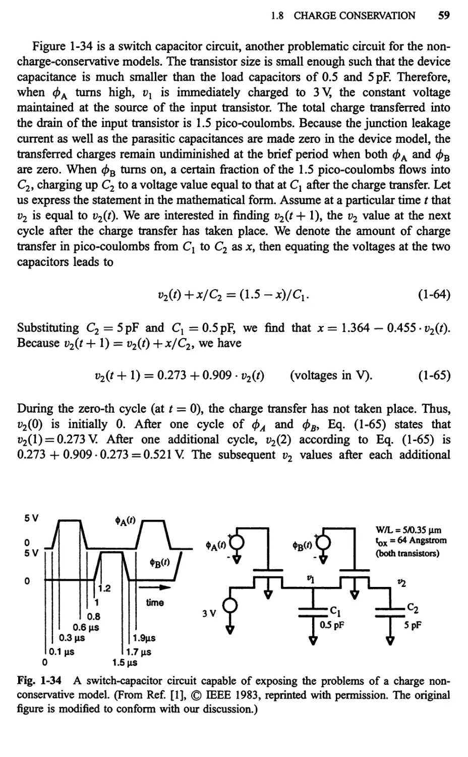
Текст
MOSFET Models for
SPICE Simula.tion
including BSIM3v3 and BSIM4
o 1 I
(
'William Li u
MOSFET MODELS
FOR SPICE SIMULATION,
INCLUDING
BSIM3v3 AND BSIM4
MOSFET MODELS
FOR SPICE SIMULATION,
INCLUDING
BSIM3v3 AND BSIM4
WILLIAM LID
Texas Instruments
A Wiley-Interscience Publication
John Wiley & Sons, Inc.
New York · Chichester. Weinheim · Brisbane · Singapore · Toronto
A NOm TO 1HE READER
This book has been electronically reproduced tram
digital information stored at John Wiley & Sons, Inc.
We are pleased that the use of this new technology
will enable us to keep works of enduring scholarly
value in print as long as there is a reasonable demand
for them. The content of this book is identical to
previous printings.
This book is printed on acid-ftee paper. @)
Copyright @ 200 1 by John Wiley & Sons, Inc. All rights reserved.
Published simultaneously in Canada.
No part of this publication may be reproduced, slored in a retrieval system or lransmitted
in any form or by any Ineans, electronic, mechanical, photocopying, recording, scanning
or otherwisc. except as pennitted undcr Scctions 107 or 108 of the 1976 United States
Copyright Act without either the plior written pelmission of the Publisher, or
authorization through payment of the appropriate per-copy fee to the Copyright
Clearance Center, 222 Rosewood Drive, Danvers, MA 01923, (978) 750-8400, fax
(978) 750-4470. Requests to the Publisher for pennission should be addressed to lhe
Permissions Depal1J11ent, John WHey & Sons, Inc., 1 J 1 River Street, Hoboken.. NJ 07030,
(201) 748-6011, fax (20]) 748-6008.
To order books or for custoiller service pJease, call I (800)-CALL-WILEY (225-5945).
Library of Congress Cataloging-in-Publication Data is available.
ISBN: 0-471-39697-4
10 9 8 7 6 5 4 3 2
To: my wife, Lee-Ping Chong
my daughters, Yiling Ashley Liu, and Yilan Audrey Liu
my parents, Chien-Shun and Li- Yue Liu
the Liu family, abroad in US or back in Taiwan
the coach, Prof. James Harris
and. . .
my idosyncratic chess pals, who master both
- .11
- II - II
and
-
II
,II
, /
oiL / , oiL
, r ,r
L oiL oiL oiL .I
r 'Ir ,r ,r 'I
L oiL oiL oiL .I
r 'I r , r , r 'I
oiL oiL
,r , / 'Ir
/ ,
CONTENTS
Preface
xi
1 Modeling Jargons 1
1.1 SPICE Simulator and SPICE Model, 1
1.2 Numerical Iteration and Convergence, 8
1.3 Digital vs. Analog Models, 11
1.4 Smoothing Function and Single Equation, 27
1.5 Chain Rule, 36
1.6 Quasi-Static Approximation, 38
1.7 Tenninal Charges and Charge Partition, 44
1.8 Charge Conservation, 50
1.9 Non-Quasi-Static and Quasi-Static y-Parameters, 62
1.10 Source-Referencing and Inverse Modeling, 70
1.11 Physical Model and Table-Lookup Model, 77
1.12 Scalable Model and Device Binning, 86
References and Notes, 98
vii
viii CONTENTS
2 Basic Facts About BSIM3 101
2.1 What Is and What's Not Implemented in BSIM3, 101
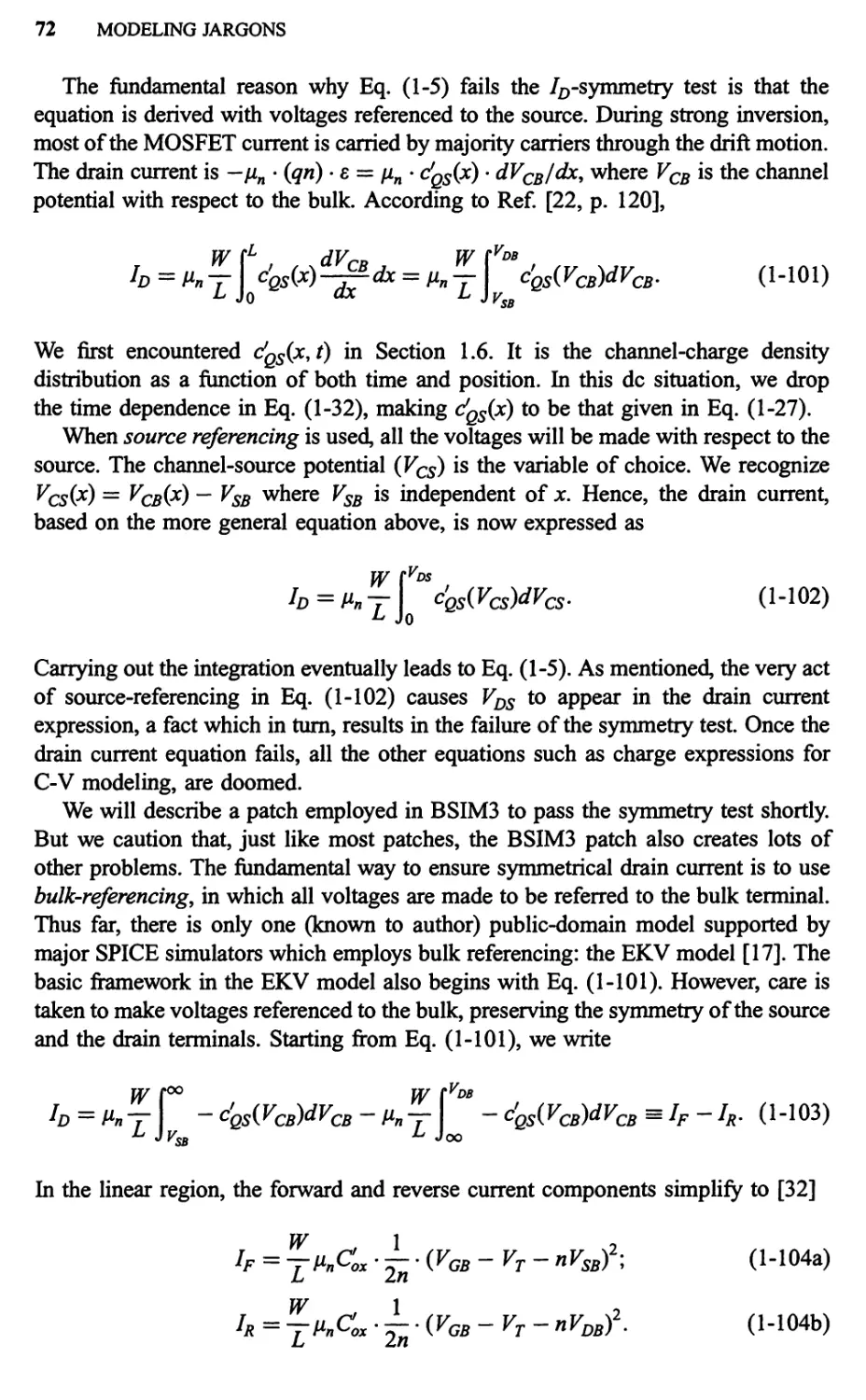
2.2 DC Equivalent Circuit Model, 104
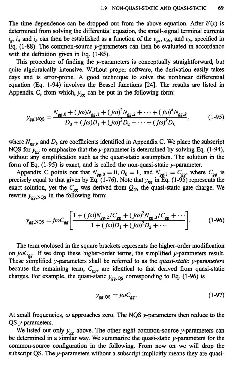
2.3 BSIM3's y-Parameters, 116
2.4 Large-Signal Equivalent Circuit, 122
2.5 Small-Signal Model, 133
2.6 Noise Equivalent Circuit, 140
2.7 Special Operating Conditions: V DS < 0, V BS > 0, Vas < 0, or
V BD > 0, 149
References and Notes, 156
3 BSIM3 Parameters 158
3.1 List of Parameters According to Function, 158
3.2 Alphabetical Glossary of BSIM3 Parameters, 162
3.3 Flow Diagram of SPICE Simulation, 275
References and Notes, 283
4 Improvable Areas of BSIM3 284
4.1 Lack of Robust Non-Quasi-Static Models: Transient Analysis, 285
4.2 Problem with the 40/60 Partition: The "Killer NOR Gate", 299
4.3 Lack of Channel Resistance (NQS Effect; Small-Signal Analysis), 303
4.4 Incorrect Transconductance Dependency on Frequency, 313
4.5 Lack of Gate Resistance (and Associated Noise), 316
4.6 Lack of Substrate Distributed Resistance (and Associated Noise), 323
4.7 Incorrect Source/Drain Asymmetry at V DS = 0, 329
4.8 Incorrect C gb Behaviors, 333
4.9 Capacitances with Wrong Signs, 339
4.10 Cgg Fit and Other Capacitance Issues, 341
4.11 Insufficient Noise Modeling (No Excess Short-Channel Thennal
Noise), 356
4.12 Insufficient Noise Modeling (No Channel-Induced Gate Noise), 362
4.13 Incorrect Noise Figure Behavior, 366
CONTENTS ix
4.14 Inconsistent Input-Referred Noise Behavior, 375
4.15 Possible Negative Transconductances, 376
4.16 Lack of GIDL (Gate-Induced Drain Leakage) Current, 382
4.17 Incorrect Subthreshold Behaviors, 387
4.18 Threshold Voltage Rollup, 390
4.19 Problems Associated with a Nonzero RDSW, 391
4.20 Other Nuisances, 392
References and Notes, 396
5. Improvements in BSIM4 399
5.1 Introduction, 399
5.2 Physical and Electrical Oxide Thicknesses, 400
5.3 Strong Inversion Potential for Vertical Nonunifonn Doping Profile, 402
5.4 Threshold Voltage Modifications, 403
5.5 V GST,eff in Moderate Inversion, 408
5.6 Drain Conductance Model, 409
5.7 Mobility Model, 412
5.8 Diode Capacitance, 414
5.9 Diode Breakdown, 417
5.10 GIDL (Gate-Induced Drain Leakage) Current, 425
5.11 Bias-Dependent Drain-Source Resistance, 427
5.12 Gate Resistance, 431
5.13 Substrate Resistance, 434
5.14 Overlap Capacitance, 435
5.15 Thennal Noise Models, 436
5.16 Flicker Noise Model, 450
5.17 N on-Quasi-Static AC Model, 451
5.18 Gate Tunneling Currents, 459
5.19 Layout-Dependent Parasitics, 465
References and Notes, 472
x CONTENTS
Appendixes 473
A BSIM3 Equations, 473
B Capacitances and Charges for All Bias Conditions, 507
C Non-Quasi-Static y-Parameters, 510
D Fringing Capacitance, 515
E BSIM3 Non-Quasi-Static Modeling, 519
F Noise Figure, 522
G BSIM4 Equations, 528
Index 583
PREFACE
Here is a little secret about BSIM3. You cannot find what BSIM stands for in the
official BSIM3 manual, nor the official BSIM3 web site (at least as of March, 2000).
The reason is simple-BSIM is a household name in the SPICE simulation
community. It is so much used that it has become a standard vocabulary, in a
similar way that we tend to forget laser stands for light amplification by stimulated
emission of radiation. To save you from scratching your head, I state that BSIM is an
acronym for Berkeley Short-Channel IGFET Model. As the full name suggests, it is a
MOSFET model capable of handling modem CMOS devices with pronounced
short-channel effects. But this description also begs the question exactly what short-
channel effects are handled by BSIM3. Or, more generally, does the model account
for various leakage currents and terminal resistances?
These questions as well as others are answered in Chapter 2, which summarizes
the key components of BSIM3. Because circuit designers tend to view devices with
an equivalent circuit, I also represent the BSIM3 model with various equivalent
circuits, for various operating conditions. Although Chapter 2 serves as an entry for
those who are eager to learn the basics of BSIM3, some modeling background is
presented in Chapter 1. This introductory chapter is where the readers can find the
meanings and connotations of various modeling jargons, such as charge conserva-
tion, quasi-static approximation, and so on. For those who really have no time to
understand the details (and thus the beauty) of modeling, I have prepared Chapter 3.
It contains an alphabetical listing of the BSIM3 parameters, as well as their
meanings and relevant equations.
No model is perfect. BSIM3 certainly shares many of the problems that haunt
other models. In Chapter 4 several areas of improvement for the BSIM3 model are
pointed out, whether it is used in a dc, ac, transient, or noise analysis. Most of these
improvements have been made in BSIM4, the to-date newest member of the BSIM
xi
xii PREFACE
family introduced in 2000. The improvements of the BSIM4 are described in
Chapter 5.
Many people cry foul when I praise BSIM3. They contend that it is just a biased
opinion. Well, the time has come for me to clarify one point. Although I have used
BSIM3 quite often and personally liked BSIM3, I am not one of the BSIM3 authors.
The misconception can arise because the chief researcher in charge of the BSIM3
(and BSIM4) development happens to have the same first name initial (w.) and the
same last name (Liu) as mine. This coincidence is evident particularly when the
BSIM3 manual is referenced. See, for example, Ref: [14] of Chapter 1. I surely did
not write any portion of the BSIM3 manual, although the reference seemingly
suggests so. I merely write this book to complement the manual. Our last name,
incidentally, is the royal last name of the most powerful Chinese dynasty. The Han
dynasty, which existed some 2000 years before the Republic of China, is credited for
the naming of the Chinese people as the Han race. And for those who aspire to be a
millionaire (such as in the popular television show), here are some trivia for you-
paper was invented in Han dynasty by a chamberlain/eunuch serving Emperor Liu,
and the newly elected president of Republic of China is a National Taiwan
University graduate named Shui-bian Chen.
The development of this book has been benefited by my colleagues at or formerly
at Texas Instruments, as well as the BSIM team from the University of California at
Berkeley. I would especially like to thank Keith Green, Karthik Vasanth, Tom
Vrotsos, Paul Koch, James Hellums and David Zweidinger for their written
comments and suggestions, and Professor Cheming Hu, Weidong Liu, Xiaodong
Jin, Mark Cao, and Yuhua Cheng for their outstanding efforts in providing the BSIM
models and for answering my questions about BSIM3 and BSIM4. Professor Hu and
Yuhua's book, MOSFET Modeling & BSIM3 Users Guide, has been very helpful in
the preparation of this work.
The discussions with Rajni Aggarwal, Ajith Amerasekera, Jonathan Brodsky,
Britt Brooks, Mi-Chang Chang, Ming Chiang, Paul Cox, Charvaka Duvvury, Paul
Ehnis, Ulvi Erdogan, Ranjit Gharpurey, Vinod Gupta, John Krick, Brian Mounce,
Ismail Oguzman, Shridar Ramaswamy, Jerry Seitchik, Robert Steinhoff: Sreenath
Unnikrishnan, Robert Virkus, Bruce Thornton, Doug Weiser, and Ping Yang, who
have helped shape the final form of this book, are gratefully acknowledged. My
special gratitude goes to "Coach", Professor James Harris of Stanford University,
who, since my graduate studies there, has inspired me to do great research and seek
physical understanding.
My fellow Stanford colleagues, Darrell Hill, now at Motorola, Chong-Hong Dai,
a manager at Intel, as well as Ken Shepard, a Columbia University professor, also
helped me with some simulator questions. I would also like to thank Christian Enz of
Conexant, Dr. Klaassen, and Luuk Tiemeijer of Philips for clarifying rf issues in
modeling. The book editor at Wiley, George Telecki, as well as the anonymous
reviewers, have all been extremely helpful in shaping this project to publication.
Finally, I thank my wife, Lee-Ping Chong, and my parents, Chien-Shun and Li- Yue
Liu, for their encouragement and support.
WILLIAM LID
1
MODELING JARGONS
1.1 SPICE SIMULATOR AND SPICE MODEL
Just about all electrical engineers have some form of encounter with SPICE,
Simu lation Pr ogram with !ntegrated Circ uit Em phasis. It could be in a homework
assignment during the undergraduate studies, or as an essential part of circuit design
at .work. As its full name suggests, SPICE is a computer program that accepts a
circuit schematic as input and outputs the simulated circuit behaviors. The simula-
tion can be performed under the nonlinear dc, nonlinear transient and linearized ac
operating conditions. The circuit may contain resistors, capacitors, inductors, mutual
inductors, independent voltage and current sources, dependent sources, loss less and
lossy transmission lines, switches, uniform distributed RC lines, and various
semiconductor devices including MOSFETs (metal oxide semiconductor field-
effect transistors). The original SPICE program, SPICE 1, was developed at Univer-
sity of Cali fomi a, Berkeley, and released for public use in May, 1972. By 1975, after
the next major release, called SPICE2, SPICE was in widespread use and adopted by
most integrated circuit manufacturers. SPICE2 was written in Fortran. With the
advent of UNIX computers in the 1980s it became increasingly obvious that SPICE
would benefit from the C-shell utilities that come with UNIX computers. This
prompted the rewriting of the SPICE program in the C-Ianguage, although the basic
algorithms remain largely intact. The revised SPICE program, called SPICE3, was
released in public domain in March, 1985.
The free distribution by Berkeley is a key factor contributing to the universal
acceptance of SPICE. Accompanying with this free lunch, however, is the inevitable
lack of "product" support. Several large companies have written their own version of
the circuit simulation program to better serve their companies' particular interests.
One notable proprietary SPICE, which pioneered the use of charge-based device
1
2 MODELING JARGONS
model as the solution to the charge non-conservation problem, is the TI-SPICE, still
in use in Texas Instruments today [1]. In a charge-based approach, the charge
(instead of voltage) becomes the state variable in calculating the transient behavior
of MOSFET. This ensured charge conservation, as discussed later in Section 1.8.
There are also vendors who develop commercial versions of SPICE to tailor the
needs of the small companies without a CAD (computer aided design) group of their
own. One commercial version is HSPICE. It is a robust SPICE program combined
with an excellent graphic interactive interface. HSPICE is used extensively on
UNIX-based workstations. Another example is PSPICE, introduced in 1984, which
runs on PC and Macintosh platforms (but at a significantly slower speed than UNIX-
based SPICE programs). Because of the proliferation of personal computers, this
PC-based SPICE program has attracted many new users and helped SPICE make
another leap in popularity since the introduction of SPICE2. These various versions
of the SPICE program provide improvements in user interfaces, user support,
numerical convergence, and device modeling. Although these (non-Berkeley)
versions contain several differences in the implementation of the numerical routines
or device models, they nonetheless retain the original SPICE's programming
structure. The following lists some notable SPICE programs that are (were) readily
available for the public's use (free or for a fee).
Berkeley SPICE The original SPICE. It is in the public domain and can be run on
UNIX platforms. See http://infopad.eecs. berkeley.edul-icde-
sign/SPICE and http://hera.eecs.berkeley.edul-software/
spice3f5.html. The latest version, SPICE3f5, supports
BSIM3v3.1, but not higher versions of models. BSIM3v3.2
and higher are supported by SPICE3e2.
I-SPICE Interactive SPICE, developed in the late 1970s. This is the first
commercial version of SPICE. As stated in [2], "it probably
would have been a success were it not for the impending
failure of the time-sharing service concept."
HSPICE Created by Meta-Software and now owned by Avant!. It is
popular within UNIX-based users, and known for its inter-
active user interfaces. BSIM2, BSIM3v2, and BSIM3v3 are
implemented as levels 39, 47, and 49, respectively. Its proprie-
tary MOSFET model (level 28) remains popular today.
PSPICE PC-based version SPICE created by Micro-Sim, which was
recently acquired by Orcad. It has evolved to support BSIM
models as well as complete IC models.
SPECTRE Created by Cadence. It can be thought of as an improved
Berkeley SPICE that addresses several numerical problems
and the inadequacies in simulation for r.t: circuits. It supports
all Berkeley MOS models.
Today there are more than 100,000 copies of SPICE in active use at universities
and industry [3], and some trial versions can be found online [4]. There are currently
about 20 companies providing SPICE products and support commercially [3].
1.1 SPICE SIMULATOR AND SPICE MODEL 3
In the previous discussion of various derivatives of the Berkeley SPICE, we did
not make a clear distinction between the SPICE simulator and the SPICE device
model. Together, these two parts form the overall SPICE program. The SPICE
simulator is the mathematical engine of SPICE, consisting of several basic
subroutines to perform numerical analyses. One exemplar numerical subroutine is
matrix inversion, which is the backbone algorithm to solve n linearly independent
equations with n unknowns. This routine, when combined with the Newton-Raphson
iteration technique, allows the solution of nonlinear equations which govern the
static nodal voltages and the branch currents of a given circuit.
Another basic SPICE subroutine solves ordinary differential equations. This type
of routine is invoked in a transient analysis involving time as the independent
variable. The transient analysis is a one-dimensional problem in which the voltages
and currents are functions of time only. Other simulation programs, notably PISCES
[5] (or its commercial version-MEDICI), which simultaneously solve the Poisson
equation and current continuity equations, address four-dimensional problems
involving space (x, y, z) and time (t) as the independent variables. As far as
numerical analysis is concerned, it is inherently more difficult to solve a multi-
dimensional partial differential equation than a one-dimensional ordinary differential
equation. Therefore, SPICE simulation of a circuit is generally faster and enjoys less
convergence problems than PISCES simulation of a device. On the other hand,
PISCES (or MEDICI) simulation solves the fundamental physical equations govern-
ing the device. Once the doping profiles and physical device structure are supplied to
the simulator, the solution represents the actual characteristics expected from the
device. Often the phrase "MEDICI results" is mentioned in the book. It is implied
that the MEDICI simulation results are the exact solution against which the SPICE
simulation results can be compared. If the results of a SPICE simulation deviate
significantly from a MEDICI simulation, we conclude that either the SPICE model
used in the simulation is imperfect, or its model parameters are not properly extracted.
Besides its number-crunching ability, the SPICE simulator also handles the input
and output details of the overall SPICE program. It takes the input SPICE deck and
constructs the circuit for simulation. It prepares results in a data fonnat specified by
the user.
The second part of a SPICE program is the device model. There can be many
semiconductor devices in a circuit, such as a diode, a bipolar transi'stor, or a
capacitor. Since this book concerns MOSFET, we shall concentrate on the MOSFET
device model in particular. A model mathematically represents the device character-
istics under various bias conditions. In dc and ac analyses, the inputs of the device
model are the drain-to-source, gate-to-source, bulk-to-source voltages, and the
device temperature. The outputs are the various terminal currents. The model
parameters, along with the equations in the SPICE model, directly affect the final
outcome of the terminal currents. In a transient analysis we can think that the SPICE
model accepts the time derivative of the bias voltages, in addition to the absolute
values of the biases themselves at an instant of time. The output of the SPICE model
is then the terminal currents at that particular instant of time. If a noise analysis is
specified in the input deck, the SPICE model also computes the noise voltages at a
particular set of bias condition and frequency.
4 MODELING JARGONS
We illustrate the interaction between the SPICE simulator and the SPICE model
using the dc circuit shown in Fig. 1-1. Although the input bias current is given, the
nodal voltages as well as the branch currents are not known. The SPICE simulator
first guesses a solution set for all the unknown nodal voltages (at node 1,2, and 3). A
subset of these guessed voltage values which bias up the MOSFET (V 2 and V 3 ) are
passed to the SPICE model as inputs. Subsequently, the SPICE model evaluates the
currents at the four tenninals of the MOSFET and feeds the information back to the
SPICE simulator. The SPICE simulator then checks whether the Kirchoff current
law is fulfilled at each node, that the sum of currents at a node is zero. (Strictly
speaking, the SPICE simulator does not really check the Kirchoff current law. It uses
a slightly different form of convergence test. We will elaborate on this fine point in
Section 1.2.) More than likely, the first guess does not prevail and the Kirchoff
current law is violated. Subsequently, the derivative of the currents with respect to
the voltages (such as gm = 8I D /8V GS ' gd = 8I D /8V Ds and gmb = 8I D /8V Bs ) are
evaluated. These derivatives are used in the Newton-Raphson subroutine to make
an educated guess of the nodal voltages for the next iteration. These newly guessed
voltages are again fed to the SPICE device model, and the terminal currents are re-
evaluated. With each successive iteration, the guessed set of voltage values
approaches the actual solution. This process iterates until the Kirchoff current law
becomes satisfied at every node. (Or, as more correctly put in Section 1.2, the
iteration stops when the nodal voltages and the branch currents are within a
prescribed tolerance in two consecutive iterations.)
There are two points relating to the convergence process of SPICE simulator.
First, even for a dc analysis, the small-signal conductances (such as gm' gd, and gmb)
are required from the model. These small-signal quantities calculated from the
SPICE model provide valuable information about the circuit itself, aiding the SPICE
simulator to make educated guesses in subsequent iterations. Therefore, suppose that
a circuit is designed to operate only at dc. A MOSFET model still needs to supply
the small-signal quantities. Second, these small-signal quantities aid the speed at
which the dc convergence is met, but does not preclude convergence when their
values are incorrect (such as due to coding errors). The SPICE simulator may still
1
2
IIN
Fig. 1-1 A circuit used to illustrate the interaction between a SPICE simulator and a SPICE
model.
1.1 SPICE SIMULATOR AND SPICE MODEL 5
converge, albeit at a much slower pace. There are occasions where a model produces
negative conductances. In this case, the convergence for the dc analysis may be
significantly hampered, and in extreme cases, prevents a solution from ever being
reached (Section 1.2). In an ac (or noise) analysis, however, the accuracy of the
small-signal parameters are critical to the accuracy of the solution itself:
We have mentioned several SPICE simulators before, including Berkeley SPICE,
HSPICE, and PSPICE. They are not complete without the SPICE models. Some
notable SPICE models for MOSFET are listed in the following, in somewhat a
chronological order of the time the model was introduced.
Levell Also known as the Shichman-Hodges model [6], this is the
original model since the dawn of Berkeley SPICE. The
model equations are simple, resembling those used in under-
graduate textbooks, and are applicable mainly to long-
channel devices. The C- V portion of the model is the
Meyer model [7], which is not a charge-conserved model
(Section 1.8).
Level 2 This model addresses several short-channel effects such as the
velocity saturation [8]. However, the mathematical imple-
mentation of the model was complicated, leading to many
convergence problems. For C- V calculation, either the
Meyer model of Level 1 or the Ward-Dutton model [9]
can be used. The Ward-Dutton model is a charge-conserved
model, which forms the backbone of all present models.
Level 3 This semi-empirical model is regarded as a simplified version
of Level 2 [8]. This model has proven to be robust and is
popular for digital circuit design. However, the model is not
very scalable and binning (Section 1.12) is almost always
required. Discontinuities in the first derivative of the drain
current exist.
BSIM It is the B erkeley Sh ort-Channel !GFET Mo del [10], some-
times referred to as Level 4. The model places less emphasis
on the exact physical formulation of the device, but instead
relies on empirical parameters and polynomial equations to
handle various physical effects. This generally leads to
improved circuit simulation behavior compared to previous
models, although its accuracy degrades in submicron FETs.
Furthermore, the polynomial equations can behave poorly,
causing negative output conductance and convergence
problems.
HSPICE Level 28 This proprietary model developed by Meta-Software is similar
to BSIM [11]. However, with proper modification in the
binning strategy and mathematical description in the transi-
tion region (Section 1.12), Level 28 has been made suitable
for analog design and remains popular to date.
6 MODELING JARGONS
BSIM2
This is an extension to BSIM, with comprehensive modifica-
tions which make it suitable for analog circuit design [12].
Although BSIM2 improves upon BSIM in terms of model
accuracy as well as convergence behavior in circuit simula-
tion, it still breaks the transistor operation into several
regions. This leads to discontinuity in the first derivative in
I-V and C-V characteristics, a result that can cause numerical
problems in simulation.
With the help of smoothing functions (Section 1.4), BSIM3
adopts a single-equation to describe device characteristics in
various operating regions [13]. This eliminates the disconti-
nuity in the I-V and C-V characteristics. BSIM3 has
evolved through three versions. BSIM3vl and BSIM3v2
contain many mathematical problems so that they are largely
replaced by the third version; BSIM3v3. There are several
variations within BSIM3v3 itself, including BSIM3v3.1 and
BSIM3v3.2. The latter eventually grew into two further
variations: BSIM3v3.2.1, and BSIM3v3.2.2 [14]. A proce-
dure to identify the exact version of a BSIM3v3 model is
found in Section 3.2, under the entry of VERSION. These
variations of BSIM3v3 have minor differences, and have
been demonstrated for accurate use in 0.181lm technologies.
The manuals, codes, and news about BSIM3 can be found
online at http://www-device. eecs.berkeley.edul-bsim3.
BSIM3 is a level 8 model. At the time of this writing there
has been discussion to release BSIM3v3.3 [15].
MOS Model 9 is the primary non-Berkeley model available for
public use [16]. The model also employs smoothing func-
tions to achieve continuity in device characteristics. The
model is accurate for sub-quarter micron technologies and
exhibits good behaviors in circuit simulation. Model 9 is
probably as good as BSIM3. However, companies generally
opted for BSIM3 because it was not obvious whether there
were intellectual property issues associated with MOS 9, a
model developed at Philips Laboratories. The manuals,
codes, and news about Model 9 can be found online
at http://www-us.semiconductors.com/Philips_Models/
mosmodeI9.stm.html
This model is unique in its use of bulk-referencing [17], while
all other mentioned model employs source-referencing
(Section 1.10). This fundamental philosophical change
allows the EKV model a greater hope of fundamentally
eliminating the asymmetry problems unavoidable in the
source-referencing models. Despite its adoption of a more
BSIM3
Model 9
EKV Model
1.1 SPICE SIMULATOR AND SPICE MODEL 7
BSIM4
physical modeling approach, the EKV model is not yet
popular, partly because of its relatively late arrival compared
to other models. The manuals, codes, and news about the
EKV model can be found online at http://legwww.epfl.ch/
ekv/.
The newest addition to the BSIM family, made public in the
year 2000. BSIM4 offers several improvements over BSIM3,
not just in the traditional I-V modeling of the intrinsic
transistor, but also in the transistor's noise modeling, and
in the incorporation of extrinsic parasitics. BSIM4, a level 14
model, is discussed in Chapter 5.
Levell, 2, and 3 models are generally referred to as the first-generation models,
in which the models emphasize the device physics. The attention given to physically
accurate representation without equal consideration to mathematical representation
often creates numerical problems during circuit simulation. The second-generation
models, epitomized by BSIM, BSIM2, and HSPICE Level 28, corrects this problem
with greater focus on mathematical implementation. Several empirical parameters
without clear physical meanings are incorporated in the model. This approach gains
the advantage of improved convergence properties, but at the cost of complicating
the parameter extraction process as well as weakening the link between model
parameters and fabrication process. The third-generation models, represented by
BSIM3 and Model 9, seek to reintroduce a physical basis to the model, while
maintaining the mathematical fitness of the model equations. These models rely on
smoothing function to result in a single-equation that describes the I-V and C-V
characteristics. In this book we will concentrate on the BSIM3 model, the Compact-
Model-Council-supported standard model and the de facto industry standard model
being used today. Details of other mentioned models can be found in Ref. [18]
Generally the term SPICE is used without a clear distinction between the SPICE
simulator and the SPICE models. For example, a statement "the simulation is done
with the Berkeley SPICE" is ambiguous. Depending on the context, the sentence
can mean that the simulation is performed with the Berkeley SPICE simulator (such
as SPICE3t), although the MOSFET model is non-Berkeley, for example, the level
28 model created by MetaSoftware. Conversely, the sentence could mean that the
simulation was done with the HSPICE simulator, but with a Berkeley SPICE model
(such as BSIM). Finally, it can also mean that the simulation was done with both the
Berkeley SPICE simulator as well as the Berkeley SPICE model. Not all MOSFET
models are supported by all SPICE simulators. Obviously, while TI-SPICE simulator
supports both TI's proprietary SPICE MOSFET model as well as BSIM3, the
Berkeley SPICE simulator does not support the TI-SPICE model. Moreover, a
SPICE simulator often supports several SPICE models for the MOSFET, using the
parameter LEVEL to distinguish between various models. For example, HSPICE
supports BSIM2, BSIM3v2, and BSIM3v3 models, and are implemented as levels
39, 47, and 49, respectively.
8 MODELING JARGONS
Some SPICE programs are basically known for their SPICE simulators. For
example, PSPICE is well known because its SPICE simulators run on the PC
platfonn. PSPICE's SPICE models for MOSFETs are those public domain models
created by Berkeley over the years. However, occasionally the SPICE model is as
well known as its SPICE simulator. Take HSPICE, for example. Its Level 28
MOSFET model was introduced at a time when there was no good analog model.
This proprietary model is used as a vehicle to gain widespread acceptance of the
HSPICE simulator.
1.2 NUMERICAL ITERATION AND CONVERGENCE
SPICE is a numerical program constructed to solve the voltages and currents of a
given circuit. Consider the simple 3-node circuit shown in Fig. 1-1. According to the
Kirchoff's current law (KCL) for node 2, we have
VI - V2 V2 - V3 W JlnC x ( v: ) 2 - 0
- - - V3 - r - .
R A R B L 2
(1-1)
For simplicity, we have modeled the drain current of the MOSFET with the well-
known saturation current equal to WIL. Jln . C x. (V GS - V r )2/2 [19], where JK the
channel width, L, the channel length, Jln' the channel mobility, C x' the device's
oxide capacitance per unit area, and V r, the threshold voltage, are known quantities
(as specified in or calculated from the SPICE model). Equation (1-1) can be
rewritten in a more abstract fashion,
f2(VI' v2, v3) = 0,
(1- 2a)
where 12 is the function relating to the various circuit elements which tie at node 2.
Similar KCL statements imposed at nodes 1 and 3 result in the following equations:
fi (VI' V2, V3) = 0;
f3(VI' V2, V3) = o.
(1-2b)
(1- 2c )
The SPICE simulator solves these three equations of three unknowns by the
Newton-Raphson algorithm [20], which seeks the solution of a set of nonlinear
equations through the iterative solutions of a sequence of linear equations. The
algorithm starts out by taking an initial ess of the solution of the circuit. Let us
denote the zero-th iteration solution as, V O), V O), and V O). The guessed solution is
checked against a set of convergence criteria. If the guessed solution is not close to
the true solution, then the algorithm calls for an evaluation of the derivatives of
f,,(VI' v2, v3) for all nodes n = 1,2, and 3. These derivatives point to the general
direction in which the next solution should be guessed to maximize the chance of
convergence. An intuitive understanding of how the derivatives help convergence is
shown in Fig. 1-2, which illustrates the I-dimensional analog of the present problem.
1.2 NUMERICAL ITERATION AND CONVERGENCE 9
f(v)
+ 1f.2)1f.l)
Solution: f( v) = 0
1/..0)
v y
v x
v
Fig. 1-2 Iterative process used in the Newton-Raphson technique to solve for the root v that
satisfies f( v) = o.
We intend to solve for v such thatf(v) crosses the x-axis. v(O) is the initial guess, and
obviously not the solution. At this particular guess, both f( v(O») and its derivative,
8f(v(O»)/8t, are evaluated. We draw a dotted line £romf(v(O») toward the x-axis, with a
slope equal to the derivative. The intersection of the dotted line with the x-axis is the
next best guess, denoted as V(l). We evaluate the function f with the new solution,
finding it equal tof(v(l»). Becausef(v(l») differs £rom 0, it is not the solution, and the
next solution is guessed, again based on the infonnation of the derivative, which is
8f(v(l»)/8t this time. This iterative process continues until some convergence criteria
are satisfied.
While most often the Newton-Raphson method converges to a solution, occa-
sionally the iteration fails to converge. The right portion of Fig. 1-2 illustrates this
possibility. Suppose instead that the initial guess is V x . Fromf(v x ) and the derivative
at that point, we follow the algorithm and trace the next guess of solution to be v y .
Because f(vy) #- 0, we have not converged to a solution and another iteration
resumes. Fromf(v y ) and the derivative at that point, we follow the algorithm and
trace the next guess of solution to be V x . This is obviously not a solution, either.
From here onward, the subsequent guesses of solution oscillate back and forth
between V x and VY' without any hope of ever converging to the root. In this particular
example, two causes are responsible for the nonconvergence. The first is a bad initial
guess, and the second, the existence of negative conductance (equal to the slope at
f(v)), which leads to the oscillations in the guessed solutions. The first problem can
be overcome by the user, with either the . NODESET or the . FORCE functions of the
SPICE simulator. The . NODESET statement allows for the user-detennined initial
voltage values for all or part of the nodes, whereas the . FORCE statement fixes the
voltage to some particular values. The second problem, however, is intrinsic to the
device model, and usually cannot be modified by the user. The user, however, may
10 MODELING JARGONS
modify the bias voltage slightly so the transistor is biased at a different operating
point, with the hope that somehow a new set of conductance values facilitates the
exit of the oscillation mode.
Figure 1-2 is a graphical illustration of the Newton-Raphson algorithm in one
dimension, for the solution of one variable and one unknown. Let us return to the
discussion of the SPICE solution for the circuit of Fig. 1-1, which is a multi-
dimensional problem. As mentioned, at each iteration the SPICE simulator guesses a
set of solutions, vI' V2' . . . , V n , where n is the number of nodes. If the solution set
does not meet a certain convergence criteria, then a new set of solution is obtained
from the derivatives at f(VI),f(V2)' . . . ,f(v n ), and the iteration continues. To
simplify the discussion of the convergence criteria used in the SPICE simulator,
let us denote the solution set at the j-th iteration as v }1, v }1, . . . , v }1. (Again, n refers
to the node number.) In SPICE, this set of solution is considered the desired solution
when the following two conditions are met simultaneously for all nodes n:
Iv j) - v j-I)I < vntol + rel tol . max(lv j)l, Iv j-I)I); (1-3a)
1 " ( (j) (j) (J) ) " ( (j-I) (j-I) (j-I» )I b 1 + lt 1
In vI ' v 2 ,..., v n - In VI ' V 2 ' . . . , V n < a s to re 0
(I ,, ( (j) (j) (j» )1 I " ( (j-I) (j-I) (j-I» )I) (1 - 3b)
. max In VI ' V 2 ,..., V n 'In VI ' V 2 ' . . . , V n .
The vntol, abstol, and rel tol are the tolerance levels, having default values
of 1 Jl 1 pA, and 0.001, respectively. Their values can be modified in the . OPTION
statement. (Note: Some SPICE simulators may have different names for these
tolerances.) The first criterion requires the voltage of a node at a given iteration to
be close to its predecessor, within a specified tolerance level. This guarantees that the
nodal voltages of a circuit settle at some stable values. The tolerance is composed of
two components. The relative tolerance (rel tol) allows the simulation of the high-
voltage and low-voltage circuits without adjusting the tolerance levels. The absolute
nodal voltage tolerance (vn tol), in contrast, is necessary in cases where the voltage
and current of the circuit are fairly close to zero. Without the latter, the updated
solution can be within the computer rounding error or simply too small to be ever
considered converged. While the first criterion (Eq. 1-3a) focuses on the voltage, the
second criterion (Eq. 1-3b) ensures the functions obtained from the KCLs at all the
nodes are relatively the same at each successive iteration. We emphasize that,
although Eq. (1-3b) seems to impose the KCL, it really just checks whether the
function values settle down. In other words, even if a solution meets both the
requirements of Eq. (1-3), the KCL is not necessarily satisfied. It turns out that
checking the Kirchoff's current law as a part of convergence criteria is not a
straightforward task. To ensure that KCLs are satisfied, we should have checked
h th " ( ()) (j) (j» ) . 1 th th 1 t
weer J" V j ,v 2 ,..., V n IS C ose to zero, ra er an c ose 0
" ( (j-I) (J-I) (j-I» ) h . h d b I th th th
In vI ' V 2 ' . . . , V n , W IC nee s not e zero. n e event at e conver-
gence criteria are met at the j-th iteration butJ;,(v }1, v j), . . . , v j») # 0, then at each
node the currents do not quite sum to zero. Equivalently, a small current source, with
a value smaller than that allowed by the convergence criteria, is connected to each of
1.3 DIGITAL VS. ANALOG MODELS 11
the nodes. The additional injected current can become problematic at a high
impedance node, since it would contribute to an appreciable amount of voltage
error. The requirement of Eq. (1-3a) curtails the degree of this problem somewhat,
by forcing the convergence to take place only after the node voltages settle down.
Nonetheless, there is always a possibility that false convergence occurs, and the
SPICE simulator reaches the wrong solution.
The accuracy and speed of the overall circuit simulation depend critically on both
the SPICE simulator and the device model. If the numerical algorithm implemented
in the SPICE simulator is not robust, then we have no hope of expediency in the
numerical convergence process, even though the SPICE model provides a realistic
representation of the device. Conversely, if the SPICE simulator is well implemented
but the SPICE model produces negative conductances or kinks in its device
characteristics, then the convergence will be slow (or never).
The above description of the algorithm to solve for the voltages and currents of a
3-noded circuit is a gross simplification of what is actually implemented in the
SPICE simulator. The actual implementation is more robust in the construction of
the nodal equations to be solved, and incorporates several subroutines to facilitate
convergence. However, the presented concepts of the algorithm are correct and allow
us better to appreciate the inner working of the SPICE simulator. The convergence
criteria of Eq. (1-3) are encountered in typical SPICE simulators, especially those
derived from the Berkeley SPICE [21]. As such, Kirchoff's current law is not
checked during the simulation (although the to-be-solved equations are fonnulated
based on KCL).
1.3 DIGITAL VS. ANALOG MODELS
Having differentiated the SPICE simulator and the SPICE model portions of the
overall SPICE program, we shall concentrate exclusively on the SPICE model from
here onward. We begin with a classic oxymoron expected of the device modeling
engIneers:
A model shall be accurate and simple.
Certainly, a model should be accurate enough so that the results produced in a
simulation are trustworthy. The model should also be simple so that the simulation
time is minimal and the process for parameter extraction can be easily implemented.
However, creating a model that is both accurate and simple is by no means a simple
task.
A balance between the model simplicity and accuracy needs to be attained. The
exact equilibrium point is primarily detennined by the end application for which the
model is used. Over 95% of the world's semiconductor sales is in silicon, the
majority of which are digital CMOS circuits. With this level of sales, it is no wonder
that the traditional MOSFET modeling efforts focus on digital circuits. These
models, loosely called digital models, are used in circuitries with many transistors
12 MODELING JARGONS
(as opposed to only a few, as in analog circuits). It is crucial that the time evaluating
the model equations be short, to minimize the overall SPICE simulation time.
Therefore, as far as the digital models are concerned, the delicate balance had
favored model simplicity in the past, sacrificing accuracy in the device model.
Although the accuracy at the device level is compromised, the simulation at the
overall circuit level can still be accurate.
The I-V characteristics produced by one extreme example of a digital model are
schematically shown in Fig. 1-3. Although the fitted ID-vs.-V Ds curve is mostly
inaccurate and the subthreshold characteristics are way off (even in a logarithmic
plot), the drive current is fitted fairly accurately. (Drive current is the device current
when the gate and drain biases are at the maximum supply voltage of a given
technology.) This kind of fitting is ghastly to analog circuit designers, but it may just
be good enough for some types of digital circuits. In fact, experiences have shown
that if the drive currents and the parasitic capacitances are modeled well, an
inverter's switching speed is well predicted by the model. The relaxed requirement
on accuracy in fitting the device I-V characteristics allows the digital model to be
fairly crude, describable with only the least amount of model parameters. Conse-
quently, in the past, when modeling activity was predominantly for the prediction of
the inverter delay time in digital circuits, a model capable of putting forth the I-V
characteristics shown in Fig. 1-3 was deemed good enough. An elaborate model
which can fit I-V characteristics in all operating regions would necessarily involve
more model parameters, making the parameter extraction process more time-
consuming. During a SPICE simulation, this more elaborate model would also
require more mathematical evaluations, thus slowing down the speed of the
simulation. The elaborate model, in the interest of digital circuits, is both overly
constructed and inefficient.
However, when the same digital model is applied to analog circuit design, gross
simulation error results. This is because there are a lot more concerns in analog
circuits than just the drive current and the parasitic capacitances. With the recent
trend toward mixed analog-digital chips, low-voltage operation, and higher speed,
the concerns of analog circuit designers progressively receive more attention. Thus
the delicate balance for the model acceptance has gradually shifted toward model
log (1 D)
VGS
ID
1 drive
V GS = vsupply
Vs"pply
vDS
Fig. 1-3 I -V characteristics produced by a particular digital model. The drain current is
plotted in the Donnal and logarithmic scales.
1.3 DIGITAL VS. ANALOG MODELS 13
accuracy. The resulting model, being analog-circuit-friendly, is often referred to as
an analog model. One particular interest of analog circuit design is the accurate fit of
the small-signal parameters such as gm' gd, and gmb. In the MOSFET, the drain
current is a function of V GS ' V DS , and V BS . The mutual transconductance measures
the amount of drain current increase caused by the increment in the gate bias:
aID
gm = av:
GS V DS ' Vss=const.
(l-4a)
The drain transconductance measures the amount of drain current increase caused
by the increment in the drain bias. It is defined as
aID
gd = av
DS vGs.vss=const.
( 1-4b )
Finally, the bulk transconductance reveals the effect of back-gate bias on the drain
current conduction:
aID
gmb = av
BS vGS.vDS=const.
(l-4c)
We use Fig. 1-4 to illustrate the stringent requirement on the analog models. From
the I-V characteristics on the left, we are tempted to think that the fit is good. The
corresponding gd, equal to the slope of I D with respect to V DS , is shown on the right.
It is clear that although the model produces fairly good fit in the I-V characteristics,
the model is nowhere close to the fitting of gd. A good analog model is required to
produce accurate fitting in both the I-V characteristics as well as the gd character-
istics. In order to accommodate the increased requirement, an analog model usually
consists of a lot of parameters. Besides, the model equations need to be carefully
derived so that the simultaneous fit of I-V and smaIl-signal quantities is possible.
From a pragmatic viewpoint, we cannot really say that the analog model is better
than the digital model, since the digital model can produce accurate circuit
\
\
'..
..
..
....... model
....... ,.,,, ,ItI,,,,,,...."".
I D model
log(gd)
VDS
VDS
Fig. 1-4 A model that produces a good fit to the I-V characteristics may still yield a bad fit to
the small-signal quantities.
14 MODELING JARGONS
simulation for its intended applications. We can only conclude that the digital model
is simpler yet less accurate. This is the recurring theme-that the delicate balance
between accuracy and simplicity depends on the application.
We have stated that the requirements for digital and analog circuit models are
quite distinct. In the rest of this section, we list some of the distinguishing features of
these models. We should recognize that the exact requirements for the digital model
differ for designers working in various applications. For example, the fitting of
subthreshold characteristics is crucial to some digital circuit designers (e.g., for the
detennination of the off current), while being totally irrelevant for other digital
circuitries. Therefore, some generalizing remarks about the characteristics of the
digital and analog models, to be made in the following, are inevitable. The digital
model can be thought as a model sufficient for the design of low-end consumer
product, and the analog model, for the relatively higher-perfonnance higher-speed
analog parts. By the natures of the applications, these two models result in sharply
different device characteristics, although they both satisfy their respective circuit
simulation needs. Incidentally, the analog model employed for the following
discussion is based on BSIM3v3, while the digital model is not. The two model
parameters were initially created from the same device measurement results.
However, we intentionally change some parameter values so that the I-V character-
istics are displaced from each other, allowing for a clear comparison between the
simulation results of the two models.
1. Discontinuity in gd Figure 1-5 shows the calculated gd as a function of V DS
for the digital and analog models, for V GS = 2 and 3 V. V BS = o. The analog model
produces smooth transition as V DS varies from 0 to 3 within which the transistor
moves from linear to saturation region of operation. The drain conductance
decreases monotonically, not saturating at a constant value. In contrast, the digital
model has some undesirable features. Upon transiting from the linear to saturation
region, the drain conductance exhibits a kink, a reminiscent of the regional equations
employed in the digital model. That is, in a typical digital model the model prepares
several sets of equations, with each set devoted to a particular operating region such
as the saturation, linear, subthreshold, depletion, and accumulation regions. While
each set of equation works well within its intended region of operation, the transition
from one set to the other as the bias sweeps across different operating regions is not
always smooth.
Besides the kink feature, there is another inaccuracy of the digital model revealed
in Fig. 1-5. After the transistor enters the saturation region, the digital model
produces a constant gd, independent of V DS . This implies that, in this digital model,
the equations are such that the drain current can be expected to increase with V DS
only at a constant slope. In reality, gd continues to be a function of V DS , even during
saturation.
2. Discontinuity in gm Figure 1-6 exhibits the mutual transconductances
simulated by the two models, at V DS = 0.1 V and V BS = 0 and - 1.5 V. We shall
focus on the curve obtained at V BS = o. Just as in the discussion concerning gd, the
analog model gives rise to smooth gm across the subthreshold region
(V GS < V T ,....., 0.7 V), the saturation region (V T < V GS < 0.8 V), and the linear
1.3 DIGITAL VS. ANALOG MODELS 15
0.1 I I I I I I I I I I I I
I-
l-
t Analog Model
-- --- ---
(BSIM3)
L Digital 1odeI l
0.01 1
E ,
1- , -1
- "
I [ , 1
a \
I ,
'-' r ,
,
,
,
I V os =2V ,
,
0.001 " 1
,
,
" ,
F ... ...
[ ".. J
....
... .....
... --
I ........ ....
10-4 I -...-. - .. ... i
I I I I I I I I I I I I I I I I _ .... I I
0 0.5 1 1.5 2 2.5 3
V DS (V)
Fig. 1-5 Calculated gd as a function of V DS , at V GS = 2 and 3 V. The discontinuity is a
characteristic of the digital model, while B81M3 produces smooth characteristics.
region (V GS > 0.8 V). The digital model, on the other hand, produces kink
characteristics between the subthreshold and the saturation region. In addition, the
calculated gm in the digital model changes abruptly as the transistor moves £rom the
saturation to the linear region, with a discontinuity in the slope of gm. These
inaccuracies are again the direct result of the regional modeling approaches adopted
in the digital model. The use of the to-be-discussed smoothing equations to smooth
out the transitions between regions are key to nice characteristics.
3. Kink in I D A discontinuity in the small-signal quantities is translated into
kink problem in the drain current. Figure 1-7 plots the drain current as a function of
V GS , with V DS = 0.01 and V BS = o. The left side reports I D in linear scale, while the
right side, in logrithmic scale. The analog model shows that the drain current
increases exponentially with V GS, without any kink behavior. The characteristics
produced by the digital model, however, display a wiggle, right when the transistor
enters into the saturation region £rom the subthreshold region. This is yet another
manifestation of the digital model's adoption of the regional equations. The analog
model's use of smoothing functions adds a fair amount of complexity into the model
equations, but successfully removes the kink problems. .
4. Discontinuity in gm/ID The mutual transconductance can be used to estimate
the magnitude of the voltage or power gain of a transistor. It is desired that it be as
large as possible. A transistor with a large area has a higher gm, but at the cost of
incurring more dissipation current: A more meaningful figure of merit than gm itself
is gm/ID, which normalizes the mutual transconductance to the current dissipation.
We bear in mind that the gm / I D ratio is not the only parameter that a circuit designer
cares about. At the maximum gm/ID point, the current mirror matching can be so
16 MODELING JARGONS
0.002 ,
Abrupt ,
,
,
0.0015 Change ,
, ,
,
, .
. ,
, .
. ,
. ,
...-.. I .
- , .
I 0.001 . .
a , I
. .
'-" . .
. .
e . . Kink
, I
00 , .
0.0005 , .
. .
. .
, ,
, ,
, ,
, ,
, . -------- Analog Model
, ,
0 . ..'
V BS = 0 (BSIM3)
V BS = - 1.5 V Digital ?vlodel
-0.0005
0.4 0.6 0.8 1 1.2 1.4 1.6 1.8 2
V GS (V)
Fig.l-6 Calculated gm as a function of V GS , at V DS = 0.1 V and Vas = 0 and -1.5 The
digital model produces a kink at the transition between the subthreshold and the saturation
regIons.
poor or the cutoff rrequency can be so low such that the circuits are not operated
there. Nonetheless, it is a good figure of merit upon which several technologies can
be compared.
The quantity gm/ID as calculated rrom the analog and digital models are shown in
Fig. 1-8, plotted as a function of V GS , and in Fig. 1-9, as a function of I D . The
transistor is biased with a V DS of3.3 Vand V BS = 0 and 3 V. When the transistor is in
saturation, gm/ID is proportional to 1/(V GS - V r ). As V BS becomes more negative,
--- Analog Model
2 x 10⁻⁴ 0.01 Digital Model
,-..
<
.........
Q 10-4
-
,-..
Kink observ <
1 x 10⁻⁴ .........
with fine Q
VGsgrid -
Kink observed
10- 6 with fine
5 x 10- 5 VGsgrid
10- 8
0.5 0.7 0.9 1.1 1.3 1.5 0.5 0.7 0.9 1.1 1.3 1.5
V GS (V) Vas (V)
Fig. 1-7 Calculated I D as a function of V GS , with V DS = 0.01 V and Vas = O. The drain
current is plotted in the linear and logarithmic scales.
35
30
25
20
-
'-' 15
0
""" 10
e
b.O
5
0
1.3 DIGITAL VS. ANALOG MODELS 17
-------- Analog Model (BSIM3)
Digital Model
-5
.-.',
, "
, "
, "
.
.
I
.
.
.
.
.
.
,
.
.
I
.
.
I
.
.
.
I
.
I
,
,
,
"
,
,
,
,
,
,
V BS = - 3 v'.
.
.
.
.
.
.
.
.
I
,
.
I
,
.
r.
"
,
"
"
V BS = 0 '..
o
0.4
2
1.6
0.8 1.2
V os (V)
Fig.I-8 Calculated gm/ID as a function of V GS , at V DS = 3.3 Vand V BS = 0 and -3 V. The
reasons why the ratio decreases as V GS approaches zero are elaborated in Section 4.17.
35
30
25
- 20
0 15
"""
e
co 10
5
-------- Analog Model (BSIM3)
Digital Model
o
10- 10
10- 6
I D (A)
10- 8
10- 4
10. 2
Fig.I-9 Same plot as Fig. 1-8, except that the gm/ID ratio is now plotted as a function of I D .
The inset shows the calculated gm / I D ratio simulated with Level 2 and Level 3 models.
18 MODELING JARGONS
the threshold voltage increases because of body effect. Therefore, Figs. 1-8 and 1-9
reveal that the peak of gm/ I D is higher for the negative V BS case than when V BS = o.
The peak value occurs at a V GS near the turning point between the subthreshold and
strong inversion regions. As V GS increases so that the transistor moves away the
saturation region and into the linear region, the ratio decreases monotonically.
As previously demonstrated, the analog model does not produce a kink or
discontinuity in either gm or I D. Hence, the gm / I D ratio calculated ftom the analog
model is well behaved, without any abrupt change of value. The digital model, again
due to the regional modeling approach, suffers ftom a discontinuity in gm/ID near
the boundary of the subthreshold and the strong inversion regions. Another
inaccuracy in the digital model relates to that fact that gm / I D stays relatively constant
in the entire subthreshold region, as more evident in the plot of Fig. 1-9. In reality,
the ratio should show some degree of bias dependence. In some even more
simplified digital models (not the one whose characteristics are shown), the gm/ID
value is, in fact, fixed as a constant value, due to the use of simplistic modeling in the
subthreshold region.
The gm/ID ratio starts out with low values when I D is about 10- 12 A. This result
comes ftom the fact that, for both the analog and digital models under consideration,
there is an extra resistor placed in parallel to the source-bulk and the drain-bulk
junctions (Section 2.2). The conductance of these resistors is equal to GMIN, which
is defaulted to 10- 12 mho but modifiable in the . OPTION statement. These resistors
are placed mainly to improve the convergence of circuit simulation. In this
simulation these resistors allow a leakage path for the drain current to pass to the
source through the bulk terminal. So, these resistors intended for numerical stability
do, in fact, model the finite leakage current flowing in the transistor. If GMI N was set
to be 10- 16 , the gm/ID ratio would remain high when I D is at the 10- 12 A levels,
rather than having a low value as indicated in Figs. 1-8 and 1-9. In a real-life circuit,
whether the gm/ID ratio should start to increase at 10- 12 or 10- 16 A (or other current
levels) is determined primarily by the amount of leakage current between the drain
and source terminals.
The inset of Fig. 1-9 shows schematically the gm/ID simulated ftom Level 2 or
Level 3 models [22], which are even more primitive than our digital model, whose
results are shown in the figure itself: The gm / I D calculated by Level 2 or 3 is
notorious among analog circuit designers. Because of the unphysical spike feature,
some circuit designers, believing everything they got ftom the simulation, thought
that they could gradually increase the bias current from 0 and reach the "sweet spot"
where gm / I D peaks at its maximum. The simulated maximum value, unfortunately, is
not real and the designed circuit often does not work properly with this unrealistic
value of gm/ID.
5. Discontinuity in subthreshold slopes The inaccurate modeling of the sub-
threshold region as well as the transition between the subthreshold and the inversion
regions can be identified ftom the aforementioned gm/ID plot. Sometimes an
alternative quantity is used to examine the modeling accuracy in the subthreshold
region-the subthreshold-slope ratio. Suppose the drain current at a small V DS
value, V DS1 (such as 0.01 V), is I Dh and the drain current at the next V DS increment,
1.3 DIGITAL VS. ANALOG MODELS 19
V DS2 (such as 0.02 V), is I D2 , then the subthreshold-slope ratio is defined as
(1m + I D1 )/(I D2 - I D1 ) X (V DS2 - VDSl)/(VDS2 + V DS1 ). This ratio is the average
of (a) the slope of the line joining the origin and the midpoint between (V DS1 ' I D1 )
and (V DS2 , 1m); and (b) the slope of the line joining (V DS1 ' I D1 ) and (V DS2 , I D2 ). In
the strong inversion when V DS is small, the transistor operates in the linear region
and the channel region can be treated as a linear resistor (linear with respect to the
terminal voltage of the channel, i.e., V DS ). Therefore, the defined slope ratio
approaches unity. In the subthreshold region, the drain current increases exponen-
tially with V GS and exhibits a V DS dependence as (1 - exp(qVDs/kT». Therefore,
the ratio is some number greater than unity, with the value determined by the
temperature as well as V DS1 and V DS2 .
Figure 1-10 shows the ratios calculated ftom the analog and digital models. It is
obtained with V DS1 = 0.01 v: V DS2 = 0.02 v: and V BS = o. The analog model
exhibits smooth characteristics, while the digital model displays a discontinuity as
the transistor enters the strong inversion from the subthreshold region. This
discontinuity feature is characteristic of the digital model, which uses separate
models to describe the transistor characteristics at different operating regions.
6. Incorrect Noise Modeling Noise is the random signal variation about its
average value, in the presence or the absence of externally applied biases. The
fluctuation in voltage or current can inteffere with the weakest signals of an analog
circuit. Hence, the modeling of noise is of great importance to an analog model. A
digital model, concerned mostly with switching between two extreme voltage levels,
does not place great emphasis on the accuracy of noise modeling. Consequently, the
noise model adopted in a digital model is primitive and inaccurate in many instances.
1.5 2
V GS (V)
Fig. 1-10 Calculated subthreshold-slope ratio with V DS1 = 0.01 V DS2 = 0.02 and
Vas = o. The subthreshold-slope ratio is defined as (I D2 + I D1 )/(I D2 - I D1 ) X
(V DS2 - VDSI)/(VDS2 + V DS1 ), where I D1 and I D2 are the drain currents corresponding to
the application of V DSI and V DS2' respectively.
o
.:;j 1.4
co
1.3
......
o
..c:
] 1.2
....,
.J:J
::s
Cf.) 1.1-
1.5
,
,
,
,
,
,
,
,
,
I
,
,
,
,
,
,
,
,
,
"
..
-- --- --- Analog Model
(BSIM3)
Digital Model
1
o
0.5
2.5
3
1
20 MODELING JARGONS
An exemplar circuit highlighting the deficiency in the digital model's noise modeling
is shown in the inset of Fig. 1-11. The zero current source connected at the drain
tenninal ensures that V DS = 0 for the transistor. With a gate voltage of 1.5 V; the
transistor operates in the linear operating region. Furthennore, the current source
behaves as a high impedance point in a small-signal (noise) analysis. Therefore, the
thermal noise associated with the drain current all flows through the output
conductance gd, and at high frequencies, through the output drain-bulk junction
capacitance as well. As shown in Fig. 1-11, the analog model yields a nonzero noise
voltage at the drain node, and its frequency dependence is qualitatively correct. The
digital model, in contrast, defies the intuitively obvious with a result of null noise. (If
the calculated mean square noise voltage spectral density is below 10- 20 V 2 /Hz in
this SPICE simulator, the value of 10- 20 is outputted, as shown in Fig. 1-11.)
Although the dc current of the transistor is zero, the noise is always present. After
all, the noise is considered as a small-signal quantity, and the device's drain
conductance is nonzero. The digital model formulates the drain noise to be
proportional to the current, thereby producing a zero noise. (It is not because we
set the noise parameters to zero.) This result is especially unacceptable when the
MOS transistor is intentionally used as a resistor. In the linear region, the MOS
transistor's channel is characterized by a resistance equal to 1 I gd at low frequencies.
We expect the thermal noise voltage to be related to 4kT f I gd' as approximately
calculated by the analog model.
7. Piecewise Continuity in C- V characteristics In the digital model, the same
methodology of regional equations to model the I-V characteristics is adopted in the
..-..
N
8 X 10- 19 ------------
> ---
'"
........... Analog Model "
,
,
6 X 10- 19 (BSIM3) ,
..-4 ,
CI;) ,
= ,
co ,
Q ,
,
drain ,
...... ,
,
l:::J 4 X 10- 19 ,
,
(.) gate ,
co ,
I ,
,
(I) ,
co 2 X 10- 19 V
CI;)
..-4 1.5 V
0
Z
co Digital Model
bO 0
S
......
oW
::s
& 10 6 10 7 10 8 10 9 10 10
::I
0
Frequency (Hz)
Fig. 1-11 Calculated output voltage noise spectral density as a function of frequency. The
circuit is shown in the inset. The absence of proper noise modeling in the digital model leads
to the zero calculated result.
1.3 DIGITAL VS. ANALOG MODELS 21
capacitance-voltage (C-V) modeling. Different capacitance expressions are devel-
oped for the accumulation, depletion/subthreshold, linear, and saturation regions.
Despite the fact that the capacitance values are continuous across different regions of
operation, they are only piecewise continuous, with discontinuity in the derivative at
the boundaries of different regions. Figure 1-12 illustrates the calculated Cgg as a
function of V GS ftom the analog and the digital models at V DS = O. Cgg is the total
gate capacitance, equal to the sum of the gate-to-drain (C gd ), gate-to-source (C gs )'
and the gate-to-bulk (C gb ) capacitances. (The exact definitions of the capacitances
will be discussed in Section 1.9.) Figure 1-13 illustrates the calculated Cgg and C gd
as a function of V DS when V GS = 2 V. Both figures reveal the piecewise continuous
nature of the C- V characteristics produced by the digital model. In contrast, the
analog model, with the same smoothing techniques adopted in the dc I-V character-
istics, produces smooth behavior without abrupt transition.
8. Lack of Subthreshold Capacitance Subthreshold characteristics do not affect
a digital circuit's perfonnance much. While the dc value of the subthreshold drain
current is somewhat important because it determines the off current of the device,
the transient subthreshold current arising from the device capacitances can well be
neglected. To reduce the overhead calculation during a transient simulation, the
device capacitances associated with the channel (notably C gs ) are simply made zero
in a digital model. Figure 1-14 compares the C gs of an analog and a digital model.
Whereas the C gs difference in the strong inversion region is caused by the differences
V GB < VFB,cv V Gs > V T
Accumulation Depletion Inversion
I I I I I I I I I . I I I I I I I I I I I I I I I I I I
-1 0
V GS (V)
Fig. 1-12 Calculated Cgg as a function of V GS from the analog and the digital models at
V DS = o. Cgg is defined as aQG/av G , as discussed in Section 1.7. The digital model produces
discontinuity in the slope, whereas the analog model is continuous in both the value and the
derivative.
3 X 10- 12 _m_____ ___ ____.
t '\
r '
Analog Model \
gg 2 x 10- 12 t (BSIM3) \
U L \
I ,
\\
L "
! '"
'"
1 x 1 0- 12 ........,
L
I
I I
I I I
I I I
I I
-3
-2
:'----\ --- ------ --- --i
Digital Model ...
J
-1
I I I I I ,
1 2 3
22 MODELING JARGONS
3 X 10- 12 --.
'-'
co 2 X 10- 12
(.)
;
.....
..-4 C gd
u 1 X 10- 12
o
o
0.5
1
1.5 2
V DS (V)
2.5
3
Fig. 1-13 Calculated Cgg and C gd as a function of V DS when V GS = 2 V.
C gs (F)
V DS = 0.1 V
C gs (F)
2 X 10- 1
2 x 10- 1
1 X 10- 1
o
-----...-
,---
"
,/ Analog Mode
i (BSIM3)
.
.
.
i
1 X 10- 1
5 X 10- 1
5 X 10- 1
o
Abrupt Chang
C = 0 in subthreshold
s
V DS = 2 V
o :
"'0.-.. :
o ('I') :
I
bO J
!
CI:J '-" ·
c:: ·
-< 1
.
.
i Digital Model
J
C = 0 in subthreshold
gs
o 0.5 1 1.5 2 2.5
V GS (V)
o 0.5 1 1.5 2 2.5
V GS (V)
Fig. 1-14 Calculated C gs as a function of V GS when V DS = 0.1 (linear region) and 2 V
(saturation region). In the digital model, the capacitance immediately goes to zero when V GS is
below the threshold voltage.
1.3 DIGITAL VS. ANALOG MODELS 23
between the models, the difference in the subthreshold region is attributed to
modeling practice. In the digital model, C gs immediately goes to zero when V GS
falls below V T. This characteristic is especially prominent in Fig. 1-14b, for
V DS = 2 V. The analog model capacitance, in contrast, gradually tapers off in the
subthreshold region. In Fig. 1-14a, for V DS = 0.1 v: we also highlight two additional
problems of the digital model. One, the capacitance turns abruptly from zero to a
large value right at V GS = V T . Second, there is a kink behavior, again at the
boundary of different operating regions (between the linear and the saturation
region, in this case).
The gross approximation of C gs by zero in the subthreshold region can cause
problems in analog circuits, although it is generally acceptable for digital circuits.
Figure 1-15 shows the output voltage of a passgate circuit. Initially, when the gate
voltage is still high, the device is in strong inversion, and both the digital and analog
models yield the correct results. However, as the device enters the subthreshold
region, the current flow in the drain of the device is found to be zero in the digital
model, because the subthreshold capacitance is modeled to be zero. The sudden halt
of current fall as V GS falls below V T prevents the output voltage from decreasing
further. The analog model, in contrast, continues to calculate a finite drain current
associated with the subthreshold capacitances.
9. Reciprocal Capacitances In a parallel-plate capacitor, there is an equal
amount of charges on the top and the bottom plates. Its capacitance, Q/ V, has
the same value independent of whether Q is measured from the top or the bottom
plate. In a four-terminal MOS transistor, the device capacitance no longer behaves as
a parallel-plate capacitor. For example, C dg , defined as -8QD/8V G , is not identical to
C gd , defined as -8QG/8V D , where QD and QG are the drain and gate charges,
0.01
0
-0.0 I
...-. -0.02
>
"-'"
-0.03 -
>
-0.04
-0.05
-0.06
-0.07
0
o MEDICI Simulation
Digital Model
-- --- --- l\nalog Model (BSI?\-13
j
40 60
Time (ns)
Fig. 1-15 Output voltage of a passgate circuit operating from strong inversion to the
subthreshold region. The MOSFET has a channel length of 5 JlID and the loading capacitance
is 3 times the oxide capacitance. The details of a passgate circuit are shown in Fig. 4-8.
20
80
100
24 MODELING JARGONS
respectively, and V D and V G are the drain and gate voltages, respectively. (A minus
sign is inserted in the above definitions to make the capacitance positive.) We shall
elaborate on the definition of capacitances and charges in Section 1.9. For now, we
just need to realize that a reciprocal relationship is not upheld in MOSFETs. That is,
Cxy =1= CYX.
The reciprocal relationship is unphysical. Nonetheless, the first-generation
models such as Levell, 2, and 3, based on the Meyer capacitance model [7], all
adopt the reciprocal relationship. This is likely because it simplifies the derivation,
but certainly at the cost of producing erroneous device characteristics. It turns out
that for digital circuits, the unphysical nature associated with the reciprocal relation-
ship does not lead to significant error in circuit simulation. Besides, the simplistic
equating of Cxy to Cyx has the advantage of simplified model equations. Therefore,
the models based on reciprocal relationship are quite numerically efficient, and still
find some use today (e.g., for simulation of a large digital circuit).
BSIM3's C- V model is derived ftom device physics. As such, it does not assume
Cxy = Cyx. Figure 1-16 compares the calculated C dg and C gd ftom the Levell model
and BSIM3. While C dg is identical to C gd in the Level 1 model, they differ in
BSIM3. We shall revisit the reciprocal relationship in the discussion of charge
conservation (Section 1.8).
10. Different V T Expressions for I-Vand C-V Characteristics An exact formu-
lation of the threshold voltage (V T) is critical in the calculation of drain current. The
charge-sharing, drain-induced barrier-lowering, and narrow-width effects, for exam-
ple, all need to be carefully accounted for in order for the modeled drain current to
5 X 10- 13
J
I
1 X 10- 13
.
..
..
"
"
"
"
'"
'"
"
"
"
"
"
C gd \,
,
,
,
,
,
\
,
,
,
,
,
,
,
I
WIL = 50/3.5 J
V GS = 2.5 V j
.-. 4 X 10- 13
u..
'-""
"0
be
U
c:
be
"0
U
3 X 10- 13 -
-i
I
I
C
_ dg ___)
_.______________ I
1
2 X 10- 13
Level 1
BSI!\13
-.
Saturation 1
I
"1
.,
J
-
o
. L...l I
o
0.5
1 1.5
V DS (V)
2
2.5
Fig.I-16 Calculated C dg and C gd from the Levell model and B81M3. Because the Levell
model assumes the reciprocity relationship, its simulated C dg is identical to C gd . These two
capacitances differ in B8IM3, as they should.
1.3 DIGITAL VS. ANALOG MODELS 25
display proper voltage and geometrical dependencies. If V T is incorrectly calculated,
then the drive current will be off, and even a simplistic simulation of the inverter
delay time will yield wrong results. In contrast, the device capacitance in saturation
is not a strong function of V T . For example, C gs 2/3 . WLC x' independent of V T ,
as long as the transistor is in saturation. V T is an important parameter for the
calculation of capacitances primarily in the linear operation region. Dig tal models
take advantage of this property. Because the switching of digital circuit often takes
place when the transistor is in or nearly in saturation, the exact fonnulation for V T is
not critical for the C- V modeling, although it is for I-V modeling.
Figure 1-17 illustrates the simulated I-V characteristics and capacitances ftom an
analog and a digital model, for a short-channel device biased at V DS = 0.1 and 4.5 V.
The drain currents produced by both models at the two voltages are displaced from
one another at the two V DS values. This separation in I D correctly indicates that the
threshold voltage at V DS = 4.5 V is smaller due to the short-channel effects. In
Fig. 1-17a, simulated by the analog model, C gs at V DS = 4.5 V is again seen to turn
on at a smaller V GS than at V DS = 0.1 V. This means that the analog model accounted
for the short-channel effects in the C- V models. In Fig. 1-17b, however, the digital
model predicts the same C gs turn-on behavior for both V DS values. It is clear that
although V T'S at the two V DS values are different in the I-V model, they are identical
in the C- V model.
As far as the digital model is concerned, arbitrarily equating the V T of a short-
channel device to the V T of a long-channel device for C-V calculation has the
following merits: First, the V T in the C- V model is simplified. The mathematical
development of charges and capacitances becomes less algebraically intensive
compared to a C- V model using the full-blown V T expression. This simplification
allows the model to be efficient. As we have argued before, for the simulation of
digital inverter delay, the exact value of threshold voltage for the calculation of
device capacitance is nonconsequential. Second, without the consideration of short-
channel effects, the V T expression used in C-V modeling is independent of V DS . This
property turns out to be crucial in preserving capacitance symmetry with respect to
drain and source at V DS = 0 (Section 1.10). Indirectly, this property can also be
shown to avoid a C gb problem encountered in analog models. The problem is that the
simulated C gb in the analog C- V model is nonzero during linear operating region
(see Section 4.8), while it is experimentally (and also verified with MEDICI
simulation) found to be zero.
As we have stated at the beginning of the section, it is not correct to say that a
digital model is inferior to an analog model. As far as its application is concerned,
the digital model is able to deliver accurate simulation with the least amount of
mathematical details. The analog model is more accurate, but more complicated, in
terms of implementation of the model as well as setting up a strategy for model
parameter extraction. However, with the present trend of increasingly more analog
content in the circuit, the desire to have an accurate, more mathematically involved
analog model is mounting. BSIM3 is an analog model capable of meeting the
expectation of analog designers as well as the digital designers. It offers continuous
26 MODELING JARGONS
10- 2
10- 3
10-4
<
'-"
-P
10- 5
10-6
8 X 10- 14
.",
".
(')
CJQ
en
",
V DS = 4.5 V
- - - VDS=O.I V
'-"
. 2 X 10- 14
C Analog Model
gs (BSIM3)
o
10- 7
0.5
I L I I I I, I 1 " I I !' I ' J.....l.i_.L-.L....J 1 " I '
0.6 0.7 0.8 0.9
V GS (V)
1
1.1 1.2
0.0 1 r-T-r-r' 'ri"r'TI-r'-j--rr-r'-'-,Tl-" -rr- rT r',-r rT-r,-:-r 10- 13
F
-
I D
I-
10-4 I
,-
r-
...
« i
r
'-" =-
Q E
-
.
c
gs
- 6 X 10- 14
(j
OQ
rn
'-"
r
10-6 ;
;- /
r
!=
c
10- 8 lt ._LL. I I
0.5 0.6
V DS =4.5V
- - - Vos=O.1 V
Digital Model
2 X 10- 14
o
I L_L-L.l....L_L_L..LLL...!_,-.U_i_l.. .L..l..!.....l..1.. '- _L.LL....L..
0.7 0.8 0.9 1
V GS (V)
1.1
1.2
Fig. 1-17 Calculated I-V and C- V characteristics from an analog and a digital model, for a
short-channel device biased at V DS = 0.1 and 4.5 V. Part (a) is the analog model result. In the
digital model, shown in part (b), the threshold voltages used for the I -V and C- V calculation
differ, resulting in the different turn-on characteristics.
I - c- and conductance characteristics, not merely in their first derivatives. The
device characteristics are smooth in the transition between the accumulation,
subthreshold, linear, and saturation regions. There are no kink behaviors which
are prevalent in a digital model with a regional approach. These characteristics are
key to BSIM3's success as the industry's de facto standard model. The promotion
and monitoring of BSIM3 as the standard compact MOSFET model is also under
way [23].
1.4 SMOOTHING FUNCTION AND SINGLE EQUATION 27
1.4 SMOOTHING FUNCTION AND SINGLE EQUATION
BSIM3 is an analog-friendly model that retains all of the good model characteristics
described in Section 1.3. The features of continuous and smooth I-V and C-V
characteristics are essential to its popularity. The continuity property is a natural
consequence of BSIM3's adoption of the smoothing function, which allows the use
of a single equation to describe BSIM3's device characteristics across all operating
regIons.
We illustrate the concept of the smoothing function (or single equation) by citing
a simple equation, which governs the drain current in the linear region:
w ' [ 1 2 ]
I D = [;JlnCox (V GS - VT)V DS - 2(1 + u)V DS .
(1-5)
V T is the threshold voltage and the parameter is the bulk-charge factor accounting
for the back-gate (bulk) effects on the transistor behavior. V T is taken to be equal to
the value at V BS = 0 plus a term due to the body effect:
V T = V T . +y( J2 <Pf - V BS - jii0.
(1-6a)
where')' is the body-effect coefficient, and cPf is the Fermi potential with respect to
the midgap in the substrate [22]. At strong inversion, the surface potential is
assumed in BSIM3 to be equal to 2<pf' given by
2<pf = 2 kT In ( NCH )
q n;
(1-6b)
NCH is a BSIM3 parameter, which is the concentration of the substrate doping near
the channel region. Throughout this book, parameters that can be specified by the
user, such as a BSIM3 parameter, are printed written in the Courier font.
2cPf for a substrate doping of 1 x 10 17 cm- 3 is 0.81 V. In a long-channel device,
')' is a function of only the oxide thickness and the substrate doping. The functional
dependence is shown in Fig. 1-18a. In a short-channel device, }' is smaller because of
the charge-sharing between the bulk and the drain/source.
The bulk-charge factor relates to ')' as
= ')'
2 J 2 cPf - V BS
dV T
--
dV BS .
(1-7)
Once ')' is determined ftom Fig. 1-18a, can be identified ftom Fig. 1-18b.
Equation (1-5) states that I D is a parabolic function of V DS . The functional
behavior is plotted in Fig. 1-19. The drain current first increases with V DS , eventually
reaching a maximum value when V DS is equal to the saturation voltage, VDS,sat. The
28 MODELING JARGONS
..-..
N 3 x 10 1 7 cm- 3
......
-
5 x 10 1 7 em- 3
1 8 X 10 17 cm- 3
5
. ....
()
IE
0
U
ti'J
I
0.1 1 x 10 17 cm- 3 -
5 X 10 16 cm- 3
0.03 Substrate Doping = 10 16 cm- 3
:
20 100 200
Oxide Thickness (Angstrom)
10
Vas = 0 -
..-.. 1 -1 Y
tI}
tI} -2Y
---
-3Y
.8
='
'-"
c,o 0.1
0.01
0.00 1 0.0 1
0.1
'Y (y l12 )
1
10
Fig. 1-18 (a) Calculated body-effect coefficient (y); (b) bulk-charge factor (£5) as a function
of the oxide thickness and substrate doping. In the calculation of the bulk-charge factor (£5),
the strong-inversion potential appearing in Eq. (1-7) is assumed to be 0.81 V (the value when
the substrate doping is 1 x 10 17 cm- 3 ).
saturation voltage is obtained by taking the derivative of I D with respect to V DS and
setting the derivative to zero. It is given by
v _ V GS - V T
DS,sat - 1 + .
(1-8)
1.4 SMOOTHING FUNCTION AND SINGLE EQUATION 29
ID
VDS = VDS,sat ID,sat
VDS
Fig. 1-19 Comparison of measured I-V characteristics and the calculated characteristics with
Eq. (1-5). The saturation voltage is typically defined as the voltage at which aID/aV Ds = O.
Once V DS surpasses V DS , sat' Eq. (1-5) predicts the drain current to decrease with
further increase of V DS . The behavior that I D decreases at high values of V DS clearly
contradicts the experimental observation that I D becomes relatively constant when
V DS reaches a certain value. The reason for the discrepancy is that Eq. (1-5) is
derived for the linear region, when V DS < VDS,sat. It ceases to be valid when the
transistor enters saturation; that is, when V DS > VDS,sat. The appropriate equation to
simultaneously describe the transistor in the linear and saturation regions is obtained
from an observation of the measured characteristics:
I D =
: Jl nc:,x[(VGS - VT)VDS - 1 + <5)VEs]
W I (V GS - V T )2
L JlnCox 2(1 + <5)
V DS < VDS,sat;
(1-9)
V DS > VDS,sat.
The lower equation in Eq. (1-9) is derived by substituting Eq. (1-8) into Eq. (1-5); it
is the maximum value for a particular V GS.
The first generation of SPICE models used equations similar to Eq. (1-9) to
describe the transistor's I - V characteristics across the linear and the saturation
regions. It soon becomes obvious that this equation, a regional-model equation
consisting of two distinct equations for different operating regions, can lead to kinks
and discontinuities in the device characteristics, and thereby numerical difficulty
during a circuit simulation. A fundamental problem daunting the regional model is
that, although both I D and dID/dV DS are continuous at VDS,sat, d2ID/dV s is not. In
order to ensure the numerical robustness, the derivatives of arbitrary order must be
continuous at all voltage values of interest. This property is sometimes referred to as
00 -differentiability.
One solution to guarantee oo-differentiability, adopted in BSIM3, is to use a
single equation to describe the drain current, rather than with two separate equations
30 MODELING JARGONS
given by Eq. (1-9). This is achievable by defining an effective drain-source bias,
V DS . eff , given by
VDS,eff = V DS . sat -t(V DS . sat - V DS -!! + J <V DS . sat - V DS -!!i +4!!V DS ,sat).
(1-10)
V DS . eff is a smoothingfunction, a function that gradually changes a variable between
two extreme values. The exact value of the parameter determines the degree of
smoothness in the transition. (Note: is essentially the BSIM3 parameter DELTA,
modifiable by the user.) In this case, V DS . eff approaches V DS (the applied bias) when
V DS is small, yet approaches V DS . sat when V DS exceeds VDS,sat. A graphical
representation of Eq. (1-10) for V DS . sat = 1.5 V is shown in Fig. 1-20 for various
values of 's.
With Eq. (1-10), we now express I D as
w ' [ 1 2 ]
I D = [;JlnCox (V GS - VT)VDS,eff - 2 (1 + u)V DS . eff
V GS > V T .
(1-11 )
When V DS is small, V DS . eff given by Eq. (1-10) is approximately equal to V DS .
Hence, Eq. (1-11) degenerates to the top equation ofEq. (1-9). In the other extreme,
when V DS greatly exceeds V DS . sat , V DS . eff is approximately equal to V DS . sat . The same
Eq. (1-11) then degenerates to the bottom equation in Eq. (1-9). The advantage of
2
0.4
Ll = 0.001
.
1.6
,,-....
e:, 1.2
It::
«)
tI5'
> Q 0.8
t
0.01 0.1
VDS,sat = 1.5 V
o
o
I L-1-
0.5
1
1.5 2
V DS (V)
2.5
3
Fig. 1-20 The effective drain-to-source voltage (V DS . eff ) as a function of applied V DS . , a
parameter in Eq. (1-10), detennines the degree of smoothness in the transition between two
extreme values.
1.4 SMOOTHING FUNCTION AND SINGLE EQUATION 31
Eq. (1-11) is that it describes the drain current behaviors in both the linear and
saturation regions. It is a continuous function without an abrupt change of value. The
derivatives of 1 D with respect to V DS , taken to an arbitrary order, are continuous
throughout all bias ranges. The numerical problem caused by discontinuity in
derivatives disappears in models based on the single-equation approach.
The aforementioned smoothing function is a quadratic function. It is conveniently
used to smooth out the transition between the linear and the saturation region
occurring in the V DS domain. By now, the readers already have a good idea about
what is meant by the smoothing function. As another example of the use of single
equation, we analyze the transition from the subthreshold to strong inversion, which
occurs when V GS increases from values below V T to values above. However, the
analysis becomes more algebraically involved. The readers can skip the rest of this
section without losing generality.
When V GS « V T , the transistor operates in the subthreshold region and the drain
current can be expressed as [13]
I = l [1 _ ( _ qVDS )] ( q(VGS - V T - V off ) )
D 0 exp kT exp nkT
V GS «V T , (1-12)
where V off is related to the off current (the drain current at zero V GS) and 10 is a
constant specific to a technology. In the strong inversion region where V GS » V T,
the drain current was that given by Eq. (1-11). Each of Eqs. (1-11) and (1-12)
describes the drain current in one particular region. N either of them remains
applicable in the entire range of V Gs . For example, while Eq. (1-12) is accurate at
V GS « V T , the same expression leads to excessively high current whe V GS » V T
(due to the exponential term.) Likewise, whereas Eq. (1-11) applies to V GS » V T , it
may lead to a negative current when it is unwisely applied at V GS < V T . Prom the
modeling perspective, it is desirable to have a single equation working for all regions
of operation. One popular but problematic method to integrate the two equations is
to write the drain current as
1 D = ID,sub + 1 D ,inv.
(1-13)
1 D ,sub is identical to Eq. (1-12) when V GS < V T . For V GS > V T , 1 D ,sub is defined to be
the value at which V GS = V T, as shown in Fig. 1-21. I D,inv, in contrast, is given by
Eq. (1-11) when V GS > V T , but is made to be zero when V GS < V T . As demonstrated
in Fig. 1-21, 1 D as defined in Eq. (1-13) is continuous for all V GS values, even when
V GS = V T. The continuity feature is attractive for several digital models. The
drawback of Eq. (1-13), however, is that its derivatives are discontinuous, a fact
that analog-model users may find problematic.
Just as we utilized the VDS,eff function to smooth out the transition between the
linear and saturation regions in the V DS domain, we can define some effective V GS
function to smooth out the transition from the subthreshold to the strong inversion.
Experiences have shown that it is easier to define an effective (V GS - V T) function,
32 MODELING JARGONS
ID
ID= ID,inv + ID,sub
Eq. (1-12)
ID, sub
ID, inv Vr
ID sub
VGS
Current not drawn to scale
Fig. 1-21 A schematic illustration of a popular but problematic method to smooth the
transition between the subthreshold and the strong inversion regions.
rather than an effective V GS function directly. An effective V GS - V T function, or
VGST,eff, is given by
2nkT /q In[ 1 + eXP( :k; T) ]
V GST eff = ( Tf v: 2V ) ,
, YGS- T- off
1 +2nexp - 2nkT/q
where n is the ideality factor of the subthreshold current increase as V GS increases,
having a value larger than unity, but smaller than 2. We will revisit the ideality factor
shortly, after we derive a simplified drain current expression in the subthreshold
region. (Note: Just as many equations presented in this chapter, the above VGST,eff
equation is not identical to that used in BSIM3, in order to reduce complexity. For
the actual BSIM3 equations, see Appendix A.)
Besides the introduction of VGST,eff, BSIM3 also modifies the VDS,sat expression
of Eq. (1-8) to
(1-14)
V GST eff + 2kT /q
V DS, sat = ' 1 + £5 . ( 1-15)
We have replaced V GS - V T in Eq. (1-8) by VGST,eff. The reason why we add the
small voltage 2kT / q in the numerator will become obvious shortly. Independent of
the exact value of VDS,sat, the VDS,eff function remains that of Eq. (1-10).
To incorporate the effective V GST function, the drain current (in the single
equation form adopted by BSIM3) is evolved from Eq. (1-11) to
W I [ (1 + £5)V DS ,eff ]
I D = L PnCox VGST,eff 1 - 2V. + 4kT /q VDS,eff'
GST,eff
We show that this equation degenerates into either Eq. (1-11) or (1-12) under
appropriate conditions. When V GS » V T , VGST,eff given by Eq. (1-14) approaches
V GS - V T . Since kT /q is a small number, Eq. (1-16) then degenerates to Eq. (1-11).
( 1-16)
1.4 SMOOTHING FUNCTION AND SINGLE EQUATION 33
At the other extreme, when V GS « V T , exp[q(V GS - V T )/(2nkT)] is a small
number. Knowing that In(1 + x) x when x is small, we find that
In [ 1 + e xp ( V GS - V T )] e xp ( V GS - V T ) .
2nkT/q 2nkT/q
(1-1 7)
Hence, when V Gs « V T , VGST,eff of Eq. (1-14) approaches kT/q. exp(q(V GS -
V T - V off ) / nkT). Because V GS - V T is smaller than zero and because V ofJ is roughly
zero, VGST,eff is much smaller than 2 . kT /q. VDS,sat given by Eq. (1-15) is roughly
equal to 2kT /q/(1 + £5). This V DS , sat value is also on the order of kT /q, a small
value. To proceed with our demonstration that Eqs. (1-16) and (1-12) are equivalent,
we need to consider two cases. If V DS » 2kT /q/(1 + £5), then VDS,eff, computed
with the help ofEq. (1-10), approaches VDS,sat when we are considering large values
of V DS . On the other hand, if V DS « 2kT /q/(1 + £5), then VDS,eff is approximately
equal to V DS . We briefly summarize the final results of these effective functions.
When V GS « V T :
kT ( V GS - V T - V off )
VGST,eff q x exp nkT /q
2 kT
1+£5q
2 kT
V DS » 1 + 15 q
2 kT
V DS « 1 + 15 q
VDS,eff
V DS
all V DS
(1-18)
( 1-19)
Substituting Eqs. (1-18) and (1-19) into Eq. (1-16), we find that the drain current
becomes
I D =
w , ( kT ) 2 1 ( V GS - V T - V off )
yJlnCox q 1 + 15 x exp nkT/q
W C' ( kT ) 2 qVDS X ( V GS - V T - V off )
L Jl n ox q kT exp nkT /q
2 kT
V DS » 1 + 15 q ;
2 kT
V DS « 1 + 15 q ·
(1-20)
We find that indeed under the appropriate extreme conditions (Le., V DS 0 or V DS
large), Eqs. (1-20) and (1-12) are equivalent. In fact, we can deduce that the
premultiplication factor, 10 of Eq. (1-12), is given by
W ( kT ) 2
10 = yJlnC'ox q
(neglecting 1 + £5 on top equation of Eq. 1-20). (1-21)
34 MODELING JARGONS
We briefly revisit the parameter n, which was previously introduced as the ideality
factor. We rewrite Eq. (1-20) as
( V GS - V T - V off )
IDcxexp nkT/q ;
or equivalently, I D cx eXP C; ;q ).
( 1-22)
We see that in the subthreshold region the drain current increases exponentially
with V GS divided by nkT / q. From undergraduate device physics, we know that the
diode current under an external bias V is proportional to exp( q V / nkT). The n in the
exponent is called the ideality factor; its ideal value is unity, but can take on a value
slightly larger than 1, such as 1.1. The ideality factor gives an indication to the
degree the measured device characteristics deviate from the ideal. Because Eq.
(1-22) has the same functional fonn as the diode current, the factor n inside the
exponent ofEq. (1-22) is also referred to as the ideality factor. Generally, the MOS's
ideality factor will not be identical to unity (although the diode would), but larger
than 1. To make the matter even more complicated, n is really not a constant, but
continuously varying with V Gs . It approaches the ideal value of unity only after I VBsl
increases. These experimental observations are used to test the model accuracy in the
subthreshold region (Section 4.17).
Figure 1-22 illustrates the smoothing functions used in BSIM3. Along the V DS
axis, we can classify the operating regions to be either saturation or linear, depending
on the relative magnitude of VDS,sat compared to V DS . VDS,eff, the effective V DS
function discussed previously, allows us to use a single equation to present the I-V
characteristics for all V DS . The second axis on Fig. 1-22 is the V GS axis. The
transistor operates either in the subthreshold or the strong inversion, depending on
the value of V GS compared to V T . The smoothing function VGST,eff is used to
represent the I-V characteristics for all V Gs . These two smoothing functions, VDS,eff
and V GST,eff' together cover the entire 1- V characteristics. For C- V calculation,
however, another effective function needs to be defined. In I-V calculation, whether
the device is in accumulation or depletion region (both belong to the subthreshold
region), the current equation is the same. However, for C- V calculation (in
CAPMOD = 2 or 3; the model which supports continuous capacitance), the capaci-
tances in accumulation differ drastically from those in the depletion. The third
smoothing equation employed by BSIM3, aimed to have a unified C-Vequation, is
the ftatband smoothing function, VFB,effCV. VFB,effCV is made to approach VFB,CV
when V GB « VFB,CV' and V GB when V GB » VFB,CV. (The exact ftatband voltage for
C-V calculation, VFB,CV' depends on the CAPMOD and VERSION values specified in
the parameter set. See the entry ofVFBCV in Section 3.2 for details.) This smoothing
function has the property that the channel charge becomes zero during accumulation,
yet it gives rise to the right depletion charge in the depletion region. The exact
equation for VFB,CV > 0 is given by
VFB.effCV = V FB . CV - !(V FB . CV - V GB - 0.02
+ J(V FB.CV - V GB - 0.02i + 4 . 0.02 . V FB . CV )
(1-23a)
1.4 SMOOTHING FUNCTION AND SINGLE EQUATION 35
Use V os eft to smooth out these two regions.
'/ "
Unear Region I Saturation Region
.. VOS
V OS,sat
Use V GS'T. eft to smooth out these two regions.
/' "
Subthreshold Region I Strong Inversion Region
V GS
V T
Use V FB eftCV to smooth out these two regions.
/ ' "
Accumulation Region D I . R .
I ep etlon eglon
.. V GB
VFB,CV
Fig. 1-22 The three smoothing functions used in B8IM3 at various bias axes.
or, for VFB,CV < 0,
VFB,effCv = V FB . CV - !(V FB . CV - V GB - 0.02
+ J (VFB,CV - V GB - 0.02i - 4. 0.02. VFB,CV)
These equations have the similar structure as Eq. (1-10) which calculates the
effective drain-to-source voltage. A noticeable change is that in Eq. (1-10) is
(1-23b)
1
. .
,
. .
. =I
.
0.01 VOFF .
. --
.
.
..-.. .
> .
.
.
'-" .
.
0.0001 .
It: I
Go) !
. -1
Cf.) . --
>0 . 3
,
10- 6 .
.
.
.
.
.
.
o. 1
.
0
10- 8 .
l 0.1 -rf
I 3
: i
.
.
10- 10 _-L_ U L-L.!... I I I I I I L...l. 1 I I _L..L.-L I I I l
-1 -0.5 0 0.5 1 1.5 2
VGS-V T (V)
Fig. 1-23 The V GSr,eff smoothing function used in B8IM3, plotted as a function of
V GS - V r . The B81M3 parameter VOFF controls the amount of leakage current at V GS = O.
36 MODELING JARGONS
1
>
'-"
o
= 1 V
.J
I
--1
0.5
>
-0.5
«)
ff
> -1
...;
...,
I
.,
l
V = - 1 V
FB,CV
-1
"'1
-1.5
I
..,
-i
-J
I
""1
-2
-2 -1.5 -1 -0.5 0 0.5
V GB (V)
1
1.5
Fig. 1-24 The VFB,effCV smoothing function used in BSIM3, plotted as a function of V GB .
replaced by 0.02 in Eq. (1-23). The serves to adjust the curvarture of the transition
of the effective function between two values. The of Eq. (1-10) is basically
DELTA, a SPICE parameter modifiable by the user. However, in Eq. (1-23), the same
coefficient is hard-coded to 0.02.
We have shown V DS . eff as a function of V DS in Fig. 1-10, at several values of
(i.e., DELTA). VGST.eff is shown in Fig. 1-23, as a function of V GS - V T , at several
values of VOFF. The simulation results are obtained with n = 1.2 and
kT /q = 0.0258 \1: The figure indicates that a close-to-zero value of VOFF is
desirable. A fairly negative value tends to distort the curves, and the subthreshold
slope would exceed unity. Figure 1-24 reveals how VFB.effCV depends on V GB , with
V FB . CV = -1 and 1 \1: Although the exact equation used to calculate VFB.effCV
depends on the sign of V FB . CV , the calculated VFB.effCV curves look as though they
came from the same equation, without an obvious dissimilarity.
1.5 CHAIN RULE
Chain rule is a fundamental concept in calculus. Let us take the drain current
function of Eq. (1-16) as an example. The drain current can be expressed more
fundamentally as ID(VGST.eff(VGS, V DS , V BS ), VDS.eff(VGS, V DS ' V BS )). Both VGST.eff
and V DS . eff are function of all three biases because V T and V DS . sat are. If we want to
take the partial derivative of I D with respect to V GS , we apply the chain rule and write
aID
av GS
aID aVGST.eff + aID aV DS . eff
aV GST . eff av GS aV DS . eff av GS
( 1-24)
1.5 CHAIN RULE 37
8I D /8V GS is the definition of gm. Using Eq. (1-24) to evaluate gm is actually not as
easy as it seems. For example, 81 D/ 8 V GST,eff is not a straightfolWard function given
I D'S dependence on V GST,eff in Eq. (1-16). A lot of patience is required to ensure the
derivative is derived correctly. Once 8I D /8V GST ,eff is found, we need to pursue
8VGST,eff/8VGST. This derivative again cannot be straightfolWardly evaluated because
VGST,eff is a convoluted function of V GS in Eq. (1-14). AftelWards, we need to
determine 8I D /8V Ds ,eff, which is again evaluated from Eq. (1-16). Finally,
8VDS,eff/8VGS needs to be determined from Eq. (1-10), knowing that VDS,sat is
some function of V GS , such as that given in Eq. (1-8). We caution that the starting
equations, Eqs. (1-16), (1-14), (1-10), and (1-8), are all relatively simplified
equations used to simplify our discussion. BSIM3 employs more complicated
equations, thus making the evaluation of the derivatives even more challenging.
BSIM3 indeed goes through the trouble of deriving expressions of these chain-
rule derivatives. The small-signal quantities such as gm' gd, and gmb are hard-coded
in terms of SPICE parameters after the derivatives are derived. BSIM3 does not
determine, for example, gm, in the following manner. First, I D, 1 at a particular
V GS , V DS , and V BS was determined. Then, ID,2 at a related bias condition with
V GS + VGS' V DS , and V BS was determined. Finally, gm was taken to be
(ID,2 - ID,l)/ VGs. This way of finding gm is conceptually satisfying because it is
basically the numerical equivalent of the definition of the derivative. However, this
method leads to serious numerical consequences because (I D,2 - I D, I) / V GS is a
ratio of two small numbers. Computer rounding error may cause the so-defined gm to
be discontinuous at a particular bias.
o
g calculated fromoIfl as
gm found with BSI1\13' equations
m
0.14
0.12
0.1
- 0.08
I
a
'-"
e 0.06
bO
0.04
0.02
0
0
V DS = 1.5 V
VDS=O.IV
0.5
I
1.5 2
V as (V)
2.5
3
Fig. 1-25 Comparison of the gm directly outputted from BSIM3 and the gm evaluated from
the derivative of the BSIM3-simulated ID-vs-V GS curves.
38 MODELING JARGONS
Instead, BSIM3 faithfully evaluates all of the derivatives and expresses the small-
signal quantities in tenns of the derivatives. Because the derivation of the derivatives
is a painstaking process, it is rather easy to make mistakes. In fact, several bug fixes
ofBSIM3 concern the correction of the expressions of the derivatives. Knowing that
there is a lot or room for algebraic error during the derivative-evaluation, we wonder
if BSIM3 's expressions for the small-signal quantities are correct. We first use a set
of BSIM3 parameters to calculate both the drain current and the mutual transcon-
ductance, as a function of V Gs . Both I D and gm so-obtained are calculated from
BSIM3 equations. Let us denote this gm as gm-BSIM3' to emphasize that the gm here is
calculated in BSIM3. We could have gotten gm through other means. We could have
taken the ID-vs.-V GS curves and found the derivative of I D with respect to V GS ,
numerically. This then constitutes gm_aIDjaVGS, which is not the same gm outputted by
BSIM3. We plot out both gm-BSIM3 and gm_aIDjaVGS in Fig. 1-25. The agreement
indicates that the gm equations used in BSIM3 are correctly derived, such that
gm-BSIM3 is nearly identical to gm_aIDjaVGs.
1.6 QUASI-STATIC APPROXIMATION
Solving transient problems is an important capability of a SPICE simulator. To
address the time-varying nature of the currents and voltages of a MOS transistor, a
device model needs to find the capacitances and charges that characterize the
transient properties of the device. To date, practically all ofMOSFET models used in
SPICE simulation have been quasi-static models. These are models based on the
quasi-static approximation, which will be discussed shortly. We should emphasize
that BSIM3 offers both a quasi-static (QS) and a non-quasi-static (NQS) model.
However, in practice, its non-quasi-static option is hardly ever used because (1) the
quasi-static approximation is, in fact, a good approximation for most of the
simulations; (2) BSIM3 's non-quasi-static model corrects some deficiencies in the
QS model, but may produce other errors not seen in its QS model; and (3) there are
remedies with the BSIM3 QS model when the NQS effects are pronounced (Section
4.1 ).
Describing the quasi-static approximation in words alone is a difficult task. A
typical explanation states that quasi-static approximation is one wherein the channel
charge is assumed to respond instantaneously to any change in the bias voltage. The
channel charge profile at a moment in time depends only on the bias voltage values
at that instant, not the history leading to that value at that instant.
Is this wording explanation ambiguously unclear? Perhaps it is best to compre-
hend the quasi-static approximation through an example. Consider the transient
problem posed in Fig. 1-26. Both the gate-source bias, vGs(t), and the drain-to-
source bias, vDS(t), vary with time. We digress to elucidate our notation convention.
A dc quantity, such as V DS, is expressed with all letters capitalized. A small-signal
quantity is expressed in all small letters, such as vds. Their sum represents the
1.6 QUASI-STATIC APPROXIMATION 39
instantaneous total value, and is given by a small letter with capitalized subscripts.
Therefore, VDS appearing in Fig. 1-26 is a instantaneous value, hinting that we are
concerned with a transient problem. If we were only concerned with dc, we would
have used V DS instead.
With these bias voltages as given, we are interested in finding the time evolution
of the tenninal currents: iD(t), is(t), iG(t), and iB(t). (Note: Although the gate and
bulk currents are zero at dc when leakage currents are neglected, they can still be
significant at high frequencies, due to the presence of device capacitances.) It turns
out that all four of these tenninal currents can be detennined once the channel
charge density, e'(x, t), in the unit of coulombs per area, is known, where x denotes
the channel position from the source and t is time. The prime in e' (X, t) is used to
emphasize that this charge is a per-unit-area quantity. The equation governing e'(x, t)
in a long-channel MOSFET with a constant mobility Jln is a partial differential
equation given by [22]
Jl n ( e l ae' ) = _ ae' (x, t) .
C x ax ax at
(1-25)
To avoid unnecessary complexity, we have assumed {) = 0 in the above equation,
thereby omitting the bulk-charge effects. The channel charge density e'(x, t) is a
negative quantity in NMOS whose conduction carriers are the electrons. If we knew
how to solve this nonlinear partial differential equation, e' (x, t) would be known and
all four terminal currents could be readily established. In the interest of keeping up
the physical picture but not the mathematical details, we concentrate on the source
and the drain currents:
a ,
iD(t) ex _ a e (x, t)
!X x=drain
is(t) ex: - c'(x. t)
x=source
(1-26)
Despite that both currents are proportional to the spatial derivative of the charge,
they are not diffusion currents. They are drift currents, with ae/ax happening to be
equal to the electric field in a MOSFET channel.
We hinted that Eq. (1-25) is more complicated than it appears; there is no general
solution of e'(x, t) for arbitrary vGs(t) and VDS(t). (There can be some particular
solutions for a specific kind of boundary condition.) In order to make progress, we
must make some approximation.
rlGS<t)
vGS<' = (0)
f7 o-J
riDS
source I 4
L
I drain
v-:
I
.
x
Fig. 1-26 A transient bias condition used to illustrate the concept of quasi-static analysis.
40 MODELING JARGONS
As a first trial, we make the static assumption. The static assumption neglects the
fact that the bias voltages are functions of time. Instead, it focuses at t = 00, when
vGs(t) and VDS(t) have ceased varying and settled to V Gs . oo and V DS . oo ' respectively.
Because there is no longer a time dependence, ae' fat appearing in Eq. (1-25) is zero.
Suddenly, Eq. (1-25) degenerates into an ordinary differential equation and an
analytical solution is available. The solution of e' (x, t), equal to c' (x) as the time
dependence drops out in this static approximation, is given by
c(x, t) = c'(x) = C(O) ,j 1 - (I - 0(2)
(static solution),
( 1-27)
where lX, the saturation index, under the biases of V Gs . oo and V DS . oo are given by
I V
1 _ DS.oo
0( = 0 V DS,sat
for V DS . oo < V DS . sat
for V DS . oo > V DS . sat
V - V Gs . oo - V r
DS,sat - 1 + {)
(1-28)
When the device is in saturation, lX = o. When lX is between 0 and 1, the device
operates in the linear region. c' (0), the charge density at the source, is known once
the gate-source voltage is known. In this static analysis, the gate-source voltage is
just VGs(t = (0), and c'(O) appearing in the above equation is given by
c'(O) = -C x(VGs.oo - V r ).
(1-29)
If we stopped our work here, we would have made little progress. After all, this
static solution has absolutely no use in a practical situation, which, by nature,
involves some time transient. Our next logical step is the quasi-static assumption, in
which we assume the overall transient to consist of a series of static events. The
approximate solution of c' (x, t) obtained this way is referred to as the quasi-static
charge density, denoted as cQs(x, t). In contrast, the actual solution of c' (x,t),
obtained by purely numerical analysis for example, is referred to as the non-
quasi-static solution.
As shown in Fig. 1-26, the gate bias is initially at a value equal to V r, such that
there is no charge inversion in the channel. Because the entire channel layer is
depleted, the transistor is initially t the cutoff mode, without a current flow. (The
minor component of the drain current, the diffusion current, is neglected.) Let us
consider the transistor operation at t = t l , at which instant vGs(t) = vGS, I. Although
only at the instant t = t l does vGs(t) attain the value vGS,I' we pretend that vGs(t) had
been equal to vGS,1 for some time prior to reaching to the instant t = t l . In this
thought experiment, the device had attained the dc operation state by the time t = t I
1.6 QUASI-STATIC APPROXIMATION 41
was reached, and that vGs(t) had been VGS,I. The channel charge profile under such a
scenario would be that of the static solution given in Eq. (1-27):
, , J x 2
CQS(x, t l ) = C (0, t l ) 1 - L (1 - a ).
(1-30)
Now consider t = t 2 , at which time vGs(t) = VGS,2. Again, although only at the
instant t = t 2 does vGs(t) reach the value VGS,2' we imagine that vGs(t) had been
equal to VGS,2 for a long time prior to reaching to the instant t = t 2 . Basically, we
assume the device had been in the dc operation long before the time t = t 2 , and that
vGs(t) had been VGS,2. The channel charge profile at t 2 would-then be governed by the
following equation:
CQS(X, t 2 ) = c'(O, t 2 ) J 1 - (1 - c( 2 ).
(1-31 )
This procedure is repeated at other times. In each instant, c'Qs-Cx, t) is obtained by
assuming that its steady-state distribution had been obtained right before the instant t
of concern. That is, c'(x, t) at any moment obeys this equation:
CQS(X, t) = d(O, t) J l - (1 - cx(ti).
(1-32)
In the quasi-static approximation, both d(O, t) and a appearing in the above equation
are functions of time because vGs(t) and vDS(t) are functions of time. They are given
by equations similar to those of Eqs. (1-28) and (1-29), with appropriate modifica-
tions for the time dependence:
1 _ VDS(t)
a(t) = VDS,sat(t)
o
for vDS < vDS,sat
VGS - V r
VDS.sat(t) = 1 + l5 ; (1-33)
for vDS > vDS,sat
C'(O, t) = -C x{vGs(t) - V r ).
(1-34)
We added the subscript QS to c'(x, t) to emphasize that the so-obtained solution
represents the quasi-static solution. Despite the similarity in forms, cQs{x,t) is not
identical to d(x) of Eq. (1-27), which represents the channel charge density at dc.
There is a time dependence in cQs(x, t), mainly through the time variations of vGs(t)
and VDS(t). If we drop the time dependencies, then c'(x) and cQs appear in the same
form.
In the quasi-static approximation, the instantaneous channel charge density given
by Eq. (1-32) is a sole function of the instantaneous values of the applied vGS and
vDS. The charge responds instantaneously to obey the above equation the moment
when vGS or vDS changes to a different value. The charge density profile as a
42 MODELING JARGONS
function of time for the circuit of Fig. 1-26, is as shown in Fig. 1-27. For simplicity,
we assume that VDS(t) is at values above the saturation voltage (VDS,sat) during the
entire transient; hence, a is always zero. At t = t l , cQs(O, tl), the channel charge
density at the source edge, is equal to vGs(t l ) - V r . At the drain side, cQs(L, t l ) is
zero because the drain bias is assumed to be high, exceeding VDS,sat(a = 0). The
quasi-static channel potential at 1 = II basically follows the static solution given by
Eq. (1-27). As t increases to 1 2 and vGs(t) increases to VGS,2' the channel potential at
the source increases, and the overall charge density at t = t 2 continues to have the
square-root shape given by Eq. (1-27). As input voltage continues to increase over
time, the channel charge per unit area at x = 0 increases. The curves shift upward, as
shown in the figure. In the quasi-static approximation the channel charge's time
evolution consists of a series of square-root-like curves of Eq. (1-27), which would
be truly obtained only in the steady state. Once the approximation is made, the drain
current given by Eq. (1-26) attains finite values, even at a time t very close to O. In
reality (when the quasi-static assumption is dropped), as discussed in the following,
the drain current remains zero for a while during the initial part of the transient. The
time duration at which i D stays zero is called the intrinsic channel transit time (-r tr ).
We now describe the actual device behavior when the QS assumption is dropped.
At t = 0 when the input bias is equal to V r, the transistor is just about to turn on.
Since vGs(t) = V r , c'(x, t) is equal to 0 at the source. There is no charge inversion
anywhere in the channel. At t > 0 such that vGS becomes greater than V r , the
electron sheet concentration at x = 0, c'(O, t), increases to a certain value. Propelled
0.8
o
II
0.6
"-"
-u
........
.....
CI.)
o
u
0.4 t
0.2
1
I I
i t=t
; 1
I
t increases
L
I
!
r
o I
o
Source
, I
0.4 0.6
Position, xIL
0.8 1
Drain
0.2
Fig. 1-27 Quasi-static charge density profile, c'Qs(x, t), as a function of location in the
channel (x), plotted at several time ftames (t). The source corresponds to x = 0 and the drain,
x = L, the channel length. The result, which applies to the bias condition shown in Fig. 1-26,
is nonnalized by the constant charge density at the source. (From Ref. [24], p. 375, @ Wiley
1999).
1.6 QUASI-STATIC APPROXIMATION 43
by the electric field, these electrons at the source start to move toward the drain. The
moment these charges move, the source current at the source contact is nonzero.
However, the charges have not reached the drain. Hence, the drain current remains
zero initially. Since it takes a certain time for the charge to traverse through the
channel, we cannot expect the steady-state profiles of Fig. 1-27 to be set up
instantaneously. We numerically solved the partial differential equation of Eq.
(1-25) for a particular case wherein C( is always 0 and wherein vGs(t) increases
linearly with time. The charge profile c' (x, t), plotted in Fig. 1-28, reveals the
existence of a charge front, which progresses from the source to the drain as time
elapses. There is no drain current before the charge front reaches the drain (before
t = t 3 ). Although Fig. 1-28 applies to the special case wherein vGs(t) increases
linearly with time, the central theme that the drain current is initially zero remains
applicable for other functions of vGs(t).
We briefly examine Fig. 1-28 to show that the figure makes sense. With C( = 0,
the boundary condition specified in Eq. (1-27) is indeed satisfied, that throughout the
entire transient, c'(L, t) = O. At the source side, c'(O, t) increases linearly with time,
since the gate voltage increases linearly. The source current inferred from Eq. (1-26)
is finite because 8c'(x, t)/8x is finite at x = o. When t is small, the drain current is
zero because 8c'(x, t)/8x = 0 at x = L. The drain current rises above zero only after
the charge front arrives at the drain, an event that gives rise to a nonzero 8c' (x, t) / 8x
at x = L.
Comparing the quasi-static curves of Fig. 1-27 and the non-quasi-static curves of
Fig. 1-28, we see that only one curve in Fig. 1-27 is exactly accurate. It is the t = 00
curve. This is because only at t = 00 can we truly obtain the steady-state solution,
consistent with the very premise of a quasi-static analysis. However, we do not need
1
0.8
0
II 0.6
-
u
........
0.4
.....
-u
t
0.2
o
o
Source
0.2
0.4 0.6
Position, xIL
0.8
1
Drain
Fig. 1-28 Exact (non-quasi-static) charge density profile without the quasi-static approx-
imation, c'(x, t). The result applies to the bias setup of Fig. 1-26. (From Ref: [24], p. 377,
@ Wiley 1999).
44 MODELING JARGONS
to wait untill t = 00. The quasi-static approximation is a pretty good approximation
as soon as the time scale of concern exceeds the intrinsic channel transit time. The
intrinsic channel transit time is given by [24]
1 [ 4 l+a+a 2 ]
T:tr = (00 X 3 (1 + cx)(1 _ c( 2 ) , (1-35)
where roo, a popular normalization frequency for MOSFETs, is
J.ln(vGS - V r ) (1 - 36)
roo = £2 .
The factor within the square brackets of Eq. (1-35) is equal to 4/3 at saturation
(a = 0). If an ac analysis is performed instead of a transient analysis, then the quasi-
static analysis is considered valid if the frequency of operation is smaller than
1/(2n . 'rtr).
We shall mostly be using the quasi-static model. Although it is just an
approximation, it is remarkably accurate for many practical situations that take
place at a time scale longer than the intrinsic channel transit time. Besides, if we
want to pursue the non-quasi-static solution in a rigorous fashion, then we must
solve the partial differential equation of Eq. (1-25), which does not have a general
analytical solution. A non-quasi-static solution almost always requires numerical
analysis. Despite that there is a non-quasi-static model in BSIM3, it is a compact
model based on some physical intuitive understanding of the device transient. By not
solving the partial differential equation, the BSIM3's NQS model suffers from
several deficiencies that naturally come about when the governing equation is
bypassed. For example, the bulk current is identically zero at any time and under
any bias condition. The drain current is sometimes artificially made zero to avoid
nonphysical results. While it is agreed that the NQS BSIM3 model represents a good
modeling effort, and is perhaps the most accurate NQS model that winds up in a
SPICE simulator, the model has not been widely used. When a BSIM3 model is used
in circuit simulation, it is almost certain that the quasi-static model is being used.
Thus far our quasi-static analysis has led us to the solution of c'Qs(x, t), given in
Eq. (1-32). Although we have described what a quasi-static approximation entails
and how cQs(x, t) is obtained, we have not demonstrated how the cQs(x, t) solution
can give us the device's terminal currents, which are the ultimate quantities of
interest. As will be discussed in Section 1.8, we can relate the transistor terminal
currents to the bias voltages after we derive the terminal charges, such as the gate
charge (QG), drain charge (QD), source charge (Qs), and bulk charge (QB). Hence,
we must somehow relate cQs(x, t) to the terminal charges, a task performed in the
next section.
1.7 TERMINAL CHARGES AND CHARGE PARTITION
MOSFET is a four-terminal device. In order to accurately calculate the dynamic
behavior of the device, a model must provide the charge expressions for each of the
1.7 TERMINAL CHARGES AND CHARGE PARTITION 45
terminal. This means, from the CQS(X' t) obtained from the last section's quasi-static
analysis, we need to establish the gate charge (QG), drain charge (QD), source charge
(Qs), and bulk charge (QB). For the clarity of presentation, we shall now assume QB
to be zero. This is tantamount to assigning lJ to zero. Once the relationships among
QG' QD, Qs, and cQs(x, t) are determined, we will present all four terminal charges'
expressions given a nonzero lJ. We believe that with this way of presentation the
mathematics is minimized and the physical picture is highlighted.
Before delving into QG, QD, or Qs immediately, let us find the total inversion
charge in the channel (sometimes referred to as the channel charge), Q/. It is the
integral of the charges per unit area in the entire channel:
Q/(t) = - w J: c'Qs(x, t)dx = - WC'ox J: (vGs(t) - V T ) ..j 1 - (I - a.(t)2)dx, (1-37)
where cQs(x, t) was given by Eq. (1-32). The channel charge is negative because the
inverted charges, the electrons, have negative charges. It is clear that the time
dependence in Q/(t) comes from the time dependencies of vGs(t) and vDS(t). We
shall from now on drop (t), remembering that Q/, vGS, vDS, and a are all time-
dependent quantities. Carrying out the above integration, we find
, 21+a+a 2
Q/ = -WLCox(vGS - V r ) 3 1 + a .
(1-38)
Charge conservation, stating that the sum of the net charge in the entire device is
zero, must be upheld at any instant of time. With Q/ + QG = 0 at all times, QG is
equal to
, 2 1 + a + a 2
QG = -Q/ = WLCox(vGS - V r ) 3 1 + a .
(1-39)
The gate current, defined positive when the positive charges are flowing into the
gate, is just the derivative of the gate charge with respect to time:
d
iG(t) = dt QG(vGs(t), vDS(t).
( 1-40)
By now we have identified the gate charge and the gate current. Naturally, we
would like to determine the drain charge and the drain current next. However, thus
far we have determined the total channel inversion charge only, given in Eq. (1-38),
but not the individual drain and source charges. We know that the sum of the two
charges is equal to the overall channel charge:
Q/ = QD + Qs.
(1-41)
46 MODELING JARGONS
However, we do not exactly know which portion of the channel inversion charge
belongs to the drain and which portion belongs to the source, at least not yet. The
assignment of the channel charge to source and drain charges is called charge
partition. A very simplistic partitioning scheme is the so-called 50/50 partition,
which arbitrarily assigns each of QD and Qs to be 50% of Q/. This partition scheme
has no physical basis. It is correct only when v DS is small such that the device is
operated in the linear region. With vDS "- 0, the MOSFET device is symmetrical, and
it is reasonable to assume QD "- Qs "- Q/ /2. As soon as vDS deviates from 0, the
50/50 partition scheme becomes progressively more erroneous, with the largest
error occurring when the device enters the saturation region.
The 50/50 charge partition is the partition scheme of convenience when only Q/
is known, but not the source and drain charges individually. After all, it is not
straightforward to detennine QD ( or Qs) from physical principles. The first
derivation of QD (or Qs) involves a double integral [9], with a slight mathematical
complexity which sometimes confuses the physical nature of the quasi-static
charges. (However, in a later publication [25], it was found that the drain and
source charge expressions can be developed from a simpler method called the first-
moment technique, to be described shortly.)
To establish QD, we first ponder the meaning of QD. (This seems circuitous, but
really, what is QD anyway?) In this regard, we make a distinction between the gate
current just discussed and the drain current. The drain current is composed of
charges which flow out of the drain contact, through the drain-to-source voltage
source, through the source contact, and then into the channel. There is a continuous
loop of current path for the electrons to travel. The charges constituting the gate
current, in contrast, flow into the gate metal and stay there. There is not a loop path
(discounting the displacement current); the electrons cannot proceed further after
entering the gate metal, because the metal-semiconductor barrier height (denoted as
q4> B in typical textbooks) is sufficient to block the electrons from entering the
semiconductor. As the gate voltage increases with time, more charges flow into and
accumulate at the gate metal. Conversely, as the gate voltage decreases with time, the
number of the charges in the gate decreases as the charges flow out of the gate. If we
neglect any possible leakage current between the gate and the semiconductor, we can
then write the gate current as the time derivative of the gate charge, as done in Eq.
( 1-40).
If we were to omit the difference between the gate and drain current flow, and
blindly apply Eq. (1-40) to formulate I D , then the drain current would be
iD(t) = dQD(t)
dt
(not useful).
(1-42)
This drain current definition is quite awkward in a dc analysis. In dc, iD(t) = I D , so
QD(t) as defined in Eq. (1-42) would be required to increase linearly with time, even
though the external bias voltages vGS and vDS are constant with time. This is in
violation of the concept embodied in the quasi-static gate charge, whose time
dependence originates from those of the bias voltages as discussed in Eq. (1-37). An
1.7 TERMINAL CHARGES AND CHARGE PARTITION 47
alternative definition of the drain charge to circumvent the problem is to define QD(t)
as
. (t) - I + dQD(t)
lD - D dt.
(1-43)
In a non-quasi-static analysis, the definition of the drain charge in Eq. (1-43) will
not be useful either. QD(t) will turn out to be an intractable expression, depending on
the time evolution of the boundary conditions. However, the above formulation
becomes quite meaningful in a quasi-static approximation. By applying the first-
moment technique [24,25], it has been demonstrated that the instantaneous drain
current is related to the dc drain current as:
8 W J L
iD(vGs(t), VDS(t)) = ID(vGs(t), vDS(t)) + _ 8 - xCQs(x, t)dx,
t L 0
( 1-44)
where I D is the dc current that will flow when the gate and drain biases are vGs(t) and
vDS(t), respectively. An expression for I D can be as simple as Eq. (1-9) or, as in
BSIM3,I D can incorporate the smoothing functions and appear like Eq. (1-16). By
comparing Eqs. (1-44) to (1-43), we find that a useful definition of the drain charge
IS
W J L
QD = L 0 xc'Qs(x, t)dx.
(1-45)
Again, x is the location from the source (Fig. 1-26) and cQs is the quasi-static charge
density in the channel. By substituting cQs(x, t) given in Eq. (1-32) into Eq. (1-45),
we find that
Q = _ WLC' [( V. _ V ) 6a3 + 12a 2 + 8a + 4 ] .
D ox GS T 15(1 + a)2
( 1-46)
The source charge (Qs) is defined in a similar fashion as the drain charge. At dc,
the source current Is is the negative of I D (we are defining a positive current as the
current which flows into a given node in the device). Therefore,
is(t) = -I D + dQs(t) .
dt
(1-47)
48 MODELING JARGONS
The same first moment technique used to establish QD can be used to find Qs. It is
given by
Qs = J: (L - x)cQs(x, t)dx
= -WLC' [( _ v: ) 4a 3 + 8a 2 + 12a + 6 ] .
ox GS T 15(1 + a)2
(1-48)
When the MOSFET operates in the saturation region, a = 0, and the QD/ Qs ratio
calculated from Eqs. (1-46) and (1-48) is 2/3. Consequently, this partition scheme,
in which Qs and QD are given by Eqs. (1-46) and (1-48), is referred to as the 40/60
partition scheme. Although so named, the 40/60 partition does not mean that QD is
always 40% of QI (which is equal to Qs + QD). QD is 40% of QI only in saturation.
During linear operation region, the integrals of the drain and source charges produce
a ratio different from 40/60.
Besides the 50/50 and the 40/60 partition schemes, another charge-partition
scheme that remains popular today is the 0/100 partition. The 0/100 partition
arbitrarily assigns all the channel charge in saturation to the source, leaving the drain
charge equal to zero. The logic is that, since the channel is pinched off at the drain,
the drain charge is zero. In reality, the fact the channel is pinched off merely suggests
that c'Qs(x = L) = O. It does not necessarily imply QD = O. After all, QD is defined
such that Eq. (1-43) relating the instantaneous and dc currents is valid. It is
impossible to establish the value of QD based solely on the infonnation of
c'Qs(x = L). Despite that the 0/100 partition is physically unsound and leads to
wrong delay time in a transient analysis, it is quite often used. This is because at
times the physically sound 40/60 partition scheme can produce numerical problems
in the initial part of a transient simulation during which the quasi-static analysis is
not correct. One particular simulation problem with the 40/60 partition, found in the
so-called Killer NOR-gate circuit, will be examined (Section 4.2). However, in a
small-signal analysis, the 40/60 partition should always be used.
There is a gross misconception that any partition scheme, be it 40/60, 50/50, or
0/100, is an arbitrary assignment of the channel charge to the source and the drain.
This misconception arises from the old days, when the methodology to seek the
charge equations based purely on device physics was not straightforward, that the
modeling engineers may have had a tendency to arbitrarily assign charges. However,
as first demonstrated with a double integral technique [9] and later with the first-
moment technique [24,25], the 40/60 partition scheme is based entirely on device
physics rather than the hunches of device engineers. The moment we make the
quasi-static assumption, the 40/60 partition becomes exactly correct. [If we were to
abolish the quasi -static assumption, then QD and Qs defined in Eqs. (1-46) and
(1-48) become meaningless. It does not make sense to partition charge under
the non-quasi-static condition anyway.] The 40/60 is not an arbitrary partition
1.7 TERMINAL CHARGES AND CHARGE PARTITION 49
scheme. Other partition schemes, such as 50/50 or 0/100, are arbitrary partitioning
schemes, at least in the sense that they cannot be rigorously shown to obey physical
laws.
In the development of the terminal charges, we have assumed that the bulk effects
are negligible and made zero (particularly in Eq. 1-25). Deriving QG and QB with
finite fJ becomes more complicated, although QD and Qs are still given by Eqs.
(1-46) and (1-48). For convenience, we list without proof the equations of QG and
QB, in the event that fJ =F 0:
o = WLC' [ V GS - V r ( 2 a2 + a + 1 ) 2fJ ( 2A. _ V )] .
....., G ox 1 + fJ + 3 1 + a + 'Y f BS
(1-49)
Qa = -WLc:,X[ 1 c> . (V GS - V r )(1 - 1X2 7:: 1 ) + 2c>(2 fjJf - Vas)]. (1-50)
How do the equations developed in this section compare to those used in BSIM3?
BSIM3's equations, once stripped of those smoothing functions, are written in a
manner found in Ref. [1]. The B8IM3 equations in the 40/60 partition scheme, are
given by [26]
, [ VDS AbulkVbs / ]
QG = WLC ox V GS - V r - T + 12(V GS _ V r _ A bulk . V Ds /2) + YV 2fjJf - Vas ·
(1-5 1)
Q - -WLC' [ (A bulk -1)VDS + (l-Abulk)AbuU,vbs +y /2 fjJ - V ]
B - ox 2 12(V GS - V r - A bu1k . V Ds /2) " 'f BS.
(1-52)
Q = -WLC' [ V GS - V r _ Abu/kVDS
D ox 2 2
(V GS - V r )2/6 -AbulkVDS(VGS - V r )/8 +A UlkVbs/40 A V ]
+ 2 bulk DS .
(V GS - V r - A bu1k . V Ds /2)
(1-53)
These equations are slightly modified from the actual BSIM3 equations to conform
with the symbols used in this book. Further, these BSIM3 equations (Eqs. 1-51 to
1-53) apply only to the linear region. At saturation, V DS is replaced by VDS,sat-
Although these equations appear to be very different from those of Eqs. (1-49),
(1-50), and (1-46), respectively, they are actually the same. The equality can be
demonstrated by substituting fJ by A bu1k - 1 and a by 1 - V DS / (V GS - V r), and y by
Eq. (1-7). Although the fonns in BSIM3 can strain eyes (especially the drain charge
term), those forms are more consistent with the rest of BSIM3 development, which
determines the modification to the charges in short-channel devices. Nonetheless, for
SO MODELING JARGONS
a first-order calculation, sufficient for many circuit engineers' applications, Eqs. (1-
49), (1-50), and (1-46), which apply to both linear and saturation regions, are more
convenient.
1.8 CHARGE CONSERVATION
It is often said that BSIM3 is a charge-conserved model. We ask, what does the
charge conservation mean, in the context of modeling? Shouldn't charge be always
conserved anyway, and so why are we making a big deal out of charge conservation?
A simple answer is that a model branded as "charge-conserved" does not necessarily
conserve charge.
Early MOSFET models were charge-conserved in the derivation of their equa-
tions, but are not charge-conserved during the implementation of the model into
SPICE. We will revisit this fine point in the latter part of this section. For now, we
demonstrate how the charges can be non-conserved. The input capacitance in this
example, C gs , is hooked directly to the input voltage V GS, as shown in Fig. 1-29. We
consider a rather ideal case where the output node of the transistor (the drain) is
isolated from the input capacitance C gs . In spite of this idealization, C gs is still made
to be a function of the output voltage, V DS , besides the tenninal voltage difference,
V Gs . (We disregard the possible dependence on V BS in this simple example.) In the
interest of having less algebra, we shall assume Cgs(V GS , V DS ) to be given by
Cgs(vGS' VDS' VBS) = 3 - vDS (capacitance in F and voltage in V). (1-54)
In a real device, C gs is a complicated functions of vGS, VDS, and VBS. The voltage
wavefonns of vGs(t) and VDS(t) for this example are shown in Fig. 1-30. The initial
state and the final state of the circuit are identical, both being at vGS = vDS = 1 V.
Without the presence of any lossy elements in the circuit, we expect that, between
t = 0 and t s , the net transfer of charge through the input voltage source (vGs) is zero;
that is, the charge is conserved. However, as demonstrated in the following, charge
non-conservation can occur if improper procedure is used to compute the charge
transfer during transitions. Let us focus at time t = t 1 when vGs(t) steps up from 1 V
to 2 V while VDS(t) maintains at 1 V. According to Eq. (1-54), C gs = 2 F. An
incremental charge Q = f i . dt = f C gs . dVGS = 2 coulombs is delivered to the
fiGS
S
C gs ( fiGS' 'lbs, s)
+
'lbs
+
Fig. 1-29 A voltage-dependent capacitor used to illustrate the concept of charge non-
conservation. Its capacitance value depends on vGS' vDS, and VBS in accordance with Eq.
(1-54). (From Ref [30], @ IEEE 1995, reprinted with pennission. The original figure is
modified to confonn with our discussion).
1.8 CHARGE CONSERVATION 51
top plate of C gs from VGS. We now consider t = t 2 . As vDS increases from 1 V to 2
vGS is held at 2 V and f1vGS = O. During this transition, f1Q = J i . dt =
J C gs . dVGS = 0 and there is no charge transfer. At t = t 3 , vGS shifts back down
from 2 V to 1 V and VDS remains steady. At this moment, C gs is still 1 F. Hence,
f1Q = J i . dt = J C gs . dVGS = -1 coulomb. At t = t 4 when only vDS changes value
while V GS remains unmodified, f1Q is again zero as at t = t 2 . At the end of the
transitions, the overall change of the charge is f1Q = 2 + 0 - 1 + 0 = 1 coulomb.
The important point is that f1Q =F 0, even after both vGS and VDS have long settled at
their initial values. The unphysical outcome of the nonzero net charge transfer is
tenned the charge non-conservation.
This anomalous result is traced back to the very use of a branch relationship used
in SPICE simulators: i = C . dv / dt. In reality, when the capacitor is nonlinear (i.e.,
capacitance value is not constant), the proper relationship should have been
i = C . dvjdt + v. dC/dt. In particular, in the case of Cgs(vGS, VDS), the correct
expression IS
dVGS dC gs dVGS ac gs dVGS ac gs dVDS
i = C gs T + vas dt = C gs T + vas dvas T + vas aVDS T. (1-55)
This equation properly accounts for the capacitance's variation on vGS and VDS.
Because the way the program is constructed, most SPICE simulators do not correctly
evaluate the current in nonlinear capacitors. A SPICE program considers only the
C as =2F Cas = I F Cas = 2 F
flas (t)
2V
IV I
t
I I I I . -
-
s (t) 11 t2 t3 t4 t5
I I
i
2V
IV
t
. . . . . -
-
tl t2 t3 t4 t5
Fig. 1-30 The vGS and vDS wavefonns applied to the voltage-dependent capacitor of Fig.
1-29.
S2 MODELING JARGONS
C gs . dVas / dt tenn in Eq. (1-55), neglecting all other contributions. Based on Eq.
(1-55), the proper amount of charge transfer at a given time is
J . ac gs ac gs
Q = l dt = Cgs Vas + vas _ a vas + vas _ a VDS.
vas vDS
(1-56)
In this particular example acgs/avas = 0 and aCgs/aVDS = -1, Q =
C gs . vas - vas . VDS (where capacitances are in farads and voltages are in
volts). We repeat the above exercise to track the charge increments across each
transition of Vas and vDS, except this time we use the modified Q expression. At
t = t 1 , C gs = 2 F, vas = 1 and vDS = o. Q at this moment is equal to 2
coulomb, just as calculated the last time. However, at t = t 2 when C gs = 2 F,
vGS = 2 vas = 0 and vDS = 1 Q based on this modified expression gives
Q = 2 . 0 - 2 . 1 = -2 coulomb, rather than zero as calculated previously. At
t = t 3 , Q = C gs . vas - vas . vDS is again -1 coulomb, whereas at t = t 4 , Q is
1 coulomb. Summing up these incremental charges across each transition, we find
after t = t s , Q = 2 - 2 - 1 + 1 = O. This time, the charge is conserved.
We see that the first cause of charge non-conservation is fundamental to the
algorithms adopted in a SPICE simulator that, in this particular example, the
simulator calculates Q from only the first term in Eq. (1-56). One way to fix
this problem is to modify the SPICE simulator fonnulation to include the remaining
terms in Eq. (1-56). With the use of a linear capacitor, a voltage-dependent resistor,
some current sources, Ref [27] demonstrates the charge conservation can indeed be
restored. Despite the demonstration, this fix has not made its way to the mainstream
SPICE simulators. We describe three likely reasons in the following.
The first reason is a fundamental numerical issue. We want to find the stored
charge after a period of time. According to Eq. (1-56), we write
1 12 J 12 aCgs(vas, VDS, VBS)
Q = Cgs(vas(t), VDS(t), VBS(t)) dVas(t) + Vas(t) av dVas(t)
t I 1 I as
1 1 2 ac 1 12 ac
+ VGS (Iv gs dVDS + VGS a gs dVBS-
11 DS 11 VBS
( 1-57)
Let us focus on just the first tenn (Ql), which is sufficient to reveal the origin of the
problem. The function Cgs(vas, vDS, VBS) is not exactly known in the entire time
interval between t 1 and t 2 . During the numerical evaluation of the integral, the
SPICE simulator is able to calculate only Cgs(vas, vDS, VBS) at t = t 1 and t 2 , but not
other time points in between. The approach to perform the numerical integration in
typical SPICE simulators is to rewrite Ql (the first tenn of Q appearing in Eq. 1-57)
as,
J J
Ql = Cgs(vas, VDS, vBs)dvas C gs dVas = C gs [vas(t 2 ) - Vas(t 1 )],
11 11
(1-58)
1.8 CHARGE CONSERVATION S3
where C gs is the average of Cgs(vas(t l ), VDS(t l ), VBS(t l )) and C gs (vas(t 2 ), VDS(t 2 ),
VBS(t2)). As demonstrated in the above integral, the charge calculation, as imple-
mented in the SPICE simulators, calculates the terminal charges from the corre-
sponding average capacitance whose value depends only on the values of the
terminal voltages at the beginning and the end of a given time interval. This non-
exact approximation (Eq. I-58) to the actual charge integral (Eq.I-57), when carried
over a period of time, can give rise to a nonzero net transfer of charge as the bias
voltages restore to their initial values after some ramp-ups and ramp-downs. There is
always some amount of error associated with this non-exact numerical integration,
although the problem can be mitigated with the use of a stringent tolerance (by
setting. TOL to a smaller value than the default of 10- 5 in the SPICE input deck.)
Tightening the . TOL value forces the SPICE simulator to takes finer time steps.
Consequently, the change in voltage across the capacitor over a time step is smaller,
and the approximation of the averaged capacitance becomes more accurate. When
carried to an extreme, we could perceive that if . TOL were made to be infinitesi-
mally small, then the error would approach zero. This statement can, in fact, be
proven with a rigorous analysis of vector calculus. However, due to computer
limitations, setting . TOL to an arbitrarily small number prevents the SPICE from
ever converging to a solution. (In fact, if the tolerance is too tight, SPICE can
converge to a wrong answer far from the true solution.) In this regard, we see that the
charge non-conservation problem is not solely an issue of the device model. The
charge non-conservation can also come from incorrect numerical integration within
the SPICE simulator.
We recapitulate. If a SPICE device model does not take special precaution to the
treatment of the nonlinear capacitance, such as accounting the extra terms in Eq.
(1-55) in addition to f C gs dVas, then the model by itself is a non-conservative
model. The aforementioned integration problem associated with the SPICE simu-
lator will only make matters worse. When the model is made to uphold charge
conservation, the overall simulation can still appear to be non-conservative because
of the numerical integration problem. However, we should stress that there are some
device models which are naturally less susceptible to the above numerical problem
than others. This is the second reason why the model of Ref. [27] is not as popular as
we might think. In 1983, Yang proposed a model that uses charge as the state
variable rather than voltage [1]. [For our purposes here, the state variable can be
thought of as the integration variable which appears in the charge integral, e.g., in
Eq. (1-58)]. It was recognized that the ultimate source of the integration inaccuracy
in early simulators lay in the approximation of the capacitance at various time points.
The capacitances were needed in the evaluation of the charge because the state
variable (or equivalently, the integration variable) was voltage. If the state variable is
charge instead, then the overall charge can be found from Q = f dQ and no
capacitance would be required to complete the calculation. The capacitance
infonnation, which represents the derivatives of the charge, will be used only in
the numerical subroutines to speed up the convergence of the solution. Even if the
capacitances are wrongly calculated in charge-based models, a correct solution is
still possible after convergence, although wrong values of capacitance will delay the
54 MODELING JARGONS
convergence. This is similar to what we discussed about the dc convergence in
Section 1.2. A charge-conservative model refers to one that specifically calculates
the charges as the state variable. Let us demonstrate the charge conservation through
the use of charge as the state variable, for the aforementioned example. We establish
an equation for Q(vGS' VDS, VBS) explicitly. To better relate the development here
with that of Section 1.7, we shall denote the charge as QG, the gate charge. It is given
by QG = Cgs(vGS, VDS, VBS) X vGS :
QG(t) = (3 - vDS(t)) x vGs(t)
(Qin coulombs andvin volts).
(1-59)
We emphasize that in the charge conservative model, we set out to determine the
charge expression first, as is done above. From the equation, we can then find
C gs = 8QG/8vGS = 3 - VDS, which is exactly that given in the example. The proper
sequence is to find charge first, from which the capacitances are derived. This
approach is also that used in BSIM3.
We go through the timing diagram of Fig. 1-30. At t = 0 when VGS = VDS = 1
Q, according to Eq. (1-59), is equal to 2 coulombs. At t = tt, vGS has changed from
1 V to 2 V while vDS maintains at 1 V. Q is thus 4 coulombs. At t = ti, vGS =
vDS = 2 and Q calculated from Eq. (1-59) is 2 coulombs. Similar calculations are
performed and we find Q to be 1 and 2 coulombs at tj and tt, respectively. As
expected, the charge at the beginning and the end of the transient, after which vGS
and vDS settle to their original values, is the same. Q at the transition times t 1 , t 2 , t 3 ,
and t4 are 2, -2, -1 and 1 coulombs, respectively. These results agree exactly with
the calculation following Eq. (1-56). They both give an overall Q of zero. The main
point about a charge-based model is that the charge expression is explicitly
expressed as a function of the terminal voltages. Even though the bias voltages
may undergo some large excursion, the charge calculated from the charge expression
regresses to exactly its original value whenever the bias voltages settle to their initial
values.
With charge as the state variable, we only need to know the voltages at a given
time, not the amount of the voltage increment, as in the previous case. In this
unrealistic example where the capacitances and voltages assume integer values,
charge calculations based on Eq. (1-56) with voltage as the state variable, and on Eq.
(1-59) with charge as the state variable, both lead to the correct charge-conservative
result. In real devices whose capacitances and bias voltages vary with non-integer
values, we expect the charge-based approach to incur fewer numerical errors because
the charge-based approach does not require the evaluation of f C gs . dVGs. However,
numerical truncation error is unavoidable in any computer simulator. At every
numerical iteration or time point, a current tolerance ()/, a voltage tolerance {)V, and
a charge tolerance, Q, are always present. When the convergence tolerance is
improperly set, these small errors made on each time step of the voltage trajectory
accumulate and the final charge is not equal to the initial charge despite the bias
voltages' return to their original values. Basically, a charge-conservative model does
not automatically guarantee the charge conservation at the circuit simulator level.
The proper convergence criteria need to be carefully chosen. In fact, with a bad set of
1.8 CHARGE CONSERVATION SS
convergence criteria, Ref: [1] showed that charge non-conservation can appear in a
linear capacitor whose capacitance values is a constant, independent of any terminal
voltages.
For a MOSFET with four terminals, a charge-based model needs to express the
terminal charges in terms of tenninal voltages. In Section 1.7 we have identified
these charges Qa, QD, Qs, and QB. As intuitively obvious, these equations must be
such that the sum of these charges be zero:
Qa + QD + Qs + QB = O.
(1-60 )
All charge-based models satisfy Eq. (1-60), although the equation is not sufficient
to guarantee that the model is charge-conservative. Sometimes a model may not
establish explicit expressions for QD and Qs, but instead lump them together as one
quantity, the channel charge Q/. In this kind of models, the charge is conserved (i.e.,
net charge is zero after bias voltages return to initial state) because Eq. (1-60) is
upheld in these models. However, because there are no explicit relationships for the
drain and source charges, the charge can mysteriously appear or disappear on the
drain and source. According to Ref [21], one example is a pioneering GaAs
MESFET (metal-semiconductor field-effect transistor) model which develops only
the gate charge but not the source and the drain charges explicitly [28]. In
MESFETs, the channel charge density c'(x, t) does not appear as simplistic as Eq.
(1-30) for the MOSFETs. In fact, c'Qs(x, t) in MESFETs does not have an analytical
form, a result that impedes the drain and source charges from being easily derived,
though it is still possible. The equations of QD and Qs for MESFET can be found in
Ref. [24].
The third reason that Ref: [27]'s non-charge-based approach is not widely
adopted to solve the charge non-conservation problem is the following: According
to Eq. (1-56), the non-charge-based model would require the knowledge of
8Cgs/8vas, 8C gs /VDS, and 8C gs /8vBS. At the time when Ref. [27] was introduced,
the smoothing function approach discussed in Section 1.4 was not yet popular. Most
of the MOSFET models then can be characterized as the digital models discussed in
Section 1.3. The models, based on regional analyses carried out separately in the
inversion, subthreshold, and accumulation regions, unavoidably introduce disconti-
nuity in the slopes of the capacitances. As evident in Figs. 1-12 and 1-13, these
models produce a sudden jump or decrease of capacitances as the bias voltage varies.
These abrupt features cause 8C gs /vas and 8C gs /8vDS to be undefined at the
boundaries of operating regions. A remedy to this dilemma is possible by defining
some intermediate region during which the capacitance values at the two regions are
interpolated. However, the remedy comes with a hefty price of complexity.
We have described two ways to modify the device model to ensure charge
conservation. The first one is exemplified in Eq. (1-56), which accounts for the
current flow associated with the derivative of capacitance with respect to time. The
second approach is the charge-based approach, which sought after the charge as the
state variable. There is a third approach, the so-called transcapacitance approach
[29]. This method eliminates the charge non-conservation problem of equating Q
S6 MODELING JARGONS
to just f C gs . dVGS' by the addition of the two other transcapacitance in parallel. The
transcapacitive scheme is illustrated in Fig. 1-31. The current through the original
capacitor, in this approach, will be taken to consist solely of C gs .8vGs/t, as
accounted for in typical SPICE simulators. The other current components (the
other terms in Eq. 1-55), are accounted for by the added transcapacitances. The
current through the transcapacitance C gd is C gd . 8vDS/8t. Likewise, the current
through C gb consists of only C gb .8VBS/8t. This approach can be understood as
follows: Instead of writing the overall current as Cdv/dt + vdC/dt as in Eq. (1-55),
we write
. dQG 8QG 8vGS 8Qa 8vDS 8QG 8VBS
1=-=-.-+-.-+-.-.
dt 8vGS 8t 8v DS 8t 8VBS 8t
( 1-61 )
Therefore, in terms of the capacitances, the current is given by
. 8vas 8VDS C 8VBS
I = C gs --at + C gd --at + gb --at .
(1-62 )
We intentionally write down Eq. (1-61) prior to Eq. (1-62). This way, we clearly
show that C gd is 8Qa/8VDs, and that C gd can be obtained once we know the
functional fonn of QG. In the transcapacitance approach reported in the literature,
C gd in particular is not obtained in this manner [30]. (C gb is irrelevant in our example
since 8V BS /8t is zero anyway.) Instead, C gd is detennined from the relationship that,
since ;¥QG/( 8v as 8v Ds) = ;¥QG/(8VDs8vas),
8C gs _ 8C gd
8VDS - 8vGS .
(1-63 )
For the Cgs(vGS, VDS, VBS) given in Eq. (1-54), the relationship governing C gd is
therefore, 8C gd / 8vas = -1. There are many possibilities of C gd satisfying this
relationship. For example, the capacitance can be C gd (in F) = -vas (in V). We go
through the timing diagram of Fig. 1-30 once more, using the transcapacitance
tlas
r"'1"'''''''''.
i'
I
'''''''''''_''-
=
y
+
tlDS
+
+
C's
I
Cgdi
''''''' ''''.I''1.
,
C
gb
"""" """""
tlBS
;, = C's aVa/at
i 2 = C gd aVDS/at
i3 = C gb atls/at
Fig. 1-31 With an addition of two capacitors in parallel to the original capacitor in Fig. 1-29,
this transcapacitive approach can eliminate the charge non-conservation problem. (From Ref.
[30], @ IEEE 1995, reprinted with pennission. The original figure is modified to confonn
with our discussion.)
1.8 CHARGE CONSERVATION 57
method represented by Fig. 1-31. Based on Eq. (1-62), the incremental charge due to
an incremental time change is: Q = C gs . vGS + C gd . vDS + C gb . VBS. In this
example, VBS is always zero, hence Q is determined from the first two terms only.
C gs = 3 - VDS, as given in Eq. (1-55), and C gd = -vGS as one expression which
satisfies Eq. (1-63). At 1 = 11 when vGS increases from 1 V to 2 V and VDS remains at
1 \; C gs = 2 F; C gd = -1 F; vGS = 1 V and vDS = o. Therefore, Q at this
transition is 2. 1 - 1 . 0 = 2 coulombs. At 1 = 1 2 , C gs = 2 F; C gd = -2 F;
vGS = 0; and 8VDS = 1 V. This leads to a Q of 2 . 0 - 2 . 1 = -2 coulombs.
At 1 = 1 3 , C gs = 1 F; C gd = -2F; vGS = -1 V; and 8VDS = O. This leads to a Q
of 1. (-1) - 2.0 = -1 coulombs. Finally, at 1 = 1 4 , C gs = 1 F; C gd = -1 F;
vGS = 0; and VDS = -1 V. This leads to a Q of 1 . 0 + 1 . 1 = 1 coulomb.
Overall, the sum of the calculated Q's across the various transitions is equal to zero,
as expected from charge conservation.
In this transcapacitance method, the transcapacitance C gd needs to be determined
from Eq. (1-63). We had used C gd = -vGS to result in charge conservation.
However, this C gd expression is not unique. Another expression, C gd = vDS - vGS,
still satisfies Eq. (1-63) and can be shown to result in charge conservation as well
(although the amount of energy transfer will differ in the two cases [30]). The
nonuniqueness in the transcapacitance can be resolved if we use the charge-based
model discussed previously. In a charge-based model, we need to find QG, among
other charges. Once QG is identified, C gd can then be uniquely determined from the
partial derivative of QG with respect to VDS. Therefore, even the transcapacitance
method points to the charge-based model as the preferred approach toward device
modeling.
We end this section by showing some circuits which expose the problems
associated with charge non-conservation. For this purpose, we compare results
simulated with BSIM3, a charge-conservative model, and MOS Levell, a non-
charge-conservative model. The first circuit, a charge-pump circuit, is shown in Fig.
1-32. The transistor size is such that the total gate capacitance is 1 pF. Hence, when
the transistor turns on, and at v DS 0, as is the case for this circuit,
C gd = C gs 0.5 pF. These intrinsic transistor capacitances is roughly equal to the
loading capacitors attached to the source and drain tenninals. (The parasitic
capacitances, such as the overlap and the junction capacitances, are made zero by
adjusting the model parameters.) When the input voltage ramps to a high value, the
device turns on. The drain node is connected at the one side with the 0.5 pF to
ground, and another, with C gd 0.5 pF to the input voltage. Therefore, the drain
voltage increases to a value roughly equal to (VIN - V r )/2, or about 1.1 V. The ramp
time of 0.02 JlS is long enough such that the source voltage settles to its stationary
value when VIN reaches 3 V. Conversely, when vIN decreases to 0 \; the transistor
turns off and its C gd becomes zero. Since the downward ramp takes a time of
0.02 JlS, we expect that the drain voltage to reach 0 V when vIN reaches 0 V. This is
physically expected behavior is indeed simulated with a charge-conserved BSIM3
model with a . TOL of 1 x 10- 12 .
However, when the same charge-conserved BSIM3 model is used with a default
. TOL of 1 x 10- 5 , a sign of charge non-conservation becomes obvious. As shown
I
0.1 J.1S time
0.07 J.1S
0.05 J.1S
0.02 J.1S
o
Fig. 1-32 A charge-pump circuit capable of exposing the problems of a charge non-
conservative model. (From Ref. [1], @ IEEE 1983, reprinted with pennission. The original
figure is modified to confonn with our discussion.)
58 MODELING JARGONS
'''IN(t)
3V
r.tN
o
+
r SPF
-r.S pF
WIL = 5013.5 J.U1l
x = 64 Angsttom
1Js
by the long dash line in Fig. 1-33, the drain voltage after one cycle of vIN variation
does not reach its initial state of zero volts, although the input voltage has returned to
its initial state at t = O. The drain voltage is negative, inconsistent with the circuit
configuration whose most negative voltage is the ground (0 V).
Figure 1-33 also shows that, with a non-charge-conservative model such as Level
1, the simulated result is unphysical even under stringent . TOL of 1 x 10- 12 . At the
time when the input voltage has returned to its initial state, the drain voltage
produced by the Level I model takes on positive value in some cycles, and negative
values in other cycles.
.- .... - Input Voltage - - - BSrrvt3, .T()L = 10- 5
BSIM3, .TOL = 10- 12 ........... Levell, .TOL = 10- 12
1.5 L : I I I i I I
r .
I
II
> ,...., =-....__. '
'-" 1.1 ' . . . " ..
G..) : \
co r,
.. .
r!
_ 0.7 r-
.=i - I'
o.a n
:> r,
00 f.
9 0.3
0-
fl:2B
..::: I
C L
-8 -0.1 I
;-
I
1
-0.5
, I I I I r--1-r, I I I I I I I T1.......,
I
\; ;1
\: :1
'........'
\ I
o
0.05
0.1 0.15
Time ()J.s)
0.2
0.25
0.3
Fig. 1-33 Simulation results of the circuit in Fig. 1-32, with a charge conservative model
BSIM3 and a non-conservative model MOS Level 2. Even with a charge conservative model,
a wrong simulation result can still occur if the tolerance value is not carefully chosen.
1.8 CHARGE CONSERVATION 59
Figure 1-34 is a switch capacitor circuit, another problematic circuit for the non-
charge-conservative models. The transistor size is small enough such that the device
capacitance is much smaller than the load capacitors of 0.5 and 5 pF. Therefore,
when cPA turns high, VI is immediately charged to 3 the constant voltage
maintained at the source of the input transistor. The total charge transferred into
the drain of the input transistor is 1.5 pico-coulombs. Because the junction leakage
current as well as the parasitic capacitances are made zero in the device model, the
transferred charges remain undiminished at the brief period when both cPA and cPa
are zero. When cPa turns on, a certain fraction of the 1.5 pico-coulombs flows into
C 2 , charging up C 2 to a voltage value equal to that at C 1 after the charge transfer. Let
us express the statement in the mathematical form. Assume at a particular time t that
V2 is equal to V2(t). We are interested in finding v2(t + 1), the V2 value at the next
cycle after the charge transfer has taken place. We denote the amount of charge
transfer in pico-coulombs from C 1 to C 2 as x, then equating the voltages at the two
capacitors leads to
V2(t) +x/C 2 = (1.5 -x)/C 1 .
(1-64 )
Substituting C 2 = 5 pF and C I = 0.5 pF, we find that x = 1.364 - 0.455 . V2(t).
Because V2(t + 1) = V2(t) +x/C 2 , we have
V2(t + 1) = 0.273 + 0.909 . V2(t)
(voltages in V).
(1-65)
During the zero-th cycle (at t = 0), the charge transfer has not taken place. Thus,
V2(0) is initially O. After one cycle of cPA and cPB, Eq. (1-65) states that
v2(1) = 0.273 V. After one additional cycle, v2(2) according to Eq. (1-65) is
0.273 + 0.909 . 0.273 = 0.521 V. The subsequent v2 values after each additional
5V
'ACt>U
3V
U WIL = 510.35 J.1m
. (I) fox = 64 Angstrom
B _ (both transistors)
"I
o
5V
o
1.2
1
0.8
0.6 J.1S
0.3 JI.S 1.9J.1s
0.1 ps 1.7 J.1S
o 1.5 J.1S
Fig. 1-34 A switch-capacitor circuit capable of exposing the problems of a charge nOD-
conservative model. (From Ref [1], @ IEEE 1983, reprinted with permission. The original
figure is modified to confonn with our discussion.)
time
Cl
f.s pF
C2
TSPF
60 MODELING JARGONS
4 6
Time (Jls)
Fig. 1-35 Simulation output voltage (v2) of the circuit in Fig. 1-34, with a charge
conservative model BSIM3 and a non-conservative model MOS Level 2. The transistors
have.a W /L of 5/0.35Ilm.
6
5
...-... 4
>
'-'
f'-2
3
G)
G) 2
bO
Cd
......
.....c
1
0
-1
0
........... <P
A
-.-.- <P
B
BSIl\13, .TOL = 10- 9
- - - Levell, .TOL = 10- 9
,... f I 1 : -
I I I
, I I I , I
I I i
I I I
I I
I i I
I I
I I I
I I I I
I I :
I
I I
I I
I , I
i I :
I I I !
I I I I I
I I I
I I
I
I
--L..-L ..L-.L-L-L '
I-J _-L-1_.._L_l
1 ---1.. I
2
10
12
8
cycle are 0.746 0.952 1.102 1.275 . . .. These values are correctly simulated
with the BSIM3 model, as shown in Fig. 1-35. Despite that the non-charge-
conservative Level 1 model predicts a similar voltage wavefonn, the quantitative
value of V2 after each cycle is incorrect. The magnitude of the error increases as the
number of cycles increases, a feature shared by the non-charge-conselVative models.
Figure 1-35 illustrates the simulation results when the transistors in Fig. 1-34
have a W /L of 5/0.35 JlID. When both transistors' size is enlarged to 50/3.5 Ilm, the
simulation results are shown in Fig. 1-36. Because the transistor capacitances are of
similar values. as the loading capacitors, there are charging and discharging of
current when 4>B is ramped up and down. However, the V2 values specified in Eq.
(1-65) remain accurate at the portion of a cycle when c/J A is high. Again, we see that
the BSIM3 model predicts v2 to be 0, 0.273 0.521 and so on, etc during those
times. These values agree the theoretical prediction of Eq. (1-65). In contrast, the
Level 1 model gives wrong voltage values as before.
The Levell's C- V model is the Meyer model, which equates Cxy with C yx . This is
an erroneous simplification because, for example, C dg is - QD/ VG while C gd is
- QG/ VD. C dg and C gd would have been equal if the gate and drain are the two
terminals of a parallel-plate capacitor. A plot of the two capacitances was shown in
Fig. 1-16. To explain why physically these two capacitances in the MOS transistor
1.8 CHARGE CONSERVATION 61
..... .. . <P
A
BSTh13'1 .TOL = 10- 9
6
5
,.-,. 4
>
'-'
CI)
.....c 3
4.)
>
4.)
...J
4.) 2
bO
Cd
......
.....c
1
0
-1
0
-.-.- <P
B
- - - Levell, .TOL = 10- 9
,... r I , : - .- . . - . .
I I I
I I I I , I
I : I I I
I ! I I
I ,
I , I I
I I
- I I , I
I , I
I I I I
, I I I
I I I
, I :
: I , I
I
I I I
I I I
I I
,
2
4 6
Time (Jls)
8
10
12
Fig.I-36 Repeat of Fig. 1-35, except with the transistor size modified to W IL of 5/3.5 J.1m.
should differ, we examine the saturation operation region in which the channel
charge is pinched off at the drain end. The source is tied to the ground so that
V G = VGS and V D = V DS . By definition, C dg is proportional to the change in the
drain charge when the gate bias is changed. Stated in another way, C dg relates to the
amount of drain current variation as the gate bias is modified. When V G increases
while the source is grounded, we expect a substantial increase in the channel charge.
The additional charges are supplied, in part, through the drain. We therefore expect
C dg to be a large value. The situation for C gd in saturation, however, is drastically
different. C gd is equal to the variation of the gate charge as V D is modified. During
saturation, the channel is pinched off at the drain, regardless of the exact value of
V DS . As long as V DS exceeds the saturation voltage value, VDS,sat, the channel charge
is not modified. The channel potential right at the pinchoff point is related to V DS.sat,
but unaffected by V DS . Therefore, during saturation, c'(x, t) remains to be the same at
all locations and for all the time, independent of the V DS variation. The unchanging
d (x, t), in turn, brings about a constant QG. This insensitivity of the gate charge with
respect to V D leads to a zero C gd in saturation.
We have seen that, physically, C gd :/= Cdg. The Meyer's capacitance model,
however, stipulates that Cxy = C yx . It is thus not surprising that this reciprocity
relationship is the root cause of the non-charge-conservation problem associated
with the Meyer model [31].
62 MODELING JARGONS
1.9 NON-QUASI-STATIC AND QUASI-STATIC y-PARAMETERS
The instantaneous gate, drain, and source currents of a MOSFET were given by Eqs.
(1-40), (1-43), and (1-47), respectively. The bulk current can also be written in a
fashion similar to the gate current. We write all four tenninal currents as
i ( t ) = dQG = 8QG . dVG + 8QG . dVD + 8QG . dvs + 8QG . dVB . ,
G dt 8vG dt av D dt 8vs dt 8VB dt (1-66a)
iD(t) = I D + dQD = I D + aQD . dVG + 8QD . dVD + aQD . dvs + 8QD . dVB ;
dt 8vG dt 8vD dt 8vs dt 8VB dt
(1-66b)
is(t) = -I D + dQs = -I D + 8Qs . dVG + 8Qs . dVD + 8Qs . dvs + 8Qs . dVB ;
dt 8vG dt 8vD dt 8vs dt 8VB dt
(1-66c)
i (t) = dQB = 8QB . dVG + 8QB . dVD + 8QB . dvs + 8QB . dVB .
B dt 8vG dt 8vD dt 8vs dt 8vB dt
( 1-66d)
Most often the FETs are biased in the common-source configuration, in which
dVs/dt = 0, dVG/dt = dVGs/dt, dVD/dt = dVDS/dt, and dVB/dt = dVBS/dt. There-
fore,
. dv dVDS d s
IG(t) = C .-- Cd .-- C b .-.
gg dt g dt g dt'
. dVGS dVDS dVBS
ID(t) = I D - Cd . - + C dd . - - C db . -.
g dt dt dt '
. dVGS dVDS dVBS
IB(t) = -C b . - - C M . - + Cbb . - .
g dt dt dt
(1-67a)
(1-67b)
(1-67c)
The source current can be inferred from the Kirchoff's current law:
is(t) = -iG(t) - iD(t) - iB(t).
(1-67d)
In digital circuits where the transistor terminal voltages toggle between two
extreme values, the transistor characteristics change drastically during the transient.
For this situation, Eq. (1-67) can be used. However, in some analog circuits, the
external bias changes represent only a small perturbation to the prior operating
condition. In these small-signal situations, some approximations can be made to
simplify Eq. (1-67). A small-signal operation of particular interest is a sinusoidal
perturbation at a frequency f. If the frequency is small, then the d / dt tenns can be
neglected. Equation (1-67b), in particular, can be written as
i D = ID(V GS + L\v gs ' V DS + L\vds, V BS + L\vbs)
8I D 8I D 8I D
'" ID(VGs, V DS ' VBS) + 8V GS L\v gs + 8V DS L\vds + 8V BS L\vbs. (1-68)
1.9 NON-QUASI-STATIC AND QUASI-STATIC 63
In the interest of understanding the high-frequency device physics in MOSFET,
we limit our consideration to long-channel MOSFET with constant mobility. At the
end, the results will be extended to all kinds of MOSFETs, a popular approach used
in compact models. The drain current appropriate for the long-channel transistor was
given by Eq. (1-9). With the definition of the saturation index (lX) ofEq. (1-33), the
drain equation can be written as
I = WC xJln (V GS - V T )2 (1 _ 2 )
D L 2( 1 + b) lX .
Knowing that alX/aVGS = (I -lx)/(V GS - V T ), and that alX/aV DS = -(1 + b)/
(V GS - V T ), we write the small-signal conductances (from Eq. 1-4) as
(1-69)
_ WC xJln ( _ V. ) 1 - lx .
gm - L GS T X 1 + b '
WC xJln (
gd= L VGS-VT)Xlx.
We also state without proof that [19],
( 1-70)
(1-71)
gmb = bg m .
( 1-72)
In the case of small-signal perturbation at low frequency, we can then write
/liD = iD(vGs, vDS, vBS) - ID(V GS ' V DS , V BS ) as
/liD = gm VGS + gd VDS + gmb VBS.
(1-73)
Further, since there is no dc current component in the gate and the bulk (and we
are neglecting transistor capacitances due to low frequency), we have
MG = M B = O.
(1-74)
When the small-signal voltages applied to an MOS transistor vary rapidly with
time, there are (capacitive) current associated with the dQG/dt, dQD/dt, and dQB/dt
terms, in addition to the current given by Eq. (1-73). In this section, we consider the
capacitive currents originating in the intrinsic portion of a MOSFET, shown in Fig.
1-37. As shown in part (a) of the figure, the d.c. bias voltages VG' V D , V s , and VB are
applied across the gate, drain, source, and bulk terminals, respectively. When we
place an incremental voltage across the gate as shown in Fig. 1-37b, there will
obviously be a corresponding change in the gate charge. Because the total charge of
the overall device sums up to zero, the increased gate charge induces an equal
amount of negative charge in the channel.
Some of the negative charge appears as drain charge, some as the source charge,
and the rest, as the bulk charge. If VG is positive, then QG is positive while
QD' Qs, and QB are negative. There are two sign conventions in defining the
+
Vs L1Vn +
Qn + L1!ln L1Vs Vn
+ Vn Vs +
VB VB
(c) (d)
64 MODELING JARGONS
+
VB
(a)
Vs
V n
+
VB
(b)
Fig. 1-37 Schematic charge distributions in the gate, channel and bulk when (a) only dc
biases are applied; (b) an incremental voltage is applied at the gate; (c) the incremental voltage
is applied at the drain; and (d) the incremental voltage is applied at the source. At all times,
QG + QB + Qs + QD = O.
capacitances. We shall adopt the convention in which the capacitance Cxy is defined
as xy x 8Qx/8Vy, where xy is equal to 1 if x = y, and -1 if otherwise. That is,
QG
Cgg = VG ;
QD
C dg = - VG ;
Qs
C sg = - VG ;
QB
C bg = - VG . (1-75)
In this convention, Cgg, C dg , C sg , and C bg are all positive quantities, in agreement
with our intuitive understanding of a capacitor. For example, with QG defined in Eq.
(1-49) and ct defined in Eq. (1-33), 8ct/8V G = (V D - Vs)/(V G - V s - V T ) =
(I - ct)/(V GS - V T ), 8 /8VG = 0, we find
c = 8QG = WLC' x 1 21 +40(+0(2 + {) ( I - ct ) 2 J
gg 8 V G ox 3 (I + ct)2 3 (1 + (5) I + ct .
(1-76)
1.9 NON-QUASI-STATIC AND QUASI-STATIC 65
When we place a positive incremental voltage VD at the drain (Fig. 1-37c), the
device operates closer to saturation and there will be more depletion of the channel
charges at the drain end. The magnitude of the channel charge decreases. However,
since the channel charge, made of electrons, is a negative quantity, the change of
channel charge in response to a positive VD is positive. The source charge and the
gate charge also adjust themselves in a way such that the total incremental charge
inside the device is zero. Following the aforementioned convention, we define the
drain-related capacitances as
QG
C gd = - AV D ;
QD
C dd = AV D ;
Qs
C sd = - AV D ;
QB
C bd = - AV D . (1-77)
Likewise, when we place an incremental voltage Vs at the source (Fig. I-37d),
we can determine the capacitances from the amount of charge variations:
QG
C gs = - AV s ;
QD
Cds = - AV s ;
Qs
C ss = AV s ;
QB
Cbs = - AV s . (1-78)
Lastly, for a VB at the bulk (not shown in Fig. 1-37),
QG
C gb = - AVa ;
QD
C db = - AVa ;
Qs
C sb = - AVa ;
QB
Cbb = AVa ' (1-79)
We revisit Fig. 1-37b. When a VG is applied, all four terminal charges change in
magnitude. However, the sum of the induced charges remains zero. Because
QG + QD + Qs + QB = 0, a relationship among the gate-related capacitances
exists:
Cgg - C dg - C sg - C bg = o.
(I-80a)
The same rationale is applied to other tenninals, resulting in the following relation-
ships:
-C gd + C dd - C sd - C bd = 0;
-C gs - Cds + C ss - Cbs = 0;
-C gb - C db - C sb + Cbb = o.
(I-80b)
(I-80c)
( I-80d)
Let us consider the situation when four voltage sources of equal magnitude are
connected to the four terminals. Namely, VG = VD = Vs = VB = V, as
shown in Fig. 1-38. Because effectively the bias condition is the same before and
after the application, QG = QD = Qs = QB = O. Further, because all four
66 MODELING JARGONS
VD
Va
-
-
Fig. 1-38 Schematic showing the bias condition when L\ V G = L\ V D = L\ V s = L\ VB = L\ V.
tenninals are subjected to the same incremental voltage, the total incremental charge
L\Q is equal to
L\Qa = CggL\V a - CgdL\V D - CgsL\V s - CgbL\V B ;
L\QD = -CdgL\V a + CddL\V D - CdsL\V S - CdbL\V B ;
L\Qs = -CsgL\V a - CsdL\V D + CssL\V s - CsbL\V B ;
L\QB = -CbgL\V a - CbdL\V D - CbsL\V S + CbbL\V B .
(1-81a)
( 1-81 b)
( 1-81 c)
(1-81d)
From the facts that L\Qa = L\QD = L\Qs = L\QB = 0 and that L\V a = L\V D =
L\V s = L\V B = L\V, we conclude
Cgg - C gd - C gs - C gb = 0;
-C dg + C dd - Cds - C db = 0;
-C sg - C sd + C ss - C sb = 0;
-C bg - C bd - Cbs + Cbb = o.
( 1-82a)
(1-82b)
(1-82c)
( 1-82d)
These four relationships, together with those given by Eq. (1-80), allow all of the
sixteen capacitances to be detennined once a linearly independent set of nine
capacitances are known.
Equations (1-75) to (1-79) can be used to find all the sixteen capacitances. They
are listed in Appendix B, for all operation regions.
We proceed to detennine the y-parameters of a MOSFET whose operating point is
V D , Va, V s , and VB. The small-signal perturbations on top of these biasing voltages
are sinusoidal at a radian frequency of (J) (equal to 2nf):
VD(t) = V D + Vd eiClJt ;
vs(t) = V s + vsei ClJt ;
Va(t) = Va + Vg ClJt;
VB(t) = VB + Vb ClJt,
( 1-83 )
1.9 NON-QUASI-STATIC AND QUASI-STATIC 67
Each of the resultant terminal currents consists of a quiescent dc value and a small-
signal value varying at the same frequency w:
. ( ) I + -: jrot . ( ) -: jrot
I D t = D Ide; IG t = 1ge ;
. ( ) I + -: jrot . ( ) -: jrot
IS t = S lse; IB t = lb e ·
( 1-84)
For the intrinsic transistor without leakage currents, I G = I B = O. Is, of course, is
equal to -I D .
We digress briefly to clarify a point. In Section 1.6 we stated that the partial
differential equation of cQs(x, t) has no analytical solution. However, our focus in
this section is small-signal operation. When the bias voltages in the time domain can
be expressed in a sinusoidal form as that in Eq. (1-83), then the time derivative in Eq.
(1-25) drops out, and the partial differential equation becomes a second-order
ordinary differential equation. Suddenly, an exact solution is possible. Once the
exact solution is found, we can then find the small-signal y-parameters characterizing
the transistor. This is the fundamental reason why there is often an apparent
disconnect between the MOSFET's small-signal and large-signal models.
A formal definition of the y-parameter is
8i x
Yxy = av '
Y node voltages other than v y are set to zero
(1-85)
where x and Y refer to any of the for transistor terminals: gate (g), drain (d), source
(s), and bulk (b). For example, Ydg denotes the ratio of the small-signal current at the
drain node with respect to a small-signal voltage at the gate, while the drain, and
source small-signal voltages are maintained at zero. With this y-parameter definition,
we express the terminal small-signal currents as a function of the small-signal bias
voltages in a compact form:
19 Y gg Ygd Ygs Ygb v g
-
id Ydg Ydd Yds Ydb vd (1-86)
- -
Is Ys g Ysd Yss Ysb V s
ib Ybg Ybd Ybs Ybb Vb
There are a total of sixteen y-parameters. Just like the capacitances, only nine of
them are linearly independent. The remaining seven y-parameters can be generated
once nine linearly independent parameters are known. Similar to the equations for
the capacitances, we write
Y gg + Ygd + Ygs + Ygb = 0; Ydg + Ydd + Yds + Ydb = 0;
Ys g + Ysd + Yss + Ysb = 0; Ybg + Ybd + Ybs + Ybb = 0;
Y gg + Ydg + Ys g + Ybg = 0; Ygd + Ydd + Ysd + Ybd = 0;
Ygs + Yds + Yss + Ybs = 0; Ygb + Ydb + Ysb + Ybb = O.
In the common-source configuration, all voltages are referenced to the source,
which is grounded. The biasing voltages consist of quiescent values as well as the
( 1-87)
68 MODELING JARGONS
small-signal perturbations. These voltages result in tenninal currents which also
consist of quiescent values and the small-signal variations. The voltages and currents
for a common-source transistor are expressed as
VDS(t) = V DS + vdsd wt ;
VGS(t) = V GS + vgsd wt ;
iD(t) = I D + idd wt ;
. ( ) --: Jwt
lG t = 19f:: ;
VBS(t) = V BS + Vbs dwt ;
( 1-88)
iB(t) = ibei wt . (1-89)
With the gate tenninal being port 1, drain tenninal, port 2, and bulk tenninal, port 3,
the small-signal relationships between the port voltages and currents are
ig -
Yll Y12 Y13 v gs
- (1-90)
id - Y21 Y22 Y23 vds
-
ib Y31 Y32 Y33 . vbs
s
The subscript s in the y-matrix emphasizes that it applies to the common-source
configuration. Comparing Eq. (1-90) with Eq. (1-86), we find the common-source Y-
parameters to be
Yll Y12 Y13
Y21 Y22 Y23
Y31 Y32 Y33 s
Y gg Ygd Ygb
- Ydg Ydd Ydb
Ybg Ybd Ybb
( 1-91 )
Often, especially in the rf circuits, the bulk is tied to the source, making the
transistor a two-port network, with port 1 referring to the gate and port 2, the drain.
The y-parameters characterizing this configuration with reference to bulk and source
are
[ Yll Y12 ] [ ygg ygd ] (1-92)
Y21 Y22 s-b - Ydg Ydd .
We briefly go through the procedure to detennine the common-source y-para-
meters of MOSFETs. Once the nine common-source y-parameters are established,
all the sixteen y-parameters can be identified, through the application of Eq. (1-87).
We start with the partial differential equation which dictates the time evolution of
channel charges (Eq. 1-25). Just as the currents and voltages which are composed of
quiescent values and small-signal perturbations, we can write the channel charge as
c'(x, t) = cQs(x) + c'(x)ei wt . (1-93)
The small-signal properties of the MOSFET are governed by an ordinary
differential equation, which is obtained by substituting Eq. (1-93) into Eq. (1-25):
TXf. C ' d2 [ ' ( ) -' ( ) J wt ] . -, Jwt ( 1 - 94)
1'1' oxPn dx 2 cQs x . C X f:: = - jaJC f:: .
1.9 NON-QUASI-STATIC AND QUASI-STATIC 69
The time dependence can be dropped out from the above equation. After C'(x) is
determined from solving the differential equation, the small-signal tenninal currents
ig, id and ib can then be established as a function of the v gs ' Vds, and Vbs specified in
Eq. (1-88). The common-source y-parameters can then be evaluated in accordance
with the definition given in Eq. (1-85).
This procedure of finding the y-parameters is conceptually straightforward, but
quite algebraically intensive. Without proper software, the derivation easily takes
days and is error-prone. A good technique to solve the nonlinear differential
equation (Eq. 1-94) involves the Bessel functions [24]. The results are listed in
Appendix C, from which, y gg can be put in the following form:
Ngg,o + (jro)Ngg, l + (jro)2 Ngg ,2 + . . . + (jro)kNgg,k
Ygg,NQS = D ( . )D ( . ) 2 D ( . ) k D '
o + Jro 1 + Jro 2 + · · . + Jro k
(1-95)
where Ngg,k and Dk are coefficients identified in Appendix C. We place the subscript
NQS for Y gg to emphasize that the y-parameter is determined by solving Eq. (1-94),
without any simplification such as the quasi-static assumption. The solution in the
form of Eq. (1-95) is exact, and is called the non-quasi-static y-parameter.
Appendix C points out that Ngg,o = 0, Do = 1, and N gg ,} = Cgg, where Cgg is
precisely equal to that given by Eq. (1-76). Note thatY gg in Eq. (1-95) represents the
exact solution, yet the Cgg was derived from QG, the quasi-static gate charge. We
rewrite Ygg,NQS in the following form:
-. C [ 1 + (jro)N gg ,2/ C gg + (jro)2 Ngg ,3/ C gg +.. . J
Ygg,NQS -Jro gg 1 + (jro)D} + (jro)2 D2 +... .
( 1-96)
The term enclosed in the square brackets represents the higher-order modification
on jroC gg . If we drop these higher-order terms, the simplified y-parameters result.
These simplified y-parameters shall be referred to as the quasi-static y-parameters
because the remaining term, Cgg, are identical to that derived from quasi-static
charges. For example, the quasi-static Ygg,Qs corresponding to Eq. (1-96) is
Ygg,QS = jroC gg .
( 1-97)
At small frequencies, ro approaches zero. The NQS y-parameters then reduce to the
QS y-parameters.
We listed" out only Y gg above. The other eight common-source y-parameters can
be determined in a similar way. We summarize the quasi-static y-parameters for the
common-source configuration in the following. From now on we will drop the
subscript QS. The y-parameters without a subscript implicitly means they are quasi-
70 MODELING JARGONS
static y-parameters without the higher-order tenns. Since BSIM3 employs a quasi-
static analysis, the y-parameters calculated in BSIM3 are quasi-static y-parameters:
Ygg =jroC gg
Ygd = -jroC gd
Ygb = -jroC gb
Y dg = gm - jroC dg
Ydd = gd + jroC dd
Ydb = gmb - jroC db
Ybg = -jroC bg
Ybd = -jroC bd
Ybb = jroC bb .
The remaining seven y-parameters are detennined from Eqs. (1-87).
Ygs = -jroC gs
Yds = -gd - gm - gmb - jroC ds
Ys g = -gm - jroC sg
Ysd = -gd - jroC sd
Yss = gd + gm + gmb + jroC ss
Ysb = -gmb - jroC sb
Ybs = -jroC bs .
(1-98a)
(I-98b)
(1-98c)
( 1-98d)
(1-98e)
( 1-98f)
(1-98g)
(1-98h)
(1-98i)
(1-99a)
(1-99b)
(1-99c)
( 1-99d)
(1-9ge)
( 1-99f)
( 1-99g)
Because the capacitances denote the intrinsic device capacitances, these Y-
parameters do not include the parasitics. They are not exactly the y-parameters
used in BSIM3, which include both the intrinsic and parasitic components. However,
the general equation fonn is correct, and remains valid in all operating regions of
MOSFET. We will incorporate the parasitic capacitances in Section 2.3.
1.10 SOURCE-REFERENCING AND INVERSE MODELING
MOSFET is often built as a symmetrical device with respect to the middle of the gate
(or bulk). The source and drain are interchangeable. Whichever tenninal is labeled as
drain is somewhat arbitrary, although the drain generally refers to the tenninal at the
higher potential. When the device's V DS is at 0, we expect from symmetry that the
device's C dx = C sx , and C xd = C xs ' Cds = C sd , and C dd = C ss , where x refers to
either the gate or the bulk tenninal. As an example, we expect C gd = C gs , for all V GS
values, as long as V DS = O. Figure 1-39 illustrates BSIM3-calculated C gd and C gs for
a long-channel and a short-channel device. It is obvious that, while C gd is roughly
equal to C gs , they are not identical. This asymmetry found in BSIM3, besides being
a concern in the accuracy of modeling, can cause numerical difficulties during circuit
simulation (Section 4.7). To facilitate understanding of the cause of the asymmetrical
5 x 10- 14
L
4 X 10- 14 L-
fi:
'-'
3 X 1 0 - 14 ["
U ;
r
c:: r
; 2 X 10- 14
U
i
r
I"
1 x 10- 14 r
!
I
i-
I
i-
0_4
1.10 SOURCE-REFERENCING AND INVERSE MODELING 71
I -. I. I
.
,
,
.
...
...... I
C gd
........... C
gs
-...-.
...
V DS = 0
.......... :1
.':.1
I
...i
WxL=5x3.5 Jlm:J
I
-I
I
"1
J
I
"1
.. ...... .-.....J
I
l
50 x 0.35 Jlm 2 l
1
i
-I
i
-2
o
V GS (V)
2
4
Fig.I-39 Calculated C gd and C gs for a long-channel and a short-channel device, at V DS = o.
The asymmetrical results are due to the source-referencing used in BSIM3.
capacitances, we shall refer the right node in Fig. 1-40 as the drain of the MOS,
whether V DS is positive or negative. Conversely, the left node is always the source.
(This practice is followed in SPICE. When the MOSFET specified in the SPICE
input deck is, "MN 1 2 3 4 . . . ", then nodes 1 and 3 are always the drain and source
nodes, respectively, regardless of whether VI is larger than V3 or not.) We know from
symmetry, the transistor's drain current (current flowing into the drain is counted as
positive) should obey:
(The drain current symmetry test)
(1-100 )
ID(V Ds ) = -I D ( - V DS )
Let us detennine if the drain current expression used in BSIM3 has the symmetry
property specified in Eq. (1-100). Equation (1-5), on which BSIM3's drain current
equation is based, is one that we have taken for granted and appears in lots of
textbooks. Unfortunately, it fails to obey drain-current symmetry relationship. The
drain current equation specified in Eq. (1-5), as well the actual (and much more
complicated) equation used in BSIM3, is applicable only when V DS > o.
--L -.L
source drain source drain
+ los(Vos) + los( . Vos)
Vos Vos
Fig. 1-40 Schematic illustrating the swapping of the source and drain nodes and the
resulting device currents.
72 MODELING JARGONS
The fundamental reason why Eq. (1-5) fails the ID-symmetry test is that the
equation is derived with voltages referenced to the source. During strong inversion,
most of the MOSFET current is carried by majority carriers through the drift motion.
The drain current is -Jl n . (qn) . e = Jln . cQs(x) . dVCB/dx, where VCB is the channel
potential with respect to the bulk. According to Ref. [22, p. 120],
W 1 L dV W J VDB
I D = J1.n T cQs(x) ;B dx = J1.n T CQS(VcB)dV CB 0
o V SB
(1-101)
We first encountered c'Qs(x, t) in Section 1.6. It is the channel-charge density
distribution as a function of both time and position. In this dc situation, we drop
the time dependence in Eq. (1-32), making c'Qs(x) to be that given in Eq. (1-27).
When source referencing is used, all the voltages will be made with respect to the
source. The channel-source potential (V cs ) is the variable of choice. We recognize
Vcs(x) = VCB(x) - V SB where V SB is independent of x. Hence, the drain current,
based on the more general equation above, is now expressed as
W 1 VDS
I D = J1.nT 0 cQs(Vcs)dVcso
( 1-102)
Carrying out the integration eventually leads to Eq. (1-5). As mentioned, the very act
of source-referencing in Eq. (1-102) causes V DS to appear in the drain current
expression, a fact which in turn, results in the failure of the symmetry test. Once the
drain current equation fails, all the other equations such as charge expressions for
C- V modeling, are doomed.
We will describe a patch employed in BSIM3 to pass the symmetry test shortly.
But we caution that, just like most patches, the BSIM3 patch also creates lots of
other problems. The fundamental way to ensure symmetrical drain current is to use
bulk-referencing, in which all voltages are made to be referred to the bulk tenninal.
Thus far, there is only one (known to author) public-domain model supported by
major SPICE simulators which employs bulk referencing: the EKV model [17]. The
basic ftamework in the EKV model also begins with Eq. (1-101). However, care is
taken to make voltages referenced to the bulk, preserving the symmetry of the source
and the drain tenninals. Starting from Eq. (1-101), we write
I D = J1.n i - cQs(VcB)dV CB - J1.n J VDB - cQs(VCB)dV CB = IF -IRo (1-103)
J V ss 00
In the linear region, the forward and reverse current components simplify to [32]
W , 1 2
IF = TJlnCox. 2n . (V GB - V r - nV SB ) ;
W 1 2
I R = TJln x. 2n . (V GB - V r - nV DB ) .
(1-104a)
(1-104b)
1.10 SOURCE-REFERENCING AND INVERSE MODELING 73
The factor n is used in the EKV model to account for the bulk charge effects. To
compare with Eq. (1-5) employed in BSIM3, we may equate n to 1 + . EKV model
separates the drain current into IF and I R . Each component depends solely on either
V SB or V DB . Therefore, the IF and I R equations given in Eq. (1-104) are valid,
independent of whether V DS is greater or smaller than zero. A little bit of algebraic
exercise shows that EKV's I D given by Eqs. (1-103) and (1-104) can be expressed as
Eq. (1-5) as used in BSIM3. However, the I D ofEKV continues to work at V DS < 0,
while Eq. (1-5) becomes inaccurate. We demonstrate this observation with a current
calculation under bias conditions schematically represented in Fig. 1-41. In a
symmetrical device, we expect the drain current to behave according to Eq.
(1-100). Figure 1-42 compares the calculated drain currents from Eq. (1-104), on
which the EKV model is based, and Eq. (1-5), on which the BSIM3 is based. It is
clear that while I D ( - V DS ) is indeed -ID(V Ds ) for the EKV model, such a symmetry
relationship is not upheld in the BSIM3 model.
Without any patchup, the BSIM3 model fails the ID-symmetry property specified
in Eq. (1-100). The model equations, such as those based on Eq. (1-5), are applicable
only at V DS > O. The additional modeling activities required specifically to take care
the V DS < 0 situation is called inverse modeling. The general strategy of BSIM3 's
inverse modeling is the following. When V DS is less than zero, BSIM3 internally
swaps the drain and the source nodes. We shall call the actual device's drain and
source as D and S, respectively. Inside BSIM3, the flipped drain and source are
denoted as D' and S', respectively. Hence, D = S' and S = D' (if V DS < 0). The gate
and bulk nodes are not swapped. In our notation, this means G = G' and B = B'.
With the interchanged nodes, V D'S', equal to - V DS , is now a positive number. V D'S' is
then substituted into Eq. (1-5), for example, to calculated lb. For clarity, we rewrite
Eq. (1-5) with the symbols under the inverse modeling:
W , [ 1 2 ]
ID' = L JlnCox (V GS ' - Vr)VD'S' - 2 (1 + )VD'S' .
(1-105)
ID" the current flowing at the D' node, is positive. Now that redefined V D'S' is a
positive value, Eq. (1-5) is valid. At the end of the BSIM3 calculation, every
quantities involving D' is swapped back to S, and S', back to D. Hence, I D' calculated
from Eq. (1-105) becomes Is of the actual device. Similarly,I D of the actual device is
3V
3V
O 2V
Bias configuration when V DS > 0
Bias configuration when V DS < 0
Fig. 1-41 Bias conditions and transistor definition used to highlight the difference between
the EKV and the BSIM3 models.
74 MODELING JARGONS
4
3
.....
II 2
.
1
0
U
c 0
:1.
-1
oS
.-
-2
Q
-3
t : , I I I I , I , ! I I I I I . I I I
;..
L
l-
f
t... . .... '.
F-
r-
I I I I I I I' I ! : I I I I I I I I
..:1
= 0.1
n = 1.1
V T = 0.5
00. oj
::i
origin
- - - BSIM3
EKV
-4
-2 -1.5
. I
, , I I I 1" , l.w. . , i , . . , ! , , I . I, ' · .
-1 -0.5 0 0.5
V os (V)
1.5
2
1
Fig. 1-42 Calculated channel currents for the circuit of Fig. 1-41, from the EKV and the
BSIM3 models.
just Is" which is -I D'. In this manner, the symmetry property of the drain current
required by Eq. (1-100) is recovered. (However, the symmetry of C gd and C gs are
still not preserved in the model.)
There are more details to BSIM3's inverse modeling. We used only the I D
calculation as an example. Other quantities, such as gm, all need to be properly
modified when V DS < O. The details are given in an algorithm:
O. If (V DS < 0), then do the following.
1. Let VD'S' = -V DS , VG,s' = V GD , VB'S' = V BD .
2. Use the nonnal mode equations (those derived with the mind-set that V DS > 0,
such as Eq. 1-5), except substitute V DS ' V GS ' V BS of the nonnal mode
equations by VD'S', VG,s', and VB'S" We apply the nonnal mode equations to
find
I G " ID" Is" I B " QG" QD" Qs', QB" gm" gmb' , gd'
y g' g' , Y g' d' , Y g' s' , Y g' b' ' Y d' g' , Y d' d' , Y d's' ' Y d' b' '
Y s' g' , Y s' d' , Y s' s' ' Y s' b' ' Y b' g' , Y b'd' , Y b' s' , Y b' b' '
(Note: In the process of calculating y-parameters, all the capacitances Cxy are
also calculated. The above list of dc and ac quantities are all the variables
which are supposed to be calculated in a model. In reality, BSIM3 calculates
only 3 of the four currents (excluding Is), since the last one is obtainable from
the Kirchoff's current law. BSIM3 calculates only 3 of the charges (excluding
Qs), since the last one is obtainable from the charge conservation principle.
1.10 SOURCE-REFERENCING AND INVERSE MODELING 75
Finally, BSIM3 calculates only nine of the sixteen y-parameters, because only
nine of them are linearly independent.)
3. Finally, we swap nodes, replacing S' by D, D' by S, G' by G, and B' by B.
Let us take the calculation of C gd for example. When V DS is positive, C gd is
calculated with BSIM3's C gd expression, which is valid for V DS > O. As V DS
becomes negative, BSIM3 internally uses a positive intermediate variable, V D'S',
which is equal to -V DS . C gd is then evaluated with BSIM3's C gs expression, which is
valid for VD'S' > O. The inverse modeling procedure therefore requires that C gd be
equal to C gs right at V DS = O. However, as shown in Fig. 1-39, C gd # C gs at V DS = 0
in BSIM3, due to the source-referencing embodied in its fundamental equations.
This inequality causes a discontinuity in the C gd , as displayed in Fig. 1-43, which is
simulation result of a transistor biased at V GS = 2 V BS = 0, as V DS is scanned
from - 0.1 V to 0.1 V. During the SPICE simulation, the parameters relating to
parasitic capacitances are made zero so that only the intrinsic capacitances are
shown. For convenience, Cds and C bd are also plotted. Although C db also has a
certain amount of discontinuity, it is not as obvious as the other two capacitances.
The discontinuities in C gd (as well as other capacitances such as C bd , Cds etc) can
cause numerical problem in circuit simulation if V DS ever crosses the zero value,
besides giving inaccurate simulation results.
There is no need for inverse modeling in the EKV model because the drain
current equation, as well as other charge equations, remains valid whether V DS is
greater or smaller than zero. The swapping of terminals does not take place in the
EKV model. Although we specifically mentioned only the drain current develop-
ment, the bulk-referencing approach should have a good chance of symmetry in
capacitance equations as well. We caution that bulk-referencing does not automa-
2.0 10- 15
C gd
ti:'
'-'
Cds
1.5 10- 15
u 1.0 10- 15 V GS = 3 V
V T - 0.5 V
5/0.35 flm
5.0 10- 16 Parasitic capacitances are removed C db
o -0.1
-0.06
-0.02 0.02
V DS (V)
0.06
0.1
Fig. 1-43 Calculated C gd , Cds' and C db as V DS is scanned from negative to positive values.
The discontinuity in C gd , for example, is due to the source-referencing used in BSIM3.
76 MODELING JARGONS
tically guarantee symmetry. When short-channel effects are added, the model often
gets complicated enough such that the symmetry is lost if no special effort was
spent. One example is an introductory version ofEKV [17], in which the symmetry
is lost when the narrow-width effects are incorporated. However, in the newer
versions of EKV model (such as version 2.6), efforts have been taken to ensure the
capacitance symmetry even after accounting for the short-channel effects.
The accuracy of C gs and C gd in bulk-referencing models is more forgiving. When
C gs # C gd in a bulk-referencing model, it is merely a model accuracy issue. This will
not become a numerical convergence issue, because no interchanging of drain!
source tenninals takes place in bulk-referencing models. This is to be contrasted
with source-referencing models, in which the capacitance asymmetry becomes a
numerical nuisance, in addition to model inaccuracy.
We examine more carefully the issue of C gs and Cgd's equivalence at V DS = O. We
mentioned that the device symmetry in BSIM3 was long lost even in the I D equation.
We naturally doubt that C gs calculated in BSIM3 will be equal to the calculated C gd
at V DS = o. Indeed Fig. 1-39 shows that they are not equal in BSIM3. Well,
surprisingly, it is really possible (although somewhat fortuitously) that C gd be equal
to C gs in source-referencing models. For example, suppose we concentrate only on
long-channel transistors with a constant threshold voltage. The gate charge was
given in Eq. (1-49). When V r is a constant, 8a/8V D =-I/(V G -V s -V r ),
8a/8V s = a./(V G - V s - V r ), and 8CJ/8V D = 8CJ/8V s = O. Therefore,
C = _ CJQG = WLC' x 2 2ac + ac 2 .
gd 8 V D ox 3 (1 + a.)2 '
C = - 8QG = WLC' x 1 + 2a. .
gs 8V s ox 3 (1 + a.)2
(1-106)
(1-107)
V DS = 0 corresponds to an a. of unity, independent of V GS . Under this condition,
we see that C gd is identical to C gs . This is a rather coincidental result. We started out
without special care for device symmetry, which in fact, results in a asymmetrical
drain current equation of Eq. (1-5). But, as long as V r is treated as a constant (or,
only depending on V BS , as in Eq. 1-6), then the capacitance symmetry is preserved.
We verify that all other capacitance pairs, such as C db and C sb , also obey the
symmetry test when V r is a constant.
Suppose that we now include a DffiL (drain-induced barrier-lowering) effect
parameter into the threshold voltage. That is, instead of having a V r ofEq. (1-6), we
write V r = V ro + y [sqrt(2<pf - V BS ) - sqrt(2<pf)] - , . V DS (V r is less at higher
drain biases). Then, fJa/8V D = -(1 +, + ,a.)/(V G - V s - V r ), and 8a./8V s =
(a. + a., - )/(VG - V s - V r ). Therefore,
C = WLC' x ( 2 2ac + ac 2 _ 2 1 + 4ac + ac 2 ) .
gd ox 3 (1 + a.)2 3 (1 + a.)2 '
C = WLC' x ( 2 1 + 2ac + 2 1 + 4ac + ac 2 ) .
gs ox 3 (1 + a.)2 3 (1 + a.)2
(1-108)
(1-109)
1.11 PHYSICAL MODEL AND TABLE-LOOKUP MODEL 77
G
G'
MN D GOO W=5 L=O.35
VDS D 0 2V
VGS G 0 O 3V
MN 0 G' S' 0 W=5 L=O.35
VS'D' S' 0 2V
VG'D' G' 0 O 3V
(a)
(b)
Fig. 1-44 Bias conditions and transistor definition used to compare small-signal conduc-
tances calculated when V DS > 0 and when V DS < o.
It is easy to verify that C gd # C gs at ex = 1 (V DS = 0), unless ,= O. The
capacitance equality is preserved in source-referencing models as long as V T is a
constant, but fails when V T incorporates some short-channel effects. This is one
reason why in some source-referencing models, the threshold voltage for the I-V and
C-V calculations are intentionally made to differ. In the I-V characteristics, V T
includes the short-channel effects so that accurate I - V characteristics can be
simulated. However, in the calculation of the C- V characteristics, a constant V T is
employed to preserve the capacitance symmetry. Of course, the C- V characteristics
cannot be exactly correct since the threshold voltage is made to be a constant.
However, this kind of modification has the advantage that the numerical convergence
problems associated with a discontinuous C gd disappears.
When a device's V DS < 0, the device's conductances are redefined as
aI S
gd = a V SD ;
aI S
gm = av GD ;
aI s
gmb = aV GD
(for V DS < 0).
(1-110)
Therefore, gd, gm, and gmb calculated from Fig. 1-44a (nonnal mode operation) and
Fig. 1-44b (inverse mode operation) are identical, both magnitude and sign.
Incidentally, based on our previous discussion, we see that, for example,
C gd , C dp C db calculated from Fig. 1-44a are identical to C gs , C sd , and Cds calculated
from Fig. 1-44b. (They are the same even in BSIM3 whose C gd and C gs would differ
at V DS = O. The identicalness stems from the inverse modeling.)
1.11 PHYSICAL MODEL AND TABLE-LOOKUP MODEL
Have you seen a journal paper entitled "A physics-based model of a semiconductor
device?" Sometimes we wonder, isn't everything pretty much physics-based, so why
78 MODELING JARGONS
does the author stress that the model he develops is physics-based? Is the author
attempting to make a distinction ftom, say, astrology-based model?
Well, it turns out that a model needs not be based on physics. It can be based on
mathematical methods. A table-lookup model is one such method. In a table-lookup
model, the measured device current and capacitances are stored for different bias
points and device geometry in a tabular form. Whenever we want to find out, for
example, the current under a particular bias condition, we then need to look up the
table entry corresponding to the bias. Limited by the available computer memory, the
entries cannot be infinite in number. The recorded values must be those measured at
a certain increment of V GS ' V DS , and Vas. If the bias voltages do not coincide with
those in the table entries, then some kind of interpolation of the stored data is
necessary [33]. The interpolation scheme must be carefully chosen to avoid the
discontinuities in a model element or the first derivatives of the element. A variation
of the table-lookup model eliminates this potential problem. Instead of directly
storing the device current, for example, the coefficients of some mathematical
functions like the cubic splines are precalculated from the original data for different
bias and geometry. Cubic spline, the type of piecewise polynomial approximation
using cubic polynomials between each successive pair of data points, ensures not
only that the interpolant is continuously differentiable on the interval, but that it has
a continuous second derivative on the interval as well. (In our problem, the drain
current is a function of V GS , V DS and Vas. The more-than-one-dimension nature of
the problem requires us to use the so-called bi-cubic spline, to be exact.) However,
the bicubic spline model does not preserve monotonicity and convexity. It is found
that the interpolated data may exhibit small local maxima, especially near the
saturation-linear and saturation-subthreshold boundaries [34]. It seems that, bicubic
bell-shaped spline (B-spine), with its variation diminishing property, preserves the
monotonicity and convexity [35].
There are clear advantages in using a table-lookup model. The device character-
istics are measured, and directly translated into mathematical functions which will
reproduce the data with minimized error. There is no need for parameter extraction,
since all measured data are stored in tabular form (or in spline coefficients). The
development of a table-lookup model takes much less time than a physical model, at
least conceptually. Furthermore, a table-lookup model is independent of technology.
The same procedure used to generate a table-lookup model is readily usable in future
technologies. This is opposed to a physical model which may need to revise its
model equations if some effects unaccounted for in the existing model become
significant in future generations of technologies.
Moreover, because a table-lookup model is directly based on measured data, the
model will naturally model the non-quasi-static effects if the data are taken at a
condition inducing pronounced NQS effects. We caution, however, a non-quasi-
static table-lookup model does not necessarily remove the zero-drain-current artifact
mentioned in Section 1.6 [35]. A roughly correct explanation is that, in the context
of Eq. (1-96), Ref [35]'s approach only includes some terms in the series expansion.
That is, quasi-static approach drops out the higher-order terms in the square brackets
of Eq. (1-96). Reference [35] makes an improvement by including the (jro) tenns
1.11 PHYSICAL MODEL AND TABLE-LOOKUP MODEL 79
inside the square bracket, but still does ot include all of the other tenns. A complete
removal the zero-drain-current problem likely requires the inclusion of a majority of
tenns. This is clearly an impossible task since the computer memory is limited.
There are quite a number of disadvantages associated with a table-lookup model.
The main objection is that it is not scalable. Suppose an initial circuit design calls for
the use of L = 0.5 and 1.2 Jlm devices. Two independent table-lookup models are
generated for them. However, unforeseen events can eventually lead the designer to
replace the 1.2 Jlm device with a 1 Jlm. If the transistor model were a physical model
such as BSIM3, this change in design poses no major problem, since the scalable
nature of the BSIM3 model works equally well for the 1 Jlm device. However, if the
table-lookup model were used, there would be no 1 Jlm model for the designer to
use. The table-lookup model for the 1 Jlm device can be made only after experi-
mental data of the device are taken, or effectively, after the transistor is made on
silicon. In a similar rationale, a table-lookup model cannot be utilized to forecast the
technology. For example, if the present technology is L = 0.35 Jlm, there is no way
to predict the device characteristics in the next generation technology with a L of
0.2 Jlm. In contrast, BSIM3 can be used for forecasting, given a certain degree of
accuracy. Based on the planned process changes ftom one generation to the next
(such as thinning of the oxide), some idea of the device characteristics of the next
generation technology can be established.
There are several other disadvantages, which can be understood after we discuss
the usual procedure of generating a table-lookup model. To simplify discussion, we
make the table-lookup model based on the quasi-static assumption, although such an
assumption is not necessary.
1. Measure s-parameters in a common-source configuration. Measure at different
sets of V DS ' V GS , and Vas. Although only one frequency point is needed, it is
desirable to scan the frequency during measurement.
2. Convert s-parameters to y-parameters using standard conversion tables [24].
3. Since we are constructing a quasi-static table-lookup model, we compare the
measured y-parameters with those quasi-static y-parameters given in Eqs.
(1-98) and (1-99). From the comparison, extract the small-signal conductances
gm' gd, gmb, as well as the capacitances Cgg, C gd , C gb , C dg , C dd , C db , C bg , C bd '
and Cbb. All of these parameters are functions of V DS , V GS , and Vas.
4. Detennine the dc currents and quasi-static charges: IG = I B = 0, and
I v GS, V DS , V BS
ID(VGs,VDS.Vas)= 0 (gmifg;+gdzJ,;;+gmbzJ;;).dV; (1-111)
I VGS' VDS' Vas
QiVGs. V DS ' Vas) = 0 (Ckgifg; + CkdzJ,;; + CkbzJ;;). dV; (1-112)
where, k denotes either gate (g), drain (d) or bulk (b) node, the caret denotes a
unit vector, and
dV = dvgsV; + dVdszJ,;; + dVbszJ;;.
(1-113)
80 MODELING JARGONS
Due to experimental error inherent in the measurement of the capacitances,
we expect the exact values of Qk obtained with various integration paths to
differ [36]. That is, Qk (1 1 0 V) obtained by integrating ftom v gs = 0 to
1 then vds = 0 to 1 should differ ftom the Qk (1 1 0 V) obtained by
integrating from v gs = 0 to 0.5 then vds = 0 to 1 and finally v gs = 0.5 to
1 V. In order to maintain charge conservation, we want Qk(V GS , V DS , Vas) to
be path-independent, that is, having the same value regardless of the integra-
tion path.
-
Mathematically, this means that V Qk is conservative, such that the curl
of the vector is zero. However, measurement error and other factors prevent
the Qk(V GS ' V DS ' Vas) matrix from being truly path independent. A good
compromise is to use a predetennined integration path known to yield
the most accurate result. Although other paths yield other matrices of
Qk(V GS , V DS , Vas), we shall deem them less accurate and discard them. It is
important that a chosen Qk(V GS , V DS , Vas) are stored as a part of the model,
rather than being computed at run time.
5. During circuit simulation, the transient currents are found from
. (t) - dQG(V GS , V DS ' Vas) . . (t) _ dQa(V Gs , V DS , Vas) .
IG - , la - ,
dt dt
d Q ( V. V V )
. (t) - I ( V. V V ) + D GS' DS' as
I D - D GS, DS, as dt .
(1-114)
The above description makes clear that the success of a table-lookup model
hinges upon the accuracy of capacitance measurement. In step 3, we basically
measure the capacitance with an indirect method, that is, through the use of s-
parameters. Because MOSFET is a four-tenninal device, measuring the common-
source y-parameters means that three-port measurements need to be perfonned. This
presents a problem, if not a major inconvenience, since most high-frequency
measurement setups and equipment are designed to make two-port measurement.
One typical solution is to tie the bulk to the source, grounding both the bulk and the
source tenninals. The measured two-port y-parameters will be (see Eq. 1-92)
[ i g ] [ ygg ygd ][ Vg ]
id - Ydg Ydd Vd.
( 1-115)
Only four y-parameters are detenninable from a measurement. The other Y-
parameters such as Ygb, Ydb, Ybg' Ybd, and Ybb are not identified. Hence, the charge
expression given by Eq. (1-112) cannot be fully integrated. For general MOSFET
circuit wherein nonzero Vas exists, missing those parameters cannot guarantee
accurate circuit simulation. Therefore, for MOSFET, the test structure for 3-port s-
parameter measurement needs to be designed with extra care.
1.11 PHYSICAL MODEL AND TABLE-LOOKUP MODEL 81
111- V field effect transistors such as MESFET, HFET, and HEMT are three-
tenninal devices [24]. Without the bulk node, the two-port characterization of the
device can be easily performed. This is one reason that the Root model [36], a
proprietary table-lookup model built in a commercial parameter extraction program,
is quite popular in III-V industries, although it is less prominent for MOSFET
modeling. (Incidentally, the Root model generation follows a similar process as
discussed above, although the Root model allows a first-order correction of the non-
quasi-static effects. The Root model measures s-parameters, which are then
converted to y-parameters. However, the real parts of the y-parameters are not
used. Therefore, I D is not obtained from integration. Instead, I D is directly measured,
from which small-signal conductances can be obtained and, hopefully, these
conductances should agree well with those measured from s-parameters. This
process allows a more accurate modeling I D because it is measured directly.)
Besides the three-port issues, a question can also be raised about the accuracy of
extracted capacitance values ftom measured s-parameters. The following high-
frequency data are from a W jL = 256jO.29 Jlm NMOS, with bulk internally shorted
to the source. Figure 1-45 illustrates y-parameters converted from measured s-
parameters. The pad capacitances inherent in the test structure [37], as well as series
gate resistance of 6 Q, drain resistance of 1.2 Q, and source resistance of 1.2 Q have
been de-embedded out [37]. At low enough frequencies, the measured y-parameters
indeed behave as those fonnulated in Eq. (1-98), indicating that the non-quasi-static
effects are negligible. For example, the measured YII is roughly purely imaginary,
with a positive magnitude that varies roughly linearly with frequency, just as y gg
Ytl -..--- Y t
0.15 - - - Y12 ............ Y22
R = real part
I = imaginary part
0.11
. ...
.' .
R. J.---' ,
. . . 4
. .......
-
.
c:
"""-'
B
I
c..
I
0.07
0.03
-0.01
-0.05
o
t Ii .
,
I . , "'. It, I I I I
.
.
. "\ r
I I
20
4
8 12 16
Frequency (GHz)
Fig. 1-45 y-parameters converted from measured s-parameters of a W /L = 256/0.29 Jlm
NMOS. V GS = 1 V BS = 0, and V DS = 1 V.
82 MODELING JARGONS
given in Eq. (1-98). Cgg can then be estimated to be the slope of measured imaginary
part of Yll. Further, Y21 = Y dg has a relatively constant real part and an imaginary
part which varies linearly with frequency. This real part corresponds to gm, while the
negative imaginary part's slope corresponds to Cdg. The above measurement result is
obtained at V GS = V DS = 1 V. We wonder if the theoretical y-parameters of Eq.
(1-98) remain equally valid in the subthreshold region. A measurement at
V GS = 0.2 V and V DS = 1.5 shown in Fig. 1-46, confinns that the equations still
apply. Of course, the values of the conductances and the capacitances change
between the strong inversion and the subthreshold region; hence, the magnitudes of
the real parts and the slopes of the imaginary parts differ from those of Fig. 1-45. In
Fig. 1-46, Y12 is approximately equal to Y21. This is because when the transistor is
nearly off, the transistor can be treated as a passive component. A passive two-port
network possesses the property that the fOlWard transmission is equal to its reverse
transmission.
Although superficially Figs. 1-45 and 1-46 demonstrate that the measurement of
capacitances from s-parameters is straightfolWard, there are problems. First, in order
that the device's gate capacitance be much larger than the parasitic pad capacitance,
the transistor width has to be on the order of 256 Jlm. This means the table-lookup
model cannot be easily implemented in a transistor with pronounced narrow-width
effects. For a width on the order of 111m, the device capacitance is just too small,
and the s-parameter measurement picks up most of the signals from the parasitic pad
capacitance. One method to make a narrow-width device with a larger total gate area
is to make the device's gate length long, say, on the order of 256 Jlm when the gate
0.03
rl- - - 1I
I ., J 2
R = re al p an
r- I = imaginary part
----- v I
., :.}
...uu.... y 22 ' , I ' , ,
i
0.02 I
r-
I
...
.
,
.,.' J
.... l
...- !
.. I
" " . _ . . .. .- -I
....- I
:- ..--............- 1
o : . -- . _. _. _. "-1
_. -. - -. -. -. -. =: =. . '-'" ....,.....
... I .......... " ...-.!---
.
:... " -'
. '- 1
L Y 12 - Y 21 ;...""'- .,
I I I " "i
I I I I I I I I I I 1 -1-
I
..---...-- ......' j
.- ::..-......
.'
",'
-
a
';; 0.01 L-
s....c
B
e
c..
I
>-
1--
-0.01
-0.02
8 12 16
Frequency (GHz)
Fig. 1-46 Same as Fig. 1-45, except obtained at V GS = 0.2 V and V DS = 1.5
o
4
20
1.11 PHYSICAL MODEL AND TABLE-LOOKUP MODEL 83
width is 1 Jlm. This device, according to Eq. (1-35), will have a very long transit
time. Equivalently, this device will run into non-Quasi-static effects at fairly low
frequencies. Therefore, modeling the narrow-width effects from such a long device
may encounter NQS effects while the actual device with shorter length does not.
Second, Figs. 1-45 and 1-46 are the de-embedded results. Without de-embedding,
the y-parameters converted from the raw s-parameters will contain parallel and serial
parasitics such that they will not agree well with Eq. (1-98), which applies only to
the intrinsic transistor. A careful de-embedding procedure appropriate for rf
measurement must then be available. The procedure needs to include the measure-
ment of test patterns, such as that to find the polygate sheet resistance. The added
measurement and calibration process slow down the overall measurement process,
and the time to complete a table-lookup model. Lastly, the measured s-parameters
incorporate the substrate effects. This point will be elaborated more in Section 4.6,
but Fig. 1-47 also demonstrates this point somewhat. When we measure the s-
parameters from a device, we may be tempted into thinking that we are measuring an
intrinsic device whose substrate resistance plays no role. After all, the substrate
o
--La te
Bulk shorted
to Source
Drain
(a)
Gate
Source
Cjdb
(b)
Fig. 1-47 (a) A schematic subcircuit that incorporates the substrate resistances; (b) the
physical locations of the substrate resistances.
84 MODELING JARGONS
resistance takes no part in Eq. (1-98). However, in practice, the coupling between the
drain-bulk capacitances becomes important at high frequencies. We are really
measuring a device whose distributed resistances becomes part of the measurement,
as shown in Fig. 1-47 a. The substrate resistances cannot be separated from the
intrinsic device. The physical origin of the substrate resistance is illustrated in Fig. 1-
47b. Therefore, the y-parameters converted from the measured s-parameters are
those of the device plus the substrate resistive network. Equating the raw data
directly to Eq. (1-98) results in a false detennination of the capacitance. Because the
value of distributed substrate resistance cannot be easily established, it is difficult to
perfonn de-embedding to ascertain the device capacitance values.
Besides s-parameters, another popular way to measure the device capacitance is
to use a multi-frequency LCR meter [38]. An exemplar LCR meter setup is shown in
Fig. 1-48, which is used to measure C sg of the device. The "HI" side of the LCR
meter consists of a dc voltage source in series with an ac small-signal voltage source
at a programmed frequency. The dc voltage source can be ramped between two
values, negative or positive. The "LO" side of the LCR meter is connected to a
current meter. The LCR meter is designed such that the current meter is always
grounded at one end, and at a virtual ground on the other end. The virtual ground is
necessary. For example, in the configuration of Fig. 1-48, all of the specified dc bias
and small-signal ac voltages at the gate node are supposed to drop across the device.
If the source of the transistor is not at virtual ground but is at some other value, then
vGS of the device is unknown. Without knowing the exact voltage dropping across
the capacitor, the capacitance cannot be ascertained even though we may still read
the current off the current meter.
Because the setup is with V DS = 0, the measured C sg is equal to C gs . In particular,
if the magnitude of V GS is <0, the channel is not inverted, and the measured C sg
represents the overlap capacitance between the gate and the source. To see why the
setup of Fig. 1-48 measures C sg , we write down the source current equation based on
the quasi-static analysis. We are interested in the source current in particular because
Virtual Ground
\
Gate
Vas = 0
Source
[8!]
Drain v DS = 0
n+
n+
p-
Substrate
The bottom of the wafer should be isolated (with paper)
from the chuck of the measurement assembly.
Fig. 1-48 An exemplar LCR meter setup used to measure C sg of the device.
1.11 PHYSICAL MODEL AND TABLE-LOOKUP MODEL 85
the current meter of the LCR meter is placed in the source. According to Eq. (1-66c),
we have
is = -I D + aQs . aVGS + aQs . av DS + aQs . avBS ;
aVGS at aVDS at avos at
8v Gs aVDS avos
= -I D + CSg-at+ CSd-at+ CSb-at.
(1-116)
VDS is identically zero because the applied V DS = 0, and because the applied
small-signal voltage source is not placed in the drain. Similarly for the bulk side;
vos is identically zero. Further, since V DS = 0, the dc current I D is identically zero.
We are then left with is = C sg . aVGs/at. Moreover, 8v Gs /at = a{V GS + vgs)/at =
av gs / at = jro v gs . Therefore, from the measurement of is and the knowledge of the
applied v gs ' C sg can be established.
The table-lookup model requires measurement of nine independent capacitances,
at various V GS , V DS and Vas. The measurement of C sg was shown to be easily done
when V DS = 0, as specified in Fig. 1-48. Suppose now that V DS is increased to the
power-supply value. Now, during part of V GS scan, the device is in strong inversion,
and I D is at some large value. (av DS / at and avos/at are still zero.) This time, the
current meter picks up a large real current I D, in addition to the imaginary current of
-jroC sg . The typical operating frequency range of a LCR meter is 10kHz to 1 MHz.
At higher frequencies, series resistances may cause inaccuracy in measurement since
the now larger ac current will result in voltage drop at the polysilicon gate [24]. At
10 kHz to 1 MHz, the magnitude of roC gs is too small in comparison to I D . When the
imaginary part sensed by the current meter is much smaller than the real part, the
measurement becomes inaccurate. Therefore, it is difficult to use LCR meter to
measure all of the required capacitance across all bias ranges. This is the reason why
in a table-lookup model [34], only C gd , and C gs are measured and recorded in a
lookup table. The missing capacitances such as C bd are calculated from a model
equation found in physical models! Further, the drain and source charges cannot be
independently identified. Hence the reference finds the inversion charge, equal to
Qs + QD, and then assumes an arbitrary 50/50 partition for the drain and source
charges.
LCR meter measurement is time consuming. Automated measurements are
difficult to do because of stray capacitance in p obecards, cabling, switching
matrices which change if the pin configuration changes. It is preferred that the
measurement be done manually when the LCR meter is used.
So, we see that there are many practical issues associated with the measurement
of the capacitance, and hence the extraction the table-lookup models. Many
publications on table-lookup models in fact bypass these practical issues, taking
the capacitance values directly from device simulator such as MEDICI. They are not
based on the measured data.
BSIM3, derived from fundamental device physics, is a physical model. From the
derivation of Section 1.7 and Section 1.9, we can establish the device capacitance
once the device I-V characteristics are measured. There is no need to directly
86 MODELING JARGONS
measure the device capacitance. This is in contrast to the table-lookup models, which
require precision capacitance measurement in order to establish the charge as a
function of biases.
There are some infonnative table-lookup papers which nonetheless appear quite
complicated to the untrained eyes, filled with spline coefficients and succinct matrix
notations. Some say this is an inevitable outcome the moment a mathematician takes
on a physics problem. It is easy to loose physical insights in a mathematical
abstraction. Many of the urgent physical questions, unfortunately, are usually not
addressed in these papers. It is difficult to establish whether these methods conserve
charge, preserve device symmetry, have discontinuity in gmlID, for example. It
seems that, since the current and capacitance are measured at V DS > 0 and with
source as the reference tenninal, most of these table-lookup models would have the
same source-referencing problems as BSIM3, that the device symmetry is inherently
lost. Further, because charges are integrated from capacitances, which are inter-
polated, it is possible to have charges which have local minimum or maximum at a
particular combination of bias condition. The charge conservation has not been
explicitly demonstrated in circuits such as the charge pump of Fig. 1-32.
1.12 SCALABLE MODEL AND DEVICE BINNING
A scalable model is one whose equations comprehend the length and width
dependencies. Therefore, the same set of model parameters apply to transistors of
various lengths and widths. A scalable model is generally a physical model, that is, a
model based on device physics. This makes sense. Only after we understand the
physics involved in the device operation can we predict correctly what the
geometrical dependencies of various parameters are. However, a scalable model
needs not be entirely based on device physics. There are occasions when the physics
is not well understood, or just too complicated. Some kind of simplification in lieu of
physical equation is then necessary for use in a compact SPICE model.
Conversely, a physical model does not necessarily guarantee scalability. It is
possible that the model equations may incorrectly fonnulate geometrical dependen-
cies of some parameters. For example, suppose that the threshold voltage of a unique
MOSFET has a quadratic dependence on V DS . If the model equation allows only
linear dependence, then the model cannot hope to be scalable. BSIM3 rarely, if ever,
runs into this type of problem. After all, BSIM3 is a culmination of the sustained
model improvement since the early days of SPICE. For many technologies with
channel length down to 0.18 Jlm, we have found BSIM3v3 to be scalable in long-
and short-channel devices, as well as in wide and narrow devices. BSIM3v3 can
therefore claim to be both a physical and a scalable model. Figure 1-49 displays the
I-V and drain conductance characteristics of several geometries. All of the simulated
characteristics are generated with the same set of BSIM3v3 parameters. Incidentally,
the I D vs V GS plot for the W IL = 4.13/0.49 J.1D1 device is a classic example wherein
the simulation is more accurate than the measurement! The measured leakage is
apparently due to some mishap, which the simulation should ignore.
E
::t
V)
('f"')
('of')
......
II
...-...
«
'-" .-.
CO
1-004 0
...-...
...... .-.
'-" 0
bjo
E
::t
V')
('f"')
('of')
......
II
...-...
«
'-"0
C
1-004 0
C
>c
II
(I)
>c
......
o
o
o
o
\0
b
......
00
b
......
-.... .,-
..';,,' ..
E
::t
V')
('f"')
('f"')
......
II
:-" .,
......
o
o
o
V)
b
......
.-.
o
o
o
o
\0
......
o
o
o
......
o
o
o
00
o
o
o
o
v
8
o
o
V)
(I)
...... >0
V')
o
o
o
-
b
......
V')
V') ,.....
.-:>
'-"
(I)
...... > C
V')
o
o
\0
b
......
V')
...-...
V1>
...... '-"
(I)
>C
.-.
V')
o
o
o
v v
bboS
s::
.
s::
o C1)
e a
o tI)
c:=
t;
s
(.)
12
]
v d
- 1-4 0
::s v .-
a ....d ..-
.-
tI) ...:::
v s::
g v
. e
tl.)V
.S c; tI)
v v E
as::eS
00....
v s:: v
bO.- c..
tI) .... ....
::s 0 v
. oS
.... ::s.-
bO
> v s::
1-4 .c: v
eS"-
t5 - .-
(;
I .B ::s
(.)
I V
v a
..
,, -
.B
v
I a
e s::
I .-
c...5
("I")v
v v
I-004.o
_ CI)
::s t:Q s::
v
.c: (.)
(.) ..- v
v.
fa i)
B
v v
::sCQ:g
tI) .
bO..........
S.S bO
a s
0:0-;;
s::..-.c:
o ::s ..-
.1: 0 s::
-5 .-
c...-
e (.)
o .. s::
U v
fr
o ....
a
,-("1"):.0
i
.iP CI) ._
CQtn
87
V')
N
..... N
e .:......
.':'.".\'.
.........'...
0\ "1
.....c >
'-"
.....c
.....c >0
II
V')
0
« 0
'-" II') r--- 0'\ -
I I I -
Q 0 0 0 I
....-c .,..,.-4 P""'4 P""'4 0
.....c
V')
N
e N
0\ "1 >
.....c '-" s::
-.::::
.....c :;f s::
c
II .....c '-"
C\
V') ,.
d .....
.-
'-
g 0
.....c ...... II') r--- 0\
'-" I I I
0 0 0
"0 ...... ....... .....c
bO 0
"1
c 0 N
8 0
0
c 0
c 0
c 0
c 0
c 0 N
c 0
c 0
e c
8
c
0
c
c "1>
c
c
0\ c ....c '-"
c
c
c
c :;f
c
0 0
.....c c
c .....
c c
II c
0
V')
d
0
« ,. II') II')
'-" I I 0
Q 0 0 0
.....c ....c .....
....-c X X X
..... ..... \0 N
V')
N
N
e
:1.
0\ "1 ...-..
>
0 .-4
'-'
......
CI.)
....c >0
.-4
II
II»
.. V')
as 0
as
a:a
1m>
aD
a:a
as
as
...-.. 0
« ....c .-4 V') \0 r--
'-' . . .
0 0 0 0 0
Q 0 0 .-4 --c --c
....-c 0 0
0
V')
N
e N
:1. ...-..
0\
"1
...-.. s::
--c > ".:::
--c s::
'-' c
CI)
'-'
II .-4
C\
,.
.....
V')
0 --
r.
"""
g 0
--c --c --c --c \0
'-' . .
0 0 0 0 0
bi 0 0 0 --c --c
0 0
0
0
0
0
0
0
0
0
0 N
0
o !J
0
0
0
0
e 0
0 ...-..
o 0
o 0 "1>
:1. o 0
o 0 --c '-'
o 0
0\ o 0
o 0 CI)
o 0
o 0 Q
o 0
o 0 --c>
o 0
o 0
o 0
--c o 0
00
00
0
00
II 0
V')
0
...-.. 0
« V') N 0\ \C 0
'-' --c --c 0 8 0
Q 0 0 0 0
....-c 0 0 0 0 0
0 0 0 0 0
90 MODELING JARGONS
The opposite of a scalable model is, obviously, a nonscalable model. It is
applicable for just one particular channel length and for widths which are wide
enough to avoid narrow-width effects. In the past when modeling was geared toward
digital circuits, a nonscalable model is considered alright. After all, the majority of a
digital circuit usually employed the minimum-geometry transistor. The need to
model different channel lengths was often just due to the desire to model process
variations.
Then, a time came when it was required to model transistors of several lengths
and widths. In the earlier generations of BSIM3, such as BSIM and BSIM2, there
was no geometrical dependencies in a lot of variables used to calculate the device
characteristics. As a comparison, we write out the equations calculating the threshold
voltage in BSIM2 and B SIM3:
V T ,BSIM3 = VTBO + Xl J2 fjJf - V BS
- {ex p ( -DSUB ) +2ex p ( -DSUB 7:) } (ETAO + ETAB. V BS )
x V DS ; (1-117a)
V T ,BSIM2 = VTBO + Xl . J 2fjJf - V BS '
(Note: The threshold voltage equations are simplified here to illustrate the difference
between the models. The above are not the exact equations used in BSIM2 or
BSIM3. For example, the BSIM3's threshold equation contains several other tenns.
We included only the DffiUs modification to the long-channel threshold voltage in
Eq. (1-117a). In addition, to aid the comparison, we replace the original BSIM2's
parameters by the equivalent BSIM3 parameters.) It is clear that, while the length
dependence of the threshold voltage is built in BSIM3, the BSIM2 equation does not
comprehend the dependence. In fact, the only significant place where there is a
geometrical dependence of the variables in BSIM2 is the drain current, which was
correctly made to be proportional to W / L.
Even though a nonscalable model may lack geometrical dependence in its model
equations, it is still possible to model devices with different sizes. The solution is
called binning. Suppose that we need to model nine transistor sizes, denoted as
(L 1 , WI), (L 2 , WI)' (L3' WI), (LI' W 2 ), for example. We then create nine models for
each transistor size as illustrated in Fig. I-50. The model extracted ftom the (LI' WI)
device is said to be valid for all L's such that LI < L < L 2 , and all W's such that
WI < W < W 2 . Likewise, the model extracted ftom the (L 2 , W 3 ) device is said to be
valid for L's such that L 2 < L < L 3 , and all W's exceeding or equal to W 3 . There are
nine models, each to cover a subregion in the geometrical space of interest. These
model subregions are referred to as bins, and the practice of creating separate models
is known as binning.
Binning, though necessary in a nonscalable model, is usually ftowned upon. It
complicates the process of parameter extraction, since independent efforts need to be
(I-II 7b)
w
W3=10Jlm
W2 = 1 J.Un
W 1 = 0.7 Jlm
1.12 SCALABLE MODEL AND DEVICE BINNING 91
Bin 7 Bin 8 Bin 9
Bin 4 BinS Bin 6
Bin 1 Bin 2 Bin 3
L1 L2
0.3 J.Un 0.4 Jlm
L3
5 Jlm
L
Fig.I-50 An exemplar binning strategy that breaks up the model's width-length space into
nine bins (regions).
spent on each of the model subregions. Some overhead in tracking is necessary to
ensure that the proper submodel is selected for a device of a particular set of Wand
L. Most importantly, binning can result in discontinuity in device characteristics as
the device geometry is varied. This is shown in Fig. 1-51, which plots the drive
current (the drain current at maximum V DS and Vas) as a function of the channel
length for a wide transistor. A discontinuity in the drive current is seen at
L = 0.4 Jlm, which is the boundary between bins 7 and 8. This erroneous simulation
0.005
0.0045
4"' 0.004
a
--8 0.0035
bO
] 0.003
--
:( 0.0025
I-C 0.002
0.0015
gm
I
0.001 LL 1._. 1 I I I I I I I I I I I I I I I I I I I I I I
0.3 0.35 0.4 0.45 0.5 0.55 0.6 0.65 0.7
Channel Length )
Fig. 1-51 Calculated drive current from a binned model. A discontinuity is observed when
the device length is right at the boundary of two bins.
92 MODELING JARGONS
is a p ssibility inherent in binning since each sub model is built within its own
subregion, independent of other submodel development at neighboring subregions.
This discontinuity is a problem if the designed channel length or the optimized
channel length is close to a bin boundary.
We mentioned that we can perform binning to amend the nonscalability problem
of a model such as BSIM or BSIM2. We basically provide several submodels to
encompass all geometrical sizes of interest. BSIM and BSIM2 offers a bin-
combining strategy to lump all the bin models into one overall model, thereby
alleviating the discontinuity problem. A slightly modified strategy is also available in
BSIM3, although as we stated, BSIM3 is a scalable model and does not really need
binning. Nonetheless, perhaps due to historical reasons or some fabrication-related
issues, it is not uncommon to see binned BSIM3 models.
To understand the bin-combining strategy in BSIM3, we classify the BSIM3
parameters into two categories. The first kind are those that make up the backbone of
the model, such as VTHO (long-channel threshold voltage). In the absence of
binning, these parameters are directly used in the calculation of current, charges,
and transconductances. We shall refer them as primary parameters. The second kind
of parameters are those whose only purpose is to support the bin-combining process.
These parameters, referred to as the bin-combining parameters, are all defaulted to
zero. When they are assigned nonzero values, they are used to modify the values of
the primary parameters specified in the SPICE input deck. For example, for a
primary parameter VTHO, there are correspondingly three bin-combining parameters,
LVTHO, WVTHO, and PVTHO, which are used to calculate the true long-channel
threshold voltage in BSIM3. The relationship is given as follows:
LVTHO WVTHO PVTHO
VTHO= VTHO + L + w + L w . (1-118)
eff eff eff' eff
The VTHO on the left-hand side, called a composite parameter, is calculated from its
right-hand-side tenns. It is this value which is fed into the model equations to
calculate currents, charges, and transconductances. The second VTHO, that on the
right-hand-side, is a device parameter specified in the SPICE model parameter deck
(. MODEL). As consistently used in this book, all of the SPICE parameters
mentioned in this book are in the planar Courier font, which differs from the bold
font chosen for the composite parameter.
Although Eq. (1-118) is just an example, the pattern of the bin-combining
equation is exactly the same for other parameters. In general, for a primary
parameter P and its corresponding three binning parameters LP, WP, and PP,
BSIM3 writes
LP WP PP
P=P+-+-+. (1-119)
Leff W eff Leff. W eff
P, in bold font, is that actually used in SPICE calculation. Of course, when binning
is not employed, LP, WP, and PP are defaulted to zero and P is identical to P, that
listed in the model deck.
Just about all of the primary parameters have their corresponding binning
parameters. However, it does not make sense to bin some of the primary parameters.
1.12 SCALABLE MODEL AND DEVICE BINNING 93
For example, TNOM is the temperature at which the SPICE parameters are extracted.
This temperature should be identical for all of submodels in the bins. It does not
make sense to extract models for one bin at a temperature and another bin at another
temperature. Therefore, TNOM is not binnable, and the parameters LTNOM, WTNOM,
and PTNOM do not exist.
We are now ready to examine BSIM3's bin-combining strategy. Suppose we have
nine bins as shown in Fig. 1-50. Each model in a bin is independently extracted, and
the bin-combining parameters (PL, PW, PP) in each model are zero. To combine all
these nine bin models, we consider bins 7, 8, and 9 first. Since W eff at these bins are
large, we can approximate Eq. (1-118) as
LVTHO
VTHO = VTHO + L .
eff
(1-120)
Let VTHO's extracted in these bins be denoted as VTH0 7 , VTHO a , and VTHOg,
respectively, and VTHO without a subscript is that of the final bin-combining model.
If we plot these values as a function of 1/ Leff' we obtain three points as shown in
Fig. 1-52.
Drawing a line with a least-square error fit, we find that if Eq. (1-120) is used to
describe the line, then the y-axis intercept is VTHO and the slope is LVTHO. Because
of the short-channel effects, the threshold voltage decreases as the channel length
decreases. Hence, LVTHO is negative.
Now we consider bins 3, 6, and 9. Because L eff at these bins are large, we can
approximate Eq. (1-118) as
WVTHO
VTHO = VTHO + .
W eff
(1-121)
VTHO values
in bin 7, 8 and 9
VTHO g
VTHO (of the combined bin)
(of the combined bin)
VTHOa
VTH0 7
11Leff,3
llL e ff,2
llL e ff,1
IlL
Fig. 1-52 Schematic showing how the parameters from bins 7, 8, and 9 of Fig. 1-50 can be
combined.
94 MODELING JARGONS
VTHO values
in bin 3, 6 and 9
VTHO g
slope = WVTHO (of the combined bin)
VTH0 3
VTH0 6
'- VTHO (of the combined bin)
I/W e ff,3
1/W e ff,2
l/Weff,l
l/W
Fig.I-53 Schematic showing how the parameters from bins 3, 6, and 9 of Fig. 1-50 can be
combined.
We plot the VTHO's extracted in these bins, denoted as VTH0 3 , VTH0 6 , and VTHO g ,
in Fig. 1-53. Again, we draw a line with a least-square error fit through the three
points. We find that when Eq. (1-121) is used to describe the line, then the y-axis
intercept is VTHO and the slope is WYTHO. Note that WYTHO > O. Narrow-width
effects usually cause the threshold voltage to increase as the width decreases.
VTHO extracted from the length variation (Eq. 1-120) and the width variation (Eq.
1-121) may not necessarily be the same. Clearly this is not acceptable if we want to
combine all nine bins into one overall model. The inconsistency results from the fact
that, in our attempt to simplify the discussion, we consider part of the overall
equation with either L or W dimension, one at a time. In practice, VTH0 1 , VTH0 2 ,
. .. and VTHO g are simultaneously fed into a program which detennines the
optimized values of VTHO, LVTHO, WYTHO, and PVTHO to minimize the error in
fitting Eq. (1-118). This procedure is repeated for the detennination of other
parameters such as Kl, LK1, WK1, PK1, and so on. One important point is that,
the found VTHO value of the bin-combining model may not be the same as VTH0 1 ,
VTH0 2 , and VTHO g at the bin boundaries. The nine VTHO values in the individual
bins are used as data to detennine, VTHO, LVTHO, WYTHO, and PVTHO. An inherent
danger is that the final bin-combining model can predict device characteristics quite
different from the individually binned model. The disparity results from the fact that
BSIM3 forces the geometrical dependence to be that ofEq. (1-118). At times, such a
geometrical dependence can be sufficiently accurate for one particular parameter.
However, the equation is made without much physical basis. It is conceivable that
Eq. (1-118) can be quite erroneous for other parameters. Generally, the closeness of
the dots shown in Figs. 1-52 and 1-53 gives an indication as to how well the overall
bin-combining model matches the individual bin models at their respective valid
regIon.
1.12 SCALABLE MODEL AND DEVICE BINNING 95
We have all seen some outdated test structures in a test die. The arcane test
structure is not deleted from the mask set because we are always afraid that someone
else may still have some use for it. Well, binning is a lot like that. In the old time
when the models were not scalable, binning started out as a necessity. It was the only
way in those models to account for the geometrical dependence of the model
parameters. As the model equations in BSIM3 are made scalable, the geometrical
dependencies become built-in. The application of binning to a scalable model
becomes rather absurd. Let us take on BSIM3' threshold voltage expression given by
Eq. (1-117a). As is, the equation already spells out the geometrical dependence of
V T , using parameters such as ETAO, ETAB and DSUB to model LlV T brought about
by the DIBL effects. The equation shows that the dependence is somewhat
exponential in fonn. If binning is used, with nonzero values of LETAO, LETAB,
LDSUB, and so on, then we are adding a roughly inversely linear dependence of Leff
(see Eq. 1-118) on top of the exponential dependence. Let us suppose that the
previously extracted ETAO, ETAB and DSUB give minimized error for devices of
various lengths in a particular bin. Then after the bin-combining process which adds
another layer of dependence on Lef[' the original fit is then lost. If binning is to be
used, it seems that the parameters ETAO, ETAB, and DSUB (among others) should all
be made zero, essentially making the BSIM3's threshold voltage to be lose its
geometrical dependence, as the BSIM and BSIM2 equations. Then the bin-
combining equation ofEq. (1-118) can be given to inject a geometrical dependence
into the threshold voltage.
The following contains more details about binning. We describe a way to improve
the binning in BSIM3, should binning be used. They are not interesting from a
device-physics standpoint, but may interest those who insist on using binning. We
can skip the rest of this section without the loss of continuity.
The bin-combining equation in BSIM3 was shown in Eq. (1-119). It has a
drawback that, for example, VTH0 1 , VTH0 2 ... and VTHO g extracted for each of
the nine bins do not appear in the final bin-combining model. The bin-combining
model may yield device characteristics differing ftom those predicted by the original
bin models in their respective valid region. HSPICE implements Eq. (1-119) in a
somewhat different manner, thereby removing the said problems. The HSPICE's bin-
combining equation is believed to be
PHSPICE = PHSPICE + LPHSPICE ( L 1 - L 1 ) + WPHSPICE ( - W 1 )
eff eff,ref eff eff,ref
( 1 1 )( 1 1 )
+ PPHSPICE - - - - .
Leff Leff,ref W eff W eff . ref
( 1-122)
Again, let us suppose that we have extracted nine bin models as shown in Fig. 1-
50. In each of the bin model, LP, WP and PP are zero. Without the bin-combining
processes, all these nine models are extracted separately and the problem of current
discontinuity across the bin boundary can occur. We attempt bin-combining to
remove the discontinuity. The HSPICE's bin-combining strategy will still result in
96 MODELING JARGONS
nine bin models (unlike just an overall one as done previously under BSIM3's
fonnulation.) However, P, LP, WP and PP in each of the bin will be assigned with
proper values such that the device characteristics across the bin boundaries are
continuous. Because there will still be nine bin models after the bin-combining
process, we shall denote P, LP, WP, and PP in n-th bin as p(n), LP(n), WP(n), and
pp(n), respectively.
Again, for clarity, we shall use VTHO as an example. When Eq. (1-122) is applied,
we have
VTHO = VTHO + LVTHO ( L 1 - L 1 ) + WVTHO ( - W 1 )
e./f e.D:ref eff ejf,ref
( 1 1 )( 1 1 )
+PVTHO -- -- .
Leff LeJ]:ref W eff We./f,ref
(1-123)
In HSPICE's fonnulation, we choose Le./f,ref and We./f.ref of a bin to be those at the
lower left comer. So Leff,ref = Le./f, 1 and Weff,ref = Weff,l for bin 1. Well, for bin 1,
the model was extracted at L eff . 1 and W eff . l . According to Eq. (1-123), VTHO (1) of
bin 1 after the bin-combining process is just equal to VTH0 1 , the VTHO value of bin
1 right after parameter extraction. Hence,
VTHO(l) = VTH0 1 .
(1-124)
Similarly for bin 2, we have VTHO (2) = VTH0 2 . However, the lower left comer of
bin 2 lands right on the lower right comer of bin 1. To ensure continuous device
characteristics across a bin boundary, we demand that VTHO of Eq. (1-123)
calculated in bins 1 and 2 be equal. The VTHO value calculated in bin 1
(Le./f,ref = Leff,l; Weff,ref = Weff,l) is
VTHO= VTHO(I) + LVTHO(I) ( f- - f- ) .
eJ]:2 eJ]: 1
(1-125)
The VTHO value calculated in bin 2 (Leff,ref = L e ./f,2; Weff,ref = Weff,l) is
VTHO = VTHO(2) = VTH0 2 .
(1-126)
Equating Eqs. (1-125) and (1-126), we have
LVTHO(I) = [VTH0 2 - VTH0 1 ] -;- ( f- - f- ) .
eJ]:2 eJ]: 1
(1-127)
1.12 SCALABLE MODEL AND DEVICE BINNING 97
Similarly,
WVTHO(I) = [VTH0 4 - VTH0 1 ] -:- ( WI - WI ) .
eff,2 eff, 1
(1-128)
We now detennine what should the value of PVTHO(I) be. From Fig. 1-50, we
see that the upper right corner of bin 1 coincides with the lower left corner of bin 5.
At the intersecting point, VTHO value calculated in bin 1 (Leff,ref = L ejf , 1 ;
Weff,ref = Weff,l) is
VTHO = VTHO(I) + LVTHO(I) ( f- - f- ) + WVTHO(I) ( WI - WI )
ejf,2 eff,l eff,2 eff,l
( 1 1 )( 1 1 )
+ PVTHO(I) --- - .
L ejf ,2 Lejf,l W e ff,2 Weff,l
(1-129)
At the same point, VTHO value calculated in bin 5 (Lejf,ref = L eff ,2; Wejf,ref =
W e ff,2) is:
VTHO = VTHO(5) = VTHO s .
(1-130)
Equating Eqs. (1-129) and (1-130), we have
PVTHO(I)
VTHO s - VTH0 1 - LVTHO(I) ( f--f- ) - WVTHO(I) ( WI - WI )
eff,2 eff,l eff,2 eff, 1
(Le .2 - L ) ( W 2 - W )
(1-131)
All the other VTHO(n), LVTHO(n), WVTHO(n), and PVTHO(n) can be similarly
obtained. For the outer bins such as bin 9, we can imagine that there are exterior bins
located at Leff,4 and W eff ,4 equal to 00. Therefore, the bin-combining parameters at
bin 9 can be calculated using equations similar to Eqs. (1-127), (1-128), and (1-131).
The above bin-combining process results in nine bins, which are modified from
those originally extracted nine bins. This bin-combining process ensures the device
characteristics to be continuous across a bin boundary. Previously in the bin-
combining description for BSIM3, we mentioned that BSIM3's strategy results in
one overall bin. However, it needs not be this way. The BSIM3's fonnulation, though
inconvenient, can still be made equivalent to the HSPICE's implementation. By
98 MODELING JARGONS
comparing Eqs. (1-122) and (1-118), we can choose P, LP, WP and PP in BSIM3 in
the following manner:
( ) _ ( ) _ LPHSPICE(n) _ WPHSPICE(n)
PBSIM3 n - PHSPICE n L ( ) W ( n )
eff,ref n eff,ref
PPHSPICE(n) .
LejJ,ref(n) . WejJ.ref(n) ,
PPHSPICE(n)
LPBSIM3(n) = LPHSPICE(n) - W () ;
ejJ,ref n
PPHSPICE(n)
WPBSIMin) = WPHSPICE(n) - L () ;
ejJ.ref n
PPBSIM3(n) = PPHSPICE(n),
( 1-13 2a)
(1-132b)
( 1-13 2c )
(1-132d)
where PHSPICE, LPHSPICE, WPHSPICE, and PPHSPICE are detennined by Eqs. (1-127),
(1-128), and (1-131).
REFERENCES AND NOTES
[1] Yang, B. Epler, and P. Chatterjee, "An investigation of the charge conservation problem
for MOSFET circuit simulation," IEEE J. Solid-State Circuits, vol. 18, pp. 128-138,
1983.
[2] R. Rohrer, "Circuit simulation-the early years," IEEE Circuits and Devices, pp. 32-37,
May 1992.
[3] T. S. Perry, "Donald O. Pederson," IEEE Spectrum, pp. 22-27, June, 1998.
[4] A trial version of PSPICE for PC can found in http://www.orcad.com/techserv/
pspprint_t:htm. For the Macintosh platfonn, see http://www.repairfaq.orglELE/F_Free_-
Spice.html.
[5] M. R. Pinto, C. S. Rafferty, and R. W. Dutton, "PISCES II: Poisson and continuity
equation solver," Stanford Electronics Laboratory Technical Report, 1984.
[6] H. Shichman and D. Hodges, "Modeling and simulation of insulated-gate field-effect
transistor switching circuits," IEEE J. Solid State Circuits, vol. 3, pp. 285-289, 1968.
[7] 1. Meyer, "MOS models and circuit simulation," RCA Review, vol. 32, pp. 42-63, 1971.
In this original work, the gate-to-bulk capacitance (C gb ) is ignored. However, subsequent
implementation of this model for SPICE simulation includes a nonzero C gb .
[8] A. Vladimirescu and S. Liu, The Simulation of MOS Integrated Circuits Using SPICE2,
Electronics Research Laboratory Memo. ERL M80/7, University of Cali fomi a, Berkeley,
1980.
[9] D. Ward and R. Dutton, "A charge-oriented model for MOS transistor capacitances,"
IEEE J. Solid-State Circuits, vol. 13, pp. 703-708, 1978.
[10] B. Sheu, D. Sharfetter, Ko, and M. Jeng, "BSIM: Berkeley Short Channel IGFET
Model for MOS transistors," IEEE J. Solid-State Circuits, vol. 22, pp. 558-566, 1987.
REFERENCES AND NOTES 99
[11] HSPICE User's Manual, Meta-Software, Inc., Campbell, CA, 1996.
[12] M. Jeng, "Design and modeling of deep submicrometer MOSFETs," University of
California, Berkeley, Electronics Research Laboratory Memorandum No. UCB/ERL
M90/90, 1990.
[13] Y. Cheng et aI., "BSIM3 Version 3.0 Manual," University of CalifornialBerkeley,
Electronics Research Laboratory (1995). See also, 1. Huang et aI., "BSIM3 Manual
(Version 2.0)," University of CalifornialBerkeley, Electronics Research Laboratory
(1994).
[14] W Liu et aI, "BSIM3v3.2.2 MOSFET Model, User's Manual," University of California,
Berkeley, posted on http://www-device.eecs.berkeley.edul-bsim3, 1999. A recent book
also provides valuable infonnation: Y. Cheng, and C. Hu, MOSFET Modeling & BSIM3
User s Guide, Boston: Kluwer, 1999.
[15] As of March 2000, the latest BSIM3 model released to the public is BSIM3v3.2.2. There
has been a discussion to release BSIM3v3.3, which would contain an improvement in the
thennal noise fonnulation (see Section 4.11 for details). Because the effort in early 2000
has been in the release of BSIM4, it is not clear at this point when BSIM3v3.3 will be
released, if it is to be released at all. See http://www-device.eecs.berkeley. edul-bsirn3 for
the latest development.
[16] R. Velghe, D. Klaasen, and F. Klaasen, "Compact MOS modeling for analog circuit
simulation," IEEE International Electron Device Meeting, pp. 485-488, 1993.
[17] C. Enz, F. Krummenacher, and E. Vittoz, "An analytical MOS transistor model valid in all
regions of operation and dedicated to low voltage and low current applications," Analog
International Circuit and Signal Proceeding, vol. 8, pp. 83-114, 1995. See also, M.
Bucher, C. Lallement, C. Enz, F. Krummenacher, "Accurate MOS modleing for analog
circuit simulation using the EKV model, IEEE Int. Symp. Circuits and Systems, pp.703-
706, 1996.
[18] D. Foty, MOSFET Modeling With SPICE, Principles and Practice, Upper Saddle River,
NJ: Prentice-Hall, 1997.
[19] See, for example, Y. Tsividis, Operation and Modeling of the MOS Transistor, New York:
McGraw-Hill, 1987.
[20] The algorithm can be found in, W H. Press, B. Flannery, S. A. Teukolsky, and W T.
Vetterling, Numerical Recipes, the Art of Scientific Computing. London: Cambridge
University Press, 1986. A step-by-step derivation, for a particular electrical problem, of
the required coefficients required by the algorithm can be found in, W Liu, Handbook of
111- V Heterojunction Bipolar Transistors, New York: Wiley, 1998, Chapter 6.
[21] K. Kundert, Designers Guide to SPICE and SPECTRE, Boston: Kluwer Academic,
1995. See p. 18 for convergence criteria and p. 173 about the GaAs FET charge model.
[22] Y. Tsivids, and K. Suyama, "MOSFET modeling for analog circuit CAD: problems and
prospects," IEEE J. Solid-State Circuits, vol. 29, pp. 210-216, 1994.
[23] The standardization effort is promoted by the Compact Model Council, which is affiliated
with the Electronics Industries Alliance. The Compact Model Council's history, mission
and members can be found in http://www.eia.orgleig/CMC/.
[24] W. Liu, Fundamentals of III-V Devices: HBTs, MESFETs, HFETs/HEMTs, New York:
Wiley, 1999. For conversion trom y-parameters to s-p, arameters see p. 249. For gate
resistance, see Section 6.5. For charge calculation, see Section 6.1.
100 MODELING JARGONS
[25] Liu, W, Bowen, C., and Chang, M. (1996) "A CAD-compatible non-quasi-static
MOSFET modeL" IEEE Int. Electron Device Meeting, pp. 151-154.
[26] B. Sheu, D. Sharfetter, C. Hu, and D. Pederson, "A compact IGFET charge model," IEEE
Trans. Circuits Systems, vol. 31, pp. 745-748, 1984.
[27] M. Cirit, "The Meyer model revisited: why is charge not conserved?," IEEE Trans.
Computer-Aided Design, vol. 8, pp. 1033-1037, 1989.
[28] H. Statz, Newman, I. Smith, R. Pucel, and H. Haus, "GaAs FET device and circuit
simulation in SPICE," IEEE Trans. Electron Devices, vol. 34, pp. 160-168, 1987. It is
believed that this paper describes the "Staz model" mentioned on p. 173 of Ref: [21].
[29] A. Snider, "Three new mathematical techniques for field effect transistor modeling and
analysis," Proc. IEEE Int. Caracas Conf on Devices, Circuits, and Systems, pp. 65-68,
1998.
[30] A. Snider, "Charge conservation and the transcapacitance element: an exposition," IEEE
Trans. Education, vol. 38, pp. 376-379, 1995.
[31] N. Arora, MOSFET Models for VLSI Circuit Simulation: Theory and Practice, New York:
Springer-Verlag, 1993.
[32] G. Machado, C. Enz, and M. Bucher, "Estimating key parameters in the EKV MOST
model for analog design and simulation," IEEE Int. Symp. Circuits and Systems, pp.
1588-1591, 1995.
[33] T. Shima, "Table lookup MOSFET capacitance model for short-channel devices," IEEE
Trans. Computer-Aided Design, vol. 5, pp. 624-632, 1986.
[34] T. Shima, H. Yamada, and R. Dang, "Table look-up MOSFET modeling system using a 2-
D device simulator and monotonic piecewise curbic interpolation," IEEE Trans. Compu-
ter-Aided Design, vol. 2 pp. 121-126, 1983.
[35] R. Daniels, A. Yang, and 1. Harrang, "A universallargejsmall signal 3-tenninal FET
model using a nonquasi-static charge-based appraoch," IEEE Trans. Electron Devices,
vol. 40, pp. 1723-1729, 1993.
[36] D. Root, S. Fan, and 1. Meyer, "Technology Independent large signal non quasi-static FET
models by direct construction from automatically characterized device data," Proc. 21st
European Microwave Conf, Stuttgart, Gennany, pp. 927-932, 1991.
[37] W Liu, Handbook of III-V Heterojunction Bipolar Transistors, New York: Wiley, 1998.
See Chapter 15 for the pad test structure and de-embedding procedure.
[38] The LCR meter gets its name because an inductor, a capacitor and a resistor are essential
for the function of the equipment. Examples ofa LCR meter include HP4275 or HP4284.
2
BASIC FACTS ABOUT BSIM3
2.1 WHAT IS AND WHAT'S NOT IMPLEMENTED IN BSIM3
BSIM3 is built upon many models before it. Although several physical effects are
now included in BSIM3, some still are not. This section intends to serve as a quick
reference to find out what BSIM3 can do, as well as what it cannot do.
Here are some characteristics of BSIM3:
. BSIM3 is a MOSFET model, for both n-channel and p-channel devices. Due to
similar equations governing the dynamics of the channel, BSIM3 model may
be used for GaAs HFET (heterojunction field-effect transistor) or HEMT (high
electron mobility transistor) with some modification [1]. However, BSIM3 is
not appropriate for GaAs MESFET (metal semiconductor field-effect transis-
tor) because their starting equations governing the channel dynamics differ.
. BSIM3 works equally well for depletion-mode devices, besides conventional
enhancement-mode devices.
. The effective channel length (L eff ) for the I -V calculation is approximately
equal to L - 2. LINT, where L is the specified drawn length of the device, and
LINT is a SPICE parameter. For the C-V calculation, the CVeffective channel
length (Leff,cv) is roughly equal to L - 2 . OLC.
The effective channel width (W eff ) for the I-V calculation is approximately
equal to W - 2 . WINT, where W is the specified drawn width of the device,
and WINT is a SPICE parameter. For the C-V calculation, the CVeffective
channel width (Weff,cv) is roughly equal to W - 2 . OWC.
The parameter Kl can be treated as the body-effect coefficient, labeled as y
in typical device textbooks, as well as in Eq. (1-6a).
. BSIM3 is a scalable model that has demonstrated success in L = 0.18 Jlm
technology, without binning. This is possible because BSIM3 accounts for a
101
102 BASIC FACTS ABOUT BSIM3
variety of short-channel effects, including the charge-sharing effects, drain-
induced barrier-lowering, reverse-short-channel effects, and those effects found
in short-channel and narrow-width devices.
. BSIM3 is adequate for a majority of analog and digital circuit simulation.
However, for fast-speed analog or rf applications, a subcircuit approach to
include parasitic elements is essential (Section 4.6).
. BSIM3 is primarily a quasi-static model; that is, based on the quasi-static
approximation (Section 1.6). BSIM3 has a non-quasi-static option, but it is
significantly less popular than its quasi-static model. If the BSIM3 parameter
NQSMOD is 0 or absent, then the quasi-static model is used in the simulation.
. BSIM3 is a charge-conservative model. The sum of the currents flowing into
the four terminals of the MOSFET is always identically zero, even in a
transient simulation.
. BSIM3 is considered a physical model, with most parameters having strong
correlation with the fabrication process and device design. However, some
parameters have weak physical significance and are introduced mainly for the
purpose of better fitting.
. BSIM3 accounts for the parasitics such as the overlap and (outer) fringing
capacitances as well as the bulk-source and bulk-drain diodes. The inner
fringing capacitance, important when the channel is not yet inverted, is not
included. The parasitic capacitance between the dain and source contacts,
important in sub-quarter-micron devices, is neglected as well.
The modeling of the parasitic diodes' behaviors in BSIM3 is adequate when
the diodes are reverse-biased. The modeling in the forward-biased region is not
complete, although this operating region is hardly encountered in a normal
MOSFET operation. BSIM3 accounts for the rapid increase of the drain
(source) and bulk currents when the drain (source)-bulk diode turns on, as
well as the depletion capacitance. However, the diffusion capacitance asso-
ciated with the minority carriers is not accounted for. As far as the noise
analysis is concerned, the 1/ f and shot noises of the p-n junction, either
forward- or reverse-biased, are neglected.
. The source and drain terminal resistances are included in BSIM3, but not the
gate or the substrate resistances. Likewise, the noises associated with the gate
and substrate resistances are absent.
. BSIM3 references the terminal voltages to the source, not bulk. As such,
BSIM3 has asymmetry problems at V DS = 0, that many device parameters
(such as C gs ) become discontinuous as V DS crosses zero.
. BSIM3 accounts for the first-order effects of temperature on the device
characteristics. The degradation of the mobility and the increase of threshold
voltage with temperature are modeled.
. BSIM3 's C- V model for the intrinsic transistor is based on long-channel
approximation. Many of its device capacitances can exhibit incorrect voltage
dependencies, although the circuit simulation can still be quite accurate.
2.1 WHAT IS AND WHAT'S NOT IMPLEMENTED IN BSIM3 103
. BSIM3's noise model is based on long-channel derivation. Its noise calculation
is inaccurate for short-channel devices.
. A conductance equal to GMIN (default = 10- 12 a-I) is often employed in a
SPICE model to speed up convergence. In BSIM3, a GMIN conductance is
placed between the source and bulk tenninals, and another conductance is
placed between the drain and the bulk terminals. This is unlike other models
which place one single GMIN conductance between the drain and source
tenninals.
Viewing from another perspective, we can also state the following about BSIM3:
. BSIM3 is not a bipolar model.
. BSIM3 does not include self-heating effects. The device temperature, once
specified, remains constant during the entire simulation. It is possible to specify
the device temperature to any particular value. BSIM3 contains the parameters
to calculate the proper device characteristics under various temperatures.
. BSIM3 does not include the parasitic bipolar effects; it cannot properly
simulate the "snap-back" phenomenon in the I-V characteristics. The substrate
current due to impact ionization is modeled in BSIM3v3.2, but not in
BSIM3v3.1. The accuracy of the substrate current model is limited to the
region when the substrate current is low enough such that the parasitic bipolar
transistor action has not been triggered. BSIM3 does not predict the avalanche
breakdown voltage.
. BSIM3 does not include the drain-induced gate noise. Only the thennal noise
and the 1 /f noise of the channel are considered (Section 4.12).
. BSIM3 does not include the gate-oxide leakage current (due to traps in oxide,
for example), or tunneling current through oxide (quantum-mechanical effect).
In fact, the dc gate current is always identically zero. There is no leakage path
between the gate and other terminals, as intuitively thought by some circuit
designers.
The only leakage currents included in BSIM3 are those associated with the
drain-bulk, the source-bulk junctions, and the substrate current brought about
by the impact ionization. When Vas is zero or negative, the subthreshold current
between the drain and the source is modeled in BSIM3. The subthreshold
current continues to decrease exponentially toward zero as Vas decreases, even
when Vas becomes negative. Hence, BSIM3 can be used to predict the off
current (the drain current at zero Vas).
. There is no GIDL (gate-induced drain leakage) modeling in BSIM3 (Section
4.16). If GIDL is significant at Vas = 0, then the off current predicted by
BSIM3 is incorrect.
. Sometimes BSIM3 assumes the device is symmetrical, that is, the drain and
source is completely interchangeable. For example, The bulk-drain junction
capacitance cannot be set independently from the bulk-source capacitance. The
parameters calculating the drain-bulk and the source-bulk capacitances, such as
104 BASIC FACTS ABOUT BSIM3
CJ, CJSW, and CJSWG, are identical. So, if a device is asymmetrical, it is not
straightfoward to use BSIM3 to model these different junction capacitances.
However, at times BSIM3 seems to allow for asymmetry. For example, the
overlap capacitance at the gate-drain side is allowed to differ from the
capacitance at the gate-source side. The gate-drain overlap capacitance is
modeled with the parameters CGDO and GGD1, while the gate-source overlap
capacitance, with CGSO and GGS1.
. Some devices have two distinct subthreshold slopes. BSIM3 will not be able to
model such a phenomenon.
. There is no parameter which specifies the maximum operating voltages for
Vas, V DS and V BS . Care must be exercised to see if the voltages fall outside the
breakdown values.
The modeling engineers like to use mathematical formulation to describe the
transistor. It is no wonder that there is not a drawing of an equivalent circuit in the
BSIM3 manual. Circuit designers, in contrast, prefer to visualize a transistor with its
equivalent circuit. In the following sections, we construct equivalent circuits based
on BSIM3's mathematical descriptions. We present the equivalent circuits (both
exact and approximate) for dc, large-signal, small-signal ac, and noise analyses.
2.2 DC EQUIVALENT CIRCUIT MODEL
Even if we know nothing about BSIM3, we still have some idea of how a MOSFET's
dc equivalent model should look like. We think there are terminal parasitic
resistances at the drain, gate, and source. We understand that besides the main
drain current flowing through the channel, there are parasitic diodes in the source-
bulk junction and in the drain-bulk junction. We also envision the existence a
leakage gate current through the oxide, either by tunneling mec anism or by
thermionic emission after the channel hot electron acquires enough energy from
the channel electric field. Our conceptual dc equivalent circuit for a MOS looks like
Fig. 2-1. The drain current flowing through the channel toward the source, IDS'
should incorporate short-channel effects and is generally a complicated function of
biases. It should also be expressed in a smoothing function format, consistent with
the desire to eliminate discontinuity in device characteristics. A generalized equation
for the channel current can be expressed as
IDS =f(V as , V DS ' V BS ).
(2-1)
The exact functional formfadopted in BSIM3 is complicated. A simplified form for
a long-channel transistor can be taken to be Eq. (1-11).
2.2 DC EQUIVALENT CIRCUIT MODEL 105
Gate
Ra
Source
Rs
I a,leakage
RD
Drain
IDS
Bulk
Fig.2-1 A conceptual dc equivalent circuit for a MOSFET.
Another drain current component originates from the drain-bulk diode. Accord-
ing to elementary device physics, the drain-bulk junction diode current should have
the fonn of
!.i.DB = Isat.DB[exp( q::D ) - 1] (not used in B81M3, see Eq. 2-3), (2-2)
where Isat,DB is some saturation constant and V BD is the tenninal voltage across the
diode.
It turns out that the BSIM3 model differs from our intuition. To contrast, we show
the dc equivalent circuit adopted by BSIM3 in Fig. 2-2. Firstly, BSIM3 does not
model any gate leakage current. The current source IG,leakage in Fig. 2-1 disappears in
Fig. 2-2. This means that, in BSIM3, there is a complete dc open between the gate
Gate
Source Rs r
- Ij,SB IDS - Ij,DB
R D
Drain
Bulk
Fig.2-2 A dc equivalent circuit adopted by BSIM3.
Isub
GMIN
106 BASIC FACTS ABOUT BSIM3
and the other side of the oxide. The dc gate current is always zero. Without any
current flowing through the gate resistor, the dc voltage drop there is also zero.
Hence, the gate resistance is left out altogether. We believe that the omission of the
gate resistance is not a sound modeling practice, especially for low noise jhigh power
applications which employ large-sized transistors. Although the dc gate current is
zero when we neglect IG.leakage, the gate current can still be finite during a transient or
an ac situation. This current, when flowing through a resistor, produces a voltage
drop.
Another difference between the BSIM3 model and our conception is the existence
of conductances labeled as GMIN, which are placed in parallel with the drain-bulk
and the source-bulk diodes. These conductances do not bear physical significance,
at least they are not meant to represent any physical effect. They are added purely
to aid the convergence of numerical solution during computer iteration. The
value of GMIN is defaulted to lo-12n- l , independent of the transistor area or the
diode area. It can be reset to other values in the .OPTION statement. Because GMIN
is placed in parallel with the diode, .DB used in BSIM3, previously given in
Eq. (2-2), is modified to
.DB = Isat.DB[exp( q::D ) -1] +GMIN. V BD .
(2-3)
The source-bulk current has a similar expression, with the replacement of Isat.DB
by Isat.sB and V BD by V BS . (We caution that the .DB expression in Eq. (2-3) is still
not exactly that used in BSIM3. It is the same only in the reverse-biased condition.
In the fOlWard-biased condition, some modification may occur, as detailed in Section
3.2, in the entry of JS). Because GMIN is a conductance whose value can be
modified by the user, we use the Courier font for its name, just as we have done
for the other BSIM3 SPICE parameters.
Finally, BSIM3 includes a substrate current component labeled as Isub' which
results from impact ionization. When an electron travels in the channel, it gains
energy from the lateral electric field established by V DS. Usually, the gained energy
is quickly dissipated in the lattice as it impacts the lattice. However, at times when
the electric field is large enough, the drifting electron can gain an amount of energy
exceeding the crystal bonding energy. When the electron finally collides with a
crystal atom, it creates an electron-hole pair. The created electron moves toward the
drain where a positive voltage of V DS is applied, while the hole moves toward
the substrate where the potential is lower. The electron-hole flow constitutes the
substrate current, which flows between the drain and the bulk contacts. Just like
the channel current, the substrate current can be generalized to the following fonn:
Isub = g(V GS ' V DS ' V BS ).
(2-4)
We use Isub to denote this substrate current generated by impact ionization. While
it flows through the bulk terminal, Isub differs from the bulk terminal current, lB. I B
consists of the drain-bulk and source-bulk junction leakage currents, in addition to
2.2 DC EQUIVALENT CIRCUIT MODEL 107
lsub. The substrate current also flows through the drain tenninal. The drain tenninal
current, I D, thus contains Isub as one component, in addition to the drain-bulk
junction leakage and the channel current of the intrinsic MOSFET. The source
tenninal current, Is, is not equal to -I D . The relationship would be correct if the
channel IDS were the only current in the entire device. Instead, the source current
consists of the channel current, as well as the source-bulk junction leakage current.
Finally, BSIM3 does not model any dc gate current. So, the gate tenninal current, la,
is identically zero. The relationships between the various tenninal currents are
summarized in the following:
la = 0;
I D = IDS + lsub - ,DB;
Is = -IDS - ,SB;
I B = -I sub + ,SB + ,DB.
(2-5a)
(2-5b)
(2-5c)
(2-5d)
Figure 2-3 shows the measured bulk current of a L = 0.8 J.1m NMOS device,
plotted as a function of Vas when V DS is fixed at several constant values. If we
ignore the junction leakage currents, then the bulk current consists solely of the
substrate current. As shown in Fig. 2-3, the substrate current is negative, indicating
that the current flows out of the substrate tenninal, consistent with the aforemen-
tioned physical picture. When V DS is small, the device operates in the linear region
independent of the gate-source bias. The channel has not pinched off and the electric
field in the channel due to the applied V DS is small. Without a high field region near
the drain, the amount of impact ionization is close to nil. The substrate current is
practically zero. When V DS is large, the transistor operates in saturation. Near the
o
-2.0 10- 6
-4.0 10-6
'-'
-6.0 10- 6
)I-oooC
-8.0 10-6
-1.0 10- 5
o
1
4
5
2 3
Vos (V)
Fig. 2-3 Measured bulk current per width of a L = 0.8 J.1111 NMOS device.
108 BASIC FACTS ABOUT BSIM3
drain where the channel pinches off: the field between the gate-drain tenninals is
large and the substrate current due to impact ionization becomes noticeable.
The measured Isub -vs- V GS at a particular V DS is bell-shape-like, indicating the
presence of two competing factors that detennine the final amount of impact
ionization. One factor is the availability of the initiating conducting carriers to
start the impact ionization. If the channel current is large (hence there are many
electron carriers), then the likelihood of impact ionization increases. The second
factor relates to the magnitude of the electric field in the channel region between the
gate-drain contacts. If the electric field is large, there will be more impact ionization
because an electron can gain a higher amount of energy in a shorter amount of
distance. Let us focus on the curve measured at a large V DS . Initially when VGS is
fairly small, the channel is not strongly inverted. The number of the conducting
electrons is minute, and the substrate current is small. As V GS increases, the channel
becomes more strongly inverted, and the amount of current flowing in the channel
increases. As there are more carriers to initiate the impact ionization, the substrate
current becomes increasingly more negative. However, this trend eventually stops.
After VGS increases past a certain value while V DS remains fixed, the voltage drop in
the saturated region decreases. This decreases the electric field and the amount of
impact ionization dwindles. In the extreme that V GS increases to a large value such
that Vas - V DS > V r , then the transistor enters linear region and the substrate
current drops back to zero.
The substrate current is a channel hot carrier effect. On the first order, we may say
that the electron and the hole impact ionization rates are about the same. However,
because the hole has a heavier effective mass than an electron, it takes more time for
a hole to acquire the required energy for impact ionization. Consequently, the
substrate current in a PMOS is significantly less than NMOS.
We make a cautionary remark here. The physical picture described above is well
modeled in BSIM3, with the parameters ALPHAO, ALPHAl and BETA. However,
when the magnitude of lsub is large enough such that there is about a 0.5 V drop
across the substrate resistance, another physical effect will be triggered and BSIM3
ceases to be accurate. This new physical effect relates to the parasitic bipolar
inherent to the MOS, fonned with the n-emitter in the source, p-base in the substrate,
and the n-collector in the drain. When there is roughly a 0.5 V drop across the
substrate, the base-emitter junction of the bipolar transistor (between the bulk and
the source) becomes fOIWard biased. Once the parasitic bipolar transistor action
kicks in, the amount of impact ionization can increase rapidly with only a small
increment of V DS. Both the drain and the bulk currents will increase substantially.
Eventually, the device breakdown associated with the parasitic bipolar occurs and
the measured ID-vs-V Ds characteristics exhibit a snap-back behavior, as shown in
Fig. 2-4. We qualitatively separate the I-V characteristics into two regions. In the one
toward the left where the drain current shows some increase due to the impact
ionization, BSIM3 is adequate. However, BSIM3 does not have equations to
comprehend the snap-back in the region to the right.
The bulk current (I B) and gate current (I G) corresponding to the I-V character-
istics of Fig. 2-4 are shown in Fig. 2-5. When the junction leakage is small, I B is
0.03
0.025
0.02
« 0.015
'-'"
0.01
0.005
0
0
2.2 DC EQUIVALENT CIRCUIT MODEL 109
Vas = 1.8 V
1.2
0.6
1 2 3 4 5 6 7
V DS (V)
Fig. 2-4 Measured I-V characteristics of a NMOS. Snap-back occurs at the right of the
marked boundary.
basically equal to Isub. This figure uses V DS as the x-axis, rather than V GS. Therefore,
the shapes of the substrate current differ from the lsub in Fig. 2-3. There are two
important points inferable from Fig. 2-5. First, the gate current is nearly zero,
independent of bias. The neglect of the gate leakage current in BSIM3 is well
justified. (Conceivably, in more advanced technologies, such as those with very thin
0.00 1
0
,...... -0.00 1
<
"-"
.J:) -0.002
=
U)
......
-0.003
-0.004
-0.005
' , · , , · , · · I ' , , , I ' , , , I I ' 0 1 fo l v ' J
j
t
I
I I
l Y GS = 1.8 Y-
L 1 1
1-
L 1
l
i 1
F I : I I I I I I . I I I I I I I : I I ! I I I I I I I I I I I I I 11
o
6
2
3 4 5
V DS (A)
7
1
Fig. 2-5 The bulk current (/s) and gate current (/G) corresponding to the I-V characteristics
of Fig. 2-4.
110 BASIC FACTS ABOUT BSIM3
oxide, gate leakage current through tunneling eventually becomes important.)
Secondly, the substrate current can be appreciable. It is at times exceeding 200/0
of the drain current plotted in Fig. 2-4.
We mentioned that BSIM3 models the substrate current well, at least prior to the
parasitic bipolar transistor turns on. However, there is a slight twist. Although
BSIM3v3.1 (or prior versions) computes l sub ' the calculated result is never outputted
to the SPICE simulator. Effectively, the lsub model in BSIM3v3.1 or earlier is absent.
This mistake is corrected in BSIM3v3.2. An example where this improper modeling
of lsub can lead to wrong circuit design is shown in Fig. 2-6. This is a common
charge pump circuit used to charge or discharge the load capacitor of a phase-lock
loop, depending on whether the PMOS or the NMOS switch is on. The transistor Ml
is intended to set up a current mirror. By design M 1 has negligible I sub because its
V DS is always small. V DS in M2 is also small, at about 0.5 V when the NMOS switch
(M3) is on. Similar to the case of Ml, the small V DS means lsub is small in M2.
Therefore, the reference current (I ref ) is accurately reflected in the drain of M2. The
5.5V
Switch 4.8 V
off
+ I D3 = I REF + Isub3 *' I REF
n Isub3 not negligible
CL
+
M3
Switch I
on
T
I REF
O.5V
+ I D2 = I S2 + I.ub2 - I REF
f) I.ub2 - 0
M2
+ I S2 = I REF
Fig. 2-6 A charge pump circuit for a phase-lock loop. The proper functioning of this circuit
depends on the accuracy of the substrate current model.
2.2 DC EQUIVALENT CIRCUIT MODEL 111
NMOS switch M3, in contrast, sustains a large V DS drop. The substrate current is a
noticeable portion of the drain current. Because the part of its drain current is
diverted to substrate before it shows up in the source, its source current is only some
fraction of the drain current. The mirrored current at the drain of M3 is therefore
larger than the designed I ref . A current mirror that does not mirror current is
certainly one of the designer's worst nightmares.
One solution is to lengthen the channel length of M3 (provided that the longer-
channel transistor still meets the speed requirement). In long-channel devices, the
electric field is smaller, hence the amount of impact ionization is smaller. Figure 2-7
illustrates the measured substrate current for L = 0.8, 1, and 4 Ilm devices at
V DS = 4.5 V.
After stressing the importance of modeling l sub , we regress to BSIM3 dc
equivalent circuit. The last items on Fig. 2-2 are the source and drain parasitic
resistances. BSIM3 offers not just one, but two independent ways to account for the
parasitic resistances, as schematically illustrated in Fig. 2-8. (It is possible to
combine these two independent ways of expressing the resistance. However, often
only one of the two methods is used.) For the present discussion, let us suppose,
as generally true in practice also, that the drain/source parasitic resistances are
constant, independent of the operating biases or current level. In this scenario, the
left-hand-side representation is the accurate approach, in which the parasitic
resistances are added externally to the transistor as lumped elements. The SPICE
simulator treats the overall MOSFET to consist of one intrinsic transistor and two
additional resistor elements. Accordingly, the SPICE simulator will solve iteratively
for the nodal voltages at the points Source', and Drain', in addition to the Source,
Gate and Drain nodes. The drain current flowing in the device, I D,l' and the device's
0 I
-0.2 r
I
I"'"
-0.4 t-
[
< -0.6 r
'-"
r
-0.8 f
:.r;, j
::I
U) L.. !
t i
-1 --,
l
-1.2 J
j
I
-1.4
0 1 2 3 4 5 6
V as (V)
Fig.2-7 Measured substrate currents in devices with various channel lengths. V DS = 4.5 V.
112 BASIC FACTS ABOUT BSIM3
Drain
Drain
,
VGS
VDS
t ID,I
j ID,2
+
+
+
Id,l
ulk
VDS" m ,!
Imb,t
Gate
VGS ,0
Kd,2
ulk VDS Km,2
Imb,2
Gate
VGS 0
+
VGS
RS
Source _
Source
(8)
(b)
Fig. 2-8 Two B8IM3 approaches to model the parasitic source and drain resistances:
(a) lumped-resistance approach; (b) absorbed-resistance approach.
intrinsic transconductances, are direct functions of the tenninal voltages of the
intrinsic device:
ID,I = fi (V GS ' Vbs)
gm,l = aID,I/aV GS
gd,l = aID,l/avbs
gmb,l = aID,I/aV BS .
(2-6)
This lumped-resistance approach, while being conceptually simple and, in fact,
more accurate than the to-be-discussed second approach, has some drawbacks. First,
there are two more nodal voltages which need to be solved for each transistor;
namely, the Source' and the Drain' nodes. This translates to lengthened computation
time in a SPICE simulation. For simple circuit with few transistors, however, we
believe this extra amount of time needed for numerical solution is trivial. Second,
generally SPICE parameters are extracted by matching the measured and simulated
values of the drain current and the mutual transconductance. In a measurement
setting, the measured current is that at the Drain node, and the measured gm, for
example, is equal to aID/aV GS (still referring to Fig. 2-8a). The calculated drain
current, which is the current at the Drain' node, will be the same current that flows
through the Drain node. Therefore, extracting parameters by fitting the simulated
current at the Drain' node against the measured current at the Drain node makes
sense. However, the calculated gm from BSIM3 is really aID/aV GS ' which often
differs significantly from measured gm equaling to aID/aV Gs . Hence, unless a
numerically intensive SPICE subroutines are incorporated to calculate the deriva-
tives at the Drain' and Source' nodes, SPICE parameters should not be extracted by
fitting the measured and simulated g'm s.
2.2 DC EQUIVALENT CIRCUIT MODEL 113
Some fonnula are proposed to correct this problem. With a certain small-signal
approximation [2], it is possible to relate the measured conductances to intrinsic
conductances:
"- gd.i .
gd "J ,
1 + gm.iRS + gd.i(R s + R D ) + gmb.iRS
gm,i .
gm 1 + gm.iRS + gd.i(R s + ...'l.D) + gmb,iRS '
gmb.i .
gmb 1 + gm.iRS + gd.i(R s + R D ) + gmb,iRS '
(2-7a)
(2-7b)
(2- 7 c)
where, for example, gd is al D / V DS , the measured drain conductance, and gd,i is the
intrinsic device conductance calculated in BSIM3, equal to aID/vbs. After the
application of Eq. (2-7b), it is possible to extract parameters by fitting BSIM3-
generated gd.i to the measured gd. We caution that, although the approximation of gd
given in Eq. (2-7b) is fairly good, using Eq. (2-7a) to relate gm and gm.i can run into
problems unless the current is fairly low. The equations expressed in Eq. (2-7), after
all, are derived with the small-signal assumption, which can sometimes fail at
nonnal operating current levels.
BSIM3 offers another approach to model the parasitic source/drain resistances,
basically by absorbing the parasitic resistances' effects on current and conductances
into the intrinsic device. The equivalent circuit is shown in the right-hand-side of
Fig. 2-8. In this absorbed-resistance approach, the nodes Drain' and Source'
disappear. The drain current and mutual transconductance are calculated from a
totally different set of equations:
I D . 2 =f2(V GS ' V DS , R D +Rs)
gm.2 = aI D . 2 /aV GS
gd.2 = aI D . 2 /8V DS
gmb.2 = aI D ,2/ aV BS.
(2-8)
We use 12 to describe the functional fonn of I D.2' in order to stress that the function
differs from fi used in the calculation of I D.I. Basically, BSIM3 devises some sort of
function 12, which is a modified version of fi to account for the effects of the
parasitic resistances. The amount of deviation from the original fi depends on
the magnitude of R D + Rs. The larger the value of R D + Rs, the more significant the
deviation. The modification is made in ways such that somehow I D ,2 is approxi-
mately equal to I D.I and more importantly, gd,2' gm,2' and gmb.2 are approximately
equal to gd,l' gm.l, gmb.l, respectively. Note the keyword above is approximately. No
matter how clever the BSIM3 modification may be, there is no way to replace the
SPICE simulator's mathematical calculations of the two additional nodal voltages if
the exact solution is desired. The approximation is most accurate when the drain
current is small such that the voltage drop across Rs is small compared to the applied
V GS. However, despite some claims to the contrary, it is believed that the error can be
quite high (exceeding 100/0 at least) when the current flow is large. Setting the issues
of dc accuracy aside, the absorbed-resistance approach is also discouraged for rf
applications. When the second approach is used, the input resistance of the
114 BASIC FACTS ABOUT BSIM3
MOSFET will be purely imaginary, without seeing the effect of Rs. This is because
BSIM3 makes an attempt to equilibrate only the drain current and the conductances
at the two sides of Fig. 2-8. The fact that the device y-parameters of the overall
device are greatly altered when two extra nodes are added is not considered.
Here are some details of the actual BSIM3 implementation. When the lumped-
resistance approach is used, Rs and R D are specified with the SPICE parameter RSH
(sheet resistance of the source and drain contact), together with the fields NRD
(number of squares in the drain contact) and NRS (number of squares in the source
contact) found in the device statement. They are given by
Rs = RSH x NRS; R D = RSH x NRD.
(2-9)
RDSW, to be discussed shortly, should be zero in this lumped-resistance approach.
In the absorbed-resistance approach, we see that the function 12 in Eq. (2-8)
depends on the sum of Rs and R D , rather than each component individually. From
this observation alone, we can infer that BSIM3 uses a completely new parameter for
this approach, independent from the aforementioned RSH, NRS and NRD. It is RDSW,
the sum of source and drain resistances per unit width. When this approach is used,
RSH should be set to zero, and RDSW can be approximated from the measured Rs
and R D :
RDSW
Rs + R D W '
(2-10)
where W is the device's width. (The actual relationship between the parasitic
resistances and RDSW includes other parameters such as WR, PRWG and PRWB to
account for secondary effects. See the RDSW entry in Section 3.2 for more details.
Equation (2-10) is valid when WR, PRWG, and PRWB assume their default values of 1,
0, and 0, respectively.) For a rf circuit designer who would like to see nonzero real
part input resistance due to the source resistance, the lumped-resistance approach is
preferred and RDSW should be zero.
Let us examine a typical digital W / L = 5/0.35 flm MOS transistor which has a
parasitic drain resistance of 32.4 n and a parasitic source resistance of 32.4 n. In the
lumped-resistance approach, the SPICE model card's RDSW parameter would be
zero. RSH in the model card is nonzero, and can be conveniently set to 1 (njsq). In
the MOS device statement, NRD and NRS would be equal to 32.4. Alternatively, if
the absorbed-resistance approach is used, RS H is set to zero (and the exact values
of NRD and NRS become irrelevant). RDSW is set to be roughly equal to
(32.4 + 32.4) x 5 = 324 (n-flm). The proper unit used for RDSW in BSIM3 is
n-flm, not n-m, although the majority of other parameters use MKS unit system.
Figure 2-9 illustrates the I -V characteristics simulated with the lumped-
(RDSW = 0) and absorbed- (RDSW = 324) resistance approaches. When the current
level is low, the two approaches yield identical I -V characteristics. However, the
difference in the models becomes significant at high current levels. This difference is
unavoidable, since by nature the absorbed-resistance approach is an approximate
alternative to the lumped-resistance approach. Figure 2-10 shows the small-signal
2.2 DC EQUIVALENT CIRCUIT MODEL 115
RDSW = 324; RSH = 0
- - - RDSvJ = 0; RSH = 1: NRD = NRS = 32.4
0.004
0.0035
0.003
0.0025
..-....
«
"-" 0.002
Q
......
0.0015
0.001
0.0005
0
0 0.5
.-.. - -- ---
---
.... .-- --
1 1.5 2
V DS (V)
2.5
3
Fig. 2-9 I-V characteristics simulated with the lumped- (RDSW = 0) and absorbed-
(RDSW = 324) resistance approaches.
RDSW = 324; RSH = 0
- - - RDSt"1 = 0: RSH = 1; NRD = NRS = 32.4
0.002
""
."
0.0016 j
..-....
-
I j
a 0.0012
"-" I
"0 .,
bO I
W IL = 5/0.35 JlID i
"0
c 0.0008 V DS = 1.5 V
e I
l
bO I
J
0.0004
gd
00 0.5 1 1.5 2 2.5 3
V OS (V)
Fig.2-10 Small-signal quantities corresponding to the I-V characteristics shown in Fig. 2-9.
116 BASIC FACTS ABOUT BSIM3
Gate
Source
Rs = RSHX NRS
I
R D = RSHX NRD
Drain
I - ,DB
- j,SB IDS = IDS (RDSw)
Isub
Bulk
Fig. 2-11 Revised B81M3 dc equivalent circuit based on Fig. 2-2. The accommodation of
the source/drain resistances, with either the lumped- or the absorbed-resistance approach, is
specifically shown.
quantities produced by the two approaches. Again, they are quite similar when the
bias level is small, but becomes increasingly different at larger bias levels.
BSIM3 allows the mixing of these two approaches. Again for the
Rs = R D = 32.4 n case, we could set RSH to be 1, with NRD = NRS = 30. The
remaining unaccounted 2.4 n can be taken up by RDSW, which would then be
roughly equal to 24 n-Ilm. One can see that the number of combinations to achieve
the desired resistance is infinite.
The dc equivalent model is now redrawn as Fig. 2-11, to emphasize the different
modeling approaches in BSIM3 for the source/drain resistances.
2.3 BSIM3'S y-PARAMETERS
Before proceeding to the discussion of BSIM3's large-signal and small-signal
models used for transient and ac analyses, it is instructive to examine the y-para-
meters of BSIM3. These y-parameters include contribution from the parasitic
capacitances, as well as those elements associated with the bulk-drain and bulk-
source diodes.
There are several parasitic capacitances: drain-bulk junction capacitance, C). DB ;
source-bulk junction capacitance, C),SB; gate-source overlap capacitance (taken to
be identical to the gate-drain capacitance), Co,,; gate-source fringing capacitance
(taken to be identical to the gate-drain fringing capacitance), C f ; and the gate-bulk
wiring capacitance, Cgb,o. Unlike the intrinsic device capacitances, all of these
parasitic capacitances are detennined exclusively by the tenninal voltage appearing
between the two ends of the capacitor. These parasitic capacitances are reciprocal.
Let us denote Cgs,p as the parasitic gate-source capacitance, defined as aQG.p/av s
where QG.P is the portion of the gate charge associated with the parasitic
2.3 BSIM3'S y-PARAMETERS 117
capacitance_ The reciprocal nature of the parasitic capacitance means that Cgs,p is the
same as Csg,p' which is aQs,p/av G - We write all of the parasitic capacitances
explicitly:
Cgd,p = Cdg,p = C ov + C f -
Cgs,p = Csg,p = C ov + C f -
Cbd,p = Cdb,p = Cj,DB-
Cbs,p = Csb,p = Cj,SB.
Cgb,p = Cbg,p= Cgb,o.
(2-11a)
(2-11b)
(2-11c)
(2-11d)
(2-11e)
Cov' C f , C),DB' C),SB' and Cgb,o are the parasitic capacitances modeled in BSIM3.
The locations of these parasitic capacitances are shown in Fig. 2-12. Specifically,
Cov, the overlap capacitance, is the capacitance associated with the overlapped area
between the gate terminal and the source junction (or the drain junction). When an
polysilicon gate
C ov oxide
Cj,DBJI:-I Cj,DB.ffiV
Lov
substrate
(a)
doping
concen.
(log scale)
pocket implants
(same polarity as channel
dopants)
position
Inside
channel
(b)
Fig.2-12 (a) Locations of the parasitic capacitances modeled in B81M3; (b) doping profile
in a transistor with pocket implants_
118 BASIC FACTS ABOUT BSIM3
inversion channel exists, the overlap capacitance is calculated by the standard
formula C ov = lox/TOX . W · Lov, where W is the width and Lov is the overlap
distance marked on Fig. 2-12, and TOX is the oxide thickness. However, when V GS is
negative and the channel is not yet inverted, the gate-to-source overlap capacitance
gradually decreases nom the value of lox/TOX . W . Lovas V GS becomes increasingly
more negative. This is because, even though the source is heavily doped, the doping
level is finite. As V GS becomes more negative, a thin layer at the top of the source,
right next to the oxide, becomes depleted. As the distance separating the gate metal
and the undepleted region of the source widens, the capacitance decreases.
The overlap capacitance is not the only parasitic capacitance between the gate and
the source. C f is used to model the capacitance associated with the fringing field at
the end of the overlap area. Several expressions of C f have been derived based on
conformal mapping techniques, and will be discussed in Section 3.2 (under the entry
of CF). From a measurement perspective, there is no straightforward method to
isolate C f and Cov. One tends to measure the parasitic capacitances as a whole. In
BSIM3, C ov is determined by the parameter CGDO, CGD1, and CKAPPA for the drain
side, and CGSO, CGS1, and CKAPPA for the source side. (Although for simplicity
we employ the same C ov notation for the overlap capacitances at the drain and the
source side, BSIM3 allows them to differ.) C f is modeled by a single parameter CF.
The junction capacitance in BSIM3 is broken down into three components. Let us
take the drain side as an example. From Fig. 2-12a, we see the C),DB calculated in
BSIM3 is a sum of C),DB...BW (bottom-wall capacitance), C),DB-SW (side wall
capacitance for the sidewall away nom the gate, i.e., the isolation side), and
C),DB-SWgate (side wall capacitance adjacent to the gate). The classification into
three components is necessary because the substrate doping concentrations at the
bottom wall, isolation-side sidewall, and gate-side sidewall are fairly different.
BSIM3 calculates C),DB...BW with the parameters CJ, MJ, and PB. C),DB-SW is
calculated with CJSW, MJSW, and PBSW. C),DB-SWgate is calculated with CJSWG,
MJSWG, and PBSWG. All these three capacitance components are calculated with
similar equations. We write out Cj,DB...BW as an example:
CJ
C),DB...BW = Bottom_Wall Area x MJ .
(1 - :)
(2-12 )
For the side-wall capacitances C),DB-SW and Cj,DB-SWgate, the appropriate sidewall
perimeter is used instead of the bottom-wall area, as well as the proper replacement
of CJ, PB, and MJ. More details about the BSIM3 equations are found in Section
3.2, under the entry of CJ.
In the past technologies, there is not an acute need to distinguish between
C),DB-SW and C),DB-SWgate. The substrate doping concentrations at the sidewalls,
either adjacent or away nom the gate side, were similar. However, modem CMOS
technologies often place pocket implants near the gate side and use shallow trench
isolation at the isolation side. The pocket implant is a way to increase the effective
2.3 BSIM3'S y-PARAMETERS 119
10- 14
'-'"
rJ')1
C:Q
o
...;
U
..
be
rJ')1
C:Q
0..
.
U
..
C:QI
C:Q
q
.
U
10- 15
-
---
-- -
10- 16
10- 17
t
18 I I I
10-
-3
t-l MOS
NMOS
-
---
C. DB SW
J, -
---
----- -j
I I I I I I I I I I I I I I l
I I I
I I I I I I I
-1 0 1
V BS (V)
2
3
-2
Fig. 2-13 Measured components of the drain-bulk junction capacitances in the NMOS and
PMOS of a L = 0.25 J..lm technology.
channel doping in short-channel devices, used to mitigate the short-channel
VT-ro II off. The doping profile in a transistor with pocket implants is shown in
Fig. 2-12b. Because of the extra doping, the sidewall capacitance adjacent to the gate
is much larger than the sidewall capacitance away from the gate. Figure 2-13 are the
measured components of the drain-bulk junction capacitances of both the NMOS
and PMOS of a L = 0.25 Jlm technology. Reverse-biasing the junctions means
applying negative V BS in the NMOS and positive V BS in the PMOS. Hence, the
NMOS curves are in the negative axis, while the PMOS curves are in the positive
axis. The figure demonstrates that the bottom-wall capacitance is the largest
component, with the gate-sidewall capacitance being a close second. Because of
the use of trench isolation, the sidewall capacitance (at the opposite end of the gate
side) is negligible. To reduce the junction capacitance, it is imperative to minimize
the size of bottom wall through lithographic advances (so that Cj,DB...BW is reduced),
and to decrease the depth of the drain junction through the use of rapid thermal
annealing (so that Cj,DB-SWgate is reduced).
There are other unmodeled parasitic capacitances, which, depending on one's
perspective, can be regarded as significant. An example is the so-called inner
fringing capacitance. The C f above, as illustrated in Fig. 2-12, is the fringing
capacitance between the gate and source metal through the external dielectric. The
inner fringing capacitance, in contrast, is through the channel region. It can be
significant when the channel is yet inverted. Other parasitic capacitances include
Cds,p' the capacitance between the drain and the source contacts. This capacitance
becomes progressively more important as the channel length decreases. These
capacitances not accounted for in BSIM3 will be discussed in more detail in Section
4.10.
120 BASIC FACTS ABOUT BSIM3
The sixteen device capacitances modeled in BSIM3, including the parasitic
capacitances, are given in the following:
Cgg,t = Cgg + Cgd,p + Cgs,p + Cgb,p = Cgg + 2(C oll + C f ) + Cgb,o.
Cgd,t = C gd + Cgd,p = C gd + (C Oll + C f ).
Cgs,t = C gs + Cgs,p = C gs + (C Oll + C f ).
Cgb,t = C gb + Cgb,p = C gb + Cgb,o.
Cdg,t = C dg + Cdg,p = C dg + (C Oll + C f ).
Cdd,t = C dd + Cdg,p + Cdb,p = C dd + (C Oll + C f ) + CJ,DBo
Cds,t = Cds.
Cdb,t = C db + Cdb,p = C db + CJ,DBo
Csg,t = C sg + Csg,p = C sg + (C Oll + Cf)o
Csd,t = C sd .
Css,t = C ss + Csg,p + Csb,p = C ss + (C Oll + C f ) + CJ,SB.
Csb,t = C sb + Csb,p = C sb + CJ,SB.
Cbg,t = C bg + Cbg,p = C bg + Cgb,o.
Cbd,t = C bd + Cbd,p = C bd + CJ,DB.
Cbs,t = Cbs + Cbs,p = Cbs + CJ,SB.
Cbb,t = Cbb + Cbd,p + Cbs,p + Cbg,p = Cbb + CJ,DB + CJ,SB + Cbg,o.
(2-13a)
(2-13b)
(2-13c)
(2. 13d)
(2.13e)
(2-13f)
(2-13g)
(2-13h)
(2-13i)
(2-13j)
(2-13k)
(2-131)
(2-13m)
(2-13n)
(2-130)
(2-13p)
MOSFET, being a four-terminal device, can be characterized with sixteen Y-
parameters. We discussed the y-parameters of an intrinsic MOFETS in Section 1.9.
The parasitic capacitances were not included. Further, the effects of the substrate
current and the source-bulk and drain-bulk diodes on the y-parameters were not
discussed. Here, we present the y-parameters used in the BSIM3 model. They are
similar to those given in Section 1.9, but with modifications to reflect the
incorporation of the parasitic elements:
ygg = jroCgg,t.
ygs = -jroCgs,t.
ygd = -jroCgd,t.
Ygb = -jroCgb,t.
Ydg = gm - jroCdg,t + G bg .
Ydd = gd + jroCdd,t + gj,BD + Gbdo
(2-14a)
(2-14b)
(2-14c)
(2-14d)
(2-14e)
(2-14f)
2.3 BSIM3'S y-PARAMETERS
Yds = -gd - gm - gmb - jroCds,t - G bg - G bd - G bb .
Ydb = gmb - jroCdb,t - gj,BD + G bb .
Ys g = -gm - jroCsg,t.
Ysd = -gd - jroCsd,t.
Yss = gd + gm + gmb + jroCss,t + gj,SB.
Ysb = -gmb - jroCss,t - gj,SB.
Ybg = -jroCbg,t - G bg .
Ybd = -jroCbd,t - gj,BD - G bd .
Ybs = -jroCbs,t - gj,BS + G bg + G bd + G bb .
Ybb = jroCbb,t + gj,BS + gj,BD - G bb ,
where,
G - a/sub . G _ a/sub . a/sub
bg - av GS · bd - av DS · G bb = av BS ;
_ alj,DB . alj,SB
gj,DB - av BD ' gj,SB = av BS .
121
(2-14g)
(2-14h)
(2-14i)
(2-14j)
(2-14k)
(2-141)
(2-14m)
(2-14n)
(2-140)
(2-14p)
(2-15)
(2-16)
lj,DB given in Eq. (1-3) includes a current flow through GMIN. Hence, the differential
drain-bulk diode conductance, gj,DB, contains a GMIN component, in addition to a
component associated with the exponential increase of the diode current. Similar
statement applies to the differential source-bulk diode conductance, gj,SB.
As V DS increases, /sub increases. Hence, G bd > O. The sign of G bg depends on the
value of V GS , as shown by the bell curve of Fig. 2-3. Hence, G bg can be positive or
negative. A similar situation exists for V BS . As V BS increases (becoming less
negative), the threshold voltage decreases. The amount of impact ionization can
increase because there are more channel carriers to initiate the impact ionization. On
the other hand, the decrease of V T can also cause the impact ionization to decrease
because the device moves away nom saturation to linear regions. Therefore, G bb can
be either positive or negative. The differential diode conductances, gj,DB and gj,SB'
are always positive.
The textbook-like expressions for the intrinsic device capacitances for all bias
conditions are found in Appendix B. The BSIM3 equations, as well as the detailed
implementations of the parasitic capacitances, are found in Appendix A.
Only nine of the sixteeny-parameters are linearly independent. Once a set of nine
linearly independent y-parameters is specified, the other seven y-parameters can
be established nom Eq. (1-87). For simplicity, the nine linearly independent
y-parameters can be chosen to be those y-parameters in the common-source
122 BASIC FACTS ABOUT BSIM3
configuration: Ygg, Ygd, Ygb, Ydg' Ydd, Ydb, Ybg' Ybd, and Ybb. Alternatively, the Y-
parameters in the common-bulk configuration can be used: Ygg, Ygd, Ygs, Ydg' Ydd, Yds,
Ys g , Ysd, and Yss. In the numerical analysis routine, BSIM3 uses common-bulk
y-parameters to solve iteratively the transient solution. We stress that, this fact has
nothing to do with whether BSIM3 is a source-referenced or a bulk-referenced
model. As mentioned in Section 1.10, the moment BSIM3 writes its drain current
equation in a form similar to Eq. (1-5), BSIM3 is a source-referenced model. After
all, the common-bulk y-parameters can be obtained nom the common-source
y-parameters by comparing Eqs. (1-86) and (1-91) and then using Eq. (1-87).
These 16 y-parameters discussed above are for a four-terminal MOSFET. If Fig.
2-8b is used to model the parasitic source/drain resistances, then the y-parameters
are those for the Drain, Source, Gate and Bulk terminals, as expected. If Fig. 2-8a is
instead used, then the y-parameters listed above apply to Drain', Source', Gate and
Bulk terminals. To obtain y-parameters for the overall transistor at the Drain, Source,
Gate, and Bulk terminals, we need to first transform the 4-port y-parameters to
equivalent 4-port z-parameters. We then add the source and drain resistances to the
z-parameter entries related to the source and drain. Finally, these new z-parameters
are transformed back to y-parameters. This process is straightforward conceptually,
but is quite algebraically intensive [3].
2.4 LARGE-SIGNAL EQUIVALENT CIRCUIT
We briefly revisit our notation for current and voltage. A dc quantity, such as I D , is
expressed with all letters capitalized. A small-signal quantity is expressed in small
letters, such as id. Their sum represents the instantaneous total value, and is given by
a small letter with a capitalized subscript. Therefore, i D is an instantaneous value.
In Section 1.5 where we discussed the meaning of quasi-static analysis, we related
the terminal currents to the terminal charges as
. dQD,FET(t)
'D,FET(t) = ID,FET + dt ;
. dQS,FETCt)
'S,FET(t) = -ID,FET + dt ;
. ( t ) _ dQG,FET(t) .
'G,FET - dt '
. (t) - dQB,FET(t)
'B.FET - dt .
(2-17a)
(2-17b)
(2-17c)
(2-17d)
We have added the subscript FET to emphasize that these charges, derived nom
solving the charge distribution in the inverted channel, are the terminal charges
associated with the MOSFET transistor action (as opposed to the parasitic diodes,
for example, to be discussed shortly).
2.4 LARGE-SIGNAL EQUIVALENT CIRCUIT 123
BSIM3, as a practical model usable for industrial applications, includes current
conduction outside the intrinsic transistor. As discussed in the previous section,
BSIM3 considers the drain-bulk and source-bulk diode currents, as well as the
substrate current due to impact ionization. Let us for convenience consider a
semiconductor diode whose p-side is labeled as the bulk and the n-side is labeled
as the drain. In dc, the diode current flowing nom the positive terminal (p-side) to
the negative terminal (n-side) is .DB' as shown in Eq. (2-3).
During a transient situation (but still under the quasi-static assumption), we state
without proof that the diode transient current entering the drain terminal is
. dVDB dVDB
lD.diode(t) = - .DB(VBD) + 0. DB (VBD)(jt + Cd.DB(VBD)(jt (not BSIM3).
(2-18)
The current flowing through the bulk terminal is exactly the negative of Eq. (2-18).
Hence, the drain-bulk diode's contribution to the bulk current is
. dVm d
lB.diode(t) = .DB(VBD) + 0. DB (VBD)(jt + Cd.DB(VBD)(jt (not BSIM3). (2-19)
In these expressions, 0.DB is the junction capacitance in the drain-bulk junction,
and Cd. DB is the diffusion capacitance in the junction. The junction capacitance is the
capacitance due solely to the fact that there is a depletion region separating the two
terminals (quasi-neutral regions) of the diode. The diffusion capacitance accounts for
the capacitance due to minority carriers in the quasi-neutral regions of the diode.
Normally the drain-bulk diode in the MOSFET is reverse-biased to ensure that the
transistor current is dominated by that associated with the inverted channel. Under
this bias condition, the minority carrier concentration is small and Cd. DB is well
approximated by zero. Therefore, the transient model of a diode adopted in BSIM3
is that shown in Fig. 2-14, which leaves out the diffusion capacitance. In order to
express Eq. (2-18) in a form consistent with charge-based model, BSIM3 rewrites
it as
iD,diode(t) = - ,DB - d DB (BSIM3),
(2-20)
where
I VSD
Qj,DB(t) = Qj,DB(VBD(t)) = 0 0,DB(vlw)dv D'
(2-21)
In BSIM3, C j . DB is determined nom the parameters CJ, CJSW, CJSWG, MJ,
MJSW, MJSWG, PB, PBSW, PBSWG, (Section 3.2, under the entry of CJ). Once
124 BASIC FACTS ABOUT BSIM3
Drain
[DB t
iDB
+
+
Drain
Bulk
IDB = - lj.DB
de
Bulk
i DB = - lj,DB + q,DB d B.
Transient
Fig. 2-14 Drain-bulk diode model adopted in BSIM3. The source-bulk diode model is
similar.
S.DB'S functional dependence on vBD is known, Qj.DB used in BSIM3 is evaluated
nom Eq. (2-21).
If forward-biasing the diodes of the MOSFET is somehow a crucial part of the
circuit operation, here is a warning. Although .DB and the junction capacitance used
in BSIM3 are somewhat correctly modeled, the diffusion capacitance is not included
at all. During a transient situation, the transient diode current will not be exactly
correct if the diode is forward-biased. It is better that the diode areas in the transistor
are declared zero. The junctions should instead be represented with semiconductor
diodes, declared external to the device. The semiconductor diode model, unlike the
BSIM3's diode model, includes the diffusion capacitance.
The accounting of the diffusion capacitance is a difference between BSIM3 diode
model and the typical semiconductor diode in SPICE. There is another difference,
perhaps more significant. In a semiconductor diode model, the breakdown voltage in
the reverse bias condition is an important parameter. However, to improve code
efficiency, BSIM3 basically assumes the drain-bulk and source-bulk diodes never
break down. Therefore, even if an outrageous drain-bulk bias of V DB = -1000 V is
mistakenly applied to the MOSFET, BSIM3 will signal no problem. BSIM3 will
proceed with the circuit simulation, although the voltage's magnitude far exceeds the
diode's reverse breakdown voltage and the circuit would not have functioned.
We now consider BSIM3's modeling on l sub , the substrate current due to impact
ionization. Unlike the diode current, the physical mechanism of this current does not
involve the charging or discharging of a capacitor associated with a junction
depletion layer. There is no minority charge storage, either. Therefore, even in the
transient situation, the drain and bulk currents due to the impact ionization current
(denoted as l sub ) are simply:
I D . sub (t) = l sub (vGs(t), VDS(t) , VBS(t));
I B ,sub(t) = -l sub (vGs(t), VDS(t), VBS(t)).
(2-22a)
(2-22b)
2.4 LARGE-SIGNAL EQUIVALENT CIRCUIT 125
When Eqs. (2-20) and (2-22) are combined with Eq. (2-17), the instantaneous
terminal currents in BSIM3 are given by
. ( t ) _ dQG,FET(t) .
'G - dt '
. ( t ) = I + I _ [. + dQD,FET(t) _ dQj,DB(t) .
'D DS sub },DB dt dt'
(2-23 a)
(2-23b)
. ( t ) - -I _ [. + dQS,FET(t) _ dQj,SB(t) .
's - DS },SB dt dt'
(2-23c)
i ( t ) = -I + [. + [. + dQB,FET(t) + dQj,SB(t) + dQj,DB(t)
B sub },SB },DB dt dt dt
(2-23d)
where we have changed the notation of ID,FET to IDs, the drain-to-source current in
the channel associated with the intrinsic MOS. We have consistently followed the
convention that the current flowing into a terminal is counted as positive.
We can rewrite the above expressions, using the chain rule nom calculus (Section
1.5):
i (t) = 8QG,FET . dVG + 8QG,FET . dVD + 8QG,FET . dvs + 8QG,FET . dVB ;
G 8vG dt 8VD dt dVS dt 8VB dt
. ( t ) = I + I _ [. + 8[QD,FET - Qj,DB] . dVG
'D DS sub },DB av G dt
8[QD FET - Qj DB] dVD 8[QD FET - Qj DB] dvs
+ ' . .-+ ' ' .-
8VD dt 8vs dt
+ 8[QD,FET - Qj,DB] . dVB .
8v B dt '
i ( t ) = -I _ [. + a[QS,FET - Qj,SB] dVG
S DS },DB 8vG dt
+ 8[Qs,FET - Qj,SB] . dVD + 8[Qs,FET - Qj,SB] . dvs
8VD dt 8vs dt
+ 8[QS,FET - Qj,SB] . dVB .
8v B dt '
i ( t ) = -I + [. + [. + 8[QB,FET + Qj,DB + Qj,SB] dVG
B sub },DB },SB dVG dt
+ 8[QB,FET + Qj,DB + Qj,SB] dVD + 8[QB,FET + Qj,DB + Qj,SB] dvs
+ 8[QB,FET + Qj,DB + Qj,SB] dVB .
8VB dt
(2-24a)
(2- 24b )
(2-24c)
(2-24d)
126 BASIC FACTS ABOUT BSIM3
Ifwe choose the source as the reference node and express the terminal voltages in
terms of the bias differences between the terminal voltage and the source voltage,
then we have dVs/dt = 0, dVG/dt = dVGs/dt, dVD/dt = dVDS/dt, and dVB/dt =
dv BS / dt. Therefore,
. dVGS dVDS
IG(t) = Cgg,t(vGS' VDS' vas) ."dt - Cgd,t(vGS' vDS' vas) ."dt
dVBS
- Cgb,t(vGS' vDS' vBS) . de; (2-25a)
iD(t) = IDs(vGS' vDS' vas) + lsub(vGS' vDS' vBS) -lj,DB(VDB)
dVGS dVDS
- Cdg,t(vGS' vDS' VBS). dt + Cdd,t(VGS' vDS' vBS) . "dt
dVBS
- Cdb,t(VGS' vDS' VBS) . de; (2-25b)
. dVGS
'B(t) = -Isub(vGS' vDS' VBS) + lj,DB(VDB) + lj,SB(VSB) - Cbg,t(vGS' vDS' vBS) ."dt
dVDS dVBS
- Cbd,t(vGS' vDS' VBS) ."dt + Cbb,t(vGS' vDS' VBS) . de; (2-25c)
where the total capacitances were expressed in Eq. (2-13). In a common-source
configuration, the exact expression of the source current is not needed to construct
the large-signal model. Just based on the above three equations, we can construct the
common-source large-signal model as shown in Fig. 2-15. It is straightforward to
verify that the terminal currents in Fig. 2-15 indeed agree with Eq. (2-25).
With some algebra manipulating the various variables in Eq. (2-25), Fig. 2-15 can
be shown to be equivalent to Fig. 2-16. The latter figure has the advantage that the
various device terminals are connected rather than isolated. This reduces the number
of components and makes the equivalent circuit more tractable. (The derivation of
Fig. 2-16 follows closely with the derivation leading to the small-signal equivalent
circuit of Fig. 2-23, which will be discussed in the next section.) The transcapaci-
tances Cm' C mb and C mx are defined as
C m = Cdg,t - Cgd,t;
C mb = Cdb,t - Cbd,t;
C mx = Cbg,t - Cgb,t.
(2-26)
(2-27)
(2-28)
C mx is almost always zero, while C m and C mb can be appreciable. The circuits shown
in Figs. 2-15 and 2-16 are effectively the same. They are the large-signal equivalent
circuits adopted in BSIM3. At times, when we merely want to rationalize how a
circuit behaves, we would like to concentrate on the principal components of the
equivalent circuit. A good approximation to the exact equivalent circuit is shown in
Fig. 2-17. This figure assumes that the substrate current is negligible and the diodes
are reverse-biased.
2.4 LARGE-SIGNAL EQUIVALENT CIRCUIT 127
Drain
RD
Cd g t
· dt
Cdd.t IDS
Cdbt dVBS 1
· dt - Ij,DZ
C b dVBS
g .t
Cb g t
, dt
lsub
GMIN
C g dt
, dt
G
bd,t dt
Cbb,t
Gate Cgg,t
- Ij,sS
Bulk
GMIN
Rs
Source
Fig.2-15 A common-source large-signal model adopted in BSIM3.
Alternatively, we can express the transistor equations in the common-bulk
configuration, wherein the reference voltage is made to bulk. If we express the
terminal voltages in terms of the bias differences between the terminal voltage and
the bulk voltage, then we have dVB/dt = 0, dVG/dt = dVGB/dt, dVD/dt = dVDB/dt,
and dVs/dt = dVSB/dt. Therefore,
. dVGB dVDB
lG(t) = Cgg,t(VGB' vDB' VSB). (it - Cgd,t(VGB' vDB' VSB) · (it
dVSB
- Cgs,t(VGB' vDB' vSB). (it; (2-29a)
iD(t) = IDs(vGB' vDB' vSB) + Isub(vGB' vDB, vSB) - I.i,DB(VDB)
dVGB
- Cdg,t(VGB' vDB' VSB) . (it
dVDB dVSB
+ Cdd,t(VGB' vDB' VSB). (it - Cds,t(VGB' vDB' vSB). (it; (2-29b)
. dVGB
lS(t) = -IDs(vGB' vDB' vSB) - I.i,SB(VSB) - Csg,t(VGB' vDB' VSB) . (it
dVDB dVSB
- Csd,t(VGB' VDB, vSB) . (it + Css,t(VGB' vDB' VSB) . (it. (2-29c)
128 BASIC FACTS ABOUT BSIM3
Gate
Cgs,t
C
m dt
Cgd,t
Rs
IDS
Source
Csdt
Cgb,t
C dVBS
mb-
dt
Isub
- Ij,SB ,
,- Ij,DB
Cbs,t
C
mx dt
Cbd,t
Bulk
Fig. 2-16 Another common-source large-signal model. Figures 2-15 and 2-16 are equiva-
lent.
Gate
Cgs,t C Cgd,t
m dt
Rs RD Drain
IDS
Source Csdt Cgb,t
C j.SB Cj.DB
Bulk
Fig. 2-17 A simplified (but nonexact) common-source large-signal model used in BSIM3.
2.4 LARGE-SIGNAL EQUIVALENT CIRCUIT 129
Based on Eqs. (2-29), we construct the common-bulk large-signal model as shown in
Fig. 2-18. At V DS = 0, our physical intuition tells us that the transistor's C gd is
identical to C gs . The equivalent circuit in the common-bulk configuration makes it
clear that the device is symmetrical about the center of the device when V DS = O. In
the common-source configuration, such a device symmetry at V DS = 0 is not so
obvious.
Whether the common-source or the common-bulk equivalent circuit is used, the
solutions of the transistor's nodal voltages will come out the same. Choosing one
configuration over the other is merely matter of convenience. It is interesting to note
that BSIM3 adopts the common-bulk equivalent circuit model to solve for its
transient solution. This fact does not imply that BSIM3 is a bulk-referencing model.
As emphasized in Section 1.10, BSIM3 is a source-referencing model, using a drain
current equation which is based on the implicit assumption that source is grounded.
Once that is done, it does not matter whether the equivalent circuit is made common
to source, or alternatively and equivalently, made common to bulk. Therefore,
although the equivalent circuit of Fig. 2-18 has the appearance of symmetry at
V DS = 0, it is in reality not symmetrical because BSIM3's source-referencing
modeling causes simulated C gd # C gs at V DS = 0
Occasionally, a circuit designer may want to replace a MOS transistor in a circuit
by the equivalent circuit shown in Fig. 2-18. This allows the designer to individually
vary any equivalent circuit component such as Cgg,t, without changing other
element's values. The effect of one parameter on the overall circuit performance
can then be made clear. In addition, this replacement allows the designer to add
extraneous components (such as substrate resistance) to account for some physical
effects or processing details inherent only to the designer's chosen technology. Of the
Source
Cdg,t d B
C 4:!!H.
ds,t dt
\
Drain
c !!::EM Gate
sd,t dt
Cgd,t!!::EM
dt
I
Cgs,t d B
Css,t
Cgg,t
Cdd,t
Isub
Bulk
IDS
Fig.2-18 A common-bulk large-signal model adopted in BSIM3. Although this circuit has
the appearance of symmetry at V DS = 0, it is not symmetrical because BSIM3's source-
referencing modeling causes simulated C gd :I C gs at V DS = 0 v.
130 BASIC FACTS ABOUT BSIM3
circuit elements appearing in Fig. 2-18, the diode, the resistor, the capacitor can all
be implemented with standard SPICE elements. The only element which is not easily
reproduced are the dependent current sources, which depend on the time derivatives
of some voltages. We show how we can use regular SPICE elements to reproduce
such dependent current sources. We use the circuit of Fig. 2-19 as an example. The
goal is to replace Cgg . dV2/dt in Fig. 2-19a with some regular SPICE elements. One
implementation is shown in Fig. 2-19b, which uses a combination of the voltage-
controlled voltage source and current-controlled current sources to generate
Cgg . dV2/ dt. A SPICE netlist for Fig. 2-19b is listed below for convenience:
Vs 1 0 pulse Ov 3v Os 0.035 0.035 0.025 0.15
R1 1 2 1e4
R2 2 3 1e4
C 3 0 1e-4
Fcccs 3 0 Vdummy 1
Evcvs 11 0 2 0 1
* this vccs makes v2 to appear the capacitor Cgg
Cgg 12 0 1e-4
Vdummy 11 12 0
.trans tstart=tstop=O.l tstep=O.OOl
.print tran v(l) v(2) i(Vdumrny)
.option nolist nomad noacct
.end
R1 R2
3
C
C dV2
gg dt
(a)
o
3
Vdummy (OV)
11 + 12
(b)
R1
R2
C
C gg
o
E = Voltage- controled
F = Current-controled voltage source
current source
Fig. 2-19 An example showing the use of regular SPICE elements to implement dependent
current sources. (a) The dependent current source Cgg . dV2/dt is to be implemented; (b) a
combination of SPICE elements to generate Cgg . dV2/dt. The SPICE netlist of Fig. 2-19b is
given in the text.
2.4 LARGE-SIGNAL EQUIVALENT CIRCUIT 131
T Vdd
t= 0
vcs(t)
VCS(O) = V dd
VGS(t)
T
V T
t= 0 t 1
CL
time
Fig.2-20 An exemplar circuit showing how B81M3 calculates current in a transient analysis.
As an instructive illustration of how BSIM3 calculates the transient current in a
large-signal situation, let us consider a NMOS whose drain is connected to a loading
capacitor initially charged up to the supply voltage, V dd , as shown in Fig. 2-20. At
t = 0, a gate input voltage ramps up from 0, reaching the threshold voltage at t = t 1
and continues its linear increase after t = t 1. When the transistor first turns on at
t = t h the transistor is in the saturation region since vGS - V T is much smaller than
VDS(t). As time progresses, the NMOS discharges the load capacitor, lowering VDS(t)
at the capacitor. In the meantime, vGs(t) increases in value. Therefore, at a certain
time after t = t l' the transistor will enter the linear region. Because of the complexity
of the analysis in the linear region, and because our goal here is to describe how the
large-signal equations are used in BSIM3, we will analyze the situation when the
transistor is either off or in saturation. Even so, we still employ some simplified
assumptions to convey the idea. Certainly the accurate solution to the problem
requires a full-blown SPICE simulation.
We assume normal device operation, so that the impact ionization current is zero.
Other nuisances associated with the diode leakage are also neglected. We can use
Fig. 2-15 to guide our thought, and use Eq. (2- 25b) directly to write down the
equation governing the transistor. With the simplifying assumptions, we write
. dVGS dVDS
l D( t) = I DS - C d . - + C.J.J . - .
g,t dt uu,t dt
(2-30)
For the sake of the hand analysis here, we shall take IDS in saturation as
Wj(2L). J.lnC x(vGS - V T )2. (Of course, BSIM3 has a more exact formulation for
IDS.) At t < t 1 , the MOS is off and IDS = 0, and the intrinsic device capacitances C dd
and C dg are identically zero. The total capacitances Cdd,t and Cdg,t are made of
purely the parasitic components, with Cdd,p = C ov + C f + C),DB' and Cdg,t =
C ov + C f . After t > t 1 , the transistor turns on and enters the saturation region of
operation. During saturation, C dd remains zero whereas C dg attains a constant value
of 4/15 . C x . W . L (Appendix B, Eq. B-9), where C x' and L are the gate
132 BASIC FACTS ABOUT BSIM3
capacitance per unit area, the gate width, and the channel length, respectively.
Applying the Kirchoff's current law at the top capacitor plate, we have
-C dVDS - C dVDS _ C dVGS
L dt - dd,p dt dg,p dt
t < t i .
(2-31 a)
dVDS W I 2 dVDS dVGS
-C L ----;It = 2L JlnCox(VGS - V T ) + Cdd,p ----;It - (C dg + Cdg,p)----;It
t > t i .
(2-31 b)
The initial condition is
VDS(O) = V dd .
(2-32)
When the SPICE simulator is given with above differential equations, it uses
numerical analysis to solve for the solution. For our demonstration here, we shall
solve it mathematically. A straightforward integration ofEq. (2-31a) from t = 0 to t I ,
together with the initial condition of Eq. (2-32), yields
C dg,p
VDS(t) = V dd + c c vGs(t)
L + dd,p
t < t I -
(2-33)
At t = t I , VDS(t) reaches a peak value of
C dg ,p
VDS(t I ) = V dd + C c V T .
L + dd,p
(2-34)
Equation (2-33) reveals that when t < t I , the current due to the parasitics flows out
of the drain tenninal, charging C L to an output voltage (VDS) larger than the drain
supply voltage (V dd ). This is because vGs(t) increases linearly with time. After t > t h
we use Eq. (2-31 b) to solve for VDS(t):
Cdg,p Cdg,t
VDS(t) = V dd + C C V T + C c (vGs(t) - V T )
L + dd,p L + dd ,p
1 J t W , ( , ) 2,
- C C 2L JlnCox(VGS t) - V T dt.
L + dd ,p to
(2-35)
We do not proceed to evaluate the integral. The process thus far demonstrates the
key equations involved in a transient analysis.
An examination of Eq. (2-31) shows that, while IDS is always positive, the
capacitive components (C dd . dVDS/dt and -C dg . dVGs/dt) are always negative. The
capacitive components partially cancel the available dc drain current to discharge C L .
2.5 SMALL-SIGNAL MODEL 133
In digital circuits where the transistor terminal voltages toggle between two
extreme values, the transistor characteristics change drastically during the transient.
However, in some analog circuits, the external bias changes represent only a
small perturbation to the prior operating condition. In these small-signal situations,
Eq. (2-25) can be simplified.
2.5 SMALL-SIGNAL MODEL
We are used to seeing a small-signal model for a FET in circuit textbooks. A circuit
analysis usually begins with a determination of the dc operating point. Then the
whole circuit is replaced with a small-signal representation, with the transistor
replaced by its small-signal equivalent (such as Fig. 2-21, to be discussed shortly),
and with voltage sources shorted and current sources opened. The small-signal nodal
voltages and branch currents are established from the small-signal circuit.
That was for the textbook-like analysis of a circuit. In this approach, we need to
have a distinct small-signal equivalent circuit for the transistor. The small-signal
equivalent circuit of the transistor can be comprehensive or as simple as that of Fig.
2-21, depending on the desired level of complexity. The primary point is that, in this
type of analysis, there is a potential disconnect between the large-signal equations
governing the transient behavior and the small-signal equivalent used to simulate the
device behavior at small-signal. In fact, in some MOSFET models (particularly those
for digital applications), the small-signal model is created based on the author's
physical understanding of the device. The small-signal model may not have a one-to-
one correspondence to the equations which are used to calculate transistor behaviors
in a large-signal transient simulation. The problem of having separate large- and
small-signal models is that, when a designer simulates small-signal problem using
the transient analysis, he gets a different answer from using an ac analysis. The only
way to guarantee the same simulation result is to derive the small-signal model based
on the large-signal equations used in the transient simulation.
Gate
(:gd.t
RD Drain
o
1
Cgs. t
Rs
t
gm figs
8mb Vbs
C j . DB + C bd
Source/Bulk
gt figs = (gm - jwC m ) figs
Fig. 2-21 A typical small-signal circuit used to describe MOSFET.
134 BASIC FACTS ABOUT BSIM3
BSIM3 guarantees that the results from ac simulation and transient simulation to
be the same because the two simulations use the same set of governing equations. In
fact, BSIM3 never seeks a topology for the small-signal equivalent circuit. In
contrast to the textbook-like circuit analysis, BSIM3, after the detennination of the
dc bias point, directly solves for the small-signal node voltages and branch currents
using the same set of equations that govern the large-signal transient response of the
transistor. There is not a replacement of the transistor by a small-signal equivalent
circuit. There is no small-signal model generated independently from the large-
signal equations.
We will not see a BSIM3 small-signal equivalent circuit in the BSIM3 manual
because an equivalent circuit is never necessary in its solution for nodal voltage and
branch currents. Nonetheless, we can still construct one from the large-signal
equations used by BSIM3, namely, Eqs. (2-25). We consider small-signal excitations
of the tenninal voltages and focus on the small-signal tenninal currents id = i D - ID'
ig = i G - IG, is = is - Is, and ib = i B - lB. We temporarily focus on IDs, the
component of I D which flows through the channel toward the source. We know
that, in response to an increment in VGS' V DS , and V BS ,
M DS = IDs(V GS + AV GS , V DS + AV DS , V BS + AV BS ) - IDs(V GS , V DS ' V BS )
gmAVGS + gdAVDS + gmbAVBS, (2-36)
where gm, gd, and gmb were defined in Eq. (1-4).
Similarly, we expect the incremental diode current due to an increment in V BD is
,DB = lj,DB(V BD + AV BD ) -lj,DB(V BD ) gj,DBAV BD .
(2-37)
The incremental substrate current in response to a increment in VGS' V DS , and V BS , is
Msub = Isub(VGS + AV GS , V DS + AV DS , V BS + AV BS ) - Isub(V GS ' V DS , V BS )
GbgAV GS + GbdAV DS + Gbb VBS. (2-38)
Knowing that IG = 0 under the dc condition, we start with Eq. (2-25) for the
common-source configuration, and obtain
ig = jroCgg,tVgs - jroCgd,tVds - jroCgb,tVbs;
id = gmVgs + gdvds + gmbvbs + GbgV gs + Gbdvds + Gbbvbs + gj,DBVdb
- jroCdg,tVgs + jroCdd,tVds - jroCdb,tVbs;
ib = -GbgV gs - GbdVds - Gbbvbs + gj,DBVbd + gj,SBVbs
- jroCbg,tVgs - jroCbd,tVds + jroCbb,tVbs.
(2-39a)
(2-39b)
(2-39c)
We have replaced dv gs / dt by jrov gs . This is consistent with the small-signal
sinusoidal excitation under consideration. Equation (2-39) expresses the small-
signal tenninaI currents in tenns of the small-signal tenninal voltages. The equation
is similar in fonn to the y-parameter equations that ig = YggV gs + YgdVds + YgbVbs;
2.5 SMALL-SIGNAL MODEL 135
id = YdgVgs + YddVds + Ydbvbs; and ib = YbgVgs + Ybdvds + Ybbvbs. A comparison of
Eq. (2-39) and the above equations leads to the y-parameters given in Section 2.3.
Based on Eq. (2-39), a small-signal model of Fig. 2-22 is obtained. (This model
differs from Fig. 2-15 in that the latter is a large-signal model.)
We can simplify the small-signal model further, for example, by making the ig
expression in Eq. (2-39a) to depend on v gs , vgd, and vgbo We rewrite Eq. (2-39a) as
ig = jroCgg,tVgs - jroCgd,tVds - jroCgb,tVbs
= jro(Cgd,t + Cgs,t + Cgb,t)V gs - jroCgd,t(v gs - Vgd) - jro C gb , t(v gs - Vgb)
= jroCgsv gs + jroCgdvgd + jroCgbvgb. (2-40a)
Similar manipulations of the terminal voltages yield the following:
id = gmVgs + gdvds + gmbvbs + GbgV gs + GbdVds + Gbbvbs + gj,DBVdb
- jroCdg,tVgs + jro(Cgd,t + Csd,t + Cbd,t)Vds - jroCdb,tVbs;
ib = -GbgV gs - GbdVds - Gbbvbs + gj,DBVbd + gj,SBVbs
- jro C bg , tVgs - jroCbd,tVds + jro(Cbg,t + Cbd,t + Cbs,t)Vbs o
(2-40b)
(2-40c)
Drain
j (J) Cgb,t Vbs
g V's + Gtxi Vds + b Vbs
j (J) Cdg,t v gs
j (J) Cgd,t Vds
j (J) Cbg,t v gs
gj,DB
Gate
Cgg,t
Cbb,t
Bulk
GMIN
gj,SB
Rs
Source
Fig. 2-22 A small-signal equivalent circuit adopted by B81M3. The transistor is in the
common-source configuration.
136 BASIC FACTS ABOUT BSIM3
With the definitions of Cm' C mb , and C mx given in Eqs. (2-26) to (2-28), we further
simplify Eq. (2-40) to the following:
ig = jmCgsv gs + jmCgdVgd + jmCgbVgb;
id = gmVgs + gdvds + gmbvbs + GbgV gs + GbdVds + Gbbvbs + gj,DBVdb
+ jroCsd,tVds + jroCgd,tVdg + jroCbd,tVdb - jroCmv gs - jroCmbvbs;
ib = -GbgV gs - Gbdvds - Gbbvbs + gj.DBvbd + gj.SBvbs
+ jroCbs,tVbs + jroCbd,tVbd + jroCgb,tVgb - jroCmxVbg o
(2-41a)
(2-41 b)
(2-41 c)
Cm' C mb , and C mx are always greater or equal to zero, under all operating regions.
These tenninal current equations allow us to develop another common-source
small-signal model, with a less complicated appearance than Fig. 2-22. This
equivalent circuit, shown in Fig. 2-23, is an exact representation of BSIM3's
model equations, covering all current components such as those of the diode and
the impact ionization current. At times, for the sake of obtaining quick physical
understanding of how a circuit operates, even more simplified small-signal equiva-
lent circuit is desired. When the substrate current is negligible, and when the diodes
Gate
Cgs,t Cgd,t
j (jJ C m V's
gm V gs
Rs RD
gd
Source r..,
Csdt
Cgb,t
cS
gmb Vbs +
"0
j (jJC m bf.f1s cS
+
gj,SB r..,
oo
tIO
Cbdt cS
Cbs,t j (jJ C mx V's ·
Bulk
Fig. 2-23 Another common-source small-signal model. Figures 2-22 and 2-23 are
equivalent.
2.5 SMALL-SIGNAL MODEL 137
are reverse-based, a reduced equivalent circuit of Fig. 2-24 can be used. Moreover, in
a typical case where the transistor's source and bulk nodes are tied together, then the
equivalent circuit of Fig. 2-21 becomes applicable.
In Fig. 2-24 (or Fig. 2-21), the voltage-controlled current source at the output is
written as glv gs , which combines the two current sources in Fig. 2-23: gm . v gs and
-jroC m . v gs . Cm' a transcapacitance given in Eq. (2-26), is C dg - C gd . From the
MOS transistor theory, it can be shown that C m can be expressed as 't1/roO, such that
glv gs assumes the form of
glv gs = gm (1 - j :0 't\ )Vgs,
(2-42)
where roo, a useful frequency scaling variable for MOSFET, was given as Eq. (1-36),
and 'tb a unitless quantity equal to (C gd - C gd ) . roo/gm, is given by [1]
4 I + 3(X + (X2
't 1 = 15 (I + (X)3 .
(2-43)
Although roo is a good scaling variable as far as theoretical modeling is
concerned, typical circuit engineers would prefer to scale frequency with something
more directly measurable. In this regard, the cutoff frequency, roT in rad/s or IT in
Hz, is often used as the scaling variable. Therefore, Eq. (2-42) is sometimes recast to
a different form:
t (I . ro )
gmVgs ""V gm - } roT 't V gs .
(2-44 )
Gate
Cgd,t
Drain
Bulk
o
1 Cgs,t 1 +v gS I
RD
Cgb,t
gmb Vbs
Cj,DB + C bd
Cj,SB + Cbs
g! figs = (gm - jwC m ) V gs
Rs
Fig.2-24 A simplified (but nonexact) common-source small-signal model used in B8IM3.
This equivalent circuit is valid when the substrate current is negligible and the diodes, reverse
biased.
138 BASIC FACTS ABOUT BSIM3
roT turns out to be about 1.5 roo in saturation and is on the same order of magnitude
as (JJT even out of saturation. Therefore, approximating Eq. (2-42) by Eq. (2-44) is
not problematic, and 't is roughly equal to 't 1 .
There is a distinction between gm and gl. The transconductance gm is constant at
a given bias condition. It is by definition equal to 8I D /8V GS while V DS and V BS are
held constant. gl, in contrast, denotes the transconductance of the voltage-controlled
current source in the small-signal equivalent circuit. gl, as demonstrated by Eq.
(2-42), is not a constant, but exhibiting some kind of frequency dependence, a
dependence that introduces phase lag between the input and output currents.
The above formulation is based on the common-source configuration. We re-
derive the above equations with bulk as the reference terminal. In this case, the
terminal currents are given by
ig = jroCgg,tVgb - jroCgd,tVdb - jroCgs,tVsb;
id = gmVgs + gdvds + gmbvbs + GbgV gs + Gbdvds + Gbbvbs + gj,DBVdb
- jroCdg,tVgb + jroCdd,tVdb - jwCds,tVsb;
is = -gmVgs - gdvds - gmbvbs + gj,SBVsb - jroCsg,tVgb
- jroCsd,tVdb + jroCss,tVsb.
(2-45 a)
(2-45b)
(2-45c)
The common-bulk small-signal model obtained from these equations is shown in
Fig. 2-25.
All of the equivalent circuits derived in this chapter are based ultimately on Eq.
(2-23), which implicitly employs the quasi-static assumption. In the time domain, the
quasi-static assumption breaks down when the time scale of interest is shorter than
Source
Gate
j toCdg.t flgb
j toCsd.t fldb
j toC sg . t fI gb
j toCgd.t fldb
\
\ j toCds.t flsb
\ \
\ \
\ \
j toCgs,t flsb
Rs
I
\
\
\
I
Cu,t Cdd.t
i
I
/
g figs + Gtxt flds + fibs
gj,SB
Bulk
gm figs + gd flds + gmb fibs
Drain
RD
Fig.2-25 A common-bulk small-signal model adopted in B81M3. Just as in Fig. 2-18, this
equivalent circuit appears symmetrical at V DS = 0, but is in reality not because of the source-
referencing implicitly assumed in the B81M3.
2.5 SMALL-SIGNAL MODEL 139
the intrinsic transistor transit time, 1" tr. This point was analyzed in Section 1.6, where
we illustrated the difference between a non-quasi-static solution and a quasi-static
solution. We can infer that, in the frequency domain, the quasi-static assumption
becomes problematic when the frequency of the small-signal variation exceeds the
inverse of the transit time, or Ij1"tr. Although not obvious at this moment, the quasi-
static assumption embodied in the equivalent circuit results in two additional
deficiencies in the model (besides the limitation to a certain frequency). Firstly,
the circuit of Fig. 2-21 (or all other circuits of this section) lacks a circuit element-
the channel resistance, which can be important when the transistor is not heavily
turned on. Secondly, the form of g has an incorrect frequency dependence. These
problems are addressed in Sections 4.3 and 4.4. In order to improve the model
accuracy at high frequencies (or at least to estimate the amount of the error), we have
to drop the quasi-static assumption from the very beginning. Although BSIM3
includes non-quasi-static option, it is not derived from first-principle device physics
and not expected to fully solve the mentioned problems of the quasi-static model.
Some SPICE simulators permit the various device parameters such as gm, gd, gmb,
C dg . t , C gd . t etc to be outputted. Even if such an option is not available in a given
simulator, we can still obtain them through a y-parameter calculation using ac
analysis. The following is an example to calculate Cgd,t, gd, and Cdd,t. The netlist of
the circuit used for this purpose is shown below:
VG gate 0 1.5V
VD drain 0 3.3V AC lV
VS source 0 O.OV
VB bulk 0 O.OV
mn drain gate source bulk nch w=5 1=0.35
.AC LIN 1 le9HZ le9HZ
.PRINT AC #-iR(VG)# #-iI(VG)# #-iR(VD)# #-iI(VD)#
* #math# denotes a mathematical operation, such as
* taking the negative
.option nolist nomod noacct
.lib dsn=model.bsim3
.end
Here are the logics behind the netlist.
1. Construct the netlist. The bulk and source are shorted, with the two-port
network's port 1 defined at the gate and port 2, at the drain. An ac voltage (V2)
is set up at the drain, and we print out the real and imaginary parts of ac
currents into both ports (i 1 and i 2 ). In this particular simulation of a device
with L = 0.35 Jlm, we find -iR(V Gs ) = 0, -iI(V Gs ) = -4.1 x 10- 7 A,
-iR(V Ds ) = 6.2 X 10- 5 A, and -iI(V DS ) = -2.2 X 10- 7 A. The current
-iR(V Gs ) is basically the real part of i 1 . A negative sign is needed because
i} is defined positive when it enters the gate. Likewise, -iI(V Gs ) is the
140 BASIC FACTS ABOUT BSIM3
imaginary part of i 1 . -iR(V Ds ) and -iI(V Ds ) are the real and imaginary parts
of i 2 , respectively.
2. We know i l = Yll · vI + YI2 · v2 and i 2 = Y21 . VI + Y22 . v2. Since VI (the ac
signal at the gate) is zero and v2 is I, Re(Y12) = 0, Im(Y12) = -4.1 x 10- 7
Q-I, Re(Y22) = 6.2 x 10- 5 Q-I, and 1m(Y22) = -2.2 x 10- 7 Q-l.
3. Since we tied the source and the bulk together, the appropriate two-port y-
parameters are given by Eq. (1-92). In other words, Yll = Ygg, Y12 = Ygd,
Y21 = Ydg' and Y22 = Ydd. From the results of the previous step, we see that
Ygd = 0 - j4.1 X 10- 7 Q-l and Ydd = 6.2 X 10- 5 - j2.2 X 10- 7 Q-l.
4. We equate the calculated Ygd with the BSIM3 formulation given in Eq.
(2-14c). Note that Re(Ygd) must be zero; Eq. (2-14c) shows that Ygd adopted
in BSIM3 does not contain a real part. This is a natural result of the quasi-
static assumption used in the BSIM3 formulation. It would be non-zero in a
non-quasi-static analysis. By equating of 1m(Y12) to -wCgd,t, we find Cgd,t to
be 6.5 x 10- 17 F (the frequency used in the ac analysis, as indicated in the
netlist, is 1 GHz).
5. Similarly, equating the calculated Ydd to Eq. (2-14f) leads to gd =
6.2 X 10- 5 Q-l and Cdd,t = -3.5 X 10- 17 F. (We have assumed the gj.DB
and G bd ofEq. 2-14fto be zero since the transistor is biased in a region where
the diode is reverse-biased and the impact ionization current is negligible.)
Note that Cdd,t in this calculation is negative. This is not a physical result. A
calculated negative C dd . t value is indeed one of the BSIM3 model inaccura-
cies, as elaborated in Section 4.9.
6. Finally, we voice a cautionary remark. In the model card of the device, RSH
should be made zero such that R D = NRD . RSH = 0 and Rs =
NRS . RSH = O. Although the actual device may contain parasitic terminal
resistances, it is important to know that our goal here is to find the
conductances and capacitances of the internal MOS without these parasitic
resistances. If the parasitic resistances are included, then the calculated Y-
parameters will not be exactly given by Eq. (2-14). Equation (2-14) is
calculated for the intrinsic transistor free of the terminal resistances. We
mentioned this point at the end of Section 2.3.
2.6 NOISE EQUIVALENT CIRCUIT
Noise places the lower limit to the magnitude of the electric signal which can be
amplified by a circuit without significant degradation in the signal quality. Even
though we may feel comfortable with a large-signal or a small-signal equivalent
circuit, we often find the noise equivalent circuit awkward. Somehow we are all more
familiar with the voltages and currents themselves, than the noises associated with
them. Before we show BSIM3's noise equivalent circuit, we give a brief tutorial as to
2.6 NOISE EQUIVALENT CIRCUIT 141
how a SPICE simulator calculates noise. We begin with a description of the noise of
an ideal resistor, a fundamental circuit element. (Other fundamental elements such as
ideal capacitor and inductor are noiseless.)
Suppose we had an extremely sensitive voltage meter which had infinite input
resistance. If it were placed to measure the voltage of an otherwise alone resistor, we
would observe random voltage variation as a function of time. The random signal
variation about its average value is called the (electrical) noise. There are several
types of noise. The aforementioned noise found in the resistor is called the thermal
noise, which is caused by the random thermally excited motion of the charge
carriers. The average value of the noise voltage is not a good figure of merit to
characterize noise. It is identically zero, due to the fact that the externally applied
bias is zero. A good figure of merit is the mean square value, which is given by the
following formula:
_.? ( _ ) 2 1 . 1 J T ( - ) 2 d
un = v - v = un - v - v t,
T oo T 0
(2-46)
where an overbar indicates an average quantity. Alternatively, the mean square noise
current follows a similar equation as the voltage equation given above Gust replace v
by i). This definition in Eq. (2-46) squares the difference between the instantaneous
value at a given time and its average over time, ensuring the noise figure of merit to
increase with random variation, rather than averaging it to zero. The thermal noise is
due to the Brownian motion of the charge particles, which provides pulses of current
even in the absence of an external bias. From intuition we expect the amount of
random motion to increase with the temperature. This is indeed reflected in the
expression of the mean square value of the noise voltage, obtained from the
definition of Eq. (2-46) and given by
.R = 4kTR f,
(2-47)
where R is the real part of the resistor's impedance. The reactive component does not
generate thermal noise. f is the noise bandwidth, which is not the same as the usual
3-dB bandwidth of the circuit being measured. The familiar power gain bandwidth is
the frequency corresponding to a 3-dB reduction (half) of the maximum power gain.
Or equivalently, it corresponds to the frequency where the voltage gain decreases by
a factor of the square root of 2. In contrast, the noise bandwidth is the frequency
span, which when multiplied by the low frequency power gain, gives the same area
under the actual power gain versus frequency curve. Mathematically, it is given by
1 J oo
f = G g(f)df,
o 0
(2-48)
142 BASIC FACTS ABOUT BSIM3
where G(f) is the power gain as a function of frequency and Go is the constant power
gain at low frequencies. Though not equal, the noise bandwidth is often well
approximated as the power gain bandwidth. Nevertheless, one important message of
Eq. (2-47) is that the amount of the noise depends in some way on the overall circuit
bandwidth, which is determined by the circuit as well as the device itself: As the
bandwidth is reduced by placing a low pass filter in the circuit, the noise associated
with a resistor decreases. As an example, if the transistor circuit has a noise
bandwidth of 1 GHz and operates under room temperature (300 K), then the mean
square voltage across a 20 Q gate resistance is calculated to be 3.3 x 10- 10 V 2 . This
corresponds to a root mean square voltage of 18 JlV.
Alternatively, we could characterize the noise of the resistor by measuring the
current instead of the voltage. With an ideal current meter with zero input
impedance, we would find the resistor current to exhibit a random variation with
time, similar to that described for the voltage. We characterize with the mean square
current, in an analogous definition as for the voltage. The mean square noise current
for the thermal noise is given by
_ 4kT A. r
l R - ilJ .
n, R
(2-49)
The two equivalent representations of a resistor are displayed in Fig. 2-26.
Another quantity characterizing a given noise relates to the noise content in a unit
of bandwidth. This is called the spectral density which is denoted as Sv( f) (in
V 2 /Hz) and SiC!) (in A 2 /Hz) for the voltage and current, respectively. For now, we
focus on the spectral density for the current, which has the following relationship
with the mean square current:
j !!J. f
i = 0 Sj(f)df.
(2-50)
R
V;oise = 4kTR f1f
R
V .2
I noise
R
4kI L1 f
'noise = R
Fig. 2-26 Two equivalent noise representations of a resistor. B81M3, as well as perhaps all
compact models, choose the current noise source representation.
2.6 NOISE EQUIVALENT CIRCUIT 143
Specifically for the thermal noise of a resistor, we find the current spectral density
to be
di R i R 4kT
Si,R(f) = dj = AI =RO
(2-51)
The subscript R is used for the fact that the equation applies to the thermal noise
found in a resistor. The spectra density in this case is independent of the frequency; it
is thus called the white noise. For the MOS transistor, there are other types of noise
sources which can be easily identified if the spectral density, rather than the mean
square voltage (or current) is known. Sometimes, the square root value of the
spectral density is reported. In that case, the root mean square spectral density has a
unit ofV-Hz- 1 / 2 for the voltage and A_Hz- 1 / 2 for the current.
We proceed to the noise analysis for a circuit, such as a resistive divider shown in
Fig. 2-27a. A sample SPICE netlist calculating the equivalent input and output
noises are shown below:
Vsource 2 0 IV ac 1V
Rx 1 2 30
Ry 1 0 70
.temp 16.85
.ac LIN 1100Hz 100Hz
.noise V(1) Vsource 1
.pr noise inoise onoise
.end
As defined by the . NO IS E statement, the input noise reference is the voltage source,
Vsource, and the output noise voltage node is node 1. A sample noise analysis
output is shown below:
node 1
Rx
VI
temperature
= 16.85 °c (290K)
.2
'noise oX = V 4ltT
Ji / Rx
Rx Ry
.2
'noise .y = V 4/rT
Ji / R. y
700
Ry
(a)
(b)
Fig. 2-27 (a) An exemplar circuit showing the noise calculation in a SPICE simulator;
(b) the equivalent circuit during the noise analysis.
144 BASIC FACTS ABOUT BSIM3
RESISTOR SQUARED NOISE CURRENTS (SQ A/HZ)
NAME RY
TOTAL 2. 288E-22 (See Eq. 2-52 for its calculation)
NAME RX
TOTAL 5. 338E-22 (See Eq. 2-53 for its calculation)
RESISTOR SQUARED NOISE VOLTAGES (SQ V/HZ)
NAME RY
TOTAL 1. 00 9E-19 (See Eq. 2-54 for its calculation)
NAME RX
TOTAL 2. 354E-19 (See Eq. 2-55 for its calculation)
TOTAL NOISE SUMMARY:
INPUT VSOURCE
EQUIVALENT INPUT NOISE 8.285E-IO /RT HZ
OUTPUT V(l)
TOTAL OUTPUT NOISE VOLTAGE 3.363E-19 SQ V/HZ
5 . 79 9E-l 0 V /RT HZ (See Eqs. 2-56 and 2-57)
(OUTPUT) / (INPUT) 0.700
FREQ INOISE_M ONOISE_M
1.000E+02 8. 285E-10 5. 799E-IO (See Eqs. 2-57 and 2-58)
During the noise analysis, the SPICE simulator shorts out all independent voltage
sources and opens up the independent current sources. Each element is replaced by
the element itself along with its noise source. Both the noise voltage and the noise
current representation are equally valid from a theoretical perspective. A SPICE
simulator typically uses noise current because adding a branch noise current source
is easier in the SPICE ftame work. Adding a noise voltage source would have created
another node, which would significantly change the matrix originally set up to
calculate the circuit voltages and currents in the ac analysis. This would add
overhead to the computation time. The equivalent noise circuit analyzed by
SPICE is given in Fig. 2-27b.
We first find the noise current sources associated with Ry and Rx. For Ry,
.2 k
In,Ry 4 T
-
f Ry
4. 1.38 X 10- 23 · 290 = 2.29 x 10- 22 A 2 .
70 HZ
(2-52)
Similarly for Rx, we have
i Rx 4kT 4 . 1.38 X 10- 23 · 290 = 5.33 x 10- 22 A 2 .
f = Rx = 30 HZ
(2- 53)
2.6 NOISE EQUIVALENT CIRCUIT 145
We proceed to find the mean noise voltage square per unit bandwidth at node 1
due to the noise from Ry. During this calculation, the noise current source due to Rx
is opened up. Therefore, from Fig. 2-27b,
vt [ J4kT ] Rx . Ry -19 V
/11' = R. (Ry/ /Rx) 2 = 4kT 2 2 = 1.01 x 10 H: .
y (Ry +Rx)
(2-54)
Similarly, the contribution of the noise from Rx to the mean square noise voltage per
bandwidth at node 1 is
vt [ J4kT ] Ry . Rx -19 V
AI' = R.(Ry//Rx) 2=4kT (R 2+ Ri =2.35XI0 .
x y x
(2-55)
From the superposition principle (applicable when the noise sources are uncorre-
lated), the total mean square noise voltage is the sum of the components of Eqs.
(2-54) and (2-55):
vf = 1.01 X 10- 19 + 2.35 x 10- 19 = 3.36 X 10- 19 V 2 "
f total Hz
(2-56)
Equivalently,
I -19JV 2 -10 V
V LV ltotal = v3.36 x 10 Hz = 5.80 x 10 .JHZ "
Since we specify the output node as node 1, the above quantity is identical to the
square root of the output noise spectral density, which is denoted as ONOISE_M in
the SPICE printout. To find the input noise spectral density, we determine from
Fig. 2-27a that Vl/Vsource = Ry/(Rx + Ry) = 0.7. That is, the voltage gain
(V I / Vsource) is 0.7. To refer the output noise spectral density to the input, we have
(2-57)
V:ource
/ -10 V
AI total = V LV ltotal 0. 7 = 8.29 x 1 0 .JHZ ·
(2-58)
This is denoted as INOISE_M in the SPICE output.
Noise analysis is a small-signal analysis. The dc bias point of the circuit is first
sought for. The SPICE simulator then performs ac analysis, with noise sources
appended in the small-signal circuit. The total noise voltage at a given node is equal
to the sum of the noises contributed from various noise sources.
It is clear from the above procedure that, as soon as the resistor's noise equivalent
circuit is known (such as that shown in Fig. 2-26), the noise analysis of a resistive
circuit can proceed. Likewise, to analyze the noise property of a circuit containing a
MOS transistor, we must identify its equivalent noise circuit. Let us discuss some of
146 BASIC FACTS ABOUT BSIM3
the MOSFET noise mechanisms, which will help us understand BSIM3's noise
modeling. In general, a MOSFET has the following noise sources:
1. Thennal noise of the channel current: this noise is generated by the Brownian
(thennally excited random) motion of the charge particles in the channel
region, which provides pulses of current even in the absence of an external
bias. The thennal noise increases with temperature because the amount of
random motion increases with the temperature.
2. Flicker (1/1) noise of the channel current: its precise origin is has not been
unequivocally identified, but its presence is surprisingly universal in all types
of semiconductor devices [4]. The magnitude of the noise depends inversely
on the frequency; so this noise is important at low frequencies or in an up-
converter. The noise may have origin in quantum mechanical effects,
occurring when the electrical charges in current are scattered by an arbitrary
potential. Or, it can be due to the bulk-related processes, such as the mobility
fluctuation. The 1/1 noise can also be related to the surface effects, resulting
from the fluctuations in the occupancy of the surface states.
3. Thennal noise associated with the tenninal source resistance Rs: the mean
square noise voltage is 4kTRs . /.
4. Thennal noise associated with the tenninal drain resistance R D : the mean
square noise voltage for the drain resistance is 4kTR D . /.
5. Thennal noise associated with the distributed gate resistance R G : the mean
square noise voltage is 4kTR G . /. The gate resistance RG is a distributed
resistance, equal to 1/3 . RSH,G . W / L, where RSH,G is the sheet resistance of
the polysilicon gate (see Section 4.5).
6. Thennal noise associated with the distributed substrate resistance: this noise
is coupled to the drain current through the substrate transconductance gmb.
This noise can be made less significant by decreasing gmb, a result achievable
by increasing the source-substrate bias V SB [5].
7. Induced gate noise: a fluctuation in the channel charge induces an equal and
opposite fluctuation in the charge on the gate electrode, causing a fluctuation
current in the gate. Because this gate current noise and the channel thennal
noise both originate from the fluctuation in the channel, the gate and the
drain noise current generators are correlated. This induced gate current noise
is important at high frequencies where the coupling through the gate
capacitance becomes more significant.
8. Shot noise associated with the small but finite gate leakage current: the shot
noise relates to the dc current flow across a certain potential barrier. During
the thennionic emission from the channel into the gate, the current is a result
of carriers with sufficient amount of energy and with velocity at the right
direction which pass through a potential barrier. The passage of the carriers is
a random event, and the resulting current consists of a large number of
independent current pulses.
2.6 NOISE EQUIVALENT CIRCUIT 147
9. Impact ionization noise: this noise is generated in the impact ionization
process. The amount of noise is proportional to lsub. When the impact
ionization noise dominates, NMOS devices are expected to have more noise
than PMOS devices.
10. The Ilf and shot noise associated with the drain-bulk and source-bulk
junction diodes: these parasitic junctions contribute to noise the same way
a semiconductor p-n junction diode does. In the usual MOS bias condition
where the drain-bulk and source-bulk junctions are reverse-biased, both the
Ilfnoise and the shot noise are small.
11. Finally, when the device is biased in the subthreshold region, the drain
current noise is a shot noise, not a thermal noise.
More details about these noise sources, a derivation of the equivalent input noise
sources, and the MOS noise figure can be found in Ref: [6]. We now turn our
attention to BSIM3's noise modeling. The first two noise sources are definitely
accounted for in BSIM3, while the incorporation of the third and fourth noise
sources depends on the method used to implement Rs and RD. As discussed in
Section 2.2, there are two ways to model these terminal resistances. By using a
combination of NRD, NRS, and RSH (the lumped-resistance approach), actual
resistances are attached to the MOSFET. During a noise analysis, BSIM3 appends
noise current sources associated with the resistances given in Eq. (2-9). An
alternative method to implement the terminal resistance employs the parameter
RDSW (the absorbed-resistance approach). This parameter at best "effectively"
accounts for the effects of the source I drain resistances on the drain current and
the conductances, but the resulting input impedance looking into the gate does not
include a physical source resistance. The input impedance is in fact purely
imaginary. Likewise, looking out through the drain current, there is no drain
resistance. Therefore, when the source I drain resistances are modeled with RDSW,
no thermal noises sources associated with these resistances will be attached to the
transistor. The noise calculation will be incorrect (even if all other mechanisms are
accounted for properly.) The proper way to include the terminal resistances, as far as
noise analysis is concerned, is to declare the source and drain resistances through the
use ofNRD, NRS, and RSH, and set RDSW to o. Finally, the fifth to the eleventh noise
sources are ignored in BSIM3 completely.
Of the four noise sources consi ered in BSIM3, the first two are lumped into one
noise source, that associated with the drain current flowing in the intrinsic device.
The third and the fourth noise sources are those associated with the terminal
resistors. The noise equivalent circuit used by BSIM3 is given in Fig. 2-28a. The
added internal small-signal noi se sources reflect the location of the corresponding
noise s ourc es. For example, iisl f is the noise source associated with &, equal to
4kTRs. iidl f is the noise source associated with R D , equal to 4kTR D . i 1 f is the
noise source associated with the drain current. It contains the channel thermal noise
and the Ilfnoise components. The exact expressions for these two noise compo-
nents are to be discussed in Section 3.2 (in the entry of NOIMOD) and Section 4.11.
148 BASIC FACTS ABOUT BSIM3
Gate
Cgs,t Cgd,t
.2 . OJ C m V's
!&.. .2
t1 f !BJl
t1 f
gmVgs
gd
Rs = RSHX NRS RD = RSH x NRD
Csdt Cgb,t
.c
cS
gmb Vbs +
"0
Cmb Vbs cS
+
gj,SB Cbd,t
Cbs,t j OJ C mx V's
Bulk
.2
'Rs .2
t1 f Gate !JM
t1 f
Source - Ij.DB RD Drain
.2 IsUb
.!L
GMIN t1 f
Bulk
No noise sou rce associated with substrate
Fig. 2-28 (a) A noise equivalent circuit used by BSIM3 shown at the top; (b) a high-level
representation of (a), shown at the bottom. The high-level representation is particularly useful
in the discussion of BSW4 improvement in Chapter 5.
2.7 SPECIAL OPERATING CONDITIONS: V DS < 0, V ss > 0, Vas < 0, OR V SD > 0 149
Because noise is internally generated small signal in the device, Fig. 2-28a resembles
the small-signal equivalent circuit of Fig. 2-23. A high-level representation of Fig. 2-
28a is shown in Fig. 2-28b.
BSIM3 considers the parasitic junction diodes to be noise free. Therefore, there
are no noise sources associated with gj,DB and gj,SB' which are the small-signal
conductances of the junction diodes. There is no noise source associated with GMIN,
either. The resistor GMIN is added to aid numerical convergence. It is not intended to
represent any physical process. Lastly, because the noise associated with the impact
ionization process is neglected, there is no noise source associated with G bg , G bd ,
and G bb .
The exclusion of the noise sources associated ith the junction diodes, the impact
ionization process, and the gate leakage current is reasonable. After all, in a nonnal
MOS operation, the diodes are reverse biased, the amount of impact ionization is
insignificant and the gate leakage current is almost nil. The neglect of the noise
sources of the gate resistance and the substrate resistance is understandable, simply
because BSIM3 does not include these resistances in the model. These resistive
noise sources can be easily incorporated into the transistor if we define a MOS
subcircuit to include the gate and the substrate resistances. While these noise sources
are either truly insignificant or can be incorporated easily into a SPICE simulation,
there is one omitted noise source which cannot be easily added. It is the
channel-induced gate noise. Without a quantitative analysis, we have no idea
whether this noise component is important or not. In Section 4.12 we will examine
this omission in BSIM3, assessing the importance of this noise source in various bias
conditions.
2.7 SPECIAL OPERATING CONDITIONS: V DS < 0, V BS > 0, V GS < 0,
OR V BD > 0
Although we have no hesitation using BSIM3 under nonnal bias conditions, we may
wonder if BSIM3 remains valid under some weird bias conditions. In this section,
we examine the BSIM3 model when it is used under V DS < 0, Vas < 0, V BS > 0 or
V BD > O.
When V DS < 0, the drain of the MOSFET acts like the source and vice versa.
BSIM3 is designed to handle such a situation. The additional amount of modeling
required to handle this inverse mode of operation, the so-called inverse modeling,
has been described in Section 1.10. Basically, BSIM3 internally swaps the drain and
the source nodes, although externally the drain and source nodes remain to be those
specified by the designer. For most circuit simulation, the inverse modeling of
swapping nodes works fine and the device symmetry is preserved as far as the
current calculation is concerned. However, the drain-source swapping approach has
its shortcomings. In analog circuits where the derivative of the drain current with
respect to applied voltage is the quantity of interest, then BSIM3 will render
unphysical results, as demonstrated in Section 4.7. Another problem is capacitance
asymmetry. When the transistor is biased from V DS below zero to above zero, the
150 BASIC FACTS ABOUT BSIM3
device capacitances calculated in BSIM3 exhibit discontinuity right at V DS = O.
Other problems are elaborated in Section 4.7.
BSIM3 handles the case of V GS < 0 without doing anything special. The drain
channel current developed in BSIM3 (Eq. 1-12), in the limit that VGS is much
smaller than the threshold voltage, is proportional to
IDS ex [1 - ex p ( - q: s )] x exp (q(V G : k ; V T » )
for VGS « V T . (2-59)
This expression continues to work correctly even when V GS becomes negative, that
is, not giving rise to numerical problems. The current, as given by Eq. (2-59),
decreases exponentially toward zero as V GS decreases.
When V GS is smaller than the threshold voltage, the device is said to operate in
the subthreshold region, the drain current in the channel is sometimes referred to as
the subthreshold current. Further, when V GS = 0, the small yet finite drain current in
the channel, in combination with the leakage current associated with the bulk-,)rain
junction and the substrate current associated with the impact ionization, is referred
to as the leakage current, or the off current. In the ideal case where both the junc-
tion leakage and the impact ionization currents can be neglected, then the off
current is given by Eq. (2-59) with the substitution of V GS by zero. It is a digital
circuit designer's ultimate dream to have a low V T MOS with a negligible off
current. However, as seen from Eq. (2-59), there is a direct relationship between V T
and [off. As the threshold voltage is made less, the off current naturally tends
to rise.
We caution that the off current simulated in BSIM3 is not exclusively determined
from Eq. (2-59). We first consider the case that the bulk is connected to a large
resistance so that it is nearly floating. When the magnitude of the off current is
smaller than V DS . GMINj2, the overall drain current is dominated by the drain
current flowing through GMIN to the substrate node, and through another GMIN out
to the source node. This current path can be seen in Fig. 2-2, showing that the drain
tenninaI current can either flow through the channel, or, first through the GMIN at the
drain side to the bulk, and then from the bulk back up to source through the GMIN at
the source side. We mentioned in Section 2.2 that the GMIN conductances, with
GMIN defaulted to 10- 12 a-I, are placed intentionally in a BSIM3 model to speed
up convergence during numerical analysis. However, in some sense it can be viewed
with some physical significance. These GMIN conductances can be used to model
the minimum leakage current between the drain and source nodes when V GS is small
(or even negative). If the off current is on the order of pA, then a good portion of the
off current comes from the conduction through GMIN. In the case where the bulk is
tied to the same potential as the source, then the off current is equal to the smaller
value of that calculated from Eq. (2-59) and V DS . GMIN. Similar to the previous
case, V DS . GMIN is the current that flows through the GMIN between the drain and
the bulk, which is at the same potential as the source.
The drain current expression adopted by BSIM3, as given by Eq. (2-59), works
well under the dc condition when VGS < O. But how about the transient situation?
2.7 SPECIAL OPERATING CONDITIONS: V DS < 0, V ss > 0, Vas < 0, OR V SD > 0 151
During a transient simulation, Eq. (2-25) shows that the four tenninal currents are
not detennined solely by IDs, but also by the sixteen device capacitances. We need to
verify if the expressions of these capacitances continue to work when Vas < 0 as
well. If somehow BSIM3's model equations for the capacitance did not apply under
such a bias condition, we would expect the overall BSIM3 model to fail. The bias
condition Vas < 0 roughly corresponds to the accumulation region of operation.
From Appendix A, where we look into BSIM3's capacitance modeling in more
details, or Appendix B, where we discuss simplified BSIM3 capacitance equations,
we see that all of the device capacitances have the right behavior, either in the nonnal
inversion region, or the accumulation region under consideration. For example, in
the accumulation region where Vas < 0, Cgg '- C gb '- C bg '- Cbb = WL . C X, while
other capacitances are roughly zero. Therefore, we conclude that BSIM3 remains
applicable when Vas < 0, even in a transient simulation.
Before we leave the discussion about Vas < 0, we mention that BSIM3 does not
account for gate-induced drain leakage (GIDL) current. Equation (2-59) models only
the subthreshold current before the channel inverts. It predicts the drain current to
exponentially decrease toward zero as Vas is made negative. Experimentally, this
needs not be the case. Figure 2-29 illustrates the measured and BSIM3-simulated
ID-vs- Vas curves for a L = 0.4 Jlm device when V DS = 2.6 V. The transistor's source
and bulk are tied together. The experimental data display an exponential increase as
Vas becomes progressively more negative, whereas BSIM3's I D calculated from Eq.
(2-59) decreases. BSIM3's I D eventually flattens out at 2.6 x 10- 12 A because the
0.01
Measured data
- - - BSIM:3
10-4
The measured off current
at V os = 0 is not
determined by Eq. (2-59)
...-..
«
'-'
10- 6
'"
.......
s::::::
::s
U
s::::::
.t;
1-4
o
10- 8
10- 10
-0.5 0
V os (V)
Fig.2-29 Measured and BSIM3-simulated ID-vs.-V GS curves for a L = 0.4 J.1m device when
V DS = 2.6'1. The major discrepancy is due to the lack of gate-induced drain leakage (GIDL)
current in BSIM3, a shortcoming that is remedied in BSIM4.
10- 12
-1.5
-1
0.5
1
1.5
152 BASIC FACTS ABOUT BSIM3
drain current then is dominated by V DS . GMIN. This discrepancy between the
experimental data and BSIM3 prediction alanns us to two points. One, the off
current simulated by BSIM3 can be smaller than the experimentally measured data.
Second, when transistor's V GS < 0, BSIM3 can significantly underestimate the drain
current.
We will discuss the physical origin of GIDL, and the experimental characteristics
of GIDL under various bias conditions and in various channel lengths in Section
4.16. A remedy to BSIM3's lack of GIDL modeling will also be discussed.
BSIM3 handles the V DS < 0 and V GS < 0 situations correctly as far as numerical
robustness is concerned. Let us now consider the bias condition V BS > 0 or V BD > O.
When the bulk-sourcejbulk-drain diode is heavily forward-biased (e.g.,
VBSjV BD = 0.7V), there are lots of current flow from the bulk to the sourcejdrain.
We no longer expect the MOS transistor to behave nonnally. Because this is not a
usual bias condition, there is no need to model the transistor accurately. However, the
model equations must still be roughly correct in this extreme operating condition
such that a circuit designer will notice some abnonnalities in his circuit behavior.
BSIM3 achieves this purpose by including an equation to account for the rapid rise
of the diode currents in the forward-bias operation. The inclusion of the diodes can
be seen in the dc equivalent circuit shown in Fig. 2-2, and the diode current
expression was given by Eq. (2-3). A bad MOSFET model would only model the
diode with a leakage current at the reverse-bias condition, but not the turn-on at the
forward bias condition. This kind of model would place the burden on circuit
designers to realize that the bulk -source junction should always be reverse-biased,
and hence, to check if the diodes indeed remain reverse-biased at all time.
We all agree that the diodes should not be heavily forward-biased. However,
occasionally with tricky circuit design, some designers would like to slightly fOlWard
bias the bulk-source diode (e.g., V BS '- 0.3 or even 0.5 V). Because this slight-
fOlWard-bias condition is sometimes used intentionally to boost circuit perfonnance,
the MOSFET model should try to model this operating condition accurately. Besides
the aforementioned modeling of the bulk-source diode current, BSIM3 also
accounts for the shift of the threshold voltage brought about by the positive V BS .
VBS's effect on threshold voltage is no stranger to us; it is called the body effect. In
the nonnal operation where V BS is less than zero, the threshold voltage used in
BSIM3 (for a large geometry device) is roughly given by
V T = VTHO + Kl . ( J 2(h - V BS - J2(h ) (not used in BSIM3 ifV BS > 0),
(2-60 )
where Kl can be viewed as the body effect coefficient, commonly denoted as y, and
VTHO can be viewed as the threshold voltage at zero V BS . (The exact V r equation
used in BSIM3, incorporating the short-channel and narrow-width effects, is quite
complicated. See Section 3.2, under the entry ofVTHO.) The above equation can be
2.7 SPECIAL OPERATING CONDmONS: V DS < 0, V ss > 0, Vas < 0, OR V SD > 0 153
compared with Eq. (1-6), which is found in most elementary textbooks. The
equation correctly predicts that as V BS becomes increasingly negative, more gate
voltage is required to invert the channel and the threshold voltage increases.
Conversely, when V BS is slightly positive, V T decreases. Clearly in the interest of
not taking a square root of a negative number, Eq. (2-60) would cease being valid if
V BS is positive with a magnitude approaching 24Jf. Nonetheless, before V BS reaches
2ljJ f' we still believe that this equation works well.
It turns out that BSIM3 abandons Eq. (2-60) as soon as V BS exceeds 0, rather than
continuously using the equation until V BS > 24Jf. When V BS > 0, BSIM3 approx-
imates 24Jf - V BS by
( ) ( ) -1 2
V BS V BS (24J f )
24>1 - V BS = 24>1 1 - 24>1 24>1 1 + 24>1 - 24>1 + V BS ·
(2-61 )
The square root of the above quantity, which appears in the threshold voltage
expression of Eq. (2-60), is further approximated by the following in BSIM3:
J "" 24>1 "" J'Efif '" ( ./24>/)3
24Jf - V BS '"" '"" '" .
J 24Jf + V BS J l + V Bs /(24J f ) 24Jf + V Bs /2
(2-62 )
Consequently, at V BS > 0, BSIM3 adopts the following threshold voltage expres-
sIon:
V T = VTHO + Kl · ( 24) :/2 - J24>1) (when V BS > 0).
(2-63)
In this BSIM3 implementation, a positive V BS will never lead to numerical difficulty.
This is to be contrasted with Eq. (2-60), wherein a positive V BS , if its magnitude is
large enough, can result in imaginary numbers during the V T calculation.
Figure 2-30 illustrates the calculated threshold voltage using BSIM3's Eqs. (2-63)
and (2-60). The calculation uses VTHO = 0.54 V and Kl = 0.53, extracted from a
long-channel device. The experimental dots are threshold voltages detennined from
the value at which I D = 0.1 JlA. . L/W. The drain bias is 0.01 low enough such that
the drain-induced barrier-lowering effects do not even come close to being
significant. The figure demonstrates that BSIM3 approximation is not good when
V BS is slightly positive. When V BS approach 24J f , we do not have experimental data
because the threshold voltage cannot be easily identified when the diode junctions
turn on. It is expected neither BSIM3's Eq. (2-63) nor Eq. (2-60) is valid in such
extreme bias conditions.
Because BSIM3 overestimates the threshold voltage at V BS > 0, we expect the
channel current (IDS) to be more than what BSIM3 calculates. Besides the threshold
154 BASIC FACTS ABOUT 8SIM3
0.6
...-..
>
'-'"
0.5
Dots: Experimental Data
VTdetenninedat = 0.1 JlA. W/L
co
oW
........
"0
........
o
..c:
en
0.4
0.3
0.2
0.1
o
0.2
0.4 0.6
V BS (V)
0.8
1
Fig. 2-30 Measured and calculated threshold voltages. The calculated results are from
B81M3's Eqs. (2-63) and (2-60). From numerical-stability consideration, BSIM3 opts for
Eq. (2-63) when V ss > 0, although the equation is inaccurate. The accurate expression of Eq.
(2-60) is used in B81M3 only at V ss < o.
voltage change, there are other modeling modifications when V BS exceeds o. One
involves the diode current and another, the diode capacitance. We will use the
source-bulk diode as the example for discussing these changes at V BS > O. Similar
modifications for the drain-bulk diode are made at V BD > O.
When V BS is less than zero, the diode current flowing from the bulk terminal to
the source tenninal is generally written as (for more exact equations, see the JS
entry in Section 3.2)
.SB = (JS x AS + JSSW x PS) . [exP( N B:T ) - I] + GMIN · VBS' (2-64)
where JS, JSSW are diode leakage current density per area and per periphery,
respectively. The tenn GMIN . V BS is added there to speed up convergence, although
it can be interpreted as an extra leakage current which varies linearly with V BS . ,SB
is negative when V BS is less than zero, meaning that a positive diode leakage current
flows from the source to the bulk.
When V BS exceeds zero, BSIM3 provides two similar models to model ,SB'
depending on the value of the parameter IJTH. If IJTH = 0 or negative, then the
exact diode equation as that of Eq. (2-64) is used. In this case, when V BS is fairly
high such that the diode is heavily turned on, the current calculated from Eq. (2-64)
may exceed the largest number allowed in the computer. Although this numerical
error gives the circuit designers something to be alerted about and is generally
2.7 SPECIAL OPERATING CONDITIONS: V DS < 0, V ss > 0, Vas < 0, OR V SD > 0 155
0.1 r
,--... 0.07475 Eq. (2-64)
<:
'-'"
CQ
en
..; 0.0495
at this intersecting point
0.02425 V BS = V lITH and Ij,sB = IJTH
-0.001_ 0 . 5 0 0.5 1
V BS (V)
Fig. 2-31 Two diode current models adopted in BSIM3. When IJTH = 0, the current
continues to increase exponentially at forward bias. When IJTH > 0, the current is linearized
once the diode current exceeds IJTH. When IJTH < 0, BSIM3 issues a fatal warning.
considered as a good feature, it is sometimes thought that BSIM3 should not allow
that to happen. BSIM3 therefore offers another model, whose calculated current
when compared with the previous model, is shown in Fig. 2-31. The figure indicates
that after ,SB calculated from Eq. (2-64) reaches IJTH, the second model calculates
a current which increases at a much slower pace, at a constant slope equal to that
at ,SB = IJTH. We denote V 1JTH as the V BS that results in an ,SB equal to
(IJTH + GMIN . V BS ). When V BS > V 1JTH , the second model calculates the diode
current as
,SB-IJ1odified = ,SB
a ,SB
+ av x (V BS - V 1JTH ).
V SS =VU11f BS VSS=V/JTH
(2-65)
This linear increase prevents ,SB--I11odified from exceeding a computer's largest
number. The detailed equations for V 1JTH and the derivative a ,SB/aVBS' are given
in Section 3.2, under the entry of JS.
Besides the diode current, the diode capacitance is also affected when V BS
exceeds zero. As mentioned in Section 2.3, the overall Cj,BS consists of the bottom
wall, the isolation-side sidewall, and the gate-side sidewall capacitances. In parti-
cular, the bottom-wall capacitance is given by
CJ
Cj,SB-BW = Bottom_Wall Area x MJ .
(1 - :)
(2-67)
156 BASIC FACTS ABOUT BSIM3
...-..
CI}
CI}
-
....,
.-
C
='
'-'
t'J
(J
.......
=
I
=
C'I)
U-,
2. 5 "'-"-"-T-: I I I-'- O_'-O'-'-" : : ',_00--;__:-_',
r-
r
r
2
...
p-
,
t-
1.5 i
r
t-
r
1 t-
i-
Forward Bias,
Eq. (2-68)
r
....
j
r-
0.5... Reverse Bias
Eq. (2-67)
o -.J_--L-L.....-1-.l......J.
-3 -2
I L- ' -L- °
-1 0 1 2
VBS(V)
Fig. 2-32 Calculated diode capacitance in BSIM3. When the diode is forward-biased,
BS1M3 linearizes the capacitance with the slope obtained at zero bias.
The capacitance is well behaved when the diode is reverse biased, that is, V BS < O.
However, as V BS approaches PB, the capacitance of Eq. (2-67) tends infinity. When
V BS > 0, BSIM3 approximates S.SB-BW as, S.SB-BW(V BS = 0) + as.SB-Bw/
av BS x V BS :
( VBS )
S.SB-BW = Bottom_Wall Area x CJ 1 + MJ PB
(V BS > 0).
(2-68)
In this equation, Cj.SB-BW is always finite. The other two components of C j . SB are
also modified accordingly. Cj.SB-BW as a function of V BS is shown in Fig. 2-32.
REFERENCES AND NOTES
[1] W. Liu, Fundamentals of III-V Devices: HBTs, MESFETs, HFETsfHEMTs, New York:
Wiley, 1999.
[2] S. Cserveny, "Relationship between measured and intrinsic conductances of MOSFETs,"
IEEE Trans. Electron Devices, vol. 17, pp. 2413-2414, 1990.
[3] A lot of the matrix manipulation can be seen in W. Liu, Handbook of 111- V Heterojunction
Bipolar Transistors, New York: Wiley, 1998. Chapter 8, especially 8-13 and 8-14.
[4] D. Harford, "A general model for fa spectral density random noise with special reference to
Flicker noise Iff," IEEE Proceeding, vol. 56, p. 251, March 1968.
REFERENCES AND NOTES 157
[5] R. Jindal, "High frequency noise in fine line NMOS field effect transistors," Proc. IEEE
International Electron Devices Meeting, pp. 68-71, 1985.
[6] I. Chen, and W. Liu, "High-Speed or Low-Voltage Low-Power Operations," in S. Sze and
C. Y. Chang, ed. ULSI Devices, New York: Wiley, pp. 547-630, 2000.
3
BSIM3 PARAMETERS
3.1 LIST OF THE PARAMETERS ACCORDING TO FUNCTION
This chapter provides detailed descriptions of the BSIM3 SPICE parameters.
Because the word SPICE is used to describe various items, we define some terms
to reduce confusion. The circuit in Fig. 1-1 is chosen as an example, for which the
input to the SPICE program may appear as
IIN 1 0 lMA
RA 1 2 lOOOHM
RB 2 3 lKOHM
RC 3 0 lKOHM
MN 2 3 0 0 NCH W=5 L=O.35 AS=5 AD=5 PS=9 PD=9 NRD=lOO
NRS=lOO TEMP=85
.OP
.MODEL NCH NMOS LEVEL=8
+ VTHO="O.5"
+ ....
.PRINT OP V(l) V(2) V(3)
.END
This is the so-called circuit netlist, or sometimes referred to as the SPICE input deck.
The circuit netlist provides the information about the circuit, the way the various
elements are to be connected. The exact syntax may vary slightly, depending on the
SPICE simulator used. The line that begins with "MN 2 3 0 0" is a MOS device (or
instance) statement. The statement describes the size of the transistor, its drain-bulk
and source-bulk junction areas and perimeters, as well as some information about
158
3.1 LIST OF THE PARAMETERS ACCORDING TO FUNCTION 159
the source and drain contact resistances. The MOS device statement also renders
information about what model characterizes the device. In this case, the device
model is called "NCH". The model parameters for the transistor with the "NCH"
model, in turn, are given under the .MODEL statement. The model statement makes
clear the MOS device is a n-channel device (NMOS). The phrase "LEVEL = 8"
indicates that this is a BSIM3 model. Depending on the simulator, sometimes other
level numbers are used to represent a BSIM3 model. For example, in HSPICE,
BSIM3 would be level 49. The entries after the model statement are the BSIM3
parameter set (or the SPICE parameter set), which gives the values of the BSIM3
parameters (or sometimes referred to as the SPICE parameters.) An argument
appearing in the MOS device statement, such as "NRD" for example, is not a SPICE
parameter (i.e., not a BSIM3 parameter). However, we use the same Courier font for
the arguments in the device statement as for the BSIM3 parameters because their
values are modifiable by the user.
Several SPICE simulators, Berkeley SPICE, HSPICE, PSPICE, for example, all
support the BSIM3 MOSFET model. However, there is a chance that a BSIM3-look-
alike model is not exactly identical to that put on the official BSIM3 web site. For
example, a "BSIM3" model adopted in some rf simulation program has a RG
parameter (for gate resistance) which does not exist in the official version. We also
caution that the arguments specifying the drain junction area (AD), drain junction
perimeter (PO), source junction area (AS), and source junction perimeter (PS), in the
MOS device statement may also have different default values from that used in
BSIM3. For example, in the official BSIM3 code, AD, PO, AS, and PS are defaulted
to zero when they are not specified. Some SPICE programs will default AS and AD
to 1 J.1m 2 instead. Nonetheless, we can safely assume that the differences are minor.
We group the BSIM3 parameters according to their functions. We see from the dc
equivalent circuit of Fig. 2-2 that there are several distinct elements in a MOSFET.
They include: 1) the diodes of the drain-bulk and the source-bulk junctions; 2) the
parasitic drain and source terminal resistances; 3) the substrate current due to impact
ionization; and finally, and most importantly, 4) the MOS transistor itself, which
includes the parasitic overlap and fringing capacitances. BSIM3 utilize several
parameters to characterize each of the elements. Some parameters are specifically
utilized for one purpose. For example, the parameter CJ is used exclusively for
junction capacitance calculation, but not anywhere else. In this case, we say that CJ
is a parameter devoted to junction capacitance calculation. Other parameters are
mainly used for one purpose, but may serve other functions. For example, the
parameter TaX is mainly used for calculating the intrinsic transistor current and
capacitances. However, TaX also affects the calculation of the substrate current due
to impact ionization current, though in a minor way. In this case, we say that TaX is a
parameter mainly used for intrinsic transistor calculation.
The parameters in parentheses denote temperature-related parameters. In addi-
tion, since we are assuming the use of the latest BSIM3 model, LEVEL should be 8
in most SPICE simulators (49 in HSPICE), and VERSION should be 3.2.2 (see the
entry of VERSION in Section 3.2). We employ the quasi-static model of BSIM3,
not considering its non-quasi-static option (see Section 1.6 for details.) Therefore,
160 BSIM3 PARAMETERS
NQSMOD = O. The exact value for ELM, which is a parameter exclusively used for
the non-quasi-static model, is immaterial.
1. Parameters devoted to the junction diodes:
Current and small-signal conductance calculation: JS, JSSW, NJ, IJTH,
(XTI).
Capacitance and charge calculation: CJ, MJ, PB, CJSW, MJSW, PBSW,
CJSWG, MJSWG, PBSWG, (TCJ, TPB, TCJSW, TPBSW, TCJSWG, TPBSWG).
2. Parameters devoted to the parasitic drain source resistances:
Lumped-resistor approach (see Section 2.2): RDSW, PRWG, PRWB, WR, (PRT).
Absorbed-resistor approach (see Section 2.2): RSH
3. Parameters devoted to the substrate current due to impact ionization:
Current and small-signal conductance calculation: ALPHAO, ALPHAl,
BETAO
4. MOS transistor:
Parameters devoted to subthreshold characteristics: VOFF, NFACTOR, CDSC,
CDSCD,CDSCB,CIT
Parameters devoted to threshold voltage calculation: VTHO, NLX, K3, K3B,
WO, DVTO, DVTOW, DVTIW, DVT2W,DSUB,ETAO,ETAB
Parameters mainly used for threshold voltage calculation: Kl, K2, DVT1,
DVT2, NCH,(KTl,KTlL,KT2)
Parameter devoted to poly-depletion calculation: NGATE
Parameters devoted to Early voltage calculation: PCLM, PDIBLCl,
PDIBLC2,PDIBLCB, DROUT, PVAG, PSCBEl,PSCBE2
Parameters devoted to saturation voltage and effective drain-source voltage
calculation: AI, A2, DELTA
Parameters devoted to bulk-charge coefficient (A bu1k ) calculation: AGS, AO,
BO,Bl,KETA
Parameters devoted to effective-channel length and width for I-V calculation:
LINT,WINT,LL,LW,LWL,WL,WW,WWL,LLN,LWN,WWN,WLN, DWG, DWB,
(Note: LLN, LWN, WWN, WLN are also used for C-Veffective-channellength
and width calculation.)
Parameters not devoted to a specific purpose, but is used mainly for channel
current calculation: TOX, TOXM, MOBMOD, UO, UA, UB, UC, VSAT, XJ, (UTE,
UAl,UBl, UCl,AT,TNOM)
Parameters which affect the channel current calculation: All of the parameters
listed under item 4 (for MOS transistor) thus far.
Parameters which affect I-V but not C-V calculation: LINT, WINT, AI, A2,
DELTA, AGS, MOBMOD, UO, UA, UB, UC, VSAT, PCLM, PDIBLCl,
PDIBLC2, PDIBLCB, DROUT, PVAG, PSCBEl, PSCBE2, VOFF,
NFACTOR,CDSC,CDSCD,CDSCB,CIT,LL,LW,LWL,WL,WW,WWL(UTE,
UAl, UBI, UCl, AT)
Parameters which affect both I-V and C-V calculation: TOX, TOXM, VTHO,
NLX, K3, K3B, WO, DVTO, DVTOW, DVTIW, DVT2W, DSUB, ETAO, ETAB,
Kl,K2,DVTl,DVT2,NCH,XJ,BO,Bl,KETA,LLN,LWN,WWN,WLN(KTl,
3.1 LIST OF THE PARAMETERS ACCORDING TO FUNCTION 161
KTlL, KT2)
Parameters mainly use for intrinsic device capacitance calculation, but may be
used for noise calculation: CAPMOD, XPART, DLC, DWC, CLE, CLC, VOFFCV,
NOFF,MOlN,ACDE,VFBCV,LLC,LWC,LWLC,WLC,WWC,WWLC
Parameters devoted to gate-drain and gate-source overlap capacitance and
charge calculation: CAPMOD, CGDO, CGDl, CGSO, CGSl, CKAPPA, CF
Parameters devoted to gate-bulk overlap capacitance and charge calculation:
CGBO
Parameters devoted to noise calculation: NOlMOD, KF, EF, AF, NOlA, NOlB,
NOlC,EM
We did not include some processing-related parameters in the above list, such as
GAMMAl, GAMMA2, NSUB, VBX, XT and VBM. These parameters are hardly ever
used because their effects can be formed with other equivalent parameters. Take
GAMMAI and GAMMA2, for instances: their effects are equivalent to Kl and K2, both
to model the body effects. Specifying either set of GAMMA's or K's is sufficient.
Usually, Kl and K2 are preferred because they are extracted directly from fitting
device characteristics, whereas GAMMAI and GAMMA2 are thought of as fundamental
parameters that can be calculated from doping profiles. The use of GAMMA's takes
place primarily when there are no silicon data available.
We did not mention the following five parameters, either: LMlN, LMAX, WMlN,
and WMAX, and BlNUNlT. The first four are used to restrict the minimum and
maximum length and width allowed for the model. They are useful parameters in
general, and when binning is used, they are essential. Binning is a reminiscent of
non-scalable models and should be discouraged, as discussed in Section 1.12. The
parameter BlNUNlT determines the unit conversion equation used for binning.
There are a whole bunch of BSIM3 parameters specifically used for binning. We
recommend setting all of them to, or leaving them at their default value of, zero,
thereby disenabling the binning option in BSIM3.
LAO LAl,LA2,LAGS,LALPHAO,LAT,LBO,LBl,LBETAO,LCDSC,LCDSCB,
LCDSCD, LCF, LCGDl, LCGSl, LClT, LCKAPPA, LCLC, LCLE, LDELTA,
LDROUT,LDSUB,LDVTO, LDVTOW, LDVTl,LDVTlW, LDVT2,LDVT2W,LDWB,
LDWG, LETAO, LETAB, LKl, LK2, LK3, LK3B, LKETA, LKTl, LKT2,
LNFACTOR, LNLX,LPCLM, LPDlBLCl, LPDlBLC2, LPDlBLC, LPRT, LPRWB,
LPRWG, LPSCBEl, LPSCBE2, PLVAG, LRDSW, LUO, LUA, LUAl, LUB, LUBl,
LUC,LUCl, LUTE, LVBM, LVBX, LVFBCV, LVOFF, LVSAT, LVTHO, LWO, LWR ,
LXJ, LXT; and PAO, PAl, PA2, PAGS, PALPHAO, PAT, PBO, PBl, PBETAO,
PCDSC, PCDSCB, PCDSCD, PCF, PCGDl, PCGSl, PClT, PCKAPPA, PCLC,
PCLE, PDELTA, PDROUT, PDSUB, PDVTO, PDVTOW, PDVTl, PDVTlW, PDVT2,
PDVT2W, PDWB, PDWG, PETAO, PETAB, PKl, PK2, PK3, PK3B, PKETA, PKTl,
PKT2, PNFACTOR, PNLX, PPCLM, PPDlBLCl, PPDlBLC2, PPDlBLCB, PPRT,
PPRWB,PPRWG,PPSCBEl,PPSCBE2,PPVAG,PRDSW,PUO,PUA,PUAl,PUBI,
PUC, PUCl, PUTE, PVBM, PVBX, PVFBCV, PVOFF, PVSAT, PVTHO, PWO, PWR,
PXJ, PXT: and at last, WAO WAl, WA2, WAGS, WALPHAO, WAT, WBO, WBl,
WBETAO, WCDSC, WCDSCB, WCDSCD, WCF, WCGDl, WCGSl, WClT, WCKAPPA,
WCLC, WCLE, WDELTA, WDROUT, WDSUB, WDVTO, WDVTOW, WDVTl, WDVTlW,
162 B8IM3 PARAMETERS
WDVT2,WDVT2W,WDWB,WDWG,WETAO,WETAB,WK1,WK2,WK3,WK3B,WKETA,
WKT1, WKT2,WNFACTOR,WNLX,WPCLM,WPDIBLC1, WPDIBLC2, WPDIBLCB,
WPRT WPRWB WPRWG, WPSCBE1, WPSCBE2, WPVAG, WRDSW, WUO, WUA, WUA1,
WUB,WUB1,WUC,WUC1,WUTE,WVBM,WVBX,WVFBCV,WVOFF,WVSAT,WVTHO,
WWO, WWR, WXJ, WXT.
The list of the binning parameters is excessively long! Inclusion of binning
parameters makes BSIM3 a model with more than 300 parameters.
Finally, the above list assumes that we are using the BSIM3v3.2 parameter set
(which is identical to the parameter set in BSIM3v3.2.1 and BSIM3v3.2.2). There
are some parameters which are introduced in BSIM3v3.2 but are nonetheless absent
in BSIM3v3.1. These parameters include: ACDE, ALPHA1, IJTH, MOIN, NOFF,
LLC, LWC, LWLC, TCJ, TCJSW, TCJSWG, TOXM, TPB, TPBSW, TPBSWG,
VERSION, VFB, VOFFCV, WLC, WWC, and WWLC.
3.2 ALPHABETICAL GLOSSARY OF BSIM3 PARAMETERS
We list all of the BSIM3 parameters in an alphabetical order. Each entry provides
quick useful information about a parameter, along with its default value and unit. If a
parameter does not appear in the ensuing pages, then the parameter is likely not an
official BSIM3 parameter. We have mentioned an example, RG, which is used to
denote the gate resistance in an unofficial implementation of BSIM3.
We describe the BSIM3 parameters with the understanding that some models
in use are still BSIM3v3.1, even though BSIM3v3.2 (or BSIM3v3.2.1 or
BSIM3v3.2.2) are quite common nowadays. New parameters specifically introduced
in BSIM3v3.2 and its derivatives are pointed out. The fine details in the differences
of these versions, in the context of examining the effects of the parameters, are
elaborated.
Just about all the equations here are not exactly the same as those used in BSIM3.
We utilize many approximate equations so that the general concept stands out, rather
than getting ourselves bogged down by fine details. The exact equations can be
found in Appendix A.
AO (default = 1, unitless) channel-length dependency parameter of the bulk-
charge coefficient. In a long-channel MOSFET without the consideration of the bulk
charges, the saturation voltage is equal to V GS - V T and the drain current is
proportional to [(V GS - V T ) . V DS - VEs/2]. (The saturation voltage, VDS,sat, is the
drain bias required to pinch off the inversion charge at the drain end.) When the bulk
charge is included, VDS,sat and I D are modified to the following:
V GS - V T
V DS,sat = I + ;
W eff , [ I 2 ]
I D = Leff J.1effC ox (V GS - VT)VDS -"2(1 +t5)VDS ·
(3-1)
(3-2)
3.2 ALPHABETICAL GLOSSARY OF BSIM3 PARAMETERS 163
The bulk-charge factor is used to account for the amount of the bulk charge's
variation with the channel-to-substrate bias. For long-channel device, is given by
= Kl
2 J 2 <P! - V BS
(3-3)
This is basically Eq. (1-7), except that we replaced ')', the commonly used symbol for
the body-effect coefficient, by Kl, a BSIM3 parameter. Its value as a function of
substrate bias and doping level can be found from Fig. 1-18. The strong-inversion
surface potential, 2<p!, is given in Eq. (1-6b).
Instead of the bulk-charge factor typically used in textbooks, BSIM3 uses the
bulk-charge coefficient A bu1k , which is equal to 1 + in a long-channel device. When
A bu1k is used, the long-channel VDS,sat and I D in BSIM3 are approximately written as
t V GS - V T
VDS,sat = A ;
bulk
t W eff , [ 1 2 ]
I D = LejJ J.1effC ox (Vas - VT)VDS - 2 AbulkVDS .
(3-4 )
(3-5)
We denote the saturation voltage with a dagger to emphasize that the voltage given
here is a dramatically simplified version of the actual saturation voltage expression
used in BSIM3, which accounts for the short-channel and long-channel devices
simultaneously. V s,sat given as such, is useful mainly for the discussion of the A 0
parameter (as well as other parameters relating to the bulk-charge coefficient). The
dagger appearing in the I d expression has similar connotation.
In order to account for short-channel effects and narrow-width effects, the actual
A bu1k used in BSIM3 is more complicated than just 1 + . When the channel is
turned on, we can express A bu1k as
I Kl [ AO · Leff
A bu1k = 1 +
2 J 2<P! - V BS Leff + 2 J XJ . X dep
X ( 1 _ AGS(V GS _ V T ) ( Leff ) 2 ) + BO ] }
Leff + 2 J XJ . X dep W eff + Bl
1
x. (3-6)
1 + KETA . V BS
We focus on AO's effects by assuming AGS, BO, and KETA all equal to zero. In
this case, A bu1k adopted in BSIM3 simplifies to
AO . Leff
A bu1k 1 + x ,
Leff + 2 J XJ . X dep
(3-7)
164 8SIM3 PARAMETERS
where XJ, the drain/source junction depth, is a SPICE parameter, and X dep , the
depletion thickness in the bulk, is given in Appendix A (Eq. A-37). As mentioned,
A bu / k should be equal to 1 + for long-channel devices. If Leff is large, then A bu / k
given in Eq. (3-7) simplifies to 1 + x AO. AO can be viewed as a fudging factor
used to better fit the device characteristics than if A 0 were identically equal to 1. The
tenn Leff /(L eff + 2sqrt(XJ . X dep )) is attached to AO. This tenn allows A bu / k to
become smaller in value as the channel length shortens. This decrease agrees with
the empirical observation that the bulk -charge effects are less pronounced in short-
channel devices.
While A 0 is viewed as a fitting parameter, it should not depart significantly from
its default value of 1, so that A bu / k 1 + for long-channel devices. AO should
always be greater than o. Generally it is limited to values between 0.5 and 1.5.
Figure 3-1 illustrates the effects of changing AO and AGS from their default
values of 1 and 0, respectively, for a short-channel device. The details about AGS's
effects are discussed separately in the AGS entry. When AO increases from 1 to 1.5,
Eq. (3-6) indicates that A bu / k increases. Consequently, I D according to Eq. (3-5)
decreases. By the nature of Eq. (3-7), AO affects only the short-channel devices. A
change of AO from 1 to 1.5 results in negligible modification of I D in the long-
channel counterpart.
Al (default = 0, unit = V-I) first non-saturation factor for RDSW 1= o. This
parameter bears no relationship with AO. As elaborated in the entry of RDSW, BSIM3
offers two methods to incorporate the effects of the parasitic drain/source resis-
unn_nn AO = 1; AGS = 0.5
AO = 1; AGS = 0
0.004 L - - - AD = 1.5: AGS = 0 I I I I I ! I I I , I
I
- - -..- - - -- - - --.- - -:.:..--:.:.,- .:.:.,--::..-. - - --
f-
V OS = 3 V
...;
--.I
I
i
-i
0.003
i...
,--..
<
'-' 0.002 t--
L
V OS =2V
- -4
i
I
.....
J
Q
i
r
I
r-
L
I-
0.00 1
--- --- - ......
l
I
-I
I
00
0.5
1
1.5 2
V DS (V)
2.5
3
Fig. 3-1 Simulated I-V characteristics with AD and AGS modified from their default values
of 1 and 0, respectively, for a short-channel device.
3.2 ALPHABETICAL GLOSSARY OF BSIM3 PARAMETERS 165
tances. In one method, wherein RDSW is identical to zero, the parasitic resistances are
incorporated as lumped resistances. In this case, the lumped-resistance approach,
BSIM3 calculates the saturation voltage according to Eq. (3-4). In another method,
RDSW 1= o. Only the effects of the parasitics resistances on I D and conductances are
reproduced, although the resistances themselves do not appear as part of the device's
input impedance. This is the absorbed-resistance approach, in which the saturation
voltage is no longer given by Eq. (3-4), but instead by some complicated function of
Al . (V GS - V r ) + A2. Without delving into the equations, we simply state that Al
and A2 are parameters which ultimately determine V DS , sat when RDSW:f. O. As
RDSW approaches zero, Al . (V GS - V r ) + A2 should approach unity. Therefore, the
defaults of Al and A2 are 0 and 1, respectively. While we view Al and A2 as purely
fitting parameters, we expect Al . (V GS - V r ) + A2 to not deviate much from unity.
Because Al and A2 control the magnitude of saturation voltage, these two
parameters are fairly important parameters which affect the drain current in transition
between the linear and the saturation regions. However, when RDSW = 0, BSIM3
uses the lumped-resistance approach to detennine the device characteristics. Al and
A2 would then produce no effect on the device characteristics.
A2 (default = 0, unit = V-i) second non-saturation factor for RDSW 1= O. This
parameter bears no relationship with AD but is intimately related to AI. See the entry
for AI.
ACDE (default = 1, unit = m/V) exponential coefficient for calculating the
centroid of the electron charge distribution in the charge-thickness capacitance
model (CAPMOD = 3). The parameter is not used in other capacitance models. It
does not affect the I-V characteristics.
CAPMOD = 2, being the most advanced capacitance model at the time of
BSIM3v3.1, is considered to be a fairly good model because the C-V curves are
smooth and continuous. It is not piecewise linear, as in the CAPMOD = 0 or 1 model.
Nonetheless, the CAPMOD = 2 model employs two common assumptions which
preclude it from accurately modeling Cgg'S voltage dependence [1], particularly
when TOX < 100 A. The first assumption is that the charge layer in the channel is of
zero thickness, so that both the accumulation and inversion charges are located right
at the semiconductor/oxide interface. The second assumption is the approximation
that the surface potential <Ps is equal to a constant of2<Pf in strong inversion, given in
Eq. (1-6b). In CAPMOD = 3, both assumptions are removed, and along with the
removal, two additional SPICE parameters are introduced: ACDE and MOIN.
According to a detailed quantum simulation [2], the channel charge layer (either
in accumulation or inversion) is not a uniform charge layer. It varies in concentration
along the normal direction (from the gate toward the bulk). The centroid of the
charge concentration, the location where the highest concentration is at, is roughly
16 A away from the oxide interface. This is for a NMOS with 30 A oxide thickness,
operated in the strong accumulation condition. As V GS is made less negative so that
the transistor steps into the depletion operating region, the centroid moves toward the
bulk, being roughly 20 A. As V GS increases to slightly above zero so that the
166 B8IM3 PARAMETERS
transistor is in the subthreshold region, the centroid becomes only slightly above
20 A. Further increases of V GS after the transistor enters saturation, the centroid
regresses toward the oxide interface. When the transistor is in the heavily inverted
operating region, the centroid moves toward 15 A. For compact modeling, the
effective separation between the gate electrode and the channel can be taken to be
the sum of TOX and the centroid (X DC). Hence, in CAPMOD = 3, the effective oxide
capacitance per unit area (C x,eff) is no longer written as Eox /TOX. If the oxide
and the silicon had the same dielectric constant, we would write C x,eff as
Eox /(TOX + X DC ). However, since they are different, BSIM3 expresses C x,eff as
C' - Eox
ox,elf - TOX / / X DC ·
The subscript s denotes silicon, as opposed to oxide. The centroid location is given
by two expressions, depending on the bias condition. In the accumulation and
depletion regions,
(3-8)
L [ ( NCH ) -1/4 V. - V - V. ]
X = Debye ex 10-8 ACDE _ . GS BS jb,zb
DC 3 P No TOX'
(3-9)
where No, an arbitrary reference level, is 2 x 1()16 cm- 3 and LDebye, the Debye length
of the channel region, is given by
LDebye =
Es.kT/q
qNCH. 10 6 .
(3-10)
The 10 6 factor in the Debye length expression is for unit conversion (NCH is in
cm -3 whereas LDebye is in m). The 10- 8 factor in the square brackets of Eq. (3-9) is
introduced so that ACDE has values around unity. In the event that ACDE is an
arbitrarily large number, the exponent in Eq. (3-9) could assume a rather large
number. BSIM3 therefore limits X DC to be LDebye/3, which, for a typical doping of
NCH = 2 x 10 17 cm- 3 , is about 30 A. If the oxide thickness greatly exceeds 30 A,
there is no need to use CAPMOD = 3.
ACDE does not affect the capacitance in subthreshold and strong inversion
operating regions, for which BSIM3 uses an alternative centroid expression.
In addressing the second assumption, CAPMOD = 3 calculates the surface
potential in inversion as 2CPI + cplJ, where CPlJ is given by
kT [ VGST,eocv(VGST,eOCV + 2Kl . J2CPI) ]
cP6=q-In MOIN.K1 2 .(kT/q) ·
(3-11)
(A similar equation, found in the BSIM3 manual, is likely erroneous. The above
equation is correct, and is that implemented in the codes.) In the equation, V GST,effCV
is given in the entry of NOFF. MOIN is the parameter used to adjust the amount of
the delta potential, which lowers the amount of charge inversion. For example,
during strong inversion, the textbook formula for the inversion charge density per
3.2 ALPHABETICAL GLOSSARY OF BSIM3 PARAMETERS 167
unit area at a certain location x along the channel is given by,
Q'inv(x) = -C x . (V GS - V T - Vcs(x)), where Vcs(x) is the channel potential with
respect to the source. Therefore, at the source, nv(x) is C x . (V GS - V T) whereas at
the drain end, nv(x) is C x. (V GS - V T - V DS ) or C x. (V GS - V T - VDS,sat),
depending on whether the transistor is in saturation. Now, in CAPMOD = 3, the
textbook-like equation is essentially modified to
nv(x) = -C x,eff X (V GS - V T - 4>lJ - Vcs(x)).
(3 -12)
Note that C x is now modified to C x,eff to account for the finite thickness of the
charge layer. Further, because the surface potential is no longer fixed at 24>1' the
threshold voltage essentially increases by an amount equal to 4>lJ. Hence, the
capacitance is lower when the non-constant surface potential is considered.
In summary, ACDE is a parameter used to calculate the centroid distance in the
accumulation region. Its default is 1. The higher the AC DE value, the thicker the
centroid value. Hence, the gate capacitance would drop more rapidly with increasing
V GS . MOIN in contrast, is a parameter modeling the incremental of surface potential
that needs to be overcome by the gate voltage before the charge is inverted. The
smaller the MO IN value, the larger the incremental potential (4) lJ)' and the more
rapidly the gate capacitance decreases with V GS in the inversion region. The default
of MOIN is 15. Independent of the PARAMCHK value, BSIM3 will check if ACDE
exceeds 1.6 or falls below 0.4. If so, a warning message is issued. Similarly, if MO IN
is below 5 or above 25, a warning message appears.
AF (default = 1, unitless) current exponent in calculating the Flicker noise
when NOIMOD = 1 or 4. This parameter is not used if NOIMOD = 2 or 3. See the
entry NOIMOD for details.
AGS (default = 0, unit = V-I) gate-bias coefficient of the body-charge coeffi-
cient, A bu / k . A bu / k is not a model parameter, but an intermediate variable used by
BSIM3 to determine the saturation voltage and current (Eqs. 3-4 and 3-5). When
V GS » V T , A bu / k in BSIM3 is expressed as
A bu / k 1 1 + [ x AD . Leff
Leff + 2 J XJ . X dep
X ( 1 _ AGS(V GS _ V T ) ( Leff ) 2 ) + BD ] }
Leff + 2 J XJ . X dep W eff + Bl
1
x (3-13)
1 + KETA . V BS ,
where is given by Eq. (3-3). A bu / k attains its theoretical value of 1 + in an ideal
long-channel device. The factor Leff/(Leff + 2sqrt(XJ . X dep )) is useq to take care of
168 BSIM3 PARAMETERS
Abu1k'S dependence on channel length, that the bulk-charge effects diminish in short-
channel devices. This was described in the entry of AD.
Bya similar token, AGS accounts for the V gs dependence of A bu1k . (BD and Bl are
to take care the narrow-width effects and KETA, VBS's effect on A bu1k ). The VGS's
dependence of A bu1k , the tenn which multiplies AGS in Eq. (3-13), is derived from
some hand-waving argument. Hence, we view AGS as a fitting parameter rather than
a purely physical parameter. As such, any value for AGS is deemed acceptable as
long as it does not cause anomalies in the I-V characteristics.
Figure 3-1 illustrates the effects of changing AD and AGS from their default
values of 1 and 0, respectively, for a short-channel device. The details about AD's
effects are discussed under the entry of AD. When AGS increases from 0 to 0.5, Eq.
(3-13) indicates that A bu1k decreases, with a larger magnitude of decrement when V GS
is large. Consequently, I D according to Eq. (3-5) increases, and more so for the
V GS = 3 V curve compared to 2 V.
ALPHAO (default = 0, unit = m/V) the first parameter of the substrate current
due to impact ionization. BSIM3 attempts to model the impact ionization near the
drain with two sets of parameters. One set involves PSCBEl and PSCBE2, which
are discussed in their respective entries. We prefer to turn off the effects of these
parameters by setting PSCBE2 = 0 and PSCBEl to 10 30 (some large number).
These parameters, if used, would yield right drain current behavior but wrong bulk
current. (See the entry P S CBE 1 for details.) This wrong simulation result can cause
the current-mirror circuit discussed in Section 2.2 to malfunction. Instead, we use
exclusively the second set of parameters, ALPHAD, ALPHAl, and BETAD, to model
the impact ionization current.
When V DS is high, a large voltage is dropped across the depletion region near the
drain. The resultant high field accelerates the electrical carriers as they flow through
the channel. If these accelerated carriers acquire enough energy, they generate
electron-hole pairs upon impacting the lattice. The generated holes move in the
direction of the field toward the substrate. The portion of the bulk terminal current
(I B ) due to these holes from impact ionization is denoted as Isub in BSIM3, with the
subscript sub meaning the substrate. The remaining components of I B are the
leakage currents associated with the drain-bulk and source-bulk diodes. I B in
BSIM3 is given as
I B = -(I sub + ,DB + ,SB).
(3-14)
A minus sign is placed to reflect the convention that the current flowing into a
tenninal is considered positive.
The impact-generated holes move toward the substrate, but the impact-generated
electrons go in the opposite direction, toward the drain. The drain current resulting
from these electrons has the same magnitude as Isub. The tenninal drain current (I D )
consists of I sub , the leakage current from the drain-bulk diode, and most importantly,
the channel current flowing through the MOSFET device to the source (IDs):
I D = IDS + Isub + ,DB. (3-15)
3.2 ALPHABETICAL GLOSSARY OF B81M3 PARAMETERS 169
Under nonnal FET operation, the diodes are all reverse biased, so ,DB and ,SB are
negligible. In the absence of impact ionization, I sub is zero altogether and I B "- 0 and
I D "- IDs, consistent with our conception of a nonnal MOSFET operation. (Note: In
BSIM3v3.1 or earlier, Isub is calculated but somehow never gets added to the drain
and bulk current expressions. The two tenninal currents in BSIM3v3.1 are written as
I D = IDS + ,DB and I B = - ,DB - ,SB. The impact ionization effects are effec-
tively not modeled!)
In BSIM3, Isub is modeled as
( ALPHAO ) [ BETAO ]
Isub = L + ALPHAl (V DS - VDS,eff)exp - V _ V X IDs.
m
(3-16)
VDS,eff is the smoothing function defined in BSIM3 to smooth out the transition
between the linear and saturation regions (Section 1.4). It is identical to V DS when
the externally applied V DS is small, and saturates to VDS,sat when V DS is large. Hence,
at small values of V DS , V DS - VDS,eff 0 and Isub is O. In contrast, as V DS
increases, VDS,eff approaches VDS,sat, and Isub attains some finite value. Therefore,
Eq. (3-16) is able to reproduce the experimentally measured bell-shaped curves of
lsub vs. V GS, as shown in Fig. 2-3.
Although Eq. (3-16) is successful in producing the bell-shaped I sub , it fails to
simulate the breakdown characteristics of the MOS transistor. Basically, BSIM3
models the impact ionization accurately only when the impact ionization current is
small compared to the intrinsic device current. BSIM3 is not able to predict the
breakdown voltage nor the bipolar snap-back effects, which are events taking place
at large impact ionization currents. The region of accuracy was shown in Fig. 2-4, to
the left of the solid line.
The fundamental reason that BSIM3 cannot predict the breakdown voltage is that
l sub ' as given in Eq. (3-16), approaches infinity only as V DS tends to infinity.
However, based on our knowledge of breakdown characteristics, Isub should
approach infinity at some finite V DS value, which is experimentally found to be
between 6-8 V in modern CMOS digital devices. This discrepancy is illustrated in
Fig. 3-2, which plots the drain tenninal current equal to the sum of IDS and Isub.
There are several papers which discuss the manners at which the BSIM3 model can
be modified. One of them [3] uses an Isub expression nearly identical to Eq. (3-16),
with the exception that IDS in Eq. (3-16) is replaced by M . IDS where M is the impact
multiplication factor. With this replacement, Ref: [3] is able to accurately represent
the sharp current increase associated with the breakdown. There are other improve-
ments in the reference to account for the parasitic bipolar transistor action.
When ALPHAO, ALPHA1, and BETAO in a parameter set are at their default
values of 0, 0, and 30, respectively, lsub is identically zero. Essentially, BSIM3's lsub
model is turned off. This does not necessarily mean that the device lacks the
substrate current. It means, more likely, that the substrate current is not adequately
modeled.
170 BSIM3 PARAMETERS
'0
We would like B51M3's
Isllb to behave like this,
Delng willing to forgo the
modeling of snapback of the
parasitic bipolar transistor.
bipolar
action,
(actual)
Instead, B51M3
now does this
Vos
Fig. 3-2 Schematic I-V characteristics obtained from BSIM3 and actual measurement.
BSIM3'8 [sub expression is not capable of producing the rapid current rise associated with
breakdown.
NMOS has a higher substrate current than PMOS because the electron has a
longer mean free path than the hole. A electron gains more energy before impacting
with the lattice, thus is more likely than a hole to generate electron-hole pairs. We
expect ALPHAO to be larger in a NMOS than a PMOS.
Because BSIM3 cannot predict the breakdown characteristics of the device,
sometimes a reverse-biased diode can be placed in parallel with the drain and source
tenninals to implement the breakdown effects. The total drain current is taken to be
the sum of the MOS device current and the diode current. This way, when V DS is
greater than the reverse breakdown of the diode, the overall drain current increases
dramatically. Usually, this drastic change in I-V characteristics is enough to alert a
designer that something is wrong and that he should not operate the circuit beyond
the specified diode breakdown voltage. This diode-remedy, while representing an
improvement over the existing BSIM3, is truly applicable only when the total drain
current is small. The moment the total drain current becomes large, parasitic bipolar
transistor intrinsic to the MOS turns on and the snap-back behavior of the drain
current occurs. At this moment, neither BSIM3 nor the diode-remedy is accurate in
reproducing the I-V characteristics. (See Section 2.2 for more details.)
When the tenn (ALPHAO/Le/f + ALPHA1) in Eq. (3-16) is less than or equal to
zero, BSIM3 equates [sub to zero.
ALPHAl (default = 0, unit = V-I) the modified first parameter to account for
length variation in the calculation of [sub. As elaborated in the entry of ALPHAO,
BSIM3's impact ionization model works fine when the calculated impact ionization
current is small. The model does not adequately handle the breakdown behavior or
the snap-back I -V characteristics associated with the parasitic bipolar transistor
action.
3.2 ALPHABETICAL GLOSSARY OF BSIM3 PARAMETERS 171
AT (default = 3.3 x 10 4 , unit = m/s) temperature coefficient for carrier
saturation velocity. VSAT given in the SPICE parameter set is the carrier saturation
velocity at the nominal temperature. The nominal temperature, TNOM, is the
temperature at which the SPICE parameter set is extracted. It may well differ
from the operating device temperature in a particular circuit simulation (see the entry
TNOM for details). In the latter case, the actual saturation velocity used in all BSIM3
calculation is modified from the VSAT specified in the SPICE parameter set.
For convenience, we shall denote VSAT specified in the SPICE parameter set as
VSAT(TNOM); that is, the saturation velocity at the nominal temperature. We denote
VSAT(Tdevice) as the actual saturation velocity used in the BSIM3 calculation when
the device temperature of concern is Tdevice. The relationship between them is
) [ Tdevice+273.15 ]
VSAT(Tdevice) = VSAT(TNOM - AT x TNOM + 273.15 - 1 ,
(3-17)
where AT is a SPICE parameter characterizing the rate at which the saturation
velocity varies as a function of the temperature. AT is a positive number, to reflect
the experimental fact that carrier saturation velocity decreases as the device
temperature increases. AT has a default value of 3.3 x 10 4 m/s. When Tdevice
turns out to be equal to TNOM, then VSAT specified in the SPICE parameter set is
precisely the value used in BSIM3 calculation.
What happens when the device temperature is high enough such that
VSAT(Tdevice) given by Eq. (3-17) decreases to a negative value? BSIM3 will
catch this unphysical event and issues a fatal error. There is another BSIM3 checking
mechanism, which requires the parameter PARAMCHK to be turned on. When
PARAMCHK is set to 1, BSIM3 will start issue warning when VSAT(Tdevice) decreases
below 1 x 10 3 m/s.
A T is an important parameter modeling the temperature dependence of the drain
current, but has no effect when Tdevice = TNOM. It should always be a positive value
(so that the saturation velocity decreases with increasing temperature). Values within
20 o of the default value are considered acceptable.
BO (default = 0, unit = m) channel-width coefficient for the calculation of the
body-charge coefficient, A bu / k . A bu / k is not a model parameter, but an intermediate
variable used by BSIM3 to determine the saturation voltage and the current (Eqs. 3-4
and 3-5). When V GS » V T , A bu / k in BSIM3 is expressed as
I [ AO.Leff
A Bu / k 1 + x
Leff + 2 .J XJ . X dep
( ( ) 2 ) ] }
Leff BO
x 1 - AGS(V GS - V T ) +
Leff + 2 .J XJ · X dep W eff + Bl
1
x ,
1 + KETA . V BS
(3-18)
172 BSIM3 PARAMETERS
where b is given by Eq. (3-3). A bulk attains its theoretical value of 1 + b in an ideal
long-channel device. The factor Lelf /(L elf + 2sqrt(XJ . X dep ) is used to take care of
A bulk 's dependence on channel length, that the bulk-charge effects diminish in short-
channel devices. This was described in the entry for AO.
Likewise, BO and Bl are to take care the narrow-width effects of A bulk . (AGS
accounts for the V GS dependence, and KETA, VBS's effect on A bulk ). Both BO and Bl
can be treated as fitting parameters. However, since the bulk -charge effects increase
in narrow-width devices, BO should be greater than zero. In addition, Bl, the offset
to the effective channel width, should be greater than the negative of the minimum
transistor width. Otherwise, the tenn B 0 / (W eff + B 1) becomes negative or infinity,
where W eff is the effective device width for dc calculations.
B1 (default = 0, unit = m) channel-width offset for the calculation of the
body-charge coefficient, A bulk . A bulk is not a model parameter. It is an intennediate
variable used by BSIM3 to detennine the saturation voltage and the current. See the
entry B 0 for details.
BETAO (default = 0, unit = V-I) the second parameter of the substrate
current due to impact ionization. As elaborated in the entry ALPHAO, BSIM3's
impact ionization model is accurate only when the impact ionization current is small.
The model does not adequately handle the breakdown behavior or the snap-back I-V
characteristics associated with the parasitic bipolar transistor action. When BETAO is
less than zero, BSIM3 equates the substrate current due to impact ionization to zero.
BINUNIT (default = 1, unitless) binning unit selector. Binning is a process
through which physical parameters are modified to acquire some geometrical
dependence, in order that a single model card can be used for devices of varying
W and Es. A good parameter set should not rely on binning. All the binning
parameters (listed in Section 3-1) should take on their default value of o. However,
there will be occasions when a good model cannot be generated in a timely fashion,
then binning becomes a necessary compromise.
When a parameter (P) is binned, the true parameter value used in the SPICE
calculation is given by
LP wP PP
Plbinned value = Plunbinned + L + W + L W '
elf elf elf X elf
(3-19)
where Lelf and W elf are the effective-channel length and width, respectively. They are
given in the entries of LINT and WINT). Let us take P to be the body-effect
parameter Kl, for example. Then the variables Plunbinned, LP, wP, and PP in the
above equation correspond to the SPICE parameters Kl, LK1, WKl, and PK1,
respecti:vely. Suppose further that Kl, LK1, WKl, and PKl are 0.41, 0.005, 0.04, and
0.02, respectively, and that effective-channel length is 0.5 Jlm and the effective
channel width is 4 Jlm. When BINUNIT = 1, BSIM3 will substitute the values for
3.2 ALPHABETICAL GLOSSARY OF BS1M3 PARAMETERS 173
Leff and W eff assuming that their unit is Jlm. Therefore, the binned value for the
body-effect parameter is
0.005 0.04 0.02 .
Kllbinnedvalue = 0.41 + 05 +-+ 0 = 0.44 (If BINUNIT = 1).
. 4 .5 x 4
If instead BINUNIT = 0, B8IM3 will substitute the values for Leff and W eff
assuming that their unit is m. Since the effective-channel length is 0.5 Jlm,
Lef! = 5 x 10- 7 when the unit is in meter. Similarly, W eff = 1 x 10- 6 . In this
case, the actual value for the body-effect parameter is
0.005 0.04 0.02
Kllbinned value = 0.41 + 5 x 10⁻⁷ + 4 x 10⁻⁶ + 2 x 10- 12 (if BINUNIT = 0).
We did not carry out the calculation because clearly the values of LK1, WK1, and
PKl are meant to be used with BINUNIT = 1.
CAPMOD (default = 2 in BSIM3v3.1 and 3 in BSIM3v3.2, unitless) CAPMOD
can be 0, 1, 2 or 3. Figure 3-3 plots Cgg,t to illustrate the differences of the four
models. The CAPMOD = 0 and 1 models produce capacitances which are piece-wise
continuous, but the slopes of the capacitances are discontinuous. In contrast,
CAPMOD = 2 and 3 capacitance models are continuous, either in the value itself
or its derivatives. This nice property is obtained at the cost of model complexity. In
the interest of avoiding numerical difficulties during the SPICE simulation, we prefer
the CAPMOD = 2 and 3 models. The CAPMOD = 0 and 1 models are provided in
BSIM3v3.2 mainly to maintain backward compatibility with previous capacitance
models. In particular, CAPMOD = 0 corresponds roughly to the capacitance model
used in BSIM, and CAPMOD = 1 resembles that used in BSIM2. There are times
when CAPMOD = 0 is useful in practice. For example, in a large digital circuit, the
simple equations of CAP MOD = 0 would reduce the number of numerical evaluation
necessary to achieve convergence. The simulation will then be faster than if
CAPMOD = 2 were used.
In the CAPMOD = 0 capacitance model, the transistor operation is classified into
four distinct regions, each region containing its own set of equati<;>ns to calculate the
device capacitances. The operating regions include the accumulation, subthreshold,
saturation and linear regions. Because the equations in each region are independent
from those in other regions, the derivatives of the device capacitances are not
continuous when plotted against V GS or V DS , although the capacitance value are
piecewise continuous. The C- V flatband voltage (VFB,CV) used in this model is equal
to the user-specified parameter VFBCV. The threshold voltage for C- V calculation
(VT,cv) is equal to VFBCV + 2ljJf + Kl . sqrt(2ljJf)' where 2ljJf is the strong-
inversion surface potential given by Eq. (1-6b). There is no channel-length
dependence in this equation, suggesting that this threshold voltage equation applies
to the ideal long-channel devices. Although the short-channel effects are neglected
in the VT,cv of CAPMOD = 0, they are included in the V T expression used to
calculate the dc I-V characteristics. Therefore, for a short-channel device, V T and
174 B81M3 PARAMETERS
o
V GS (V)
Fig. 3-3 Comparison of Cgg,t, total gate capacitance including parasitic components,
simulated with CAPMOD = 0, 1, 2, and 3.
00
tIO
U
J
u
c
(U
.....
.-
u
(U
Co4
(U
U
v
.....
(U
o
-
(U
.....
1 X 10- 13
CAPMOD = 0
- - - CAPMOD= 1
- . - - - CAPMOD = 2
________u_ CAPMOD = 3
..-... I-
..-_.-._-_.-..._-
'-"
!
8 X 10- 14 L
!
r
i
I
6 X 10- 14 r-
r
L-
4x 10- 14
i
r
I
r
2x10- 14 !
-4
V DS = 1.5 V
L = 2.5 Ilm
-2
2
4
VT,CV differ in the CAPMOD = 0 capacitance model. The obvious drawback is that
the turn-on characteristics of the capacitance (such as C gs or Cgg) are not properly
modeled. However, the practice of adopting unequal threshold voltage values has the
advantage of preserving capacitance symmetry at V DS = O. This was discussed in
Section 1.10.
The CAPMOD = 1 model also has the regional characteristics, with discontinuous
capacitance derivatives across several operating regions. It improves upon the
CAPMOD = 0 model by introducing an "effective V GS " smoothing function (similar
to that discussed in Section 1-4), which smoothes out the transition between the
subthreshold and the strong inversion regions. However, the overall CAPMOD = 1
model still breaks the device operation into various distinct operation regions-the
accumulation and the non-accumulation regions, as well as the linear and saturation
regions. Whereas CAPMOD = 1 is in the right step toward removing the capacitance
discontinuity, particularly when the device is between the subthreshold and the
strong inversion regions, the model still produces a capacitance which changes
abruptly at some bias conditions (such as at V GS "- -1 and 2.5 V in Fig. 3-3). In this
model, the ftatband voltage is not user-specified. It is equated to the zero-bias
ftatband voltage calculated in the model (for BSIM3v3.2.2), or the bias-dependent
ftatband voltage (for BSIM3v3.2.1). See the entry under VERSION to clarify the
confusion between the two BSIM3 models. The threshold voltage used in the
CAPMO D = 1 model is identical to that used for the dc I-V calculation. This is also
another fundamental difference between this model and the CAPMOD = 0 model.
The CAPMOD = 1 model employs the effective V GS function to smooth out the
device capacitances between the subthreshold and the strong inversion regions. The
3.2 ALPHABETICAL GLOSSARY OF BS1M3 PARAMETERS 175
CAPMOD = 2 model further introduces effective ftatband voltage and effective V DS
functions which smooth out the transition between the accumulation and the non-
accumulation regions, and between the saturation and linear regions, respectively.
The three smoothing functions result in smooth device characteristics at any bias
condition. The property of continuous capacitance derivatives is the trademark of
CAPMOD = 2 model. This property is one key reason why BSIM3 is well received in
the industry. As in CAPMOD = 1 model, the threshold voltage in the CAPMOD = 2
capacitance model is identical to that for the dc I -V calculation. The ftatband voltage
is equated to the zero-bias ftatband voltage calculated in the model (for
BSIM3v3.2.2), or the bias-dependent ftatband voltage (for BSIM3v3.2.1).
The capacitance models discussed so far all have existed since the introduction of
BSIM3v3.1. The CAPMOD = 3 made its debut in the BSIM3v3.2 model. It can be
thought to be the CAPMOD = 2 capacitance model, but with two major improve-
ments. The first is the inclusion of the quantum mechanical effects, that the channel
carriers do not reside right on the oxide/semiconductor interface, but at a distance
into the silicon. As the oxide in modern transistors approaches 30 A-40 A range, the
channel electrons can no longer be thought to be localized right at the edge of
the oxide. Instead, due to the wave nature of the electrons, the centeroid of the
electron wavefunctions (where the most probable chance of finding the electrons is
located) is at a finite distance away from the oxide/semiconductor interface. The
distance between the top metal gate charges and the channel charges is then larger
than the physical oxide thickness. We note that generally the quantum mechanical
effects are neglected in the I -V modeling, although it is critical in C- V modeling
when the oxide thickness is thin. The quantum mechanical effects are not important
for dc I-V calculation because the effects are easily absorbed into the effective
mobility.
The second improvement of the CAPMOD = 3 model is the abolishment of the
constant surface potential. Fixing the surface potential of inverted channel to 2<pf is an
assumption employed in a majority of the compact MOS models. The CAPMOD = 3
model, instead, correctly calculates the surface potential as a function of biases.
Two parameters exclusively created for the CAPMOD = 3 model are ACDE and
MOIN. ACDE is used to model the quantum mechanical effects, and MOIN, the
varying surface potential. See the entry of ACDE for the detailed equations used in
the CAPMOD = 3 capacitance model. The CAPMOD = 3 uses the zero-bias ftatband
voltage exclusively. There is no option for the user to choose the bias-dependent
ftatband voltage, which can yield negative C gs anyway. The threshold voltage used in
the capacitance model is identical to that used in the dc I -V model.
Although CAPMOD = 3 is more accurate than CAPMOD = 2, the latter is
sufficient to result in a trouble-free SPICE simulation (since there is no discontinuity
in the capacitance slopes.) Further, in order to use CAPMOD = 3, two additional
parameters (ACDE and MOIN) need to be extracted. We consider both CAPMOD = 2
and 3 to be good capacitance models. All four capacitance models account for the
poly-depletion effects.
CDSC (default = 2.4 x 10- 4 , unit = F /m2) drain/source to channel coupling
capacitance per unit area. In spite of its name, CDS C is purely a dc parameter which
176 BSIM3 PARAMETERS
does not affect the C- V characteristics of the transistor. CDSC modifies the
subthreshold slope of the I D turn-on characteristics in short-channel devices. A
negative CDS C is strongly discouraged, since when carried to an extreme, the overall
subthreshold slope can have a negative, unphysical value. The details of CDSC, as
well as the ideality factor of the subthreshold tum-on, are described in the entry
NFACTOR.
CDSCB (default = 0, unit = F Im 2 - V) body-bias sensitivity of CDSC.
Although it appears to be a capacitance, CDSCB is purely a dc parameter which
does not affect the C- V characteristics of the transistor. CDS CB affects the
subthreshold slope of short-channel devices under a nonzero V BS . A positive
CDSCB is discouraged, since when carried to an extreme, the subthreshold slope
can become negative. The details of CDS CB, as well as the ideality factor of the
subthreshold turn-on, are described in the entry NFACTOR
CDSCD (default = 0, unit = F Im 2 - V) drain-bias sensitivity ofCDSC. CDSCD
is purely a dc parameter without a relationship to the transistor's C- V characteristics.
CDSCD affects the subthreshold slope of short-channel devices biased with a
nonzero V DS . A negative CDSCD can cause the subthreshold slope to be negative,
and thereby should be avoided. The details of CDSCD, as well as the ideality factor
of the subthreshold turn-on, are described in the entry NFACTOR
CF (default = computed, unit = F 1m) fringing-field capacitance per side.
BSIM3 assumes the fringing capacitances to be the same in the gate-drain and the
gate-source sides. The capacitance at each side is denoted as C f (in the unit of F)
which is a constant independent of bias. In BSIM3, the parameter CF (in the unit of
F 1m) is taken to be the numerical value of C f divided by the transistor's effective
width.
The physical origin of this parasitic capacitance is shown in Fig 2-12. It is
basically the extra capacitance due to the fringing fields at the edges of a parallel
plate capacitor. C f (and hence, C F) accounts for the charges on the sidewall and the
top edge of the polysilicon gate. Co\" in contrast, accounts for only the charges at the
bottom side of the portion of the polysilicon gate that overlaps the junction. In
practice, C f and C ov cannot be separated out from measured capacitances. In
B8IM3, the default value for CF is obtained from a confonnal mapping technique
CF = 2 Eox In ( 1 + T poly )
1t TOX '
(3-20)
where T poly denotes the polysilicon gate thickness. Because T po / y is not used
anywhere else in the model, it is not economical to make T po / y a BSIM3 parameter.
In the BSIM3 source code, CF is arbitrarily defaulted to the value calculated with the
above fonnula, except with 4000 A substituted in the place of T po / y . A derivation of
Eq. (3-20) can be found in Ref [4].
3.2 ALPHABETICAL GLOSSARY OF BS1M3 PARAMETERS 177
Although Eq. (3-20) may be a good approximation, we introduce another
formula:
CF = 2 :ox [In ( 1 + ;:; ) + In ; + 0.308]-
This equation has the advantage that its complete derivation (and hence the implicit
assumption) can be found in Appendix D. By setting CF of the parameter list to the
value calculated from Eq. (3-21), we avoid leaving CF blank, an action which will
prompt BSIM3 to use Eq. (3-20) to calculate the defaulted CF at a T po1y of 4000 A.
For completeness, we mention another popular formula for CF (in the dimension
ofF/m) is
(3-21 )
CF = Eox [( TOX + TOX + Tpo/Y ) In ( 1 + 2TOX )
1t TOX + Tpo/y TOX Tpo/Y
( TOX + T po1y TOX ) ]
+2 - .
4TOX 4(TOX + T po1y )
(3-22)
Unfortunately, the above formula's origin is not entirely clear.
CGBO (default = 0, unit = F 1m) gate-bulk overlap capacitance per unit gate
length. The gate-bulk overlap capacitance (Cgb,p' in the dimension ofF) is due to the
overlapping gate metal on top of the field oxide, as shown in Fig. 3-4. Because the
oxide thickness is thinner near the device (at the birdsbeak region), CGBO is mostly
determined by the overlap nearby the intrinsic device. In BSIM3, CGBO is defaulted
to 2DWC . C x' where C x = Eox ITOX. The factor of 2 appears because DWC is the
width offset in one side of the transistor only.
CGBO is a capacitance per unit gate length. The gate-bulk overlap capacitance,
Cgb,p' (in the unit ofF rather than F 1m) is equal to CGBO . Leff.CV. This capacitance
is added to the intrinsic gate-bulk capacitance to form the total gate-bulk capaci-
tance.
Dr:J .
o.Jll'}
11
w
gate poly
Channel
Cgb,p
s#
OlJrce
Fig. 3-4 Location of the gate-bulk overlap capacitance, showing that CGBO is appropriately
a per unit-length (not unit-width) parameter.
178 BSIM3 PARAMETERS
CGDO (default = computed, unit = F 1m) voltage-independent gate-drain
overlap capacitance per unit gate width. The description about CGDO is identical
to that of CGSO, except that CGSO applies to the gate-source capacitance while
CGDO concerns with the gate-drain capacitance. See the entry CGSO for details.
CGSO (default = computed, unit = F 1m) voltage-independent gate-source
overlap capacitance per unit gate width. The overall gate-source capacitance in a
MOS transistor consists of the intrinsic component, the mnging capacitance (C f )
and the overlap capacitance (COy). As shown in Fig. 2-12, COy is the portion of the
parasitic capacitance associated purely with the parallel plate capacitor between the
gate and the overlapped source region (within the distance LOY marked in the figure).
C f represents the rest of the parasitic capacitance, due to mnging field outside the
parallel plate capacitor.
Figure 3-5 illustrates measured gate-to-source capacitance of a NMOS transistor.
The device is multi-fingered, so that the overall capacitance is large enough to be
measured with a certain precision. In the measurement, the device's source, drain,
and bulk are tied to ground while gate bias varies from negative to positive.
(However, only the small-signal current flowing out of the source terminal is
recorded; hence, the capacitance translated from the small-signal current is the
gate-source capacitance.) Because the applied small-signal variation is across the
gate and source terminals, the measured capacitance is the total gate-source
capacitance (C gStt )' equal to the sum of C gs (intrinsic component) and Cgs,p (parasitic
component). When V GD = V GB = VGS = negative, the channel is depleted of
carriers. The measured Cgs,t is solely the parasitic component, Cgs,p' which, as
mentioned, is equal to COy + C f . As discussed in the entry CF, the mnging
capacitance is a constant, independent of the bias voltage. The finite voltage
dependence seen in Fig. 3-5 is a result of the finite depletion thickness in the
4 x 10- 11
U
]
Q,)
2 x 10- 11
I Channel inverted
Channel depleted t
C in the channel
gs
(at V GS > V T ,
channel is inverted)
+
6 x 10- 11
'-'
C =C +C
gStP ov f
o
,.
-5
-3
-1 1
V GS (V)
3
5
Fig. 3-5 Measured gate-to-source capacitance of a NMOS transistor.
3.2 ALPHABETICAL GLOSSARY OF BSIM3 PARAMETERS 179
source junction. As V GS becomes progressively more negative, the n+ -doped source
region becomes slightly more depleted near the oxide surface. Although the source
doping level is high and the depletion thickness is expected to be small, the depletion
thickness can still be a noticeable fraction of the gate oxide thickness. Therefore, as
more reverse bias is applied, the effective separation between the gate terminal and
the undepleted source becomes progressive larger. Consequently, the overlap
capacitance decreases. When V GS is positive, there is a sudden dramatic increase
in the measured Cgs,t. This is because a positive VGS causes the intrinsic device's
channel region to be inverted. The overall measured Cgs,t then includes the additional
component originating from the channel.
We now describe how we can estimate the value of CGSO (and CGS1) from the
measured curve shown in Fig. 3-5. For this purpose, the measured capacitance in the
inversion region is not interesting as it contains the intrinsic component. We will
focus on VGS < O. BSIM3's equation modeling the parasitic capacitance is some-
what complex, but it can be effectively represented by the following equation:
Cgs,p = Weff,cv x CF + CGSO + CGSl - CGSl 1-
1
1 _ 4. V GS,overlap
CKAPPA
X/(VGS)}
(3-23 )
Clearly, BSIM3 models C f as Weff,cv. CF, where Weff,cv is the effective device
width for all CV calculations. The rest of the capacitance is simply the overlap
capacitance:
C ov = Weff,cv x
CGSO + CGSl - CGSl I-
1 _ 4. VGS,overlap
CKAPPA
1
xf(V Gs ) ,
(3-24a)
where
VGS.overlap = [VGS + 0.02 - J (VGS + 0.02i + 0.08 ]
and f(V Gs ) is a smoothing function which varies from 0 (at V Gs » 0) to 1 (at
Vas « 0). VaS,overlap has the property that it is equal to 0 when Vas » 0 and equal
to Vas when Vas «0. When Vas is very positive (strong inversion), the overlap
capacitance is equal to CGSO + CGS1. When Vas is very negative (gate-source
reverse biased), the overlap capacitance asymptotically decrease toward CGS o. The
parameter CKAPPA basically adjusts the degree of capacitance variation in these two
extreme capacitance values. As indicated in Fig. 3-5, CGS 1 can be treated as the
amount of capacitance variation between V GS = 0 and a very negative Vas value.
Figure 3-6 illustrates the effect of CKAPPA. In typical transistors, CKAPPA is on
the order of unity.
(3-24b)
180 8SIM3 PARAMETERS
The extraction of CGSO, CGSl and CKAPPA is straightfoxward from fitting the
measured capacitance of Fig. 3-5. Sometimes, if the voltage dependence of the
capacitance is weak, we can approximate CGSl as O. CGSO is then equal to the
measured capacitance (Cgs,t) at 0 V subtracted by CF . Weff,cv.
The default of CGS 0 depends on two conditions. If OLC is not given, or if OLC is
equal to or less than 0, then CGS 0 is defaulted to 0.6. XJ . C x. In the above
expression, XJ is a BSIM3 parameter and C x is the gate oxide capacitance per unit
area, equal to Eox ITOX. If instead OLC is given and greater than 0, CGS 0 is then
defaulted to of OLC . C x - CGS l, but with a caveat. During the error checking stage
at the beginning of a SPICE run, BSIM3 checks whether the default of
DLC . C x - CGSl is greater than O. If not, CGSO will be redefaulted to 0, and a
warning message is issued to alert the users that a negative CGS 0 makes no physical
sense.
CGDl (default = 0, unit = F 1m) voltage-dependent gate-drain overlap capa-
citance per unit gate width. CGOl is similar to the CGSl discussed in the entry
CGSO, except that CGDl applies to the gate-drain capacitance while CGSl, the gate-
source capacitance. CGOl represents the amount of capacitance difference between
V GD = 0 and a heavily reverse-biased V GD value.
CGSl (default = 0, unit = F 1m) voltage-dependent gate-source overlap capa-
citance per unit gate width. As discussed in the entry CGS 0, CGS 1 represents the
amount of capacitance difference between VGS = 0 and a heavily reverse-biased VGS
value.
V DS = V BS = 0
...-...
tI.c
......" I
1.5 X 10- 15 - __ _ --
U L.-..----
1.7 X 10⁻¹⁵rr'j'-r- "'---T -:--,'-j-r""-l-- ---; --'T--i'-r-'--T!-,..-r-;--r'
WIL = 5/0.35 Jlm
CGSO = 2.74 x 10- 11 (F/m) / :
1.6 x 10⁻¹⁵ CGSl = 6.07 x 10- 11 (F/m) , ::-;
/ .' -:
/' . -
.'
.'
..
..
..
..
..
..
---
.....
..-.--
...--.....
I -...---... 0.5
r. --..-.- _e. --. ---..
L
I
1.4 x 10- 15 r-
/'
1.2 ..
.., '
....
i
I
CKAPPA = 0.01
i
--
-!
0-
j
I
1.3 X 10- 15 ! I
-3
I I
; --L.-l.-L I , I I
: I I I I
. I !
J
I i
-1.5
V os (V)
Fig.3-6 Effects of CKAPPA on BSIM3-calculated overlap capacitance.
-2.5
-2
-1
-0.5
o
3.2 ALPHABETICAL GLOSSARY OF BSIM3 PARAMETERS 181
CIT (default = 0, unit = F 1m2) interface trap capacitance per unit area. In
contrast to what its formal name suggests, crT is purely a dc parameter which does
not affect the C- V characteristics of the transistor. As elaborated in the entry
NFACTOR, crT is used mainly to increase (if crT> 0) or decrease (if crT < 0)
the subthreshold slope of the turn-on characteristics. A negative crT can cause the
subthreshold slope to have a negative, unphysical value. Generally, the term
CIT/C x should be at most 0.1. C x is the gate oxide capacitance per unit area,
equal to Eox ITOX. For a technology with TOX of 60 A, C x = 5.8 X 10- 3 F 1m 2 ,
CrT should then be restricted between 0 and 5.8 x 10- 4 (F 1m 2 ).
It is perhaps better to treat CrT just as a fitting parameter which results in the best
match in subthreshold characteristics by fixing the ideality factor. It would not be
practical to extract this parameter by actually measuring the interface trap capaci-
tance of a device.
CJ (default = 5 x 10- 4 , unit = F/m 2 ) source/drain bottom junction capaci-
tance per unit area when the device temperature is equal to TNOM. This parameter is
used for the calculation of both the source-bulk and the drain-bulk bottom-wall
junction capacitances. BSIM3 assumes the source and drain junctions to be
symmetrical, and the same set of parameters are used to describe the source-bulk
and drain-bulk capacitances. For example, the parameter CJSW, whose "S" does not
mean source but instead denote the sidewall, is a sidewall junction capacitance
parameter used for both the drain-bulk and the source-bulk junctions. (When it
comes to the overlap capacitance between the gate and source, or between the gate
and drain, somehow BSIM3 starts to view MOS as an asymmetrical device and
utilizes distinct overlap capacitance parameters for the drain and the source sides.
For example, CGDO and CGDl are used for the gate-drain overlap capacitance, while
CGSO and CGSl are used for the gate-source overlap capacitance.)
We describe various parameters using the drain-bulk junction as the example.
The same description applies to source-bulk capacitances, except for the appropriate
change of C).DB to C),SB' AD to AS, and PD to PS. The total drain-bulk capacitance is
given by
C CJ CJSW ( W )
j,DB = ( V ) MJ AD + ( V ) MJSW PD - ejJ,CV
1 - BD 1 _ BD
PB PBSW
CJSWG
+ ( V ) MJSWG Weff,CV.
1- BD
PBSWG
(3-25)
This equation is applicable when the junction is reverse-biased (V BD < 0). In a
fOlWard-biased condition, BSIM3 modifies the equation somewhat, as detailed in
Section 2.7.
The first component of Cj,DB is the bottom-wall junction capacitance, which is
labeled as Cj,DB-BW in Section 2.3. The second and the third components refer to the
182 881M3 PARAMETERS
sidewall capacitances at the isolation side and at the gate side. They are denoted as
CJ,DB-SW and CJ,DB-SWG' respectively, in Section 2.3. The physical locations of the
three capacitances are shown in Fig. 2-12. There is a need to distinguish between the
isolation-side and the gate-side sidewall capacitances because the substrate doping is
usually lighter in the isolation side than the gate side. This is especially true in
modem CMOS devices, in which the channel engineering has resulted high substrate
doping at the gate-side sidewall, and the shallow trench isolation has resulted low
substrate doping at the device isolation side. The relative magnitudes of these three
capacitance components in a modem CMOS technology are shown in Fig. 2-13.
The parameters PB, PBSW, and PBSWG are the built-in potentials of the junctions
at the bottom-wall, isolation sidewall, and the gate sidewall, respectively. The built-
in potential is a logarithmic function of the substrate doping at the appropriate
region; thus, it stays relatively constant even if the substrate doping varies by orders
of magnitude. In practice, PB, PBSW, and PBSWG are fixed at about 0.8 V. We rely on
other parameters (CJ, CJSW, CJSWG, MJ, MJSW, and MJSWG) to capture the voltage
dependencies of the three capacitance components.
The exponents MJ, MJSW, and MJSWG characterize the capacitances' variation
with the voltage drop across the junction. In an abrupt junction, where the drain
region is considered infinitely doped and the substrate doping is constant, then the
exponent has a theoretical value of 1/2. In a linearly graded junction, where the
substrate doping increases linearly with the distance away from the junction,
the exponent has a theoretical value of 1/3. In a hyper-abrupt junction, where the
substrate doping decreases inversely with the distance away from the junction, the
exponent is expected to be 1. Generally, the substrate doping is usually higher when
it is close to the junction, and becomes lower as we move away from the junction.
...-...
u.c
......"
ca,
ca
o
.; 7 X 10- 14
Q)
o
c
.....
.-
o
c..
o
c
o
.B 4 x 10- 15
c
::s
.
-
-
e
o
.....
.....
o
MJ = 0.333
-2.5 -2 -1.5
V BS (V)
Fig.3-7 Effects of MJ on B8IM3-calculated bottom-wall junction capacitance.
10- 15
-3
-1
-0.5
o
3.2 ALPHABETICAL GLOSSARY OF BSIM3 PARAMETERS 183
Therefore, MJ, MJSW, and MJSWG have values between 0.5 and 1. (Caution: In some
simulators, placing a value of 1 for MJ, for example, can lead to numerical error
because there may be a singularity during the derivative evaluation.) Figure 3-7
illustrates the bottom-wall junction capacitance as a function of MJ. When MJ is
high, the capacitance varies rapidly with bias voltage.
In the relatively rare situation where the junctions are heavily forward-biased, the
junction capacitance can become infinite as V BS (or V BD ) approaches PB, PBSW, or
PBSWG if Eq. (3-25) is strictly enforced. To avoid this numerical difficulty, BSIM3
modifies the equation to ensure that the calculated capacitance is finite, even at
fOlWard-biased conditions. The capacitance expression under positive biases was
discussed in Section 2.7.
Prior discussion applies when the device temperature Tdevice is equal to TNOM, the
temperature at which the SPICE parameters are extracted. If not, some variables
need to be modified. For clarification, we rewrite CJ, CJSW, CJSWG, PB, PBSW, and
PBSWG of the SPICE parameter set as CJ(TNOM), CJSW(TNOM), CJSWG(TNOM),
PB(TNOM), PBSW(TNOM) and PBSWG(TNOM), respectively. That is, for example, CJ
as listed.in the SPICE parameters is the junction capacitance per unit area only when
Tdevice = TNOM. When T device # TNOM, BSIM3 modifies Eq. (3-25) to the following:
C ( T ) - CJ(Tdevice) CJSw(Tdevice) ( W )
j,DB device - ( V ) MJ AD + ( V ) MJSW PD- ejJ,CV
1- BS 1- BS
PB(T devke ) PBSw(T devke )
CJSWG(T wce) W
+ ( V ) MJSWG ejJ,CV'
1- BS
PBSWG(Tdevice)
where,
CJ(Tdevice) = CJ(TNOM) x [1 + TCJ . (Tdevice - TNOM)];
PB(Tdevice) = PB(TNOM) - TPB . (Tdevice - TNOM);
CJSW(Tdevice) = CJSW(TNOM) x [1 + TCJSW . (Tdevice - TNOM)];
PBSW(Tdevice) = PBSW(TNOM) - TPBSW . (Tdevice - TNOM);
CJSWG(T device ) = CJSWG(TNOM) x [1 + TCJSW . (Tdevice - TNOM)];
PBSWG(Tdevice) = PBSWG(TNOM) - TPBSWG . (Tdewce - TNOM).
(3-26)
(3-27a)
(3-27b)
(3-27c)
(3-27d)
(3-27e)
(3-27f)
If the temperature is high enough, it is possible that CJ(Tdevice)' CJSW(T device ) or
CJSW(Tdevice) becomes negative. When that happens, BSIM3 issues an warning and
fix the capacitance values at o. Likewise, it is possible that PB(Tdevice)' PBSW(T device ),
or PBSWG(Tdevice) goes below 0.01 (V). Under this scenario, BSIM3 issues a
warning and fix the built-in voltages at 0.01 (V).
CJSW (default = 5 x 10- 10 , unit = F/m) source/drain sidewall junction capa-
citance per unit length at the isolation sidewall, when the device temperature is equal
184 8SIM3 PARAMETERS
to TNOM. This parameter is used for the calculation of both the source-bulk and the
drain-bulk sidewall junction capacitances at the isolation side. The equation of the
total source-bulk capacitance and the discussion about the origin of the capacitance
components are given in the entry CJ. The total capacitance includes two sidewall
capacitance terms. CJSW characterizes the per length capacitance along the isolation
side of the sidewall. CJSWG, in contrast, characterizes that along the gate side of the
sidewall. CJSW generally differs from CJSWG because the substrate doping levels on
the two sides of the junction are different.
CJSWG (default = CJSW, unit = F /m) source/drain sidewall junction capaci-
tance per unit length at the gate sidewall, when the device temperature is equal to
TNOM. This parameter is used for the calculation of both the source-bulk and the
drain-bulk sidewall junction capacitances at the gate side. The equation of the total
source-bulk capacitance and the discussion about the origin of the capacitance
components are given in the entry CJ. The total capacitance includes two sidewall
capacitance terms. CJSWG characterizes the per length capacitance along the gate
side of the sidewall. CJSW, in contrast, characterizes that along the isolation side of
the sidewall. CJSWG generally differs from CJSW because the substrate doping
levels on the two sides of the junction are different.
CKAPPA (default = 0.6, unit = V) coefficient of the overlap capacitance
variation. It models the dependence of the overlap capacitance on the gate-to-
drain or gate-to-source voltage. The overlap capacitance is not a constant, especially
when V GS or V GD is negative. This is because the source and drain, though heavily
doped, are still finite in doping concentration. The reverse bias between the gate and
the source, for example, can partially deplete the source junction. As the effective
separation between the gate and source charges increases, the overlap capacitance
decreases. See the entry CGS 0 for details. The overlap capacitance as a function of
CKAPPA was shown in Fig. 3-6.
CLC (default = 1 x 10- 7 , unit = m) Leff-dependence coefficient for A bu1k in
the capacitance calculation. This parameter, along with CLE, is used to calculate the
capacitances in short-channel devices. They do not affect the capacitance of long-
channel devices.
The channel in a short-channel device can be classified into two regions,
depending on the speed at which the electrons travel. At the region near the
source, the charges emitted from the source move at a speed equal to the mobility
times the channel electric field. As the charges move toward the drain, they
experience a higher and higher magnitude of electric field. However, the electron
velocity cannot increase indefinitely as the field increases. Once the field exceeds a
certain value, they travel at a constant velocity. (BSIM3 uses the parameter VSA T to
denote such a saturation velocity). One key outcome of the velocity saturation is that
the saturation voltage is smaller in a short-channel device than a long-channel
device.
3.2 ALPHABETICAL GLOSSARY OF BSIM3 PARAMETERS 185
It turns out that I-V modeling accounting for the different physics involved in the
two regions can be easily developed. Indeed BSIM3 's I-V characteristics fully
accounts for the effects associated with the saturation velocity. However, the C- V
modeling becomes fairly complicated if the same two-region model were used.
Instead of plodding through the equations to derive a C- V model based on the short-
channel device physics, BSIM3 adopts a heuristic approach. It develops the C- V
model based on the long-channel device physics, assuming that electron velocity is
equal to mobility times electric field, throughout the entire channel. But then,
knowing that the saturation voltage decreases as the channel length decreases,
BSIM3 arbitrarily modifies the saturation voltage in the long-channel C- V model
equations to inject some characteristics of short-channel devices. The saturation
voltage used in the C-V model, VDS,satCV, if without the modification, would have
been written in a manner similar to Eq. (3-4):
Vas - V r
VDS,satCV = A (not used in BSIM3),
bulk. 0
(3-28)
where Abulk,O is the bulk-charge coefficient used in BSIM3's C-V modeling. Note,
BSIM3 intends to separate the I-V modeling and C-V modeling for the short-
channel devices. The parameter A bulk given in Eq. (3-6) is used to calculate I-V
characteristics, but a slightly different expression is used for Abulk,O of the C- V
model. Despite the difference, they are both roughly equivalent, and both degenerate
to 1 + () in long-channel devices.
VDS,satCV, as is given in Eq. (3-28), lacks any channel length dependence. To
reduce the value of V DS.satCV as channel length decreases, BSIM3 modifies it to
Vas - V r
VDS,satCV = A
bulk,CV
Vas - V r
- Abu/k,O [ 1 + ( L CLC ) CLE ] ,
ejJ, CV
(3-29)
where LejJ,cv is the effective-channel length for C- V calculation (see the entry DLC
for more details.) Basically, BSIM3 replaces A bulk of the I-V model by Abulk,CV in all
of the capacitance expressions originally derived for long-channel devices. The
dependence of the capacitances on the channel length is therefore modeled with CLC
and CLE, through the use of Eq. (3-29).
This approach is not theoretically robust, but it is better than doing nothing to
account for the short-channel effects. While we expect the capacitance to be
incorrect in short-channel devices, the simulation results at the circuit level are
often surprisingly accurate. This "is likely because as channel length gets shorter, the
parasitic capacitances play a more important role in the overall circuit performance.
In this regard, changing CLC and CLE's values often does not result in a noticeable
difference in the simulated circuit performance. Besides, it is not easy to perform
experiments or design test structures to establish their values. Therefore, CLC is
usually taken to be 0 and CLE is taken to be 1, thereby eliminating Abulk,CV'S channel
186 8SIM3 PARAMETERS
length dependence. BSIM3 uses a default value of 10- 7 (m) for CLC and 0.6 for
CLE. CLC should be greater or equal to zero to avoid a possible negative value for
Abu1k,CV.
The intrinsic device capacitances are greatly modified by CLC and CLE. Figure 3-
8a illustrates the Cgg plotted against Vas at Vas = 1.5 and Fig. 3-8b, C gd and Cgs
plotted against V DS at Vas = 2.5 The channel length is 0.35 Jlm. When CLC = 0
and CLE = 1, the simulated capacitances for the short-channel device would be
identical to those in a long-channel device. We can therefore visualize the CLC = 0,
CLE = 1 result as a long-channel device result. It is obvious from Fig. 3-8b that
5 x 10. 1 S
1 x 10- IS
-3 -2 -1
CLE = 0.6; CLC = 10- 7 (m)
4 x 10- 1S
...-...
..
2 x 10- IS
Sat.
Linear
Sat. Linear
:8 3 X 10- 1S
U
012
V GS (V)
3
4
5
4 X 10- 15 .-" I I , I I
I
1 0 .
3 X 10- 15 r
r
......" 15 "
'0 2 x 10. .."
f)O .......
U.:.
U 1 X 10- 15 f
t-
t
I Linear
I I
, I o..-,--,--r
C
gs
" CLE = O.6 ;-C LC - = O-7 (m \ --
"
, CLE = 1
CLC = 0
o
Sat.
C gd
V os = 2.5 V
o
1
2 3
V DS (V)
4
5
Fig. 3-8 Effects of CLC and CLE on BSIM3-calculated intrinsic capacitances of a 0.35 flm
NMOS. (a) Cgg plotted against V GS at V DS = 1.5 (b) C gd and C gs plotted against V DS at
V GS = 2.5 V.
3.2 ALPHABETICAL GLOSSARY OF 8SIM3 PARAMETERS 187
when CLC = 10- 7 and CLE = 0.6 causes VDS,satCV to be smaller than the long-
channel device. (The fact that VDS,satCV is smaller in the short-channel device can be
deciphered from Fig. 3-8a also, although more difficult than from Fig. 3-8b. If Fig.
3-8a is used, we can consider the capacitances at V GS = 2.5 while noting that V DS
for the entire figure is at 1.5 V. At that voltage, V DS,satCV must be smaller than 1.5 V
for the short-channel device because the transistor is in the saturation region.
Conversely, V DS,sat must be larger than 1.5 V for the long-channel device because
the transistor is in the linear region. From these two statements, we can deduce that
VDS,satCv is smaller in the short-channel device, consistent with Fig. 3-8b.)
Besides the capacitances, CLC and CLE may affect another quantity calculated by
BSIM3: the thermal noise. (See Fig. 2-28 for the equivalent noise model adopted in
BSIM3.) When NOIMOD is set to be 2 or 4, the terminal noise of the MOSFET is
given by
i 4kTJleff
r = L2 IQinvl,
eff
(3-30)
where Qinv, the total channel inversion charge, is equal to the sum of source and
drain charges (see Section 1.7 for Qs and QD). Because Qs and QD are u se d to
calculate capacitances, CLC and CLE have a direct impact on the calculated i .
CLE (default = 0.6, unitless) Leff-dependence exponent for Abu1k,CV in the
capacitance calculation. See the entry CLC for details.
DELTA (default = 0.01, unit = V) effective V DS smoothing parameter. In a
regional model, we analyze MOSFET by separating the device operation into several
operating regions, such as subthreshold, linear, and saturation regions. In each
region, an equation relating to the drain current and the bias voltages is developed.
When a bias condition falls into the saturation region, for example, the equation
appropriate for the saturation region is used. When the bias condition corresponds to
the linear region of operation, then the linear-region equation is used. This kind of
model is a regional model, which is known to cause numerical difficulties because of
the discontinuity in the calculated device characteristics. For instance, while the
drain current can somehow be made continuous across different operating regions,
its derivative often cannot.
BSIM3 abandons the regional model, which has been the basic framework in
textbook and the early SPICE models. BSIM3 ensures that the current, as well as its
derivatives, is continuous across various operating regions by defining several
smoothing functions. V DS,eff' the smoothing function used to smooth the transition
between the linear and saturation regions, is equal V DS when V DS approaches zero,
but asymptotically tends toward VDS,sat (the saturation voltage; Eq. 3-4) when V DS is
188 8SIM3 PARAMETERS
high. DELTA is the parameter used to control the curvature of the transition between
V DS = 0 and V DS » VDS,sat. The VDS,eff function is given by
VDS,eff = VDS, sat - [(VDS,sat - V DS - DELTA)
+ J (VDS,sat - V DS - DELTAi + 4DELTA. VDS,sat J.
(3-31)
(DELTA is the same as the L\ ofEq. 1-10.) The VDS,eff as a function of V DS at several
values of DELTA is shown in Fig. 1-20. The larger the value of DELTA, the faster
VDS,eff starts to make the transition from 0 to VDS,sat. Generally, DELTA can vary
from 0.001 to 0.1 to result in a good fit between simulation and measured data.
Figure 3-9 illustrates the I-V characteristics when DELTA varies from 0.001, 0.01, to
0.1, while all other parameters remain unchanged.
More details of the VDS,eff function is found in Section 1.4.
DLC (default = LINT, unit = m) effective channel-length offset for capaci-
tance calculations. When the MOSFET is in strong inversion and V DS is nearly zero,
the total gate capacitance is equal to Cox, which is written as Leff,cv x Weff,cv x
Eox /TOX. Leff,cv, the effective channel length for all CV calculations, is not equal to
DELTA = 0.001
- - - DELTA = 0.01
-- --- --- DELTA = 0.1
0.004 t
0.OO3 l
<
'-" 0.002
Q
r-
I
0.00 1
0
0
3V
.....-- .-- .--.-
. ..- ..- ..----
--
2.5 V
----------------------------
2V
--- -.- ------ --- -- ------ --- - ---
.-
-.
.'
1.5 V
V GS = 1 V
1.5 2
V DS (V)
Fig.3-9 Effects of DELTA on BSIM3-calculated I-V characteristics.
0.5
1
2.5
3
3.2 ALPHABETICAL GLOSSARY OF BSIM3 PARAMETERS 189
the L specified in the device statement due to some offset resulted from device
processing. It can be written as
Leff,cv = L - 2 . DLC - 2 . f1Lgeometry,CV'
(3-32)
where L is the drawn length. This equation indicates that most of the channel-length
offset is accounted for by DLC, a constant value independent of the drawn L and Wof
the device. This makes sense, since we tend to think whatever processing steps that
give rise to a channel-length offset in one device also cause the same amoUnt of
change in other devices. However, during the photolithography, there are potentially
some optical reasons which can make the channel-length offset to depend on the
device's geometry. These factors are considered of secondary importance, and are
lumped into 8.Lgeometry,CV, whose exact expression used in BSIM3 is given in the
entry LLC. Most often 8.Lgeometry,Cv is either zero or close to zero. We then can
approximate Leff,cv as L - 2 . DLC.
Leff,cv differs from Leff' the latter being the effective-channel length used in the
I-V calculation. Similar to Leff,cv given in Eq. (3-32), Leff is expressed as
Leff = L - 2 . LINT - 8.Lgeometry, where Mgeometry is typically zero, barring any
photolithographical nonuniformities. We tend to think that Leff,cv for the C-V
calculation should be equal to the Leff for the I-V calculation. Therefore, DLC, the
length offset for C-V calculation, should be identical to LINT, the length offset for I-
V calculation. However, experiences have shown that it is best to not equate DLC and
LINT. The values of DLC and LINT should be optimized separately to improve the
fit for C-Vand I-V characteristics. When DLC is not specified, it is defaulted to
LINT.
DLC can be either positive or negative, although it tends to be positive so that the
effective-channel length is shorter than the drawn length (L). DLC should not be
large enough such that Leff,cv becomes negative.
For details about Weff,cv, the effective channel width for all CV calculations, see
the entry DWC.
DROUT (default = 0.56, unitless) Leff-dependence exponent in the drain-
induced barrier-lowering's (DIBL) correction on the Early voltage. See the entry
PCLM for details.
DSUB (default = DROUT, unitless) Leff-dependence exponent of the drain-
induced barrier-lowering (DIBL) effects on the threshold voltage. The default of
DSUB is equal to the value of DROUT specified in the SPICE parameter set. If
DROUT is not specified, then DSUB (as well as DROUT) is defaulted to 0.56. See the
entry ETAO for other details.
190 881M3 PARAMETERS
DVTO (default = 2.2, unitless) first coefficient of the charge-sharing s effect on
the threshold voltage in short-channel and wide-width devices. The threshold
voltage in BSIM3 can be expressed as
V T = VTHO + t5NP( VT.body_effect - VT.charge-sharing - VT.DIBL
+ VT,reverse-short_channel + VT,narrow_width + VT.smaILsize)' (3-33)
where t5 NP is + 1 for NMOS and -I for PMOS. A general description of each of the
components is found in the entry VTHO. Here, we are specifically interested in the
charge-sharing component. In long-channel devices, the threshold voltage is
calculated as the voltage required to first deplete the bulk charge enclosed in the
channel region and subsequently invert the channel. The channel region can be
thought of as the area rigidly defined by the effective-channel length, as marked by
the lightly shaded region in Fig. 3-10a. The threshold voltage, so calculated for
NMOS, is equal to VTHO plus the body-effect component. (The exact equation is to
be shown shortly.) In short-channel devices, however, some of the bulk charge in the
channel region is no longer controlled directly by the gate voltage. The charges in
the depletion regions of the source-bulk and drain-bulk junctions, for example, are
already depleted by the source and drain voltages, as shown in Fig. 3-IOb. The
amount of the bulk charge to be depleted by the gate voltage is only that enclosed in
the marked trapezoidal region. Because there are fewer bulk charges to be depleted,
the threshold voltage decreases in short-channel devices. The charge-sharing
component in Eq. (3-33) should always be a positive value. There is a minus sign
in front of VT.charge-sharing' so that V T calculated from Eq. (3-33) is smaller when
Leff decreases. The charge-sharing component in BSIM3 is given by
L1V T .charge....sharing = DVTO [ex p ( -DVTl ) + 2 ex p ( -DVTl Lt) ](Vbi - 24>/).
(3-34)
Trapezoidal charge region
Channel Region
I
II Charge Sharing
Region
(b)
(a)
Fig.3-10 Channel charge regions: (a) in long-channel device; (b) in short-channel device.
3.2 ALPHABETICAL GLOSSARY OF BSIM3 PARAMETERS 191
where 2</>1 is the strong-inversion surface potential given in Eq. (1-6b) and
Lt =
E X,J
S uep ( 1 + DVT2 . V )
C' BS
ox
(3-35)
and V bi is the built-in voltage of the source-bulk (or, equivalently, the drain-bulk)
junction given in Appendix A (Eq. A-33).
The charge-sharing component modeled in BSIM3 is a product of several tenns.
The tenn enclosed in the rightmost parentheses, V bi - 2</>1' does not depend much
on any SPICE parameter. It is therefore not interesting to us. We only need to know
that V bi - 2</>1 is positive in practical devices. We shall concentrate on the tenns
containing DVTO, DVTl and DVT2, through which the amount of charge-sharing's
effect to threshold voltage is modeled. As mentioned, the charge sharing between the
drain/source and the bulk nodes is more prominent in short-channel devices.
Il V T,charge-sharing should be zero for long-channel devices, but increasing in magni-
tude as the channel length becomes shorter. Indeed L\VT,charge-sharing given by Eq. (3-
34) reflects this trend. When Leff is large, the exponents are fairly negative numbers,
and the exponential functions in Eq. (3-34) are effectively O. When Leff is small, in
contrast, the exponents become small negative numbers, resulting in finite values in
the square brackets of Eq. (3-34). When multiplied by DVTO and V bi - 2</>1' the
charge-sharing tenn is of some finite value, consistent with the fact that the charge-
sharing correction to the threshold voltage is increasingly large for the short-channel
devices. The above description makes clear. that the main purpose of DVT 1 is to
model the charge-sharing component's dependence on Leff. DVTO is used as a
proportional constant to scale the value of the charge-sharing component for various
technologies. Because of the minus sign in front of the charge-sharing component,
DVTO is positive. DVTl should always have positive values, too. Negative DVT1 can
cause the exponents of the exponential functions to be numerically too large (to be
handled by computer).
The default values for DVTO and DVT1 are 2.2 and 0.53, respectively. These
default values do not have much physical significance. Often, particularly. the value
of DVTO, can differ from the default value by several orders of magnitude. This is
because DVT 0 and DVT 1 are so-called paired parameters which tend to cancel each
other's effect when their values are varied in a certain fashion. For example, let us
suppose one parameter set is used to model a particular short-channel device. The
threshold voltage produced by a certain pair of DVT 0 and DVT 1 values can be nearly
the same if DVT1 of the pair is increased and DVTO is also made to increase to offset
the change in DVT 1. Since the two pairs of DVT 0 and DVT 1 yield the same
threshold voltage, either pair can be used. The most effective method to establish the
absolute values of DVTO and DVT1 is to simultaneously extract their values from a
set f devices of varying Leff. By fitting the functional dependence of the threshold
voltage on Leff' DVT1 can be extracted. Subsequently, DVTO can be extracted by
192 8SIM3 PARAMETERS
fitting the required magnitude of the charge-sharing correction to the threshold
voltage.
DVT2 is used to model the bulk-bias' effect on the charge-sharing component
and, hence, on the threshold voltage. Here are some experimental facts which can
guide us to establish the proper sign for DVT2. First, in a long-channel device, the
threshold voltage increases as V BS becomes more negative. This can be understood
by noting that, as V BS becomes more negative, the lightly shaded region of Fig. 3-10
enlarges. As more bulk charges need to be inverted, the threshold voltage increases.
The effect on V T by V BS is called the body effect. In a long-channel device with wide
width, all of the L\ V T terms in Eq. (3-33) approach 0, except!! VT,body-effect. For a
NMOS device, the threshold voltage can be written as VTHO + L\VT,body-effect or
V T = VTHO + Kl . ( J 2<p! - Vas - J2<P! ) - K2 . V BS '
(3- 36)
where 24>/ is the strong-inversion surface potential given in Eq. (1-6b). The second
relevant experimental fact is that, in a short-channel device, the threshold voltage
change due to the body effect is less significant than the long-channel counterpart.
This is because, in a short-channel device, a great portion of the charge in the
channel responds to either the drain or source voltage, but not the bulk bias. Since
we are discussing DVT2 which relates to the charge-sharing effect, we modify Eq.
(3-36) for a short-channel device to account for !!V T due to charge-sharing:
V T = VTHO + Kl . ( J2 <P! - Vas -..fii;) - K2 · V BS - L\VT,charge-sharing(V as ).
(3-37)
L\ V T,charge-sharing is a function of V BS itself: In fact, DVT2 is the parameter controlling
the functional dependence of L\ V T,charge-sharing on V BS . !! V T.charge-sharing is zero in
a long-channel device, for which the V T given by Eq. (3-37) then reduces to Eq.
(3-36). As we mentioned, the body effect becomes less dramatic in short-channel
devices when V BS becomes more negative. This requires that
L\VT,charge-sharing(V BS = negative) > !!VT,charge-sharing(V BS = 0).
(3-38)
By examining the exact expression of L\ VT,charge-sharing from Eq. (3-34), we conclude
that DVT2 must be negative such that DVT2. V BS is positive.
DVT2 has a default value of -0.032. We mentioned that DVTO and DVTl can be
very different from their respective default values. Especially for DVTO, the value in
a given SPICE parameter set can be off by several orders of magnitude. However,
DVT2 is not a paired parameter. Its value in a SPICE parameter set should not
deviate much from the default value.
We comment some more on the choice of the default value for DVTO. As
mentioned, BSIM3 chooses a default value of 2.2. However, sometimes it is thought
that DVT O's default should be set at zero. After all, the circuit designers generally
3.2 ALPHABETICAL GLOSSARY OF B81M3 PARAMETERS 193
assume that the short-channel effects are made negligible when the parameters
relating to short-channel effects are not specified.
DVTl (default = 0.53, unitless) Leff-dependence exponent of the charge-
sharing's effect on the threshold voltage. Together with DVTO and DVT2, DVTl
models the charge-sharing's correction to the threshold voltage in short-channel and
wide-width devices. The details of DVTl are found in the entry DVTO.
The default of DVTl is 0.53, a value that does not bear much physical
significance. As mentioned in the entry of DVTO, DVTO and DVTl are considered
as paired parameters. As such, the value of DVTl varies with the choice for DVTO,
and both can have fairly different values from their respective default values. DVT 1
should always be positive.
DVT2 (default = -0.032, unit = V-I) body-effect coefficient of the charge-
sharing's effect on the threshold voltage. Together with DVTO and DVT1, DVT2
models the charge-sharing's correction to the threshold voltage in short-channel and
wide-width devices. The details of"DVT2 are found in the entry DVTO.
DVT2 should always be a negative number, and it should be close to its default of
-0.032. At times a positive value may be encountered. Although it does not agree
with physical intuition, the wrongful effects associated with a positive DVT 2 can be
offset by other body-effect-related parameters. Therefore, as far as I-V characteristics
are concerned, having a nonphysical positive value of DVT2 may still allow for a
good fitting. However, an unphysical value of DVT2 is not desirable because it may
lead to unphysical (negative) values of the bulk conductance (gmb). It is important to
check whether gmb values are always greater than zero under all practical bias
conditions. Negative bulk conductances are known to cause numerical problem in
SPICE simulation.
DVTOW (default = 0, unitless) first coefficient of the small-size's effect on the
threshold voltage. The threshold voltage in BSIM3 can be expressed as
V T = VTHO + t5 NP (L\V T ,body_effect - VT,charge-sharing - VT,DIBL
+ VT,reverse-shorLchannel + VT,narrow_width + L\V T ,sma11-size) (same as 3-33)
where t5 NP is + 1 for NMOS and -1 for PMOS. A general description of each of the
components is found in the entry ofVTHO. Here, we are specifically -interested in the
small-size effect component, which is given by
[ ( WeffLeff )
L\Vr,smalLsize = DVTOW exp -DVT1W 2Ltw
( WeffLeff )]
+2exp -DVT1W Ltw (Vb; - 2<pf)'
(3-39)
194 8SIM3 PARAMETERS
where 2</>1 is the strong-inversion surface potential given in Eq. (1-6b), and
Ltw =
E X..J
S uep ( 1 + DVT2W . V )
C' BS
ox
(3-40)
and V bi is the built-in voltage of the source-bulk (or, equivalently, the drain-bulk)
junction given in Appendix A (Eq. A-33).
Equation (3-34) describes the charge-sharing's effect on the threshold voltage
in short-channel devices with wide widths, using DVTO, DVTl, and DVT2 to adjust
the amount of the correction. Though appearing nearly the same as Eq. (3-34),
Eq. (3-39) is meant to correct the threshold voltage in short-channel devices with
narrow widths, using instead the parameters DVTOW, DVTIW, and DVT2W.
The small-size component of Eq. (3-39) is a product of several terms. The term
enclosed in the parentheses, V bi - 24J 1 , does not depend much on the input SPICE
parameters. It is therefore not interesting to us. We only need to know that V bi - 24J 1
is positive in practical devices. We shall concentrate on the terms containing DVTOW,
DVTl W, and DVT2W, through which the amount of charge-sharing's effect in the
narrow-width and short-channel devices is modeled. When the product Leff . W eff is
large, the exponents in 8. V T,smalLsize are fairly negative. The exponential functions
are basically equal to O. When Leff. W eff is small, the exponents become small
negative numbers, resulting in finite values in the square brackets of Eq. (3-39).
When multiplied by DVT ow and (V bi - 2 </>1 ), 8. V T,smalLsize attains some finite value,
consistent with the fact that there is a threshold voltage shift in short-channel
narrow-width devices. In brief, DVTl W is used to model 8. VT,smalLsize'S dependence
on Leff . W eff and DVTOW serves as a proportional constant to scale the amount of
L\V T correction.
DVTIW should be positive. Negative DVTIW gives rise to positive exponent
values in Eq. (3-39), a fact that may cause numerical problems. Establishing the sign
of DVTOW is not so straightforward, unfortunately. From elementary device physics,
we know that short-channel effects cause V T to decreases, while the narrow-width
effects increase V T. When a device is both short-channel and narrow-width, it is not
clear whether the threshold voltage should increase or decrease. Therefore, DVTOW
could be either positive or negative.
DVT2W is used to model the bulk bias' effect on 8.V T ,smaILsize. As V BS becomes
increasingly negative, the threshold voltage increases. The amount of the increase is
not as significant in a short-channel device compared to the long-channel device.
Viewed from another perspective, 8.V T as a result of the body effect is more
significant in a narrow-width device compared to a wide-width device. Based on
these two conflicting considerations, it is not clear what the sign should be for
DVT2W. If the correction for the short-channel effects is more significant than the
correction for the narrow-width effects, then DVT2W should be negative, and vice
versa. In practice, DVT2W can be viewed as a fitting parameter and is free to assume
any value that fits the data well.
DVTOWand DVTIW are paired parameters. That is, DVTOW and DVTIW's values
tend to cancel each other's effect when their values are varied in a certain fashion.
3.2 ALPHABETICAL GLOSSARY OF BSIM3 PARAMETERS 195
For example, let us suppose one parameter set is used to model a particular small-
size (short-channel and narrow-width) device. The threshold voltage detennined by
a certain pair of DVT 0 W and DVT 1 W values can be nearly the same if DVT 1 W of the
pair is increased and DVTOW is also made to increase to offset the change in DVTIW.
Because both pairs of DVTOW and DVTl W produce the same threshold voltage, either
pair can be used. The method to establish the absolute values of DVT ow and DVT W
requires a set of devices with varying Leff . W eff . DVTl W is extracted by fitting the
functional dependence of the threshold voltage on Leff . W eff . Subsequently, DVTOW
is extracted by fitting the required magnitude of the small-size effect's correction to
the threshold voltage.
The default values for DVTOW, DVTIW, and DVT2W are 0 and 5.3 x 10 6 , and
-0.032, respectively. When the exact modeling of the narrow-width devices is not
critical, we do not need to spend a great deal of time extracting these parameters. We
can rely on only K3, K3B and Wo to model the narrow-width effects, although these
parameters are meant for the modeling of long-channel devices only. DVTOW,
DVTl W, and DVT2W are considered to produce only secondary effects, and we
can leave DVTOW at its default value of zero.
DVT1W (default = 5.3 x 10 6 , m- I ) Leff-dependence exponent of the small-
size effect on the threshold voltage. Together with DVTOW and DVT2W, DVTIW
models the correction to the threshold voltage in small-size transistors, that is, those
with narrow widths and short channel lengths. The details of DVT 1 W are found in the
entry DVTOW. DVTIW should always be positive to avoid numerical difficulty
associated with exponential functions in Eq. (3-39).
DVT2W (default = -0.032, unit = V-I) body-effect coefficient of the charge-
sharing's effect on the threshold voltage. Together with DVTOW and DVTIW. DVT2W
models the charge-sharing's correction to the threshold voltage in narrow-width,
short-channel devices. The details of DVT2W are found in the entry DVTOW. DVT2W
can be either positive or negative.
DWB (default = 0, unit = mjV 1 / 2 ) coefficient of the substrate bias' depen-
dence of the width offset. In BSIM3, W eff is given by,
W eff = W - 2 . WINT - 2 . Wgeometry - 2 . Wbias_dependency' (3-41)
where W is the drawn width, Wgeometry is detailed in the entry WL, and
Il Wbias_dependency is given by
L1W bias ..dependency = DWG · [VGS - V T ] + DWB · [ J 2,pf - V BS - J2,pf J. (3-42)
24>/ is the strong-inversion surface potential given in Eq. (1-6b). Equation (3-41)
indicates that the majority of the channel-width offset is modeled with the parameter
WINT, a constant value specified in the parameter set. However, W eff can depend on
the transistor's own drawn W and L, as well as due to biases. The geometrical
dependence, accounted for by Il Wgeometry, is due to the processing nonunifonnity
associated with photolithography. It is generally zero. The bias dependence of W eff is
196 881M3 PARAMETERS
modeled with 8. Wbias-dependency. From Eq. (3-42), we see that DWB serves to decrease
the effective width in response to an increase in the magnitude of V BS . Let us
suppose that a transistor's 24J f is 1 V and that the most negative V BS is -2.5 If at
most a 0.1 J.1m width reduction is caused by the bulk modulation, then DWB should be
at most 1.15 x 10- 7 m/V 1 / 2 .
DWC (default = WINT, unit = m) effective channel-width offset for capaci-
tance calculations. When the MOSFET is in inversion and V DS is nearly zero, the
total gate capacitance is equal to Cox = Le/f,ev x We/f,ev x Eox ITOX. We/f,ev, the
effective channel width for CV calculation, is not equal to the W specified in the
device statement due to some offset resulted from device processing. It is given by
We/f,ev = W - 2 . DWC - 2 . L\Wgeometry.eV.
(3-43)
This equation indicates that most of the channel-width offset is accounted for by
DWC, a constant value independent of the drawn L and Wof the device. This makes
sense. We tend to think whatever processing steps that change the channel-width
offset in one device also cause the same amount of change in other devices.
However, during the photolithography step, there are potentially some optical
reasons which can make the channel-width offset to depend on the device's
geometry. These factors are considered to be of secondary importance, and are
lumped into 8.Wgeometry,eV' whose exact expression used in BSIM3 is given in the
entry WLC. Most often 8.Wgeometry,eV is either zero or close to zero. We then can
approximate W ejJ . ev as W - 2 . DWC.
We/f.ev differs from We/f' the latter being the effective-channel width used in the
I-V calculation. Similar to We/f.ev given in Eq. (3-43), We/f is expressed as
We/f = W - 2 . WINT - 8.Wgeometry - 8.Wbias_dependency, where L\Wgeometry is typi-
cally zero, barring any photolithographical nonuniformities, and L\ Wbias_dependency
is also typically zero. Conceptually, We/f.ev for the C-V calculation should be equal
to the We/f for the I-V calculation. Therefore, DWC, the width offset for C-V
calculation, should be identical to WINT, the width offset for I-V calculation.
However, particularly in devices with narrow widths, experiences have shown that it
is best to not equate DWC and WINT. The values of DWC and WINT should be
optimized separately to improve the fit for C- V and I-V characteristics. When DWC is
not specified, it is defaulted to WINT.
DWC can be either positive or negative, although it tends to be positive so that the
effective-channel width is narrower than the drawn width (W). DWC should not be
large enough such that We/f.ev becomes negative.
For details about LejJ .ev, the effective channel length for all CV calculations, see
the entry DLC.
DWG (default = 0, unit = m/v) coefficient of the gate-voltage dependence of
the width offset. In BSIM3, the effective width for dc I-V calculation is given by
We/f = W - 2 . WINT - 2 . 8.Wgeometry - 2 .8.W bias -dependency,
(3-44)
3.2 ALPHABETICAL GLOSSARY OF BSIM3 PARAMETERS 197
where Wis the drawn transistor width; WINT is a constant width offset; 8.Wgeometry is
the offset which depends on transistor's geometry; and finally, 8. Wbias_dependency is the
portion of the width offset that varies with V GS and V BS . L\Wgeometry, whose
expression is given in the entry WL, is generally zero. The term of interest here is
L\Wbias_dependency, which is given by
L\Wbias_dependency = DWG. (VGS - V r ) + DWB. ( J 2,pf - Vas - J2,pf) ' (3-45)
where 24J f is the strong-inversion surface potential given in Eq. (1-6b). DWG is the
parameter which decreases the effective width in response to an increase in the gate
bias. Suppose that a device of a 2.5 V technology with a V T -., 0.5 V has a channel
width of 1 Jlm. If at most a 0.1 Jlm width reduction is caused by the gate modulation,
then DWG should be at most 5 x 10- 8 m/V.
In most cases, the width offset is accounted for by WINT, which represents the
constant channel width reduction per side. 8. Wgeometry and 8. Wbias_dependency, are small
and made zero by setting WL, WW, WWL, DWB, and DWG to their default values of o.
EF (default = 1, unitless) frequency exponent of the Flicker noise. This
parameter should be between 0.9 and 1.2. See the entry NOIMOD for details.
ELM (default = 5, unitless) Elmore constant of the channel, used in BSIM3's
non-quasi-static (NQS) model. A great majority of simulation using the BSIM3
model is performed with its quasi-static (QS) model. NQS model is important for the
accurate modeling of transient effects when the time of interest is comparable to the
transit time of charges across the channel. This can happen in an analog circuit in
which a short-channel device drives a long-channel device. In digital circuits in
which roughly all transistors are of the same minimum geometry, the NQS effects
are less significant.
Even in the relatively rare events that N QS is important, a special technique based
on BSIM3's QS model can be applied to simulate the NQS effects (Section 4.1).
Besides, there is some question about the accuracy of BSIM3's NQS model, that its
bulk current is equated to 0 during the entire transient, and the waveform of other
terminal currents are not exactly correct (Section 4.1). Due to the concern of the
model accuracy and the rarity of significant NQS events, it is better to not invoke the
B8IM3 NQS model. This is achieved by assigning the parameter NQSMOD to its
default value of O. In this case, the exact value of ELM is irrelevant.
EM (default = 4.1 x 10', unit = Vim) saturation field used in the Flicker
noise calculation when NOIMOD = 2 or 3. This parameter is not used if
NOIMOD = 1 or 4. In any event, EM does not affect the calculation of the I-V and
C-V characteristics. See the entry NOIMOD for details.
198 BSIM3 PARAMETERS
ETAO (default = 0.08, unitless) drain-induced barrier-lowering (DIBL) coeffi-
cient for threshold voltage calculation. The threshold voltage in BSIM3 can be
expressed as
V T = VTHO + NP( VT,body_effect - VT,charge-5haring - VT,DIBL
+ VT,reverse-shoIt_channel + VT,narrow_width + Vr,small-size) (same as 3-33)
where NP is + 1 for NMOS and -1 for PMOS. A general description of each of the
components is found in the entry ofVTHO. Here, we are specifically interested in the
DIBL component, which is given by
. [ ( Leff ) ( Leff )]
11 V T,DlBL = exp - DSUB 2LIQ + 2 exp - DSUB LIQ (ETAO + ETAB · V BS )
x V DS , (3-46)
where
LtO =
Es Xdep,o
C x
(3-47)
Xdep,O, the depletion thickness in the substrate at zero bulk bias, is given in Appendix
A (Eq. A-38).
DIBL is a short-channel effect. Figure 3-11 schematically shows the surface
potential as a function of xl L, where x is the position away from the source and L is
the channel length. The source junction corresponds to xl L = 0, and the drain
junction, xl L = 1. In the long-channel device, the surface potential is fairly flat in
the entire channel, independent of V DS . In this case, DffiL is absent and V DS yields
little change on the threshold voltage. In the short-channel device, in contrast, there
is a noticeable change in the surface potential as V DS changes. When V DS increases,
the barrier blocking the carriers in the drain from entering the channel diminishes,
and the device turns on sooner. This barrier lowering is induced by V DS. Hence, it is
referred as the drain-induced barrier-lowering effect. VT,DIBL' based on this
physical picture, should be zero for long-channel devices, but increase in magnitude
as the channel length becomes shorter. We verify whether VT,DIBL given by Eq.
(3-46) behaves as expected. When Leff is large, the exponents in Eq. (3-46) are fairly
Surface Potential
L = short
VDS = 3 V
L = long
VDS = 0.3
or3V
source ·
· drain
--/ x "---
o L
L = short
VDS = 0.3 V
xIL
Fig. 3-11 Schematic drawing of surface potential across the channel.
3.2 ALPHABETICAL GLOSSARY OF BSIM3 PARAMETERS 199
negative. The exponential functions are basically equal to 0, as desired. When Leff is
small, the exponents become small negative numbers, resulting in finite values in the
square brackets of Eq. (3-46). ETAO is used as a proportional constant to scale the
DffiL value for the threshold correction in the absence of V BS . ETAB serves as a
parameter to correct for the VBS's dependence.
DSUB is a parameter used to control the amount of I1V T ,DIBL as a function of LeJJ.
Negative DSUB can cause the exponential functions in Eq. (3-46) to approach
infinity. DSUB should always be positive. In addition, based on the fact that the
short-channel devices have smaller threshold voltage compared to the long-channel
devices, the sign ofETAO is positive. In this way, the DffiL term given by Eq. (3-46)
is positive for short-channel devices and nearly zero for long-channel devices. The
negative sign in front of the DIBL term in the overall threshold voltage expression of
Eq. (3-33) makes the threshold voltage of the long-channel to be larger than that of
the short-channel.
The default value for ETAO is 0.08. The default of DSUB is equal to the value of
DROUT specified in the SPICE parameter set. If DROUT is not specified, then DSUB
(as well as DROUT) is defaulted to 0.56. However, these default values do not have
much physical significance. Often, particularly the value of ETAO, can differ from
the default value by several orders of magnitude. This is because ETAO and DSUB
are so-called paired parameters, which tend to cancel each other's effect when their
values are varied in a certain fashion. For example, suppose one parameter set is
used to model a particular short-channel device. The threshold voltage produced by
a certain pair of ETAO and DSUB values can be nearly the same if DSUB of the pair
is increased and ETAO is made to increase to offset the change in DSUB. Since these
two pairs ofETAO and DSUB yield nearly the same threshold voltage, either pair can
be used. Establishing the absolute values of ETAO and DSUB requires a set of
devices with varying Leff. DSUB is extracted by fitting the functional dependence of
the threshold voltage on Leff. ETAO is extracted by fitting the required magnitude of
the DIBCs correction to the threshold voltage.
ETAB is used to model the bulk bias' effect on I1V T ,DIBL. We intend to establish
the proper sign for ETAB. In a long-channel device, we know that the threshold
voltage increases as V BS becomes more negative. This effect, the body effect, is
modeled by the parameters Kl and K2. The threshold voltage can be expressed as
V T = VTHO + Kl . ( J 24>/ - V BS - )24>/) - K2 · V BS
(same as Eq. 3-36)
where 2<pf is the strong-inversion surface potential given in Eq. (1-6b). Further, we
know that !:! V T due to the body effect is less significant as the channel length
decreases. The channel region in a short-channel device becomes progressively
influenced by the drain and source biases. As there are less bulk charges to be
depleted by the gate voltage before the inversion, V T decreases. Since we are
discussing ETAB which relates to the DIBL effect, we rewrite the above threshold
200 BSIM3 PARAMETERS
voltage to account for the change in threshold voltage due to DIBL in short-channel
devices:
V T = VTHO + Kl · ( J 24Jf - V BS - J24Jf) - K2 . V BS - VT.DIBL(VBS)' (3-48)
We have emphasized that f1V T ,DIBL is a function of V BS itself, and as mentioned,
ETAB is the parameter controlling the functional dependence of I1V T ,DIBL on V BS .
f1 V T,DmL is a short-channel effect. It is zero in a long-channel device, for which V T
given by Eq. (3-48) then reduces to Eq. (3-36). As we mentioned, the body effect
becomes less dramatic in short-channel devices. This requires that
f1V T ,DIBL(V BS = negative) > I1V T ,DIBL(V BS = 0).
(3-49)
By examining the exact expression of f1V T ,DIBL from Eq. (3-46), we conclude that
ETAB must be negative such that ETAB . V BS is positive.
That was a theoretical determination ofETAB. From a practical standpoint, ETAB
can be treated as merely a fitting parameter meant to improve accuracy of the
threshold voltage with respect to the applied V BS . Hence, we do not restrict ETAB to
be negative; positive values are acceptable. The only requirement is that the
magnitude of ETAB . V BS should be much smaller than ETAO; othelWise, we may
have inadvertently given V BS too much influence on the DIBL effects. The default
value of ETAB is -0.07.
The default value for ETAO is nonzero. Some believe it should be set at zero.
After all, a circuit designer generally assumes that the short-channel effects are made
negligible when the parameters relating to short-channel effects are not specified.
ETAB (default = -0.07, unit = V-I) bulk-bias coefficient of the drain-
induced barrier-lowering (DIBL) effects. See the entry of ETAO for details.
GAMMAl (default = calculated, unit = V 1 / 2 ) first-order textbook-like body-
effect factor. It is named the textbook-like body-effect factor because: 1) we want to
avoid the confusion with the body-effect factors Kl and K2, which are used in
BSIM3 to directly calculate the threshold voltage; and 2) the equation used to
calculate the default value of GAMMAl (when it is not specified in the parameter set)
is indeed found in typical textbooks. The default value of GAMMAl is given by
.J 2q Es NCH
GAMMAl = C' .
ox
(3-50)
When either Kl or K2 is specified in the parameter set, GAMMAl becomes a useless
parameter, independent of whether GAMMAl is specified or not. For a detailed
description of GAMMA 1 (as well as all the parameters relating to the modeling of the
body-effects in BSIM3), see the entry NCH.
3.2 ALPHABETICAL GLOSSARY OF BSIM3 PARAMETERS 201
GAMMA2 (default = calculated, unit = V 1 / 2 ) second-order textbook-like
body-effect factor. It is named the textbook-like body-effect factor because: 1) we
want to avoid the confusion with the body-effect factors Kl and K2, which are used
in BSIM3 to directly calculate the threshold voltage; and 2) the equation used to
calculate the default value of GAMMA2 (when it is not specified in the parameter set)
is found in standard textbooks. The default value of GAMMA2 is given by
.j 2q Es NSUB
GAMMA2 = C' .
ox
(3-51)
When either Kl or K2 is specified in the parameter set, GAMMA2 becomes a useless
parameter, independent of whether GAMMA2 is specified or not. For a detailed
description of GAMMA2 (as well as all the parameters relating to the modeling of the
body-effects in BSIM3), see the entry NCH.
IJTH (default = 0.1, unit = A) limiting current for the source-bulk and drain-
bulk diode turn-on. When IJTH is finite, the diode current does not go exponen-
tially toward infinity with the applied fOlWard bias. When IJTH = 0, the diode is
modeled to have the usual exponential turn-on characteristics. A negative value does
not make physical sense and BSIM3 issues a fatal error as a consequence. See the
entry JS for details. We recommend this parameter be set to 0 explicitly.
JS (default = 10- 4 , unit = A/m2) source-bulk and drain-bulk junction
saturation current per unit area when the device temperature (Tdevice) is equal
TNOM. TNOM is the SPICE parameter which specifies the temperature of the
measured device data from which the parameter set is extracted. We will discuss
the modification when Tdevice i= TNOM shortly. But for now, we will concentrate on
the situation when Tdevice = TN OM.
We use the drain-bulk junction as an illustration in the following discussion. The
models for the source-bulk junction and the drain-bulk junction are identical, except
that the appropriate bias voltage used in the source-bulk junction is V BS , while in the
drain-bulk junction, V BD .
In BSIM3, the drain current is written as
I D = IDS + Isub - ,DB'
(3-52)
where IDS is the channel current flowing from the drain to source in a normal
MOSFET operation, Isub is the current due to impact ionization (described in the
entry ALPHAO) that flows between the drain and the bulk, and ,DB is the drain-bulk
junction current of interest. A minus sign is placed in front of ,DB to reflect the fact
that the drain terminal is the negative terminal in a p-n junction.
BSIM3 provides two similar models to model ,DB. In the reverse-biased
condition, these two models are identical. When the junction is fOlWard-biased
(an unlikely event in a normal MOSFET operation), then the calculated current
202 BSIM3 PARAMETERS
depends on the value of IJTH. When IJTH = 0, ,DB for either fOIWard-biased or
reverse-biased junction is written as
.DB = Isat, DB [ eXP( N B T) - 1] + GMIN. V BD (IJTH = 0),
(3-53 )
where, the subscript "sat" in Isat,DB means saturation. Isat,DB is given by
JS x AD+ JSSW x PD
Isat,DB = 10- 14 A
o
the result is > 0
if AD and PD are both 0
JS x AD + JSSW x PD < O.
(3-54)
When V BD < 0, ,DB calculated from Eq. (3-53) is negative. According to Eq.
(3-52), the magnitude of ,DB is then added to the overall drain current, hence
the minus sign in front of ,DB in Eq. (3-52) is correct.
Let us discuss Eq. (3-53) some more. The first component is the usual p-n
junction current expression, with NJ being the ideality factor of the current's
exponential increase with V BD . Isat,DB is the saturation current of the drain-bulk
junction, which is generally the sum of the saturation current in the bulk area, equal
to JS (in A/m 2 ) times the drain area AD, and the saturation current in the junction
periphery, equal to JSSW (in Aim) times the drain periphery PD. There is a second
component in the ,DB expression: GMIN. V BD . This component has no physical
significance. BSIM3 adds this term to aid the numerical convergence of the dc
solution in the SPICE simulation. The variable GMIN is not a SPICE parameter. It
has a default value of 10-12(Q-l), but can be reset in the .OPTION control
statement.
One problem with Eq. (3-53) is that the diode current increases rapidly with V Bn
when V BD is positive. If V BD is high enough, the current calculated from Eq. (3-53)
can quickly exceed the largest number allowed in the computer. Although this
numerical error gives a circuit designer something to be alerted about and is
generally considered as a good feature, sometimes it is thought that BSIM3
should have an option to prevent it from happening. BSIM3 therefore offers another
model, which is invoked whenever IJTH > O. The diode currents calculated when
IJTH = 0 and when IJTH > 0 are compared in Fig. 3-12.
When IJTH = 0, the calculated diode current increases indefinitely as V BD
increases. If I JTH > 0, then after the diode current given by Eq. (3-53) reaches the
value of I JTH, the diode current is modified so that it increases at a much slower
pace. We denote V 1JTH as the V BD that results in an IJ,DB equal to
(IJTH + GMIN. V BD ). When V BD > V 1JTH , the second model calculates the diode
current as
a ,DB
,DB...modified = ,DB I VSD=V U77i + a v x (V BD - V/JTH) ,
BD V SD = V /JTH
(3-55)
10000
100
1
...-....
..(
'-' 0.01
Q 10- 4
......;..;
] 10- 6
::s
0 10- 8
"a
U
10- 10
10- 12
0
3.2 ALPHABETICAL GLOSSARY OF BSIM3 PARAMETERS 203
BSIM3 issues fatal warning if IJTH is negative
0.2
0.4
1.2
0.6 0.8
V BD (V)
1
Fig.3-12 Effects of IJTH on BSIM3-calculated diode current.
where ,DB is that given in Eq. (3-53). For completeness, we carry out the derivative
and the algebraic manipulation, and list the second model ,DB..modified for all bias
conditions as
,DB-D1odified =
where
Isat.DB[exP( N BZT ) - 1] + GMIN. V BD if V BD < V/JTH;
I JTH + Isat DB q (3-56)
IJTH + NJ ' x kT (V BD - V 1JTH ) + GMIN. V BD
if otheIWise;
kT ( IJTH )
V UTH = NJ-In + 1 .
q Isat, DB
(3-57)
This second model is not recommended. If a designer wants to place a current-
limiting resistor in series with the junction, he or she should be the person to do so,
rather than letting the model to take care of it.
In a brief summary, BSIM3 uses JS, JSSW, NJ and IJTH to model the diode
currents. These same parameters are used for the source-bulk and drain-bulk
junctions. Depending on the value of IJTH, the diode current will be either given
by Eq. (3-53) or (3-56). The default values for JS, JSSW, and NJ are 10- 4 (A/m2),
204 BSIM3 PARAMETERS
o (Aim), and 1 (unitless), respectively. While the N J value should not deviate too
much from 1 (between 1 and 1.1), JS and JSSW depend on the technology. Their
values need not be close to the default values. Because the bulk-drain and bulk-
source diodes are usually in reverse bias, the values of JS and JSSW do not affect
much the circuit performance. Rather than spending extra effort to extract JS and
JSSW separately, sometimes we assume the saturation current to come entirely from
the junction area, without a perimeter component. In this simplified extraction
methodology, the parameter list specifies JS only, but leaves JSSW defaulted to O. A
JS value on the order of 10- 3 to 10- 8 (A/m 2 ) is common. The IJTH's default value
is 0.1 (A). Since its default is not zero, the modified diode current given in Eq. (3-56)
will be used in BSIM3 if IJTH is left unspecified. As mentioned, it is preferred that
IJTH be. set to 0, so that the diode current is calculated from Eq. (3-53), rather than
Eq. (3-56). If somehow IJTH is given a negative value, BSIM3 issues a fatal
warning, whether the PARAMCHK parameter is 0 or not.
Prior discussion applies when the device temperature Tdevice is equal to TNOM, the
temperature at which the SPICE parameters are extracted. If not, some variables
need to be modified. In the following discussion, both Tdevice and TNOM are assumed
to have been converted from their default unit of Celcius to Kelvin. JS and JSSW
appearing in the SPICE parameters are really JS(TNOM) and JSSW(TNOM),
respectively. That is, JS and JSSW, as listed in the SPICE parameters, are the
area and periphery saturation current densities when Tdevice = TNOM. When
Tdevice i= TNOM, BSIM3's diode current is expressed as
.DB = Isat.DB [ exp ( . ) - 1 ] + GMIN . V BD ,
N J device
(3-58)
where
JS(Tdevice) X AD + JS SW(Tdevice) X PD if the result is > 0
Isat.DB = IO- 14 A if AD and PD are both 0 (3-59)
o if JS x DA + JSSW x PD < O.
J S ( T . ) = JS ( TNOM )[ ex ( Eg(Tdevice) _ Eg(TNOM) )]
device P NJ. kT. NJ . kTNOM
device
( T . ) XTI/NJ
X device .
TN OM
(3-60)
[ ( E ( T ) E ( TNOM ) )] ( T ) XTI/NJ
JSSW ( T . ) = JSSW ( TNOM ) ex g device _ g X device
device P NJ. kT. NJ . kTNOM TNOM
device
(3-61 )
3.2 ALPHABETICAL GLOSSARY OF BSIM3 PARAMETERS 205
In these equation, the silicon bandgap energy as a function of temperature is given
by
Eg(l . n eV) = 1.16 - 7.02 X 10⁻⁴T evice (T .. K I . )
device IS In e vln .
Tdevice + 1108
(3-62)
(There is a minor typo in the BSIM3 manual.) In the expressions of JS(Tdevice) and
JSSw(Tdevice)' there are two factors which model the temperature dependence of
th se saturation current densities. The first one, enclosed in square brackets, relates
to the fact that the bandgap energy shrinks as temperature increases, leading to a
higher concentration of intrinsic carriers. This is the dominant factor determining JS
and JSSW's temperature dependencies. The second factor, relates to the ratio of
Tdevice and TN OM, uses a new SPICE parameter, XTI, in the exponent to model the
mobility's variation with the temperature. The exponent is to account for 1) the
change in the intrinsic carrier concentration due to the temperature dependence of
the conduction and valance band density of states; and 2) the change in the carrier
diffusion coefficient and recombination lifetime as a function of temperature [5]. If
we neglect the contribution from the second effect, then XTI/NJ should be equal to
3. (Since NJ is almost always equal to 1, this means XTI would be 3, which is the
default value used in BSIM3.) XTI/NJ may deviate a little bit from 3 due to the
aforementioned second effect, however.
Although Eg(Tdevice) is the primary contributor to JS and JSSW's temperature
dependencies, the exact dependence is hard-coded in BSIM3 and cannot be
modified. XTI is the only parameter (besides TNOM) which can affect the
temperature dependence of the saturation current densities. When XT I increases,
the saturation current densities increase.
JSSW (default = 0, unit = Aim) source-bulk and drain-bulk junction side-
wall saturation current per unit periphery at Tdevice = TN OM. See the entry JS for
details.
Kl (default = calculated, unit = V 1 / 2 ) first-order body-effect factor. Kl,
together with K2, is used to model the body effects in BSIM3. These two parameters
directly impact the threshold voltage, which is given by
V T = VTHO + NP(dVT,body_effect - VT,charge-5haring - VT,DIBL
+ VT,reverse-5hort_channel + L\VT,narrow_width + VT,smaIl-5ize) (same as 3-33)
where NP is +1 for NMOS and -1 for PMOS. A general description of each of the
components is found in the entry ofVTHO. Here, we are specifically interested in the
body effect component, which is given by
L\VT.body_effect = Kl . ( J 24>J - V BS - j2i;) - K2 · V BS '
(3 -63)
206 BS 3PARAMETERS
where 2cPf is the strong-inversion surface potential given in Eq. (1-6b). Kl is
positive for both NMOS and PMOS and K2 is generally negative for both devices.
Sometimes a circuit technique calls for a temporary application of positive V BS . This
reduces the threshold voltage and increases the drive current. However, in the normal
NMOS operation, V BS is negative so that the threshold voltage becomes larger when
the body effects are present. !:! VT,body_effect, as given in Eq. (3-63), is independent of
the channel length. Empirically, the body effects are less pronounced in short-
channel devices due to the charge sharing. The threshold voltage is found to be
smaller in short-channel devices, compared to their long-channel counterpart. The
reduction in the threshold voltage is taken care by the term VT,charge-sharing in Eq.
(3-34), as elaborated in the entry DVTO.
For a typical CMOS process with channel doping on the order of 10 17 cm -3 and
an oxide thickness below 100A, Kl should be between 0.3 and 0.6. Kl is BSIM3's
parameter for the body-effect coefficient, which is generally denoted as y in
textbooks. The value of Kl (or y) as a function of oxide thickness and substrate
doping can be found in Fig. 1-18.
Occasionally, Kl in the parameter set may be very small or very large, such as
0.01 or 1.5. This is an indication that the parameter set was extracted from rf
transistors whose bulk is tied to the source. In these transistors, V BS is always zero,
and the threshold voltage becomes insensitive to Kl and K2. If these parameters are
accidentally optimized during the parameter extraction process, then Kl and K2 will
hit their boundary values (such as 0.01 or 1.5) without producing any effect to the
I-V characteristics. Hence, the extracted values for Kl and K2 may be wrong. One
can argue that, even with the wrong set of Kl and K2, V T will still be correctly
computed since no matter what their values are, V BS = 0 will make V T independent
of V BS . However, parameters such as gmb directly depend on K2, for example, rather
than K2 . V BS . A wrong value for Kl and K2, while not producing noticeable effect
in the I-V characteristics, will impact the calculation of the small-signal parameters.
The higher the value of K 1 is, the more significant the body effects are.
Therefore, at the same bulk-substrate bias, a transistor with a higher K 1 value will
have a higher threshold voltage and hence, a lower amount of current flow.
When K2 is specified but Kl is not, Kl is defaulted to 0.53. If neither Kl nor K2
is specified, then Kl and K2 are defaulted in accordance with the following
equations:
(GAMMAl - GAMMA2)( J 2<pf - VBX - J2<Pf)
K2 = .
2J2i/ii( J 2 <pf - VBM - J2ifii) + VBM
(3-64 )
Kl = GAMMA2 - 2 · K2 · J 2<P! - VBM.
(3-65)
See the entry NCH for more details when Kl and K2 are not specified in the
parameter set.
3.2 ALPHABETICAL GLOSSARY OF BSIM3 PARAMETERS 207
K2 (default = calculated, unitless) second-order body-effect factor. K2,
together with KI, is used to model the body effects in BSIM3. These two parameters
directly impact the threshold voltage calculation, as discussed in the entry KI. K2
should be between 0 and -0.06, for either NMOS or PMOS. A positive K2 causes
the threshold voltage to decrease with increasing more negative V BS , a result which
is physically incorrect. A negative K2 with a large magnitude, such as -0.1, is
equally troublesome because it tends to cause gmb to be negative. The bulk
transconductance is usually not a critical parameter, and a designer rarely checks
whether it is negative. From a physical standpoint, gmb should always be positive.
More importantly, from a numerical point of view, gmb should stay positive to avoid
numerical problems during SPICE simulation (Section 1.2). Sometimes, having
positive gmb in all bias conditions is achieved by arbitrarily setting K2 to a very small
negative value, such as -1 x 10- 10 . In effect, the entire channel region is treated as a
uniformly doped area, with the substrate doping equal to NCH. This way, gmb tends to
remain positive.
Figure 3-13 illustrates the I-V characteristics with the same parameter set, except
that K2 is changed from -0.05 to -1 x 10- 10 . Figure 3-14 is the calculatedg mb for
these two cases. When V BS is small, such as -1 the modification in the drain
current is small as K2 changes value. However, at the same V BS , the change in K2's
value brings a significant change in gmb. Even though K2 is often viewed as a minor
parameter because it does not greatly affect I D, it is fairly important from the
viewpoint of fitting gmb.
When KI is specified but K2 is not, then K2 is defaulted to -0.0186. (Note: The
BSIM3 manual states that K2 is defaulted to O. This is inconsistent with the source
code and is likely an error.) If neither KI nor K2 is specified, then Kl and K2 are
0.004
0.0035
0.003
0.0025
-;
V BS = 0
,
- -"""
- - -j
<
0.002
0.0015
0.001
0.0005
o
o
V BS =-IV
-3V
I
-3
-{
.j
-I
....
-
I
-i
-1
-j
""j
K2 = - 1 X 10- 10
- - - K2 = - 0.05
0.5
I I I I I I I I I
1 1.5 2
V DS (V)
I I I
i
I
I
2.5
3
Fig.3-13 Effects of K2 on BSIM3-calculated I-V characteristics.
208 B81M3 PARAMETERS
,-..
-
I
a
'-'
.&:J
j
3 x 1 0-4 r -. I
r
I-
L
t
I
r
2 x 10⁻⁴
I I : T "'-:.-"'-r-'--r:---r-rr-.--r..---;-r I
(.)
c:::::
.....
(.)
::s
c:::::
o
(.)
CI.)
c:::::
F=
(.)
t
I
I
I
r
I
t
I
l-
I x 10-4 -.
-3
-;
J
-I
.L.J -L..L _..L.__l -L.. .;...._..:..-J _L_L._ J. J_.L.._ L-1_ _ J ._J_..J _:... J._.J._ J
-2 -1.5 -1
V BS (V)
Fig. 3-14 Effects of K2 on BSIM3-calculated gmb'
-2.5
-0.5
o
defaulted in accordance with Eqs. (3-64) and (3-65). See the entry NCH for more
details when Kl and K2 are not specified in the parameter set.
K3 (default = 80, unitless) narrow-width coefficient for threshold voltage
calculation. When transistor's width is narrow (below 1 Ilm) and the usual field-
oxide isolation is used to define the active region of the device, then the threshold
voltage is found to increase compared to the wide devices. For transistors with trench
isolation, the narrow-width effects are less pronounced. The distribution of the
transistor width in a digital circuit used for a computer CPU is shown in Fig. 3-15. It
can be seen that there is a small amount of transistors which fall into the narrow
width category. The number of transistors with width between 0 Jlffi and 0.9 Ilm is
roughly 1 percent of the total number of transistors on the circuit.
The threshold voltage in BSIM3 can be expressed as
V r = VTHO + <5NP(L\Vr.body_effect - L\Vr.charge-sharing - L\Vr.DIBL
+ L\Vr.reverse-short..channel + L\Vr.narrow_width + L\Vr.small-size) (same as 3-33)
where <5 NP is + 1 for NMOS and -1 for PMOS. A general description of each of the
components is found in the entry VTHO. Here, we are specifically interested in the
narrow-width component, which is given by
TOX
L\Vr.narrow_width = (K3 + K3B . V BS ) w + wo 2l/J f .
eff
W eff is the effective width of the device, whose expression is given in the entry of
WINT. 2l/Jf' the strong-inversion surface potential given by Eq. (1-6b), is usually
about 0.85 When the transistor is wide, L\Vr.narrow_width produces a negligible
amount of correction to the threshold voltage. It becomes significant only when W eff
(3-66)
3.2 ALPHABETICAL GLOSSARY OF BSIM3 PARAMETERS 209
50 I I
. I
I
.....
I
l
j
40
,...... t
I
"-' 30 l
bO
...., ;-
c:::::
20 I
r
r
10 I
t-
r
I
!
L
0 i
O O.9
I
-i
I
l
-J
I
1
J
J
I
-.
J
-i
1
1 1.9 2 4.9 5 9.9 10 14.9 15 19.9
Width (JJ.m)
Fig.3-15 Distribution of the transistor width in a CPU chip. There is a finite small amount
of devices which qualify as the narrow-width transistors.
is small, as the name suggests. Physically, the narrow-width effect arises from the
fact the fringing field emanating from the gate terminates at bulk charges outside th.e
intrinsic portion of the transistor (as defined by Weff)' as illustrated in Fig. 3-16.
Therefore, it takes a larger gate voltage to deplete the bulk charges before an
inversion layer can be formed. Generally, the L\V T due to the narrow-width effect is
on the order of 0.1 V when the transistor width is 1 J..Lm.
Of the four parameters appearing in L\VT.narrow_width, TOX is really not an
optimizable parameter, since it is fixed for a given process. However, parameters
such as K3, K3B and Wo are tunable parameters which can be optimized to improve
simulation fit. K3 represents the linear coefficient of the narrow-width effect when
L
Dr '
"'II}
If
gate poly
C gb . p
BOll JI ...
rCa
extra bulk charge to
be depleted by gate voltage
Weft
Fig.3-16 Schematic drawing showing the extra bulk charges responsible for fJAVr.narrow_width.
210 8SIM3 PARAMETERS
V BS = O. Because the narrow-width effect is known to increase the threshold voltage
independent of V BS , K3 should be greater or equal to zero. BSIM3 chooses a default
K3 value of 50. The model found in Ref [6], which has a similar equation for the
narrow-width effect as in Eq. (3-66), shows that K3 to be about 9.4. In general, K3
values between 0 and 100 are used. A K3 value exceeding 100 usually indicates that
some threshold voltage parameters are incorrectly extracted, so an exceedingly large
value of K3 is required to compensate the inadequacy of the threshold voltage.
The default ofK3 is not zero. The narrow-width effect is built into BSIM3 even if
K3 is left unspecified. If the narrow-width effect is to be disregarded (such as if the
transistor widths of the process all exceed 2 Ilm), K3 must be explicitly set to zero.
K3B quantifies the amount of the narrow-width effect due to V BS variation. In
NMOS, V BS is negative in a normal transistor operation. When I V BS I increases, the
amount of bulk charge controlled by the body node increases (both inside the
intrinsic transistor defined by W eff , or outside the region defined by W eff ). Therefore,
it takes an even larger gate voltage (relative to when V BS = 0) to fully deplete the
bulk charges and then invert the channel. Consequently, V r is larger as I V BS I
increases. With V BS being negative in NMOS, K3B is thus a negative number. (For
PMOS, an internal sign adjustment is made inside BSIM3 such that K3B should still
be negative.)
The default value of K3B is zero. However, according to the model discussed in
Ref [6], K3B should have a default value equal to -K3/(2<pf). Because 2<pf is
approximately equal to 0.8 V for practical transistors and K3 was estimated to be
9.42 for the model in Ref [6], K3B is about -11.8 V-I. Generally, according to the
theoretical relationship that K3B "V -K3/(24)f)' K3B and K3 have values on the
same order of magnitude and differing in sign. It is not clear why BSIM3 makes K3
default to a nonzero value while K3B is defaulted to O.
In the first-order analysis [6], the narrow-width effect on the threshold voltage is
found to be inversely proportional to the transistor width. To accommodate some
deviation from the theoretical result, BSIM3 introduces a width offset (WO) such that
the narrow-width effect becomes inversely proportional to the sum of W eff and wo.
w 0 should be a positive number. The larger the value, the less significant the narrow-
width effect becomes. BSIM3 does not check whether Wo is negative or not. Ifwo is
negative, some caution needs to be exercised to prevent W eff + wO from being
negative. This is because the narrow-width effect typically gives a positive
contribution to V r , while a negative overall value of W eff + WO results in a negative
narrow-width effect. If Wo in a parameter set is negative, the parameter set is likely
not well extracted.
Although BSIM3 does not check whether Wo is negative, BSIM3 checks whether
Wo + W eff is identically zero. If so, SIM3 issues a fatal error since the narrow-
width term calculated from the above equation would be infinite. However, due to
numerical rounding, this situation almost never arises. Instead, it is believed that
BSIM3 should check if the absolute value of wo + W eff is smaller than a trivially
small number (such as 10- 12 ). If the SPICE parameter PARAMCHK is set to be 1 (or
any nonzero value), BSIM3 performs one additional check on Wo + W eff . If the
3.2 ALPHABETICAL GLOSSARY OF 8SIM3 PARAMETERS 211
absolute value of wo + W eff is smaller than 0.1 Jlm, BSIM3 issues an warning (not
error), since the narrow-width effect's contribution to V r would be somewhat large
and would be inconsistent with the notion that narrow-width effect is a small
perturbation.
If it is known that the devices have negligible narrow-width effects, or if the
devices are all fairly wide, then it is advisable to set K3 (and K3B also) to zero.
K3B (default = 0, unit = V-I) body-effect coefficient of K3. Together with
K3 and WO, K3B models the narrow-width effect's contribution to the threshold
voltage. The details of K3B are found in the entry of K3. Although its default value
is zero, K3B should generally be a negative number, on the order of -10.
KETA (default = -0.047, unit = V-I) bulk-bias effect coefficient of the bulk-
charge coefficient, A bu1k . A bu / k is not a model parameter. It is an intennediate variable
used in BSIM3 to detennine the saturation voltage and the current, as elaborated in
the entry of AO. A bu / k can be expressed as
I [ AO . Leff
A bu / k = 1 + x
Lelf + 2 J XJ . X dep
( ( ) 2 ) ] }
Leff BO
x 1 - AGS(V GS - V r ) +
Lelf + 2 J XJ . X dep W eff + Bl
1
x
1 + KETA . V BS
(same as 3-13)
where is given by Eq. (3-3). A bu / k attains its theoretical value of 1 + in an ideal
long-channel device. The factor Leff / (Leff + 2sqrt(XJ . X dep )) accounts for Abu/k'S
dependence on channel length, that the bulk-charge effects diminish in short-channel
devices.
By an examination ofEq. (3-13), it is obvious that the parameter KETA is to take
care VBS's dependence of A bu / k . (AGS accounts for VGS's effect and BO and Bl, the
narrow width's effect).
Equation (3-13) appears problematic when KETA . V BS < -1. Under this circum-
stance, A bu / k would become negative, and produce unphysical results. However, in
the actual BSIM3 codes, when KETA. V BS starts to be smaller than -0.9, Eq. (3-13)
is modified in a manner that A bu / k never goes below zero. This coding maneuver
avoids numerical problems during a SPICE simulation. However, a good parameter
set should be one such that KETA. V BS is never close to -1.
Figure 3-17 illustrates the effects of KETA on the I-V characteristics. When
V BS = 0, the drain current is not affected by KETA since KETA is multiplied by V BS
as shown in Eq. (3-13). (However, gmb, equal to the derivative of the drain current
212 8SIM3 PARAMETERS
0.004 ::.--,---r-r--r,T"I" "-r r"-l--r-r-r I
L
!
p-
I ' , , , I , ---,--r-r'J
0.0035 f-
L.
r-
0.003
E
0.0025
0.0015 E-
...
I
0.002
Q
0.001
0.0005
o
o
0.5
1 1.5 2
V DS (V)
2.5
3
Fig.3-17 Effects of KETA on BSIM3-calculated I-V characteristics.
with respect to V BS , is affected by KETA even at V BS = O. This is similar to the
observation that K2 does not affect the I-V characteristics at V BS = 0, but can
contribute to negative gmb.) When V BS is negative, KETA influences the drain current
level through the modification of the bulk-charge coefficient (A bu / k )' for both the
short-channel and long-channel devices. When KETA changes from 0 to -0.1, the
drain current increases because, as indicated in Eq. (3-13), the factor
1/(1 + KETA . V BS ) becomes smaller. As A bu / k is made smaller, the current
Increases.
KF (default = 1, unitless) proportional constant in the calculation of the
Flicker noise when NOIMOD = 1 or 4. This parameter is not used if NOIMOD = 2
or 3. See the entry NOIMOD for details.
KTl (default = -0.11, unit = V) temperature coefficient of the threshold
voltage. All of the SPICE parameters are extracted at the temperature specified by
TNOM. It is generally the room temperature. (See TNOM for more details.) If the
device temperature is also equal to TNOM, then the threshold voltage is determined
exclusively from Eq. (3-33), shown in the entry VTHO. However, the device
temperature under simulation needs not be the same as TNOM. For example, due
to thermal resistance of the package, the whole circuit may operates at 60°C above
the ambient temperature, often taken to be 27 °C. In that case, we shall denote the
threshold voltage calculated in Eq. (3-33) as the threshold voltage at the nominal
temperature, Vr(TNOM). The actual threshold voltage at the device temperature,
3.2 ALPHABETICAL GLOSSARY OF BSIM3 PARAMETERS 213
Tdevice, is denoted as Vr(Tdevice). KTl, KTlL and KT2 are used to relate these two
quantities:
[ KTlL ] ( Tdevice )
Vr(Tdevice) = Vr(TNOM) + KTl + L + KT2 V BS x-I .
eff TNOM
(3-67)
KTl is the main parameter modeling the threshold voltage's temperature depen-
dence. KTlL is used to improve fitting the dependence on the channel length, and
KT2 is used to correct the bulk bias' effects. Despite its simplicity, Eq. (3-67) is
apparently adequate to result in good fit in the I-V characteristics at various
temperatures. Because the threshold voltage decreases with temperature, KTl
should be negative. (Although the threshold voltage decreases with temperature,
there is hardly any observation of thermal instability. This is because the mobility's
degradation at high temperatures more than offsets the threshold voltage's effects on
the drive current. As temperature increases, the drive current decreases.) KT 1 L and
KT2 are viewed as fitting parameters. KTlL is generally positive, whereas KT2 is
negative. The default values for KTl, KTlL, and KT2 are -0.11, 0, and 0.22,
respectively.
KT1L (default = 0, unit = V . m) channel-length coefficient of the threshold
voltage's temperature dependence. See the entry KT 1 for details.
KT2 (default = 0.022, unit = V . m) bulk-bias coefficient of the threshold
voltage's temperature dependence. See the entry KTl for details.
The following are binning parameters: LAO, LAl, LA2, LAGS, LALPHAO,
LAT, LBO, LBl, LBETAO, LCDSC, LCDSCB, LCDSCD, LCF, LCGDl, LCGSl,
LCIT, LCKAPPA, LCLC, LCLE, LDELTA, LDROUT, LDSUB, LDVTO, LDVTOW,
LDVTl, LDVTlW, LDVT2, LDVT2W, LDWB, LDWG, LETAO, LETAB, LKl, LK2,
LK3, LK3B, LKETA, LKTl, LKT2, LN.FACTOR, LNLX, LPCLM, LPDIBLCl,
LPDIBLC2, LPDIBLCB, LPRT, LPRWB LPRWG, LPSCBEl, LPSCBE2, LPVAG,
LRDSW,LUO, LUA, LUAl, LUB, LUBl, LUC, LUCl, LUTE, LVBM, LVBX,LV FBCV,
LVOFF,LVSAT, LVTHO, LWO,LWR, LXJ,LXT;
LEVEL (default = 8, unitless) This is the MOSFET model selector. This
parameter is 8 in order to select BSIM3v3 model in most of the SPICE simulators.
(It is 49 in the HSPICE simulator.) Other common models of the past are the
LEVEL = 1, 2, and 3 models. The predecessor of BSIM3, BSIM, is LEVEL = 4.
Choosing LEVEL equal to 8 does not guarantee that we are running the latest BSIM3
version, which is BSIM3v3.2.2. Depending on when the BSIM3v3 model is
implemented in the SPICE simulator, LEVEL = 8 could invoke a BSIM3v3.1
(1996), BSIM3v3.2 (1998), BSIM3v3.2.1 (1999) or BSIM3v3.2.2 (1999) model.
All these versions of the BSIM3 model are quite similar, except that the latter
versions contain some significant improvement over BSIM3v3.1, in the C-V
214 881M3 PARAMETERS
calculation. All of the versions are capable of accurate circuit simulation. For more
details, see the entries under VERSION and CAPMOO.
LINT (default = 0, unit = m) channel-length offset for dc I-V characteristics.
In BSIM3, the effective-channel length for dc calculation is given by
Leff = L - 2 . LINT - 2 . Mgeometry'
(3-68)
where L is the channel length specified in the MOSFET device statement. Mgeometry
accounts for any geometry-dependent effects which modify the effective channel
length. The exact expression of Mgeometry is given in the entry LL, but it can be
approximated as zero. Therefore, LINT, representing a the channel length reduction
per side, is the major parameter that effects Leff. LINT is generally a positive
number, although it may be negative. When it is negative, the effective-channel
length becomes larger than the drawn L.
For C-V calculation, the appropriate channel-length offset is OLC. Conceptually,
LINT and OLC should be identical. However, from a fitting's point of view, it is
better to use these two length reduction parameters to independently model I-V and
C-V behaviors. OLC often comes out slightly larger than LINT.
LL (default = 0, unit = m LLH ) coefficient of length dependence for channel-
length offset in I-V calculation. There are two effective-channel lengths used in
BSIM3. One is for dc calculations (including the Flicker noise), denoted as Leff' and
another is for C-V calculations (including the thermal noise), denoted as Le./ftCv.
Here, we are concerned with Leff' which is given by
LeJJ = L - 2 . LINT - 2 . geometry'
(same as 3-68)
where
LL LW LWL
Mgeometry = LLLN + WLWN + LLLN WLWN .
(3-69)
L is the drawn channel length. Most of the channel-length offset is modeled with
LINT, and typically, Mgeometry = O. However, at times, due to the geometrical
effects in the photolithographical development of photoresist, Leff may exhibit
dependencies on the exposure area (or, effectively, the transistor's size). Mgeometry
is used to characterize such a dependence. LL, in combination of LLN (the exponent
of the channel length), specifies the amount of channel-length reduction due to the
length dependence.
Disregarding the processing-related issues, LL should be at its default value of
zero. LL's counterpart in the LefftCV expression is LLC.
LLC (default = 0, unit = m LLH ) coefficient of length dependence for channel-
length offset in the C-V calculation. The effective channel length for I-V calculation
(including the Flicker noise), Leff' is given in the entry LL. There is another effective
3.2 ALPHABETICAL GLOSSARY OF BSIM3 PARAMETERS 215
channel length in BSIM3, that used for C- V calculations (including the thermal
noise), denoted as Lefl.CY. Here, we are concerned with the latter:
L eff . CV = L - 2 . DLC - 2 · MgeometrytCV
(same as 3-32)
where
LLC LWC LWLC
Mgeometry,CY = LLLN + WLWN + LLLN WLWN ·
(3-70)
L is the drawn channel length. Most of the channel-length offset is modeled with
DLC, and typically, geometrytCY = O. However, at times, due to the geometrical
effects in the photolithographical development of photoresist, L eff . CY may exhibit
dependencies on the exposure area (or, effectively, the transistor's size). Mgeometry,CY
is used to characterize such a dependence. LLC, in combination with LNN (the
exponent of the channel length), specifies the amount of channel length reduction
due to the length dependence.
LLC's counterpart in I-V calculation is LL. LLC is a new parameter introduced in
BSIM3v3.2. In BSIM3v3.1, the LLC appearing in the Eq. (3-70) is replaced by LL.
Disregarding the processing-related issues, LLC should be at its default value of
zero.
LLN (default = 1, unitless) power exponent of the length dependence in the
calculation of the I-V and C-V channel-length offsets. BSIM3 calculates two
effective channel lengths, Leff' which is used for I-V calculation, and Leff,cy,
which is used for C- V calculation. LLN affects both of them. The effective channel
length for I-V calculation can be expressed as: Leff = L - 2 . LINT -
2 · Mgeometry. LLN is the exponent of I/L in the Mgeometry expression, given in
the entry LL (Eq. 3-69). Mgeometry is usually zero unless there are processing-related
issues which cause Leff to depend on geometry. When LL, LW, and LWL assume their
default value of zero such that Mgeometry = 0, then the value of LLN is incon-
sequential.
The effective channel length for C- V calculation can be expressed as:
Leff,cy = L - 2 . DLC - 2. Mgeometry,CY. LLN is the exponent of I/L in the
Mgeometry,CY expression given in the entry LLC (Eq. 3-70). Mgeometry,CV is usually
zero unless there are processing-related issues which cause LefftCY to depend on
geometry. When LLC, LWC, and LWLC assume their default value of zero such that
Mgeometry,CY = 0, then the value of LLN is inconsequential.
LMAX (default = 1, unit = m) maximum channel length. This parameter is
meant to specify the maximum channel length allowable for a given MOSFET
parameter set. Combined with LMIN, WMIN and WMAX, LMAX appears to be a
convenient parameter defining the geometrical space for which a binned model is
applicable (Section 1.12). It seems that the intended purpose of this parameter is to
specify the maximum channel length permissible for a given MOSFET. For example,
216 8SIM3 PARAMETERS
if a circuit file uses a L = 20 Ilm MOSFET as part of the circuit element while LMAX
in the model card is specified as 5 Ilm, then the SPICE program should either abort
or issue a warning. However, somehow the BSIM3 code does not check whether L
given in a MOSFET device statement is smaller than LMAX or not. Consequently,
LMAX is a parameter which produces no effect. It is up to the designer to verify that
the channel length of a MOSFET is indeed smaller than LMAX.
LMIN (default = 0, unit = m) minimum channel length. This parameter is
meant to specify the minimum channel length allowable for a given MOSFET
parameter set. Combined with LMAX, WMIN and WMAX, LMIN appears to be a
convenient parameter defining the geometrical space for which a binned model is
applicable (Section 1.12). It seems that the intended purpose of this parameter is to
specify the minimum channel length allowable for a given MOSFET. For example, if
a circuit file uses a L = 0.2 JlD1 MOSFET as part of the circuit element while LMIN
in the model card is specified as 0.5 Ilm, then the SPICE program should either abort
or issue a warning. However, somehow the BSIM3 code does not check whether L
given in a MOSFET device statement is larger than LMIN or not. Consequently,
LMIN is a parameter which produces no effect. It is up to the designer to verify that
the channel length of a MOSFET is longer than LMIN.
LW (default = 0, unit = m LMN ) coefficient of width dependence in the calcula-
tion of the dc channel-length offset. This parameter is similar to LL; they both
modify the effective-channel length for I-V calculation, Leff. LL is a parameter
which accounts for the length variation, whereas LW accounts for the width variation.
See Eqs. (3-68) and (3-69), listed in the entry LL. Unless there are processing-related
issues which cause the effective channel length to depend on the device geometry,
LW should be zero. LW's counterpart in C- V calculation.is LWC.
LWC (default = 0, unit = m LWN ) coefficient of width dependence in the calcu-
lation of the C- V channel-length offset. This parameter is similar to LLC; they both
modify the effective-channel length for C- V calculation, Leff,CV. LLC is a parameter
which accounts for the length variation, whereas LWC accounts for the width
variation. See Eqs. (3-32) and (3-70), listed in the entry LLC. Unless there are
processing-related issues which cause the effective channel length to depend on the
device geometry, LWC should be zero.
LWC's counterpart in I-V calculation is LW. LWC is a new parameter introduced in
BSIM3v3.2. In BSIM3v3.1, the LWC appearing in Eq. (3-70) is replaced by LW.
LWL (default = 0, unit = m LMN + LLH ) coefficient of length and width depen-
dence in the calculation of the dc channel-length offset. This parameter is similar to
LL; they both modify the effective-channel length for I-V calculation, Leff. LL is a
parameter which accounts for the length variation, whereas LWL accounts for the
product of the length and width variation. See Eqs. (3-68) and (3-69), listed in the
entry LL. Unless there are processing-related issues which cause the effective
3.2 ALPHABETICAL GLOSSARY OF BSIM3 PARAMETERS 217
channel length to depend on the device geometry, LWL should be zero. LWL's
counterpart in C- V calculation is LWLC.
LWLC (default = 0, unit = m L1iN + LLH ) coefficient of length and width depen-
dence in the calculation of the C- V channel-length offset. This parameter is similar
to LLC; they both modify the effective-channel length for C-V calculation, LeJf,cv.
LLC is a parameter which accounts for the length variation, whereas LWLC accounts
for the length and width variation. See Eqs. (3-32) and (3-70), listed in the entry
LLC. Unless there are processing-related issues which cause the effective channel
length to depend on the device geometry, LWLC should be zero.
LWLC's counterpart in I-V calculation is LWL. LWLC is a new parameter
introduced in BSIM3v3.2. In BSIM3v3.1, the LWLC appearing in Eq. (3-70) is
replaced by LWL.
LWN (default = 1, unitless) power exponent of the width dependence in the
calculation of the I-V and C-V channel-length offsets. BSIM3 calculates two
effective channel lengths, Leff' which is used for I-V calculation, and Leff,cv,
which is used for C-V calculation. LWN affects both of them. The effective channel
length for I-V calculation can be expressed as: Leff = L - 2 · LINT - 2 . Mgeometry.
LWN is the exponent of 1/ W in the geometry expression given in the entry of LL
(Eq. 3-69). Mgeometry is usually zero unless there are processing-related issues which
cause Leff to depend on geometry. When LL, LW, and LWL assume their default value
of zero such that Mgeometry = 0, then the value of LWN is inconsequential.
The effective channel length for C- V calculation can be expressed as:
Leff,cv = L - 2 . DLC - 2 . Mgeometry. LWN is the exponent of IjW in the
Mgeometry,Cv expression given in the entry LLC (Eq. 3-70). Mgeometry,CV is usually
zero unless there are processing-related issues which cause Leff,cv to depend on
geometry. When LLC, LWC, and LWLC assume their default value of zero such that
Mgeometry,CV = 0, then the value of LWN is inconsequential.
MJ (default = 0.5, unitless) grading coefficient of the bottom-wall junction
capacitance. It is the bias-voltage's exponent of the bottom-wall capacitance, which
is the first term in Eq. (3-25). The bottom-wall capacitance as a function of MJ is
shown in Fig. 3-7. See the entry CJ for more details.
MJSW (default = 0.33, unitless) grading coefficient of the isolation-side side-
wall junction capacitance. It is the bias-voltage's exponent of the isolation-side
sidewall capacitance, which is the second term in Eq. (3-25). See more details in the
entry CJ.
MJSWG (default = MJSWG, unitless) grading coefficient of the gate-side side-
wall junction capacitance. It is the bias-voltage's exponent of the gate-side sidewall
capacitance, which is the last term in Eq. (3-25). See more details in the
entry CJ.
218 BSIM3 PARAMETERS
MOBMOD (default = 1, unitless) This parameter selects the mobility model to
calculate the effective mobility in the channel. It can be either 1, 2, or 3. The
equations used in the three mobility models are listed in the entry Uo. Either the
MOBMOD = 1 or 3 model is preferred for enhancement-mode MOSFETs. These
models uses (Vas + V r )/(6. TOX) to represent the average nonnal electric field in
the channel [7]. (Nonnal electric field is the field across the oxide layer, between the
gate metal and the channel region.) As electrons travel across the channel, they are
constantly pulled toward the gate due to the nonnal field. The electrons continue to
collide with the oxide while they traverse along the channel. The electron mobility in
the channel thus decreases as the nonnal field increases. In MOBMOD = 2, the nonnal
electric field is taken to be (Vas - V r ) / (6 . TOX), a value obtained when the depleted
bulk charges are neglected. Therefore, MOBMOD = 2 is preferred for depletion-mode
MOSFETs.
The difference between MOBMOD = 1 and MOBMOD = 3 is insignificant, mainly
in the ways the body effects are accounted for. Despite the differences in the three
models, all three models work equally well, at least as far as the fitted device
characteristics are concerned. However, if it is desired to switch the mobility models,
such as between MOBMOD = 1 and MOBMOD = 3, the parameters UA, UB, and UC
need to be re-extracted.
MOIN (default = 15, unitless) coefficient in calculating the offset surface-
potential in the strong inversion region. It is used only in the charge-thickness
model to calculate C-V characteristics (CAPMOD = 3). It models the amount of the
surface potential in excess of 2<jJf that must be overcome by the gate voltage before
the channel layer is inverted. The smaller the MOIN value, the more rapidly the gate
capacitance decreases with Vas in the inversion region. MOIN does not affect the I-V
characteristics. More details are found in the entry ACDE.
NCB (default = either 1.7 x 10 17 or calculated, unit = cm- 3 ) channel doping
concentration. This parameter should have positive value, whether the device is
NMOS or PMOS. BSIM3 models the complex channel doping profiles as a two-
level step profile as shown in Fig. 3-18. NCH is used to represent the higher doping
level, nearby the silicon/oxide interface. N S UB is used to denote the doping level
toward the substrate. These two doping levels, together with the VBM and VBX
parameters, can be used to solve for the two body-effect factors (Kl, and K2) that
detennine the body-effect component of the threshold voltage, AVr,body_effect (Eq. 3-
63). The relationships between NCH, NSUB and Kl, K2 are
(GAMMAl - GAMMA2) ( .J2<p! - VBX - .J2<p! )
K2 =
2 J2<P! ( .J 2<p! - VBM - .j2(Iif) + VBM
Kl = GAMMA2 - 2 . K2 . J2 <p! - VBM
(same as 3-64)
(same as 3-65)
3.2 ALPHABETICAL GLOSSARY OF BSIM3 PARAMETERS 219
Channel Doping
n
NCH
NSUB
-
-
XT
Depth into Substrate
Fig.3-18 Two-level channel doping profile assumed in B81M3 to calculate the threshold
voltage.
where 2<jJf is the strong-inversion surface potential given in Eq. (1-6b), and
G.AMr-:1A2 =
2q Es NCH
C x
(same as 3-50)
G.AMr-:1Al =
2q Es NSUB
C x
(same as 3-51)
The body-effect factors used to calculate the threshold voltage in BSIM3 are Kl, and
K2. They can be extracted once the I-V characteristics are available. So, why does
BSIM3 introduce parameters such as NCH, NSUB, G.AMr-:1Al, and G.AMr-:1A2? There
are times when the silicon devices are not available, so a strawman model needs to
be created to do a preliminary simulation. In this case, a SUPREME simulation,
which outputs the transistor doping profiles, allows us to establish NCH and NSUB
directly. (SUPREME is a process simulation program.) The parameters Kl and K2
are not readily available from such a process simulator, and must be inferred from
the above equations.
By the fact that NCH, NSUB, GAMMAl, G.AMr-:1A2, Kl, and K2 are all BSIM3
parameters, it is hinted that there are many ways to calculate AVr,body_effect. First,
when Kl and K2 are given in the parameter set, then NCH, NSUB, GAMMAl, and
GAMMA2, whether specified or not, become irrelevant. BSIM3 will directly substitute
the specified Kl and K2 parameter values into Eq. (3-63) to find A V r,body-effect.
Second, ifneither Kl nor K2 is specified but G.AMr-:1Al and G.AMr-:1A2 are, then BSIM3
no longer needs to compute G.AMr-:1Al and G.AMr-:1A2 from Eqs. (3-50) and (3-51).
Instead, BSIM3 directly substitutes the given G.AMr-:1Al and G.AMr-:1A2 parameter
values into Eqs. (3-64) and (3-65) to find Kl and K2. From the calculated Kl and K2
values, the A Vr,body_effect can be detennined. Last, when none of G.AMr-:1Al, G.AMr-:1A2,
Kl, and K2 are specified in the parameter set, then BSIM3 will take either the
specified or defaulted values of NCH and NSUB to calculate G.AMr-:1Al and G.AMr-:1A2
220 BS 3PA RS
from Eqs. (3-50) and (3-51). Subsequently, K1 and K2 are found. These values then
enable the calculation of AVT,body_effect.
In the case K1 and K2 values are provided in the parameter set, BSIM3 will
discard GAMMA 1, GAMMA2, and NSUB, even though they may be specified with
certain values. BSIM3 will print out a warning message, basically stating the fact
that once K1 and K2 are specified, GAMMA1 and GAMMA2, NSUB (as well as XT,
VBX, which are not discussed here) need not be given. We might think that perhaps
the warning message should also apply to NCH. However, NCH is used in other parts
of BSIM3. Even if K1 and K2 are specified, NCH is still needed to calculated 2cP/
(strong-inversion surface potential), Xdep,o (depletion thickness in the channel region
at zero V BS ), Vb; (drain/source-bulk junction potential), X max (one-third the Debye
length of the channel, andX Dc (the dc charge thickness). (Note: The BSIM3 manual
states that X DC depends on NSUB, not NCH. However, the actual BSIM3 code uses
NCH instead of NSUB.)
For the curious designers, we pose this question. What happens if either K1 or K2
is given, but not both? Would NCH and NSUB be used to model the body effects at
all? The answer is, BSIM3 will first print out a warning message, stressing that one
should always give K1 and K2 in pairs, not just one of them. Subsequently, internally
in BSIM3, Kl will be defaulted to 0.53 if it is K2 which is specified, or K2 will be
defaulted to -0.0186 if it is K1 which gets specified. With the default values, both
Kl and K2 values then become available to enable a calculation of AVT,body-effect.
The parameters GAMMA1, GAMMA2, NCH, and NSUB remain unused for the body-
effect calculation.
In the event that NCH is not specified in the parameter set, NCH is defaulted to one
of two possible values. If GAMMA1 is not given either, then NCH is defaulted to
1.7 x 10 17 cm- 3 (and further, GAMMA1 will then be calculated from this value of
NCH by using Eq. 3-50). If GAMMA1 is instead given, then NCH is defaulted to a
value given by
GAMMA 1 2 I 2
NCH = 2 (Cox) .
q Es
(3-71)
Note that this default process for NCH takes place regardless of whether K1 or K2 are
specified in the SPICE parameter set.
In the event that NSUB is not specified in the parameter set, NSUB is defaulted to
6 x 10 16 cm- 3 . If neither K1, K2, nor GAMMA2 is specified, then NSUB (either the
specified value or the default value of 6 x 10 16 cm- 3 ) will be used to calculate
GAMMA 2 . However, if GAMMA2 is specified, then N SUB is never used in BSIM3. We
have some use for it, though. In the event that either PB, PBSW, or PBSWG is not
given, we can use NSUB to estimate their values. See the entry PB for more details.
How about a trick question? What happens if both GAMMA1 and NCH are given?
The answer depends on whether K1 and K2 are specified. In the case that either Kl
or K2 is given, GAMMA1 will never be used. BSIM3, in fact, issues a warning that
GAMMA1 now becomes a redundant parameter. NCH, however, is used to calculate
2cP/, Xdep,o, V bb X max , and X DC . The relationship given in Eq. (3-50) will not be used.
If, on the other hand, neither K1 nor K2 is given, then GAMMA1 will be used in Eqs.
3.2 ALPHABETICAL GLOSSARY OF B81M3 PARAMETERS 221
(3-64) and (3-65) to calculate Kl and K2. NCH, is still used to calculate 2cP/, Xdep,o,
Vb;, X max , and X DC . The relationship given in Eq. (3-50), again, will not be used.
Generally a SPICE model is generated after the silicon devices have been
fabricated. From a fit to measured I-V characteristics, the parameters Kl and K2
can be easily extracted. Therefore, a SPICE parameter set often contains values for
Kl and K2, obliterating the need to specify NSUB, GAMMAl, GAMMA2, XT, and VBX.
(We did not talk about XT and VBX in detail here. These two parameters are used for
the calculation ofKl and K2 given in Eqs. 3-64 and 3-65. See the entry XT for more
details.) Besides, using GAMMAl, and GAMMA2 (or NCH and NSUB) to model the
body effects instead of Kl and K2 has some severe limitation. Sometimes the
channel doping profile cannot be well grouped into the two distinct levels shown in
Fig. 3-18. Rather, the doping is initially at a low value at the oxide/substrate
interface. It gradually increases to a peak value as the position moves away from the
oxide and then decreases to a small value at a distance well into the substrate. In this
case, it is difficult to specify NCH and NSUB for the structure. Choosing GAMMAI
and GAMMA2 are also difficult since we really do not expect the theoretical equations
of Eqs. (3-50) and (3-51) to work well in practice.
NFACTOR (default = 1; unitless) subthreshold turn-on swing factor. The drain
current increases exponentially with Vas in the subthreshold region. This empirical
result is reflected in BSIM3's I D expression, which is made to be proportional to
exp(qVas/nkT) when Vas < V r . Adopting the tenninology used to describe the
diode current, we shall refer to n in the exponent as the ideality factor. Although the
ideality factor of a diode often takes on the minimum value of 1, the ideality factor in
MOS is always larger than 1 and is bias-dependent. According to Ref. [6],
C ep + crT
n=l+ C' ,
ox
(3-72)
where C ep is the depletion capacitance per unit area in the bulk given in Appendix
A (Eq. A-45a), crT is the interface capacitance per unit area (a BSIM3 parameter)
and C x is the oxide capacitance per unit area. Figure 3-19 illustrates $e turn-on
characteristics at V DS = 0.05 V for NMOS and -0.05 V for PMOS. The ideality
factors for NMOS and PMOS, whether long- or short-channel, are about 1.35 in this
modem CMOS technology.
In order to improve the fit between simulation and measured data, as well as to
accommodate various device geometries under various bias conditions, BSIM3
modifies the above ideality factor equation to the following:
1 C ep crT CDSC + CDSCD . V DS + CDSCB . V BS
n= +NFACTOR.-+-+
C x C x C x
x [ex p ( -DVTl !) +2ex p ( -DVTl Ll ) l
(3-73 )
222 BSIM3 PARAMETERS
Short-channel device
- - - Long-channel device
:j
;-... 10-4
« . 3
'-' -;
""""' _ -'!!i
CI:) ."". - 3
0 10- 6 " ..;
e ...... I
:!
c.. "
'-' ....
Q i
-!
I
"0 10- 8
c::
cu n = 1.38 n = 1.34
;-... 1
CI:) 1
0
e 10- 10 -J
c::
'-' =
....P
=
10- 12
I
-1.5 -1 -0.5 0 0.5 1 1.5
V GS (V)
Fig. 3-19 Measured tum-on characteristics at V DS = 0.05 V for NMOS and -0.05 V for
PMOS. The ideality factor is about 1.35.
Comparing this equation with the idealized equation of Eq. (3-72), we see that
NFACTOR should have a value close to 1. However, as long as the ideality factor is
matched between the measurement and simulation, we tend not to care exactly how
that ideality factor is produced, whether by adjusting crT or by adjusting NFACTOR.
Therefore, despite that NFACTOR should be close to 1, it is not uncommon to see a
high value of 5 being used. On the other hand, it is not desirable to have a NFACTOR
smaller than unity, or even worse, smaller than zero. A negative NFACTOR may
cause unforeseen error in the computation of the drain current, due to a possible
negative ideality factor which may result. An NFACTOR smaller than 1 usually
indicates other components making up the ideality factor take on excessively high
values.
Just like NFACTOR, crT is treated as a fitting parameter, although physically it is
used to denote the interface charge capacitance per unit area. crT has a default of
zero. It should never assume a value smaller than zero, but can be as large as
required to result in a good fit in the ideality factor.
The last tenn in Eq. (3-73) is multiplied by a factor enclosed in square brackets. It
is the same factor which appears in the charge-sharing's correction to the threshold
voltage in short-channel devices (Eq. 3-34). Therefore, the last tenn is meant to be
important only in short-channel devices. It is used to model the effects from the
coupling capacitances between the drain or source to the channel. CDSC, CDSDC,
and CDSCB have default values of2.4 x 10- 4 (F/m2), 0 and 0, respectively. CDSC
and CDSCD should be positive numbers, whereas CDSCB should be negative (since
3.2 ALPHABETICAL GLOSSARY OF B81M3 PARAMETERS 223
V BS in nonnal operation is negative.) Generally, when the absolute values of any of
the three parameters exceed 0.1, some kinks in simulated drain current may develop
under certain bias condition. Because of the danger of unexpected I-V character-
istics, and because the last tenn is meant only for second-order correction to the
ideality factor, often CDSC, CDSCB, and CDSCB are simply made to be zero.
NFACTOR is the main BSIM3 parameter that modifies the subthreshold ideality
factor. Another parameter, VOFF, is used to fit the transistor's off current (the drain
current at VGS = 0). Under nonnal circumstances, VOFF is about 0 or only slightly
negative. One can then independently optimize the values of NFACTOR and VOFF,
using NFACTOR to fit the subthreshold slope and VOFF to fit the off current.
However, when VOFF is fairly negative, these two parameters are no longer
independent of each other. The VGST,eff adopted in BSIM3 is such that NFACTOR
and VOFF can both affect the turn-on characteristics when VOFF is fairly negative.
In this scenario, I D no longer increases with VGS with the ideality factor given in Eq.
(3-73). A wrongly extracted VOFF value therefore can lead to a unrealistic value for
NFACTOR.
Figure 3-20 shows the calculated drain currents, as the values of VOFF and
NFACTOR are modified. The lowest curve, produced with VOFF = -0.11 (V) and
NFACTOR = 1.12, fits closely with the experimentally measured data. However, by
changing just the VOFF value to -0.5 (dashed curve), we observe some big changes
in the turn-on characteristics. The first one, that the off current at V GS = 0 increases
significantly, is understandable. It is BSIM3's intention to use VOFF to fit to the off
current. The second change, unforeseen from the fonnulation of Eq. (3-73), is that I D
increases with V GS with a fairly large ideality factor. This large ideality factor is not
caused by a large NFACTOR, but instead is an artifact of VOFF. Figure 3-20 also
shows the effect of changing only the NFACTOR (dotted curve) to 3. As expected,
0.001
10- 5
,-....
<
'-"
Q
10- 7
10- 9
1 0- 11 -
10- 13
I I
I I I '
I ii
3
1
1
"1'J
.,
1
"""ri
=I
..,
1
-1i
- - - VOFF = -0.50; NFACTOR = 1.12
...______u VOFF = -O..ll r4 crrOR = 3
VOFF = -0.11; NFACTOR = 1.12
V DS =O.IV
"i
o
0.3
1.2
1.5
0.6 0.9
V GS (V)
Fig. 3-20 Effects of VOFF and NFACTOR on BSIM3-calculated turn-on characteristics.
224 B81M3 PARAMETERS
the ideality factor of the calculated curve is higher than when NFACTOR = 1.12
(solid curve).
NGATE (default = 0, unit = cm- 3 ) doping concentration in the polysilicon
gate. The doping should be inputted as a positive number for both NMOS and
PMOS devices. This parameter is used to model the poly-depletion effects, which
affect the transistor's I-V and C- V characteristics. When the polysilicon doping is
light, the portion of the poly right above the gate oxide is depleted during inversion.
Let us consider NMOS whose gate poly is doped n-type. The depletion in the n-type
poly is analogous to the depletion in the n-region of a p-n junction. The region is
depleted of the free electrons; hence the ionized charges are positive. A positive
voltage then drops across the depletion region, between the top of the gate electrode
to the polysiliconj oxide interface. This positive voltage drop reduces the available
gate voltage to invert the channel. Effectively, poly-depletion reduces the amount of
gate voltage seen by the channel. The drive current and device capacitance are lower
than if the poly depletion effects were neglected.
NGATE is the parameter used to model the poly-depletion effects. Suppose that
we set NGATE to an unrealistic high value of 10 23 (cm- 3 ), then the poly-depletion
model in BSIM3 is essentially bypassed. That is, because the doping is so high, the
amount of the depletion is negligible, and the entire applied gate voltage is available
to invert the channel. Experiences have shown that, even though poly-depletion
effects exist in some devices, we can still obtain good fits to measured I-V
characteristics by tweaking parameters other than NGATE. However, the parameters
may fall outside their nonnal physical values, which, in turn, will result in significant
overprediction of the device capacitance [8]. Therefore, it is preferred to model the
poly-depletion effects properly, by setting the NGATE parameter to its realistic value.
Figure 3-21 illustrates the I-V characteristics of a L = 0.35 Jlm device at three
NGATE doping levels: 10 23 , 10 20 , and 3 x 10 19 (cm- 3 ). The value 10 23 is not
physically possible; but it can be taken to be the case if the poly-depletion effects
were totally negligible. As shown in the figure, the poly-depletion effects on the 1- Y
characteristics can be significant at doping levels below 10 20 cm- 3 . Figure 3-22 plots
Cgg's variation with NGATE. The overall gate capacitance can be thought to consist
of a capacitance associated with the poly-depletion layer and the oxide capacitance
associated with TOX. Because these two capacitance components are in series, the
overall capacitance decreases as NGATE decreases.
Alternatively, we can view the poly-depletion effects as a cause for an incremental
threshold voltage. A popular threshold voltage expression accounting for the poly-
depletion effects is [8]
K12(C' )2
Vrlinclude polydepletion Vrl no polydepletion + 2q Es N TE (24J f ).
(3-74)
For a typical 0.35 Jlffi process with NGATE = 3 x 10 19 (cm- 3 ), Kl = 0.53 (y 1 / 2 ),
C x=4.9x 10⁻⁷P/cm 2 (corresponding to TOX=70A), and 2l/J f given by Eq.
3.2 ALPHABETICAL GLOSSARY OF BSIM3 PARAMETERS 225
0.004
0.0035
0.003
0.0025
,-...
« 0.002
'-"
c
......
0.0015
0.00 1
0.0005
0
0
NGATE = 102 (c.'nl- 3 )
NGATE = 102° (em- 3 )
NGATE= 3 x 10 19 (cm- 3 )
------
-------------
-- -- -
-----.. - --=_-:- --_..-
- ...------
...
.,
--------- --------------_.._-
1.5 2
V os (V)
Fig. 3-21 Effects of NGATE on B8lM3-calculated I-V characteristics.
0.5
1
2.5
3
(1-6b) is about 0.85 then the additional threshold voltage is 0.0057 V. This appears
to be a underestimation, since the I-V characteristics for the NGATE 3 x 10 19 cm- 3
shown in Fig. 3-21 exhibit significant drain current degradation.
The value used for NGATE should be the activated doping concentration, not the
chemical doping concentration. For NMOS, the polysilicon is doped n-type to a
level at roughly 2 x 10 20 cm- 3 , although the activated portion is only about
6 x 10 19 cm- 3 . Hence, generally NGATE is about 6 x 10 19 for NMOS. For
PMOS, the polysilicon is doped p-type with boron to roughly 1 x 10 20 cm- 3 .
10- 15
-3
I I _--=--I.
NGATE = 10 23 (cm- 3 )
I /
- l --
-.......... '"
lO:O-r-
3 x 10 19
4 X 10- 15
,.-..
3 X 10- 15
2 X 10- 15
V DS = 1.5 V
L = 0.35 J.1m
00
00
U
o 1
V GS (V)
Fig. 3-22 Effects of NGATE on B8IM3-calculated Cgg.
-2 -1
2
3
226 BSIM3 PARAMETERS
However, the activation is only at the low 1 x 10 19 cm - 3 level. (In fact, the activation
can be as low as 1 x 10 17 cm- 3 in the area right above the oxide, a result which
worsens the poly-depletion effects.) A typical NGATE value for PMOS is 1 x 10 19 .
The default of NGATE is O! This value does not lead to near infinity increase in
the threshold voltage, as suggested by Eq. (3-74). The BSIM3 code basically
neglects the poly-depletion effects when NGATE is below 10 18 or above
10 2s cm- 3 . Therefore, as we change NGATE from 10 20 (cm- 3 ) to 10 19 , and then to
10 18 , we would see worsened device characteristics with lower drive currents and
lower gate capacitance. However, if we continue to decrease NGATE to below 10 18 ,
suddenly, the device characteristics improve to the level when NGATE is very large
(such as 10 23 ). This behavior is not desirable, because it leads to confusion.
NJ (default = 1, unitless) junction emission coefficient. The current of a p-n
diode can be expressed as 10 x exp(q V /nkT), where n is often referred to as the
ideality factor of the diode. BSIM3 employs the same diode expression (with minor
modification) for the bulk-source diode and models its junction current as
Isat,sB x exp(q VBS/NJkT). The junction emission coefficient is basically the ideality
factor of the bulk-source diode. N J has an ideal value of unity. In practice, it can
deviate slightly from 1, to a value of 1.1 or so. When the recombination current in
the diode is excessively large, NJ may approach 2. However, NJ should be very
close to unity in most of the diodes. For the bulk-drain diode, BSIM3 uses the same
N J as the junction emission coefficient. There is not a separate junction emission
coefficient for the bulk-source and the bulk-drain diodes. See the entry JS for more
details.
NLX (default = 1.74 x 10- 7 , unit = m) reverse-short-channel-effect coeffi-
cient. The threshold voltage in BSIM3 can be expressed as
V T = VTHO + £5 NP (AV T ,body_effect - AVT,charge..sharing - AVT,DIBL
+ AVT,reverse..short-ehannel + AVT,narrow_width + AVT,small..size) (same as 3-33)
where £5 NP is + 1 for NMOS and -1 for PMOS. A general description of each of the
components is found in the entry VT H o. Here, we are specifically interested in the
reverse-short-channel effect component, given by
8 V T,reverse-short-.ehannel = Kl ( J 1 + :: - 1) J 2<fJf '
(3-75)
Leff is the effective channel length of the device, given by Eq. (3-68), and 2cPf is the
strong-inversion surface potential given by Eq. (1-6b). When the transistor is long
(L eff is large), the above tenn produces a negligible amount of correction to the
threshold voltage. In the early CMOS technologies, the threshold voltage is always
found to decrease as the channel length decreases. The reduction in threshold
voltage, referred to as the short-channel effect, is accounted for by the tenn,
3.2 ALPHABETICAL GLOSSARY OF BSIM3 PARAMETERS 227
-AVr,charge-sharing, in Eq. (3-33). However, in modem technologies, it is often
observed that the threshold voltage first increases as Leff decreases, before picking
up its expected trend of decrease as Leff decreases. To correctly model the fact that
the threshold voltage can temporarily increase as Leff decreases, A V r,reverse-shorLchannel
is a positive tenn, increasing as Leff decreases. The reverse-short-channel effect is
significant only when Lef! is small. For a given technology, the measured threshold
voltages as a function of channel length is shown in Fig. 3-23. The figure shows that
the threshold voltage decreases as L decreases below 0.7 JlIn, due to the short-
channel effects. However, the threshold voltages increases steadily as L decreases
from 10 to 0.7 Jlm.
In the classic short-channel effects, V T steadily rolls off with decreasing channel
length. When the reverse short-channel effects are absent, NLX should be set to zero.
NOFF (default = 1, unitless) smoothing parameter in the VGS - V r effective
function for C- V calculation. BSIM3 relies on smoothing functions to ensure
continuous I-V and C- V characteristics across various operation regions. One of
the smoothing functions is VGSr.eff, which approaches exp(V GS - V r ) in the
subthreshold region and V GS - V r, in the strong inversion region. V GSr,eff is used
exclusively for I-V calculation. To achieve a better fitting in the C- V characteristics,
BSIM3 defines a similar but different function, V GSr,effCV given by
nkT [ ( VGS - V r - VOFFCV )]
VGSTetK:v=NOFF.-ln l+exp kT/ .
, q NOFF . n q
(3-76)
Reverse short channel effect
(V T increases with decreasing L)
...-..
0.902
I
j
I
l-
I
l-
t
L
I
r
0.9
V DS = 0.1 V
E--
>
as' 0.898
r
o
>
"0
o
.c:
0.896
0.894
\
Short-channel Effect
1
Effective Channel Length, L (J..un)
Fig. 3-23 Measured threshold voltages as a function of channel length in a given technology.
0.892 0.1
10
228 BSIM3 PARAMETERS
When V GS « V T , exp[q(V GS - V T - VOFFCV)/(NOFF . nkT)] is a small number.
Knowing that In(l +x) x when x is small, we find that VGST,effCV to be
proportional exp[q(V GS - VT)/(NOFF. nkT)] in the subthreshold region
(V GS «V T ). It approaches V GS - V T - VOFFCV during inversion region
(V GS » V T ). We summarize the differences between VGST,eff (for I-V calculation)
and VGST,effCV (for C-V calculation) in the following:
V GS « V r
VGSr,eff
( V GS - V T - VOFF )
ex: exp nkT / q
V GS - V T
V Gsr ,effCV
( V GS - V r - VOFFCV )
ex: exp
NOFF. nkT /q
V GS - V T - VOFFCV
V GS » V T
The parameter NOFF enables VGST,effCV to increase at a different slope from
VGST,eff in the subthreshold region. The parameter VOFFCV represents the offset
threshold voltage between the I-V and C-V characteristics. Without these two
parameters to independently optimize the fit in the I-V and the C- V characteristics,
a good fit in the I-V characteristics may nonetheless result in a poor fit in the
C- V characteristics. A pertinent example is Fig. 3-24, which is a comparison of the
measured and calculated Cgg's of a long-channel device (L = 70 Jlm). The simula-
tion is obtained with a BSIM3v3.1 model, while the NOFF parameter is introduced
in BSIM3v3.2. Without the availability ofNOFF to adjust the tum-on behavior of the
C- V characteristics, Fig. 3-24 exhibits different tum-on slopes of the measured and
simulated Cgg's. There is, however, a potential problem associated with using a high
value of NOFF, as detailed in Section 4.10.
Data
Simulation
"",-,--;-y--',--r "
I ...--r' T r--r-r--'-l-T -r --: -'1-'-. I
W :.: :) i) (: G ,.; .
::
_ iJ 0 c :; ,-
I:'''
C
_)o()o(IoC..:__
3 X 10- 10
...
u !: :)
I)
c
CI
.-..
t1..
'-"
(.
-
U 2 X 10- 10 .-
c:
a"
Different _
Turn-on Slopes .
:)
...
..
1 X 10- 10 V DS = V BS = 0
_ L-L...1_ .1..-L L-L.":- L _1_.J . _L_l _.l _ .L--1. _.. .L .-L._. 1._ J . ..L L .-L _L.J.. _ L-L _.:.. ...
-3 -2 -1 0 1 2 3
V GS (V)
Fig. 3-24 Comparison of the measured and calculated total gate capacitances of a L = 70 Jlm
device. The total gate capacitance includes the intrinsic as well as the parasitic components.
3.2 ALPHABETICAL GLOSSARY OF BSIM3 PARAMETERS 229
The default values ofNOFF and VOFFCV are 1 and 0, respectively. Although the
final optimized values often do not deviate from the default, the freedom to have
their values vary is crucial to simultaneously obtain a good fit in the I-V and the C-V
characteristics.
Independent of the PARAMCHK value, BSIM3 will check if NOFF exceeds 4 or
falls below 0.1. If so, a warning message is issued. Similarly, if VOFFCV is below
-0.5 (V) or above 0.5 (V), a warning message appears.
NOIA (default = 1 x 10 20 for NMOS and 9.9 x 10 18 for PMOS, unitless)
noise parameter A for the Flicker .noise calculation when NOIMOD = 2 or 3. This
parameter is not used if NOIMOD = 1 or 4. See the entry NOIMOD for details.
NOIB (default = 5 x 10 4 for NMOS and 2.4 x 10 3 for PMOS, unitless)
noise parameter B for the Flicker noise calculation when NOIMOD = 2 or 3. This
parameter is not used if NOIMOD = 1 or 4. See the entry NOIMOD for details.
NOIC (default = -1.4 x 10- 12 for NMOS and 1.4 x 10- 12 for PMOS,
unitless) noise parameter C for the Flicker noise calculation when NOIMOD = 2
or 3. This parameter is not used if NOIMOD = 1 or 4. See the entry NOIMOD for
details.
NOIMOD (default = 1, unitless) This is the flag to choose one of the four noise
models. BSIM3 does not consider the noise associated with the parasitic gate
resistance and substrate resistance. BSIM3 also neglects the noise generated from
the parasitic source and drain resistance if the resistances are modeled with the
absorbed-resistance approach (i.e., using the parameter RDSW; see the entry RDSW
for details). If the source/drain resistances are incorporated through the lumped-
resistance approach (i.e., using the RSH parameter), then the usual thennal noise
associated with the resistors are included in the BSIM3 calculation.
As far as the intrinsic transistor is concerned, BSIM3 ignores the channel-induced
noise at the gate tenninal, a noise that can be important at high frequencies.
However, both the Flicker (l/f) noise and the channel thennal noise are included.
The exact model used to calculate the Flicker and the channel thennal noise depends
on the value of NOIMOD, which takes on integer values between 1 and 4. Here is a
summary:
NOIMOD
1
2
3
4
Flicker noise model
SPICE2-Flicker
BSIM-Flicker
BSIM-Flicker
SPICE2-Flicker
Channel thennal noise model
SPICE2-channel
BSIM-channel
SPICE2-channel
BSIM-channel
NOIMOD = 4 is the preferred combination (although NOIMOD = 2 can be more
accurate, as discussed below). When NOIMOD = 4, BSIM3 uses a so-called
"SPICE2-Flicker" model to calculate the Flicker noise and a so-called "BSIM-
230 BSIM3 PARAMETERS
channel" model to calculate the channel thennal noise. The SPICE2-Flicker noise
model states that the average value of the square of the drain current at a particular
frequency (f) is
:r (IDs)AF 11'
'dlFlicker = KF X C' [2 fEF Y
ox efJ
(SPICE2 - Flicker),
(3-77)
where KF is the proportional factor; AF characterizes the power dependence of the
measured of i on IDs; and EF characterizes the power dependence of i on the
frequency. (IDS is the portion of the drain current which flows through the channel,
not including the drain-bulk junction current or the substrate current due to impact
ionization. The noises of the latter two drain current components are neglected in
BSIM3.) KF depends critically on processing. In fact, i can vary all over the wafer if
there is no appropriate monitoring during device processing. The default of KF is 0
in BSIM3, although in real life KF is always greater than zero. KF in NMOS is on
the order of 10- 28 A . F. In PMOS, KF is slightly smaller. AF has a default value of
1, although it may not be surprising if the extracted value for a process differs
significantly from it, such as 2. In contrast, E F is usually close to 1, with values
generally ranging from 0.9 to 1.2. If EF is much greater than 1, such as 2, then
potentially the measured noise is due to bulk traps [9], which are known to give rise
to a Lorenztian noise spectrum.
The BSIM3-channel model for channel noise calculation states that i due to
channel noise is
_ 4kTJleff
'dlchannel - L2 IQinvlL\f
eff
(BSIM - channel; BSIM3v3.2.2 or before).
- 4kT
i lchannel = R [2 /( IQ \) 11/
DS + eff Jleff inv
(3-78a)
(BSIM - channel; BSIM3v3.3). (3-78b)
At the time of this writing, BSIM3v3.3 has not been fonnally released (see Ref. [15]
in Chapter 1). Equation (3-78b) is more accurate than Eq. (3-78a) because it
incorporates the thennal-noise related to R DS , which is nonzero when RDSW ;/: 0,
as elaborated in Section 4.11. Both equations work well for long-channel devices,
but both may underestimate the amount of thennal noise in short-channel transistors
(Section 4.11). Equation (3-78) can at times exhibit a kink behavior at the transition
between the subthreshold and the inversion regions (Section 4.11). Lastly, some feel
that L eff . CV (Eq. 3-32) would have been the more appropriate effective-channel
length than LejJ (Eq. 3-68) to be used in the denominator. After all, Qinv is the total
inversion layer charge integrated from the source to the drain, and is proportional to
the product of L ejJ . cv and W ejJ . CV .
Whereas NOIMOD = 4 is the preferred combination of noise models, at times the
BSIM-Flicker and the SPICE2-channel noise models are also used. The BSIM-
3.2 ALPHABETICAL GLOSSARY OF BSIM3 PARAMETERS 231
Flicker noise is considerably more complicated than the SPICE2-Flicker noise ofEq.
(3-77). The details can be found in Appendix A. It suffices to represent the model
with a simplified equation:
":2 "- [ IDs g(EM)I DS ]
'dlFlicker '" j(NOIA, NOIB, NOIC) x C' £2 fEF + W £2 fEF I1j
ox ej} eff ej}
(BSIM - Flicker), (3-79)
where f is some function of the SPICE parameters NOlA, NOIB, NOIC, and g is
some function of the SPICE parameter EM. NOIA, NOIB, and NOIC can be treated
as fitting parameters, just like KF in the SPICE2-Flicker noise model. EM represents
the field at which the carrier velocity saturates. Despite its name, EM is a parameter
that affects only the noise calculation, but not the I -V or the C- V characteristics. The
biggest problem with using this Flicker noise model lies in the amount of noise
measurements needed to extract the NOIA, NOIB, NOIC, and EM parameters.
However, if the resources to extract these parameters are available, the BSIM-
Flicker noise model provides better accuracy than the SPICE2-Flicker noise model.
Figure 3-25a illustrates the measured data and the calculation result based on the
SPICE2-Flicker noise model, for a fixed V GS of 2 V and varying V DS . In this model,
there is only one primary parameter (KF) which can vary the magnitude of the noise.
The figure shows that, although the model captures the trend of varying V DS , the
optimizer is not able to fit all three data sets simultaneously. The fit of the SPICE-
Flicker noise model is even poorer when we focus on a fixed V DS of 0.8 V and
varying V GS, as shown in Fig. 3-25b. Despite that the data are clustered together and
independent of V GS , the model predicts some distinct V GS dependency.
In contrast, the BSIM-Flicker noise model fits to those data fairly well. Partly
because there are more than one parameter, but more importantly because the
physics is well captured by the model, the BSIM-Flicker noise model is accurate for
varying V DS and varying Vas. The results are illustrated in Fig. 3-26a for V GS = 2 V
and varying V DS , and in Fig. 3-26b for V DS = 0.8 V and varying V Gs .
The SPICE2-channel model states that the i due to channel noise is
- 8kT
i lchannel = 3 x (gm + gd + gmb) f
(SPICE2 - channel),
(3-80)
where the conductances are defined in Eq. (1-4). This equation is loved by circuit
designers who often have no clue about how to calculate Qinv, but have no trouble
detennining the conductances. Although this equation is good for hand-calculation,
it yields wrong result in the linear region (Section 4.11). Therefore, the BSIM3-
channel noise model is the preferred model to calculate the thennal noise.
The BSIM3-channel noise model is not problem-free, however. Both Eqs. (3-78)
and (3-80) are derived with the long-channel approximation. They will grossly
underestimate the noise in short-channel devices. See Section 4.11 for more details.
232 BSIM3 PARAMETERS
-
N
ffi
«
"-
co
,g
C'
_'C
"-
£0
-17
· Measurelnent: V DS = 1.2 V
.. .. - .. .. - Calculation; V DS = 1.2 V
i\'1ea l1renlent; V DS = 0.4 V
Calculation; V DS = 0.4 V
Measurement; V DS = 0.1 V
- - - Calculation; V DS = 0.1 V
-18 t .." ............ ·
-.. _ ... ."", ....I/o
.... - - - ...
-19 . --..-..-..... J
-20 t . . ."!.. -- - - -:: ::-:- -:_---
. -. ................,
. .. . ... ...., ,::t, ,. ........ .. ..... -
-21 . ... .. · ...."'... ; . . . . - - -..
. o. . .... z .
C.. 0 . ._. . 0 I .
: W o;;:4VJlfl1 ., :. : 0..
t.__._...._._.l____.._..J.....__ .._._ ___'_.. ... ...L..l._____.... ......_. __......._...._.L__.....J...._...i......_...._.._ :.
-24
1
10
Frequency (Hz)
100
-17.5
-18
-
N
ffi -18.5
«
"-
-19
C' -19.5
<2
M""
._'C -20
"-
co
,g
-20.5
-21
1
leasl1rement: V GS = 3.2 V
- - - - - - Calculation; V GS = 3.2 V
\:It:asurt'menr: V GS = 2.4 V
- - - Cakulatj{)u: V ( .'s = 2.4 V
1,
Measurement; V GS = 1.8 V
Calculation; V GS= 1.8 V
---r
....
...
......
........ . .:..'- . ..
....... . ,. -.Y." 't
....... . . .... '.
...... ". · 4i t" .
...... . .. :0
....... \c..
'-A,-:.r .. l ."'"
"'- "10 J-o."_ '
...... -.
.... --I
_J
. -i
V DS = 0.8 V
WIL = 32/4 f-lm
I
-.
10
Frequency (Hz)
100
Fig. 3-25 Comparison of measured Flicker noise and the calculation result based on the
SPICE2-Flicker noise model. (a) V GS = 2 V and V DS varies; (b) V DS = 0.8 V and V GS varies.
The bias dependence of the SPICE2-Flicker noise model is incorrect. Data are not taken
nearby 60 Hz to avoid noises associated with the ac electrical power.
NQSMOD (default = 0, unitless) NQSMOD is a flag for the non-quasi-static
(NQS) model. The quasi-static approximation, detailed in Section 1.6, assumes the
transistor charges respond instantaneously to any bias voltage variation. This
approximation is used in almost all of the compact MOSFET models. The NQS
effects are considered insignificant except at high ftequencies (higher than the cutoff
frequency) or at short transient (at the scale of transistor's transit time.) Fortunately,
the NQS effects are negligible in a majority of practical situations (see Section 4.1
for exceptions). Indeed, despite that there is a NQS option, BSIM3 is known for its
quasi-static model.
-
N
::c
.......
N
«
--
co
..2
C'
r:_"O
--
co
..2
-17.5
-18
'N'
-18.5
«
--
co
..2 -19
C'
r:_"O -19.5
--
co
..2
-20
-20.5
1
3.2 ALPHABETICAL GLOSSARY OF BSIM3 PARAMETERS 233
-17 -'-'--'T-'--:-'Y'-T
1easurement; V os = 1.2 V
- - - - - - Calculation: V DS = 1.2 V
Yk<1 ur\?mcnt; V DS = OA V
- - - Ca1culation; V DS = 0.4 V
Measurement; V DS = 0.2 V
Calculation; V DS = 0.2 V
i
-18
-19
-20
-21
V GS = 2V
W IL = 32/4 f!m
-. .
A
.,. ..:
.:. :
. . ,
. .eI
-22
1
10
Frequency (Hz)
100
l\1easurement; V GS = 3.2 V
- - - - - - Calculation; V GS = 3.2 V
\'1ea urelnent; V GS = ::!.4 V
- - - Calculation; V G = .4 V
Measurement; V GS = 1.8 V
Calculation; V GS = 1.8 V
V DS = 0.8 V
W IL = 32/4 f!m
: '. 1°
. I
____.....___--'_.. _L...:-L._.:..-L...L-_--L..-_...L_--'--i- __
10
Frequency (Hz)
100
Fig. 3-26 Comparison of measured Flicker noise and the calculation result based on the
BSIM-Flicker noise model. (a) V GS = 2 V and V DS varies; (b) V DS = 0.8 V and V GS varies.
The bias dependence of the BSIM-Flicker noise model is fairly good. Data are not taken
nearby 60 Hz to avoid noises associated with the ac electrical power.
The NQS and QS models in BSIM3 are not compatible. From a purely theoretical
perspective, a NQS solution approaches a QS solution when the time scale of
interest far exceeds the intrinsic transistor delay time. However, if we were to
simulate a circuit with slow-varying signals with BSIM3, we find that its NQS model
solution does not converge to its QS model solution for either a transient or an ac
analysis. This is because BSIM3's NQS and QS models are not based on the same
set of governing equations.
There are some inherent inaccuracies of the NQS model in BSIM3. For example,
the bulk current is always zero, and the terminal currents' wavefonns can deviate
significantly from the actual (Section 4.1). Because of these inaccuracies, sometimes
234 8SIM3 PARAMETERS
it is preferred to continue using BSIM3's QS model, but with some modification to
the transistor element to "effectively" incorporate the N QS effects. This is detailed
in Section 4.1.
Setting NQSMOD = 1 invokes the NQS model, which can be used together with
either a transient or an ac analysis. Besides the mentioned problems inherent to
BSIM3's NQS model, there is the additional problem that the ac analysis imple-
mentation of the model is likely incorrect. Therefore, while NQSMOD = 1 can be
used with some advantage in a transient analysis, it does not make sense to use
NQSMOD = 1 in an ac analysis. NQSMOD = 0 uses the default quasi-static model for
both the transient and ac analyses. Almost always, the quasi-static portion of the
BSIM3 should be used, and NQSMOD should be set to o. More description of
BSIM3's NQS model (used in transient analysis) can be found in Appendix E.
General guidelines estimating whether a QS model is valid, for both transient and ac
analyses, were given by Eqs. (1-35) and (1-36).
NSUB (default = 6 x 10 16 , unit = cm- 3 ) substrate doping concentration. It is
lower than the channel doping concentration, NCH. The description ofNSUB, as well
as its default value, is found in the entry NCH.
The following are binning parameters: PAO, PAl, PA2, PAGS, PALPHAO,
PAT, PBO, PB1, PBETAO, PCDSC, PCDSCB, PCDSCD, PCF, PCGD1, PCGS1,
PC IT, PCKAPPA, PCLC, PCLE, PDELTA, PDROUT, PDSUB, PDVTO, PDVTOW,
PDVT1, PDVT1W, PDVT2, PDVT2W, PDWB, PDWG, PETAO, PETAB, PK1, PK2,
PK3, PK3B, PKETA, PKT1, PKT2, PNFACTOR, PNLX, PPCLM, PPDIBLC1,
PPDIBLC2, PPDIBLCB, PPRT, PPRWB, PPRWG, PPSCBE1, PPSCBE2, PPVAG,
PRDSW,PUO,PU PUA1,PUB,PUB1,PUC,PUC1,PUTE,PVBM,PVBX,PVFBCV,
PVOFF, PVSAT, PVTHO, PWO, PWR, PXJ, PXT.
PARAMCHK: (default = 0, unitless) This parameter, when set to 1, signals
BSIM3 to verify whether some parameters and some intennediate variables have
physically meaningful values. For example, when the oxide thickness (TOX) in the
parameter set is specified to be below loA, we know this is likely an erroneous entry
because modem commercial technologies employ oxide thickness thicker than loA.
Besides, if the oxide thickness is truly below loA, BSIM3 would not be able to
simulate the device characteristics accurately because BSIM3 does not account for
the tunneling through thin oxide layer. PARAMCHK, or parameter check, is used to
check for the value of TOX, and issues a warning message if TOX is less than loA.
Other parameters checked by PARAMCHK are: NLX, TOX, NCH, NSUB, NGATE,
DVTO, WO, NFACTOR, CDSC, CDSCD, ETAO, Bl, A2, RDSW, PDIBLC1,
PDIBLC2, CGDO, CGSO, and CGBO. PARAMCHK also verifies whether the following
intennediate variables have physically meaningful values: LejJ (Eq. 3-68), Le/f.cv
(Eq. 3-32), We/f (Eq. 3-44), W ejJ . CV (Eq. 3-43), R DS (Eq. 3-89) and VSAT(Tdevice)
(Eq.3-17). If not, a warning message is issued.
We caution that the checkings perfonned when PARAMCHK = 1 represent only a
subset of the overall checking routine in BSIM3. PARAMCHK checks whether the
3.2 ALPHABETICAL GLOSSARY OF BSIM3 PARAMETERS 235
value of a given parameter makes physical sense. If not, such as in the case that
o < TOX < loA, the SPICE simulation may still proceed without numerical
problems. There is another kind of checking in BSIM3, which is performed
independent of whether PARAMCHK is 1 or not. This second kind of checking
detennines whether a given parameter value can cause numerical difficulty during
simulation. For example, if TOX is less than zero, then oxide capacitance becomes
negative and some tenns involving of the square root of the capacitance then become
imaginary. This clearly would cause a fatal error during computer calculation.
Therefore, BSIM3 always perfonns an initial checking. When numerically proble-
matic values are identified, BSIM3 prints out a fatal warning message and stops the
simulation right away. The following are parameters which are checked for fatal-
error-causing values: NLX, TOX, TOXM, NCH, NSUB, NGATE, XJ, DVT1, DVT1W,
WO, DSUB, Bl, UO, DELTA, NOFF, VOFFCV, IJTH, PCLM, DROUT, PSCBE2,
CJSW, CJSWG, CLC, MOIN, and ACDE. It also checks PD and PS in the device
statement and the intennediate variable VSAT(Tdevice).
Finally, there is a special checking (again invoked whether PARAMCHK is 1 or
not) on the VERSION parameter when either BSIM3v3.2.2 or BSIM3v3.2.1 is used.
A warning is issued when the VERSION value specified in the parameter set does not
correspond to the version of the BSIM3 model being used. See the entry VERSION
for more details.
Although PARAMCHK checks whether Leff and W eff are of reasonable values, it
does not check whether the L specified in the MOSFET device statement is smaller
than LMIN, or larger than LMAX. Similar statement can be made for with
relationship to WMIN and WMAX. For details, see the entries LMIN, LMAX, WMIN, and
WMAX.
PB (default = 1.0, unit = V) built-in potential of the bottom-wall junction
capacitance, when the device temperature is equal to TNOM. The bottom-wall
junction capacitance appears as the first tenn of the overall junction capacitance
given in Eq. (3-25). PB can be estimated as kT /q x In(N sD . NSUB/n;), where N SD
is the source/drain doping level and NSUB is the substrate doping at the bottom wall
of the junction. However, it is most often optimized to give the best fit in the junction
capacitance. More details of PB, as well as its temperature-dependence fonnulation,
can be found under the entry of CJ.
PBSW (default = 1.0, unit = V) built-in potential of the isolation-side sidewall
junction capacitance, when the device temperature is equal to TNOM. This sidewall
junction capacitance appears as the second tenn of the overall junction capacitance
given in Eq. (3-25). PBSW can be estimated as kT /q x In(N sD . NSUB/n;), where
N SD is the source/drain doping level and NSUB is the substrate doping at the bottom
wall of the junction. However, it is most often optimized to give the best fit in the
junction capacitance. More details of PBSW, as well as its temperature-dependence
fonnulation, can be found under the entry CJ.
236 BSIM3 PARAMETERS
PBSWG (default = PBSW, unit = V) built-in potential of the gate-side sidewall
junction capacitance, when the device temperature is equal to TNOM. This sidewall
junction capacitance appears as the third tenn of the overall junction capacitance
given in Eq. (3-25). PBSWG can be estimated as kT /q x In(N sD . NSUB/nr), where
N SD is the source/drain doping level and NSUB is the substrate doping at the bottom
wall of the junction. However, it is most often optimized to give the best fit in the
junction capacitance. More details of PBSWG, as well as its temperature-dependence
fonnulation, can be found under the entry CJ.
PCLM (default = 1.3, unitless) channel-length modulation parameter in the
calculation of drain current. In long-channel MOSFETs, the current remains
constant with V DS once V DS exceeds VDS,sat. In short-channel devices, there is
some finite of slope to the current due to a combination of the channel-length
modulation and DmL (drain-induced barrier-lowering) effects. (Current may also
increase due to impact ionization, an effect not well modeled in BSIM3 if the
amount of impact ionization is large. See the entries ALPHAO and PSCBEl for
details.) The I-V characteristics are schematically shown in Fig. 3-27. Although the
following equation is not exactly that used in BSIM3, it describes the essence of
BSIM3's modeling of the increase in drain current due to V DS . The drain current in
the channel is given by
I - I ( 1 + VDS - VDS,sat )
DS - DS,O V '
A
(3-81 )
where I DS,O is the ideal long-channel current in the absence of the channel-length
modulation and the DIBL effects, and VA' the Early voltage, is a variable that adjusts
the slope of the variation of the drain current with respect to V DS. Graphically, VA
can be taken to be value on the -x axis for which the current extrapolates to 0, as
shown in Fig. 3-27. Experimentally, VA is found to increase as V GS increases. BSIM3
writes VA as
VA = VA,sat + VA,CML-DIBL.
(3-82)
- V A (vGS,2)
IDS,O(V GS)
IDS
- VA(vGS,l)
V DS,sat(V GS)
VDS
Fig. 3-27 Schematic drawing of I-V characteristics showing the relationship between the
Early voltage and the slope of the current in saturation.
3.2 ALPHABETICAL GLOSSARY OF BSIM3 PARAMETERS 237
VA,sat is meant to calculate the ideal VA in absence of short-channel effects.
VA,CML-DIBL, in contrast, models VA'S dependence on the channel-length modulation
and drain-induced barrier-lowering effects. VA,sat is given by
VA,sat = fo(Leff' VSAT, R DS ' . . .).
(3-83 )
fo denotes a complicated function of a lot of parametersjintennediate variables. We
do not intend to write out the exact fonn offo to reduce complexity (see Appendix A
for the exact VA,sat equations; Eq. A-78). It suffices to know that the main parameters
affecting VA,sat are Leff (Eq. 3-68), VSAT, and R DS (Eq. 3-89). The functionfo is such
that VA,sat attains a high value when Leff is long, and decreases when Leff is short.
The dependence of VA, sat on Leff is similar to the saturation voltage's (VDS,sat)
dependence on Leff. This makes sense. Even in the absence of any short-channel
effects, the Early voltage is a function of Leff because the Early voltage is related to
the saturation voltage, which, in turn, is a function of Leff. If the channel length is
short, or if VSAT is low, or if R DS is high, the carriers quickly accelerate to the
saturation velocity at a position not far from the source. In this case, the saturation
voltage is small. The saturation voltage would be independent of Leff only if the
carrier still travels at a speed smaller than VSAT when it reaches the drain. We
emphasize that the fact VA,sat decreases with decreasing Leff is not due to channel
length modulation or DmL effects, but due to channel pinchoff.
When Leff is long, VA ,sat is large and, further, VA is independent of the
contribution from VA,CML-DIBL. These two characteristics ensure IDS to approach
the constant value of IDs, 0 at a given V GS regardless of V DS . When the channel length
is small, however, both VA,sat and VA,CML-DIBL contribute to the overall VA stated in
Eq. (3-82). VA,CML-DIBL is given by
I + PVAG. (V GS - V r ) . Jleff/(2VSAT . L eff )
V =
A.CML-DIBL PCLM. .r + () ( 1 + PDIBLCB . V ) . I: '
J 1 rout BS J 2
(3-84)
where
Orout = PDIBLCl x [ex p ( -DROUT ) +2ex p ( -DROUT 7:) ] + PDIBLC2.
(3-85)
LtO was given in Eq. (3-47), andfi, andh are rather complicated functions of A bu1k ,
bias conditions, as well as other variables. Again, we do not list out the details of
these functions in order to highlight the dependence of the Early voltage on various
SPICE parameters.
The parameters appearing in VA,CML-DIBL, including PVAG, PCLM, DROUT,
PDIBLC1, PDIBLC2, and PDIBLCB, affect only the short-channel devices.
According to Eq. (3-85), PVAG is a parameter used account for VA,CML-DffiL'S
variation with V Gs . We see the tenn multiplying PVAG, (V GS - V r ) . Jleff/
(2 . VSAT . LeJJ)' which, for a Leff = 0.3 Jlm transistor with a mobility of
238 B81M3 PARAMETERS
0.067m 2 V-I s-l, a saturation velocity of 10 5 mis, and a bias of V GS - V T = 2 is
equal to 2.2. Usually VA does not vary significantly with V Gs . To ensure that the
whole tenn involving PVAG is to be less than 1, then PVAG needs to be smaller than
1/2.2 or about 0.5. In addition, as shown in Fig. 3-27, VA generally increases with
increasing V Gs . This empirical observation suggests that PVAG should be a positive
number. Having said that, we stress that we really do not assign much physical
significance to PVAG. PVAG can be treated merely as a fitting parameter through
which we get a match in the I-V characteristics when there is finite slope in the drain
current. Hence, negative values of PVAG are also acceptable. BSIM3's default value
for PVAG is o.
Besides PVAG, all the other short-channel parameters such as PCLM, PDIBLCl,
PDIBLC2, PDIBLCB, and DROUT appear in the denominator of VA,CML-DIBL. It is
obvious that increasing PCLM, PDIBLC!, and PDIBLC2 decreases VA' an action
which will lead to a more rapid increase in the drain current with respect to V DS .
Although BSIM3 refers to PCLM as a channel-length modulation parameter and the
PDIBL's as the DmL parameters, there are no need for a circuit designer to separate
them. For a designer, these parameters are simply ones to optimize the fit between
the measured and simulated I-V characteristics at the saturation region. From this
perspective, if better fitting is achieved, it is possible to turn off completely the
effects of PCLM, by setting PCLM to a value close to zero, such as 10- 1 °. (Setting
PCLM to zero will receive a fatal-error warning from BSIM3 and the simulation will
be halted.) We then rely solely PDIBLCl, and PDIBLC2 to obtain the desired fit.
Conversely, making PDIBLCI = PDIBLC2 = 0 but optimizing PCLM is also
feasible. The default values for PCLM, PDIBLC!, and PDIBLC2 are 1.3, 0.39,
and 0.0086, respectively. There is no particular physical significance to any of these
values. They may appear with quite different values in a particular parameter set.
DROUT appears in the exponent of the tenn multiplying PDIBLC!. If the tenn
associated with PCLM is negligible, then the larger the value for DROUT, the more
the dependence of VA on the channel length. PDIBLCI and DROUT are paired
parameters which tend to cancel each other's effect when their values are varied in a
certain fashion. For example, let us suppose one parameter set is used to model a
particular short-channel device. The Early voltage produced by a certain pair of
PDIBLCI and DROUT values can be nearly the same if DROUT of the pair is
increased and PDIBLCI is made to increase to offset the change in DROUT. Since
the two pairs of PDIBLCI and DROUT produce the same VA' either pair can be used.
A way to establish some absolute values for them is to simultaneously fit a group of
devices of varying channel length. DROUT can be detennined from a fit of the
functional dependence on Leff' and PDIBLCI is extracted by fitting the required
magnitude of the DffiCs correction to the Early voltage. The default of DROUT is
0.56. The value in a particular parameter set can be fairly different. After all, DROUT
is best treated as another fitting parameter. However, its value should be greater or
equal to 0, since a negative value can cause mathematical difficulty for the
exponential function.
PDIBLCB is used to model VBS's effects on the Early voltage. Typical measure-
ments reveal that VA decreases as V BS becomes increasingly more negative. This
3.2 ALPHABETICAL GLOSSARY OF BSIM3 PARAMETERS 239
means that PDIBLCB should be negative. However, in the consideration that we are
treating PDIBLCB merely as a fitting parameter, whether it is negative or positive is
acceptable. The default of PDIBLCB is o.
Even though the measured I-V characteristics reveal that VA is modified as V BS
changes, the amount of modification is small. Hence, the magnitude of PDIBLCB
should be smaller than 1/1 V BS I. When the maximum magnitude of V BS in a
technology is 3.3 v: PDIBLCB's magnitude should be less than 0.3.
PDIBLCl (default = 0.39, unitless) first coefficient of DIBCs correction on
the Early voltage. See the entry PCLM for details.
PDIBLC2 (default = 0.0086, unitless) second coefficient ofDIBCs correction
on the Early voltage. See the entry PCLM for details.
PDIBLCB (default = 0.39, unitless) body-effect coefficient to the DIBI.:s
correction on the Early voltage. See the entry PCLM for details.
PRT (default = 0, unit = .n . ILm WR ) temperature coefficient of RDSW. As
elaborated in the entry RDSW, BSIM3 offers two methods to incorporate the effects
of the parasitic drain/source resistances. In one method, wherein RDSW is identically
zero, the parasitic resistances are incorporated as lumped resistances. In this lumped-
resistance approach, the source / drain resistances are not allowed to vary with
temperature. In another method, RDSW # o. Only the effects of the parasitics
resistances on I D and conductances are reproduced, although the resistances
themselves do not appear as part of the device's input impedance. This is the
absorbed-resistance approach, in which the temperature dependence of the resistance
modeled by RDSW can change with temperature. PRT is the parameter used for this
purpose. It is meaningful only in the absorbed-resistance approach.
The parameter TNOM in the SPICE parameter set specifies the temperature at
which the parameters are extracted. TNOM is generally 27°C. However, the circuit
may operate at an elevated temperature. In this case wherein TNOM in the SPICE
parameter set differs from the circuit temperature of the simulation, then R DS to be
given in Eq. (3-89) is replaced by
R = [ RDSW + PRT X ( Tdevice - 1 )]
DS TNOM
[1 + PRWG . V GS + PRWB( ..j 24>/ - V BS - ..j24>/) ]
X
(10 6 X W eff )WR '
(3-86)
where 24>/ is the strong-inversion surface potential given in Eq. (1-6b). The
temperatures are in kelvins. PR T is the parameter to correct the temperature
dependence of RDSW as the circuit temperature Tdevice deviates from the TNOM
specified in the SPICE parameter set. We can treat the tenn inside the square
brackets of Eq. (3-86) as the "effective-RDSW" at various temperatures. The
"effective-RDSW" is precisely equal to RDSW of the SPICE parameter at
240 BSIM3 PARAMETERS
Tdevice = TNOM. Figure 3-28a displays extracted "effective-RDSW" at various
temperatures for a logic CMOS process. In Fig. 3-28b we replot the figure with
the x-axis modified to be (Tdevice/TNOM - 1), so that the parameter PRT as given in
Eq. (3-86) can be easily identified. From a least-square-error fit, we see that PRT has
the value of 122 (Q-J.1m) for this process. In typical digital CMOS processes, PRT
can range between 30 to 200 (Q-J.1m). In MOSFETs for high-voltage applications
(such as 60 V), it is not uncommon to see PRT on the order of 10 4 (Q-J.1m; with
340
330
[
I
a 320
'-"
310
300
li3 290
=:
280
0
2S 50 75 100 125 150
Device Temperature, T device (Celcius)
y = 297.33 + J 22.32. (T n . I TNOM - 1)
e,'lCt'
340 ,-,-,.-,-,--,-..,. , I I · I · I I I I I I I I I I I
I
330
320
'-'
u
>
.::1
310
300
290
280
-0.1
1
j
"1
-;
-i
i
-1
i
---L-..J_ I I I I I I I I I i I I 1 I I . I I
o 0.1 0.2 0.3 0.4
Tdevice/TNOM -1 (wbereTsareinKelvins)
Fig.3-28 (a) Extracted "effective-RDSW" at various temperatures for a logic CMOS process;
(b) same data plotted against (Tdevice/TNOM - 1), so that the parameter PRT as given in Eq. (3-
86) can be easily identified.
3.2 ALPHABETICAL GLOSSARY OF BSIM3 PARAMETERS 241
WR = 1). Sometimes, the temperature dependence of RDSW is not measured and
PRT is arbitrarily set to its default value of o.
PRWG (default = 0, unit = V-I) gate-bias effect coefficient of RDSW. The
details of this parameter are described in the entry for RDSW. Generally, PRWG is a
secondary parameter and its value should be close to zero, or at least, the product of
!PRWG! and V GS should be smaller than 0.1. PRWG, viewed as a fitting parameter
without too much physical significance, can take on either a positive or a negative
sIgn.
PRWB (default = 0, unit = V- I / 2 ) body-effect coefficient ofRDSW. The details
of this parameter are described in the entry RDSW. Generally, PRWB is a secondary
p arameter and its value should be close to zero, or at least, the product of! PRWG! and
( J 2 4>f - V BS J24>f) should be smaller than 0.1. PRWB, viewed as a fitting
parameter without too much physical significance, can take on either a positive or
a negative sign.
PSCBEl (default = 4.24 x 10 8 , unit = V 1m) first high-voltage drain-
conductance modification factor. In the BSIM3 manual, this parameter's fonnaI
name is "the first substrate current body-effect parameter." We change the name
because we feel the BSIM3 name is somewhat misleading. Firstly, PSCBEl does not
detennine the substrate current at all; I sub is calculated with other parameters, as
detailed in the entry of ALPHAO. Secondly, PSCBEI bears no relationship with the
body effects that we typically associate with; when we hear body effects we are
generally reminded of the parameters such as Kl which modifies the threshold
voltage due to V BS .
So, what exactly does PSCBEI do? It is meant to model the drain current increase
at high V DS , due to the increased current from impact ionization. Neglecting the
drain-bulk junction leakage, we can equate the drain tenninaI current (I D) as the sum
of the MOSFET channel current (IDs) plus the impact ionization current (I sub ). With
a nonzero Isub' I D increases while IDs, the channel current in the absence of impact
ionization, remains constant. BSIM3 models this increase in drain terminal current
by
I - I 1 1 ( V V ) PSCBE2 [ PSCBEI. Lill ] I
D - DS + DS - DS,eff X L exp - V V '
eff DS - DS,eff
(3 -8 7)
where the variable Litl is
Lill = J Es TOX · XJ.
Eox
(3-88)
(As always, many equations in this section are not exactly the same as those used in
BSIM3. We present the simplified fonns to facilitate discussion. For the exact
242 BSIM3 PARAMETERS
equations, see Appendix A). V DS . eff is the smoothing function defined in BSIM3 to
smooth out the transition between the linear and saturation regions (Section 1.4). It is
identical to V DS when the externally applied V DS is small, and saturates to V DS . sat
when V DS is large. Hence, we see that at small values of V DS , V DS - V DS . eff in Eq.
(3-87) approaches 0 and I D IDS. As V DS increases, V DS . eff approaches V DS . sat , and
I D becomes greater than IDS. The equation makes sense thus far. However, the actual
implementation of this equation is where the problem comes. As I D exceeds IDS
when PSCBEI and PSCBE2 are adjusted to certain values, we would expect to find
a nonzero bulk current equal to I D - IDS. However, BSIM3 produces a bulk current
of identically zero, even though I D may greatly exceed IDS. Apparently BSIM3
calculates the effects of the impact ionization on the drain tenninal current, but not
on the bulk terminal current. This is the reason why we prefer to treat P S CBE 1 and
PSCBE2 merely as fitting parameters and name them accordingly. They can be used,
in addition to PCLM, PDIBLCl, PDIBLC2, PDIBLCB, and DROUT, to modify the
Early voltage of the transistor.
The defaults of PSCBEI and PSCBE2 are 4.24 x 10 8 (V 1m) and 1 x 10- 5
(m/V), respectively. The default value of PSCBEI is roughly equal to the inverse of
L ill , which, for a typical technology with TOX = 64 A and XJ = 2000 A, is equal to
6.2 x 10- 8 . Hence, the exponent enclosed by the square brackets in Eq. (3-87) is on
the order of 1 or 10 when V DS is large. A small PSCBE2 default value of 1 x 10- 5
ensures I D IDS' a situation wherein the impact ionization can be neglected. A
larger value of PSCBE2 leads to increased drain current as V DS increases. The I-V
characteristics obtained with two combinations of P S CBE 1 and P S CBE 2 are shown
in Fig. 3-29. In the case where PSCBEI = 10 9 , the drain current behaves nonnally.
When PSCBEI = 4.6 x 10 3 , the drain current increases rapidly with V DS , even
beyond VDS,sat. Despite the significant difference in the drain currents, the bulk
currents in these two cases are small, consisting mainly of the drain-bulk junction
leakage current.
From a purely physical point of view, PSCBEI and PSCBE2 should both be
positive values. However, we take on the viewpoint that both parameters are fitting
parameters. We can tolerate PSCBE2 to be negative, in the rare event that the
tenninal drain current decreases with V DS . Generally, due to channel modulation,
impact ionization, and so on, the drain current increases with V DS. However, if the
device's self-heating is significant, it is possible that the drain current decreases with
increasing power dissipation brought by an increase in V DS . PSCBE2 can then be
used to model this phenomenon. BSIM3 issues a warning when PSCBE2 is negative
(whether the parameter check PARAMCHK value is 0 or 1).
As a final note, Eq. (3-87) is similar to the Isub of Eq. (3-16), given in the entry
ALPHAO. Therefore, the discussion about the Isub given in Eq. (3-16) applies to the
drain current expression under consideration. That is, I D, as given in Eq. (3-87), will
not simulate the rapid rise of drain current associated in the event of avalanche
breakdown. I D approaches infinity only as V DS approaches infinity. However, based
on our knowledge of breakdown characteristics, I D should approach infinite at some
finite V DS value, which is experimentally found to be between 6 V to 8 V in modem
CMOS digital devices.
3.2 ALPHABETICAL GLOSSARY OF BS1M3 PARAMETERS 243
0.01
0.008
PSCBE1= 4.6e3
PSCBE2= 0.35e-6
".......
<
'-'"
0.006
Q
)oooooC
0.004
0.002
PSCBEl = 1e9
PSCBE2 = 0.35e-6
1.5 2
V DS (V)
Fig. 3-29 Effects of PSCBEI and PSCBE2 on BSIM3-calculated I-V characteristics.
o
o
0.5
1
2.5
3
PSCBE2 (default = 1 x 10- 5 , unit = m/V) second high-voltage drain-
conductance modification factor. In the BSIM3 manual, this parameter's fonnal
name is "the second substrate current body-effect parameter." We change the name
because the fonnal name can be misleading. See the entry PSCBEl for more details.
PVAG (default = 0, unitless) gate-bias dependence of Early voltage. See the
entry PCLM for details.
RDSW (default = 0, unit = a . ILm WR ) drain-source resistance per Ilm of gate
width. There are tenninal resistances associated with the drain and the source in a
real device. As discussed in Section 2.2, BSIM3 employs two independent
approaches to model such resistances: the lumped-resistance and absorbed-resis-
tance approaches. The lumped-resistance approach relies on using the parameter
RSH along with NRD and NRS in the device statement to calculate the values of the
drain and source tenninal resistances. In this approach, RDSW should be set to zero.
RDSW is a parameter used in the absorbed-resistance approach, wherein BSIM3
assumes R D + Rs as a whole takes on the following fonn:
A RDSW[1 + PRWG. (V GS - V T ) + PRWB( J 2 <Pf - V BS - .j2(/if)]
R - R +R -
DS - D S - (106 X Weff)WR '
(3-89)
where W eff is the effective width (see a special note in the entry of WL for the exact
definition of W eff in this case), and 2<pf is the strong-inversion surface potential
244 BSIM3 PARAMETERS
given in Eq. (I-6b). For simplicity, we did not include the temperature dependence in
the above equation. See the entry PRT for more details.
For a transistor in nonnal operation, PRWG, PRWB, and WR should be at their
default values of 0, 0 and 1, respectively. In this case, R DS (the sum of R D and Rs) is
simplified to, R DS = RDSW/(10 6 . W eff ). The factor of 10 6 is used to offset the unit
imbalance, that W eff is in meters whereas RDSW is in n. Ilm WR = n . Ilm (when
WR = 1). Basically, R DS of the transistor is taken to be RDSW divided by the width of
the transistor. RDSW in typical digital NMOS ranges between 250 and 500 (n . Ilm).
For a symmetrical 10 Ilm NMOS, RDSW = 500 implies that the transistor has a drain
resistance of 25 n and a source resistance of 25 n. Because the hole mobility is
lower, RDSW in typical PMOS is several times higher, at about 800-1800 (n . Ilm).
RDSW characterizes the drain-source resistance, which exists right in the current
path. A large value lowers the drive current and degrades the device transient
perfonnance. In DRAM devices, however, the name of the game is cost reduction.
Without a critical need for high speed, the silicided process used to reduce contact
resistance is often omitted in a DRAM process. The RDSW value is thus much higher
than the quoted values found in typical digital processes.
WR, the exponent in the denominator, should ideally be I. Generally the drain and
the source resistances scale inversely with the device width. To improve fitting,
BSIM3 uses WR to allow the exponent to deviate from unity. However, a value ofWR
exceeding 1.1 or smaller than 0.9 is likely unphysical. Note that WR and RDSW are
so-called paired parameters, which tend to cancel each other's effect when their
values are varied in a certain fashion. For example, ifRDSW in the SPICE parameter
set is unrealistically high, WR will then need to be large so that the final R DS used in
the transistor calculation is adjusted to some reasonable value. (See the entry DVTO
to find another example of paired parameters.)
When we compared the lumped-resistance and the absorbed-resistance
approaches in Section 2.2, we assumed that R D and Rs are constant. This assumption
is tantamount to assuming PRWG = PRWB = o. When the bias dependencies are
considered, the absorbed-resistance approach has one additional advantage. Suppose
Rs and R D of Fig. 2-8 are a function of V GS and V DS , rather than having constant
values. Because resistors in SPICE generally do not accept dependence on nodal
voltages (except with some controlled dependent voltage sources), the lumped-
resistance approach in Fig. 2-8a cannot be easily implemented in the SPICE
simulator. The absorbed-resistance approach of Fig. 2-8b, however, can easily
account for the bias dependencies which are built into Eq. (3-89). PRWG is used
to model the incremental resistance due to the application of V GS. In one theoretical
view, increasing V GS causes more carriers to be present at the source/drain region,
hence reducing R DS . In this regard, PRWG should be a negative number. However,
PRWG is really a parameter of secondary importance. In a more pragmatic view, its
sign is immaterial, as long as the value of PRWG results in a good fit. Generally, the
magnitude of PRWG should be small enough such that PRWG. V GS is much smaller
than unity.
Just as PRWG models the gate bias' effect on R DS , PRWB is used to model the
incremental resistance due to the application of V BS . In one theoretical view, making
3.2 ALPHABETICAL GLOSSARY OF BSIM3 PARAMETERS 245
V BS more negative reduces the number of carriers at the source/drain region, hence
increasing R DS . In this regard, PRWG should theoretically be a positive number.
However, we treat PRWB as a parameter whose main use is to improve fitting. In
this practical viewpoint, it does not matter what PRWB's sign is, as long as its value
gives goo d fit. Gen erally, the magnitude of PRWB is small enough such that
PRWB. ( J 2ljJf - V BS - J2ljJf) is much smaller than unity.
RSH (default = 0, unit = a/square) the sheet resistance in the source diffu-
sion, which is assumed to be identical as the sheet resistance in the drain. This value,
when multiplied with NRS (specified in the MOSFET device statement) gives the
source resistance appended externally at the source node of the transistor. Similarly,
the extrinsic drain resistance is equal to the product of RS H and NRD (the latter is
also specified in the MOSFET device statement).
Using this parameter along with NRD and NRS is just one way to establish the
values of the source and drain tenninal resistances in BSIM3. The second way to
account for the source and drain resistances is to use RDSW. When the second way is
employed, RDSW is non-zero and RSH is made to have its default value of zero. The
details of the two methods to calculate the drain and source resistances were
described in Section 2.2. We caution that these two methods are exactly equivalent
only when the device current is small, as demonstrated in Figs. 2-9 and 2-10.
Although physically RSH is used to denote the sheet resistance, RSH is often
assigned a value of 1 Q/D. Suppose through experiment we measure the extrinsic
source and drain resistances to be 2.1 Q and 3.4 Q, respectively, then assigning NRS
to be 2.1 and NRD to be 3.4 will result in the desired extrinsic resistances. This
approach, nonetheless, should be used with caution. In some SPICE simulators, both
NRS and NRD have a default value of 1, not O! IfRSH takes on the value of 1 (Q/D)
and NRS and NRD are not specified in the MOSFET device statement, BSIM3 will
assign extrinsic source and drain resistances to be 1 Q.
TCJ (default = 0, unit = K- 1 ) temperature coefficient of CJ. See the entry
CJ for details.
TCJSW (default = 0, unit = K- 1 ) temperature coefficient of CJSW. See the
entry CJ for details.
TCJSWG (default = 0, unit = K- 1 ) temperature coefficient ofCJSWG. See the
entry C J for details.
TNOM (default = device temperature, unit = °C) the nominal temperature;
the temperature at which the parameters of a particular model card are extracted. The
importance of this parameter is illustrated by the following example. Suppose the
entire circuit inside a package operates at a junction temperature Tdevice = 100°C.
However, the SPICE parameters were extracted from measurements perfonned at the
room temperature, that is, with a TNOM = 27°C. In this scenario, the MOSFET
model card will be inaccurate if all of the model parameters (which apply to 27°C)
246 B81M3 PARAMETERS
are used to simulate circuit perfonnance at 100°C. It is important then to account for
the temperature difference by modifying those SPICE parameters and intennediate
variables whose values are sensitive to temperature. Although arguably all para-
meters and intennediate variables depend on the temperature somewhat, BSIM3v3
focuses only on those which show predominant effects, such as the threshold voltage
(see KTl). mobility (see UAl and UTE), saturation velocity (see AT), drain-source
resistances (see PRT), junction capacitance (see TCJ), and junction leakage currents
(see XTI). Here, we examine the temperature variation of the parameter UA, just to
make a point:
) ) [ Tdevice + 273.15 ]
UA(Tdevice = UA(TNOM + UAI x 2 3 5 - 1 .
TNOM + 7 .1
(3-90)
In the above expression, UA(Tdevice) is the UA at the device temperature, which is the
actual UA that gets used for the I-V and C- V calculations. UA(TNOM) is the UA value
specified in the parameter set; it is the UA extracted at TNOM. UAI is the temperature
coefficient of UA; it is also a BSIM3 parameter. If the device temperature in a circuit
simulation is identical to the temperature at which the measurement used to extract
the parameters is made (i.e., Tdevice = TNOM), then the above equation states that
UA(Tdevice) = UA(TNOM), as expected. Under this scenario, the value of UAI
becomes irrelevant.
In Eq. (3-90), both Tdevice and TNOM are added with 273.15, the offset used by
BSIM3 to convert degree Celsius to Kelvin. Both Tdevice and TNOM have a default
unit of °C.
When TNOM is not specified in the parameter list, it is defaulted to the device
temperature (Tdevice)' which is prescribed by either of the following two ways. First,
if the TEMP field of the MOSFET device statement is left blank, then the device
temperature is whatever the temperature specified in the .TEMP control statement in
the SPICE circuit deck. The temperature specified in the .TEMP control statement is
often called the circuit temperature. If . TEMP control statement is absent, then the
circuit temperature is defaulted to the TNOM specified in the .OPTION control
statement. (Note: The TNOM in the .OPTION control statement has no relationship
with the TNOM in the MOSFET parameter set.) If again TNOM is unspecified in the
.OPTION control statement, then the circuit temperature is defaulted to 27°C. The
aforementioned description of finding the device temperature is nullified if TEMP
field of the MOSFET device statement is specified to some value. (Note: This TEMP
field is available only in some SPICE simulators.) In this latter case, the device
temperature is whatever specified in the TEMP field of the MOSFET device
statement. Whatever circuit temperature specified in the .TEMP or the .OPTION
control statements would have no effect on the default value of TNOM.
TOX (default = 150 x 10- 1 °, unit = m) gate oxide thickness. The TOX value
will affect both I -V characters and C- V characteristics, through the intennediate
variable of C x(=Eox/TOX). Some SPICE models use TOX as a parameter to
calculate C x' but use another parameter (such as Kappa) to calculate Ileff . C x. In
3.2 ALPHABETICAL GLOSSARY OF BSIM3 PARAMETERS 247
these models, TOX will affect only the C- V calculation, whereas Kappa affects the
I-V calculation. In BSIM3, TOX directly affects both I-V and C-V characteristics.
This simplifies the statistical modeling.
TOXM (default = TOX, unit = m) gate oxide thickness at which the parameter
set was extracted. This is a new parameter in BSIM3v3.2 unavailable in BSIM3v3.1.
This parameter is mainly used for next-technology look-ahead or statistical model-
ing. For example, suppose we currently have a production process based on 80 A
oxide, for which a model extracted from fabricated transistors is available. We are
asked to forecast the model for the next technology node based on 60 A oxide, so
that the circuit designers can start designing activities on paper. In a crude
approximation, the forecast model can be identical to the existing model, except
with TOXM made to be 80 x 10- 10 (m) while TOX assigned to be 60 x 10- 10 (m). In
the SPICE calculation, C x will be calculated with the new TOX value of 60 A.
Furthennore, Kl and K2, still being those values of the 80 A transistor, theoretically
depend on the inverse of the oxide thickness. (This fact can be inferred from the first
four equations listed in the entry NCH.) Therefore, for the new 60 A-oxide transistor,
Kl and K2 are multiplied by the ratio of TOX/TOXM before the calculation of the I-V
and C- V characteristics.
While BSIM3 correctly modifies Kl and K2 in the event of a difference between
TOX and TOXM, there is one unfortunate omission. This deficiency will lead to
significant simulation error if the device's gate-drain and gate-source overlap
capacitances are important factors detennining the transient response (or high-
frequency) properties. Basically, continuing the above example, we envision the
gate-drain and gate-source overlap capacitances to increase by a 33 % as the oxide
thickness decreases from 80 A to 60 A. However, parameters relating to these
overlap capacitances, such as CGDO, CDGl, CGSO, CGS1, and CF are not modified.
In fact, the only parameters which are modified are the aforementioned Kl and K2.
Since overlap capacitances are known to have profound effects in short-channel
devices, some sort of manual modification on the overlap capacitance parameters are
necessary. Of the five overlap capacitance parameters, CF is relatively more difficult
to be modified than the rest.
TPB (default = 0, unit = V IK) temperature coefficient of PB. See the entry
CJ for details.
TPBSW (default = 0, unit = V IK) temperature coefficient of PBSW. See the
entry CJ for details.
TPBSWG (default = 0, unit = V IK) temperature coefficient of PBSWG. See the
entry C J for details.
UO (default = 0.067 for NMOS and 0.025 for PMOS, unit = m 2 /V-s) zero-
field mobility in the universal mobility fonnulation, when the device operating
temperature is equal to TNOM (the temperature at which the model parameters are
248 BSIM3 PARAMETERS
Enonnal(X = 0) Enonnal(x)
Enonnal(X = xi)
.
ateral
Drain
"---'"
Source
Fig. 3-30 Schematic drawing showing the movrment of an electron as it leaves the source
toward the drain.
extracted). When an electron leaves the source region, it drifts toward the drain
because of the lateral electric field established by V DS along the channel. Under the
low-field condition, its velocity has not saturated and is given by the produc of the
channel mobility and the lateral electric field. The channel mobility is smaller than
the bulk mobility because as the electron travels in the channel, it is constantly
attracted toward the gate by a normal electric field formed between the gate electrode
and the channel region. As shown in Fig. 3-30, the electron makes several collisions
with the oxide before it reaches the drain.
The amount of mobility degradation, in this physical picture, depends on the
magnitude of the normal electric field, but is independent of the lateral electric field.
The normal field, Bnormab is a function of the depth away from the oxide/silicon
interface, which is labeled as x in Fig. 3-30. Right on the oxide/silicon interface
where x = 0, the normal electric field according to the Gauss' law is
( 0) Q'B + nv
Bnonnal X = = ,
Es
(3-91 )
where Q'B is the bulk charge per unit area, and nv is the inversion charge per unit
area. At a depth equal to the inversion thickness, Xi' the contribution from nv drops
out since there is no more inversion charge beyond x = Xi. Because the inversion
thickness is much smaller than the bulk-charge depletion thickness, the full
contribution by Q'B remains. Therefore, at x = Xi'
Bnonnal (x = Xj) = Q'B .
Es
(3-92)
When the carrier mobility (usually extracted from the measured I D ) is plotted as a
function of the normal field right on the interface, the mobility is seen to be a
function of bias conditions, substrate doping levels, and so forth [7]. This is
schematically shown in Fig. 3-31 a. Reference [7] notes that an electron at different
depth (x) experiences different amount of normal electric field, with the two extreme
800
700
3.2 ALPHABETICAL GLOSSARY OF BSIM3 PARAMETERS 249
800
700
600
500
N
e 400
C)
'-'
} 300
200
100
o
2 x 10 5 6 X 10 5 1 X 10 6
Nonnal Electric Field at x = 0 (V/cm)
,-..
500
M
E 400
'-'
} 300
200 Curves at DifferentVas's
Overlay One Another
2 x 10 5 6 x 10 5 1 x 10 6
Average Normal Electric Field (V/cm)
(a)
(b)
Fig. 3-31 (a) Mobility plotted as a function ofnonnal electric field at various biases; (b) the
same set of mobility plotted as a function of the average nonnal electric field.
values given in Eqs. (3-91) and (3-92). An average normal electric field can be
defined, given by
(e ) - Q'B + Q';nv/ 2
nonnal - ·
Es
(3-93)
When the data plotted in Fig. 3-31a are replotted with (enonnal) as the x-axis, then all
of the mobilities coincide. The curve given in Fig. 3-31 b is therefore called the
universal mobilitY curve. In real life, we expect the universal mobility curve to be not
so universal. After all, the formation of the curve presumes that the mobility is a
function of only the normal electric field, but not the lateral. It also assumes that an
average effective normal electric field can be used to represent the mobility
degradation of all the electrons spread out in the inversion layer. It is not surprising
to see measured data to lie outside of the universal mobility curve of Fig. 3-31 b.
According to the universal mobility model, the effective mobility at which the
carriers drift inside the channel is given by (for NMOS) [10]
670cm 2 /V-s V GS + V T
Jleff = 1.6 ' where (enonnal) 6 . (3-94)
1 + ( (enonnal) ) TOX
6.6 X 10 5 V /cm
The average normal electric field, (enonnal)' is the average field emanating from the
gate and terminate at the channel charges and the bulk charges. The factor of six in
the expression of (enonnal) comes from an averaging of an integral, as well as the fact
that Es/ Eox 3. BSIM3 offers three mobility models, all of which are slight
250 BSIM3 PARAMETERS
variations of the said universal mobility model. The BSIM3 models explicitly
quantify the amount of mobility degradation as a function of V GS and V BS . They
do not depend on V DS because BSIM3 assumes mobility to be independent of the
lateral electric field. The user chooses the desired model through the parameter
MOBMOD, which can have a value of 1, 2 or 3:
uo
Jleff = ( V + V ) ( V + V )
1 + ( UA + UC . V ) GS T + UB GS T
BS TOX TOX
if MOBMOD = 1;
(3-95a)
uo
Jleff = ( V - V ) V V 2
1 + ( UA + UC . V ) GS r + UB ( GS - r )
TOX T
if MOBMOD = 2;
(3-95b)
uo
Jleff = [ ( V V ) ( V + V ) 2 ]
1 + UA G :x T + UB G ox T (l + uc · Vas)
if MOBMOD = 3;
(3-95c)
where U a is the zero-field mobility of the universal mobility model (with a default
value equal to 670 cm 2 jV-s for NMOS, or in the BSIM3 unit, 0.067 m 2 jV-s; for
PMOS, it is 250 cm 2 /V-s). UA, UB, and UC are fitting parameters used to model the
amount of mobility degradation due to the average electric field. The mobility
models of Eq. (3-95) are somewhat different from the original universal mobility
model given in Eq. (3-94). In the original equation, a calculation requires evaluating
a power exponent of 1.6. It turns out that evaluating non-integer powers consumes a
lot of computation time. BSIM3's mobility models approximate such an exponent
with two terms, one being linearly proportional to (enormal)' as modeled by UA, and
another, being parabolically proportional to (enonnal)' as modeled by UB. UC is used
in BSIM3 to account for any possible V BS dependence, although the universal
mobility model given in Eq. (3-94) does not depend on V BS at all. The MOBMOD = 1
and MOBMOD = 3 models differ only in the modeling of the V BS contribution to the
mobility. Choosing between these two models is a matter of preference. The
MOBMOD = 2 model differs from the other two models in that the effective electric
field is proportional to (V GS - Vr)jTOX, rather than (V GS + Vr)jTOX. This modi-
fication is necessary for the modeling of the depletion-mode MOSFET, whose Q's
can be treated as zero.
The universal mobility model has become a norm against which engineers
compare their mobility data. However, as mentioned, the "universal" property of
the mobility is based on many assumptions. We need not be alanned if the optimized
Uo which best fits the I-V data of a device is not close to 670 cm 2 jV-s (for NMOS).
It is not uncommon to see values between 350 and 700 cm 2 jV-s. In fact, the Uo in a
sample NMOS model card provided in the official BSIM3 website has a value of
388 cm 2 /V-s.
3.2 ALPHABETICAL GLOSSARY OF BSIM3 PARAMETERS 251
One can raise question about the validity of the MOBMOD = 1 and 3 models. These
models correctly predict the mobility degradation with increasing V Gs . Unfortu-
nately, the models can be problematic when applied to several devices with several
channel lengths. Consider a short-channel device with significant DIBL effects. As
V DS increases, its therehsold voltage V r decreases. This results in a smaller
denominator for the short-channel device in comparison to a long-channel device.
This means that the short-channel device would have a higher effective mobility than
the long-channel device, a result that is at odds with experimental results.
The above discussion is valid only when TNOM (the temperature at which the
SPICE parameters are extracted) is identical to Tdevice (the device junction tempera-
ture). Since mobility is a function of temperature, UO extracted at TNOM is identical
to the mobility value during device operation only if Tdevice = TNOM. If the device
temperature in a circuit simulation is not equal to TNOM, BSIM3 adjusts the Uo
parameter by a factor:
( ) UTE
Tdevice + 273.15
UO(Tdevice) = UO(TNOM) x TNOM + 273.15 '
(3-96)
where UO(TNOM) is the Uo specified in the parameter set, whereas UO(Tdevice) is the
mobility value actually used for the I-V and C-V calculations. The parameter UTE
specifies the amount of temperature dependence of the mobility variation. See UTE
for more details about the UO(Tdevice).
UA (default = 2.25 x 10- 9 , unit = m/V) first-order mobility-degradation
coefficient. BSIM3 offers three models of the mobility degradation due to the
normal electric field pointing from the gate to the channel. The parameters UA, UB
and UC, can be treated as fitting parameters which describe the effective mobility's
dependence on biases and the oxide thickness. The equations for the three effective
mobility models are given in the entry for Uo. Here, we list only the default model
(MOBMOD = 1) for illustration:
UO
Jleff = ( V, V ) ( V, V ) 2
1 + ( UA + UC . V ) GS + r + UB GS + r
BS TOX TOX
if MOBMOD = 1.
(3-97)
In a first-order approximation, we shall neglect the quadratic effect of the normal
electric field (by equating UB to 0). Further, if V BS = 0, the effect from UC can
also be omitted. The effective mobility is then approximated as Jleff =
UO/[1 + UA. (V GS + Vr)/TOX]. Based on a generalization that the effective mobi-
lity decreases to roughly 1/3 of the bulk mobility during strong inversion, we can
estimate the denominator 1 + UA(V GS + Vr)/TOX to be equal to 3. When
V GS '" 2.5 V r '" 0.5 and TOX = 50 A, then UA is roughly equal to
3.3 x 10- 9 m/Y. Certainly the UA value depends on the technology. The above
exercise elucidates how one can estimate UA for various technologies.
Thus far we have neglected the temperature dependence of UA. See UAl for more
details on UA's temperature dependency. The default value ofUA, 2.25 x 10- 9 , does
252 BSIM3 PARAMETERS
not have much physical significance. The value in a parameter set may differ
significantly from the default.
UAl (default = 4.31 x 10- 9 , unit = m/V) temperature coefficient for UA UA
appearing in the SPICE parameter set represents the first-order mobility degradation
coefficient at TNOM (the temperature for which the SPICE parameters are extracted).
The device operation temperature, Tdevice, is not necessarily equal to TNOM. Since
mobility is a function of temperature, UA extracted at TNOM is identical to the
mobility value during device operation only if Tdevice = TNOM. If the device
temperature in a circuit simulation differs from TNOM, BSIM3 modifies Eq. (3-97)
to the following:
Jleff( Tdevice)
UO(Tdevice)
2 .
( V GS + V T ) ( VGS + V T )
1 + [UA(Tdevice) + UC(Tdevice)VBSJ + UB(Tdevice)
TOX TOX
(3-98)
We denote UA(TNOM) as the UA specified in the parameter set. BSIM3 relates
UA(TNOM) and UA(Tdevice) according to
[ T . + 273.15 ]
UA ( T . ) = UA ( TNOM ) + UA1 x device - 1
device TNOM + 273.15 '
(3-99)
where UA1 is the parameter quantifying the amount of temperature dependence of
UA. For the temperature dependencies of UO, UB, and UC, see the respective entries.
See TNOM for more details about the distinction between Tdevice and TNOM.
Carrier mobility is known to decrease with temperature. There are many
parameters in Eq. (3-98) that control the mobility's temperature variation, such as
UTE, UA1, UB1 and UC1. Let us neglect the temperature dependencies of the latter
two parameters so that UB(Tdevice) = UB(TNOM) and UC(Tdevice) = UC(TNOM).
Instead, we concentrate on UTE and UA1, which control the temperature variations
of Uo and UA, respectively. Suppose that somehow UTE is more negative than it
should, then UO(Tdevice) decreases below the correct value. UA1 thus needs to be
negative in order to compensate the overdrastic reduction in UO(T device ). This mental
exercise shows that UTE and UA1 are paired parameters, whose effects tend to cancel
the other's. It is quite likely that the temperature-related parameters in Eq. (3-98) are
not properly extracted in a particular parameter set. UTE, UA1, UB1, and UC1 can
have unphysical values yet still produce a good fit in I-V characteristics. An approach
to avoid this problem is to attribute all of the mobility's temperature dependence to
UO(Tdevice). By making UTE negative while making all UA1, UB1 and UC1 to zero, we
will definitely obtain lowering mobility values at higher temperatures.
The default value of UA1 is 4.31 x 10- 19 . It is important to realize that the
default value of UA1 is some number, not zero. Therefore, a SPICE parameter set
3.2 ALPHABETICAL GLOSSARY OF BSIM3 PARAMETERS 253
can simulate the temperature dependence of I-V characteristics, even though UAl is
not specified. The nonzero default can sometimes be viewed as a bad feature. A
designer may falsely believe that, since parameters such as UAl is not specified,
there ought not be any temperature dependence on the I-V characteristics.
UB (default = 5.87 x 10- 19 , unit = m 2 /V 2 ) parabolic mobility-degradation
coefficient. BSIM3 offers three models of the mobility degradation due to the
nonnal electric field pointing from the gate to the channel. The parameter UA, along
with UB and UC, can be treated as fitting parameters which describe the effective
mobility's dependence on biases and the oxide thickness. The equations for the three
effective mobility models are given in the entry Uo. Here, we list only the default
model (MOBMOD = 1) for illustration:
UO
Jleff = ( V + V ) ( V + V ) 2
1 + (UA + UC . V) GS r + UB GS r
BS TOX TOX
if MOBMOD = 1 (same as 3-97)
Let us consider V BS = 0, so that the effect from UC can be omitted. Based on a
generalization that the effective mobility decreases to 1/3 of the bulk mobility
during strong inversion, we can estimate the denominator 1 + UA(V GS + V r )/
TOX + UB[(V GS + V r )/TOX]2 to be equal to 3. To determine an extreme value for
UB, we assume that somehow the mobility degradation has a purely parabolic
dependence on the normal electric field (see DO for details). Hence, we suppose that
UA = O. If, further, we consider a technology in which V GS '" 2.5 V r '" 0.5 and
TOX = 50 A, then UB is roughly equal to 5.6 x 10- 18 m 2 /V 2 . Certainly the exact UB
value depends on the technology and on the value of UA. The default value of UB in
B8IM3, 5.87 x 10- 19 , does not have much physical significance. The value in a
parameter set may differ significantly from the default.
Thus far we have neglected the temperature dependence ofUB. See UBl for more
details on UB's temperature dependency.
UBl (default = -7.61 x 10- 18 , m 2 /V 2 ) temperature coefficient for UB. UB
appearing in the SPICE parameter set represents the parabolic mobility degradation
coefficient at TNOM (the temperature for which the SPICE parameters are extracted).
The device operation temperature, Tdevice, is not necessarily equal to TNOM. Since
mobility is a function of temperature, UB extracted at TNOM is identical to the
mobility value during device operation only if Tdevice = TNOM. If the device
temperature in a circuit simulation differs from TNOM, BSIM3 modifies Eq. (3-97)
to Eq. (3-98). We denote UB(TNOM) as the UB specified in the parameter set. BSIM3
relates UB(TNOM) and UB(Tdevice) according to
( ( ) [ Tdevice + 273.15 ]
UB Tdevice) = UB TNOM + UBl x 273 5 - 1 ,
TNOM + .1
(3-100)
254 BSIM3 PARAMETERS
where UBI is the parameter quantifying the amount of temperature dependence of
UB. See TNOM for more details about the distinction between Tdevice and TNOM.
The default value of UBI is -7.61 x 10- 18 . See UAI for a note about the
negative value of the temperature coefficient. It is important to realize that the default
value of UBI is some number, not zero. Therefore, a SPICE parameter set can
simulate the temperature dependence of I-V characteristics, even though UBI is not
specified. The nonzero default can sometimes be viewed as a bad feature. A designer
may falsely believe that, since parameters such as UB 1 are not specified, there ought
not be any temperature dependence on the I-V characteristics.
UC (default = -4.65 x 10- 11 for MOSHOD = 1 or 2, or -0.0465 for
MOSHOD = 3, unit = m/V 2 for MOSHOD = 1 or 2, or V-I for
MOSHOD = 3) body-effect coefficient of mobility-degradation (due to the applica-
tion of a finite V BS ). As discussed in the entry of UO, BSIM3's mobility model is
based on the universal mobility formulation. According to the formulation, the
effects of V BS have been absorbed into the average normal electric field; therefore,
the universal mobility does not depend on V BS , at least theoretically. However, just in
case there is any residual V BS dependence in the measurement results, BSIM3
introduces UC as a parameter to accommodate such a dependence. Prom this
perspective, it seems that UC should be defaulted to O. However, BSIM3 gives a
nonzero default value for UC, reflecting the observation that mobility data measured
in various laboratories often do not strictly obey the universal mobility curve. The
nonuniversal characteristic of the universal mobility model is discussed in the entry
UO.
BSIM3 develops three mobility models out of the universal mobility formulation.
The equations for the three models are given in the entry Uo. For the convenience of
the following discussion, we repeat the equation for MOBMOD = 3 here:
UO
Jleff = [ ( V, + v: ) ( V, + v: ) 2 ]
1 + UA G ox T + UB G ox T (1 + uc . V BS )
if MOBMOD = 3.
(3-101)
We attempt to estimate the value of UC. From the experimental data of [7], we see
that when the average normal electric field is high, the effective mobility increases
by .7 % (from 360 to 380 cm 2 /V-s) when V BS changes form 0 V to -20 V. A high
effective electric field corresponds to a high value of (V GS + V r )/TOX (see the entry
Uo for details). Hence, Jleff under high field is proportional to 1/(1 + UC . V BS ).
We can therefore equate 1.057 with 1/(1 - UC .20). UC is estimated to be
+ 2.1 x 10- 5 .
The above estimate of UC, when MOBMOD = 3, is based on a set of experimental
data. If we were to model the same set of data using MOBMOD = 1 (or 2), the DC
parameter would be a different value because the (1 + UC . V BS ) factor appears at a
different location of the equation. Referring to the MOBMOD = 1 equation listed in
3.2 ALPHABETICAL GLOSSARY OF BSIM3 PARAMETERS 255
Eq. (3-95a), we see that UC is roughly on the order of 2.1 x 10- 5 times UA, where
the 2.1 x 10- 5 value was that estimated for MOBMOD = 3 and according to the entry
for UA, UA has an estimated value of3.3 x 10- 9 . Hence, UC for MOBMOD = 1 (or 2)
is estimated to be 2.1 x 10- 5 .3.3 x 10- 9 =7 X 10- 14 .
The estimated UC values, 7 x 10- 14 for MOBMOD = 1 or 2 and 2.1 x 10- 5 for
MOBMOD = 3, are obtained from the experimental data ofRet: [7], which fit well to
the universal mobility curve. It will not be surprising, however, that experimental
data measured out of another laboratory yield a different set of the universal mobility
curve. Therefore, it is not uncommon to see UC values differing significantly from
the aforementioned estimated values or BSIM3's default values, either in magnitude
or sIgn.
Thus far we have neglected the temperature dependence ofuc. See UCl for more
details on UC's temperature dependency.
UCl (default = -5.6 x 10- 11 for MOBMOD = 1 or 2, or -0.056 for
MOBMOD = 3, unit = mjV 2 for MOBMOD = 1 or 2, or V-I for MOBMOD =
3) temperature coefficient for UC. UC appearing in the SPICE parameter set is a
mobility degradation coefficient at TNOM (the temperature for which the SPICE
parameters are extracted). In general, the device operation temperature, Tdevice, is not
necessarily equal to TNOM. Since mobility is a function of temperature, UC extracted
at TNOM is identical to the mobility value during device operation only if
T device = TNOM. If in the device temperature in a circuit simulation differs from
TNOM, BSIM3 modifies the Eq. (3-101) to
Jleff( Tdevice) =
UO(Tdevice)
[ 2 ] .
V GS + V r V GS + V r
1 + UA(Tdevice)( TOX ) + UB(T device ) ( TOX ) (1 + UC(Tdevice) · Vas)
(3-102)
We denote UC(TNOM) as the UC specified in the parameter set. BSIM3 relates
UC(TNOM) and UC(Tdevice) according to
( ( ) [ Tdevice + 273.15 ]
UC Tdevice) = UC TNOM + UCl x TNOM + 273.15 - 1 ,
(3-103)
where UCl is the parameter quantifying the amount of temperature dependence of
UC. The temperature dependencies of UO, UA and UB are described in their
respective entries. As discussed in the entry of UAl, it is sometimes best to drop
UA, UB, and Uc's temperature dependencies and rely only on UO's temperature
dependence to reflect Jleff'S temperature dependency. See TNOM for more details
about the distinction between Tdevice and TNOM.
The default value of UC 1 is some number, not zero. Therefore, a SPICE
parameter set can simulate the temperature dependence of I-V characteristics,
even though UCl is not specified. The nonzero default can sometimes be viewed
256 BSIM3 PARAMETERS
as a bad feature. A designer may falsely believe that, since parameters such as UCl
are not specified, there ought not be any temperature dependence on the I-V
characteristics.
UTE (default = -1.5, unitless) temperature coefficient for the zero-field
universal mobility, Uo. UO appearing in the SPICE parameter deck is the value at
TNOM, the temperature at which the SPICE parameters are extracted. In general,
TNOM differs from Tdevice, the device junction temperature. Since mobility is a
function of temperature, U 0 extracted at TNOM is identical to the mobility value
during device operation only if Tdevice = TNOM. When the device temperature in a
circuit simulation is not equal to TNOM, BSIM3 adjusts the Uo parameter by a factor:
( T . + 273 15 ) UTE
U O ( T . ) = UO ( TNOM ) x device .
device TNOM + 273.15
(same as 3-96)
where TO(TNOM) is the Uo specified in the parameter set and UO(Tdevice) is the
mobility value used in the I-V and C-V calculations. The parameter UTE specifies
the amount of temperature dependence of the mobility variation.
The default value for UTE is -1.5 in BSIM3, a theoretical value obtained when
the mobility is dominated by acoustic phonon scattering [5]. We expect UTE to be
negative because the mobility decreases with temperature. In the following, we give
an estimate for UTE, based on the experimental data of Ref: [7]. It is found that at a
low effective field of 105 V jcm, the mobility decreases from 700 to 350 cm 2 jV-s as
the device temperature increases from 25°C to 140°C. Following Eq. (3-96), we can
equate UTE with log(UO(T 1 )jUO(T 2 ))j log«T l + 273.15)j(T 2 + 273.15)). UTE is
calculated to be log(700j350)j log(298.15j413.15) = -2.1.
It is important to realize that the default value of UTE is a negative number, not
zero. Therefore, a SPICE parameter set can simulate the temperature dependence of
I-V characteristics, even though UTE is not specified. The nonzero default can
sometimes be viewed as a bad feature. A designer may falsely believe that, since
parameters such as UTE are not specified, there ought not be any temperature
dependence on the I-V characteristics.
VBX (default = calculated, unit = V) the bulk-source bias at which the
depletion thickness equals to XT, which is the depth of the channel doping
marked in Fig. 3-18. Most often, either Kl or K2 is specified in the SPICE
parameter set. In this case, VBX becomes unused, and is often left unspecified.
In the event that neither Kl nor K2 is specified, VBX is used to determine the
values for Kl and K2, in accordance with Eq. (3-64). Further, ifvBX is not specified
in the SPICE parameter set, then its default value is calculated by the following:
q . NCH . XT 2
VBX = 24>1 - ,
2 Es
(3-104)
where 24>1 is the strong-inversion surface potential given in Eq. (1-6b).
IfVBX is given in the SPICE parameter set, it should have a negative value, either
for NMOS or PMOS. A positive VBX in BSIM3 would mean the bulk-source
3.2 ALPHABETICAL GLOSSARY OF BSIM3 PARAMETERS 257
junction is forward-biased (in either NMOS or PMOS), a condition not normally
encountered in MOSFET. Therefore, if VBX is given a positive value, BSIM3
internally reassigns VBX to the negative of its original value.
VBM (default = -3, unit = V) minimum bulk-substrate bias for body-effect
calculation. This parameter should have a negative value, for either NMOS or
PMOS. A positive VBM in BSIM3 would mean the bulk-source junction is forward-
biased (in either NMOS or PMOS), a condition not normally encountered in
MOSFET. However, if VBM is specified to have a positive value, BSIM3 internally
reassigns VBM to the negative of its original value.
There are two uses of VBM in BSIM3. The first lies in the model of the body
effects. In the relatively rare event that neither Kl nor K2 is specified in the SPICE
deck, VBM is then used to calculate Kl and K2 according to Eq. (3-64). Often,
however, either Kl or K2 is specified. Under such a scenario, VBM is useful only for
the determination of a BSIM3 internal variable called the maximum bulk-substrate
bias (which is labeled as vbc in the BSIM3 manual and in this book, but as vbsc in
the BSIM3 code). To avoid numerical difficulties, BSIM3 does not accept a negative
V BS of an arbitrarily large magnitude. To prevent V BS from being more negative than
vbc, BSIM3 defines an effective bulk-source bias given by
(VBS - vbc - I) + J (VBS - Vbc - 1)2 - 4 lvbc
V BS . eff = vbc + 2 ;
£5 1 = 0.001.
(3-105)
The plot of V BS . eff as a function of V BS is shown in Fig. 3-32. When V BS is in its
practical range, V BS . eff is basically equal to V BS . However, when V BS is more negative
than the desired minimum value of Vbc, V BS . eff then becomes equal to vbc. By using
0
-0.5
-1
,-..
>
'-'"
It:: -1.5
G)
tIi
>
-2
-2.5
-3
-6
v bc = - 3 V
-5
-4 -3
Vas (V)
-2
-1
o
Fig. 3-32 Smoothing function VBS,eff plotted as a function of V BS '
258 BSIM3 PARAMETERS
V BS . eff in the rest of the program wherever V BS is to be used, BSIM3 avoids using a
V BS value which is more negative than vbc.
Now, we are ready to tie VBM with vbc. The actual value chosen for vbc (in the unit
of V) is determined through a set of conditions. First, ifK2 > 0, vbe is equated to the
more negative value of -30 and VBM. As mentioned in the entry for VBM, VBM is
defaulted to -3 when it is not specified in the SPICE parameter set. In this case, vbc
will then be equal to -30. Note that K2 > 0 is really an unphysical scenario (Le., K2
should always be smaller than zero). But BSIM3 wants to be able to accommodate
unphysical model extraction, so this possibility is included in the source code as
well.
In the more likely situation where K2 < 0, vbc is determined as follows. (In this
case, the determination of v be does not require the knowledge of VBM.) First, a
temporary voltage, denoted as V x here, is calculated as
( Kl 2 )
V x = 0.9 x 2<pf - 2 '
4K2
(3-106)
where 2<pf is the strong-inversion surface potential given in Eq. (1-6b). If V x > -3
vbe is fixed at -3 (V). If V x < -30 (V), vbe is fixed at -30 (V). At -30 < V x < -3,
then v be is equated to V x .
BSIM3 has four smoothing functions. VFB.effCV is the smoothing function used to
smooth out the transition between the accumulation and the depletion regions;
V DS . eff , between the linear and the saturation regions; and V GST.eff, between the
subthreshold and the strong inversion regions. In contrast, V BS . eff is not used to
smooth out the device characteristics. It serves only to prevent a very negative V BS
value from being applied to the device.
VERSION (default = 3.1 in the BSIM3.1 model, 3.2 in the BSIM3v3.2 model,
3.2.1 in the BSIM3v3.2.1 model and 3.2.2 in the BSIM3v3.2.2 model,
unitless) This parameter establishes the version of the BSIM3 model to be used
in simulation. It was first created when BSIM3v3.1 was released in December, 1996.
However, the parameter VERSION in BSIM3v3.1 does not affect the calculation of
device characteristics in any way. It really would not have mattered if VERSION
were removed out of the parameter list.
The parameter VERSION begins to be functional in BSIM3v3.2. BSIM3v3.2
contains several important improvements over the 3.1 version (BSIM3v3.1), mostly
relating to the C- V modeling, as further discussed in the entry of CAPMOD. Although
BSIM3v3.1 remains popular even to date, version 3.2 is preferred. Some circuit
simulator vendors may have released their product prior to June 1998. Then,
BSIM3v3.1 is the BSIM3 model that is supported in the simulator.
To appreciate the function of VERSION, we need to rave a little about history.
When BSIM3v3.1 was released, it was well received because it introduced the
CAPMOD = 2 capacitance model which results in smooth C-V characteristics. At that
time, the smoothness feature was considered a revolutionary improvement over the
3.2 ALPHABETICAL GLOSSARY OF BSIM3 PARAMETERS 259
previous capacitance models (such as CAPMOD = 1 or 0), whose discontinuity
features often cause numerical difficulties during SPICE simulation. However, the
CAPMOD = 2 model in BSIM3v3.1 has several problems not fully uncovered at the
time of its release. For example, C gs implemented in BSIM3v3.1 can be negative
in the accumulation region, as revealed in Fig. 3-33, which are calculated results
from BSI 13v3.1 and BSIM3v3.2's CAPMOD = 2 models. The negative C gs in
BSIM3v3.1 can be a numerical nuisance. Besides, it indirectly causes C gb to exceed
Cgg in accumulation.
It was later identified that the bias-dependent flatband voltage (Vjb,(v») used in
BSIM3v3.1 is responsible for the problem. In BSIM3v3.2, a so-called zero-bias
tlatband voltage (Vjb,zb) is formulated to correct the negative C gs problem. It would
seem reasonable to simply abolish the bias-dependent flatband voltage of
BSIM3v3.1. However, at times, the backward compatibility issue is more important
than the negative C gs problem. It is crucial to take the BSIM3v3.1 model parameters
extracted previously, run the SPICE simulation with the updated BSIM3v3.2 model,
and get the same results as before. It does not matter if a negative C gs is to be
reproduced in BSIM3 v3 .2, but it matters that the identical simulation results be
obtained with both BSIM3v3.1 and BSIM3v3.2. The parameter VERSION serves
the purpose of backward compatibility. When BSIM3v3.2 is the MOSFET model
used in a SPICE simulator, then assigning VERSION with a value of3.1 instructs the
code to utilize the same bias-dependent flatband voltage. The BSIM3v3.2 model will
then lead to the same C-V simulation results as BSIM3v3.1. However, if the
backward compatibility is not an issue, then VERSION should be set to the default
value of 3.2. In this way, the zero-bias flatband voltage is chosen instead, thereby
removing the negative C gs problem.
2.5 x 10- 15
1.5 x 1O- l l
r
V DS = 0
CAPMOD = 2
version
Accumulation
o
BSIM3v3.2
- 5 x 10- 16 I
-4
-3
-2
-1 0 1
V GS (V)
2
3
4
Fig. 3-33 Calculated C gs (not including the overlap capacitance) from BSIM3v3.1 and
B IM3v3.2's CAPMOD = 2 models. The negative Cgs in BSIM3v3.1 can be a numerical
nUIsance.
260 BSIM3 PARAMETERS
The expressions for the bias-dependent ftatband voltage, Vjb,(v), the zero-bias
ftatband voltage, Vjb,zb, are given in the entry VFBCV.
In BSIM3v3.2, the parameter VERSION was created as a compromise between
the need for accurate results and backward compatibility. However, assigning
VERSION to. be 3.1 in a BSIM3v3.2 model is awkward. By April 1999 when the
next and latest version of BSIM3 was released, it was decided that VERS ION should
not be used to select between models, (i.e., with the bias-dependent or zero-bias
ftatband voltages). Two models, BSIM3v3.2.1 and BSIM3v3.2.2, are simultaneously
released. BSIM3v3.2.2 uses exclusively the zero-bias ftatband voltage which
eliminates the negative C gs problem. In this model, VERS ION is defaulted to
3.2.2. If the user specifies any other version number, a warning is issued, but the
simulation proceeds with the zero-bias ftatband voltage regardless the user-input
VERSION value. Backward compatibility with BSIM3v3.1 is impossible. In
contrast, the BSIM3v3.2.1 model solely uses the bias-dependent ftatband voltage
which is known to cause the negative C gs problem. In this model, VERS ION is
defaulted to 3.2.1. If the user specifies some other version numbers, a warning is
issued, but the simulation proceeds with the bias-dependent ftatband voltage.
Here is a summary:
BSIM3v3.1: The parameter VERS ION has no effect. It does not matter whether
the user-inputted value is 3.1 or not. The calculation always utilizes the bias-
dependent Vjb, leading to the negative C gs problem.
BSIM3v3.2: The parameter VERSION has the effect of choosing the desired
ftatband voltage expression. If VERS ION is specified to be 3.1, then the bias-
dependent ftatband voltage is used. Although this leads to the negative C gs
problem, the backward compatibility with BSIM3v3.1 is maintained. If
VERS ION is set to 3.2, then the zero-bias Vjb is used instead.
BSIM3v3.2.1: The parameter VERSION serves only one purpose-for check-
ing. If the user-specified value is not 3.2.1, then a warning is issued. However,
independent of the inputted value, the calculation always proceeds with the
bias-dependent Vjb, as in BSIM3v3.1.
BSIM3v3.2.2: Again the parameter VERSION serves only the checking
purpose. If the user-specified value is not 3.2.2, then a warning is issued.
However, independent of its value, the calculation always proceeds with the
zero-bias Vjb, as in BSIM3v3.2.
Here is a method to find out whether a BSIM3 model is BSIM3v3.1, BSIM3v3.2,
BSIM3v3.2.1, or BSIM3v3.2.2. First, identify whether IJTH is one of the SPICE
parameters. If not, add that parameter in and assign a value of O. Second, run SPICE
simulation. If the simulation tenninates nonnally, then the model is BSIM3v3.2 or
above. If the simulation aborts, then the model is BSIM3v3.1. Third, assign the
parameter VERSION to a value of 3.2 and then rerun the simulation. If the
simulation proceeds without giving a warning, then the model is BSIM3v3.2. If
the model is something else, then the warning message would specify whether
BSIM3v3.2.2 or BSIM3v3.2.1 is the model being used for simulation.
3.2 ALPHABETICAL GLOSSARY OF BSIM3 PARAMETERS 261
VFB (default = -lor calculated, unit = V) ftatband voltage for dc I-V
calculation. This is a new parameter introduced in BSIM3v3.2. In BSIM3v3.1,
the ftatband voltage is merely an intennediate variable, without the possibility of
user specification. Its value is dictated by the same set of rules that detennines the
default value of the VFB parameter in BSIM3v3.2, which is described shortly (i.e.,
Eq. 3-108). There are two places where BSIM3 (both v3.1 and v3.2) utilizes the
flatband voltage: a) in the calculation of VTHO when VTHO is not specified in the
SPICE parameter set; and b) in the calculation of poly-depletion effects. In the case
that the poly-depletion effects are negligible, then the dc ftatband voltage in BSIM3
is used mainly for the purpose of item (a), that is, the ftatband voltage is used to
calculate VTHO (when VTHO is not specified):
VTHO = 0NP . (VFB + 2<pf + Kl.j2i;),
(3-107)
where b NP is +1 for NMOS and -1 for PMOS, and 2<pf is the strong-inversion
surface potential given in Eq. (1-6b). The above equation of finding VTHO from VFB
is valid only when VTHO is not given. IfvTHO is specified in the SPICE parameter
set, VFB (whether the user-specified value or the default value) is left only with the
role of item (b). The details of the dc ftatband voltage's effect on the effective V GS
due to poly-depletion are seen in Appendix A (Eq. A-41).
The main purpose for adopting VFB as a new parameter in BSIM3v3.2 is to allow
accurate modeling for MOS with gate materials other than the conventional
polysilicon. When VFB is not specified, its default value depends on whether the
VTHO is specified in the SPICE parameter set or not. IfvTHO is not specified, VFB
assumes a value of -1. (The predominant MOS processes uses polysilicon gate, for
which the ftatband voltage is fairly close to -1 V [6, p. 42].) Otherwise, VFB is
defaulted to an equation based on Eq. (3-107):
VFB = 0NP · VTHO - 2<pf - Kl /2<pf '
(3-108)
In BSIM3, the ftatband voltage used for dc calculation (discussed above)
generally differs from the ftatband voltage used for c.v. calculation. For the latter,
the ftatband voltage is taken to be VFBCV if CAPMOD = 0, and Vjb,zb if CAPMOD =
1, 2, or 3. Vjb,zb, the zero-bias ftatband voltage, is the ftatband voltage at V GS =
V DS = V BS = o. See the entry VFBCV for more details.
VFBCV (default = -1, unit = V) ftatband voltage used to calculate Vr,cv
when CAPMOD = o. (Vr,cv is the threshold voltage used for C-V calculation.) At
other CAPMOD values, this parameter is not used at all. When CAPMOD = 0, the
relationship between VFBCV and Vr,cv is given by
V r . cv = VFBCV + 2<pf + Kl · /2<Pf (CAPMOD = 0),
(3-109)
262 BSIM3 PARAMETERS
where 2cPf is the strong-inversion surface potential given in Eq. (1-6b). Vr,cv, differs
from the threshold voltage for dc I-V calculation, V r (Eq. 3-33, see the entry VTHO).
While V r accounts for various short-channel effects, only the body effects have been
incorporated in the Vr,cv in Eq. (3-109). There are at least two advantages to
decouple the I-V and C- V threshold voltages, as discussed in Section 1.3. The
decoupling enables capacitance symmetry at V DS = 0, and C gb to be identically zero
in strong inversion, instead of some finite values. Of course, CAPMOD = 0 suffers
from the fact that C gs , among others, turns on at a different threshold voltage from
the drain current (Fig. 1-17). (The notable problem associated with CAPMOD = 0,
that the capacitance's slopes are discontinuous as shown in Fig. 3-3, is a problem
unrelated to the use of VFBCV.)
In CAPMOD = I, 2, or 3, the threshold voltages for I-V and C-V calculations are
identical. With Vr,cv equated to V r of Eq. (3-33), the capacitance asymmetry and
the finite C gb problem cannot be easily avoided. Therefore, despite its primitiveness,
CAPMOD = 0 can be more accurate than the other models in some regards.
The ftatband voltage for C-V calculations depends on the values of CAPMOD, as
well as the version of the BSIM3 model being used to run the simulation. To find out
whether a BSIM3 model is BSIM3v3.2.2, BSIM3v3.2.1, BSIM3v3.2, or
BSIM3v3.1, see the entry VERSION. In the following, we list the C-V flatband
voltages (VFB,CV) used under various scenarios:
BSIM3v3.2.2, (which forces VERSION to be 3.2.2)
CAPMOD = 0 VFB,CV = VFBCV
CAPMOD = I, 2, 3 VFB,CV = Vjb,zb
BSIM3v3.2.1, (which forces VERSION to be 3.2.1)
CAPMOD = 0 VFB,CV = VFBCV
CAPMOD = I, 2 VFB,CV = Vjb,(v)
CAPMOD = 3 VFB,CV = Vjb,zb
BSIM3v3.2, with VERSION specified as 3.2
CAPMOD = 0 VFB,CV = VFBCV
CAPMOD = I, 2, 3 VFB,CV = Vjb,zb
BSIM3v3.2, with VERSION specified as 3.1
CAPMOD = 0 VFB,CV = VFBCV
CAPMOD = I, 2 VFB,CV = Vjb,(v)
CAPMOD = 3 VFB,CV = Vjb,zb
BSIM3v3.1 (which ignores VERSION parameter in the codes)
CAPMOD = 0 VFB,CV = VFBCV
CAPMO D = I, 2, (3 is unavailable) VFB,CV = Vjb,(v)
As shown, there are three kinds of flatband voltages for C- V calculations in
BSIM3. VFBCV was discussed above; it is used exclusively for CAPMOD = o. When
CAPMOD = I was introduced, it was felt that the I-V and C-V characteristics should
share the same tum-on behavior at the threshold voltage. This desire leads to the
development of the voltage-dependent flatband voltage expression, which is given by
Vjb.(v) = V r - 2<pj - Kl J2<Pj .
(3-110)
3.2 ALPHABETICAL GLOSSARY OF BSIM3 PARAMETERS 263
Vjb,(v) is voltage-dependent because V r (Eq. 3-33, see the entry VTHO) is generally a
function of V GS , V DS , and V BS . The fact that Vjb,(v) ensures the same threshold
voltages for C- V and I -V calculations can inadvertently cause the asymmetrical
device capacitances at V DS = 0, and unphysical nonzero C gb under strong inversion.
These problems are sometimes deemed unimportant. However, the fact that Vjb,(v) is
bias dependent means the derivatives of Vjb,(v) with respect to the bias voltages are
nonzero. These nonzero derivatives ultimately cause severe problems in the
capacitance calculation, that Cgg is smaller than C gb and that C gs can be negative
in accumulation. Both problems can be overcome in BSIM3v3.2, by the use of the
zero-bias ftatband voltage: Vjb,zb. It is given by
Vjb,zb = Vr(VGS = V DS = V BS = 0) - 24J f - Kl J24Jf ' (3-111)
That is, Vjb,zb is calculated under the condition that all external bias voltages are
zero. This definition makes Vjb,zb to be bias-independent, a property which removes
both the Cgg < C gb and negative C gs problems. However, the asymmetrical capaci-
tance and finite C gb problems still remain (Sections 4.7 and 4.8). (As mentioned,
these last two problems can be removed by using different expressions for Vr,cv and
V r .)
Once the ftatband voltage for C-V calculation (VFB,CV) is known, its value is used
in Eq. (1-23) to find the effective ftatband voltage. This, in turn, enables the
calculation of various tenninal charges.
VOFF (default = -0.08, unit = V) offset voltage in the subthreshold region.
When V GS = 0, the drain current is referred to as the off current, [off. It is the leakage
current in the off state, and should be minimized. Let us focus on the situation when
V DS is large, According to Eqs. (1-12) and (1-21),
( ) 2 ( )
W , kT qV r qVOFF
IofflvDs-+large = yllnCox q exp - nkT x exp( - nkT ).
(3-112)
If VOFF were absent, we would need to fit [off by optimizing V r , Jln' or C X"
However, all these variables' values are fixed after fitting the I-V characteristics in
the strong inversion region. Optimizing them to improve the fit in the off current
ultimately creates problem in fitting current in other regions. Vo FF renders an extra
degree of freedom, in the simultaneous optimization of the drain current in both the
subthreshold and the strong-inversion regions.
VOFF is a fitting parameter which can be either positive or negative. The -0.08 V
value used as the default does not bear much physical significance. As demonstrated
in Fig. 3-20, VOFF can also affect the calculated ideality factor of the subthreshold
characteristics, in addition to the off current. When NFACTOR deviates significantly
from I (such as below 0.6 or above 2), usually it is because VOFF takes on an
excessively negative value.
VOFFCV (default = 0, unit = V) offset threshold voltage in the V GS - V r
effective function for C- V calculation. See the entry of NOFF for details.
264 BSIM3 PARAMETERS
VSAT (default = 8 x 10 4 , unit = mjs) carrier saturation velocity at the nominal
temperature, TNOM. This parameter, when used in NMOS, denotes the electron
saturation velocity. When used in PMOS, VSAT denotes the hole saturation velocity.
Therefore, VSAT in NMOS should be slightly larger than the VSAT in PMOS.
In BSIM3, VSAT is a critical parameter detennining the device current in short-
channel devices, but has negligible impact on long-channel devices. This agrees with
the physical intuition that in long-channel devices, the electric field parallel to the
current conduction is small and the electron drift velocity is roughly equal to the
mobility times the field. The drift velocity never reaches a magnitude comparable to
VSA T. In short-channel devices, in contrast, the field is large enough such that the
carriers travel at the saturation velocity in a sizable portion of the channel.
It is desirable that VSAT has a physically meaningful value. The saturation
velocity for silicon has been measured to be about 8 x 10 4 mj s at the room
temperature, which is the default value for VSAT. However, because of the particular
fashion that the mobility's dependence on electric field is modeled in BSIM3, it is
possible to extract a VSAT value twice as large. VSAT values generally range
between 8 x 10 4 and 2 x 10 5 mjs. A VSAT value outside this range is a sign that
other parameters relating to the effective mobility (U 0, UA, UB, and UC) have
incorrect values.
Figure 3-34 illustrates the effects of VSAT on the I-V characteristics of a short-
channel device. When VSAT is at its typical value of 10 5 (mjs), the drain current is
- - - VSAT= 1 x 10 7 (mls)
VSAT = 1 x 10⁵ (mls)
0.008 I I I , : I I , I I I I , I I I I I , I I ',.j
..- -
- - i
I -' I
.", l
I
-!
,
0.006 I I
I
r- .J
i
,.-.. L !
0.004 I l
r- i
Q i-
- --
-- -
-- '" ""1
.", - I
i
" 2V
/' i
0.002 -1
i
I
r
I
- ---
0
0 0.5 1 1.5 2 2.5 3
V DS (V)
Fig. 3-34 Effects of VSAT on BSIM3-calculated I-V characteristics of a short-channel
device.
3.2 ALPHABETICAL GLOSSARY OF BSIM3 PARAMETERS 265
seen to saturate at nonnal voltage ranges. However, when VSAT is replaced by an
unphysically high value of 10 7 (mjs), the drain current shoots up, without displaying
a noticeable saturation behavior. The figure demonstrates the importance of extract-
ing a proper value for VSAT; the drain current can differ by 100 0 /0. When the
channel length continues to decrease as the processing technologies evolve, it
becomes possible for an electron emitted from the source to not experience a
scattering event before reaching the drain. In this non-equilibrium situation, the
electron velocity can exceed the saturation velocity, resulting in the so-called velocity
overshoot. Depending on the extent of the velocity overshoot, we see from Fig. 3-34
that the phenomenon can dramatically increase the drain current.
We said at the beginning that VSA T is the carrier saturation velocity at the
nominal temperature, TNOM, the temperature at which the SPICE parameter set is
extracted. It may well differ from the operating device temperature (see the entry
TNOM for details). When Tdevice #- TNOM, the actual saturation velocity used in the
I-V and C-V calculation is different from VSAT. See the entry AT for details.
VTHO (default = calculated, unit = V) threshold voltage of a long-channel
device at zero V BS . This is one of the most important parameters in the whole
parameter set. VTHO should be a positive number for NMOS, and negative for
PMOS. (In BSIM3, VTHO is the only parameter whose sign should differ for NMOS
and PMOS.) The threshold voltage of a transistor is given by
V r = VTHO + bNP(i\Vr,bOdy_effect - i\Vr.charge..sharing - i\Vr,DIBL
+ i\Vr,reverse..short_channel + i\Vr,narrow_width + i\Vr,smaU..size)
(same as 3-33)
AVr.bodpffect = Kl . ( J 2l/lf - V BS - j2i;) - K2 · V BS (same as 3-63)
AVr,charge...sharing = DVTO [ex p ( -DVTl ) + 2 ex p ( -DVTl L; ) ]
(V bi - 2QJf) (same as 3-34)
AVr,DIBL = [ex p ( -DSUB ) +2ex p ( -DSUB ?:) ]
(ETAO + ETAB . V BS ) x V DS (same as 3-46)
A V r.rever.;e...short..channel = K1 ( J 1 + ; - 1) J 2l/lf (same as 3-75)
TOX
Vr,narrow_width = (K3 + K3B · V BS ) w + wo 2QJf (same as 3-66)
eff
[ ( WeffLeff ) ( WeffLeff )]
AVr,small...size = DVTOW exp -DVTIW 2Ltw + 2exp -DVTIW Ltw
(V bi - 2QJf) (same as 3-39)
266 BSIM3 PARAMETERS
where 2<pf is the strong-inversion surface potential given in Eq. (1-6b) and
Lt=
Es Xdep,o
C x
(same as 3-47)
LtO =
E X.J
s uep ( 1 + DVT 2 . V )
C' BS
ox
(same as 3-35)
Ltw =
E X
s uep ( I + DVT 2 W . V )
C' BS
ox
(same as 3-40)
b NP is +1 for NMOS and -I for PMOS. At least theoretically, all the tenns inside
the brackets are positive (except f1 V r,smalLsize' which can be either positive or
negative.). Therefore, the tenn which contributes to body effect will add on VTHO to
make V T larger. Conversely, the tenn representing the charge-sharing effects will be
subtracted from VTHO, leading to a smaller value of V r . Figure 3-23 illustrates
measured threshold voltage as a function of channel length, in a digital CMOS
process. The general trend at short L's is that, as L decreases, V r also decreases. This
is the so-called short-channel effects. Because V DS is small (0.1 V) in this figure, the
drain-induced barrier-lowering is not yet significant, and most of the short-channel
effects are due to charge-sharing effect. Figure 3-23 also reveals the reverse short-
channel effect. At intennediate channel length values, the devices' threshold voltage
exhibits an increasing trend as L decreases. Eventually, the short-channel effects take
control and the threshold voltage drops off.
We highlight the situation under which each tenn inside the parentheses of Eq.
(3-33) becomes important:
Body effect:
Large reverse bulk-source bias (Vas)
Heavy channel doping (NCH)
Short-channel transistors
Short-channel devices under large V DS
Short-channel transistors with large NLX
Narrow-width devices
Narrow-width and short-channel transistors
Charge sharing:
Drain-induced barrier-lowering:
Reverse short-channel effect:
Narrow-width effect:
Small-size effect:
It is clear from the above table that, in order to minimize the f1V r tenns, the device
must be wide and long, biased at zero V BS and a small V DS . VTHO therefore
represents the threshold voltage of a large-geometry device biased with zero V BS and
a small V DS value of, for example, 0.05 As a rough estimate, VTHO can be
approximated to be the V GS value when the drain current per gate width reaches a
value of 10- 8 A/Jlm. VTHO generally falls between 0.3 and 0.8 V for NMOS, and
-0.2 and -0.8 V for PMOS.
Extracting VTHO for a transistor has always been the most important process of a
model generation. If VT H 0 is not extracted and left unspecified in the parameter set,
3.2 ALPHABETICAL GLOSSARY OF BSIM3 PARAMETERS 267
BSIM3 will calculate the default of VTHO based on a textbook-like equation. The
equation makes grossly simplified assumptions about the transistor process. With the
complexity of modem transistor structure, VTHO calculated from equations just
would not be good enough to fit the I-V characteristics. If in the rare event that VTHO
is left unspecified, BSIM3v3.1 defaults VTHO to a value given by
VTHO = 0NP · ( -I + 2<pf + Kljii;)
(BSIM3v3.1 ).
(3-113)
The flatband voltage is hard-coded to be -1 V. (In the case that VTHO is given in the
parameter set in BSIM3v3.1, the flatband voltage is then not -I V; but calculated
from an equation. See the entry VFB for more details.)
In BSIM3v3.2, the flatband voltage is a user-specifiable parameter (VFB), which
can be used to replace as VTHO as the parameter to model the threshold voltage of
the long-channel device under zero V BS and small V DS . If VTHO is unspecified in
BSIM3v3.2, then VTHO is defaulted to the following:
VTHO = 0NP . (VFB + 2<pf + Kljii;) (BSIM3v3.2).
(3-114)
(Note: The BSIM3 manual states that VTHO, when unspecified, defaults to 0.7 for
NMOS and -0.7 for PMOS. The codes reflecting such a statement are found in
b3set.c. However, in b3temp.c, the 0.7 values are erased, replaced with the value
given by the above equation. This note applies to BSIM3v3.1 also, that the
BSIM3v3.I's description about VTHO's default value of 0.7 is also likely
incorrect.) If both VFB and VTHO are unspecified in BSIM3v3.2, then VFB is
assigned a value of -1 V; and VTHO is calculated from Eq. (3-114).
By declaring a value for VFB, we effectively specify the parameter VTHO through
the above equation. When VFB and VTHO are both given, BSIM3v3.2 simply uses
the specified VTHO value to calculate the threshold voltage in accordance with Eq.
(3-33), just like BSIM3v3.1. Equation (3-114) will be ignored. VFB is used only in a
very remote part of the codes, concerning poly depletion. Even there, it is used only
in a conditional statement, and VFB's effect is usually insignificant. We think that
BSIM3 could issue a warning that, when both VFB and VTHO are specified in the
SPICE parameter set, VFB is not much used in the code. Otherwise, users may have
a false impression that the threshold voltage is somehow related to the specified
VFB.
There is a reason why we would specify VFB (but not VTHO), and thereby using
VFB to calculate the threshold voltage. Imagine that the transistor uses polysilicon as
the gate material and a model has been extracted. We are now developing a metal-
gate process (such as for use in rf power amplifier applications). If our current
process relies on VFB to specify the threshold voltage (with VTHO unspecified), then
we can readily predict the new process' I-V characteristics by modifying the VFB
value from that of the polysilicon to that of the metal.
268 BSIM3 PARAMETERS
Thus far we have neglected the temperature dependence of the threshold voltage.
See the entry KT 1 for more details.
The following are binning parameters: WAO, WA1, WA2, WAGS, WALPHAO,
WAT, WBO, WB1, WBETAO, WCDSC, WCDSCB, WCDSCD, WCF, WCGD1, WCGS1,
WCIT, WCKAPPA, WCLC, WCLE, WDELTA, WDROUT, WDSUB, WDVTO, WDVTOW,
WDVT1, WDVTIW, WDVT2, WDVT2W, WDWB, WDWG, WETAO, WE TAB, WK1, WK2,
WK3, WK3B, WKAET, WKT1, WKT2, WNFACTOR, WNLX, WPCLM, WPDIBLC1,
WPDIBLC2, WPDIBLCB, WPRT WPRWB WPRWG, WPSCBE1, WPSCBE2, WPVAG,
WRDSW,WUO,WUA,WUA1,WUB,WUB1,WUC,WUC1,WUTE,WVBM,WVBX,WVFBCV,
WVOFF,WVSAT,WVTHO,WWO,WWR,WXJ,WXT.
Wo (default = 2.5 x 10- 6 , unit = m) channel-width offset to calculate narrow-
width's effect on the threshold voltage. The details of WO is found in the entry K3.
Although WO can assume negative values, effort should be made so that WO is greater
than or equal to zero. The default of Wo is 2.5Jlm. It is not clear how this default
value is chosen; it is likely a value that results the best fit for a particular process.
The theoretical value for the offset width should be zero.
WINT (default = 0, unit = m) channel-width offset for dc I-V characteristics.
In BSIM3, the effective-channel width for dc calculation is given by
W eff = W - 2 . W I NT - 2 . 1:\ Wgeometry - 2 . 1:\ Wbias_dependency
(same as 3-41)
where W is the drawn transistor width; W I NT is a constant width offset; 1:\ Wgeometry is
the offset which depends on transistor's geometry; and finally, 1:\ Wbias_dependency is the
width offset which varies with V GS and V BS . The detailed expressions for 1:\Wgeometry
and Wbias_dependency are shown in the entries of WL and DWB, respectively. Generally
Wgeometry is zero, as WL, W and WWL take their default values of O. Similarly,
Wbias_dependency is zero, as DWB, and DWG take their default values of O. Therefore,
WINT, representing a constant channel width reduction per side, is the major
parameter that effects W eff . WINT is generally a positive number, although it may
be negative. When it is negative, the effective channel width becomes larger than the
drawn
For C-V calculation, the appropriate channel-width offset is DWC. Conceptually,
WINT and DWC should be identical. However, from a fitting's point of view, it is
better to use two width-reduction parameters to independently model I-V and C-V
behaviors.
WL (default = 0, unit = mWLN) coefficient of width dependence for channel-
width offset in I - V calculation. There are two effective-channel widths used in
BSIM3. One is for dc calculations (including the Flicker noise), denoted as W eff , and
another is for C-V calculations (including the thennal noise), denoted as Weff,cv.
Here, we are concerned with W eff , which is given by
W eff = W - 2 . WINT - 2 . Wgeometry - 2 . Wbias_dependency
(same as 3-41)
3.2 ALPHABETICAL GLOSSARY OF BSIM3 PARAMETERS 269
where
WL WW WWL
1:\Wgeometry = LWLN + WWWN + LWLNJVWWN ; (3-115)
dWbias_dependency = DWG. [VGS - V r ] + DWB · [ J 24Jf - Vas - J24Jf J
(same as 3-42)
W is the drawn channel width. Most of the channel-width offset is modeled with
WINT, and typically, both Wgeometry and Wbias_dependency are O. However, at times,
due to the geometrical effects in the photolithographical development of photoresist,
W eff may exhibit dependencies on the exposure area (or, effectively, the transistor's
size). Wgeometry is used to characterize such a dependence. WL, in combination with
WLN (the exponent of the channel length), specifies the amount of channel width
reduction due to some length dependence, as shown in Eq. (3-115).
Disregarding the processing-related issues, WL should be at its default value of
zero. WL's counterpart in the Weff,cv expression is WLC.
Here is a special note. The W eff expression given in Eq. (3-41) are used in just
about all of the dc I-V calculation, but not quite. During the Flicker noise calculation
(if NOIMOD = 2 or 3) as well as the source-drain resistance (R DS ) calculation from
the parameter RDSW, somehow the W eff tenn used there is equal to the W eff of Eq.
(3-41) with the substitution of DWG = DWG = O. This description is true for Eqs.
2.5.11, 8.2, and 8.7 of the BSIM3 manual. We believe this is a very minor mistake,
likely caused by the somewhat confusing notation of W eff used in the BSIM3 source
code (or manual).
WLC (default = 0, unit = mWLN) coefficient of length dependence for channel-
width offset in the C- V calculation. The effective channel width for I-V calculation
(including the Flicker noise), W eff , is given in the entry WL. This is another effective
channel length in BSIM3, that used for C-V calculations (including the thennal
noise), denoted as W eff . CV . Here we are concerned with the latter:
Weff,CV = W - 2 . DWC - 2 . Wgeometry,Cv
(same as 3-43)
where
WLC WWC WWLC
Wgeometry,CV = LWLN + JVWWN + LWLNJVWWN.
(3-116)
W is the drawn channel width. Most of the channel-width offset is modeled with
DWC, and typically, 1:\ Wgeometry,CV = O. However, at times, due to the geometrical
effects in the photolithographical development of photoresist, W eff . CV may exhibit
dependencies on the exposure area (or, effectively, the transistor's size).
Wgeometry,Cv is used to characterize such a dependence. WLC, in combination
WLN (the exponent of the channel length), specifies the amount of channel width
reduction due to some length dependence, as shown in Eq. (3-116).
270 BSIM3 PARAMETERS
WLC's counterpart in I-V calculation is WL. WLC is a new parameter introduced in
BSIM3v3.2. In BSIM3v3.l, the WLC appearing in the Eq. (3-116) is replaced by WL.
Disregarding the processing-related issues, WLC should be at its default value of
zero.
WLN (default = 1, unitless) power exponent of the length dependence in the
calculation of the I-V and C- V channel-width offsets. BSIM3 calculates two effective
channel widths, W eff , which is used for I-V calculation, and Weff,cv, which is
used for C- V calculation. WLN affects both of them. The effective channel width
for I-V calculation can be expressed as: W eff = W - 2 . WINT - 2 . Wgeometry-
2 . Wbias_dependency. WLN is the exponent of 1/ L in the Wgeometry expression given
in the entry ofWL (Eq. 3-115). Wgeometry is usually zero unless there are processing-
related issues which cause W eff to depend on geometry. When WL, WW, and WWL
assume their default value of zero such that Wgeometry = 0, then the value of WLN is
inconsequential.
The effective channel length for C- V calculation can be expressed as:
W eff . CV = W - 2 . DWC - 2. Wgeometry,CV. WLN is also the exponent of I/L in
the Wgeometry.CV expression given in the entry of WLC (Eq. 3-116). Wgeometry,CV is
usually zero unless there are processing-related issues which cause Weff,cv to depend
on geometry. When WLC, WWC, and WWLC assume their default value of zero such
that Wgeometry,Cv = 0, then the value of WLN is inconsequential.
WMIN (default = 0, unit = m) minimum channel width. This parameter is
meant to specify the minimum channel width allowable for a given MOSFET
parameter set. Combined with WMAX, LMIN and LMAX, WMIN is a convenient
parameter to define the binning region for which the model is applicable (Section
1.12). It seems that this parameter is meant to specify the minimum channel width
allowable for a given MOSFET model card. For example, if the circuit file used a
W = 0.5 Jlm MOSFET as part of the circuit element while WMIN in the model card
was specified as 1 JlIIl, then the SPICE program would either abort or issue a
warning. However, somehow the BSIM3 code does not actually check whether W
given in a MOSFET device statement is larger than WMIN or not. Basically, WMIN is
a parameter which produces no effect. It does not matter what the value for this
parameter is.
WMAX (default = 1, unit = m) maximum channel width. This parameter is
meant to specify the maximum channel width allowable for a given MOSFET
parameter set. Combined with WMIN, LMIN and LMAX, WMAX, is a convenient
parameter to define the binning region for which the model is applicable (Section
1.12). It seems that this parameter is meant to specify the maximum channel width
allowable for a given MOSFET model card. For example, if the circuit file used a
W = 30 Jlm MOSFET as part of the circuit element while WMAX in the model card
was specified as 20 Jlm, then the SPICE program would either abort or issue a
warning. However, somehow the BSIM3 code does not actually check whether W
given in a MOSFET device statement is smaller than WMAX or not. Basically, WMAX
3.2 ALPHABETICAL GLOSSARY OF BSIM3 PARAMETERS 271
is a parameter which produces no effect. It does not matter what the value for this
parameter is.
WR (default = 1, unitless) exponent of the effective device width for the
calculation of RDSW. It should be close to unity, between 0.9 and 1.1. The details
of this parameter are described in the entry RDSW.
WW (default = 0, unit = m WNN ) coefficient of width dependence in the calcula-
tion of the dc channel-width offset. This parameter is similar to WL; they both
modify the effective-channel width for I-V calculation, W eff . However, WL is a
parameter that accounts for the length variation, whereas WW accounts for the width
variation. See Eqs. (3-41) and (3-115), listed in the entry WL. Unless there is
processing-related issues which cause the effective channel width to depend on the
device geometry, WW should be zero. WW's counterpart in C-V calculation is WWC.
WWC (default = 0, unit = m WNN ) coefficient of width dependence in the calcu-
lation of the C- V channel-width offset. This parameter is similar to WLC; they both
modify the effective-channel width for C-V calculation, Weff,cv. However, WLC is a
parameter that accounts for the length variation, whereas WWC accounts for the width
variation. See Eqs. (3 -43) and (3-116), listed in the entry WLC. Unless there are
processing-related issues which cause the effective channel width to depend on the
device geometry, WWC should be zero.
WWC's counterpart in I-V calculation is WW. wwc is a new parameter introduced in
BSIM3v3.2. In BSIM3v3.1, the WWC appearing in Eq. (3-116) is replaced by WW.
WWL (default = 0, unit = mWNN+WLN) coefficient of length and width depen-
dence in the calculation of the dc channel-width offset. This parameter is similar to
WL; they both modify the effective-channel width for I-V calculation, W eff . However,
WL is a parameter that accounts for the length variation, whereas WWL accounts for
the product of the length and width variation. See Eqs. (3-41) and (3-115), listed in
the entry WL. Unless there are processing-related issues which cause the effective
channel width to depend on the device geometry, WWL should be zero. WWL's
counterpart in C- V calculation is WWLC.
WWLC (default = 0, unit = mWNN+WLN) coefficient of length and width depen-
dence in the calculation of the C- V channel-width offset. This parameter is similar to
WLC; they both modify the effective-channel width for C-V calculation, Weff,cv.
However, WLC is a parameter that accounts for the length variation, whereas WWLC
accounts for the product of the length and width variation. See Eqs. (3-43) and (3-
116), listed in the entry WLC. Unless there are processing-related issues which cause
the effective channel width to depend on the device geometry, WWLC should be zero.
WWLC's counterpart in I-V calculation is WWL. WWLC is a new parameter
introduced in BSIM3v3.2. In BSIM3v3.1, the WWLC appearing in Eq. (3-116) is
replaced by WWL.
272 BSIM3 PARAMETERS
WWN (default = 1, unitless) power exponent of the width dependence in
the calculation of the I-V and C-V channel-width offsets. BSIM3 calculates
two effective channel widths, W eff , which is used for I - V calculation, and
W eff . CV , which is used for C-V calculation. WWN affects both of them. The
effective channel width for I-V calculation can be expressed as: W eff =
W - 2 . W I NT - 2. t! Wgeometry - 2 . t! Wbias-dependency. WWN is the exponent of 1/ W
in the t! Wgeometry expression given in the entry WL (Eq. 3-115). t! Wgeometry is usually
zero unless there are processing-related issues which cause W eff to depend on
geometry. When WL, WW, and WWL assume their default value of zero such that
t! Wgeometry = 0, then the value of WWN is inconsequential.
The effective channel length for C- V calculation can be expressed as:
W eff . CV = W - 2. DWC - 2 . t!Wgeometry.CV. WWN is the exponent of I/W in the
t! Wgeometry,CV expression given in the entry WLC (Eq. 3-116). t! Wgeometry,CV is
usually zero unless there are processing-related issues which cause Weff,cv to
depend on geometry. When WLC, WWC, and WWLC assume their default value of
zero such that t! Wgeometry,CV = 0, then the value of WLN is inconsequential.
XJ (default = 1.5 x 10- 7 , unit = m) source/drain junction depth. This para-
meter is used in the calculation of the default values of CGS 0 and CGDO, as well as
the following intennediate variables: A bulk (which quantifies the amount of bulk-
charge effects), VA (the Early voltage). Even though XJ is a very important
parameter for process control, XJ is a weak BSIM3 parameter. Most often, CGDO
and CGS 0 are specified; hence, the value of XJ does not affect the overlap
capacitance. The impact of XJ on the aforementioned intennediate variables is
also small. Take A bulk of Eq. (3-6), for example. Even if XJ's value were input
incorrectly, other parameters such as AO and AGS can be optimized (varied) to
absorb the effects of XJ.
XPART (default = 0, unitless) charge partition flag. This parameter chooses
the desired charge partitioning scheme through which the channel charge is divided
into the drain and the source charges. As detailed in Section 1.7, the transient
tenninal currents in the MOS transistor are related to the time derivatives of the
tenninal charges. It turns out that, for MOS, it is rather easy to detennine the gate
and bulk charges, as well as the channel charge which is the sum of the drain charge
(QD) and the source charge (Qs). However, it is not straightforward to establish the
individual drain charge and source charge from the overall channel charge. XPART is
the parameter used to specify the desired manner to partition the channel charge.
Although producing absolutely no effect as far as dc characteristics are concerned,
XPART has major impact on the frequency dependencies of the device transcon-
ductance and input-referred noise (see Sections 4.4 and 4.14).
When XPART = 0 (or any value below 0.5 but not less than 0, such as 0.4),
BSIM3 uses the so-called 40/60 charge partition scheme, in which, when the
transistor is in saturation, 40 % of the channel charge is assigned to be QD while
60 %, Qs. The QD/QS ratio is strictly 40/60 only during the saturation operation
region. In linear region, the charge ratio is not 40/60, and depends on the bias
3.2 ALPHABETICAL GLOSSARY OF BSIM3 PARAMETERS 273
condition. When XPART = 1 (or any value above 0.5), the 0/100 partitioning
scheme applies. Just as in the 40/60 scheme, the charge ratio in the 0/100 scheme is
o only in saturation. Finally, when XPART = 0.5, the 50/50 partitioning scheme
applies. Unlike the previous two schemes, the 50/50 scheme truly divides the
channel charge equally between the source and drain charges, regardless of whether
the device is in linear or saturation region. If XPART is mistakenly given a negative
value, there will be no charge calculation and the transient (or high-frequency)
analysis will be incorrect. For PMOS device, XPART should still be between 0 and 1.
The availability of the various partitioning schemes often leads people to believe
that the amount of channel charge partitioning is arbitrary. However, as detailed in
Section 1.7, the moment we make a quasi-static assumption in the device operation,
the proper partitioning scheme is 40/60. Other partition schemes, such as the 0/100
and 50/50 schemes, lack strong physical basis (i.e., they are based from hand-
waving arguments and not derivable from device physics). A question naturally
arises. If the 40/60 partition is the only one with physical basis, why do we ever need
the 0/100 and the 50/50 partitioning schemes? It turns out that the quasi-static
approximation embodied in all the charge partition schemes fails when the time scale
is comparable to the transit delay time of the transistor. When a transistor is given a
step ramp in the gate voltage, then the output voltages simulated from all three quasi-
static models are incorrect at the initial part of the transient. Particularly for the case
of the 40/60 partition scheme, there is an unphysical initial rise in the output
voltage, resulting in a bump feature (Section 4.1). Unfortunately, sometimes this
bump can cause numerical difficulty during a SPICE simulation. A case and point is
the Killer-NOR gate, discussed in Section 4.2. Although lacking a solid physical
foundation, the 0/100 partition scheme becomes popular because it removes the
bump problem associated with the 40/60 partition scheme. However, because 0/100
is a quasi-static model, its result is still inaccurate at the initial part of transient. In
fact, because it lacks strong physical foundation, it gives a wrong estimation of the
rise time even during the latter part of the transient (Section 4.1). Nonetheless, the
avoidance of numerical nuisances is a great feature of the 0/ 1 00 model.
Figure 3-35 shows the calculated C dg of a L = 0.35 Jlm NMOS, with XPART
equal to 0, 1, and 0.5. The correct C dg behavior is obtained with the 40/60 partition
(XPART = 0), with a finite capacitance value at saturation, and increases in the
linear region. The 0/100 partition scheme (X PART = 1) yields a zero C dg when the
transistor is in saturation. We will show in Section 4.2 that, because the C dg in
saturation is zero for XPART = 1, the 0/100 partition scheme is able to avoid the
bump problem associated with the 40/60 scheme. It is rather ironic that while the
40/60 partition is physically based and calculates the right C dg behavior, the
partition scheme can lead to quite unphysical overall circuit results (at the initial
part of the transient). Conversely, with wrong C dg characteristics, the 0/100 partition
somehow becomes more numerically robust during a circuit simulation.
The general guideline for XPART is the following. For rf modeling at the
frequency domain, XPART should be set to 0 (40/60 partition) unless the frequency
of concern is nearby the cutoff frequency of the device. Above the cutoff frequency,
it is better to switch to XPART = 1, to avoid the incorrect voltage gain's dependence
274 BSIM3 PARAMETERS
2XIo-lS '
L
[ XPART = 0.5
1.5 x 10- 15 f /50) _ _ .:
g 1 X 10- 15 f XPART = 0 /'
t (40/60)!
5 X 10- 16 t- / · Linear
r Saturation ./
../XPART = 1 (0/100)
o ... ..... i I L-l I I . I , .t-.-l--L.. I
234
Vas (V)
I . --r---r-r---r-r , I I
I - J
...--:: - ...... ..j
. .- -f
....... I
...... ]
... !
./ L = 0.35 l
V DS = 1.5 V i
I
I
--J
1
1
"I
I
1
I l
5
00
"'0
U
o
1
Fig.3-35 Effects of XPART on BSIM3-calculated C dg .
on frequency (see Sections 4.4 and 4.14). For transient studies, however, XPART
should be set to 1 (0/100 partition) so that the unphysical bump feature found in
40/60 will never surface. The 50/50 partition scheme has no fundamental benefits
over the other two schemes. It should not be used, other than for the debugging
purpose.
XT (default = 1.55 x 10- 7 , unit = m) doping depth. It is the depth, from the
oxide interface into the substrate, where the channel doping can be approximated to
be NCH. Figure 3-18 indicates the position of XT. If either Kl, K2, or VBX are
specified in the SPICE parameter set, then XT becomes unused. Because very often
Kl and K2 in the SPICE parameter set are specified, XT is usually left out of the
parameter set.
In the event that neither Kl, K2, nor VBX is specified, XT is used (and only used)
to calculate the value of VB X, as shown in Eq. (3-104). VB X is then substituted into
Eqs. (3-64) and (3-65) to detennine the values for Kl and K2. VBX itself is a
parameter. Therefore, when the parameter value for VBX is given, the value is
directly used in Eqs. (3-64) and (3-65). XT, whether specified or defaulted to the
value of 1.55 x 10- 7 (m), then does not produce any effect.
XTI (default = 3.0, unitless) junction saturation current densities' temperature
exponent. This parameter is used to model the temperature dependence of JS and
JSSW, which are the saturation current densities used to calculated the diode current
in the drain-bulk and the source-bulk junctions. For details, see the entry JS.
3.3 FLOW DIAGRAM OF SPICE SIMULATION 275
3.3 FLOW DIAGRAM OF SPICE SIMULATION
The BSIM3 program takes vBS, vas, VDS, and Tdevice as the input. After some
calculation, the BSIM3 model outputs all the I-V and C-V characteristics. The I-V
characteristics include the four tenninal currents, as well as the small-signal
quantities associated with the tenninal currents. The C- V characteristics include
the four tenninal charges and the 16 device capacitances. The noise quantities are
also calculated. We present the flow of the BSIM3 calculation in the following
diagrams.
BSXM3 parameters
used for the calculation
Specify S' fiGS, S and Tdevice
L,LXHT,LL,LLH,LW,LWN,LWL
W, WXHT, WL, WLN, ww, WWH, WWL,
DWG, DWB
Calculate effective channel length (Leff)
and effective channel width (WefP
L, DLC, LLC, LLN, LWC, LWN, LWLC
W, WWC, WLC, WLN, wwc, WtDI, WWLC
Calculate CV effective channel length
(LefjCV) and CV effective channel
width (We.DCV)
ifKl, K2 not specified
GAMMAl, GAMMA2, VBM, VBX,
NCB, HSUB, XT
if Xl, K2 specified
TOX, HCB
Calculate oxide capacitance per area
(Cox'), inversion potential (2'f), built-in
potential of source/drain-bulk junction
(V bi)
VB., lU., K2
(and the calculated 2'r)
Calculate V BS,eff' used to prevent
device's V BS from going below a
specified most negative V BS value.
HCB
(and the calculated 2c1>r, V BS err)
Calculate depletion thickness in bulk
()(dep)' and the depletion thickness at
zero VBS,eff(Xdep,o).
276 BSIM3 PARAMETERS
AD, PD, JS, JSSW, HJ, ZJTB,
XTZ, THOM
AS, ps, JS, JSSW, HJ, ZJTH,
XTZ, THOll
VTHO,Xl,K2,NCR,THOM,KT1,KT2
, Jt'l'lL (and ratio of TOX/TOXM" and
calculated L eff )
Kl,KT1,KT1L,TNOM,NLX,HCR,K3
, K3B, TaX, WO (and ratio of
TOX TOXM, and calculated Le
DVTO,DVT1,DVT2,DVTOW,DVT1W,
DVT2W, (and the calculated Vb;' Xdep'
C ox ',2cPf)
DSUB, ETAO, ETAS, (and the
calculated X dep .() V BS,eff)
HFACTOR,CDSC,CDSCD,CDSCB,
DVTl, DVT2, CZT,(and the calculated
Xdep' Cox', VSS,efT)
i
Calculate drain-bulk diode current
(lj,DB), and small-signal junction
conductance (gj,DB) at T device-
Calculate source-bulk diode cUlTent
(Ij,SS), and small-signal junction
conductance (gj,SS) at Tdevice'
Calculate long-channel threshold
voltage at T device'
Calculate V T due to reverse short-
channel and nmow width effects
Calculate V T due to short -channel
charge-sharing effects.
Calculate V T due to short -channel
drain-induced banier loweri ng effects.
Sum the long channel threshold voltage
and AV T components to find V r .
Calculate subthreshold slope (n).
3.3 FLOW DIAGRAM OF SPICE SIMULATION 277
VFB,HGATB, X,(and the calculated
2+)
El, AO, XJ, AGS, BO, Bi,
KETA (and ratio of TOX/TOXM, and
calculated Xdep' Leff' W eff , 2+C)
MOBHDD,UO,OA,UB,UC,TOX,OAi
, UBi, OC1, tJ'TB, THOM (and the
calculated VGsr:eff' V T and VSS,eff)
RDSW,PRWG,PRWB,WR,PRT, OM,
(and the calculated V GS7:eff, 2CPf, and
V BS,eff)
RSH,NJU),NRS
A1, A2 , VSAT, AT, THOM, (and the
calculated Abu/k' RDS, Cox', VGST,eff,
Leff and Jln)
DBLTA, (and the calculated V DS,saV
Al, A2, VSAT, AT, mOM, (and the
calculated Abu/k' R DS , C nx ', Vns,sat, ,
V GST.eff, Leff W.o: and J.I,,)
Calculate effective gate-to-source
voltage after accounting for gate poly-
depletion effects (V GS.eff)
Calculate the smoothing function of
VGS.eff- VTto smooth out subthresh-
old and inversion regions (V Gsr:eff)
Calculate bulk charge factor (Abulh
which is - 1 + 6).
Calculate channel mobility (JJ.n) at
Tdev;ce'
Calculate the dmin-source saturation
voltage (V DS,sat), at T device'
Calculate the smoothing function of
V DS to smooth out linear and saturation
regions (VDS,eff)
Calculate the Early voltage at the
saturation voltage (VA ,sat)
278 8SIM3 PARAMETERS
PCLII, XJ, '1'OX, VSAT, AT, TITOII, (
and the calculated Abulk' V DS,eff ,
V GST,eff9 Lelf, and J.ln)
PDZBLC1,PDZBLC2,PDZBLCB,
DROU'l' , (and the calculated A bullet
VDS,sat' V GST,eftt LeI. Cox' and Xdep,O>
PVAG, VSA'l',A'l', TITOII,(and the
calculated V GSJ:eff' Lefj J.ln' VA,sat'
VA,CLM' and VA,DIBLd
PSCBB1, PSCBE2, '!'Ox, XJ (and
calculated Leffi V DS,eff)
VSA'l' , A'l' , mOM, (and the calculated
VDS,ef'f V GST,eftt Abu/let Cox', W effi Leffi
and Jln)
{with the calculated V DS,ef R DS ' 1 DS,f>
VA' and V A,SCBW
ALPHAO, ALPllAl, BB'l'AO, (and the
calculated V DS.efF I DS,Ot RDS' Leff' and
VA)
!
Calculate the Early voltage due to
channel length modulation (V A,CLM)
Calculate the Early voltage due to drain
induced barrier lowering (VA ,DIBLe>
Combine the above three Early voltages
into one Early voltage (VA)
Calculate the Early voltage due to
substrate cUlTent induced body effect
(V A,SCB&o
Calculate channel drain cUlTent when
Early voltage is 00 (1 DS,&, at Tdevice-
Calculate channel drain cWTent, (IDS)'
and small-signal conductances (gds'
gms' and gmbs)' at Tdevice.
Calculate substrate current, (1 sub)' and
the associated small-signal
conductances (G bg , GbcJ' and G bb ) at
T device.
3.3 FLOW DIAGRAM OF SPICE SIMULATION 279
(sum the calculated IDS. Tsub' and-
Tj.Da)
(sum the calculated -T sub ' and T jDB )
CAPMOD,CGDO,CGD1,CKAPPA,CP
(and the calculated W ff,CV)
CAPMOD,CGSO,CGS1,CKAPPA,CP
(and the calculated W /f,CV)
CGBO (and the calculated L /f.CV)
CJ,TCJ,MJ,PB,TPB,CJSW,TCJSW
MJSW,PBSW,TPBSW,CJSWG,
TCJSWG, MJSWG, PBSWG, '1'PBSWG, ·
AD, PD, THOM (and the calculated
W elf )
Calculate total d c drain tenninaJ
current (I D)
Ca1culate the total d c bulk tenninal
CUITeot (Is)
Set the total d c gate terminal current
(I G) to zero.
Calculate the parasitic capacitance
between gate and drain (Cgd.p)' as well
as the associated charge (Qgd.P>.
Calculate the parasitic capacitance
between gate and soun:e (Cgs,p)' as well
as the associated charge (Qg. ,P>.
Calculate the parasitic capacitance
between gate and bulk (Cgb,p)' as well
as the associated charge (Qgb,rJ.
Calculate the parasitic drain-bulk
j unction capacitance (Cj.DB), as well as
the associated charge (Q.;.DB).
280 881M3 PARAMETERS
CJ,TCJ,MJ,PB,TPS,CJSW,TCJSW
MJSW,PBSW,TPBSW,CJSWG,
TCJSWG,MJSWG,PBSWG,TPBSWG,
AS, PS, 'l'NOH (and the calculated
W eff )
CAPMOD,VPBCV,Kl,KT1,KT1L,
'l'NOH (and the calculated V r , 2 f' and
V BS,eff)
(with the calculated Abu/k)
CLC, CLB (and the calculated Abulk.O'
and Le/f.CV)
Calculate the parasitic source-bulk
junction capacitance (Cj,SB), as wen as
the associated charge (Q.;,SB).
Calculate the flatband voltage for CV
calculation (VFB,CV).
Evaluate A bu/k, 0. which is the A bu1k
value at V GS7:eff = o.
:
i
!
i
i
:
i
Calculate Abu/k.CY
We shall concentrate on CAPMOD = 2
and 3 from here onward.
(with the calculated V FB,CV)
NOPP, VOPPCV (and the calculated
V andn)
ACDB, NCB, '1'OX (and the calculated
V FB,CY)
lU, MODI (and the ratio of
TOXI TOXM. and the calculated 2 f'
and V GST,effCV)
Calculate smoothing function V FB,eff
to smooth out transition between
accumulation and depletion regions
Calculate smoothing function V GS'T,effC
to smooth out transition between
subthreshold and inversion regions
CAPMOD = 3
CAPMOD = 2
3.3 FLOW DIAGRAM OF SPICE SIMULATION 281
r '"
(with the calculated S' and V GSI:effCV -- Calculate the saturation voltage for CV I
and Abulk,CV) .. \.. calculation ( V DS,,satCV ) ..)
,
(with the calculated V DS,efrcv) /' ,
- Calculate smoothing function V DS,effCV
!! - to smooth out transition between
- linear and saturation regions
\..
CAPMOD = 3 CAPMOD = 2
,
XPAR'!' (and the calculated 5' Co efi, r "' , "
Calculate the Calculate the
VGST.effCV, VDS,effCV, VFS.effCV, Lejf,CV ..... tenninal charges tenninal charges
W lf,CV' and A bulk,CV) - in the intrinsic in the intrinsic
transistor: QD, transistor: QD'
Qs, QG' Qs, and Qs, QG, Qs, and
the 16 device the 16 device
XPART (and the calculated Cox', - capacitances C xy capacitances C xy
V GST,effCV' V DS.cffCV' V FB ,cffCV, \... ..) '" ..)
Lelf,CV' W effiCV ' and Abulk,CV) 4
" , r
r "'"
(Sum the calculated C,ry' Cgd.p' C gs . P ' Calculate the overalJ tenninal
- capacitances by summing intrinsic caps
'! --
C gb . p ' Cj,DB' and Cj,SB) with parasitic caps (C xy total).
\. '
r "'"
(Sum the calculated QD' Qs, QG' QB, - - Calculate the ovemll tenninal charges
Qgd.f'7 Qgs,p' Qgb,p' Qj,DB' and Qj,SB) - by summing intrinsic charges with
parasitic charges.
\...
, , ""
(With the calculated IO,total' IS.total, ..... Calculate the instantaneous tenninal
IG,total' IS.total' 8d' 8m' gmb' Gbg' Gbd. - CUlTents, i D , is, is' iGo
Gbb' gj.BD, gj,BS, and CX)..total) "'-
NOIMOD= 1,4 NOIMOD = 2,
,- ,r
3
282 8SIM3 PARAMETERS
KF, EJ' , U (and the calculated IDS,
Cox', and Leg)
ROn, HODS,IJOXC, BII, BP, VSA ,
AT ,IJ'HOII, '!'Ox, XJ (and the
calculated IDS, Cox', V DS . sat ' V r , J!n,
Weffiand Leff)
(with the calculated gm' gd' and gmb)
(with the calculated Abulk,Cv, Cox',
VDS,eOCY, VGaIT,eOCY' Pu, W4J;Cv,and
Lejf.Cv)
NOIMOD= 1,4
NOIMOD = 2, 3
NOIMOD = 1, 3
NOIMOD = 2,4
Calculate thermal
noise
DONE
REFERENCES AND NOTES 283
REFERENCES AND NOTES
[1] R. Rios, N. Arora, C. Huang, N. Khalil, 1. Faricelli, and L. Gruber, "A physical compact
MOSFET model, including quantum mechanical effects, for statistical circuit design
applications," IEEE International Electron Device Meeting, pp. 937-940, 1995.
[2] W Liu, X. Jin, Y. King and C. Hu, "An accurate MOSFET intrinsic capacitance model
considering quantum mechanical effect for BSIM3v3.2," Memorandum No. UCB/ERL
M98/4, University of California, Berkeley, July, 1998.
[3] S. Ramaswamy, A. Amerasekera, and M. Chang, "A unified substrate current model for
weak: and strong impact ionizatin in sub-0.25 J.1J.1 NMOS devices," IEEE International
Electron Device Meeting, pp. 885-888, 1997.
[4] K. Suzuki, "Parasitic capacitance of submicrometer MOSFET's, IEEE Trans. Electron
Devices, vol. 46, pp. 1895-1900, 1999.
[5] S. Sze, Physics of Semiconductor Devices, 2nd ed., New York: Wiley, 1981. For the
discussion on carrier lifetime's temperature dependence, see p. 88. For the discussion on
mobility's temperature dependence, see p. 28.
[6] Y. Tsividis, Operation and Modeling of the MOS Transistor, New York: McGraw-Hill,
1987. For the discussion on narrow-width e ects, see Eq. (5.4.22).
[7] A. Sabnis, and 1. Clemens, "Characterization of electron velocity in the inverted (1 OO) Si
surface," IEEE International Electron Devices Meeting, pp. 18-21, 1979.
[8] R. Rios, N. Arora, and C. Huang, "An analytic polysilicon depletion effect model for
MOSFETs," IEEE Electron Device Lett., vol. 15, pp. 129-131, 1994.
[9] D. Costa, and 1. Harris, Low-frequency noise properties of Npn AIGaAs/GaAs hetero-
junction bipolar transistors," IEEE Trans. Electron Devices, vol. 39, pp. 2383-2394,
1992.
[10] M. Liang, 1. Choi, Ko, and C. Hu, "Inversion-layer capacitance and mobility of very
thin gate-oxide MOSFETs," IEEE Trans. Electron Devices, vol. 33, p. 409, 1986.
4
IMPROVABLE AREAS OF BSIM3
When his wife cooks dinner, Johnny will never criticize the taste of the recipes.
Criticism is almost always irritating to his wife after she toils in the kitchen for so
long, and for free. In the discussion about BSIM3, likewise, we want to set aside
some space for praise. BSIM3 is a fine dish, a noncommercial product of the many
graduate students (as well as professors) who have spent years perfecting. In fact, it
is probably the best public-domain MOSFET model. According to the official
BSIM3 website [1], companies such as Texas Instruments, AMD, Analog Devices,
Chartered, Hyundai, IBM, Intel, Lucent, NEC, Samsung, Siemens, and TSMC are
either internally using or offering BSIM3 models. The company endorsement is the
most convincing testimony of the quality of BSIM3. The whole BSIM3 team ought
to be commended for their dedicated works. The entire source code ofBSIM3 can be
downloaded from the Internet [1].
We have no intention to spoil the dinner here, either. We humbly point out some
of the more problematic areas of BSIM3, so that we, as BSIM3 users, are better
infonned in assessing the simulation result. In each of the following sections of this
chapter, we describe a particular area of improvement for BSIM3.
Finally, it is really not our intention to single out BSIM3. Almost all of the
problems discussed in this chapter are common to other compact models. We are
confident that the BSIM development team is well aware of these problems. With the
available resources, they had dealt with the previously more serious problems, and
will continue to resolve issues which are pointed out this chapter. Some of these
problems are, in fact, addressed in BSIM4, the next generation of the BSIM model
beyond BSIM3. We will highlight the modifications of BSIM4 in Chapter 5.
284
4.1 LACK OF ROBUST NON-QUASI-STATIC MODELS: TRANSIENT ANALYSIS 285
4.1 LACK OF ROBUST NON-QUASI-STATIC MODELS: TRANSIENT
ANALYSIS
Non-quasi-static (NQS) modeling is significantly more difficult than quasi-static
(QS) modeling. Since quasi-static approximation is good enough for most situations,
BSIM3 spends less effort on the NQS model development, in comparison to its QS
model. As a consequence, BSIM3's NQS model is less robust than its QS counter-
part. A great majority of simulation which uses BSIM3 is performed with its QS
model. In this section, we discuss mostly about BSIM3's QS model. We will touch
upon BSIM3's NQS model toward the end of this section.
A good rule-of-thumb in deciding whether NQS effects are important is to
compare the time scale of interest with the transistor's transit time. The quasi-static
approximation assumes that, as the external bias voltages vary with time, the channel
charges arrange themselves instantaneously to reach their steady-state profile
(Section 1.6). When the time scale is short (as compared to the transit time of
charges from source to drain, or roughly the inverse of the cutoff frequency), the
quasi-static approximation would be violated because the charge definitely has not
reached their steady state profile in such a short amount of time. A classic example,
discussed in Section 1.6, involves applying a step voltage to the gate to invert the
channel. Realistically, as the gate voltage switches to high, electron charges from the
source start drifting toward the drain. We estimated the transit time 't tr of the carrier
movement from source to drain to be that given in Eq. (1-35). In a QS approxima-
tion, however, the steady-state charge profile is assumed to be established instanta-
neously, at the very moment the gate voltage changes from low to high. A QS model
therefore predicts a finite drain current even at t < 't tr. Realistically, the drain current
should remain 0 in that duration, and becomes nonzero only after the charges from
the source reach the drain.
Equation (1-35) states that the transit time is at the minimum when the transistor
operates in saturation. We will thus calculate the transit time when C( = o.
Considering as an example a L = 5 Jlm device in a 3 V technology with a V r
of 0.5 COo is found from Eq. (1-36) to be 5 x 10 9 radjs (assuming Jln = 500 cm 2 j
V-s). 'ttr, equal to the inverse of coo, is about 2 x 10- 10 s. This means that if there is a
ramp voltage changing values between two extrema with a time shorter than
2 x 10- 10 s, then this L = 5 JlII1 device would exhibit severe NQS effects. If the
ramp time is longer than the transit time, the QS approximation becomes progres-
sively more valid as the ramp time increases. Figure 4-1 illustrates the inverter
transient behaviors simulated with NQS and QS simulators. The NMOS inverter is
connected to a load capacitor initially charged to the supply voltage, equal to 3 V in
this example. The load capacitance, which is basically the capacitance seen in the
next inverter stage, is taken to be equal to WLC x of the NMOS inverter. The NQS
results of Fig. 4-1 is provided by MEDICI, a device simulator that solves the current
continuity and the Poisson equation simultaneously, and exactly (within the
numerical tolerance). We use BSIM3's QS model to represent the QS results in
Fig. 4-1. The BSIM3 QS model allows user to specify the channel charge partition to
the drain and the source. If the parameter XPART is set to 0.4, then the so-called
286 IMPROVABLE AREAS OF BSIM3
L = Sllm
MEDICI (NQS)
........... BSIM3 (QS; 40/60)
- - - BSIM3 (QS; 0/100)
4
3.5
......... 3
2.5
S
-
0 2
>
......
=' 1.5
g.
8 1
0.5
0
0
..............
-.
-..
.
.
.
.
.
" "
'\ '. ...
,
, it
v. o
.
GCL
I [i T
F -
0.4
0.8
1.2
1.6
2
Time (ns)
Fig. 4-1 Inverter transient behaviors simulated with NQS (MEDICI) and QS (BSIM3)
analyses. The circuit connection is shown as an inset. L = 5 Jlm.
40/60 partition is used in the QS model. If X PART is taken to be 0, then the partition
is 0/100. We discussed in Section 1.7 that once the quasi-static approximation is
assumed, then the 40/60 partition is the physically correct partition scheme. The
0/100 partition does not make much physical sense, but it has a unique advantage, to
be discussed shortly.
The transit time for the L = 5 JlID NMOS was calculated to be 0.2 ns. Figure 4-1
shows simulation under two voltage ramps; one increases from 0 to 3 V in 1 ns, and
another, 0.1 ns. Compared to the NQS (the exact) MEDICI solution, the QS 40/60
solution gives fairly accurate fall time in the 1 ns ramp, but the accuracy degrades
slightly as the ramp time decrease to 0.1 ns. The good agreement between the QS
40/60 model and the N QS results indicates that 40/60 is the physical partition
scheme. This partition scheme, nonetheless, suffers from gross discrepancy with the
NQS result at the initial portion of the transient. This is understandable because the
very premise of the quasi-static approximation is invalid during the initial part of the
transient. The 40/60 QS simulation displays a bump, whose magnitude becomes
increasingly larger as the ramp time falls shorter than the transit time. This bump in
the capacitor voltage is nonphysical, and has been shown to be inconsistent with the
energy conservation principle. We examine the fundamental cause of the bump by
first writing out the drain current used in BSIM3:
. dVGS dVDS dVBS
lD(t) = I D - Cdg--;jf + Cdd--;jf - Cdb-;Jt.
(4-1)
We neglected second-order effects such as the impact ionization; the exact equation
was previously given in Eq. (2-25b). We refer I D as the dc current and the remaining
4.1 LACK OF ROBUST NON-QUASI-STATIC MODELS: TRANSIENT ANALYSIS 287
three tenns as the capacitive currents. We use intrinsic capacitances rather than
Cdg,t, Cdd,t and Cdb,t because we want to focus on the origin of the unphysical bump,
which is due to the QS approximation used in the intrinsic transistor. The parasitic
capacitances will contribute slightly to the magnitude of the bump, but their
contribution are physical and will be addressed separately after the present discus-
sion. Initially when vGS < V r , the transistor is not yet turned on. All of I D and Cxy's
in Eq. (4-1) are zero. With drain current being zero, the output voltage then
maintains relatively constant. The moment vGS exceeds V r , the transistor is
considered on, although vGS - V r is still small. Since vGS - V r is negligible in
the initial part of transient, we can drop I D out of the equation. Moreover,
C db . dVBS/dt = 0 because vBS does not change with time, and C ild is 0 because
the transistor is in saturation. Equation (4-1) therefore degenerates into:
iD(t) -C dg . dVGs/dt. In the 40/60 partition,. C dg in saturation region is equal to
4/15 . WLC x' a finite positive number (see Appendix B, Eq. B-9). Because vGs(t)
increases with time, iD(t) is negative, meaning that the drain current exits the device
and goes externally toward the load capacitor. This current charges up the capacitor
to a value larger than its initial value, resulting in the bump. After a while, vGS
eventually exceeds V r by a certain amount such that the dc component I D becomes
appreciable. This I D is a positive drain component, which soon exceeds the negative
capacitive current. Once this happens, the overall drain current becomes positive.
The MOSFET then acts to discharge the capacitor, as it should in an inverter. The
output voltage decreases after a certain time.
The above description points out the inherent reason for the bump in a 40/60 QS
model. In many inverter-type simulations, the input voltage switches from L (low) to
H (high) while the NMOS' drain is initially at H. Because the transistor is initially in
saturation, C dg is positive and the capacitive component of the QS drain current (Eq.
4-1) is negative. During the portion of time when vGS - V r is still small so that the
dc component I D is nearly zero, the overall drain current is then negative. This
negative current charges up the output node capacitance, resulting in the bump. The
bump disappears only after some time elapses so that vGS - V r is appreciable and I D
is large.
A comparison of C dg in 0/100 (x PART = 0) and 40/60 (X PART = 0.4) was
shown in Fig. 3-35. In the 0/100 partition scheme, C dg is zero during saturation
rather than being finite. The bump problem caused by the negative drain .current in
the 40/60 model therefore disappears. The paper which introduced the 0/100
partition scheme, which is also the foundation of all of the charge models, noted
that the 0/100 partition eliminates spikes in transient simulation, although the model
is not necessarily physical (see Ref. [1] of Chapter 1). In a 50/50 partition scheme,
C dg is positive in saturation just like the 40/60 scheme. Hence, the bump problem is
also present in the 50/50 partition.
The large bump due to the 40/60 partitioning in some SPICE simulator can cause
numerical problems, or at least cause unphysical voltage values in a particular time
interval during which the external voltage sources switch levels rapidly. Therefore,
sometimes the nonphysical 0/100 partition scheme is used for simulation. In Section
4.2 we will discuss a so-called Killer NOR-Gate circuit which accentuates the bump
problem of the 40/60 partition. As shown in Fig. 4-1, although the 0/100 scheme
288 IMPROVABLE AREAS OF BSIM3
does not have the bump problem during the initial portion of the transient, it gives
rise to an erroneous wavefonn.
Ifwe examine carefully, and particularly at the 0.1 ns ramp time, we see that even
the NQS MEDICI simulation exhibits an initial increase of voltage across the
capacitor to values above 3 V. This relatively small increase, in contrast to the bump
of the 40/60 QS model, is physical. This increase in voltage is associated with the
parasitic overlap and fringing capacitances between the gate and drain tenninal,
C ov + Cfo Figure 4-2 captures the situation at the initial portion of the transient.
When t '"v 0, the transistor is not turned on yet, and both the gate and the drain
current flows in the transistor are insignificant. As vGS ramps up, it sends out a
transient current as indicated by the arrow nearby the input voltage source. The
current flows toward the drain node of the transistor. (In the BSIM3 QS model, the
transistor is assumed to reach its QS state the moment transistor turns on. Although
I D is still nearly zero initially, there is a negative capacitive drain current proportional
to C dg which flows out of the transistor. This additional and unphysical current does
not exist in the MEDICI simulation because MEDICI is a NQS simulator.) But since
the transistor is off: the current originating from the voltage source has no place to go
but to the loading capacitor. Consequently, the output voltage increases. This is
understandable by writing the Kirchoff's current law at the output node:
( c +C ) d(VGS-VDS) =C dVDS .
ov f dt L dt
(4-2)
We rearrange the equation, obtaining
d vDS
dt
C ov + C f d vGS
X
C ov + C f + C L dt
(VGS < V r ).
(4-3)
Since vGS increases with time, vDS also increases with time (when the transistor is
not yet turned on). Once the transistor turns on, however, the above equations
neglecting the MOSFET's transistor current are no longer valid. As the transistor
turns on and sinks down the charges accumulated in C L , the output voltage
decreases.
flout = flDS
V G is
small
because
Cgg is
small.
Fig. 4-2 Detailed examination of the circuit in Fig. 4-1 to explain the relationship between
the bump in voltage and the parasitic capacitances between the gate and drain tenninal.
i D - 0
'lJGsC t )
I I
ramp time
T CL
4.1 LACK OF ROBUST NON-QUASI-STATIC MODELS: TRANSIENT ANALYSIS 289
We have made similar simulations at other ramp times and with a different value
of the loading capacitor. We define the error of the QS 40/60 model as
(Vpeak,QS- Vpeak,NQS)/Vpeak,NQS' where V peak denotes the peak of the bump. Figure
4-3 shows the error as a function of the ramp time for the L = 5 Jlm device.
Incidentally, meticulous care has been taken so that the comparison of MEDICI
and BSIM3 simulations are meaningful. (This is also true for other similar
comparisons discussed in this section.) To ensure this, we extract the SPICE
parameters using the following method. A MEDICI grid for a particular device
length is created using realistic doping profiles and dielectric structures obtained
from process simulators. The dc current-voltage characteristics and parasitic
capacitances are generated at various drain-to-source, gate-to-source, and bulk-to-
source biases. An optimization routine is then used to extract SPICE parameters so
that the simulated device characteristics are well reproduced by BSIM3. We basically
followed the same procedure to extract SPICE model parameters from the data,
except that this time the data were not measured from silicon but simulated from
MEDICI.
Figures 4-1 and 4-3 reveal that, the shorter the ramp time, the worse the quasi-
static approximation becomes. So, exactly what is the duration of the ramp time
beneath which we need to worry about the non-quasi-static effects? A while ago we
used the guideline provided by the transit time given in Eq. (1-35) with (X set to O. We
caution, however, that the equation was derived without the consideration of velocity
saturation, a phenomenon quite frequently encountered in short-channel devices.
Because of the excruciating difficulty in a proper derivation of the transit time in
velocity saturated devices, we take on a practical approach. We simply use the MOS
model (which includes all the parasitic capacitances and resistances) from a given
30
25
..-...
£ 20
=
. ..-4
a.>
= 15
f.+::
a.>
'-'"
I-c 10
g
tIJ
5
0
0.1
· C L = WLC ox '
......... C = 3 WLC ·
L ox
1
Ramp Time (ns)
10
Fig. 4-3 Error of the QS 40/60 model, defined as (Vpeak,QS-Vpeak,NQS)/Vpeak,NQS' as a
function of the ramp time for a L = 5 Jlm device.
290 IMPROVABLE AREAS OF BSIM3
NMOS
........... J?IV[C:>
100
,,-..,
N
::c
o
'-'"
c
o
.=
!
c
o
.-
cu
.... 0.1
=
cu
fI')
co
.2 0.01
=
cJ-
0.00 1
0.1
10
0.01
100
10
1
1
........
.-.1
0.1
,,-..,
:1
rn
'-'"
I
I:
0.001
100
I
I i Ii
1 10
Drawn Channel Length (pm)
Fig. 4-4 Calculated cutoff frequency and its inverse for both NMOS and PMOS. If the ramp
time is longer than 1/(21C . iT)' then the QS approximation is considered valid.
node of CMOS technology and use BSIM3 to calculate the cutoff frequency as a
function of channel length. For all of the calculation, the device is operated in
saturation, with V GS = 1.5 V and V DS = 3 V. Figure 4-4 illustrates the calculated
results for both NMOS and PMOS. If the ramp time is longer than 1/(21t .fr), then
the QS approximation is considered valid, and vice versa.
According to Fig. 4-1, the L = 5 Jlm NMOS exhibits NQS effects if the ramp
time is 0.1 ns. By modem technology standard, a 0.1 ns seems fairly long. We are
tempted to believe that NQS effects are severe only in the past technologies, such as
in the early 1980s when, in fact, the minimum geometry was 5 Jlm. However, in that
particular technology node, the fastest transistor is also a 5 Jlm MOS. There is no
component which could possibly produce a signal with a ramp time shorter than
0.1 ns. With a 5 JlID transistor feeding signals into 5 Jlm transistors, the ramp time of
the bias voltage at any given transistor is longer than the 5 Jlm transistors' transit
time. Therefore, QS approximation is quite accurate for the past technologies, even
though the channel length is long by the present standard. Similarly, in modem-day
digital circuits, most of the devices are the minimum geometry device. With a
0.18 Jlm transistor feeding signals into 0.18 Jlm transistors, the ramp time of the bias
voltage at any given transistor is longer than the 0.18 Jlm transistors' transit time.
Hence, QS approximation is valid.
QS approximation would likely fail in analog circuits which use devices of a
mixture of lengths. Suppose somehow aL = 0.18 Jlm transistor is feeding the signals
to a L = 5 Jlm device. If the 0.18 Jlm is designed to operate at its top speed, then its
transit time from Fig. 4-4 is about 2.5 ps. The ramp time of the signal provided to the
4.1 LACK OF ROBUST NON-QUASI-STATIC MODELS: TRANSIENT ANALYSIS 291
5 Jlm device can then be on the order of 2.5 ps. In this case, we would expect
significant NQS effects in the 5 Jlm device.
We repeat the inverter simulation with L = 0.35 Jlm, instead of 5 Jlm as in Fig.
4-1. The simulation results are shown in Fig. 4-5. From Fig. 4-4, the 0.35 Jlm NMOS
has a transit time of 5 ps. Figure 4-5 shows that, even with a ramp time as short as
lOps, both the 0/100 and 40/60 BSIM3 results agree well with the MEDICI
simulation, although the agreement is better for the 40/60 partition scheme. One
reason that NQS effects become less noticeable as channel length decreases is that,
in shorter channel devices, the parasitic capacitances are a bigger portion of the
overall device capacitances (sometimes up to 50%). The transient behavior can be
dictated by the parasitic capacitances, and to a lesser degree, by the intrinsic device
capacitances. Therefore, the accurate modeling of the intrinsic device itself becomes
less critical.
A quick fix to model the NQS effects with BSIM3's QS models is to break to the
long-channel device into several shorter channel devices. This is shown in the inset
of Fig. 4-6. The figure itself is a comparison between the QS simulation of a 5 Jl11l
transistor by itself and the QS simulation of 160 instances of L = 0.03125 Jlm
transistors connected in series. The inner subtransistors are assumed to have zero
source and drain areas. Each of the 160 subtransistors, now with a channel length of
only 0.03125 Jlm, has a transit time much smaller than the input ramp time of 1 ns.
Therefore, the N QS effects disappear in the 160 serially connected subtransistors,
and the bump at the initial portion of the transient is gone.
The simulation results of Fig. 4-6 (whether with one whole transistor or 160
subtransistors) are both from BSIM3 40/60 QS models. Being able to account the
NQS effects by simply sectioning the transistors into serially connected subtransis-
tors, we might be tempted to conclude that NQS modeling is not needed. This is not
3.5 I
L= 0.35 J.1.m
3
> 2.5 'i:
a.> '\
Of) 'IIoii:
S 2 \;
P"""'4 '\ 10 ps Ramp
...... 1.5
::I
.& 100 ps
::I
0 1 'i:
MEDICI (NQS)
0.5 ........... SPICE 40/60 (QS)
- - - SPICE 0/100 (QS)
0
0 20 40 60 80 100 120
Time (ps)
Fig. 4-5 Inverter simulation of Fig. 4-1, except the transistor has a L = 0.35 Jlm, instead of
5 Jlm.
292 IMPROVABLE AREAS OF BSIM3
3.5
1
I I I I
a.>
bO
cu
.....c
::I
&
::I
o
2
N = 160 /
to simulate
NQS effects
IlJ:L
I C T
IL
v. 0
I
J
ILL
I ,..-, . -I
-I c --j
-.LCL
Tl
-j
j
I
3
L = 5 J.1.m
>
2.5
o 0
I I
-i
....-i
j
j
-1
1
j
J
I
j
-i
1.5
VI
.
.
.
0.5
-I L W:UN
0.4 0.8 1.2
Time (ns)
2
Fig. 4-6 Comparison between the QS simulation of a 5 Jlm transistor by itself and the QS
simulation of 160 instances of L = 0.03125 Jlffi transistors connected in series.
a correct attitude. There are several drawbacks associated with breaking up the
transistor. First, the short-channel effects must be removed from each of the
subtransistors. Otherwise, with its ultrashort channel length, the threshold voltage
correction for the subtransistor would be enonnous. Next, M used to correct the
actual channel length should be set to O. Otherwise, the subtransistor may likely have
a negative effective channel length. Finally, the parameters relating to junction areas,
body effect, and subthreshold current need to be properly adjusted so that the
subtransistor behaves nonnally as a transistor. A lot of care needs to be exercised
when the transistor-breakup approach is used. It is easy to conceive cases where the
breakup approach would be difficult to be implemented in practice.
For completeness, the transistor-breakup technique is applied to the L = 0.351lm
transistor. We see from Fig. 4-7 that, whether N = 1 or 160, the results simulated
with BSIM3's QS models almost overlay each other. This is an indication that, with
the ramp time of lOps used in the simulation, the NQS effects are insignificant. This
finding is consistent with the results of Fig. 4-5, which shows that BSIM3's 40/60
QS results match fairly closely to the NQS MEDICI simulation.
So far we have concentrated on the NQS effects observed in inverter circuits.
Another type of circuit commonly cited to have significant NQS effects is the
pass gate circuit, shown in Fig. 4-8. When the gate voltage is high (usually one
threshold voltage above the highest drain/source voltage), the fact that the drain
current is practically nil requires vDS be approximately zero. Hence, vOUT is equal to
vIN. Let us suppose vIN is tied to a 0 V source voltage. When the gate voltage is high,
vOUT also reaches the value of O. As the gate voltage ramps down, we perceive vOUT
to continue to be equal to VIN, which is still held at 0 However, in practice, vOUT
tends to be slightly negative. The amount of difference between VOUT and VIN is
4.1 LACK OF ROBUST NON-QUASI-STATIC MODELS: TRANSIENT ANALYSIS 293
3.5
L = 0.35 Jlm
3
..-... N = 160 I L
> 2.5 to simulate
.......,.
a.> / NQS effects I T
co
cu 2 -
IL -
......
v.
I
.
1.5 .
=' _r _I L W:LIN
& J
::I lOps =-
0 1
. 0 ILL
1
0.5
-
o 0 10 20 30 40 50 60
Time (ps)
Fig. 4-7 Comparison between the QS simulation of a 0.35 J.lID transistor by itself and the QS
simulation of 160 instances of L = 0.0021875 Jlm transistors connected in series.
termed the error voltage. The error voltage is highest in our example in which VIN is
tied to 0 V. When vIN is tied to higher voltage values, the error voltage is smaller [2].
We caution that the error voltage exists even if there is no leakage current which
dissipates the charges in the capacitor. Indeed we neglect the leakage current in our
analysis by properly adjusting the device parameters.
Let us think through what should happen to the circuit as the gate voltage ramps
down. When the gate voltage is high (H) in the steady-state condition, VIN drives the
vOUT; that is, vOUT approaches the value of VIN, but never exceeds it. Since
VIN > vOUT, we label VIN as the drain node and vOUT as the source node. As we
shall illustrate, the transient values of vOUT during the gate voltage ramp down are
also below VIN. Hence vIN is still appropriately named the drain node during the
voltage ramp down as well. We base our analysis on the equivalent large-signal
model of Fig. 2-16. There are several simplifying assumptions which are valid here.
First, while vOUT is not identical to V/N, their difference is small, on the order of
1 mV to 100mV. With V DS '"v 0, we can approximate I D to be zero. Likewise, Cm'
equal to C dg - C gd , is also about zero. (These are crude approximations, but we will
! il)
ramp-down time v
IN
Fig.4-8 An exemplar passgate circuit which shows significant NQS effects.
294 IMPROVABLE AREAS OF BSIM3
do so in order to get a glimpse of the circuit operation.) Second, none of the drain-
bulk and the source-bulk junctions are forward-biased. The diode currents are small
enough to be neglected. Third, the substrate current associated with impact
ionization near the drain is insignificant. Fourth, we make the parasitic tenninal
source/drain resistances zero. Fifth, we neglect the parasitic gate-to-bulk capacitance
due to the crossing of the gate and metal over the field oxide. Lastly, we focus on the
voltage transient at the gate, and consider dVDB/dt and dVSB/dt = O. The resulting
equivalent circuit pertaining to the passgate circuit is given in Fig. 4-9.
C sd is negative in linear operating region. (It is possible to have negative
capacitance in a transistor.) However, because the difference between vIN and
vOUT is small, we can obliterate C sd from Fig. 4-9. After this is done, vOUT can
be detennined from summing the branch currents at the output node:
( c C ) d vOUT _ C d(vGS - vOUT)
L + j,SB dt - gd,t dt '
( 4-4)
from which we obtain
dVOUT
dt
Cgd,t x d vGS
(C L + CJ,SB + Cgd,t) dt.
(4-5)
Since dVGs/dt < 0, dVOUT/dt < O. Further, with VOUT(t = 0) = 0, VOUT is negative
as time progresses. Although Fig. 4-9 is based on a QS equivalent circuit and Eq.
(4-5) thereby embodies the QS approximation, we expect the conclusion that vOUT is
negative to be correct. However, when the vGS ramp-down time is short, NQS effects
can occur and the magnitude of vOUT may not be ascertained from our analyses.
Figure 4-10 shows the simulation results for the passgate circuit when the NMOS
is 5 Jlm long. VIN is held constant at zero and C L is three times the device's oxide
capacitance. From the previous studies on the inverter transient, we expect the ramp-
flGS<t)
"--
I I
Gate
imjn : 1
C jJ)B T
Bulk
II
rr
vOUT Sou rce
· -L
T CjSB T C L
Bulk
Csd.t
Fig.4-9 Equivalent circuit of the passgate circuit shown in Fig. 4-8.
4.1 LACK OF ROBUST NON-QUASI-STATIC MODELS: TRANSIENT ANALYSIS 295
0.1
0
-0.1
..-... I
> -0.2 F
'-"
... l
::s
>0 -0.3
-0.4
-0.5 r
-0.6 I
0
T--r-r-r
MEDICI (NQS)
.....Uuu BSIM:3 40/60 (QS; N=l)
- - - BSIM3 40/60 QS (N=160)
I I I I I I I I I I I
100
200 300
Time (ps)
400
500
Fig. 4-10 Comparison of the QS (with and without dissecting the transistor into 160
elements) and NQS simulations for the passgate circuit. L = 5 J.1m.
down time of the gate voltage, 0.1 ns, is short enough to dramatize the NQS effects.
We see that when the QS analysis (BSIM3) is applied to the transistor as a whole, the
resulting error voltage (vour) deviates significantly from the NQS simulation
(MEDICI). As we apply the transistor-breakup technique and divide the 5 Jlm into
160 equal sections, then the same QS analysis now approaches the NQS results.
These findings all point to the importance of NQS effects in this circuit.
Figure 4-11 is another passgate circuit simulation, except that this time the
transistor length is 0.35 Jlm and the gate voltage ramp down time is lOps. The figure
again shows that the transistor-breakup technique with N = 160 gives nearly the
same results as the NQS simulation. This time, due to the fact that parasitic
capacitances are a significant portion of a shorter-channel device, the QS analysis
with N = 1 does not produce significant error compared to the NQS results.
We have described the transistor-breakup technique as a quick fix to account for
NQS effects. We also mentioned that, while the technique is beneficial in illustrating
the degree of NQS effects, the technique is often difficult to be implemented in
practice. The ultimate cure to properly model the NQS effects is not by breaking up
the transistor, but by devising a NQS model. BSIM3 has a NQS model, allowing a
circuit designer to perform NQS simulation when the NQSMOD parameter is set to 1.
We compare BSIM3's NQS simulation with the exact NQS solution obtained
from numerical analysis. We consider a NMOS whose drain is held constant at Vo.
The gate voltage increases from V r at t (time) equal zero to V o + V r at the end,
where V r is the threshold voltage. The rate of gate voltage ramp is (JV Is. The
296 IMPROVABLE AREAS OF BSIM3
0
-0.02
-0.04
>
'-'
... -0.06
::s
>0
-0.08
-0.1
-0.12
0
MEDICI (NQS)
- - - B8IM3 40/60 QS (N = 1)
--..------- B51M3 40/60 QS (N = ] 60)
T---1
J
-1
.,
I
....
I
-I
-j
I
J
L = 0.35 Jlm
I
-1
-1
two curves nearly overlay 1
I I
4
16
20
8 12
Time (ps)
Fig. 4-11 Comparison of the QS (with and without dissecting the transistor into 160
elements) and NQS simulations for the passgate circuit. L = 0.35 Jlm.
substrate is grounded. In order to allow the graphs to be applicable to all channel
lengths and various scales of time, we report the results in nonnalized variables [3]:
Jl n V o
tnormalized = (1 + {)L 2 t;
(1 + {)L 2
(J normalized = V 2 (J;
Jl n 0
[ w V2 ] -1
. , 0 .
'D,normalized = L fJ.nCox (1 + <5) XID;
(4-6)
(4-7)
(4-8)
where () is the bulk-charge factor whose value can be identified from Fig. 1-18; and L
is the effective channel length. The last equation for the normalized drain current can
be similarly applied to other tenninal currents. Figure 4-12 plots out the tenninal
currents with (Jnormalized = 0.25. For a L = 5 Jlm technology and a () = 0.2, a
Jln = 400 cm 2 /V-s and a V o = 2.5 we see from Eq. (4-7) that, in the real time
domain, (J = 0.25 . 400 . (2.5)2 /1 . 2/ (5 X 10⁻⁴)2 = 2 X 10 9 V Is. Equivalently,
(J = 2 V Ins.
Figure 4-12 illustrates the simulation results from numerical analysis and
BSIM3's NQS model. The normalized ramp rate, 0.25, is equivalently to a (J of
2 V Ins. We found from the inverter transient study that the transit time is about
0.2 ns for this transistor. We therefore expect both results to be quite close, and
indeed they appear to be so. However, there are signs which signal some flaws in the
BSIM3 NQS model. The foremost is that BSIM3 NQS model always produces a
4.1 LACK OF ROBUST NON-QUASI-STATIC MODELS: TRANSIENT ANALYSIS 297
0.6
r'-J 0.5
....
==
... 0.4
...
==
u
'C 0.3
N
.-
- 0.2
=
E
a..
0 0.1
I:
0
-0.1
0
i D 1 "-1 O 1
0"
slope = 0.25 -
1
234 5
t (normalized time)
6
Fig. 4-12 Comparison of tenninal currents simulated with BSIM3's NQS model and the
exact NQS analysis (MEDICI). L = 5 J.1m; = 0.2; Jln = 400 cm 2 /V-s; V o = 2.5 V; and
8nonnalized = 0.25. (From Ref: [3], IEEE 1996, reprinted with pennission)
zero bulk current, no matter what the bias conditions are. In this rather slow
transient, setting i B to zero in BSIM3 is not too alarming because the bulk current
simulated from the numerical analysis happens to be relatively small anyway.
However, as the ramp slope increases, the improper modeling of the bulk current
becomes progressively troublesome. This zero bulk current results from the fact that
the BSIM3 NQS model is not as robust a physical model as its QS counterpart.
Some arbitrary channel partition is needed (we used the NQS default of
XPART = 0.5) to separate the channel charges into the source and drain charges.
If the bulk charge is not assumed to be zero, then BSIM3 will need to create another
parameter just to distribute a portion of the channel charge to the bulk. The second
problem with BSIM3's NQS model is that the drain current can be negative at the
initial part of the transient. The numerical solution, in contrast, correctly points out
that the drain current is identically zero until the charge originating from the source
reaches the drain. Although BSIM3 calculates a negative drain current, BSIM3
authors understand this result is unphysical. Therefore, a slight change of coding is
made to BSIM3 such that the outputted drain current is made zero if it is calculated
to be a negative value.
Many designers, particularly those who never worked on NQS MOSFET
modeling, are unforgiving about arbitrarily setting the drain current to zero. There
is certainly a good reason for feeling this way. After all, with this kind of
arbitrariness, there will be many scenarios, such as dynamic boundary conditions
in which drain voltage oscillates between positive and negative values, wherein the
actual solution is unknown. However, it seems that the non-zero drain current at the
initial part of a transient is not an easily solvable problem. Reference [4] uses table-
298 IMPROVABLE AREAS OF BSIM3
lookup model (Section 1.11) that considers the first-order correction to the NQS
effects. However, the drain current is still found negative. They had to arbitrarily set
i D to zero in the initial part of the transient, too.
The last problem of BSIM3 NQS model, evident from Fig. 4-12, is that the gate
current does not agree well with the numerical solution. The gate current simulated
by BSIM3's NQS model always starts out being zero. The numerical solution
indicates that the gate current is not zero initially. This problem also worsens at faster
transient.
Figures 4-13 and 4-14 show the results of faster transients. In these figures, we
followed BSIM3 NQS model's somewhat arbitrary fix in setting the drain current to
zero when it is negative. Therefore, the drain current looks fairly close to the
numerical simulation. However, the bulk and the gate currents reveal significant
discrepancy. In addition, in these faster transients, the tum-on characteristics of the
drain current is not too well modeled by BSIM3's NQS model.
Besides some of the inaccuracies pointed out previously, there is a bigger (and
perhaps a bit academic) problem associated with the BSIM3 NQS model. There is a
disconnect between BSIM3's NQS and QS models. The two models are developed
from fairly different frameworks. Conceptually, we would expect that, when the time
transient is slow enough, the solution obtained from BSIM3's NQS model should
converge to that obtained from BSIM3's QS model. However, we doubt that this
expectation will be fulfilled. After all, the fact that i B is set to zero in the NQS model
precludes a good equivalence in the QS and NQS models since i B i= 0 is still quite
possible in the QS model.
The author does not have access to the BSIM3's NQS model through a SPICE
simulator, so he had to reproduce the BSIM3 NQS model with his own Fortran
Nonnalized Slope = 1
0.8 1.2 1.6
t (nonna1ized time)
Fig. 4-13 Comparison of tenninal currents simulated with BSIM3's NQS model and the
exact NQS analysis (MEDICI). L = 5 Jlm; {) = 0.2; Jl n = 400 cm 2 /v-s; V o = 2.5 V; and
Ononnalized = 1. (From Ref [3], @ IEEE 1996, reprinted with pennission).
1 L
,
r
r
0.8 l-
i-
13
= 0.6
.-.
t
::s I
(.) ...
-0 0.4 l-
v -
I
N
=a
E 0.2 -
0 L
=
0 r
r
-0.2 I
0
-........-- -1
S
---.-..---- 1
D
...-. 0&--- -- 1
G
.---.0&----- 1
B
-i
1
-,
....
..i
-
...;
-
..i
j
I : i
I
l
1
0.4
2
4.2 PROBLEMS WITH THE 40/60 PARTITION: THE "KILLER NOR GATE" 299
nonnalized slope = 4
3
1
I · I . -
-----.----- -1
S
-----0----- 1
D
- - - - - f'.- - - - - 1
G
-----&----- 1
B
.
lG
2 -
tI'.)
.....
=
()
CD
N
. ....
e
o
s::
.
lD
o
-1
o
0.2 0.4 0.6
t (nonnaIized time)
0.8
1
Fig. 4-14 Comparison of tenninal currents simulated with BSIM3's NQS model and the
exact NQS analysis (MEDICI). L = 5 Jlffi; {) = 0.2; Jl n = 400 cm 2 /V-s; V o = 2.5 V; and
0normalized = 4. (From Ref. [3], @ IEEE 1996, reprinted with pennission)
programs. (C programming, like the reverse Polish notation, is too encryptic!) The
NQS BSIM3 simulation performed for this section has been simulated from the
author's programs, not directly from BSIM3's NQS model. However, the author
believes that the implementation is correct and that his program results should be
quite close to that simulated with the actual BSIM3 NQS model. For clarity, the
details of how BSIM3 NQS model would treat a ramp transient are described in
Appendix E. If the content in Appendix E is not exactly that of BSIM3 NQS model,
then the claimed BSIM3 NQS results here are perhaps questionable. Nonetheless,
the author believes that the basic conclusions of this section are still valid. They are:
1) BSIM3's NQS model results in zero bulk current, for all the time; 2) BSIM3's
NQS model does not accurately predict zero current at the initial part of a turn-on
transient. Instead, the drain current has to be arbitrarily set to zero to avoid negative
drain current.
4.2 PROBLEMS WITH THE 40/60 PARTITION: THE "KILLER NOR
GATE"
The bump problem mentioned in the previous section is not a BSIM3 problem per
se; it is a common to all models employing the quasi-static approximation with the
40/60 charge partitioning scheme. The 50/50 charge partitioning does not eliminate
the problem, either. Only the 0/100 partitioning is free of the problem. However,
300 IMPROVABLE AREAS OF B81M3
since the 0/ 100 partitioning scheme is unphysical, using the 0/ I 00 model is subject
to the inaccuracies described in the previous section.
In this section, we present a circuit, the Killer NOR-Gate [5], which accentuates
the bump problem of the 40/60 model. The Killer NOR-Gate is shown in Fig. 4-15.
It is a practical day-to-day circuit, rather than a pathological circuit used for pedantic
illustration. B8IM3 simulation results are shown in Figure 4-16. Part a of the figure
corresponds to the 40/60 simulation (XPART = 0), and Part b, the 0/100 simulation
(XPART = I). As far as the output voltage is concerned, V(Q), both models give rise
to comparable wavefonns, in a manner agreeable to the NOR logic function of the
two input voltages. The voltage at node X, V(X), however, is drastically different in
the two simulations. In the 40/60 simulation, V(X) reaches a -30 V value at
t = 83 ns, clearly an unphysical value because it is way smaller than the lowest
supply voltage of o. In the 0/100 simulation, V(X) maintains reasonable values
throughout the entire transient.
The fundamental reason why V(X) reaches -30 V in the 40/60 simulation is the
negative capacitive current discussed in the previous section (that associated with
C dg ). At t = 83 ns, nB starts to descend in value, thus dVGs/dt in Mpl is positive.
(The source ofMpl is held at V dd .) Because Mpl at that time frame is in saturation,
C dg is a finite positive value in the 40/60 partition scheme. Moreover, since I D at that
moment is small, the net drain current is negative. The current marked as Ix in Fig. 4-
15 is therefore positive, flowing from node X into Mpl. Ix must come from Mp2,
which, in turn, comes from either Mnl or Mn2. Because nA is low while nB is
high at t = 83 ns, Mnl is off, and a finite current Iy from Mn2 is needed to supply
the required Ix at the X node. Iy, in the direction shown in Fig. 4-15, is positive. This
means that V (Q) is negative (at this particular instant, the drain of Mn2 is therefore
the ground and node Q is the source.) Because nB is H, the magnitude of V(Q)
needs only be small to supply enough current for the required Ix at node Q. Now that
Iy flows out of Mn2, it must traverse through Mp2. For this particular transistor at
t = 83 ns, the bias voltage V inA is zero and V(Q) is slightly negative as mentioned.
B
..
5V
A
Vd Vdd 0 5v
VinA A 0 pulse Ov 5v 0 5n 5n SO n 100n
VinB B 0 pulse Ov 5v 25 n 5n 5n SO n 100n
Mp1 X B Vdd Vdd pch w=8. 1=10.
Mp2 a A X Vdd pch w=8. 1=3.
Mn1 a A 0 0 nch w=8. 1=3.
Mn2 a BOO nch w=8. 1=3.
.tra ns tsta rt= 0 tst op=1 SOn 1$ te p= 1 n
.print tr an yeA) V(B) vex) v(a)
.include nmos.mod pmos.mod
.end
Fig. 4-15 The Killer NOR-Gate [5], which highlights the problems of a QS model with
40/60 partition.
4.2 PROBLEMS WITH THE 40/60 PARTITION: THE "KILLER NOR GATE" 301
....-..
>
'-'
CI)
e
c.S
Q.)
>
Q.)
OJ)
.....
1O
5
o
-5
-10
-15
r
[
,
-20
-25
-30
....-..
>
'-'
CI)
e
c.E
Q.)
Q.)
OJ)
.....
40/60 Partition
. I I
I I
I I I I I 1
I I I I I I I
! I I
-----
.
.
.
.
.
.
.
:
.
.
.
---VinA
uuu_u__ VinB
V(X)
V(Q)
I I I I I
I I I I I I I
I I I
I I I I I , I
o
25
125
150
50 75 100
Time (ns)
0/100 Partition
6
5
4
3
2
1
o
-1
I I
o
25
150
50 75 100
Time (ns)
125
Fig.4-16 BSIM3 simulation results of the Killer NOR-Gate of Fig. 4-15. (a) With the 40/60
charge partition scheme (XPART = 0); (b) 0/100 partition (XPART = 1).
Further, we want a positive current to flow from node Q to node X This means that
node Q is the source and node X is the drain. V GS in this case is V;nA - V(Q), which
is slightly negative and Mp2 is in the subthreshold operation. The only manner (at
least in the model) that the transistor can generate a current of the size of Ix is to have
a fairly negative V(X). The magnitude of the drain-to-source voltage in Mp2,
302 IMPROVABLE AREAS OF B8IM3
V(Q) - VeX), can then be fairly large, and subsequently, give rise to an appreciable
amount of current. It turns out that veX) needs to be roughly -30 V to generate an
amount equal to Ix.
In real life, the moment V;nB switches from H to L at t = 83 ns, Ix is roughly zero,
instead of equal to C dg . dVGs/dt as calculated in a QS model. The non-quasi-static
behavior in Mp 1 acts as an inertia element resisting the voltage change. Without a
need to supply Ix to Mpl, Iy will be roughly zero and VeX) does not reach -30V.
The Titanic story tells us that many unfortunate factors need to all come together
to forge a great disaster (i.e., fast nautical speed at night, iceberg in ocean, shortage
of lifeboats, lack of a sense of emergency, pure bad luck and, according to a 1998
Hollywood film, having fun in an unconventional place.) Similarly, many peculia-
rities exist in this circuit, and together they give rise to an outrageous simulation
result. Although not obvious from the figure, the node X actually connects to several
other nodes, besides the source of Mp2. One connection is to the gate of Mpl,
through the gat rain overlap and fringing parasitic capacitances. These capaci-
tances, C f + C ov , fonn Cdg,p which can be lumped with the aforementioned C dg
associated with the intrinsic device. When these parasitic capacitances are consid-
ered, the magnitude of Ix is even larger than C dg . dVGs/dt. Therefore, the problem of
making VeX) excessively negative to supply Ix is even more acute.
The second nonobvious connection from node X is to the power supply V dd
through Cj,DB ofMpl. This connection would partially supply the needed IX' in the
fonn of ICj,DB . dV(X)/dtl. Therefore, VeX) would not be as negative as -30V if
Cj,DB is large. However, the Killer NOR-Gate, as given in Fig. 4-15, neglects S,DB
by not declaring the source and drain junction areas and peripheries in the device
statement. This omission cuts off the Cj,DB path, making the Killer NOR-Gate results
more unphysical. The third non-obvious connection is again to the power supply V dd '
but this time the connection is through Cj,SB of Mp2. Just like S,DB of Mp I, this
S,SB would have supplied part of the required Ix, and would have resulted in a more
reasonable value of Vex). Nonetheless, the Killer NOR-Gate circuit given in Fig.
4-15 does not include this junction capacitance.
We note that Mp 1 has a L of 10 Jlm while all other transistors have a much
smaller channel length. This abnonnally long channel length results in a larger value
of C dg , as compared to when L = 3 Jlm. Hence, Ix is made larger with L = 10 Jlm,
making the problem worse. Finally, the voltage wavefonns used in the simulation
have a fall/rise time of 5 ns. This is an unrealistically fast transient for the transistors
of this technology. A ring-oscillator composed of PMOS and NMOS transistors of
L = 3 Jlm is found to have a rise/fall time of roughly 25 ns. Therefore, for the
L = 3 Jlm technology assumed in the circuit, the appropriate rise/fall times used in
the simulation should be 5 times slower. The magnitude of Ix = C dg . dVGs/dt would
then be 5 times smaller. The magnitude of VeX) then would not be as negative as
-30
We resimulate the circuit with following modifications: 1) adding S,DB of Mp 1,
and Cj,SB of Mp 1; 2) making Mp2 to have L = 3 Jlm as other transistors; 3) revising
the input wavefonns to V;nA = OV 5V 0 25n 25n 250n 500n and V;nB = OV 5V
125n 25n 25n 250n 500n (basically the rise/fall time is made to be 25 ns instead
4.3 LACK OF CHANNEL RESISTANCE (NQS EFFECT: SMALL-SIGNAL ANALYSIS) 303
- - - VmA
-..-.-.-... VIIlEJ
40/60 Partition V(X) 40i60
6 V(Q) 40/60
5 . - -.---------.
. . .
. : , .
.
,........ , . , . .
> : . .
. . I .
. .
'-" 4 i . , . .
. . .
.
. . , .
J . . .
tI'.) . , . .
e . . .
: . r .
.
3 . , .
tS . :
.
. .
, .
Q) . .
.
> . .
. .
2 . , .
. .
. .
. .
. , .
. .
Q) . , .
OJ) . .
1 . , .
. :
. I
..... . .
, . .
. . .
.
. . I .
. . .
. .
0 . .
-----
-1
0 125 250 375 500 625 750
Time (ns)
Fig. 4-17 BSIM3 simulation results of the Killer NOR-Gate when the circuit and bias
conditions are modified to more realistic values. See text for the modifications. V (X) no
longer has absurd values.
of 5 ns). With these more real life scenarios, the Killer NOR-Gate with the 40/60
model is suddenly not as fonnidable as before. V(X) is found to have the smallest
value of 2 as shown in Fig. 4-17.
4.3 LACK OF CHANNEL RESISTANCE (NQS EFFECT: SMALL-SIGNAL
ANALYSIS)
The last few sections concern primarily with the NQS effects during a. transient
analysis. We mentioned a simple rule to decide whether NQS effects are significant
in a particular event. If the time of interest is long compared to the transistor's delay
time, given in Fig. 4-4, then NQS effects are negligible.
We are interested in small-signal ac analysis in this section. The rule establishing
the importance ofNQS effects follows logically from that proposed for the transient
analysis. If the frequency of operation is smaller than the IT of the device, then NQS
effects are negligible. The calculated IT as a function of the channel length is also
found in Fig. 4-4.
What parts of the BSIM3's QS small-signal model become incorrect when the
NQS effects are important in the intrinsic device? Although there are several,
perhaps only two are considered most important. They are 1) incorrect transcon-
304 IMPROVABLE AREAS OF BSIM3
ductance frequency dependence; and 2) absence of a channel resistance. Let us
examine the first deficiency. In a BSIM3 small-signal equivalent model (such as
Figs. 2-21 or 2-24), the transconductance of the output current source due to the
input voltage has some frequency dependence. In order to avoid confusion between
this frequency-dependent transconductance and the device transconductance
(gm = aID/aV Ds ), we shall denote the fonner as g and keep the latter as gm.
Therefore, in BSIM3 QS model,
g = gm - jro(C dg - C gd ).
(4-9)
It is instructive to re-express this equation with the frequency nonnalization factor,
roo, which was introduced in Eq. (1-36). After some algebra, it can be shown that Eq.
(4-9) is equivalent to [6]
t ( .ro )
gm.BSIM3 = gm 1 - ] roo "1 ,
(4-10)
where 't 1 is given by
4 1 + 3a + a 2
'tl = 15 (1 + a)3 .
(4-11)
We append the subscript BSIM3 to emphasize that gl ofEq. (4-10) is essentially that
used in BSIM3. A revisit of Section 2.5 (or Appendix C) shows that g ,BSIM3 is
simply Ydg - Ygd, where the y-parameters are the quasi-static y-parameters used in
BSIM3, and are listed in Eqs. (1-98) and (1-99). If the NQS effects are to be
modeled, the NQS y-parameters (denoted Ydg,NQS and Ygd,NQS) should be used
instead. The derivation of the NQS y-parameters is quite algebraically intensive
[6]. According to Appendix C, g ,NQS' the g obtained from Ydg,NQS - Ygd,NQS is
t -l
gm,NQS - k-+-oo 1 + (jro )D 1 + Vro)2 D 2 + . . . + (jro)k Dk '
(4-12)
where Dk's are given in Appendix C (Eq. C-4). A good approximation is possible
when we just keep the k = 1 tenn. Substituting Dl from Appendix C (Eq. C-14), we
find Eq. (4-12) is simplified to
t gm
gm,NQS 'V 1 + jro / roo . 't 1 ·
(4-13)
At frequencies close to roo, we can apply the approximation that 1{(1 + x) -., 1 - x.
We then see the equivalence between g ,NQS ofEq. (4-13) and gm,BSIM3 ofEq. (4-
10). This is an important finding. Although BSIM3 is built purely from quasi-static
approx ation, the resulting transconductance gl does contain a first-order correc-
tion of the NQS effects. There has been an assertion that BSIM3's transconductance
4.3 LACK OF CHANNEL RESISTANCE (NQS EFFECT: SMALL-SIGNAL ANALYSIS) 305
was poorly modeled because it was frequency independent. Such a statement is not
entirely correct, and is likely a result of the confusion between the exact meanings of
transconductance. As mentioned, gm given by aID/aV GS is correctly a frequency-
independent quantity in BSIM3. gl in BSIM3, as riven in Eq. (4-10), contains a
frequency dependence which is similar to that of gm,NQS in the first-order approx-
imation. There is, however, an important distinction between Eqs. (4-10) and (4-13).
Ig ,BsIM31 always increases with frequency, whereas Ig ,NQS I decreases with
frequency. This discrepancy needs to be taken into consideration when we interpret
high-frequency simulation results from the BSIM3 model. Figure 4-18 illustrates the
calculated g ,BSIM3 and g .NQS with k as a parameter, for a = 0.5 (linear region) and
(X = 0 (saturation region). Even with a k value as small as 1, they are already
approximately equal up to certain high frequencies. If a high degree of accuracy is
required, then k = 2 is desirable.
The discrepancy between g ,BSIM3 and g ,NQS is the first deficiency of the BSIM3
QS small-signal model when NQS effects are important. The deficiency will be
elaborated upon in the next section. The next improvable area relates to the absence
of a channel resistance. In a BSIM3 small-signal equivalent circuit (such as Fig. 2-21
or 2-24), the branch connecting the intrinsic gate and the intrinsic source nodes
consists of a capacitor, Cgs,t. The impedance of this branch is purely imaginary.
However, it is not uncommon to see equivalent circuits reported in the literature
whose branch of interest consists of a series connection of the aforementioned
capacitance and, in addition, a resistor which we shall denote as the channel
resistance (r ch).
In the NQS equivalent circuit, the impedance of the branch is no longer purely
imaginary. Although the magnitude of the resistive portion can be much smaller than
the imaginary part, it is nonetheless finite and needs to be considered during an
impedance matching design. To understand the origin of the real part, we notice that
a = 0.5 a=O
2.2 0 2.2 0
1.8 k=1 -0.5 1.8 k=1 -0.5
k=2 """" k=2
:3 """"
,.... 1.4 k = 5, 10 . a
Q! 1.4 k = 5, 10 . -I
_.
- -1 :::I :;"
'-' - "\
'-' \ -1.
I ." 1
ca -1.5! !
Q) 0.6 ca
dot: BSTh13 QS - -2 -:::
C 0.6 dot: BSTh13 QS
line: NQS k=l '-' line: NQS C
-2 k=1 '-'
0.2 k = 2, 5, 10 - 0.2 -2.5
k = 2, 5, 10
-0.2
0.1
I
WOO
o
-2.5
10
-0.2
0.1
-3
10
I
WOO
o
Fig. 4-18 Calculated g ,BSIM3 (Eq. 4-10) and g .NQS (Eq. 4-13) with k as a parameter, for
tX = 0.5 (linear region) and (X = 0 (saturation region).
306 IMPROVABLE AREAS OF BSIM3
the admittance of the branch is basically -Ygs. (For now, we will concentrate on the
intrinsic portion of the transistor only. The parasitic elements will be added later.)
B8IM3, a Q8 model, utilizes the Ygs given by Eq. (1-99a), that is, -Ygs = +jroC gs .
This Y gs is a quasi-static approximation of the more exact non-quasi-static Y gs' or,
Ygs,NQS. According to Appendix C, Ygs,NQS is quite complicated, equal to a
summation of infinite frequency power tenns. If we take up to the second frequency
power, then Ygs.NQS can be written as
. 1 + j( ro I roO)'[2
Ygs,NQS = -JwC gs 1 + j(w/wo)1:J
- _. C _. C j(ro/ ro O)('[2 - 'tl)
- :Jro gs Jro gs 1 + j(ro/roo)'[1 '
(4-14a)
(4-14b)
where '[} was given in Eq. (4-11) and '[2 is
1 2 + 8a + 5a 2
'[2 = 15 (1 + a)2(1 + 2a) .
(4-15)
It turns out that working with the impedance between the gate and the source is
easier than working with the admittance. We therefore evaluate -1 IY gs,NQS as
1
1 1 + j(ro/roo)'tl 1
x rch + .
jroC gs 1 + j( ro I roO)'[2 jroC gs
(4-15)
Ygs,NQS
The channel resistance is the real part of the input impedance, given by
R ( -1 ) 1 (ro/roo)['[1 -'[2] '[I -'[2 1
rch = e = x 2 2 = X 2 2.
Ygs.NQS roCgs 1 + (ro/roo) '[2 rooC gs 1 + (ro/roo) 't 2
( 4-17)
Equation (4-17) demonstrates that the channel resistance exists even as the
frequency approaches zero.
At frequencies much smaller roo, r ch is simplified to
'[I -'[2
rch =
roo C gs
1 3a 3 + 15a 2 + 10a+2 3(1 +a)2
x
rooWLC x 15(1 + a)3(1 + 2a) 2 2a + 1
1 3a 3 +15a 2 +10a+2
- rooWLC x 10(1 + a)(1 + 2a)2 .
(4-18)
4.3 LACK OF CHANNEL RESISTANCE (NQS EFFECT: SMALL-SIGNAL ANALYSIS) 307
We substitute (00 from Eq. (1-36) into Eq. (4-18). The resulting expression is then in
tenns of the fundamental device parameters:
[ ] -1 3 2
r - W C' V _ v: 3a + 15a + lOa + 2
ch - L J1. n oxC GS T) 10(1 + a)(1 + 2ai .
( 4-19)
Sometimes rch is expressed in tenns of gm, which was given in Eq. (1-70). We write
rch as (neglecting {) in comparison to I)
1 (3a 3 + 15a 2 + lOa + 2)(1 - a)
r -
ch - gm 10(1 + a)(1 + 2a)2
( 4-20)
It is common to see a resistive element of rch = 1/(5g m ) in a circuit model. When
the device is in saturation, a substitution of a = 0 into Eq. (4-20) reveals the factor
of 5 in the denominator.
Because BSIM3 is a QS model, rch is always zero in its small-signal equivalent
circuit and Y gs of the intrinsic device is always purely imaginary. Figure 4-19 shows
the physical origin of rch, that the inverted channel lying between the gate and the
source terminals is resistive. An equivalent circuit of the branch is shown in Fig.
4-19b. The resistance acts as an inertia element so that the transistor does not turn on
and establish its static profile instantaneously. The gate-source parasitic capacitance
is in parallel with the branch formed by rch and C gs . Therefore, a proper NQS small-
signal, based on Fig. 2-24, is as shown in Fig. 4-20. The equivalent circuit of Fig.
4-19b appears in the Fig. 4-20, in the branch connecting the intrinsic gate and the
source nodes. We have inserted other new elements that are not found in Fig. 2-24.
These elements appear when we carry out the non-quasi-static y-parameter analysis
for other branches, in a similar fashion that we have done for Ygs,NQS. The channel
Gate
C ov + cf
Gate 0
1
-L
c gs
'ch
C ov + cf
Source
Drain
Source
inverted channel
(a)
(b)
Fig.4-19 (a) Schematic drawing showing the physical origin ofrch, an element that is absent
in a QS model; (b) the location of r ch in relation to intrinsic and extrinsic capacitances. (From
Ref: [6], p. 418, @ Wiley 1999)
308 IMPROVABLE AREAS OF 8SIM3
C ov + C f
Gate
C ov + C f
r,d
Drain
Cgb,t
figs
rch
t t
gm figs gmb figs
C"D B
},
r,b
rbd
Rs
Source
Fig. 4-20 A NQS small-signal model based on Fig. 2-24 that incorporates the channel
resistance of Fig. 4-19 as well as other NQS elements.
resistance rch was given in Eq. (4-20) and g was given in Eq. (4-13). The other
elements associated with the NQS effects in Fig. 4-20 are given by
r - [ w C' v. _ V ] -12a 3 + IOa 2 + 15a + 3
gd - L J1. n ox( GS T) IOa(I + a)(2 + a)2 .
r =_ [ W C' ( V. _V )] -1 4a4+34a3+60a2+26a+4 x 1+0 .
gb L J1 n ox os T 5(1 + a)(1 _ a)4
I
rbs = rch.
( 4- 21 )
( 4-22)
( 4- 23)
I
rbd = rgd.
t gmb
gmb = I + jOJ/OJ o . tl
tl
Ld = -gd.
OJ o
( 4- 24)
(4-25)
(4-26)
Because rch is the most important effect among all of the above NQS-related
elements, most often other elements in Fig. 4-20 do not appear in a so-called NQS
equivalent circuit. This is certainly the scenario in typical high-frequency GaAs FET
equivalent circuits reported in the literature. Finally, we note that r gb is a negative
quantity, albeit small.
4.3 LACK OF CHANNEL RESISTANCE (NQS EFFECT: SMALL-SIGNAL ANALYSIS) 309
We have defined rch as Re( -1/Y g s,NQs); it is equal to 1/(5g m ) in saturation.
Sometimes a similar quantity, ri, is used to denote Re(1 /Ygg,NQS). It is the real part of
the impedance looking into the gate tenninal when the drain, source and bulk
terminals are at ac ground. During saturation, rgd = 00 (so we do not need to
consider the branch between gate and drain), and rgb = -4/(5g m ) x (1 + )/ . For a
parallel combination of RI in series of C I and R 2 in series of C 2 , the real part of the
impedance of the parallel combination is equal to (R I · Cf + R 2 · C )/(CI + C 2 )2.
Therefore, r i is given by [7]
( 1 ) rch.C s+rgb.Cib 4(gm+gmb)
r Re (in saturation).
i = Ygg,NQS = (Cgs + C gb )2 = 5(2g m + 3g mb )2
(4-27)
Because gmb in modem CMOS can approach 20% of gm' ri is roughly 1/(7g m ) in
saturation.
We would like to evaluate magnitude of rch in real-life transistors. We focus on
two extreme lengths of L = 35 and 0.35 Jlm. For the L = 35 Jlm, we find thatfT is
4.6 MHz. We also run BSIM3 simulation to detennine gm' VDS,sat (which allows us
to find the saturation index a), C gs (i.e., the intrinsic C gs ), as well as C ov + Cf. From
SPICE simulation at three bias conditions, we calculate rch from Eq. (4-20) and C gs
and C ov + C f in the following:
Bias
A
B
C
V GS
0.02
0.5
4.0
V DS
3.0
3.0
3.0
r ch (Q)
2.3 x 10¹¹
4.5 X 10 5
4.3 X 10 3
C gs (F)
2.58 x 10- 16
2.23 X 10- 13
7.57 X 10- 13
C ov + C f (F)
1.37 X 10- 15
1.40 X 10- 15
1.40 X 10- 15
The data of rch, C gs and C ov + C f are then used to simulate the frequency
response of the branch equivalent circuit of Fig. 4-19b, as shown in Fig. 4-21. When
the transistor is nearly off (V GS = 0.02 V; Fig. 4-21a), the channel resistance is huge.
The overall frequency response is determined by C ov + C f . Hence, the NQS-related
r ch can be safely neglected. In the other extreme when the transistor is heavily turned
on (V GS = 4.0 V; Fig. 4-21c), the channel resistance is small. The overall frequency
response is dominated by the intrinsic transistor this time. However, the frequency
response is detennined by C gs which is in series with rch. Hence, the NQS-related rch
is again negligible. The channel resistance is most important when the long-channel
transistor nearly turns on (V GS = 0.5 V; Fig. 4-21b). In this case, the real part of the
overall impedance exceeds the imaginary part at certain high frequencies.
We repeat the above analysis for L = 0.35 Jlm. We find the cutoff frequency to be
44 GHz and the relevant parameters are:
Bias
A
B
C
V GS
0.02
0.5
4.0
V DS
3.0
3.0
3.0
rch (Q)
6.8 x 10 8
1.9 x 10 3
1.2 X 10 2
C gs (F)
2.82 x 10- 16
1.21 x 10- 15
3.06 X 10- 15
C ov + C f (F)
1.37 X 10- 15
1.37 X 10- 15
1.37 X 10- 15
310 IMPROVABLE AREAS OF 8SIM3
I im(l/y ) I (n)
gs
a
<L>
s::::
;J
,........
(I)
be
>-
'""
.-4
'-'
E
V')
o
.-4
x (u) (Sg A/I) 'M
\C
o
I im(l/y ) I «(2)
gs
f-
o
.....c
x (U) (s8 All ) }1
\C
o
I im(l/y ) I (Q)
gs
o
-
o
....
o
x (U) (Sl AJI lI
\0
,........
(I)
bO
........
.....c
'-'
Go)
'"
o
....
,......
(/.)
(/.)
o
'::I
--
c
::s
'-'
cJ-
Oc;:.
....
.....
o
.-4
,-...
.-4 (/.)
. (/.)
o
...,
-a
::s
'-'
.....
oc.J-
o
....
o
o
o
....
,-...
..... (/.)
. (/.)
o 0
';I
-a
....
oc:::.
.....
o
o
o
... >.
>a"i
N ..Go)
o 0 c
d Go)
II N
Go) 04:;:
J::J a...
0
'-'.....e
=
o E c
>. ::s 0
"i: c
cu-S
c 04:;:.-
UJ a...
.: .c:
0.-:: c
..... cu
. _ 0
UJ _
a
.- .c:
f-4 S . ::s
,........ J::J :> b.O
cu 0 c.,::
'-'UJ
E -- B .,g
::1. Go)cu.....
c-
V').- ::s c
- C).-
("t') _
1I.,g B
UJ ..UJ . r;;
cu ,........._
t'o >
cSGo) >.
....c: -c "'C
J::Jf-4,-,cu
0\ . EGo)
-c,........ u
> ......,
. i2 9
b.O - ::s -
. - "II b.O
II c.,:: .
c.o Go)
.....-..c: c
......-:.......cu
_ .S '-' c... ..
e, eco
._ 0 C) ._
C)UJt:-
..... e cu
c Ot .-
2
> cCD
.-.- CU.c:
& J::J"'"
Go)Go)t:..c:
..c: ..c: cu.
C) Ot
cgc UJ
Cod UJ Go)
. r;; .....
c ><.-
.s B .5
c...,........ 0
o C) ..... C)
'-' >.
Go) ... c _
UJ > .-
c V') U
o . > c
Ot 0 ._
II b.O
04:;: .-
>. a... -
C)
c,-, CD
Go) -..c:
::s c ..... UJ
tr 0 ..c: cu
Go) .-=:
cl:: UJ Go)
e -s
Go) 2 CD ..
>..5 i2
--cu o
::S ""'c..=i
C) cu J::J CD
- Go) 0
cu C Go)
U CIf.c:
g .S f-4
UJ_
N .r;; Go)
. c E
"11I:I' e 0
. ...., UJ UJ
B.s.s
-
c..>
-
-
«I
-
4.3 LACK OF CHANNEL RESISTANCE (NQS EFFECT: SMALL-SIGNAL ANALYSIS) 311
I im(l/y ) I (n)
gs
-5
...J
CI)
CoO
'""
....-4
'-"
e
CI)
co
P'"'C
'-"
(1)
'"
(9')
o
....-4
o
.....-4
x (U) (s8 All ) }l
\C
o
I im(l/y ) I (Q)
gs
c
o
-::I
i
CI)
CI)
boO
.c
P'"'C
'-"
e
a
o
x (U) (S8 All ) }1
\0
I im(l/y ) I (Q)
gs
--'I
o
.c
...,
w&J
::s
CI)
II')
o
.....
o
x (U) (sS ,(/I) 'H
\0
o
.....
,.....
.....
-a
.a
c.J-
o
.....
o
o
P'"'C
.....
o
-
...,
.-
c
::s
'-'
.....cJ-
o
.....
o
o
.....
,.....
o 0
--
c
::s
'-'
.....
cJ-
oc:::.
.....
o
o
o
.... C1) C1)
>.s.s
N >.
ai
o ...C1)
II e c
e
C1)
'-'.J::J -c:
= 0 I..
0'; e
>. C1) C1)
i: e
S
c c
. -c: oS
.-
o I..
t;oS
.-.- s::
.. 0
c C1)
["""'"" C C1)
"_ N
S - P
'-' .J::J 0;:: -
e 0.- ::s
b.O
._ c.,::
V') C1) C1) C1)
("t') o . . 5 oS
--
::s c
II C1)..E.-
B.£
r,..J::J
o .r;;
C1) .-
"'..c:: >
.J::J -......:>.
0\ -"'C
-"...:..,,-,
>e
. 0 0
b.O . ...
.- 0
t: II Sh c
o c= .
:0 . C1)
- ::s ,-"..c:: C
cC:::
.6 0 0 cf
0 C
5 8 t:=
c;.a :g
> >. --
.- _ 0
::s.- C
trru C1)
C1) C1) ..c::
..c::..c::.J::J
o t:..c::
a g "
.J::J . r;;
C1) C . C1)
.s ><:g
c.... C1) 0
O C
o ""._
'-' ..... 0
."'oS 0
c>c>.
o V') "- i:
d c
II
>. "6"o C1)
o - C
C 13 "-
C1)'-'I..-
::SCC1)
C" o.c: C1)
_ ..c::
8..c::
.a .
.B C1)
b oS
::s C1) ...
o s:: CD
- C1).- w.;..
r C S cE
\"J .J::J
o 0
t; ... C1)
N -- C1) ..d
N S::L..
I c"- ["""'""
"IIIII:I' -CLi
· b e
CI) =
._ o
-
«I
--
312 IMPROVABLE AREAS OF BSIM3
In short-channel devices, the parasitic capacitance often exceeds the intrinsic
device capacitances (Fig. 4-22). In all three parts of the figure, we see that the real
part is smaller than the imaginary part in all useful frequency range. This means that
the channel resistance IS not an ovelWhelming factor deciding the transistor's
perfonnance.
The channel resistance is most important when the transistor is near the threshold
voltage, a condition under which the channel resistance is significantly reduced
while the gate-to-source capacitance has not increased much yet. Figure 4-21
demonstrates that rch of a long-channel device can exceed the impedance of C gs .
Therefore, the dominant impedance of the branch connecting the gate and the source
is rch, no' longer C gs . The QS approximation of the entire branch by a simple
capacitor (of magnitude C gs ) is hence grossly in error. For the short-channel device
shown in Fig. 4-22, we see that rch, though becoming comparable to l/jroC gs , never
exceeds the latter. So, it seems that the quasi-static representation by a pure capacitor
is sufficient and the presence of rch can be neglected. However, the calculation of
Fig. 4-22 is based on the rch fonnula given in Eq. (4-20). It is a fonnula, we stress,
obtained for long-channel devices whose velocity is always given by the mobility
times the electric field and does not saturate. The r ch fonnula therefore does not
V GS = 0.5 V V DS = 1.8 V
:: . '-'-W' _.-..- -W::'--' j '--' - ....1...... ..1........ ....... . ..r
x =:=lJ _ eo __ . . . _
. ::. ::-: : : x'.;:: 0,5'" ---- :\ 2'
. ..' !. ':..:.' _ . . _ . _ . - x _ _=:./.. . . . '.
. -. . : .. .
r . " -'--:---"
: III).... ,.
" = :.... .;':
x'=',Q. ".... "'1(.,'
.-..... a.i '"
.....;-.._-. :.'.
"........
''''.
tI)
'-"
. .. .. ':'..
; -..... :-.. ..-.
m. - . .. " -.--t ...- ..... .: .', . t. , : :'. .:: , , ::: , ::: Xz/r' t
. .:.. .. . - . .
' I .... :.1:'
....,' ,.. ,..r . . ".
. . .
e
.....
. .
. ,
.- .. ..
......... .,'
,
r
. NQS2 ,...... : "
. N QS 1 . "\' 1 <> GH "" C'.''''.''.:. ..'
QS \...! ..'... a.:".,,'"
:' . ""..,t, ::.. ,.".".... '., J
. ;. " .
: i . . . .
" · I. .: :' '. _ 1
o 1
Re(sll)
r
- 1
1
o
Fig. 4-23 Comparison of measured and calculated Sil for a L = 0.29 J.1m transistor. The
NQSl and NQS2 calculations are described in the text.
4.4 INCORRECT TRANSCONDUCTANCE DEPENDENCY ON FREQUENCY 313
really apply to a short-channel devices wherein the velocity saturation plays a critical
role in the transistor dynamics. When the velocity saturation is accounted for the r ch
calculation by making a particular adjustment in 't 1 [8], we see that r ch is, in fact,
important for short-channel devices near the threshold voltage region. Figure 4-23
illustrates the comparison of measured Sil and that calculated from a L = 0.29 Jlm
transistor model. The QS calculation is when r ch is identically zero. The NQS 1
calculation includes r ch in series with C gs , with r ch calculated from the long-channel
expression given in Eq. (4-20). The NQS2 calculation is obtained with a larger rch
value calculated with the aforementioned adjustment. The adjustment is necessary in
accurately fitting the measured Sll (in dots) of the short-channel device.
Although BSIM3 is a QS model and rch is not accounted for, there is a work-
around which can correct this problem. The work-around, to be described in the next
section, is applicable only for ac analysis, not large-signal transient analysis.
4.4 INCORRECT TRANSCONDUCTANCE DEPENDENCY ON
FREQUENCY
We mentioned that Igll calculated in BSIM3 increases with frequency. (gl is the
transconductance of the voltage-controlled current source at the output, whereas gm
denotes 8I D /8V DS for the intrinsic device.) The actual g derived from an NQS
analysis, given by Eq. (4-13), has the correct property that its magnitude decreases
with frequency. Although g ,BSIM3 given by Eq. (4-9), and equivalently in Eq. (4-
10), is approximately equal to g ,NQS' many unphysical results can surface just
because Ig:,BSIM31 increases with frequency. Let us demonstrate this problem with a
simple amplifier circuit shown in Fig. 4-24. A simplified small-signal equivalent
circuit, based on Fig. 2-21, is shown in Fig. 4-24b. We are interested in the
magnitude of the ratio of the small-signal output voltage (v o ) to the small-signal
input voltage (Vi). Out of intuition, as well as demonstrated in a non-quasi-static
1.5 V d.c.
1 V a.c.
gZ rigs = (gm - jOJCmJ rigs
Cgd,t
R L
Cgs,t
Cj,DB + C bd
sourcel bulk
(a)
(b)
Fig.4-24 (a) An amplifier circuit that highlights the wrong frequency response of the device
transconductance, g ; (b) its equivalent circuit.
314 IMPROVABLE AREAS OF BSIM3
analysis, we expect I vol Vi I to decrease with frequency. At low frequencies,
I VolVj I 'V g ,BSIM3 . R L 'V gm . R L .
We temporarily neglect the junction capacitance Cj,DB. Figure 4-25, illustrating
results from BSIM3 simulation, shows that IVolvjl increases with frequency. This is a
direct consequence of the fact that g:,BSIM3 simulated in BSIM3 increases with
frequency. This unphysical simulation can overestimate a circuit's frequency
response. This problem is somewhat mitigated when Cj,DB is considered. Cj,DB'
placed in parallel with R L at the output port, begins to shunt current away from R L at
high frequencies. Therefore, Cj,DB'S presence reduces IVolvd. For the circuit of
concern, IVolvjl's decrease due to Cj,DB apparently more than offsets Ig ,BSIM31's
increase with frequency. The net result is a decrease of IVolvjl with frequency, just as
expected. Although the overall simulation result agrees qualitatively with expecta-
tion, this result nonetheless is not accurate at high frequencies. This is because
IVolvjl's decrease comes from Cj,DB' but Ig ,BSIM31 still increases with frequency.
For long-channel devices whose Cj,DB is much smaller than the intrinsic device
capacitance, IVolvd will increase with frequency, whether Cj,DB is considered or not.
We should also emphasize that Fig. 4-25 is obtained with XPART = O. When
XPART = 1, C dg and C gd appearing in Eq. (4-9) are nearly zero when the device is in
saturation. Therefore, Ig I's does not increase with frequency. When XPART = 0,
C dg becomes nonzero. Igli thus incorrectly increases with frequency. The difference
in the voltage-gain's dependencies on frequency, for XPART = 0 and 1, will be
examined again in Section 4.14.
Although we have demonstrated that the magnitude of volvi is problematic in
BSIM3, we comment that the phase of volvj is equally wrong.
1.8 I I I I I I I I I I I I I · " J
1.6 Neglect Cj,DB
I
1.4 --J
t
;
.- J
> 1.2 -
........ I
0 l C.,DB ]
>
1 not Jnegligible
t
WIL = 5/0.35 Jlm
0.8 I
0.6
0.4 r I I I I I I I I I I , , I I I I I II
10 8 10 9 10 10 1011
Frequency (Hz)
Fig. 4-25 BSIM3-calculated IVo/Vil for the circuit of Fig. 4-24a, with XPART = O. The
voltage gain unphysically increases with frequency when Cj,DB = O.
4.4 INCORRECT TRANSCONDUCTANCE DEPENDENCY ON FREQUENCY 315
It is not easy to correct this problem, since Ig ,BSIM31's frequency dependence
builds on top the quasi-static assumption. To remove this assumption would mean a
major revision of BSIM3. There is, however, a work-around. This work-around is
not really recommended for day-to-day simulation, so the readers may skip the rest
of this section. However, this work-around can be useful under special circum-
stances, such as debugging the simulation results. For the simplicity of illustrating
the concept, we will assume that the device's overlap, fringing capacitances, and
parasitic tenninal resistances are negligible. First, we detennine the device's
C dg , C gd , and gm. Second, we notice that, from a comparison of Eqs. (4-9), (4-
10), and (4-13), the desired g ,NQS can be rewritten as
t gm
gm.NQS = I + jro(C dg - C gd ).
Third, we append a voltage-controlled current source (VCCS), VCCSI, in the right-
hand-side dashed box of Fig. 4-26. This right-hand-side dashed box shows the
modification to the default SPICE MOS element to account for the desired g ,NQS.
(The left-hand-side dashed box, used to modify l/Y g s,BSIM3 to l/Ygs,N S' is to be
described shortly.) VCCSI, equal to gm . v x , is basically identical to gm,NQS . vgs,i.
However, because BSIM3 already produces internally a current source equal to
g ,BSIM3 . vgs,b we need to subtract out this component. This subtraction is
implemented with VCCS2.
The left-hand-side dashed box is used to result in a finite rch. By choosing
Rl = 'Cl/(roO . C gs )' we find the overall gate current of the modified MOS to be
(4-28)
ig = -iy + jroCgsvgs,i'
(4-29)
where iy is
. jroC 2 jroC 2
1= v.= v.
Y I + I jVroRl C gs ) gs,. I + I /Vro'Cl) gs,..
(4-30)
drain
I <1n = Cdg - Cgd I
VCCS2 = (gm - jroC m > flgs,i
gate
ig .,
+
flgs,i
+
fiX
VCVS3 = flgs,i VCVS4 = fly CCCS5 = iy
VCVS = flgs,i
VCCS1 = gm fix
source
Fig. 4-26 A workaround to correct Ig .BSIM31's frequency dependence.
316 IMPROVABLE AREAS OF 8SIM3
The overall Ygs, equal to ig/Vgs,i' then becomes
. C 1 + jW'tl (1 - C 2 /C gs ) (4 - 31)
Y gs = JW gs x 1 . .
+ JW'C 1
By choosing C 2 = C gs . (1 - 'C2/'Cl), we then yield aygs equal to Ygs,NQS given in Eq.
(4-14a) .
In the event that the parasitic capacitances and resistances are significant, the
same concept remains applicable. However, the device parameters need to be
properly adjusted to move the capacitances and tenninal resistances outside the
transistor. They are incorporated externally to the transistor, allowing the above
work-around to be communicated with the intrinsic nodes of the device.
This work-around is a little bit complicated. A much more straightfoIWard
solution to this problem is for the circuit designers to pay more attention in
interpreting their simulation results. Because the frequency at which Ig I increases
noticeably occurs nearby /T' the circuit designers need to watch out peculiar result
when IVo/vil increases beyond/To
4.5 LACK OF GATE RESISTANCE (AND ASSOCIATED NOISE)
The gate of modem MOS technologies is made of polysilicon. Metal gate, often
mentioned in idealized examples, is not used because the typical metal work
functions are at values which would result in high-threshold voltage. The adoption
ofpolysilicon as the gate material has its drawback, that polysilicon is more resistive
than metal. An important parameter characterizing the gate resistance is the gate
sheet resistance, RSH,G (in WO). It is equal to the gate material's resistivity (PG, in
Q-cm) divided by the gate thickness (A G ):
R PG
SH,G = AG · (4-32)
Generally, the silicided polysilicon gate sheet resistance ranges from 3 Q/D at
L = 1 Jlm to 6 Q/D at L = 0.35 Jlm. The unsilicided polysilicon sheet resistance is
generally on the order of 40 Q/D. The metal gate sheet resistance can retain a low
value at 2 Q/D as L shrinks to 0.05 JlII1 [9].
RSH,G is a useful parameter because it is easily measurable from a test structure
consisting of a wide metal gate with probe pads at the two ends, as shown in Fig. 4-
27. The material underneath the gate structure is designed to be isolated from the
active area, so that the current injected from one end of the gate all comes out at the
other end. To ensure accurate measurement, two extra voltage-sensing probe pads
are attached at the ends of the test structure. The gate sheet resistance is related to the
measured gate resistance (Rmeasure) by
W
Rmeasure = RSH,G xL.
( 4- 33)
Wand L are the width and the length of the gate metal, respectively.
4.5 LACK OF GATE RESISTANCE (AND ASSOCIATED NOISE) 317
Voltage-sensing Pad
Dummy gate finger to study proximity
effects during processing. This dashed-
Uned structure, and the one below, are
optional, used to study gate length variation
when several Bngen are adjacent.
\
\
Current-forcing Pad
1-
T
L
w
===j
Voltage-sensing Pad
Current-forcing Pad
Fig.4-27 A test structure used to measure the sheet resistance of the gate material. (From
Ref: [6], p. 423, Wiley 1999)
When we wrote Eq. (4-33) for the test structure of Fig. 4-27, the current is
restricted in the metal, not flowing into the semiconductor. Whatever charge entering
one end comes out at the other end. This kind of signal flow does not occur in a
device operation. As shown in Fig. 4-28, the gate charges entering one end of the
gate do not all come out at the other end. Instead, the gate current is continuously
diverted to the channel through Cgg [in the fonn of Cgg . dVGs/dt, as seen in Eq.
(2-25a)]. At the other end of the gate, there is no more gate current since all of the
gate charges have been diverted to the channel. This kind of current flow makes RG a
distributed resistance, which differs from that given in Eq. (4-33). The fonnula for
the distributed gate resistance has been detennined for small-signal situation [6], as
well as large-signal transient situation [10]. In either case, the fonnula is the same,
and is given by
1 W
RG = 3 RSH,G y.
(4-34)
In the gate structure of an actual transistor, some signals remain in the gate for a
longer portion of the gate width before exiting to the channel. Some signals depart
sooner. The factor 1/3 accounts for the distributed nature of the current conduction.
If the metal is contacted from both ends, then the gate resistance becomes
lW
RG = 12 yRsH,G.
( 4-35)
One might expect the factor to be 1/6. The reason that the resistance decreases by
four-fold instead of two-fold is the following. When the gate metal is contacted by
two sides, then the location at which the metal current equals zero occurs at
x = W /2, rather than "W: The resistance already decreases by two-fold due to the
width reduction. The overall resistance decreases by another two-fold due to the fact
318 IMPROVABLE AREAS OF BSIM3
iG at the end = 0
flGS(I)
/L
Y
Ac;
current flow into semiconductor
due to capacitive coupling
through oxide
Source
Fig. 4-28 Signal flow in the gate of a transistor. The gate charges enter through one end of
the gate but none comes out at the other end. (From Ref. [6], p. 425, @ Wiley 1999)
that there are two contacts connected in parallel. For those designers working with
bipolar transistors, this factor of 1/12 is similar to that encountered in the intrinsic
base resistance of the bipolar transistors [11].
Equation (4-34) works for a single-finger device. If the device consists of several
fingers, then the overall device gate resistance is given by
1 W 1
RG = 3 yRSH,G X N .
(4-36)
Here, W represents the gate width per finger and N is the number of fingers. If all of
the N fingers are connected at both ends, then the factor 1/3 should be replaced by
1/12.
If all we care is the dc analysis, then the neglect of gate resistance in BSIM3
would not cause any hann. After all, the dc gate current is always identical to zero.
(As discussed in Section 2.1, BSIM3 does not include any gate leakage current, so
the dc gate current in BSIM3 is truly zero all the time.) The voltage drop across the
gate resistor would be zero anyway. However, in an ac or transient analysis, a finite
amount of transient gate current exists due to the coupling through the gate
capacitance. This current flowing through the gate resistor develops a finite voltage
drop, reducing the available gate-to-source voltage in the intrinsic device to invert
the channel.
Besides the issue associated with reduced effective gate-to-source voltage, there
are two additional errors when the gate resistance is neglected. First, the input
4.5 LACK OF GATE RESISTANCE (AND ASSOCIATED NOISE) 319
resistance seen through the gate becomes dramatically smaller if the gate resistance
is omitted. As discussed in Section 4.1, the input resistance in the intrinsic MOSFET
is purely imaginary, without any real part. The inclusion of the gate resistance
greatly affects the overall device's y-parameters (or s-parameters) and thus have a
profound impact in the impedance matching design. Second, the noise associated
with the gate resistance automatically drops out of the picture if the gate resistance is
neglected. Some people may wonder if the noise spectral density of a distributed
resistance is the same as if the resistance were a nonnal, lumped element. It turns out
that the same fonnula of spectral density of Eq. (2-49) can be used if R in the
equation is substituted by a distributed resistance. Therefore, specifically for the
distributed gate resistance under consideration, the noise spectral density associated
with it is given by
-:r-
In,RG 4kT
f = RG
(in ).
(4-37)
where RG has the identical expressions as those given above. [That is, depending on
whether it is contacted both sides, we should use either Eqs. (4-34), (4-35), or
(4-36).] A sample calculation of the relatively magnitudes of the gate resistance
noise compared to the channel's thermal noise can be found in Ref. [12].
Figure 4-29a is a physical representation of a transistor with a distributed gate
resistance. The BSIM3 model does not account for the gate resistance, a problem
which can be solved by two techniques. In the first technique, we replace the
transistor by an ideal transistor without any gate resistance and then add a lumped
R G , as shown in Fig. 4-29b. We are basically approximating the distributed nature of
the current conduction with a lumped resistor whose value is given Eq. (4-34).
However, the transformation from Fig. 4-29a to Fig. 4-29b can fail under some
circumstances. A more physically correct technique, yet more laborious, is to dissect
the single W x L transistor of Fig. 4-29a into N sections, each subtransistor then has
a width equal to W / N and a length of L, as shown in Fig. 4-29c. Because Fig. 4-29c
is meant to reproduce the distributed nature of the transistor, each gate resistance
associated with a given section, R, is given by RSH,G x W / L, without the distributed-
current factor of 1/3.
According to a transient analysis of the distributed nature of the gate resistance
[10], the approximation of Fig. 4-29a by Fig. 4-29b fails when the time of interest is
shorter than the RC time constant 't'RG:
IW
't'RG = RGC gg = 3 LRsH,GC gg ,
(4-38)
where Cgg in the saturation region is roughly 2/3 times the oxide capacitance (see
Appendix B, Eq. B-5). Generally, the time scale of interest will be shorter than 't RG
for typical gate width. Therefore, the approximation with a lumped RG is valid under
almost all cases. For example, let us consider a W / L = 56/0.35 J.l1tl NMOS. It is
established that, if ideal NMOS and PMOS having zero distributive gate resistance
320 IMPROVABLE AREAS OF BSIM3
gate
drain
Circled Transistor means
it has perfect gate
without resistance
(a)
gate
drain
source
==+
Perfect gate
without resistance
gate
bulk
R
R = RsH,G WI NI L
source
f\; = 1/3 RSH,G W/L
N Sections
bulk node not shown to simplify figure.
(b)
(c)
Fig. 4-29 (a) A physical representation of a transistor with a distributed gate resistance; (b)
an equivalent circuit with a lumped gate resistance; (c) an equivalent circuit with N elements to
more accurately represent the distributed nature of the gate resistance. (From Ref: [10], @
IEEE 1998, reprinted with pennission)
are concatenated to fonn a ring oscillator, the natural rise time of the output voltages
coming out of n-th stage (n much larger than 1) is about 0.1 ns. This represents the
shortest ramp time that is physically possible for this given technology. Then, we
simulate an inverter transient analysis, with a 56/0.35)lm NMOS' source and bulk
nodes connected to ground, drain connected to a load capacitor of 8 pF (its exact
value is not important as long as it is not too small.) The gate sheet resistance is
assumed to be 400/0, a fairly high value by today's standard. The load capacitor is
initially charged to 3 V. The gate input voltage increases from 0 V to 3 V in a ramp
time of 0.1, 0.2, 0.5, 1 to 2 ns. The simulation results are found in Fig. 4-30. The
distributed simulation result, simulated with the circuit of Fig. 4-29c with N = 160
sections, is considered the exact solution since the distributed nature of the gate
resistance is captured. The lumped resistance result with Fig. 4-29b, although
being slightly less accurate, is seen to agree well with the distributed results, even
with ramp time as small as 0.5 ns. For the 56/0.35)lm NMOS, RG =
1/3 . RSH,G . W /L = 2133 O. Cgg = 2/3 . WLC x = 5.94 X 10- 14 F (the oxide
thickness for this technology is 75 A). -r RG, calculated from Eq. (4-38), is equal to
0.13 ns. Therefore, the results between the distributed and the lumped circuits in Fig.
4-30 do not show much discrepancy, even for the ramp time down to 0.5 ns.
800 1200
Time (ps)
Fig. 4-30 Comparison of inverter transients simulated with Figs. 4-29b and 4-29c, under
various gate voltage ramp times. R SH . G = 40 a/D. The details of the inverter circuit are
described in the text. (From Ref. [10], @ IEEE 1998, reprinted with pennission)
3.5
,-....,
>
'-' 2.5
G.)
E 2
o
>
1.5
:3
o 1
0.5
4.5 LACK OF GATE RESISTANCE (AND ASSOCIATED NOISE) 321
Distributed Ckt (Fig.4-29c)
........... Lumped Ckt (Fig. 4-29b)
3
3V/.5ns
'-
3V/.2n
o
o
1600
2000
400
However, at a ramp time of 0.1 ns (the limit of the technology according to the ring-
oscillator simulation), some deviation starts to become noticeable.
We repeat the simulation for a ramp time of 1 ns only, in Fig. 4-31, but the R SH . G
is varied from 40/0 to 4000/0. As shown, at RSH,G of 4000/0, the transient
behaviors simulated from the lumped transistor approach begin to exhibit some
inaccuracy. For this particular case, RG = 21333 0, whereas Cgg remains at
5.94 x 10- 14 F. 7:RG, calculated from Eq. (4-38), is equal to 1.3 ns. Since the ramp
time in the simulation is only 1 ns, the lumped circuit results in a certain amount of
error.
For ac analysis, the approximation by a lumped circuit would fail at high
frequencies. The radian frequency above which the approximation becomes poor,
according to the analysis of Ref: [6], can be given by
1 ( 1 W ) -1
WRG = RGC gg = 3 LRsH,GC gg
(4-39)
It is found that OJ RG is equal to 1/7: RG, although OJ RG and 't RG are derived from
completely independent analyses (one is ac, and another, transient). As the equation
reflects, the wider the width, the smaller the value of the critical frequency. Figure 4-
32 plots the input resistance (R;n) and input capacitance (C;n) as seen into the gate,
for a FET with a Cgg of 5.22 x 10- 13 F and a RG of 33.2 O. R;n equals to RG and C;n
322 IMPROVABLE AREAS OF BSIM3
Distrihuted Ckl (Fig. 4-29c)
3.5 ""-----;- ........... Lumped Ckt (Fig.4-29b)
3
2.5 -
&
S 2 r-
r-
--- ...
1.5
....
8 1
0.5
0
0
...........
..
-.
..
.
.
.
.
.
.
-
.
.
.
.
.
.
.
.
.
.
Ramp Tune = Ins
R SB = 400 C/Sq
40D
4C -
-4
j
j
0.5
I
1.5 2 2.5
Time (ns)
3
3.5
4
Fig. 4-31 Same as Fig. 4-30, except the ramp time is fixed at 1 ns and RSH,G is varied. (From
Ref: [10], @IEEE 1998, reprinted with pennission)
is equal to Cgg at low frequencies, but decrease in values as (J) reaches (J) RG = 9 GHz.
A device's perfonnance always degrades over frequency. An intuitive expectation
would be that the input resistance increased with frequency, since degradation in
device perfonnance was thought to be accompanied by a higher resistance. However,
the result shown in Fig. 4-32 suggests that the input resistance decreases with
frequency when (J) exceeds (J)RG. This is because when the frequency gets higher,
less and less amount of signal travels through the entire width of the gate before
diverting to the channel. When only a certain portion of the width is accessible to the
input signal, the effective width decreases and the input resistance decreases. This is
similar to the intrinsic base resistance's dependence on frequency in bipolar
transistors [11].
The inclusion of RG is especially important for transistor with wide width,
generally found in high-power or low-noise applications. The gate resistance must be
included for a proper input impedance matching, as well as noise calculation
We mentioned that, in BSIM3, the branch connecting the source and the gate does
not contain a real part. If the parasitic source resistance is zero, then YII is purely
imaginary. For some designers, such a result is totally unacceptable. In an attempt to
introduce a real part to YII, they intentionally add a gate resistance to the device so
thatYII is no longer purely real [13]. In this case, the resistance appended at the gate
is not meant to be a physical resistance associated with the gate tenninaI. This is a
good work-around of the QS model. Despite that some success can be achieved, we
4.6 LACK OF SUBSTRATE DISTRIBUTED RESISTANCE (AND ASSOCIATED NOISE) 323
50 r--rT..r.,.TI11f----......r.. TTTm r
45 -
I I Tn.il'f"-:'-r-rTTTTl'f"-'..- .r-m
6 X 10- 13
40
C1 35
'-' -
C
- 30
25
20
15
10 10 6
c
gg
_0
:s
torj
'-'
c.
In
R.
In
4 X 10- 13
RSH,G (W/3L)
2 X 10- 13
10 7
10 8 10 9 10 10
Frequency (Hz)
1011
Fig.4-32 Calculated input resistance (R in ) and input capacitance (C in ) as seen into the gate.
They decrease at high frequencies because a smaller amount of signal reaches the end of the
gate finger. (From Ref. [6] p. 428, @ Wiley 1999)
will not expect such a quick fix to work for all frequency ranges and the fundamental
solution to the modeling of NQS effects requires the change of the model itself.
We compare the geometrical dependency of the physical gate resistance RG and
the intrinsic channel resistance rch. According to Eq. (4-34), RG is proportional to
The wider the transistor, the higher the gate resistance. The rch given by Eq. (4-19),
in contrast, is inversely proportional to
4.6 LACK OF SUBSTRATE DISTRIBUTED RESISTANCE (AND
ASSOCIATED NOISE)
Unlike bipolar junction transistor (BJT) modeling, fitting the s-parameters is not an
active part of the parameter extraction for the MOS transistor. For example, in BITs,
the fitting of the s-parameters as a function of biases is required to properly extract
the base resistance parameters. In MOS modeling, however, s-parameters, if
measured, are often used only as a check but serves no active role in the model
extraction. After a modeling engineer measures a couple of dc I-V characteristics
and some parasitic junction and overlap capacitances, he can extract the whole set of
SPICE parameters. Most of the parameters, including those with profound high
frequency impact, are in fact determined from a fit of the dc I -V characteristics. This
practice, at least up to now, has been acceptable because the SPICE model had
mainly served the digital circuit designers. For this type of circuits, especially in
324 IMPROVABLE AREAS OF BSIM3
shorter channel devices, the key to an accurate fit in the delay time is to have an
accurate fit in the dc drive current and the parasitic capacitances. The digital circuit
is designed with a large I D, such that it dominates over the transient tenns given in
Eq. (2-25b), for example. A good modeling of the parasitic capacitances further
reduces the error from the capacitive currents.
For rf engineers, the accurate fit to the dc drive current is not as critical. But it is
vital for them to have reasonable fit to the s-parameters, with which the impedance
matching and the power gain calculation are closely tied. Let us demonstrate a
problem confronting the rf circuit designers when a model which accurately
simulates the behaviors of digital circuits is used to calculate the s-parameters.
The rf NMOS has a cutoff frequency of 46 GHz and a maximum oscillation
frequency of 21 GHz. It has a channel length of 0.29 J.1m, composing of 32 fingers
to yield a total width of 256 J.1m. The threshold voltage is about 0.35 V. Figure 4-33
illustrates the comparison between the measured (de-embedded) and BSIM3-
simulated S22, at two bias conditions. Results of other bias conditions can be
found in Ref. [8]. The calculated S22 from a modified BSIM3 model with added-
on substrate resistive network, to be discussed shortly, is also shown. Similarly, Fig.
4-34 exhibits the comparison of the measured (de-embedded) and BSIM3-simulated
S21. These figures reveal a clear mismatch between the measured and simulated
s-parameters, although the BSIM3 model has been found to work well in digital
circuits and accurately predict the delay times in digital gates.
S22 characterizes the output impedance when the input port (gate) is tenninated
with Ro = 50 Q. The measured S22 data in Fig. 4-33 occupy on a roughly semicircle
characterized by r 0.6, indicating that the real part of the output impedance (Rout)
is 0.6 x 50 30 Q and is independent of frequency. Figure 4-35a illustrates an
intuitive but wrong approach to detennine the value of Rout. Because the transistor is
in saturation, on the first order the impedance path to ground seen from the output
port consists of a serial connection of the overlap and fringing gate-drain capaci-
tance (C ov + C f ) and the tenninating resistance of 50 Q. Rout, in this consideration,
is identical to 50 Q. However, the circuit of Fig. 4-35a neglects the presence of a
larger parasitic capacitance, the drain-bulk junction capacitance (Cj,DB). Because the
default BSIM3 configuration ties the bulk to the source, the path connecting the
output to the ground gives rise to a Rout of about 0 Q, as shown in Fig. 4-35b.
An approach to amend the problem is to connect a resistor to the bulk node. As
shown in Fig. 4-35c, the output impedance consists of Cj,DB in series with Rsub. Rout
is therefore said to be equal to Rsub.
Unfortunately, this reasoning is still incorrect. Fig. 4-35d gives a more accurate
representation of the transistor. Besides Cj,DB' the source-bulk junction capacitance
(Cj,SB) also exists at the bulk node. The overall output impedance consists of Cj,DB
in series with a parallel combination of Rsub and Cj,SB. At high frequencies, Cj,SB
bypasses the signal which nonnally flows through R sub , reducing Rout from the low
frequency value of Rsub toward 0 at high frequencies. The measurement, in contrast,
reveals that Rout remains constant with frequency. Merely adding a substrate
resistance to the bulk node of the transistor clearly does not lead to a good fitting
of S22 across all frequencies. (It may be sufficient at lower frequencies.)
4.6 LACK OF SUBSTRATE DISTRIBUTED RESISTANCE (AND ASSOCIATED NOISE) 325
,-..,
N
("001
UJ
'-'
",....."
N
("001
en
'-'"
:t 0
.5
1
. Measured Data
BSIM3 + Substrate Resistive Network
- - - BST 13.. No Substrate Net\\'"ork
o
-1
-1
o
Real(s22)
1
I
Vas = 1.0V
V DS = 1.0 V
. Measured Data
BSIM3 + Substrate Resistive Network
- - - BSIM3, No Substrate Network
-1
-1
o
Rea1(s22>
]
Fig.4-33 Comparison between the measured (de-embedded) and BSIM3-simulated $22 for a
WjL = 256jO.29JJ,m device. (a) V GS = O.5 V DS = 1.8 (b) V GS = V DS = 1.0V. (From
Ref: [8], @ IEEE 1997, reprinted with pennission)
326 IMPROVABLE AREAS OF BSIM3
. Measured Data
3 BSIM3 + Substrate Resistive Network
2.4 - - - BSIM3, No Substrate Network
1.8
1.2
0.6
-
N 0
CI:)
0.6
1.2
1.8 V GS = 0.5 V
V DS = 1.8 V
2.4
3
6
4.5
3
1.5
-
N
CI.)
0
1.5
3 BSIM3 + Substrate Resitive Network
4.5 - - - BSIM3, No Substrate Network
6
Fig. 4-34 Comparison between the measured (de-embedded) and BSIM3-simulated $22.
(a) V GS = 0.5 V, V DS = 1.8 V. (b) V GS = V DS = 1 (From Rei [8], @ IEEE 1997, reprinted
with pennission)
4.6 LACK OF SUBSTRATE DISTRIBUTED RESISTANCE (AND ASSOCIATED NOISE) 327
C ov + Cf
son
COy + Cf
small
..-
Zout
Zout
son
CjJ)B
large
(a)
(b)
son
Rsub
son
Rsub
(c)
(d)
C. 5B
J,
Fig. 4-35 Several intuitive but wrong approaches to detennine the value of Rout, the real part
of the output impedance of a MOS. (a) Considers overlap capacitances only; (b) considers
junction capacitance but no substrate resistance; ( c) appends a substrate resistance; (d)
considers both junction capacitances and a substrate resistance. (From Ref: [8], @ IEEE
1997, reprinted with pennission)
The above exercise reveals the importance of inserting a resistance between Cj,OB
and Cj,SB. Without such a resistance, Cj,SB always shunts the signal flow from the
output to ground at high frequencies. In the BSIM3 model, Cj,OB and Cj,SB are hard-
wired to the bulk node, not allowing for an addition of resistance between the two
ends of the capacitors. We propose declaring the transistor's junction areas and
junction peripheries to be zero, thereby eliminating Cj,OB and Cj,SB in the transistor.
Instead, semiconductor capacitances tantamount to Cj,OB and Cj,SB are declared
externally. In this manner, resistances (Rsub,2 + R sub ,3) can be inserted between the
junction capacitances, as shown in Fig. 4-36. In accordance with the symmetry
criteria, Rsub,2 = Rsub,3 and RSUb, 1 = Rsub,4. Figure 4-37 is the small-signal equivalent
circuit when the substrate resistive network is added to the basic equivalent circuit of
Fig. 2-24. From Fig. 4-37, we observe that Rout is essentially equal to Rsub,l. Its
magnitude is not affected by Cj,SB because of the high-resistance path through
Rsub,2 + Rsub,3. We placed a channel resistance (r ch) in the model so that it becomes
even more accurate for all bias conditions. However, as discussed, BSIM3 is a QS
model and rch does not exist in a BSIM3 equivalent circuit. The rest of the substrate
resistive network, however, can be readily implemented in a BSIM3 framework by
devising a subcircuit. The equivalent circuit model includes tenninal resistances and
inductances. Their values are extracted from a shorted test structure. While the
majority of the serial impedances is introduced by the feedthroughs of the rfprobing
structure, RG is due to the distributed gate resistance discussed in Section 4.5.
328 IMPROVABLE AREAS OF BSIM3
/
AS, AD, PS,
PD are zero
Rsub4
Deftne CJPB and
CJ B as extemal
semlcoDductor capacitances
Fig. 4-36 An approach to correctly model the substrate effects at high frequencies. The
transistor's junction areas and junction peripheries are deliberately made to be O. Semicon-
ductor capacitances tantamount to 0.DB and 0.S8 are declared externally. (From Rei [8], @
IEEE 1997, reprinted with pennission)
We have two comments. First, the substrate resistive model of Fig. 4-36 is not the
only model that can give desired accuracy. Any model that separates the junction
capacitances from the intrinsic device's bulk node and inserts a certain substrate
resistance between the two junction capacitances will do the job. Second, the
substrate resistances in the network, such as R sub . 1 , and so on, are not easily
estimated because the current flow is multidimensional. A good fonnula to calculate
the resistance can be that used to calculate the subcollector resistance in a bipolar
structure [6, Fig. 4-19]. Alternatively, it has been published that the sheet resistivity
Gate
o
Cgd.t
Drain
Cg t 1 +v gs
Cgb.t
RD
t
gm V gs
Cj,DB + C bd
Cj,SB + Cbs
R sub2
RSubl
R sub4
Rs
Source
Fig. 4-37 Small-signal equivalent circuit based on Fig. 2-24, with the addition of the
substrate resistive network of Fig. 4-36. (From Ref: [8], @ IEEE 1997, reprinted with
pennission)
4.7 INCORRECT SOURCE/DRAIN ASYlv.tMETRY AT V DS = 0 329
is 0.76 Q-cm for a 0.5 J.1m epitaxial CMOS process, and 0.33 Q-cm for a 0.25 J.1ID
bulk CMOS process [14].
The substrate resistance network is required for an accurate fit in s22 and S21 for
all biases, as demonstrated in Fig. 4-36. Additionally, the resistive network is
important for the fitting in s II when the transistor is not yet turned on. This is due to
the coupling of Cgb,t [8].
4.7 INCORRECT SOURCE/DRAIN ASYMMETRY AT V DS = 0
Power MaS structures, such as drain-extended MaS, have an intentionally lower
doped region in the drain junction to sustain high voltage drop. However, the source
does not have such a region so that the source resistance can be small. The structures
wherein the source and the drain differ are called asymmetrical structures. Most
frequently, MOS transistors are fabricated in a symmetrical manner, with the source
and drain tenninals indistinguishable from each other. These symmetrical structures
is the subject of this section.
Based on the device symmetry, we expect the characteristics associated with the
drain and the source tenninals to be identical when V DS = O. This means
C dg = C sg ;
C gd = C gs ;
C db = C sb ;
C bd = Cbs; Cds = C sd
@V DS = O. (4-40)
Further, when V DS = 0, we can consider the drain and source are tied together to
fonn a common node. Therefore, the gate and drain/source tenninals of the
MOSFET constitute a two-tenninal device, and we expect C dg = C gd at V DS = O.
A similar logic can be applied to the bulk tenninal. Therefore, C db = C bd at
V DS = O. Expressing these as well as other similar expressions, we write
C dg = C gd ;
C sg = C gs ;
C db = C bd ;
C sb = Cbs
@V DS = O.
( 4-41 )
In fact, at V DS = 0 and under strong inversion, according to Appendix B:
1 ,
C dg = C gd = C sg = C gs = 2 WLC ox .
,
C db = C bd = C sb = Cbs = 2 WLC ox .
1 ,
Cds = C sd = - 6 WLC ox .
( 4-42)
( 4-43)
(4-44 )
We mentioned in Section 1.10 that BSIM3 is a source-referenced model. That is,
its model equations are fonnulated with the implicit assumption that the source is
the tenninal to which all the voltages are referenced. Source-referencing, while
330 IMPROVABLE AREAS OF BSIM3
convenient to use due to historical reasons, nonetheless destroys the device sym-
metry in the model construction. The device symmetry is more easily preserved in
bulk-referencing models, due to the fact that the device is symmetrical about the
bulk of the MOSFET.
Because of its use of source-referencing, BSIM3 fails to maintain the equalities
specified in Eqs. (4-40) and (4-41). Figure 4-38 shows the plot of device
capacitances at V DS = O. The equivalence should be observed for all V GS values.
However, as the figure demonstrates, the equivalence in BSIM3's capacitance
5 x 10- 14 :---r--rrm
u..
'-'
VDS=O
C bd
C C
dg' sg
C db '
Q)
3 X 10- 14 _ WIL = 5/3.5 J1m
.
(J
tU
tU
U
(J
.
CI)
c
.5
c
1 X 10- 14
- 1 x 10- 14
-2
-1
o
1 2
V GS (V)
3
4
, ry- . I I
I '- i 'I .
C C
dg' sg
--- -
2 X 10- 14
'-'
V DS = 0
WIL = 50/0.35 Jlm
Q)
(J
C
tU
.
1 X 10- 14
U
(J
.
CI)
c
.5
c
0 C I
sd
-5 x 10- 15 I I
-2 -1 0 1 2 3 4
VGS
C bd
' C sb
bs
Fig. 4-38 BSIM3-ca1culated device capacitances at V DS = O. (a) W IL = 5/3.5 Jlm;
(b) W IL = 50/0.35 JlD1.
4.7 INCORRECT SOURCE/DRAIN ASYMMETRY AT V DS = 0 331
modeling is observed only with C dg = C sg and C db = C sb . All the other equiv-
alencies fail.
There are four capacitance models in BSIM3. The parameter CAPMOD can be set
to 0, 1, 2, or 3 to select a particular model (see Section 3.2, under the entry of
CAPMOD). We mentioned that CAPMOD 2 or 3 should be used, because they result in
continuous capacitance as well as its derivatives. This property is important in
maintaining numerical robustness during simulation. All of the simulation discussed
so far in this section is obtained with CAPMOD = 2. Now, here is a Catch-22. While
CAPMOD = 2 ensures continuity and differentiability, it has the asymmetry problem
exemplified in Fig. 4-38. CAPMOD = 0, on the other hand, has the differentiability
problem, but its C gs and C gd are fairly close for all V GS values at V DS = O. Figure
4-39 compares the simulation results for CAPMOD = 0 and 2. We see that the
difference between C gs and C gd is much smaller for CAPMOD = 0, especially at V GS
nearby V r , a region where significant error exists in the CAPMOD = 2 result. This is a
reason why, even to this day, CAPMOD = 0 is used (besides the issue of numerical
efficiency). The CAPMOD = 1 result is similar to CAPMOD = O. That is, the
difference between C gd and C gs is small, but the capacitance is also piecewise-
connected.
In addition to capacitance, there is a practical analog circuit which highlights the
symmetry problem in BSIM3. The circuit is shown in Fig. 4-40. As V;np varies, the
drain voltage (equal to V;np + Vcommon) increases from 1.5 to 3 whereas the source
voltage (equal to - V;np + Vcommon) decreases from 1.5 to 0 V. When
V;np = 0, V DS = 0 and we expect the device characteristics to be inversely symme-
trical about V;np = O. That is,
ID(V;np) = -I D ( - 'V;np).
(4-45)
Because I D is an odd function of V;np, the even-order derivatives of I D with respect to
V;np at V;np = 0 must be zero. In particular,
(flI D
2 = O.
a V;np V inp=O
( 4-46)
Figure 4-41 illustrates aID/aV Ds and gd for L = 5 J.1m and 0.35 J.1m devices. We show
gd merely to point out that it is not identical to aID/aV Ds ; rather, gd is equal to the
derivative at the condition that V GS and V BS are constant. In this circuit, V GS and V BS
are not constant.
The derivative aID/aV Ds of the long-channel device shapes like a parabola,
reaching the minimum at V inp = O. This fact implies that Eq. (4-46) is upheld and
BSIM3 model behaves as expected. However, for the short-channel device, we find a
kink right at V;np = 0, and Eq. (4-46) is not fulfilled. The presence of the kink
indicates that the BSIM3 model, although properly extracted and found to predict
digital circuit perfonnance, suffers from the device symmetry problem. Caution
must be exercised when the MOSFETs in the circuits operate at the V DS = 0 region.
332 IMPROVABLE AREAS OF BSIM3
6 X 10- 14 I I
o
VDS=O
CAPMOD = 2
C
gs
4 X 10- 14
fI)
00
U
C
tU
"0 2 X 10- 14
bO
U
-2
-1
o 1
V GS (V)
2
3
5 x 10- 14 " I I
4 X 10- 14
C (top)
gs
C gd (slightly below)
tl.c
'-'
fI)
U
a 2 x 10- 14
"0
U
VDS=O
CAP MOD = 0
o
-2
-1
o 1
V GS (V)
2
3
Fig.4-39 BSIM3-calculated C gd and Cgs at V DS = O. (a) CAP MOD =2; (b) CAPMOD=O.
Conceivably, a new effective V DS function could be introduced to remove the
asymmetry in I D , through purely numerical means. (For example, VDS,new could
be defined as J[(VBs + 2) - 2 / ,J(VBs + 2)], as once considered in BSIM4 but
then later dropped due to some numerical issues.) This type of solution would
remove the current problem that C dg # C gd at V DS = O. However, the problem that
C dg # C sg at V DS = 0 would likely remain.
4.8 INCORRECf C gb BEHAVIORS 333
Vas
2.5V
Vinp
o 1.5 V
- V inp
V common
1.5 V
+ -
o -1.5 V
Fig. 4-40 An analog circuit that reveals the symmetry problem of BSIM3.
We have a last item on the subject of symmetry. Because the source and drain
tenninals are interchangeable, we require Yds be equal to Ysd at V DS = O. These two
y-parameters, first derived in Section 1.9, are given below:
Yds = -gm - gmb - gd - jroC ds .
Ysd = -gd - jroC sd .
( 4-47)
( 4-48)
When Cds # C sd at V DS = 0, the imaginary parts of Yds and Ysd will not agree.
Further, it seems that the real part of Yds and Ysd would never coincide at V DS = 0
since the real parts of their expressions are quite different. It turns out that at
V DS = 0, gm and gmb are identically zero as simulated in BSIM3. Therefore, there is
no discontinuity in the real part of Yds (or Ysd) as V DS switches from positive to
negative.
4.8 INCORRECT C gb BEHAVIORS
The most significant enhancement from BSIM3v3.1 to BSIM3v3.2 is the so-called
"charge-thickness capacitance model" discussed in Section 3.2 (under the entry
ACDE). Another important, yet less prominent, capacitance-model enhancement
involves the revision of the flatband voltage used for C-V calculation, VFB,CV. The
various expressions for VFB,CV used in BSIM3v3.2 and BSIM3v3.1 are clarified in
Section 3.2 (under the entry VFBCV). They include, among others, a bias-dependent
flatband voltage (Vjb,(v»)' used mostly in BSIM3v3.1 and a zero-bias flatband voltage
(Vjb,zb)' used mostly in BSIM3v3.2.
Figure 4-42a displays Cgg, C gd , c gs , and C gb of a L = 0.35 J.1m MOS, while Fig.
4-42b exhibits Cgg,t, Cgd,t, Cgs,t, and Cgb,t. The figure is simulated with the bias-
dependent flatband voltage of BSIM3v3.1. From the plot of the intrinsic capaci-
tances, we immediately spot three problems. First, Cgg should always be greater than
or at least equal to C gb . Yet in the accumulation, Fig. 4-42a shows a C gb which is
larger than Cgg. A side effect of this is that Cgg in the inversion region is slightly
larger than the Cgg in the accumulation region. Experimentally, it should be the other
way around. The second problem lies in that C gd and C gs are negative, a rather
unphysical outcome. The third problem, less troublesome, is that C gb is finite rather
than zero during strong inversion. When V DS = 0 and V GS is large enough such that
334 IMPROVABLE AREAS OF BSIM3
1.5 x 10⁻⁴ I I I I I I I . I I I I I I I I ! I , I
r l :-1
gd .rr"..MI
".r" 4
I \l'-\t - - - aI IdV. . !
,-..... ,w' 1
- 1 X 10⁻⁴ ., D Inp
I
g If -,
I
Q) \ I ...J
(J \ i
a I I -I
r , I
(J r
=' , I
5 X 10- 5 t j
\ I
C /
0
U \ I
1 . A. J
0 . r . . j
I . . I , . I
-1.5 -1 -0.5 0 0.5 1 1.5
V inp (V)
0.0012
gd
- - - aI rf iJV.
mp
0.001
'll f.1. ·
- , y,,,,,-\
1,
"
,
\
/'
i
1
-!
I
_, J.."J.\ljJ
",'linT, l
/r .
...i
I
-1
J
i
I
l
,-.....
-
0.0008 t
! 0.0006 f
8 0.0004 r
I
I
0.0002
-i
...j
..!
o
-1.5
i
-1
-0.5 0 0.5
V inp (V)
1
1.5
Fig. 4-41 Comparison of 8I D /8V Ds and gd for the circuit of Fig. 4-40. (a) L = 5 Ilm;
(b) L = 0.35 JlID.
the channel inverts, we expect the channel charge to shield off the body from the
gate. Therefore, C gb should be zero, an intuitive result which has also been verified
with MEDICI simulation. These problems are not as visible when the total
capacitances are plotted instead, as in Fig. 4-42b. The most noticeable problem is
that Cgg,t in the inversion region exceeds that in the accumulation region, by a
4.8 INCORRECT C gb BEHAVIORS 335
VDS=o
5 x 10- 15
3 x 10- 1 5
,-...
'-'
><
U
_ 10-1 5
-4
8 X 10- 15
6 X 10- 15
,-.....
tl.c
'-'
>.
><
U
2 X 10- 15
o
egg CD
hversion
Accumulation
C Q)
gb
-3
-2
-1 0 1
Vas (V)
2
3
4
V DS = 0
o
-4
-3
4
-1 0 1
V GS (V)
3
-2
2
Fig. 4-42 Calculated capacitances of a L = 0.35 Jlm NMOS, with the bias-dependent
ftatband voltage of BSIM3v3.1. (a) Cgg, C gd , c gs , and C gb ; (b) Cgg,t, Cgd,t, Cgs,t, and Cgb,t.
336 IMPROVABLE AREAS OF BSIM3
VDS=O
5 X 10- 15 r
i-
>.
><
U
t
I
C , C b
gg g
I
i-
L
3 X 10"15 r
I
r
r
i--
version
,-.....
u..
'-'
Accumulation
r--
[
o F
L
L
I
_ 10- 15 r I I I I I I I I I I , I I , I I I I
-4 -3 -2 -1
C C
gs' gd
C b
o
V GS (V)
1
2
3
4
V DS = 0
8 X 10- 15
2 X 10- 15
C
gg,t
,-.....
u..
'-'
>.
><
U
Accumula n I
C
gb,t
hversion
6 X 10- 15
C ,C d
gs,t g ,t
1
...J
...J
--:1
j
-!
o
-4
-3
-2
-1 0 1
V GS (V)
2
. ....L..J
3 4
Fig. 4-43 Same calculation as Fig. 4-42, except with the zero-bias flatband voltage of
BSIM3v3.2.
noticeable amount. Although Cgs,t, for example, is positive because the parasitic
C ov + C f masks out the negative intrinsic C gs value, the negative C gs still indicates
something is fundamentally incorrect about the model. It turns out that the
rudimentary cause for all the mentioned problems is the bias-dependent ftatband
voltage expression adopted in BSIM3v3.1.
4.8 INCORRECf C gb BEHAVIORS 337
V DS = 1.5 V
1 X 10- 13
c c
gg' gb
6 X 10- 14
,-.....
u..
........,
>.
><
U
Accumulation
o
.
c c
gs' gd
Negative C b
I
- 2 X 10- 14
-4
-3
-2
-1
o 1
V GS (V)
2
3
4
,-.....
u..
........,
V DS = 1.5 V
1 x 10- 13 r I
t- Cgg' C gb
I
r
t-
6 x 10- 14
I
i
I
r
i
r
Accumulation
[
I
r-
I
[ C C
gs' gd
o !
C slightly negative .,..;r
i- gs
- 2 X 10- 14 I I
-4
>.
><
U
Negative C
-3
-2
-1
o
V GS (V)
1
2
3
4
Fig. 4-44 Calculated capacitances of a long-channel (L = 3.5 Ilm) NMOS. (a) with
BSIM3v3.1; (b) with BSIM3v3.2. The two simulation results are nearly identical; they
differ only in some fine features.
In BSIM3v3.2, a new, bias-independent, ftatband voltage expression is used.
Immediately the capacitance behaviors in the accumulation region are corrected. As
shown in Fig. 4-43, with the modified ftatband expression, C gs and C gd are no longer
negative in the accumulation region. C gb no longer exceeds Cgg there, either. There
338 IMPROVABLE AREAS OF 8SIM3
are only two fairly minor problems that remain. The first is that C gb is still greater
than zero in the inversion region. Another problem is that Cgg of inversion is slightly
larger than the Cgg of accumulation.
Figures 4-42 and 4-43 are short-channel results. The long-channel intrinsic
capacitances are shown in Fig. 4-44 (L = 3.5 Jlm). Figure 4-44a, simulated with
the BSIM3v3.1 flatband voltage expression, does not have the same negative
C gd , C gs problem seen in the short-channel device. However, we observe that C gb
can become negative, as shown in Fig. 4-44a. This problem occurs for all V DS
1 X 10- 15
V DS = 0
L = 0.35 J.1m
5 X 10- 15
G; 3 X 10- 15
'-'
><
U
---C
gb
g
-4
-3
-2
-1 0 1
V os (V)
2
3
4
1 X 10- 13
6 X 10- 14
V DS = 0
L = 3.5 J.1m
..-...
'-'
- - - Cgb
Cbg
><
U
o
-2 X 10- 14
-4
I J I I I J
-1 0 1 2
V os (V)
Fig. 4-45 Calculated C gb and C bg with BSIM3v3.2. (a) L = 0.35 Jlm; (b) L = 3.5 Jlm.
-3
-2
3
4
4.9 CAPACITANCES WITH WRONG SIGNS 339
values, although the figure applies to V DS = 1.5 V. The negative C gb is clearly an
unphysical result. This problem persists even when BSIM3v3.2 flatband voltage
expression is used, as shown in Fig. 4-44b. In fact, Figs. 4-44a and 4-44b appear
identical except for some fine features.
The last problem associates with the gate-to-bulk capacitance relates to the fact
that C gb should be equal to Cbg under all bias conditions. BSIM3, however, fails to
maintain this property. Figure 4-45 illustrates the calculated C gb and C bg , for a short-
channel transistor (L = 0.35 Jlm) in part a and for a long-channel transistor
(L = 3.5 Jlm) in part b. In both calculations, the zero-bias flatband voltage adopted
in BSIM3v3.2 is used. The figure demonstrates that C gb and Cbg calculated by
BSIM3 differ, particularly in the inversion region.
4.9 CAPACITANCES WITH WRONG SIGNS
We focus only on the intrinsic capacitances in this section. The parasitic capacitances
are made negligible by zeroing BSIM3 parameters such as CJ, CGDO, and CF. The
BSIM3 model, prior to the modification on the parasitic capacitance parameters, has
been properly extracted and found to fit digital circuit perfonnances well.
C gd , according to Eq. (B-6) in Appendix B, has the minimum value of zero. It is
never negative. However, as demonstrated in Fig. 4-46 for an L = 0.35 Jlm device
biased at V DS = 2 BSIM3 can produce negative C gd values. This problem is
especially serious in short-channel devices operating in saturation. Sometimes it was
argued, somewhat qualitatively, that short-channel effects can cause C gd to be
5 X 10- 15
r--
3 x 10- 15
tI..
'-"
t
u
r
t
0
- 1 X 10- 15
-2 -1
V DS = 2 V
L = 0.35 Jlm
C
gg
C
gs
C gb
C gd (Negative here)
I I I
o
3
4
1 2
V os (V)
Fig.4-46 Negative C gd is possible in BSIM3, most notable in short-channel devices biased
in saturation.
340 IMPROVABLE AREAS OF 881M3
negative. However, in light of so many capacitance problems, either mentioned
before or to follow, it is likely that the negative C gd is simply caused by improper
modeling, perhaps associated with the source-referencing.
Partly because C gd can be negative, C dd calculated by BSIM3 sometimes also
takes on negative values. This is again unphysical. According to the fonnula given
by Eq. (B-I0), as well as MEDICI simulation, C dd should always be positive. For a
change, we display this negative C dd problem by plotting C dd against V DS (rather
than V Gs ) in Fig. 4-47. We see that, just like the negative C gd problem, negative
values of C dd occur mostly at high V DS values, in the saturation operation region.
In a two-tenninal device, we expect the device capacitances to be positive. In
three-tenninal or four-tenninal devices, it is possible to have negative capacitances.
For MOSFET, Cds and C sd are negative, and physical explanation for having
negative values are found in Ref: [15]. Figure 4-48 illustrates these two capacitances
calculated by BSIM3, for both a long- and a short-channel device. The figure
indicates that Cds and C sd calculated by BSIM3 are not always negative, especially in
the linear operating region. In fact, C sd is always positive, never reaching zero.
Further, the magnitudes of these two capacitances do not match with the theoretical
expressions given in Eqs. (B-ll) and (B-14). For example, according to the
equations, we expect C sd = Cds i= 0 w en V DS = o. However, the figure shows
that C sd and Cds both start out being nearly zero at V DS = O.
It is fair to say that many capacitances in BSIM3 do not agree with their
theoretical expressions, especially the intrinsic components. Nonetheless, as long as
the key capacitances (such as Cgg, c gs , and C gd ) are correctly modeled, BSIM3 has
been quite successful in accurately simulating digital and small-signal analog
circuits.
..-...
-I
I
-!
i
-1
-1
1
L 1
I
. . . 0 . . 0 . 0 . . . . . . 0 . . . . 0 . 0 . . 0 0 0 . 0 . . . . 0 . 0 . . . . . . 0 . . . . 0 . 0 .. 0 0 . . 0 0 0 . . . 0 . 0 0 . . . oj
i
L J
I !
I" -1
1- -
j
!
L i
L = 0.35 J.1 m V - 3 0 V I I
r os - · ;
-
- 5 X 10- 16 ! I I I I I I I I I : I I I I I I I : I I I I I I I I I I I I , I , I I
o 0.5 1 1.5 2 2.5 3 3.5
V DS (V)
5 X 10- 16 L! I I I I I
I
I
...
L
L
: . I I I' I I ! I . I I
V os = 1.5 V
o
"0
u"O
Fig.4-47 Negative C dd is possible in B81M3, occurring mostly at high V DS values.
4.10 Cgg FIT AND OTHER CAPACITANCE ISSUES 341
Vos = 2 V
5 X 10- 15
o
I ...---r-
g - 1 X 10- 14
. P"4
(,)
u
- 2 X 10- 14
,
,
, j
......
)-----------
C
ds WIL = 5/3.5 J.1m
- - - W/L = 50/0.35 '.un
1
'-'"
- 3 x 10- 14
o
L-.
1
2
V DS (V)
3
4
Fig.4-48 BSIM3-calculated Cds and C sd ; their behaviors are inconsistent with a theoretical
analysis.
4.10 Cgg FIT AND OTHER CAPACITANCE ISSUES
The most up-to-date capacitance model in BSIM3 is the charge-thickness model
(CAPMOD = 3). Because it requires more fitting parameters than the simpler
CAPMOD = 2 model, the latter is still quite popular. The CAPMOD = 2 (or 1 or 0)
model, unfortunately, does not produce accurate fitting in Cgg, especially for short-
channel devices. Figure 4-49, plotting both simulated and measured Cgg as a
function of V GS at V DS = V BS = 0, illustrates the problem. The figure shows that
the measured capacitance is higher at the accumulation operation region than
inversion. The transition from accumulation to epletion, and then to inversion, is
gradual. However, the CAPMOD = 2 simulation always gives the same maximum
capacitance for both the accumulation and the inversion regions, and the transition
between operating regions is more abrupt than the measured results. The inaccuracy
in Cgg can be important in many analog circuits which bias the MOS transistor just
above the threshold to maximize the ratio of gm/ID. It is therefore critical to
accurately model the exact voltage at which Cgg turns on, as well as Cgg's magnitude.
The temptation to use MOSFET as a capacitor is especially great for analog
designers who prefer high-density capacitor to reduce chip size. Typical metal-
poly capacitor is about 2 fF / Jlm 2 , while a MOS capacitor is about 7 fF / Jlm 2 (for an
oxide thickness of 50 A). However, the MOS capacitor modeling is not as accurate
as its I-V modeling. Caution should be exercised when the MOS transistor is used as
a capacitor.
342 IMPROVABLE AREAS OF 8SIM3
I
. Data
BSIM3; CAPMOD = 2
co
co
U
.
V DS = 0
-1 0 1
V os (V)
Fig. 4-49 Comparison of measured and calculated Cgg,t (total gate capacitance) with
CAPMOD = 2. Discrepancy in capacitance values in accumulation can be removed with
CAPMOD = 3.
-3
-2
2
3
There are numerous occasions when the Cgg fit is much worse than that shown in
Fig. 4-49. Figure 4-50 illustrates such a fit for a high-voltage asymmetrical MOS.
The individual components making up Cgg,t, such as Cgd,t, Cgs,t, and Cgb,t, are also
shown. The simulated Cgg is produced from a set of parameters extracted from I-V
characteristics and parasitic capacitances. Figure 4-50 exhibits a considerable
discrepancy between the simulated and measured curves, particularly in the slope
at which Cgg,t increases with V GS during inversion.
Although the inaccurate fit of Cgg,t in the inversion region is the center of our
discussion here, we briefly mention other problems revealed in Fig. 4-50. The
simulation, with CAPMOD = 2 and VERSION = 3.2, shows that the simulated Cgg,t
in accumulation decreases as V GS becomes progressively more negative. This trend
is opposite to the measured data, which attain the highest value when V GS is most
negative. The decrease of simulated Cgg,t in the negative V GS axis is due to a
combination of two facts. First, the Cgd,p of this high-voltage device shows
significant bias dependence, a property also observed experimentally as discussed
under the entry CGSO in Section 3.2. Second, the Cgd,p decrease spans over a wide
negative V GS range. The decrease continues at V GS values well beyond (more
negative than) the simulated VFB,CV. It is believed that the magnitude of the
simulated VFB,CV is much smaller than the realistic value. Therefore, C gb saturates
at its peak value earlier than expected experimentally. These two facts work together
to cause a decrease in the simulated Cgg,t. If the simulated VFB,CV were to have a
much more negative value (than the roughly 0 value shown in Fig. 4-50), then C gb
4.10 Cgg FIT AND OTHER CAPACITANCE ISSUES 343
.
Measured C t
Simulation gg,
v =0
OS
1.5 X 10- 10 -
E
t
I
C
gg,t
,........
L
'-' I C
_ t gb,t
.. I
co
co r
U t
L
'5XlO-11
t-
r
V GB < VFB,CV
C
gs,t
BSIM3 Parameter:
NOFF = 1
VOFFCV = 0
t C d t
o
-10
-6
-2 2
V GS (V)
6
10
Fig. 4-50 Comparison of measured and calculated Cgg,t (total gate capacitance) for a high-
voltage MOS. Significant disagreement is found in the slope at which Cgg,t increases with
V Gs .
could continue to increase toward its maximum value even when C gd,P has decreased
and approached an asymptotic value. In this manner, the simulated Cgg,t would
continue to increase with - V GS, as observed in the measured data.
Another problem (not displayed in Fig. 4-50) is that C gd is slightly negative in the
accumulation region. This problem was discussed in Section 4.8. The observation
that the simulated Cgs,t i= Cgd,t in inversion should not be construed as an error,
however. The high-voltage transistor, such as the one under discussion, typically
employs asymmetrical source-drain structure to maximize the breakdown voltage.
The structure inherently has different Cgs,ov and Cgd,ov.
Finally, the most serious problem revealed in Fig. 4-50, as far as the circuit design
is concerned, is the wrong slope at which the simulated Cgg,t increases with V GS in
the strong inversion region. The error is especially severe for analog-circuit
transistors which are biased near the threshold voltage value. The simulation was
perfonned with BSIM3v3.2, using defaulted NOFF of 1 and VOFFCV of o. These
two parameters are absent in BSIM3v3.1. They are introduced in BSIM3v3.2 o
allow a greater flexibility in adjusting the effective V GS value, and thereby improving
the accuracy of C gs . Applying default values of NOFF and VOFFCV in BSIM3v3.2
yields essentially the same results as BSIM3v3.1.
We take advantage of the fact that NOFF and VOFFCV are tunable parameters
made available to us (since we are using BSIM3v3.2). After experimenting with
344 IMPROVABLE AREAS OF 8SIM3
several combinations of NOFF and VOFFCV values, we find that a NOFF of 8 and
VOFFCV of -0.5 yield the best fit to Cgg,t, as shown in Fig. 4-51. We see that now
the simulated Cgg,t increases with V GS , with the slope observed experimentally. The
minimum Cgg,t values, simulated or measured, are roughly the same. The displace-
ment between the two curves in the negative V GS axis can be explained by a
discrepancy between the simulated VFB,CV and the realistic value. It seems that, at
least from Fig. 4-51, we have made great stride toward accurate fitting in Cgg,t.
However, there is a suprise. Figure 4-52 illustrates the simulated Cgd,t, Cgs,t, and
Cgb,t, which together comprise the simulated Cgg,t shown in Fig. 4-51. These three
components' dependencies on V GS are totally unexpected, although their sum, Cgg,t,
matches closely with the experimental data. For example, in the depletion region,
Cgs,t becomes negative while Cgd,t continues to have relatively high values. These
unexpected behaviors can be eventually attributed to the use of source-referencing in
the device model.
Besides the problems associated with the fit to the total gate capacitance, there are
other minor capacitance problems. When the transistor is not yet turned on, there is
still a finite gate-to-drain capacitance. It is not zero because the gate overlaps with a
portion of the drain junction. In a first-order analysis, the overlap capacitance (C ov)
can be treated as an ideal parallel plate capacitance whose magnitude is fixed
independent of VGD.1n practice, because the n+ drain is not infinitely doped, a small
finite depletion region right underneath the oxide expands gradually as V GD becomes
· Measured C
gg,t
Simulated C t
gg,
1.5 X 10- 10 . I -'- T- -r -, -T-- r -r-
.....-
i ..
..
L ..
!
I - I ._----r---:-.-:---'-'-_._- ...--- --..-.........
I
r
'-' t-
- I
00 i
C)I) L
U 1
I
r
i-
I
-
-...
........
..
.
.
.
.
.
.
.
.
.
L.
1.2 X 10- 10 L
V DS = 0
.
· BSIM3 Parameter:
NOFF = 8
VOFFCV = - 0.5
.
. .
I
i-
L.
.
.
.
I
I
1.1 X 10⁻¹⁰ i
-10
-2 2
V os (V)
Fig. 4-51 The fit of Cgglt in Fig. 4-50 can be improved after setting NOFF to 8 and VOFFCV
to - 0.5.
-6
6
10
4.10 Cgg FIT AND OTHER CAPACITANCE ISSUES 345
1.5 X 10- 10
5 X 10- 11
C
gg,t
G:'
'-'
...,
><
co
U
BSIM3 Parameter:
NOFF = 8
VOFFCV = - 0.5
C
gd,t
C
gs,t
-5 X 11 f
-10
C
gb,t
V DS = 0
-6
-2 2
V os (V)
6
..J
I I I
10
I. . I
I I I I I
Fig. 4-52 Individual components of the Cgg,t shown in Fig. 4-51 exhibit unphysical
behaviors. For example, C gs . t can be negative.
more negative. Therefore, C ov decreases gradually with I V GD I. The degree of change
is a direct function of the doping level in the drain. The doping profiles of a digital
CMOS transistor are such that measured COY vs. V GD exhibits a behavior shown as
the solid line in Fig. 4-53. The overlap capacitance varies roughly 20% as V GD
changes from 0 V to -2.5 V. However, for analog CMOS, such as drain-extended or
lightly-doped drain (LDD) structures, sometimes a deliberately low drain doping is
used to increase the breakdown voltage (with a side benefit of lowered overlap
capacitance). It is not impossible then to have a COY shown as dashed line in Fig. 4-
53, which decreases by to-fold as V GD varies. The equation used in BSIM3 to model
COY'S V GD dependence works well with the solid curve of Fig. 4-53. However, the
equation will not fit the dashed curve of the same figure. Just due to the way the
equation is constructed in BSIM3, the equation likely cannot reproduce a capaci-
tance variation of more than one order of magnitude. Although this shortcoming can
be easily eliminated with a change of equation, it is nonetheless a problem now. An
analog circuit designer using a MOS with exotic drain structures should always
verify whether the overlap capacitance is modeled correctly. Chances are that the
voltage-dependency is not well captured.
As the transistor dimension shrinks, the parasitic capacitances become a sizable
portion of the overall device capacitance. It is therefore crucial to model the
parasitics accurately. For the gate-drain (and the gate-source) parasitics, BSIM3
accounts for both the overlap capacitance and the ftinging capacitance. However,
BSIM3 misses a so-called inner fringing capacitance. The various components of
the capacitances at V GS < V T are shown in Fig. 4-54a. The inner ftinging
capacitance is present only when the channel is not yet turned on. Once V GS
346 IMPROVABLE AREAS OF 8SIM3
2 X 10- 8
I I I
I I
I
1
J
!
/1
"
i
I
...J
i
I
J
i
J
i
J
i
-;
I
1.5 X 10- 8 -
5 X 10- 9
"
Typical Digital NMOS /
/
/
/
/
/
/
"
€
1 x 10- 8
U
.."
1
i
i
!
1
j
j
"
_ _ - - - -' Special Analog NMOS
0- 2 . 5
-2
-1.5 -1
V GD (V)
-0.5
o
Fig. 4-53 C gd . t measured in a typical CMOS and a high-voltage MOS. They have fairly
different voltage dependencies.
exceeds V T , the inversion layer is fonned, screening off the field line emanating from
the source and the drain junctions. The inner fringing capacitance then becomes
zero. The inner fringing capacitance can be estimated from confonnal mapping,
using simplified drawing of Fig. 4-54b. In the calculation of C/,inner' the top gate
metal is assumed to extend to -00 and +00. The bottom plate, of the n-well, extends
from -00 to x = O. All of the capacitances at x < 0 are assumed to be known, equal
to COy + C f (see Fig. 4-54a). The inner ftinging capacitance is therefore the
Gate
- 00
Capacitance
on this side
= c ov + Cf
Source
CJ,inner
oxide
Cf
4
I x
x=o
(b)
00
LS
CSd,p (to be discussed shortly) - 00
I x
x = 0 (a)
I
x=L
Fig.4-54 (a) Various parasitic capacitances in a device prior to strong inversion. C inner and
C sd . p are not considered in BSIM3; (b) idealized device geometry used to estimate the inner
fringing capacitance with confonnal mapping.
4.10 Cgg FIT AND OTHER CAPACITANCE ISSUES 347
capacitance between the top plate from x = 0 to +00, and the bottom plate. This
capacitance, arising from the fringing field of the parallel capacitor, is given by [6]
ES
C f inner = - W
, 1t
(V GS < V T ).
( 4-49)
Let us compare the magnitude of Cf,inner with COy, which is Eox jTOX · W . Lov,
where Lov is the overlap length. We have
Cf,inner = ( Es ) TOX .
C ov 1t Eox Lov
( 4-50)
The factor inside the parentheses is roughly unity. In a L = 0.35 Jlm technology, TOX
is 'V 60 A and Lov 'V 600 A. Hence, Cf,inner is roughly 10% of COy. Because the inner
fringing capacitance is not accounted for in a BSIM3 model, it needs to be added
across the gate j source and the gate j drain tenninals. Cf,inner should be replaced by
zero once the transistor turns on.
BSIM3 also neglects another parasitic capacitance, the capacitance between the
source and the drain junctions (Csd,p)' shown in Fig. 4-54a. As the channel length is
continually scaled down, Csd,p becomes important. Because the drain and source
contacts are laid out horizontally on the same level, the usual parallel plate
capacitance does not apply. However, through the use of confonnal mapping,
such a capacitance can still be found [6]
Csd,p = (k) KI(k)W,
( 4-51 )
where k = Lj(L + 2. L s ), with L being the drawn length between the source and
drain junctions, and Ls (see Fig. 4-54a) is the length of the source junction (assumed
to be the same as L D for the drain junction). K(k), the complete elliptic integral of
the first kind, is given by
J l dw
K-
- 0 (1 - w2)1/2(1 - k 2 w2)1/2
(4-52)
and K'(k) = K(J(1 - k 2 )). We calculate Csd,p per Jlm width in Fig. 4-55, assuming
that Ls = L D = 0.5 J..lID. In the same figure, we plot the oxide capacitance per Jlm
width = Eox jTOX . L for TOX = 60 A. Certainly the TOX value is arbitrary, but it
provides a reference against which we can estimate the significance Csd,p. The figure
demonstrates that Csd,p becomes significant (10% of Cox) as channel length
decreases below 0.3 Jlm. The remedy to BSIM3's lack of modeling of Csd,p is to
add a parallel capacitance between the source and drain nodes of the transistor, with
a value calculated from Eq. (4-51) or estimated from Fig. 4-55.
BSIM3's capacitance model is based on long-channel device physics. There are
some tweaks implemented so that BSIM3 contains a first-order improvement for
348 IMPROVABLE AREAS OF BSIM3
10. J 4
----
.....----
.",. ."". -- C pe r unit width,
,. ox
" ", assumin g T = 60 A
ox
/
e
i3
. ....
St
....
8.
«)
o
!
.
U
10.1 S
10- 16
C d per unit width
5 ,p
0.2 0.4 0.6 0.8
L, channel length (JJm)
Fig. 4-55 Calculated Csd,p per Ilm width from Eq. (4-51) and Cox per Ilm width.
Ls = L D = 0.5 JlID and TOX = 60 A.
10- 17
o
1
short-channel devices. We recognize that short-channel capacitance modeling, taking
account of the velocity saturation effects, is extremely difficult. In fact, we believe
that BSIMJ has taken the right approach in adopting the long-channel ftamework for
the development of device capacitances. This simplifies the model development
time, allowing the BSIM3 team to work on other more pressing problems. However,
with more and more devices exhibiting pronounced short-channel effects, the issues
of short-channel capacitance modeling may need to be revisited.
The modeling of short-channel capacitance is further hampered by the fact that
many of the MOS device capacitances cannot be easily measured (see Section 1.11).
Lacking experimental data to compare against, we cannot assert that the short-
channel C- V characteristics simulated by BSIM3 is incorrect, although we tend to
think so because BSIM3 C- V is really a long-channel model. The next best
alternative to experimental data is device simulation result. In the following we
present the simulation data from MEDICI. The doping profiles used in the MEDICI
simulation are generated from SUPREME3 simulation, whose simulation para-
meters, in turn, have been calibrated with experimental data of the dopant profiles.
Some material parameters used by MEDICI, such as mobility and semiconductor
work function, are tuned so that the MEDICI simulation agrees with measured I-V
characteristics as well as Cgg-VS-V Gs . Once the simulation parameters have been
properly tuned, we run an ac analysis at low frequency to extract the C- V
characteristics.
Two devices are subjected to the above procedure. One is a long-channel device
of L = 48.9 J.1IIl (the width is assumed 1 Jlm in MEDICI). The C- V characteristics,
4.10 Cgg FIT AND OTHER CAPACITANCE ISSUES 349
...
.rS
u
u
...
rn
U
e
:::1.
00\
II
II
>
In
o
N - 0
o 0 0 0
- N
o 0
I I
U It.x
';) / ';)
i
u
e
:::1.
00\
II
V,) II
>Q
...
.rS
U
...
rn
U
-
\0
o 0
U It.x
';) / ';)
N
o
00
o
N
-
--.
>
.......",
V,)
o >0
-
I
N
I
I
o
I
N
-
--.
>
.......",
V,)
o >0
-
I
N
I
('f")
I
o
...
rn
lit
U
...
.rS
lit
U
...
"i
u
e
:::1.
00\
II
II
>
\n
o
N - 0
o 0 0 0
U It.x
';) / ';)
- N
o 0
I I
...
-0
CIO
U
is
u
..
...
rIG
CIA
U
e
:::1.
('f")
00\
II
II
>
-
N
o
\0
o
o
U It.x
';)/
';)
00
o
('f")
o
I
o
N
o (f.)
>0
N
-
--.
t::,
V,)
0>°
-
I
N
I
I
-
-
I
N
I
('f")
I
en
o
o
B
.
o
o
E5
..-:..
u
......
o
pJ
=
.-
e
:L
.-4
o
.s
"0
o
en
en
(U
U,)
.-
oS
"0
.
o
S
o
o
.
"0
e
:L
00
II
....
cS
<::>
II
en d
. 0
en .60
.t: CI)
o
e .
(U
..c.!:!
o ::s
>
I 0
U 0
"0 (U
.s
-
::se..-
e 0
.- ...
rI:) -
o
...... u
.s
.s
"0
\C
W) ._
I -
(U
e
- 0
=
350 IMPROVABLE AREAS OF BSIM3
... - M ...
.Q rA ... ("II
... :g ... eO .Q
eO U U .- . fit
U . U U
U U
- -
(g -
0> 0
>r3 ;>
[ - e - II
I ::1 I
> rt')
> ("II
("II II 00
II 00 M .s
S II M
I I .-
S II >
>
Go)
t)
I I
rt') M - 0 - M V') M 0 - Go)
0 0 0 0 0 0 0 0 0 0 0 0 0 0 v5
I I I I I
ii AX:::> ""
Ii:::> / "-x I
:::> :::>/ v
bO
("t') .-
...
.Q
.c
U Go)
... e
("II , CIO ("II (U
CIO CI)
... U
.;
.c
U t"-
O - - It)
- I
II - e
i > ::1
......, > o >r3
rt') .-
u r3 0\
0 M 00
> II
S II
>
[ - -
I I
>
0\
("II 00
II M ("II
S II I I
>
rt') rt')
I I
- 00 ("II 0 - 00 0
0 0 0 0 - 0 0 0 0
18 J..x n AX
:::> / :::> :::> / :::>
4.10 Cgg FIT AND OTHER CAPACITANCE ISSUES 351
...
00
tIO
U
...
,,;
tIO
U
...
-0
tIO
U
......
00
o
\0
o 0
1'U "-x
';) I ';)
M
o
M
-
-
>
-
V,)
o
0>
-
I
M
I
I
o
...
-0
"Q
U
...
u
...
.D
"Q
U
e
:::1.
o
II 0
II
>
-
C"!
-
-
00 \0
000
1'U "-x
';) I ';)
e
:::1.
o
II 0
V,) II
>Q
...
rA
.D
U
j
U
M
o
o
M
"1
-
-
V')
M
1'U "-x
';) I ';)
V')
o
M
o
I
o
M
-
-
>
......,
o V,) u
>0
g
"0
u
e
::s
en
en
(U
-
I
M
I
I
M
-.-...
>
......,
0>
-
I
M
I
I
en
U
o
=
S
.-
o
(U
o
u
E5
..-:...
......
u
Q
pJ
=
"-
e
:L
.-4
en
.-
-s
"0
.
u
S
u
o
'S:
u
"0
e
=t
00
.-4
d
II d
II
(U
cS
U,) =
. 0
-;;"EO
.t: e
u
'0 5
e .-
.!
o ::s
> e
I ::s
U g
"0 (U
u u
..c
::SC+-c
e 0
.- -
en -
cJ
u
ffi-s
g
"0
oe
W) "_
(;
E
.. 0
=
352 IMPROVABLE AREAS OF BSIM3
('f")
('f")
...
= M
N U
-
.a
u
-
-
-
.-... >
> -
-
V,) 0 V,)
°
0 >0 >
u ::>
-
e - e I
I
> :::1. > :::1. II
M 00 M 00
- -
II 0 II 0 M
II M II I
.
> > .;;
.-
('f")
('f") I &
I - 00 \0 M 0
- 00 \0 M 0 M \0 0 0 0 0 0
0 0 0 0 0 0 0 -
U
I I I 1'U "-x
1'U "-x ';)/ ';)
""
';) / ';) I
V
('f") ('f") bO
.-
en
e (U
> :::1. M M U
M 00 e
- (U
II 0 CI)
II ... ...
rn :8 - -
> .D -
U U > W)
.-... - I
> (f.)
- 0>° .
... 0
.D V,) --
.D >0 r.
U
- -
I I
e
:::1.
M 00 M
I - I
('f")
I
('f")
I
V')
N
M "1
-
V')
o
o
-
00
o
o 0
1'U "-x
';)/ ';)
M
o
o
-
tfi "-x
';) / ';)
4.10 Cgg FIT AND OTHER CAPACITANCE ISSUES 353
nonnalized to the Cgg,t of the accumulation region, are given in Fig. 4-56 for
V DS = 0 and Fig. 4-57 for V DS = 2 V. These plots agree well with the long-channel
expressions given in Appendix B. Because the parasitic capacitances are small, the
total capacitances are essentially equal to the intrinsic device capacitances.
The other simulated device is a short-channel device with a drawn length of
0.18 flm. The total capacitances, which include C ov , C f , Cj,SB' and Cj,DB' are shown
in Figs. 4-58 and 4-59, for V DS = 0 and 2 respectively. Again, the capacitances are
normalized by the Cgg,t value at V GS = -3.3 V. Because Cj,SB and Cj,DB do not add
to Cgg,t, the Cbs,t and Cbd,t ratios, and so forth, are seen to have values exceeding 1.
With some judgment, we estimated the magnitude of the parasitic capacitances and
subtract them from the total capacitances. The resulting intrinsic device capacitances
are plotted in Figs. 4-60 and 4-61, for V DS = 0 and 2 respectively. The intrinsic
capacitances are normalized with Cgg (not Cgg,t) at V GS = -3.3 V. We note that there
is a certain degree of arbitrariness in determining the values of the parasitic
capacitances. MEDICI does not make a distinction between the intrinsic and the
parasitic part of the device.
BSIM3's C- V model is based on long-channel equations. The SPICE results
simulated with BSIM3 agree well with the long-channel MEDICI results shown in
Figs. 4-56 and 4-57. For example C gs is about 2/3 Cox and Cds is -1/6 Cox in
saturation. However, because these C- V characteristics differ from those short-
channel results shown in Figs. 4-60 and 4-61, we expect the BSIM3 model to cease
being accurate in short-channel devices. The degree that various capacitances
simulated by BSIM3 differ from the actual can be estimated by comparing Figs.
4-56 and 4-60 for the V DS = 0 case, and Figs. 4-57 and 4-61 when V DS = 2 V.
There are some interesting results in Fig. 4-61, simulated under the saturation
operating condition for the short-channel device. First, several publications based on
MEDICI simulation have found C gs to exceed its long-channel limit of2/3 Cox. For
example, for a short-channel device exhibiting strong velocity saturation effects, C gs
can be as high as 0.9 . Cox [16]. Here, our simulation does not reproduce such a
claim. We do not know whether it is simply due to the fact that the simulation here
has been tuned to experimental results of a production process. With the considera-
tion of poly-depletion, mobility degradation, perhaps C gs of short-channel devices
does not deviate much from the long-channel theoretical value.
Another observation is that C sd in short-channel devices is positive in saturation.
Its long-channel theoretical value should be zero. We are not sure if this positive
capacitance is due to parasitic capacitance between the source and drain contacts,
which was assumed zero during the conversion from Fig. 4-59 to Fig. 4-61. Further,
C sb is negative. This result is rather counter-intuitive. We do not know the apparent
physical reason for this occurrence. The MEDICI results have been checked to make
sure the results are not due to convergence error or simply wrongful data entry.
There has not been a detailed study on how BSIM3 C- V models, based on long-
channel derivation, affect simulation results in short-channel devices. It seems that
the digital circuits are not greatly affected by the capacitance accuracy. For them, the
drive current and parasitic capacitances are the primary factors determining the gate
delay time. The error is probably more significant in analog circuits.
354 IMPROVABLE AREAS OF BSIM3
e
::l
o
II 0
S II
>
o
c:""! - 0 -
000
I
f"')
o
N
o
I
U AX
';)/ ';)
u
e
::l
O
II 0
S II
>
- 00
o
\0
o 0
II';) / AX';)
o
rt')
N
-
--.
o
>
-
I
N
I
rt')
I
rt')
o
I
rt')
M
-
0>
-
I
N
I
f"')
I
o
e
::l
00
-
,Q
u
-
00
o 0
o
il AX
';)/ ';)
U lll
e
::l
O
II 0
S II
>
o
rt') C"'! - 0
000
n .(x
';) / ';)
-
o
I
,Q
,Q
U
M
o
M
o
I
o
rt')
M
-
€
o >r3
-
I
M
I
I
o
I
C
(U
"0
.8
(U
e
.-
en
U
e
(U
en
8
!
.
M
o
o
.-
.-
en
-
o>r3 .s
....
u
ct:
(U
00
V')
I
00
c
.-
-
I
M
I
I
en
U
::s
"'C
.8
(U
]
.-
en
I
t-oI
U
t-oI
Q
tIJ
u
..d
-
o
-
bO
C
:.a
c
o
en
o
o
en
U
o
C
S
.-
o
(U
o
o .
._ 0
en
'B I
.5
u
..=...
f--4 ::s
o
=B
';> 0
4.10 Cgg FIT AND OTHER CAPACITANCE ISSUES 355
"0
S
"0
u
.-
en
U
(U
en
U
rt') rt') 0
B
t)"O .-
S 0
CIO (U
t) M > M
00 u 0
III M -
u"O n 0 0
0 . .-
S II -
II .-
t) en
> -
- :8
t) .D
- .D €
t) u
(f.) 0 >r3 .s
0 >0 a....
u
ct:
(U
e - 0\
- I
> I 'I")
I
M 00
-
II 0 bO
fg II N .-
N I
> I
C
.-
en
U
('f") ('f") ::s
I -
I 00 \0 M 0
\0 0 N \0 00 ci ci ci
ci ci 0 0 0 ci 0 0 "0
I I I I n x B
n x ';) / ';)
-
';)/ ';) ::s
e
.-
('f") rt') en
I
.....c
U
t-oI
Q
M tIJ
III 0 N
CIA II
U "0 U
co -5
t)
- - s
-
€ bJ)
c
r3 .-
"0
e 0> o r3 c
> ::1. > 0
N 00 en
-
II 0
fg II - e - 0
I I 0
> > ::1. en
M 00 U
- 0
II 0 C
M S II M S
I I "-
> 0
(U
('f") ('f") 0;>
I .
I rt') - 0
- 00 \0 M 0 - rt') V') en
0 0 0 0 0 0 0 0 0 0 0 c II
0 . I I I I 'B
IS "-x Ii "-x C
';)/ ';) ';)/ ';) .-
u
..c .....
::s
0
"0
u
\C -
I 0
...c
.- ::s
'- en
356 IMPROVABLE AREAS OF BSIM3
4.11 INSUFFICIENT NOISE MODELING (NO EXCESS SHORT-
CHANNEL THERMAL NOISE)
BSIM3 develops two distinct models to calculate l/f noise, and another two models
to calculate the channel thermal noise. There are a total of four combinations,
depending on the particular l/f noise and thermal noise model desired. We are
primarily interested in the thermal noise in this section; therefore, we are concerned
with NOIMOD = 1 and 4 (see Section 3.2, under the entry NOIMOD, for more
details) .
When NOIMOD = 1, BSIM3 employs the thermal noise model adopted by circuit
designers:
- 2
i = 4kT I1f x - (gm + gmb + gd).
3
(4-53)
There is s om e rationale behind this heuristic equation. When the transistor is in
saturation, i is theoretically found to be 4kT I1f x 2/3 (gm + gmb). This equation,
although valid only in the saturation region, was soon applied indiscriminately to all
operating regions, including when V DS 0 (linear region). This practice was bad
beca us e when V DS 0, gm and gmb both app roa ched zero, leading a prediction of
zero i . This problem was realized, and an oth er i equation is derived specifically for
the linear region. This time, it is found that i = 4kT 111 x gd. There is not a factor of
2/3. These two equations are derived specifically for their respective applicable
region of operation. A good compromise accounting for both operating regions
would then to combine them, as done in Eq. (4-53). For example, in saturation,
gd = 0 and Eq. (4-53) degenerates to 4kTI1f x 2/3 (gm + gmb), as expected.
However, at V DS 0, gm = gmb = 0 and Eq. (4-53) degenerates to
4kT I1f x 2/3 gd. Note that, the theoretical expression in the linear region lacks
the 2/3 factor. This suggests that Eq. (4-53) is not exactly correct in all operating
regIons.
An example circuit exposing this problem is the inset of Fig. 1-11, with the figure
itself showing the simulation results. According to the discussion about Fig. 1-11,
the circuit operates at V DS = O. By printing out the operating condition, we know
that the device's gd = 1.4 X 10- 2 a-I, whereas gm = gmb = O. At low frequencies,
the MOS transistor behaves like a resistor, with a resistance equal to 1/ gd. The
thermal noise of the drain current is 4kT I1f . gd and noise voltage at the in is
expected to be 4kTI1f /gd. At the circuit temperature of298 K, we calculate / I1f to
be 4.1.38 x 10- 23 .298/1.4 X 10- 2 = 1.2 X 10- 18 V 2 /Hz. The simulation result
with BSIM3, shown in Fig. 1-11, is only 0.78 x 10- 18 V 2 /Hz at low frequencies. It
is clear that BSIM3 underestimates the noise square voltage by a factor of2/3 when
NOIMOD = l.
Up to BSIM3v3.2.2 (officially released in 1999), the thermal noise model offered
in NOIMOD = 4 writes
i = 4kT/).f x 1 IQjnvl,
eff
( 4-54)
4.11 INSUFFICIENT NOISE MODELING 357
where Qinv (in coulombs) is the inversion charge in the channel, and Lejf is the
effective channel length. (Note: In the actual BSIM3 implementation, Lejf rather than
Lejf,cv appears in the denominator of Eq. (4-54), although Qinv is proportional to
Lejf,cv. Wejf,cv.) Equation (4-54) is a fundamental equation. When the relationships
between Qinv and the trans conductances are established, it is found that, for long-
channel transistors, Eq. (4-54) degenerates into 4kT f x 2/3 (gm + gmb) in satura-
tion, and into 4kT f x gd, in the linear region, without the extra 2/3 factor.
Although Qinv is a difficult quantity to calculate by hand, it is nonetheless a
simple quantity to be evaluated in computer. After all, when BSIM3 calculates the
device capacitances, Qinv is already a calculated variable. There is thus no overhead
associated with calculating the thermal noise from Eq. (4-54). We recommend
NOIMOD = 4 over NOIMOD = 1, at least for its accuracy in long-channel devices.
Having made this recommendation, we want to warn the designers that there is a
potential drawback ofNOIMOD = 4. This is not a concern if the circuit has a stable
dc operating point, but can be troublesome if the bias point moves around during
circuit operation. Figure 4-62 compares the NOIMOD = 1 and 4 models as a function
of V Gs . The results are obtained with the circuit of Fig. 1-11, with V DS = 0.1 V and
V GS scanned between 0 and 3 ONOISE refers to the noise voltage (in V / .J(Hz)) at
the drain node. The figure demonstrates that there is a kink behavior of the drain
noise voltage at the transition between the subthreshold and the strong inversion
region, for NOIMOD = 4. The kink behavior is absent in NOIMOD = 1, in contrast.
This is because the noise voltage simulated by the NOIMOD = 1 model depends on
the small-signal quantities, which are ensured to be continuous in their derivatives by
the use of the smoothing functions.
10- 11
- - - NOIMOD= 1
10- 12 i NOIMOD = 4
r
"......,
N F
::r:
"""-' l-
t: 1 0- 13 i
c:r
en Kink in ONOISE
.........
> c
simulated with
10- 14 NOIMOD = 4
U)
H E
0 ,
Z 10- 15 t
0
V DS = 0.1 V
10- 16 I
I I i I
0 0.1 0.2 0.3 0.4 0.5 0.6 0.7 0.8
V GS (V)
Fig.4-62 BSIM3-calculated output noise voltage for the circuit of Fig. 1-11. NOIMOD = 1
and 4.
358 IMPROVABLE AREAS OF 8SIM3
noiseless A
implemented with
VCCS
d l
1GH
d
V sense
MN1
1 n
1GF
T 1GF
drain
gl
MNexcess
1GH g
gate
Fexcess
Fig. 4-63 A workaround to add the excess noise in short-channel devices (i.e., that
associated with the fact that y exceeds 2/3).
Let us now discuss the short-channel devices, the main focus of this section. For
convenience, we shall concentrate on the saturation region, for which the channel
thennal noise can be written as
i = 4kT f x ygm.
( 4-55)
For a long-channel device, y = 2/3. In short-channel devices, y is found to be larger
[17]. It can vary between 1-2 [18], or all the way up to 4-8 [19]. It generally
increases with drain current as well as V DS . A possible (but not necessarily
unequivocally verified) explanation of the apparent increase of y in short-channel
devices is that the hot electrons, after being accelerated by the channel field, can have
hot electron temperatures several times larger than the room temperature [20]. As the
electron temperature increases, y of Eq. (4-55) must increase if T in the equation
remains to be the room temperature. Unfortunately, y is not a BSIM3 parameter; it
has a fixed value of 2/3 at saturation region, whether it is long- or short-channeI.
There is no BSIM3 parameter that allows us to adjust the level of the thennal noise.
Nonetheless, there is a work-around to add this excess noise (i.e., that associated
with the fact that y exceeds 2/3), albeit not too simplistic. This is illustrated in Fig.
4-63 [21]. The transistor on the left-hand side (MN 1) is the MOS of interest. The
one on the right (MNexcess) has the sole purpose of introducing additional noise of
the MOS on the left. The SPICE netlist for this circuit is:
* Add Excess Noise to MNI
psqrtEXTRA = 3 /*assign value to the parameter*/
VG gate 0 1.5V AC 1
VD x 0 3.3V
VS source 0 O.OV
VB bulk 0 O.OV
GnoiselessR x drain x drain 1
MNI drain gate source bulk NCH w=5 1=0.35
4.11 INSUFFICIENT NOISE MODELING 359
* Add excess noise here
.option capmax=lelO
mnExcess d g s b nch w=5 1=0.35
EVDimage dprime 0 drain 0 1
CVDbypass dprime 0 le9
LVDdcfeed dprime d le9
EVGimage gprime 0 gate 0 1
CVGbypass g 0 le9
LVGdcfeed gprime g le9
EVBimage bprime 0 bulk 0 1
CVBbypass b 0 le9
LVBdcfeed bprime b le9
EVSimage sprime 0 source 0 1
CVSbypass s 0 le9
LVSdcfeed sprime s le9
vsense d a 0
csense a 0 le9
Fexcess drain source vsense #psqrtEXTRA#
.OP
.AC LIN 1 lelHZ lelHZ
.NOISE V(drain) VG 1
.PRINT noise inoise onoise
.lib dsn=model.bsim3 (containing NCH MOS model files)
.end
In this circuit, the voltages at the drain, gate, source, and bulk of MN 1 are
reflected to MNexcess through the use of voltage-controlled voltage sources
(VCVS). We are only interested in reflecting the dc components of the voltages,
so that the dc current, and hence, gm, gmb, and gd ofMNexcess are identical to those
ofMNI. The inductors and capacitors placed in series and in parallel to the VCVS
serve precisely this purpose, ensuring that the small-signal quantities do not enter
Iv1Nexcess. Because MNexcess has the same width and length as MNl, the thermal
noise given by Eq. (4-54) is identical in the two transistors once the dc bias
conditions are identical.
The thermal noise in MNexcess appears at the drain node. We place the sensing
capacitor over there to sink in the noise current, allowing it to pass through a sensing
voltage source of 0 which acts as a current meter. This current meter measures the
square root of i . A current-controlled current source (CCCS) denoted by Fexcess
multiplies this current by the parameter psqrtEXTRA Suppose that we know that
the thermal noise of MNI is characterized by y = 2/3 x 10. BSIM3, as menti ned,
fixes the MNI thermal noise to be y = 2/3 only. In this case, psqrtEXTRA should
have a value of3, such that after it is squared, Fexcess introduces 9 times the thermal
noise ofMN1. The total thermal noise appearing at the drain node ofMNl is thus 10
times as much, leading to an effective y of 2/3 x 10.
The drain resistor between the drain node and the x node is implemented with a
voltage-controlled current source (VCCS), GnoiselessR. This way the resistor is
360 IMPROVABLE AREAS OF BSIM3
noiseless, simplifying our calculation of noise voltage due to the transistors. There
are several ways to implement noiseless resistor. Some SPICE simulators allow the
user to simply turn off the noise calculation for a resistor. The noiseless resistor can
also be implemented with a current-controlled voltage source.
There is another potential source of error in the thermal-noise calculation of
short-channel devices. As first pointed out in Section 2.2 and then emphasized in
Section 2.6, when the absorbed-resistance approach is used to model the sour-
ce/drain resistance, the noises associated with the resistances are not accounted for
in Eq. (4-54). In the absorbed-resistances approach, the parameter RDSW is used to
model the effects of the source/drain resistance on current and conductances,
although there is really no physical resistance and the real part of Yll is identically
zero. (The resistance Rs in the lumped-resistance approach, in contrast, is a physical
resistance which would cause the real part of Yll to be nonzero.) For long-channel
devices, the channel resistance dominates over the source I drain resistances. Hence,
Eq. (4-54) still yields correct results. However, as channel length becomes shorter, a
significant part of the device thennal noise originates from the source I drain
resistances, in addition to that associated with the intrinsic channel. To accommodate
the shortcoming of the absorbed-resistance approach in noise modeling, BSIM3v3.3
has been considered to be introduced in 2000, after the release of BSIM4 (see Ref:
[15] of Chapter I). In this future BSIM3 version, Eq. (4-54) will be modified to
i 4kT
-- 2 .
I R DS + Leffl(JlefflQinvl)
( 4-56)
R DS is given by
RDSW[I + PRWG . VGST,eff + PRWB( .j 24J/ - VBS,eff - .J2CIif)]
R DS = 6 WR ' (4-57)
(10 x Weff,special)
where Weff,special is found in Appendix A (Eq. A-3), although it can be approximated
to be W - 2 · WI NT. The 10 6 factor is inserted because W eff in BSIM3 is in meters,
while RDSW is in Q-Jlm. We caution that R DS is still a nonphysical resistance. Hence,
despite the modification in the noise expression, Re(Yll) remains zero when the
absorbed-resistance approach is used.
It is interesting to compare i /(4kT f) with the device's gd when V DS 0
(linear region), particularly when the device's source I drain resistance is accounted
for by the absorbed-resistance approach. Figure 4-64 illustrates the ratio of
i /(4kT /) to gd, as a function of L, for devices with RDSW = 423.5 (Q-Jlm),
and PRWG = PRWB = O. (The III noise's contribution is deliberately made zero.)
The figure shows that when Eq. (4-54) ofBSIM3v3.2.2 (or before) is used, the ratio
is 1 for the long-channel devices, but deviates significantly from 1 as L becomes
shorter. This is an indication that the source/drain resistance becomes comparable to
the channel resistance. When Eq. (4-56) of BSIM3v3.3 is used, the ratio remains
close to 1 for all channel lengths.
4.11 INSUFFICIENT NOISE MODELING 361
. with RDSW cotTectiou; Eq. (4-56)
. without RDSW correction: Eq. (4-54)
2.4
2.2
,,-..
fn
2
-::2
.-
! 1.8
1.6
i 1.4
(e..e
1.2
N"
.-
1
0.8 I -1..
0.1 1 10 100
L (JUIl)
Fig.4-64 BSIM3-calculated ratio ofi /(4kTAf) to gd, as a function of L, with Eq. (4-54) of
BSIM3v3.2.2 and Eq. (4-56) of the proposed BSIM3v3.3 (see Ref. [15] of Chapter 1).
RDSW =423.5 (!1-Jlm); PRWG = PRWB = O. The l/f noise's contribution is deliberately made
to be zero.
We have used the phrase "excess noise" to mean the amount of thermal noise in
short-channel devices exceeding the theoretical value found in long-channel devices.
Basically, if y in the device exceeds 2/3, there is an excess noise, which can be
accounted for with Fig. 4-63. Sometimes, excess noise refers to another phenom-
enon, which is not modeled by BSIM3, either. Resistors, depending on the
composition of the material, are known to produce more noise than that attributable
solely to temperature [22]. In this case, the excess current noise is the III noise not
accountable by the usual 4kT I I R expressions. As shown in the noise equivalent
circuit of Fig. 2-28 there are several resistive (parasitic) components in the MOS
transistor. Each of them contributes to noise. In BSIM3, they are modeled with the
thermal noise given in Eq. (2-49). The excess III noise, potentially important at low
frequencies, can be added in with a method similar to that of Fig. 4-63 [22].
The substrate diodes (source-bulk and drain-bulk junctions) appended in the
BSIM3 model are noiseless. However, in reality, there are III noise and shot noise
associated with the diodes. Both noises are proportional to the diode current (or the
square of the diode current). Because the source-bulk and drain-bulk junctions in
MOSFET are designed to be reverse-biased, the diode currents (/.;,SB and /';,DB) are
nearly zero. The omission of these noises is thus reasonable. If it is desirable to
consider the III noise in the diodes, particularly when the diode is slightly fOlWard
biased, then this excess noise can be added with a method similar to that of Fig. 4-63
[22] .
362 IMPROVABLE AREAS OF BSIM3
4.12 INSUFFICIENT NOISE MODELING (NO CHANNEL-INDUCED
GATE NOISE)
BSIM3 models two noise sources in MOSFETs: the thermal noise and the l/f noise,
and both are associated with the drain current. Another noise source often described
in the noise literature, the drain-induced gate noise, is conspicuously absent. This is
likely a result that the induced gate noise is thought to be important only at high
frequencies, and that for a long time SPICE (not just BSIM) caters only to the needs
of baseband (the low-frequency) designers. Prior to the advent of wireless commu-
nications, the concerns of rf engineers in the past had largely been buried in the
background noise.
The noise equivalent circuit in BSIM3 was given in Fig. 2-28. We would like to
simplify to circuit somewhat to focus on the essential. If we neglect the parasitic
terminal resistances, tie the source and bulk to ground, and bias the transistor in
saturation so C gd as well as other elements can be approximated as 0, then we have a
fairly simplified equivalent circuit shown in Fig. 4-65a. Only the drain current noise
appears in the figure; the gate current noise is not modeled in BSIM3. The drain
current noise, in the BSIM3 implementation, consists of the thermal noise and the
l/f noise. As discussed in Section 3.2 (in the NOIMOD entry), BSIM3 offers two
models of thermal noise and two models of llf noise, thus giving rise to 4 different
combinations (NOIMOD = 1, 2, 3, or 4). Although the noises calculated in each of
the model will differ, in general, they are on the same order of magnitude. When a
transistor is at saturation, the drain current noise is roughly equal to
- 2
i = 4kT f x 3 gm .
(4-58)
We dropped the l/f component because we assume the transistor to operate at a
certain high frequency.
In a more accurate representation of the noise equivalent circuit (Fig. 4-65b), the
gate current noise is included. The gate current noise is equal to the thermal noise
associated with the appended conductance in parallel with C gs [23]. It is given by
- 4 (J)2C 2 s
Z '2 = 4k T r x g
g 15 .
gm
( 4- 59)
The MOS transistor can be viewed as an RC distributed network, with the capacitive
coupling to the gate representing the distributed capacitance and the channel itself
representing the distributed resistance. At high frequency, the local channel voltage
fluctuations due to thermal noise couple to the gate through the oxide capacitance,
inducing the gate noise current to flow. Therefore, the noise sources given in Eqs.
4.12 INSUFFICIENT NOISE MODELING (NO CHANNEL-INDUCED GATE NOISE) 363
c:
'as
c
r;;+
M
'V)
II
o
Q)
I .Y
(I,)
co
>
8
bO
t;oo
,
c:
.as
c
r;
(I,)
co
>8
bO
r1j
& b I
-
as
-
..=
C.)
c"
o
'E
c
Q)
r/:)
0..
V')
0\
o
-
Q)
N
1-4
Q)
"0
C
-
.c Q)
- oS
.
I
II
=
Q)
.-
o
. ...c
Q)
o
C.)
=
o
.-
as
.....
Q)
t::
o
o
..
'S
.-
C.)
c
Q)
.
Q)
Q)
r/:)
'0
c
Q)
e
::s
C.)
C.)
as
o
e
as
..-..
. ..
00
N
I
N
bO
e
.8
.=
C.)
'S
Q)
.
- Q)
Q) r/:)
Q) .-
r/:) 0
.- c
o Q)
c
13
c;="O
:.:: Q)
0..C.)
e ::s
._ "0
r/:) C
< .;;
..-..-5
as
'-"r/:)
Q)
tI') e
\C 0
· 0
. C.)
'- .5
364 IMPROVABLE AREAS OF BSIM3
(4-54) and (4-59) are correlated. Their correlation coefficient in saturation region is
given by [23]
_ ig. ij _ . {5 _ .
C = f4 - -Jv Yi - -JO.395.
Z"2 1 2
g d
( 4-60)
The correlation coefficient has a negative sign here because the drain and gate noise
current sources are assigned with opposite directions in Fig. 4-65b (one is into the
gate terminal, and the other is out of the drain terminal). Often in other references
both the noise currents are assigned with the same direction; then the correlation
coefficient would be +jO.395. The magnitude of the correlation coefficient is slightly
higher ( 0.445) in the linear operating region [23].
We bias the transistor with a choke inductor placed between the gate of the
transistor and the input voltage source. This inductor serves as a dc short between
the gate and the input voltage source, but presents an infinite ac impedance looking
out of the gate port (Le., Zy = 00 in Fig. 4-65b):ye are now inte rested in fin din g the
noise current flowing through the drain node, IJ. Note that IJ differs from i . The
latter denotes the individual noise source, whereas the former is the overall effected
noise due to both i and ii . Knowing that the conductance is much smaller than the
admittance associated with C gs , we ignore the presence of the conductance G in Fig.
4-65b. The drain node current, I d , is then given by
. ig t
Id = Zd + . C . gm'
Jill gs
( 4-61 )
where g is the output transconductance in the small-signal equivalent circuit, given
in Eq. (4-9). For most applications, g can be approximated as gm, the device
transconductance equaling to 8I D /8V Ds .
We show the process of determining the drain-no de-current noise step by step, a
process that underscores the reason why the correlation coefficient is defined as the
way in Eq. (4-60):
IJ = Id . Ij = ( id + ig . g ) . ( i' - i; . g )
Jill gs Jill gs
. .j + . .* + ( ..* gm .* . gm )
= ld . I Zg . 19 2 rr? 19ld. C - 19ld. C
ill \.., gs } ill gs Jill gs
-=2 + ":2 2R ( . .* gm )
= ld Zg 2d + e 19ld . C
ill gs Jill gs
_ -=2 a _ 2 gm Fi
- ld + 19 2C 2 32 C V Ii V ld
ill gs ill gs
(Zy = 00).
( 4-62)
4.12 INSUFFICIENT NOISE MODELING (NO CHANNEL-INDUCED GATE NOISE) 365
Substituting ii and i from Eqs. (4-58) and (4-59), we get
- [ 2 4 1 ]
IJ = 4kT f 3 gm +15 gm - 3 gm
(Zy = (0).
(4-63 )
The first term is due to i , the second term, ii, and the last term, their correlation. zi ,
along with the correlation term, is neglected in BSIM3. It turns out that in this case
of Zy = 00, such an omission does not result in a significant error. This is because
the correlation term, being negative, partially cancels out the contribution from
zi (4/15 - 1/3 = -1/15, which is much smaller than 2/3). _
However, there are situations where neglecting the contribution from zi (and the
correlation) is error-prone. One simplistic example is the circuit shown in Fig. 4-66a,
whose netlist is given below:
VG yl 0 1.5V AC 1
HCCVS yl gate VG 1
VD xl 0 3.3V
LD xl drain 1
VS source 0 O.OV
VB bulk 0 O.OV
MNMOS drain gate source bulk NCH w=5 1=0.35
.AC LIN 1 lelOHZ lelOHZ
.NOISE V(gate) VG 1
.PRINT noise inoise onoise
.lib dsn=model.bsim3 (containing NCH MOS model files)
.end
A current-controlled voltage source (CCVS) is used to create a 1 Q resistor at the
input. This resistor is noiseless, allowing SPICE to compute the noise voltage at the
L D
(1 or 0 H)
drai1
1 Q
(noiseless )
Gate
t
gIll "gsJ
0pen1fLo=1 H
Short If Lo = 0
Cad.!
DraIn
+
I1 gs J
-
C... t
C'OD
. .ict
source! bulc
1.5 V d.c.
1 V B.c. (a)
(b)
Fig.4-66 (a) An exemplar circuit wherein the induced gate noise should not be ignored; (b)
its equivalent circuit in a noise analysis.
366 IMPROVABLE AREAS OF BSIM3
gate node due solely to the transistor. Since this 1 a resistor is in parallel with C gs ,
whose impedance is much larger, we can drop C gs out of the equivalent circuit.
Consequently, the current source g VgS,i is also negligible. For now, we intentionally
eliminate the effects of Cj,DB by properly modifying the relevant SPICE parameters.
Under the bias condition V D = 3.3 Y and V G = 1.5 the transistor has a gm' gd,
and C gd of 1.53 x 10- 3 a-I, 6.2 x 10- 5 0-1, and 1.42 x 10- 15 F, respectively. We
calculate i / 1 to be 4kT. 2/3. gm 1.7 X 10- 23 A 2 /Hz.
Let us consider the case wherein the drain inductor is 1 H. Because the inductor is
an ac open, all of the drain current noise i moves toward the left. At the frequency
of operation (10 GHz), the admittance of Cgd,j 8.2- x 10- 5 0-1, is just slightly
larger than gd. Therefore, ightly more than half of i shows up at the 1 Q resistor.
The square noise voltage (vi) at the ga te node computed in the SPICE simulation is
hence close to 1.7 x 10- 23 A 2 . (1 0)2/2 = 0.8 x 10- 23 y 2 . Whereas we und erstan d
that BSIM3 does not calculate the drain-induced gate noise's contribution to vi, we
know that the combination of the contribution and the correlation term nearly
cancels out. We would not expect the final answer to differ from that calculated
above.
Now we consider the case when the drain inductance is 0, that the drain node of
the transistor is tied directly to the voltage source. In the noise analysis, the drain
node is shorted to the ground, as shown in Fig. 4-66b. All of the drain current noise
goes to the nearbY..Bround and never passes through the 1 a resistor. Since BSIM3
considers only the i noise source, BSIM3 predicts a zero vi . (The SPICE output for
A I/:if, however, is reported as 10- 20 V Isqrt(Hz), which is the defaulted minimum
value in some SPI CE simulator.) Since i 's contribution to vi is zero in this case, it is
critical to consider ii. BSIM3 therefore underpredicts the noise present in this circuit.
The effect of a large Cj,DB is tantamount to shorting the drain node to ground at
high frequencies.
It is said that the induced gate noise is not too important in modem CMOS. Often
the noises associated with the gate resistance and the distributed substrate resistance
are more significant [24].
4.13 INCORRECT NOISE FIGURE BEHAVIOR
We assume that the readers are somewhat familiar with the basic terminology about
noise figure. For a detailed review, see Rei [22]. The noise figure (NF) is a good
figure of merit characterizing the device. At a fixed frequency, NF is a function of the
impedance at the input seen toward outside the device, but is independent of the
impedance at the output seen toward outside the device. Experimental results have
shown that the noise figure first decreases with frequency (due to lowered 1/1 noise)
at low frequencies, maintains a relatively constant value at mid-frequencies, and then
increases again at high frequencies. Figure 4-67 illustrates the measured NF at high
frequencies for two devices, both with a total width of 192 Jlm. One device has 24
fingers, and hence the per-finger width is 8 Jlm. The other has 48 fingers, with 4 JlI11
width in each finger. The different layout geometries result in a difference in their
4.13 INCORRECT NOISE FIGURE BEHAVIOR 367
gate distributed resistances. As mentioned in Section 4.5, the gate resistance
introduces thermal noise. Indeed, Fig. 4-67 shows that the two devices have different
noise figures. However, in the subsequent discussion, for convenience we will
neglect the gate resistance's contribution to noise figure. The important point of Fig.
4-67 is that, for various bias conditions, the NF always increases with frequency at
high frequencies.
It has been ambiguously stated that the gate-induced noise is a high-frequency
noise. A wrong but plausible corollary is that, since BSIM3 encompasses only the
drain current noise, BSIM3 model cannot predict NF's increase with fre ncy. In
fact, it can be shown that the input equivalent noise source due solely to i is [23]
2 ( ro 2 C 2 ) 2 ( ro ) 2
I; = 4kT 1:11 x 3 gm g; gs 4kT 1:11 x 3 gm roT ·
( 4-64)
Since NF is proportional to I; times Rp (source resistance of the input power
source), NF increases with frequency even though Eq. (4-64) is derived without
considering ii . Another rather elaborate explanation for I; 's dependence on
frequency is found in [22, pp. 143-145].
In this section, we show that the BSIM3 model often correctly predicts the NF to
increase with frequency. In some cases where BSIM3 predicts NF to decrease with
frequency, we demonstrate that the problem is actually associated with the wrongful
4.5
· 48 fingers, WIL = 4/0.23 J.1.m per finger
-,:- 24 fingers; \V/L = 8/0.23)lm per finger
4
V GS = 0.4 V
V DS = 1 V
..-...
3.5
=
bO
.
3
tI.)
.
o
Z
2.5
. -.------<;
':, ,-
".. ..
\,J
V GS = 1 V
V Ds =1.8V
2
o
1
234 5
Frequency (GHz)
6
7
Fig. 4-67 Measured noise figure at high frequencies for a 24 x 8 Jlm wide device (24 is the
number of fingers), and a 48 x 4 Jlm device. The different layout geometries result in a
difference in their gate distributed resistance.
368 IMPROVABLE AREAS OF BSIM3
dependence of gl on frequ ency (Section 4.4), not the fact that BSIM3 omits i .
(BSIM3's omission of l , however, makes its simulation results less accurate.)
Because the NF is not obtainable from SPICE simulation in a straightforward
manner, we start by describing a procedure to calculate NF. For simplicity, we
consider a two-port consisting of purely resistive elements, as shown inside the
dashed box in Fig. 4-68. From an independent simulation tool, we find this 3-resistor
network has a NF of 11.76 dB when the power source resistance is 50 Q. The noise
figure is independent of the ambient temperature in this case, and is independent of
the load impedance attached to the output of the two-port.
Figure 4-68 demonstrates the proper circuit schematic used to calculate the noise
figure. Most noteworthy is the use of a noiseless resistor R L at the output. Although
the noise figure is independent of the value of R L , we need to place a nonzero R L
there. This is because SPICE does not calculate noise current and we need some
resistor at the output to allow us calculate the noise voltage at the output node. The
output resistor must be noiseless; otherwise, the noise voltage at the output node will
have contribution from the load resistor itself. We implement the noiseless resistor
through the use of a current-controlled voltage source (CCVS). The SPICE netlist is
provided below:
VS 1 0 IV AC IV
RS 1 2 50 TEMP=16.85
RA 2 3 50
RB 3 0 50
RC 3 4 50
Vdum 4 5 0
HCCVS 5 0 Vdum 50
.temp 27
.AC LIN 10 1e9HZ IeIOHZ
.NOISE V(4) VS 1
.PRINT noise inoise onoise
.end
Rp
50'1
50'1
50'1
V dum
Noiseless
R L
f\> is at 18.65 C I while the rest of the
network is at an arbitrary ambient temperature
Fig. 4-68 A bias setup used to detennine the noise figure of a 3-resistor two-port network.
4.13 INCORRECT NOISE FIGURE BEHAVIOR 369
The noise figure is the ratio of the input signal-to-noise ratio to the output signal-
to-noise ratio:
NF = SilNi
SoiN o .
( 4-65)
(Note: In a strict definition, this ratio is the noise factor, and the noise figure should
be lOx log 1 0 of the noise factor. However, we will not distinguish between these
two quantities.) In general, both the signal (5') and the noise (N) can be either square-
voltage or square-current quantities. However, again, because SPICE does not
calculate noise current, we will concentrate on the voltage. In the exemplar circuit
of Fig. 4-68, we take No to be the noise square-voltage at the output node (node 4).
In the SPICE simulation printout, ONOISE denotes the noise voltage at the output
node per Hz. Hence, No =(ONOISE)2 · f1f. N i is the noise square-voltage
introduced by the power-source resistance itself. Therefore,
N i = 4kTof1f Rp,
( 4-66)
where k, the Boltzmann constant, is 1.38 x 10- 23 J/oC, and To = 290K. We caution
that N i i= 4kT f1f . Rp, where T is the ambient temperature (27°C in the netlist).
According to the IEEE definition, NF is reported with reference to To = 290 K. Even
if the ambient temperature T differs from To, the input noise square voltage should
be calculated with To = 290 K (or approximately 16.85°C). This is the reason why
the power-source resistance Rp in the netlist is specified to be at the temperature of
16.85°C. (Incidentally, To is so chosen because kTo is equal to 4.0 x 10- 21 J, a
convenient round number. It is not because IEEE is headquartered in New Jersey,
where the room temperature is generally colder, at 290 K.)
The signal square voltage at the output is (v(4))2. Likewise, Si = (v(I))2. The
noise figure is, therefore,
NF = (ONOISE)2 · f:1j x I
4kTof1f Rp (voltage gain)2
(ONOISE)2 . f1f v(I)2 1 ( ) 2
= X 2 = x INOISE ,
4kTof1f Rp v(4) 4kToRp
( 4-67)
where INOISE is quantity appearing in the SPICE simulation printout. (In some
simulators, ONOISE is in the unit of y 2 /Hz or A 2 /Hz, rather than in Y I .J(Hz) or
AI.J(Hz) as in Eq. 4-67. A similar statement can be made about INOISE.) INOISE
is the input-referred noise, equal to ONO I SE divided by the voltage gain between the
input voltage (v(I)) and the output voltage (v(4)). SPICE simulation indicates that
INOISE= 3.46 x 10- 9 Y I .J(Hz). Because 4kTo. Rp = 8.0 X 10- 19 y 2 /Hz, Eq.
(4-67) calculates NF to be 15, or 11.76 dB, agreeing with a commercial rfsimulation
tool.
370 IMPROVABLE AREAS OF 881M3
We now calculate the NF of a MOSFET biased at V GS = 1.5 V and V DS = 3.3 V.
The schematic circuit used for this purpose is shown in Fig. 4-69. The SPICE netlist
is shown below for convenience:
.option CAPMAX=10
VP 1 0 OV AC 1
RP 1 2 50 Temp = 16.85
Cbias 1 2 3 1
Lbiasl 3 5 1
VG 5 0 1.5V
MNMOS 4 3 0 0 NCH w=5 1=0.35
Lbias2 4 6 1
VD 6 0 3.3V
Cbias2 4 7 1
Vdum 7 8 0
HCCVS 8 0 Vdum 50
.AC DEC 10 1e6HZ 1e11HZ
.print ac #lv(4)/v(1) 1# #lv(4)/v(3) 1#
.NOISE V(4) VP 0
.PRINT noise inoise onoise
.lib dsn=model.bsim3 (containing NCH MOS model files)
.end
We eliminate Cj,DB to mInImIze confusion. We plot out Iv(4)/v(I)1 and
Iv(4)/v(3)I in Fig. 4-70. The noise figure calculated in accordance with Eq. (4-67)
is also shown. NF initially decreases with frequency because of the reduction in 1 If
noise. It then starts to saturate as the Ilf becomes insignificant in comparison to the
contribution from the thennal noise, while the gain ratio remains constant. However,
as frequency continues to increase, NF decreases again with frequency. This is an
V p
3.3 V
1H V dum
7
noiseless R (50 n)
implemented with
CCVS
Ap is at 18.65 C , while the rest of the
network is at an arbitrary ambient temperature
Fig. 4-69 A bias setup used to find the noise figure of a MOSFET biased at V GS = 1.5 V and
V DS = 3.3 V.
4.13 INCORRECT NOISE FIGURE BEHAVIOR 371
unphysical result. We expect NF to increase with ftequency at high frequencies, as
observed experimentally. We trace such a NF frequency behavior to the fact that
Iv(4)jv(I)1 increases with frequency. In this circuit, wherein Rp = 50 Q and
C gs = 4 X 10- 15 F, we see that Rp > (ljcoC gs ) for ftequencies all the way to
800GHz. At frequencies of interest (below 100GHz), we therefore see that most
of the voltage from V p drops across the capacitor. This is verified from Fig. 4-70,
which shows Iv(4)jv(I)1 to be indistinguishable from Iv(4)jv(3)1, which, in turn, is
equal to Igl. RLI. Although in reality gl decreases with frequency, we discussed in
Section 4.4 that gl implemented in BSIM3 wrongfully increases with frequency.
This unphysical behavior causes Iv(4)jv(I)1 to increase with frequency, resulting in
the incorrect NF's dependency on frequency.
Let us now resimulate the circuit with Rp = 5000 Q. The results of
Iv(4)jv(I)I, Iv(4)jv(3)1, and NF are shown in Fig. 4-71. With Rp being 5000Q
and C gs = 4 X 10- 15 F, Rp becomes smaller than (l/wC gs ) at frequencies above
8 GHz. Therefore, above 8 GHz, most of V p drops across the resistor, not C gs .
Consequently, Iv(4)jv(I)1 decreases, despite that Iv(4)jv(3)1 still increases due to the
wrong behavior of gl in BSIM3. The fact that Iv(4)jv(I)1 decreases with frequency
causes INOISE, and hence NF, to increase with frequency. Although the calculated
NF is not too accurate due to the wrong behavior of gl, at least the trend that NF
increases with frequency at high ftequencies agrees with experimental results.
The noise figure is a function of the power-source resistance, or more exactly,
source impedance. It is also a function of transistor size. Figure 4-72 plots the
calculated noise figures for a single-finger device (L x W = 0.35 x 5 Ilm 2 ) and a
0.115 30
0.11 1 - - - noise figure I
\ 25
0.105 \: . Z
0 \ 0
. 0.1 ....
-t-t 20 c::n
CD
, v(4)/v(l) "'I1
Q) 0.095 , ....
OQ
, ........... v(4)/v(3) =
-t-t 15 Ci
--c
0.09 ,
Q.
"- t:C
.....
0.085 ....... '-"
.,.., ---. - - - -
Rp = 50 Q 10
0.08
0.075 5
10 6 10 7 10 8 10 9 10 10 1011
Frequency (Hz)
Fig. 4-70 Calculated noise figure, Iv(4)jv(I)I, and I v(4)jv(3) I of the circuit in Fig. 4-69.
C j . DB is made to be zero by adjusting parameters. R p = 50 Q. The noise figure unphysically
decreases with frequency at high frequencies.
372 IMPROVABLE AREAS OF BSIM3
Rp = 5000 Q
0.12 ' 1 ' 1 I I I I I I I , 34
I
v(4)/v(1) J.
. I 32
0.1 r.
...-... . !
CI.) /;
CI.) ........... v( 4 )/v(3)
Q) ..i 30 Z
.....
..... . .
. 0.08 - .. ... ...-- ... ... .......- . 0
c:: I ....
=' c:n
'-' J 28 CD
! toor1
0 0.06 I ....
. OQ
..... I
\ I C
I ---J 26 ....
CD
Q) \ I ...-...
OJ) 0.04 1 - - - noise figure I 0.
\ I t:C
..... --; 24
..... '-'
, I
!
!
0.02 , -.J 22
'"' I
......
- - -
-----..-.
0 20
10 6 10 7 10 8 10 9 10 10 1011
Frequency (Hz)
Fig. 4-71 The same results as Fig. 4-70, except with Rp = 5000 Q. The noise figure now
increases with frequency at high frequencies.
40-finger device (0.35 x 5 x 40 Jlm 2 ), as a function of Rp at 2 GHz. If the transistor
properties scale exactly with the transistor area, then the minimum noise figure for
the two devices would be the same, although the corresponding power-source
resistances to achieve the minimum noise figure differ. In practical circuits where
the maximization of the power transfer is a concern, the power-source resistance is
maintained at about 50 Q. An input impedance matching network is inserted between
the device and the 50 Q Rp to achieve a compromise between maximizing the power
transfer and minimizing the noise figure. Figure 4-72 demonstrates that when the
transistor consists of 40 fingers, the resistance to achieve the minimum noise figure
is not far from 50 Q. Because the impedance match network can be easily designed
when the desired resistance match is close to 50Q, we often see multi-finger device
used as a low-noise amplifier, although the minimum size device is used for high-
speed applications.
It is not convenient to use SPICE to calculate the minimum noise figure (NF min).
We present in Appendix F a method to detennine NF min, as well as other parameters
that characterize the noise of a two-port network.
We end this section with a notorious modeling artifact, that it is possible to
simulate 0 dB noise figure if the gate and substrate resistances are zero, and the drain
and source resistances are modeled by RDSW instead of parasitic resistances placed
externally. Figure 4-73a illustrates the circuit schematic for simulating the noise
figure of an input-matched transistor. For the simplicity of analysis, we adjust the
device parameters to yield a nearly zero Cgd,t (by making the overlap capacitance
4.13 INCORRECT NOISE FIGURE BEHAVIOR 373
Frequency = 2 GHz
15
1
Single-Finger Transistor j
1
...-... 1
10 1
'-'
='
bO
. P""4
I
Q)
f:I.)
.P""4 5
0
Z
o
10 100 1000 10 4 10 5 10 6
Power Source Resistance, (Q)
Fig. 4-72 Calculated noise figures for a single finger device (L x W = 0.35 x 5 JlIn2) and a
40-finger device (0.35 x 5 x 40 Jlm 2 ), as a function of R p at 2 GHz.
zero and operating in the saturation region). The input impedance matching is
provided by a serial inductor whose value is given by
L 1 1 (4-68)
= (J)2C = w2(C gs ,t + Cgb,t).
The small-signal equivalent circuit, along with the thennal noise of the FET and the
thermal noise of R p , is shown in Fig. 4-73b. Because the inductor is designe d to
resonate with the input device capacitance at the operating frequency, all of the iJu,
noise current flows through the inductor into the capacitor, without going into R p
itself. The noise current is amplified by gl and appears as an output noise. From
inspection, we write
0i = Igll ( R // ) ,
'It! _ roC L gd V!J
due to iiP
( 4-69)
where,
iJu, 4kTo
f = Rp ;
The output noise due to the drain thennal noise of the intrinsic transistor is given as
To = 290 K.
(4-70)
0i ( 1 )
'I t! = Rd / gd V t] °
due to l
( 4-71 )
374 IMPROVABLE AREAS OF 8SIM3
1F
noiseless A (SO D)
Implemented with
CCVS
mL = 1/(mC gS . t + wC gb , t)
(a)
t
g", I1gs,i
VIi,
+
"gsJ
Drain
L
Gate C,dJ = 0
c= C'6J + C,bJ
0,08 J ict 2
SOD
Load
sourceJ bulk
(b)
Fig. 4-73 (a) Circuit schematic of an input-matched transistor; (b) its equivalent circuit. The
input matching provided by the inductor L can incorrectly lead to 0 dB noise figure in BSIM3
because BSIM3 ignores the induced gate noise.
For a 0.35 Jlm transistor biased at V GS = 1.5 Y and V fs = 3.3 Y and operated at
2 GHz, Cgd,t "V 0, Cgs,t + Cgb,t = 4.66 X 10- 15 F, gm "V gm = 1.53 X 10- 3 a-I,
gd = 6.2 x 10- 5 a-I. Further, let us take the common case with
Rp = R L = 50 a. A cc ording to Eq. (4-70), iJu, / f = 3.2 x 10- 22 A 2 /Hz. When
biased in saturation, i 1 f is roughly l to 4kT . 2/3 . gm = 2.0 X 10- 23 A 2 /Hz.
The output square noise due to iJu,/ f, calculated from_Eq. (4-69), is
5.41 x 10- 16 y 2 /Hz. In contrast, the output square noise due to i 1 f, calculated
from Eq. (4-71), is 5.0 x 10- 20 y 2 /Hz. The overall output square noise is the sum of
these two components, which is equal to 5.4105 x 10- 16 y 2 /Hz. The voltage gain
of the transistor, v(8)lv(l) of Fig. 4-73a, is equal to
A = v(8) = x Igli ( R // ) .
v v(l) R p coC L gd
(4-72)
The gain is calculated to be 26. The noise figure is computed from Eq. (4-67):
NF = 5.4105 X 10- 16 /(4. 1.38 x 10- 23 .290 . 50 . 26 2 ) I, or effectively, 0 dB.
4.14 INCONSISTENT INPUT-REFERRED NOISE BEHAVIOR 375
One may be tempted to conclude that, because all of the extrinsic resistances are
removed, the minimum noise figure naturally should be 0 dB. This is a wrong
conception. In Chapter 5 we will demonstrate that when the induced gate noise
(Section 4.12) is incorporated into the model, the minimum noise figure is no longer
close to 0 dB, even after all extrinsic resistances are removed.
4.14 INCONSISTENT INPUT-REFERRED NOISE BEHAVIOR
Input-referred noise (INOISE) is the output noise (ONOISE) divided by the gain of
the amplifier. Both INOISE and ONOISE can be either noise in a node voltage or in
a branch current, although generally SPICE simulation calculates these quantities
only for a node voltage. In this section, we examine the INOISE and ONOISE of a
cascaded two-stage amplifier shown in Fig. 4-74a. The device sizes and load
resistors are chosen so that both transistors are dc-biased at V GS = 1.5 V, where
gm is near the highest value. To avoid complication, the junction capacitances are
neglected in the analysis, by properly assigning junction capacitance parameters to
zero. The small-signal noise equivalent circuit is shown in Fig. 4-74b, which
demonstrates that the noise of the input transistor is amplified by the output
transistor and shows up as part of the ONOISE.
It turns out that the simulation results depend on whether XPART is 0 or 1, and on
whether the NQS model is invoked. The noise's frequency response in each of the
four combinations is drastically different from the other. Figure 4-75a illustrates the
ONOISE and INOISE simulated with the QS analysis (NQSMOD = 0), for both the
cases XPART = 0 and 1. The corresponding voltage gains at the drains of the two
stages are shown in Fig. 4-75b. The figures shows that ONOISE's frequency
behaviors are comparable for the two XPART values, but INOISE's exhibits great
discrepancies. The difference originates from the fact that when XPART = 0, the
voltage gain increases unrealistically with frequency, as discussed in Section 4.4.
When XPART = 1, Igli does not increase with frequency, and the voltage gains are
seen to roll off continuously with frequency. The INOISE with XPART = 1
therefore behaves as expected, at least qualitatively.
When NQSMOD is set to 1 so that the NQS analysis is invoked, we expect the NQS
effects of the transistor to introduce another pole to Ig I. Consequently, we expect
the voltage gain, and hence ONOISE, to roll off at a smaller frequency. The NQS
simulation results are shown in Fig. 4-76a for ONOISE and INOISE, and in Fig. 4-
76b for the voltage gains. The results certainly do not meet our expectation. Instead
of rolling off, ONOISE and INOISE in this NQS simulation flattens out at high
frequencies, for both XPART = 0 and 1.
Without an experimental verification, it is difficult to judge whether the right
result is obtained with XPART = 0 or 1, and with NQSMOD = 0 or 1. Nonetheless, it
is noted that drastically different behaviors in the noises' frequency responses can be
simulated by merely changing these two parameters.
source
1.5 V d.c. WIL = 2000/50 Jim 4000/50 Jim
1 V a.c.
(a)
ONOISE
t C gdl t
Gate C gdl 8ml vgsl Drain Gate 8m2 v gs 2
+ +
_ tJgsl C gs2 tJ gs 2
C gs1
source! bulk Jii source! bulk Jii
376 IMPROVABLE AREAS OF B8IM3
G\TE
1000 Q
3.3 V
500Q
(b)
Fig. 4-74 (a) A two-stage amplifier used to examine the noise models; (b) its equivalent
circuit. The noise of the input transistor is amplified by the output transistor.
4.15 POSSIBLE NEGATIVE TRANSCONDUCTANCES
Figure 4-77 plots measured gmb for both a short and a long-channel device at various
bias conditions. The back-gate transconductance, defined as 8I D /8V Bs , is always
positive.
In a basic BSIM3 parameter extraction process, the SPICE parameters are
obtained by matching the experimental I D curves under various bias conditions.
Sometimes the matching of small-signal quantities, such as gd or/and gm, is also part
of the extraction to improve accuracy. The gmb data, in contrast, are rarely used in
parameter extraction; therefore, we do not expect gmb calculated from a BSIM3
parameter set to match closely with the measured gmb. However, for numerical
stability during a circuit simulation, it is desirable to ensure that gmb of the transistors
be positive for all values of V BS . Figure 4-78 illustrates calculated gmb from a
parameter set which otherwise fits I D , gm, and gd within 7% r.m.s. error in a wide
4.15 POSSmLE NEGATIVE TRANSCONDUCTANCES 377
00
s::
.-
I s::
0
II 0
- CI)
II 0
.-4
0
II C)
II
/1 ...c
/1
N
00 :I: a
/ / 0,-,
/ / .-4 0
g II
/ -
OM Go) .r:. E-4
= -
/ II II C" f::(
e a..
88 u.. x
rere CI)
\0 Q)
0 CI)
.-4
C)
I Q)
oS
I
I 0
.D
I-c
1:> c.8
8 - l' 0
0 0 II
- 0 0
0
:E
W S IOA tJ!1U(I CJ)
0
z
'-'
-
ONOISE (V21Hz) Q)
0
\0 00 N e
- - C"'I
. . . . . CI)
0 0 0 0 0 CI
.-4
0-
0
- Q)
0
-
::s
e
'-
CI)
CI)
Q)
00 rn
N S
00 ::r: - Q)
o '-" 00
0 Q) CI)
s::::: - . !
Go)
:s --
I Q)
0 H ::SoS
.&c..-.
II II ::s 0
\0 o CI)
rn 0
0 s::
s:: 0-
e
>< ::s Q)
oS
I
I
CI)
1:> '-'s::
I '-
C'f'\ r- Q\ - C'f'\ "" V)
- - - - N N N 1'00
. . . . . . .
0 0 0 0 0 0 0 I Q)
oo
.... .... ..... .S
(ZHIzA> aSION! CII-
.- 0
>
378 IMPROVABLE AREAS OF BSIM3
I
I 0
o rot I 0
...-4
II II I
E-tE-t I
I
I
><>< I oog
I
I ...-4 -
I u .J:)
I --
I c
CI)
I ='
C"
I
/.
-
\0 II
0
...-4 Q
N 0
c
.a CJ)
()l
f/J Z
CQ '-'
-
v
0
0 e
-
8 0 ...-4 tI'.)
...-4 0 CI
...-4 Z
..en
M
W g81loA 1J!1U<I
1-004
tI'.)
ONOISE (V21Hz) .....
.-
V\ \0 r--- .....
- - - c.c
. I , I V
0 0 0 0 ()
...-4 -"" -"" ><
v
I ..
V)
I t-
I
0 v
I -
0 bb
I ...-4 .-
I en
Cd
I v
e
I (U
00 tI'.)
I
o '-" \C
I r---
I
I -
C'G
CI) -
, ::s
C" .-
0 -4 \ G) r.
u:
II II I()
8 0
...-4
><
I
I
l-n 0
\C .... 00 ...-4
- - - -
I . . ,
0 0 0 0
..... .... .... ...-4
<ZHItA> aSIONl
4.15 POSSffiLE NEGATIVE TRANSCONDUCTANCES 379
N
.
rn
> c
0
V') .-
.....
.-
II U)
= =
> ('t') > 0
I ()
e CI.)
II (U
:1. .-
.,D
V') >r3 CI.)
Q ::s
0
V') .t:
II
.....
(U
0
()
.-
V')
I
V') V') V') V') 0
. . . I . -
0 0 0 0 0 0
..... ..... ..... ..... .....
x x x x x
..... 00 \0 N
()
I
(U/I) qW g
0
-
(U
0
> fa
V') 1::
II 0
.=
> CI.)
..... (U
I
-> > .;;
0
..... .,D
N 10-4
II tS
U) N > ooC)
>0 I
'-'
U)
>=
CI.)
(U
('t') G)
I
r---
r;-
.-
V')
V') I
V') V') V') V') 0
I I . . .
0 0 0 0 0
..... ..... ..... ..... .....
x x x x x
V') ('t') N .....
(U/l) qW g
o
.....
I
380 IMPROVABLE AREAS OF BSIM3
0.00025
0.0002
0.00015
" 0.0001
5.0 x 10. 5
.-4
.....",
.&;)
e 0
be
-5.0 x 10. 5
-0.000 1
-0.00015 -3 -2.5
-2 -1.5
Vas (V)
-1
-0.5
o
Fig.4-78 BSIM3-calculated gmb' It can be negative at times.
variety of bias conditions. This parameter set is generally considered accurate for
digital circuit simulation and is likely sufficient for general analog circuit simulation.
Despite the excellent fit to ID' gm and gd, the calculated gmb exhibits quite different
behaviors from the measured results shown in Fig. 4-77. As mentioned, we are really
not surprised by the difference. However, we are concerned with the fact that the
calculated gmb is negative.
It is not easy to identify why one parameter set gives rises to positive gmb,
whereas another seemingly equivalent set produces negative gmb. A systematic
procedure to detennine the cause for negative gmb requires one to access the BSIM3
codes and print out the numerous intennediate variables (no less than 30 of them!).
This procedure is clearly not suitable for the average users. The following is a
checklist which helps correct the negative gmb problem: 1) make sure that the
parameter UC < 0; 2) make sure that K.l > K2, and Kl should be on the order of
0.4; 3) try to make K2 = 0 (or a very small value such as 10- 1 °); 4) increase the
value of KE T A (either make it less negative or more positive); 5) increase the values
of PDIBLCB, ETAB, and DVT2 (either make them less negative or more positive);
and 6) make sure that V BS is 0 or negative; if it has to be positive for specialized
circuits, V BS should not approach the value of 2. <PI. Often after the above
correction, the SPICE parameters need to be reoptimized so that ID' gd and gm
are once again closely match to experimental results.
It is also possible that calculated gm becomes negative. From Fig. 1-6, we see that
gm initially increases with V GS as the channel turns on, reaches a maximum value,
but then gradually decreases due to mobility degradation with increasing V Gs . When
carried to an extreme, calculated gm can eventually become negative, especially
when V DS is small, as illustrated in Fig. 4-79. Generally this problem does not
deserve much attention. After all, gm becomes negative at fairly high values of V GS
3 x 10⁻⁴
,-... V DS = 0.1 V
Q!
2 X 10⁻⁴
'-'
J.
4) g is negative here
oW
,.....c 1 x 10⁻⁴ m
=' \
(.)
,.....c
U
0
I I I I I
0 2 4 6 8 10
V GS (V)
4.15 POSSffiLE NEGATIVE TRANSCONDUCTANCES 381
Fig.4-79 BSIM3-calculated gm. It can be negative, especially when V DS is small.
(unless V DS is extremely small), usually at values outside of range used in a
technology. However, it is still good to bear in mind that gm can decrease below
zero when V GS is high. In real devices, measured gm is always positive except in
advanced processing technologies [25].
A related problem that occasionally surfaces is that calculated gm can be
discontinuous in its derivative. In Chapter 1 we emphasized that BSIM3 does not
0.0025
0.002
"
0.0015
....
'-"
E
co 0.001
0.0005
o
o
0.4
0.8 1.2
Vas (V)
1.6
2
Fig.4-80 BSIM3-calculated gm. A bump related to bad choice of Al and A2 may become
apparent in a fine V GS grid.
382 IMPROVABLE AREAS OF BSIM3
share many problems of a digital MOS model. One of improvement that BSIM3
brings with its use of smoothing functions is that gm is smooth, exhibiting no
discontinuity. While this is true, in general, a bad parameter set can still cause
problems. Figure 4-80 shows the calculated gm from a parameter set which fits
I D , gm and gd well. In fact, when plotted on a coarse V GS scale, the bumpy gm
problem highlighted by a circle does not appear. This problem relates to a variable A.
(see Eq. A-71), used to detennine the saturation voltage. It is known that this
problem often occurs when the value of Al is high (such as 0.4), and can be
eliminated once the Al parameter is chosen below 0.1. There are also problematic
occasions when both Al and A2 are small, in the range of 0.02. In these cases,
increasing Al and A2 to values close to 1 often removes the gm kink. However, the
exact cause is not well understood. Regardless, the lesson here is that one should
always plot out calculated gm (and other values) to check for kink features or
discontinuities.
4.16 LACK OF GIDL (GATE-INDUCED DRAIN LEAKAGE) CURRENT
When we discussed BSIM3's modeling for V GS < 0 in Section 2.7, we mentioned
that BSIM3 does not account for the gate-induced drain leakage. Consequently,
BSIM3 potentially underestimates the off current at V GS = 0, as well as the leakage
current when V GS < O. A typical figure contrasting the experimentally measured I D
versus that calculated by BSIM3 was shown in Fig. 2-29. In order that we make
proper remedy to this situation, we need to understand the physics ofGIDL so that a
judgment of how to account for the device leakage current can be properly made.
Figure 4-81a shows the measured I D and -I B for a short-channel device, and Fig.
4-81 b, for a long-channel device of the same technology. We make several
observations. Afterward, we discuss a physical mechanism of GIDL which agrees
with the experimental results.
First, let us have a sanity check. In the short-channel device, we see that the drain
current turns on at a smaller V GS as V DS increases from 1.1 V to 2.6 This makes
sense. The change in the threshold voltage is due to DIBL (drain-induced barrier-
lowering). For the long-channel device, DffiL is insignificant and we see that the
drain current has the same turn-on characteristics, independent of V DS .
Second, at V GS < 0, the amount of the drain current increase is identical to the
amount of the bulk current increase. This fact is especially obvious in the
V DS = 2.6 V curves in both Figs. 4-81a and 4-81b, where the leakage current is
significantly larger than the noise floor. We therefore conclude that the GIDL current
flows between the drain and the bulk. We have also verified that the source current at
V GS < 0 remains at the instrument-limitation level. In Section 2.2, we discussed the
dc equivalent circuit used in BSIM3, which was shown in Fig. 2-2. The equivalent
circuit does not include GIDL. Based on the observation that GIDL flows into the
drain and exits through the bulk, we propose an improved dc' equivalent circuit
which aids our following discussion, as shown in Fig. 4-82. The addition of the
GIDL current source reflects the presence of the GIDL current between the drain and
4.16 LACK OF GIDL (GATE-INDUCED DRAIN LEAKAGE) CURRENT 383
-
0
V')
.
I (,)
, I
1::
= , i 0
..... .
I tI'.)
I .....
I '(;'
. '-'
.
, ts
,
Q , V')
..... , 0
,
" .-
"
-'" ....-. bO
G 0
t - =
" 0 .t:J
.....
, >r3 -- (U
,
» , =
\O , 0
@ , =
C'i-: , V') .-
II II , d e
0
, I '-c
(I) en , c..
>'t>C , CI.)
, .-
, =
,
, I t
,
, ::s
I (,)
, G)
, V') bO
(U
I
...... V'\ r--- 0\ cor') G)
0 . I . - - -
0 0 0 . .
...... ...... 0 0 c::
...... ...... .-
0
(V) S1U .un::> H A!1eg N pue u!tU<I -0
0
(,)
V') ::s
-0
c::
.-
I
t c 0
..... ..,0
. bO
Q.c .... 0
.a
0 >=
......
, \0
" V') N
, .
" 0 -0
"
" a
"
..
, >
", .-4
.. .
'" " ' '-' - .-4
0 II
> > ! " I (I) --
. >0
\0 ..... ,
. ,
N - ,
II II , V')
,
> .} 0 , 0
I
, I 0
, (,)
, -0 .-
, fa.8
,
I I a)
I
, ]
,
I '-c
, V') ::s (,)
I
G) bO
V') r-- 0'1 - cor') I S
0 I . I - -
0 0 0 . . -
0 0 0 ....-.
d
QO
I
(V) S1UaJrn::> na Apeg N pue tI!tUQ (,)
. .-
CI»
.- G)
-o
384 IMPROVABLE AREAS OF BSIM3
Gate
Source
Rs
r
RD
Drain
,
IDS
,
Bulk S . ° fi
.gnl Icant
when
V DS < 0
Fig. 4-82 A non-BSIM3 dc equivalent circuit which aids our understanding of the gate-
induced drain leakage current.
Significant
when
V GS > V T
GIDL
\
Significant
when
V GS < V T
- Ij,sB
bulk, in addition to those already accounted for in BSIM3: ,DB (drain-bulk diode
leakage), GMIN (a nonphysical resistor for numerical robustness), and lsub (impact
ionization current). GIDL is a drain-to-bulk leakage current induced by the gate bias.
The dc gate current remains at zero.
Third, I B is dominated by GIDL at V GS < V r and by lsub at V GS > V r . This
observation is more clearly seen in Fig. 4-81 b for the long-channel device. When
V GS is -1.5 V, I D and -I B are identical, meaning that I D + I B = O. This is the GIDL
current which flows between the drain and the bulk. As V GS increases toward zero,
the leakage current decreases. Because the leakage current is a function of the gate-
to-source bias, this drain leakage current is properly called the gate-induced drain
leakage current. As V GS increases above zero, GIDL decreases rapidly and I B is
small. I B picks up in magnitude once again when V GS exceeds the threshold voltage
V r, due to impact ionization. The magnitude of the bulk current first increases with
V GS because there are more carriers for impact ionization. However, the impact
ionization current is a function of both the availability of the carriers as well as the
electric field dropping across the drain depletion region. As V GS increases beyond a
certain level, the transistor exits the saturation operation region and enters the linear
region. The electric field at the drain then decreases. Hence, - I B eventually
decreases with V Gs .
Fourth, we see that the magnitude of GIDL is roughly the same for the long- and
the short-channel devices. For example, at V GS = -1.5 V and V DS = 2.6 V, Figs.
4-81a and 4-81b both demonstrate that -I B "-' 2 X 10- 7 A. This means that GIDL is
not a function of the channel length! This is markedly distinct from the impact
ionization current, the other component of lB. The impact ionization current depends
on the field in the channel, and hence is a strong function of the channel length. The
two figures show that, at V GS = 1.5 V, -IB's of the two devices are dramatically
different.
There are many theories explaining the origin of GIDL [26]. They all agree
roughly on the big picture, but may differ in details. We present an explanation
4.16 LACK OF GIDL (GATE-INDUCED DRAIN LEAKAGE) CURRENT 385
9
FGIDL (CCCS)
b
1
MN2
(swit ch)
3
V gs
V
EVgd (VCV s)
Ddiode
4
Vdum; OV
EVgs (vcvs)
Fig.4-83 A workaround to incorporate the gate-induced drain leakage current in B8IM3.
which is consistent with the four observations we have made, using NMOS as the
exemplary device. The leakage current is related to the generation of carriers in the
overlap region between the gate and the drain. From basic device physics, we know
that a positive gate bias tends to invert the p-type channel. Likewise, a negative gate
bias tends to invert the n-type drain junction in the overlapped region. The inversion
of the drain does not easily take place, though, since the drain is doped much more
heavily than the channel. Nonetheless, when V GD is fairly negative, the bias at least
causes the overlap region to be depleted of carriers. As the minority carriers,
generated either by band-to-band tunneling or trap-assisted tunneling, arrive at the
surface to attempt to fonn the inversion layer, they are immediately swept laterally to
the substrate. The current that flows as a result of the carriers being swept from the
overlapped region constitutes the GIDL current. In the framework of this explana-
tion, we see that GIDL is not a short-channel effect. The leakage current tends to be
significant in LDD devices where the overlapped region is lightly doped. GIDL is
generally less a problem in sub-O.25 Jlm devices whose drain is fonned with a single-
heavily doped junction.
GIDL needs to be accounted for if the standby current of a circuit is an important
specification. Unfortunately, BSIM3 does not model the GIDL effects. A quick fix to
incorporate the extra leakage current between the drain and the bulk is shown in Fig.
4-83. The associated SPICE netlist is the following:
Vds d 0 3V
Vgs g 0 -1.5V
Vss s 0 OV
Vbs b 0 OV
MNl d g s b NCH w=5 1=0.35
EVdg 1 0 d g 1 (a voltage-controlled voltage source)
MN2 1 2 3 3 NCH w=lOOO 1=0.35
EVgs 2 3 s g 1 (a voltage-controlled voltage source)
Ddiode 3 4 diodeMOD area=l
.model diodeMOD D IS=le-19 N=12 RS =0 TNOM=27
386 IMPROVABLE AREAS OF BSIM3
Vdum 4 0 OV
FGIDL d b vdum 1
(a current-controlled current source)
.dc vgs -3 3 0.01
.pr dc #-I(Vds)#
.lib dsn=model.bsim3 (containing NCH MOS model file)
.end
In this quick fix, the drain-to-gate voltage is referenced through EVdg to drive a
diode. The diode parameters are set such that it produces the GIDL current, which
increases exponentially with V GD at. an ideality factor on the order of 10. However,
we realize that GIDL exists only when V GS < O. Therefore, a wide NMOS switch is
used such that a negative V GS (referenced through EVgs) can switch on the signal to
the diode, but a positive V GS shuts off the NMOS (note the EVgs voltage source is
referenced to -V GS , not V Gs ). The NMOS switch has an arbitrarily wide width so
that the on resistance of the switch is small and the voltage drop across the drain and
source of the switch is nearly zero when the switch is on. The diode is connected to a
dummy voltage source of 0 V. It acts as a current meter of the diode, whose current is
referenced back to the original NMOS through FGIDL. FGIDL is the excess current
associated with GIDL. The I-V characteristics produced with Fig. 4-83, along with
the BSIM3 simulation, are shown in Fig. 4-84. For different technologies, the circuit
configuration, as well as the diode model parameters, can be changed to better reflect
the measured GIDL.
,-....
<
"-'"
0.01 I I I I I I I I I I
Quick Fix To
-4 F Add GIDL
10 r --- BS 3
Ir
10-6
l-
t""
-
1 0- 8
c:
r
I
Jr
I I
I
I
1
....
"1
3
-
1
...;
-
."g
j
,
3
l
1
I
1
I
2 3
10- 10 r
I
F----------'
10- 12 r I I I I I I I I I i I I I I I
-3 -2 -1 0 1
V as (V)
Fig. 4-84 Comparison of the I-V characteristics produced by the default BSIM3 and the
workaround circuit of Fig. 4-83.
4.17 INCORRECT SUBTHRESHOLD BEHAVIORS 387
We end this section with the reminder that, because GIDL is not modeled in
BSIM3, the noise due to GIDL is not accounted. Under certain bias conditions, the
amount of drain current due to GIDL can be appreciable. Because the current is
associated with a certain energy barrier, we believe that the noise associated with
GIDL is shot noise in nature. Therefore, suppose that the drain current due to GIDL
is Igidb then the drain noise square current should be
i ldue to GIDL = 2qIgidl f,
(4-73)
where q is 1.6 X 10- 19 C. The magnitude of the noise depends on the magnitude of
the GIDL current.
4.17 INCORRECT SUBTHRESHOLD BEHAVIORS
We defined the subthreshold-slope ratio in Section 1.3. We calculated the ratio to
show the regional nature of a digital model. Figure 1-10 leaves us a clear impression
that a digital model can give rise to discontinuity in the device characteristics, while
an analog model such as BSIM3 produces smooth characteristics without abrupt
transition. However, the smooth characteristic does not necessarily mean the analog
model results of Fig. 1-10 are correct. Although qualitatively the BSIM3 behavior
exhibited in Fig. 1-10 is right, it does not agree with the theoretical quantitative
value.
In a long-channel device, we expect the drain current to be proportional to
1 - exp(-q. VDs/kT) in the subthreshold region as shown in Eq. (1-12). (In short-
channel device, the DIBL lowering of the drain barrier may disqualify the above
statement.) In a regional model such as that often employed in a digital model, it is
easy to make the subthreshold current to exhibit such V DS dependence. However,
BSIM3 uses a smoothing function to manipulate its strong inversion models to work
in the subthreshold region. Therefore, the subthreshold drain current may not be
exactly proportional to 1 - exp(-q. VDs/kT). As demonstrated in Section 1.4, we
were able to show that I D of BSIM3 can have the 1 - exp( -q. VDs/kT) dependence
only after making several approximations. Often, the approximations are only
grossly approximate, and the subthreshold current's V DS dependence is not exactly
correct.
The subthreshold-slope ratio is a benchmark parameter that reveals the frequent
failure of the 1 - exp( -q . V DS / kT) dependence in the BSIM3 subthreshold current.
The ratio is defined as (I D2 +ID1)/(I m -I DI ) x (V DS2 - VDSI)/(VDS2 + V DSI ). In
Fig. 4-85, we plot the ratio of a L = 10 Jlm transistor with V DS, I = 0.001 V and
V DS ,2 = 0.002 V. We have made the JS parameter to be zero and GMIN to be
10- 26 (Q-I) so that the leakage current is negligible, even when V GS approaches
zero. Let us take the case when the ambient temperature is -55°C. Figure 4-85
indicates that the subthreshold slope ratio calculated from BSIM3 approaches 1.027.
The theoretical value, after substituting I = 1 - exp( - V DS / kT) into the ratio
388 IMPROVABLE AREAS OF BSIM3
....-. 1.04
CI.) r
CI.)
i Theoretical Subthreshold Slope
.8 L-
I Ratio as V os -> 0
= I-
'-' 1.03 L T = - 55 C
0 i T = -55 C 1.153
..-4
I
('is >- T= 25 C 1.108
!
& r 25C T = 85 C 1.089
0 1.02 r T = 125 C 1.072
en
I
,......
0
..c L 150C
CI.) L
1.01 i
r
.,t::J L
= :
en r-
!
1 ! I I ____.....1-__
. ---
0 V os (V) 1.2
Fig. 4-85 Subthreshold-slope ratio of a L = 10 J..lffi transistor with VDS,I = 0.001 V and
V DS ,2 = 0.002 The ratio is defined as (I D2 + ID1)/(I m - I D1 ) x (V DS2 - V DS1 )/
(V DS2 + V DS1 ).
definition, is 1.153. The discrepancy, as mentioned, is a basic problem when the
smoothing function is adopted. The smoothing function necessary converges to the
saturation equation when V GS is high. Although the smoothing function attempts to
acquire the 1 - exp( - V DS / kT) dependence when V GS is small, it does not quite get
there. At other temperatures, we also see that the subthreshold slope ratios calculated
from BSIM3 differ from the theoretical values, though with less discrepancy.
Another incorrect subthreshold behavior of BSIM3 is revealed in Fig. 4-86,
which plots gm/ID vs. V GS , at various V BS . We first showed the gm/ID behavior in
Fig. 1-8. Back in Section 1.3, we were not interested with the quantitative results of
the calculated gm/ID. We were mainly concerned with the fact that typical digital
model produces discontinuity in the ratio, while BSIM3 is continuous. Here, we are
interested in its quantitative value.
In Fig. 1-8, the gm/ID ratio is seen to have a peak somewhere near the transition
between the subthreshold and the strong inversion regions. The ratio decreases
because the mobility degradation associated with high V GS lowers the transconduc-
tance and, hence, the ratio. But, what is the reason for the decrement of the ratio as
V GS approaches zero? It turns out that BSIM3 predicts the ratio to decrease toward
zero because of two leakage currents. The first one is that associated with the drain-
bulk junction diode, and the second one is related to GMIN, the "numerical" resistor
placed between the drain and the bulk to speed up numerical iteration (see Section
2.2). In order to concentrate on the intrinsic device behaviors, here we make the
parameters JS and JSSW to be zero, so that the drain-bulk junction leakage is zero.
We further set GMIN to be 10- 26 (Q-l) through the . OPTION statement, so that the
current through GMIN is negligible in the transistor of interest. After these two steps
4.17 INCORRECT SUBTHRESHOLD BEHAVIORS 389
40 l-
E
35 I
""........
- 30
>
'-'
Q 25
e
00 20
15
10
5
0
0
-3V
-2V
JS = JSSW =0
GMIN = 10- 26 (a-I)
V DS = 3 V
0.4
0.8 1.2
V os (V)
1.6
2
Fig. 4-86 BSIM3-calculated gm/ I D vs. Vas, at various body biases.
are taken, we then obtain Fig. 4-86, instead of Fig. 1-8. An obvious modification
from the characteristic before is the flattening of the gm/ID ratio in the subthreshold
region. It is now independent of V Gs . This is understandable because BSIM3
formulates I D to be proportional to exp(qVGs/nkT) when V GS is smaller than V T ,
where n is the ideality factor given in Eq. (3-72) or Eq. (3-73). Therefore, gm/ID is a
constant, independent of V Gs . The constant gm/ID ratio in the subthreshold region is
observed in all VBS's. As V BS becomes more negative, n becomes smaller. Therefore,
the gm/ID ratio increases. In fact, as V BS tends -00, n would approach unity and
gm/ID would approach q/kT.
Figure 4-86 is simulated with BSIM3. An experimental result showing the
measured gm/ID for a short-channel device is shown in Fig. 4-87. The device's
leakage currents are small. There is a drastic difference between the experimental
and the BSIM-simulated curves. In the measured results, gm/ID is seen to peak at a
certain value, rather than attaining a constant value as calculated by BSIM3. This is
an important observation for circuit designers who would like to maximize the gm/ID
ratio of a particular transistor to obtain high gain at a small dissipation current. The
BSIM3 result shown in Fig. 4-85 would mislead the designers that they could bias
the transistor all the way to V GS = 0 and would still get the maximum gm/ID. In
practice, the maximum occurs right near the subthreshold-strong-inversion bound-
ary. The idea of a constant subthreshold slope is in reality only an approximate
concept, which is not truly correct.
For designers whose circuit functions mostly in either the linear or saturation
regions, the subthreshold inaccuracy inherent in BSIM3 is not a big deal. In fact,
since most circuits tend to work outside of the subthreshold region, we agree with
BSIM3 that we should place priority in ensuring the smoothing function to work in
the strong inversion region. The after effects of slight inaccuracy in subthreshold
390 IMPROVABLE AREAS OF BSIM3
20
r
r
15
r
L
....-.
-
> i
r
'--' I
Q 10 r"
e
t
b.O
!
5 l
I
I
o I 0.5
0
" I I I I
V D = 2.5 V
1 1.5
V os (V)
2
2.5
Fig. 4-87 Measured gm/ID for a short-channel device. The measured results differ from
BSIM3-calculated curves of Fig. 4-86. The leakage current plays a minor role in the decrease
below Vas = 0.5 V.
characteristics are considered as an unavoidable outcome of the smoothing function.
The designers just need to be aware the subthreshold characteristics calculated by
BSIM3 may differ from the measured data.
4.18 THRESHOLD VOLTAGE ROLLUP
The threshold voltage adopted in BSIM3 was given under the entry VTHO in Section
3.2. For the discussion here, let us focus on transistors without narrow-width effects,
at low V DS biases and V BS = o. Under this scenario, only two VT terms remain
significant: the charge-sharing term and the reverse short-channel-effect term. The
threshold voltage for NMOS can be approximated as
V T = VTH 0 - V T.charge....sharing + V T.reverse....short_channel'
( 4-7 4)
where VTHO is a constant-value parameter and
AVT.charge....sharing = DVTo[ex p ( -DVTl t) +2ex p ( -DVTl ) ](Vbi - 2cPf);
(4-75)
AVT.reverseJhort-Cbannel = Kl( JI + : - I) J2cPf '
( 4-76)
4.19 PROBLEMS ASSOCIATED WITH A NONZERO 391
The details of various variables such as V bi were discussed in the entry VTHO in
Section 3.2. The details are really not interesting here; just an examination of the
functional dependences of the two L\ V T tenns on Leff is sufficient to underscore the
point of this section.
Equation (4-75) shows that, as Leff tends to zero, L\VT,charge....sharing approaches a
constant vaiue equal to the product of DVTO and 3(V bi - 2l/J f ). Equation (4-76), in
contrast, states that L\ VT,reverse....short-ehannel goes to infinity as Leff approaches zero.
Therefore, BSIM3 equations predict V T to roll up as Leff decreases, a phenomenon
which is at odds with experimental results. Generally, the measured V T, shown in
Fig. 3-23, first increases slightly as Leff decreases, due to the reverse short-channel
effects (modeled by the tenn Eq. 4-76). As Leff decreases further, the measured V T
decreases rapidly toward a small value, due to the short-channel effects (modeled by
Eq. 4-75).
The inconsistency between the modeled and experimental behavior of V T can be
either irrelevant or problematic, depending on whether the model is to be used for
predictive purpose. Suppose the model is only to be used for the present technology
node, then the inconsistency poses no issue. After all, the parameters of DVT 0,
DVT1, NLX are extracted such that the BSIM3 equations accurately reflect the
measured data. However, if the same model is used to predict the behavior of the
next-technology-node transistors, the same set of DVTO, DVT1, NLX may lead to an
increase in the threshold voltage because the next-technology-node transistors have a
channel length shorter than the minimum channel length of the present technology
node.
4.19 PROBLEMS ASSOCIATED WITH A NONZERO RDSW
This section appears just for the completeness of this chapter, even though this
problem has been described adequately in Section 2.6. Basically, there are two
approaches in modeling the source and drain resistances in BSIM3, as described in
Section 2.2. In the lumped-resistance approach, the parameter RSH is used in
conjunction with NRS and NRD to calculate the Rs and R D in Fig. 2-8a. In the
absorbed-resistance approach of Fig. 2-8b, Rs = R D = 0, yet the drain current and
conductances are modified by a nonzero RDSW such that the final calculated results
are approximately equal to those of the lumped-resistance approach. This RDSW
parameter at best "effectively" accounts for the effects of the source and drain
resistances on the drain current and the conductances, but the resulting input
impedance looking into the gate does not include a physical source resistance.
The input impedance is in fact purely imaginary. Likewise, looking out through the
drain, there is no drain resistance. In other words, only I D' gm' gmlP and gd are
correctly calculated when RDSW is used, but Yll' sll and so on, will all be incorrect.
These are severe limitations as far as the rf characteristics are concerned.
In addition, when the source and drain resistances are modeled with RDSW, no
thennal noise sources associated with the resistances will be attached to the
transistor. The proper way to include the terminal resistances, as far as noise
392 IMPROVABLE AREAS OF BSIM3
analysis is concerned, is to declare the source and drain resistances through the use
of NRD, NRS, and RSH, and set RDSW to zero.
4.20 OTHER NUISANCES
No software can please everyone. You probably know a popular PC/MAC software.
Do you find the creepy dancing paper clip (in PC) and the dancing SE/30 (in MAC)
of the newer versions of the program to be extremely annoying? Well, according to
manuals, they are supposed to be my friends in fonnatting the document. My advice
to those dancing friends-just get out of my sight.
BSIM3, by its nature as a software, cannot please everyone, either. What appear
to be nice features ultimately become cumbersome for some. These features are not
bugs because they are not necessarily incorrect. They are just nuisances. We list
them in no particular order.
1. BSIM3's junction capacitance differs from the SPICE's junction capacitance
element in that BSIM3's junction capacitance does not include diffusion
capacitance. In the reverse-bias condition which is typically encountered in a
nonnal MOS operation, the BSIM3 model works well. However, in some
circuits where V BS is made positive, the neglect of the diffusion capacitance
may be problematic, as mentioned in Section 2.4.
2. All diodes have breakdown voltages. When the junction is reverse biased to
an extreme, eventually the junction breaks down and a lot of current flows
through the diode. In BSIM3, both the source-bulk and the drain-bulk
junction diodes are assumed to function indefinitely as the reverse bias
increases. Therefore, BSIM3 proceeds nonnally in calculating the device
currents when the drain is connected to 1 V while the bulk is tied to -10 V;
for example. In reality, if the reverse breakdown occurs at -7 V; then the
reverse bias of -11 V would have caused the drain current (and bulk current)
to increase dramatically. The device is useless under the said bias condition.
BSIM3, however, would still presume the device to function nonnally.
This problem can be corrected by making the junction areas in the device
to be zero. The diode behaviors are accounted for by a separate specification
of semiconductor junction diodes placed in parallel to the drain-bulk
junction and the source-bulk junction. The semiconductor junction diode,
as a SPICE device component, allows for the specification of the breakdown
voltage.
3. BSIM3 will take a V GS of -30 V and calculates device current as though the
device operates under the nonnal condition. In reality, the oxide has broken
down under such a high bias voltage across the oxide. The lack of
specification for the maximum (either positive or negative) gate biases is a
drawback.
4. The bulk-drain junction capacitance cannot be set independently from the
bulk-source capacitance. They both are calculated from the same CJ, CJSW,
4.20 OTHER NUISANCES 393
CJSWG parameters (among others). Once the value of CJ Gunction capaci-
tance per unit area), for example, is assigned a given value for the source-
bulk junction, the same value is applied to the drain-bulk junction. The two
capacitances can differ only if either the bias or the junction geometry is
different.
When the device is asymmetrical, then the junction capacitance per unit
areas should be different. Asymmetrical MOS is useful for power applica-
tions, because its extended lowly-doped drain region can sustain a large
voltage drop. Sometimes for higher voltage capability, the pocket implants
placed near the drain is intentionally made to be different from the source to
increase the drive. current. The solution to model devices with asymmetrical
source and drain is to use two independent semiconductor junction diodes to
replace the BSIM3 diodes. This approach was also suggested for nuisance
#2.
While there is no freedom in independently setting up the junction
capacitance parameters, the overlap capacitances (such as CGDO, CGSO)
can be made to differ for the gate-source and the gate-drain parasitics. The
fringing capacitance of the gate-source and gate-drain parasitics, however,
are characterized by the same parameter, CF.
5. When BSIM3 calculates the junction capacitance, it first calculates the built-
in potential, which is given by
Built-in potential = PB - TPB · (T device - TNOM),
(4- 77)
where Tdevice is the operating temperature, and TNOM is the temperature at
which the SPICE parameters are extracted. PB is the SPICE parameter which
characterizes the value of the built-in potential at TNOM. The temperature
coefficient, TPB, is another SPICE parameter that user supplies. Sometimes
TPB is extracted at a temperature near TNOM. If the value is used for high
temperature (large Tdevice)' it is possible to obtain unrealistically small values.
(BSIM3 will clamp the value at 0.01 V if the built-in potential calculated
from above is below 0.01 ) It seems that the linear temperature dependence
of the built-in potential is only a crude approximation that cannot be correct
at indefinitely high Tdevice. Perhaps the built-in potential initially decreases
linearly with T device , but the rate of decrease may slow down at higher
temperatures.
6. BSIM3 's calculation of the junction capacitance is based on the transistor
layout often used for digital circuits, as shown in Fig. 4-88a. The source is at
one side of the gate, and the drain is at the other side. In this case, the
capacitance is correctly calculated as
Cj,DB = C),DB-BW . AD + C),DB-SW . (PD - Weff,cv) + Cj,DB-SWG . Weff,cv,
( 4-78)
394 IMPROVABLE AREAS OF BSIM3
Isolation-side junction periphery
( gate-side junctiO eriPhery
t
Weff,CV
!
G \/ G
End Junction
(Shared) Junction
Shared Junction
(a) (b)
Isolation-side junction periphery
o gate:ide junction pe:hery
s
Fig.4-88 (a) Typical transistor layout adopted for digital circuits, where the source is at one
side of the gate, and the drain is at the other side; (b) multi-finger transistor layout used in
many analog circuits. In this example, there are two gates with two source junctions but only
one drain junction.
where C;.DB-BW is the bottom-wall capacitance per area (F 1m 2 ), Cj.DB-S W is
the side wall capacitance per length at the isolation side (F 1m), and
C;.DB-SWG is the side wall capacitance per length at the gate side (F 1m).
The formula works well for the junctions in Fig. 4-88a. It is easy to verify
that AD in Eq. (4-78) has the normal meaning of the drain junction area, and
PD has the normal meaning of the periphe.ry of the drain junction.
It is not uncommon in analog circuits that a MOS transistor consists of
multiple gates, with multiple junction areas. Fig. 4-88b is one example,
showing two gates with three junction areas. In this example, the two outer
junctions are the source, and the middle acts as the drain. The drain-bulk
junction capacitance should be written as
C;.DB = C;.DB-BW . AD + C;.DB-SW . (PD - 2W eff . CV ) + C;.DB-SWG .2W eff . CV .
(4-79)
This equation differs from Eq. (4-78), which is the equation adopted in
BSIM3. In order to properly calculate the drain-bulk capacitance of Fig. 4-
4.20 OTHER NUISANCES 395
88b with the fonnula of Eq. (4-78), the meaning of PD or Weff,cv will
necessarily be changed. While it is not an unsolvable problem, any tweak to
correct the situation adds a certain amount of confusion to the modeling.
Figure 4-88b is just one example wherein the calculation of the junction
capacitance requires care. Many other types of layouts have similar problems.
7. We can generalize the source (or drain) parasitic resistance to consist of two
components, as shown in Fig. 4-89. The figure is a cross-section view of the
transistor region indicated in Fig. 4-88a. The resistance consists of a
component associated with the metal-semiconductor contact (denoted
R cont )' and an access resistance between the n+ source junction and the
inverted channel (denoted Raccess). Generally, the access resistance tends to
dominate. It is a resistance that is inversely proportional to the channel width.
The wider the width, the more the periphery to conduct current and the
smaller the resistance. The contact resistance, in contrast, does not scale
linearly with the width, although it also decreases as the width widens. The
nonlinear scalability is shown in Fig. 4-88a, where we see that the contacts
are placed with a fixed spacing between them. A stripe contact that would
connect a colunm of the four contacts is not used in practice. The contacts are
made with the same size across the wafer to improve the uniformity of the
reactive ion etching of the oxide during the fonnation of the contact.
The source and drain resistance calculated in BSIM3, either using the
RDSW parameter or NRD-NRS-RSH combination (see Section 2.2 for
details), is assumed to scale linearly with the transistor width. This is
indeed the case when the access resistance dominates. However, when
contact resistance is a major portion of the overall parasitic source resistance,
then BSIM3 equations can become problematic.
8. There is no gate leakage current in BSIM3, nor the gate shot noise associated
with the leakage current. As the gate oxide thickness continues to 1Je scaled
down, the amount of carrier tunneling through the oxide barrier increases. At
present, there does not seem to be an overwhelming need to model the gate
Polysilicon Gate
Rcont
.
.
s
Raccess
\
Inverted Channel D
Fig. 4-89 Two components of source (or drain) parasitic resistance: the metal-semiconductor
contact (denoted R cont )' and an access resistance between the n+ source junction and the
inverted channel (denoted Raccess).
396 IMPROVABLE AREAS OF BSIM3
current, mainly because its magnitude remains small in present production
technologies, with the ratio of IGII D often below 10- 10 . Perhaps because the
hole effective mass is larger than the electron, the gate current in a PMOS
device is about 1 % of the gate current in the NMOS device of the same
CMOS technology. More discussion about the gate current can be found in
Section 5.18.
BSIM3 does account for the substrate current (I sub ) due to impact
ionization. However, the noise associated with lsub is not modeled.
9. BSIM3 overestimates the threshold voltage when V BS > o. Somehow BSIM3
switches to a different threshold voltage expression the moment V BS becomes
positive. This problem was detailed in Section 2.7.
10. BSIM3 does not support a thennal resistance (neither do popular SPICE
simulators). The device self-heating cannot be simulated in BSIM3.
11. Binning should always be used as the last alternative. However, if binning is
desired, it is awkward to be used in BSIM3. The way BSIM3 is set up tends
to lead to discontinuity in device characteristics across bin boundaries. This
problem, as well as a remedy, was detailed in Section 1.12.
12. There is an inconsistency about using TOX and TOXM. See the entry of TOXM
in Section 3.2 for more details.
13. We wish BSIM3 to have a reliability model.
14. This item depends on the SPICE simulator which implements the BSIM3
model. Sometimes, funny simulation results are possible when seemingly
harmless parameter values are used. Try setting K2 = 0,
CKAPPA = 0, MJ = 1, MJSW = 1, or MJSWG = 1. In most simulators,
numerical difficulty will result. Perhaps BSIM3 should issue warnings
when those values are used.
REFERENCES AND NOTES
[1] The official BSIM3 website is: http://www-device.eecs.berkeley.edu/-bsim3
[2] B. Sheu, and C. Hu, "Switch-induced error voltage on a switched capacitor," IEEE J.
Solid-State Circuits, vol. 19, pp. 519-525, 1984.
[3] W. Liu, C. Bowen, and M. Chang, "A CAD-compatible non-quasi-static MOSFET
model," IEEE International Electron Device Meeting, pp. 151-154, 1996.
[4] R. Daniels, A. Yang, and 1. Harrang, "A universal large/small signal 3-tenninal FET
model using a nonquasi-static charge-based approach," IEEE Trans. Electron Devices,
vol. 40, pp. 1723-1729, 1993.
[5] The Killer NOR-Gate first came to the author's attention in a broadcast e-mail, dated
October 1997, apparently having been copied and fOlWarded several times. It seems that
the original author of the mail, as well as the author who documents this problem, is D.
Foty, of Gilgamensh Associates, http://www.sover.net/-dfoty
REFERENCES AND NOTES 397
[6] W. Liu, Fundamentals of III-V Devices: HBTs, MESFETs, HFETs/HEMTs, New York:
Wiley, 1999.
[7] L. Tiemeijer, L. de Maaijer, R. van Langevelde, A. Scholten, and D. Klaassen, "RF
CMOS modeling, Workshop on Advances in Analog Circuit Design, AACD Proc., 1999.
(The statement that r; is Re( -1/Ygs,NQs) in the paper is likely a typo.)
[8] W. Liu, R. Gharpurey, M. C. Chang, U. Erdogan, R. Aggarwal, and 1. Mattia, "RF
MOSFET modeling accounting for distributed substrate and channel resistances with
emphasis on the BSIM3v3 SPICE model," IEEE Int. Electron Device Meeting, 1997.
[9] 1. Hu, H. Yang, R. Kraft, A. Rotondaro, S. Hattangady, W. Lee, A. Chapman, C. Chao, A.
Chatterjee, M. Hanratty, M. Rodder, and I. Chen, "Feasibility of using W /TiN as metal
gate for conventional 0.13 J..lffi CMOS technology and beyond," IEEE Int. Electron Device
Aleedng,pp. 825-828,1997.
[10] W. Liu, and M. C. Chang, "Transistor transient studies including trans capacitive current
and distributive gate resistance for inverter circuits," IEEE Trans. Circuits Systems-I:
Fundamental Theory Appl., vol. 45, pp. 416-422, 1998.
[II] W. Liu, Handbook of III- V Heterojunction Bipolar Transistors, New York: Wiley, 1998,
Section 4.3.
[12] I. Chen, and W. Liu, "High-speed or Low-voltage low-power operations," in S. Sze and
C. Y. Chang, ed. ULSI Devices, New York: Wiley, pp. 547-630, 2000.
[13] S. Tin, A. Osman, and K. Mayaram, "BSIM3 MOSFET model accuracy for RF circuit
simulation," IEEE RAWCON Proc. pp. 351-354, 1998.
[14] T. Kolding, "Test structure for universal estimation of MOSFET substrate effects at
gigahertz frequencies," Proc. Int. Conf. on Alicroelectronic Test Structures, pp. 106-111,
2000.
[15] Y. Tsividis, Operation and Alodeling of the AlOS Transistor, New York: McGraw-Hill,
1987. p. 364.
[16] D. Cho, S. Kang, K. Kim, and S. Lee, "An accurate intrinsic capacitance modeling for
deep submicrometer MOSFET's," IEEE Trans. Electron Devices, vol. 42, pp. 54 548,
1995.
[17] A. Abidi, "High frequency noise measurement on FET's with small dimensions," IEEE
Trans. Electron Devices, vol. 33, pp. 1801-1805, 1986.
[18] 1. Ou, X. Jin, Gray, and C. Hu, "Recent developments in BSIM for CMOS RF ac
and noise modeling," Proc. Workshop on Advances in Analog Circuit Design (AACD),
1999.
[19] T. Manku, "Microwave noise modeling of CMOS transistors," Proc. Workshop on
Advances in Analog Circuit Design (AACD), 1999.
[20] C. Jacobini, "A review of some charge transport properties of silicon," Solid-State
Electronics, vol. 20, pp. 77-89, 1977.
[21] Private communication with 1. Leete, U.C.L.A.
[22] C. Motchenbacher, and 1. Connelly, Low-Noise Electronic System Design, New York:
Wiley, 1993.
[23] A. van der Ziel, Noise in Solid State Devices and Circuits, New York: Wiley, 1986, pp.
88-91.
[24] C. Enz, and Y. Cheng, "MOS transistor modeling issues for RF circuit design, Proc.
Workshop on Advances in Analog Circuit Design, AACD, 1999.
398 IMPROVABLE AREAS OF BSIM3
[25] R. Versan, and B. Ricco, "MOSFET's negative transconductance at room temperature,"
IEEE Trans. Electron Devices, vol. 46, pp. 1189-1195, 1999.
[26] See, for example, S. Parke, 1. Moon, H. Wann, Ko, and C. Hu, "Design for suppression
of gate-induced drain leakage in LDD MOSFET's using a quasi-two-dimensional
analytical model," IEEE Trans. Electron Devices, vol. 39, pp. 1694-1703, 1992.
5
IMPROVEMENTS IN BSIM4
5.1 INTRODUCTION
While BSIM3 is being promoted by the Compact Model Council as the industry's
standard model [1], the development ofBSIM4 is already under way [2,3]. The bulk
of BSIM4 is based on BSIM3. However, because there are several significant
modifications and additions, the BSIM4 model was not simply made to be another
version of BSIM3. Besides, BSIM3v3 currently includes these versions:
BSIM3v3.0, BSIM3v3.1, BSIM3v3.2, BSIM3v3.2.1, and BSIM3v3.2.2. (At the
time of this writing, BSIM3v3.3 has not been released and may, in fact, never be
released. See Ref: [15] of Chapter 1.) By virtue of being a BSIM3v3 model, all these
versions are backward compatible, that model cards generated previously remain
functional in the updated version. For example, a model card generated with the
BSIM3v3.0 model should yield the same simulation characteristics as the
BSIM3v3.2 model. This is certainly a valuable feature to the model users. None-
theless, as the number of versions increases, keeping backward compatibility
requires increasingly more overhead in ensuring the codes to be compatible. Perhaps
after a certain point, one just has to say enough is enough, and start something fresh,
without the burden of maintaining the continuity from past history.
Each of the following sections describes a piece of improvement found in
BSIM4. The new model parameters introduced in BSIM4, as well as the BSIM3
parameters they replace, will be discussed and summarized (usually) at the end of
each section.
The BSIM4 model described herein is the BSIM4.1.0, released on October 11,
2000. The detailed equations of BSIM4 are given in Appendix G.
399
400 IMPROVEMENTS IN BSIM4
5.2 PHYSICAL AND ELECTRICAL OXIDE THICKNESSES
BSIM3 uses TOX as the sole parameter describing the oxide thickness. As the
transistor technology advances every year, the oxide becomes progressively thinner.
A discernment between the physical and electrical oxide thicknesses has become
necessary. The physical oxide thickness is the actual grown thickness of the oxide,
such as that measured ftom a TEM (transmission electron microscope) image. The
electrical oxide thickness does not have a strict definition; it is loosely used to mean
any oxide thickness that results in a good fit to the measured data. As far as the
BSIM4 model is concerned, we can take the electrical thickness to be the oxide
thickness inferred ftom a gate-capacitance measurement. (We left out the detail of
specifying whether it is obtained ftom the accumulation or the inversion region.
After all, it is a non-precise thickness. One can argue that ftom the modeling
perspective, the electrical thickness should be that inferred ftom a capacitance
measurement in the inversion region.)
When the oxide thickness is large, distinguishing between the physical and
electrical thicknesses produces minor differences. However, when the oxide thick-
ness is 30 A, for example, a 3 A discrepancy between the physical and electrical
thicknesses can lead to a roughly 10% difference in the I-V and C-V simulation
results. BSIM4 introduces several parameters to alleviate the ambiguity encountered
in BSIM3:
Parameter Name
Description
Default Value
Electrical oxide thickness
Physical oxide thickness
TOXE at which other BSIM4 parameters
are extracted
DTOX TOXE - TOXP
EPSROX Oxide's relative dielectric constant
TOXREF See section 5.18
Replaced BSIM3 Parameters: TOX, TOXM
TOXE
TOXP
TOXM'
4 X 10- 9 (m)
TOXE
TOXE
o
3.9
3 x 10- 9 (m)
EPSROX is the oxide's relative dielectric constant. As technology advances, there
tends to be more interest in using higher dielectric-constant material for the gate
oxide. We mention in passing that TOXREF is used only in the tunneling current
calculation, which will be detailed in Section 5.18.
The parameter TOXM in the above table has the same meaning as that used in
BSIM3 (see the TOXM entry in Section 3.2.) We point out this parameter in the above
table to show that its default value is TOXE. (TOXM was defaulted to TOX in BSIM3.
Since TOX is not used in BSIM4, it is defaulted to TOXE instead.)
The following is a brief algorithm during the parsing of the input SPICE file:
5.2 PHYSICAL AND ELECTRICAL OXIDE THICKNESSES 401
o. DTOX is defaulted to 0 if it is not specified.
1. Are TOXE and TOXP both given? If no, goto step 2. If yes, then certainly
TOXE and TOXP get their respective specified values. BSIM4 also issues
warning if somehow the specified values do not obey the relationship
DTOX = TOXE - TOXP. (Whether a warning is issued, BSIM4 always
proceeds with TOXE and TOXP being their respective specified values.)
2. Is TOXE given? If no, goto step 3. If yes, TOXP is equated with
TOXE - DTOX.
3. Is TOXP given? If no, goto step 4. Otherwise, TOXE is equated to
TOXP + DTOX.
4. When neither TOXE nor TOXP is given, TOXE and TOXP are both set to
4 x 10- 9 (m).
When TOXE is the only specified parameter, then following the above algorithm
leads to TOXP = TOXM = TOXE, and DTOX = o. This resorts back to the BSIM3
scenario wherein TOX is the sole oxide parameter.
TOXE is used to compute the majority of intermediate variables in BSIM4: V T ,
A bu1k , n (subthreshold ideality factor), JleJ/' VDS,sat, tunneling currents (examined in
Section 5.18), all capacitances and charges in CAPMOD = 0 and 1, and so on. For
example, Cgg in the strong inversion has the value
Cgg = C x,e x Weff,CVLeff,CV'
(5-1)
where C x,e is the electrical capacitance per unit area, equal to Eox /TOXE.
Although TOXP appears less often than TOXE, TOXP is the critical parameter in
the charge-thickness capacitance model (CAPMOD = 2 model of BSIM4, which
corresponds to CAPMOD = 3 in BSIM3). In this capacitance model, Cgg in the strong
inversion is given by
Cgg = C xtinv x Wef/,CVLef/,cv,
(5-2)
where
C'. - Eox Es
oX,mv - TOXP / / .x; .
DC,mv
_ [ VGST,eOCV + 4(VTHO - V FB - 2<P f ) ] O.7
XDC,inv - 1 + 2 x 10 8 . TOXP .
(5-3)
(5-4)
In a classical analysis, the charges are assumed to concentrate right on the oxide-
silicon interface. The relevant oxide thickness is TOXP. In reality, the maximum
probability of carrier distribution occurs at some distance (XDC,inv) away from the
interface. The overall gate capacitance can be viewed as a serial combination of two
parallel capacitors, one with a thickness of TOXP, and another, of XDC,inv. The oxide
capacitance for the inversion calculation is thus that given in Eq. (5-3). More details
402 IMPROVEMENTS IN BSIM4
about the charge-thickness model was described under the ACDE entry in Section
3.2.
We have just discussed that the charge-thickness capacitance model is a part of
BSIM4 which critically depends on TOXP. There is another area where TOXP plays
an important role. It is in the calculation of the drain current, which, in both BSIM3
and BSIM4, has the following general form:
I - IDS. 0 x (I + VDS - V Ds . eff )
DS- R I '
1 + DS DS.O VA
V DS.eff
(5-5)
where VA is the Early voltage. I DS . O in BSIM3 is
I - WeffJleffC x VGST.eff [ 1 _ A bu1k V DS . eff ] V (5-6)
DS.O - Leff[l + VDS.eff/(esatLeff)] 2(V GST . eff + 2kT /q) DS.eff,
whereas the corresponding I DS . O in BSIM4 is
I - WeffJleffC x.IV VGST.eff [1 Abulk V DS . eff ] V
DSO - - DSeff.
· Leff[1 + VDS.eff/(esatLeff)] 2(VGSr.eff + 2kT /q) ·
(5-7)
Here is the key difference between the BSIM3 and the BSIM4 expressions. In
BSIM3, I DS . O is proportional to C x' which is basically C x.e in BSIM4. In contrast,
I DS . O in BSIM4 is proportional to C x.IV' a per-area capacitance approximately equal
to the C x.inv of Eq. (5-3). (The fine difference between C x.IV and C x.inv can be
found in Appendix G.) We can therefore say that I DS . O is closely related to the
electrical oxide thickness in BSIM3, but it is related to the physical oxide thickness
in BSIM4.
5.3 STRONG INVERSION POTENTIAL FOR VERTICAL NONUNIFORM
DOPING PROFILE
In a standard treatment of MOSFET device operating in the strong inversion, the
surface potential is said to be pinned at 24>1' where 4>1 is the Fermi level of the bulk
material. The typical 24>1 expression found in textbooks is essentially that adopted in
BSIM3 :
2<pf = 2 kT In ( NCH ) .
q n;
(5-8)
NCH is a BSIM3 parameter, which is the concentration of the substrate doping near
the channel region.
5.4 THRESHOLD VOLTAGE MODIFICATIONS 403
In BSIM4, the surface potential under strong inversion, still denoted as 2<pf
throughout this book, assumes a more complicated expression:
kT ( NDEP )
2<Pf = -In + 0.4 + PHIN.
q n;
(5-9)
It is obvious that NDEP now replaces NCH as a BSIM4 parameter. In addition, a new
parameter, PHIN, is introduced. It is said that this new formulation is needed to
model a vertical nonuniform doping profile in the channel, especially when it is a
steep retrograde doping profile. Some limited experiences have shown that the
BSIM3 formulation of 2<Pf can do as a good as a job as the BSIM4 formulation.
PHIN gives one more degree of freedom in fitting, but does not seem to make
significant contribution to the fitting accuracy.
Here are the relevant parameters:
Parameter Name
Description
Default Value
PHIN Vertical nonuniform doping coefficient
NDEP Channel Doping Concentration
Replaced BSIM3 Parameters: NCH
o (V)
1.7 X 10 17 (cm- 3 )
5.4 THRESHOLD VOLTAGE MODIFICATIONS
The threshold voltage in BSIM3 is given as
V T = VTHO + bNP(L\VT,body_effect - L\VT,charge-sharing - L\VT,DIBL
+ L\VT,reverse-short_channel + L\VT,narrow_width + L\VT,small-size). (5-10)
Some of these terms remain unperturbed in BSIM4, but some undergo either a
cosmetic modification or a major surgery. We list the BSIM3 terms that get modified
in BSIM4:
AVT.body....effect = K1 J 2€jJf - Vas - Kl . J2€jJf - K2 Vas (BSIM3). (5-11)
AVT.reverse-Short-channel = Kl ( J 1 + ; - 1) J2€jJf (BSIM3). (5-12)
AVT.charguharing = DVTo[ex p ( -DVTl r)
+ 2ex p ( -DVTl L; ) ](Vbi - 2€jJf)
(BSIM3).
(5-13)
404 IMPROVEMENTS IN BSIM4
2<pf in the above expressions is that given in Eq. (5-8) and Lt was given in Eq.
(3-35). (The above equations are not exactly correct, to facilitate focusing on the
essential changes between BSIM3 and BSIM4. The exact BSIM3 equations are
given in Appendix A.)
In BSIM4, the threshold voltage is instead given as
V T = VTHO + bNP(L\VT,body_effect - L\VT,charge-sharing - L\VT,DIBL
+ L\ V T,reverse-short-.channel + L\ V T,narrow _width + L\ V T ,smalLsize
- L\VT,pocket.implant). (5-14)
In comparison to BSIM3, BSIM4 adds one extra threshold voltage correction, that
due to the pocket implants (see Fig. 2-12b). Further, as alluded to, several tenns
differ from the corresponding terms in BSIM3. These terms as well as
L\ V T,pocket-implant are given by
AVr.body_effect = [Kl J2 <Pf - V BS - Kl . J2<Pf] x
LPEB
1 + L - K2 V BS .
eff
(5-15)
A Vr.reverse....short-Channel = Kl (
1 + L:EO - 1 ) J2<Pf .
eff
(5-16)
0.5
AVr.charge...sharing = DVTO h( L ) 1 (Vb; - 2<pf).
cos DVTl x Leff/ t -
(5-17)
L\V . - n kT In [ Leff ]
T,pocket-tmplant - q Leff + DVTPO(l + exp( -DVTPl . V DS )) .
( 5-18)
(Again, the above equations are not exactly correct. The exact BSIM4 equations are
given in Appendix G.) ,
Let us examine the rationales behind these changes. The first two L\ V T'S can be
considered together; they describe the effects due to nonuniform lateral doping in the
channel. In CMOS processing, even without an intentional pocket implants to
increase the channel doping nearby the drain and source areas (see Fig. 2-12b), the
doping level there is generally higher than that in the mid-channel. The origin of this
nonuniform lateral doping has not been unequivocally established, but it is believed
to be related to the transient enhanced diffusion of the channel dopant. This effect is
particularly significant in NMOS. The heavy source/drain implantation with arsenic
creates lattice damages at the two edges of the gate poly. These damages promote the
boron channel dopant to pile up there. As the channel length becomes shorter, the
portion of the increased-channel-doping region to the overall channel region
becomes more significant. This leads to the reverse short-channel effects, that the
threshold voltage increases as the channel length decreases. In BSIM3, the sole
parameter modeling these effects is NLX, as evidenced in Eq. (5-12). In BSIM4, NLX
is renamed LPEO. In addition, BSIM4 considers VBS's effects on the body effect
5.4 THRESHOLD VOLTAGE MODIFICATIONS 405
coefficient Kl, which directly impacts L\VT,body_effect. Comparing Eq. (5-11) to Eq.
(5-15), we see that BSIM4 uses LPEB to accomplish this goal.
The next modification, on L\ V T,charge-sharing' has rather subtle impacts on predictive
modeling. (But if the model will not be used for predictive purposes, then the
following discussion is not all that relevant.) We mentioned that the reverse short-
channel effects cause V T to increase with decreasing L. However, after L decreases
below a certain value, the short-channel effects due to charge sharing eventually
overshadows the reverse short-channel effects, and V T is found to decrease as L
approaches zero. L\ V T,charge-sharing is to be subtracted from the overall V T in Eqs.
(5-10) and (5-14), reflecting the short-channel effects that the threshold voltage
decreases with decreasing channel length. Its BSIM3 expression, given in Eq.
(5-13), approaches a constant value as Leff diminishes toward O. In contrast,
L\VT,reverse-short-.channel (either the BSIM3 or BSIM4 expressions), increases without
bound as Leff becomes small. As described in Section 4.18, the two L\ V T's
dependencies on L in BSIM3 often results in a modeling artifact, that when the
channel length of a future technology is designed to be smaller than L min (minimum
channel length) of a given technology, the threshold voltage again increases. In fact,
as L tends to zero, BSIM3 predicts an infinite V T , while measured data suggest V T
continues to decrease, even assume negative values in some cases.
BSIM4's new expression of L\ V T,charge-sharing removes such an artifact. BSIM4
recognizes the origin of the problem resides in that L\ V T,charge-Sharing approaches a
constant value when L goes to zero. By adopting the L\VT,charge-sharing given in Eq. (5-
17), BSIM4 ensures that L\VT,charge-sharing goes to infinity at a faster rate than
L\ V T,reverse-short_channel. Consequently, the threshold voltage calculated in BSIM4 will
be consistent with the experimental results that V T becomes monotonically smaller
as L decreases, even at L's below L min . Although the basic equations for
L\VT,charge-sharing have changed from BSIM3 to BSIM4, BSIM4 continues to use
the BSIM3 parameter names of DVTO and DVT1.
In a conventional CMOS process, the V GS tum-on characteristics for a long-
channel device are nearly identical whether V DS is 0 (such as 0.01 V) or the supply
voltage V DD . The L\V T shift at the two extreme V DS values is negligible. When
pocket implants are used in the process, however, a .!\V T shift is often observed even
in a long-channel (L = 10 JlIn) device, as shown in Fig. 5-1. BSIM3 is not able to
produce such a L\V T shift because all of the L\V T terms in Eq. (5-10) are nearly zero
at L = 10 Jlm (and V BS = 0). To correct this, BSIM4 introduces the term
AVT,pocket-implant, which induces a V DS dependence in the V T of a long-channel
device. The parameters DVTPO and DVTPl controls the amount of the dependence.
Some caution needs to be exercised in extracting the value for DVTP1. It is often
observed that a parameter set with DVTPl = 1000 can fit the I-V characteristics of
various-sized transistors well. However, the same parameter set could yield unphy-
sical device capacitances. As shown in Fig. 5-2, a parameter set with DVTPl = 1000
produces very negative C gd and further, its C gs far exceeds Cgg by ten times. Similar
C- V behaviors are observed for PMOS as well. This occurs despite a great fit in the
I-V characteristics.
Figure 5-3, which plots the L\ V T,pocket-implant term in BSIM4, helps to illustrate the
source of the unphysical capacitance values. Independent of the exact value of
406 IMPROVEMENTS IN BSIM4
0.00 1
10- 5
10- 7
<
'-'
Q
..... 10- 9
10- 11
10- 13
0
V DS = 0.1 V
L = 10 J.1m
i
i
1
-1
-"!
=I
..,
1
:i
0.8 1.2
V as (V)
Fig. 5-1 Measured A V T shift in a long-channel (L = 10 J.1In) device, when pocket implants
are used.
0.4
1.6
2
DVTP1, L\VT,pocket-implant always varies between two extreme values. The parameter
DVTPl determines the V DS level at which the transition is made. When
DVTPl = 1000, Fig. 5-3 reveals that L\VT,pocket-implant calculated at V DS > 0.01 V
is relatively constant. If the to-be- fitted measured data are all at V DS > 0.0 1 and if
8 X 10- 12 I I
C
gs
4 X 10- 12
C
gg
CI)
Q) 0
(.) C gb
a
....
. ....
(.)
C gd
t.) -4 X 10- 12
-6 X 10- 12 I I I I I
I I I
-2 -1.5 -1 -0.5 0 0.5 1 1.5 2
Vas (V)
Fig. 5-2 BSIM4-calculated capacitances when DVTPl = 1000 at V DS = 0.001 V.
5.4 THRESHOLD VOLTAGE MODIFICATIONS 407
DC I-V data usually are fitted
at V DS > 0.1 V
-0.115
-0.135
10- 7
DVTPl = 1000
>' -0.12
'-'
.-
a
-
Dc
.5,-0.125
.-
g
Dc
-0.13
0.00 1
V DS (V)
Fig. 5-3 BSIM4-calculated AVT.pockeLimplant at various DVTPI values.
10- 5
0.1
AVT.pocket-implant is insensitive to V DS at V DS > 0.01 then it is perfectly fine for an
optimizer to extract a DVTPl of 1000. Although at V DS < 0.01 V the derivative of
A V T,pocket-implant with respect to V DS is high, the extractor never realizes this fact
since it is dealing with data taken at V DS > 0.01 The C-V calculation of Fig. 5-2,
however, is carried out at a V DS of 1 m which corresponds to the bias condition in
which the derivative of A V T.pocket-implant is fairly large. This large derivative
ultimately causes C gd and C gs to misbehave.
One straightforward way to eliminate the unphysical capacitances is to limit
DVTPl below a certain value, thereby avoiding the sharp derivatives associated with
AVT,pocket.Jmplant. When DVTPl = 0.2, for example, the C-V values are found to
match those produced by a comparable BSIM3 parameter set.
There are two more observations about A V T,pocket-implant introduced in BSIM4.
First, we mentioned that its purpose is to account for the AV T shift in long-channel
devices at V DS "V 0 and V DD . However, AVT,pockeLimplant itself approaches zero when
Leff approaches infinity, rather than asymptotically reaches a nonzero value. Second,
AVT.pocket-implant increases toward -00 as Leff goes toward zero, causing the overall
V T to increase toward 00. This is similar to the increase of A VT,reverse-short_channel with
respect to shrinking Leff' but only at a slower pace. We mentioned that
AVT,charge-sharing will cause V T to decrease toward -00 at a faster rate than
AV T ,reverse-shol1_channel. Hence, AVT.pocket-implant will not cause the secondary V T
rollup problem discussed in Section 4.18 and in the earlier portion of this section.
408 IMPROVEMENTS IN BSIM4
Here are the relevant parameters:
Parameter Name
Description
Default Value
Nonuniform lateral doping distance
Nonuniform lateral doping effect on Kl
First coefficient of charge-sharing's
correction to V r
Second coefficient of charge-sharing's
correction to V r
First coefficient of pocket implant correction
to V r
Drain-bias coefficient of pocket implant
correction to V r
t Same spelling as BSIM3 parameters, but appearing in different equations from
BSIM3 's. Replaced BSIM3 Parameter: NLX.
LPEO
LPEB
DVTOt
DVTlt
DVTPO
DVTPI
5.5 V GST,eff IN MODERATE INVERSION
1.74 X 10- 7 (m)
1.7 x 10 17 (cm- 3 )
O(m)
O(m)
O(m)
O(V-I)
The quantity VGSr,eff is used to smooth the transition from subthreshold to strong
inversion. It is approximately equal to V GS - V r in strong inversion, but becomes
proportional to exp[q(V GS - Vr)/nkT] in subthreshold region. In BSIM3, it is given
by
2nkT/qln[ 1 + exp(VG1::T :T)]
V GST eff = 1 ( V. V. 2 ) ,
, Cox GS,eff - r - . VOFF
1+ 2n C' exp - 2 kT/
dep, 0 n q
( 5-19)
where V GS,eff is the effective V GS after accounting for the poly-depletion effects; n is
the subthreshold slope; and C ep,O is the capacitance per unit area associated with the
channel depletion layer. Their detailed expressions are given in Appendix A.
BSIM4 improves the smoothness of the transition by adding two more param-
eters. V GSr,eff in BSIM4 is given as
kT I [1 ( m* VGS,eff - V r )]
n- n +exp-
q n kT/q
VGSr,eff = C ' [ (1 * )(V. V. ) V ] ,
* oX,e - m GS,eff - r - off
m +nC' exp - kT /
dep, 0 n q
where
m* = ! + arctan(MINV) ;
2 1t
VOFFL
V off = VOFF + L .
eff
(5-20)
(5-21)
(5-22)
5.6 DRAIN CONDUCTANCE MODEL 409
One obvious change from BSIM3 to BSIM4 is the replacement of the parameter
VOFF in Eq. (5-19) by a variable V off in Eq. (5- 20). V off in BSIM4, given in Eq. (5-
22), is not a constant, but instead shows some dependence on Leff. As discussed in
the entry ofVOFF in Section 3.2, the constant VOFF in BSIM3 and the variable V off
in BSIM4 are used to fit the drain leakage current (I off ) at V GS = o. The modification
from VOFF to V off is found to be necessary in fitting advanced CMOS technologies
with nontrivial channel doping profiles, across an array of channel lengths.
The second change is the introduction of MINV, through the variable m*. This
parameter is particularly useful in minimizing the fitting errors in the moderate
inversion regions of the gm/ID curve. The dependence of m* on MINV can be
calculated using Eq. (5-21), as plotted in Fig. 5-4. As shown m* is limited between 0
and 1, a property which improves convergence during the parameter optimization.
Parameter Name
Description
Default Value
VOFFt
VOFFL
Offset voltage in the subthreshold region
Coefficient of offset voltage's length
dependence
MINV Coefficient of moderate inversion 0
t Same spelling as BSIM3 parameters, but appearing in different equations from
BSIM3 's.
-0.08 (V)
Oem)
5.6 DRAIN CONDUCTANCE MODEL
The drain terminal current in BSIM4 consists of several components, given by
-2 2 6
MINV (unitless)
Fig.5-4 BSIM4-calculated intermediate variable m* as a function of the parameter MINV.
0.8
..-..
CI.)
CI.) 0.6
Q)
....-4
. .....
c::::
='
""--"
* 0.4
e
0.2
I D . IDS + Isub + Igilll - ,DB - Igd,tunnel - Igcd,tunnel,
(5-23)
1
o
-10
-6
10
410 IMPROVEMENTS IN BSIM4
where IDS is the channel current flowing from the drain to source in a nonnal
MOSFET operation, Isub is the current due to impact ionization (unchanged from the
BSIM3 formulation and described in the entry ALPHAO in Section 3.2), Igidl is the
gate-induced drain leakage current to be described in Section 5.10, and ,DB is the
drain-bulkjunction current to be described in Section 5.9. A minus sign is placed in
front of ,DB to account for the fact that the drain terminal is the negative terminal in
a p-n junction. The last two terms are tunneling currents between the drain and the
gate terminals. They will be described in Section 5.18.
We shall concentrate on the portion of drain current which flows through the
channel in this section. In BSIM3, it is given by
IDS = IDS,o ( 1 + V DS - VDS,eff ) . ( 1 + V DS - VDs,eff ) (5-24)
1 + RDsI DS,O VA,sat + VA,CLM-DIBL VA,SCBE'
VDS,eff
where IDs,o is the constant drain current derived for long-channel devices in typical
textbook [4]. The variables VA,sat, VA,cLM-DmL and VA,SCBE have been described
under the entries of PCLM and PSCBEI in Section 3.2. Their exact equations can be
found in Appendix A. In BSIM4, we have instead,
IDS = :' ( 1 + In VA,sat + VA,CLM ) x ( 1 + V DS - VDs,eff )
1 + DS DS,O C clm VA ,sat VA,DIBL
VDS,eff
X ( 1 + V DS - VDs,eff ) X ( 1 + V DS - VDs,eff ) X NF.
VA,DITS VA,SCBE
(5-25)
The most obvious change occurring in BSIM4 is the introduction of NF, an
instance parameter used to mean the number of fingers. If a transistor has 10 gate
fingers, each having a width of 5 Jlm, then W in the MOSFET instance statement
should be 50 JlIn and NF should be 10 (the number of instances MI is 1). In BSIM3,
the same device would be specified with a W of 5 Jlm, with the number of instances
equal to 10. NF and MI together, rather than just MI alone, offers more flexibility in
specifying the device geometry in BSIM4. Consider a 2-finger device, with the two
outer contacts being the source and only one drain contact located between the
fingers. It will be difficult to model the parasitics of this transistor in BSIM3 as
discussed in Section 4.20, but it is relatively straightforward in BSIM4, as will be
demonstrated in Section 5.19.
Note that if the NF value is so large such that the effective width calculated in
Appendix G (Eq. G-2) is negative, then a fatal warning is issued. Furthermore, in
BSIM4.0.0., NF is somehow reset to 20 if the user-inputted value exceeds 500.
The second change involves the various Early voltage (VA) components. There
are two Early voltage components which remain the same ftom BSIM3 to BSIM4.
They are VA,SCBE' the Early voltage associated with the impact ionization current,
and VA ,sat' the Early voltage associated with velocity saturation. Besides these,
BSIM4 make several modifications. First, VA,CLM-DIBL in BSIM3 is separated out
5.6 DRAIN CONDUCTANCE MODEL 411
into two separate entities, VA,CLM (Early voltage due to channel-length modulation)
and VA,DmL (Early voltage due to drain-induced barrier lowering). BSIM4 further
introduces VA,DITS' the Early voltage due to drain-induced threshold voltage shift.
Knowing the exact equations of these Early voltages is of no interest to us. They
can be found in Appendix G anyway. Here, we concentrate on making some simple
observations. First, BSIM4 uses separate VA,CLM and V.A,DmL expressions because
VA,cLM-DmL in BSIM3 was derived with the wrong assumption that the Early voltage
due to channel-length modulation is independent of V DS . Ifwe omit the contribution
from other Early voltages, then removing this particular BSIM3 assumption results
in the following:
IDS 0 ( I VDS 1 )
IDS = ' 1 + d V DS
1 + RDsIDs,o vA,sat VA,sat + VA,CLM
VDS,eff
I ( IV +V )
%s. 1 + -In A,sat A.CLM .
1 + DS DS,O C clm VA ,sat
VDS,eff
(5-26)
This explains the origin of the first term in Eq. (5-25).
Another observation is that BSIM4 is intended to work with transistors with
significant pocket implants. These implants, placed nearby the drain and source end
of the channel as shown in Fig. 2-12b, are designed to increase the drive current in
digital circuits. However, they simultaneously cause a noticeable increase in the
drain conductance, particularly for the short-channel devices but also somewhat
noticeable in long-channel devices. Therefore, many of the Early voltage compo-
nents in BSIM4 incorporate some corrections due to the pocket implants. The
pocket-implant correction factor, Fp, is given by [3]
( ) -1
JLeff
Fp = 1 + FPROUT. V GS _ V r + 2kT/q ·
(5-27)
For example, in the calculation of VA,CML' C clm appearing in Eq. (5-25) is given by
C clm Fp L x ( 1 + R sIDS'O ) x ( LefT + V DS.sat ) . (5-28)
PCLM itl DS,eff Bsat
The parameter FPROUT determines the amount of drain-conductance degradation
due to the pocket implants. When the transistor does not have pocket implants, the
parameter FPROUT should be set at its default value of o. FPROUT can be on the
order of 500 (V /mo. s ) in devices with significant pocket implants.
The third observation is that BSIM4 introduces VA,DITS, a new BSIM4 term used
to model the drain-induced threshold shift [3]. We have seen Fp ofEq. (5-27) affects
VA,CML. It turns out that Fp also appears in VA,DITS' which is given by
Fp
VA DITS = [1 + (1 + PDITSL . LelT) x exp(PDITSD. V DS )]. (5-29)
· PDITS W
412 IMPROVEMENTS IN BSIM4
Basically, the potential barrier at the drain can be lowered in long-channel devices
when there is sufficient amount of pocket implants. There are three parameters used
to characterize this Early voltage. PDITS affects the magnitude of the voltage,
PDITSL describes its dependence on Leff' and PDITSD, on the drain bias.
We have seen in this section that BSIM4 allows greater flexibility in modeling the
output resistance by introducing some more parameters. It is believed that most often
BSIM3 can get the job done just as well, as far as fitting the output conductance is
concerned. BSIM4, however, offers greater flexibility in fitting the conductances of
long- and short-channel devices simultaneously.
Parameter Name
Description
Default Value
NF
FPROUT
PDITS
Number of fingers (instance)
Pocket-implant degradation parameter
First coefficient of DITS effects on Early
voltage
L-dependence of DITS effects on Early
voltage
VDs-dependence of DITS effects on Early
voltage
PDITSL
PDITSD
5.7 MOBILITY MODEL
1
o (V /mo. s )
o (V-I)
O(m- I )
o (V-I)
BSIM4 keeps two of the BSIM3 mobility models and introduces one more. The
MOBMOD = 0 model in BSIM4 is the MOBMOD = 1 model in BSIM3, and the
MOBMOD = 1 model in BSIM4 is the MOBMOD = 3 model in BSIM3. The BSIM3
models were described in the MOBMOD entry in Section 3.2. The new mobility model
in BSIM4 is invoked by specifying MOBMOD = 2, which is given by
UO
JlejJ = ( V. _ v: + v: ) EU'
1 + ( UA + UC . V ) GS r r-jb-c/J
BS TOXE
where
_ { 2 x (VTHO - V FB - 24>j)
VT-Jb-tP - 2.5 x (VTHO - V FB - 24J j )
for NMOS;
for PMOS.
(5-30)
(5-31)
TOXE is the electrical oxide thickness, differing from the physical oxide thickness
TOXP by a value DTOX. The factor (V GS - V r + Vr-jb_c/J)/TOXE can be roughly
5.7 MOBILITY MODEL 413
treated as the normal electric field between the gate and the channel (see the U 0 entry
in Section 3.2). As an electron emitted ftom the source travels through the channel to
the drain, it gets attracted to the gate due to the normal electric field established by
VGs. As it drifts horizontally in the channel by the field established by V DS , it also
tends to collide with the oxide. The effective mobility degrades. This is why the
effective mobility given in Eq. (5-30) is some function of this normal field.
To understand the rationale behind this new mobility model, we write out the
preferred mobility model in BSIM3 (MOBMOD = 3 in BSIM3, or MOBMOD = 1 in
BSIM4):
UO
JlejJ = [ ( V. V ) ( V. + V ) 2 ] .
1 + UA GS + T + UB GS T (1 + UC . V )
TOXE TOXE BS
( 5-32)
Equation (5-32) was developed based on the universal-mobility theorem described
under the entry Uo in Section 3.2. The model correctly predicts the mobility
degradation with increasing VGs. Unfortunately, it can be problematic when it is
applied to devices with varying channel length. Consider a short-channel device with
significant drain-induced barrier-lowering (DffiL) effects. As V DS increases, its
threshold voltage V T decreases. This results in a smaller denominator value for
the short-channel device in comparison to a long-channel device. The short-channel
device would have a higher effective mobility than the long-channel device, a result
that is at odds with experimental finding.
BSIM4's new mobility model given in Eq. (5-30) is designed to circumvent this
unphysical outcome. Because V T is smaller in short-channel devices due to DIBL,
the denominator in Eq. (5-30) is larger, leading to a smaller effective mobility for the
short-channel device in comparison to the long-channel device. However, there is
still a problem embedded in Eq. (5-30). This problem occurs in CMOS technologies
with significant pocket implants and, to a lesser extent, reverse short-channel effects.
Both factors increase the average channel doping, with pocket implants being
intentional and reverse-short-channel effects coming from boron pileup (Section
5.4). In these devices, the threshold voltage first increases almost linearly as L
decreases from, say, 10 Ilm to 0.3 Ilm. (Certainly when L decreases below 0.3 Ilm, for
example, the short-channel effects due to charge-sharing dominate and V T decreases
rapidly, as discussed in typical textbooks.) Because V T for the long-channel device
with L = 10 Ilm is smaller than the short-channel device with L = 0.3 Ilm, the
denominator in Eq. (5-30) is larger for the long-channel device. This then translates
to a smaller effective mobility value for the long-channel device, again contradicting
the experimental results. Because of this unphysical artifact, it is not clear whether
this newly introduced BSIM4 mobility model offers better predictability than the
previous BSIM3 models.
414 IMPROVEMENTS IN BSIM4
There is only one new parameter introduced in BSIM4 for mobility modeling:
1 (PMOS)
0.067 (m 2 /V-s) (NMOS)
0.025 (m 2 /V-s) (PMOS)
10 9 (m/v) (MOBMOD = 0, 1)
10- 15 (m/v) (MOBMOD = 2)
10- 19 (m 2 /V 2 ) (MOBMOD = 0, 1)
not used (MOBMOD = 2)
-0.0465 (V-I) (MOBMOD = 1)
-0.0465 x 10- 9 (m/V 2 )
(MOBMOD = 0, 2)
t Same spelling as BSIM3 parameters, but appearing in different equations from
BSIM3 's.
Parameter
Name
Description
Exponent coefficient for the
MOBMOD = 2 model
EU
uot
Low field mobility
UAt
First-order mobility-degradation
coefficient
Parabolic mobility-degradation
coefficient
Body-effect coefficient of
mobility-degradation
UBt
uct
5.8 DIODE CAPACITANCE
Default Value
1.67 (NMOS)
BSIM3 distinguishes between the effective device width for the I-V calculation
(W eff ) and the effective width for the C- V calculation (Weff,cv). For simplicity, we
can approximate W eff as W - 2. WINT, and Weff,cv as W - 2 . DWC. In the case of
calculating drain current, it is intuitively clear that W eff should be used. In the
calculation of the gate oxide capacitance, it is obvious that Weff,cv should be used.
How about for the calculation of the drain-bulk junction capacitance? Given a
choice between W eff and Weff,cv, we naturally would opt for the latter just because a
junction capacitance is a capacitance. This is certainly the way adopted in BSIM3.
'A more careful examination reveals that the effective width for the junction
capacitance needs not be the same as the effective width for the gate oxide
capacitance. The effective width in a junction relates to the amount of depletion
created by the bias voltage across the junction, at a location away from the intrinsic
device. The effective width in a oxide capacitance calculation relates to the amount
of inversion created by the gate voltage. BSIM4 takes note of this fine difference,
and defines a new effective width. It is the junction effective width (Weff,CJ)' which
can be approximated as W - 2 . DWJ. DWJ is a parameter introduced in BSIM4.
Many of the BSIM3 equations and parameters implicitly assume that the
MOSFET device structure is symmetrical with respect to the gate (or substrate).
There is no physical difference between the source and the drain. For example, the
parameter CJ is the unit-area capacitance parameter used to calculate the areal
capacitances of the both source-bulk and the drain-bulk junctions. BSIM4, in
contrast, assumes that the device is asymmetrical. BSIM4 provides two unit-area
capacitance parameters: CJS for the source-bulk junction, and CJD for the drain-
5.8 DIODE CAPACITANCE 415
bulk junction. Other parameters in BSIM3 that apply to both the source and the
drain, are made to differ in BSIM4 by appending either S or D. For example, in
BSIM4, the gate-side sidewall junction capacitance in the source-bulk diode is
CJSWGS, and in the drain-bulk diode, CJSWGD. Similarly, the isolation-side
sidewall junction capacitance in the source-bulk diode is CJSWS, and in the
drain-bulk diode, CJSWD.
When the diode is reverse biased, the drain-bulk junction capacitance in BSIM4
is given by
CJD CJSWD
Cj,DB = ( V ) MJDADe fl + ( V ) MJSWDPDe ff
I - BD I _ BD
PBD PBSWD
CJSWGD
+ ( V ) MJSWGD Weff,CJ X NF,
1- BD
PBSWGD
(5-33)
where ADeff under most circumstances is just the AD (drain area) specified in the
MOSFET instance statement, and PDeff is roughly equal to PD (drain periphery)
minus Weff,CJ · NF. Weff,CJ' the effective width in the junction capacitance calculation,
IS
W
Weff,CJ = NF - 2 . DWJ - 2 . L\Wgeometry,CY.
(5-34)
W is the width specified in the MOSFET instance statement; it represents the total
device width. If the device's number of fingers (NF) is 10 and each finger is 5 Ilm
wide, then the W specified in the instance should be 50 Ilm. L\Wgeometry,CY was given
in Appendix A; it is usually zero. DWJ is the L\W for the effective junction width
calculation.
Equation (5-33) states that the drain-bulk junction capacitance consists of three
components. The first component is the bottom-wall junction capacitance, which is
labeled as Cj,DB-BW in Section 2.3. The second and the third components refer to the
sidewall capacitances at the isolation side and at the gate side, respectively. They
were denoted as Cj,DB_SW and Cj,DB-SWG' respectively, in Section 2.3. The physical
locations of the three capacitances are shown in Fig. 2-12a. In BSIM3, Cj,DB is given
by the following instead of Eq. (5-33):
CJ CJSW
Cj'DB= ( V ) MJ AD + ( V ) MJSWCPD-Weff,CV)
I - BD I _ BD
PB PBSW
CJSWG
+ ( V ) MJSWG Weff,CY'
1- BD
PBSWG
(BSIM3)
(5-35)
where WefJ,cv = W - 2 . DWC - 2 . L\Wgeometry,CV.
416 IMPROVEMENTS IN BSIM4
A comparison between Eqs. (5-33) and (5-35) reveals a key difference between
BSIM4 and BSIM3. In BSIM3, there is no Weff,CJ. As mentioned previously, BSIM3
takes Weff,cv to be the junction width used for the junction capacitance calculation.
In addition, BSIM3 does not use NF as an instance parameter. Therefore, the
effective junction width Weff,cv used in BSIM3 is roughly equal to the W specified
in the MOSFET instance statement. On the other hand, Weff,CJ used in BSIM4 is
roughly equal to W INF. Weff,CJ is seen to multiply by NF in Eq. (5-33), in order that
the total junction width be reproduced. Finally, (PD - Weff,cv) is used as the
multiplication factor in the BSIM3 equation while PDeff is that used in BSIM4.
The BSIM3 and BSIM4 expressions are basically equivalent since PDeff ofBSIM4
is generally equal to PD - Weff,CJ . NF. BSIM4 chooses to use the intermediate
variable PDeff to provide more flexibility in specifying the device geometry, as
detailed in Section 5.19.
If V BD is positive and approaches PBD, for example, Eq. (5-33) would approach
infinity. This is the artifact resulting from the depletion approximation used to derive
the capacitance. When V BD > 0, BSIM4 linearizes the capacitance, with the slope of
the capacitance equal to that at V BD = o. The capacitance at V BD > 0 is given by
CjDB = CJD ( 1 + MJD VBD ) AD eff + CJSWD ( 1 + MJSWD V BD ) PD efl
, PBD PBSWD
+ CJSWGD ( l + MJSWGD V BD ) Weff,CJ x NF.
PBSWGD '
(5- 36)
The source-bulk junction capacitance has a similar expression as Eqs. (5-33) and
(5-36), except with appropriate changes for the source-bulk diode parameters.
Parameter Name Description Default Value
DWJ L\W 12 in the effective junction width DWC (m)
calculation
CJS Bottom source-bulk junction capacitance per 5 x 10- 4 (F 1m2)
unit area
CJD Bottom drain-bulk junction capacitance per CJS
unit area
PBS Bottom source-bulk junction built-in 1 (V)
potential
PBD Bottom drain-bulk junction built-in potential PBS
MJS Bottom source-bulk junction grading 0.5
coefficient
MJD Bottom drain-bulk junction grading MJS
coefficient
CJSWS Source-bulk isolation sidewall junction 5 x 10- 10 (F 1m2)
capacitance
Parameter Name Description Default Value
5.9 DIODE BREAKDOWN 417
CJSWD
CJSWS
Drain-bulk isolation sidewall junction
capacitance
Source-bulk isolation sidewall built-in
potential
Drain-bulk isolation sidewall built-in
potential
Source-bulk isolation sidewall grading
coefficient
Drain-bulk isolation sidewall grading
coefficient
Source-bulk gate sidewall junction
capacitance
Drain-bulk gate sidewall junction
capacitance
Source-bulk gate sidewall built-in potential PBSWS
Drain-bulk gate sidewall built-in potential PBSWD
Source-bulk gate sidewall grading MJSWS
coefficient
MJSWGD Drain-bulk gate sidewall grading coefficient MJSWD
Replaced BSIM3 parameters: CJ, PB, MJ, CJSW, PBSW, MJSW, CJSWG, PBSWG, MJSWG
PBSWS
PBSWD
MJSWS
MJSWD
CJSWGS
CJSWGD
PBSWGS
PBSWGD
MJSWGS
5.9 DIODE BREAKDOWN
1 (V)
PBSWS
0.33
MJSWS
CJSWS
CJSWD
In both BSIM3 and BSIM4, the diodes' I-V characteristics are totally independent of
their C- V characteristics. The CV parameters mentioned in the previous section do
not in any way affect the I-V characteristics, and vice versa.
To speed up the dc convergence, BSIM3 treats the source-bulk and the drain-
bulk junctions as ideal junctions without avalanche breakdowns. Therefore, the
junction leakage current in the reverse-bias region remains relatively constant with
bias, never displaying the sharp increase associated with a junction breakdown.
Although the lack of breakdown can be beneficial for numerical reasons (less
computational time and faster convergence), unphysical values of terminal voltages
may become valid solutions. BSIM4 improves upon BSIM3 by offering the option of
having breakdown characteristics in the source-bulk and drain-bulk junctions.
When the option is turned on (by picking an appropriate value for DIOMOD), the
junction current (the ,DB component in Eq. 5-23) increases exponentially when the
reverse bias approaches the specified breakdown voltage values.
We briefly review how BSIM3 calculates ,DB. There are actually two ,DB
models in BSIM3. In the reverse-biased condition, the two models' expressions are
identical. When the junction is forward-biased (an unlikely event in a normal
418 IMPROVEMENTS IN BSIM4
MOSFET operation), then the calculated current depends on the value of IJTH. If
IJTH = 0, then
.DB = Isot.DB [ exp ( N :;BZ r ) - 1] + GMIN · V BD
(IJTH = 0),
(5-37a)
where Isat.DB, the drain-bulk diode junction saturation current, is given by
{ JS x AD + JSSW x PD
Isat.DB = 10- 14 A
o
the result is > 0
if AD and PD are both < 0 (5-37b)
JS x AD + JSSW x PD < 0
BSIM3 does not distinguish between the gate-sidewall and the isolation-sidewall
components.
That was for IJTH = 0, wherein the diode current in Eq. (5-37). increases
indefinitely as V BD increases. If instead IJTH > 0, then after the diode current given
by Eq. (5-37) reaches the value of IJTH, the diode current is modified (linearized)
so that it increases at a much slower pace. We denote V IJTH as the V BD that results in
an .DB equal to (IJTH + GMIN. V BD ). When V BD > V 1JTH , the second model
calculates the diode current as
!;.DB...modified = .DB
a ,DB
+ av
V SD = v JJrH BD V SD = V /JTH
X (V BD - V 1JTH ),
(5-38)
where .DB is that given in Eq. (5-37). The complete expression which carries out the
derivative was given in Section 3.2, under the entry JS. Because !;.DB..rnodified of Eq.
(5-38) differs from ,DB of Eq. (5-37) only after V BD > V IJTH , we said the two
BSIM3 models are identical in the reverse-bias region. As mentioned, neither of the
two .DB models produces the breakdown characteristics. In the reverse-bias region,
!;.DB in both models is small, roughly equal to Isat,DB' the reverse saturation current.
In BSIM4, the proper .DB expression is selected by DIOMOD, rather than IJTH
(or its equivalent in BSIM4, IJTHDFWD for the drain-bulk junction and IJTHSFWD
for the source-bulk junction). Because we have just alluded to the different
parameters used for the drain-bulk and source-bulk junctions, we fonnaIIy state
another BSIM3/BSIM4 difference besides the different ,DB expressions being
analyzed shortly. Just as BSIM4 separates out the C- V parameters for the drain-bulk
and source-bulk junctions, BSIM4 also separates out the 1- V parameters. For
example, in Section 5.8 we described that CJS (source-bulk junction) and CJD
(drain-bulk junction) used in BSIM4 basically replace CJ (applicable for both
junctions) in BSIM3. For the I-V parameters, we therefore expect to have
IJTHDFWD, the forward limiting current for the drain-bulk junction, and
IJTHSFWD, the forward limiting current for the source-bulk junction. Since we
are discussing ,DB' we will see only the drain-side parameters in the following
equations. However, all of the drain-side parameters have their counterpart source-
side parameters.
5.9 DIODE BREAKDOWN 419
Let us continue our discussion of ,DB in BSIM4. When DIOMOD is set to 0, the
nonlinearized (or resistance-free) expression of ,DB is selected. By nonlinearized
expression, we mean the junction current is not affected by IJTHDFWD, in the same
manner described for Eq. (5-37) given above. Without any linearization, ,DB is
given by
.DB = Isat.DB[ eXP( N; T ) - 1] X./breakdown + GMIN · V BD .
(5-39)
where the junction saturation current in BSIM4 is given by
Isat,DB =
JSD . ADeff + JSWD . PDeff + JSWGD . Weff.CJ . NF
10- 14 A
the result is > 0
if ADeff and PDeff
are both < 0
the result is o.
(5-40)
o
and the newly introduced factor fbreakdown is given by
( qBVD + q V BD )
fbreakdown = 1 + XJBVD . exp - N JD . kT .
(5-41)
JSD, JSWD, and JSWGD are the drain-bulk junction leakage current per unit area,
per unit isolation-side periphery, and per unit gate-side periphery, respectively. As
mentioned in Section 5.8, ADeff under most circumstances is just the AD (drain area)
specified in the MOSFET instance statement, and PDeff is roughly equal to PD (drain
periphery) minus Weff.CJ . NF.
BVD is the breakdown voltage for the drain-bulk junction. It should be a positive
number even though the breakdown occurs in the reverse-bias operation. Whenever
a negative BVD is supplied, BSIM4 will reset BVD to 10 V. When V BD is slightly
negative, fbreakdown 1. Hence, ,DB calculated in Eq. (5-39) is roughly equal to
Isat,DB X fbreakdown = Isat,DB' just as we expect. As V BD becomes increasingly more
negative, with its magnitude approaching BVD, then fbreadown becomes a large
number dominated by the second component. Consequently, ,DB Isat,DB x
XJBVD. exp[-q(BVD + VBD)/(NJD. kT)]. This gives rise to the rapid rise in ,DB
after I VBDI > BVD. The parameter XJBVD controls the knee voltage at which the
junction current increases exponentially with bias. If XJBVD is set to zero, then
fbreakdown is always 1. The breakdown characteristics then disappear and DIOMOD =
o model would yield resistance-free diode characteristics in the forward bias region
and no breakdown in the reverse bias region. Figure 5-5 displays ,DB with various
values of XJBVD.
420 IMPROVEMENTS IN BSIM4
BVD = 10
10-4
XJBVD =1
- - - XJBVD = 1 e-l 0
5 x 10- 5 -
----------- }c !3\1[) = 1000
..-.
<
'-' 0
Q
..; Forward Bias
-5 x 10- 5
drain-bulk junction
reverse biased
-10-4
-2 0 2 4 6 8 10 12
V DB (V)
Fig. 5-5 BSIM4-ca1culated .DB with various values of XJBVD, showing the reverse-
breakdown characteristics. DIOMOD = O.
When DIOMOD = 1, theibreakdown factor in Eq. (5-39) is removed. .DB generally
appears as
.DB = Isat.DB[exP (N T ) - 1] + GMIN. V BD
(when V BD < V 1JTHD ).
(5-42)
However, ,DB gets linearized when the calculated ,DB exceeds IJTHDFWD. We
denote V /JTHD as the V BD at which ,DB in Eq. (5-42) becomes equal to
(IJTHDFWD + GMIN . V BD ). Then, when V BD > V 1JTHD , ,DB in Eq. (5-42) is
replaced by the following:
.DB-IIlodified = ,BD
a ,DB
+ av x (V BD - V 1JTHD ).
VSD=V UTHD BD VSD=V UTHD
(5-43)
The DIOMOD = 1 model is, in principle, similar to the BSIM3 diode model; it is
therefore chosen to be the default model in BSIM4. Both do not allow breakdown
characteristics and both have a IJTH-like parameter for linearization. However, in
BSIM3, the user can set IJTH to zero to effect a resistance-free diode model in the
forward bias region. However, in BSIM4, setting IJTHDFWD < 0 in DIOMOD = 1
will cause I JTHDFWD to be reset to its default value of 0.1. In other words, ,DB in
the DIOMOD = 1 model of BSIM4 is always linearized at some current level.
Certainly, if that current level is set to a very large value, such as lOA, then ,DB is
5.9 DIODE BREAKDOWN 421
0.005
IJTHDFWD = 1
- - - IJTHDFWD = le-4
cc
Q
..;
\
0.004 r \
[ \
I \
0.003 r \
L \
- \
0.002 \
0.001 r
\
-1 x 10⁻⁴
-2
drain - bulk junction
forward biased
..-.
<
'-'
DIOMOD = 1
1 2
V DB (V)
Fig.5-6 BSIM4-calculated ,DB when DIOMOD = 1, for two different values of IJTHDFWD.
There is no diode breakdown.
-1
o
3
4
5
essentially resistance free, at least in the useful practical operating region. Figure 5-6
compares the calculated ,DB when DIOMOD = 1, for two different values of
IJTHDFWD. For the curve with IJTHDFWD = 10- 4 (A), the linearization takes
place right at 10- 4 A. In the scale of the figure, the curve with IJTHDFWD = 1 (A)
just exponentially increases, in comparison.
The DIOMOD = 2 model is the most comprehensive one; it models the break-
down characteristics just like DIOMOD = 0, and it also allows the linearization of
current in both the forward-bias mode (by specifying IJTHDFWD) and in the
reverse-bias mode (by specifying IJTHDREV). When the calculated junction current
in the forward bias is smaller than IJTHDFWD or when its magnitude in the reverse
bias is smaller than IJTHDREV, then it is exactly that given by Eq. (5-39), repeated
here for convenience:
/.i.DB = Isat.DB [ exp ( N; T ) - 1] X fbrealaJown + GMIN · V BD
(when VIJTHDREV < V BD < VIJTHDFWD).
(5-44)
However, when V BD > V lJTHDFWD, which is the V BD at which ,DB in Eq. (5-44)
becomes equal to (IJTHDFWD + GMIN . V BD ), then
,BD-IIlodified = ,DB
a ,DB
+ av x (V BD - VlJTHDFWD).
VSD=VUTHDFWD BD VSD=VurHDFWD
(5-45)
422 IMPROVEMENTS IN BSIM4
When V BD < VIJTHDREV, which is the V BD at which .DB in Eq. (5-44) becomes equal
to (-IJTHDREV + GMIN. V BD ), then (Note: IJTHDREV is a positive number)
.BD..modified = .DB
a .DB
+ av x (V BD - VIJTHDREV). (5-46)
VSD=VlJTHDREY BD VSD=VurHDREY
Figure 5-7 is simulation results with DIOMOD = 2: one with
IJTHDFWD = IJTHDREV = 1 (A), and another case with IJTHDFWD =
IJTHDREV = 1 x 10- 4 (A). Both cases use XJBVD = 1 and exhibit diode break-
down characteristics. Because the linearization takes place at a smaller current
magnitude for the latter case, the calculated .DB has a smaller magnitude when the
diode is heavily forward-biased or heavily reverse-biased.
We use Fig. 5-8 to illustrate the different diode models in the reverse-bias region.
In all three simulations with DIOMOD = 0, 1, and 2, XJBVD is fixed at 1 and
IJTHDREV = 10- 4 (A). When DIOMOD = 0, breakdown characteristics are
modeled, but the model does not allow linearization. The IJTHDREV parameter
is ignored during the calculation, and the magnitude of .DB continues to increase
exponentially. The DIOMOD = 1 model does not model the breakdown at all,
ignoring the values of both XJBVD and IJTHDREV. Hence, .DB remains at a
slight negative value in the entire V DB scan. In contrast, the DIOMOD = 2 model
captures both the breakdown and the reverse linearization. The magnitude of
simulated .DB hence does not increase as rapidly as the DIOMOD = 0 model.
We have mentioned about reseting parameter values here and there. Let us
summarize, using the drain-side parameters as examples, although the resets apply to
the source-side parameters as well. For all three diode models, if BVD < 0, then BVD
=
Q
..;
0.005
\
0.003 \
\
0.001 \
f-
L
I
-0.00 1 -
!
r
r
IJTHDFWD = IJTHDREV = 1
- - - IJTHDFWD = IJTHDREV = le-4
. r"-- ' I ' , , - i I I I I , --,-, I I ' -:-r-J-:
...J
<
'-"
...
I
-i
4 6
V BD (V)
Fig. 5-7 BSIM4-calculated .DB when DIOMOD=2, with IJTHDFWD= IJTHDREV= 1
(A), and with IJTHDFWD = IJTHDREV = 1 x 10- 4 (A). XJBVD = 1. DIOMOD = 2 combines
the features of DIOMOD = 0 and 1.
-0.003
I
r
j-
-0.005 i
-2
DIOMOD
= 2
I
,
-J
!
I
\
\ -1
I
\ !
\l
\j
I I
o
2
8
10
12
5.9 DIODE BREAKDOWN 423
BVD = 10; XJBVD = 1; IJTHDREV = 1e-4
0.001
-0.0005 i
.
- - - DIOMOD = 0 n
.
I :
«
'-' DIOMOD = 1 I \
.
cc -0.002 I
q .nnun__ DIOMOD = 2 .
.
- .
.
Forward Bias .
.
.
.
.
.
.
.
-0.0035 .
.
drain-bulk junction
reverse biased
-0.005
-2 0 2 4 6 8 10 12
V DB (V)
Fig. S-8 Comparison of BSIM4-calculated /.i.DB with DIOMOD = 0, 1, and 2. XJBVD = 1 and
IJTHDREV= 10-4 (A).
is set to 10; if IJTHDREV < 0, then IJTHDREV is set to 0.1; and if
IJTHDFWD < 0, IJTHDFWD is set to 0.1. Finally, for DIOMOD = 2 only, XJBVD
is reset to 1 if XJBVD < 0; and for DIOMOD = 0 only, XJBVD is reset to 1 if
XJBVD < o. From these rules, we see that if we set XJBVD = 0 in the DIOMOD = 0
model, then we remove the breakdown characteristics in the diode so that
DIOMOD =.0 becomes comparable to DIOMOD = 1.
For completeness, we mention that JSD, JSWD, and JSWGD appearing in the
Isat.DB expression have temperature dependencies through the parameter XTID. Let's
write the temperature variations of JSD and JSWD:
J SD ( T . ) = JSD ( TNOM )[ ex ( Eg(Tdevice) _ Eg(TNOM) )]
device P NJD. kT. NJD · kTNOM
device
( T . ) XTID/NJD
X device .
TNOM
[ ( Eg(Tdevice) Eg(TNOM) )]
JSWD(Tdevice) = JSWD(TNOM) exp k - k
NJD. Tdev NJD. TN OM
( T . ) XTID/NJD
X device .
TNOM
(5-47)
(5-48)
The bandgap energy's temperature dependence, Eg(Tdevice)' can be found in
Appendix G (Eq. G-398). The temperature dependence of JSWGD is similar to
that of JSWD in Eq. (5-48).
424 IMPROVEMENTS IN BSIM4
When V BD < 0, ,DB calculated from all of the above diode equations are
negative. According to Eq. (5-23), the magnitude of ,DB is then added to the
overall drain current, hence the minus sign in front of ,DB in Eq. (5-23) is
correct.
Parameter Name Description Default Value
DIOMOD Diode 1- V model selector 1
NJS Source-bulk junction ideality factor 1
NJD Drain-bulk junction ideality factor NJS
JSS Source-bulk reverse saturation current per 10- 4 (A/m 2 )
unit area
JSD Drain-bulk reverse saturation current per JSS
unit area
JSWS Source-bulk reverse saturation current per o (Aim)
unit isolation-side periphery
JSWD Drain-bulk reverse saturation current per JSWS
unit isolation-side periphery
JSWGS Source-bulk reverse saturation current per o (Aim)
unit gate-side periphery
JSWGD Drain-bulk reverse saturation current per JSWGS
unit gate-side periphery
XTIS Source-bulk junction current temperature 1
coefficient
XTID Drain-bulk junction current temperature XTIS
coefficient
BVS Source-bulk junction breakdown voltage 10 (V)
BVD Drain-bulk junction breakdown voltage BVS
XJBVS Source-bulk breakdown voltage fitting 1
parameter
XJBVD Drain-bulk breakdown voltage fitting XJBVS
parameter
IJTHSFWD Limiting current in forward-biased 0.1 (A)
source-bulk diode
IJTHDFWD Limiting current in forward-biased IJTHSFWD
drain-bulk diode
IJTHSREV Limiting current in reverse-biased 0.1 (A)
source-bulk diode
IJTHDREV Limiting current in reverse-biased drain-bulk IJTHSREV
diode
Replaced BSIM3 parameters: NJ, JS, JSSW, XTI, IJTH
5.10 GIDL (GATE-INDUCED DRAIN LEAKAGE) CURRENT 425
5.10 GIDL (GATE-INDUCED DRAIN LEAKAGE) CURRENT
We complained in Section 4.16 that the gate-induced drain leakage (GIDL) current is
not incorporated in BSIM3 and proposed a BSIM3-compatible sub circuit to account
for the GIDL current. This is considered a patch, not a pennanent solution, since the
subcircuit is somewhat complicated. A more fundamental approach is to include the
GIDL effects directly in the model equations. BSIM4 does just that. With a simple
equation, BSIM4 calculates the GIDL current as a function of V DS , Vas, and V BS :
[ V DS - VaS,eff - EGIDL ]
19idI = NF x AGIDL . Weff.CJ 3
' . TOXE
( -3. TOXE x BGIDL ) V B
x exp 3 '
V DS - VaS,eff - EGIDL CGIDL + V DB
(5-49)
where NF, the number of fingers, was described in Section 5.6, and We.D:CJ, the
effective channel width for junction-related-quantity calculation, was defined in
Section 5.8. Agreeing with GIDVs physical origin outlined in Section 4.16, the Igidl
expression adopted in BSIM4 is independent of the channel length, and exhibits
weak bulk-bias dependence. The magnitude of Igidl is most affected by V Da , the
voltage dropping between the drain and the gate. I gidI can be made zero by assigning
AGIDL to its default value of zero.
BSIM3's dc equivalent circuit, shown in Fig. 2-2, does not contain I gidI . In Fig. 4-
82 we suggested Igidl should be placed between the drain and the bulk terminals, so
that it parallels with the impact ionization current. This fact is observed in a
simplified equivalent circuit adopted in BSIM4, shown in Fig. 5-9. (Figure 5-9 is
Source
Rs ,eltd
Gate
lro{RDS * =.1
I RDSMOD = 0; RGATEMOD = 0; I
RBODYMOD = 0
- Ij.DB
RD,eltd Drain
Isub + Igidl
Bulk
Fig. 5-9 BSIM4's dc equivalent circuit, when the tunneling currents discussed in Section
5.18 are ignored (IGCMOD = IGBMOD = 0). This equivalent circuit, more specifically, is for
RDSMOD = 0 (Section 5.11), RGATEMOD = 0 (Section 5.12), and RSUBMOD = 0 (Section
5.13). Other parasitic drain/source, gate, and substrate resistances may need to be added under
other conditions.
426 IMPROVEMENTS IN BSIM4
slightly modified from Fig. 4-82 to reflect the tenninology used in BSIM4. More-
over, in order to avoid complexity, Fig. 5-9 is constructed assuming the tunneling
currents discussed in Section 5.18 are zero, a result achieved when
IGCMOD = IGBMOD = 0.) We caution that Fig. 5-9 applies to the case when
RDSMOD = 0 (Section 5.11), RGATEMOD = 0 (Section 5.12), RSUBMOD = 0
(Section 5.13). These three parameters specify whether the parasitic drain/source,
gate, and substrate resistances should be added into the model. Although the exact
BSIM4 equivalent circuit depends on the values of RDSMOD, RGATEMOD, and
RSUBMOD, the circuit will all appear similar to Fig. 5-9 as far as the location of I gidI
is concerned.
BSIM4's tenninal-current equations can be understood from the equivalent circuit
of Fig. 5-9.
I D = IDS + Isub + I gidI - ,DB.
Is = -IDS - ,SB.
I B = -I sub - IgidI + ,SB + lj,DB.
IG = o.
(5-50)
(5-51)
(5-52)
(5-53)
The above equations exclude the tunneling currents, since Fig. 5-9 does not include
those components. The complete current equations including the tunneling currents
will be discussed in Section 5.18 and we found in Appendix G (Eqs. G-264 to
G-267).
BSIM4's GIDL equation is physics-based. When the junction leakage currents are
negligible, the magnitude of the bulk current becomes a sum of the GIDL current
and the substrate impact ionization current. As mentioned in Section 4.16, I B is
dominated by IgidI when V GS < V r and by Isub at V GS > V T . Figure 5-10 illustrates
the drain tenninal current as a function of V GS at V DS = 1.5 In the simulation,
GMIN is set to be 10- 20 to prevent the calculated I D from being affected by the GMIN
resistors (Fig. 5-9). The junction leakage currents are made negligible by assigning
JSS, JSD, JSWS, JSWD, JSWGS and JSWGD to small values. The impact ionization
current is made zero by making ALPHAO = ALPHAl = O. The GIDL parameters
are: AGIDL = 1; BGIDL = 6.33 x 10⁹; and CGIDL = 10- 3 . Figure 5-10 shows
that the gate-induced drain leakage current is prominent when V GS is negative, and
IgidI increases exponentially with V GS throughout the entire negative V GS axis. The
drain current in the strong inversion region (positive V GS)' in contrast, is not
perturbed by the GIDL equations.
Parameter Name
Description
Pre-exponential coefficient of I gidI
Exponential coefficient of I gidI
Bulk-bias parameter of Igidl
Minimum bend bending
Default Value
AGIDL
BGIDL
CGIDL
EGIDL
o (0- 1 )
2.3 X 10 9 (V /m)
0.5 (V3)
0.8 (V)
5.11 BIAS-DEPENDENT DRAIN-SOURCE RESISTANCE 427
0.01
0.0001 V DS = 1.5 V
10- 6 !""
l- V BS = 0
i-
10- 8 F=
f
10- 10
r
10- 12 r-
« r
'-" 1 0- 14 F.
.
Q . ..."'., __unn... EGIDL = 0.8
10- 16
, '" ,
..
10- 18 , ,
, .. - - - EGIDL = 1.0
, ,
\ . ..
10- 20 ..
.
. EGlDL = 1.2
10- 22
10- 24
-1.5 -1 -0.5 0 0.5 1 1.5
V as (V)
Fig. 5-10 BSIM4-calculated I D as a function of Vas at V DS = 1.5 showing the BSIM4's
capability to calculate the gate-induced drain leakage current. GMIN = 10-20; JSS, and JSD
are set to small values; and JSWS = JSWD = JSWGS = JSWGD = ALPHAO = ALPHAl = o.
The GIDL parameters are: AGIDL = 1; BGIDL = 6.33 x 10⁹; CGIDL = 10-3; and
I GCMOD = IGBMOD = O.
5.11 BIAS-DEPENDENT DRAIN-SOURCE RESISTANCE
BSIM3 offers two methods to represent the source and the drain resistances, as
detailed in Section 2.2. In the lumped-resistance approach, the parameter RSH is
used in conjunction with NRS and NRD to calculate the Rs and R D in Fig. 2-8a, and
RDSW = O. In the absorbed-resistance approach of Fig. 2-8b, Rs = R D = 0, yet the
drain current and conductances are modified by a nonzero RDSW, such that the final
calculated I D , gd, gm and gmb are approximately equal to those of the lumped-
resistance approach.
BSIM4 has a similar arrangement, except that it introduces a parameter RDSMOD
to select the desired resistance approach, rather than relying on RDSW's magnitude
to choose between the lumped-resistance and the absorbed-resistance approaches.
Furthennore, BSIM4 allows greater flexibility in defining the resistance. A
RDSMOD = 1 equivalent circuit is given Fig. 5-11. This figure assumes
RGATEMOD = RSUBMOD = O. Nonzero RGATEMOD and RSUBMOD only compli-
cates the circuit and our discussion here; these two BSIM4 parameters will be
detailed in the subsequent two sections. They key point in Fig. 5-11 is that the
internal device resistances are modeled by bias-dependent resistances RS,bias-dep and
RD,bias-dep and the parasitic electrode resistances are modeled by RS,eltd and RD,eltd.
When RDSMOD is equated with its default value of zero, the equivalent circuit
becomes Fig. 5-9, in which RS,eltd and RD,eltd remain but the bias-dependent
resistances become zero. Although RS,bias-dep = RD,bias-dep = 0, the channel drain
428 IMPROVEMENTS IN BSIM4
Gate
IDs{RDS
RDSMOD = 1; RGATEMOD = 0;
RBODYMOD = 0
- Ij,DB
RD,bias-dep RD,eltd
Isub + Igidl
Fig. 5-11 A high-level equivalent circuit of BSIM4 when RDSMOD = 1, showing the bias-
dependence resistances and the parasitic electrode resistances at the drain and the source.
RGATEMOD = RSUBMOD = O. I GCMOD = IGBMOD = O.
current IDS and small-signal conductances are modified by an effective internal
source-drain resistance (R DS ) such that the final calculated current and conductances
are approximately the same as those in RDSMOD = 1. R DS is not a real resistance,
similar to the fact that the absorbed-resistance approach of BSIM3 results in no real
part in the input impedance (Section 4.19). R DS only ensures IDS' gm, gmb, and gd are
calculated correctly, but YII, S II' and so forth, will be incorrect. In this sense,
RDSMOD = 0 is comparable to the absorbed-resistance approach in BSIM3, and
RDSMO D = 1, the lumped-resistance approach.
The effective internal source-drain resistance is calculated as
RDSWMIN + RDSW x ![Tmp + .JTmp2 + 0.01]
R DS = (10 6 x We.D:CJ)WR
o
if RDSMOD :/= 1;
if RDSMOD = 1;
(5-54)
where
Tmp = 1 \v. V. ) + P RWB ( J 2 <Pf - V BS - f2i;\.
+ PRWG . GS - T V 'Yf J
( 5-55)
The multiplier to RDSW, [Tmp + sqrt(T mp 2 + 0.01)]/2, has the property that it will
never be negative. Even if Tmp somehow becomes a very negative number due to a
bad choice of parameter values, the multiplier has the minimum value of o. The
multiplier approaches to Tmp when Tmp is a large positive number. The parameters
appearing in Tmp, PRWG and PRWB, account for gate bias and substrate bias' effects
on the effective resistance, respectively. The factor 10 6 is to convert the unit between
the meter used in Weff,CJ (Section 5.8) and the Q.llm used for RDSW.
5.11 BIAS-DEPENDENT DRAIN-SOURCE RESISTANCE 429
R DS is a finite number for RDSMOD = O. It affects in the calculation for I D , gm,
gmb, and gd in a rather complicated fashion, as detailed in Appendix G. R DS is zero in
RDSMO D = I, a model setting that relies on physical resistances RS.bias-dep and
RD.bias-dep to account for the internal device's source-drain resistances' effects on
transistor properties. The source bias-dependent resistance is given by
RSWMIN + RSW x ![Tmp + JTmp2 + 0.01]
RS.bias-dep = NF X (10 6 X Weff,CJ)WR
o
if RDSMOD = 1;
if RDSMOD :/= 1;
(5-56)
where
1
Tmp = - PRWBV BS ;
1 + PRWG(V GS - VFB,SD)
k[TNOM + 273.15] In ( NGATE ) if NGATE > 0;
VFB,SD = q NSD
o if otherwise.
(5 - 57)
(5-58)
VFB,SD is the flatband voltage in the source/drain junctions, whose doping level is
NSD. Note that NF appears in Eq. (5-56), but not in Eq. (5-54). Conceptually,
resistance is inversely proportional to the number of fingers. NF does not appear in
Eq. (5-54) because R DS is used to find individual finger current only. Once the
individual current is determined, the overall channel current gets multiplied by NF, as
seen in Eq. (5-25). Similarly, for the drain side,
RDWMIN + RDW x ! [Tmp + JTmp2 + 0.01]
RD,bias-dep = NF x (10 6 X We./J.CJ)WR
o
if RDSMOD = 1;
if RDSMOD :/= 1;
(5-59)
where
1
Tmp = - PRWB V BD .
1 + PRWG(V GD - VFB,SD)
( 5-60)
For completeness, we also write out the electrode source and drain resistances,
RS,eltd and RD.eltd:
{ 0.001 (n)
RS,eltd =
R$, eltd
if ,eltd = 0 and (RGEOMOD :/= 0 or
RDSMOD :/= 0 or TNOIMOD :/= 0);
if otherwise;
(5 -61 )
430 IMPROVEMENTS IN BSIM4
where RS. e1td is
1 0
RS,eltd = NRS . RSH
see Section 5.19
if RGEOMOD = 0;
if NRS is given and RGEOMOD 1:= 0;
if NRS is not given and RGEOMOD 1:= O.
(5-62)
Setting RS.eltd to an arbitrary 0.001 Q in Eq. (5-61) is necessary at times to avoid
numerical problems (singular matrix) associated with a O-Q resistor element.
Likewise, for the drain side:
1 0.001 (Q)
R D . e1td =
RD,eltd
if RD,eltd = 0 and (RGEOMOD 1:= 0 or
RDSMOD 1:= 0 or TNOIMOD 1:= 0)
if otherwise
(5-63)
where Rb.eltd is
1 0 if RGEOMOD = 0
RD,eltd *- NRD. RSH if NRD is given and RGEOMOD 1:= 0;
see Section 5.19 if NRD is not given and RGEOMOD 1:= O.
RSH in BSIM4 is the same parameter in BSIM3. NRD and NRS are both instance
parameters declared in a MOSFET instance statement; they are also available for
BSIM3.
(5-64)
Parameter Name Description Default Value
RDSMOD Bias-dependent source-drain resistance 0
model selector
RDSWt Zero-bias effective internal device resistance 200 (Q.lJ.mWR)
per width
RDSWMIN Minimum effective internal device resistance o (Q.lJ.mWR)
per width
RDW Zero-bias resistance per width for RD,bias_dep 100 (Q.J.1 m WR)
calculation
RDWMIN Minimum resistance per width for RD,bias_dep o (Q.lJ.mWR)
calculation
RSW Zero-bias resistance per width for RS,bias_dep 100 (Q.JlmWR)
calculation
RSWMIN Minimum resistance per width for RS,bias-dep o (Q.JlmWR)
calculation
PRWGt Gate bias dependence of internal device 1 (V-I)
resistance
PRwBt Body bias dependence of internal device o (V-a.s)
resistance
WRt Width dependence of internal device I
resistance
t Same as BSIMS parameters, repeated here for convenience
5.12 GATE RESISTANCE 431
5.12 GATE RESISTANCE
BSIM3 does not have a built-in gate resistance. The finite resistance in the
polysilicon gate can be accounted for only by adding an external resistor. BSIM4
offers several gate resistance models, allowing the users greater flexibility in
modeling the gate resistance. When RGATEMOD = 1, a gate electrode resistance is
appended to the intrinsic transistor's gate terminal:
RSHG . ( XGW + Weff,CJ )
R _ 3NGCON
G,eltd - NGCON. (L - XGL) . NF '
(5-65)
where RSHG is the polysilicon gate's sheet resistance in '1/0. NGCON is the number
of gate contact for each gate finger; it can be either one if the gate finger is contacted
from one side, or two if the gate finger is contacted from both sides. (BSIM4 issues a
warning if the user-supplied NGCON is neither I nor 2.) XGW is distance between the
gate contact to the channel edge, and XGL is the difference between the L specified
in the MOSFET instance statement and the physical gate length. These geometrical
details are illustrated in Fig. 5-12, for both NGCON = 1 and 2. When NGCON = 1,
XGW = XGL = 0, and NF = 1, Eq. (5-65) is reduced to
1 Weff, CJ
RG,eltd = 3 x RSHG L
(5-66)
Where does the 1/3 factor come from? If all of the gate signals that go into one end
of the gate finger in Fig. 5-12a were to go out the other end, then the gate resistance
would follow our intuitive formula of simple resistance: RG,eltd = RSHG . Weff,CJ/ L.
However, in the gate structure of an actual transistor, all of the signals go into one
end of the gate, but none of them goes out at the other end. These ac signals
eventually all leave the gate and enter the channel through Cgg (in the form of
Cgg . dVGs/dt). Some signals remain in the gate for a longer portion of the gate width
before exiting to the channel. Some signals depart sooner. The factor 1/3 accounts
for the distributed nature of the current conduction, as derived in Ref: [4]. Because
of the way the current flows in the gate finger, the gate resistance is called a
distributed resistance.
Figure 5-12b illustrates the layout when NGCON = 2. If XGW = XGL = 0, and
NF = 1, Eq. (5-65) then becomes
1 Weff,CJ
RG,eltd = 12 x RSHG L
( 5-67)
When NGCON increases from 1 to 2, one might expect the factor to halve from 1/3
to 1/6. The reason that the resistance decreases by four-fold instead of two-fold is
the following: When the gate metal is contacted by two sides, then the location at
which the gate current equals zero occurs at x = W e ff,CJ/2, rather than Weff,CJ. The
resistance already decreases by two-fold due to the width reduction. The overall
resistance decreases by another two-fold due to the fact that there are two contacts
432 IMPROVEMENTS IN BSIM4
To interconnect
L-XGL Metal (assume
o n in 881M)
4
XGW
D S
S
t t
D
Weff,CJ Weff,CJ
+ +
XGW
G , G
To interconnect
Metal (assume
o n in 881M)
(a) (b)
Fig. 5-12 Geometrical details used In calculating the gate resistance In BSIM4. (a)
NGCON= 1; (b) NGCON=2.
connected in parallel. This factor of 1/12 is similar to that encountered in the
intrinsic base resistance of bipolar transistors [4,5].
When RGATEMOD = 2, a "channel-reflected gate resistance", RG,crg' is added to
the gate tenninal in addition to gate electrode resistance, RG,eltd. A description about
RG,crg is given in Ref: [6]. RG,crg is not a physical resistance; thus the noise
equivalent circuits of Section 5.15 do not include a thennal noise source for this
resistance. RG ,erg can be thought of as an equivalent resistance that represents the
first order non-quasi-static effects in the channel (Section 5.17). Reference [6]
establishes that this gate resistance component is critical in matching the noise data.
RG,erg is given by
RG,crg = (1 )'
IDS kT W eff I
XRCRGl x V + XRCRG2 - Jleff - Cox,IV . NF
DS,eff q Leff
(5-68)
where VDS,eff was given by Eq. (1-10) and C x,IV was described in Section 5.2.
XRCRGl and XRCRG2 are two parameters used to correct the value of RG,erg.
RGATEMOD = 3 is nearly identical to RGATEMOD = 2, except that the location of
the overlap capacitances differs. The equivalent circuits for various gate resistance
5.12 GATE RESISTANCE 433
RGATEMOD = 0 1 a te
Source Cov,GS Cov,GD Drain
o--N N , , v-., ¥v-o
Rs ,eltd Rs ,bias-dep RD,bias-dep RD,eltd
IDS
Cov,GS
Gate
RGATEMOD = 1
Source
Cov,GD
Drain
o--N
N
v-., ¥v-o
RD,bias-dep RD,eltd
Rs ,eltd
Rs ,bias-dep
IDs
Cov,GS
Gate
Ra,eltd
RGATEMOD = 2
Source
Cov,GD
Drain
o--N N
.-
v-., ¥v-o
RD,bias-dep RD,eltd
Rs ,eltd Rs ,bias-dep
IDS
o--N N
Ra,eltd
RGATEMOD = 3
RBODYEMOD = 0
RDSMOD = 1 Cov,GS
Source
Cov,GD
Drain
v-., ¥v-o
RD,bias-dep RD,eltd
Rs ,eltd Rs ,bias-dep
IDS
Fig. 5-13 High-level equivalent circuits of BSIM4 at various RGATEMOD values.
RDSMOD= 1, RSUBMOD=O. I GCMOD= IGBMOD=O.
434 IMPROVEMENTS IN BSIM4
models are shown in Fig. 5-13. The relative position of the overlap capacitances are
indicated in the figure.
Parameter Name
Description
Default Value
RGATEMOD
RSHG
XGW
Gate resistance model selector
Gate electrode sheet resistance
Distance from the gate contact to the channel
edge
Difference between L and the physical gate
length
Number of gate contacts per finger; either 1
or 2
First parameter of channel-reflected gate
resistance
Second parameter of channel-reflected gate
resistance
XGL
NGCON
XRCRGl
XRCRG2
5.13 SUBSTRATE RESISTANCE
o
o (Q/square)
Oem)
O(m)
1
12
1
The MOSFET modeled in BSIM3 does not contain internal substrate resistance. A
straightforward remedy to incorporate the substrate's resistive effects is to add an
external resistor at the substrate node. If the distributed effects of the substrate
resistance are to be included, a more complicated sub circuit with several resistors
needs to be used. When the parameter RBODYMOD is changed from its default value
of 0 to 1, BSIM4 appends a rather rigid, five-resistor network to the substrate of the
intrinsic transistor, as shown in Fig. 5-14. (Figure 5-14 is specifically for the case
RDSMOD = RGATEMOD = 0, and IGCMOD = IGBMOD = O. Appropriate changes
for RDSMOD 1:= 0 and/or RGATEMOD 1:= 0 can be found in Sections 5.11 and 5.12,
respectively. The changes for IGCMOD or IGBMOD 1:= 0 can be found in Section
5.18.) The BSIM4's resistive network is a good compromise between retaining a
Gat
RBPslI GBMIN
RBPD /I GBMIN
RBDB II GBMIN
RBSB /I GBMIN
Substrate
Fig.5-14 The five-resistor substrate resistance network adopted in BSIM4. RSUBMOD is set
to 1. RDSMOD = RGATEMOD = O. IGCMOD = IGBMOD = O.
5.14 OVERLAP CAPACITANCES 435
simplistic subcircuit and accounting for the first-order distributed substrate effects,
similar to that proposed in Ref: [7].
The key advantage of using the BSIM4 body model is that the source-bulk
capacitance does not directly connect to the drain-bulk capacitance. They are
separated by the distributed substrate resistances RBPS and RBPD. This feature
has been identified as a key to properly model the output impedance of the transistor,
especially at high frequencies [7].
The BSIM4 substrate resistance model is not scalable unless the parameters are
effectively parameterized with geometrical dependence through the SPICE simula-
tor. As the transistor size becomes twice as large, the substrate resistance network
which appends to the device remains unaltered, until the parameter values for RBPS,
RBPD, RBPB, RBSB, or RBDB are specifically changed by the user. The substrate
resistance model is also non-scalable with respect to NF, the number of fingers.
When NF changes from 1 to 2, for example, again the same substrate resistance
network is used unless any of the aforementioned substrate resistance parameters is
modified. A corollary is the following. The substrate resistance parameters should be
extracted for the total device as a whole, not on a per-finger basis.
In order to avoid numerical difficulty (singular matrix) when the substrate
resistance is too small, the resistance is replaced by 0.001 0 if it is smaller than
0.001 Q. For example, if RBPS/ /GBMIN of Fig. 5-14 is 10- 4 0, then it is replaced
by 0.001 Q during the numerical calculation.
Several ways to estimate the values of substrate resistances were discussed in
Section 4.6.
Parameter Name
Description
Default Value
RBODYMOD
RBPB
RBPD
RBPS
RBDB
RBSB
GBMIN
Substrate resistance model selector
Substrate resistance element, see Fig 5-14
Substrate resistance element, see Fig 5-14
Substrate resistance element, see Fig 5-14
Substrate resistance element, see Fig 5-14
Substrate resistance element, see Fig 5-14
Minimum conductance for the substrate
resistance model
5.14 OVERLAP CAPACITANCES
o
50(Q)
50(0)
50(0)
50(0)
50(0)
10- 12 (1/0)
The gate-to-source and gate-to-drain overlap capacitances in BSIM4 are given by
Cov,GS = NF x Weff,cv x CGS 0 + CGS 1 - CGS 1 1-
1 _ 4. V GS,overlap
CKAPPAS
(V GS + £5 1 )
2 J (VGS + b J )2 + 4b J
1
( 5-69)
436 IMPROVEMENTS IN BSIM4
Cov,GD = NF X Weff,CV X CGDO + CGDl - CGDl 1-
1
1 _ 4. V GD,overlap
CKAPPAD
1 (V GD + £5 1 )
X --
2 2 ! (VGD + hd + 4b 1
(5-70)
where NF is the number of fingers, Weff,cv is the effective width per finger for CV
calculations, and
VGS,overlap = [VGS + hi - !(VGS + hli + 4h l ] ;
VGD,overlap = [V GD + hi - J (VGD + hli + 4h l }
£5} = 0.02;
(5-71)
£5} = 0.02.
(5-72)
These expressions produce the voltage dependence of the overlap capacitance due to
the depletion in the heavily doped source and drain junctions (see CGSO entry in
Section 3.2). The rate at which Cov,GD decreases with V GD is controlled by
CKAPPAD, and the rate at which Cov,GS decreases with V GS , by CKAPPAS. These
expressions are identical to those used in BSIM3, except that BSIM3 does not
distinguish between CKAPPAS and CKAPPAD. Instead, BSIM3 uses the same
CKAPPA in both Eqs. (5-69) and (5-70).
The replacement of CKAPPA in BSIM3 by CKAPPAS and CKAPPAD in BSIM4
is consistent with BSIM4's attempt to break the symmetry between the source- and
the drain-side parasitics. In practice, particularly in high-voltage devices, Cov,GS and
C ov . GD differ considerably, not just in magnitude but also in the voltage dependence.
Parameter Name
Description
Default Value
CKAPPAS Voltage dependence coefficient of Cov,GS
CKAPPAD Voltage dependence coefficient of C ov . GD
Replaced BSIM3 Parameters: CKAPPA
0.6 (V)
CKAPPAS
5.15 THERMAL NOISE MODELS
There are two thermal noise models in BSIM4. TNOIMOD = 0, the default, chooses
the charge-based long-channel thermal noise model used in BSIM3 (more specifi-
cally, BSIM3v3.3, to be elaborated upon shortly). TNOIMOD = 1 invokes the
holistic thermal noise model, a new model developed for BSIM4. We shall devote
a great deal of discussion to the holistic model, mainly because it models the induced
gate noise. The incorporation of this second intrinsic noise source represents a fairly
significant advancement over BSIM3's thermal noise models.
5.15 THERMAL NOISE MODELS 437
For the discussion of the TNOIMOD = 0 model, some historical perspective is in
order. Up to BSIM3v3.2.2 (officially released in 1999), the charge-based thermal
noise model in BSIM3 is given by
i 4kT
-- 2 .
f Lefll(p,ef/IQinvD
(5-73)
As discussed in Section 4.11, for long-channel devices, this expression correctly
degenerates to 4kT f x 2/3(gm + gmb) in saturation, and into 4kT f x gd, in the
linear region. However, for short-channel devices, Eq. (5-73) becomes problematic
in two respects. One, if the absorbed-resistance approach is used to model the
source 1 drain resistance, the noise associated with the resistance is not accounted for.
(This point was also discussed in Section 2.6.) In order to accommodate the
shortcoming of the absorbed-resistance approach in noise modeling, BSIM3v3.3
has been discussed to be introduced in 2000, after the release of BSIM4 (see Ref.
[15] of Chapter 1 for more information about this yet released BSIM3 version). In
this particular BSIM3 version, Eq. (5-73) will be modified to
i 4kT
-- 2 .
f R DS + Lef//(p,ejJIQinvl)
(5-74)
R DS was given by Eq. (4-57). Equation (5-74) remains valid in the lumped-resistance
approach in which physical source and drain resistances are added to the intrinsic
transistor (Section 2.2). Under this approach, RDSW and hence R DS is zero. The
overall device noise is then the sum of the intrinsic device's thermal noise (given by
Eq. 5-74 with R DS = 0), and the thermal noises coming from the attached source and
drain resistances.
Equation (5-73) is also improvable for the short-channel devices in another
aspect. As discussed in Section 4.11, Y appearing in Eq. (4-55) is no longer its long-
channel value of 2/3 when L shrinks. y can be much larger than 2/3. When Eq.
(5- 73) is used, y is implicitly made to be fixed at 2/3.
BSIM4's TNOIMOD = 0 model corrects both shortcomings of Eq. (5-73), by
writing the device thermal noise as
i 4kT. NTNOI
-= 2
f R DS + Leff/(ueff I Qinvl)
(TNOIMOD = 0),
(5-75)
where R DS in BSIM4, given in Eq. (5-54) in Section 5.11, is zero when RDSMOD = 1
and determined by RDSW and RDSMIN when RDSMOD = O. By keeping R DS in the
denominator, BSIM4 properly accounts for the noise due to R DS even though R DS is
not a physical resistance. Moreover, by introducing the parameter NTNOI, BSIM4
effectively allows the short-channel devices to have a y much larger than 2/3.
Although having NTNOI as a parameter is an improvement, it still does not allow
438 IMPROVEMENTS IN BSIM4
scaling in the noise modeling. For example, once fixing NTNO I to a value of 10 for a
noisy short-channel device, the same value of NTNOI applied to a long-channel
device would then overestimate the thennal noise. In addition, as mentioned in
Section 4.11, the increase in the y value in short-channel devices can be viewed as a
manifestation of the hot electron temperature in the channel. As the electron
temperature depends on the channel field, we expect NTNOI in Eq. (5-75) to be a
strong function of V DS as well. However, NTNOI in BSIM4 is a fixed parameter, not
exhibiting any bias dependency.
We plotted in Fig. 4-64 the ratio of i /(4kTt!.f) to gd, as a function of L, for
devices with RDSW = 423.5 (g- m). That was BSIM3. Figure 5-15 displays the
same ratio as a function of the channel length, except with BSIM4's TNOIMOD = 0
and 1 models. (The TNOIMOD = 1 model will be described shortly.) For the
TNOIMOD = 0 simulation, NTNOI is set to its default value of 1. For the
TNOIMOD = 1 simulation, TNOIA and TNOIB are set to their default values of
1.5 and 3.5, respectively. The transistor is biased at V DS = 0.001 V and V GS = 5
and the III noise's contribution is deliberately made zero by setting mOIMOD = 0
and KF = O. The ratio is approximately equal to 1 for all devices, consistent with the
fact that R DS is included in the thennal noise calculation. It is interesting to note that
the TNOIMOD = 1 model, which includes the induced gate noise, has a ratio closer
to unity than the TNOIMOD = 0 model.
The noise equivalent circuits for TNOIMOD = 0 are shown in Fig. 5-16. (Thus far
we have not considered the tunneling currents, which will be elaborated in Section
1.025
u 1.02
-=
.
c
='
'-'"
1.015
co
1.01
......
1.005 -
N
-0
.
j 1
0.995
0.1
· TNOIMOD = 0
· TNOIMOD = 1
...-
..... ..
1
10 100
L (pm)
Fig. S-15 BSIM4-calculated ratio of i /(4kTAf) to gd, as a function of L. Just as in Fig.
4-64, RDSW = 423.5 (!1-J.1II1); PRWG = PRWB = O. The 1 If noise's contribution is deliberately
made to be zero.
5.15 THERMAL NOISE MODELS 439
.2
IRS .eltd _ .AkL
AI Rs.eltd
.2
!J!
AI
IDi. RDS 0
.2
'RD,eltd =
AI
4kT
RD.eJtd
.2
AI
.2
= Eq. (5-75)
.2
!&!
AI
RS.eltd
Source
Drain
RD,eltd
lsub + 19idl
.2
t = 2q( Igs,1IIDDd + Igcs,tunnel)
Bulk
.2
= 2q( 19d.tunnel + l,altunnel)
AI
(a)
.2
= 2q 19b.tunnel
AI
.2
'RS ,bias-dep = 4k.T
AI Rs ,biaHep
- Ij.sB
Gate
RDS = 0)
.2
I RD,bias-dep = 4kT
AI RD.bbHep
Source R
S .eltd Rs ,bias-dep
-
.2
IRS .eltd = .AkL
AI Rs ,eltd
+
, - Ij.DB
.2
= Eq. (5-75) with
RDS=O
GMIN
RD.bias-dep RD,eltd Drain
.2
I RD,eltd = 4kT
A I RD.eltd
lsub + 19idl
Bulk
(b)
Fig. 5-16 BSIM4's noise equivalent circuits when TNOIMOD = o. (a)
RDSMOD = RGATEMOD = RBODYMOD = 0; (b) RDSMOD = 1, RGATEMOD = RBODYMOD = 0;
(c) RDSMOD=O RGATEMOD=3, and RBODYMOD= 1. The 1/1 noise, given in Section 5.16,
should be added in the i / Ai expressions in the figure to complete the noise model. The shot
noises associated with the tunneling currents are shown only in Fig. 5-16a to maintain clarity
(see Fig. 5-17 for other cases). The tunneling currents are discussed in Section 5.18.
5.18. Although BSIM4 neglects the shot noises associated with l sub , Igidb ,DB' it
incorporates the shot noises ass.ociated with the tunneling currents, as shown in Figs.
5-16 and 5-17. The noise equations for the tunneling currents, i;s / t!.f, i;d / t!.f, and
i;b/ t!.f, are given in the figures.) The equivalent circuits are shown for various model
selectors. Note that in Fig. 5-16c, when the comprehensive gate resistance model is
turned on, RG,crg does not have an associated thennal noise source. This point was
discussed in Section 5.12.
We devote the remainder of this section to TNOIMOD = 1. This model is touted
as the holistic thennal model, in the sense that the induced gate noise is included and
that the drain current noise implicitly incorporates the short-channel effects through
its dependence on gm, gmb, and gd. The derivation of the model is found in Ref. [8].
We will not repeat the derivation here, nor will we describe the logics behind it. We
440 IMPROVEMENTS IN BSIM4
.2
'RG.elld = 4kT
AI RG.elld
.2
'RS.elld _
AI RS.eJ1IJ
.2
'RD.eltd = 4kT
A I RD.eltd
Isub + I gidJ
.2
'RB,db
A/
.2
A/
RBPBII GBMIN
RBSB II GBMIN
.2
A/
.2
'RB.pd
A/
RBDB II GBMIN
.2
'RB.sb = 4lcT
AI RBSBII GMIN
Bulk
(C)
Fig. 5-16 (Continued)
will, however, show that the model yields correct simulation results in several test
circuits. The equivalent circuits for BSIM4's holistic model are shown in Fig. 5-17,
for various combinations of RDSMOD, RGATEMOD, and RBODYMOD. There are two
main noise sources: i / t!.f, and ik/ t!.f. (The noise sources i'iw/ t!.f, i G,eltd/ t!.f,
iJm,pd/ Ilf, e.g., are conventional resistor thennal noise sources, which are not
essential to this discussion.) A typical noise-equivalent representation, referred to
as the van der Ziel representation [9,10], accounts for the induced gate noise with a
i;/ t!.f at the gate, as shown in Fig. 4-65b. A BSIM4's representation, such as Fig. 5-
17 a, in stark contrast, does not have i; / t!.f. Through equivalent circuit transfonna-
tion, BSIM4 accounts for the i; / t!.f noise source of the van der Ziel representation
by ik / t!.f. The noise sources in the holistic model are given by
i V DS eff 2 2
111 = 4kT I (pgm + Pgmb + gd) - 4kTRigm + gmb + gd); (5-76)
ik = 4kT Rx + RS,eltd + Rs.bias ep ; (5-77)
t!.f (RS.eltd + RS,bias_dep)
iRs _ Eq. (5-77) with
AI - Rs .bias-dep = 0
5.15 THERMAL NOISE MODELS 441
.2
AI
ID RDs ;It 0)
- Ij.8B
.2
!J! = 24..I gs JUnnd + Igcs,tunnel)
AI
& = Eq. (5-77)
AI
- Ij.sB
Rs ,elld + Rs ,biasep +
Source
GMIN
.2
AI
.2
I RD,elld = 4kT
AI RD.e111J
.2
!&!
AI
.2
.!JL = Eq. (5-76)
AI
Bulk
.2
= 2q( 1 gd.tunnel + IgcdtuMet)
AI
.2
AI
RD.el1d Drain
Isub + I gidl
.2
= Eq. (5-76)
Bulk
.2
= 2q 1 9 b tuMd
AI ·
(a)
.2
YlIL - 4kT
A I RD.el1d + RD.bias-dep
Drain
+ - Ij.DB
RD.el1d + RD.bias-dep
lsub + Igidl
CHIN
(b)
Fig.5-17 Same as Fig. 5-16, except with TNOIMOD = 1, the holistic thennal model. The l/f
noise, given in Section 5.16, should be added in the i / Af expressions in the figure to
complete the model. See also Section 5.18 for the tunneling currents.
where
R = ()2 VDS,eff .
x I ,
DS
( 5-78)
p = 0.577 x [ 1 + TNOIA. Leff ( VGsr,eff ) 2 ] ;
BsatLeff
( 5-79)
() = 0.37 x [ 1 + TNOIB. Leff ( VGsr,eff ) 2 ] .
BsatLeff
(5-80)
8sat' the saturation electric field, is defined to be 2 · VSAT / Jleff' just as in th dc I-V
calculation.
442 IMPROVEMENTS IN BSIM4
i& _ Eq. (5-77) with
M\RS' .:=
.2
I RG .eltd
=
AI
4 kT
RG.eltd
RG.eltd
Rs .eltd
Source
.2
t = Eq. (5-76)
.2
AI
.2
'RD.eltd = 4kT
A I RD.eltd
GMIN
RBPsII GBMIN
.2
IRB.db
AI
.2
I RB.ps
AI
RBPBII GBMIN
RBSB II GBMIN
.2 .
'RB.sb = 4kT
AI RBSBII GMIN
.2
AI
.2
'RB.pd
AI
RBDB /I GBMIN
Bulk
(c)
Fig. 5-17 (Continued)
Equation (5-77) applies to RDSMOD = 0 or 1 (RS,bias_dep becomes zero in
RDSMOD = 0). There is no appearance of R DS in the above equations, unlike Eq.
(5-75), because the noise sources in the holistic model are made to be functions of
the conductances (gd, gm, gmb), which have already accounted for R DS .
BSIM4's transfonnation of i / t!.f at the gate tenninal into ih / t!.f at the source
tenninal has at least two advantages. First, i / Ilf of the van der Ziel representation is
frequency dependent. On the other hand, ih/ t!.f in the holistic model is independent
of frequency. Second, as shown in the derivation of the holistic model [8], the
channel noise is easily partitioned in a manner such that the resulting i / t!.f and
ih / t!.f are uncorrelated. In contrast, i / t!.f and i; / t!.f of the van der Ziel
representation are strongly correlated. These two features facilitate the model
implementation into typical SPICE simulators.
We use two examples to demonstrate that the holistic model of BSIM4 and the
van der Ziel representation yield comparable results, despite that they appear fairly
different. Consider first a circuit shown in Fig. 5-18. In this bias setup with an
inductor at the gate tenninal, the impedance looking out of the gate port is infinite
(i.e., Zy = 00 in Fig. 4-65b), so all of the gate noise current flows into the gate node
5.15 THERMAL NOISE MODELS 443
of the device. A small drain resistance of 10- 8 n is ins erted, mainly to establish drain
curre nt no ise (IJ) from the drain noise voltage (VJrain)' with the relationship
VJrain = IJ x (10-8)2. Without this resistance, the output voltage noise at the
drain would be zero and those SPICE simulat ors without the capability to output
noise current would not yield infonnation about IJ. A little thought suggests that the
noise equivalent circuit of Fig. 5-18 can be represented by Fig. 4-65b, for which Eq.
(4-63) applies. We repeat the result here for convenience:
IJ = 4kTL\I[fgm + gm -lgm]
(Zy=oo).
(5-81 )
As discussed in Section 4.12, the first tenn is due to i , the second term, 'i , an.!!.. the
last tenn, their correlation. When the induced gate noise is neglected, IJ is
proportional to 2/3. gm. When it is included, IJ is proportional to 3/5. gm.
Therefore, and interestingly, IJ calculated from the van der Ziel representation
decreases by 10% the moment the induced gate noise is considered. Let us examine
whether BSIM4 predicts the same decrease in IJ , as TNOIMOD is switched from 0
(no induced gate noise) to 1 (accounting for induced gate noise). In the calculation,
we make sure that III noise is zero so that this noise component does not enter the
picture. The small-signal frequency is chosen to be 10Hz, low enough to prevent
capacitances such as C gs and C gd from having any impact. The parameters NTNOI,
TNOIA, and TNOIB assume their default values of 1, 1.5 and 3.5, respectively. We
find for a particular transistor IJ = !)2 X 10- 24 A 2 /Hz when TNOIMOD = O. As
TNOIMOD is switched to 1, indeed IJ is found to decrease by roughly 10%, to a
value of 1.215 x 10- 24 A 2 1Hz. We conclude that the holistic model passes our first
test.
The second test circuit is again rather simple, as shown in Fig. 5-19. With
V GS = 1.5 V and V DD = 3.3 the transistor is biased in the saturation region. The
drain end is de lib erately connected to a voltage source, so that all of the drain current
thennal noise (i ) as well as the III noise flows to the ground, and does not affect
10- 8 a
I noiseless resistor
rr
2
V drain drain
Fig. 5-18 The first circuit used to test the equivalency between BSIM4's TNOIMOD = 1
model (such as Fig. 5-17a) and the van der Ziel representation of Fig. 4-65b.
444 IMPROVEMENTS IN BSIM4
V dd = 3.3 V d.c.
drain
1.5 V d.c.
1 V a.c.
Fig.5-19 The second circuit used to test the equivalency between BSIM4's TNOIMOD = 1
model and the van der Ziel representation.
the noise voltage at the gate, V;atee This is a classi c examp le in which the induced
gate noise must be included to produce the correct V;a either BSIM3's thennal
noise model or BSIM4's TNOIMOD = 0 model is used, V;ate will be identically zero.
When BSIM4's holistic model (TNOIMOD = 1) is used, we obtain a nonzero V;ate as
shown in Fig. 5-20. Let us see if we can quantitatively reproduce BSIM4 simulation
results with a hand analysis based on van der Ziel's representation. For simplicity, we
consider the case when RS.eltd = 10- 3 0, which is 0, so the equivalent noise
circuit is that shown in Fi g. 4-6 6b (in the case L D is zero and the drain is shorted to
ground). It is clear that V;ate = i x (1 0)2. The induced gate noise current, in
saturation, was given by Eq. (4-59). From a separate SPICE run, we find the device
parameters at RS.eltd = 10- 3 0 are: gd = 7.7 X 10- 8 a-I; gm = 8.75 X 10- 5 a-I;
C gs = 9.4 X 10- 13 F; C gd OF; I D = 4.23 x 10- 5 A. At 10 9 Hz,
-:z = 4 . 1.38 X 10- 23 . 300 . (21t · 109i(9.4 X 10⁻¹³)2 = 1 76 X 10- 21 A 2 .
'g 15 8.75 x 10- 5 . Hz
(5-82)
Consequently, V;ate = 1.76 x 10- 21 V 2 /Hz, a value fairly close to the BSIM4
calculation shown in Fig. 5-20. When the frequency is 10 6 Hz, it is straightfolWard
to detennine that V;ate = 1.76 x 10- 27 V 2 /Hz, again close to the BSIM4 result.
It is instructive to derive the above results using BSIM4's holistic equivalent noise
circuit shown in Fig. 5-17 (more specifically, Fig. 5-17a since Fig. 5-20 was obtained
with RDSMOD = 0). The circuit of Fig. 5-19, with the replacement of the transistor
by its equivalent, becomes that shown in Fig. 5-21a. The device is biased in
saturation so C gd 0 and is omitted from the figure. Further, because the impedance
looking int o the source of the device is much larger than RS.eltd, all of the noise
current ik flows through RS.eltd and the noise voltage at the source node is relatively
constant. This is rep resente d in Fig. 5-21 b, which replaces the parallel combination
of RS.eltd and ik by Vlource.
5.15 THERMAL NOISE MODELS 445
V gate 21M (V21Hz) V D S 3.3 V V Gs =1.5 V
. Hand-Calculation using Van der Ziel Model
10- 21 10, 10- 12
(same curve)
"".......
N
ffi 10- 23
>
'-"
<I 10 4
........
("II
G) 10
- 10- 25
cG
co
> 10 6
10 7 10 8
Frequency (Hz)
Fig. 5-20 BSIM4-calculated Viate of Fig. 5-19 when TNOIMOD = 1. Two hand-calculated
values (see text) from the van der Ziel representation are shown as dots.
10- 27
10 6
10 9
10 10
ONOISE = V: are
Gate
t '
gm fig"
= 1 g ,
+
,
rig"
t '
gm rig"
+
,
riB"
RS.eltd
rI",
source
source
v1o"rr - 4kT (R Rs )
AI % + .eJtd
i = 4IcT R% + Rs.elld
AI Rl.eJ1d
(a)
(b)
Fig. 5-21 (a) The circuit of Fig. 5-19 after the transistor is replaced by BSIM4's noise
equivalent circuit of Fig. 5-17 a; (b) redrawing of (a) by replacing the noise current source in
the source by a noise voltage source. The noise sources of BSIM4, at the drain and at the
source, are uncorrelated.
446 IMPROVEMENTS IN BSIM4
Summing the current flow at the gate node, we can write -vgl RG =
jroCgs(v g - v s ). Therefore,
vlate Vlo urce jroCgsRG 2
f = 4f x 1 + jroCgsRG ·
(5 -83)
As mentioned, the device has a C gs of 9.4 x 10- 13 F. With RG being 1 Q,jroC gs is
much smaller than 1 for frequencies below 10 GHz. We will therefore approximate
V;ate as
V;ate ( ( ) 2
4f = 4kT Rx + RS,eltd) x roCgsRG ·
(5 -84)
Let us evaluate Rx. For the long-channel device under consideration, the velocity
saturation is not a significant effect. Bsat. Leff is a large quantity, so Eq. (5-80)
reduces to (} = 0.37. Substituting this value into Eq. (5-78), with the knowledge
that VDS,eff'V VDS,sat = 0.664 V and IDS = 4.22 X 10- 5 A, we find Rx to be
2.32 x 10 3 Q. This is certainly much larger than RS.eltd = 10- 3 Q. At 10 9 Hz,
according to Eq. (5-84) is
v,2
7 = 4 . 1.38 X 10- 23 · 300 · 2.32 X 10 3 . (21t · 10 9 )2(9.4 x 10- 13 i.
V;ate is calculated to be 1.34 x 10- 21 V 2 /Hz with the holistic equivalent circuit, a
value which compares favorably with the 1.76 x 10- 21 V 2 /Hz calculated with the
van der Ziel representation.
Thus far we have shown that BSIM4's noise equivalent circuit yields the same or
similar results as the van der Ziel representation. We now go one step further. We
shall show that the moment the induced gate noise is included, the minimum noise
figure ceases to be 0 dB in an intrinsic transistor without RG. We first mentioned the
simulation artifact in Section 4.13, that a BSIM3 model for a transistor without
extrinsic resistances produces 0 dB minimum noise figure. We further demonstrated
that, with the inductor value given in Eq. (4-68), the circuit shown in Fig. 4-73 yields
a noise figure (and thus the minimum noise figure) of 0 dB. In the following we shall
prove that when the induced gate noise is incorporated, the circuit of Fig. 4-73 will
no longer produce a 0 dB noise figure. .
We use the van der Ziel representation to illustrate this point. When the induced
gate noise enters the picture, we redraw Fig. 4-73b in Fig. 5-22. We use the
superposition principle to detennine the total noise current flowing through the drain
node. We shall approximate gl by gm, and also keep in mind that the inductor L is
5.15 THERMAL NOISE MODELS 447
designed such that jooL + l/(jooC) = When the device noises i and 11 are
omitted, the drain current noise due to i'iP is given by
a 2 2
d gm 'RP
Af due to P = ooC Af '
RP
( 5 -8 5)
where i'iP was given by Eq. (4-70). In the second ste2.. of applying the superposition
principle, we focus on th e no ise contribution from i and 'i of the transistor, and
omit the contribution from i'iP. The drain node current in general can be expressed as
Id = id + ig[ j C / /(jroL + R p )] x gm = id + ig j "'c + ig ; .
( 5-86)
Hence, the drain noise current due to i and i is
[2 1 _ ( . + . gm . gm L ) ( .* .* gm .* gm L )
d due to device - ld 19 jooC + 'g RpC . 'd - 'g jooC + 'g RpC
= + -;z + g;, + -;z g;,L 2 +2R ( . .* gm ) +2R ..* gm L
ld 'g aJlCl 'g 00 2 R e 19ld jooC e 'g'd .RpC
_ g;, -;z g;,L2 2 [5 gm q fj 2 [5 gm L q fi
- 'd + 'g ro 2 C2 + 'g w2R - V YiroC Y 'N 'g - V YiRpC Y 'dY 'g'
( 5-87)
where the orrel ati on coefficient of i and 'i, c = -j(5 /32)1/2, was used. In
saturation, i and i are given by Eqs. (4-58) and (4-59), respectively.
Substituting these quantities into Eq. (5-87), we obtain
[2 [ 2 4 1 4 00 2 L 2 1 ooL ]
;1" . = 4kT 3 gm +15 gm - 3 gm +15 R2 gm - 3 Tgm ·
.., due to devIce P P
(5 -8 8)
The ac voltage gain is similar to that given in Eq. (4-72):
v(drain) R L gm
Av = Vp = R p x roC '
(5-89)
448 IMPROVEMENTS IN BSIM4
L
g flgs,i
Gate C = C,s.t + C 8 bJ llgd» R L
.y Ii,
'" i g"
+
f.lgs,i
R L =
SOD
c
JT;
source! bulk
correlation coeff'dent of J il and J ii Is - j J 5132
Fig. 5-22 The circuit of Fig. 4-73a after the transistor is replaced by the van der Ziel
representation. The original circuit yielded a minimum noise figure of 0 dB in BSIM3 (Section
4.13), but gives rise to reasonable value with BSM4 which includes the induced gate noise
source. The correlation coefficient is negative because the currents in the drain and gate noise
sources are drawn to be of opposite directions.
Using the noise figure definition of Eq. (4-67), we can write it as
(IJ I due to T + IJ I due to device)RI 1
NF= RP Xl
4kToRp Av
= !...- +!...- aiC 2 R p X ( 3 + W2 2 _ WL ) .
To To gm 5 15 Rp 3 Rp
(5-90)
We perfonn the calculation on aWl L = 20/0.5 Jlm device, whose device parameters
at V Gs = 1.5V and V Ds =3.3V are: Cgd"-'O, C=Cgs+C gb . 1.7 x 10- 14 F,
gm = 3.6 X 10- 3 a-I. At 2GHz, L is designed to be 3.727 x 10⁻⁷R. Using
R L = Rp = 500, T = 300K and To = 290K, we find NF = 1.034 + 1.034. 6.33x
10- 4 . (2244) = 4 dB.
Figure 5-23 contrasts the noise figures calculated for the said WI L = 20/0.5 J.1ltl
device, with TNOIMOD = 0 and 1 models. The source and drain resistances are
accounted for by RDSW. When TNOIMOD = 0, RS,eltd = 0 and there is no noise
source associated with the source and drain resistances. When TNOIMOD = 1, RS,eltd
is defaulted to 0.001 a, as given by Eqs. (5-61). Although RS,eltd is small, ikl f
given in Eq. (5-77) is significant since it incorporates transfonned contribution from
the gate induced noise through Rx. When TNOIMOD = 0, the noise figure can be
fairly close to 0 dB. However, as the induced gate noise is included in the
TNOIMOD = 1 model, the noise figure is some finite number.
The equivalent circuits in Fig. 5-17 apply to the normal operating condition of
V DS > O. Because of the asymmetry between the noise sources iksl f and Piw/ f, it
matters to the holistic model whether user-defined source-terminal is physically the
source of the transistor. When V DS < 0, the two noise sources need to be swapped.
Figure 5-24 displays the equivalent circuit for RDSMOD = I when V DS < O.
5.15 THERMAL NOISE MODELS 449
.
TNOIMOD = 0 (no i 21M)
TNOIMOD = 1 (incluaes induced gate noise)
.
0.8
0.7
0.6 l
0.5 t--
[:
0.4 F
f
0.3
0.2 -
0.1
Ro=O
R =0
sub
and Rg are
accounted for by RDSW
,-...
"'0
'-'
o 10 100 1000 10 4 105
Rp' Power-Source Resistance «(1)
Fig. 5-23 Noise figures calculated for the circuit of Fig. 4-73a, when W / L = 20/0.5 Ilm.
TNOIMOD = 0 does not have induced gate noise and suffers from the same 0 dB result as
BSIM3. TNOIMOD= 1 model of BSIM4 results in correct noise figures.
ih = 4kT
2/ RS.eltd + Rs.bias-dep
RGATEMOD = 0
RBODYMOD = 0
RDSMOD = 1
TNOIMOD = 1
Gate
i iD = 4kT Rx + RD,eltd + RD,bias-dep
2/ (RD.e1td + RD.b
J ...
Drain
RS. e ltd + Rs .bias-dep
Source
RD.eltd + RD.bias«p
lsub +lgidl
GMIN
Bulk
No noise source associated with substrate when RBODYMOD = 0
1/1 noise described in Section 5.16 needs to be added to i1111.
The shot noises associated with tunneling currents are not
shown to reduce complexity.
Fig.5-24 BSIM4's noise equivalent circuit for TNOIMOD= 1 when V DS < O. RDSMOD= 1.
450 IMPROVEMENTS IN BSIM4
Although this is the longest section in Chapter 5, the parameters relating to the
thennal noise models are surprisingly few.
Parameter Name
Description
Default Value
TNOIMOD Thermal noise model selector 0
NTNOI Noise factor for short-channel devices in 1.0
TNOIMOD = 0
TNOlA L-dependence coefficient in TNOIMOD = 1 1.5
TNOIB Noise partition parameter for L-dependence 1.0
in TNOlMOD = 1
Replaced BSIM3 Parameters: NOIMOD
5.16 FLICKER NOISE MODELS
BSIM4 provides the same two Flicker noise models available in BSIM3, the SPICE-
Flicker noise model (FNOIMOD = 0) and the BSIM-Flicker noise model
(FNOIMOD = 1). The SPICE-Flicker noise expression in BSIM4 is given by
i IF1icker = KF X C,(Iv;.t F /:if. (SPICE-Flicker)
ox.e efJ
(5-91)
The SPICE-Flicker noise model in BSIM3 was given by Eq. (3-77). A comparison
shows that Eqs. (5-91) and (3-77) are identical, except for the difference in use of
Cox in BSIM3 and Cox,e in BSIM4. This is a natural consequence of the fact that
BSIM4 adopts the electrical oxide thickness for most of its capacitance calculations,
while BSIM3 does not make a concerted effort to distinguish between the physical
and the electrical oxide thicknesses (Section 5.2).
The BSIM-Flicker noise model in BSIM4 also follows the basic framework of
BSIM3, but with the improvements of using smoothing functions and considering
the bulk charge effect. Just as the BSIM3 expression given in Eq. (3-79), the BSIM-
Flicker noise in BSIM4 can be represented as
i IFl;cker 1'(NOlA, NOlB, NOlC)
x [ IDS g'(EM)I DS ] I
C:n.eL fEF + WeffL fEF
(B SIM - Flicker),
(5-92)
where I' is some function of the SPICE parameters NOlA, NOlB, NOIC, and g' is
some function of the SPICE parameter EM. NOlA, NOlB, and NOlC can be treated
as fitting parameters, just like KF in the SPICE2-Flicker noise model given in Eq.
(5-91). We use primes to emphasize that BSIM4's I' and g' of Eq. (5-92) differ
somewhat from BSIM3'sl and g ofEq. (3-79). However, it is not important to find
out the details of their difference; the exact expressions for f and g can be found in
5.17 NON-QUASI-STATIC AC MODEL 451
Appendix A, and I' and g', in Appendix G. The important fact to realize is that,
because of the change in these functions, the values of NOlA, NOlB, and NOlC ofa
BSIM3 model can not be directly transferred to a BSIM4 model. The definitions of
NOlA, NOlB, and NOlC all have been modified. In fact, these parameters are
unitless in BSIM3, but have some rather complicated units in BSIM4. EM is a
parameter that retains the same meaning in both BSIM3 and BSIM4. It represents
the field at which the carrier velocity saturates. Despite its name, EM is a parameter
that affects only the noise models, but not the 1- V or the C- V characteristics.
In BSIM4, the Flicker noise expression given in Eq. (5-91) or Eq. (5-92) is
simply added into i I f in the noise equivalent circuits of Figs. 5-16 and 5-17. This
addition of Flicker noise to the thermal noise to form the overall intrinsic device
noise is similarly done in BSIM3.
Parameter Name
Description
Default Value
Flicker noise model selector
Flicker noise frequency exponent in
FNOlMOD = 0 model
Flicker noise coefficient in FNOlMOD = 0 0 (A 2 -AF . SI-EF . F)
model
First Flicker noise parameter in
FNOlMOD = 1 model default: NMOS =
6.25 x 1041; PMOS = 6.188 x 10 40
(Sl-EF leV 1m 3 )
Second Flicker noise parameter in
FNOIMOD = 1 model default: NMOS =
3.125 X 1026; PMOS = 1.5 x 10 25
(Sl-EF leV 1m)
Third Flicker noise parameter in
FNOIMOD = 1 model default: 8.75 x 10 9
(Sl-EF . m/eV)
EMt Saturation field in FNOlMOD = 1 model
t Same as BSIM3 parameters, repeated here for convenience.
tt Same spelling as BSIM3 parameters, but appearing in different equations from
BSIM3 'so
Replaced BSIM3 Parameters: NOlMOD
FNOlMOD
EFt
KFt
NOlAtt
NOIBtt
NOlCtt
1
1
4.1 x 10 7 (VIm)
5.17 NON-QUASI-STATIC AC MODEL
BSIM3 offers a non-quasi-static (NQS) model for transient analysis, which can be
invoked by setting the parameter NQSMOD to 1. (Although NQSMOD = 1 can be used
together in an ac analysis, the implementation there is likely incorrect. Therefore, the
NQSMOD = 1 model in BSIM3 should not be used in an ac analysis.) The transient
NQS model equations were detailed in Appendix E. Any attempt to NQS modeling
faces the difficulty that there is no general solution to the partial differential equation
governing the MOS dynamics (Eq. 1-25). The quasi-static (QS) approximation,
452 IMPROVEMENTS IN BSIM4
discussed in Section 1.6, is an effective method to deliver a good solution without
significant computation cost. Most simulations can be handled effectively with the
QS approximation, which comprises the bulk of all compact MOS models including
BSIM3 and BSIM4. Only occasionally will there be a need to select the NQS option.
A NQS model removes the underlying assumption of the QS approximation, that
the channel charge could respond instantaneously to the change in tenninal voltages.
The degree of the NQS model accuracy is a tradeoff between the computation
efficiency and model complexity. The most accurate NQS model would probably
require a partial equation solver, which is beyond the capability of standard SPICE
simulators. (SPICE simulators can solve ordinary differential equations with one
unknown variable, usually time in the transient analysis.) We therefore do not expect
BSIM3 NQS model, or any compact NQS model, to be accurate in all regards. We
have discussed some of the shortcomings of the BSIM3 NQS model in the NQSMOD
entry in Section 3.2, as well as in Section 4.1.
BSIM4 uses two different NQS model selectors to turn on its NQS portion of the
code. Setting TRNQSMOD = 1 invokes BSIM4's transient NQS model for transient
analysis, and setting ACNQSMOD = 1 invokes BSIM4's ac NQS model for ac
analysis. The TRNQSMOD model is nearly identical to, and hence shares the
problems with, the transient NQS model of BSIM3. Their only difference relates
to the relaxation time expression. According to Eq. (E-9) in Appendix E, the
relaxation time in BSIM3 can be viewed to be
L;jJ.cv
T= .
ELMPn(vGS - V T )+ 16Pn x kT/q
(5-93)
The exact expression in the code is more complicated, mainly to take care of
smoothing of vGS - V r among various regions of operation. ELM is the NQS
parameter adjusting the relaxation time. In BSIM4, a completely new relaxation time
expression is used. It is related to the channel-reflected gate resistance given by Eq.
( 5-68).
T = RG,crg X WejJ.cvLejJ.cvC x,e x NF
(5-94)
Instead of ELM, BSIM4 relies on XRCRGl and XRCRG2 to adjust the time constant
through modifying RG,crg. We shall refer the readers to Appendix E for other details
of the transient NQS model in BSIM4. In addition, because the channel-reflected
gate resistance has been accounted for in either the transient or the ac NQS model,
RGATEMOD of 2 and 3 cannot be selected if either TRNQSMOD or ACNQSMOD is
equal to 1.
The ACNQSMOD = 1 model in BSIM4, to be used in an ac analysis, is completely
rewritten. The implementation errors thought to be associated with BSIM3's ac NQS
model are eliminated. The ac NQS model is developed from the same fundamental
equations governing as the transient NQS model. However, the ac NQS model does
not require the internal NQS charge node required by the transient model.
The ac NQS model's major advantage over the QS model is the removal of the
unphysical increase of device's transconductance as frequency increases. This QS
model artifact was detailed in Section 4.4, and is briefly reviewed here. In a BSIM4
5.17 NON-QUASI-STATIC AC MODEL 453
small-signal equivalent model, which is similar to BSIM3 equivalent model given in
Fig. 2-21, the transconductance of the output current source due to the input voltage
has some frequency dependence. In order to avoid confusion between this
frequency-dependent transconductance and the device transconductance
(gm = 8I D I8V Ds ), we have denoted the former as gl and kept the latter as gm. In
BSIM4, gl relates to gm according to (see Eq. 4-9):
gl = gm - jw(C dg - C gd ).
(5-95)
In the QS model, gm, C dg , and C gd are all independent of frequency. Once a set of
bias conditions is known, their values are determined. It is obvious that, as frequency
increases, Igll in the QS model increases with frequency, clearly an unphysical
event. In the ac NQS model, in contrast, the above three quantities display some
frequency dependence through the relaxation time 't:
gm,O 2w 2 T,I DS,O &r
gm = 1 + w 2 't 2 (1 + W 2 't 2 )2 8v gs
_ . [ gm.OW1: + wI Ds . o (1 - w2-r2) ;n ]
} 1 + W 2 't 2 (1 + W 2 't 2 )2 8v gs .
C _ Cdg,o 2w 2 1:QD.O;n
dg - 1 + w 2 ,,2 (1 + w 2 't 2 )2 8v gs
_ . [ Cdg.OW1: + WQD,O(1 - W 2 1: 2 ) ;n ]
} 1 + w 2 't 2 (1 + W 2 't 2 )2 8v gs .
C _ C gd , 0 2w 2 1:QG.o;n
gd - 1 + w 2 ,,2 (1 + w 2 't 2 )2 8v gs
_ . [ Cgd,OW1: + wQG,o(1 - W 2 1: 2 ) ;n ]
] 1 + w21: 2 (1 + w21: 2 )2 oV gs '
(5-96)
(5-97)
(5-98)
Because all three quantities roll off with frequency, we expect Igli to decrease with
frequency.
Figure 4-24 is a useful circuit to test Ig I's frequency dependence. As demon-
strated in Fig. 4-25, a QS model predicts Igll to increase with frequency when the
drain-bulk junction capacitance is negligible. To demonstrate the effectiveness of
BSIM4's ac NQS model, we simulate the circuit of Fig. 4-24 with appropriate
change in parameters so that Cj,DB is zero. Figure 5-25 displays IVo/Vil for a
L = 0.5 Jlm device. With the NQS modeling, Igli and hence Ivo/vii decreases with
frequency as expected. Figure 5-26 is the simulation result of a L = 10 Jlm device.
When a device's channel length increases, the comer frequency at which NQS
effects become significant is lowered (see Eq. 1-36). Figure 5-26 is consistent with
454 IMPROVEMENTS IN BSIM4
2.5
CI.)
CI.)
C)
';:2
....
c::
='
'-'
2.4 _.
2.3
:
>
2.2
2.1
2
10 7
I I I
XPART = 0
(40/60 charge partition)
L = 0.5
10 8 10 9 10 10
Frequency (Hz)
1011
Fig. 5-25 BSIM4-calculated IVo/vil for the circuit of Fig. 4-24, with L = 0.5 Jlm.
this fact, showing that the gain rolloff frequency scales roughly with L -2. The low-
frequency voltage gain is lower in this L = 10 Jlm device because gm is smaller in the
longer channel device.
The ac NQS model in BSIM4 works seamlessly with a noise analysis, for both the
TNOIMOD = 0 and 1 models. Figure 5-27 illustrates BSIM4-simulated voltages
and noise quantities for the 2-stage circuit shown in Fig. 4-74. In this simulat-
0.18 I I t I I III I I I ; I I II I I I II' ! ' . , I
t-
0.16 l
l
0.14 L = 10 J.Lm
CI.)
CI.)
C) 0.12
F
....
c::
=' 0.1 I"-
'-' t
>-
"0 0.08 t
>
0.06
I
0.04
L
L
0.02 I '" J
10 7 10 8 10 9 10 10 1011
Frequency (Hz)
Fig. 5-26 Same result as Fig. 5-25, except with L = 10 JlIn.
5.17 NON-QUASI-STATIC AC MODEL 455
ion, TNOIMOD = 0 and ACNQSMOD = 1. Figure 5-28 is a resimulation with
TNOIMOD = 1 (the holistic thermal model) and ACNQSMOD = 1.
A useful test to verify the NQS model's implementation is to compare some
voltage magnitudes simulated by an ac analysis and by a transient analysis. In the
following discussion, XPART is set to 1 for the 0/100 charge partitioning. The two
circuits shown in Figs. 5-29a and 5-29b are basically the same. In one, an ac analysis
is performed with vGS equated to a dc component of 1.5 V plus a 1 MHz ac
component of 0.01 V. In another, a transient analysis is performed with VGS specified
as 1.5 + 0.01 sin(2n . 10 6 t). These two analyses should yield the same Iv( drain)l, for
example, after the steady state is achieved in. the transient analysis. This statement
should remain correct whether a QS or a NQS model is used. As a starting point, we
verify that the same Iv(drain)I is obtained when ACNQSMOD = TRNQSMOD = 0 (i.e.,
QS model). The ac analysis yields a I v(drain) I of 0.0154 V. Figure 5-30 displays
v( drain) as a function of time, calculated with the transient analysis. As a reference,
the voltage wavefonn of Iv(gate)1 is also shown. We see that v(drain) oscillates with
the same forcing frequency of 1 MHz, with a peak-to-peak value of 0.0308 V, which
is exactly twice the 0.0154 V calculated from the ac analysis. Therefore, we conclude
that BSIM4's QS model passes this consistency test.
Next, we test the NQS model. We set ACNQSMOD = 1 in the ac analysis, and
TRNQSMOD = 1 in the transient analysis. Because 1 MHz is too small a frequency
for NQS effects to become significant in the 0.5 Jlm device, we find again the ac
analysis yields a Iv(drain)I of 0.0154 V, and the transient analysis yields the same
plot as Fig. 5-30. At this point, we conclude that BSIM4's NQS model passes the
consistency test when the NQS effects are not expected to be significant.
Finally, we test the NQS model when NQS effects are expected to be important.
We change the channel lengths of the devices in Fig. 5-29 from 0.5 Jlm to 50 Jlm.
Moreover, we increase the operating frequency from 1 MHz to 100 MHz. The ac
analysis with ACNQSMOD =° 1 determines I v (drain) I to be 0.004573 V. The result
from the transient analysis with TRNQSMOD = 1 is shown in Fig. 5-31. The peak-to-
peak value of Iv(drain)1 in the transient analysis is 0.0487 V, which greatly exceeds
2 x 0.00573 V from the ac analysis. The difference is found to be smaller when
XPART is changed to O. However, it is still alanning to see such a drastic difference
at XPART = 1. We therefore conclude that there is some inconsistency between the
ac NQS and transient NQS models when the NQS effects are very significant. In our
example, the operating frequency of 100 MHz is roughly 30 times the cutoff
frequency of the L = 50 Jlm device. It is believed that the transient NQS model is
just not accurate enough at this high a frequency. There will not be too much interest
at this kind of frequency anyway (for the L = 50 Ilm device).
Parameter Name
Description
Default Value
TRNQSMOD Transient NQS model selector
ACNQSMOD ac NQS model selector
Replaced BSIM3 Parameters: ELM
o (off)
o (off)
ONOISE (V2/HZ) .
-
\0 II
- - - -
I I I I
0 0 0 0 Q
0
\ en
()I
\ 0 Z
- u
\ 0 ,::(
U) "'0
\ H fa
0
, Z 0
, H II
" ..-.. 0
N 0
" 00 ::r::
" 0 '-' H
" 0
(.) :z
c ..-.. E-t
Q) .&:J
=' '-'" v
0"
0 M t'-
.
tl.4 v
II II bO
\0 .-
8 E-t 0
c.::
C
< .-
><: ><:
0
I ..r::
v.I
I ...
.-
::s
I 0 0
.....c \0 00 0 N \0 00 .-
0 0 8 I I - - - - - (.)
0 0 I I I I I
0 0 0 0 0 0 CL)
q bO
S
0 v.I
.
(ZH/ SIONI
CL)
oS
"-
c.e
v.I
CL)
I .-
...
.-
0 ...
I c:::
- =
I 0 ::s
CT
I CL)
v.I
.-
I 0
c:::
/ "'0
..-.. s:::
N =
00 ::r:: v.I
o '-' CL)
bO
S
(.) -
C 0
Q) ..-.. >
OM =' = "'0
0" '-'" CL)
II II
tl.4 -
88 ::s
(.)
\0 -
0 =
(.)
I
V
><:><:
I
CI)
I CO
I t"-
N
I
0 In
0 .....c 0'\ .-
0 0 I I I r.
0 0 0
0
0
456
ONOISE (V 2 /HZ)
\0 I"'"-
- - -
I I I
0 0 0
\
\ riI 0
-
\ U) 0
H
\ 0
, Z
H
,
" ...-...
N
"- 00 ::c
"- o '-'
"-
" 0
C ..-..
"- Q) .&:J
=' '-'"
M [
.
t1.4 .....c
II "
\0
8 0 0
...-4 0
H
>< 0
:z
I E-I
I ..r::
....
.-
I 0
0 ...... ...... \0 00 0 N \0 00 ....
0 0 0 I I - - - - -
0 0 I I I I I (1)
...... 0 0 ...-4 ...... 0 0 0 0 0 (.)
0 ...... ...... ......
0 (1)
r-:
(zHlzN SIONI N
I
V)
bi>
.-
tIJ
=
I ....
I -
::s
I 0 tIJ
I -
I I 0 CL)
I I
/ CI)
/
/ / QC
/ N
/ ...-... I
,/ N In
00 ::c
/ ,/ o '-' --
// / >. r.
(.)
c
/' Q)
:s ..-..
0" =
J: '-'"
88 \0
0
......
...-... Cl.I
...... ><:><:
c
.a I
"'-c
"'0 I
'-'
> I
0
......
0 ...... ...... I"'"- 0\
I I I
...... 0 0 0 0 0
0 ...... ......
0
(N S U1IOA U Ja
457
458 IMPROVEMENTS IN BSIM4
3.3 V
TE
200Q
200Q
TE
source
W/L = 20/0.5 J1m
WIL = 20/0.5 J1I11
1.5 V d.c.
0.01 V 8.C.
Frequency = 1 MHz
1.5 V
+ 0.01 sin (21t 10 6 t) V
(b) transient analysis
(a) ac analysis
Fig. 5-29 Circuits used to test BSIM4's equivalency of transient and ac small-signal models.
(a) ac analysis circuit; (b) transient analysis circuit.
2.12
2.096
....-.
2.072
....-.
c
.-
e
2.048
>
2.024
0.0308 V
1.58
1.56
.
i
r
i-
f
r-
v(drain)
<:
1.54 <
1 ....-.
(JQ
i
-; S
: 1.52 '-'"
......
> ....-.
<:
'-'"
1.5
v(gate) = 1.5 + 0.01 sin(23t 10 6 t)
,-
2
0 2
6
8
i 0 1.48
4
Time (J1S)
Fig. 5-30 BSIM4-calculated v( drain) as a function of time, calculated with the transient
analysis, TRNQSMOD = 1 (Fig. 5-29b). L = 0.5 J.1I11; oscillating frequency is 1 MHz.
5.18 GATE TUNNELING CURRENTS 459
0.0487 V
1.56 -A' , ,
1.52
I . I I
1.58
1.4
1.56
>
'-' 1.48
1.54 <
OQ
'-'
c
.;J
....
1.44
>
1.52
<
'-'
1.5
1.36
I I -L--.-!.-_ .
. I . . I I .
I I
o
20
40
60
80
Time (os)
Fig. 5-31 Same result as Fig. 5-30, except with L = 50 J.1I11, and oscillating frequency is
100 MHz.
5.18 GATE TUNNELING CURRENTS
As the oxide becomes progressively thinner in each new generation of technology,
the magnitudes of tunneling currents through the oxide become more significant.
BSIM4 considers five tunneling components, as shown in Fig. 5-32. Igd,tunnel is the
tunneling current between the gate and the heavily doped drain junction. Igcd,tunnel
denotes the tunnel current from the gate to the channel and then to the drain.
Likewise, Igs.tunnel and Igcs,tunnel are similar currents, but associated with the source
junction. Finally, 1 9b , tunnel is the component that tunnels between the gate and the
bulk. A thorough analysis of these tunneling currents unavoidably involves quantum
mechanics. We point out some references for the physics of tunneling [11,12], but
shall concentrate on the BSIM4 fonnulation of these currents.
One key intennediate variable in the calculation of tunneling currents is the
voltage dropping across the oxide. It is given by
v ox = VFB,tunnel - VFB,efLtunnel + Kl · J <Ps,dep + V GST,eff'
(5-99)
VFB.tunnel, the flatband voltage for tunneling-current calculation, is chosen to be
Vjb,zb, defined in Eq. (3-111). VFB,eff _tunnel is the flatband smoothing function, made
to approach V FB , tunnel when V GB « VFB,tunneb and V GS when V GB » VFB,tunnel. This
smoothing function is similar to VFB,effCV, the flatband smoothing function for CV
calculation, described in Section 1.4. 4> s,dep is the surface potential. We add a
subscript, dep, to emphasize that it is meant to be applicable in depletion region, as
well as strong inversion. If the transistor operates purely in strong inversion, we
460 IMPROVEMENTS IN BSIM4
polysilicon gate
19s,tunoel 19cs,tunnel 19cd,tunnel 19d,tunnel
drain
I gb,tunoel
substrate
Fig.5-32 Five dc tunneling current components considered in BSIM4. There are no ac or
transient tunneling components.
could have replaced ljJ s.dep by 2ljJf' the strong-inversion surface potential used
throughout the book. The equation for the surface potential is
r;:-- J K12 Kl
V ljJs.dep = 4 + (V GB - VFB.eff_tunnel - VGST,eff) - T.
(5-100)
Finally, VGST,eff is given by Eq. (1-14). It is the smoothing function used to
smooth the device characteristics from the subthreshold region to the strong
inversion region. VGST,eff decreases exponentially toward zero when VGS < V T ,
but approaches V GS - V T in the strong inversion region.
It turns out that it is advantageous to separate Vox into two tenns, that associated
with the accumulation region (Vox,acc)' and the depletion/ inversion region
(Vox,depinv):
Vox,acc = VFB,tunnel - VFB,eff_tunnel.
Vox.depinv = Kl . J ,ps,dep + V GS.eff'
(5-101)
(5-102)
Once the oxide potentials are established, all of the tunneling components are
written in a similar fashion. In order to maximize flexibility in turning on various
components, BSIM4 utilizes two model selectors. When IGBMOD has its default
value of 0, 19b. tunnel is left zero. 1 9b , tunnel is calculated only when I GBMOD =1= o.
Similarly, when IGCMOD = 0, all Igcs,tunnel, Igs,tunneb Igcd,tunnel and Igd,tunnel are set to
O. They are calculated only when IGCMOD =1= O. Let us write down the expression of
19b , tunnel first. This tunneling current, flowing between the gate and the bulk tenninal,
5.18 GATE TUNNELING CURRENTS 461
is broken down into that associated with the accumulation region (Igb,acc) and that
associated with the inversion region (Igb,inv):
I - { Igb,acc + Igb,inv
gb , tunnel - 0
if IGBMOD =1= 0;
if IGBMOD = 0;
(5-103)
where
Al ( TOXREF ) NTOX kT
1 9b ,acc = NF WeffLeff TOXE 2 TOXE VGB,efLtunnel X NIGBACCq-
In [ 1 + ex p ( - q(VGB,eff_tunnel - VFB,CV) )] x exp[-Bl · TOXE(AIGBACC
kT.NIGBACC
- BIGBACCVox,acc). (1 + CIGBACCVox,acc)] (5-104)
A2 ( TOXREF ) NTOX kT
1 9b ,inv = NF WeffLeff TOXE 2 TOXE VGB,eff..tunnel X NIGBINV q-
[ ( q( V . - EIGBINV ))]
In 1 + exp - ox,depmv X exp[-B2 · TOXE(AIGBINV
kT.NIGBINV
- BIGBINV Vox,depinv) . (1 + CIGBINV Vox,depinv)]. (5-105)
The coefficients Al and Bl are 4.97232 x 10- 7 AfV2 and 7.45669 x lOll gl/2/
(Fl/2 · s). The g in the unit of Bl is gram. The coefficients A2 and B2 are
3.75956 x 10- 7 AfV2 and 9.8222 x lOll gl/2/(F 1 / 2 · s). TOXREF and NTOX are
useful for predictive modeling, for the case that the measured devices have TOXE but
the target devices have TOXREF.
The tunneling currents between the gate and source through the channel
(Igcs,tunnel)' and between the gate and drain through the channel (Igcd,tunnel)' have
similar expressions. They are different by some factor which is purely a function of
V DS through the use of PIGCD. This parameter has a default value of 1 in
BSIM4.0.0. In BSIM4.1.0, however, its default somehow has some bias dependen-
cies! The two channel tunneling currents are given by,
IgCSt tunnel =
I x -1 + PIGCD. V DS + exp(-PIGCD. V DS ) + 10- 4
ge (PIGCD. V ns )2 + 2 x 10- 4
if IGCMOD =1= 0
o if IGCMOD = O.
I x 1 - (PIGCD . V DS + 1) . exp( -PIGCD . V DS ) + 10- 4
ge (PIGCD . V DS )2 + 2 x 10- 4
if IGCMOD =1= 0
o if IGCMOD = o.
(5-106)
Iged ,tunnel =
(5-107)
462 IMPROVEMENTS IN BSIM4
Generally Igcs, tunnel and Igcd, tunnel do not sum up to Igc. These two components,
however, are identical when V DS = 0, each equal to half of Igc, which is given by
A3 ( TOXRE NTOX
I = NF W L V.
gc eff eff TOXE2 TOXE GS,eff
x NIGC kT In [ 1 + ex p ( + q(V;.eff - VTHO) )]
q T.NIGC
x exp[-B3 . TOXE(AIGC - BIGCVox,depinv) . (1 + GIGCVox,depinv)]. (5-108)
The coefficients A3 and B3 are given by
{ 4.97232 x 10- 7
A3 = 3.42537 X 10- 7
{ 7.45669 x 10¹¹
B3=
1.16645 x 10 12
(nmos)
(pmos)
(nmos)
(pmos)
A
V 2 '
gl/2
F 1 /2 . S
The last two tunneling currents are those associated between the gate and
source/drain junctions. These are the regions where the overlap capacitances
reside. These tunneling currents depend on the area fonned by W eff (not Weff,cv)
and DLCIG (not LINT or DLC). DLCIG is the overlap distance of the gate-
source/gate-drain junctions. It has a similar meaning as LINT for I-V calculation
and DLC for C- V calculation. This parameter is introduced rather than equated to
LINT because sometimes the extracted LINT for a best fit is negative and because
LINT may not exactly represent the overlapping diffusion distance. It is not equated
to DLC because the gate tunnel currents are dc quantities. Finally, a POXEDGE
parameter is used to account for the fact that the oxide thickness in the overlap areas
may be slightly different from that of the intrinsic device. The currents are given by
{ Igs
I -
gs, tunnel - 0
if IGCMOD =1= 0;
if IGCMOD = 0;
if IGCMOD =1= 0;
if IGCMOD = 0;
(5-109)
{ Igd
I -
gd, tunnel - 0
(5-110)
where
A3 ( TOXREF ) NTOX
I = NF W DLCIG V. x v.'
gs eff (TOXE . POXEDGE)2 TOXE. POXEDGE GS GS
x exp[-B3 . TOXE . POXEDGE(AIGSD - BIGSD V GS )
. ( 1 + CIGSD V GS )];
V GS = J (VGS - VFB.SDi + 10-4;
(5-111)
(5-112)
5.18 GATE TUNNELING CURRENTS 463
and
A3 ( TOXREF ) NTOX
I = NF W DLCIG V. x v.'
gd eff (TOXE . POXEDGE)2 TOXE. POXEDGE aD aD
x exp[-B3 · TOXE . POXEDGE(AIGSD - BIGSDV GD ) . (1 + CIGSDVbD)];
(5-113)
V GD = J (VGD - V FB ,SD)2 + 10- 4 ,
(5-114)
VFB,SD is the flatband voltage in the source/drain junctions, whose doping level is
NSD, was given in Eq. (5-58).
Figures 5-9 and 5-11 are dc equivalent circuits when the tunneling currents are
zero. When IGCMOD and/or IGBMOD are turned on, the equivalent circuits need to
incorporate the five tunneling currents. We show the equivalent circuit when
RDSMOD = 1, in Fig. 5-33. The equivalent circuit for RDSMOD = 0 is obtained by
removing RS,bias-dep and RD,bias_dep in the figure.
Figure 5-34 compares the measured versus simulated gate current for an
advanced device. The scale is removed to protect the anonymity of this device.
However, there" are some qualititive characteristics worth describing. The simulation
is perfonned with IGBMOD = 0; Igb, tunnel is detenmned to be negligible. When
V DS = 0, Ia is always positive. As Vas increases, the tunneling current from the gate
to the channel turns on exponentially. The rise of Iged dominates all other tunneling
components. When V DS = V DD , Ia can be negative when Vas is low. Under this bias
condition, there is significant tunneling current from the drain to the gate at the
drain-gate overlap region. Ia has a negative sign because V DS > Vas. As Vas
Gate
RDSMOD = 1; RGATEMOD = 0;
RBODYMOD = 0
[gcs,tunnel + [gs,nmnel
[gcd,tunnel + Igd,tunnel
- [j,DB RD,bias-dep RD,eltd
[sub + [gUll
Fig. 5-33 A BSIM4 dc equivalent circuit similar to Fig. 5-11, except the tunneling current
components are now included. RDSMOD= 1.
464 IMPROVEMENTS IN BSIM4
4 -r-t----r-r-.--.-T-r-r-r-r-r-r-i----r-r-.--r-T-r--,---r-j
....-.
. .....
c::
::s
. .....
'-'"
.
lneasured Ig
calculated Ig
I
I I
3
2
.....
c::
::s
U
.....
o
1
o
V DD /2
V os (V)
Fig. 5-34 Measured versus BSIM4-calculated gate current for an advanced device.
-1
V DD
increases, however, the increase of Iged eventually overshadows the finite I gd , and IG
becomes positive. Finally, this figure demonstrates that BSIM4's tunneling-current
model is accurate. We have also tested the temperature and channel length
dependencies, and found the BSIM4 model to produce excellent fit.
Although not advertised in the release note, BSIM4 actually includes shot noises
for these tunneling currents. The shot noise expressions are found in the noise
equivalent circuits in Figs. 5-16a and 5-17a.
Parameter
Name
Description
Default Value
I GCMOD
o (off)
IGBMOD
AIGBACC
BIGBACC
CIGBACC
NIGBACC
AIGBINV
BIGBINV
CIGBINV
EIGBINV
NIGBINV
AIGC
BIGC
Model selector for all tunneling
current except Igb,tunnel
Model selector for 19b , tunnel
First parameter for Igb,acc
Second parameter for Igb.acc
Third parameter for Igb,acc
Ideality factor of Igb,acc
First parameter for Igb,inv
Second parameter for Igb,inv
Third parameter for Igb,inv
Voltage offset parameter for Igb,inv
Ideality factor of Igb,inv
First parameter for Igcs, Iged
Second parameter
o (off)
0.43 (F. S2 Ig- 1 )1/2 1m
0.054 (F. S2 Ig)I/2 I (V. m)
0.075 V-I
1
0.35 (F. S2 I g-1 )1/2 1m
0.03 (F. s2 /g)I/2 I (V. m)
0.006 V-I
1.1 V
3
0.43 (F. S2 Ig-I)I/2 1m (nmos)
0.31 (F. S2 Ig-I )1/2 1m (nmos)
0.054 (F. S2 Ig)I/2 I (V. m) (nmos)
0.024 (F. S2 Ig)I/2 I (V. m) (pmos)
(continued)
Parameter
Name
CIGC
AIGSD
BIGSD
CIGSD
NIGC
DLCIG
POXEDGE
PIGCD
NTOX
TOXREF
5.19 LAYOUT-DEPENDENT PARASITICS 465
Description
Default Value
Third parameter for Igcs, Iged
0.075 V-I (nmos)
0.03 V-I (pmos)
0.43 (F. S2 /g-I)I/2 /m (nmos)
0.31 (F. S2 / g-I )1/2 1m (nmos)
0.054 (F. S2 Ig)I/2 /(V. m) (nmos)
0.024 (F. S2 /g)I/2 /(V. m) (pmos)
0.075 V-I (nmos)
0.03 V-I (pmos)
1
LINT
First parameter for Igs, Igd
Second parameter
Third parameter for Igs, Igd
Ideality factor of Igs, Igcs, I gd , Iged
Gate-source/gate-drain overlap for
calculating Igs, Igd
Oxide thickness factor in overlap
regIon
V DS dependence of Igcs, [ged
1
1 (BSIM4.0.0); calculated
(BSIM4.1.0)
1
3 x 10- 9 (m)
Exponent of oxide ratio
Nominal gate oxide thickness
5.19 LAYOUT-DEPENDENT PARASITICS
BSIM3 concentrates primarily on a single-finger transistor, the dominant type of
transistor in digital CMOS circuits. Multi-finger transistor in BSIM3 is treated as a
multiple replica of the singe-finger transistor unit, through the use of the "number-
of-instance" parameter in the device field (MI). This representation requires a
distinct source and drain to be associated with a finger. The whole unit is repeated
MI-times. If MI is equal to 2, for example, there will be 2 gate fingers, 2 source
contacts, and 2 drain contacts.
This representation is awkward in multi-finger transistors found in analog and
large-power circuits, which employs interdigitated layout to save the junction area. In
a 2-finger transistor, we may choose to have a layout with two source junctions, one
at the leftmost and another at the rightmost sides of the transistor (such as Fig.
4-88b). A single drain contact is placed between the two gate fingers. Essentially,
two drain contacts are merged in the center to fonn just one drain contact. This
interdigitated layout cannot be easily represented in a BSIM3 model, because a
straightforward assignment of MI = 2 would lead to one extra drain contact area.
This inconvenience is addressed in BSIM4 by introducing several new para-
meters. Some key parameters include, NF, which denotes the number of fingers, and
MIN, GEOMOD and RGEOMOD, which specify the geometrical arrangement of the
drain/source contacts in relation to the gate fingers. A whole new subroutine is used
by BSIM4 to calculate the drain parasitic resistance, source parasitic resistance,
drain-bulk junction capacitance, and source-bulk junction capacitances, depending
on the combination of these parameters. The number-of-instance field in the device
466 IMPROVEMENTS IN BSIM4
statement can still be used in BSIM4, but it now means the number of replica of the
multi-finger MOS defined by NF, PERMOD, MIN, GEOMOD and RGEOMOD.
Let us back up one step to describe why we are interested in knowing the
geometrical details of a device. The main reason is that we would like to calculate
the junction capacitances associated with the source-bulk and the drain-bulk diode
areas. Let us take the drain-bulk junction capacitance as an example, which was
given in Eq. (5-33). The first component of C j . DB is the bottom-wall junction
capacitance, which was labeled as C).DB..BW in Section 2.3. The second and the third
components refer to the sidewall capacitances at the isolation side and at the gate
side. They were denoted as C).DB-SW and C).DB-SWG, respectively, in Section 2.3. The
physical locations of the three capacitances are shown in Fig. 2-12a. There is a need
to distinguish between the isolation-side and the gate-side sidewall capacitances
because the substrate doping is usually lighter in the isolation side than the gate side.
In the BSIM4's framework, PDeff appearing in Eq. (5-33) is not the entire drain
junction periphery. Instead, it should be the total periphery minus the gate-side
periphery. However, there is a possible confusion that PD specified by a designer (in
the MOS instance statement) is used to mean the entire periphery, without the
subtraction of the gate-side periphery. BSIM4 reduces the chance of communication
error by defining the effective junction area and periphery as
ADeff = I *
eff
PD
PDeff = PD - We./f.CJ . NF
PDiJJ
if AD is given;
if AD is not given.
(5-115)
if PD is given and PERMOD = 0;
if PD is given and PERMOD =1= 0;
if P D is not given,
(5-116)
where ADiJJ and PDiJJ are discussed shortly. At present, the key message of the
above equations is that the new BSIM4 parameter PERMOD clarifies what is meant
by PD. When PERMOD = 0, PD given in the instance statement does not include the
gate-side periphery. Conversely, when PERMOD =1= 0, PD includes the gate-side
periphery. Therefore, prior to the calculation of C).DB, PDeff is detennined as the
total drain periphery subtracted by We.D:CJ · NF, where We.o: CJ is the effective width
for junction-related calculation.
When the device geometry is simple, it is straightforward to calculate AD and PD.
However, when the device has more than one finger, computing the correct values
for AD and PD can be challenging. Fortunately, BSIM4 can calculate those numbers
by specifying NF, MIN, and GEOMOD. Basically, as suggested in Eqs. (5-115) and
(5-116), when AD and PD are not specified in the instance statements, BSIM4 go
ahead and use NF, MIN and GEOMOD to figure out ADiJJ and PDeff. They are then
equated to AD and PD, respectively, right before the computation of C j . DB .
It is easy to understand the meaning NF; it is just the number of fingers. When NF
is odd, one end junction must be a source, and the other, drain. When NF is even, we
only know that the two end junctions are of the same contact. The end contacts can
both be drain contacts, or they can both be source contacts. BSIM4 relies on the
5.19 LAYOUT-DEPENDENT PARASITICS 467
parameter MIN to remove this ambiguity. When MIN = 1, the number of source
contacts is to be minimized. Therefore, both end junctions are drain junctions. When
MIN =1= 1, both end junctions are source junctions. By the way, BSIM4 does not
check whether the inputted NF is an integer; doing so possibly degrades the code
efficiency. Hence, when NF is assigned with a value of2.5, BSIM4 will proceed with
the code and output some results.
BSIM4 further uses GEOMOD to describe whether the source/drain junctions are
isolated, shared, or merged junctions. These tenns are illustrated in Fig. 5-35. An
isolated junction is a junction with a contact, located at the end of a device structure
and not connected to any other device. A merged junction is a contactless junction. It
is a junction shared with another device; therefore, a merged junction must appear at
either end of a device. For example, in a NAND-gate circuit, the source of an input
transistor is connected to the drain of the second input transistor. There is no need to
layout two completely isolated transistors and then make the said connection with an
interconnect metal. The two input transistors can be merged into one lumped block
instead, with the source of one transistor directly overlay the drain of the second
transistor. In this manner, the overall circuit size is reduced and the parasitics
associated with a junction are minimized.
BSIM4 assumes all the junctions between gate fingers to be shared junctions. A
shared junction is a junction with contact, and can be conceptually divided into two
equal portions. The right portion can be thought to belong to the finger to the right,
DMDG
DMCG
DMCG
Considered
to be part of
the adjacen
device whic
utilizes this
same merge
junction are
- - ----. -
-
-- - - -
- - - -
t
h
d
a
/
ctlon
-- - - - ,
- - - "
- - - ......
- Is
G
H
n MDMC'
t
We CJ
Merged Jun
!
olated Junction
Shared Junction
Junction periphery (non-gate-side)
I Gate-side junction periphery
D SID junction area
Fig.5-35 Geometrical details used in association with the GEOMOD parameter.
468 IMPROVEMENTS IN BSIM4
and the left portion, to the finger to the left. This conceptual division simplifies the
equations for resistance, junction area, and junction periphery calculation. A shared
junction can also appear as an end contact. It is similar to a merged junction just
described, except that a contact is made. The critical dimensions DMCI, DMCG and
DMDG are marked in the figure.
BSIM4 assumes the following for a device's structure. The end contacts of the
device can either be an isolated, merged, or shared contacts, but all of the
intermediate contacts ( contacts between two gate fingers) are shared contacts.
BSIM4 uses GEOMOD = 0 to denote a device having a source end contact which
is isolated and a drain end contact which is isolated. Implicitly in the definition, the
NF must be odd so that there can be one source end contact and one drain end
contact. When GEOMOD = 1, the device has at least one source end junction, and
the source junction(s) is(are) isolated. The drain end contact is either absent (such as
NF is even) or a shared contact (when NF is odd). We can keep on going, but there
are a total of 11 GEOMOD options. It is best to summarize them in the following
table:
GEOMOD Source End Contact Drain End Contact Comment
0 isolated isolated NF must be odd
1 isolated shared or none NF can be even or odd
2 shared or none isolated NF can be even or odd
3 shared or none shared or none NF can be even or odd
4 isolated merged NF must be odd
5 shared or none merged NF can be even or odd
6 merged iso lated NF must be odd
7 merged shared or none NF can be even or odd
8 merged merged NF must be odd
9 isolated/ shared shared or none NF must be even
or none
10 shared or none isolated/ shared or none NF must be even
GEOMOD should be set to 6 for the transistor in Fig. 5-35, if the leftmost contact is
a source contact. It should be set to 4 if the leftmost contact is a drain contact. In the
case ofGEOMOD = 9, NF must be even. IfMIN = 0, then the two ends of the device
are source contacts. One of the source contacts is shared, and another, isolated. If
MIN # 0, then the two ends of the device are drain contacts. Both drain contacts are
assumed shared in this case. When GEOMOD = 10, NF must also be even. If
MIN = 0, then the two ends of the device are source contacts. Both source contacts
are assumed shared in this case. If MIN I: 0, then the two ends of the device are
drain contacts. One of the drain contacts is shared, and another, isolated.
The equations used in BSIM4 code to calculate ADeff and PDin- are straightfor-
ward but quite convoluted (see Appendix G). This is because the code need to apply
5.19 LAYOUT-DEPENDENT PARAsmcs 469
to all the above 11 GEOMOD cases, for any combination ofNF and MIN. Let us carry
out a calculation specifically for GEOMOD = 6, which is the layout shown Fig. 5-35
if the leftmost contact is a source contact. For this case,
AD:g. = (DMCG + DMCI - 2DMCGT) x WeJ]:CJ + 2(DMCG - DMCGT) x WeJ]:CJ.
PD:n- = [2(DMCG + DMCI - 2DMCGT) + WeJ]:CJ] + 4(DMCG - DMCGT).
DMCG, DMCI and DMCG were marked on Fig. 5-35. In both of the above equations,
the first term is that associated with the isolated end junction, and the second term,
the shared intermediate junction. If DMCGT is 0, then the above equation is
straightfolWard to understand. The reason BSIM4 performs the subtraction of
DMCGT is to correct the values of DMCG, DMCI and DMDG of test structures.
If our end goal is only to calculate the junction capacitance, then the above
mentioned PERMOD, NF, MIN, GEOMOD, DMCG, DMCI, DMDG, and DMCGT are
sufficient. However, BSIM4 also calculates the parasitic epitaxial resistance asso-
ciated with the junctions. A separate parameter RGEOMOD is introduced to specify
the exact type of contacts: point, wide or merged. Figure 5-36 shows the distinction
between a point and a wide contact. A point contact may increase packing density,
but a wide contact enjoys a smaller associated resistance [13]. There is a need to
DMDG
DMCG
DMCG
H
another
device
i1 MDMC'
Rpoint
Rwide
t
Rmerged
We CJ
Merged Junction
without contact
!
G
An Isolated Junction
with Point Contact
All intermediate contacts are assumed Wide Contact
Fig.5-36 Geometrical details used in association with the RGEOMOD parameter.
470 IMPROVEMENTS IN BSIM4
distinguish between the two types of contact because the paths of current flows
differ. The expressions for Rpoint and R wide shown in the figure are
R _ RSH . (DMCG - DMCGT)
wide - W .
eff, CJ
(5-117)
RSH . We.D:CJ
Rpoint = 6(DMCG + DMCI - 2DMCGT) .
(5-118)
Note: Rpoint above is the Rpoint for the isolated end junction. If the end junction is a
shared junction, then replace DMCI in the equation with DMCG.
BSIM4 assumes all intermediate junctions to be shared junctions (see the
GEOMOD discussion above). Additionally, BSIM4 assumes all these intermediate
junction to have wide contacts. The point contact is possible only at an end junction.
In the case the end junction is a merged contact, then there is no contact at that end
junction. The epitaxial resistance Rmerged is given by
R _ RSH . (DMDG - DMCGT)
merged - W .
eff, CJ
(5-119)
RGEOMOD specifies whether an end contact is a wide or a point contact, according
to the following table:
RGEOMOD Source End Contact Drain End Contact Intermediate Contact
0 no Rs noRD wide (shared)
1 wide wide wide (shared)
2 wide point wide (shared)
3 point wide wide (shared)
4 point point wide (shared)
5 wide merged wide (shared)
6 point merged wide (shared)
7 merged wide wide (shared)
8 merged point wide (shared)
These resistance calculations eventually end up being part of RS,eltd (source
electrode resistance) and RD,eltd ( drain electrode resistance), first mentioned in
Section 5.11. These electrode resistances are in the BSIM4 equivalent circuit,
whether RDSMOD is 0 (Fig. 5-9) or 1 (Fig. 5-11). We repeat the RD,eltd equations
given in Section 5.11 here:
I 0.00 1 (Q)
R D . eltd =
RJ).eltd
if R1),eltd = 0 and (RGEOMOD I: 0 or RDSMOD I: 0 or
TNOIMOD I: 0);
if otherwise;
(5-120)
5.19 LAYOUT-DEPENDENT PARAsmcs 471
where RJ),eltd is
R1),eltd = { RD x RSH
RD,endl I RD,int
if RGEOMOD = 0;
if NRD is given and RGEOMOD i= 0; (5-121)
if NRD is not given and RGEOMOD i= 0;
where RD,end is the end drain contact resistance, and RD,int is the internal drain
contact resistance. Let us consider Fig. 5-36 and assume the rightmost contact is a
drain contact. The Fig. 5-36 corresponds to RGEOMOD = 8 (and GEOMOD = 6).
RD,end for this particular case is
RSH . WeffCJ
R - ' .
D,end - 6(DMCG + DMCI - 2DMCGT) ,
R _ RSH . (DMCG - DMCGT)
D,int - 2W .
eJJ: CJ
Note that RD,int is only half of Rw;de. This is because there are two equal paths from
the internal drain contact to the adjacent gate fingers. As stated in Eq. (5-121), if
NRD is not given and if RD,endl I RD,int is a finite number, then RD,eltd for this
particular case becomes RD,end/ / RD,int. This exercise of calculating RD,eltd has been
relatively simple. The actual BSIM4 code is quite involved, since it has to
accommodate all GEOMOD and RGEOMOD cases. The details of these equations
can be found in Appendix G.
Parameter Name Description Default Value
PERMOD Specifying whether PD and PS includes 1 (yes)
gate-edge periphery
GEOMOD Specify whether. end junction is isolated, 0
shared, or merged
RGEOMOD Specify whether end junction contact is wide, 0
point, or merged
DMCG Distance from the contact center to the gate Oem)
edge
DMCI Distance from the contact center to the isola- DMCG (m)
tion edge
DMDG Same as DMCG but for merged devices only; Oem)
see Fig. 5-35
DMCGT DMCG of test structures Oem)
NF Number of fingers 1
MIN Whether to minimize source contacts when o (no)
NF = even
472 IMPROVEMENTS IN BSIM4
REFERENCES AND NOTES
[1] The standardization effort is promoted by the Compact Model Council, which is affiliated
with the Electronics Industries Alliance. The Compact Model Council's history, mission,
and members can be found in http:j jwww.eia.orgjeigjCMCj
[2] See http:j jwww-device.eecs.berkeley.eduj bsim3 for the latest development.
[3] K. Cao et aI., "Modeling of pocket implanted MOSFETs for anomalous analog
behavior," Proc. IEEE International Electron Device Meeting, 1999.
[4] W. Liu, Fundamentals of III-V Devices: HBTs, MESFETs, and HFETsjHEMTs, New
York: Wiley, 1999. See Section 6.5 for the distributed gate resistance. See Section 3.7 for
distributed base resistance. See Eq. (5-133) for the expression of IDs, 0 (written as IDs,sat in
the reference).
[5] W. Liu, Handbook of III-V Heterojunction Bipolar Transistors, New York: Wiley, 1998.
[6] x. Jin, 1. Ou, C. Chen, W. Liu, Gray, and C. Hu, "An effective gate resistance model for
CMOS RF and noise modeling," IEEE International Electron Device Meeting, pp. 961-
964, 1998.
[7] W. Liu, R. Gharpurey, M. C. Chang, U. Erdogan, R. Aggarwal, and 1. Mattia, "RF
MOSFET modeling accounting for distributed substrate and channel resistances with
emphasis on the BSIM3v3 SPICE model," IEEE Int. Electron Device Meeting, 1997.
[8] x. Jin, 1. Ou, K. Cao, W. Liu, and C. Hu, "Noise partition-an accurate short-channel
MOSFET thermal noise model for RF low noise applications," to be published.
[9] A. van der Ziel, Noise in Solid State Devices and Circuits, New York: Wiley, 1986.
[10] A. van der Ziel, "Gate noise in field effect transistors at moderately high frequencies,"
IEEE Proc., vol. 51, pp. 461-467, 1963.
[11] W. Lee, and C. Hu, "Modeling gate and substrate currents due to conduction- and
valence-band electron and hole tunneling,"IEEE VLSI Tech. Digest, pp. 198-199, 2000.
[12] N. Yang, W. Henson, 1. Hauser, and 1. Wortman, "Modeling study of ultrathin gate oxides
using direct tunneling current and C-V measurements in MOS devices," IEEE Trans.
Electron Dev., pp. 1464-1471, 1999.
[13] 1. C. Chen and W. Liu, "High-speed or low-voltage, low-power operations," in C. Y.
Chang and S. Sze (eds), ULSI Devices, New York: Wiley, pp. 566-567, 2000.
APPENDIX A
BSIM3 EQUATIONS
The equations given in this appendix follows roughly as those used in the actual
BSIM3 codes. There are instances where the equations here differ from those in the
official BSIM3 manual because the manual equations are not always the actual
equations being coded. For example, in the evaluation of charges using the charge-
thickness model (CAPMOD = 3), a variable calls for the use of a variable VGB,acc.
However, the variable never appears in the BSIM3 code, and thus does not appear in
the equations given below. There are also numerous instances where the official
manual gives approximate equations. Here, we strive to follow faithfully the exact
details given in the codes. A side benefit of using code to formulate our equations
here is the following: There are some typos in the manual equations, such as that for
4> in the charge-thickness capacitance model. However, since we base our equations
from the code directly, the likely errors in the official BSIM3 manual are not
reproduced.
There are factors such as 10 6 in the following equations. This is because, while
the majority of BSIM3 parameters are expressed in the MK.S system, some are in
cgs. These factors are used to ensure the correctness of unit conversion. For
example, in the RDSW equation, the factor of 10 6 is used to offset the unit imbalance,
that ff is in meters, whereas RDSW is in Q.,umWR = Q.Jlm (when WR = 1). The
factor 273.15 is to convert the temperature unit from °C to Kelvin.
The following equations apply to BSIM3v3.1, BSIM3v3.2, BSIM3v3.2.1, and
BSIM3v3.2.2. The equations relating to binning are not listed here. For binning
equations, see Section 1.12.
The Input Variables
Bias Conditions: V GS , V DS , V BS .
Temperature: Tdevice.
473
474 APPENDIX A
Geometrical Information: L, W (We will consider other geometrical information,
such as NRD, PD, AD, and NRS, PS, and AS as SPICE parameters, since they can be
modified by the user. Therefore, these parameters, just as those BSIM3 parameters,
are in the COURIER font)
Effective Channel Length/Width for I-V Calculation
Leff = L - 2 . LINT - 2 . Mgeometry
ff = W - 2 . WINT - 2 . LlWgeometry - 2 . LlWbias_dependency
(See more discussion in Eq. A - 7)
.o:specia1 = W - 2 . WINT - 2 . LlWgeometry,
(A-I)
(A-2)
(A-3)
where
LL LW LWL
Mgeometry = LLLN + WLWN + LLLN WLWN '
(A-4)
WL WW WWL
LlWgeometry = LWLN + WWWN + LWLNWWWN ' (A-5)
LlWbiaUlependency = DWG · [VGST,elf] + DWB · [ /2 <Pf - VaS,elf - /2<Pf J. (A-6)
ff is the true effective width meant in BSIM3. However, under some special
circumstances, .o:specia1 is used, particularly in the calculation of R DS and noise
calculation. See Section 3.2, under the entry WL. (Note: ff defined here is written
as pParam->BSIM3weff in the BSIM3 code, and W eff , special is written as Weff
in b3ld.c of the BSIM3 code.) The expression for VGST,eff appearing in Eq. (A-6)
is to be given in Eq. (A-44), and VBS,eff is given in Eq. (A-22). See also a note in Eq.
(A-24).
Here is a special note. BSIM3 is touted as a robust program capable of handling
user abuse. As such, BSIM3 needs to accommodate unreasonable SPICE parameter
values supplied by the user. For example, what could happen if DWG is a very large
positive number? LlWbias_dependency calculated from Eq. (A-6) can be large, hence
leading to a negative ff as governed by Eq. (A-2). A negative effective channel
width is definitely unphysical. In addition, a negative ff value can cause numerical
problem in evaluating many equations that follow. Therefore, BSIM3 performs a
check on the value of ff after it is calculated in Eq. (A-2). If the value is below
0.02 Jlm (or, in the BSIM3 unit, 2 x 10- 8 m), then it is replaced by
( 4 x 10- 8 - JV. _ )
ff = 2 x 10- 8 . -8 ejJ. from Eq. (A 2) .
6 x 10 - 2 . .o: from Eq. (A-2)
(A-7)
In this manner, even if the effective channel width calculated from Eq. (A-2) is
negative, the final ff used by BSIM3, that calculated from Eq. (A-7), is still
positive. The particular choice of factor enclosed in the parentheses of Eq. (A-7)
APPENDIX A 475
allows ff and its derivative with respect to Ll Wbias_dependency to be continuous right
at 2 x 10- 8 m.
ff,specia1 and Leff given above, as well as ff,CV and Leff,cv to be given shortly,
do not receive the same special treatment. The moment their values are negative or
zero, BSIM3 issues a fatal warning that their values are nonphysical.
Effective Channel Length/Width for C-V Calculation
LejJ.cv = L - 2 . DLC - 2 . Mgeometry,CV;
jJ.cv = W - 2 . DWC - 2 . LlWgeometry,CV;
(A-8)
(A-9)
where
LLC LWC LWLC
Mgeometry,CV = LLLN + WLWN + LLLN WLWN ;
WLC WWC WWLC
LlWgeometry,CV = LWLN + WWWN + LWLN WWWN .
(A-l 0)
(A-II)
Basic Quantities
q = 1.6 X 10- 19
Es= 8.85 X 10- 12 . 11.7055
Eox= 8.85 x 10- 12 . 3.9018
k = 1.3806226 X 10- 23
10 TNOM
n; = 1.45 x 10 . 300.15 .
(A-12)
(A-13a)
(A-13b)
(A-14)
TNOM [ Eg(TNOM) ]
300.15 · exp 21.5565981 - 2k(TNOM + 273.15)
(A-IS)
note that n; is really the intrinsic carrier concentration at TNOM. It is not a function of
Tdev;ce. Eg, the energy bandgap, will be given in Eq. (A-216).
24> = 2 k[TNOM + 273.15] In ( NCH )
'f q n;
C', = Eox
ox TOX
COX = jJ.cvLejJ.cv x C x
(A-16)
(A -17)
(A-18)
I TNOM+273.15
T=
T device + 273.15
if T device is not given
if T device is given
(A-19)
476 APPENDIX A
Flatband Voltage for I-V Calculation
If the BSIM3 model is BSIM3v3.2 or above, and if a value for the BSIM3 parameter
VFB is given, then the dc flatband voltage (V FB ) is given by
V FB = VFB.
(A-20)
OtheIWise, the dc flatband voltage V FB is given by,
V FB = ()NP · VTHO - 2<pj - Kl J2<Pj ,
(A-21)
where lJ NP is + 1 for NMOS and -I for PMOS. The parameter Kl given above is not
multiplied by TOX/TOXM, as it often is in the later part of the code.
Note: The flatband voltage for C- V calculation will be described later.
Effective Bulk-to-Source Voltage Function
(VBS - vbc - ()l) + J (VBS - vbc - {)Ii - 4{)1 vbc
VBS,eff = vbc + 2 ;
lJ 1 = 0.001,
(A-22)
where vbc is determined by a set of conditions. First, if K2 > 0, vbc is equated to the
more negative value of -30 and VBM. As mentioned in the entry for VBM, VBM is
defaulted to -3 when it is not specified in the SPICE parameter set. In this case, vbc
will then be equal to -30. Note that K2 > 0 is really an unphysical scenario (i.e., K2
should always be smaller than zero). In the more likely situation where K2 < 0, vbc
is detennined as follows. (In this case, the detennination of vbc does not require the
knowledge ofVBM.) First, a temporary voltage, denoted as V x here, is calculated as
( Kl 2 )
V x = 0.9 x 24>/ - 2 '
4K2
(A-23)
where 24>/ is the strong-inversion surface potential given in Eq. (A-I 6). If
V x > -3 V, vbc is fixed at -3 (V). If V x < -30 (V), vbc is fixed at -30 (V). At
-30 < V x < -3, then vbc is equated to V x .
Special Note about VBS,efl' > 0
If VBS,eff calculated above is greater than zero, then
(P;Y
Replace / 2<pj - VBS,eff by for Eq. (A-6) and ail
" 24>/ + V BS ,eff/ 2
equations to follow.
(A-24)
APPENDIX A 477
For example, the VT,body_eff expression, to appear shortly, should be modified to the
following when VBS,eff > o.
TOX ( J2ff) 3 j2i; TOX
V T body effect = Kl V - Kl. 2ljJf - K2 V BS eff- (A-25)
,- TOXM 2ljJ + BS,eff TOXM '
1 2
Threshold Voltage
V T = VTHO + NP( VT,body_effect - VT,charge_sharing - VT,DIBL
+ VT,reverse_short_channel + VT,narrow_ width + VT,smaILsize);
(A-26)
TOX / TOX
VT,body_effect = Kl TOXM " 2ljJf - VBS,eff - Kl · V 2ljJf - K2 TOXM VBS,eff; (A-27)
LlVT,charge_sharing = DVTo[ex p ( -DVTl r)
+ 2ex p ( -DVTl Ll ) ](Vbi - 24>f);
(A-28)
LlVT,DIBL = [ex p ( -DSUB :) + 2 ex p ( -DSUB :) ]
x (ETAO + ETAB . VBS,eff) X V DS ;
(Not exactly that used in BSIM3; see below)
(A-29)
TOX ( )
LlVT,revmuhorcchannel = Kl · TOXM ' V 1 + Leff - 1 ,,24>f;
(A-30)
TOX
VT,narrow_width = (K3 + K3B - VBS,eff) W. + wo 2ljJf;
eff
(A-31 )
[ ( fYeffLeff )
LlVT,smalUize = DVTOW exp -DVTIW 2Ltw
( ffLeff )]
+ 2exp -DVTlW Ltw (V bi - 24>f);
(A-32)
478 APPENDIX A
where
. _ k[TNOM + 273.15] In ( NCH . N SD ) .
hi - 2 '
q n;
N 10 20 -3
SD= cm.
(A-33)
LIO =
Es Xdep,O
C ' ·
ox
(A-34)
Lt = (A-35)
Es X dep
C' X (1 + DVT2 . VBS,eff) if DVT2 . VBS,eff > -0.5;
ox
Es X dep 1 + 3 . DVT2 . V BS eff
X ' if DVT2 . VBS,eff < -0.5.
C x 3 + 8 · DVT2 . VBS,eff
Es X dep
C' x (1 + DVT2W . VBS,eff) if DVT2W · VBS,eff > -0.5;
ox
Ltw = (A-36)
Es X dep 1 + 3 . DVT2W . V BS eff
X ' if DVT2W . VBS,eff < -0.5.
C x 3 + 8 · DVT2W · VBS,eff
X dep =
2 Es (2l/J f - VBS,eff)
qNCH
(A-37)
Xdep,O =
2 Es (2l/J f )
qNCH
(A-38)
The drain-induced barrier-lowering (DIBL) tenn should always be positive, so
that the threshold voltage at large V DS is smaller than when V DS = O. It therefore
makes physical sense that ETAO + ETAB . VBS,eff is a positive number. There are
times when the values ofETAO and ETAB supplied by the user yield a negative value
for ETAO + ETAB . VBS,eff. To prevent the model nom producing unexpected
results, BSIM3 calculates L1 V T,DIBL by first defining a temporary variable (Tmp) as
Tmp = (ETAO + ETAB . V BS . eff ).
[ex p ( -DSUB ) +2ex p ( -DSUB : ) ]V DS x Tmp
if Tmp > 10-4;
L1 V T.DIBL = [ ( L ) ( L ) ]
exp -DSUB 2 +2exp -DSUB l: V DS
2 x 10- 4 - Tmp
x if Tmp < 10- 4 .
3 - 2 x 1 ()4 . Tmp
(A-39)
(A-40)
APPENDIX A 479
The L1V T ,DIBL calculated from Eq. (A-40) is always a positive tenn even when Tmp
evaluated from Eq. (A-39) is negative.
Effective V GS After Accounting for Poly-Depletion Effects
v = q Es NGATEC:'/ .10 6 [ 1 + 2(VGS - V FB - 2l/J f ) _ 1 ] 2.
poly 2 q E NGATEC' 2 . 10 6 (A-41)
s ox
Vpo(y,eff = 1.12 - (1.12 - Vpoly - () + / (1.12 - Vpoly - ())2 + 4. (). 1.12 )
(b fixed at 0.05). (A-42)
VGS,eff = V GS - Vpo1y,eff. (A-43)
The main goal of Eq. (A-42) is to prevent V po1y , the voltage drop across the
polysilicon gate, from exceeding 1.12 V (the silicon bandgap voltage). If it exceeds
1.12 then Vpo1y,eff will be fixed at 1.12 V. The Vpo1y,eff function is such that Vpo1y,eff
varies between 0 (when V po1y = 0) and 1.12 (when V po1y » 1.12).
Effective V GS - V T Smoothing Function
This smoothing function smoothes out the characteristics between the subthreshold
and the strong inversion operating regions.
2nkT/qln[1 +exp(VG;::T qVT)]
VGST,eff = C' ( V. - v: - 2 · VOFF ) ,
1 2 ox GS,eff T
+ n C' exp - 2 kT /
dep, 0 n q
(A-44)
where
C' Es
dep,O = X
dep, 0
(A-45a)
and a similar, soon-to-be used quantity C dep is defined as
C ' Es
dep = x.
dep
(A-45b)
480 APPENDIX A
The ideality n generally appears as
C dep CIT CDSC + CDS CD . V DS + CDSCB . V SS eff
n = 1 + NFACTOR . C' + C' + c' ,
ox ox ox
x [ex p ( -DVTl ) +2ex p ( -DVTl Lt) ]
(Not exactly that used in BSIM3).
(A-46)
BSIM3 does not exactly use Eq. (A-46) to prevent unreasonable user-specified
parameters nom producing numerical errors during simulation. For example, if user
somehow specifies NFACTOR to be a negative number, then n calculated nom Eq.
(A-46) would lead to negative ideality factor. BSIM3 calculates the ideality factor in
two steps. In the first, a Tmp variable is defined:
C dep CIT CDSC + CDSCD . V DS + CDSCB . V BS eff
Tmp=NFACTOR.-+-+ '
C x C x C x
x [ex p ( -DVTl ) +2ex p ( -DVTl L; ) 1
(A-47)
Then, the ideality factor is given by
{ I + Tmp
n= 1+3.Tmp
3 + 8 . Tmp
if Tmp > -0.5;
if Tmp < -0.5.
(A-48)
With n defined this way, the ideality factor never goes below zero, even though the
Tmp variable calculated nom Eq. (A-47) can be fairly negative.
Mobility Model
There are three mobility models. The user can pick the desired mobility model by
assigning the parameter MOBMOD to either 1, 2, or 3. The first step toward the
evaluation of the effective mobility (p,eff) is to evaluate a temporary variable Tmp:
When MOBMOD = 1, then
Tm = ( UA + UC . V ) ( VGSr,eff + 2 . V r ) + UB ( VGSr,eff + 2 . V T ) 2. ( A-49 )
'P BS,eff TOX TOX
APPENDIX A 481
If MOBMOD = 2, then
Tm = ( UA + UC . V )( VGST,eff ) + UB ( V GST ,eff ) 2.
'P BS,eff TOX TOX
(A-50)
If MOBMOD = 3, then
[ ( + 2 . v: ) ( + 2 . v: ) 2 ]
Tm = UA GST,eff T + UB GST,eff T ( 1 + UC . V ) .
'P TOX TOX BS,eff
(A-51)
The effective mobility for all three models is given by the generalized fonn:
uo
J.leff = Denominator'
(A-52)
where
{ I + Tmp
Denominator = 0.6 + Tmp
7 + 10. Tmp
if Tmp > -0.8;
if Tmp < -0.8.
(A-53)
Drain-Source Resistance
BSIM3 perfonns a checking prior to the evaluation of the drain-source resistance, to
ensure the calculated resistance value makes physical sense. The checking is
summarized as
If user-inputted RDSW < 0, then RDSW is set to o.
(A-54)
Under most circumstances, the drain-source resistance is calculated as
RDSW[ 1 + PRWG · VGST,eff + PRWB( J 2 4>f - VaS,eff - )]
RDS = «()6 w )WR
1 x e.D:spercial
(not exactly that used in BSIM3). (A-55)
BSIM3 is a robust program that needs to account for the fact that sometimes the
user-supplied parameter values may lead to unphysical result. For example, if PRWG
is a fairly negative value, then the tenn inside the square parentheses in Eq. (A-55)
may become negative. This, in turn, leads to a negative R DS . BSIM3 provides a
remedy, defining a temporary variable as
Tmp = PRWG . V GST,eff + PRWB ( /2 4>f - Vas,eft" - .fii;).
(A-56)
482 APPENDIX A
Then, R DS is calculated depending on some condition:
RDSW
6 WR X [1 + Tmp]
(lOx ff,special)
RDSW [ 0.8 . Tmp ]
WRX 1+
(10 6 x .o:special) 17 + 20 . Tmp
if Tmp > -0.9;
R DS =
if Tmp < -0.9.
(A-57)
In this manner, R DS is never negative, even when Tmp defined in Eq. (A-56)
decreases to below unity.
Bulk-Charge Coefficient
Under most circumstances, the bulk -charge coefficient is calculated as
{ K1 TOX [ AD. Leff
A Bulk = 1 +
2 J 2 cPf - VBS,eff TOXM Leff + 2 J XJ . X dep
( ( Leff ) 2 ) BO ]}
x 1 - AGS. VGSTeff +
, Leff + 2 J XJ . X dep ff + B1
1
x
1 + KETA . VBS,eff
(not exactly that used in BSIM3).
(A-58)
A Bulk cannot have arbitrary values. Physically, it should be greater than zero. In fact,
in the present technologies, A Bulk should exceed 0.1. BSIM3, being a robust
program, ensures that A Bulk retains physical values. Therefore, instead of evaluating
A Bulk with Eq. (A-58), BSIM3 evaluates a temporary variable first:
{ K1 TOX [ AD. Leff
A Bulk bnp = 1 +
, 2 J 2 cPf - VBS,eff TOXM Leff + 2 J XJ . X dep
( ( Leff ) 2 ) BO ]}
x l-AGS. VGSTeff +.
, Leff + 2 J XJ . X dep ff + B1
(A-59)
Then, A Bulk is related to ABu/k,bnp in accordance with
A Bulk =
A 1
Bulk,bnp X 1 + KETA . V
BS, eff
0.2 - A Bu / k bn p 1
, x
3 - 20 . ABu/k,bnp 1 + KETA. VBS,eff
if ABu/k,bnp > 0.1;
(A-60)
if ABu/k,bnp < 0.1.
APPENDIX A 483
In the event that 1 + KETA. VBS,eff is negative, A Bu1k calculated from the above
equation becomes negative and thus, unphysical. BSIM3 takes care this situation by
a conditional statement. If KETA . V BS . eff ever falls below -0.9, then
Replace 1 of Eq. (A-60) by, 17 + 20KETA · VBS,eff (A-61)
1 + KETA. VBS,eff 0.8 + KETA. VBS,eff .
This replacement ensures that A Bu1k is always positive, even if 1 + KETA. VBS,eff is
negative. The choice of replacement preserves continuity of its value as well as its
derivative with respect to VBS,eff at KETA . VBS,eff = -0.9.
Drain Saturation Voltage
2.VSAT
Bsat =
Jleff
(A-62)
If R DS = 0, then
BsatLeff . (VGST,eff + 2kT jq)
V DS sat = ·
, AbulkBsatLeff + (VGST,eff + 2kT jq)
(A-63)
If R DS i= 0, then
-b - b2 - 4ac
V DS,sat = 2a ;
(A-64)
2 , ( 1 ) .
a = Abulk ffVSATCoxRDS + A. - 1 A bu1k ,
(A-65)
b = -[ (VGST,eff + 2:T) · G - 1) + A bulk Bsa,LejJ
( 2kT ) ,
+ 3A bu1k VGST,eff + q .DVSATCo.xRDS];
( 2kT ) ( 2kT ) 2 ,
C = VGST,eff +q Bsa,LejJ +2 VGST,eff +q WejJVSATCo.xRDS;
(A-66)
(A-67)
where A. is detennined by the parameters Al and A2. In general, A. is meant to be
equal to A2 + Al . V GST,eff. However, we need to make sure A. attains only physically
meaningful values between 0 and 1. Therefore, A. is obtained according to the
following equations j conditions.
Foremost, BSIM3 checks whether the user-inputted values for A2 makes sense.
The actions involved in the checking process are summarized as:
If user-inputted A2 < 0.01, then A2 is set to 0.01. (A-68)
If user-inputted A2 > 1, then A2 is set to 1, and Al is set to o. (A-69)
484 APPENDIX A
Once the checking is done, BSIM3 detennines A. depending on the sign of Al. If
Al > 0:
I
Tmp = (1 - A2) - 2:(1 - A2 - Al . VGST,eff - t5
+ J(1 - A2 - Al · VGST,eff - fJ)2 + 4 . fJ . (1 - A2»
A. = A2 + Tmp.
t5 = 0.001. (A-70)
(A-7I)
Equation (A-70) follows the same pattern as the smoothing function VDS,eff given
by Eq. (1-10). In that equation, VDS,eff is made to vary between 0 (when V DS = 0) to
V DS . sat (when V DS » V DS , sat). Similarly, the temporary variable Tmp varies between
o (when Al. VGST,eff = 0) to 1 - A2 (when Al. VGST,eff » 1 - A2). Conse-
quently, A. varies between its minimum value of A2 and its maximum value of 1.
If instead Al < 0, then let Al' be -Al so that Al'is a positive quantity.
Tmp = A2 - ( A2 - Al' . VGST,eff - fJ + J (A2 - Al' · VGST,eff - fJi + 4 · fJ . A2)
t5 = 0.001. (A-72)
A. = A2 - Tmp. (A-73)
In this case, the Tmp variable varies between 0 (when Al' . VGST,eff = 0) to A2
(when Al' . VGST,eff » A2). Consequently, A. varies between its maximum value of
A2 and its minimum value of o.
So, what is going on here? Generally, as long as Al . V GST,eff is not too large or
too negative, A. is equated to A2 + Al . VGST,eff. However, when Al . VGST,eff is too
large, the smoothing function employed in Eq. (A-70) ensures that A. varies only
between A2 and 1. Hence, A. cannot exceed 1. (Because of the condition set in Eq.
A-68, A2 is never negative. So, A. is below 1, but always greater than 0.) In the other
extreme when Al . VGST,eff has a very negative value, the smoothing function
employed in Eq. (A-72) ensures that A. varies only between 0 and A2. Hence, A.
never goes below O. As Al . VGST,eff varies between -00 and +00, A. varies between
o and 1.
Effective Drain-to-Source Voltage
VDS,eff = V DS . sat - (v DS . sat - V DS - DELTA
+ J (VDS.sat - V DS - DELTAi + 4. DELTA. V DS . sat ).
(A-74)
As explained in Section 1.4, VDS,eff varies between 0 (when V DS = 0) and VDS,sat
(when V DS » V DS , sat).
APPENDIX A 485
Drain Current in Intrinsic MOS
This is the dominant component of the drain current, which flows through the
channel to the source.
IDS = IDs,a ( 1 + V DS - VDs,eff ) . ( 1 + V DS - VDs,eff ) ,
1 + RDsIDs,o VA VA,SCBE
VDS,eff
(A-75)
where
I - ffJleffC xVGST,eff [1 _ AbulkVDS,eff ] V
DS ° - - DS eff.
, L eff [1 + VDS,eff/(BsatLeff)] 2(V GST ,eff + 2kT /q) ,
(A-76)
VA = VA,sat + VA,CLM-DIBL.
(A-77)
BsatLeff + VDS,sat + 2RDSVSATC x ffVGST,eff [ A bulk V DS , sat ]
VA sat = X 1 - .
, 2/),,-1 +RDSVSATC x ffAbulk 2(V GST ,eff + 2kT/q)
(A-78)
( T f ) ( ) -1
PVAG Y GST ,eff 1 1
VA,CLM-DIBL = 1 + L x V + V
Bsat eff A,CLM A,DIBL
(see note below.)
(A-79)
VA,CLM =
AbulkBsatLeff + VGST,eff
(V DS - VDS,eff)
PCLM AbulkBsatLitl
5.834617425 X 10 14
if otherwise.
if V DS - VDs,eff > 10-10;
(A-80)
The expression for L it / is given in Eq. (A-84). Here is a special note for the
calculation of VA,CLM. Before BSIM3 calculates all these Early voltages, BSIM3
perfonns a check on the value of PCLM. If PCLM is equal to or smaller than zero,
then BSIM3 issues a fatal error and the SPICE simulation is halted. The value
5.834617425 x 10 14 is the maximum number adopted in BSIM3; a computer is not
capable of comprehending 00.
OroU! = PDIBLCl x [ex p ( -DROUT zJ + 2ex p ( -DROUT 7:) ]
+ PDIBLC2.
(VGST,eff + 2kT /q)
Orout(l + PDIBLCB . VBS,eff)
(A -81 )
if Orout > 0;
VA,DIBL =
x [ I Abulk VDS,sat ]
Abulk V DS,sat + V GST,eff + 2kT / q
5.834617425 X 10 14
(A-82)
if Orout < O.
486 APPENDIX A
The above equation for VA,DIBL represents that used in most circumstances.
However, under some special conditions discussed below, the expression is modified
slightly to avoid having negative values of VA,DIBLo
Leff ( PSCBEIL itl )
exp
PSCBE2 V DS - VDS,eff
5.834617425 X 10 14
if PSCBE2 > 0;
VA,SCBE =
(A-83)
if otherwise.
Litl = / Es x TOX . XJ.
Eox
(A-84)
In the event that 1 + PVAG . V GST,eff / (Bsat . L eff ) is negative, VA,CLM-DIBL calcu-
lated from Eq. (A-79) becomes negative and thus unphysical. BSIM3 takes care this
situation by a conditional statement. If PVAG . V GST,eff / (Bsat . L eff ) ever falls below
-0.9, then
PVAG v, G 'C"7' e tT 0.8 + PVAG . VGST , eff/(BsatLelT)
Replace 1 + I. , of Eq. (A-79) by W
BsatLeff 17 + 20 . PVAG . VGST,etT/(BsatLeff).
(A-85)
This replacement ensures that VA,CLM-DIBL is always positive, even if
I + PVAG . V GST,eff / (Bsat . L eff ) is negative.
Similarly, in the event that 1 + PDIBLCB . VBS,eff is negative, VA,DmL calculated
from Eq. (A-82) becomes negative and thus unphysical. BSIM3 takes care this
situation by a conditional statement. If PDIBLCB . VBS,eff ever falls below -0.9,
then
Replace
1 of Eq. (A-81) by 17 + 20 · PDIBLCB · V aS . elf
1 + PDIBLCB . VBS,eff 0.8 + PDIBLCB ° VBS,eff .
(A-86)
This replacement ensures that VA,DffiL is always positive, even if
1 + PDIBLCB . VBS,etT is negative. The choice of replacement preserves continuity
of its value as well as its derivative with respect to V BS . eff at PDIBLCB . VBS,eff =
-0.9.
Impact Ionization Current
( ALPHAO ) [ BETAO ]
l sub = L +ALPHAl (VDS-VDS,eff)exp - V -v
M d
x f'OI ( 1 + V DS - VDs.eff ) .
1 + DS DS,O VA
V DS.etT
(A-87)
APPENDIX A 487
However, either if the tenn (ALPHAO/L ejJ + ALPHA1) < 0, or if the parameter
BETAO < 0, then [sub is made to be zero.
{ JS x AD + JSSW x PD
[sat,DB = 10- 14 A
o
If IJTH = 0, then
,DB = Isat,DB [ exp ( N ZT ) - 1 ] + GMIN · V BD .
If IJTH > 0, then
Isat'DB[eXP( N ZT ) - 1] + GMIN. V BD
Drain-Bulk Junction Current
,DB =
the result is > 0;
if AD and PD are both < 0;
JS x AD + JSSW x PD < O.
(A-88)
(A-89)
if V DB < V 1JTH ;
IJTH + [sat DB q
IJTH + NJ ' X kT (V BD - V 1JTH ) + GMIN. V BD
if otherwise.
(A-90)
kT ( IJTH )
V 1JTH = NJ-In + 1 .
q [sat ,DB
{ JS x AS + JSSW x PS
[sat,SB = 10- 14 A
o
If IJTH = 0, then
.SB = I sat . SB [exP( N B:T ) - 1 ] + GMIN · V BS '
If IJTH > 0, then
Isat,SB [ exp ( N B:T ) - 1] + GMIN · V BS
IJTH + [sat sa q
IJTH + NJ ' x kT (V BS - V 1JTH ) + GMIN. V BS
Source-Bulk Junction Current
,SB =
(A-91)
the result is > 0;
if AS and PS are both < 0,
JS x AS + JSSW x PS < o.
(A-92)
(A-93)
if V BS < V /JTH;
if otherwise
(A-94)
(A-95)
kT ( IJTH )
V1JTH=NJ-ln +1.
q [sat,SB
Note: V BS is used in the above expressions, not VBS,eff.
488 APPENDIX A
Dc Current Equations
I D = IDS + lsub - ,DB;
Is = -IDS - ,SB;
I B = -I sub + ,SB + ,DB;
IG = O.
(A-96)
(A-97)
(A-98)
(A-99)
Small-Signal Conductances
We write out definition here. BSIM3 derives the actual equations with the chain rule
discussed in Section 1.5. The equations are too complicated to be expressed here.
aID aID aID
gm = aV G ; gd = aV D ; gmb = aV B .
aIDS
gms = aV G ;
G - al sub .
bg - aV G '
a ,DB .
gj,DB = aV BD '
(A-IOOa)
aIDS
gds = aV D ;
aI sub
G bd = aV D ;
a ,SB
gj.SB = aVBS .
aIDS
gmbs = aV B
G - al sub
bb - aV B .
(A-IOOb)
(A-IOI)
(A-102)
Because of space limitation, we will describe only the CAPMOD = 2 and
CAPMOD = 3 capacitance models. CAPMOD = 0 and CAPMOD = 1 models are
essentially the same as those given in Appendix B.
Flatband Voltage for C-V Calculation
The ftatband voltage expression used for C- V calculations depends on the values of
CAPMOD, as well as the version of the BSIM3 model being used to run the
simulation. (To find out whether a BSIM3 model is BSIM3v3.2.2, BSIM3v3.2.1,
BSIM3v3.2, or BSIM3v3.1, see the entry VERSION in Section 3.2.) The C-V
ftatband voltage (VFB,CV) is equated to one of the following three variables, VFBCV
(a BSIM3 parameter), J)-b,(v) (bias-dependent ftatband voltage), or J)-b,zb (zero-bias
ftatband voltage), as shown in the following table.
BSIM3v3.2.2, (which forces VERSION to be 3.2.2)
CAPMOD = 0 VFB,CV = VFBCV
CAPMOD = 1,2,3 VFB,CV = J)-b,zb
BSIM3v3.2.1, (which forces VERSION to be 3.2.1)
CAPMOD = 0 VFB,CV = VFBCV
CAPMOD = 1,2 VFB,CV = J)-b,(v)
CAPMOD = 3 V FB . CV = J)-b,zb
APPENDIX A 489
BSIM3v3.2, with VERSION specified as 3.2
CAPMOD = 0 VFB,CV = VFBCV
CAPMOD = 1,2,3 VFB,CV = Jj-b,zb
BSIM3v3.2, with VERSION specified as 3.1
CAPMOD = 0 VFB,CV = VFBCV
CAPMOD = 1,2 VFB,CV = Vjb,(v)
CAPMOD = 3 VFB,CV = Jj-b,zb
BSIM3v3.1 (which really ignores VERSION parameter to the codes)
CAPMOD = 0 VFB,CV = VFBCV
CAPMOD = 1,2 (3 is unavailable) VFB,CV = Vjb,(v)
where
Vjb,(v) = V r - 2<pj - Kl J2<pj ;
Vjb,zb = Vr(VGS = V DS = V BS = 0) - 2<pj - KI J2<pj .
(A-I03)
(A-I 04)
The Vjb,zb equation given here apppears different from the one listed on p. B-25 of
the BSIM3 manual.
At the writing of this book, there has been talk of releasing a new version of
BSIM3, after the release of BSIM4. This new version has been designated as
BSIM3v3.3; see Ref [IS] of Chapter I. This new BSIM3 version is to be the same
as BSIM3v3.2.2, except for a thennal noise expression. Therefore, VFB,CV of this
new BSIM3 version can be taken to be that of BSIM3v3.2.2 listed above.
Effective V BS Smoothing Function for C-V Calculation
VBS,eftCV =
VBS,eff
2cPf
2<pj - 2<pj 2<p V
'f + BS,eff
if VBS,eff < 0;
if VBS,eff > O.
(A-I 05)
Effective V GB Smoothing Function for C-V Calculation
VGB,eftCV = VGS,eff - VBS,eftCV.
(A-I 06)
Effective Flatband Smoothing Function for C- V Calculation
If VFB,CV > 0, then
VFB,eftCV = VFB, CV - 4 (VFB,CV - VGB,effCV - b J
+ J (VFB,CV - VGB,efJI:V - b J )2 + 4 . b J · VFB,CV).
(A-I07a)
490 APPENDIX A
or, if VFB,CV < 0,
VFB.efJI:V = V FB . CV - (V FB . CV - VGB.effCV - b 3
+ J (VFB.CV - V GB.effCV - b 3 i - 4 · b 3 . V FB . CV )'
(A-I07b)
£5 3 is fixed at 0.02. Equation (A-I07) is similar to the VDS,eff function given in Eq.
(A-74). VFB,effCV is made to vary between 0 (when V GB = 0) and VFB,CV (when
V GB » V FB . CV ). Equation (A-I07a) works only when V FB . CV exceeds or equals to
zero. For VFB,CV < 0, appropriate change in a sign inside the square-root function
needs to be made to prevent taking the square root of a negative number as shown in
Eq. (A-I07b).
Effective V GS - V T Smoothing Function for C-V Calculation
nkT [ ( VGS,eff - V r - VOFFCV )]
V GST efJI:V = NOFF · -In I + exp kT / .
, q NOFF . n q
(A-I08)
The ideality factor n was given in Eq. (A-48).
Modified Bulk-Charge Coefficient for C-V Calculation
BSIM3 uses a reduced bulk-charge coefficient (ABulk.O)' instead of the A Bulk of Eq.
(A-60), to calculate the bulk-charge coefficient of C- V calculation (ABulk,CV). Under
most circumstances, the reduced bulk-charge coefficient is calculated as
I Kl TOX [ AO . Leff BO ] I
A.ao= 1+ +
, 2 .J 2 4>/ - V BS TOXM Leff + 2 .J XJ · X dep ff + Bl
I
x (Not exactly that used in BSIM3.)
1 + KETA . VBS,eff
(A-I 09)
However, A Bulk, 0 cannot have arbitrary values. Physically, it should be greater than
zero. In fact, in the present technologies, ABulk,O should exceed 0.1. BSIM3, being a
robust program, ensures that A Bulk,O retains physical values. Therefore, instead of
evaluating ABulk,O with Eq. (A-I09), BSIM3 evaluates a temporary variable first:
I Kl TOX [ AO . Leff BO ] I
A Bulk 0 tmp = I + +.
· , 2 .J 2t/>/ - V BS TOXM Leff + 2 .J XJ . X dep ff + Bl
(A-I 10)
APPENDIX A 491
Then, ABulk,O is related to ABul/cO,tmp in accordance with
I
ABulk,O,tmp x I + KETA . V
A BS,eff
Bulk , O = 0 2 A 1
. - Bulk 0 tmp
, , x
3 - 20 . ABulk,O,tmp I + KETA . VBS,eff
if ABulk,O,tmp > 0.1;
if ABulk,O,tmp < 0.1.
(A-Ilia)
In the event that I + KETA. VBS,eff is negative, then ABulk,O calculated from the
above equation becomes negative and thus, unphysical. BSIM3 takes care this
situation by a conditional statement. If KETA. VBS,eff ever falls below -0.9, then
Replace I of Eq. (A-IlIa) by 17 + 20 KETA · VBS,eff
1 + KETA. VBS,eff 0.8 + KETA. VBS,eff ·
(A-I lib)
In the above few equations, VBS,eff is used (as indicated), not VBS,effCV. Finally, the
bulk-charge coefficient for C-V calculation is given by
ABulk,CV = ABUlk,O [ 1 + ( L CLC ) CLE ] . (A-I 12)
efJ, cv
Intrinsic Device Charge for CAPMOD = 2 (Which Becomes CAPMOD = 1 in
BSIM4)
V GST,effCV
VDS,satCV = A .
Bulk,CV
VDS,effCV = VDS,satCV - (VDS,satCV - V DS - tJ 4 )/2
(VDS,satCV - V DS - tJ 4 )2 + 4tJ 4 VDS,sat,CV
+ 4
(A-I 13)
tJ 4 is fixed at 0.02.
(A-I 14)
A substitution of V DS = 0 into the equations involving the evaluation of VDS,effCV
will prove that VDS,effCV = 0 when V DS = O. However, just due to rounding errors, a
computer may evaluate VDS,effCV to be a finite (though very small) value at V DS = O.
In order to make sure VDS,effCV is zero when V DS is zero, BSIM3 specifically adds a
if-then statement that sets VDS,effCV to zero when V DS is precisely zero.
Qacc = Cox(VFB,effCV - VFB,CV). (A-liS)
Qsub,O = Cox ( Kl TTo°dk) [ (Kl :oo 2 +Tmp - (Kl TTO ] if Tmp > 0;
Cox x Tmp if Tmp < 0;
(A-116a)
492 APPENDIX A
where Cox and its related C x were those used to calculate the I-V characteristics,
defined in Eqs. (A-I7) and (A-I8), and
Tmp = VGS,eff - VFB,effCV - VBS,effCV - VGST,effCV.
(A-I 16b)
The other charge components are
Q _ C [ 1 -Abulk,CV V _ (1 -Abu1k,cv)Abulk.CvVbs,effCv ]
sub - ox 2 DS,effCV 12(V. A V /2) .
GST,effCV - bulk,CV DS,effCV
(A-I 17)
Q . = -C [( v. _ Abulk,cvVDs,em:v )
mv ox GST,effCV 2
A 2 V 2 ]
+ bulk,CV DS,eOCV
12(V GST ,efR:V - Abu1k,CV V DS ,effCV/2) ·
QG = -Q;nv - Qsub + Qacc + Qsub,O.
QB = Qsub - Qacc - Qsub,O.
(A-I 18)
(A-I 19)
(A-I20)
If XPART < O.S (40/60 charge partition), then
Q _ _ Cox
S- 2
2 ( V. Abulk,CV VDs,effCV )
GST,effCV - 2
[ 3 4 2
X VGST,effCV - 3 VGST,effCVAbulk,CVVDS,effCV
2 2 2 23 3 ]
+ 3 VGST,effCVAbulk,CV VDS,effCV -15 Abu1k ,cv VDS,effCV .
(A-I2I)
Q _ _ Cox
D- 2
2 ( V. Abulk,CV VDs,effCV )
GST,effCV - 2
[ 3 S 2
X VGST,effCV - 3 VGST,effCVAbulk,CV VDS,effCV
2 I 3 3 ]
+ VGST,effCVAbulk,CVVDS,effCV - S Abu1k,CvVDS,effCV .
(A-I 22)
APPENDIX A 493
If XPART = 0.5 (50/50 charge partition), then
Q Q Q;nv
S = D =-.
2
(A-123)
If XPART > 0.5 (0/100 charge partition), then
[ V, A V A 2 V ]
Qs = -Cox GST,effCV + bulk,CV DS,effCV _ bulk,CV DS,effCV .
2 4 24(V GST ,effCV - Abulk,CVVDS,effCV/2
(A-124)
[ V, 3A V A 2 V 2 ]
QD = -Cox GST,effCV + bulk,CV DS,effCV + bulk,CV DS,effCV .
2 4 8(V GST ,effCV - Abulk,CVVDS,effCV/2)
(A-125)
Intrinsic Device Charge for CAPMOD = 3 (Which Becomes CAPMOD = 2 in
BSIM4)
We saw in the CAPMOD = 2 equations that there are several basic components to the
gate, bulk, source, and drain charges: Qacc, Qsub,O, bQsub, and Qinv. QD and Qs are
basically some kind of partition of Qinv; their sum adds up to Qinv. QG and QB are
some combination of the four basic components. Of these four components, Qacc
and Qsub,O are associated with the accumulation and depletion regions. They are
most important when V GS is below the threshold voltage value. Due to the
smoothing properties, they remain finite (but fairly close to zero) above the
threshold. In contrast, bQsub and Qinv are charges associated with the inversion
channel. These latter components are significant only at V GS greater than the
threshold voltage, although they are also not quite zero below the threshold.
In CAPMOD = 3, BSIM3 decides that there are really two effective oxide
thicknesses to work with. One thickness matters most to the calculation of charges
in the accumulation and the depletion region, while another, the strong inversion
region. Consequently, the effective oxide thickness for the calculations of Qacc,
Qsub,O, differs from the effective oxide thickness used to calculate Qinv and bQsub.
For the calculation of Qacc and Qsub,O,
C' - Eox Es
oX,eff - TOX / / X
DC,eff
(A-126)
where
(XOC,max - X DC - b x ) + J (XDC,max - Xoc - b x )2 + 4b7oc,max
XDC,eff = XDC,max - 2 .
(A-127)
494 APPENDIX A
The various tenns inside the XDC,eff are given by
L Debye [ ( NCH ) -1/4 V GB,eff - Vjb,zb ]
X DC = 3 exp ACDE 2 x 10 16 . 10 8 X TOX .
(A-128)
[Authors note: The factor involving (NCH/(2 x 1016)) is found in b3temp.c.]
L Debye =
Es .k[TNOM + 273.15]/q
qNCH. 10 6
X _ L Debye
DC,max - 3
b x = 10- 3 TOX.
(A-129)
(A-130)
(A-I31)
The XDC,eff calculated above is used only for the calculation of accumulation charge
in the accumulation region.
Cox,eff = Leff,cv ff,CVC'ox,eff;
Qacc = Cox,eff(VPB,effCV - VPB,cv);
(A-132)
(A-133)
C ( TO \ [
oX,eff Kl TOXW
1 ( TOX ) 2 1 ( TO \ ]
4 Kl TOXM + Tmp - 2 Kl TOXW
if Tmp > 0;
Qsub,O =
Cox x Tmp
if Tmp < 0;
where
Tmp = VGS,eff - VFB,effCV - VBS,effCV - VGST,effCV.
(A-134)
For the calculation of Qinv and bQsub: The moment the transistor enters sub-
threshold/depletion or inversion region, another X DC is sought.
C' - Eox Es
oX,inv - TOX / / X . '
DC,mv
(A-135)
APPENDIX A 495
where
1.9 X 10- 9
[ 1 + VGST,efJI:V + 4(V T - Vjb,zb - 2rJ>f) ] 0.7
2 x 10 8 . TOX
1.9 X 10- 9
[ V. + 10- 2 ° ] °.7
I + GST,effCV
2 x 10 8 . TOX
if (V T - Vjb,zb - 2cPf) > 0;
if (V T - Vjb,zb - 2cf>f) < O.
XDC,inv =
Cox,inv = LejJ.cV .u:CVc:,x,inv.
(A-I 36)
(A-I 37)
In addition to the new X DC ' BSIM3 also accounts for the fact that the surface
potential does not get fixed at 2cPf in the strong inversion region.
kT [ VGST effCV(V GST efJCV + 2. Kl . (TOX/TOXM). J2 cP f ) ]
-In I + ' ,
q MOIN. K1 2 (TOX/TOXM)2. (kT/q)
cP{) = if Kl > 0;
kT In [ 1 + VGST,effCV(VGST,eftCV + .j2<Pf) ]
q 0.25 x MOIN(kT /q)
if Kl < O.
v - VGST,effCV - cP6
DS ,satCV - A .
bulk,CV
(A-I 38)
(A-I 39)
V DS,effCV = V DS,satCV
(VDS,satCV - V DS - <5 4 ) + J(VDS,satCV - V DS - <5 4 )2 + 4c5 4 V Ds ,satCV
2
<>4 is fixed at 0.02. (A-140)
A substitution of V DS = 0 into the equations involving the evaluation of VDS,effCV
will prove that VDS,effCV = 0 when V DS = O. However, just due to rounding errors, a
computer may evaluate VDS,effCV to be a finite (though very small) value at V DS = O.
In order to make sure VDS,effCV is identically zero when V DS is zero, BSIM3
specifically adds a if-then statement that sets VDS,effCV to zero when V DS is precisely
zero.
[( "" Abu1k,CV VDs,effCV )
Q;nv = -C ox . inv VGST,effCV - 0/6 - 2
A 2 V 2 ]
+ bulk, CV DS ,effCV
20 .
12( V GST,effCV - cP {) - Abulk,CV V DS,effCV /2 + 10- )
(A-141)
496 APPENDIX A
The factor 10- 20 is added in the denominator, mainly to prevent the tenn from going
to negative value when the tenn without the factor is negative and close to o.
[ I - AbuUc CV
Qsub = Cox,inv 2 ' VDS,eftCV
_ (I - Abulk,cv)Abulk,CV VEs,eftCv ]
20. (A-142)
12(V GST ,eftCV - cPb - Abu1k,CV V DS ,eftCV/2 + 10- )
After all four charge components are found (with different effective oxide thick-
nesses), the tenninal charges are given by
QG = -Q;nv - Qsub + Qacc + Qsub,O. (A-143)
QB = Qsub - Qacc - Qsub,O. (A-144)
If XPART < 0.5 (40/60 charge partition; the 10- 20 factor is dropped to simplify
expression), then
C . 3
Qs = - ( ox.:; V ) 2 X [(VGST,efICV - cP{)
2 V. bulk,CV DS,eftCV
GST,eOCV - o/b - 2
- (VGST,effCV - cPb)2 Abulk,CVVDS,efICV + t(VGST,eftCV - cP{)A ulk,cvV.5s,efICV
- 5 A ulk,CV V s,eOCV].
Q Cox,inv [( V )3
D = - ( A V: ) 2 X GST,eftCV - o/{)
2 V. bulk,CV DS,eOCV
GST,eftCV - 0/ {) - 2
- i(VGST,eftCV - cP{)2Abulk,CVVDS,eftCV + (VGST,eftCV - cP{)A ulk,cVV.5S,eftCV
- !A ulk,CV VJs,eOCv]. (A-I 46)
If XPART = 0.5 (50/50 charge partition), then
Qs = QD = Qinv .
2
(A-147)
If XPART > 0.5 (0/100 charge partition), then
Q = -C . [ VGST,eocv - cP6 + Abulk,CVVDS,eftCV
S ox, mv 2 4
A ulk,CV VEs,eftCV ]
20 .
24( V GST,efR:V - cP {) - Abu1k,CV V DS,eftCV /2 + 10- )
Q = -C . [ VGST,eftCV - cP{) _ 3Abulk,CVVDS,effCV
D oX,mv 2 4
A 2 V 2 ]
+ bulk,CV DS,eftCV
20 ) .
8(V GST ,eftCV - cPb - Abulk,CVVDS,eftCV/2 + 10-
(A-148)
(A-149)
APPENDIX A 497
Intrinsic Device Capacitances
The device capacitances are obtained from chain rule. Although BSIM3 works out
the exact expressions, they are quite complicated. We will just express the definition.
BQx
Cxy = Uxy av. .
y
(A-I 50)
b xy = 1 if x = y, and -1 if x i= y. For example, Cgg = +BQG/aV G , and
C gd = -BQG/aV D .
Source-Bulk Junction Charge and Capacitance
If V BS < 0, then
CJ CJSW
c;.SB = ( V ) MJ AS + ( V ) MJSW (PS - ff,cv)
I_ BS 1- BS
PB PBSW
CJSWG
+ ( V ) MJSWG .u:cv. (A-I 51)
1- BS
PBSWG
Qj,SB = fBS c;.sB(V s)dV s
_ CJ. AS . PB [ ( VBS ) I-MJ ] CJSW. (PS - .u:cv). PBSW
- 1 - 1-- +
1 - MJ PB 1 - MJSW
x [ 1 _ ( VBS ) I-MJSW ] + CJSWG . .u:cv . PBSWG
PBSW 1 - MJSWG
[ ( V ) I-MJSWG ]
x 1 - 1 - BS . (A-I 52)
PBSWG
If V BS > 0, then
c;,SB = CJ(l + MJ ) AS + CJSW( 1 + MJSW p w )(PS - WE1f,cv)
+CJSWG(l +MJSWG p:: G )WE1f,CV. (A-l 53)
( MJ Vis ) ( MJSW V;s )
Qj,SB = CJ. AS V BS + PB 2 + CJSW. (PS - .u:cv) V BS + PBSW 2
( MJSWG Vis )
+ CJSWG. .o:cv V BS + PBSWG 2 · (A-I 54)
498 APPENDIX A
Drain-Bulk Junction Charge and Capacitance
If V BD < 0, then
CJ CJSW
Cj,DB = ( V ) MJ AD + ( V ) MJSW (PD - g:cv)
I_ BD 1- BD
PB PBSW
CJSWG W.
+ ( V ) MJSWG eg:CV.
1- BD
PBSWG
(A-I 55)
j V SD
Qj,DB = 0 C;,DB(V D)dV D
CJ. AD. PB [ ( VBD ) l-MJ ] CJSW. (PD - ff,CV). PBSW
= 1- 1-- +
1 - MJ PB 1 - MJSW
[ ( ) l-MJSW ] W
V BD CJSWG · ejf,CV. PBSWG
x 1- 1- +
PBSW 1 - MJSWG
[ ( V ) I-MJSWG ]
xI-I- BD .
PBSWG
(A-I 56)
If V BD > 0, then
( VBD ) ( VBD )
C;,DB = CJ 1 + MJ PB AD + CJSW 1 + MJSW PBSW (PD - ff.cv)
( VBD )
+ CJSWG 1 + MJSWG R"cv.
PBSWG :JJ.
(A-I 57)
( MJ V1 D ) ( MJSW V1 D )
Qj,DB = CJ . AD V BD + PB 2 + CJSW . (PD - ff,cv) V BD + PBSW 2
( MJSWG V1 D )
+ CJSWG . jf,cv V BD + 2 .
, PBSWG
(A-I58)
APPENDIX A 499
Gate-Source Overlap Capacitance and Charge
VGS,overlap = [V GS + <5 1 - J (VGS + <5li + 4<5 1 }
b 1 = 0.02.
(A-159)
Qov,GS = W E1J ,cv x {CGSO · V GS + CGSI [V GS - VGS,overiap
_ CKA;PA ( _ 1 +
1 _ 4. V Gs,overlap ) ] } .
CKAPPA
(A-160)
C aQov,GS TIT [ 0 1 1 1
oV,GS = av GS = "'E1J,cv x CGS + CGS - CGS -
1
1 _ 4. V GS,overlap
CKAPPA
1 (V GS + b l )
x --
2 2 J (VGS + <5li + 4<5 1
(A-161)
Gate-Drain Overlap Capacitance and Charge
VGD,overiap = [V GD + <5 1 - J (VGD + <5li + 4<5 1 } <5 1 = 0.02. (A-162)
Qov,GD = ff,cv X {CGOO · V GD + CGOl [V GD - VGD,overlap
_ CKAPPA ( _1 + 1- 4. VGD,overla p )]} . (A-163)
2 CKAPPA
BSIM3 uses the same CKAPPA parameter for the gate-drain and gate-bulk overlap
charges.
C aQov,GD TIT [ 0
oV,GD = aV GD = "'E1J,CV x CGO + CGOl
-CGDl 1-
1
1
2
(V GD + b 1 )
2 J (VGD + <5 1 i + 4<5 1
1 _ 4. V GD,overlap
CKAPPA
(A-I64)
500 APPENDIX A
Fringing Capacitance and Charge
C/ = ff,CV . CF.
(A-165)
I VGS
Qf.GS = 0 CfdV GS = ff,cv . CF . V GS '
(A-166)
I VGD
Qf.GD = 0 CfdV GD = ff,CV' CF. V GD .
(A-167)
BSIM3 assumes gate-source and gate-drain fringing capacitances are
identical.
Parasitic Gate-Bulk Capacitance and Charge
Cgb,o = Lejf,cv . CGBO.
I VGB
QGB,p = 0 CGB,pdV GB = Leff,cv · CGBO . V GB .
(A-l 68)
(A-169)
Total Terminal Charges (Intrinsic Plus Parasitic Charges)
QG,t = QG + Qov,GS + Qov,GD + Q/,GS + Q/,GD + QGB,p.
(A-170)
QD,t = QD - Qov,GD - Q/,GD - Qj,DB.
(A-171)
Qs,t = Qs - Qov,GS - Q/,GS - Qj,SB.
(A-l 72)
QB,t = QB + Qj,SB + Qj,DB - QGB,p.
(A-173)
Total Device Capacitances (Intrinsic Plus Parasitic Capacitances)
In the following equations, C/,GS and C/,GD are identical to the C/ given in Eq.
(A-165). BSIM3 does not distinguish between the fringing capacitances at the source
side and the drain side. We denote them separately to make the equations more easily
understandable. The overlap capacitances for the source side and the drain side
(Cov,GS and Gov,GD), in contrast, are different in BSIM3. They were given in Eqs.
APPENDIX A 501
(A-161) and (A-164), respectively.
Cgg,t = Cgg + Cov,GS + Cf,GS + Cov,GD + Cf,GD + Cgb,o.
Cgd,t = C gd + Cov,GD + Cf,GD.
Cgs,t = C gs + Cov,GS + Cf,GS-
Cgb,t = C gb + Cgb,o.
Cdg,t = C dg + Cov,GD + Cf,GD.
Cdd,t = C dd + Cov,GD + Cf,GD + Cj,DB.
Cds,t = Cds.
Cdb,t = C db + C),DB.
Csg,t = C sg + Cov,GS + Cf,Gs.
Csd,t = C sd .
Css,t = C ss + Cov,GS + Cf,GS + C),SB.
Csb,t = C sb + C),SB-
Cbg,t = C bg + Cgb,o.
Cbd,t = C bd + Cj,DB.
Cbs,t = Cbs + C),SB.
Cbb,t = Cbb + C),SB + C),DB + Cgb,o°
(A-174)
(A-175)
(A-176)
(A-177)
(A-178)
(A-179)
(A-180)
(A-181)
(A-182)
(A-183)
(A-184)
(A-185)
(A-186)
(A-187)
(A-188)
(A-189)
The following trans capacitances are not really used in the code, but it is
convenient for us to list them out, anyway.
C m = Cdg,t - Cgd,t o
C mb = Cdb,t - Cbd,t.
Cnu; = Cbg,t - Cgb,t.
Transient Current Equations
. dv dVDS d s
'G(t) = Cgg,t . -at - Cgd,t 0 -at - Cgb,t . (it .
. dVGS dVDS dVBS
'D(t) = IDS + Isub - ,DB - Cdg,t . -at + Cdd,t . -at - Cdb,t . (it 0
. dVGS dVDS dVBS
'B(t) = -I sub + ,DB + ,SB - Cbg,t . -at - Cbd,t . -at + Cbb,t . (it.
is(t) = -iG(t) - iD(t) - i8(t).
(A-190)
(A-191)
(A-192)
(A-193)
(A-194)
(A-195)
(A-196)
502 APPENDIX A
Small-Signal Current Equations
ig = jmCgsv gs + jmCgdVgd + jmCgbVgb.
id = gmVgs + gdvds + gmbvbs + GbgV gs + GbdVds + GbbVbs + gj,DBVdb
+ jmCsd,tVds + jmCgd,tVdg + jm C bd , tV db - jmC m V gs - jmCmbVbs.
ib = -GbgV gs - GbdVds - GbbVbs + gj,DBVbd + gj,SBVbs
+ jmCbs,tVbs + jmCbd,tVbd + jmCgb,tVgb - jmCmxVbg.
is{t) = -ig{t) - id{t) - ib{t).
(A-197)
(A-198)
(A-199)
(A-200)
Temperature Modeling
If the device temperature is not equal to TNOM, then various quantities need to be
substituted with the results given below. See the entry TNOM in Section 3.2 for more
details.
( ( ) [ KTIL ] [ Tdevice + 273.15 ]
V T T device ) = V T TNOM + KTI + Lef! +KT2V BS ,eff X TNOM+273.15 -I .
(A-201)
( ) ( ) [ Tdevice + 273.15 ]
VSAT Tdevice = VSAT TNOM - AT x TNOM + 273.15 - 1 .
(A-202)
Suppose that the device temperature is high enough such that VSAT{Tdevice) given
above decreases to a negative value. BSIM3 will catch this unphysical event and
issues a fatal error. There is another BSIM3 checking mechanism, which requires the
parameter PARAMCHK to be turned on. When PARAMCHK is set to 1, then BSIM3
will start to issue a warning when VSAT{Tdevice) decreases below 1 x 10 3 m/s.
( ) UTE
Tdevice + 273.15
UO{Tdevice) = UO{TNOM) x TNOM + 273.15 .
(A-203)
BSIM3 checks whether UO{Tdevice) is less than o. If so, BSIM3 issues a fatal
warning since the mobility must be a positive number. It is clear from the above
equation that the only way to make UO{Tdevice) < 0 is by having nonphysical
Uo (TNOM) .
( ) ( ) [ Tdevice + 273.15 ]
UA Tdevice = UA TNOM + UAI x TNOM + 273.15 - 1 .
( ) [ Tdevice + 273.15 ]
UB Tdevice = UB{TNOM) + UBI x TNOM + 273.15 - 1 .
( ) [ Tdevice + 273.15 ]
UC{Tdevice) = UC TNOM + UCI x TNOM + 273.15 - 1 .
(A-204)
(A-205)
(A-206)
APPENDIX A 503
UA, UB, and UC are coefficients which modify the carrier mobility. They can be
negative or positive, as far as calculating a numerical value for the carrier mobility is
concerned. BSIM3 does not check whether they are positive or negative.
) ( ) [ Tdevice + 273.15 ]
RDSW{Tdevice = RDSW TNOM + PRT x TNOM + 273.15 - 1 ·
(A-207)
If the calculated R DS RDSW{Tdevice)/ ff from Eq. (A-57) is found to be
smaller than 0.001 Q, then BSIM3 issues a warning and sets RDSW{T device ) to O.
CJ{Tdevice) = CJ{TNOM) x [1 + TCJ . (Tdevice - TNOM)]
(A-208)
If TCJ . (Tdevice - TNOM) is less than -1, then BSIM3 issues a warning and set
CJ{Tdevice) to O.
PB{Tdevice) = PB{TNOM) - TPB . (Tdevice - TNOM).
(A-209)
If the calculated PB{Tdevice) is less than 0.01, then BSIM3 issues a warning and
set PB{Tdevice) to 0.01.
CJSW{Tdevice) = CJSW{TNOM) x [1 + TCJSW . (Tdevice - TNOM)].
(A-210)
If TCJSW . (Tdevice - TNOM) is less than -1, then BSIM3 issues a warning and
set CJSW{Tdevice) to O.
PBSW{Tdevice) = PBSW{TNOM) - TPBSW . (Tdevice - TNOM).
(A-211)
If the calculated PBSW{Tdevice) is less than 0.01, then BSIM3 issues a warning and
set PBSW{Tdevice) to 0.01.
CJSWG{Tdevice) = CJSWG{TNOM) x [1 + TCJSWG . (T device - TNOM)]. (A-212)
504 APPENDIX A
If TCJSWG . (Tdevice - TNOM) is less than -I, then BSIM3 issues a warning and
set CJSWG(Tdevice) to O.
PBSWG(Tdevice) = PBSWG(TNOM) - TPBSWG . (Tdevice - TNOM).
(A-213)
If the calculated PBSWG(Tdevice) is less than 0.01, then BSIM3 issues a warning
and set PBSWG(Tdevice) to 0.01.
Due to space limitation, Tdevice and TNOM in the following three equations are
assumed to be in Kelvin.
[ ( E ( T ) E ( TNOM ) )] ( T ) XTI/NJ
JS ( T . ) = JS ( TNOM ) ex g device - g X device .
devIce P NJ. kT. NJ . kTNOM TNOM
device
(A-214)
JSSW ( T . ) = JSSW ( TNOM )[ ex ( Eg(Tdevice) _ Eg(TNOM) )]
device P NJ. kT. NJ · kTNOM
devIce
( T . ) XTI/NJ
X devIce
TNOM '
(A-215)
where
Eg (in eV) = 1.160 _ 7.02 X 1O- 4 rl vice
Tdevice + 1108
(Tdevice is in Kelvin).
(A-216)
Noise Modeling
See the special note about the ff used in the noise models, found in the discussion
right after Eq. (A-6).
8kT
.6.1 = 3 x Igm + gd + gmbl.
channel,SPICE2
(A-217)
i I 4kT J.leff
r = L2 IQinvl.
.., channel, BSIM3 eff
(A-218a)
Equation (A-218a) is applicable for BSIM3v3.3.2 or prior versions. At the
writing of this book, there has been talk of releasing a new version of BSIM3,
after the release of BSIM4. This new version has been designated as BSIM3v3.3;
see Ref: [15] of Chapter 1. This new BSIM3 version is to be the same as
APPENDIX A 50S
BSIM3v3.2.2, except for the above thennal noise expression, as discussed in Section
4.11. For this new version of BSIM3,
4kT
- - 2 .
!!f channel.BSIM3 R DS + Leff/(ueffIQinvl)
i IIDSIAF
!!f = KF x C' 12 f EF.
Flicker,SPICE2 o e.f}
(A-218b)
(A-219)
i I Sinversion
AI Flicker,B81M3 = Ssubthreshold
if V GS > V T + 0.1,
if otherwise.
(A-220)
q 2 kTJ.leffI Ds [ ( No + 2 x 10¹⁴ )
Sinversion = C JEFI08 NOIAln N 1 + 2 x 10 14 + NOIB(N O - Nt)
NO I C ( N. 2 _ N 2 )] kT / qlbs clm
+ 2 0 1 + W. . L2 f EF I0 8
eff, special eJJ.
NOlA + NOlB . N 1 + NOlC . Nf
x (N I + 2 x 10¹⁴)2 .
(A-221 )
s - Slimit X Sweak-inversion
subthreshold - S S '
limit + weak-inversion
(A-222)
where
clm =
No = C x(VGS - VT)/q.
N 1 = C [VGS - V T - min(V DS ' VDS,sat)] .
q
Lit1ln [ (V DS - VDs.sat)/Littl + EM ]
8sat
(A-223)
(A-224)
if V DS > VDS,sat;
(A-225)
o
if otherwise.
Slim it = Sinversion
evaluated at V GS = V T + 0.1.
(A-226)
NOlA kT/q1bs
Sweak-inversion = W . L fEF. 4 x 10 36 '
eJf, Special eff.
(A-227)
It is Leff' not Leff,cv, in all of the above equations.
506 APPENDIX A
External Resistor Calculation (R D , Rs):
As described in Section 2.2, there are several ways to represent the effects of
source/drain resistances. Two fundamental representations were shown in Fig. 2-8.
In Fig. 2-8a, the contact resistances are lumped elements connected externally to the
intrinsic transistor, which should be characterized with a RDSW of O. In Fig. 2-8b, the
effects of the resistances are absorbed by the MOS transistor, with the parameter
RDSW. That is, Rs = R D found in Fig. 2-8a become zero in Fig. 2-8b. However, a
nonzero RDSW modifies the equations in the MOS of Fig. 2-8b, effectively
producing nearly identical I-V and small-signal characteristics. The third method
to represent the source/drain resistances is a combination of the said two methods,
using a combination of calculated lumped elements as well as RDSW. The actual
BSIM3 code, as it is written, implicitly uses the third method. Therefore, the overall
transistor consists of Rs and R D plus a MOS whose RDSW can be zero or nonzero. Rs
and R D external to the MOS are calculated as
Rs = RSH x NRS;
R D = RSH x NRD;
(A-228)
(A-229)
where NRS and NRD are specified in the MOS device statement, along with the
transistor size and junction areas and peripheries. The internal R DS modeled by
RDSW has been calculated using the equations starting at Eq. (A-54).
APPENDIX B
CAPACITANCES AND CHARGES FOR
ALL BIAS CONDITIONS
We write out the charge and capacitance expressions here. They are not exactly
identical to those of BSIM3. However, these simplified expressions are convenient
for users to do back-of-envelope type of calculations. They apply to the intrinsic
transistor, not including the parasitic capacitances. These expressions are derived
with the 40/60 partition scheme, which is the physical partition scheme once the
quasi-static approximation is made (see XPART entry in Section 3.2). For the
detailed BSIM3 expressions, see Appendix A.
The following expressions apply to the inversion region (V GS > V T , the threshold
voltage), whether the transistor is in the linear region or saturation region.
Q =WLC' [ VGS-VT ( fJ 2a2+a+l ) J 2A. -v ]
G ox 1 + b + 3 1 + a + Y 'Yf BS.
, [ b ( 2 a 2 + a + 1 ) J ]
QB = -WLC ox 1 + b . (V GS - V T ). 1 - 3 1 + a + Y 2cPf - V BS .
Q = _ WLC' [( V _ v: ) 6a3 + 12a 2 + 8a + 4 ] .
D ox GS T 15(1 + a)2
Q = _ WLC' [( V _ v: ) 4a3 + 8a 2 + 12a + 6 ] .
S ox GS T 15(1 + a)2
C - WLC' [ 2 x a 2 + 4a + 1 b x ( 1 - a ) 2 ]
gg - ox 3 (1 + ai + 3(1 + fJ) 1 + a ·
, [ 2 a2 + 2a ]
C gd = WLC ox 3 x 2 .
(1 + a)
(B-1 )
(B-2)
(B-3)
(B-4)
(B-5)
(B-6)
507
508 APPENDIX B
, [ 2 2a + 1 ]
C gs = WLC ox 3 x 2 .
(1 + a)
[ ( 1 - rJ. ) 2 ]
C gb = WLC 3(1 + 0) x I + ex ·
C = WLC' [ 2- x 3a 2 + l1a 2 + 14a + 2 ] .
dg ox 15 (1 + rJ.)3
C = WLC' [ 2(1 + £5) x 3a 3 + 9a 2 + 8a ] .
dd ox 15 (1 + a)3
C = -WLC' [ 4(1 + £5) x a 2 + 3a + 1 ] .
ds ox 15 (1 + a)3
C db = £5 X Cdg.
C = WLC' [ 2- x 2a 2 + 14a 2 + 11 a + 3 ] .
sg ox 15 (1 + rJ.)3
C = -WLC' [ 4(1 + £5) x a 3 + 3a 2 + a ] .
sd ox 15 (1 + a)3
C = WLC' [ 2(1 + £5) x 8a 2 + 9a + 3 ] .
ss ox 15 (1 + a)3
C sb = £5 x C sg .
C bg = C gb .
C bd = £5 X C gd .
Cbs = £5 x C gs .
, [ 2£5 a2 + 4a + 1 £5 ( 1 - a ) 2 ]
Cbb = WLC ox "3 x (1 + exi + 3(1 + 0) x I + ex ·
(B-7)
(B-8)
(B-9)
(B-1 0)
(B-ll )
(B-12)
(B-13 )
(B-14 )
(B-15)
(B-16)
(B-17)
(B-18)
(B-19)
(B-20)
The saturation index (a) is found in Eq. (1-33). The bulk-charge factor (£5) is found
in Eq. (1-7).
In the depletion region (V GS < V T but V GB > V FB , the ftatband voltage):
QG = WLC [Y( - + ; + V GB - V FB ) 1
QB = -QG.
QD = Qs = O.
(B-21 )
(B-22)
(B-23)
y
= = = =
2 ; + V GB - V FB
C gs = C gd = C dg = C dd = Cds = C db = C sg = C sd = C ss = C sb = C bd = Cbs = 0,
(B-25)
APPENDIX B 509
where}', the body-effect coefficient, can be identified from Fig. 1-18. Its relationship
with is described in Eq. (1-7).
In the accumulation region (V GB < V FB ):
QG = WLC x[VGS - CPms].
QB = -QG-
QD = Qs = O.
Cgg = C gb = Cbb = C bg = WLC x.
C gs = C gd = C dg = C dd = Cds = C db = C sg = C sd
= C ss = C sb = C bd = Cbs = 0,
(B-26)
(B-27)
(B-28)
(B-29)
(B-3 0)
where CPms is the metal-semiconductor work function. The interface charge is
assumed to be zero.
APPENDIX C
NON-QUASI-STATIC y-PARAMETERS
We present the fonnula for the common-source y-parameters for MOSFETs [1,2].
The remaining seven y-parameters can be obtained from these nine linearly
independent y-parameters, according to Eq. (1-87). The common-source y-param-
eters are expressed in the following fonns:
_ Ngg(jro) .
Y gg - D(jro) ,
_ Ndg(jro) .
Ydg - D(jro) ,
Nbg(jro )
Ybg = D(jro) ;
N gd ( jro )
ygd = D(jro) ;
Ndd(jro )
Ydd = D(jro) ;
Nbd(jro )
Ybd = D(jro) ;
where D(jro) and N;r:y(jro)'s are given by
Ngb(jro )
ygb = D(jro) ;
Ndb(jro)
Ydb = D(jro) ;
Nbb(jro)
Ybb = D(jro) ;
(C-l )
D(jro) = Do + (jro)DI + (jro)2 D 2 + . . .
Ngg(jro) = N gg . o + (jro)N gg . 1 + (jro)2N gg . 2 + . . .
Ngd(jro) = Ngd,o + (jro)N gd . 1 + (jro)2 Ngd .2 + . . . (C-2)
Ndg(jro) = N dg . O + (jro)N dg . 1 + (jro)2 Ndg .2 + . . .
Ndd(jro) = Ndd,Q + (jro)N dd . 1 + (jro)2 N dd , 2 + . . .
510
APPENDIX C 511
For n = 0, we have
Do = I;
Ndg,o = gm;
Nbg,o = 0;
Ngg,o = 0;
Ndd,O = gd;
Nbd,O = 0;
Ngd,o = 0; Ngb,o = 0;
Ndb,O = gm = gmb;
Nbb,O = o.
(C-3)
The following is for n > 1:
4 n + 1 { I _ a 3n + 2
D = w- n x
n ° 2(1 - ( 2 )2n+l n!3 n n:rl 1 3i - 1
N a3n-3m+3 _ a 3m - 1 }
+ fl (m - l)!(n - m + 1)!3 n n;:1 3i - 1 n ,:-:" 3i + 1
(C-4 )
N 1 w 1 - n 4 n { I
gg,n = D + 0
WLC x 1 + n-I 1 + (1 - ( 2 )2n-I(1 + a)3 n - 1 (n - I)! n 1 3i - 1
[ _ (1 - a)(a 3n - 1 + a 3n - 2 + ... + 1) ]
x a - a 3n 1 +
3n
n-I a _ a 3m - 1
+ fl (m - l)!(n - m)! n;:1 3i - 1 n ,:-:,,-I 3i + 1
a 3n - 3m + a3n-3m-l + . . . + 1
x
3n - 3m + 1
(a 3m _ a)(a3n-3m-1 + a3n-3m-2 + . . . + 1) }
+ mIen - m - 1)!(3n - 3m) n;: 1 3i + 1 n ':-:" 3i - 1 ·
(C-5)
N d wl-n4na { I
g, ,n °
WLC x - (1 - ( 2 )2n-I(1 + a) (n - 1)!3 n - 1 n l 3i - 1
( a 3n - 1 + a 3n - 2 + . . . + 1 )
x -1
3n
n-l a 3m - 1 + a 3m - 2 + . . . + 1
+ L I( )'3 n n m 3' 1 nn-m-I 3' 1
m=l m. n - m . i= 1 l - i= 1 l +
a 3m + a 3m - 1 + . . . + 1 }
( C-6)
mIen - m - 1)!3 n - 1 (3m + 1) n:l 1 3i + 1 n:-;n 3i - 1 .
512 APPENDIX C
N b -b b w 1 - n 4 n { a - a 3n - 1
8 ,0 = D + 0
WLC x 1 + b n-l 1 + b (1 - ( 2 )2n-I(1 + a) (n - 1)!3 n - 1 n 1 3i - 1
(1 - a)(a 3n - 1 + 0:3n-2 + . . ° + 1)
+ ' 3 n n n 3 . - 1
n. i=1 Z
n-m (a - a 3m - 1 )(a 3n - 3m + a3n-3m-l + . . . + 1)
+ f1 (m - I)!(n - m)!3 n - I (3n - 3m + 1) n:'1 3i - 1 n7 ;,-1 3i + 1
(a 3m _ a)(a3n-3m-l + a3n-3m-2 + . . . + I) }
x 1 .
m!(n - m)!3 n n:l 3i + 1 n:-l m 3i - 1
N,J ro 1 - n 4 n { a2 _ a 3n
u g,o 0
WLC x - (1 - 0:2)2n (n - 1)!3 n - 1 n 1 3i - 1
a 3n - a (1 - a )a 3n
+ n!3 n n7 11 3i + 1 + n!3 n n7=1 3i - 1
n-l (a 2 _ a 3m ) ° a 3n - 3m
+ L ( 1)1( )'3 n - 1 n m 3. 1 nn-m 3' 1
m= 1 m - . n - m . i= 1 I - i= 1 Z +
(a 3m - a) . a 3n - 3m }
, ,n m-l. n-m. .
m.(n - m).3 ni=1 31 + 1 ni=1 3z - 1
N w 1 - n 4 n { 0: a 3n + 1
dd,o = 1 + b x 0 +
WLC ( ) (1 - a. 2 )2n n!3 n n7 / 3i + 1 n!3 n n7=1 3i - 1
('1.,2
(n - 1)!3 n - 1 n 1 3i - 1
n-l a3n-3m+l
+ m 1 m!(n - m)!3 n n:'i 1 3i + 1 n7 ;' 3i - 1
n m }
- (m - l)!(n - m)!3 n - 1 n l 3i - 1 n:-l m 3i + 1 .
Ndb,n = b X Ndg,oo
Nbg,n = N gb , 0 .
Nbd,n = b X Ngd,n.
( C-7)
(C-8)
(C-9)
(C-I0)
(C-ll )
(C-12 )
APPENDIX C 513
N b 2 ro l - n 4 n { a _ a 3n - 1
bb,n = D + 0
WLC x 1 + n-I 1 + (1 - ( 2 )2n-I(I + a) (n - I)!3 n - 1 07:1 3i - 1
(I - a)(a 3n - 1 + a 3n - 2 + . . . + 1)
+ n!3 n 0:=1 3i - 1
n-m (a - a 3m - 1 )(a 3n - 3m + a3n-3m-l + . . · + 1)
+ fl (m - 1)!(n - m)!3 n - I (3n - 3m + 1) 0:'1 3i - 1 O:,:-{"-I 3i + 1
(a 3m _ a)(a3n-3m-l + a3n-3m-2 + . . . + I) )
+ 1 .
, ( ) ' 3 O m- 3 . 1 O n-m 3 . 1
m. n - m . n i= 1 l + i= 1 l -
(C-I3 )
It is convenient to express some of these coefficients explicitly, up to n = 2. The
terms with n = 0 were described in Eq. (C-3). The following are the terms associated
with n = 1 and 2.
D _ 1 a 2 + 3a + 1
1 - 15 roo (1 + a)3 .
D _ a 2 + 4a + 1
2 - 45 ro5 (1 + a)4 .
N _ WLC' { 2 a 2 + 4a + 1 }
gg,l - ox 3(1 + 15) (1 + ai + 1 + 15 .
N WLC x { 2 2a 2 + Ila + 2 4 a 2 + 3a + I }
gg,2 = (00 45(1 + 15) (1 + a.)3 + 151 + 15 (1 + a.)3 .
N - -WLC' 2 a(a + 2)
gd,1 - ox 3 (1 + a)2 .
N _ _ WLC x 2 a(2a 2 + 8a + 5)
gd,2 - roo 45 (1 + a)4
N - -WLC' I ( 1 - a ) 2 )
gb,1 - ox 3(1 + ) 1 + 0: .
N _ _ WLC x { 2- 4a 2 + 7a + 4 }
gb,2 - roo 45 1 + (1 + a)3 .
Ndg,1 = Ngd,l.
N dg ,2 = N gd ,2.
, 2 a( a + 2)
N dd I = WLCox(I + ) x 3 2 .
, (1 + a)
(C-I4)
(C-I5)
(C-I6)
( C-I7)
(C-I8)
(C-I9)
(C-20)
(C-2I)
(C-22)
(C-23)
(C-24)
514 APPENDIX C
N = WLC (1 + (5) x a(2a 2 + 8a + 5) .
dd,2 roo 45 (1 + a)4
Ndb,l = X Ngd,l.
N db ,2 = X N gd ,2.
Nbg,l = Ngb,l.
N bg ,2 = N gb , 2 .
Nbd,1 = X Ngd,l.
N btJ ,2 = X N gd ,2.
N _ WLC I 15 + 215 2 a.2 + 4a + 1 \
bb,l - ox 1 + 3(1 + ) (1 + a)2 .
N _ WLC x I 2 2 2a 2 + Ila + 2 4 a 2 + 3a + 1 \
bb,2 - (00 45(1 + (5) (1 + ai + 151 + 15 (1 + a)3 ·
It can be shown that, for all n i= 0, Ndg,n = Ngd,n' and Ngb,n = Nbg,n.
REFERENCES
(C-25)
(C-26)
(C-27)
(C-28)
(C-29)
(C-30)
(C- 31 )
(C-32)
(C-33)
[1] Y. Tsividis, Operation and Modeling of the MOS Transistor, New York: McGraw-Hill,
1987.
[2] W. Liu, Fundamentals of III-V Devices: HBTs, MESFETs, and HFET's/HEMTs, New York:
Wiley, 1999. Appendices A and B.
APPENDIX D
FRINGING CAPACITANCE
The fringing capacitance cannot be measured. At best, the sum of the overlap and the
fringing capacitance can be measured. The usual practice is to use a theoretical
fonnula to calculate the fringing capacitance based on geometrical infonnation. The
rest is then attributed to the overlap capacitance.
The theoretical fonnula for fringing capacitance requires a knowledge of
confonnal mapping, a rather archaic branch of mathematics whose importance is
dimished with the use of computer calculation. For modeling purpose, where an
equation is required to determine the fringing capacitance under all possible
geometrical layout, there is no more straightforward way than confonnal mapping.
Unfortunately, there are several fringing capacitance equations floating in the
literature, yet most of them do not give meaninful origin of derivation. It is
always bothersome to see an equation without a known source. Therefore, we
spend some time developing what we think is a plausible fringing capacitance
equation here. The derivation as well as the symbols are based mostly on Ref. [I].
We consider the bottom dark line of Fig. D-Ia to be the bottom plate of a
capacitor, and the upper dark line, the top plate. The top plate of the capacitor bends
at a right angle upward, mimicking the poly gate which does not extend parallely
with the bottom plate forever. For convenience, we call the inside top plate as the
horizontal portion of the top plate and the outside top plate as the vertical plate. The
separation between the bottom plate and the inside top plate is d. Figure D-I a is an
ideal representation of the capacitor. In reality, the poly gate is not infinitely thick, so
the representation from the comer to infinity is not exactly correct. Although a
comfonnal mapping for a finite polygate thickness is possible, the derivation
becomes quite complicated. The idealization is a good approximation of the realistic
geometry. The top plate is assumed connected to a bias V o and the bottom plate is
grounded.
515
516 APPENDIX D
8
II
8
II
o
II
:c
8
II
.....
II
"C
o
II
8
II
Q)
C
«S
Q.
.
Q)
c
«S
Q.
.
u
C
0..
I
u
..t::
.
U)
:.a
(1)
::s
tr
.8
..t::
(.)
u
bO
C
.
e
t;
E (1)
c.E c
c
o
(.) I
><
U 0
-S
c..... u
o a
u
bO ·
S
cc.....
0
"C C
0
u .
e
s 0
C+=C
.s U)
c
....
o
.u '0'
'-'"
.
u
(.) C
bO-
C
._ I
bO
C
u .s
-s
Q)
c
«S
Q.
.
N
u
c..... C
o
-a
C I
o
.:= (,p.c
S 0
c c
.2
&e
.... 0
_tt=c
U)
u C
-0
.- b
c
B
"2'd
'-" 0
.-
.....s
I C
Q
e
APPENDIX D 517
The capacitor plates are drawn on the z-plane. As in all of the confromal mapping
techniques, the first step is to transform the shaded region in the z-plane to the
shaded region in the w-plane (Fig. D-I b). Then, all of the shaded region is
transformed into the shaded region in the w-plane (Fig. D-Ic). The logic behind
ending up in the x-plane is that, with the two infinitely long capacitor plates as
shown in Fig. D-I c, the field distribution are governed by well known formula.
Because the electric field is invariant under the conformal transfonnation, the
electric field in the z-plane is known as well. Note that d' is the separation between
the two plates in the x-plane; it differs from d in the z-plane, the real-life geometrical
plane.
It can be shown that the final transformation equation between the x-plane and the
z-plane is given by
z = [ 2 J exp ;, X + 1 - 2ln ( J exp ;, X + 1 + 1 ) + ;, X ] · (D-I)
As a check, we substitute X = (O,jd') into Eq. (D-I), and get z = jd. Therefore, the
point (0, jd') in the x-plane maps into the point (0, jd) in the z-plane, agreeing with
intuition. Substitution of other points demonstrates that the bottom plate in the
x-plane is mapped into the bottom plate of the z-plane. The top plate at the negative
x-axis in the x-plane maps into the top plate at the negative x-axis of the z-plane. The
top plate at the positive x-axis of the x-plane maps into the bent top plate (which runs
in the y-axis) in the z-plane.
The electric field at the top plate of the x-plane, at an arbitrary point x + jd', is
given by
. . V o 1 + .JU
ex - jeylx=x+jd l =J- d .JU '
u+ u
(D-2)
where
'It
U = 1 - ex p -x.
d'
(D- 3)
Because the electric field is conserved during conformal transformation, the same
electric field is found in the z-plane. However, it is much more convenient to work on
the x-plane.
Let us concentrate on the plate between X = (-oo,jd') and (O,jd'). In this region,
x < 0; hence, u > 0 (or at least, nonimaginary) and ex = O. The electric field in the y
direction is
__Vol+.JU
e - .
Y du+.JU
The total charge density (in the dimension of Cfcm 2 ) associated with that half plane
IS
(D-4 )
V o 1 + .JU 1 + .JU
u = - Eox e y = Eox d t;; = U 0 t;; ,
u+vu u+vu
(D-5)
518 APPENDIX D
where (J 0 is the ideal charge density in a parallel plate. Part of the fringing charge
(that associated with the inside plate) is, therefore,
1 0 1+.JU d
.1.Qinside = wO"o .JU - Idx = wO"o - x 0.615.
-00 u + u n
(D-6)
The integral is numerically evaluated.
The other portion of the flinging charge appears in the outside plate. Because
x > 0 there, u < 0 and we shall let u be -u. The electric field in the y direction is
zero, and ex is
. V o 1 + j,JU V o 1
ex = ] d -u + j,JU = d ,JU .
(D-7)
The fringing charge at the outside plate is thus
J :>'O Vo 1 J :>'o 1
.1.Qinside = W d Eox d .JU dy = wO"o d .JU dy,
(D-8)
where Yo is the location in the x-plane that corresponds to the y = T po1y + d in the
z-plane, and T po / y is the polygate thickness. With the help of Eq. (D-I), it can be
shown that the u corresponding to Yo is
_ = n ( T po / y + d ) 2
U 2 d .
(D-9)
Continuing the evaluation of the Qoutside integral, we find
x ( TpoIj'+d\ 2
r -) 1 W (Jod [ ( Tpo/y + d ) n ]
.1.Qoulside=WO"0Jd ,JU d y = 7t 2ln d +21° 2 '
(D-I0)
The fringing capacitance is equal to ( Qoutside + Qinside)/(W . V o ). Letting C x
be Eox /d = (Jo/V o , we obtain
d [ ( T 01 + d ) n ]
Cf=C xx 7t 2ln p +21° 2 + 0 . 615 .
(D-Il )
REFERENCE
[1] Gibbs, W (1958) Conformal Transformations in Electrical Engineering, London,
Chapman & Hall, Chapter 8, pp. 87-96.
APPENDIX E
BSIM3 NON-QUASI-STATIC MODELING
As mentioned in the NQSMOD entry in Section 3.2, setting NQSMOD = 1 invokes
BSIM3's non-quasi-static (NQS) model. Although NQSMOD = 1 can be used in
either a transient or an ac analysis, there is likely some code implementation error in
the coding of the ac NQS model. Therefore, we shall concentrate describing the
transient NQS model.
In BSIM3's quasi-static (Qs) model, the tenninal currents are given by
. dQD
lD = I D + ---;jt. (E-I)
. dQs
lS = -I D + --;It. (E-2)
. dQG
lG = ---;jt. (E-3)
. dQB
lB = --;It. (E-4)
The charges are functions of the instantaneous voltages vDS, vGS and vBS. Take
QD ofEq. (1-46), for example. Once the instantaneous voltage values are given, QD
can be found. In its NQS model, the current expressions are totally rewritten, as
given by
i D = I D + XPART . Qdef .
't
. I ( ) Qdef
lS = - D + 1 - XPART . - .
't
. Qdef
lG = - -.
't
i B = 0,
(E-5)
(E-6)
(E-7)
(E-8)
519
520 APPENDIX E
where XPART is the parameter for partitioning the channel charge to the drain and
source, and the relaxation time 't is given by
L ff.cv
T= .
ELMPn(vGS - V T ) + 16Pn x kT/q
(E-9 )
Note that 't dynamically changes with time because vGS and V T are functions of
time. The SPICE parameter ELM, used to fit the "Elmor's constant," has a default of
5. In the simulation presented in Section 4.1, we set ELM to 10, which has been
shown to give the best fit by the BSIM3 authors [I]. Qdef' the deficit channel charge
(or the surplus charge if its sign is changed), depends not just on the instantaneous
voltage values, but also the time revolution of these voltages. This is because Qdef is
determined from a time-dependent differential equation, rather than a simple
algebraic equation as in the case of QD in Eq. (1-46). The time derivative of the
deficit charge is given by
dQdef dQch Qdef
dt =dt- '
(E-I 0)
where Qch, is the quasi-static channel charge equal to Qs + QD. (Qch was labeled as
Q/, the inversion charge, in Section 1.7. We change the symbol here to confonn with
the BSIM3 notation.) In the strong inversion, Qch is then (from Eq. 1-38):
, 2 I + a + a 2
Qch = -WLCox(vGS - V T ) x 3 I + a .
(E-ll )
Because Qch is a function of VGS, vDS (a depends on vDS), and vBS (V T depends on
VBS), dQch/ dt = aQch/aVGS . aVGs/at + aQch/aVGS . aVGs/at + aQch/aVGS . aVGs/at.
For the transistor transient considered in Section 4.1, the transistor is always in
the saturation region. Hence, the saturation index a = 0, and Eq. (E-IO) during
saturation can be simplified to
dQdef 2 , d(vGS - V T ) Qdef
dt =-3WLCox dt -v(ELMJ.ln(VGS- V T)+16Pn xkT /q).
(E-12)
For the problem considered in Section 4.1, we therefore substitute vGs(t) = (}t
into Eq. (E-12), and solve numerically the differential equation. Once Qdef(t) is
established from Eq. (E-12), Qdef(t) is substituted into Eqs. (E-5) to (E-8) to find the
tenninal currents.
We comment that the QS current equations given in Eqs. (E-l) to (E-4) can be
derived from fundamental physics principles, as demonstrated in Section 1.7.
However, the NQS current equations of Eqs. (E-5)--(E-8) are written down in a
less vigorous manner. While the logics behind the equations is not completely hand-
waving, it nonetheless does not have a solid physical background. Consequently,
APPENDIX E 521
waveforms simulated under slow transients using the BSIM3 NQS model can
grossly differ from that simulated with the BSIM3 QS model.
REFERENCE
[1] M. Chan, K. Hui, R. Neff: C. Hu, and Ko, "A relation time approach to model the non-
quasi-static transient effects in MOSFETs," IEEE Int. Electron Devices Meeting,
pp. 169-172, 1994.
APPENDIX F
NOISE FIGURE
In Section 4.13 we calculated the noise figure (NF) as a function of the source
resistance. We see from Fig. 4-72 that NF is high when Rp (the source resistance of
the input power source) is small, gradually decreases as Rp keeps on increasing, and
finally increases with Rp. The parabolic type of the NF behavior occurs in transistors
with different sizes. As the transistor size increases, the minimum point of the
parabolic shifts toward lower Rp value.
In the NF discussion in Section 4.13, we varied the source resistance value to
minimize the NF. The freedom of changing the source resistance. might be possible
in low frequency circuits without power transfer considerations. However, in high-
frequency amplifier circuits where maximum power transfer is to be delivered, the
source resistance of the power source is generally fixed at 50 Q. Some kind of
impedance matching circuit, consisting of lossless inductors and capacitors, is
inserted between the input power source and the amplifying transistor. Figure F-l
is an exemplar circuit showing the input impedance matching network, made of a
shunting 2 pF capacitor in series with a I nH inductor. The circuit is to be operated at
2 GHz. The source resistance of the input power source remains at 50 Q. If we
consider the two-port network to consist of both the input matching circuit as well
as the transistor, then the noise figure of the network can still be calculated with Eq.
(4-67). A SPICE simulation of Fig. F-l indicates that INOISE =
4.833 x 10- 9 V jsqrt(Hz). Substituting this value and a Rp of 50 Q into
Eq. (4-67), we find the noise figure to be 14.6 dB. This value differs from
10.8 dB, calculated in Section 4.13 (see the 2 GHz point of Fig. 4-70) for the case
of no input impedance matching. It is clear that, although the matching circuits
capacitor and inductor are noiseless elements, they nonetheless modify the noise
figure of the overall two-port network.
522
APPENDIX F 523
1.5 V 3.3 V
Input Impedance 1H Velum
Match
7
Rp = 50 C 28 1 nH
V p 2 1F noiseless R (50 Q)
implemented with
Zin CCVS
Fig. F -1 An exemplar circuit showing the input impedance matching network, made of a
shunting 2pF capacitor in series with a InH inductor. For noise figuration calculation, the
power-source resistance Rp is at 18.65°C, while the rest is at an arbitrary ambient temperature.
Let us replace the circuit of Fig. F-I with an equivalent to gain more under-
standing about the noise figure. Zjn, the input impedance indicated in Fig. F -I, is
equal to 19.4 + j 11.8 Q at 2 GHz. The input portion of the circuit can be replaced
by a series combination of 19.4 Q in series with a 6.75 pF capacitor, as shown in Fig.
F-2. Because Figs. F-I and F-2 are equivalent, we expect that the noise figures are
identical. Running a SPICE simulation for the circuit of Fig. F-2, we find that
INOISE = 3.016 x 10- 9 V /sqrt(Hz). Let us continue to use Eq. (4-67), except this
time the proper source resistance to be used is Ro = 19.4 Q, instead the previous
50 Q. We get again a NF of 14.6 dB. This result signifies that Eq. (4-67) can be
applied to either circuit configuration. However, for Fig. F-I, a Rp value of 50 n
should be used, while for Fig. F-2, Rp should be 19.4 Q.
We have used voltage source as our input power source, with the power-source
resistance Rp connected in series with the source. In the noise network theory, it is
often more convenient to represent the power source as a current source in parallel
with the power-source conductance (G s ) and the source immitance (B s )' as shown in
Fig. F-3. For this type of representation, Eq. (4-67) is no longer applicable. The
proper noise figure equation is now developed.
The noise figure definition is still that ofEq. (4-65); No/So/(Ni/S i ). For the circuit
of Fig. F-3, we can think of No as the noise square current at node 4, N j as the noise
1.5 V
3.3 V
1H V dum
7
6.75 pF
noiseless R (50 Q)
implemented with
CCVS
Fig. F -2 An equivalent circuit of Fig. F -1. For noise figure calculation, the power-source
resistance Rp is at 18.65°C, while the rest is at an arbitrary ambient temperature.
524 APPENDIX F
G s
1 .5 V 5
3.3 V
1H V dum
7
IS
noiseless R (50 Q)
implemented with
CCVS
Fig. F -3 A circuit with an input current source in parallel with the power-source conduc-
tance and immitance. For noise figure calculation, G s is at 18.65°C, while the rest is at an
arbitrary ambient temperature.
square current associated with the source resistance, So as the square of
the current at node 4, and Si as the square of IS, the input source current. Expressed
in terms of the SPICE simulation output, No = ONOISE 2 . Because the noiseless
resistor at the output (node 4) is 50 Q, the output current is simply v(4)/50. Hence,
So = v(4)2/ 50 2 . N i , the noise square current associated with the source resistance, is
4kT /Rp, where Rp is I/G s . Finally, Si is IS 2 . Since in the SPICE circuit files we
always make I S to have a unity magnitude, Si = 1.
Substituting No, N i , So, and Si into Eq. (4-65), we write
NF = ONOISE 2 Rp X 50 2 . 2 _
5()2 4 kTo v2(4) IS
ONOISE 2 Rp
v2(4) 4 kTo.
(F -1 )
As an illustration, we apply Eq. (F-I) to calculate the noise figure for a case of
Rp = I/G s = 50 Q and Bs = O. In this case, we know from basic circuit theory that
Fig. F-3 becomes equivalent to Fig. 4-69. A SPICE simulation indicates that
ONOISE = 2.36 x 10- 10 , and v(4) = 3.811 V. (v(4) is a huge value because we
made the ac magnitude of I S to be 1 A.) Substituting these values and a Rp of 50 n
into Eq. (F-I), we find NF = 10.8 dB, which is exactly the same result we got in
Section 4.13.
We further consider the impedance matching's effects on the noise figure calcula-
tion. Instead of Fig. F-l, we can redraw an equivalent circuit as shown in Fig. F-4, with
the V p - 50 Q series branch replaced by an IS in parallel with the 50 Q. The SPICE
simulation result for Fig. F-4 is: ONOISE = 2.297 x 10- 10 , and v(4) = 2.371.
These values, together with Rp = 50 Q, lead to a noise figure of 14.67 dB according
to Eq. (F-l). This is again the same result as that calculated for Fig. F-l.
The input impedance seen away from the device, indicated as Y s in Fig. F-4, is
0.037646 + j 0.02291 Q-l at 2 GHz. (It is equivalent to a 26.56 Q resistor in
parallel with a 1.824pF capacitor.) Figure F-4 can therefore be represented by
Fig. F-3, with G s = 1/26.56 Q-l and a Bs of 0.02291 Q-l. The SPICE simula-
tion of Fig. F-3 with the said G s and Bs values yield an ONOISE of
2.297 x 10- 10 V /sqrt(Hz) and a V(4) of 1.728. We substitute these values into
APPENDIX F 525
1.5 V 3.3 V
Input Impedance 1H V dum
Match
7
1nH
1
I 2 1F
- noiseless R (SO Q)
Rp Implemented with
V. CCVS
Fig. F-4 Equivalent circuit of Fig. F-1, in the G s - Bs configuration of Fig. F-3. For noise
figure calculation, Rp is at 18.65°C, while the rest of the network is at an arbitrary ambient
temperature.
Eq. (F-l), along with Rp = 26.56 Q (not 50 Q), we obtain a NF of 14.67 dB with
Fig. F-3's construct, again identical to that found in Figs. F-l and F-4. We see that
Eq. (F -1) applies to all configurations with current source as the input and a Y s as
the input admittance.
The two-port noise theory states that, there is an optimum pair of G s and Bs in
Fig. F-3 which results in the lowest noise figure for a given transistor. The lowest
noise figure value is called the minimum noise figure, denoted by NF min. A
conceptually straightforward method to find NF min for a transistor shown in Fig.
F-3 is to vary G s and Bs, calculate the noise figure. After exhausting all combina-
tions of G s and Bs, we can then find the NF min . This method suffers from the
drawback that it is not detenninistic, and one always wonder that if the NF min found
in the calculated cases is the real NF min. A better alternative relies on network theory,
which finds that for all combinations of G s and Bs, the NF can be expressed as
Rn [ 2 2
NF = NF min + G (G s - G opt ) + (Bs - B opt ) ].
s
(F-2)
Where G opt and Bopt denote the optimum pair of G s and Bs which leads to the
minimum noise figure NF min . Rn, for our purpose, can be treated as a device
parameter whose value depends on the magnitudes of the noise sources in the
transistor. Once the four noise parameters of a transistor, NF min , G opt , B opt , and Rn,
are known, the transistor's noise properties are completely characterized.
Equation (F-2) is an exact equation. It accounts for the fact that the noise sources
in a transistor can be correlated. An important revelation ofEq. (F-2) is that the noise
figure depends only on the input admittance. NF is independent of the output
impedance. There are four unknowns in the equations: NF min , G opt , B opt , and Rn. If
there are four linearly independent equations, then we can solve for these unknowns
uniquely. To achieve this end, we can first simulate the circuit of Fig. F-3 with a
particular G s1 and BSb for which we obtain a noise figure equal to NFl. We then
modify the value of G s and Bs to G s2 and B s2 and resimulate. This time, a new noise
figure denoted as NF 2 is obtained. This process is repeated two more times, during
which we then obtain NF 3 and NF 4 . With a numerical routine, we can then obtain
526 APPENDIX F
NF min , G opt , B opt , and Rn. (For circuit designers with simulation tools such as LffiRA
or HP-ADS, the detennination of the NF min , for example, is just several clicks away.
However, for modeling groups, it may not be economical to own those software
packages just to detennine the NF min. Therefore, writing a small numerical routine is
worthwhile
to some.)
The following notes are made to those with some experiences in numerical
analysis. Our common sense states that all we need is four equations to detennine the
values of the four noise parameters. We could have varied only G s but kept Bs to be
identically zero for all four calculations. That is, we calculate NFl from G s1 and
BSI = 0, NF 2 from G s2 and B s2 = 0, and so on. This seems to simplify the process a
bit, especially the coding of the numerical program to solve for four unknowns with
four equations. However, setting Bs = 0 has a nonobvious deleterious effect.
Typically the numerical routine to solve N -equations with N -unknowns is based
on the Newton-Raphson iteration technique. A set of nonlinear equations, like what
we have here, are first linearized. The linearization involves taking the derivatives of
Eq. (F-2) with respect to each of the variables, such as NF min , G opt , Bopt and Rn.
Somehow when Bs = 0, these derivatives fonn a singular matrix when they are
arranged in a matrix fonn. This prevents the numerical routine from proceeding to
solve for the unknowns. (In the jargon of numerical analysis-the matrix cannot be
inverted when the pivoting element is zero.) It is better to generate the four equations
with nonzero G s and nonzero Bs. For those interested in writing up his own
numerical routine to solve for the four unknowns, we recommend the MNEWT
subroutine in Ref: [1]. Adopting their use of symbols, we set up the following four
equations [2]:
Rn 2 ) 2 ]
gi = NF min + G . [(Gs,i - G opt ) + (Bs,i - Bopt - NF i
S,1
i = 1, 2, 3, 4. (F - 3)
Our goal is to minimize gj(NFmin, G opt , B opt , Rn) during each iteration. To this end,
MNEWT requires the evaluation of 16 (X and 4 P coefficients (i = 1, 2, 3, 4):
ag i
(Xi,l = aNF . = 1.
mm
(F -4)
ag i Rn (
(Xi,2 = aG = G . 2G opt - 2G s ,i).
opt s ,I
(F-5)
ag i Rn ( )
(Xi,3 = aB = G . 2Bopt - 2Bs,i .
opt S,1
(F-6)
ag i 1 2 2
(Xi,4 = aR = G . [(Gs,i - G opt ) + (Bs,i - B opt ) ].
n S,l
(F-7)
Pi = -gi(NF min , G opt , B opt , Rn).
(F-8)
APPENDIX F 527
We demonstrate the procedure to find NF min using the circuit of Fig. F-3. The
transistor in the figure is a 5/0.35 pm device with 40 fingers in parallel. We have
found in Fig. 4-72 that a fairly high source resistan e exceeding 10 4 Q is needed to
achieve NF min for a single finger device of 5/0.35 Ilm. We would like to make our
example more applicable to those used in practice. Therefore, we choose a 40-finger
device whose NF min occurs closer to 50 Q. We run SPICE simulations for the circuit
four times, each time with a different combinations of G s and Bs. The following table
displays the simulation results at a frequency of 2 GHz (w = 2n . 2 x 10 9 rad/ s):
G s ,1 = (50Q)-I;
G s ,2 = (20 Q)-I;
G s ,3 = (100 Q)-I;
G s ,4 = (200 Q)-I;
B s ,1 = wC Q-I; C = 2 pF
Bs,2 = wC Q-l; C = 3 pF
Bs,3 = wC Q-I; C = I pF
Bs,4 = wC Q-I; C = 0.5 pF
NFl = 1.85156 (not dB);
NF 2 = 2.17347 (not dB);
NF 3 = 1.50644 (not dB);
NF 3 = 1.3432 (not dB);
With these four sets of data points, we are able to establish that NF min = 1.06
(0.25 dB); G opt = 6.85 X 10- 4 Q-I; G B = -2.94 X 10- 3 g-I; and Rn = 13.6 Q.
Although the previous development provides an easily understood way of
calculating NF min , this method can run into numerical problems at times. In an
attempt to best fit the four data points, for example, NF min so calculated from the
described numerical subroutine can become negative. A better approach that
provides numerical stability is to find the equivalent noise sources at the input,
and then detennine NF min based upon these equivalent noise sources. However, this
topic is beyond the scope of this book.
REFERENCES AND NOTES
[1] W. Press, B. Flannery, S. Teuko I sky, and W. Vetterling, Numerical Recipes, the Art of
Scientific Computing. London: Cambridge University Press, 1986.
[2] It is possible to reduce four unknowns to three, by developing an equation relating NF min
to Rn and G opt . (Communication with 1. S. Goo of Stanford University.) See also,
. Danneville, H. Happy, G. Dambrine, 1. Belquin, and A. Cappy, "Microscopic noise
modeling and macroscopic noise models: how good a connection?" IEEE Trans. Electron
Devices, vol. 41, pp. 779-786, 1994.
APPENDIX G
BSIM4 EQUATIONS
There are factors such as 10 6 in the following equations. This is because, while the
majority of BSIM4 parameters are expressed in the MKS system, some are in cgs.
These factors are used to ensure the correctness of unit conversion. For example, in
the RDSW equation, the factor of 10 6 is used to offset the unit imbalance, that W eff is
in meters whereas RDSW is in.Q. Jlm WR =.Q. Jlm (when WR = I). The factor 273.15
is to convert the temperature unit nom °C to Kelvin.
The following equations apply to BSIM4.1.0. The equations relating to binning
are not listed here. For binning equations, see Section 1.12.
The Input Variables
Bias Conditions: V GS , V DS , V BS .
Temperature: Tdevice.
Geometrical Information: L, W (We will consider other geometrical infonnation,
such as NRD, PD, AD, and NRS, PS, and AS, as SPICE
parameters, since they can be modified by the user. Therefore,
these parameters, just as those BSIM:4 parameters, are in the
COURIER font.)
Effective Channel Length/Width for I-V Calculation
Leff = L - 2 . LINT - 2 . M,geometry; (G-I)
W
W eff = NF - 2 . WINT - 2 . Wgeometry - 2 . Wbias_dependency
(see more discussion about Eq. G-7); (G-2)
W
We.D:special = NF - 2 . WI NT - 2 . Wgeometry; (G-3)
528
APPENDIX G 529
where
LL LW LWL
Mgeometry = LLLN + WLWN + LLLN WLWN ; (G-4)
WL WW WWL
Wgeometry = LWLN + WWWN + LWLNWWWN ; (G-5)
L\Wbias_dependency = DWG · [VaST,eff] + DWB . [ J 2 cPf - VaS,eff - J 2 cPf J. (G-6)
W eff is the true effective width meant in BSIM4. However, under some special
circumstances, Weff,special is used, particularly in the calculation of R DS and noise
calculation. See Section 3.2, under the entry WL. (Note: W eff defined here is written
as pPararn->BSIM4Weff in the BSIM4 code, and W special is written as W eff in
b4ld.c of the BSIM4 code.) The expression for VGST,eff appearing in Eq. (G-6) is to
be given in Eq. (G-49), and VBS,eff is given in Eq. (G-26). See also a note in Eq. (G-28).
Here is a special note. BSIM4 is touted as a robust program capable of handling
user abuse. As such, BSIM4 needs to accommodate unreasonable SPICE parameter
values supplied by the user. For example, what could happen if OWG is a very large
positive number? Wbias_dependency calculated nom Eq. (G-6) can be large, hence
leading to a negative W eff as governed by Eq. (G-2). A negative effective channel
width is definitely unphysical. In addition, a negative W eff value can cause numerical
problem in evaluating many equations that follow. Therefore, BSIM4 perfonns a
check on the value of W eff after it is calculated in Eq. (G-2). If the value is below
0.02 Jlm (or, in the BSIM4 unit, 2 x 10- 8 m), then it is replaced by
( 4 X 10- 8 - W _ )
W eff = 2 X 10- 8 . eff,from Eq. (G 2) .
6 X 10- 8 - 2 . Weff,from Eq. (G-2)
( G-7)
In this manner, even if the effective channel width calculated nom Eq. (G-2) is
negative, the final W eff used by BSIM4, that calculated nom Eq. (G-7), is still
positive. The particular choice of factor enclosed in the parentheses of Eq. (G-7)
allows W eff and its derivative with respect to Wbias_dependency to be continuous right
at 2 x 10- 8 m.
Weff,special and Leff given above, as well as Weff,CV, Weff,CJ and Leff,cv to be given
shortly, do not receive the same special treatment. The moment their values are
negative or zero, BSIM4 issues a fatal warning that their values are nonphysical.
Effective Channel Length/Width for C- Junction Capacitance and Current
Calculation
Leff,cv = L - 2 . OLC - 2 . Mgeometry,CV;
( G-8)
W
Weff,cv = NF - 2 . OWC - 2 · Wgeometry,CV;
(G-9)
W
Weff,CJ = NF - 2 . OWJ - 2 . Wgeometry,CV;
(G-IO)
530 APPENDIX G
where
LLC LWC LWLC
/)Lgeometry,CV = LLLN + WLWN + LLLN WLWN ;
WLC WWC WWLC WWN
I1Wgeometry,CV = LWLN + WWWN + LWLN W .
(G-ll )
(G-12)
Basic Quantities
q = 1.6 X 10- 19 .
Es= 8.85 X 10- 12 . 11.7055.
Eox= 8.85 x 10- 12 . EPSROX.
_ 4 10 TNOM TNOM
n i - 1. 5 x 1 0 . 300.15 . 300.15
[ (TN OM) ]
· exp 21.5565981 - 2 . k(TNOM + 273.15)
(G-13 )
(G-14a)
(G-14b)
(0-15)
note that n i is really the intrinsic carrier concentration at TNOM. It is not a function at
Tdevice. Eg is given in Eq. (G-398).
k = 1.3806226 x 10- 23 .
2 A-. k[TNOM + 273.15] 1 ( NDEP ) 0 4
'PI = n + . + PHIN.
q n;
(G-16)
(G-17)
In BSIM4, there are a total of five oxide-thickness parameters: TOXE, TOXP,
DTOX, TOXM, and TOXREF. The last one plays only a minor role, in the tunneling
current calculation. It will appear in the latter part of this appendix. The other four
parameters, in contrast, affect the whole I-V and C- V characteristics. Their meanings
and default values were discussed in Section 5.2. If TOXE is given but not TOXP,
then TOXP is set as
TOXP = TOXE - DTOX.
Conversely, if TOXP is given but not TOXE, then TOXE is set as
TOXE = TOXP + DTOX.
(G-18)
(G-19)
Most of the time, TOXE is used for the I-V calculation. However, particularly in
the charge-thickness capacitance model (CAPMOD = 2), TOXP is the primary oxide
parameter.
C' - Eox
oX,e - TOXE .
C' - Eox
ox,p - TOXp.
Cox,e = Weff,CVLeff,CV x C x,e x NF.
{ TNOM + 273.15 if Tdevice is not given;
T=
Tdevice + 273.15 if Tdevice is given.
(G-20)
(G-21)
(G-22)
(G-23)
APPENDIX G 531
Flatband Voltage for I-V Calculation
If a value for the BSIM4 parameter VFB is given, then it is given by
V FB = VFB.
Otherwise, the dc ftatband voltage V FB is given by
V FB = ()NP · VTHO - 2rPf - K1 J 2 rPf '
(G-24)
( G-25)
where b NP is + 1 for NMOS and -1 for PMOS. The parameter Kl given above is not
multiplied by TOXE/TOXM, as it often is in the later part of the code. If for some
reason VTHO is not specified in the parameter set, then V FB is equated to -1 (V).
The ftatband voltage for C- V calculation will be described later.
Effective Bulk-to-Source Voltage Function
(VBS - vbc - ()\) + J (VBS - vbc - ()li - 4()\vbc
VBS,eff = vbc + 2 ;
b 1 = 0.001,
(G-26)
where Vbc is detennined by a set of conditions. First, ifK2 > 0, vbc is equated to the
more negative value of -30 and VBM. As mentioned in the entry for VBM in section
3.2, VBM is defaulted to -3 when it is not specified in the SPICE parameter set. In
this case, vbc will then be equal to -30. Note that K2 > 0 is really an unphysical
scenario (i.e., K2 should always be smaller than zero). In the more likely situation
where K2 < 0, vbc is detennined as follows. (In this case, the determination of Vbc
does not require the knowledge ofVBM.) First, a temporary voltage, denoted as V;x
here, is calculated as
( K12 )
V;x = 0.9 x 24>1 - 2 '
4 K2
(G-27)
where 24>1 is the strong-inversion surface potential given in Eq. (G-16). If
V;x > -3 V, vbc is fixed at -3 (V). If V x < -30 (V), vbc is fixed at -30 (V). At
-30 < V;x < -3, then Vbc is equated to V x .
Special Note About VBS,eff > 0
If VBS,eff calculated above is greater than zero, then
Replace J 2rPf - VBS,eff by
( .j2i/if)3
2rPf + V BS ,eff/ 2 for Eq. (G-6) and all
equations to follow. (G-28)
532 APPENDIX G
For example, the I1V r ,body_eff expression, to appear shortly, should be modified to the
following when V BS > o.
TOXE (J2i/if)3 r::;;z- TOXE
I1V r body effect = Kl V - Kl . ,,24>1 - K2 V BS eff. (G-30)
,- TOXM 24> + BS,eff TOXM '
'f 2
Threshold Voltage
V r = VTHO + b NP (I1V r ,body_effect -I1V r ,eharge_sharing -I1V r ,DIBL
+ I1V r ,reverse_shorLehannel + I1V r ,narrow_width + I1V r ,small,size
- 11 V r,pockeC implant).
(G-31)
L\Vr,bodptTect = [Kl :J2 4>f - VBS,etT - Kl · J24>f ] X
1 + LPEB
LefJ
TOXE
- K2 TOXM VBS,eff.
I1V T h hari = DVTO 0.5 ( V: b o - 2A,. 'f) .
,e arage_s ng cosh(DVTl X Leff/Lt) _ 1 I 'Y
L\Vr,BIBL = [ex p ( -DSUB ) + 2 ex p ( -DSUB 7:) ]
X (ETAO + ETAB . VBS,eff) X v DS
(not exactly that used in BSIM4; see below). (G-34)
(G-32)
(G- 33)
TOXE ( LPEO ) r::;;z-
L\Vr,reverse_shortchannel = Kl · TOXM · 1 + L eff - 1 V 24>f'
(G-35)
TOXE
I1V r ,narrow_width = (K3 + K3B . VBS,eff) W + wo 24>1.
eff
(G-36)
[ ( WeffLeff )
L\Vr,smalLsize = DVTOW exp -DVTIW 2Ltw
( WeffLeff )]
+2exp -DVTIW Ltw (V bi - 24>f)'
(G-37)
I1V r ,pocket_implant is to be given after the ideality factor n is found. See Eq. (G-57).
APPENDIX G 533
The various variables appearing in the above equations are:
v: . = k[TNOM + 273.15] m ( NDEP . NSD ) .
fu q nf
(G-38)
LtO =
Es Xdep,o
C ' .
oX,e
(G-39)
Es X dep
C' x (1 + DVT2 . VBS,eff) if DVT2 . VBS,eff > -0.5;
oX,e
Lt = (G-40)
Es X dep 1 + 3 . DVT2 . V BS eff
X ' if DVT2 . VBS,eff < -0.5.
C x,e 3 + 8 . DVT2 . VBS,eff
Es X dep
, x (1 + DVT2W . VBS,eff) if DVT2W . VBS,eff > -0.5;
C ox . e
Ltw = (0-41)
Es X dep 1 + 3 . DVT2W . V BS eff
X ' if DVT2W · VBS,eff < -0.5.
C x,e 3 + 8 · DVT2W · V BS . eff
X dep =
2 Es (24)1 - VBS,eff)
q NDEP
(G-42)
Xdep,o =
2 Es (24)1)
q NDEP
(G-43)
The drain-induced barrier-lowering (DIBL) tenn should always be positive, so
that the threshold voltage at large V DS is smaller than when V DS = O. It therefore
makes physical sense that ETAO + ETAB VBS,eff is a positive number. There are
times when the values ofETAO and ETAB supplied by the user yield a negative value
for ETAO + ETAB VBS,eff. To prevent the model nom producing unexpected results,
BSIM4 calculates I1V r ,DIBL by first defining a temporary variable (Tmp) as
I1Vr.DIBL =
Tmp = (ETAO + ETAB . VBS,eff). (G-44)
[ex p ( -DSUB ) + 2 ex p ( -DSUB 7:) ] v DS x Tmp
if Tmp > 10-4;
[ex p ( -DSUB ) + 2( -DSUB 7:) ]v DS x 3 2 : 21 -:; .T;:p
if Tmp < 10- 4 .
(G-45)
534 APPENDIX G
The Vr,DIBL calculated nom Eq. (G-45) is always a positive tenn even when Tmp
evaluated nom Eq. (G-44) is negative.
Effective V GS after Accounting for Poly-Depletion Effects
2
V = q Es NGATEC e .10 6 [ 1 2(V GS - V FB - 2QJf) _ I ] .
poly 2 + q E NGATEC 12 . 10 6
s oxe
Vpoly,eff = 1.12 - !(I.12 - Vpoly - () + J (I.12 - Vpoly - (»2 + 4. (). 1.12)
(fJ fixed at 0.05).
( G-46)
VGS,eff = V GS - Vpoly,eff.
(G-47)
(G-48)
The main goal of Eq. (G-47) is to prevent Vpoly, the voltage drop across the
polysilicon gate, nom exceeding 1.12 V (the silicon bandgap voltage). If it exceeds
1.12 v: then Vpoly,eff will be fixed at 1.12 V. The Vpo1y,eff function is such that Vpoly,eff
varies between 0 (when V poly = 0) and 1.12 (when Vpo/y » 1.12).
Effective V GS - V T Smoothing Function
This smoothing function smoothes out the characteristics between the subthreshold
and the strong inversion operating regions.
kT ln[1 ( m* VGS,eff - V r )]
n q + exp n kT / q
VGST,eff = * C .e [ (1 - m*)(VGS,eff - V r ) - V off ] ,
m +nC' exp - kT /
dep, 0 n q
(G-49)
where
m* = ! + arctan(MINV) ;
2 1t
VOFFL
V off = VOFF + L
ejJ
(G-50)
(G-51)
, Es
Cdep,o = X ;
dep,O
( G-52)
and a similar, soon-to-be used quantity C dep is defined as
, Es
C dep = x.
dep
(G-53)
APPENDIX G 535
The ideality n generally appears as
_ C dep crT CDSC + CDS CD . V DS + CDSCB . VBS,eff
n -1 +FACTOR. C + C + C'
aX,e oX,e aX,e
0.5
x
cosh(DVTl x Lejf/Lt) - 1
(not exactly that used in BSIM4). (0-54)
BSIM4 does not exactly use Eq. (G-54), to prevent unreasonable user-specified
parameters nom producing numerical errors during simulation. For example, if user
somehow specifies NFACTOR to be a negative number, then n calculated nom Eq.
(G-54) would lead to negative ideality factor. BSIM4 calculates the ideality factor in
two steps. In the first, a Tmp variable is defined:
C dep crT CDSC + CDSCD . V DS + CDSCB . V BS eff
Tmp = NFACTOR. C + C + C' ,
aX,e aX,e aX,e
0.5
x .
COSh(DVTl x Leff/Lt) - 1
(G-55)
Then, the ideality factor is given by
{ I +Tmp
n = 1 + 3 . Tmp
3+8.Tmp
if Tmp > -0.5;
if Tmp < -0.5.
(G-56)
With n defined this way, the ideality factor never goes below zero, even though the
Tmp variable calculated nom Eq. (G-55) can be fairly negative.
V T Correction Due to Pocket Implant
We mentioned that the I1V T correction due to pocket implant requires the knowledge
of the ideality factor, n. Since n is identified above, we are now ready to calculate
11 V T ,pockec implant:
I1V . - n kT In [ Leff ]
T,pockeumplant - q Leff + DVTPO(1 + exp( -DVTPl · V DS»' (G-57)
Mobility Model
There are three mobility models. The user can pick the desired mobility model by
assigning the parameter MOBMOD to either 0, 1 or 2. The first step toward the
evaluation of the effective mobility (p,ejf) is to evaluate a temporary variable Tmp:
536 APPENDIX G
If MOBMOD = 0 (corresponding to MOBMOD = 1 in BSIM3), then
Tmp = (UA + UC . V ) ( VGSr,eff + 2. V r ) + U B ( VGSr,eff + 2. V r ) 2. (G-58)
BS,eff TOXE TOXE
When MOBMOD = I (corresponding to MOBMOD = 3 in BSIM3), then
[ ( V. + 2 . v: ) ( V. + 2 . v: ) 2 ]
Tm = UA GSr,eff r + UB GSr,eff r ( 1 + UC . V ) .
'P TOXE TOXE BS,eff
(G-59)
If MOBMOD is any number other than 0 or 1, such as when MOBMOD = 2, then
( V. + V ) EU
Tm = ( UA + UC . V ) GSr,eff r -fb-t/J
'P BS,eff TOXE '
(G-60)
where EU is set to zero if the user-supplied value is negative and
! 2(VTHO - V FB - 24>f)
V r fb t/J = .
- - 2.5(VTHO - V FB - 24>f)
for NMOS;
for PMOS.
(G-6I)
The effective mobility for all three models is given by the generalized fonn:
UO
JlifJ = ,
e Denominator
(G-62)
where
1 1 + Tmp
Denominator = 0.6 + Tmp
7 + 10 . Tmp
if Tmp > -0.8;
if Tmp < -0.8.
(G-63 )
The MOBMOD = 2 model is newly introduced in BSIM4.
Effective Internal Source-Drain Resistance
BSIM4 perfonns a checking prior to the evaluation of the drain-source resistance, to
ensure the calculated resistance value makes physical sense. The checking is
summarized as:
If user-inputted RDSW < 0, then RDSW is set to O.
If user-inputted RDSWMIN < 0, then RDSWMIN is set to O.
(G-64)
(G-65)
APPENDIX G 537
The effective internal source-drain resistance is calculated as
{ RDSWMIN + RDSW x ![Tmp + J Tmr + 0.01]
if RDSMOD # 1;
R DS = (10 6 X Weff,CJ)WR
o if RDSMOD = 1;
(G-66)
where
Tmp = 1 + PRWB ( J 2cPf - VBS,eff - J2cPf ) .
1 + PRWG . V GST,eff
(G-67)
The multiplier to RDSW, [Tmp + sqrt(T mp 2 + 0.01)]/2, has the property that it will
never be negative. Even if Tmp somehow becomes a very negative number due to a
bad choice of parameter values, the multiplier has the minimum value of o. The
multiplier approaches to Tmp when Tmp is a large positive number.
Bulk-Charge Coefficient
Under most circumstances, the bulk-charge coefficient is calculated as
I dV T,Long.L [ AO . Leff
A Bu1k = 1 - X
dVBS,eff Leff + 2 J XJ . X dep
X ( I-AGS.VGSTeff ( Leff ) 2 ) + BO ]}
, Leff + 2 J XJ . X dep W eff + Bl
1
x (not exactly that used in BSIM4), (G-68)
1 + KETA . VBS,eff
where
dVT,long-L _
dVBS,eff
1 LPEB Kl TOXE
+ x
Leff 2 J 2 <pt - VBS,eff TOXM
TOXE TOXE
+ K2 - K3 x W 2<pf.
TOXM eff + wo
(G-69)
A bu1k cannot have arbitrary values. Physically, it should be greater than zero. In
fact, in the present technologies, A bu1k should exceed 0.1. BSIM4, being a robust
538 APPENDIX G
program, ensures that A bu1k retains physical values. Therefore, instead of evaluating
A bu1k with Eq. (G-68), BSIM4 calculates a temporary variable first:
I dVT,long-L [ AD. Leff
A Bulk tmp = 1 - X
, dVBS,eff Leff + 2 J XJ . X dep
( ( ) 2 ) ] }
Leff BO
x 1 - AGS . V GST eff +.
, Leff + 2..;xJ . X dep W eff + B 1
(G-70)
Then, A bu1k is related to Abu1k,tmp, in accordance with
A Bulk =
A 1
Bulk,tmp x 1 + KETA. V
BS, eff
0.2 - A Bu1k tm p 1
, x
3 - 20 . ABu1k,tmp 1 + KETA . VBS,eff
if ABu1k,tmp > 0.1;
if ABu1k,tmp < 0.1.
(G-71 )
In the event that 1 + KETA . VBS,eff is negative, A bu1k calculated from the above
equation becomes negative and thus, unphysical. BSIM4 takes care this situation by
a conditional statement. If KETA . VBS,eff ever falls below -0.9, then
Replace
1
1 + KETA . VBS,eff
of Eq. (G-71) by,
17 + 20 KETA . VBS,eff
0.8 + KETA . VBS,eff .
(G-72)
This replacement ensures that A Bu1k is always positive, even if 1 + KETA . VBS,eff is
negative. The choice of replacement preserves continuity of its value as well as its
derivative with respect to VBS,eff at KETA . VBS,eff = -0.9.
Drain Saturation Voltage
2 . VSAT
8sat =
Peff
(G-73)
If R DS = 0, then
8sat L eff . (VGST,eff + 2kT jq)
V DS sat = .
, Abulk 8 sat L eff + (VGST.eff + 2kT jq)
(G-74)
APPENDIX G 539
If R DS # 0, then
-b - b2 - 4ac
V DSsat = 2 ;
· a
2 , ( 1 )
a = AbulkWejfVSATCox.eRDS + A -I A bu1k ;
b = - [ (V GST,eff + 2:T) . G - 1) + AbulkesarLejJ
( 2kT ) ' ]
+ 3Alndk VGST,eff + q WejJVSATCox.eR DS ;
( 2kT ) ( 2kT ) 2 ,
C = VGST,eff + q esarLejJ + 2 VGST,eff + q WeffVSATCox,eRDS;
(G-75)
(G-76)
(G-77)
(G-78)
where A is detennined by the parameters Al and A2. In general, A is meant to be
equal to A2 + Al . V GST.eff. However, we need to make sure A. attains only physically
meaningful values between 0 and 1. Therefore, A. is obtained according to the
following equations/conditions:
If user-inputted A2 < 0.01, then A2 is set to 0.01.
If user-inputted A2 > 1, then A2 is set to 1, and Al is set to O.
(G-79)
(G-80)
Once the checking is done, BSIM4 determines A depending on the sign of AI. If
Al > 0, then
Tmp = (1 - A2) - (1 - A2 - Al · VGST,eff - /J
+ / (1 - A2 - Al · VGST,eff - /Ji + 4 . /J · (1 - A2») /J = 0.001. (G-81)
A = A2 + Tmp. (G-82)
Equation (G-81) follows the same pattern as the smoothing function V DS . eff given
by Eq. (1-10). In that equation, V DS . eff is made to vary between 0 (when V DS = 0) to
V DS . sat (when V DS » VDS.sat). Similarly, the temporary variable Tmp varies between
o (when Al . VGST.eff = 0) to 1 - A2 (when Al . VGST.eff » 1 - A2). Consequently,
A. varies between its minimum value of A2 and its maximum value of 1.
If instead Al < 0, then let AI' be -AI so that AI' is a positive quantity.
Tmp = A2 - (A2 - AI' · VGST,eff - /J
+ / (A2 - AI' · VGST,eff - /Ji + 4/JA2)
A. = A2 - Tmp.
£5 = 0.001,
(G-83 )
(G-84)
540 APPENDIX G
In this case, the Tmp variable varies between 0 (when AI' . VGST,eff = 0) to A2
(when AI' . VGST,eff » A2). Consequently, A varies between its maximum value of
A2 and its minimum value of o.
So, what is going on here? Generally, as long as Al . VGST.eff is not too large or too
negative,AisequatedtoA2 + Al . VGST,eff.However, whenAl . VGST,eff is too large, the
smoothing function employed in Eq. (G-81) ensures that A varies only between A2
and 1. Hence, A cannot exceed 1. (Because of the condition set in Eq. G-79, A2 is
never negative. So, A is below 1, but always greater than 0.) In the other extreme,
when Al . VGST. has a very negative value, the smoothing function employed in Eq.
cff
(G-83) ensures that A varies only between 0 and A2. Hence, A never goes below O.
As Al . VGST.eff varies between -00 and +00, A varies between 0 and 1.
Effective Drain-to-Source Voltage
VDS,eff = VDS, sat - t (v Ds,sat - V DS - DELTA
+ J (VDs,sat - V DS - DELTAi + 4 · DELTA · VDS,sat). (G-85)
As explained in Section 1.4, VDS,eff varies between 0 (when V DS = 0) and
V DS . sat ). A substitution of V DS = 0 into the equation will prove that VDS,eff = 0 when
V DS = O. However, just due to rounding errors, a computer may evaluate VDS,eff to
be a finite (though very small) value at V DS = O. In order to make sure VDS,eff is
identically zero when V DS is zero, BSIM4 specifically adds a if-then statement that
sets VDS,eff to zero when V DS is precisely zero.
Effective Oxide Capacitance for I-V Calculation
In the calculation of the drain current, BSIM4 notes that the drain current is
significant mainly in the strong inversion region. In classical analysis, the charges are
assumed to concentrate right on the oxide-silicon interface. The relevant oxide
thickness would then be TOXP. However, in reality, the maximum probability of
carrier distribution occurs at some distance (XDC,inv) away from the interface.
Therefore, an oxide capacitance for the inversion calculation is sought.
C' - Eox Es
oX,IV - TOXP / / X '
DC, IV
(G-86)
where
1.9 X 10- 9
[ 1 + VGST,eff +4(VTHO - V FB - 2<P j ) ] 0.7
2 x 10 8 . TOXP
XDC,IV = if (VTHO - V FB - 2l/Jf) > 0;
1.9 X 10- 9
[ ] 0.7
1 + GST,eff
2 X 10 8 . TOXP
if (VTHO - V FB - 2l/J f ) < O.
( G-87)
APPENDIX G 541
Drain Current in Intrinsic MOS
This is the dominant portion of the drain current, which flows through the channel to
the source.
I ( IV ) ( V -v )
IDS = DS,O 1 +-In A x 1 + DS DS,eff
1 + RDSIDS,o C clm VA ,sat VA,DIBL
VDs,eff
X ( 1 + V DS - VDs,eff ) X ( I + V DS - VDs,eff ) X NF,
FA,DITS VA,SCBE
(G-88)
where
I - WejfJlejfC x,IV V GST,eff [I _ Abulk VDS,eff ] V
DS ° - DS eff.
, Leff[1 + VDS,eff/(esatLejf)] 2(V GST ,eff + 2kT /q) ,
(G-89)
(Note: The same IDS,o expression above is found in BSIM3. IDS,o is labeled as Idl
in BSIM3 code. However, Idl in the BSIM4 code refers to IDS,o/VDS,eff to facilitate
the implementation of the holistic thennal noise model. Therefore, V DS,eff needs to
be multiplied to Idl to effect the overall drain current expression of Eq. G-89).
There are many tenns associated with the various Early voltages. They are given
by
VA = VA,sat + VA,CLM.
esatLejf + VDS,sat + 2RDSVSATC x,eWejfVGST,eff
VA,sat = ,
2/).. - 1 +RDSVSATCox,eWejfAbulk
x [ 1 _ bulk DS,sat ]
2(VG T.e:+ 2kT /q) ·
( 1 + FPROUT . ;r;g. ) -1 if FPROUT > 0;
Fp = V GST,eff + 2kT / q
1 if FPROUT < O.
(G-90)
(G-91)
(G-92)
Fp is tenned the degradation factor due to pocket implantation, a processing step
which affects the characteristics of both the long and short channel devices.
F vG =
1 + PVAG V GST,eff
esatLejf
0.8 + PVAG · VGST,eff/(esatLejf)
17 + 20 . PVAG . VGST,eff/(esatLejf)
if PVAG V GST eff
l ' > -0.9;
esatLejf
if otherwise.
(G-93)
542 APPENDIX G
F VG is a factor that accounts for the effects of gate bias on the slope of IDS in the
saturation region.
Tmp = Fp FVG x ( I + RDSIDS'O ) x ( L eff + VDS,sat ) .
PCLM Litl VDS,eff e sat
! Tmp ifpCLM> 0 and (V DS - VDS,eff) > 10-10;
C clm = (G-95)
5.834617425 x 10 14 if otherwise.
! Cclm(VDS - VDS,eff) if PCLM > 0 and (V DS - VDS,eff) > 10- 10
VA CLM =
, 5.834617425 X 10 14 if otherwise
(G-94)
(G-96)
The expression for Litl is given in Eq. (G-I02). Here is a special note for the
calculation of VA,CLM. Before BSIM4 calculates all these Early voltages, BSIM4
perfonns a check on the value of PCLM. If PCLM is equal to or st:naller than zero,
then BSIM4 issues a fatal error and the SPICE simulation is halted. The value
5.834617425 x 10 14 is the maximum number adopted in BSIM4; a computer is not
capable of comprehending 00.
()rout = PDIBLCl x [ex p ( -DROUT zJ + 2ex p ( -DROUT ?:) ]
+ PDIBLC2.
(VGST,eff + 2kT jq)
xF vG
0rout(1 + PDIBLCB . VBS,eff)
[ 1 Abulk VDS,sat ]
A bulk V DS,sat + V GST,eff + 2kT j q
5.834617425 X 10 14
(G-97)
VA,DIBL =
if Orout > 0;
(G-98)
if Orout < O.
In the event that 1 + PDIBLCB . VBS,eff is negative, VA,DIBL calculated from Eq.
(G-97) becomes negative and thus, unphysical. BSIM4 takes care this situation by a
conditional statement. If PDIBLCB . VBS,eff ever falls below -0.9, then
Replace
1
of Eq. (G-97) by
1 + PDIBLCB . VBS,eff
17 + 20 . PDIBLCB . VBS,eff
0.8 + PDIBLCB . V BS . eff .
(G-99)
This replacement ensures that VA,DIBL is always positive, even if 1 +
PDIBLCB. VBS,eff is negative. The choice of replacement preserves continuity of
its value as well as its derivative with respect to VBS,eff at PDIBLCB . V BS . eff = -0.9.
APPENDIX G 543
The Early voltage due to drain induced threshold voltage shift is given by
F
P [I + (1 + PDlTSL . Len) X exp(PDlTSD . V DS )]
PDlTS
VA.DITS = if PDlTS > 0; (G-I00)
VA.SCBE =
5.834617425 X 10 14
Leff ( PSCBEILitl )
exp
PSCBE2 V DS - V DS . eff
5.834617425 X 10 14
if otherwise.
if PSCBE2 > 0;
(G-I01)
if otherwise.
L itt = J Es x TOXE · XJ.
Eox
(G-I02)
Electrode and Channel-Reflected Gate Resistances (RG.eltd' RG.crg)
B8IM4 allows four options to account for the gate resistance. RGATEMOD = 0 (or
any number other than 1, 2, or 3) corresponds to the B8IM3 model, in which no gate
resistance was accounted for. When RGATEMOD = 1, a constant gate resistance
associated with the electrode is attached to the internal M08 gate. As shown in Fig.
5-13, there is one. additional node. When RGATEMOD = 2, a "channel-reflected"
gate resistance is added on top of the said electrode resistance. Because these two
resistances are in series, B8IM4 uses only one extra node compared to the
RGATEMOD = 0 case. When RGATEMOD = 3, two extra nodes are needed. Figure
5-13 shows that one node is devoted to separate out RG.eltch and RG.crg, so that the
overlap capacitance current does not pass through RG.crg.
The fonnula for Rg.eltd, and R G . crg are given by
RSHG . ( XGW + Wejf.CJ )
R _ 3 NGCON .
G.eltd - NGCON. (L - XGL) . NF '
( IDS kT W eff , )
R G . crg = XRCRGI X V + X RCRG2-,u e ff- L C ox . IV . NF .
DS.eff q eff
(G-I03)
(G-I04)
Substrate Resistance Network (R B . pb , RB,pd, R B . ps , R B . db , R B . sb )
B8IM4 allows a substrate resistance network to be attached to the intrinisc transistor,
as shown in Fig. 5-14. Previously in B8IM3, if high-frequency accuracy is desired,
the users have to create their own subcircuit to add a substrate resistance network. In
B8IM4, a fixed network is provided for the users' convenience, when the parameter
RBODYMOD is set to 1. When RBODYMOD has its default value of 0, no substrate
resistance network is present.
When RBODYMOD = 1, BSIM4 calculates the substrate resistances according to
the following:
I RBPB/ /GBMIN- 1
R -
B,pb - 0.00 I
I RBPD/ /GBMIN- 1
R -
B,pd - 0.001
I RBPS/ /GBMIN- 1
R -
B,ps - 0.001
I RBDB/ /GBMIN- 1
R -
B,db - 0.001
I RBSB/ /GBMIN- 1
R -
B.sb - 0.001
544 APPENDIX G
if RBPB > 0.001 (0);
if RBPB < 0.001 (0).
if RBPD > 0.001 (0);
if RBPD < 0.001 (Q).
if RBPS > 0.001 (Q);
if RBPS < 0.001 (Q).
if RBDB > 0.001 (Q);
if RBDB < 0.001 (Q).
if RBSB > 0.001 (0);
if RBSB < 0.001 (Q).
(G-I05)
(G-I06)
(G-I07)
(G-I08)
(G-I09)
The purpose of GBMIN is to prevent the five resistances from having excessively
large resistance values. It: for example, R B . sb is nearly infinite, then R B . sb used by
BSIM4 will be effectively equal to (GBMIN)-l. From this regard, GBMIN should not
be too small a number. BSIM4 issues a warning if GBMIN is below 10- 2 °, although
the GBMIN value will not be altered.
Effective Source/Drain Area and Perimeter (ASeff' PS eff , ADeff' PD eff )
As described in Section 5.19, the choice of AS eff , PS ejf , AD ejf , and PDeff is largely
governed by the equation used to calculate the source-bulk and drain-bulk junction
capacitances and the junctions' epitaxial resistances.
I AS if AS is given;
AS eff =
AS: ff if AS is not given.
I AD if AD is given;
AD eff =
AD:jf if AD is not given.
PS if PS is given and PERMOD = 0;
PS eff = PS - We./f.CJ . NF if PS is given and PERMOD # 0;
P S:ff if PSis not given.
PO if PO is given and PERMOD = 0;
PD ejf = PO - We./f.CJ . NF if PD is given and PERMOD # 0;
PD:jf if PO is not given.
AS:jf' PS:jf, AD:jf and PD:jf are quite complicated functions of NF (number of
fingers), GEOMOD (specifies whether drain/source contacts are shared, isolated or
(G-IIO)
(G-lll)
(G-112)
(G-112)
APPENDIX G 545
merged), RGEOMOD (specifies whether the drain/source contacts are wide or point
contacts). Prior to the detennination the junction capacitances and junction epitaxial
resistances, we need to establish the number of source and drain contacts in a multi-
finger device, at the end as well as in the intennediate locations. ND end denotes the
number of drain contacts at the two ends of a transistor. It can be either 0, 1, or 2.
ND int denotes the number of drain contacts in the intennediate locations. Likewise,
NS end and NS int refer to the number of source contacts at the two ends and in the
intennediate locations, respectively.
If the number of finger (NF) is an odd number, then
ND end = NS end = 1
NF-l
ND int = NS int = 2
(if NF odd);
(G-II4)
(if NF odd).
(G-II5)
It: on the other hand, NF is an even nUmber, then the calculation of ND end , NS end ,
ND int , and NS int depends on whether the number of source or drain contacts is to be
minimized. For example, if we intend to minize the number of source contacts, then
we would place two drain contacts at the two ends of the transistor. A BSIM4
parameter, MIN, is used to convey this infonnation. If the number of drain contacts is
to be minimized, then MIN = o. Conversely, if the number of the source contacts is
to be minimized, then MIN = 1. Therefore,
If the number of finger (NF) is an even number, then
ND end = {
NS end = {
if NF is even and MIN = 1;
if NF is even and MIN # 1.
(G-I16)
if NF is even and MIN = 1;
if NF is even and MIN =f:. 1.
(G-II7)
{ NF /2 - 1
ND. t =
In
NF
if NF is even and MIN = 1;
if NF is even and MIN =f:. 1.
(G-118)
{ 2
NS int =
NF /2 - 1
if NF is even and MIN = 1;
if NF is even and MIN # 1.
(G-119)
We can now proceed to find AS: ff , PS: ff , AD: ff and PD:ffo Their exact value
depends on the parameter GEOMOD.
Note: NS int and ND int given in this appendix is half of the "nuEndS" and
"nuEndD" values used in the BSIM4 code. In this way, NS int is truly the number of
intennediate source fingers and ND int is truly the number of intennediate drain
fingers.
546 APPENDIX G
If GEOMOD = 0 (both the drain and source end contacts are isolated), then
AS: ff = NS end . (DMCG + DMCI - 2 DMCGT) x Weff,CJ
+ NS int . 2(DMCG - DMCGT) x Weff,CJ;
PS: ff = NS end . [2(DMCG + DMCI - 2 DMCGT) + Weff,CJ]
+ NS int . 4(DMCG - DMCGT);
AD: ff = ND end . (DMCG + DMCI - 2 DMCGT) x Weff,CJ
+ ND int . 2(DMCG - DMCGT) x Weff,CJ;
PD: ff = ND end . [2(DMCG + DMCI - 2 DMCGT) + Weff,CJ]
+ ND int . 4(DMCG - DMCGT).
(G-120)
(G-121)
(G-122)
(G-123)
If GEOMO D = 1 (source end contact is isolated; drain end contact is either absent
or shared), then
AS: ff = NS end . (DMCG + DMCI - 2 DMCGT) x Weff,CJ
+ NS int . 2(DMCG - DMCGT) x Weff,CJ; (G-124)
PS: ff = NS end . [2(DMCG + DMCI - 2 DMCGT) + Weff,CJ]
+ NS int . 4(DMCG - DMCGT); (G-125)
AD: ff = ND end . (DMCG - DMCGT)Weff,CJ + 2ND int (DMCG - DMCGT)Weff,CJ;
(G-126)
PD: ff = ND end .2(DMCG - DMCGT) + ND int . 4(DMCG - DMCGT) (G-127)
If GEOMOD = 2 (source end contact is either absent or shared; drain end contact is
isolated), then
AS: ff = NSend(DMCG - DMCGT)Weff,CJ + 2NS int (DMCG - DMCGT)Weff,CJ;
PS: ff = NS end . 2(DMCG - DMCGT) + NS int . 4(DMCG - DMCGT);
AD: ff = ND end . (DMCG + DMCI - 2DMCGT) x Weff,CJ
+ ND int . 2(DMCG - DMCGT) x Weff,CJ;
PD: ff = ND end . [2(DMCG + DMCI - 2 DMCGT) + Weff,CJ]
+ ND int . 4(DMCG - DMCGT).
(G-128)
(G-129)
(G-130)
(G-131)
APPENDIX G 547
If GEOMOD = 3 (both the drain and source end contacts are either absent or
shared), then
AS: ff = NSend(DMCG - DMCGT)Weff,CJ + 2NS int (DMCG
- DMCGT)Weff,CJ;
PS: ff = NS end . 2(DMCG - DMCGT) + NS int . 4(DMCG - DMCGT);
AD: ff = NDend(DMCG - DMCGT)Weff,CJ
+ 2ND int (DMCG - DMCGT)Weff,CJ;
PD: ff = ND end . 2(DMCG - DMCGT) + ND int . 4(DMCG - DMCGT).
(G-132)
(G-133)
(G-134)
(G-135)
IfGEOMOD = 4 (source end contact is isolated; drain end contact is merged), then
AS: ff = NS end . (DMCG + DMCI - 2 DMCGT) x Weff,CJ
+ NS int . 2(DMCG - DMCGT) x Weff,CJ;
PS: ff = NS end . [2(DMCG + DMCI - 2 DMCGT) + Weff,CJ]
+ NS int . 4(DMCG - DMCGT);
AD: ff = NDend(DMDG - DMCGT)Weff,CJ
+ 2ND int (DMCG - DMCGT)Weff,CJ;
PD: ff = ND end . 2(DMDG - DMCGT) + ND int . 4(DMCG - DMCGT).
(G-136)
(G-137)
(G-138)
(G-139)
If GEOMOD = 5 (source end contact is either absent or shared; drain end contact is
merged), then
AS: ff = NSend(DMCG - DMCGT)Weff,CJ + 2NS int (DMCG - DMCGT)Weff,CJ;
PS: ff = NS end . 2(DMCG - DMCGT) + NS int . 4(DMCG - DMCGT);
AD = NDend(DMG - DMCGT)Weff,CJ + 2ND int (DMCG - DMCGT)Weff,CJ;
PD: ff = ND end . 2(DMDG - DMCGT) + ND int · 4(DMCG - DMCGT).
(G-140)
(G-141)
(G-142)
(G-143)
IfGEOMOD = 6 (source end contact is merged; drain end contact is isolated), then
AS: ff = NSend(DMDG - DMCGT)Weff,CJ + 2NS int (DMCG - DMCGT)WejJ.CJ;
PS:./f = NS end . 2(DMDG - DMCGT) + NS int . 4(DMCG - DMCGT);
AD: ff = ND end . (DMCG + DMCI - 2DMCGT) x Weff,CJ
+ ND int . 2(DMCG - DMCGT) x Weff,CJ;
PD: ff = ND end . [2(DMCG + DMCI - 2DMCGT) + Weff,CJ]
+ ND int . 4(DMCG - DMCGT).
(G-144)
(G-145)
(G-146)
(G-147)
548 APPENDIX G
If GEOMOD = 7 (source end contact is merged; drain end contact is either absent
or shared), then
AS: ff = NSend(DMDG - DMCGT)We.D:CJ + 2NS int (DMCG - DMCGT)We.D:CJ; (G-148)
PS: ff = NS end . 2(DMDG - DMCGT) + NS int . 4(DMCG - DMCGT); (G-149)
AD: ff = NDend(DMCG - DMCGT)We.D:CJ
+ 2ND int (DMCG - DMCGT)We.D:CJ;
PD: ff = ND end . 2(DMCG - DMCGT) + ND int . 4(DMCG - DMCGT).
(G-150)
(G-151)
If GEOMOD = 8 (both source end and drain end contacts are merged), then
AS: ff = NSend(DMDG - DMCGT)Weff.CJ
+ 2NS int (DMCG - DMCGT)We.D:CJ;
PS: ff = NS end . 2(DMDG - DMCGT) + NS int . 4(DMCG - DMCGT);
AD: ff = NDend(DMDG - DMCGT)Weff.CJ
+ 2ND int (DMCG - DMCGT)We.D:CJ;
PD: ff = ND end . 2(DMDG - DMCGT) + ND int . 4(DMCG - DMCGT).
(G-152)
(G-153)
(G-154)
(G-155)
If GEOMOD = 9 (NF must be even in this case. If MIN = 0, then the two ends of
the device are source contacts. One of the source contacts is shared, and another,
isolated. If MIN # 0, then the two ends of the device are drain contacts. Both drain
contacts are assumed to be shared in this case), then
AS: ff = (pMCG + DMCI - 2 DMCGT)We.D:CJ
+ (NF - 1)(DMCG - DMCGT)Weff,CJ;
PS: ff = [2(DMCG + DMCI - 2 DMCGT) + Weff,CJ]
+ 2(NF - 1)(DMCG - DMCGT);
AD: ff = NF . (DMCG - DMCGT) x We.D:CJ;
PD: ff = NF . 2(DMCG - DMCGT).
(G-156)
(G-157)
(G-158)
(G-159)
IfGEOMOD = 10 (NF must be even in this case. IfMIN = 0, then the two ends of
the device are source contacts. Both source contacts are assumed shared in this case.
APPENDIX G 549
If MIN # 0, then the two ends of the device are drain contacts. One of the drain
contacts is shared, and the other is isolated), then
AS: ff = NF · (DMCG - DMCGT) x WeJJ:CJ;
PS:jf .= NF · 2(DMCG - DMCGT);
AD: ff = (DMCG + DMC I - 2 DMCGT) Weff,CJ
+ (NF - I)(DMCG - DMCGT)Weff,CJ;
PD: ff = [2(DMCG + DMCI - 2 DMCGT) + We.D:CJ]
+ 2(NF - I)(DMCG - DMCGT).
(G-160)
(G-161)
(G-162)
(G-163)
External Resistor Calculation (R D , Rs):
As described in Section 5.11, the overall source resistance has two components: the
bias-dependent source resistance (RS,bias-dep) associated with the transistor, and the
electrode source resistance (RS,eltd) associated with the contacts. The distinction
between them is a bit arbitrary. However, RS,bias-dep can be thought as the resistance
between the n+ source and the inverted channel, while RS,eltd is purely due to contact
fonned between the metal interconnect and the n+ source.
RSWMIN + RSW x t[Tmp + JTmpl + 0.01]
RS,bias-dep = NF x (10 6 x Weff,CJ)WR
o
if RDSMOD = I;
if RDSMOD # I
(G-164)
where
I
Tmp = - PRWBV BS ;
I + PRWG(V GS - VFB,SD)
k[TNOM + 273.15] In ( NGATE ) if NGATE > 0;
VFB,SD = q NSD
o if otherwise;
(G-165)
(G-166)
For the drain side,
RDWMIN + RDW x ![Tmp + JTmpl + 0.01]
RD,bias-dep = NF x (10 6 x Weff,CJ)WR
o
if RDSMOD = I
if RDSMOD # I
(G-167)
550 APPENDIX G
where
1
Tmp = - PRWB V BD .
1 + PRWG(V GD - VFB,SD)
The multiplier to RSW and RDW, [Tmp + sqrt(T mp 2 + 0.01)]/2 has the property
that it will never be negative. Even if Tmp somehow becomes a very negative
number due to a bad choice of parameter values, the multiplier has the minimum
value of o. The multiplier approaches to Tmp when Tmp is a large positive number.
Let us determine an intennediate variable for RS,eltd:
{ 0 if RGEOMOD = 0;
R$,eltd = NRS . RSH if NRS is given and RGEOMOD # 0;
RS,endl 1 RS,int if NRS is not given and RGEOMOD # 0;
(G-168)
(G-169)
where RS,end (end source contact resistance) and RS,int (internal source contact
resistance) are given by a complicated function ofRGEOMOD, and so forth. Likewise,
an intennediate variable is defined for the drain side:
RD,eltd = { NRD RSH
RD,endl 1 RD,int
if RGEOMOD = 0;
if NRD is given and RGEOMOD # 0; (G-170)
if NRD is not given and RGEOMOD # 0;
where RD,end is the end drain contact resistance, and RD,int is the internal drain
contact resistance. The RS,eltd and RD,eltd expressions given above have an asterisk,
indicating that they are not the exact electrode resistances used in BSIM4. In order to
avoid numerical problems associated with a singular matrix, BSIM4 will modify
these expressions somewhat when they have a value of o. The modifying equations
are to appear shortly. Before that, we present the resistance components RS,end, RS,int'
RD,end, and RD,int' which appear in the above expressions. These components depend
on GEOMOD, a parameter that specifies the layout geometry of the contacts.
If GEOMOD = 0 (both the drain and source end contacts are isolated, then only
NF = odd makes sense. However, no warning message will be given ifNF = even,
and some meaningless results will be computed by BSIM4.):
RS,int = RSH . (DMCG - DMCGT)/(2NS int . Weff,CJ); (G-171)
RSH . (DMCG - DMCGT)/(2NS end . Weff,CJ)
if RGEOMOD = 1,2,5;
RS,end = (G-172)
RSH. W e ff,CJ/[6NS end . (DMCG + DMCI - 2 DMCGT)]
if RGEOMOD = 3, 4, 6;
RD,int = RSH . (DMCG - DMCGT)/(2ND int . Weff,CJ); (G-173)
RSH . (DMCG - DMCGT)/(2ND end . Weff,CJ)
if RGEOMOD = 1,3,7;
RD,end = (G-174)
RSH. W e ff,cJ/[6ND end . (DMCG + DMCI = 2 DMCGT)]
if RGEOMOD = 2, 4, 8.
APPENDIX G 55!
If GEOMOD = I (source end contact is isolated; drain end contact is either absent
or shared), then
RS,int = RSH . (DMCG - DMCGT)/(2NS int . Weff,CJ); (G-175)
RSH . (DMCG - DMCGT)/(2NS end . Weff,CJ) if RGEOMOD = 1,2,5;
RS,end = RSH · W e ff,CJ/[6NS end · (DMCG + DMCI - 2DMCGT)]
if RGEOMOD = 3, 4, 6;
(G-176)
(G-177)
if RGEMOD = 1,3,7;
if RGEOMOD = 2, 4, 8.
RD,int = RSH · (DMCG - DMCGT)/(2ND int . Weff,CJ);
I RSH . (DMCG - DMCGT)/(2ND end . Weff,CJ)
R D end =
, RSH . W e ff,CJ/[12ND end . (DMCG - DMCGT)]
(G-178)
Note: if ND end = 0, then RD,end = 00. In this scenario, RD,end/ /RD,int of Eq.
(G-170) simply reduces to RD,int.
If GEOMOD = 2 (source end contact is either absent or shared; drain end contact
is isolated), then
R S . int = RSH . (DMCG - DMCGT)/(2NS int . Weff:CJ);
I RSH . (DMCG - DMCGT)/(2NS end . Weff,CJ)
RS end =
, RSH . Weff:CJ/[12NS end · (DMCG - DMCGT)]
(G-179)
if RGEOMOD = 1,2,5;
if RGEOMOD = 3,4,.6;
(G-180)
(G-181)
RD,int = RSH · (DMCG - DMCGT)/(2ND int . Weff:CJ);
RSH . (DMCG - DMCGT)/(2ND end . Weff,CJ)
if RGEOMOD = 1,3,7;
= [ )
RSH. Weff,CJ/ 6ND end . (DMCG + DMCI - 2 DMCGT ]
if RGEOMOD = 2, 4, 8.
(G-182)
If GEOMOD = 3 (both the drain and source end contacts are either absent or
shared), then
RS,int = RSH . (DMCG - DMCGT)/(2NS int . Weff,CJ);
I RSH . (DMCG - DMCGT)/(2NS end . Weff,CJ)
RS.end = RSH. W e ff,CJ/[12NS end · (DMCG - DMCGT)]
RD,int = RSH · (DMCG - DMCGT)/(2ND int . Weff,CJ);
RSH . (DMCG - DMCGT)/(2ND end . Weff,CJ)
if RGEOMOD = 1,3,7;
RD,end =
RSH. W e ff,CJ/[12ND end . (DMCG - DMCGT)]
if RGEOMOD = 2, 4, 8;
(G-183)
if RGEOMOD = 1,2,5;
if RGEOMOD = 3, 4, 6;
(G-184)
(G-185)
(G-186)
552 APPENDIX G
If GEOMOD = 4 (source end contact is isolated; drain end contact is merged. In
this GEOMOD, only NF = odd makes sense. However, no warning message will be
given if NF = even and some meaningless results will be computed by BSIM4.
Because NF should be odd, ND end = I is implicitly assumed in the BSIM4 code.):
RS,int = RSH · (DMCG - DMCGT)/(2NS int · Weff.CJ);
RSH . (DMCG - DMCGT)/(2NS end . Weff,CJ)
if RGEOMOD = 1,2,5;
RS,end =
RSH . W e ff,cJ/[6NS end . (DMCG + DMCI - 2 DMCGT)]
if RGEOMOD = 3, 4, 6;
RD,int = RSH . (DMCG - DMCGT)/(2ND int . Weff,CJ);
RD,end = RSH . (DMDG - DMCGT)/Weff,CJ.
(G-187)
(G-188)
(G-189)
(G-190)
If GEOMOD = 5 (source end contact is either absent or shared; drain end contact is
merged), then
RS,int = RSH . (DMCG - DMCGT)/(2NS int . We.D:CJ);
RSH . (DMCG - DMCGT)/(2NS end . Weff.CJ)
if RGEOMOD = 1,2,5;
RS,end =
RSH . W e ff,cJ/[12NS end . (DMCG - DMCGT)
if RGEOMOD = 3, 4, 6;
RD,int = RSH . (DMCG - DMCGT)/(2ND int . Weff,CJ);
RD,end = RSH . (DMDG - DMCGT)/We.D:CJ.
(G-191)
(G-192)
(G-193)
(G-194)
If GEOMOD = 6 (source end contact is merged; drain end contact is isolated. In
this GEOMOD only NF = odd makes sense. However, no warning message will be
given if NF = even and some meaningless results will be computed by BSIM4.
Because NF should be odd, NS end = I is implicitly assumed in the BSIM4 code.):
R S . int = RSH. (DMCG - DMCGT)/(2NS int . Weff,CJ); (G-195)
RS,end = RSH. (DMDG - DMCGT)/Weff,CJ; (G-196)
RD,int = RSH . (DMCG - DMCGT)/(2ND int . Weff,CJ); (G-197)
RSH . (DMCG - DMCGT)/(2ND end . We.D:CJ) if RGEOMOD = 1,3,7;
R D . end = RSH. We.o:cJ/[6NDend.(DMCG + DMCI - 2 DMCGT)]
if RGEOMOD = 2, 4, 8.
(G-198)
APPENDIX G 553
If GEOMOD = 7 (source end contact is merged; drain end contact is either absent
or shared), then
RS,int = RSH . (DMCG - DMCGT)/(2NS int . Weff,CJ);
RS,end = RSH · (DMDG - DMCGT)/We.D:CJ;
RD,int = RSH . (DMCG - DMCGT)/(2ND int . Weff,CJ);
RSH . (DMCG - DMCGT)/(2ND end . We.D:CJ)
if RGEOMOD = 1,3,7;
RD,end =
RSH · W e fJ,CJ/[12ND end . (DMCG - DMCGT)]
if RGEOMOD = 2, 4, 8.
(G-199)
(G-200)
(G-201)
(G-202)
If GEOMOD = 8 (both source end and drain end contacts are merged. In this
GEOMOD, only NF = odd makes sense. However, no warning message will be given
if NF = even and some meaningless results will be computed by BSIM4. Because
NF should be odd, NS end = ND end = 1 is implicitly assumed in the BSIM4 code.):
RS,int = RSH . (DMCG - DMCGT)/(2NS int . Weff,CJ); (G-203)
RS,end = RSH . (DMDG - DMCGT)/We.D:CJ; (G-204)
RD,int = RSH . (DMCG - DMCGT)/(2ND int . Weff,CJ); (G-205)
RD,end = RSH . (DMDG - DMCGT)/We.D:CJ. (G-206)
If GEOMOD = 9 (NF must be even in this case. If MIN = 0, then the two ends of
the device are source contacts. One of the source contacts is shared, and another,
isolated. If MIN # 0, then the two ends of the device are drain contacts. Both drain
contacts are assumed shared in this case. All contacts are assumed to be wide
contacts; there is no point contact.):
RS,end/ /RS,int = RSH . (DMCG - DMCGT)/(NF . Weff,CJ);
RD,end/ /RD,int = RSH . (DMCGT - DMCGT)/(NF · WefJ,CJ).
(G-207)
(G-208)
Note: Rather than separating out the internal and end components, we directly
calculate the overall resistances in this case. The actual equations used in the BSIM4
codes are somewhat convoluted. We simplify them by taking advantage of the fact
that 1/2 in parallel with 1/(NF - 2) is equal to I/NF.
IfGEOMOD = 10 (NF must be even in this case. IfMIN = 0, then the two ends of
the device are source contacts. Both source contacts are assumed shared in this case.
If MIN # 0, then the two ends of the device are drain contacts. One of the drain
contacts is shared, and another, isolated. All contacts are assumed to be wide
contacts; there is no point contact.):
RS,end/ /RS,int = RSH · (DMCG - DMCGT)/(NF. WefJ,CJ);
RD,end/ /RD,int = RSH . (DMCG - DMCGT)/(NF. We.D:CJ).
Note: Rather than separating out the internal and end components, we directly
calculate the overall resistances in this case. The actual equations used in the BSIM4
(G-209)
554 APPENDIX G
codes are somewhat convoluted. We simplify them by taking advantage of the fact
that 1/2 in parallel with I/(NF - 2) is equal to I/NF. One would have to examine
the BSIM4 codes to decipher what is meant by the above statement.
The above calculations of RS,end, RS,int' RD,end, and RD,int are used to calculate
RS,eltd and Rt"eltd. As mentioned previously, RS,eltd and Rt"eltd are modified to avoid
a singular matrix:
0.001(0)
RS,eltd
if RS,eltd = 0 and (RGEOMOD # 0 or RDSMOD # 0
or TNOIMOD i= 0); (G-211)
if othelWise;
RS,eltd =
0.001(0) if RS,eltd = 0 and (RGEOMOD # 0 or RDSMOD # 0
RD,eltd = or TNOIMOD i= 0); (G-212)
Rt"eltd if othelWise.
Drain-Bulk Junction Current (lj,DB)
{ VBD
-
BD,jet - V
DBD
if RBODYMOD = 0;
if RBODYMOD = I;
(G-213)
JSD . ADeff + JSWD . PDeff + JSWGD . Weff,CJ . NF if the result is > 0;
[sat,DB = 10-14A if ADeff and PDeff are both < 0;
o if the result is < o.
(G-214)
The exact relationship between ,DB and [sat,DB depends on the value of DIOMOD,
which can be either 0, 1 or 2.
When DIOMOD = 0, then
.DB = [sat.DB [exP( :; 'i;" ) - 1] Xibreakdown,BD + GMIN . V BD . jct . (G-215)
where
( BVD + VBD,jct )
ibreakdown BD = 1 + XJBVD . exp - kT / ·
, N JD . q
BVD is the absolute value of the breakdown voltage. hreakdown,BD remains to be
roughly 1 as long as VBD,jct > - BVD. Only when VBD,jet becomes much more
negative than - BVD will fbreakdown,BD becomes a large number. This large number,
when multiplied with -I in the square parentheses, becomes a large negative
number. This then produces the desired large negative current associated with the
reverse breakdown.
When DIOMOD = I, the model is identical to BSIM3v3.2, without the reverse
breakdown voltage. Therefore, at DIOMOD = I, the value of BVD is irrelevant. The
(G-216)
APPENDIX G 555
current instead depends on the value of IJTHD. Although this model is, in effect,
identical to that of BSIM3v3.2, some intennediate variables are introduced. There-
fore, the following equations may appear different from those of Appendix A. The
introduction of these interemediate variables are to better extend the equations for
DIOMOD = 2.
If IJTHD = 0, then
[ ( qVBD,jct ) ]
,DB = Isat,DB exp NJD _ kT - 1 + GMIN . VBD,jct-
(G-217)
If IJTHD > 0, then
[ ( qVBD,jct ) ]
Isat,DB exp NJD. kT - 1 + GMIN . VBD,jct
if VBD,jct < V 1JTHD ;
1. D B =
J,
( I I ) + I Vjdm_Fwd
Vjdm_Fwd - sat,DB NJD
(G-218)
q
x kT (VBD,jct - V IJTHD) + GMIN . VBD,jct
kT ( IJTHD )
V 1JTHD = NJD-In 1 + 1 ;
q sat ,DB
if othelWise;
(G-219)
I I ( q VIJTHD ) .
Vjdm_Fwd = sat,DB. exp NJD kT '
basically equal to IJTHD + Isat,DB- (G-220)
When DIOMOD = 2, then the model is a combination of the DIOMOD = 1 and the
DIOMOD = 0 models.
IJTHD ( q. BVD )
Tmp = 1 + I - XJBVD . exp - k ;
sat, DB NJD T
(G-22I)
V lJTHD = NJD k; In [ (Tm p + / TmpZ + 4 XJBVD. exp( B;; )) l (G-222)
If VBD,jct < - BVD, then
I BVD = Isat.DB x (1 + XJBVD)[ exp( - N T) - I);
SlopeBVD · N: a:' /q x [exp( - N T ) + XJBVD l
,DB = I BVD + SlopeBVD x (BVD + VBD,jct) + GMIN · VBD,jct.
(G-223)
(G-224)
(G-225)
556 APPENDIX G
If VBD,jct > -BVD and VBD,jct < VIJTHD, then
[ ( q · VBD,jct ) ] [ ( BVD + VBD,jct )]
.DB = Isat.DB x exp NJD. kT - 1 · 1 + XJBVD . exp - NJD. kT /q
+ GMIN . VBD,jct. (G-226)
If VBD,jct > VI JTHD, then
I -[ x [ exp ( q. V 1JTHD ) 1 ]
Vjdm_Fwd - sat,DB NJD . kT -
. [ 1 + XJBVD. ex p ( - BVD + V 1JTHD )] .
NJD. kT/q
Slope = q · Isat.DB x [ ex p ( q VIJTHD )
IJTHD N JD kT N JD kT
+ XJBVD · exp ( - B : ; n;::D ) 1
,DB = IVjsm_Fwd + Slope/JTHD x (VBD,jct - V 1JTHD ) + GMIN . VBD,jct.
Source-Bulk Junction Current (lj,SB)
I VBS
V -
BS,jct -
SBS
if BODYMOD = 0;
if RBODYMOD = 1.
(G-227)
(G-228)
(G-229)
(G-230)
JSS . AS ejJ + JSWS . PS eff + JSWGS . Weff,CJ . NF if the result is > 0;
Isat,SB = IO- 14 A if AS ejJ and PS ejJ are bo < 0;
o if the result is < O.
(G-231)
The exact relationship between ,SB and Isat,SB depends on the value of DIOMOD,
which can be either 0, 1, or 2.
When DIOMOD = 0, then
[ ( qVBS,jct ) ]
,SB = Isat,SB exp NJS. kT - 1 Xhreakdown,BS + GMIN . VBS,jct,
where
( BVS + VBS,jct )
fbreakdown BS = 1 + XJBVS · exp - kT / ·
, NJS . q
(G-232)
(G-233)
APPENDIX G 557
BVS is the absolute value of the breakdown voltage. hreakdown,BS remains to be
roughly 1 as long as VBSjct > -BVS. Only when VBS,jct becomes much more
negative than -BVS will hreakdown,BS become a large number. This large number,
when multiplied with -1 in the square parantheses, becomes a large negative
number. This then produces the desired large negative current associated with the
reverse breakdown.
When DIOMOD = 1, then the model is the BSIM3v3.2 equivalent, without the
reverse breakdown voltage. Therefore, at DIOMOD = 1, the value of BVS is
irrelevant. The current instead depends on the value of IJTHS. Although this
model is similar to that of BSIM3v3.2, some intennediate variables are introduced.
Therefore, the following equations may appear different from those of Appendix A.
The introduction of these intennediate variables are to better extend the equations for
DIOMOD = 2.
If IJTHS = 0, then
[ ( qVBS,jct ) ]
,SB = Isat,sB exp NJS. kT - 1 + GMIN · VBS,jct.
(G-234)
If IJTHS > 0, then
Isat,sB [exp( :;: j;T ) - 1] + GMIN · VBS,jct if V BSjct < V lJTHS;
,SB = ( ) IVjdm_Fwd q ( )
IVjdm_Fwd - Isat,sB + NJS x kT VBS,jct - V lJTHS + GMIN. VBS,jct
if othelWise.
(G-235)
kT ( IJTHS )
V lJTHS = NJS-In I + 1 ;
q sat,SB
(G-236)
I I ( qV IJTHS ) .
Vjdm_Fwd = sat,SB. exp NJS kT '
basically equal to IJTHS + Isat,sB. (G-237)
When DIOMOD = 2, then the model is a combination of the DIOMOD = 1 and the
DIOMOD = 0 models.
IJTHS ( q.BVS )
Tmp = 1 + I - XJBVS . exp - kT ·
sat, SB N JS
V lJTHS = NJS k; In [ ( Tmp + J T mp 2 + 4 XJBVS · exp( - ;: i )) ].
(G-238)
(G-239)
SS8 APPENDIX G
If VBS,jct < -BVS, then
I Bvs = Isat,sB x (I + XJBVS)[ exp( - N : T ) - 1 ],
Isat SB [ ( q BVS ) ]
SlopeBvs = NJS .'kT/q x exp - NJS . kT + XJBVS .
,SB = I BVS + SlopeBvs x (BVS + VBS,jct) + GMIN . VBS,jct.
If VBS,jct > -BVS and VBS,jct < VIJTHS, then
(G-240)
(G-241)
(G-242)
[ ( q . VBS,jct ) ] [ ( BVS + VBS,jct ) ]
SB = lsat SB x exp k - 1 · 1 + XJBVS . exp - k /
' · NJS. T NJS. T q
+ GMIN . VBS,jct. (G-243)
IF VBS,jct > VIJTHS, then
[ ( q . V IJTHS ) ]
IVjsm_Fwd = Isat,SB x exp NJS. kT - 1
. [ 1 + XJBVS . ex p ( - BVS + V IJTHS )] .
NJS.kT/q
Sl q . Isat,SB
ope IJTHS = kT
NJS
x [ exp ( qVIJTHS ) + XJBVS . ex p ( - BVS + V IJTHS )] .
NJS kT NJS kT/q
,SB = IVjsm_Fwd + SlopelJTHS x (VBS,jct - V IJTHS) + GMIN . VBS,jct.
Impact Ionization Current
( ALPHAO ) [ BETAO ]
Isub = NF x L + ALPHAl (V DS - VDS,eff) exp - V _ V
m d
I ( IV ) ( V -V )
X DS,Q 1 +-ln x 1 + DS DS,eff
1 + RDSIDS,Q C cIm VS,sat VA,DIBL
VDS,eff
X ( 1 + V DS - VDs,eff ) .
VA,DITS
(G-244)
(G-245)
(G-246)
(G-247)
APPENDIX G SS9
However, if either the tenn (ALPHAO j Leff + ALPHAl) < 0, or if the parameter
BETAO < 0, then lsub is made to be zero.
Gate-Induced-Drain-Leakage (GIDL) Current
[ V DS - V GS eff - EGIDL ]
1 9 idl = NF x AGIDL . We.D:CJ 3 '
, . TOXE
( -3. TOXE x BGIDL )
x exp
V DS - VGS,eff - EGIDL
VJB
x 3 .
CGIDL + V DB
(G-248)
However, if the tenn in square brackets is < 0, or if the parameter AGIDL < 0, or if
BGIDL < 0, or if CGIDL < 0, or if V DB < 0, then I G1DL is made to be zero.
Flatband Voltage for C-Vand Thnneling Current Calculation
VFB,CV = Vjb,zb = Vr(VGS = V DS = VBS = 0) - 2<Pf - Kl !2<Pf '
(G-249)
Depletion Surface Potential for C-Vand Thnneling Current Calculation
J 4Js, dep =
[ 1 ( TOX ID 2 'n 1 ( TOXE )]
- Kl + mp-- Kl
4 TOX 2 TOXM
( TOXE )
Tmpj Kl
TOXM
if Tmp > 0;
if Tmp < 0;
(G-250)
where
Tmp = VGS,eff - VPB,effCV - VBS,eff - VGST,eff.
(G-251)
Effective V GB Smoothing Function for Thnneling Calculation
VGB,eff_tunnel = VGS,eff - V BS . eff .
(G-252)
560 APPENDIX G
Effective Flatband Smoothing Function for C- V Calculation
If VPB,cv > 0, then
V - V _ VpB,cv - VGB,eff_tunnel - 3
PB,eff_tunnel - FB,CV 2
(V pB CV - V GB eff tunnel - 3)2 + 4 3 V PB CV
I , _ , .
2 '
(G-253a)
Of, if VPB,CV < 0, then
v - V _ VFB,CV - VGB,eff_tunnel - 3
FB,efLtunnel - PB, CV 2
J (VFB,CV - V GB,elf_tunnel - 'hi - 4 3 VFB,CV
2
(G-253b)
Accumulation and Inversion Oxide Voltages for Thnneling Current Calculation
Vox,ace = VPB,cv - VPB,eff_tunnel;
(G-254)
( TOX \ r;:-
Vox,depinv = Kl TOXWV l!Js,dep + VGST,eff-
(G-255)
Gate-to-Bulk Thnneling Currents
I - { Igb,acc + I gb ,inv
gb, tunnel - 0
if IGBMOD =1= 0;
if IGBMOD = 0;
(G-256)
where
Al ( TOXREF ) NTOX
I = NFW L V.
gb,acc eff eff TOXE2 TOXE GB,eff_ tunnel
x NIGBACC kT In [ 1 +ex ( _ q(VGB,eff_tunnel - VFB,CV) )]
q P kT - NIGBACC
x exp[-BI . TOXE(AIGBACC - BIGBACCVox,acc)
- (I + CIGBACC Vox,acc)].
(G-250)
-7 A
Al = 4.97232 X 10 2;
V
gl/2
BI = 7.45669 X lOll 1/2 -
F .s
(G-25 I )
APPENDIX G 561
NF W iff L iff A2 ( TOXRE NTOX
I - e e V
gb,inv - TOXE2 TOXE GB,eff_tunnel
kT [ ( q( V . - EIGBINV» )]
x NIGBINV-In 1 + ex _ ox,depmv
q P kT.NIGBINV
x exp[-B2 . TOXE(AIGBINV - BIGBINVVox,depinv)
. (I + CIGBINVVox,depinv)]. (G-252)
A gl
A2 = 3.75956 x 10- 7 2"; B2 = 9.82222 x lOll 1/2 . (G-253)
V F . s
-I+PIGCD. V DS +exp(-PIGCD. V DS ) + 10- 4
I x
gc (PIGCD. V DS )2 + 2 x 10- 4
I I ( G-254 )
gcs,tunne = if IGCMOD =I 0;
o if IGCMOD = O.
I x 1 - (PIGCD . V DS + 1) . exp( -PIGCD . V DS ) + 10- 4
gc (PIGCD. V DS )2 + 2 x 10- 4
I - ( G-255 )
gcd, tunnel - if IGCMOD =I 0;
o if IGCMOD = O.
I I gS
Igs, tunnel = 0
I I gd
I -
gd, tunnel - 0
if IGCMOD =I 0;
if IGCMOD = O.
if IGCMOD =I 0;
if IGCMOD = 0;
(G-256)
(G-257)
where
A3 ( TOXREF ) NTOX
I = NF W L V
gc eff eff TOXE2 TOXE GS,eff
kT [ ( q(v' - VTHO )]
x NIGC-In I + exp + k GS,eff
q T.NIGC
x exp[-B3 . TOXE(AIGC - BIGCVox,depinv) . (1 + CIGCVox,depinv)]. (G-258)
A3 ( TOXREF ) NT OX
I = NF W DLCIG V x v,'
gs eff (TOXE . POXEDGE)2 TOXE. POXEDGE GS GS
x exp[-B3 · TOXE . POXEDGE(AIGSD - BIGSD V GS )
. (1 + CIGSDV GS )].
(G-259)
562 APPENDIX G
Vas = J (VGS - VFB,SDf + 10- 4 . (G-260)
A3 ( TOXREF ) NTOX
I d = NFW iff DLCIG V. x V.'
g e (TOXE 0 POXEDGE)2 TOXE 0 POXEDGE GD GD
X exp[-B3 . TOXE . POXEDGE(AIGSD - BIGSD VbD)
. ( 1 + CIGSD VbD)] (G-261)
V aD = J (VGD - V FB ,SD)2 + 10- 4 . (G-262)
A3 _ { 4.97232 X 10- 7 (nmos) .
- 3.42537 X 10- 7 (pmos) V 2 '
{ 7.45669 X lOll (nmos) gl/2
B3 = .
1.16645 X 10 12 (pmos) Fl/2 0 s
Dc Current Equations
I D = IDS + Isub + Igidl - .DB - Igd.tunnel - Igcd.tunnelo
Is = -IDS - .SB - Igs.tunnel - Igcs.tunnel.
I B = - Isub - Igidl + .SB + .DB - Igb.tunnel.
IG = Igd.tunnel + Igcd.tunnel + Igs.tunnel + Igcs.tunnel + Igb.tunnel.
(G-263)
(G-264)
(G-265)
(G-266)
(G-267)
Small-Signal Conductances
We write out definition here. BSIM4 derives the actual equations with the chain rule
discussed in Section 1.5. The equations are too complicated to be expressed here.
aID
gm = aV G ;
aIDS
gms = aV G ;
aI sub
G bg = aV G ;
aI gidl
Ggidl,g = aV G ;
_ a .DB .
gj.DB - aV BD '
aID
gd = aV D ;
aIDS
gds = aV D ;
G - aI sub .
bd - aV D '
al gidl
Ggidl,d = aV D ;
a .SB
gj.SB = av BS .
aID
gmb = aV B .
aIDS
gmbs = aV B
G - aI sub
bb - aV B ·
al gidl
Ggidl,b = aV B ·
(G-268a)
(G-268b)
(G-269)
(G-270)
(G-271)
8l gcs ,tunnel .
ggcs,tunneLg = 8V G '
8l gcs , tunnel
ggcs,tunneLb = 8V B .
_ 8I gcd ,tunnel .
ggcd,tunneLg - 8V G '
8I gcd ,tunnel
ggcd,tunnel-b = 8V B .
8I gs ,tunnel .
ggs,tunneLg = 8V G '
8I gd ,tunnel .
ggd,tunneLg = 8V G '
ggd,tunneLb = O.
APPENDIX G 563
_ 8l gcs , tunnel .
ggcs,tunneLd - 8V D '
(G-272)
_ 8I gcd ,tunnel .
ggcd,tunneLd - 8V D '
(G-273)
ggs,tunneLd = 0;
ggs,tunneLb = O.
(G-274)
8I gd ,tunnel
ggd,tunneLd = 8V D
8I gd ,tunnel .
8V G '
(G-275)
8l gb ,acc 8I gb ,inv .
ggb,tunneLg = aV G + aV G '
_ 81 gb , inv .
ggb,tunneLd - 8V D '
8I gb ,acc 8I gb ,inv
ggb,tunneLb = 8V B + 8V B .
(G-276)
Due to space limitation, we describe only the CAPMOD = 1 and CAPMOD = 2
capacitance models. The CAPMOD = 0 model is essentially the same as those given
in Appendix B.
Effective V BS Smoothing Function for C-V Calculation
if VBS,eff < 0;
if VBS,eff > O.
{ VBS,eff
Vas,eOCv = 2<jJf - 2<Pf 2<pf
2ljJf + VBS,eff
(G-277)
Effective V GB Smoothing Function for C-V Calculation
VGB,effCV = VGS,eff - VBS,effCV.
(G-278)
S64 APPENDIX G
Effective Flatband Smoothing Function for C- V Calculation
If VFB,CV > 0, then
VFB,eOCV = VFB, cv - ! (VFB,CV - VGB,efI(;V - 8 3
+ J (VFG,CV - VGB,eOCV - 8 3 i + 4.8 3 . VFB,CV}
(G-279a)
or, if VPB,cv < 0, then
VFB.eOCV = VFB, CV -! (VFB,CV - VGB,eOCV - 8 3
+ J (VFB,CV - VGB.eOCV - 8 3 i - 4 · 8 3 · VFB,CV).
(G-279b)
3 is fixed at 0.02. Equation (G-279) is similar to the VDS,eff function given in Eq.
(A-74). VPB,effCV is made to vary between 0 (when V GB = 0) and VpB,cv (when
V GB » VPB,cv). Equation (G-279a) works only when VPB,cv exceeds or equals to
zero. For VFB,CV < 0, appropriate change in a sign inside the square-root function
needs to be made to prevent from taking the square root of a negative number.
Effective V GS - V T Smoothing Function for C-V Calculation
nkT [ ( VGS eff - V T - VOFFCV )]
VGSTeflCv=NOFF.-ln l+exp ' kTj ·
, q NOFF . n q
(G-280)
The ideality factor n was given in Eq. (G-56).
Modified Bulk-Charge Coefficient for C-V Calculation
BSIM4 uses a reduced bulk-charge coefficient (Abu1k,O)' instead of the A bu1k of Eq.
(G-71), to calculate the bulk-charge coefficient of C- V calculation (Abu1k,CV). Under
most circumstances, the reduced bulk-charge coefficient is calculated as
I dVr,long_L [ AD. Leff B D ] j
A Bu1k 0 = I - x +
, dV BS . eff Leff + 2 J XJ . X dep W eff + Bl
1
x
1 + KETA. VBS,eff
(not exactly that used in BSIM4),
(G-281)
APPENDIX G S6S
where the derivative dV T,long_L/ dVBS,eff was given in Eq. (G-69). Abulk,O cannot have
arbitrary values. Physically, it should be greater than zero. In fact, in the present
technologies, Abulk,O should exceed 0.1. BSIM4, being a robust program, ensures
that Abulk,O retains physical values. Therefore, instead of evaluating A bulk, ° with
Eq. (G-281), BSIM4 evaluates a temporary variable first:
I dVT,long_L [ AD. Leff B D ] ]
A Bulk ° tmp = 1 - x +. (G-282)
, , dVBS,eff Leff + 2 J XJ · X dep W eff + Bl
Then, Abulk,O is related to Abulk,O,tmp in accordance with
A I
Bulk,O,tmp X 1 + KETA . V
BS, eff
0.2 - A Bulk ° tm p I
, , x
3 - 20 . ABulk,O,tmp I + KETA . VBS,eff
if ABulk,O,tmp > 0.1;
ABuIk,O =
if ABulk,O,tmp < 0.1.
(G-283)
In the event that 1 + KETA. VBS,eff is negative, Abulk,O calculated from the above
equation becomes negative and thus unphysical. BSIM4 takes care this situation by a
conditional statement. If KETA. VBS,eff ever falls below -0.9, then
Replace 1 of Eq. (G-283) by 17 + 20 KETA · VBS,eff
1 + KETA. VBS,eff 0.8 + KETA. VBS,eff ·
(G-284)
In the above few equations, VBS,eff is used (as indicated), not VBS,effCV. Finally, the
bulk-charge coefficient for C- V calculation is given by
ABu/k,CV = ABu/k,O [1 + (L v ) CLE]. (G-285)
Intrinsic Device Charge for CAPMOD = 1 (Which Was CAPMOD = 2 in BSIM3)
V GST,effCV
VDS,satCV = A .
Bulk,CV
V DS,effCV = V DS,satCV
(VDS,satCv - V DS - 4) + j(VDS,satCV - V DS - 4i + 4 4VDS,satCV
2
(G-286)
4 is fixed at 0.02. (G-287)
A substitution of V DS = 0 into the equations involving the evaluation of VDS,effCV
will prove that VDS,effCV = 0 when V DS = O. However, just due to rounding errors, a
computer may evaluate VDS.effCV to be a finite (though very small) value at V DS = O.
566 APPENDIX G
In order to make sure VDS,effCV is zero when VDS,effCV is zero, BSIM4 specifically
adds an if-then statement that sets V DS,effCV to zero when V DS is precisely zero.
Qacc = Cox,e(VFB,effCV - VPB,cv).
(G-288)
c ( TO \ r;:-
Qsub,O = oX,e Kl TOXMJV 4Js,dep.
(G-289)
fJ Q - C [ 1 -Abulk,CV V _ (1 -ABulk,cv)Abulk,CvVbs,effCv ]
sub - oX,e 2 DS,effCV 12(V. A Tf /2) .
GST,effCV - bulk, CV Y DS,effCV
(G-290)
Q . = -C [( v. _ AbU/k,cvVDs,effCV )
mv oX,e GST,effCV 2
A 2 V 2 ]
+ bulk,CV DS ,effCV
12( V GST,effCV - Abulk,CV V DS,effCV /2) .
(G-291)
QG = -Qinv - fJQsub + Qacc + Qsub,O.
(G-292)
QB = fJQsub - Qacc - Qsub,O.
(G-293)
If XPART < 0.5 (40/60 charge partition), then
C
Q _ _ oX,e
S - 2 ( V. _ Abulk,CV VDs,effCV ) 2
GST,effCV 2
X [V sT,effCv - V8ST,effCv A bulk,CV VDS,effCV
+ V GST,effCVA ulk,CV VbS,effCv - 1 2 5 A ulk,CV V S,effCV].
(G-294)
Q _ _ Cox,e
D- 2
2 ( VGST,effCV - A;"lk,CV VDs,effCV )
X [V ST,effCv - V8ST,effCv A bulk,CV VDS,effCV
+ V GST,effCVA ulk,CV VbS,effCV - ! A ulk,CV V S,effCv].
(G-295)
APPENDIX G 567
If XPART = 0.5 (50/50 charge partition), then
Qs = QD = Qinv ,
2
(G-296)
If XPART > 0.5 (0/100 charge partition), then
[ V. A V
Q = -c GST,effCV + bulk,CV DS,effCV
S oX,e 2 4
Aiulk,CV V S,effCv ]
- 24(V GST ,effCV - Abu1k,CV V Ds ,effCv/2) ·
[ V. 3A V
Q = -c GST,effCV + bulk,CV DS,effCV
D oX,e 2 4
A 2 V 2 ]
+ bulk,CV DS,effCV
8(V GST,effCV - Abu1k,CV VDS,effCV 12) .
(G-297)
(G-298)
Intrinsic Device Charge for CAPMOD = 2 (Which Was CAPMOD = 3 in BSIMJ)
We saw in the CAPMOD = 1 equations that there are several basic components to the
gate, bulk, source, and drain charges: Qacc, Qsub,O' Qsub' and Qinv. QD and Qsare
basically some kind of partition of Qinv; their sum adds up to Qinv. QG and QB are
some combination of the four basic components. Of these four components, Qacc
and Qsub.O are associated with the accumulation and depletion regions. They are
most important when V GS is below the threshold v ltage value. Due to the
smoothing properties, they remain finite (but fairly close to zero) above the
threshold. In contrast, Qsub and Qinv are charges associated with the inversion
channel. These latter components are significant only at V GS greater than the
threshold voltage, although they are also finite below threshold.
In CAPMOD = 2, BSIM4 decides that there are really two effective oxide
thicknesses to work with. One thickness matters most to the calculation of charges
in the accumulation and the depletion region, while another, the strong inversion
region. Consequently, the effective oxide thickness for the calculations of Qacc,
Qsub,O' differs from the effective oxide thickness used to calculate Qinv and Qsub.
For the calculation of Qacc and Qsub,O:
c' - Eox Es
oX,eff - TOXP / 1 X;
DC,eff
(G-299)
where
(XDC,max - X DC - 8x) + J (XDC,max - X DC - 8x)2 + 487DC,max
X DC . eff = X DC . max - 2 .
(G-300)
568 APPENDIX G
The various terms inside the XDC,eff are given by
X LDebvp [ ( NDEP ) -1/4 VGB eff - v, jb zb ]
= ;- exp ACDE . " .
DC 3 2 X 10 16 10 8 X TOXP
(G-301)
L Debye =
Es .k[TNOM + 273.15]jq
qNDEp. 10 6
(G-302)
X - LDebye
DC,max - 3 .
fJ x = 10- 3 TOXP .
(G-303)
(G-304)
The XDC,eff calculated above is used only for the calculation of accumation charge in
the accumulation region.
Cox,eff = c:,x,eff X Weff,cv x Leff,cv x NF.
Qacc = Cox,eff(VFB,effCV - VFB,CV).
(G-305)
(G-306)
C ( TOXE ) r;:-
Qsub,O = ox,eff Kl TOXM "CPs, ep.
(G-307)
For the calculation of Qinv and fJQsub: The moment the transistor enters sub-
threshold/ depletion or inversion region, another X DC is sought.
c' - Eox Es
ox,inv - TOXP / / X 0
DC.mv
(G-308)
where
1.9 X 10- 9
[ 1 + VGST,eftCV + 4(VTHO - V FB - 2 4J f ) ] 0.7
2 x 10 8 . TOXP
XOC,inv = if (VTHO - V FB - 2cpf) > 0; (G-309)
1.9 X 10- 9
[ V ] 007
1 + GST,effCV
2 x 10 8 . TOXP
if (VTHO - V FB - 24>/) < O.
It appears that XOC,inv is identical to XDC,IV (used for the I-V calculation). A closer
examination shows that XDC,inv utilizes VGST,effCV, while XDC,IV uses VGSTeff.
Cox,inv = C x,inv X Weff,cvLeff,cv x NF.
(G-310)
APPENDIX G 569
In addition to the new X DC , BSIM3 also accounts for the fact that the surface
potential does not get fixed at 2CPf in the strong inversion region.
kT [ 1 + VGST,eOCV(VGST,eftCV + 2. Kl · (TOX/TOXM). J24>f) ]
-In
q MOIN. K1 2 (TOX/TOXM)2. (kT/q)
<p{) = ifKl > 0;
kT In [ 1 + VGST,eftCv(VGST,eftCV + .fIiIif) ] if Kl < o.
q 0.25 x MOIN(kT jq)
v - VGST,eOCV - cp{)
DS,satCV - A .
bulk, CV
V - V _ (VDS,satCV - V DS - 4)
DS,eOCV - DS, satCV 2
j(V DS,satCv - V DS -lJ 4 i + 4lJ 4 V DS,satCV
2
(G-311)
(G-312)
4 is fixed at 0.02. (G-313)
A substitution of V DS = 0 into the equations involving the evaluation of VDS,eOCV
will prove that VDS,effCV = 0 when V DS = O. However, just due to rounding errors, a
computer may evaluate VDS,effCV to be a finite (though very small) value at V DS = O.
In order to make sure VDS,eOCV is zero when V DS is zero, BSIM4 specifically adds an
if-then statement that sets VDS,effCv to zero when V DS is precisely zero.
[( A,. Abulk,CV VDs,effCV )
Qinv = -Cox,inv V GST,effCV - 'P {) - 2
A 2 V 2 ]
+ bulk,CV DS,eOCV
20 .
12(V GST ,effCV - cp{) - Abulk,CVVDS,effCV/2 + 10- )
The factor 10- 20 is added in the denominator, mainly to prevents the term from
going to a negative value when the term without the factor is negative and close to O.
(G-314)
[ 1 - Abulk,CV
Qsub = Cox,inv 2 VDs,eOCV
_ (1 - Abulk,CV )Abulk,CV V S,effCv ]
A,. 20 ·
12(V GST ,eOCV - 'P{) - Abulk,CVVDS,effCV/2 + 10- )
After all four charge components are found (with different effective oxide
thicknesses), the terminal charges are given by
(G-315)
QG = -Qinv - Qsub + Qacc + Qsub,O;
QB = Qsub - Qacc - Qsub,O.
(G-316)
(G-317)
570 APPENDIX G
If XPART < 0.5 (40/60 charge partition; the 10- 20 factor is dropped to simplify
expression), then
Q _ _ Cox,inv
S- 2
2 ( V. A,. A bulk , CV V Ds,effCV )
GST,effCV - 'P{) - 2
x [( V GST,effCV - cP {))3
- (VGST,effCV - l/J{))2 Abulk,CV VDs,effCV
+ (VGST,effCV - CP{))A lk,CV VZS,effCV
- ts AZulk,CV VJS,effCV].
QD = - ( COX,i V Y
2 V. A,. bulk,CV DS'effCV
GST,effCV - 'P{) - 2
(G-318)
X [(VGST,effCV - cp{))3
- t (V GST,effCV - cp{))2 Abulk,CV VDS,effCV
+ (VGST,effCV - CP{))A ulkCV VZS,effCv
- !AZulk,CV VJS,effCv].
(G-319)
If XPART = 0.5 (50/50 charge partition), then
Qs = QD = Qinv .
2
(G-320)
If XPART > 0.5 (0/100 charge partition), then
Q = -c . [ VGST,effCV - cp{) + Abulk,CVVDS,effCV
S 2 4
A lk,CV V S,effCv ] .
24( V GST,effCV - cP {) - Abulk,CV V DS,effCV /2 + 10- 2 °) ,
Q = -c . [ VGST,effCV - cp{) _ 3Abulk,CVVDS,effCV
D oX,mv 2 4
A 2 V 2 ]
+ bulk, CV DS,effCV
8( V GST,effCV - cP {) - Abulk,CV V DS,effCV /2 + 10- 20 ) .
(G-321)
(G-322)
APPENDIX G 571
Intrinsic Device Capacitances
The device capacitances are obtained from chain rule. Although BSIM4 works out
the exact expressions, they are quite complicated. We will just express the definition.
C BQx )
xy = Uxy av . (G-323
y
xy = 1 if x =y, and -1 if x =ly. For example, Cgg = +BQG/BV G , and
C gd = -BQG/BV D .
Source-Bulk Junction Charge and Capacitance
If V BS < 0, then
CJS CJSWS
CJ.SB = ( V ) MJS ASejf + ( V ) MJSWS PSejf
1 - --E.... 1 _ BS
PBS PBSWS
CJSWGS
+ ( 1 VBS ) MJSWGS Wejf.CJ X NF. (G-324)
PBSWGS
Qj,SB = 1:8$ CJ,sB(Vss)dV ss
= CJS . ASejfPBS [ 1- ( 1 _ V BS ) l-MJS ]
1 - MJS PBS
CJSWS . PS PBSWS [ ( V ) I-MJSWS ]
+ ejf 1-1- BS
1 - MJSWS PBSWS
CJSWGS . W x NF . PBSWGS [ ( V ) I-MJSWGS ]
+ ejf. CJ 1 _ 1 _ BS .
1 - MJSWGS PBSWGS
(G-325)
If V BS > 0, then
CJ SB = CJS ( 1 + MJS V BS ) AS ejf + CJSWS ( 1 + MJSWS V BS ) PSeR'
· PBS PBSWS
+ CJSWGS ( 1 + MJSWGS V BS ) WeR'CJ X NF.
PBSWGS .
( MJS V1s ) ( MJSWS V1s )
QJ SB = CJS . AS ejf V BS + -- 2 + CJSWS . PS ejf V BS +
· PBS PBSWS 2
( MJSWGS V1s )
+ CJSWGS . Weff,CJ x NF V BS + 2 .
· PBSWGS
(G-326)
(G-327)
572 APPENDIX G
Drain-Bulk Junction Charge
If V BD < 0, then
CJD CJSWD
Cj,DB = ( V ) MJDADe lf + ( V ) MJSWDPDelf
1 - BD 1 _ BD
PBD PBSWD
CJSWGD
+ MJSWGD Weff,CJ x NF.
(1 P :GD)
(G-328)
I VBD
Qj.DB = 0 0.DB(VI/D)dV I /D
CJD. AD PBD [ ( V ) I-MJD ]
= elf 1 _ 1 _ BD
1 - MJD PBD
CJSWD . PD PBSWD [ ( V ) I-MJSWD ]
+ elf 1-1- BD
1 - MJSWD PBSWD
+ CJSWGD. Weff,CJ X NF . PBSWGD
1 - MJSWGD
[ ( V ) I-MJSWGD ]
X 1- 1- BD .
PBSWGD
(G-329)
If V BD > 0, then
0.DB = CJD( 1 + MJD :: ) ADeff + CJSWD( 1 + MJSWD P: D )PD
+ CJSWGD ( 1 + MJSWGD V BD ) Weff,CJ X NF. (G-330)
PBSWGD '
( MJD V1D ) ( MJSWD V1D )
Qj,DB = CJD . ADelf V BD + PBD 2 + CJSWD . PDelf V BD + PBSWD 2
( MJSWGD V1D )
+ CJSWGD . WeR'CJ X NF V BD + 2 .
, PBSWGD
(G-331)
APPENDIX G 573
Gate-Source Overlap Capacitance and Charge
V GS.overIap = [V GS + b l - ..j eVGS + b1i + 4 ll I = 0.02.
Qov.GS = NF x Weff,CV x {CGSO . V GS + CGSl [V GS - VGS.overlap
_ CKAPPAS ( _ 1 + 1 _ 4. VGS'OVerlaP )] } .
2 CKAPPAS
C aQov,GS W [
oV,GS = av GS = NF x eff,CV X CGSO + CGSl
1
! - (V GS + l)
2 ..j e V GS + Ii + 4 1
-CGSl 1-
1 _ 4. VGs,overlap
CKAPPAS
Gate-Drain Overlap Capacitance and Charge
VGD,overlap = [V GD + b 1 - J eVGD + 1)2 + 4 ll
l = 0.02.
Qov.GD = NF x Weff,cv x {CGDO · V GD + CGDl [V GD - VGD,overlap
_ CKA PAD ( _ 1 +
1 _ 4. VGD,overlap )] } .
CKAPPAD
C aQov,GD W
ov,GD = a v. = NF x eff,CV X
GD
(CGDO + CGDl
(V GD + l)
2 J e V GD + .i + 4 1
1
-CGDl 1-
1 _ 4. V GD,overlap
CKAPPAD
(G-332)
(G-333)
(G-334)
(G-335)
(G-336)
(G-337)
574 APPENDIX G
Fringing Capacitance and Charge
C f = NF x Weff,CV . CF.
(G-338)
j V GS
Qj,GS = 0 CjdV GS = NF x Weff,CV . CF. VGS'
(G-339)
j V GD
Qj,GD = 0 CjdV GD = NF x Weff,CV · CF. V GD .
(G-340)
BSIM4 assumes that gate-source and gate-drain fringing capacitances are identical.
Parasitic Gate-Bulk Capacitance and Charge
Cgb,o = NF x Leff,cv . CGBO.
(G-341)
j V GB
QGB,p = 0 CGB,pdV GB = NF x Leff,cV . CGBO · V GB .
(G-342)
Total Terminal Charges (Intrinsic Plus Parasitic Charges)
QG,t = QG + Qov,GS + Qov,GD + Qf,GS + Qf,GD + QGB,p.
(G-343)
QD,t = QD - Qov,GD - Q/,GD - Qj,DB.
(G-344)
Qs,t = Qs - Qov,GS - Qf,GS - Qj,SB.
(G-345)
QB,t = QB + Qj,SB + Qj,DB - QGB,p.
(G-346)
Total Device Capacitances (Intrinsic Plus Parasitic Capacitances)
In the following equations, C/,GS and C/,GD are identical to the C f given in Eq.
(G-338). BSIM4 does not distinguish between the fringing capacitances at the source
side and the drain side. We denote them separately to make the equations easier to
understand. The overlap capacitances for the source side and the drain side (Cov,GS
APPENDIX G 575
and Cov,GD), in contrast, are different in BSIM4. They were given in Eqso (G-334)
and (G-337), respectively.
Cgg,t = Cgg + Cov,GS + Cf,GS + Cov,GD + Cf,GD + Cgb,o.
Cgd,t = C gd + Cov,GD + Cf,GD.
Cgs,t = C gs + Cov,GS + Cf,Gs.
Cgb,t = C gb + Cgb,o°
Cdg,t = C dg + Cov,GD + Cf,GD.
Cdd,t = C dd + Cov,GD + Cf,GD + Cj,DB.
Cds,t = Cds.
Cdb,t = C db + Cj,DB.
Csg,t = C sg + Cov,GS + CI,Gs.
Csd,t = C sd .
Css,t = C ss + Cov,GS + Cf,GS + Cj,SB.
Csb,t = C sb + Cj,SB.
Cbg,t = C bg + Cgb,o°
Cbd,t = C bd + Cj,DB.
Cbs,t = Cbs + Cj,SB.
Cbb,t = Cbb + Cj,SB + Cj,DB + Cgb,o.
(G-347)
(G-348)
(G-349)
(G-350)
(G-351 )
(G-352)
(G-353)
(G-354)
(G-355)
(G-356)
(G-357)
(G-358)
(G-359)
(G-360)
(G-361)
(G-362)
The following trans capacitances are not really used in the code, but it is
convenient for us to list them out anyway.
C m = Cdg,t - Cgd,t o
C mb = Cdb,t - Cbd,t o
C mx = Cbg,t - Cgb,t.
Transient Current Equations
i t - C . dVGS - C . dVDS _ C . dVBS
G( ) - gg,t dt gd,t dt gb,t dt.
. dVGS dVDS dVBS
ZD(t) = IDS + lsub - ,DB - Cdg,t . (it + Cdd,t 0 (it - Cdb,t . (it.
. dVGS dVDS dVBS
zB(t) = -I sub + ,DB + ,SB - Cbg,t . (it - Cbd,t . (it + Cbb,t . (it.
is(t) = -iG(t) - iD(t) - iB(t).
(G-363)
(G-364)
(G-365)
(G-366)
(G-367)
(G-368)
(G-369)
576 APPENDIX G
Small-Signal Current Equations
ig = jroCgsv gs + jroCgdVgd + jroCgbVgb.
(G-370)
id = gmVgs + gdvds + gm/JVbs + GbgV gs + GbdVds + GbbVbs + gj,DBVdb
+ jroCsd.tVds + jroCgd,tVdg + jroCbd,tVdb - jroCmv gs - jroCmbVbs. (G-371)
ib = -GbgV gs - GbdVds - GbbVbs + gj,DBVbd + gj,SBbbs
+ jroCbs,tVbs + jroCbd,tVbd + jroCgb.tVgb - jroCmxVbg.
(G-372)
(G-373)
is(t) = -ig(t) - id(t) - ib(t).
Temperature Modeling
If the device temperature is not equal to TNOM, then various quantities need to be
substituted with the results given below. See the entry TNOM in Section 3.2 for more
details.
[ KTIL ]
Vr(T device ) = Vr(TNOM) + KTl + L eff + KT2 VaS,eff
x [ Tdevice + 273.15 _ 1 ] .
TNOM + 273.15
) [ Tdevice + 273.15 ]
VSAT(Tdevice = VSAT(TNOM) - AT x 7 - 1 .
TNOM+23.15
(G-374)
(G-375)
Suppose that the device temperature is high enough such that VSAT(Tdevice) given
above decreases to a negative value. BSIM4 will catch this unphysical event and
issues a fatal error. There is another BSIM4 checking mechanism, which requires the
parameter PARAMCHK to be turned on. When PARAMCHK is set to 1, BSIM4 will
start to issue a warning when VSAT(Tdevice) decreases below 1 x 10 3 m/s.
( ) UTE
T device + 273.15
UO(T device ) = UO(TNOM) x 273 1 .
TNOM+ . 5
(G-376)
BSIM4 checks whether UO(Tdevice) is less than O. If so, BSIM4 issues a fatal
warning since the mobility must be a positive number. It is clear horn the above
APPENDIX G 577
equation that the only way to make UO(Tdevice) < 0 is by having nonphysical
UO(TNOM).
) ) [ Tdevice + 273.15 ]
UA(Tdevice = UA(TNOM + UAl x TNOM + 273.15 - 1 .
{ ( [ Tdevice + 273.15 ]
UB Tdevice) = UB TNOM) + UBl x TNOM + 273.15 - 1 .
[ Tdevice + 273.15 ]
UC{Tdevice) = UC(TNOM) + UCl x TNOM + 273.15 - 1 .
(G-377)
(0-378)
(0-379)
UA, UB, and UC are coefficients that modify the carrier mobility. They can be
negative or positive, as far as calculating a numerical value for the carrier mobility is
concerned. BSIM4 does not check whether they are positive or negative.
( [ Tdevice + 273.15 ]
RDSW(Tdevice) = RDSW TNOM) + PRT x TNOM + 273.15 - 1 .
(G-380)
If the calculated RDSW(T device ) is negative, then BSIM4 issues a warning and sets
RDSW(Tdevice) to O.
( ) ( ) [ Tdevice + 273.15 ]
RDSWMIN Tdevice = RDSWMIN TNOM + PRT x TNOM + 273.15 - 1 .
(0-381)
If the calculated RDSWMIN{Tdevice) is negative, then BSIM4 issues a warning and
sets RDSWMIN{Tdevice) to o.
{ ( [ Tdevice + 273.15 ]
RSW Tdevice) = RSW TNOM) + PRT x 273 1 - 1 .
TNOM + . 5
(G-382)
If the calculated RSW{Tdevice) is negative, then BSIM4 issues a warning and sets
RSW(T device ) to O.
{ ( [ Tdevice + 273.15 ]
RSWMIN Tdevice) = RSWMIN TNOM) + PRT x 3 1 - 1 ·
TNOM + 27 . 5
(G-383)
If the calculated RSWMIN{Tdevice) is negative, then BSIM4 issues a warning and
sets RSWMIN(Tdevice) to O.
( ) ( ) [ Tdevice + 273.15 ]
RDW T device = RDW TNOM + PRT x 273 5 - 1 .
TNOM+ .1
(G-384)
578 APPENDIX G
If the calculated RDW(T device ) is negative, then BSIM4 issues a warning and sets
RDW(Tdevice) to O.
( ) ( ) [ Tdevice + 273.15 ]
RDWMIN Tdevice = RDWMIN TNOM + PRT x 3 - 1 .
TNOM+27 .15
(G-385)
If the calculated RDWMIN(T device) is negative, then BSIM4 issues a warning and
sets RDWMIN(Tdevice) to O.
CJ(Tdevice) = CJ(TNOM) x [1 + TCJ . (Tdevice - TNOM)].
(G-386)
If TCJ. (Tdevice - TNOM) is less than -1, then BSIM4 issues a warning and sets
CJ(Tdevice) to O.
PB(Tdevice) = PB(TNOM) - TPB . (Tdevice - TNOM).
(G-387)
If the calculated PB(Tdevice) is less than 0.01, then BSIM4 issues a warning and
sets PB(Tdevice) to 0.01.
CJSW(Tdevice) = CJSW(TNOM) x [1 + TCJSW . (T device - TNOM)].
(G-388)
IfTCJSW. (Tdevice - TNOM is less than -1, then BSIM4 issues a warning and sets
CJSW(Tdevice) to O.
PBSW(Tdevice) = PBSW(TNOM) - TPBSW . (Tdevice - TNOM).
(G-389)
If the calculated PBSW(Tdevice) is less than 0.01, then BSIM4 issues a warning and
sets PBSW(Tdevice) to 0.01.
CJSWG(Tdevice) = CJSWG(TNOM) x [1 + TCJSWG . (Tdevice - TNOM)]. (G-390)
If TCJSWG . (Tdevice - TNOM) is less than -1, then BSIM4 issues a warning and
sets CJSWG(T device) to O.
PBSWG(Tdevice) = PBSWG(TNOM) - TPBSWG . (Tdevice - TNOM).
(G-39I)
APPENDIX G 579
If the calculated PBSWG(Tdevice) is less than 0.01, then BSIM4 issues a warning
and sets PBSWG(Tdevice) to 0.01.
J SS ( T . ) = JSS ( TNOM )[ ex ( Eg(Tdevice) _ Eg(TNOM) )]
device P NJS. kT. NJS · k TNOM
device
( T . ) XTIS/NJS
X device .
TNOM '
J SD ( T . ) = JSD ( TNOM )[ ex ( Eg(Tdevice) _ Eg(TNOM) )]
device P NJD. kT. NJD . k TNOM
device
( T . ) XTID/NJD
X device
TN OM
JSWS ( T . ) = JSWS ( TNOM )[ ex ( Eg(Tdevice) _ Eg(TNOM) )]
device P NJS. kT. NJS . k TNOM
device
( T . ) XTIS/NJS
X device .
TNOM '
J SWD ( T . ) = JSWD ( TNOM )[ ex ( Eg(Tdevice) _ Eg(TNOM) )]
device P NJD. kT. NJD. k TNOM
device
( T . ) XTID/NJD
X device .
TN OM '
JSWGS ( T . ) = JSWGS ( TNOM )[ ex ( Eg(Tdevice) _ Eg(TNOM) )]
device P NJS. kTJ' NJD . k TNOM
uevlCe
( T . ) XTIS/NJS
X device .
TNOM '
J SWGD ( T . ) = JSWGD ( TNOM )[ ex ( Eg(Tdevice) _ Eg(TNOM) )]
device P NJD. kT.J. NJD . k TNOM
uevlce
( T . ) XTID/NJD
X device .
TNOM '
where
Eg (in eV) = 1.16 _ 7.02 X 1O- 4 TJevice
Tdevice + 1108
(Tdevice is in Kelvin).
(G-392)
(G-393)
(G-394)
(G-395)
(G-396)
(G-397)
(G-398)
Thermal Noise Modeling
In BSIM4, there are basically two thennal noise models. TNOIMOD = 0 resembles
the model used in BSIM3. TNOIMOD = 1 is touted the holistic thenna! noise model,
since all the short-channel effects and velocity saturation effects that are incor-
porated in the I-V model are automatically included in this thennal noise model.
580 APPENDIX G
When TNOIMOD = 0 (whether RDSMOD = 1 or 0), then
4kT.NTNOI
-= 2 .
f R DS + Leff/(PeffIQ;nvD
(G-399)
When TNOIMOD = 1 (whether RDSMOD = 1 or 0; see the noise equivalent
circuits in Fig. 5-17), then
-=2 V
'd DS eff 2 2
Af = 4kT I (ftgm + Pgmb + gd) - 4kTR,,(gm + gmb + gd) ;
(G-400)
ik = 4kT R " + RS,eltd +Rs.b ;
I1f (RS,eltd + RS,bias-dep)
(G-401)
where
R - (} 2 VDS,eff .
x- ,
IDS
(G-402)
p = 0.577 x [ 1 + TNOIA. Leff ( VGST,eff ) 2 ] ,
8sat L eff
() = 0.37 x [ 1 + TNOIB . Leff ( VGST,eff ) 2 ] .
BsatLeff
(G-403)
(G-404)
e sat , the saturation electric field, is defined to be 2 · VSAT/ J1.eff' as given in Eq. (G-
73). The following equations apply to only to TNOIMOD = 0; they were not needed
for TNOIMOD = 1 because Eq. (G-401) incorporates their noise sources already.
ik,eltd 4kT
f - RS,eltd .
(G-405)
.2
'RS,bias-dep _ 4kT
I1f - Rs ,bias-dep .
(G-406)
APPENDIX G 581
The following equations apply to bo th TNOIMOD = 0 and I:
ik,eltd 4kT
I1f - RD,eltd .
.2
'RD,bias-dep 4kT
f1j RD,bias-dep
iiG,eltd 4kT
I1f - RG,eltd ·
ik,pb 4kT
I1f = RB,pb .
.2
I RB,pd
I1j
4kT
=-
RB,pd
ik,ps 4kT
-V = RB,ps .
ik,db _ 4kT
I1f - RB,db .
ik,Sb 4kT
I1f = RB,sb .
( G-407)
(G-408)
(G-409)
(G-410)
(G-411)
(G-412)
(G-413)
(G-414)
Flicker Noise Modeling
When FNOIMOD = 0, a simple Flicker noise model is used.
i 2 I I I AF
.....!L = KF X DS 2 . (G-415)
4f C x,eLeffJEF
When FNOIMOD = 1, a rather complicated Flicker noise model is used.
i Sinversion X Ssubthreshold .
-= ,
I1f Sinversion + Ssubthreshold
q 2 kTPeffIDs [ ( No +N* )
Sinversion = C' L 2 A JEFIOIO NOlA In N N* + NOIB(N o - N 1 )
oX,e eff bulk 1 +
+ NOlI C (NJ - N'f) ]
kTjqI sl1Lclm NOIA + NOIB. N 1 + NOIC. Nt .
+ w specia1L JEF 10 10 (N 1 + N*i ·
s _ NOIA kT jqIbs .
subthreshold - W . L (f EF ) . ( N* ) 2 . 10 10 '
,special
(G-416)
(G-417)
(G-418)
582 APPENDIX G
where
* _ kT, , .
N - q2 (Cox,e + C dep + CIT),
where C ep was defined in Eq. (G-53).
No = C x,e V GST,eff / q;
N 1 = C:.r,e V GST,eff ( I _ A bulk VDS,eff ) ;
q VGST,eff + 2kT /q
AT _ L . 1 [ (VDS - VDS,eff)/Litl + EM ] .
o.J..Jclm - It I n ,
tsat
where L itl was defined in Eq. (G-I02), and tsat in Eq. (G-73).
In the noise models, it is Leff' not LejJ,cv, in all of the above equations.
(G-419)
(G-420)
(G-421)
(G-422)
INDEX
oo-differentiability, 29
A bu1k , see Bulk-charge coefficient
Analog model, Section 1.3
Asymmetrical MOSFET, 340, 343, 345, 393
Asymmetry, see Symmetry property
Avalanche breakdown, 103, 170, 242
Bandgap energy, 205, 423
Berkeley SPICE, 1, 2, 159
Binning, 90, Section 1.12, 161-162, 172,
396
Body effect, 192, 266, 403-404
Body-effect coefficient (y), 27, 101, 206.
See also Bulk-charge factor
Body-effect factors (GAMI'-1Al, GAMM2, Kl,
K2), 200-201, 205-207
BSIM, BS1M2 models, 5, 6
BSIM3, 6, 26, Appendix A
backward compatibility, 259, 399
BSIM3v3.1, BSIM3v3.2, BSIM3v3.2.1,
BSIM3v3.2, see BSIM3, versions
BSIM3v3.3, 6, 99, 360, 399, 437
calculation flow diagram, 275-282
capacitance simulation artifacts, 25,
Sections 4.8 to 4.10
C-V model, 102, 120, 173-175, 184-
186, 347, 353. See also CAPMOD
derivatives, model vs. numerical, 37-38
diode model, see Diode
impact-ionization model, see
Impact-ionization
industry usage, 284, 399
I-V model, 104-109
large-signal (transient) model, Section 2.4
noise model, 103, Section 2.6, 187. See
also Noise modeling
parameters, Section 3.1, Section 3.2
parameter check, 234-235
predictive modeling, 247, 251, 390-391,
413
simulation artifacts, Chapter 4
small-signal model, Section 2.5
summary, Section 2.1
unofficial, 159, 162
versions, 6, 162, 174,235,258-460,333,
343,399
version test, 260
y-parameters, Section 2.3
BSIM4, 7, 399, Chapter 5, Appendix G
capacitance issues, 406-407
predictive modeling, 405, 413, 461
Built-in voltage, 191, 235, 393
Bulk-charge coefficient (A bu1k )' 163, 167,
171, 185, 211, 272,401. See also Bulk-
charge factor
Bulk-charge factor (<5), 27, 49
relation to A bu1k , 49, 163. See also Body-
effect coefficient
Bulk-referencing, 72, 129
Bump in output voltage, 132, 273, 287, 299
Capacitance, see also BSIM3, Capacitor,
C- V characteristics
0/100 vs. 40/60 charge partition, 273,
507
Cdg's effect on quasi-static analysis, 132,
273, 287, 302, 314
C gd # C gs at V DS = 0, see Symmetry
property
583
584 INDEX
Capacitance (continued)
C gs , Cgs,p' and Cgs, distinction, see
Notation convention
CX}' = Cyx (reciprocity), 23, 61, 116-117.
See also Meyer capacitance model
CX}' # Cyx (non-reciprocity), 61
definition, 64
diffusion, 123-124
fringing, see Fringing capacitance
intrinsic device, 120, Appendix B
junction, see Diode, C- V model
linear relationships in device
capacitances, 65-66
measurement, 81-82, 84-85
negative, see Negative capacitance
nonlinear, 51
non-quasi-static, 453
overlap, see Overlap capacitance
theoretical expressions, Appendix B
velocity saturation effect, 185-186, 353
Capacitor
MOSFET,341
parallel plate, 23, 60
CAPMOD (capacitance model), 34, 165,
173-175, 341
Chain rule, 36, Section 1.5, 125
Channel charge,
governing equation, 39, 68
quasi-static solution, 40-41
small-signal solution, 69, Appendix C
static solution, 40
Channel doping, 218-220
Channel length modulation, 236, 242
Channel reflected gate resistance, see Gate
resistance
Channel resistance (rch)' 5 Section 4.3, 327
Charge,
0/100 vs. 40/60, 492-493,496,567-568,
571
MOSFET (QG' QB' Qs, QD, Qinv)' 45-49,
79, 187, 357, Appendix B
numerical evaluation, 80
SPICE calculation, 52
Charge-based model, 2, 53, 55, 123
Charge conservation, 5 Section 1.8, 102
Charge front, 43
Charge non-conservation, 51, 57
in linear capacitor, 55
test circuits, 57, 59
Charge partition, Section 1.7, 85, 272-274,
286-287, 375
0/100 vs. 40/60, 286, 300, 314
nrisconception, 48, 273
non-quasi-static model, 47, 519
Charge sharing, 102, 190-192, 266, 390,
403-404
Charge-thickness capacitance model,
165-167, 175, 401
Circuits
charge-pump, 57
current mirror, 110
induced gate noise, 365
input-impedance matched amplifier, 374,
522, 525
Killer NOR gate, Section 4.2
NMOS discharging capacitor, 131, 288,
296
noise correlation verification, 443, 444
noise figure calculation, 368, 370
parallel branches of R-C, 309
passgate, 293
switch-capacitor, 59
two-stage amplifier, 376
Common-bulk, 127
vs. bulk-referencing, 129
Common-source, 126, 136
Compact-Model Council, 7, 399
Conductance, 63, see also gm/ID
1/(5 gm)' 307, 309
definition 13, 77
gl, 137-139, 304, Section 4.4, 371, 375,
453
GMIN, see GMIN
model vs. numerical, 37
modification by source/drain resistance,
113
negative, see Negative conductance
Confonnal mapping, 347, Appendix D
Convergence, 4, 9-11, 18, 54, 207, 273.
See also Singular matrix, Tolerance
Cubic Spline, 78
Cutoff frequency, 290. See also Transit time,
intrinsic-channel
C- V characteristics, 20-26
BSIM3 simulated, 338-341
BSIM3v3.1 and BS IM3v3.2,
comparison, 335-337
Cgg tum-on characteristics, 228, 342,
343-345
MEDICI simulation, 349-355
negative, see Negative capacitance
polydepletion effects, 225
VOFFCV, NOFF, effects on, 343
Debye length, 166
De-embedding, 83
, see Bulk-charge factor
A, 30
DELTA, 30, 187-188
Depletion mode device, 101, 250
Diffusion capacitance, see Capacitance,
diffusion
Digital model, Section 1.3
Diode, 102-103, 105-106, 160
breakdown, 124, 170, 392, Section 5.9
built-in voltage, see Built-in voltage
C-V model, 118-121, 155-156,
181-183, 393, Section 5.8, 466
I-V model, 152-155, 201-205, Section
5.9
junction capacitance, effects on circuits,
302,314,366,453
large-signal model, 123
source-bulk/ drain-bulk symmetry, 181,
392-393, 418
Discontinuity in simulated characteristics,
Section 1.3, 29, 31
Drain-bulk diode, see Diode
Drain current, 104, 125, 126, 127, 201, 241
BSIM4, 409-412, 426
finite current artifact at t < 'fIr' 42-44, 78,
297
Drain-induced barrier-lowering (DIBL), 76,
102, 189, 198, 236, 266, 382
Drain-induced gate noise, 103
Drain-induced threshold shift, 411
Early voltage, 189, 236-239, 272, 402,
410-411
Effective channel length, 101, 188, 214-217
Effective channel width, 101, 195-197,
268-270
special note, 269, 360
Effective junction width, 414, 431
EKV model, 6, 72, 75
Electric field
lateral, 248
nonnal, 248-249, 413
Elmore constant, 197, 520
Equivalent circuit
BSIM3, Chapter 2
BSIM4, 425, 428, 433, 434, 439-442,
449,463
Error voltage, 293
First-generation models, 7, 24
First-moment technique, 46
Flatband voltage, see also Smoothing
function, VPB.effCV
INDEX 585
C-V calculation, 34, 173, 175, 259-260,
261, 333, 342
I-V calculation, 261
Fortran programming, 1, 298-299
Fringing capacitance, 102, 116-121,
176-177, 302, Appendix D
inner, 119, 345-346
Gate-bulk parasitic capacitance, 116,
177-178
Gate-induced drain leakage (GIDL), 103,
151, Section 4.16, Section 5.10
Gate leakage current, 103, 104, 318, 395.
See also Tunneling current.
Gate material, polysilicon or metal, 224,
261, 267, 316
Gate resistance,
1/3 vs. 1/12 factor, 317-318, 431
BSIM4 equivalent circuit, 433, 440, 442
channel-reflected resistance, 432, 452
distributed resistance, 105-106, 149,
Section 4.5, Section 5.12
sheet resistance/resistivity, 316, 431
Gauss law, 248
GBMIN, 435
gm/ID' 15-18, 341, 388, 409
g , see Conductance.
GMIN, 18, 103, 106, 121, 149, 202, 384,
418
effect on off current, 150
Holistic thennal noise model, 439, Section
5.15
verification with van der Ziel
representation, 442-449
Hot carrier, 108
HSPICE, 2, 159. See also Level 28
Ideality factor, 34, 221-223
VBS dependence, 34
Impact-ionization, 103, 106-111, 150, 160,
241,384,396
BSIM3, 168-170
conductances, 121
large-signal model, 124
NMOS vs. PMOS, 108, 110
noise, 147
Impedance matching, 319, 373, 522
Inverse modeling, 73, Section 1.10, 149
586 INDEX
Junction, isolated, merged, shared, 467
Killer-NOR gate, 48, 273, Section 4.2
Kink, see Digital model
Kirchoff current law, 4, 8, 62, 132, 288
Layout, transistor, 394, 432, Section 5.19
LCR meter, 84-85
LEVEL, 7, 159, 213
Levell, 2, 3 models,S, 18, 24, 60
Level 28, 8
Linear region, 29, 40
Liu, xii, 99
Maximum operating voltage, 104
MEDICI, 3, 85, Section 4.1, 340, 348-355
MESFET, 55, 81, 101
Meyer capacitance model, 24, 61
Mobility, 247-256, Section 5.7
model predictability, 251, 413
temperature dependency, 251, 256
universal mobility, 249, 413
MOS Model 9, 6
Narrow width effect, 208-210, 266
Negative capacitance
Cds' C sd (physical), 340
C dtb 340
C gb ,337
C gd , 339, 406-407
C ,259-260,335,337,340,344-345
Negative conductance,S, 9, Section 4.15
gm, 380-382
gmb, 193,207,212,376
Newton-Raphson algorithm, 3, 4, 8-10, 526
NF, number of finger, 410, 415, 429, 465,
467. See also Noise figure
Number of instances, difference, 410, 465
Noise analysis, 144
calculation with correlation coefficient,
364, 443, 447
Noise figure, Section 4.13, Appendix F
o dB simulation artifact, 372-375, 446
calculation using SPICE, 368
definition, 369
frequency dependency, 370
measured results, 367
minimum, 372, Appendix F
Noise modeling, 19, Section 2.6. See also
Holistic thermal noise model.
correlation coefficient, 364
distributed gate resistance, 319
excess noise factor (y), 358, 361,
437-438
Flicker noise, 146, 229-230, 361, 370,
Section 5.16
impact ionization, 147
induced-gate noise, 146, 149, Section
4.12
junction diode, 149
kink in NOIMOD=4, 357
noiseless resistor, 359, 365, 368
resistor, 142-143
shot noise, 146, 387, 439, 464
thermal noise, 141, 146, 230-231,
Section 4.11, Section 5.15
tunneling currents, 439, 441, 464
van der Ziel representation, 363, 440,
442-439
white noise, 143
Non-quasi-static model, Section 1.6,
Section 4.1, 432
in BSIM3, 38, 102, 197, 232-234,
296-299, Appendix E
in BSIM4, Section 5.17, Section 5.18
small-signal equivalent circuit, 308
Notation convention,
capacitance, intrinsic, (such as C ) 70
capacitance, parasitic, (such as Cgs,p) 116
capacitance, sign, 64
capacitance, total, (such as Cgs,t) 120
current direction, 125
noise current sources, 364
prime, 39
static vs. instantaneous, 38
Number of instances, see NF.
Off (drain-leakage) current, 103, 150, 223,
409
Overlap capacitance, 102, 104, 116-121
effects on circuit, 302, 307, 324
voltage dependency, 178-180, 345,
Section 5.14
Oxide thickness, 165-166
electrical, 246, Section 5.2
measured, 247, 396, 400
physical, Section 5.2, 402
Paired parameters, 191, 195, 199, 238, 244
Parasitic bipolar transistor, 103, 108, 110,
169
Parasitics, see also Diode, Fringing
capacitance, Gate-bulk capacitance,
Overlap capacitance, Resistance,
Source/ drain capacitance
Partition, see Charge partition
Path-independent, 80
PISCES, see MEDICI
Pocket implant, 118, 413
BSIM4 modeling, 404-407, 411
Polydepletion, 224
Predictive modeling, see BSIM3, BSIM4
PSPICE, 2, 159
Quantum mechanical effects, 103, 165,
175
Quasi-static
assumption validity, 44, 138, 285
comparison with non-quasi-static model,
Section 4.1
model, Section 1.6, Chapter 2,
Appendix B
sectioning transistor, see Sectioning
transistor
Regional Model, 15, 29, 174, 187
Relaxation time, 452, 520
Reliability, 396
Resistance,
access resistance, 395
channel, see Channel resistance
gate, see Gate resistance
measurement, 316-317
source/ drain, see Source/drain resistance
substrate, see Substrate distributed
resistance
Reverse short-channel effects, 102, 226,
266,390,403-404
Root model, 81
Saturation index, 40
Saturation region, 29
Saturation velocity, 171, 184, 264, 313.
See also Velocity saturation
temperature dependence, 171
Saturation voltage (VDS,sat), 27-29, 32, 185,
401
Scalable model, Section 1.12, 101, 435
Second-generation models, 7
Sectioning transistor (transistor breakup
technique)
distributed resistance simulation, 319
quasi-static simulation, 291-296
INDEX 587
Self-heating, 103, 242, 396
Single equation, 29, 31. See also
Smoothing function
Singular matrix, 435
Small-size effect, 193, 266
Smoothing function, 30, Section 1.4
V BS . eff , 257-258
VDS,eff, 27, 30, 187, 242, 258
VPB.effCv, 34, 258
VGST.eff, 32, 228, 258, 408
VGST.effCV, 227
Snap-back, see Parasitic bipolar transistor
Source-bulk diode, see Diode
Source/drain capacitance, 119, 347
Source/drain resistance, 104, 110, 244
absorbed/lumped approaches, 112-116,
160,165,243-245,360
BSIM4, Section 5.11, 437, 440, 442
conductance modification, 113
problems of the absorbed approach,
113-114, 147, Section 4.19
sheet resistance, 245
temperature dependence, 239
y-parameters, effects on, 122, 140
Source-drain swapping, see Inverse
modeling
Source-referencing, 72, Section 1.10, 122,
129
s-parameters, 79
measured, 312, 324-327
measurement consideration, 82-84, 327
panuneterexnaction,323
SPECTRE, 2
SPICE, 158
acronym, 1
history, Section 1.1
models, Section 1.1
netlist, 130, 158
panuneters, 92, 159, Section 3.2
simulator, Section 1.1, 435, 452
SPICE special-function circuits
C . dv/dt, 130
excess noise correction, 358-359
GIDL correction, 385
gl correction, 315
noise analysis, 143-145
noise figure calculation, 370, Appendix F
small-signal parameters, 139-140
Static assumption, 40
Strong inversion region, 431
Substrate distributed resistance 83, 149,
Section 4.6, Section 5.13
analytical formula, 328
BSIM4 equivalent circuit, 440, 442
588 INDEX
Subthreshold, 150
capacitance, 21, 23
discontinuity in model, 18
slope, 104
subthreshold-slope ratio, 18, Section 4.17
Subthreshold region, 31
Surface potential (2cPf)' 27, 175, 198,
402-403,459
cPlJ, 166-167
Symmetry property (or lack of), 103,
Section 4.7
Capaciamce, 70, 76, 102, 129, 329
Current, 71-73, 331
Table-lookup model, 78, Section 1.11, 297
'tl,137,304,313
't2, 306
Temperature effects, 102, 245-246
junction capacitance, 183
junction leakage, 204,423
mobility, 251
saturation velocity, 171
source-drain resistance, 239
threshold voltage, 213
Third-generation models, 7
Threshold voltage, 224, 265-267,
Section 5.4
difference between I-V and C- 24, 76,
173
m uredreswt,227
rollup, Section 4.18, 405, 407
temperature dependency, 212
T.1. SPICE, 2
Tolerance, 10, 53, 54, 57-58
Transcapacitance, 55-56, 126
Transistor breakup technique, see
Sectioning transistor
Transit time, intrinsic-channel, 42, 44, 139,
285
Tunneling current, 103, 395, Section 5.18
noise, 439, 441, 464
Velocity overshoot, 265
Velocity saturation, effect on capacitance,
185-186, 353
roo, 44, 137, 285
X PART , 272-274. See also Charge partition
y-parameters
BSIM3, Section 2.3
common-source, common-bulk
configurations, 68, 80
conversion from s-parameters, 79
definition, 67
including parasitics, 120, 122, 140
intrinsic transistor, 120-121
linearly dependent relationships, 67, 121
measured results, 81
non-quasi-static, 69, 306, Appendix C
quasi-static, 69-70, 79
Ygg, purely imaginary, 319, 322, 360, 428
Y gs' 306
Printed in the United Kingdom
by Lightning Source UK Ltd.
12851IUKOOOOIB/9/A
IIIII III
9 780471 396970
An expert guide to understanding and
making optimum use of BSIM
Used by more chip designers worldwide than any other comparable
model, the Berkeley Short-Channel IGFET Model (BSIM) has over the
past few years, established itself as the de facto standard MOSFET SPICE
model for circuit simulation and CMOS technology development. Yet,
until now, there have been no independent expert guides or tutorials to
supplement the various BSIM manuals currently available. Written by a
noted expert in the field, this book fills that gap in the literature by
providing a comprehensive guide to understanding and making optim l
use of B51M3 and BSIM4
Drawing upon his extensive experience designing with BSIM, William
Liu provides a brief history of the model, discusses the va io s
advantages of B51M over other models, and axplores the reasons why
BSIM3 has been adopted by the majority of circuit manufacturers. He
then provides engineers with the detailed practical information and
guidance they need to master all of B51M's features. He:
· Summarizes key BSIM3 components
· Represents the B51M3 model with equivalent circuits for various
operating conditions
· ProVIdes a comprehensive glossary of modeling terminology
· Lists alphabetically BSIM3 parameters along with their meanings
and relevant equations
· Explores BSIM3's flaws and provides improvement suggestions
· Describes all of BSIM4's improvements and new features
.
WILLIAM LIU, PhD, is a senior member of the technical staff at Texas
Instruments, where he has worked since obtaining his PhD in electrical
engineering from Stanford University in 1991. Dr. Liu has been Tfs lead
contact in mentoring the development of BSIM4 model equations with
UC Berkeley, and has been in charge of the modeling development for
LDMOS/DEMOS and RF -CMOS in TI's SPICE Modeling Laboratory. Dr. Liu
has authored/coauthored five book chapters and has written more than
fifty journal papers on modeling, device characterization, and fabrica-
tion. Dr. Liu has also published tw books on III-V device technologies.
Dr. Liu holds sixteen U.S. patents and is a senior member of IEEE
WILEY-INTERSCIENCE
John Wiley & Sons, Inc.
Scientific, Technical, and Medical Division
605 Third Avenue, New York, N.'l10158-0012
New York · Chichester · Weinheim
Brisbane · Singapore · Toronto
ISBN 978-0-471-3969
901
9 780471 396970