/


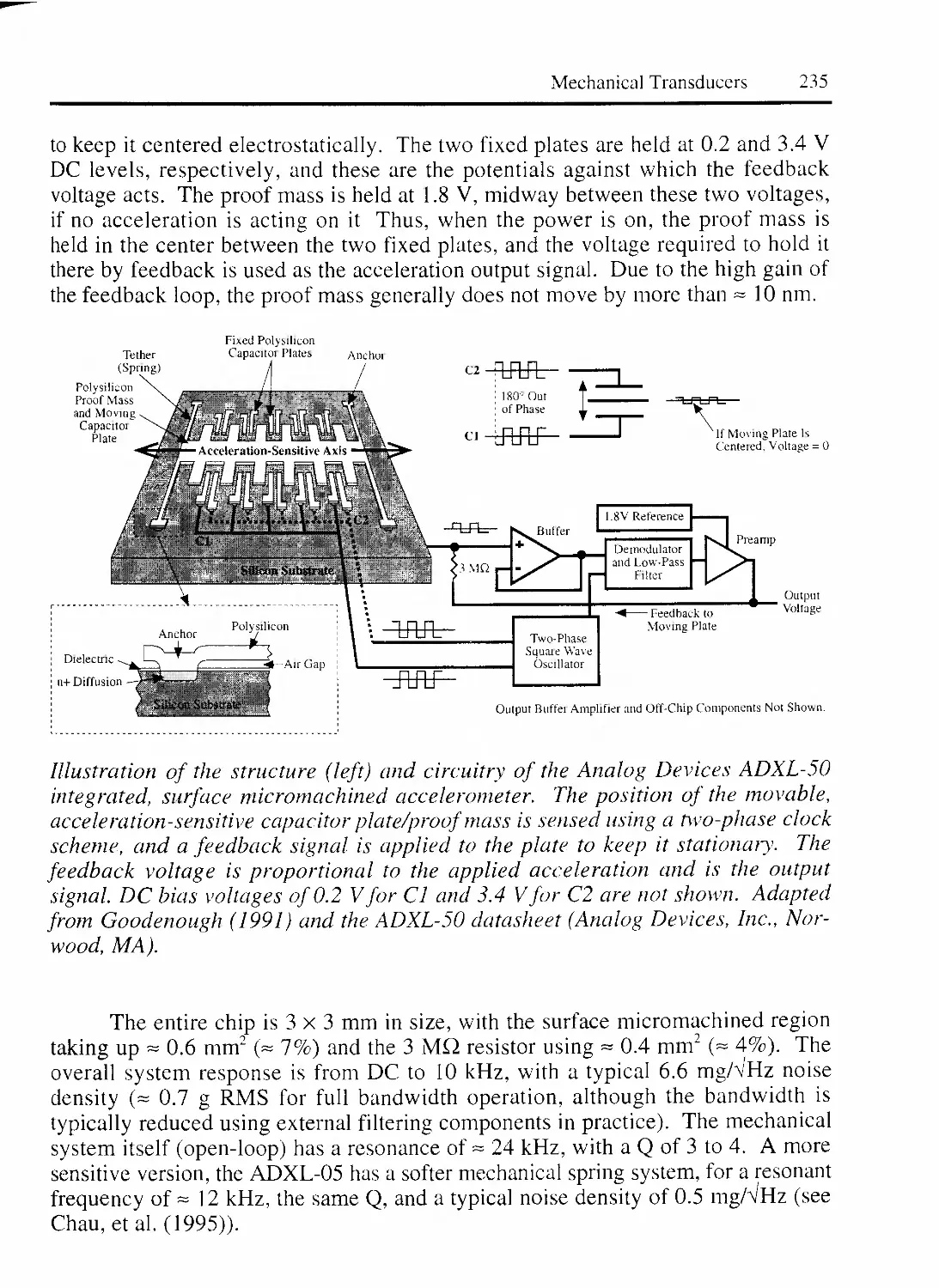


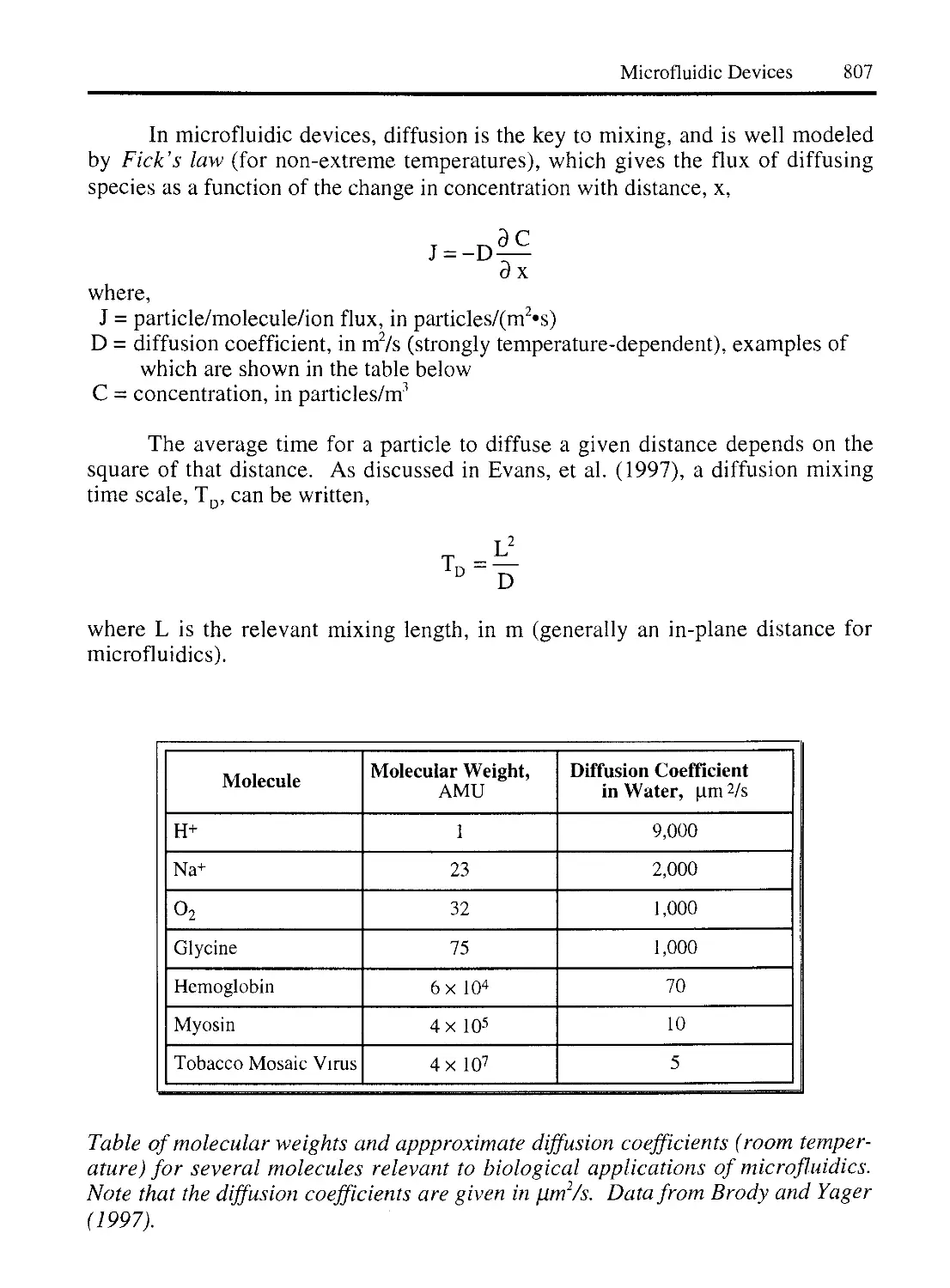
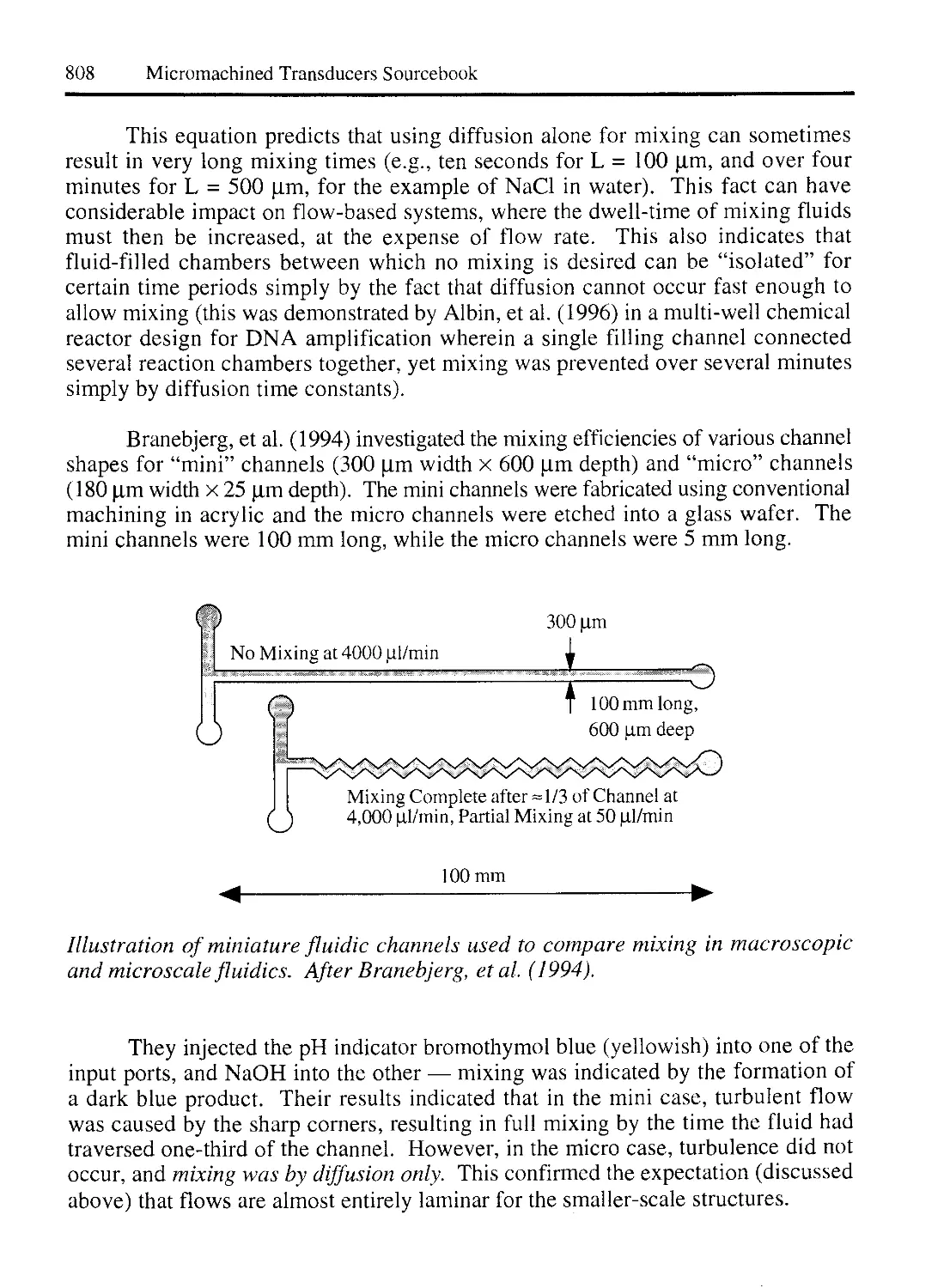


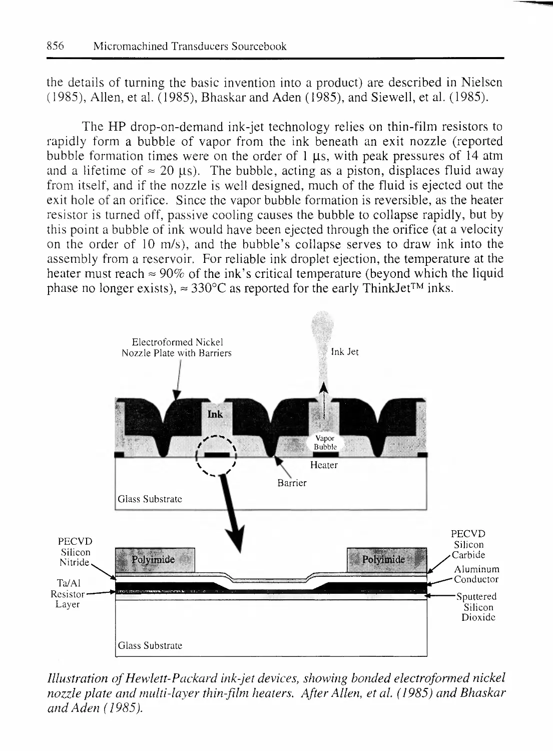


Автор: Kovacs Gregory T.A.
Теги: electrical engineering electronics sourcebook
ISBN: 0-07-290722-3
Год: 1998


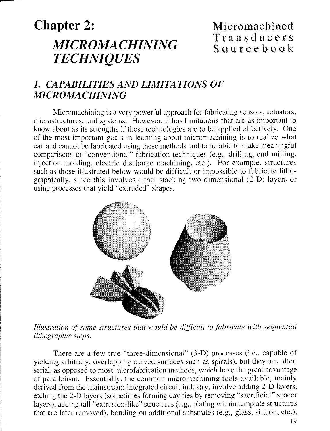
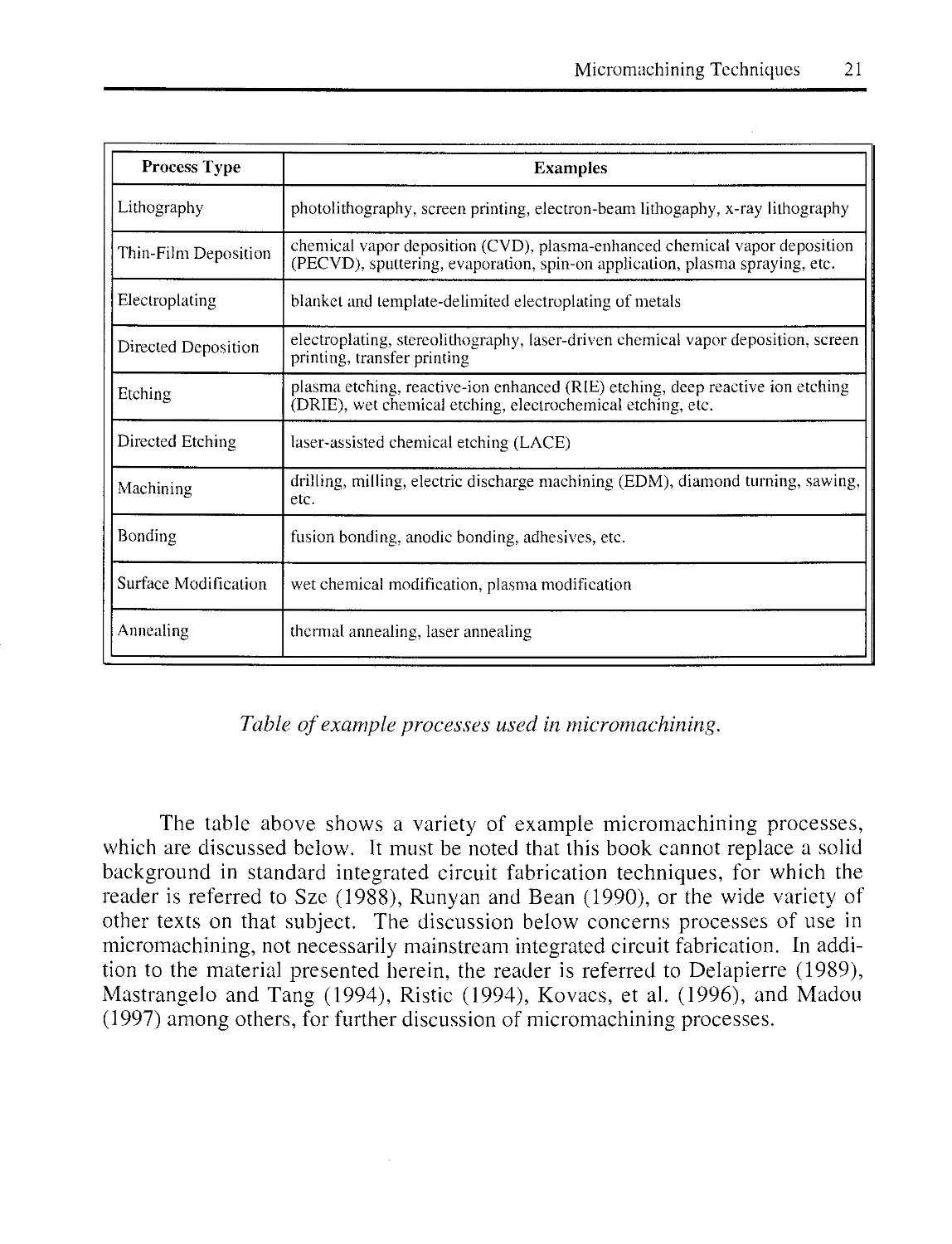
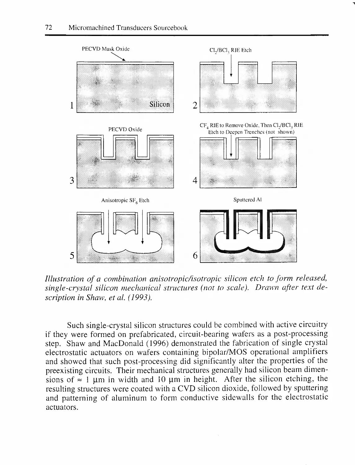
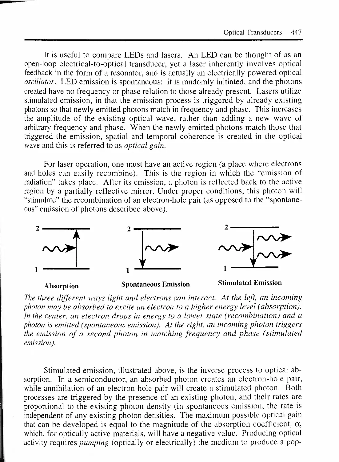
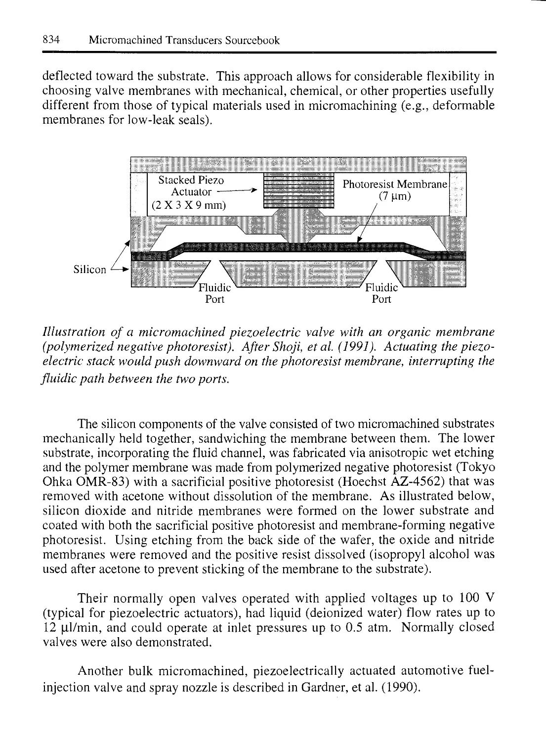
Текст
Micromachined
Transducers
SOURCEBOOK
McGraw-Hill Series in Electrical and Computer Engineering
Senior Consulting Editor
Stephen W. Director, University of Michigan, Ann Arbor
Circuits and Systems
Gommmicatims and Signal Processing
Computer Engineering
Control Theory
Electmmagnetics
Electronics and VLSI Circuits
Introductory
Power and Energy
Radar and Antennas
Previous Consulting Editors
Ronald N. Bracewell, Colin Cherry, James F. Gibbons, Willis W. Harman, Hubert
Heffner, Edward W. Herold,John G. Linvill, Simon Ramo, Ronald A. Rohrer,
Anthony E. Siegman, Charles Susskind, Frederick E. Terman,John G. Truxal, Ernst
Weber, and John R. Whinnery
Electronics and VLSI Circuits
Senior Consulting Editor
Stephen W. Director, University of Michigan, Ann Arbor
Consulting Editor
Richard C. Jaeger, Auburn University
Colclaser and Diehl-Nagel: Materials and Devices for Electrical Engineers and Physicists
DeMicheli: Synthesis and Optimization of Digital Circuits
Elliot: Microlithography: Process Technology for IC Fabrication
Fabricius: Introduction to VLSI Design
Ferendici: Physical Foundations of Solid-State and Electron Devices
Fonstad: Microelectronic Devices and Circuits
Franco: Design with Operational Amplifiers and Analog Integrated Circuits
Geiger, Allen, and Strader: VLSI Design Techniques for Analog and Digital Circuits
Grinich and Jackson: Introduction to Integrated Circuits
Hodges and Jackson: Analysis and Design of Digital Integrated Circuits
Huelsman: Active and Passive Analog Filter Design: An Introduction
Ismail and Fiez: Analog VLSI: Signal and Information Processing
Kasap: Principles of Electrical Engineering Materials and Devices
Kovacs: Micromachined Transducers Sourcebook
Laker and Sansen: Design of Analog Integrated Circuits and Systems
Long and Butner: Gallium Arsenide Digital Integrated Circuit Design
Millman and Grabel: Microelectronics
Millman and Halkias: Integrated Electronics: Analog, Digital Circuits, and Systems
Millman and Taub: Pulse, Digital, and Switching Waveforms
Neamen: Electronic Circuit Analysis and Design
Neamen: Semiconductor Physics and Devices
Ng: Complete Guide to Semiconductor Devices
Offen: VLSI Image Processing
Roulston: Bipolar Semiconductor Devices
Ruska: Microelectronic Processing: An Introduction to the Manufacture of Integrated Ciraiits
Schilling and Belove: Electronic Circuits: Discrete and Integrated
Seraphim: Principles of Electronic Packaging
Singh: Optoelectronics: An Introduction to Materials and Devices
Singh: Physics of Semiconductors and Their Heterostructures
Singh: Semiconductor Devices: An Introduction
Singh: Semiconductor Optoelectronics: Physics and Technology
Smith: Modern Communication Circuits
Sze: VLSI Technology
Taub: Digital Circuits and Microprocessors
Taub and Schilling: Digital Integrated Electronics
Tsividis: Mixed Analog-Digital VLSI Devices and Technology
Tsividis: Operation and Modeling of the MOS Transistor
Wait, Huelsman, and Korn: Introduction to Operational and Amplifier Theory Application
Yang: Microelectronic Devices
Zambuto: Semiconductor Devices
Also Available from McGraw-Hill
Schaum’s Outline Series in Electronics & Electrical Engineering
Most Outlines include basic theory, definitions, and hundreds of example problems solved in step-by-
step detail, and supplementary problems with answers.
Related titles 011 the current list include:
Analog & Digital Communications
Basic Circuit Analysis
Basic Electrical Engineering
Basic Electricity
Basic Mathematics for Electricity & Electronics
Digital Principles
Electric Circuits
Electric Machines & Electromechanics
Electric Power Systems
Electromagnetics
Electronic Communication
Electronic Devices & Circuits
Feedback & Control Systems
Introduction to Digital Systems
Microprocessor Fundamentals
Signals & Systems
Schaum’s Electronic Tutors
A Schaum’s Outline plus the power of Mathcad* software. Use your computer to learn the theory and
solve problems—every number, formula, and graph can be changed and calculated on screen.
Related titles on the current list include:
Electric Circuits
Feedback & Control Systems
Electromagnetics
College Physics
Available at most college bookstores, or for a complete list of titles and prices, w rite to:
The McGraw-Hill Companies
Schaum’s
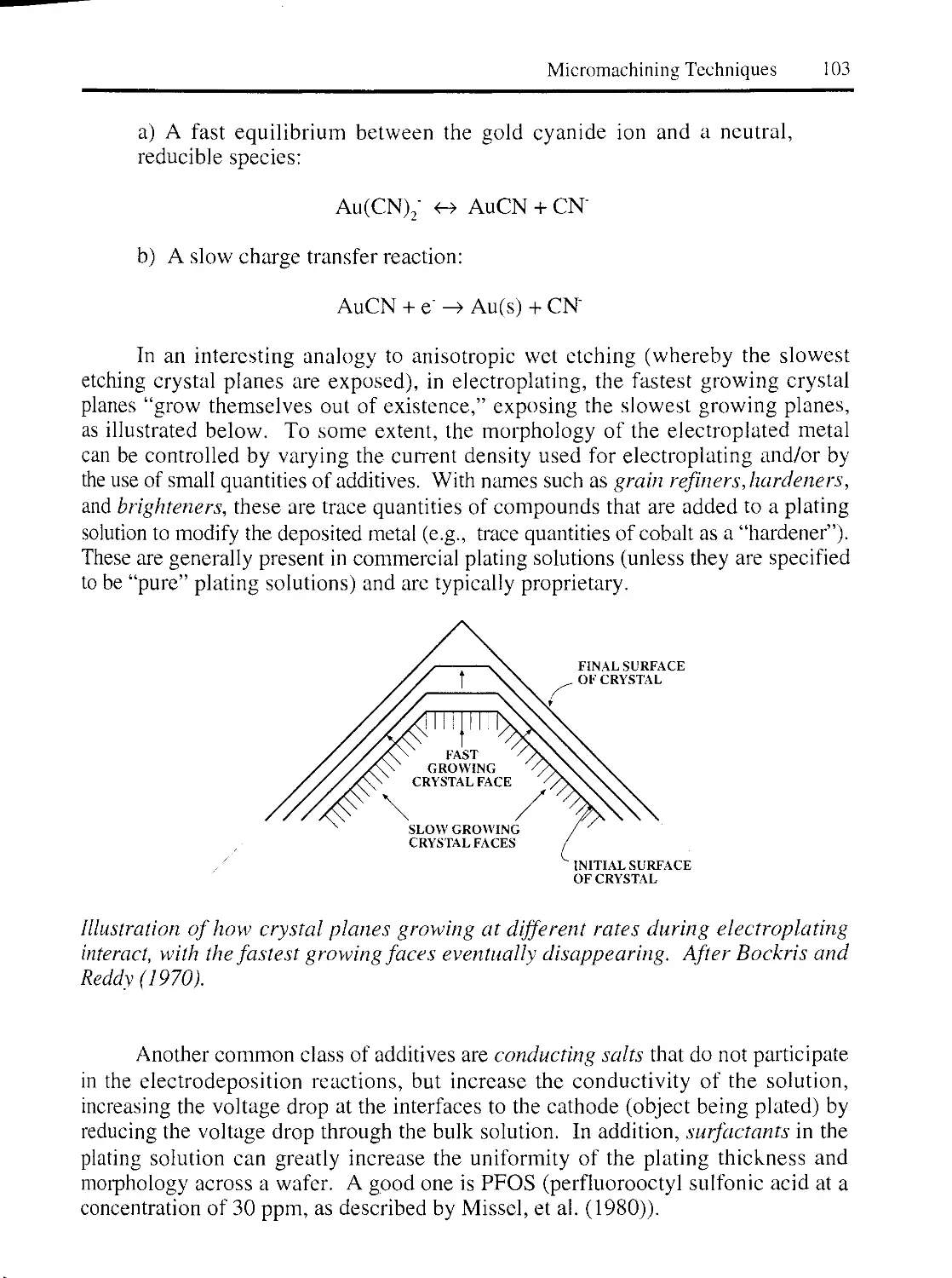
11 West 19th Street
New York, New York 10011-4285
(212-337-4097)
Micromachined
Jrahsducers
I SOURCEBOOK
Gregory T.Ä. Kovacs
Stanford University
^McGraw-Hill
Boston Burr Ridge, IL Dubuque, IA Madison, WI New York San Francisco St. Louis
Bangkok Bogotá Caracas Lisbon London Madrid
Mexico City Milan New Delhi Seoul Singapore Sydney Taipei Toronto
WCB/McGraw-Hill
A Division of The McGraw-Hill (Companies
Micromachined Transducers Sourcebook
Copyright © 1998 by The McGraw-Hill Companies, Inc. All rights reserved. Printed in the United States of
America. Except as permitted under the United States Copyright Act of 1976, no part of this publication
may be reproduced or distributed in any form or by any means, or stored in a data base or retrieval system,
without the prior written permission of the publisher.
This book is printed on acid-free paper.
1234567890 DOC DOC 3 2 10 9 8
ISBN 0-07-290722-3
Editorial director: Kevin Kane
Publisher: Tom Casson
Sponsoring editor: Lynn Cox
Editorial coordinator: Nina Kreiden
Marketing manager: John Wannemacher
Project manager/production supervisor: Natalie Durbin
Cover designer: Francis Owens
Printer: R. R. Donnelley & Sons Company
Library of Congress Cataloging-in-Publication Data
Kovacs, Gregory T. A.
Micromachined transducers sourcebook / Gregory T.A
p. cm.
Includes bibliographical references and index.
ISBN 0-07-290722-3
1. Transducers. 2. Microelectromechanical systems.
TK7872.T6K68 1998
681 ’.2—dc21
. Kovacs.
I. Title
98-4846
CIP
http ://w ww.mhhe.com
This book is dedicated to my parents, George and Klara Kovacs, who raised
with love and inspired me to wonder about the world around me.
ABOUT THE AUTHOR
GREGORY T. A. KOVACS received the B.A.Sc. degree in Electrical Engineering
from the University of British Columbia, the M.S. degree in Bioengineering from
the University of California, Berkeley, the Ph.D. degree in Electrical Engineering
and the M.D. degree from Stanford University.
He is an Associate Professor of Electrical Engineering at Stanford University,
where he has been a member of the faculty since 1991. He teaches courses in
electronic circuits and micromachined transducers. His present research areas
include solid-state sensors and actuators, micromachining technologies, biological
and medical applications of fluidic devices, and analog circuits for transducer
applications, all with emphasis on solving practical problems. He has authored
over eighty technical publications and holds several patents. He held the Robert N.
Noyce Family Faculty Scholar Chair from 1992 to 1994, received a National
Science Foundation Young Investigator Award in 1993, was appointed a Terman
Fellow in 1994, was appointed to the Defense Sciences Research Council in 1995,
and was appointed a University Fellow in 1996. He has broad industry experience
in the design of circuits and instruments, commercial product design, and intellectual
property law consulting. In addition, he has been one of the founders of several
technology companies, most recently Cepheid, Inc., in Sunnyvale, CA.
PREFACE
The field of micromachined sensors and actuators, often referred to as “MEMS”
(microelectromechanical systems), has been growing at an exciting pace in recent
years. Using tools originally developed for the silicon integrated circuit industry,
people are now fabricating miniaturized transducers and structures from silicon
and other materials. In many (but not all) cases, these new devices offer advantages
over their “conventional” counterparts, including great reductions in size, new
functions that could not otherwise be realized, the capability to include on-chip
signal processing/control circuitry (if the substrate is a semiconductor), reductions
in per-unit cost, and the ability to fabricate scaled and multimodal arrays. Of
course, new technologies bring with them new problems, such as the need for new
packaging and power sources, system integration issues that need to be addressed,
the need for CAD and simulation tools, and process compatibility considerations.
All of these challenges are gradually being dealt with.
This sourcebook began, as many books do, as the notes for a graduate
course. The main goal I set for myself was to provide a fairly complete overview
of the field, beginning with micromachining approaches and including all major
categories of transduction (including some that may not be familiar to the reader).
The approach I have taken is, where possible, to study the way individual devices
were fabricated and what the key design issues were. In this way, I hope that the
reader will gain an intuitive sense for how to develop his or her own processes and
designs.
I also sought to provide sufficient examples of important transducers or
structures for the reader to compare the performance obtainable through different
approaches. In many cases this was not possible. In studying hundreds of papers
in this area, spanning many years, I found the lack of metrics by which to compare
different designs quite striking. Even for relatively simple devices, such as pressure
sensors, where metrics for their macroscopic counterparts are well-established,
reporting of performance in the literature is sparse and inconsistent. One could
certainly speculate that reasons for this might be that the authors choose to omit
poor characteristics of prototypes, have a need to protect proprietary information,
or lack familiarity with existing specifications. In any case, it is likely that this
situation will have to improve in order for a significant number of designs to
succeed against competitive “conventional” devices.
This book does not cover simulation methods as they relate to micromachining.
The tools for these purposes are still evolving and proving themselves useful to
designers, and covering them is beyond the scope of this book. Second, circuits
specific to transducer applications are not covered — one could write another
entire book on that subject!
i
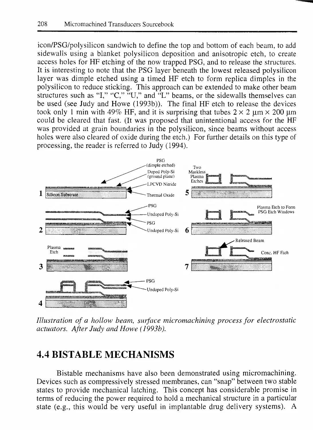
While the book is a fairly comprehensive overview of the field, it is not
meant to be a complete catalog. I have carefully selected examples based on a
number of criteria. I certainly wanted to focus on those with interesting operating
principles, designs, or fabrication processes. I also sought to choose papers wherein,
after close inspection, real experimental verification of device operation was provided
(I decided not to cite several interesting examples where even basic functionality
had not been verified — in this type of paper the word “simulated” appears next to
the word “data”). It was quite interesting to follow up, via electronic searching, on
many of the papers where a pretty picture was presented with some phrase like
“testing is in progress.” For a large number of them, there never was a follow-on
publication, even many years later. But that is to be expected from a discipline that
is young and dynamic. Priorities change, graduate students move on, and some
things simply don’t work. I have also included a few examples of devices that
have not been micromachined but that could be.
Many people have made substantial contributions to this work. Most notably,
Bruce Darling, who read and critiqued the entire manuscript twice. Invaluable
comments, additions, and general advice on the text also came from Nadim Maluf,
Tom Kenny, Kurt Petersen, Henry Baltes, Godfrey Mungal, Paul Yager, Roger
Howe, Fred Forster, Dorian Liepmann, Chris Storment, Tony Flannery (who receives
special thanks for his ongoing support), Dave Borkholder, Ken Honer, Micki Leder,
and Josh Molho. I am also very grateful to my EE312 students for their helpful
comments, for “beta testing,” and for bringing many interesting papers and patents
to my attention, particularly to Peter Ho, for providing many key references on
thin-film batteries. Special thanks go to everyone who helped me with several of
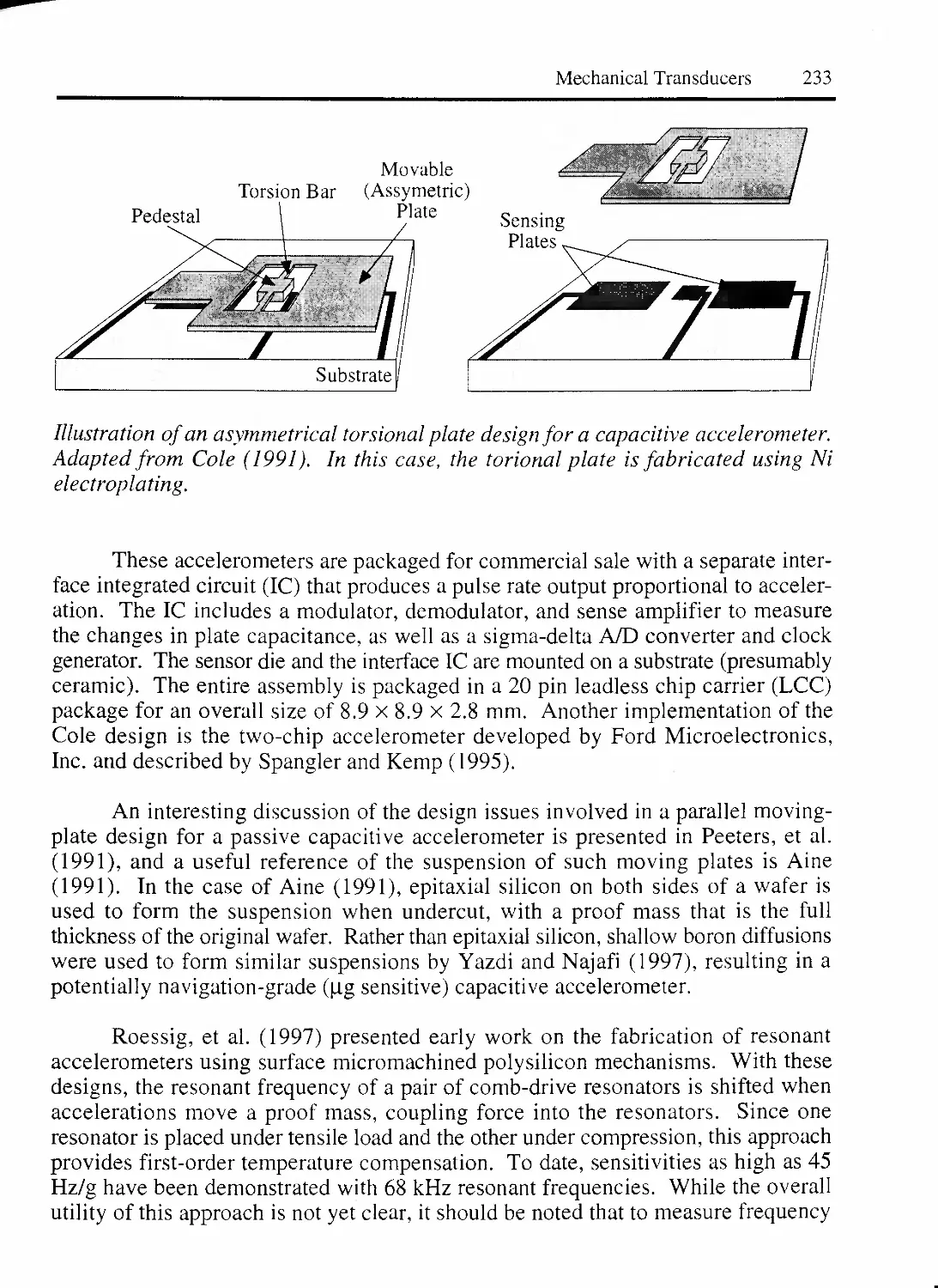
the figures, including Stephen Ryu, Tamara Ahrens, Sasha Mittelman, Peter
Krulevitch, Rosanna Foster, Tony Flannery, Dave Borkholder, and Ken Honer. I
am sure I have not remembered everyone, but I extend my most sincere thanks to
those above and any I have regrettably forgotten to name. Last but not least,
special thanks to my wife, Laurel Joyce, for putting up with my many grumpy or
spaced-out, computer-fogged comments while I hacked away at this project, and
for her massive assistance with the final set of changes to the manuscript.
Although I have made my best effort to bring this material together into a
useful form, I have undoubtedly made errors of fact or omission, and sincerely
apologize for them. I welcome hearing from readers about such errors, key concepts,
papers that may have been omitted, format suggestions, etc., via electronic mail
(kovacs@cis.stanford.edu). Updates, corrections and other information will be
available at the McGraw-Hill web site: http://www.mhhe.com.
Here’s to your enjoyment of this exciting field!
Oregon’ T. A. Kovacs
Stanford, CA, January, 1998
u
PROLOGUE
Kurt Petersen, Ph.D., Cepheid, Inc., Sunnyvale, CA
Several defining events independently contributed to the unambiguous
emergence of microelectromechanical systems (MEMS) as a vital technical discipline
in the early 1980’s. During 1982 and 1983, the first mass-produced MEMS products
were released into high volume production, the micromachined automotive MAP
(Manifold Absolute Pressure) sensor and the micromachined disposable medical
blood pressure sensor. In 1983, the first international conference on Solid State
Sensors and Actuators was held at Delft Technical University in the Netherlands.
In 1981 and 1982, the first start-up companies were founded that were committed
to the commercialization of additional applications (other than pressure sensors)
for this new technology, Microsensor Technology, Inc. and Transensory Devices,
Inc. In 1982, the first review paper on the field was published in the Proceedings
of the IEEE, “Silicon as a Mechanical Material” (Petersen (1982)). Pioneered by
Professor James B. Angell at Stanford University (who had research projects in the
field of micromachining dating from the early 1970’s), every major university in
the United States had a formally established maior research program in MEMS by
about 1983.
During these early years, only about five Fortune 500 companies had research
programs in MEMS; today over 25 such companies are contributing to the technology.
During this time, only one type of MEMS product existed, the micromachined
pressure sensor; today accelerometers, micro-valves, projection display chips,
biosensors, ink jet nozzle arrays, and other products are all manufactured and
shipped in commercial volumes. During this time, fundamental MEMS processes
were invented, researched, and defined; today, these processes are being refined in
manufacturing environments and are being applied to additional products. During
this time, little technical and communication infrastructure existed; today, several
MEMS journals are thriving and an entire series of scheduled conferences are held
every year. During this time, MEMS experts were few and far between; today,
well-established and well-respected university programs graduate dozens of Ph.D.
MEMS students every year in the United States alone. During this time, government
research funding was sparse, unorganized, and low profile; today, funding from
DARPA and other government agencies amounts to over $100M/year and is targeted
and organized around specific militarily and commercially strategic applications.
As a result of all this progress, the future of micromachining and MEMS is
more than bright — it is dazzling. With a strong infrastructure in place, well-
established university programs, many trained and experienced engineers, and a
proven diverse series of successful products, a strong momentum has developed
which is beginning to change the nature of many large technical disciplines, including
in
biotechnology, storage technology, instrumentation, input/output, and
telecommunications.
Because MEMS technology employs many of the same manufacturing
techniques as integrated circuits, the business of MEMS is often compared to the
IC business. However, this comparison is misleading. The integrated circuit is
used only to manipulate electronic signals. MEMS devices are actually the interface
between the physical world and the electronic world. As such, they must function
in a much wider, more diverse, and much more complicated overall environment,
interacting effectively and accurately both in the electronic and in the physical
worlds. On one hand, this reality greatly complicates the design, production
implementation, and performance qualifications for any single application. On the
other hand, a vastly broader and more diverse range of utility for MEMS devices,
from optical fiber switching, to fluid control, to micromechanical electrical relays,
to biosensors is made possible.
In fact, no single aspect characterizes the field of MEMS more succinctly
than its wide diversity. This diversity is expressed both in the multi-disciplinary
approach required for design, engineering, and manufacturing as well as in the
wide range of markets and application areas that employ MEMS devices. The
most important technical disciplines required for MEMS research and development
include electrical engineering, mechanical engineering, integrated circuit processing,
circuit design, materials science, chemistry, instrumentation, fluidic engineering,
optics, and packaging. This diverse range of technical disciplines creates a very
complex and challenging background from which devices and systems must be
designed, built, and tested. In addition, the important markets and application
areas for MEMS devices and systems are also very diverse, including sensors, fluid
control and manipulation, optics, displays, printing, electrical switching, chemical
analysis, biochemical fluid processing, precise mechanical motion and actuation,
and data storage systems. Such a wide diversity of engineering disciplines and
varied fields of application creates a challenging situation for anyone trying to
understand, summarize, and learn MEMS technology.
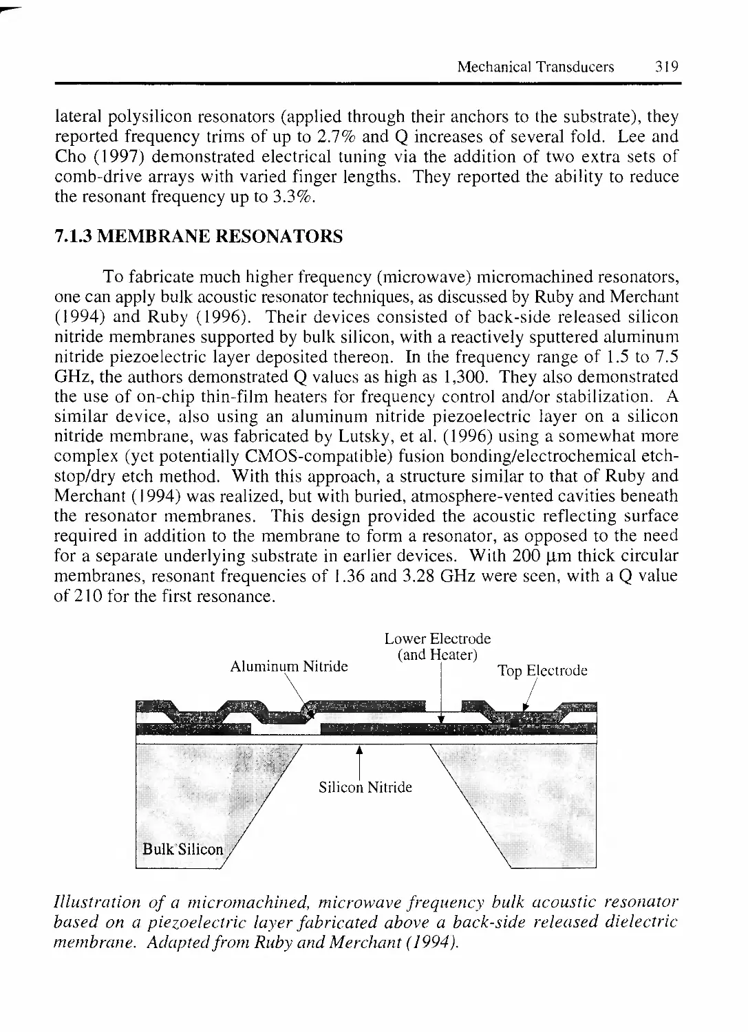
Previous efforts to review MEMS technology have been made either very
early in the history of the technology (Petersen (1982)), in limited reviews (for
example, reviews of micromachined sensors in Ristic (1994)), or in anthologies of
important papers (as in Muller, et al. (1991), and Trimmer (1997)). In fact, the
very prospect of reviewing the entire field of MEMS, entirely because of the vast
breadth and diversity of the technology (especially in recent years), has been viewed
as a daunting task to say the least.
With this backdrop, Gregory Kovacs has undertaken the ambitious and
formidable task of comprehensively reviewing the current status of micromachined
transducers and MEMS technology in a single book. The effort is phenomenally
iv
successful. This book is the most thorough review of micromachining technology
available. It meticulously covers virtually every proposed application of MEMS.
It is unusually detailed and incisive, delving into the physics and theory behind the
applications and into the reasons and rationale for miniaturization. It is extremely
well-researched and referenced with well over 1,500 references. No published
work summarizes and characterizes the diversity of the MEMS field better and
more completely than Micromachined Transducers Sourcebook.
“Silicon as a Mechanical Material” served as a technical introduction and
reference during the nascent years of MEMS development. The comprehensive
Micromachined Transducers Sourcebook will serve as the primary technical
reference for the next ten years. If you will be working in the field of MEMS, or
using MEMS devices or products, this book is indispensable.
Kurt Petersen
San Jose, CA, January 1998
v
PROLOGUE REFERENCES
Muller, R. S.. Howe, R. T„ Senturia, S. D., Smith, R. L., and White, R. M. [eds.], •‘Microsensors,'"
IEEE Press, New York, NY, 1991.
Petersen, K. E., "Silicon as a Mechanical Material," Proceedings of the IEEE, vol. 70, no. 5, May
1982, pp. 420-457.
Ristic, Lj. [ed.], "Sensor Technology and Devices," Artech House, London, 1994.
Trimmer, W. S., “Micromechanics and MEMS: Classic and Seminar Papers to 1990,” IEEE
Press, New York, NY, 1997.
VI
TABLE OF CONTENTS
Chapter 1: INTRODUCTION AND OVERVIEW l
1. INTRODUCTION TO MICROMACHINED DEVICES 1
2. WHAT ARE TRANSDUCERS? 2
3. COMPONENTS OF TRANSDUCER SYSTEMS 3
4. WHAT ARE MICROMACHINED TRANSDUCERS? 4
5. WHEN DOES IT MAKE SENSE TO “MICROMACHINE”? 4
5.1 SCALING AND PERFORMANCE 5
5.2 COST REDUCTION ISSUES 5
5.3 COMPLEXITY OF MICROMACHINED DEVICES AND SYSTEMS 6
6. ISSUES TO CONSIDER 9
7. WHAT ARE THE MARKETS FOR MICROMACHINED TRANSDUCERS? 10
7.1 MICROMACHINING AS AN "ENABLING TECHNOLOGY" 11
7.2 IS THE MARKET "READY TO EXPLODE”? 12
8. INFORMATION RESOURCES 12
8.1 ON-LINE RESOURCES 12
8.2 MICROMACHINED TRANSDUCERS MEETINGS 13
8.3 TEXTBOOKS AND PAPER COLLECTIONS 14
8.4 JOURNALS 14
8.5 THESES 15
8.6 PATENTS 15
9. CONCLUSION 15
INTRODUCTION AND OVERVIEW REFERENCES 16
Chapter 2: MICROMACHINING TECHNIQUES 19
1. CAPABILITIES AND LIMITATIONS OF MICROMACHINING 19
2. MATERIALS FOR MICROMACHINING 22
2.1 SUBSTRATES 22
2.2 ADDITIVE FILMS AND MATERIALS 22
3. MICROMACHINING TERMS 23
4. GENERAL PROPERTIES OF COMMON SEMICONDUCTORS 25
4.1 MECHANICAL PROPERTIES OF SILICON 26
4.2 NATIVE OXIDES OF SILICON AND OTHER SEMICONDUCTORS 27
4.3 TYPICAL SILICON WAFER TYPES 27
5. “BULK” (SUBTRACTIVE) PROCESSES 29
5.1 WET ETCHING OF SILICON 31
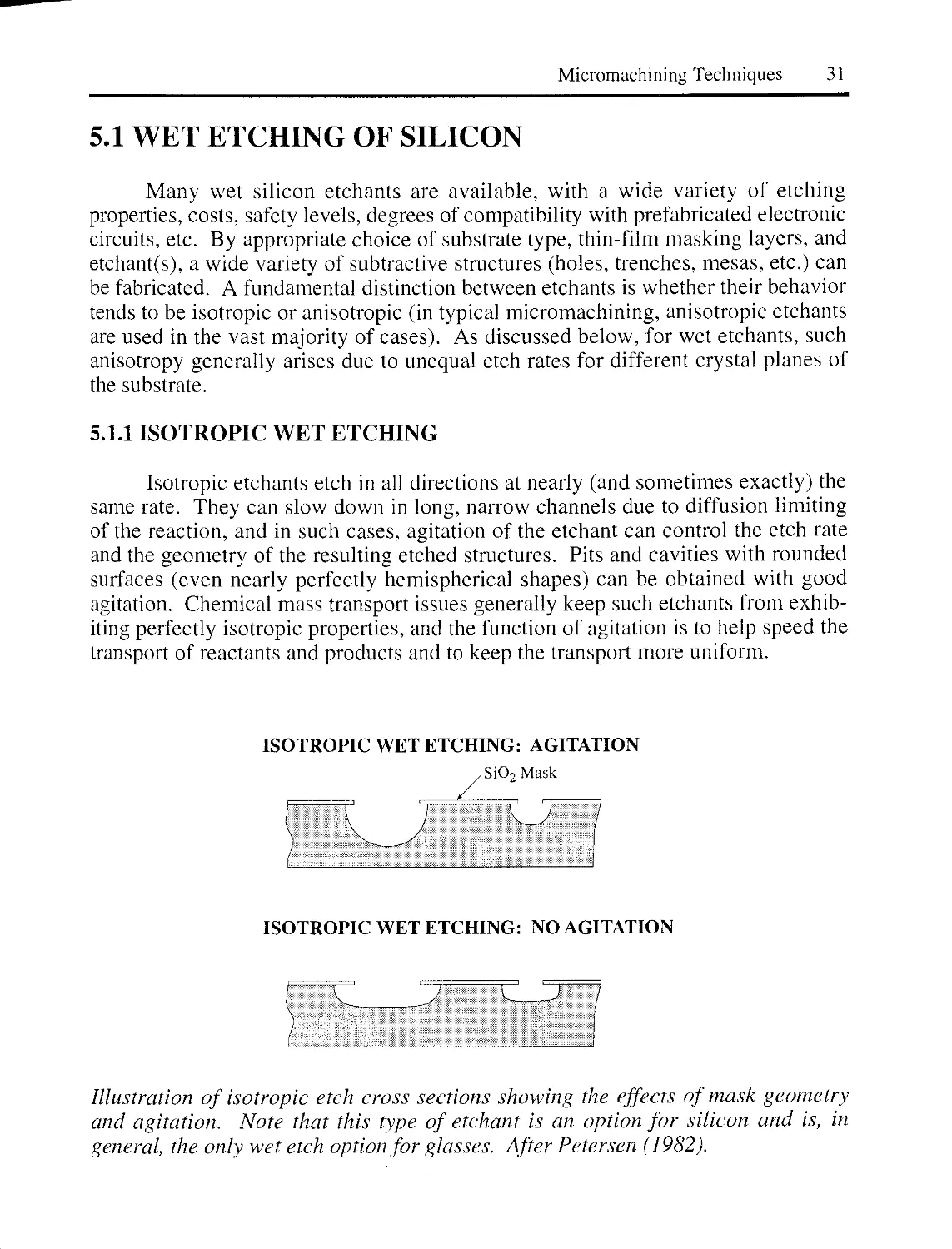
5.1.1 ISOTROPIC WET ETCHING 31
HF/HNO,/ACETIC ACID (“HNA”) 32
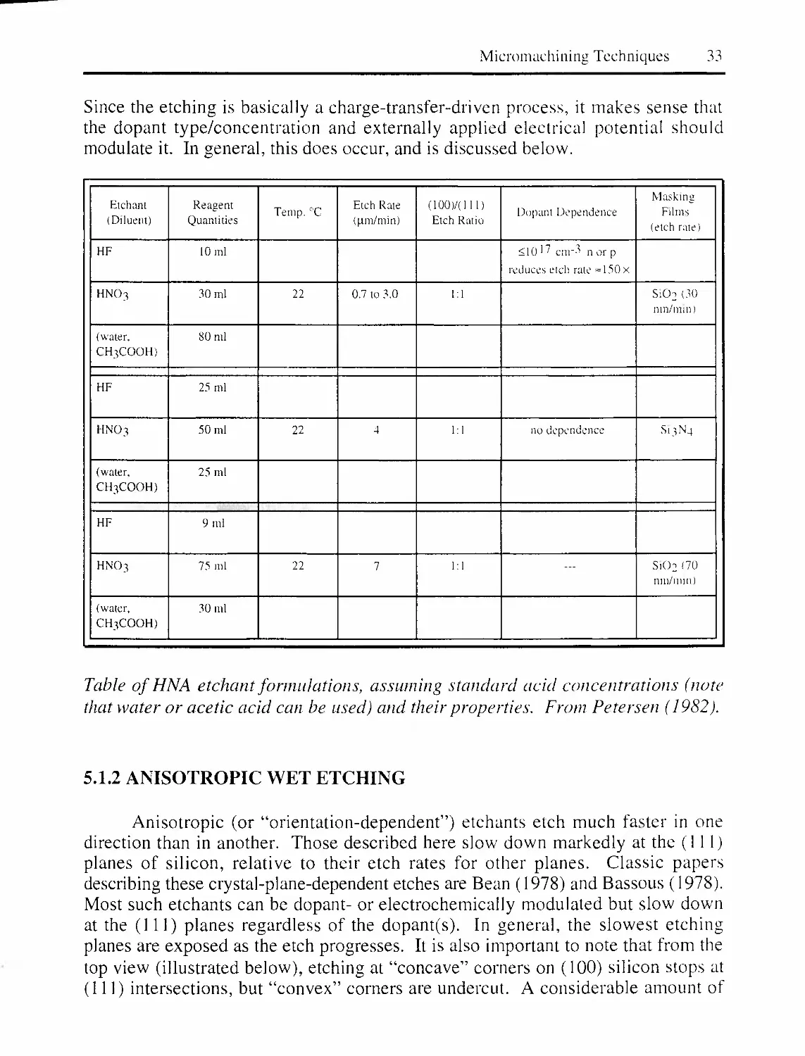
5.1.2 ANISOTROPIC WET ETCHING 33
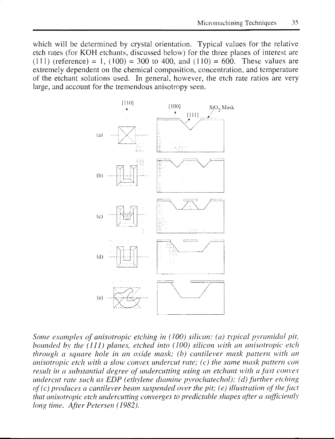
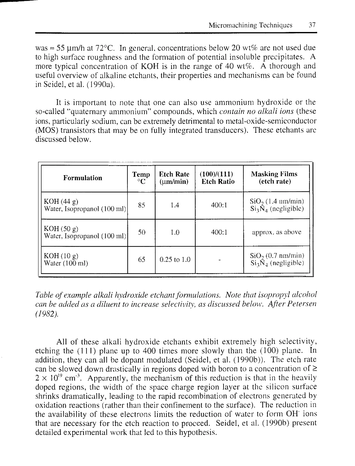
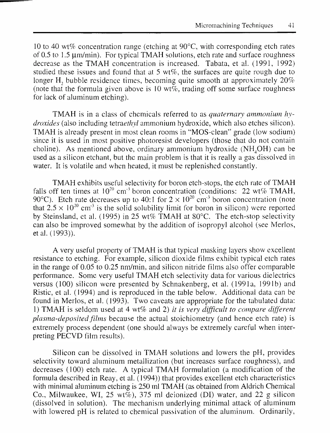
ALKALI HYDROXIDE ETCHANTS 36
AMMONIUM HYDROXIDE 40
TETRAMETHYL AMMONIUM HYDROXIDE (TMAH) 40
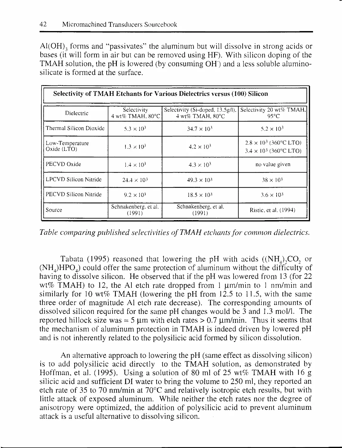
ETHYLENE DIAMINE PYROCHATECHOL (EDP) 43
HYDRAZINE 45
AMINE GALLATES 45
ULTRASONIC AGITATION IN WET ETCHING 46
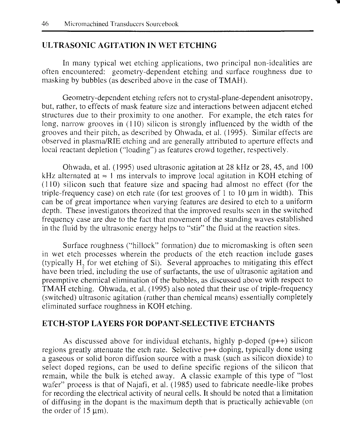
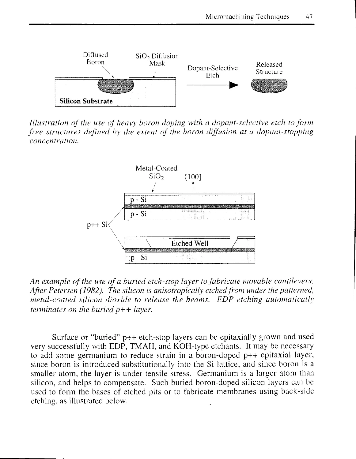
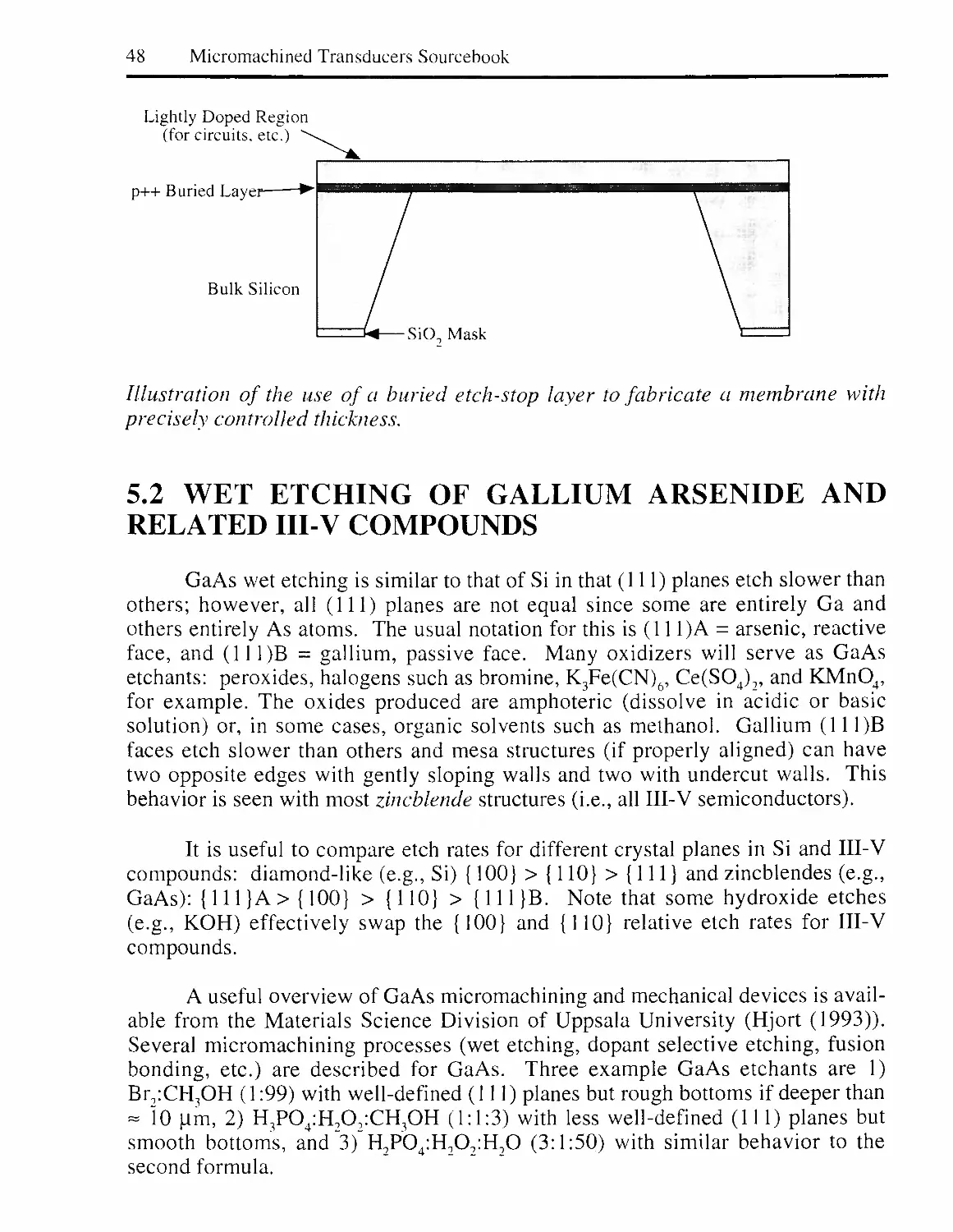
ETCH-STOP LAYERS FOR DOPANT-SELECTIVE ETCHANTS 46
5.2 WET ETCHING OF GALLIUM ARSENIDE AND RELATED III-V COMPOUNDS..48
5.3 ELECTROCHEMICAL MODULATION OF WET ETCHING 49
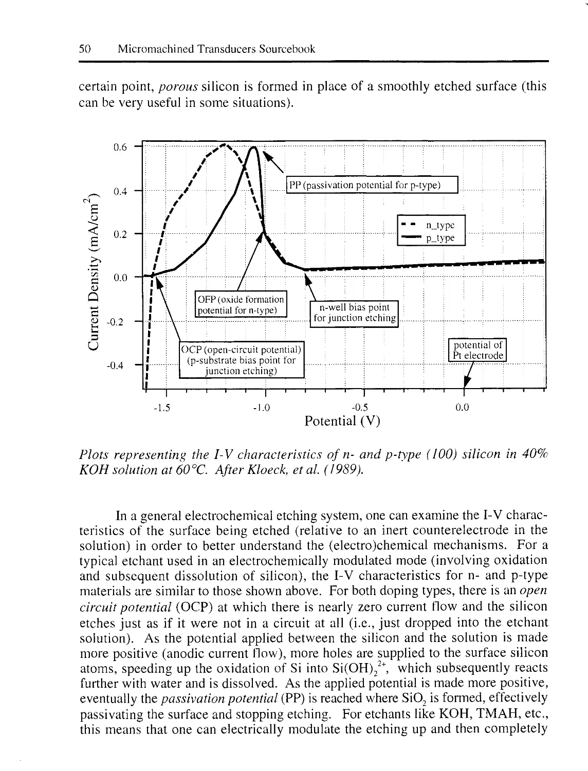
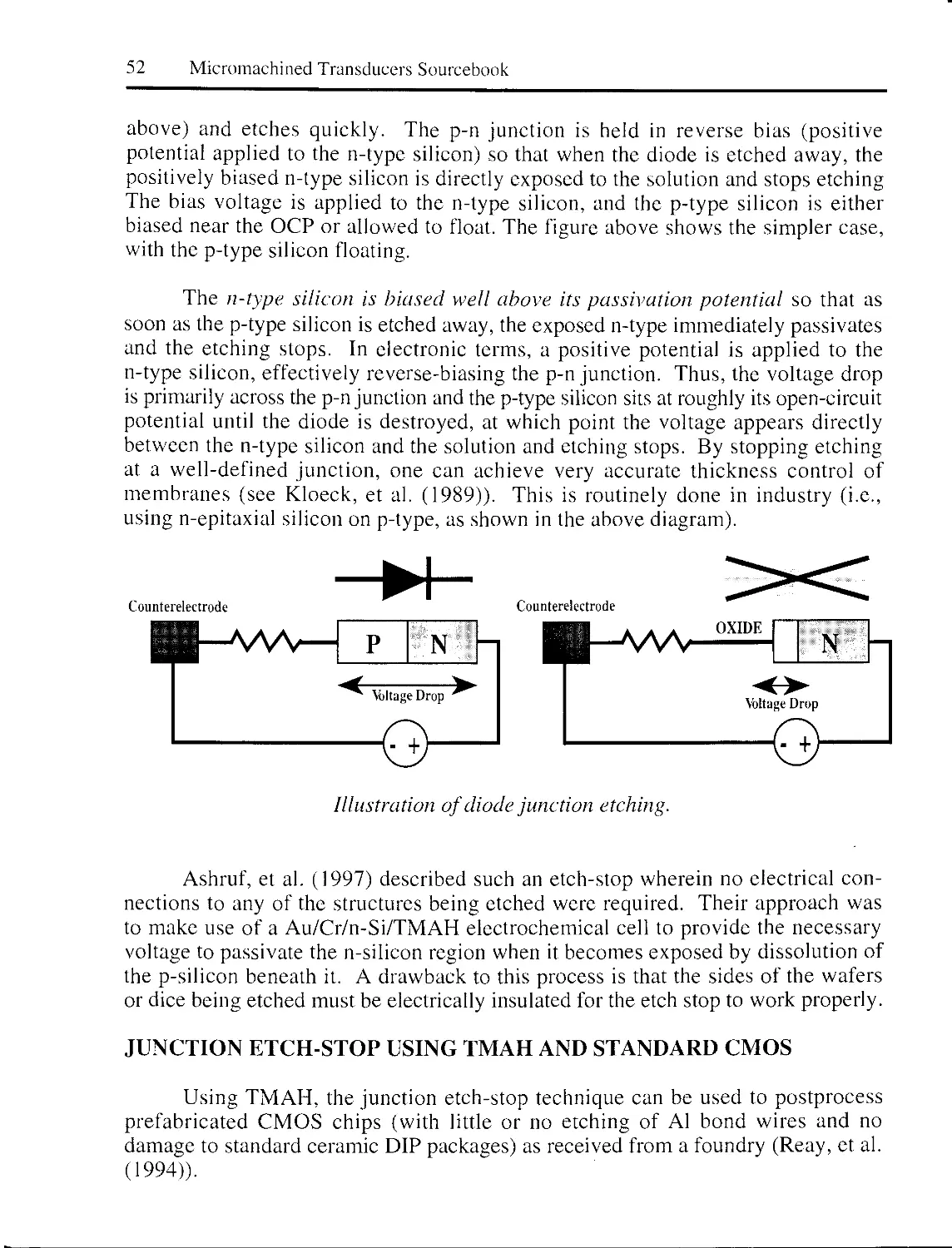
5.3.1 DIODE JUNCTION ETCH-STOP 51
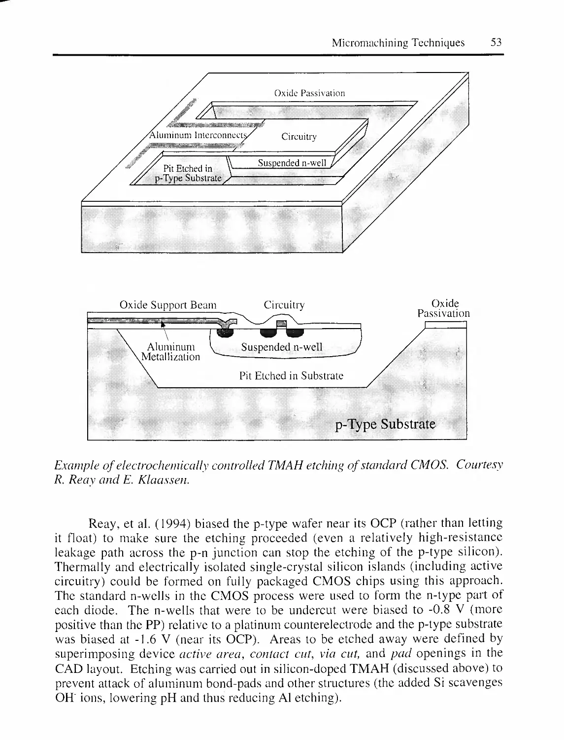
JUNCTION ETCH-STOP USING TMAH AND STANDARD CMOS 52
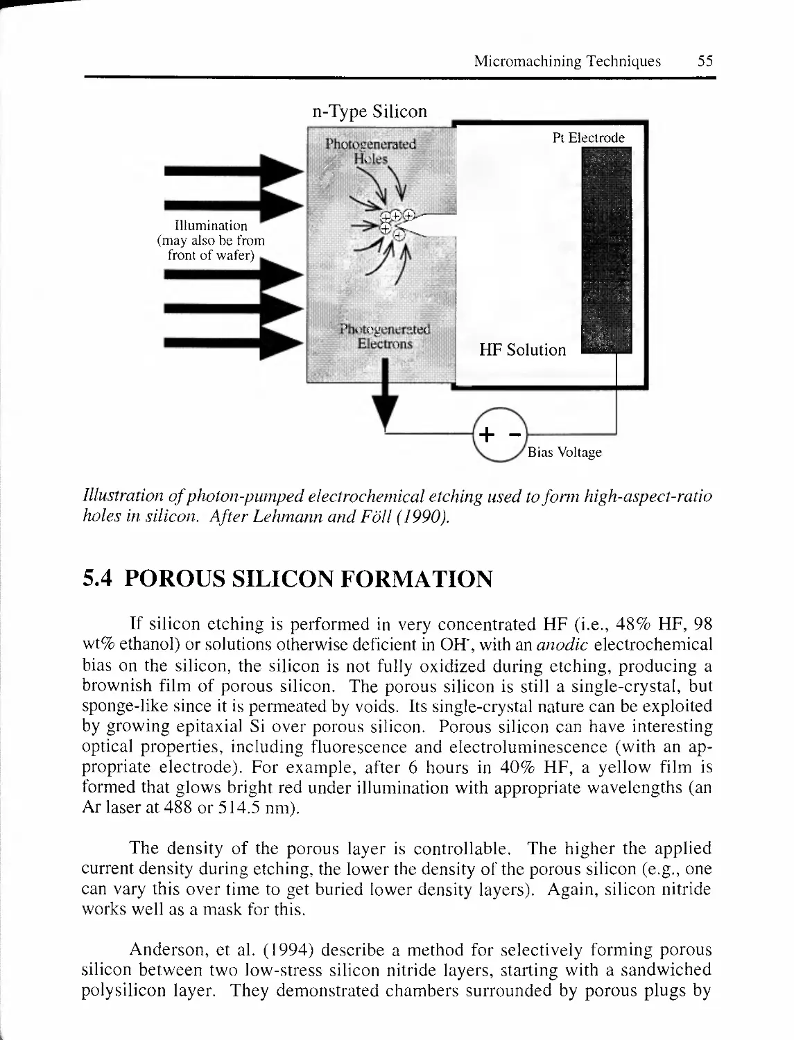
5.3.2 PHOTON-PUMPED ELECTROCHEMICAL ETCHING 54
5.4 POROUS SILICON FORMATION 55
5.5 OTHER BULK WET ETCH TECHNIQUES AND MATERIALS 56
5.5.1 ANISOTROPIC WET ETCHING OF POROUS ALUMINUM 56
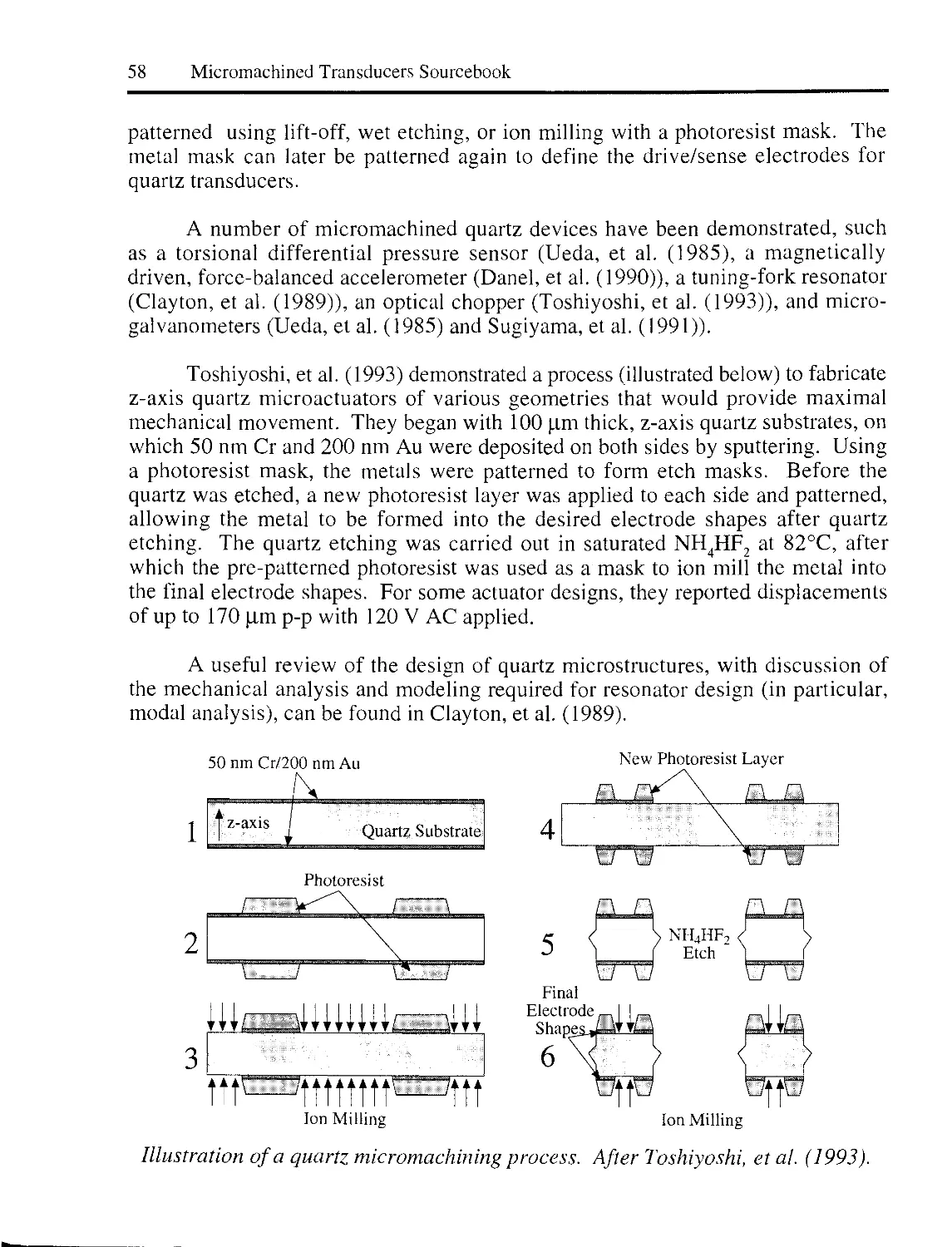
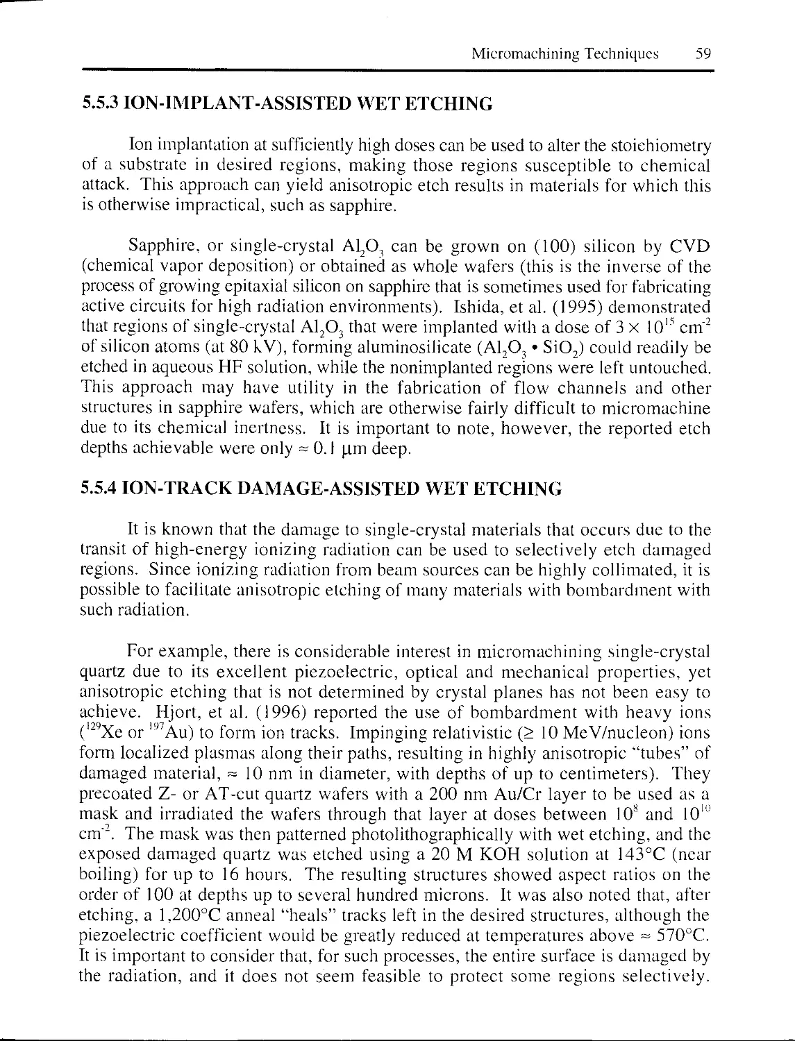
5.5.2 ANISOTROPIC WET ETCHING OF QUARTZ 57
5.5.3 ION-IMPLANT-ASSISTED WET ETCHING 59
5.5.4 ION-TRACK DAMAGE-ASSISTED WET ETCHING 59
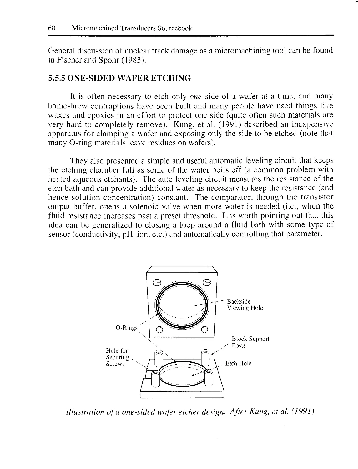
5.5.5 ONE-SIDED WAFER ETCHING 60
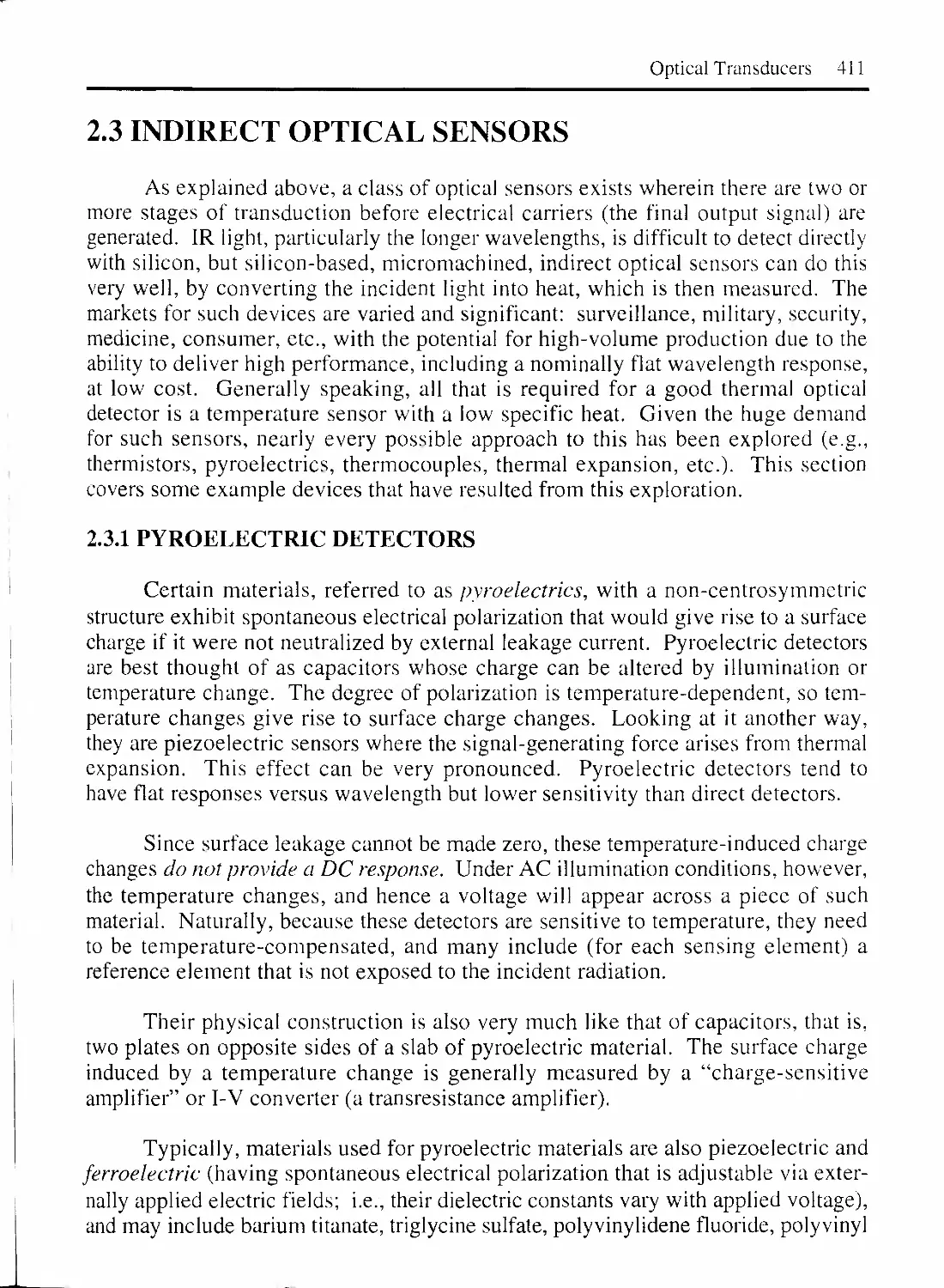
5.5.6 GENERAL WET-ETCHING CONCEPTS 61
5.6 VAPOR-PHASE ETCHING 62
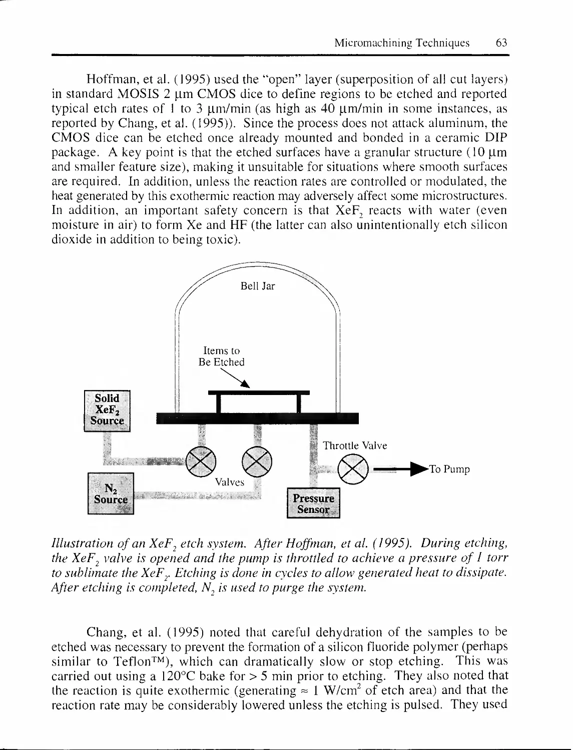
5.6.1 XENON DIFLUORIDE ETCHING 62
5.6.2 INTERHALOGEN ETCH CHEMISTRIES 64
5.6.3 OTHER VAPOR-ETCHING METHODS 65
5.7 PLASMA/REACTIVE ION ETCHING 65
5.7.1 DOPANT-DEPENDENT PLASMA ETCH ISOTROPY 68
5.7.2 HIGH-ASPECT-RATIO DRY ETCHING METHODS 69
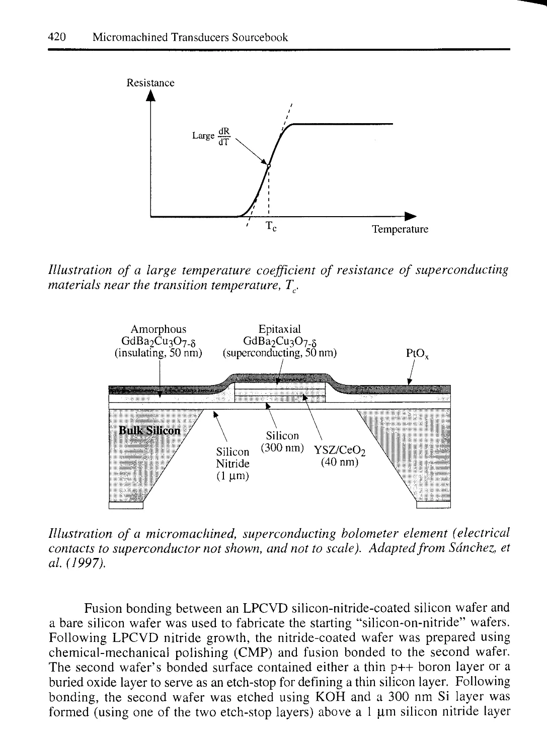
DEEP REACTIVE ION ETCHING (DRIE) 69
CRYOGENIC DRY ETCHING 69
MAGNETICALLY CONTROLLED DRY ETCHING 70
THERMALLY ASSISTED ION-BEAM ETCHING 71
5.7.3 VARIABLE ANISOTROPY ETCH PROCESSES 71
DRY ETCHING OF NON-SILICON SEMICONDUCTORS 74
5.8 LASER-DRIVEN BULK PROCESSING 74
5.8.1 LASER DRILLING 74
5.8.2 LASER ANNEALING 75
5.8.3 LASER-DRIVEN ETCHING 75
6. “SURFACE” (ADDITIVE) PROCESSES 77
6.1 THIN-FILM PROCESSES 77
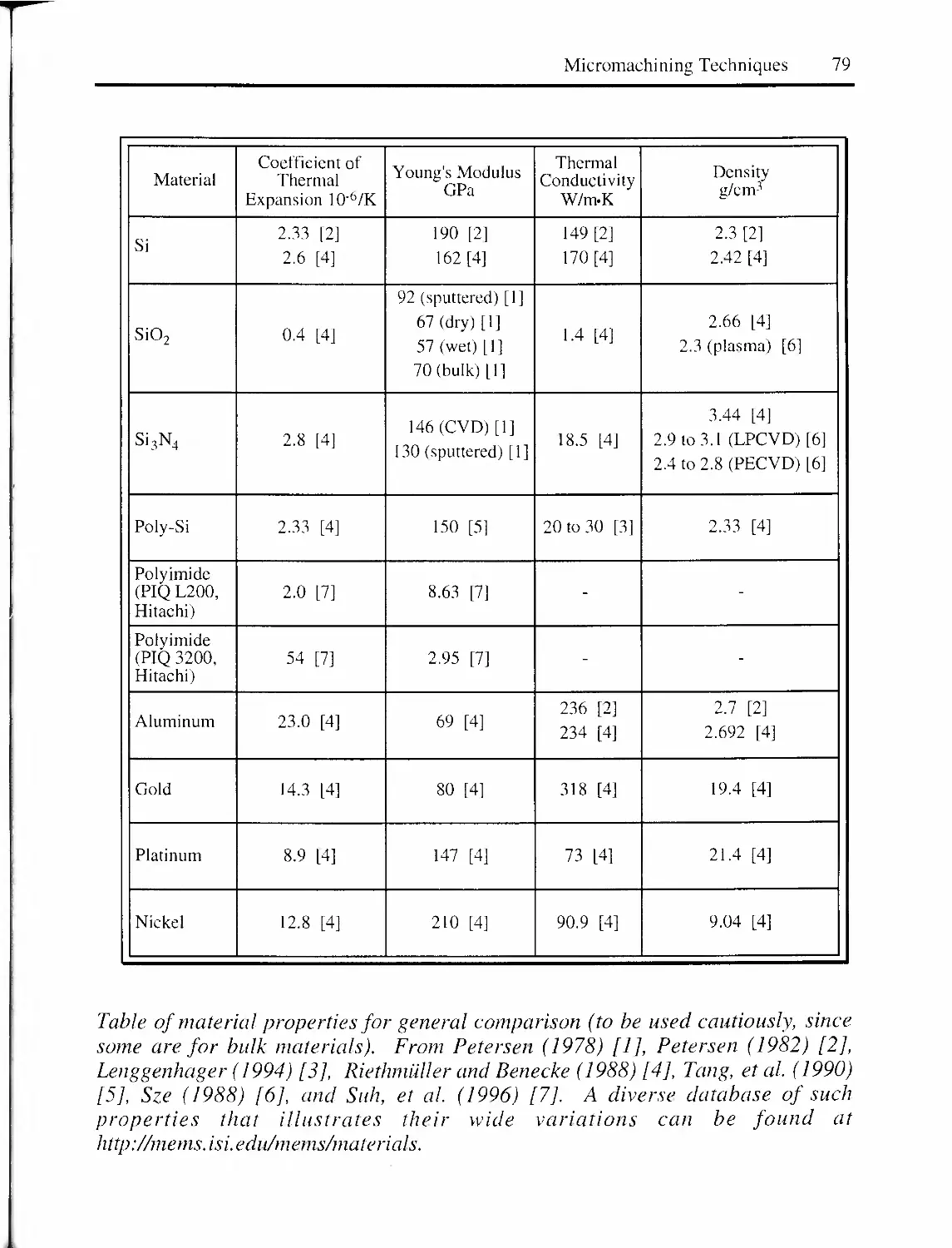
6.1.1 NON-METALLIC THIN-FILMS FOR MICROMACHININC. 77
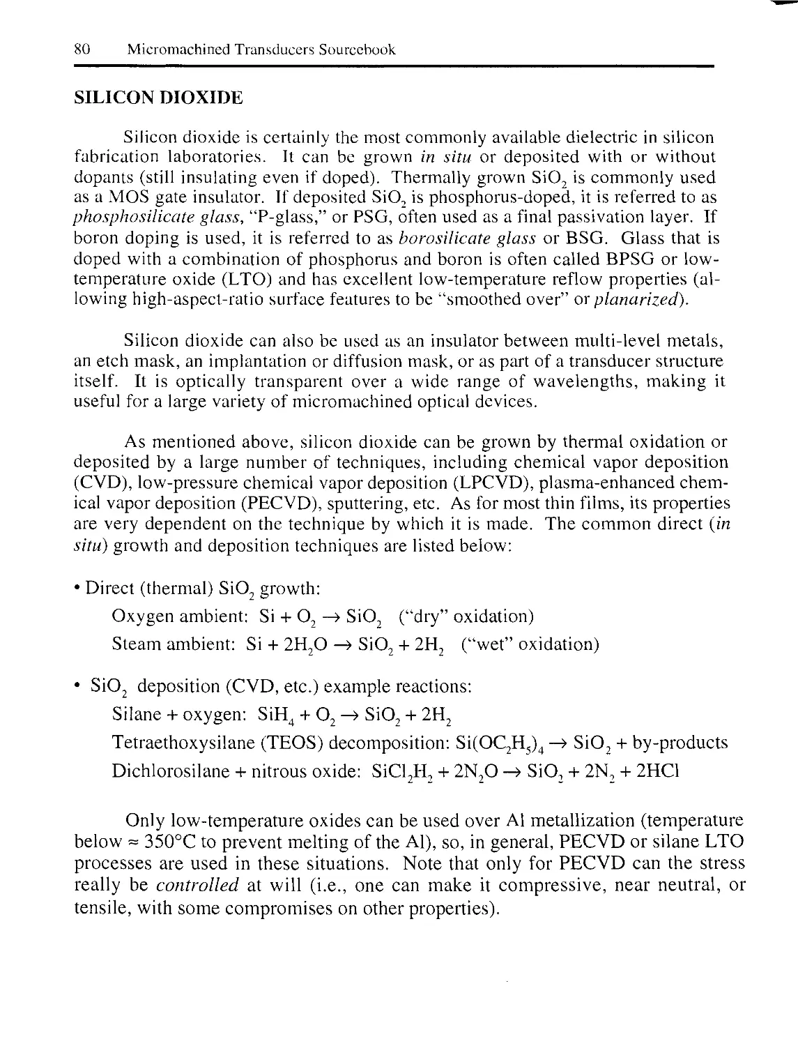
SILICON DIOXIDE 80
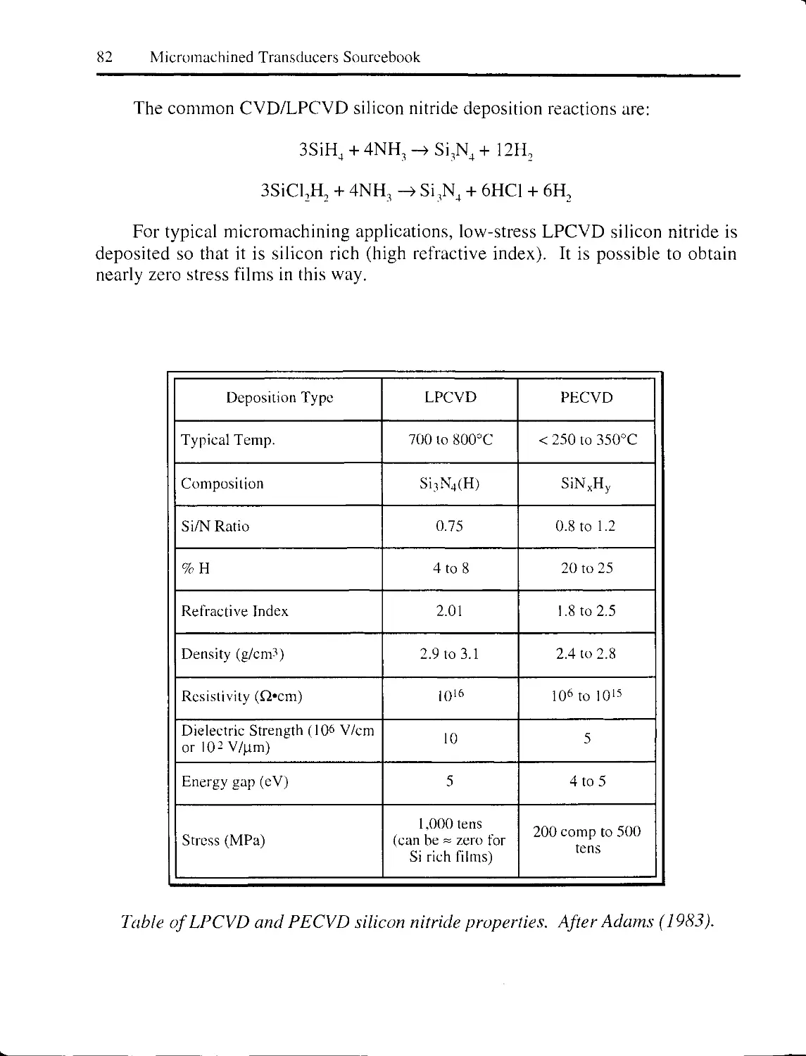
SILICON NITRIDE 81
SILICON CARBIDE 83
POLYCRYSTALLINE DIAMOND 84
POLYSILICON 85
OTHER SEMICONDUCTORS AND THIN-FILM TRANSISTORS 86
ORGANIC COMPOUNDS 86
viii
SPUTTERED INORGANIC THIN-FILMS 87
SPIN-ON NON-METALLIC THIN-FILMS 88
6.1.2 WET ETCHING OF NON-METALLIC THIN-FILMS 88
6.1.3 DRY ETCHING OF NON-METALLIC THIN-FILMS 89
6.1.4 METALLIC THIN-FILMS FOR MICROMACHINING 90
RESISTIVE EVAPORATION 90
ELECTRON-BEAM EVAPORATION 91
SPUTTER DEPOSITION 92
COMPARISON OF EVAPORATION AND SPUTTERING 93
CHEMICAL VAPOR DEPOSITION OF METALS 95
SELECTIVE METAL CVD 96
ADHESION LAYERS FOR METALS 96
6.1.5 WET ETCHING OF METALLIC THIN-FILMS 97
6.1.6 DRY ETCHING OF METALLIC THIN-FILMS 98
6.1.7 LIFT-OFF PATTERNING 98
6.2 LASER-DRIVEN DEPOSITION 100
6.3 ELECTRODEPOSITION (ELECTROPLATING) 102
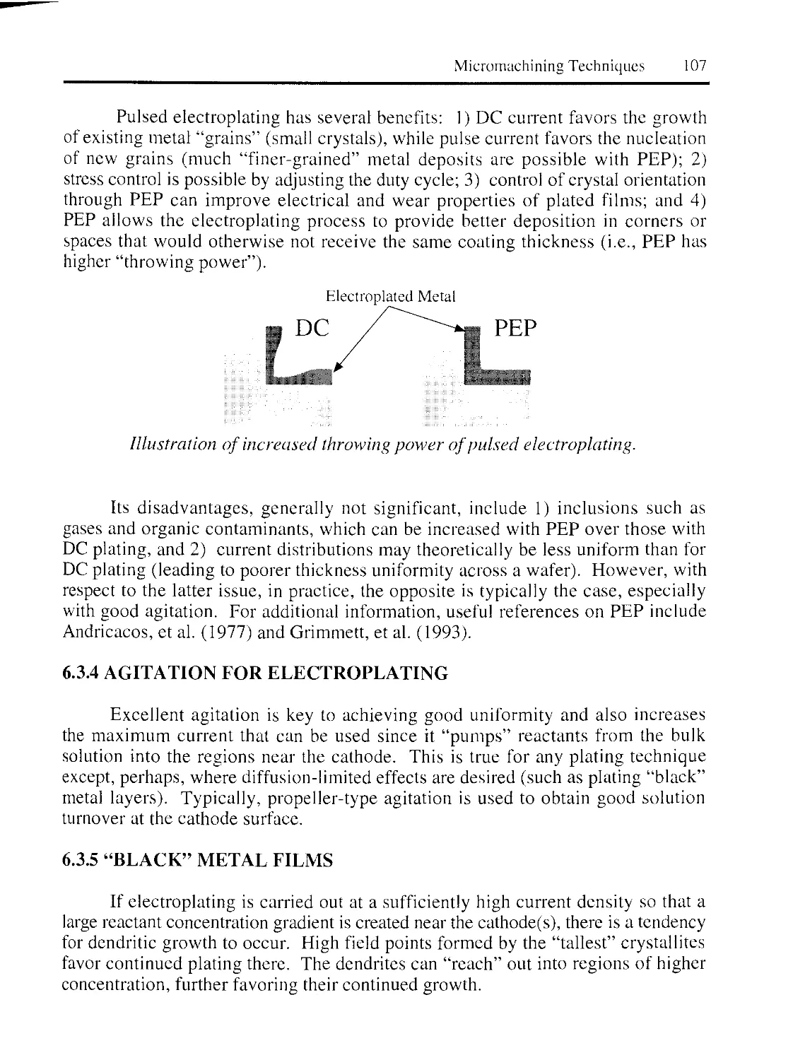
6.3.1 ELECTRODEPOSITION MECHANISMS 105
6.3.2 DC ELECTROPLATING 106
6.3.3 PULSED ELECTROPLATING (“PEP”) 106
6.3.4 AGITATION FOR ELECTROPLATING 107
6.3.5 “BLACK” METAL FILMS 107
6.3.6 “ELECTROLESS” PLATING 108
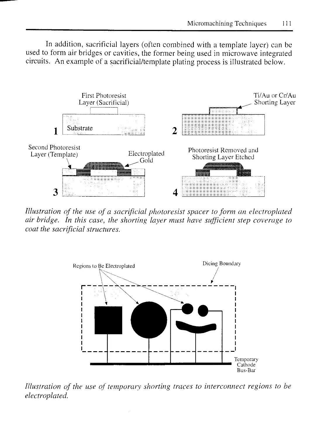
6.3.7 TEMPLATES FOR PLATING 110
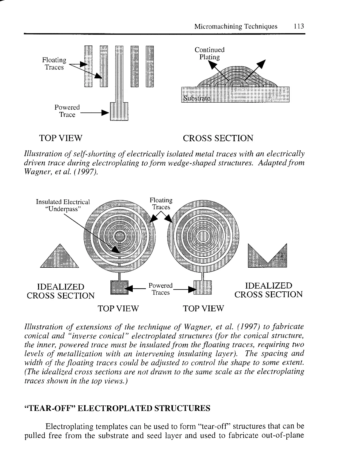
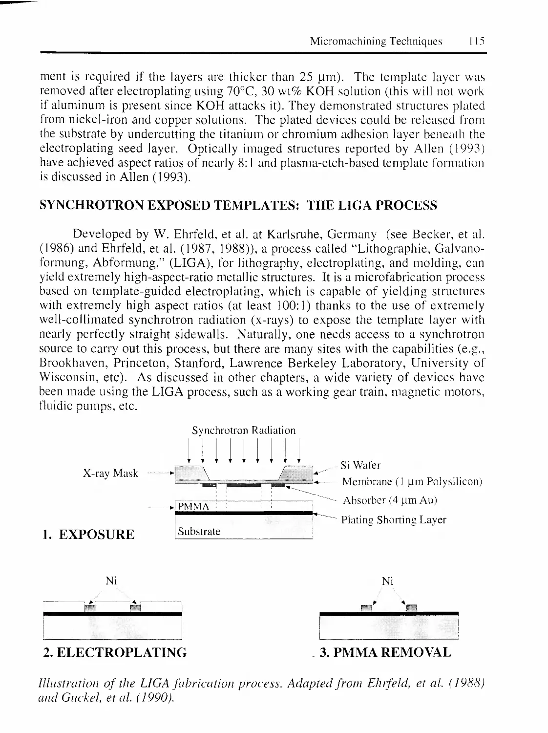
SELF-SHORTING PLATING PATTERNS 112
“TEAR-OFF’ ELECTROPLATED STRUCTURES 113
PHOTOIMAGED PLATING TEMPLATES 114
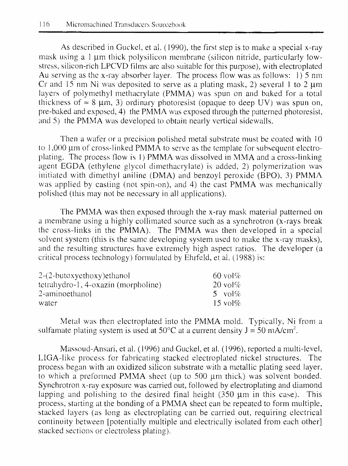
SYNCHROTRON EXPOSED TEMPLATES: THE LIGA PROCESS 115
RIE OR PLASMA-ETCHED TEMPLATES 117
6.3.8 TEMPLATE-FREE LOCALIZED ELECTROPLATING 117
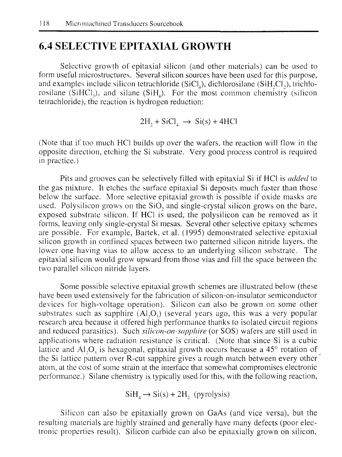
6.4 SELECTIVE EPITAXIAL GROWTH 118
7. BONDING PROCESSES 119
7.1 ANODIC BONDING 119
7.1.1 ANODIC BONDING USING DEPOSITED GLASS 121
7.2 SILICON FUSION BONDING 122
7.3 OTHER BONDING TECHNIQUES 123
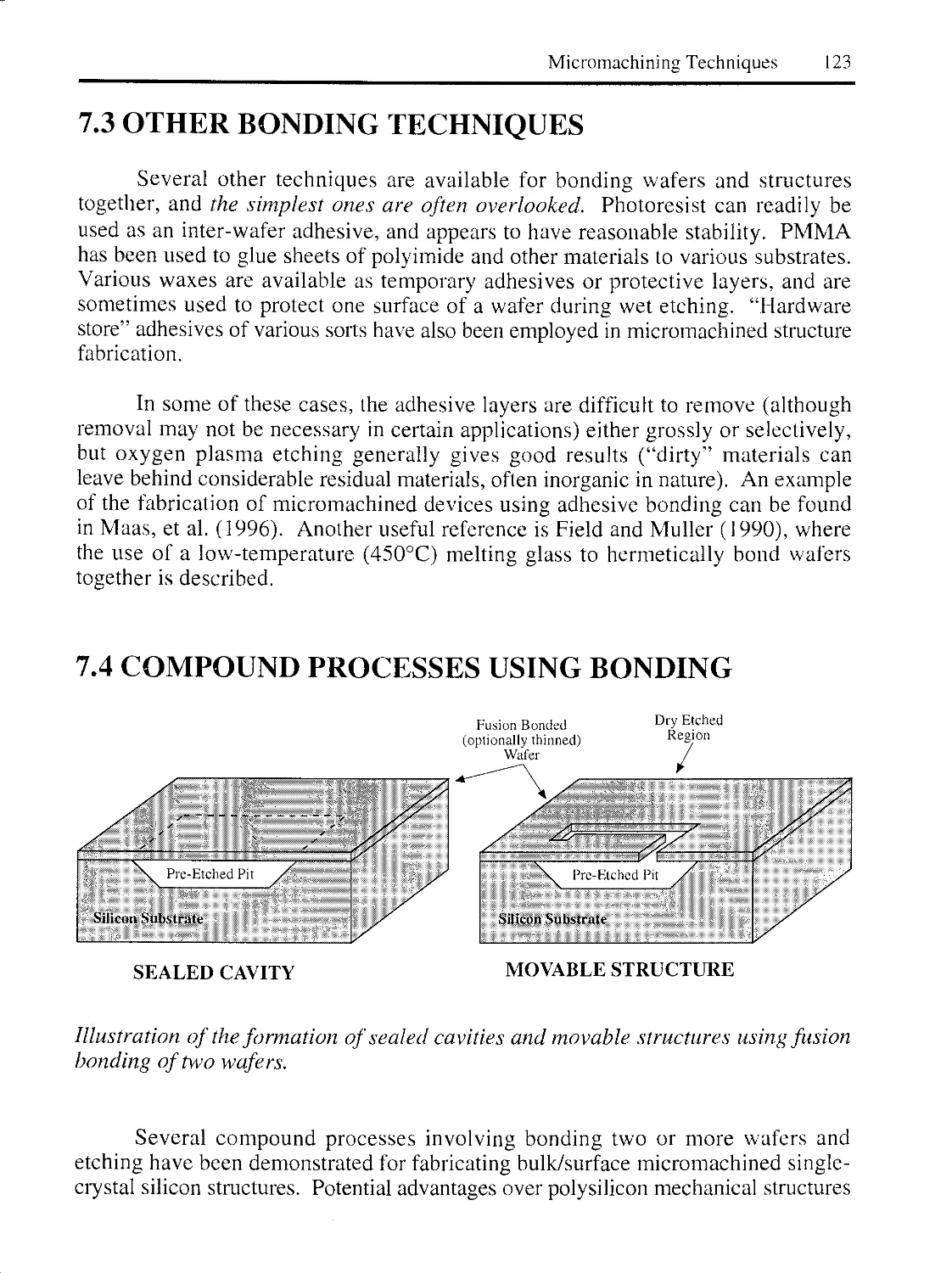
7.4 COMPOUND PROCESSES USING BONDING 123
8. SACRIFICIAL PROCESSES 126
8.1 STICKING PROBLEMS DURING WET RELEASE 127
8.1.1 PREVENTING STICKING DURING WET ETCH RELEASE 128
PHASE-CHANGE RELEASE METHODS 128
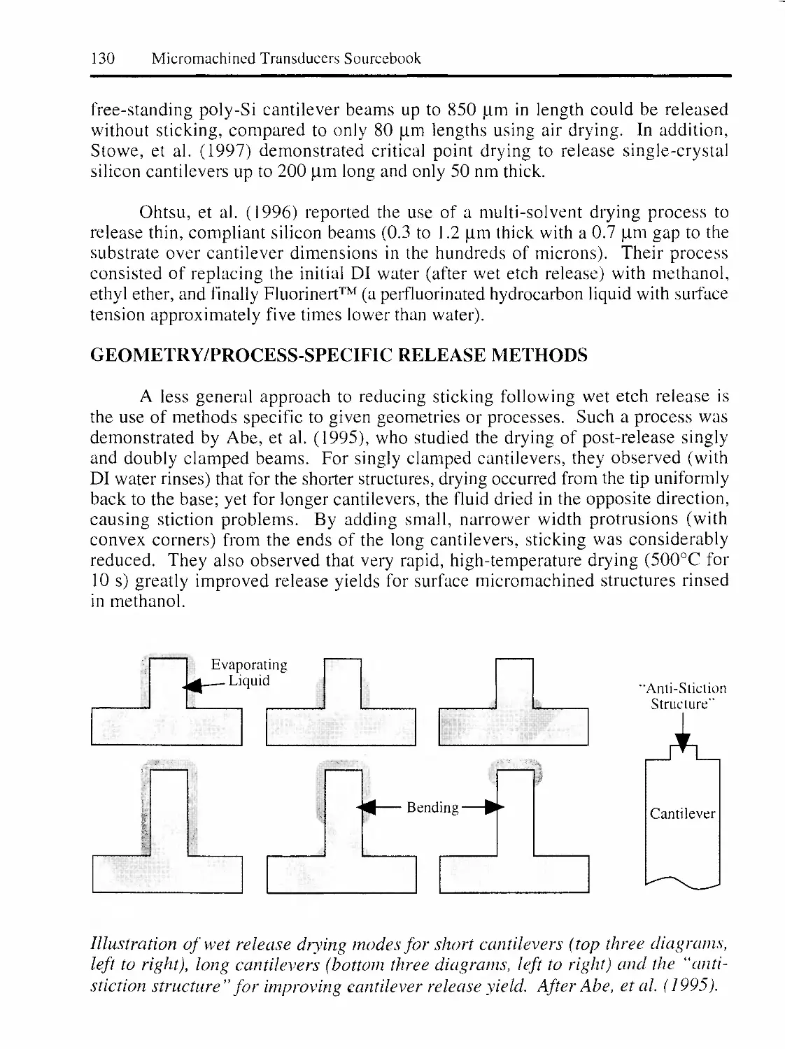
GEOMETRY/PROCESS-SPECIFIC RELEASE METHODS 130
SURFACE TREATMENT RELEASE METHODS 131
8.2 EXAMPLE SACRIFICIAL PROCESSES 131
8.2.1 SACRIFICIAL LIGA (“SLIGA”) PROCESS 131
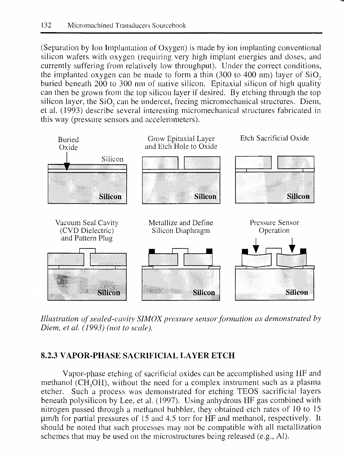
8.2.2 SIMOX AS A SACRIFICIAL LAYER 131
8.2.3 VAPOR-PHASE SACRIFICIAL LAYER ETCH 132
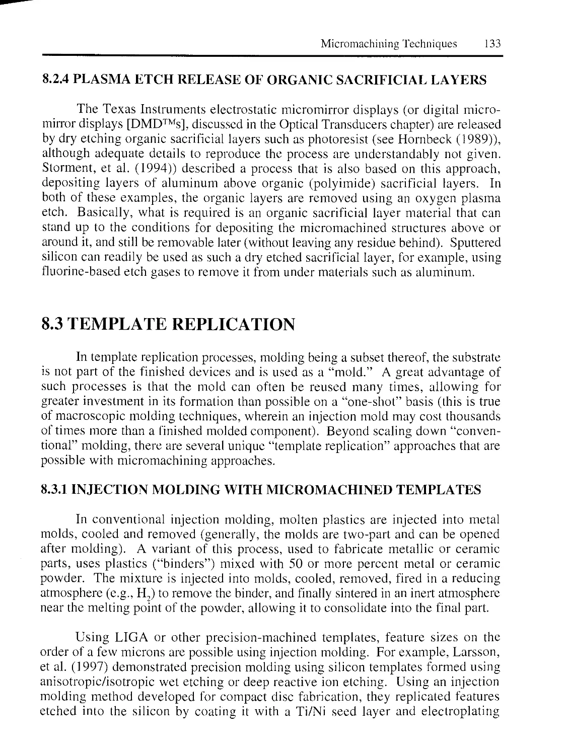
8.2.4 PLASMA ETCH RELEASE OF ORGANIC SACRIFICIAL LAYERS 133
8.3 TEMPLATE REPLICATION 133
8.3.1 INJECTION MOLDING WITH MICROMACHINED TEMPLATES 133
8.3.2 PLATING-BASED TEMPLATE REPLICATION 134
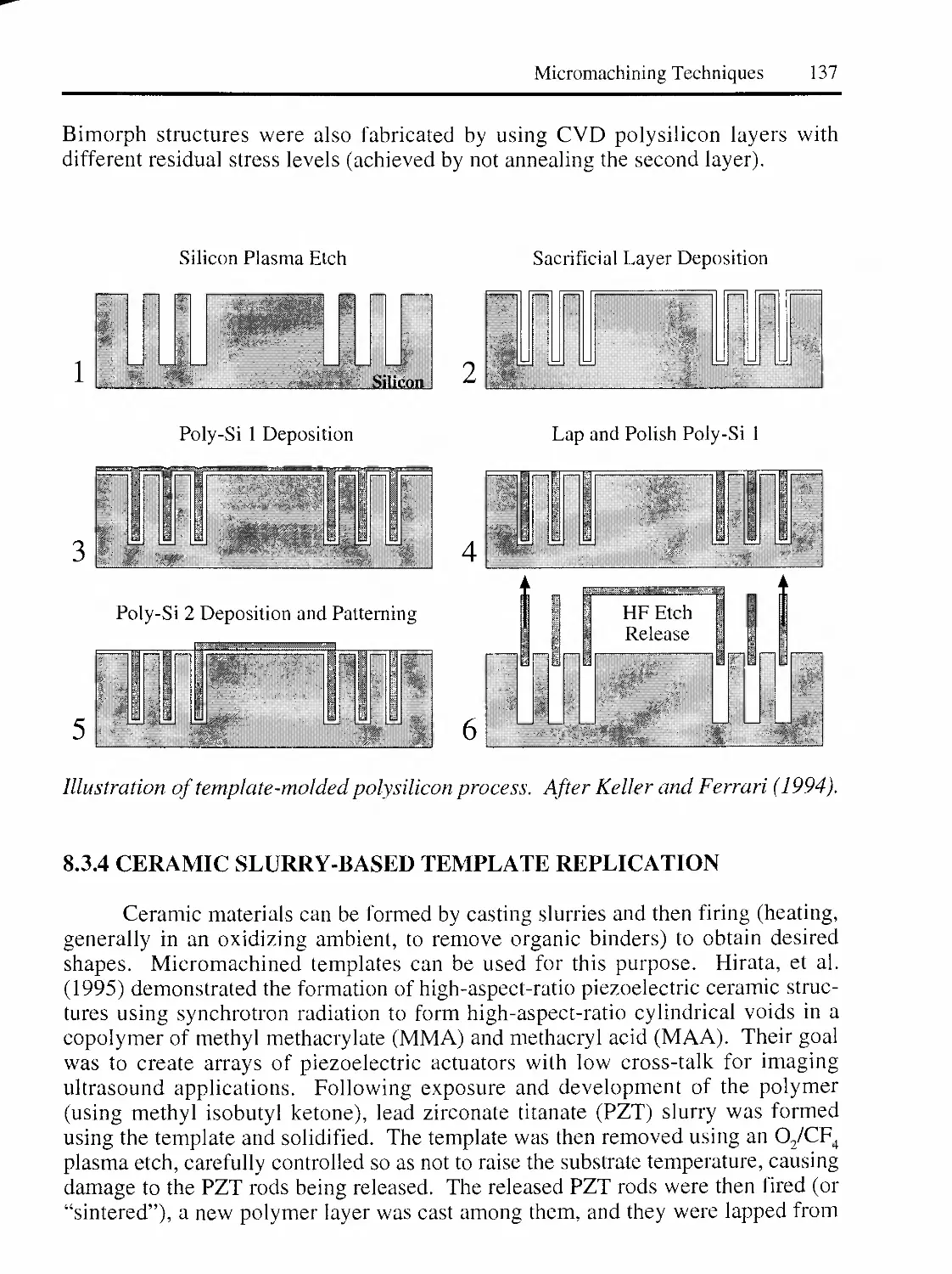
8.3.3 CVD-BASED TEMPLATE REPLICATION 136
ix
8.3.4 CERAMIC SLURRY-BASED TEMPLATE REPLICATION 137
8.3.5 PREFORMED, ABOVE SUBSTRATE TEMPLATES 138
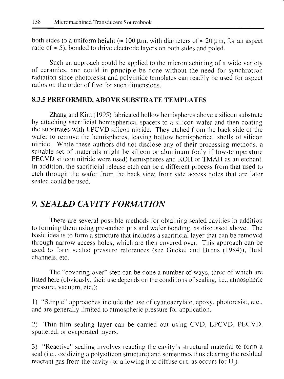
9. SEALED CAVITY FORMATION 138
9.1 GETTERS FOR SEALED CAVITIES 139
10. SURFACE MODIFICATION 140
11. PRINTING AND STEREOLITHOGRAPHY 142
11.1 SCREEN PRINTING 143
11.2 TRANSFER PRINTING 143
11.3 POWDER-LOADED POLYMERS FOR PRINTING 144
11.4 THREE-DIMENSIONAL LITHOGRAPHY 145
1 1.5 SPATIAL FORMING VIA TRANSFER PRINTING 145
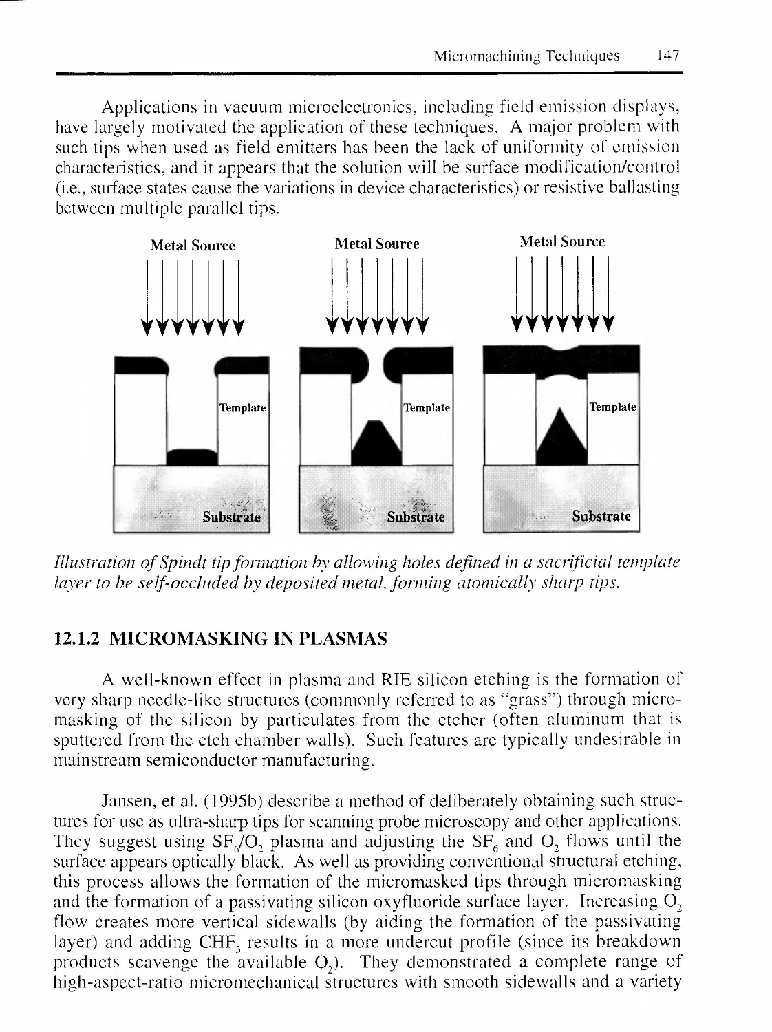
12. OTHER MICROMACHINING TECHNIQUES 146
12.1 SHARP TIP FORMATION 146
12.1.1 SELF-OCCLUDING MASKS 146
12.1.2 M1CROMASKING IN PLASMAS 147
12.1.3 WET ETCHING 148
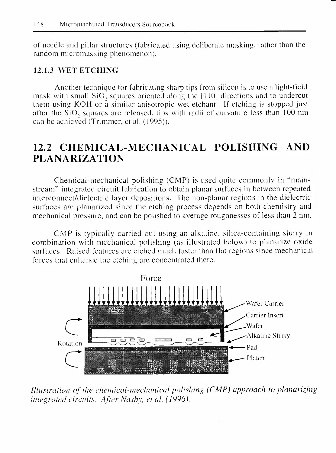
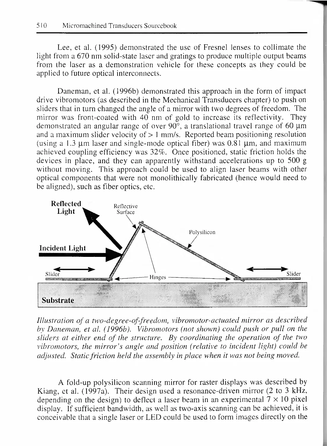
12.2 CHEMICAL-MECHANICAL POLISHING AND PLANARIZATION 148
12.3 ELECTRIC DISCHARGE MACHINING (EDM) 149
12.4 ABRASIVE POWDER MACHINING 150
12.5 PRECISION MECHANICAL MACHINING 150
12.6 SCANNING PROBE MACHINING 151
12.7 THERMOMIGRATION 151
12.8 PHOTOSENSITIVE GLASS MICROMACHINING 152
12.9 FOCUSED ION-BEAM MICROMACHINING 152
MICROMACHINING TECHNIQUES REFERENCES 154
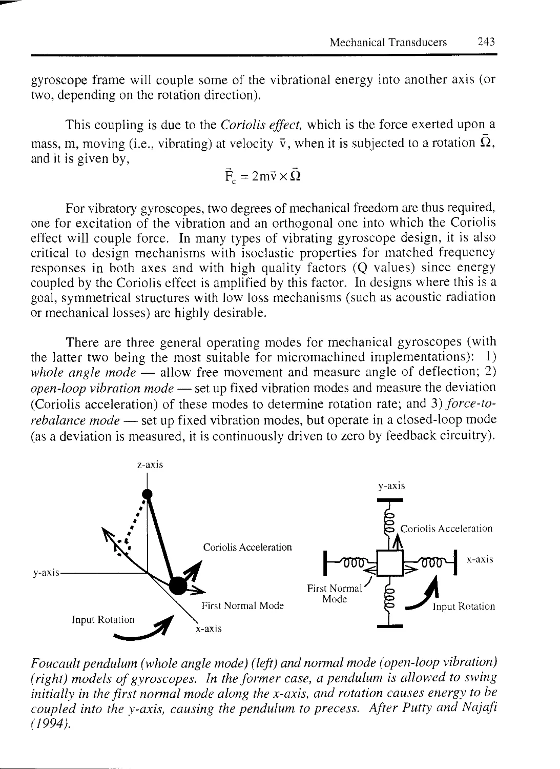
Chapter 3: MECHANICAL TRANSDUCERS 179
1. INTRODUCTION 179
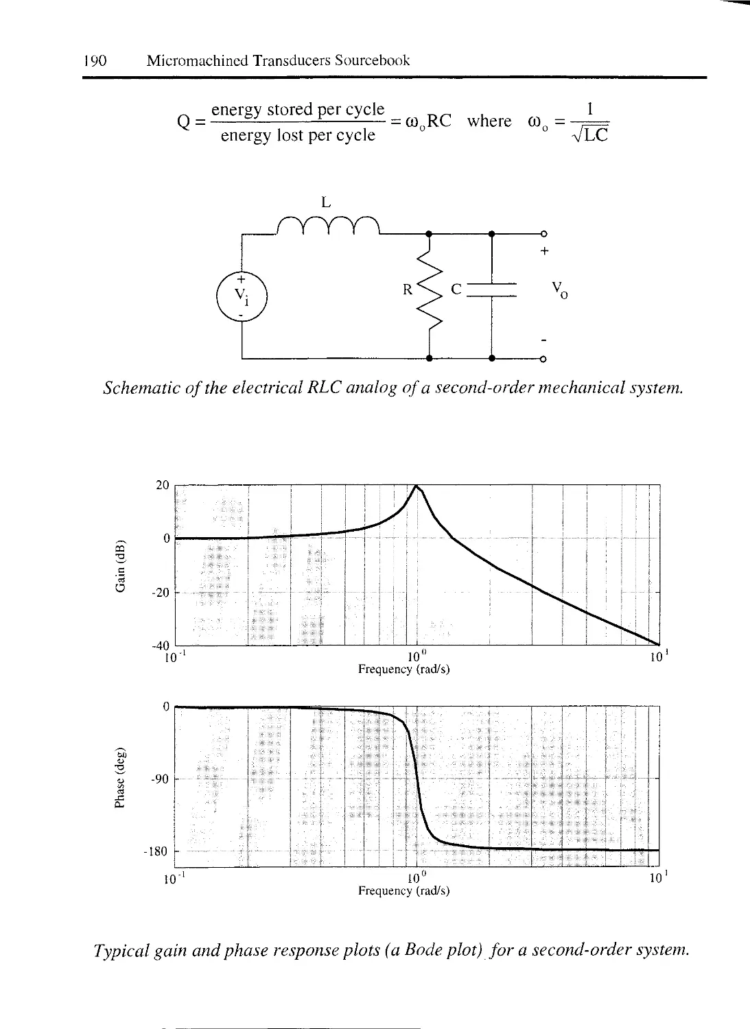
2. BASIC MECHANICS 180
2.1 AXIAL STRESS AND STRAIN 180
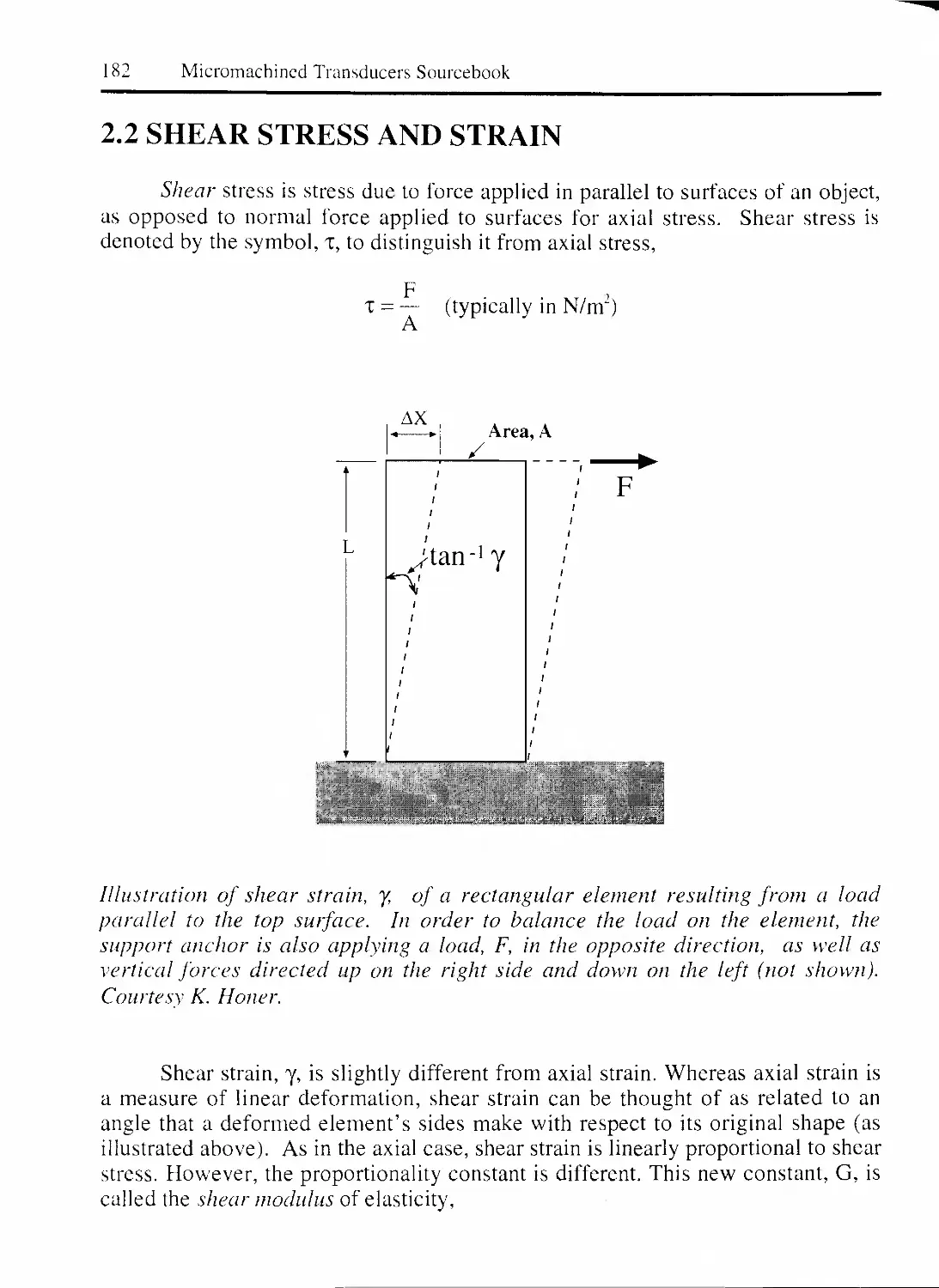
2.2 SHEAR STRESS AND STRAIN 182
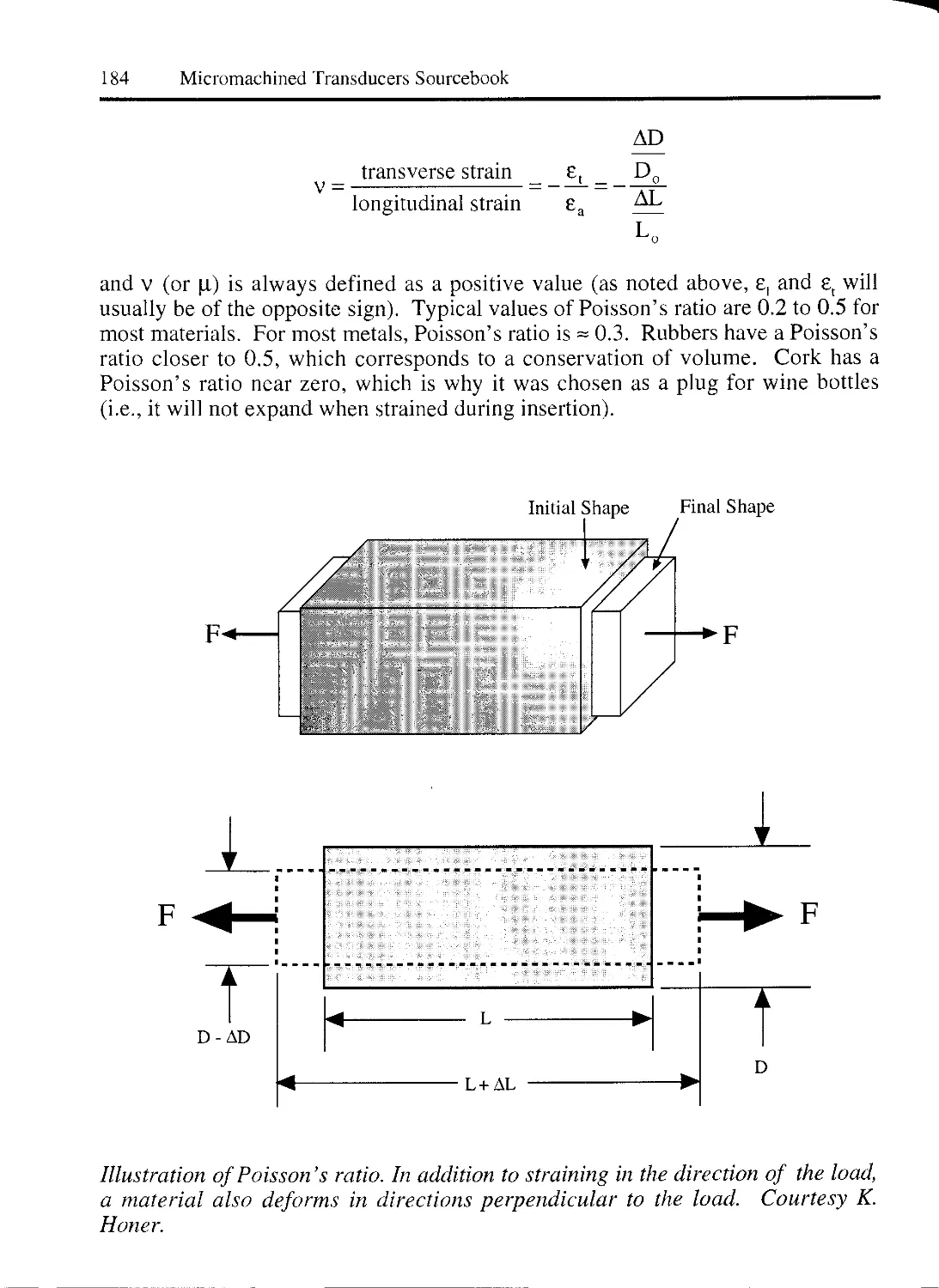
2.3 POISSON'S RATIO 183
2.4 COMMONLY USED DEFLECTION EQUATIONS FOR MICROSTRUCTURES .... 185
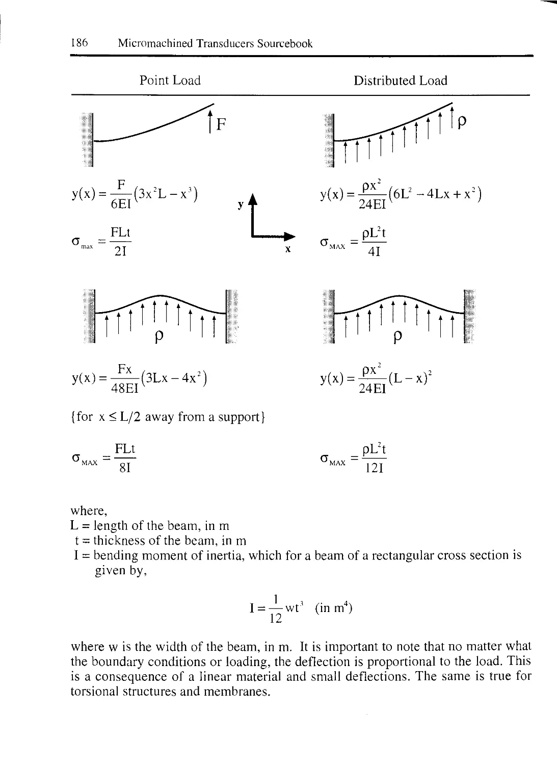
2.4.1 STATIC BEAM EQUATIONS 1 85
2.4.2 STATIC TORSION EQUATIONS 1 87
2.4.3 STATIC PLATE EQUATIONS 188
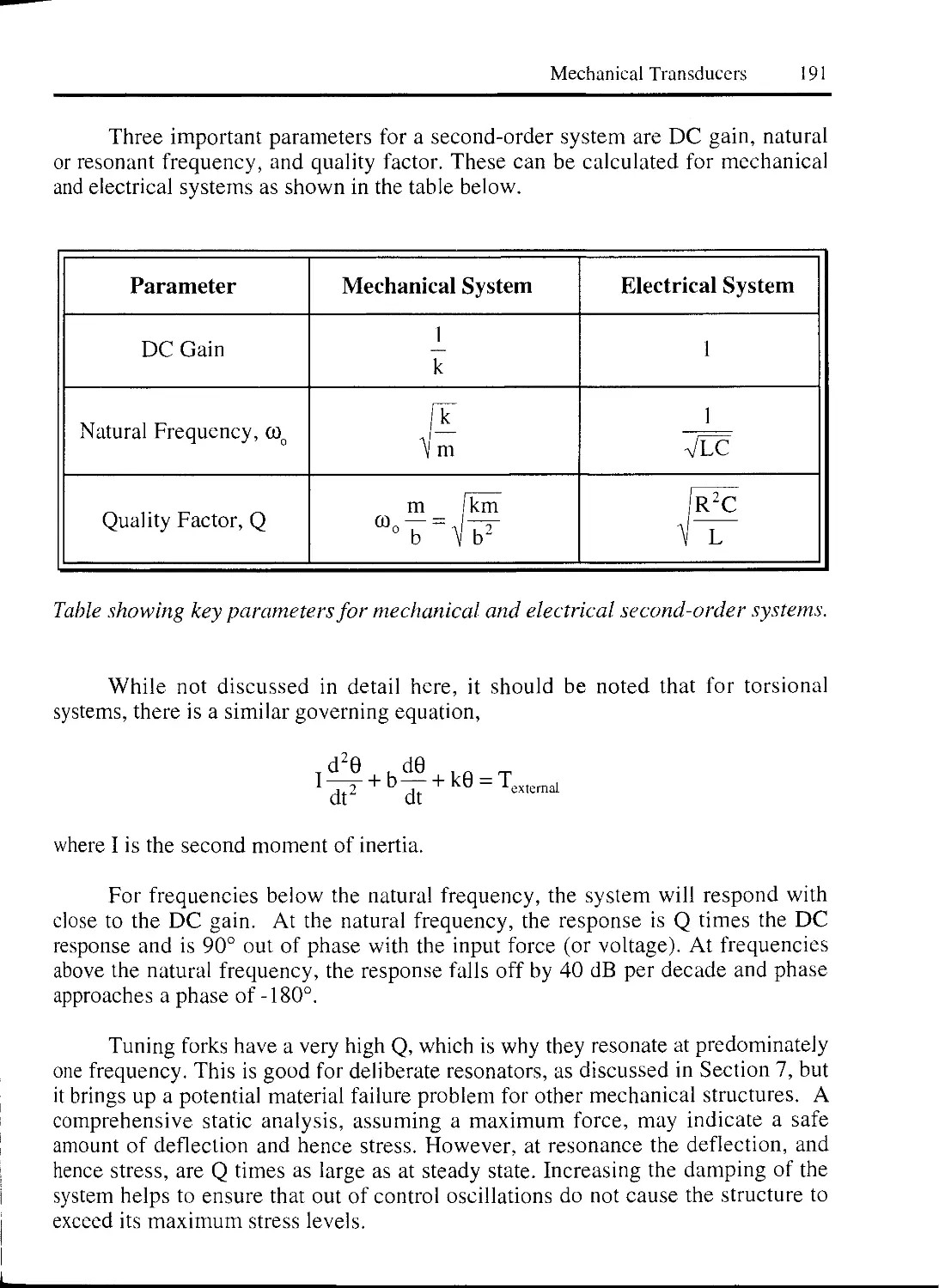
2.5 DYNAMICS 188
2.6 THERMAL NOISE 192
3. MECHANICAL PROPERTIES OF MATERIALS 193
3.1 MATERIAL FAILURE 193
x
3.2 GENERAL MATERIALS CONSIDERATIONS 194
3.3 MECHANICAL CHARACTERIZATION OF THIN-FILMS 195
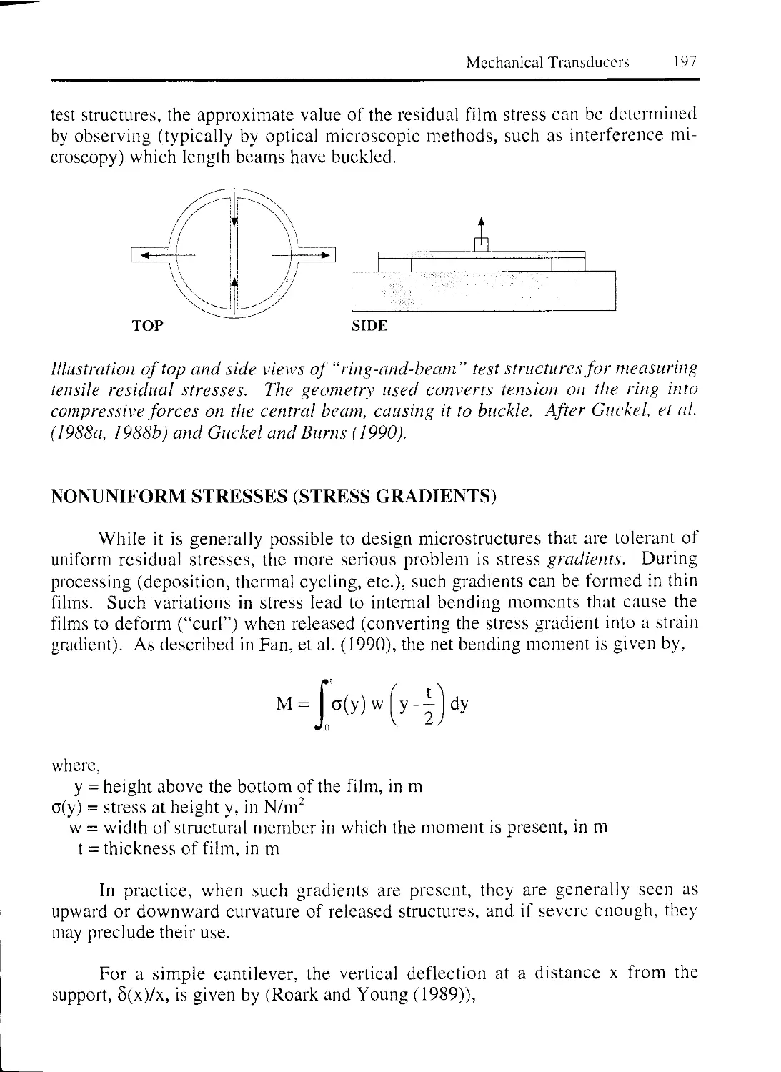
3.3.1 STRESS MEASUREMENT 195
UNIFORM STRESSES 195
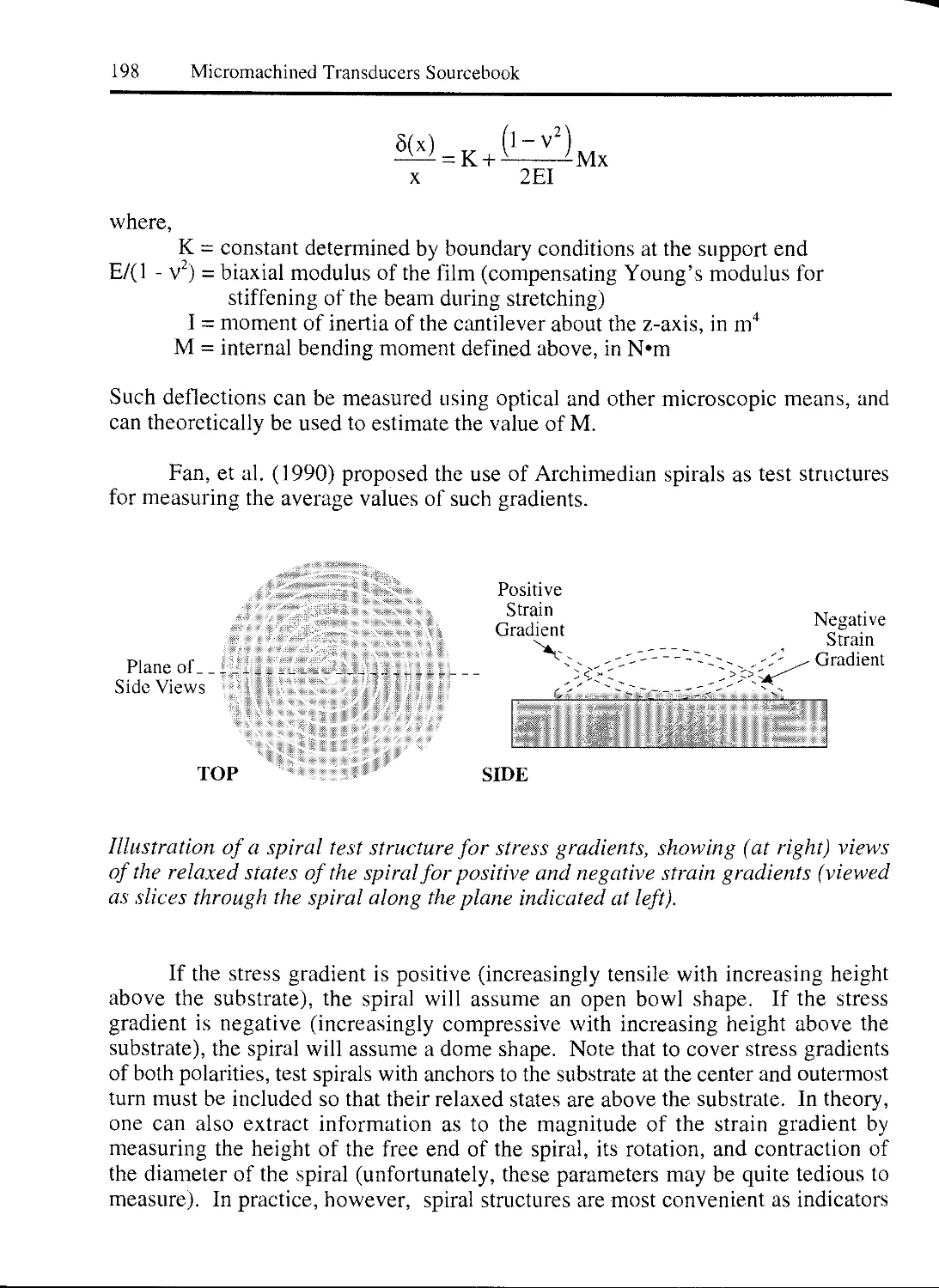
NONUNIFORM STRESSES (STRESS GRADIENTS) 197
3.3.2 MEASUREMENT OF OTHER MECHANICAL PROPERTIES 199
DIRECT MEASUREMENT 199
INDIRECT MEASUREMENT 201
4. BASIC MECHANISMS AND STRUCTURES 201
4.1 IN-PLANE ROTARY MECHANISMS 202
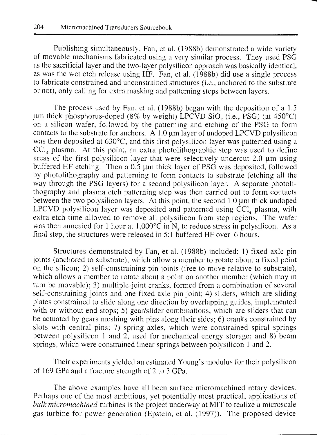
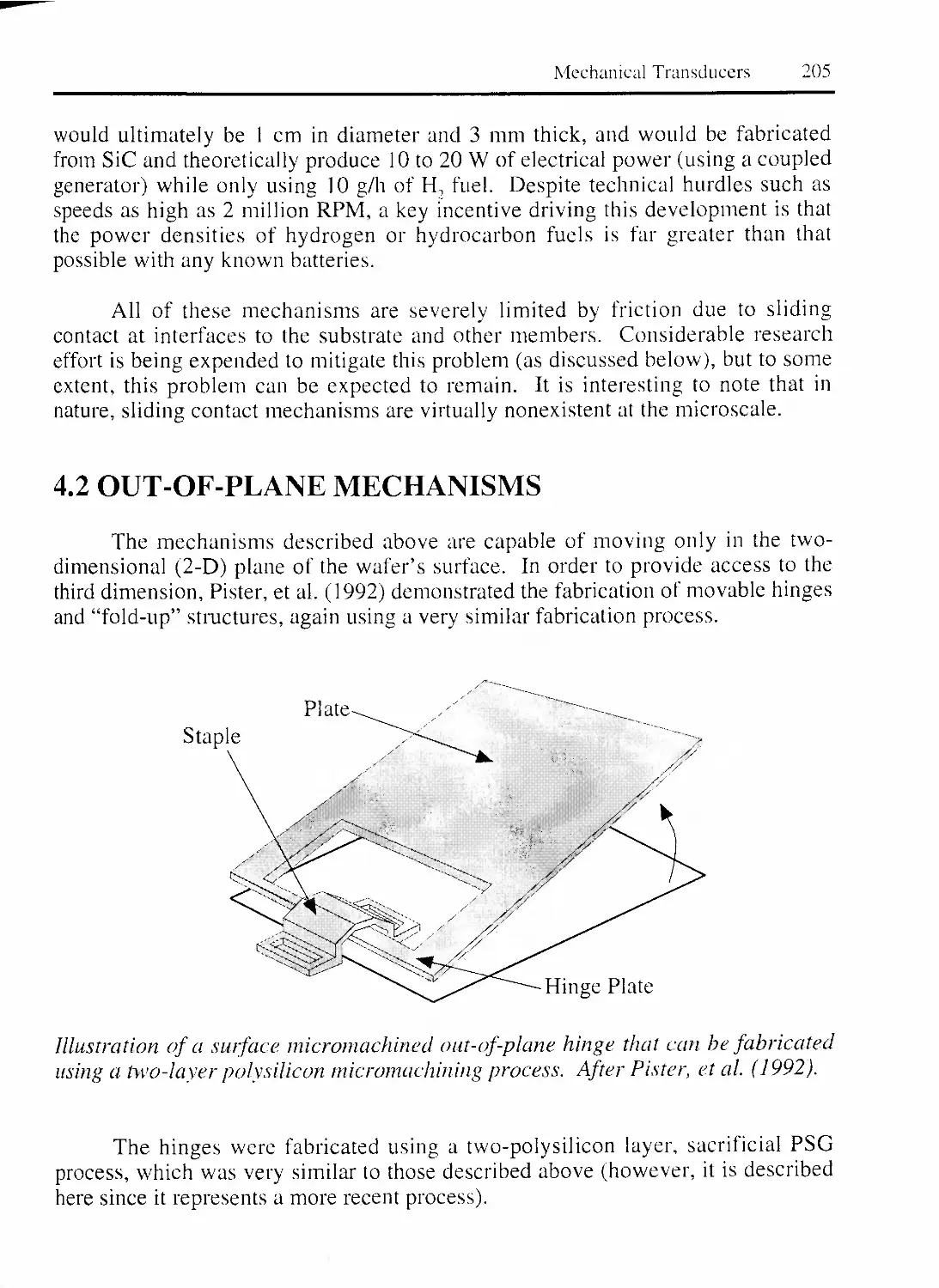
4.2 OUT-OF-PLANE MECHANISMS 205
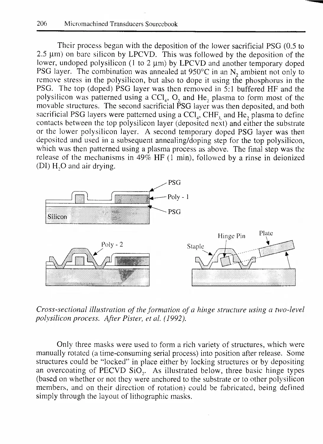
4.3 STRUCTURAL MEMBERS 207
4.4 BISTABLE MECHANISMS 208
4.5 SELF-ASSEMBLY 209
5. MECHANICAL SENSORS 210
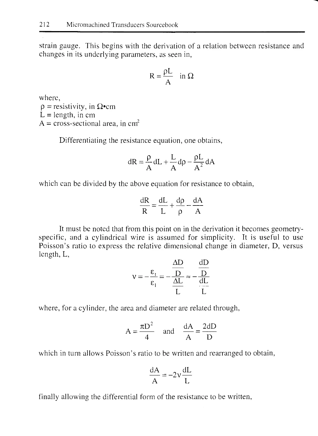
5.1 SENSING MECHANISMS 210
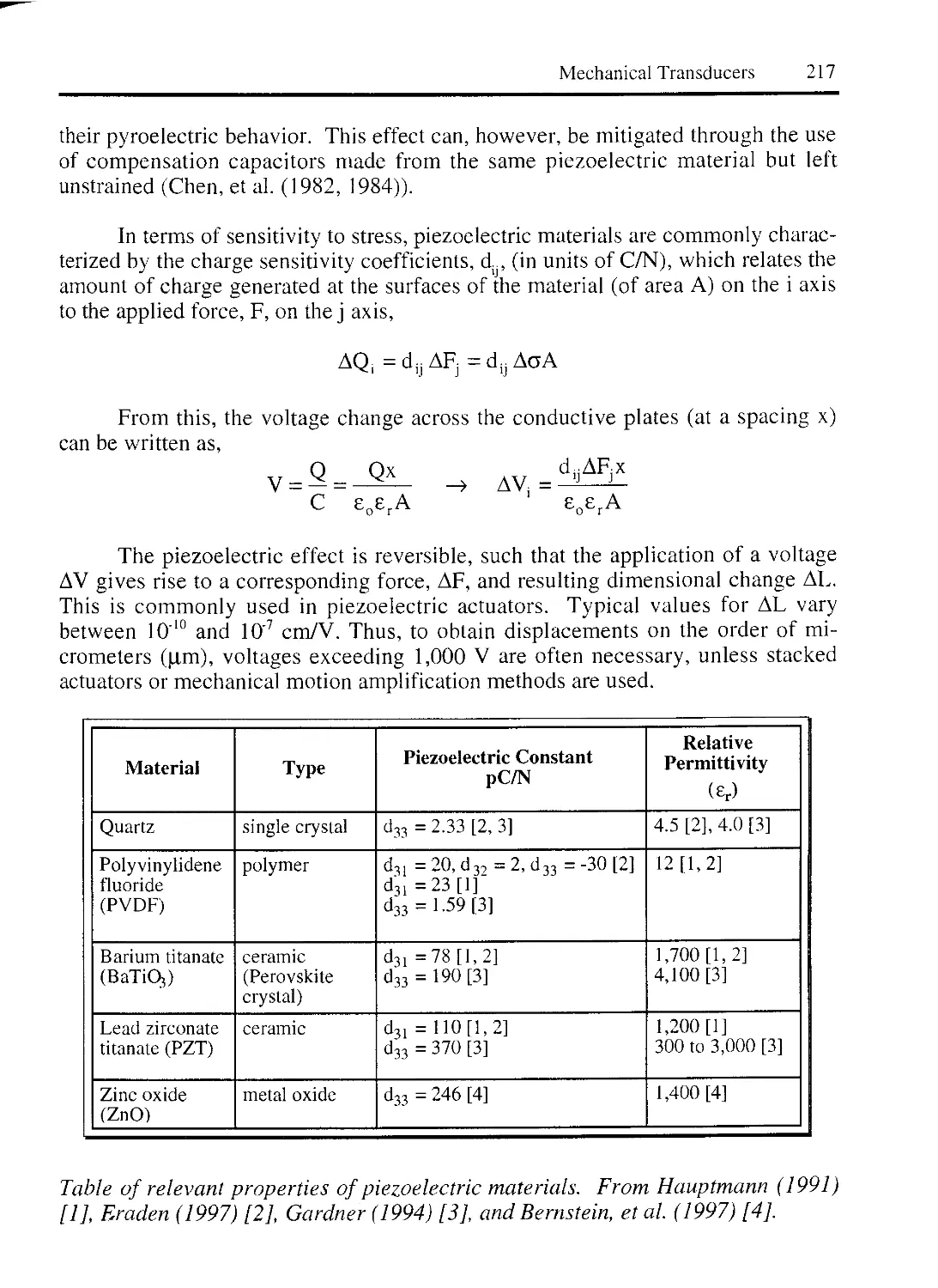
5.1.1 RESISTIVE AND PIEZORESISTIVE STRAIN SENSORS 21 1
METALLIC STRAIN GAUGES 213
SEMICONDUCTOR STRAIN GAUGES 214
5.1.2 PIEZOJUNCTION EFFECT 215
5.1.3 PIEZOELECTRIC EFFECT 215
5.1.4 CAPACITIVE SENSING 219
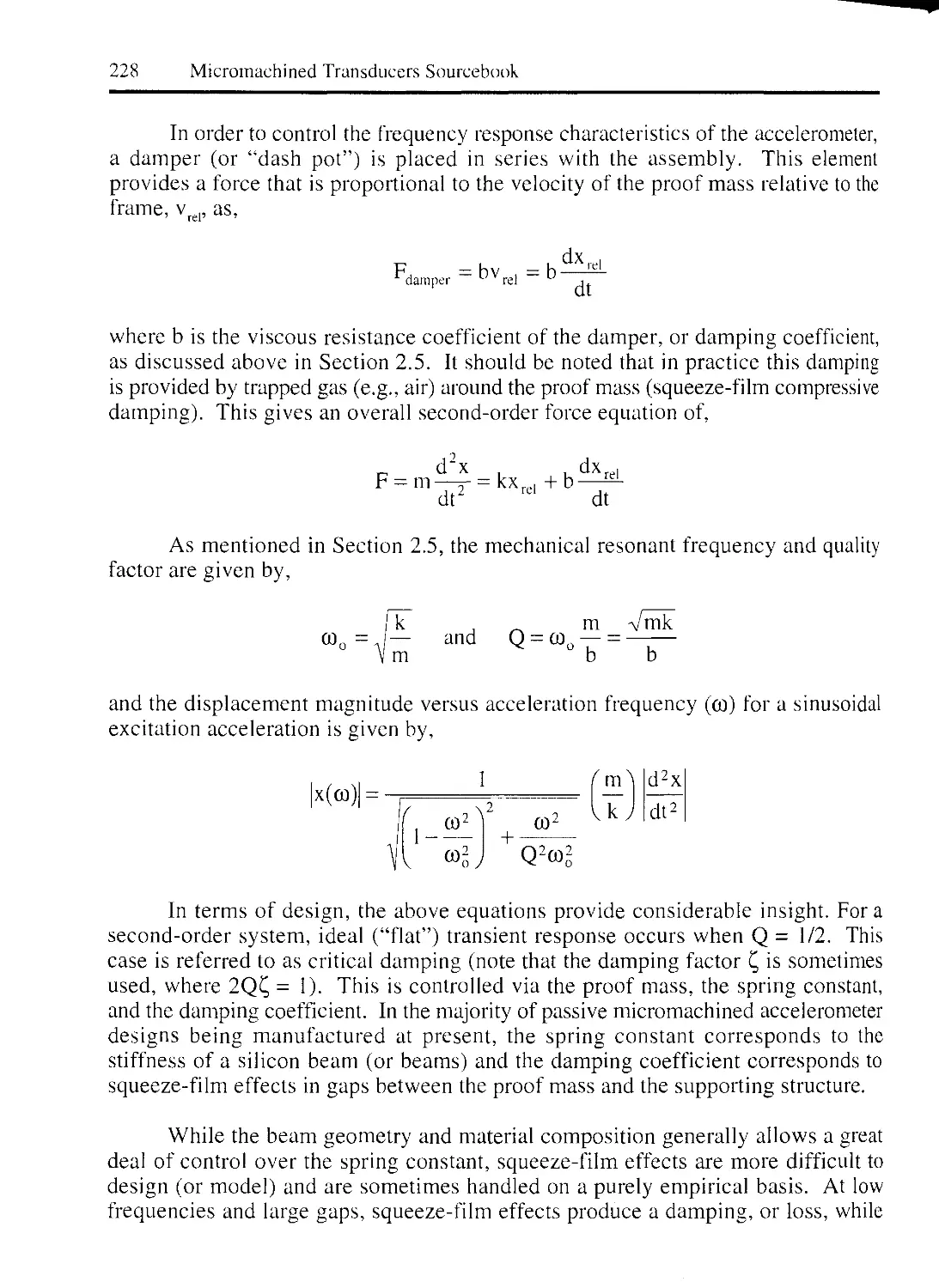
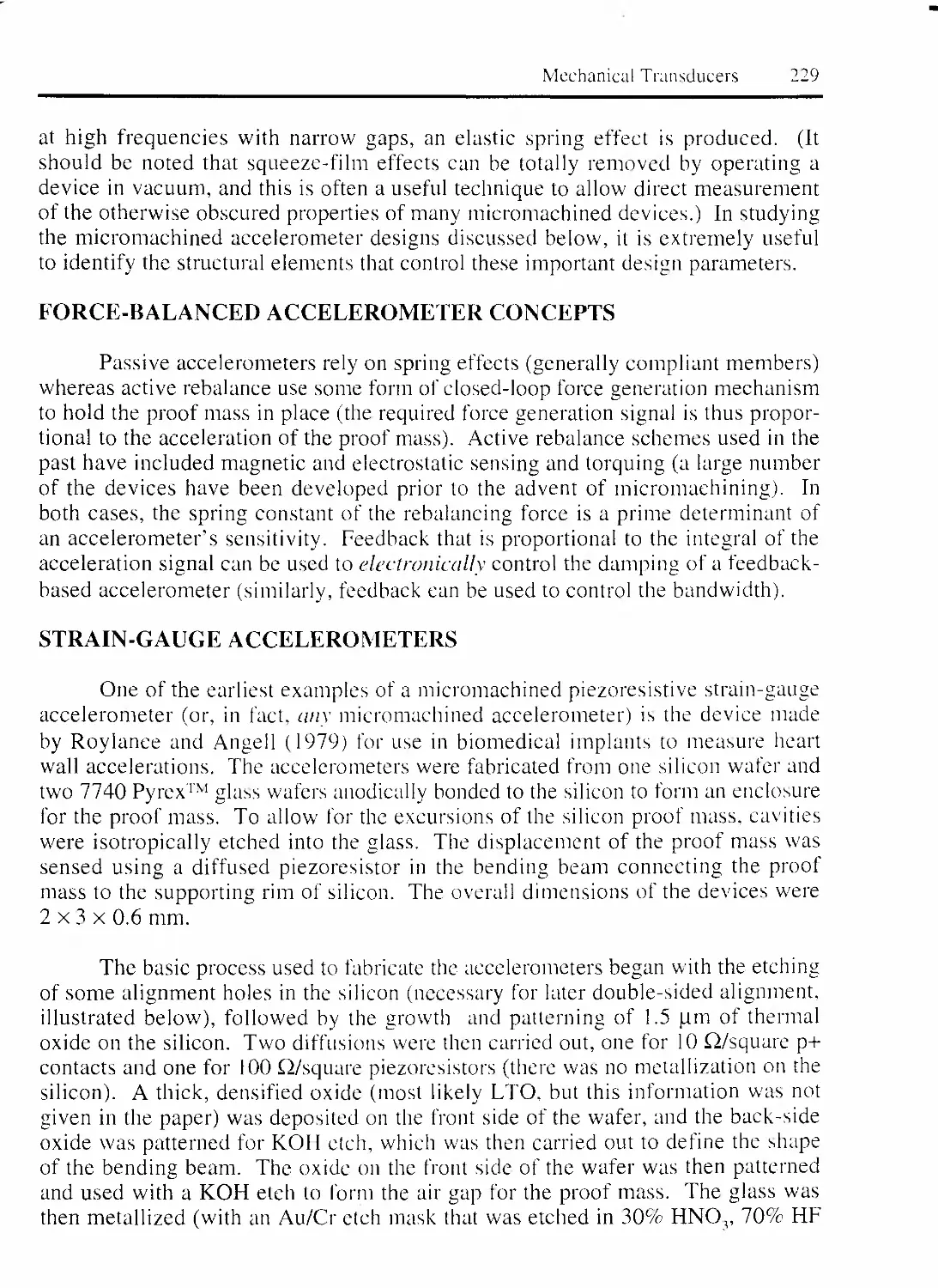
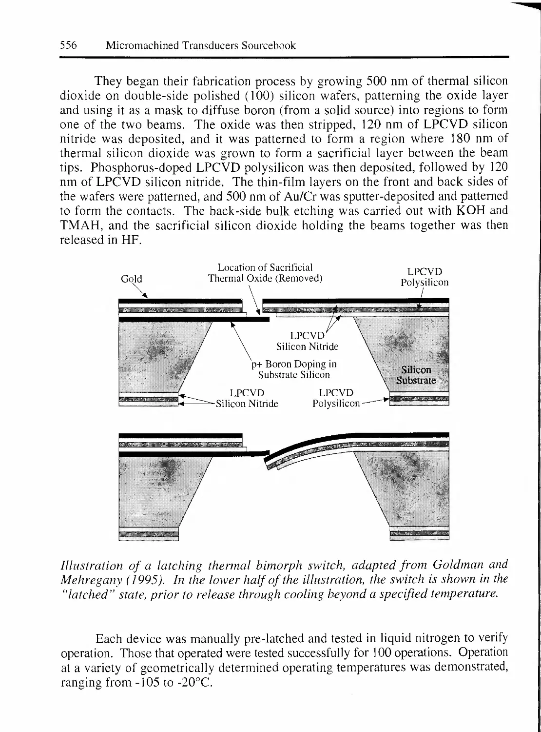
5.1.5 TUNNELING SENSING 221
5.2 MICROMACHINED MECHANICAL SENSORS 222
5.2.1 MICROMACHINED STRAIN GAUGES 222
IMPLANTABLE STRAIN GAUGES 222
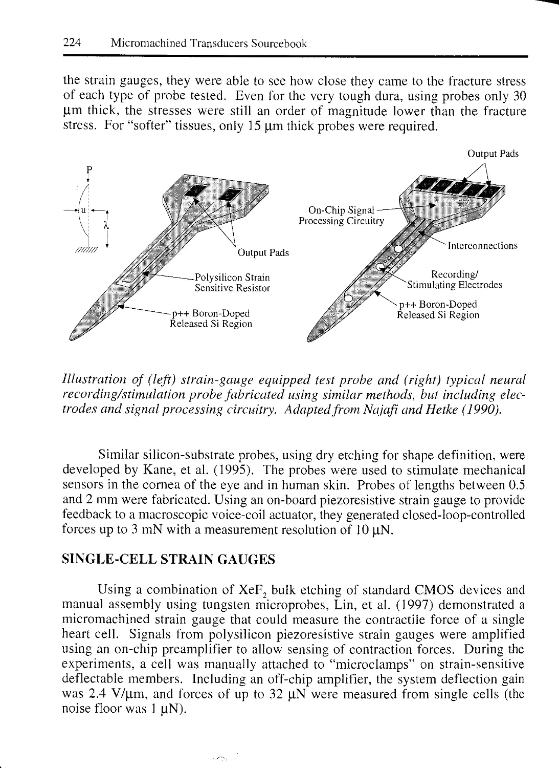
PENETRATING M1CRO-STRAIN-GAUGE PROBE 223
SINGLE-CELL STRAIN GAUGES 224
RESONANT STRAIN GAUGES 225
5.2.2 ACCELEROMETERS 225
BASIC ACCELEROMETER CONCEPTS 226
FORCE-BALANCED ACCELEROMETER CONCEPTS 229
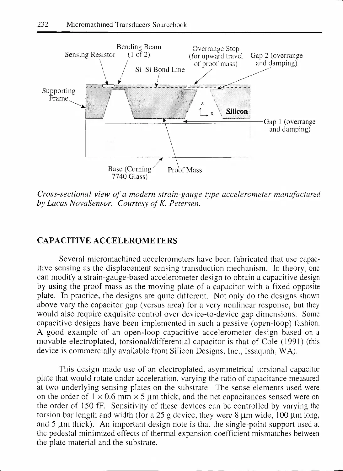
STRAIN-GAUGE ACCELEROMETERS 229
CAPACITIVE ACCELEROMETERS 232
FORCE-BALANCED CAPACITIVE ACCELEROMETERS 234
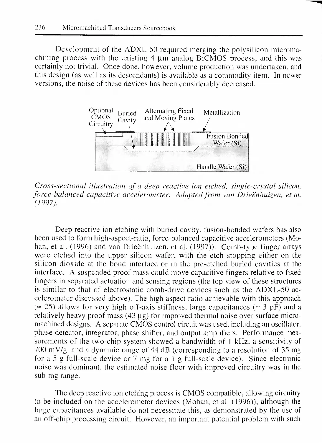
PIEZOELECTRIC ACCELEROMETERS 237
TUNNELING ACCELEROMETERS 239
LATCHING ACCELEROMETERS 240
ACCELEROMETER SWITCH ARRAYS 240
MULTI-AXIS ACCELEROMETERS 242
5.2.3 MICROMACHINED GYROSCOPES 242
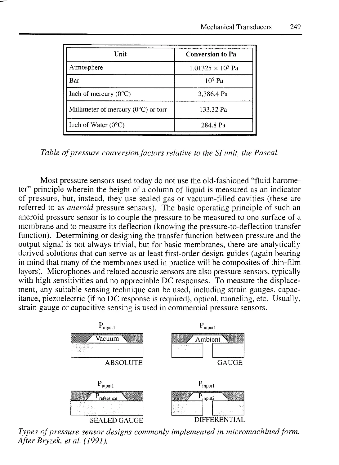
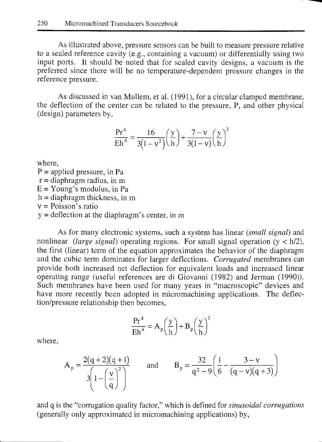
5.2.4 MECHANICAL PRESSURE SENSORS 248
PRESSURE MEASUREMENT UNITS 248
PIEZORESISTIVE PRESSURE SENSORS 252
INTEGRATED PIEZORESISTIVE PRESSURE SENSORS 254
SURFACE MICROMACHINED PIEZORESISTIVE PRESSURE SENSORS 254
CAPACITIVE PRESSURE SENSORS 255
PRESSURE SWITCHES 259
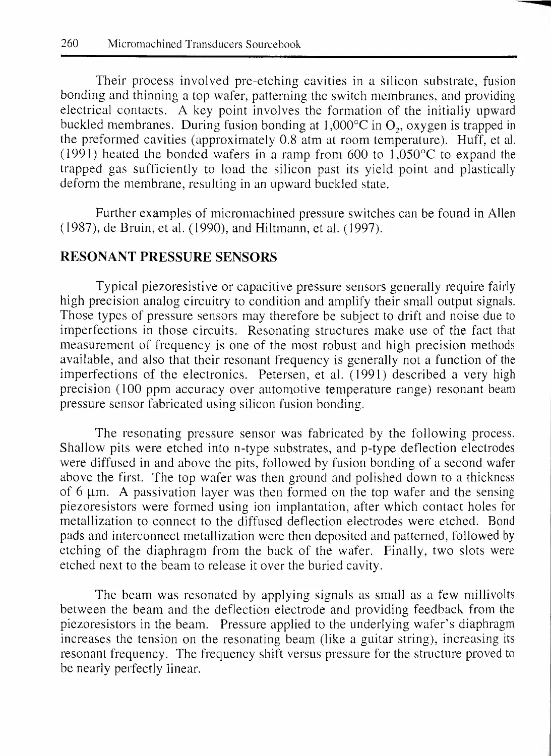
RESONANT PRESSURE SENSORS 260
5.2.5 MICROPHONES 261
PIEZORESISTIVE MICROPHONES 262
CAPACITIVE MICROPHONES 263
PIEZOELECTRIC MICROPHONES 265
xi
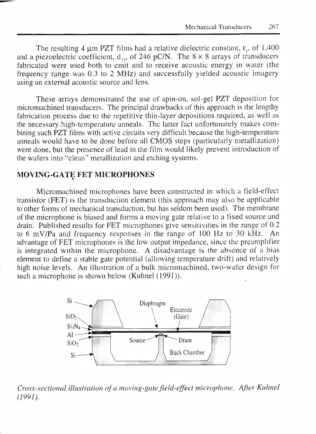
MOVING-GATE FET MICROPHONES 267
5.2.6 TACTILE SENSORS 268
PIEZOELECTRIC TACTILE SENSORS 268
RESISTIVE TACTILE SENSORS 269
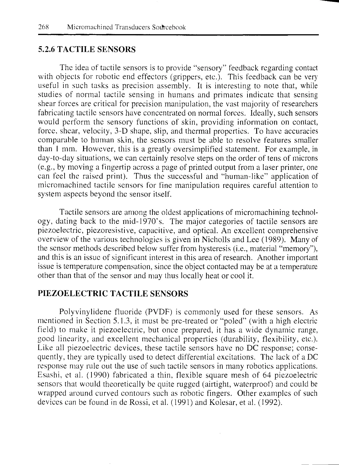
CAPACITIVE TACTILE SENSORS 270
OPTICAL TACTILE SENSORS 271
OTHER TACTILE SENSORS 272
5.2.7 BIOLOGICAL MECHANOSENSORS 272
BIOLOGICAL ACCELEROMETERS 272
BIOLOGICAL TACTILE SENSORS 273
BIOLOGICAL ACOUSTIC SENSORS 273
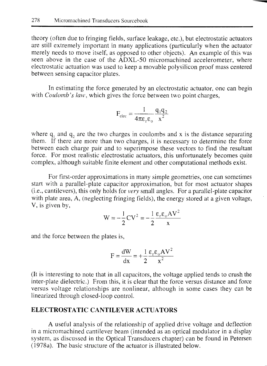
6. MECHANICAL ACTUATORS 276
6.1 ACTUATION MECHANISMS 276
6.1.1 ELECTROSTATIC ACTUATION 277
ELECTROSTATIC CANTILEVER ACTUATORS 278
TORSIONAL ELECTROSTATIC ACTUATORS 281
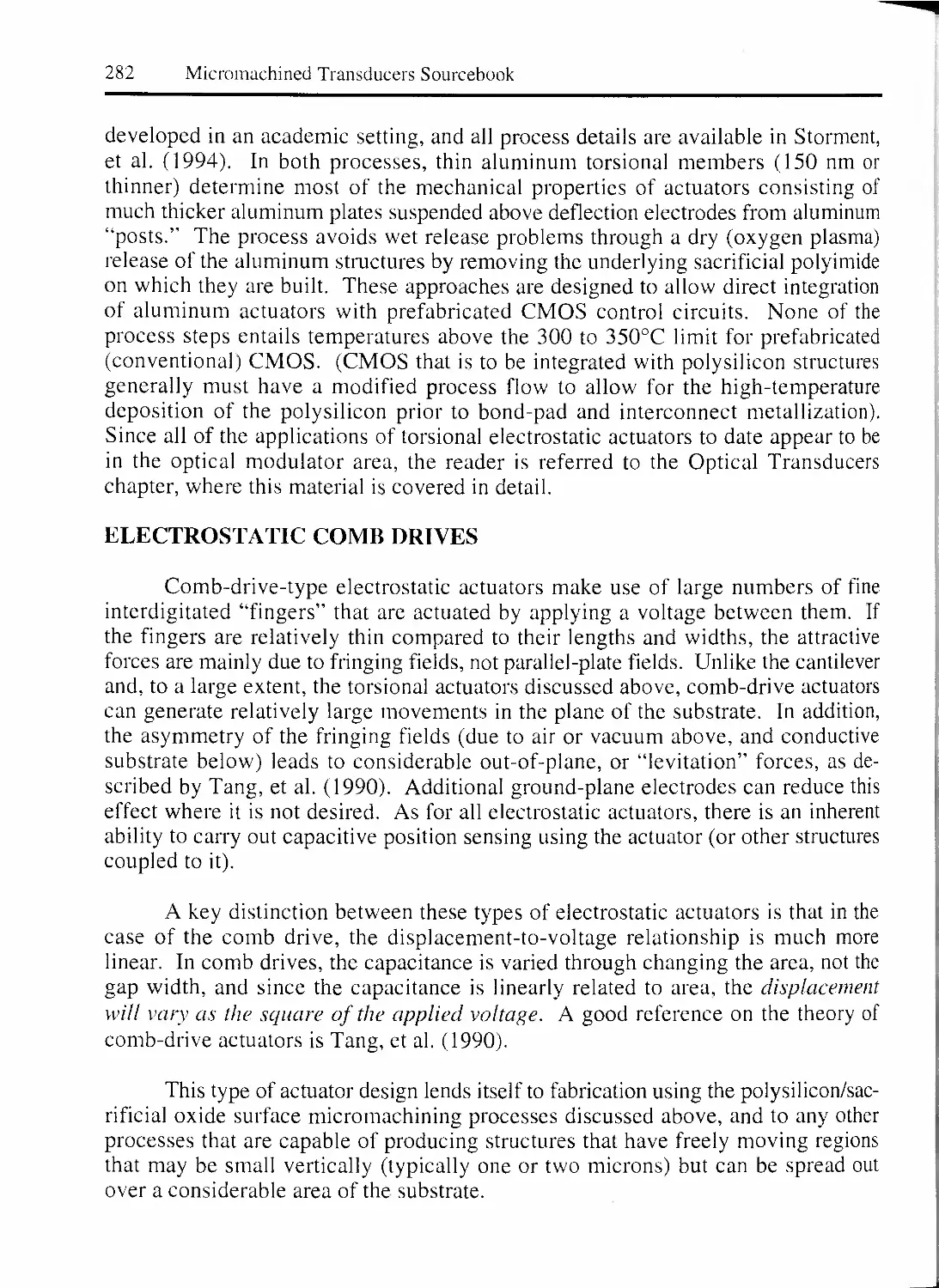
ELECTROSTATIC COMB DRIVES 282
FEEDBACK STABILIZATION OF ELECTROSTATIC ACTUATORS 283
ELECTROSTATIC ROTARY MICROMOTORS 284
ELECTROSTATIC LINEAR MICROMOTORS 286
ELECTROSTATIC MICROGRIPPERS 288
ELECTROSTATIC RELAYS AND SWITCHES 289
6.1.2 THERMAL ACTUATION 289
THERMAL EXPANSION OF SOLIDS 289
BIMORPH THERMAL ACTUATORS 289
THERMAL ARRAY ACTUATORS 291
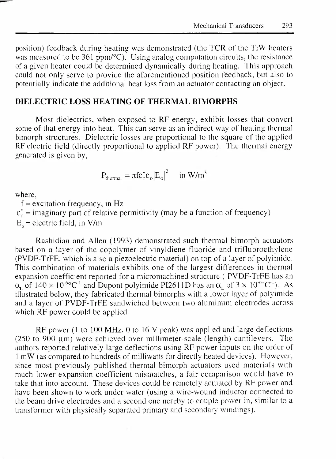
DIELECTRIC LOSS HEATING OF THERMAL BIMORPHS 293
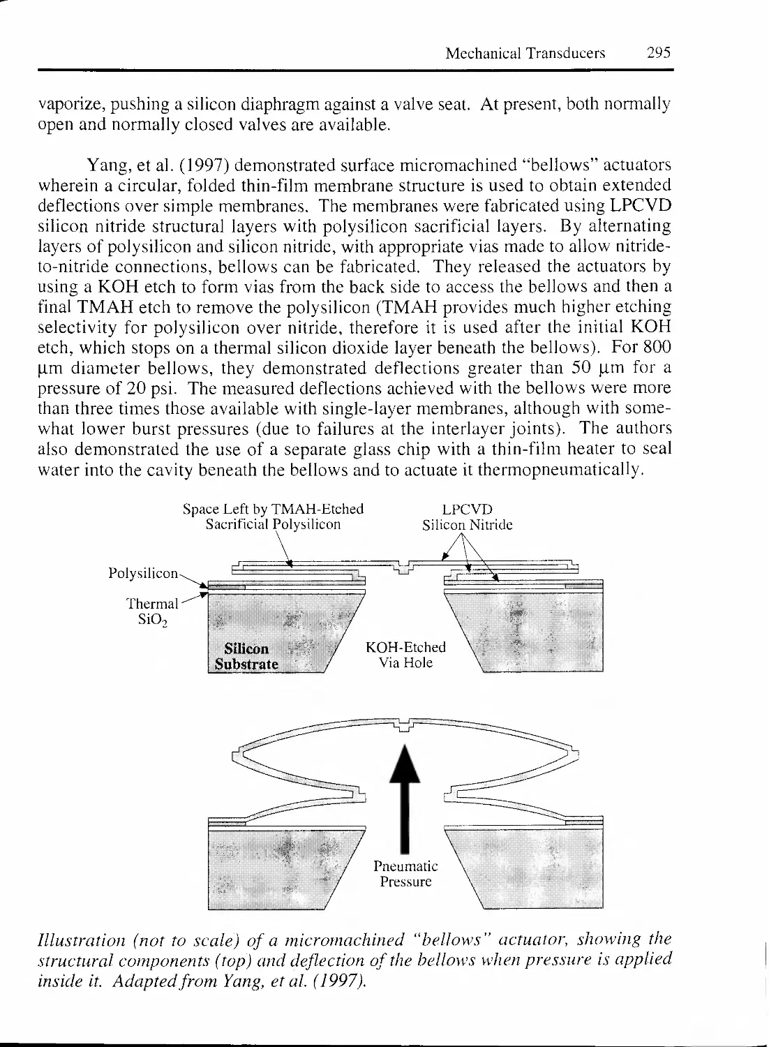
VOLUME EXPANSION AND PHASE-CHANGE ACTUATORS 294
6.1.3 SHAPE MEMORY ALLOY ACTUATION 296
6.1.4 PNEUMATIC/HYDRAULIC ACTUATION 297
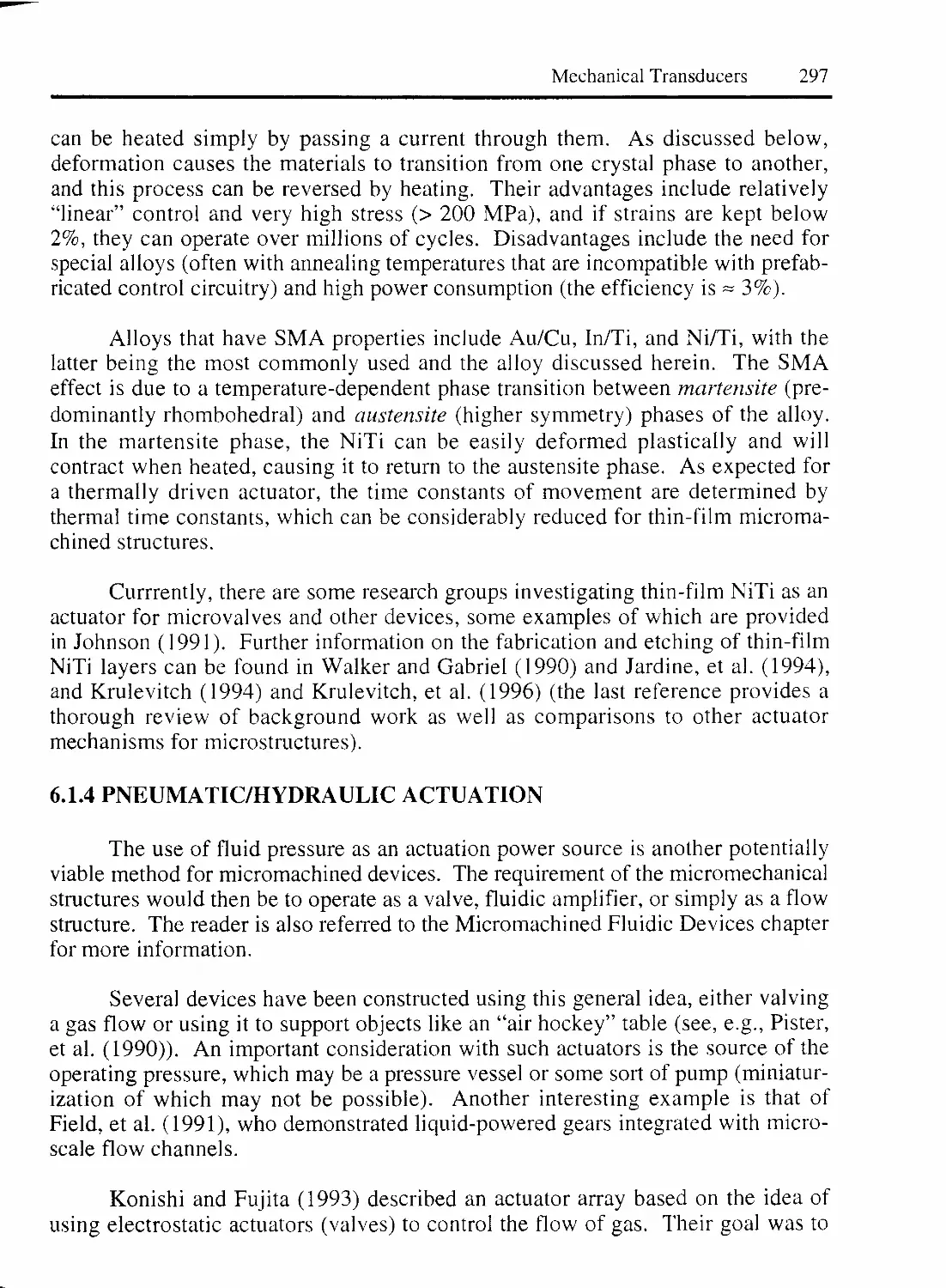
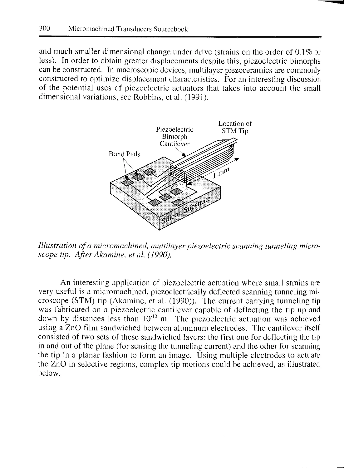
6.1.5 PIEZOELECTRIC ACTUATION 299
6.1.6 MAGNETIC ACTUATORS 301
6.1.7 CHEMICAL ACTUATORS 301
6.1.8 HYBRID ACTUATION SCHEMES 301
6.1.9 BIOLOGICAL ACTUATORS 302
CYTOSKELETON AND MICROTUBULES 302
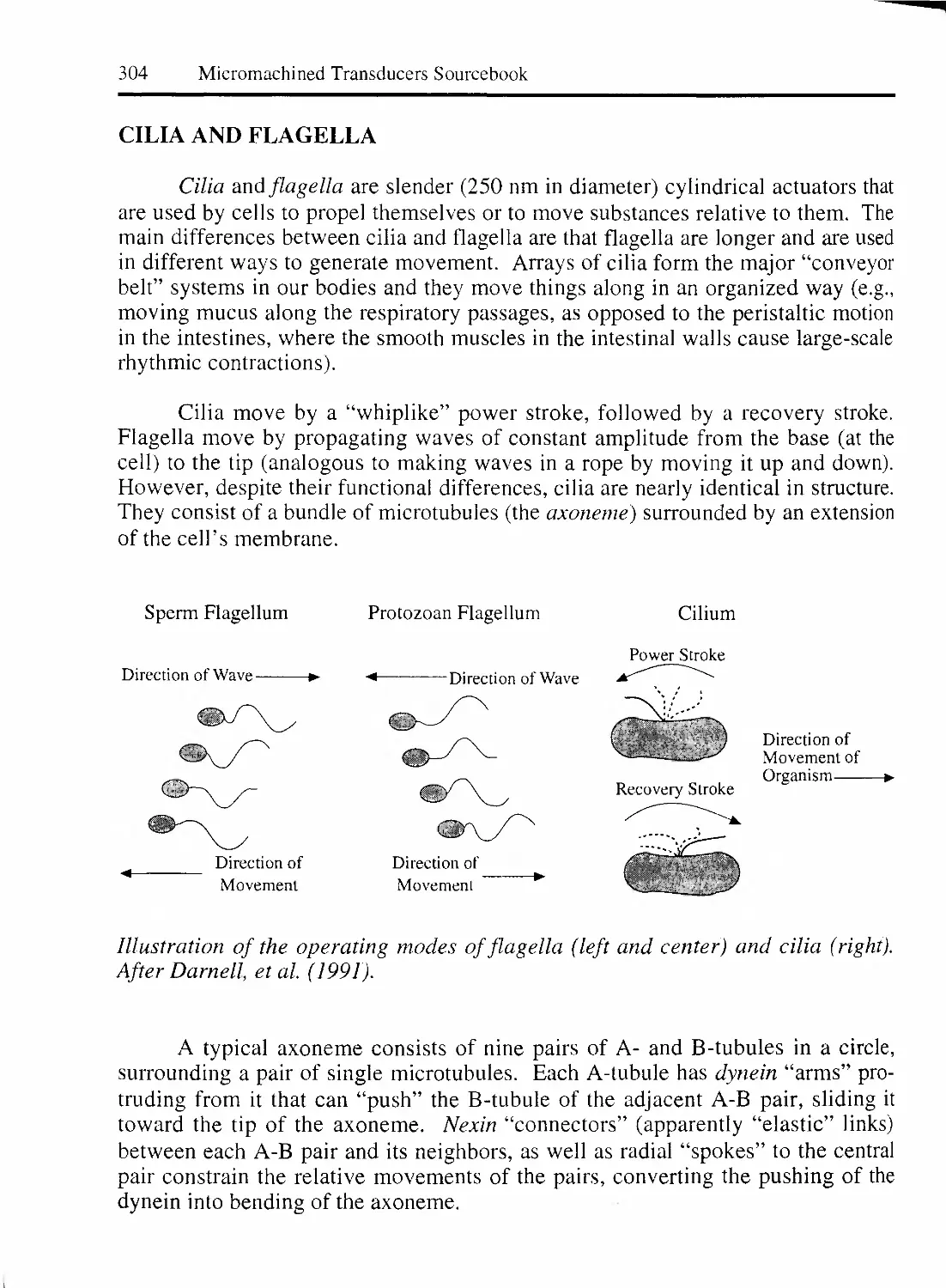
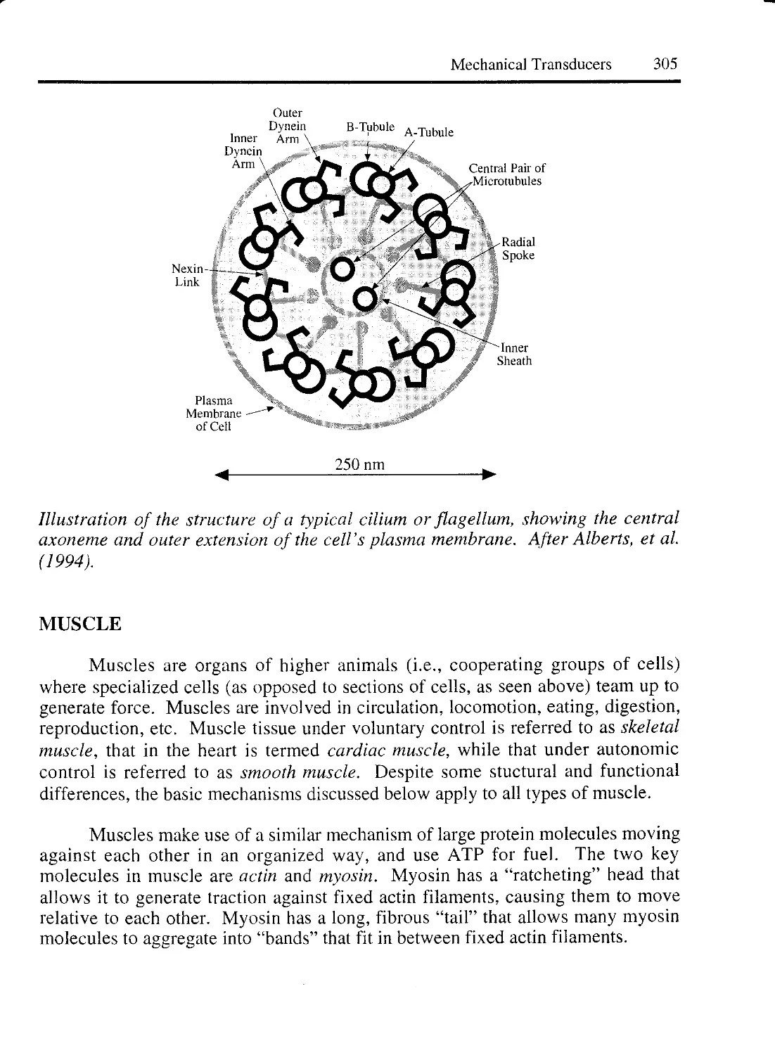
CILIA AND FLAGELLA 304
MUSCLE 305
7. MECHANICAL CIRCUIT COMPONENTS 308
7.1 MECHANICAL RESONATORS 308
7.1.1 CANTILEVER RESONATORS 308
7.1.2 LATERAL RESONATORS 315
7.1.3 MEMBRANE RESONATORS 319
7.2 MECHANICAL RELAYS AND RF SWITCHES 320
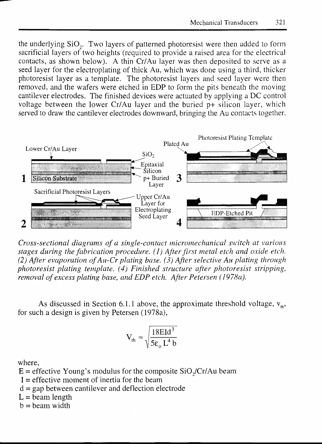
7.2.1 GENERAL PURPOSE RELAYS 320
ELECTROSTATICALLY DRIVEN RELAYS 320
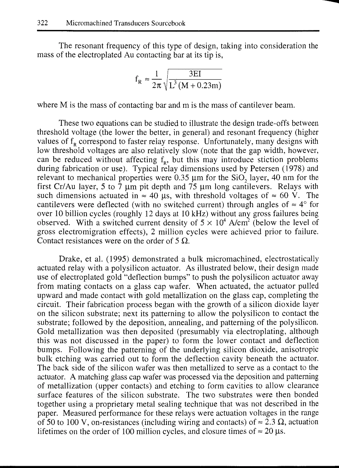
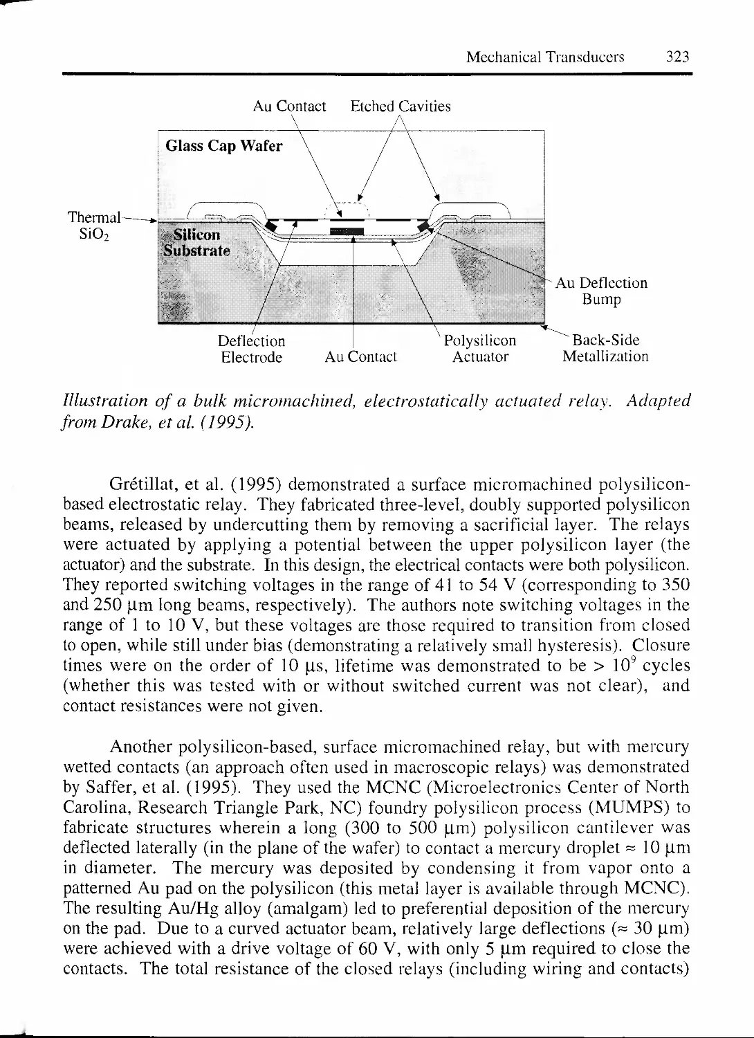
MAGNETICALLY DRIVEN RELAYS 325
7.2.2 RF SWITCHES AND SWITCHED CIRCUITS 328
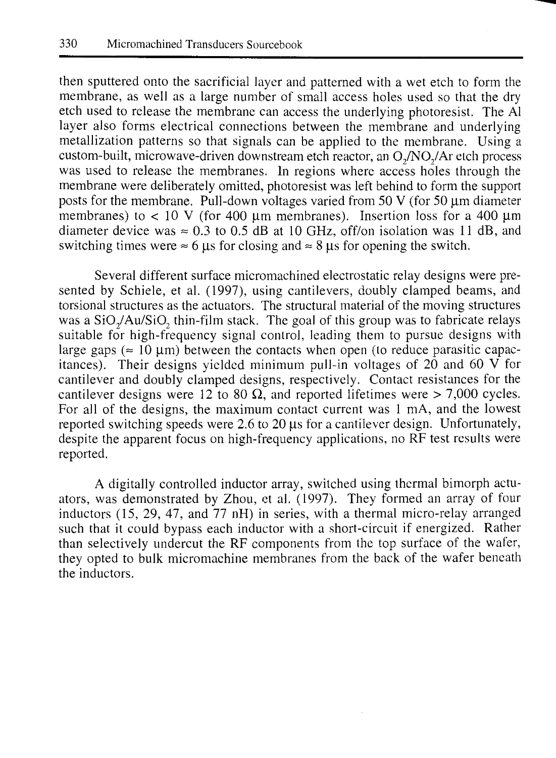
MECHANICAL TRANSDUCERS REFERENCES 333
xii
Chapter 4: OPTICAL TRANSDUCERS 357
1. INTRODUCTION 357
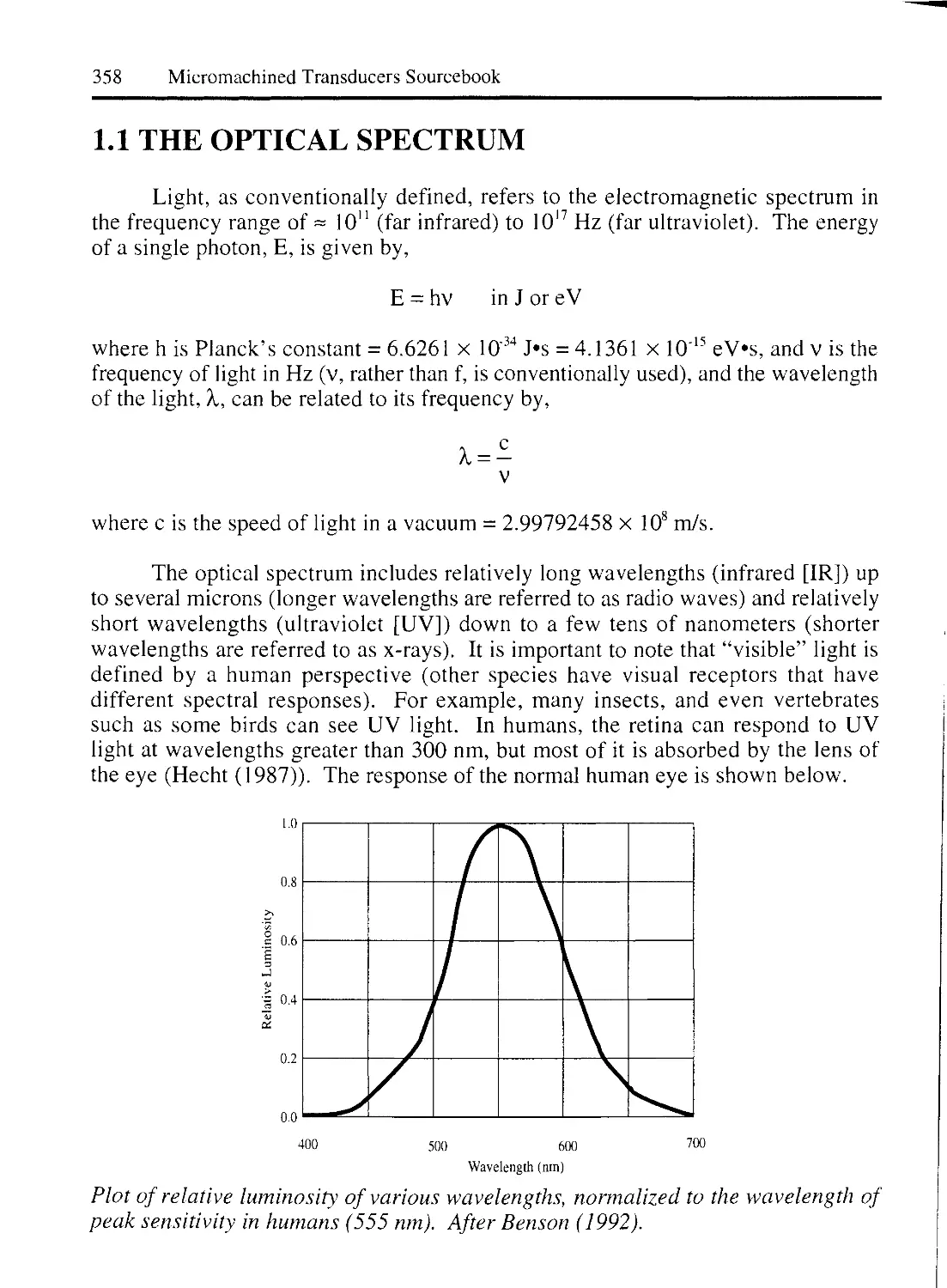
1.1 THE OPTICAL SPECTRUM 358
1.2 UNITS RELEVANT TO OPTICAL TRANSDUCERS 359
1.3 BLACKBODY RADIATION 360
2. OPTICAL SENSORS 362
2.1 TYPES OF OPTICAL SENSORS 362
2.1.1 FUNDAMENTAL PRINCIPLE OF OPTICAL DETECTION 362
2.1.2 DIRECT ELECTRONIC OPTICAL SENSORS 363
2.1.3 INDIRECT OPTICAL SENSORS 363
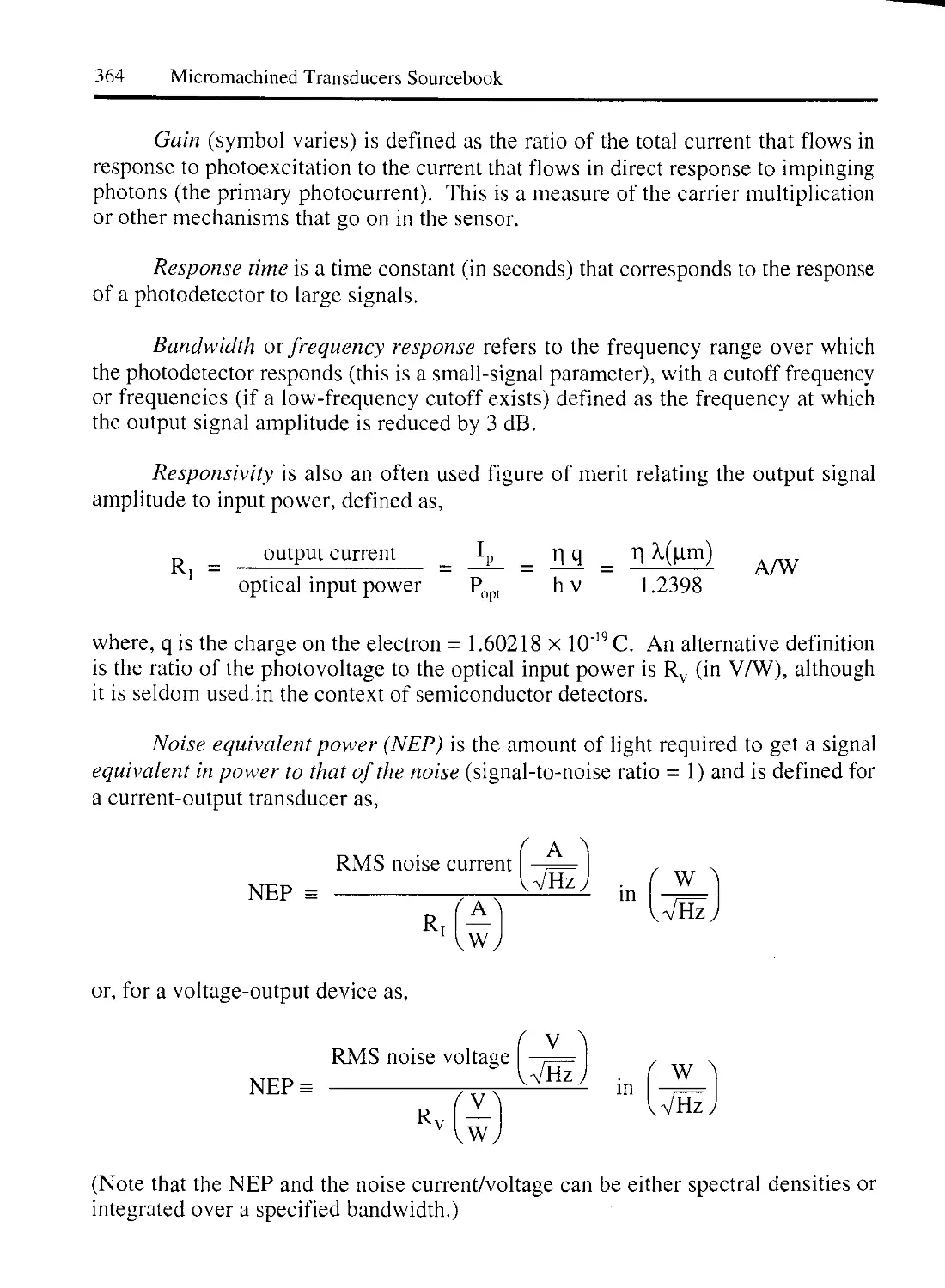
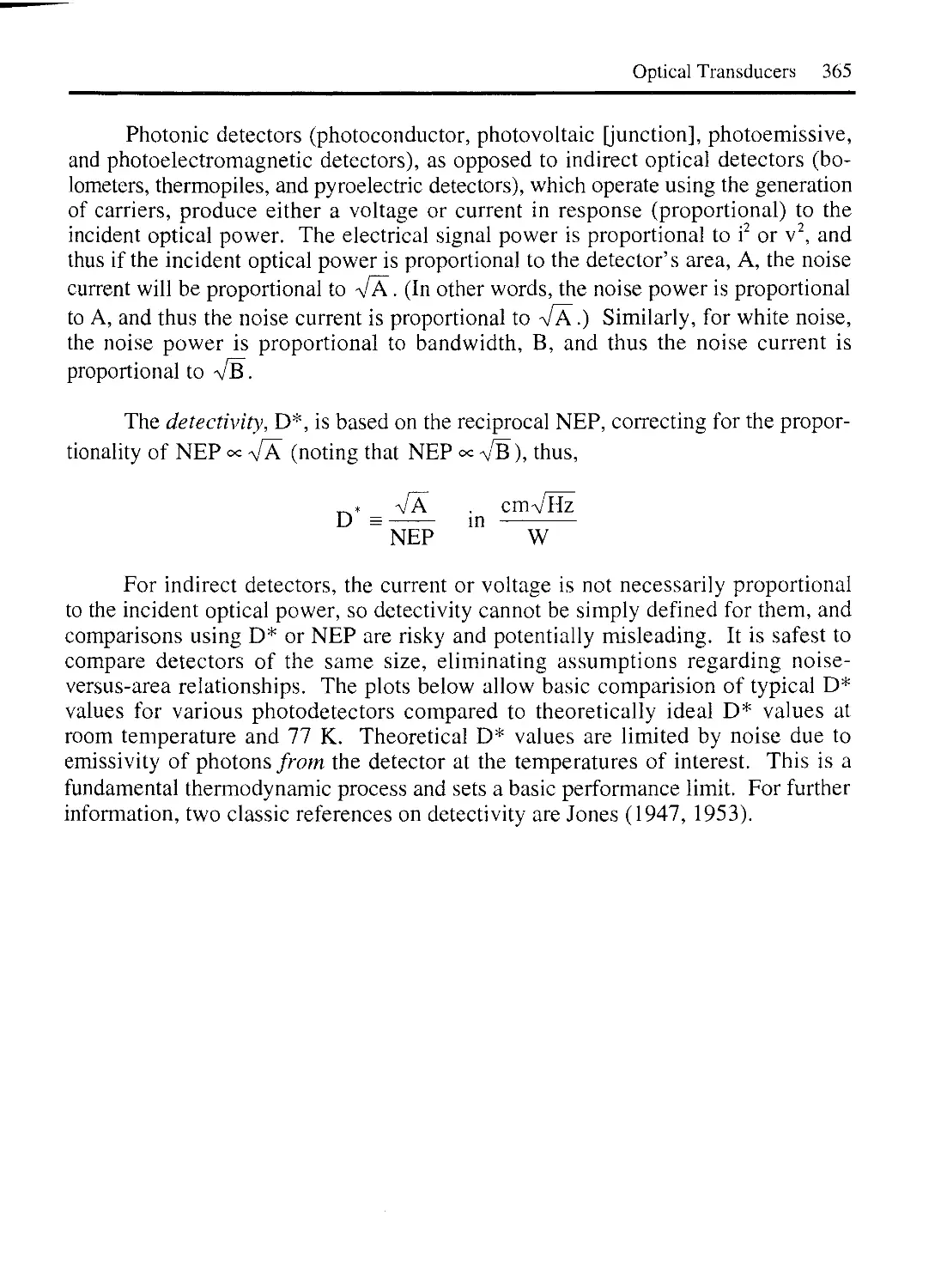
2.1.4 MAJOR SPECIFICATIONS FOR PHOTODETECTORS 363
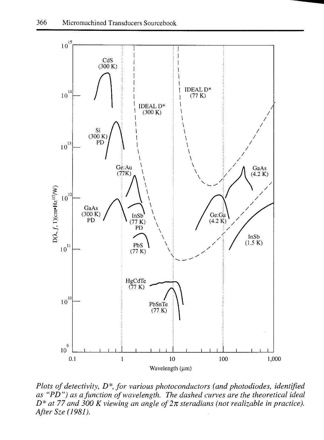
2.2 DIRECT ELECTRONIC OPTICAL SENSORS 367
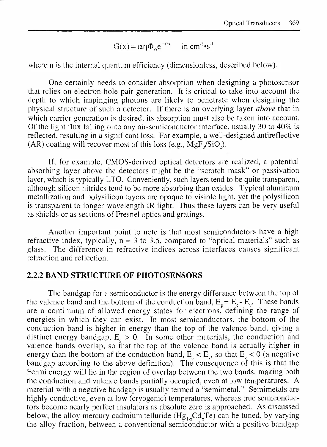
2.2.1 LIGHT ABSORPTION IN SEMICONDUCTORS 368
2.2.2 BAND STRUCTURE OF PHOTOSENSORS 369
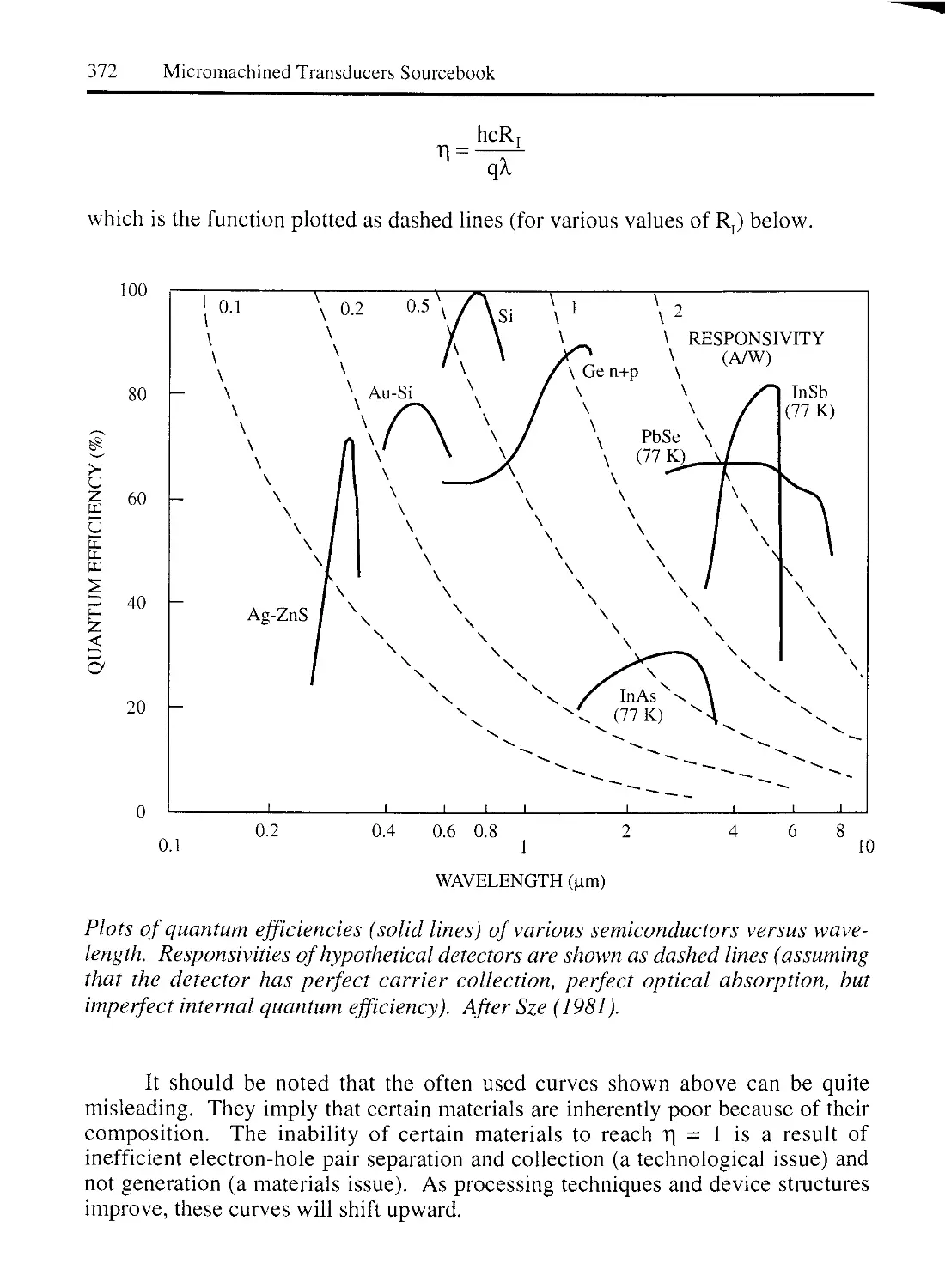
2.2.3 QUANTUM EFFICIENCY 371
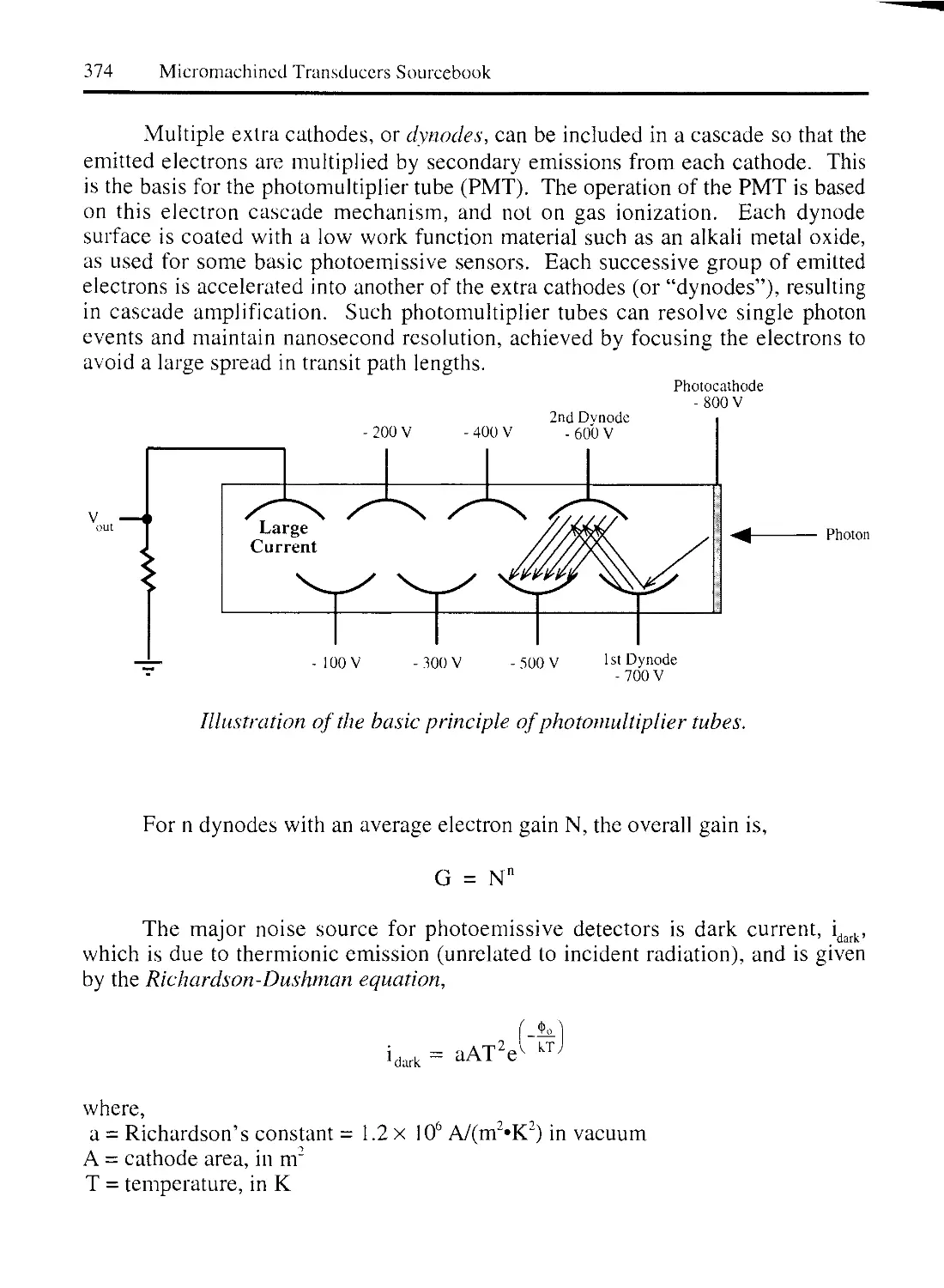
2.2.4 PHOTOEMISS1VE SENSORS 373
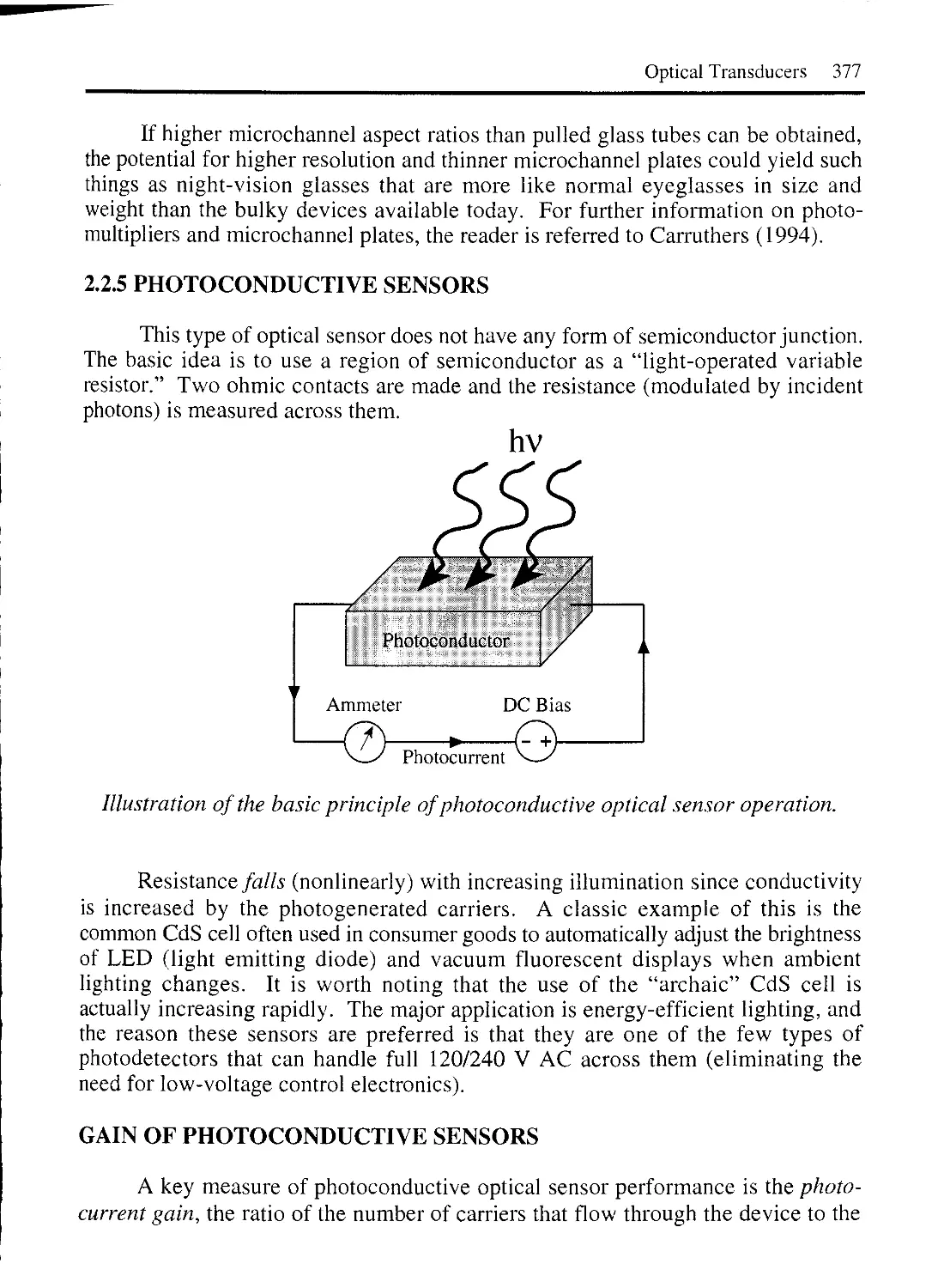
2.2.5 PHOTOCONDUCT1VE SENSORS 377
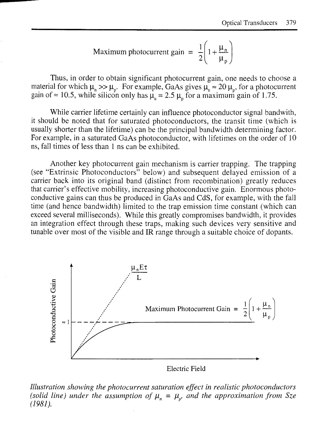
GAIN OF PHOTOCONDUCTIVE SENSORS 377
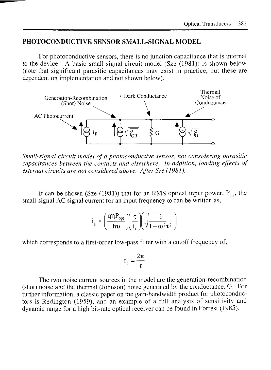
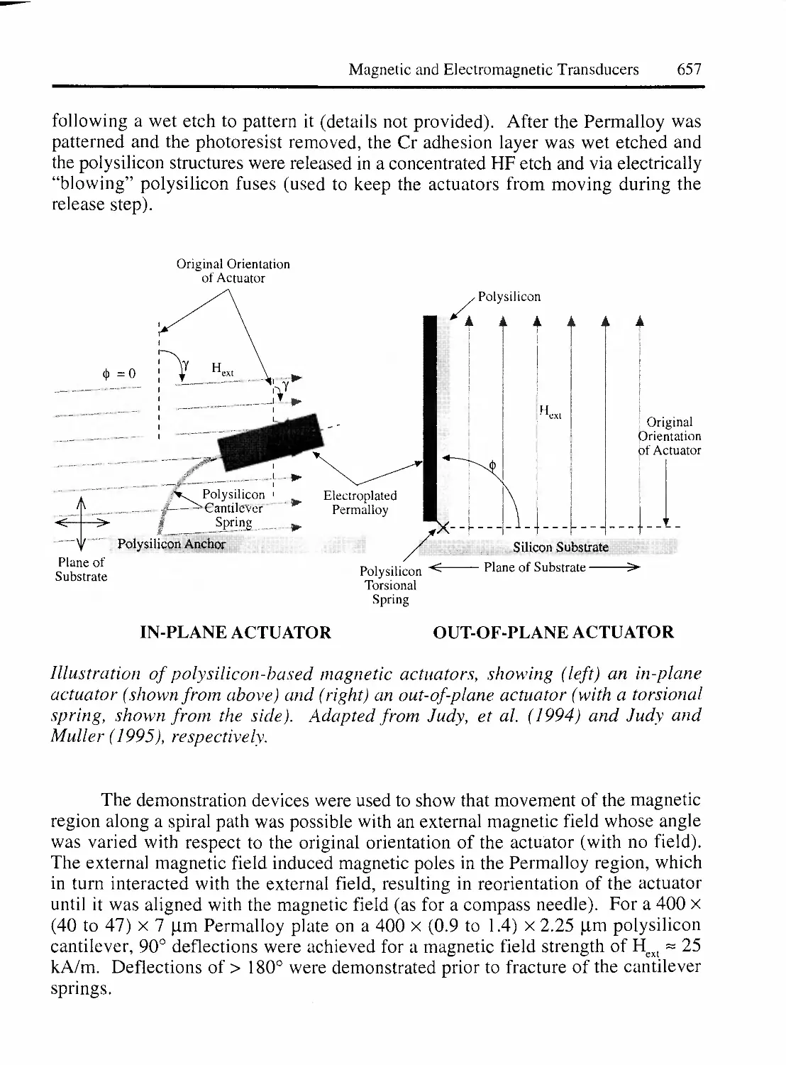
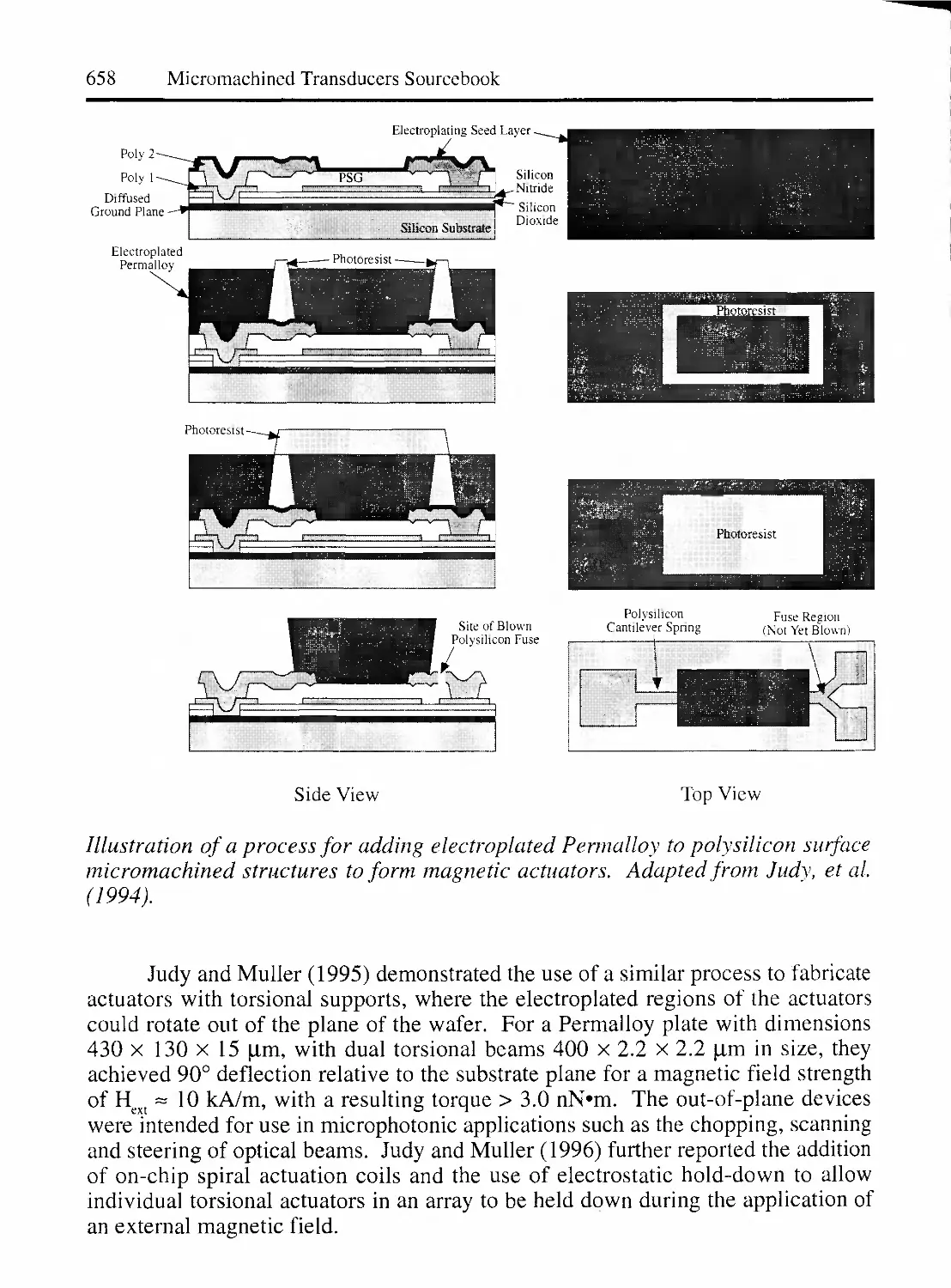
PHOTOCONDUCTIVE SENSOR SMALL-SIGNAL MODEL 381
INTRINSIC PHOTOCONDUCTORS 382
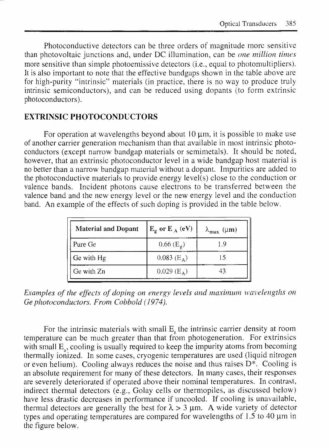
EXTRINSIC PHOTOCONDUCTORS 385
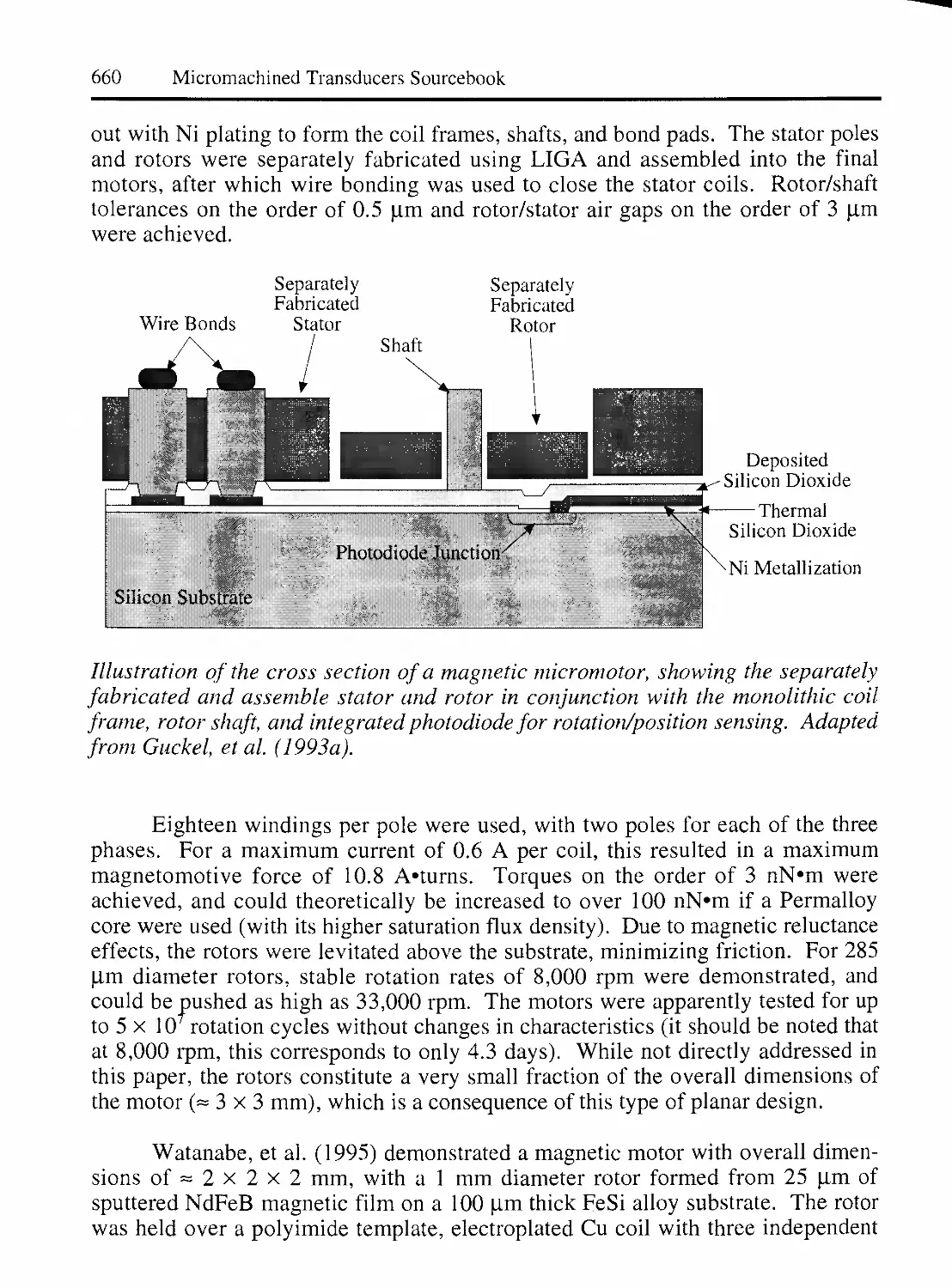
CADMIUM SULFIDE AND CADMIUM SELENIDE 386
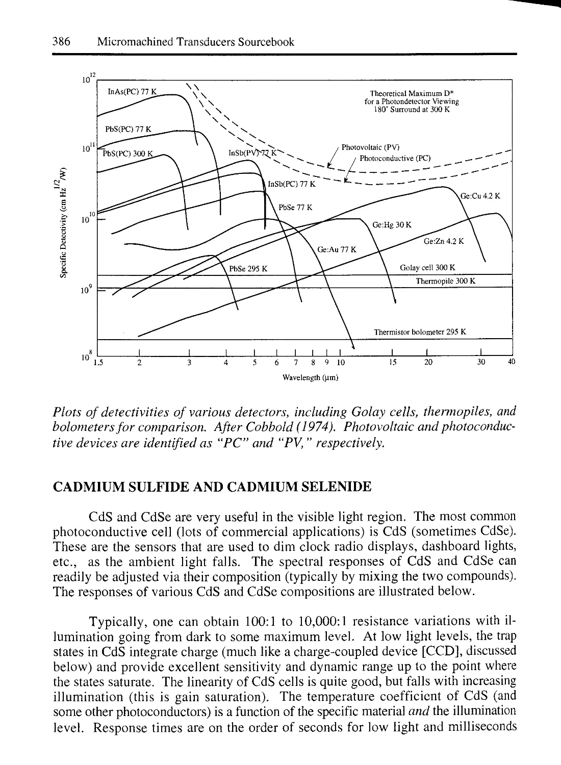
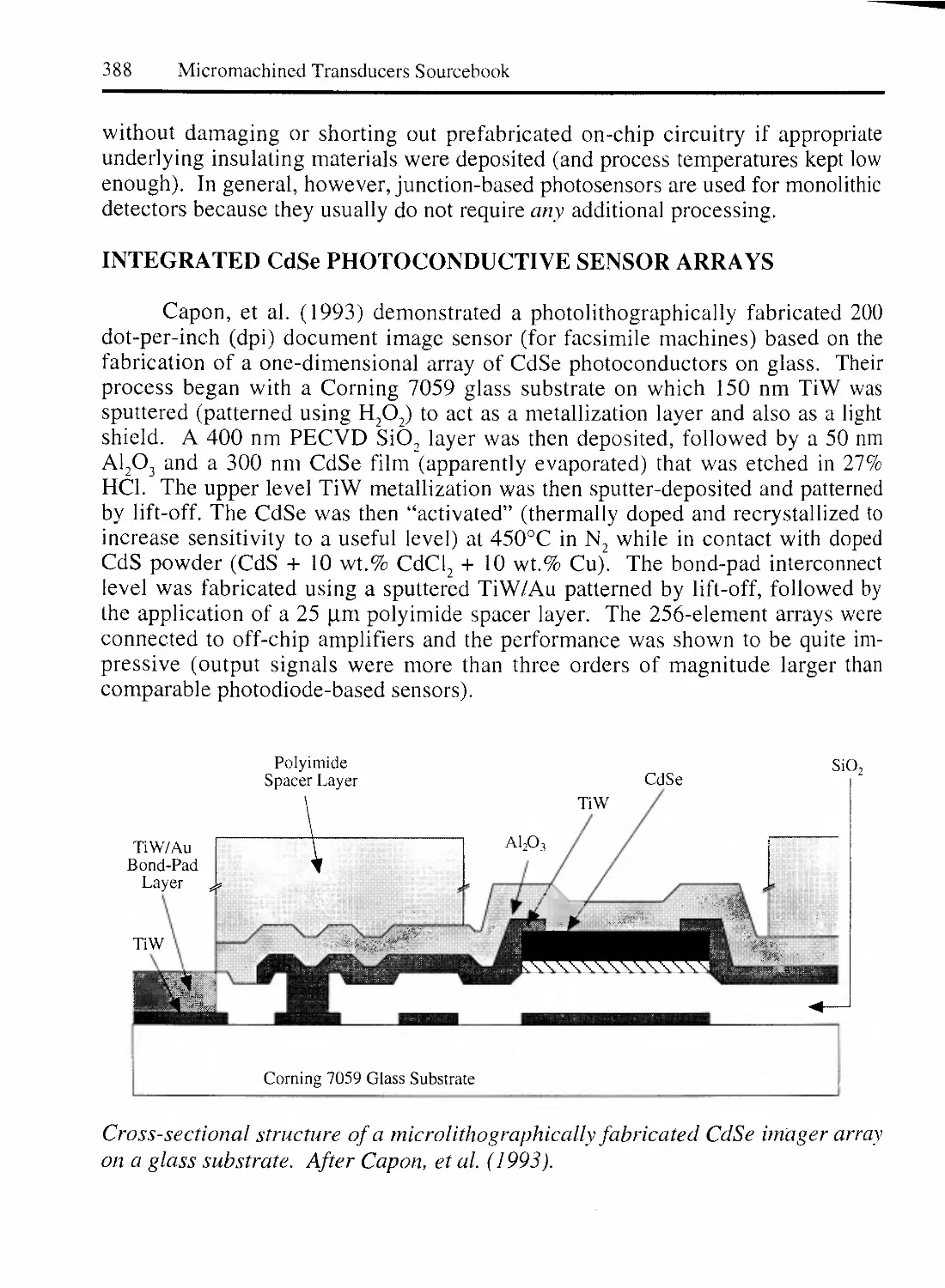
INTEGRATED CdSe PHOTOCONDUCTIVE SENSOR ARRAYS 388
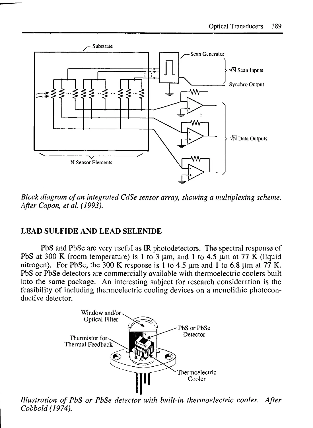
LEAD SULFIDE AND LEAD SELENIDE 389
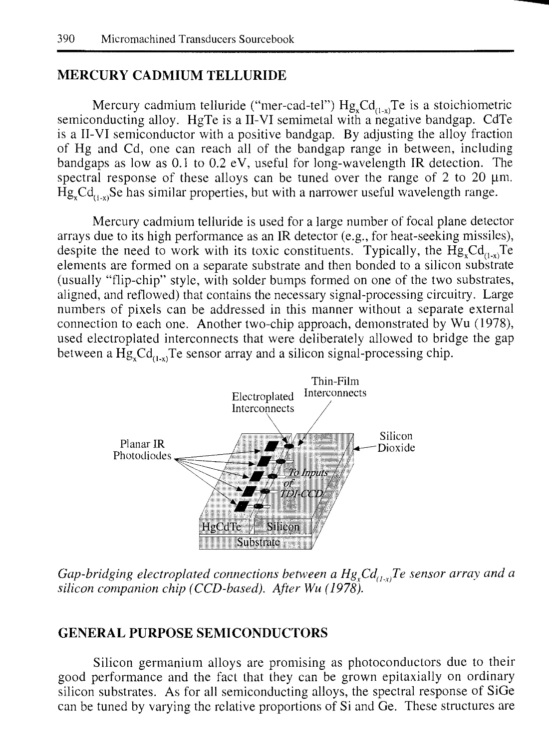
MERCURY CADMIUM TELLURIDE 390
GENERAL PURPOSE SEMICONDUCTORS 390
METAL-SEMICONDUCTOR-METAL PHOTOCONDUCTIVE SENSORS 391
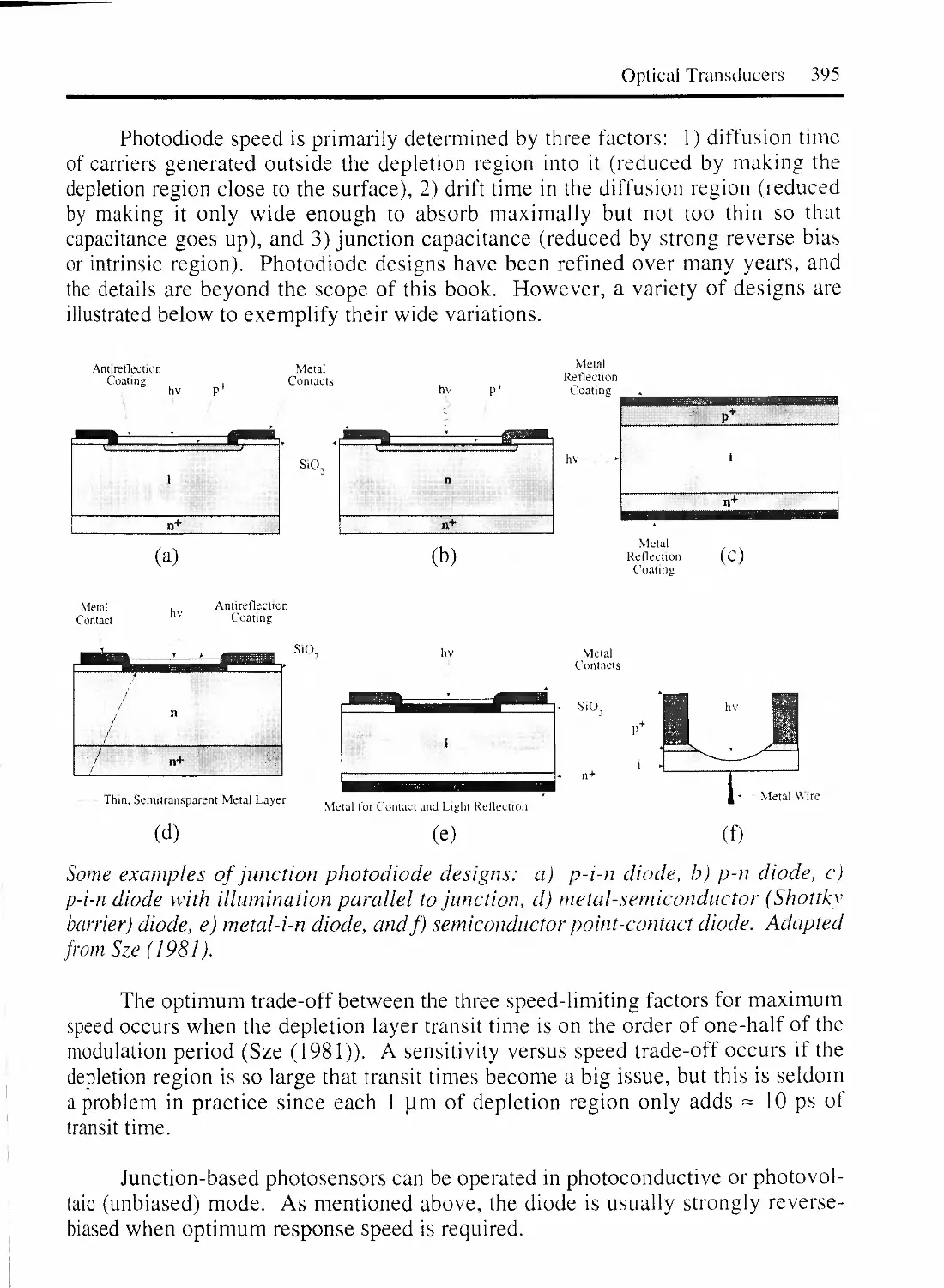
2.2.6 JUNCTION-BASED PHOTODETECTORS 392
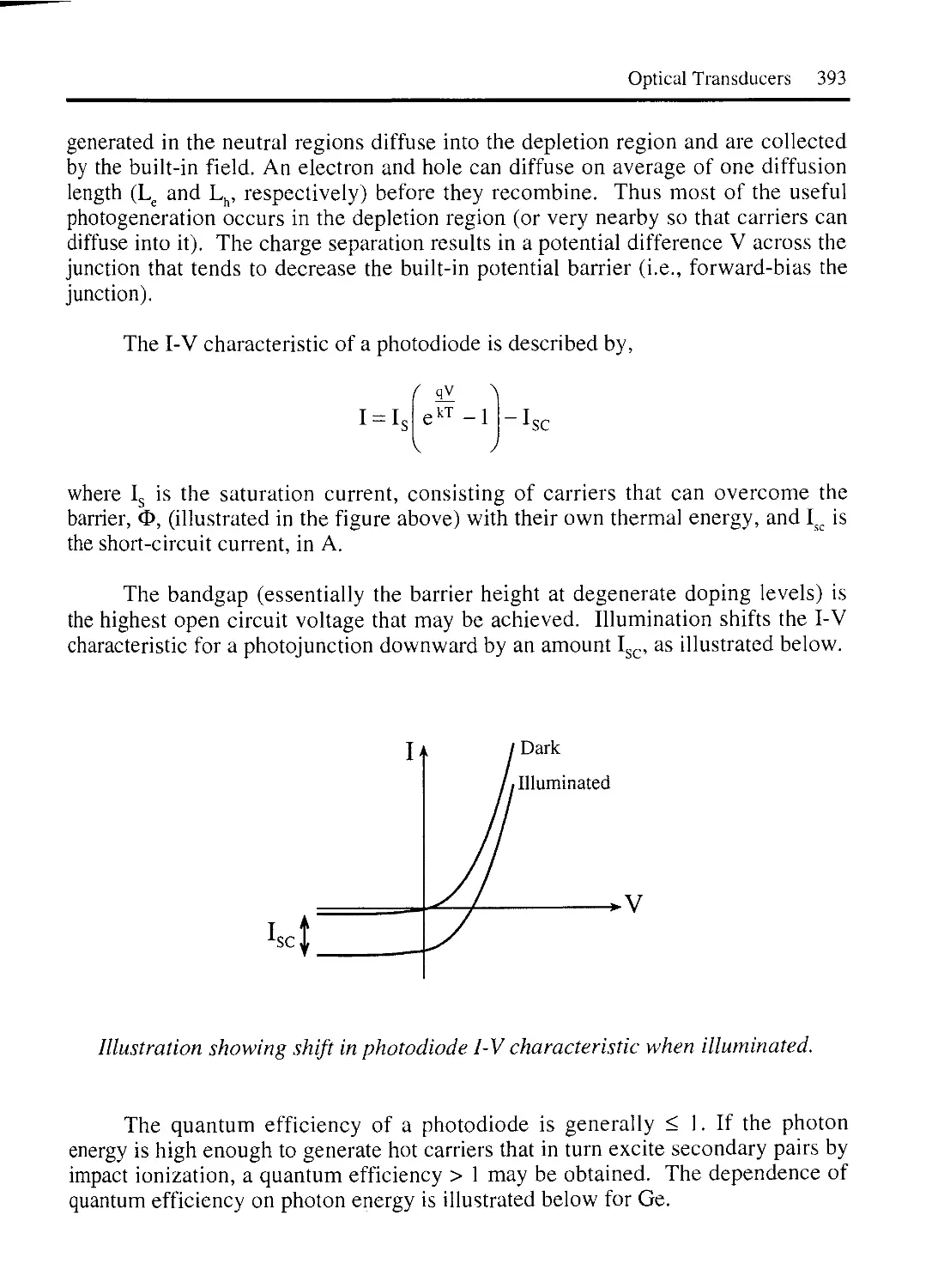
PHOTODIODE DESIGN ISSUES 394
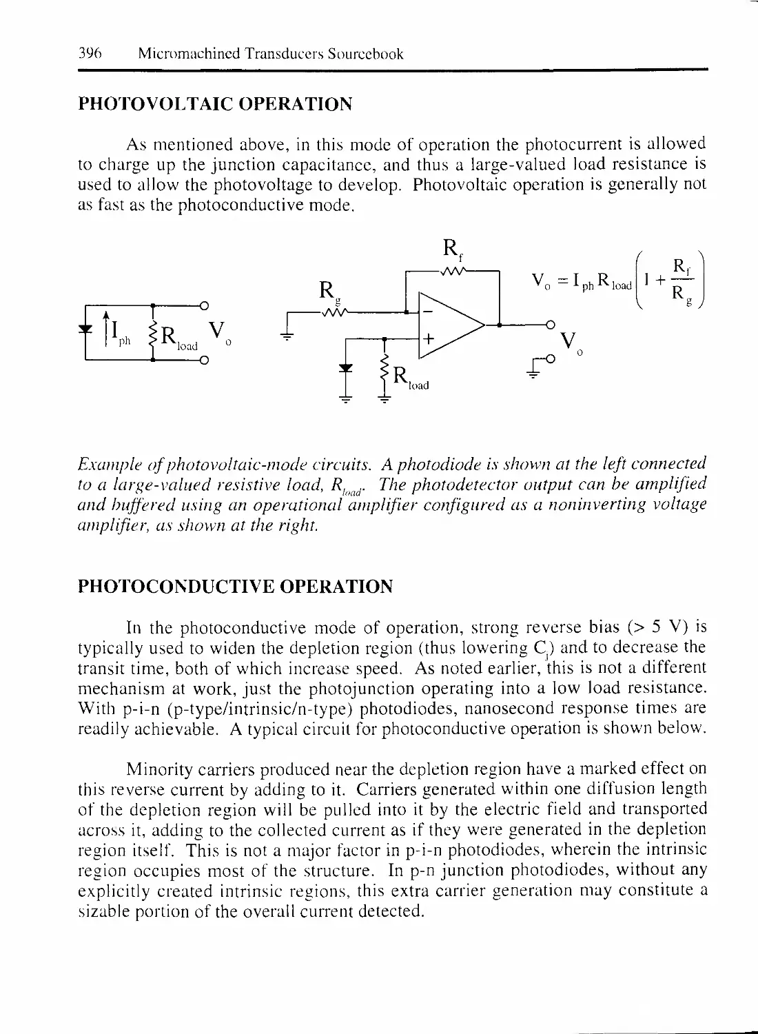
PHOTOVOLTAIC OPERATION 396
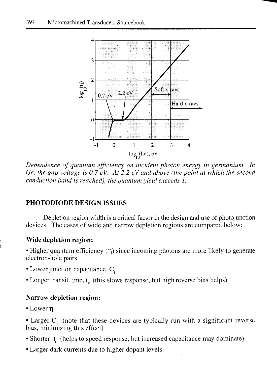
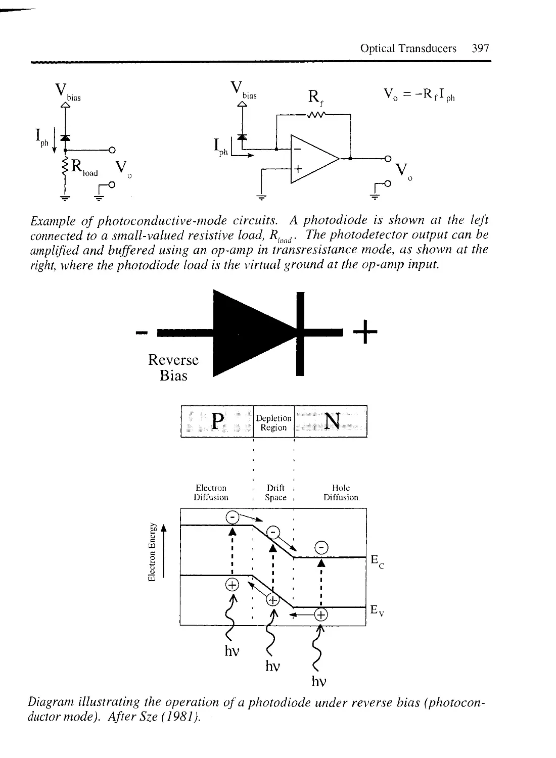
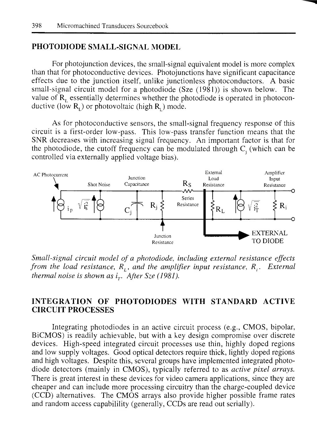
PHOTOCONDUCTIVE OPERATION 396
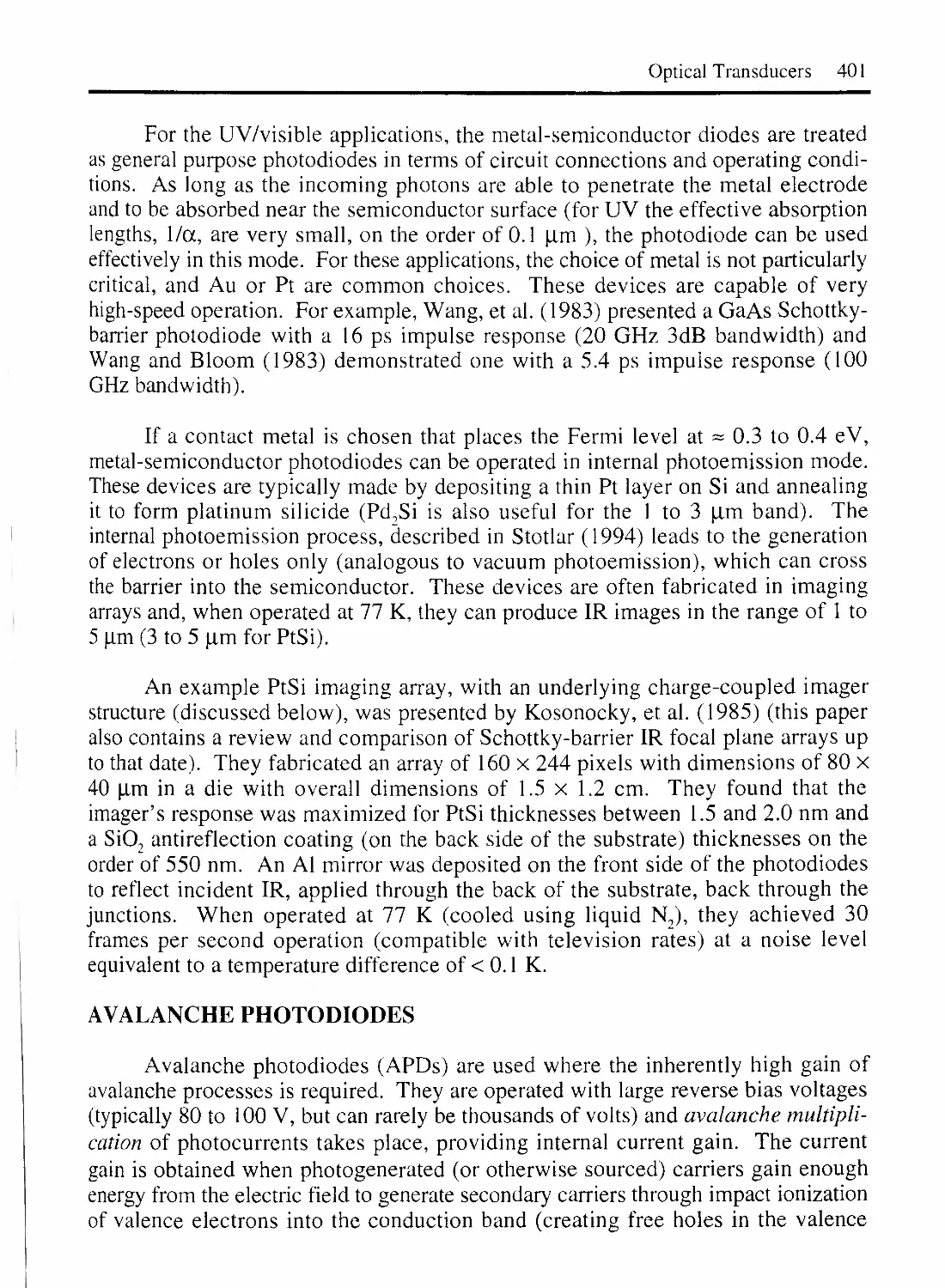
PHOTODIODE SMALL-SIGNAL MODEL 398
INTEGRATION OF PHOTODIODES WITH STANDARD ACTIVE CIRCUIT PROCESSES 398
ULTRAVIOLET-OPTIMIZED PHOTODIODES 400
P-I-N PHOTODIODES 400
METAL-SEMICONDUCTOR (SCHOTTKY) PHOTODIODES 400
AVALANCHE PHOTODIODES 401
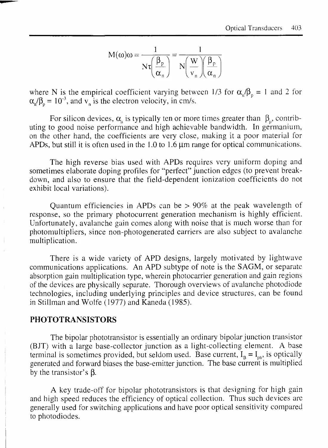
PHOTOTRANSISTORS 403
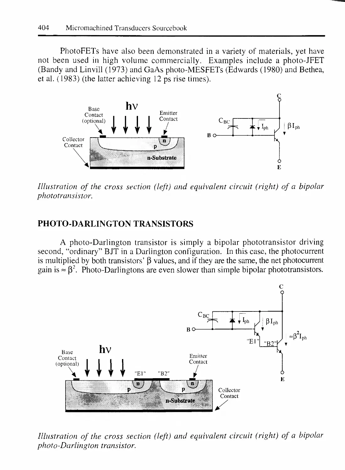
PHOTO-DARLINGTON TRANSISTORS 404
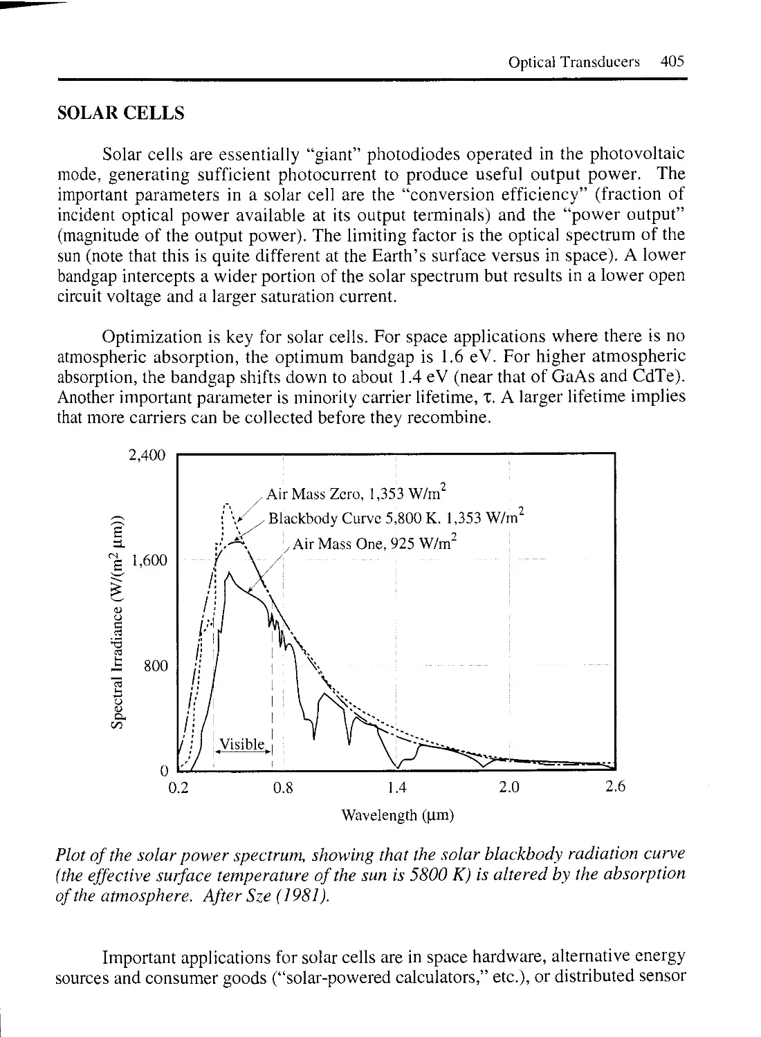
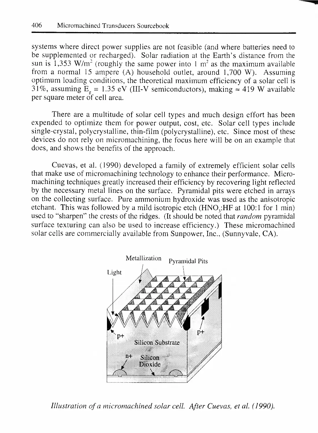
SOLAR CELLS 405
ANOMALOUS PHOTOVOLTAIC EFFECT 407
2.2.7 CAPACITIVE PHOTOSENSORS 407
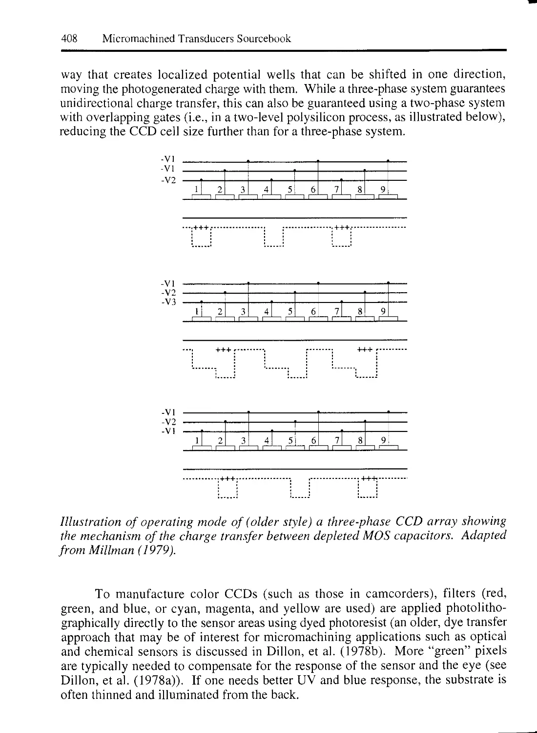
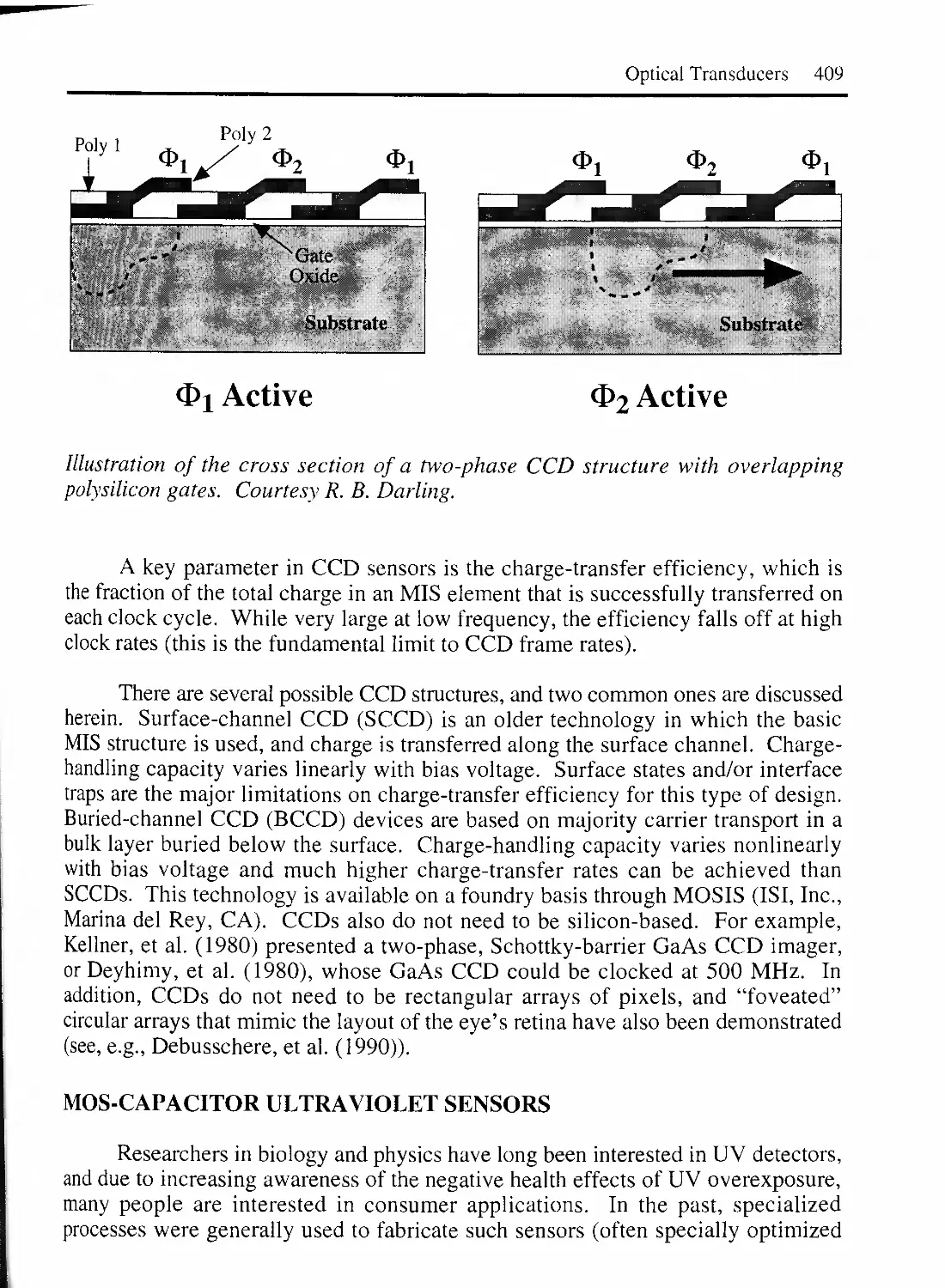
CHARGE-COUPLED IMAGE SENSORS 407
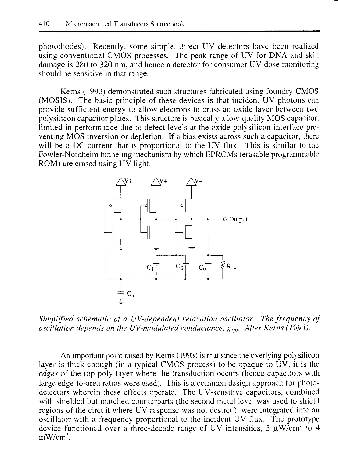
MOS-CAPACITOR ULTRAVIOLET SENSORS 409
2.3 INDIRECT OPTICAL SENSORS 411
2.3.1 PYROELECTRIC DETECTORS 411
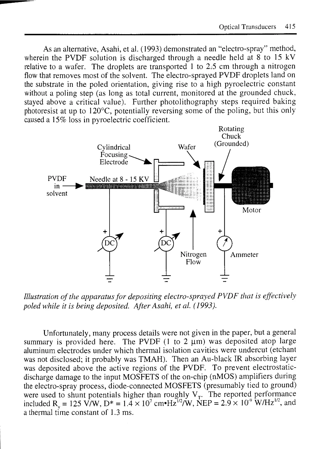
ELECTRO-SPRAYED PVDF PYROELECTRIC SENSOR 414
2.3.2 BOLOMETERS 416
UNCOOLED BOLOMETERS 418
SUPERCONDUCTING BOLOMETERS 419
2.3.3 THERMOPILES 421
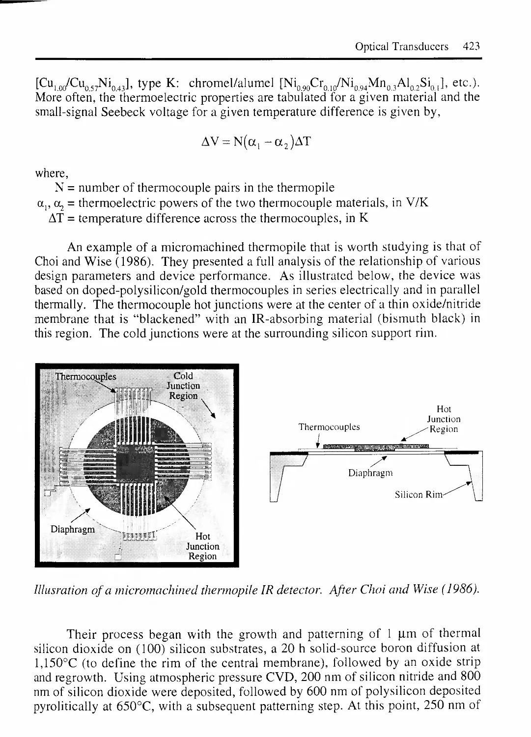
2.3.4 GOLAY CELLS 427
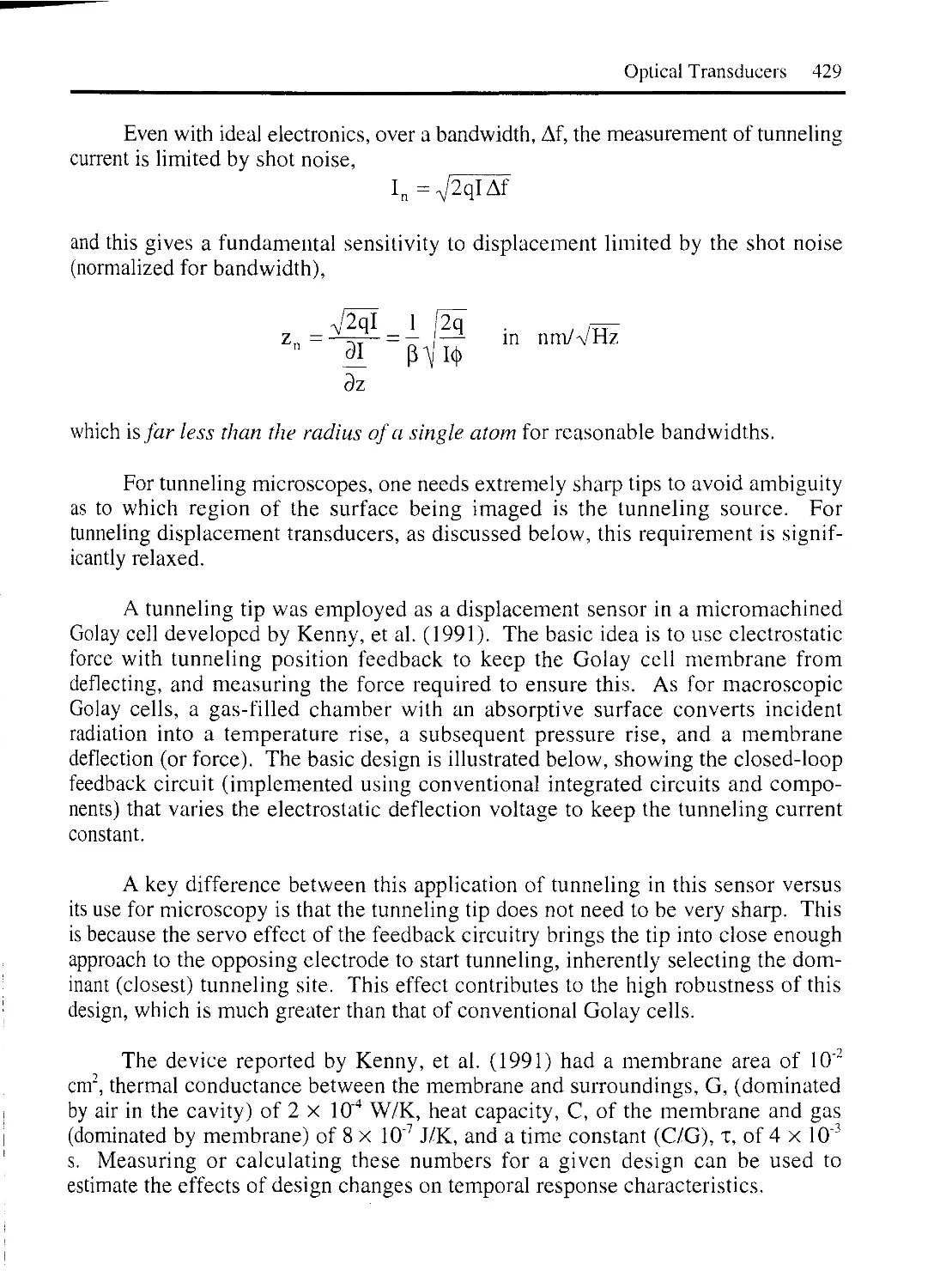
MICROMACHINED TUNNELING-BASED GOLAY CELL 428
MICROMACHINED CAPACITIVE GOLAY CELL 431
xiii
2.3.5 PHOSPHORS AND OTHER “INDIRECT” LIGHT SENSORS 433
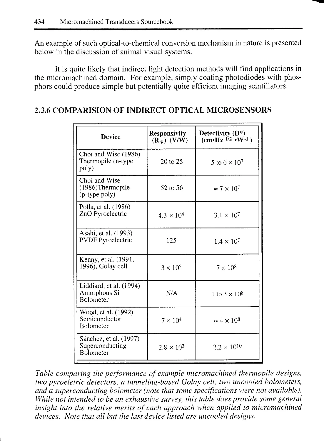
2.3.6 COMPARISION OF INDIRECT OPTICAL MICROSENSORS 434
2.4 BIOLOGICAL LIGHT SENSORS 435
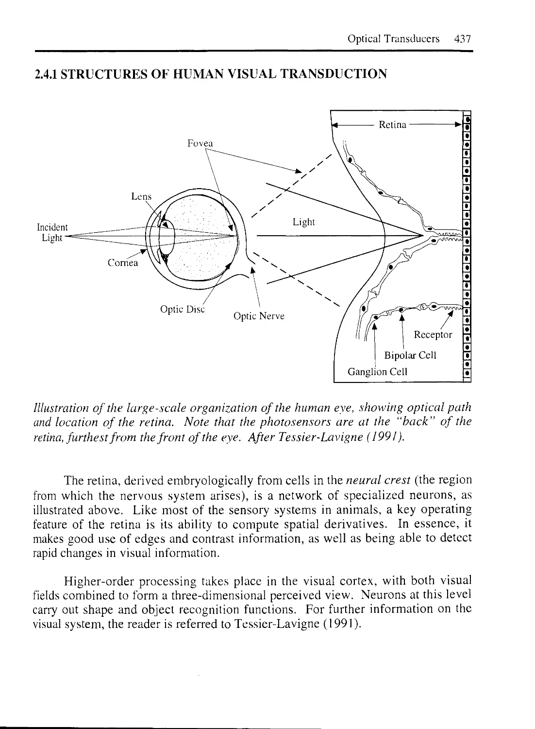
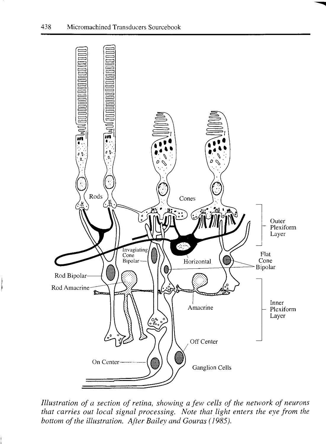
2.4.1 STRUCTURES OF HUMAN VISUAL TRANSDUCTION 437
2.4.2 BASIC VISUAL TRANSDUCTION MECHANISM 440
3. OPTICAL ACTUATORS 441
3.1 LIGHT EMITTERS 441
3.1.1 LIGHT EMITTING DIODES 441
3.1.2 SILICON LIGHT EMITTING DIODES 444
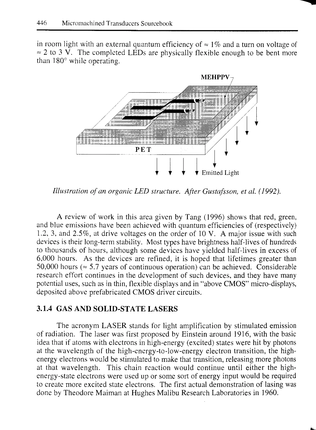
3.1.3 ORGANIC LIGHT EMITTING DIODES 445
3.1.4 GAS AND SOLID-STATE LASERS 446
MICROMACHINED SOLID-STATE LASERS 449
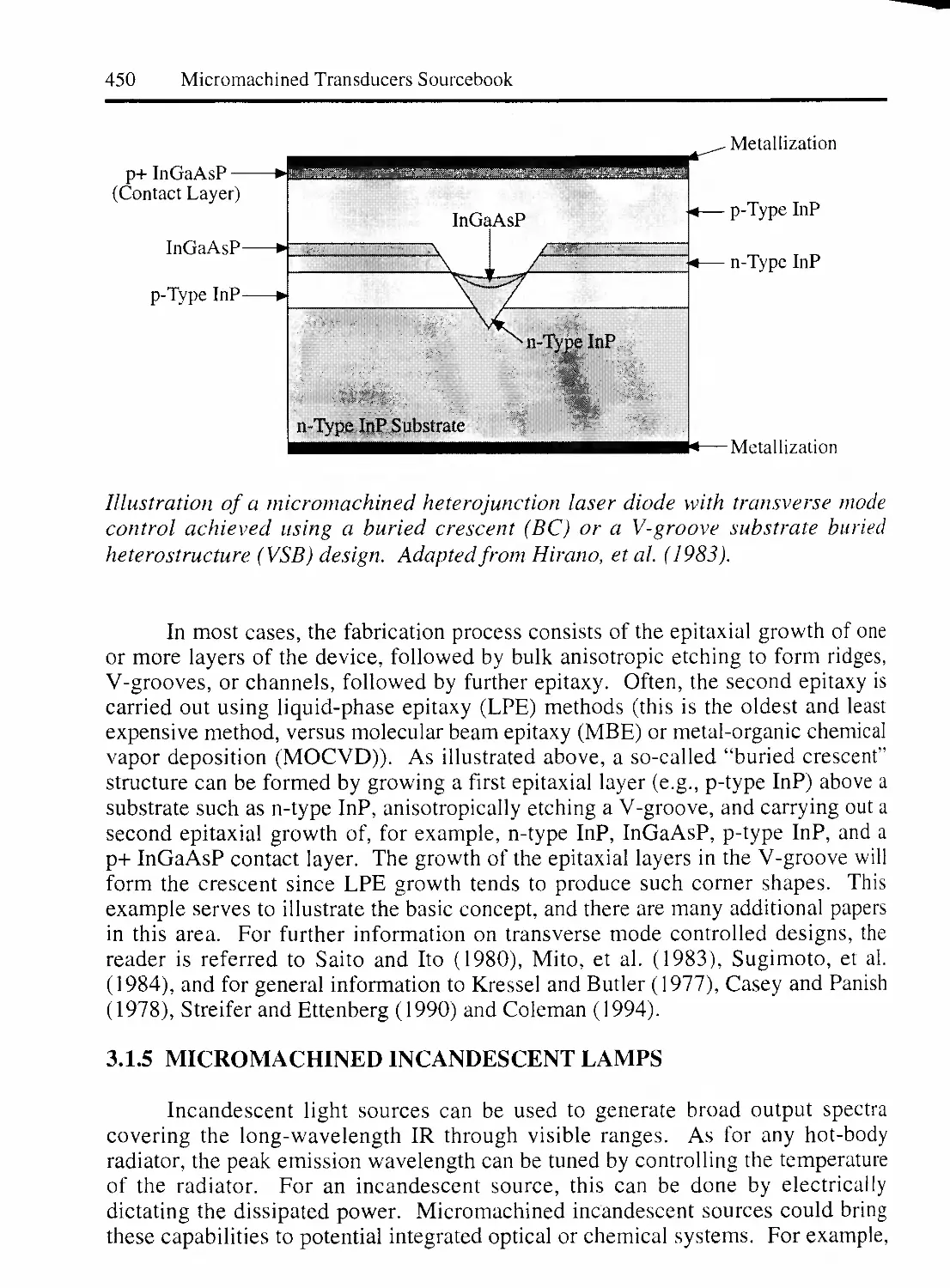
3.1.5 MICROMACHINED INCANDESCENT LAMPS 450
3.1.6 PLASMA LIGHT SOURCES 453
3.1.7 ELECTROLUMINESCENT LIGHT SOURCES 453
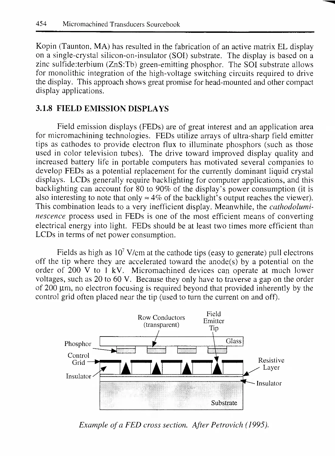
3.1.8 FIELD EMISSION DISPLAYS 454
3.1.9 BIOLUMINESCENCE 455
3.2 LIGHT MODULATORS 456
3.2.1 LIQUID CRYSTAL DISPLAYS 456
NEMATIC LIQUID CRYSTALS 456
DYNAMIC SCATTERING LIQUID CRYSTALS 459
TRANSFERRED SILICON ACTIVE LC DISPLAYS 460
CHOLESTERIC LIQUID CRYSTALS 460
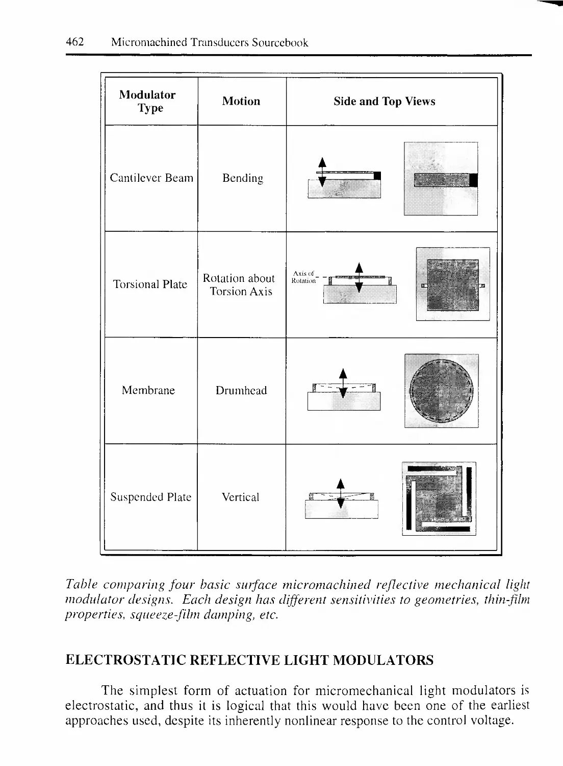
3.2.2 REFLECTIVE MICROMECHANICAL LIGHT MODULATORS 461
ELECTROSTATIC REFLECTIVE LIGHT MODULATORS 462
WESTING HOUSE MIRROR MATRIX TUBE 463
SILICON CANTILEVER LIGHT MODULATORS 465
TORSIONAL SILICON ELECTROSTATIC LIGHT MODULATORS 467
TORSIONAL ALUMINUM ELECTROSTATIC LIGHT MODULATORS 468
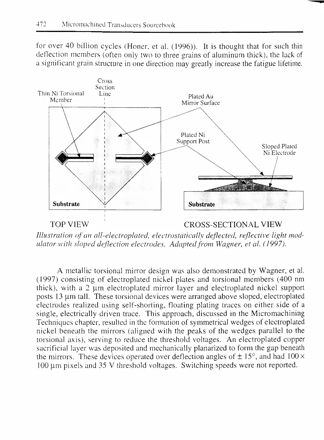
POLYSILICON TORSIONAL OPTICAL MODULATORS 473
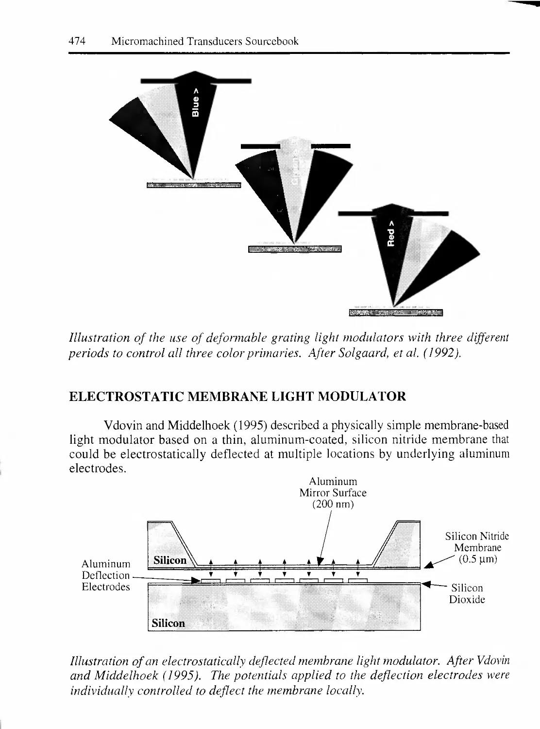
DEFORMABLE GRATING LIGHT MODULATORS 473
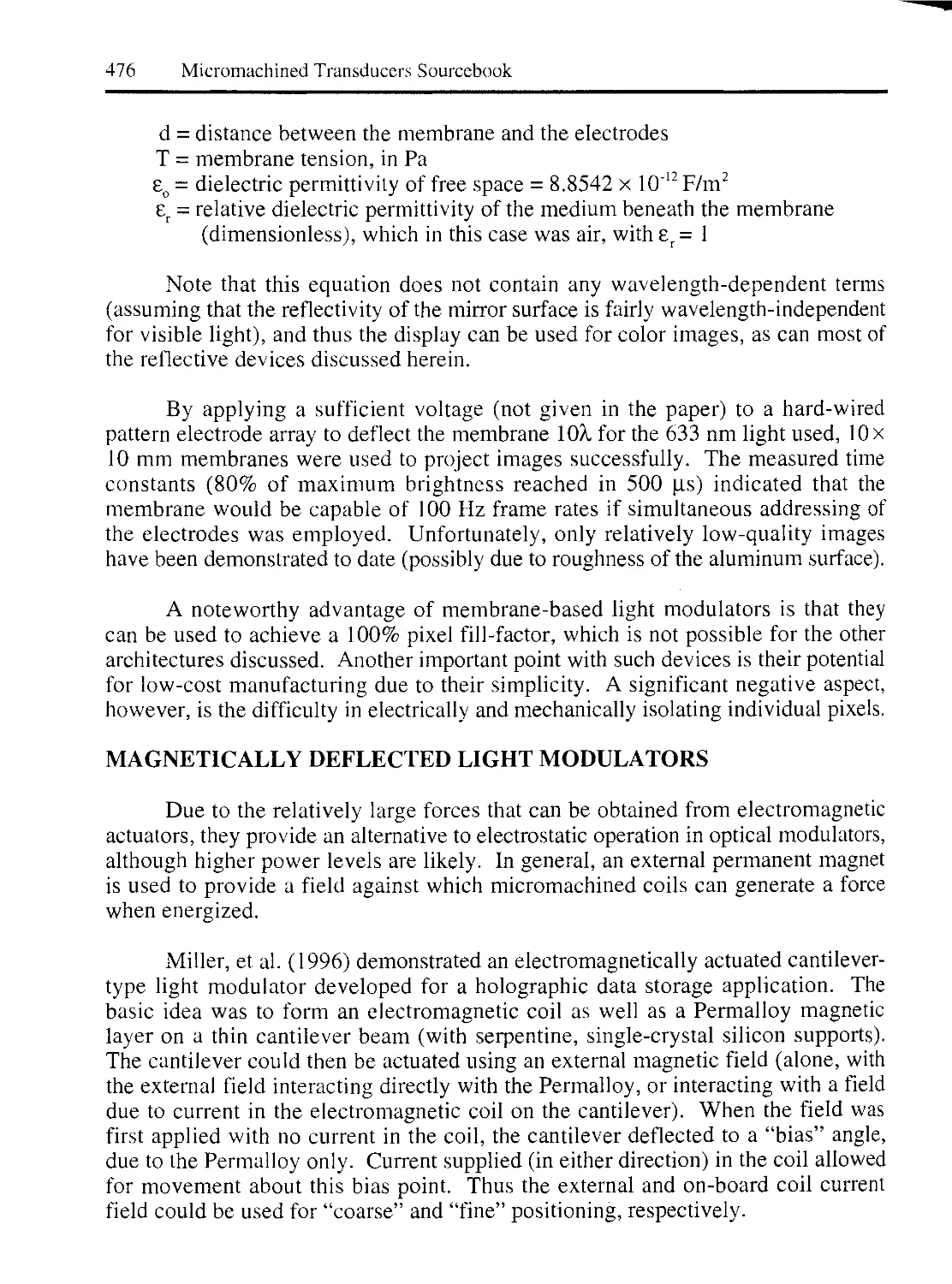
ELECTROSTATIC MEMBRANE LIGHT MODULATOR 474
MAGNETICALLY DEFLECTED LIGHT MODULATORS 476
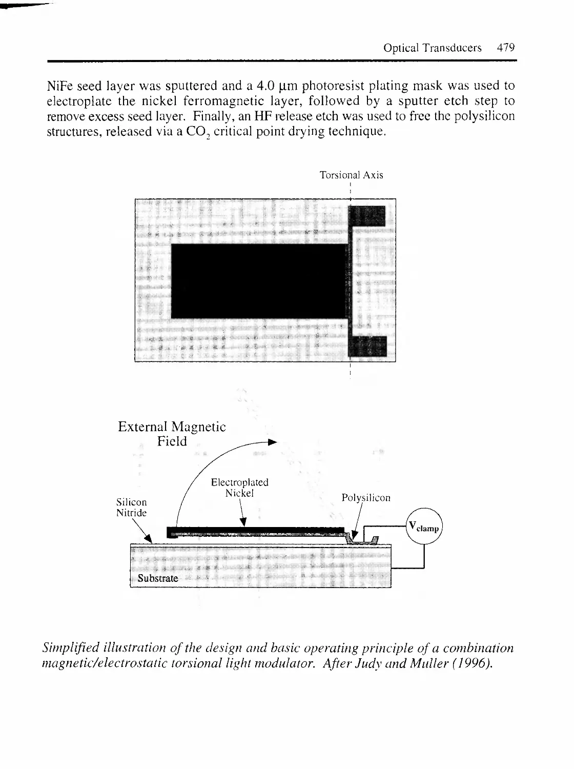
MAGNETIC/ELECTROSTATIC LIGHT MODULATORS 478
3.2.3 TRANSMISSIVE MICROMECHANICAL LIGHT MODULATORS 481
3.2.4 OTHER LIGHT MODULATORS 481
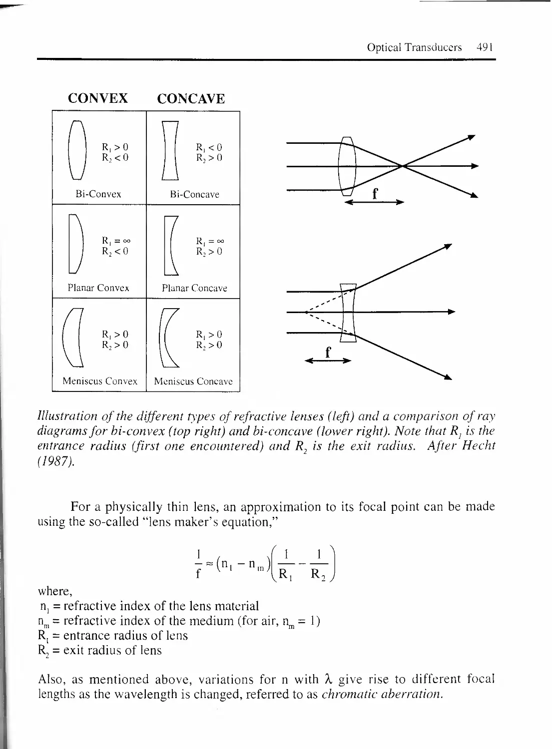
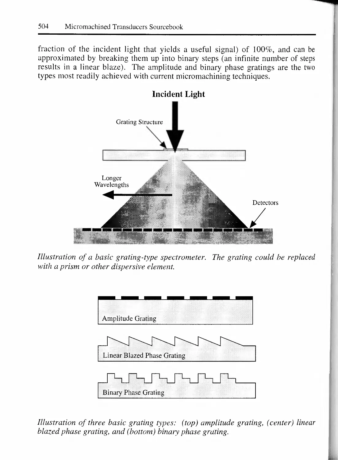
4. MICROMACHINED OPTICAL STRUCTURES 484
4.1 MICROMACHINED FIBER-OPTIC COUPLERS 484
4.2 MICROMACHINED REFLECTIVE COMPONENTS 485
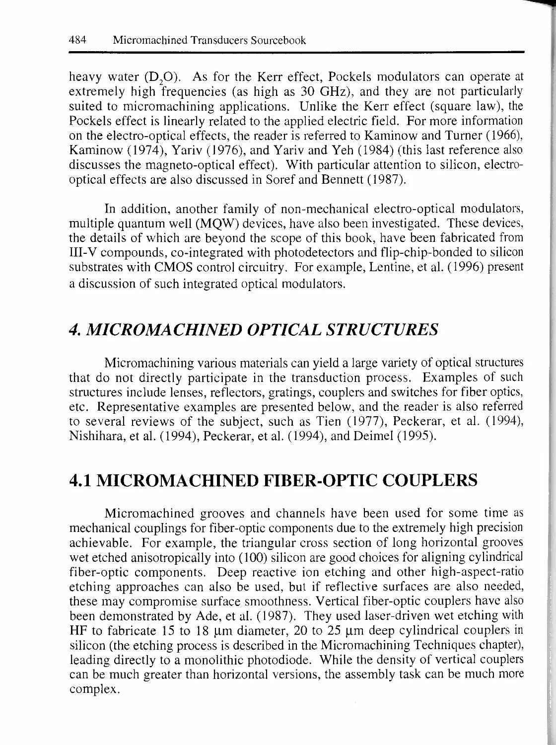
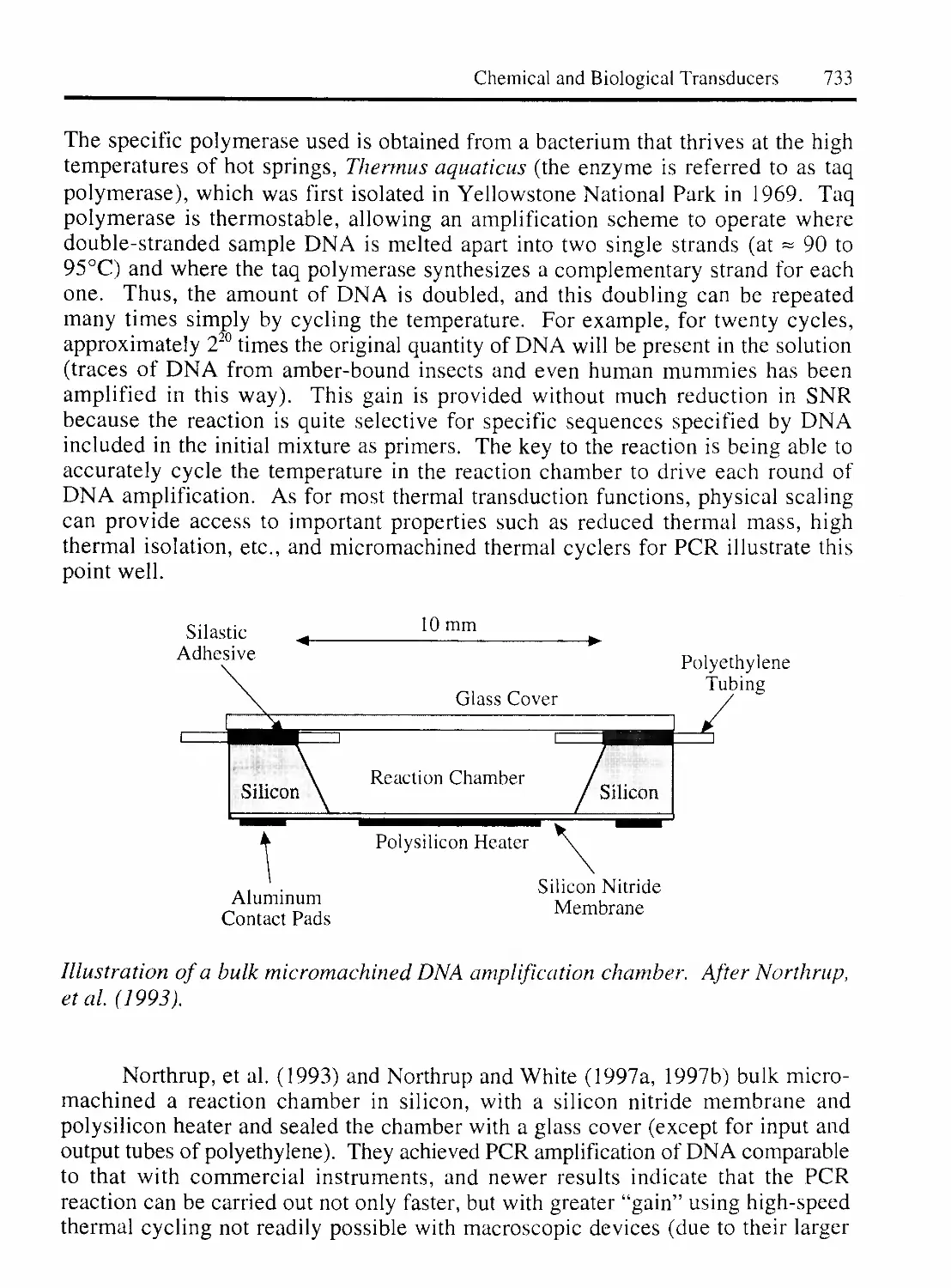
4.2.1 FIXED MICROMIRRORS 485
4.2.2 POSITIONABLE MICROMIRRORS 486
4.3 MICROMACHINED TRANSMISSIVE COMPONENTS 487
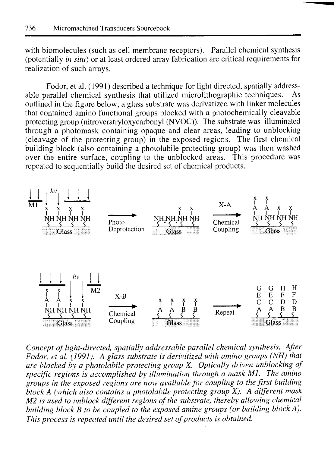
4.3.1 OPTICAL WAVEGUIDES 487
4.3.2 LENSES 488
REFRACTIVE LENSES 488
DIFFRACTIVE GRATINGS AND LENSES 494
4.4 FILTERS AND SPECTROMETERS 497
4.4.1 INTERFERENCE FILTERS 497
4.4.2 FABRY-PEROT FILTERS 498
4.4.3 MECHANICALLY TUNABLE IR FILTERS 499
4.4.4 SPECTROMETERS 500
FABRY-PEROT SPECTROMETERS 500
DISPERSIVE SPECTROMETERS 503
xiv
4.5 INTEGRATED OPTICAL SYSTEMS 509
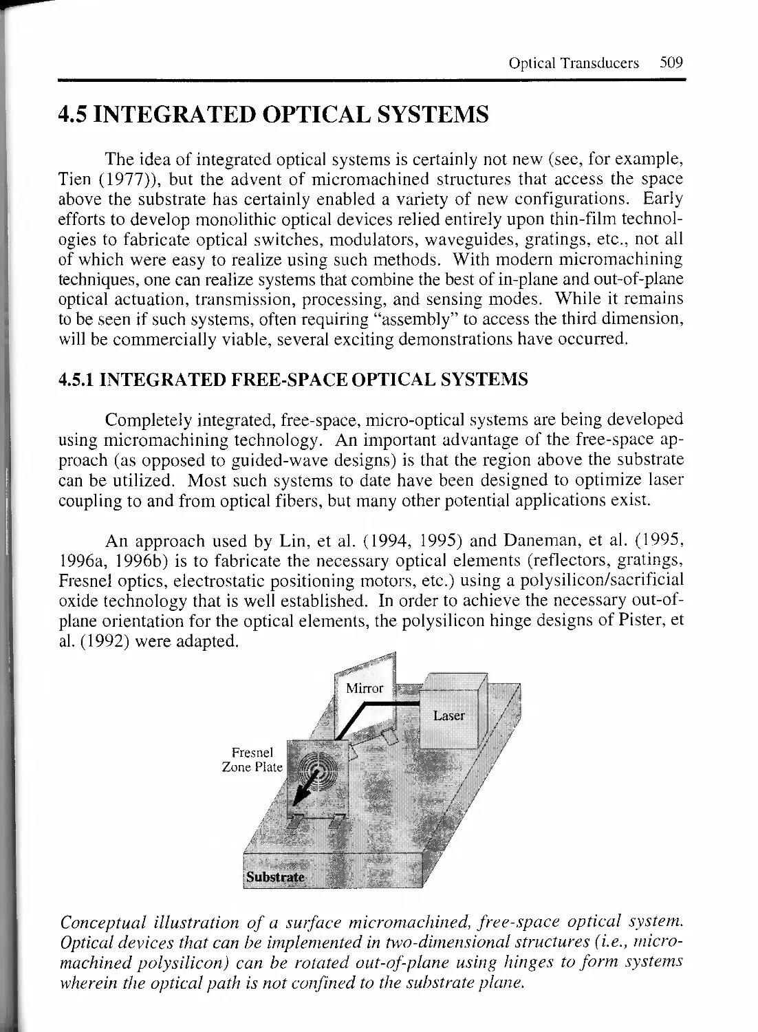
4.5.1 INTEGRATED FREE-SPACE OPTICAL SYSTEMS 509
OPTICAL TRANSDUCERS REFERENCES 513
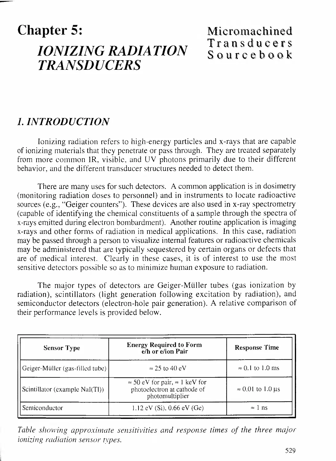
Chapter 5: IONIZING RADIATION TRANSDUCERS 529
1. INTRODUCTION 529
1.1 UNITS OF MEASURE FOR RADIATION 530
1.2 TYPES OF RADIATION 531
1.2.1 ALPHA RADIATION 532
1.2.2 BETA RADIATION 532
1.2.3 GAMMA RADIATION AND X-RAYS 533
1.2.4 NEUTRON RADIATION 533
2. IONIZATION-BASED DETECTORS 533
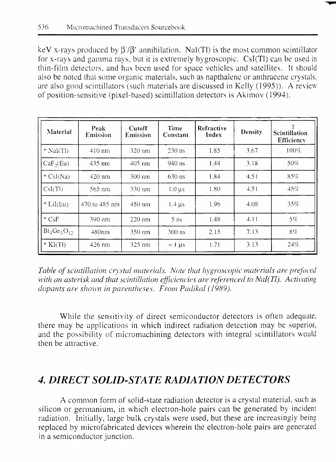
3. SCINTILLATION DETECTORS 535
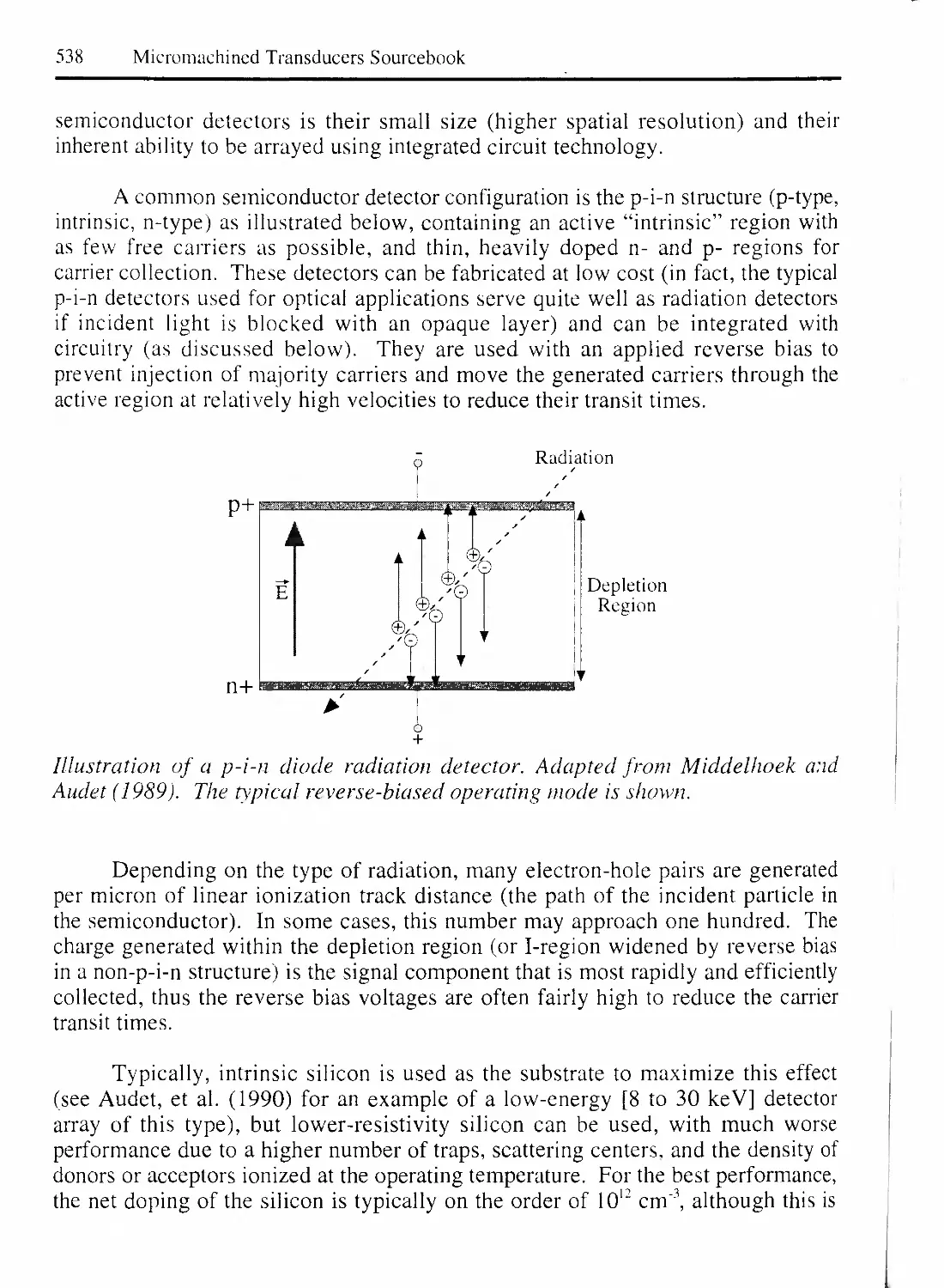
4. DIRECT SOLID-STATE RADIATION DETECTORS 536
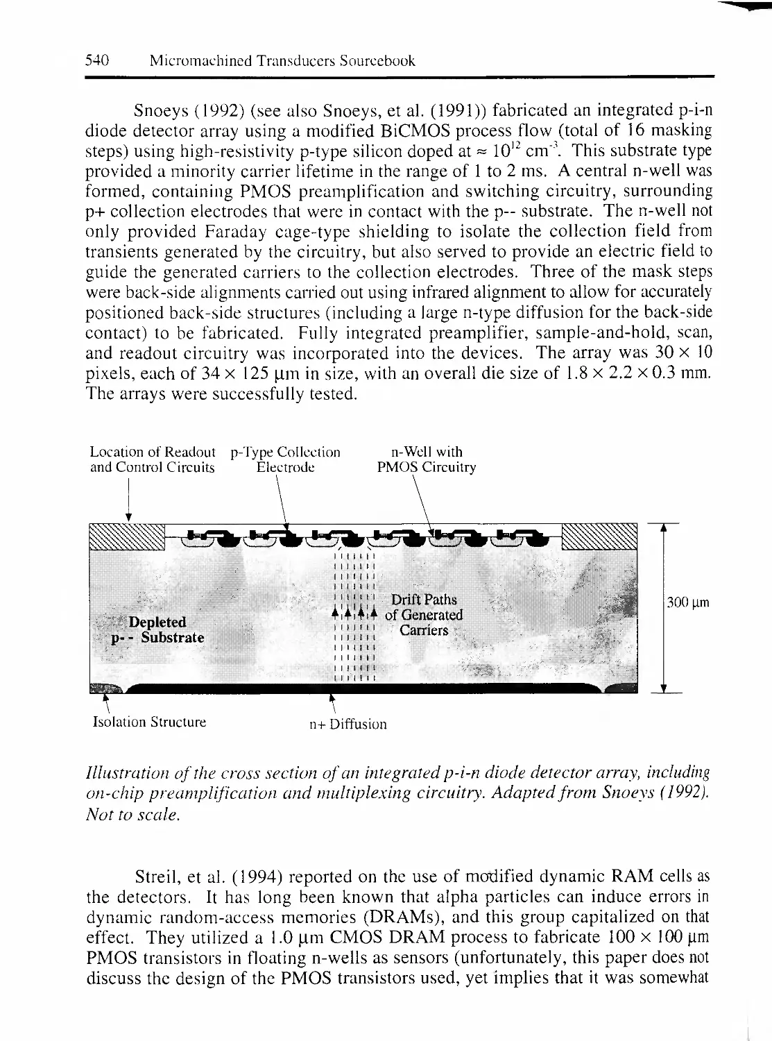
4.1 INTEGRATED DETECTOR ARRAYS 539
5. OTHER DETECTOR TYPES 541
5.1 TRANSMUTATION-BASED SENSORS 541
5.2 CERENKOV EFFECT DETECTORS 541
5.3 THERMAL DETECTORS 542
5.4 MOS THRESHOLD VOLTAGE SHIFT DETECTORS 542
5.5 THERMOLUMINESCENT DETECTORS 543
5.6 COLLIMATORS 544
6. RADIATION EFFECTS ON ELECTRONICS 545
7. BIOLOGICAL INTERACTIONS WITH RADIATION 546
RADIATION TRANSDUCERS REFERENCES 547
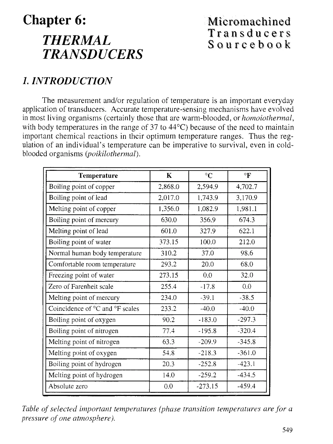
Chapter 6: THERMAL TRANSDUCERS 549
1. INTRODUCTION 549
2. TEMPERATURE MEASUREMENTS 550
2.1 BASIC TERMS 550
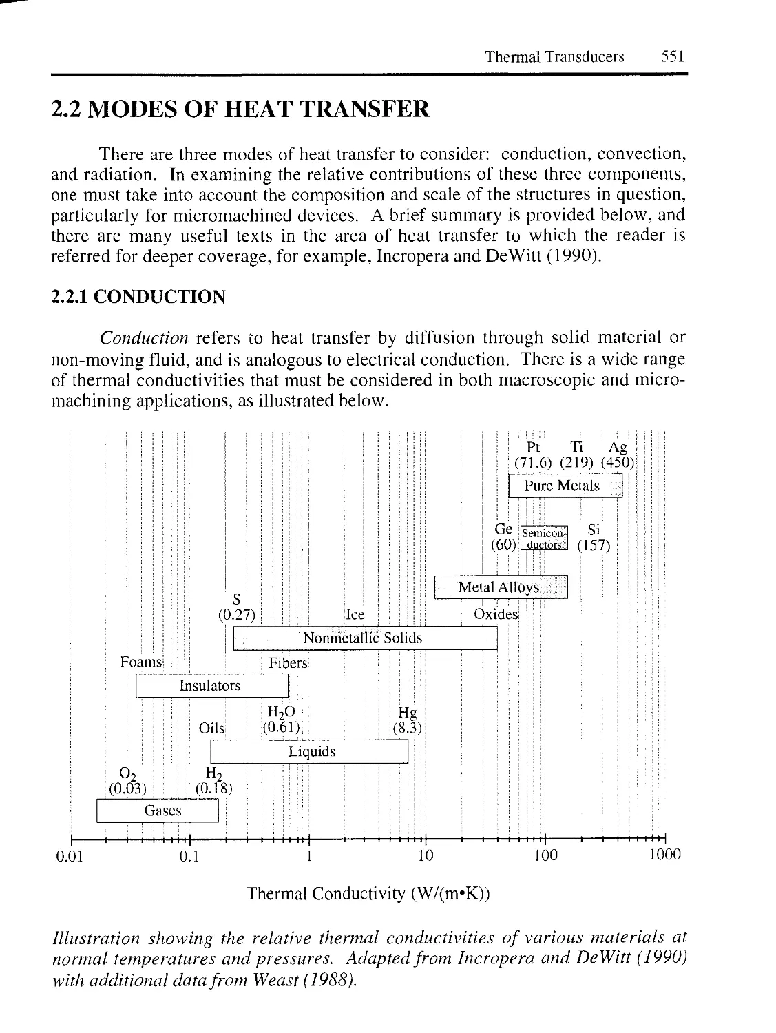
2.2 MODES OF HEAT TRANSFER 551
2.2.1 CONDUCTION 551
2.2.2 CONVECTION 553
2.2.3 RADIATION 553
2.3 NON-CONTACT TEMPERATURE MEASUREMENTS 554
2.4 THERMO-MECHANICAL SENSORS 554
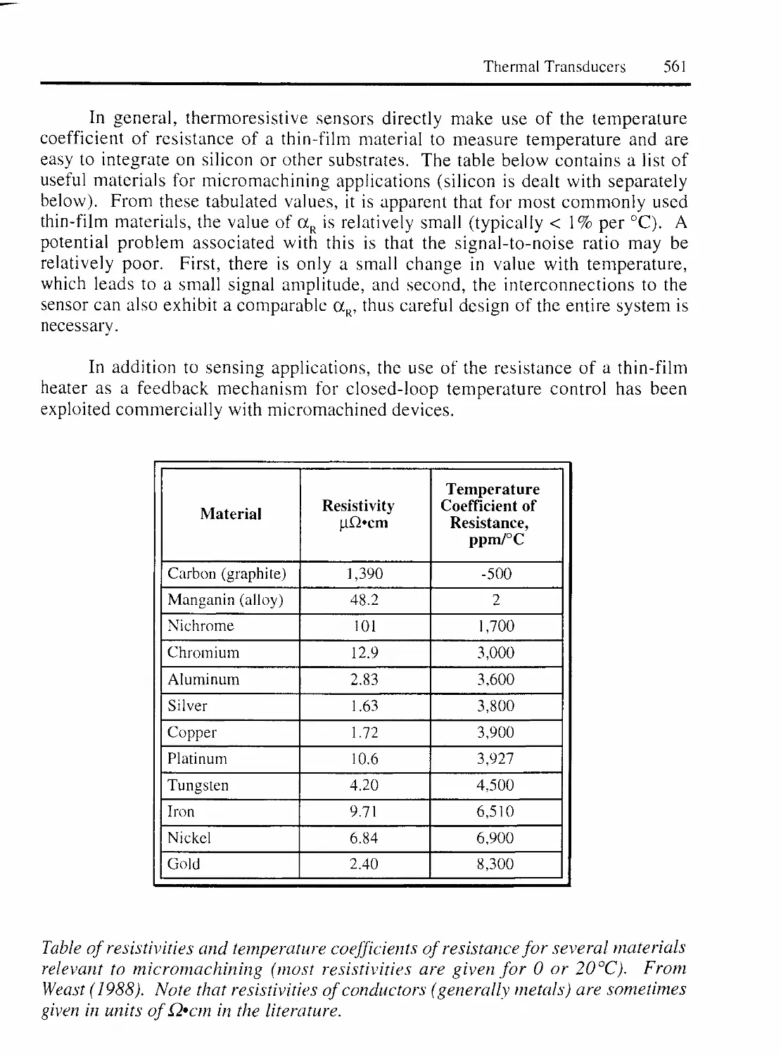
2.5 THERMORESISTIVE TRANSDUCERS 559
2.5.1 THERMORESISTIVE EFFECTS 559
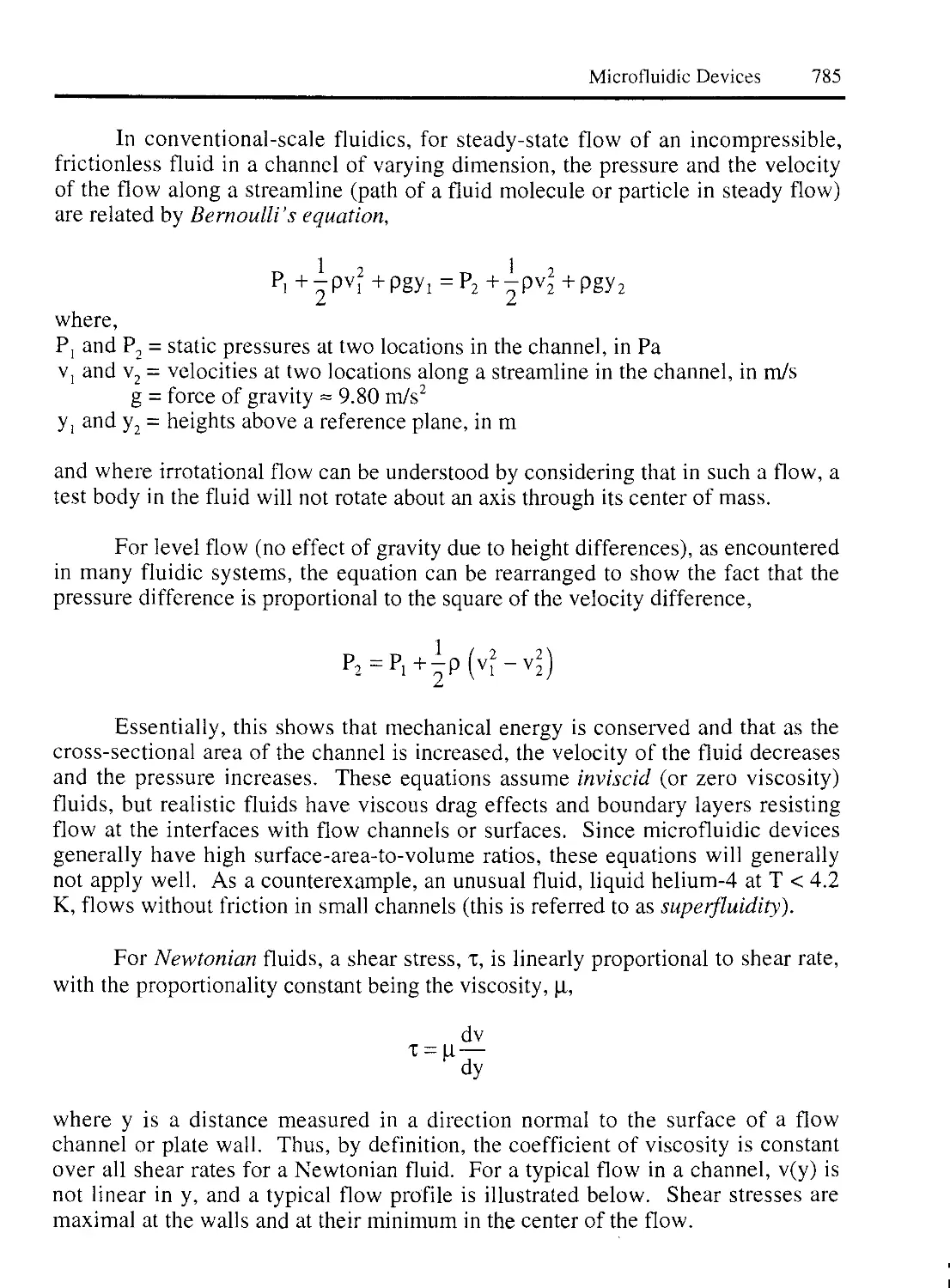
2.5.2 SIMPLE THIN-FILM THERMORESISTORS 560
XV
2.5.3 THERMISTORS 562
2.5.4 SEMICONDUCTOR THERMORESISTORS/THERMISTORS 562
2.5.5 SELF-HEATING EFFECTS IN RESISTIVE SENSORS 565
2.5.6 INTERFACE CIRCUITS 565
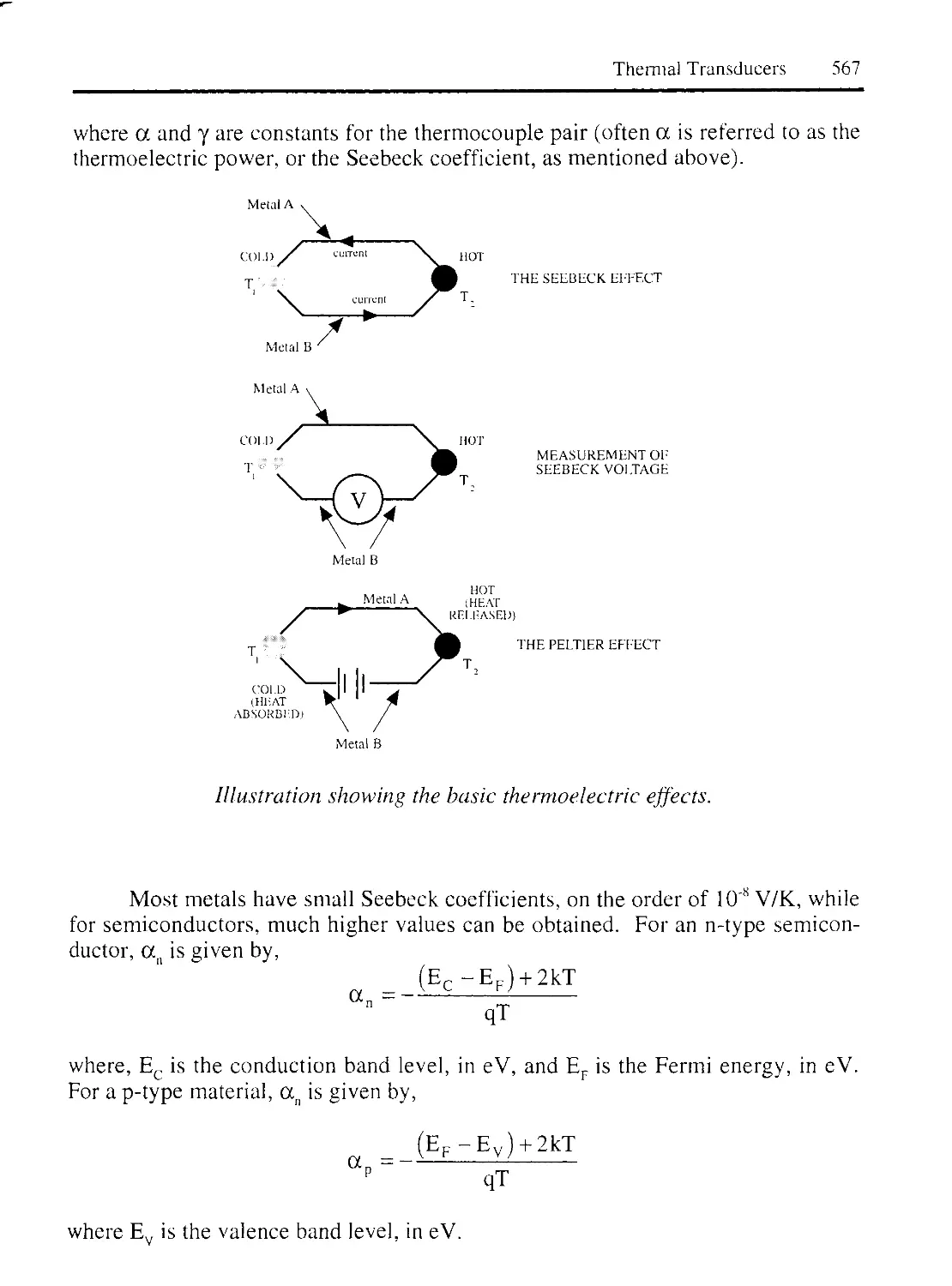
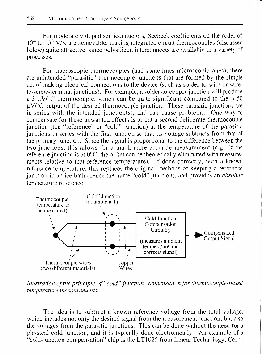
2.6 THERMOCOUPLES 565
2.7 JUNCTION-BASED THERMAL SENSORS 570
2.7.1 DIODE TEMPERATURE SENSORS 570
2.7.2 TRANSISTOR TEMPERATURE SENSORS 574
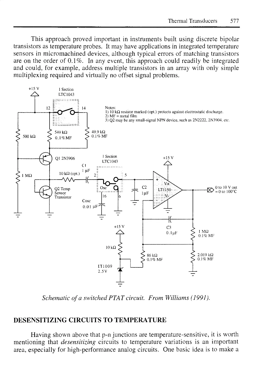
BASIC PTAT CIRCUIT 575
SWITCHED PTAT CIRCUIT 576
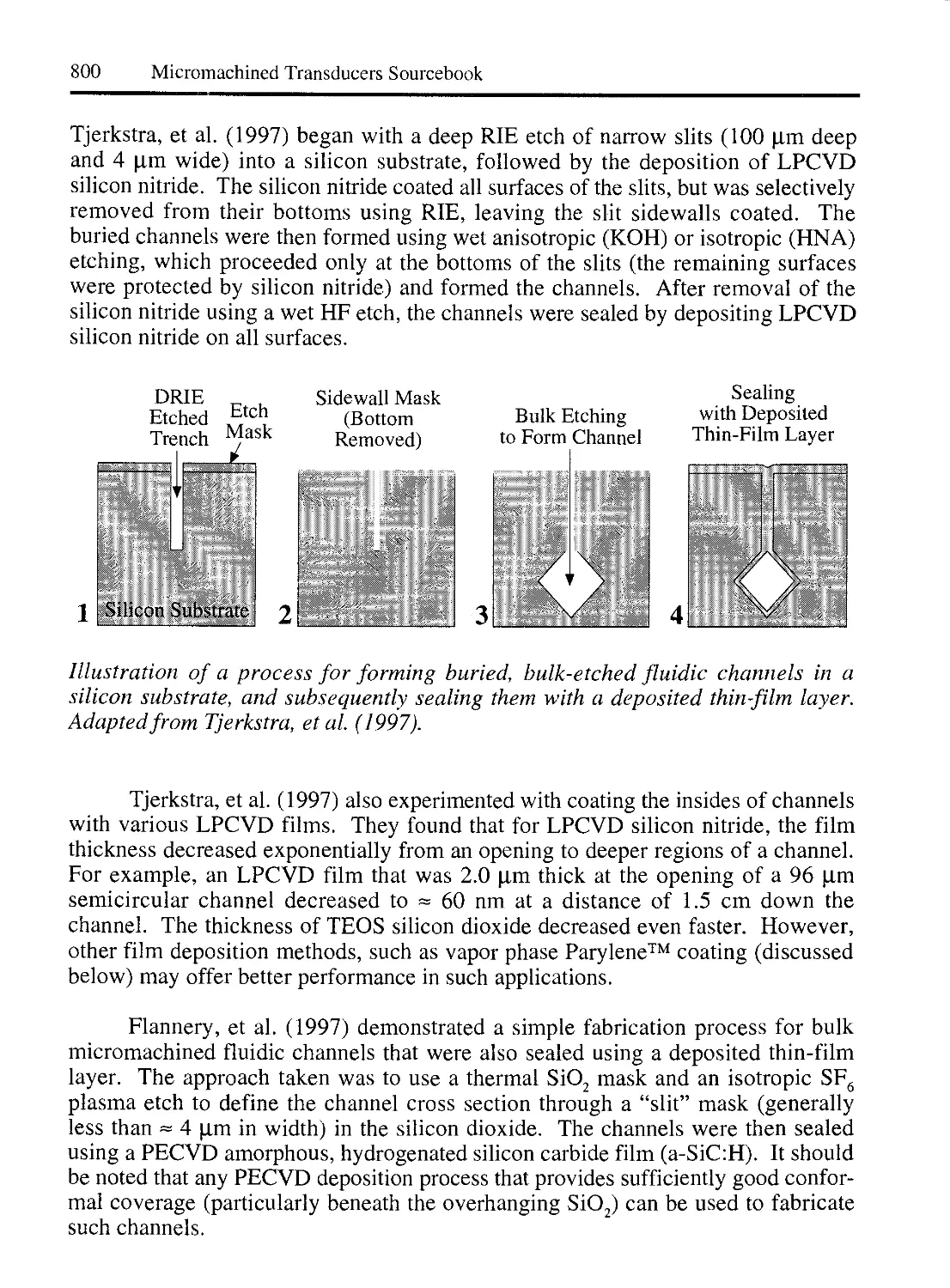
DESENSITIZING CIRCUITS TO TEMPERATURE 577
2.8 OTHER THERMAL SENSORS 578
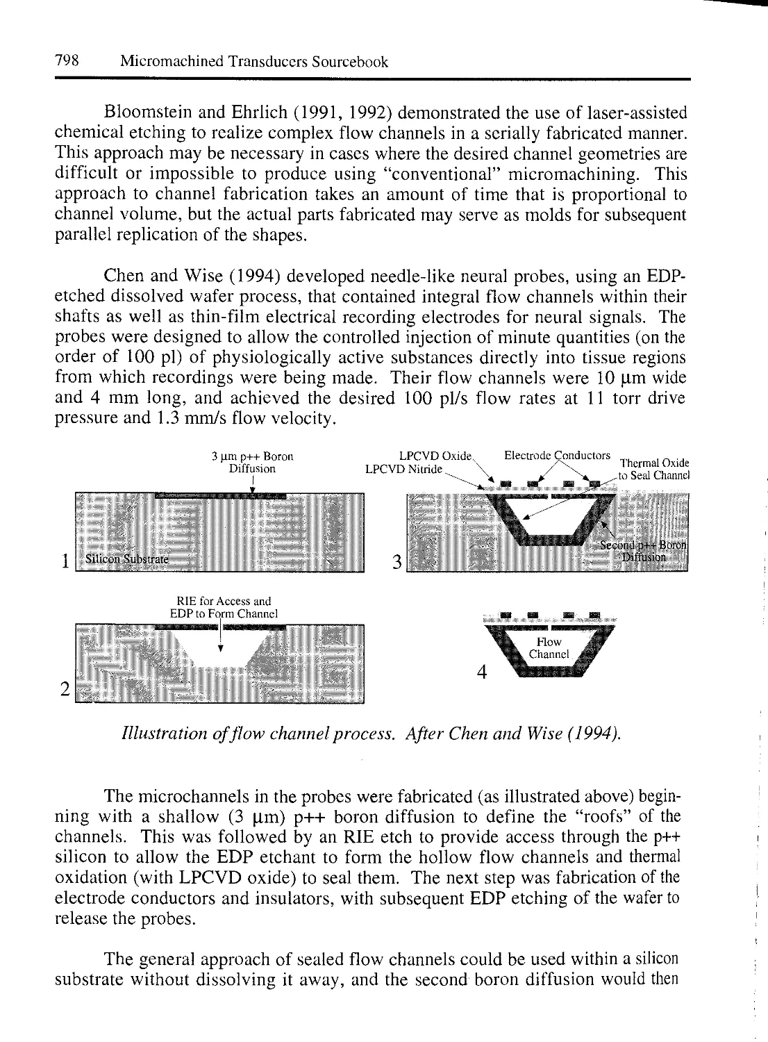
2.8.1 ACOUSTIC TEMPERATURE SENSORS 578
2.8.2 QUARTZ AND OTHER RESONANT TEMPERATURE SENSORS 578
2.8.3 TUNNELING TEMPERATURE SENSORS 579
2.9 BIOLOGICAL THERMAL SENSORS 579
3. THERMAL ACTUATORS 580
3.1 JOULE-THOMPSON REFRIGERATORS 581
3.2 OTHER FLUIDIC COOLERS 583
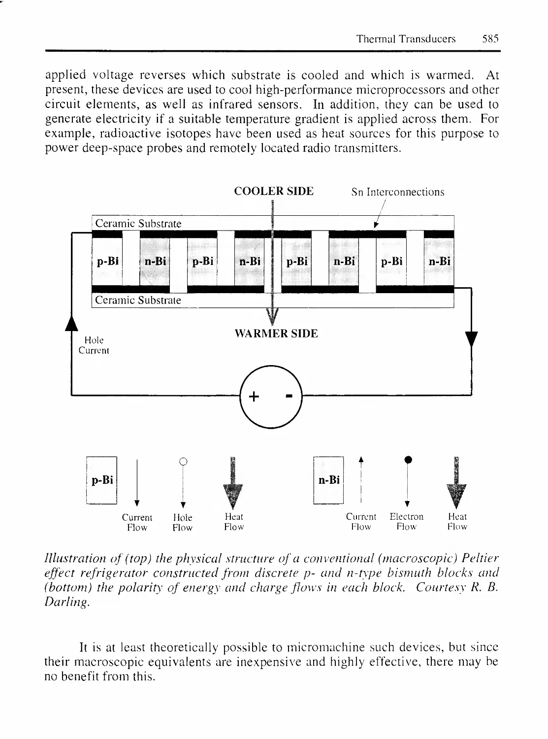
3.3 PELTIER EFFECT HEAT PUMPS 584
4. THERMAL SENSOR/ACTUATOR COMBINATIONS 586
4.1 THERMALLY STABILIZED CIRCUITS 586
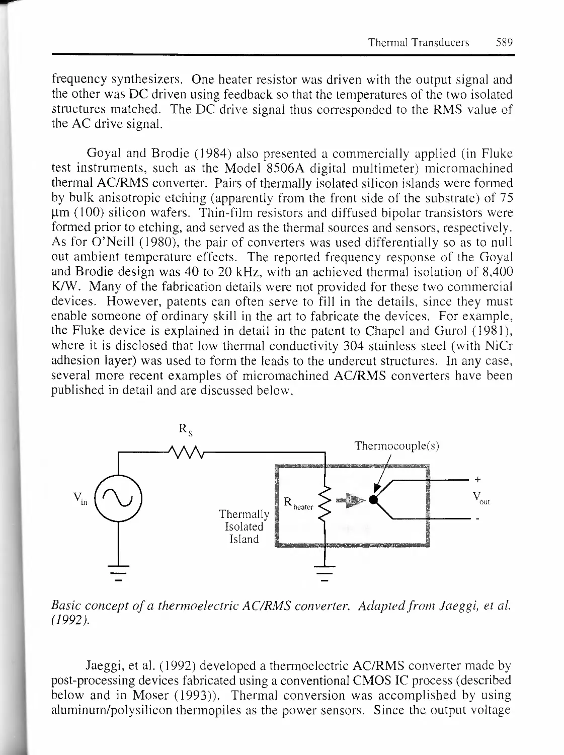
4.2 THERMAL AC/RMS CONVERTERS 588
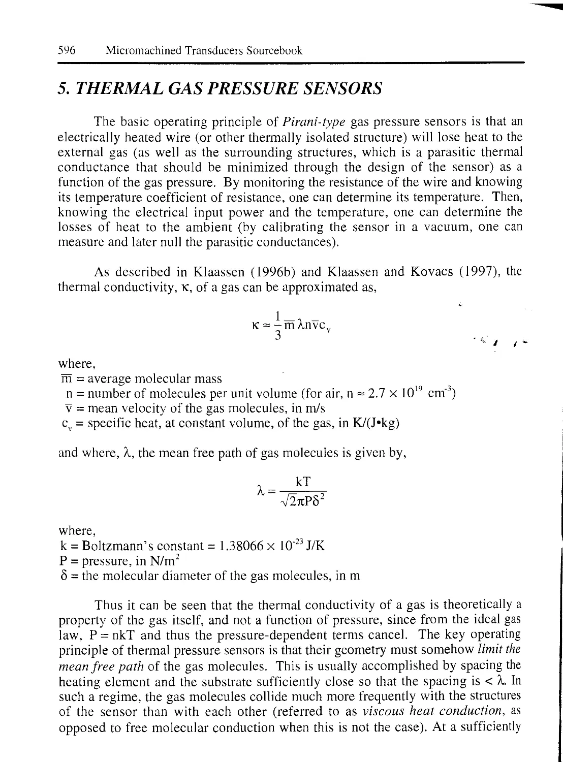
5. THERMAL GAS PRESSURE SENSORS 596
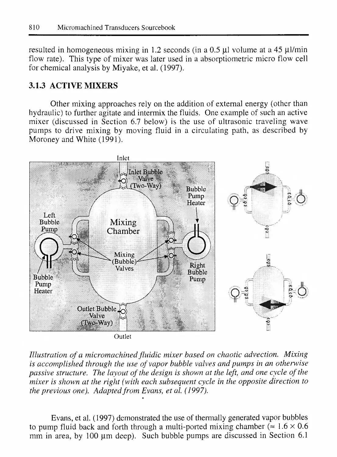
6. THERMAL FLOW SENSORS 599
7. OTHER THERMAL SENSORS 600
7.1 MICROMACHINED CALORIMETERS 601
7.2 DEW-POINT (THERMAL) HUMIDITY SENSORS 601
7.3 THERMAL ELECTROMAGNETIC MIXERS 601
THERMAL TRANSDUCERS REFERENCES 603
Chapter 7: MAGNETIC & ELECTROMAGNETIC TRANSDUCERS 611
1. INTRODUCTION 611
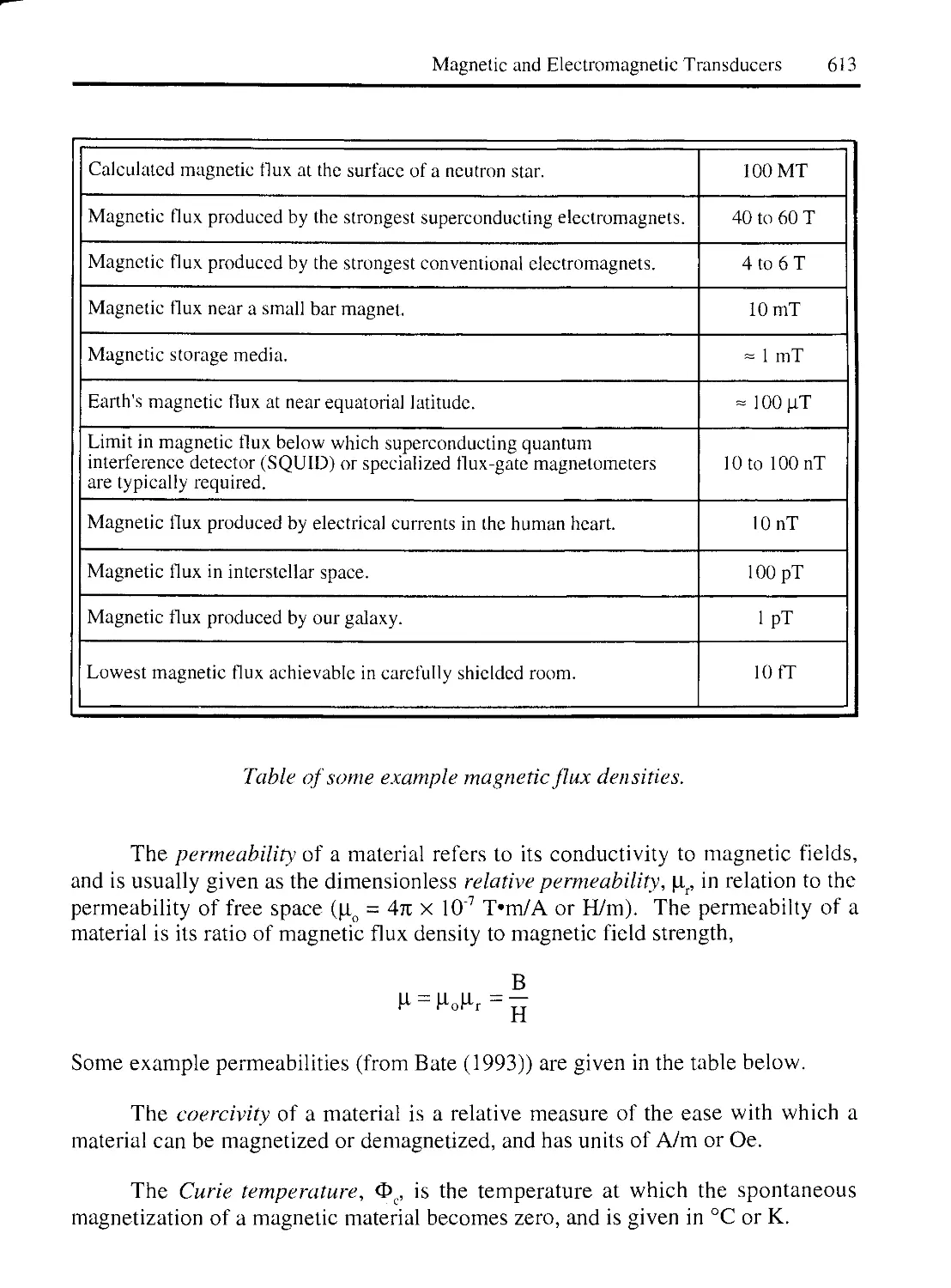
1.1 TERMS AND DEFINITIONS 612
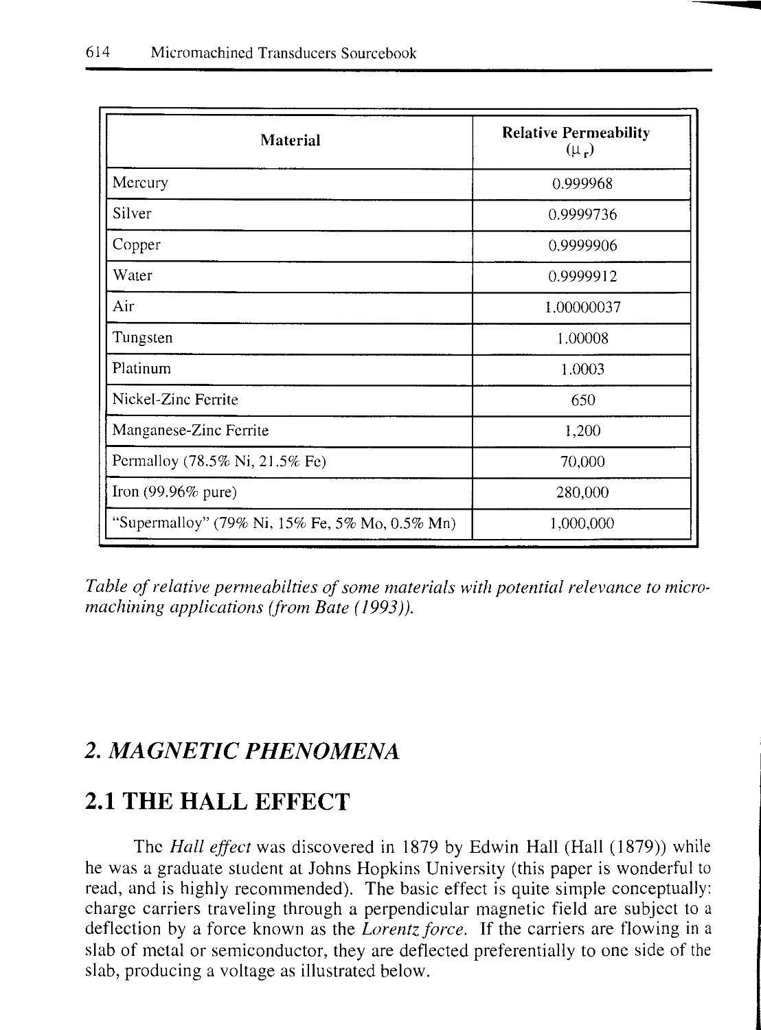
2. MAGNETIC PHENOMENA 614
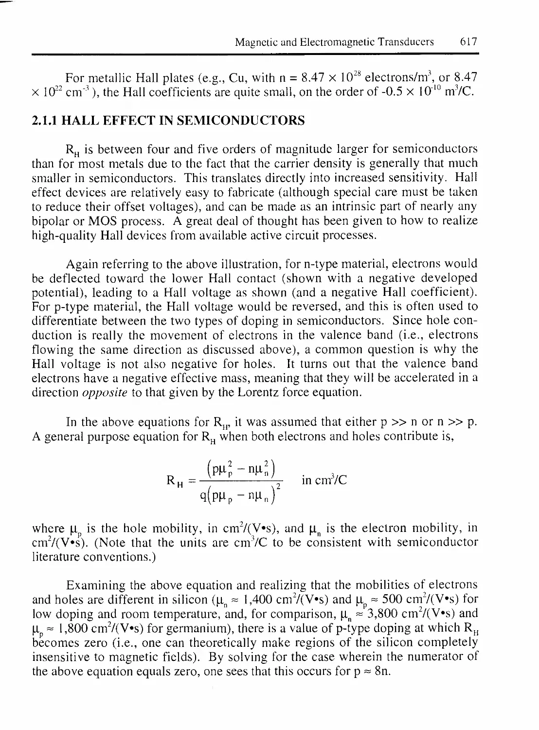
2.1 THE HALL EFFECT 614
2.1.1 HALL EFFECT IN SEMICONDUCTORS 617
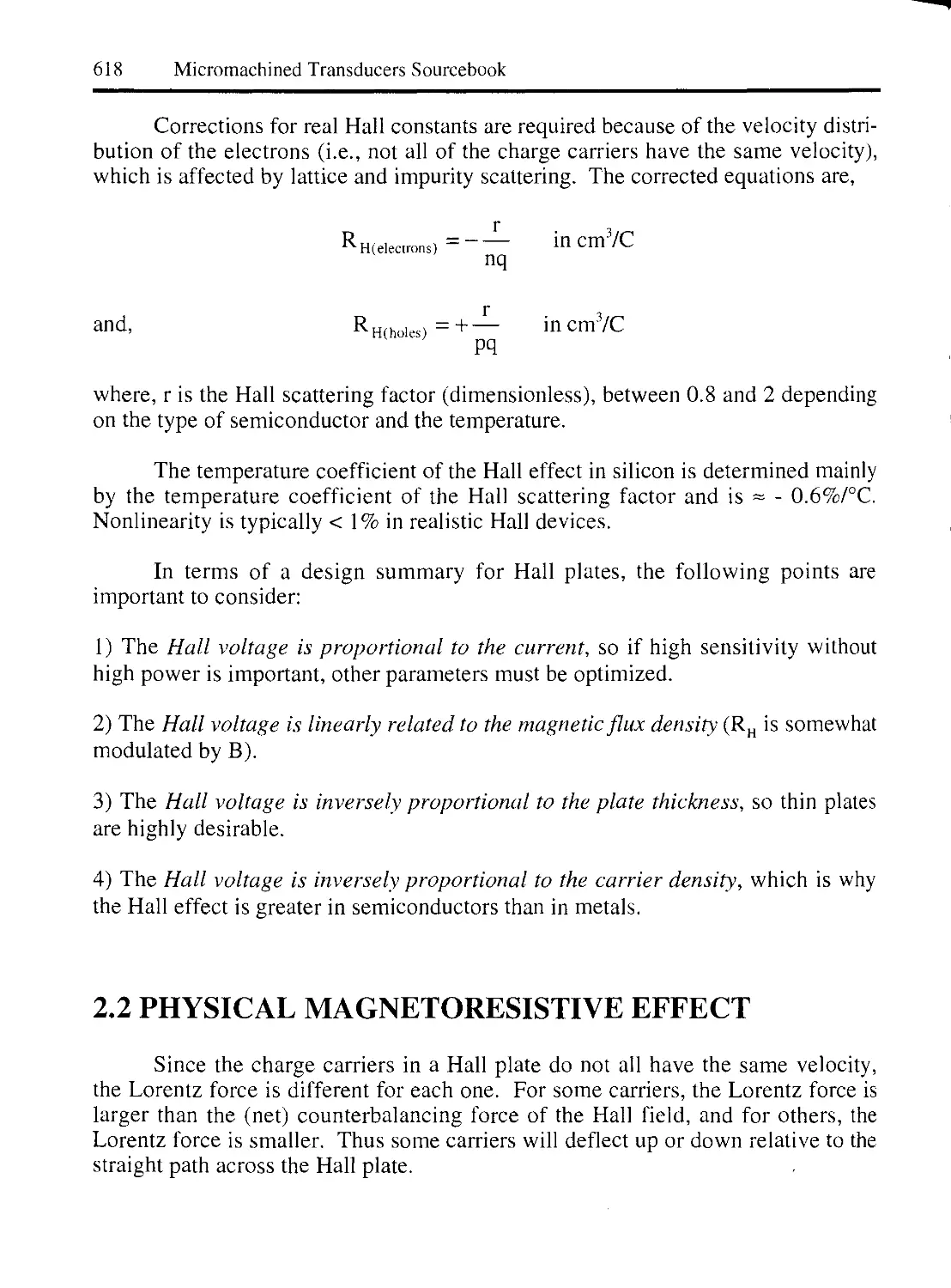
2.2 PHYSICAL MAGNETORESISTIVE EFFECT 618
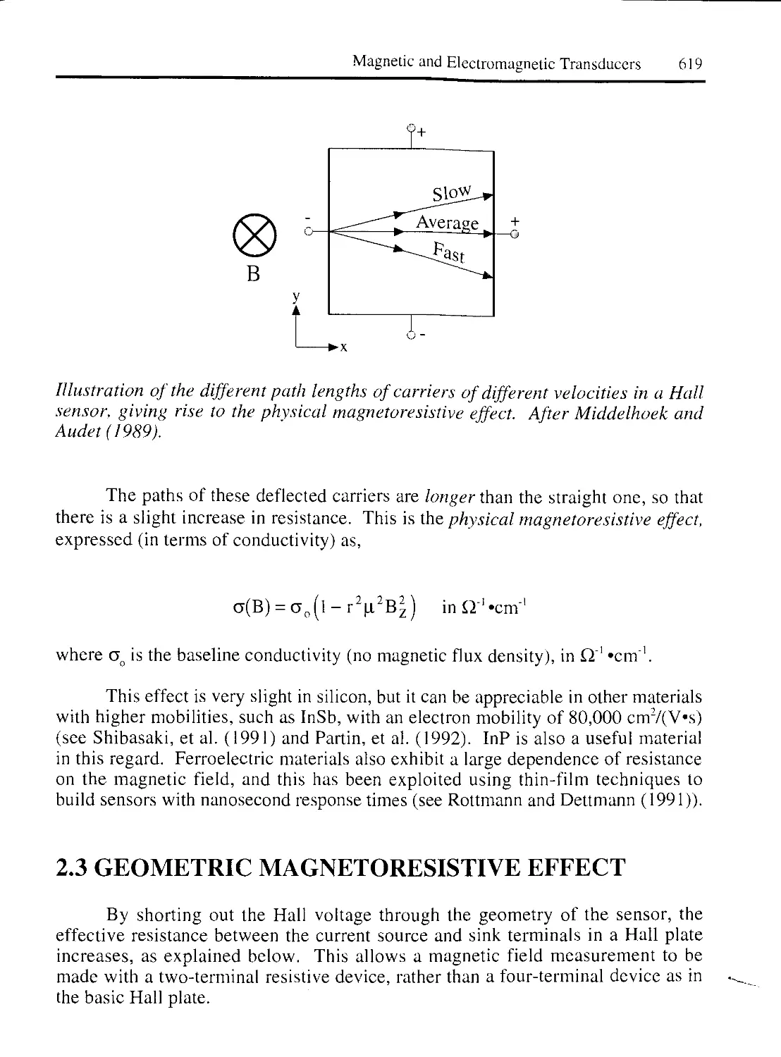
2.3 GEOMETRIC MAGNETORESISTIVE EFFECT 619
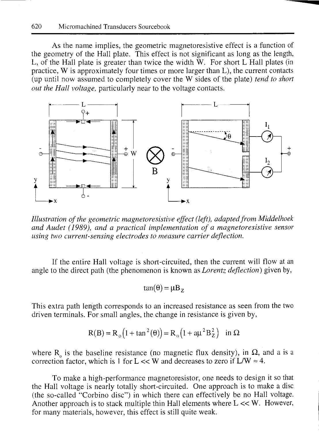
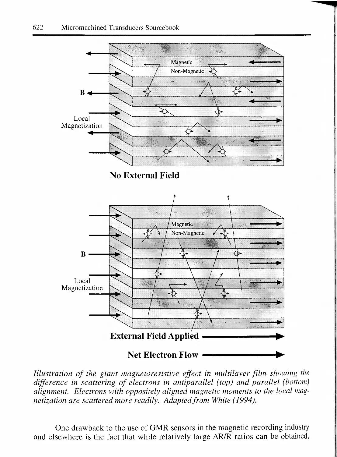
2.4 GIANT MAGNETORESISTIVE EFFECT 621
2.5 MAGNETO-OPTICAL EFFECTS 623
2.6 MAGNETIC ANISOTROPY 624
2.6.1 SHAPE ANISOTROPY 624
XVI
2.6.2 STRESS ANISOTROPY 624
2.6.3 CRYSTALLINE ANISOTROPY 625
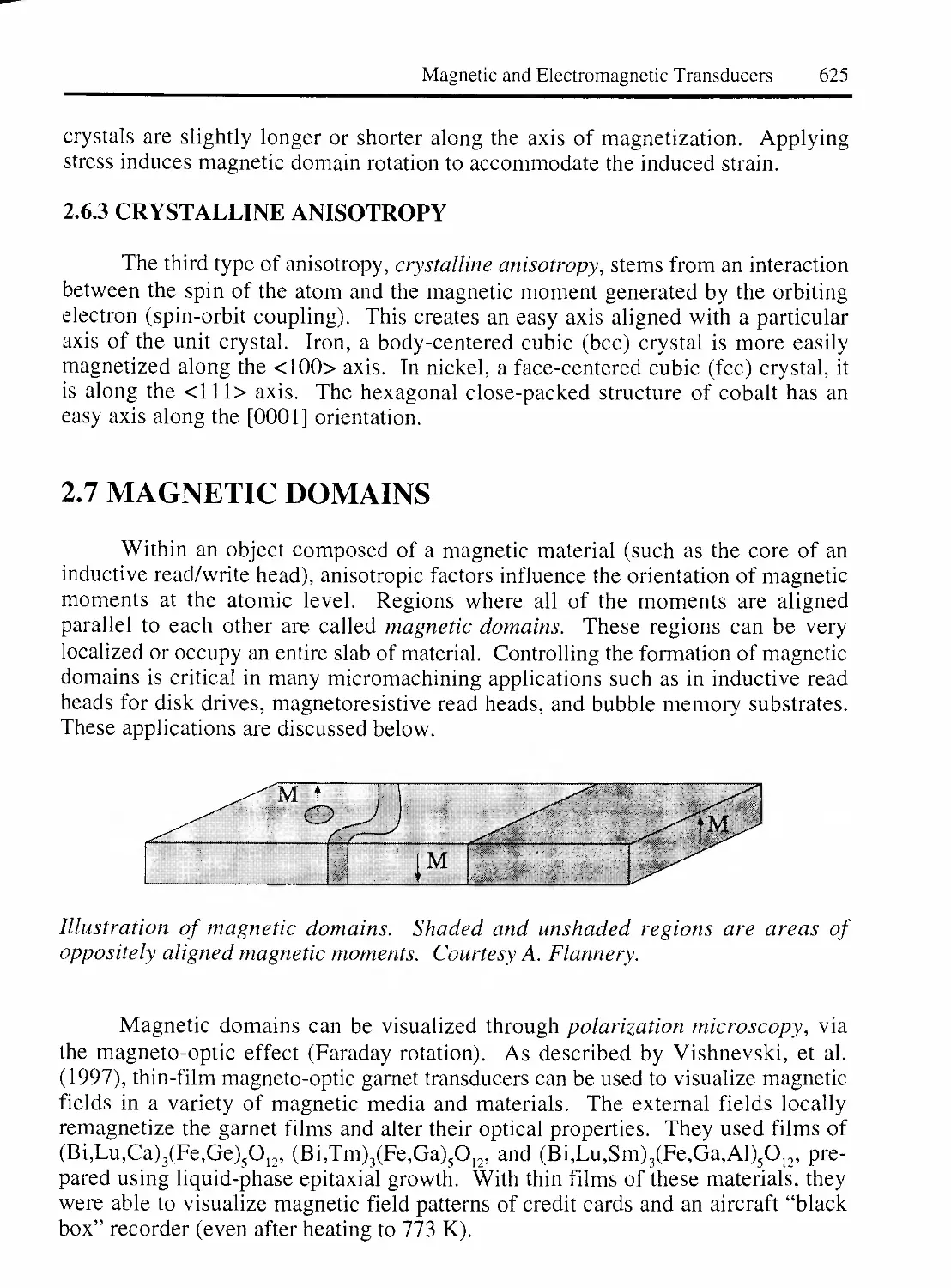
2.7 MAGNETIC DOMAINS 625
3. MAGNETIC SENSORS 626
3.1 HALL EFFECT SENSORS 626
3.1.1 PLATE DESIGN FOR HALL-VOLTAGE SENSORS 626
3.1.2 OFFSET VOLTAGE ISSUES 627
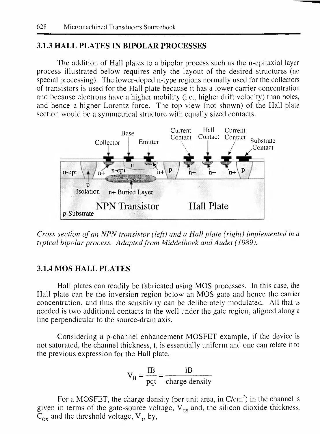
3.1.3 HALL PLATES IN BIPOLAR PROCESSES 628
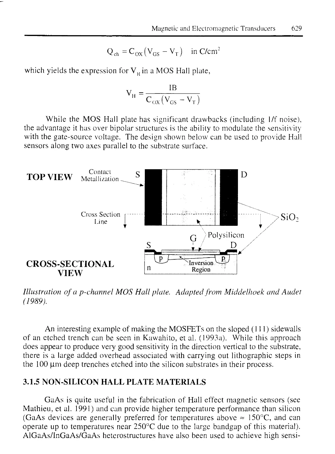
3.1.4 MOS HALL PLATES 628
3.1.5 NON-SILICON HALL PLATE MATERIALS 629
3.1.6 MAGNETODIODES 630
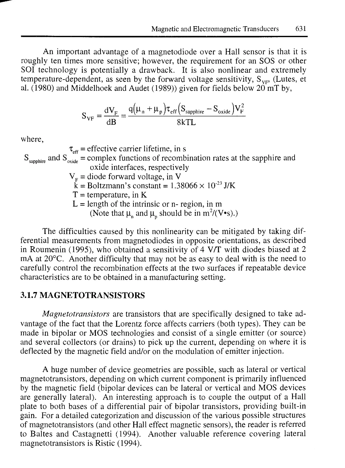
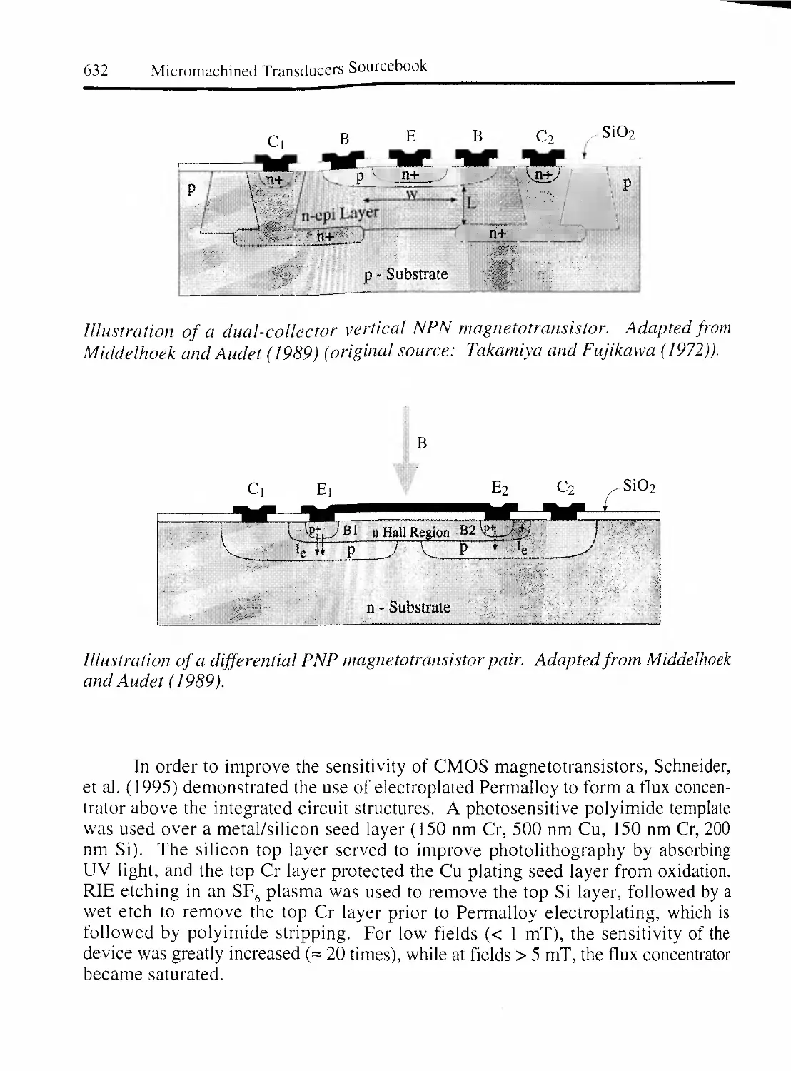
3.1.7 MAGNETOTRANSISTORS 631
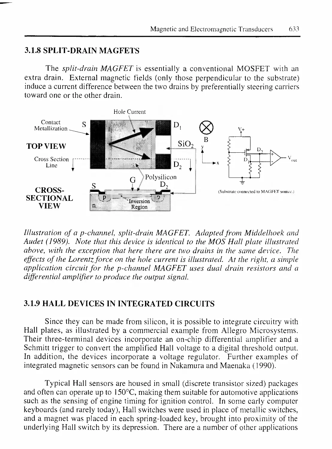
3.1.8 SPLIT-DRAIN MAGFETS 633
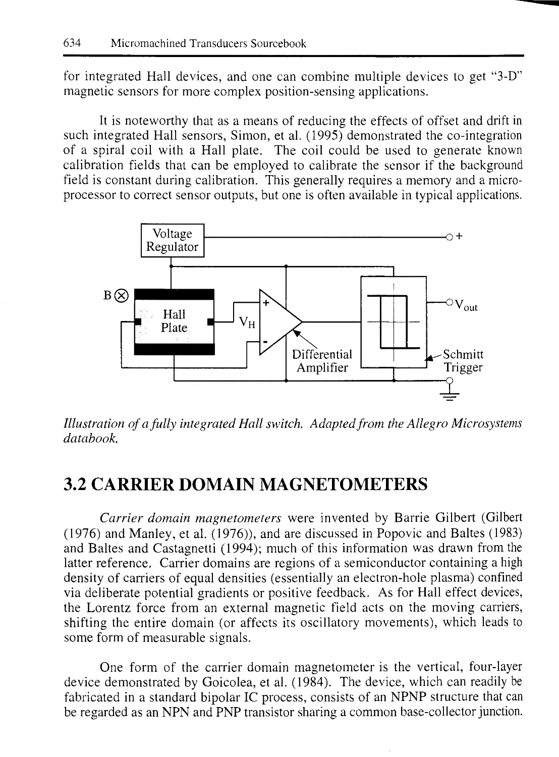
3.1.9 HALL DEVICES IN INTEGRATED CIRCUITS 633
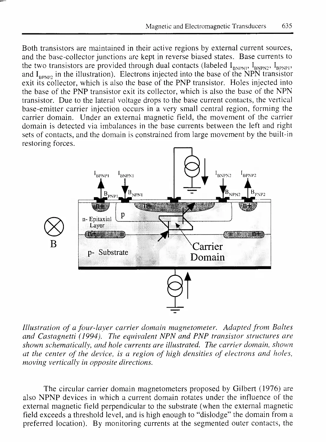
3.2 CARRIER DOMAIN MAGNETOMETERS 634
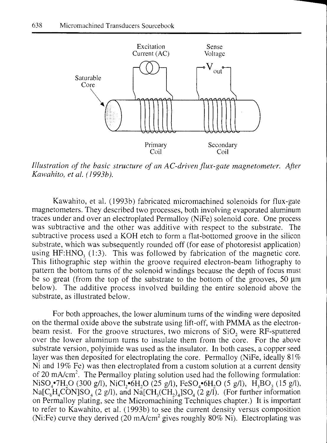
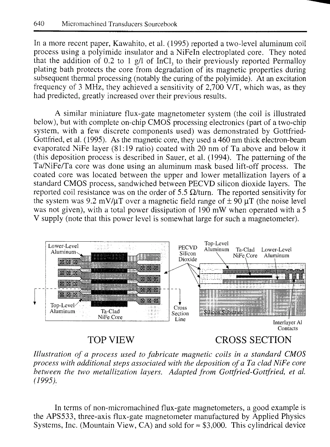
3.3 FLUX-GATE MAGNETOMETERS 636
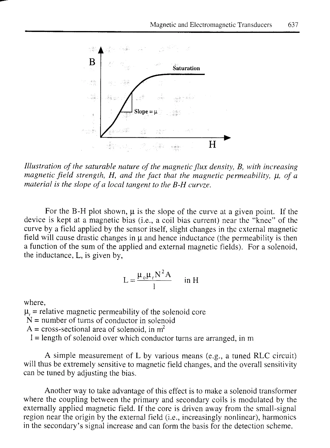
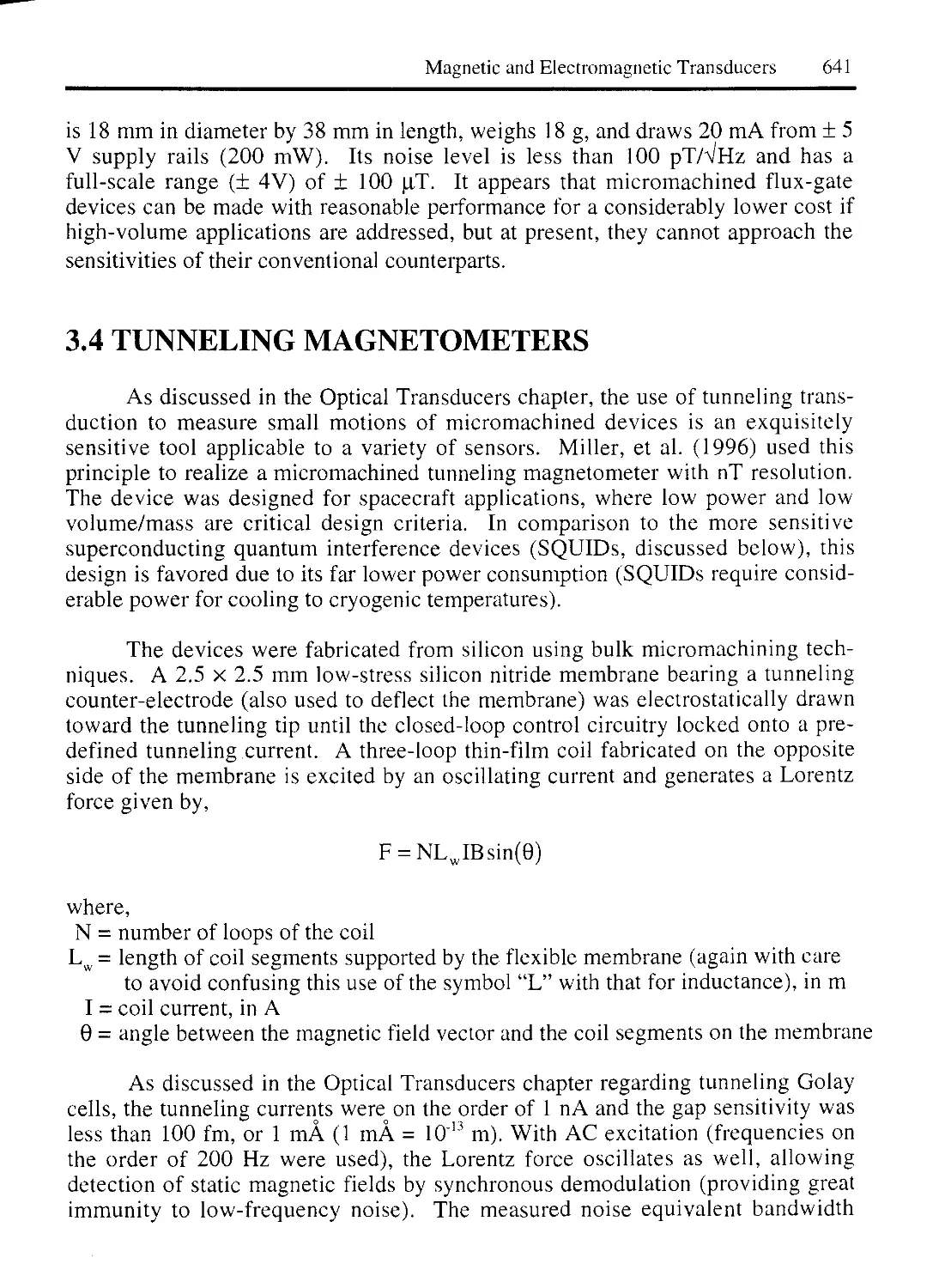
3.4 TUNNELING MAGNETOMETERS 641
3.5 TUNNEL DIODE MAGNETIC SENSORS 642
3.6 VACUUM ELECTRON MAGNETIC SENSORS 643
3.7 SUPERCONDUCTING QUANTUM INTERFERENCE MAGNETOMETERS 645
3.8 OTHER MAGNETIC SENSORS 647
3.8.1 WIEGAND WIRES 647
3.9 BIOLOGICAL MAGNETIC SENSORS 648
4. MAGNETIC ACTUATORS 649
4.1 MAGNETIC FIELD ACTUATORS 649
4.2 MAGNETOSTRICTIVE ACTUATORS 651
4.3 MAGNET FABRICATION 652
4.4 MAGNETIC ACTUATORS WITH DRIVE COILS 652
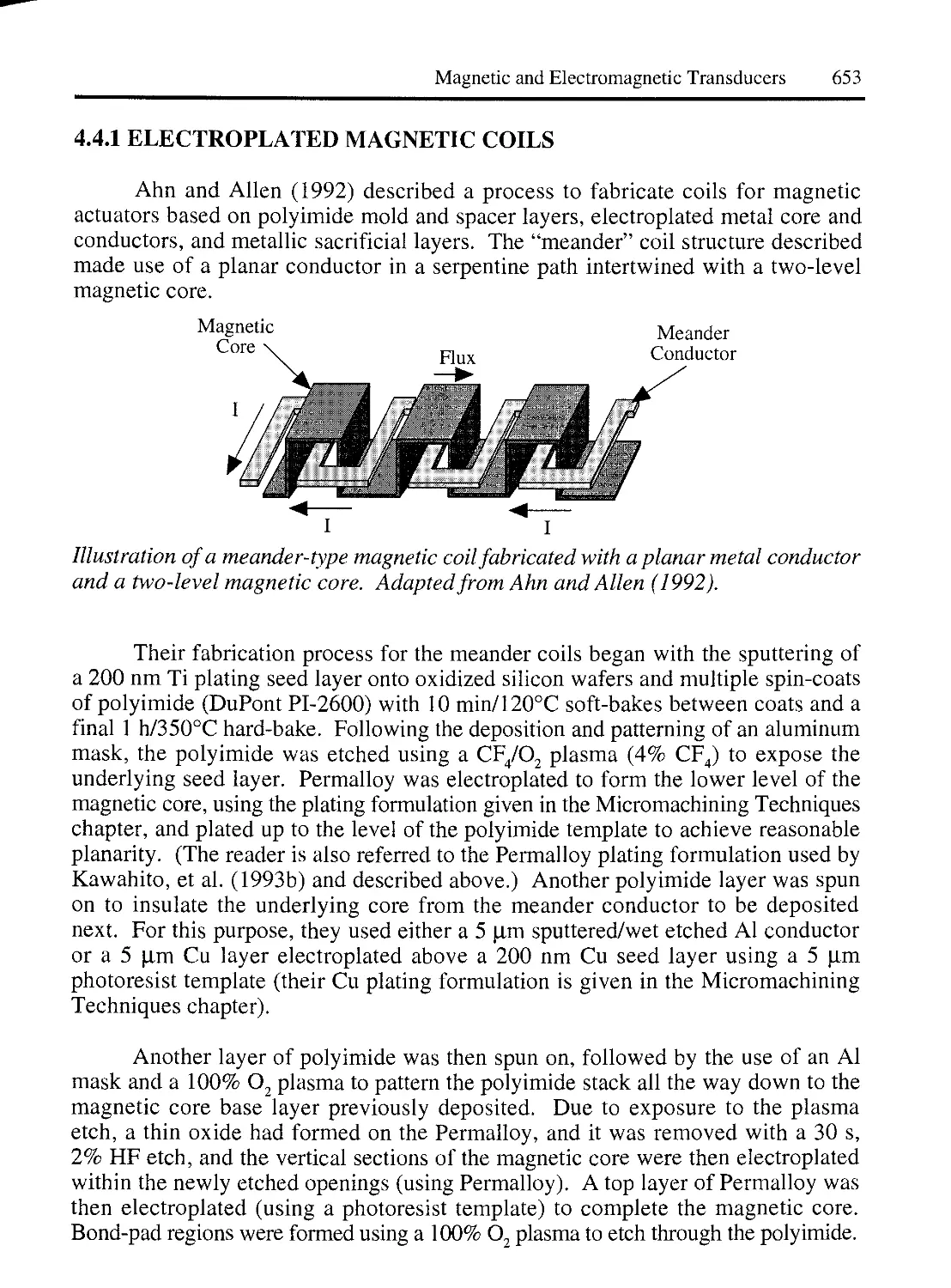
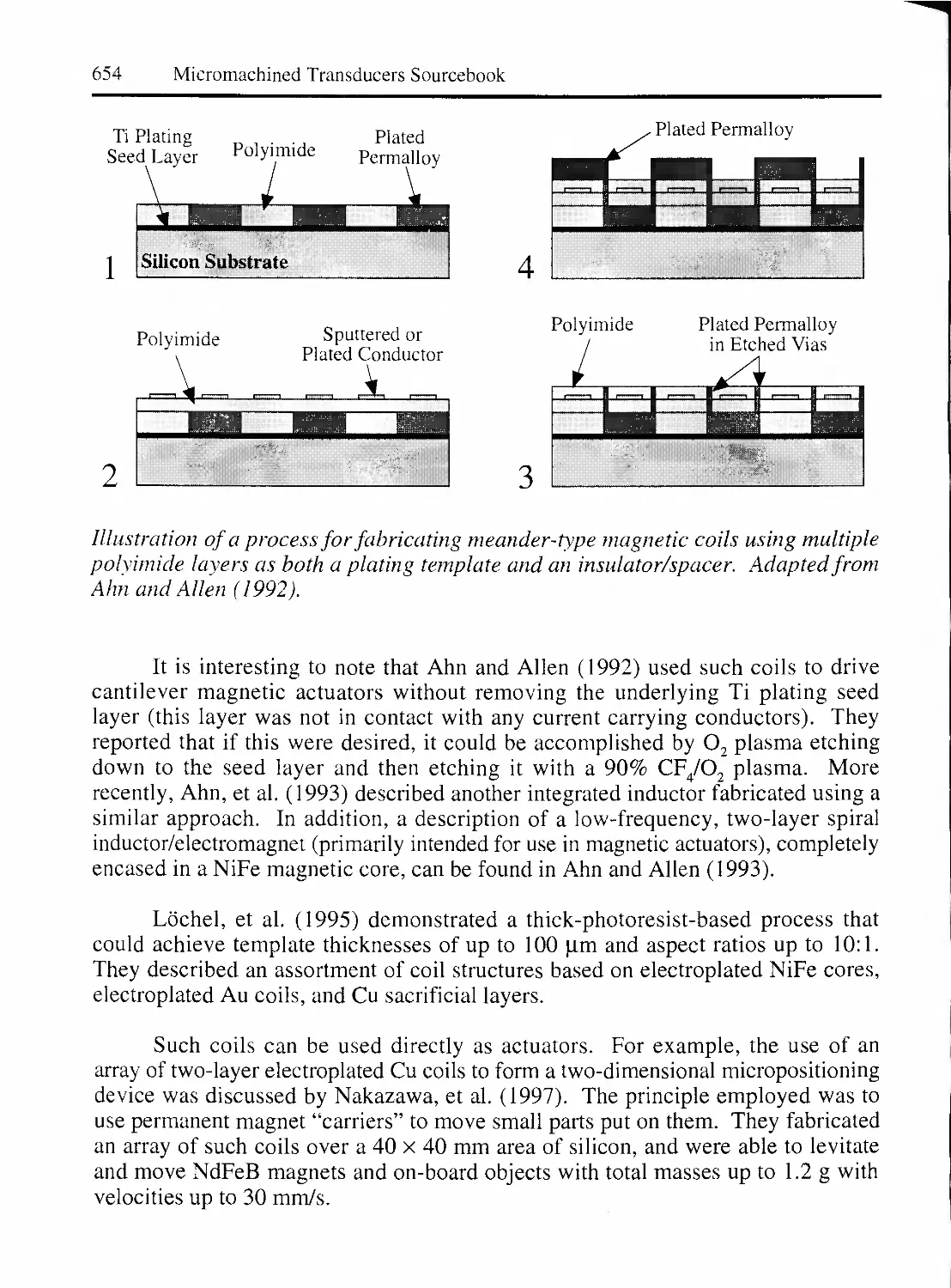
4.4.1 ELECTROPLATED MAGNETIC COILS 653
4.4.2 WIRE-BONDED MAGNETIC COILS 655
4.4.3 EXTERNALLY WOUND MAGNETIC COILS 655
4.5 MAGNETIC ACTUATORS USING EXTERNAL FIELDS 656
4.6 MAGNETIC MICROMOTORS 659
4.7 EDDY-CURRENT DEFECT SENSORS 661
4.8 RESONANT MAGNETIC SENSORS 662
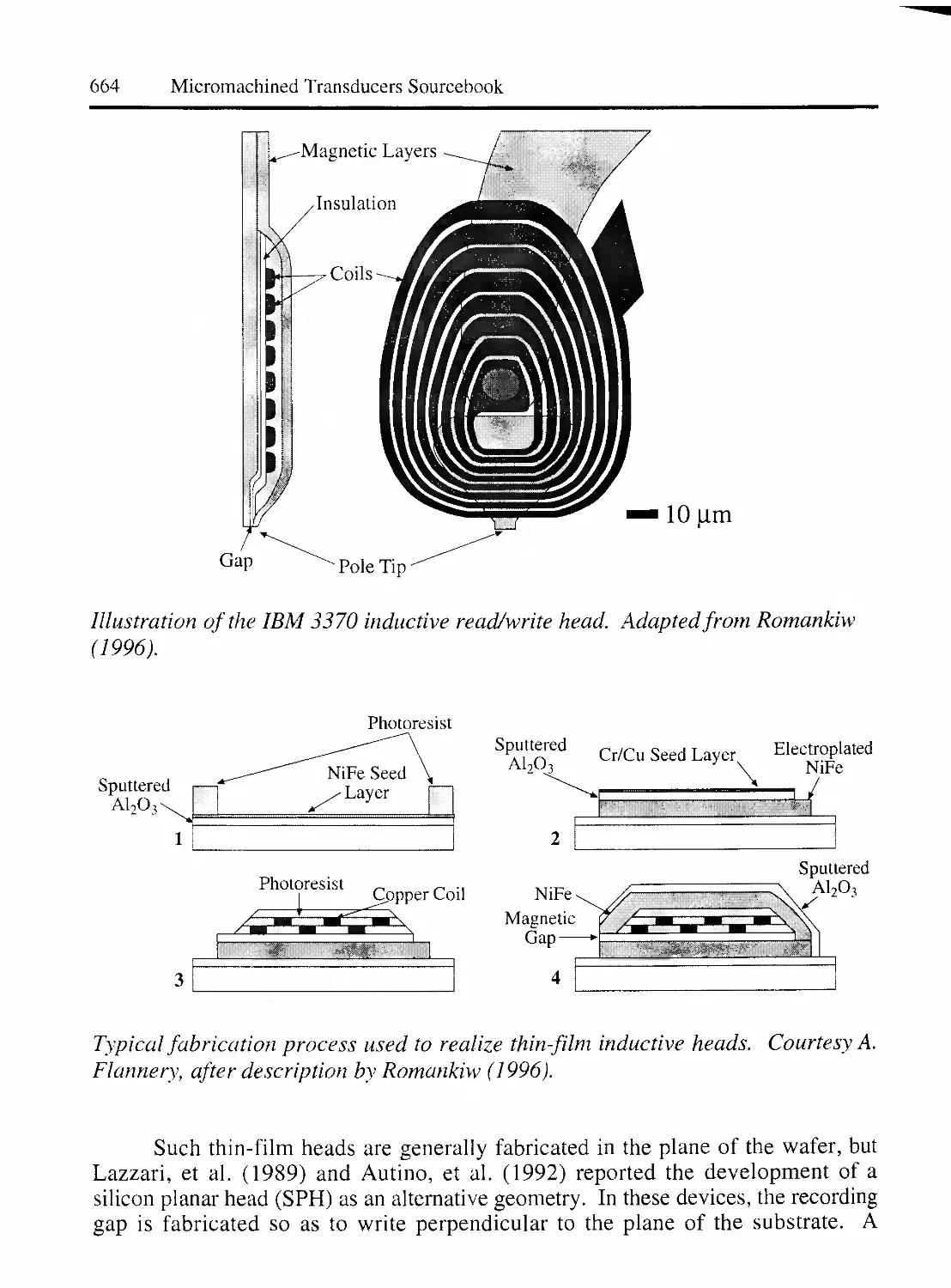
4.9 MAGNETIC READ/WRITE HEADS 663
4.9.1 MAGNETIC HEADS FOR STORAGE DEVICES 663
INDUCTIVE MAGNETIC HEADS 663
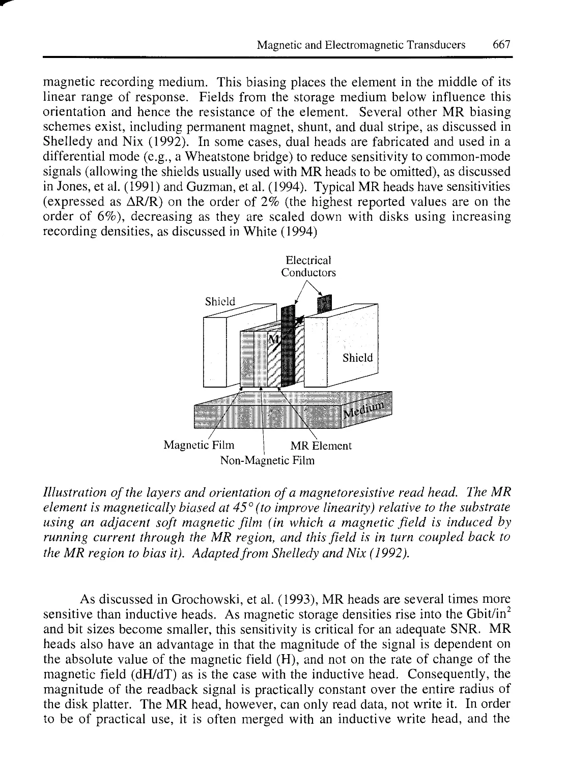
MAGNETORESISTIVE READ HEADS 666
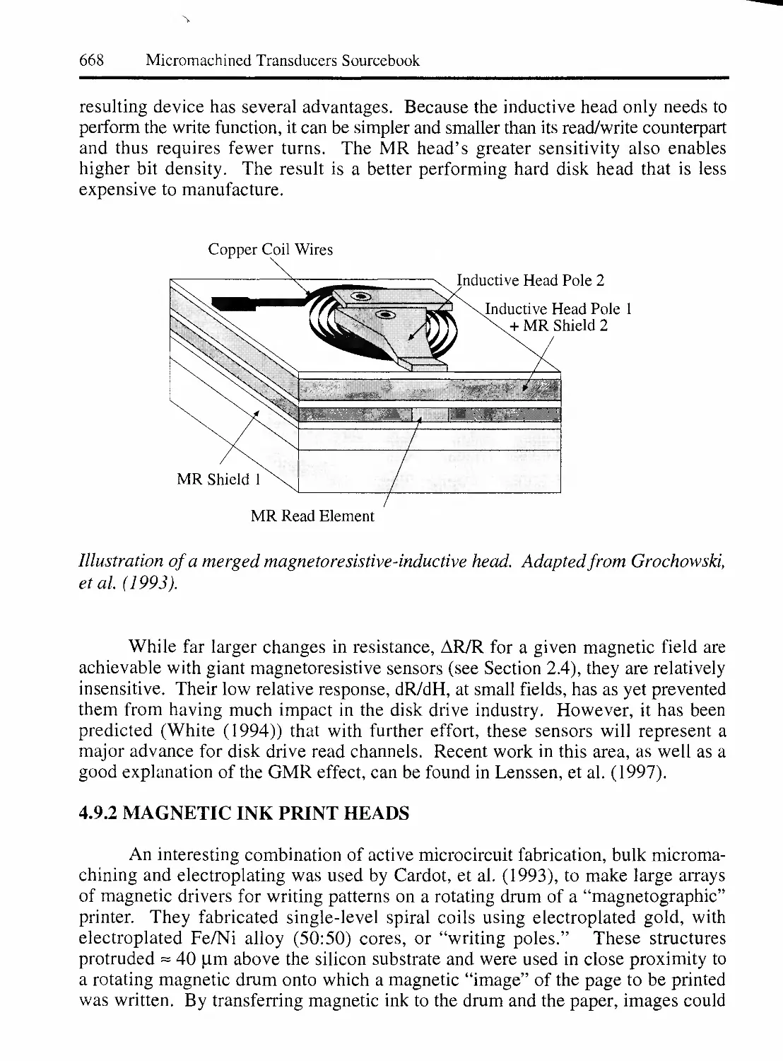
4.9.2 MAGNETIC INK PRINT HEADS 668
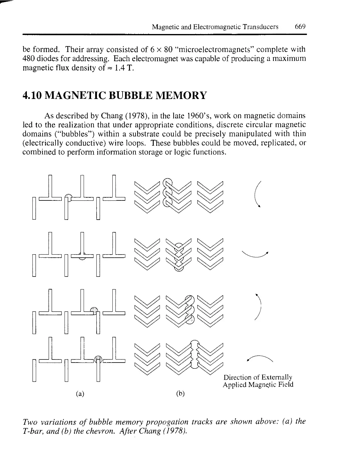
4.10 MAGNETIC BUBBLE MEMORY 669
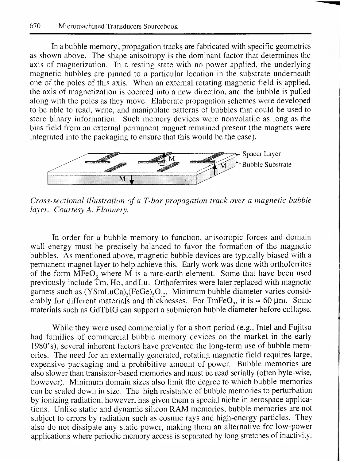
5. MICROMACHINED ELECTROMAGNETIC DEVICES 671
5.1 PASSIVE COMPONENTS AND CIRCUITS 671
5.2 OTHER RF APPLICATIONS OF MICROMACHINING 675
MAGNETIC AND ELECTROMAGNETIC TRANSDUCERS REFERENCES 676
XVÜ
Chapter 8: CHEMICAL AND BIOLOGICAL TRANSDUCERS 687
1. INTRODUCTION 687
2. CHEMICAL SENSORS 688
2.1 PASSIVE CHEMICAL SENSORS 689
2.1.1 CHEM1 RESISTORS 689
2.1.2 CHEMICAPACITORS 690
2.1.3 CHEMOMECHANICAL SENSORS 692
2.1.4 CALORIMETRIC SENSORS 693
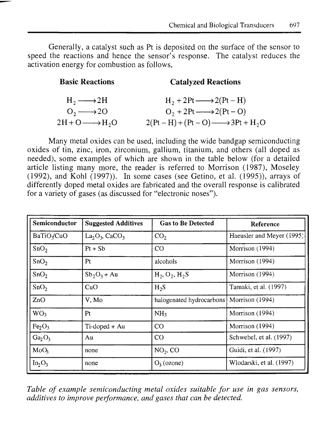
2.1.5 METAL-OXIDE GAS SENSORS 695
2.2 WORK-FUNCTION-BASED SENSORS 700
2.2.1 ADFET GAS SENSORS 701
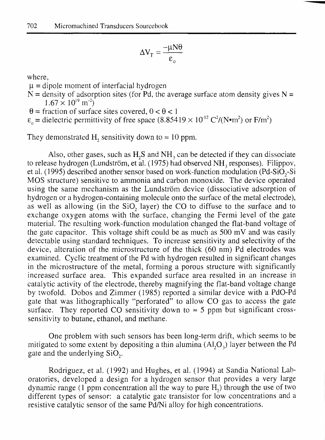
2.2.2 PLATINIDE-BASED HYDROGEN SENSORS 701
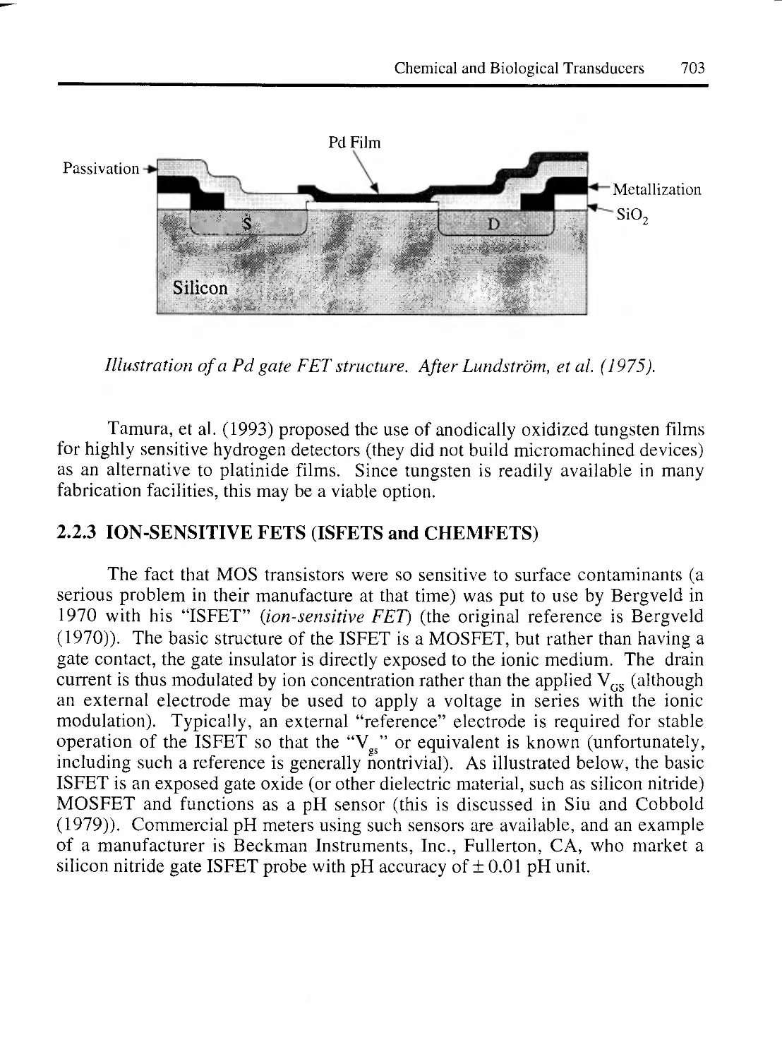
2.2.3 ION-SENSITIVE FETS (ISFETS and CHEMFETS) 703
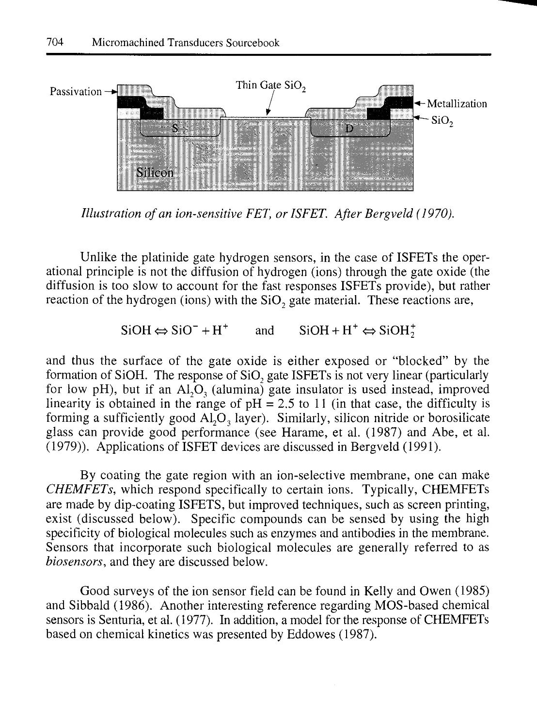
2.3 ELECTROCHEMICAL TRANSDUCERS 705
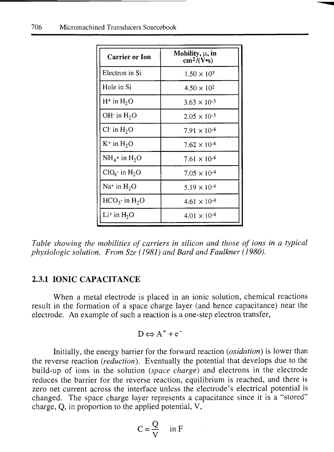
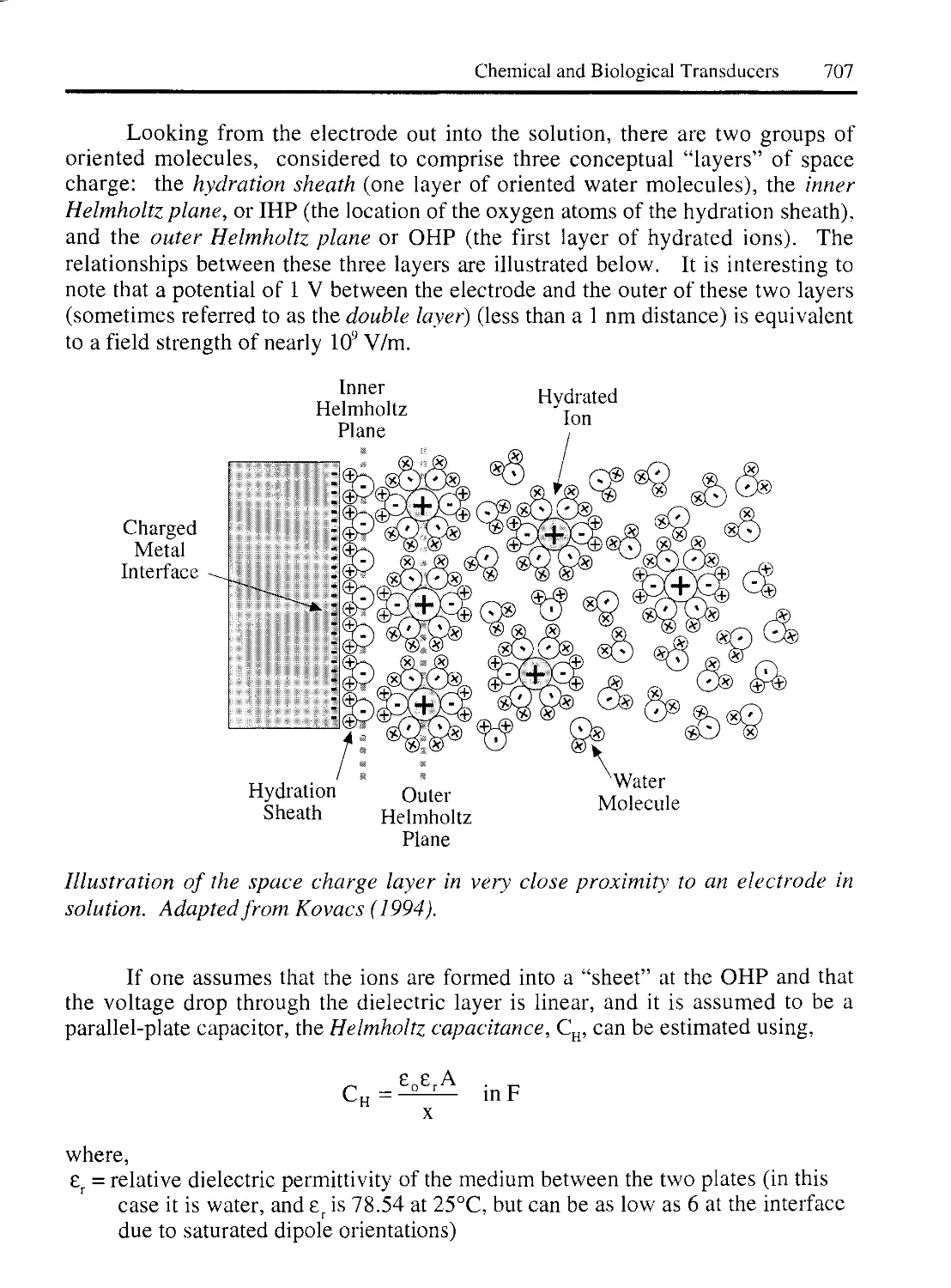
2.3.1 IONIC CAPACITANCE 706
2.3.2 CHARGE TRANSFER: RESISTIVE MECHANISMS 708
2.3.3 SPREADING RESISTANCE AND WARBURG IMPEDANCE 711
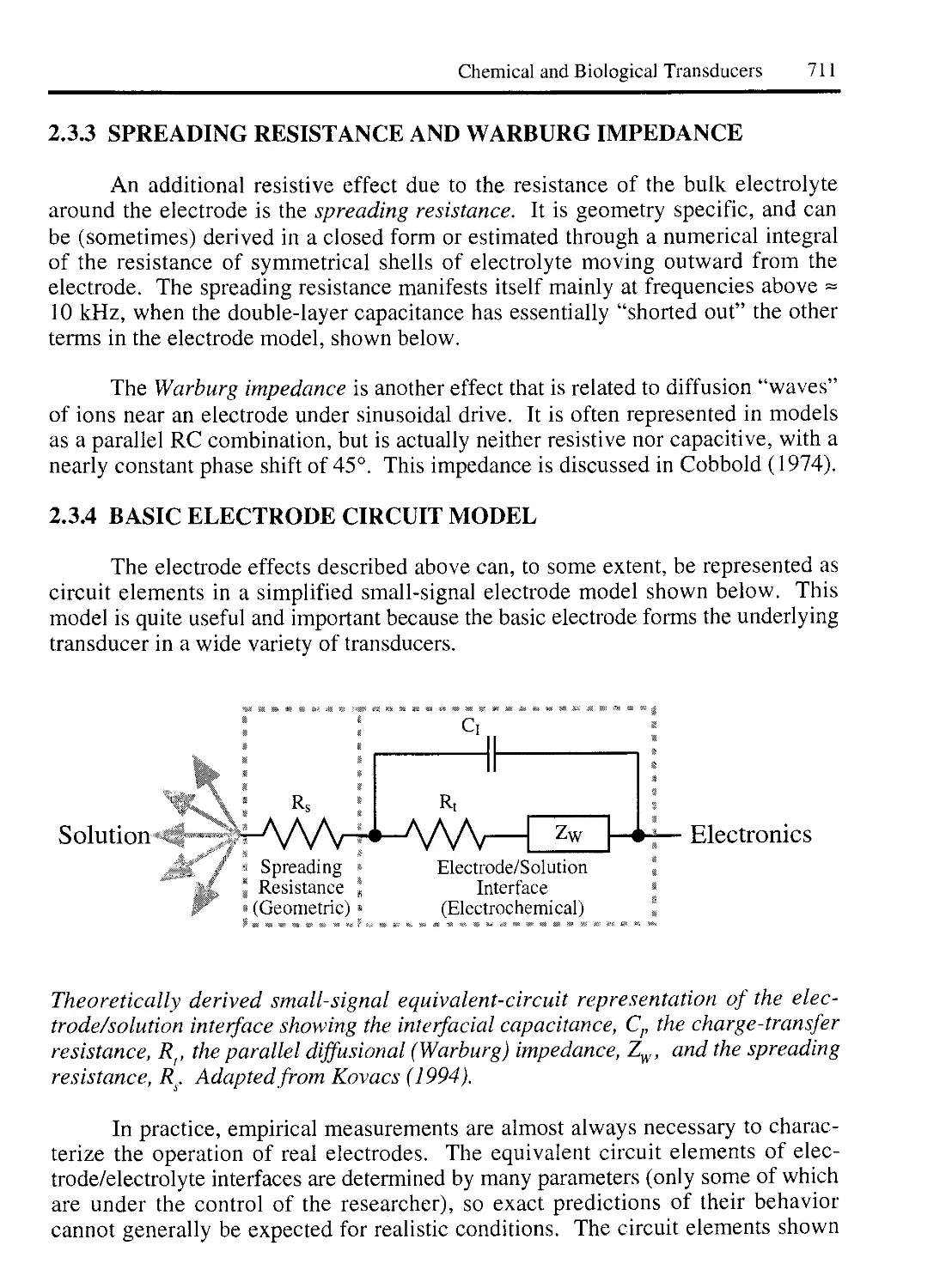
2.3.4 BASIC ELECTRODE CIRCUIT MODEL 711
2.3.5 ELECTROCHEMICAL SENSING USING MICROELECTRODES 712
POTENTIOMETRIC SENSING 713
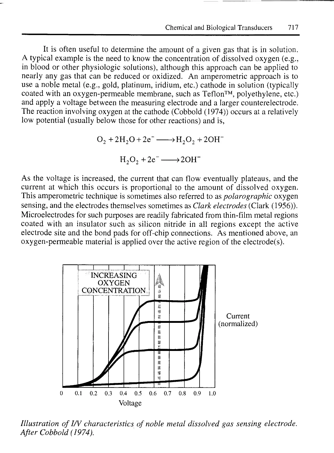
AMPEROMETRIC SENSING 715
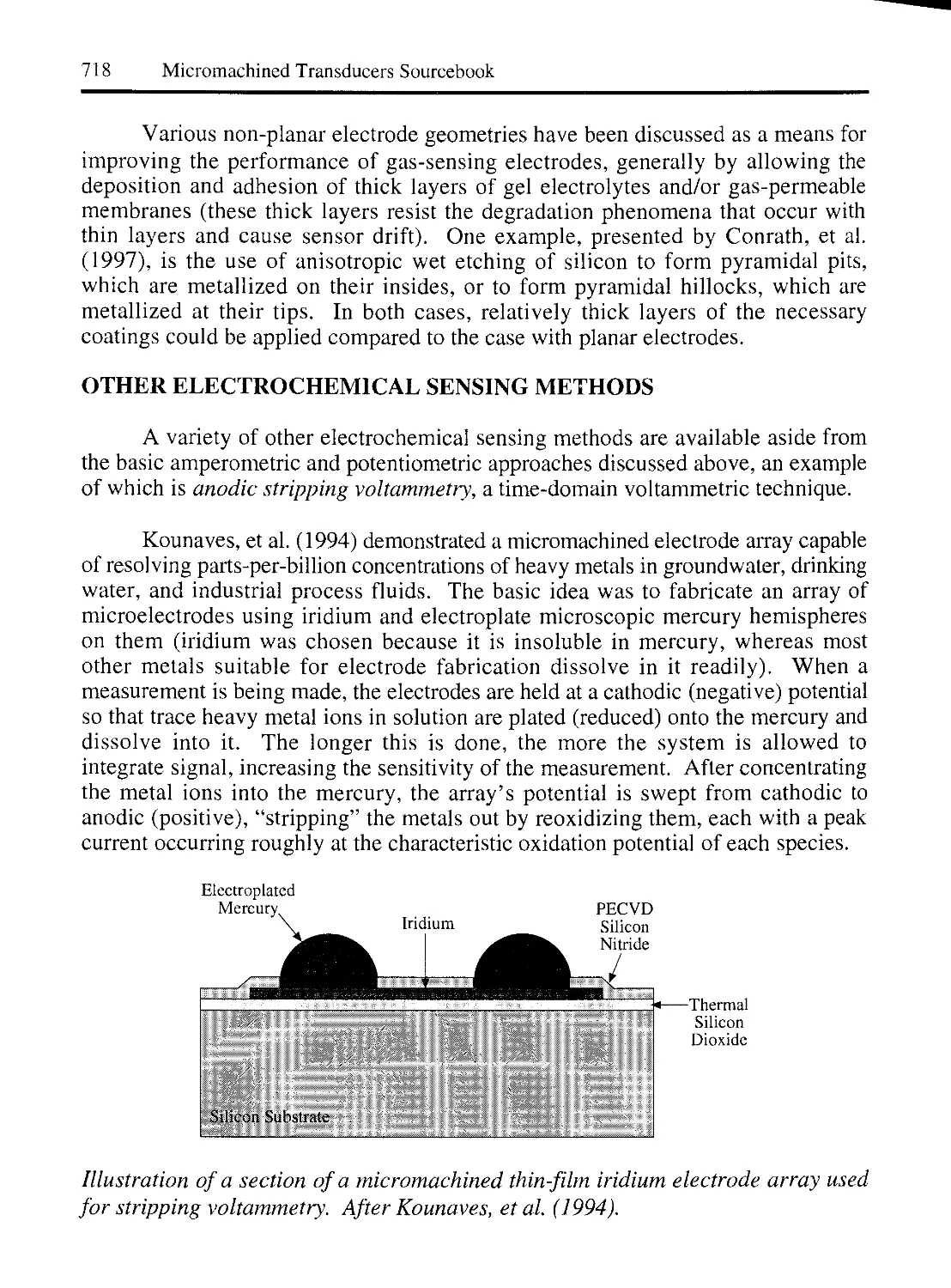
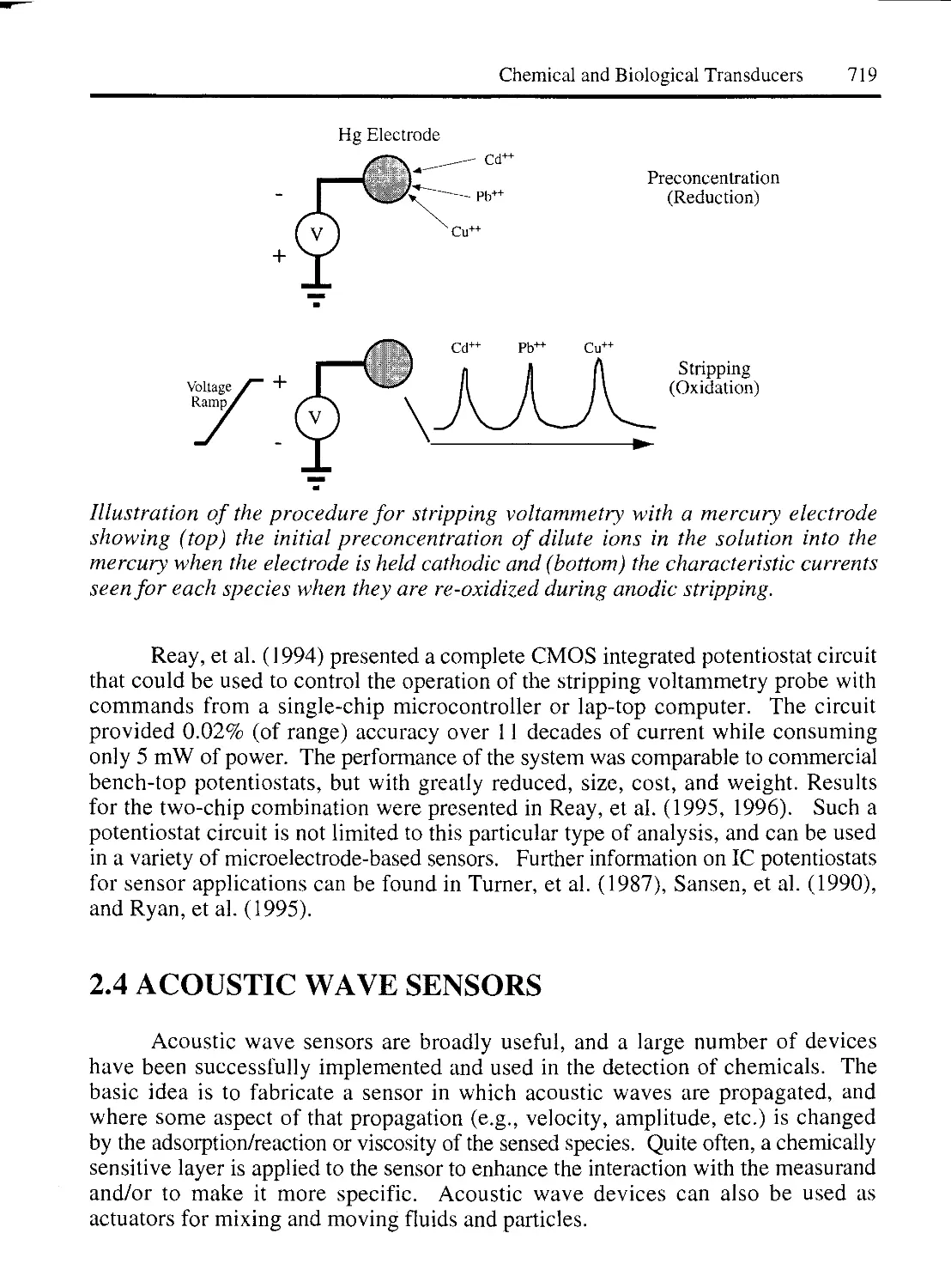
OTHER ELECTROCHEMICAL SENSING METHODS 718
2.4 ACOUSTIC WAVE SENSORS 719
2.5 BIOSENSORS 722
2.5.1 RESONANT BIOSENSORS 724
2.5.2 OPT1CAL-DETECTION BIOSENSORS 724
2.5.3 THERMAL-DETECTION BIOSENSORS 725
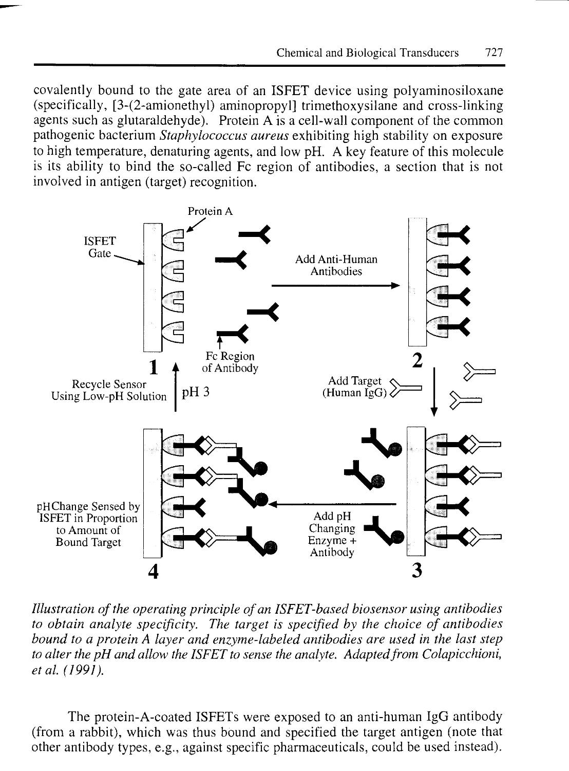
2.5.4 ISFET BIOSENSORS (CHEMFETs) 726
2.5.5 OTHER pH-BASED BIOSENSORS 728
2.5.6 ELECTROCHEMICAL-DETECTION BIOSENSORS 729
2.5.7 CMOS-COMPATIBLE BIOSENSOR PROCESS 730
2.5.8 OTHER BIOSENSOR TECHNOLOGIES 732
2.6 BIOMOLECULAR GAIN MECHANISMS 732
2.7 SELECTIVITY IMPROVEMENT USING ARRAYS 734
2.8 COMBINATORIAL ARRAYS 735
2.9 BIOLOGICAL CHEMICAL SENSORS 737
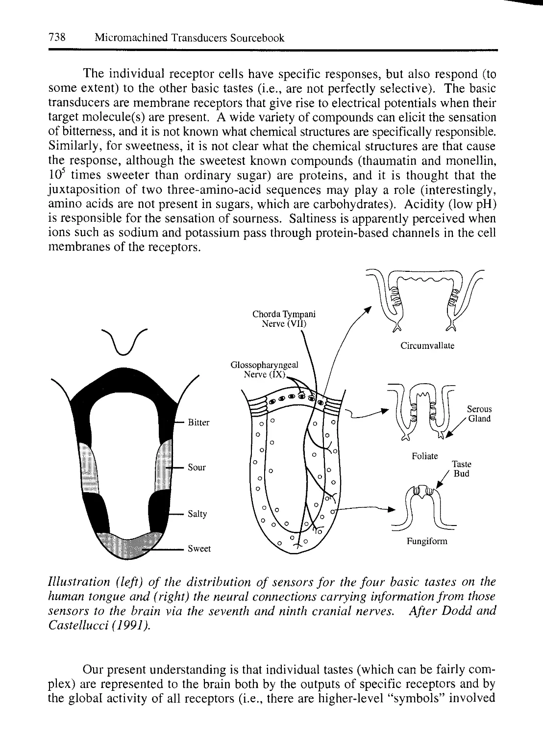
2.9.1 BIOLOGICAL "TASTE” SENSORS 737
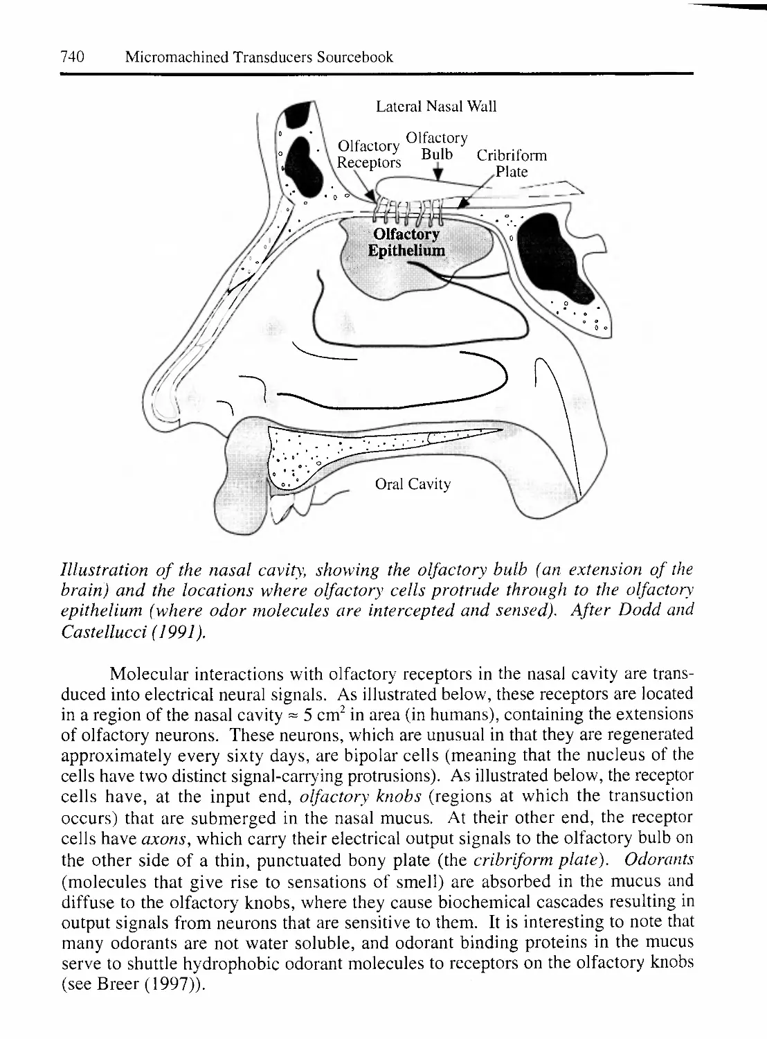
2.9.2 BIOLOGICAL ODOR SENSORS 739
3. CHEMICAL ACTUATORS 741
3.1 ELECTROCHEMICAL MECHANICAL ACTUATORS 742
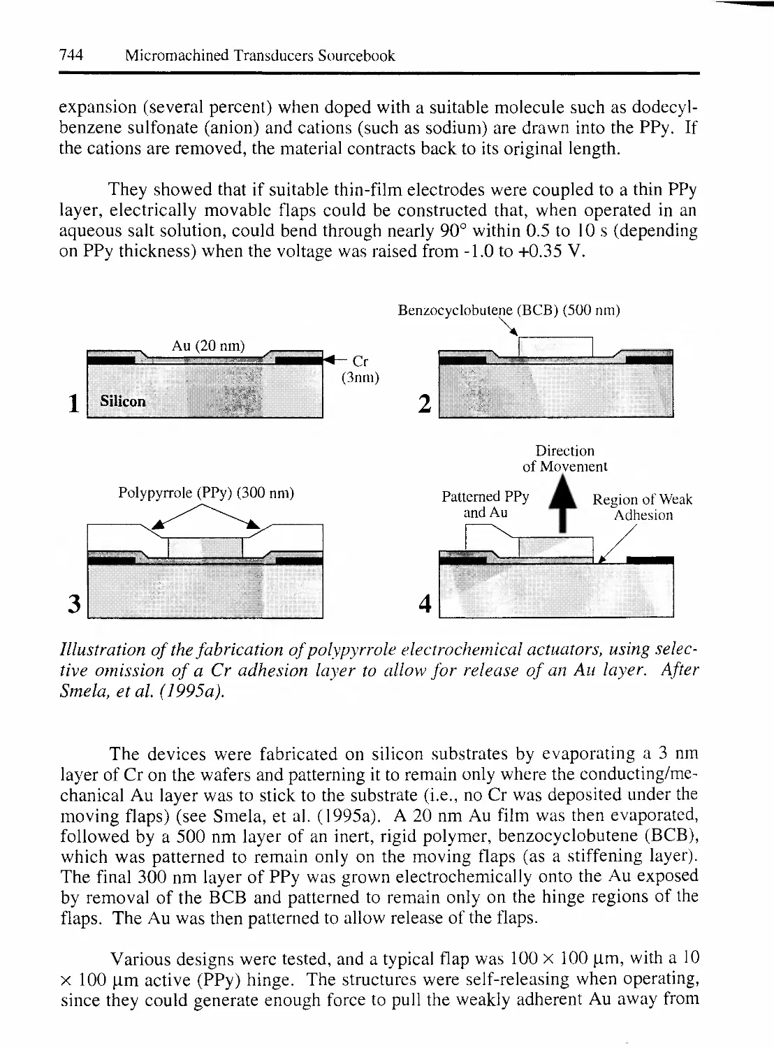
3.2 POLYMER MECHANICAL ACTUATORS 743
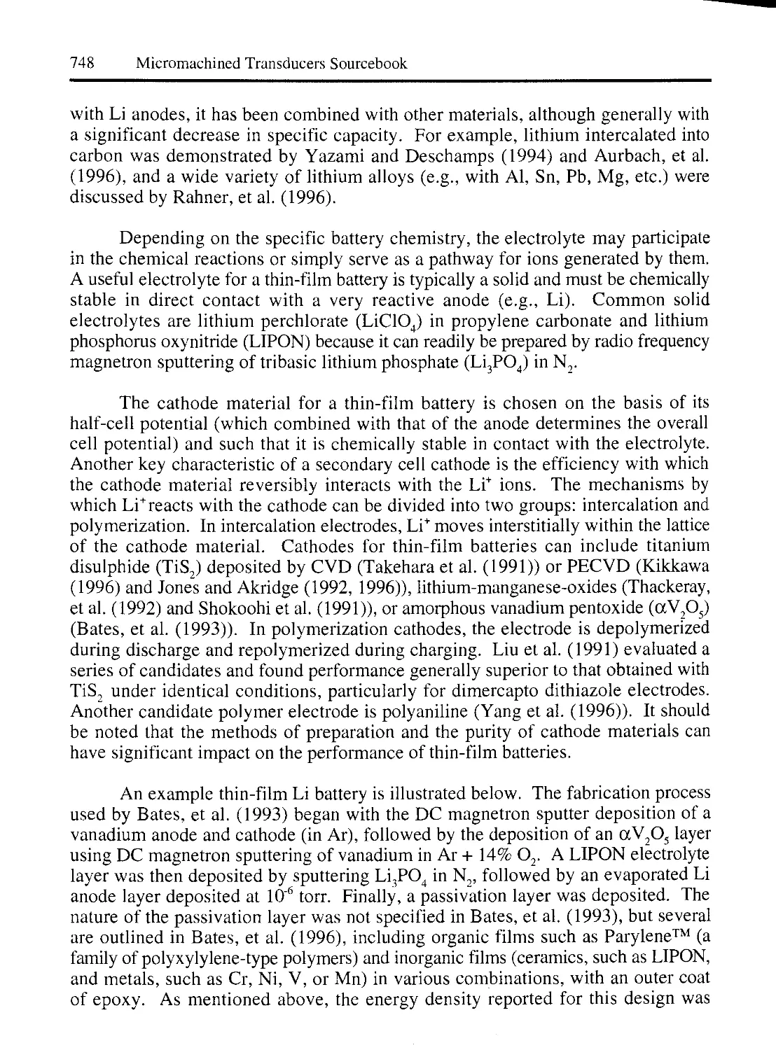
3.3 THIN-FILM BATTERIES 745
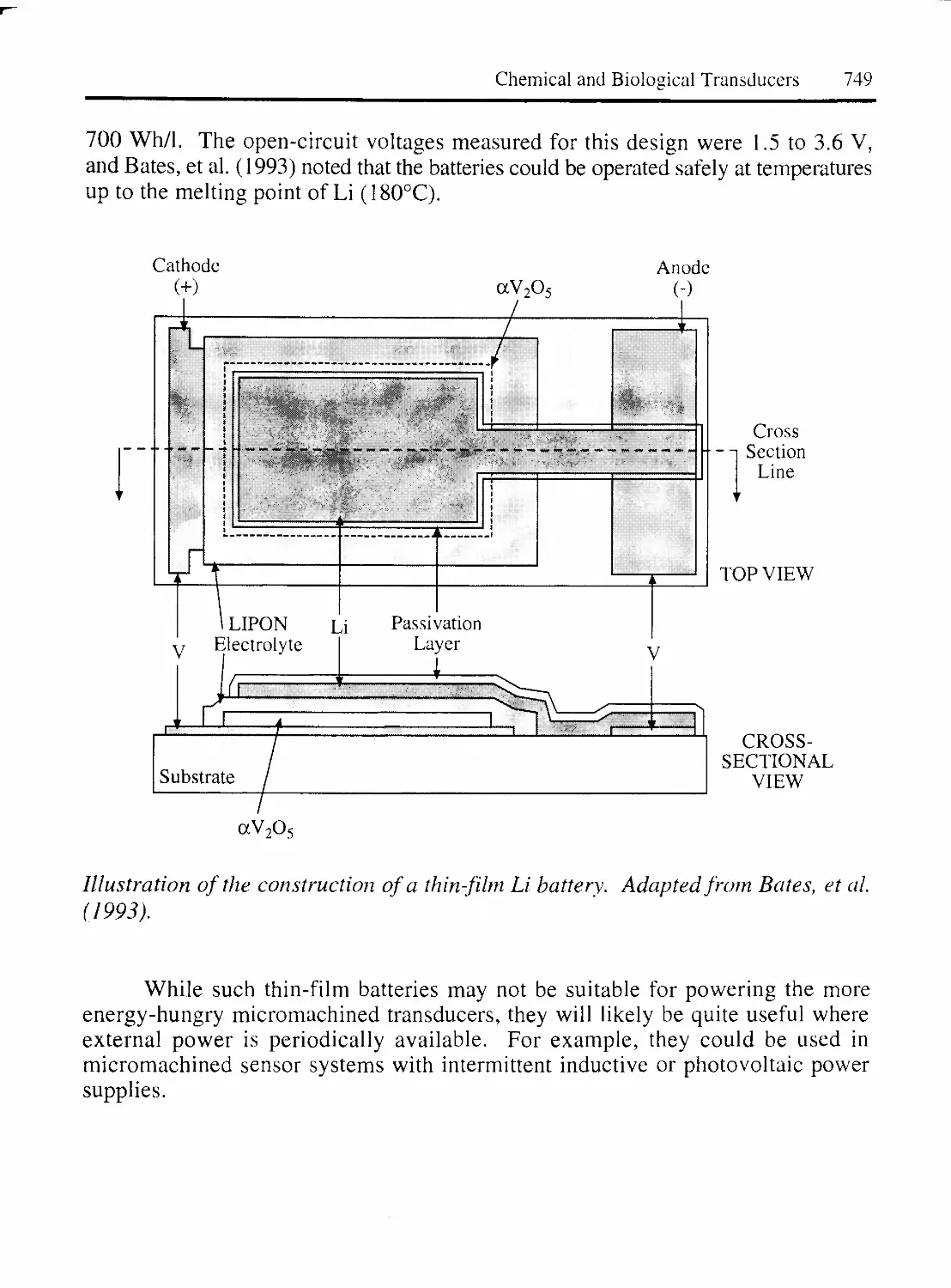
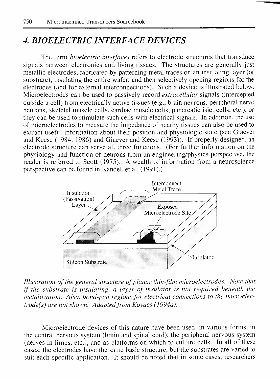
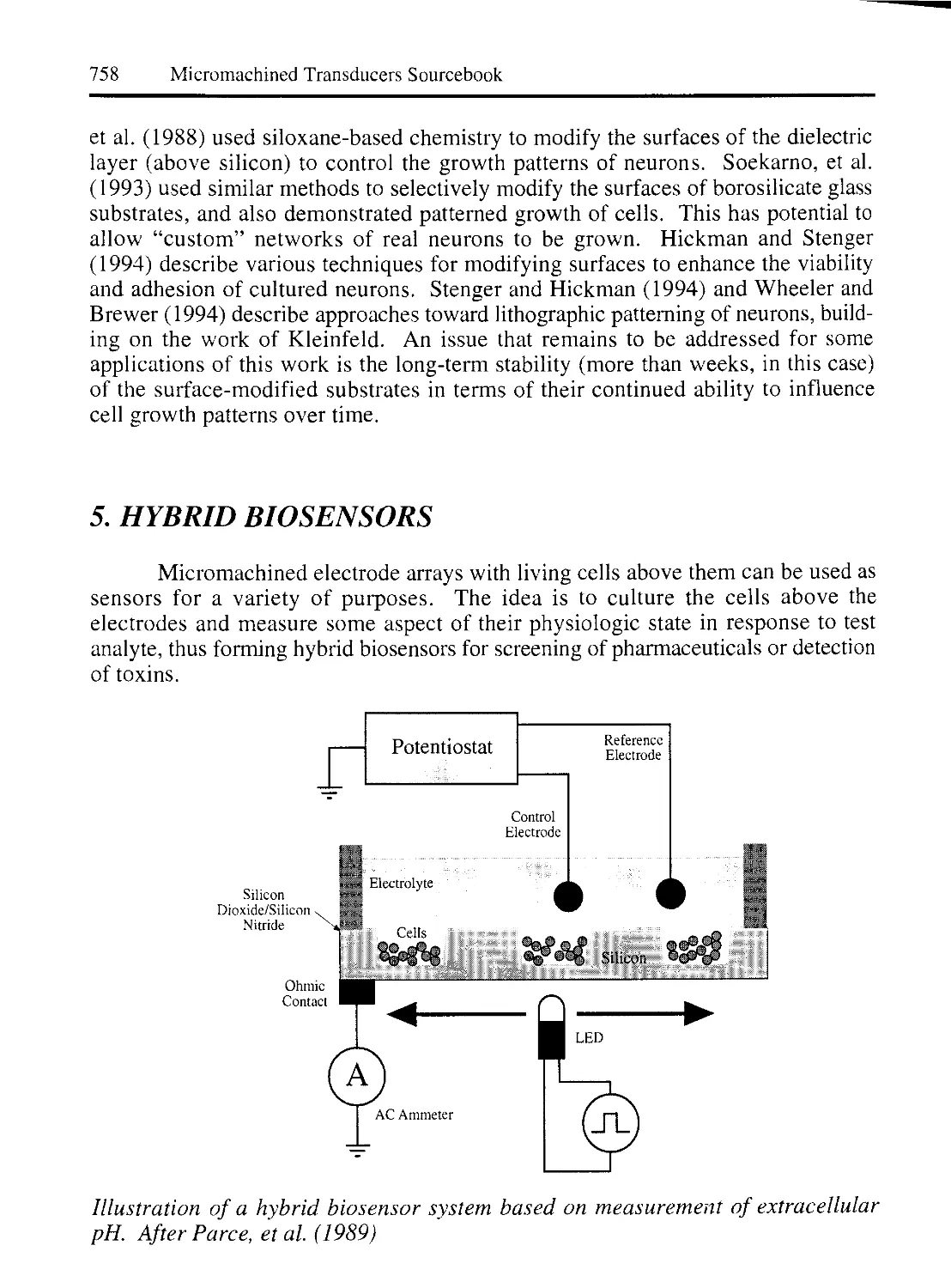
4. BIOELECTRIC INTERFACE DEVICES 750
4.1 PENETRATING NEURAL PROBES 751
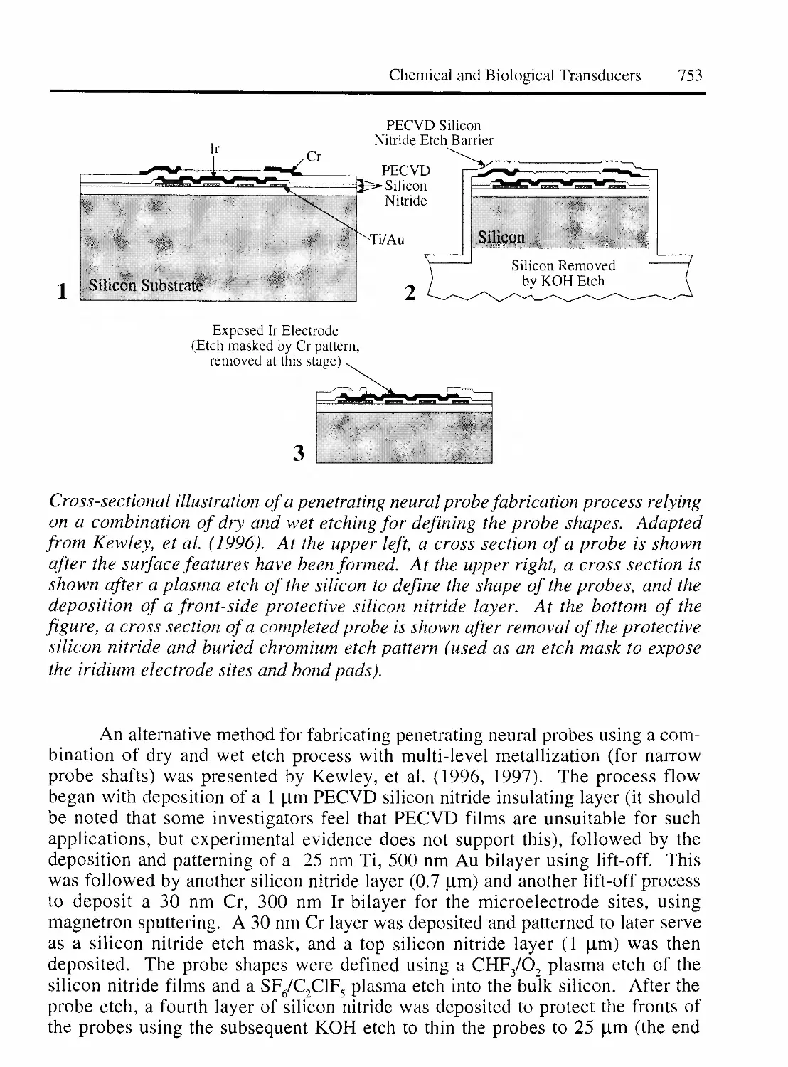
4.2 REGENERATION NEURAL ELECTRODES 754
4.3 CULTURED CELL SYSTEMS 757
4.3.1 SURFACE MODIFICATION FOR CULTURE SYSTEMS 757
xviii
5. HYBRID BIOSENSORS 758
CHEMICAL AND BIOLOGICAL TRANSDUCERS REFERENCES 761
Chapter 9: MICROFLUIDIC DEVICES 779
1. INTRODUCTION 779
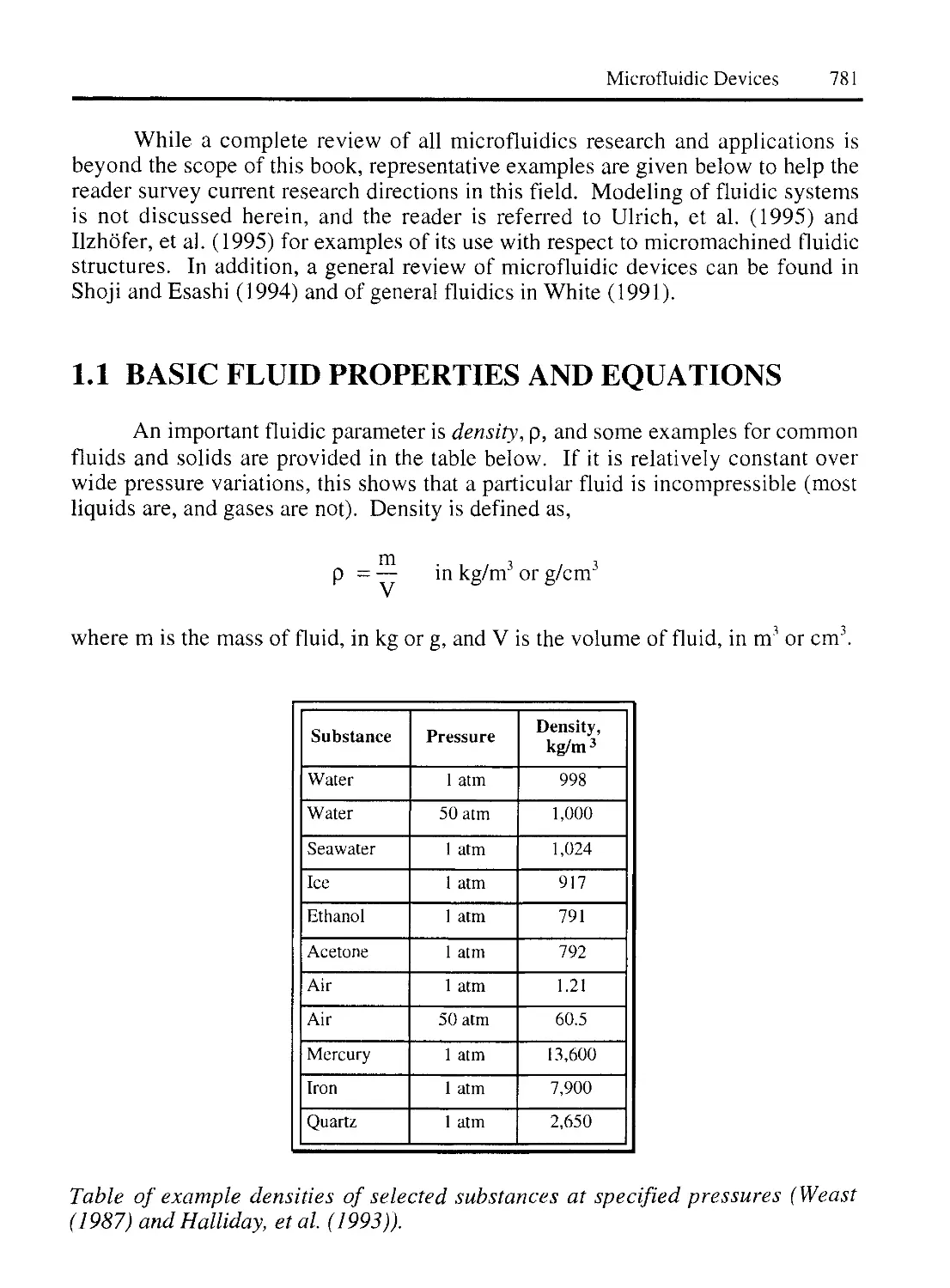
1.1 BASIC FLUID PROPERTIES AND EQUATIONS 781
1.2 TYPES OF FLOW 787
1.3 BUBBLES AND PARTICLES IN MICROSTRUCTURES 789
1.4 CAPILLARY FORCES 791
1.5 FLUIDIC RESISTANCE 792
1.6 FLUIDIC CAPACITANCE 793
1.7 FLUIDIC INDUCTANCE 794
2. FLOW CHANNELS 795
2.1 BULK MICROMACHINED CHANNELS 796
2.2 SURFACE MICROMACHINED CHANNELS 801
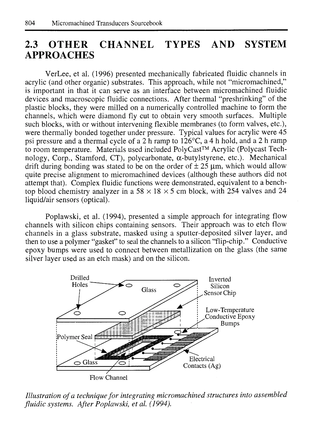
2.3 OTHER CHANNEL TYPES AND SYSTEM APPROACHES 804
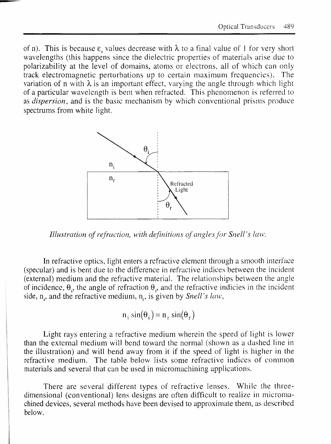
3. FLUIDIC CHANNEL APPLICATIONS 805
3.1 MIXERS 805
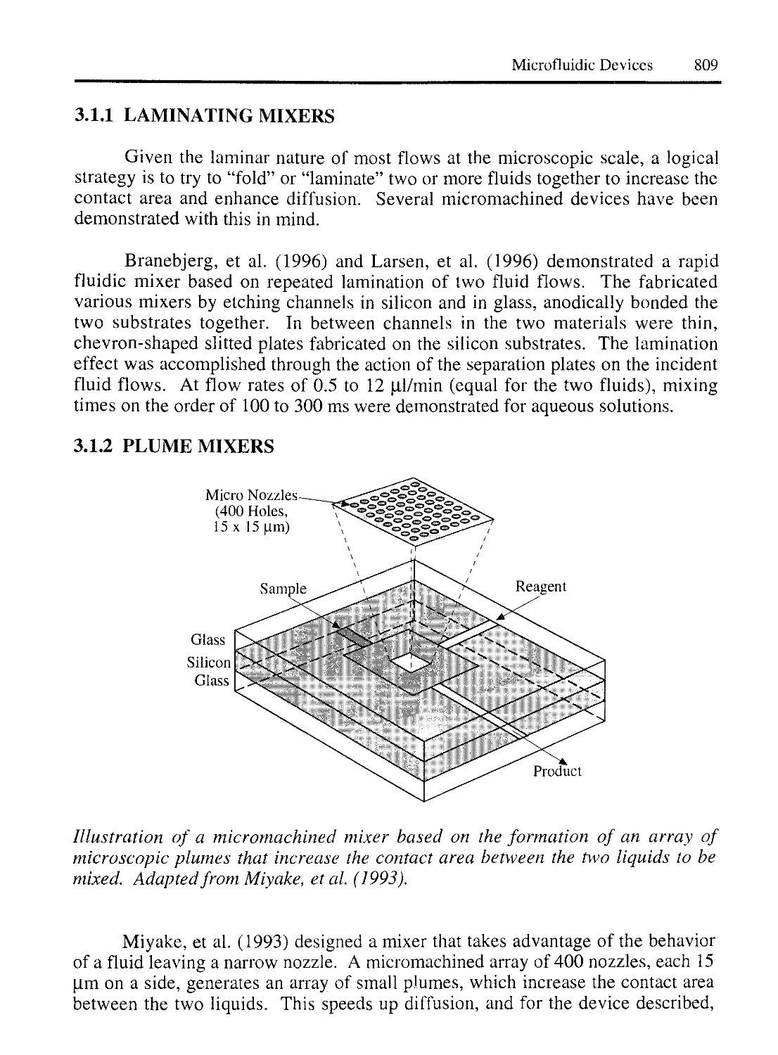
3.1.1 LAMINATING MIXERS 809
3.1.2 PLUME MIXERS 809
3.1.3 ACTIVE MIXERS 810
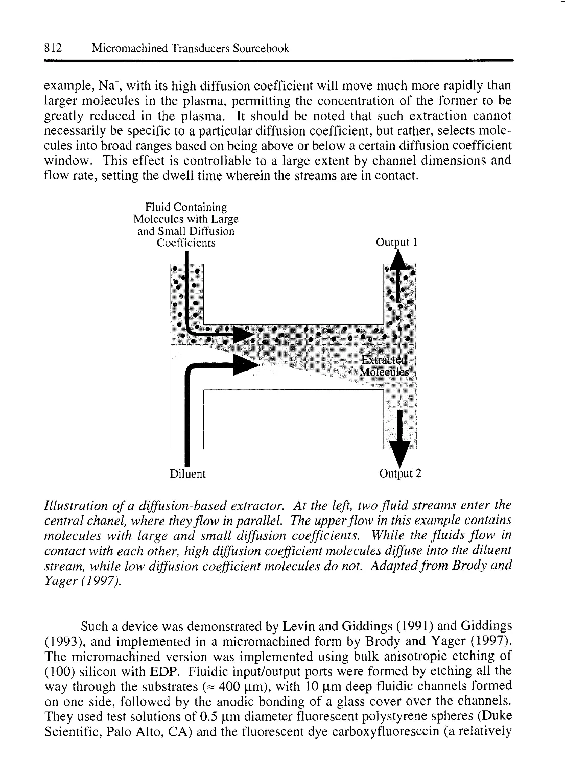
3.2 DIFFUSION-BASED EXTRACTORS 811
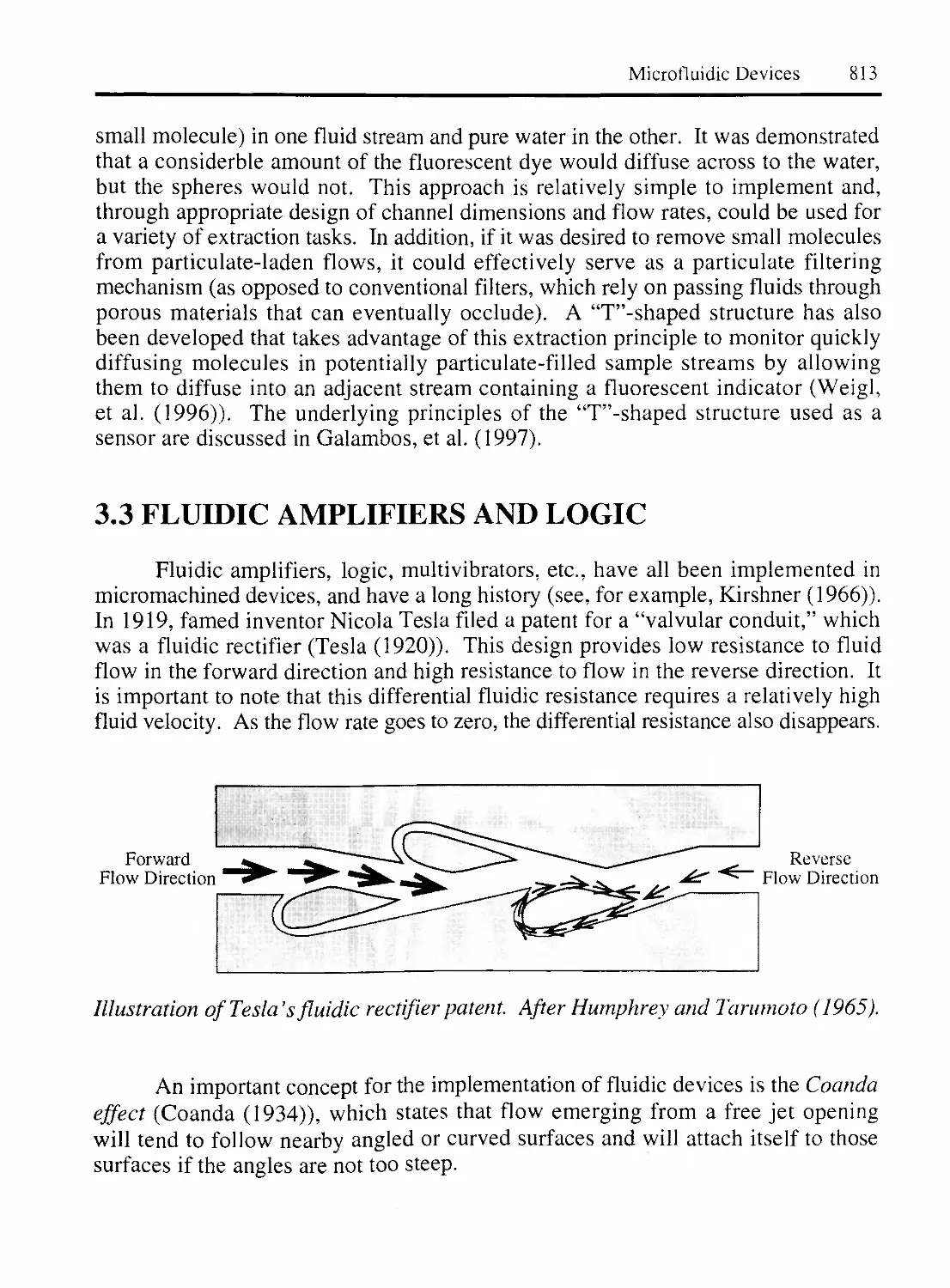
3.3 FLUIDIC AMPLIFIERS AND LOGIC 813
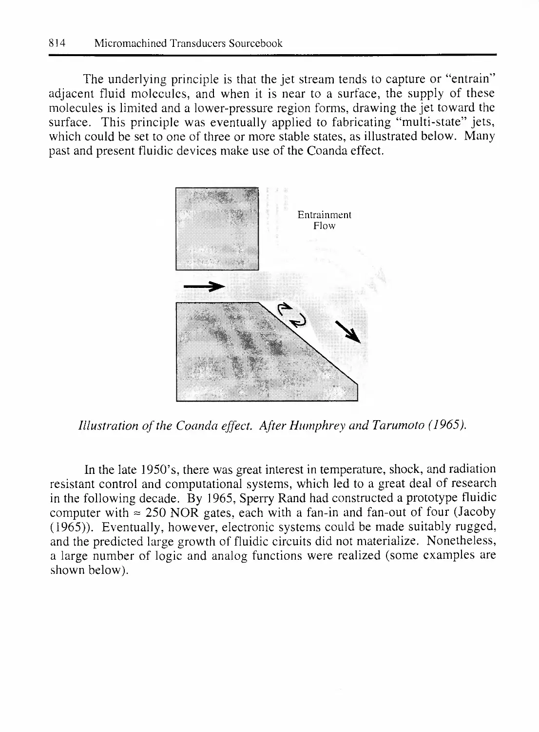
4. FLUIDIC SENSORS 819
4.1 FLOW SENSORS 819
4.2 VISCOSITY/DENSITY SENSORS 821
4.3 OTHER FLUIDIC SENSORS 823
5. VALVES 823
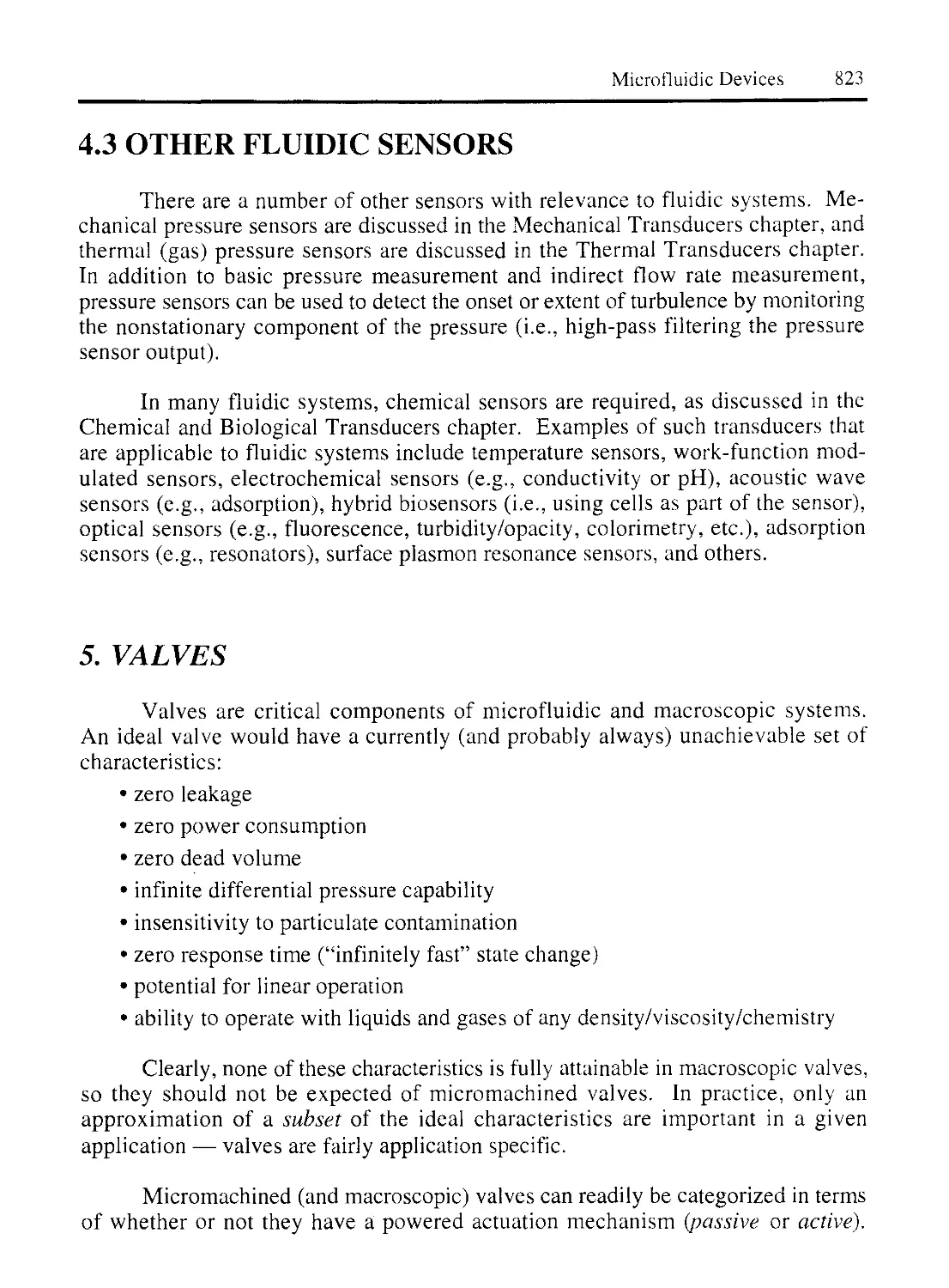
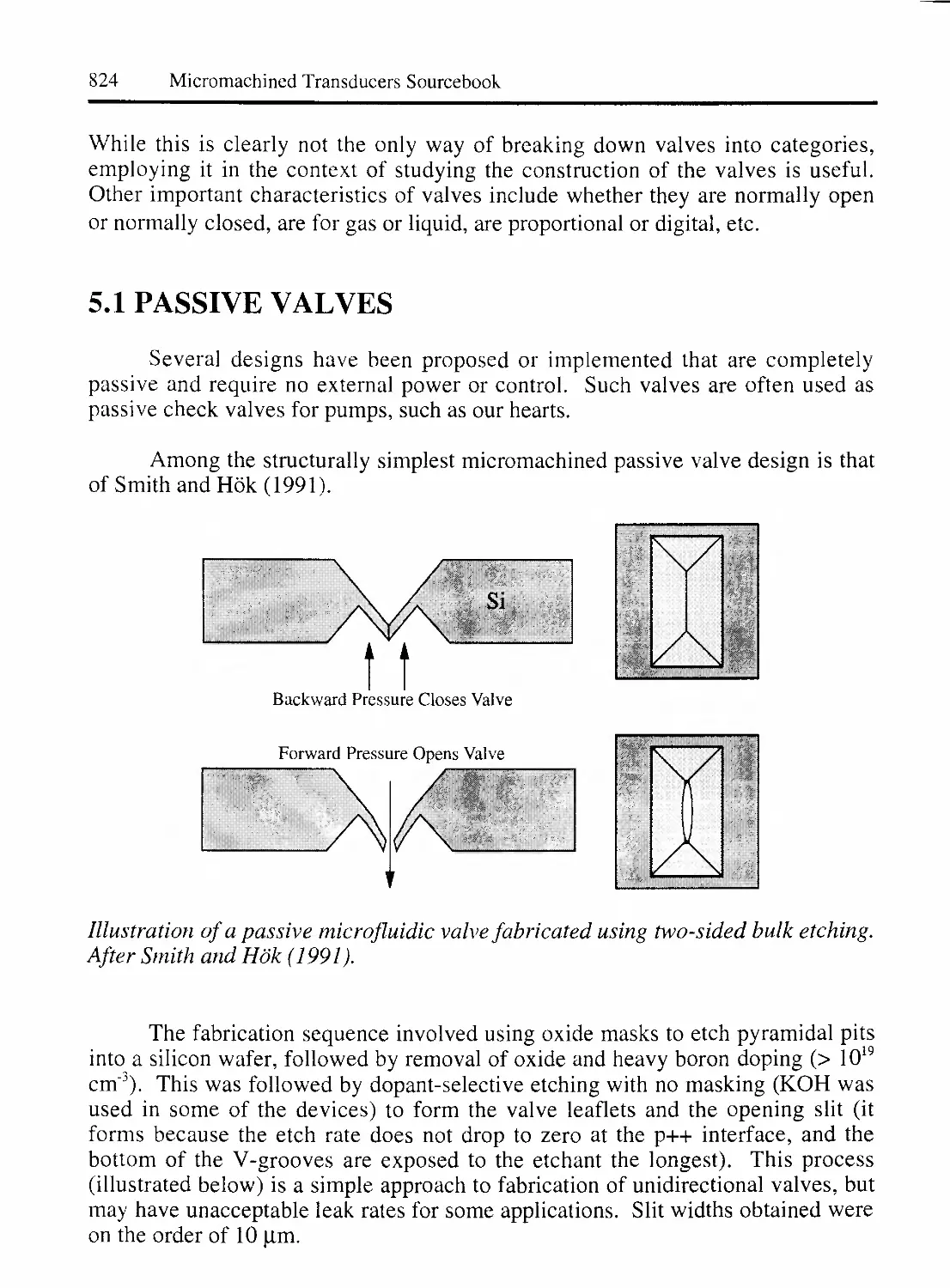
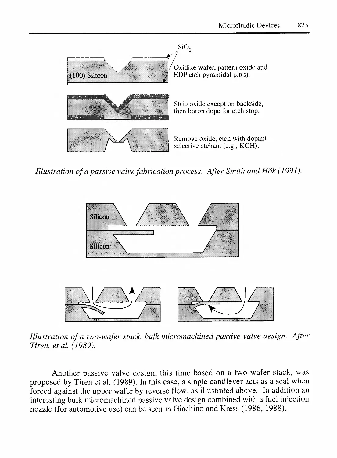
5.1 PASSIVE VALVES 824
5.2 ACTIVE VALVES 826
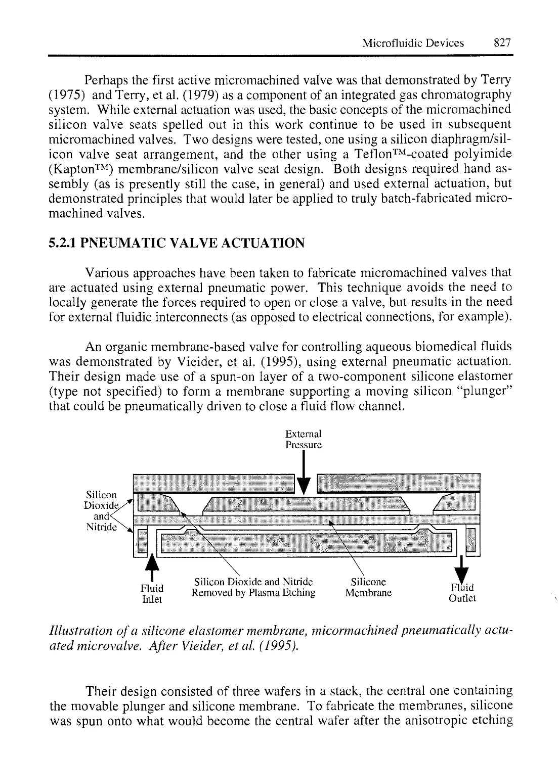
5.2.1 PNEUMATIC VALVE ACTUATION 827
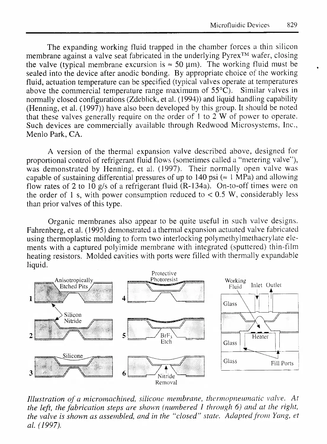
5.2.2 THERMOPNEUMATIC VALVE ACTUATION 828
5.2.3 PHASE-CHANGE VALVE ACTUATION 830
5.2.4 SOLID-EXPANSION THERMAL VALVE ACTUATION 831
5.2.5 PIEZOELECTRIC VALVE ACTUATION 833
5.2.6 ELECTROSTATIC VALVE ACTUATION 835
5.2.7 ELECTROMAGNETIC VALVE ACTUATION 836
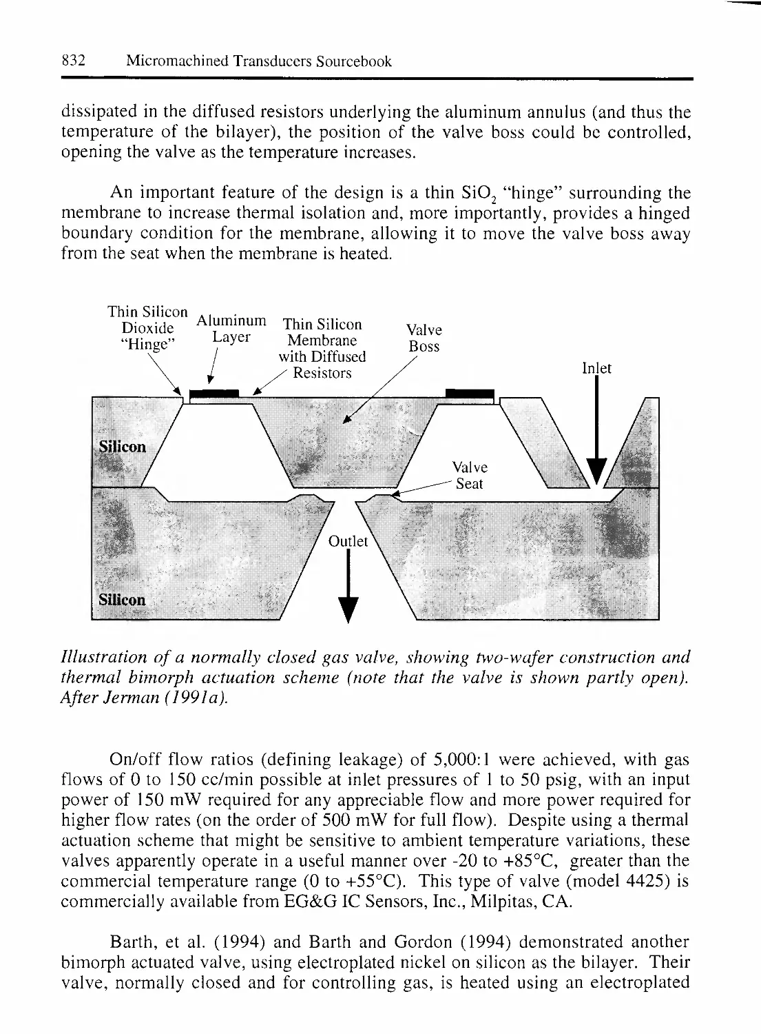
5.2.8 BISTABLE VALVE STRUCTURES 837
6. PUMPS 839
6.1 BUBBLE PUMPS 839
6.2 MEMBRANE PUMPS 839
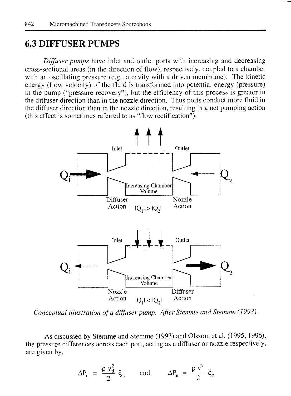
6.3 DIFFUSER PUMPS 842
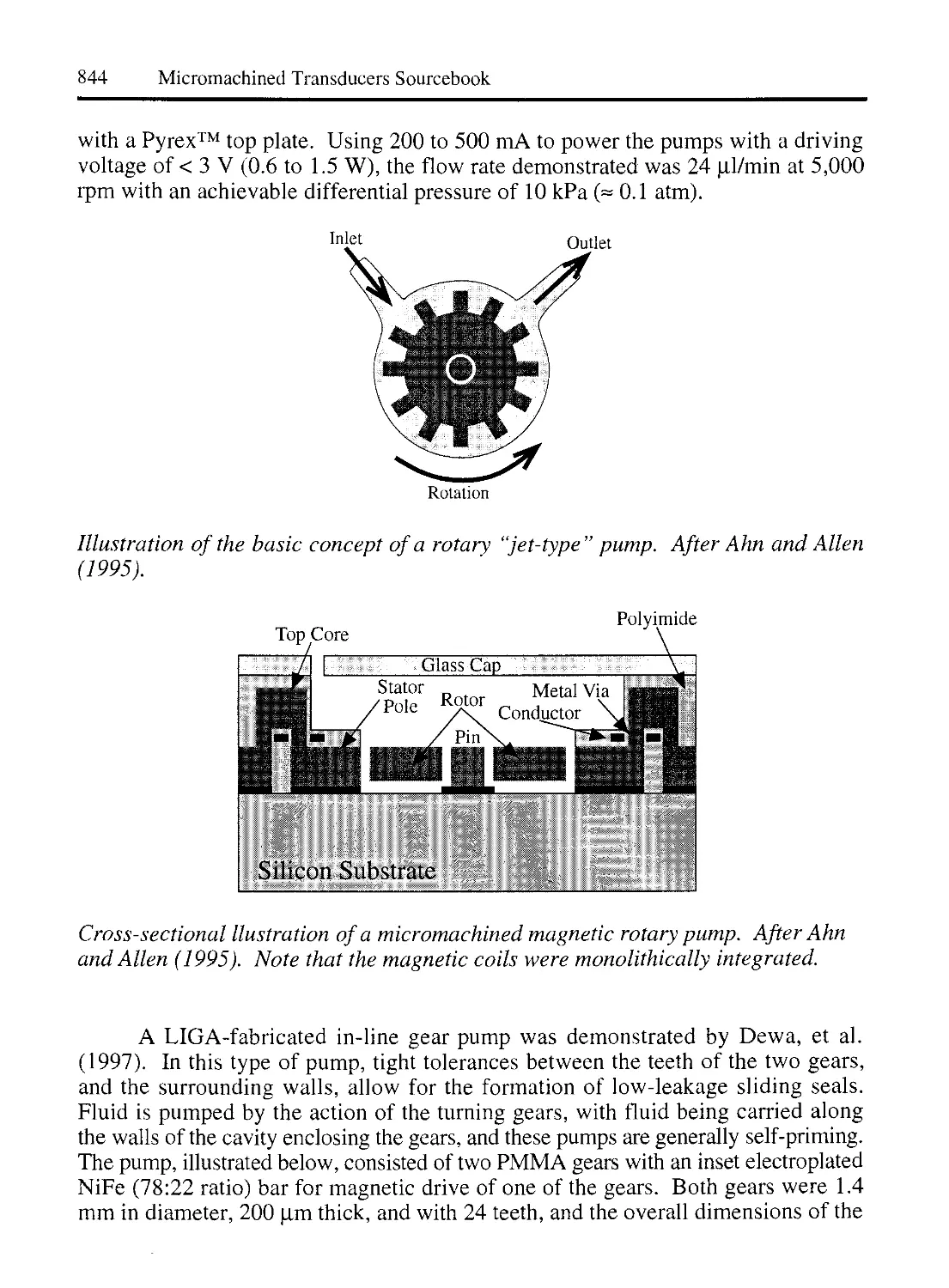
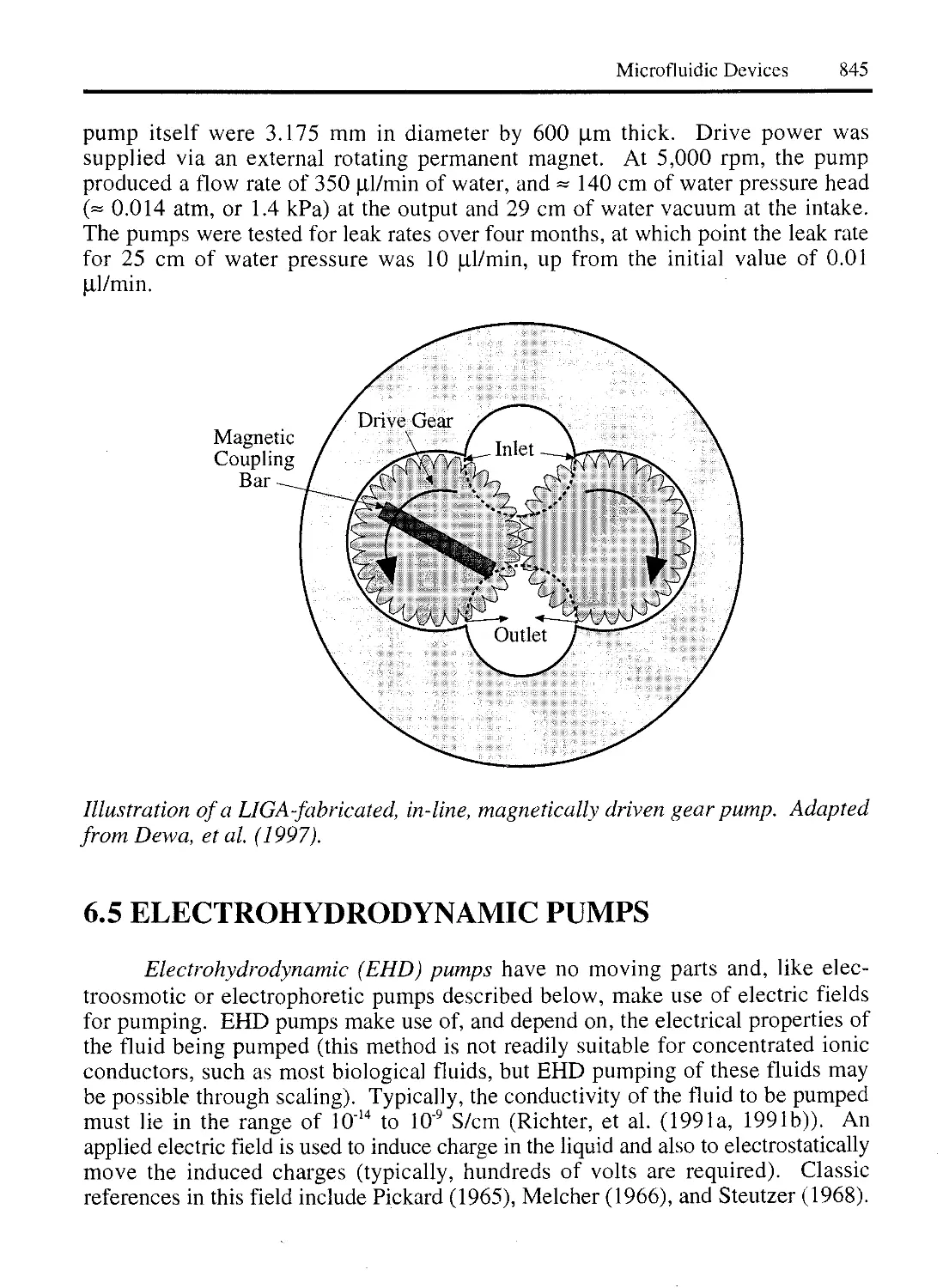
xix
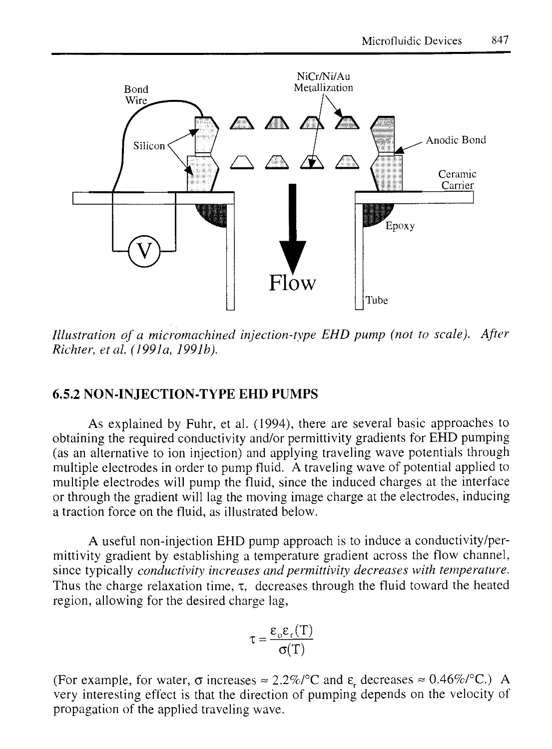
6.4 ROTARY PUMPS 843
6.5 ELECTROHYDRODYNAMIC PUMPS 845
6.5.1 INJECTION-TYPE EHD PUMPS 846
6.5.2 NON-INJECTION-TYPE EHD PUMPS 847
6.6 ELECTROOSMOTIC/ELECTROPHORETIC PUMPS 849
6.7 ULTRASONIC PUMPS 852
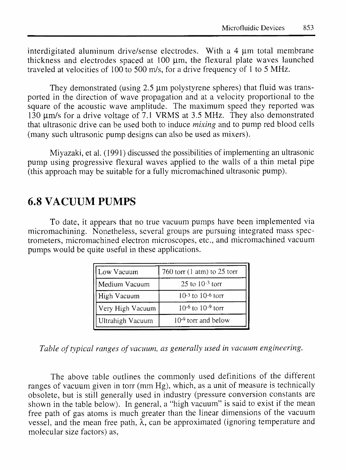
6.8 VACUUM PUMPS 853
7. DROPLET GENERATORS 855
8. OTHER DEVICES 859
8.1 CONTROL OF MACROSCOPIC FLOWS WITH MICRODEVICES 859
8.2 PARTICLE FILTERS AND TRAPS 861
9. MICROFLUIDIC SYSTEM ISSUES 862
9.1 INTERCONNECTS 863
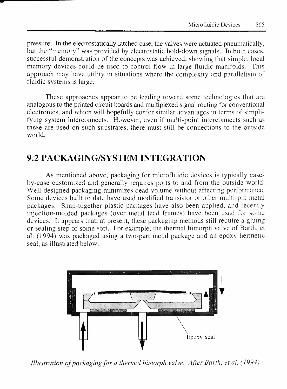
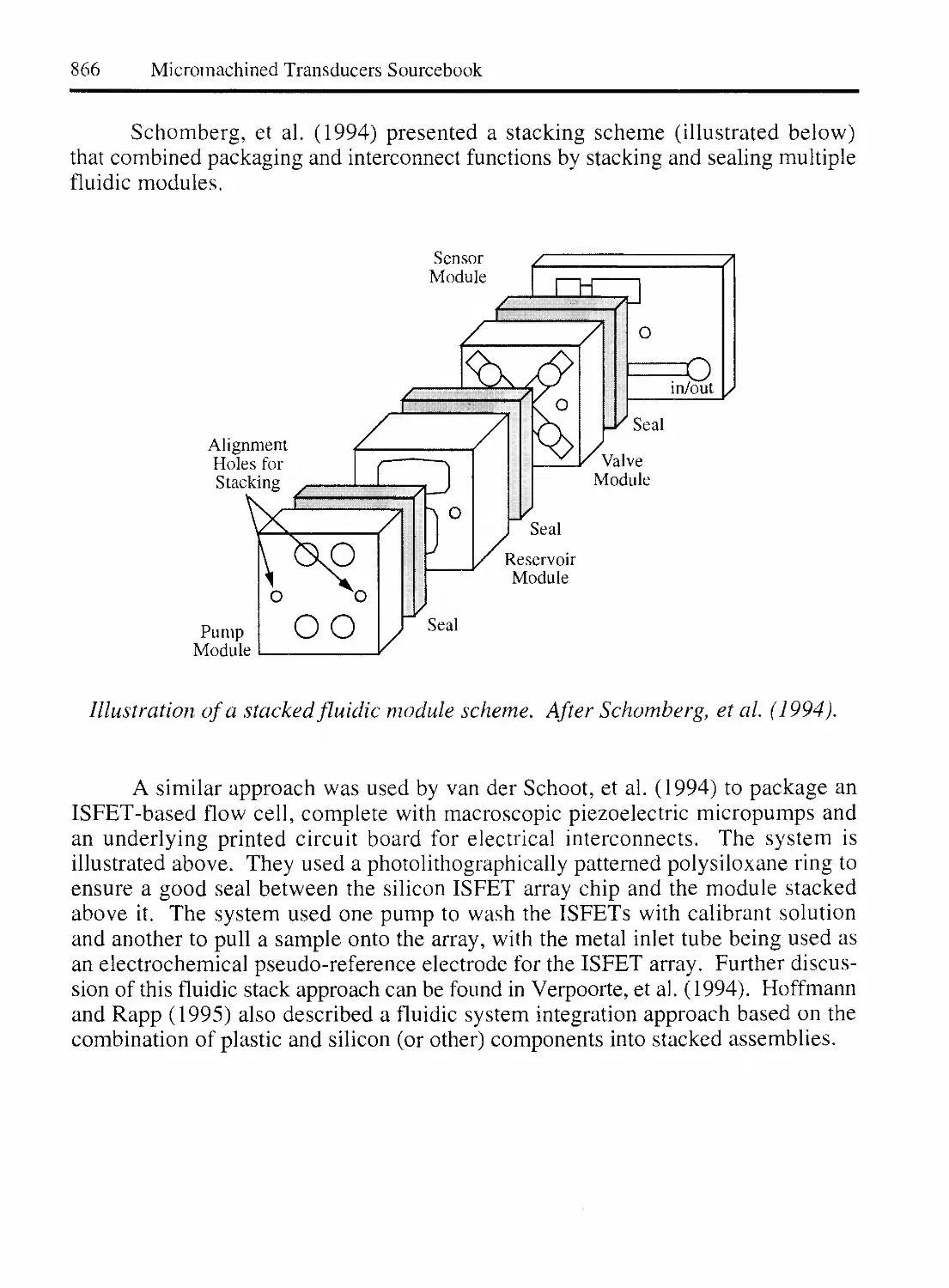
9.2 PACKAGING/SYSTEM INTEGRATION 865
9.3 DESIGN FOR DISPOSAL OR REUSE 867
10. INTEGRATED CHEMICAL ANALYSIS SYSTEMS 868
10.1 SCALING ISSUES FOR CHEMICAL ANALYSIS 868
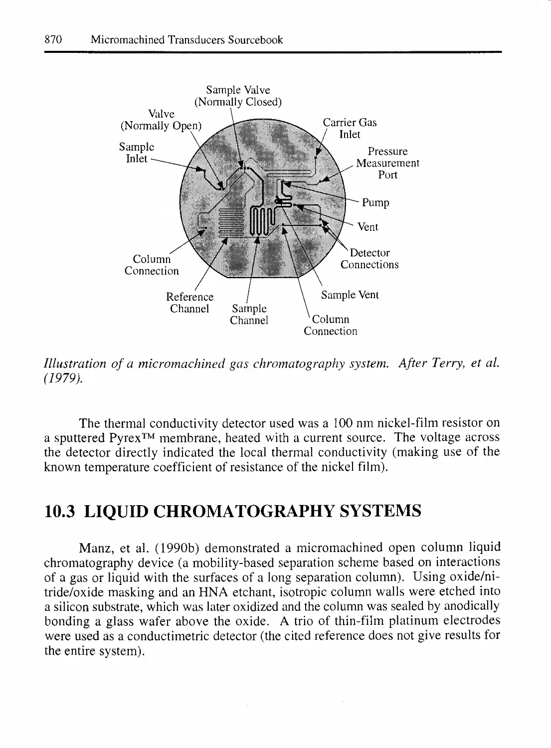
10.2 GAS CHROMATOGRAPHY SYSTEMS 869
10.3 LIQUID CHROMATOGRAPHY SYSTEMS 870
10.4 ELECTROPHORESIS SYSTEMS 871
10.5 CELL FUSION DEVICES 875
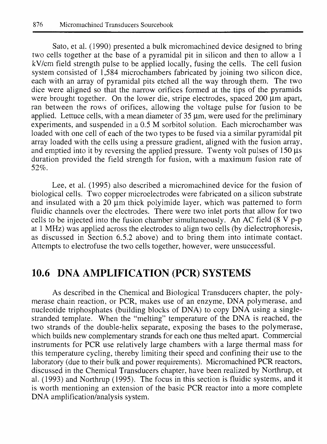
10.6 DNA AMPLIFICATION (PCR) SYSTEMS 876
10.7 MULTIFUNCTIONAL FLUIDIC SYSTEMS 878
11. BIOLOGICAL FLUIDIC SYSTEMS 879
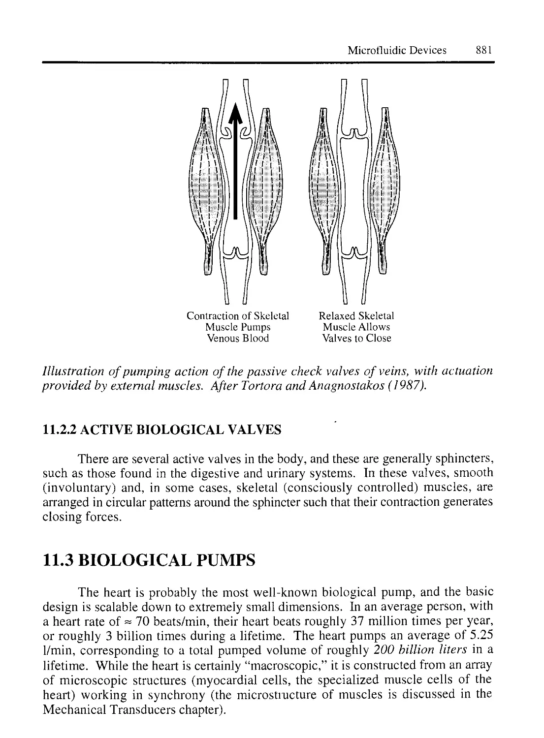
11.1 BIOLOGICAL FLOW CHANNELS 879
11.2 BIOLOGICAL VALVES 880
11.2.1 PASSIVE BIOLOGICAL VALVES 880
11.2.2 ACTIVE BIOLOGICAL VALVES 881
11.3 BIOLOGICAL PUMPS 881
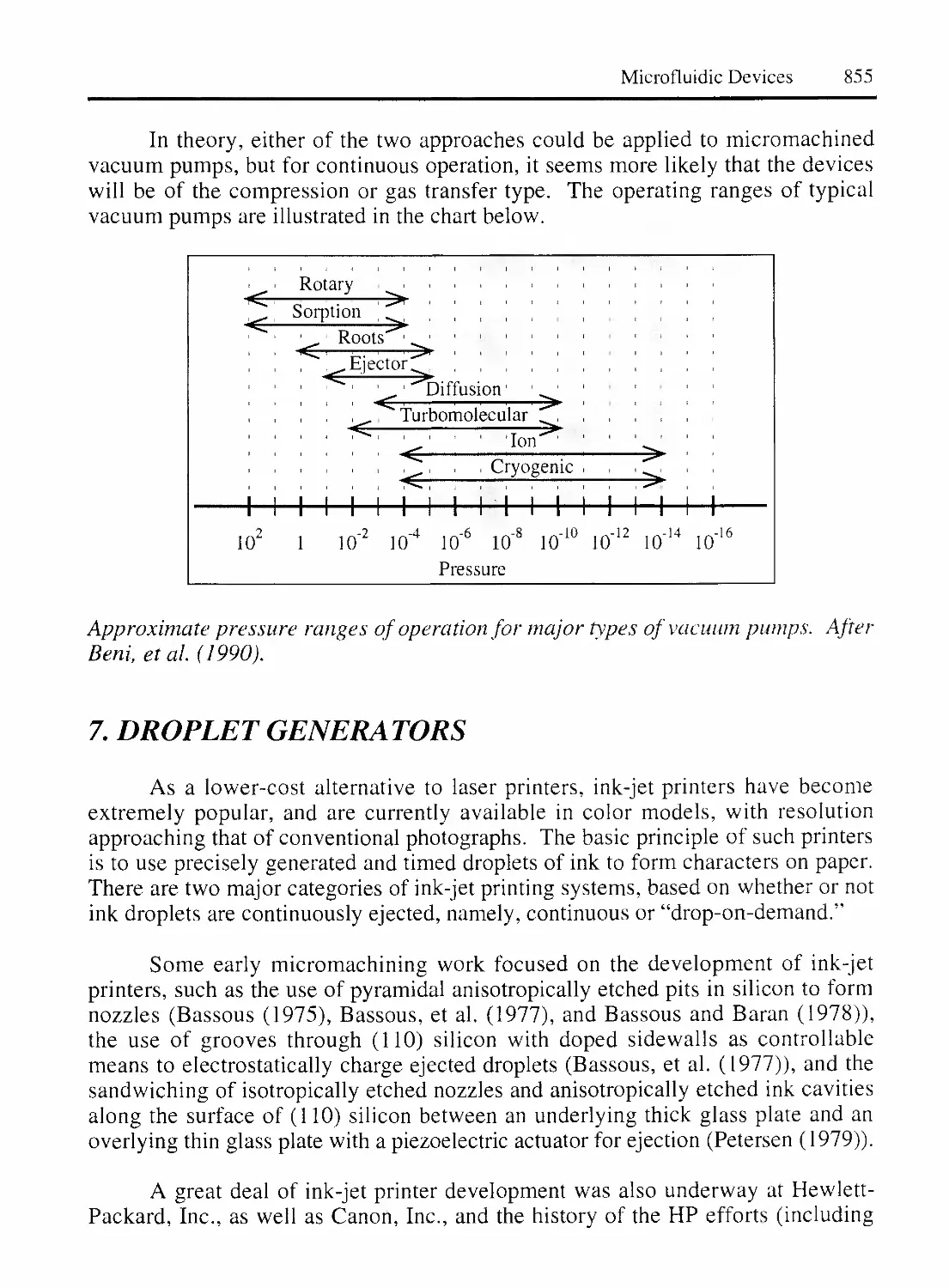
MICROFLUIDIC DEVICES REFERENCES 883
xx
Chapter 1:
INTRODUCTION
AND OVERVIEW
Micromachined
Transducers
Sourcebook
1. INTRODUCTION TO MICROMACHINED DEVICES
The use of lithographic and other microfabrication technologies to create
miniaturized sensors, actuators, and structures has become increasingly popular in
many areas of science and engineering. In order to fabricate such devices, the
addition, subtraction, modification, and patterning of materials are typically done
using techniques originally developed for the integrated circuit industry. In the late
1960’s, researchers began to appreciate the fact that silicon and other semiconductors
could be used to fabricate not only discrete and integrated electronic circuits, but
also transducers and other devices with new properties due to the materials used
and their miniature size. The term micromachining broadly refers to the use of
lithographic and other precision techniques to carry out such fabrication. (The
resulting devices are sometimes referred to as “MEMS,” for microelectromechanical
systems, although the term is misleading since many micromachined devices are
not mechanical in any sense.)
The interdisciplinary nature of both micromachining techniques and their
applications can and does lead to exciting synergies. Use of these technologies has
resulted in an unprecedented range of devices that can be employed in applications
through either displacement of macroscopic competitors or by enabling functions
that are otherwise impossible. It is the latter case where the use of micromachining
can be most effective in creating new capabilities and products.
In many cases, the use of these miniaturization technologies confers advantages
beyond the obvious decreases in physical volume and weight, such as increased
performance and reliability, and decreased cost. However, this is certainly not
always the case for a number of reasons, discussed below. For the newcomer to
micromachining or the seasoned professional, a key aspect of successful design is
the a priori consideration of the important issues of scaling device properties, the
need to integrate circuitry, packaging, testability, and many others. In addition, if
performance comparisons are useful, it is critical to choose appropriate metrics,
which are not always obvious for some classes of devices.
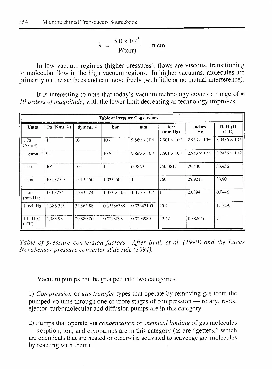
2 Micromachined Transducers Sourcebook
2. WHAT ARE TRANSDUCERS?
Transducers, by definition, convert one form of energy into another. This
term encompasses both sensors and actuators. For practical purposes, a transducer
is a conduit for transforming energy between two or more domains (i.e., chemical
to electrical). In some cases, an intermediate transformation is required, as in a
sensor that converts light to heat and then to electricity. The noun transducer and
the verb transduce are relatively new in the English language, as can be seen from
the definitions in Webster’s Ninth New Collegiate Dictionary’’.
transduce \tran(t)s-’d(y)iis, tranz-\ vt trans»duced; trans*ducing [L
transducere to lead across, transfer, fr. trans- + ducere to lead] (1947)
1: to convert (as energy or a message) into another form...
transducer \-d(y)u-ser\ n (1924): a device that is actuated by power
from one system and supplies power usually in another form to a second
system (as a telephone receiver that is actuated by electric power and
supplies acoustic power to the surrounding air)
In practice, the vast majority of work in the field has been on sensors rather
than actuators. Sensors measure something in their environment and (generally)
provide an electrical output that relates to the parameter(s) they measure. As
discussed in this book, there are a large number of things that can be sensed,
including the broad areas of mechanical, optical, (electro)magnetic, ionizing radi¬
ation, thermal, and chemical phenomena. Some authors, such as Lion (1969),
White (1987), and Ristic (1994) divide sensors into “domains” such as:
Thermal (temperature, heat, and heat flow)
Mechanical (force, pressure, velocity, acceleration, and position)
Chemical (concentration of chemicals, composition, and reaction rate)
Magnetic (magnetic field intensity, flux density, and magnetization)
Radiant (electromagnetic wave intensity, wavelength, polarization, and phase)
Electrical (voltage, current, and charge)
It is inevitable that, in applying such categories, there will be devices that
either do not fit well into any category or belong in several. The organization of
Introduction and Overview 3
this book is partly by the type of input/output energy associated with the transducer
(e.g., optical), but also by function (e.g., fluidics). The reader will quickly realize
that there are considerable overlaps between domains in terms of applications. For
example, a mechanical sensor such as a strain gauge can be considered a biomedical
sensor if it is implanted in the body. Thus, extraordinary efforts to define a rigid
“domain-based” taxonomy for micromachined devices was felt to be unwarranted.
Actuators are still a developing area in micromachining, since very few
micromachined actuators have “actuated” objects other than themselves and even
fewer have been used in commercial products. Actuators are, however, often
incorporated into sensors (an example is the use of electrostatic or thermal expansion
actuators to provide “self-test” capability for accelerometers).
Micromachined structures, such as holes, channels, cantilevers, membranes,
etc., are also very useful and important as building blocks for more complex
micromachined devices. In particular, they are being used in microfluidic systems,
which are a relatively new development in the field.
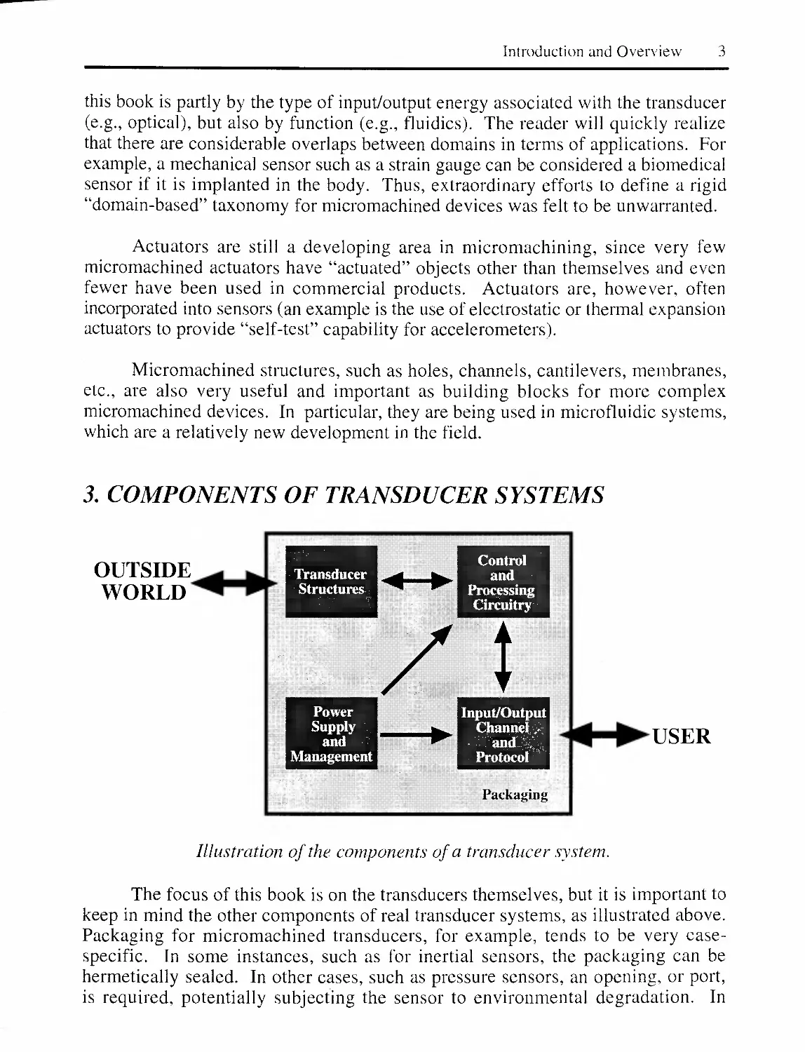
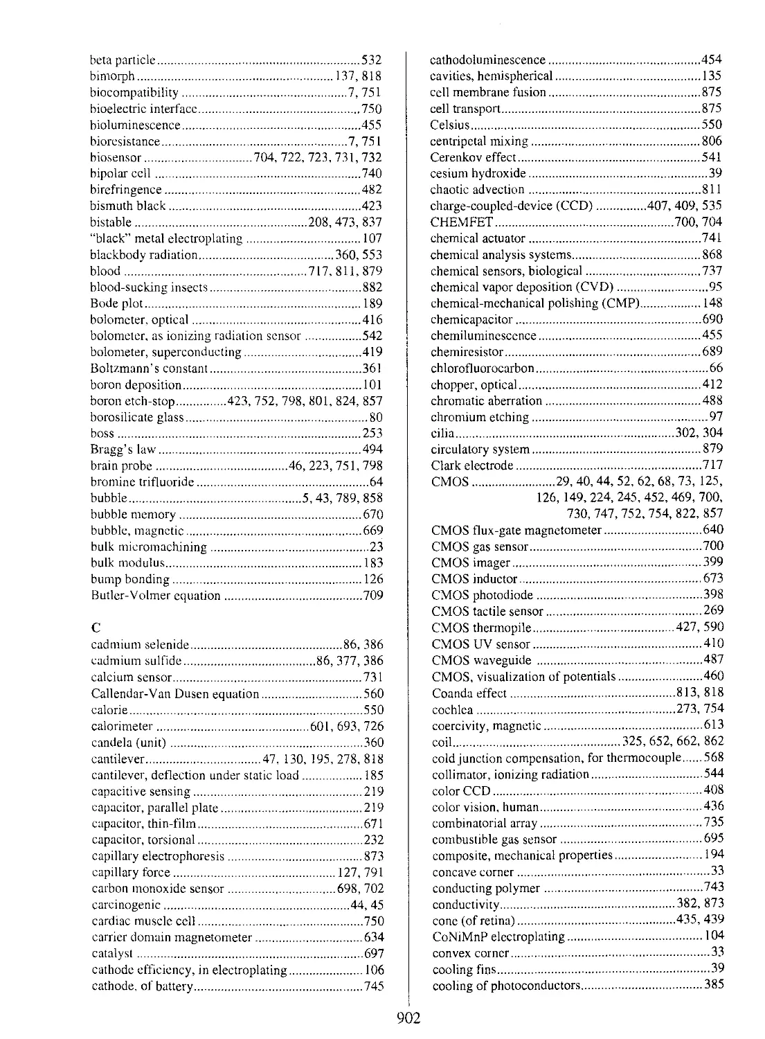
3. COMPONENTS OF TRANSDUCER SYSTEMS
OUTSIDE
WORLD
Transducer
Structures
Control
and
Processing
Circuitry
Packaging
USER
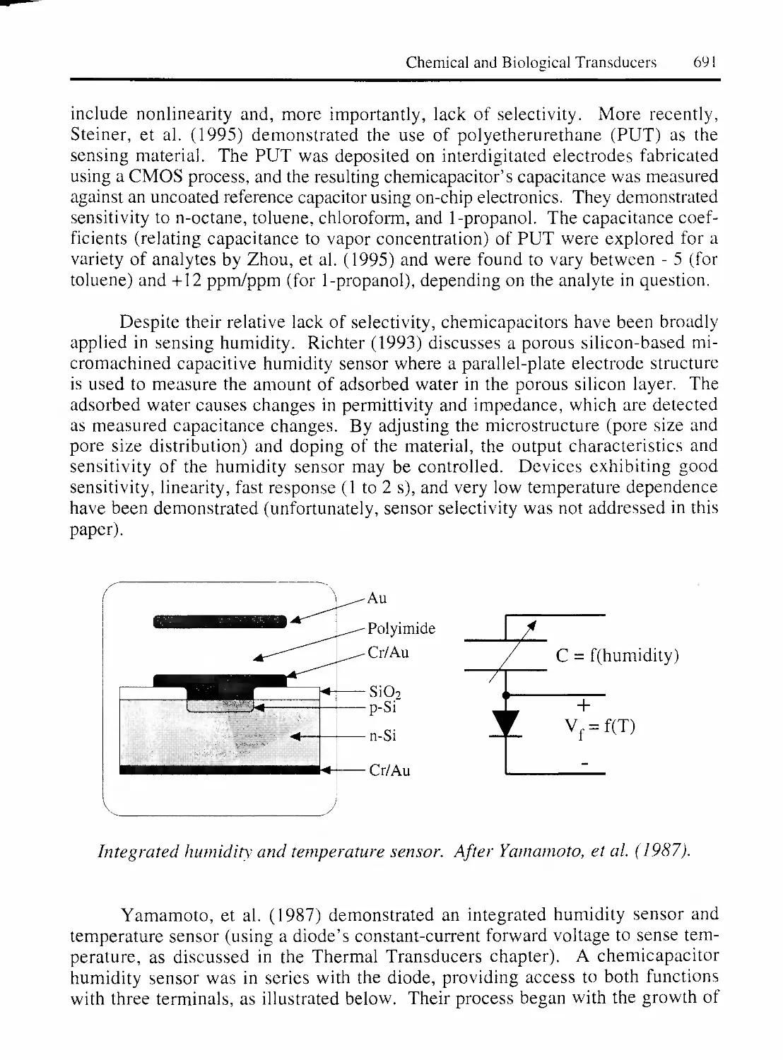
Illustration of the components of a transducer system.
The focus of this book is on the transducers themselves, but it is important to
keep in mind the other components of real transducer systems, as illustrated above.
Packaging for micromachined transducers, for example, tends to be very case-
specific. In some instances, such as for inertial sensors, the packaging can be
hermetically sealed. In other cases, such as pressure sensors, an opening, or port,
is required, potentially subjecting the sensor to environmental degradation. In
4 Micromachined Transducers Sourcebook
addition, testing is a major issue that needs to be considered when trying to build
micromachined transducer systems. In some research circles, the bulk of the
research efforts focus on the transducers themselves, yet moving them out into the
“real world” requires some or all of the other aspects illustrated above. Naturally,
these are prime considerations among industrial users.
4. WHAT ARE MICROMACHINED TRANSDUCERS?
As mentioned above, micromachined transducers are (generally) those that
arc fabricated using tools and techniques developed for the integrated circuit industry,
such as microlithography, etching, etc., or some of the newer techniques developed
specifically by and for the micromachining community. Micromachined devices
are generally not at the forefront of lithography, typically requiring no features
smaller than 1 |j,m, and generally much larger. So-called “nanotechnology” is
beyond the scope of this book.
As discussed in the following chapter, micromachining can be grossly cate¬
gorized into “bulk” and “surface.” Bulk micromachining involves removal of
significant regions of the substrate (e.g., etching cavities in a silicon substrate) and
can thus be thought of as a subtractive process. Surface micromachining involves
building up and patterning thin-film layers to realize the desired structures on the
surface of the wafer (an additive process). As mentioned above, not all microma¬
chining is done using tools for integrated circuits, and some “traditional” methods,
such as electric discharge machining or injection molding, have been modified
down to produce micron-scale features.
5. WHEN DOES IT MAKE SENSE TO ‘ ‘MICRDMA CHINE’’?
When surveying the rapidly growing body of literature related to microma¬
chining, many publications will cause the reader to question the need to micromachine
a device in the first place. This is certainly a more common question among
industrial, as opposed to academic workers. Sometimes, an “advanced, microma¬
chined transducer” actually offers no advantages in terms of performance,
size/weight, reliability, cost, etc., and such devices are generally not worth fabricating
unless they are stepping stones to more successful designs. Whether or not a
device “should” have been micromachined based on the measured performance,
cost, size, path to future micromachined devices, etc., is a healthy question to ask.
Introduction and Overview 5
Quite often, micromachining a transducer can confer great advantages in one
or more areas, and the key is to evaluate the benefits of micromachining before
undertaking a project. It is a key goal of this book to provide the reader with some
of the background to make such judgments. Since there is no simple, generic
“algorithm,” the only practical way to get to this point is to obtain an overview of
the field and then compare proposed micromachined devices to others (both micro¬
machined and “conventional”) in terms of performance. A general approach to this
is to learn the underlying physical mechanisms of importance to a proposed device,
to understand the scaling of desired and undesired (parasitic) effects as the design
is miniaturized, and, if things make sense, to plan a realistic fabrication process.
While a book of this nature cannot possibly cover the entirety of these areas, it can
at least help the reader build intuition.
As stated by Prof. Kurt Petersen during his address at the Transducers '95
conference in Stockholm, Sweden, “MEMS has competition.” The point is that
one is not always micromachining a device that is unique. Typically, there is
another way to accomplish the same result. In cases where “there is no other way,”
or there are clear advantages, micromachining can be a very powerful technique.
5.1 SCALING AND PERFORMANCE
In terms of performance, while some physical effects scale favorably into
the microns-to-millimeters scale of micromachined devices, others do not. Thermal
transport properties of microstructures allow for local regions to be highly coupled
or isolated, and this can be a problem or a great benefit. Enhanced mass transport
properties of electrochemical microelectrodes can be extremely advantageous and
are readily harnessed. Increased surface-area-to-volume ratios at the microscale
often provide tremendous improvements in separation techniques such as capillary
electrophoresis or gas chromatography. However, while fluidic channels can be
scaled down, there are dimensions at which bubbles cannot be purged for any
reasonable applied pressures due to capillary forces. Actuation mechanisms at the
microscale tend to be quite limited, and if substantial forces are required, may
involve considerable power dissipation in greatly reduced volumes. There are
numerous other examples, and, as mentioned above, one must be keenly aware of
the scaling laws pertaining to the project at hand. As with any engineering endeavor,
there are multitudes of trade-offs, and skillful design can lead to good, functional
compromises.
5.2 COST REDUCTION ISSUES
In terms of cost, an often-touted advantage of micromachining is that devices
are fabricated in large batches, in parallel. This is certainly true. Unfortunately,
however, for most microsensors, the parallelism does not extend into packaging
and testing, which are domains that, when taken together, can account for as much
6
Micromachined Transducers Sourcebook
as three-quarters of the final cost of a device. For conventional integrated circuits,
testing is not parallel, but it is at least rapid and inexpensive. Testing is generally
carried out by rapidly making temporary connections to each chip (still on a silicon
wafer) and exercising it electrically. Some optical or magnetic devices can be
tested in a similar way, by adding the necessary non-contact stimuli. For the vast
majority of micromachined transducers designed to interact with physical phenomena
in other domains (e.g., acceleration, chemical interaction, fluidic effects), such
rapid testing is not possible. In those cases, usually individual chips are tested and
often only after they are packaged. For some types, such as accelerometers, this
testing can be fairly rapid, as they still can be tested using fast methods such as
mechanical shakers. For devices such as wet chemical sensors, however, there
currently seems to be no way to carry out testing rapidly. For at least some
chemical sensors, however, this problem may be mitigated through the use of
redundant arrays, differential measurement techniques, and calibration at the point-
of-use.
As for any product successful in volume production, mass market drivers
must be found or created. In the micromachined transducers marketplace, the
automotive industry has provided a major market pull for such devices as manifold
air pressure sensors and accelerometers for air bag systems (for an overview of
current and future automotive sensors needs, see Giachino and Miree (1995)).
Unfortunately, while needing high volumes, automotive and other durable goods
markets are extremely cost-sensitive, making it difficult for manufacturers to amortize
their net development costs. One approach taken by commodity sensor manufacturers
to move “up the food chain” has been adding more value through the manufacture
of subsystems that perform functions beyond simple measurements (e.g., moving
from production of valves to that of flow controller modules). In this way, they
can often achieve more realistic profit margins, necessary for long-term survival
and growth. For chemical and biomedical applications, disposable devices are
likely to increase in importance, since volumes can be orders of magnitude greater
than those for comparable items permanently affixed in durable goods. In the case
of single-use devices for common applications such as clinical diagnostics, it appears
that there is tremendous potential for growth and profitability.
5.3 COMPLEXITY OF MICROMACHINED DEVICES AND SYSTEMS
Surveying the micromachining literature, one observes that the complexity
of the sensors, actuators, and subsystems being fabricated is increasing over time.
For example, research laboratories have produced a broad range of sensors that
include on-chip circuitry to locally process sensor outputs into forms more palatable
to computers. In the industrial world, such highly integrated sensors are certainly
becoming available, although the bulk of the micromachined sensors being sold
today do not contain transistor circuits. As an example of a trend toward integration
in another area, microfluidic systems have been realized on an experimental basis
Introduction and Overview 7
where interconnecting channels, reaction chambers, and other functions are combined
with micromachined valves and pumps. At present, however, there are few, if any,
fully monolithic fluidic systems.
A principal issue with increasing the complexity of micromachined systems
is that, as for hybrid assemblies in the electronics industry, the net yield of fully
functional devices is usually negatively affected by increased complexity. The
often-debated question of whether or not to integrate circuitry with micromachined
sensors, appears to have an answer that is domain- and case-specific. For example,
integrating circuitry might make sense for an accelerometer where there may be
great market pressures for reduction of a subassembly (including a sensor and
electronics) to a single chip. On the other hand, for disposable micromachined
pressure sensors for medical applications, there may be considerably less pressure
to integrate since the installed base of equipment that uses the sensors could not
take advantage of such advanced capabilities. This latter market, however, may
still be quite profitable and benefit from the high yields obtained with relatively
simpler processes. A sensible strategy for developing micromachined devices that
may some day have on-chip circuitry is to plan an evolutionary path such that the
micromachining technologies used do not preclude the later addition of such circuits.
At the system level, many researchers make statements about building a
“chemistry lab on a chip” but do not mention that sample volumes and supporting
hardware may not scale down comparably. For example, it has long been possible
to fabricate compact mass spectrometers (e.g., quadrupole designs), yet the technol¬
ogy for fabricating the necessary gas pumping systems has lagged far behind.
Similarly, for miniaturized systems requiring self-contained electrical power, the
power requirements of many crucial microactuators (e.g., valves, pumps) have in
many cases remained roughly comparable to their macroscopic counterparts while
power densities of batteries have not increased sufficiently to allow overall minia¬
turization. When miniaturizing clinical diagnostic instruments, in many cases the
sample volumes required to obtain statistically valid samples of bacteria or viruses
are many times larger than the microstructures themselves (potentially reducing
throughput if they must be routed through microfluidic devices). Discussion of
these issues by no means implies that miniaturized systems will not be successful.
On the contrary, they certainly will have a major impact. It is important, however,
that the “big” picture be considered rather than immediately miniaturizing parts of
a system simply because one can.
Additional systems issues are faced by those seeking to use micromachining
technologies in (bio)chemical, clinical, or similar domains. For example, for devices
that come into contact with body fluids or are implanted, the issues of biocompatibility
and bioresistance must be considered. Biocompatibility refers to the ability of
materials to function in contact with biological media and not adversely affect cells
or tissues (e.g., by invoking inflammatory responses or leaching out toxic com¬
8 Micromachined Transducers Sourcebook
pounds). Bioresistance refers to the ability of materials to withstand the harsh
chemical environments faced in such settings (e.g., corrosive attack by body fluids
and cells). The materials commonly available in micromachining research facilities
are often not the best for such applications, and considerable work is needed in the
area of coating materials and surface modification methods.
There are also several categories of systems where the optimal implementations
will be in the mesoscopic (“sugar-cube-to-fist-sized”) domain, rather than micro¬
scopic. These include chemical reactors, synthesizers, and analyzers; heating and
cooling units; and combustors and fuel cells. For example, it is possible to revisit
chemical reactions that are very unstable at the macroscopic scale, and use them
effectively through a massively parallel array of microreactors. The enhanced
mass and energy transport properties at this scale make this possible, and a mesoscopic
array of microdevices could still produce substantial volumes of product. This
parallel approach can, in many other applications, bring the advantages of microscale
devices to bear on a larger physical scale. It is worth noting that such mesoscopic
systems may include micromachined elements, or be made from them. Thus, the
advantages of operating over an expanded range of physical scales can be harnessed.
An area that requires considerable research for all micromachined systems is
the development of suitable interconnect and packaging methods. Just as the
integration of wiring onto the integrated circuit transformed electronic systems a
few decades ago, it is likely that analogous developments for fluidic devices, for
example, will have a major impact in our ability to integrate micro- and mesoscopic
systems in many domains. It is also probable that such interconnects and packages
will not all be fabricated using relatively expensive silicon technologies, but perhaps,
instead, using ceramics and injection-molded plastics, which can already provide
the necessary precision to interface with micromachined structures. Unfortunately,
discussion of packaging for micromachined transducers and structures has not
appeared frequently in the literature, and standard integrated circuit packaging is
seldom appropriate.
Introduction and Overview 9
6. ISSUES TO CONSIDER
There are several important issues to consider when studying an existing
micromachined device or planning a project to develop one. As discussed above,
the most important question to answer is whether or not a device should be fabricated
using micromachining technologies. The table below can serve as a starting point
for a “checklist” of these issues.
Establish commercial or research need in light of “conventional” competition.
Understand the basic physics and operating principles, including scaling laws.
Understand the important issues in designing macroscopic and micromachined versions.
Survey prior work in micromachined versions, as well as “natural” (biological) analogs.
Consider the potential need to integrate on-chip circuitry (now or in the future).
Design a feasible, not overly complex, and reasonably priced fabrication process. If active
circuits are, or may be, required, be sure to allow for that by avoiding incompatible steps.
Consider the issues of packaging. Can existing packages be adapted?
Consider realistic testing methods that suit the market (e.g., 100% test or statistical).
Estimate the final cost of the “ready-to-use” or “ready-to-ship” device (does it make sense?).
Consider the possibilities of evolving the design in the future to improve performance,
reduce cost, etc. (this may, for example, feed back into the process design).
Make an overall decision as to feasibility prior to embarking on the research effort.
Table of issues to consider before undertaking a micromachining research and
development effort or when studying an existing device. While this table is not
intended to be all-inclusive, it should serve as a starting point.
10 Micromachined Transducers Sourcebook
7. WHAT ARE THE MARKETS FOR MICROMACHINED
TRANSDUCERS?
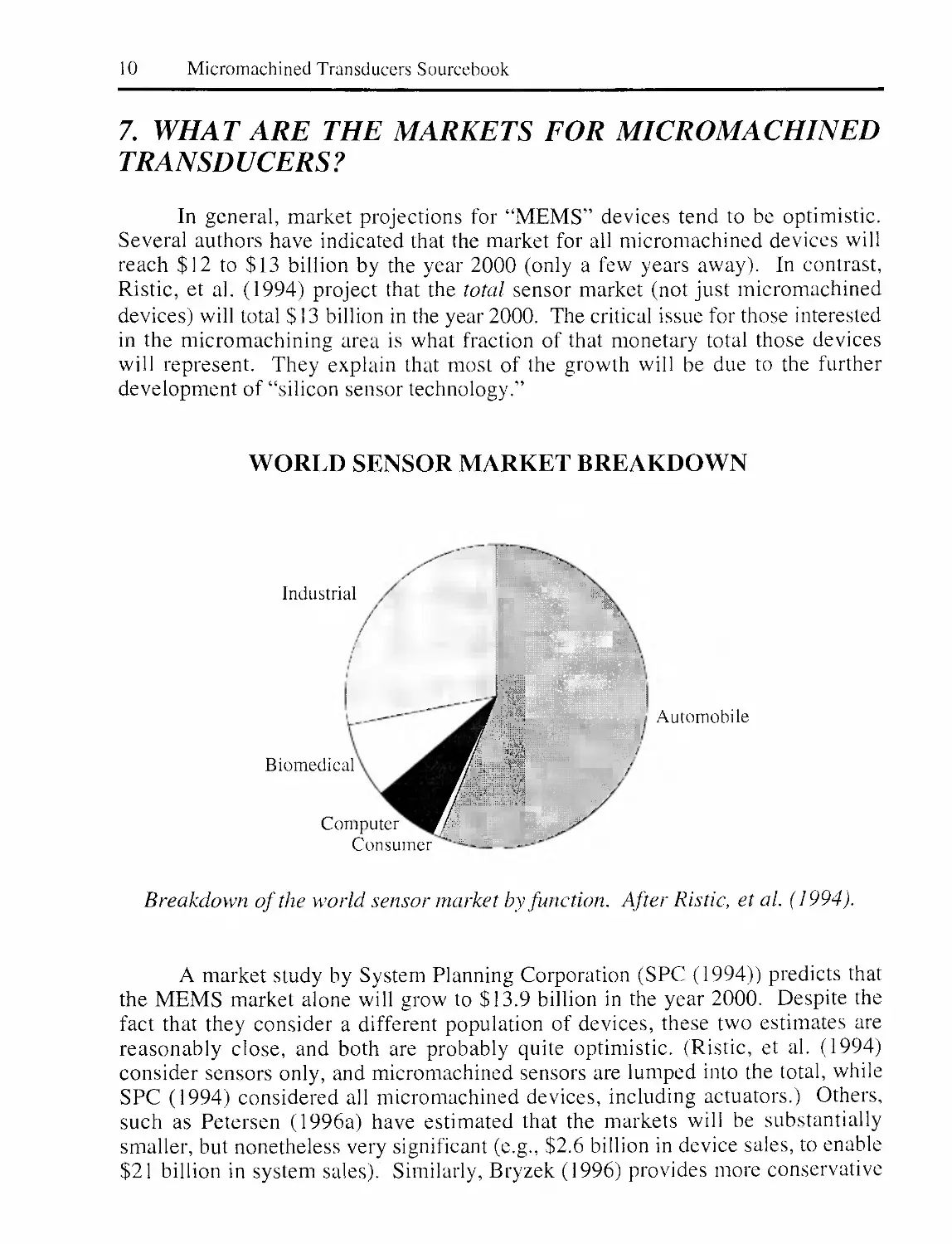
In general, market projections for “MEMS” devices tend to be optimistic.
Several authors have indicated that the market for all micromachined devices will
reach $12 to $13 billion by the year 2000 (only a few years away). In contrast,
Ristic, et al. (1994) project that the total sensor market (not just micromachined
devices) will total $13 billion in the year 2000. The critical issue for those interested
in the micromachining area is what fraction of that monetary total those devices
will represent. They explain that most of the growth will be due to the further
development of “silicon sensor technology.”
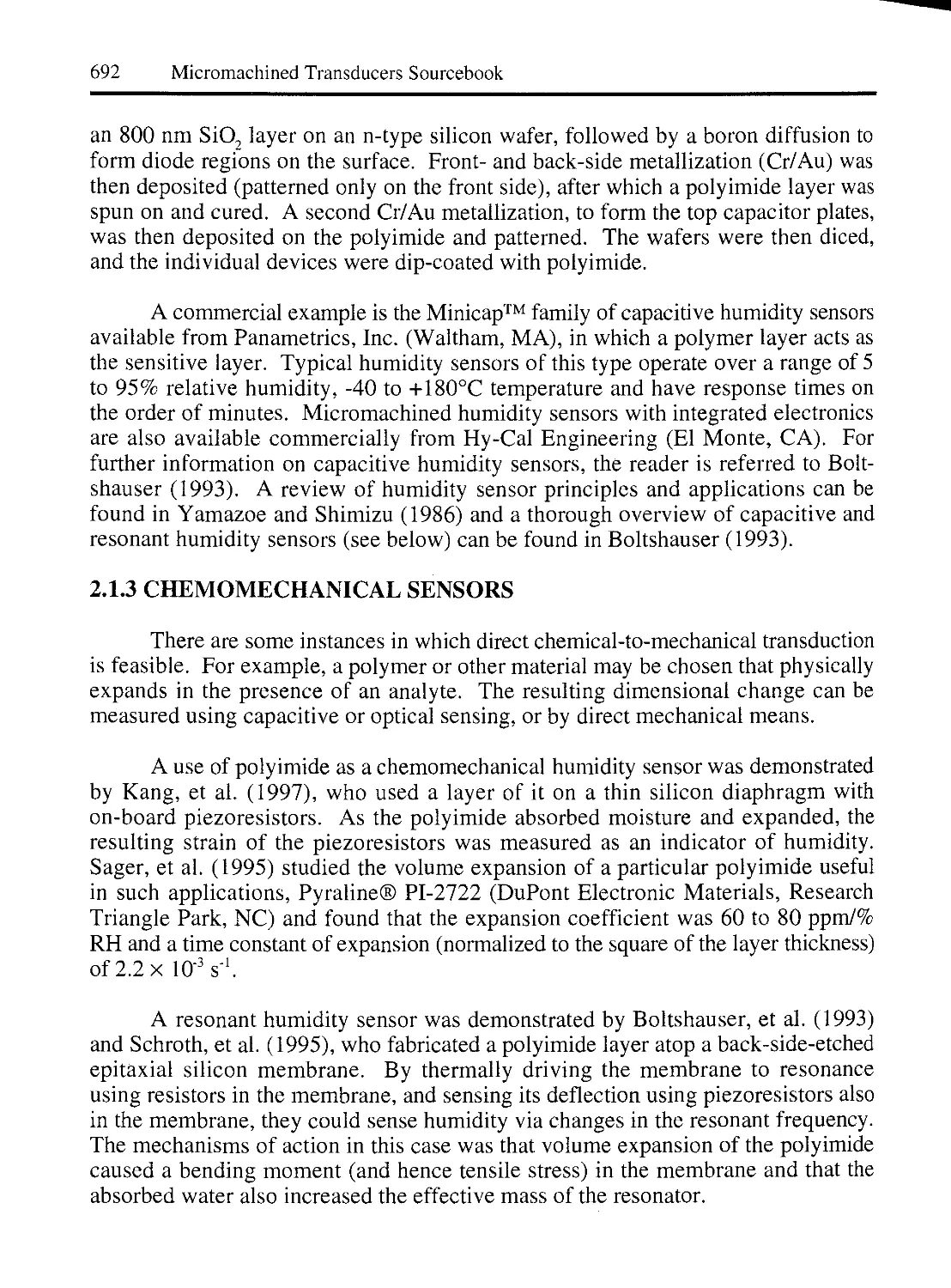
WORLD SENSOR MARKET BREAKDOWN
Automobile
Industrial
Biomedical
Computer
Consumer
Breakdown of the world sensor market
by function. After Ristic, et al. (1994).
A market study by System Planning Corporation (SPC (1994)) predicts that
the MEMS market alone will grow to $13.9 billion in the year 2000. Despite the
fact that they consider a different population of devices, these two estimates are
reasonably close, and both are probably quite optimistic. (Ristic, et al. (1994)
consider sensors only, and micromachined sensors are lumped into the total, while
SPC (1994) considered all micromachined devices, including actuators.) Others,
such as Petersen (1996a) have estimated that the markets will be substantially
smaller, but nonetheless very significant (e.g., $2.6 billion in device sales, to enable
$21 billion in system sales). Similarly, Bryzek (1996) provides more conservative
Introduction and Overview
11
estimates of $10.5 billion for all micromachined devices in the year 2005. Bryzek
also notes that, when making such estimates, there is generally a ten to twenty year
time lag between first prototypes and large-scale sales.
In terms of breaking down sensor markets by category, most experts agree
that automotive applications will dominate for the near future. The two sources
referred to above break the market down quite differently (Ristic, et al. (1994) by
market type and SPC (1994) by device type). In any case, it is likely that markets
using disposable devices, such as the medical device market, will increase relative
to the others since non-disposables mainly represent durable goods.
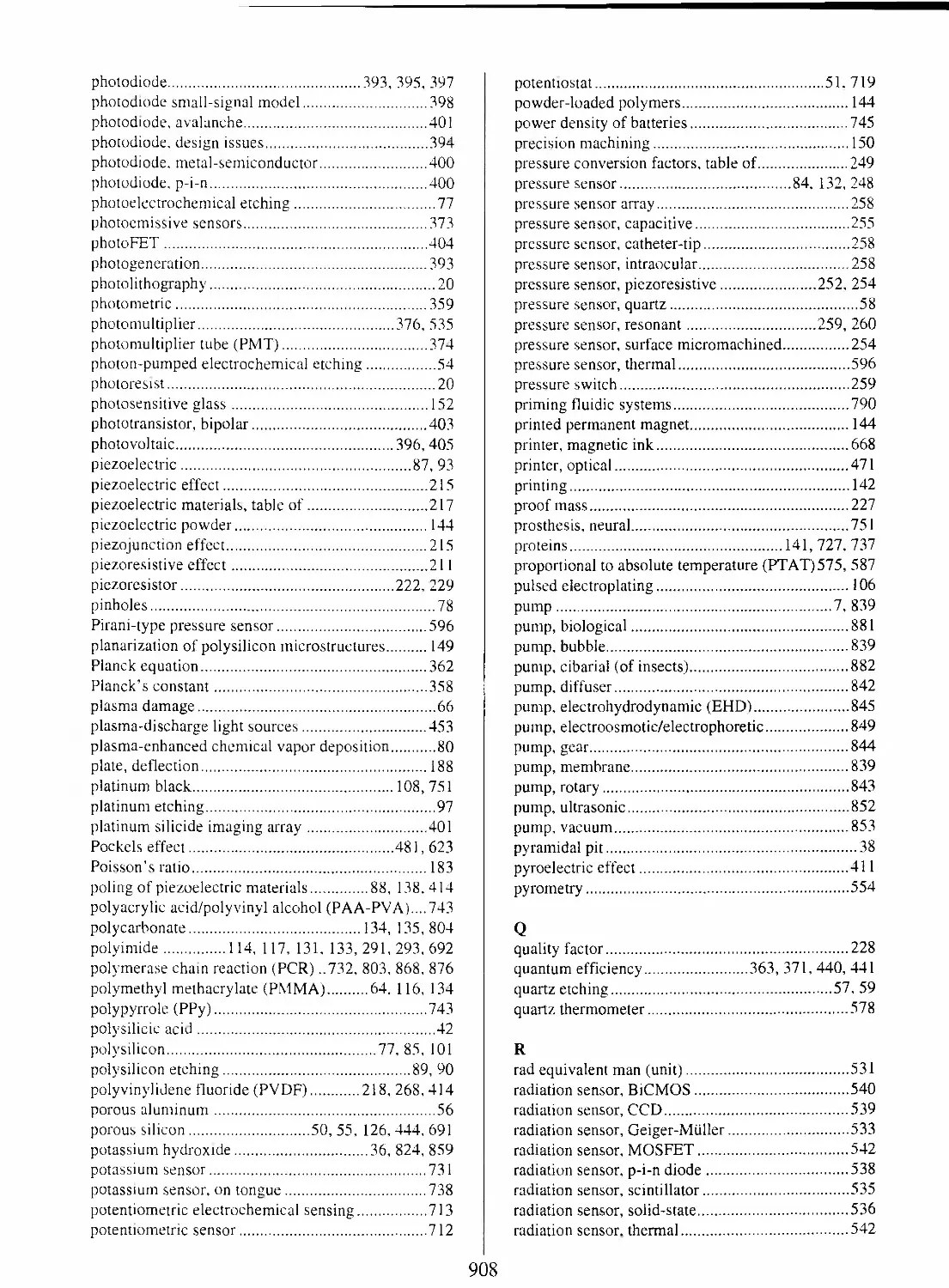
WORLD MARKET FOR MICROMACHINED
DEVICES BY FUNCTION
Breakdown of the world market for micromachined devices by function. After SPC
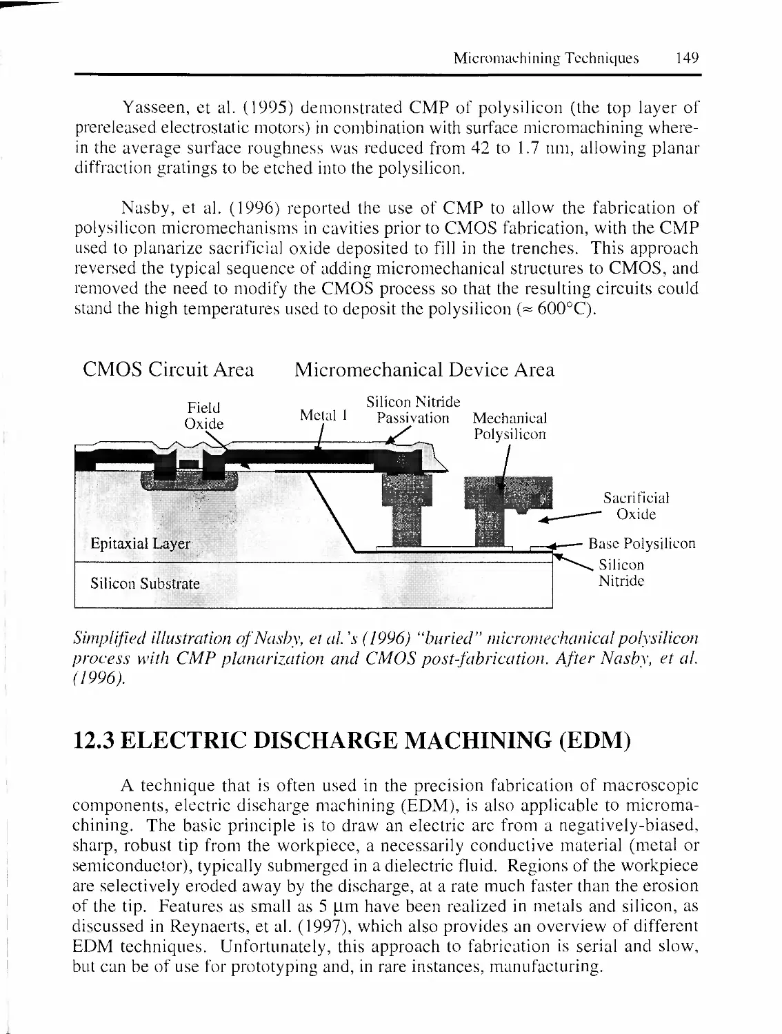
(1994).
7.1 MICROMACHINING AS AN “ENABLING TECHNOLOGY”
A key point is that micromachined sensors and actuators constitute enabling
technologies, wherein their greatest power lies in enabling and adding value to
systems. The SPC report cited above estimates (perhaps somewhat optimistically)
that by the year 2000, the $13.9 billion annual sales of micromachined devices will
enable nearly $100 billion in overall annual sales. However, when looked upon as
an important enabling technology, one could make similar statements for injection
molding, printed circuit boards, adhesives, etc. Further discussion of the concept
of “enabled” sales may well be academic, but it will undoubtedly continue.
12 Micromachined Transducers Sourcebook
7.2 IS THE MARKET “READY TO EXPLODE”?
The market for micromachined transducers is still being developed and does
not have the explosive growth rate of, for example, integrated circuits in the 1970’s.
Some authors like to compare the two, but this does not really make sense, since
there is no “dominant technology” in micromachining that is analogous to MOS
(metal oxide semiconductor) circuitry (which led, in a large part, to the exponential
growth of the digital electronics industry). Perhaps a better comparison would be
likening micromachining to analog integrated circuit technology, which is certainly
enabling, but with nowhere near the market volume of digital circuits such as
memories and microprocessors. However, time will ultimately provide the answers
as to how important this new set of technologies are.
At the moment, a great deal of research in this area is focused on “surface”
micromachining (fabricating thin-film structures above the substrate, as discussed
in detail in the Micromachining Techniques chapter), yet in industry the vast majority
of shipping devices are manufactured using much older “bulk” micromachining.
While some surface micromachined devices are now being produced in volume, it
will take a few more years for this approach to make a large impact in the market.
It is unlikely that one approach will dominate, at least in the short run, as new
devices using both surface and bulk micromachining (circuits can be integrated in
either case) continue to be marketed. An interesting and important aspect of the
development of micromachined devices has been that their “incubation times”
from conception to volume shipment often exceed a decade, so it is likely to be too
early to rely too heavily on technology predictions.
8. INFORMATION RESOURCES
8.1 ON-LINE RESOURCES
Micromachining is a relatively new field, and is growing rapidly at present.
At the moment, most of the interesting publications appear first in conference
proceedings and then later, if at all, in more easily accessible journals. Thus,
computer databases are often an extremely useful tool for tracking new developments.
Several excellent on-line databases exist, but even papers as recent as the 1970’s
may not appear in some databases (particularly if higher-cost access to older records
is not subscribed to).
The Information Sciences Institute (ISI) in Marina del Rey, CA, operates a
DARPA-sponsored MEMS “bulletin board” (BBS) that serves as a “clearinghouse”
for MEMS information. For general information, one can send e-mail to
mems@isi.edu, or visit their web site at http://mems.isi.edu/mems.html. Their web
Introduction and Overview 13
pages contain convenient links to some of the major university sites, although in
general, web links may not be as frequent as one would hope.
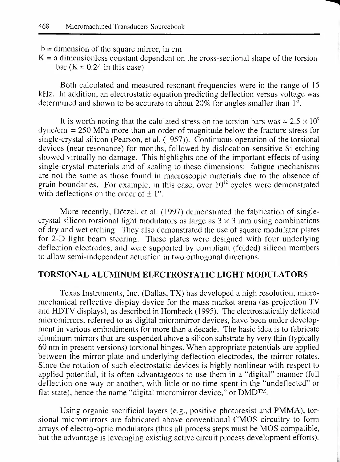
8.2 MICROMACHINED TRANSDUCERS MEETINGS
There are a large number of meetings whose focus is micromachined trans¬
ducers. A few of the best-known examples are:
• Solid-State Sensor and Actuator Workshop, or “Hilton Head” (small, North
American only, limited attendance meeting held at Hilton Head, SC, on alternate
years, e.g., 1992, 1994, 1996, ...).
• International Conference on Solid-State Sensors and Actuators, or “ Transducers ”
(large, international meeting held in Asia, North America, or Europe on alternate
years, e.g., 1991, 1993, 1995, ...).
• Micro Electro Mechanical Systems Workshop, or “MEMS” (moderate sized,
international workshop, with a focus on actuators and mechanical devices, held
annually).
• Micro Toted Analysis Systems, or “jiTAS” (international, focus on micromachined
chemical systems, held alternate years in Europe, e.g., 1994 (first), 1996, ...).
• Eurosensors (European, with broad coverage, held annually).
There are many micromachining-specific meetings in North America and
abroad. In addition, many long-established “mainstream” conferences in specific
disciplines are adding “MEMS” tracks. This seems natural since as the microma¬
chining field matures, the end-users in other disciplines will adopt the useful aspects
of the technology.
The proceedings from these meetings are an excellent source of material if
one can find them. In some cases, copies of prior meeting proceedings can be
obtained by writing to the host organizations. A few examples are given below.
14 Micromachined Transducers Sourcebook
Meeting
Host Organization
Hilton Head
Transducers Research Foundation, Inc., P.O. Box 18195 Cleveland
Heights, OH, USA.
Transducers
Variable, depends on host country: 1995 is available from the Royal
Swedish Academy of Engineering Sciences, IVA, Box 5073, S-102, 42
Sweden, 1997 is available from the IEEE, at the address given below.
MEMS
IEEE Service Center, 445 Hoes Lane, P.O. Box 1331, Piscataway, NJ,
USA.
UTAS
1994 - Kluwer Academic Publishers, P.O. Box 17, 3300 AA Dordrecht,
The Netherlands.
1996 - AMI Editorial Office, Miinsterplatz 6, Postfach 1955, CH-4001,
Base, Switzerland.
Table of organizations from which copies of micromachining-related conference
proceedings can be ordered. Note that searching the web or otherwise contacting
the host organizations is often critical to obtaining such material.
8.3 TEXTBOOKS AND PAPER COLLECTIONS
There are several relevant books on the market, covering micromachined
and/or macroscopic transducers in various proportions. Each book tends to have
its own particular set of strengths, and in general, a researcher in this field will
want to own several. Some examples, without particular endorsements (caveat
emptor!) are listed in the General References section at the end of this chapter. In
addition, two bound collections of “classic” papers on micromachined devices,
Muller, et al. (1991) and Trimmer (1997) are available from IEEE, and are good
sources for background information.
8.4 JOURNALS
There are several journals now available that cover the micromachined trans¬
ducer area. Some examples are:
A) Journals with a primary focus in the MEMS area:
• Sensors and Actuators A (Physical)
• Sensors and Actuators B (Chemical)
• Sensors and Actuators C (Materials)
Introduction and Overview 15
• IEEE/ASME Journal of Microelectromechanical Systems (JMEMS)
• Journal of Micromechanics and Microengineering
B) Journals with information of interest to the MEMS community and occasional
MEMS papers:
• IEEE Electron Device Letters
• Journal of the Electrochemical Society
• Journal of the Vacuum Society
• Proceedings of the SPIE — International Society for Optical Engineering
8.5 THESES
An often-overlooked but rich information resource are M.S. and Ph.D. theses.
These can be obtained through University Microfilms, Inc. (300 North Zeeb Road,
P.O. Box 1346, Ann Arbor, MI 48106-1346, Phone: (313) 761-4700) or by directly
contacting the authors or their advisors. Unfortunately, the major difficulty is
knowing about them, since they are not necessarily searchable on-line.
8.6 PATENTS
Another often-overlooked (at least by academics) yet critical information
resource is patents. Quite frequently, companies or research groups will file for
patents long before publishing, and sometimes companies will never publish. Patents
can be searched on-line (through patent service providers or on the web, e.g., at
IBM’s patent server site: http://patent.womplex.ibm.com/) or at patent libraries.
9. CONCLUSION
Micromachining technologies are clearly going to have a major impact on
domains including basic science, consumer goods, aerospace, environmental mon¬
itoring, and medicine. Their successful application typically requires broad knowl¬
edge of physical principles and scaling laws. Equally important are system-level
issues of complexity, packaging, testing, and manufacturability. As these technol¬
ogies mature, and are adopted by more end-users, exciting developments will
certainly occur, particularly in interdisciplinary domains. For further information
on trends in micromachining, predictions of future growth and reviews of new
application areas, the reader is referred to Baltes (1996), Bryzek (1996), Fujita
(1996) and Petersen (1996b).
16 Micromachined Transducers Sourcebook
INTRODUCTION AND OVERVIEW REFERENCES
GENERAL REFERENCES
Fraden, J„ "Handbook of Modern Sensors,” Second Edition, American Institute of Physics Press,
Woodbury, NY, 1996.
Gardner, J. W., “Microsensors: Principles and Applications,” John Wiley and Sons, Inc., Chichester,
West Sussex, UK, 1994.
Hauptmann, P., “Sensors: Principles and Applications,” Prentice-Hall International (UK), Hert¬
fordshire, UK, 1991.
Janata, J., “Principles of Chemical Sensors,” Plenum Press, New York, NY, 1989.
Khazan, A. D., “Transducers and Their Elements: Design and Application,” Prentice-Hall, Inc.,
Englewood Cliffs, NJ, 1994.
Kress-Rogers, E. [ed.], “Handbook of Biosensors and Electronic Noses: Medicine, Food and the
Environment,” CRC Press, Inc., Boca Raton, FL, 1997.
Madou, M., “Fundamentals of Microfabrication,” CRC Press, Inc., Boca Raton, FL, 1997.
Madou, M. J., and Morrison, S. R., “Chemical Sensing with Solid State Devices,” Academic
Press, Inc., San Diego, CA, 1989.
Middelhoek, S., and Audet, S. A., “Silicon Sensors,” Academic Press; Inc., Boston, MA, 1989.
Muller, R. S., Howe, R. T., Senturia, S. D., Smith, R. L., and White, R. M. [eds.], “Microsensors,”
IEEE Press, New York, NY, 1991.
Noltingk, B. E. [ed.], “Instrumentation Reference Book,” Second Edition, Butterworth-Heinemann,
Ltd., Oxford, UK, 1995.
Norton, H. N„ “Handbook of Transducers,” Prentice-Hall, Inc., Englewood Cliffs, NJ, 1989.
Ristic, Lj. [ed.], “Sensor Technology and Devices,” Artech House, London, 1994.
Sze, S. M., “Semiconductor Sensors,” John Wiley and Sons, Sommerset, NJ, 1994.
Trimmer, W. S., “Micromechanics and MEMS: Classic and Seminar Papers to 1990,” IEEE
Press, New York, NY, 1997.
Introduction and Overview 17
SPECIFIC REFERENCES
Baltes, H., “Future of IC Microtransducers,” Sensors and Actuators, vol. A56, nos. 1 - 2, Aug.
1996, pp. 179 - 192.
Bryzek, J., “Impact of MEMS Technology on Society,” Sensors and Actuators, vol. A56, nos. 1 -
2, Aug. 1996, pp. 1 - 9.
Fujita, H., “Future of Actuators and Microsystems,” Sensors and Actuators, vol. A56, nos. 1 - 2,
Aug. 1996, pp. 105-111.
Giachino, J. M., and Miree, T. J., “The Challenge of Automotive Sensors,” Proceedings of the
SPIE Conference on Microlithography and Metrology in Micromachining, Austin, TX, Oct. 23 -
24, 1995, SPIE vol. 2640, pp. 89 - 98.
Lion, K. S., “Transducers: Problems and Prospects,” IEEE Transactions on Industrial Electronics
and Control Instrumentation, vol. IECI-16, no. 1, July 1969, pp. 2 - 5.
Petersen, K. E., personal communication, 1996.
Petersen, K., “From Microsensors to Microinstruments,” Sensors and Actuators, vol. A56, nos. 1
-2, Aug. 1996, pp. 143 - 149.
Ristic, Lj. [ed], “Sensor Technology and Devices,” Artech House, London, 1994
System Planning Corporation, “Microelectromechanical Systems (MEMS): An SPC Market
Study,” July 1, 1994, available from System Planning Corporation, 1429 North Quincy Street,
Arlington, VA 22207, Phone: (703) 351-8461, Fax: (703) 351-8662.
White, R. M., “A Sensor Classification Scheme,” IEEE Transactions on Ultrasonics, Ferroelectrics
and Frequency Control, vol. UFFC-34, no. 2, Mar. 1987, pp. 124 - 126.
18 Micromachined Transducers Sourcebook
Chapter 2:
MICROMACHINING
TECHNIQUES
Micro machined
Transducers
Sourcebook
1. CAPABILITIES AND LIMITATIONS OF
MICROMACHINING
Micromachining is a very powerful approach for fabricating sensors, actuators,
microstructures, and systems. However, it has limitations that are as important to
know about as its strengths if these technologies are to be applied effectively. One
of the most important goals in learning about micromachining is to realize what
can and cannot be fabricated using these methods and to be able to make meaningful
comparisons to “conventional” fabrication techniques (e.g., drilling, end milling,
injection molding, electric discharge machining, etc.). For example, structures
such as those illustrated below would be difficult or impossible to fabricate litho¬
graphically, since this involves either stacking two-dimensional (2-D) layers or
using processes that yield “extruded” shapes.
Illustration of some structures that would be difficult to fabricate with sequential
lithographic steps.
There are a few true “three-dimensional” (3-D) processes (i.e., capable of
yielding arbitrary, overlapping curved surfaces such as spirals), but they are often
serial, as opposed to most microfabrication methods, which have the great advantage
of parallelism. Essentially, the common micromachining tools available, mainly
derived from the mainstream integrated circuit industry, involve adding 2-D layers,
etching the 2-D layers (sometimes forming cavities by removing “sacrificial” spacer
layers), adding tall “extrusion-like” structures (e.g., plating within template structures
that are later removed), bonding on additional substrates (e.g., glass, silicon, etc.),
19
20 Micromachined Transducers Sourcebook
and etching the substrate. Since microfabrication tools are almost applied with
successive photolithographic patterning, any 3-D aspects of micromachined devices
are due to patterning of the 2-D layers, interaction of stacked and patterned 2-D
layers, selective etching of the layers or the substrate, or the use of bending or
hinged structures. Getting a sense for the geometric, chemical, and thermal interac¬
tions of the large assortment of processes discussed below is key to their successful
application. Studying the examples provided in this book and found in the literature
should aid in this process.
ULTRAVIOLET LIGHT
Photoresist Removed
During Development
Photoresist
Illustration of the basic photolithographic process employed in the vast majority of
micromachining processes. A photoresist layer is first spun-on and baked (not
shown) and exposed to ultraviolet (UV) light through a mask (a quartz plate
covered with a thin film of chromium, which is selectively removed to allow light
through). The exposed photoresist (positive photoresist is shown) then dissolves in
a developer solution, leaving only the non-exposed regions behind.
Micromachining Techniques 21
Process Type
Examples
Lithography
photolithography, screen printing, electron-beam lithogaphy, x-ray lithography
Thin-Film Deposition
chemical vapor deposition (CVD), plasma-enhanced chemical vapor deposition
(PECVD), sputtering, evaporation, spin-on application, plasma spraying, etc.
Electroplating
blanket and template-delimited electroplating of metals
Directed Deposition
electroplating, stereolithography, laser-driven chemical vapor deposition, screen
printing, transfer printing
Etching
plasma etching, reactive-ion enhanced (RIE) etching, deep reactive ion etching
(DRIE), wet chemical etching, electrochemical etching, etc.
Directed Etching
laser-assisted chemical etching (LACE)
Machining
drilling, milling, electric discharge machining (EDM), diamond turning, sawing,
etc.
Bonding
fusion bonding, anodic bonding, adhesives, etc.
Surface Modification
wet chemical modification, plasma modification
Annealing
thermal annealing, laser annealing
Table of example processes used in micromachining.
The table above shows a variety of example micromachining processes,
which are discussed below. It must be noted that this book cannot replace a solid
background in standard integrated circuit fabrication techniques, for which the
reader is referred to Sze (1988), Runyan and Bean (1990), or the wide variety of
other texts on that subject. The discussion below concerns processes of use in
micromachining, not necessarily mainstream integrated circuit fabrication. In addi¬
tion to the material presented herein, the reader is referred to Delapierre (1989),
Mastrangelo and Tang (1994), Ristic (1994), Kovacs, et al. (1996), and Madou
(1997) among others, for further discussion of micromachining processes.
22 Micromachined Transducers Sourcebook
2. MATERIALS FOR MICROMACHINING
2.1 SUBSTRATES
Substrate materials for micromachining need not be silicon. Micromachining
efforts to date have primarily focused on silicon, partly for historical reasons, and
partly for practical ones. In general, crystalline semiconductors (Si, Ge, GaAs,
etc.) are used to take advantage of their inherent features: 1) well characterized
and readily available, 2) multitude of mature processing techniques available (at
least for Si), 3) useful crystal plane anisotropy for micromachining, and 4) potential
for integration of active circuits. Silicon is certainly the dominant substrate material
for transducers, but it is important to pay attention to work in progress with other
materials and to consider them for new projects. Aside from the ability to integrate
circuitry directly on a transducer substrate (not always useful in the final analysis),
a great number of other suitable, non-semiconductor substrates exist. A partial list
includes metals, glasses, quartz and other crystalline insulators, ceramics, plastics
and polymers, and other organic and inorganic materials. It is also important to
note that the functional material(s) of the transducer may be added above the
substrate, or be the substrate itself.
2.2 ADDITIVE FILMS AND MATERIALS
The category of additive films and materials to be deposited on the substrate
includes conductors, semiconductors, and insulators. A partial list of possible
thin-film materials includes silicon (epitaxial [single crystal], polycrystalline, amor¬
phous); silicon compounds (SixN , Si02, SiC, etc.); metals and metallic compounds
(e.g., Au, Cu, Ni, Al, ZnO, GaAs, IrOx, CdS); a wide variety of ceramics (e.g.,
AkO, and more complex compounds); and organics (i.e., diamond, polymers, en¬
zymes, antibodies, DNA, RNA, etc.). By adding such materials to semiconductor
substrates, the ability to co-fabricate active circuitry is retained. The trade-off,
however, is that the additive materials are generally subject to variations in their
physical properties that are far wider than those for single-crystal semiconductor
substrates, which are remarkably uniform. It is worth noting that active circuitry
can also be fabricated using thin-film layers, allowing them to be added to a wide
variety of substrates such as glasses and plastics. Despite the apparent attractiveness
of such a capability, it has not been used in any significant way in mainstream
micromachined transducers, although its use in active-matrix liquid-crystal displays
is routine. Thin-film transistors are discussed briefly in Section 6.1.1 below.
Micromachining Techniques 23
3. MICROMACHINING TERMS
People working in the micromachining field use some specialized terms, but
the bulk of the vocabulary is drawn directly from that of integrated circuit fabrication.
It should be noted that these terms are not perfect, nor are there “official” definitions.
Surface micromachining is processing “above” the substrate (i.e., not involving
the substrate in a big way: in other words, mainly using it as a base to build upon).
Bulk micromachining is processing that removes “bulk” substrate (i.e., large pits,
holes to the back side of a wafer, sawing, etc.).
Examples of “subtractive” (left) and “additive” (right) cantilever beams.
The two major types of processing are subtractive (etching, laser machining,
mechanical milling, etc.) and additive (deposition of dielectrics, metals, etc.). When
categorizing an overall microstructure, some define “subtractive” structures as any
that involve etched pits, voids, holes, etc., and “additive” structures such as those
that are only built “up” from the substrate. These definitions for structures tend to
lose their meaning for some of the more complex structures (i.e., made from
multiple components).
Aspect ratio is a key term referring to the ratio of the depth to the width of
an etched hole or a grown structure. It is often used as a metric by which to
compare different processes.
Isotropic and anisotropic refer to how perpendicular (e.g., to the wafer surface)
the sidewalls of an etched void or structure are for a given fabrication process
(etching, deposition, etc.). Isotropic processes (e.g., etching) progress with equal
rates in all directions, but in practice etch rates are not always entirely omnidirectional.
Isotropic processes tend to produce structures with “rounded” features. Anisotropic
processes tend to progress in a preferred direction (usually perpendicular to the
substrate) and produce features with sharply defined features in the vertical direction.
24 Micromachined Transducers Sourcebook
These terms are used more as relative than absolute measures since there is really a
continuum of possible process profiles (e.g., an etch may be described as “fairly
anisotropic,” but stating the aspect ratio is much more descriptive).
High Aspect
Ratio Structure
Low Aspect
High Aspect Ratio Structure
Ratio Hole l0w Aspect
1 Ratio Hole i
Examples of high and low aspect ratio features.
A wide variety of micromachining processes are available, and these form
an important part of the vocabulary. A variety of examples are discussed below.
Micromachining Techniques 25
4. GENERAL PROPERTIES OF COMMON
SEMICONDUCTORS
GENERAL PROPERTIES @ 300 K
Si
Ge
GaAs
Atomic Weight
28.09
72.60
144.63
Density (g/cm3)
2.328
5.3267
5.32
Atomic Density (atoms/cm3)
5.0 x 10²²
4.42 x 10²²
4.42 x 10²²
Lattice Constant À
5.43095
5.64613
5.6533
THERMAL PROPERTIES
Melting Point (°C)
1,415
937
1,238
Specific Heat (J/g*K)
0.7
0.31
0.35
Linear Coeff. of Thermal Expansion (a =
AL/(LAT), inK-i)
2.6 x 10⁻⁶
5.8 x 10⁻⁶
6.86 x 10⁻⁶
Thermal Conductivity (at 300 K) (W/cm*K)
1.5
0.6
0.46
Thermal Diffusivity (cm2/s)
0.9
0.36
0.24
ELECTRICAL PROPERTIES
Energy Gap (eV) at 300 K
1.12
0.66
1.424
Intrinsic Carrier Concentration (cm-3)
1.45 x 10¹⁰
2.4 x 10¹³
1.79 x 10⁶
Intrinsic Resistivity (Q'cm)
2.3 x 10⁵
47
108
Dielectric Constant (DC only)
11.9
16.0
13.1
* Breakdown Field (V/cm)
«3 x 10⁵
„105
«4 x 10s
* Minority Carrier Lifetime (s)
2.5 x 10⁻³
10-3
«10-8
* Electron Mobility (cm2/V*s)
1,500
3,900
8,500
* Hole Mobility (cm2/V*s)
450
1,900
400
Table of basic physical, thermal, and electrical properties of Si, Ge, and GaAs.
Note that the properties marked with asterisks at the left are for the highest-quality,
undoped samples and are never fully achieved in practice. From Sze (1988).
26 Micromachined Transducers Sourcebook
4.1 MECHANICAL PROPERTIES OF SILICON
Single-crystal silicon is a brittle material. It yields via catastrophic failure
(like glass), rather than plastic deformation (like most metals). It has a Young’s
modulus, hardness, and tensile yield strength that approach those of many commonly
used metals such as stainless steel. The mechanical properties of silicon are
anisotropic and hence are orientation-dependent.
There is a tendency for cracks to propagate along certain crystal planes.
These planes tend to reveal themselves when wafers are cleaved (or unintentionally
broken). The more perfect (“polished”) the surface and edges of a piece of silicon,
the less likely it will crack under mechanical loading, since imperfections serve as
starting points for cracks (as do edges and corners, even if they are perfectly
smooth). It is important to note that micromachining processes vary in the degree
with which they damage silicon surfaces, thus greatly affecting the mechanical
properties of the finished devices.
Material
Yield
Strength
(10y N/m2)
Knoop
Hardness
(kg/mm2)
Young's
Modulus
(GPa)
Density
(g/cm3)
Thermal
Conductivity
(W/cnrK)
Thermal
Expansion
Coefficient
(106/K)
*Diamond
53
7.000
1,035
3.5
20
1
*SiC
21
2,480
700
3.2
3.5
3.3
*TiC
20
2,470
497
4.9
3.3
6.4
*A12°3
15.4
2,100
530
4
0.5
5.4
*Si3N4
14
3,486
385
3.1
0.19
0.8
*Iron
12.6
400
196
7.8
0.803
12
Si02 (fibers)
8.4
820
73
2.5
0.014
0.55
*Si
7
850
190
2.3
1.57
2.33
Steel (max
strength)
4.2
1,500
210
7.9
0.97
12
W
4
485
410
19.3
1.78
4.5
Stainless
Steel
2.1
660
200
7.9
0.329
17.3
Mo
2.1
275
343
10.3
1.38
5
A1
0.17
130
70
2.7
2.36
25
Table of mechanical properties of silicon and other materials. From Petersen
(1982). (Note that the values marked with asterisks at the left are for single-crystal
materials and are not necessarily useful for amorphous or polycrystalline forms.)
Micromachining Techniques 27
4.2 NATIVE OXIDES OF SILICON AND OTHER SEMI¬
CONDUCTORS
It is important to note that Si, unlike Ge and GaAs, has a broadly useful
native oxide that can come in handy for many simple micromachining tasks (it was
particularly useful in the early days of micromachining, before a large variety of
high-quality thin films could so easily be deposited). All semiconductors have
native oxides, but of the three common ones listed above, only silicon has an oxide
(SiO:) that is very suitable for photolithographic masking, has excellent thermal
stability, is very adherent (since it is grown in situ), and has sufficiently low
electronic defect densities at the Si/SiO, interface to allow MOSFETs (metal oxide
semiconductor field-effect transistors) to be successfully realized.
Germanium’s native oxide, Ge02, is water soluble (making it useless for wet
processing except where one would like to remove it, as was the case for early
point contact diodes and transistors).
Gallium arsenide has over ten different native oxides, the most common
being Ga20,, As203, As205, GaO, and As02. Each oxide has very different properties
and the relative proportions of each type varies with the type of processing (several
of the oxides can transmute between stoichiometries during thermal processing).
Arsenic oxides tend to be more soluble in acidic solutions, while gallium oxides
tend to be more soluble in alkaline solutions, providing for both problems and
advantages in GaAs processing.
Oxide growth is very different for GaAs and other III-V compounds from
that for Si or Ge. In Si, 02 diffuses through the existing oxide and growth occurs at
the Si/Si02 interface. In GaAs, for example, the Ga and As are more volatile and
diffuse through the existing oxide, and growth occurs at the oxide/gas interface
(resulting in large electronic defect densities at the GaAs/oxide interface in addition
to poor adhesion of the oxide to the substrate).
4.3 TYPICAL SILICON WAFER TYPES
At present, many groups doing micromachining research and/or manufacturing
are using 100 mm (4 in.) or, in some cases, 150 mm (6 in.) silicon wafers (considered
completely obsolete by the “mainstream” semiconductor industry). Typical 100
mm wafers are ~ 500 pm thick, but wafers of nearly any thickness can be obtained
from commercial vendors or fabricated by chemical/mechanical thinning). While
the mainstream integrated circuit industry is scaling from 8 in. to 12 in. wafers, the
bulk of the micromachining community has not even faced the transition to 6 in.
wafers. It is interesting to note that one of the main drivers for the transition in the
micromachining field is the diminishing availability of 4 in. silicon wafers.
28 Micromachined Transducers Sourcebook
Wafers are typically marked with “flats,” as shown below, to indicate the
orientation of certain crystal planes (note that the flats may have different meanings
for some wafer sizes, as well as for III-V materials for which international standards
differ).
n-Type (100)
Secondary
Flat may be
here (0°)
Secondary
Flat
135=
p-Type(100)
Primary
Flat
(110)
, Plane
Secondary
Flat
90°
Primary
Flat
(110)
, Plane
n-Type (111)
45°
Primary
Flat
(110)
Plane
p-Type (111)
Primary
Flat
(110)
Plane
Secondary
Flat
Illustration of coded “flats” as typically used on 4 in. wafers to help identify them
(the configuration shown at upper left is the most common). (SEMI standard.)
Notation for Miller indices:
(ijk)
a specific crystal plane or face
{ijk}
a family of equivalent planes
[ijk]
a specific direction of a unit vector
<i j k>
a family of equivalent directions
Table showing standard notation for Miller indices.
Micromachining Techniques 29
The table above shows the standard notation for Miller indices, which are
often used to indicate crystal orientations, crystal planes, etc. It is possible to order
wafers of nearly any crystal orientation and nearly any thickness (although they
may be quite expensive). Wafers of glass, quartz, sapphire, and a variety of
ceramics can also be obtained.
5. “BULK” (SUBTRACTIVE) PROCESSES
Many etching methods are available for bulk processing of silicon. Wet and
dry etchants are selected on the basis of a large number of characteristics, including
selectivity to etch masks; exposed metallization and other materials; availability of
etch-stop methods (e.g., doping or electrochemical); etch rate; degree of surface
roughness created; safety; disposal difficulty; circuit compatibility; availability in a
given fabrication facility; cost; etc. In practice, would-be etch users often make
their selection based more on the historical availability of etchants in a given
facility (including staff/institutional acceptance and familiarity) rather than starting
from scratch. Quite often, the etchants are used for post-processing of prefabricated
structures that may contain CMOS (complementary metal oxide semiconductor)
circuitry, aluminum metallization, etc., which places significant constraints on the
choice of etchants (interesting early papers considering these issues are Parameswa-
ran, et al. (1988, 1989) and Moser, et al. (1990)).
The most common etches used for micromachining are those for silicon, and
representative types are presented below in a comparison table (the table is intended
for general comparison only, since the etchants themselves are described in detail
below). Etches for other materials, including typical thin-film layers used in micro¬
fabrication are discussed in Section 6.1 below. An excellent summary of etch
processes for micromachining applications, suitable for comparison of a large number
of approaches, can be found in Williams and Muller (1996). Another useful survey
of such techniques can be found in Madou (1997).
30 Micromachined Transducers Sourcebook
Comparison of Example Silicon Etchants
HNA
(HF+HNO,
+Acetic
Acid)
Alkali-OH
EDP
(ethylene
diamine
pyrochat-
echol)
TMAH
(tetramethyl-
ammonium
hydroxide)
XcF2
SFf,
Plasma
DRIE
(Deep
Reactive
Ion Etch)
Etch Type
wet
wet
wet
wet
dry 1
dry
dry
Anisotropic?
no
yes
yes
yes
no
varies
yes
Availability
common
common
moderate
moderate
limited
common
limited
Si Etch Rate
(.tm/min
1 to 3
1 to 2
1 to 30
= 1
1 to 3
= 1
> 1
Si Roughness
low
low
low
variable^
high3
variable
low
Nitride Etch
low
low
low
1 to 10
nm/min
7
low
low
Oxide Etch
10 to 30
nm/min
1 to 10
nm/min
1 to 80
nm/min
= 1 nm/min
low
low
low
Al Selective
no
no
no 4
yes 5
yes
yes
yes
Au Selective
likely
yes
yes
yes
yes
yes
yes
p++ Etch Stop?
no
(n slows)
yes
yes
yes
no
no (some
dopant
effects)
no
Electrochemical Stop?
?
yes
yes
yes
no
no
no
CMOS Compatible?6
no
no
yes
yes
yes
yes
yes
Cost 7
low
low
moderate
moderate
moderate
high
high
Disposal
low
easy
difficult
moderate
N/A
N/A
N/A
Safety
moderate
moderate
low
high
moderate?
high
high
1 Suhlimaiion from solid source.
2 Varies with wt7c TMAH, can he controlled to yield very low roughness.
3 Addition of Xe to vary stoichiometry in V or Br etch systems can yield optically smooth surfaces.
4 Some formulations do not attack Al. but are not common.
5 With added Si, polysilicic acid or pH control.
6 Defined as 1) allowing wafer to be immersed directly with no special measures and 2) no alkali ions.
7 Includes cost of equipment.
Table comparing the general features of various etchants suitable for micromachining
applications. Note that the values presented are approximate and depend on exact
formulations and on the chemistry of the material being etched.
Micromachining Techniques 31
5.1 WET ETCHING OF SILICON
Many wet silicon etchants are available, with a wide variety of etching
properties, costs, safety levels, degrees of compatibility with prefabricated electronic
circuits, etc. By appropriate choice of substrate type, thin-film masking layers, and
etchant(s), a wide variety of subtractive structures (holes, trenches, mesas, etc.) can
be fabricated. A fundamental distinction between etchants is whether their behavior
tends to be isotropic or anisotropic (in typical micromachining, anisotropic etchants
are used in the vast majority of cases). As discussed below, for wet etchants, such
anisotropy generally arises due to unequal etch rates for different crystal planes of
the substrate.
5.1.1 ISOTROPIC WET ETCHING
Isotropic etchants etch in all directions at nearly (and sometimes exactly) the
same rate. They can slow down in long, narrow channels due to diffusion limiting
of the reaction, and in such cases, agitation of the etchant can control the etch rate
and the geometry of the resulting etched structures. Pits and cavities with rounded
surfaces (even nearly perfectly hemispherical shapes) can be obtained with good
agitation. Chemical mass transport issues generally keep such etchants from exhib¬
iting perfectly isotropic properties, and the function of agitation is to help speed the
transport of reactants and products and to keep the transport more uniform.
ISOTROPIC WET ETCHING: AGITATION
^^Si02 Mask
ISOTROPIC WET ETCHING: NO AGITATION
'J - '
Illustration of isotropic etch cross sections showing the effects of mask geometry
and agitation. Note that this type of etchant is an option for silicon and is, in
general, the only wet etch option for glasses. After Petersen (1982).
32
Micromachined Transducers Sourcebook
HF/HNO3/ACETIC ACID (“HNA”)
The most common isotropic silicon etch is “HNA,” a mixture of hydrofluoric
acid (HF), nitric acid (HN03), and acetic acid (CH3COOH). The HN03 drives the
oxidation of the silicon, while fluoride ions from HF then form the soluble silicon
compound H2SiF6. The acetic acid, which is much less polar than water (smaller
dielectric constant in the liquid state), helps prevent the dissociation of HN03 into
N03 or NO,, thereby allowing the formation of the species directly responsible for
the oxidation of silicon,
N204< >2N02
Despite this, the same mixture without the acetic acid is found to be nearly as
effective (for short etch times, until the NO, is depleted). The etching chemistry is
complex (due to HN03’s autocatalytic ionization), and etch rates depend on chemical
mixture and silicon doping. The overall reaction (Williams and Muller (1996)) is,
18HF + 4HN03 + 3Si -» 2H2SiF6 + 4NO(g) + 8H20
A potential drawback of this etchant is that it attacks Si02 relatively quickly
(30 to 70 nm/min). It is also noteworthy that the HNA etch is slowed down in etch
rate =150 times by regions of light doping (<1017 cm'3 n- or p-type) relative to more
heavily doped regions. Further information on HNA etchants for silicon can be
found in Bogenschiitz, et al. (1967). Discussion of the related HF:H,0,:CH3C00H
etchant for selectively etching SiL xGex relative to Si is found in Cams, et al. (1995).
In general, the basic mechanism of wet single-crystal silicon etchants is: 1)
injection of holes into the Si to form Si2+ or Si+, 2) attachment of OH' groups to the
Si2+ to form Si(OH)22+, 3) reaction of the “hydrated” Si (silica) with a complexing
agent in the solution, and 4) dissolution of the reaction products into the solution.
Thus, for such an etch, one needs a source of holes, OH', and a complexing
agent. It should be noted that the idea of chemical reactions producing holes is
nothing more than moving the electrons used to the other side of the equation. The
isotropic HNA system, described above, is used as an example to illustrate this
point, as discussed in Petersen (1982),
2e + HN02 + HN03 + H20 -» 2HN02 + 20H
which can be written,
HN02 + HN03 + H20 -» 2HN02 + 20H + 2h+
This is therefore an electrochemical reaction. A source for holes on one side
of the equation is equivalent to reduction (addition of electrons) on the other side.
Micromachining Techniques 33
Since the etching is basically a charge-transfer-driven process, it makes sense that
the dopant type/concentration and externally applied electrical potential should
modulate it. In general, this does occur, and is discussed below.
Etchant
(Diluent)
Reagent
Quantities
Temp. °C
Etch Rate
(pm/rnin)
(100)/(1 11)
Etch Ratio
Dopant Dependence
Masking
Films
(etch rate)
HF
10 ml
<1017 cnr3 n or p
reduces etch rate =150 x
HNO3
30 ml
22
0.7 to 3.0
1:1
SiOl (30
nm/min I
(water.
CH3COOH)
80 ml
HF
25 ml
HNO3
50 ml
22
4
1:1
no dependence
S13N4
(water.
CH3COOH)
25 ml
HF
9 ml
HNO3
75 ml
22
7
1:1
...
SiOi (70
11 m/mm)
(water,
CH3COOH)
30 ml
Table of HNA etchant formulations, assuming standard acid concentrations (note
that water or acetic acid can be used) and their properties. From Petersen (1982).
5.1.2 ANISOTROPIC WET ETCHING
Anisotropic (or “orientation-dependent”) etchants etch much faster in one
direction than in another. Those described here slow down markedly at the (111)
planes of silicon, relative to their etch rates for other planes. Classic papers
describing these crystal-plane-dependent etches are Bean (1978) and Bassous (1978).
Most such etchants can be dopant- or electrochemically modulated but slow down
at the (111) planes regardless of the dopant(s). In general, the slowest etching
planes are exposed as the etch progresses. It is also important to note that from the
top view (illustrated below), etching at “concave” corners on (100) silicon stops at
(111) intersections, but “convex” corners are undercut. A considerable amount of
34
Micromachined Transducers Sourcebook
effort is often expended in designing mask patterns to take these effects into
account.
ANISOTROPIC WET ETCHING: (100) SURFACE
(100) Surface Orientation
r (HD t , , ,
( Nf /^54.74° ^ 7
/ SILICON I
ANISOTROPIC WET ETCHING: (110) SURFACE
(110) Surface Orientation
Illustration of anisotropic wet etching of (100) [top] and (110) silicon [bottom].
After Petersen (1982).
Concave
Corners
Illustration of convex and concave corners on (100) silicon. The former are
rapidly undercut by anisotropic silicon etchants.
While the reaction mechanisms have generally been elucidated, the mech¬
anisms of dopant modulation and anisotropic etching along crystal planes have not
been fully explained. The phenomena of crystal cleavage and anisotropic etching
stopping on certain crystal planes are commonly thought to result from the plane
with the “least surface density” of atoms, but this theory cannot account for all of
the behavior seen. As an example, for cubic crystals (zincblende and diamond
structures), the surface density of atoms does not vary by more than a few percent
over all possible directions, and this cannot possibly account for the >100:1 anisotro¬
pies and cleavage preferences seen in practice. Another factor influencing this
anisotropy is likely to be “screening” of the surface by attached H20 molecules,
Convex
Corners
Micromachining Techniques 35
which will be determined by crystal orientation. Typical values for the relative
etch rates (for KOH etchants, discussed below) for the three planes of interest are
(111) (reference) = 1, (100) = 300 to 400, and (110) = 600. These values are
extremely dependent on the chemical composition, concentration, and temperature
of the etchant solutions used. In general, however, the etch rate ratios are very
large, and account for the tremendous anisotropy seen.
[110]
*
(a)
(b)
[100]
SiO, Mask
K
71
\
\
ik.
\
Some examples of anisotropic etching in (100) silicon: (a) typical pyramidal pit,
bounded by the (111) planes, etched into (100) silicon with an anisotropic etch
through a square hole in an oxide mask; (b) cantilever mask pattern with an
anisotropic etch with a slow convex undercut rate; (c) the same mask pattern can
result in a substantial degree of undercutting using an etchant with a fast convex
undercut rate such as EDP (ethylene diamine pyrochatechol); (d) further etching
of (c) produces a cantilever beam suspended over the pit; (e) illustration of the fact
that anisotropic etch undercutting converges to predictable shapes after a sufficiently
long time. After Petersen (1982).
36 Micromachined Transducers Sourcebook
Unfortunately, there are not as yet any “master equations” that predict etching
performance directly from user-controllable factors (an example of a semiempirical
etch rate equation can be found in Seidel (1987)). One typically needs to obtain
etch rates and characteristics from the literature and by experiment. Also, many of
the reported etch rates, etc., are time and usage dependent (i.e., only achieved for
“fresh” etchants). Once the etch parameters and etch mixture lifetimes are well
defined, most etchants give extremely reproducible results. As mentioned above,
the etchant comparison of Williams and Muller (1996) is particularly useful since
the entire study was carried out using a consistent set of materials.
ALKALI HYDROXIDE ETCHANTS
The hydroxides of alkali metals (i.e., KOH, NaOH, CeOH, RbOH, etc.) can
be used as crystal-orientation-dependent etchants of silicon. The chemistry is still
under some debate, but the basic reaction is,
Silicon (s) + Water + Hydroxide Ions —> Silicates + Hydrogen
The exact reaction is not clear, but none of this debate has much impact on
the actual use of the etchants. The reaction sequence appears to be the following
(Seidel (1987), Seidel, et al. (1990a)). Silicon atoms at surface react with hydroxyl
ions. The silicon is oxidized and four electrons are injected from each silicon atom
into the conduction band,
Si + 20H- -» Si(OH)22+ + 4e'
Simultaneously, water is reduced, leading to the evolution of hydrogen,
4H20 + 4e -» 40H + 2H,
The complexed silicon, Si(0H)22+, further reacts with hydroxyl ions to form a
soluble silicon complex and water,
Si(OH)22+ + 40H -» Si02(0H)22' + 2H20
Thus the overall reaction is,
Si + 20H + 2H20 -» Si02(0H)22' + 2H2
For KOH, Seidel (1987) demonstrated that at 72°C the etch rate was maximal
at 15 weight percent (wt%) KOH (it should be considered that typical KOH pellets
are anhydrous, but absorb H,0 rapidly from air), and for increasing concentrations,
the rate decreased with the fourth power of the water concentration (since water is
consumed by the reaction). Using 15 wt% KOH, Seidel’s reported (100) etch rate
Micromachining Techniques 37
was ~ 55 |am/h at 72°C. In general, concentrations below 20 wt% are not used due
to high surface roughness and the formation of potential insoluble precipitates. A
more typical concentration of KOH is in the range of 40 wt%. A thorough and
useful overview of alkaline etchants, their properties and mechanisms can be found
in Seidel, et al. (1990a).
It is important to note that one can also use ammonium hydroxide or the
so-called “quaternary ammonium” compounds, which contain no alkali ions (these
ions, particularly sodium, can be extremely detrimental to metal-oxide-semiconductor
(MOS) transistors that may be on fully integrated transducers). These etchants are
discussed below.
Formulation
Temp
°C
Etch Rate
(um/min)
(100)/(111)
Etch Ratio
Masking Films
(etch rate)
КОН (44 g)
Water, Isopropanol (100 ml)
85
1.4
400:1
Si02 (1.4 nm/min)
Si3N4 (negligible)
KOH (50 g)
Water, Isopropanol (100 mlj
50
1.0
400:1
approx. as above
KOH (10 g)
Water (100 ml)
65
0.25 to 1.0
-
Si02 (0.7 nm/min)
Si-,N4 (negligible)
Table of example alkali hydroxide etchant formulations. Note that isopropyl alcohol
can be added as a diluent to increase selectivih', as discussed below. After Petersen
(1982).
All of these alkali hydroxide etchants exhibit extremely high selectivity,
etching the (111) plane up to 400 times more slowly than the (100) plane. In
addition, they can all be dopant modulated (Seidel, et al. (1990b)). The etch rate
can be slowed down drastically in regions doped with boron to a concentration of >
2 x 1019 cm"3. Apparently, the mechanism of this reduction is that in the heavily
doped regions, the width of the space charge region layer at the silicon surface
shrinks dramatically, leading to the rapid recombination of electrons generated by
oxidation reactions (rather than their confinement to the surface). The reduction in
the availability of these electrons limits the reduction of water to form OH' ions
that are necessary for the etch reaction to proceed. Seidel, et al. (1990b) present
detailed experimental work that led to this hypothesis.
38 Micromachined Transducers Sourcebook
Price (1973) showed that the addition of sufficient isopropyl alcohol (IPA),
a less polar diluent, to saturate the solution (typically, a layer of IPA stays above
the KOH solution) greatly increases the selectivity for (111) versus (100) planes.
Although reporting much lower selectivities than other authors, he showed that the
(111):(100) etch rate ratios went from 8 without IPA in 40 wt% KOH to 34 with
IPA at saturation.
For most micromachining and active circuit processing (e.g., MOS devices),
(100) orientation material is used, for which hydroxide etches produce pyramidal
pits with 54.74° (111) sidewall angles relative to the surface. It is possible to
obtain very low-etched surface roughness for a “mirror-like” finish (this is more
difficult with the other anisotropic etchants such as EDP and TMAH, which are
described below). In general, KOH etching produces smoother surfaces at low and
high molarities, with the maximum roughness occurring at 5 to 6 M (28 to 34
wt%), decreased dramatically with stirring (presumably displacing hydrogen bubbles)
and increased temperature (Palik, et al. (1991)). Hillock formation can also be
suppressed by the addition of a suitable oxidizing agent (e.g., ferricyanide ions,
Fe(CN)63'), as described by Bressers, et al. (1996). They reported a drastic reduction
in hillock formation with the use of 18 mM K,Fe(CN)6 as an additive to 4 M KOH
solutions, used at 70°C.
Illustration of pyramidal pit with exposed (111) planes as typically obtained using
wet anisotropic etchants without etching to completion of the pyramid.
Micromachining Techniques 39
Using (110) silicon, one can obtain “perfectly” rectangular trenches over
considerable distances because the etch rate is so high in the (110) direction relative
to the other two planes (Bean (1978)). Tuckerman and Pease (1981) demonstrated
the use of such trenches as liquid cooling fins for integrated circuits. One can use
“fusion bonding” (explained below) to couple a separate micro heat sink directly to
an ordinary silicon wafer (i.e. (100)) on which active circuits could be fabricated.
Another useful reference on such devices is Kaminsky (1985).
A commonly asked question is whether or not one can make holes all the
way through a wafer using anistotropic etches. The answer is yes, but not with a
constant cross-section or high aspect ratio. This is because for (110) wafers, one
obtains two perfectly parallel sides and two convergent planes that would effectively
“close off’ a hole. In the case of the long cooling channels shown below, these
planes only appear at the ends of the trenches that were sawed off.
Diagram of a micromachined silicon heat sink incorporated into an integrated
circuit (IC). For a 1 cm2 silicon 1C chip, using water as the coolant, the optimum
dimensions are approximately Ww= Wc = 57 jdm and z = 365 ¡Am. The channels
are anisotropically etched into the (110) wafer with a KOH-based etchant. The
cover plate is 7740 (Pyrex™) glass anodically bonded to the silicon (see below)
forming a fluid-tight seal. Thermal resistances less than 0.1°C/W were measured,
demonstrating extremely high heat transfer capability. Adapted from Tuckerman
and Pease (1981).
Further considerations of micromachining with (110) silicon can be found in
Bean (1978) and Kendall and deGuel (1985). General discussions of wet etching
mechanisms for alkaline etchants can be found in Seidel (1987) and Seidel, et al.
(1990a, 1990b). Descriptions of cesium hydroxide as anisotropic silicon etchants
40 Micromachined Transducers Sourcebook
can be found in Clark, et al. (1988) and Chambers and Wilkiel (1993), and rubidium
hydroxide is discussed in Wang, et al. (1994). Another interesting wet silicon
etching paper is Backlund and Rosengren (1992).
AMMONIUM HYDROXIDE
As mentioned above, certain hydroxide-based anisotropic etchants for silicon
do not incorporate alkali ions that can be detrimental to CMOS integrated circuits
(and sometimes prohibited in clean rooms). Ammonium hydroxide (NH4OH) is
one such etchant that has been known about for many years.
Kern (1978) demonstrated the use of NH4OH (9.7% in H20) to achieve 0.11
)lm/min (6.6 |Lim/h) etch rates in (100) Si (temperature range 85 to 92°C). Little
further work appears to have been done on this subject until Schnakenberg, et al.
(1990) presented their analysis. They explored a variety of concentrations from 1
to 18 wt% NH4OH at a temperature of 75°C. They noted a maximum (100) silicon
etch rate of 30 (im/h but extremely bad hillock formation (surface roughness).
They reported that their best results were obtained at 3.7 wt% at 75°C for stirred
etch baths, and for this recipe, they demonstrated boron-dependent etch rate mod¬
ulation at 1.3 x 1020 cm'3 with a selectivity of 1:8,000.
Ammonia-based etchants have not been popular for a number of reasons,
including their relatively slow etch rate, hillock formation problems, and rapid
evaporative losses of ammonia gas (noxious) when heated. As discussed below,
tetramethyl ammonium hydroxide in various formulations can be used in its place,
with far superior performance and still without alkali metal contamination.
TETRAMETHYL AMMONIUM HYDROXIDE (TMAH)
Tetramethyl ammonium hydroxide (TMAH, (CH3)4NOH), is one the more
useful wet etchant chemistries for silicon. It is safer than EDP (discussed below),
can be modified with additives so that it does not etch aluminum, begins to slow
down for boron-doping levels above approximately 1 x 1019 cm"3, and is relatively
low cost. Due to these features, some micromachining operations are showing a
trend away from EDP and toward TMAH as a wet silicon etchant where alkali
hydroxides are not suitable. In general, TMAH formulations are reported as a
weight percentage of TMAH in water (additives are sometimes used to improve
etch properties, as described below).
A potentially significant trade-off with the use of TMAH is that, as for
NH4OH, the surface morphology tends to be rougher than that obtained with the
other common etchants, although new formulations (discussed below) appear to
control this effect. In addition, the (100):(111) plane selectivity ratios tend to be
much lower than for alkali hydroxides, on the order of 10 to 35 for TMAH in the
Micromachining Techniques 41
10 to 40 wt% concentration range (etching at 90°C, with corresponding etch rates
of 0.5 to 1.5 ¡J.m/min). For typical TMAH solutions, etch rate and surface roughness
decrease as the TMAH concentration is increased. Tabata, et al. (1991, 1992)
studied these issues and found that at 5 wt%, the surfaces are quite rough due to
longer H2 bubble residence times, becoming quite smooth at approximately 20%
(note that the formula given above is 10 wt%, trading off some surface roughness
for lack of aluminum etching).
TMAH is in a class of chemicals referred to as quaternary ammonium hy¬
droxides (also including tetraethyl ammonium hydroxide, which also etches silicon).
TMAH is already present in most clean rooms in “MOS-clean” grade (low sodium)
since it is used in most positive photoresist developers (those that do not contain
choline). As mentioned above, ordinary ammonium hydroxide (NH4OH) can be
used as a silicon etchant, but the main problem is that it is really a gas dissolved in
water. It is volatile and when heated, it must be replenished constantly.
TMAH exhibits useful selectivity for boron etch-stops, the etch rate of TMAH
falls off ten times at 102° cm'3 boron concentration (conditions: 22 wt% TMAH,
90°C). Etch rate decreases up to 40:1 for 2 x 1020 cm'3 boron concentration (note
that 2.5 x 1020 cm'3 is the solid solubility limit for boron in silicon) were reported
by Steinsland, et al. (1995) in 25 wt% TMAH at 80°C. The etch-stop selectivity
can also be improved somewhat by the addition of isopropyl alcohol (see Merlos,
et al. (1993)).
A very useful property of TMAH is that typical masking layers show excellent
resistance to etching. For example, silicon dioxide films exhibit typical etch rates
in the range of 0.05 to 0.25 nm/min, and silicon nitride films also offer comparable
performance. Some very useful TMAH etch selectivity data for various dielectrics
versus (100) silicon were presented by Schnakenberg, et al. (1991a, 1991b) and
Ristic, et al. (1994) and is reproduced in the table below. Additional data can be
found in Merlos, et al. (1993). Two caveats are appropriate for the tabulated data:
1) TMAH is seldom used at 4 wt% and 2) it is very difficult to compare different
plasma-deposited films because the actual stoichiometry (and hence etch rate) is
extremely process dependent (one should always be extremely careful when inter¬
preting PECVD film results).
Silicon can be dissolved in TMAH solutions and lowers the pH, provides
selectivity toward aluminum metallization (but increases surface roughness), and
decreases (100) etch rate. A typical TMAH formulation (a modification of the
formula described in Reay, et al. (1994)) that provides excellent etch characteristics
with minimal aluminum etching is 250 ml TMAH (as obtained from Aldrich Chemical
Co., Milwaukee, WI, 25 wt%), 375 ml deionized (DI) water, and 22 g silicon
(dissolved in solution). The mechanism underlying minimal attack of aluminum
with lowered pH is related to chemical passivation of the aluminum. Ordinarily,
42 Micromachined Transducers Sourcebook
Al(OH)3 forms and “passivates” the aluminum but will dissolve in strong acids or
bases (it will form in air but can be removed using HF). With silicon doping of the
TMAH solution, the pH is lowered (by consuming OH ) and a less soluble alumino-
silicate is formed at the surface.
Selectivity of TMAH Etchants for Various Dielectrics versus (100) Silicon
Dielectric
Selectivity
4 wt% TMAH, 80°C
Selectivity (Si-doped, 13.5g/l),
4 wt% TMAH, 80°C ~
Selectivity 20 wt% TMAH,
95°C
Thermal Silicon Dioxide
5.3 X 10³
34.7 X 10’
5.2 X 10³
Low-Temperature
Oxide (LTO)
1.3 X 10'
4.2 X 10³
2.8 X 10³ (360°C LTO)
3.4 X 10³ (360°C LTO)
PECVD Oxide
1.4 X 10³
4.3 X 10³
no value given
LPCVD Silicon Nitride
24.4 X 1(P
49.3 X 10⁻¹
38 X 103
PECVD Silicon Nitride
9.2 X 10³
18.5 X 10³
3.6 X IO3
Source
Schnakenberg, et al.
(1991)
Schnakenberg, et al.
(1991)
Ristic, et al. (1994)
Table comparing published selectivities of TMAH etchants for common dielectrics.
Tabata (1995) reasoned that lowering the pH with acids ((NH4)2C02 or
(NH4)HP04) could offer the same protection of aluminum without the difficulty of
having to dissolve silicon. He observed that if the pH was lowered from 13 (for 22
wt% TMAH) to 12, the A1 etch rate dropped from 1 |j.m/min to 1 nm/min and
similarly for 10 wt% TMAH (lowering the pH from 12.5 to 11.5, with the same
three order of magnitude AI etch rate decrease). The corresponding amounts of
dissolved silicon required for the same pH changes would be 3 and 1.3 mol/1. The
reported hillock size was = 5 |im with etch rates > 0.7 ¡im/min. Thus it seems that
the mechanism of aluminum protection in TMAH is indeed driven by lowered pH
and is not inherently related to the polysilicic acid formed by silicon dissolution.
An alternative approach to lowering the pH (same effect as dissolving silicon)
is to add polysilicic acid directly to the TMAH solution, as demonstrated by
Hoffman, et al. (1995). Using a solution of 80 ml of 25 wt% TMAH with 16 g
silicic acid and sufficient DI water to bring the volume to 250 ml, they reported an
etch rate of 35 to 70 nm/min at 70°C and relatively isotropic etch results, but with
little attack of exposed aluminum. While neither the etch rates nor the degree of
anisotropy were optimized, the addition of polysilicic acid to prevent aluminum
attack is a useful alternative to dissolving silicon.
Micromachining Techniques 43
Hydrogen evolved from the etch reaction can form bubbles that can in turn
cause local “micromasking,” resulting in hillocking of the etched surface. If a
sufficiently high hillock density forms on the surface of the silicon, the (100) etch
rate can drop a great deal. It is thus logical to consider the use of oxidizers to
consume the hydrogen as it is generated. The addition of oxidizers to such etchants
(including the other alkaline etchants) has been investigated by several groups,
including Schnakenberg, et al. (1991a), Campbell, et al. (1995), and Schnakenberg,
et al. (1991b), with various degrees of success (difficulties included the necessity
to carefully control oxidizer concentrations, reduction in etch rates, and etching of
aluminum despite loading TMAH with silicon). Klaassen, et al. (1996), described
the use of peroxydisulfate oxidizers in TMAH to eliminate hillock formation yet
preserve aluminum etch protection via added silicon or silicic acid (adding
peroxydisulfates actually increases etch rates on the order of 25%, presumably
through elimination of hydrogen masking). The optimum formulation reported
was 5 g/1 ammonium peroxydisulfate ((NH4)2S2Og) in 5 wt% TMAH solution with
16 g/1 dissolved silicon at 80°C for an etch rate of = 0.8 pm/min and a 6 to 8 hour
working life when mixed (due to dropping pH over time).
ETHYLENE DIAMINE PYROCHATECHOL (EDP)
Ethylene diamine pyrochatechol (EDP, sometimes referred to as EPW for
ethylene diamine pyrochatechol water) is a classic, but hazardous, anisotropic dopant-
modulated silicon etch, as described by Finne and Klein (1967), Bassous (1975),
and Reisman, et al. (1979). It should be noted that the (100):( 111) selectivity of
EDP formulations is on the order of 35, much lower than those of alkali hydroxide
etchants, but its selectivity for heavy p-type doping is much greater. A typical
EDP formulation (Reisman, et al. (1979)) is 1 liter ethylene diamine, 160 g pyro¬
chatechol, 6 g pyrazine, and 133 ml water. Petersen (1982) also gives two formula¬
tions, along with etch rates of silicon and masking films, shown in the table below.
Formulation
Temp
°C
Etch Rate
((rm/min)
(100)/(111)
Etch Ratio
Masking Films
(etch rate)
Ethylene diamine (750 ml)
Pyrocatechol (120 g)
Water (100 ml )
115
0.75
35:1
SiO-, (0.2 nm/min)
Si_?N4 (0.1 nm/min)
Au, Cr, Ag, Cu, Ta
(negligible)
Ethylene diamine (750 ml)
Pyrocatechol (120 g)
Water (240 ml)
115
1.25
35:1
as above
Table of EDP formulations, showing etch rates for silicon, (100)/(111) etch rate
ratios, and etch rates of masking films. After Petersen (1982).
44 Micromachined Transducers Sourcebook
The basic chemistry of EDP etching (after Finne and Klein (1967)) includes
the following steps:
Ionization of Ethylenediamine:
NH2(CH2)2NH2 + H20 -» NH2(CH2)2NH+ + OH"
Oxidation - Reduction (oxidation of silicon):
Si + 20H' + 4H20 -» Si(OH)^' + 2H2
Chelation of Hydrous Silica:
Si(OH)^- + 3C6H4(OH)2 [Si(C6H402)3]2" + 6H20
Heavy (> 7 x 1019 cm’3) boron doping results in a 50 times slowing of etch
rate, and this etch is still 35:1 anisotropic for the (111) versus the (100) planes.
One can use epitaxially grown silicon that is in situ doped for such an etch stop or
boron can be diffused into the wafer (the diffusion can be oxide masked). EDP
etching is readily masked using Si02, Si3N4, Au, Cr, Ag, Cu, Ta, and many other
materials (this is often a key consideration when choosing etchants). The fact that
it does not readily attack Si02 means one can use very simple (native oxide) masks,
and much of the early bulk etching work was done this way.
Some EDP etchants attack aluminum quickly, which can be a major constraint
to micromachining with “standard” processes such as foundry CMOS. The formu¬
lation given above has one of the lowest aluminum etch rates (400:1 Al versus
(100) silicon), as described by Moser (1993) (he provides an excellent review of
the use of EDP with standard CMOS as a post-processing step). Moser (1993)
published silicon etch rates versus temperature for the EDP formulation given
above of 14 jim/h at 70°C, 20 |im/h at 80°C, 30 jxm/h at 90°C, and 36 (im/h at
97°C. He also describes a cure for the common problem of etch pits being coated
with polymerized Si(OH)4 and the aluminum bond pads with aluminum hydroxide
Al(OH)3. Moser’s post-EDP etch protocol consists of a 20 s rinse in DI water, a
120 s dip in 5% ascorbic acid solution (vitamin C), a 120 s rinse in DI water, and a
60 s dip in hexane (C6Hi4) helps to prevent any undercut microstructures from
sticking during drying.
While such procedures can improve the etching results, EDP mixtures are
very corrosive and potentially carcinogenic (as are many materials in typical clean
rooms, including photoresist)! EDP etchants require the use of a reflux condenser,
are incredibly corrosive, and are usually never allowed in most clean rooms used
for “mainstream” integrated circuit fabrication.
Micromachining Techniques 45
HYDRAZINE
As noted in Petersen (1982), hydrazine (H4N2)/water mixtures can serve as
anisotropic silicon etchants. The recipe of 100 ml hydrazine (H2N4) in 100 ml
water (and/or isopropanol), used at 100°C, yields an etch rate of 2 jim/min, has no
doping dependence, and can be masked with silicon dioxide or aluminum. No
(100):(111) etch rate selectivity was reported. A detailed study by Mehregany and
Senturia (1988) discussed the 50:50 hydrazine/water mixture in detail. They reported
(100) silicon etch rates over the temperature range of 70 to 120°C (the latter being
the boiling temperature for the mixture) of ~ 0.8 to 2 jim/min for heavily antimony
doped wafers and 1.5 to 3.3 jim/min for moderately doped samples. The (100):(111)
selectivities measured were lower than those for KOH or EDP. At 118°C, silicon
dioxide was etched at ~ 10 nm/h, with the etch rates for silicon nitride, Ag, Au, Ti,
and Ta not being measurable. It was also stated that Al, Cu, Zn, and organic
polymers are rapidly etched by hydrazine. It should be noted that hydrazine is
highly corrosive, potentially explosive, requires the use of a reflux reactor, and is a
suspect carcinogen, making it somewhat unattractive as an etchant for microma¬
chining.
AMINE GALLATES
Amine gallate etchants, as described by Linde and Austin (1992), are comprised
of a mixture of ethanolamine (high boiling point solvent), gallic acid, water, pyrazine,
hydrogen peroxide, and a surfactant. These etchants achieve high etch rates (up to
140 jim/h on (100) Si) and stop at high boron concentrations (> 3 x 1019 cm'3, a
lower concentration than it takes to stop EDP). Amine gallates are similar to EDP
in terms of etching and masking layers (gentle on Si02), but apparently safer.
Peroxide and pyrazine can be added to increase the etch rate, but surface roughness
also increases. There is not much information on amine gallate etchants in the
literature, probably due to the success of alternative etchants such as EDP and
TMAH (see below).
An example of amine gallate etchant formulation from Linde and Austin
(1992) is 100 g gallic acid, 305 ml ethanolamine, 140 ml water, 1.3 g pyrazine, and
0.26 ml of 10% FC-129™ surfactant (Aldrich Chemical Co., Milwaukee, WI).
When used at 118°C, the reported etch rate is 1.7 jim/min, with a (100):(111)
selectivity in the range of 50 to 100, and etch rate reduction by ten times for boron
doping levels above 1020 cm-3. This etch formulation can readily be masked using
silicon dioxide, silicon nitride, or a number of metal films (e.g., Au, Cr, Ag, Cu,
and Ta).
46 Micromachined Transducers Sourcebook
ULTRASONIC AGITATION IN WET ETCHING
In many typical wet etching applications, two principal non-idealities are
often encountered: geometry-dependent etching and surface roughness due to
masking by bubbles (as described above in the case of TMAH).
Geometry-dependent etching refers not to crystal-plane-dependent anisotropy,
but, rather, to effects of mask feature size and interactions between adjacent etched
structures due to their proximity to one another. For example, the etch rates for
long, narrow grooves in (110) silicon is strongly influenced by the width of the
grooves and their pitch, as described by Ohwada, et al. (1995). Similar effects are
observed in plasma/RIE etching and are generally attributed to aperture effects and
local reactant depletion (“loading”) as features crowd together, respectively.
Ohwada, et al. (1995) used ultrasonic agitation at 28 kHz or 28, 45, and 100
kHz alternated at = 1 ms intervals to improve local agitation in KOH etching of
(1 10) silicon such that feature size and spacing had almost no effect (for the
triple-frequency case) on etch rate (for test grooves of 1 to 10 um in width). This
can be of great importance when varying features are desired to etch to a uniform
depth. These investigators theorized that the improved results seen in the switched
frequency case are due to the fact that movement of the standing waves established
in the fluid by the ultrasonic energy helps to “stir” the fluid at the reaction sites.
Surface roughness (“hillock” formation) due to micromasking is often seen
in wet etch processes wherein the products of the etch reaction include gases
(typically H2 for wet etching of Si). Several approaches to mitigating this effect
have been tried, including the use of surfactants, the use of ultrasonic agitation and
preemptive chemical elimination of the bubbles, as discussed above with respect to
TMAH etching. Ohwada, et al. (1995) also noted that their use of triple-frequency
(switched) ultrasonic agitation (rather than chemical means) essentially completely
eliminated surface roughness in KOH etching.
ETCH-STOP LAYERS FOR DOPANT-SELECTIVE ETCHANTS
As discussed above for individual etchants, highly p-doped (p++) silicon
regions greatly attenuate the etch rate. Selective p++ doping, typically done using
a gaseous or solid boron diffusion source with a mask (such as silicon dioxide) to
select doped regions, can be used to define specific regions of the silicon that
remain, while the bulk is etched away. A classic example of this type of “lost
wafer” process is that of Najafi, et al. (1985) used to fabricate needle-like probes
for recording the electrical activity of neural cells. It should be noted that a limitation
of diffusing in the dopant is the maximum depth that is practically achievable (on
the order of 15 |im).
Micromachining Techniques 47
Diffused
Boron
Si02 Diffusion
Mask
Released
Structure
Dopant-Selective
Etch
►
Silicon Substrate
Illustration of the use of heavy boron doping with a dopant-selective etch to form
free structures defined by the extent of the boron diffusion at a dopant-stopping
concentration.
An example of the use of a buried etch-stop layer to fabricate movable cantilevers.
After Petersen (1982). The silicon is anisotropically etched from under the patterned,
metal-coated silicon dioxide to release the beams. EDP etching automatically
terminates on the buried p++ layer.
Surface or “buried” p++ etch-stop layers can be epitaxially grown and used
very successfully with EDP, TMAH, and KOH-type etchants. It may be necessary
to add some germanium to reduce strain in a boron-doped p++ epitaxial layer,
since boron is introduced substitutionally into the Si lattice, and since boron is a
smaller atom, the layer is under tensile stress. Germanium is a larger atom than
silicon, and helps to compensate. Such buried boron-doped silicon layers can be
used to form the bases of etched pits or to fabricate membranes using back-side
etching, as illustrated below.
Metal-Coated
Si02 [100]
p - Si
P++ Si
p - Si
48 Micromachined Transducers Sourcebook
Lightly Doped Region
Illustration of the use of a buried etch-stop layer to fabricate a membrane with
precisely controlled thickness.
5.2 WET ETCHING OF GALLIUM ARSENIDE AND
RELATED III-V COMPOUNDS
GaAs wet etching is similar to that of Si in that (111) planes etch slower than
others; however, all (111) planes are not equal since some are entirely Ga and
others entirely As atoms. The usual notation for this is (111)A = arsenic, reactive
face, and (111 )B = gallium, passive face. Many oxidizers will serve as GaAs
etchants: peroxides, halogens such as bromine, K3Fe(CN)6, Ce(S04)2, and KMn04,
for example. The oxides produced are amphoteric (dissolve in acidic or basic
solution) or, in some cases, organic solvents such as methanol. Gallium (111 )B
faces etch slower than others and mesa structures (if properly aligned) can have
two opposite edges with gently sloping walls and two with undercut walls. This
behavior is seen with most zincblende structures (i.e., all III-V semiconductors).
It is useful to compare etch rates for different crystal planes in Si and III-V
compounds: diamond-like (e.g., Si) {100} > {110} > {111} and zincblendes (e.g.,
GaAs): {111}A > {100} > {110} > {111 }B. Note that some hydroxide etches
(e.g., KOH) effectively swap the {100} and {110} relative etch rates for III-V
compounds.
A useful overview of GaAs micromachining and mechanical devices is avail¬
able from the Materials Science Division of Uppsala University (Hjort (1993)).
Several micromachining processes (wet etching, dopant selective etching, fusion
bonding, etc.) are described for GaAs. Three example GaAs etchants are 1)
Br2:CH3OH (1:99) with well-defined (111) planes but rough bottoms if deeper than
= 10 fim, 2) H3P04:H202:CH30H (1:1:3) with less well-defined (111) planes but
smooth bottoms, and 3) H2P04:H202:H20 (3:1:50) with similar behavior to the
second formula.
Micromachining Techniques 49
Illustration of a mesa structure possible in III-V compounds (see Runyan and Bean
(1990)).
An etchant system with = 10:1 to 100:1 selectivity between AlGaAs and
GaAs is citric acid:H202:H20 (one possible composition is 5 g:2 ml:5 ml) and can
be useful for sacrificial etches of epitaxial layers, for example. (It is noteworthy
that since Al is generally more reactive than Ga, most selective etchants etch
AlxGa(l x)As faster than GaAs.) This etchant is discussed in Juang, et al. (1990) for
GaAs/Al03Ga07As. They obtained optimum selectivity (~ 95:1 GaAs to AlGaAs
etch ratio) using a 10:1 ratio of citric acid (50% by weight) and H202 (30%) at
room temperature (note that the GaAs must be semi-insulating for this etchant to
work as described). This etch is safe and environmentally friendly. One can
readily fabricate AlGaAs membranes using such an etch system. It is also worth
noting that very high selectivity (~107) of AlxGa(lx)As over GaAs can be obtained
using an HF etchant when x, the Al fraction, exceeds ~ 0.4 to 0.5 (see Konagai, et
al. (1978)). Other useful GaAs and general III-V semiconductor wet etch references
include Kern (1978), Shaw (1981), Juang, et al. (1990), and Yablonovitch, et al.
(1987).
5.3 ELECTROCHEMICAL MODULATION OF WET
ETCHING
Injection of holes to permit Si to be oxidized to hydroxides can be controlled
by external application of a potential, and this approach can be used with various
etchants to obtain different effects. An electrochemical circuit is formed in a
solution, with the silicon held positive (anodic) relative to a platinum counterelec¬
trode. Typically, HF/H20 solution is used for very smooth silicon etching (referred
to as “electropolishing”). The positive applied voltage provides a source of holes
at the silicon surface that attracts OH ions; this causes the silicon to oxidize, and
since the oxide is very quickly dissolved by HF, the reaction continues. Silicon
nitride works quite well as a masking layer for such HF etches, in particular,
LPCVD films. As discussed below, if the applied potential is reduced below a
50 Micromachined Transducers Sourcebook
certain point, porous silicon is formed in place of a smoothly etched surface (this
can be very useful in some situations).
Potential (V)
Plots representing the I-V characteristics of n- and p-type (100) silicon in 40%
KOH solution at 60°C. After Kloeck, et al. (1989).
In a general electrochemical etching system, one can examine the I-V charac¬
teristics of the surface being etched (relative to an inert counterelectrode in the
solution) in order to better understand the (electro)chemical mechanisms. For a
typical etchant used in an electrochemically modulated mode (involving oxidation
and subsequent dissolution of silicon), the I-V characteristics for n- and p-type
materials are similar to those shown above. For both doping types, there is an open
circuit potential (OCP) at which there is nearly zero current flow and the silicon
etches just as if it were not in a circuit at all (i.e., just dropped into the etchant
solution). As the potential applied between the silicon and the solution is made
more positive (anodic current flow), more holes are supplied to the surface silicon
atoms, speeding up the oxidation of Si into Si(OH)22+, which subsequently reacts
further with water and is dissolved. As the applied potential is made more positive,
eventually the passivation potential (PP) is reached where Si02 is formed, effectively
passivating the surface and stopping etching. For etchants like KOH, TMAH, etc.,
this means that one can electrically modulate the etching up and then completely
Micromachining Techniques 51
off if desired. If HF/HjO is used, the etch rate can be increased without a passivation
limit since Si02 dissolves readily in HF. It is worth noting that A1 and Ti also
exhibit such passivation potentials. Another interesting point is that the potentials
used to control such etch-stop phenomena can sometimes be generated from mono¬
lithic photovoltaic cells, as demonstrated by Lapadatu, et al. (1995) (however, this
approach will neither be area efficient nor generally applicable).
5.3.1 DIODE JUNCTION ETCH-STOP
Another approach to electrochemical etch modulation is to form a p-n junction
on the surface of a p-type wafer and set things up so that etching stops at the n-type
layer’s surface (i.e., when the diode is destroyed). A potentiostat is used to control
the voltages in the system. The potentiostat essentially is a voltage regulator, using
feedback from the reference electrode to control the voltage between the wafer and
the solution (the reference electrode scheme helps to account for resistive voltage
drops through the bulk solution since the reference electrode is physically very
close to the wafer).
A standard three-electrode system for electrochemical etch-stops. After Kloeck, et
al. (1989).
As shown above, the p-type silicon floats at its OCP (or is held there electrically
to prevent it from shifting due to potential leakage currents, but this is not illustrated
52 Micromachined Transducers Sourcebook
above) and etches quickly. The p-n junction is held in reverse bias (positive
potential applied to the n-type silicon) so that when the diode is etched away, the
positively biased n-type silicon is directly exposed to the solution and stops etching
The bias voltage is applied to the n-type silicon, and the p-type silicon is either
biased near the OCP or allowed to float. The figure above shows the simpler case,
with the p-type silicon floating.
The n-type silicon is biased well above its passivation potential so that as
soon as the p-type silicon is etched away, the exposed n-type immediately passivates
and the etching stops. In electronic terms, a positive potential is applied to the
n-type silicon, effectively reverse-biasing the p-n junction. Thus, the voltage drop
is primarily across the p-n junction and the p-type silicon sits at roughly its open-circuit
potential until the diode is destroyed, at which point the voltage appears directly
between the n-type silicon and the solution and etching stops. By stopping etching
at a well-defined junction, one can achieve very accurate thickness control of
membranes (see Kloeck, et al. (1989)). This is routinely done in industry (i.e.,
using n-epitaxial silicon on p-type, as shown in the above diagram).
Counterelectrode
H—VA—
N
Voltage Drop
Illustration of diode junction etching.
Ashruf, et al. (1997) described such an etch-stop wherein no electrical con¬
nections to any of the structures being etched were required. Their approach was
to make use of a Au/Cr/n-Si/TMAH electrochemical cell to provide the necessary
voltage to passivate the n-silicon region when it becomes exposed by dissolution of
the p-silicon beneath it. A drawback to this process is that the sides of the wafers
or dice being etched must be electrically insulated for the etch stop to work properly.
JUNCTION ETCH-STOP USING TMAH AND STANDARD CMOS
Using TMAH, the junction etch-stop technique can be used to postprocess
prefabricated CMOS chips (with little or no etching of Al bond wires and no
damage to standard ceramic DIP packages) as received from a foundry (Reay, et al.
(1994)).
Micromachining Techniques 53
Oxide Passivation
"Aluminum Interconnect:
Circuitry
Pit Etched in
p-Type Substrate
Aluminum
Metallization
Suspended n-well
Pit Etched in Substrate
p-Type Substrate
Oxide Support Beam
Circuitry
Example of electrochemically controlled TMAH etching of standard CMOS. Courtesy
R. Reay and E. Klaassen.
Reay, et al. (1994) biased the p-type wafer near its OCP (rather than letting
it float) to make sure the etching proceeded (even a relatively high-resistance
leakage path across the p-n junction can stop the etching of the p-type silicon).
Thermally and electrically isolated single-crystal silicon islands (including active
circuitry) could be formed on fully packaged CMOS chips using this approach.
The standard n-wells in the CMOS process were used to form the n-type part of
each diode. The n-wells that were to be undercut were biased to -0.8 V (more
positive than the PP) relative to a platinum counterelectrode and the p-type substrate
was biased at -1.6 V (near its OCP). Areas to be etched away were defined by
superimposing device active area, contact cut, via cut, and pad openings in the
CAD layout. Etching was carried out in silicon-doped TMAH (discussed above) to
prevent attack of aluminum bond-pads and other structures (the added Si scavenges
OH ions, lowering pH and thus reducing Al etching).
54
Micromachined Transducers Sourcebook
A variant of this process was demonstrated by Olgun, et al. (1997) in which
very low thermal mass p+ silicon/n polysilicon thermopiles were fabricated. By
following the electrochemically controlled n-well etch with an EDP etch to remove
the n-wells, only the p+ regions remained suspended beneath the silicon dioxide
supports. Schneider, et al. (1997) also demonstrated a similar process, but where
both p- and n-type MOSFET’s could be integrated onto the same suspended silicon
island. This was accomplished through the use of deep n-wells to completely
surround any desired p-wells, which were thereby protected during the electrochem¬
ically modulated KOH etch used.
5.3.2 PHOTON-PUMPED ELECTROCHEMICAL ETCHING
Another interesting approach to modulation of wet etching is to photon-pump
to generate the holes to drive the etching of silicon. Peeters, et al. (1994) described
one such technique using photon pumping in a KOH system to generate the carriers
across a p-n junction. Lehmann and Foil (1990) and Lehmann (1996) used photo¬
generated carriers to supply the necessary holes to the bases of prefabricated pits
whose sharp bases served “high field points” to “focus” the holes and to obtain
very highly anisotropic etch results. HF was used as the etchant, and its anodic I-V
characteristic has two important ranges such that below a critical current density
(JPSI), porous silicon is formed, and above it, electropolishing occurs. They used
anodically biased n-type silicon and demonstrated that a broad range of hole mor¬
phologies could be etched. Extremely deep, high-aspect-ratio holes (> 70:1) and
trenches were obtained (remarkable for a wet etch that is not crystal plane dependent).
This is not a trivial process to undertake, but allows formation of porous silicon as
well (under voltage control) (see Lehmann and Foil (1990)).
Lehmann (1996) described the application of this technology to the formation
of arrays of 2 jj.m pores 165 jj.m deep that were insulated with a dielectric layer and
then coated with doped polysilicon to form dense capacitors (specific capacitance
= 4 |iF»V/mm3). This approach may only offer significant benefits in certain
applications such as this (where high-aspect-ratio dry etching cannot be used to
obtain equivalent performance). Another useful reference for this type of etching
is Lehmann (1993).
Micromachining Techniques 55
n-Type Silicon
Illumination
(may also be from
front of wafer)
Illustration of photon-pumped electrochemical etching used to form high-aspect-ratio
holes in silicon. After Lehmann and Foil (1990).
5.4 POROUS SILICON FORMATION
If silicon etching is performed in very concentrated HF (i.e., 48% HF, 98
wt% ethanol) or solutions otherwise deficient in OH', with an anodic electrochemical
bias on the silicon, the silicon is not fully oxidized during etching, producing a
brownish film of porous silicon. The porous silicon is still a single-crystal, but
sponge-like since it is permeated by voids. Its single-crystal nature can be exploited
by growing epitaxial Si over porous silicon. Porous silicon can have interesting
optical properties, including fluorescence and electroluminescence (with an ap¬
propriate electrode). For example, after 6 hours in 40% HF, a yellow film is
formed that glows bright red under illumination with appropriate wavelengths (an
Ar laser at 488 or 514.5 nm).
The density of the porous layer is controllable. The higher the applied
current density during etching, the lower the density of the porous silicon (e.g., one
can vary this over time to get buried lower density layers). Again, silicon nitride
works well as a mask for this.
Anderson, et al. (1994) describe a method for selectively forming porous
silicon between two low-stress silicon nitride layers, starting with a sandwiched
polysilicon layer. They demonstrated chambers surrounded by porous plugs by
56 Micromachined Transducers Sourcebook
changing the applied potential between the level at which electropolishing occurs
(forming the chamber) and porous silicon formation occurs (forming the porous
plugs).
Further details of porous silicon formation and properties can be found in
Beale, et al. (1985), Canham (1990), and Lehmann and Gösele (1991). An interesting
example of its use as a sacrificial layer can be found in Steiner, et al. (1993). The
formation and use of porous polycrystalline silicon has also been studied, and is
discussed in Anderson, et al. (1994).
5.5 OTHER BULK WET ETCH TECHNIQUES AND
MATERIALS
Due to their simplicity and low cost, wet etch techniques are likely to remain
a popular micromachining approach. There are a number of such methods beyond
those described above, and several apply to materials other than silicon or III-V
compound semiconductors. Potentially useful examples of these techniques are
presented below.
5.5.1 ANISOTROPIC WET ETCHING OF POROUS ALUMINUM
It is well known that aluminum can be anodically oxidized in certain dilute
acid solutions (chromic, oxalic, phosphoric, sulfuric, etc.) and that a porous aluminum
oxide forms due to dissolution of the oxide as it forms. Columnar “cells” of
aluminum oxide 40 to 300 nm in diameter form during oxidation, with central
pores much smaller than this that form due to electrochemical etching of the oxide
from the bottom of the pores, which is enhanced by the high electric field there.
Tan, et al. (1995), demonstrated high-aspect-ratio aluminum microstructures
that were fabricated from pure aluminum substrates by forming a porous anodic
oxide on the entire substrate and masking regions of the oxide using patterned Cr,
sealing the pores in those regions. The unmasked anodic oxide regions were rapidly
etched in a weak acid, apparently by rapid lateral etching between the pores. Their
process began cleaning in trichloroethane, acetone and 2-propanol (in an ultrasonic
bath) and electropolishing the substrates in a solution of 130 ml H20, 40 g CrO.,
260 ml 85% H3P04, and 80 ml 98% H2S04 at 80°C at a current density of 0.2
A/cnr for 3 min. Sulfuric, oxalic and phosphoric acids in the 2 to 10% concentration
range were used for anodization relative to a Pt counterelectrode at a current
density of 60 mA/cm2. For 5% H2S04 anodizing solution at 20°C and 60 mA/cm:
(not regulated, constant 24 V voltage used), the anodic film formation rate was = 1
(im/min. After deposition and patterning of the Cr mask layer, the exposed porous
anodic oxide was removed by etching in 5% sulfuric acid solution at 40°C (no
Micromachining Techniques 57
electrical bias for strictly chemical etching) and resulted in vertical etch rates of ~ 2
pin/min, with less than 1 nm/min lateral etch rate.
5.5.2 ANISOTROPIC WET ETCHING OF QUARTZ
Quartz (single-crystal Si02) has a hexagonal lattice, with no center or plane
of symmetry, and is an electrical insulator with very useful piezoelectric properties.
The photolithographic micromachining of quartz dates back at least to the late
1960’s, when the first quartz tuning forks were fabricated for wrist watches (see
Staudte (1968) and Staudte (1973)).
Quartz can be anisotropically etched using wet etchants that attack Si02,
such as HF, ammonium flouride (NH4F), or saturated ammonium bifluoride
(NH4HFJ. A complete discussion of this is presented by Danel, et al. (1990),
Danel and Delapierre (1991), and Hedlund, et al. (1993). Typically NH4HF2 is
used, at a temperature of 82°C (see Ueada, et al. (1985) and Danel, et al. (1990)).
In terms of the crystallographic axes of quartz, the etch rates can be as high as 75
|j,m/h along the z-axis, many fold higher than for the x- or y-axes, providing
considerable anisotropy (it should be noted that the resulting etch profiles are
dependent upon the type of etchant and etching conditions). Thus, most work
reported to date has been carried out using z-axis quartz wafers (z-axis perpendicular
to the wafer surface). A table of etch rates versus etchant compositions is given
below (note that these data are for a temperature of 25°C, while most etching
reported in the literature was carried out at temperatures of ~ 80°C), as presented
by Vondeling (1983) in a paper containing an overview of fluoride-based etchants
for quartz. Vondeling (1983) also discussed the effects of etchant composition and
etching conditions on the resulting surface roughness.
Etchant Formula
(mol/1)
x-Axis Etch
Rate (nm/hr)
y-Axis Etch
Rate (jim/hr)
z-Axis Etch
Rate (urn/hr)
10.9 HF
0.02
< 0.005
9.6
7.2 HF + 4 NH 4F
0.025
0.005
2.55
5.4 NH4NH2
0.015
0.015
1.1
5.4 NH4HF2 + I.8NH4F
0.015
0.015
0.75
Table of quartz etch rates for various etchant formulations, along x-, y-, and z-axes
at 25 °C. After Vondeling( 1983).
Generally, the etching is masked using thin metal patterns (e.g., 200 nm
Au/50 nm Cr, as used by Toshiyoshi, et al. (1993)), which can be deposited, then
58 Micromachined Transducers Sourcebook
patterned using lift-off, wet etching, or ion milling with a photoresist mask. The
metal mask can later be patterned again to define the drive/sense electrodes for
quartz transducers.
A number of micromachined quartz devices have been demonstrated, such
as a torsional differential pressure sensor (Ueda, et al. (1985), a magnetically
driven, force-balanced accelerometer (Danel, et al. (1990)), a tuning-fork resonator
(Clayton, et al. (1989)), an optical chopper (Toshiyoshi, et al. (1993)), and micro¬
galvanometers (Ueda, et al. (1985) and Sugiyama, et al. (1991)).
Toshiyoshi, et al. (1993) demonstrated a process (illustrated below) to fabricate
z-axis quartz microactuators of various geometries that would provide maximal
mechanical movement. They began with 100 (im thick, z-axis quartz substrates, on
which 50 nm Cr and 200 nm Au were deposited on both sides by sputtering. Using
a photoresist mask, the metals were patterned to form etch masks. Before the
quartz was etched, a new photoresist layer was applied to each side and patterned,
allowing the metal to be formed into the desired electrode shapes after quartz
etching. The quartz etching was carried out in saturated NH4HF2 at 82°C, after
which the pre-patterned photoresist was used as a mask to ion mill the metal into
the final electrode shapes. For some actuator designs, they reported displacements
of up to 170 ]J,m p-p with 120 V AC applied.
A useful review of the design of quartz microstructures, with discussion of
the mechanical analysis and modeling required for resonator design (in particular,
modal analysis), can be found in Clayton, et al. (1989).
50 nm Cr/200 nm Au
I z-axis
Quartz Substrate
New Photoresist Layer
a n^\ a u
TTTT
rpn
Photoresist
Final
Electrode
6
Ion Milling Ion Milling
Illustration of a quartz micromachining process. After Toshiyoshi, et al. (1993).
nh4hf2
Etch
Micromachining Techniques 59
5.5.3 ION-IMPLANT-ASSISTED WET ETCHING
Ion implantation at sufficiently high doses can be used to alter the stoichiometry
of a substrate in desired regions, making those regions susceptible to chemical
attack. This approach can yield anisotropic etch results in materials for which this
is otherwise impractical, such as sapphire.
Sapphire, or single-crystal A1203 can be grown on (100) silicon by CVD
(chemical vapor deposition) or obtained as whole wafers (this is the inverse of the
process of growing epitaxial silicon on sapphire that is sometimes used for fabricating
active circuits for high radiation environments). Ishida, et al. (1995) demonstrated
that regions of single-crystal A1203 that were implanted with a dose of 3 x 1015 cm"2
of silicon atoms (at 80 kV), forming aluminosilicate (A1203 • Si02) could readily be
etched in aqueous HF solution, while the nonimplanted regions were left untouched.
This approach may have utility in the fabrication of flow channels and other
structures in sapphire wafers, which are otherwise fairly difficult to micromachine
due to its chemical inertness. It is important to note, however, the reported etch
depths achievable were only = 0.1 jim deep.
5.5.4 ION-TRACK DAMAGE-ASSISTED WET ETCHING
It is known that the damage to single-crystal materials that occurs due to the
transit of high-energy ionizing radiation can be used to selectively etch damaged
regions. Since ionizing radiation from beam sources can be highly collimated, it is
possible to facilitate anisotropic etching of many materials with bombardment with
such radiation.
For example, there is considerable interest in micromachining single-crystal
quartz due to its excellent piezoelectric, optical and mechanical properties, yet
anisotropic etching that is not determined by crystal planes has not been easy to
achieve. Hjort, et al. (1996) reported the use of bombardment with heavy ions
(l29Xe or 147Au) to form ion tracks. Impinging relativistic (> 10 MeV/nucleon) ions
form localized plasmas along their paths, resulting in highly anisotropic “tubes” of
damaged material, ~ 10 nm in diameter, with depths of up to centimeters). They
precoated Z- or AT-cut quartz wafers with a 200 nm Au/Cr layer to be used as a
mask and irradiated the wafers through that layer at doses between 10s and 101"
cm'2. The mask was then patterned photolithographically with wet etching, and the
exposed damaged quartz was etched using a 20 M KOH solution at 143°C (near
boiling) for up to 16 hours. The resulting structures showed aspect ratios on the
order of 100 at depths up to several hundred microns. It was also noted that, after
etching, a 1,200°C anneal “heals” tracks left in the desired structures, although the
piezoelectric coefficient would be greatly reduced at temperatures above ~ 570°C.
It is important to consider that, for such processes, the entire surface is damaged by
the radiation, and it does not seem feasible to protect some regions selectively.
60 Micromachined Transducers Sourcebook
General discussion of nuclear track damage as a micromachining tool can be found
in Fischer and Spohr (1983).
5.5.5 ONE-SIDED WAFER ETCHING
It is often necessary to etch only one side of a wafer at a time, and many
home-brew contraptions have been built and many people have used things like
waxes and epoxies in an effort to protect one side (quite often such materials are
very hard to completely remove). Kung, et al. (1991) described an inexpensive
apparatus for clamping a wafer and exposing only the side to be etched (note that
many O-ring materials leave residues on wafers).
They also presented a simple and useful automatic leveling circuit that keeps
the etching chamber full as some of the water boils off (a common problem with
heated aqueous etchants). The auto leveling circuit measures the resistance of the
etch bath and can provide additional water as necessary to keep the resistance (and
hence solution concentration) constant. The comparator, through the transistor
output buffer, opens a solenoid valve when more water is needed (i.e., when the
fluid resistance increases past a preset threshold. It is worth pointing out that this
idea can be generalized to closing a loop around a fluid bath with some type of
sensor (conductivity, pH, ion, etc.) and automatically controlling that parameter.
Illustration of a one-sided wafer etcher design. After Kung, et al. (1991).
Micromachining Techniques 61
I
Water Bottle
Example of an automatic aqueous etchant leveler system. After Kung, et al. (1991).
A similar O-ring-based one-sided etching chuck design, complete with optical
end-point detection (accomplished by shining light through the wafer during etching
and measuring the transmitted light) was described by Brugger, et al. (1997).
5.5.6 GENERAL WET-ETCHING CONCEPTS
General theory of crystalline etching (Gibbs (1928)) states that the equilibrium
form of a crystal is that which minimizes the surface energy (i.e., the energy that
can be liberated by chemical reaction there). A useful discussion of the use of free
energy theorems to predict the shapes of etched or growing crystals can be found
in Jaccodine (1962). There are numerous etchants for a multitude of materials
described in the literature, but very few of them have been used for micromachining
(e.g., micromachining of single-crystal quartz has been investigated in detail, as
62 Micromachined Transducers Sourcebook
described above). It is likely that some interesting materials and etchants will be
“rediscovered” by studying literature of other disciplines.
5.6 VAPOR-PHASE DRY ETCHING
In addition to plasma-based methods (described below), dry etching can be
achieved spontaneously with suitably reactive gases/vapors. In some cases, this
approach yields the desired release properties of plasma/RIE etching without the
need for complex and expensive equipment.
Although the fact that a family of fluorine-containing compounds (noble gas
fluorides and interhalogens) will readily etch silicon (with nearly infinite selectivity
to masking layers such as Si02) has been known for more than a decade, it is only
recently that interest in the use of these techniques for micromachining has picked
up. One key reason for this, aside from avoiding plasma processing equipment, is
that the reactions are at least theoretically quite controllable through temperature
and the partial pressure of the reactant species (typically in an inert diluent gas), as
described by Ibbotson, et al. (1984). In contrast, the many variables in plasma
etching may or may not be readily controllable (via feed gas composition, pressure
and power, which in turn influence substrate temperature, reactant species concen¬
tration, etc., in a coupled manner). Significant differences between the two types
of etching, however, are that the spontaneous non-plasma reactions are all isotropic
(nearly perfectly so, which can be very advantageous in some situations).
5.6.1 XENON DIFLUORIDE ETCHING
A non-plasma, isotropic dry etch process for silicon is possible using XeF2
(Winters and Coburn (1979) and provides very high selectivity for aluminum,
silicon dioxide, silicon nitride, and photoresist. These properties make it an extremely
useful etchant for post-processing CMOS integrated circuits, although the etched
surfaces produced are extremely rough. Used originally for exposing the undersides
of MOS transistors by etching away the underlying substrate silicon (Hecht, et al.
(1985)), the applicability of XeF2 to micromachined sensors and actuators was
demonstrated by Hoffman, et al. (1995). They showed that with a simple bell-jar
setup run at 1 torr, XeF, could be sublimed from its solid form at room temperature
and that this etch has excellent selectivity for CMOS process layers. The etch
reaction, as discussed in Chang, et al. (1995), is (approximately),
2XeF2 + Si —> 2Xe + SiF4
where only the silicon is in a solid phase. This reaction proceeds by non-dissociative
adsorption of XeF2 at the silicon surface, dissociation of fluorine, reaction to form
the adsorbed SiF4 product, and desorption of the product and residual xenon.
Micromachining Techniques 63
Hoffman, et al. (1995) used the “open” layer (superposition of all cut layers)
in standard MOSIS 2 jj.m CMOS dice to define regions to be etched and reported
typical etch rates of 1 to 3 fim/min (as high as 40 |im/min in some instances, as
reported by Chang, et al. (1995)). Since the process does not attack aluminum, the
CMOS dice can be etched once already mounted and bonded in a ceramic DIP
package. A key point is that the etched surfaces have a granular structure (10 jim
and smaller feature size), making it unsuitable for situations where smooth surfaces
are required. In addition, unless the reaction rates are controlled or modulated, the
heat generated by this exothermic reaction may adversely affect some microstructures.
In addition, an important safety concern is that XeF2 reacts with water (even
moisture in air) to form Xe and HF (the latter can also unintentionally etch silicon
dioxide in addition to being toxic).
Pump
Illustration of an XeF2 etch system. After Hoffman, et al. (1995). During etching,
the XeF2 valve is opened and the pump is throttled to achieve a pressure of 1 torr
to sublimate the XeF,. Etching is done in cycles to allow generated heat to dissipate.
After etching is completed, N2 is used to purge the system.
Chang, et al. (1995) noted that careful dehydration of the samples to be
etched was necessary to prevent the formation of a silicon fluoride polymer (perhaps
similar to Teflon™), which can dramatically slow or stop etching. This was
carried out using a 120°C bake for > 5 min prior to etching. They also noted that
the reaction is quite exothermic (generating ~ 1 W/cm2 of etch area) and that the
reaction rate may be considerably lowered unless the etching is pulsed. They used
Items to
Be Etched
Solid
XeF2
Source
Throttle Valve
Pressure
Sensor
Source
64
Micromachined Transducers Sourcebook
1 minute etch intervals at 2.5 torr XeF2, with pumping down to vacuum (~ 20
mtorr). With such a protocol, they noted considerable improvements in etch rate
over continuous etching at 2.5 torr.
In terms of masking films, Pister (1995) reported that XeF2 does not appear
to etch several useful materials, including photoresist, thermal silicon dioxide,
PSG, BPSG, Al, Au, TiNi alloy, silicon nitride, and acrylic. More recently, Chu, et
al. (1997) confirmed that there was no measurable etch rate for Al, Cr, TiN,
stoichiometric LPCVD silicon nitride, thermal silicon dioxide, PECVD silicon
carbide, and photoresist. They measured some etching of Ti and W, with selectivities
to Si etching given as Ti:Si = 85:1 and Mo:Si = 6:1. It should be noted that most
metals form passivated and non-volatile fluorides at their surfaces, preventing etching.
Hoffman, et al. (1995) demonstrated aluminum hinges, piezoresistive ac¬
celerometers, and complex fold-to-assemble structures realized through CMOS
post-processing.
5.6.2 INTERHALOGEN ETCH CHEMISTRIES
Köhler, et al. (1996) described a method to avoid the extremely rough silicon
surfaces that are formed using XeF2 etching, yet still retaining its advantage of
being a simple-to-implement dry etch process. They developed a process to fabricate
smooth and accurately shaped molds in silicon for the fabrication of microlenses
through the molding of PMMA in them. In order to carry out the silicon etching,
they used a thermal silicon dioxide mask and various interhalogen gases (BrF3 and
C1F3) with a xenon diluent (note that the interhalogens were formed from single¬
element feed-gases). The reported results were obtained with BrF3.
BrF3 is formed from bromine and fluorine and reacts with exposed silicon,
forming SiF4 and elemental bromine, which can be reused. The mixture for which
optimum results were obtained was 7 mbar (5.3 torr) of bromine, 21 mbar (15.8
torr) of fluorine, and 980 mbar (735 torr) of xenon (as also reported in Köhler, et
al. (1995)). Compared to silicon etched in pure fluorine, the surface roughness was
reduced from =150 nm to <40 nm (reportedly indistinguishable from the unetched,
polished wafer surfaces). The etch results were nearly perfectly isotropic. Wang,
et al. (1997) measured etch rates for thin-films in BrF3 and reported selectivities
with respect to silicon for several materials: LPCVD silicon dioxide:Si = 3,000:1;
silicon nitride (depends on Si concentration) = 400 to 800:1; hard-baked AZ4400
and AZ1518 photoresist = 1,000:1; and Al, Cu, Au, and Ni = > 1,000:1.
Such interhalogen etches could be quite useful in a number of silicon etching
applications, and it is likely that they can be used to post-process CMOS integrated
circuits, for example. However, the complexities and dangers of working with
halogen gases must be given serious consideration.
Micromachining Techniques 65
5.6.3 OTHER VAPOR-ETCHING METHODS
It is likely that several other etching methods for silicon are possible, partic¬
ularly using strongly reactive vapors of acids. In addition, these methods should be
applicable to non-silicon materials used in micromachining, as discussed below.
For example, Huang, et al. (1996) reported the use of HF vapor to etch sputter-
deposited ZnO piezoelectric layers.
5.7 PLASMA/REACTIVE ION ETCHING
In this class of “dry” etching reactions, external energy in the form of radio
frequency (RF) power drives chemical reactions (i.e., takes the place of elevated
temperatures or very reactive chemicals). Energetic ions supply the necessary
energy such that reactions can be achieved at low temperatures in a plasma that
might otherwise require temperatures upwards of 1,000°C. For example, many
such reactions can operate in the temperature range of 150 to 250°C, and some can
even be run at room temperature. This is a very powerful type of process that can
achieve impressive anisotropy (aspect ratio) in cases where bombardment of the
surface by ions (generally perpendicular to the wafer) drive the etch reaction. The
full spectrum of isotropic through anisotropic etches is available using these methods.
Dry etches were originally developed in the early 1970’s partly because
silicon nitride turned out to be a nearly ideal passivation layer for MOS devices,
but there was no fully satisfactory wet etchant available, particularly when Al was
exposed. RF energy applied to a pair of plates accelerates stray electrons, increasing
their kinetic energy to levels at which they can break chemical bonds in the reactant
gases upon impact, forming ions and additional electrons. With ongoing input of
RF energy into the chamber, electron/molecule collisions continue to yield ions
and electrons, while exposed surfaces within the chamber absorb or neutralize
these species. After a number of RF cycles, a steady-state discharge is reached in
which the generation and loss processes are balanced.
At this point the discharge is characterized by a central glow or bulk region
and dark or sheath regions between the bulk region and the electrodes (it is the
sheath regions where nearly all of the potential drop occurs between the electrodes,
analogous to the case of a depletion region). The bulk region is semi-neutral, with
nearly equal numbers of negative and positively charged particles. The higher
mobility electrons can exit the bulk region more readily than ions in response to
the RF cycles, giving rise to the high-field sheath regions that form to retard the
further departure of electrons from the bulk region (maintaining charge neutrality).
The DC component of the sheath field (sheath bias) accelerates positive ions
originating in the bulk region and thus gives rise to the bombardment of the wafers
66 Micromachined Transducers Sourcebook
by the resulting highly energetic ions. The DC bias will occur on its own (as
described above), or it can be controlled using a separate DC power supply (typically
0 to 600 V). This produces a “bias-sputter” or “bias-etch” configuration and
allows some control of the electron and ion impact energies on the wafers (often
done to reduce plasma damage to acceptable levels).
PLASMA ETCHER REACTIVE ION ETCHER
Powered Electrode
Conceptual illustration of a plasma etcher (left) (grounded wafer, symmetrical
electrodes) and a reactive ion etcher (right) (powered wafer, grounded surface
area much greater than powered electrode). The reactive ion etcher (RIE), with 1)
the wafer on the powered electrode, 2) asymmetric electrodes, and 3) relatively
low operating pressures (10'3 to 10'1 torr versus 10' to 10+I torrfor plasma etching)
generates relatively higher energy ions perpendicular to the wafer surface.
Some examples of Si etch chemistries (reactant gases) are CC1F, (Freon™
13) + Cl2, CHC13 + Cl2, SF6, NF3, CC14, CF4 (Freon™ 14) + H2, and C2C1F5
(Freon™ 115). It should be noted that chlorofluorocarbon (CFC) etchants are
generally being phased out (by law) since they are harmful to the Earth’s ozone
layer.
As an example of plasma/RIEetch mechanisms, the SF6/Freon™ 115 (C2C1F5)
etch chemistry commonly used to anisotropically etch silicon is examined. For
SF6, dissociation, ionization, and attachment reactions release the fluorine free
radicals, which carry out the bulk of the silicon etching (a similar but much larger
series of reactions is possible for C2C1F5). The SF6 reactions are:
Micromachining Techniques 67
Dissociation Reactions Ionization Reactions
e- + SF6 -> SF5 + F + e- e- + SF6 —> SF5 + F + 2e"
e- + SF5 -» SF4 + F + e- e- + SF6 —> SF3 + F2 + F + 2e'
e- + SF4 -» SF3 + F + e- e- + SF4 —> SF3 + F + 2e'
Attachment Reactions
e- + SF6 -» SF5 + F
e- + SF4 —> SF3 + F
e- + SF4 -> SFi + F + 2e‘
Fluorine free radicals from the dissociation of SF6 are mainly responsible for the
desired silicon etching,
SiFx + F —> SiFx+i where x = 0 to 3
and it is believed that silicon is removed from the wafer surface mainly as SiF4.
Unlike chlorine- and bromine-based processes, the fluorine plasma silicon etching
reactions proceed spontaneously, not requiring ion bombardment. Thus the fluorine
free radicals result in high etch rates but by themselves produce etch profiles that
are nearly isotropic (the lateral etch rate is nearly equal to the vertical rate).
The role of the C,C1F5 is to introduce a polymeric deposition process in
parallel with the etch process. In regions of low ion bombardment (such as the
sidewalls of etched holes), a fluorine-rich fluorocarbon polymer layer (6 to 10 nm)
forms and greatly inhibits the lateral silicon etching. At the vertical surfaces,
where ion bombardment is the highest, the fluorocarbon layer is carbon-rich and
less than 2 nm thick and here the silicon etch rate is substantial (> 250 nm/min).
The C,C1F5 in addition to the SF(i is not sufficient to form the etch-retarding sidewall
layer and additional carbon from photoresist mask erosion is required. For deep
silicon etches, a relatively thick (many microns) photoresist layer is required (e.g.,
AZ4660 positive-working resist [Hoechst] can be used). By adjusting the composition
of the reactant mixture, anisotropy can be controlled, and algorithmic approaches
to the control of etch characteristics can be determined, as demonstrated by Jansen,
et al. (1995a, 1995b).
For all such dry etch processes, the amount of exposed silicon in a given
area, as well as the geometries of etched features, can locally affect etch depths
through a number of factors. These include variations in the consumption of
reactants (which must diffuse into the regions being etched), changes in the amount
of ion bombardment (e.g., less for small, deep pits) at the etched surfaces, and
potentially diffusion of reaction products away from the etched features. These
phenomena are sometimes taken into account by designing mask patterns ap¬
propriately, based on experimental etch results.
68 Micromachined Transducers Sourcebook
Many dry silicon etch chemistries do not attack the dielectrics and metals
used in CMOS processing, and if isotropic, they can be used to undercut structures
to form bridges and cantilevers. For example, Linder, et al. (1991) discussed
various structures that could be fabricated by undercutting aluminum thin-film
regions using plasma etching with an SF6/0, chemistry. They reported 1.3 pm/min
silicon etch rate with > 300:1 selectivity for aluminum and nearly fully isotropy
(0.8:1 undercut:depth ratio).
5.7.1 DOPANT-DEPENDENT PLASMA ETCH ISOTROPY
Contrary to popular belief, it is possible (in some cases) to modulate silicon
plasma etch anisotropy via local dopant concentrations. Li, et al. (1995) demonstrated
that a Cl-based plasma etch can be used to etch lightly doped p- or n-type silicon
anisotropically and heavily n-doped silicon isotropically. By forming buried n+
layers beneath a lightly doped epitaxial layer, they were able to selectively undercut
structures above the buried n+ regions.
PECVD Mask Oxide
Cl2
Lightly Doped Epitaxial Silicon
I n+ Region I
Substrate Silicon
Illustration of dopant-dependent plasma etch isotropy. After Li, et al. (1995).
While a definitive explanation for this effect is not yet available, it has been
proposed that since the heavy n-doping raises the Fermi level, the energy barrier
for charge transfer to chemisorbed Cl atoms is reduced, enhancing the reaction. In
addition, the more ionic nature of the Si-Cl bond formed on the heavily n-doped
silicon facilitates Cl chemisorption and penetration into the Si lattice. For undoped,
or lightly doped silicon, Cl etching will not take place without bombardment by
energetic ions, but the enhanced etching of heavily n-doped silicon will occur
without this bombardment, facilitating the desired undercutting effect. For implanted
As+ ions, the minimum dose for this effect to appear was 1 x 101^ cm'2 (for a peak
carrier concentration of 8 x 1019 cm'3, an extremely high doping level). It is
noteworthy that Sb cannot be used as the dopant for this application since the
required threshold dose is greater than its solid solubility limit in silicon (2 to 5 x
1019 cm'3).
Micromachining Techniques 69
Li, et al. (1995) demonstrated the combination of this approach with a
standard bipolar process to fabricate an integrated accelerometer, but results were
not reported.
5.7.2 HIGH-ASPECT-RATIO DRY ETCHING METHODS
The ability to etch deep, anisotropic structures in silicon is of considerable
interest in the micromachining community for a variety of applications, including
fabricating deep fluidic channels and single-crystal mechanical structures. There
are several approaches to obtaining deep etching with high anisotropy, and at least
two commercial etchers designed for this purpose are currently available.
DEEP REACTIVE ION ETCHING (DRIE)
A very high-aspect-ratio silicon etching method referred to as deep reactive
ion etching (DRIE) relies on a high-density (inductively coupled) plasma source
and an alternating process of etching and protective polymer deposition to achieve
aspect ratios of up to 30:1 (sidewall angles 90 ± 2°), with photoresist selectivities
of 50 to 100:1, silicon dioxide selectivities of 120 to 200:1, and etch rates on the
order of 2 to 3 |im/min (see Klaassen, et al. (1995) and Bhardwaj, et al. (1997)).
The practical maximum etch depth capability of this approach is on the order of 1
mm, and precise etch depths can readily be obtained using buried SiO^ etch-stop
layers (e.g., formed by bonding an oxidized wafer to a second wafer).
The concept of alternating between etching and polymer deposition is described
in the German patent of Larmer and Schilp (1994). They describe the etching step
using SF6/Ar with a substrate bias of -5 to -30 V so that the cations generated in the
plasma are accelerated nearly vertically into the substrate being etched. Alter
etching for a short time, the polymerization process is started. A mixture of
trifluoromethane (CHF3) and argon was used (although other fluorocarbon gases
such as C4F8 combined with SF6 tend to be utilized in current commercial equipment),
and all exposed surfaces (sidewalls and horizontal surfaces) are coated with a
Teflon™-like (polymerized CF2) polymer layer = 50 nm thick. If ion bombardment,
due to a small applied bias voltage, is used during the polymerization step, the
formation of polymer on the horizontal surfaces can essentially be prevented. The
etching step is then repeated, and the polymer deposited on the horizontal surfaces
is rapidly moved due to the ion bombardment and the presence of reactive fluorine
radicals. Commercial etchers of this type are now available from Surface Technology
Systems, Ltd., Redwood City, CA, and Plasma-Therm, Inc., St. Petersburg, FL.
CRYOGENIC DRY ETCHING
Cryogenic cooling of the wafer can greatly enhance anisotropy of etching.
Commercial machines have appeared on the market using this approach (e.g.,
70 Micromachined Transducers Sourcebook
Alcatel, San Jose, CA). By cooling the chuck to liquid nitrogen temperatures (77
K) and using a helium gas flow under the wafer to transfer heat, the wafer's
temperature can be maintained at cryogenic temperatures during etching. Appar¬
ently, the mechanism is condensation of the reactant gas(es) on the sidewalls of the
etched structures (condensing gas at the bottoms of the structures is removed by
ion bombardment). A potentially important issue with cryogenic dry etching is
that if microstructures become thermally isolated due to the etching, cryogenic
temperatures (and hence high aspect ratios) may not be maintained locally.
Using pure SF6, the Alcatel machine can yield aspect ratios on the order of
30:1 and is capable of etching all of the way through a full-thickness silicon wafer.
For useful examples of the application of cryogenic dry etching to micromachining,
see Murakami, et al. (1993), or Esashi, et al. (1995).
Both the DRIE and cryogenic approaches have great promise (especially for
micromechanics) and yield devices of single crystal silicon with extremely high
aspect ratios and uniform, well-defined mechanical properties.
MAGNETICALLY CONTROLLED DRY ETCHING
Furuya, et al. (1993) showed very high-aspect-ratio results for oxygen RIE
etching polyimide using a titanium etch mask. They could attain nearly 7:1 aspect
ratios with extremely smooth sidewalls. They used magnetically controlled reactive
ion etching (MC-RIE) to obtain high-density, low-energy plasmas. This involves
setting up a magnetic field parallel to the cathode surface (i.e., the plate on which
the wafers sit), forcing the plasma density to vary with the applied magnetic field.
They noted that, ordinarily, if one adds fluorine-containing reactant gases to
an oxygen RIE or plasma etch of polyimide, the etch rates rise, but unfortunately,
the Ti, Si, Cr, or other mask layers are etched quite rapidly. They circumvented
this by incorporating the fluorine into the polyimide rather than adding it as a
reactant gas, thereby providing a very localized source of fluorine with only oxygen
in the feed gas. Unfortunately, the fluorinated polymers they used are not com¬
mercially available (Murakami, et al. (1993) synthesized them for their own use at
NTT labs). Another very useful feature of these materials is that they are very
transparent and useful for optical applications.
They observed that the Ti mask etching was governed by ion bombardment
(as the plasma density goes up, the ion flux goes up but its kinetic energy goes
down) and the etch rate peaks and then tapers off. The polyimide etch rate increases
monotonically with plasma density, suggesting that availability of reactant species
is the rate-limiting step. Therefore, they chose to etch at a field strength above the
Ti etch rate peak, increasing the polyimide etch rate. It should be noted that the
incorporated fluorine method may work even without MC-RIE.
Micromachining Techniques 71
THERMALLY ASSISTED ION-BEAM ETCHING
Berenschot, et al. (1996) reported the use of thermally assisted ion beam
etching to fabricate high-aspect-ratio (on the order of 20:1) structures in Teflon™
(polytetrafluoroethylene, or PTFE). Ion-beam etching (using argon ions) was used
to obtain a highly directional ion flux and low operating pressure (below 1 mtorr)
and, in combination with radiant heating from a halogen incandescent light source,
provided the high aspect ratios reported. Masking was accomplished through the
use of shadow masks of silicon or the use of a thin intermediate layer of Al or Ti to
enhance adhesion of photoresist, which is then patterned as usual. Etch rates on
the order of 1.5 (im/min were reported.
5.7.3 VARIABLE ANISOTROPY ETCH PROCESSES
Single-crystal silicon microstructures such as cantilevers, suspended beams,
etc., can be realized using a combination of anisotropic and isotropic dry etches.
By switching between them during the process, it is possible to form undercut
structures. In the process described by Shaw, et al. (1993a, 1993b, 1994) and
Zhang and MacDonald (1991, 1992), a silicon wafer was coated with 2.5 |im of
PECVD silicon dioxide, and patterned resist was used to pattern this masking
oxide using magnetron ion etching. This was followed by an anisotropic C1/BC1,
RIE etch to form the trenches and the deposition of a thin (0.3 |im) PECVD silicon
dioxide layer to protect the sidewalls. The bottoms of the oxide-coated trenches
were opened with a CF4 RIE etch, followed by a second anisotropic C12/BC1, RIE
etch to deepen the trenches. The beam structures thus formed were then undercut
using an isotropic SF6 etch, after which aluminum is sputtered to form electrostatic
electrodes.
There are many possible variations on such processes wherein combinations
of anisotropic and isotropic etches are used to obtain the desired geometries. Nat¬
urally, there are geometric limitations on structures that can reasonably be undercut,
generally restricting the structures obtained to assemblies of uniform cross sectional
beams. A variant of the process that can produce two levels of electrically isolated,
suspended microstructures was reported by Hofmann and MacDonald (1997).
72 Micromachined Transducers Sourcebook
CL/BCl, RIE Etch
2
PECVD Oxide
CF4 RIE to Remove Oxide, Then CI./BC1, RIE
Etch to Deepen Trenches (not shown)
Anisotropic SF, Etch
Sputtered Al
nnr
Illustration of a combination anisotropic/isotropic silicon etch to form released,
single-crystal silicon mechanical structures (not to scale). Drawn after text de¬
scription in Shaw, et al. (1993).
Such single-crystal silicon structures could be combined with active circuitry
if they were formed on prefabricated, circuit-bearing wafers as a post-processing
step. Shaw and MacDonald (1996) demonstrated the fabrication of single crystal
electrostatic actuators on wafers containing bipolar/MOS operational amplifiers
and showed that such post-processing did significantly alter the properties of the
preexisting circuits. Their mechanical structures generally had silicon beam dimen¬
sions of ~ 1 |im in width and 10 pm in height. After the silicon etching, the
resulting structures were coated with a CVD silicon dioxide, followed by sputtering
and patterning of aluminum to form conductive sidewalls for the electrostatic
actuators.
PECVD Mask Oxide
Micromachining Techniques 73
Prefabricated CMOS (3-Level Al)
Anisotropic CHF3/09 RIE Etch
Metal 3
Anisotropic SF6/02 RIE Etch
Isotropic SF6/02 RIE Etch
T T
Ш \Ш
1=1
=
4
Combination anisotropic/isotropic etch to release laminated aluminum/silicon diox¬
ide beams using conventional prefabricated CMOS integrated circuits. After Fedder,
et al. (1996).
Fedder, et al. (1996) demonstrated the use of a similar approach of combined
anisotropic/isotropic dry etching to fabricate laminated aluminum/silicon dioxide
mechanical structures using the top level metal as an etch mask. They used an
anisotropic silicon dioxide etch (47 seem CHF3 + 3 seem 02, 25 mtorr, 200 W, 44
nm/min etch rate), to remove the silicon dioxide, followed by an anisotropic silicon
etch (50 seem SF6 + 12.5 seem 02, 150 mtorr, 100 W, 0.5 |im/min etch rate) and
finally an isotropic silicon etch (50 seem SF6 + 5 seem 02, 50 mtorr, 100 W, 1
|im/min etch rate) to release the mechanical structures. While no circuits were
combined with the mechanical structures (nor were any test circuit results reported
to verify lack of damage from the post-processing), the released mechanical devices
demonstrated were fabricated directly from standard CMOS wafers, indicating that
full integration should be readily achievable.
In addition, a variable anisotropy method combining deep reactive ion etching
with XeF2 vapor etching was demonstrated by Toda, et al. (1997).
Another method of obtaining variable anisotropy in etching was demonstrated
by Juan and Pang (1995a, 1995b). They performed high-aspect-ratio reactive ion
etching and followed it with the diffusion of a heavy boron etch-stop into the
silicon. This provided high-aspect-ratio structures that could withstand wet etching
74 Micromachined Transducers Sourcebook
(using EDP) that would only take place in areas where the heavily doped silicon
was first removed by dry etching. A variation of this process, used for fabricating
selectively anchored micromechanical structures was reported by Weigold and
Pang (1997). Another example of a combination of dry and wet etching was
presented by Ensell (1995), who demonstrated the fabrication of undercut single¬
crystal silicon beams from (111) wafers. This process involved the use of dry
etching to define the shapes of the beams, oxidation to protect the sidewalls of the
beams (the oxide at the bases of the dry-etched features was removed using another
dry etch), and lateral undercutting using a two-step HNA/KOH etch chemistry.
DRY ETCHING OF NON-SILICON SEMICONDUCTORS
A variety of dry etching processes exist for non-silicon semiconductors, such
as III-IV compounds. For example, high-aspect-ratio etching methods also have
been demonstrated for GaAs, as described by Zhang and MacDonald (1993).
5.8 LASER-DRIVEN BULK PROCESSING
5.8.1 LASER DRILLING
Without special ambient gases, powerful enough laser beams can be used to
simply ablate silicon (a localized, rapid, thermal evaporation process). This tech¬
nology has been used to drill holes through wafers (silicon and silicon-on-sapphire
drilling are both well documented in the literature) with the hope of fabricating
electrical feed-throughs (Anthony (1982a, 1982b)). Drilling of silicon was reported
with light at a wavelength of 1.06 jim from an Nd:YAG laser (neodymium-doped
yttrium aluminum garnet). Short pulses (typically 100 ns) were used to ablate
rather than melt the silicon. Holes as small as 8 }im in diameter have successfully
been drilled through wafers 100 to 200 |im in thickness (aspect ratio = 12.5:1 to
25:1), but unfortunately considerable damage may be caused (cracking, silicon
ejecta, dislocation defects, vacancies, etc.), but it is likely that this could be improved
if desired.
Laser drilling methods can be slow (depends on equipment) but in any case
it is not a parallel process (analogous to a pen plotter). However, even visually
transparent materials can be micromachined in this way (i.e., glass or sapphire) as
long as the appropriate wavelength, power, and pulse timing is selected. One can
also diffuse dopants into the holes to make diodes and drive the junction in beyond
the damaged region (this might be useful for interconnects since the diodes could
be self-insulating from the substrate and conductive through the substrate).
Micromachining Techniques 75
5.8.2 LASER ANNEALING
Similar to laser drilling, but with lower energy, larger spot sizes can be used
to anneal silicon. Variants of this approach may prove useful for reducing stresses
in micromechanical structures, although this has not yet been reported in the literature.
It should be noted that, in practice, most blanket annealing is done using rapid
thermal processing (e.g., using high-power infrared lamps) rather than lasers, which
are generally too slow and inefficient.
5.8.3 LASER-DRIVEN ETCHING
Another way to selectively add external energy for micromachining is to use
laser beams to drive chemical reactions (Ehrlich and Tsao (1989)), referred to as
laser-assisted chemical etching (LACE). It takes much less delivered energy to
drive chemical reactions for etching or deposition than to vaporize silicon. In
certain ambient gases (e.g., Cl2 at 100 torr), the application of laser energy to
silicon surfaces can result in very high local etch rates, such as 100 jim/s.
Direct heating of the silicon speeds the reaction locally, and if the appropriate
wavelength is chosen (e.g., 500 nm for Cl,), free radicals (e.g., Cl') can be formed
by photolysis as in plasma/RIE etching. The laser beam may be scanned across the
silicon using galvanometers or other deflection methods and some form of amplitude
modulation to control etching (e.g., sequentially removing unit volume elements or
voxels). This process can be used to make via holes, channels and very complex
structures (undercut, overhanging structures cannot be etched, however).
Etch resolutions approaching 1 (j.m3 have been achieved in some materials
and voxel rates of 5 x 10⁴ per second have been attained using acousto-optic
scanners, a microscope objective scanned across the wafer, beam-blanking optics,
and a 15 W CW argon-ion laser at 488 nm (Bloomstein and Ehrlich (1991)). The
focal plane can be lowered in steps that correspond to one side of a voxel after one
2-D etching step is completed. Using the published numbers of Bloomstein and
Ehrlich (1992), a 900 mW incident laser power, for 1 |im2 spot (assuming no
losses) gives a power density of 90 kW/cnr (only 55 kW/cm2 is required to melt
the Si). In this case, the reaction is not diffusion-limited because of the small spot
size, but is limited by the rate of collision of Cl2 molecules with the surface
(therefore the speed can be increased by increasing Cl2 pressure, and scales roughly
linearly with it). The spot size of the laser can also be increased to speed up the
etch rate, but more laser power is then required. Bloomstein and Ehrlich (1991)
predicted that a ten times speedup is possible.
76
Micromachined Transducers Sourcebook
Laser Beam
Illustration of laser-assisted chemical etching (LACE) in Cl2. After Bloomstein
and Ehrlich (199!). The Cl* symbols represent the highly reactive chlorine radicals
formed locally by the laser beam.
Times to remove large volumes of silicon can sometimes become prohibitive.
For example, to remove a 10 x 10 |im cube, it takes = 0.02 s, a 100 x 100 |im cube
takes ~ 20 s, and a 1 x 1 mm cube takes = 5.6 h. Even with the predicted ten times
speedup, this will still be fairly slow, but still potentially faster than electric discharge
machining at these scales. The Cl2 process is extremely selective (1,000:1) for
silicon over SiO,, so buried (continuous) channels can be etched under a Si02 layer
(potentially useful for fluidics, etc.). However, the Cl, and SiCl4 must be able to
diffuse to the opening of the channels at the edge of the die/wafer, limiting channel
length.
It is noteworthy that a similar etch process for GaAs was previously demon¬
strated by Osgood, et al. (1984), in which CF,Br was photodissociated using a 193
nm light from a pulsed excimer laser. This produced various volatile organic
species such as Ga(CF,),, GaBr(CF,),, etc., and resulted in etch rates of 1 |im/min,
but with a buildup of reaction products that required continuous UV laser irradiation
to remove.
In addition to the dry etch processes discussed above, a laser-driven wet
etching process was described by Ade, et al. (1987). They used a dilute HF
solution (10% by volume) to locally etch cylindrical holes in n-type (10 Q*cm)
(100) silicon using UV excitation. A frequency-doubled Ar-ion laser was used to
obtain a 257 nm light, focused down to the desired hole diameter (15 to 18 jim).
Micromachining Techniques 77
Using a power density of 10 W/cnr, they were able to etch 20 to 25 fim deep holes
with a 1 pm/min etch rate. A similar liquid-based, laser-driven etch system for
GaAs and AlGaAs was demonstrated by Podlesnik, et al. (1984) and Willner, et al.
(1989). Podlesnik, et al. (1984) used various ratios of H,S04:H,0,:H20 (e.g.,
1:1:100) to obtain a wide variety of etch rates. In n-type GaAs, using 257 nm light
at 10 W/cnr, they obtained etch rates on the order of 10 pm/min. They demonstrated
the etching of 1 |im via holes through a 100 pm thick GaAs substrate using a
power of 100 mW/cnr. By using a mixture of HN0,:H,0 (1:20) or HF:HnO
(1.5:20), and using a 257 nm laser power density of 3 kW/cnr, they achieved etch
rates of = 20 and 500 pm/min, respectively. In addition, Willner, et al. (1989) used
a mixture of HF:HN0,:H20 at ratios of 4:1:50 and a 257 nm laser power density of
3 kW/cm2 to obtain GaAs and AlGaAs etch rates on the order of 750 |im/min.
Further information on such photoelectrochemical etching of GaAs and InP can be
found in Khare, et al. (1992, 1993a, 1993b).
Again, LACE is not a parallel process and not fast enough for most man¬
ufacturing applications. Nonetheless, it may have utility in specialty micromachining
or for making molds, etc. (see Mullenborn, et al. (1995) for additional discussion
of its applications in silicon micromachining).
6. “SURFACE” (ADDITIVE) PROCESSES
This section contains a discussion of processes that add material (sometimes
to act as spacers, later to be removed, in the case of sacrificial layers) above the
surface of the substrate. Many of them are more common in typical integrated
circuit fabrication than bulk wet etches or the more “exotic” micromachining pro¬
cesses. In this section many additive methods are presented, including a wide
variety of thin-film deposition and etching processes, electroplating, epitaxial growth,
and others.
6.1 THIN-FILM PROCESSES
6.1.1 NON-METALLIC THIN-FILMS FOR MICROMACHINING
Probably the most common dielectric thin-films in semiconductor fabrication
facilities are silicon dioxide and silicon nitride, and polysilicon is also typically
available. Combination films, such as silicon oxynitrides are also becoming more
readily available. Other interesting, but less common, films include SiC, SiB,
C-diamond, and others, as discussed below. Some useful properties of the common
thin-films (and some metals for comparison) are given in the table below. A key
78 Micromachined Transducers Sourcebook
warning with respect to this is that these values can only be treated as approximations!
They are all extremely process-dependent.
Key parameters for thin-films in micromachining applications are temperature
of deposition (trying not to destroy underlying materials/devices), intrinsic
stress/strain (and gradients) of the film (can warp microstructures), step coverage,
resistance to micromachining etchants, resistance to ion penetration (particularly
for “wet” transducers), and uniformity/pinholes (defects will cause breakdown or
failure during etching). These parameters vary for a given type of film depending
on the type of deposition used and the exact settings for each type of deposition.
This variability is a non-trivial issue, especially in production settings. The intrinsic
stresses in films are very dependent on the process and exact parameter used,
discussed for each of the materials below. For information on resistance to wet
etchants, see discussions in the preceding sections dealing with each of the etchants
themselves.
Rapid Surface Migration
Long Mean Free Path and
No Surface Migration
Short Mean Free Path and
No Surface Migration
Substrate
Substrate
Illustration of possible step coverage profiles. After Adams (1983): A) rapid
surface migration process (before reaction), yielding uniform coverage since reac¬
tants adsorb and move, then react; B) long mean free path process and no surface
migration, with reactant molecule arrival angle determined location on features
(local “field of view” effects are important); and C) short mean free path process
with no surface migration, yielding nonconformal coating.
Deposition processes all have characteristic deposition properties, and a critical
one is step coverage (the ability of the film to conform to steps in the substrate or
surface features). Of course, sometimes choosing a thin-film for structural or
masking purposes is not so much a decision about optimal properties, but, rather,
how best to use available equipment.
Micromachining Techniques 79
Material
Coefficient of
Thermal
Expansion 10'6/K
Young's Modulus
GPa
Thermal
Conductivity
W/m-K
Density
g/cm3
Si
2.33 [2]
2.6 [4]
190 [2]
162 [4]
149 [2]
170 [4]
2.3 [2]
2.42 [4]
Si02
0.4 [4]
92 (sputtered) [1]
67 (dry) [1]
57 (wet) [1]
70 (bulk) [1]
1.4 [4]
2.66 [4]
2.3 (plasma) [6]
Si3N4
2.8 [4]
146 (CVD) [1]
130 (sputtered) [1]
18.5 [4]
3.44 [4]
2.9 to 3.1 (LPCVD) [6]
2.4 to 2.8 (PECVD) [6]
Poly-Si
2.33 [4]
150 [51
20 to 30 [3]
2.33 [4]
Polyimide
(PIQ L200,
Hitachi)
2.0 [7]
8.63 [7]
-
-
Polyimide
(PIQ 3200,
Hitachi)
54 [7]
2.95 [7]
-
-
Aluminum
23.0 [4]
69 [4]
236 [2]
234 [4]
2.7 [2]
2.692 [4]
Gold
14.3 [4]
80 [4]
318 [4]
19.4 [4]
Platinum
8.9 [4]
147 [4]
73 [4]
21.4 [4]
Nickel
12.8 [4]
210 [4]
90.9 [4]
9.04 [4]
Table of material properties for general comparison (to be used cautiously, since
some are for bulk materials). From Petersen (1978) [1], Petersen (1982) [2],
Lenggenhager (1994) [3], Riethmiiller and Benecke (1988) [4], Tang, et al. (1990)
[5], Sze (1988) [6], and Suh, et al. (1996) [7]. A diverse database of such
properties that illustrates their wide variations can be found at
http://mems. isi. edu/mems/materials.
80 Micromachined Transducers Sourcebook
SILICON DIOXIDE
Silicon dioxide is certainly the most commonly available dielectric in silicon
fabrication laboratories. It can be grown in situ or deposited with or without
dopants (still insulating even if doped). Thermally grown Si02 is commonly used
as a MOS gate insulator. If deposited Si02 is phosphorus-doped, it is referred to as
phosphosilicate glass, “P-glass,” or PSG, often used as a final passivation layer. If
boron doping is used, it is referred to as borosilicate glass or BSG. Glass that is
doped with a combination of phosphorus and boron is often called BPSG or low-
temperature oxide (LTO) and has excellent low-temperature reflow properties (al¬
lowing high-aspect-ratio surface features to be “smoothed over” or planarized).
Silicon dioxide can also be used as an insulator between multi-level metals,
an etch mask, an implantation or diffusion mask, or as part of a transducer structure
itself. It is optically transparent over a wide range of wavelengths, making it
useful for a large variety of micromachined optical devices.
As mentioned above, silicon dioxide can be grown by thermal oxidation or
deposited by a large number of techniques, including chemical vapor deposition
(CVD), low-pressure chemical vapor deposition (LPCVD), plasma-enhanced chem¬
ical vapor deposition (PECVD), sputtering, etc. As for most thin films, its properties
are very dependent on the technique by which it is made. The common direct (in
situ) growth and deposition techniques are listed below:
• Direct (thermal) Si02 growth:
Oxygen ambient: Si + 02 —> Si02 (“dry” oxidation)
Steam ambient: Si + 2H20 —» Si02 + 2H2 (“wet” oxidation)
• Si02 deposition (CVD, etc.) example reactions:
Silane + oxygen: SiH4 + 02 —> Si02 + 2H2
Tetraethoxysilane (TEOS) decomposition: Si(0C2H5)4 —» SiOz + by-products
Dichlorosilane + nitrous oxide: SiCl2H2 + 2N20 —> SiO, + 2N2 + 2HC1
Only low-temperature oxides can be used over Al metallization (temperature
below ~ 350°C to prevent melting of the Al), so, in general, PECVD or silane LTO
processes are used in these situations. Note that only for PECVD can the stress
really be controlled at will (i.e., one can make it compressive, near neutral, or
tensile, with some compromises on other properties).
Micromachining Techniques 81
Deposition
Type
PECVD
SiH 4 + O 2
TEOS
SiCl2H2 +
n2o
Native Oxide
(thermal)
Typical Temp.
200°C
450°C
700°C
900°C
1,100°C
Composition
Si019(H)
Si02(H)
Si02
Si02(Cl)
Si02
Step Coverage
Varies
(Adams says
nonconformal)
Nonconformal
Conform al
Conform al
Conformal
Thermal
Stability
Loses H
Densities
Stable
Loses Cl
Excellent
Density
(g/cm--')
2.3
2.1
2.2
2.2
2.2
Refractive
Index
1.47
1.44
1.46
1.46
1.46
Stress MPa
300 comp to
300 tens
300 tens
100 comp
300 comp
300 comp
Dielectric
Strength
(106 V/cm or
102V/nm)
3 to 6
8
10
10
10
Etch Rate
(nm/min)
(100:1
H20:HF)
40
6
3
3
= 3
Table of silicon dioxide properties for several deposition methods. After Adams
(1983).
SILICON NITRIDE
Silicon nitride is an extremely useful dielectric material, but it can only be
effectively wet etched using a boiling phosphoric acid (H3P04 mixture), generally
necessitating the use of plasma etching to pattern it. It is useful as a passivation
layer (good barrier for H,0 and alkali ions), a capacitor dielectric, a structural
material and as a mask for etching, selective oxidation of Si, etc. For short optical
path lengths (where its large losses are acceptable), it has reasonable optical trans¬
parency. Since silicon nitride’s refractive index is different from silicon dioxide, it
can be used to make antireflective coatings and dielectric mirrors and filters, as
discussed in the Optical Transducers chapter.
82 Micromachined Transducers Sourcebook
The common CVD/LPCVD silicon nitride deposition reactions are:
3SiH4 + 4NH, -» Si,N4 + 12H2
3SiCl2H2 + 4NH3 -» Si ,N4 + 6HC1 + 6H2
For typical micromachining applications, low-stress LPCVD silicon nitride is
deposited so that it is silicon rich (high refractive index). It is possible to obtain
nearly zero stress films in this way.
Deposition Type
LPCVD
PECVD
Typical Temp.
700 to 800°C
< 250 to 350°C
Composition
Si3N4(H)
SiNxHy
Si/N Ratio
0.75
0.8 to 1.2
% H
4 to 8
20 to 25
Refractive Index
2.01
1.8 to 2.5
Density (g/cirf)
2.9 to 3.1
2.4 to 2.8
Resistivity (Q*cm)
1016
106 to 1015
Dielectric Strength (106 V/cm
or 102 V/|im)
10
5
Energy gap (eV)
5
4 to 5
Stress (MPa)
1,000 tens
(can be = zero for
Si rich films)
200 comp to 500
tens
Table of LPCVD and PECVD silicon nitride properties. After Adams (1983).
Micromachining Techniques 83
Common PECVD silicon nitride deposition reactions are:
• Silane and N20 in Ar plasma: SiH4 + 4N20 -4 Si02 + 4N2 + 2H20
• Silane in NH3 in Ar plasma: SiH4 + NH3 -» SiNH + 3H0
(“theoretical” reaction: 3SiH4 + 4NH3 -» Si3N4 + 12H2 at 700 to 900°C)
• Silane in nitrogen plasma: 2SiH4 + N2 —» 2SiNH + 3^
PECVD nitrides are not stoichiometric (SixNy) and incorporate hydrogen.
This may not be a problem, but it may affect etchant resistance, for example. The
plasma drive frequency used has a significant effect on stoichiometry and stress in
PECVD silicon nitrides: 13.56 MHz yields ~ 400 MPa Tensile stress and frequencies
in the range of 50 kHz yield « 200 MPa compressive stress. Some newer PECVD
systems (such as those from Surface Technology Systems, Ltd., Redwood City,
CA.) use rapid switching between two frequencies to obtain nearly stress-free
films. If the switching speed is slow relative to the deposition rate, one obtains
stacked layers of alternating stress properties. If the switching speed is fast enough,
one can obtain sub-monolayer deposition of each stress state, yielding a more
uniform film. By controlling the relative duty cycle of the two oscillators, stress
can be readily controlled.
Refractive index is a very useful diagnostic tool for examining LPCVD and
PECVD films: high indices indicate silicon-rich films, while low indices generally
indicate oxygen impurities.
The sodium barrier efficiency of silicon nitride has been tested with CVD
silicon nitride by evaporating radioactive Na22Cl on the surface, using a 600°C, 22
h drive-in, and then counting the radioactivity as the nitride is etched away. Typical
penetrations were less than 5 nm (Dalton and Drobeck (1968), Franz and Langheinrich
(1969)). Similar experiments were conducted by Kwon (1986) on PECVD silicon
nitride using a 40 h boil in 0.9% saline, an 80 h room temperature saline soak, and
a 10 h 300°C “drive-in.” Using Auger electron microscopy and secondary ion
mass spectroscopy (SIMS), it was shown that ion penetration was limited to the top
3 nm of the silicon nitride.
SILICON CARBIDE
Silicon carbide is also a very useful dielectric material due to its extreme
hardness and resistance to chemical attack (it can, however, readily be chemically
patterned). It can be deposited using PECVD techniques or grown in situ. A
typical deposition reaction is,
84
Micromachined Transducers Sourcebook
Amorphous, hydrogenated silicon carbide (a-SiC:H) can be deposited using
PECYD methods and, as for all PECVD films, properties can vary widely, dependent
on exact deposition conditions, as described in Tong, et al. (1993) and El Khakani,
et al. (1994). Due to its high corrosion resistance and good mechanical properties
(if the film is prepared properly), silicon carbide can be used in many micromachining
applications (see Klumpp, et al. (1994) and Flannery, et al. (1997a)), but unfortunately,
it is not available in all integrated circuit laboratories.
Flannery, et al. (1997a) demonstrated the use of a dual-frequency (13.5 MHz
and 187 kHz) plasma deposition system (STS 310 PC, Surface Technology Systems,
Ltd., Redwood City, CA) to prepare PECVD a-SiC:H films with a broad range of
properties. The best reported film was deposited at a temperature of 350°C and a
pressure of 1,600 mtorr from CH4 (1400 seem) and 2% SiH4 in Ar (2840 seem)
with 100 W of high-frequency power in 2 s pulses and 150 W of low-frequency
power in 4 s pulses. The resulting film properties included a stress level of -80
MPa (compressive); a volume resistivity of 2 x 10" Q»cm; and no measurable etch
rates in KOH (45 wt%, 80°C), HF (49%, 25°C), or aqua regia (1:3 70% HN03 and
40% HC1 at 25°C). The film could readily be etched (~ 70 nm/min) in an SF6-based
plasma. This particular PECVD a-SiC:H film was used to fabricate electrochemical
sensors that could operate continuously in HF, sealed fluidic channels for transporting
corrosive chemicals, for protecting a standard silicon pressure sensor (with bond
wires), and as an etch mask for glass. Typical ranges of properties for a-SiC:H
films from Flannery (1997b) and El Khakani, et al. (1994), respectively, are density
1.5 to 2.4 and 2.4 g/cnr, and Young’s modulus 100 and 88 to 153 GPa.
Polycrystalline SiC can also be grown from a polysilicon base by reaction
with hydrocarbon fragments from propane gas at 1,360°C, as demonstrated by
Fleischman, et al. (1996). They grew films of poly-SiC on the order of 2 jam thick
on 2 jim poly-Si films (deposited on oxidized silicon wafers). The poly-SiC was
then patterned using a patterned 0.5 |im Al mask, reactive ion etching in CHF3/02
(97%:3%) (with an SiC etch rate of 40 nm/min), removal of the Al mask in HF,
and release by etching the polysilicon layer with KOH. It is important to note that
since these films were grown and not deposited, they were unable to form SiC
anchors to the substrate, and, instead, relied on regions wherein the poly-Si was not
fully undercut as anchors. Also, as mentioned above and described in Tong, et al.
(1992), single-crystal silicon carbide can be grown epitaxially on silicon.
POLYCRYSTALLINE DIAMOND
A variety of processes have been developed for the deposition of polycrystalline
diamond films on a variety of substrates. The high hardness and thermal conductivity
of diamond make this material attractive for a number of applications, although the
high temperatures used for deposition (on the order of 900°C) and highly stressed
films (several hundred MPa or even GPa) have limited its use in micromachining.
Micromachining Techniques 85
Aslam and Shulz (1995) describe some applications of diamond to microstruc¬
tures. Their hot-filament CVD process uses CH4 and H2, brought in the vicinity of
a Ta filament held at 2,200 to 2,400°C. At a pressure of 50 torr and a substrate
temperature of 890°C, polycrystalline diamond films can be grown to thicknesses
of 3 to 4 |im. They also described a selective diamond growth process in which
photoresist loaded with microscopic diamond crystals was used to selectively nucleate
further CVD diamond growth. This special photoresist was spun onto Cr-coated
silicon wafers, baked and patterned. An electroplated Cr template was then formed
around the remaining photoresist regions, after which the wafers were placed into
the CVD reactor. The photoresist vaporized, leaving behind the diamond particles,
which acted as nucleation sites for diamond growth. At 900°C, 4 to 6 pm thick
diamond films were grown. After growth, the Cr template could be removed. The
authors noted that the relatively high vapor pressure of Cr at 900°C led to reactor
contamination problems, and suggested that other template matals be investigated.
POLYSILICON
Polysilicon is useful not only as a gate material for MOSFETs, but also for
high-value resistors, conductors, ohmic contacts to crystalline silicon, mechanical
structures (broadly used in the micromachining community), piezoresistors, etc.
Typically, polysilicon is deposited using LPCVD by pyrolizing silane in a low-
pressure reactor at 600 to 650°C (usually the silane is diluted to 1 to 2% in
nitrogen, below the concentration at which it spontaneously burns in air),
SiH4 —> Si + 2H:
At lower temperatures, deposition rates are too slow to be practical. At
higher temperatures, the reaction occurs in the gas phase as well as on the surface,
so one obtains poor, non-adherent films. Poly-Si can also be deposited using
PECVD methods.
The structure of the poly-Si is strongly influenced by dopants, deposition
temperature, and subsequent thermal processing. This is, of course, critical for
transducer applications. For example, at 605°C, an amorphous film is obtained,
while at 630°C, a columnar architecture forms.
Poly-Si can be doped in situ by adding phosphine, arsine, or diborane (phos-
phine and arsine decrease the deposition rate significantly, while diborane increases
it). Conductivity is a strong function of temperature for in situ doped poly-Si, and
it is critical to take this into account if it is being used over a wide temperature
range. Poly-Si can also be doped by implantation or diffusion (the former is used
most often in MOS circuit manufacture).
86
Micromachined Transducers Sourcebook
Poly-Si can also be sputter-deposited (doped as desired) and, as demonstrated
by Abe and Reed (1996), can be annealed to form fine-grained, low-stress films for
micromechanical structures. A useful reference on the mechancial properties of
surface micromachined polysilicon is Kahn, et al. (1996).
OTHER SEMICONDUCTORS AND THIN-FILM TRANSISTORS
It is readily possible to deposit a variety of other semiconductors using
sputtering, evaporation, CVD, PECVD, or other methods. Using suitable materials
(e.g., Te, CdS, CdSe, other II-VI compounds, amorphous Si, and polycrystalline
Si) and processes, it is possible to fabricate thin-film transistors (TFT’s) on a
variety of substrates (e.g., glass, plastics, paper, etc.). Such devices could be used
to enable whole new classes of micromachined sensors and actuators with on-board
circuitry, and require only simple vacuum processing methods, and some (e.g.,
CdSe) can be deposited by ordinary thermal evaporation onto room temperature
substrates. Despite their potential utility, there appears to be no work to date on
combining TFT’s with micromachined sensors or actuators, except displays and
perhaps some early optical sensor arrays.
Efforts to develop TFT technologies, begun in the early 1960’s, and despite
the successful demonstrations of large-scale active matrix displays, optical sensor
arrays, and circuits, they have only recently (1980’s) become accepted in volume
manufacturing of TFT-driven liquid crystal displays (see the Optical Transducers
chapter). A detailed discussion of TFT fabrication is beyond the scope of this
book, and the reader is referred to the outstanding historical review of these tech¬
nologies by Brody (1984). A more recent review, comparing the relative merits of
CdSe, amorphous and polycrystalline Si TFT’s can be found in Brody (1992). In
addition, an example description of a process to fabricate complementary CdSe/In
and CdSe/Ge:Cu TFT’s on glass (or other) substrates can be found in Doutreloigne,
et al. (1991).
ORGANIC COMPOUNDS
Many organic compounds can be deposited via PECVD, and carbon-based
polymers are sometimes involved in anisotropic plasma/RIE etches as sidewall
protection layers. Such films can be deposited from many organic precursors (such
as Freon™ gases used in plasma/RIE etching).
Organic films can be used to improve mechanical properties of surfaces or to
form hydrophobic regions. For example, Jansen, et al. (1994) demonstrated the
deposition and patterning of fluoropolymers using PECVD with CHF3 as the source
gas. They also discussed spin-on and evaporation deposition methods, and the
applications of the polymers in micromachining. Man, et al. (1996) reported the
use of a Faraday cage to create a field-free region in a parallel-plate plasma system
Micromachining Techniques 87
within which fluorocarbon films (CF2)x (polymerized tetraflouoroethylene, or PTFE)
could be grown conformally to thicknesses of 10 to 20 nm. They used tetraflu-
oroethylene (C2F4) or decafluorobutane (C4F10) as the source gases and fabricated a
stainless steel mesh Faraday cage above the specimen being coated to protect it
from ion bombardment that could remove the polymer. They observed very good
release properties for structures after direct immersion in DI water. Elevated tem¬
perature (Arrhenius) accelerated testing, predicted a lifetime of > 10 yr at 150°C,
and repetitive contact tests indicated continued hydrophobicity after 108 contacts.
Similarly, Smith, et al. (1997) reported on the use of trifluoromethane (CHF3)
in a plasma system to deposit similar (CF2)x polymers, but used the system’s
inherent ground grid within the chamber to ensure that there was minimal ion
bombardment of the substrate without using a Faraday cage. They observed that
the coefficient of friction (apparently the dynamic coefficient) was reduced from
1.0 to 0.07 for polysilicon micromotors, comparing favorably for the coefficient of
bulk Teflon™ (PTFE) of 0.04.
SPUTTERED INORGANIC THIN-FILMS
Sputtered films of inorganic compounds can be deposited, but care must be
taken to ensure that the resulting films have the desired stoichiometry. This approach
is very common for film deposition for optical devices, typically using MgFn, CaO,
LiF, SiO (silicon monoxide), and indium-tin oxide (ITO, a transparent, conductive
film often used in LCD displays). When sputtering nonconductive materials RF-
driven sputtering is used.
A very useful description of sputter deposition of piezoelectric lead-zirconate-
titanate (PZT, or PbZrTi, x03) films for micromachined transducer applications is
provided in Mescher, et al. (1995). They used RF sputtering from a mixed lead,
zirconium, and titanium oxide target with a ratio of zirconium to titanium oxide of
52:48 and a 5% molar excess of lead oxide to compensate for proportionally less
lead incorporated into the deposited films. They used a RF power level of 100 W
for a 2 inch target in an argon ambient with 10% oxygen and a substrate temperature
of 450°C (maintained by radiant heating). To transform the film from the as-deposited
pyrochlore phase to the desired perovskite structure, they used a rapid thermal
annealer in pure oxygen and reported an optimal anneal temperature of 700°C for
only two seconds (they also described furnace annealing, but reported poor perfor¬
mance with that approach).
Sakata, et al. (1996) also reported on sputtered PZT with a piezoelectric
coefficient of 100 pC/N, comparable to bulk PZT materials. They used a multi¬
element metal target (Pb/Sr/Ti) and controlled the stoichiometry of the films through
the relative areas of the target elements (1:8:9). The process used magnetron
sputtering in an argon/oxygen ambient, followed by a 600 s, 700°C anneal in pure
88
Micromachined Transducers Sourcebook
oxygen and a 2.5 to 10 V/(j.m poling step at 200°C. The film stress increased
during annealing to = 400 MPa, and the measured Young’s modulus was 75 GPa.
SPIN-ON NON-METALLIC THIN-FILMS
Spin-on dielectrics are available and are applicable to micromachining. Most
spin-on dielectrics are glasses (spin-on glass or “SOG”), and “prelayers” of SOG
can be used to reduce stress in reflowable films such as PSG and BPSG.
A typical spin-on-glass (SOG) formula, after Quenzer, et al. (1996) is: 40 g
ethanol, 0.6 g HC1, 40 g tetraethylorthosilicate (TEOS), and 14 g H20, mixed
together in this sequence and heated at 60°C for 1 h. This recipe yields an SOG
that is only suitable for thin (300 nm) layers. The SOG is annealed at 420°C in air
to decompose the organic materials and densify the film.
Spin-on organic layers are also commonly available (e.g., photoresist, poly-
imide, etc.), as well as fluorocarbons such as the cyclic perflouro polymer reported
by Matsumoto, et al. (1997).
6.1.2 WET ETCHING OF NON-METALLIC THIN-FILMS
There are hundreds of wet etchants (some well characterized, others not) for
a variety of materials in the literature, and a large number are commercially available.
• Silicon dioxide is typically wet etched with HF in various aqueous concentrations
and is commonly buffered with ammonium fluoride since the etch rate depends on
the fluoride concentration and it is consumed by the reaction:
Si02 + 6HF -» H2SiF6 + 2H20
The commonly used form of buffered HF (BHF) is 10:1 HF/NH,F, also
known as buffered oxide etch (BOE). HF does not etch Si or GaAs appreciably,
but HF will flourinate the surface of oxide-free silicon.
Alkali hydroxides (i.e., NaOH, KOH, etc.) will etch Si02 slowly, as well as
photoresist and the substrate if it is Si or GaAs (but only if the hydroxides are
present in high concentrations; not the case, e.g., for positive photoresist developers).
It is sometimes desirable to etch Si02 without etching Al, for example, when
the oxide is used as a sacrificial layer for Al-based micromechanical structures.
Gennissen and French (1997) describe a suitable approach using highly concentrated
HF solutions. They noted that etching of Al in HF is governed by the concentration
of H,0+ ions, which is low in concentrated HF since it is a weak acid:
Micromachining Techniques 89
2A1 + 6H30+ -» 3A13+ + H2 t + 3H20
They demonstrated the use of 73% HF to achieve a thermal Si02 etch rate of 1.5
|im/min versus 2.2 nm/min for Al (680:1 selectivity). To aid in release (by maintaining
a liquid film on the released microstructures when they are removed from the
etchant bath), one can add isopropyl alcohol with considerable reduction in selectivity.
The authors noted that water rinses should not be used after release, since the
dilution of the remaining HF will immediately increase the H30+ concentration,
attacking the Al rapidly (they used multiple isopropyl alcohol rinses, followed by a
cyclohexane rinse with sublimation to release the structures).
• Silicon nitride is typically wet etched using phosphoric acid (H3P04), which will
attack Si02 at l/40th the rate, allowing it to be used as a mask. “Hot” (often
boiling, with a reflux condenser) H3P04 must be used to get acceptable etch rates
(on the order of 1 to 10 nm/min). HF can be used, but it is very slow. Plasma/RIE
etching is far more practical and thus is more common (see below).
• Organic films are generally etched using strong oxidizers, chosen depending on
the composition of the films. Sulfuric acid/hydrogen peroxide (“Piranha”) will
etch most organic compounds (including, e.g., photoresist). In general, when the
above etchants fail, the compound is either resistant due to halogenation, incorporates
considerable quantities of inorganic materials, or has some other chemical resistance
(oxygen plasma etching often succeeds in such cases).
• Polysilicon is generally etched with the same chemistries as for silicon (KOH,
EDP, TMAH) but with faster etch rates (e.g., Ristic, et al. (1994) reported 77 |im/h
etch rate for polysilicon versus 64 |im/h for (100) silicon in 20 wt% TMAH at
95°C). Increased etch rates for poly-Si over single-crystal Si are probably due to
increased etch rates at grain boundaries. As for single-crystal silicon, dopants can
also affect etch rates of polysilicon.
6.1.3 DRY ETCHING OF NON-METALLIC THIN-FILMS
Dry etching allows etching in situations that may be impossible to address
with wet etchants (e.g., undercutting aluminum structures by dry etching the under¬
lying silicon or photoresist). It can eliminate sticking problems with wet etching of
microstructures that are often drawn down toward the substrate by capillary forces
when drying after release. Many of these processes can yield high-aspect-ratio
features. Some examples of etchant chemistries are given below:
• Silicon dioxide: CF4 (Freon™ 14) + 02 (10%), CHF3 (Freon™ 23), C2F6 (Freon™
116) or C3Fg (Freon™ 118).
90 Micromachined Transducers Sourcebook
• Silicon nitride: CF4 (Freon™ 14) + O, (4%), CHF, (Freon™ 23), C,F6 (Freon™
116) or SF6 + He.
• Silicon Carbide: SF6, CF4orNF3
• Organic films: 02 is used to “burn” them to H20, CO, and CO, (this process is
often referred to as plasma ashing). This is often the best way to remove charred
or overbaked photoresist.
• Polysilicon: CC1F, (Freon™ 13) + Cl2, CHC1, + Cl2, SF6, NF„ CC14, CF4
(Freon™ 14) + H, or C,C1F, (Freon™ 115). Dry etching of polysilicon is also
modulated by dopants. For example, n-type doping of polysilicon increases etch
rates in chlorine plasmas (Williams and Muller (1996)).
It is important to note that many of the etchant gases shown above are
chlorinated fluorocarbons, known to damage the ozone layer of the atmosphere.
Thus most etch processes tend to emphasize SF^ as a fluorine source since it is not
a “greenhouse gas.”
6.1.4 METALLIC THIN-FILMS FOR MICROMACHINING
There is a large variety of metallic thin-films that are potentially useful in
micromachining applications, such as conductors, resistors, mechanical elements,
transducer elements, etc. Due to its popularity in the fabrication of conventional
integrated circuits, by far the most common metal available in semiconductor
fabrication facilities is aluminum, and it has been used extensively in micromachining.
There are a variety of metal deposition techniques including resistive evap¬
oration, electron-beam evaporation, sputter deposition, magnetron sputter deposition,
CVD, laser-assisted CVD, and electrodeposition (the latter two are covered in
separate sections below). Each approach is applicable to certain metals, and there
are many trade-offs when choosing one for a given application. This section
covers the common thin-film deposition processes, while laser and electroplating
methods are covered in separate sections below.
RESISTIVE EVAPORATION
In resistive evaporation, an electrically heated filament of the desired metal
or a refractory metal “boat” containing the desired metal is used to evaporate a film
onto the wafer(s). (This is sometimes referred to as “thermal” evaporation, but all
evaporation processes are thermal in nature.)
Nearly any material can be evaporated (if it can be raised to a temperature at
which a vapor pressure of ~ 10'3 to 10'2 torr can be generated). The melting point
Micromachining Techniques 91
of a metal is not necessarily a criterion for suitability, since some metals sublimate
(although many melt before evaporating). The major limitation of resistive evap¬
oration is the limiting temperature of the tungsten “boat” typically used (= 1400°C),
but this is quite suitable for Au, Al, Mg, etc., and Cr is just at the limit of feasibility.
Resistive evaporation is essentially a vapor condensation process. The metal
atoms stick as soon as they arrive at a surface, not allowing for much movement
that can help with step coverage and limiting stress. The substrate temperature has
a great influence on the final stress by controlling the amount “stuck” metal atoms
can move around. For unheated silicon substrates, evaporated films will generally
be tensile (low melting point metals such as Al and Au tend to have low stresses,
and as the melting point increases, stress tends to increase as well). If the substrate
is heated to a temperature comparable to the metal’s melting point, stress will tend
to decrease since this is an epitaxial growth situation (with metal atoms able to
move to their lowest-energy positions, for minimal stress). It should be noted that
adhesion of evaporated films is often poorer than sputtered films. Typical deposition
rates (material dependent) are on the order of 0.5 to 5 nm/s, and there can be
substantial substrate heating due to direct infrared illumination.
ELECTRON-BEAM EVAPORATION
An electron beam (8 to 10 keV, generally 100 to 200 mA) is scanned over a
target, generating a vapor for deposition. Target temperatures, controlled via electron-
beam power (typically 1 kW into a 1 mm3 volume), focus, and degree of target
cooling, can reach ~ 2,800°C. This allows for the deposition of the same metals
possible with resistive evaporation, as well as Ti, Pt, Pd, and refractory metals such
as W (very useful since it has a nearly identical thermal expansion coefficient to
Si), Mo, and Ta. High deposition rates are possible with electron (e)-beam evap¬
oration, generally = ten times faster than CVD or sputtering (typically 5 to 200
nm/s), and there is generally less substrate heating than for resistive evaporation.
Metals and certain dielectrics can be deposited (this is seldom done in the same
system). As for resistive evaporation, stresses are generally tensile for unheated
substrates, and increase with the melting temperature of the metal.
At higher voltages, x-rays generated can damage silicon and necessitate
anneal steps for MOS devices. These x-rays originate from “soft” metals such as
Al or Mg, with energies of only 100 to 200 eV. They generally do not pose a
health hazard, unless the Cu underlying the target (used for its high thermal conduc¬
tivity) is bombarded and K-a x-rays are generated (this requires ~ 30 kV acceleration
voltage, and most electron-beam evaporators use < 10 kV). In addition, secondary
electrons are produced and, depending upon the degree of shielding provided, can
reach the substrate, potentially causing damage.
92
Micromachined Transducers Sourcebook
An ion gun can be used with evaporation to drive the film to compressive
rather than tensile stresses. Ions striking the surface impart extra energy to the
metal atoms on the surface, effectively making their arrangement more compact
than that achieved with simple evaporative condensation. The amount of this
compression is controlled by the energy and flux of ions emitted by the gun. For
metals of high melting points, and thus high tensile stresses, the co-bombardment
of the surface with ions of well-controlled energies and fluxes can provide the
ability to effectively null the tensile stresses in evaporated films.
SPUTTER DEPOSITION
In sputter deposition, inert ions (e.g., Ar+) are accelerated using DC or RF
drive through a potential gradient so that they bombard a target, generating ejected
clusters of the target material from the recoil of their incident momentum. Almost
any material can be sputtered if a sufficiently high-energy plasma can be generated
(for dielectrics, RF sputtering is required). There are several methods to obtain the
necessary plasma: DC glow discharge (simple hardware, only for soft metals,
low-energy plasma), planar RF (two parallel plates, RF applied to target, works for
dielectrics as well), planar magnetron (where a magnetic field creates semicircular
electron trajectories, increasing interaction with gas molecules, creating more ions)
and cylindrical magnetron, or S-gun (where a magnetically induced closed “race¬
track” trajectory is created for electrons, forming a high-energy plasma region near
the target, away from the substrate).
Illustration of relationship among pressure, atomic mass of the metal, and stress in
sputtered films.
Micromachining Techniques 93
Sputtering provides a flux of more energetic atoms than in evaporation,
allowing them more surface mobility and also knocking off (resputtering) some
that are already deposited. Thus, sputtering has better step coverage and stress
control, but a trade-off is that lift-off is more difficult (due to improved step
coverage).
Sputtering is an excellent method to deposit alloys (same composition as
target) and dielectric compounds. For example, Walker, et al. (1990) describe
sputter deposition of TiNi alloy (“shape memory alloy,” as described in the Me¬
chanical Transducers Section). Mescher, et al. (1995) and Sakata, et al. (1996)
describe the use of sputtering to deposit piezoelectric lead zirconate titanate (PZT)
thin films. Araki and Okabe (1996) describe sputtered NdTbFeB thin-film magnets.
Negative aspects of sputtering include the fact that there is some incorporation
of “background” gas (i.e., Ar) and that there may be considerable heating of substrate
due to secondary electrons emitted from the target.
Typically, sputter-deposited metal films are under tensile stress, sometimes
nearing or exceeding the yield strength (cracking). As seen from the literature for
Cr, Ti, Ni, Mo, Ta, etc. (probably true for most, if not all metals), at low working
pressures the stress changes to compressive. The pressure at which the transition
occurs increases with the atomic mass of the metal being deposited. An excellent
reference on stresses in sputtered films is Thornton and Hoffman (1977).
COMPARISON OF EVAPORATION AND SPUTTERING
Since evaporation and sputtering are the main methods for depositing metallic
films in micromachining, it is useful to compare their properties in terms of step
coverage, shadowing, and composition of the resulting films (the stresses typically
encountered with each type of deposition were discussed above).
STEP COVERAGE
Evaporation is a “directional from the source” deposition process, and thus
has poor step coverage (however, this is very useful for lift-off processes, discussed
below). Sputtering is also directional, but from a spatially distributed source, so
that the molecules maintain some directionality for only roughly their mean free
path (typically = 1 cm at a pressure of ~ 10 mtorr). For planar RF or planar
magnetron sputtering, sidewall coating is nearly equal to surface coating (since the
substrate is immersed in the plasma). For S-gun sputtering, the substrate is removed
from the plasma and the sidewalls are coated less thickly than the surface.
94 Micromachined Transducers Sourcebook
Substrate
Substrate
EVAPORATION PLANAR SPUTTERING S-GUN SPUTTERING
Illustration highlighting the differences in step coverage between evaporation (left),
planar sputtering (center), and S-gun sputtering (right).
SHADOWING
The directionality of evaporation leads to shadow effects that can be a problem
in some cases, but it can also offer advantages in micromachining. To avoid
shadowing effects (for good step coverage), wafers can be mechanically scanned in
front of an evaporation source using a rotating planetary’ stage. The shadowing
effect can also be deliberately utilized to create features smaller than the minimum
lithographic resolution, as illustrated below.
Substrate
Illustration of the use of shadowing to produce features finer than the lithographic
resolution. At left, a sacrificial layer (typically photoresist) is used to deposit
metal at a known angle. At right, after removal of the sacrificial layer, a finer
structure remains than the original line width. This approach is similar to standard
“lift-off” deposition (discussed below), but in that case, an overhanging “lip” of
photoresist is used to aid removal of the unwanted metal.
Sacrificial
Layer
Substrate
Micromachining Techniques 95
Another related technique is that of shadow masking, in which a physical
template is held in close proximity to the substrate to pattern deposited metal
(again, generally using a directional process such as evaporation). The template
generally consists of a thin membrane with holes made in it such that only metal
with a “line-of-site” path through the holes can arrive at the substrate. Burger, et
al. (1995) demonstrated micromachined shadow masks made using a combination
of wet and dry etching. They etched the mask patterns 25 ¡im into the surface of a
(100) silicon wafer using RIE, coated the wafer with LPCVD silicon nitride, and
then etched from the back side using KOH until the bottoms of the RIE-etched
holes were visible. Following removal of the silicon nitride, the shadow masks
were used with an e-beam evaporator to form patterned metallizations on the sides
and bottoms of 380 }xm deep pyramidal pits (etched using KOH into (100) silicon).
The mask may also be a part of a micromachined structure, and Burger, et al.
(1995) also demonstrated this using undercut silicon nitride membranes over deep
pyramidal pits as in situ shadow masks. Paranjape, et al. (1997) also reported
using a patterned membrane, undercut using a TMAH etch, with shadow mask
deposition to pattern metal in the resulting etched pit.
FILM COMPOSITION
Since evaporation is a high-temperature process for the source material, the
compositions of source compounds may change on the way to the substrate (e.g.,
2SiO, 2SiO + O,, 2Si3N4 2Si3N2 + N2, ZnS -»Zn + S).
Dual-beam evaporation (two independently controlled electron beams and
two separate targets) can be used to control stoichiometry (as for Ti/W alloys)
when the two materials have very different vapor pressures.
Sputtering generally does «or cause changes in composition and is preferred
for compounds and alloys where the composition is critical.
CHEMICAL VAPOR DEPOSITION OF METALS
Direct chemical vapor deposition (CVD) from volatile metal compounds
provides good step coverage since it is not “directional.” Generally, thermal energy
drives the reaction that yields the desired metal as a product. CVD processes
generally occur at high temperatures (600 to 800°C) unless they are plasma enhanced
(PECVD). This may be an important consideration when planning the thermal
budget of a process (in terms of when CVD steps must be carried out so as not to
damage previously fabricated structures). Primarily W, but also Mo, Ta, and Ti
have been deposited using CVD (also Al in research applications).
96 Micromachined Transducers Sourcebook
SELECTIVE METAL CVD
This class of reactions is based on chemistry that replaces silicon atoms with
those of the desired metal. A well-known example is selective deposition of
tungsten using low-pressure CVD , described by the following reaction,
2WF, + 3Si -» 2W + 3SiF,
D 4
In practice, one exposes silicon or polysilicon to the WF6 gas stream only
where W is desired, typically using Si02 as a masking layer. An interesting use of
such a process for fabricating microstructures (loops, wires, etc.), was presented by
Busta, et al. (1987). MacDonald, et al. (1989) demonstrated a wide variety of
selective CVD W structures deposited on silicon, thin-film polysilicon or metals,
and silicon-implanted Si02.
Manginell, et al. (1996) demonstrated the selective deposition of platinum
on electrically heated, silicon nitride encapsulated, surface micromachined polysil¬
icon beams. Deposition was carried out using platinum acetylacetonate as the
reactant. This compound was vaporized by heating to 140°C in a nitrogen purged,
atmospheric pressure deposition chamber. Deposition of Pt occurs only on surfaces
heated above 450°C, and the beams on which Pt was desired were heated electrically
by DC or pulsed power. DC heating tended to produce rougher films (mass
transport limited), while pulsed heating yielded smoother layers. (When used as
catalytic hydrogen sensors, the rougher, thicker films were more sensitive.)
ADHESION LAYERS FOR METALS
Quite often it is necessary to deposit a thin (10 to 30 nm) adhesion layer of a
reactive metal such as Ti, Hf, Cr, etc., beneath a relatively non-reactive metal that
would otherwise not adhere. This is absolutely necessary for Au, Pt, and other
low-reactivity metals, but selective removal of the adhesion layer can result in
selective release of some regions of metal (see Smela, et al. (1995)).
A typical “trilayer” is Ti/Au/Ti at 30 nm/500 nm/30 nm, with the top Ti
layer included to promote adhesion of the next layer to be deposited above it (when
vias through the layer above the trilayer are desired, the Ti must be removed if
electrical contact is desired. Since some of the adhesion metals can alloy with the
metal being deposited (e.g., Ti/Au), diffusion barrier layers such as Pt or Pd are
sometimes included (if not, Au can also diffuse through Ti and into GaAs or Si
substrates).
Micromachining Techniques 97
6.1.5 WET ETCHING OF METALLIC THIN-FILMS
Wet etching, for patterning deposited films, is possible for certain metals,
but only if the etchant does not attack desirable structures consisting of other
materials (i.e., underlying dielectrics).
• Aluminum can be etched by strong acids or bases (would react with water if it
was not self-passivating with its oxide, A1203).
2A1 + 6NaOH -» 2Na,A103 + 3H2
2A1 + 6HC1 -» 2A1C13 + 3H2
A typical Al etchant (parts by volume) is acetic acid:nitric acidiphosphoric acid
20:3:77 (this mixture will etch GaAs, so HC1:FL,0 is used 1:2 instead when this is
not desired). If the A1203 on the Al is too thick, a small amount of HF in the
etchants will allow etching to proceed.
• Gold can be etched with aqueous KI3 solution, an opaque, black etchant with
corrosive vapors (due to excess I2). The opacity of this etchant makes end-point
detection quite difficult. A typical KI3 etchant recipe is 4 g KI, lg I2 in 40 ml H,0.
It is generally used in the temperature range of 20 to 50°C.
• Platinum can be etched using aqua regia, which is nitric acid:hydrochloric acid
in a 1:3 ratio (this mixture will also etch gold).
• Chromium can be etched using etchants such as 5 g eerie ammonium nitrate, 4
ml nitric acid (70%) in 5 ml H20, generally used at 25°C.
• Copper can be etched using diluted nitric acid (5 ml nitric acid (70%) in 5 ml
H20) at 25°C. Aqueous solutions of ferric chloride (FeCl3) are often used as well,
and are commercially available as printed-circuit board etchants.
• Nickel etching can be done using 25 ml nitric acid (70%) and 15 g ammonium
persulfate in 100 ml H,0 at 25°C. As for copper, ferric chloride solutions are also
useful etchants.
• NiCr can be etched using 10 g eerie ammonium nitrate and 10 ml nitric acid
(70%) in 100 ml H20 at 25°C.
• Palladium can be etched using 3 g potassium dichromate, 260 ml phosphoric
acid (85%), and 20 ml hydrochloric acid (37%) in 120 ml H20 at 25°C.
98 Micromachined Transducers Sourcebook
• Titanium can be etched in dilute HF or HF/H20,.
• TiW (a thin-film resistive material with sheet resistance of ~ 25 to 200 Q/square
and temperature coefficient of resistance (TCR) of = 0 to 50 ppm/°C [sometimes
much higher]) can be etched in 30% hydrogen peroxide at 40°C.
• TaN (a thin-film resistive material with sheet resistance of ~ 25 to 100 Q/square
and TCR of ~ -50 to -100 ppm/°C) can be etched using 50 ml of nitric acid (70%)
and 100 ml of hydrofluoric acid (49%) in 50 ml of H20 at 25°C.
The above etching formulas (except that for Al) can be found in the “Thin
Film Products and Services” literature of American Technical Ceramics (Huntington
Station, NY). For considerably more extensive listings of etchants for metals and
non-metals, the reader is referred to Vossen and Kern (1978) and Williams and
Muller (1996).
6.1.6 DRY ETCHING OF METALLIC THIN-FILMS
Dry etching of many metals is possible, but Al is almost the only metal dry
etched in the mainstream semiconductor industry. For Al, the etch process must be
able to break through A1203 layer (self-passivation) and argon carrier gas can be
used for this purpose via sputtering that breaks through the oxide. Some example
reactants for Al etching include BC13, CC14, HBr + Ar, HC1 + Ar, BCl, + Cl, +
CHC13 + N,, etc.
For gold, C2C12F4 or C2C12F4 + 02 can be used (the latter has a higher etch
rate), but such etching is generally not permitted in etchers that are used to fabricate
active circuits due to concerns about gold contamination. Other metals for which
there are available dry etch processes are: molybdenum, tungsten, titanium, Ti:W,
and several silicides (i.e., Ti, Ta, and W). There is a large and comprehensive table
of etch chemistries in Runyan and Bean (1990). Cross-contamination via the etch
chamber, not only for gold, is often a serious problem when chambers are shared
with “mainstream” processes. Etch-rate data and selectivities for several dry etches
for metals are given in Williams and Muller (1996).
There are many structures that can be built using dry etching of thin-films
and/or bulk material (i.e., Si) that cannot readily be fabricated any other way (e.g.,
by dry etching sacrificial layers to avoid sticking problems with microstructures
that are released via wet etching).
6.1.7 LIFT-OFF PATTERNING
A simple (and old-fashioned) method to pattern metallic films is simply to
allow metal to adhere to the substrate only in regions where it is ultimately desired
Micromachining Techniques 99
(as opposed to “etch back” processes wherein the metal is blanket deposited and
later patterned). Lift-off is particularly useful for metals that cannot be etched
without attacking/destroying the substrate, such as Ir.
Lift-off processes take advantage of the fact that the step coverage of most
metal deposition methods (except CVD and electrodeposition) is quite limited
(worse for evaporation), so the metal cannot overcoat steep or undercut steps. A
“negative” mask (i.e., patterned photoresist) is fabricated for the metal (exposing
only underlying regions where metal is wanted) and the edges of the mask are
undercut, allowing discontinuous metal regions on the substrate and on the mask to
be formed. The “sacrificial” mask, is then dissolved away, “lifting off’ the unwanted
metal.
Metal Source
Acetone
Substrate
Illustration of a photoresist-based lift-off metal deposition process used to fabricate
metallization patterns. Metal is deposited by evaporation and adheres to the
substrate where photoresist was exposed and developed away. After evaporation,
the photoresist is dissolved in acetone, lifting off the undesired metal.
A typical process involves the use of standard photoresist that is processed
by soaking briefly in chlorobenzene to form an overhang “lip” that forms the
discontinuous metal layers and at the same time allows solvent (or etchant) access
to the sacrificial layer. The mechanism of this type of lift-off structure formation
(as described in Halverson, et al. (1982)) is 1) chlorobenzene penetrates into the
resist to a certain depth (controlled by the duration of its exposure to it) and
removes residual solvent and low-molecular-weight resins and 2) the penetrated
photoresist layer develops at a slower rate and thus forms the overhanging lip. An
example is the use of AZ1350J photoresist (see Hatzakis, et al. (1980), a classic
lift-off paper): spin on and pre-bake at 70°C for 15 min, expose and soak in
chlorobenzene (prior to development) for ~ 5 min (soak time controls lip shape).
This process is extremely sensitive to timing, temperature, and the water content of
100 Micromachined Transducers Sourcebook
the spun-on photoresist. It is interesting to note that Brumfield and Walker (1958)
reported that Jello™ could be used as a lift-off mask for aluminum deposition.
They stated that Jello™ was painted on wafers, allowed to dry, patterned by hand,
and lifted off in water. They did extensive testing, noting that “various Jellos were
evaluated with lemon giving best results.”
An alternative is to utilize various combinations materials, such as a bilayer
of two that will allow the lower layer to be undercut, forming the necessary over¬
hanging structures. These materials do not need to be photosensitive. An example
is the use of sputtered silicon above a layer of aluminum. The silicon and aluminum
can be patterned by dry etching and the aluminum undercut using a brief wet etch.
After deposition of the desired material, the aluminum can be completely removed
using a standard etchant (i.e., acetic acid:nitric acid:phosphoric acid), lifting off the
unwanted metal and silicon. Using different etchants, the roles of the two layers
can be reversed.
Substrate
Illustration of polysilicon/aluminum bilayer lift-off structure, with the aluminum
undercut to form overhang structures.
6.2 LASER-DRIVEN DEPOSITION
A laser can supply energy to drive a deposition reaction (“LCVD”), allowing
metal to be deposited in specific locations. For example, Gilgen, et al. (1987)
demonstrated laser-driven patterned deposition of W from W(CO)6, Mo from
Mo(CO)6, and Pt from Pt-bis-hexafluoro acetylacetonate using an Ar+ laser operating
in the range of 350 to 360 nm, at power levels of 0.15 to 1 MW/cm2. As another
example, Bloomstein and Ehrlich (1992) discussed the laser-driven deposition of
thin layers of Pt from Pt(PF,)4 and Co from Co2(CO)|0 to provide metallization on
top of three-dimensional subtractive structures fabricated using LACE.
Spectacular three-dimensional structures can also be fabricated using LCVD
(Westberg, et al. (1991), Wallenberger (1995)). They are obtained by scanning the
focal point of a laser beam using various mechanical or optical means. Once
Micromachining Techniques 101
deposition is started on a surface, the beam can be moved away from it if the
direction growth is desired.
Westberg, et al. (1991) demonstrated the fabrication of various non-planar
boron structures using LCVD decomposition of BC14 at a pressure of ~ 16 torr and
a reactant gas flow velocity of 2.1 cm/s, using an Ar+ laser at a wavelength of
514.5 nm. The reaction used was,
2 BCl3(g) + 3 H2(g) -> 2 B(s) + 6 HC1
The process was used to make crystalline (B-form) or amorphous B structures,
depending on the delivered laser power (100 and 50 kW/cm2 for crystalline and
amorphous deposition, respectively). Growth rates were 5 |im/s for crystalline and
2 |im/s for amorphous. Further work on LCVD boron structures can be found in
Wallenberger and Nordine (1992).
Single-crystal and polycrystalline Si can also be laser deposited from SiH4,
using a process such as that reported by Boman, et al. (1992) and Westberg, et al.
(1993). They fabricated Si rods and more complex 3-D structures using 6% SiH4
in Ar with a CW Ar+ laser with a 13 |im spot size and a wavelength of 514.5 nm.
The deposition reaction was identical to that used for CVD polysilicon deposition,
SiH4(g)^Si(s) + 2H2(g)
Boman, et al. (1992) and Westberg, et al. (1993) also demonstrated a micro¬
solenoid made by growing tungsten on a silicon fiber. With their approach, apparently
W could only be laser grown from WF6 on silicon surfaces, due to the involvement
of the Si in the reaction. They used a 6:1 mixture of WF6/FL, at 300 torr and the
same laser setup as for the Si deposition. For tungsten LCVD, the reactions were,
2WF6(g) + 3Si(s) 2W(s) + 3 SiF4 (initial reaction)
WF6(g) + 3H,(g) W(s) + 6HF(g) (once started)
Lehmann and Stuke (1991) demonstrated millimeter-scale, 3-D Al structures
achieved from (CH3)3N»A1H,#N(CH,)3 using LCVD with an Ar+ laser at a wavelength
of 514.5 nm. Ten micron Al lines with an average spacing of 150 |im were
deposited on a polycarbonate form. After deposition, the polycarbonate was dissolved
in liquid chloroform (CH,C1), leaving behind free-standing Al structures. They
used this method to fabricate complex structures as tall as 7 mm. Later work by
Lehmann and Stuke (1994) demonstrated the ability to grow similar complex struc¬
tures from insulating aluminum oxide. They used precursors of trimethylamine
alane (A1H,»N(CH3)3) and oxygen or N20. With oxygen at concentrations in the 30
to 35% range, optically transparent aluminum oxide was deposited. They achieved
102 Micromachined Transducers Sourcebook
growth rates of 10 to 80 (im/s for aluminum oxide rods between 3 and 20 |im in
diameter.
Several other materials have been deposited by LCVD. For example, Krch-
navek, et al. (1987) demonstrated the laser-driven deposition of Zn from a diethyl-Zn
precursor using a 272 nm, frequency-doubled Ar+ laser at a power density of 15
kW/cnr. In addition, Wallenberger and Nordine demonstrated the deposition of C
from using a 5 W yttrium-aluminum-garnet (YAG) laser, using methane and ethylene
precursor gases. Many other CVD processes can theoretically be adapted to LCVD,
with the principal difference being that in LCVD, the thermal energy to drive the
reaction is supplied locally rather than globally. While the LCVD approach has
the potential for making complex structures, it is a serial process by nature, and
thus limited in throughput.
6.3 ELECTRODEPOSITION (ELECTROPLATING)
Electroplating is a very useful process for producing additive metal structures
above a substrate and can be done in a beaker with simple and inexpensive equipment
(often as a processing step done outside of the clean room). The object to be plated
is metallized and/or masked to define regions on which metal is to be deposited
and is maintained at a negative potential (it is the cathode) relative to an inert
(generally Pt) positive counterelectrode (anode). The electroplating solution (gen¬
erally aqueous) contains a reducible form of ion of the desired metal. By biasing
the surfaces to be plated at a negative potential, electrons are supplied to the
surface of the exposed metallic conductors and metal ions in the solution are
reduced at the surface (one or more electrons are added to each ion so that it
becomes a metal atom), depositing metal there. The metal ions must also bond to
the surface for plating to be effective (an intermediate layer may be required for
some combinations of plated metal and substrate). Two excellent electroplating
references are Harrison and Thompson (1973) and Bockris and Reddy (1970).
A large number of metals can be electroplated, such as Au, Ag, Cu, Ni, Pt,
Pd, and several others. Two examples of reduction processes, showing different
mechanisms, are shown below:
• Copper is typically plated from copper sulfate solution. The reaction is a one-step
reduction:
Cu2+ + 2e' —» Cu(s)
• Gold is typically plated from a cyanide solution and the reaction is a two-step
process.
Micromachining Techniques 103
a) A fast equilibrium between the gold cyanide ion and a neutral,
reducible species:
Au(CN); AuCN + CN'
b) A slow charge transfer reaction:
AuCN + e‘ -» Au(s) + CN
In an interesting analogy to anisotropic wet etching (whereby the slowest
etching crystal planes are exposed), in electroplating, the fastest growing crystal
planes “grow themselves out of existence,” exposing the slowest growing planes,
as illustrated below. To some extent, the morphology of the electroplated metal
can be controlled by varying the current density used for electroplating and/or by
the use of small quantities of additives. With names such as grain refiners, hardeners,
and brighteners, these are trace quantities of compounds that are added to a plating
solution to modify the deposited metal (e.g., trace quantities of cobalt as a “hardener”).
These are generally present in commercial plating solutions (unless they are specified
to be “pure” plating solutions) and are typically proprietary.
Illustration of how crystal planes growing at different rates during electroplating
interact, with the fastest growing faces eventually disappearing. After Bockris and
Reddy (1970).
Another common class of additives are conducting salts that do not participate
in the electrodeposition reactions, but increase the conductivity of the solution,
increasing the voltage drop at the interfaces to the cathode (object being plated) by
reducing the voltage drop through the bulk solution. In addition, surfactants in the
plating solution can greatly increase the uniformity of the plating thickness and
morphology across a wafer. A good one is PFOS (perfluorooctyl sulfonic acid at a
concentration of 30 ppm, as described by Missel, et al. (1980)).
104 Micromachined Transducers Sourcebook
Examples of plating solutions (not tested by the author) that are useful for
micromachining include:
• Gold (Andricacos, et al. (1977))
Potassium gold cyanide (dicyanoaurate) (KAu(CN)2)
Potassium citrate (K3C6H507»H20)
Potassium phosphate (dibasic) (HK204P)
(used with a current density of 100 mA/cm2)
• Nickel (Andricacos, et al. (1977))
Nickel sulfate (NiS04* 6H20)
Nickel chloride (NiCl2# 6H20)
Boric acid (H3B03)
(used at 60°C with a current density of 100 mA/cm2)
• Nickel-Iron (Frazier and Allen (1993))
Nickel sulfate (NiS04* 6H20)
Nickel chloride (NiCl2* 6H20)
Ferrous sulfate (FeS04»7H,0)
Boric acid (H3B03)
Sodium saccharin (C7H4NNa03S»2H20)
Sulfuric acid (H2S04) to bring the pH to 2.5
(used with a current density of 5 to 10 mA/cm2)
(Note that other Ni-Fe, or Permalloy™ electroplating references include Liu, et al.
(1995), Castellani, et al. (1978), Anderson and Grove (1981), Komaki (1993), and
Grande and Talbot (1993).)
•Copper (Frazier and Allen (1993))
Copper sulfate (CuS04* 5H20)
Sulfuric acid (H2S04)
(used with a current density of 10 mA/cm2)
Liakopoulos, et al. (1996) demonstrated the electroplating of thick CoNiMnP
structures, followed by their magnetization using an external rare-earth permanent
magnet. Their electroplating formula, used at a current density of 10 to 20 mA/cm2
at room temperature, consisted of:
Cobaltous chloride (CoCl2»6H20) 23.8 g/1
Nickel chloride (NiCl2*6H20) 23.8 g/1
Manganese sulfate (MnS04*H20) 3.38 g/1
Sodium chloride (NaCl) 23.4 g/1
Boric acid (B(OH)3) 24.7 g/1
Sodium phosphate (NaFLPCVHjO)* 4.4 g/1
120 g/1
100 g/1
20 g/1
150 g/1
40 g/1
330 g/1
45 g/1
38 g/1
200 g/1
5 g/1
8 g/1
25 g/1
3 g/1
Micromachining Techniques 105
Sodium lauryl sulfate [wetting agent] (C12H25Na04S) 0.20 g/1
Sodium saccharin (C7H4NNa03S«2H20) ' ~ 1 g/1
* Possible error in the manuscript
Complete recipes for electroplating NiFe, NiCo, and NiFeMo high-permeability
magnetic films are also described in Taylor, et al. (1997).
Electroplating should always be done in a fume hood. Note that many
plating solutions are cyanide-containing compounds. These solutions should be
kept away from strong acids that could unintentionally lead to the release of HCN.
HCN can be formed and may escape into the air. CN' binds so tightly to hemoglobin
in blood that oxygen cannot be transported, potentially leading to death.
Electroplating of photoresist can also be carried out from aqueous solutions
(see Vidusek (1989), Kersten, et al. (1995), and Linder, et al. (1996)). The use of
such a resist (PEPR 2400, a product of Shipley, Ltd., Newton, MA) to fabricate
through-wafer interconnects was demonstrated by Linder, et al. (1996). The PEPR
2400 resist was deposited from an aqueous solution onto 200 to 300 nm Cu, Al, or
Au seed layers at a current density of 10 mA/cm2 (100 to 300V applied), with the
deposition self-terminating at a thickness of 5 to 18 ¡im as a function of a thickness
controlling additive (PEPR 2400 TC), bath temperature, and applied voltage. The
electroplated photoresist was soft-baked at 105°C, exposed (Linder, et al. (1996)
describe optimum exposure conditions for patterning within pyramidal pits, taking
into account reflections), and developed. The standard developer is 1 wt% sodium
bicarbonate in water at 35°C (= 1 |im/min development rate), but it attacks aluminum.
Although these researchers developed a developer that does not suffer from this
problem, it was not reported. Further information on electroplated photoresist can
be found in Heschel and Bouwstra (1997).
6.3.1 ELECTRODEPOSITION MECHANISMS
The electrochemical mechanisms underlying electrodeposition exhibit a sat¬
urable J-V characteristic (current density, J, is used, rather than the total current, I).
Above a certain applied potential, the total current depositing metal plateaus at Jlim.
Further increases in voltage above this point do increase the current, but the excess
current ends up driving unwanted reactions (i.e., electrolysis of water). The excess
voltage above the saturation current density is called the overpotential. If the
overpotential is large, porous or “black” metal can be formed (see below). Thus,
for a given electroplating chemistry, there is generally a recommended current
density that, for a specified temperature, provides a nearly optimal deposition rate.
Often, these recommended current densities do not simply correspond to the max¬
imum rate, but also take into account the morphology of the plated metal. For
more information about electrode reactions, the reader is directed to the Chemical
and Biological Transducers chapter.
106 Micromachined Transducers Sourcebook
"Ideal" Curve
Cathode. Efficiency = 100%
'metal — ’total
Normalized plot showing that of the total applied current density, only a fraction
(thisfraction, expressed as a percentage, is referred to as the “cathode efficiency”)
is available for metal ion reduction, with the balance being consumed by unwanted
reactions such as water hydrolysis. Modified after Andricacos, et al. (1977).
6.3.2 DC ELECTROPLATING
Direct current electroplating is the “basic” method discussed above. Typically,
a DC power supply is used (potentiostatic) and the voltage is adjusted to obtain the
desired current density. An alternative approach is to regulate the current (amper-
ostatic), compensating for changing impedances of the electrodes during plating to
maintain a more constant current density.
6.3.3 PULSED ELECTROPLATING (“PEP”)
An alternative to DC electroplating is to pulse the current on and off at a
specified duty cycle (e.g., typical pulse parameters for gold deposition are 1 kHz
pulse frequency with a 10% duty cycle), referred to as pulsed electroplating (or
PEP). To obtain a comparable plating rate (usually in |im/min for a constant
surface area), one therefore needs higher peak currents than for DC plating. A
benefit of this approach is that diffusion of reactant species from the bulk solution
in between current pulses can “recharge” the region closest to the cathode where
the reactants are depleted by each plating pulse. This can raise the reactant concen¬
tration at the interface (normally quite depleted during DC plating).
Micromachining Techniques 107
Pulsed electroplating has several benefits: 1) DC current favors the growth
of existing metal “grains” (small crystals), while pulse current favors the nucleation
of new grains (much “finer-grained” metal deposits are possible with PEP); 2)
stress control is possible by adjusting the duty cycle; 3) control of crystal orientation
through PEP can improve electrical and wear properties of plated films; and 4)
PEP allows the electroplating process to provide better deposition in corners or
spaces that would otherwise not receive the same coating thickness (i.e., PEP has
higher “throwing power”).
Electroplated Metal
Illustration of increased throwing power of pulsed electroplating.
Its disadvantages, generally not significant, include 1) inclusions such as
gases and organic contaminants, which can be increased with PEP over those with
DC plating, and 2) current distributions may theoretically be less uniform than for
DC plating (leading to poorer thickness uniformity across a wafer). However, with
respect to the latter issue, in practice, the opposite is typically the case, especially
with good agitation. For additional information, useful references on PEP include
Andricacos, et al. (1977) and Grimmett, et al. (1993).
6.3.4 AGITATION FOR ELECTROPLATING
Excellent agitation is key to achieving good uniformity and also increases
the maximum current that can be used since it “pumps” reactants from the bulk
solution into the regions near the cathode. This is true for any plating technique
except, perhaps, where diffusion-limited effects are desired (such as plating “black”
metal layers). Typically, propeller-type agitation is used to obtain good solution
turnover at the cathode surface.
6.3.5 “BLACK” METAL FILMS
If electroplating is carried out at a sufficiently high current density so that a
large reactant concentration gradient is created near the cathode(s), there is a tendency
for dendritic growth to occur. High field points formed by the “tallest” crystallites
favor continued plating there. The dendrites can “reach” out into regions of higher
concentration, further favoring their continued growth.
108
Micromachined Transducers Sourcebook
If the current density is increased even further, the structure of the dendritic
metal can become so fine that it is better described as “porous” and is often
optically black. “Platinum black” is commonly deposited on microelectrodes used
to record bioelectric signals because it can greatly increase the effective surface
area of the microelectrode, decreasing its electrical impedance by two (or more)
orders of magnitude (this reduces Johnson noise but keeps the signal recording site
localized in space). Various “black” films are also used as infrared absorbers for
infrared detectors since they are extremely efficient at converting the incident
radiation into heat (they perform well in “black body” absorbers). It is interesting
to note that such “black” metal films can be as little as 5% metal by volume.
Illustration of preferential electroplating at high field points. After Bockris and
Reddy (1970).
A typical platinum black plating solution (used with a current density of 30
mA/cnr) (Lang, et al. (1992)) is:
Chloroplatinic acid (ILPtCl() (anhydrous)) 2 g
Lead acetate (Pb(CH,COOH)2 • 3H20) 16 mg
Water 58 ml
“Black” metal films can also be deposited by evaporation of metal in an
atmosphere of low-pressure nitrogen (Lang, et al. 1992) or other gases such as
argon. For pressures on the order of 10 torr, metal atoms are scattered by the
background gas. Some stick to each other, and can be deposited as a porous
“snow-like” layer.
6.3.6 “ELECTROLESS” PLATING
Electroless plating of metals makes use of chemical reducing agent, rather
than electrical reduction, to deposit metals from solution. Electroless plating solutions
are set up so that they are nearly unstable (i.e., the temperature is adjusted to just
below the point at which all of the metal ions would be spontaneously reduced
[precipitate]). Exposed metal surfaces (sometimes pre-treated with a catalyst such
Micromachining Techniques 109
as Pd) induce the reduction reaction, which continues to proceed locally after
initiation. Examples of reducing agents for electroless gold plating are potassium
borohydride (KBH4) or dimethylamine borane (DMAB).
The following is an example of a useful electroless Au formula:
The above formula must be mixed in the sequence listed and not heated above
85°C. At 75°C, a deposition rate of = 6 |im/h is obtained. Similar approaches
exist for copper and other metals, as described in Mallory and Hajdu (1990).
Furukawa, et al. (1993) described a method for direct electroless plating on
bare silicon, accomplished through an initial roughening step of the silicon, followed
by a conventional Pd “seed” layer deposition and plating. Their process consisted
of 1) degrease cleaning (weak base solution); 2) silicon surface roughening using
HNO,/HF/DI water solution (18% of 49 wt% HF solution/44% of 70 wt% HNO,
solution/38%); 3) catalytic deposition of Pd from PdCI„ SnCf, and HC1 solution;
4) removal of residual hydrated Sn complex using HC1; and 5) electroless plating
of nickel.
The plating solution used by this group consisted of NiS04 as the nickel
source, NaH,PO, as the reducing agent, and CH3COONa as a buffer and complexing
agent for nickel. The plated film stress could be controlled through the amount of
incorporated phosphorus. Their plating solution is commercially available from
McGean-Rohco, Inc., Cleveland, OH. Depending on bath temperature and pH,
plating rates between 2 and 40 jim/h are possible. They successfully demonstrated
structures as narrow as 2.5 |j,m and as tall as 15 |im (aspect ratio = 6:1) using
photoresist templates.
As an alternative to wet seed layer deposition, Bhansali and Sood (1995)
demonstrated that, through implantation of Pd ions into patterned polyimide (PIX
3400, used as a thick plating template) on silicon, electroless Cu plating could be
seeded either on the silicon alone or on both the silicon and polyimide (they used a
CuCN, KOH, and formaldehyde-based plating solution). The dose for silicon-only
plating was 1.5 x 10!i cm'2 and for both silicon and polyimide was 3.2 x 1015 cm'2.
While this process requires a “metal vapor vacuum arc” (MEVVA) implanter that
may not be commonly available, it does provide some ideas for future selective
electroless plating work.
Potassium hydroxide
Potassium cyanide
Potassium borohydride
Potassium gold cyanide
KOH
KCN
KBH4
KAu(CN),
11-2 g/1
13.0 g/1
21.6 g/1
5.8 g/1
Micromachined Transducers Sourcebook
6.3.7 TEMPLATES FOR PLATING
Template layers (generally sacrificial) formed above a substrate are extremely
useful for electroplating (and for electroless plating and selective CVD as mentioned
above) and serve to define the regions in which metal will be deposited. Electrical
contact to the regions to be electroplated (exposed where the template is removed)
must be made. A thin “shorting layer” of metal is deposited over all of the
underlying structures, connecting them together electrically. This layer is generally
removed upon completion of the electroplating step and removal of the template.
In a typical process, the shorting layer is deposited prior to the fabrication of the
template, which may be spun-on photoresist, for example. However, if the template
layer has a sufficiently low aspect ratio to allow contiguous metal coverage, the
shorting layer can be deposited after its fabrication.
For example, in Au electroplating, a Ti/Au or Cr/Au shorting layer is often
used. After plating, the Au can be removed using a quick etch with KI, solution
(short enough that the plated structures are not damaged or undercut), and the Ti
can be removed using buffered HF solution (e.g., buffered oxide etch, or “BOE”).
Similarly, approaches with various template layers (including polyimides and other
organics) can be used with a wide variety of substrates. Very high-aspect-ratio
submicron structures have been fabricated in this way (e.g., see Romero (1983)).
Ovcrplated Au
Electroplated Au
Ti/Au Bilayer
(30 nm/50 nm)
Silicon
Dioxide
Illustration of the use of a sacrificial photoresist template layer for electroplating
gold onto an oxidized silicon substrate. A temporary electrical shorting layer is
necessary to interconnect regions where metal deposition is desired. Note that if
plating is not halted before the metal exceeds the height of the template, overplating
can occur (in some cases, it can be used to advantage, in others it is highly
undesirable).
Micromachining Techniques 111
In addition, sacrificial layers (often combined with a template layer) can be
used to form air bridges or cavities, the former being used in microwave integrated
circuits. An example of a sacrificial/template plating process is illustrated below.
First Photoresist
Layer (Sacrificial)
Ti/Au or Cr/Au
Shorting Layer
4
Illustration of the use of a sacrificial photoresist spacer to form an electroplated
air bridge. In this case, the shorting layer must have sufficient step coverage to
coat the sacrificial structures.
Second Photoresist
Layer (Template)
Electroplated
Gold
Photoresist Removed and
Shorting Layer Etched
Temporary
Cathode
Bus-Bar
Dicing Boundary
/
Regions to Be Electroplated
Illustration of the use of temporary shorting traces to interconnect regions to be
electroplated.
112
Micromachined Transducers Sourcebook
Example of global organization of shorting traces for electroplating, designed for
disconnection during dicing.
Another approach to electrically interconnecting regions to be electroplated
is to use a photolithographic “shorting trace” that connects the desired regions
together and is later removed (i.e., is sawed through during dicing). If “shorting
traces” or “temporary bus-bars” are used, the electroplated devices can be arrayed
to minimize the number of dicing saw cuts to separate them. This approach is
commonly used in the manufacture of printed circuit boards (particularly for board
edge connectors).
SELF-SHORTING PLATING PATTERNS
It is possible to make use of the fact that plating processes are fairly isotropic
by allowing nearby plated features to merge together (over a template layer or
without one) deliberately by “overplating,” forming final shapes that would otherwise
be very difficult to realize. This approach was demonstrated by Wagner, et al.
(1997), who used the natural shorting of electrically isolated metal traces on the
substrate with one electrically powered trace to form wedge-shaped structures using
electroplating. As plated metal spread out from the driven trace, the nearby traces
were eventually shorted to it and began to be plated. This process continued, with
the metal deposited over the driven trace being the tallest, and with decreasing
height over each of the subsequently merged electrically isolated traces.
If the electrically driven trace in an array of floating traces could be suitably
positioned, this approach could be used to fabricate a wide variety of useful 3-D
structures, two hypothetical examples of which are illustrated below. By ap¬
propriately varying the spacing between the floating traces (Wagner, et al. (1997)
used a linear spacing), one could also exert some degree of control over the slopes
of the structures.
Micromachining Techniques 113
Floating J
Traces
Powered
Trace ^ I
Continued
TOP VIEW
CROSS SECTION
Illustration of self-shorting of electrically isolated metal traces with an electrically
driven trace during electroplating to form wedge-shaped structures. Adapted from
Wagner, et al. (1997).
IDEALIZED
CROSS SECTION
IDEALIZED
CROSS SECTION
TOP VIEW TOP VIEW
Illustration of extensions of the technique of Wagner, et al. (1997) to fabricate
conical and “inverse conical” electroplated structures (for the conical structure,
the inner, powered trace must be insulated from the floating traces, requiring two
levels of metallization with an intervening insulating layer). The spacing and
width of the floating traces could be adjusted to control the shape to some extent.
(The idealized cross sections are not drawn to the same scale as the electroplating
traces shown in the top views.)
“TEAR-OFF” ELECTROPLATED STRUCTURES
Electroplating templates can be used to form “tear-off’ structures that can be
pulled free from the substrate and seed layer and used to fabricate out-of-plane
114 Micromachined Transducers Sourcebook
features. For example, if a narrow trench (e.g., 5 |im) is etched through a photoresist
template down to an electroplating seed layer, the cross section of the electroplated
metal rapidly assumes a nearly cylindrical shape once the plating proceeds past the
top of the template. Distortion of the photoresist may occur, often helping to make
the base of the plated structure more rounded. The resulting structure is attached to
the substrate only along a very thin strip originally forming the base of the template
trench. If a soft metal, such as gold, is used for the electroplating, these structures
can readily be lifted from their thin adhered regions and folded into complex
structures. For example, 100 |im diameter Au rods, starting from 5 p.m trenches in
photoresist, were fabricated in this manner and folded up to form vertical structures
several millimeters in height above the substrate (Kovacs, et al. (1992)).
1
Illustration of the use of deliberate template distortion around a narrow trench to
form electroplated metal structures that can be lifted from the substrate and fanned
into out-of-plane structures.
PHOTOIMAGED PLATING TEMPLATES
Directly photoimaged plating templates can be fabricated using many photo¬
sensitive materials (photoresists, polyimide, etc.) as opposed to using templates
that require patterning via plasma or RIE etching (such as thick, preformed sheets
of organic material), for example. Photoresist is very useful for relatively low-
aspect-ratio structures, but can be distorted by stresses of the plating process (plated
metal expanding against the patterned resist), resulting in distorted final devices
(high-temperature “hard-baking” or UV hardening the photoresist helps to resist
distortion). Polyimide is much stiffer than photoresist when fully cured, and is
often a better choice for higher aspect ratios.
Allen (1993) and Frazier and Allen (1993) described the use of photosensitive
polyimide (Ciba-Geigy Probimide 348) as a template material. Direct patterning
was done using UV exposure at 350 mJ/cm2 for 40 |im thick layers, followed by
Ciba-Geigy QZ3301 developer and QZ3312 rinse (ultrasonically assisted develop-
Structure
Photoresist
Distortion
Plating
Seed
Photoresist
Template
Micromachining Techniques 115
ment is required if the layers are thicker than 25 ¡im). The template layer was
removed after electroplating using 70°C, 30 wt% KOH solution (this will not work
if aluminum is present since KOH attacks it). They demonstrated structures plated
from nickel-iron and copper solutions. The plated devices could be released from
the substrate by undercutting the titanium or chromium adhesion layer beneath the
electroplating seed layer. Optically imaged structures reported by Allen (1993)
have achieved aspect ratios of nearly 8:1 and plasma-etch-based template formation
is discussed in Allen (1993).
SYNCHROTRON EXPOSED TEMPLATES: THE LIGA PROCESS
Developed by W. Ehrfeld, et al. at Karlsruhe, Germany (see Becker, et al.
(1986) and Ehrfeld, et al. (1987, 1988)), a process called “Lithographie, Galvano-
formung, Abformung,” (LIGA), for lithography, electroplating, and molding, can
yield extremely high-aspect-ratio metallic structures. It is a microfabrication process
based on template-guided electroplating, which is capable of yielding structures
with extremely high aspect ratios (at least 100:1) thanks to the use of extremely
well-collimated synchrotron radiation (x-rays) to expose the template layer with
nearly perfectly straight sidewalls. Naturally, one needs access to a synchrotron
source to carry out this process, but there are many sites with the capabilities (e.g.,
Brookhaven, Princeton, Stanford, Lawrence Berkeley Laboratory, University of
Wisconsin, etc). As discussed in other chapters, a wide variety of devices have
been made using the LIGA process, such as a working gear train, magnetic motors,
fluidic pumps, etc.
Synchrotron Radiation
X-ray Mask
1. EXPOSURE
pmma ; :
Substrate
Si Wafer
Membrane ( 1 |am Polysilicon)
Absorber (4 (im Au)
Plating Shorting Layer
Ni
2. ELECTROPLATING
Ni
3. PMMA REMOVAL
Illustration of the LIGA fabrication process. Adapted from Ehrfeld, et al. (1988)
and Guckel, et al. (1990).
1 16 Micromachincd Transducers Sourcebook
As described in Guckel, et al. (1990), the first step is to make a special x-ray
mask using a 1 |im thick polysilicon membrane (silicon nitride, particularly low-
stress, silicon-rich LPCVD films are also suitable for this purpose), with electroplated
Au serving as the x-ray absorber layer. The process flow was as follows: 1) 5 nm
Cr and 15 nm Ni was deposited to serve as a plating mask, 2) several 1 to 2 Jim
layers of polymethyl methacrylate (PMMA) was spun on and baked for a total
thickness of ~ 8 ¡am, 3) ordinary photoresist (opaque to deep UV) was spun on,
pre-baked and exposed, 4) the PMMA was exposed through the patterned photoresist,
and 5) the PMMA was developed to obtain nearly vertical sidewalls.
Then a wafer or a precision polished metal substrate must be coated with 10
to 1,000 |im of cross-linked PMMA to serve as the template for subsequent electro¬
plating. The process flow is 1) PMMA was dissolved in MMA and a cross-linking
agent EGDA (ethylene glycol dimethacrylate) is added, 2) polymerization was
initiated with dimethyl aniline (DMA) and benzoyl peroxide (BPO), 3) PMMA
was applied by casting (not spin-on), and 4) the cast PMMA was mechanically
polished (this may not be necessary in all applications).
The PMMA was then exposed through the x-ray mask material patterned on
a membrane using a highly collimated source such as a synchrotron (x-rays break
the cross-links in the PMMA). The PMMA was then developed in a special
solvent system (this is the same developing system used to make the x-ray masks),
and the resulting structures have extremely high aspect ratios. The developer (a
critical process technology) formulated by Ehrfeld, et al. (1988) is:
2-(2-butoxyethoxy)ethanol 60 vol%
tetrahydro-1, 4-oxazin (morpholine) 20 vol%
2-aminoethanol 5 vol%
water 15 vol%
Metal was then electroplated into the PMMA mold. Typically, Ni from a
sulfamate plating system is used at 50°C at a current density J = 50 mA/cnr.
Massoud-Ansari, et al. (1996) and Guckel, et al. (1996), reported a multi-level,
LIGA-like process for fabricating stacked electroplated nickel structures. The
process began with an oxidized silicon substrate with a metallic plating seed layer,
to which a preformed PMMA sheet (up to 500 jim thick) was solvent bonded.
Synchrotron x-ray exposure was carried out, followed by electroplating and diamond
lapping and polishing to the desired final height (350 |im in this case). This
process, starting at the bonding of a PMMA sheet can be repeated to form multiple,
stacked layers (as long as electroplating can be carried out, requiring electrical
continuity between [potentially multiple and electrically isolated from each other]
stacked sections or electroless plating).
Micromachining Techniques 117
Molds (for producing large numbers of replicas) can be formed by vacuum
casting a suitable resin into the metallic shapes. Metal deposition into the molds
can be used to make a succeeding generation of metal replicas. While molding
may have been the original intent of the LIGA process developers, it has been
rarely used for this purpose thus far. For further information on LIGA, other
useful references include Rogner, et al. (1992) and Mohr, et al. (1992). In addition,
the combination of LIGA and active circuitry (on an underlying substrate) is discussed
inEhrfeld, et al. (1987, 1993).
RIE OR PLASMA-ETCHED TEMPLATES
RIE-based template patterning has been used successfully in many electro¬
plating applications. For example, spin-on polyimide can be used by hard curing
it, depositing a thin Si mask (e.g., a sputtered Si layer of ~ 300 nm serves as an
excellent etch mask [Cr can also be used, but it is typically highly stressed]),
patterning the mask, and using oxygen RIE for the high-aspect-ratio template etch.
For example, Amoco Ultradel 7505D can be used, but solvent evaporation from
thick layers creates a large amount of stress. Presumably, lower solvent-content
polyimides would be better suited to this application.
Another approach to etched electroplating template formation is the use of
preformed polymer layers that are glued onto the wafer (above the electroplating
seed layer). Preformed sheets of polyimide (DuPont Kapton™), available in various
thicknesses, including 25, 50, 75, and 125 jim, have been successfully used in this
manner, with various adhesive layers including polymethylmethacrylate (PMMA)
(in the case of PMMA, vacuum curing with a weight atop the sheet yielded adequate
adhesion for electroplating conditions). Aspect ratios on the order of 10:1 have
been obtained for structures as tall as 70 |im using this approach. A variety of
other materials can potentially be used in such applications as long as they can be
patterned to achieve sufficient aspect ratios.
6.3.8 TEMPLATE-FREE LOCALIZED ELECTROPLATING
Localized electroplating to produce 3-D microstructures (columns and helical
springs) was demonstrated by Madden and Hunter (1996). They used an x-y-z
stepper motor stage to move an electrochemically sharpened, epoxy-coated Ptlr
wire electrode (de-insulated at its tip) over a Cu or Ni substrate submerged in a
plating solution. Electroplating current could be locally controlled, and the electrode
moved to direct the formation of various structures. The authors demonstrated Ni
columns that were 100 (im tall and 10 |am in diameter, and a five-turn Ni spring
with a turn diameter of = 1 mm and a cross-sectional diameter of = 150 ¡im.
Although this process is clearly serial and therefore slower than parallel lithographic
methods, it may have applications in rapid prototyping of metallic microcomponents.
118
Micromachined Transducers Sourcebook
6.4 SELECTIVE EPITAXIAL GROWTH
Selective growth of epitaxial silicon (and other materials) can be used to
form useful microstructures. Several silicon sources have been used for this purpose,
and examples include silicon tetrachloride (SiCl4), dichlorosilane (SiH,Cl2), trichlo-
rosilane (SiHCl,), and silane (SiH4). For the most common chemistry (silicon
tetrachloride), the reaction is hydrogen reduction:
2H2 + SiCl4 -> Si(s) + 4HC1
(Note that if too much HC1 builds up over the wafers, the reaction will flow in the
opposite direction, etching the Si substrate. Very good process control is required
in practice.)
Pits and grooves can be selectively filled with epitaxial Si if HCI is added to
the gas mixture. It etches the surface epitaxial Si deposits much faster than those
below the surface. More selective epitaxial growth is possible if oxide masks are
used. Polysilicon grows on the SiO, and single-crystal silicon grows on the bare,
exposed substrate silicon. If HCI is used, the polysilicon can be removed as it
forms, leaving only single-crystal Si mesas. Several other selective epitaxy schemes
are possible. For example, Bartek, et al. (1995) demonstrated selective epitaxial
silicon growth in confined spaces between two patterned silicon nitride layers, the
lower one having vias to allow access to an underlying silicon substrate. The
epitaxial silicon would grow upward from those vias and fill the space between the
two parallel silicon nitride layers.
Some possible selective epitaxial growth schemes are illustrated below (these
have been used extensively for the fabrication of silicon-on-insulator semiconductor
devices for high-voltage operation). Silicon can also be grown on some other
substrates such as sapphire (A1,0?) (several years ago, this was a very popular
research area because it offered high performance thanks to isolated circuit regions
and reduced parasitics). Such silicon-on-sapphire (or SOS) wafers are still used in
applications where radiation resistance is critical. (Note that since Si is a cubic
lattice and A1,03 is hexagonal, epitaxial growth occurs because a 45° rotation of
the Si lattice pattern over R-cut sapphire gives a rough match between every other
atom, at the cost of some strain at the interface that somewhat compromises electronic
performance.) Silane chemistry is typically used for this, with the following reaction,
SiH4 —> Si(s) + 2H2 (pyrolysis)
Silicon can also be epitaxially grown on GaAs (and vice versa), but the
resulting materials are highly strained and generally have many defects (poor elec¬
tronic properties result). Silicon carbide can also be epitaxially grown on silicon,
Micromachining Techniques 119
and may be quite useful in micromachining applications, as described by Tong, et
al. (1992).
Window in SiO,
SiO->
Silicon
Depression Etched in Silicon
Depression Refilled
by Selective Epitaxy
Window in SiO,
SiO,
В
Window in Oxide Refilled
by Selective Epitaxy
1 4
Silicon
Sidewall Si02
С Silicon
SiO,
Depression Refilled by
Selective Epitaxy
г r
Illustration of three possible schemes of selective epitaxy. After Runyan and Bean
(1990).
7. BONDING PROCESSES
Bonding processes are widely used in micromachining applications to allow
similar or dissimilar substrates and/or components to be permanently coupled me¬
chanically (and sometimes electrically). There are a variety of processes available,
ranging from those that form covalent bonds between the substrates to those using
intermediate adhesive layers as simple as commercial glues. In many cases, hermetic
sealing is desired, and this requirement is becoming more important as bonded-on
cavities are being used for packaging micromachined devices that would be com¬
promised by conventional plastic injection molded packaging (very commonly
used with low-cost integrated circuits).
7.1 ANODIC BONDING
There are well-known bonding methods where a metal/glass interface is
heated to the point that metal oxides form and “mix” with the glass, forming an
120 Micromachined Transducers Sourcebook
excellent bond (this method is used in making hard vacuum seals in vacuum
tubes). The problem is that the required temperature can be on the order of
1.000°C. Pomerantz (1968) and Wallis and Pomerantz (1969) showed that high
electric fields in anodic bonding can substitute for the high temperatures, permitting
the bond to be formed at ~ 400°C. Anodic bonding is therefore a more versatile
bonding process that can be used when one wishes to permanently bond a glass
sheet to a silicon wafer (i.e., to form a cavity). Positive ions in the glass drift
toward the negative electrode, producing a large electric field at the glass/silicon
interface. The large field pulls the two surfaces together, facilitating the bonding
that would otherwise have to take place at much higher temperatures. The anodic
bonding process can be carried out by 1) placing a glass (e.g., Corning 7740) sheet
on a bare or oxidized silicon wafer, 2) heating the assembly to = 400°C, and 3)
holding the silicon at positive (anodic) potential relative to the glass (a power
supply on the order of 1.2 kV is typically used).
To help minimize thermal stresses, one should use glasses with thermal
expansion coefficients close to that of silicon, such as Corning 7740 (Pyrex™) and
7070, Schott 8330 and 8329, as well as 7570 (Iwaki) types. A key point for anodic
bonding is that while several references in the literature state that anodic bonding
must be done in vacuum, this is not the case (atmospheric bonding works well).
If cavities are to be formed by bonding glass over pre-etched pits, the pressure
within the pits will reflect the ambient pressure and temperature during bonding
(thus a wide range of cavity pressures is possible) so that the final pressure can be
predicted via the ideal gas law if the cavity volume, sealing pressure, and temperature
are approximately taken into account using the ideal gas law.
Illustration of a typical anodic bonding apparatus.
Thin (on the order of 500 nm) metal lines passing under the glass do not
interfere with the hermeticity of the seal. However, the metal used must withstand
the temperatures used. For thicker lines, one can planarize with, for example, LTO
and then chemomechanically polish (see Sooriakumar, et al. (1993)).
Micromachining Techniques 121
A potential problem when anodically bonding glass to substrates containing
prefabricated circuits is the possibility of electrostatic discharge damage, although
this can be mitigated through the use of static protection circuits, metallic shields,
and pre-etched cavities in the glass above the location of the underlying circuitry.
Also, as discussed below, silicon-to-siiicon bonding with thin deposited glass layers
can be accomplished at far lower voltages.
7.1.1 ANODIC BONDING USING DEPOSITED GLASS
The anodic bonding process can also be used to bond silicon to silicon using
an intermediate glass layer that can be sputtered, evaporated, or deposited using
spin-on glass. Esashi, et al. (1990) used a sputtered glass film (i.e., Pyrex™) for
this purpose, and reported deposition of 0.5 to 4.0 pm layers of 7740 (Pyrex™) and
7570 (Iwaki) glasses using magnetron RF sputtering in 30% 02/70% Arat 6 mtorr.
As usual, the negative side of the power supply was connected to the glass-covered
wafer and the positive side (anodic) to the bare silicon. It is important to note that
for this type of anodic bonding, the minimum bonding voltages were only 30 to 60
V (versus roughly 1 kV for bulk glass-to-silicon bonding). This process worked
for bonding glass-coated Si to bare Si, Al-coated glass, and indium-tin-oxide-
(ITO) coated glass, and could have broad utility in micromachining applications.
Evaporated glass can also be used for anodic bonding, and is often more
appropriate than sputtered glass since the deposition rates have been reported to be
as much as three orders of magnitude higher (see de Reus and Lindahl (1997)).
Krause, et al. (1995) used Shott 8329 glass deposited using electron-beam evaporation
to achieve deposition rates as high as 4 ¡j.m/min. They observed large compressive
stresses in the films (enough to cause 50 to 60 |im of bowing in standard 4 in.
silicon wafers) after deposition. Annealing at 500°C for 10 min greatly reduced
the stress, and this temperature was recommended because it is higher than that
used for the bonding and allows out-gassing to occur that could otherwise cause
problems during bonding. Cracking during the anneal step limited glass thickness
to ~ 10 |im (more than adequate for most applications). Pre-cleaning in organic
solvents (not specified) was found to be critical to bond quality. Silicon-to-silicon
bonds with 7 |im glass layers were carried out at 150 V at 450°C. The bond
strengths were at least as high as bulk silicon-to-glass anodic bonds, reaching
values up to 40 MPa. de Reus and Lindahl (1997) further discussed this approach,
and reported that anodic bonding could be initiated with voltages as low as 15 V
for 5 |im thick glass layers, and at temperatures as low as 300°C. They noted that
annealing at 340°C for 15 min was suitable for greatly reducing the stress in the
evaporated glass layer.
Quenzer, et al. (1996) demonstrated anodic bonding of two silicon wafers
using a specially formulated spin-on-glass mixture containing the necessary mobile
alkali ions for the bonding to take place. They reported the use of two formulations,
122 Micromachined Transducers Sourcebook
of which the most generally useful is 35.5 g methyltriethylorthosilicate (MTEOS),
11.5 g tetraethylorthosilicate (TEOS), 50.0 g silica sol (presumably a silica suspen¬
sion), 10 g H20, 16 g potassium acetate (10% solution in methanol), and 5 g acetic
acid, mixed together in that sequence and refrigerated thereafter (the shelf-life
under refrigeration is ~ 2 weeks). Using this formulation, 0.6 to 1.5 fim thick
layers can be deposited, and are treated using a 450 to 500°C air anneal to decompose
the organic components. Anodic bonding was successful at 400 to 420°C at 60 V
(for the 1.5 |im SOG film).
7.2 SILICON FUSION BONDING
The fusion bonding process involves direct silicon-to-silicon bonding, and is
broadly used in industry to fabricate a variety of micromachined structures (as well
as substrates for high-voltage circuits where silicon-on-insulator structures are ben¬
eficial). Two wafers, with or without thermal Si02 layers, can be directly bonded
together. The resulting composite has almost no thermal stress because the thermal
expansion coefficients of the two substrates are identical. In addition, the bonds
have effectively the same mechanical strength as the silicon itself, making for a
very robust method of forming cavities, channels, etc., in between wafers.
The exact mechanisms of bond formation are apparently not yet fully under¬
stood (see Barth (1990)). However, the basic idea is to make sure the two surfaces
have plenty of hydroxyl groups (this can be accomplished in many ways; Barth
suggests boiling in nitric acid). This step makes the wafers very hydrophilic.
Hydrogen bonds formed when the wafers are brought into contact hold them initially
until the (postulated) bonding reaction occurs,
Si-O-H + H-O-Si -» Si-0-Si + H,0
The bonding process occurs between 300 and 800°C, and sometimes, 800 to
1,100°C anneals in oxygen or nitrogen are used to strengthen the bonds. An
alternative process exists that substitutes higher temperatures (~ 1,100°C) and elec¬
trostatic energy for the hydration step, but Si02 must be present on both surfaces.
Particulates trapped between the wafers can form voids that may be a problem in
some applications. They can be visualized using transmission infrared microscopy
(as discussed in, e.g., Harendt, et al. (1990)) as a diagnostic technique.
Micromachining Techniques 123
7.3 OTHER BONDING TECHNIQUES
Several other techniques are available for bonding wafers and structures
together, and the simplest ones are often overlooked. Photoresist can readily be
used as an inter-wafer adhesive, and appears to have reasonable stability. PMMA
has been used to glue sheets of polyimide and other materials to various substrates.
Various waxes are available as temporary adhesives or protective layers, and are
sometimes used to protect one surface of a wafer during wet etching. “Hardware
store” adhesives of various sorts have also been employed in micromachined structure
fabrication.
In some of these cases, the adhesive layers are difficult to remove (although
removal may not be necessary in certain applications) either grossly or selectively,
but oxygen plasma etching generally gives good results (“dirty” materials can
leave behind considerable residual materials, often inorganic in nature). An example
of the fabrication of micromachined devices using adhesive bonding can be found
in Maas, et al. (1996). Another useful reference is Field and Muller (1990), where
the use of a low-temperature (450°C) melting glass to hermetically bond wafers
together is described.
7.4 COMPOUND PROCESSES USING BONDING
Illustration of the formation of sealed cavities and movable structures using fusion
bonding of two wafers.
Several compound processes involving bonding two or more wafers and
etching have been demonstrated for fabricating bulk/surface micromachined single¬
crystal silicon structures. Potential advantages over polysilicon mechanical structures
124 Micromachined Transducers Sourcebook
are much greater uniformity of properties and the ability to easily integrate circuits
on the structures themselves. However, this is traded off against the need to carry
out bulk processing that is typically wet, as well as the bonding step itself. One
approach, using fusion bonding combined with “pre-etched” silicon pits, can be
used for cavity formation or to make movable structures (examples of such processing
can be found in Petersen, et al. (1988, 1991) and Hsu and Schmidt (1994).
Noworolski, et al. (1995) demonstrated a process wherein an underlying
“handle” wafer is pre-etched with KOH to form cavities, oxidized and fusion
bonded to a p-type substrate with an n-type epi layer (defining the final structure
thickness). The p-type region of the top wafer is etched away in an electrochemical
etch in KOH, leaving the n-type layer behind on the underlying oxide. If moving
structures are desired, plasma etching is carried out through the n-type silicon
above the prefabricated cavities. A limitation of this type of process is the maximum
practical epi-layer thickness (and hence cost), determining the maximum micro¬
structure thickness.
p-Type Silicon Substrate
Si “Handle" Wafer
n-Type Epitaxial Si Layer
^ Silicon Dioxide Layer
2
Illustration of fusion bonding and an electrochemical etch-stop used to form a
well-defined silicon layer above a cavity-containing “handle” wafer. After No¬
worolski, et al. (1995).
Klaassen, et al. (1995) demonstrated a similar process wherein cavity-
containing “handle” wafers were fusion bonded to top wafers on which both moving
and fixed structures could be formed by dry etching. In this process, however,
deep reactive ion etching (DRIE) was carried out to achieve extremely high-aspect-
ratio mechanical structures without the need for the electrochemical etch-stop process
described above. It should be noted that while electrically isolated structures can
be formed (anchored to the silicon dioxide between the two bonded wafers), making
electrical connections to the individual structures was difficult and required the use
Plasma Etched Opening
Micromachining Techniques 125
of wire bonds. Brosnihan, et al. (1997) demonstrated a technique for forming
planar regions in between isolated structures that are silicon nitride lined and
back-filled with polysilicon. This allows conductive traces to be formed between
isolated structures at the cost of several extra process steps. While not yet demon¬
strated with on-chip circuitry, the process may alleviate the need for wire bonds
between regions. The economics and reliability issues associated with forming a
few extra wire bonds versus increasing the process complexity are not yet clear.
Gui, et al. (1997) demonstrated a fairly complex process for fabricating
movable, single-crystal silicon mechanical structures using a stack consisting of
silicon, oxide, polysilicon, oxide, and silicon. Using anisotropic etching of the top
silicon wafer, followed by isotropic undercutting by etching the polysilicon, the
structures were released.
Lightly Doped Structures
Formed Using Electrochemical
Etch-Stop
Heavily Boron Doped
Regions (3 or 15 jam thick)
Anodic Diode for Metal
Metal
Interconnects Glass
Accelerometer
Illustration of compound anodic bond/boron etch stop/electrochemical etch-stop
process. After Gianchandani, et al. (1995). CMOS circuitry (center) can be
fabricated on n-epitaxial silicon that is protected from the EDP etchant using an
appropriate electrochemical bias. Two levels of heavy boron doping provide a
second etch-stop mechanism for fabricating mechanical structures such as ac¬
celerometers (right).
Another compound-wafer, single-crystal silicon approach was demonstrated
by Gianchandani, et al. (1995), which combined heavily doped boron regions with
electrically biased n-epi regions (containing CMOS circuitry in some cases) anod-
ically bonded to a glass substrate, and released using an EDP etch (dissolving away
most of the original silicon wafer). Shallow (3 |im) and deep (15 ¡im) boron
diffusion steps were used to form thick and thin regions of silicon. They demonstrated
capacitive accelerometers and fully functional operational amplifiers on dice pro¬
cessed in this manner.
126
Micromachined Transducers Sourcebook
Flip-chip, or bump bonding is another relevant bonding process in which
circuit-bearing dice are transferred onto circuit boards or other substrates using
solderable or alloyable metallic “bumps” on the bond pads. The dice are turned
upside-down and aligned to matching pads on the substrate, then thermally bonded.
This approach, which has been in use for several decades, is useful for simultaneously
forming a large number of electrical interconnects, potentially between dissimilar
materials (e.g., bump bonding is used to connect HgCdTe infrared focal plane
arrays to underlying silicon-based signal processing chips). Singh, et al. (1997)
demonstrated the use of such a process to transfer polysilicon microstructures to
glass substrates (such transfers to CMOS substrates also appear feasible). Whether
it is the circuitry or the micromachined structures that are transferred, this approach
allows the two processes to be carried out independently, each with its own optimi¬
zation paths unconstrained by the other.
8. SACRIFICIAL PROCESSES
Several interesting processes have been demonstrated that rely on “sacrificial”
materials that are used as “forms” or “spacers” to make desired shapes and are later
removed (some sacrificial layer concepts were presented in the electroplating sec¬
tions). In a sense, when photoresist is used to define a pattern, it is a sacrificial
layer since it is almost always removed. However, in the current context, sacrificial
processes refer to those for making three-dimensional (or at least not completely
planar) structures.
As described by Howe (1988), CVD phosphosilicate glass (PSG) etches
much faster in HF than thermally grown or undoped oxides, making it an attractive
sacrificial layer for undercutting polysilicon structures. Fan, et al. (1987) used
such a process to realize moving mechanical structures, including pin joints, springs,
cranks, etc. Oxidized porous silicon etches even faster, making it another very
useful sacrificial layer material (Steiner, et al. (1993)). Aluminum, photoresist,
and a number of other materials common in microfabrication laboratories can also
be used as sacrificial layers, and can often readily (and selectively) be etched using
dry etch methods. A large number of sacrificial processes have been demonstrated,
using both wet and dry etching, and the technique can readily be extended to form
multiple levels of interconnected, released structures (including trapped moving
structures such as rotating and sliding members, as discussed in other chapters,
particularly Mechanical Transducers).
Micromachining Techniques 127
Released Structure
Illustration of the use of a sacrificial layer (e.g., phosphosilicate glass) to form a
raised and released microstructure of another material (e.g., polysilicon). After
Howe (1988).
8.1 STICKING PROBLEMS DURING WET RELEASE
Attractive capillary forces can be a real problem with wet-released micro¬
structures because the drying fluid (usually water) tends to pull deformable micro¬
structures into contact with the substrate and/or each other. (Wetted wafers can
stick together with impressive force.)
Opposing
Released Structure Forces
Surface
Tension
Forces
Illustration of surface tension forces in opposition to forces resisting the “pulling
down ” of a micromechanical structure. After Legtenberg, et al. (1993).
Legtenberg, et al. (1993) studied these phenomena. They studied the capillary
forces and showed that once deflected, van der Waals forces (attractive and repulsive
electrostatic dipole-dipole interactions between molecules) are responsible for the
stiction of hydrophobic surfaces and hydrogen bonding (a particularly strong attrac¬
tion between a hydrogen atom of one molecule and a pair of unshared electrons of
another molecule) is the dominant adhesion mechanism for hydrophilic surfaces.
128
Micromachined Transducers Sourcebook
These conclusions were reached by studying various beams (double-clamped) during
drying, equating the mechanical forces opposing the surface tension forces:
Utotal = Unending + Ustretching + Usurface tension
Hydrogen bonding can occur when there are hydrogen atoms bonded to
nitrogen, oxygen, or fluorine. This is a fairly common situation with the compounds
used in micromachining. For example, hydrophilic silicon has a large number of
surface -OH groups. It is well known that the use of less polar solvents than water,
such as methanol, ethanol, etc., greatly reduces this effect.
H
\"4
Hydrogen
Bond
Illustration of hydrogen bonding between water molecules.
8.1.1 PREVENTING STICKING DURING WET ETCH RELEASE
A wide variety of stiction-minimizing process approaches have been developed
for surface micromachining applications. One technique is to remove the liquid in
a way that does not allow surface tension to have any detrimental effects, such as
freeze-drying or critical point drying, wherein the liquid/solid transitions directly to
gas. Another approach is to take advantage of geometry- or process-specific methods
to mitigate the forces leading to stiction. Also, one can carefully control the
surfaces so that the attractive forces are minimized, typically by chemical means.
PHASE-CHANGE RELEASE METHODS
A variety of phase-change release methods are reviewed in Kim and Kim
(1997), all relying on avoiding the surface tension force of drying solvent below
microstructures by transitioning it to gas phase either from a solid form or by
removing the liquid/gas interface (critical point methods). Takeshima, et al. (1991)
discussed the use of tertiary-butyl (t-butyl) alcohol in a freeze-drying scheme wherein
the water was replaced by it, the butyl alcohol was frozen and then sublimed under
relatively low vacuum. This is a simple and effective method. Similar work with
p-dichlorobenzene was done by Kobayashi, et al. (1992) and Lin, et al. (1995),
H—Ô:--
I
H
Microniachining Techniques 129
despite that compound’s toxicity, higher melting temperature (56°C versus 26°C
for butyl alcohol), and longer sublimation times. For both of these compounds, the
liquid surrounding the devices to be released (typically polysilicon structures with
sacrificial PSG or similar oxide) is changed from the etchant (e.g., HF) to DI
water, methanol, and the final sublimating compound. Kim and Kim (1997) describe
the use of a Peltier heat pump to control the substrate temperature during the
sublimation, good control over rates of change of temperatures.
Mulhern, et al. (1993) demonstrated the use of critical point drying to release
micromechanical structures. Critical point drying is very commonly used (and has
been for decades) in the preparation of biological specimens for electron microscopy,
where one wishes to remove the water without distorting the tissues. The basic
idea is to take advantage of the fact that, under the correct conditions (the “supercritical
region”), the liquid and vapor phases cease to exist as distinct states. When this
occurs, the interface between them is eliminated and, after transitioning directly to
the gas phase, the gas can be gently vented without disturbing the structures.
Illustration of the phase relationships in the method of critical point drying. After
Mulhern, et al. (1993).
For C09, the supercritical region is for temperatures above 31.1 °C and pressures
above 72.8 atm (1073 psi). Mulhern, et al. (1993) made simple polysilicon structures
using an LTO sacrificial layer and the LTO was HF etched and the structures
rinsed in DI water without letting them dry. The water was exchanged with
methanol by dilution and then transferred to a pressure vessel in which the methanol
was replaced by liquid C02 at 25°C and 1,200 psi. The contents of the pressure
vessel were then heated to 35°C and the C02 was vented at a temperature above
35°C (ensuring that it only exists in gaseous form). Their results showed that
130 Micromachined Transducers Sourcebook
free-standing poly-Si cantilever beams up to 850 ¡im in length could be released
without sticking, compared to only 80 |im lengths using air drying. In addition,
Stowe, et al. (1997) demonstrated critical point drying to release single-crystal
silicon cantilevers up to 200 ¡im long and only 50 nm thick.
Ohtsu, et al. (1996) reported the use of a multi-solvent drying process to
release thin, compliant silicon beams (0.3 to 1.2 |im thick with a 0.7 |J,m gap to the
substrate over cantilever dimensions in the hundreds of microns). Their process
consisted of replacing the initial DI water (after wet etch release) with methanol,
ethyl ether, and finally Fluorinert™ (a perfluorinated hydrocarbon liquid with surface
tension approximately five times lower than water).
GEOMETRY/PROCESS-SPECIFIC RELEASE METHODS
A less general approach to reducing sticking following wet etch release is
the use of methods specific to given geometries or processes. Such a process was
demonstrated by Abe, et al. (1995), who studied the drying of post-release singly
and doubly clamped beams. For singly clamped cantilevers, they observed (with
DI water rinses) that for the shorter structures, drying occurred from the tip uniformly
back to the base; yet for longer cantilevers, the fluid dried in the opposite direction,
causing stiction problems. By adding small, narrower width protrusions (with
convex corners) from the ends of the long cantilevers, sticking was considerably
reduced. They also observed that very rapid, high-temperature drying (500°C for
10 s) greatly improved release yields for surface micromachined structures rinsed
in methanol.
Evaporating
Liquid
"Anti-Stiction
Structure"
Ju
Cantilever
Illustration of wet release drying modes for short cantilevers (top three diagrams,
left to right), long cantilevers (bottom three diagrams, left to right) and the “anti-
stiction structure” for improving cantilever release yield. After Abe, et al. (1995).
Micromachining Techniques 131
In addition, Liu, et al. (1997) demonstrated the use of magnetic levitation of
electroplated NiFe alloy magnetic structures on thin-film cantilevers as a means for
improving wet etch release. The sacrificial PSG layer was removed in HF, followed
by rinsing in water and a final rinse solution (water, isopropyl or methyl alcohol,
acetone, etc.) and drying using heat while applying a magnetic field to pull the
cantilevers in the out-of-plane direction. As for the previous example, this may not
be a very general approach. Another special purpose approach is that of Suh, et al.
(1996, 1997) that took advantage of the tendency of polyimide bilayers to curl out
of the substrate plane while the underlying Al sacrificial layer was etched. This
naturally provides a mechanical force to oppose that of the drying fluid meniscus
beneath each structure, greatly aiding the release process.
SURFACE TREATMENT RELEASE METHODS
Chemical modification of the surfaces to be released, carried out after release
but while they are still wet, can also greatly reduce stiction forces. These techniques
are discussed below in the Surface Modification section.
8.2 EXAMPLE SACRIFICIAL PROCESSES
A few examples of sacrificial processes are presented below that extend
beyond the surface micromachined polysilicon methods discussed above. Some
processes use wet etching for release, and there is also a great deal of interest in the
use of sacrificial layers that can be removed by dry etching. If carefully done, the
structures can be released with no damage to the micromechanical structures unless
the etching chamber is vented rapidly enough to cause local turbulence.
8.2.1 SACRIFICIAL LIGA (“SLIGA”) PROCESS
Similar to the use of organic sacrificial layers to form electroplated air
bridges (as discussed above), Christenson, et al. (1992) discuss the use of sacrificial
layers with the LIGA technique to form high-aspect-ratio electroplated metal struc¬
tures with underlying cavities. They made use of sacrificial layers such as polyimide,
deposited silicon dioxide or polysilicon, all of which could be selectively removed
without damaging the electroplated Ni microstructures. This process, with a suitable
choice of sacrificial layer (deposited at a sufficiently low temperature), was shown
to be compatible with prefabricated photodiodes in the silicon substrate (and is
likely to be compatible with more complex circuit fabrication processes).
8.2.2 SIMOX AS A SACRIFICIAL LAYER
Wafers with a “buried” silicon dioxide layer (beneath a top layer of silicon)
are available and quite useful for micromachining. The basic “SIMOX” wafer
132
Micromaehined Transducers Sourcebook
(Separation by Ion Implantation of Oxygen) is made by ion implanting conventional
silicon wafers with oxygen (requiring very high implant energies and doses, and
currently suffering from relatively low throughput). Under the correct conditions,
the implanted oxygen can be made to form a thin (300 to 400 nm) layer of Si02
buried beneath 200 to 300 nm of native silicon. Epitaxial silicon of high quality
can then be grown from the top silicon layer if desired. By etching through the top
silicon layer, the Si02 can be undercut, freeing micromechanical structures. Diem,
et al. (1993) describe several interesting micromechanical structures fabricated in
this way (pressure sensors and accelerometers).
Buried
Oxide
Silicon
Grow Epitaxial Layer
and Etch Hole to Oxide
Silicon
Etch Sacrificial Oxide
Vacuum Seal Cavity
(CVD Dielectric)
and Pattern Plug
Silicon
Metallize and Define
Silicon Diaphragm
Pressure Sensor
Operation
Illustration of sealed-cavity SIMOX pressure sensor formation as demonstrated by
Diem, et al. (1993) (not to scale).
8.2.3 VAPOR-PHASE SACRIFICIAL LAYER ETCH
Vapor-phase etching of sacrificial oxides can be accomplished using HF and
methanol (CH3OH), without the need for a complex instrument such as a plasma
etcher. Such a process was demonstrated for etching TEOS sacrificial layers
beneath polysilicon by Lee, et al. (1997). Using anhydrous HF gas combined with
nitrogen passed through a methanol bubbler, they obtained etch rates of 10 to 15
|im/h for partial pressures of 15 and 4.5 torr for HF and methanol, respectively. It
should be noted that such processes may not be compatible with all metallization
schemes that may be used on the microstructures being released (e.g., Al).
Micromachining Techniques 133
8.2.4 PLASMA ETCH RELEASE OF ORGANIC SACRIFICIAL LAYERS
The Texas Instruments electrostatic micromirror displays (or digital micro¬
mirror displays [DMD™s], discussed in the Optical Transducers chapter) are released
by dry etching organic sacrificial layers such as photoresist (see Hornbeck (1989)),
although adequate details to reproduce the process are understandably not given.
Storment, et al. (1994)) described a process that is also based on this approach,
depositing layers of aluminum above organic (polyimide) sacrificial layers. In
both of these examples, the organic layers are removed using an oxygen plasma
etch. Basically, what is required is an organic sacrificial layer material that can
stand up to the conditions for depositing the micromachined structures above or
around it, and still be removable later (without leaving any residue behind). Sputtered
silicon can readily be used as such a dry etched sacrificial layer, for example, using
fluorine-based etch gases to remove it from under materials such as aluminum.
8.3 TEMPLATE REPLICATION
In template replication processes, molding being a subset thereof, the substrate
is not part of the finished devices and is used as a “mold.” A great advantage of
such processes is that the mold can often be reused many times, allowing for
greater investment in its formation than possible on a “one-shot” basis (this is true
of macroscopic molding techniques, wherein an injection mold may cost thousands
of times more than a finished molded component). Beyond scaling down “conven¬
tional” molding, there are several unique “template replication” approaches that are
possible with micromachining approaches.
8.3.1 INJECTION MOLDING WITH MICROMACHINED TEMPLATES
In conventional injection molding, molten plastics are injected into metal
molds, cooled and removed (generally, the molds are two-part and can be opened
after molding). A variant of this process, used to fabricate metallic or ceramic
parts, uses plastics (“binders”) mixed with 50 or more percent metal or ceramic
powder. The mixture is injected into molds, cooled, removed, fired in a reducing
atmosphere (e.g., H2) to remove the binder, and finally sintered in an inert atmosphere
near the melting point of the powder, allowing it to consolidate into the final part.
Using LIGA or other precision-machined templates, feature sizes on the
order of a few microns are possible using injection molding. For example, Larsson,
et al. (1997) demonstrated precision molding using silicon templates formed using
anisotropic/isotropic wet etching or deep reactive ion etching. Using an injection
molding method developed for compact disc fabrication, they replicated features
etched into the silicon by coating it with a Ti/Ni seed layer and electroplating
134
Micromachined Transducers Sourcebook
nickel to a thickness between 400 |im and 1 mm in a nickel sulfamate bath. The
backsides of the electroplated mold replicas were planarized (method not given),
removed from the silicon masters, and used in a commercial injection molding
machine. Polycarbonate, with a glass temperature of 144°C was used at an injection
temperature of 360°C, a tool temperature of 120°C, and a pressure of 6 MPa. This
approach provided a relief depth of = 0.5 fxm and a lateral resolution of a few
microns, with molding cycle times of less than 10 s. As another example, Lin, et
al. (1997) demonstrated the use of anisotropically wet etched pyramidal pits in
(100) silicon to form plastic light reflecting pyramids. They carried out the molding
by hot embossing thin PMMA sheets with a silicon mold.
Both, et al. (1995) demonstrated the use of LIGA-fabricated structures for
precision molding to replicate them, and since molds can often be reused hundreds
of times, this approach should prove quite cost-effective in some applications.
They fabricated the “positive” (geometry identical to the final, desired objects)
mold using conventional LIGA (electroplated Ni) and fabricated a custom molding
fixture that was designed for thermal expansion mismatch minimization since the
molding is done at up to 250°C (but still requiring alignment to ± 10 |im at forces
of up to several tens of kN).
The test structures (accelerometers) required a Ti conducting layer for the
anchored regions and a Cu sacrificial layer for the moving regions. Once these
layers were patterned, a thick PMMA layer was formed on the substrate. The
PMMA was molded using the custom fixture and the remaining thin layer of
PMMA in the regions where it was excluded was removed using On RIE etching.
Although the authors do not discuss how, apparently the Ti (as well as the Cu) thus
exposed was directly used as the plating base, allowing the original mold to be
replicated using electroplating. Finally, the Cu sacrificial layer was etched, freeing
the movable regions.
8.3.2 PLATING-BASED TEMPLATE REPLICATION
A plating-based template replication process was used by Kiewit (1973) to
make metal scribes and chisels for ruling optical gratings. Pyramidal and more
complex shapes were made by wet etching (EDP-related compounds) patterns into
silicon using patterned SiO, masks. Eleciroless plating was used to fill in the pits
with Ni-P or Ni-B alloy. A backing layer of electroplated copper was added and
the was silicon etched away using the same etchant, leaving behind the “microtools.”
Micromachining Techniques 135
Cr/Au Etch
Mask Layer
Silicon
Nitride
Open Mask and Flash Seed Layer Metal
Selectively Deposit Wall
and Remove Seed Layer
О
Lift-Off Hemishell
Fabrication sequence for free-standing metal hemishells using an isotropic silicon-
etching technique. After Wise, et al. (1979, 1981).
Another example is the hemispherical cavities made by Wise, et al. (1979,
1981) for use as thermonuclear fusion targets. Isotropic etching was used to make
hemispherical cavities in silicon, and the cavities were then replicated by either
growing oxide or using a conformal metal thin-film layer as a base and then
electroplating metal selectively in the cavities (using the substrate as an electrical
connection). Typical dimensions of the hemishells were 350 ¡am diameter with 4
p,m thick walls.
As described above, LIGA-derived structures can be used to form extremely
high-aspect-ratio templates for electroplating. As an alternative, high-aspect-ratio
reactive ion etching to fabricate the molding templates was described by Elders, et
al. (1995). They used SF6/02/CHF3 etch chemistries with a 50 nm Cr mask to etch
(100) silicon to greater than 20 ¡am depth with low roughness. They demonstrated
electroplating directly onto the silicon substrate using a nickel sulfamate based
plating chemistry (in order to make them conductive enough, the silicon wafers
were boron doped using B2H6 for 1 h at 1,100°C for a sheet resistance of 3.9
Q/square, after which the silicon was etched in KOH to expose the Ni structures).
The silicon templates fabricated by Elders, et al. (1995) were also used
directly as mold templates to emboss 0.75 mm polycarbonate sheets at temperatures
of 185 to 200°C (above the polycarbonate’s glass transition temperature of 145°C).
To facilitate release of the plastic structures, the silicon was plasma-coated with a
thin fluorocarbon layer in the same plasma system used to etch the template.
136 Micromachined Transducers Sourcebook
Electroforming is a related plating-based template replication process in which
templates are formed in metal and plating is used to replicate them. In some
electroforming processes, the template is “peeled” away from the plated replica,
and in others it is dissolved away. As described by Siewell, et al. (1985), Hewlett-
Packard ink-jet print heads made use of a thin-film, 3-D electroformed nickel
nozzle for ink ejection. The electroformed orifice plates are formed using an
etched stainless steel template or “mandrel.” The reusable mandrel is prepared for
electroplating by the lamination of dry film photoresist to its surface, and the
subsequent patterning of the resist. Nickel electroplating is then carried using a
custom sulfate/chloride nickel plating solution and the electroplated nickel is then
peeled away from the mandrel (it is weakly adherent since the steel has a surface
oxide). This approach can be used to fabricate a wide variety of metallic objects
with micron-scale precision.
8.3.3 CVD-BASED TEMPLATE REPLICATION
Keller and Ferrari (1994) presented a process by which high-aspect-ratio (on
the order of 20:1) polysilicon structures could be formed by etching deep trenches
in a silicon wafer, growing or depositing a sacrificial silicon dioxide release layer
within the trenches, filling the trenches with polysilicon, and etching the sacrificial
layer, releasing the template-molded polysilicon. Extensions to this basic process
include the addition of lateral polysilicon bridges by lapping and polishing the
initial polysilicon deposit and depositing a second layer that is patterned prior to
release. A more recent paper by Keller and Howe (1995) describes the process in
detail. The process (referred to by the authors as “HEXSIL”) is illustrated below.
A simplified description of the process (from both of the above references)
proceeds as follows. Plasma (not RIE) etching of the silicon was carried out (400
seem He2, 180 seem Cl2 at 425 mtorr and 300 W RF power) using a CVD silicon
dioxide mask. After each 30 min of etching, the sidewall residue was removed in a
“silicon isotropic wet etch.” After completing the plasma etch, the silicon isotropic
etch was performed again to smooth the sidewalls (in the earlier reference, a thin
thermal oxide was grown and removed to aid in smoothing). To optimally shape
the sacrificial layer, a trilayer of 5.5 |im PSG, 3.5 jtm CVD silicon nitride and 5.5
|im PSG (or one of several variations) was deposited. The structural layer of CVD
polysilicon (or CVD silicon nitride or electroless nickel) was then deposited in the
trenches. At this point, the CVD polysilicon 1 layer was deposited at 580°C so that
it would be very fine-grained, to replicate the template shape well. After the
polysilicon 1 layer was annealed in pure nitrogen at 1,000°C for 1 h, it was lapped
and polished (slurry of 0.3 jtm alumina in glycerin). The polysilicon 2 layer was
then deposited and patterned, mechanically coupling the polysilicon 1 structures
together. The sacrificial layer of silicon dioxide was then removed in 49% HF and
a surfactant, freeing the structures, and the template could be reused at this point.
Micromachining Techniques 137
Bimorph structures were also fabricated by using CVD polysilicon layers with
different residual stress levels (achieved by not annealing the second layer).
Silicon Plasma Etch
Sacrificial Layer Deposition
•Silicon
Poly-Si 1 Deposition
Lap and Polish Poly-Si 1
Poly-Si 2 Deposition and Patterning
HF Etch
Release
Illustration of template-molded poly silicon process. After Keller and Ferrari (1994).
8.3.4 CERAMIC SLURRY-BASED TEMPLATE REPLICATION
Ceramic materials can be formed by casting slurries and then firing (heating,
generally in an oxidizing ambient, to remove organic binders) to obtain desired
shapes. Micromachined templates can be used for this purpose. Hirata, et al.
(1995) demonstrated the formation of high-aspect-ratio piezoelectric ceramic struc¬
tures using synchrotron radiation to form high-aspect-ratio cylindrical voids in a
copolymer of methyl methacrylate (MMA) and methacryl acid (MAA). Their goal
was to create arrays of piezoelectric actuators with low cross-talk for imaging
ultrasound applications. Following exposure and development of the polymer
(using methyl isobutyl ketone), lead zirconate titanate (PZT) slurry was formed
using the template and solidified. The template was then removed using an 02/CF4
plasma etch, carefully controlled so as not to raise the substrate temperature, causing
damage to the PZT rods being released. The released PZT rods were then fired (or
“sintered”), a new polymer layer was cast among them, and they were lapped from
138 Micromachined Transducers Sourcebook
both sides to a uniform height (~ 100 |im, with diameters of ~ 20 ¡am, for an aspect
ratio of = 5), bonded to drive electrode layers on both sides and poled.
Such an approach could be applied to the micromachining of a wide variety
of ceramics, and could in principle be done without the need for synchrotron
radiation since photoresist and polyimide templates can readily be used for aspect
ratios on the order of five for such dimensions.
8.3.5 PREFORMED, ABOVE SUBSTRATE TEMPLATES
Zhang and Kim (1995) fabricated hollow hemispheres above a silicon substrate
by attaching sacrificial hemispherical spacers to a silicon wafer and then coating
the substrates with LPCVD silicon nitride. They etched from the back side of the
wafer to remove the hemispheres, leaving hollow hemispherical shells of silicon
nitride. While these authors did not disclose any of their processing methods, a
suitable set of materials might be silicon or aluminum (only if low-temperature
PECVD silicon nitride were used) hemispheres and KOH or TMAH as an etchant.
In addition, the sacrificial release etch can be a different process from that used to
etch through the wafer from the back side; front side access holes that are later
sealed could be used.
9. SEALED CAVITY FORMATION
There are several possible methods for obtaining sealed cavities in addition
to forming them using pre-etched pits and wafer bonding, as discussed above. The
basic idea is to form a structure that includes a sacrificial layer that can be removed
through narrow access holes, which are then covered over. This approach can be
used to form sealed pressure references (see Guckel and Burns (1984)), fluid
channels, etc.
The “covering over” step can be done a number of ways, three of which are
listed here (obviously, their use depends on the conditions of sealing, i.e., atmospheric
pressure, vacuum, etc.):
1) “Simple” approaches include the use of cyanoacrylate, epoxy, photoresist, etc.,
and are generally limited to atmospheric pressure for application.
2) Thin-film sealing layer can be carried out using CVD, LPCVD, PECVD,
sputtered, or evaporated layers.
3) “Reactive” sealing involves reacting the cavity’s structural material to form a
seal (i.e., oxidizing a polysilicon structure) and sometimes thus clearing the residual
reactant gas from the cavity (or allowing it to diffuse out, as occurs for H2).
Micromachining Techniques 139
Access Hole
Polysilicon
Access Hole
Formation
of Structures
Polysilicon
Cavity
Sealing Film
(Nitride, Oxide, etc.)
Thin-Film Sealing Layer
Removal of
Sacrificial Layer
Substrate
t
□ c
Thermal Oxide
Reactive Seal
Sealed Cavity
'■A.
Substrate
‘Reactive” Sealing
Illustration of the use of a sacrificial layer to form sealed, surface micromachined
cavities using either a thin-film seeding layer (left) or a “reactive” seal (right).
9.1 GETTERS FOR SEALED CAVITIES
When sealed cavities are made, as presented above or by various bonding
techniques, it is often desirable to remove residual gases that could potentially
react with the sealed microstructures over time. In the fabrication of vacuum
tubes, a typical approach was to include a getter material (typically a highly reactive
metal, such as barium) that could be activated after the tube was sealed (by electrically
heating a small region where the getter was located). The hot getter would react
with all residual gases (except noble gases, such as argon) and eliminate them from
the tube cavity, where they could lead to many problems over time.
140 Micromachined Transducers Sourcebook
This approach is being explored for micromachined devices, particularly
since sealed cavities are being used experimentally for transducers that may be
affected by residual gas (e.g., hot-filament devices that may react with such gases,
or inertial sensors, which are affected by squeeze-film damping effects). Minami,
et al. (1995) described the use of an integrated non-evaporable getter composed of
a thin Ni/Cr heater 2 mm x 6 mm x 50 (im in size, coated locally with a mixture of
Ti and a Zr/V/Fe alloy. When electrically heated to = 400°C, the mixture could
react with gases trapped during cavity formation. They demonstrated this approach
with anodically bonded accelerometer cavities, and showed that the use of the
getter to remove residual gases could be used to decrease squeeze-film damping
effects on the accelerometer’s frequency response.
10. SURFACE MODIFICATION
Surface modification entails the covalent bonding of monolayers (generally)
of chemicals to a surface in order to change its surface properties. There are two
major classes of surface modification chemistries that are in common use: siloxane
chemistries for silicon substrates and thiol chemistries for gold. This approach is
finding increasing use in biotechnology applications of micromachining (e.g., making
surfaces more compatible with cells, biochemicals, etc.) and is being investigated
for wet etch release promotion, mechanical property enhancement, etc. For these
approaches to be of use beyond lab bench demonstrations, they must be stable over
time and often (e.g., when packaging involves elevated temperatures) thermally.
In addition, application-specific properties may be important, such as lack of reaction
or degradation in chemical/fluidic applications and resistance to impact or shear in
mechanical devices.
The most common surface modification chemistry used in clean rooms is
hexamethyldisilazane (HMDS). It is used to enhance adhesion of photoresist to an
underlying layer by coating it with methyl (CH3) groups (“methylating” the surface).
The formula for HMDS is,
(CH3)_, - Si - NH - Si - (CH,)3 or [(CH3),Si]2NH
This is useful to examine not only because it is common, but also because it
is a model for a class of surface modification processes that are very useful for
micromachined transducers. The chemical modification mechanism is the removal
of ligands and/or moisture on the surface of (e.g., an Si02 layer) by reacting with
them, leaving a surface that is methylated and very compatible with photoresist and
other organic materials. Hydroxyl groups are removed from the Si02 surface by
the following reaction,
Micromachining Techniques 141
2SiOH + [(CH3)3Si]2NH -» 2SiOSi(CH,)3 {bound to the surface} + NH3
Surface moisture is removed by the formation of hexamethyldisiloxane and
ammonia (both of which evaporate),
H20 + [(CH3)3Si]2NH [(CH3)3Si]20 + NH3
The Si02 surface then is coated with a monolayer of methyl groups.
This type of coupling chemistry can be used to attach a wide variety of
molecules (including proteins and DNA) to silicon substrates, etc., that can be
coupled to a similar silane compound (or thiol group for attachment to gold). The
resulting monolayers are often referred to as self-assembled monolayers, or SAMs.
For example, a variety of trichlorosilanes of the form RSiCl, (where R is an alkyl
group) are available to form SAMs on silicon. As described by Srinivasan, et al.
(1997), the reaction at the surface involves hydrolysis of the SiC13 group to form
three silanols (SiOH bonds), which condense with other silanols on both oxidized
silicon and other reacting precursor molecules. The result is a dense, cross-linked
network of siloxanes at the surface, with an oriented array of the alkyl tail groups
forming the SAM, which may greatly alter the surface properties of the original
surfaces.
Deng, et al. (1995) reported the use of silane-based SAMs to improve the
wear characteristics of polysilicon-based micromotors. After removal of the sacrifi¬
cial low-temperature oxide layers, the polysilicon was hydrated/oxidized in a solution
of 70:30 H2S04:H202 for 10 min at 80°C, followed by rinsing in H20, methanol
and chloroform (or dichloromethane), followed by reaction with the desired alkyl
dichloro- or tricholoro-silane compound. Covalent bonds are formed between the
hydroxyl groups on the substrate and the hydrolyzed alkyl silane molecules, and
trace adsorbed water on the surfaces allows cross-linking of the alkyl groups through
a siloxane network (near to the surface to which they are bound covalently). They
investigated several potential SAMs, finding marked improvements in wear and
stiction for octadecyltrichlorosilane (OTS) and (3,3,3-trifluororopyl) trichlorosilane
(TFP) over a 9 month testing period (9 months and 80 million cycles).
A similar SAM approach (also using OTS) was demonstrated by Houston, et
al. (1996) to greatly reduce adhesion forces (nearly four orders of magnitude) and
produce SAMs that are thermally stable up to 400°C for short periods (5 min in
nitrogen or vacuum). As well as using typical solvent mixtures for the OTS (e.g.,
4:1 hexadecanexarbon tetrachloride), they demonstrated the use of chloroform
instead of carbon tetrachloride. Approximately one drop of 95% OTS was used
per 50 ml of solvent solution, for a concentration of = 1 mM. The SAM deposition
process used consisted of an H20 rinse, H202 soak (15 min), H20 rinse, isopropyl
alcohol rinse (twice), isooctane rinse for water removal (twice), ~OTS solution soak
142
Micromachined Transducers Sourcebook
(15 min), isooctane rinse (twice), isopropyl alcohol rinse (twice), and a final H^O
rinse. An anneal step at ~ 100°C is then carried out to form cross-links between
the OTS alkyl chains. The resulting OTS SAMs were « 2.5 nm in thickness.
More recent work by Srinivasan, et al. (1997) presented an alternate antistiction
SAM chemistry using 1 H, 1 H,2H,2H-perflourodecyltrichlorosilane (FDTS,
C10H4F17SiCl3) that avoided the use of chlorinated solvents and provided thermal
stability up to 400°C in N2 (i.e., compatibility with even high-temperature packaging
steps for microstructures). A 1 mM FDTS solution in iso-octane was prepared in
an N2-filled glovebox to prevent water vapor in the air from causing bulk polymer¬
ization of the FDTS. In a procedure similar to that described above for OTS,
polysilicon microstructures with sacrificial silicon dioxide that had been etched
away were treated with FDTS. The resulting SAMs provided better antistiction
and thermal stability performance than OTS.
While this area needs further study, particularly in terms of long-term perfor¬
mance of such monolayer films, the results to date indicate that useful improvements
in stiction and mechanical properties are possible with such surface modifications.
Chemical properties of surfaces may also be modified using the SAM approach.
Thomas, et al. (1996) presented an example of improving the selectivity of a
chemical sensor (surface acoustic wave device, in this case) through surface mod¬
ification using a SAM on an Au film. Dendrimers, hyper-branched polymers with
regularly repeating branch sequences attached to a central “trunk,” have also been
used to modify sensor surfaces to confer molecular recognition properties. They
confer good chemical sensitivity (comparable to thicker polymer layers) but retain
the fast response of SAMs (since binding and other reactions do not have to
propagate through thicker layers). Crooks, et al. (1996) demonstrated the use of
spheroidal poly(amidoamine) dendrimers to modify gold-coated surface acoustic
wave sensors via an intermediate mercaptoundecanoic acid SAM layer. Results
for detection of various hydrocarbons were improved over non-dendrimer SAMs.
11. PRINTING AND STEREOLITHOGRAPHY
Various forms of relatively simple printing can be adapted to the fabrication
of microstructures with feature sizes comparable to the smallest achievable by
conventional microlithography. While such approaches currently cannot be used
to fabricate complex microstructures, or those with integrated electronics, they can
potentially be used to fabricate microstructures in applications where other methods
may not be viable (e.g., fabricating micron- or submicron-scale features on very
non-planar surfaces or over very large areas). By repeatedly printing layers that
become part of a final structure (or act as sacrificial layers during its fabrication),
Micromachining Techniques 143
such printing-based methods can be extended to form 3-D structures (this is referred
to as stereolithography). While none of these printing methods is likely to displace
mainstream microlithography in the near term, one key advantage they have is
their low cost in comparison to typical clean room processing.
11.1 SCREEN PRINTING
The basic principle of screen printing is to use a template or “mask” that is
removed in certain areas to allow the transfer of “ink” in desired patterns to an
underlying substrate (analogous to lift-off deposition of a metal film using a template
layer). Typically, the template ink is applied through regions of a screen (historically,
silk has been used for this purpose, hence the term “silk screening”) that allow it to
wick through, while preventing it from penetrating through the remaining regions.
The application of this approach to micromachining does not necessarily require
any new technology, but alignment accuracy may be considerably less than for
conventional optical lithography, particularly if many layers must be accurately
superimposed. Conventional screen printing has accuracies that are quite sufficient
to pattern relatively large features (on the order of 100 |j.m or larger) on wafers,
such as active polymer layers in biosensors. A key advantage of this approach is
that such a layer can be applied patterned in one operation, as opposed to, for
example, spinning it on, applying photoresist, patterning the resist, selectively
removing the layer, and finally removing the remaining resist. Naturally, however,
the material to be deposited must be available in a liquid form that is compatible
with screen printing (appropriate viscosity and chemical nature), such as an organic
polymer dissolved in a solvent. After screening, nearly all thick film pastes must
be fired at 200 to 400°C. Modern screen printing for surface-mount printed circuit
board manufacturing has a resolution of = 500 jim, with registration capability of «
75 to 125 |im
An example of the use of screen printing (and transfer printing, as discussed
below) to the fabrication of metal oxide gas sensors (discussed in the Chemical and
Biological Transducers chapter) is provided by Golovanov, et al. (1995). They
used printing techniques to fabricate a variety of sensors on alumina (A1203) substrates,
including Pt heating traces and Sn02 sensing layers. The methods used were
described by Leppavuori, et al. (1994), and are capable of producing 50 |im features.
11.2 TRANSFER PRINTING
Transfer printing is a very mature technology due to its ubiquitous use in the
preparation of books, newspapers, magazines, and the like. The basic principle is
to “wet” a plate with raised regions (or regions that attract the ink via surface
144 Micromachined Transducers Sourcebook
tension effects, while the remaining regions repel it) and transfer the desired pattern,
via an intermediate (unpatterned) carrier, to the object to be inked. Interesting uses
of micro- and nanoscale contact/transfer printing are described in Wilbur, et al.
(1994). They used microcontact printing to transfer self-assembling monolayers
(SAMs) of long chain alkanethiolates to act as nanometer-scale resists. Jackman,
et al. (1995), describe the use of similar printing techniques with flexible stamps to
form features as small as 25 |im on curved surfaces.
11.3 POWDER-LOADED POLYMERS FOR PRINTING
The technique of “loading” polymer or other initially liquid matrix materials
with powders can be used to obtain composite materials with desired mechanical,
magnetic, thermal, electrical, chemical, or other properties that can be applied like
paints, silk-screened, and sometimes photolithographically patterned. For example,
loading a liquid matrix with finely powdered silver has been used for many years
to form conductive traces that can be screened or hand painted in the desired
shapes. Slowly diffusing (or “depot”) forms of chemicals such as pharmaceuticals
are often prepared by mixing powders into matrices with varying degrees of perme¬
ability to a solvent, generally water, that will be present in the site of use (e.g.,
implantable devices, catheters, etc.).
As an example of a magnetic application, Lagorce and Allen (1996) demon¬
strated the loading of Dupont PI-2555 polyimide with strontium ferrite powder to
form patternable permanent magnets. Unfortunately, their paper does not provide
information as to the optimal amount of powder added nor about additives that
were added to improve particle dispersion. They demonstrated application of the
ferrite loaded polyimide via 100 ¡am thick silk-screening (250 |0,m features) or
spin-coating with multiple ~ 9 |im layers. The spin-coated layers were patterned
using a top patterned layer of photoresist and using the photoresist developer to
expose regions of the polyimide as the photoresist is developed (200 |im features
were achieved with this method).
Piezoelectric powders can also be used to load liquids, as discussed by
Clegg, et al. (1997), who loaded epoxy resin with 60% (by volume) bismuth
ferrite-doped lead titanate powder (14.1% Ti, 37.3% Pb, 35.1% Bi, and 13.5% Fe,
from Morgan Matroc Ltd., Worcestershire, UK), cured the epoxy, and poled the
resulting composite piezoelectric material at 3.3 MV/m for 1 h at 65°C. They were
able to demonstrate successful opertation of piezoelectric actuators fabricated using
this approach.
Micromachining Techniques 145
11.4 THREE-DIMENSIONAL LITHOGRAPHY
Three-dimensional “stereolithography” (or solid free-form fabrication) with
polymers is well known for making macroscale prototypes. Typically, optical
energy (i.e., laser) is focused and locally hardens a photopolymer, which is built up
in layers to form the desired object. For example, Ikuta and Hirowatari (1993)
discuss a polymer-based stereolithography technique for microscale devices using
a Xenon lamp as the light source, scanning the substrate using an X-Y stage and
the focusing lens using a Z-positioner. They achieved a 5 ¡im spot size for (roughly)
5x5x3 jim voxels. Unfortunately, their paper gives no information as to the type
of polymer, nor any of the details to replicate the work. However, there are some
interesting examples of 3-D structures. Another useful reference in this area is
Takagi and Nakajima (1993).
11.5 SPATIAL FORMING VIA TRANSFER PRINTING
Taylor, et al. (1995) demonstrated a process that they consider a hybrid
between injection molding and stereolithography (referred to as “spatial forming”).
They used a customized offset printer to transfer “negative” ink for a template that
was later filled with a “positive” ink (binder/metal powder mix) in a manner
similar to injection molding.
One negative (template) ink used consisted of polyurethane acrylate resin
(Resin 783, Morton Thiokol, Inc., Chicago, IL) with ~ 20% boron nitride pigment.
This ink was transferred using a conventional lithographic printing plate (patterned
using an e-beam defined lithographic mask) using a non-wettable silicone coating
removed where ink is to stick for transfer. A printing roller was used to pick up
the patterned ink from the plate and to transfer it to the (ceramic) substrates. Each
~ 0.5 jim ink layer was individually UV-cured and the process was repeated until
20 to 30 layers were deposited. At this point, the positive (metal-containing) ink,
consisting of an epoxy acrylate (600 Ebecryl™, Radcure Specialties, Louisville,
KY) loaded with 50% (vol.) 17-4 PH stainless steel powder (3 |im average grain
size), was knifed into the template, UV-cured, and the entire assembly was mechan¬
ically planarized. These steps were repeated until = 600 layers were deposited. At
this point, the organic binder and negative ink were decomposed in a H, atmosphere
at = 800°C, followed by a 1,250°C Ar2 sintering step. Finished parts with heights
of up to 250 |im and feature sizes down to 25 |i,m were realized for “extruded”
shapes, and there is considerable discussion of methods for continuously fabricating
(i.e., in a conveyor belt fashion) large-scale, interlinked, 3-D structures.
146
Micromachined Transducers Sourcebook
Pick Up Template Ink
xRoI||||
1 Lithographic Plate
UV Cure Metal-Loaded Ink Completed Stack
Reduction of Template Sintering and Release
s ê
8
Illustration of the “spatial forming” process. After Taylor, etal. (1995).
12. OTHER MICROMACHINING TECHNIQUES
12.1 SHARP TIP FORMATION
In a variety of applications, such as tunneling transducers, field emission
devices, and scanning tunneling or scanning force microscopes, very sharp tips are
required. Micromachining methods offer a variety of techniques for achieving this,
and some relevant examples are presented below.
12.1.1 SELF-OCCLUDING MASKS
Very sharp field emitter tips can be formed by allowing continued metal
deposition (which needs to be nearly perpendicular to the substrate, as obtained
with evaporation) onto a template layer to gradually close off holes in which metal
is being deposited (Spindt, et al. (1989)). When tip formation is completed, the
unwanted metal is simply lifted off by dissolving the template, with extremely
(atomically) sharp tips formed within the template. Alternative sharp tip microfab¬
rication processes are described in McGruer, et al. (1991), Branston and Stephani
(1991), and Marcus, et al. (1991).
Transfer Template Ink UV Cure Template Ink Apply Metal-Loaded Ink
li
Micromachining Techniques 147
Applications in vacuum microelectronics, including field emission displays,
have largely motivated the application of these techniques. A major problem with
such tips when used as field emitters has been the lack of uniformity of emission
characteristics, and it appears that the solution will be surface modification/control
(i.e., surface states cause the variations in device characteristics) or resistive ballasting
between multiple parallel tips.
Metal Source Metal Source Metal Source
A
Template
Substrate
Illustration ofSpindt tip formation by allowing holes defined in a sacrificial template
layer to be self-occluded by deposited metal, forming atomically sharp tips.
12.1.2 MICROMASKING IN PLASMAS
A well-known effect in plasma and RIE silicon etching is the formation of
very sharp needle-like structures (commonly referred to as “grass”) through micro-
masking of the silicon by particulates from the etcher (often aluminum that is
sputtered from the etch chamber walls). Such features are typically undesirable in
mainstream semiconductor manufacturing.
Jansen, et al. (1995b) describe a method of deliberately obtaining such struc¬
tures for use as ultra-sharp tips for scanning probe microscopy and other applications.
They suggest using SF6/02 plasma and adjusting the SF6 and 02 flows until the
surface appears optically black. As well as providing conventional structural etching,
this process allows the formation of the micromasked tips through micromasking
and the formation of a passivating silicon oxyfluoride surface layer. Increasing 02
flow creates more vertical sidewalls (by aiding the formation of the passivating
layer) and adding CHF3 results in a more undercut profile (since its breakdown
products scavenge the available OJ. They demonstrated a complete range of
high-aspect-ratio micromechanical structures with smooth sidewalls and a variety
Template
148
Micromachined Transducers Sourcebook
of needle and pillar structures (fabricated using deliberate masking, rather than the
random micromasking phenomenon).
12.1.3 WET ETCHING
Another technique for fabricating sharp tips from silicon is to use a light-field
mask with small SiO^ squares oriented along the [110] directions and to undercut
them using KOH or a similar anisotropic wet etchant. If etching is stopped just
after the SiO, squares are released, tips with radii of curvature less than 100 nm
can be achieved (Trimmer, et al. (1995)).
12.2 CHEMICAL-MECHANICAL POLISHING AND
PLANARIZATION
Chemical-mechanical polishing (CMP) is used quite commonly in “main¬
stream” integrated circuit fabrication to obtain planar surfaces in between repeated
interconnect/dielectric layer depositions. The non-planar regions in the dielectric
surfaces are planarized since the etching process depends on both chemistry and
mechanical pressure, and can be polished to average roughnesses of less than 2 nm.
CMP is typically carried out using an alkaline, silica-containing slurry in
combination with mechanical polishing (as illustrated below) to planarize oxide
surfaces. Raised features are etched much faster than flat regions since mechanical
forces that enhance the etching are concentrated there.
Force
er Carrier
• Insert
a 1er
ine Slurry
Pad
Platen
Illustration of the chemical-mechanical polishing (CMP) approach to planarizing
integrated circuits. After Nasby, et al. (1996).
Rotation
q
Г
F
Microniachining Techniques 149
Yasseen, et al. (1995) demonstrated CMP of polysilicon (the top layer of
prereleased electrostatic motors) in combination with surface micromachining where¬
in the average surface roughness was reduced from 42 to 1.7 nm, allowing planar
diffraction gratings to be etched into the polysilicon.
Nasby, et al. (1996) reported the use of CMP to allow the fabrication of
polysilicon micromechanisms in cavities prior to CMOS fabrication, with the CMP
used to planarize sacrificial oxide deposited to fill in the trenches. This approach
reversed the typical sequence of adding micromechanical structures to CMOS, and
removed the need to modify the CMOS process so that the resulting circuits could
stand the high temperatures used to deposit the polysilicon (~ 600°C).
CMOS Circuit Area Micromechanical Device Area
Metal
Silicon Nitride
Passivation
Mechanical
Polysilicon
Silicon
Sacrificial
Oxide
Base Polysilicon
Silicon
Nitride
Simplified illustration of Nasby, et al. 's (1996) “buried” micromechanical polysilicon
process with CMP planarization and CMOS post-fabrication. After Nasby, et al.
(1996).
12.3 ELECTRIC DISCHARGE MACHINING (EDM)
A technique that is often used in the precision fabrication of macroscopic
components, electric discharge machining (EDM), is also applicable to microma¬
chining. The basic principle is to draw an electric arc from a negatively-biased,
sharp, robust tip from the workpiece, a necessarily conductive material (metal or
semiconductor), typically submerged in a dielectric fluid. Regions of the workpiece
are selectively eroded away by the discharge, at a rate much faster than the erosion
of the tip. Features as small as 5 |im have been realized in metals and silicon, as
discussed in Reynaerts, et al. (1997), which also provides an overview of different
EDM techniques. Unfortunately, this approach to fabrication is serial and slow,
but can be of use for prototyping and, in rare instances, manufacturing.
150 Micromachined Transducers Sourcebook
An interesting application of EDM to microstructure fabrication can be found
in Suzuki, et al. (1995). They used EDM with 2 |im resolution to fabricate a
l/l,000th-scale model automobile in Al, which was diamond powder polished to
achieve a mean surface roughness of 0.13 |itn. A 30 |J.m thick NiP (95% Ni, 5% P)
layer was then plated onto the Al, which was subsequently etched away using
KOH. Finally, the NiP shell was plated with 2 |im of Au. Using this technique
and various other precision machining methods, an entire model car was fabricated,
4.8 x 1.8 x 1.8 mm in size, complete with operating electromagnetic motor and
even a front license plate. The car was able to move at 100 mm/s. The EDM-based
shell-fabrication process used to form the model’s body was seen to be able to
yield impressively accurate small-scale models. However, the time-consuming
EDM-fabricated mold is destroyed each time a part is made.
12.4 ABRASIVE POWDER MACHINING
Abrasive powder machining, or “sandblasting,” can also be applied to micro¬
machining. A variety of resist materials could conceivably withstand such processing.
For example, Little (1984) reported the following recipe for gelatin-based photoresist
that is apparently tough enough to withstand abrasive etching with alumina grit.
Dissolve 7 g (one packet) of Knox™ unflavored gelatin in 75 ml of water at 40 to
50°C, filter to remove bubbles and add 0.3 g potassium dichromate. Store in an
amber bottle in the refrigerator. Shelf life when refrigerated was reported to be ~ 1
month. This resist was applied to a substrate with an eye dropper at 40°C under
yellow safelights and dried at room temperature (3 to 4 h). Exposure was carried
out using 365 nm radiation. (Note that Little used this resist on glass and exposed
it from the glass side). Development was done in hot water (60°C) for 10 to 20
min, followed by drying and abrasive machining.
12.5 PRECISION MECHANICAL MACHINING
As evidenced by a long history of very high precision “conventionally”
machined components, these well-established techniques can be used alone or in
combination with the other micromachining techniques described herein. For a
number of years, ultraprecision machining techniques have been capable of yielding
components with large sizes (several meters) and tolerances that in some cases
exceed that of lithography used in micromachining. For example, these errors
were on the order of 0.4 |im straightness errors and 1.27 |im displacement errors
over 0.4 m for a diamond turning machine in operation at the Lawrence Livermore
National Laboratory in 1979, as discussed in Bryan (1979). As described by
Donaldson and Patterson (1983), a more accurate diamond turning machine was
Micromachining Techniques 151
built at the same laboratory to handle components up to 2.1 m in diameter and
weighing up to 4500 kg, with accuracies on the order of 25 nm RMS.
Yamagata, et al. (1996) reported the fabrication of microstructures (such as a
10 |lm diameter cylindrical shaft and ~ 100 pn diameter threaded screw) using
precision cutting. Their reported tool resolution was that 0.05 and 0.5 [im per
cycle cut depths were used. Friedrich and Vasile (1996) discussed the use of 22 to
100 |lm micromilling tools for precision fabrication of molds in PMMA and other
materials. They demonstrated wall slopes as high as 89.5° for trench depths as
high as 62 |im. Perhaps the most impressive in this area is the use of less than
$1,000 worth of bench-top equipment (miniature lathe) to fabricate ultraprecision
structures, such as miniature screws 0.01 in. in diameter (254 (im) with a thread
depth of 12.7 |im (Sherline Products Inc., San Marcos, CA). An overview of the
concepts of precision mechanism design using “conventional'’ machining can be
found in Evans (1989) and Smith and Chetwynd (1992). These examples are
useful to provide some perspective and show that lithographic processing is not the
only way to achieve high precision, although the parallelism it provides does make
it attractive in a wide variety of applications. A variety of other precision mechanical
machining approaches are also reviewed in Madou (1997).
12.6 SCANNING PROBE MACHINING
The availability of scanning probe microscopy has opened up the avenue of
its use in precision micromachining. While at present a serial process (until parallel
probes are developed), this approach does offer the ability to manipulate materials
at the atomic level. The use of this approach in micromachining is described by
Suda, et al. (1996).
12.7 THERMOMIGRATION
Droplets of metals that alloy with silicon can be “migrated” in straight-line
paths from a cold side of a wafer to the hot side (temperature gradient of =
50°C/cm, or 2.75°C across a typical wafer). The basic process is that the molten
“alloy zone” migrates toward the hot side, dissolving silicon atoms at the hot side,
transporting them through the zone, and depositing them on the cold side. Conductive
paths are left in the “wake” of the moving alloy zone, which moves at ~ 3 |j,m/min
at 1,100°C. Conductive “wires” have been made in this way that reach all the way
through a wafer. The idea was to use them to make “double-sided” chips and other
structures that depend on through-substrate connections.
152
Micromachined Transducers Sourcebook
One problem is that thermomigration must be carried out at very high tem¬
peratures (= 1,000°C) and another is that high stresses are induced in the wafers. A
potential solution to this problem is to use a CW laser to guide the thermomigration
and then follow that with a thermal anneal step to reduce stress. This type of
process has potential importance in “stacked-chip” processes for applications where
high density is essential. Good references for thermomigration techniques include
Cline and Anthony ( 1978), Mizrah (1980), and Kimerling, et al. ( 1980).
12.8 PHOTOSENSITIVE GLASS MICROMACHINING
Photosensitive glasses, patterned using standard UV photolithographic tech¬
niques, are available for micromachining. As discussed in Trotter (1991) and
Madou (1997), a variety of photosensitive mechanisms can be used. For example,
in glasses made from mixtures of SiO„ Li02, K20, AlnO,, Ce02 and Ag, incident
UV light causes photoelectrons to be released from the Ce atoms. These electrons
are trapped to form a latent image analogous to that in photographic film. Heating
to 500°C releases the electrons, which reduce Ag ions to form islands that in turn
nucleate the crystallization of a variety of compounds such as lithium metasilicate,
sodium bromide, or sodium fluoride. These crystallized regions etch much faster
(15 to 30 times) than the unexposed regions, allowing selective etching.
An example photosensitive glass process is available from Schott Glass, Inc.
(Schott Glaswerke, Mainz, Germany). The Foturan® photoetchable glass is exposed
to UV light via a standard chromium-on-quartz photolithographic mask. The glass
is then heat-treated, and UV-exposed regions crystallize, as explained above. When
the exposed glass is etched in HF, the crystallized regions are removed, leaving
only the unexposed glass structures behind. The use of Foturan® for micromachining
is discussed in Dietrich, et al. (1993). Another photosensitive glass manufactured
by Corning, Inc. (Corning, NY), makes use of the fact that during thermal crystal¬
lization, the UV-exposed regions physically contract, forcing unexposed regions to
bulge outward under pressure. This technique has been used to fabricate arrays of
photolithographically defined optical lenses, as discussed in the Optical Transducers
chapter. Other photosensitve materials, such as plastics, are discussed in Madou
(1997).
12.9 FOCUSED ION-BEAM MICROMACHINING
Focused beams of reactive ions such as fluorine can also be used to microma¬
chine a wide variety of materials. While inherently a serial process, impressive
resolution is achievable with focused ion beam, or FIB, etching (see Shaver and
Micromachining Techniques 153
Ward (1985)). For example, an argon beam was used by Davies, et al. (1996) to
fabricate components in the size range of 1 to 100 |im, with tolerances on the order
of 0.1 Jim. They demonstrated the fabrication of beams, shafts, and cantilevers in
Al, Ni, stainless steel, etc., and also fabricated disks, gears, and cogs with a resolution
down to 50 nm. An example of silicon micromachining with FIB etching can be
found in Moore, et al. (1995), who demonstrated the fabrication of submicron gaps
at oblique angles through 7 pn thick silicon cantilevers. A variety of other materials
have been micromachined using FIB etching, including CVD diamond (Mori, et al.
(1995)) and single-crystal diamond (Hunn and Christensen (1994)). Specific ap¬
plications of FIB etching to diode laser mirrors and other optical components can
be found in Elliott, et al. (1988) and Gargin, et al. (1973), respectively.
154 Micromachined Transducers Sourcebook
MICROMACHINING TECHNIQUES REFERENCES
GENERAL REFERENCES ON MICROFABRICATION
Madou. M.. “Fundamentals of Microfabrication,” CRC Press, Inc., Boca Raton, FL, 1997.
Petersen, K. E.. "Silicon as a Mechanical Material,” Proceedings of the IEEE, vol. 70, no. 5, May
1982, pp. 420-457.
Ristic, Lj. [ed.J, “Sensor Technology and Devices,” Artech House, London, 1994.
Runyan, W. R.: and Bean K. E., "Semiconductor Integrated Circuit Processing Technology,”
Addison-Wesley Publishing Company, Inc., 1990.
Sze, S. M. [ed.], “VLSI Technology," McGraw-Hill, Inc., New York, NY, 1983.
SPECIFIC REFERENCES
Abe, T., and Reed. M. L., “Low Strain Sputtered Polysilicon for Micromechanical Structures,’'
Proceedings of IEEE International Workshop on Micro Electro Mechanical Systems, San Diego.
CA, Feb. 11 - 15, 1996, pp. 258 - 261.
Abe, T., Messner, W. C., and Reed, M. L.. “Effective Methods to Prevent Stiction During
Post-Release-Etch Processing," Proceedings of the IEEE Micro Electro Mechanical Systems
Conference, Amsterdam, Netherlands, Jan. 29 - Feb. 2, 1995, pp. 94 - 99.
Ade, R. W., Harstead, E. E., Amirfazli, A. H., Cacouris, T., Fossum, E. R., Prucnal, P., and
Osgood, R. M., Jr., "Silicon Photodetector Structure for Direct Coupling of Optical Fibers to
Integrated Circuits,” IEEE Transactions on Electron Devices, vol. ED-34, no. 6, June 1987, pp.
1283 - 1289.
Adams, A. C., “Dielectric and Polysilicon Film Deposition,” Chapter 3 in "VLSI Technology,”
Sze, S. M„ [ed.], McGraw-Hill, Inc., New York, NY, 1983, pp. 93 - 129.
Allen, M. G., “Polyimide-Based Process for the Fabrication of Thick Electroplated Microstruc¬
tures,” Proceedings of Transducers ’93, the 7th International Conference on Solid-State Sensors
and Actuators, Yokohama, Japan, June 7 - 10, 1993, Institute of Electrical Engineers, Japan, pp.
60 - 65.
Anderson, N. C., and Grove, N.C., Jr., U.S. Patent No. 4,279,707, issued 1981.
Anderson, R. C., Muller, R. S., and Tobias, C. W., “Porous Polycrystalline Silicon: A New
Material for MEMS,” Journal of Microelectromechanical Systems, vol. 3, no. 1, Mar. 1994, pp.
10- 18.
Andricacos, P. C., Cheh, H. Y., and Linford, H. B., "Application of Pulsed Plating Techniques to
Metal Deposition: Part IV - Microthrowing Power of Gold Deposition,” Interim Report AES
Project 35, Plating and Surface Finishing, Sept. 1977, pp. 44 - 46.
Anthony, T. R.. "Diodes Formed by Laser Drilling and Diffusion,” Journal of Applied Physics,
vol. 53, no. 12, Dec. 1982, pp. 9154 - 9164.
Micromachining Techniques 155
Anthony, T. R., “Forming Feedthroughs in Laser-Drilled Holes in Semiconductor Wafers by
Double-Sided Sputtering,” IEEE Transactions on Components, Hybrids, and Manufacturing Tech¬
nology, vol. CHMT-5, no. 1, Mar. 1982, pp. 171 - 180.
Araki, T„ and Okabe, M.. “(Nd, Tb)-Fe-B Thin Film Magnets Prepared by Magnetron Sputtering,"
Proceedings of IEEE International Workshop on Micro Electro Mechanical Systems, San Diego,
CA, Feb. 11-15, 1996, pp. 244 - 249.
Ashruf, C. M. A., French, P. J., Sarro, P. M., Nagao, M., and Esashi, M., “Fabrication of
Micromechanical Structures with a New Electrodeless Electrochemical Etch Stop,” Proceedings
of Transducers '97, the 1997 International Conference on Solid-State Sensors and Actuators,
Chicago, IL, June 16 - 19, 1997, vol. 1, pp. 703 - 706.
Aslam, M., and Schulz, D., “Technology of Diamond Microelectromechanical Systems," Pro¬
ceedings of Transducers ’95, the 8th International Conference on Solid-State Sensors and Actuators,
Stockholm, Sweden, June 25 - 29, 1995, vol. 2, pp. 222 - 224.
Bäcklund, Y., and Rosengren, L., “New Shapes in (100) Si Using KOH and EDP Etches,”
Journal of Micromechanics and Microengineering, vol. 2, no. 2, June 1992, pp. 75 - 79.
Bartek, M., Gennissen, P. T. J., French, P. J., and Wolfl'enbuttel, R. F., “Confined Selective
Epitaxial Growth: Potential for Smart Silicon Sensor Fabrication,” Proceedings of Transducers
’95, the 8th International Conference on Solid-State Sensors and Actuators, Stockholm, Sweden,
June 25 - 29, 1995, vol. 1, pp. 91 - 94.
Barth, P., “Silicon Fusion Bonding for Fabrication of Sensors, Actuators and Microstructures,”
Sensors and Actuators, vols. A21 - A23, Feb. - Apr. 1990, pp. 919 - 926.
Bassous, E., “Fabrication of Novel Three-Dimensional Microstructures by the Anisotropic Etching
of (100) and (110) Silicon,” IEEE Transactions on Electron Devices, vol. ED-25, no. 10, Oct.
1978, pp. 1178 - 1185.
Bassous, E„ U.S. Patent No. 3,921,916, issued 1975.
Beale, M. I. J., Chew, N. G.. Uren, M. J., Cullis, A. G., and Benjamin, J. D., “Microstructure and
Formation Mechanism of Porous Silicon,” Applied Physics Letters, vol. 46, no. 1, Jan. 1, 1985,
pp. 86 - 88.
Bean, K. E., "Anisotropic Etching of Silicon,” IEEE Transactions on Electron Devices, vol.
ED-25, no. 10, Oct. 1978, pp. 1185 - 1193.
Becker, E. W., Ehrfeld, W., Hagmann, P., Maner, A., and Munchmeyer, D., “Fabrication of
Microstructures with High Aspect Ratios and Great Structural Heights by Synchrotron Radiation
Lithography, Galvanoforming, and Plastic Moulding (LIGA Process),” Microelectronic Engineer¬
ing, vol. 4, no. 1, May 1986, pp. 35 - 56.
Berenschot, E., Jansen, H., Burger, G.-J., Gardeniers, H., and Elwenspoek, M., “Thermally
Assisted Ion Beam Etching of Polytetrafluoroethylene: A New Technique for High Aspect Ratio
Etching of MEMS,” Proceedings of IEEE International Workshop on Micro Electro Mechanical
Systems, San Diego, CA, Feb. 11 - 15, 1996, pp. 277 - 284.
Bhansali, S., and Sood, D. K., “Selective Seeding of Copper Films on Polyimide Patterned
Silicon Substrate, Using Ion Implantation,” Proceedings of Transducers ’95/Eurosensors IX,
Stockholm, Sweden, June 25 - 29, 1995, vol. 1, pp. 95 - 98.
156 Micromachined Transducers Sourcebook
Bhardwaj, J., Ashraf, H., and McQuarrie, A., “Dry Silicon Etching for MEMS,” Proceedings of
the 191st Meeting of the Electrochemical Society, Microstructures and Microfabricated Systems
III Symposium, Montréal, PQ, May 4-9, 1997, vol. 97-5, pp. 118 - 130.
Bloomstein, T. M., and Ehrlich, D. J., “Laser Deposition and Etching of Three-Dimensional
Microstructures,” Proceedings of Transducers ’91, the 1991 International Conference on Solid-State
Sensors and Actuators Digest of Technical Papers, IEEE Press, San Francisco, CA, June 24 - 27,
1991, pp. 507 - 511.
Bloomstein, T. M., and Ehrlich, D. J., “Stereo Laser Micromachining of Silicon,” Applied
Physics Letters, vol. 61, no. 6, Aug. 1992, pp. 708 - 710.
Bockris, J. O'M., and Reddy, K. N.. “The Electrogrowth of Metals on Electrodes,” Section 10.2
in "Modern Electrochemistry,” Plenum Press, New York, NY, 1970, pp. 1173 - 1231.
Bogenschütz, A. F., Krusemark, W., Löcherer, K.-H., and Mussinger, W., “Activation Energies
in the Chemical Etching of Semiconductors in HNO,-HF-CH3COOH,” Journal of the Electro¬
chemical Society: Solid State, vol. 114, no. 9, Sept. 1967, pp. 970 - 973.
Boman, M., Westberg, H., Johansson, S., and Schweitz, J.-A., “Helical Microstructures Grown
by Laser Assisted Chemical Vapour Deposition,” Proceedings of the IEEE Workshop on Micro
Electro Mechanical Systems ’92, Travemünde, Germany, Feb. 4 - 7, 1992, pp. 162 - 167.
Both, A., Bacher, W., Heckele, M., Müller, K. D., Ruprecht, R., and Strohrmann, M., “Molding
Process with High Alignment Precision for the LIGA Technology,” Proceedings of the IEEE
Micro Electro Mechanical Systems Conference, Amsterdam, Netherlands, Jan. 29 - Feb. 2, 1995,
pp. 186 - 190.
Branston, D. W., and Stephani, D., “Field Emission from Metal-Coated Tips,” IEEE Transactions
on Electron Devices, vol. 38, no. 10, Oct. 1991, pp. 2329 - 2333.
Bressers, P. M. M. C., Kelly, J. J., Gardeniers, J. G. E., and Elwenspoek, M., “Surface Morphology
of p-Type (100) Silicon Etched in Aqueous Alkaline Solution,” Journal of the Electrochemical
Society, vol. 143, no. 5, May 1996, pp. 1744 - 1750.
Brody, T. P., “CdSe - The Ideal Semiconductor for Active Matrix Displays,” Proceedings of the
SPIE Conference on High-Resolution Displays and Projection Systems, San Jose, CA, Feb. 11 -
12, 1992, vol. 1664, pp. 2- 13.
Brody, T. P., “The Thin-Film Transistor - A Late Flowering Bloom,” IEEE Transactions on
Electron Devices, vol. ED-31, no. 11, Nov. 1984, pp. 1614 - 1628.
Brosnihan, T. J., Bustillo, J. M., Pisano, A. P., and Howe, R. T., “Embedded Interconnect and
Electrical Isolation for High-Aspect-Ratio, SOI Inertial Instruments,” Proceedings of Transducers
’97, the 1997 International Conference on Solid-State Sensors and Actuators, Chicago, IL, June
16-19, 1997, vol. l,pp. 637-640.
Brugger, J., Beljakovic, G., Despont, M., Biebuyck, H., de Rooij, N. F., and Vettiger, P., “High-Yield
Wafer Chuck for Single-Sided Wet Etching of MEMS Structures,” Proceedings of Transducers
’97, the 1997 International Conference on Solid-State Sensors and Actuators, Chicago, IL, June
16- 19, 1997, vol. l,pp. 711 - 713.
Brumfield, D„ and Walker, P., 1958, reference unknown.
Micromachining Techniques 157
Bryan, J. B., “Design and Construction of an Ultraprecision 84 Inch Diamond Turning Machine,”
Precision Engineering, vol. l,no. 1, July 1979, pp. 13- 17.
Burger, G. J., Smulders, E. J. T., Berenschot, J. W., Lammerink, T. S. J., Fluitman, J. H. J., and
Imai, S., “High Resolution Shadow Mask Patterning in Deep Holes and Its Application to an
Electrical Wafer Feed-Through,” Proceedings of Transducers '95, the 8th International Conference
on Solid-State Sensors and Actuators, Stockholm, Sweden, June 25 - 29. 1995, vol. 1, pp. 573 -
576.
Busta, H. H., Feinerman, A. D., Ketterson, J. B., and Cueller. R. D., "Strings, Loops and
Pyramids - Building Blocks for Microstructures,” 1987 IEEE Micro Robots and Teleoperators
Workshop, Hyannis, MA, Nov. 1987, pp. 9/1 - 9/5.
Campbell, S. A., Cooper, K., Dixon, L., Earwaker, R., Port., S. N.. and Schiffrin, D. J., "Inhibition
of Pyramid Formation in the Etching of Si p(100) in Aqueous Potassium Hydroxide-Isopropanol,”
Journal of Micromechanics and Microengineering, vol. 5, no. 3, Sept. 1995, pp. 209 - 218.
Canham, L. T., “Silicon Quantum Wire Array Fabrication by Electrochemical and Chemical
Dissolution of Wafers,” Applied Physics Letters, vol. 57, no. 10, Sept. 3, 1990, pp. 1046 - 1048.
Cams, T. K., Tanner, M. O., and Wang, K. L., “Chemical Etching of Si ,G v in
HF:HtO,:CH3COOH,” Journal of the Electrochemical Society, vol. 142. no. 4, Apr. 1995. pp.
1260- 1266/
Castellani, E. E., Powers, J. V., and Romankiw, L. T., U.S. Patent No. 4,102,756, issued 1978.
Chambers, F. A., and Wilkiel, L. S., “Cesium Hydroxide Etching of (100) Silicon,” Journal of
Micromechanics and Microengineering, vol. 3, no. 1, Mar. 1993, pp. 1 - 3.
Chang, F. I., Yeh, R., Lin, G., Chu, P. B., Hoffman, E., Kruglick, E. J. J., Pister, K. S. J., and
Hecht, M. H., “Gas-Phase Silicon Micromachining with Xenon Difluoride,” Microelectronic
Structures and Microelectromechanical Devices for Optical Processing and Multimedia Applica¬
tions, Oct. 24, 1995, Austin, TX, in Proceedings of the SPIE, July 1995, vol. 2641, pp. 117 - 128.
Christenson, T. R., Guckel, H., Skrobis, K. J., and Jung, T. S., "Preliminary Results for a Planar
Microdynamometer,” Technical Digest of the Solid-State Sensor and Actuator Workshop, Hilton
Head Island, SC, June 22 - 25, 1992. pp. 6 - 9.
Chu, P. B„ Chen, J. T„ Yeh, R„ Lin, G„ Huang, J. C. P., Warneke, B. A., and Pister, K. S. J.,
“Controlled Pulse-Etching with Xenon Difluoride,” Proceedings of Transducers '97, the 1997
International Conference on Solid-State Sensors and Actuators, Chicago, IL, June 16 - 19. 1997,
vol. 1, pp. 665 - 668.
Clark, L. D., Jr., Lund, J. L., and Edell, D. J., “Cesium Hydroxide (CsOH): A Useful Etchant for
Micromachining Silicon,” Technical Digest of the IEEE Solid State Sensor and Actuator Workshop,
Hilton Head Island, SC, 1988, p. 5.
Clayton, L. D., Eernisse, E. P., Ward, R. W., and Wiggins, R. B., “Miniature Crystalline Quartz
Electromechanical Structures,” Sensors and Actuators, vol. 20, nos. 1 - 2, Nov. 1989. pp. 171 -
177.
Clegg, W. W., Jenkins, D. F. L., and Cunningham, M. J., "The Preparation of Piezoceramic-Polymer
Thick-Films and Their Application as Micromechanical Actuators,” Sensors and Actuators, vol.
A58, no. 3, Mar. 1997, pp. 173 - 177.
158 Micromachined Transducers Sourcebook
Cline, H. E., and Anthony, T, R., “Migration of Fine Molten Wires in Thin Silicon Wafers,”
Journal of Applied Physics, vol. 49, no. 4, Apr. 1978, pp. 2412 - 2419.
Crooks, R. M., Bergbreiter, D. E., Bruening, M. L., Wells, M., Zhou, Z., Ricco, A. J., and
Osbourn, G. C., "Versatile Materials for Use as Chemically Sensitive Interfaces in SAW-Based
Sensor Arrays,” Proceedings of the 1996 Solid-State Sensor and Actuator Workshop,” Hilton
Head Island, SC, June 3 -6, 1996, pp. 19 - 22.
Dalton, J. V., and Drobeck, J., “Structure and Sodium Migration in Silicon Nitride Films,”
Journal of the Electrochemical Society, vol. 115, 1968, pp. 865 - 868.
Danel, J. S., and Delapierre, G., “Quartz: A Material for Microdevices,” Journal of Micromechanics
and Microengineering, vol. 1, no. 4, Dec. 1991, pp. 187 - 198.
Danel, J. S., Michel, F., and Delapierre, G., “Micromachining of Quartz and its Application to an
Acceleration Sensor,” Sensors and Actuators, vol. A23, nos. 1 - 3, Apr. 1990, pp. 971 - 977.
Davies, S. T., Hayton, D. A., and Tsuchiya, K., “Fabrication of Microstructures by Ion Beam
Micromachining,” Microlithography and Metrology in Micromachining II, Austin, TX, Oct. 14 -
15. 1996, in Proceedings of the SPIE - The International Society for Optical Engineering, vol.
2880, Oct. 1996, pp. 248- 255.
de Reus, R., and Lindahl, M„ “Si-to-Si Wafer Bonding Using Evaporated Glass,” Proceedings of
Transducers '97, the 1997 International Conference on Solid-State Sensors and Actuators, Chicago,
IL, June 16 - 19, 1997, vol. 1, pp. 661 - 664.
Delapierre, G., “Micro-Machining: A Survey of the Most Commonly Used Processes,” Sensors
and Actuators, vol. 17, nos. 1 - 2, May 1989, pp. 123 - 138.
Deng, K., Collins, R. J., Mehregany, M., and Sukenik, C., “Performance Impact of Monolayer
Coating of Polysilicon Micromotors,” Proceedings of the IEEE Micro Electro Mechanical Systems
Conference, Amsterdam, Netherlands, Jan. 29 - Feb. 2, 1995, pp. 368 - 373.
Diem, B., Delaye, M. T., Michel, F., Renard, S., and Delapierre, G., “SOI (SIMOX) as a
Substrate for Surface Micromachining of Single Crystalline Sensors and Actuators,” Proceedings
of Transducers '93, the 7th International Conference on Solid-State Sensors and Actuators,
Yokohama, Japan, June 7 - 10, 1993, Institute of Electrical Engineers, Japan, pp. 233 - 236.
Dietrich, T. R., Abraham, M., Diebel, J., Lacher, A., and Ruf, J., “Photoetchable Glass for
Microsystems: Tips for Atomic Force Microscopy,” Journal of Micromechanics and Microengi¬
neering, vol. 3, no. 4,Dec. 1993, pp. 187 - 189.
Donaldson, R. R., and Patterson, S. R., “Design and Construction of a Large, Vertical Axis
Diamond Turning Machine,” Proceedings of the SPIE Conference on Contemporary Methods of
Optical Manufacturing and Testing, San Diego, CA, Aug. 24 - 26, 1983, SPIE vol. 433, pp. 62 -
67.
Doutreloigne, J., de Baets, J., de Rycke, I., de Smet, H., van Calster, A., and Vanfleteren, J.,
“The Electrical Performance of a Complementary CdSe:In/Ge:Cu Thinfilm Transistor Technology
for Flat Panel Displays," Solid-State Electronics, vol. 34, no. 2, Feb. 1991, pp. 143 - 147.
Ehrfeld, W., Bley, B., Gotz, F., Hagmann, P., Maner, A., Mohr, J., Moser, H. O., Mtinchmeyer,
D., Schelb, W., Schmidt, D., and Becker, E. W., “Fabrication of Microstructures Using the LIGA
Process,” 1987 IEEE Micro Robots and Teleoperators Workshop, Hyannis, MA, Nov. 9-11,
1987,pp. 11/1 - 11/11.
Micromachining Techniques 159
Ehrfeld, W„ Gotz, F., Schelb, W., and Schmidt, D., “Method of Producing Microsensors with
Integrated Signal Processing,” U.S. Patent No. 5,194,402, issued Mar. 16, 1993.
Ehrfeld, W„ Gotz, F., Miinchmeyer, D., Schelb, W„ and Schmidt, D., “LIGA Process: Sensor
Construction Techniques via X-Ray Lithography,” Technical Digest, IEEE Solid-State Sensor
and Actuator Workshop, Hilton Head Island, SC, June 6 - 9, 1988, pp. 1 - 4.
Ehrlich, D. J., and Tsao, J. Y. [Eds.], “Laser Microfabrication: Thin Film Processes and Lithogra¬
phy,” Academic Press, Inc., Boston, MA, 1989.
El Khakani, M. A., Chaker, M., Jean, A., Boily, S., Kieffer, J. C., O’Hern, M. E., Ravet, M. F.,
and Rousseaux, F„ “Hardness and Young’s Modulus of Amorphous a-SiC Thin Films Determined
by Nanoindentation and Bulge Tests,” Journal of Materials Research, vol. 9, no. 1, Jan. 1994, pp.
96-103.
Elders, J., Jansen, H. V., Elwenspoek, M., and Ehrfeld, W., "DEEMO: A New Technology for
the Fabrication of Microstructures,” Proceedings of the IEEE Micro Electro Mechanical Systems
Conference, Amsterdam, Netherlands, Jan. 29 - Feb. 2, 1995, pp. 238 - 243.
Elliott, R. A., DeFreez, R. K., Puretz, J., Orloff, J., and Crow, G. A., “Focused-Ion-Beam
Micromachining of Diode Laser Mirrors,” Communications Networking in Dense Electromagnetic
Environments, Los Angeles, CA, Jan. 14 - 15, 1989, in Proceedings of the SPIE - The International
Society for Optical Engineering, vol. 876, Jan. 1988, pp. 114 - 120.
Ensell, G., “Free Standing Single-Crystal Silicon Microstructures," Journal of Micromechanics
and Microengineering, vol. 5, no. 1, Mar. 1995, pp. 1 - 4.
Esashi, M., Nakano, A., Shoji, S., and Hebiguchi, H., "Low-Temperature Silicon-to-Silicon
Anodic Bonding with Intermediate Low Melting Point Glass,” Sensors and Actuators, vol. A23,
nos. 1 - 3, Apr. 1990, pp. 931 - 934.
Esashi, M., Takinami, M., Wakabayashi, Y., and Minami, K., “High-Rate Directional Deep Dry
Etching for Bulk Silicon Micromachining,” Journal of Micromechanics and Microengineering,
vol. 5, no. 1, Mar. 1995, pp. 5 - 10.
Evans, C., “Precision Engineering: An Evolutionary View," Cranfield Press, Bedford. U.K.,
1989.
Fan, L. S., Tai, Y. C., and Muller, R. S., “Pin Joints, Gears, Springs, Cranks, and Other Novel
Micromechanical Structures,” Proceedings of Transducers ’87, Fourth International Conference
on Solid-State Sensors and Actuators Digest of Technical Papers. IEEE Press, Tokyo, Japan,
June 2 - 5, 1987, pp. 849 - 852.
Fedder, G. K., Santhanam, S., Reed, M. L., Eagle, S. C., Guillou, D. F., Lu, M. S.-C., and
Carley, L. R., "Laminated High-Aspect-Ratio Microstructures in a Conventional CMOS Process,”
Proceedings of IEEE International Workshop on Micro Electro Mechanical Systems, San Diego,
CA, Feb. 11 - 15, 1996, pp. 13- 18.
Field, L. A., and Muller, R. S., “Fusing Silicon Wafers with Low Melting Temperature Glass,”
Sensors and Actuators, vol. A23, nos. 1 - 3, Apr. 1990, pp. 935 - 938.
Finne, R. M., and Klein, D. L., “A Water-Amine Complexing Agent System for Etching in
Silicon,” Journal of the Electrochemical Society, vol. 114, no. 9, Sept. 1967, pp. 965 - 970.
160 Micromachined Transducers Sourcebook
Fischer, B. E., and Spohr, R., "Production and Use of Nuclear Tracks: Imprinting Structure on
Solids,” Review of Modern Physics, vol. 55, no. 4, Oct. 1983, pp. 907 - 948.
Flannery, A. F., Mourlas, N. J., Storment, C. W., Tsai, S., Tan, S. H., and Kovacs, G. T. A.,
“PECVD Silicon Carbide for Micromachined Transducers,” Proceedings of Transducers ’97, the
1997 International Conference on Solid-State Sensors and Actuators, Chicago, IL, June 16 - 19,
1997, vol. 1, pp. 217- 220.
Flannery, A. F., personal communication, 1997.
Fleischman, A. J., Roy, S., Zorman, C. A., Mehregany, M., and Matus, L. G., “Polycrystalline
Silicon Carbide for Surface Micromachining,” Proceedings of IEEE International Workshop on
Micro Electro Mechanical Systems, San Diego, CA, Feb. 11-15, 1996, pp. 234 - 238.
Franz, I., and Langheinrich, W„ “Distribution of Sodium in Silicon Nitride,” Solid State Electronics,
vol. 12, no. 3, Mar. 1969, pp. 145 - 150.
Frazier, A. B., and Allen, M. G., “Metallic Microstructures Fabricated Using Photosensitive
Polyimide Electroplating Molds,” Journal of Microelectromechanical Systems, vol. 2, no. 2, June
1993, pp. 87 - 94.
Friedrich, C. R., and Vasile, M. J., “Development of the Micromilling Process for High-Aspect-Ratio
Microstructures,” Journal of Microelectromechanical Systems, vol. 5, no. 1, Mar. 1996, pp. 33 -
38.
Furukawa, S., Miyajima, H., Mehregany, M., and Liu, C. C., “Electroless Plating of Metals for
Microelectromechanical Structures,” Proceedings of Transducers ’93, the 7th International Con¬
ference on Solid-State Sensors and Actuators, Yokohama, Japan, June 7 - 10, 1993, Institute of
Electrical Engineers, Japan, pp. 66 - 69.
Furuya, A., Shimokawa, F., Matsuura, T., and Sawada, R., “Micro-Grid Fabrication of Fluorinated
Polyimide by Using Magnetically Controlled Reactive Ion Etching (MC-RIE),” Proceedings of
the IEEE Micro Electro Mechanical Systems Conference, Fort Lauderdale, FL, Feb. 1993, pp. 59
-64.
Gargin, H. L., Garmire, E., Somekh, S., Stoll, H„ and Yariv, A., “Ion Beam Micromachining of
Integrated Optics Components,” Applied Optics, vol. 12, no. 3, Mar. 1973, pp. 455 - 459.
Gennissen, P. T. J., and French, P. J., “Sacrificial Oxide Etching Compatible with Aluminum
Metallization,” Proceedings of Transducers ’97, the 1997 International Conference on Solid-State
Sensors and Actuators, Chicago, IL, June 16 - 19, 1997, vol. 1, pp. 225 - 228.
Gianchandani, Y. B., Ma, K. J., and Najafi, K„ “A CMOS Dissolved Wafer Process for Integrated
P++ Microelectromechanical Systems,” Proceedings of Transducers ’95/Eurosensors IX, Stock¬
holm, Sweden, June 25 - 29, 1995, vol. 1, pp. 79 - 82.
Gibbs, J. W., “Collected Works,” Longmans, Green & Co., New York, NY, 1928.
Gilgen, H. H., Cacouris, T., Shaw, P. S., Krchnavek, R. R., and Osgood, R. M., Jr., “Direct
Writing of Metal Conductors with Near-UV Light,” Applied Physics B, vol. 43, 1987, pp. 55 -
66.
Micromachining Techniques 161
Golovanov, V., Solis, J. L., Lantto, V., and Leppavuori, S., “Different Thick-Film Methods in
Printing of One-Electrode Semiconductor Gas Sensors,” Proceedings of Transducers ’95, the 8th
International Conference on Solid-State Sensors and Actuators, June 25 - 29, 1995, Stockholm,
Sweden, vol. 2, pp. 874 - 877.
Grande, W., and Talbot, J., “Electrodeposition of Thin Films of Nickel-Iron: 1. Experimental,”
Journal of the Electrochemical Society, vol. 140, no. 3, Mar. 1993, pp. 669 - 674.
Grimmett, D., Schwartz, M., and Nobe, K., “A Comparison of DC and Pulsed Fe-Ni Alloy
Deposits,” Journal of the Electrochemical Society, vol. 140, no. 4, Apr. 1993, pp. 672 - 677.
Guckel, H., and Burns, D. W., “Planar Processed Polysilicon Sealed Cavities for Pressure Trans¬
ducer Arrays,” Proceedings of the IEEE International Electron Devices Meeting, San Francisco,
CA, Dec. 9 - 12, 1984, pp. 223 - 225.
Guckel, H., Christenson, T. R., Skrobis, K. J., Denton, D. D., Choi, B., Lovell, E. G., Lee, J. W.,
Bajikar, S. S., and Chapman, T. W., “Deep X-Ray Lithographies for Micromechanics,” Technical
Digest of the 1990 Solid-State Sensor and Actuator Workshop, Hilton Head Island, SC, June 4 -
7, 1990, pp. 118- 122.
Guckel, H., Mangat, P. S., Emmerich, H., Massoud-Ansari, S., Klein, J., Earles, T., Zook, J. D.,
Ohnstein, T., Johnson, E. D., Siddons, D. P., and Christenson, R. T„ “Advances in Photoresist-Based
Processing Tools for 3-Dimensional Prescision and Micro Mechanics,” Proceedings of the Solid-
State Sensor and Actuator Workshop, Hilton Head Island, SC, June 3 - 6, 1996, pp. 60 - 63.
Gui, C., Jansen, H., de Boer, M., Berenschot, J. W., Gardeniers, J. G. E., and Elwenspoek. M.,
“High Aspect Ratio Single Crystalline Silicon Microstructures Fabricated with Multi Layer
Substrates,” Proceedings of Transducers '97, the 1997 International Conference on Solid-State
Sensors and Actuators, Chicago, IL, June 16 - 19, 1997, vol. 1, pp. 633 - 636.
Halverson, R. M., MacIntyre, M. W., and Motsiff, W. T., "The Mechanism of Single-Step Liftoff
with Chlorobenzene in a Diazo-Type Resist,” IBM Journal of Research and Development, vol.
26, no. 5, Sept. 1982, pp. 590 - 595.
Harendt, C., Graf, H.-G., Penteker, E., and Hofflinger, B., “Wafer Bonding: Investigation and in
situ Observation of the Bond Process,” Sensors and Actuators, vol. A23, nos. 1 - 3, Apr. 1990,
pp. 927 - 930.
Harrison, J. A., and Thompson, J., “The Electrodeposition of Precious Metals; A Review of the
Fundamental Electrochemistry,” Electrochemica Acta, vol. 18, no. 11, 1973, pp. 829 - 834
Hatzakis, M., Canavello, B. J., and Shaw, J. M., "Single-Step Optical Lift-Off Process,” IBM
Journal of Research and Development, vol. 24, no. 4, July 1980, pp. 452 - 460.
Hecht, M. H., Vasquez, R. P., and Grunthaner, F. J., "A Novel X-ray Photoelectron Spectroscopy
Study of the Al/SiO, Interface,” Journal of Applied Physics, vol. 57. no. 12, June 1985. pp. 5256
-5261.
Hedlund, C., Lindberg, U., Bucht, U., and Soderkvist, J., "Anisotropic Etching of Z-Cut Quartz,”
Journal of Micromechanics and Microengineering, vol. 3, no. 2. June 1993, pp. 65 -73.
Heschel, M., and Bouwstra, S., “Conformal Coating by Photoresist of Sharp Corners of Anisotro-
pically Etched Through Holes in Silicon,” Proceedings of Transducers '97. the 1997 International
Conference on Solid-State Sensors and Actuators, Chicago, IL, June 16 - 19, 1997, vol. 1, pp.
209- 212.
162 Micromachined Transducers Sourcebook
Hirata, Y., Okuyama, H., Ogino, S., Numazawa, Т., and Takada, H., “Piezoelectric Composites
for Micro-Ultrasonic Transducers Realized with Deep-Etch X-Ray Lithography," Proceedings
of the IEEE Micro Electro Mechanical Systems Conference, Amsterdam, Netherlands, Jan. 29 -
Feb. 2, 1995, pp. 191-196.
Hjort, K., “Gallium Arsenide Micromechanics,” PhD Thesis, Acta Universitatis Upsaliensis,
Upsalla, Sweden, 1993.
Hjort, K., Thornell, G., Spohr, R., and Schweitz, J.-A., “Heavy Ion Induced Etch Anisotropy in
Single Crystalline Quartz,” Proceedings of IEEE International Workshop on Micro Electro Me¬
chanical Systems, San Diego, CA, Feb. 11-15, 1996, pp. 267 - 271.
Hoffman, E., Warneke, B., Kruglick, E., Weigold, J., and Pister, K. S. J., “3D Structures with
Piezoresistive Sensors in Standard CMOS,” Proceedings of the IEEE Micro Electro Mechanical
Systems Conference, Amsterdam, Netherlands, Jan. 29 - Feb. 2, 1995, pp. 288 - 293.
Hofmann, W„ and MacDonald, N. C., “Fabrication of Multiple-Level Electrically Isolated High-
Aspect-Ratio Single Crystal Silicon Microstructures,” Proceedings of the Tenth Annual Workshop
of Micro Electro Mechanical Systems, Nagoya, Japan, Jan. 26 - 30, 1997, pp. 460 - 464.
Hornbeck, L. J., “Deformable-Mirror Spatial Light Modulators,” in Spatial Light Modulators and
Applications III, in Proceedings of the SPIE - the International Society for Optical Engineering,
1990, San Diego, CA, Aug. 7 - 8, 1989, vol. 1150, pp. 86 - 102.
Houston, M. R., Maboudian, R., and Howe, R. Т., “Self-Assembled Monolayer Films as Durable
Anti-Stiction Coatings for Polysilicon Microstructures,” Proceedings of the 1996 Solid-State
Sensor and Actuator Workshop,” Hilton Head Island, SC, June 3 - 6, 1996, pp. 42 - 47.
Howe, R. Т., “Surface Micromachining for Microsensors and Microactuators,” Journal of Vacuum
Science and Technology B, vol. 6, no. 6, Nov./Dec. 1988, pp. 1809 - 1813.
Hsue, С. H. and Schmidt, M. A., “Micromachined Structures Fabricated Using A Wafer-Bonded
Sealed Cavity Process,” Technical Digest of the Solid-State Sensor and Actuator Workshop,
Hilton Head Island, SC, June 13 - 16, 1994, pp. 151 - 155.
Huang, Y., Zhang, H., Kim, E. S., Kim, S. G., and Jeon, Y. B., “Piezoelectrically Actuated
Microcantilever for Actuated Mirror Array Application,” Proceedings of the 1996 Solid-State
Sensor and Actuator Workshop, Hilton Head Island, SC, June 3 - 6, 1996, pp. 191 - 195.
Hunn, J. D., and Christensen, C. P., “Ion Beam and Laser-Assisted Micromachining of Single-
Crystal Diamond,” Solid State Technology, vol. 37, no. 12, Dec. 1994, pp. 57 - 60.
Ibbotson, D. E., Mucha, J. A., Flamm, D. A., and Cook, J. М., “Plasmaless Dry Etching of
Silicon with Fluorine-Containing Compounds,” Journal of Applied Physics, vol. 56, no. 10, Nov.
1984, pp. 2939- 2942.
Ikuta, K, and Hirowatari, K, “Real Three Dimensional Micro Fabrication Using Stereo Lithography
and Metal Molding,” Proceedings of the IEEE Micro Electro Mechanical Systems Conference,
Fort Lauderdale, FL, Feb. 7 - 10J993, pp. 42 - 47.
Ishida, М., Kim, H., Kimura, Т., and Nakamura, Т., “A New Etching Method for Single Crystal
A1,0, Film on Si Using Si Ion Implantation,” Proceedings of Transducers ’95/Eurosensors IX,
Stockholm, Sweden, June 25 - 29, 1995, vol. 1, pp. 87 - 90.
Micromachining Techniques 163
Jaccodine, R. J., “Use of Modified Free Energy Theorems to Predict Equilibrium Growing and
Etching Shapes," Journal of Applied Physics, vol. 33, no. 8, Aug. 1962. pp. 2643 - 2647.Jackman,
R. J., Wilber, J. L., and Whitesides, G. M., “Fabrication of Submicrometer Features on Curved
Substrates by Microcontact Printing,” Science, vol. 269, no. 5224, Aug. 4, 1995, pp. 664 - 666.
Jansen, H. V., Gardeniers, J. G. E., Elders, J., Tilmans, H. A. C., and Elwenspoek. M., "Applications
of Fluorocarbon Polymers in Micromechanics and Micromachining," Sensors and Actuators,
vols. A41 - A42, nos. 1 - 3, Apr. 1994, pp. 136 - 140.
Jansen, H.. de Boer, M., and Elwenspoek, M., "The Black Silicon Method VI: High Aspect
Ratio Trench Etching for MEMS Applications,” Proceedings of IEEE International Workshop
on Micro Electro Mechanical Systems, San Diego, CA, Feb. 11-15, 1996. pp. 250 - 257.
Jansen, H., de Boer, M., Legtenberg, R., and Elwenspoek, M., “The Black Silicon Method: A
Universal Method for Determining the Parameter Setting of a Fluorine-Based Reactive Ion
Etcher in Deep Silicon Trench Etching with Profile Control,” Journal of Micromechanics and
Microengineering, vol. 5, no. 2, June 1995, pp. 115 - 120.
Jansen, H., de Boer, M., Otter, B., and Elwenspoek, M., “The Black Silicon Method IV: The
Fabrication of Three-Dimensional Structures in Silicon with High Aspect Ratios for Scanning
Probe Microscopy and Other Applications,” Proceedings of the IEEE Micro Electro Mechanical
Systems Conference, Amsterdam, Netherlands, Jan. 29 - Feb. 2, 1995, pp. 88 - 93.
Juan, W. H., and Pang, S. W., "A Novel Etch-Diffusion Process for Fabricating High Aspect
Ratio Si Microstructures," Proceedings of Transducers '95, Stockholm. Sweden. June 25 - 29.
1995, vol. 1, pp. 560 - 563.
Juan, W. H., and Pang, S. W., "High-Aspect-Ratio Si Etching for Microsensor Fabrication,”
Journal of Vacuum Science and Technology A, vol. 13, no. 3, part 1, May - June 1995, pp. 834 -
838.
Juang, C., Kuhn, K. J., and Darling, R. B., "Selective Etching of GaAs and Aln ,Ga„7As with
Citric Acid/Hydrogen Peroxide Solutions,” Journal of Vacuum Science and Technology B, vol.
8, no. 5, Sept./Oct. 1990, pp. 1122 - 1124.
Kahn, H., Stemmer, S., Nandakumar, K, Heuer, A. H., Mullen, R. L., Ballarini. R.. and Huff, M.
A., “Mechanical Properties of Thick, Surface Micromachined Polysilicon Films," Proceedings of
IEEE International Workshop on Micro Electro Mechanical Systems, San Diego, CA. Feb. 11 -
15, 1996, pp. 343 - 348.
Kaminsky, G., “Micromachining of Silicon Mechanical Structures,” Journal of Vacuum Science
and Technology, vol. B3, no. 4, July/Aug. 1985, pp. 1015 - 1024.
Keller, C., and Ferrari, M., "Milli-Scale Polysilicon Structures." Technical Digest of the 1994
Solid-State Sensor and Actuator Workshop, Hilton Head Island. SC, June 13 - 16. 1994. pp. 132
- 137.
Keller, C. G., and Howe, R. T., "Hexsil Bimorphs for Vertical Actuation," Proceedings of
Transducers "95, the 8th International Conference on Solid-State Sensors and Actuators. Stockholm.
Sweden, June 25 - 29, 1995, vol. 1, pp. 99 - 102.
Kendall, D. L., and deGuel, G. R., "Orientations of the Third Kind: The Coming of Age of (110)
Silicon,” Micromachining and Micropackaging of Transducers, Elsevier. Amsterdam, Netherlands.
1985.
164 Micromachined Transducers Sourcebook
Kern, W., “Chemical Etching of Silicon, Germanium, Gallium Arsenide and Gallium Phosphide,"
RCA Review, vol. 39, June 1978, pp. 278 - 308.
Kersten, P., Bouwstra, S., and Petersen, J. W., “Photolithography on Micromachined 3D Surfaces
Using Electrodeposited Photoresists," Sensors and Actuators, vol. A51, no. 1, Oct. 1995, pp. 51 -
54.
Khare, R., Hu, E. L., Brown, J. J., and Melendes, M. A., “Micromachining of III-V Semiconductors
Using Wet Photoelectrochemical Etching," Journal of Vacuum Science and Technoloey, vol.
B11, no. 6, Nov./Dec. 1993, pp. 2497 - 2501.
Khare, R., Hu, E. L., Reynolds, D., and Allen, S. J., “Photoelectrochemical Etching of High
Aspect Ratio Submillimeter Waveguide Filters from n4 GaAs Wafers,” Applied Physics Letters,
vol. 61, no. 24, Dec. 14, 1992, pp. 2890 - 2892.
Khare, R., Young, D. B., Snider, G. L.. and Hu, E. L., “Effect of Band Structure on Etch-Stop
Layers in the Photoelectrochemical Etching of GaAs/AlGaAs Semiconductor Structures," Applied
Physics Letters, vol. 62, no. 15, Apr. 12, 1993, pp. 1809 - 1811.
Kiewit, D. A., “Microtool Fabrication by Etch Pit Replication," Review of Scientific Instruments,
vol. 44, no. 12, Dec. 1973, pp. 1741 - 1742.
Kim, J. Y., and Kim, C.-J., “Comparative Study of Various Release Methods for Polysilicon
Surface Micromachining," Proceedings of the Tenth Annual Workshop of Micro Electro Mechan¬
ical Systems, Nagoya, Japan, Jan. 26 - 30, 1997, pp. 442 - 447.
Kimerling, L. C., Leamy, H. J., and Jackson, K. A., "Photoinduced Zone Migration (PIZM) in
Semiconductors,” in Proceedings of the Symposium on Laser and Electron Beam Processing of
Electronic Materials, The Electrochemical Society, vol. 80-1, 1980, p. 242.
Klaassen, E. H., Petersen, K, Noworolski, J. M., Logan, J., Maluf, N. I., Brown, J.. Storment,
C., McCulley, W., and Kovacs, G. T. A., “Silicon Fusion Bonding and Deep Reactive Ion
Etching; A New Technology for Microstructures," Digest of Technical Papers from Transducers
'95/Eurosensors IX, Stockholm, Sweden, June 25 - 29, 1995, vol. 1, pp. 556 - 559.
Klaassen, E. H., Reay, R. J., Storment, C.. Audy, J., Henry, P., Brokaw, A. P.. and Kovacs, G. T.
A., "Micromachined Thermally Isolated Circuits," Proceedings of the 1996 Solid-State Sensor
and Actuator Workshop, Hilton Head Island, SC, June 3 - 6, 1996, pp. 127 -131.
Kloeck, B., Collins, S., de Rooij, N., and Smith, R. L, "Study of Electrochemical Etch-Stop for
High-Precision Thickness Control of Silicon Membranes,” IEEE Transactions Electron Devices,
vol. 36, no. 4, Apr. 1989, pp. 663 - 669.
Klumpp, A., Schaber, U., Offereins, H. L, Kiihl, K, and Sandmair, H., "Amorphous Silicon
Carbide and Its Application in Silicon Micromachining," Sensors and Actuators, vol. A41. nos. 1
-3, Apr. 1994, pp. 310-316.
Kobayashi, D., Hirano, T., Furuhata, T., and Fujita, H„ "An Integrated Lateral Tunneling Unit,"
IEEE Micro Electro Mechanical Systems Workshop, Travemiinde, Germany, 1992, pp. 214 -
219.
Micromachining Techniques 165
Köhler, U., Guber, A. E., Bier, W., Heckele, M., and Schaller, Th., “Fabrication of Microlenses
by Combining Silicon Technology, Mechanical Micromachining and Plastic Molding," Miniatur¬
ized Systems with Micro-Optics and Micromechanics, San Jose, CA, Jan. 30 - 31, 1996, in
Proceedings of the SPIE - The International Society for Optical Engineering, Jan. 1996, vol.
2687, pp. 18 - 22.
Köhler, U., Guber, A., and Bier, W., “Plasmaless Silicon Etching with Mixtures of Bromine and
Fluorine,” 11th European Symposium on Fluorine Chemistry, Bled, Slovenia, Sept. 1995, p. 22.
Komaki, K., "Analysis of Domain Structure and Permeability of Electrodeposited NiFe Strip
Films,” Journal of the Electrochemical Society, vol. 140, no. 2, Feb. 1993, pp. 529 - 533.
Konagai, M., Sugimoto, M., and Takahashi, K.. “High Efficiency GaAs Thin Film Solar Cells by
Peeled Film Technology," Journal of Crystal Growth, vol. 45, 1978, pp. 277 - 280.
Kovacs, G. T. A., Cutkosky, M., Maluf, N. I., and Storment, C. W., “Out-of-Plane Microactuator
Demonstration,” Semiannual DARPA Technical Report for the Period Aug. 1 - Dec. 15 1992,
Stanford University.
Kovacs, G. T. A., Petersen, K., and Albin, M., “Silicon Micromachining: Sensors to Systems,"
Analytical Chemistry, vol. 68, 1996, pp. 407A - 412A.
Krause, P., Sporys, M., Obermeier, E., Lange, K., and Grigull, S., "Silicon to Silicon Anodic
Bonding Using Evaporated Glass,” Proceedings of Transducers ’95, the 9th International Confer¬
ence on Solid-State Sensors and Actuators, Stockholm, Sweden, June 25 - 29, 1995, vol. 1, pp.
228 - 231.
Krchnavek, R. R., Gilgen, H. H., Chen, J. C., Shaw, P. S., Licata, T. J., and Osgood, R. M.. Jr.,
“Photodeposition Rates of Metal from Metal Alkyls,” Journal of Vacuum Science and Technology,
vol. B5, no. 1, Jan./Feb. 1987, pp. 20 - 26.
Kung, J. T., Karanicolas, A. N., and Lee, H.-S., “A Compact, Inexpensive Apparatus for One-Sided
Etching in KOH and HF,” Sensors and Actuators, vol. A29, no. 3, Dec. 1991, pp. 209 - 215.
Kwon, O.-H., “A Microelectrode with CMOS Multiplexer for an Artificial Ear,” Doctoral Dis¬
sertation in Electrical Engineering, Stanford University, Technical Report No. G909-3, Oct.
1986.
Lagorce, L. K., and Allen.. M. G., “Micromachined Polymer Magnets,” Proceedings of IEEE
International Workshop on Micro Electro Mechanical Systems, San Diego, CA, Feb. 11 - 15,
1996, pp. 85 - 90.
Lang, W., Kühl, K., and Sandmaier, H., "Absorbing Layers for Thermal Infrared Detectors,”
Sensors and Actuators, vol. A34, no. 2, Sept. 1992, pp. 243 - 248.
Lapadatu, D., De Cooman, M., and Puers, R., “A Double Sided Capacitive Miniaturised Ac¬
celerometer Based on Photovoltaic Etch Stop Technique,” Proceedings of Transducers ’95, the
8th International Conference on Solid-State Sensors and Actuators, Stockholm, Sweden, June 25
-29. 1995, vol. 2, pp. 546- 549.
Lärmer, F., and Schilp, P., "Method of Anisotropically Etching Silicon,” German Patent No. DE
4,241,045, issued 1994.
166 Micromachined Transducers Sourcebook
Larsson, O., Öhman, O., Billman, Ä., Lundbladh, L., Lindeil, C., and Palmskog, G., “Silicon
Based Replication Technology of 3D-Microstructures by Conventional CD-Injection Molding
Techniques,” Proceedings of Transducers '97, the 1997 International Conference on Solid-State
Sensors and Actuators, Chicago, IL, June 16 - 19, 1997, vol. 2, pp. 1415 - 1418.
Lee, J. H., Lee, Y. I., Jang, W. I., Lee, C. S., and Yoo, H. J., "Gas-Phase Etching of Sacrificial
Oxides Using Anhydrous HF and CH,OH,” Proceedings of the Tenth Annual Workshop of
Micro Electro Mechanical Systems, Nagoya, Japan, Jan. 26 - 30, 1997, pp. 448 - 453.
Legtenberg, R., Elders, J., and Elwenspoek, M., “Stiction of Surface Microstructures after Rinsing
and Drying: Model and Investigation of Adhesion Mechanisms,” Proceedings of Transducers
'93, the 7th International Conference on Solid-State Sensors and Actuators, Yokohama, Japan,
June 7 -10, 1993, Institute of Electrical Engineers, Japan, pp. 198 - 201.
Lehmann, O., and Stuke, M., “Generation of Three-Dimensional Free-Standing Metal Micro-
Objects by Laser Chemical Processing,” Applied Physics A (Solids and Surfaces), vol. A53,
1991, pp. 343 - 345.
Lehmann, O., and Stuke, M., “Three-Dimensional Laser Direct Writing of Electrically Conducting
and Isolating Microstructures,” Materials Letters, vol. 21, Oct. 1994, pp. 131 - 136.
Lehmann, V., "Porous Silicon - A New Material for MEMS,” Proceedings of IEEE International
Workshop on Micro Electro Mechanical Systems, San Diego, CA, Feb. 11- 15, 1996, pp. 1 - 6.
Lehmann, V., “The Physics of Macropore Formation in Low Doped n-Type Porous Silicon,”
Journal of the Electrochemical Society, vol. 140, 1993, pp. 2836 - 2843.
Lehmann, V., and Foil, H., “Formation Mechanism and Properties of Electrochemically Etched
Trenches in n-Type Silicon,” Journal of the Electrochemical Society, vol. 137, no. 2, Feb. 1990,
pp. 653 - 659.
Lehmann, V., and Gösele, U., “Porous Silicon Formation: A Quantum Wire Effect,” Applied
Physics Letters, vol. 58, no. 8, Feb. 25, 1991, pp. 856 - 858.
Lenggenhager, R., “CMOS Thermoelectric Infrared Sensors,” Dissertation for the Degree of
Doctor of Natural Sciences, Swiss Federal Institute of Technology, Zurich, Switzerland, DISS.
ETHno. 10744, 1994.
Leppävuori, S., Väänänen, J., Lahti, M., Remes, J., and Uusimäki, A., “A Novel Thick-Film
Technique, Gravüre Offset Printing, for the Realization of Fine-Line Sensor Structures,” Sensors
and Actuators, vol. A42, nos. 1 - 3, Apr. 15, 1994, pp. 593 - 596.
Li, Y. X.. French, P. J., Sarro, P. M., and Wolffenbuttel, R. F., “Fabrication of a Single Crystalline
Silicon Capacitive Lateral Accelerometer Using Micromachining Based on Single Step Plasma
Etching,” Proceedings of the IEEE Micro Electro Mechanical Systems Conference, Amsterdam,
Netherlands, Jan. 29 - Feb. 2, 1995, pp. 398 - 403.
Liakopoulos, T. M., Zhang, W., and Ahn, C. H., “Electroplated Thick CoNiMnP Permanent
Magnet Arrays for Micromachined Magnetic Device Applications, “Proceedings of IEEE Interna¬
tional Workshop on Micro Electro Mechanical Systems, San Diego, CA, Feb. 11 - 15, 1996, pp.
79 - 84.
Micromachining Techniques 167
Lin, G., Kim, C.-J., Konishi, S., and Fujita, H., “Design, Fabrication and Testing of a C-Shape
Actuator,” Proceedings of Transducers ’95/Eurosensors IX, Stockholm, Sweden, June 25 - 29,
1995, vol. 2, pp. 416 - 419.
Lin, L., Shia, Т. K., and Chiu, C.-J., “Fabrication and Characterization of IC-Processed Brightness
Enhancement Films,” Proceedings of Transducers ’97, the 1997 International Conference on
Solid-State Sensors and Actuators, Chicago, IL, June 16 - 19, 1997, vol. 2, pp. 1427 - 1430.
Linde, H., and Austin, L., “Wet Silicon Etching with Aqueous Amine Gallates," Journal of the
Electrochemical Society, vol. 139, no. 4, Apr. 1992, pp. 1170 - 1174.
Linder, C., Tschan, Т., and de Rooij, N. F., “Deep Dry Etching Techniques as a New IC
Compatible Tool for Silicon Micromachining,” Proceedings of Transducers ’91, the 1991 Inter¬
national Conference on Solid-State Sensors and Actuators Digest of Technical Papers, IEEE
Press, San Francisco, CA, June 24 - 27, 1991, pp. 524 - 527.
Linder, S., Baltes, H., Gnaedinger, F., and Doering, E., “Photolithography In Anisotropically
Etched Grooves,” Proceedings of IEEE International Workshop on Micro Electro Mechanical
Systems, San Diego, CA, Feb. 11-15, 1996, pp. 38 - 43.
Little, W. A., “Microminiature Refrigeration,” Review of Scientific Instruments, vol. 55, no. 5,
May 1984, pp. 661 - 680.
Liu, C., Tsao, Т., and Tai, Y.-C., "A High-Yield Drying Process for Surface Microstructures
Using Active Levitation,” Proceedings of Transducers ’97, the 1997 International Conference on
Solid-State Sensors and Actuators, Chicago, IL, June 16 - 19, 1997, vol. 1, pp. 241 - 244.
Liu, C„ Tsao, T„ Tai, Y.-C., Leu, Т.-S., Ho, C.-H., Tang. W.-L., and Miu, D„ “Out-of-Plane
Permalloy Magnetic Actuators for Delta-Wing Control,” Proceedings of MEMS ’95, Amsterdam,
Netherlands, IEEE, Jan. 29 - Feb. 2, 1995, pp. 7-12.
Maas, D., Biistgens, B., Fahrenberg, J., Keller, W., Ruther, P., Schomburg, W. K, and Seidel,
D., “Fabrication of Microcomponents Using Adhesive Bonding Techniques,” Proceedings of
IEEE International Workshop on Micro Electro Mechanical Systems, San Diego, CA, Feb. 11 -
15, 1996, pp. 331 - 336.
MacDonald, N. C., Chen, L. Y., Yao, J. J., Zhang, Z. L„ McMillan, J. A., Thomas, D. C„ and
Haselton, K. R., “Selective Chemical Vapor Deposition of Tungsten for Microelectromechanical
Structures,” Sensors and Actuators, vol. 20, nos. 1 - 2, Nov. 1989, pp. 123 - 133.
Madden, J. D., and Hunter, I. W., “Three-Dimensional Microfabrication by Localized Electro¬
chemical Deposition,” Journal of Microelectromechanical Systems, vol. 5, no. 1, Mar. 1996, pp.
24 - 32.
Mallory, G. O., and Hajdu, J. B. [eds.J, “Electroless Plating: Fundamentals and Applications,"
American Electroplaters and Surface Finishers Society, Orlando, FL, 1990.
Man, P. F., Gogoi, B. P., and Mastrangelo, С. H., “Elimination of Post-Release Adhesion in
Microstructures Using Thin Conformal Fluorocarbon Films,” Proceedings of IEEE International
Workshop on Micro Electro Mechanical Systems, San Diego, CA, Feb. 11 - 15, 1996, pp. 55 -
60.
168 Micromachined Transducers Sourcebook
Manginell, R. P., Smith, J. H., Ricco, A. J., Moreno, D. J., Hughes, R. C., Huber, R. J., and
Senturia, S. D., “Selective, Pulsed CVD of Platinum on Microfilament Gas Sensors,” Proceedings
of the 1996 Solid-State Sensor and Actuator Workshop,” Hilton Head Island, SC, June 3 - 6,
1996, pp. 19-22.
Marcus, R. B., Ravi, R. S., Gmitter, T., Busta, H. H., Niccum, J. T., Chin, K. K., and Liu, D.,
“Atomically Sharp Silicon and Metal Field Emitters,” IEEE Transactions on Electron Devices,
vol. 38, no. 10, Oct. 1991, pp. 2289 - 2293.
Massoud-Ansari, S., Mangat, P. S., Klein, J., and Guckel, H., “A Multi-Level LIGA-Like Process
for Three-Dimensional Actuators,” Proceedings of IEEE International Workshop on Micro Electro
Mechanical Systems, San Diego, CA, Feb. 11-15, 1996, pp. 285 - 289.
Mastrangelo, C. H., and Tang, W. C., “Semiconductor Sensor Technologies,” Chapter 2 in
“Semiconductor Sensors,” Sze, S. M. [ed.], John Wiley and Sons, New York, NY, 1994, pp. 17 -
95.
Matsumoto, Y., Yoshida, K., and Ishida, M., “Fluorocarbon Film for Protection from Alkaline
Etchant and Elimination of In-Use Stiction,” Proceedings of Transducers ’97, the 1997 International
Conference on Solid-State Sensors and Actuators, Chicago, IL, June 16 - 19, 1997, vol. 1, pp.
695 - 698.
McGruer, N. E., Warner, K., Singhal, P., Gu, J. J., and Chan, C., “Oxidation-Sharpened Gated
Field Emitter Array Process,” IEEE Transactions on Electron Devices, vol. 38, no. 10, Oct. 1991,
pp. 2389-2391.
Mehregany, M., and Senturia, S. D., “Anisotropic Etching of Silicon in Hydrazine,” Sensors and
Actuators, vol. 13, no. 4, Apr. 1988, pp. 375 - 390.
Merlos, A., Acero, M., Bao, M. H„ Bausells, J., and Esteve, J., “TMAH/IPA Anisotropic Etching
Characteristics,” Sensors and Actuators, vols. A37 - A38, June - Aug. 1993, pp. 737 - 743.
Mescher, M., Abe, T., Brunett, B., Metla, H., Schlesinger, T. E., and Reed, M., “Piezoelectric
Lead-Zirconate-Titanate Actuator Films for Microelectromechanical Systems Applications,” Pro¬
ceedings of the IEEE Micro Electro Mechanical Systems Conference, Amsterdam, Netherlands,
Jan. 29 - Feb. 2, 1995, pp. 261 - 266.
Minami, K., Moriuchi, T., and Esashi, M., “Cavity Pressure Control for Critical Damping of
Packaged Micro Mechanical Devices,” Proceedings of Transducers ’95, the 8th International
Conference on Solid-State Sensors and Actuators, Stockholm, Sweden, June 25 - 29, 1995, vol.
l,pp. 240-243.
Missel, L., Duke, P., and Montelbano, T., “Square Profile Gold by Pulse Plating,” Semiconductor
International, Feb. 1980, pp. 67 - 78.
Mizrah, T., “Joining and Recrystallization of Si Using the Thermomigration Process,” Journal of
Applied Physics, vol. 51, no. 2, Feb. 1980, pp. 1207 - 1210.
Mohr, J., Bley, P., Stohrmann, M., and Wallrabe, U., “Microactuators Fabricated by the LIGA
Process,” Journal of Micromechanics and Microengineering, vol. 2, no. 4, Dec. 1992, pp. 234 -
241.
Micromachining Techniques 169
Moore, D. F., Burgess, S. C., Chiang, H.-S., Klaubert, H., Shibaike, N., and Kiriyama, T.,
“Micromachining and Focused Ion Beam Etching of Si for Accelerometers," Micromachining
and Microfabrication Process Technology, Austin, TX, Oct. 23 - 24, 1995, in Proceedings of the
SPIE - The International Society for Optical Engineering, Oct. 1995, vol. 2639, pp. 253 - 258.
Mori, Y., Ino, T., Tokura, H., and Yoshikawa, M., “Micromachining of CVD Diamond Films
Using a Focused Ion Beam,” Proceedings of the 3rd International Conference on the Applications
of Diamond Films and Related Materials, Gaithersburg, MD, Aug. 21 - 24, 1995, vol. 1, pp. 233
-240.
Moser, D., “CMOS Flow Sensors,” Doctoral Thesis, Swiss Federal Institute of Technology,
Zurich, Switzerland, 1993.
Moser, D., Parameswaran, M., and Baltes, H., “Field Oxide Microbridges, Cantilever Beams,
Coils and Suspended Membranes in SACMOS Technology,” Sensors and Actuators, vols. A21 -
A23, Feb. - April 1990, pp. 1019 - 1022.
Mulhem, G. T., Soane, D. S., and Howe, R. T., “Supercritical Carbon Dioxide Drying of Micro¬
structures,” Proceedings of Transducers ’93, the 7th International Conference on Solid-State
Sensors and Actuators, Yokohama, Japan, June 7 -10, 1993, Institute of Electrical Engineers,
Japan, pp. 296 - 299.
Mullenborn, M., Dirac, H., Petersen, J. W., and Bouwstra, S., “Fast 3D Laser Micromachining of
Silicon for Micromechanical and Microfluidic Applications,” Proceedings of Transducers ’95,
the 8th International Conference on Solid-State Sensors and Actuators, Stockholm, Sweden, June
25 -29, 1995, vol. l,pp. 166- 169.
Murakami, K., Wakabayashi, Y., Minami, K., and Esashi, M., “Cryogenic Dry Etching for High
Aspect Ratio Microstructures,” Proceedings of the IEEE Microelectromechanical Systems Con¬
ference, Fort Lauderdale, FL, Feb. 1993, pp. 65 - 70.
Najafi, K., Wise, K. D., and Mochizuki, T., “A High-Yield IC-Compatible Multichannel Recording
Array,” IEEE Transactions on Electron Devices, vol. ED-32, no. 7, July 1985, pp. 1206 - 1211.
Nasby, R. D., Sniegowski, J. J., Smith, J. H., Montague, S., Barron, C. C., Eaton, W. P., and
McWhorter, P. J., “Application of Chemical-Mechanical Polishing to Planarization of Surface-
Micromachined Devices,” Proceedings of the 1996 Solid-State Sensor and Actuator Workshop,”
Hilton Head Island, SC, June 3 -6, 1996, pp. 48 - 53.
Noworolski, J. M., Klaassen, E., Logan, J., Petersen, K., and Maluf, N., “Fabrication of SOI
Wafers with Buried Cavities Using Silicon Fusion Bonding and Electrochemical Etchback,”
Proceedings of Transducers ’95/Eurosensors IX, Stockholm, Sweden, June 25 - 29, 1995, vol. 1,
pp. 71 - 74.
Ohtsu, M., Minami, K., and Esashi, M., “Fabrication of Packaged Thin Beam Structures by an
Improved Drying Method,” Proceedings of IEEE International Workshop on Micro Electro
Mechanical Systems, San Diego, CA, Feb. 11 - 15, 1996, pp. 228 - 233.
Ohwada, K., Negoro, Y., Konaka, Y., and Oguchi, T., “Groove Depth Uniformization in (110) Si
Anisotropic Etching, by Ultrasonic Wave and Application to Accelerometer Fabrication,” Pro¬
ceedings of the IEEE Micro Electro Mechanical Systems Conference, Amsterdam, Netherlands,
Jan. 29 - Feb. 2, 1995, pp. 100 - 105.
170 Micromachined Transducers Sourcebook
Olgun, Z., Akar, O., Kulah, H., and Akin, Т., “An Integrated Thermopile Structure with High
Responsivity Using Any Standard CMOS Process,” Proceedings of Transducers ‘97, the 1997
International Conference on Solid-State Sensors and Actuators, Chicago, IL, June 16 - 19, 1997,
vol. 2, pp. 1263 - 1266.
Osgood, R. М., Jr., Gilgen, H. H., and Brewer, P., “Summary Abstract: Low-Temperature
Deposition and Removal of Material Using Laser-Induced Chemistry," Journal of Vacuum Science
and Technology, vol. 2, no. 2, Apr. - June 1984, pp. 504 - 505.
Palik, E. D., Glembocki, O. J., Heard, I., Jr., Burno, P. S., and Tenerz, L., "Etching Roughness
for (100) Silicon Surfaces in Aqueous KOH," Journal of Applied Physics, vol. 70, no. 6, Sept.
15, 1991. pp. 3291 - 3300.
Parameswaran, M., Baltes, H. P., and Robinson. A. M., "Polysilicon Microbridge Fabrication
Using Standard CMOS Technology," Digest of Technical Papers, IEEE Solid-State Sensors and
Actuators Workshop, Hilton Head Island. SC, June 6 - 9, 1988, pp. 148 - 150.
Parameswaran. M., Baltes, H. P., Ristic, Lj., Dhaded, A. C., and Robinson, A. M., "A New
Approach for the Fabrication of Micromechanical Structures,” Sensors and Actuators, vol. 19,
no. 3, Sept. 1989, pp. 289 - 307.
Paranjape, M., Giacomozzi, F., Landsberger, L., Kahrizi, M., Margesin, В., Nikpour, В., and
Zen, В., "A Micromachined Angled Hall Magnetic Field Sensor Using Novel In-Cavity Patterning,"
Proceedings of Transducers ’97, the 1997 International Conference on Solid-State Sensors and
Actuators, Chicago, IL, June 16 - 19, 1997, vol. 1, pp. 397 - 400.
Peeters, E., Lapadatu, D., Puers, R. and Sansen, W., “PHET, An Electrodeless Photovoltaic
Electrochemical Etchstop Technique,” Journal of Microelectromechanical Systems, vol. 3., no.
3, Sept. 1994, pp. 113 - 123.
Petersen, K. E., “Dynamic Micromechanics in Silicon: Techniques and Devices,” IEEE Transac¬
tions on Electron Devices, vol. ED-25, no. 10, Oct. 1978, pp. 1241 - 1250.
Petersen, K. E., Barth, P., Poydock, J., Brown, J., Mallon, J., Jr., and Bryzek, J., “Silicon Fusion
Bonding for Pressure Sensors,” Digest of Technical Papers, IEEE Solid-State Sensors and Actuators
Workshop, Hilton Head Island, SC, June 6- 9, 1988, pp. 144 - 147.
Petersen, K. E., Gee, D., Pourahmadi, F., Craddock, R., Brown, J., and Christel, L., "Surface
Micromachined Structures with Silicon Fusion Bonding,” Proceedings of Transducers '91, the
1991 International Conference on Solid-State Sensors and Actuators Digest of Technical Papers,
IEEE Press, San Francisco, CA, June 24 - 27, 1991, pp. 397 - 399.
Pister, K. S. J., personal communication, 1995.
Podlesnik, D. V., Gilgen, H. H., and Osgood, R. M., Jr., “Deep-Ultraviolet Induced Wet Etching
of GaAs,” Applied Physics Letters, vol. 45, no. 5, Sept. 1, 1984, pp. 563 - 565.
Pomerantz, D. I., "Anodic Bonding,” U.S. Patent No. 3,397,279, issued Aug. 13, 1968.
Price, J. B., “Anisotropic Etching of Silicon with KOH-H,O-Isopropyl Alcohol,” in Semiconductor
Silicon, Huff, H. R. and Burgess, R. R. [eds.], Electrochemical Society Proceedings, Princeton,
NJ. 1973, p. 339.
Micromachining Techniques 171
Quenzer, H. J., Dell, C., and Wagner, B., “Silicon-Silicon Anodic-Bonding with Intermediate
Glass Layers Using Spin-On Glasses," Proceedings of IEEE International Workshop on Micro
Electro Mechanical Systems, San Diego, CA, Feb. 11-15, 1996, pp. 272 - 276.
Reay, R. J., Klaassen, E. H. and Kovacs, G. T. A., "Thermally and Electrically Isolated Single-
Crystal Silicon Structures in CMOS Technology," IEEE Electron Device Letters, vol. 15, no. 10,
Oct. 1994, pp. 399-401.
Reisman, A., Berkenblit, M., Chan, S. A., Kaufmann, F. B., and Green, D. C., "The Controlled
Etching of Silicon in Catalyzed Ethylene-Diamine-Pyrochatechol-Water Solutions,” Journal of
the Electrochemical Society: Solid-State Science and Technology, vol. 126, no. 8, Aug. 1979,
pp. 1406- 1415.
Reynaerts, D., Heeren, P.-H., and van Brussel, H., “Microstructuring of Silicon by Electro-Discharge
Machining (EDM) - Part I: Theory," Sensors and Actuators, vol. A60, nos. 1 - 3, May 1997, pp.
212-218.
Riethmüller, W., and Benecke, W., “Thermally Excited Silicon Microactuators,” IEEE Transactions
on Electron Devices, vol. 35, no. 6, June 1988, pp. 758 - 763.
Rogner, A., Eicher, J., Munchmeyer, D., Peters, R.-P., and Mohr, J., “The LIGA Technique -
What Are the Opportunities?,” Journal of Micromechanics and Microengineering, vol. 2, no. 3,
Sept. 1992, pp. 133 - 140.
Romero, G., "Fabrication of Submicrometer Gold Lines Using Optical Lithography and High-
Growth-Rate Electroplating,” IEEE Electron Device Letters, vol. EDL-4, no. 7, July 1983, pp.
210-212.
Sakata, M., Wakabayashi, S., Goto, H., Totani, H., Takeuchi, M., and Yada, T., “Sputtered High
ld„l Coefficient PZT Thin Film for Micro Actuators,” Proceedings of IEEE International Workshop
on Micro Electro Mechanical Systems, San Diego, CA, Feb. 11 - 15, 1996, pp. 263 - 266.
Schnakenberg, U., Benecke, W., and Lange, P., “TMAHW Etchants for Silicon Micromachining,"
Proceedings of Transducers ’91, the 1991 International Conference on Solid-State Sensors and
Actuators Digest of Technical Papers, IEEE Press, San Francisco, CA, June 24 - 27, 1991, pp.
815 - 818.
Schnakenberg, U., Benecke, W., and Löchel, B., “NH4OH-Based Etchants for Silicon Microma¬
chining,” Sensors and Actuators, vol. A23, nos. 1 - 3, Apr. 1990, pp. 1031 - 1035.
Schnakenberg, U., Benecke, W., Löchel, B., Ullerich, S., and Lange, P., "NH4OH Based Etchants
for Silicon Micromachining: Influence of Additives and Stability of Passivation Layers,” Sensors
and Actuators, vol. A25, nos. 1 - 3, Oct. 1990 - Jan. 1991, pp. 1 - 7.
*
Schneider, M., Müller, T., Häberli, A., Hornung, M., and Baltes, H., “Integrated Micromachined
Decoupled CMOS Chip On Chip,” Proceedings of the Tenth Annual Workshop of Micro Electro
Mechanical Systems, Nagoya, Japan, Jan. 26 - 30, 1997, pp. 512 - 517.
Seidel, H., “The Mechanism of Anistotropic Silicon Etching and Its Relevance for Micromachin¬
ing,” Proceedings of Transducers ’87, Record of the 4th International Conference on Solid-State
Sensors and Actuators, Tokyo, Japan, June 2 - 5, 1987, pp. 120 - 125.
Seidel, H., Csepregi, L., Heuberger, A., and Baumgärtel, H., "Anisotropie Etching of Crystalline
Silicon in Alkaline Solutions I: Orientation Dependence and Behavior of Passivation Layers,"
Journal of the Electrochemical Society, vol. 137, no. 11. Nov. 1990, pp. 3612 - 3626.
172
Micromachined Transducers Sourcebook
Seidel, H., Csepregi, L., Heuberger, A., and Baumgartel, H., “Anisotropic Etching of Crystalline
Silicon in Alkaline Solutions II: Influence of Dopants," Journal of the Electrochemical Society,
vol. 137, no. 11, Nov. 1990, pp. 3626 - 3632.
Shaver, D. C., and Ward, B. W., "Semiconductor Applications of Focused Ion Beam Microma¬
chining," Solid State Technology, vol. 28, no. 12, Dec. 1985, pp. 73 - 78.
Shaw, D. W., “Localized GaAs Etching with Acidic Hydrogen Peroxide Solutions,” Journal of
the Electrochemical Society: Solid-State Science and Technology, vol. 128, no. 4, Apr. 1981,
pp. 874 - 880.
Shaw, K. A., Adams, S. G., and MacDonald, N. C., “A Single-Mask Lateral Accelerometer,”
Digest of Technical Papers, Transducers '93, Yokohama, Japan, June 7 - 10, 1993, pp. 210 - 213.
Shaw, K. A., and MacDonald, N. C., “Integrating SCREAM Micromachined Devices with Inte¬
grated Circuits," Proceedings of IEEE International Workshop on Micro Electro Mechanical
Systems, San Diego, CA, Feb. 11-15, 1996, pp. 44 - 48.
Shaw, K. A., Zhang, Z. L., and MacDonald, N. C., “SCREAM I: A Single Mask, Single-Crystal
Silicon Process for MicroElectroMechanical Structures," Proceedings of the 1993 Micro Electro
Mechanical Systems Workshop - MEMS '93, Fort Lauderdale, FL, Feb. 7 - 10, 1993 pp. 155 -
160.
Shaw, K. A., Zhang, Z. L., and MacDonald, N. C., "SCREAM I: A Single Mask, Single-Crystal
Silicon, Reactive Ion Etching Process for MicroElectroMechanical Structures,” Sensors and
Actuators, vol. A40, 1994, pp. 210 - 213.
Siewell, G. L., Boucher, W. R., and McClelland, P. H., “The ThinkJet Orifice Plate: A Part with
Many Functions,” Hewlett-Packard Journal, May 1985, pp. 33 - 37.
Singh, A., Horsley, D. A., Cohn, M. B., Pisano, A. P., and Howe, R. T., “Batch Transfer of
Microstructures Using Flip-Chip Solder Bump Bonding,” Proceedings of Transducers '91, the
1997 International Conference on Solid-State Sensors and Actuators, Chicago, IL, June 16 - 19,
1997, vol. 1, pp. 265 - 268.
Smela, E., Inganas, O., and Lundrstrom, I., “Differential Adhesion Method for Microstructure
Release: An Alternative to the Sacrificial Layer, Proceedings of Transducers '95, the 8th
International Conference on Solid-State Sensors and Actuators, Stockholm, Sweden, June 25 -
29, 1995, vol. 2, pp. 350- 351.
Smith, B. K., Sniegowski, J. J., and LaVigne, G., “Thin Teflon-Like Films for Eliminating
Adhesion in Polysilicon Microstructures," Proceedings of Transducers ’91, the 1997 International
Conference on Solid-State Sensors and Actuators, Chicago, IL, June 16 - 19, 1997, vol. 1, pp.
245 - 248.
Smith. S. T., and Chetwynd, D. G., “Foundations of Ultraprecision Mechanism Design,” Gordon
and Breach Science Publishers, Philadelphia, PA, 1992.
Sooriakumar, K., Haeberle, R. J., and Meitzler, A. H., "A Technique for Anodically Bonding
Glass Wafers with Metal Surface Patterns to Silicon Wafers,” Proceedings of Transducers '93,
the 7th International Conference on Solid-State Sensors and Actuators, Yokohama, Japan, June 7
- 10, 1993, Institute of Electrical Engineers, Japan, pp. 191 - 193.
Micromachining Techniques 173
Spindt, C.A., Holland, C. E., Brodie, I., Mooney, J. B., and Westerberg, E. R., “Field-Emitter
Arrays to Vacuum Fluorescent Display.” IEEE Transactions on Electron Devices, vol. 36, no. 1,
part 2, Jan. 1989, pp. 225 - 228.
Srinivasan, U., Houston, M. R., Howe, R. T., and Maboudian, R., “SeiI'-Assembled Fluorocarbon
Films for Enhanced Stiction Reduction,” Proceedings of Transducers ’97, the 1997 International
Conference on Solid-State Sensors and Actuators, Chicago, IL, June 16 - 19, 1997, vol. 2, pp.
1399 -1402.
Staudte, J. H., “Micro-Resonators in Electronics,” Proceedings of the 22nd Annual Frequency
Control Symposium, Atlantic City, NJ, Apr. 22 - 24, 1968, pp. 226 - 231.
Staudte, J. H., "Subminiature Quartz Tuning Fork Resonator,” Proceedings of the 27th Annual
Frequency Control Symposium, Cherry Hill, NJ, June 12 - 14, 1973, pp. 50 - 54.
Steiner, P., Richter, A., and Lang, W., "Using Porous Silicon as a Sacrificial Layer,” Journal of
Micromechanics and Microengineering, vol. 3, no. 1, Mar. 1993, pp. 32 - 36.
Steinsland, E., Nese, M., Hanneborg, A., Bernstein, R. W., Sandmo, H., and Kittilsland, G.,
“Boron Etch-Stop in TMAH Solutions,” Proceedings of Transducers ’95, the 8th International
Conference on Solid-State Sensors and Actuators, Stockholm, Sweden, June 25 - 29, 1995, vol.
1, pp. 190- 193.
Storment, C. W., Borkholder, D. A., Westerlind, V., Suh, J. W., Maluf, N. I., and Kovacs, G. T.
A., “Flexible, Dry-Released Process for Aluminum Electrostatic Actuators,” Journal of Micro¬
electromechanical Systems, vol. 3, no. 3, Sept. 1994, pp. 90 - 96.
Stowe, T. D., Yasumura, K., Kenny, T. W., Botkin, D., Wago, K., and Rugar, D., “Attonewton
Force Detection Using Ultra-Thin Silicon Cantilevers,” Applied Physics Letters, vol. 71, no. 2,
July 14, 1997, pp. 288"- 290.
Suda, M., Nakajima, K., Furuta, K., Mitsuoka, Y., Sakuhara, T., and Ataka, T., "Electrochemical
and Optical Processing of Micro Structures by Scanning Probe Microscopy (SPM),” Proceedings
of IEEE International Workshop on Micro Electro Mechanical Systems, San Diego, CA, Feb. 11
- 15, 1996, pp. 296- 300.
Sugiyama, N., Yamazaki, D., and Ueda, T., “A Quartz Galvanometer for Optical Scanning in a
Laser Printer Application,” Proceedings of Transducers ’91, the 1991 International Conference
on Solid-State Sensors and Actuators, San Francisco, CA, June 24 - 27, 1991, pp. 734 - 737.
Suh, J. W., Glander, S. F., Darling, R. B., Storment, C. W., and Kovacs, G. T. A., “Combined
Organic Thermal and Electrostatic Omnidirectional Ciliary Microactuator Array for Object Posi¬
tioning and Inspection,” Proceedings of the 1996 Solid-State Sensor and Actuator Workshop,
Hilton Head Island, SC, June 3 - 6, 1996, pp. 168 - 173.
Suh, J. W., Glander, S. F., Darling, R. B., Storment, C. W., and Kovacs, G. T. A., “Organic
Thermal and Electrostatic Ciliary Microactuator Array for Object Manipulation," Sensors and
Actuators, vol. A58, no. 1, Jan. 1997, pp. 51 - 60.
Suzuki, H., Ohya, N.. Kawahara, N., Yokoi, M., Ohyanagi, S., Kurahashi, T., and Hattori, T.,
“Shell-Body Fabrication for Micromachines,” Journal of Micromechanics and Microengineering,
vol. 5, no. 1, Mar. 1995, pp. 35 - 40.
Tabata, O., “pH-Controlled TMAH Etchants for Silicon Micromachining,” Proceedings of Trans¬
ducers ’95/Eurosensors IX, Stockholm, Sweden, June 25 - 29, 1995, vol. 1, pp. 83 - 86.
174 Micromachined Transducers Sourcebook
Tabata, O., Asahi, R., Funabashi, H., and Sugiyama, S., “Anisotropic Etching of Silicon in
(CH,)4NOH Solutions," Proceedings of Transducers ’91, the 1991 International Conference on
Solid-State Sensors and Actuators Digest of Technical Papers, IEEE Press, San Francisco, CA,
June 24- 27, 1991, pp. 811 -814.
Tabata, O., Asahi, R., Funabashi, H., Shimaoka, K., and Sugiyama, S., “Anisotropic Etching of
Silicon in TMAH Solutions,” Sensors and Actuators, vol. A34, no. 1, July 1992, pp. 51 - 57.
Takagi, T„ and Nakajima, N., “Photoforming Applied to Fine Machining,” Proceedings of IEEE
Micro Electro Mechanical Systems Conference, Fort Lauderdale, FL, Feb. 7 - 10, 1993, pp. 173 -
178.
Takahata, K., Aoki, S., and Sato, T., “Fine Surface Finishing Method for 3-Dimensional Micro
Structures,” Proceedings of IEEE International Workshop on Micro Electro Mechanical Systems,
San Diego, CA, Feb. 11 - 15, 1996, pp. 73 - 78.
Takeshima, N., Gabriel, K. J., Ozaki, M., Takahashi, J., Horiguchi, H., and Fujita, H., “Electrostatic
Parallelogram Actuators,” Proceedings of Transducers ’91, the 1991 International Conference on
Solid-State Sensors and Actuators, IEEE Press, San Francisco, CA, June 24 - 27, 1991, pp. 63 -
66.
Tan, S., Reed, M., Han, H., and Boudreau, R., “High Aspect Ratio Microstructures on Porous
Anodic Aluminum Oxide,” Proceedings of the IEEE Micro Electro Mechanical Systems Confer¬
ence, Amsterdam, Netherlands, Jan. 29 - Feb. 2, 1995, pp. 267 - 272.
Tang, W. C., Nguyen, T.-C., H., Judy, M. W., and Howe, R. T., “Electrostatic-Comb Drive of
Lateral Polysilicon Resonators,” Sensors and Actuators, vols. A21 - A23, Feb. - Apr. 1990, pp.
328 - 331.
Taylor, C. S., Cherkas, P., Hampton, H., Frantzen, J. J., Shah, B. O., Tiffany, W. B., Nanis, L.,
Booker, P., Salahieh, A., and Hansen, R., “‘Spatial Forming’ A Three Dimensional Printing
Process,” Proceedings of the IEEE Micro Electro Mechanical Systems Conference, Amsterdam,
Netherlands, Jan. 29 - Feb. 2, 1995, pp. 203 - 208.
Taylor, W. P., Schneider, M., Baltes, H., and Allen, M. G., “Electroplated Soft Magnetic Materials
for Microsensors and Microactuators,” Proceedings of Transducers ’97, the 1997 International
Conference on Solid-State Sensors and Actuators, Chicago, IL, June 16 - 19, 1997, vol. 2, pp.
1445 - 1448.
Thomas, R. C., Ricco, A. J., Yang, H. C., Dermody, D., and Crooks, R. M., “Chemical Class
Specificity Using Self-Assembled Monolayers on SAW Devices,” Proceedings of the 1996 Solid-
State Sensor and Actuator Workshop,” Hilton Head Island, SC, June 3 -6, 1996, pp. 28-31.
Thornton, J. A., and Hoffman, D. W., “Internal Stresses in Titanium, Nickel, Molybdenum, and
Tantalum Films Deposited by Cylindrical Magnetron Sputtering,” Journal of Vacuum Science
and Technology, vol. 14, no. 1, Jan./Feb. 1977, pp. 164 - 168
Toda, R., Minami, K., and Esashi, M., “Thin Beam Bulk Micromachining Based on RIE and
Xenon Difluoride Silicon Etching,” Proceedings of Transducers ’97, the 1997 International Con¬
ference on Solid-State Sensors and Actuators, Chicago, IL, June 16 - 19, 1997, vol. 1, pp. 671 -
674.
Tong, L., Mehregany, M., and Matus, L. G., "Silicon Carbide as a New Micromechanics Material,”
Technical Digest of the Solid-State Sensor and Actuator Workshop, Hilton Head Island, SC,
June 22 - 25, 1992, pp. 198 - 201.
Micromuchining Techniques 175
Tong, L., Mehregany, M., and Tang, W. C., "Amorphous Silicon Carbide Films by Plasma-
Enhanced Chemical Vapor Deposition," Proceedings of the IEEE Micro Electro Mechanical
Systems Conference, Fort Lauderdale, FL, Feb. 1993, pp. 242 - 247.
Toshiyoshi, H., Fujita, H., Kawai, T., and Ueda, T., “Piezoelectrically Operated Actuators by
Quartz Micromachining for Optical Applications,” Proceedings of the IEEE Micro Electro
Mechanical Systems Workshop, Fort Lauderdale, FL, Feb. 7 - 10, 1993, pp. 133 - 138.
Trimmer, W., Ling, P., Chin, C.-K., Orton, P., Gaugler, R., Hashimi, S., Hashimi, G., Brunett,
and Reed. M., "Injection of DNA into Plant and Animal Tissues with Micromechanical Piercing
Structures,” Proceedings of the IEEE Micro Electro Mechanical Systems Conference, Amsterdam,
Netherlands, Jan. 29 - Feb. 2, 1995, pp. Ill - 115.
Trotter, D. M., Jr., “Photochromic and Photosensitive Glass," Scientific American, vol. 264. no.
4, Apr. 1991, pp. 56 - 61.
Tuckerman, D. B., and Pease, R. F. W., "High-Performance Heat Sinking for VLSI,” IEEE
Electron Device Letters, vol. EDL-2, no. 5, May 1981, pp. 126 - 129.
Ueda, T., Koshaka, F., and Yamazaki, D., "Quartz Crystal Micromechanical Devices,” Proceedings
of the Third International Conference on Solid-State Sensors and Actuators, Transducers ’85.
Philadelphia, PA, June 11-14, 1985. pp. 113 - 116.
Vidusek, D. A., “Electrophoretic Photoresist Technology: An Image of the Future-Today,"
Circuit World, vol. 15. no. 2, Jan. 1989, pp. 6 - 10.
Vondeling, J. K., “Fluoride-Based Etchants for Quartz," Journal of Materials Science, vol. 18,
no. 1, Jan. 1983. pp. 304- 314.
Vossen, J. L.. and Kern, W., Thin Film Processes, Academic Press, Inc.. New York, NY, 1978.
Wagner, B., Reimer, K., Maciossek, A., and Hofmann, U., "Infrared Micromirror Array with
Large Pixel Size and Large Dellection Angle,” Proceedings of Transducers ‘97, the 1997
International Conference on Solid-State Sensors and Actuators, Chicago, IL, June 16 - 19, 1997,
vol. 1, pp. 75 - 78.
Walker, J. A., Gabriel, K. J., and Mehregany, M., "Thin-Film Processing of TiNi Shape Memory
Alloy," Sensors and Actuators, vols. A21 - A23, Feb. - Apr. 1990, pp. 243 - 246.
Wallenberger, F. T., “Rapid Prototyping Directly from the Vapor Phase,” Science, vol. 267, no.
5202, Mar. 3, 1995, pp. 1274 - 1275.
Wallenberger, F. T., and Nordinc, P. C.. “Strong, Small Diameter, Boron Fibers by LCVD,”
Materials Letters, vol. 14, no. 4, Aug. 1992, pp. 198 - 202.
Wallis, G., and Pomerantz, D. I., "Field Assisted Glass-Mctal Sealing," Journal of Applied
Physics*, vol. 40, no. 10, Sept. 1969, pp. 3946 - 3949.
Wang. T., Surve, S., and Heskcth, P. J., "Anisotropic etching of silicon in rubidium hydroxide,"
Journal of the Electrochemical Society, vol. 141, no. 9, Sept. 1994, pp. 2493 - 2497.
Wang, X.-Q., Yang, X., Walsh, K., and Tai, Y.-C., “Gas-Phase Silicon Etching with Bromine
Trifluoride,” Proceedings of Transducers '97, the 1997 International Conference on Solid-State
Sensors and Actuators, Chicago, IL, June 16 - 19, 1997, vol. 2, pp. 1505 - 1508.
176 Micromachined Transducers Sourcebook
Weast, R. C. [ed.], “CRC Handbook of Chemistry and Physics,” CRC Press, Inc., Boca Raton,
FL,1988.
Weigold, J. W., and Pang, S. W., “A New Frontside-Release Etch-Diffusion Process for the
Fabrication of Thick Si Microstructures,” Proceedings of Transducers ’97, the 1997 International
Conference on Solid-State Sensors and Actuators, Chicago, IL, June 16 - 19, 1997, vol. 2, pp.
1435 - 1438.
Westberg, H., Boman, M., Johansson, S., and Schweitz, J.-A., “Free-Standing Silicon Micro¬
structures Fabricated by Laser Chemical Processing,” Journal of Applied Physics, vol. 73, no.
11, June 1993, pp. 7864-7871.
Westberg, H., Boman, M., Johansson, S., and Schweitz, J.-A., “Truly Three Dimensional Structures
Microfabricated by Laser Chemical Processing,” Proceedings of Transducers ’91, the 1991 Inter¬
national Conference on Solid-State Sensors and Actuators Digest of Technical Papers, IEEE
Press, San Francisco, CA, June 24 - 27, 1991, pp. 516-519.
Wilbur, J. L., Kumar, A., Kim, E., and Whitesides, G. M., “Microfabrication by Microcontact
Printing of Self-Assembled Monolayers,” Advanced Materials, vol. 6, nos. 7-8, July - Aug.
1994, pp. 600 - 604.
Williams, K. R., and Muller, R. S., “Etch Rates for Micromachining Processing,” Journal of
Microelectromechanical Systems, vol. 5, no. 4, Dec. 1996, pp. 256 - 269.
Willner, A. E., Podlesnik, D. V., Gilgen, H., and Osgood, R. M., Jr., “Ultrafast Aqueous Etching
of Gallium Arsenide,” Proceedings of the Materials Research Society Symposium on Photon,
Beam, and Plasma Stimulated Chemical Processes at Surfaces, Boston, MA, Dec. 1 - 4, 1986,
pp. 403-410.
Willner, A. E., Ruberto, M. N., Blumenthal, D. J., Podlesnik, D. V., and Osgood, R. M., Jr.,
“Laser Fabricated GaAs Waveguiding Structures,” Applied Physics Letters, vol. 54, no. 19, May
8, 1989, pp. 1839- 1841.
Winters, H. F., and Coburn, J. W., “The Etching of Silicon with XeF2 Vapor,” Applied Physics
Letters, vol. 34, no. 1, 1979, pp. 70 - 73.
Wise, K. D„ Jackson, T. N., Masnari, N. A., Robinson, M. G., Solomon, D. E., Wuttke, G. H.,
and Rensel, W. B., “Fabrication of Hemispherical Structures Using Semiconductor Technology
for Use in Thermonuclear Fusion Research,” Journal of Vacuum Science and Technology, vol.
16, 1979, pp. 936- 939.
Wise, K. D., Robinson, M. G., and Hillegas, W. J., “Solid-State Process to Produce Hemisperical
Components for Inertial Fusion Targets,” Journal of Vacuum Science and Technology, vol. 18,
no. 3, Oct. 1981, pp. 1179- 1182.
f
Wu, S.-Y., “A Hybrid Mass-Interconnection Method by Electroplating,” IEEE Transactions on
Electron Devices, vol. ED-25, no. 10, Oct. 1978, pp. 1201 - 1203.
Yablonovitch, E., Gmitter, T., Harbinson, J. P., and Bhat, R., “Extreme Selectivity in the Lift-Off
of Epitaxial GaAs Films,” Applied Physics Letters, vol. 51, no. 26, Dec. 28, 1987, pp. 2222 -
2224.
Micromachining Techniques 177
Yamagata, Y., Mihara, S., Nishioki, N., and Higuchi, T., “A New Fabrication Method for Micro
Actuators with Piezoelectric Thin Film Using Precision Cutting Technique,” Proceedings of
IEEE International Workshop on Micro Electro Mechanical Systems, San Diego, CA, Feb. 11 -
15, 1996, pp. 307- 311.
Yasseen, A. A., Smith, S. W., Mehregany, M., and Merat, F. L„ “Diffraction Grating Scanners
Using Polysilicon Micromotors,” Proceedings of the IEEE Micro Electro Mechanical Systems
Conference, Amsterdam, Netherlands, Jan. 29 - Feb. 2, 1995, pp. 175 - 180.
Zhang, H., and Kim, E. S., “Dome-Shaped Diaphragm Microtransducers,” Proceedings of the
IEEE Micro Electro Mechanical Systems Conference, Amsterdam, Netherlands, Jan. 29 - Feb. 2,
1995, pp. 256-260.
Zhang, Z. L., and MacDonald, N. C., “An RIE Process for Submicron, Silicon Electro-Mechanical
Structures,” Proceedings of Transducers ’91, the 1991 International Conference on Solid-State
Sensors and Actuators Digest of Technical Papers, IEEE Press, San Francisco, CA, June 24 - 27,
1991, pp. 520 - 523.
Zhang, Z. L., and MacDonald, N. C., "A RIE Process for Submicron Silicon Electromechanical
Structures,” Journal of Micromechanics and Microengineering, vol. 2, no. 1, Mar. 1992, pp. 31 -
38.
Zhang, Z. L., and MacDonald, N. C., “Fabrication of Submicron High-Aspect-Ratio GaAs Actu¬
ators,” Journal of Microelectromechanical Systems, vol. 2, no. 2, June 1993, pp. 66 - 73.
178 Micromachined Transducers Sourcebook
CITED INDUSTRY REFERENCES AND SUPPLIERS
Source of Unusual Silicon Substrates
Virginia Semiconductor, 1501 Powhatan St., Fredericksburg, VA 22401, Phone: (703) 373-2900.
Sources of Glass and Quartz Wafers
Hayward Quartz, 4190 Technology Drive, Fremont CA 94538, Phone: (510) 657-9605, Fax:
(510) 657-6404.
Hoya Electronics, 960 Rincon Circle, San Jose, CA 95131, Phone: (408) 435-1450.
Source of Xenon Difluoride
Harris Specialty Chemicals, PCR Division, Inc., P.O. Box 1466, Gainsville, FL 32602, Phone:
(352) 376-8246.
Source of Photosensitive Polyimides
Olin Microelectronic Materials, Inc., 1025 S. 52nd St., Tempe, AZ 85281, Phone: (602) 829-1010.
Source of Piezoelectric Powders and Other Ceramics
Morgan Matroc Ltd., Bewdley Road Stourport-on-Severn, Worcestershire DY13 8QR England,
Phone: 01299 827000, Fax: 01299 827872, http://www.morganmatroc.com/
Source of Thin-Film Products and Services
American Technical Ceramics, Inc., One Norden Lane, Huntington Station, NY 11746-2102,
Phone: (516) 547-5700, Fax: (516)547-5748.
Precision Machining
Sherline Products, Inc., 170 Navajo Street, San Marcos, CA 92069-2593, Phone: (619) 744-3674,
Fax: (619) 744-1574, http://www.sherline.com/sherline
Source of Electroplatable Photoresist
Shipley, Inc., 455 Forest St., Marlborough, MA 01752-3001, Phone: (508) 481-7950, Fax:
(508) 485-9113.
Micromachined
Transducers
Sourcebook
1. INTRODUCTION
Numerous micromachined mechanical transducers have been developed or
demonstrated, and many of the truly “micromachined” sensor devices being shipped
today are mechanical (as opposed to sensors based on conventional integrated
circuits that, through inherent mechanisms, sense light, temperature, etc.)- This
chapter focuses on the phenomena that can be sensed or acted upon with microma¬
chined mechanical devices, but the reader should be aware that important discussion
of mechanical transduction is presented in other chapters, since it appears as an
intermediate mechanism in many devices. Also, some categories of mechanical
devices, such as valves, flow restrictors, pumps, etc., are covered in the separate
Microfluidic Devices chapter.
An important addition to “conventional” uses of common semiconductors
(mainly silicon) began in the 1970’s as some engineers realized that silicon possessed
remarkable mechanical properties. The first mechanical uses of silicon were in the
area of strain gauges, where their extremely high sensitivities compared to competing
methods quickly won them market share. This was followed by the gradual devel¬
opment of a large variety of applications, and today the dominant micromachined
mechanical transducers are pressure sensors and accelerometers. Petersen (1982)
provides an excellent overview of the wide variety of silicon applications in me¬
chanical devices that had already been studied by the early 1980’s. (This classic
review article is probably the most cited paper in the field of micromachining.)
This chapter begins with a concise review of basic mechanics, followed by a
discussion of basic mechanisms. The remainder of the chapter progresses through
sensing mechanisms, sensor designs, actuation mechanisms, and specific actuators,
including resonators and electrical relays.
Chapter 3:
MECHANICAL
TRANSDUCERS
179
180 Micromachined Transducers Sourcebook
2. BASIC MECHANICS
This section is provided to familiarize the reader with some of the basic
concepts and terminology of mechanical design and analysis. It is not intended to
replace a thorough review of mechanics, and one is encouraged to refer to Gere
and Timoshenko (1990) or Popov (1968). However, as a convenient reference, and
as an aid to understanding the mechanical scaling laws applicable to microstructures,
some of the most relevant concepts have been included.
2.1 AXIAL STRESS AND STRAIN
When a force is applied to a surface, that surface is said to be stressed. The
average value of this stress equals the loading force, F, divided by the area, A, over
which it is applied,
p
a = — (typically in N/m2, or Pa)
Forces that act perpendicular to the surface are called axial or normal forces and
produce axial or normal stresses. By convention, tensile forces, which pull on a
surface, are given a positive sign. Compressive stresses, which push on a surface,
are negative. It should be noted that a is used to represent normal strain and x to
represent shear stress, as discussed below.
1 XJ
/
1 1
F *«-} t
1 ✓
t
D
i
- L0 —
-Ln+ AL~
Illustration of the relationship of an applied force to a beam and the resulting
dimensional change. Note that the assumption here is that there is no resultant
dimensional change in D, which is generally not the case, as explained below. The
strained beam is longer by ALfrom its original length, Lo. Courtesy K. Honer.
Mechanical Transducers 181
When subjected to a stress, materials literally get pushed (or pulled) out of
shape. Strain, e, is a measure of this deformation (within the elastic limit for a
material), and equals the change in length, AL, divided by the original length, Lo,
of an object,
_ AL
£"l7
(It should be noted that the term microstrain is often used, and simply refers to e x
10'6. This is convenient since in many practical situations, strains are in the 1 to
100 microstrain range.)
Most materials of interest obey Hooke’s law; that is, they deform linearly
with load. Since load is proportional to stress and deformation is proportional to
strain, stress and strain are linearly related. The proportionality constant that relates
them is known as the elastic modulus or Young’s modulus of a material, and is
usually given the symbol, E,
„ stress a . ...
E = = — (typically in N/nr)
strain £
This parameter is relatively constant below the plastic flow point of a given material.
The higher the elastic modulus of a material, the less it deforms for a given stress,
and thus the stiffer it is. For example, an incompressible material (i.e., one that
would not deform under any stress) would have an infinite Young’s modulus,
E = lim
— ->0 ^
1 T
while a “soft” material would deform considerably for a given amount of stress, so
its modulus of elasticity would be quite small.
For example, E for Si is 190 GPa (1 Pa = 1 n/m2), 73 GPa for Si02 (quartz),
and 1,035 GPa for diamond. The Young’s moduli of several other materials used
in micromachining are given in the Micromachining Techniques chapter. It should
be pointed out that the elastic moduli for crystalline materials is dependent on their
orientation. However, the calculation of orientation-dependent moduli is beyond
the scope of this book and one can usually use average values for initial calculations
to good effect. In addition, for most materials, the moduli for tension and compression
are equal, but their maximum values of stress in these states may not be equal.
182
Micromachined Transducers Sourcebook
2.2 SHEAR STRESS AND STRAIN
Shear stress is stress due to force applied in parallel to surfaces of an object,
as opposed to normal force applied to surfaces for axial stress. Shear stress is
denoted by the symbol, x, to distinguish it from axial stress,
p
T = — (typically in N/m2)
/ F
Illustration of shear strain, y, of a rectangular element resulting from a load
parallel to the top surface. In order to balance the load on the element, the
support anchor is also applying a load, F, in the opposite direction, as well as
vertical forces directed up on the right side and down on the left (not shown).
Courtesy K. Honer.
Shear strain, y, is slightly different from axial strain. Whereas axial strain is
a measure of linear deformation, shear strain can be thought of as related to an
angle that a deformed element’s sides make with respect to its original shape (as
illustrated above). As in the axial case, shear strain is linearly proportional to shear
stress. However, the proportionality constant is different. This new constant, G, is
called the shear modulus of elasticity,
Mechanical Transducers 183
F
shear stress _ x a
shear displacement angle (rad) y AX
L
(typically in N/m2)
For isotropic materials (those having identical properties in every direction,
which is not the case for most single-crystal materials), the shear modulus, G, is
related to the elastic modulus, E, by,
E = 2G(l + |i) = 3K(1 - 2|i)
where ¡1 is Poisson’s ratio and K, the bulk modulus, is defined as the ratio of
hydrostatic stress to volume compression,
£
hydrostatic stress a . 1T, 1
K = — = ~~~ in N/m"
volume compression
V
The bulk modulus of a material represents its volume change under uniform
pressure. In general, solids are less compressible (larger K) than liquids due to
their rigid atomic lattices (e.g., for water, K = 2.0 x 10⁹ N/m2, for aluminum, K = 7
x 1010 N/m2, and for steel, K = 14 x 1010 N/m2 (from Giancoli (1989)).
2.3 POISSON’S RATIO
When a material is subjected to an axial load, it deforms in the direction of
the load. However, it may also deform in directions perpendicular to the load as
shown in the figure below. When subjected to a tensile load, the length of an
object will typically increase and its girth will decrease. When compressed, its
length will decrease and its girth will increase.
In this situation, there are two strains, one axial (£,) and one transverse (et),
AL , AD
and as illustrated below, the longitudinal strain is tensile and the transverse strain is
compressive (8, and et will usually be of the opposite sign). Note that the sign
convention is e, > 0 for tension and £, < 0 for compression. Poisson ’s ratio is the
ratio of the transverse strain to the axial strain,
184 Micromachined Transducers Sourcebook
AD
_ transverse strain _ et
longitudinal strain ea
and v (or (i) is always defined as a positive value (as noted above, e, and et will
usually be of the opposite sign). Typical values of Poisson’s ratio are 0.2 to 0.5 for
most materials. For most metals, Poisson’s ratio is ~ 0.3. Rubbers have a Poisson’s
ratio closer to 0.5, which corresponds to a conservation of volume. Cork has a
Poisson’s ratio near zero, which is why it was chosen as a plug for wine bottles
(i.e., it will not expand when strained during insertion).
Initial
Final Shape
Illustration of Poisson’s ratio. In addition to straining in the direction of the load,
a material also deforms in directions perpendicular to the load. Courtesy K.
Honer.
Mechanical Transducers 185
2.4 COMMONLY USED DEFLECTION EQUATIONS FOR
MICROSTRUCTURES
Most micromechanical structures are based on deflection of rectangular cross-
sectional beams, torsion of rectangular cross-sectional beams, or deflection of mem¬
branes. This is to be expected due to the fact that the thin films from which the
structures are fabricated tend to take on such cross sections when patterned. Naturally,
the degree to which they are actually “rectangular” depends on the anisotropy of
the etch used to form them, but to a first approximation, the rectangular assumption
is usually satisfactory. The following subsections present the most common equations
for linear deflection of these three basic structures.
2.4.1 STATIC BEAM EQUATIONS
Many common microstructures are based on deflection of beams. They are
used in the suspension of rigid plates or by themselves as cantilever devices and
are a natural choice for bearing-less motion. For the standard beam equations to be
valid, the beams must have lengths at least an order of magnitude greater than their
other dimensions and the deflections must be small relative to their lengths as well.
Most micro-beams are constrained at one or two points and subjected to
either a point load or an evenly distributed load. The equations that describe the
load versus deflection of a beam for these boundary conditions are shown below,
for a point load, F, in N, or a distributed load, p, in N/m.
186 Micromachined Transducers Sourcebook
Point Load
Distributed Load
ÎF
O' =
FLt
21
y(x):
24EI
(6L2 - 4Lx + x2)
pL2t
41
y(x):
Fx
(3Lx-4x2)
48EI
{for x < L/2 away from a support}
FLt
81
y(x) = -P^(L-x)2
24EI
^MAX
_ pL2t
where,
L = length of the beam, in m
t = thickness of the beam, in m
I = bending moment of inertia, which for a beam of a rectangular cross section is
given by,
I = — wt1 (in m4)
12
where w is the width of the beam, in m. It is important to note that no matter what
the boundary conditions or loading, the deflection is proportional to the load. This
is a consequence of a linear material and small deflections. The same is true for
torsional structures and membranes.
Mechanical Transducers 187
2.4.2 STATIC TORSION EQUATIONS
In addition to bending, beams may be twisted about their axes. This is
known as torsion and is illustrated in the figure below.
Illustration of torsion of a rectangular cross-sectional beam about its primary axis.
Courtesy K. Honer.
The constitutive equation for torsional structures deflecting through an angle
0 (in radians) is,
0 =
TL
KG
where T is the applied torque, and K is a constant depending on geometry.
For a circular beam, K is given by,
-rr 1 4
K = - 7tr
2
where r is the radius of the beam.
For a rectangular beam of dimensions x0 and y0, K is given by,
K=xoy0
16
— - 0.21 —
3 x
1-
o V
12x
for x0 > y0
There are equations in the literature for other shapes. Useful references are
Hopkins (1987), Roark and Young (1989), Avallone and Avallone (1996), and
Gere and Timoshenko (1990).
188 Micromachined Transducers Sourcebook
2.4.3 STATIC PLATE EQUATIONS
Plates are similar to beams except that plates have widths comparable to
their lengths and are typically much thinner than their lengths or widths. In
addition, in plates there may be stress gradients in the z-direction (thickness). For
these structures, Poisson’s ratio becomes important as the lateral strain serves to
stiffen the plates. Thus a plate will have less curvature than a beam under equivalent
load — approximately (1 - v2) as much for a plate bending in only one direction.
One way of looking at this is that for a simple beam being deflected downward,
material closer to the bottom surface of the beam will expand, while the upper part
will contract. A plate can be considered to be an array of parallel beams fused
together, and their interaction opposes these dimensional changes, resulting in
greater resistance to bending.
Membranes are generally thinner than plates and typically have fixed (con¬
strained) boundaries (e.g., a drumhead). The stress in the z-direction is typically
uniform (not always the case in microstructures). Membranes usually deflect in
two directions. Under uniform pressure, P, in N/m2, a circular membrane will
deflect as follows:
The above equation assumes that the membrane is under zero initial stress. This is
usually not the case. Residual tensile stresses will tend to reduce the maximum
deflection, while residual compressive stresses may result in buckling even in the
absence of a load. Micromachined membranes are usually intentionally under
moderate tensile stresses.
2.5 DYNAMICS
In the above sections, the loads on the structures were assumed to be constant
over time, and no such assumption is made here. The basics of dynamic response
for microstructures is described to illustrate that a static analysis may be insufficient
to ensure a safe design.
Any lumped mechanical structure can be modeled as a simple mass on a
spring. For this case, the governing equation is,
Mechanical Transducers 189
Damping (b)
x
—t- + b 1- kx = F,
dt2 dt
external
Spring (k) Mass (m)
where,
m = mass, in kg
b = damping coefficient, in (N*s)/m
k = spring constant, in N/m
Fextemai = applied force, in N = (kg»m)/s2
Damping arises from any losses that the system experiences when it moves.
It can be due to aerodynamic drag of the mass or from small plastic deformations
taking place in the spring, among other things. The external load can be any force,
such as gravity, electrostatic attraction, or thermal expansion. If, however, Fextemal
has the form of a sine wave, the movement of the mass will also be sinusoidal at
the same frequency (since this is a linear system). The magnitude and relative
phase of this sine wave is a strong function of frequency for such a second-order
system (a typical log-log plot of this dependence, called a Bode plot, is shown
below).
Analyzing this second-order system, one obtains a second-order (low-pass
filter) force-to-displacement response of the form (where s is the Laplace variable),
The electrical analog of this system is an RLC circuit, as illustrated below. This
circuit has an electrical transfer function (volts-to-volts) given by,
H(s)~
m
H(S) = —=
2
o
with a natural frequency and quality factor, Q, (a measure of how “lossless” the
system is in terms of energy — high Q systems tend to resonate for long periods of
time once energized) given by,
Phase (deg) Gain(dB)
190 Micromachined Transducers Sourcebook
^ energy stored per cycle , 1
Q = — — = co0RC where co0 = -j=
energy lost per cycle VL
L
Schematic of the electrical RLC analog of a second-order mechanical system.
Frequency (rad/s)
Typical gain and phase response plots (a Bode plot) for a second-order system.
Mechanical Transducers 191
Three important parameters for a second-order system are DC gain, natural
or resonant frequency, and quality factor. These can be calculated for mechanical
and electrical systems as shown in the table below.
Parameter
Mechanical System
Electrical System
DC Gain
1
1
k
Natural Frequency, coo
i
1
Vlc
m 1 km
|r2c
Quality Factor, Q
V L
Table showing key parameters for mechanical and electrical second-order systems.
While not discussed in detail here, it should be noted that for torsional
systems, there is a similar governing equation,
t d20 i d0 rp
j-Jj-2 ¿j; external
where I is the second moment of inertia.
For frequencies below the natural frequency, the system will respond with
close to the DC gain. At the natural frequency, the response is Q times the DC
response and is 90° out of phase with the input force (or voltage). At frequencies
above the natural frequency, the response falls off by 40 dB per decade and phase
approaches a phase of -180°.
Tuning forks have a very high Q, which is why they resonate at predominately
one frequency. This is good for deliberate resonators, as discussed in Section 7, but
it brings up a potential material failure problem for other mechanical structures. A
comprehensive static analysis, assuming a maximum force, may indicate a safe
amount of deflection and hence stress. However, at resonance the deflection, and
hence stress, are Q times as large as at steady state. Increasing the damping of the
system helps to ensure that out of control oscillations do not cause the structure to
exceed its maximum stress levels.
192 Micromachined Transducers Sourcebook
2.6 THERMAL NOISE
As discussed above, damping is desirable unless a structure should deliberately
resonate. Unfortunately, anywhere damping is present there is also noise. This is
directly analogous to the electronic case, wherein pure LC circuits (infinite resistance)
can have infinite Q in theory. In practice, resistive damping limits Q quite severely.
These electrical resistances all generate Johnson noise (thermal noise), which is flat
in spectral density (“white”), but is generally shaped by the transfer function of the
circuit it is in.
In the case of mechanical noise, the molecules in any material at a temperature
above absolute zero are constantly vibrating. This vibration produces small random
motions in microstructures. When the position of a microstructure in a sensing
mechanism, this random vibration shows up as noise analogous to Johnson noise in
electronic circuits. The equipartition theorem states that the value of this noise is,
kb = Boltzmann’s constant = 1.38066 x 10'23 J/K (note that here kb is used,
rather than k, to avoid confusion with the spring constant, k)
T = temperature in K
(Note that this is an idealized model, derived based on the assumption of a thermally
driven, statistical ensemble of non-interacting particles, e.g., a gas. In this case, it
should be treated as an approximation.)
In terms of the spectral density of the noise force, one can use Nyquist’s
relation to obtain,
where simply replacing the damping, b, with the electrical resistance, R, allows the
formula to be used for electrical noise. In fact, the same techniques used to model
circuits can be used to model noise in mechanical structures by taking advantage of
the parallelism between mechanical structures and circuits. The output noise of a
mechanical system is white noise filtered by the force-to-displacement response of
the system and the electrical transfer function in the electronic case. Noise issues
are discussed in more detail in Section 7 below, and the reader is also referred to
Gabrielson (1993, 1995) and Motchenbacher and Connelly (1993).
where,
(x2) = mean squared average displacement
(v2^ = mean squared average velocity
noise
Mechanical Transducers 193
3. MECHANICAL PROPERTIES OF MATERIALS
3.1 MATERIAL FAILURE
As indicated above, when a material is stressed, it undergoes a strain propor¬
tional to the stress. This is true up to a point. If the stress is above the yield stress,
the material will deform significantly more and will be permanently deformed
when the stress is removed. If, however, the stress is above the ultimate stress, the
material will fail completely and break into separate sections if not constrained.
For some materials, such as many metals, the ultimate stress is significantly
greater than the yield stress. These materials will bend before they break and are
referred to as ductile. Materials such as silicon, however, have ultimate stresses
that are virtually the same as their yield stresses. These materials will break suddenly
and without warning. These materials are brittle. The table below shows the yield
strengths for some common materials, with more examples provided in the Micro¬
machining Techniques chapter.
Material
Yield Strength
(MPa)
A1
170
Steel
2,100
W
4,000
Si
7,000
Quartz (Si02)
8,400
Diamond
53,000
Brief table of example yield strengths of materials. From Petersen ( 1982).
Determining when a structure will fail is not as simple as summing up the
contributions from all loads and checking to see if they exceed the yield stress. For
example, some materials fail at lower stresses in shear, others in tension, making
the sign of the applied load particularly important. However, checking to make
sure stresses are below the yield stress is a good way to eliminate grossly erroneous
designs quickly.
A material can also fail even if it is never exposed to a load greater than its
yield strength. Over time, cyclic loads can cause fatigue at stresses significantly
194 Micromachined Transducers Sourcebook
below yield values. When a material fatigues, tiny cracks appear as a result of local
stress and grow with each cycle until the material breaks. For some materials used
in micromachined structures, fatigue failures have been documented and for others,
such as the < 100 nm metal films used in various mechanical light modulators,
large strains can be applied without failure over trillions of cycles (this is discussed
in the Optical Transducers chapter). General rules for the fatigue properties of
microscale materials are not yet clear, but several groups are actively investigating
these issues. Connally and Brown (1991, 1992) and Brown, et al. (1993, 1997)
used deliberate stress concentration regions on resonators to show that the presence
of moisture during mechanical cycling had a major influence on crack growth and
failure. The effect of stress level on fatigue life was also demonstrated, consistent
with intuition from macroscopic devices.
3.2 GENERAL MATERIALS CONSIDERATIONS
It is critical to note that the commonly available tabulated values of mechanical
properties of materials are generally derived from bulk specimens, and thus may
not be very relevant to the materials and scales used in micromachined devices.
For example, one can find wide variations in published values of parameters such
as Young’s moduli for polysilicon, and these are likely to be different due more to
the process-specific nature of polysilicon properties than to experimental errors.
Also, as mentioned above, crystalline materials have anisotropic mechanical proper¬
ties. Even if the properties were consistent, since the Young’s moduli for many of
the materials of interest are very high, there are practical issues that interfere with
measurements of these materials, such as compliance of measuring tools.
Micromachined structures are often laminates. In macroscopic composites,
it is well known that the overall properties are not simply a linear interpolation
between the properties of the individual constituent materials (e.g., fiberglass behaves
neither like glass fibers nor like epoxy, nor like anything in between). This is a
key concept to keep in mind when analyzing the mechanical (and other) properties
of microstructures.
There will be considerable ongoing benefit to more basic science work in the
area of mechanical and other properties of thin-film and small-scale materials as
the micromachining industry continues to expand. Such efforts have, to some
extent, been hampered by the fact that process parameters greatly influence these
properties and may be difficult to reproduce on one set of equipment, let alone on
the equipment of others. In a great many cases, improved knowledge of material
properties would greatly reduce the amount of “cut-and-try” engineering that is
common in micromachining endeavors despite the emergence of modeling tools.
Mechanical Transducers 195
3.3 MECHANICAL CHARACTERIZATION OF
THIN-FILMS
For many micromachined transducers and structures, the mechanical properties
of applied thin-films can be critical to their success, as discussed in Ristic, et al.
(1994). For example, stresses or stress gradients can cause thin-film structures
(such as surface micromachined polysilicon or metal devices) to warp to the point
that they are useless. It is often also necessary to determine other mechanical
properties such as Young’s moduli, Poisson’s ratios, etc. This section is concerned
with direct and indirect means of measuring or estimating these parameters.
3.3.1 STRESS MEASUREMENT
It should be noted that stresses can be due to the deposition process(es)
themselves or to the post-deposition process history of a thin-film. With appropriately
designed experiments, it is usually possible to determine the stage at which such
stresses arise.
The typical macroscopic method for measuring stresses in thin-films is to
quantify optically the differential “bow” or curvature of a wafer before and after
the deposition of the film. Commercial instruments that operate on this principle
can provide stress resolutions in the MPa range without difficulty. A useful discussion
of this technique is provided in Flinn (1988). Microscale methods for measuring
such stresses can make use of a variety of methods, including deflection of thin-film
structures freed by removal of a sacrificial layer, external mechanical probing of
free regions of a film, pressure-based membrane-deflection methods, or resonant
frequency measurement.
UNIFORM STRESSES
For films wherein the stress is uniform in the direction perpendicular to the
substrate surface, a free region of the film will relax to a non-stressed state, with an
accompanying dimensional change.
Ax
H
Illustration of (left) dimensional change (expansion) of a simple cantilever with a
uniform, compressive residual stress when released, and (right) the buckling of a
doubly supported beam in the same circumstances.
196 Micromachined Transducers Sourcebook
For a simple cantilever, the length, L, will change an amount AL, and this
can potentially be measured directly relative to a fixed landmark or vernier on the
substrate, as demonstrated by Fan, et al. (1988). If the Young’s modulus of the
film, E, is known, the stress, e, can be estimated (since AL/L is the strain, a) using,
a
s = —
E
As discussed in Ristic, et al. (1994), this type of measurement is difficult
with films having large Young’s moduli since the strains are very small. However,
one advantage of this approach is that both compressive and tensile stresses can be
measured. Test structures that geometrically amplify the strains somewhat can be
used in some cases, but the total deflections still generally remain small for reasonable
device sizes (see Allen, et al. (1987) and Mehregany, et al. (1987)). If both
high-resolution lithography and electron microscopy are available, such measurement
approaches may be useful for stress estimates.
For estimating compressive stress, a simple technique is to fabricate doubly
supported beams of various lengths and determining which of them have buckled
at a given stress level. As demonstrated by Guckel, et al. (1985), the stress can be
estimated in this case using the equation for the critical buckling strain,
_ 7X 212
£cr ~ kiT
where t is the beam thickness, in m, and K is a constant with value 3 < K < 12,
where the low and high bounds represent a doubly supported beam and a cantilever
beam, respectively. In this case, the constant K needs to be determined, as well as
the Young’s modulus, in order to obtain a stress value from the estimated strain.
For estimating tensile stress, the “ring-and-beam” test structure (illustrated
below) introduced by Guckel, et al. (1988a, 1988b) and Guckel and Burns (1990)
can be used. When released from the substrate so that the structure is supported at
the ends of two supporting members, the film will relax to relieve residual tensile
stress by contracting. As the ring contracts, the central beam will be compressed
and, if the compressive forces are sufficient, will buckle. The critical value of
strain required for this buckling is given by,
£cr ~~
3G
( . \2
7Tt
V^CR J
where Rcr is the ring radius, in m, and G is the geometry-dependent ratio of strain
in film to strain in crossbar. With a scaled array of cantilever and/or ring-in-beam
Mechanical Transducers 197
test structures, the approximate value of the residual film stress can be determined
by observing (typically by optical microscopic methods, such as interference mi¬
croscopy) which length beams have buckled.
Illustration of top and side views of “ring-and-beam” test structures for measuring
tensile residual stresses. The geometry used converts tension on the ring into
compressive forces on the central beam, causing it to buckle. After Guckel, et al.
(1988a, 1988b) and Guckel and Burns (1990).
NONUNIFORM STRESSES (STRESS GRADIENTS)
While it is generally possible to design microstructures that are tolerant of
uniform residual stresses, the more serious problem is stress gradients. During
processing (deposition, thermal cycling, etc.), such gradients can be formed in thin
films. Such variations in stress lead to internal bending moments that cause the
films to deform (“curl”) when released (converting the stress gradient into a strain
gradient). As described in Fan, et al. (1990), the net bending moment is given by.
where,
y = height above the bottom of the film, in m
a(y) = stress at height y, in N/m2
w = width of structural member in which the moment is present, in m
t = thickness of film, in m
In practice, when such gradients are present, they are generally seen as
upward or downward curvature of released structures, and if severe enough, they
may preclude their use.
For a simple cantilever, the vertical deflection at a distance x from the
support, 5(x)/x, is given by (Roark and Young (1989)),
198 Micromachined Transducers Sourcebook
8(x)
x
where,
K = constant determined by boundary conditions at the support end
E/(l - v2) = biaxial modulus of the film (compensating Young’s modulus for
stiffening of the beam during stretching)
I = moment of inertia of the cantilever about the z-axis, in m4
M = internal bending moment defined above, in N»m
Such deflections can be measured using optical and other microscopic means, and
can theoretically be used to estimate the value of M.
Fan, et al. (1990) proposed the use of Archimedian spirals as test structures
for measuring the average values of such gradients.
Illustration of a spiral test structure for stress gradients, showing (at right) views
of the relaxed states of the spiral for positive and negative strain gradients (viewed
as slices through the spiral along the plane indicated at left).
If the stress gradient is positive (increasingly tensile with increasing height
above the substrate), the spiral will assume an open bowl shape. If the stress
gradient is negative (increasingly compressive with increasing height above the
substrate), the spiral will assume a dome shape. Note that to cover stress gradients
of both polarities, test spirals with anchors to the substrate at the center and outermost
turn must be included so that their relaxed states are above the substrate. In theory,
one can also extract information as to the magnitude of the strain gradient by
measuring the height of the free end of the spiral, its rotation, and contraction of
the diameter of the spiral (unfortunately, these parameters may be quite tedious to
measure). In practice, however, spiral structures are most convenient as indicators
Positive
Strain
Gradient
Negative
Strain
Gradient
Plane of _ _ !
Side Views
TOP
SIDE
Mechanical Transducers 199
of the presence and sign of significant residual stress gradients. For further infor¬
mation on stress gradient effects on a variety of thin-film microstructures, the
reader is referred to Howe (1994).
3.3.2 MEASUREMENT OF OTHER MECHANICAL PROPERTIES
DIRECT MEASUREMENT
As is commonly done for macroscopic specimens, key mechanical properties
of materials (Young’s modulus, Poisson’s ratio, and tensile strength) can be measured
directly by applying carefully controlled, uniform stress to a specimen and measuring
the resulting dimensional changes. By measuring the resulting dimensional changes
in the directions of, and perpendicular to, the applied stress, the Young’s modulus
and Poisson’s ratio can be computed.
Sharpe, et al. (1996, 1997) reported on a relatively simple technique for
measuring these parameters for thin-film specimens. Their approach is based on
the fabrication of a released, doubly supported cantilever beam of the thin-film to
be tested. Markers of different reflectivity from the thin-film under test are fabricated
on the beam, and laser interferometry is used to measure their displacements relative
to each other. As described in Sharpe, et al. (1996, 1997), test specimens were
fabricated by depositing the test layer on a silicon wafer and back-side etching to
form the released, doubly supported membrane. In this example, the authors used
two layers of polysilicon, one 2.0 |J.m thick and the other 1.5 |im thick, both
deposited by LPCVD and annealed at 1,050°C for 1 hour to reduce the grain size
and stress. Prior to deposition of the polysilicon, the substrates were coated with
silicon nitride and PSG (phosphosilicate glass) on both sides. To release the
beams, the wafers were cut into individual dice, the back-side polysilicon and PSG
were removed, the back-side silicon nitride was patterned, the top side of the wafer
was protected by waxing it to a carrier, and the silicon bulk was etched using an
unspecified wet etchant. With the bulk etching complete, the PSG beneath the
polysilicon test film was removed using HF and the die was removed by dissolving
the wax in an organic solvent. Key to practical handling of the final dice was the
inclusion of support strips of bulk silicon that prevent forces from being applied to
the test beam before it is mounted in the stress test assembly. Once a test die was
mounted (with adhesive), the support strips were cut using a diamond saw.
200 Micromachined Transducers Sourcebook
^ 4 mm >i
Illustration (not to scale) of a bulk micromachined, doubly supported cantilever
with removable support strips (at top and bottom of top view) for handling prior to
stress testing. Adapted from Sharpe, et al. (1997).
The measurements were made using an air-bearing supported mechanism
with a piezoelectric translator and a load cell. Movement of optical markers on the
test specimen’s surface was detected by measuring the changes in fringe patterns
from laser light diffracted from each edge of a marker on the polysilicon’s surface.
It should be noted that although Sharpe, et al. (1997) reported only on the use of
this direct method on polysilicon, it could, in principle, be applied to any thin-film
material from which a doubly supported cantilever could be fabricated.
Sharpe, et al. (1997) also present an excellent summary of the mechanical
properties of polysilicon, with average values that are in agreement with many
previously reported results. The reader should be warned that for any such mea¬
Mechanical Transducers 201
surements, process-, doping-, and thermal-history-dependent variations must be
considered when making comparisons. The results Sharpe, et al. (1997) presented
were derived from polysilicon fabricated using the Microelectronics Center of
North Carolina’s “MUMPS” polysilicon foundry process. Those values were
Young’s modulus = 169 ± 6.15 GPa, Poisson’s ratio = 0.22 ± 0.011, and tensile
strength = 1.20 ± 0.150 GPa. It should be noted that their paper also summarizes
similar results from 13 other references and brief comments on the methods used.
An excellent discussion of the structural and mechanical properties of poly silicon
deposited using various methods can be found in Krulevitch (1994).
INDIRECT MEASUREMENT
As alternatives to direct measurement of mechanical properties of thin films,
several indirect methods are available. Several of these are reviewed in Sharpe, et
al. (1997) and Ristic, et al. (1994). For example, if a cantilever can be electrostatically
(easiest for conductive films) or photothermally driven (e.g., with a laser beam)
with a sinusoidal waveform and its vibration amplitude is measured (typically
using a deflected laser beam), a plot of amplitude versus frequency will show a
characteristic resonance at a frequency fR. From this information, the Young’s
modulus of the film can be estimated using,
2ltf’AL4p
E
where,
A = cross-sectional area, in m2
L = cantilever length, in m
p = film density, in kg/m3
I = moment of inertia of the cantilever, in m4
A doubly supported beam can also be used in a similar fashion, with the
resonant frequency determined by the tension in the beam.
4. BASIC MECHANISMS AND STRUCTURES
As a building block for fabricating sensors or machines on a microscale,
mechanisms are often necessary to couple energy between actuators and sensors
and/or the outputs of a mechanical system. A useful definition of “mechanism”
(from Mehregany, et al. (1988) is the “means for transmitting, controlling, or
constraining relative movement.” It is possible to make mechanisms such as
joints, linkages, gears, sliders, hinges, etc., using micromachining techniques.
202 Micromachined Transducers Sourcebook
The three major process examples discussed below all rely on some combina¬
tion of oxide or PSG sacrificial layers and polysilicon. This reflects the fact that
most of the micromachined mechanisms to date have been fabricated using surface
micromachining. It would be more difficult to use such bulk methods to fabricate,
for example, rotating structures.
4.1 IN-PLANE ROTARY MECHANISMS
An interesting example of early surface micromachined mechanisms is a
paper by Mehregany, et al. (1988). This paper contains a good general discussion
of “kinematic pairs.” Higher kinematic pairs are defined as those in contact over a
point, line, or a curve (e.g., meshed gear teeth) and lower kinematic pairs are those
in contact over a larger area (e.g., ball joint, screw, etc.). The fabrication of gear
trains, turbines with flow channels, and grippers or “tongs” was accomplished
using a fairly general purpose process.
The basic process (illustrated below) began with the growth of thick (4.0
|lm) thermal Si02 on a silicon substrate (it is interesting to note that this would
introduce considerable wafer bow due to the compressive stress in thermal Si02).
An RIE etch (using CHF, plasma) was done all the way through the thick oxide in
some regions (for flow channels) and only part way through in other regions to
later define the shapes of annular bearings and such structures. This was followed
by the deposition of 4.5 ¡im of low-stress LPCVD polysilicon at 630°C over the
patterned oxide. Then 2.0 ¡im of CVD oxide (TEOS) was deposited over the
polysilicon and patterned with a CHF, plasma to form a mask for polysilicon
etching. The polysilicon thus exposed was then patterned using a Cl2/CFC1,/Ar
RIE etch, followed by the removal of the remaining etch-mask oxide. Next 1.2 |im
of CVD oxide (TEOS) was blanket deposited and patterned for a subsequent etch
to define constraining members. The next step was to RIE etch (using CHF3)
through the exposed oxide (made in the first step) down to the silicon substrate to
allow for attachment of the constraining members (also defining fluid flow channels).
A second 3.0 |im thick polysilicon layer was then deposited and patterned using a
Cl2/CFC13/Ar RIE etch to form constraining members. Finally, the mechanisms
were released in an HF wet etch.
It should be noted that the release etch often took 6 to 8 hours at room
temperature in 10:1 buffered HF but only 40 min for 1:1 HF:water. Miniature
“tongs,” requiring a large area to be undercut by the sacrificial etch) took 48 hours
to release. In later designs, many researchers included several perforations through
large polysilicon structures to allow increased access of the etchant to the sacrificial
layer(s). Also noteworthy is that no annealing step was required to reduce stress in
the polysilicon, although this is commonly used in more recent processes of this
type. In addition, current processes use much thinner layers.
Mechanical Transducers 203
Thermal Oxide
,
Silicon Suhstraic
CVD Oxide
Polysilicon
CVD Oxide
Rotor
Shaft and Cap
Flow Channel Walls
Illustration of a process flow used to surface micromachine rotating mechanisms.
After Mehregany, et al. (1988).
Microturbines 125 |J.m in diameter were successfully fabricated and run with
air pressure, but their speed could not be accurately measured using 2,000 frame -
per-second cameras. Estimated speeds were greater than 15,000 RPM, and while
this sounds very fast, it should be pointed out that a typical Cox Tee-Dee™ 0.028
size (0.28 in3 displacement) internal combustion model airplane engine will operate
at 28,000 RPM under castor-oil power, many motorcycle engines “red-line” at ~
14,000 RPM, and automotive turbo chargers can reach 50,000 RPM. Gear trains
with annular bearings were successfully demonstrated, with reduction ratios between
1.4:1 and 1:1. Under high-speed operation, the constraining shaft “caps” often
failed by breaking off. In addition, in-plane grippers (or “tongs”) that were fabricated
in this manner were manually actuated by pushing on a “handle.”
204 Micromachined Transducers Sourcebook
Publishing simultaneously, Fan, et al. (1988b) demonstrated a wide variety
of movable mechanisms fabricated using a very similar process. They used PSG
as the sacrificial layer and the two-layer polysilicon approach was basically identical,
as was the wet etch release using HF. Fan, et al. (1988b) did use a single process
to fabricate constrained and unconstrained structures (i.e., anchored to the substrate
or not), only calling for extra masking and patterning steps between layers.
The process used by Fan, et al. (1988b) began with the deposition of a 1.5
fim thick phosphorus-doped (8% by weight) LPCVD Si02 (i.e., PSG) (at 450°C)
on a silicon wafer, followed by the patterning and etching of the PSG to form
contacts to the substrate for anchors. A 1.0 Lim layer of undoped LPCVD polysilicon
was then deposited at 630°C, and this first polysilicon layer was patterned using a
CC14 plasma. At this point, an extra photolithographic step was used to define
areas of the first polysilicon layer that were selectively undercut 2.0 Jim using
buffered HF etching. Then a 0.5 |im thick layer of PSG was deposited, followed
by photolithography and patterning to form contacts to substrate (etching all the
way through the PSG layers) for a second polysilicon layer. A separate photoli¬
thography and plasma etch patterning step was then carried out to form contacts
between the two polysilicon layers. At this point, the second 1.0 |im thick undoped
LPCVD polysilicon layer was deposited and patterned using CC14 plasma, with
extra etch time allowed to remove all polysilicon from step regions. The wafer
was then annealed for 1 hour at 1,000°C in N., to reduce stress in polysilicon. As a
final step, the structures were released in 5:1 buffered HF over 6 hours.
Structures demonstrated by Fan, et al. (1988b) included: 1) fixed-axle pin
joints (anchored to substrate), which allow a member to rotate about a fixed point
on the silicon; 2) self-constraining pin joints (free to move relative to substrate),
which allows a member to rotate about a point on another member (which may in
turn be movable); 3) multiple-joint cranks, formed from a combination of several
self-constraining joints and one fixed axle pin joint; 4) sliders, which are sliding
plates constrained to slide along one direction by overlapping guides, implemented
with or without end stops; 5) gear/slider combinations, which are sliders that can
be actuated by gears meshing with pins along their sides; 6) cranks constrained by
slots with central pins; 7) spring axles, which were constrained spiral springs
between polysilicon 1 and 2, used for mechanical energy storage; and 8) beam
springs, which were constrained linear springs between polysilicon 1 and 2.
Their experiments yielded an estimated Young’s modulus for their polysilicon
of 169 GPa and a fracture strength of 2 to 3 GPa.
The above examples have all been surface micromachined rotary devices.
Perhaps one of the most ambitious, yet potentially most practical, applications of
bulk micromachined turbines is the project underway at MIT to realize a microscale
gas turbine for power generation (Epstein, et al. (1997)). The proposed device
Mechanical Transducers 205
would ultimately be 1 cm in diameter and 3 mm thick, and would be fabricated
from SiC and theoretically produce 10 to 20 W of electrical power (using a coupled
generator) while only using 10 g/h of H2 fuel. Despite technical hurdles such as
speeds as high as 2 million RPM, a key incentive driving this development is that
the power densities of hydrogen or hydrocarbon fuels is far greater than that
possible with any known batteries.
All of these mechanisms are severely limited by friction due to sliding
contact at interfaces to the substrate and other members. Considerable research
effort is being expended to mitigate this problem (as discussed below), but to some
extent, this problem can be expected to remain. It is interesting to note that in
nature, sliding contact mechanisms are virtually nonexistent at the microscale.
4.2 OUT-OF-PLANE MECHANISMS
The mechanisms described above are capable of moving only in the two-
dimensional (2-D) plane of the wafer’s surface. In order to provide access to the
third dimension, Pister, et al. (1992) demonstrated the fabrication of movable hinges
and “fold-up” structures, again using a very similar fabrication process.
Staple
Illustration of a surface micromachined out-of-plane hinge that can he fabricated
using a two-layer polysilicon micromachining process. After Pister, et al. (1992).
The hinges were fabricated using a two-polysilicon layer, sacrificial PSG
process, which was very similar to those described above (however, it is described
here since it represents a more recent process).
206 Micromachined Transducers Sourcebook
Their process began with the deposition of the lower sacrificial PSG (0.5 to
2.5 |im) on bare silicon by LPCVD. This was followed by the deposition of the
lower, undoped polysilicon (1 to 2 ¡im) by LPCVD and another temporary doped
PSG layer. The combination was annealed at 950°C in an N2 ambient not only to
remove stress in the polysilicon, but also to dope it using the phosphorus in the
PSG. The top (doped) PSG layer was then removed in 5:1 buffered HF and the
polysilicon was patterned using a CC14, 02 and He2 plasma to form most of the
movable structures. The second sacrificial PSG layer was then deposited, and both
sacrificial PSG layers were patterned using a CC14, CHF, and He2 plasma to define
contacts between the top polysilicon layer (deposited next) and either the substrate
or the lower polysilicon layer. A second temporary doped PSG layer was then
deposited and used in a subsequent annealing/doping step for the top polysilicon,
which was then patterned using a plasma process as above. The final step was the
release of the mechanisms in 49% HF (1 min), followed by a rinse in deionized
(DI) H20 and air drying.
^ PSG
JrTL ii
Silicon
-Poly - 1
-PSG
Hinge Pin
Plate
Cross-sectional illustration of the formation of a hinge structure using a two-level
polysilicon process. After Pister, et al. (1992).
Only three masks were used to form a rich variety of structures, which were
manually rotated (a time-consuming serial process) into position after release. Some
structures could be “locked” in place either by locking structures or by depositing
an overcoating of PECVD Si02. As illustrated below, three basic hinge types
(based on whether or not they were anchored to the substrate or to other polysilicon
members, and on their direction of rotation) could be fabricated, being defined
simply through the layout of lithographic masks.
Mechanical Transducers 207
I
"1"
Poly - 1
Poly - 2
Contact
Illustration of three basic hinge ty’pes available in a two-level polysilicon surface
micromachining process. After Pister, et al. (1992).
They demonstrated a variety of demonstration devices, including hot-wire
anemometers (200 |lrn long, 2 |im wide polysilicon “hot wires” with electrical
contacts through serpentine springs), a conformal micro-probe, a “tissue growth
dynamometer” (for measuring forces exerted by growing embryonic tissues), and a
parallel-plate gripper (pulling the “handle” in turn pulled on 1 mm long “tendons”
that pulled the normally closed gripper plates apart). More recently, Yeh, et al.
(1995) demonstrated a variety of more complex “fold-up” structures for exploratory
work in fabricating articulated manipulators for miniaturized robotic systems.
4.3 STRUCTURAL MEMBERS
While not strictly considered mechanisms by themselves, structural members
are critical in connecting between mechanisms, supporting other structures, etc. In
the processes discussed above, such members can readily be fabricated from lengths
of polysilicon. They can be made using one or both layers of polysilicon (the latter
being possible if a contact cut is made in the inter-polysilicon sacrificial layer prior
to deposition of the upper layer).
Rather than using solid poly silicon, however, Judy and Howe (1993a, 1993b),
developed a process for fabricating hollow polysilicon beams. Their process is
more complicated than the “typical” single-layer polysilicon processes often used
for electrostatic actuators, but offers a significant advantage: increased “stiffness-
to-mass ratio,” leading to higher resonant frequencies for a given geometry (allowing
for higher-frequency operation). The basic process (details covered in Judy and
Howe (1993a, 1993b), and illustrated below) was essentially to pattern a polysil¬
208 Micromachined Transducers Sourcebook
icon/PSG/polysilicon sandwich to define the top and bottom of each beam, to add
sidewalls using a blanket polysilicon deposition and anisotropic etch, to create
access holes for HF etching of the now trapped PSG, and to release the structures.
It is interesting to note that the PSG layer beneath the lowest released polysilicon
layer was dimple etched using a timed HF etch to form replica dimples in the
polysilicon to reduce sticking. This approach can be extended to make other beam
structures such as “I,” “C,” “U,” and “L” beams, or the sidewalls themselves can
be used (see Judy and Howe (1993b)). The final HF etch to release the devices
took only 1 min with 49% HF, and it is surprising that tubes 2x2 jxm x 200 |im
could be cleared that fast. (It was proposed that unintentional access for the HF
was provided at grain boundaries in the polysilicon, since beams without access
holes were also cleared of oxide during the etch.) For further details on this type of
processing, the reader is referred to Judy (1994).
PSG
(dimple etched)
Doped Poly-Si
(ground plane)
LPCVD Nitride
Thermal Oxide
PSG
Undoped Poly-Si
PSG
Undoped Poly-Si 6
Plasma
Etch
J=LS
Plasma Etch to Form
PSG Etch Windows
Released Beam
Cone. HF Etch
PSG
Undoped Poly-Si
Illustration of a hollow beam, surface micromachining process for electrostatic
actuators. After Judy and Howe (1993b).
4.4 BISTABLE MECHANISMS
Bistable mechanisms have also been demonstrated using micromachining.
Devices such as compressively stressed membranes, can “snap” between two stable
states to provide mechanical latching. This concept has considerable promise in
terms of reducing the power required to hold a mechanical structure in a particular
state (e.g., this would be very useful in implantable drug delivery systems). A
Two
Maskless
Plasma
Etches
;
a
Mcchanical Transducers 209
good example of such structures can be found in Huff, et al. (1991), but very few
bistable micromechanical devices have been realized to date.
4.5 SELF-ASSEMBLY
While still in early stages of development, various groups have discussed the
concept of self-assembly of three-dimensional (3-D) microstructures. On the nano-
scopic scale, nature makes use of this approach extensively in biological systems
(e.g., the self-assembly of complex proteins from individual subunits). In these
cases, non-covalent bonding forces reversibly hold individual components into
larger aggregates. In these cases, random (Brownian) motion provides the input
energy to drive the subunits into their correct orientations. Considerable discussion
of this subject, as well as the large variety of non-self-assembled biological systems
can be found in Alberts, et al. (1994), Darnell, et al. (1991), and many other
molecular biology texts.
A variety of self-assembly processes have been demonstrated on a microscopic
scale in an effort to eliminate the need for manual or robotic assembly of microma¬
chined structures for multiple components. To date, the two methods used are the
use of random motion to drive mechanical interaction/latching or chemical bond
assembly mechanisms. Cohn, et al. (1991) demonstrated purely mechanical self-
assembly of hexagonal silicon dice into ordered arrays, using an underlying vibrating
diaphragm to provide energy. As an alternative to assembling structures from
non-connected components, mechanical self-assembly of coupled, hinged polysilicon
members has been demonstrated. The use of water turbulence during rinsing, or
directed air jets, to drive hinged polysilicon structures into their final positions was
described by Pister, et al. (1992). Latching mechanisms for microstructures have
been described in several publications, including Yeh, et al. (1995) and Han, et al.
(1992). Fan, et al. (1997) used on-chip scratch-drive actuators (later used as
positioners) to power the folding of hinged polysilicon structures into a 3-D shape
above the substrate.
The use of surface tension to promote self-assembly was demonstrated by
Hosokawa, et al. (1996). They used thin-film structures of polysilicon, polyimide,
and nickel with a large rounded semicircle and a sharp pointed end connected to
the cut line of the semicircle. The authors took advantage of the fact that large
surface tension forces acted at the sharp points when the objects were floated in
water, drawing them together to form clusters when they were agitated using a
magnet. Green, et al. (1995) made use of the surface tension of molten solder to
drive self-assembly of microstructures. Bowden, et al. (1997) demonstrated the
use of controllable regions of hydrophobic and hydrophilic polydimethylsiloxane
(PDMS) structures to drive their self-assembly while floating in water. PDMS is
naturally hydrophobic, but can be made hydrophilic by oxidation in an 02 plasma.
After oxidation, hydrophobic surfaces can be regenerated by cutting away regions
210 Micromachined Transducers Sourcebook
of PDMS (or by covering them with tape prior to oxidation). Using externally
powered swirling of the water bath, a variety of different shapes were self-assembled
into ordered arrays. Yeh and Smith (1994a, 1994b) demonstrated the fluid-powered
self-assembly of GaAs light-emitting diodes (LEDs) into etched holes in a silicon
substrate.
As an alternative to such self-assembly techniques, the batch transfer of
microcomponents from one substrate or assembly to another could be used to
construct more complex micromachines. Such a technique was demonstrated by
Cohn, et al. (1996) using the transfer of separately fabricated polysilicon structures
to a single-crystal silicon substrate. In principle, this approach could be extended
to realize multi-level transferred structures, but it does not appear to have the
ability to replace the folding of hinged structures, for example, in terms of achievable
object complexity. However, such batch-transfer approaches do not require any
further interaction with the resulting microstructures.
5. MECHANICAL SENSORS
As mentioned above, there is a tremendous variety of direct mechanical
sensors that have and could be micromachined. In order to study this vast area, it
makes sense to begin with a discussion of the basic mechanical sensing mechanisms
(e.g., for force, displacement, strain, etc.) and then see how these mechanisms can
be applied to realize a wide range of micromachined sensors.
5.1 SENSING MECHANISMS
The following table summarizes the commonly used mechanical sensing
mechanisms in micromachined devices. Important considerations when choosing
such a mechanism include the need for local (or even monolithically integrated)
circuitry, whether or not the transduction mechanism is DC-responding (piezoelectric
sensors are the only common variety that are generally not), temperature coefficients,
long-term drift, overall system complexity, and others.
Mechanical Transducers 211
Mechanism
Parameter
Sensed
Needs
Local
Circuits?
DC
Response?
Complex
System?
Linearity
Issues
Metal Strain
Sensor
strain
NO
YES
+
+++
• low sensitivity
• very simple
Piezoresistive
Strain Sensor
strain
NO
YES
+
+++
• temperature effects can
be significant
• easy to integrate
Piezoelectric
force
NO
NO
++
++
• high sensitivity
• fabrication can be
complex
Capacitive
displacement
YES
YES
++
poor
• very simple
• extremely low
temperature coefficients
Tunneling
displacement
YES
YES
+++
poor
» sensitive to surface states
• drift performance not yet
proven
Optical
displacement
NO
YES
+++
+++
• rarely employed in
mechanical microsensors
Table comparing some of the major properties of the mechanical sensing mechanisms
commonly used in micromachined devices.
5.1.1 RESISTIVE AND PIEZORESISTIVE STRAIN SENSORS
Strain sensors are an integral part of many micromachined devices, serving
to measure strain or, indirectly, displacement of structures. A strain gauge is a
conductor or semiconductor that is fabricated on or bonded directly to the surface
to be measured. Changes in gauge dimensions result in proportional changes in
resistance in the sensor. This is partly due to stretching (changes in dimension)
and partly due to the piezoresistive effect, discovered by Lord Kelvin in 1856. As
might be expected, the sensitivity of gauges can be quite different, depending on
their design. Strain gauges of all types can be very linear over considerable ranges
of strain, making them attractive in a variety of applications.
In general, the sensitivity is expressed by the gauge factor (dimensionless),
AR
_R_ = ^:
AL £r
L
(here longitudinal strain, e,, is used). One can use partial derivatives to derive a
general expression for the gauge factor in terms of the physical parameters of the
relative resistance change
Cjf =
strain
212
Micromachined Transducers Sourcebook
strain gauge. This begins with the derivation of a relation between resistance and
changes in its underlying parameters, as seen in,
where,
p = resistivity, in £>cm
L = length, in cm
A = cross-sectional area, in cm2
Differentiating the resistance equation, one obtains,
dR = — dL + — dp - Qr dA
A A A2
which can be divided by the above equation for resistance to obtain,
dR _ dL dp _ dA
R ~ L p A
It must be noted that from this point on in the derivation it becomes geometry-
specific, and a cylindrical wire is assumed for simplicity. It is useful to use
Poisson’s ratio to express the relative dimensional change in diameter, D, versus
length, L,
AD dD
v = -A = _1l„_J0_
e AL dL
17 L
where, for a cylinder, the area and diameter are related through,
A TtD2 , dA 2dD
A = and — =
4 AD
which in turn allows Poisson’s ratio to be written and rearranged to obtain,
dA „ dL
— = -2v —
A L
finally allowing the differential form of the resistance to be written,
Mechanical Transducers 213
dR , . >dL dp
— = (l+2v)—- + ^
R L p
where the first term represents the dimensional effect and the second term represents
the piezoresistive effect (change in resistivity of the material of the strain gauge).
From this, the gauge factor can be expressed in terms of these parameters as,
dR dR #
R _ R
i
GF = -£- = -^ = (1 + 2v) +
dL e, e
L
Naturally, such a derivation can be carried out for strain gauges with non-
cylindrical shapes.
As shown in the table below, the gauge factors of different types of strain
gauges can be vastly different, due mainly to whether or not they have a significant
piezoresistive effect (as do the semiconductor types).
Type of Strain Gauge
Gauge Factor
Metal Foil
1 to 5
Thin-Film Metal
»2
Bar Semiconductor
80 to 150
Diffused Semiconductor
80 to 200
Table comparing the gauge factors of different types of strain gauges.
METALLIC STRAIN GAUGES
For metals, p does not vary significantly with strain (as long as the cross-
sectional dimensions are much larger than the grain size), and v is typically in the
range of 0.3 to 0.5, for gauge factors on the order of two. However, in practice,
macroscopic metal strain gauges often have gauge factors higher than this, so it
appears that some piezoresistive effect and/or change in total wire volume comes
into play. Whether or not this would be helpful in micromachined strain gauges is
most likely a moot point since the much larger gauge factors of piezoresistive
strain gauges make them nearly ubiquitous in this domain.
214
Micromachined Transducers Sourcebook
Metal strain gauges may be made from thin wires or metal films (thin-film
strain gauges) that may be directly fabricated on top of microstructures. Thin-film
metal strain gauges are easier to fabricate (photolithographically) and allow for
more complex shapes. They are generally built on flexible plastic substrates (some¬
times self-adhesive) and can be glued onto a surface.
fill
Illustration of typical metal strain gauge designs. Three strain gauges arranged as
shown in the lower part of the illustration allow <7, o and rv to be resolved at a
given location (this is a standard configuration). After Norton (1989).
SEMICONDUCTOR STRAIN GAUGES
In semiconductor strain gauges, the piezoresistive effect is very large, leading
to much higher gauge factors. P-type silicon has a gauge factor up to 200 and
n-type has a negative gauge factor, down to ~ -140. Strain gauges can be locally
fabricated in bulk silicon through ion implantation or diffusion, or the entire substrate
can be used as the sensor. Unfortunately, these semiconductor strain gauges also
have much higher-temperature coefficients of resistivity, making temperature com¬
pensation more important. (For example, one can use a Wheatstone bridge with a
reference strain gauge that is not deformed to compensate, as long as all bridge
elements are isothermal.)
Mechanical Transducers 215
The detailed theory of piezoresistivity is not covered herein, but good expla¬
nations can be found in Kanda (1982), Yamada, et al. (1982), and Middelhoek and
Audet (1989). In short, the effective mobilities of majority carriers in a piezoresistive
material are affected by stress (this effect is highly orientation dependent). For
p-type materials, the effective mobility of holes decreases so the resistivity increases.
For n-type materials, the effective mobility of electrons increases so the resistivity
decreases. The observed change in mobility results from the strain-induced distortions
of the energy band structure, and this can be calculated quite accurately if necessary.
While the strong temperature dependence of the gauge factor for single-crystal
semiconductor strain gauges makes their use sometimes more difficult, polycrystal¬
line and amorphous silicon are useful alternatives (which are not anisotropic). The
total resistance of polycrystalline silicon is determined by the resistance of the
silicon grains and that of the grain boundaries, the latter being the most important
aspect. Within the grains, the resistivity behaves essentially like that of the single¬
crystal material, and so as the temperature increases, the mobility decreases and the
resistivity increases. At grain boundaries, depletion regions develop due to charge
trapping, and here as the temperature increases, more carriers can overcome these
boundaries, decreasing the resistivity. By balancing these effects (i.e., changing
the dose of ion implant doping), the net temperature coefficient can be adjusted to
nearly zero. It is worth pointing out that silicon (and polysilicon and amorphous
silicon) are centrosymmetric and not piezoelectric (unless stressed). Piezoresistive
behavior is completely different from piezoelectric properties (discussed below).
5.1.2 PIEZOJUNCTION EFFECT
A related effect to piezoresistance is the piezojunction effect, which is a
marked shift in the I-V characteristic of a p-n junction when mechanical stresses
are applied to it. One can also fabricate pressure sensitive tunnel diodes, MOSFETs,
MESffiTs, etc. While this effect has been discussed in the micromachining literature,
little use has been made of it in micromachined transducers. Friedrich, et al.
(1997) presented a piezojunction-based strain sensor where reverse I-V characteris¬
tics, dominated by band-to-band tunneling, were modulated by applied strain.
5.1.3 PIEZOELECTRIC EFFECT
Piezoelectricity is a phenomenon in which a mechanical stress on a material
produces an electrical polarization and, reciprocally, an applied electric field produces
a mechanical strain. The Curies discovered the effect in 1880, and the first useful
applications were made by Cady in 1921 with his work on quartz resonators (see
Cady (1964)). The effect can certainly be used to sense mechanical stress (or,
indirectly, displacement, etc.) and as an actuation mechanism. However, a key
potential limitation of this transduction mechanism is that the piezoelectric effect
produces a DC charge (polarization), but not a DC current. Thus such transducers
216 Micromachined Transducers Sourcebook
are inherently incapable of providing a DC response. The limited low-frequency
response of piezoelectric devices is primarily due to parasitic charge leakage paths,
and can be significantly improved through micromachining and directly coupling
piezoelectric outputs to MOSFET gates (see Chen, et al. (1982, 1984), discussed
below in the accelerometer section).
Force
Illustration showing the generation of incremental charge (and hence voltage) on
metallized electrodes on opposite sides of a slab of piezoelectric material, in response
to the application of force.
Centrosymmetric crystals such as silicon and germanium are not piezoelectric.
If such materials are strained, the effective centers of the positive and negative
charges do not move with respect to each other, preventing the formation of dipoles
as required for piezoelectricity. Thus, materials whose crystal structures lack centers
of symmetry are required for the piezoelectric effect to be possible. Thus, to
fabricate silicon-based piezoelectric transducers, a suitable material must be deposited
on the devices. (It is possible to make centrosymmetric crystals such as silicon
exhibit a weak piezoelectric effect by applying a uniaxial stress, but the effect is
too small for any practical applications.) The III-V and II-VI compounds (e.g.,
GaAs, CdS, ZnO, etc.) are not centrosymmetric and have bonds that are partly
covalent and partly ionic in nature, and thus are piezoelectric. Materials such as
CdS and ZnO can be deposited by co-evaporation or sputtering, with the sputtered
ZnO being more common approach.
Piezoelectricity, pyroelectricity, and ferroelectricity all derive from one single
physical cause: the existence of an electric polarization vector, P. As a rule of
thumb, if a crystal is piezoelectric, almost always it will be pyroelectric and fer¬
roelectric too (there are very few exceptions in some exotic materials). This points
out another factor limiting the use of piezoelectric sensing for low frequencies and
DC, since most suitable materials exhibit considerable temperature errors due to
Mechanical Transducers 217
their pyroelectric behavior. This effect can, however, be mitigated through the use
of compensation capacitors made from the same piezoelectric material but left
unstrained (Chen, et al. (1982, 1984)).
In terms of sensitivity to stress, piezoelectric materials are commonly charac¬
terized by the charge sensitivity coefficients, dij5 (in units of C/N), which relates the
amount of charge generated at the surfaces of the material (of area A) on the i axis
to the applied force, F, on the j axis,
AQ, = djj AFj = dy AgA
From this, the voltage change across the conductive plates (at a spacing x)
can be written as,
v = Q = _Ql_ _> AV]=^
C £0£rA E0£rA
The piezoelectric effect is reversible, such that the application of a voltage
AV gives rise to a corresponding force, AF, and resulting dimensional change AL.
This is commonly used in piezoelectric actuators. Typical values for AL vary
between 10'10 and 10‘7 cm/V. Thus, to obtain displacements on the order of mi¬
crometers (|J,m), voltages exceeding 1,000 V are often necessary, unless stacked
actuators or mechanical motion amplification methods are used.
Material
Type
Piezoelectric Constant
pC/N
Relative
Permittivity
(er)
Quartz
single crystal
d33 = 2.33 [2, 3]
4.5 [2], 4.0 [3]
Polyvinylidene
fluoride
(PVDF)
polymer
d31 = 20, d32 = 2, d33 = -30 [2]
d31 = 23 [1]
d33 = 1.59 [3]
12 [1,2]
Barium titanate
(BaTiO,)
ceramic
(Perovskite
crystal)
d31 =78 [1,2]
d33 = 190 [3]
1,700 [1,2]
4,100 [3]
Lead zirconate
titanate (PZT)
ceramic
d31 = 110 [1,2]
d33 = 370 [3]
1,200 [1]
300 to 3,000 [3]
Zinc oxide
(ZnO)
metal oxide
d33 = 246 [4]
1,400 [4]
Table of relevant properties of piezoelectric materials. From Hauptmann (1991)
[1], Eraden (1997) [2], Gardner (1994) [3], and Bernstein, et al. (1997) [4].
218 Micromachined Transducers Sourcebook
Common piezoelectric materials with applications in micromachining include
quartz (basis of quartz crystal oscillators and resonators); polyvinylidene fluoride
(PYDF); lead zirconate titanate (PZT); perovskite crystals such as barium titanate ,
lithium niobate, etc.; Ill-V compounds such as GaAs, GaP; and II-VI compounds
such as ZnO, ZnS, ZnSe, etc. Relevant properties of several piezoelectric materials
are given in the table above.
PZT is a ceramic with a high value for the piezoelectric strain constant.
However, it is somewhat difficult to deposit as a thin film. Polyvinylidene fluoride
(PVDF) and ZnO are most often used in the microfabrication of piezoelectric
transducers.
PVDF, which is a carbon-based polymer, is usually deposited as a spin cast
film from a dilute solution in which PVDF powder has been dissolved. As for
most piezoelectric materials, processing after deposition greatly affects the behavior
of the PVDF film. For example, heating and stretching can increase or decrease the
piezoelectric effect. PVDF and most other piezoelectric films require a polarization
after deposition (called poling). This is done by the application of a large electric
field for a few hours using electrodes deposited on both sides of the film. The net
polarization (which is closely related to the piezoelectric strain constant) at the end
of this process depends on the time integral of the applied field up to a saturation
level. It is important to note the electro-spray PVDF deposition method of Asahi,
et al. (1993) discussed in the Optical Transducers chapter. Alternatively, Swartz
and Plummer (1979) described the attachment of a prefabricated PVDF sheet to an
array of MOSFETs using epoxy (in their application, ultrasound receivers, acoustic
energy impinging upon the PVDF generated charges that were sensed by the MOS¬
FETs). These approaches eliminate the need for a poling step, and may make
PVDF a more attractive thin-film piezoelectric material than the others.
ZnO is the most common piezoelectric material used in microfabrication.
Unlike PVDF, it can be sputter-deposited as a polycrystalline thin film with its
с-axis (along which piezoelectricity is strongest) perpendicular to the surface of the
substrate. Pure Zn is usually sputtered in an 02/Ar plasma to form ZnO. ZnO has
also found broad applications as a pyroelectric material.
The required high voltages make piezoelectric materials poor actuators for
displacements in the micron regime, but they are precise actuators on the sub¬
nanometer scale (the reverse argument shows that small displacements will cause
large detectable voltages making piezoelectric materials very sensitive sensors).
Piezoelectric actuation is ideal, however, for scanning tunneling and scanning force
microscopes, where small, precise displacements are required. Piezoelectric materials
are also very useful in micromachined transducers such as surface acoustic wave
(SAW) devices, accelerometers, microphones, etc.
Mechanical Transducers 219
5.1.4 CAPACITIVE SENSING
Perhaps one of the most important, and oldest, precision sensing mechanisms
is capacitive (or electrostatic). The physical structures of capacitive displacement
sensors are extremely simple (one or more fixed plates, with one or more moving
plates). The inherent nonlinearity of most capacitive sensors is often overshadowed
by their simplicity and very small temperature coefficients. With the monolithic
integration of signal conditioning circuitry, the additional problem of measuring
often miniscule capacitance changes in the face of large parasitics is mitigated.
Several potential capacitive sensing modes are illustrated below.
1
c —
I
B
Illustration of four different possible capactive sensing modes. After Cobbold
(1974). In case A, the distance between the plates is varied, which leads to an
extremely nonlinear transfer function. In case B, an intermediate plate is moved
relative to two fixed plates, providing a fixed total capacitance and lending itself to
differential measurements. Cases C and D represent two modes (single-ended and
differential, respectively) where the overlap area of the plates is varied with position,
providing far greater linearity (impeded to some extent, nonetheless by fringing
field effects). Another mode of operation, varying the dielectric constant between
the plates (e.g., by moving a dielectric slab between them) is illustrated as case E.
The basic parallel-plate capacitor equation (assuming no fringing fields) is,
220
Micromachined Transducers Sourcebook
where,
8o = dielectric constant of free space = 8.854188 x 10'14 F/cm
£r = relative dielectric constant of the material between the plates
A = overlapping plate area, in cm
d = plate separation, in cm
Similarly, as is often the case in micromachined structures, for n dielectric
layers of a relative dielectric constant, £n, the overall capacitance is,
e A
C = ^ inF
iL + ik... O
V^rl ^r2 ^rn J
Capacitive sensor structures are relatively simple to fabricate. As illustrated
above, one can vary d, £, or A, providing very nonlinear (in the former two cases)
or quite linear position-to-capacitance transfer functions (in the latter case). While
macroscopic capacitive transducers of nearly any imaginable shape can be (and
largely have been) implemented, this is not the case for micromachined devices.
Membrane-type capacitive devices (e.g., microphones or pressure sensors) are
straightforward to fabricate, but they are extremely nonlinear, since d varies. Comb-
type capacitors are commonly used in surface micromachined devices, and are
theoretically based on varying the overlapping area for greater linearity. However,
at such scales (particularly for surface micromachined devices), fringing fields can
become very significant or even dominant. Thus, the parallel-plate capacitor equation
is only useful for first-order estimates at best. Varying the dielectric constant
between the plates (e.g., by moving a slab of a different dielectric constant from
the ambient between the plates) appears not to have been employed in micromachined
devices often, and there seems to be little incentive to do so given the relative ease
of using the other two modes. One noteworthy exception is the class of humidity
and chemical sensors in which the dielectric constant of a sensitive layer is varied
in relation to the concentration of analyte.
Despite these potentially difficult issues, a key redeeming feature of capacitive
transducers is their near lack of a temperature coefficient (as long as the material in
the gap has a low-temperature coefficient of its dielectric coefficient, e.g., as air
and vacuum do). According to Baxter (1997), the temperature coefficient of the
dielectric constant of air at 1 atm and 20°C is ~ 2 ppm/°C for dry air and 7 ppm/°C
for moist air. However, the change in dielectric coefficient of air versus pressure is
more sizable at 100 ppm/atm. If the dielectric between the plates is a gas at a
stable pressure (or vacuum), the dominant (and often minor) thermal effect on
capacitance is due to differential thermal expansion of the structures themselves.
An additional advantage of capacitive sensing is the fact that it is non-contact. A
classic paper on capacitive transduction is Foldvari and Lion (1964), showing
Mechanical Transducers 221
many basic configurations of mechanical to capacitive devices (although the circuits
discussed, e.g., the diode twin-T network, are dated in specific implementation,
they are still very relevant). Furthermore, a book entirely dedicated to capacitive
sensing is Baxter (1997).
While capacitive transduction is inherently less noisy than resistive (with its
attendant thermal, or Johnson noise), the noise performance of capacitive versus
piezoresistive approaches is not always better, particularly since surface microma¬
chining approaches often result in extremely small (femto or attofarad) capacitances.
In such cases, the necessary interface electronics (and Brownian motion of the
extremely low-mass capacitive structures) often supplies enough noise to eliminate
any potential signal-to-noise ratio (SNR) advantage of capacitive sensing (one
needs only examine current commercial piezoresistive versus capacitive accelerom¬
eters to verify this).
Changing capacitance can be measured using a number of well-known circuit
techniques, such as 1) charge-sensitive amplifiers, 2) charge-redistribution tech¬
niques, 3) impedance measurements (measuring the impedance in a bridge or other
configuration), 4) RC oscillators (making the unknown capacitance the time-constant
determining capacitance in an oscillator and measuring the frequency), and 5)
direct charge coupling (e.g., use the moving plate as the gate of a field-effect
transistor (FET)). In general, these circuits can (and often must) be integrated with
the capacitive sensors themselves, or at least positioned nearby to minimize the
effects of parasitic capacitances. Examples of capacitive sensor interface circuits
for micromachined sensors can be found in Park and Wise (1983), Smith, et al.
(1986), Kung, et al. (1988), and Kung and Lee (1992).
Such electrostatic devices are also capable of being used as actuators, but are
very nonlinear in this mode, as discussed below.
5.1.5 TUNNELING SENSING
Tunneling transduction, as discussed in the Optical Transducers chapter, is
extremely sensitive due to the exponential relationship of tunneling current, I, to
the tip/surface separation ,
I = Ioe(-W*>
where,
I = scaling factor, dependent on materials, tip shape, etc.
(3 = conversion factor, typical value = 10.25 eV'1/2/nm
<\> = tunnel barrier height in electronvolts (eV), typical value = 0.5 eV
z = tip/surface separation in nanometers (nm), typical value = 1 nm
222 Micromachined Transducers Sourcebook
While extremely nonlinear, the sensitivity of this displacement sensing ap¬
proach can be harnessed by using closed-loop feedback to linearize the system.
Also, while imaging microscopy applications call for extremely (atomically) sharp
tunneling tips, this is not necessary for displacement sensing applications since one
atom or another will be closest to the tunneling current sink and will thus dominate.
To date, there have been limited applications of tunneling transduction in microma¬
chined systems (note that Grade, et al. (1996) and Scheeper, et al. (1997) discuss
the issues involved in manufacturing such devices).
5.2 MICROMACHINED MECHANICAL SENSORS
In this section, a sampling of the wide variety of micromachined mechanical
sensors is presented, beginning with strain gauges and progressing to more complex
devices. Again, the reader is encouraged to explore the large and growing literature
discussing a multitude of other examples.
5.2.1 MICROMACHINED STRAIN GAUGES
The examples of micromachined strain gauges discussed here were chosen
because they demonstrate strain measurement where it would be difficult or impos¬
sible using fabrication methods other than micromachining.
IMPLANTABLE STRAIN GAUGES
Angell, et al. (1980) fabricated microminiature silicon strain gauges for im¬
plantation in animals to study the forces in tissues that lead to decubitus ulcers
(“bed sores”) in patients who are bedridden for prolonged periods. The overall
length of the devices was 1.7 mm, and they include silicon loops at each end for
passing through a fine surgical suture, used to anchor them to the tissues. Piezore-
sistive elements were formed through a masked diffusion, and wet etching was
used to define the overall shape of the gauges, with an overall thickness of 60 |j.m.
The active region (location of the piezoresistor) was thinned to 30 (im using a
back-side etch.
Mechanical Transducers 223
Ohmic Contacts
Suture Loop
V
r
é
4
TOP VIEW
Piezoresistor (Diffused)
60 um ,UI—
30
SIDE VIEW
(CROSS SECTION)
□
□
1.7 mm
Illustration of a micromachined implantable strain gauge. After Angell (1980).
PENETRATING MICRO-STRAIN-GAUGE PROBE
As part of an ongoing effort at the University of Michigan to realize penetrating
probes for recording from and stimulating brain tissue, Najafi and Hetke (1990)
demonstrated a microprobe with an on-board strain gauge. A key question was
whether or not the probes were strong enough to penetrate the overlying tissues of
the brain (arachnoid and pia, and the very tough dura mater). The probes should
be made as thin as possible (minimizing damage to cells) while remaining strong
enough to penetrate the tissues.
The probe shapes were defined using a boron diffusion etch-stop and an
EDP etch, being etched away from the starting wafer. Some versions of the probes
carry on-board electronics to amplify electrical activity of brain cells (this is discussed
in the Biological Transducers chapter). To measure the forces required for tissue
penetration, Najafi and Hetke (1990) outfitted their probes with phosphorus-doped
polysilicon piezoresistive sensors, pushed them through various tissues, and recorded
the deflections in real time. The change in resistance is proportional to the deflection
of the probe (bending or buckling), which is proportional to the force on the probe.
As expected, the change in resistance was nearly perfectly linear with deflection
and did not exhibit hysteresis.
The authors measured the fracture stress for various probe widths and, knowing
Young’s modulus, they were able to determine the maximum strain and hence
maximum deflection allowable for the probes. An important result is that the
actual fracture stresses for small silicon “needles” is five to six times higher than
that for bulk silicon. By measuring the actual deflection (and hence stress) using
224 Micromachined Transducers Sourcebook
the strain gauges, they were able to see how close they came to the fracture stress
of each type of probe tested. Even for the very tough dura, using probes only 30
|im thick, the stresses were still an order of magnitude lower than the fracture
stress. For “softer” tissues, only 15 |im thick probes were required.
Output Pads
Strain
Sensitive Resistor
p++ Boron-Doped
Released Si Region
On-Chip Signal
Processing Circuitry
Interconnections
Recording/
Stimulating Electrodes
p++ Boron-Doped
Released Si Region
Illustration of (left) strain-gauge equipped test probe and (right) typical neural
recording/stimulation probe fabricated using similar methods, but including elec¬
trodes and signal processing circuitry. Adapted from Najafi and Hetke (1990).
Similar silicon-substrate probes, using dry etching for shape definition, were
developed by Kane, et al. (1995). The probes were used to stimulate mechanical
sensors in the cornea of the eye and in human skin. Probes of lengths between 0.5
and 2 mm were fabricated. Using an on-board piezoresistive strain gauge to provide
feedback to a macroscopic voice-coil actuator, they generated closed-loop-controlled
forces up to 3 mN with a measurement resolution of 10 jiN.
SINGLE-CELL STRAIN GAUGES
Using a combination of XeF2 bulk etching of standard CMOS devices and
manual assembly using tungsten microprobes, Lin, et al. (1997) demonstrated a
micromachined strain gauge that could measure the contractile force of a single
heart cell. Signals from polysilicon piezoresistive strain gauges were amplified
using an on-chip preamplifier to allow sensing of contraction forces. During the
experiments, a cell was manually attached to “microclamps” on strain-sensitive
deflectable members. Including an off-chip amplifier, the system deflection gain
was 2.4 V/|j,m, and forces of up to 32 |iN were measured from single cells (the
noise floor was 1 fiN).
Mechanical Transducers 225
RESONANT STRAIN GAUGES
In direct analogy to the use of increased string tension to tune instruments
such as guitars, the resonant frequency of a doubly supported beam can be altered
by applied strain. This approach has been used to fabricate pressure sensors
(discussed in Section 5.2.4) and accelerometers (see Bums, et al. (1995) and Roszhart,
et al. (1995)). A stand-alone resonant strain gauge with optical excitation and
readout was demonstrated by Zook, et al. (1995). Their designs were a merged
combination of a photodiode, an electrostatically deflected resonator beam and an
upper cap. The cap and beam were surface-micromachined using polysilicon with
sacrificial silicon dioxide layers. In operation, light entered through the cap layer,
passing through the beam on its way to the photodiode below. The photogenerated
potential would electrostatically attract the resonator beam, which in turn would
alter the optical interference in the cavity formed by the three structures. With
such deflection of the beam, the photovoltage would decrease, allowing the beam
to return to its original state. If the correct phase relationship between the photovoltage
and the beam’s position was maintained, self-generating oscillations would ensue
when the device was illuminated, and the frequency at which reflected light was
modulated could be used as the optical readout of the applied strain. A variety of
electrostatically excited resonant strain gauges have also been implemented, and an
interesting example can be found in Yoshida, et al. (1995), with a useful discussion
of relevant design issues in Gui, et al. (1995).
5.2.2 ACCELEROMETERS
Accelerometers find application in diverse areas, including automotive uses
such as deploying air bags, navigation, activity detection for pacemakers, machine
monitoring, etc. Micromachined accelerometers are rapidly opening up new ap¬
plication areas, thanks to their reduced cost/volume and improved performance in
many (but not all) designs. For example, MacDonald (1990) is a useful overview
of automotive applications (although the review is somewhat dated due to the rapid
advance of micromachining technology, it is still useful as a reference point).
Interesting general overviews of sensors for automotive applications (including
accelerometers) are found in Sulouff (1991) and Giachino and Miree (1995).
It is worth noting that the automotive environment, as described by Giachino
and Miree (1995), includes temperatures in the range of -40 to 150°C, mechanical
shocks up to 50 g, vibration up to 15 g, electromagnetic fields up to 200 V/m, and
exposure to a variety of chemicals (e.g., fuels, oil, brake fluid, transmission fluid,
antifreeze fluid, salt spray, etc.). Needless to say, even for transducers that do not
need physical ports in their packaging, such as accelerometers, these harsh conditions
make the transition from laboratory demonstration to practical application quite
challenging.
226 Micromachined Transducers Sourcebook
(Note that in the context of accelerometers, the unit “g” is used to represent the
acceleration due to the Earth’s gravity, which is 9.80665 m/s2 at 45° latitude at sea
level, and should not be confused with grams.)
Range
± 1 g
antilock braking (ABS)/traction control system (TCS)
±2g
vertical body motion
±40 g
wheel motion
± 50 g
air bag deployment
± 1007s
steering feedback
Accuracy
+ 2 %
5% at temperature extremes
Cross-Axis Sensitivity
< 1 to 3 %
all applications
Shock Survivability
> 500 g
1 m drop onto concrete
Frequency Response
0 to 5 Hz
vertical motion
0.5 to 50 Hz
horizontal motion (up to 1 kHz for air bags)
Temperature Range
-40 to 85°C
most applications
-40 to 125°C
under hood
Table of typical automotive accelerometer specifications. After MacDonald (1990).
BASIC ACCELEROMETER CONCEPTS
One can develop accelerometers to measure linear acceleration, defined by,
d2x dv , dx
a = —7- = — where v = —
dt2 dt dt
and where x is the linear displacement in meters (m), and v is the linear velocity in
meters per second (m/s).
In addition, one can measure angular acceleration, defined by,
d20 dco , d0
a = —t— = — where co = —-
dt2 dt dt
and where 0 is the angular displacement in rad, and co is the angular velocity in
rad/s.
Mechanical Transducers 227
For each of the axes in three dimensions, this corresponds to three linear and
three angular accelerations, for a total of six acceleration components. Typically,
angular acceleration is measured using linear accelerometers at known positions
relative to the rotational axis of interest. Thus the discussion herein will be limited
to linear accelerometer designs.
In general, accelerometers sense acceleration by using a proof mass, or
seismic mass on which external acceleration can act, and measure the displacement
of the proof mass, the force exerted by the proof mass against the frame, or the
force required to keep it in place (the latter case, an active accelerometer, requires a
closed-loop control system). These designs rely upon measuring the force generated
by the acceleration acting on the proof mass directly, m, or indirectly. This force is
simply F = ma. There are many ways to measure the force or displacement,
including strain gauges, capacitors, surface acoustic wave devices, strain-sensitive
resonant beams, magnetometers, optical detectors (interferometers, etc.), tunneling
sensors, etc.
In practice, a typical passive accelerometer has the basic components illustrated
below: a proof mass, a spring, a damping element, and a hard limiter. In this case,
the displacement of the proof mass is measured by equating the force generated by
acceleration of the mass to the displacement of a spring,
F = ma = kxrel
where k is the stiffness of the spring, or the spring constant, and xrd is the displacement
relative to the accelerometer frame (as opposed to x, displacement of the frame
itself). The spring also serves to return the proof mass back to its null position
when acceleration ceases.
Illustration of the basic components of an accelerometer.
228
Micromachined Transducers Sourcebook
In order to control the frequency response characteristics of the accelerometer,
a damper (or “dash pot”) is placed in series with the assembly. This element
provides a force that is proportional to the velocity of the proof mass relative to the
frame, vrel, as,
Fdamper = Kel = b
where b is the viscous resistance coefficient of the damper, or damping coefficient,
as discussed above in Section 2.5. It should be noted that in practice this damping
is provided by trapped gas (e.g., air) around the proof mass (squeeze-film compressive
damping). This gives an overall second-order force equation of,
F = m^ = kxrel +b^-
dt2 rel dt
As mentioned in Section 2.5, the mechanical resonant frequency and quality
factor are given by,
[Y J ^ m Vmk
C0o =,— and Q = co —
and the displacement magnitude versus acceleration frequency (co) for a sinusoidal
excitation acceleration is given by,
c(w)|:
coz
V ®»y
+ -
C0‘
d2x
dt:
Q2co I
In terms of design, the above equations provide considerable insight. For a
second-order system, ideal (“flat”) transient response occurs when Q = 1/2. This
case is referred to as critical damping (note that the damping factor Ç is sometimes
used, where 2QÇ = 1). This is controlled via the proof mass, the spring constant,
and the damping coefficient. In the majority of passive micromachined accelerometer
designs being manufactured at present, the spring constant corresponds to the
stiffness of a silicon beam (or beams) and the damping coefficient corresponds to
squeeze-film effects in gaps between the proof mass and the supporting structure.
While the beam geometry and material composition generally allows a great
deal of control over the spring constant, squeeze-film effects are more difficult to
design (or model) and are sometimes handled on a purely empirical basis. At low
frequencies and large gaps, squeeze-film effects produce a damping, or loss, while
Mechanical Transducers 229
at high frequencies with narrow gaps, an elastic spring effect is produced. (It
should be noted that squeeze-film effects can be totally removed by operating a
device in vacuum, and this is often a useful technique to allow direct measurement
of the otherwise obscured properties of many micromachined devices.) In studying
the micromachined accelerometer designs discussed below, it is extremely useful
to identify the structural elements that control these important design parameters.
FORCE-BALANCED ACCELEROMETER CONCEPTS
Passive accelerometers rely on spring effects (generally compliant members)
whereas active rebalance use some form of closed-loop force generation mechanism
to hold the proof mass in place (the required force generation signal is thus propor¬
tional to the acceleration of the proof mass). Active rebalance schemes used in the
past have included magnetic and electrostatic sensing and torquing (a large number
of the devices have been developed prior to the advent of micromachining). In
both cases, the spring constant of the rebalancing force is a prime determinant of
an accelerometer’s sensitivity. Feedback that is proportional to the integral of the
acceleration signal can be used to electronically control the damping of a feedback-
based accelerometer (similarly, feedback can be used to control the bandwidth).
STRAIN-GAUGE ACCELEROMETERS
One of the earliest examples of a micromachined piezoresistive strain-gauge
accelerometer (or, in fact, any micromachined accelerometer) is the device made
by Roylance and Angell (1979) for use in biomedical implants to measure heart
wall accelerations. The accelerometers were fabricated from one silicon wafer and
two 7740 Pyrex™ glass wafers anodically bonded to the silicon to form an enclosure
for the proof mass. To allow for the excursions of the silicon proof mass, cavities
were isotropically etched into the glass. The displacement of the proof mass was
sensed using a diffused piezoresistor in the bending beam connecting the proof
mass to the supporting rim of silicon. The overall dimensions of the devices were
2 x 3 x 0.6 mm.
The basic process used to fabricate the accelerometers began with the etching
of some alignment holes in the silicon (necessary for later double-sided alignment,
illustrated below), followed by the growth and patterning of 1.5 jam of thermal
oxide on the silicon. Two diffusions were then carried out, one for 10 Q/square p+
contacts and one for 100 Q/square piezoresistors (there was no metallization on the
silicon). A thick, densified oxide (most likely LTO, but this information was not
given in the paper) was deposited on the front side of the wafer, and the back-side
oxide was patterned for KOH etch, which was then carried out to define the shape
of the bending beam. The oxide on the front side of the wafer was then patterned
and used with a KOH etch to form the air gap for the proof mass. The glass was
then metallized (with an Au/Cr etch mask that was etched in 30% HNO.,, 70% HF
230 Micromachined Transducers Sourcebook
at 48°C) to form the necessary cavities, after which the Au/Cr mask was removed
and A1 metallization was deposited and patterned on the glass to form bond pads.
The silicon wafer, sandwiched between the two glass wafers, was then anodically
bonded and diced.
3 mm
Overall structure of an early micromachined piezoresistive accelerometer. Adapted
from Roylance and Angell (1979). Note that the upper piezoresistor is not subject
to strain. (Not to scale.)
SiOo-—
Silicon'
Support Rim
Beam
' /
Si Mass
I 1 Back-Side Photolithography
7%Z/i 2 KOH I itch
rv-r/ 3 Front-Side Photolithography
4 KOH Etch
Air Gap
Procedure for double-sided etching to release the silicon accelerometer beam.
Adapted from Roylance and Angell (1979).
Mechanical Transducers 231
These devices were used to demonstrate the detection of accelerations down
to 0.001 g, allowing cardiac accelerations to be measured directly. They reported a
full-scale range of ± 200 g, a sensitivity of 50 [AV/(g»Vs ly), an off-axis sensitivity
of 10%, a piezoresistive effect temperature coefficient or -0.2 to -0.3%/°C (i.e., the
variation in sensitivity versus temperature), and a resonant frequency of 2,330 Hz.
Their paper also presents a thorough analysis of the mechanics (static and dynamic)
and SNR limitations of their accelerometers.
This approach provides a good example of the use of both front-side and
back-side bulk micromachining to obtain more complex shapes than those available
with single-sided etching. As will be seen from the examples below, modern
designs rely on better controlled processes to decrease the physical dimensions of
the devices, provide tighter device-to-device matching, and carefully tune their
performance. However, at least for bulk micromachined devices, there are still
many similarities, such as the use of double-sided processing and (often) anodic
bonding to a glass substrate.
The illustration below shows a modern, bulk micromachined, strain gauge
accelerometer and exhibits the refinements such as the use of silicon fusion bonding,
design for overrange and damping, and optimized strain-gauge positioning. The
silicon fusion bonding is used to form the precisely controlled upper layer of
silicon over a predefined cavity in the underlying wafer, where the cavity forms a
damping gap (shown as “Gap 2” in the illustration). The strain gauge is positioned
farther back onto the supporting frame than one could guess using intuition (i.e.,
one might place it on the beam itself), since it was determined through finite
element modeling that the maximum stress concentration is located this far back
from the beam’s anchor point. In addition, self-test capability is available on some
units, provided through a thermally expanded (under electrical control) beam, which
can buckle and push the proof mass downward, simulating a known acceleration.
A similar accelerometer, with electrostatic self-test capability has also been demon¬
strated (Allen, et al. (1990)).
A wide variety of more complex piezoresistive accelerometers have been
fabricated. For example, a three-axis device, fabricated using anisotropic bulk
etching of silcon was presented by Takao, et al. (1995). The integration of piezore¬
sistive accelerometer elements with commercial CMOS are discussed in Riethmuller,
et al. (1991) and Seidel, et al. (1995). In general, however, current high-volume
commercial piezoresistive accelerometers are passive designs with off-chip elec¬
tronics (this is typically dictated by yield issues, although in some cases a major
limiting factor is the fact that the manufacturers do not have CMOS fabrication
capabilities in-house).
232 Micromachined Transducers Sourcebook
Cross-sectional view of a modern strain-gauge-type accelerometer manufactured
by Lucas NovaSensor. Courtesy of K. Petersen.
CAPACITIVE ACCELEROMETERS
Several micromachined accelerometers have been fabricated that use capac¬
itive sensing as the displacement sensing transduction mechanism. In theory, one
can modify a strain-gauge-based accelerometer design to obtain a capacitive design
by using the proof mass as the moving plate of a capacitor with a fixed opposite
plate. In practice, the designs are quite different. Not only do the designs shown
above vary the capacitor gap (versus area) for a very nonlinear response, but they
would also require exquisite control over device-to-device gap dimensions. Some
capacitive designs have been implemented in such a passive (open-loop) fashion.
A good example of an open-loop capacitive accelerometer design based on a
movable electroplated, torsional/differential capacitor is that of Cole (1991) (this
device is commercially available from Silicon Designs, Inc., Issaquah, WA).
This design made use of an electroplated, asymmetrical torsional capacitor
plate that would rotate under acceleration, varying the ratio of capacitance measured
at two underlying sensing plates on the substrate. The sense elements used were
on the order of 1 x 0.6 mm x 5 pm thick, and the net capacitances sensed were on
the order of 150 fF. Sensitivity of these devices can be controlled by varying the
torsion bar length and width (for a 25 g device, they were 8 pm wide, 100 |im long,
and 5 pm thick). An important design note is that the single-point support used at
the pedestal minimized effects of thermal expansion coefficient mismatches between
the plate material and the substrate.
Mechanical Transducers 233
Torsion Bar
Pedestal
Movable
(Assymetric)
Plate
Substrate I
Sensing
Plates
Illustration of an asymmetrical torsional plate design for a capacitive accelerometer.
Adapted from Cole (1991). In this case, the torional plate is fabricated using Ni
electroplating.
These accelerometers are packaged for commercial sale with a separate inter¬
face integrated circuit (IC) that produces a pulse rate output proportional to acceler¬
ation. The IC includes a modulator, demodulator, and sense amplifier to measure
the changes in plate capacitance, as well as a sigma-delta A/D converter and clock
generator. The sensor die and the interface IC are mounted on a substrate (presumably
ceramic). The entire assembly is packaged in a 20 pin leadless chip carrier (LCC)
package for an overall size of 8.9 x 8.9 x 2.8 mm. Another implementation of the
Cole design is the two-chip accelerometer developed by Ford Microelectronics,
Inc. and described by Spangler and Kemp (1995).
An interesting discussion of the design issues involved in a parallel moving-
plate design for a passive capacitive accelerometer is presented in Peeters, et al.
(1991), and a useful reference of the suspension of such moving plates is Aine
(1991). In the case of Aine (1991), epitaxial silicon on both sides of a wafer is
used to form the suspension when undercut, with a proof mass that is the full
thickness of the original wafer. Rather than epitaxial silicon, shallow boron diffusions
were used to form similar suspensions by Yazdi and Najafi (1997), resulting in a
potentially navigation-grade (|ig sensitive) capacitive accelerometer.
Roessig, et al. (1997) presented early work on the fabrication of resonant
accelerometers using surface micromachined polysilicon mechanisms. With these
designs, the resonant frequency of a pair of comb-drive resonators is shifted when
accelerations move a proof mass, coupling force into the resonators. Since one
resonator is placed under tensile load and the other under compression, this approach
provides first-order temperature compensation. To date, sensitivities as high as 45
Hz/g have been demonstrated with 68 kHz resonant frequencies. While the overall
utility of this approach is not yet clear, it should be noted that to measure frequency
234
Micromachined Transducers Sourcebook
to 1 hertz resolution requires a 1 second counting period (or a phase-locked frequency
multiplier), which illustrates the limited signal frequency response of such ac¬
celerometers (which may, however, be adequate for navigation and other low-
frequency applications).
FORCE-BALANCED CAPACITIVE ACCELEROMETERS
For several possible geometries, it is possible to apply electrostatic rebalancing
forces to the moving mass of an accelerometer and to obtain the acceleration signal
directly from the rebalance signal. The force-balancing concept has been in use for
many years in macroscopic accelerometers and geophones, since it provides inherent
linearization and other benefits such as the capability for built-in self-test (with the
test signal applied as an electrical offset to the force-balance loop).
This approach, implemented with off-chip circuits, was used with a bulk
micromachined capacitive accelerometer as presented by Rudolf, et al. (1987) for
use in aerospace applications. They implemented a force-balanced system with
electrically switchable ranges of ±1 g (0 to 3 kHz bandwidth), ±0.1 g (0 to kHz),
±0.01 g (0 to 1 kHz) and ± 0.001 g (0 to 100 Hz), and demonstrated |ig resolution.
As discussed by Goodenough (1991) and Sherman, et al. (1992), Analog
Devices is now producing the ADXL-50, a ± 50 g accelerometer for air bag
deployment, which has been one of the most publicized micromachined devices to
date. The device, packaged in a standard TO-100 IC package, contains a microma¬
chined polysilicon suspended comb structure and complete on-chip BiMOS signal
conditioning circuitry. The basic polysilicon surface micromachining technology
is the same as that discussed in the Micromachining Techniques chapter (release
via sacrificial oxide). As illustrated below, a 2 ¡am thick polysilicon movable proof
mass/central capacitor plate with a large number of ~ 100 jam polysilicon fingers is
positioned such that the fingers are located between alternating sets of fixed fingers
at a spacing of 1 |im (with the structure held 1 urn above the substrate). Each of
the two sets of fixed fingers collectively forms a capacitor plate. The capacitance
measurement used to sense displacement of the proof mass is differential measure¬
ment between the proof mass fingers and both sets of fixed fingers. If the proof
mass is centered, the two capacitances are equal. Any displacement away from
center causes one capacitance to rise while the other decreases.
The difference in capacitances is measured by applying one of two com¬
plementary (180° out of phase) 1 MHz square waves to each of the fixed plates and
by measuring the voltage on the proof mass plate. If the two capacitances are
equal, the measured voltage should theoretically be zero. An on-chip amplifier
buffers this voltage and it is then demodulated to remove any residual components
of the 1 MHz carrier. The resulting DC voltage is amplified further and used as a
feedback signal, through a 3 MQ resistor, applied to the proof mass plate in order
Mechanical Transducers 235
to keep it centered electrostatically. The two fixed plates are held at 0.2 and 3.4 V
DC levels, respectively, and these are the potentials against which the feedback
voltage acts. The proof mass is held at 1.8 V, midway between these two voltages,
if no acceleration is acting on it Thus, when the power is on, the proof mass is
held in the center between the two fixed plates, and the voltage required to hold it
there by feedback is used as the acceleration output signal. Due to the high gain of
the feedback loop, the proof mass generally does not move by more than ~ 10 nm.
Fixed Polysilicon
Capacitor Plates
If Moving Plate Is
Centered, Voltage = 0
Output
Voltage
Output Buffer Amplifier and Off-Chip Components Not Shown.
Illustration of the structure (left) and circuitry of the Analog Devices ADXL-50
integrated, surface micromachined accelerometer. The position of the movable,
acceleration-sensitive capacitor plate/proof mass is sensed using a two-phase clock
scheme, and a feedback signal is applied to the plate to keep it stationary. The
feedback voltage is proportional to the applied acceleration and is the output
signal. DC bias voltages of 0.2 Vfor Cl and 3.4 Vfor C2 are not shown. Adapted
from Goodenough (1991) and the ADXL-50 datasheet (Analog Devices, Inc., Nor¬
wood, MA).
The entire chip is 3 x 3 mm in size, with the surface micromachined region
taking up = 0.6 mm2 (~ 7%) and the 3 MQ resistor using ~ 0.4 mm2 (~ 4%). The
overall system response is from DC to 10 kHz, with a typical 6.6 mg/VHz noise
density (= 0.7 g RMS for full bandwidth operation, although the bandwidth is
typically reduced using external filtering components in practice). The mechanical
system itself (open-loop) has a resonance of ~ 24 kHz, with a Q of 3 to 4. A more
sensitive version, the ADXL-05 has a softer mechanical spring system, for a resonant
frequency of ~ 12 kHz, the same Q, and a typical noise density of 0.5 mg/VHz (see
Chau, et al. (1995)).
236 Micromachined Transducers Sourcebook
Development of the ADXL-50 required merging the polysilicon microma¬
chining process with the existing 4 pm analog BiCMOS process, and this was
certainly not trivial. Once done, however, volume production was undertaken, and
this design (as well as its descendants) is available as a commodity item. In newer
versions, the noise of these devices has been considerably decreased.
Optional
CMOS
Buried
Cavity
Alternating Fixed
and Moving Plates
A _
Metallization
Fusion Bonded
Wafer (Si)
Cross-sectional illustration of a deep reactive ion etched, single-crystal silicon,
force-balanced capacitive accelerometer. Adapted from van Drieënhuizen, et al.
(1997).
Deep reactive ion etching with buried-cavity, fusion-bonded wafers has also
been used to form high-aspect-ratio, force-balanced capacitive accelerometers (Mo¬
han, et al. (1996) and van Drieenhuizen, et al. (1997)). Comb-type finger arrays
were etched into the upper silicon wafer, with the etch stopping either on the
silicon dioxide at the bond interface or in the pre-etched buried cavities at the
interface. A suspended proof mass could move capacitive fingers relative to fixed
fingers in separated actuation and sensing regions (the top view of these structures
is similar to that of electrostatic comb-drive devices such as the ADXL-50 ac¬
celerometer discussed above). The high aspect ratio achievable with this approach
(~ 25) allows for very high off-axis stiffness, large capacitances (~ 3 pF) and a
relatively heavy proof mass (43 |ig) for improved thermal noise over surface micro¬
machined designs. A separate CMOS control circuit was used, including an oscillator,
phase detector, integrator, phase shifter, and output amplifiers. Performance mea¬
surements of the two-chip system showed a bandwidth of 1 kHz, a sensitivity of
700 mV/g, and a dynamic range of 44 dB (corresponding to a resolution of 35 mg
for a 5 g full-scale device or 7 mg for a 1 g full-scale device). Since electronic
noise was dominant, the estimated noise floor with improved circuitry was in the
sub-mg range.
The deep reactive ion etching process is CMOS compatible, allowing circuitry
to be included on the accelerometer devices (Mohan, et al. (1996)), although the
large capacitances available do not necessitate this, as demonstrated by the use of
an ot'f-chip processing circuit. However, an important potential problem with such
Mechanical Transducers 237
designs is that in order to electrically isolate electrode and circuit regions, they
must be separated from the bulk silicon by etching down to the underlying silicon
dioxide layer. While resulting in excellent isolation, this necessitates forming
electrical interconnects after the etching has been carried out. This has been done
using wire bonding (van Drieenhuizen, et al. (1997)), but this may not be desirable
in all manufacturing settings. As an alternative interconnect method, Brosnihan, et
al. (1997) demonstrated the use of a technique for forming planar regions in between
isolated structures that are silicon nitride lined and back-filled with polysilicon.
This allows conductive traces to be formed between isolated structures at the cost
of several extra process steps, with the relative trade-offs with respect to wire
bonding not clear at present.
PIEZOELECTRIC ACCELEROMETERS
Macroscopic piezoelectric accelerometers are quite common, although they
generally offer no useful DC response due to charge leakage and pyroelectric
(temperature-dependent) effects. A classic use of micromachining technology to
compensate for these factors and to realize a piezoelectric accelerometer with near
DC response was that of Chen, et al. (1982, 1984) (this appears to be the first
accelerometer demonstrated that includes monolithic amplification circuitry). ZnO
thin-film piezoelectric elements were coupled to the gates of MOSFETs to nearly
eliminate leakage paths (due to direct coupling). Unstrained ZnO compensation
capacitors in series with the strained sense capacitors served to nearly cancel the
pyroelectric effect. They measured decay times for stress-induced piezoelectric
signals of * 7 days using this approach.
Their fabrication sequence consisted of a modified PMOS process (this also
could easily be done today using a CMOS process). Following field oxide growth,
thin gate/sensor thermal oxide growth, threshold adjust implant, and polysilicon
gate deposition, a heavy boron implant was carried out to define the source/drain
regions, to dope the polysilicon gates, and to form an etch-stop for a later EDP etch
to free the cantilevers. ZnO was magnetron-sputtered and etched using dilute
acetic and phosphoric acids, followed by sputtered Si02, NiCr/Al metallization,
and a final sputtered Si02 layer. The cantilevers were etched using either a direct
EDP etch (with the = 1 |xm p++ region defining the cantilever’s thickness) or
etched from both sides of the wafers using patterned Si09 masks rather than the
p++ etch stop to define the cantilever (thus being as thick as the substrate). Using
a region of unetched silicon at the free end of a beam for a proof mass, they
reported a sensitivity of 1.5 mV/g and a flat frequency response from 3 Hz to 3
kHz. Noise was reported as having a flat spectral distribution and magnitude of
0.05 g for a 3.63 Hz bandwidth (or roughly 26 mg/VHz, for a full bandwidth noise
level of 1.4 g). Further work on this type of accelerometer (and discussion of
resonant and force-rebalance designs) appears in Motamedi (1987).
238 Micromachined Transducers Sourcebook
p well
Resistor
Bond
Pads
Vdd
Source
Cantilever
Hearn
Zinc Oxide
\
Source
Drain
Undercut
Piezoelectric thin film capacitors:
1 - Strained capacitor on beam
2 - Unstrained compensation capacitor
Physical structure and schematic of a micromachined piezoelectric (or so-called
“PI-FET”) accelerometer. Adapted from Chen, et al. (1982).
NiCr/Al Metalization
Polysilicon
Drain
Upper
'Sputtered SiC>2
Lower
-Sputtered SiC>2
Thermal SiO?
Aluminum
Support
Cross-sectional view of a PI-FET accelerometer. After Chen, et al. (1982). The
beam as shown would be defined by double-sided wafer etching, although the p+ +
region defined by ion implantation could also be used to define thinner beams.
(Not to scale.)
DeVoe and Pisano (1997) demonstrated a surface micromachined implemen¬
tation of piezoelectric accelerometers (also using ZnO as the sensing material).
They fabricated polysilicon beams (released using an HF etch of a sacrificial layer)
with a silicon nitride top layer, a sputtered ZnO piezoelectric layer, and a top
platinum electrode layer. The multilayer stack was patterned using ion-milling,
Mechanical Transducers 239
after which the polysilicon was dry etched using a chlorine plasma. Considerable
attention was paid to balancing the residual stresses between the layers to prevent
unwanted curvature of the beams (primarily due to the -80 MPa stress of the ZnO
layer). They demonstrated 2% linearity over a full-scale range of ± 25 g, with a
sensitivity of 0.21 fC/g. Naturally, the use of such thin-film multimorph structures
has some key limitations, including the need for careful stress control and the
potential for large deflections with temperature changes (with degradation of sensi¬
tivity and linearity). Nonetheless, the work presented demonstrated that piezoelectric
accelerometers can be constructed in miniscule volumes using surface microma¬
chining techniques.
TUNNELING ACCELEROMETERS
As discussed above, tunneling is an extremely sensitive means of sensing
displacement at the sub-nanometer level. In practice, this approach requires closed-
loop control to be practical, so all tunneling accelerometers implemented to date
have required some form of this. Rockstad, et al. (1993) developed a series of
mechanical transducers that utilize the tunneling effect. Electrostatic actuation is
used to maintain a constant tunneling current in the face of applied acceleration so
the tip does not actually move appreciably, but the voltage applied to the electrostatic
plates varies in direct proportion to the acceleration. The devices were fabricated
by stacking multiple wafers (often glued together using photoresist) that were
patterned using laser-printer-generated masks. As mentioned above, since the
tunneling tips for non-imaging applications need not be particularly sharp, they
were able to realize functional tunneling-based sensors with relatively simple fabri¬
cation methods.
Descriptions of more recent efforts to fabricate tunneling-based accelerometers
using a variety of approaches can be found, for example, in Rockstad, et al. (1995),
Wang, et al. (1996), Grade, et al. (1996), Scheeper, et al. (1997), and Yeh and
Najafi (1997).
One of the key concerns with tunneling accelerometers is that despite their
high sensitivity, there is the potential for long-term drift. Whether or not this
would actually be an issue in a production device, there is considerable effort to
address it. Grade, et al. (1997) demonstrated that the dominant source of this
low-frequency noise in tunneling accelerometers is due to thermal expansion mis¬
match. This result is encouraging in the sense that the effect can potentially be
mitigated through improved designs.
240 Micromachined Transducers Sourcebook
c
L
Cantilever
Mass Deflection
Electrodes
£
X
Cantilever Deflection Tunneling
Electrodes Contact' Proof Mass
Illustration of a bulk micromachined tunneling accelerometer. After Rockstad, et
al (1993).
LATCHING ACCELEROMETERS
Ciarlo (1992) demonstrated micromachined accelerometers that latch when a
threshold acceleration is reached (providing a mechanical memory). There may be
many applications of such accelerometers to monitor the shipping of delicate equip¬
ment, for example (i.e., for handling damage claims) if they could be conveniently
interrogated. At present, no commerically available micromachined latching ac¬
celerometers appear to exist.
ACCELEROMETER SWITCH ARRAYS
As for a large number of micromachined transducers, there are many potential
benefits to fabricating arrays of accelerometers on a single chip, including increased
dynamic range and redundancy. Dynamic range enhancement with arrays is possible
if the accelerometer being monitored at a given time is in its optimal operating
range (i.e., most linear). By using an array of scaled accelerometers with overlapping
ranges, it is possible to always locate one that is in its optimal range, providing a
greater overall dynamic range than possible with a single accelerometer. This is
loosely analogous to the use of a scaled sensor or actuators in biological tissues,
Mechanical Transducers 241
referred to as recruitment (in muscle, e.g., more actuator units and those of increased
strength are brought to bear as more force is needed).
Threshold accelerometers, or g-switches, are basically switches that close
when there is sufficient acceleration acting on the proof mass to bend a beam and
to make an electrical contact. In 1972, the first micromachined (plated gold)
accelerometer arrays were demonstrated (Frobenius, et al. (1972)). The state of the
art in this area in 1987, as well as practical problems with existing designs, was
reviewed by Robinson, et al (1987).
Loke, et al. (1991) fabricated arrays of such accelerometers with different
sensitivities, acting electrically like an array of acceleration comparators. They
used silicon dioxide cantilevers of different lengths in an array to obtain different
acceleration thresholds. Their process consisted of depositing a low-stress CVD
oxide 2.2 |im thick on a silicon substrate, followed by a 1,000°C anneal in nitrogen
for 30 min for stress relief. Thermal evaporation was then used to deposit 20 nm
Cr and 100 nm Au, which was patterned to serve as a mask for etching the
underlying oxide at 50°C in 10:1 buffered oxide etch (this is a higher temperature
than normal for densified CVD oxide). The remaining Au/Cr was then patterned
to form metallization for the arrays (including switch contacts on the cantilevers,
interconnects, and bond pads), and the silicon was EDP etched to form cavities for
accelerometer movement. Using a Cr/Au mask, pits were etched into 7740 Pyrex™
glass, the metal mask was stripped, and 20 nm Cr and 1,000 nm Au were deposited
and patterned on the glass to form the switch contacts. The silicon cantilevers
were then coated with protective photoresist and diced, followed by resist removal
and O, plasma cleaning of all surfaces. The glass and silicon wafers were then
glued together with epoxy and diced. Electrostatic drive was used to pre-test the
switches, and it is interesting to note that despite the use of 100 MQ current-limiting
resistors, welding tended to occur. Accelerations from 400 to 20,000 g could be
measured with the arrays.
Another example of such an array of accelerometer switches was presented
by Noetzel, et al. (1995), who formed laterally deflectable beams above a substrate
using electroplating of Au above a patterned sacrificial layer (covered by the plating
seed layer of Cr/Au) such as Al. Using a photoresist template, they formed long
beams with rectangular proof masses positioned at various points along them. The
ends of the beams were positioned so that if they deflected sufficiently, they would
touch matching electroplated Au contacts, completing the electrical circuit. A
potential advantage of this approach is that the fabrication technology is very low
cost. However, a high degree of control over the electroplated metal’s mechanical
properties would be required if consistency between arrays and between fabrication
runs was required.
242 Micromachined Transducers Sourcebook
MULTI-AXIS ACCELEROMETERS
It is often necessary to measure accelerations along multiple axes. While it
is certainly possible simply to integrate two or more discrete, single-axis accelerom¬
eters into a single package to achieve this, there is considerable interest in the
development of monolithic multi-axis designs. Aside from potential cost and size
advantages, a key feature of fabricating multi-axis accelerometers on a single die is
that their alignment is extremely precise, since it is defined lithographically.
An example of a bulk micromachined, piezoresistive, fully integrated three-
axis accelerometer is the design presented by Takao, et al. (1997). They integrated
all of the necessary signal processing electronics for the three axes into a CMOS
die, with a suspended central proof mass released through a post-CMOS combination
of wet and dry etching. Accelerations were sensed by measuring induced strains in
the four silicon suspension beams. They reported z-, x-, and y-axis sensitivities of
192, 23, and 23 mV/g; nonlinearities of < 1%, < 1.5%, and < 1.5%; and resonant
frequencies of 1.5, 1.25, and 1.25 kHz, respectively. Unfortunately, 25% cross-axis
errors were measured for the x- and y-axes, but this could apparently be reduced
computationally.
Surface micromachining has also been used to fabricate multi-axis acceler¬
ometers, as exemplified by a design described by Lemkin, et al. (1997). They used
standard polysilicon structural layers, combined with on-chip CMOS circuitry, to
achieve simultaneous multi-axis force balancing of a single proof mass. They
reported a noise floor for all three axes of 0.7 mg/VHz, z-, x-, and y-axis full-scale
ranges of ±5.5, ±11, and ±11 g; resonant frequencies of 5.2, 6.6, and 6.6 kHz,
respectively. Cross-coupling between axes was no worse than -36 dB.
Given market demand for multi-axis accelerometers, it is likely that fully
integrated designs will be considerably refined in the near future.
5.2.3 MICROMACHINED GYROSCOPES
A gyroscope is a device that measures rotation rate or whole angle rotation.
As such, it has many applications in transportation such as navigation, adaptive
control of braking and acceleration, etc. Macroscopic gyroscopes fall into two
broad categories: nonmechanical (optical) or mechanical. Nonmechanical gyro¬
scopes make use of optical rings in which light beams are directed in counterrotating
directions. Doppler shifts of the light beams are detected when the gyroscope
frame rotates (this is the Sagnac effect). While macroscopic mechanical gyroscopes
often use a spinning disk to create an inertial reference, micromachined gyroscopes
typically use vibrating structures because of the difficulty of micromachining rotating
parts with sufficient mass to be useful. Vibratory gyroscopes make use of the fact
that if a mechanical member is vibrating along one reference axis, rotation of the
Mechanical Transducers 243
gyroscope frame will couple some of the vibrational energy into another axis (or
two, depending on the rotation direction).
This coupling is due to the Coriolis effect, which is the force exerted upon a
mass, m, moving (i.e., vibrating) at velocity v, when it is subjected to a rotation Q,
and it is given by,
Fc = 2mv x Q.
For vibratory gyroscopes, two degrees of mechanical freedom are thus required,
one for excitation of the vibration and an orthogonal one into which the Coriolis
effect will couple force. In many types of vibrating gyroscope design, it is also
critical to design mechanisms with isoelastic properties for matched frequency
responses in both axes and with high quality factors (Q values) since energy
coupled by the Coriolis effect is amplified by this factor. In designs where this is a
goal, symmetrical structures with low loss mechanisms (such as acoustic radiation
or mechanical losses) are highly desirable.
There are three general operating modes for mechanical gyroscopes (with
the latter two being the most suitable for micromachined implementations): 1)
whole angle mode — allow free movement and measure angle of deflection; 2)
open-loop vibration mode — set up fixed vibration modes and measure the deviation
(Coriolis acceleration) of these modes to determine rotation rate; and 3) force-to-
rebalance mode — set up fixed vibration modes, but operate in a closed-loop mode
(as a deviation is measured, it is continuously driven to zero by feedback circuitry).
z-axis
Foucault pendulum (whole angle mode) (left) and normal mode (open-loop vibration)
(right) models of gyroscopes. In the former case, a pendulum is allowed to swing
initially in the first normal mode along the x-axis, and rotation causes energy to be
coupled into the y-axis, causing the pendulum to precess. After Putty’ and Najafi
(1994).
244
Micromachined Transducers Sourcebook
As discussed by Putty and Najafi (1994), there are five classes of vibratory
gyroscopes. Vibrating prismatic beams are essentially beams that are fixed at one
end and vibrated along one direction, with coupled vibration sensed in the orthogonal
direction. Tuning forks are, as the name implies, structures with two identical tines
and a common base, with the two tines driven differentially and the resulting
Coriolis force detected as a twisting force about the base of the assembly (an
example of a micromachined quartz tuning fork gyroscope can be found in Soderkvist
(1990)). Dual accelerometer designs use a pair of accelerometers driven 180° out
of phase (as for tuning fork designs) in a direction orthogonal to their acceleration
sensing axis, and rotation-induced vibrations are sensed along their sensitive axes.
Vibrating shells are symmetrical structures in the shape of a hollow cylinder, ring
or similar structure, where vibrational energy is stored in an elliptically shaped
mode that can precess in a manner analogous to the Foucault pendulum illustrated
above.
Greiff, et al. (1991) demonstrated a micromachined gyroscope (along the
lines of a vibrating prismatic beam design) using a gimbal structure as illustrated
below. Their gyro was driven in force-to-rebalance mode (measure force required
to re-balance the structure) for improved linearity and extended bandwidth. The
outer gimbal structure was driven to oscillation (3 kHz) at a constant amplitude.
Coriolis force acting upon the inner gimbal is sensed and driven to zero by electrodes
bridging above the device and other electrodes buried in the substrate. The moving
parts of the device were undercut using an EDP anisotropic etchant, with the entire
gimbal structure defined by a high concentration boron diffusion etch-stop. They
reported a resolution of 4.07s in a 1 Hz bandwidth and demonstrated measurement
of change in output signal capacitance on the order of tens of attofarads.
Input Axis
Illustration of a micromachined force-to-rebalance gyroscope. After Greiff, et al.
(1991).
Mechanical Transducers 245
A piezoelectrically driven and sensed tuning fork gyro prototype was demon¬
strated by Voss, et al. (1997). Their design, using AIN piezoelectric material, was
fabricated using bulk micromachining of bonded SOI-wafers. While actual angular
rate responses were not published, the design is worth mention because the bulk
silicon forming the tuning fork had a significantly larger inertial mass than any of
the surface micromachined designs demonstrated, and thus could potentially provide
a greater sensitivity. It is also worth noting that the authors used laser ablation to
tune the two resonant modes of the tuning fork.
Putty and Najafi (1994) described an electroplated ring (hollow shell design)
gyroscope built above integrated active circuits, as illustrated below. The symmetry
of the device provided two identical resonance modes with the same natural frequency.
Initial Vibration Pattern
H
Vibration Pattern after Rotation
Illustration of micromachined resonant ring gyroscope. After Putty and Najafi
(1994).
The balanced and isolated support of the post allowed for high Q and long
time constant devices for high performance applications. Thirty-two electroplated
capacitive electrodes were oriented around the vibrating ring to drive, sense, and
thus control its vibration. On-chip CMOS circuitry converted the ring vibration
into a buffered output voltage (in the future, more circuits could be integrated).
Sizes:
Diameter = 1 mm
Thickness = 19 |am
Width = 5 |J.m
Electrode Gaps = 7 |im
Springs
Representing the 32
Drive, Pickoff, Control
Electrodes
246 Micromachined Transducers Sourcebook
Conductive
Sacrificial
Spaccr Laye
Silicon
Substrate
Prefabricated
CMOS
Circuitry
. Electroplating template definition by UV exposure.
Electroplated
Metal -—
1
IS
7<==
-1—fn+ n-i-> r-
1 pwell J
2. Electroplating of sensor element.
Free-Standing Sensor Element
(Cross Section)
3. Template and sacrificial spacer layer removal.
Fabrication process for electroplated ring gyroscope with on-chip active circuits.
Adapted from Putty and Najafi (1994).
The fabrication process (illustrated above) was begun with the active circuit
base prefabricated. The exposed A1 metallization of the underlying CMOS circuits
was passivated and an AI interconnect for the ring anchor pad was deposited and
patterned. An unspecified conductive sacrificial spacer was deposited and patterned
to define movable portions of the sensor and to serve as a base layer for electroplating
Mechanical Transducers 247
the ring structure. A template layer was deposited and patterned using UV lithogra¬
phy, followed by the electroplating of the sensor (ring) structure and fixed electrodes.
This was followed by removal of the template and sacrificial layer.
Their measured results included a Q of 2,000 and a resolution of 0.57s in a
10 Hz bandwidth. A follow-up paper by Sparks, et al. (1997) discusses improvements
to the design, which was then implemented as a two-chip set (gyro resonator with
simple CMOS buffers/amplifier and a more complex mixed-signal CMOS control
IC, vacuum packaged in a ceramic dual in-line carrier). The reported performance
for the packaged gyro system includes a rate range of ± 1007s, bias drift < ± 107s,
sensitivity drift < ± 3%, nonlinearity < 0.2% , noise level < 0.57s RMS, bandwidth
of 25 Hz, and a supply current of 35 mA at 5 V.
Illustration of the operating principle of a two-axis micromachined gyroscope with
Z-axis resonant drive. Rotation about either the x- or y-axis results in a Coriolis
angular acceleration, and thus a tilting oscillation in the other of the two in-plane
axes. Adapted from Juneau, et al. (1997).
Multi-axis micromachined gyroscopes have also been demonstrated and offer
the same advantage of lithographically precise inter-axis alignment available in
multi-axis accelerometers. Juneau, et al. (1997) described a polysilicon-based,
surface micromachined, two-axis gyroscope with on-chip circuitry. Their design
made use of a z-axis resonantly driven angular rotor, suspended by four orthogonal
springs. Any rotation of the substrate around the x-axis would induce a Coriolis
angular acceleration about the y-axis, in turn causing a tilting oscillation of the
248 Micromachined Transducers Sourcebook
rotor about the y-axis. Similarly, rotations of the substrate about the y-axis result
in oscillation about the x-axis. Different sense modulation frequencies were used
for each of the two axes, with two pickup electrodes for each. Variations in
processing produced devices with well-matched modes and low noise but with
worse cross-axis sensitivity, and devices with poorly matched modes, high noise,
and better cross-axis sensitivity. A proposed means to avoid the trade-off nature of
these parameters was to employ closed-loop operation in future designs.
Generally speaking, gyroscope sensitivity is related to the moment of inertia
of the moving element. Miniaturization reduces this moment, and therefore micro¬
machined gyroscopes suffer from sensitivity problems (as do micromachined ac¬
celerometers) compared to macroscopic competitors. Due to the broad interest in
gyroscopes in consumer applications including vehicle stabilization, video camera
stabilization, and personal navigation, improving them is likely to remain a topic
on which a considerable amount of energy will be expended. It is likely that
micromachining approaches will succeed, although very low cost gyroscopes made
using injection molding, metal stamping, and other conventional technologies cur¬
rently dominate the marketplace.
5.2.4 MECHANICAL PRESSURE SENSORS
Pressure sensors represent another fairly mature and commercially viable
area for micromachined mechanical sensors. Examples of a wide variety of designs
will be discussed below, following a brief description of the units of measure and
basic operating principles. Only mechanical pressure sensors are discussed here
(thermal conductivity, or Pirani-type pressure sensors are discussed in the Thermal
Transducers chapter).
There is an enormous range of application areas for sensing pressure in
liquids and gases. Examples include automotive manifold air pressure and other
systems (tires, hydraulics, oil, etc.), environmental (heating, ventilation, and air
conditioning) control, aerospace systems, medical (arterial blood pressure, etc.),
and many others. Micromachining technology has been able to make large inroads
into this area due to improved performance, reduced size, and (sometimes) reduced
cost. However, as for most micromachined devices, particularly in commodity
markets, the cost of the sensor die itself is often just a fraction (sometimes as little
as 20%) of that of the total tested and packaged sensor.
PRESSURE MEASUREMENT UNITS
There are many unusual units for measuring pressure, but the preferred (SI)
unit is the Pascal (Pa), which is 1 N/m2. The reader will undoubtedly encounter
most of these units when researching this topic, and thus a table of conversion
factors is given below.
Mechanical Transducers 249
Unit
Conversion to Pa
Atmosphere
1.01325 x 10⁵ Pa
Bar
105 Pa
Inch of mercury (0°C)
3,386.4 Pa
Millimeter of mercury (0°C) or ton-
133.32 Pa
inch of Water (0°C)
284.8 Pa
Table of pressure conversion factors relative to the SI unit, the Pascal.
Most pressure sensors used today do not use the old-fashioned “fluid barome¬
ter” principle wherein the height of a column of liquid is measured as an indicator
of pressure, but, instead, they use sealed gas or vacuum-filled cavities (these are
referred to as aneroid pressure sensors). The basic operating principle of such an
aneroid pressure sensor is to couple the pressure to be measured to one surface of a
membrane and to measure its deflection (knowing the pressure-to-deflection transfer
function). Determining or designing the transfer function between pressure and the
output signal is not always trivial, but for basic membranes, there are analytically
derived solutions that can serve as at least first-order design guides (again bearing
in mind that many of the membranes used in practice will be composites of thin-film
layers). Microphones and related acoustic sensors are also pressure sensors, typically
with high sensitivities and no appreciable DC responses. To measure the displace¬
ment, any suitable sensing technique can be used, including strain gauges, capac¬
itance, piezoelectric (if no DC response is required), optical, tunneling, etc. Usually,
strain gauge or capacitive sensing is used in commercial pressure sensors.
P P
A input 1 A input 1
Vacuum
ABSOLUTE
• input 1
SEALED GAUGE
/ Ambieni \
P
GAUGE
nputl
./-V
nDUt2 \ * i 'x
DIFFERENTIAL
Types of pressure sensor designs commonly implemented in micromachined form.
After Bryzek, et al. (1991).
250 Micromachined Transducers Sourcebook
As illustrated above, pressure sensors can be built to measure pressure relative
to a sealed reference cavity (e.g., containing a vacuum) or differentially using two
input ports. It should be noted that for sealed cavity designs, a vacuum is the
preferred since there will be no temperature-dependent pressure changes in the
reference pressure.
As discussed in van Mullem, et al. (1991), for a circular clamped membrane,
the deflection of the center can be related to the pressure, P, and other physical
(design) parameters by,
where,
P = applied pressure, in Pa
r = diaphragm radius, in m
E = Young’s modulus, in Pa
h = diaphragm thickness, in m
v = Poisson’s ratio
y = deflection at the diaphragm’s center, in m
As for many electronic systems, such a system has linear (small signal) and
nonlinear (large signal) operating regions. For small signal operation (y < h/2),
the first (linear) term of the equation approximates the behavior of the diaphragm
and the cubic term dominates for larger deflections. Corrugated membranes can
provide both increased net deflection for equivalent loads and increased linear
operating range (useful references are di Giovanni (1982) and Jerman (1990)).
Such membranes have been used for many years in “macroscopic” devices and
have more recently been adopted in micromachining applications. The deflec¬
tion/pressure relationship then becomes,
Pr4 16 7-v
ZTT - 7 TT + —— T
3
Eh4 3(i_v2)Vh7 3(1-v) Vh
where,
_ 2(q + 2)(q + l)
P i r \2\
and q is the “corrugation quality factor,” which is defined for sinusoidal corrugations
(generally only approximated in micromachining applications) by,
Mechanical Transducers 251
where,
s = corrugation arc length
H = corrugation depth
L = corrugation spatial period
(Note that q = 1 for a flat diaphragm and that the exact corrugation shape has little
influence on q so that sinusoidal approximations for rectangular cross sections are
generally reasonable.)
Van Mullem, et al. (1991) give an excellent description of the relative perfor¬
mance improvements available through the use of corrugations. They fabricated
test membranes using a simple sacrificial layer process wherein the sacrificial layer
(aluminum) was etched only part way through to the substrate and then used as a
template for forming polyimide membranes. They pointed out that for the types of
micromachining processes employed, they could achieve a maximum diaphragm
quality factor of = 10 (limited by minimum diaphragm thickness and etching aspect
ratios), but that this provides an extension of the linear operating range over two
orders of magnitude. Additional discussion of the use of corrugated silicon di¬
aphragms can be found in Jerman (1990) (in this case, the diaphragms were fabricated
by etching the corrugations into silicon, diffusing in an etch stop, and then bulk
etching to form the membrane).
_7 \
ACCESS HOLE ETCH SACRIFICIAL LAYER
(partially etched)
Polyimide^
POLYIMIDE MEMBRANE MEMBRANE RELEASE
Sacrificial layer process for fabricating corrugated membranes. After van Mullem,
etal. (1991).'
Most commercial diaphragm-type pressure sensors do not as yet use corrugated
membranes, but they achieve impressive performance nonetheless. It may, however,
be worth the extra effort to take advantage of this approach in new designs.
252 Micromachined Transducers Sourcebook
PIEZORESISTIVE PRESSURE SENSORS
A typical structure of a piezoresistive pressure sensor is a planar silicon
diaphragm formed by electrochemical or dopant-selective anisotropic etching (bulk
micromachining). The majority of currently shipping micromachined pressure
sensors are of this type. Piezoresistors are placed near the edge(s) of the membrane,
and, within the linear operating range of the sensor, provide an electrical output
that is proportional to the deflection of the membrane and hence the pressure (the
piezoresistors in these devices actually measure strain at the edges of the membrane).
In practice, four piezoresistors are used, arranged in a Wheatstone bridge so
as to maximize the output signal. In addition, temperature compensation and trim
resistors are often included (note that this type of design applies to accelerometers
and other piezoresistance-based sensors as well in some cases). A typical circuit
configuration is illustrated below. Even an uncompensated piezoresistive pressure
sensor can provide accuracies on the order of 1 % over a 55°C operating temperature
span. However, temperature coefficients can be a major problem for automotive
and other application areas where wide temperature variations are routine.
Simplified diagram of a typical piezoresistive bulk micromachined diaphragm silicon
pressure sensor (differential configuration shown).
Mechanical Transducers 253
Illustration of simple (left) and temperature-compensated (right) bridges as typically
used in piezoresistive pressure sensors. After Bryzek, et al. (1991).
For low-pressure operation, membrane thickness must be decreased to maintain
usable deflections; yet membrane stress increases at a far greater rate, ultimately
limiting this type of scaling. For such applications, the membrane is typically
stiffened in sections (by adding bosses) to limit overall diaphragm deflection and
thereby limiting the stress in the diaphragm. The use of bossed membranes to
obtain 500 times overpressure protection in an micromachined pressure sensor is
discussed in Christel, et al. (1990), and further discussion of bossed designs can be
found in Mallon, et al. (1990).
Examples of bossed membranes that are typical in low-pressure bulk micromachined
pressure sensors. After Bryzek, et al. (1991).
254 Micromachined Transducers Sourcebook
INTEGRATED PIEZORESISTIVE PRESSURE SENSORS
An interesting example of a commercially available integrated piezoresistive
pressure sensor is the Motorola MPX5100 series (Motorola, Inc., Phoenix, AZ). A
previous bipolar circuit process (unfortunately not designed around a (100) wafer
orientation) was adapted to incorporate a bulk micromachined membrane fabricated
using back-side etching. On-chip temperature compensation and (active) signal
conditioning circuitry (bipolar circuitry) are included on some devices in the form
of three operational amplifiers. These devices and their descendants are now in
volume production and provide on the order of ± 1 % accuracy over a temperature
range of -40 to +100°C. The processes are not published but can be inferred to be
quite similar to the bulk micromachined pressure sensors described above, starting
with the bipolar process steps.
SURFACE MICROMACHINED PIEZORESISTIVE PRESSURE SENSORS
Guckel (1991) described one of the few attempts to realize fully surface
micromachined pressure sensors. To date, there still do not appear to be any
shipping in volume despite the potential cost savings achievable with the smaller
surface area micromachined structures. The idea behind this work was to make
such a purely surface micromachined pressure sensor largely of a single material to
avoid thermal mismatch problems. A surface machined cavity (“pill box”) approach
was chosen (as illustrated below), providing an inherent overpressure stop.
Almost perfectly planar oxide-filled cavities were formed in the starting
wafer, to be later etched out to form the sealed reference cavity, taking advantage
of the fact that for each micron of Si02 grown thermally from silicon, theoretically
0.43 p.m of silicon must be consumed. Approximately 750 nm of thermal Si02 was
grown (masked with silicon nitride) in regions that would form the cavities, using
up approximately one-half as much silicon. The oxide was then stripped in HF,
and another 750 nm was grown. Since the oxide is roughly half as dense as the
silicon, this second oxidation ensured that the oxide layers in the cavities were
nearly flush with the wafer’s surface. It should be noted that the formation of the
initial cavities on the order of 0.3 jim deep could have been done using a plasma
etch or other process as well, as long as they did not produce rough surfaces.
Piezoresistive elements (doped polysilicon) were formed, sandwiched between
silicon nitride films on top of the polysilicon plates that were fabricated above the
cavities. An implant dose of 1.75 x 10¹⁵/cm2 at 80 keV results in a near zero
temperature coefficient of resistance (TCR) for the (p-type) polysilicon resistors.
The sacrificial oxide beneath the plates was then removed and the resulting empty
cavities were vacuum sealed using a reactive sealing technique (as discussed in the
Micromachining Techniques chapter).
Mechanical Transducers 255
Metal Interconnect
'acuum-
Silicon Substrate
Metal Interconnect
Polysilicon Piezoresistors
Illustration of a surface micromachined pressure transducer. After Guckel (1991).
The pressure transducers fabricated in this way apparently worked quite
well, but their quantitative performance was not reported in Guckel (1991). However,
referring to Burns (1988), it can be seen that devices with full-scale ranges of 5 to
500 psi were fabricated. Example sensitivities were in the range of 0.54 to 1.3% of
full scale for devices ranging from 5 to 25 psi full scale, with linearity on the order
of 0.2% at fixed temperatures and a temperature coefficient of 143 ppm/°C.
CAPACITIVE PRESSURE SENSORS
Capacitive sensing mechanisms can readily be employed to realize pressure
sensors, despite the fact that this mechanism is inherently nonlinear (since the
capacitance is inversely proportional to gap width). As for other applications of
capacitive sensing in mechanical transducers, the near zero temperature coefficient
256 Micromachined Transducers Sourcebook
of the approach is very attractive. Ford Motor Company introduced the first
silicon capacitive manifold air pressure sensor in 1979 (termed the “SCAP”), followed
by micromachined capacitive pressure sensors for implantable/clinical use (with
and without monolithic circuitry) reported by Sander, et al. (1980), Ko, et al.
(1982), Lee and Wise (1982), and a number of others since that time.
Since the membranes employed are typically clamped at all edges, the capac¬
itance of such membrane structures is not given simply by the parallel-plate capacitor
equation, but it can be used as a crude starting point,
which gives a AC in terms of change in gap width, Ad, of,
For non-parallel plates, it is necessary to integrate the local gap height,
d(x,y) over the entire plate area,
where d0 is the initial (parallel) gap width. Quite often, finite element or other
numerical approaches are used for this purpose (or linearized small-signal solutions
may be used for small membrane deflections).
An interesting example of a micromachined capacitive pressure sensor is an
acutely implantable blood pressure sensor developed at the University of Michigan
in the 1980’s (see Chau and Wise (1988) and Ji, et al. (1991)). They fabricated the
pressure transducer membranes using boron-selective EDP etching of structures
that were anodically bonded to a glass substrate pre-etched to form cavities for lead
attachment and metallized to form the lower capacitor plate and interconnections to
a separate CMOS processor chip. As illustrated below, the membrane formation
process was carried out by pre-etching depressions into a silicon wafer, oxidizing
and patterning the oxide, and performing a deep boron diffusion to define the
membrane frame. This was followed by a shallower boron diffusion to form the
membrane and the deposition of a silicon dioxide/silicon nitride electrical insulating
layer on the surface of the diaphragm (all other dielectric materials were removed).
The silicon wafer was anodically bonded to a metallized glass wafer containing the
opposite capacitor plates, bond pads, and etched grooves to accept interconnect
wires. The silicon wafer was then etched away in EDP, leaving behind the membranes.
d
Mechanical Transducers 257
Thermal Silicon
Dioxide
Silicon Substrate
KOH Etch.
p++ Silicon
Supports
Deep Boron Diffusion.
Silicon Dioxide + Silicon Nitride
Electrical Insulating Layer
Shallow Boron Diffusion and
Dielectric Layer Deposition.
p++ Silicon
Diaphragm
K
Capacitor Plate
Metallization (Au/Cr)
Glass
Oxide Removal, Anodic Bonding
to Glass and EDP Etch.
Process sequence for boron-selective etch capacitive membrane pressure sensor.
After Chau and Wise (1988).
For 290 x 550 x 1.5 |im sensor diaphragms with a capacitor gap of 2 jim,
the zero pressure capacitance was 490 fF at 37°C. The pressure sensitivity at that
point was 0.41 fF/mm Hg (3.1 aF/Pa), increasing to 1.39 fF/mm Hg (10.4 aF/Pa) at
a pressure of 500 mm Hg (66.7 kPa, less than 1 atm). The measured capacitance
was used as the frequency-determining capacitance in a simple Schmitt-trigger
oscillator whose output signal was transmitted out as a modulation of the supply
current. Thus only two wires were required to energize and read out pressure from
the devices. The nonlinearly scaled output frequency was digitized by counting
pulses and linearized using a compensation look-up table stored in a nonvolatile
memory. The original processor chip was implemented in a 10 |im E/D (enhance¬
ment/depletion) NMOS process, but the later work was done using a 3 ^tm CMOS
process, resulting in an idle current of < 10 jiA.
As illustrated below, the sensor and circuit dice were mounted on the same
glass substrate. The completed assemblies were 350 ¡im x 100 jxm x 1 mm,
including electronics.
258 Micromachined Transducers Sourcebook
Sensor
Silicon Diaphragm
Sensor Die * Z'
Illustration of the overall construction of a catheter-based in vivo pressure sensor.
After Chau and Wise (1988).
Zhang and Wise (1995) and Chavan and Wise (1997) described a capactive
pressure sensor fabricated using a similar boron diffusion/sacrificial silicon/glass
substrate process, but they fabricated the sensors in scaled arrays. The scaled array
concept allows the dynamic range of the array to greatly exceed that of any individual
sensor (this approach can be applied to a wide variety of scalable sensors and
actuators).
Another interesting biomedical application of capacitive pressure sensors is
in intraocular (within the eye) pressure monitoring (useful in diseases such as
glaucoma, wherein the pressure in the anterior chamber of the eye becomes abnor¬
mally high). As discussed by Collins (1967, 1970), passive implantable pressure
sensors with wireless readout capabilities were realized using miniature capacitive
pressure sensors and inductors to form pressure-sensitive tuned LC resonators.
The resonant frequency of the sensor could be determined using a so-called “grid-dip”
oscillator (a circuit in which the oscillation frequency is determined by a tunable
LC resonant tank and in which the amplitude can be diminished by inductive
coupling of a nearby resonator of appropriate frequency). By scanning the grid-dip
oscillator’s frequency, the resonant frequency of the pressure sensor (and hence the
pressure) was measured via the location of the maximum attenuation of the oscillator.
Mechanical Transducers 259
The original designs of Collins (1967, 1970), typically a 5 mm diameter by 1
to 2 mm thick and cylindrically shaped, were fabricated by hand. On both sides of
a hollow cylindrical glass support, thin glass or mylar membranes were attached,
each connected to flat, 50 p,m thick copper spiral coils that were positioned in close
proximity within the sensor. When external pressure deflected the glass membranes
inward, the two coils were brought closer together, increasing their mutual coupling
and decreasing the resonant frequency.
More recently, Rosengren, et al. (1994) demonstrated such resonant pressure
sensors (proposed by Backlund, et al. (1990)) made using bulk micromachined
silicon pressure sensors and external wire coils. The pressure-sensing membranes
were fabricated using KOH etching of high-resistivity silicon wafers (> 14 kQ»cm)
to prevent coupling losses, and the membrane region was doped to 0.1 £>cm to
form one of the capacitor plates. The other capacitor plate was formed using a
second high-resistivity oxidized silicon wafer to which the membrane-bearing wafer
was fusion bonded (forming a sealed vacuum reference cavity). Once the pressure
sensors were diced, a 5 mm diameter, 6 to 12 turn coil of 50 |im diameter gold wire
was formed around each sensor die, and electrically connected in parallel with the
sensing capacitor. Each assembly was then sealed in silastic (Dow Corning 3140
RTV). Measurements on earlier designs indicated a pressure sensitivity of 1
kHz/mmHg over the range of 0 to 80 mmHg, a quality factor (Q) of ~ 30, and a
resonant frequency of ~ 1 MHz. The authors predicted that, by using the low-
resistivity silicon, the quality factor would be > 100 and the resonant frequency
could be increased to 40 MHz.
An additional example of an integrated pressure sensor with on-board telemetry
was presented by Carr, et al. (1995). They used a single-transistor Hartley oscillator,
an on-chip inductor, and the capacitive pressure sensor to form an externally powered,
pressure-tuned LC oscillator.
Further examples of capacitive pressure sensors, but with fully monolithic
circuitry, can be seen in papers such as Suzuki, et al. (1985, 1987), Kress, et al.
(1990), Schorner, et al. (1990), Kung and Lee (1991), Shoneberg, et al. (1991).
Kandler, et al. (1992), Dudaicevs, et al. (1993, 1995).
PRESSURE SWITCHES
In several applications, the measured pressure needs only to be compared
against a fixed reference level and an on or off (“one-bit” D/A conversion) output
produced. Such needs can be addressed by pressure switches, as long as their
overall cost is lower than, for example, a linear pressure sensor and a comparator
circuit. Huff, et al. (1991) demonstrated pressure switches based on bistable mem¬
branes that can be in only two states, buckled upward or downward. This mechanically
derived hysteresis proves to be very useful for threshold pressure switches.
260 Micromachined Transducers Sourcebook
Their process involved pre-etching cavities in a silicon substrate, fusion
bonding and thinning a top wafer, patterning the switch membranes, and providing
electrical contacts. A key point involves the formation of the initially upward
buckled membranes. During fusion bonding at 1,000°C in 02, oxygen is trapped in
the preformed cavities (approximately 0.8 atm at room temperature). Huff, et al.
(1991) heated the bonded wafers in a ramp from 600 to 1,050°C to expand the
trapped gas sufficiently to load the silicon past its yield point and plastically
deform the membrane, resulting in an upward buckled state.
Further examples of micromachined pressure switches can be found in Allen
(1987), de Bruin, et al. (1990), and Hiltmann, et al. (1997).
RESONANT PRESSURE SENSORS
Typical piezoresistive or capacitive pressure sensors generally require fairly
high precision analog circuitry to condition and amplify their small output signals.
Those types of pressure sensors may therefore be subject to drift and noise due to
imperfections in those circuits. Resonating structures make use of the fact that
measurement of frequency is one of the most robust and high precision methods
available, and also that their resonant frequency is generally not a function of the
imperfections of the electronics. Petersen, et al. (1991) described a very high
precision (100 ppm accuracy over automotive temperature range) resonant beam
pressure sensor fabricated using silicon fusion bonding.
The resonating pressure sensor was fabricated by the following process.
Shallow pits were etched into n-type substrates, and p-type deflection electrodes
were diffused in and above the pits, followed by fusion bonding of a second wafer
above the first. The top wafer was then ground and polished down to a thickness
of 6 jam. A passivation layer was then formed on the top wafer and the sensing
piezoresistors were formed using ion implantation, after which contact holes for
metallization to connect to the diffused deflection electrodes were etched. Bond
pads and interconnect metallization were then deposited and patterned, followed by
etching of the diaphragm from the back of the wafer. Finally, two slots were
etched next to the beam to release it over the buried cavity.
The beam was resonated by applying signals as small as a few millivolts
between the beam and the deflection electrode and providing feedback from the
piezoresistors in the beam. Pressure applied to the underlying wafer’s diaphragm
increases the tension on the resonating beam (like a guitar string), increasing its
resonant frequency. The frequency shift versus pressure for the structure proved to
be nearly perfectly linear.
Mechanical Transducers 261
Cross-sectional illustration of a micromachined resonant pressure sensor. After
Petersen, et al. ( 1991 ).
Further discussion of similar micromachined resonant pressure sensors can
be found in Ikeda, et al. (1990a, 1990b), Parsons, et al. (1992), Stemme and
Stemme (1990, 1992), Welham, et al. (1995), and Burns, et al. (1995). Another
type of resonant pressure sensor relies on the dependence of resonant frequency on
the pressure-dependent viscosity of a gas film trapped between two membranes.
Such devices were described by Andrews, et al. (1993) and Gutierrez, et al. ( 1997).
The latter group described a micromachined resonant pressure sensor with a range
of 1 O'6 to 10 'torr.
5.2.5 MICROPHONES
Microphones are transducers that convert acoustic energy into electrical energy
and are essentially “leaky” pressure transducers, since it is undesirable for them to
sense DC pressure changes (to prevent overloading of the diaphragms with barometric
pressure changes). At the same time, they are required to be as sensitive as
possible. In general, microphones are ubiquitous in communicationsTievices, con¬
sumer electronics, etc. Micromachined microphones could be attractive for volume
and cost-sensitive applications such as hearing aids and surveillance devices, where
competition on a cost basis is less difficult. It is important to note that in the
262
Micromachined Transducers Sourcebook
conventional size domain for microphones, with volumes as small as ~ 0.25 cm3,
there are outstanding devices available for a fraction of a dollar, making it difficult
for micromachined versions to compete.
As illustrated below, microphones generally consist of a diaphragm that is
caused to vibrate by impinging waves of acoustic pressure. The enclosure behind
the diaphragm serves to define its amplitude response, and must include a pressure
equalization port of some kind to prevent the microphone from operating as a static
(DC) pressure sensor. A back plate, acoustic holes, and a back chamber allow the
response of the microphone to be tuned (the back chamber provides an acoustic
compliance in a manner analogous to those in loudspeakers). Although the example
shown below is of a condenser microphone (discussed below), most microphones
have these components in some form.
Schematic cross-sectional view of an idealized capacitive or “condenser” micro¬
phone to illustrate general aspects of the microphone structure. After Scheeper, et
al. (1994).
Micromachining has enabled fabrication of piezoelectric, piezoresistive, ca¬
pacitive, and FET microphones with diaphragm areas less than 1 mm2. A thorough
overview of micromachined microphones has been written by Scheeper, et al.
(1994).
PIEZORESISTIVE MICROPHONES
Piezoresistive microphones make use of a diaphragm incorporating four pi¬
ezoresistors in a Wheatstone bridge configuration. Piezoresistive microphones
typically have sensitivities in the range of 25 |J.V/Pa and frequency responses in the
range of 100 Hz to 5 kHz. Despite this relatively low sensitivity, an advantage of
piezoresistive transduction is relatively low output impedance. An example of
such a device is shown below (Schellin and Hess (1992).
Mechanical Transducers 263
Polysilicon
Piezoresistor
Metallization
Silicon
Dioxide
Boron-Doped Diaphragm \ Silicon
Illustration of the cross section of a piezoresistive microphone. After Schellin and
Hess (1992). Note that the microphone requires a vented back chamber to operate
(not shown).
CAPACITIVE MICROPHONES
Capacitive or “condenser” microphones are by far the most common type of
silicon microphone to date, and consist of a variable gap capacitor. To operate,
such microphones need to be biased with a DC voltage (to form a surface charge).
Capacitive micromachined microphones typically have sensitivities in the range of
0.2 to 25 mV/Pa, capacitances between 1 and 20 pF, and frequency responses in
the range of 10 Hz to 15 kHz. A potential disadvantage of capacitive sensing is
decreased sensitivity for high frequencies (for a given area) due to air-streaming
resistance of the narrow air gap. However, published data seem to indicate comparable
responses to micromachined microphones realized using other transduction methods.
The illustration below shows some examples of the many types of microma¬
chined capacitive microphones that have been implemented. These exathples are
cited in Scheeper, et al. (1994) and include Hohm (1986), Bergqvist and Rudolf
(1990), Bergqvist, et al. (1991), Bourouina, et al. (1992), Scheeper, et al. (1992),
and van der Donk (1992). Another recent example can be found in Horwath, et al.
(1995). In addition, micromachined capacitive microphones for underwater use, or
hydrophones, were presented by Bernstein, et al. (1994).
264
Micromachined Transducers Sourcebook
Bond Pad
Diaphragm
After Hohm (1986) After Bergqvist and Rudolf ( 1990)
Top View of
E2 Electrodes
Back Chamber
After van der Donk (1992)
After Bourouina. et al. (1992)
Diaphragm
After Bergqvist, et al. ( 1991)
(Aluminum)
After Scheeper, et al. (1992)
Illustrations of example micromachined capacitive microphones. After authors
shown beneath each figure, and adapted from Scheeper, et al. ( 1994).
A polyimide membrane, capacitive microphone with an integrated CMOS
preamplifier was described by Pedersen, et al. (1997). The process used relied
only on low-temperature (< 300°C) processing (e.g., polyimide deposition/curing
and metallization), and was thus feasible as a CMOS post-processing method.
Mechanical Transducers 265
Despite the inclusion of an on-chip amplifier, however, the reported sensitivity of
2.5 mV/Pa was not outside the range achievable with passive capacitive microphones.
Capacitive microphones optimized for ultrasound applications have also been
micromachined, and an example with many background references is presented in
Jin, et al. (1997).
Electret-type. microphones are also capacitive transducers, but the electret
material can store a permanent charge, eliminating the need for external DC biasing.
Most commercial microphones of this type use Teflon™ electret materials. Hsieh,
et al. (1997) demonstrated a micromachined Teflon™ electret microphone fabricated
using spin-on Teflon™ (DuPont AF 1601S). To form the permanently stored
charge in the electret layer, electrons were implanted into the Teflon™ using a
back-lighted thyratron, which can produce pulsed electron beams of millimeter
diameters and keV energies. Charge densities of 1 x 10"5 to 6 x 10'4 C/m2 were
obtained using this method, and at room temperature, the charge was stable for
greater than 1 year. The reported microphone sensitivity was 0.2 mV/Pa, with a
bandwidth greater than 8 kHz.
PIEZOELECTRIC MICROPHONES
Piezoelectric microphones make use of a piezoelectric material that is me¬
chanically coupled to the diaphragm. Piezoelectric micromachined microphones
typically have sensitivities in the range of 50 to 250 |iV/Pa and frequency responses
in the range of 10 Hz to 10 kHz. A disadvantage of piezoelectric microphones is
their relatively high noise level. An example of such a design is shown below
(Royer, et al. (1983)) in which a thin silicon membrane supports a ZnO piezoelectric
layer and electrodes.
Illustration of the cross section of a micromachined piezoelectric microphone.
After Royer, et al. (1983). Note that the microphone requires a vented back
chamber to operate (not shown).
266 Micromachined Transducers Sourcebook
A more recent ZnO-based design was presented by Lee, et al. (1996) in
which a cantilever, rather than a diaphragm supported on all sides, was used to
increase the compliance of the structure. Careful stress management during fabrica¬
tion resulted in flat cantilevers (less than 20 |im deflection) even with relatively
large sizes (2x2 mm, for a 4.5 |im thickness). Not only did this microphone have
one of the highest measured sensitivities for a micromachined device (30 mV/Pa),
but it was also demonstrated as a micro-speaker, with a sound output level of 100
dB SPL (sound pressure level) at 4.8 kHz with a 6 V drive signal.
Bernstein, et al. (1997) described the use of an array of sol-gel deposited
lead zirconate titanate (PZT) piezoelectric transducers as an underwater acoustic
imager. The fabrication process is noteworthy because it illustrates the use of
sol-gel deposition of piezoelectric materials. After oxidizing silicon wafers and
patterning the oxide, a heavy boron dose was diffused in all but the oxide-protected
areas where through-wafer via holes would later be etched. The wafers were then
re-oxidized, and a Ti/Pt lower electrode layer was deposited. This was followed by
deposition of the PZT by spinning on a sol-gel mixture of lead acetate trihydrate,
zirconium n-propoxide and titanium isopropoxide in a glacial acetic acid solvent.
The sol-gel was spun on, dried at 150°C to remove the solvent, rapidly heated at
400°C to remove residual organic^, and pre-annealed at 600°C (6 min) to densify
the layer and prevent further shrinkage. The final anneal was done at 700°C for 1
hour. The PZT deposition yielded an 0.25 |am layer, and the process was repeated
many times to obtain a useful total thickness. The PZT was then wet-etched using
a photoresist mask (etchant not described). The top insulator was formed using
spin-on polyimide, which was patterned to allow contacts to the PZT to be formed
by a Ti/Pt interconnect layer that was then deposited and patterned. Finally, an
EDP back-side etch was used to form membranes defined on the actuator side by
the p++ diffused boron layer. The PZT films were then poled at room temperature
at 50 V DC bias (10 V/|im for the 5 j^m thick PZT layer) for 2 minutes.
Ti/Pt Bottom Ti/Pt Top
Electrode and Electrode and
Contact Contact
Illustration of a micromachined underwater microphone, with sol-gel deposited
PZT piezoelectric transducer layer. Adapted from Bernstein, et al. (1997).
Mechanical Transducers 267
The resulting 4 |im PZT films had a relative dielectric constant, er, of 1,400
and a piezoelectric coefficient, d„, of 246 pC/N. The 8x8 arrays of transducers
fabricated were used both to emit and to receive acoustic energy in water (the
frequency range was 0.3 to 2 MHz) and successfully yielded acoustic imagery
using an external acoustic source and lens.
These arrays demonstrated the use of spin-on, sol-gel PZT deposition for
micromachined transducers. The principal drawbacks of this approach is the lengthy
fabrication process due to the repetitive thin-layer depositions required, as well as
the necessary .high-temperature anneals. The latter fact unfortunately makes com¬
bining such PZT films with active circuits very difficult because the high-temperature
anneals would have to be done before all CMOS steps (particularly metallization)
were done, but the presence of lead in the film would likely prevent introduction of
the wafers into “clean” metallization and etching systems.
MOVING-GATE FET MICROPHONES
Micromachined microphones have been constructed in which a field-effect
transistor (FET) is the transduction element (this approach may also be applicable
to other forms of mechanical transduction, but has seldom been used). The membrane
of the microphone is biased and forms a moving gate relative to a fixed source and
drain. Published results for FET microphones give sensitivities in the range of 0.2
to 6 mV/Pa and frequency responses in the range of 100 Hz to 30 kHz. An
advantage of FET microphones is the low output impedance, since the preamplifier
is integrated within the microphone. A disadvantage is the absence of a bias
element to define a stable gate potential (allowing temperature drift) and relatively
high noise levels. An illustration of a bulk micromachined, two-wafer design for
such a microphone is shown below (Kuhnel (1991)).
Cross-sectional illustration of a moving-gate field-effect microphone. After Kuhnel
(1991).
268 Micromachined Transducers Soifrcebook
5.2.6 TACTILE SENSORS
The idea of tactile sensors is to provide “sensory” feedback regarding contact
with objects for robotic end effectors (grippers, etc.). This feedback can be very
useful in such tasks as precision assembly. It is interesting to note that, while
studies of normal tactile sensing in humans and primates indicate that sensing
shear forces are critical for precision manipulation, the vast majority of researchers
fabricating tactile sensors have concentrated on normal forces. Ideally, such sensors
would perform the sensory functions of skin, providing information on contact,
force, shear, velocity, 3-D shape, slip, and thermal properties. To have accuracies
comparable to human skin, the sensors must be able to resolve features smaller
than 1 mm. However, this is a greatly oversimplified statement. For example, in
day-to-day situations, we can certainly resolve steps on the order of tens of microns
(e.g., by moving a fingertip across a page of printed output from a laser printer, one
can feel the raised print). Thus the successful and “human-like” application of
micromachined tactile sensors for fine manipulation requires careful attention to
system aspects beyond the sensor itself.
Tactile sensors are among the oldest applications of micromachining technol¬
ogy, dating back to the mid-1970’s. The major categories of tactile sensors are
piezoelectric, piezoresistive, capacitive, and optical. An excellent comprehensive
overview of the various technologies is given in Nicholls and Lee (1989). Many of
the sensor methods described below suffer from hysteresis (i.e., material “memory”),
and this is an issue of significant interest in this area of research. Another important
issue is temperature compensation, since the object contacted may be at a temperature
other than that of the sensor and may thus locally heat or cool it.
PIEZOELECTRIC TACTILE SENSORS
Polyvinylidene fluoride (PVDF) is commonly used for these sensors. As
mentioned in Section 5.1.3, it must be pre-treated or “poled” (with a high electric
field) to make it piezoelectric, but once prepared, it has a wide dynamic range,
good linearity, and excellent mechanical properties (durability, flexibility, etc.).
Like all piezoelectric devices, these tactile sensors have no DC response; conse¬
quently, they are typically used to detect differential excitations. The lack of a DC
response may rule out the use of such tactile sensors in many robotics applications.
Esashi, et al. (1990) fabricated a thin, flexible square mesh of 64 piezoelectric
sensors that would theoretically be quite rugged (airtight, waterproof) and could be
wrapped around curved contours such as robotic fingers. Other examples of such
devices can be found in de Rossi, et al. (1991) and Kolesar, et al. (1992).
Mechanical Transducers 269
RESISTIVE TACTILE SENSORS
Resistive tactile sensors have a DC response and thus are useful for shear
and bending stress sensors, pressure sensors, etc. A single piezoresistive element
in a Wheatstone bridge is a common implementation, but this will not necessarily
provide adequate temperature compensation (it depends on where the bridge elements
are relative to the transducer element). Some examples of micromachined piezore¬
sistive tactile sensors can be found in French, et al. (1988) and Pati, et al. (1988).
Sugiyama, et al. (1990) demonstrated a 32 x 32 element piezoresistive normal
force sensing tactile sensor with on-chip CMOS scanning circuitry. Their 16,000
transistor integrated tactile sensor could generate force images (using external can¬
cellation of offsets) and had a sensitivity of 1 to 2 mV»cnr/Kg (= 10 to 20 |iV/kPa).
TMAH Etched Pit
Silicon
Substrate
Contact Surface
Silicone I.a\cr :
Si
: Silicon '
Section A
Aluminum
■ Interconnect
Polysilicon
Strain
Bridge Shuttle Plate . ^
Illustration of a micromachined, CMOS-compatible shear and normal force tactile
sensor. After Kane, et al. (1996). Courtesy B. J. Kane.
Kane, et al. (1996) demonstrated a micromachined CMOS-compatible normal
and two-axis shear-sensing tactile sensor based on TMAH-undercut square shuttle
plates (80 x 80 |im) of LTO supported at their four corners by LTO-encased
polysilicon strain gauges. After the shuttle plates were fully undercut, a preformed
elastomer layer was glued to the sensing surfaces to form as a mechanical interface
and a protection layer. By algebraically combining the output signals from the
four strain gauges, the two shear components and normal force could be independently
resolved. The sensors exhibited sensitivities of 12 mV/kPa to shear stresses and 51
mV/kPa to normal stresses, with a noise floor (including external electronics) of
3.6 mV and minimum resolvable stresses (SNR = 1) of 0.29 and 0.07 kPa, respectively.
The mechanical natural frequency of the system, including the elastomer layer, was
- 40 Hz.
As a simple alternative to piezoresistive sensors, conductive elastomer (con¬
taining conductive particles) can be used. In such materials, the overall conductivity
270 Micromachined Transducers Sourcebook
goes up with applied pressure, and can be reasonably linear and certainly very
inexpensive. The basic concept of a conductive rubber normal force tactile sensor
is illustrated below (this approach is used in some keyboards). Shear sensors can
also be realized with this approach if one electrode is split, and the resistance is
measured differentially (this method could potentially be extended to resolve both
in-plane shear components). This approach may be readily applicable to microma¬
chined devices via silk screening or similar printing methods (see the Micromachining
Techniques chapter for further information on this approach), allowing such con¬
ductive materials to be added above prefabricated active circuitry.
Electrode
Conductive
Rubber
Electrode
Illustration showing the basic concept of a conductive rubber tactile sensor. After
Nicholls and Lee (1989).
CAPACITIVE TACTILE SENSORS
As for other mechanical transduction applications, capacitive methods can
readily be applied to tactile sensors. The capacitance in such devices can be varied
either by deflecting the electrodes with respect to each other, by moving a piece of
dielectric into or out of the space between the plates, or by measuring the capacitance
between fixed plates on the sensor and the object(s) being sensed.
Novak (1989) reported a capacitive sensor (moving electrode type) that detects
both 2-D shear and normal forces simultaneously. Wolfenbuttel and Regtien
(1990) described a surface micromachined polysilicon bridge capacitive tactile
sensor with local signal conditioning circuitry.
Suzuki, et al. (1990a, 1990b) described a boron-doped, EDP-etched capacitive
tactile sensor array wherein the capacitive elements were anodic bonded to a glass
substrate, as illustrated below. Their 32 x 32 element array (1.6 x 1.6 cm overall
size) was fabricated with two boron diffusions (one deep and one shallow), followed
Mechanical Transducers 271
by the anodic bonding and release steps. The thick center plate for the sense
capacitor was supported by thinner beams. The authors reported a sensitivity of
0.27 pF/g/element (maximum force 1 g/element) and a temperature coefficient of
< 30 ppm/°C. More recently, De Souza and Wise (1997) reported the use of a
similar process to fabricate such tactile sensors at spatial resolutions up to 500
pixels per inch.
Force Transducer
One element of a micromachined capacitive tactile sensor. After Suzuki, et al.
(1990a, 1990b).
Chu, et al. (1995) demonstrated a capacitive tactile sensor with the ability to
resolve shear and normal forces (three axes). They made use of a bulk micromachining
process to fabricate circular membranes with four underlying electrodes. Using a
silicon protrusion above the membrane, forces applied were translated into capac¬
itance changes that could be decomposed into the three axes of force. The authors
reported sensitivities of 0.13 pF/g for normal forces and 0.32 pF/g for shear forces.
OPTICAL TACTILE SENSORS
There are a variety of ways to measure force and/or shear using optical
means. One approach, discussed by Chao and Neudeck (1990), is to modulate the
transmitted light through an optical fiber by bending it under pressure. Kawashima
and Aoki (1987) have proposed a 2-D array of optical sensors that recovers a
pressure distribution using CT (computerized tomography) decoding algorithms.
This sensor is rugged (able to withstand over a Newton of force), flexible, and
simple. It requires considerable external signal processing to decode its results,
however. King and White (1985) and White (1987) described a tactile sensor
272 Micromachined Transducers Sourcebook
based on the deformation of a elastomer membrane with pyramidal protrusions
against an edge-lighted transparent sheet. As the protrusions press against the
lighted sheet, light is reflected outward in relation to the pressure applied, and can
be detected using a solid-state camera, for example. While none of these approaches
was micromachined, these basic principles could be applied in such implementations.
OTHER TACTILE SENSORS
Several other types of tactile sensors have been fabricated, including those
based on electric field measurement (Jiang, et al. (1991)); tunneling current changes
as a function of applied pressure; and magnetoelastic sensing (materials modulate
an incident magnetic field with applied stress). In addition, Wang et al. (1991)
designed a PMOS ring oscillator whose frequency is modulated by forces acting on
pressure-sensitive transistors.
5.2.7 BIOLOGICAL MECHANOSENSORS
It has long been critical for living organisms to perceive their external envi¬
ronment through mechanical means (among others, such as optical, chemical, etc.).
Even a cursory study of physiology brings to light the fact that the simplest of
organisms are really sensor-driven systems.
BIOLOGICAL ACCELEROMETERS
In a wide variety of vertebrate animals, the sense of balance is obtained
through a multi-axis accelerometer system designed to determine the orientation of
the organism’s head relative to the gravitation vector. More precisely, these vestibular
organs function as inclinometers, measuring one’s angle relative to the direction
considered to be “down.” In many organisms, fluid moving in tubes provides this
function, and in humans, three-axis tilt sensing is provided by the semicircular
canals, the utricle and the saccule, located near the inner ear organ, the cochlea
(discussed below). Fluid movement is sensed by shear-responsive hair cells that
transduce this signal into neural impulses.
Gravity sensing is even found in single-celled organisms. For example,
Fenchel and Finlay (1984) discuss gravity sensing in the ciliated protozoan Loxodes
striatus, which must locate its optimum oxygen concentration in water by swimming
up or down. Thus, it requires gravity sensors, which are provided in the form of
specialized organelles known as Muller bodies, containing granules of Ba or Sr
salts (apparently the sulphates). Apparently, these 2 to 4 fim diameter gravity
sensors (one to four per organism) are directly coupled to the cilia that propel the
organism, providing direct orientation-to-position feedback. Interestingly, as ob¬
served by Gabrielson (1995), if these sensors were only four times smaller, thermal
noise would make it impossible for the organisms to differentiate up from down.
Mechanical Transducers 273
BIOLOGICAL TACTILE SENSORS
The skin, constituting the largest organ of a human, is a vast array of mechanical
and thermal sensors. The major mechanical sensory modalities are described as
discriminative touch (recognition of shape, size, and texture), proprioception (sense
of position and movement of limbs and body), nociception (pain), and thermal
sense. This is a complex ana only partly understood subject, and more than a
simple introduction is beyond the scope of this book.
Considering only mechanical sensors in the skin, there are four major receptor
types, differentiated by the types of stimuli they respond to and thus their physical
construction. As for most of the nervous system, the information output of these
sensors appears to be encoded in frequency-modulated streams of electrical impulses
referred to as action potentials. The sensors are located in the skin itself, and the
signals they generate are transmitted quite far before being processed at a simple
level in the spinal cord and finally in the brain. The four basic types of mech-
anoreceptors in the skin are:
1) Meissner’s corpuscles — touch, rapidly adapting
2) Pacinian corpuscles — flutter, rapidly adapting
3) Ruffini corpuscles — vibration, rapidly adapting
4) Merkel’s receptors — steady skin indentation, slowly adapting
These receptors differ in the rates at which they slow down their action
potential frequencies in response to a mechanical input signal (rapidly adapting
receptors slow down their firing rates quickly and thus can respond to rapidly
changing inputs). In addition, bare nerve endings (without visible, specialized
sensory structures) in the skin respond to pricking pain (as well as to thermal
insults to the skin). These latter sensors can be as small as 300 to 500 nm in
diameter.
The reader interested in further information on this subject is referred to
Kandel, et al. (1991), which contains excellent overviews of the sensory systems
themselves, as well as the coding and processing of sensory information.
BIOLOGICAL ACOUSTIC SENSORS
Another major mechanical input system is the organs of hearing, a complex
series of structures. The central structure in the human auditory system is the
cochlea, which is effectively a mechanical spectrum analyzer. The other components
function to couple acoustic energy to the cochlea and to route information from it
to other parts of the nervous system. The external ear gathers acoustic energy, and
mechanical impedance matching between the eardrum and the oval window (entry
274
Micromachined Transducers Sourcebook
point of acoustic energy into the cochlea) of the cochlea is carried out by three
bones known as the malleus, incus, and stapes (moving inward from the eardrum).
Illustration of the anatomy of (left to right) the outer, middle, and inner ear of the
human, with functions indicated in engineering terms below. Adapted from Kelly
(1991).
The basilar membrane in the fluid-filled cochlea oscillates in response to
mechanically coupled acoustic energy applied to the oval window. Hair cells in
the basilar membrane convert its mechanical movements into electrical/chemical
neural signals that are routed to the brain.
The basilar membrane is narrow and stiff near the entry point for sounds (the
oval window) and becomes progressively wider and more compliant near the end
of the spiral. The basilar membrane also has taut cross striations akin to the strings
in a piano. The stiff end of the cochlea responds to high-frequency sounds, decreasing
in frequency to the end of the spiral (the apex), which senses low-frequency sounds.
Thus the hair cells at different locations along the basilar membrane are tuned by
virtue of their position. (It should be noted that a micromachined analog of the
Mechanical Transducers 275
cochlea, meant as a mechanical spectrum analyzer, was demonstrated by Haronian
and MacDonald (1995).)
The structure of the hair cells also varies along the length of the cochlea.
They are short and stiff near the oval window and long and floppy at the apex. In
addition, the hair cells have resonant properties, due to a coupled electrical/mechanical
feedback system within them. The combination of these tuning effects results in
extremely high-frequency resolution at the level of the hair cells. Interestingly,
hair cells are also capable of generating acoustic energy, and acoustic emissions
from the ear have been studied for some time.
Illustration of a hair cell and surrounding supporting cells, positioned in the basilar
membrane. Adapted from Kelly (1985).
It would be quite difficult to micromachine as versatile an acoustic sensor as
the ear (120 dB dynamic range, exquisite frequency selectivity, long operating
lifetime, very low power), but it is certainly worth studying for inspiration.
276 Micromachined Transducers Sourcebook
6. MECHANICAL ACTUATORS
6.1 ACTUATION MECHANISMS
By definition, mechanical actuators convert electrical (or other) energy into
mechanical energy. Unfortunately, there is no “perfect” actuator technology, but,
rather a series of trade-offs in terms of fabrication complexity, environmental
robustness, range of motion, available force, etc. The “ideal” actuator would use
little power, have a high mechanical efficiency, be robust to mechanical/environ¬
mental conditions, be capable of fast motion if necessary, have a high power-to-mass
ratio, and have a linear proportionality between force/torque/speed, etc., and a
control signal. In practice, not all of these issues would matter (e.g., one might
require a slow, but strong actuator that is always shielded from temperature variations,
such as some types of muscle fibers).
There have recently been several interesting surveys of actuator technologies,
and the reader is referred to Fujita and Gabriel (1991), Hollerbach, et al. (1991),
and Hunter and Lafontaine (1992) for useful comparisons and a multitude of literature
references on the subject. Two general comparison tables based on the first and
third of these references are shown below.
Type of Motor
Torque/Mass
(N*m/kg)
Power/Mass
(W/kg)
Sarcos Dextrous Arm (electrohydraulic)
120
600
McGill/MIT Electromagnetic Motor
15
200
Polyacrylic Acid/Polyvinyl Alcohol Polymeric Actuator
17
6
NiTi Shape Memory Alloy
20
6
Human Biceps Muscle
20
50
Burleigh Piezoelectric Inchworm
3
0.1
Table of general comparisons of (macroscopic) robotics motors and human skeletal
muscle, in terms of torque/mass and power/mass ratios. After Hollerbach, et al.
(1991).
Mechanical Transducers 277
Type of Actuator
Stress
(MPa)
Strain
(%)
Strain
Rate
(Hz)
Power
Density
(W/kg)
Efficiency
%
Electrostatic (macroscopic
composite)
0.04
> 10
> 1
> 10
>20
Cardiac Muscle (human)
0.1
>40
4
> 100
>35
Polymer (polyacrylic
acid/polyvinyl alcohol)
0.3
>40
0.1
>5
30
Skeletal Muscle (human)
0.35
>40
5
> 100
> 35
Polymer (polyaniline)
180
>2
> 1
> 1,000
> 30
Piezoelectric Polymer (PVDF)
3
0.1
> 1
> 100
< 1
Piezoelectric Ceramic
35
0.09
> 10
> 1,000
>30
Magnetostrictive (Terfenol-D)
70
0.2
1
> 1,000
<30
Shape Memory Alloy (NiTi
bulk fiber)
>200
>5
3
> 1,000
>3
Table of linear actuator materials. After Hunter and Lafontaine (1992). The
authors noted that the values provided did not always represent optimal materials,
as development is active in many of these categories and that the power needed for
accessory’ systems, such as cooling, were not included in the calculations.
This section is organized by actuation mechanism, not by specific actuator
function, since relatively few useful stand-alone actuators have been demonstrated.
In general, the actuators form part of an overall functional unit, and these are
described throughout the chapters in the appropriate domains of operation.
6.1.1 ELECTROSTATIC ACTUATION
The fundamental actuation principle behind electrostatic actuators is the at¬
traction of two oppositely charged plates, as was quite familiar to Benjamin Franklin.
In principle, despite the nonlinear force-to-voltage relationship in such actuators,
they are very low power and simple to fabricate. They have been used extensively
in micromachined devices, since it is relatively simple to fabricate closely spaced
gaps with conductive “plates” on opposite sides (see Muller (1990)). In many
cases, the delivered output power and efficiency are far less than those predicted by
278 Micromachined Transducers Sourcebook
theory (often due to fringing fields, surface leakage, etc.), but electrostatic actuators
are still extremely important in many applications (particularly when the actuator
merely needs to move itself, as opposed to other objects). An example of this was
seen above in the case of the ADXL-50 micromachined accelerometer, where
electrostatic actuation was used to keep a movable polysilicon proof mass centered
between sensing capacitor plates.
In estimating the force generated by an electrostatic actuator, one can begin
with Coulomb’s law, which gives the force between two point charges,
F - 1 qiq2
elec , 2
47T£r£0 X
where q, and q2 are the two charges in coulombs and x is the distance separating
them. If there are more than two charges, it is necessary to determine the force
between each charge pair and to superimpose these vectors to find the resultant
force. For most realistic electrostatic actuators, this unfortunately becomes quite
complex, although suitable finite element and other computational methods exist.
For first-order approximations in many simple geometries, one can sometimes
start with a parallel-plate capacitor approximation, but for most actuator shapes
(i.e., cantilevers), this only holds for very small angles. For a parallel-plate capacitor
with plate area, A, (neglecting fringing fields), the energy stored at a given voltage,
V, is given by,
w- 1 cv~ — le.e.Av2
2 2 x
and the force between the plates is,
r_dW_ | l£r£0AV2
dx 2 x2
(It is interesting to note that in all capacitors, the voltage applied tends to crush the
inter-plate dielectric.) From this, it is clear that the force versus distance and force
versus voltage relationships are nonlinear, although in some cases they can be
linearized through closed-loop control.
ELECTROSTATIC CANTILEVER ACTUATORS
A useful analysis of the relationship of applied drive voltage and deflection
in a micromachined cantilever beam (intended as an optical modulator in a display
system, as discussed in the Optical Transducers chapter) can be found in Petersen
(1978a). The basic structure of the actuator is illustrated below.
Mechanical Transducers 279
q(x) dx
Illustration of an electrostatically deflected cantilever structure showing variable
definitions for analysis. After Petersen ( 1978a).
Following Petersen’s derivation, the goal is to obtain a relationship between
applied drive voltage and tip deflection. From the mechanical engineering theory,
it is known that a concentrated load at a position, x, from the fixed end of a
cantilever beam of width, w, results in a tip deflection, 8T, given by,
(dô)T = (3L - x)wq(x) dx
6EI
where the electrostatic force, q(x), at a distance x, is,
q(x):
V
.d-d(x)_
and where,
E = Young’s modulus of the cantilever
I = moment of inertia of the cantilever
L = beam length
x = distance of force (load) from the fixed end of the beam
d = gap between cantilever and deflection electrode
The total tip deflection can be found by integrating the above equation from
the fixed end to the tip of the beam (x = L),
280 Micromachined Transducers Sourcebook
To make the solution of the integral possible, one can assume a square-law
curvature of the beam at any point along its length,
This in turn yields a normalized load, F, required to produce a specified tip deflection,
where A is the deflection at the tip (8/d).
This equation for normalized load is plotted below versus normalized deflection
and shows that the relationship between tip deflection and applied voltage is indeed
extremely nonlinear, and that once deflection exceeds a threshold voltage, the
position of the tip is unstable, and the beam spontaneously deflects all the way
down.
f_£0wL4V2 _ 2f 2 tanh-1 Va ln(l-A)^ 1
2 Eld3 “ 1,3(1-A) VA 3A ,
2.0
Unstable
►
►
0.1 0.2 0.3 0.4 0.5 0.6 0.7 0.8 0.9 1.0
Normalized Deflection A = (Sp/d)
Plot showing the normalized load, F, versus the normalized deflection, A, for an
electrostatically deflected cantilever. Adapted from Petersen (1978a). Beyond a
certain threshold deflection, spontaneous collapse of the cantilever occurs.
Mechanical Transducers 281
The threshold voltage is approximately given by,
V*
18EId
5e0L4w
and appeared to be fairly accurate in correlating with Petersen’s experimental
results. Petersen also noted that the effective Young’s modulus/moment of inertial
product for such a composite structure (his were a layer of metal above an insulating
layer of silicon dioxide) could be approximated to first order (and used for the El
product in the above equations) by,
wt.
vl2y
t2 E.t, ^
4 + 6-l + —LL
i+E.‘i
E2t2
where, t,, t2, E,, and E2 are the thicknesses and Young’s moduli, respectively, of the
lower (1) and upper (2) layers of the beam. This illustrates a point made above:
most micromachined structures need to be treated as composite materials. Further,
for such a cantilever beam structure, the first resonant frequency (bending) can be
estimated using,
f _ 3.52 [ET
R1 ~ 2k 1 vL4
As can be seen from this reasonably tractable example (keeping in mind that
fringing fields, which can be quite important at these aspect ratios, were ignored),
the analyses of electrostatic structures can be rather involved. Analysis of more
complex structures, such as the torsional or comb-drive electrostatic actuators dis¬
cussed below, is often done using numerical approaches.
TORSIONAL ELECTROSTATIC ACTUATORS
Torsional electrostatic actuators have, in some cases, advantages over cantile¬
ver designs, particularly since they are (if supplied with dual deflection electrodes)
able to deflect in two directions, rather than only one. As for the cantilever
designs, they can be fabricated using a number of processes, including polysilicon
with sacrificial oxide, electroplated metal with sacrificial organic layer, sputtered
aluminum with sacrificial organic layer, etc.
As well as the Texas Instruments torsional electrostatic actuators discussed
in Hornbeck (1995), a similar all-aluminum electrostatic actuator technology was
282 Micromachined Transducers Sourcebook
developed in an academic setting, and all process details are available in Storment,
et al. (1994). In both processes, thin aluminum torsional members (150 nm or
thinner) determine most of the mechanical properties of actuators consisting of
much thicker aluminum plates suspended above deflection electrodes from aluminum
“posts.” The process avoids wet release problems through a dry (oxygen plasma)
release of the aluminum structures by removing the underlying sacrificial polyimide
on which they are built. These approaches are designed to allow direct integration
of aluminum actuators with prefabricated CMOS control circuits. None of the
process steps entails temperatures above the 300 to 350°C limit for prefabricated
(conventional) CMOS. (CMOS that is to be integrated with polysilicon structures
generally must have a modified process flow to allow for the high-temperature
deposition of the polysilicon prior to bond-pad and interconnect metallization).
Since all of the applications of torsional electrostatic actuators to date appear to be
in the optical modulator area, the reader is referred to the Optical Transducers
chapter, where this material is covered in detail.
ELECTROSTATIC COMB DRIVES
Comb-drive-type electrostatic actuators make use of large numbers of fine
interdigitated “fingers” that are actuated by applying a voltage between them. If
the fingers are relatively thin compared to their lengths and widths, the attractive
forces are mainly due to fringing fields, not parallel-plate fields. Unlike the cantilever
and, to a large extent, the torsional actuators discussed above, comb-drive actuators
can generate relatively large movements in the plane of the substrate. In addition,
the asymmetry of the fringing fields (due to air or vacuum above, and conductive
substrate below) leads to considerable out-of-plane, or “levitation” forces, as de¬
scribed by Tang, et al. (1990). Additional ground-plane electrodes can reduce this
effect where it is not desired. As for all electrostatic actuators, there is an inherent
ability to carry out capacitive position sensing using the actuator (or other structures
coupled to it).
A key distinction between these types of electrostatic actuators is that in the
case of the comb drive, the displacement-to-voltage relationship is much more
linear. In comb drives, the capacitance is varied through changing the area, not the
gap width, and since the capacitance is linearly related to area, the displacement
will vary as the square of the applied voltage. A good reference on the theory of
comb-drive actuators is Tang, et al. (1990).
This type of actuator design lends itself to fabrication using the poly silicon/sac¬
rificial oxide surface micromachining processes discussed above, and to any other
processes that are capable of producing structures that have freely moving regions
that may be small vertically (typically one or two microns) but can be spread out
over a considerable area of the substrate.
Mechanical Transducers 283
Comb
Anchors to
Substrate
'Moving
"Shuttle”
Freely Moving >-
Truss
= Anchored to Substrate
= Undercut (free to move)
Illustration of the comb-drive electrostatic actuator concept. After Judy and Howe
(1993a, 1993b). Note that the anchors to the substrate may or may not be insulated
from it electrically, allowing, potentials to be applied as needed.
Comb-drive actuators have been used to drive many electrostatic actuators,
such as the electrostatically controlled microgripper of Kim, et al. (1990, 1992),
discussed below. There have been several devices constructed wherein the moving
structure’s resonant frequency is used to advantage, such as high-Q mechanical
filters (or oscillator elements).
FEEDBACK STABILIZATION OF ELECTROSTATIC ACTUATORS
In some situations, the highly nonlinear voltage-to-position relationships in
electrostatic actuators can be a significant drawback. However, several techniques
are available to apply feedback to stabilize and linearize them. As explained
above, electrostatic comb drives can be stabilized using an extra set of combs to
measure the position of the shuttle and to provide an appropriate bias voltage to
return the shuttle to a desired position. For example, this approach is employed in
the Analog Devices ADXL series of accelerometers (see Goodenough (1991) and
Sherman, et al. (1992)). Torsional and cantilever type actuators can be stabilized
using out-of-plane feedback via optical means, as demonstrated by Honer, et al.
(1995, 1996) for characterizing aluminum torsional devices, although this technique
is not likely to be useful in fully integrated devices.
284 Micromachined Transducers Sourcebook
As a general concept for “passive” stabilization, Seeger and Crary (1997)
showed, through simulations, that placing a capacitor (conventional or MOS) in
series with an electrostatic actuator can serve to stabilized it. The effect of the
series capacitance is such that as the actuator begins to collapse, the voltage division
between the two capacitors forces the voltage across the actuator to decrease as it
closes (since its capacitance then increases). This provides local, negative feedback
and considerable stabilization. The major trade-off with using this approach is that
since a voltage divider is used, there is an inherent increase in the overall voltage
that must be applied to obtain actuation.
ELECTROSTATIC ROTARY MICROMOTORS
Electrostatic actuation has also been used to implement rotary motor structures.
The basic idea is to create a central freely moving rotor with surrounding capacitive
plates that can be driven in correct phase to cause the rotor to turn. Relatively high
speeds are possible, and recent work has advanced the modeling and design of
these structures. Unfortunately, these motors were the subject of a good deal of
hype in the popular press, and few, if any, practical applications have resulted.
However, it is not unreasonable to expect that some useful applications for these
devices will materialize, particularly if their lifetimes can be extended to many tens
of thousands of hours (one promising application area is optical scanning, as discussed
in Yasseen, et al. (1995)). Approaches to lubricating such motors using chemical
surface modification are discussed in the Micromachining Techniques chapter.
These devices have generally been fabricated using sacrificial oxide/polysil¬
icon processes as discussed above. Fan, et al. (1988a), presented the first paper on
such micromotors, describing a variety of motors with rotor diameters in the range
of 60 to 120 |im. These designs used six stator poles and eight rotor poles (or
“teeth”). Using voltages of 200 to 300 V, and a three-phase drive scheme, they
achieved rotation rates of 50 to 500 RPM. Further information on this subject,
showing the evolution of the designs and their analyses can be found in Lober and
Howe (1988), Fan, et al. (1989), Mehregany, et al. (1989, 1990a, 1990b), Tai and
Muller (1989), and Tai, et al. (1989). In addition, Hackett, et al. (1991) described
the fabrication of electrostatically actuated motors for RF switches on GaAs (dis¬
cussed below in Section 7.2).
As described in Trimmer and Jebens (1989a, 1989b), harmonic, or “wobble”
motors are designed around the principle of a rotor turning in a slightly larger
stator ring, such that it “wobbles” around the central axis as it turns. An interesting
advantage of such motors is that in an ideal case, the motor operates purely by
rolling, without sliding friction. Also, since the rotor can closely approach the
stator, large electrostatic forces can be developed. As the rotor rolls around the
stator ring, each turn causes only a fractional rotation of the rotor about its own
axis, leading to an effective “gear reduction” or ratio between drive frequency and
Mechanical Transducers 285
rotation frequency. As described by Mehregany, et al. (1990a, 1990b, 1991), for a
wobble motor with a central bearing (as shown above), this ratio, n, is given by,
where rb is the radius of the bearing, and 5 is the bearing clearance (gap between
bearing and rotor).
Rotor
Bearing
Bushing
Heavily Doped
Illustration of a typical surface micromachined electrostatic motor, in this case of
the harmonic, or “wobble motor” type. Adapted from Mehregany, et al. (1991).
The top view shows the complete motor, and the bottom view shows a cross section.
Trimmer and Jebens (1989a, 1989b) demonstrated a version made by conven¬
tional machining. Jacobsen, et al. (1989a, 1989b) demonstrated a variety of micros¬
cale wobble motors made using direct assembly of microscale components, electric
286 Micromachined Transducers Sourcebook
discharge machining, cylindrical photolithographic etching, and coextrusion of metal
and plastic. Mehregany, et al. (1990a, 1990b, 1991, 1992) demonstrated surface
micromachined, polysilicon wobble motors and provided detailed analyses of their
theory and performance. More recently, electroplating has been used to fabricate
electrostatically driven wobble motors. Fan and Woodman (1995a) and Fan, et al.
(1995) presented a two-level electroplating process using a low-stress copper plating
process with photoresist templates. They fabricated millimeter-scale motors for
actuation of rotating magnetic media and read/write heads for future disk drives.
As a demonstration of conversion of the outputs of linear actuators to rotary
motion, Garcia and Sniegowski (1995) presented a “microengine'’ in which the
outputs of two orthogonal electrostatic comb drives (driven with square waves 90°
out of phase) were coupled to an output gear via two drive linkages. They fabricated
the devices using a sacrificial oxide, three-level polysilicon process, and demonstrated
operation at angular speeds between 30 and 300,000 RPM. They also completed
life tests exceeding 12 million rotations at 1,200 RPM (corresponding to 7 days).
ELECTROSTATIC LINEAR MICROMOTORS
In addition to rotary micromotors, electrostatic linear motors have also been
micromachined, as proposed by Trimmer and Gabriel (1987). Hoen, et al. (1997)
fabricated such a motor assembled from two separately fabricated silicon structures:
a stator consisting of two levels of metallization (insulated using PSG) and electro¬
plated nickel posts (to align to the translator) and a translator fabricated from
silicon using the “SCREAM” variable anisotropy etching process. They demonstrated
displacements of up to 8 |im (total displacement of 16 ¡im) with 1 (im step sizes,
using only 6 V of applied bias (4 ¡im displacements were achieved with only 4 V,
below the 5 V levels often used for logic circuits). Hoen, et al. (1997) also provide
a description of the underlying theory of operation for such motors.
Lateral comb drives can also be used to fabricate a class of linear micromotor,
the linear vibromotor, based on repeated oblique impacts to a slider in order to
periodically overcome static friction and cause stepwise movement (Lee, et al.
(1993)). Only short duration (a few microseconds) forces are required for this
purpose. A single slider can be outfitted with opposing sets of impactors that can
provide push/pull motion.
As discussed by Daneman, et al. (1996), the quadratic response of comb
drives leads to a primary driving frequency (fundamental) proportional to the product
of the DC and AC voltage components. Electrostatic comb drives can be driven at
resonance, amplifying the original electrostatic force by the quality factor (they
reported 30 to 100 in air at 1 atm). Several comb-drive cycles are required for the
amplitude to increase, so Daneman, et al. (1996) ran them in bursts of four to five
cycles and demonstrated such motors for use in positioning optical elements (see
Mechanical Transducers 287
the Optical Transducers chapter and Daneman, et al. (1995)) and achieved linear
motion velocities of > 1 mm/s. (In general, it appears that optical applications of
such actuators may be one of the first areas in which they become practical.)
An interesting micromachined actuator capable of very precise, stepwise
linear motion is the so-called “scratch drive” actuator (Akiyama and Shono (1993)).
As illustrated below, the basic concept is to utilize a flexible, conductive plate with
a small bushing at one end. When a voltage is applied between the plate and a
buried conductor on the substrate, the plate buckles down, pushing the bushing
forward a small distance. When the voltage is removed, asymmetries in the friction
between the bushing and the insulator surface result in some degree of “rectification”
of motion, producing a net movement of the plate. The cycle can be repeated, for
continous, stepwise linear motion.
Conductor
I I
I I
I I
I I
I I
I I
Illustration of the operation of an electrostatic scratch drive actuator. Adapted
from Fukuta, et al. (1997).
In a recent example, Fukuta, et al. (1997) reported the use of 70 ¡j.m long, 50
jim wide, 1 jam thick, and 1.5 |im bushing height scratch drive actuators. The
288
Micromachined Transducers Sourcebook
actuators were operated with ± 180 V pulses at 250 Hz. The relatively high forces
generated were sufficient to deform considerably larger polysilicon structures, which
were heated using electric current to permanently reshape them thermally in their
new orientations.
ELECTROSTATIC MICROGRIPPERS
Kim, et al. (1990, 1992) demonstrated a polysilicon electrostatic microgripper
that could achieve a 10 |im movement with only 20 V applied voltage. The
microgripper consisted of a 7 x 5 mm silicon die, a 1.5 mm long support cantilever
of boron-doped silicon substrate silicon (protruding from the die), and a 400 (im
long polysilicon overhanging gripper extending from the end of the support cantilever.
The fabrication process used is illustrated below.
Silicon Substrate
PSG --'r!
2
Alignment
Window
№
PSG Break Line
E3 E
V-Groove
Polysilicon
5
p+ Support Cantilever
Electrostatic microgripper fabrication process. After Kim, et al. (1992). Note that
in the final stage (5), some regions of the polysilicon are undercut and free to
move, and others are anchored to the subsrate.
Mechanical Transducers 289
ELECTROSTATIC RELAYS AND SWITCHES
Applications of micromachining to the fabrication of relays and RF switches
are discussed in detail below in Section 7.2. Electrostatic actuation has been one
of the more successful means for driving these devices due to its extremely low
power requirements, although most current devices still require relatively large
voltages.
6.1.2 THERMAL ACTUATION
As discussed in the Thermal Transducers chapter, there are a number of
possible thermal actuation means based on the expansion of solids or fluids. A
large number of them have been exploited in micromachined devices.
THERMAL EXPANSION OF SOLIDS
Thermal expansion of materials can be readily applied to the actuation of
microstructures. An interesting example is the thermal-expansion-driven gripper
design demonstrated by Keller and Howe (1997). The gripper was fabricated using
the HEXSIL silicon mold replication process (described in the Micromachining
Techniques chapter). The 8 x 1.5 mm x 40 |im, normally closed gripper could be
opened 35 fim with a 75 mW power input, and silicon dioxide pegs as small as 1 x
4 x 40 |im could be manipulated and placed in 4 x 4 (im holes. In addition, an
example of the use of single-crystal silicon beams as thermal expansion actuators
can be found in Klaassen, et al. (1995). As for all thermal expansion driven
actuators, careful design to maximize the generated strain and the thermal isolation
of the expanding region are key to achieving realistic operating power levels.
BIMORPH THERMAL ACTUATORS
One of the basic thermal actuation schemes is to use the difference in thermal
coefficients of expansion of two bonded materials, referred to as thermal bimorph
actuation. A heater is typically sandwiched between the two “active” materials and,
when electrically driven, causes them to expand differentially. Advantages of this
approach include nearly linear deflection-versus-power relationships and environ¬
mental ruggedness (e.g., these actuators can be run in liquids of sufficiently low
thermal conductivities). Disadvantages include high power, low bandwidth (deter¬
mined by thermal time constants), and more complex construction than simple
electrostatic actuators. Despite their disadvantages, these actuators have been used
extensively. The basic principles of thermal bimorph actuators (differential thermal
expansion) are discussed in the Thermal Transducers chapter. In addition, the
underlying theory is discussed in a classic paper, Timoshenko (1925). It should be
noted that micromachined bimorphs can be constructed from a wide variety of
materials, both organic and inorganic.
290 Micromachined Transducers Sourcebook
Electroplated Au ^ ^ .
1
p+ Silicon
Polysilicon Heater Resistor
LPCVD
Silicon
Nitride
Cross-sectional illustration of a thermal bimorph actuator where electroplated
gold and a layer of epitaxial silicon form the main bimorph structure (with thin
polysilicon and silicon nitride layers interspersed). After Riethmüller and Bencke
(1988). (Not to scale.)
П FI П П
LPCVD Nitride
й
Gold/silicon thermal bimorph actuator process. After Riethmüller and Benecke
(1988).
Cr/Au
Electroplating
Seed Layer
ReithmUller and Benecke (1988) demonstrated a thermal bimorph actuator
based on the differential thermal expansion of gold and silicon. Their actuators
used up to 200 mW per actuator to achieve deflections up to 100 (tm. The
Mechanical Transducers 291
fabrication process used to realize these devices is illustrated below. They began
with the epitaxial growth of a 4 (im thick p+ silicon layer (1.3 x 1020 cm'3) on
p-type (100) wafers. A thin LPCVD silicon nitride electrical insulating layer was
then deposited, followed by the deposition of an 0.5 ¡im polysilicon layer and its
doping via ion implantation. The polysilicon was then patterned using dry etching
to form the heaters, followed by the deposition of another LPCVD silicon nitride
layer, which was patterned to form contact vias and to define the geometry of the
actuators. A Cr seed layer was deposited, followed by the electroplating of a 1.8
|im gold layer to serve as the top layer of the bimorph and the electrical interconnects.
Finally, the Cr/Au layer was ion-milled, and the silicon etched in EDP to undercut
the bimorph cantilevers.
Yang and Kim (1995) demonstrated a multilayer thermal cantiliver actuator
(actually a trilayer structure rather than a bimorph) that made use of two independent
polysilicon heater layers with a central silicon dioxide layer. Such an actuator
could be deflected up or down, based on which of the polysilicon layers was heated
by passing a current through it. Two of these actuators were combined with a
tension band of silicon nitride to form a bistable cantilever structure that could be
changed from an “up” to a “down” state with thermal drive, but with no holding
power. Electrical heating pulse times as low as 2 ¡is were used, for a maximum
mechanical switching frequency greater than 200 Hz.
THERMAL ARRAY ACTUATORS
Ataka, et al. (1993a, 1993b) presented an interesting paper demonstrating the
use of an array of thermal bimorph actuators to move objects by ciliary motion.
An array of 256 (total) actuators (128 facing each direction) were actuated with a
total average power of 1 W. A 2.6 x 1.5 x 0.26 mm piece of silicon weighing 2.4
mg was moved using this array. This early ciliary actuator array was limited such
that objects could only be moved along a line. Fujita, et al. (1996) described such
thermal acutators, as well as pneumatic devices (discussed below) and the strategies
required to operate them to obtain useful macroscopic motions of carried objects.
Suh, et al. (1996) demonstrated omnidirectional ciliary actuators using a
similar thermal bimorph actuation scheme, coupled with electrostatic actuators.
The actuators, as illustrated below, were fabricated using two layers of different
polyimides, Hitachi PIQ-L200 and PIQ-3200 (with coefficients of linear thermal
expansion of 2.0 and 54 ppm/°C, respectively). PECVD silicon nitride stiffening
layers, TiW heating resistors, and aluminum electrostatic plates were embedded
between the two polyimide layers. The devices were fabricated atop a sacrificial
aluminum layer that, in other regions where it was protected with a PECVD silicon
nitride layer removed after release, also served as the bond-pad and interconnect
layer. When the actuators were released using a standard aluminum wet etchant,
they deflected upward from the substrate (since they were cured at a higher temper¬
292 Micromachined Transducers Sourcebook
ature, and the upper polyimide layer had the larger thermal expansion coefficient),
aiding the release process.
The actuators, in groups of four (lxl mm in size for each set of four) to
allow four different basic motion directions, were fabricated in an 8 x 8 element
array, for a total of 256 actuators. Each actuator element dissipated 16.7 mW for a
5 V drive signal, with a theoretical lifting capacity of 76 jiN. Through proper
sequencing, small objects could be moved across the array in arbitrary directions.
Objects tested included a 3 x 3 mm silicon chip (8.6 mg), a #4-40 stainless steel
nut (0.16 g), and an 8-pin plastic dual in-line packaged IC (0.5 g). Step sizes were
as small as ~ 3 |J.m. Electrostatic hold-down of the actuators after thermal actuation
was also demonstrated with voltages as low as 100 V (but 500 V was required for
purely electrostatic pull-in). Demonstrations of omnidirectional, vectored motions
of components, as well as strategies for operation of such arrays, were presented by
Konishi and Fujita (1995) and Bohringer, et al. (1997).
Illustration of one-quarter of an omnidirectional, thermal/electrostatic ciliary actu¬
ator. An embedded TiW heating resistor drives the device in thermal mode, and an
aluminum electrostatic plate in its tip can be used to hold it down via electrostatic
force relative to the substrate. Courtesy J. W. Suh, from Suh, et al. (1996).
Suh, et al. (1995) also demonstrated multi-segmented thermal bimorph actu¬
ators fabricated in the same manner. By thermally isolating regions of a bimorph
via removal of selected regions of material, and using one TiW heater per segment,
it was shown that individual segments could be actuated with only moderate cross-talk.
The use of the resistance of the TiW heaters to provide temperature (and, indirectly,
Mechanical Transducers 293
position) feedback during heating was demonstrated (the TCR of the TiW heaters
was measured to be 361 ppm/°C). Using analog computation circuits, the resistance
of a given heater could be determined dynamically during heating. This approach
could not only serve to provide the aforementioned position feedback, but also to
potentially indicate the additional heat loss from an actuator contacting an object.
DIELECTRIC LOSS HEATING OF THERMAL BIMORPHS
Most dielectrics, when exposed to RF energy, exhibit losses that convert
some of that energy into heat. This can serve as an indirect way of heating thermal
bimorph structures. Dielectric losses are proportional to the square of the applied
RF electric field (directly proportional to applied RF power). The thermal energy
generated is given by,
P,hermal = ^fi^o |Eo |' in W/m3
where,
f = excitation frequency, in Hz
£’’ = imaginary part of relative permittivity (may be a function of frequency)
Eo = electric field, in V/m
Rashidian and Allen (1993) demonstrated such thermal bimorph actuators
based on a layer of the copolymer of vinyldiene fluoride and trifluoroethylene
(PVDF-TrFE, which is also a piezoelectric material) on top of a layer of polyimide.
This combination of materials exhibits one of the largest differences in thermal
expansion coefficient reported for a micromachined structure ( PVDF-TrFE has an
aL of 140 x 10‘6oC' and Dupont polyimide PI261 ID has an aL of 3 x lO'^C'1). As
illustrated below, they fabricated thermal bimorphs with a lower layer of polyimide
and a layer of PVDF-TrFE sandwiched between two aluminum electrodes across
which RF power could be applied.
RF power (1 to 100 MHz, 0 to 16 V peak) was applied and large deflections
(250 to 900 |im) were achieved over millimeter-scale (length) cantilevers. The
authors reported relatively large deflections using RF power inputs on the order of
1 mW (as compared to hundreds of milliwatts for directly heated devices). However,
since most previously published thermal bimorph actuators used materials with
much lower expansion coefficient mismatches, a fair comparison would have to
take that into account. These devices could be remotely actuated by RF power and
have been shown to work under water (using a wire-wound inductor connected to
the beam drive electrodes and a second one nearby to couple power in, similar to a
transformer with physically separated primary and secondary windings).
294 Micromachined Transducers Sourcebook
Simplified cross-sectional view of a dielectric loss heated thennal bimorph actu¬
ator. After Rashidian and Allen (1993).
Dielectric loss heating of thermal bimorphs could turn out to be a very useful
way of generating mechanical force in micromachined structures, particularly if
they are relatively isolated from each other.
VOLUME EXPANSION AND PHASE-CHANGE ACTUATORS
Rather than making use of linear expansion of solids, it is possible to construct
micromachined actuators that take advantage of volume expansion. A typical
approach is to form a cavity with a sealed fluid (e.g., air, water vapor, liquid water,
etc.) that can be heated and thus expanded. If part of the cavity (i.e., one wall) is
compliant, it will deform under pressure and generate mechanical force. This
approach can generate large deflections and forces, but, like most thermal actuation
schemes, uses a great deal of power and has low bandwitdh due to thermal time
constants. In addition, the formation of sealed, fluid-containing chambers may
complicate a fabrication process. Most of these actuators are more properly described
as phase-change devices, discussed below.
Phase-change thermal actuators involve thermally changing the phase of a
substance to expand its volume and to create pressure (and hence mechanical
force). For example, one can change liquids such as water from the liquid to gas
phase by heating, generating bubbles that can be used to power mechanisms. Lin,
et al. (1991) presented some such “bubble-powered” devices.
As discussed in the Microfluidic Devices chapter, an example of a thermop¬
neumatic valve is the so-called “fluistor,” which is commercially available from
Redwood Microsystems (Menlo Park, CA) and is described in Zdeblick, et al.
(1994). This device makes use of a resistive heater to cause a trapped fluid to
Mechanical Transducers 295
vaporize, pushing a silicon diaphragm against a valve seat. At present, both normally
open and normally closed valves are available.
Yang, et al. (1997) demonstrated surface micromachined “bellows” actuators
wherein a circular, folded thin-film membrane structure is used to obtain extended
deflections over simple membranes. The membranes were fabricated using LPCVD
silicon nitride structural layers with polysilicon sacrificial layers. By alternating
layers of polysilicon and silicon nitride, with appropriate vias made to allow nitride-
to-nitride connections, bellows can be fabricated. They released the actuators by
using a KOH etch to form vias from the back side to access the bellows and then a
final TMAH etch to remove the polysilicon (TMAH provides much higher etching
selectivity for polysilicon over nitride, therefore it is used after the initial KOH
etch, which stops on a thermal silicon dioxide layer beneath the bellows). For 800
pm diameter bellows, they demonstrated deflections greater than 50 pm for a
pressure of 20 psi. The measured deflections achieved with the bellows were more
than three times those available with single-layer membranes, although with some¬
what lower burst pressures (due to failures at the interlayer joints). The authors
also demonstrated the use of a separate glass chip with a thin-film heater to seal
water into the cavity beneath the bellows and to actuate it thermopneumatically.
Space Left by TMAH-Etched LPCVD
Illustration (not to scale) of a micromachined “bellows” actuator, showing the
structural components (top) and deflection of the bellows when pressure is applied
inside it. Adapted from Yang, et al. (1997).
296 Micromachined Transducers Sourcebook
Sniegowski (1993) demonstrated an expanding vapor-powered piston actuator
that moves parallel to the plane of the substrate. According to Sniegowski (1993),
in a comparable substrate surface area, surface-tension-based actuators can provide
forces that can be two orders of magnitude greater than those with other actuation
schemes. Unfortunately, however, they must be operated in liquid environments,
which may limit their maximum operating speeds (through viscosity) and efficiencies
(due to the thermal conductivities of the liquids).
Substrate
Cross Section at Piston
Simplified illustration of a bubble- (surface tension) driven actuator. After Sniegowski
(1993). Bubbles of water vapor are thermally formed by the polysilicon heater and
expand within the piston cavity, pushing the piston outward. When heating is
stopped, the bubble in the piston cavity collapses, allowing the piston to return.
6.1.3 SHAPE MEMORY ALLOY ACTUATION
There are a few materials, notably titanium/nickel alloys, that can exhibit
considerable changes in their length (contraction) when heated, and they are col¬
lectively referred to as shape memory alloys (SMAs). As reviewed in Hunter and
Lafontaine (1992) and Krulevitch, et al. (1996), the original observations, made in
the early 1950’s were that some alloys, once mechanically deformed, would return
to their original, undeformed state when heated. Since they are conductive, they
Polysilicon
Resistive
Heater
Electrical
Current
W Piston
Polysilicon
Substrate
Anchor
Á
Flexure
Motion
▼
Mechanical Transducers 297
can be heated simply by passing a current through them. As discussed below,
deformation causes the materials to transition from one crystal phase to another,
and this process can be reversed by heating. Their advantages include relatively
“linear” control and very high stress (> 200 MPa), and if strains are kept below
2%, they can operate over millions of cycles. Disadvantages include the need for
special alloys (often with annealing temperatures that are incompatible with prefab¬
ricated control circuitry) and high power consumption (the efficiency is ~ 3%).
Alloys that have SMA properties include Au/Cu, In/Ti, and Ni/Ti, with the
latter being the most commonly used and the alloy discussed herein. The SMA
effect is due to a temperature-dependent phase transition between martensite (pre¬
dominantly rhombohedral) and austensite (higher symmetry) phases of the alloy.
In the martensite phase, the NiTi can be easily deformed plastically and will
contract when heated, causing it to return to the austensite phase. As expected for
a thermally driven actuator, the time constants of movement are determined by
thermal time constants, which can be considerably reduced for thin-film microma¬
chined structures.
Currrently, there are some research groups investigating thin-film NiTi as an
actuator for microvalves and other devices, some examples of which are provided
in Johnson (1991). Further information on the fabrication and etching of thin-film
NiTi layers can be found in Walker and Gabriel (1990) and Jardine, et al. (1994),
and Krulevitch (1994) and Krulevitch, et al. (1996) (the last reference provides a
thorough review of background work as well as comparisons to other actuator
mechanisms for microstructures).
6.1.4 PNEUMATIC/HYDRAULIC ACTUATION
The use of fluid pressure as an actuation power source is another potentially
viable method for micromachined devices. The requirement of the micromechanical
structures would then be to operate as a valve, fluidic amplifier, or simply as a flow
structure. The reader is also referred to the Micromachined Fluidic Devices chapter
for more information.
Several devices have been constructed using this general idea, either valving
a gas flow or using it to support objects like an “air hockey” table (see, e.g., Pister,
et al. (1990)). An important consideration with such actuators is the source of the
operating pressure, which may be a pressure vessel or some sort of pump (miniatur¬
ization of which may not be possible). Another interesting example is that of
Field, et al. (1991), who demonstrated liquid-powered gears integrated with micro¬
scale flow channels.
Konishi and Fujita (1993) described an actuator array based on the idea of
using electrostatic actuators (valves) to control the flow of gas. Their goal was to
298 Micromachined Transducers Sourcebook
use the pneumatic force to move small objects above an array of such actuators.
The basic idea was to make valves that could reside in either of four states: venting
gas to both sides, to one side, to the opposite side, or completely closed. Their
states could be controlled with two electrodes at each valve that would control the
position of polyimide valve flaps containing a third electrode. By pulsing the gas
pressure and controlling the valves in between pulses, they were able to obtain
directionally controlled pulses of gas to move objects.
Polyimide
Individually
Controllable
Electrodes
Right Electrode "ON"
Left Electrode "ON"
Both Electrodes "ON”
Illustration showing the concept of electrostatically gated pneumatic valves capable
of directing gas flow in both directions (top left), to the left (top right), to the right
(lower left) and turning gas flow off'(lower right).
The authors used a process based on a combination of etch pit replication (to
form the basic shape of the valve actuators) on an SOI wafer, an electroplated
metallic sacrificial layer (copper), and polyimide valve actuators with sandwiched
gold electrodes. The basic process began with 525 |im Si substrate with buried 2
|im oxide and 20 |iim thick (100) single-crystal Si top layer (the buried oxide would
later serve as an etch-stop). Thermal oxide was grown and HF used to etch the
locations of the top surface etch pits for use as electroplating templates, with the
pits themselves being etched using KOH. A 100 nm Cr/Cu seed layer was then
deposited by evaporation, followed by the application and patterning of a 4 |im
photoresist mask and electroplating of a 2 to 3 цт Cu sacrificial layer. At this
point, a 1 |im layer of polyimide was deposited to form the lower layer of the
valve flaps, followed by lift-off deposition of the 10 nm Cr, 150 nm Au, 100 nmNi
electrostatic electrodes, and the subsequent deposition of another 1 jim thick poly¬
imide layer. Interestingly, the polyimide sandwich was patterned using a relatively
thick 7 |im photoresist layer and an 02 plasma etch to remove the polyimide down
to the sacrificial Cu layer (photoresist would not typically be used for this since it
erodes very quickly in an 02 plasma). A 2 Jim layer of silicon nitride on the back
side of the wafer (when it was deposited was not clearly stated) was then patterned
and used, with KOH etching stopping at the buried oxide layer to form a large
Mechanical Transducers
299
diaphragm on which the actuators would be located (another omission is the de¬
scription of how the front side polyimide was protected from the KOH). Finally,
the sacrificial Cu and buried oxide layer at the valve sites was wet etched, freeing
the actuators.
KOH Etched Pit
Au Electrodes
Thermal Oxide
Polyimide
Buried
(SOI)
Oxide
Simplified illustration of the fabrication process for electrostatically gated pneumatic
valves used in a micromachined object transport system. After Konishi and Fujita
(1993).
Arrays of 63 actuators were fabricated in an overall area of 2 x 3 mm.
Actuation voltages reported were 90 V for 100 |im wide valves with 2 |j.m gaps.
Pulsating (~ 1 Hz) air pressure (~ 2 kPa, or 0.3 psi) was applied from the back side
and not only provided pulsatile driving power for objects being moved, but un¬
doubtedly also helped to prevent sticking of the valves. A 1 x 1 x 0.3 mm piece of
silicon (700 |ig) could be moved by the array.
6.1.5 PIEZOELECTRIC ACTUATION
As discussed in Section 5.1.3 above, the piezoelectric effect can be used in
both sensing and actuation. As an actuation mechanism, the electrically induced
strain is approximatly proportional to the applied electric field. Potential advantages
include high stress (tens of MPa), high bandwidth, high energy density, and potentially
lower operating voltages than electrostatics (this is geometry-dependent). Disad¬
vantages include more complex fabrication (sometimes including a poling step)
Plasma Etch
of Polymide
Nitride Etch c
Mask J
(for 500 |im
Si etch)
300 Micromachined Transducers Sourcebook
and much smaller dimensional change under drive (strains on the order of 0.1% or
less). In order to obtain greater displacements despite this, piezoelectric bimorphs
can be constructed. In macroscopic devices, multilayer piezoceramics are commonly
constructed to optimize displacement characteristics. For an interesting discussion
of the potential uses of piezoelectric actuators that takes into account the small
dimensional variations, see Robbins, et al. (1991).
Location of
Illustration of a micromachined, multilayer piezoelectric scanning tunneling micro¬
scope tip. After Akamine, et al. (1990).
An interesting application of piezoelectric actuation where small strains are
very useful is a micromachined, piezoelectrically deflected scanning tunneling mi¬
croscope (STM) tip (Akamine, et al. (1990)). The current carrying tunneling tip
was fabricated on a piezoelectric cantilever capable of deflecting the tip up and
down by distances less than 10'10 m. The piezoelectric actuation was achieved
using a ZnO film sandwiched between aluminum electrodes. The cantilever itself
consisted of two sets of these sandwiched layers: the first one for deflecting the tip
in and out of the plane (for sensing the tunneling current) and the other for scanning
the tip in a planar fashion to form an image. Using multiple electrodes to actuate
the ZnO in selective regions, complex tip motions could be achieved, as illustrated
below.
Mechanical Transducers 301
Aluminum
Electrodes
Dielectric
Illustration of the cross section (left) and achievable tip motions of a micnnomachined
piezoelectric STM tip. After Akamine, et al. (1990). Note that the individual
electrodes allow control of specific regions of the ZnO piezoelectric layers.
6.1.6 MAGNETIC ACTUATORS
A wide variety of micromachined magnetic actuators have been realized,
including those that depend on external magnetic fields and those that generate
their own, via on-chip coils or even permanent magnets. These actuators are
discussed in the Magnetic Transducers chapter.
6.1.7 CHEMICAL ACTUATORS
There are a number of potential chemical actuation techniques that might be
applicable to micromachined devices. These materials are attractive from the point
of view that they can generate large strains (> 40% for some polymer actuators)
and be relatively efficient (~ 30%), but their drawbacks generally include the need
for a wet environment and questionable long-term stability. Further information
on chemical actuators is presented in the Chemical Transducers chapter.
6.1.8 HYBRID ACTUATION SCHEMES
A potentially important approach to overcoming the limitations of individual
actuation schemes is to use more than one approach at once in hybrid. For example,
electrostatic actuation and thermal bimorph actuation can be combined to yield a
high-force thermal actuator that can switch to a low-power electrostatic hold-down
mode (demonstrations of this are described in Suh, et al. (1996), and Sun, et al.
(1996), and a device capable of this mode of operation was described by Lin, et al.
(1995)). As another example, magnetic and electrostatic forces can be combined to
achieve a combination of the large movements of the magnetic approach, with a
low-power electrostatic hold-down state (this is demonstrated in Judy and Muller
(1996), discussed in detail in the Optical Transducers chapter). Undoubtedly,
several other actuation methods will be combined to obtain similar benefits.
302 Micromachined Transducers Sourcebook
6.1.9 BIOLOGICAL ACTUATORS
Some of the most versatile and efficient microactuators in existence are
those in living organisms (two excellent general references for this are Darnell, et
al. (1991) and Alberts, et al. (1994)). Advantages to molecular actuators include
incredible diversity of function, low cost, nanoscale size, self-assembly, and available
existence proof. Their disadvantages include the need for chemical “food” (typically),
finite operating lifetime, requirement for specific environmental conditions (i.e.,
37°C or another organism’s normal body or cell temperature), and a current lack of
tools to make use of them.
There are three major classes of biological actuators: cytoskeleton/microtu-
bules (within the individual cell, controlling its shape and movements of its or¬
ganelles), cilia/flagella (propulsion for the whole cell), and muscle (contraction of
the entire cell under external control via other cells) of skeletal (voluntary control)
plus cardiac and smooth (involuntary control) types. These actuators evolved over
billions of years, and are encoded in multiple gene families. The specific DNA is
very similar (“highly conserved”) between primitive organisms and humans. This
generally indicates that the approach that evolved is a fundamental and unique one.
All of these actuators are constructed from polypeptides (long strings of coupled
amino acids, synthesized under the control of DNA via transfer-RNA (t-RNA), and
messenger-RNA (m-RNA)). At some point, the energy for the movements of these
actuators is derived from food, via ATP (adenosine triphosphate), an essential
energy storage molecule. Specific enzymes catalyze the local oxidation of ATP,
allowing specific interactions to occur between the different actuator proteins.
Such interactions are generally the sliding of filaments past each other by means of
making and breaking particular molecular associations between the proteins.
CYTOSKELETON AND MICROTUBULES
The cellular “skeleton,” or cytoskeleton, and subcomponents called microtu¬
bules, are only part of the actuators within cells. They are really structural members
that are either moved against other structures or have smaller structures moving
along them. They are comprised of 7 nm diameter actin microfilaments, 24 nm
diameter microtubules, and 10 nm diameter intermediate filaments. Their existence
(assembly or disassembly) within a cell is under tight control by the cell’s nucleus.
For example, during cell division (mitosis), complex webs of microtubules assemble
to pull the duplicated chromosomes apart. In other cases, the same materials are
around in permanent forms (cilia, etc.).
Microtubules are self-assembled from two repeating subunits: a - and 15-
tubulin. Microtubule associated proteins (MAPs) are also involved in control of
self-assembly and do not actually form part of the “structure.” Typically (with an
Mechanical Transducers 303
important exception being some outgrowths of neural cells), microtubule organizing
centers (MTOCs) are the physical “starting points” for microtubules, but their
function is poorly understood at present.
Many intracellular components (organelles, proteins, etc.) are transported
within cells by movement along microtubules, not by diffusion. For example,
since protein synthesis only occurs at ribosomes near the cell body, proteins must
be transported to where they are needed, and this can be several meters in cells
with long extensions such as neurons. Molecular “motors” using ATP “fuel” do
this work of transporting molecules along the microtubules. One of them is kinesin
(molecular weight 380,000, length « 70 nm). Kinesin can either “stick” to the
microtubules and move things along them or “stick” to another surface (i.e., a glass
or silicon substrate) and move things relative to the substrate (a mode that may be
useful for micromachined actuators), as illustrated above.
Stationary Microtubule
Kinesin
Receptor
^^^^lovingMicrot^
Illustration of two modes of kinesin-based transport, showing (top) protein-filled
vescicles being transported along a stationary microtubule by kinesin and (bottom)
stationary kinesin molecules moving a microtubule. After Darnell, et al. (1991).
304 Micromachined Transducers Sourcebook
CILIA AND FLAGELLA
Cilia and flagella are slender (250 nm in diameter) cylindrical actuators that
are used by cells to propel themselves or to move substances relative to them. The
main differences between cilia and flagella are that flagella are longer and are used
in different ways to generate movement. Arrays of cilia form the major “conveyor
belt” systems in our bodies and they move things along in an organized way (e.g.,
moving mucus along the respiratory passages, as opposed to the peristaltic motion
in the intestines, where the smooth muscles in the intestinal walls cause large-scale
rhythmic contractions).
Cilia move by a “whiplike” power stroke, followed by a recovery stroke.
Flagella move by propagating waves of constant amplitude from the base (at the
cell) to the tip (analogous to making waves in a rope by moving it up and down).
However, despite their functional differences, cilia are nearly identical in structure.
They consist of a bundle of microtubules (the axoneme) surrounded by an extension
of the cell’s membrane.
Sperm Flagellum
Protozoan Flagellum
Direction of Wave-
Direction of
Movement
"Direction of Wave
Direction of
Movement
Direction of
Movement of
Organism ►
Illustration of the operating modes of flagella (left and center) and cilia (right).
After Darnell, et al. (1991).
A typical axoneme consists of nine pairs of A- and B-tubules in a circle,
surrounding a pair of single microtubules. Each A-tubule has dynein “arms” pro¬
truding from it that can “push” the B-tubule of the adjacent A-B pair, sliding it
toward the tip of the axoneme. Nexin “connectors” (apparently “elastic” links)
between each A-B pair and its neighbors, as well as radial “spokes” to the central
pair constrain the relative movements of the pairs, converting the pushing of the
dynein into bending of the axoneme.
Cilium
Power Stroke
Recovery Stroke
Mechanical Transducers 305
Outer
A-Tubule
Central Pair of
Nexin
Link
Radial
Spoke
Illustration of the structure of a typical cilium or flagellum, showing the central
axoneme and outer extension of the cell’s plasma membrane. After Alberts, et al.
(1994).
MUSCLE
Muscles are organs of higher animals (i.e., cooperating groups of cells)
where specialized cells (as opposed to sections of cells, as seen above) team up to
generate force. Muscles are involved in circulation, locomotion, eating, digestion,
reproduction, etc. Muscle tissue under voluntary control is referred to as skeletal
muscle, that in the heart is termed cardiac muscle, while that under autonomic
control is referred to as smooth muscle. Despite some stuctural and functional
differences, the basic mechanisms discussed below apply to all types of muscle.
Muscles make use of a similar mechanism of large protein molecules moving
against each other in an organized way, and use ATP for fuel. The two key
molecules in muscle are actin and myosin. Myosin has a “ratcheting” head that
allows it to generate traction against fixed actin filaments, causing them to move
relative to each other. Myosin has a long, fibrous “tail” that allows many myosin
molecules to aggregate into “bands” that fit in between fixed actin filaments.
306 Micromachined Transducers Sourcebook
Z Disk
(+)
- 2.2 jim
Myosin Thick Actin Thin
Filament Filament
\
\ Z Disk
J
t 11
<71 ' \ ' ' '
—1
1
1
Ö -
,,,rTTr
111
<<<<<<<<
Q i
I Band
A Band
I Band
RELAXED STATE
SARCOMERE
• 0.7 (im
Ll
¿..A A
(+)
(-) (-)
(+)
> >^ > > > > > < < <_ < _< < _<
rr r
* * *
111
> > > > J> ■ >. > < < < < < < < <
I Band
!
A Band
i_r
I Band
SARCOMERE
CONTRACTED STATE
Illustration of the structure of the sarcomere (the basic muscle unit), showing (top)
the relaxed and (bottom) the contracted states. After Darnell, et al. (1991).
One can couple actin to a substrate such as silicon or glass and get myosin-
coated objects to move along the substrate in the presence of ATP. Like microtubules,
the actin fibers are polarized, so there is a defined direction along which myosin
can move.
The contraction of muscle is controlled by the release of calcium ions (Ca2+)
from a specialized reservoir called the sarcoplasmic reticulum (a membrane structure
within the muscle cell). Neural command signals from nerves cause (indirectly)
the release of Ca2+ into the muscle fibers, allowing contraction to occur.
It is interesting to study the overall hierarchy of physical structure in skeletal
muscle (illustrated below) that shows how multitudes of micron-scale actuators can
be arranged to form macroscopic actuators with central control mechanisms.
Mechanical Transducers 307
Muscle
Bundle of
Myofibers
sol
Myofibril
Plasma
Membrane
One Myofiber
Í
Nucleus
Sarcomere
50
(im
Enlarged Myofibril
Showing Sarcomere
and Adjacent Bands
!
Ü
CD
O
•I
CD
P
c/2
P
CfQ
C/2
N
CD
t
1 (im
I band
Z disk
A band
Illustration of the overall hierarchical structure of skeletal muscle. After Darnell,
etal. (1991).
The different types of muscle have differences in function and structure, as
mentioned above. In skeletal muscle, as previously discussed, myofibers are so-called
syncitia, in which many cells share a single nucleus. In cardiac muscle (which
must contract billions of times over the lifetime of a human), there are separate
muscle cells, each with its own nucleus. These cells are coupled together by
structures called desmosomes, which provide mechanical linkage, as well as electrical
signaling channels between cells, allowing them to synchronize their beating. Finally,
smooth muscle, in the gut and other regions of the body, is not under conscious
control. These are also separately nucleated cells, but with a much more disorganized
internal structure of the actin and myosin.
It seems that the application of biological molecules in micromachining is
still in its infancy, and can bridge the gap between micron-scale and nanometer
scale structures. It is certainly worth studying molecular biology as a source of
inspiration and perhaps tools for engineering. Molecular structures have evolved
308 Micromachined Transducers Sourcebook
into some amazingly optimized forms and possess unique properties, including
self-assembly, which one cannot presently replicate using other technologies.
7. MECHANICAL CIRCUIT COMPONENTS
7.1 MECHANICAL RESONATORS
Mechanical resonators, for applications in precision frequency generation
and filters, have been used at least as far back as the late 1940’s (see Mason (1948)
and Roberts and Burns (1949)). (It should be noted that mechanical resonators for
other applications are discussed in several other sections of this book, most notably
as sensors in the Chemical and Biological Transducers chapter, and a thorough
review of piezoelectric resonators can be found in Benes, et al. (1995).) As
reviewed in Hathaway and Babcock (1957) and Borner (1965), machined metal
components with a variety of mechanical-to-electrical transducers were typically
used in early versions of such devices, and their primary application was as inter¬
mediate frequency (IF) filters for heterodyne radios. A large variety of both
torsional and flexural devices was developed and successfully employed for many
years. Surface acoustic wave (SAW) resonators also have been widely used (see
Smith, et al. (1969, 1972) for a good overview of their analysis and design).
Currently, macroscopic ceramic resonators (a good early description of these
devices can be found in Sauerland and Blum (1968)) are used in high volumes for
microprocessor clock generation (where absolute accuracy and stability is not critical)
and for IF filters. Based on the use of PZT ceramics (see, for example, Kulcsar
(1961) and Srivastava, et al. (1995)), these devices have been broadly applied due
to their low cost and relatively high performance (e.g., Q values can range from
200 to 1,500). Typical resonant frequencies are the AM radio IF of 455 kHz, 4.5
MHz for television audio, and 10.7 MHz IF used in commercial FM radio and
other communications applications. A variety of micromachined designs have
been fabricated, as reviewed in Howe (1994a).
7.1.1 CANTILEVER RESONATORS
In the early 1960’s, a group at Westinghouse laboratories began to develop
micromachined mechanical resonators (Nathanson and Wickstrom (1965),
Nathanson, et al. (1965, 1967), and Newell (1968)), which were probably among
the earliest micromachined transducers. The motivation for this work was that
while tuning fork oscillators (e.g., quartz) had been greatly reduced in volume, no
monolithic fabrication method was available for obtaining high-quality on-chip
resonators, as discussed in Newell (1964). They focused on flexural cantilever
Mechanical Transducers 309
resonators and, as discussed below, implemented both singly and doubly clamped
versions.
The resonant frequency for a singly clamped cantilever (this equation also
holds for the fundamental mode of resonance for a doubly clamped cantilever) of
length, L, and thickness, t, is given by,
(For silicon, using a density of 2.33 g/cm3 and a Young’s modulus of 130 GPa, one
obtains an acoustic velocity of 7.47 x 10³ m/s.)
and where,
k = beam spring constant
m = beam mass
t = beam thickness
L = beam length
E = Young’s modulus of beam material
p = density of beam material
From the resonant frequency equation, it can be seen that the width of the
cantilever is not a frequency-determining factor (increasing the width increases
both the mass, mr, and the spring constant kr, linearly). Thus, for a given material,
the key to increasing the resonant frequency of a cantilever is by maximizing the
thickness relative to the length (short, thick beams intuitively provide higher resonant
frequencies).
As discussed by Newell (1968), the deflection of such a cantilever due to
gravity, 8g, is given by,
where the longitudinal acoustic velocity is given by,
v =
where,
W = cantilever weight
w = cantilever width
g = force of gravity = 9.83 m/s2 (at sea level)
310 Micromachined Transducers Sourcebook
Thus, the magnitude of this gravitational deflection, relative to that of the
desired resonance (which increases by a factor of approximately Q per g (force of
gravity) of acceleration) decreases as the square of the resonant frequency, making
it a difficulty primarily in low-frequency cantilever resonators. The gravitationally
induced resonant frequency shift (depending on the orientation of the cantilever
relative to the DC gravitation force) is in the range of,
As mentioned above, mechanical filters are widely used as radio IF sections
(as band-pass elements) and as low-cost alternatives to quartz crystals in clock
circuits. Low-frequency oscillator/filter applications can generally be dealt with
using mixed analog/digital techniques that were not available at reasonable cost in
the past (e.g., low-frequency clocks derived by digitally dividing a higher frequency,
and band-pass filters using switched capacitor filters, which are clocked using a
higher-frequency resonator). Thus gravitational effects are generally not of concern,
as the primary applications of micromachined mechanical resonators appear to be
at higher frequencies where high-volume commercial applications exist.
In terms of the RMS thermal noise produced by such micromechanical res¬
onators, the noise spectrum is flat (“white” noise) but shaped by the force-to-
displacement transfer function of the resonator such that it peaks at fR. (This is a
general point; i.e., for a mechanism, the displacement noise is white noise shaped
by the structure’s force-to-displacement transfer function.) As mentioned above,
in such a cantilever structure, with noise displacement 6N, one can equate the
potential energy of thermal agitation (of the molecules comprising the cantilever)
to the stored potential energy in the cantilever of effective spring constant, k, for
each degree of freedom as,
again noting that kb is Boltzmann’s constant. It can be shown that, for a simple
cantilever, 6N is given by,
fR +6Lf¿
where (8^ j is the average displacement spectral density over all frequencies, and
M J [27tfRJ v
2kbTL3 V
Ewt3 ,
m
v Ewt
where M is the effective mass of the cantilever.
Mechanical Transducers 311
A more accurate expression for a simple mass-spring-damper system such as
a cantilever is,
In general, to obtain the displacement noise in a given frequency range, it is
necessary to integrate the above equation over the frequencies of interest. If f «
f0, this simplifies to a form where integration is reduced to multiplying by the
square root of the desired frequency range,
From these equations it can be seen that as such resonators are reduced in
size through micromachining, their masses will decrease and thermal noise will
increase. This is a very important result of scaling and is a serious consideration
for a broad variety of mechanical transducers. Similar equations can be derived for
other micromachined structures where the effective spring constant can be derived
or estimated. It turns out that thermal noise of this nature can be a major problem,
and this is apparent in commercial products such as some of the Analog Devices
ADXL series integrated accelerometers (wherein the active sensing regions are
polysilicon thin-film structures). It should also be noted that noise/drift can also be
generated through the adsorption and desorption of contaminating molecules on
the surface of the structures, but that this particular noise source can probably be
mitigated through careful process control.
Another factor affecting such resonators is the viscous damping of the sur¬
rounding gas (or liquid) medium, which is inversely related to Q. For vacuum
operation, the viscous damping is zero, and Q is not infinity due to intrinsic
damping due to energy dissipation in the resonator material itself (much less in
single-crystal materials, e.g., than in amorphous or polycrystalline).
For pressures much below 1 atm (P < 0.04/w, in Pa), the mean free path of
gas molecules is sufficiently long that they do not interact with each other signif¬
icantly. Under these conditions, they exchange momentum with the resonator
structure at a rate proportional to the difference in velocity between the gas molecules
and the resonator (Newell (1968)). In this regime, damping is proportional to gas
pressure and Q can be estimated, using,
312 Micromachined Transducers Sourcebook
Q =
where P is the pressure and MM is the molar mass « 28.9 g/mol for air, which can
be simplified, by subsituting the resonant frequency equation and assuming that air
is the surrounding gas, to,
which illustrates the strong dependence of Q on the ambient gas pressure. For
most currently practical micromachined resonators (with widths greater than 0.4
|im), gases can be treated as a viscous fluid (molecules interact with each other)
and Stoke’s law can be employed to compute Q by taking into account the damping
force. For a simple cantilever that is far away from any stationary structures (i.e.,
no squeeze-film damping effects), this gives (not taking into account dissipative
losses in the cantilever),
(noting that 1 atm = 105 Pa).
If squeeze-film damping effects are present, Q is further reduced. Using the
simplified model in Newell (1968) (assuming that the mass of the air molecules is
small relative to the mass of the cantilever and that flow velocities are subsonic),
one can derive a new Q value (for cases when the gap between the resonant
cantilever and the substrate, d, is less than approximately one-third the width, w),
Q = t— for pressures P >
24 vL
0.04
in Pa
w
(Ep)2 wt21'dV
vL2 IwJ
Similar concepts, although with potentially more complex analyses, apply to
other resonator geometries, such as doubly supported cantilevers, drum-head mem¬
branes, etc.
Mechanical Transducers 313
Drain
Diffusion
Output
Voltage
Polarization
Voltage
Channel
Cantilever
Gate Electrode
Source
Diffusion
Deflection
Electrode
Electroplated
Gold
;ain ^ I Output
BiaS^I I Load
Voltage (VhWs Resistor
Input
Signal
Oxidized Silicon Wafer
Illustration of a resonant gate field-ejfect transistor. Adapted from Nathanson, et
al. (1967).
The Westinghouse team developed a field-effect transistor structure wherein
the “gate” was an electroplated gold cantilever. The so-called resonant gate transistor
(RGT), illustrated above, was operated by placing a bias, or “polarization” voltage
on the cantilever and electrostatically deflecting it using an electrode on the substrate.
While not fully described in the available references, the fabrication process for the
RGTs made use of a metal sacrificial layer (above pre-diffused n+ source and drain
regions), deposited via a process likely to have been lift-off, onto which the gold
cantilever was electroplated.
For the singly clamped cantilever RGT devices, the deflection at resonance,
8r, is approximated by,
VP )
( L4£ V. ^
^ o in
V
y pmax y
I t3Ed J
where,
r| = dimensionless deflection electrode geometry dependent constant, giving
ratio of deflection at gate to deflection at tip = 0.2
Vp = polarization voltage applied to the cantilever
314
Micromachined Transducers Sourcebook
V M = “pull-in voltage,” above which the cantilever collapses
Vin = input signal used to deflect the cantilever
With Vp/Vpmax typically set to ~ 0.5, assuming E for electroplated gold at 8 x
10'° N/m2, and with the relatively high Vp values used of 20 to 70 V, the behavior
of the RGT devices could be predicted fairly well. For example, dimensions of L =
500 jam, t = d = 5 |im (note thick gold plating required), Q ~ 100 (in air), fR = 6.5
kHz, and 6R ~ 1 jam. Devices could readily be fabricated with resonant frequencies
in the range of 1 to 50 kHz. Dual cantilever designs, with the two cantilevers
coupled by a short “web” at their bases, were also fabricated to form loosely
coupled, multipole band-pass filters.
While the project was eventually abandoned, successful resonators of various
types were demonstrated. Difficulties encountered included inadequate control
over fabrication steps (primarily the electroplating step) to adequately limit variations
in Q and fR (20 to 30% variations in fR were observed), difficulty in finding suitable
low temperature-coefficient resonator material (likely not a problem with today’s
technology), difficulty in increasing resonant frequency beyond 50 kHz (potentially
solvable using doubly clamped cantilevers, but if so, not using the high temperature-
coefficient electroplated gold available to these researchers), and the need for
relatively high polarization voltages for the geometries available at the time.
More recently, Clark, et al. (1997) used doubly supported, electrostatically
driven and capacitively sensed polysilicon beams to realize a variety of band-pass
filters. They demonstrated Butterworth, Chebyshev, and Bessel filters with center
frequencies of ~ 14.5 MHz, Q values in the range of 830 to 1,600, and DC-bias
tuning ranges on the order of 500 kHz (it should be noted that the demonstration
devices had 13 to 14 dB insertion losses and were tested at 10 jiitorr using a
turbomolecular pump). Tuning for these devices was accomplished via the super¬
position of a DC bias voltage, V , with the AC signal being filtered (reducing the
mechanical spring constant k via the nonlinear electrostatic spring constant that
effectively subtracted from it), resulting in a new resonant frequency given by,
P o
kd2 j
2
where Co is the beam/electrode overlap capacitance without bias, and d is the
beam/electrode gap. This tuning approach should be applicable to fairly complex
filters, which can be constructed by arranging several such resonators in series for
the signal path, and individually controlling the DC bias voltage for each one.
Newell (1968) reported silicon-based, doubly clamped cantilever resonators
(referred to as “tunistors”) with piezoelectric transduction. These devices eliminated
Mechanical Transducers
315
the need for an underlying FET structure (and eliminated its noise contribution)
and due to the matched the temperature coefficient of the silicon cantilever, virtually
eliminated thermal stability problems. For such designs, the deflection of the
center of the cantilever at resonance, 6R, is approximated by,
where d31 is the piezoelectric coefficient of the transducing film, and sn is the
compliance of transducing film.
The doubly clamped silicon resonators were fabricated using cadmium sulfide
as the piezoelectric film (d31 « 5.2 x 10'12 C/N and su = 2.1 x 10 “ nr/N) and
resonant frequencies and Q values achieved were on the order of 250 kHz and 500,
respectively (in air). The measured temperature coefficients of frequency were on
the order of 40 ppm/°C. Although micromachining technology available at the
time somewhat impeded the formation of the resonators, the major difficulties
encountered in further developing these resonators were in depositing suitable
piezoelectric films.
A cantilever-based, surface micromachined piezoelectric resonator was de¬
scribed by Lau, et al. (1996). Their fabrication process began with the deposition
and patterning of a 300 nm spin-on-glass sacrificial layer, followed by a 150 nm
LPCVD silicon nitride mechanical support layer, and a 2 |im RF-sputtered ZnO
piezoelectric layer. After the ZnO was patterned, a 400 nm Al electrode layer was
evaporated and patterned, followed by a second 600 nm Al layer (for step coverage
over the 2 jim ZnO layer). Finally, the silicon nitride was patterned and the
cantilevers were released using vapor-phase HF etching. Such a resonator with
dimensions of ~ 40 x 60 |im was shown to have a resonant frequency of 531 MHz
and a Q of 738.
Prak, et al. (1992) described methods for deliberately exciting only specific
resonance modes of doubly clamped cantilevers. The underlying principle is the
deliberate shaping of the excitation (and perhaps sensing) devices on the cantilevers
(e.g., piezoelectric deflection films patterned along the cantilevers) to deliberately
drive desired modes. While these principles are general, the authors demonstrated
them with electrostatically actuated resonators and showed relatively selective exci¬
tation of modes 1, 2, and 3 in a silicon beam.
7.1.2 LATERAL RESONATORS
More recently, lateral flexural resonators fabricated from polysilicon have
been demonstrated that have the potential to be scaled up to the standard radio
316 Micromachined Transducers Sourcebook
intermediate frequencies. As described in Nguyen and Howe (1993a, 1994) and
Nguyen (1995), standard sacrificial oxide released surface micromachined polysil¬
icon structures are employed to realize a wide variety of mechanical filter config¬
urations. In vacuum, Q values approaching 100,000 appear to be achievable with
this approach.
Folded-Beam
Suspension
Electrostatic
Comb Fingers
Fixed
Anchor
Points
<-v -, Bias
^ p' Voltage
‘Ground” Plane
at Same Potential
as Shuttle
O-
Cn
c
R.
'
Illustration of a two-port, folded-beam lateral comb-drive resonator. Adapted
from Nguyen (1995), with RLC equivalent circuit.
As illustrated above, folded-beam lateral comb-drive resonators can readily
be fabricated in polysilicon using a standard sacrificial layer process (example
processes are discussed in the Micromachining Techniques chapter). The resonant
frequency of such a two-port device is given by (Nguyen (1995)),
271
2 Et
Mt 12Mb
M_ +—L + -
p 4 35
where,
w = width of suspension beams
Mechanical Transducers 317
t = thickness of suspension beams
L = length of suspension beams (see illustration above)
M = mass of shuttle
= mass of folding trusses
Mb = total mass of suspension beams
Also, the DC-bias tuning approach used with doubly clamped beam resonators by
Clark, et al. (1997) (discussed in Section 7.1.1 above) can be used in this case as
well (the same equation for the new resonant frequency, fR', described in that
section is valid).
For a 100 kHz resonator with typical values of 2 jam thick polysilicon and 2
p.m comb finger gaps, Nguyen (1995) gives equivalent circuit component values of
40,000 (note that Cx, Lx and Rx depend upon the DC bias across the transducer,
which sets its electrical-to-mechanical transfer function). In comparison, a typical
100 kHz quartz crystal (NT cut) has equivalent circuit component values of Cx = 8
pF, Lx = 365 H, and Rx = 2 kQ, for a Q value of 3,380 (from Kemper and Rosine
(1969), with a more recent published Q of 5,100 for a 90 kHz quartz crystal from
Malik (1995)). In both cases, the value of Q was computed, using,
Referring to the resonant frequency equation above, it can be noted that the
temperature coefficient of fR, TCfr, derives from the temperature dependence of the
Young’s modulus, TCE, and the thermal expansion coefficient of the polysilicon in
the direction of flexing (i.e., change in the variable t), TCt. Nguyen (1995) reported
a -10 ppm/°C temperature coefficient of frequency, with a derived temperature
coefficient of polysilicon’s Young’s modulus of -22.5 ppm/°C (where TCE = 2TCfr
Similar to the cantilever case discussed above, the noise displacement of a
lateral resonator can be derived by equating the potential energy of thermal agitation
to the stored potential energy in the mechanism. For an effective spring constant,
k, this yields a root-mean-squared noise displacement similar in form, but with a
new effective mass and spring constant. As for the cantilever case, the noise is Q
times larger at resonance due to the shaping of the white spectrum of the thermal
noise by the force-to-displacement relationship of the mechanism). The thermal
noise itself is fully modeled by the equivalent resistance in the above circuit, and
the shaping of its spectrum is similarly modeled by the effects of the other components.
Cx = 0.5 fF, Lx = 200 kH, Rx = 500 kQ and Coi = C00 = 15 fF, for a Q value of
-TCt).
318 Micromachined Transducers Sourcebook
The equivalent resistor value, Rx, (representing the only noise source in the
electrrical model) is given by,
where,
k = effective spring constant
M = effective mass of mechanism
V = applied DC bias voltage
C = comb capacitance
x = displacement
Further analysis shows that Rx, and hence the total system noise, can be
minimized by minimizing the gaps in the comb-drive fingers (maximizing the
partial derivative to capacitance with respect to displacement), which is achievable
through process improvements (lithography and dry etching).
Yao and MacDonald (1995) described a single-crystal silicon lateral resonator
fabricated using a variable anisotropy dry etching process (described in the Micro¬
machining Techniques chapter). With structural members on the order of 0.25 |0,m
wide by 2 to 3 |j,m thick and up to 200 |i,m long, a resonator was demonstrated with
fR = 0.96 MHz, Q = 4,370 (in vacuum), and an electrical tuning range of -60 kHz
for a 35 V tuning voltage.
Nguyen (1995) and Nguyen and Howe (1993a) described the integration of
CMOS (a standard process with the exception that W metallization and TiSi,
contact barriers were used so that it could withstand the high temperatures associated
with polysilicon processing) with the polysilicon micromechanisms. A fully inte¬
grated oscillator was demonstrated, combining the resonator mechanism, a transre¬
sistance amplifier, and an output buffer in a 500 x 500 jim space. Thermally
isolated silicon nitride membranes were also used to support some resonator designs
and allowed them to be locally heated to reduce shifts in resonant frequency with
temperature In addition, multi-resonator filters were implemented with more complex
transfer functions, such as the third-order 300 kHz band-pass filter (Q = 590 and
stop-band rejection was greater than 38 dB) presented by Wang and Nguyen (1997).
As for the macroscopic multi-stage mechanical filters developed in the 1940’s and
thereafter, it is likely that far more complex filters can be synthesized using this
approach.
R
VkM
X
The use of local thermal annealing for tuning such devices was described by
Wang, et al. (1997). By pulsing relatively high currents through regions of polysilicon
Mechanical Transducers 319
lateral polysilicon resonators (applied through their anchors to the substrate), they
reported frequency trims of up to 2.7% and Q increases of several fold. Lee and
Cho (1997) demonstrated electrical tuning via the addition of two extra sets of
comb-drive arrays with varied finger lengths. They reported the ability to reduce
the resonant frequency up to 3.3%.
7.1.3 MEMBRANE RESONATORS
To fabricate much higher frequency (microwave) micromachined resonators,
one can apply bulk acoustic resonator techniques, as discussed by Ruby and Merchant
(1994) and Ruby (1996). Their devices consisted of back-side released silicon
nitride membranes supported by bulk silicon, with a reactively sputtered aluminum
nitride piezoelectric layer deposited thereon. In the frequency range of 1.5 to 7.5
GHz, the authors demonstrated Q values as high as 1,300. They also demonstrated
the use of on-chip thin-film heaters for frequency control and/or stabilization. A
similar device, also using an aluminum nitride piezoelectric layer on a silicon
nitride membrane, was fabricated by Lutsky, et al. (1996) using a somewhat more
complex (yet potentially CMOS-compatible) fusion bonding/electrochemical etch-
stop/dry etch method. With this approach, a structure similar to that of Ruby and
Merchant (1994) was realized, but with buried, atmosphere-vented cavities beneath
the resonator membranes. This design provided the acoustic reflecting surface
required in addition to the membrane to form a resonator, as opposed to the need
for a separate underlying substrate in earlier devices. With 200 |im thick circular
membranes, resonant frequencies of 1.36 and 3.28 GHz were seen, with a Q value
of 210 for the first resonance.
Lower Electrode
(and Heater)
Illustration of a micromachined, microwave frequency bulk acoustic resonator
based on a piezoelectric layer fabricated above a back-side released dielectric
membrane. Adapted from Ruby and Merchant (1994).
320 Micromachined Transducers Sourcebook
Again, since SNR is a critical parameter in electronic systems, a similar
noise analysis can be done for membrane resonators once an effective spring
constant is determined. In general, the concepts discussed above with respect to
micromachined resonators can be applied to a wide variety of other microstructures.
The concept of looking at noise spectrum to examine the mechanical frequency
transfer function of a microstructure can be broadly applied. Two excellent references
on thermal-mechanical noise analyses are Gabrielson (1993, 1995).
7.2 MECHANICAL RELAYS AND RF SWITCHES
This section covers relays and RF switches, both of which are based on the
principle that contacts are physically in contact or separated by an insulating gap
(gas or vacuum), depending on the desired state (on or off) of the device. Such
electrically controlled switches have a wide variety of applications in electronic
circuits (and have been used in the past to construct logic circuits without using
any active components). It is important to note that RF switches are somewhat
distinct from genera] purpose relays in that the former are optimized for impedance
and parasitic parameters required for higher frequencies, while the latter are often
optimized for relatively high currents. While this distinction is fairly arbitrary, in
the current literature, it seems to be used consistently.
7.2.1 GENERAL PURPOSE RELAYS
Macroscopic relays are broadly applied in electronic switching where high
resistance, low capacitance isolation is necessary, and low on-resistance is advanta¬
geous, such as in precision electronic instruments. No solid-state switch (e.g.,
CMOS transmission gate, JFET, etc.) has yet demonstrated the outstanding off-state
isolation, low cross-talk, and on-resistance of conventional, electromagnetic relays.
However, a growing number of efforts are being made to micromachine mechanical
relays for inclusion on IC substrates. The bulk of the work done to date has been
on the use of electrostatic drive for the relays (due to the low power required),
although electromagnetic and thermal drive schemes have been demonstrated (ther¬
mally driven RF switches are discussed below).
ELECTROSTATICALLY DRIVEN RELAYS
Petersen (1978) described micromachined relays and switches that were elec¬
trostatically actuated, with the aim of taking advantage of the extremely low power
dissipations achievable with this approach. As illustrated below, a bulk microma¬
chining process was used to fabricate the devices, beginning with the growth of a
thermal Si02 layer on silicon wafers with a buried p+ layer and more lightly doped
upper epitaxial layer (used as a sacrificial in regions where the relays were formed).
This was followed by the deposition of a Cr/Au layer and the patterning of it and
Mechanical Transducers 321
the underlying Si02. Two layers of patterned photoresist were then added to form
sacrificial layers of two heights (required to provide a raised area for the electrical
contacts, as shown below). A thin Cr/Au layer was then deposited to serve as a
seed layer for the electroplating of thick Au, which was done using a third, thicker
photoresist layer as a template. The photoresist layers and seed layer were then
removed, and the wafers were etched in EDP to form the pits beneath the moving
cantilever electrodes. The finished devices were actuated by applying a DC control
voltage between the lower Cr/Au layer and the buried p+ silicon layer, which
served to draw the cantilever electrodes downward, bringing the Au contacts together.
Lower Cr/Au Layer
1
Plated Au
Photoresist Plating Template
SiCb
X [Silicon Substrate
Sacrificial Photoresist Layers
Epitaxial
~ Silicon
" p+ Buried
Layer
Upper Cr/Au
Layer for
Electroplating
Seed Layer
\ l-DP-Etched Pit J.
Cross-sectional diagrams of a single-contact micromechanical switch at various
stages during the fabrication procedure. (I) After first metal etch and oxide etch.
(2) After evaporation of Au-Cr plating base. (3) After selective Au plating through
photoresist plating template. (4) Finished structure after photoresist stripping,
removal of excess plating base, and EDP etch. After Petersen (1978a).
As discussed in Section 6.1.1 above, the approximate threshold voltage, vlt
for such a design is given by Petersen (1978a),
V„
18EId3
5e0 L4 b
where,
E = effective Young’s modulus for the composite Si02/Cr/Au beam
I = effective moment of inertia for the beam
d = gap between cantilever and deflection electrode
L = beam length
b = beam width
322 Micromachined Transducers Sourcebook
The resonant frequency of this type of design, taking into consideration the
mass of the electroplated Au contacting bar at its tip is,
where M is the mass of contacting bar and m is the mass of cantilever beam.
These two equations can be studied to illustrate the design trade-offs between
threshold voltage (the lower the better, in general) and resonant frequency (higher
values of fR correspond to faster relay response. Unfortunately, many designs with
low threshold voltages are also relatively slow (note that the gap width, however,
can be reduced without affecting fR, but this may introduce stiction problems
during fabrication or use). Typical relay dimensions used by Petersen (1978) and
relevant to mechanical properties were 0.35 ¡im for the Si02 layer, 40 nm for the
first Cr/Au layer, 5 to 7 [im pit depth and 75 ¡im long cantilevers. Relays with
such dimensions actuated in ~ 40 [is, with threshold voltages of ~ 60 V. The
cantilevers were deflected (with no switched current) through angles of ~ 4° for
over 10 billion cycles (roughly 12 days at 10 kHz) without any gross failures being
observed. With a switched current density of 5 x 10⁴ A/cm2 (below the level of
gross electromigration effects), 2 million cycles were achieved prior to failure.
Contact resistances were on the order of 5 Q.
Drake, et al. (1995) demonstrated a bulk micromachined, electrostatically
actuated relay with a polysilicon actuator. As illustrated below, their design made
use of electroplated gold “deflection bumps” to push the polysilicon actuator away
from mating contacts on a glass cap wafer. When actuated, the actuator pulled
upward and made contact with gold metallization on the glass cap, completing the
circuit. Their fabrication process began with the growth of a silicon dioxide layer
on the silicon substrate; next its patterning to allow the polysilicon to contact the
substrate; followed by the deposition, annealing, and patterning of the polysilicon.
Gold metallization was then deposited (presumably via electroplating, although
this was not discussed in the paper) to form the lower contact and deflection
bumps. Following the patterning of the underlying silicon dioxide, anisotropic
bulk etching was carried out to form the deflection cavity beneath the actuator.
The back side of the silicon wafer was then metallized to serve as a contact to the
actuator. A matching glass cap wafer was processed via the deposition and patterning
of metallization (upper contacts) and etching to form cavities to allow clearance
surface features of the silicon substrate. The two substrates were then bonded
together using a proprietary metal sealing technique that was not described in the
paper. Measured performance for these relays were actuation voltages in the range
of 50 to 100 V, on-resistances (including wiring and contacts) of ~ 2.3 Q, actuation
lifetimes on the order of 100 million cycles, and closure times of ~ 20 |J,s.
Mechanical Transducers 323
Au Contact Etched Cavities
Illustration of a bulk micromachined, electrostatically actuated relay. Adapted
from Drake, et al. (1995).
Gretillat, et al. (1995) demonstrated a surface micromachined polysilicon-
based electrostatic relay. They fabricated three-level, doubly supported polysilicon
beams, released by undercutting them by removing a sacrificial layer. The relays
were actuated by applying a potential between the upper polysilicon layer (the
actuator) and the substrate. In this design, the electrical contacts were both polysilicon.
They reported switching voltages in the range of 41 to 54 V (corresponding to 350
and 250 jim long beams, respectively). The authors note switching voltages in the
range of 1 to 10 V, but these voltages are those required to transition from closed
to open, while still under bias (demonstrating a relatively small hysteresis). Closure
times were on the order of 10 (is, lifetime was demonstrated to be > 109 cycles
(whether this was tested with or without switched current was not clear), and
contact resistances were not given.
Another polysilicon-based, surface micromachined relay, but with mercury
wetted contacts (an approach often used in macroscopic relays) was demonstrated
by Saffer, et al. (1995). They used the MCNC (Microelectronics Center of North
Carolina, Research Triangle Park, NC) foundry polysilicon process (MUMPS) to
fabricate structures wherein a long (300 to 500 jinn) polysilicon cantilever was
deflected laterally (in the plane of the wafer) to contact a mercury droplet = 10 jj.m
in diameter. The mercury was deposited by condensing it from vapor onto a
patterned Au pad on the polysilicon (this metal layer is available through MCNC).
The resulting Au/Hg alloy (amalgam) led to preferential deposition of the mercury
on the pad. Due to a curved actuator beam, relatively large deflections (~ 30 |im)
were achieved with a drive voltage of 60 V, with only 5 (j.m required to close the
contacts. The total resistance of the closed relays (including wiring and contacts)
324 Micromachined Transducers Sourcebook
was between 1.9 and 3.2 kQ, with a current capabiltiy of > 10 mA. It should be
noted that these resistance levels were larger than those obtained with commercial
CMOS analog switches, but this design could potentially handle larger currents.
Deflection
RELAY ON
Illustration of a surface micromachined, mercury-contact electrostatic relay in the
off state (top) and on state (bottom). Adapted from Saffer, et al. (1995).
Zavracky, et al. (1997) and Majumder, et al. (1997) described a surface
micromachined electrostatic relay, consisting of an electroplated Ni beam, released
by etching a sacrificial Cu layer. Gold electrode contacts were used, with electroplated
Au bumps contacting sputter-deposited Au electrodes. Measured contact resistances
have been in the range of ~ 0.1 to 5 Q, with threshold voltages of 30 to 300 V, off
impedances > 1012 Q, and lifetimes exceeding 109 cycles (cold switched, with no
current flowing) in a nitrogen environment. At 5 mA current levels, lifetimes on
the order of 10® cycles were possible, extending to as many as 107 cycles at 10 |iA.
It is likely that for practical use, the actuation voltages will need to be reduced to
values closer to typical IC power supply rails and the operating lifetimes will need
to be extended. However, even preliminary results show that the extremely high
isolation impedances desired for many instrumentation applications can be achieved.
Mechanical Transducers 325
Substrate
Electoplatetl Electroplated Metai|lzatiün
Ni Beam Au Bump Laygr
Deflection
Electrode
Cross-sectional illustration of a surface micromachined, electrostatic relay, fabri¬
cated by electroplating Au bump contacts and Ni beams above a sacrificial copper
layer (not shown). Adapted from Zavracky, et al. (1997).
MAGNETICALLY DRIVEN RELAYS
Since the bulk of miniature relays sold at present are magnetically driven, it
stands to reason that researchers would attempt to micromachine relays using this
operating principle. An important (and obvious) consideration for relays is that, in
general, they should use less power to actuate than the power they switch. Most
miniature relays are reed-relays, wherein a magnetic field causes two Fe:Ni beams
(“reeds”) to contact each other, so as to reduce the magnetic flux in the gap
between them. These devices are very simple, and since the mass of the beams is
generally quite small, require only small magnetic fields (or coil currents). These
relays are more efficient than larger solenoid-type devices. Unfortunately, high
efficiency is not always possible in micromachined magnetic relays, particularly
those with lithographically fabricated coils, due to their relative lack of efficiency.
Rogge, et al. (1995) demonstrated a sacrificial, two-stage LIGA-based mag¬
netic relay with a Permalloy core and electroplated copper coil turns (with underlying
sputtered copper pass-throughs beneath the core). Their 4 x 2.3 mm relay was
fabricated on an A1203 substrate beginning with the sputter deposition and patterning
of an 0.1/1.0 |im Cr/Au layer to form the bond pads and the bottoms of the coils
(the pass-throughs that carry current underneath the core). This was followed by
the sputter deposition and patterning of a 5.0 jim Ti sacrificial layer, application of
a 120 |im PMMA layer, and LIGA processing to form a high aspect ratio template
for formation of the magnetic core. The core was then electroplated (Ni or Ni/Fe,
with reported coercivities of 7,500 and 200 A/m, saturation magnetizations of 0.8
and 1.2 T, and relative permeabilities of 12 and 400, respectively), followed by the
removal of the first PMMA and application of a second, thicker PMMA layer (170
(Xm). At this point, a 0.1/0.3 |im Cr/Au plating seed layer was sputter deposited
and patterned, defining the regions where copper plating would occur during the
final plating step. Once completed, the PMMA was removed and the Ti sacrificial
layer was etched away.
326 Micromachined Transducers Sourcebook
Movable “Keeper”
\
feSSIli = Anchored to Substrate Substrate
Contact
Block
Illustration of monolithic, micromachined magnetic relay. Adapted from Rogge, et
al. (1995).
For a relay of such a design, the electromagnetic force generated by the
‘keeper” moving toward the core is given by,
■ MAG
\2
NIjLL0l^r
A
gap
A
V core
L„
■2dm
gap
Ho
with the optimum value of Agap for maximum force, given by,
A
A = 9 core J
gapopt j r^r
core
where,
N = number of turns
I = coil current
jio = permeability of free space = 4n x 10'7 T*m/A
(ir = relative magnetic permeability of core
Agap = cross-sectional area of gap
Acore = cross-sectional area of core
Lcore = path length of magnetic flux (being careful not to confuse this use of the
symbol “L” with that for inductance)
d = gap width
Mechanical Transducers 327
Cu Coils
Illustration of the process steps used to fabricate the micromachined magnetic
relay using a two-stage LIGA process. Adapted from Rogge, et al. (1995).
Electroplated
Core (PMMA
Removed)
Due to the relatively small number of turns possible with monolithically
fabricated coils, the switching currents for this design were quite high, at 1 A and
45 mA, with zero-gap forces of 0.22 and 250 mN for the Ni and NiFe, respectively.
Since the maximum demonstrated switched current was 1 mA, it is not clear
whether or not these relays can switch more power than that used to control them
(unfortunately, the coil resistance was not given).
As opposed to the above “in plane” motion relay, Taylor, et al. (1996a,
1996b) demonstrated a monolithic “vertical” actuation micromachined magnetic
relay. Magnetic flux generated in a planar meander coil with interdigitated NiFe
core draws downward a magnetic plate that is supported by four compliant members
at its corners. This plate then shorts out two contacts, which can be opened by
turning off the drive current in the coil. These microrelays were fabricated using a
polyimide template electroplating process (the material used for the magnetic plate
was not given). Actuation occurred with a coil current of 600 mA (320 mW, for a
coil resistance of ~ 0.9 i2), the contact resistance was < 30 Q, and the maximum
current that could be electromagnetically switched was 60 mA. The relays were
tested over = 17,000 actuation cycles. (It should be noted that Taylor, et al.
(1996a) contains useful references to several other efforts to fabricate micromachined
relays.) A more recent paper by Taylor and Allen (1997) describes improved
devices (normally open and normally closed), with minimum actuation currents of
180 mA (for a power of 33 mW), carrying 1.2 A of contact current. Lifetime
testing has shown that for currents of = 2.5 mA, these relays can survive > 300,000
cycles without degradation (although these current levels are far below those needed
Sputtered Cr/Au
^Bond/Interconnect
Sputtered and
Patterned Ti
Sacrificial Layer
Patterned
Seed
Layer
Second PMMA
Layer
328 Micromachined Transducers Sourcebook
to actuate the relays). The off-state resistance was measured to be > 1010 Q, and
the pull-in and release times were on the order of 1 to 5 and 2.5 ms, respectively.
7.2.2 RF SWITCHES AND SWITCHED CIRCUITS
Several groups have developed and demonstrated relays specifically designed
for RF applications (impedance matched to transmission lines and potentially ca-
pacitively coupled). These RF switches have a broad variety of applications where
active and passive components can be switched into or out of RF circuits. Example
applications are digitally controlled antenna matching circuits, transmit/receive
switches, phase shifters for phased array radars, input filters, tuning circuits, and a
number of others. In this section, the switches are not separated on the basis of
actuation mechanism.
Hackett, et al. (1991) and Larson, et al. (1991 a, 1991 b) presented an assortment
of micromachined, electrostatically actuated RF switching devices fabricated on
GaAs substrates. The fabrication process they employed began with GaAs substrates
with a pre-implanted active layer, with metallization and ohmic contacts patterned
and alloyed into the surface. A 200 nm layer of CVD silicon nitride was then
deposited and patterned to remain only in the areas where electrostatic actuators
would be fabricated, increasing the breakdown voltage to the substrate. Using a
sequence of thin-films and electroplated gold layers, a wide variety of cantilever
switches and rotary motor/rotary switch devices were fabricated, in parallel with
the active devices on the substrate. For the cantilever switches, characterized over
2 to 45 GHz, reported off-isolation was 35 dB, insertion loss was 0.4 dB, and
actuation voltages were in the range of 80 to 200 V.
A family of electrostatic RF switches was demonstrated by Yao and Chang
(1995), using PECVD silicon dioxide as the structural material, polyimide as the
sacrificial layer, and evaporated gold for contacts and metallization. They presented
results that showed a minimum actuation voltage of 28 V, closure time of ~ 30 (is,
cycle test survival beyond 6.5 x 10¹⁰ cycles, and a DC resistance of 0.22 Q. Over
the frequency range of 100 MHz to 4 GHz, the insertion loss for the switch was ~
0.1 dB, and isolation was > 50 dB. It is particularly noteworthy that the lack of
failure over such a large number of mechanical cycles was achieved using a 2 |im
PECVD silicon dioxide structural layer for the cantilevers.
Goldsmith, et al. (1995, 1996) and Randall, et al. (1996) fabricated and
tested a family of membrane-deflection-based capacitive RF switches for microwave
applications. A key advantage of capacitive switches over their resistive counterparts
are the potential to make use of non-conductive anti-stiction coatings on the electrodes.
Also, as for all electrostatically actuated devices, the drive power can be extremely
small. As described in Randall, et al. (1996), the switches consisted of 300 nm
thick, circular Al or Au membranes (fabricated with diameters ranging from 50 to
Mechanical Transducers 329
400 jo.ni) suspended 2 to 4 ¡im above a dielectric-insulated electrode. A 100 nm
silicon nitride film on the bottom electrode allows DC deflection voltages to be
applied without interference with the AC-coupled RF signal passing through the
switch. For such a switch, a critical parameter is the off/on impedance ratio, which
defines the off-isolation, and is given by,
Zpff _ Con _ ^R^air djns _ ^R^air
^on C0ff dins dins
where,
eR = relative dielectric constant of insulating layer
djns = thickness of insulating layer
dair = height of air gap between top membrane and insulating layer
Contact
Via
Etch Access
Holes
100 nm Silicon
Nitride Insulator
300 nm A1
Membrane
SWITCH OFF
Photoresist
Support Post
-Ti/Au/Cr
Conductor
SWITCH ON
Illustration of a capacitively coupled, electrostatically actuated membrane-type RF
switch. Adapted from Goldsmith, et al. (1996).
For typical film properties and thicknesses used, this gives an impedance
ratio of = 100:1, which is more than adequate for most microwave switching
applications. As described in Randall, et al. (1996), the fabrication process used a
series of steps that are compatible with a variety of possible substrates (e.g., silicon,
silicon-on-sapphire, or GaAs). They began by lift-off depositing a trilayer of 20
nm of Ti, 550 nm of Au, and 50 nm of Cr, follwed by the deposition and patterning
of 100 nm of PECVD silicon nitride for the electrode insulator. Gold was then
electroplated to form the transmission lines (presumably using photoresist templates)
and a 4 )im (in this case) photoresist sacrificial layer was then deposited and
patterned. The membrane A1 layer (300 nm thick, in tension at = 20 MPa) was
330 Micromachined Transducers Sourcebook
then sputtered onto the sacrificial layer and patterned with a wet etch to form the
membrane, as well as a large number of small access holes used so that the dry
etch used to release the membrane can access the underlying photoresist. The Al
layer also forms electrical connections between the membrane and underlying
metallization patterns so that signals can be applied to the membrane. Using a
custom-built, microwave-driven downstream etch reactor, an 02/N02/Ar etch process
was used to release the membranes. In regions where access holes through the
membrane were deliberately omitted, photoresist was left behind to form the support
posts for the membrane. Pull-down voltages varied from 50 V (for 50 jxm diameter
membranes) to < 10 V (for 400 (im membranes). Insertion loss for a 400 |im
diameter device was « 0.3 to 0.5 dB at 10 GHz, off/on isolation was 11 dB, and
switching times were ~ 6 ¡is for closing and ~ 8 ¡is for opening the switch.
Several different surface micromachined electrostatic relay designs were pre¬
sented by Schiele, et al. (1997), using cantilevers, doubly clamped beams, and
torsional structures as the actuators. The structural material of the moving structures
was a Si02/Au/Si02 thin-film stack. The goal of this group was to fabricate relays
suitable for high-frequency signal control, leading them to pursue designs with
large gaps (~ 10 (im) between the contacts when open (to reduce parasitic capac¬
itances). Their designs yielded minimum pull-in voltages of 20 and 60 V for
cantilever and doubly clamped designs, respectively. Contact resistances for the
cantilever designs were 12 to 80 Q., and reported lifetimes were > 7,000 cycles.
For all of the designs, the maximum contact current was 1 mA, and the lowest
reported switching speeds were 2.6 to 20 ¡is for a cantilever design. Unfortunately,
despite the apparent focus on high-frequency applications, no RF test results were
reported.
A digitally controlled inductor array, switched using thermal bimorph actu¬
ators, was demonstrated by Zhou, et al. (1997). They formed an array of four
inductors (15, 29, 47, and 77 nH) in series, with a thermal micro-relay arranged
such that it could bypass each inductor with a short-circuit if energized. Rather
than selectively undercut the RF components from the top surface of the wafer,
they opted to bulk micromachine membranes from the back of the wafer beneath
the inductors.
Mechanical Transducers 331
/ТУЛЛ
D3
D2
Dl
Digital Control Signals
DO
SCHEMATIC
Insulated Au
Conductor Beneath
Silicon Dioxide Signal
Path
PECVD Silicon Dioxide
LPCVD Silicon Dioxide
LPCVD Silicon Nitride—t
Thermal SiOi
"V
Membrane
Wet Etched Via Hole
Silicon Substrate
LPCVD
Silicon Nitride
CROSS
SECTION
Illustration of a micromachined, digitally controlled inductor array, using thermal
bimorph actuators for switching. Adapted from Zhou, et al. (1997). As seen in the
schematic (top), one of the series inductor/switch combinations are shown in the
top view (center) and cross section (bottom). When a particular switch is actuated,
it bypasses the associated inductor.
Their process began with the growth of an 800 nm thermal silicon dioxide
layer on (100) wafers, followed by the deposition of a 200 nm LPCVD silicon
nitride and 500 nm LPCVD silicon dioxide layers. Two sets of alternating layers
of Au (1 |j.m thick) and Al (1.5 ¡J.m thick) were then deposited and patterned, with
the Au forming the switch contacts (one layer forming the substrate-level contacts
and the other forming the gold contacts on the switch cantilevers) and the Al
332 Micromachined Transducers Sourcebook
forming sacrificial layers. The thermal bimorphs for the switches were then formed
by depositing and patterning 1.5 |J.m PECVD silicon dioxide and 400 nm TaSi,
(patterned using SF6 plasma etching) layers. A third 1.5 jam Au layer was then
deposited to form the inductor coils and the bonding contacts for the switches. The
back-side vias to form the membranes were then etched by patterning the silicon
nitride on the backs of the wafers using RIE, followed by a KOH etch. Finally, the
switches were released using a standard wet A1 etchant. The resulting devices
exhibited considerable mutual inductance between the inductors, making the available
inductances for the array much larger than the sum of the individual values. However,
digital control was demonstrated, with self-resonant frequencies between 1.9 and
4.6 GHz and Q factors between 1.7 and 3.3. The switches (DC-coupled) had
measured on-resistances of 0.6 to 0.8 Q, with thermal closing power requirements
of 8 mW (they could be electrostatically held with 20 V) and closure times of 12
jus. The entire switched inductor array was 3.2 x 0.9 mm in size.
Mechanical Transducers 333
MECHANICAL TRANSDUCERS REFERENCES
GENERAL REFERENCES
Bryzek, J., Petersen, K., Mallon, J. R., Christel, L., and Pourahmadi, F., “Silicon Sensors and
Microstructures,” Lucas NovaSensor, 1055 Mission Court, Fremont, CA, 1991.
Norton, A. N., “Handbook of Transducers,” Prentice-Hall, Inc., Englewood Cliffs, NJ, 1989.
Petersen, К. E., “Silicon as a Mechanical Material,” Proceedings of the IEEE, vol. 70, no. 5, May
1982, pp. 420-457.
SPECIFIC REFERENCES
Aine, H. E., U.S. Patent No. 5,000,817, issued Mar. 19, 1991.
Akamine, S., Albrecht, T. R., Zdeblick, M. J., and Quate, C. F., “A Planar Process for Microfabri¬
cation of a Scanning Tunneling Microscope,” Sensors and Actuators, vol. A23, nos. 1 - 3, Apr.
1990, pp. 964-970.
Akiyama, T., and Shono, K., “Controlled Stepwise Motion in Polysilicon Microstructures,”
Journal of Microelectromechanical Systems, vol. 2, no. 3, Sept. 1993, pp. 106 - 110.
Alberts, B., Bray, D., Lewis, J., Raff, M., Roberts, K., and Watson, J. D., “Molecular Biology of
the Cell,” Third Edition, Garland Publishing, Inc., New York, NY, 1994.
Allen, H. V., “Silicon-Based Micromechanical Switches for Industrial Applications," Proceedings
of the IEEE Micro Robots and Teleoperators Workshop, Hyannis, MA, Nov. 9 -11, 1987, pp.
8/1 - 8/3.
Allen, H. V., Terry, S. C., and de Bruin, D. W., “Accelerometer Systems with Built-in Testing,”
Sensors and Actuators, vols. A21 - A23, Feb. - Apr. 1990, pp. 381 - 386.
Allen, M. G., Mehregany, M., Howe, R. T., and Senturia, S. D., “Microfabricated Structures for
In-Situ Measurement of Residual Stress, Young’s Modulus, and Ultimate Strain of Thin-Films,”
Applied Physics Letters, vol. 51, no. 4, July 27, 1987, pp. 241 - 243.
Andrews, M. K., Turner, G. C., Harris, P. D., and Harris, I. M., “A Resonant Pressure Sensor
Based on a Squeezed Film of Gas,” Sensors and Actuators, vol. A36, no. 3, May 1993, pp. 219 -
226.
Angell, J. B., “Transducers for in vivo measurement of force, strain and motion,” in “Physical
Sensors for Biomedical Applications,” Neuman, M. R., Fleming, D. G., Cheung, P. W., and Ko,
W. H. [eds.], CRC Press, Boca Raton, FL, 1980, pp. 46 - 53.
Asahi, R., Sakata, J., Tabata, O., Mochizuki, M., Sugiyama, S., and Taga, Y., “Integrated Pyro¬
electric Infrared Sensor Using PVDF Thin-Film Deposited by Electro-Spray Method,” Proceedings
of Transducers ’93, the 7th International Conference on Solid-State Sensors and Actuators,
Yokohama, Japan, June 7 -10, 1993, pp. 656 - 659.
334 Micromachined Transducers Sourcebook
Ataka, M., Omodaka, A., and Fujita, H., “A Biomimetic Micro Motion System - A Ciliary
Motion System," Proceedings of Transducers ’93, the 7th International Conference on Solid-State
Sensors and Actuators, Yokohama, Japan, June 7 - 10, 1993, Institute of Electrical Engineers,
Japan, pp. 38 - 41.
Ataka, M., Omodaka, A., Takeshima, N., and Fujita, H., “Fabrication and Operation of Polyimide
Bimorph Actuators for a Ciliary Motion System,” Journal of Microelectromechanical Systems,
vol. 2, no. 4, Dec. 1993, pp. 146 - 150.
Avallone, T. B., Ill, and Avallone, E. A., [eds.], “Marks' Standard Handbook for Mechanical
Engineers,” Tenth Edition, McGraw-Hill, New York, NY, 1996.
Biicklund, Y., Rosengren, L., Hok, B., and Svedbergh, B., “Passive Silicon Transensor Intended
for Biomedical, Remote Pressure Monitoring,” Sensors and Actuators, vol. A21, nos. 1 - 3, Feb.
1990, pp. 58-61.
Baxter, L. K., “Capacitive Sensors: Design and Applications,” IEEE Press, New York, NY,
1997.
Benes, E., Groschl, M., Burger, W., and Schmid, M., “Sensors Based on Piezoelectric Resonators,”
Sensors and Actuators, vol. A48, no. 1, May 1995, pp. 1-21.
Bergqvist, J., and Rudolf, F., “A New Condenser Microphone in Silicon,” Sensors and Actuators,
vol. A21, nos. 1 - 3, Feb. 1990, pp. 123 - 125.
Bergqvist, J., Rudolf, F., Maisano, J., Parodi, F., and Rossi, M., “A Silicon Condenser Microphone
with a Highly Perforated Backplate,” Proceedings of Transducers ’91, the 1991 International
Conference on Solid-State Sensors and Actuators, San Francisco, CA, June 24 - 27, 1991, pp.
266 - 269.
Bernstein, J., Houston, K., Niles, L., Finberg, S., Chen, H., Cross, L. E., Li, K., and Udayakumar,
K., “Micromachined Ferroelectric Transducers for Acoustic Imaging," Proceedings of Transducers
’97, the 1997 International Conference on Solid-State Sensors and Actuators, Chicago, IL, June
16- 19, 1997, vol. 1, pp. 421 -424.
Bernstein, J., Weinberg, M., McLaughlin, E., Powers, J., and Tito, E., “Advanced Micromachined
Condenser Hydrophone,” Proceedings of the 1994 Solid-State Sensor and Actuator Workshop,
Hilton Head Island, SC, June 13 - 16, 1994, pp. 73 - 77.
Bohringer, K. F„ Donald, B. R., MacDonald, N. C., Kovacs, G. T. A., and Suh, J. W„ “Computational
Methods for Design and Control of MEMS Micromanipulator Arrays,” IEEE Computational
Science and Engineering, vol. 4, no. 1, Jan. - Mar. 1997, pp. 17 - 29.
Borner, M., "Progress in Electromechanical Filters,” The Radio and Electronic Engineer, vol. 29,
no. 3, Mar. 1965, pp. 173 - 184.
Bourouina, T., Spirkovitch, S., Baillieu, F., and Vauge, C., “A New Silicon Condenser Microphone
with a p+ Silicon Membrane,” Sensors and Actuators, vol. A31, nos. 1 - 3, Mar. 1992, pp. 149 -
152.
Bowden, N.. Terfort, A., Carbeck, J., and Whitesides, G. M., “Self-Assembly of Mesoscale
Objects into Ordered Two-Dimensional Arrays,” Science, vol. 276, no. 5310, Apr. 11, 1997, pp.
233 - 235.
Mechanical Transducers 335
Brosnihan, T. J., Bustillo, J. M., Pisano, A. P., and Howe, R. T., “Embedded Interconnect and
Electrical Isolation for High-Aspect-Ratio, SOI Inertial Instruments,” Proceedings of Transducers
’97, the 1997 International Conference on Solid-State Sensors and Actuators. Chicago, IL, lune
16 - 19, 1997, vol. 1, pp. 637 - 640.
Brown, S. B., Povrik, G., and Connally, J., “Measurement of Slow Crack Growth in Silicon and
Nickel Micromechanical Devices,” Proceedings of the 1993 Micro Electro Mechanical Systems
Workshop, Fort Lauderdale, FL, Feb. 7 -10, 1993, pp. 99 - 104.
Brown, S. B., Van Arsdell, W., and Muhlstein, L., “Materials Reliability in MEMS Devices,”
Proceedings of Transducers ’97, the 1997 International Conference on Solid-State Sensors and
Actuators, Chicago, IL, June 16 - 19, 1997, vol. 1, pp. 591 - 593.
Burns, D. W., “Micromachanics of Integrated Sensors and the Planar Processed Pressure Trans¬
ducer,” Doctoral Dissertation, University of Wisconsin, Madison, 1988.
Burns, D. W., Horning, R. D., Herb, W. R., Zook, J. D„ and Guckel, H., “Resonant Microbeam
Accelerometers,” Proceedings of Transducers '95, the 8th International Conference on Solid-State
Sensors and Actuators, Stockholm, Sweden, June 25 - 29, 1995, vol. 2, pp. 659 - 662.
Burns, D. W., Zook, J. D., Horning, R. D., Herb, W. R., and Guckel, H., “Sealed-Cavity
Resonant Microbeam Pressure Sensor,” Sensors and Actuators, vol. A48, no. 3, May 1995, pp.
179 - 186.
Cady, W. G., "Piezoelectricity,” (original edition 1946, McGraw-Hill, New York, NY), revised
edition, Dover Publications, New York, NY, 1964.
Carr, W. N., Chamarti, S., and Gu, X., "Integrated Pressure Sensor with Remote Power Source
and Remote Readout,” Proceedings of Transducers '95, the 8th International Conference on
Solid-State Sensors and Actuators, Stockholm, Sweden, June 25 - 29, 1995, vol. 1, pp. 624 - 627.
Chao, H.-L., and Wise, K. D., “An Ultraminiature Solid-State Pressure Sensor for a Cardiovascular
Catheter,” IEEE Transactions on Electron Devices, vol. 35, no. 2, Dec. 1988, pp. 2355 - 2362.
Chao, J. H. C., and Neudeck, G. W., "Optical Fibre Microbending Sensors by Micromachining
Techniques,” Electronics Letters, vol. 26, no. 8, Apr. 14, 1990, pp. 513 - 515.
Chau, K. H.-L., Lewis, S. R., Zhao, Y., Howe, R. T., Bart, S. F., and Marcheselli, R. G., “An
Integrated Force-Balanced Capacitive Accelerometer for Low-G Applications,” Proceedings of
Transducers '95, the 8th International Conference on Solid-State Sensors and Actuators, Stockholm,
Sweden, June 25 - 29, 1995, vol. 1, pp. 593 - 596.
Chavan, A. V., and Wise, K. D., “A Batch-Processed Vacuum-Sealed Capacitive Pressure Sensor,”
Proceedings of Transducers ’97, the 1997 International Conference on Solid-State Sensors and
Actuators, Chicago, IL, June 16 - 19, 1997, vol. 2, pp. 1449 - 1452.
Chen, P.-L., Muller, R. S., and Andrews, A. P., “Integrated Silicon Pi-FET Accelerometers with
Proof Mass,” Sensors and Actuators, vol. 5, no. 2, Feb. 1984, pp. 119 - 126.
Chen, P.-L., Muller, R. S., Jolly, R. D„ Halac, G. L„ White, R. M„ Andrews, A. P., Lim, T. C„
and Motamedi, M. E., “Integrated Silicon Microbeam PI-FET Accelerometer,” IEEE Transactions
on Electron Devices, vol. ED-29, no. 1, Jan. 1982, pp. 27 - 33.
336 Micromachined Transducers Sourcebook
Christel, L., Petersen, K., Barth, P., Pourahmadi, F., Mallon, J., Jr., and Bryzek, J., “Single-Crystal
Silicon Pressure Sensors with 500 X Overpressure Protection,” Sensors and Actuators, vols. A21
- A23, Feb. - Apr. 1990, pp. 84 - 88.
Chu, Z., Sarro, P. M., and Middelhoek, S., “Silicon Three-Axial Tactile Sensor,” Proceedings of
Transducers ’95, the 8th International Conference on Solid-State Sensors and Actuators, Stockholm,
Sweden, June 25 - 29, 1995, vol. 1, pp. 656 - 659.
Ciarlo, D. R. “A Latching Accelerometer Fabricated by the Anisotropic Etching of (110)
Oriented Silicon Wafers,” Journal of Micromechanics and Microengineering, vol.2, no.l, Mar.
1992, pp. 10-13.
Clark, J. R., Bannon III, F. D., Wong, A.-C., and Nguyen, C. T.-C., “Parallel Resonator HF
Micromechanical Bandpass Filters,” Proceedings of Transducers ’97, the 1997 International
Conference on Solid-State Sensors and Actuators, Chicago, IL, June 16 - 19, 1997, vol. 2, pp.
1161 - 1164.
Cobbold, R. S. C., “Transducers for Biomedical Measurements,” John Wiley and Sons, New
York, NY, 1974.
Cohn, M. B., Kim, C.-J., and Pisano, A. P., “Self-Assembling Electrical Networks: An Application
of Micromachining Technology,” Proceedings of Transducers ’91, the 1991 International Confer¬
ence on Solid-State Sensors and Actuators, San Francisco, CA, June 24 - 27, 1991, pp. 490 - 493.
Cohn, M. B., Liang, Y., Howe, R. T., and Pisano, A. P., “Wafer-to-Wafer Transfer of Microstructures
for Vacuum Packaging,” Proceedings of the 1996 Solid-State Sensor and Actuator Workshop,
Hilton Head Island, SC, June 3-6, 1996, pp. 32 - 35.
Cole, J. C., “A New Sense Element Technology for Accelerometer Subsystems,” Proceedings of
Transducers ’91, the 1991 International Conference on Solid-State Sensors and Actuators, San
Francisco, CA, June 24 - 27, 1991, pp. 93 - 96.
Collins, C. C., “Biomedical Transensors: A Review,” Journal of Biomedical Systems, vol. 1, no.
1, 1970, pp. 23 - 39.
Collins, C. C., “Miniature Passive Pressure Transensor for Implanting in the Eye,” IEEE Transac¬
tions on Biomedical Engineering, vol. BME-14, 1967, pp. 74 - 83.
Connally, J. A., and Brown, S. B., “Micromechanical Fatigue Testing,” Proceedings of Transducers
’91, the 1991 International Conference on Solid-State Sensors and Actuators, San Francisco, CA,
June 24 - 27, 1991, pp. 953 - 956.
Connally, J. A., and Brown, S. B., “Slow Crack Growth in Single-Crystal Silicon,” Science, vol.
256, no. 5063, June 12, 1992, pp. 1537 - 1539.
Daneman, M. J., Tien, N. C., Solgaard, O., Lau, K. Y., and Muller, R. S., “Linear Vibromotor-
Actuated Micromachined Microreflector for Integrated Optical Systems,” Proceedings of the
1996 Solid-State Sensor and Actuator Workshop, Hilton Head Island, SC, June 3 - 6, 1996, pp.
109-112.
Daneman, M. J., Tien, N. C., Solgaard, O., Pisano, A. P., Lau, K. Y., and Muller, R. S., “Linear
Microvibromotor for Positioning Optical Components,” Proceedings of the IEEE Micro Electro
Mechanical Systems Conference, Amsterdam, Netherlands, Jan. 29 - Feb. 2, 1995, pp. 55 - 60.
Mechanical Transducers 337
Darnell, J., Lodish, H., and Baltimore, D., “Molecular Cell Biology,” Second Edition, Scientific
American Books, W. H. Freeman and Co., New York, NY, 1991.
de Bruin, D. W., Allen, H. V., Terry, S. C., Jerman, J. H., “Electrically Trimmable Silicon
Micromachined Pressure Switch,” Sensors and Actuators, vol. A21, nos. 1 - 3, Feb. 1990, pp. 54
-57.
de Rossi, D., Caiti, A., Bianchi, R., and Сапера, G., “Fine-Form Tactile Discrimination Through
Inversion of Data from a Skin-like Sensor,” Proceedings of the 1991 IEEE International Conference
on Robotics and Automation, Sacramento, CA, Apr. 9-11, 1991, pp. 398-403.
De Souza, R. J., and Wise, K. D., “A Very High Density Bulk Micromachined Capacitive Tactile
Sensor,” Proceedings of Transducers ’97, the 1997 International Conference on Solid-State Sensors
and Actuators, Chicago, IL, June 16 - 19, 1997, vol. 2, pp. 1473 - 1476.
DeVoe, D. L., and Pisano, A. P., “A Fully Surface-Micromachined Piezoelectric Accelerometer,”
Proceedings of Transducers ’97, the 1997 International Conference on Solid-State Sensors and
Actuators, Chicago, IL, June 16 - 19, 1997, vol. 2, pp. 1205 - 1208.
di Giovanni, М., “Flat and Corrugated Diaphragm Design Handbook,” Marcel Dekker, Inc., New
Уогк, NY, 1982.
Drake, J., Jerman, H., Lutze, B., and Stuber, М., “An Electrostatically Actuated Micro-Relay,”
Proceedings of Transducers ’95, the 8th International Conference on Solid-State Sensors and
Actuators, Stockholm, Sweden, June 25 - 29, 1995, vol. 2, pp. 380 - 383.
Dudaicevs, H., Kandler, М., Manoli, Y., Mokwa, W„ and Spiegel, E., “Surface Micromachined
Pressure Sensors with Integrated CMOS Read-Out Electronics.” Proceedings of Transducers
’93, the 7th International Conference on Solid State Sensors and Actuators, Yokohama, Japan,
June 7-10, 1993, pp. 992 - 994 (also published in Sensors and Actuators, vol. A43, nos. 1 - 3,
May 1994, pp. 157 - 163).
Dudaicevs, H., Manoli, Y., Mokwa, W., Schmidt, М., and Speigel, E., “A Fully Integrated
Surface Micromachined Pressure Sensor with Low Temperature Dependence,” Proceedings of
Transducers ’95/Eurosensors IX, Stockholm, Sweden, June 25 - 29, 1995, vol. 1, pp. 616 - 619.
Epstein, A. H., Senturia, S. D., Anathasuresh, G., Ayon, A., Breuer, K., Chen, K.-S., Ehrich, F.
E., Gauba, G., Ghodssi, R., Groshenry, C., Jacobson, S., Lang, J. H., Lin, C.-C., Mehra, A.,
Miranda, J. М., Nagle, S., Orr, D. J., Piekos, E., Schmidt, M. A., Shirley, G., Spearing, M. S.,
Tan, C. S., Tzeng, Y.-S., and Waitz, I. A., “Power MEMS and Microengines,” Proceedings of
Transducers ’97, the 1997 International Conference on Solid-State Sensors and Actuators, Chicago,
IL, June 16- 19, 1997, vol. 2, pp. 753 - 756.
Esashi, М., Shoji, S., Yamamoto, A., and Nakamura, K., “Fabrication of Semiconductor Tactile
Imager,” Electronics and Communications in Japan, Part 2 (Electronics), vol. J73C-II, no. 1, Jan.
1990, pp. 97- 104.
Fan, L. S., Muller, R. S., Yun, W., Howe, R. Т., and Huang, J., “Spiral Microstructures for the
Measurement of Average Strain Gradients in Thin Films,” Proceedings of the 1990 IEEE Conference
on Micro Electro Mechanical Systems, Napa Valley, CA, Feb. 11 - 14, 1990, pp. 177 - 181.
Fan, L., Wu, М. C., Choquette, K. D., and Crawford, М. H., “Self-Assembled Microactuated
XYZ Stages for Optical Scanning and Alignment,” Proceedings of Transducers ’97, the 1997
International Conference on Solid-State Sensors and Actuators, Chicago, IL, June 16 - 19, 1997,
vol. 1, pp. 319- 322.
338 Micromachined Transducers Sourcebook
Fan, L.-S., and Woodman, S., “Batch Fabrication of Mechanical Platforms for High Density
Data Storage,” Proceedings of Transducers ’95, the 8th International Conference on Solid-State
Sensors and Actuators, Stockholm, Sweden, June 25 - 29, 1995, vol. 1, pp. 434 - 437.
Fan, L.-S., Tai, Y.-C., and Muller, R. S., “IC-Processed Electrostatic Micromotors,” Proceedings
of the IEEE International Electron Devices Meeting, San Francisco, CA, Dec. 12 - 14, 1988, pp.
666 - 669.
Fan, L.-S., Tai, Y.-C., and Muller, R. S., “IC-Processed Electrostatic Micromotors.” Sensors and
Actuators, vol. 20, no. 1-2, Nov. 15, 1989, pp. 41 - 47.
Fan, L.-S., Tai, Y.-C., and Muller, R. S., “Integrated Movable Micromechanical Structures for
Sensors and Actuators,” IEEE Transactions on Electron Devices, vol. 35, no. 6, June 1988, pp.
724 - 730.
Fan, L.-S., Woodman, S. J., and Crawforth, L., “Integrated Multilayer High Aspect Ratio Mil-
liactuators,” Sensors and Actuators, vol. A48, no. 3, May 1995, pp. 221 - 227.
Fenchel, T., and Finlay, B., “Geotaxis in the Ciliated Protozoan Loxodes,” Journal of Experimental
Biology, vol. 110, 1984, pp. 17 - 33.
Field, L. A., White, R. M., and Pisano, A. P., “Fluid-Powered Rotary Gears and Micro-Flow
Channels,” Proceedings of Transducers ’91, the 1991 International Conference on Solid-State
Sensors and Actuators, San Francisco, CA, June 24 - 27, 1991, pp. 1033 - 1036.
Flinn, P. A., “Principles and Applications of Wafer Curvature Techniques for Stress Measurements
in Thin Films,” Proceedings of the Materials Research Society Symposium: Thin Films: Stresses
and Mechanical Properties, Boston, MA, Nov. 28 - 30, 1988 (published in 1989 by the Materials
Research Society), vol. 130, pp. 41 - 51.
Foldvari, T. L., and Lion, K. S., “Capacitive Transducers,” Instruments and Control Systems,
Nov. 1964, pp. 77 - 85.
Fraden, J., “Handbook of Modern Sensors: Physics, Designs, and Applications,” AIP Press,
Woodbury, NY, 1997.
French, P. J., and Evans, A. G. R., “Polysilicon Strain Sensors Using Shear Piezoresistance,”
Sensors and Actuators, vol. 15, 1988, pp. 257 - 272.
Friedrich, A. P., Besse, P. A., Ashruf, C. M. A., and Popovic, R. S., “New Piezo-Tunneling
Strain Sensor with Very Low Temperature Sensitivity,” Proceedings of Transducers ’97, the
1997 International Conference on Solid-State Sensors and Actuators, Chicago, IL, June 16 - 19,
1997, vol. l,pp. 133 - 136.
Frobenius, W. D., Zeitman, S. A., White, H. M., O’Sullivan, D. D., and Hamel, R. G., “Micro¬
miniature Ganged Threshold Accelerometers Compatible with Integrated Circuit Technology,”
IEEE Transactions on Electron Devices, vol. ED-19, no. 1, 1972, pp. 37 - 40.
Fujita, H., and Gabriel, K. J., “New Opportunities for Micro Actuators,” Proceedings of Transducers
’91, the 1991 International Conference on Solid-State Sensors and Actuators, San Francisco, CA,
June 24-27, 1991, pp. 14-20.
Fujita, H., Ataka, M., and Konishi, S., “Group Work of Distributed Microactuators,” Robotica,
vol. 14, no. 5, Sept. - Oct. 1996, pp. 487 - 492.
Mechanical Transducers 339
Fukuta, Y., Collard, D., Akiyama, T., Yang, E. H., and Fujita, H., “Microactuated Self-Assembling
of 3D Polysilicon Structures with Reshaping Technology,” Proceedings of the Tenth Annual
Workshop of Micro Electro Mechanical Systems, Nagoya, Japan, Jan. 26 - 30, 1997, pp. 477 -
481.
Gabrielson, T. B., "Fundamental Noise Limits for Miniature Acoustic and Vibration Sensors,”
Journal of Vibration and Acoustics, Transactions of the ASME, vol. 117, Oct. 1995, pp. 405 -
410.
Gabrielson, T. B., “Mechanical-Thermal Noise in Micromachined Acoustic and Vibration Sensors,”
IEEE Transactions on Electron Devices, vol. 40, no. 5, May 1993, pp. 903 - 909.
Garcia, E. J., and Sniegowski, J. J., “Surface Micromachined Microengine,” Sensors and Actuators,
vol. A48, no. 3, May 1995, pp. 203 - 214.
Gardner, J. W., “Microsensors: Principles and Applications,” John Wiley and Sons, New York,
NY, 1994.
Gere, J. M., and Timoshenko, S., “Mechanics of Materials,” Third Edition, PWS Publishers,
Boston, MA, 1990.
Giachino, J. M., and Miree, T. J., “The Challenge of Automotive Sensors,” Proceedings of the
SPIE Conference on Microlithography and Metrology in Micromachining, Austin, TX, Oct. 23 -
24, 1995, SPIE vol. 2640, pp. 89 - 98.
Giancoli, D. C., "Physics for Scientists and Engineers,” Second Edition, Prentice-Hall, Inc.,
Englewood Cliffs, NJ, 1989.
Goldsmith, C., Lin, T.-H., Powers, B., Wu, W.-R., and Norvell, B., "Micromechanical Membrane
Switches for Microwave Applications,” Proceedings of the 1995 IEEE MTT-S International
Microwave Symposium, Orlando, FL, May 16 - 20, 1995, vol. 1, pp. 91 - 94.
Goldsmith, C., Randall, J., Eshelman, S., Lin, T.-H., Denniston, D., Chen, S., and Norvell, B.,
“Characteristics of Micromachined Switches at Microwave Frequencies,” Proceedings of the
1996 IEEE MTT-S International Microwave Symposium, San Francisco, CA, June 17 - 21,
1996, vol. 2, pp. 1141 - 1144.
Goodenough, F., “Airbags Boom When IC Accelerometer Sees 50 g,” Electronic Design, vol.
39, no. 15, Aug. 8, 1991.
Grade, J., Barzilai, A., Reynolds, J. K., Liu, C. H., Partridge, A., Kenny, T. W„ VanZandt, T. R.,
Miller, L. M., and Podosek, J. A., “Progress in Tunnel Sensors,” Proceedings of the 1996
Solid-State Sensor and Actuator Workshop, Hilton Head Island, SC, June 3 - 6, 1996, pp. 72 -
75.
Grade, J., Barzilai, A., Reynolds, J. K, Liu, C.-H., Partridge, A., Miller, L. M., Podosek, J. A.,
and Kenny, T., “Low Frequency Drift in Tunnel Sensors,” Proceedings of Transducers '91, the
1997 International Conference on Solid-State Sensors and Actuators, Chicago, IL, June 16 - 19,
1997, vol. 2, pp. 871 - 874.
Green, P. W., Syms, R. R. A., and Yeatman, E. M., “Demonstration of Three-Dimensional
Microstructure Self-Assembly,” Journal of Microelectromechanical Systems, vol. 4, no. 4, Dec.
1995, pp. 170- 176.
340 Micromachined Transducers Sourcebook
Greiff, P., Boxenhorn, B., King, T., and Niles, L., “Silicon Monolithic Micromcchanical Gyro¬
scope,” Proceedings of Transducers '91, the 1991 International Conference on Solid-State Sensors
and Actuators, San Francisco, CA, June 24 - 27, 1991, p. 966 - 968.
Grctillat, M.-A., Thiebaud, P., Linder, C., and de Rooij, N. F., “Integrated Circuit Compatible
Electrostatic Polysilicon Microrelays,” Journal of Microelectronics and Microengineering, vol. 5,
no. 2, June 1995, pp. 156 - 160.
Guckel, H., “Surface Micromachined Pressure Transducers,” Sensors and Actuators, vol. A28,
no. 2, July 1991, pp. 133 - 146.
Guckel, H., and Burns, D. W., “Polysilicon Thin Film Process,” U.S. Patent No. 4,897,360,
issued Jan. 30, 1990.
Guckel, H., Burns, D. W., Tilmans, H. A. C., DeRoo, D. W., and Rutigliano, C. R., “Mechanical
Properties of Fine Grained Polysilicon: The Repeatability Issue,” Technical Digest of the IEEE
Solid-State Sensor and Actuator Workshop, Hilton Head Island, SC, June 6 - 9, 1988, pp. 96 -
99.
Guckel, H., Burns, D. W., Visser, C. C. G., Tilmans, H. A. C., and DeRoo, D., “Fine Grained
Polysilicon Films with Built-In Tensile Strain,” IEEE Transactions on Electron Devices, vol.
ED-35, no. 6, June 1988, pp. 800 - 801.
Guckel, H., Randazzo, T., and Burns, D. W., “A Simple Technique for the Determination of
Mechanical Strain in Thin Films with Applications to Polysilicon,” Journal of Applied Physics,
vol. 57, no. 5, Mar. 1, 1985, pp. 1671 - 1675.
Gui, C., Legtenberg, R., Tilmans, H. A. C., Fluitman, J. H. J., and Elwenspoek, M., “Nonlinearity
and Hysteresis of Resonant Strain Gauges,” Proceedings of the IEEE Micro Electro Mechanical
Systems Conference, Amsterdam, Netherlands, Jan. 29 - Feb. 2, 1995, pp. 157 - 162.
Gutierrez, R. C., Tang, T. K., Stell, C. B., Vorperian, V., and Shcheglov, K, “Bulk Micromachined
Vacuum Sensor,” Proceedings of Transducers ’97, the 1997 International Conference on Solid-State
Sensors and Actuators, Chicago, IL, June 16 - 19, 1997, vol. 2, pp. 1497 - 1500.
Hackett, R. H., Larson, L. E., and Melendes, M. A., “The Integration of Micro-Machine Fabrication
with Electronic Device Fabrication on III-V Semiconductor Materials,” Proceedings of Transducers
’91, the 1991 International Conference on Solid-State Sensors and Actuators, San Francisco, CA,
June 24 - 27, 1991, pp. 51 - 54.
Han, H., Weiss, L. E., and Reed, M. L., “Micromechanical Velcro,” Journal of Microelectrome¬
chanical Systems, vol. 1, no. 1, Mar. 1992, pp. 37 - 43.
Haronian, D., and MacDonald, N. C., “A Microelectromechanics Based Artificial Cochlea (MEM-
BAC),” Proceedings of Transducers '95, the 8th International Conference on Solid-State Sensors
and Actuators, Stockholm, Sweden, June 25 - 29, 1995, vol. 2, pp. 708 - 711.
Hathaway, J. C., and Babcock, D. F., "Survey of Mechanical Filters and Their Applications,”
Proceedings of the IRE, Jan. 1957, pp. 5 - 16.
Hauptmann, P., "Sensors: Principles and Applications,” Prentice-Hall International (UK) Ltd.,
Hertfordshire, UK, 1991.
Mechanical Transducers 341
Hiltmann, K. M., Schmidt, B., Sandmaier, H., and Lang, W., “Development of Micromachined
Switches with Increased Reliability,” Proceedings of Transducers ’97, the 1997 International
Conference on Solid-State Sensors and Actuators, Chicago, IL, June 16 - 19, 1997, vol. 2, pp.
1157- 1160.
Hoen, S., Merhcant, P., Koke, G., and Williams, J., “Electrostatic Surface Drives: Theoretical
Considerations and Fabrication,” Proceedings of Transducers ’97, the 1997 International Confer¬
ence on Solid-State Sensors and Actuators, Chicago, IL, June 16 - 19, 1997, vol. 1, pp. 41 - 44.
Hohm, D., and Gerhard-Multhaupt, R., “Silicon-Dioxide Electret Transducer,” Journal of the
Acoustical Society of America, vol. 75, no. 4, Apr. 1984, pp. 1297 - 1298.
Hohm, D., “Kapazitive Silizium-Sensoren fur HorschallanWendungen,” Fortschritt-Berichte VDI,
VDI, Düsseldorf, 1986.
Hollerbach, J. M., Hunter, I. W., and Ballantyne, J. A., “A Comparative Analysis of Actuator
Technologies for Robotics,” in The Robotics Review 2, Khatib, O., Craig, J. J., and Lozano-Perez,
T. [eds.], MIT Press, Cambridge, MA, 1991, pp. 301 - 345.
Honer, K. A., Maluf, N. I., Martinez, E., and Kovacs, G. T. A., “A High-Resolution Laser-Based
Deflection Measurement System for Characterizing Aluminum Electrostatic Actuators,” Proceed¬
ings of Transducers ’95/Eurosensors IX, Stockholm, Sweden, June 25 - 29, 1995, vol. 1, pp. 308
-311.
Honer, K. A., Maluf, N. I., Martinez, E., and Kovacs, G. T. A., “Characterizing Deflectable
Microstructures via a High-Resolution Laser-Based Measurement System,” Sensors and Actuators,
vol. A52, nos. 1 - 3, Mar. - Apr. 1996, pp. 12 - 17.
Hopkins, R. B., “Design Analysis of Shafts and Beams,” Second Edition, Robert E. Krieger
Publishing Company, Malabar, FL, 1987.
Hornbeck, L. J., “Digital Light Processing and MEMS: Timely Convergence for a Bright
Future,” Proceedings of the SPIE Workshop on Micromachining and Microfabrication ’95, Austin,
TX, Ocf. 23 - 24, 1995, pp. 3-21.
Horwath, P., Erlebach, A., Köhler, R., and Kück, H„ “Miniature Condenser Microphone with a
Thin Silicon Membrane Fabricated on SIMOX Substrate,” Proceedings of Transducers ’95, the
8th International Conference on Solid-State Sensors and Actuators, Stockholm, Sweden, June 25
-29, 1995, vol. 2, pp. 696-699.
Hosokawa, K., Shimoyama, I., and Miura, H., "Two-Dimensional Micro-Self-Assembly Using
the Surface Tension of Water,” Proceedings of the Ninth Annual IEEE Workshop on Micro
Electro Mechanical Systems, San Diego, CA, Feb. 11 - 15, 1996, pp. 67 - 72.
Howe, R. T., “Applications of Silicon Micromachining to Resonator Fabrication,” Proceedings
of the 1994 IEEE International Frequency Control Symposium, Boston, MA, May 31 - June 3,
1994, pp. 2 - 7.
Howe, R. T., “Microstructural Design in BIMOS-2C: Polysilicon Properties and Implications
for Suspension Design,” Workshop on BIMOS-2C Design, Berkeley Sensors and Actuator Center,
University of California, Berkeley, CA, Mar. 7, 1994.
Hsieh, W. H., Hsu, T.-Y., and Tai, Y.-C., “A Micromachined Thin-Film Teflon Electret Micro¬
phone,” Proceedings of Transducers ’97, the 1997 International Conference on Solid-State Sensors
and Actuators, Chicago, IL, June 16 - 19, 1997, vol. 1, pp. 425 - 428.
342 Micromachined Transducers Sourcebook
Huff, M.A., Nikolich, A. D., and Schmidt, M. A., “A Threshold Pressure Switch Utilizing Plastic
Deformation of Silicon,” Proceedings of Transducers ’91, the 1991 International Conference on
Solid-State Sensors and Actuators, San Francisco, CA, June 24 - 27, 1991, pp. 177 - 180.
Hunter, I. W., and Lafontaine, S., “A Comparison of Muscle with Artificial Actuators,” Proceedings
of the 1992 Solid-State Sensor and Actuator Workshop, Hilton Head Island, SC, June 22 - 25,
1992, pp. 178 - 185.
Ikcda, K., Kuwayama, H., Kobayashi, T., Watanabe, T., Nishikawa, T., Yoshida, T., and Harada,
K., "Silicon Pressure Sensor Integrates Resonant Strain Gauge on Diaphragm,” Sensors and
Actuators, vols. A21 - A23, Feb. - Apr. 1990, pp. 146 -150.
Ikeda, K., Kuwayama, H., Kobayashi, T., Watanabe, T., Nishikawa, T., Yoshida, T., and Harada,
K. "Three-Dimensional Micromachining of Silicon Pressure Sensor Integrating Resonant Strain
Gauge on Diaphragm,” Sensors and Actuators, vols. A21 - A23, Feb. - Apr. 1990, pp. 1007 -
1010.
Jacobsen, S. C., Price, R. H., Wood, J. E., Rytting, T. H„ and Rafaelof, M., “A Design Overview
of an Eccentric-Motion Electrostatic Microactuator (the Wobble Motor),” Sensors and Actuators,
vol. 20, nos. 1 - 2, Nov. 1989, pp. 1-15.
Jacobsen, S. C., Price, R. H., Wood, J. E., Rytting, T. H., and Rafaelof, M., "The Wobble Motor:
An Electrostatic, Planetary-Armature, Microactuator,” Proceedings of the IEEE Workshop on
Micro Electro Mechanical Systems, Salt Lake City, UT, Feb. 20 - 22, 1989, pp. 17 - 24.
Jardine, A. P., Madsen, J. S.. and Mercado, P. G., “Characterization of the Deposition and
Materials Parameters of Thin-Film TiNi for Microactuators and Smart Materials,” Materials
Characterization, vol. 32, no. 3, Apr. 1994, pp. 169 - 178.
Jerman, J. H., “The Fabrication and Use of Micromachined Corrugated Silicon Diaphragms,”
Sensors and Actuators, vol. A23, nos. 1 - 3, Apr. 1990, pp. 988 - 992.
Ji, J., Cho, S. T., Zhang, Y., Najafi, K, and Wise, K. D., “An Ultraminiature CMOS Pressure
Sensor for a Multiplexed Cardiovascular Catheter,” Proceedings of Transducers '91, the 1991
International Conference on Solid-State Sensors and Actuators, San Francisco, CA, June 24 - 27,
1991, pp. 1018 - 1020.
Jiang, J. C., White, R. C., and Allen, P. K., "Microcavity Vacuum Tube Pressure Sensor for
Robot Tactile Sensing,” Proceedings of Transducers ’91, the 1991 International Conference on
Solid-State Sensors and Actuators, San Francisco, CA, June 24 - 27, 1991, pp. 238 - 240.
Jin, X. C., Ladabaum, I., and Khuri-Yakub, B. T., "The Microfabrication of Capacitive Ultrasonic
Transducers," Proceedings of Transducers ’97, the 1997 International Conference on Solid-State
Sensors and Actuators, Chicago, IL, June 16 - 19, 1997, vol. 1, pp. 437 - 440.
Johnson, A. D., "Vacuum-Deposited TiNi Shape Memory Film: Characterization and Applications
in Microdevices,” Journal of Micromechanics and Microensjineering, vol. 1, no. 1, Mar. 1991,
pp. 34 - 41.
Judy, J. W., and Muller, R. S., “Batch-Fabricated, Addressable, Magnetically Actuated Micro¬
structures," Proceedings of the 1996 Solid-State Sensor and Actuator Workshop, Hilton Head
Island, SC, June 3 - 6, 1996, pp. 187 - 190.
Judy. M. W., "Micromechanisms Using Sidewall Beams,” Doctoral Dissertation in Electrical
Engineering and Computer Sciences, University of California, Berkeley, CA, 1994.
Mechanical Transducers 343
Judy, M. W., and Howe, R. T., “Highly Compliant Lateral Suspensions Using Sidewall Beams,”
Proceedings of Transducers ’93, the 7th International Conference on Solid-State Sensors and
Actuators, Yokohama, Japan, June 7 - 10, 1993, Institute of Electrical Engineers, Japan, pp. 54 -
57.
Judy, M. W., and Howe, R. T., “Polysilicon Hollow Beam Lateral Resonators,” Proceedings of
the IEEE Microelectromechanical Systems Conference, Fort Lauderdale, FL, Feb. 7 - 10, 1993,
pp. 265 - 271.
Juneau, T., Pisano, A. P., and Smith, J. H., “Dual Axis Operation of a Micromachined Rate
Gyroscope,” Proceedings of Transducers ’97, the 1997 International Conference on Solid-State
Sensors and Actuators, Chicago, IL, June 16- 19, 1997, vol. 2, pp. 883 - 886.
Kanda, Y., “A Graphical Representation of the Piezoresistance Coefficients of Silicon,” IEEE
Transactions on Electron Devices, vol. ED-29, no. 1, Jan. 1982, pp. 64 - 70.
Kandel, E. R., Schwartz, J. H., and Jessell, T. M. [eds.], “Principles of Neural Science,” Third
Edition, Elsevier, New York, NY, 1991.
Kandier, M., Manoli, Y., Mokwa, W., Spiegel, E., and Vogt, H., “A Miniature Single-Chip
Pressure and Temperature Sensor,” Journal of Micromechanics and Microengineering, vol. 2, no.
3, Sept. 1992, pp. 199 - 201.
Kane, B. J., Cutkosky, M. R., and Kovacs, G. T. A., “CMOS-Compatible Traction Stress Sensor
for Use in High-Resolution Tactile Imaging,” Sensors and Actuators, vol. A54, nos. 1 - 3, June
1996, pp. 511-516.
Kane, B. J., Storment, C. W., Crowder, S. W., Tanelian, D. L., and Kovacs, G. T. A., “Force-Sensing
Microprobe for Precise Stimulation Of Mechanosensitive Tissues,” IEEE Transactions on Bio¬
medical Engineering, vol. 42, no. 8, Aug. 1995, pp. 745 - 750.
Kawashima, T., and Aoki, Y., “An Optical Tactile Sensor Using the CT Reconstruction Method,”
Electronics and Communications in Japan, Part 2 (Electronics), vol. 70, no. 10, Oct. 1987, pp. 35
-43.
Keller, C. G., and Howe, R. T., “HEXSIL Tweezers for Teleoperated Micro-Assembly,” Pro¬
ceedings of the Tenth Annual Workshop of Micro Electro Mechanical Systems, Nagoya, Japan,
Jan. 26- 30, 1997, pp. 72- 77.
Kelly, J. P., “Auditory System,” Chapter 31 in “Principles of Neural Science,” Second Edition,
Kandel, E. R., and Schwartz, J. H. [eds.], Elsevier, New York, NY, 1985, pp. 396 - 408.
Kelly, J. P., “Hearing,” Chapter 32 in “Principles of Neural Science,” Third Edition, Kandel, E.
R., Schwartz, J. H., and Jessell, T. M. [eds.], Elsevier, New York, NY, 1991, pp. 481 - 499.
Kemper, D., and Rosine, L., “Quartz Crystals for Frequency Control,” Electro-Technology, June
1969, pp. 43 - 50.
Kim, C.-J., Pisano, A. P., and Muller, R. S., “Silicon-Processed Overhanging Microgripper.”
Journal Of Microelectromechanical Systems, vol. 1, no. 1, Mar. 1992, pp. 31 - 36.
Kim, C.-J., Pisano, A. P., Muller, R. S., and Lim, M. G., “Polysilicon Microgripper." Technical
Digest of the IEEE Solid-state Sensor and Actuator Workshop, Hilton Head Island, SC, June 4 -
7, 1990, pp. 48-51.
344 Micromachined Transducers Sourcebook
King. A. A., and White, R. M., “Tactile Sensing Array Based on Forming and Detecting an
Optical Image,” Sensors and Actuators, vol. 8, no. 1, Sept. 1985, pp. 49 - 63.
Klaassen, E. H., Petersen, K., Noworolski, J. M., Logan, J., Maluf, N. I., Brown, J., Storment, C.,
McCulley, W., and Kovacs, G. T. A., “Silicon Fusion Bonding and Deep Reactive Ion Etching:
A New Technology for Microstructures," Proceedings of Transducers ’95, the 8th International
Conference on Solid-State Sensors and Actuators, Stockholm, Sweden, June 25 - 29, 1995, vol.
1. pp. 556 - 559.
Ko, W. H., Bao, M.-H., and Hong, Y.-D., “A High-Sensitivity Integrated-Circuit Capacitive
Pressure Transducer,” IEEE Transactions on Electron Devices, vol. ED-29, no. 1, Jan. 1982, pp.
48 - 56.
Kolesar, E. S., Jr., Reston, R. R., Ford, D. G., and Fitch, R. C., Jr., “Multiplexed Piezoelectric
Polymer Tactile Sensor,” Journal of Robotic Systems, vol. 1, no. 9, Feb. 1992, pp. 37 - 63.
Konishi, S., and Fujita, H., “A Conveyance System Using Air Flow Based on the Concept of
Distributed Micro Motion Systems,” Proceedings of Transducers ’93, the 7th International Con¬
ference on Solid-State Sensors and Actuators, Yokohama, Japan, June 7 - 10, 1993, Institute of
Electrical Engineers, Japan, pp. 28-31.
Konishi, S., and Fujita, H., “System Design for Cooperative Control of Arrayed Microactuators,”
Proceedings of the IEEE Micro Electro Mechanical Systems Conference, Amsterdam, Netherlands,
Jan. 29 - Feb. 2, 1995, pp. 322 - 327.
Kress, H.-J., Bantien, F., Marek, J., and Willmann, M., “Silicon Pressure Sensor with Integrated
CMOS Signal-Conditioning Circuit and Compensation of Temperature Coefficient,” Sensors and
Actuators, vol. A25, nos. 1 - 3, Oct. 1990 - Jan. 1991, pp. 21 - 26.
Krulevitch, P. A., “Micromechanical Investigations of Silicon and Ni-Ti-Cu Thin Films,” Doctoral
Dissertation in Mechanical Engineering, University of California, Berkeley, CA, 1994.
Krulevitch, P. A., Lee, A. P., Ramsey, P. B., Trevino, J. C., Hamilton, J., and Northrup, M. A.,
“Thin Film Shape Memory Alloy Microactuators,” Journal of Microelectromechanical Systems,
vol. 5, no. 4, Dec. 1996, pp. 270 - 282.
Kuhnel, W., “Silicon Condenser Microphone with Integrated Field Effect Transistor,” Sensors
and Actuators, vol. A26, nos. 1 - 3, Mar. 1991, pp. 521 - 525.
Kulcsar, F., U.S. Patent No. 3,006,857, issued Oct. 1, 1961.
Kung, J. T., and Lee, H.-S., “An Integrated Air-Gap-Capacitor Pressure Sensor and Digital
Readout with Sub-100 Attofarad Resolution,” Journal of Microelectromechanical Systems,” vol.
1, no. 3, Sept. 1992, pp. 121 - 129.
Kung, J. T., and Lee, H.-S., “An Integrated Air-Gap-Capacitor Process for Sensor Applications,”
Proceedings of Transducers ’91, the 1991 International Conference on Solid-State Sensors and
Actuators, San Francisco, CA, June 24- 27, 1991, pp. 1010- 1013.
Kung, J. T., Lee, H.-S., and Howe, R. T., “A Digital Readout Technique for Capacitive Sensor
Applications," IEEE Journal of Solid-State Circuits, vol. 23, no. 4, Aug. 1988, pp. 972 - 977.
Larson, L. E., Hackett, R. H., and Lohr, R. F., “Microactuators for GaAs-Based Microwave
Integrated Circuits," Proceedings of Transducers '91, the 1991 International Conference on
Solid-State Sensors and Actuators, San Francisco, CA, June 24 - 27, 1991, pp. 743 - 746.
Mechanical Transducers 345
Larson, L. E., Hackett, R. H., Melendes, M. A., and Lohr, R. F., “Micromachined Microwave
Actuator (MIMAC) Technology - A New Tuning Approach for Microwave Integrated Circuits,”
Proceedings of the 1991 IEEE MTT-S International Microwave Symposium, Boston, MA, June
10-11, 1991, pp. 27- 30.
Lau, W. W., Song, Y., and Kim, E.-S., “Lateral-Field Excitation Acoustic Resonator for Monolithic
Oscillators and Filters,” 1996 IEEE International Frequency Control Symposium, Honolulu, HI,
June 5 -7, 1996, pp. 558 - 562.
Lee, A. P., Nikkei, D. J., and Pisano, A. P., “Polysilicon Linear Microvibromotors,” Proceedings
of Transducers ’93, the 7th International Conference on Solid-State Sensors and Actuators,
Yokohama, Japan, June 7 - 10, 1993, Institute of Electrical Engineers, Japan, pp. 46 - 49.
Lee, K. B., and Cho, Y.-H., “Frequency Tuning of a Laterally Driven Microresonator Using an
Electrostatic Comb Array of Linearly Varied Length,” Proceedings of Transducers ’97, the 1997
International Conference on Solid-State Sensors and Actuators, Chicago, IL, June 16 - 19, 1997,
vol. 1, pp. 113 - 116.
Lee, S. S., Ried, R. P., and White, R. M., “Piezoelectric Cantilever Microphone and Microspeaker,”
Journal of Microelectromechanical Systems, vol. 5, no. 4, Dec. 1996, pp. 238 - 242.
Lee, Y. S., and Wise, K. D., “A Batch-Fabricated Silicon Capacitive Pressure Transducer with
Low Temperature Sensitivity,” IEEE Transactions on Electron Devices, vol. ED-29, no. 1, Jan.
1982, pp. 42-48.
Lemkin, M. A., Boser, B. E., Ausländer, D., and Smith, J. H., “A 3-Axis Force Balanced
Accelerometer Using a Single Proof-Mass,” Proceedings of Transducers ’97, the 1997 International
Conference on Solid-State Sensors and Actuators, Chicago, IL, June 16 - 19, 1997, vol. 2, pp.
1185 - 1188.
Lin, G., Kim, C.-J., Konishi, S., and Fujita, H., “Design, Fabrication, and Testing of a C-Shape
Actuator,” Proceedings of Transducers ’95, the 8th International Conference on Solid-State
Sensors and Actuators, Stockholm, Sweden, June 25 - 29, 1995, vol. 2, pp. 416 - 419.
Lin, G., Palmer, R. E., Pister, K. S. J., and Roos, K. P., “Single Heart Cell Force Measured in
Standard CMOS,” Proceedings of Transducers ’97, the 1997 International Conference on Solid-
State Sensors and Actuators, Chicago, IL, June 16 - 19, 1997, vol. 1, pp. 199 - 200.
Lin, L., Pisano, A. P., and Lee, A. P., “Microbubble Powered Actuator,” Proceedings of Transducers
’91, the 1991 International Conference on Solid-State Sensors and Actuators, San Francisco, CA,
June 24 - 27, 1991, pp. 1041 - 1044.
Lober, T. A., and Howe, R. T., “Surface-Micromachining Processes for Electrostatic Microactuator
Fabrication,” Technical Digest of the IEEE Solid-State Sensor and Actuator Workshop, Hilton
Head Island, SC, June 8 - 9, 1988, pp. 59 - 62.
Loke, Y., McKinnon, G. H., and Brett, M. J., “Fabrication and Characterization of Silicon
Micromachined Threshold Accelerometers,” Sensors and Actuators, vol. A29, no. 3, Dec. 1991,
pp. 235 - 240.
Lutsky, J. J., Naik, R. S., Reif, R., and Sodini, C. G., “A Sealed Cavity TFR Process for RF
Bandpass Filters,” Technical Digest of the International Electron Devices Meeting, San Francisco,
CA, Dec. 8- 11, 1996, pp. 95 -98.
346 Micromachined Transducers Sourcebook
MacDonald, G. A., “A Review of Low Cost Accelerometers for Vehicle Dynamics,” Sensors and
Actuators, vol. A21, nos. 1 - 3, Feb. 1990, pp. 303 - 307.
Majumder, S., McGruer, N. E., Zavracky, P. M., Adams, G. C., Morrison, R. H., and Krim, J.,
“Measurement and Modeling of Surface Micromachined, Electrostatically Actuated Microswitch¬
es,” Proceedings of Transducers ’97, the 1997 International Conference on Solid-State Sensors
and Actuators, Chicago, IL, June 16 - 19, 1997, vol. 2, pp. 1145 - 1148.
Malik, N. R., "Electronic Circuits,” Prentice-Hall, Inc., Englewood Cliffs, NJ, 1995, pp. 737 -
739.
Mallon, J. R., Jr., Pourahmadi, F., Petersen, K., Barth, P., Vermeulen, T., and Bryzek, J., “Low-
Pressure Sensors Employing Bossed Diaphragms and Precision Etch-Stopping,” Sensors and
Actuators, vols. A21 - A23, Feb. - Apr. 1990, pp. 89 - 95.
Mason, W. P., “Electromechanical Transducers and Wave Filters,” Van Nostrand, New York,
NY, 1948.
Mehregany, M., Bart, S. F., Tavrow, L. S., Lang, J. H., Senturia, S. D., and Schlecht, M. F., “A
Study of Three Microfabricated Variable-Capacitance Micromotors,” Proceedings of Transducers
’89, the 5th International Conference on Solid-State Sensors and Actuators, and Eurosensors III,
vol. 2, Montreaux, Switzerland, June 25 - 30, 1989, pp. 173 - 179.
Mehregany, M., Bart, S. F., Tavrow, L. S., Lang, J. H., Senturia, S. D., and Schlecht, M. F., “A
Study of Three Microfabricated Variable-Capacitance Micromotors,” Sensors and Actuators, vol.
A21, nos. 1 - 3, Feb. 1990, pp. 173 - 179.
Mehregany, M., Gabriel, K. J., and Trimmer, W. S. N., “Integrated Fabrication of Polysilicon
Mechanisms,” IEEE Transactions on Electron Devices, vol. 35, no. 6, June 1988, pp. 719 - 723.
Mehregany, M., Howe, R. T., and Senturia, S. D., “Novel Microstructures for the In-Situ Mea¬
surement of Mechanical Properties of Thin-Films,” Journal of Applied Physics, vol. 62, no. 9,
Nov. 1, 1987, pp. 3579 - 3584.
Mehregany, M., Nagarkar, P., Senturia, S. D., and Lang, J. H., “Operation of a Microfabricated
Harmonic and Ordinary Side-Drive Motors,” Proceedings of the IEEE Workshop on Micro
Electro Mechanical Systems, Napa Valley, CA, Feb. 11 - 14, 1990, pp. 1 - 8.
Mehregany, M., Phillips, S. M., Hsu, E. T., and Lang, J. H., “Operation of Harmonic Side-Drive
Micromotors Studied Through Gear Ratio Measurements,” Proceedings of Transducers '91, the
1991 International Conference on Solid-State Sensors and Actuators, San Francisco, CA, June 24
- 27, 1991, pp. 59- 62.
Mehregany, M., Senturia, S. D., Lang, J. H., and Nagarkar, P., “Micromotor Fabrication,” IEEE
Transactions on Electron Devices, vol. 39, no. 9, Sept. 1992, pp. 2060 - 2069.
Middelhoek, S., and Audet, S. A., “Silicon Sensors,” Academic Press, Inc., London, UK, 1989,
pp. 109 - 125.
Mohan, J., Maluf, N. I., Petersen, K. E., and Kovacs, G. T. A., “An Integrated Accelerometer as
a Demonstration of a New Technology Using Silicon Fusion Bonding and Deep Reactive Ion
Etching,” Late News Poster Session Supplemental Digest of the Solid-State Sensor and Actuator
Workshop, Hilton Head Island, SC, June 3 - 6, 1996, pp. 21 - 22.
Mechanical Transducers 347
Motamedi, M. E., “Acoustic Accelerometers,” IEEE Transactions on Ultrasonics, Ferroelectrics
and Frequency Control, vol. UFFC-34, no. 2, Mar. 1987, pp. 237 - 242.
Motchenbacher, C. D., and Connelly, J. A., “Low Noise Electronic System Design,” John Wiley
and Sons, New York, NY, 1993.
Muller, R. S., “Microdynamics,” Sensors and Actuators, vols. A21 - A23, Feb. - Apr. 1990, pp.
1 -8.
Najafi, K., and Hetke, J., “Strength Characterization of Silicon Microprobes in Neurophysiological
Tissues,” IEEE Transactions on Biomedical Engineering, vol. 37, no. 5, May 1990, pp. 474 -
481.
Nathanson, H. C., and Wickstrom, R. A., “A Resonant Gate Transistor with High-Q Bandpass
Properties,” Applied Physics Letters, vol. 7, no. 4, Aug. 1965, pp. 84 - 86.
Nathanson, H. C., Newell, W. E., and Wickstrom, R. A., “'Tuning Forks’ Sound a Hopeful
Note,” Electronics, vol. 38, Sept. 20, 1965, pp. 84 - 87.
Nathanson, H. C., Newell, W. E., Wickstrom, R. A., and Davis, J. R., Jr., “The Resonant Gate
Transistor,” IEEE Transactions on Electron Devices, vol. ED-14, no. 3, Mar. 1967, pp. 117 -
133.
Newell, W. E., “Miniaturization of Tuning Forks,” Science, vol. 161, Sept. 27, 1968, pp. 1320 -
1326.
Newell, W. E., “Tuned Integrated Circuits - A State-of-the-Art Survey,” Proceedings of the
IEEE, Dec. 1964, vol. 52, pp. 1603 - 1608.
Newell, W. E., Wickstrom, R. A., and Page, D. J., “Tunistors - Mechanical Resonators for
Microcircuits,” Proceedings of the IEEE International Meeting on Electron Devices, Washington,
DC, Oct. 1967, p. 24.
Nguyen, C. T.-C., “Micromechanical Resonators for Oscillators and Filters,” Proceedings of the
1995 IEEE International Ultrasonics Symposium, Seattle, WA, Nov. 7 - 10, 1995, pp. 489 - 499.
Nguyen, C. T.-C., and Howe R. T., “Design and Performance of Monolithic CMOS Microme¬
chanical Resonator Oscillators,” Proceedings of the 1994 IEEE International Frequency Control
Symposium, Boston, MA, May 31 - June 3, 1994, pp. 127 - 134.
Nguyen, C. T.-C., and Howe, R. T., “CMOS Micromechanical Resonator Oscillator.” Proceedings
of the IEEE International Electron Devices Meeting, Washington, DC, Dec. 5 - 8, 1993, pp. 199
-202.
Nguyen, C. T.-C., and Howe, R. T., “Microresonator Frequency Control and Stabilization Using
an Integrated Micro Oven,” Digest of Technical Papers of Transducers ’93, the 7th International
Conference on Solid-State Sensors and Actuators, Yokohama, Japan, June 7 -10, 1993, pp.
1040- 1043.
Nicholls, H. R. and Lee, M. H., “A Survey of Robot Tactile Sensing Technology," International
Journal of Robotics Research, vol. 8, no. 3, June 1989, pp. 3 - 30.
Noetzel, J., T0nnesen, T„ Benecke, W., Binder, J., and Mader, G., “Quasianalog Accelerometer
Using Microswitch Array,” Proceedings of Transducers ’95, the 8th International Conference on
Solid-State Sensors and Actuators, Stockholm, Sweden, June 25 - 29, 1995, vol. 2, pp. 671 - 674.
348 Micromachined Transducers Sourcebook
Norton, A. N., “Handbook of Transducers,” Prentice-Hall, Inc., Englewood Cliffs, NJ, 1989.
Novak, J. L., “Initial Design and Analysis of a Capacitive Sensor for Shear and Normal Force
Measurement,” IEEE International Conference on Robotics and Automation, Scottsdale, AZ,
May 14 - 19, 1989, pp. 137 - 144.
Park, Y. E., and Wise, K. D., “An MOS Switched-Capacitor Readout Amplifier for Capacitive
Pressure Sensors,” Record of the IEEE 1983 Custom IC Conference, Rochester, NY, May 23 -
25, 1983, pp. 380- 384.
Parsons, P., Glendinning, A, and Angelidis, D., “Resonant Sensor for High Accuracy Pressure
Measurement Using Silicon Technology,” IEEE Aerospace and Electronics Systems Magazine,
vol. 7, no. 7, July 1992, pp. 45 - 48.
Pad, Y. C., Friedman, D., Krishnaprasad, P. S., Yao, C. T., Peckerar, M. C., Yang, R., and
Marrian, C. R. K., “Neural Networks for Tactile Perception,” 1988 IEEE International Conference
on Robotics and Automation, Philadelphia, PA, Apr. 24 - 29, 1988, pp. 134-139.
Pedersen, M., Olthius, W., and Bergveld, P., “A Polymer Condenser Microphone on Silicon with
On-Chip CMOS Amplifier,” Proceedings of Transducers ’97, the 1997 International Conference
on Solid-State Sensors and Actuators, Chicago, IL, June 16 - 19, 1997, vol. 1, pp. 445 - 446.
Peeters, E., Vergote, S., Puers, B., and Sansen, W., “A Highly Symmetrical Capacitive Micro-
Accelerometer with Single Degree-of-Freedom Response,” Proceedings of Transducers ’91, the
1991 International Conference on Solid-State Sensors and Actuators, San Francisco, CA, June 24
- 27, 1991, pp. 97- 100.
Petersen, K. E, “Dynamic Micromechanics on Silicon: Techniques and Devices,” IEEE Transac¬
tions on Electron Devices, vol. ED-25, no. 10, Oct. 1978, pp. 1241 - 1250.
Petersen, K. E., “Micromechanical Membrane Switches on Silicon,” IBM Journal of Research
and Development, vol. 23, no. 4, July 1978, pp. 376 - 385.
Petersen, K. E., Pourahmadi, F., Brown, J., Parsons, P., Skinner, M., and Tudor, J., “Resonant
Beam Pressure Sensor Fabricated with Silicon Fusion Bonding,” Proceedings of Transducers
’91, the 1991 International Conference on Solid-State Sensors and Actuators, San Francisco, CA,
June 24-27, 1991, pp. 177 - 180.
Pister, K. S. J., Judy, M. W., Burgett, S. R., and Fearing, R. S., “Microfabricated Hinges.”
Sensors and Actuators, vol. A33, no. 3, June 1992, pp. 249 - 256.
Pister, K. S., Fearing R., and Howe, R., “A Planar Air Levitated Electrostatic Actuator System,”
IEEE Micro Electro Mechanical Systems, Napa Valley, CA, Feb. 1990, pp. 67 - 71.
Popov, E. P., “Introduction to the Mechanics of Solids,” Prentice-Hall, Inc., Englewood Cliffs,
NJ, 1968.
Prak, A., Elwenspoek, M., and Fluitman, J. H. J., “Selective Mode Excitation and Detection of
Micromachined Resonators,” Journal of Microelectromechanical Systems, vol. 1, no. 4, Dec.
1992, pp. 179 - 186.
Putty, M., and Najafi, K., “A Micromachined Vibrating Ring Gyroscope,” Solid State Sensor and
Actuator Workshop, Hilton Head Island, SC, June 13 - 16, 1994, pp. 213 - 220.
Mechanical Transducers 349
Randall, J. N., Goldsmith, C., Denniston, D., and Lin, T.-H., “Fabrication of Micromechanical
Switches for Routing Radio Frequency Signals,” Journal of Vacuum Science and Technology,
vol. B14, no. 6, Nov./Dec. 1996, pp. 3692 - 3696.
Rashidian, B., and Allen, M. G., “Electrothermal Microactuators Based on Dielectric Loss Heating,”
Proceedings of the IEEE Microelectromechanical Systems Conference, Fort Lauderdale, FL,
Feb. 1993, pp. 24- 29.
Riethmuller, W. and Benecke, W., “Thermally Excited Silicon Microactuators,” IEEE Transactions
on Electron Devices, vol. 35, no. 6, June 1988, pp. 758 - 763.
Riethmuller, W., Benecke, W., Schnakenberg, U., and Wagner, B., “Development of Commercial
CMOS Process-Based Technologies for the Fabrication of Smart Accelerometers,” Proceedings
of Transducers ’91, the 1991 International Conference on Solid-State Sensors and Actuators, San
Francisco, CA, June 24 - 27, 1991, pp. 416 - 419.
Ristic, Lj., Shemansky, F. A., Kniffin, M. L., and Hughes, H., “Surface Micromachining Technol¬
ogy,” Chapter 4 in “Sensor Technology and Devices,” Ristic, Lj. [ed.], Artech House, Boston,
MA, 1994, pp. 95 - 155.
Roark, R., and Young, W., “Formulas for Stress and Strain,” McGraw-Hill, New York. NY,
1989.
Robbins, W. P., Polla, D. L., Tamagawa, T., Glumac, D. E., and Judy, J. W., “Linear Motion
Microactuators Using Piezoelectric Thin Films,” Proceedings of Transducers ’91, the 1991
International Conference on Solid-State Sensors and Actuators, San Francisco, CA, June 24 - 27,
1991, pp. 55 - 58.
Roberts, W. van B., and Bums, L. L., “Mechanical Filters for Radio Frequencies,” RCA Review,
vol. 10, Sept. 1949, pp. 348 - 365.
Robinson, C., Overman, D., Warner, R., and Blomquist, T., "Problems Encountered in the
Development of a Microscale g-Switch Using Three Design Approaches,” Digest of Technical
Papers, Transducers ’87, the 4th International Conference on Solid-State Sensors and Actuators,
Tokyo, Japan, June 3 - 5, 1987, pp. 410 - 413.
Rockstad, H. K., Kenny, T. W., Reynolds, J. K., Kaiser, W. J., and Gabrielson, T. B., “A
Miniature High-Sensitivity Broad-Band Accelerometer Based on Electron Tunneling Transducers,”
Proceedings of Transducers ’93, the 7th International Conference on Solid State Sensors and
Actuators, Yokohama, Japan, June 7-10, 1993, pp. 836 - 839 (also published in Sensors and
Actuators, vol. A43, nos. 1 - 3, May 1994, pp. 107 - 114).
Rockstad, H. K., Reynolds, J. K, Tang, T. K., Kenny, T. W., Kaiser, W. J., and Gabrielson, T.
B., “A Miniature, High-Sensitivity, Electron Tunneling Accelerometer,” Proceedings of Trans¬
ducers ’95, the 8th International Conference on Solid-State Sensors and Actuators, Stockholm,
Sweden, June 25 - 29, 1995, vol. 2, pp. 675 - 678.
Roessig, T. A., Howe, R. T., Pisano, A. P., and Smith, J. H., “Surface-Micromachined Resonant
Accelerometer,” Proceedings of Transducers ’97, the 1997 International Conference on Solid-State
Sensors and Actuators, Chicago, IL, June 16 - 19, 1997, vol. 2, pp. 859 - 862.
Rogge, B., Schulz, J., Mohr, J., Thommes, A., and Menz, W., “Fully Batch Fabricated Magnetic
Microactuators Using a Two Layer LIGA Process,” Digest of Technical Papers, Transducers ’95,
Stockholm, Sweden, June 25 - 29, 1995, vol. 1, pp. 320 - 323.
350 Micromachined Transducers Sourcebook
Rosengren, L., Bäcklund, Y., Sjöström, T, Hök, B., and Svedbergh, B., “A System for Wireless
Intraocular Pressure Measurements Using a Silicon Micromachined Sensor,” Journal of Microme¬
chanics and Microengineering, vol. 2, no. 3. Sept. 1992, pp. 202 - 204.
Rosengren, L., Rangsten, P., Bäcklund, Y., Hök, B., Svedbergh, B., and Selen, G., “A System for
Passive Implantable Pressure Sensors,” Sensors and Actuators, vol. A43, nos. 1 - 3, May 1994,
pp. 55 - 58.
Roszhart, T. V., Jerman, H., Drake, J., and de Cotiis, C., “An Inertial-Grade, Micromachined
Vibrating Beam Accelerometer,” Proceedings of Transducers ’95, the 8th International Conference
on Solid-State Sensors and Actuators, Stockholm, Sweden, June 25 - 29, 1995, vol. 2, pp. 656 -
658.
Royer, M., Holmen, J., Wurm, M., Aadland, O., and Glenn, M., “ZnO on Si Integrated Acoustic
Sensor,” Sensors and Actuators, vol. 4, no. 3, Nov. 1983, pp. 357 - 362.
Roylance, L. M., and Angell, J. B., "A Batch-Fabricated Silicon Accelerometer,” IEEE Transactions
on Electron Devices, vol. ED-26, no. 12, Dec. 1979, pp. 1911 - 1917.
Ruby, R., “Micromachined Cellular Filters,” Proceedings of the 1996 IEEE MTT-S International
Microwave Symposium, San Francisco, CA, June 17 - 21, 1996, pp. 1149 - 1152.
Ruby, R., and Merchant, P., “Micromachined Thin Film Bulk Acoustic Resonators,” Proceedings
of the 1994 IEEE International Frequency Control Symposium, Boston, MA, May 31 - June 3,
1994, pp. 135 - 138.
Rudolf, F., Jornod, A., and Bencze, P., “Silicon Microaccelerometer,” Digest of Technical Papers,
Transducers ’87, the 4th International Conference on Solid-State Sensors and Actuators, Tokyo,
Japan, June 3 - 5, 1987, pp. 395 - 398.
Saffer, S., Simon, J., Kim, C.-J., Park, K. H., and Lee, J. H., “Mercury-Contact Switching with
Gap-Closing Microcantilever,” Proceedings of the SPIE Micromachined Devices and Components
Conference II, Austin, TX, Oct. 14 - 15, 1995, SPIE vol. 2882, pp. 204 - 209.
Sander, C. S., Knutti, J. W., and Meindl, J. D., “A Monolithic Capacitive Pressure Sensor with
Pulse-Period Output,” IEEE Transactions on Electron Devices, vol. ED-27, no. 5, May 1980, pp.
927 - 930.
Sauerland, F., and Blum, W., “Ceramic IF Filters for Consumer Products,” IEEE Spectrum, vol.
5, no. 11, Nov. 1968, pp. 112 - 126.
Scheeper, P. R., Reynolds, J. K., and Kenny, T. W., “Development of a Modal Analysis Ac¬
celerometer Based on a Tunneling Displacement Transducer,” Proceedings of Transducers ’97,
the 1997 International Conference on Solid-State Sensors and Actuators, Chicago, IL, June 16 -
19, 1997, vol. 2, pp. 867- 870.
Scheeper, P. R., van der Donk, A. G. H., Olthuis, W., and Bergveld, P., “A Review of Silicon
Microphones,” Sensors and Actuators, vol. A44, no. 1, July 1994, pp. 1 - 11.
Scheeper, P. R., van der Donk, A. G. H., Olthuis, W., and Bergveld, P., “Fabrication of Silicon
Condenser Microphones Using Single Wafer Technology,” IEEE Journal of Microelectromechan¬
ical Systems, vol. 1, no. 3, Sept. 1992, pp. 147 - 154.
Schellin, R., and Hess, G., “A Silicon Subminiature Microphone Based on Piezoresistive Polysilicon
Strain Gauges,” Sensors and Actuators, vol. A32, nos. 1 - 3, Apr. 1992, pp. 555 - 559.
Mechanical Transducers 351
Schiele, I., Huber, J., Evers, C., Hillerich, B., and Kozlowski, F., “Micromechanical Relay with
Electrostatic Actuation,” Proceedings of Transducers ’97, the 1997 International Conference on
Solid-State Sensors and Actuators, Chicago, IL, June 16 - 19, 1997, vol. 2, pp. 1165 - 1168.
Schorner, R., Poppinger, M., and Eibl, J., “Silicon Pressure Sensor with Frequency Output,”
Proceedings of Transducers ’89, the 5th International Conference on Solid-State Sensors and
Actuators and Eurosensors, Montreux, Switzerland, June 25 - 30, 1989 (also published in Sensors
and Actuators, vol. A21, nos. 1 - 3, Feb. 1990, pp. 73 - 78.
Seeger, J. I., and Crary, S. B., “Stabilization of Electrostatically Actuated Mechanical Devices,”
Proceedings of Transducers ’97, the 1997 International Conference on Solid-State Sensors and
Actuators, Chicago, IL, June 16 - 19, 1997, vol. 2, pp. 1133 - 1136.
Seidel, H., Fritsch, U., Gottinger, R., Schalk, J., Walter, J., and Ambaum, K, “A Piezoresistive
Silicon Accelerometer with Monolithically Integrated CMOS-Circuitry,” Proceedings of Trans¬
ducers ’95, the 8th International Conference on Solid-State Sensors and Actuators, Stockholm,
Sweden, June 25 - 29, 1995, vol. 1, pp. 597 - 600.
Sharpe, W. N., Jr., Yuan, B., Vaidyananthan, R., and Edwards, R. L., “Measurements of Young’s
Modulus, Poisson’s Ratio, and Tensile Strength of Polysilicon,” Proceedings of the Tenth Annual
Workshop of Micro Electro Mechanical Systems, Nagoya, Japan, Jan. 26 - 30, 1997, pp. 424 -
429.
Sharpe, W. N., Jr., Yuan, B., Vaidyanathan, K. R., and Edwards, R. L., “New Test Structures and
Techniques for Measurement of Mechanical Properties of MEMS Materials,” Proceedings of the
SPIE Symposium on Micromachining and Microfabrication, Oct. 14 - 15, 1996, vol. 2880, pp.
78-91.
Sherman, S. J., Tsang, W. K„ Core, T. A., Payne, R. S., Quinn, D. E., Chau, K. H.-L., Farash, J.
A., and Baum, S. K., “A Low Cost Monolithic Accelerometer; Product/Technology Update,”
Proceedings of IEEE International Electron Devices Meeting, San Francisco, CA, Dec. 13 - 16,
1992, pp. 501 -504.
Shoneberg, U., Schnatz, F. V., Brockherde, W., Kopystynski, P., Melhorn, T., Obermeier, E.,
and Benzel, B., “CMOS Integrated Capacitive Pressure Transducer with On-Chip Electronics
and Digital Calibration Capability,” Proceedings of Transducers ’91, the 1991 International
Conference on Solid-State Sensors and Actuators, San Francisco, CA, June 24 - 27, 1991, pp.
304 - 307.
Smith, M. J. S., Bowman, L., and Meindl, J. D., “Analysis, Design, and Performance of Micropower
Circuits for a Capacitive Pressure Sensor IC,” IEEE Journal of Solid-State Circuits, vol. SC-21,
no. 6, Dec. 1986, pp. 1045 - 1056.
Smith, W. R., Gerard, H. M., and Jones, W. R., “Analysis and Design of Dispersive Interdigital
Surface-Wave Transducers,” IEEE Transactions on Microwave Theory and Techniques, vol.
MTT-20, no. 7, July 1972, pp. 458 - 471.
Smith, W. R., Gerard, H. M., Collins, J. H., Reeder, T. M., and Shaw, H. J., “Design of
Surface-Wave Delay Lines with Interdigital Transducers,” IEEE Transactions on Microwave
Theory and Techniques, vol. MTT-17, no. 11, Nov. 1969, pp. 865 - 873.
Sniegowski, J. J., “A Microactuation Mechanism Based on Liquid-Vapor Surface Tension,”
Abstracts of Late News Papers from Transducers ’93, the 7th International Conference on Solid-
State Sensors and Actuators, Yokohama, Japan, June 7 - 10, 1993, Institute of Electrical Engineers,
Japan, pp. 12 - 13.
352 Micromachined Transducers Sourcebook
Soderkvist, J., “Design of a Solid-State Gyroscopic Sensor Made of Quartz,” Sensors and Actuators,
vols. A21 - A23, Feb. - Apr. 1990, pp. 293 - 296.
Spangler, L., and Kemp, C. J., “ISAAC — Integrated Silicon Automotive Accelerometer,” Pro¬
ceedings of Transducers ’95, the 8th International Conference on Solid-State Sensors and Actuators,
Stockholm, Sweden, June 25 - 29, 1995, vol. 1, pp. 585 - 588.
Sparks, D. R., Zarabadi, S. R., Johnson, J. D., Jiang, Q., Chia, M., Larsen, O., Higdon, W., and
Castillo-Borelley, P., “A CMOS Integrated Surface Micromachined Angular Rate Sensor: Its
Automotive Applications,” Proceedings of Transducers ’97, the 1997 International Conference
on Solid-State Sensors and Actuators, Chicago, IL, June 16 - 19, 1997, vol. 2, pp. 851 - 854.
Srivastava, A., Bhalla, A., and Cross, L. E., “PZT Ceramic Compositions Having Reduced
Sintering Temperatures and Process for Producing Same,” U.S. Patent No. 5,433,917, issued
July 18, 1995.
Stemme, E., and Stemme, G., “A Balanced Resonant Pressure Sensor,” Sensors and Actuators,
vols. A21 - A23, Feb. - Apr. 1990, pp. 336 - 341.
Stemme, E., and Stemme, G., “A Capacitively Excited and Detected Resonant Pressure Sensor
with Temperature Compensation,” Sensors and Actuators, vol. A32, nos. 1 - 3, Apr. 1992, pp.
639 - 647.
Storment, C. W., Borkholder, D. A., Westerlind, V., Suh, J. W., Maluf, N. I., and Kovacs, G. T.
A., “Flexible, Dry-Released Process for Aluminum Electrostatic Actuators,” Journal of Micro¬
electromechanical Systems,” vol. 3, no. 3, Sept. 1994, pp. 90 - 96.
Sugiyama, S., Kawahata, K., Yoneda, M., and Igarashi, I., “Tactile Image Detection Using a
lk-Element Silicon Pressure Sensor Array,” Sensors and Actuators, vols. A21 - A23, Feb. - Apr.
1990, pp. 397-400.
Suh, J. W., Glander, S. F., Darling, R. B., Storment, C. W., and Kovacs, G. T. A., “Combined
Organic Thermal and Electrostatic Omnidirectional Ciliary Microactuator Array for Object Posi¬
tioning and Inspection,” Proceedings of the 1996 Solid-State Sensor and Actuator Workshop,
Hilton Head Island, SC, June 3 - 6, 1996, pp. 168 - 173.
Suh, J. W., Storment, C. W., and Kovacs, G. T. A., “Characterization of Multi-Segment Organic
Thermal Actuators,” Proceedings of Transducers ’95, the 8th International Conference on Solid-
State Sensors and Actuators, Stockholm, Sweden, June 25 - 29, 1995, vol. 2, pp. 333 - 336.
Sulouff, R. E., “Silicon Sensors for Automotive Applications,” Proceedings of Transducers ’91,
the 1991 International Conference on Solid-State Sensors and Actuators, San Francisco, CA,
June 24-27, 1991, pp. 170- 176.
Sun, X.-Q., Gu, X., and Carr, W. N., “Lateral In-Plane Displacement Microactuators with Combined
Thermal and Electrostatic Drive,” Proceedings of the 1996 Solid-State Sensor and Actuator
Workshop, Hilton Head Island, SC, June 3 - 6, 1996, pp. 152 - 155.
Suzuki, K., “High-Density Tactile Sensor Arrays,” Advanced Robotics, vol. 7, no. 3, 1993, pp.
283 - 287.
Suzuki, K., Ishihara, T., Hirata, M., and Tanigwa, H., “Nonlinear Analyses on CMOS Integrated
Silicon Pressure Sensor,” IEEE International Electron Devices Meeting, Washington, DC, Dec. 1
-4, 1985, pp. 137- 140.
Mechanical Transducers 353
Suzuki, K., Ishihara, T., Hirata, M., and Tanigwa, H.. “Nonlinear Analyses on CMOS Integrated
Silicon Pressure Sensor,” IEEE Transactions on Electron Devices, vol. ED-34, no. 6, June 1987.
pp. 1360- 1367.
Suzuki, K., Najafi, K., and Wise, K. D., “A 1024-Element High-Performance Silicon Tactile
Imager,” IEEE Transactions on Electron Devices, vol. 37, no. 8, Aug. 1990, pp. 1852 - 1860.
Suzuki, K., Najafi, K., and Wise, K. D., “Process Alternatives and Scaling Limits for High-density
Silicon Tactile Imagers,” Sensors and Actuators, vol. A23, nos. 1 - 3, Apr. 1990, pp. 915 - 918.
Swartz, R. G., and Plummer, J. D„ “Integrated Silicon-PVF, Acoustic Transducer Arrays,” IEEE
Transactions on Electron Devices, vol. ED-26, no. 12, Dec. 1979, pp. 1921 - 1931.
Tai, Y.-C., and Muller, R. S., “IC-Processed Electrostatic Synchronous Micromotors,” Sensors
and Actuators, vol. 20, nos. 1 - 2, Nov. 15, 1989, pp. 49 - 55.
Tai, Y.-C., Fan, L.-S., and Muller, R. S., “IC-Processed Micro-Motors: Design, Technology and
Testing,” Proceedings of the IEEE Workshop on Micro Electro Mechanical Systems, Salt Lake
City, UT, Feb. 20 - 22, 1989, pp. 1 - 6.
Takao, H., Matsumoto, Y., and Ishida, M., "A Monolithically Integrated Three Axial Accelerometer
Using Stress Sensitive CMOS Differential Amplifiers,” Proceedings of Transducers ’97, the
1997 International Conference on Solid-State Sensors and Actuators, Chicago, IL, June 16 - 19,
1997, vol. 2, pp. 1173 -1176.
Takao, H., Matsumoto, Y., Seo, H.-D., Tanaka, H., Ishida, M., and Nakamura, T., “Three
Dimensional Vector Accelerometer Using SOI Structure for High Temperature,” Proceedings of
Transducers ’95, the 8th International Conference on Solid-State Sensors and Actuators, Stockholm,
Sweden, June 25 - 29, 1995, vol. 2, pp. 683 - 686.
Tang, W. C., Nguyen, H., Judy, M. W., and Howe, R. T., "Electrostatic-Comb Drive of Lateral
Polysilicon Resonators," Sensors and Actuators, vol. A21, nos. 1 - 3, Feb. 1990, pp. 328 - 331.
Taylor, W. P., Allen, M. G., and Dauwalter, C. R., “A Fully Integrated Magnetically Actuated
Micromachined Relay,” Technical Digest of the 1994 Solid-State Sensor and Actuator Workshop,
Hilton Head Island, SC, June 3 - 6, 1996, pp. 231 - 234.
Taylor, W. P., Allen, M. G., and Dauwalter, C. R., “A Packaging Compatible Fully Integrated
Micromachined Relay," Proceedings of the 1996 International Symposium on Microelectronics.
Minneapolis, MN, Oct. 8 -10, 1996, SPIE vol. 2920, pp. 202 - 207.
Taylor, W. P., and Allen, M. G., “Integrated Magnetic Microrelays: Normally Open, Normally
Closed, and Multi-Pole Devices,” Proceedings of Transducers ’97, the 1997 International Conter-
ence on Solid-State Sensors and Actuators, Chicago, IL, June 16 - 19, 1997, vol. 2, pp. 1149 -
1152.
Timoshenko, S. P., “Analysis of Bi-Metal Thermostats,” Journal of the Optical Society of America,
vol. 11, 1925, pp. 233 - 255.
Trimmer, W. S. N., and Gabriel, K. J., “Design Considerations for a Practical Electrostatic
Micro-Motor,” Sensors and Actuators, vol. 11, no. 2, Mar. 1987, pp. 189 - 206.
Trimmer, W. S. N., and Jebens, R., “Harmonic Electrostatic Micromotors," Sensors and Actuators,
vol. 20, nos. 1 - 2, Nov. 1989, pp. 17- 24.
354 Micromachined Transducers Sourcebook
Trimmer, W., and Jebens, R., “An Operational Harmonic Electrostatic Motor,” Proceedings of
the IEEE Workshop on Micro Electro Mechanical Systems, Salt Lake City, UT, Feb. 1989, pp.
13-16.
van der Donk, A., “A Silicon Condenser Microphone: Modeling and Electronic Circuitry,” Ph.D.
Thesis, University of Twente, 1992.
van Drieenhuizen, B. P., Maluf, N. I., Opris, I. E., and Kovacs, G. T. A., “Force-Balanced
Accelerometer with mG Resolution, Fabricated Using Silicon Fusion Bonding and Deep Reactive
Ion Etching,” Proceedings of Transducers ’97, the 1997 International Conference on Solid-State
Sensors and Actuators, Chicago, IL, June 16- 19, 1997, vol. 2, pp. 1229 - 1230.
van Mullem, C. J., Gabriel, K. J., and Fujita, H., “Large Deflection Performance of Surface
Micromachined Corrugated Diaphragms,” Proceedings of Transducers ’91, the 1991 International
Conference on Solid-State Sensors and Actuators, San Francisco, CA, June 24 - 27, 1991, pp.
1014- 1017.
Voss, R., Bauer, K., Ficker, W., Gleissner, T., Kupke, W., Rose, M., Sassen, S., Schalk, J.,
Seidel, H., and Stenzel, E., “Silicon Angular Rate Sensor for Automotive Applications with
Peizoelectric Drive and Piezoresistive Read-Out,” Proceedings of Transducers ’97, the 1997
International Conference on Solid-State Sensors and Actuators, Chicago, IL, June 16 - 19, 1997,
vol. 2, pp. 879 - 882.
Walker, J. A., Gabriel, K. J., and Mehregany, M., “Thin-Film Processing of TiNi Shape Memory
Alloy,” Sensors and Actuators, vol. A21, nos. 1 - 3, Feb. 1990, pp. 243 - 246.
Wang, J., McClelland, B., Zavracky, P. M., Hartley, F., and Dolgin, B„ “Design, Fabrication and
Measurement of a Tunneling Tip Accelerometer,” Proceedings of the 1996 Solid-State Sensor
and Actuator Workshop, Hilton Head Island, SC, June 3 - 6, 1996, pp. 68 - 71.
Wang, K., and Nguyen, C. T.-C., “High-Order Micromechanical Electronic Filters,” Proceedings
of the IEEE Micro Electro Mechanical Systems Workshop, Nagoya, Japan, Jan. 26 - 30, 1997,
pp. 25 - 30.
Wang, K., Wong, A.-C., Hsu, W.-T., and Nguyen, C. T.-C., “Frequency Trimming and Q-Factor
Enhancement of Micromechanical Resonators via Localized Filament Annealing,” Proceedings
of Transducers ’97, the 1997 International Conference on Solid-State Sensors and Actuators,
Chicago, IL, June 16 - 19, 1997, vol. 1, pp. 109 - 112.
Wang, Y., Zheng, X., Liu, L., and Li, Z., “A Novel Structure of Pressure Sensors,” IEEE
Transactions on Electron Devices, vol. 38, no. 8, Aug. 1991, pp. 1797 - 1802.
Welham, C. J., Gardner, J. W., and Greenwood, J., “A Laterally Driven Micromachined Resonant
Pressure Sensor,” Proceedings of Transducers ’95, the 8th International Conference on Solid-State
Sensors and Actuators, Stockholm, Sweden, June 25 - 29, 1995, vol. 2, pp. 586 - 589.
White, R. M., “Tactile Sensor Employing a Light Conducting Element and a Resiliency Deformable
Sheet,” U.S. Patent No. 4,668,861, issued May 26, 1987.
Wolffenbuttel, M. R., and Regtien, P. P. L., “Design Considerations for a Silicon Capacitive
Tactile Cell,” Sensors and Actuators, vol. A24, no. 3, Sept. 1990, pp. 187 -190.
Yamada, K., Nishihara, M., Shimada, S., Tanabe, M., Shimazoe, M., and Matsuoka, Y., “Nonlin¬
earity of the Piezoresistance Effect of p-Type Silicon Diffused Layers,” IEEE Transactions on
Electron Devices, vol. ED-29, no. 1, Jan. 1982, pp. 71 - 77.
Mechanical Transducers 355
Yang, X., Tai, Y.-C., and Ho, C.-M., “Micro Bellow Actuator,” Proceedings of Transducers '97,
the 1997 International Conference on Solid-State Sensors and Actuators, Chicago, IL, June 16 -
19, 1997, vol. 1, pp. 45 -48.
Yang, Y.-J., and Kim, C.-J., "Testing and Characterization of a Bistable Snapping Microactuator
Based on Thermo-Mechanical Analysis,” Proceedings of Transducers ’95, the 8th International
Conference on Solid-State Sensors and Actuators, Stockholm, Sweden, June 25 - 29, 1995, vol.
2, pp. 337 - 340.
Yao, J. J., and Chang, M. F., “A Surface Micromachined Miniature Switch for Telecommunications
Applications with Signal Frequencies from DC up to 4 GHz,” Digest of Technical Papers,
Transducers 95, Stockholm, Sweden, June 25 - 29, 1995, vol. 2, pp. 384 - 387.
Yao, J. J., and MacDonald, N. C., “A Micromachined, Single-Crystal Silicon, Tunable Resonator,”
Journal of Micromechanics and Microengineering, vol. 5, no. 3, Sept. 1995, pp. 257 - 264.
Yasseen, A. A., Smith, S. W., Mehregany, M., and Merat, F. L., “Diffraction Grating Scanners
Using Polysilicon Micromotors,” Proceedings of the IEEE Micro Electro Mechanical Systems
Conference, Amsterdam, Netherlands, Jan. 29 - Feb. 2, 1995, pp. 175 - 180.
Yazdi, N., and Najafi, K., “An All-Silicon Single-Wafer Fabrication Technology for Precision
Microaccelerometers,” Proceedings of Transducers ’97, the 1997 International Conference on
Solid-State Sensors and Actuators, Chicago, IL, June 16 - 19, 1997, vol. 2, pp. 1181 - 1184.
Yeh, C., and Najafi, K., “Micromachined Tunneling Accelerometer with a Low-Voltage CMOS
Interface Circuit,” Proceedings of Transducers ’97, the 1997 International Conference on Solid-
State Sensors and Actuators, Chicago, IL, June 16 - 19, 1997, vol. 2, pp. 1213 - 1216.
Yeh, H.-J., J., and Smith, J. S., “Fluidic Self-Assembly of GaAs Microstructures on Si Substrates,”
Sensors and Materials, vol. 6, no. 6, 1994, pp. 319 - 332.
Yeh, H.-J., J., and Smith, J. S., “Fluidic Self-Assembly of Microstructures and Its Application to
Integration of GaAs on Si,” Proceedings of the Seventh Annual IEEE Workshop on Micro
Electro Mechanical Systems, Oiso, Japan, Jan. 25 - 28, 1994, pp. 279 - 284.
Yeh, R., Kruglick, E. J. J., and Pister, K. S. J., “Microelectromechanical Components for Articulated
Microrobots,” Proceedings of Transducers ’95, the 8th International Conference on Solid-State
Sensors and Actuators, Stockholm, Sweden, June 25 - 29, 1995, vol. 2, pp. 346 - 349.
Yoshida, T., Kudo, T., Kato, S., Miyazaki, S.-I., Kiyono, S., and Ikeda, K., "Strain Sensitive
Resonant Gate Transistor,” Proceedings of the IEEE Micro Electro Mechanical Systems Confer¬
ence, Amsterdam, Netherlands, Jan. 29 - Feb. 2, 1995, pp. 316 - 321.
Zavracky, P. M., McGruer, N. E., and Majumder, S., "Micromechanical Switches,” Journal of
Microelectromechanical Systems, vol. 6, no. 1, Mar. 1997, pp. 3-9.
Zdeblick, M. J., Anderson, R., Jankowski, J., Kline-Schoder, B., Christel, L., Miles, R., and
Weber, W., “Thermpneumatically Actuated Microvalves and Integrated Electro-Fluidic Circuits,"
Proceedings of the Solid-State Sensor and Actuator Workshop, Hilton Head Island, SC, June 13 -
16, 1994, pp. 251 -255.
Zhang, Y., and Wise, K. D., “A High-Accuracy Multi-Element Silicon Barometric Pressure
Sensor,” Proceedings of Transducers ’95, the 8th International Conference on Solid-State Sensors
and Actuators, Stockholm, Sweden, June 25 - 29, 1995, vol. 1, pp. 608 - 611.
356 Micromachined Transducers Sourcebook
Zhou, S., Sun, X.-Q., and Carr, W. N., “A Micro Variable Inductor Chip Using MEMS Relays,”
Proceedings of Transducers ’97, the 1997 International Conference on Solid-State Sensors and
Actuators, Chicago, IL, June 16- 19, 1997, vol. 2, pp. 1137 - 1140.
Zook, J. D., Burns, D. W., Herb, W. R., Guckel, H., Kang, J.-W., and Ahn, Y., “Optically
Excited Self-Resonant Strain Transducers,” Proceedings of Transducers ’95, the 8th International
Conference on Solid-State Sensors and Actuators, Stockholm, Sweden, June 25 - 29, 1995, vol.
2, pp. 600-603.
CITED INDUSTRY REFERENCES AND SUPPLIERS
Open-Loop Capacitive Accelerometers
Silicon Designs, Inc., 1445 NW Mall Street, Issaquah, WA 98027, Phone: (206) 391-8329.
Piezoresistive Pressure Sensors with and without On-Chip Signal Conditioning Circuitry
Motorola, Inc., P.O. Box 20912, Phoenix, AZ 85036, Phone: (800) 441-2447, http://www.mot.com7
Piezoresistive Pressure Sensors
Sensym, Inc., 1804 McCarthy Blvd., Milpitas, CA 95035, USA, Phone: (800)573-6796,
http://www.sensym.com/
Lucas NovaSensor, 1055 Mission Court, Fremont, CA 94539, Phone: (800) 962-7364 .
Closed-Loop Capacitive Accelerometers
Analog Devices, Inc., One Technology Way, P.O. Box 9106, Norwood, MA 02062-9106, Phone:
(617) 329-4700, http://www.analog.com/
Chapter 4: Micromachined
nvTrra r Transducers
ur-Lll'AL Sourcebook
TRANSDUCERS
1. INTRODUCTION
This chapter is concerned with micromachined optical transducers: sensors
that detect light and “actuators” that emit or modulate light. Compared to microme¬
chanical devices, this is a well-established market, yet new devices continue to
emerge rapidly. A powerful commercial driver for optical transducers has been
consumer electronics. This market sector has provided a high-volume demand for
devices such as light emitting and laser diodes, photodiodes and phototransistors,
charge-coupled (and recently CMOS) imagers, and computer displays. With ag¬
gressive cost competition, these devices have all moved from expensive laboratory
items to relatively low-cost commodities.
Recently, some of the micromachining approaches discussed in the previous
chapters have been applied to optical transducers. For example, micromechanical
mirror displays are currently being used for projection video display applications,
and micromachined electromechanical fiber-optic transceivers have been demon¬
strated. There are many more potential applications for micromachining in optical
transducers in areas of beam scanning, beam positioning, fiber-optic coupling, new
light emitter structures, advanced photodetectors, and complete miniaturized optical
systems.
There is considerable overlap between the transduction mechanisms used in
this application domain and others. For example, thermal transduction is often
used as an intermediate means of detecting optical energy (particularly for infrared
applications) and ultimately generating an electrical output signal. Similarly, mi¬
cromechanical actuators are often used in optical beam steering. Thus, the reader
is referred to the Thermal Transducers, Mechanical Transducers, and other chapters
for further information on such indirect transduction methods.
357
358 Micromachined Transducers Sourcebook
1.1 THE OPTICAL SPECTRUM
Light, as conventionally defined, refers to the electromagnetic spectrum in
the frequency range of = 10" (far infrared) to 10i7 Hz (far ultraviolet). The energy
of a single photon, E, is given by,
E = hv in J or eV
where h is Planck’s constant = 6.6261 x 10'34 J*s = 4.1361 x 10'15 eV»s, and v is the
frequency of light in Hz (v, rather than f, is conventionally used), and the wavelength
of the light, X, can be related to its frequency by,
\ = ±
v
where c is the speed of light in a vacuum = 2.99792458 x 10⁸ m/s.
The optical spectrum includes relatively long wavelengths (infrared [IR]) up
to several microns (longer wavelengths are referred to as radio waves) and relatively
short wavelengths (ultraviolet [UV]) down to a few tens of nanometers (shorter
wavelengths are referred to as x-rays). It is important to note that “visible” light is
defined by a human perspective (other species have visual receptors that have
different spectral responses). For example, many insects, and even vertebrates
such as some birds can see UV light. In humans, the retina can respond to UV
light at wavelengths greater than 300 nm, but most of it is absorbed by the lens of
the eye (Hecht (1987)). The response of the normal human eye is shown below.
Wavelength (nm)
Plot of relative luminosity of various wavelengths, normalized to the wavelength of
peak sensitivity in humans (555 nm). After Benson (1992).
Optical Transducers 359
The light from the sun, the basis for the evolution of our visual systems, is
not “flat” or “white,” but has a characteristic spectrum that is in turn modulated by
the Earth’s atmosphere due to absorptions characteristic of its chemical constituents.
Similarly, all light sources normally encountered have emission spectra that are not
uniform across large wavelength bands. Those emission spectra are also affected
by the media through which the light must pass before reaching the detector (with
its own spectral response).
Wavelength (nm)
Spectral distribution of solar radiant power density at sea level, showing the ozone,
oxygen, water, and C02 absorption bands. After Benson (1992).
1.2 UNITS RELEVANT TO OPTICAL TRANSDUCERS
Some of the commonly used units of optical measurement are given below
for reference. It should be noted that there are two sets of units for measuring
optical output:
Radiometric - measuring pure, raw energy flow, regardless of wavelength, X
Photometric - measuring energy flow within the wavelength range of human vision
Radiometric units are based on the watt (W) and photometric units are based
on the lumen. The two are related at X - 555 nm, the peak of the human visual
response, for which 1 W at 555 nm = 683 lumens (lm). For wavelengths other than
360 Micromachined Transducers Sourcebook
555 nm, the number of lumens is weighted by the “standardized” human visual
response (sometimes referred to as efficacy). The term “efficacy” is also used to
describe the output properties of illumination sources (e.g., a light bulb producing
some number of lumens per watt).
The international definition of the lumen is derived from the candela (base
unit). But the above definition is generally more appealing to engineers since it
emphasizes the fact that lumens represent power in a conventional sense and provides
a conversion between radiometric and photometric units that is based on the human
visual response.
As one might expect the “basic” units of light intensity can be defined using
the simple SI units, such as defining radiant flux in watts or flux density as W/m2.
Luminous intensity: A candela (cd) is the luminous intensity, in a given direction,
of a source that emits monochromatic radiation of frequency 540 x 1012 Hz (555
nm, or 2.23 eV, corresponding to the peak sensitivity of the human visual system)
and that has a radiant intensity in that direction of (1/683) watt per steradian (sr).
One candela (cd) per square meter is known as a “nit.”
Luminous flux: A lumen (lm) is the luminous flux emitted in a solid angle of one
steradian by a point source having a uniform intensity of one candela (cd*sr). Note
that the luminous power output in lumens (photometric) of light emitters outside
the human range of perception is, by definition, zero.
1 lm = (1 cd)(l sr)
Illuminance (lx): A lux is the illuminance produced by a luminous flux of 1 lumen
uniformly distributed over a surface of one square meter (cd»sr/m2),
1 lm 1 cd • sr
1.3 BLACKBODY RADIATION
The radiant flux, Wx, (referred to as the spectral flux density or spectral
excitance) emitted by a body of emissivity, e, at an absolute temperature, T, is
given by the Planck equation, which is notably comprised entirely of fundamental
constants. The flux per unit area of emitter, per unit wavelength, centered at a
wavelength, is given by,
Optical Transducers 361
W*
2 x
1 x
e(X) 271110"
X5
in W/m2
where e(^.) is the emissivity (dimensionless) as a function of wavelength, and k is
Boltzmann’s constant = 1.38066 x 10‘23 J/K.
4 x 10’1]
3x 10'11
0 10 20 30 40 50
Wavelength (|j.m)
Plot of Wx versus A (fim) for a 300 K (room temperature) object assuming £ = 1
(human body temperature corresponds to a peak at -9.4 ¡dm).
The emissivity of a body, e, expresses the degree to which a body emits less
efficiently than a blackbody, for which 8=1. It should be noted that 8 usually
varies with X. The wavelength at which the radiant flux is at its maximum is
obtained by differentiating the Planck equation with respect to X and setting it
equal to zero, to obtain Wien’s displacement law (assuming e(X) is constant),
. 2898 .
peak = ~Y~ 111 ^
This relationship of peak wavelength to temperature forms the basis of optical
temperature measurements (pyrometry) and for equating colors to temperatures as
used in astronomy and photography (e.g., 3,000 K tungsten or 2,600 K “natural”
lighting).
362 Micromachined Transducers Sourcebook
The total radiated power per unit area can be determined by integrating the
Planck equation from X = 0 to which yields the Stefan-Boltzmann equation,
where a is the Stefan-Boltzmann constant = 5.6697 x 10'12 W/cm2»K4
The fourth-power dependence on temperature in this equation can be mis¬
leading, since the fact that a is so small means that in typical engineering practice,
objects must become very hot before radiating appreciable amounts of energy.
One basic principle captures the process of optical detection: photon absorption
causes an electron to undergo an upward energy transition. This energy transition
may be of several possible types:
1) Transition from the valence band to the conduction band of a solid
(photovoltaic effects).
2) Transition from the conduction band to a vacuum {photoelectric effect).
3) Transition to a virtual energy state. After a certain lifetime, the electron
returns to its initial energy level (this is the basis of the index of refraction
and other polarization effects, e.g., birefringence, the Kerr and Pockels
electro-optic effects).
4) Transition to midgap states and back to an initial relaxed level. Photon
energy is dissipated by phonons (i.e., heat generation, the basis of many
“thermal” optical detectors).
2. OPTICAL SENSORS
2.1 TYPES OF OPTICAL SENSORS
2.1.1 FUNDAMENTAL PRINCIPLE OF OPTICAL DETECTION
5) Other mechanisms such as excitons (the electron and a hole form a
hydrogen-like molecule with a distinct set of energy levels).
Optical Transducers 363
2.1.2 DIRECT ELECTRONIC OPTICAL SENSORS
This category of optical sensors consists of those devices wherein the detection
of photons directly results in an electronic signal (without any intermediate trans¬
duction stages such as a conversion of light to heat and a subsequent temperature
measurement). There are three basic classes of direct electronic photosensors:
1) Photoemissive (Einstein, Nobel prize) — one electron is released
from a metal photocathode (in a vacuum) per photon of sufficient
energy.
2) Bulk photoconductive (no junction) — photons generate carriers
that lower the bulk resistance of the material.
3) Junction-based — photons generate electron-hole pairs in the de¬
pletion region of a semiconductor junction.
All of these photosensors have three basic underlying processes that occur in
the transduction process and determine the sensor’s final gain: 1) carrier generation
by incident light, 2) carrier separation, transport and/or carrier multiplication, and
3) collection of current by an external circuit.
2.1.3 INDIRECT OPTICAL SENSORS
The terms “direct” and “indirect” with respect to optical sensors should not
be confused with direct and indirect as used to describe the bandgaps of materials.
As mentioned above, for optical sensors direct means direct transduction to an
electronic signal, whereas indirect means conversion of optical signals into an
intermediate energy form (thermal, chemical, etc.), which is then measured electri¬
cally. For example, indirect optical sensors are often used to detect IR light by
absorbing it, converting it to heat, which is then measured with what is essentially
a thermometer (referred to as a bolometer in this case). Other indirect optical
sensors might include intermediate states, such as chemical bonds, mechanical
forces, etc.
2.1.4 MAJOR SPECIFICATIONS FOR PHOTODETECTORS
Quantum efficiency (r|) is defined as the number of carriers generated (but
not necessarily collected) per incident photon. The internal quantum efficiency
refers to the number of carriers generated, while the external quantum efficiency
accounts for only the carriers collected. As long as the photon energy hv exceeds
the bandgap of a semiconductor, the internal r\ is essentially unity.
364 Micromachined Transducers Sourcebook
Gain (symbol varies) is defined as the ratio of the total current that flows in
response to photoexcitation to the current that flows in direct response to impinging
photons (the primary photocurrent). This is a measure of the carrier multiplication
or other mechanisms that go on in the sensor.
Response time is a time constant (in seconds) that corresponds to the response
of a photodetector to large signals.
Bandwidth ox frequency response refers to the frequency range over which
the photodetector responds (this is a small-signal parameter), with a cutoff frequency
or frequencies (if a low-frequency cutoff exists) defined as the frequency at which
the output signal amplitude is reduced by 3 dB.
Responsivity is also an often used figure of merit relating the output signal
amplitude to input power, defined as,
Ri
output current
optical input power
p _
Opt
M
h v
îl Ml-H
1.2398
AAV
where, q is the charge on the electron = 1.60218 x 10'19 C. An alternative definition
is the ratio of the photovoltage to the optical input power is Rv (in V/W), although
it is seldom used in the context of semiconductor detectors.
Noise equivalent power (NEP) is the amount of light required to get a signal
equivalent in power to that of the noise (signal-to-noise ratio = 1) and is defined for
a current-output transducer as,
RMS noise current
NEP =
VHz
R'l#
in
' W ^
VHz
or, for a voltage-output device as,
RMS noise voltage
V
Rv I —
v ' w
in
w
VHz
(Note that the NEP and the noise current/voltage can be either spectral densities or
integrated over a specified bandwidth.)
Optical Transducers 365
Photonic detectors (photoconductor, photovoltaic [junction], photoemissive,
and photoelectromagnetic detectors), as opposed to indirect optical detectors (bo¬
lometers, thermopiles, and pyroelectric detectors), which operate using the generation
of carriers, produce either a voltage or current in response (proportional) to the
incident optical power. The electrical signal power is proportional to i2 or v2, and
thus if the incident optical power is proportional to the detector’s area, A, the noise
current will be proportional to л/А. (In other words, the noise power is proportional
to A, and thus the noise current is proportional to л/А.) Similarly, for white noise,
the noise power is proportional to bandwidth, B, and thus the noise current is
proportional to л/В.
The detectivity, D*, is based on the reciprocal NEP, correcting for the propor¬
tionality of NEP °c л/А (noting that NEP л/В), thus,
* л/А . cmVHz
D = in
NEP W
For indirect detectors, the current or voltage is not necessarily proportional
to the incident optical power, so detectivity cannot be simply defined for them, and
comparisons using D* or NEP are risky and potentially misleading. It is safest to
compare detectors of the same size, eliminating assumptions regarding noise-
versus-area relationships. The plots below allow basic comparision of typical D*
values for various photodetectors compared to theoretically ideal D* values at
room temperature and 77 K. Theoretical D* values are limited by noise due to
emissivity of photons from the detector at the temperatures of interest. This is a
fundamental thermodynamic process and sets a basic performance limit. For further
information, two classic references on detectivity are Jones (1947, 1953).
366 Micromachined Transducers Sourcebook
Wavelength (|im)
Plots of detectivity, D*, for various photoconductors (and photodiodes, identified
as “PD”) as a function of wavelength. The dashed curves are the theoretical ideal
D* at 77 and 300 K viewing an angle of 2n steradians (not realizable in practice).
After Sze (1981).
Optical Transducers 367
2.2 DIRECT ELECTRONIC OPTICAL SENSORS
As mentioned above, direct electronic optical sensors operate by direct trans¬
duction of incident photons into electronic carriers in the sensor. This is a very
broad category of devices, including the familiar photodiodes, phototransistors,
etc., and many less common devices. Several types are illustrated in the figure
below, and a general comparison table also follows.
hv
Photovoltaic Junction
hv
- AR
Photoconductive Device
hv hv
Photoelectromagnetic Sensor
Bias
Voltage
hv hv hv
T
Photoemissive Device
hv
Collector
hv hv
) Collector )
? \ ?
Photodiodes
Base
¡IIP— Emitter
Base-
itter — i —
Emitter
Phototransistors
Conceptual illustration of several different types of direct photosensors. After Sze
(1981).
368 Micromachined Transducers Sourcebook
Device Type
Gain
Response Time (s)
Typical
Temperature
Photomultiplier
> 106
10-7 to 10-9
300 (sometimes
cooled)
Photoconductor
1 to 106
10-3 to 10-8
4.2 to 300
Metal-Semiconductor-Metal
Photodetector
1 or less
10'10 to 10-12
300
p-n Photodiode
1 or less
IO'6 to 10-11
300 (sometimes
cooled to 77 K)
p-i-n Photodiode
1 or less
10-6 to IO 9
300
Metal-Semiconductor Diode
1 or less
10-9 to 10-12
300
Avalanche Diode
102 to 104
10-10
300
Bipolar Phototransistor
102
10-6 to 10-8
300
Bipolar Photo-Darlington
104
10-5 to 10-6
300
Field-Effect Phototransistor
10
10-7
300
CCD Cell (Metal-Insulator-
Semiconductor Capacitor)
1 or less
10-5 to 10-8
300 (sometimes
cooled)
Gains and response times of some typical photodetectors (some are optimistic!).
After Sze (1981). Note that the CCD cell, and some extrinsic photoconductors, are
integrating detectors, and thus the response time figures can be somewhat misleading.
2.2.1 LIGHT ABSORPTION IN SEMICONDUCTORS
Assuming no reflection, if the photon flux density at the surface is <E>0, then
the photon flux at depth x is given by Beer’s law,
4>(x) = O0e~ax in photons/(cm2*s)
where a is the absorption coefficient, typically in cm-1. (Note that ®o can be
related to be optical power, Io, by, Io = hv<3>0, in W.) It is important to note that a is
a strong function of X and this function varies greatly for each material. The
electron-hole pair generation rate at a depth x from the illuminated side of the
semicondutor layer (the depletion region in a junction-based device), is given by,
Optical Transducers 369
G(x) = ar|O0e ax in cm'3»s1
where n is the internal quantum efficiency (dimensionless, described below).
One certainly needs to consider absorption when designing a photosensor
that relies on electron-hole pair generation. It is critical to take into account the
depth to which impinging photons are likely to penetrate when designing the
physical structure of such a detector. If there is an overlying layer above that in
which carrier generation is desired, its absorption must also be taken into account.
Of the light flux falling onto any air-semiconductor interface, usually 30 to 40% is
reflected, resulting in a significant loss. For example, a well-designed antireflective
(AR) coating will recover most of this loss (e.g., MgF2/Si02).
If, for example, CMOS-derived optical detectors are realized, a potential
absorbing layer above the detectors might be the “scratch mask” or passivation
layer, which is typically LTO. Conveniently, such layers tend to be quite transparent,
although silicon nitrides tend to be more absorbing than oxides. Typical aluminum
metallization and polysilicon layers are opaque to visible light, yet the polysilicon
is transparent to longer-wavelength IR light. Thus these layers can be very useful
as shields or as sections of Fresnel optics and gratings.
Another important point to note is that most semiconductors have a high
refractive index, typically, n = 3 to 3.5, compared to “optical materials” such as
glass. The difference in refractive indices across interfaces causes significant
refraction and reflection.
2.2.2 BAND STRUCTURE OF PHOTOSENSORS
The bandgap for a semiconductor is the energy difference between the top of
the valence band and the bottom of the conduction band, Eg = Ec- Ev. These bands
are a continuum of allowed energy states for electrons, defining the range of
energies in which they can exist. In most semiconductors, the bottom of the
conduction band is higher in energy than the top of the valence band, giving a
distinct energy bandgap, Eg > 0. In some other materials, the conduction and
valence bands overlap, so that the top of the valence band is actually higher in
energy than the bottom of the conduction band, Ec < Ev, so that Eg < 0 (a negative
bandgap according to the above definition). The consequence of this is that the
Fermi energy will lie in the region of overlap between the two bands, making both
the conduction and valence bands partially occupied, even at low temperatures. A
material with a negative bandgap is usually termed a “semimetal.” Semimetals are
highly conductive, even at low (cryogenic) temperatures, whereas true semiconduc¬
tors become nearly perfect insulators as absolute zero is approached. As discussed
below, the alloy mercury cadmium telluride (Hg; xCdxTe) can be tuned, by varying
the alloy fraction, between a conventional semiconductor with a positive bandgap
370 Micromachined Transducers Sourcebook
(x = 1, CdTe) to a semimetal with a negative bandgap (x = 0, HgTe), and crosses
over between positive to negative bandgaps at = x = 0.06 (6% Cd).
It is important to distinguish between direct and indirect bandgap materials
with respect to optical detection (however, this distinction is not relevant to photoe-
missive sensors, wherein the emissive material’s work function is the key parameter).
If the minimum energy gap of the solid happens at the k = 0 point in momentum
space (i.e., at the T point), the crystal is said to have a direct bandgap (e.g., GaAs),
otherwise, it is said to be an indirect gap material (e.g., Si, Ge). Because the
valence band maxima always occur at T, the structure of the conduction band
determines what type of bandgap a material has.
Schematic band diagram for direct and indirect bandgap materials.
A direct bandgap implies that no phonon (i.e., change in the carrier momentum)
is necessary for an electron to complete an energy transition. This makes the
transition a one-particle process, making it very likely to happen. If a phonon is
required (change in carrier momentum), the transition becomes a two-particle process
and the transition probability drops dramatically.
While both direct and indirect materials have a sharp cutoff in the absorption
coefficient at hv = E , they have very different slopes in their absorption spectra, as
shown below (optical absorption in any material follows the same functional energy
dependence as the joint conduction/valence band density of states, which is the
basic principle of optical determinations of energy band structure).
Optical Transducers 371
a
r
Propor
hv
Illustration of the absorption spectra of direct and indirect processes.
2.2.3 QUANTUM EFFICIENCY
The (internal) quantum efficiency of a photodetector is the number of electron-
hole pairs generated per absorbed photon (neglecting reflection losses at the surface),
where Ip is the photogenerated current, in A, and Popt is the incident optical power,
The plots below are useful to provide a sense for what theoretical maximum
responsivities can be obtained for a given wavelength and internal quantum efficiency,
assuming other detector properties are ideal. For near bandgap photons, this is
essentially limited to one electron-hole pair. At greater energies (e.g., 3 to 4 eV,
deep in the UV region), more than one electron-hole pair can be generated per
absorbed photon.
Noting that the responsivity, Rp is given by,
opt
in W.
Popt hV hc
the quantum efficiency as a function of wavelength for a given responsivity is,
372 Micromachined Transducers Sourcebook
Î1
hcRj
qX,
which is the function plotted as dashed lines (for various values of R,) below.
£
u
2
m
u
P-
Ph
w
t-
z
<
D
a
WAVELENGTH i)imj
Plots of quantum efficiencies (solid lines) of various semiconductors versus wave¬
length. Responsivities of hypothetical detectors are shown as dashed lines (assuming
that the detector has perfect carrier collection, perfect optical absorption, but
imperfect internal quantum efficiency). After Sze (1981 ).
It should be noted that the often used curves shown above can be quite
misleading. They imply that certain materials are inherently poor because of their
composition. The inability of certain materials to reach T| = 1 is a result of
inefficient electron-hole pair separation and collection (a technological issue) and
not generation (a materials issue). As processing techniques and device structures
improve, these curves will shift upward.
Optical Transducers 373
2.2.4 PHOTOEMISSIVE SENSORS
The basic mechanism of photoemissive sensors is electrons released from a
photocathode by elastic collisions with photons of sufficient energy E = hv = hf
(v and f simply represent frequency). Gas pressure only effects the backscatter
after emission, not the emission process itself; but, in practice, such devices are run
at low pressures. The work function, (J)o (in eV), of the photocathode (negatively
biased electron emitter) determines the maximum wavelength that can be detected.
This wavelength is obtained simply by equating the work function with the energy
of an incoming photon (Einstein photoelectric effect),
<P0
The key to fabricating a usable sensor is the appropriate choice of photoemissive
material, optimizing quantum efficiency. Pure metals have relatively high work
functions and low quantum efficiencies (~ 0.1 %), so they are rarely used as
photocathodes. Typical photocathodes are comprised of evaporated layers of alkali
and group V metals (e.g., NaKCsSb) on a metal electrode. Negative electron
affinity (NEA) photocathodes are also often used in such applications. NEA photo¬
cathodes are wide bandgap semiconductors (E typically 1 eV or greater), in which
the bands at the surface are bent down sufficiently to position the vacuum energy
level below the level of the conduction band in the bulk semiconductor. P-type
semiconductors are typically used such that the absorption of a photon causes the
promotion of an electron from the valence to the conduction band. Once the
electron reaches the conduction band, it can escape from the semiconductor surface
with no additional energy required. In practice, the wide bandgap semiconductor
(e.g., GaAs) is heavily p-doped and then the surface is treated to create defect
states that cause the desired band bending at the surface. For GaAs NEA devices,
the surfaces are often treated to deposit very thin (monolayer) films of cesium and
oxygen for this purpose (the other common alkali metals, Li, Na, K, and Rb, are
also effective, but less than Cs). NEA photocathodes should be readily applicable
to micromachined photoemissive detectors, should this be desired. An excellent
reference on this NEA theory and applications is Escher (1981).
Typical photoemissive sensors obtain additional gain through introducing
some noble gas molecules into the vacuum cavity. Emitted electrons can ionize
gas atoms, generating further electrons for gain increases of roughly one order of
magnitude. The unfortunate side effect of this is that the shot noise is thus increased
by more than an order of magnitude, actually reducing the SNR (signal-to-noise
ratio).
374 Micromachined Transducers Sourcebook
Multiple extra cathodes, or dynodes, can be included in a cascade so that the
emitted electrons are multiplied by secondary emissions from each cathode. This
is the basis for the photomultiplier tube (PMT). The operation of the PMT is based
on this electron cascade mechanism, and not on gas ionization. Each dynode
surface is coated with a low work function material such as an alkali metal oxide,
as used for some basic photoemissive sensors. Each successive group of emitted
electrons is accelerated into another of the extra cathodes (or “dynodes”), resulting
in cascade amplification. Such photomultiplier tubes can resolve single photon
events and maintain nanosecond resolution, achieved by focusing the electrons to
avoid a large spread in transit path lengths.
Photocathode
-800 V
Illustration of the basic principle of photomultiplier tubes.
For n dynodes with an average electron gain N, the overall gain is,
G = Nn
The major noise source for photoemissive detectors is dark current, idark,
which is due to thermionic emission (unrelated to incident radiation), and is given
by the Richardson-Dushman equation,
idark = aATV kT
where,
a = Richardson’s constant = 1.2 x 10⁶ A/(m2»K2) in vacuum
A = cathode area, in nr
T = temperature, in K
Optical Transducers 375
Another significant noise source is shot noise, due to the discrete nature of
arriving electrons and fluctuations in their arrival rate, usually a standard Poisson
process. It is important to note that for photomultipliers, electrons considered to be
noise (i.e., thermionically emitted) are also amplified by the gain, G. Naturally, in
a real system, noise is also added externally by detection electronics such as the
load resistor shown above (although running the current into a “virtual ground”
solid-state transresistance stage may provide lower noise).
Incident
Radiation
Semitransparent
Photocahtode-
Focusing
Ring
Electron
Multiplier
Shield \
Typical physical construction of a photomultiplier tube.
PMT operation is inherently a much less noisy process than avalanche multi¬
plication in a semiconductor (see below). At any temperature, a PMT has a better
SNR than an avalanche photodiode (APD) (discussed below). In an APD, avalance
multiplication is randomly initiated in space, but in a PMT, the multiplication
process occurs semi-coherently at the dynodes. This coordinated multiplication
process is less noisy than a randomly initiated one. In addition, single-carrier
multiplication is inherently less noisy than a bipolar (electron-hole pair) multiplication
process. As yet, a decent solid-state analog to the PMT has not been invented.
376 Micromachined Transducers Sourcebook
As illustrated below, microchannel devices include a continuous cascade of
“cathodes” along slightly angled channels, so that electron multiplication can be
obtained as an incident electron passes down the channel. The cathodes are actually
fabricated by depositing a thin film of low work function material down the entire
length of each channel. Voltage is dropped along the channels, effectively making
one long continuous amplification cathode equivalent to a multitude of infinitesimally
small discrete cathodes. Arrays of such microchannels (microchannel plates) are
used in so-called “starlight-scopes” and other night-vision equipment. Microchannel
plates were used by Tektronix for extra gain from an impinging electron beam to
manufacture the world’s fastest production analog oscilloscope, the Model 7104,
reaching a 3 dB bandwidth of 1 GHz (with digital oscilloscopes eclipsing the
analog models, this pinnacle of oscilloscope engineering is no longer manufactured,
but is still used).
At present, microchannel plates are made by “pulling” large numbers of
parallel glass capillaries and cutting the fused arrays at an appropriate angle, followed
by cathode film deposition. Micromachined photomultipliers have not as yet been
realized, despite some efforts such as that of Horton, et al. (1990). One of the
problems is the need for very high-aspect-ratio microchannels at angles other than
90° to the substrate’s surface (possibly done using the deep reactive ion etching
techniques discussed in the Micromaching Techniques chapter). Another potential
approach to fabricating such structures is to use LIGA to form electroplated nickel
molds, replicate them with spin-on glass and reverse electroplate the mold away,
leaving glass microchannels, as described by Liu, et al. (1997). Another key
problem to be solved prior to fabricating useful devices is the need for uniform
deposition of cathode materials within the microchannels after they are fabricated.
Photoemissive
Layer
Low Work Function
Coating
Silicon-
LJ U
/
F1
'
N
\N
/ /
/
/
u
N
\ i
и
Phosphor
and
Transparent
Anode
Glass
Conceptual illustration of a micromachined silicon microchannel plate (similar to
'first-generation” image intensifier tubes).
Optical Transducers 377
If higher microchannel aspect ratios than pulled glass tubes can be obtained,
the potential for higher resolution and thinner microchannel plates could yield such
things as night-vision glasses that are more like normal eyeglasses in size and
weight than the bulky devices available today. For further information on photo¬
multipliers and microchannel plates, the reader is referred to Carruthers (1994).
2.2.5 PHOTOCONDUCTIVE SENSORS
This type of optical sensor does not have any form of semiconductor junction.
The basic idea is to use a region of semiconductor as a “light-operated variable
resistor.” Two ohmic contacts are made and the resistance (modulated by incident
photons) is measured across them.
hv
Illustration of the basic principle of photoconductive optical sensor operation.
Resistance falls (nonlinearly) with increasing illumination since conductivity
is increased by the photogenerated carriers. A classic example of this is the
common CdS cell often used in consumer goods to automatically adjust the brightness
of LED (light emitting diode) and vacuum fluorescent displays when ambient
lighting changes. It is worth noting that the use of the “archaic” CdS cell is
actually increasing rapidly. The major application is energy-efficient lighting, and
the reason these sensors are preferred is that they are one of the few types of
photodetectors that can handle full 120/240 V AC across them (eliminating the
need for low-voltage control electronics).
GAIN OF PHOTOCONDUCTIVE SENSORS
A key measure of photoconductive optical sensor performance is the photo¬
current gain, the ratio of the number of carriers that flow through the device to the
378 Micromachined Transducers Sourcebook
number generated per photon (the longer a photogenerated carrier exists prior to
recombining the larger this gain). Long-lived carriers contribute more to an
increase in conductivity since they permit increased current to flow until they
recombine. If the carriers are swept out of the photoconductor quickly, they can
make less of a contribution. While this concept is discussed in several textbooks
(e.g., Sze (1981)), commonly presented derivations and equations can be misleading
or erroneous in practical situations. For example, the photocurrent gain presented
by Sze (1981) is,
UnEx xvd x
Photocurrent gam = —— = —- = —
L L tr
where,
|Xn = electron mobility, in cm2/(V*s)
E = V/L = electric field within the photoconductor, in V/cm
L = length of the photoconductor slab, in cm
vd = |inE = drift velocity, in cm/s
T = carrier lifetime, in s
tr = L/vd = transit time, in s
is actually only valid for electric fields of zero (not practically useful) and predicts
that the photocurrent gain can be increased linearly with the applied field without
limit (not true). While it is appealing because it illustrates that carrier lifetime is
important and that a short carrier transit time can increase gain, this equation does
not properly model real photoconductive devices.
The above equation assumes only a single carrier type, yet electrons and
holes are always generated in pairs. A space charge arises due to unequal carrier
mobilities, with holes drifting out more slowly and additional carrier (electron)
injection occurring at the contacts to maintain neutrality, providing the actual pho¬
tocurrent gain. If |in = |ip, the maximum photocurrent gain is unity.
In addition, the above equation assumes that carriers only recombine within
the photoconductor, yet, in practice, most carriers are swept out to the contacts by
the electric field and thus recombine by means of the external circuit. At a sufficent
field where all photogenerated carriers are swept out of the photoconductor, the
photocurrent gain saturates. Typically, photoconductors are operated in this sat¬
urated region for high-speed applications.
It can be shown that the maximum (saturated) photocurrent gain is a function
of the ratio of electron and hole mobilities (Beneking (1982)),
Optical Transducers 379
Maximum photocurrent gain = — 1 + —
^ I j
Thus, in order to obtain significant photocurrent gain, one needs to choose a
material for which jln » up. For example, GaAs gives |in ~ 20 |ip, for a photocurrent
gain of « 10.5, while silicon only has jin = 2.5 |ip for a maximum gain of 1.75.
While carrier lifetime certainly can influence photoconductor signal bandwith,
it should be noted that for saturated photoconductors, the transit time (which is
usually shorter than the lifetime) can be the principal bandwidth determining factor.
For example, in a saturated GaAs photoconductor, with lifetimes on the order of 10
ns, fall times of less than 1 ns can be exhibited.
Another key photocurrent gain mechanism is carrier trapping. The trapping
(see “Extrinsic Photoconductors” below) and subsequent delayed emission of a
carrier back into its original band (distinct from recombination) greatly reduces
that carrier’s effective mobility, increasing photoconductive gain. Enormous photo-
conductive gains can thus be produced in GaAs and CdS, for example, with the fall
time (and hence bandwidth) limited to the trap emission time constant (which can
exceed several milliseconds). While this greatly compromises bandwidth, it provides
an integration effect through these traps, making such devices very sensitive and
tunable over most of the visible and IR range through a suitable choice of dopants.
с
*c3
О
>
ts
p
с
о
о
о
Photocurrent Gain =
1 +
Electric Field
Illustration showing the photocurrent saturation effect in realistic photoconductors
(solid line) under the assumption of ¡1 = fl, and the approximation from Sze
(1981). " "
Maximum
380 Micromachined Transducers Sourcebook
In terms of photoconductive optical sensor design, it is generally useful to
choose materials with large carrier mobility ratios; short slab lengths, L, to make
the transit time short and the bandwidth high (also reducing the resistance and
hence thermal noise); and thick photoconductor layers to produce more photocurrent
and to increase the fraction of incident light intercepted (increasing the thickness
only to the point at which the bulk of the incoming photons have been absorbed).
The maximum practical applied voltage depends on the type of photoconductor,
but generally only needs to be adequate to saturate the photoconductor. If the
material has a high intrinsic conductivity (giving unwanted dark current), one may
have excessive power dissipation,
where,
R = resistance of photoconductor at operating point, in Q
p = resistivity of material, in Q»cm
A = cross-sectional area of photoconductor, in cm2
a = conductivity of material, in (Q»cmy‘
In order to make the transit time short (to improve bandwidth), the inter¬
electrode gap, L, can be reduced, and to increase the active area of the photoconductor,
the inter-electrode gap can be made to cover a long distance. This leads to the
interdigitated electrode designs (and serpentine gaps) seen in most CdS cells.
V2 _ V2 _ V2gA
"r~ ~~ f pL^ ~~ L
v Ay
in watts
Output
Leads,
Photoconductor
/
Ceramic
Substrate
H
\
Top View
Side (Cross Section) View
Illustration of a typical CdS photocell.
Optical Transducers 381
PHOTOCONDUCTIVE SENSOR SMALL-SIGNAL MODEL
For photoconductive sensors, there is no junction capacitance that is internal
to the device. A basic small-signal circuit model (Sze (1981)) is shown below
(note that significant parasitic capacitances may exist in practice, but these are
dependent on implementation and not shown below).
Thermal
Generation-Recombination ~ Dark Conductance Noise of
Small-signal circuit model of a photoconductive sensor, not considering parasitic
capacitances between the contacts and elsewhere. In addition, loading effects of
external circuits are not considered above. After Sze (1981).
It can be shown (Sze (1981)) that for an RMS optical input power, Popt, the
small-signal AC signal current for an input frequency CO can be written as,
( qTipopt Ï
r \
X
f
1 1
I hi) J
v'-r J
I
1 + C02T2 ,
which corresponds to a first-order low-pass filter with a cutoff frequency of,
The two noise current sources in the model are the generation-recombination
(shot) noise and the thermal (Johnson) noise generated by the conductance, G. For
further information, a classic paper on the gain-bandwidth product for photoconduc¬
tors is Redington (1959), and an example of a full analysis of sensitivity and
dynamic range for a high bit-rate optical receiver can be found in Forrest (1985).
382 Micromachined Transducers Sourcebook
INTRINSIC PHOTOCONDUCTORS
These materials are “pure” (no intentional dopants) and electron-hole pairs
are generated when the photon energy is greater than the bandgap, E , as illustrated
below. If this type of carrier generation is the dominant mechanism, the devices
are referred to as intrinsic detectors. In such detectors, the semiconductor is
chosen based (typically) on the basis of the maximum wavelength to be detected,
given by equating the photon energy (E = hv = hc/?i) to the bandgap (to determine
the maximum wavelength at which a photon can move an electron into the conduction
band),
where Eg is the bandgap, in eV.
For semiconductors, the conductivity is given by,
q = charge on the electron = 1.60218 x 1 O'19 C
(in, |i = electron and hole mobilities, in cm2/(V*s)
n, p = density of electrons and holes, in cm"3 (for intrinsic materials, n = p = n^
and the light-induced change in conductivity is,
where,
Aa = qG(|inTn +|XpTp)
where xn, xp is the electron and hole lifetimes, in s, and G is the generation rate
(note different usage of “G” from conductance as above), in cm'3,s"'.
Optical Transducers 383
INTRINSIC PHOTOCONDUCTOR
p~<f Electron '
) 0
■Conduction
Band
Photon
Eg
Free
Hole
Valence
, Band
EXTRINSIC PHOTOCONDUCTOR
Trapped by Hole
Acceptor
PHOTOJUNCTION
Comparative band diagrams for intrinsic-, extrinsic- and photojunction-type optical
sensors. After Cobbold (1974).
384 Micromachined Transducers Sourcebook
Semiconductor
Bandgap (eV) 300 K
Bandgap (eV) 0 K
^max (Hm) 300 K
BN
7.500
0.165
C
5.470
5.480
0.227
ZnS
3.680
3.840
0.337
GaN
3.360
3.500
0.369
ZnO
3.350
3.420
0.370
Alpha-SiC
2.996
3.030
0.414
CdS
2.420
2.560
0.512
GaP
2.260
2.340
0.549
BP
2.000
-
0.620
CdSe
1.700
1.850
0.729
AlSb
1.580
1.680
0.785
CdTe
1.560
-
0.795
GaAs
1.420
1.520
0.873
InP
1.350
1.420
0.919
Si
1.120
1.170
1.107
GaSb
0.720
0.810
1.722
Ge
0.660
0.740
1.879
PbS
0.410
0.286
3.024
InAs
0.360
0.420
3.444
PbTe
0.310
0.190
4.000
InSb
0.170
0.230
7.294
Sn
-
0.082
15.122 @ OK
Table of various semiconductors in order of increasing Xmax. From Sze (1981).
Various materials can be used and give quite different responses, as indicated
in the table above. Photoconductive detectors are sometimes cooled to increase
SNR by reducing noise, with the primary mechanism being reduction of intrinsic
carriers. Note that Eg increases as temperature decreases, thus low-temperature
operation causes the usable XMAX to fall (slightly).
Optical Transducers 385
Photoconductive detectors can be three orders of magnitude more sensitive
than photovoltaic junctions and, under DC illumination, can be one million tunes
more sensitive than simple photoemissive detectors (i.e., equal to photomultipliers).
It is also important to note that the effective bandgaps shown in the table above are
for high-purity “intrinsic” materials (in practice, there is no way to produce truly
intrinsic semiconductors), and can be reduced using dopants (to form extrinsic
photoconductors).
EXTRINSIC PHOTOCONDUCTORS
For operation at wavelengths beyond about 10 |im, it is possible to make use
of another carrier generation mechanism than that available in most intrinsic photo¬
conductors (except narrow bandgap materials or semimetals). It should be noted,
however, that an extrinsic photoconductor level in a wide bandgap host material is
no better than a narrow bandgap material without a dopant. Impurities are added to
the photoconductive materials to provide energy level(s) close to the conduction or
valence bands. Incident photons cause electrons to be transferred between the
valence band and the new energy level or the new energy level and the conduction
band. An example of the effects of such doping is provided in the table below.
Material and Dopant
Eg or E A (eV)
A.maX (Hm)
Pure Ge
0.66 (Eg)
1.9
Ge with Hg
0.083 (EA)
15
Ge with Zn
0.029 (Ea)
43
Examples of the effects of doping on energy levels and maximum wavelengths on
Ge photoconductors. From Cobbold (1974).
For the intrinsic materials with small Eg the intrinsic carrier density at room
temperature can be much greater than that from photogeneration. For extrinsics
with small Ea, cooling is usually required to keep the impurity atoms from becoming
thermally ionized. In some cases, cryogenic temperatures are used (liquid nitrogen
or even helium). Cooling always reduces the noise and thus raises D*. Cooling is
an absolute requirement for many of these detectors. In many cases, their responses
are severely deteriorated if operated above their nominal temperatures. In contrast,
indirect thermal detectors (e.g., Golay cells or thermopiles, as discussed below)
have less drastic decreases in performance if uncooled. If cooling is unavailable,
thermal detectors are generally the best for X > 3 |0.m. A wide variety of detector
types and operating temperatures are compared for wavelengths of 1.5 to 40 |j.m in
the figure below.
386 Micromachined Transducers Sourcebook
Wavelength (}im)
Plots of detectivities of various detectors, including Golay cells, thermopiles, and
bolometers for comparison. After Cobbold (1974). Photovoltaic and photoconduc-
tive devices are identified as “PC” and “PV, ” respectively.
CADMIUM SULFIDE AND CADMIUM SELENIDE
CdS and CdSe are very useful in the visible light region. The most common
photoconductive cell (lots of commercial applications) is CdS (sometimes CdSe).
These are the sensors that are used to dim clock radio displays, dashboard lights,
etc., as the ambient light falls. The spectral responses of CdS and CdSe can
readily be adjusted via their composition (typically by mixing the two compounds).
The responses of various CdS and CdSe compositions are illustrated below.
Typically, one can obtain 100:1 to 10,000:1 resistance variations with il¬
lumination going from dark to some maximum level. At low light levels, the trap
states in CdS integrate charge (much like a charge-coupled device [CCD], discussed
below) and provide excellent sensitivity and dynamic range up to the point where
the states saturate. The linearity of CdS cells is quite good, but falls with increasing
illumination (this is gain saturation). The temperature coefficient of CdS (and
some other photoconductors) is a function of the specific material and the illumination
level. Response times are on the order of seconds for low light and milliseconds
Optical Transducers 387
for strong light. In addition, CdS cells exhibit an interesting hysteresis or “light
history” effect wherein the conductance depends on the sensor’s previous exposure
to light and the duration of that exposure. This is caused by slow carrier emission
from the long lifetime trap states that are responsible for the devices’ high sensitivities
at low light levels, as mentioned above.
515 735
Wavelength (nm)
Spectral responses of various CdS and CdSe compositions. After Norton (1993).
Typical commercial CdS or CdSe cells use evaporated photoconductor patterns
on ceramic substrates, often with hermetic packaging complete with an optical
window. A water-based slurry of CdS can also be used to fabricate such devices
(an electrolytic jet spray technique can be used, followed by a sintering step).
Following sintering to form the CdS film, the metal electrodes can be deposited
using evaporation or sputtering. This could be done on a silicon (or other) substrate
388 Micromachined Transducers Sourcebook
without damaging or shorting out prefabricated on-chip circuitry if appropriate
underlying insulating materials were deposited (and process temperatures kept low
enough). In general, however, junction-based photosensors are used for monolithic
detectors because they usually do not require any additional processing.
INTEGRATED CdSe PHOTOCONDUCTIVE SENSOR ARRAYS
Capon, et al. (1993) demonstrated a photolithographically fabricated 200
dot-per-inch (dpi) document image sensor (for facsimile machines) based on the
fabrication of a one-dimensional array of CdSe photoconductors on glass. Their
process began with a Corning 7059 glass substrate on which 150 nm TiW was
sputtered (patterned using H202) to act as a metallization layer and also as a light
shield. A 400 nm PECVD Si02 layer was then deposited, followed by a 50 nm
A1203 and a 300 nm CdSe film (apparently evaporated) that was etched in 27%
HC1. The upper level TiW metallization was then sputter-deposited and patterned
by lift-off. The CdSe was then “activated” (thermally doped and recrystallized to
increase sensitivity to a useful level) at 450°C in N2 while in contact with doped
CdS powder (CdS + 10 wt.% CdCl2 + 10 wt.% Cu). The bond-pad interconnect
level was fabricated using a sputtered TiW/Au patterned by lift-off, followed by
the application of a 25 |im polyimide spacer layer. The 256-element arrays were
connected to off-chip amplifiers and the performance was shown to be quite im¬
pressive (output signals were more than three orders of magnitude larger than
comparable photodiode-based sensors).
Corning 7059 Glass Substrate
SiO
CdSe
Polyimide
Spacer Layer
TiW/Au
Bond-Pad
Layer
Cross-sectional structure of a microlithographically fabricated CdSe imager array
on a glass substrate. After Capon, et al. (1993).
Optical Transducers 389
Block diagram of an integrated CdSe sensor array, showing a multiplexing scheme.
After Capon, etal. (1993).
LEAD SULFIDE AND LEAD SELENIDE
PbS and PbSe are very useful as IR photodetectors. The spectral response of
PbS at 300 K (room temperature) is 1 to 3 Jim, and 1 to 4.5 |im at 77 K (liquid
nitrogen). For PbSe, the 300 K response is 1 to 4.5 Jim and 1 to 6.8 Jim at 77 K.
PbS or PbSe detectors are commercially available with thermoelectric coolers built
into the same package. An interesting subject for research consideration is the
feasibility of including thermoelectric cooling devices on a monolithic photocon-
ductive detector.
Illustration of PbS or PbSe detector with built-in thermoelectric cooler. After
Cobbold(1974).
390 Micromachined Transducers Sourcebook
MERCURY CADMIUM TELLURIDE
Mercury cadmium telluride (“mer-cad-tel”) HgxCd(1 x)Te is a stoichiometric
semiconducting alloy. HgTe is a II-VI semimetal with a negative bandgap. CdTe
is a II-VI semiconductor with a positive bandgap. By adjusting the alloy fraction
of Hg and Cd, one can reach all of the bandgap range in between, including
bandgaps as low as 0.1 to 0.2 eV, useful for long-wavelength IR detection. The
spectral response of these alloys can be tuned over the range of 2 to 20 |im.
HgxCd ,_x)Se has similar properties, but with a narrower useful wavelength range.
Mercury cadmium telluride is used for a large number of focal plane detector
arrays due to its high performance as an IR detector (e.g., for heat-seeking missiles),
despite the need to work with its toxic constituents. Typically, the HgxCd(l x)Te
elements are formed on a separate substrate and then bonded to a silicon substrate
(usually “flip-chip” style, with solder bumps formed on one of the two substrates,
aligned, and reflowed) that contains the necessary signal-processing circuitry. Large
numbers of pixels can be addressed in this manner without a separate external
connection to each one. Another two-chip approach, demonstrated by Wu (1978),
used electroplated interconnects that were deliberately allowed to bridge the gap
between a HgxCd(1_x)Te sensor array and a silicon signal-processing chip.
Thin-Film
Electroplated Interconnects
Interconnects /
Silicon
Dioxide
To Inputs
of ;
TDI-CCDf
icoii //
Gap-bridging electroplated connections between a HgCdnxTe sensor array and a
silicon companion chip (CCD-based). After Wu (1978).
GENERAL PURPOSE SEMICONDUCTORS
Silicon germanium alloys are promising as photoconductors due to their
good performance and the fact that they can be grown epitaxially on ordinary
silicon substrates. As for all semiconducting alloys, the spectral response of SiGe
can be tuned by varying the relative proportions of Si and Ge. These structures are
Planar IR
Photodiodes.
HgCdTe ,f Sil:
Suhstiaio
Optical Transducers 391
typically fabricated using molecular beam epitaxy (MBE) methods. A good overview
of this topic can be found in Kasper and Schäffler (1991). Silicon and GaAs can
also be useful as photoconductors. The two are compared in Constant, et al.
(1988b), with the focus on high-gain GaAs devices, and an example of their use in
spectroscopic systems is presented in Constant, et al. (1988a).
METAL-SEMICONDUCTOR-METAL PHOTOCONDUCTIVE SENSORS
Metal-semiconductor-metal (MSM) photodetectors (Auston (1983)) consist
of two metal lines configured to form a microstrip (typically 50 Q characteristic
impedance) over a semiconductor substrate, separated by a narrow gap (typically 1
to 10 |im). Impinging photon pulses can cause the exposed semiconductor to
conduct briefly across the gap, transmitting a pulse from one microstrip to the
other. Due to their coplanar structure, the gap capacitance is quite low, leading to
relatively fast devices (switching times 100 ps to 1 ns). The structures can be
improved by interdigitating the two electrodes (Slayman and Figueroa (1981)), and
~ 50 ps response times have been obtained.
These devices can be built on GaAs to get better results than for silicon, and
diamond film provides even better performance (lower dark current). With response
times down to = 2 ps in some cases, GaAs MSMs are the fastest semiconductor
photodetectors available at present. Typically, high-power lasers are required to
activate such sensors, since a large number of carriers must be generated to result
in the large reduction in gap resistance generally hoped for (down to a few ohms).
Illustration of the cross section of a metal-semiconductor-metal photodetector. An
alternative geometry is to use a thin photoconductive film on an insulating substrate.
392 Micromachined Transducers Sourcebook
A key feature of MSM devices is that they only require a single lithographic
step and can readily be integrated into a variety of processes. Other useful references,
illustrating a variety of such devices, include Auston (1975), Lee (1977), Leonberger
and Moulton (1979), Auston, et al. (1980), DeFonzo (1981), Degani, et al. (1981),
Figueroa and Slayman (1981), and Darling (1990). These devices have also been
integrated with monolithic amplifiers, such as a four-channel integrated detector
described by Wada, et al. (1986), with 1.5 Gbit/s data rates and 110 VAV responsivity
or a single-channel version with 2 Gbit/s data rate and 400 V/W responsivity
presented by Hamaguchi, et al. (1987). Another interesting paper on integrated
GaAs MSM detectors is Pohjonen and Andersson (1990).
2.2.6 JUNCTION-BASED PHOTODETECTORS
Junction-based photodetectors have a p-n junction in which the photogener¬
ation of carriers occurs as it does for photoconductors. There is a high electric
field across the depletion region (since this is where most of the voltage across the
diode is dropped) that serves to separate generated electron-hole pairs (quasi-neutral
regions in a detector are essentially loss regions).
The commonly referred to “photovoltaic effect” is the photocurrent generated
within the depletion region charging up the open-circuited depletion capacitance.
If the junction is shorted (i.e., current flows into a ground or virtual ground), the
voltage is lost. Thus the photovoltaic effect is simply an external circuit-based
effect.
Generation of a voltage at a p-n junction by the creation of an electron-hole pair.
Incoming photons with greater than bandgap energy generate electron-hole
pairs that can be swept away by the built-in electric field at the junction. Carriers
Optical Transducers 393
generated in the neutral regions diffuse into the depletion region and are collected
by the built-in field. An electron and hole can diffuse on average of one diffusion
length (Le and Lh, respectively) before they recombine. Thus most of the useful
photogeneration occurs in the depletion region (or very nearby so that carriers can
diffuse into it). The charge separation results in a potential difference V across the
junction that tends to decrease the built-in potential barrier (i.e., forward-bias the
junction).
The I-V characteristic of a photodiode is described by,
I = Is
f sX A
ekT -1
V /
Isc
where Is is the saturation current, consisting of carriers that can overcome the
barrier, <J>, (illustrated in the figure above) with their own thermal energy, and Isc is
the short-circuit current, in A.
The bandgap (essentially the barrier height at degenerate doping levels) is
the highest open circuit voltage that may be achieved. Illumination shifts the I-V
characteristic for a photojunction downward by an amount Isc, as illustrated below.
Isc I
Illustration showing shift in photodiode I-V characteristic when illuminated.
The quantum efficiency of a photodiode is generally < 1. If the photon
energy is high enough to generate hot carriers that in turn excite secondary pairs by
impact ionization, a quantum efficiency > 1 may be obtained. The dependence of
quantum efficiency on photon energy is illustrated below for Ge.
Dark
Illuminated
394 Micromachined Transducers Sourcebook
logio(hv), eV
Dependence of quantum efficiency on incident photon energy in germanium. In
Ge, the gap voltage is 0.7 eV. At 2.2 eV and above (the point at which the second
conduction band is reached), the quantum yield exceeds 1.
PHOTODIODE DESIGN ISSUES
Depletion region width is a critical factor in the design and use of photojunction
devices. The cases of wide and narrow depletion regions are compared below:
Wide depletion region:
• Higher quantum efficiency (r)) since incoming photons are more likely to generate
electron-hole pairs
• Lower junction capacitance, Cj
• Longer transit time, tr (this slows response, but high reverse bias helps)
Narrow depletion region:
• Lower r)
• Larger Cj (note that these devices are typically run with a significant reverse
bias, minimizing this effect)
• Shorter tr (helps to speed response, but increased capacitance may dominate)
• Larger dark currents due to higher dopant levels
Optical Transducers 395
Photodiode speed is primarily determined by three factors: 1) diffusion time
of carriers generated outside the depletion region into it (reduced by making the
depletion region close to the surface), 2) drift time in the diffusion region (reduced
by making it only wide enough to absorb maximally but not too thin so that
capacitance goes up), and 3) junction capacitance (reduced by strong reverse bias
or intrinsic region). Photodiode designs have been refined over many years, and
the details are beyond the scope of this book. However, a variety of designs are
illustrated below to exemplify their wide variations.
Antireflection
Coating
hv
P+
Metal
Contacts
hv p+
Metal
Reflection
Coating
. ? __
P*
1.1
*
:
1
SiO,
n
hv .
i
"U+
n+
n+
*
(a)
(b)
Metal
Reflection
Coating
(C)
Metal h Antireflection
Contact v Coating
hv Metal
Contacts
i
(d) (e) (f)
Some examples of junction photodiode designs: a) p-i-n diode, h) p-n diode, c)
p-i-n diode with illumination parallel to junction, d) metal-semiconductor (Shottky
barrier) diode, e) metal-i-n diode, andf) semiconductor point-contact diode. Adapted
from Sze (1981).
The optimum trade-off between the three speed-limiting factors for maximum
speed occurs when the depletion layer transit time is on the order of one-half of the
modulation period (Sze (1981)). A sensitivity versus speed trade-off occurs if the
depletion region is so large that transit times become a big issue, but this is seldom
a problem in practice since each 1 jam of depletion region only adds ~ 10 ps of
transit time.
Junction-based photosensors can be operated in photoconductive or photovol¬
taic (unbiased) mode. As mentioned above, the diode is usually strongly reverse-
biased when optimum response speed is required.
SiO,
1-1,5
Metal Wire
396
Micromachined Transducers Sourcebook
PHOTOVOLTAIC OPERATION
As mentioned above, in this mode of operation the photocurrent is allowed
to charge up the junction capacitance, and thus a large-valued load resistance is
used to allow the photovoltage to develop. Photovoltaic operation is generally not
as fast as the photoconductive mode.
T—°
1, ÎR V
Ph < load 0
A o
f Rf 1
I 8 )
V
Example of photovoltaic-mode circuits. A photodiode is shown at the left connected
to a large-valued resistive load, Rload. The photodetector output can be amplified
and buffered using an operational amplifier configured as a noninverting voltage
amplifier, as shown at the right.
PHOTOCONDUCTIVE OPERATION
In the photoconductive mode of operation, strong reverse bias (> 5 V) is
typically used to widen the depletion region (thus lowering C) and to decrease the
transit time, both of which increase speed. As noted earlier, this is not a different
mechanism at work, just the photojunction operating into a low load resistance.
With p-i-n (p-type/intrinsic/n-type) photodiodes, nanosecond response times are
readily achievable. A typical circuit for photoconductive operation is shown below.
Minority carriers produced near the depletion region have a marked effect on
this reverse current by adding to it. Carriers generated within one diffusion length
of the depletion region will be pulled into it by the electric field and transported
across it, adding to the collected current as if they were generated in the depletion
region itself. This is not a major factor in p-i-n photodiodes, wherein the intrinsic
region occupies most of the structure. In p-n junction photodiodes, without any
explicitly created intrinsic regions, this extra carrier generation may constitute a
sizable portion of the overall current detected.
Optical Transducers 397
V,
bias
ph
-O
v„
r°
ph
Example of photoconductive-mode circuits. A photodiode is shown at the left
connected to a small-valued resistive load, Rload. The photodetector output can be
amplified and buffered using an op-amp in transresistance mode, as shown at the
right, where the photodiode load is the virtual ground at the op-amp input.
Reverse
Bias
Depletion
Region
N
Diagram illustrating the operation of a photodiode under reverse bias (photocon¬
ductor mode). After Sze (1981 ).
398 Micromachined Transducers Sourcebook
PHOTODIODE SMALL-SIGNAL MODEL
For photojunction devices, the small-signal equivalent model is more complex
than that for photoconductive devices. Photojunctions have significant capacitance
effects due to the junction itself, unlike junctionless photoconductors. A basic
small-signal circuit model for a photodiode (Sze (1981)) is shown below. The
value of Rl essentially determines whether the photodiode is operated in photocon¬
ductive (low Rl) or photovoltaic (high RL) mode.
As for photoconductive sensors, the small-signal frequency response of this
circuit is a first-order low-pass. This low-pass transfer function means that the
SNR decreases with increasing signal frequency. An important factor is that for
the photodiode, the cutoff frequency can be modulated through C] (which can be
controlled via externally applied voltage bias).
AC Photocurrent
Î!
Shot Noise
Junction
Capacitance
Rs
External
Load
Resistance
Amplifier
Input
Resistance
Î. v'îîi
I Cj"
i f
1 Series
^ Rj < Resistance
1
;
1
:R;
Junction
Small-signal circuit model of a photodiode, including external resistance effects
from the load resistance, RL, and the amplifier input resistance, Rr External
thermal noise is shown as iT. After Sze ( 1981 ).
INTEGRATION OF PHOTODIODES WITH STANDARD ACTIVE
CIRCUIT PROCESSES
Integrating photodiodes in an active circuit process (e.g., CMOS, bipolar,
BiCMOS) is readily achievable, but with a key design compromise over discrete
devices. High-speed integrated circuit processes use thin, highly doped regions
and low supply voltages. Good optical detectors require thick, lightly doped regions
and high voltages. Despite this, several groups have implemented integrated photo¬
diode detectors (mainly in CMOS), typically referred to as active pixel arrays.
There is great interest in these devices for video camera applications, since they are
cheaper and can include more processing circuitry than the charge-coupled device
(CCD) alternatives. The CMOS arrays also provide higher possible frame rates
and random access capabilility (generally, CCDs are read out serially).
Optical Transducers 399
P+
Jjlpr û+
n- libstrate
,-ry^- -ry
p- 7
.p- 4 :
|V ' ' n*f
Illustration of integrated photojunctions in CMOS. After Kramer, et al. (1992).
Extremely wide dynamic range is achievable using weak inversion (sub¬
threshold) MOSFET loads for the photodiodes, providing a typical dynamic range
of six to seven decades, compared to four to six decades for a CCD array. It is
worth noting that the dynamic range of the subthreshold load/photodiode pixel is
limited by that of the subthreshold circuitry, not the photodiode itself, which may
operate over more than eight decades of range.
Ricquier and Dierickx (1994) demonstrated a 256 x 256 pixel CMOS imager
using a 2.4 (tm CMOS process with square pixel sizes of = 26 |im per side. Their
array included an 8-bit A/D converter to provide direct digital outputs. These
devices had large variations in pixel gains (so-called fixed-pattern noise or FPN)
due to variations in threshold voltages. There are ways to improve FPN due to
threshold voltage variations through improved circuit design of off-chip correction.
Photodiode
MOSFET Pull-Up
in Weak Inversion
(logarithmic I/V
characteristic)
Photodiode
(fA-nA ¿A
photocurrent)
Row Selection
Output
CMOS imager pixel architecture schematic (left) and layout (right). After Ricquier
and Dierickx (1994).
400 Micromachined Transducers Sourcebook
More recent examples of active pixel arrays include those of Kramer, et al.
(1992), Denyer, et al. (1993), Mendis, et al. (1994), Denyer (1995), Fossum (1995),
Nakamura, et al. (1995), Nixon, et al. (1996), and Panicacci, et al. (1996). Many
of these authors addressed the FPN problem and were seeking to approximate
CCD performance with their CMOS imagers.
ULTRAVIOLET-OPTIMIZED PHOTODIODES
Photodiodes are generally operated in the visible and IR ranges, and they can
be optimized for UV applications. An example of this can be found in Bolliger, et
al. (1995) and Bolliger (1995), who discussed the use of a modified bipolar process
to realize specialized UV photodiodes. Through the use of multiple shallow implants
and an integral Fabry-Perot interference filter using multiple evaporated Si and
Si02 layers, UV-selective photodiode structures were obtained. The reported sensi¬
tivity was 90 mA/W at 310 nm for a 1 mm2 diode with a concentrating lens in the
package.
P-I-N PHOTODIODES
The discussion of photodiode operation above applies equally well to the
p-i-n diode, which is fabricated with an intrinsic (undoped) region between the p-
and n-doped regions. The p-i-n structure allows much higher reverse bias to be
applied, providing higher electric fields and shorter transit times (on the order of
10 ps/|im). The width of the intrinsic region can be optimized for the desired
wavelength range and the required speed. These diodes are often selected for
detector applications when a discrete device can be used and a high bandwith at a
reasonable cost is desired. An additional benefit of the intrinsic region is that the
leakage current is greatly reduced compared to standard junctions.
METAL-SEMICONDUCTOR (SCHOTTKY) PHOTODIODES
Metal-semiconductor photodiodes are simple structures fabricated by deposit¬
ing a very thin metal layer (= 10 nm) (and generally an antireflection coating, e.g.,
50 nm ZnS) on a semiconductor, forming a Schottky diode. (For reference, it
should be noted that in Schottky diodes, the metal contact takes the role of the
missing doping polarity of the semiconductor. In other words, if a Schottky diode
was formed with an n-type substrate, the metal contact would act as the “p-type”
material and form the anode.) Illumination passes (in most cases) through the thin
metal layer to interact with the junction and substrate (if able to penetrate). This
general class of devices is divided into two functional groups: UV/visible detectors
acting as conventional photocarrier generation diodes and IR detectors making use
of a principle known as internal photoemission.
Optical Transducers 401
For the UV/visible applications, the metal-semiconductor diodes are treated
as general purpose photodiodes in terms of circuit connections and operating condi¬
tions. As long as the incoming photons are able to penetrate the metal electrode
and to be absorbed near the semiconductor surface (for UV the effective absorption
lengths, 1/a, are very small, on the order of 0.1 (j.m ), the photodiode can be used
effectively in this mode. For these applications, the choice of metal is not particularly
critical, and Au or Pt are common choices. These devices are capable of very
high-speed operation. For example, Wang, et al. (1983) presented a GaAs Schottky-
barrier photodiode with a 16 ps impulse response (20 GHz 3dB bandwidth) and
Wang and Bloom (1983) demonstrated one with a 5.4 ps impulse response (100
GHz bandwidth).
If a contact metal is chosen that places the Fermi level at = 0.3 to 0.4 eV,
metal-semiconductor photodiodes can be operated in internal photoemission mode.
These devices are typically made by depositing a thin Pt layer on Si and annealing
it to form platinum silicide (Pd^i is also useful for the 1 to 3 jim band). The
internal photoemission process, described in Stotlar (1994) leads to the generation
of electrons or holes only (analogous to vacuum photoemission), which can cross
the barrier into the semiconductor. These devices are often fabricated in imaging
arrays and, when operated at 77 K, they can produce IR images in the range of 1 to
5 jim (3 to 5 |im for PtSi).
An example PtSi imaging array, with an underlying charge-coupled imager
structure (discussed below), was presented by Kosonocky, et al. (1985) (this paper
also contains a review and comparison of Schottky-barrier IR focal plane arrays up
to that date). They fabricated an array of 160 x 244 pixels with dimensions of 80 x
40 |im in a die with overall dimensions of 1.5 x 1.2 cm. They found that the
imager’s response was maximized for PtSi thicknesses between 1.5 and 2.0 nm and
a Si02 antireflection coating (on the back side of the substrate) thicknesses on the
order of 550 nm. An Al mirror was deposited on the front side of the photodiodes
to reflect incident IR, applied through the back of the substrate, back through the
junctions. When operated at 77 K (cooled using liquid N2), they achieved 30
frames per second operation (compatible with television rates) at a noise level
equivalent to a temperature difference of < 0.1 K.
AVALANCHE PHOTODIODES
Avalanche photodiodes (APDs) are used where the inherently high gain of
avalanche processes is required. They are operated with large reverse bias voltages
(typically 80 to 100 V, but can rarely be thousands of volts) and avalanche multipli¬
cation of photocurrents takes place, providing internal current gain. The current
gain is obtained when photogenerated (or otherwise sourced) carriers gain enough
energy from the electric field to generate secondary carriers through impact ionization
of valence electrons into the conduction band (creating free holes in the valence
402 Micromachined Transducers Sourcebook
band). These secondary carriers are also accelerated by the electric field and
participate in further impact ionizations, providing gain.
As described in Stillman and Wolfe (1977), the output current is thus the
primary photocurrent times the avalanche multiplication factor, M, which is depen¬
dent on the bias voltage. The impact ionization coefficients of electrons and holes,
an(E) and Pp(E) (in cm'1), respectively, represent the reciprocal of the average
distance that a carrier will travel (for a given electric field) before generating an
additional electron-hole pair through impact ionization (the impact ionization process
can occur for both carrier types). It turns out that for high performance APDs, it is
desirable to have one of the two coefficients equal to zero, and for a depletion
region width, W, the avalanche multiplication factor for electrons is then given
The time course of a current pulse resulting from a single electron is equivalent
to the electron’s inherent transit time through the depletion region, xn, plus the hole
transit time, t , making it roughly twice the duration with avalanche gain as without,
and is independent of the degree of multiplication (100 GHz bandwidths are feasible
for certain APDs). Thus (for the case when one of the impact ionization coefficients
is equal to zero) there is no gain-bandwidth product limitation for avalanche multi¬
plication. The reason that one of the coefficients should ideally be zero is illustrated
by the case where they are equal. While the gain can be very high in this case, the
pulse width resulting from a single carrier becomes very long (infinitely long when
avalanche breakdown occurs), representing a gain-bandwidth relationship (in addi¬
tion, noise is greater for cases where one coefficient is non-zero). In practice,
neither ionization coefficient is zero, and the avalanche multiplication factor is
given by,
(with pp = 0) by,
The gain-bandwidth product for values of M > an/[3 and high-frequency
operation is maximized for small depletion region widths, W (in cm), and high
electron velocities, and is given by (not considering parasitic RC effects),
Optical Transducers 403
M((o)co =
Nt
N
'w'
fM
lVn J
UnJ
where N is the empirical coefficient varying between 1/3 for ocn/(3p = 1 and 2 for
an/(3p = 10'3, and vn is the electron velocity, in cm/s.
For silicon devices, an is typically ten or more times greater than (3p, contrib¬
uting to good noise performance and high achievable bandwidth. In germanium,
on the other hand, the coefficients are very close, making it a poor material for
APDs, but still it is often used in the 1.0 to 1.6 |0,m range for optical communications.
The high reverse bias used with APDs requires very uniform doping and
sometimes elaborate doping profiles for “perfect” junction edges (to prevent break¬
down, and also to ensure that the field-dependent ionization coefficients do not
exhibit local variations).
Quantum efficiencies in APDs can be > 90% at the peak wavelength of
response, so the primary photocurrent generation mechanism is highly efficient.
Unfortunately, avalanche gain comes along with noise that is much worse than for
photomultipliers, since non-photogenerated carriers are also subject to avalanche
multiplication.
There is a wide variety of APD designs, largely motivated by lightwave
communications applications. An APD subtype of note is the SAGM, or separate
absorption gain multiplication type, wherein photocarrier generation and gain regions
of the devices are physically separate. Thorough overviews of avalanche photodiode
technologies, including underlying principles and device structures, can be found
in Stillman and Wolfe (1977) and Kaneda (1985).
PHOTOTRANSISTORS
The bipolar phototransistor is essentially an ordinary bipolar junction transistor
(BJT) with a large base-collector junction as a light-collecting element. A base
terminal is sometimes provided, but seldom used. Base current, IB = Iph, is optically
generated and forward biases the base-emitter junction. The base current is multiplied
by the transistor’s (3.
A key trade-off for bipolar phototransistors is that designing for high gain
and high speed reduces the efficiency of optical collection. Thus such devices are
generally used for switching applications and have poor optical sensitivity compared
to photodiodes.
404
Micromachined Transducers Sourcebook
PhotoFETs have also been demonstrated in a variety of materials, yet have
not been used in high volume commercially. Examples include a photo-JFET
(Bandy and Linvill (1973) and GaAs photo-MESFETs (Edwards (1980) and Bethea,
et al. (1983) (the latter achieving 12 ps rise times).
Base
Contact
(optional)
Collector
Contact
hv
Hin
Emitter
Contact
n-Substrate
ßlph
Illustration of the cross section (left) and equivalent circuit (right) of a bipolar
phototransistor.
PHOTO-DARLINGTON TRANSISTORS
A photo-Darlington transistor is simply a bipolar phototransistor driving
second, “ordinary” BJT in a Darlington configuration. In this case, the photocurrent
is multiplied by both transistors’ (3 values, and if they are the same, the net photocurrent
gain is = (32. Photo-Darlingtons are even slower than simple bipolar phototransistors.
c
Illustration of the cross section (left) and equivalent circuit (right) of a bipolar
photo-Darlington transistor.
Optical Transducers 405
SOLAR CELLS
Solar cells are essentially “giant” photodiodes operated in the photovoltaic
mode, generating sufficient photocurrent to produce useful output power. The
important parameters in a solar cell are the “conversion efficiency” (fraction of
incident optical power available at its output terminals) and the “power output”
(magnitude of the output power). The limiting factor is the optical spectrum of the
sun (note that this is quite different at the Earth’s surface versus in space). A lower
bandgap intercepts a wider portion of the solar spectrum but results in a lower open
circuit voltage and a larger saturation current.
Optimization is key for solar cells. For space applications where there is no
atmospheric absorption, the optimum bandgap is 1.6 eV. For higher atmospheric
absorption, the bandgap shifts down to about 1.4 eV (near that of GaAs and CdTe).
Another important parameter is minority carrier lifetime, T. A larger lifetime implies
that more carriers can be collected before they recombine.
Wavelength (|im)
Plot of the solar power spectrum, showing that the solar blackbody radiation curve
(the effective surface temperature of the sun is 5800 K) is altered by the absorption
of the atmosphere. After Sze (1981).
Important applications for solar cells are in space hardware, alternative energy
sources and consumer goods (“solar-powered calculators,” etc.), or distributed sensor
406 Micromachined Transducers Sourcebook
systems where direct power supplies are not feasible (and where batteries need to
be supplemented or recharged). Solar radiation at the Earth’s distance from the
sun is 1,353 W/m2 (roughly the same power into 1 m2 as the maximum available
from a normal 15 ampere (A) household outlet, around 1,700 W). Assuming
optimum loading conditions, the theoretical maximum efficiency of a solar cell is
31%, assuming Eg = 1.35 eV (III-V semiconductors), making ~ 419 W available
per square meter of cell area.
There are a multitude of solar cell types and much design effort has been
expended to optimize them for power output, cost, etc. Solar cell types include
single-crystal, polycrystalline, thin-film (polycrystalline), etc. Since most of these
devices do not rely on micromachining, the focus here will be on an example that
does, and shows the benefits of the approach.
Cuevas, et al. (1990) developed a family of extremely efficient solar cells
that make use of micromachining technology to enhance their performance. Micro¬
machining techniques greatly increased their efficiency by recovering light reflected
by the necessary metal lines on the surface. Pyramidal pits were etched in arrays
on the collecting surface. Pure ammonium hydroxide was used as the anisotropic
etchant. This was followed by a mild isotropic etch (HN03:HF at 100:1 for 1 min)
used to “sharpen” the crests of the ridges. (It should be noted that random pyramidal
surface texturing can also be used to increase efficiency.) These micromachined
solar cells are commercially available from Sunpower, Inc., (Sunnyvale, CA).
Metallization Pyramidai pits
Illustration of a micromachined solar cell. After Cuevas, et al. (1990).
Optical Transducers 407
ANOMALOUS PHOTOVOLTAIC EFFECT
A high-voltage photovoltaic effect is observed in some thin-layer semicon¬
ductors. The voltage can be many times larger than the bandgap potential. Little is
understood about this phenomenon, and its magnitude depends on the way the film
growth was performed. It has been observed in GaAs, PbS, CdTe, Si, and Ge. A
voltage of up to 500 V can develop in CdTe at an illuminance of 0.1 lux. Voltages
of up to 100 V have been observed in thin-film Si structures. The simplest model
for the anomalous photovoltaic effect uses the concept of summation of photovoltages
generated in an array of “microcells” defined by microscopic grain boundaries. It
would certainly be of interest to explore micromachining structures that deliberately
make use of this effect.
2.2.7 CAPACITIVE PHOTOSENSORS
Probably the simplest and commonest photodetector (used in camcorders
and other consumer applications) is the metal-insulator-semiconductor (MIS) device,
otherwise referred to as a charge-coupled-device (CCD) cell. The basic structure,
as shown below, is a metal gate above a dielectric and a semiconductor substrate
below. This forms a MOS capacitor, the charge on which arises from photogenerated
carriers. Generally, the gate oxide for MIS photodetectors is made as thin as
possible.
A bias is applied to place the underlying semiconductor in an inversion state
(i.e., positive gate voltage for p-type substrate) so that electron-hole pairs generated
by incident photons will be separated. The accumulated charge can be shifted
between potential wells created below the MIS structures, forming a basis for the
CCD arrays used for imaging. A key point is that this charge transfer has an
extremely high efficiency (> 99.99% in typical devices). It should be noted that
this direct charge transfer is not comparable to switched capacitor charge transfer
(closing a switch between two capacitors and allowing charge to move until equilib¬
rium is reached), which has a maximum efficiency of 50%.
CHARGE-COUPLED IMAGE SENSORS
CCD arrays are, as mentioned above, arrays of MIS sensors arranged so that
photogenerated charge can be stored and transferred between elements by an ap¬
propriate variation of control voltages applied to surface electrodes. The CCD was
developed as a way to increase the density of photosensor arrays that could be
integrated for imaging purposes and as a memory/signal processing approach. The
former is now by far its dominant use.
MIS structures are arranged in groups (usually of three if older metal-gate
technology is used) that are electrically interconnected and addressed together in a
408 Micromachined Transducers Sourcebook
way that creates localized potential wells that can be shifted in one direction,
moving the photogenerated charge with them. While a three-phase system guarantees
unidirectional charge transfer, this can also be guaranteed using a two-phase system
with overlapping gates (i.e., in a two-level polysilicon process, as illustrated below),
reducing the CCD cell size further than for a three-phase system.
-vi
-VI
-V2
T 1
4
5
6
7
00 [_
r
9
-VI
-V2
-V3
1
2
3
4
5
6
7
8
9
+++
+4-4-
:
:
; !
-VI
-V2
-VI
i
2
3
4
5
6
7
8
9
Illustration of operating mode of (older style) a three-phase CCD array showing
the mechanism of the charge transfer between depleted MOS capacitors. Adapted
from Millman (1979).
To manufacture color CCDs (such as those in camcorders), filters (red,
green, and blue, or cyan, magenta, and yellow are used) are applied photolitho-
graphically directly to the sensor areas using dyed photoresist (an older, dye transfer
approach that may be of interest for micromachining applications such as optical
and chemical sensors is discussed in Dillon, et al. (1978b). More “green” pixels
are typically needed to compensate for the response of the sensor and the eye (see
Dillon, et al. (1978a)). If one needs better UV and blue response, the substrate is
often thinned and illuminated from the back.
Optical Transducers 409
'Gate
O.vide
Substrate
Oi Active O2 Active
Illustration of the cross section of a two-phase CCD structure with overlapping
polysilicon gates. Courtesy R. B. Darling.
A key parameter in CCD sensors is the charge-transfer efficiency, which is
the fraction of the total charge in an MIS element that is successfully transferred on
each clock cycle. While very large at low frequency, the efficiency falls off at high
clock rates (this is the fundamental limit to CCD frame rates).
There are several possible CCD structures, and two common ones are discussed
herein. Surface-channel CCD (SCCD) is an older technology in which the basic
MIS structure is used, and charge is transferred along the surface channel. Charge-
handling capacity varies linearly with bias voltage. Surface states and/or interface
traps are the major limitations on charge-transfer efficiency for this type of design.
Buried-channel CCD (BCCD) devices are based on majority carrier transport in a
bulk layer buried below the surface. Charge-handling capacity varies nonlinearly
with bias voltage and much higher charge-transfer rates can be achieved than
SCCDs. This technology is available on a foundry basis through MOSIS (ISI, Inc.,
Marina del Rey, CA). CCDs also do not need to be silicon-based. For example,
Kellner, et al. (1980) presented a two-phase, Schottky-barrier GaAs CCD imager,
or Deyhimy, et al. (1980), whose GaAs CCD could be clocked at 500 MHz. In
addition, CCDs do not need to be rectangular arrays of pixels, and “foveated”
circular arrays that mimic the layout of the eye’s retina have also been demonstrated
(see, e.g., Debusschere, et al. (1990)).
MOS-CAPACITOR ULTRAVIOLET SENSORS
Researchers in biology and physics have long been interested in UV detectors,
and due to increasing awareness of the negative health effects of UV overexposure,
many people are interested in consumer applications. In the past, specialized
processes were generally used to fabricate such sensors (often specially optimized
410 Micromachined Transducers Sourcebook
photodiodes). Recently, some simple, direct UV detectors have been realized
using conventional CMOS processes. The peak range of UV for DNA and skin
damage is 280 to 320 nm, and hence a detector for consumer UV dose monitoring
should be sensitive in that range.
Kerns (1993) demonstrated such structures fabricated using foundry CMOS
(MOSIS). The basic principle of these devices is that incident UV photons can
provide sufficient energy to allow electrons to cross an oxide layer between two
polysilicon capacitor plates. This structure is basically a low-quality MOS capacitor,
limited in performance due to defect levels at the oxide-polysilicon interface pre¬
venting MOS inversion or depletion. If a bias exists across such a capacitor, there
will be a DC current that is proportional to the UV flux. This is similar to the
Fowler-Nordheim tunneling mechanism by which EPROMs (erasable programmable
ROM) are erased using UV light.
Simplified schematic of a UV-dependent relaxation oscillator. The frequency of
oscillation depends on the UV-modulated conductance, guv. After Kerns (1993).
An important point raised by Kems (1993) is that since the overlying polysilicon
layer is thick enough (in a typical CMOS process) to be opaque to UV, it is the
edges of the top poly layer where the transduction occurs (hence capacitors with
large edge-to-area ratios were used). This is a common design approach for photo¬
detectors wherein these effects operate. The UV-sensitive capacitors, combined
with shielded but matched counterparts (the second metal level was used to shield
regions of the circuit where UV response was not desired), were integrated into an
oscillator with a frequency proportional to the incident UV flux. The prototype
device functioned over a three-decade range of UV intensities, 5 |j.W/cm2 fo 4
mW/cm2.
Optical Transducers 411
2.3 INDIRECT OPTICAL SENSORS
As explained above, a class of optical sensors exists wherein there are two or
more stages of transduction before electrical carriers (the final output signal) are
generated. IR light, particularly the longer wavelengths, is difficult to detect directly
with silicon, but silicon-based, micromachined, indirect optical sensors can do this
very well, by converting the incident light into heat, which is then measured. The
markets for such devices are varied and significant: surveillance, military, security,
medicine, consumer, etc., with the potential for high-volume production due to the
ability to deliver high performance, including a nominally flat wavelength response,
at low cost. Generally speaking, all that is required for a good thermal optical
detector is a temperature sensor with a low specific heat. Given the huge demand
for such sensors, nearly every possible approach to this has been explored (e.g.,
thermistors, pyroelectrics, thermocouples, thermal expansion, etc.). This section
covers some example devices that have resulted from this exploration.
2.3.1 PYROELECTRIC DETECTORS
Certain materials, referred to as pyroelectrics, with a non-centrosymmetric
structure exhibit spontaneous electrical polarization that would give rise to a surface
charge if it were not neutralized by external leakage current. Pyroelectric detectors
are best thought of as capacitors whose charge can be altered by illumination or
temperature change. The degree of polarization is temperature-dependent, so tem¬
perature changes give rise to surface charge changes. Looking at it another way,
they are piezoelectric sensors where the signal-generating force arises from thermal
expansion. This effect can be very pronounced. Pyroelectric detectors tend to
have flat responses versus wavelength but lower sensitivity than direct detectors.
Since surface leakage cannot be made zero, these temperature-induced charge
changes do not provide a DC response. Under AC illumination conditions, however,
the temperature changes, and hence a voltage will appear across a piece of such
material. Naturally, because these detectors are sensitive to temperature, they need
to be temperature-compensated, and many include (for each sensing element) a
reference element that is not exposed to the incident radiation.
Their physical construction is also very much like that of capacitors, that is,
two plates on opposite sides of a slab of pyroelectric material. The surface charge
induced by a temperature change is generally measured by a “charge-sensitive
amplifier” or I-V converter (a transresistance amplifier).
Typically, materials used for pyroelectric materials are also piezoelectric and
ferroelectric (having spontaneous electrical polarization that is adjustable via exter¬
nally applied electric fields; i.e., their dielectric constants vary with applied voltage),
and may include barium titanate, triglycine sulfate, polyvinylidene fluoride, polyvinyl
412 Micromachined Transducers Sourcebook
fluoride, lithium tantalate (LiTa04), PLZT (lanthanum-doped lead zirconate tanta-
late), and several others. If one carries out an AC analysis of such a detector’s
performance, it turns out that for high responsivity, one needs to choose materials
that have a large ratio of pyroelectric coefficient to dielectric constant. It is important
to note that thermal (rather than electrical) time constants tend to determine the
speed of such detectors, and thus the specific heat of the chosen material is critical,
as is the overall thermal capacity of the detector. In addition, materials with large
thermal expansion coefficients deliver the greatest sensitivities.
In some designs, an optical “chopper” can be used to produce an alternating
temperature change, AT, (when DC temperature measurements are desired) at the
sensor, this gives rise to an alternating charge on the electrodes,
AQ = pqA AT
where p is the pyroelectric coefficient in |iC/(cm2*K), and A is the detector area
over which radiation is absorbed, in cm2.
Example of an optical chopper system for using indirect optical sensors where
temperature offsets need to be canceled. This ensures that the transducer sees the
impinging radiation rapidly changing from ambient (reference) to the measured
level. A lock-in, or synchronous detection scheme, is used to remove the background
(reference) signal. After Cobbold (1974). This type of approach is used in many
industrial and medical non-contact thermometers, such as those used to estimate
temperature via 1R emissions.
Optical Transducers 413
The resultant photocurrent is proportional to the rate of change of temperature,
d(AT)
=pqA-
dt
Some macroscopic pyroelectric detectors have excellent characteristics: re¬
sponse from far UV to far IR (often limited to IR by means of a wavelength-selective
window [filter]), rise times that can be in the nanosecond range, and detectivities in
the range of D* ~ 108 cm*Hzl/2/W. Classic references on conventionally fabricated
pyroelectric detectors include Putley (1970, 1977) and Marshall (1978). Example
values of pyroelectric coefficients (typically on the order of 0.001 to 0.07 |iC/(cm2,K)
at 300 K) can be found in Stotlar (1994).
Several pyroelectric materials can readily be harnessed in micromachined
devices, as seen in the examples discussed below. One example is the work of
Polla, et al. (1986) wherein ZnO (1 |im thick) was deposited by RF-magnetron
sputtering and etched with acetic acid:phosphoric acid:water (1:1:30). Since the
substrate temperature can be kept below 250°C, it is relatively easy to integrate this
type of pyroelectric film with MOS circuits (as Polla did).
Polla’s process began with fabrication of poly-gate NMOS circuits processed
to the step just before metallization is applied and encapsulated in 400 nm of
phosphorous-doped Si02 (p-glass). This was followed by deposition and patterning
of ZnO and encapsulation of the ZnO with more p-glass (400 nm) and etching of
contact pads for transistor metallization. At this point, specific sensor metals (Pt,
SnO, or Cr) were deposited using lift-off. Then EDP etching (from the back side)
was carried out to form 25 fim thick membranes to thermally isolate the pyroelectric
sensors.
Note that since ZnO is basically a temperature sensor (typical pyroelectric
coefficients for ZnO are in the range of 0.001 to 0.002 |iC/(cm2*K) at 300 K), it
can be used for many things other than for measuring IR light (Polla used it for an
anemometer, an IR detector array, a chemical reaction sensor, and a CCD structure
on the same chip). The piezoelectric properties of ZnO were also exploited to
make a capacitive tactile sensor, a SAW chemical vapor sensor, and a microbeam
accelerometer (also on the same chip). Using ZnO as a pyroelectric IR detector,
Polla, et al. achieved Rv = 4.3 x 10⁴ VAV, a time constant of 0.76 s, and D* = 3.1 x
107 cm»Hz1/2AV.
414 Micromachined Transducers Sourcebook
As Field Oxide
Gate Oxide I! I [ \ II
1
2
3
p-substrate
Poly-Si
CVD Oxide
7
CVD Oxide
5
■ ■
Pt
4
ZnO
8
Er* Mr
n+ n+ “ ' 11+ ■
Illustration of the multisensor pyroelectric process used by Polla, et al. (1986): 1)
initial oxidation, channel-stop implantation, LOCOS, and threshold implantations;
2) poly-Si deposition and patterning, self-aligned source, and drain ion implant; 3)
CVD Si02 encapsulation; 4) ZnO deposition and patterning; 5) CVD Si02 encapsu¬
lation; 6) Al-Si sputtering; 7) sensor metallizations (Pt, SnO or Cr); and 8) EDP
anisotropic backside etching. Adapted from Polla, et al. (1986).
ELECTRO-SPRAYED PVDF PYROELECTRIC SENSOR
As mentioned above, PVDF (polyvinylidene fluoride) is a very useful material
for pyroelectric detectors, and can be patterned with oxygen RIE without reducing
the pyroelectric coefficient of the remaining film. However, PVDF, like most
piezoelectric/pyroelectric materials, requires “poling.” This is carried out by heating
or stretching the material while applying a high electric field to orient the dipoles
within the film. Integrated pyroelectric sensor approaches have included gluing
pre-poled sheets of PVDF to silicon substrates, spinning on copolymers such as
P(VDF-TrFE) (see Lee, et al. (1989)), and then trying to pole it on the substrate.
On-chip poling is often unsuccessful due to the relatively high voltages/temperatures
required, tending to lead to dielectric breakdown of the materials being poled.
Optical Transducers 415
As an alternative, Asahi, et al. (1993) demonstrated an “electro-spray” method,
wherein the PVDF solution is discharged through a needle held at 8 to 15 kV
relative to a wafer. The droplets are transported 1 to 2.5 cm through a nitrogen
flow that removes most of the solvent. The electro-sprayed PVDF droplets land on
the substrate in the poled orientation, giving rise to a high pyroelectric constant
without a poling step (as long as total current, monitored at the grounded chuck,
stayed above a critical value). Further photolithography steps required baking
photoresist at up to 120°C, potentially reversing some of the poling, but this only
caused a 15% loss in pyroelectric coefficient.
Rotating
Cylindrical
Focusing
Electrode
Wafer
Chuck
(Grounded)
PVDF
in —
solvent
Ammeter
Illustration of the apparatus for depositing electro-sprayed PVDF that is effectively
poled while it is being deposited. After Asahi, et al. (1993).
Unfortunately, many process details were not given in the paper, but a general
summary is provided here. The PVDF (1 to 2 ¡j.m) was deposited atop large
aluminum electrodes under which thermal isolation cavities were undercut (etchant
was not disclosed; it probably was TMAH). Then an Au-black IR absorbing layer
was deposited above the active regions of the PVDF. To prevent electrostatic-
discharge damage to the input MOSFETS of the on-chip (nMOS) amplifiers during
the electro-spray process, diode-connected MOSFETS (presumably tied to ground)
were used to shunt potentials higher than roughly VT. The reported performance
included Rv = 125 VAV, D* = 1.4 x 107 cm*Hzl/2/W, NEP = 2.9 x 10"' W/Hz1/2, and
a thermal time constant of 1.3 ms.
416 Micromachined Transducers Sourcebook
Illustration of a cross section of a completed PVDF-on-MOS optical sensor. After
Asahi, et al. (1993).
The electro-sprayed pre-poled pyroelectric approach has many potential ap¬
plications, including two-dimensional active IR imagers that are enabled by the
relative ease of combining such detectors with active integrated circuitry.
2.3.2 BOLOMETERS
This class of devices is essentially a circuit consisting of two (or more)
thermally sensitive resistors with one of them shielded from the incident radiation
to serve as a reference. Typically, the (closely matched) sensors are connected in
opposite arms of a Wheatstone bridge circuit, as shown below. A macroscopic
design might use semiconductor- (e.g., Si or InSb) or thermistor- (e.g., oxide of
Mn, Co, Ni, etc., with a negative temperature coefficient, or positive TC types)
type detectors. A wavelength-selective filter window (e.g., a Ge window for 2 to
20 |Lim response) is usually included as part of the packaging, and responsivities on
the order of Rv = 300 V/W are generally obtained (note that the actual response is a
change in resistance, so Rv figures assume a particular circuit configuration). Without
an input filter, bolometers have a virtually flat response versus wavelength (like all
thermal optical sensors) and do have a DC response.
Bolometers exhibit voltage noise due to the Johnson (thermal) noise of the
resistors given by (for a particular resistor),
v„ = V4kTRB
where,
T = temperature, in K
R = value of a particular resistor
B = bandwidth, in Hz
Optical Transducers 417
Energy fluctuation due to heat conduction through the support gives rise to a
thermal “Johnson-like” noise, the power of which is given by,
Pn =V4kT2GB
where G is the thermal conductivity through supports of the bolometer. Well-designed
bolometers are limited by both of these noise sources.
hv
Bolometric Detection
Illustration of a typical Wheatstone bridge circuit used within a bolometer. Thermally
sensitive resistors are shown on the right, with one exposed to incident optical
energy and the other shielded from it.
A key specification for the bolometer design is the thermal coefficient of
resistance for the sensor material, for a bolometer resistor value, R,
a = _LdR inK-i
R dT
which can be used to determine Rv for a given circuit configuration (generally R
must be specified as well).
The responsivity of a bolometer is given by,
rjlRa
Rv =
G.u-Vl +CÜ2!2
where,
r\ = optical absorptivity of the sensing region (not quantum efficiency)
I = current used to interrogate the bolometer resistor, in A
Gth = thermal conductance to the supporting structure (i.e., substrate), in W/K
418 Micromachined Transducers Sourcebook
0) = angular frequency of input light modulation, in rad/s
x = thermal time constant, in s, of the bolometer structure = C/Gth
UNCOOLED BOLOMETERS
Micromachined bolometers are readily achievable, and can offer extremely
good performance due to the ability to fabricate very well thermally isolated micro¬
structures. With the exception of superconducting bolometers, discussed below,
the vast majority are uncooled devices. For example, Wood, et al. (1992) demonstrated
uncooled, high-pixel-count, active IR focal plane arrays based on thin-film mi¬
crobolometers. The thermoresistive elements were formed from a 50 nm semicon¬
ducting layer of non-stoichiometric vanadium oxide (VOx) with a TCR of 20,000
ppm/°C, yet having low 1/f noise (a property usually found in metallic thin-films,
with far lower TCR values).
Supporting
Conceptual illustration of micromachined bolometers developed by Wood, et al.
(1992), showing a single pixel at the left and an array of bolometers at the right.
They thermally isolated the thermoresistive material by undercutting thin
silicon nitride islands supported by narrow silicon nitride supporting members, and
achieved a per pixel thermal conductance of 1 x 10'7 W/K and a thermal capacity
of 10'9 J/K, corresponding to a thermal time constant of 10 ms. They reported a
responsivity of 7 x 10⁴ V/W (tested with 300 K blackbody radiation). A 336 x 240
pixel array was demonstrated with a 48% fill-factor for 50 |0,m pixels. Other
examples of actively scanned, micromachined bolometer arrays have been presented
by Oliver, et al. (1995) and Tanaka, et al. (1995).
Ringh, et al. (1995) demonstrated a bolometer array where the resistance of
the individual thin-film amorphous silicon bolometer elements form part of an RC
oscillator for each pixel, generating an output frequency proportional to optical
power input. The operational principle is to count the number of oscillator output
Optical Transducers 419
pulses since the beginning of an imaging frame and then very accurately (with a
much higher frequency clock) determine the phase of the last rising edge in the
imaging frame. This provided extremely high accuracy frequency/phase measure¬
ments. Their prototype used separate amorphous silicon thin-film bolometers (see
Liddiard, et al. (1994)) and CMOS RC oscillators and reported an a of 0.02 K"1, a
resistance in the range of 1 to 2 Mfí, a D* of 1 to 3 x 108 cm»Hzl/2/W, and a
thermal time constant of 0.4 ms. Using this approach of optical-to-frequency
conversion (a simple form of analog-to-digital conversion), it is anticipated that a
high performance N x N array of CMOS bolometer IR sensors could be integrated
that would require only very simple off-chip circuitry for readout.
Several other groups are actively pursuing similar uncooled micromachined
bolometer devices that are now capable of offering performance comparable to
cryogenically cooled HgCdTe, InSb, AlGaAs/GaAs, and PtSi detectors that are
considerably more expensive and more difficult to integrate with active circuits.
SUPERCONDUCTING BOLOMETERS
A distinct class of bolometers makes use of high-temperature superconductive
films to obtain extremely high sensitivities. The high-Tc superconductor film is
formed into thermally isolated regions that are heated by incident radiation. By
maintaining the film near its transition temperature, one sees that very small changes
in temperature result in immense changes in resistance. For a superconductor near
Tc, the temperature coefficient of resistance, a, can be on the order of 0.2 K/\ as
opposed to = 0.002 K'1 for metals and ~ 0.01 K1 for semiconductors. Examples of
such bolometers in the literature include Kruse (1990), Quelle (1990), Neff, et al.
(1995), and Sánchez, et al. (1997).
Sánchez, et al. (1997) demonstrated a micromachined, superconducting bo¬
lometer making use of a GdBa2Cu307 g high-Tc superconductor film (0.64 mm2 in
area) thermally isolated using a 2 mm x 2 mm x 1 jim silicon nitride membrane.
The process flow for such a superconducting device is sufficiently unusual to merit
discussion here.
420 Micromachined Transducers Sourcebook
Resistance
Illustration of a large temperature coefficient of resistance of superconducting
materials near the transition temperature, T.
Amorphous
GdBa2Cu3C>7_5
(insulating, 50 nm)
Bulk Silicon
\ Silicon \
Silicon (300 nm) YSZ/Ce02
Nitride (40 nm)
(1 |Ж1)
Epitaxial
GdBa2Cu3C>7_5
(superconducting, 50 nm)
Illustration of a micromachined, superconducting bolometer element (electrical
contacts to superconductor not shown, and not to scale). Adapted from Sánchez, et
al. (1997).
Fusion bonding between an LPCVD silicon-nitride-coated silicon wafer and
a bare silicon wafer was used to fabricate the starting “silicon-on-nitride” wafers.
Following LPCVD nitride growth, the nitride-coated wafer was prepared using
chemical-mechanical polishing (CMP) and fusion bonded to the second wafer.
The second wafer’s bonded surface contained either a thin p4-+ boron layer or a
buried oxide layer to serve as an etch-stop for defining a thin silicon layer. Following
bonding, the second wafer was etched using KOH and a 300 nm Si layer was
formed (using one of the two etch-stop layers) above a 1 Jim silicon nitride layer
Optical Transducers 421
on the first silicon wafer. A 40 nm thick yttria stabilized Zr02 (YSZ), and Ce02
layer was deposited on the silicon and patterned using ion-milling. (YSZ and Ce02
are buffer layer materials typically used when depositing high-Tc superconductors
on silicon and similar materials, and they not only compensate for lattice mismatch
between the superconductor and substrate, but also prevent diffusion of silicon into
the superconductor.) A 50 nm thick GdBa2Cu307 s high-Tc superconductor film
was then deposited above the buffer layer via magnetron sputtering, and was coated
with 200 nm PtOx. The superconductor layer is only epitaxial (and thus functional)
over the buffer layer; thus it did not need to be patterned, since amorphous
GdBa2Cu307 5 is an insulator. At the bond pads, the PtOx layer was reduced to
metallic Pt via laser heating. Finally, the membranes were released using a front-side
protection chuck in a KOH bath.
Operating at 85 K, the bolometer’s measured parameters were thermal con¬
ductance, G = 3.3 x 10'5 W/K; time constant, % = 27 ms; NEP at 5 Hz = 3.7 x 10¹²
W/Hz1/2 (close to the theoretical phonon noise limit of 3.6 x 10¹² W/Hz1/2); maximum
responsivity of 2,800 V7W at the temperature where dR/dT is maximal (= 85.3 K);
and detectivity D* = 2.2 x 1010 cm*Hz1/2AV. At this temperature, the superconductor
exhibited a TCR, a = 1.1 K ’, and a resistivity, p = 26 (j,Q»cm. While superconducting
bolometers require cooling, for high-Tc materials, this is not a particularly difficult
requirement, and the available performance is excellent.
2.3.3 THERMOPILES
Thermopiles use the thermoelectric effect as the transduction mechanism to
generate electrical signals. If junctions are made between two electrical conductors
(typically, but not necessarily metals) forming a thermocouple at each junction,
and one junction is preferentially heated, a voltage is generated that is a function of
the temperature difference. Many junctions can be placed in a “pile” (an obsolete
term derived from series-connected piles of batteries) so that they are electrically in
series and thermally in parallel, and are collectively referred to as a thermopile.
This approach can be used to greatly increase the output voltage over that from a
single thermocouple. Coating the preferentially heated junction(s) with an absorber
(i.e., gold or bismuth black) converts incident radiation into heat, in turn generating
a voltage signal.
These devices do not need an electrical bias to operate and have a DC
response as long as the temperature difference across the junctions can be maintained
(for micromachined versions, this may not really be possible in steady-state, so
choppers may be necessary). Without an optical input filter, thermopiles have a
virtually flat response versus wavelength.
422 Micromachined Transducers Sourcebook
THE SEEBECK EFFECT
MEASUREMENT OF
SEEBECK VOLTAGE
Illustration of the Seebeck (thermocouple) effect (top) and its use to measure
temperature (bottom).
The basic thermocouple effect (Seebeck effect) depends on the types of
electrical conductors used and their thermoelectric power (sensitivity). The Seebeck
voltage is really a complex function of temperature and is best fit with a high-order
polynomial, but it is often approximated as a lower-order function for simplicity.
The Seebeck voltage is (approximately) related to the (two) junction temperatures
as (first two terms of the polynomial),
V = a(T, -T2) + y(T,2 -T|)
where a and у are constants for the thermocouple pair (see note below — often a
is referred to as the thermoelectric power). Even though the Seebeck effect is
nonlinear, it is well known for many metals, allowing for very accurate temperature
measurements. The thermoelectric power, S, (good means of comparison between
materials) is defined as the derivative of the above equation with respect to T,, yet
it is often given as a alone for small signals,
S = — = a + 2yr, - a in V/°C
dT,
Tabulated values of S for bimetallic thermocouples vary from 6.2 to 80
|aV/°C in commonly used metal pairs (e.g., type T: copper/constantan
Optical Transducers 423
[Cu100/Cu0 57Ni043], type K: chromel/alumel [Ni090Cr010/Ni094Mn03Al02Si0,], etc.).
More often, the thermoelectric properties are tabulated for a given material and the
small-signal Seebeck voltage for a given temperature difference is given by,
AV = N(oC[ -oc2)AT
where,
N = number of thermocouple pairs in the thermopile
0Cj, a, = thermoelectric powers of the two thermocouple materials, in V/K
AT = temperature difference across the thermocouples, in K
An example of a micromachined thermopile that is worth studying is that of
Choi and Wise (1986). They presented a full analysis of the relationship of various
design parameters and device performance. As illustrated below, the device was
based on doped-polysilicon/gold thermocouples in series electrically and in parallel
thermally. The thermocouple hot junctions were at the center of a thin oxide/nitride
membrane that is “blackened” with an IR-absorbing material (bismuth black) in
this region. The cold junctions were at the surrounding silicon support rim.
Hot
Junction
lllusration of a micromachined thermopile IR detector. After Choi and Wise (1986).
Their process began with the growth and patterning of 1 )J.m of thermal
silicon dioxide on (100) silicon substrates, a 20 h solid-source boron diffusion at
1,150°C (to define the rim of the central membrane), followed by an oxide strip
and regrowth. Using atmospheric pressure CVD, 200 nm of silicon nitride and 800
nm of silicon dioxide were deposited, followed by 600 nm of polysilicon deposited
pyrolitically at 650°C, with a subsequent patterning step. At this point, 250 nm of
Thermocouples Cold
Ji
Region
\
Diaphragm
Hot
Junction
Region
424 Micromachined Transducers Sourcebook
CVD silicon dioxide was deposited, with thermocouple contacts opened to the
polysilicon below. A 300 nm Au/Cr layer was deposited and patterned to form
thermocouple junctions and electrical interconnects, followed by EDP etching to
form the thermally isolated membranes for the thermopiles.
To optimize such a structure and to obtain design insight, one needs to write
equations that predict the performance of the device based on structural and materials
parameters. One assumption made by Choi and Wise (1986) was that there was no
radiative heat loss (reasonable, since objects have to become very hot to radiate
much energy) and no convective heat flow (probably reasonable, and readily checked
by vacuum operation). Thus only conductive heat flow was considered.
A key figure of merit is the responsivity, defined as,
where Qin is the power density of the incident radiation, in W/cm2, and At is the
total active area of the device (discussed below), in cm2, and it is this parameter
that their analysis sought to relate to design choices.
Typically, thermal conductance is used rather than resistance, and thus it is
useful to write the equations in the form (analogous to Ohm’s law),
One can write an expression giving AT in terms of the temperature of the
heated central absorber plus the temperature drop across the membrane from the
hot to cold junctions,
where,
tip T|2 = absorptivities of each region (at r, it is the r\ for the bismuth black), not
quantum efficiencies
Gt(r) = total thermal conductance at a distance r from the center of the device
Qjn = power density of the incident radiation
Aj = area of the hot junction (blackened) region = 7tr,2
rt = outer radius of the blackened region
r2 = radius at which the cold junction lies
^5 = in V/W
optical input power Q in A t
output voltage _ AV
V = IR = —
G
o AT = = —
thermal conductance G
heat flow QA
Optical Transducers 425
(Note that polar coordinates were used for this analysis, despite the square shape of
the silicon rim, since they simplify the analysis.)
There are two components to the conductance: Glead(r), the thermal conductance
of the thermocouple leads and Gdiap(r), the thermal conductance of the diaphragm
(in parallel). Adding the two conductances gives the total conductance,
N
0M=GM(r) + Gailph(r) = N ^
2TCtadiaph
(r2 - 0 ln( £2
i=Au, poly-Si
where,
N = total number of thermocouple leads
a, = thermal conductivity of each thermocouple lead (Au or poly-Si)
&. = cross-sectional area of each thermocouple lead
r2 - r = length of lead from a radius r out to the cold junction
t = thickness of the diaphragm
adiaPh= thermal conductivity of the diaphragm material
The equations can be combined to yield an expression for the responsivity,
Rv =
AV N(a!-a2)AT N^-o^)
QhA QinAt At
f r N
JHA + „ _?iLdr
G,(r,) G,(r)
which can be simplified assuming the blackened area is much more absorptive than
the cold junction area (r|, » rj2). The second term can be neglected and the total
area taken to be the area of the blackened region, Ap
ri1N(oc1 cx2) rj^aj -a2)
k, ~
^v
Gt(ri) aa 2itta
N > +
I
[h ~ r) Inf II
i=Au, poly-Si 1UI
Since one generally wants to maximize the responsivity, Rv, it can be seen
from this analysis that 1) the hot region’s absorptivity, r|,, should be maximized, 2)
a large number of thermocouples, N, is helpful as long as the added thermal
conductivity of their leads does not significantly reduce AT, 3) the difference
between the thermoelectric powers for the two materials should be maximized, and
4) the diaphragm materials should have low thermal conductivities.
426 Micromachined Transducers Sourcebook
Items 1 and 2 are quite clear, with 1 being relatively simple and 2 being a
lithographic resolution and transducer design issue. Item 3 presents a trade-off
because for semiconductors, the thermoelectric power increases as doping concen¬
tration decreases, but this also causes the resistance to increase (and hence thermal
noise increases as Rl/2), thus reducing the SNR at some point. Item 4 is pretty
straightforward, but one needs diaphragm material that meets this goal and is
strong enough and etchant resistant.
It is now useful to consider the detectivity of the device, which takes into
account responsivity and detector noise to yield a specification analogous to SNR.
Recalling that the DC detectivity is,
* VA , RMS noise voltage RMS noise current
D = and NEP = — or
NEP Rv R,
one can write,
i
D* = Ti,(a,-a2)( NA,
Gt(r,) ^4kTR
cm
in
VHz
e /
w
where Ro is the electrical resistance of each thermocouple in the thermopile.
In addition to the equation for Rv, the D* equation provides insight into the
trade-off of D* for increased Rv due to greater thermal noise from the thermocouples.
As for an electrical RC time constant, one can obtain a thermal time constant,
Gt
where,
ct = Yw. inJ/K
l
where,
v. = volume of material i, in m3
1 Ï
pj = mass density of material i, in kg/m
ci = volume specific heat of material i, in J/(kg*K)
This simply illustrates the parameters that could potentially be in the designer’s
control to minimize the thermal capacitance of the structure, which (for all such
micromachined thermal optical sensors is a key response-time-limiting factor).
Optical Transducers 427
It is worth reviewing the design issues involved in these devices. Since Choi
and Wise (1986) chose to use EDP as the bulk silicon etchant, their material
choices were contstrained (e.g., no Al). The boron diffusion etch stop made the
active membrane size insensitive to wafer thickness, making the process less depen¬
dent on etch timing. Because they did not have low-stress dielectrics, stacked SiO,
(compressive), Si3N4 (tensile), and SiO^ (compressive) layers were used, illustrating
an important concept: the use of stress compensation by stacking multiple layers
to approximate neutral stress. In terms of device performance, responsivity was
found to increase nearly linearly with diaphragm radius (r, fixed), but detectivity
rose at a much lower rate (square root) due to increased resistance and thermal
noise. This illustrates that for these devices, geometry is key.
A recent overview of thermopile-based infrared sensors fabricated by post¬
processing CMOS integrated circuits can be found in Lenggenhager (1994).
2.3.4 GOLAY CELLS
Invented around 1947 by Marcel Golay (Golay (1947, 1949)), the basic
principle of operation of the Golay cell is that incident radiation heats a volume of
trapped gas that expands (approximately) following the ideal gas law,
PV = nRT
where,
P = pressure, in Pa = N/m2
V = volume, in m3
n = number of moles (mol)
R = gas constant, 8.31451, in N»m/(mol»K)
T = absolute temperature, in K
And the expansion of the gas is measured as a deflection of a membrane mirror
that forms one wall of the gas cavity.
Without an input filter, Golay cells have a virtually flat response versus
wavelength, but, in practice, they are often used with optical choppers to compensate
for ambient temperature changes (which also affect gas expansion). Macroscopic
Golay cells have been able to achieve detectivity values on the order of 109.
It turns out that Golay cells can readily be implemented in a micromachined
form and retain excellent performance characteristics. The key transduction mech¬
anism used in a micromachined version discussed herein is displacement sensing
through tunneling, as explained below.
428 Micromachined Transducers Sourcebook
Leak
Port Mirror and Lens Block
To Amplifier
Illustration of a typical macroscopic Golay cell structure. The incident radiation
is converted to heat on an absorbing film, heating gas trapped in a pneumatic
chamber. The expanding gas deflects a flexible mirror, the movement of which is
detected optically with high precision. After Norton (1989).
MICROMACHINED TUNNELING-BASED GOLAY CELL
Prior to discussing the micromachined Golay cells developed by Kenny, et
al. (1991), it is necessary to introduce the concept of tunneling as a means of
sensing displacement. The first major use of tunneling transducers (at IBM’s
Zurich research labs in 1982) was scanning tunneling microscopy. Using tunneling
of electrons from an ultra-sharp tip through a very narrow gap as a means of
measuring distance (moving the tip to keep the gap and tunneling current constant),
the IBM researchers obtained atomic resolution images of surfaces using piezoelectric
X-Y-Z scanners (see Binnig, et al. (1982) and Binnig and Rohrer (1987))
As described in the Mechanical Transducers chapter, the basic equation for
the DC tunneling current through the tip, I, is,
I = Ioe(~PV^)
where,
I0 = scaling factor, a function of the materials, tip geometry, etc.
(3 = conversion factor, in eV'l/2/nm, (typical value = 10.25 eV~1/2/nm)
0 = tunnel barrier height, in eV (typical value = 0.5 eV)
z = tip/surface separation, in nm, (typical value = 1 nm)
Optical Transducers 429
Even with ideal electronics, over a bandwidth, Af, the measurement of tunneling
current is limited by shot noise,
In=V2qIAf
and this gives a fundamental sensitivity to displacement limited by the shot noise
(normalized for bandwidth),
z VpI = I ® in nm/VHz
dz
which is far less than the radius of a single atom for reasonable bandwidths.
For tunneling microscopes, one needs extremely sharp tips to avoid ambiguity
as to which region of the surface being imaged is the tunneling source. For
tunneling displacement transducers, as discussed below, this requirement is signif¬
icantly relaxed.
A tunneling tip was employed as a displacement sensor in a micromachined
Golay cell developed by Kenny, et al. (1991). The basic idea is to use electrostatic
force with tunneling position feedback to keep the Golay cell membrane from
deflecting, and measuring the force required to ensure this. As for macroscopic
Golay cells, a gas-filled chamber with an absorptive surface converts incident
radiation into a temperature rise, a subsequent pressure rise, and a membrane
deflection (or force). The basic design is illustrated below, showing the closed-loop
feedback circuit (implemented using conventional integrated circuits and compo¬
nents) that varies the electrostatic deflection voltage to keep the tunneling current
constant.
A key difference between this application of tunneling in this sensor versus
its use for microscopy is that the tunneling tip does not need to be very sharp. This
is because the servo effect of the feedback circuitry brings the tip into close enough
approach to the opposing electrode to start tunneling, inherently selecting the dom¬
inant (closest) tunneling site. This effect contributes to the high robustness of this
design, which is much greater than that of conventional Golay cells.
The device reported by Kenny, et al. (1991) had a membrane area of 10'2
cm2, thermal conductance between the membrane and surroundings, G, (dominated
by air in the cavity) of 2 x 10'4 W/K, heat capacity, C, of the membrane and gas
(dominated by membrane) of 8 x 10'7 J/K, and a time constant (C/G), T, of 4 x 10'3
s. Measuring or calculating these numbers for a given design can be used to
estimate the effects of design changes on temporal response characteristics.
430 Micromachined Transducers Sourcebook
IR Absorber
Incident Radiation
u i (Ï
') 1 ) ) )J
\ <; (;> \ \ '
Membrane
Illustration of micromachined Golay cell and external feedback circuitry. After
Kenny, et al. (1991).
The frequency response of deflection (mechanical) was measured by feeding
white noise into the reference channel of the feedback circuit and measuring the
ratio of measured tunneling current versus reference current versus frequency. For
the devices described above, the 3 dB point occurred at ~ 50 KHz.
While predicted noise types included photon, phonon, electron, and amplifier
noise, an “unexpected” noise source that turned out to be quite significant is that of
accelerations of the transducer elements (taking advantage of this, very sensitive
accelerometers have been built), often referrred to as microphonics when they are
associated with acoustic events.
The responsitivity, Rv, for these devices was ~ 3 x 10⁵ V/W (from 1 to 30
Hz, decreasing as 1/f above 30 Hz) and the detectivity, D*, was on the order of 7 x
108 cm»Hz1/2/W. The NEP for the tunneling Golay cells was nearly an order of
Optical Transducers 431
magnitude lower than, for example, a state-of-the-art pyroelectric sensor, in the
range of 3 to 8 x 10"10 W/VHz. The smaller end of this NEP range is near the
state-of-the-art for uncooled IR detectors with active areas near 2x2 mm.
Modifications for improved performance have included adding a pinhole to
the top membrane to prevent temperature/pressure drift from affecting performance
and adding corrugations to the lower membrane to allow operation at larger sep¬
arations and lower voltages. Also, Grade, et al. (1997) described a wafer-scale,
production style process for fabricating the tunneling Golay cells. Their new
design yielded devices with Rv = 1.25 x 10⁵ V/W (from 0.5 to 20 Hz) and NEP = 6
x lO10 W/VHz.
Illustration of an improved tunneling Golay cell design. After Kenny, et al. (1991).
MICROMACHINED CAPACITIVE GOLAY CELL
Chevrier, et al. (1995) described a micromachined Golay cell based on mod¬
ulation of the inter-electrode spacing of an air-gap capacitor by the expanding gas
in the cell. The basic design of the devices, as illustrated below, made use of a 200
nm LPCVD silicon nitride membrane as the deflectable part of a parallel-plate
capacitor. If it was heated via IR light warming an absorber layer, the trapped gas
expanded and deformed the cavity and narrowed the gap between two 15 nm Au
electrodes (one on the membrane and the other, fixed electrode, on an anodically
bonded Pyrex™ glass layer). The gap width was determined by an initial dry etch
step prior to membrane deposition (this technique could readily be adapted to other
capacitive membrane designs). Anodic bonding was also used to attach the optical
input window, another Pyrex™ region with predefined 10 nm thick Au IR absorbers.
432 Micromachined Transducers Sourcebook
200 nm Silicon
Nitride Membrane
Electrodes (2 jim gap Contact
formed by dry etching) pacj
Contact
Pad
10 nm Semi-Transparent
Au Absorber Layer
10 |im
Leak Port
Incident Radiation
Illustration of capacitively sensed, micromachined Golay cell. After Chevrier, et
al. (1995).
Their prototypes had a membrane area of 1 mm2 and a cavity height of 0.5
mm (approximately standard 4 in. wafer thickness). An 0.5 |Lim x 10 |im x 1 mm
pneumatic leak port was fabricated using dry etching to allow the low-frequency
pressure offsets due to environmental temperature variations to equalize. It is
worth noting that the fluidic time constant (analogous to an RC product) of the leak
port is given by,
^ leak = Z inS
leak ttD4P
_128|iairVd
^ leak
where,
jo,air = viscosity of air at room temperature = 18 x 10'6 kg/(m»s)
V = volume of the gas cavity, in m3
d = length of the leak port, in m
D = hydraulic diameter of the leak port (see the Microfluidic Devices chapter),
in m
P = static pressure, in Pa
This is an important design point for micromachined Golay cells, since this
time constant should be designed to be much longer than that of the membrane/cavity
system (i.e., the leak should have a much lower frequency response than the sensor),
where the sensor time constant will be given by,
Optical Transducers 433
where C is the thermal capacity of the gas in the cavity, in J/K, and G is the
thermal conductance seen from the cavity, in W/K.
For a given design, knowing the values of C and G allow the design of an
optimized leak port that does not compromise the desired frequency response of
the sensor.
To date, the capacitive Golay cells have demonstrated lower performance
than the tunneling-based devices with roughly the same complexity of construction.
Arguments by Chevrier, et al. (1995) that capacitive transduction is more reliable
than tunneling have yet to be proven in this case.
2.3.5 PHOSPHORS AND OTHER “INDIRECT” LIGHT SENSORS
Phosphors can be excited by electron bombardment (such as that used in a
television or oscilloscope cathode-ray tube [CRT]) or photons (“light-to-light” trans¬
ducers), depending on the type of phosphor. This phenomenon is referred to as
fluorescence. Due to their use in a wide variety of industrial processes, many
phosphors are well developed and commonly available. It should be noted that
many phosphors are not only fluorescent, but also display phosphorescence, or
slow emission of light after the removal of the initial exciting event (e.g., “glow-in-
the-dark” paint).
Phosphors are sometimes used to make “indirect” photosensors to convert
light of wavelengths invisible to an available sensor into wavelengths it can detect.
One example of this is the scintillation detectors used to detect ionizing radiation
events via the pulses of light that are generated by their interaction with the scintillator
material. In general, the emitted wavelengths are longer than those exciting the
phosphor.
A less common phosphor type with potential utility for micromachined devices
are so-called up-converting phosphors that convert light to a shorter wavelength.
An example is the IR-sensitive phosphors manufactured by Eastman Kodak (Roch¬
ester, NY), which can be used to re-emit invisible IR light at a wavelength detectable
by simple detectors such as a silicon photodiode (or your eye). Sheets coated with
this type of phosphor are very useful for locating and/or aligning low-power IR
beams.
Another possible, but less developed “indirect” optical sensing approach
involves direct optical-to-chemical conversion, with subsequent electronic detection.
434 Micromachined Transducers Sourcebook
An example of such optical-to-chemical conversion mechanism in nature is presented
below in the discussion of animal visual systems.
It is quite likely that indirect light detection methods will find applications in
the micromachined domain. For example, simply coating photodiodes with phos¬
phors could produce simple but potentially quite efficient imaging scintillators.
2.3.6 COMPARISION OF INDIRECT OPTICAL MICROSENSORS
Device
Responsivity
(Rv) (V/W)
Detectivity (D*)
(cm»Hz 1/2 »W1 )
Choi and Wise (1986)
Thermopile (n-type
poly)
20 to 25
5 to 6 x 10⁷
Choi and Wise
(1986)Thermopile
(p-type poly)
52 to 56
~ 7 x 10⁷
Polla, et al. (1986)
ZnO Pyroelectric
4.3 x 10⁴
3.1 x 10⁷
Asahi, et al. (1993)
PVDF Pyroelectric
125
1.4 x 10⁷
Kenny, et al. (1991,
1996), Golay cell
3x 10⁵
7 x 10⁸
Liddiard, et al. (1994)
Amorphous Si
Bolometer
N/A
1 to3x 108
Wood, etal. (1992)
Semiconductor
Bolometer
7 x 104
= 4 x 10⁸
Sánchez, et al. (1997)
Superconducting
Bolometer
2.8 x 10³
2.2 x 10¹⁰
Table comparing the performance of example micromachined thermopile designs,
two pyroeletric detectors, a tunneling-based Golay cell, two uncooled bolometers,
and a superconducting bolometer (note that some specifications were not available).
While not intended to be an exhaustive survey, this table does provide some general
insight into the relative merits of each approach when applied to micromachined
devices. Note that all but the last device listed are uncooled designs.
Optical Transducers 435
A brief comparison of the performance of the example micromachined IR
detectors presented above are shown in the table above. It should be noted that
non-micromachined pyroelectric detectors, thermopiles, and bolometers routinely
achieve D* values of > 5 x 10⁸ for millimeter-sized devices. Micromachined
versions should have advantages due to lower thermal capacity and conductance,
but thermal sensor materials issues have limited their D* values to roughly an
order of magnitude lower than their “conventional” counterparts.
2.4 BIOLOGICAL LIGHT SENSORS
Optical sensors are the rule rather the exception in higher animals. Clearly,
the retina (or compound eyes in insects) is an amazingly sensitive and high-
dynamic-range sensor (the human retina is capable of detecting single-photon events,
although they are not perceived consciously). Animals have a wide variety of
optical systems that are adapted to their environments. For example, pit vipers
(■Crotalidae) and boa constrictors (Boidae) use IR sensors in arrays under the eyes
and along the jaw, respectively, to locate and target their prey. The human retina
has two types of visual sensor cells: rods and cones, the properties of which are
compared in the table below.
Rods
Cones
More photopigment
Less photopigment
Slow response: long integration time
(can detect flickering light up to 12 Hz)
Fast response: short integration time
(can detect flickering light up to 55 Hz)
High amplification: single quantum detection
Probably less amplification
Saturating response
Nonsaturating response
Not directionally sensitive
Directionally sensitive
Highly convergent retinal pathways
Less convergent retinal pathways
High sensitivity
Low sensitivity
Low acuity
High acuity
Achromatic: one type of pigment
Polychromatic: three types of pigment
Table comparing properties of rods and cones in the human retina. The two types
of sensor are complementary, with rods serving in low-light vision and cones
serving higher light level and higher acuity color vision. From Tessier-Lavigne
(1991).
436 Micromachined Transducers Sourcebook
The plots below show the relative luminosity of human bright light color
vision (photopic, mainly cones) and dim light monochrome vision (scotopic, rods
only). The shift in sensitivity to shorter wavelengths for monochrome vision is
referred to as scototaxis.
Wavelength (nm)
Plot showing relative luminosity of various wavelengths of light for monochrome
and color vision. Plotted using data from Benson (1992).
300 400 500 600 700 800
Wavelength (nm)
Logarithmic sensitivity plot of spectral sensitivities of the three types of human
cone cells obtained from the study of individuals who lack one or more of them in
their retinas (i.e., color blindness). After Bailey and Gouras (1985).
Optical Transducers 437
2.4.1 STRUCTURES OF HUMAN VISUAL TRANSDUCTION
Illustration of the large-scale organization of the human eye, showing optical path
and location of the retina. Note that the photosensors are at the “back” of the
retina, furthest from the front of the eye. After Tessier-Lavigne ( 1991).
The retina, derived embryologically from cells in the neural crest (the region
from which the nervous system arises), is a network of specialized neurons, as
illustrated above. Like most of the sensory systems in animals, a key operating
feature of the retina is its ability to compute spatial derivatives. In essence, it
makes good use of edges and contrast information, as well as being able to detect
rapid changes in visual information.
Higher-order processing takes place in the visual cortex, with both visual
fields combined to form a three-dimensional perceived view. Neurons at this level
carry out shape and object recognition functions. For further information on the
visual system, the reader is referred to Tessier-Lavigne (1991).
438 Micromachined Transducers Sourcebook
Illustration of a section of retina, showing a few cells of the network of neurons
that carries out local signal processing. Note that light enters the eye from the
bottom of the illustration. After Bailey and Gouras (1985).
Optical Transducers 439
Outer _
Segment
Inner
Segment
Synaptic _
Terminal
Outer
Segment
Inner
Segment
Synaptic
Terminal
Folding of
Outer Cell—
Membrane
Free-Floating
Discs
Folding of
Outer Cell —
Membrane
Connecting
Cilium
Cone
Idealized (top) and physical (bottom) structures of rods and cones. After Bailey
and Gouras (1985).
440 Micromachined Transducers Sourcebook
2.4.2 BASIC VISUAL TRANSDUCTION MECHANISM
The actual mechanism of visual transduction is a chemical front-end with
electrochemical output. A brief overview of the operation of these mechanisms
within rods is presented below.
The basic transduction mechanism is the interaction of photons with the
visual pigment, rhodopsin. Rhodopsin has two components, retinal (an aldehyde
form of vitamin A) and the actual pigments, opsin(s), which are bound together in
the dark when retinal is in the 11-cis form. (Note that the prolonged absence of
vitamin A can lead to total blindness, since rhodopsin must, in part, be synthesized
from it. Night blindness occurs first if vitamin A is deficient.) The absorption of
photons changes 11-cis-retinal to trans-retinal, which cannot bind to opsin. (This
is analogous to photogeneration in solid-state optical sensors: quantum efficiency
is determined at this step.) If one is exposed too long to a bright light, much of the
available rhodopsin is broken down, leading to difficulty in seeing when moving
from brightly lit to darker areas.
The presence of rhodopsin through a “second messenger,” cyclic GMP (gua-
nosine monophosphate), keeps sodium channels in the cell membranes open in the
dark. The absorption of a single photon by one rhodopsin molecule, results in the
breakdown of the rhodopsin and a corresponding decrease of cyclic GMP, which in
turn leads to the closure of several hundred sodium channels. This is the gain
stage in the photodetection mechanism.
o
CH
cv
CH
All-trans-retinal
11-cis-retinal
Illustration of the two states of the retinal component of rhodopsin.
Optical Transducers 441
3. OPTICAL ACTUATORS
3.1 LIGHT EMITTERS
3.1.1 LIGHT EMITTING DIODES
The light emitting diode (LED) is a p-n junction diode with a key difference
(in comparison to “ordinary” diodes) that both the p and n regions are heavily
doped (almost degenerate). The basic principle of an LED’s light emission is
simple: an electron makes a transition from the conduction band to the valence
band, which is equivalent to saying an electron recombines with a hole and the
energy is conserved by giving rise to a photon. This light emission is said to be
“spontaneous” (i.e., nothing is needed to trigger it). The photon energy, or the
frequency of emitted light is, by conservation of energy, almost identical to the
energy difference between the conduction band and valence band (the energy gap,
Eg, where X = 1.24/E in |im (E in eV).) The light emitted is incoherent, which
means that there is no temporal or spatial relationship between the phases of
different phase fronts of the emitted electromagnetic wave (since the emission is
spontaneous).
The quantum efficiency, r], of a LED is determined primarily by the “ease”
of an electron and a hole recombining, and as one expects, r\ may not exceed 1.
This ease is a strong function of the band nature of the semiconductor. Direct band
materials make good LED materials (e.g., GaAs, GaP), whereas indirect band
materials are very inefficient in optical emission (e.g., Si, Ge, SiC). In a direct
band material, an electron making an energy transition yields one photon (to conserve
energy). The electron’s momentum does not change in the process (momentum is
thus conserved). This transition is a very probable one. The corresponding quantum
efficiency is very large (> 80%). (The quantum efficiency for light emission is the
ratio of the electron-hole pair recombination processes that are radiative to the total
of all recombinations.)
In indirect materials, the energy transition requires a photon (to conserve
energy) and a phonon (to conserve momentum) (a phonon is an interaction between
the electron and the thermal oscillations of the atoms in a lattice). This two-particle
process is not a probable process. The quantum efficiency is thus extremely low
(e.g., in Si, it is < 10'4). Another factor that determines the quantum efficiency of
an LED is the I2R losses. This is an important reason to heavily dope both sides of
the diode.
The recombination that results in light generation occurs near the depletion
region under the condition of forward bias as shown in the figure below. When a
forward bias is applied to the p+/n+ diode, the electrons acquire enough energy to
442 Micromachined Transducers Sourcebook
spill over beyond the n+ region into the depletion region and to propagate into the
p+ region (minority carrier injection). The reverse happens to holes in the valence
band.
Electron Injection
Large Numbers of
Electrons
Transitions on the n+
side are non-radiative.
hv
■50000
000
n+
p+
Large Numbers of
Holes
Band diagram of a forward biased LED. Under injection conditions, the carriers
overcome the barrier, a current flows, and recombination occurs, resulting in the
spontaneous emission of light. Note that emission only occurs from injected electrons
on the p+ side.
The injection condition creates a spatial overlap of holes and electrons on
both sides of the diode. Under sufficient injection by forward bias, band-to-band
(conduction to valence band) transitions occur and light is emitted. Emission
occurs only from electrons injected on the p+ side of the LED junction. The
emitted photons have no phase relationship among each other.
It is important to realize that in addition to direct carrier recombination
between the conduction band and valence band (via a photon whose energy equals
the bandgap), it is possible to get recombination, radiative and non-radiative, by
many other different mechanisms, such as transitions to acceptor and donor levels
(remember the diode is heavily doped). These other mechanisms reduce the efficiency
of the LED and result in a broad emission spectrum or no emission at all. As
shown in the figure above, transitions of electrons from conduction to valence band
in the n+ region are non-radiative.
GaP is the common material used for red LEDs (for red, one requires a
bandgap on the order of 1.7 eV). Its quantum efficiency is very high, and this can
be observed by noting that red LEDs can be extremely bright, despite the fact that
GaP is an indirect semiconductor. Green LEDs can be made by reversing the
principle used to fabricate extrinsic photoconductive detectors (see Groves, et al.
(1971), Craford, et al. (1972) and Campbell, et al. (1974)). When GaP is doped
Optical Transducers 443
with nitrogen (providing an extrinsic level in the band structure), one obtains a
green emitting LED at 550 nm.
ec
N-Level +
hv (550 nm)
Ev
Band diagram of N-doped GaP showing the mechanism of green light emission.
Blue LEDs were initially fabricated using SiC. Their quantum efficiencies
were very small because SiC is an indirect material, and this resulted in very dim
LEDs. More recently, GaN has been used to fabricate very bright blue LEDs (see
Nakamura, et al. (1991, 1993, 1994), placing the emphasis on developing more
efficient blue-green devices for future color displays and other applications.
It is possible to improve the quantum efficiency of indirect material LEDs
by creating states in the bandgap to facilitate the electron-hole recombination, as
described above. In Si, this was achieved by bombarding single-crystal material
with C atoms, or doping it with Er (Erbium) and Y (Yttrium). The result was a
quantum efficiency an order of magnitude higher (=10-3) than without such doping,
but still too small for any useful commercial application.
An extremely important non-display application of LEDs is in opto-isolators,
which couple two circuits together through an insulating, but optically transmissive
layer. Electrical input signals are sent through the layer by a modulated LED and
are converted back into electrical signals on the other side using a phototransistor,
photodiode, photo-SCR, etc. Opto-isolators are commonly used for power electron¬
ics, medical instruments, and other applications where such high-voltage-capable
isolation is desirable.
444 Micromachined Transducers Sourcebook
Illustration of a typical packaged LED. For low-cost applications, the LED die is
mounted on a lead frame and, once the bond wire is attached, clear or tinted
encapsulant is injected around the assembly.
3.1.2 SILICON LIGHT EMITTING DIODES
Since silicon is an indirect bandgap material, light emitting diodes fabricated
from it will likely be very inefficient. In addition, as discussed by Haynes and
Westphal (1956), emissions will have energies in a narrow band near the bandgap,
making silicon detectors inefficient for detection. However, silicon LEDs have
been fabricated using standard CMOS processes. Kramer, et al. (1993) demonstrated
highly interdigitated pn junctions that, when forward biased at a forward voltage of
= 1.2 V, would emit a narrow-band IR light centered at 1,160 nm with an electrical-
to-optical conversion efficiency of 10'4. When operated in avalanche mode in
reverse bias (6.5 to 52 V), the same junctions would emit visible light in the range
of 450 to 800 nm with efficiencies of = 10'8. While these LEDs are clearly
extremely inefficient, their successful development could enable such devices as
all-silicon opto-couplers and reflective sensors. As mentioned above, implantation
with C atoms or doping with Er or Y can be used to increase r| to ~ 10'3. For
further information on Si LEDs, the reader is directed to Kramer, et al. (1993) and
Wolffenbuttel and van Drieenhuizen (1991), both of which have good lists of
references in the area.
It has also been known for some time that porous silicon (methods for
forming it are presented in the Micromachining Techniques chapter) would emit
visible light if stimulated with green to blue, or UV light (see Canham (1990) and
Jung, et al. (1993)). It is also possible to form Schottky diodes by depositing a thin
Optical Transducers 445
(e.g., 25 nm), conductive electrode on the surface of a porous silicon region (e.g.,
indium tin oxide, or ITO, 90% ln203 + 10% Sn02 or a conductive polymer). As
reviewed by Xu and Steckl (1994), a variety of electrically driven porous silicon
LEDs have been demonstrated, with emission wavelengths between 480 and 700
nm. They demonstrated the use of pure chemical (as opposed to electrochemical)
etching of boron-doped (100) silicon (6 to 16 £>cm) to form the porous silicon
(using HF:HN03:H20, 1:3:5) and the use of ITO electrodes to obtain optical emission
at « 640 nm at current densities > 3 mA/cm2. The important point regarding the
use of purely chemical porous silicon etching is that it might be convenient to carry
out such etching of silicon islands on (locally protected) glass substrates to fabricate
large area displays. Considerable further work in this area seems to be required in
order to better understand the mechanisms of emission, to investigate means of
obtaining a variety of colors of emission, and to optimize quantum efficiency.
3.1.3 ORGANIC LIGHT EMITTING DIODES
There is considerable interest in developing organic LEDs, which might, if
successful, enable thin, flexible displays. As described in Tang (1996), recombination
electroluminescence in a molecular solid has a theoretical maximum quantum ef¬
ficiency of 25%, but, due to loss mechanisms including optical coupling, an overall
efficiency of 5% should be realistic with organic emitters. For comparison, direct
bandgap semiconductor LEDs can have quantum efficiencies in the 80% range. A
variety of such organic electroluminescent (EL) structures (sometimes referred to
as organic LEDs) have been fabricated, and can produce a similar range of colors
to CRT displays.
The basic structure of a two-layer organic EL device is a hole transport layer
(generally an aromatic amine, typically in the benzidine family) in contact with an
electron transport layer (typically a host material doped with a small concentration
of fluorescent molecules), each with its respective carrier injection electrode. The
mismatch in energy levels between the two layers creates a potential barrier at the
interface, where recombination preferentially occurs. In some cases, a thin emission
layer can be placed between the two main transport layers, and can be varied to
tune the output wavelength. A typical hole injection electrode (anode) is ITO, and
a typical electron injection electrode is a metallic alloy (examples of alternative
electrode choices are discussed in Gustafsson, et al. (1992)).
Flexible, organic LEDs were demonstrated by Gustafsson, et al. (1992).
Poly(ethylene terephthalate), or PET was used as the substrate, and soluble polyaniline
was used as the hole-injecting electrode (anode). Substituted poly(l,4-phenylene-
vinylene) was used as the electroluminescent layer (poly(2-methoxy, 5-(2'-ethyl-
hexoxy)-l,4-phenylene-vinylene), or MEH-PPV). Metallic calcium was used as
the electron-injecting top contact (cathode) (this requires that Ca be encapsulated
to avoid oxidation by water vapor in the air). The LED’s output was easily visible
446 Micromachined Transducers Sourcebook
in room light with an external quantum efficiency of = 1% and a turn on voltage of
= 2 to 3 V. The completed LEDs are physically flexible enough to be bent more
than 180° while operating.
Illustration of an organic LED structure. After Gustafs son, et al. (1992).
A review of work in this area given by Tang (1996) shows that red, green,
and blue emissions have been achieved with quantum efficiencies of (respectively)
1.2, 3, and 2.5%, at drive voltages on the order of 10 V. A major issue with such
devices is their long-term stability. Most types have brightness half-lives of hundreds
to thousands of hours, although some devices have yielded half-lives in excess of
6.000 hours. As the devices are refined, it is hoped that lifetimes greater than
50.000 hours (= 5.7 years of continuous operation) can be achieved. Considerable
research effort continues in the development of such devices, and they have many
potential uses, such as in thin, flexible displays and in “above CMOS” micro-displays,
deposited above prefabricated CMOS driver circuits.
3.1.4 GAS AND SOLID-STATE LASERS
The acronym LASER stands for light amplification by stimulated emission
of radiation. The laser was first proposed by Einstein around 1916, with the basic
idea that if atoms with electrons in high-energy (excited) states were hit by photons
at the wavelength of the high-energy-to-low-energy electron transition, the high-
energy electrons would be stimulated to make that transition, releasing more photons
at that wavelength. This chain reaction would continue until either the high-
energy-state electrons were used up or some sort of energy input would be required
to create more excited state electrons. The first actual demonstration of lasing was
done by Theodore Maiman at Hughes Malibu Research Laboratories in 1960.
Optical Transducers 447
It is useful to compare LEDs and lasers. An LED can be thought of as an
open-loop electrical-to-optical transducer, yet a laser inherently involves optical
feedback in the form of a resonator, and is actually an electrically powered optical
oscillator. LED emission is spontaneous: it is randomly initiated, and the photons
created have no frequency or phase relation to those already present. Lasers utilize
stimulated emission, in that the emission process is triggered by already existing
photons so that newly emitted photons match in frequency and phase. This increases
the amplitude of the existing optical wave, rather than adding a new wave of
arbitrary frequency and phase. When the newly emitted photons match those that
triggered the emission, spatial and temporal coherence is created in the optical
wave and this is referred to as optical gain.
For laser operation, one must have an active region (a place where electrons
and holes can easily recombine). This is the region in which the “emission of
radiation” takes place. After its emission, a photon is reflected back to the active
region by a partially reflective mirror. Under proper conditions, this photon will
“stimulate” the recombination of an electron-hole pair (as opposed to the “spontane¬
ous” emission of photons described above).
<
2 —
/N/\^
1 ,r
Absorption Spontaneous Emission Stimulated Emission
The three different ways light and electrons can interact. At the left, an incoming
photon may be absorbed to excite an electron to a higher energy level (absorption).
In the center, an electron drops in energy to a lower state (recombination) and a
photon is emitted (spontaneous emission). At the right, an incoming photon triggers
the emission of a second photon in matching frequency and phase (stimulated
emission).
Stimulated emission, illustrated above, is the inverse process to optical ab¬
sorption. In a semiconductor, an absorbed photon creates an electron-hole pair,
while annihilation of an electron-hole pair will create a stimulated photon. Both
processes are triggered by the presence of an existing photon, and their rates are
proportional to the existing photon density (in spontaneous emission, the rate is
independent of any existing photon densities. The maximum possible optical gain
that can be developed is equal to the magnitude of the absorption coefficient, a,
which, for optically active materials, will have a negative value. Producing optical
activity requires pumping (optically or electrically) the medium to produce a pop¬
448 Micromachined Transducers Sourcebook
ulation inversion in which there exists more electrons in an upper energy state than
in a lower one. This is thermodynamically unfavored, and will never occur in
equilibrium. In a semiconductor laser, for example, population inversion is achieved
by forward-bias carrier injection in a pn junction.
The two reflective mirrors placed at opposite ends of the active luminescent
region form what is known as a Fabry-Perot resonator. In essence, when the spacing
between the mirrors is an integral multiple of a half-wavelengths (nA/2), there is
constructive interference and the light intensity at that particular wavelength X
increases dramatically. Under this condition, the stimulated emission of photons
increases and “light amplification” occurs. The above description applies to all
kinds of lasers, gas and solid-state lasers (including semiconductor lasers), although
some types of pulsed lasers only use single-pass feedback.
There are many different types of lasers, and examples are provided below:
Ruby laser: Ruby consists of aluminum oxide (A1203) with about 0.03% chromium
oxide (Cr,03). The Cr3+ ions occupy locations otherwise filled by Al3+ and are
responsible for the emission of light. The energy difference is 1.8 eV corresponding
to a wavelength of 694 nm (red). Such lasers are usually optically pumped using
an external xenon flash tube.
Neodymium laser: The active Nd3+ ion is incorporated into several hosts, in particular,
YAG (yttrium aluminum garnet) or glass. The output wavelength is in the IR at
1.06 |im, but they are commonly doubled to 530 nm (green). These lasers can be
operated with flashlamp pumping or in a continuous wave (CW) mode.
Organic dye laser: In this case, the active medium is an organic dye dissolved in a
suitable solvent (the most common are ethylene glycol, dimethyl sulfoxide (DMSO),
and ethanol). They suffer from the requirement of great pumping power to maintain
a population inversion and the fact that the organic dyes (rhodamine, fluorescein,
coumarin, etc.) can be extremely toxic. These lasers are usually pulsed and can
achieve pulse durations well under 1 ps.
Helium-Neon (He-Ne) laser: Unlike the above lasers that are optically pumped,
the He-Ne type is electrically pumped. The active medium is a mixture of five
parts He to each part of Ne, at a pressure of 3 torr. Pumping takes place because of
a plasma established in the tube. The main emission line occurs at 633 nm. These
are very common lasers, used in most supermarket bar-code scanners.
Ion laser (Ar-ion and Kr-ion): The Ar laser has two main spectral lines in the
blue (488 nm) and the green (514.5 nm), and typically are in the 1 to 20 W power
range, despite very inefficient operation (they are popular nonetheless due to their
very useful output wavelengths).
Optical Transducers 449
C02 laser: In this case, the oscillation is in the IR at 10.6 |im. The transitions
occur between the different vibrational energy levels of the C02 molecule. It is the
only molecular laser based on a vibrational/rotational energy transition. These are
the most efficient of all lasers, with outputs of > 1 kW readily achievable.
Excimer laser: These designs use halides of the noble gases as the active media.
Excimer lasers are pulsed and can provide very intense peak powers in the UV
wavelengths (KrCl: 222 nm, KrF: 248 nm, XeCl: 308 nm, XeF: 351 nm), and are
thus of interest for submicron lithography.
Semiconductor laser: The wavelength of semiconductor lasers depends on the
energy levels, which may be tuned either thermally (tuning the bandgap) or by
constructing “quantum wells” using heterojunctions. Semiconductor lasers are fab¬
ricated using III-V compounds (GaAs, AlGaAs, GaP, GalnAsP, InP, etc). Semi¬
conductor lasers are usually low power (a few mW), but devices in the 1 to 10 W
range are also available (often used for electromagnetic-interference (EMI) resistant
detonators for explosives, as a replacement for such devices as blasting caps).
These devices have certainly been enabled by micromachining technology, yet the
approaches used are quite specific to III-V compounds. Such fabrication methods
are discussed below.
MICROMACHINED SOLID-STATE LASERS
A variety of micromachining processes have long been employed in the
fabrication of solid-state laser diodes. A complete review of these many approaches
is beyond the scope of this book, but a representative example is presented below.
One method of forcing the optical wave in a solid-state laser to follow the
active region is to limit the horizontal extent of the pumped area. Such optical
waveguiding is easily created in the vertical (epitaxial growth) direction using the
refractive indices of the materials, confinement in the horizontal axis is also needed.
Gain guiding is the simplest means of achieving this, by creating the p-n junction
along a stripe, which focuses the carrier injection, and hence population inversion,
to a specified optical path (see Ripper, et al. (1971), Dyment, et al. (1972), and
Yonezu, et al. (1973)). However, lateral spreading of the injected current makes
the width of the stripe much larger than its physical dimension as fabricated. An
attractive alternative is to use micromachining techniques to produce a horizontal
refractive index pattern that confines the wave, and this is referred to as transverse
mode control.
450 Micromachined Transducers Sourcebook
Illustration of a micromachined heterojunction laser diode with transverse mode
control achieved using a buried crescent (BC) or a V-groove substrate buried
heterostructure (VSB) design. Adapted from Hirano, et al. ( 1983).
In most cases, the fabrication process consists of the epitaxial growth of one
or more layers of the device, followed by bulk anisotropic etching to form ridges,
V-grooves, or channels, followed by further epitaxy. Often, the second epitaxy is
carried out using liquid-phase epitaxy (LPE) methods (this is the oldest and least
expensive method, versus molecular beam epitaxy (MBE) or metal-organic chemical
vapor deposition (MOCVD)). As illustrated above, a so-called “buried crescent”
structure can be formed by growing a first epitaxial layer (e.g., p-type InP) above a
substrate such as n-type InP, anisotropically etching a V-groove, and carrying out a
second epitaxial growth of, for example, n-type InP, InGaAsP, p-type InP, and a
p+ InGaAsP contact layer. The growth of the epitaxial layers in the V-groove will
form the crescent since LPE growth tends to produce such corner shapes. This
example serves to illustrate the basic concept, and there are many additional papers
in this area. For further information on transverse mode controlled designs, the
reader is referred to Saito and Ito (1980), Mito, et al. (1983), Sugimoto, et al.
(1984), and for general information to Kressel and Butler (1977), Casey and Panish
(1978), Streifer and Ettenberg (1990) and Coleman (1994).
3.1.5 MICROMACHINED INCANDESCENT LAMPS
Incandescent light sources can be used to generate broad output spectra
covering the long-wavelength IR through visible ranges. As for any hot-body
radiator, the peak emission wavelength can be tuned by controlling the temperature
of the radiator. For an incandescent source, this can be done by electrically
dictating the dissipated power. Micromachined incandescent sources could bring
these capabilities to potential integrated optical or chemical systems. For example,
Optical Transducers 451
in IR absorption identification of organic compounds, relatively long IR wavelengths
are needed, and incandescent sources are generally the only practical means by
which to achieve this. However, very tiny “grain-of-wheat” bulbs are common and
inexpensive, and thus a strong case for using micromachined devices would be
required.
Mastrangelo and Muller demonstrated a micromachined incandescent lamp
(Mastrangelo and Muller (1989), and Mastrangelo, et al. (1992)). The filaments
were made from either bare or silicon-nitride-coated p+ polysilicon suspended
above a silicon V-groove that helped to reflect some of the photons away from the
underlying silicon. Silicon nitride was used to coat the filaments in some designs.
The silicon nitride was between 300 and 500 nm thick and the polysilicon filaments
were 900 nm thick. The filaments were varied in length between 110 and 510 )0.m.
The filaments were sealed in a vacuum, protected from the atmosphere by a 2.5 to
2.8 i^m silicon nitride window, which was thick enough to resist the pressure
difference.
Nitride
PSG
p+ Poly-Si Filament
-Nitride
Etch Channel
Sealed Channel
(100) p-Type Silicon Substrate
PSG Mesa
Etch Channel
Nitride Window
Anchor
Etched Cavity Sealed Cavity
Fabrication sequence used to realize micromachined incandescent lamps. After
Mastrangelo and Muller ( 1989).
452 Micromachined Transducers Sourcebook
As a useful example of sealed cavity formation, as well as detailing the
incandescent filament fabrication, the process flow of Mastrangelo and Muller
(1989) can be summarized as follows. The process began with the deposition of
0.5 |im of low-stress silicon nitride, patterned to define V-groove boundaries and
0.7 jxm of phosphosilicate glass (PSG), patterned to form a spacer layer for the
filament. This was followed by the deposition of 0.3 ¡im of low-stress nitride for
the base of the filament and a quick HF dip to remove residual nitride and oxide.
An 0.9 |0.m layer of undoped polysilicon was then deposited and ion implanted with
boron for a resistivity of 4 x 10'3 £>cm. This polysilicon was then patterned using
plasma etch (stopping at the nitride layer) with a quick HF dip to remove residual
nitride and oxide. An 0.3 |U,m layer of low-stress silicon nitride was then deposited
to form the top of the filament seal, and both filament nitride layers were then
patterned. A 3 |im PSG layer was deposited, and the wafers were heated to 1,050°C
for 30 min to activate dopants and to reflow the PSG. PSG mesas were then
formed with an HF etch and 0.8 jim of PSG was deposited and patterned to form
etch channel spacers. A 1 fxm layer of low-stress silicon nitride was then deposited,
patterned and etched to open etch channels from which the PSG was removed in
HF in 2.5 min. After drying, the cavities thus formed were sealed in a vacuum
with an additional silicon nitride layer, after which contacts to the polysilicon bond
pads were opened and metal for bonding was deposited and sintered to complete
the process.
Emitted power for these devices was in the microwatt range and was visible
to the naked eye (the power required to reach visible incandescence was ~ 5 mW
for a 510 x 5 x 1 |j,m filament). An interesting phenomenon was observed when
testing these devices. The resistance of the polysilicon decreased (negative TCR)
above a certain power level (not expected), leading to thermal runaway (it has been
proposed that thermal breakdown of the polysilicon was occurring).
Parameswaran, et al. (1991) and Swart, et al. (1993) discussed the use of
undercut dielectric/polysilicon layers in a standard CMOS process to fabricate an
array of resistively beated IR emitters for use in projecting calibration images onto
IR focal plane arrays. The authors used EDP etching to undercut dielectric plates
consisting of the field oxide, polysilicon resistors, and an upper CVD silicon dioxide
(Si02) layer. Cole, et al. (1995a, 1995b) demonstrated a surface micromachined
512 x 512 pixel IR scene projector with on-chip control electronics. Their arrays
were fabricated by adding surface micromachined structures above prefabricated
CMOS wafers (not all process details were provided). The emitters were serpentine
TiN resistors on undercut silicon nitride plates, with underlying IR reflectors. A
high level of thermal isolation (thermal resistances to the plates was on the order of
107 W/K) was achieved through the use of a pair of thin silicon nitride supports for
each emitter plate.
Optical Transducers 453
3.1.6 PLASMA LIGHT SOURCES
Plasma light sources make use of ionization of gases at low pressure (generally
“noble” gases such as neon, argon, etc.) to create the familiar plasma discharges of
“neon signs.” The emitted light spectra are characteristic for a given gas and
ionization state, and phosphors are sometimes used to change the emitted wavelength
(e.g., household fluorescent lamps, which use a mercury plasma to excite a phosphor
on the inner surface of the tube, translating the largely UV plasma output to visible
light).
A great deal of work has been done on plasma displays, despite their inevitable
need for high voltages (> 60 V) to achieve gas ionization. As yet, there has been
little use of plasma devices in micromachined systems, but it is worthwhile to
consider for future applications. One effort in this area was made by Yeh (1991),
who fabricated a variety of gas discharge lamps using polysilicon electrodes. Un¬
fortunately, it was found that quite high voltages (300 V AC) were required to
strike a Ne plasma, and that the 500 nm thick electrodes were sputtered away in =
10 seconds. It is possible that such micromachined devices could be fabricated
with lower operating voltages and longer lifetimes, but it seems that considerable
further research would be required.
3.1.7 ELECTROLUMINESCENT LIGHT SOURCES
The operating principle of electroluminescence is the application of AC
electric fields to phosphors between conductive electrodes, leading to light emission.
Typically, the lower electrode is an opaque metal (generally reflective), while the
top (light exit) electrode is a transparent conductor such as ITO. To prevent
unwanted DC currents, the phosphor is typically covered on both sides with a thin
dielectric layer. For example, starting with a glass substrate, one can deposit ln,03
as a bottom conductor, the phosphor layer, an insulating layer of Sm203 or Ta2Os,
and aluminum metallization (electrodes) (see Kozawaguchi, et al. (1982)).
Today electroluminescence (EL) is most often used in “backlights” for LCD
displays (see below), but his role is generally being taken over by conventional
vacuum fluorescent tubes. Typically, the EL phosphor (i.e., ZnS doped with 0.5
wt% Mn or 3 wt% TbF3) is driven by a high-voltage (100 to 400 V p-p) AC
waveform in the range of 50 to 400 Hz. This approach to light generation also has
tremendous potential for integration with electronics to form high resolution displays.
One could start with a silicon substrate with Al bottom electrodes and a thin
dielectric, add the phosphor locally, add a thin dielectric, and deposit top electrodes
of something reasonably transparent (e.g., ITO) (see Kozawaguchi, et al. (1982)).
A consortium formed by Planar Systems (Beaverton, OR), the David Sarnoff
Research Center (Princeton, NJ), Allied Signal Aerospace (Columbia, MD), and
454 Micromachined Transducers Sourcebook
Kopin (Taunton, MA) has resulted in the fabrication of an active matrix EL display
on a single-crystal silicon-on-insulator (SOI) substrate. The display is based on a
zinc sulfide:terbium (ZnS:Tb) green-emitting phosphor. The SOI substrate allows
for monolithic integration of the high-voltage switching circuits required to drive
the display. This approach shows great promise for head-mounted and other compact
display applications.
3.1.8 FIELD EMISSION DISPLAYS
Field emission displays (FEDs) are of great interest and an application area
for micromachining technologies. FEDs utilize arrays of ultra-sharp field emitter
tips as cathodes to provide electron flux to illuminate phosphors (such as those
used in color television tubes). The drive toward improved display quality and
increased battery life in portable computers has motivated several companies to
develop FEDs as a potential replacement for the currently dominant liquid crystal
displays. LCDs generally require backlighting for computer applications, and this
backlighting can account for 80 to 90% of the display’s power consumption (it is
also interesting to note that only = 4% of the backlight’s output reaches the viewer).
This combination leads to a very inefficient display. Meanwhile, the cathodolumi¬
nescence process used in FEDs is one of the most efficient means of converting
electrical energy into light. FEDs should be at least two times more efficient than
LCDs in terms of net power consumption.
Fields as high as 107 V/cm at the cathode tips (easy to generate) pull electrons
off the tip where they are accelerated toward the anode(s) by a potential on the
order of 200 V to 1 kV. Micromachined devices can operate at much lower
voltages, such as 20 to 60 V. Because they only have to traverse a gap on the order
of 200 |J.m, no electron focusing is required beyond that provided inherently by the
control grid often placed near the tip (used to turn the current on and off).
Row Conductors
,, Emitter
(transparent) y
Resistive
- Layer
Insulator
Phosphor
Control
Grid
Insulator
Example of a FED cross section. After Petrovich ( 1995).
Optical Transducers 455
Recent advances in micromachining FEDs have greatly improved performance.
Nonuniformities in the tips, often resulting in excessive current (even “exploding”
tips) were dealt with by connecting the tips together with an underlying resistive
(ballasting) layer that limits current to each one. In some cases, individual pixels
are driven by up to 2,000 individual field emitter tips, thus increasing reliability
and improving uniformity.
There is a great deal of research going on in this area around the world. This
is an example of “micromachining on a large scale,” calling for the manufacture of
as many as 2 billion field emitter tips, with 1 (j.m minimum features, in a single
display.
Gated field emitter tips can also be used to illuminate solid-state light emitters
such as ZnSe, AlGaN, GaN, etc., in which p-n junctions may be very difficult or
impossible to fabricate. This is accomplished by gating the electron flow on and
off, and gigahertz switching speeds for the optical output appear to be feasible.
Busta, et al. (1994) demonstrated such an application of micromachined, gated
field emitter tips.
3.1.9 BIOLUMINESCENCE
In nature, there are several chemical mechanisms that are capable of generating
light by direct chemical means (i.e., without heat, hence the term “cold light”),
referred to as chemiluminescence or bioluminescence. Fireflies are a common
example, as are certain plankton and bacteria. These reactions are essentially
oxidation/reduction systems. An example is luminol (5-Amino-2, 3-dihydro-1,4-
phthalazinedione, C8H7N,02), which produces a great deal of light when oxidized.
A general class of common biological chemiluminescent compounds are the
luciferins, including those from the American firefly (Photinus pyralis), the limpet
(Latia neritoides), and several other species. These compounds are activated by
the enzyme luciferase. Light emission requires the involvement of magnesium
ions, oxygen, adenosine triphosphate (ATP), luciferase, and the luciferin itself. It
is interesting to note that if firefly luciferin (4,5-Dihydro-2-(6-hydroxy-2-
benzothiazolyl)-4-thiazolecarboxylic acid, CnH8N203S2) is extracted from fireflies,
the yield is ~ 9 mg from 15,000 active insects.
A variety of synthetic chemiluminescent systems have been developed. A
common example is the so-called “light-stick,” which is a plastic tube containing a
mixture of chemicals and an inner glass vial filled with a catalyst and hydrogen
peroxide. When the plastic tube is bent, the glass vial breaks, releasing its contents
and causing the generation of a bright light (available in a variety of colors, including
white) that can last several hours. Typical compositions of the contents include a
fluorescer (e.g., 9,10-bis(4-methoxyphenyl)-2-chloroanthracene, which produces
456 Micromachined Transducers Sourcebook
blue light), an oxalate compound (e.g., bis(2,4,5-trichloro-6-carbopentoxyphenyl)ox-
alate), an organic solvent (e.g., dibutyl phthalate), a perylene dye (to obtain a white
output light by converting some of the blue light into a longer wavelength, such as
red) (e.g., N,N’-bis(2,5-di-t-butylphenyl)-3,4,9,10-perylenedicarboximide), and hy¬
drogen peroxide. A thorough discussion regarding the operation and variants of
such mixtures can be found in the relevant patents of the American Cyanamid
Company (Stamford, CT) such as Bollyky and Rauhut (1982), Dugliss (1987), and
Koroscil (1988).
It is not clear whether or not these compounds can have any impact on
micromachined systems, but it is worth considering that many redox reactions can
be electrically controlled (see the discussion regarding electrochemiluminescence
in the Chemical Transducers chapter).
3.2 LIGHT MODULATORS
This section covers light modulators, as opposed to light emitters. Light
modulators of various forms are possible, including mechanical and non-mechanical
means. To date, those that have been micromachined have nearly all been mechanical
in nature, although without that restriction, the dominant optical modulator is certainly
the liquid crystal display.
3.2.1 LIQUID CRYSTAL DISPLAYS
Liquid crystal displays are a simple, low-power and inexpensive type of
optical “actuator” and have found widespread use in many types of electronic
devices (industrial, consumer, military, etc.). The basic idea is to “gate” the passage
of light through a layer of liquid crystal material that can be electrically controlled
to modulate it. The term liquid crystal (LC) refers to liquid materials that are
somewhat ordered (i.e., “anisotropic”) as opposed to fully ordered (crystal) or fully
disordered (ordinary liquids, i.e., “isotropic”). To fit into this category, the molecules
within the liquid crystal must be “alignable” by various means, such as surface
interactions or electrical fields. While liquid crystal materials had been known
since the late 1800’s, their application to displays did not occur until the mid-1960’s,
when researchers at RCA demonstrated the first working units, which required
80°C operating temperatures. This constraint was soon removed (Heilmeier, et al.
(1968)), and ongoing development of this class of displays has been carried out
ever since.
NEMATIC LIQUID CRYSTALS
Nematic liquid crystals (LCs) are rod-shaped molecules (typically 2 x 0.5
nm in diameter) that maintain a degree of parallel alignment despite the disruption
Optical Transducers 457
from thermal energy. They are commonly used in consumer electronic devices as
displays. They are fast enough for display applications, but generally are not fast
enough for optical signal processing.
The key to the operation of nematic LC displays is the interactions between
polarized light and the oriented molecules. The direction of polarization of the
light can be made to follow that of the oriented molecules. Physically buffing the
glass (orienting its surface by various means) can “program” the orientation of the
nematic LC molecules that will end up in contact with the glass. They align with
their long axes perpendicular to the direction of “buffing.” In practice, manufacturers
apply (by spin-coating or transfer printing) an “alignment layer,” which is buffed,
rather than the surface of the glass itself.
Typical nematic LCDs are constructed as shown in the illustration below,
consisting of 1) an outer polarizer (analyzer) of buffed glass (often with an “alignment
layer”) with a transparent electrode evaporated on its inner surface (typically ITO),
2) a layer of nematic LC material, typically 6 ¡im thick, 3) an inner polarizer of
buffed glass (with an alignment layer) with another ITO electrode on its inner
surface (in contact with the LC), and 4) a reflective surface behind the assembly.
To precisely form the LC gap, various spacer layers can be employed, and they are
typically photolithographically patterned.
LCDs can be reflective (as shown below) or transmissive (without a bottom
reflective layer, such that light either passes through or is blocked). Transmissive
LCD displays are often used in projection television systems, “spatial light modulator
arrays,” etc.
In the case of reflective LCDs, light from crossed (90°) polarizers is blocked,
but if the oriented LC molecules can rotate the light such that it is aligned to pass
the outer polarizer (or analyzer) then light can be transmitted. The oriented nematic
LC continuously twists from the direction imposed by the outer buffed glass plate
and the inner one. The incident light polarized in the same direction as the outer
polarizer (it is now coherent) is passed and then follows the twist of the LC and
ends up aligned to the inner polarizer, which passes it on to the mirror. This light is
reflected back through the inner polarizer, follows the twist of the LC on the way
back out, and ends up aligned to the outer polarizer. One then can see that light as
an “off’ part of the LCD (bright). To turn “on” a segment (or pixel of the LCD),
an electric field (usually AC) is applied across the two electrodes, forcing the LC
molecules to take on an orientation orthogonal to the glass. This destroys the LCs
ability to rotate the polarization of the incident light such that very little gets back
out of the display. One can see this as an “on” part of the LCD (dark). The
so-called “supertwist” displays use a 270° twisted nematic LC material to obtain a
much greater viewing angle and four times the contrast of 90° twisted nematics.
458 Micromachined Transducers Sourcebook
Turning off the electric field allows the LC to return to its natural (twisted)
orientation within 10 to 100 ms (typically). In general, the relaxation time is
greater than the excitation time. AC signals are used, typically 3 to 10 V p-p (DC
signals will cause irreversible and destructive chemical changes to occur).
Temperature effects are important in LCDs. If the temperature is too low,
the orientation “freezes” and cannot be altered easily by external fields. With too
high a temperature, the orientation changes from anisotropic to isotropic (random)
at the transition temperature (loss of contrast). Typical LCD operation is from a
few degrees Celsius (°C) and around room temperature, and can be extended by
mixing materials of varying transition temperatures.
FIELD OFF FIELD ON
Diagram illustrating the principles behind the nematic LCD display. Note that the
“buffing directions” (not shown) are orthogonal to the polarizer orientations. In
the left-hand state (field off), the display appears transparent or bright, whereas in
the right-hand state (field on), the display appears dark. After Cladis ( 1988).
In “passive” LCD displays a metal-insulator-metal (MIM) junction (made of
tantalum pentoxide [Ta205] is typically sandwiched between two conductive oxide
layers, e.g., ITO). Another glass plate, coated with ITO is typically used to form
the other side of the display. The MIM junction has a bidirectional transfer function
like a Zener diode’s reverse bias I-V characteristic. It blocks voltages lower than a
threshold, allowing for multiplexing of the display. Unfortunately, MIM LCDs
Optical Transducers 459
have only two states (on or off), and gray-scale modulation is very useful for
computer or video applications.
Active matrix LCDs replace the MIM with a thin-film transistor to handle
the switching, allowing for gray-scale modulation of light. The TFTs can be
configured as flip-flops (inherent memory in the display) or as linear drivers for the
pixels. A colored-pixel filter can also be inserted between the glass plates to make
a color display.
Tantalum
Pentoxide
Between
ITO Lines
Illustration of a metal-insulator-metal LCD pixel.
DYNAMIC SCATTERING LIQUID CRYSTALS
Some of the first LC displays and later LCD televisions (circa 1969) were
made by making use of the dynamic scattering mode of LC operation. In this
mode, the LC material (specific types are designed for this type of operation)
passes light when it is “off’ (no applied field) because the molecules align themselves
to the walls of the structure they are in (i.e., between sheets of ITO-coated glass).
With an applied field, the molecules become disorganized (random) and scatter
light, making a pixel appear cloudy, or “on.” It is noteworthy that dynamic scattering
operation can provide larger viewing angles than twisted nematic displays. Higher
drive voltages may be needed (up to 15 V AC) but response times are roughly the
same, on the order of 100 ms. The increased drive voltages may decrease the life
of a display to about 30,000 hours (about 60% of the life of twisted nematics).
Column
Addressing
Line
460 Micromachined Transducers Sourcebook
Dynamic scattering operation does not require polarizers. This makes it
suitable for simple device structures, such as silicon substrate displays (see below).
It is worth noting that one can pour most types of LC material directly onto silicon
integrated circuits, power them up, and observe their operation under a microscope.
The induced fields from the metallization and polysilicon conductors on the chip
are sufficiently strong locally to affect the LC material’s orientation. This technique
is particularly suitable for static digital CMOS ICs where potentials are roughly
either zero or Vdd, and the circuits can be clocked slowly enough for the eye to see.
TRANSFERRED SILICON ACTIVE LC DISPLAYS
A noteworthy technology in micromachined active LC displays has been
developed by Kopin, Inc. (Taunton, MA). The display is a very high-density
transmissive unit in the format of a 35 mm slide that can be inserted into a
conventional slide projector to form a projection video system. Unfortunately, the
technical details are proprietary at this time, but the essence of the fabrication
process is to prefabricate all switching circuits on a single-crystal silicon-on-insulator
substrate and then to transfer the single-crystal transistors to a glass substrate.
Announced displays based on this technology provide 500 lines-per-inch resolution
and the company claims that they can achieve 1,000. A key advantage of this
approach is that the single-crystal transistors offer much higher switching speeds
than amorphous or polysilicon devices typically used in active LC displays. The
Kopin devices can run at video rates.
CHOLESTERIC LIQUID CRYSTALS
The main difference between cholesteric and nematic LCs is that the cholesteric
types form helices spontaneously (i.e., without the need to be guided by the surfaces
they interact with). The pitch of the helices can be comparable to the wavelengths
of visible light. A layer of cholesteric LC will pass all incident light through
except light that is circularly polarized at the wavelength of the pitch of the helix.
This light is scattered back and is thus visible. In typical applications, the cholesteric
LC is placed between an outer plastic cap and an optically absorptive (black) layer,
and light at the wavelength of the LC helix pitch is scattered back. The pitch of the
LC helix is very sensitive to temperature (the helix pitch varies with temperature),
explaining why LC thermometers show different colors as they are heated, and can
range from black (so cool that the pitch is in the IR), to red through blue. (This is
the basic principle behind “mood rings” and LC thermometers.) One can glue
sheets of cholesteric LC thermometer material to surfaces (i.e., heat sinks, operating
silicon chips, etc.) or just spray on the material and directly visualize the temperature
profiles. Cholesteric liquid crystals have not as yet been utilized with micromachined
devices, but many applications are possible, such as directly visualizing temperature
gradients (with a color microscope camera).
Optical Transducers 461
3.2.2 REFLECTIVE MICROMECHANICAL LIGHT MODULATORS
As mentioned above, the majority of micromachined light modulators have
been mechanical. In this section, the evolution of such devices will be outlined.
As for many micromachined devices, their origins go back decades before the
terms “MEMS” or micromachining were coined (this should be noted by readers
doing literature searches). There are several important issues with mechanical light
modulators, including speed, sticking, fatigue, and long-term reliability. These
areas are of concern for nearly all micromachined actuators, but are of particular
importance for light modulators that are part of huge arrays used in displays.
Thanks to favorable scaling laws, the mechanical microdevices for light
modulation have generally been extremely fast responding and have not used much
power. From an actuation perspective, a light modulator is one of the few cases
where an actuator only needs to move itself (as opposed to interacting with other
objects). A down-side of this scaling is the increased possibility of failure due to
sticking of the actuators. This latter issue, as well as that of long-term fatigue of
flexures, is currently being addressed by several research teams.
Several different geometries of reflective mechanical light modulators have
been micromachined, and the table above shows the four major categories or
mechanical structures used. The bulk of the devices demonstrated to date have
used electrostatic actuation, although magnetic, magnetic/electrostatic, and piezo¬
electric actuation schemes have also been demonstrated.
462
Micromachined Transducers Sourcebook
Modulator
Type
Motion
Side and Top Views
Cantilever Beam
Bending
■f
Torsional Plate
Rotation about
Torsion Axis
Axis of_
Rotation
*
Membrane
Drumhead
Suspended Plate
Vertical
4
imm
Table comparing four basic surface micromachined reflective mechanical light
modulator designs. Each design has different sensitivities to geometries, thin-film
properties, squeeze-film damping, etc.
ELECTROSTATIC REFLECTIVE LIGHT MODULATORS
The simplest form of actuation for micromechanical light modulators is
electrostatic, and thus it is logical that this would have been one of the earliest
approaches used, despite its inherently nonlinear response to the control voltage.
Optical Transducers 463
WESTINGHOUSE MIRROR MATRIX TUBE
Apparently, the earliest micromachined mechanical light modulator was the
“mirror matrix tube” projection display device developed at Westinghouse Research
Labs (Pittsburgh, PA) in the mid-1970’s (Nathanson and Davis (1973), Guldberg
and Nathanson (1975), and Thomas, et al. (1975)). Previous projection TV systems
used electrostatically dimpled oil films to modulate light in the projection beam
(the “Eidophor”), a technology developed in the 1950’s. The mirror matrix tube
concept was to fabricate 300 nm aluminum-coated Si02 “flaps” (30 nm of aluminum),
supported by 4 to 5 |im high silicon posts on a sapphire substrate. These flaps
could be deflected relative to the substrate by charging them with an electron
beam.
The entire assembly was sealed in a standard vidicon tube with normal
electron beam deflection plates. When the electron beam was directed at one of
the membranes, it would deflect up to 4°, which would modulate light on the
screen through reflective Schlieren optics. Deflection would occur because the
illuminating electron beam knocked more electrons (secondary) off the oxidized
aluminum than those that hit it, rendering the flaps positively charged relative to
the underlying aluminum grid. The patterns could be erased by holding the grid at
a negative potential and flooding the array with low-energy electrons to equalize
the different potentials on the flaps. In practice, images could be stored for several
hours, demonstrating the inherent memory capability of the devices. Contrast ratios
were on the order of 10:1.
Their process began with 1.5 in. silicon-on-sapphire wafer and a thermal
silicon dioxide layer was grown to form the “flaps” (~ 300 nm). The oxide was
then patterned to form the four-flap structures. A second, “hinge” oxide was then
grown and patterned to define the deflectable flaps. The silicon was then etched in
HNA (with rotation of the substrate to increase mass transport) to define the posts.
Finally, a 30 nm aluminum layer was deposited to form the reflective surfaces on
the flaps and also the grid on the substrate.
It is noteworthy that, initially, the evaporated aluminum was too tensile and
deflected the flaps up to 2°. If low partial pressures of oxygen were used during
evaporation, the aluminum became compressive (a pressure at which the stress was
nearly neutral was ~ 10'6 torr).
Despite successful demonstration of the devices, the devices were never
commercially viable. Difficulties with the HNA etch required to free the deflectable
elements were very important (variations in post size across the arrays drastically
affected yields). In addition, inability to achieve good enough electron-beam focusing
prevented the use of individual pixels (each actual pixel was spread, on average,
over four adjacent actuators). Since electron-beam resolution limited both cathode-
464 Micromachined Transducers Sourcebook
ray tubes and the mirror matrix displays, there was no great advantage provided.
Further details of the reasons these devices did not succeed commercially can be
found in Petersen (1982).
50 jam ►!
Illustration of top and side views of the Westinghouse mirror matrix device. Si02
membranes grown on epitaxial silicon on sapphire, released by undercutting the
silicon and coated with aluminum formed the deflectable mirror surfaces. After
Thomas, et al. (1975).
During the same time period, researchers at IBM also developed such electron-
beam-addressed optical modulators. As described in Altman, et al. (1986), their
designs used individual Si02 membranes on a silicon-on-sapphire substrate, with a
single Si02 support post located at one corner of each membrane. The membranes
were also aluminized to render them reflective, and the substrates were mounted in
a vacuum tube with a scanned electron gun. Despite what were apparently substantial
efforts by these two research groups, such display devices did not appear to have
much commercial impact.
Optical Transducers 465
SILICON CANTILEVER LIGHT MODULATORS
Petersen demonstrated single-crystal cantilever micromechanical light mod¬
ulators (Petersen (1977)), which are a useful example since the structure is relatively
straightforward to model.
Illustration of undercut cantilever mechanical light modulators. After Petersen
(1977).
Petersen’s process began with a buried p+ epitaxial silicon layer under -12
|a,m of p-type epitaxial silicon. A silicon dioxide layer 500 nm thick was grown to
form the cantilevers, followed by the deposition of a 50 nm Cr-Au film. The metal
was then patterned to form the electrodes and bond pads, after which the silicon
dioxide was etched using the patterned metal as a mask. Finally, EDP was used to
form the cavities, with the etch stopping on the buried p+ epitaxial layer.
The cantilevers could be individually deflected by applying a voltage between
the electrodes and the substrate p+ layer. Independent electrical connections were
provided to each beam via the top metallization. Such electrostatic actuators are
inherently nonlinear, and it was observed that once a cantilever was deflected past
a threshold angle (i.e., at a threshold voltage), it spontaneously deflected all the
way into the etched well.
A demonstration display was made using a 16-element modulator with beam-
forming optics and a galvanometer to scan the modulated beam across a ground-glass
target. In effect, each modulator element was responsible for forming a single
horizontal line on the screen.
466 Micromachined Transducers Sourcebook
Beam-Forming
Optics
Light Modulator
Array
I:
Aperture
Pi
Galvanometer
(40 Hz)
Ground Glass
Screen
Illustration of experimental setup used with electrostatic cantilever light modulators.
After Petersen (1977).
Three models of deflection versus voltage were considered (discussed in the
Mechanical Transducers chapter): 1) parallel-plate capacitor, with uniform force
along the cantilever (accurate for ~ 10% deflection); 2) approximate numerical
solution taking into account the fact that once the cantilever bends, the tip is closer
to the other electrode and has a higher force on it (accurate to ~ 30% deflection);
and 3) assuming a curved cantilever (a still more accurate model that predicted the
nonlinear deflection observed above the threshold voltage for full deflection). For
modeling such electrostatically deflected devices, it is important to determine whether
or not simple (small-signal) models will be suitable for the actual operating conditions
or whether more complex, nonlinear models will be required.
The resonant frequency (a key factor for display update rate) was calculated
using,
E = Young’s modulus of Si =190 GPa (19 MN/cm2)
K = correction factor depending upon density (~ 1)
t = silicon cantilever thickness, in cm
L = cantilever beam length, in cm
p = density of Si = 2.32 g/cm2
in Hz
where,
Optical Transducers 467
TORSIONAL SILICON ELECTROSTATIC LIGHT MODULATORS
As an alternative optical deflector for display or galvanometer applications, silicon
torsion mirrors were made by Kurt Petersen at IBM based on a two-substrate
construction (Petersen (1980, 1982)). A glass substrate was etched to form a well
into which the torsion plate could deflect, a support ridge was used to hold the
plate away from the well (i.e., to prevent it from being pulled down in parallel to
the base of the well), and a pair of metal deflection electrodes were fabricated in
the well. The silicon substrate was anisotropically etched to form the torsion plate
and torsion bars. The two pieces were glued together and the silicon was grounded
during the operation.
Illustration of silicon torsion mirror optical modulator. After Petersen (1980).
Based on previous analysis of such torsional structures (Higdon and Stiles
(1961)), the resonant frequency was estimated from,
/
Silicon
Substrate
Torsion Bar
Mirror
Surface
Electrode 2
where,
t = silicon wafer thickness, in cm (132 |am in this case, or 0.0132 cm)
v = Poisson’s ratio of silicon = 0.09
L = length of each torsion bar, in cm
468 Micromachined Transducers Sourcebook
b = dimension of the square mirror, in cm
K = a dimensionless constant dependent on the cross-sectional shape of the torsion
bar (K ~ 0.24 in this case)
Both calculated and measured resonant frequencies were in the range of 15
kHz. In addition, an electrostatic equation predicting deflection versus voltage was
determined and shown to be accurate to about 20% for angles smaller than 1°.
It is worth noting that the calulated stress on the torsion bars was ~ 2.5 x 10⁹
dyne/cm2 = 250 MPa more than an order of magnitude below the fracture stress for
single-crystal silicon (Pearson, et al. (1957)). Continuous operation of the torsional
devices (near resonance) for months, followed by dislocation-sensitive Si etching
showed virtually no damage. This highlights one of the important effects of using
single-crystal materials and of scaling to these dimensions: fatigue mechanisms
are not the same as those found in macroscopic materials due to the absence of
grain boundaries. For example, in this case, over 1012 cycles were demonstrated
with deflections on the order of ± 1°.
More recently, Dotzel, et al. (1997) demonstrated the fabrication of single¬
crystal silicon torsional light modulators as large as 3 x 3 mm using combinations
of dry and wet etching. They also demonstrated the use of square modulator plates
for 2-D light beam steering. These plates were designed with four underlying
deflection electrodes, and were supported by compliant (folded) silicon members
to allow semi-independent actuation in two orthogonal directions.
TORSIONAL ALUMINUM ELECTROSTATIC LIGHT MODULATORS
Texas Instruments, Inc. (Dallas, TX) has developed a high resolution, micro¬
mechanical reflective display device for the mass market arena (as projection TV
and HDTV displays), as described in Hornbeck (1995). The electrostatically deflected
micromirrors, referred to as digital micromirror devices, have been under develop¬
ment in various embodiments for more than a decade. The basic idea is to fabricate
aluminum mirrors that are suspended above a silicon substrate by very thin (typically
60 nm in present versions) torsional hinges. When appropriate potentials are applied
between the mirror plate and underlying deflection electrodes, the mirror rotates.
Since the rotation of such electrostatic devices is highly nonlinear with respect to
applied potential, it is often advantageous to use them in a “digital” manner (full
deflection one way or another, with little or no time spent in the “undeflected” or
flat state), hence the name “digital micromirror device,” or DMD™.
Using organic sacrificial layers (e.g., positive photoresist and PMMA), tor¬
sional micromirrors are fabricated above conventional CMOS circuitry to form
arrays of electro-optic modulators (thus all process steps must be MOS compatible,
but the advantage is leveraging existing active circuit process development efforts).
Optical Transducers 469
After the underlying circuits are fabricated, the process begins with the fabrication
of the deflection and “landing” electrodes (landing electrodes are kept at the same
voltage as the mirror beams and are intended for the beam’s tips to land on in order
to prevent them from welding down in the “on” state).
Incident
Light
Mirror
Conceptual illustration of the basic operation of a Texas Instruments torsional
electrostatic micromirror. The tip of the torsional plate is allowed to land on an
equipotential “landing electrode ” to prevent sticking. Actual mirror designs have
evolved considerably over time and are more complex.
It should be noted that the process described below has evolved over time,
and this can be tracked through several published references (Hornbeck (1987,
1990, 1991a, 1991b, 1995) and Sampsell (1990)). Unfortunately, but understandably,
none of the published process descriptions is complete. At present, an 0.8 Jim
CMOS process is first run to form the underlying static RAM address circuitry. As
illustrated below, a thick oxide layer is deposited and planarized using CMP to
provide an optically flat starting surface. A third-level aluminum metallization
(above the two levels of the CMOS itself) is then deposited and patterned, followed
by the deposition and patterning of the lower organic sacrificial layer (most likely
photoresist or PMMA). A thin aluminum alloy layer (~ 60 nm) is then sputter-
deposited and covered with plasma-deposited SiOz, which is patterned to form as
an etch mask for the hinges in a subsequent step. A thicker layer of aluminum is
then sputter-deposited and patterned to form the yoke structures and the hinge
470 Micromachined Transducers Sourcebook
support posts (by filling in holes in the lower organic sacrificial layer). A plasma
etch is then used to pattern both the yoke metal and the underlying hinge metal
(using the previously patterned silicon dioxide etch mask). Next, an upper organic
sacrificial layer is spun on and patterned, followed by sputter deposition of the
mirror layer, which is patterned with a plasma-deposited SiOz mask layer.
Metal 3-
CMP Silicon-
Dioxide
Mirror Support Post
■Yoke
Mirror
Hinge Support Post
Torsion Hinge
Metal
Silicon Substrate with CMOS Drive Circuitry
Mirror
Mirror
Support
Post Address
Electrode
Torsion
Hinge
Landing!
Tip
Illustration of current-generation torsional DMD devices, showing a “hidden hinge”
design. After Hornbeck (1995) (not to scale). The top view shows a cross section
and the bottom view shows the overall shape of the structure. The actual mirrors
are 16 x 16 flm on 17 ¡im centers.
Critical to the processing of such surface micromachined devices is to leave
the sacrificial layers in place during wafer sawing. The DMD™ wafers are partailly
sawed and then plasma-etched (presumably in oxygen) to remove the sacrificial
layers. At this point an anti-stiction self-assembled monolayer of perfluorodecanoic
acid (PFDA) is deposited by vapor condensation (Henck (1997)) and the individual
Optical Transducers 471
chips are tested after the wafers are mounted to sticky tape carriers. After testing,
the tape backing is brought into contact with a dome that controllably breaks the
wafers into dice, which are then mounted in packages and wire-bonded. Final
plasma etch cleaning and repeat anti-stiction steps are done prior to the welding of
an optical window on to the package.
It should be noted that careful selection of aluminum alloys for the different
layers was carried out. For example, to prevent hillocking of the mirror surfaces,
typical alloys include a small percentage of Cu and Si. Early publications also
disclosed that the critically important hinge layer was 0.2% Ti, 1% Si, rest Al. A
later patent (Webb, et al. (1996)) described a large variety of possible hinge materials
(e.g., Al, Al alloys, TiAV alloy, titanium nitride, titanium tungsten nitride, Cr, etc.)
that were implanted with low-solubility implanted ions intended to harden the
hinges and to reduce creep during torsional cycling. Interestingly, the authors
noted that in typical applications, such as video projection, the hinges spend 75%
of their time deflected in one direction versus 25% in the other, producing permanent
offsets if creep occurs. The preferred implanted ions included O, N, B, C, a
nitride, a carbide, or a metal such as Co. Alternatively, Tregilgas (1996) describes
methods of fabricating the hinges from various aluminum compounds with other
metals or non-metals to prevent creep (preferred alloys include Al,Fe, Al3Nb,
Al3Ni, Al3Zr, Al4Mo, A14W, AlAs, AlLi, AIN, etc., but no particular one is identified
as the best). It is noteworthy that Tregilgas (1996) states that these aluminum
alloys can be etched using conventional aluminum etchants. Such anti-creep concepts
are likely to be useful, or even necessary in a variety of other micromachined
devices.
A variety of different DMD™ arrays have been demonstrated, including an
848 x 600 array for projection television and computer graphics applications, a
1,280 x 1,024 array for high performance displays, and a 7,056 x 64 array for 600
dpi printer applications. For display applications, amplitude control is obtained by
time division multiplexing (tyically, 8-bit amplitude resolution is obtained), and a
rotating RGB color wheel is used to add an extra level of time multiplexing for
color operation. Current devices operate through ± 10° angles with mechanical
switching times on the order of 15 |is and optical switching times on the order of 2
|is. Total deflection voltages are on the order of 20 V and a distributed bias
electrode structure is used with an off-chip voltage source to minimize the voltage
that the CMOS control circuitry must switch.
A key observation from this work is that the fatigue characteristics of the
thin aluminum alloy hinges are radically different from those of macroscopic hinges
of the same materials. In work at Texas Instruments, no gross failures have been
observed in such torsional hinges after one trillion operations (Hornbeck (1995)
and also Henck (1997)). In similar work at Stanford by Storment, et al. (1994), no
resonant frequency shifts (very sensitive to material property changes) were observed
472 Micromachined Transducers Sourcebook
for over 40 billion cycles (Honer, et al. (1996)). It is thought that for such thin
deflection members (often only two to three grains of aluminum thick), the lack of
a significant grain structure in one direction may greatly increase the fatigue lifetime.
Illustration of an all-electroplated, electrostatically deflected, reflective light mod¬
ulator with sloped deflection electrodes. Adapted from Wagner, et al. ( 1997).
A metallic torsional mirror design was also demonstrated by Wagner, et al.
(1997) consisting of electroplated nickel plates and torsional members (400 nm
thick), with a 2 (im electroplated mirror layer and electroplated nickel support
posts 13 |im tall. These torsional devices were arranged above sloped, electroplated
electrodes realized using self-shorting, floating plating traces on either side of a
single, electrically driven trace. This approach, discussed in the Micromachining
Techniques chapter, resulted in the formation of symmetrical wedges of electroplated
nickel beneath the mirrors (aligned with the peaks of the wedges parallel to the
torsional axis), serving to reduce the threshold voltages. An electroplated copper
sacrificial layer was deposited and mechanically planarized to form the gap beneath
the mirrors. These devices operated over deflection angles of ± 15°, and had 100 x
100 |im pixels and 35 V threshold voltages. Switching speeds were not reported.
Optical Transducers 473
POLYSILICON TORSIONAL OPTICAL MODULATORS
Another interesting example of torsional micromirror-type light modulators
is the work of Jaecklin, et al. (1994). They demonstrated micromirrors using surface
aluminized, phosphorus-doped polysilicon structures released by wet etching a
sacrificial oxide using buffered HF and glycerine (NH4F (from 40% solution):HF
(from 48% solution):glycerine, 4:1:2). The added glycerine helped to prevent the
etching of the aluminum. The 30 x 30 |im mirrors switched at ~ 30 V, swinging
through angles as large as 7.6° and landing on landing electrodes at the same
potential (to prevent sticking). The measured resonant frequency of the micromirrors
was 97 kHz, with a Q of 4.8. The fact that such devices are bistable (the mirrors
can be held down by a voltage substantially lower then the pull-down voltage) was
taken advantage of to fabricate an X-Y addressable array without on-board electronics
(using row-column addressing with appropriate voltages).
DEFORMABLE GRATING LIGHT MODULATORS
Another interesting micromechanical light modulator is the deformable grating
modulator (DGM) demonstrated by Solgaard, et al. (1992). Their modulators are
based on arrays of taut aluminum beams that can be pulled down from planarity
with the surrounding reflective surface to change from a fully reflective surface to
a diffraction grating (“off’ pixel), scattering light to the sides. Such modulators
have been shown to switch in as little time as 20 ns, with contrast ratios as high as
200:1, and are bistable (useful for display applications). The 25 x 25 |im pixels
could allow for high-density integration. A display with high color saturation can
be built from a 2-D array of DGM devices. By using three different grating
periods, each of the three color primaries can be generated. Such displays are
under development by Silicon Light Machines, Inc., San Jose, CA.
Grating Up: Reflection
Grating Down: Diffraction
112
Silicon SulwnMc
Illustration of the basic operating principle of a deformable grating light modulator.
After Solgaard, et al. (1992). The actuators themselves consist of aluminum on
silicon nitride.
474 Micromachined Transducers Sourcebook
Illustration of the use of deformable grating light modulators with three different
periods to control all three color primaries. After Solgaard, et al. (1992).
ELECTROSTATIC MEMBRANE LIGHT MODULATOR
Vdovin and Middelhoek (1995) described a physically simple membrane-based
light modulator based on a thin, aluminum-coated, silicon nitride membrane that
could be electrostatically deflected at multiple locations by underlying aluminum
electrodes.
Aluminum
Mirror Surface
(200 nm)
Illustration of an electrostatically deflected membrane light modulator. After Vdovin
and Middelhoek (1995). The potentials applied to the deflection electrodes were
individually controlled to deflect the membrane locally.
Optical Transducers 475
The membrane was formed by KOH etching an 0.5 jam thick silicon-nitride-
coated wafer and then metallizing the back side with 200 nm of aluminum to form
the mirror surface. A separate silicon die, containing independently addressable
aluminum deflection electrodes on a Si02 insulating layer, was mounted a fixed
distance (25 to 100 |j.m) from the membrane.
Q Light
Source
Collimator
Beam
Splitter
Light
Modulator
A
: : : :
Projection Lens
Screen
Formed
Image
z = 0
Illustration of the operating mode of an electrostatically deflected membrane light
modulator. After Vdovin and Middellioek (1995).
The intensity of the light intensity in the formed image plane (distance z,
from the membrane) at a location (x, y) is given by,
i(x,y,Zi) « Ic
1 +
d2T
where,
I0 = intensity in the plane of the deformable mirror, in W/cm2
V(x, y) = voltage applied to a deflection electrode at location (x, y)
476 Micromachined Transducers Sourcebook
d = distance between the membrane and the electrodes
T = membrane tension, in Pa
eo = dielectric permittivity of free space = 8.8542 x 10'12 F/m2
er = relative dielectric permittivity of the medium beneath the membrane
(dimensionless), which in this case was air, with er = 1
Note that this equation does not contain any wavelength-dependent terms
(assuming that the reflectivity of the mirror surface is fairly wavelength-independent
for visible light), and thus the display can be used for color images, as can most of
the reflective devices discussed herein.
By applying a sufficient voltage (not given in the paper) to a hard-wired
pattern electrode array to deflect the membrane 10A, for the 633 nm light used, 10 x
10 mm membranes were used to project images successfully. The measured time
constants (80% of maximum brightness reached in 500 }is) indicated that the
membrane would be capable of 100 Hz frame rates if simultaneous addressing of
the electrodes was employed. Unfortunately, only relatively low-quality images
have been demonstrated to date (possibly due to roughness of the aluminum surface).
A noteworthy advantage of membrane-based light modulators is that they
can be used to achieve a 100% pixel fill-factor, which is not possible for the other
architectures discussed. Another important point with such devices is their potential
for low-cost manufacturing due to their simplicity. A significant negative aspect,
however, is the difficulty in electrically and mechanically isolating individual pixels.
MAGNETICALLY DEFLECTED LIGHT MODULATORS
Due to the relatively large forces that can be obtained from electromagnetic
actuators, they provide an alternative to electrostatic operation in optical modulators,
although higher power levels are likely. In general, an external permanent magnet
is used to provide a field against which micromachined coils can generate a force
when energized.
Miller, et al. (1996) demonstrated an electromagnetically actuated cantilever-
type light modulator developed for a holographic data storage application. The
basic idea was to form an electromagnetic coil as well as a Permalloy magnetic
layer on a thin cantilever beam (with serpentine, single-crystal silicon supports).
The cantilever could then be actuated using an external magnetic field (alone, with
the external field interacting directly with the Permalloy, or interacting with a field
due to current in the electromagnetic coil on the cantilever). When the field was
first applied with no current in the coil, the cantilever deflected to a “bias” angle,
due to the Permalloy only. Current supplied (in either direction) in the coil allowed
for movement about this bias point. Thus the external and on-board coil current
field could be used for “coarse” and “fine” positioning, respectively.
Optical Transducers 477
Serpentine
Springs
RIE-Etched
Vias
Permalloy
(Ni9,Fe7)
Copper
Coils
Silicon
Mirror Surface
Torque from
Permalloy
¡Incident Laser Beam
Torque from
* coii
Illustration of (top) components of an electromagnetic optical modulator and (bottom)
operation of the modulator showing torques generated by interaction of the external
magnetic field with the Permalloy and with the electromagnetic field from the coil
(when energized). Note that in the top drawing, the other dimension of the mirror
membrane was 4 mm. Also, the restoring torques from both the serpentine spring
and thermal bimorph (expansion coefficient mismatch) forces are not shown. After
Miller, et al. (1996).
Their fabrication process used a 40 (im thick epitaxial layer to form a mem¬
brane, using a thin, buried p++ boron etch-stop layer. Back-side etching was
carried out to form the rectangular membrane, the bottom of which would ultimately
478 Micromachined Transducers Sourcebook
form the optical reflecting surface. The p++ layer was removed, and a Si02 layer
was grown to serve as an electrical insulator. A Ti/Cu seed layer was evaporated
onto the top surface, followed by the electroplating of a 30-turn, 9 |im thick, planar
actuation coil from copper. This was followed by the deposition and hard baking
of an insulating photoresist layer over the coil, the evaporation of another Ti/Cu
seed layer, and the electroplating of an 11 |im thick Permalloy layer. The final step
involved the selective removal of the Si02 and RIE etching of the serpentine hinges
and cuts to free the 4x5 mm mirror membrane.
Using a high external field to saturate the Permalloy (79,122 A/m, or 994
Oe), the bias angle was 58°, with ±10° deflection with moderate linearity (apparently,
suitable for their application). They typically used a magnetic field of ~ 200 Oe at
the mirror, generated using a permanent magnet located 2 mm above it. The first
resonant mode of the structures was 65 Hz, with a step response time of 25 ms.
Miller, et al. (1997) demonstrated electromagnetically actuated cantilever
and torsional fiber-optic light switches. These single-crystal silicon devices consisted
of 30 |lm thick silicon plates, each with a 70-turn electroplated copper coil in two
layers (insulated with ITO). The reflecting surfaces were separately fabricated
(110) silicon mirror, etched using TMAH. A permanent magnet was mounted
beneath each device, which was deflected by passing current through the coils (30
mA produced 200 (im of deflection). They reported switching times of 10 ms at
currents of 20 to 30 mA (corresponding to power levels of 17 to 38 mW). It is
interesting to note that the cantilever devices could not survive a 20 g shock test,
while the torsional designs could readily do so.
MAGNETIC/ELECTROSTATIC LIGHT MODULATORS
Judy and Muller (1996) demonstrated a combination magnetic/electrostatic
torsional light modulator. By using magnetic fields from external or on-chip coils,
nickel-plated polysilicon plates with thin torsional members at one end could be
rotated out of the plane of the substrate. If a sufficient voltage was applied to some
of the plate(s) (relative to the substrate) prior to application of the magnetic field,
those plates would not deflect because they were held down by electrostatic clamping.
Their fabrication process consisted of coating a 10 Q»cm n-type silicon
wafer with 2 |im of LPCVD silicon nitride, followed by a 2 |im LPCVD PSG
sacrificial layer. Vias were etched down to the silicon nitride (anchors) and directly
to the silicon (ground contacts). A 2 |im thick LPCVD polysilicon structural layer
was then deposited at 605°C, followed by an 0.5 |im layer of LPCVD PSG and a
nitrogen anneal at 1,000°C for 1 h to dope the poly silicon with phosphorus from
the PSG. The top PSG was patterned and used as a RIE etch mask to pattern the
underlying polysilicon. The top PSG was then removed in an HF etch that also
partially undercut the mechanical polysilicon structures. At this point, a 100 nm
Optical Transducers 479
NiFe seed layer was sputtered and a 4.0 |im photoresist plating mask was used to
electroplate the nickel ferromagnetic layer, followed by a sputter etch step to
remove excess seed layer. Finally, an HF release etch was used to free the polysilicon
structures, released via a C02 critical point drying technique.
Torsional Axis
External Magnetic
Electroplated
Silicon
Nitride
Simplified illustration of the design and basic operating principle of a combination
magnetic/electrostatic torsional light modulator. After Judy and Muller (1996).
480 Micromachined Transducers Sourcebook
The clamping force acting on the torsional plate (assumed to be the same as
for a simple parallel-plate capacitor) is,
where,
£r = relative dielectric constant of the material between the plate and ground plane
A = plate area
d = electrode separation when clamped
V = applied voltage
The resulting electrostatic torque can be obtained by integrating this force
over the length of the plate, L,
where w is the plate width (along the torsional axis).
The magnetic torque when the plate is clamped (zero angle) is given by,
where,
V = volume of magnet
M = magnetization of the film (calculated from the coercivity of the film, as
discussed in Judy and Muller (1996)), in tesla (T)
H = external magnetic field, in A/m
By equating the electrostatic clamping force to the induced magnetic torque,
one can obtain an equation for the minimum clamping voltage,
where t is the thickness of the ferromagnetic material.
From this, a clamping voltage of 4.1 V was computed for their design and
materials, which agreed well with experimental results (= 5 V in a 10 kA/m
magnetic field). The devices were capable of deflecting through 80°, with resonant
frequencies on the order of 200 Hz (the response was, in fact, somewhat nonlinear
and hysteretic, so that there was no resonant frequency in the true sense).
F„ =
TM (clamped) = VmagMH
Optical Transducers 481
3.2.3 TRANSMISSIVE MICROMECHANICAL LIGHT MODULATORS
Another category of micromechanical light modulator is that of transmissive
devices, wherein the mechanism interrupts the path of light passing through the
substrate (or through a micromachined hole in the substrate). These devices generally
involve surface micromachined structures that are electrostatically driven, such as
motors or in-plane springs.
Kraus, et al. (1997) demonstrated the use of an electrostatic motor to serve
as a rotating transmissive light modulator (or shutter) for pyroelectric IR detectors.
They used a standard sacrificial oxide, polysilicon mechanism process, combined
with the deposition of a gold layer on pie-slice-shaped regions of the center of the
rotor as well as back-side KOH etching to form a path for light to travel through
the substrate. Once these steps were completed, the surface microstructures were
released using an HF etch followed by a p-dichlorobenzol sublimation step to
prevent stiction. Rotor diameters of 800 |im and 1.2 mm were demonstrated, with
drive voltages ranging from 35 to 60 V (starting voltages ranged from 60 to 100
V), and rotation rates of 0 to 7,000 RPM (two shutter events per rotation, since two
of the rotor quadrants were gold-coated). The 50 nm gold layer used to block light
showed a transmittance of < 0.1% over the wavelength range of 2.5 to 25 jim. It
should be noted that for operation above a few microns of wavelength, the back-side
via may not be necessary, since IR light of those wavelengths passes readily
through silicon (although with a wavelength-dependent attenuation).
Perregaux, et al. (1997) demonstrated the use of an in-plane spring to move a
polysilicon shutter blade along a circular path to modulate visible light (200 to 500
nm). They fabricated the lateral shutters using a sacrificial oxide, polysilicon
mechanism process with a back-side etch (not specified) to form vias for light
transmission. No metal coating was apparently used on the polysilicon shutters,
since they are opaque to light at the specified wavelengths. Shutters with dimensions
of 30 x 90 |im, on 190 (am long, 2.5 |im wide, and 2 |im thick polysilicon beams
were used, yielding a resonant frequency of 9.5 kHz, a quality factor of 33, a
switching voltage of = 70 V, and a release voltage of 28 V. Apparently, switching
times were close to the required 50 jis. Arrays of 28 x 21 elements on a 180x 180
|im pitch were fabricated.
3.2.4 OTHER LIGHT MODULATORS
Several non-mechanical optical modulation effects exist, such as the Faraday
(magneto-optical), Kerr (square-law electro-optical), and Pockels effects (linear
electro-optical), of which a good overview is provided in Hecht (1987).
Faraday discovered that the application of a strong magnetic field in the
direction of propagation of light through a physical medium would lead to a rotation
482 Micromachined Transducers Sourcebook
of the plane of vibration of the light. If rotated polarizers were placed at both entry
and exit regions of the medium in question, a so-called Faraday effect optical
modulator could be formed. The rotation angle, p, is given by,
(3 = VBd
where,
V = the Verdet constant for a given material, in min of arc/(gauss*cm)
B = magnetic flux density, in gauss (G)
d = distance the light travels through the modulator medium, in cm
In practice, the effect is quite wavelength-dependent (the Verdet constant
falls as the wavelength increases), and relatively small for typical materials. For
visible or UV applications, paramagnetic materials (e.g., terbium-doped borosilicate
glass) or diamagnetic materials (e.g., zinc selenide) are used (see the table below).
Ferromagnetic materials such as rare earth garnets can have quite large Verdet
constants and can be used in a variety of IR modulator applications (particularly in
the 1.1 to 1.6 |0,m range commonly used for IR laser diodes in communcations
systems). It is conceivable that suitable materials for Faraday effect electro-optic
modulators could be monolithically integrated (or attached as a hybrid) with micro¬
machined coils and optical elements to yield extremely compact modulator or
complete systems., particularly since on-chip magnets could be very closely coupled
to the active material.
In order to discuss two other important effects, the Kerr and Pockels effects,
the term birefringence must be introduced. Birefringent materials effectively have
two different refractive indices, such that an image viewed along certain directions
through such a material will appear “doubled.” For example, the refractive indices
in two orthogonal directions, referred to as no and ne, can be quite different in some
materials, such as calcite crystal (no = 1.6584 and ne= 1.4864 at X= 589.3 nm).
The Kerr effect occurs when an isotropic, transparent substance is placed in
an electric field and thus becomes birefringent, with a refractive index difference
given by,
An = A-0KE2
where K is the Kerr constant in peculiar units of 10'7cm/statvolt2, where a statvolt
~ 300 V, and E is the field strength, in statvolts/cm.
Optical Transducers 483
Material
Conditions
Verdet Constant
in min. of arc/(gauss*cm)
Yttrium-Iron-Garnet (YIG)
X = 1,300 nm, T = N/A
10.5
Yttrium-Iron-Garnet (YIG)
X = 1,550 nm, T = N/A
9.2
Light Flint Glass
X = 578 nm, T= 18°C
0.0317
water
?i = 578 nm, T = 20°C
0.0131
NaCl
X = 578 nm, T = 16°C
0.0359
Single-Crystal SiO 2 (quartz)
X = 578 nm, T = 20°C
0.0166
Air
X = 578 nm, T = 0°C, P = 1 atm
0.00000627
C02
X = 578 nm, T = 0°C, P = 1 atm
0.00000939
NH 4Fe(S04)2* 12H20
X = 578 nm, T = 26°C
-0.00058
Bismuth-Substituted YIG (BIG)
1,300 nm, T=N/A
-600
Bismuth-Substituted YIG (BIG)
1,550 nm, T = N/A
-806
Table ofVerdet constants for various materials. From Hecht (1987) and Young, et
al. (1993).
Since the Kerr effect is proportional to the square of the field strength, it
may not be ideal for some modulation applications (nonlinear), although frequency
responses as high as 10 GHz are achievable. In addition, most efficient Kerr
modulators (or Kerr cells) use liquids such as nitrobenzene or carbon disulfide, not
readily adapted to micromachined applications. Some solid materials such as
potassium tantalate niobate or barium titanate exhibit the Kerr effect and are poten¬
tially suitable in such cases. It is important to note that at the micromachined
scale, the voltages (which can be multiple kilovolts for macroscale Kerr cell mod¬
ulators) can be reduced greatly since it is the field strength that is of importance.
The Pockels effect also makes use of electric-field-induced birefringence,
and occurs in certain crystals lacking a center of symmetry (these crystals, referred
to as non-centrosymmetric, are also piezoelectric). Typical materials used for such
modulators are KD2P04 (potassium dideuterium phosphate) or CsD2As04 (cesium
dideuterium arsenate) are used, fabricated by growing the crystals in a solution of
484 Micromachined Transducers Sourcebook
heavy water (D20). As for the Kerr effect, Pockels modulators can operate at
extremely high frequencies (as high as 30 GHz), and they are not particularly
suited to micromachining applications. Unlike the Kerr effect (square law), the
Pockels effect is linearly related to the applied electric field. For more information
on the electro-optical effects, the reader is referred to Kaminow and Turner (1966),
Kaminow (1974), Yariv (1976), and Yariv and Yeh (1984) (this last reference also
discusses the magneto-optical effect). With particular attention to silicon, electro-
optical effects are also discussed in Soref and Bennett (1987).
In addition, another family of non-mechanical electro-optical modulators,
multiple quantum well (MQW) devices, have also been investigated. These devices,
the details of which are beyond the scope of this book, have been fabricated from
III-V compounds, co-integrated with photodetectors and flip-chip-bonded to silicon
substrates with CMOS control circuitry. For example, Lentine, et al. (1996) present
a discussion of such integrated optical modulators.
4. MICROMACHINED OPTICAL STRUCTURES
Micromachining various materials can yield a large variety of optical structures
that do not directly participate in the transduction process. Examples of such
structures include lenses, reflectors, gratings, couplers and switches for fiber optics,
etc. Representative examples are presented below, and the reader is also referred
to several reviews of the subject, such as Tien (1977), Peckerar, et al. (1994),
Nishihara, et al. (1994), Peckerar, et al. (1994), and Deimel (1995).
4.1 MICROMACHINED FIBER-OPTIC COUPLERS
Micromachined grooves and channels have been used for some time as
mechanical couplings for fiber-optic components due to the extremely high precision
achievable. For example, the triangular cross section of long horizontal grooves
wet etched anisotropically into (100) silicon are good choices for aligning cylindrical
fiber-optic components. Deep reactive ion etching and other high-aspect-ratio
etching approaches can also be used, but if reflective surfaces are also needed,
these may compromise surface smoothness. Vertical fiber-optic couplers have also
been demonstrated by Ade, et al. (1987). They used laser-driven wet etching with
HF to fabricate 15 to 18 |0,m diameter, 20 to 25 Jim deep cylindrical couplers in
silicon (the etching process is described in the Micromachining Techniques chapter),
leading directly to a monolithic photodiode. While the density of vertical couplers
can be much greater than horizontal versions, the assembly task can be much more
complex.
Optical Transducers 485
In general, there are many applications wherein the precision of micromachined
mechanical components is extremely useful in optical systems, as discussed further
in Section 4.5 below.
4.2 MICROMACHINED REFLECTIVE COMPONENTS
4.2.1 FIXED MICROMIRRORS
Since there are many anisotropic etching approaches that yield nearly perfect
crystal plane surfaces, it is natural to expect these to be taken advantage of as
mirror surfaces in optical systems.
Corner-type, bulk micromachined silicon beam splitter for fiber-optic applications.
After Rosengren, et al. (1994).
For example, Rosengren, et al. (1994) discuss the fabrication of optical
planes and reflectors from silicon. They took advantage of the well-defined 45°
angle between the (100) and (110) planes to make optical reflectors and fabricated
V-grooves bounded by (111) planes to hold optical fibers. They used KOH etching
(28 wt%, 80°C, 1 |J.m thermal Si02 mask) of (100) wafers to realize the structures,
which were coated with evaporated aluminum after etching to increase their reflec¬
tivity. Beam splitters based on either vertical semitransparent walls or reflecting
corners were successfully implemented. It is interesting to note that the vertical
486 Micromachined Transducers Sourcebook
walls were obtained by etching to reveal the <100> planes perpendicular to the
wafer surface. Etching does not stop on these planes, but rather continues etching
laterally at the same rate as vertical etching. The point is that the planes must
remain vertical.
In some cases, an optical transducer itself has built-in micromachined optical
surfaces. For example, cleaved-coupled-cavity laser diodes are often fabricated by
making use of the (110) cleavage planes of GaAs and its alloys to allow tuning of
longitudinal lasing modes (see, e.g., Antreasyan, et al. (1986)).
High aspect ratio dry etching can be used to remove dependencies on crystal
planes, as demonstrated by Marxer, et al. (1997). They reported sidewall angles of
greater than 89.3° and surface roughnesses of ~ 40 nm RMS. They etched 75 |im
deep channels down to a buried oxide etch-stop, after which the surfaces were
coated with various reflective metal films using electron-beam evaporation. In
addition, electrostatically driven mechanical light switches, released by etching the
oxide etch-stop layer, were fabricated on the same substrates (the switches could
be actuated in under 200 |is with a drive voltage of 30 V).
4.2.2 POSITIONABLE MICROMIRRORS
Positionable micromirrors (or microreflectors), as opposed to moving light
modulators, are generally moved at relatively low speeds and then fixed in position
for optical alignment (however, there is not always a useful distinction between the
two).
A very useful structure constructed from three square mirrors meeting at a
single corner is known as a corner-cube retroreflector (CCR). A CCR can reflect
light directly back down its incident path (this type of reflector is commonly
employed in bicycle and road sign reflectors).
A micromachined polysilicon CCR with an aluminum reflecting surface was
designed by Comtois and Bright (1996) and fabricated using the MCNC polysilicon
foundry process. The mirrors were folded out of plane and held in place using
hinges and latching elements of the type developed by Pister (1992). They used
polysilicon thermal actuators to modulate the position of one of the CCR’s mirrors.
Similarly, Chu, et al. (1997) used electrostatic actuation of Au-coated polysilicon
CCRs to modulate the reflected beam at rates as high as 1 kbps.
Optical Transducers 487
4.3 MICROMACHINED TRANSMISSIVE COMPONENTS
4.3.1 OPTICAL WAVEGUIDES
Optical waveguides are analogous to wires for electrical signals in the sense
that they can be used in micromachined optical systems to route optical energy
from one region to another. Typically, a high refractive index material is sandwiched
between two layers of a lower-index material (or, in the case of a cylindrical
optical fiber, the high-index core is clad with a lower-index coating). It should be
noted that the low-index material can be, for example, air, but usually both materials
are deposited solids. Light in the waveguide tends to follow the higher-index
material if approaching the interface at a sufficiently glancing angle. The angle of
incidence of light propagating down a waveguide is generally measured relative to
the perpendicular direction to propagation, so that the angle needs to be greater
than the critical angle 0c for total internal reflection (theoretically, lossless prop¬
agation) to occur. The critical angle is given by,
0C = sin 1
f \
Vnw J
where nc is the refractive index of the cladding (outer) layer, and nw is the refractive
index of the waveguide (inner) layer.
Fullin, et al. (1994) demonstrated integration of photodiodes with CMOS as
well as single-mode strip waveguides and waveguide-to-photodiode couplers. Their
approach relied on adding three extra layers to a commercial 2 |J.m CMOS process,
most notably a silicon oxynitride (SixOyNz, n = 1.51) layer in between to Si02
layers (n = 1.46) to act as the waveguide for 780 nm laser light. By etching pits
with mirror surfaces (the details of the process are not given), reflective coupling
between the waveguide and the photodiode was achieved.
Silicon nitride has a refractive index greater than silicon dioxide so it could
theoretically be used to form a guided wave structure without the need to invoke
oxynitrides. However, silicon nitride is generally too lossy for this to be practical.
488 Micromachined Transducers Sourcebook
n * Pniinlpr
Waveguide
(an) 1
I ^ nj
Photodiode
1— CMOS Circuits
p-Substrate
0.5 |im Si00
2.0 |яш SiO,
Illustration of a CMOS-integrated waveguide and reflective coupler (not to scale).
After Fullin, et al. (1994).
4.3.2 LENSES
There are two types of lenses: refractive and diffractive. Refractive optics
encompass the well-known optical lenses used in everyday applications such as
cameras, and operate on bending, or refraction, of light passing through optical
elements. Diffractive optics, used for gratings and other applications, operate on
the basis of forming multiple wavefronts from incident light and using constructive
and destructive interference to obtain desired optical functions (potentially equivalent
to those of refractive optics). Both types of optics have focal length and other
effects that are wavelength-dependent, leading to chromatic aberrations, but these
effects are different in the two types and can sometimes be cencelled by combining
them.
REFRACTIVE LENSES
The refractive index, n, is typically uniform in the refractive material (usually
glass), and relates the speed of light in the refractive material, v, to its speed in
vacuum, c,
c
n = —
v
It is also useful to note that the refractive index can be related to a material’s
dielectric constant and magnetic permeability by,
where er is the relative dielectric constant of a particular material, and jir is the
relative magnetic permeability of a particular material. However, the above equation
must be used with care in practice. While |ir can generally be taken to be one for
optical materials, er at the frequencies of interest in optical systems is typically
substantially less than the value calculated from electrical measurements (DC value
Optical Transducers 489
of n). This is because er values decrease with A, to a final value of 1 for very short
wavelengths (this happens since the dielectric properties of materials arise due to
polarizability at the level of domains, atoms or electrons, all of which can only
track electromagnetic perturbations up to certain maximum frequencies). The
variation of n with X is an important effect, varying the angle through which light
of a particular wavelength is bent when refracted. This phenomenon is referred to
as dispersion, and is the basic mechanism by which conventional prisms produce
spectrums from white light.
Illustration of refraction, with definitions of angles for Snell’s law.
In refractive optics, light enters a refractive element through a smooth interface
(specular) and is bent due to the difference in refractive indices between the incident
(external) medium and the refractive material. The relationships between the angle
of incidence, 0t, the angle of refraction 0r, and the refractive indicies in the incident
side, n^ and the refractive medium, nr, is given by Snell's law,
nisin(ei) = nrsin(0r)
Light rays entering a refractive medium wherein the speed of light is lower
than the external medium will bend toward the normal (shown as a dashed line in
the illustration) and will bend away from it if the speed of light is higher in the
refractive medium. The table below lists some refractive indices of common
materials and several that can be used in micromachining applications.
There are several different types of refractive lenses. While the three-
dimensional (conventional) lens designs are often difficult to realize in microma¬
chined devices, several methods have been devised to approximate them, as described
below.
490 Micromachined Transducers Sourcebook
Material
Refractive Index (n = c/v)
Air (0CC, 1 atm)
1.0002926
Liquid Nitrogen
1.21
Ice
1.31
Methanol
1.326
Water (20°C)
1.333
Acetone
1.357
Ethanol
1.359
Fused Silica (SiO-,)
1.438
Hoya QZ Quartz Glass
1.46
Thermal Silicon Dioxide (TF)
1.46
PECVD Silicon Dioxide (TF)
= 1.47 (may vary)
Corning 7740 Pyrex™ Glass
1.473
Benzene
1.498
Plexiglass™ (PMMA)
1.5014
Borosilicate Glass
1.517
Phosphate Crown Glass
1.518
Hoya SL (70% Si02, 8% Na20,
94c K^O. 13?c Refractory Metal Oxides)
1.52
Sodium Chloride
1.53
Hoya LE (Aluminosilicate)
1.53
Light Flint Glass
1.581
Flint Glass
1.620
PECVD Silicon Nitride (TF)
1.8 to 2.5
LPCVD Silicon Nitride (TF)
2.01
Gallium Nitride (ordinary-ray)
2.35
Diamond
2.38
Gallium Arsenide
3.32
Silicon
3.415
Germanium
4.001
Table of refractive indices for various materials. Note that with the exception of
the thin-film materials marked (TF), these are bulk values. It is also worth noting
that many of the tabulated values in the literature do not include the wavelengths
at which they were measured. From Sze (1981), Weast (1988), Waynant and
Ediger ( 1994), Hoya Electronics, Inc., Corning Incorporated, and Giancoli ( 1989).
Optical Transducers 491
Illustration of the different types of refractive lenses (left) and a comparison of ray
diagrams for bi-convex (top right) and bi-concave (lower right). Note that is the
entrance radius (first one encountered) and R2 is the exit radius. After Hecht
(1987).
For a physically thin lens, an approximation to its focal point can be made
using the so-called “lens maker’s equation,”
where,
n( = refractive index of the lens material
nm = refractive index of the medium (for air, nm = 1)
R, = entrance radius of lens
Rj = exit radius of lens
Also, as mentioned above, variations for n with X give rise to different focal
lengths as the wavelength is changed, referred to as chromatic aberration.
492 Micromachined Transducers Sourcebook
One approach to allow refractive optics to be realized in micromachined
devices is the surface relief lens (useful for slab-waveguide integrated optics),
which takes advantage of the fact that the effective refractive index of thin films is
a function of their thickness (this effective n can be estimated analytically but is
generally determined empirically for a given device structure). A planar thin-film
layer is patterned to form a shaped mesa structure wherein the effective refractive
index is different from the rest of the thin-film layer. The mesa is generally shaped
like one of the cross sections of typical 3-D lenses illustrated above. Surface relief
lenses are their 2-D equivalents.
Cross-Sectional View
Illustration of a surface relief lens fabricated by forming a mesa in a thin-film
refractive layer.
A related lens structure is the Luneberg lens, in which a thin-film layer is
mechanically ground or chemically etched to form a spheroidal depression that acts
as a lens in the plane of the substrate. Again, the basic principle is to make use of
the fact that the effective refractive index of the thin-film layer is a function of its
local thickness. The use of KOH etching to form such structures through the timed
removal of an etch mask (allowing for the formation of the rounded features rather
than pyramidal pits) was demonstrated by Kendall, et al. (1994). They noted that
the surface of a 550 jim diameter structure, 9.6 |im deep, had undesirable surface
features constrained to less than 5 nm in height.
Glass, a common transmissive optical material, can readily be etched using
etchants such as HF, but the resulting surfaces are often unsuitable for optical uses
(typically too rough on a microscale). In addition, it is difficult to precisely control
cross sections and 3-D shapes with such isotropic etchants.
Refractive
Thin-Film
Optical Transducers 493
Spheroidal Depression
Refractive
Thin-Film
Cross-Sectional View
Illustration of a Luneberg lens structure fabricated by forming a spheroidal depres¬
sion part way through a refractive thin-film layer.
Photosensitive glasses are available that allow direct photolithographic pat¬
terning to form lenses, etc. For example, Corning, Inc., (Corning, NY) has a
proprietary process to fabricate so-called “SMILE” lenses by subjecting a light-
sensitive glass material to a photothermal process.
U1
1
travio
’
et Li
'
ght
Mask
/
— — 4
Photosensitive Glass ^
Exposure Thermal Treatment
Illustration of the fabrication of microlens arrays using photosensitive glass. Adapted
from Corning datasheet.
In the Corning process, the glass is exposed to UV light through a chrome
photomask, as is typical for most microlithography. The glass is then thermally
treated, causing the area exposed to UV light to undergo crystallization and densifi¬
cation. During crystallization, the exposed glass physically contracts in three
dimensions, forcing the unexposed glass to erupt into spherical shapes. In addition
to forming the lenses, the thermal process renders the area surrounding the lens
optically opaque (in short-wavelength applications, this provides optical isolation
and eliminates the need for apertures).
SMILE
Lenses
Opaque
Surrounding
Material
494 Micromachined Transducers Sourcebook
Another photosensitive glass product (also mentioned in the Micromachining
chapter), Foturan® from Schott Glass, Inc. (Schott Glaswerke, Mainz, Germany)
allows UV-exposed regions to be etched away. This could allow the resulting
voids to be filled in with a material of different refractive index (or left empty to
use the refractive index of air) to form optical devices. The use of Foturan® for
micromachining is discussed in Dietrich, et al. (1993).
Illustrating yet another approach, 3-D (extruded shapes only) refractive lenses
and prisms fabricated using LIGA molds to form them from plastic were demonstrated
by Brenner, et al. (1993). This approach, while potentially having a high up-front
cost (mold fabrication) allows for the low-cost fabrication of high-volume precision
optical assemblies.
DIFFRACTIVE GRATINGS AND LENSES
As mentioned above, diffractive optics operate by generating phase or ampli¬
tude differences between different parts of a wavefront passing through them.
Constructive and destructive interference occurs and can, for example, focus light
as a refractive lens would. There is no physical difference between interference
and diffraction, but interference generally refers to the interaction of a small number
of wavefronts (from distinct apertures many X apart) and diffraction to the interaction
of a large number of wavefronts (also in diffraction, the aperture spacing is on the
order of X or smaller).
Diffractive Gratings
Diffractive gratings (discussed below in the Section 4.4.4) are arrays of
equally spaced, parallel slits in a material opaque to the wavelengths of interest
(note that gratings can be transmissive, as described, but also reflective). Light
rays that pass through all of the slits without deviation (i.e., are oriented perpendicular
to the grating, or 0 = 0° referenced to the perpendicular direction) interfere con¬
structively to form a bright peak (a maximum). Light passing through the grating
at angles also leads to maxima. This occurs when the light travels a distance equal
to an integer number of wavelengths, m?^, before encountering light from an adjacent
slit. These maxima occur at angles given by Bragg’s law,
where d is the distance between slits (grating pitch), and m is the (integer) order of
the maximum (0, 1, 2,...).
Thus, it can be seen that the location of the maxima are a function of slit
width (narrower slits result in more spreading apart of the peaks) and the wavelength
(longer wavelengths end up at larger angles). The ability of such gratings to
Optical Transducers 495
separate light into its constituent wavelengths (like a conventional prism) is thereby
apparent.
The resolution (sharpness of resolved wavelength peaks, otherwise referred
to as resolving power) of a grating is a function of the number of slits, and is given
where N is the number of grating lines illuminated.
As mentioned above, reflective gratings can also be realized. One approach
is to pattern fine lines in a reflective surface such as aluminum on a nonreflective
substrate.)
Fresnel Optics
If light from a point source is passed through a small, circular hole in an
opaque plate, the emerging light will be modulated spatially such that there is a
central peak with decreasing amplitude side rings (in fact, the amplitude of the
far-field pattern is approximately a sin(r)/r pattern resulting from the frequency
domain multiplication of the incoming light with the circular aperture). The individual
rings (negative and positive in amplitude) are referred to as Fresnel zones. The
radius of a zone, m, is given by (note that the second term is often negligible for
small m),
where ro is the distance of the plane of observation from the aperture, and m is the
(integer) zone number (m = 1,2, 3,...).
The number of zones within a given aperture of radius R is approximated by,
where p is the distance from the point source to the aperture (for a plane wave, p =
°°). Thus larger apertures have more zones, and the number of zones increases as
the wavelength becomes shorter.
by,
Re —= Nm
A A,
496 Micromachined Transducers Sourcebook
Simulated far-field intensity pattern from a circular aperture. A 2-D grayscale
intensity plot is shown at the left and a 3-D representation is shown at the right
(intensity mappings were nonlinearly scaled to highlight detail).
Since the odd and even zones tend to cancel each other out, selectively
removing one set will greatly increase the irradiance observed at the center (an
experiment carried out by Lord Rayleigh in 1871). A plate that alters (in amplitude
or phase) every other zone is referred to as a Fresnel zone plate. Diffracted light
from the plate openings converges at a primary focal length f,, given by,
f
1 mA-
It is apparent from this equation that while operating in a manner similar to a
refractive lens to form an image, the focal point will be much more wavelength-
dependent (giving rise to extensive chromatic aberrations) than for refractive optics.
Another important difference between Fresnel zone plates and refractive lenses is
the existence of lower-intensity focal points at distances f/3, f/5, f/7, etc., from
the plate.
The Fresnel-zone-plate approach works not only for visible light, but also
for far-UV and x-ray light (critical for these shorter wavelengths where refractive
optics do not exist).
Optical Transducers 497
Supporting
Struts
l-lw®
■V- .
* " ■ .■ ■ Open
Areas
Optically
Opaque
Sheet
Illustration of a Fresnel zone plate fabricated from a thin-film sheet that is opaque
to the wavelengths of interest.
Lin, et al. (1994, 1995), demonstrated Fresnel zone plates fabricated by
etching patterns in polysilicon in a sacrificial oxide process. As described below,
this approach, when combined with polysilicon hinge technology, allows the Fresnel
zone plates to be raised into an out-of-plane position to form complete optical
systems.
4.4 FILTERS AND SPECTROMETERS
4.4.1 INTERFERENCE FILTERS
A very common wavelength-selective structure is the interference filter. The
basic principle is to stack layers of alternating high- and low-index thin-films on a
transparent substrate (e.g., glass). The typical arrangement is to make the dielectric
layers equal to one-quarter the wavelength of the cutoff (or center, depending on
the type of filter) wavelength and arrange the stacks to obtain a band-pass response.
As discussed by Hecht (1987), these stacks are given designations based on
starting with the glass layer (g) and naming each high-n quarter-wave layer “H,”
each low-n quarter-wave layer “L,” and the air (or ambient), “a.” For example, a
stack of one high- and low-n layer would be referred to as, “gHLa,” whereas a set
of three repeating high/low-n layers would be referred to as “g(HL)3a.” As more
alternating layers are added, the band-pass response is sharpened (i.e., given steeper
out-of-band roll-off without changing the bandwidth). These filters reflect light in
their pass-band and pass light outside the pass-band. Similar dielectric stacks can
be used as antireflection coatings and embedded laser diode mirrors.
498 Micromachined Transducers Sourcebook
To obtain high- and low-pass filters, eighth-wave layers and one extra quarter-
wave layer can be added to the stacks. A high-pass (short wavelength passing)
filter would have a designation of “g(0.5L)(HL)mH(0.5L)a,” while a low-pass
filter would have a designation of “g(0.5H)L(HL)m(0.5H)a.”
Since this type of interference filter is basically a thin-film structure, it can
generally be directly integrated with micromachined devices through the deposition
of suitable films such as MgF2 (n = 1.38) or CeF3 (n = 1.63) for L layers and Ti02
(n = 2.40) or ZnS (n = 2.32) as H layers. For example, for non-conductive layers,
RF sputtering is a suitable deposition technique.
4.4.2 FABRY-PEROT FILTERS
The basic Fabry-Perot filter is a tuned cavity (resonator) consisting of two
semi-transmissive mirrors (partially, or “half-silvered” glass mirrors are commonly
used in macroscopic versions) aligned in parallel at a certain distance. Light
entering through one mirror is multiply reflected within the cavity, and when the
gap between mirrors is an integer multiple of a particular wavelength, the light is
passed through the cavity (this technique is widely used to tune laser cavities). If
the distance between mirrors is varied, the extremely narrow pass-band of the
resonant cavity can be tuned. In terms of nomenclature, if the mirrors are fixed,
the assembly is referred to as an etalon, and if they are movable, it is referred to as
an interferometer (discussed below).
The ratio of the incident light intensity, I, to the light intensity that is
transmitted, It, is given by,
where,
T = transmittance of the reflecting surfaces
R = reflectance of mirror surfaces
n = refractive index of gap
d = gap spacing
0j = angle of incidence of incoming light
(j) = phase shift on reflection
While these devices can be used as spectrometers in some cases (see below),
a fundamental limitation is that multiple wavelengths will pass through a given
Fabry-Perot cavity (subject to the above limitation of integer wavelength multiples).
In practice, this effect may be mitigated through the use of input band-pass filters
Optical Transducers 499
(e.g., interference filters, as discussed above). For detectors with broad, flat responses
with wavelength (e.g., indirect thermal optical sensors), this must be considered.
All-dielectric (no metallic mirrors) thin-film (fixed wavelength) Fabry-Perot
interferometers can be fabricated by forming quarter-wave dielectric stacks with
designations, such as “gHLHLLHLHa” or “gHLHLHHLHLHa” (see Section 4.4.1
above).
4.4.3 MECHANICALLY TUNABLE IR FILTERS
Ohnstein, et al. (1995, 1996) described mechanically tunable IR filters designed
to operate over the 8 to 32 |am range. The filters are constructed as a set of metal,
high aspect ratio plates supported by flexures that allow the inter-plate spacing to
be varied simply by pulling on the assembly. A pair of such parallel-plate arrays,
oriented orthogonally to each other in the light path, act as a 2-D waveguide array.
Each plate array acts as a polarizer, and the net effect of these facts is that TE
polarized radation does not pass through the filter if it is a longer wavelength
(lower frequency) than a cutoff given by, A,c = 2d, where d is the plate spacing.
The total energy admitted by the filter increases as the cutoff wavelength is increased,
as expected for a low-pass filter.
Flexures-
Plates
Pull to
Increase
Cutoff
Wavelength
d
Simplified top view illustration of mechanically tunable IR low-pass filter as described
by Ohnstein, et al. (1995, 1996), showing flexures at upper and lower extremes of
the drawing and plates that are tall in the direction orthogonal to the drawing. In
operation, two such arrays are stacked, with the plates oriented at ninety degrees
to each other.
500 Micromachined Transducers Sourcebook
The devices were fabricated using the SLIGA (sacrificial LIGA) process to
realize the 200 pm tall, 60:1 aspect ratio plates desired. While they are still in
development, the basic components have all been demonstrated, including semi-
monolithic micromachined stepper motors to elongate the plate arrays (the electro¬
magnetic coils use LIGA cores, but are externally wound and assembled on to the
stepper motor bases).
4.4.4 SPECTROMETERS
Spectrometers are devices used to examine the different wavelength compo¬
nents of light (if light intensity versus wavelength is quantitatively measured, the
more proper term is spectrophotometer). This can be used to examine the chemical
composition or state of a substance by measuring its emission or absorption spectrum,
to measure the temperature of an object (optical pyrometry), to quantify color
matching, etc. One way to achieve this function is to provide a tuned filter, such as
a Fabry-Perot resonant cavity, with a variable pass-band wavelength (i.e., movable
reflector(s)). This device can then be tuned to, or swept over, the wavelengths of
interest and the light passing through is detected (analogous to a fixed or tunable
band-pass filter for electrical signals).
Another spectrometer approach is to use a dispersive element to break up the
incoming light into its constituent wavelengths by spreading them out in space (a
common dispersive element is a simple refractive prism). This latter approach
provides a continuous output representing a continuum of wavelengths simulta¬
neously. Both types of spectrometers have been implemented in micromachined
forms.
There are several terms that are commonly used in spectrometry that are
worth defining. Thefull-width half-maximum (FWHM), or half-width (HW) is the
width of a resolved peak at half-amplitude and is a measure of spectral resolution
(resolution is defined as FWHM"1). The, free spectral range (FSR) is the frequency
range over which the spectrometer can make accurate measurements. Finally, the
finesse, F, is defined as the ratio of the FWHM to the specified wavelength \.
FABRY-PEROT SPECTROMETERS
Several groups have fabricated micromachined Fabry-Perot spectrometers
using bulk or thin-film techniques. For such devices, with a mirror spacing d, the
transmission peaks are separated by a wavelength range, AA,, defining the FSR as,
and the FWHM is given by,
Optical Transducers 501
FWHM = R>
mwR
While developed as light-modulating devices, Aratani, et al. (1994) demon¬
strated an array of surface micromachined Fabry-Perot cavities designed for an
incident wavelength of 780 nm (near infrared, just beyond the typical upper wave¬
length of visible light at ~ 750 nm). By electrostatically varying the cavity spacing,
the reflectance (note that these devices were not transmissive Fabry-Perot elements)
could be adjusted from nearly one down to a small value, modulating the light.
Cross-Section Line
TOP VIEW
(metallization
not shown)
V »»Layer
n-Type Epitaxial Layer
p-Type Substrate
Aluminum
Contact
Polysilicon
Silicon
Nitride
Polysilicon
Silicon Dioxide
Aluminum
Contact
CROSS-SECTIONAL
VIEW
Illustration of a surface micromachined, electrostatically tunable Fabry-Perot in¬
terferometer. After Aratani, et al. ( 1994). The illustration (not to scale) shows a
top view of a cavity as well as a cross section along one set of supporting beams.
The cavities were formed by removing a sacrificial PSG layer separating an
electrostatically deflectable polysilicon/nitride/polysilicon top reflector from an un¬
derlying polysilicon/oxide/silicon (substrate) reflector. The deflectable reflectors
502
Micromachined Transducers Sourcebook
were supported by four beams consisting of the polysilicon/nitride/polysilicon layer
used to form the reflective surface itself. In addition, an underlying n-epi/p-substrate
photodiode structure was integrated with the modulators. The active regions of the
modulators were 20 x 20 |im, with a nominal cavity gap of 410 to 430 nm.
Aratani, et al. (1994) demonstrated their modulators using a ± 5 V, 500 kHz
sinusoidal drive signal. Since the membranes were attracted by both polarities of
applied potential, the net drive frequency was 1 MHz. They reported a 25%
modulation depth for the reflectance of the devices.
Jerman, et al. (1991) and Raley, et al. (1992) demonstrated bulk micromachined
Fabry-Perot interferometers based on bonding two bulk-etched wafers together,
with electrostatically controlled cavity gaps and peripherally corrugated membranes
to linearize deflection. The two designs were for near IR and visible light, respectively.
Jerman, et al. (1991) proposed the interferometers primarily as tunable, narrow-
linewidth optical filters for wavelength division multiplexing in fiber-optic com¬
munications networks. By using silicon in the optical path, these devices were
limited to operation at wavelengths longer than 1.15 ¡im, and were designed to
operate around a center wavelength of 1.3 jim.
Bond
Pads
Corrugated
Support
Control
Electrodes
Movable
Anti-Reflection Silicon
Coating Mesa
Illustration of a bulk micromachined IR Fabn'-Perot interferometer making use of
electrostatic tuning control. After Jerman, et al. (1991).
Multilayer
Dielectric
Mirrors
Unfortunately, not all of the process details are given in their paper. As
shown above, a two-step anisotropic wet etch was carried out on the fusion-bonded
“cap” wafer first to define the gap depth (= 25 jim) and then to define the spacing
between the control electrodes (= 6 |im). A key process step was the subsequent
brief etch that exposed the Si02 layer between the fusion-bonded regions of the cap
Optical Transducers 503
wafer to provide an optically flat surface for the top dielectric mirror. The two
wafers were then bonded using a metal-to-metal scheme (while not stated, Au/Sn
or Au/Ti alloy systems are commonly used), which also provided electrical signal
connections between them. On the lower wafer (containing the movable tuning
mesa), an etch-stopped, corrugated support membrane was used to extend the
linear operating range.
Jerman, et al. (1991) reported measured performance figures at 1.3 |im of
FWHM = 0.9 nm, FSR = 38 nm, and finesse = 40. For the electrostatic tuning, a 0
to 70 V applied potential provided tuning over the entire FSR. In addition, they
provide an interesting discussion of the use of such interferometers as highly
accurate membrane position sensors, including their use as pressure sensors.
The design of Raley, et al. (1992), did not require that the incident or exiting
radiation pass through silicon. Instead, they used CVD silicon nitride membranes,
supporting 14-layer quarter-wave interference filters with a center frequency (for
maximum reflectance) of 450 nm. The filter layers were alternating SiO^ (n =
1.44, 78 nm thick) and Hf02 (n = 1.80, 63 nm thick). The maximum reflectance
achieved was = 92% at the center frequency, with an overall bandwidth of ~ 400 to
520 nm. Although the integrated devices were not fully functional, several interesting
design ideas were presented.
DISPERSIVE SPECTROMETERS
For dispersive spectrometers, gratings are often used (particularly attractive
for micromachined implementations due to their relative simplicity), and a key
parameter is the dispersion, D, which is the amount of lateral distance change with
respect to wavelength, given by,
= —- (dimensionless, but often given in nm/nm)
e=e„ dcos'(0o)
where,
m = spectral order (typically the first spectral order is used, where m = 1)
h = optical distance between the dispersive element and the detector
9o = angle of dispersion
Three basic grating types are illustrated in the figure below: amplitude,
linear blazed, and binary> phase. An amplitude grating consists of an array of slits
that give relatively low efficiency in terms of the fraction of the incoming light that
ends up in the first spectral order (multiple “copies” of the light’s spectrum appear
at successively shallower angles to the grating), which is typically where the detector
is located. Linear blazed gratings theoretically have an efficiency (defined as the
D =
dx
dX
504 Micromachined Transducers Sourcebook
fraction of the incident light that yields a useful signal) of 100%, and can be
approximated by breaking them up into binary steps (an infinite number of steps
results in a linear blaze). The amplitude and binary phase gratings are the two
types most readily achieved with current micromachining techniques.
Incident Light
Grating Structure
Longer ;::.v
Wavelengths
.
Detectors
—k
Detec
Illustration of a basic grating-type spectrometer. The grating could be replaced
with a prism or other dispersive element.
Amplitude Grating
Illustration of three basic grating types: (top) amplitude grating, (center) linear
blazed phase grating, and (bottom) binary phase grating.
Optical Transducers 505
As described by Goodman (1996), the diffraction efficiency, r\, of a binary
phase grating is given by,
TV
sine
m
I
sine
m -
ÎSL
2k
sine
m -
2k
I
where,
m = diffraction order
I = number of binary steps in the grating structure
<\>0 = peak-to-peak phase difference (maximum) introduced by the grating
with,
<t>0 =271
^o(ng no)
where,
Ao = total distance from top surface of grating to the deepest etched level
no = refractive index of ambient medium
ng = refractive index of grating substrate material
= wavelength in ambient medium
Cremer, et al. (1992) fabricated a monolithic reflective grating spectrometer
with integrated photodiodes on a 4 x 7 mm InP substrate. The spectrometer was
designed to operate in the 1.5 ¡im range for wavelength division multiplexing of
fiber-optic communications (the goal was to demonstrate a fully integrated device,
potentially suited to mass production). Their design had 7 input waveguides and
42 output photodiodes. Waveguides were fabricated using (from the substrate up)
an 0.5 |0,m InP buffer layer, an 0.6 |j,m InGaAsP waveguide layer, an 0.2 |im InP
intermediate layer, a 1 (tm GaAs absorption layer, and an 0.5 |im InP cladding
layer all deposited using molecular vapor phase epitaxy (MOVPE). A silicon
nitride passivation layer was also deposited.
Photodiodes were formed using Zn diffusion through the (patterned) silicon
nitride layer, and the reflective grating and output waveguides were RIE etched,
and the grating was metallized with Au to increase its reflectivity.
506 Micromachined Transducers Sourcebook
In operation, the light input through a given input waveguide diverges freely
within the slab waveguide and is diffracted and focused onto the appropriate output
waveguides and transmitted to their individual photodiodes. The waveguides were
separated by 7 jim, which corresponded to a spectral separation of 7 nm, with
cross-talk of -15 dB between channels.
Illustration of a fully integrated InGaAsP/InGaAs/lnP spectrometer with integrated
detectors. After Cremer, et al. (1992) (not to scale).
Kwa and Wolffenbuttel (1992) presented a bulk micromachined, integrated
grating spectrometer with a detector array. Incoming light entered through a binary
grating and was reflected three times from silicon surfaces prior to impinging on an
integral photodiode array. They used n-type epitaxial silicon layers (with diffused
n+ contacts for electrochemical etch bias) on p-type substrates to form thin, etch-stop
layers. The device was constructed through the fusion bonding of two bulk micro¬
machined silicon wafers. In the lower wafer, the n-type silicon exposed via anisotropic
etching served as one of the reflecting surfaces, as did the exposed (111) planes of
the p-type silicon. The upper wafer received a p-type implant to form 2 (im wide
photodiodes on a 4 |j,m spacing. A silicon nitride layer was deposited above the
silicon, followed after patterning, with an aluminum layer that was also patterned
to form the grating as well as interconnects and the photodiode light shield.
Optical Transducers 507
With a 3.4 x 2 mm channel in the reflecting wafer, a 32-slit grating, and a
200-element photodiode array, they demonstrated a 380 to 720 nm FSR with a
FWHM of 3.4 nm. Due to alignment variations and silicon wafer thickness tolerances,
this design requires a single-wavelength calibration. In a later paper, Kwa, et al.
(1997) describe the fabrication of the back-illuminated photodiodes in detail.
Illustration of a bulk micromachined grating-type spectrometer. After Kwa and
Wolffenbuttel (1992) (not to scale).
Yee, et al. (1996) demonstrated a simple spectrometer structure based on the
combination of a micromachined grating and a silicon CCD detector. Their approach
was to fabricate the arrays using electron-beam lithography to expose a polymethyl
methacrylate (PMMA) layer on a quartz lithographic mask plate with a 105 nm Cr
layer beneath the PMMA. Binary phase gratings were fabricated by patterning the
Cr and using RIE etching with oxygen to etch the quartz. This process was
repeated for the necessary number of steps. The grating stuctures thus fabricated
were bonded to CCD detector arrays, and a diffraction efficiency of 63% was
achieved, with spectral resolution of 1.7 nm/pixel and 2.55 nm/pixel for two different
types of CCD (specialized, 512 x 64 element detector versus consumer-grade 320
x 240 element device). The free spectral range of these devices was 400 to 800
nm, limited by the CCD’s response spectrum.
In addition to the basic linear binary phase gratings, a Fresnel zone plate was
added in the direction perpendicular to that of the dispersion, to help focus more
light into the detector, nearly doubling the signal amplitude. Computed gratings
were also demonstrated, wherein numerical techniques were used to generate more
complex grating patterns than the simple slit patterns described above. The continuous
tone grating functions computed were implemented using dithering algorithms (as
508 Micromachined Transducers Sourcebook
used in laser printers) to simulate them. Using this computational approach, the
diffracted spectra could be compressed in certain regions to discard areas of little
interest (such as broad, nonspecific absorption regions for chemicals) and thus
utilize a smaller detector. These nonlinear gratings can also be computed such that
they form filters matched to a particular absorption or emission spectrum.
Goldman, et al. (1990) fabricated and tested a glass substrate, micromachined
guided-wave spectrometer. While no detectors were integrated on to the devices,
the fabrication process is very simple, making this a potentially attractive approach.
They used a phase grating etched into the glass (n = 1.52) to provide light at an
appropriate angle (i.e., wavelength) to propagate down a submicron waveguide
layer on the glass (polystyrene, n = 1.59 or Ta^, n = 2.12) in a way that it could
interact with an external sample, and a second phase grating to act as a spectrometer
for the light exiting the waveguide.
The binary phase gratings were HF etched into glass microscope slides using
photoresist masks (exposed with an interference pattern to produce the gratings,
with 0.8 or 0.4 |j.m periods). A 15 s etch in 1:10 buffered HF:H20 yielded the
desired depth of ~ 0.1 ¡im. Polystyrene was spun on from an isobutyl ketone
solvent or Ta205 was sputtered from a Ta target in an oxygen-argon ambient gas
mixture (the stoichiometry was controlled via the total pressure and oxygen content).
They reported resolution as high as 0.15 nm/channel with a 1024-element
photodiode array. Unfortunately, due to the low coupling efficiency of light into
the waveguide, the overall efficiency of the system was only 0.01%. However, in
theory, the efficiency could be increased by several orders of magnitude if the
coupling of the gratings to the waveguide could be increased (e.g., by increasing
the depth of the gratings).
Ultra-Thin
Illustration of a glass substrate guided-wave spectrometer employing a submicron
waveguide layer to promote interaction of the guided light with an external sample.
After Goldman, et al. (1990) (not to scale). Note that the actual grating cross
section would be much more isotropic with HF etching.
Optical Transducers 509
4.5 INTEGRATED OPTICAL SYSTEMS
The idea of integrated optical systems is certainly not new (see, for example,
Tien (1977)), but the advent of micromachined structures that access the space
above the substrate has certainly enabled a variety of new configurations. Early
efforts to develop monolithic optical devices relied entirely upon thin-film technol¬
ogies to fabricate optical switches, modulators, waveguides, gratings, etc., not all
of which were easy to realize using such methods. With modern micromachining
techniques, one can realize systems that combine the best of in-plane and out-of-plane
optical actuation, transmission, processing, and sensing modes. While it remains
to be seen if such systems, often requiring “assembly” to access the third dimension,
will be commercially viable, several exciting demonstrations have occurred.
4.5.1 INTEGRATED FREE-SPACE OPTICAL SYSTEMS
Completely integrated, free-space, micro-optical systems are being developed
using micromachining technology. An important advantage of the free-space ap¬
proach (as opposed to guided-wave designs) is that the region above the substrate
can be utilized. Most such systems to date have been designed to optimize laser
coupling to and from optical fibers, but many other potential applications exist.
An approach used by Lin, et al. (1994, 1995) and Daneman, et al. (1995,
1996a, 1996b) is to fabricate the necessary optical elements (reflectors, gratings,
Fresnel optics, electrostatic positioning motors, etc.) using a polysilicon/sacrificial
oxide technology that is well established. In order to achieve the necessary out-of-
plane orientation for the optical elements, the polysilicon hinge designs of Pister, et
al. (1992) were adapted.
Conceptual illustration of a surface micromachined, free-space optical system.
Optical devices that can be implemented in two-dimensional structures (i.e., micro¬
machined polysilicon) can be rotated out-of-plane using hinges to form systems
wherein the optical path is not confined to the substrate plane.
Fresnel
Zone Plate
Substrate
510 Micromachined Transducers Sourcebook
Lee, et al. (1995) demonstrated the use of Fresnel lenses to collimate the
light from a 670 nm solid-state laser and gratings to produce multiple output beams
from the laser as a demonstration vehicle for these concepts as they could be
applied to future optical interconnects.
Daneman, et al. (1996b) demonstrated this approach in the form of impact
drive vibromotors (as described in the Mechanical Transducers chapter) to push on
sliders that in turn changed the angle of a mirror with two degrees of freedom. The
mirror was front-coated with 40 nm of gold to increase its reflectivity. They
demonstrated an angular range of over 90°, a translational travel range of 60 |im
and a maximum slider velocity of > 1 mm/s. Reported beam positioning resolution
(using a 1.3 |im laser and single-mode optical fiber) was 0.81 |im, and maximum
achieved coupling efficiency was 32%. Once positioned, static friction holds the
devices in place, and they can apparently withstand accelerations up to 500 g
without moving. This approach could be used to align laser beams with other
optical components that were not monolithically fabricated (hence would need to
be aligned), such as fiber optics, etc.
Illustration of a two-degree-of-freedom, vibromotor-actuated mirror as described
by Daneman, et al. (1996b). Vibromotors (not shown) could push or pull on the
sliders at either end of the structure. By coordinating the operation of the two
vibromotors, the mirror’s angle and position (relative to incident light) could be
adjusted. Static friction held the assembly in place when it was not being moved.
A fold-up polysilicon scanning mirror for raster displays was described by
Kiang, et al. (1997a). Their design used a resonance-driven mirror (2 to 3 kHz,
depending on the design) to deflect a laser beam in an experimental 7x10 pixel
display. If sufficient bandwidth, as well as two-axis scanning can be achieved, it is
conceivable that a single laser or LED could be used to form images directly on the
Optical Transducers 511
retina with this approach. With a very similar design, Kiang, et al. (1997b) added a
micromachined diffraction grating to the deflectable mirror with the potential to
form a scanning spectrophotometer.
Lin, et al. (1997) presented a full x-y-z reflective beam positioning control
using a pair of independent fold-up mirrors, movable in orthogonal directions. By
using electrostatic “scratch-drive” actuators, they were able to achieve beam motion
in all three directions with a range of > 30 ¡im and a step size of 11 nm.
A fold-up x-y-z reflective beam positioning system was demonstrated by
Fan, et al. (1997), also based on polysilicon scratch-drive actuators, but used an
elevated polysilicon plate containing four Fresnel lenses as focusing elements.
They demonstrated x- and y-axis travels of 120 ¡im, vertical travel of 250 ¡im, and
27 nm step size for ± 90V drive pulses. It is noteworthy that the structures did not
require intervention other than electrical drive for their own assembly, eliminating
the hand assembly that is common with fold-up polysilicon optical systems (not all
geometries, however, are suitable for such self-driven assembly).
Cross
Illustration of a fold-up polysilicon, electrostatically driven x-y-z beam positioning
system with integrated Fresnel lenses for focusing. Adapted from Fan, et al.
(1997).
512 Micromachined Transducers Sourcebook
In addition, Lee, et al. (1997) demonstrated a polysilicon fold-up optical
system for switching light between four optical fibers. The switch was operated by
using electrostatic scratch-drive actuators to move a mirror out of the convergence
of four optical fibers, thus controlling the path of the light. To move from reflecting
to transmitting light across its center, the mirror was moved until a mechanical
latch was engaged, which would hold the mirror in position without further power
input. By briefly energizing a thermal actuator, the latch could be released, allowing
a polysilicon pull-back spring to return the mirror to its centered position. By
driving the scratch-drive actuators with an 80 V sinusoidal signal at 50 kHz, they
reported linear velocities of 2.5 mm/s, and rise/fall times of 6 and 15 ms, respectively.
These authors addressed a concern about vibrational effects on such micro-optical
systems by subjecting an operating switch to 200 Hz to 10 kHz vibrations at up to
89 g amplitudes, and showing that there was no observable effect on its operation.
The beam steering examples above all are designed for relatively small-width
light beams, which are typically appropriate for fiber-optic applications. An approach
to larger beam (> 1 mm) steering was demonstrated through the use of an array of
rectangular, metallized, tiltable polysilicon structures by Burns and Bright (1997).
The array, analogous to the angled slats of window blinds, collectively formed a
reflective blaze grating, where the blaze angle of each slat could be controlled (via
electrostatic or thermal actuation). Through the appropriate choice of the slat
angle, chosen diffraction orders could be steered as needed.
While only a few degrees of steering is generally possible with the variable
blaze grating approach, no “folding” or “assembly” of the components was required.
A potential drawback to the approaches that do require such final assembly, when
applied to mass production, is that the final configuration of the optical system
requires a lot of precision positioning. Thus, the mass-production benefits of
lithographic fabrication may not confer the cost reductions often associated with
them. As mentioned above, however, some self-powered assembly methods have
been demonstrated and have considerable promise (for example, see Fan, et al.
(1997) or, for a paper focused on automated assembly of such structures, see Reid,
et al. (1997)).
It is interesting to note that such free-space optical devices appear not as yet
to have been applied to GaAs and other III-IV substrates. This would not be
technically difficult, particularly if low-temperature PECVD-deposited films were
used for the structural regions of the devices. The advantage of taking this approach
would be that high-efficiency optical emitters (and detectors) could be integrated
directly into the substrate.
Optical Transducers 513
OPTICAL TRANSDUCERS REFERENCES
GENERAL REFERENCES
Benson, K. B., “Television Engineering Handbook,” McGraw-Hill, New York, NY, 1992.
Bube, R. H., “Photoconductivity of Solids,” John Wiley and Sons, New York, NY, 1962.
Cobbold, R. S. C., “Transducers for Biomedical Applications,” John Wiley and Sons, New York,
NY, 1974.
Giancoli, D. C., “Physics for Scientists and Engineers with Modern Physics,” Prentice-Hall, Inc.,
Englewood Cliffs, NJ, 1989.
Goodman, J. W., “Introduction to Fourier Optics,” McGraw-Hill, New York, NY, 1996.
Hecht, E., “Optics,” Addison-Wesley Publishing, Inc., Reading, MA, 1987.
Khazan, A. D., “Transducers and Elements,” Prentice-Hall, Inc., Englewood Cliffs, NJ, 1994.
Norton, A. N., “Handbook of Transducers,” Prentice-Hall, Inc., Englewood Cliffs, NJ, 1989.
Sze, S. M., “Physics of Semiconductor Devices,” John Wiley and Sons, New York, NY, 1981.
Waynant, R. W., and Ediger, M. N. [eds.], “Electro-Optics Handbook,” McGraw-Hill, New
York, NY, 1994.
SPECIFIC REFERENCES
Ade, R. W., Harstead, E. E., Amirfazli, A. H., Cacouris, T., Fossum, E. R., Prucnal, P., and
Osgood, R. M., Jr., “Silicon Photodetector Structure for Direct Coupling of Optical Fibers to
Integrated Circuits,” IEEE Transactions on Electron Devices, vol. ED-34, no. 6, June 1987, pp.
1283 - 1289.
Altman, C., Bassous, E., Osburn, C. M., Pleshko, P., Reisman, A., and Skolnik, M. B., “Mirror
Array Light Valve,” U.S. Patent No. 4,592,628, issued June 3, 1986.
Antreasyan, A., Napholtz, S. G., Wilt, D. P., and Garbinski, P. A., “Monolithic Integration of
InGaAsP/InP Semiconductor Lasers Using the Stop-Cleaving Technique,” IEEE Journal of Quan¬
tum Electronics, vol. QE-22, no. 7, July 1986, pp. 1064 - 1072.
Aratani, K., French, P. J., Sarro, P. M., Poenar, D., Wolffenbuttel, R. F., and Middelhoek, S.,
“Surface Micromachined Tuneable Interferometer Array,” Sensors and Actuators, vol. A43, nos.
1-3, May 1994, pp. 17-23.
Asahi, R., Sakata, J„ Tabata, O., Mochizuki, M., Sugiyama, S., and Taga, Y., “Integrated Pyro¬
electric Infrared Sensor Using PVDF Thin-Film Deposited by Electro-Spray Method,” Proceedings
of Transducers ’93, the 7th International Conference on Solid-State Sensors and Actuators,
Yokohama, Japan, June 7 - 10, 1993, Institute of Electrical Engineers, Japan, pp. 656 - 659.
j
514
Micromachined Transducers Sourcebook
Auston, D. H., “Impulse Response of Photoconductors in Transmission Lines,” IEEE Journal of
Quantum Electronics, vol. QE-19, no. 4, Apr. 1983, pp. 639 - 648.
Auston, D. H., “Picosecond Optoelectronic Switching and Gating in Silicon," Applied Physics
Letters, vol. 26, no. 3, Feb. 1, 1975, pp. 101 - 103.
Auston, D. H., Lavallard, P., Sol, N., and Kaplan, D., “An Amorphous Silicon Photodetector for
Picosecond Pulses,” Applied Physics Letters, vol. 36, no. l,Jan. 1, 1980, pp. 66- 68.
Bailey, C. H., and Gouras, P., “The Retina and Phototransduction,” Chapter 27 in “Principles of
Neuroscience.” Second Edition, Kandel, E. R., and Schwartz, J. H. [eds.], Elsevier, New York,
NY, 1985.
Bandy, S. G., and Linvill, J. G., “The Design, Fabrication, and Evaluation of a Silicon Junction
Field-Effect Photodetector,” IEEE Transactions on Electron Devices, vol. ED-20, no. 9, Sept.
1973, pp. 793 - 801.
Beneking, H., “On the Response Behavior of Fast Photoconductive Optical Planar and Coaxial
Semiconductor Detectors,” IEEE Transactions on Electron Devices, vol. ED-29, no. 9, Sept.
1982,pp. 1431 - 1441.
Bethea, C. G., Chen, C. Y., Cho, A. Y., Garbinski, P. A., and Levine, B. F., “Picosecond
AlxGa, xAs Modulation-Doped Optical Field-Effect Transistor Sampling Gate,” Applied Physics
Letters, vol. 42, no. 8, Apr. 15, 1983, pp. 682 - 684.
Binnig, G., and Rohrer, H., "Scanning Tunneling Microscopy - from Birth to Adolescence,”
Reviews of Modern Physics, vol. 59, no. 3, pt. 1, July 1987, pp. 615 - 625.
Binnig, G., Rohrer, H., Gerber, C., and Weibel, E., “Tunneling Through a Controllable Vacuum
Gap,” Applied Physics Letters, vol. 40, no. 2, Jan. 15, 1982, pp. 178 - 180.
Bolliger, D., “Integration of an Ultraviolet Sensitive Flame Detector," Dissertation for the Doctor
of Natural Sciences Degree, Swiss Federal Institute of Technology, Zurich, Switzerland, DISS.
ETHNo. 11359, 1995.
Bolliger, D., Popovic, R. S., and Baltes, H., “Integration of a Smart Selective UV Detector,”
Proceedings of Transducers ’95, the 8th International Conference on Solid-State Sensors and
Actuators, Stockholm, Sweden, June 25 - 29, 1995, vol. 2, pp. 144 - 147.
Bollyky, L. J., and Rauhut, M., “Superior Oxalate Ester Chemical Lighting System,” U.S. Patent
No. 4,313,843, issued Feb. 2, 1982.
Brenner, K.-H., Kufner, M., Kufner, S., Moisei, J., Müller, A., Sinzinger, S., Testorf, M., Göttert,
J., and Mohr, J., “Application of Three-Dimensional Micro-Optical Components Formed by
Lithography, Electroforming, and Plastic Molding,” Applied Optics, vol. 32, no. 32, Nov. 10,
1993, pp. 6464 - 6469.
Burns, D. M., and Bright, V. M., "Micro-Electro-Mechanical Variable Blaze Gratings,” Proceedings
of the Tenth Annual Workshop of Micro Electro Mechanical Systems, Nagoya, Japan, Jan. 26 -
30, 1997, pp. 55 - 60.
Busta, H., Dallesasse, J., Smith, S., Pogemiller, J., Zimmerman, B., and Mathius, R., "Light
Emission from an AlGaAs Single-Quantum-Well Heterostructure by Electron Excitation from a
Micromachined Field Emitter Source," Journal of Micromechanics and Microengineering, vol. 4,
no. 2, 1994, pp. 55 - 59.
Optical Transducers 515
Campbell, J. C., Holonyak, N., Jr., Craford, M. G., and Keune, D. L., “Band Structure Enhancement
and Optimization of Radiative Recombination in GaAs] xPx:N (and In,_xGaxP:N),” Journal of
Applied Physics, vol. 45, no. 10, Oct. 1974, pp. 4543 - 4553.
Canham, L. T., "Silicon Quantum Wire Array Fabrication by Electrochemical and Chemical
Dissolution of Wafers,” Applied Physics Letters, vol. 57, no. 10, Sept. 3, 1990, pp. 1046 - 1050.
Capon, J., de Baets, J., de Rycke, I., de Smet, H., Doutreloigne, J., van Calstcr, A., and Vanfleteren,
J., “A Lensless Contact-Type Image Sensor Based on a CdSe Photoconductive Array," Sensors
and Actuators, vols. A37 - A38, June - Aug. 1993, pp. 546 - 551.
Carruthers, G. R., "Ultraviolet and X-Ray Detectors,” Chapter 15 in "Electro-Optics Handbook,”
Waynant, R. W., and Ediger, M. N. [eds.], McGraw-Hill, New York, NY, 1994, pp. 15.1 - 15.39.
Casey, H. C., and Panish, M., "Heterostructure Lasers: Parts A and B,” Academic Press, Inc.,
New York, NY, 1978.
Chevrier, J.-B., Baert, K., and Slater, T„ "An Infrared Pneumatic Detector Made by Micromachining
Technology," Journal of Micromachining and Microengineering, vol. 5, no. 2, June 1995, pp.
193 - 195.
Choi, I. H., and Wise, K. D., "A Silicon-Thermopile-Based Infrared Sensing Array for Use in
Automated Manufacturing,” IEEE Transactions on Electron Devices, vol. ED-33, no. 1, Jan.
1986, pp. 72 - 79.
Chu, P. B., Lo, N. R., Berg, E. C., and Pister, K. S. J., “Optical Communication Using Micro
Comer Cube Reflectors,” Proceedings of the Tenth Annual Workshop of Micro Electro Mechanical
Systems, Nagoya, Japan, Jan. 26 - 30, 1997, pp. 350 - 355.
Cladis, P. E., “The Liquid Crystal State of Materials or How Does the Liquid Crystal Display
(LCD) in My Wristwatch Work?,” Essay #20 in "Fundamentals of Physics,” Extended Third
Edition, Halliday, D., and Resnick, R., John Wiley and Sons, New York, NY, 1988, pp. E20-1 -
E20-8.
Cobbold, R. S. C., “Transducers for Biomedical Applications,” John Wiley and Sons, New York,
NY, 1974.
Cole, B. E., Han, C. J., Higashi, R. E., and Ridley, J., "512 X 512 Infrared Cryogenic Scene
Projector Arrays,” Sensors and Actuators, vol. A48, no. 3, May 1995, pp. 193 - 202.
Cole, B. E., Han, C. J., Higashi, R. E., Ridley, J., and Holmen, J., "Monolithic 512 x 512
CMOS-Microbridge Arrays for Infrared Scene Projection,” Proceedings of Transducers ’95, the
8th International Conference on Solid-State Sensors and Actuators, Stockholm, Sweden, June 25
-29, 1995, vol. 2, pp. 628-631.
Coleman, J. J., “Semiconductor Lasers,” Chapter 6 in “Electro-Optics Handbook," Waynant, R.
W„ and Ediger, M. N. [eds.], McGraw-Hill, New York, NY, 1994, pp. 6.1 - 6.26.
Collet, M. G., “Solid-State Imaging Sensors,” Sensors and Actuators, vol. 10, nos. 3 - 4, Nov. -
Dec. 1986, pp. 287 - 302.
Comtois, J. H., and Bright, V. M., “Surface Micromachined Polysilicon Thermal Actuator Arrays
and Applications,” Proceedings of the 1996 Solid-State Sensor and Actuator Workshop. Hilton
Head Island, SC, June 3 - 6, 1996, pp..174 - 177.
516 Micromachined Transducers Sourcebook
Constant, M., Boussekey, L., Decoster, D., and Vilcot, J. P., “Use of GaAs High-Gain Photocon¬
ductors as New Detectors in Spectroscopic Systems,” Electronics Letters, vol. 24, no. 3, Feb. 4,
1988, pp. 141 - 147.
Constant, M., Lefebvre, D., Boussekey, L., Decoster, D., and Vilcot, J. P., “Detectivity of
High-Gain GaAs Photoconductive Detectors,” Electronics Letters, vol. 24, no. 16, Aug. 4, 1988,
pp. 1019-1021.
Craford, M. G., Shaw, R. W., Herzog, A. H., and Groves, W. O., “Radiative Recombination
Mechanisms in GaAsP Diodes with and without Nitrogen Doping,” Journal of Applied Physics,
vol. 43, no. 10, Oct. 1972, pp. 4075 - 4083.
Cremer, C., Emeis, N., Schier, M., Heise, G., Ebbinghaus, G., and Stoll, L., “Grating Spectrograph
Integrated with Photodiode Array in InGaAsP/InGaAs/InP,” IEEE Photonics Technology Letters,
vol. 4, no. 1, Jan. 1992, pp. 108-110.
Cuevas, A., Sinton, R. A., Midkiff, N. E. and Swainish, R. M., “26-Percent Efficient Point-Junction
Concentrator Solar Cells with a Front Metal Grid,” IEEE Electron Device Letters, vol. 11, no. 1,
Jan. 1990, pp. 6-8.
Daneman, M. J., Solgaard, O., Tien, N. C„ Lau, K. Y., and Muller, R. S., “Integrated Laser-to-Fiber
Coupling Module Using a Micromachined Alignment Mirror,” IEEE Photonics Technology
Letters, vol. 8, no. 3, Mar. 1996, pp. 396 - 398.
Daneman, M. J., Tien, N. C., Solgaard, O., Lau, K. Y., and Muller, R. S., “Linear Vibromotor-
Actuated Micromachined Microreflector for Integrated Optical Systems,” Proceedings of the
1996 Solid-State Sensor and Actuator Workshop, Hilton Head Island, SC, June 3 - 6, 1996, pp.
109- 112.
Daneman, M. J., Tien, N. C., Solgaard, O., Pisano, A. P., Lau, K. Y., and Muller, R. S., “Linear
Microvibromotor for Positioning Optical Components,” Proceedings of the IEEE Micro Electro
Mechanical Systems Conference, Amsterdam, Netherlands, Jan. 29 - Feb. 2, 1995, pp. 55 - 60.
Darling, R. B., “Surface Sensitivity and Bias Dependence of Narrow-Gap Metal-Semiconductor-
Metal Photodetectors,” Journal of Applied Physics, vol. 67, no. 6, Mar. 15, 1990, pp. 3152 -
3162.
Debusschere, I., Bronckaers, E., Claeys, C., Kreider, G., Van Der Spiegel, J., Sandini, G., Dario,
P., Fantini, F., Bellutti, P., and Soncini, G., “A Retinal CCD Sensor for Fast 2D Shape Recognition
and Tracking,” Sensors and Actuators, vol. A22, nos. 1 - 3, Mar. 1990, pp. 456 - 460.
DeFonzo, A. P., “Picosecond Photoconductivity in Germanium Films,” Applied Physics Letters,
vol. 39, no. 6, Sept. 15, 1981, pp. 480-483.
Degani, J., Leheny, R. F., Nahory, R. E., Poliak, M. A., Heritage, J. P., and DeWinter, J. C.,
Applied Physics Letters, vol. 38, no. 1, Jan. 1, 1981, pp. 27 - 29.
Deimel, P. P., “Micromachined Devices for Optical Applications,” Proceedings of Transducers
’95, the 8th International Conference on Solid-State Sensors and Actuators, Stockholm, Sweden,
June 25 - 29, 1995, vol. 1, pp. 340 - 343.
Denyer, P. B., “Intelligent CMOS Imaging,” Proceedings of the SPIE Conference on Charge-
Coupled Devices and Solid State Optical Sensors V, San Jose, CA, Feb. 6- 7, 1995, Proceedings
of the SPIE, vol. 2415, 1995, pp. 285 - 291.
Optical Transducers 517
Denyer, P. B., Renshaw, D., Guoyu, W., and Mingying, L., “CMOS Image Sensors for Multimedia
Applications,” Proceedings of the Custom Integrated Circuits Conference, San Diego, CA, May
9- 12, 1993, pp. 11.5.1-11.5.4.
Deyhimy, I., Eden, R. C., Anderson, R. J., and Harris, I. S., Jr., “A 500-MHz GaAs Charge-Coupled
Device,” Applied Physics Letters, vol. 36, no. 2, Jan. 15, 1980, pp. 151 - 153.
Dichter, B. K., “Fluorescent-Phosphor-Based Broadband UV Light Sensors,” Journal of Machine
Perception, vol. 10, no. 4, Apr. 1, 1993, p. 19.
Dietrich, T. R., Abraham, M., Diebel, J., Lacher, A., and Ruf, J., “Photoetchable Glass for
Microsystems: Tips for Atomic Force Microscopy,” Journal of Micromechanics and Microengi-
neering, vol. 3, no. 4, Dec. 1993, pp. 187 - 189.
Dillon, P. L. P., Brault, A. T., Horak, J. R., Garcia, E., Martin, T. W., and Light, W. A.,
“Fabrication and Performance of Color Filter Arrays for Solid-State Imagers,” IEEE Transactions
on Electron Devices, vol. ED-25, no. 2, Feb. 1978, pp. 97 - 101.
Dillon, P. L., Lewis, D. M„ and Kaspar, F. G., “Color Imaging System Using a Single CCD Area
Array,” IEEE Transactions on Electron Devices, vol. ED-25, no. 2, Feb. 1978, pp. 102 - 107.
Dötzel, W., Gessner, T., Hahn, R., Kaufmann, C., Kehr, K., Kurth, S., and Mehner, J., “Silicon
Mirrors and Micromirror Arrays for Spatial Laser Beam Modulation,” Proceedings of Transducers
’97, the 1997 International Conference on Solid-State Sensors and Actuators, Chicago, IL, June
16- 19,1997, vol. 1, pp. 81 - 84.
Dugliss, C. H., “Chemiluminescent Composition,” U.S. Patent No. 4,678,608, issued July 7,
1987.
Dyment, J. C., d’Asaro, L. A., North, T. C., Miller, B. I., and Ripper, J. E., “Proton Bombardment
Formation of Stripe-Geometry Heterostructure Lasers for 300 K CW Operation,” Proceedings of
the IEEE, vol. 60, no. 6, June 1972, pp. 726 - 728.
Edwards, W. D., “Two and Three Terminal Gallium Arsenide FET Optical Detectors,” IEEE
Electron Device Letters, vol. EDL-1, no. 8, Aug. 1980, pp. 149 - 150.
Escher, J. S., “NEA Semiconductor Photoemitters,” Chapter 3 in “Semiconductors and Semimetals
- Volume 15: Contacts, Junctions and Emitters,” Willardson, R. K., and Beer, A. C. [eds.],
Academic Press, Inc., New York, NY, 1981, pp. 195 - 301.
Fan, L., Wu, M. C., Choquette, K. D., and Crawford, M. H., "Self-Assembled Microactuated
XYZ Stages for Optical Scanning and Alignment,” Proceedings of Transducers ’97, the 1997
International Conference on Solid-State Sensors and Actuators, Chicago, IL, June 16 - 19, 1997,
vol. 1, pp. 319 - 322.
Figueroa, L., and Slayman, C. W., “A Novel Heterostructure Interdigital Photodetector (HIP)
with Picosecond Optical Response,” IEEE Electron Device Letters, vol. 2, no. 8, Aug. 1981, pp.
208 - 210.
Forrest, S. R., “The Sensitivity of Photoconductor Receivers for Long-Wavelength Optical Com¬
munications,” Journal of Lightwave Technology, vol. LT-3, no. 2, Apr. 1985, pp. 347 - 360.
Fossum, E. R., "CMOS Image Sensors: Electronic Camera on a Chip,” Technical Digest -
International Electron Devices Meeting, IEDM ’96, Washington, DC, Dec. 10 - 13, 1995, pp. 17
-25.
518
Micromachined Transducers Sourcebook
Fullin, E., Voirin, G., Chevroulet, M., Lagos, A., and Moret, J.-M., “CMOS-Based Technology
for Integrated Optoelectronics: A Modular Approach,” Technical Digest of the International
Electron Devices Meeting, San Francisco, CA, Dec. 11 - 14, 1994, pp. 527 - 530.
Golay, M. J. E., “A Pneumatic Infrared Detector,” Review of Scientific Instruments, vol. 18, no.
5, 1947, p. 347.
Golay, M. J. E., "The Theoretical and Practical Sensitivity of the Pneumatic Infra-Red Detector,”
The Review of Scientific Instruments,” vol. 20, no. 11, Nov. 1949, pp. 816 - 820.
Goldman, D. S., White, P. L., and Anheier, N. C., “Miniaturized Spectrometer Employing Planar
Waveguides and Grating Couplers for Chemical Analysis,” Applied Optics, vol. 29, no. 31, Nov.
1, 1990, pp. 4583 -4589.
Grade, J., Barzilai, A., Reynolds, J. K., Liu, C.-H., Partridge, A., Jerman, H., and Kenny, T„
“Wafer-Scale Processing, Assembly and Testing of Tunneling Infrared Detectors,” Proceedings
of Transducers '97, the 1997 International Conference on Solid-State Sensors and Actuators,
Chicago, IL, June 16 - 19, 1997, vol. 2, pp. 1241 - 1244.
Groves, W. O., Herzog, A. H., and Craford, M. G., “The Effect of Nitrogen Doping on GaAs,.xPx
Electroluminescent Devices,” Applied Physics Letters, vol. 19, no. 6, Sept. 15, 1971, pp. 184-
186.
Guldberg, J., and Nathanson, H. C., “Electrostatically Deflectable Light Valve with Improved
Diffraction Properties,” U.S. Patent No. 3,886,310, issued May 27, 1975.
Gustafsson, G., Cao, Y., Treacy, G. M., Klavetter, F., Colaneri, N., and Heeger, A. J., “Flexible
Light-Emitting Diodes Made from Soluble Organic Polymers,” Nature, vol. 357, June 1 1, 1992,
pp. 477 - 479.
Hamaguchi, H., Makiuchi, M., Kumai, T., and Wada, O., “GaAs Optoelectronic Integrated
Receiver with High-Output Fast-Response Characteristics,” IEEE Electron Device Letters, vol.
EDL-8, no. 1, Jan. 1987, pp. 39-41.
Harris, J. F., and Gamow, R. I, “Snakes,” Science, vol. 172, 1971, pp. 1252 - 1253.
Haynes, J. R., and Westphal, W. C., “Radiation Resulting from Recombination of Holes and
Electrons in Silicon,” Physics Review, vol. 101, 1956, pp. 1676 - 1678.
Heilmeier, G. H., Zanoni, L. A., and Barton, L. A., "Dynamic Scattering: A New Electro-Optic
Effect in Certain Classes of Nematic Liquid Crystals,” Proceedings of the IEEE, vol. 56, 1968,
pp. 1162- 1171.
Henck, S. A., “Lubrication of Digital Micromirror Devices™,” Tribology Letters, vol. 3, no. 3,
June 1997, pp. 239- 247.
Higdon, A., and Stiles, W. D., “Engineering Mechanics, Volume II: Dynamics,” Prentice-Hall,
Inc., Englewood Cliffs, NJ, 1961, p. 555.
Hirano, R., Oomura, E., Higuchi, H., Sakakibara, Y., and Suzaki, Y., “Low Threshold Current
1.3 pm InGaAsP Buried Crescent Lasers,” Japanese Journal of Applied Physics (Supplement),
vol. 22, 1983, pp. 231 - 234.
Optical Transducers 519
Honer, K. A., Maluf, N. I., Martinez, E., and Kovacs, G. T. A., “Characterizing Deflectable
Microstructures via a High-Resolution Laser-Based Measurement System,” Sensors and Actuators,
vol. A52, nos. 1 - 3, Mar. - Apr. 1996, pp. 12 - 17.
Hombeck, L. J., "Deformable-Mirror Spatial Light Modulators" Proceedings of the SPIE Workshop
on Spatial Light Modulators and Applications III, Proceedings Of The SPIE - The International
Society for Optical Engineering, San Diego, CA, Aug. 7 - 8, 1989, vol. 1150 (published 1990),
pp. 86 - 102.
Hornbeck, L. J., “Digital Light Processing and MEMS: Timely Convergence for a Bright
Future,” Proceedings of the SPIE Workshop on Micromachining and Microfabrication Processes,
Proceedings Of The SPIE - The International Society for Optical Engineering, Austin, TX, Oct.
23 - 24, 1995, vol. 2639, pp. 3 - 21.
Hornbeck, L. J., “Spatial Light Modulator and Method,” U.S. Patent No. 4,710,732, issued Dec.
1, 1987.
Hornbeck, L. J., “Spatial Light Modulator and Method," U.S. Patent No. 5,061.149, issued Oct.
29,1991.
Hornbeck, L. J., “Spatial Light Modulator System,” U.S. Patent No. 5,028,939, issued July 2,
1991.
Hornbeck, L. J., “Spatial Light Modulator,” U.S. Patent No. 4,956,619, issued Sept. 11, 1990.
Horton. J. R., Tasker. G. W., Fijol, J. J., “Characteristics and Applications of Advanced Technology
MicroChannel Plates,” Proceedings of the SPIE Workshop on Sensor Fusion III Workshop,
Proceedings Of The SPIE - The International Society for Optical Engineering, Orlando, FL, Apr.
4 - 20, 1990, vol. 1306, pp. 169 - 178.
Huang, Y., Zhang, H., Kim, E. S., Kim, S. G., and Jeon, Y. B., “Piezoelectrically Actuated
Microcantilever for Actuated Mirror Array Application,” Proceedings of the 1996 Solid-State
Sensor and Actuator Workshop, Hilton Head Island, SC, June 3 - 6, 1996, pp. 191 - 195.
Jaecklin, V. P., Linder, C., de Rooij, N. F., Moret, J.-M., and Vuilleumier, R., “Line-Addressable
Torsional Micromirrors for Light Modulator Arrays,” Sensors and Actuators, vol. A41, nos. 1 -
3, Apr. 1994, pp. 324- 329.
Jerman, J. H„ Clift, D. J., and Mallinson, S. R„ “A Miniature Fabry-Perot Interferometer with a
Corrugated Silicon Diaphragm Support,” Sensors and Actuators, vol. A29, no. 2, Nov. 1991, pp.
151-158.
Jones, R. C., “The General Theory of Bolometer Performance,” Journal of the Optical Society of
America, vol. 43, 1953, p. 1.
Jones, R. C., “The Ultimate Sensitivity of Radiation Detectors,” Journal of the Optical Society of
America, vol. 37, 1947, p. 879.
Judy, J. W., and Muller, R. S., “Batch-Fabricated, Addressable, Magnetically Actuated Micro¬
structures,” Proceedings of the 1996 Solid-State Sensor and Actuator Workshop, Hilton Head
Island, SC, June 3 - 6, 1996, pp. 187 - 190.
Jung, K. H., Shih, S., and Kwong, D. L., "Developments in Luminescent Porous Si,” Journal of
the Electrochemical Society, vol. 140, no. 10, Oct. 1993, pp. 3046 - 3064.
520 Micromachined Transducers Sourcebook
Kaminow, I. P., “An Introduction to Electrooptic Devices,” Academic Press, Inc., New York,
NY, 1974.
Kaminow, I. P., and Turner, E. H., “Electrooptic Light Modulators,” Proceedings of the IEEE,
vol. 54, no. 10, Oct. 1966, pp. 1374-1390.
Kaneda, T., “Silicon and Germanium Avalanche Photodiodes," Chapter 3 in "Semiconductors
and Semimetals - Volume 22, Part D: Lightwave Communications Technology,” Willardson, R.
K., and Beer, A. C. [eds.], Tsang, W. S. [volume ed.], Academic Press, Inc., New York, NY,
1985, pp. 247 - 328.
Kasper, E., and Schäffler, F., “Group-IV Compounds,” Chapter 4 in “Semiconductors and Semi¬
metals - Volume 33: Strained-Layer Superlattices: Materials Science and Technology,” Willardson,
R. K., and Beer, A. C. [eds.], Academic Press, Inc., New York, NY, 1991, pp. 223 - 309.
Kellner, W., Ablassmeier, U., and Kniepkamp, H., “A Two-Phase CCD on GaAs with 0.3-|im-Wide
Electrode Gaps,” IEEE Transactions on Electron Devices, vol. ED-27, no. 6, June 1980, pp. 1195
- 1197.
Kendall, D. L., Eaton, W. P., Manginell, R., and Digges, T. G., Jr., “Micromirror Arrays Using
K0H:H20 Micromachining of Silicon for Lens Templates, Geodesic Lenses and Other Applica¬
tions,” Optical Engineering, vol. 33, no. 11, Nov. 1994, pp. 3578 - 3587.
Kenny, T. W., Kaiser, W. J., Waltman, S. B., and Reynolds, J. K., "Novel Infrared Detector
Based on a Tunneling Displacement Transducer,” Applied Physics Letters, vol. 59, no. 19, Oct.
7, 1991, pp. 1820-1822.
Kerns, D., “A Monolithic Si UV Detector-Dosimeter,” Sensors and Actuators, vol. A39, no. 3,
Dec. 1993, pp. 225 - 229.
Kiang, M.-H., Francis, D. A., Chang-Hasnain, C. J., Solgaard, O., Lau, K. Y., and Muller, R. S.,
“Actuated Polysilicon Mirrors for Raster-Scanning Displays,” Proceedings of Transducers ’97,
the 1997 International Conference on Solid-State Sensors and Actuators, Chicago, IL, June 16 -
19, 1997, vol. l,pp. 323 - 326.
Kiang, M.-H., Nee, J. T., Lau, K. Y., and Muller, R. S., “Surface-Micromachined Diffraction
Gratings for Scanning Spectroscopic Applications,” Proceedings of Transducers ’97, the 1997
International Conference on Solid-State Sensors and Actuators, Chicago, IL, June 16 - 19, 1997,
vol. 1, pp. 343 - 345.
Koroscil, A., “Chemiluminescent Composition,” U.S. Patent No. 4,717,511, issued Jan. 5, 1988.
Kosonocky, W. F., Shallcross, F. V., Villani, T. S., and Groppe, J. V., “160 X 244 Element PtSi
Schottky-Barrier IR-CCD Image Sensor,” IEEE Transactions on Electron Devices, vol. ED-32,
no. 8, Aug. 1985, pp. 1564 - 1573.
Kozawaguchi, H., Ohwaki, J., Tsujiyama, B., and Murase, K., “Low-Voltage AC Thin-Film
Electroluminescent Devices,” Proceedings of the 1982 SID International Symposium, Cherry
Hill, NJ, Oct. 19 - 21, 1982, Proceedings of the Society for Information Display, vol. 23, no. 3,
1982, pp. 181 - 186.
Kramer, J., Seitz, P., and Baltes, H., “Industrial CMOS Technology for the Integration of Optical
Metrology Systems (Photo-ASICS),” Sensors and Actuators, vol. A34, no. 1, July 1992, pp. 21 -
30.
Optical Transducers 521
Kramer, J., Seitz, P., Steigmeier, E. F., Auderset, H., and Delley, B., “Light-Emitting Devices in
Industrial CMOS Technology," Sensors and Actuators, vols. A37 - A38, no. 2, June - Aug. 1993.
pp. 527 - 533.
Kraus, Th., Baltzer, M., and Obermeier, E., “A Micro Shutter for Applications in Optical and
Thermal Detectors,” Proceedings of Transducers ’97, the 1997 International Conference on
Solid-State Sensors and Actuators, Chicago, IL, June 16 - 19, 1997, vol. 1, pp. 67 - 70.
Kressel, H., and Butler, J. K., “Semiconductor Lasers and Heterojunction LEDs,” Academic
Press, Inc., New York, NY, 1977.
Kruse, P. W., “High Tc Superconducting IR Detectors,” Proceedings of the SPIE Conference on
Superconductivity Applications for Infrared and Microwave Devices, Orlando, FL, Apr. 19-20,
1990, Proceedings of the SPIE, vol. 1292, 1990, pp. 108 - 177.
Kwa, T. A., and Wolffenbuttel, R. F., "Integrated Grating/Detector Array Fabricated in Silicon
Using Micromachining Techniques,” Sensors and Actuators, vol. A31, nos. 1 - 3, Apr. 1992, pp.
259 - 266.
Kwa, T. A., Sarro, P. M., and Wolffenbuttel, R. F., “Backside-Illuminated Silicon Photodiode
Array for an Integrated Spectrometer,” IEEE Transactions on Electron Devices, vol. 44, no. 5,
May 1997, pp. 761 - 765.
Lee, A., Fiorillo, A. S., van der Spiegel, J., Bloomfield, P. E., Dao, J., and Dario, P., “Design and
Fabrication of a Silicon-P(VDF-TrFE) Piezoelectric Sensor,” Thin Solid Films, vol. 181, Dec.
1989, pp. 245 - 250.
Lee, C. H., “Picosecond Optoelectronic Switching in GaAs,” Applied Physics Letters, vol. 30,
no. 2, Jan. 15, 1977, pp. 84 - 86.
Lee, S. S., Lin., L. Y., and Wu, M. C., “Surface-Micromachined Free-Space Micro-Optical
Systems Containing Three-Dimensional Microgratings,” Applied Physics Letters, vol. 67, no. 15.
Oct. 9, 1995, pp. 2135 - 2137.
Lee, S.-S., Motamedi, E., and Wu, M. C., “Surface-Micromachined Free-Space Fiber Optic
Switches with Integrated Microactuators for Optical Fiber Communication Systems,” Proceedings
of Transducers ’97, the 1997 International Conference on Solid-State Sensors and Actuators,
Chicago, IL, June 16 - 19, 1997, vol. 1, pp. 85 - 88.
Lenggenhager, R., “CMOS Thermoelectric Infrared Sensors,” Dissertation for the Doctor of
Natural Sciences Degree, Swiss Federal Institute of Technology, Zurich, Switzerland, DISS.
ETH No. 10744, 1994.
Lentine, A. L., Goossen, K. W., Walker, J. A., Chirovsky, L. M. F., D’Asaro, L. A., Hui, S. P.,
Tseng, B. T., Leibenguth, R. E., Kossives, D. P., Dahringer, D. W., Bacon, D. D., Woodward, T.
K, and Miller, D. A. B„ “Arrays of Optoelectronic Switching Nodes Comprised of Flip-Chip-
Bonded MQW Modulators and Detectors on Silicon CMOS Circuitry,” IEEE Photonics Technology
Letters, vol. 8, no. 2, Feb. 1996, pp. 221 - 223.
Leonberger, F. J., and Moulton, P. F., “High-Speed InP Optoelectronic Switch,” Applied Physics
Letters, vol. 35, no. 9, Nov. 1, 1979, pp. 712 - 714.
522 Micromachined Transducers Sourcebook
Liddiard, K. C., Unewisse, M. H., and Reinhold, O., “Design and Fabrication of Thin-Film
Monolithic Bolometer Infrared Detector Arrays,” Proceedings of the SPIE Conference on Infrared
Detectors and Focal Plane Arrays III, Orlando, FL, Apr. 5 - 6, 1994, Proceedings of the SPIE,
vol. 2225, 1994, pp. 62-71.
Lin, L. Y., Lee, S. S., Pister, K. S. J., and Wu, M.C., “Micro-Machined Three-Dimensional
Micro-Optics for Free-Space Optical Systems,” IEEE Photonics Technology Letters, vol. 6, no.
12, Dec. 1994, pp. 1445- 1447.
Lin, L. Y., Lee, S. S., Wu, M. C., and Pister, K. S. J., “Micromachined Integrated Optics for
Free-Space Interconnections,” Proceedings of the IEEE Micro Electro Mechanical Systems
Conference, Amsterdam, Netherlands, Jan. 29 - Feb. 2, 1995, pp. 77 - 82.
Lin, L. Y., Shen, J. L., Lee, S. S., Su, G. D., and Wu, M.C., "Microactuated Micro-XYZ Stages
for Free-Space Micro-Optical Bench,” Proceedings of the Tenth Annual Workshop of Micro
Electro Mechanical Systems, Nagoya, Japan, Jan. 26 - 30, 1997, pp. 43 - 48.
Liu, R. H., Vasile, M. J., Goettert, J., and Beebe, D. J., “Investigation of the LIGA Process to
Fabricate MicroChannel Plates,” Proceedings of Transducers ’97, the 1997 International Conference
on Solid-State Sensors and Actuators, Chicago, IL, June 16 - 19, 1997, vol. 1, pp. 645 - 648.
Marshall, D. E., “A Review of Pyroelectric Detector Technology,” Proceedings of the SPIE
Conference, Los Angeles, CA, Jan. 16 - 18, 1978, Proceedings of the SPIE, vol. 132, 1978, pp.
100- 117.
Marxer, C., Gretillat, M.-A., de Rooij, N. F., Battig, R., Anthamatten, O., Valk, B., and Vogel,
P., “Vertical Mirrors Fabricated by Reactive Ion Etching for Fiber Optical Switching Applications,"
Proceedings of the Tenth Annual Workshop of Micro Electro Mechanical Systems, Nagoya,
Japan, Jan. 26 - 30, 1997, pp. 49 - 54.
Mastrangelo, C. H., and Muller, R. S., “Vacuum-Sealed Silicon Micromachined Incandescent
Light Source,” Technical Digest of the International Electron Devices Meeting, Washington,
DC, Dec. 3 - 6, 1989, pp. 503 - 506.
Mastrangelo, C. H., Yeh, J. H.-J., and Muller, R. S., “Electrical and Optical Characteristics of
Vacuum-sealed Polysilicon Microlamps,” IEEE Transactions on Electron Devices, vol. 39, no. 6,
June 1992, pp. 1363 - 1375.
Mendis, S., Kemeny, S. E., and Fossum, E. R., “CMOS Active Pixel Image Sensor,” IEEE
Transactions on Electron Devices, vol. 41, no. 3, Mar. 1994, pp. 452 - 453.
Miller, R. A., Burr, G. W., Tai, Y.-C., Psaltis, D., Ho., C.-H., and Katti, R. R., “Electromagnetic
MEMS Scanning Mirrors for Holographic Data Storage,” Proceedings of the 1996 Solid-State
Sensor and Actuator Workshop, Hilton Head Island, SC, June 3 - 6, 1996, pp. 183 - 186.
Miller, R. A., Tai, Y.-C., Xu, G., Bartha, J., and Lin, F., “An Electromagnetic MEMS 2X2
Fiber Optic Bypass Switch,” Proceedings of Transducers ’97, the 1997 International Conference
on Solid-State Sensors and Actuators, Chicago, IL, June 16 - 19, 1997, vol. 1, pp. 89 - 92.
Millman, J., “Microelectronics: Digital and Analog Circuits and Systems,” McGraw-Hill, New
York, NY, 1979, pp. 298 - 312.
Optical Transducers 523
Mito, I., Kitamura, M„ Kobayashi, K., Murata, S., Seki, ML, Odagiri, Y„ Nishimoto, H., Yamaguchi,
M., and Kobayashi, K,. “InGaAsP Double-Channel-Planar-Buried-Heterostructure Laser Diodes
(DC-PBH LD) with Effective Current Confinement,” IEEE Journal of Lightwave Technology,
vol. LT-1, no. 1, Mar. 1983, pp. 195 - 202.
Miyajima, H., Yamamoto, E., Ito, M., Hashimoto, S., Komazaki, I., Shinohara, S., and Yanagisawa,
K., “Optical Micro Encoder Using Surface-Emitting Laser,” Proceedings of IEEE International
Workshop on Micro Electro Mechanical Systems, San Diego, CA, Feb. 11 - 15, 1996, pp. 412 -
417.
Nakamura, J.-I., Kemeny, S. E., and Fossum, E. R., “CMOS Active Pixel Image Sensor with
Simple Floating Gate Pixels,” IEEE Transactions on Electron Devices, vol. 42, no. 9, Sept. 1995,
pp. 1693 - 1694.
Nakamura, S., Mukai, T., and Senoh, M., “Candela-Class High-Brightness InGaN/AlGaN Double-
Heterostructure Blue-Light-Emitting Diodes,” Applied Physics Letters, vol. 64, no. 13, Mar. 28,
1994, pp. 1687-1689.
Nakamura, S., Mukai, T., and Senoh, M., “High-Power GaN P-N Junction Blue-Light-Emitting
Diodes,” Japanese Journal of Applied Physics, Part 2 (Letters), vol. 30, no. 12A, Dec. 1, 1991,
pp. LI998 - L2001.
Nakamura, S., Senoh, M., and Mukai, T., "p-GaN/N-InGaN/N-GaN Double Heterostructure
Blue-Light-Emitting Diodes," Japanese Journal of Applied Physics, Part 2 (Letters), vol. 32, no.
1A-B, Jan. 15, 1993, pp. L8-L11.
Nathanson, H. C., and Davis, J. R., Jr., “Electrostatically Deflectable Light Valves for Projection
Displays,” U.S. Patent No. 3,746,911, issued July 17, 1973.
Neff, H., Laukemper, J., Khrebtov, I. A., Tkachenko, A. D., SteinbeiB, E., Michalke, W., Burnus,
B., Heidenblut. T., Hefle, G., and Schwierzi, B., “Sensitive High-Tc Transition Edge Bolometer
on a Micromachined Silicon Membrane." Applied Physics Letters, vol. 66, no. 18, 1995, pp.
2421 - 2423.
Nishihara, H„ Haruna, M., and Suhara, T., “Optical Integrated Circuits,” Chapter 26 in “Electro-
Optics Handbook,” Waynant, R. W., and Ediger, M. N. [eds.], McGraw-Hill, New York, NY,
1994, pp. 26.1- 26.39.
Nixon, R. H., Kemeny, S. E., Staller, C. O., and Fossum, E. R., “256 X 256 CMOS Active Pixel
Sensor Camera-on-a-Chip,” Digest of Technical Papers - IEEE International Solid-State Circuits
Conference, San Francisco, CA, Feb. 8 -10, 1996, pp. 178 - 179.
Ohnstein, T. R., Zook, J. D., Cox, J. A.. Speldrich, B. D., Wagener, T. J., Guckel, H., Christenson.
T. R., Klein, J., Earles, T., and Glasgow. I., "Tunable IR Filters Using Flexible Metallic Micro¬
structures,” Proceedings of the IEEE Micro Electro Mechanical Systems Conference, Amsterdam,
Netherlands, Jan. 29 - Feb. 2, 1995, pp. 170 - 174.
Ohnstein, T. R., Zook, J. D., French, H. B., Guckel, H., Earles, T., Klein, J., and Mangat, P.,
“Tunable IR Filters with Integral Electromagnetic Actuators,” Proceedings of the 1996 Solid-State
Sensor and Actuator Workshop, Hilton Head Island, SC, June 3 - 6, 1996, pp. 196 - 199.
Oliver, A. D., Baer, W. G., and Wise, K. D., "A Bulk-Micromachined 1024-Element Uncooled
Infrared Imager,” Proceedings of Transducers ’95, the 8th International Conference on Solid-State
Sensors and Actuators, Stockholm, Sweden, June 25 - 29, 1995, vol. 2, pp. 636 - 639.
524 Micromachined Transducers Sourcebook
Panicacci, R., Kemeny, S. E., Matthies, L. H., Pain, B., and Fossum, E. R., “Programmable
Multiresolution CMOS Active Pixel Sensor,” Proceedings of the SPIE Conference on Solid State
Sensor Arrays and CCD Cameras, San Jose, CA Jan. 31 - Feb. 2, 1996, Proceedings of the SPIE,
vol. 2654, 1996, pp. 72- 79.
Parameswaran, M., Robinson, A. M„ Blackburn, D. L., Gaitan, M., and Geist, J., "Micromachined
Thermal Radiation Emitter from a Commercial CMOS Process,” IEEE Electron Device Letters,
vol. 12, no. 2, Feb. 1991, pp. 57 - 59.
Pearson, G. L., Reed, W. T., Jr., and Feldman, W. L., “Deformation and Fracture of Small
Silicon Crystals,” Acta Mettalurgica, vol. 5, 1957, p. 181.
Peckerar, M., Ho, P.-T., and Chen, Y. J., “High-Resolution Lithography for Optoelectronics,”
Chapter 22 in, “Electro-Optics Handbook,” Waynant, R. W„ and Ediger, M. N. [eds.], McGraw-Hill,
New York, NY, 1994, pp. 22.1 - 22.40.
Perregaux, G., Weiss, P., Kloek, B., Vuilliomenet, H., and Thieaud, J.-P., “High-Speed Micro-
Electromechanical Light Modulation Arrays,” Proceedings of Transducers ’97, the 1997 Interna¬
tional Conference on Solid-State Sensors and Actuators, Chicago, IL, June 16 - 19, 1997, vol. 1,
pp. 71 -74.
Petersen, K. E., "Dynamic Micromechanics on Silicon: Techniques and Devices,” IEEE Transac¬
tions on Electron Devices, vol. ED-25, no. 10, Oct. 1978, p. 1241
Petersen, K. E., “Micromechanical Light Modulator Array Fabricated on Silicon,” Applied Physics
Letters, vol. 31, no. 8, Oct. 1977, pp. 521 - 523.
Petersen, K. E., “Silicon as a Mechanical Material,” Proceedings of the IEEE, vol. 70, no. 5, May
1982, pp. 420-457.
Petersen, K. E., “Silicon Torsional Scanning Mirror,” IBM Journal of Research and Development,
vol. 24, no. 5, Sept. 1980, pp. 631 - 637.
Petrovich, T., "Industry Trends Favor Low-Power Displays,” Electronic Design, Jan. 9, 1995,
pp. 95 - 102.
Pister, K. S. J., Judy, M. W., Burgett, S. R., and Fearing R. S., “Microfabricated Hinges,”
Sensors and Actuators, vol. A33, no. 3, June 1992, pp. 249 - 256.
Pohjonen, H., and Andersson, M., “Integrated Optoelectronic Circuits Using Metal-Semiconductor-
Metal Photodetectors,” Sensors and Actuators, vol. A23, nos. 1 - 3, Apr. 1990, pp. 1124 - 1127.
Polla, D. L., Muller, R. S., and White, R. M., “Integrated Multisensor Chip,” IEEE Electron
Device Letters, vol. EDL-7, no. 4, Apr. 1986, pp. 254 - 256.
Polla, D. L., Muller, R. S., and White, R. M., “Pyroelectric Properties and Applications of
Sputtered Zinc-Oxide Thin Films,” Record of the IEEE Ultrasonics Symposium, San Francisco,
CA, Oct. 16 - 18, 1985, pp. 495 - 498.
Putley, E. H., “The Pyroelectric Detector - An Update,” in “Semiconductors and Semimetals,”
Willardson, R. K., and Beer, A. C. [eds.], Academic Press, Inc., New York, NY, 1977, pp. 441 -
449.
Putley, E. H., “The Pyroelectric Detector,” in “Semiconductors and Semimetals,” Willardson, R.
K., and Beer, A. C. [eds.], Academic Press, Inc., New York, NY, 1970, pp. 259 - 285.
Optical Transducers 525
Quelle, F. W., “Superconducting IR Focal Plane Arrays,” Proceedings of the SPIE Conference
on Electron Image Tubes and Image Intensifiers, Santa Clara, CA, Feb. 15 - 16, 1990, Proceedings
of the SPIE, vol. 1243, 1990, pp. 206 - 213.
Raley, N. F., Ciarlo, D. R., Koo, J. C., Beiriger, B., Trujillo, J., Yu, C., Loomis, G., and Chow,
R., “A Fabry-Perot Microinterferometer for Visible Wavelengths,” Proceedings of the 1992
Solid-State Sensor and Actuator Workshop, Hilton Head Island, SC, June 22 - 25, 1992, pp. 170
-173.
Redington, R. W., “Gain Band-Width Product of Photoconductors," Physical Review, vol. 115,
no. 4, Aug. 15, 1959, pp. 894- 896.
Reid, R. J., Bright, V. M., and Comtois, J. H., “Automated Assembly of Flip-Up Micromirrors,”
Proceedings of Transducers ’97, the 1997 International Conference on Solid-State Sensors and
Actuators, Chicago, IL, June 16 - 19, 1997, vol. 1, pp. 347 - 350.
Renshaw, D., Denyer, P. B., Wang, G., and Lu, M., “ASIC Vision,” Proceedings of the IEEE
1990 Custom Integrated Circuits Conference, Boston, MA, May 13 - 16, 1990, pp. 7.3.1 - 7.3.4.
Ricquier, N., and Dierickx, B., “Random Addressable CMOS Image Sensor for Industrial Ap¬
plications,” Sensors and Actuators, vol. A44, no. 1, July 1994, pp. 29 - 35.
Ringh, U., Jansson, C., Svensson, C., and Liddiard, K., “CMOS RC-Oscillator Technique for
Digital Readout from an IR Bolometer Array,” Proceedings of Transducers '95/Eurosensors IX,
Stockholm, Sweden, June 25 - 29, 1995, vol. 1, pp. 138 - 1412.
Ripper, J. E., Dyment, J. C., d’Asaro, L. A., and Paoli, T. L., “Stripe-Geometry Double-
Heterostructure Junction Lasers: Mode Structure and CW Operation above Room Temperature,”
Applied Physics Letters, vol. 18, no. 4, Feb. 15, 1971, pp. 155 - 157.
Rogalski, A., “New Trends in Infrared Detector Technology,” Infrared Physics and Technology,
vol. 35, no. 1, Feb. 1994, pp. 1 - 21.
Rosengren, L., Smith, L., and Bácklund, Y., "Micromachined Optical Planes and Reflectors in
Silicon,” Sensors and Actuators, vol. A41, nos. 1 - 3, Apr. 1994, pp. 330 - 333.
Saito, K., and Ito, R., “Buried Heterostructure AlGaAs Lasers,” IEEE Journal of Quantum
Electronics, vol. QE-16, no. 2, Feb. 1980, pp. 205 - 215.
Sampsell, J. B., “Spatial Light Modulator,” U.S. Patent No. 4,954,789, issued Sept. 4, 1990.
Sánchez, S., Elwenspoek, M., Gui, C., de Nivelle, M. J. M. E., de Vries, R., de Korte, P. A. J.,
Bruijn, M. P., Wijnbergen, J. J., Michalke, W., SteinbeiB, E., Heidenblut, T., and Schwierzi, B.,
“A High-Tc Superconducting Bolometer on a Silicon Nitride Membrane,” Proceedings of the
Tenth Annual Workshop of Micro Electro Mechanical Systems, Nagoya, Japan, Jan. 26 - 30,
1997, pp. 506 - 511.
Slayman, C. W., and Figueroa, L., "Frequency and Pulse Response of a Novel High-Speed
Interdigitated Surface Photoconductor (IDPC),” IEEE Electron Device Letters, vol. 2, no. 5, May
1981,pp. 112- 114.
Solgaard, O., Sandejas, F. S. A., and Bloom, D. M., "Deformable Grating Optical Modulator,"
Optics Letters, vol. 17, no. 9, May 1, 1992, pp. 688 - 690.
526 Micromachined Transducers Sourcebook
Soref, R. A., and Bennett, B. R., “Electrooptical Effects in Silicon,” IEEE Journal of Quantum
Electronics, vol. QE-23, no. 1, Jan. 1987, pp. 123 - 129.
Stillman, G. E., and Wolfe, C. M., “Avalanche Photodiodes,” Chapter 5 in “Semiconductors and
Semimetals - Volume 12: Infrared Detectors II,” Willardson, R. K., and Beer, A. C. [eds.],
Academic Press, Inc., New York, NY, 1977, pp. 291 - 393.
Storment, C. W., Borkholder, D. A., Westerlind, V., Suh, J. W., Maluf, N. I., and Kovacs, G. T.
A., “Flexible, Dry-Released Process for Aluminum Electrostatic Actuators,” IEEE/ASME Journal
of Microelectromechanical Systems, Sept. 1994, vol. 3, no. 3, pp. 90 - 96.
Stotlar, S. C., "Infrared Detectors,” Chapter 17 in “Electro-Optics Handbook,” Waynant, R. W.,
and Ediger, M. N. [eds.], McGraw-Hill, New York, NY, 1994, pp. 17.1 - 17.25.
Strandman, C., Rosengren, L., and Bäcklund, Y., “Fabrication of 45° Optical Mirrors on (100) Si
Using Wet Anisotropic Etching,” Proceedings of the IEEE Micro Electro Mechanical Systems
Conference, Amsterdam, Netherlands, Jan. 29 - Feb. 2, 1995, pp. 244 - 249.
Streifer, W., and Ettenberg, M. [eds.], “Semiconductor Diode Lasers,” vol. 1, IEEE Press, New
York, NY, 1990.
Sugimoto, M., Suzuki, A., Nomura, H„ and Lang, R., “InGaAsP/InP Current Confinement Mesa
Substrate Buried Heterostructure Laser Diode Fabricated by One-Step Liquid-Phase Epitaxy,”
IEEE Journal of Lightwave Technology, vol. LT-2, no. 4, Aug. 1984, pp. 496 - 503.
Swart, N. R., Parameswaran, M., and Nathan, A., “Optimisation of the Dynamic Response of an
Integrated Silicon Thermal Scene Simulator,” Proceedings of Transducers ’93, the 7th International
Conference on Solid-State Sensors and Actuators, Yokohama, Japan, June 7 - 10, 1993, Institute
of Electrical Engineers, Japan, pp. 750 - 753.
Tanaka, A., Matsumoto, N., Itoh, S., Endoh, T., Nakazato, A, Kumazawa, Y., Hijikawa, M.,
Gotoh, H., Tanaka, T., and Teranishi, N., “Silicon IC Process Compatible Bolometer Infrared
Focal Plane Array,” Proceedings of Transducers ’95, the 8th International Conference on Solid-State
Sensors and Actuators, Stockholm, Sweden, June 25 - 29, 1995, vol. 2, pp. 632 - 635.
Tang, C. W., “Organic Electroluminescent Materials and Devices,” Information Display, vol. 12,
no. 10, Oct. 1996, pp. 16 - 19.
Tessier-Lavigne, M., “Phototransduction and Information Processing in the Retina,” Chapter 28
in “Principles of Neuroscience,” Kandel, E. R., Schwartz, J. H. and Jessel, T. M. [eds.], Third
Edition, Elsevier Science Publishing Co., Inc., New York, NY, 1991.
Thomas, R. N., Guldberg, J., Nathanson, H. C., and Malmberg, P. R., “The Mirror-Matrix Tube:
A Novel Light Valve for Projection Displays,” IEEE Transactions on Electron Devices, vol.
ED-22, no. 9, Sept. 1975, pp. 765 - 775.
Tien, P. K., “Integrated Optics and New Wave Phenomena in Optical Waveguides,” Reviews of
Modem Physics, vol. 49, no. 2, Apr. 1977, pp. 361 - 420.
Tregilgas, J. H„ “Micromechanical Device Having an Improved Beam,” U.S. Patent No. 5,552,924,
issued Sept. 3, 1996.
Vdovin, G., and Middelhoek, S., “Deformable Mirror Display with Continuous Reflecting Surface
Micromachined in Silicon,” Proceedings of the IEEE Micro Electro Mechanical Systems Confer¬
ence, Amsterdam, Netherlands, Jan. 29 - Feb. 2, 1995, pp. 61 - 65.
Optical Transducers 527
Wada, 0., Hamaguchi, H., Makiuchi, М., Kumai, Т., Ito, М., Nakai, K., Horimatsu, Т., and
Sakurai, Т., “Monolithic Four-Channel Photodiode/Amplifier Receiver Array Integrated on a
GaAs Substrate," Journal of Lightwave Technology, vol. LT-4, no. 11, Nov. 1986, pp. 1694 -
1703.
Wagner, B., Reimer, K., Maciossek, A., and Hofmann, U., "Infrared Micromirror Array with
Large Pixel Size and Large Deflection Angle,” Proceedings of Transducers ’97, the 1997
International Conference on Solid-State Sensors and Actuators, Chicago, IL, June 16 - 19, 1997,
vol. 1, pp. 75 - 78.
Wang, S. Y., and Bloom, D. М., "100 GHz Bandwidth Planar GaAs Schottky Photodiode,"
Electronics Letters, vol. 19, no. 14, July 7, 1983, pp. 554 - 555.
Wang, S. Y., Bloom, D. М., and Collins, D. М., “20-GHz Bandwidth GaAs Photodiode,"
Applied Physics Letters, vol. 42, no. 2, Jan. 15, 1983, pp. 190 - 192.
Weast, R. C., [ed.], “CRC Handbook of Chemistry and Physics,” CRC Press, Inc., Boca Raton,
FL, 1988.
Webb, D. A., and Gnade, B., "Method for Fabricating a DMD Spatial Light Modulator with a
Hardened Hinge," U.S. Patent No. 5,504,614, issued Apr. 2, 1996.
Wolffenbuttel, R. F., and van Drieenhuizen, B. P., “Direct Electro-Optical Actuation in Silicon,"
Proceedings of Transducers ’91, the 1991 International Conference on Solid-State Sensors and
Actuators, San Francisco, CA, June 24 - 27, 1991, pp. 286 - 288.
Wood, R. A., Han, C. J., and Kruse, P. W., "Integrated Uncooled Infrared Detector Imaging
Arrays,” Proceedings of the 1992 Solid-State Sensor and Actuator Workshop, Hilton Head
Island, SC, June 22 - 25, 1992, pp. 132 - 135.
Wu, S.-Y., “A Hybrid Mass-Interconnection Method by Electroplating,” IEEE Transactions on
Electron Devices, vol. ED-25, no. 10, Oct. 1978, pp. 1201 - 1203.
Xu, J., and Steckl, A. J., “Visible Electroluminescence from Stain-Etched Porous Si Diodes,”
IEEE Electron Device Letters, vol. 15, no. 12, Dec. 1994, pp. 507 - 509.
Yariv, A., “Introduction to Optical Electronics,” Second Edition, Holt, Rinehart and Winston,
New York, NY 1976.
Yariv, A., and Yeh, P., "Optical Waves in Crystals,” Wiley Interscience, New York, NY, 1984.
Yee, G. M„ Hing, P. A., Maluf, N. I., and Kovacs, G. T. A., "Miniaturized Spectrometers for
Biochemical Analysis,” Proceedings of the 1996 Solid-State Sensor and Actuator Workshop,
Hilton Head Island, SC, June 3 - 6, 1996, pp. 64 - 67.
Yeh, H.-J., “Miniature Gaseous Light Sources,” Master of Science Research Project Report,
Department of Electrical Engineering and Computer Science, University of California, Berkeley,
CA, May 1991.
Yonezu, H., Sakuma, I., Kobayashi, K., Kamejima, Т., Ueno, М., and Nannichi, Y., "A GaAs-
AlxGa, As Double Heterostructure Planar Stripe Laser,” Japanese Journal of Applied Physics,
vol. 12, no. 10, Oct. 1973, pp. 1485 - 1492.
Young, D., Wang, C.-L., and Pu, Y, “Magnetooptics," Chapter 54 in "The Electrical Engineering
Handbook," Dorf, R. C. [ed.], CRC Press, Inc., Boca Raton, FL, 1993, pp. 1162 - 1172.
528 Micromachined Transducers Sourcebook
CITED INDUSTRY REFERENCES AND SUPPLIERS
CCD Information
"Kodak CCD Primer, #KCP-001, Charge-Coupled Device (CCD) Image Sensors,” Eastman
Kodak Company - Microelectronics Technology Division, B81, Floor 4, RL, Rochester, NY,
14650-2010.
“Kodak CCD Primer, #KCP-002, Conversion of Light (Photons) to Electronic Charge,” Eastman
Kodak Company - Microelectronics Technology Division, B81, Floor 4, RL, Rochester, NY,
14650-2010.
Photoformed Glass
Corning Incorporated, Materials Business, MP 21-3-2, Corning, NY 14831, Phone: (607) 974-7964.
Liquid Crystal Materials
EM Industries, 5 Skyline Drive, Hawthorne, NY 10532, Phone: (914) 592-4660.
Texas Instruments Digital Imaging Group (Web Site)
http://www.ti.com/dlp
Chapter 5: Micromachined
T A 7ÏT7 T TV n A 1\ T A T'I/l TKJ TfâlIiS(l\IC@ï'S
IONIZING RADIATION Sourcebook
TRANSDUCERS
1. INTRODUCTION
Ionizing radiation refers to high-energy particles and x-rays that are capable
of ionizing materials that they penetrate or pass through. They are treated separately
from more common IR, visible, and UV photons primarily due to their different
behavior, and the different transducer structures needed to detect them.
There are many uses for such detectors. A common application is in dosimetry
(monitoring radiation doses to personnel) and in instruments to locate radioactive
sources (e.g., “Geiger counters”). These devices are also used in x-ray spectrometry
(capable of identifying the chemical constituents of a sample through the spectra of
x-rays emitted during electron bombardment). Another routine application is imaging
x-rays and other forms of radiation in medical applications. In this case, radiation
may be passed through a person to visualize internal features or radioactive chemicals
may be administered that are typically sequestered by certain organs or defects that
are of medical interest. Clearly in these cases, it is of interest to use the most
sensitive detectors possible so as to minimize human exposure to radiation.
The major types of detectors are Geiger-Muller tubes (gas ionization by
radiation), scintillators (light generation following excitation by radiation), and
semiconductor detectors (electron-hole pair generation). A relative comparison of
their performance levels is provided below.
Sensor Type
Energy Required to Form
e/h or e/ion Pair
Response Time
Geiger-Miiller (gas-filled tube)
= 25 to 40 eV
= 0.1 to 1.0 ms
Scintillator (example Nal(Tl))
= 50 eV for pair, = 1 keV for
photoelectron at cathode of
photomultiplier
» 0.01 to 1.0 us
Semiconductor
1.12 eV (Si), 0.66 eV (Ge)
= 1 ns
Table showing approximate sensitivities and response times of the three major
ionizing radiation sensor types.
530 Micromachined Transducers Sourcebook
In general, as described by Goulding and Stone (1970), if the energy of an
incident particle is totally absorbed within the sensor (i.e., the particle stops within
it), the amount of ionization, light emission, or electron-hole pair generation will
be proportional to the particle’s energy, allowing for spectroscopic analysis. Since
solids are roughly three orders of magnitude denser than in gases, the detector
thicknesses required to stop particles are much smaller in the former case. As a
consequence, gas ionization detectors are best suited to detection of slow, charged
particles, while semiconductor detectors are able to sense a much broader spectrum.
Secondly, the energy required to produce ionization is much lower in solids than
gases, such that approximately an order of magnitude more ionization is produced
in the former (with correspondingly larger signals). This effect is also important in
scintillators, which in some cases have higher absorption efficiencies than semicon¬
ductor detectors. However, the relatively low efficiencies of conversion of the
absorbed energy into light limits their SNR and the energy resolution.
1.1 UNITS OF MEASURE FOR RADIATION
An older unit of measure for absorbed radiation dose is the Roentgen, R,
which was defined as the amount of radiation that produces one electrostatic unit
(esu, defined as the charge on each of two points 1 cm apart that gives rise to 1
dyne of force) of charge in 1 cm3 of air at standard temperature and pressure (STP).
This corresponds to 87 ergs of energy per gram of air (1 J = 107 erg), or 1.6 x 10¹²
ion pairs. At present, the Roentgen is defined as the amount of x-ray or gamma
radiation that delivers 0.878 x 10² J of energy per kg of air. A more modern unit
of absorbed dose is the rad, where 1 rad is the amount of radiation that delivers
1.00 x 10'2 J/kg in any absorbing material (1 rad is also equal to 100 ergs/g).
When ionization is not the main issue, the basic SI unit for an absorbed dose
is the Gray (Gy), where,
, _ 1 Joule of absorbed energy . _4 ergs ,
1 Gray = — = 10 —— = 100 rads
1 kg mass of absorber g
Of critical importance in radiation interactions with biological tissues is that
more of the energy from incident radiation is deposited in denser tissues (e.g.,
bone). In addition, the biological damage caused by radiation is strongly dependent
on the nature of the radiation. For example, a given dose (e.g., in rads) of alpha
radiation can be more than an order of magnitude more damaging than an equivalent
dose of gamma or beta radiation since the alpha radiation moves more slowly than
equivalent energy gamma or beta radiation due to its larger mass. This results in
more closely spaced ionizing collisions (their close spacing means that biological
Ionizing Radiation Transducers 531
molecules can be more focally, and hence seriously damaged). In order to relate
the different types of radiation in these terms, the relative biological effectiveness
(RBE) is defined as the (approximate) relative amount of x-ray or gamma radiation
that causes biological damage equal to that from 1 rad of the radiation in question.
Type of Radiation
RBE
ß-, ß+, X, y (E < 0.03 MeV)
= 1
ß-, ß+, x, y (E > 0.03 MeV)
= 1.7
Slow (Thermal) Neutrons
= 3
Fast Neutrons, Protons
= 10 to 20
a-Particles
= 10 to 20
Recoil Ions (heavy ions)
up to 30
Table of approximate relative biological effectivenesses (RBEs) of different types
of radiation.
Using the RBE, one can define the rent, which stands for rad equivalent man
and represents the effective dose,
rem = (dose in rad)(RBE)
and the newer SI unit, the sievert (Sv), is defined as,
Sv = (dose in Gy)(RBE)
In the United States, the government-specified maximum allowed annual
radiation dose is 0.5 rem, of which the natural background radioactivity provides
on the order of 0.1 rem (varies with geographic location and altitude). The maximum
occupational exposure is 5 rem/year. For further information, see Giancoli (1989).
1.2 TYPES OF RADIATION
The term “ionizing radiation” covers a wide spectrum of energies, from
alpha particles that can be stopped by a sheet of ordinary paper, through gamma
rays, which can penetrate a meter or more of concrete or metal. It is important to
532 Micromachined Transducers Sourcebook
note the symbols used to refer to isotopes of given elements. The notation used is,
^X, where A is the atomic mass number (sum of the number of protons and
neutrons), Z is the atomic number (number of protons, or electrons if the atom is
not ionized).
1.2.1 ALPHA RADIATION
Alpha radiation (or alpha particles) are doubly ionized helium nuclei produced
by the decay of radioactive parent atoms. They are low energy, and can be stopped
by a single sheet of ordinary paper (their low energy makes them difficult to detect,
since they are not always capable of entering a sensors active region). An example
of a decay reaction for the formation of an alpha particle is,
238 t t . 234 rpi . 4 t t
92 90 2
where \ He is a. Since the alpha particle consists of two neutrons and two protons,
it has a net positive charge and can be deflected by a magnetic field.
1.2.2 BETA RADIATION
Beta particles are high-energy electrons or their antiparticles, positrons. The
notation used is “(3” for electrons and “(3+” for positrons (combining the two
releases pure energy). While the electrons that typically make up beta particles are
no different from orbital electrons, they originate in the nucleus of the decaying
atom. This type of radiation can generally be stopped by sheets of metal (e.g., 1
cm of aluminum).
Example decay reactions that give rise to p' particles are,
]H—^He + (3” and “Na-*“Ne + (T
Similarly, (3+ are generated by other decay reactions, such as,
lgNe->lSF + P+
Neutrinos or antineutrinos are also emitted during such decays (they are very
small particles with tiny masses that travel at the speed of light). When (3' particles
are released, antineutrinos are as well, and for (3+ decays, neutrinos are produced.
Since beta particles are charged, they can be deflected by a magnetic field in
a manner similar to alpha particles, but in a direction depending on their sign.
Ionizing Radiation Transducers 533
1.2.3 GAMMA RADIATION AND X-RAYS
Gamma radiation (or gamma rays) and x-rays are high-energy electromagnetic
radiation (photons), typically in the MeV range and keV range, respectively. If
they are generated by an atomic nucleus transitioning from a higher- to a lower-energy
state, they are referred to as gamma rays. If they are generated through the
interaction of an energetic electron and an atom, they are referred to as x-rays. For
the higher-energy gamma rays, more than one meter of concrete or metal may be
required to stop them. Being photons, gamma and x-rays are not deflected in
magnetic fields. A typical decay reaction that liberates gamma rays is,
60Co (5.26 yr half-life) -V60 Ni (stable) + |T +y, (1.173 MeV) + y2 (1.332 MeV)
where the above decay is a sequence.
This form of radiation is often involved in damage to biological tissues, as
discussed below.
1.2.4 NEUTRON RADIATION
Neutrons are massive particles without charge. Their mass is 1838.7 times
the mass of an electron, the latter being 9.109 x 10'31 kg, for a neutron mass of
1.675 x 10'27 kg (for completeness, the mass of the proton is 1836.2 times the mass
of the electron). They are broadly categorized as “thermal” or slow neutrons and
fast neutrons. These particles have limited ionizing potential (and are thus more
difficult to detect than other forms of ionizing radiation).
2. IONIZATION-BASED DETECTORS
Perhaps the simplest ionizing radiation sensor with direct electrical output is
the Geiger-Miiller tube. This device is a low-pressure chamber filled with an
ionizable (usually inert) gas, and containing two electrodes biased with a moderately
high ( ~ 100 V) DC voltage. A key advantage of this type of detector over the
other types below is that it can survive in extreme radiation enviroments.
Ionizing radiation of sufficient energy passing through the gas ionizes it.
The ions are attracted to the cathode and the electrons to the anode, and this results
in a current that can be detected (typically routed through a transresistance amplifier
or a resistor to convert it to a voltage).
534 Micromachined Transducers Sourcebook
Radiation
\
o
!+} b Gas
i+)
L
jL
HI o Output
-A/V + Bias
Rl
■ - Bias
Illustration of the basic concept of a Geiger-Müller tube. After Norton (1989).
Physically, most macroscopic Geiger-Müller (G-M) tubes consist of a cylin¬
drical (or disk-shaped “pancake”) case with a central anode and a thin window for
admitting the incident radiation. Implementation of the window presents a trade-off
since making it thinner increases the sensitivity, but also increases its fragility.
Cathode Anode
Front Side ®"
Illustration of the physical construction of a typical “end-window” Geiger-Müller
tube design. Adapted from Norton (1989).
A “side-window” G-M tube design is shown below. This type of device is
an alternative to designs with the window on the end of the cylinder and more
closely resembles a structure that could be micromachined.
Although no publications appear to exist regarding micromachined G-M
devices, there is no reason that they could not be realized, singly or in arrays for
spatial localization of radiation sources. It should be quite possible to form the
necessary windows from thin dielectrics and to deposit the electrodes using standard
thin-film techniques. Low-pressure sealing of chambers with the necessary ionizable
gas(es) would also be technically feasible.
Ionizing Radiation Transducers 535
Illustration of a “side-window” Geiger-Müller tube. After Norton (1989). This
device is shown in a cross-sectional view, and from the top view it may be virtually
any shape (often circular).
3. SCINTILLATION DETECTORS
The operating principle of scintillators is to convert the incident radiation
into light using an intermediate phosphor. The light is then detected using a
conventional optical detector (the assembly is an “indirect” transducer). Simple
materials such as doped zinc sulfide (as used in electroluminescent displays and
cathode-ray tubes) can be used, or more exotic materials such as rare-earth phosphors
or scintillation crystals may offer advantages in some cases. A variety of optical
detectors can be used, such as CCDs, avalanche photodiodes, and photomultipliers.
One can easily imagine some of the structures that could be built in a
micromachined format (i.e., phosphor plate imaged by a separate CCD array, a
fully integrated “phosphor-on-detector” system, etc.). Naturally, the electronics
would have to be sufficiently radiation hardened in many applications.
Important criteria for the efficiency of a scintillator material are that it be
highly efficient in converting incoming photons into light, and that it be sufficiently
transparent to the generated light so that it can effectively reach the detector. As
for optical detectors, there is a “quantum efficiency” term, rj , which represents the
efficiency of down-conversion of photon wavelength.
In typical applications, the scintillator material is machined to the desired
shape and coated with an optically reflective material on all surfaces except that
from which light is coupled to the detector. Often, a collimator (see below) is used
to provide some directionality to the detector.
For neutron detection, lithium iodide with europium activator, Lil(Eu), is
typically used, and for nuclear medicine, the most popular scintillator materials are
Nal, Csl, CaF2, and Bi4Ge3012 (BGO). BGO was developed specifically for positron
emission (e.g., PET [positron emission tomography] scanners) to detect the 170
536 Micromachined Transducers Sourcebook
keV x-rays produced by (3'/(3+ annihilation. Nal(Tl) is the most common scintillator
for x-rays and gamma rays, but it is extremely hygroscopic. CsI(Tl) can be used in
thin-film detectors, and has been used for space vehicles and satellites. It should
also be noted that some organic materials, such as napthalene or anthracene crystals,
are also good scintillators (such materials are discussed in Kelly (1995)). A review
of position-sensitive (pixel-based) scintillation detectors is Akimov (1994).
Material
Peak
Emission
Cutoff
Emission
Time
Constant
Refractive
Index
Density
y
Scintillation
Efficiency
* Nal(Tl)
410 nm
320 nm
230 ns
1.85
3.67
100%
CaFn(Eu)
435 nm
405 nm
940 ns
1.44
3.18
50%-
* CsI(Na)
420 nm
300 nm
630 ns
1.84
4.51
85%
CsI(Tl)
565 nm
330 nm
1.0 jus
1.80
4.51
45%
* Lil(Eu)
470 to 485 nm
450 nm
1.4 (is
1.96
4.08
35%
* CsF
390 nm
220 nm
5 ns
1.48
4.11
5%
Bi4Ge,Op
480nm
350 nm
300 ns
2.15
7.13
8%
* KI(T1)
426 nm
325 nm
= 1 (US
1.71
3.13
24%
Table of scintillation crystal materials. Note that hygroscopic materials are prefaced
with an asterisk and that scintillation efficiencies are referenced to Nal(Tl). Activating
dopants are shown in parentheses. From Padikal ( 1989).
While the sensitivity of direct semiconductor detectors is often adequate,
there may be applications in which indirect radiation detection may be superior,
and the possibility of micromachining detectors with integral scintillators would
then be attractive.
4. DIRECT SOLID-STATE RADIATION DETECTORS
A common form of solid-state radiation detector is a crystal material, such as
silicon or germanium, in which electron-hole pairs can be generated by incident
radiation. Initially, large bulk crystals were used, but these are increasingly being
replaced by microfabricated devices wherein the electron-hole pairs are generated
in a semiconductor junction.
Ionizing Radiation Transducers 537
As described by Goulding and Stone (1970), in order to realize high-quality
solid-state detectors, the free charges generated by the passage of radiation must
have lifetimes that are long compared to the transit time across the active region of
the detector (generally 10'6 to 10'9 s), allowing them to be collected before they
recombine or are trapped. In order to accomplish this, the carrier velocity should
be high in the material used.
Output
Radiation ^
+ Bias
- Bias
Illustration of electron-hole pair generation in a bulk semiconductor crystal. Adapted
from Norton (1989).
Illustration of electron-hole pair generation in a semiconductor device with a
junction. Adapted from Norton (1989). Electron-hole pairs are generated throughout
the material, but those generated in the depletion region are most rapidly and
efficiently collected.
Electron-hole pair generation occurs at an average of 3 eV versus 30 eV for
gaseous ionization. In some cases, semiconductor detectors have higher sensitivities
and SNRs (although a scintillator and photomultiplier can generally provide a SNR
one to two orders of magnitude higher than that of a silicon junction device).
While photomultipliers can operate with nanosecond response times, semi¬
conductor devices also offer comparable speed with greatly reduced cost. Their
lower cost is a key advantage over competing technologies. For example, a scintil¬
lator/photomultiplier combination can cost as much as one thousand times more
than a comparable semiconductor diode detector. Another important advantage of
538 Micromachined Transducers Sourcebook
semiconductor detectors is their small size (higher spatial resolution) and their
inherent ability to be arrayed using integrated circuit technology.
A common semiconductor detector configuration is the p-i-n structure (p-type,
intrinsic, n-type) as illustrated below, containing an active “intrinsic” region with
as few free carriers as possible, and thin, heavily doped n- and p- regions for
carrier collection. These detectors can be fabricated at low cost (in fact, the typical
p-i-n detectors used for optical applications serve quite well as radiation detectors
if incident light is blocked with an opaque layer) and can be integrated with
circuitry (as discussed below). They are used with an applied reverse bias to
prevent injection of majority carriers and move the generated carriers through the
active region at relatively high velocities to reduce their transit times.
Illustration of a p-i-n diode radiation detector. Adapted from Middelhoek and
Audet (1989). The typical reverse-biased operating mode is shown.
Depending on the type of radiation, many electron-hole pairs are generated
per micron of linear ionization track distance (the path of the incident particle in
the semiconductor). In some cases, this number may approach one hundred. The
charge generated within the depletion region (or I-region widened by reverse bias
in a non-p-i-n structure) is the signal component that is most rapidly and efficiently
collected, thus the reverse bias voltages are often fairly high to reduce the carrier
transit times.
Typically, intrinsic silicon is used as the substrate to maximize this effect
(see Audet, et al. (1990) for an example of a low-energy [8 to 30 keV] detector
array of this type), but lower-resistivity silicon can be used, with much worse
performance due to a higher number of traps, scattering centers, and the density of
donors or acceptors ionized at the operating temperature. For the best performance,
the net doping of the silicon is typically on the order of 1012 cm'3, although this is
Ionizing Radiation Transducers 539
dependent on the methods used to manufacture the “intrinsic” silicon. It should be
noted that if a detector that stops high-energy incident radiation as well as detecting
it is desired, higher atomic weight materials such as germanium, cadmium telluride,
or mercuric iodide must be considered.
The major sources of leakage current in p-i-n radiation detectors are surface
conduction at the sides of the devices and thermal carrier generation. The latter
effect can be mitigated by cooling the detector (often using liquid nitrogen [77 K]).
Other junction-based designs have been demonstrated that make use of het¬
erojunctions. An example of this was presented by Yabe and Sato (1990), who
fabricated such detectors using plasma-deposited amorphous Si:H on single-crystal
silicon. They used a SiH4/Hn (9:1) in a plasma reactor to deposit 0.6 to 0.8 um
Si:H films on 10 to 30 k£>cm p-type silicon substrates. The resulting devices were
capable of a resolution (full-width half-maximum) of 8.3 keV for 59.5 keV gamma
rays (from 241 Am).
4.1 INTEGRATED DETECTOR ARRAYS
For high-energy physics applications, one is often interested in tracking the
paths of individual particles and their decay products, if any. Multielement detectors
can be made by selectively forming multiple n+ and/or p+ collectors on opposite
sides of an I wafer. This allows the position of a particle to be localized to one or
two dimensions. Multielement detectors such as these can be stacked to address
the third dimension. Since many of the arrays are fabricated on silicon substrates,
it would seem natural to integrate multiplexing and even signal-processing circuitry
into them as well.
Tsoi, et al. (1985) demonstrated a deep depletion CCD imager for soft x-ray
(1 to 10 keV) detection. They fabricated 512 x 96 pixel arrays in high-resistivity
(50 kf2*cm) silicon substrates. Since the depletion layer width of junctions increases
with resistivity, large depletion regions (> 100 }im) could be obtained. This greatly
reduced the pixel-to-pixel cross-talk problem seen with CCD detectors as x-ray
detectors due to the fact that the x-ray photons penetrate tens of microns into the
silicon, generating minority carriers that can diffuse laterally (this problem also
affects CCDs with optical input wavelengths longer than = 750 nm because of the
lower absorption coefficients at longer wavelengths). Most of the incident x-ray
photons are absorbed in the deep depletion layers, instead of the underlying substrate,
and the field in the depletion layers pulls minority carriers toward the surface,
greatly reducing lateral diffusion. Great care was required during processing to
maintain the high resistivity of the substrates. The authors showed that single 5.9
keV x-ray photons could be resolved within single 26 x 26 jim pixels.
540 Micromachined Transducers Sourcebook
Snoeys (1992) (see also Snoeys, et al. (1991)) fabricated an integrated p-i-n
diode detector array using a modified BiCMOS process flow (total of 16 masking
steps) using high-resistivity p-type silicon doped at « 1012 cm'3. This substrate type
provided a minority carrier lifetime in the range of 1 to 2 ms. A central n-well was
formed, containing PMOS preamplification and switching circuitry, surrounding
p+ collection electrodes that were in contact with the p— substrate. The n-well not
only provided Faraday cage-type shielding to isolate the collection field from
transients generated by the circuitry, but also served to provide an electric field to
guide the generated carriers to the collection electrodes. Three of the mask steps
were back-side alignments carried out using infrared alignment to allow for accurately
positioned back-side structures (including a large n-type diffusion for the back-side
contact) to be fabricated. Fully integrated preamplifier, sample-and-hold, scan,
and readout circuitry was incorporated into the devices. The array was 30 x 10
pixels, each of 34 x 125 |im in size, with an overall die size of 1.8 x 2.2 x 0.3 mm.
The arrays were successfully tested.
pm
Illustration of the cross section of an integrated p-i-n diode detector array, including
on-chip preamplification and multiplexing circuitry’. Adapted from Snoeys (1992).
Not to scale.
Streil, et al. (1994) reported on the use of mollified dynamic RAM cells as
the detectors. It has long been known that alpha particles can induce errors in
dynamic random-access memories (DRAMs), and this group capitalized on that
effect. They utilized a 1.0 Jim CMOS DRAM process to fabricate 100 x 100 jj,m
PMOS transistors in floating n-wells as sensors (unfortunately, this paper does not
discuss the design of the PMOS transistors used, yet implies that it was somewhat
Location of Readout p-Type Collection
and Control Circuits Electrode
n-Well with
PMOS Circuitry
Isolation Structure n+ Diffusion
Ionizing Radiation Transducers 541
“special”). Their entire array of 1,024 sensors/preamplifiers, a 4-bit A/D converter,
an analog comparator with programmable threshold, and all necessary addressing
circuitry were integrated into a single chip of 56 mm2 total area. They reported
detection of alpha particles with energies in the range of 5.5 to 7.9 MeV, with an
energy resolution on the order of 300 keV. The use of such devices was demonstrated
in a home tap water monitoring system to detect levels of radon.
5. OTHER DETECTOR TYPES
5.1 TRANSMUTATION-BASED SENSORS
Thin-film sensors have been demonstrated wherein the incident particles
cause dose-related changes in their resistances by conversion of one type of atom
into another. An important advantage of such sensors is that these processes are
irreversible and thus provide an inherent “dose memory.” Kervalishvili, et al.
(1993) discussed the use of 10B enriched boron-carbide films in which neutrons can
be captured to form lithium atoms, which modulate the film’s conductivity,
10B + n—>7Li+4He
They grew the films epitaxially onto (insulating) sapphire substrates heated
with a pulsed laser. The films were then irradiated with thermal neutrons in a
nuclear reactor with neutron flows of 2 x 1011 cm'2,s'' and their resistivities were
measured. It was found that the normalized variations in resistivities were nearly
linearly related to the neutron dose up to 3 x 10¹⁶ n/cm2.
Similarly, silicon or germanium neutron sensors could, in principle, be fabri¬
cated by doping those crystals with 10B. In this case, the concentration of holes
decreases with neutron radiation due to the decrease in boron acceptor sites and
their replacement with lithium donor atoms. Another approach would be to monitor
the conversion of silicon atoms into phosphorus impurities by neutron irradiation.
5.2 CERENKOV EFFECT DETECTORS
The Cerenkov effect is radiation-induced light emission that occurs in some
pure, transparent materials (e.g., certain glasses) and water. These materials can be
used in conjunction with some type of photon detector such as a solid-state device
or a photomultiplier. In these materials, the velocity of the radiation is greater than
the velocity of light (in that particular material), and this gives rise to the emission
542 Micromachined Transducers Sourcebook
of light (the optical equivalent of a “sonic boom"). For Cerenkov emissions to be
produced, the product of the relative velocity of the radiation in the medium, [3, and
the refractive index of the medium, n, must be greater than one (|3 is defined as v/c.
where v is the radiation velocity and c is the speed of light).
The blue glow seen in reactor fuel storage ponds is caused by this effect. It
is unlikely that this effect would have much relevance to micromachined devices
and is presented here only for completeness.
5.3 THERMAL DETECTORS
In some cases, it is possible to use miniature bolometers (as discussed in the
Optical Transducers chapter) to detect incident ionizing radiation via the heat
liberated during its interaction with the detector. In general, these devices are
operated at temperatures near absolute zero, typically < 4 K.
Such detectors have been micromachined, and an example is presented in
Racine, et al. (1990). Using bulk micromachining techniques, they fabricated
suspended 2x2 mm single-crystal silicon islands containing thermistors. Each of
the islands was thermally isolated from the substrate using four thin silicon support
beams (3.5 mm long, 120 jum wide, and 5 to 40 fim thick). Operating at temperatures
of 1 to 4 K, they demonstrated a sensitivity of 530 kVAV and a resolution of 33
keV for 5.5 MeV alpha particles (from 24lAm). Given the high degree of thermal
isolation possible with micromachining approaches, it is likely that this approach
could readily be adapted to large arrays of such detectors with on-chip scanning
and amplification circuitry.
5.4 MOS THRESHOLD VOLTAGE SHIFT DETECTORS
Another category of solid-state detector, with inherent electrical readout ca¬
pability is the MOS radiation-sensing transistor. The basic concept is that the
threshold voltages of MOSFETs are sensitive to radiation-induced trapped charges
in the oxide and at the oxide/semiconductor interface. The net shift in VT is related
to the accumulated dose, providing an inherent “memory.” As discussed in Ristic,
et al. (1997), the threshold voltage shift as a function of the absorbed dose, AVT(D),
is given by,
AVT(D)-^-ANot(D)
£o£0x
where,
q = charge on the electron = 1.60218 x 10'19 C
Ionizing Radiation Transducers 543
tox = oxide thickness, in cm
£o = dielectric constant of free space = 8.854188 x 10'14 F/cm
£ox = relative dielectric constant of Si02 (~ 3.9)
ANot(D) = areal density of trapped charges (in cm'2) in the Si02 as a function of
dose, D
It is assumed in the above equation that trapped charges in the Si02 dominate over
those at the interface, and this was demonstrated by Ristic, et al. (1997).
This effect was harnessed in a dosimeter design many years ago (no author
given (1971)) where Rds was measured (with the transistor in a diode connection)
as an indicator of accumulated charge. It was noted that the radiation-induced shift
in the measured resistance was linear up to doses of 104 rads, and with simple
circuitry it could be linearized up to a dose of 1.5 x 10⁵ rads. Other useful
references in this area are Holmes-Siedle (1974) and Ensell, et al. (1988). More
recent work (e.g., Ristic, et al. (1997)) has provided insight into the mechanisms of
device operation and their performance as dosimeters.
MOSFET-based detectors may prove quite useful in dosimetry due to their
simple construction, potential for inherent storage of dose information, and ease of
signal readout.
5.5 THERMOLUMINESCENT DETECTORS
In certain materials, such as LiF with an Mn activator a small fraction of the
energy from absorbed radiation is stored in metastable states and can be recovered
as emitted photons if the material is heated. This phenomenon is referred to as
thermoluminescence. These materials (typically LiF(Mn) or CaF2(Mn)) have wide
energy responses from 30 keV to > 2 MeV (they respond to most forms of radiation)
and can accumulate doses from mrads to 105 rads without errors due to the rate at
which the dose is delivered. These materials also have no significant response
nonlinearities and can be reset and reused repeatedly. While no micromachined
thermoluminescent detectors have apparently been fabricated, such materials on
thermally isolated structures with optical detection capabilities could theoretically
be used to realize very versatile radiation monitors. A key feature of this approach
would be that the monitors would continuously accumulate radiation without needing
to be powered and the data could be accessed at any time.
544
Micromachined Transducers Sourcebook
5.6 COLLIMATORS
It is often desirable to measure gamma and x-ray (photon) radiation in a
directional fashion. Devices referred to as collimators are typically used to make a
detector more directional, although they do not operate as optical lenses. The
principle of operation of radiation collimators is like that of pinhole cameras,
diffractive rather than refractive optics. A dense material is used to absorb radiation
incident in any directions other than those accepted by the collimator. A useful,
but dated review of collimators in gamma-ray cameras is Moody, et al. (1970).
As for other photons, their absorption as a function of depth, x, into the
absorber is given by Beer’s law,
<E>(x) = O0e~ax
where Oo is the photon flux at the surface, in photons/cm2,s, and a is the absorption
coefficient, in cm'1, which is a function of wavelength.
For lead, a commonly used absorber, the collimator thicknesses begin to
become impractical for energies approaching 500 keV, at which point = 5 cm of
lead is required to absorb 99.9% of incident gamma radiation.
Energy (MeV)
Plot of absorption coefficient versus energy for lead as an absorber. Note that the
thickness of absorber required for 99.9% absorption is obtained from Beer’s law
and is ~ 9.2 a Plotted from tabulated data in Moody, et al. ( 1970).
Ionizing Radiation Transducers 545
While this type of optical device is quite inefficient, they are nonetheless
useful due to the highly efficient detectors that are available. In addition, microma¬
chining techniques (e.g., electroplating of dense metals such as Ni, Pb, etc.) can be
used to fabricate very precise collimating optics for such applications, potentially
co-fabricated with solid-state detectors.
6. RADIATION EFFECTS ON ELECTRONICS
The transfer of mass, charge, or energy from ionizing radiation to electronic
circuitry is determined by the means by which the radiation is stopped or absorbed
within the circuitry (if the radiation passes through the circuitry, it is typically not a
problem in terms of permanent damage). One way to achieve “radiation hardness”
is to reduce the sensitive volume of the circuitry by using shallow junction devices
(bulk devices tend to be more susceptible to radiation effects).
There are two basic radiation stopping effects: nuclear stopping (mass based,
involving direct collision with nuclei, and dominant at low energies) and electronic
stopping (electrostatic in nature, also referred to as coulombic scattering, and dom¬
inant at high energies). There are three basic classifications of device effects:
prompt ionizing effects, long-term degeneration, and single-event upsets.
Prompt ionizing effects involve the creation of electron-hole pairs in semi¬
conductors or photoemission of electrons in vacuum devices. Typically, these
effects are caused by x-rays and gamma rays, but some beta particles can also
cause them. This carrier generation ceases when the radiation is removed and
underlies the operation of most radiation sensors. This type of effect typically does
not cause long-term damage.
Long-term degradation is irreversible, cumulative structural damage to devices
due mainly to nuclear stopping of heavy particles such as alpha particles and
neutrons. Damage is usually in the form of dislocations in the crystal lattices and
so-called Frenkel defects associated with the trajectories of particles and its second¬
aries. In polysilicon, this produces smaller grain sizes and drives the structure
toward that of amorphous silicon. In single-crystal electronic devices, there is a
great reduction in carrier lifetimes (affecting bipolar devices much more than MOS)
and the introduction of trapping and deep level defect centers.
Single-event upsets are caused by individual impinging particles and manifest
(usually in digital circuits) as a change in state. Floating-gate devices and small
MOS capacitances (e.g., CCDs and dynamic RAMs) are most susceptible, and
these events are the sources of classic “soft” (or random) errors in MOS memories,
due to alpha particles (in some cases, polyimide shield layers above the passivation
546 Micromachined Transducers Sourcebook
layer eliminates the effect, with alpha particles typically originating from the pack¬
aging materials. Also, as mentioned in Section 5.4 above as a sensing mechanism,
ionizing radiation can give rise to trapped charges in MOS gate regions, leading to
shifts in threshold voltages.
7. BIOLOGICAL INTERACTIONS WITH RADIATION
Ionizing radiation can cause harmful effects in biological systems due to the
creation of free radicals and through direct damage to DNA. It is worth noting that
while there are many well-documented effects of ionizing radiation on biological
tissues, there are no known biological sensors for it (i.e., sensors that might have
evolved to aid an organism in avoiding high-radiation areas).
An example of the types of radiation effects leading to damage of biomolecules
is the creation of hydroxyl radicals, and in turn peroxides, which are extremely
strong oxidixers (capable of damaging proteins and nucleic acids),
1) H20 + radiation —> (H20)+ + e~
2) (H20)+ + H20 -» H30+ + OH*
3) OH' +OH‘ —>H202
Antioxidants should theoretically aid in preventing such damage to some extent.
Ionizing Radiation Transducers 547
RADIATION TRANSDUCERS REFERENCES
GENERAL REFERENCES
Audet, S. A. and Wouters, S. E., “Monolithic Integration of a Nuclear Radiation Sensor and
Transistors on High-Purity Silicon,” IEEE Transactions on Nuclear Science, vol. 37, no. 1., Feb.
1990, pp. 15-20.
Giancoli, D. C., "Physics for Scientists and Engineers,” second edition, Chapter 46, Prentice-Hall,
Inc., Englewood Cliffs, NJ, 1989.
Kelly, D. A., “Measurements Employing Nuclear Techniques,” Chapter 4 in “Instrumentation
Reference Book,” Noltingk, B. E. [ed.], Butterworth-Heinemann, Ltd., Oxford, UK, 1995, pp.
3/124- 3/143.
Middelhoek, S., and Audet, S. A., “Silicon Sensors,” Academic Press, Inc., London, UK, 1989.
Norton, H. N., “Handbook of Transducers,” Prentice-Hall, Inc., 1989.
Tove, P. A., “Review of Semiconductor Detectors for Nuclear Radiation,” Sensors and Actuators,
vol. 5, 1984, pp. 103-117.
SPECIFIC REFERENCES
Akimov, Y. K., “Position-Sensitive Scintillation Detectors of Nuclear Radiation (Review),” In¬
struments and Experimental Techniques, vol. 37, no. 6, Part 1, 1994, pp. 667 - 699.
Audet, S. A., Schooneveld, E. M., Wouters, S. E., and Kim, M. H., “High-Purity Silicon Soft
X-Ray Imaging Sensor Array,” Sensors and Actuators, vol. A22, nos. 1 - 3, Mar. 1990, pp. 482 -
486.
Ensell, G., Holmes-Siedle, A., and Adams, L., "Thick Oxide pMOSFET Dosimeters for High
Energy Radiation,” Nuclear Instruments and Methods in Physics Research, vol. A269, no. 3,
June 20, 1988, pp. 655 - 658.
Goulding, F. S., and Stone, Y., “Semiconductor Radiation Detectors,” Science, vol. 170, Oct. 16,
1970, pp. 280-289.
Holmes-Siedle, A., “The Space-Charge Dosimeter: General Principles of a New Method of
Radiation Detection,” Nuclear Instruments and Methods, vol. 121, no. 1, Oct. 1, 1974, pp. 169 -
179.
Kelly, D. A., “Nucleonic Instrumentation Technology,” Chapter 3 in “Instrumentation Reference
Book,” Noltingk, B. E. [ed.], Butterworth-Heinemann, Ltd., Oxford, UK, 1995, pp. 3/95 - 3/123.
Kervalishvili, P. J., Karumidze, G. S., Shavelashvili, Sh., Kalandadze, G. I., and Shalamberidze,
S. O., “Semiconductor Sensor for Neutrons,” Sensors and Actuators, vol. A36, no. 1, Mar. 1993,
pp. 43 -45.
548 Micromachined Transducers Sourcebook
Moody, N. F., Paul, W„ and Joy, M. L. G., “A Survey of Medical Gammay-Ray Cameras,”
Proceedings of the IEEE, vol. 58, no. 2, Feb. 1970, pp. 217 - 242.
(No author listed), “A New Use for MOS Transistors: To Detect Accumulated Radiation,”
Electronic Design, vol. 11, May 27, 1971, p. 32.
Padikal, T. N., “Medical Physics,” Section 14 in “A Physicist’s Desk Reference: The Second
Edition of Physics Vade Mecum,” Anderson, H. L. [ed.], American Institute of Physics, New
York, NY, 1989, pp. 226-237.
Racine, G.-A., Buser, R. A., de Rooij, N. F., Stucki, G., Stucki, R„ and Pretzl, K., “Low-Temperature
Operating Silicon Bolometers for Nuclear Radiation Detection,” Sensors and Actuators, vol.
A22, nos. 1 - 3, Mar. 1990, pp. 478 - 481.
Ristic, G., Jaksic, A., and Pejovic, M., “pMOS Dosimetric Transistors with Two-Layer Gate
Oxide,” Sensors and Actuators, vol. A63, no. 2, Oct. 1997, pp. 129 - 134.
Snoeys, W. J., “A New Integrated Pixel Detector for High Energy Physics,” Doctoral Dissertation
in Electrical Engineering, Stanford University, Aug. 1992, Technical Report No. 92-017.
Snoeys, W., Plummer, J., Parker, S., and Kenny, C., “A New Device Structure and Process How
for a Low-Leakage P-I-N Diode-Based Integrated Detector Array,” summary of conference
paper, in IEEE Transactions on Electron Devices, vol. 38, no. 12, Dec. 1991, pp. 2696 - 2697.
Streil, T., Klinke, R., Erlebach, A., Hübler, P., Kluge, W., Kück, H., and Zimmer, G., “New
Alpha Radiation Detection Systems for Environmental Surveys,” Sensors and Actuators, vol.
A41, nos. 1 - 3, Apr. 1994, pp. 85 - 87.
Tsoi, H.-Y., Ellul, J. P., King, M. I., White, J. J., and Bradley, W. C„ “A Deep-Depletion CCD
Imager for Soft X-Ray, Visible and Near-Infrared Sensing,” IEEE Transactions on Electron
Devices, vol. ED-32, no. 8, Aug. 1985, pp. 1525 - 1530.
Yabe, M., and Sato, N, “Silicon Nuclear Radiation Detectors of a-Si:H/c-Si Heterojunction
Structure with Sensitive Large Area or Array Area,” Sensors and Actuators, vol. A22, nos. 1 - 3,
Mar. 1990, pp. 487-493.
Chapter 6: Micromachined
at Transducers
1 tihKMAL Sourcebook
TRANSDUCERS
1. INTRODUCTION
The measurement and/or regulation of temperature is an important everyday
application of transducers. Accurate temperature-sensing mechanisms have evolved
in most living organisms (certainly those that are warm-blooded, or homoiothermal,
with body temperatures in the range of 37 to 44°C) because of the need to maintain
important chemical reactions in their optimum temperature ranges. Thus the reg¬
ulation of an individual’s temperature can be imperative to survival, even in cold¬
blooded organisms (poikilothermal).
Temperature
K
°C
°F
Boiling point of copper
2,868.0
2,594.9
4,702.7
Boiling point of lead
2,017.0
1,743.9
3,170.9
Melting point of copper
1,356.0
1,082.9
1,981.1
Boiling point of mercury
630.0
356.9
674.3
Melting point of lead
601.0
327.9
622.1
Boiling point of water
373.15
100.0
212.0
Normal human body temperature
310.2
37.0
98.6
Comfortable room temperature
293.2
20.0
68.0
Freezing point of water
273.15
0.0
32.0
Zero of Farenheit scale
255.4
-17.8
0.0
Melting point of mercury
234.0
-39.1
-38.5
Coincidence of °C and °F scales
233.2
-40.0
-40.0
Boiling point of oxygen
90.2
-183.0
-297.3
Boiling point of nitrogen
77.4
-195.8
-320.4
Melting point of nitrogen
63.3
-209.9
-345.8
Melting point of oxygen
54.8
-218.3
-361.0
Boiling point of hydrogen
20.3
-252.8
-423.1
Melting point of hydrogen
14.0
-259.2
-434.5
Absolute zero
0.0
-273.15
-459.4
Table of selected important temperatures (phase transition temperatures are for a
pressure of one atmosphere).
549
550 Micromachined Transducers Sourcebook
Measurement and regulation of temperature are important functions in a
wide variety of consumer, industrial, and medical applications, covering a wide
range of temperatures of interest. Since these application areas have generally
been around for many years, this has led to the development of a wide variety of
temperature-sensing approaches. The examples given below are drawn from them,
with a focus on relevance to micromachined transducers.
2. TEMPERATURE MEASUREMENTS
2.1 BASIC TERMS
Some useful terms and definitions include are given below.
Heat flux, which is analogous to the “current” of heat flowing across a unit
area per unit time.
Thermal conductivity, the thermal analog of electrical conductivity.
Heat capacity, the ability of a substance to “hold” thermal energy, in a
manner analogous to electrical capacitance. Heat capacity is defined as the quantity
of heat required to raise the temperature of something one degree (K or °C unless
otherwise specified).
Temperatures are generally given in degrees Kelvin (K), the base SI unit,
defined as the fraction 1/273.15 of the thermodynamic temperature of the triple
point of water. For conversion from Celsius degrees, one can use K = °C + 273.15.
(For reference, °F = 1.8(°C) + 32.)
The calorie (cal) is defined as the amount of heat required to raise the
temperature of one gram of water from 14.5 to 15.5°C. (For reference, the BTU,
or British Thermal Unit, is defined as the amount of heat to raise the temperature
of one pound of water from 63 to 64°F.)
Some other common units of thermal energy are:
1 J = 0.2389 cal = 9.481 x 10‘4 BTU
1 kcal (dietary calorie) = 103 cal
Thermal Transducers 551
2.2 MODES OF HEAT TRANSFER
There are three modes of heat transfer to consider: conduction, convection,
and radiation. In examining the relative contributions of these three components,
one must take into account the composition and scale of the structures in question,
particularly for micromachined devices. A brief summary is provided below, and
there are many useful texts in the area of heat transfer to which the reader is
referred for deeper coverage, for example, Incropera and DeWitt (1990).
2.2.1 CONDUCTION
Conduction refers to heat transfer by diffusion through solid material or
non-moving fluid, and is analogous to electrical conduction. There is a wide range
of thermal conductivities that must be considered in both macroscopic and micro¬
machining applications, as illustrated below.
0.01
0.1 1 10
Thermal Conductivity (W/(m*K))
100
1000
Illustration showing the relative thermal conductivities of various materials at
normal temperatures and pressures. Adapted from Incropera and DeWitt (1990)
with additional data from Weast (1988).
552 Micromachined Transducers Sourcebook
Fourier’s law gives the heat flux or energy transfer rate (in one dimension),
as a function of the temperature gradient across an object, in units of watts (W), as,
dQ , dT
q = — = -kA —
dt dx
where
Q = quantity of heat transferred, in joules (J)
K = thermal conductivity, in W/(m»K) or J/(s*m*K)
A = cross-sectional area, in m2
T = temperature, in K
x = distance in the direction of heat flow (normal to A), in m
(Note that quite often the dimensional parameter used in tabulated values is the
centimeter rather than the meter, as shown above.)
The more general form of this equation is an expression of the heat flux in
W/m2, as,
q = -K VT
where V is the three-dimensional del operator.
The diffusion equation represents the temporal diffusion of thermal energy,
and is,
dt pc
where p is the mass density, in kg/m3, and c is the heat capacity, in J/(kg»K). Note
that K/(pc), or a, is often referred to as the thermal diffusivity of a material (in
m2/s). This parameter reflects the thermal conductivity of a material relative to its
ability to store thermal energy (analogous to an electrical RC time constant). High
a materials respond more quickly to thermal transients.
For most materials, the thermal conductivity is a function of temperature.
For example, in the case of aluminum oxide, its thermal conductivity varies roughly
twenty times over the temperature range of 100 to 2,000 K. However, for the
temperature ranges encountered by most micromachined structures, K is generally
assumed to be constant.
The thermal properties of thin-film materials often differ significantly from
those published for bulk samples. As discussed by Paul, et al. (1995), variations
Thermal Transducers 553
between standard CMOS processes and between runs of a single process can be
significant enough to require the use of dedicated test structures for characterization
on a per-run basis. For example, the thermal conductivities of n+ polysilicon
layers from three different CMOS processes ranged from 16 to 24 W/m»K. It does
appear that great care must be exercised when using published values for design,
and that each process or deposition technique needs thorough characterization.
2.2.2 CONVECTION
Convection refers to heat transfer by the movement of fluid or gas. In
general, convective processes are difficult to model numerically, but several useful
empirical methods exist for the estimation of convective heat flows.
There are essentially two types of convection: free and forced. Free convection
is the case wherein a fluid will move and transfer heat due to thermal gradients
(e.g., a typical heat sink for power semiconductors). Forced convection refers to
cases where the fluid transferring heat is actively pumped (e.g., a heat sink with a
fan blowing air onto it). In general, one can estimate a convection coefficient that
models the heat transfer by this mechanism. Unfortunately, this is often a complicated
task, and for a thorough treatment of the relevant methods, a useful reference is
Incropera and DeWitt (1990).
Of particular importance to micromachined structures, convective heat flow
can be completely interrupted if the structure is operated in a vacuum.
2.2.3 RADIATION
Radiation refers to heat transfer via the emission of electromagnetic waves.
The Stefan-Boltzmann law relates the total amount of heat radiated (in W) to the
temperature, T (in K), of the emitting surface (for a blackbody [nonreflective]
radiator),
dt
where,
Q = total heat radiated from the surface of an ideal blackbody, in J
eT = emissivity (dimensionless correction factor for how closely a given material
approximates the characteristics of an ideal blackbody radiator)
a = Stefan-Boltzmann constant = 5.67032 x 10'8, in W/m2»K4
A = area of emitting surface, in m
554 Micromachined Transducers Sourcebook
For reflective surfaces, there is a similar form of equation,
— = CTm
dt
where C is a scaling constant, and m is a material dependent factor (4 < m < 5.5)
(e.g., m ~ 5 for Pt).
The wavelength of maximum radiance from the emitting body can be deter¬
mined using Wien’s displacement law (discussed in the Optical Transducers chapter),
2.8978 X 1(T3
^MAX - rp 10 m
where Wien’s constant is 2.8978 x 10"3 m»K.
2.3 NON-CONTACT TEMPERATURE MEASUREMENTS
The concept of optical, non-contact temperature measurement, referred to in
general as “pyrometry,” is discussed in the Optical Transducers section and makes
use of Wien’s displacement law to determine the temperature of an object. Optical
pyrometry is the only practical means for measuring temperatures above = 2,000°C.
Using a spectrophotometer or one or more known filters, the temperature of an
object can be accurately estimated. A common example is the infrared thermometers
that measure the temperature of the eardrum by pyrometry.
2.4 THERMO-MECHANICAL SENSORS
Thermo-mechanical transduction is one of the most common methods of
sensing and regulating temperature in household and automotive thermostats. It is
also an actuation method, and this is discussed separately in the Mechanical Trans¬
ducers chapter. The basic idea is that all materials have a coefficient of (linear)
thermal expansion, aL, which quantifies the relative dimensional change of an
object that occurs for a change in temperature, AT,
aL = —— or AL = La, AT in °C
L L AT L
As discussed in the Mechanical Transducers chapter, one can use the effect
of two different thermal expansions of sandwiched materials to obtain a desired
Thermal Transducers 555
movement when the temperature of the assembly is changed. This is the basis for
the common bimetallic (or thermal bimorph) thermostat switch, illustrated below.
The radius of curvature of a bimetallic strip is given (assuming that neither
material has any residual strain) by,
R _ (ll +t2 Y
6(aLi-aL2)(Tf-To)t,t2
where,
tp t2 = thicknesses of each material
To = resting temperature, in °C
Tf= final temperature, in °C
aLi’ aL2= thermal coefficient of expansion of each material, in °C‘
■
Material with Smaller
Thermal Expansion
Coefficient
——
Illustration of the basic operating principle of a thermal bimorph switch.
Goldman and Mehregany (1995) demonstrated a thermal bimorph switch
that was intended to provide an electrically sensed mechanical memory that would
indicate if the structure had experienced hot or cold temperature excursions beyond
designed values. As illustrated below, two bimorph beams could be manually
“pre-latched” (using a probe tip) such that they would be released when cooling
beyond a specified temperature, causing the beams to become “unlatched.” This
approach also works in the reverse direction to sense high-temperature excursions.
556 Micromachined Transducers Sourcebook
They began their fabrication process by growing 500 nm of thermal silicon
dioxide on double-side polished (100) silicon wafers, patterning the oxide layer
and using it as a mask to diffuse boron (from a solid source) into regions to form
one of the two beams. The oxide was then stripped, 120 nm of LPCVD silicon
nitride was deposited, and it was patterned to form a region where 180 nm of
thermal silicon dioxide was grown to form a sacrificial layer between the beam
tips. Phosphorus-doped LPCVD polysilicon was then deposited, followed by 120
nm of LPCVD silicon nitride. The thin-film layers on the front and back sides of
the wafers were patterned, and 500 nm of Au/Cr was sputter-deposited and patterned
to form the contacts. The back-side bulk etching was carried out with KOH and
TMAH, and the sacrificial silicon dioxide holding the beams together was then
released in HF.
Silicon
Substrate
Gold
LPCVD
Polysilicon
Location of Sacrificial
Thermal Oxide (Removed)
LPCVD
Silicon Nitride
p+ Boron Doping in
Substrate Silicon
LPCVD
Silicon Nitride
LPCVD
Illustration of a latching thermal bimorph switch, adapted from Goldman and
Mehregany (1995). In the lower half of the illustration, the switch is shown in the
“latched” state, prior to release through cooling beyond a specified temperature.
Each device was manually pre-latched and tested in liquid nitrogen to verify
operation. Those that operated were tested successfully for 100 operations. Operation
at a variety of geometrically determined operating temperatures was demonstrated,
ranging from -105 to -20°C.
Thermal Transducers 557
There are a large number of potential applications of thermal bimorph con¬
structs for sensing and actuation in micromachined structures. The thermal conduc¬
tivities and expansion coefficients from some important thin-film materials are
given in the table below.
For liquids, the logical thermal expansion parameter is the volume coefficient
of expansion, (3, which gives the change in volume with temperature,
AV = V{3 AT
where (3 = 30^, in °C'‘. (Note that this is the same ocL for linear expansion if the
material is homogeneous and aL is not orientation-dependent.)
And the above equation is obtained from the binomial expansion,
V + AV = (L + AL)3 = L3 +3L2AL + --- = L3 +3L2LaT AT
Most materials expand when heated (see the table at the beginning of this
chapter), although water ice initially contracts ~ 0.2% when heated above freezing
(the fact that frozen water is less dense than liquid explains why bodies of water
freeze from the top down), but at higher temperatures it expands. Silicon also
expands upon freezing. A “classic” device that makes use of volume expansion for
temperature sensing is the fluid-filled thermometer.
Single-crystal materials have coefficients of linear thermal expansion that
are a function of direction with respect to crystal planes (e.g., [100], [110], and
[111] for silicon).
Phase-change-based thermo-mechanical transducers (such as TiNi alloy) can
also be used in such sensor applications, and have unusual heat-to-length or heat-
to-force transfer functions (a very large length change with temperature). These
materials are discussed in the Mechanical Transducers chapter. In addition, thermal
expansion of a trapped fluid can also be used as a means of generating mechanical
force in a sensor (e.g., the Golay cell discussed in the Optical Transducer chapter).
It is also worth noting that single-use micromachined thermal sensors could
be constructed based on the use of the known melting points of various materials
(e.g., a layer of such a material melting at a specific temperature and allowing two
electrical contacts to close). Such devices would make use of stored mechanical
energy in the structure, for example, using stress gradients in thin films that are
normally a problem.
558 Micromachined Transducers Sourcebook
Material
Thermal Conductivity
W/cm'K (@300K)
Temperature Coefficient
of Expansion, ppm/K
Aluminum
2.37
25.0
Aluminum Oxide (polycrystalline
0.36
8.7
Aluminum Oxide (sapphire)
0.46
-
Carbon, Amorphous
0.016
-
Carbon, Diamond
23
-
Chromium
0.94
6.00
Copper
4.01
16.5
Gallium Arsenide
0.56
5.4
Germanium
0.60
6.1
Gold
3.18
14.2
Iridium
1.47
6.40
Iron
0.80
11.8
Molybdenum
1.38
5.00
Nickel
0.91
13.0
Platinum
0.716
8.8
Polyimide, Amoco Ultradel 1414
-
191
Polyimide, Dupont PI261 ID
-
3.00
Polyimide, Hitachi PIQ-3200
50.0
Polysilicon
0.34
2.33
Silicon
1.49
2.60
Silicon Carbide
4.90
-
Silicon Dioxide (fused silica)
0.0138
0.4
Silicon Dioxide (thermal)
0.0138
0.35
Silicon Nitride
0.16
1.6
Silver
4.29
18.9
Teflon™ (PTFE)
0.0225
-
Tin
0.67
22
Titanium
0.219
8.6
Tungsten
1.73
4.50
Table of thermal conductivities and expansion coefficients for useful thin-film mate¬
rials. (Sources: Riethmiiller and Benecke (1988), Weast (1988), Incropera and
DeWitt (1990), Lide (1996), Madou (1997), and Amoco/Hitachi/Dupont data from
respective specification sheets.)
Thermal Transducers 559
Thermal means can also be used for actuation, rather than sensing, in a large
number of contexts. Thermally driven pumps, bubble-powered (phase-change)
actuators, thermal bimorph actuators, and a variety of other thermal devices are
discussed in the Microfluidic Devices and Mechanical Transducers chapters.
2.5 THERMORESISTIVE TRANSDUCERS
2.5.1 THERMORESISTIVE EFFECTS
Thermoresistive temperature transducers are based on the fact that the resis¬
tance (or resistivity) of most materials changes with temperature. This can be seen
from the basic equation for the resistance of a bulk material,
where
p = resistivity, in £>cm
L = length of conductor, in cm
A = cross-sectional area of conductor, in cm2
Over temperature, dimensional variables (A and L) will vary, but here it is
assumed that only p varies significantly. For most common materials, their resistance
increases with temperature (positive temperature coefficient). Some materials (e.g.,
ceramics used in certain “thermistors,” and most semiconductors) exhibit negative
temperature coefficients (the thermistors with this characteristic are called “NTC,”
or negative temperature coefficient type). Examples are carbon and certain ceramics.
560 Micromachined Transducers Sourcebook
2.5.2 SIMPLE THIN-FILM THERMORESISTORS
For moderate temperature excursions (between 0 and 100°C), one can ap¬
proximate the electrical resistance of a material using,
RT = R0 (1 + c*r[t - t0])
where Ro is the resistance at temperature To, and is the temperature coefficient
of resistance, in °C'1.
If To is 0°C and Ro is measured at 0°C (common in published tables), then
one can use,
RT = R0 (l + ocRT)
For larger temperature excursions, material-dependent nonlinearities neces¬
sitate the use of third-order equations such as the Callendar-Van Dusen equation
(exclusively for platinum wires, an international standard),
RT = R0 + R0a [t - 8(0.0IT - 1)(0.01T) - (3(0.01T - 1)(0.01T)3]
or, more clearly showing the relative magnitudes of each coefficient,
Rx = R0 +R0a( [l + 0.018]T - 0.00018T2 +1 X 10‘6(3T3 -1 X 10“8pT4)
where,
R0 = resistance at 0°C, in Q
a = 0.00392 for Pt (determined at 100°C)
P = 0 if T is positive and 0.11 if T is negative (determined well below 0°C,
typically-183.96°C)
8 = 1.49 (determined well above 100°C, typically 444.7°C)
One can continue refining the correction factors ad nauseum (20th order
polynomial fits are available), although the overall accuracy can be extremely high
with even a few terms.
As mentioned above, platinum resistance thermometers are often used for
calibration standards, but they are generally not low cost. However, Pt thin films
are not particularly expensive and can be used to make extremely accurate micro¬
machined thermometers that can be calibrated to achieve extremely high performance
(most platinum thermometers can resolve 0.01°C). An overview of Pt thermometry,
including linearization and instrument design can be found in Foster (1974).
Thermal Transducers 561
In general, thermoresistive sensors directly make use of the temperature
coefficient of resistance of a thin-film material to measure temperature and are
easy to integrate on silicon or other substrates. The table below contains a list of
useful materials for micromachining applications (silicon is dealt with separately
below). From these tabulated values, it is apparent that for most commonly used
thin-film materials, the value of aR is relatively small (typically < 1% per °C). A
potential problem associated with this is that the signal-to-noise ratio may be
relatively poor. First, there is only a small change in value with temperature,
which leads to a small signal amplitude, and second, the interconnections to the
sensor can also exhibit a comparable aR, thus careful design of the entire system is
necessary.
In addition to sensing applications, the use of the resistance of a thin-film
heater as a feedback mechanism for closed-loop temperature control has been
exploited commercially with micromachined devices.
Material
Resistivity
(al>cm
Temperature
Coefficient of
Resistance,
ppm/°C
Carbon (graphite)
1,390
-500
Manganin (alloy)
48.2
2
Nichrome
101
1,700
Chromium
12.9
3,000
Aluminum
2.83
3,600
Silver
1.63
3,800
Copper
1.72
3,900
Platinum
10.6
3,927
Tungsten
4.20
4,500
Iron
9.71
6,510
Nickel
6.84
6,900
Gold
2.40
8,300
Table of resistivities and temperature coefficients of resistance for several materials
relevant to micromachining (most resistivities are given for 0 or 20°C). From
Weast (1988). Note that resistivities of conductors (generally metals) are sometimes
given in units of Q*cm in the literature.
562 Micromachined Transducers Sourcebook
2.5.3 THERMISTORS
Thermistors are temperature sensors, generally made from semiconducting
oxides, that exhibit large and well-characterized thermal coefficients of resistance
(usually negative, hence the designation NTC, or negative temperature coefficient).
Typical materials are sintered mixtures of metal oxides, selenides, sulfides, etc.
Some example metals are Li, Cu, Co, Ti, Mn, Fe, Ni, and U. The metallic oxides
are mixed in specific proportions to obtain the desired R versus T transfer curve. A
slurry of the mixed oxides is formed and either pressed into individual “pills” or
formed into wafers that are metallized and diced.
In general, the signals obtained from thermistors are quite a bit larger than
those from simple thermoresistors (around 4 to 6% per K [40,000 to 60,000 ppm/K]
versus < 1%). This increases the SNR and minimizes the effect of the thermal
resistance change of long interconnect leads. However, this also reduces the tem¬
perature range over which thermistors can be used, generally limited to « 100°C
full-scale. In addition, modern thermistors are typically of such high repeatability
that they can deliver an (interchangeable) temperature tolerance of ± 0.1 °C.
The resistance of an NTC thermistor (typically, this is the type used, rather
than PTC, which is the way nearly any ordinary material changes its resistance
with temperature) can be approximated using the Steinhcirt-Hart equation. Here it
is given in terms of T (measurand),
where T is the temperature, in K, and a, b, and c are calibration constants determined
for a given sensor.
The calibration coefficients are derived from measurements of resistance
(Rp R2, and R3) at three different temperatures, Tp T2, and T, which are used to
generate a set of three simultaneous equations using the Steinhart-Hart equation
(generally in terms of 1/T). A good description of thermistor operation in practical
applications can be found in McGillicuddy (1993).
Thermistor materials could readily be integrated with silicon or other micro¬
machined structures. For example, they could be applied to a substrate and fired
in place, or plasma-sprayed on.
2.5.4 SEMICONDUCTOR THERMORESISTORS/THERMISTORS
Since the bulk of the micromachined transducer work today is done using
silicon, it makes sense to consider how well “intrinsic” or doped silicon works as a
Thermal Transducers 563
thermal sensor. It should be noted that the term intrinsic can be used only loosely
with silicon, since, at present, “good” low-doped silicon has impurity levels on the
order of 1012 cm-3, which is still two decades from truly intrinsic silicon. Thus it
would be more correct to refer to the typical intrinsic silicon as “unintentionally
doped” instead.
For truly intrinsic semiconductors, one can express the conductivity (typically
in Q‘1*cm"'or S/cm) as,
where,
ni = intrinsic carrier concentration, in cm'3
jj.n = electron mobility, in cm2/(V»s)
|LLp = hole mobility, in cm2/(V»s)
As mentioned above, the impurity concentration in “good” unintentionally
doped silicon is on the order of 1012 cm'3, giving a resistivity of ~ 5 kQ*cm and a
negative temperature coefficient of resistivity (reduction in carrier mobility with
increasing temperature). The temperature-dependent components are the carrier
mobilities and the intrinsic carrier concentration, n.. The intrinsic carrier concentration
’ l
varies with temperature as,
where Eg is the bandgap of the semiconductor, in eV, and Cj is a constant. The
bandgap in the above equation varies as given by Thurmond’s formula (for Si)
(Thurmond (1975)),
where Eg(0) is the bandgap of silicon at absolute zero =1.17 eV.
Thermal effects on mobilities are more difficult to determine, but one can
obtain equations such as (for silicon at light doping),
5
where C2 is a constant. Thus the conductivity versus temperature relationship is
extremely nonlinear, and indicates a negative temperature coefficient of resistance
(from the reciprocal of the equation below),
564 Micromachined Transducers Sourcebook
( (4.73xlO“4)T2
E*(0H
a(T) = n,(T)q[|ln(T) + ^p(T)]-Te
T+636
2kT
Intentionally doped silicon also has a very nonlinear dependence of conduc¬
tivity on temperature (this discussion assumes an n-type dopant), as illustrated
below. For low temperatures (typically below ~ 50 K), the thermal energy is not
sufficient to excite electrons from the dopant atoms into the conduction band. This
is referred to as the “freeze-out” range. Thus, for temperatures low enough for
freeze-out to occur, the conductivity decreases with further cooling. In this range,
bulk Ge and InSb (and other narrow bandgap semiconductors are often used for
cryogenic temperature sensing).
Temperature
Illustration of electron concentration versus temperature. Adapted from Muller
and Kamins (1986).
Above this temperature range there is a broad range of temperatures up to ~
600 K, wherein the dopant atoms are nearly all ionized and the carrier concentration
in the doped silicon remains roughly constant. However, the conductivity of the
silicon does vary due to the temperature dependence of mobility. Above ~ 600 K,
all dopants are ionized, and additional increases in conductivity come about through
the thermal ionization of silicon atoms.
An example of the use of arrays of thin-film, amorphous Ge temperature
sensors on glass, alumina, and polyimide substrates can be found in Urban, et al.
(1990). These authors deposited the amorphous Ge by evaporation, and noted a
TCR at 300 K of 2%/K.
Thermal Transducers 565
2.5.5 SELF-HEATING EFFECTS IN RESISTIVE SENSORS
To measure any resistive thermal sensor, a current must be passed through it,
and there is always a possibility that the power dissipated within the sensor will
heat it and thus alter the measurements. This effect is referred to as “self-heating”
and must be avoided by limiting the internal dissipation of the sensor. Unfortunately,
as sense currents are reduced, thermal noise or circuit constraints begin to limit the
SNR (in theory, with large enough resistors, their temperature could be measured
via the Johnson noise, but this is not a practical technique).
If the thermal time constants of a thermoresistive sensor system are known,
pulsed measurements may be used to increase accuracy by limiting self-heating if
the electrical time constants are sufficiently short to allow measurement times
substantially faster than the sensor’s thermal time constant.
It should also be noted that self-heating with a negative temperature coefficient
material can lead to thermal instability or even thermal runaway (destruction of the
sensor through increased power dissipation with positive feedback), and this is the
fundamental cause of several secondary breakdown modes in semiconductor devices.
2.5.6 INTERFACE CIRCUITS
Clearly, there are many circuits one can build to measure resistance, bearing
in mind the self-heating effects mentioned above, and they are essentially either
current- or voltage-driven ohmmeters (with explicit or indirect calculation of resis¬
tance), perhaps with a digital correction table for nonlinearities. An example of a
commercial CMOS integrated interface circuit is the ATMOS (San Jose, CA) chip.
Packaged in a 20-pin package, the chip includes an on-chip reference voltage
generation, sensor drive and sense circuits, a 12-bit A/D and an internal calibration-
curve EEPROM (16 bit x 4). The ATMOS chip can be preprogrammed to take
into account the calibration curves of standard or nonstandard sensors.
As an aside, it should be noted that a classic example of thermal circuit
stabilization (using the temperature coefficient of resistance of a light bulb to
stabilize the amplitude of a Wein bridge sine wave oscillator, rather than to measure
a temperature) was used in the first product produced by the Hewlett-Packard
company, described in Hewlett (1939).
2.6 THERMOCOUPLES
Thermocouples are also discussed in the Optical Transducers chapter in the
context of infrared-to-electrical transduction by simply absorbing the incident radi¬
566 Micromachined Transducers Sourcebook
ation, thus converting it into heat and measuring the temperature. The arrays of
thermocouples often used to accomplish this are referred to as thermopiles. They
have been used in a wide variety of micromachined transducers, and the reader is
referred to van Herwaarden (1990) for a useful overview.
As a basic temperature transducer, the thermocouple is probably the most
common because it is inexpensive, reliable, interchangeable, and covers much
broader temperature ranges than other types (except non-contact methods such as
optical pyrometry). The concept is to form a junction between two different
materials and to measure the temperature-dependent voltage that arises across the
junction. Typical thermocouples have output signals on the order of 50 (iV/°C and
some can span temperature ranges from -270 to +2,700°C with (calibrated) accuracies
on the order of 0.5 to 2°C (e.g., K-type thermocouples).
The Seebeck effect (Seebeck (1822)) occurs when a temperature gradient
(generally in a long, thin bar to reduce thermal conductivity) sets up an electric
field that acts in the opposite direction to the temperature gradient. The measurement
of the potential that arises is the basis for thermocouples. The physical basis of the
Seebeck and Peltier effects can be explained using the fact that electric charge
carriers (electrons and holes, the former being present alone in metals) not only
carry a charge but also carry energy. Whenever there is a flux of carriers, there is,
of course, a flux of charge (i.e., current), and also a flux of energy: heat flux. In
the case of the Seebeck effect in metals, the “hot” electrons on the hot side migrate
or diffuse to the cold side, setting up an electric field that will oppose the diffusion
of any additional electrons (provided that current is allowed to flow). This is much
like the built-in electric field in a diode that comes about due to the diffusion
gradient across the junction (instead of a temperature gradient).
The constant that relates the amplitude of the electric field across a piece of
material and the temperature is called the Seebeck coefficient and is usually denoted
as a (in physics, it is usually defined in terms of an electric field, i.e., V/m»K; but
in engineering, it is often given as V/K). The electric field (or voltage) that arises
across such an object can be given as a simple function of the temperature gradient
and the Seebeck coefficient, a,
V = a AT
The Seebeck voltage at a two-metal thermocouple junction is a complex
function of temperature and is best fit with a high-order polynomial, but is often
approximated as a lower-order function for simplicity. The Seebeck voltage is
approximately related to the two junction temperatures, Tj and T2, as,
V * a(T,-T2) + t(t,2 -t|)
Thermal Transducers 567
where a and y are constants for the thermocouple pair (often a is referred to as the
thermoelectric power, or the Seebeck coefficient, as mentioned above).
Meial A
COI.I) y'
T
V
Metal B
>
Metal A
COI.D
(Hi-; at
ABSORBED)
HOT
T
THE SEEBECK EFFECT
MEASUREMENT OF
SEEBECK VOLTAGE
HOT
(HEAT
RELEASED)
THE PELTIER EFFECT
Y /
Metal B
Illustration showing the basic thermoelectric effects.
Most metals have small Seebeck coefficients, on the order of 10'8 V/K, while
for semiconductors, much higher values can be obtained. For an n-type semicon¬
ductor, an is given by,
an =-
(Eç -Ef) + 2kT
qT
where, Ec is the conduction band level, in eV, and EF is the Fermi energy, in eV.
For a p-type material, an is given by,
(EF-Ev) + 2kT
a = n
p qT
where Ev is the valence band level, in eV.
568 Micromachined Transducers Sourcebook
For moderately doped semiconductors, Seebeck coefficients on the order of
10'4 to 10‘3 V/K are achievable, making integrated circuit thermocouples (discussed
below) quite attractive, since polysilicon interconnects are available in a variety of
processes.
For macroscopic thermocouples (and sometimes microscopic ones), there
are unintended “parasitic” thermocouple junctions that are formed by the simple
act of making electrical connections to the device (such as solder-to-wire or wire-
to-screw-terminal junctions). For example, a solder-to-copper junction will produce
a 3 |iV/°C thermocouple, which can be quite significant compared to the « 50
¡lV/°C output of the desired thermocouple junction. These parasitic junctions are
in series with the intended junction(s), and can cause problems. One way to
compensate for these unwanted effects is to put a second deliberate thermocouple
junction (the “reference” or “cold” junction) at the temperature of the parasitic
junctions in series with the first junction so that its voltage subtracts from that of
the primary junction. Since the signal is proportional to the difference between the
two junctions, this allows for a much more accurate measurement (e.g., if the
reference junction is at 0°C, the offset can be theoretically eliminated with measure¬
ments relative to that reference temperature). If done correctly, with a known
reference temperature, this replaces the original methods of keeping a reference
junction in an ice bath (hence the name “cold” junction), and provides an absolute
temperature reference.
Thermocouple
(temperature to
be measured)
“Cold” Junction
(at ambient T)
\
Thermocouple wires
(two different materials)
Cold Junction
Compensation
Circuitry
(measures ambient
temperature and
corrects signal)
Copper
Wires
„Compensated
Output Signal
Illustration of the principle of “cold” junction compensation for thermocouple-based
temperature measurements.
The idea is to subtract a known reference voltage from the total voltage,
which includes not only the desired signal from the measurement junction, but also
the voltages from the parasitic junctions. This can be done without the need for a
physical cold junction, and it is typically done electronically. An example of a
“cold-junction compensation” chip is the LT1025 from Linear Technology, Corp.,
Thermal Transducers 569
shown below in use with a “J-type” thermocouple (from Williams (1988), which is
an excellent practical overview of thermocouples and their applications). The
operational amplifier (LT1001) generates an output signal that is the amplified
difference between the thermocouple’s output and that of the cold-junction compen¬
sator. The cold-junction compensator is basically a solid-state temperature sensor
that measures the ambient temperature at the “cold junction” and generates a
properly scaled voltage that simulates another thermocouple measuring the cold-
junction temperature (i.e., has the same temperature-to-voltage slope).
Schematic of a cold-junction compensation circuit in a signal conditioning amplifier
for a J-type thermocouple. After Williams (1988).
In terms of micromachined thermocouple-based devices, the cold-junction
compensation technique may still be important, and could in principle be ac¬
complished directly or electronically. The effect of different metallizations in
570 Micromachined Transducers Sourcebook
series must be considered (including bond wires and packaging), since these form
additional parasitic junctions. The importance of having such compensation carried
out locally may be decreased if one can control or eliminate the parasitic junctions.
In addition, the need for compensation is eliminated if one is only interested in
relative measurements (i.e., AT) such as those used with thermopile optical sensors
discussed in the Optical Transducers chapter.
The above discussion has not addressed the problem of thermocouple nonlin¬
earity, which can become significant over large temperature ranges (e.g., 500°C,
which are not likely in micromachined devices, particularly if circuitry is to be
included). Several techniques and even complete chips for doing this are discussed
in the catalogs of manufacturers such as Analog Devices, Inc. (Norwood, MA) and
an article by Williams (1988).
2.7 JUNCTION-BASED THERMAL SENSORS
For a vast number of day-to-day non-extreme temperature measurements,
silicon-junction-based thermal sensors are ubiquitous. While the discussion below
applies to any semiconductor junction, silicon is the most common due to its ready
availability and the ease with which other circuitry can be combined with the
sensors.
2.7.1 DIODE TEMPERATURE SENSORS
The temperature dependence of the diode I-V characteristics arises from a
number of factors beyond the obvious appearance of temperature in the equation
below (the intrinsic carrier density [the major contributor], the diffusion coefficients,
the diffusion lengths, and the bandgap). For a forward-biased diode, the current
flowing for a given applied voltage is given by the Shockley equation,
where,
ID = diode current (DC)
q = charge on the electron = 1.60218 x 10'19 C
VD = voltage across diode, in V
n = ideality factor (=1 for integrated diodes and ~2 for discrete diodes)
k = Boltzmann’s constant = 1.38066 x 10'23 J/K
T = temperature, in K (or 273.15 + temperature in °C)
and Is is the reverse saturation current (or scale current, proportional to the diode
area and doping profile), given by,
Thermal Transducers 571
where the diffusion coefficients (in cm2/s),
and D = |i
q
are proportional to T1/2, the diffusion lengths (in cm), Ln = Dnxn and
Lp s^DpXp are proportional to T'l/4, and the intrinsic carrier density, n, is the
major source of temperature dependence of Is,
where Nc is the effective density of states in the conduction band, in cm'3, Nv is the
effective density of states in the valence band, in cm'3, and the product is
proportional to T3. In practice, either electron or hole current will dominate. It
should be noted that the above expression for Is is valid only for cases where the
ideality factor for the diode, n, is one (as in integrated diodes). If the ideality factor
is not one, the current flow is not due to diffusion, and this expression cannot be
employed.
Relative to some reference temperature, To, the temperature dependence of n
can be seen in,
Similarly, one can write an expression for Is relative to Is(To), the reverse
saturation current,
This latter expression is extremely useful to evaluate temperature effects on
semiconductor junctions and is accurate over the range of -200 to +500°C. Typical
approximations near 300 K that are often cited as designer’s “rules of thumb,”
make use of the fact that the predominant effect of temperature on Is arises from
the first exponential term. If one neglects the temperature cubed factor, as well as
nf = NCNve kT
Vo/
572 Micromachined Transducers Sourcebook
the temperature dependence of the bandgap, the equation simplifies to standard
Arrhenius form,
Is T0 e
j i_
kT,
and from which, using an Arrhenius plot, the bandgap of a material can be obtained
(when ln(Is/Is(To)) is plotted versus 1/T, the slope is -E /k). Near 300 K, one can
approximate (using a Taylor series about T = To),
In
f I ^
's
_5l
' 1 r
V Is(T0 )j
k
U tJ
kT;
and it is from this equation that the often cited rule of thumb stating that Is doubles
per 5°C temperature rise originates, by solving for the required temperature rise for
a doubling,
AT = T - T =
kT^
Eg
ln(2)
26 mV]
1.12 V j
|(300 K)ln(2) ~ 4.83 K
It turns out that a practical circuit configuration for measuring the temperature
of a diode junction is to measure the voltage across it, VD, when operated at a fixed
forward bias current. From the Shockley equation, it can be seen that,
nkT
VD = In
D
V Is J
At first glance, this equation implies that VD is proportional to T, but, in fact,
the variation of VD with temperature is negative and is caused primarily by the
temperature dependence of Is. (It is worth noting that taking a derivative of the
above equation with respect to T, incorrectly assuming ID and Is are not temperature-
dependent, by chance gives the correct magnitude but the wrong slope for the
diode temperature dependence.) Using the “full” expression for IS(T), one obtains,
kT
q
VD=— In
Mt„)
kT
Ee(T,
kT,,
which can be rearranged to show the contributions of each temperature-dependent
term,
Thermal Transducers 573
v kT i
VD = — In
/
Id
IsCO
3kT ,
In
T,
+ ES(T) E,(T„)
kT kT,
A rp A
vToy
This expression can be differentiated with respect to T to determine the
contribution of each term (note that by differentiating the Thurmond’s formula
given above, for Si at 300 K, the derivative of E with respect to T at T = 300 K is
-0.255 meV/K) and evaluated at T = To = 300 K,
— = — - — + dE,ITI -= +2.000-0.260-0.255- 3.750 mV/K
<JT T0 q qT0 qT0
Thus VD decreases at ~ -2.27 mV/K (varies from 2.0 to 2.4 mV/K in practice).
(It should be noted that the first and fourth terms are nearly linear, with nonlinearities
arising mainly from the second and third terms. The first term produces a slight
bias-dependent effect.) This well-defined voltage variation with temperature has
been used in numerous cases as a low-cost electronic thermometer (0.1° accuracy
is possible with inexpensive silicon diodes, such as 1N4148 devices, once the
circuit is calibrated).
An interesting example of the use of micromachined diode arrays for ther¬
mometry is Barth and Angell’s (1982) micromachined linear diode arrays for tem¬
perature feedback in a medical application. Hyperthermia is a form of treatment
for cancer in which the tissue to be destroyed is heated locally using ultrasound or
RF energy (including microwave), sometimes in combination with chemo- or radi¬
ation therapy. A problem with this approach is to minimize the heating of healthy
tissue while delivering a lethal (at the cellular level) dose to the cancer cells. In
order to accomplish closed-loop heating control, temperature must be sensed within
the tissue. This can be done by fabricating a linear array of temperature sensors
that can be pushed into the tissue.
Diodes can be “multiplexed” by taking advantage of their rectifying transfer
function, and thus fairly large numbers of them can be interrogated for their
temperature-dependent forward I-V characteristics using relatively few wires, as
illustrated below. Using such a scheme, N wires can be used to interrogate N x (N
- 1) diodes.
Barth and Angell (1982) fabricated two types of such linear diode temperature
probes, one based on manually attaching stainless steel wires to chemically etched
(grooved) discrete diodes and one using a monolithic array, interconnected using
polyimide supports. The latter devices were made by etching away the wafer,
leaving the silicon diode “islands” attached to the polyimide at various points.
574 Micromachined Transducers Sourcebook
a4-
B4-
c4-
D6
Schematic showing a diode multiplexing scheme for a thermal sensor array. After
Barth and Angell (1982).
2.7.2 TRANSISTOR TEMPERATURE SENSORS
As seen above, any structures with a p-n junction will work as a temperature
sensor, and VBE of bipolar transistors is often used (examples are presented in Ohte
and Yamaguta (1977) and Meijer (1986)). In a similar approach as that used for
diode-based temperature sensors, one can operate a bipolar transistor at a constant
collector current and measure the base-emitter voltage. The collector current versus
the base-emitter voltage, VBE, is given by,
IqVBEj
Ic = Is eUï / = a IE
where ^ is the collector current (DC), in A, and Ij is the saturation current (or scale
current, proportional to the emitter area and doping profile, as for the diode case),
in A. Rearranging to solve for VBE, one obtains,
v -kT i
Vbe — In
£c
V*s )
As for the diode, Is is very strongly temperature dependent. A logical
approach to developing a transistor-based temperature sensor would be to remove
the Is term entirely, and end up with a sensor with an output proportional to
absolute temperature. One way to accomplish that is to use a pair of transistors of
different emitter areas and to measure the difference in VBE’s between them, as
discussed in Timko (1976) (it should be noted that Timko normalizes for the
emitter area and uses current density, J, instead of current),
AVbE ~ ^BEl VbE2 —
kT
In
Ici I
S2
V^C2 Isi J
This means that one can use either equal collector currents and different
emitter areas or different collector currents and equal emitter areas to set the
Thermal Transducers 575
scaling factor (assuming identical current densities in both devices) within the
logarithm. In any case, the above approach can result in temperature sensors that
(to first order) have an output of the form,
AVbe = (constant) x T
Such a circuit that generates a voltage that is “proportional to absolute tem¬
perature” in this way is often referred to as a “PTAT” circuit, as discussed in a
temperature sensor application by Dobkin (1974).
BASIC PTAT CIRCUIT
A basic PTAT circuit (Timko (1976)) is shown below. The base-emitter
voltage of Q2 mirrors VBE of diode-connected Ql, constraining the collector currents
of Q3 and Q4 to be equal. Since Q4 is diode-connected and tied to V-, the
difference in VBE’s appears across the resistor, Rl.
Schematic of a basic PTAT circuit. After Timko (1976).
By scaling the ratio of emitter areas, one can adjust the scaling factor for the
output voltage. If the emitter of Q3 is “r” times larger than that of Q4, the voltage
is simply,
kT
AVBE = — ln(r) - 26 ln(r) in mV (for T = 300 K)
q
576 Micromachined Transducers Sourcebook
In practice, there are some problems with this circuit (start-up, high output
impedance, potential for oscillation, etc.), as discussed in Timko (1976), but these
have generally been addressed in commercially available devices with both voltage
and current outputs (to make a current-output device, one starts by observing that if
R1 had a zero temperature coefficient, the total current drawn by the circuit will
also be PTAT).
An example of a current-output PTAT device is the Analog Devices AD592,
which draws 1 |jA/K and has a maximum nonlinearity of 1.8°C over the range of
-55 to +125°C. This is achieved through a more complex circuit than that shown
above, and uses laser trimming for one-time calibration at the wafer level. Current
mode operation allows measurements over long cables without the need to compen¬
sate for voltage drops (the current can readily be converted back into a voltage at
the receiving end). In addition, an interesting example of a Fahrenheit-scaled
temperature sensor is presented in Pease (1984).
Newer commercial devices incorporate some form of on-chip analog-to-digital
conversion, such as a serial A/D converter, frequency output proportional to tem¬
perature, or a D/A converter combined with a comparator to provide a programmable
set point. An example of a fully integrated CMOS temperature sensor with an
on-chip sigma-delta A/D converter, a ± 1°C accuracy (after two-point calibration)
over -40 to 120°C, and a 7 pW power dissipation is presented in Bakker and
Huijsing (1996). A fully integrated PTAT temperature sensor with a set-point
output switch (one-bit A/D) is described in Brokaw (1996).
SWITCHED PTAT CIRCUIT
An alternative implementation is the switched PTAT circuit (as discussed in
Williams (1991)) that achieves ± 1°C accuracy for randomly selected NPN transistors
(shown as Q2 in the schematic). In this circuit, instead of looking at the ratio of
VBE’s between two transistors with different Ic’s, just one transistor is used with
two different Ic values switched over time.
The idea is to change the current periodically through diode-connected tran¬
sistor Q2 from 10 to 100 pA (it is the ratio of the currents that must remain
constant, not their absolute values). Since VBE increases 59.16 mV per decade of
current at room temperature (this number is simply kT/q times the logarithm of
ten), and varies at -198 |iV/°C from that temperature (dividing the former factor by
300 K). In the circuit shown below, capacitor Cl removes the DC bias from Q2
and allows for the extraction of the AVBE signal. The remainder of the circuit
(noninverting op-amp configured with a deliberate offset voltage) provides amplifi¬
cation and offset (so that 0°C = 0 V) to scale the signal such that the full-scale
range of 0 to 10 V corresponds to 0 to 100°C.
Thermal Transducers 577
This approach proved important in instruments built using discrete bipolar
transistors as temperature probes. It may have applications in integrated temperature
sensors in micromachined devices, although typical errors of matching transistors
are on the order of 0.1%. In any event, this approach could readily be integrated
and could, for example, address multiple transistors in an array with only simple
multiplexing required and virtually no offset signal problems.
+ 15 V i Section
Schematic of a switched PTAT circuit. From Williams (1991).
DESENSITIZING CIRCUITS TO TEMPERATURE
Having shown above that p-n junctions are temperature-sensitive, it is worth
mentioning that desensitizing circuits to temperature variations is an important
area, especially for high-performance analog circuits. One basic idea is to make a
578 Micromachined Transducers Sourcebook
temperature sensor and to use it to correct for the unwanted temperature sensitivities
of the rest of the circuitry. This subject is not within the scope of this book, but the
interested reader is referred to Gray and Meyer (1993) for in-depth coverage of this
area in the context of bandgap references.
Another temperature desensitization approach is to deliberately heat the entire
circuit above the expected ambient temperature range, thus rendering it insensitive
to ambient variations. Naturally, the stability of the heater servo circuit is important
to avoid drift. This approach has been used for many years to stabilize quartz
crystals in oscillators, voltage references, and other circuits, as well as early
navigation-grade accelerometers for ballistic missiles. The only serious drawback
to this approach is the relatively high power consumption of the heaters. Through
micromachining, one can deliberately thermally isolate a section of a microcircuit
and perform this type of thermal stabilization using very little power, as discussed
below.
2.8 OTHER THERMAL SENSORS
2.8.1 ACOUSTIC TEMPERATURE SENSORS
Another temperature-sensing mechanism that is potentially relevant in micro¬
machined systems is the use of the variation in acoustic propagation velocities in
materials. For example, one can construct a surface acoustic wave oscillator whose
self-resonant frequency varies with temperature (due to variations in propagation
velocity as well as substrate expansion), potentially providing very high resolution.
An example of such a sensor can be found in Neumeister, et al. (1990).
2.8.2 QUARTZ AND OTHER RESONANT TEMPERATURE SENSORS
One of the most sensitive thermal measurement methods (which has not
been used to fabricate micromachined devices) is the use of special quartz oscillators
(see Benson and Krause (1974), Fraden (1997) and Schafer (1989)). Single-crystal
Si02 is cut at an orientation that maximizes the linearity of the sensitivity of
resonant frequency to temperature via the temperature dependence of the piezoelectric
effect. In general, resonant frequency shift, Af, can be approximated for temperature
shift, AT, by,
— - 1 + a! AT + a2 AT2 + a3 AT3
f'o
where a0, a,, a2 and a3 are calibration coefficients, and f0 is the resonant frequency
at the calibration temperature. With a careful choice of crystal cut (e.g., doubly
Thermal Transducers 579
rotated Y-cut), the second and third coefficients can be made negligibly small, and
aj can be on the order of 35 ppm/K (as discussed in Norton (1989), such a crystal
can be excited at its third harmonic resonance and can provide sensitivities on the
order of 1 kHz/К). A frequency counter can be used to obtain temperature information.
Since frequency is easily measurable to 0.1 Hz resolution (with a 10 s count time),
extremely high-resolution temperature measurements are possible (improved with
ROM-based digital corrections, which also allow more sensitive but less linear
crystal cuts to be used). An instrument based on this principle, with 100 |iK
resolution, is the Hewlett-Packard 2804A quartz thermometer. If nonlinearities
can be externally compensated, more sensitive cuts can be used, such as a singly
rotated AT-cut (0 = -20°) with a, = 67 ppm/K, a2 = 0.02 ppm/K2, and a, ~ 0 ppm/K'
(see Ziegler (1984).
An example of a bulk micromachined quartz thermometer was presented by
Ueda, et al. (1986). They used an NH4F/HF bulk etch with a Cr/Au mask to
pattern tuning fork-shaped resonators from singly rotated Y-cut quartz (0 = -40.23°),
for theoretical sensitivity coefficients of a, = -58 ppm/K, a2 = -0.027 ppm/K2, and
a3 = -2.8 x 1 O'6 ppm/K3. Their measured a, coefficient was -54.1 ppm/K. Other
micromachined versions are possible, such as thermally isolated arrays of quartz
resonators for an uncooled IR imaging array, as proposed by Vig, et al. (1996).
A potential limitation of this approach is that the resonators require environ¬
mental protection (sealed packaging), and thus often take considerable time to
equilibrate to an external temperature change. However, if the devices are scaled,
and suitably scaled packaging is found, these time constants can probably be drasti¬
cally reduced.
2.8.3 TUNNELING TEMPERATURE SENSORS
The use of thermal, or Johnson, noise (electrical or mechanical) as a means
of determining temperature has been considered for thermometers that theoretically
do not need absolute calibration. Chmielowski and Witek (1994) proposed fabricating
such a device based on electron tunneling from a sharp emitter tip to a small quartz
resonator beam. It remains to be seen if the sensor’s temperature-dependent thermal
noise can be adequatedly separated from other noise sources such as those associated
with tunneling, electronics, and external acoustic disturbances.
2.9 BIOLOGICAL THERMAL SENSORS
Thermal sensation in living things is relatively poorly understood at the
present time. Thermal sensors in human skin are localized to ~ 1 mm diameter
regions, but can respond outside these regions due to thermal diffusion. These
sensors are specialized in “hot” or “cold” functions. Cold receptors are activated
580 Micromachined Transducers Sourcebook
within the range of 1 to 20°C below normal skin temperature (~ 34°C) and produce
trains of electrical discharges (action potentials) at frequencies related to the degree
of cooling (most of the nervous system uses a similar form of amplitude-to-frequency
A/D conversion for information transfer between the sensor and signal processing
regions). Paradoxical sensations of cold can be elicited by touching a hot probe (=
45°C) to a known cold-sensitive region. In such a case, a person will report feeling
cold because the receptors are inappropriately activated by heat, but are “wired” to
the brain as sensing cold only. Heat receptors are selectively activated within the
range of 32 to 45°C and generate action potentials at a rate that increases with
temperature. Temperatures above 45°C are perceived as pain rather than as heat.
Interestingly, decreases in a diabetic person’s sensitivity to temperature is a
sensitive method for detecting the peripheral nerve damage (neuropathy) that is
common in the extremities. A miniature, but not micromachined, Peltier effect
thermal signal for use in such sensitivity testing and other biological thermal sensor
research was described by Maluf, et al. (1994).
3. THERMAL ACTUATORS
Thermal actuators, or simply “heaters,” are useful in a large variety of micro¬
machined devices, and are thus quite common. A simple resistor can be used to
heat a structure, such as an entire die, a floating island of dielectric, a floating
island of single-crystal silicon, a bilayer actuator, etc. Similarly, other approaches
to generate heat from electricity can be employed, such as dissipated power in an
active device (such as a MOSFET) or dielectric loss heating through the application
of radio frequency power to lossy dielectrics. These heating methods are discussed
below and in other chapters, as appropriate to the type of sensors or actuators in
which they are used. The discussion of thermal actuators below is primarily
limited to the basic approaches used to convert electrical or other energy into
thermal energy or to transfer thermally energy from place to place. Thermal
actuators with mechanical motion or force as output signals are discussed in the
Mechanical Transducers chapter, and heater arrays for generating IR imagery are
discussed in the Optical Transducers chapter.
The reader should note that there are many as yet unexplored approaches to
thermal actuation that could be applied to micromachining, such as the use ot
chemical energy for heating or cooling (common in macroscopic devices). As
micromachined structures increasingly are made for disposable applications, these
potentially “one-shot” actuation mechanisms may become more attractive.
Thermal Transducers 581
A device that transfers heat from a cold to a hot reservoir is referred to as a
refrigerator, and has an efficiency (referred to as the coefficient of performance),
K, defined as,
iQd
K = T ^ 7
IQhI-IQcI
where Qc is the quantity of heat extracted from a cold reservoir, in J, and QH is the
quantity of heat that is discharged to a hot reservoir (includes extracted and waste
heat), in J. It should be noted that this equation relates the amount of heat transferred
to the amount of waste energy expended to accomplish that, so K values are often
much greater than one, and an ideal refrigerator would have a K value of infinity.
A key limitation to efficiency is the unavoidable thermal leakage between the cold
and hot reservoirs. In micromachined devices, this becomes even more critical.
3.1 JOULE-THOMPSON REFRIGERATORS
The expansion of an ideal gas through a nozzle is an isenthalpic process
(i.e., the internal energy plus the pressure-volume product, U + PV, remains constant
for the gas). In ideal gases, both terms in this sum are proportional to absolute
temperature, and thus the temperature of the exiting gas remains constant. For real
gases, however, intermolecular forces cause work to be done as the result of such a
pressure change, causing a temperature change in the gas. This is known as the
Joule-Thompson effect.
Every gas has a Joule-Thompson inversion temperature, Tinv, for which T <
Tjnv causes cooling and T > Tinv causes heating (the latter generation of extra heat
becomes an important issue in many jet engines and rocket motors). Joule-Thompson
cooling is only feasible at temperatures where the gas temperature remains above
its critical temperature to avoid condensation.
Thus, for input and output gas temperatures Tin and Tout, respectively, the
practical limits on the Joule-Thompson effect (for cooling) are,
T < T < T < T
crit out in inv
For N2, these values give 126 K < Tout < Tin < 621 K, which provides a broad
working temperature range. Similarly, 02 has values of Tcrjt = 155 K and Tinv = 893
K. Not all gases (e.g., C02, CH4, or NH3), provide such useful operation, but this is
of little consequence, since N2, for example, is so readily available. It should be
noted that using high gas pressures is not necessary, but increases the amount of
energy transfer.
582 Micromachined Transducers Sourcebook
This approach to cooling is used in most air-conditioning plants, and can
also be applied to micromachined refrigerators, as demonstrated by Little (1984).
His micromachined Joule-Thompson refrigeration devices could cool very quickly
from room temperature to 80 K using 1,800 psi nitrogen. (In the published examples,
the energy used for cooling came from compressed N2 from a gas cylinder, but if
some form of compressor were used at the same time as the cooler, its efficiency
could be computed more readily.) In the micromachined devices, as for their
macroscopic counterparts, the gas was routed through a fluidic channel until it
reached either a porous plug or an expansion nozzle, at which point cooling occurred.
Additional cooling can be obtained through “pre-cooling” the incoming high-
pressure gas using a countercurrent heat exchanger principle wherein the incoming
gas passes by, and comes into thermal “contact” with the outgoing, cooler gas.
This approach was invented by Carl von Linde in 1895, and is known as the Linde
cycle (it is the standard process for liquifying air, and is used to produce liquid
nitrogen and oxygen in bulk for industrial use).
Heat Flow
WARMER COLDER
Diagram illustrating the fluidic channel design of a micromachined Joule-Thompson
refrigerator. Adapted from Little (1984).
The key requirement for Joule-Thompson refrigerators is relatively long,
closed channels that can withstand the pressures of the incoming gas. At first,
silicon was used as a substrate for the channels (using Si02 masks with EDP
etchant) and a Pyrex™ top-plate was anodically bonded on to seal the channels.
The high thermal conductivity of the silicon provided a large thermal leakage
Thermal Transducers 583
between the ambient and cooled ends of the devices, and efforts to reduce this
effect by using thinner silicon substrates failed because adequately thin silicon
could no longer withstand the pressures. (Some success was achieved with silicon-
based Joule-Thompson coolers using C02 and ethylene at lower pressures.)
Present designs rely on the deep etching of glass plates using extremely
resilient gelatin-based photoresist (described in the Micromachining Techniques
chapter) and “sand-blasting” the glass using 27 |im A1203 (alumina) grit in a
high-pressure gas stream (forced through a small nozzle that is scanned across the
glass). Precise channels from 2 to 100 |im in depth can be etched in this manner
(this approach should work with almost any substrate material) with nearly vertical
sidewalls (unfortunately, quantitative aspect ratio information was not included in
the cited publication). To close the channels, a glass top cover is bonded onto the
substrate using ultraviolet-cured adhesive, “solder glass” (low-temperature glass
frit), or methods proprietary to the manufacturer (MMR, Inc., Mountain View,
CA).
Commercial devices fabricated in this manner can reach temperatures on the
order of 70 K and “fast cool-down” versions can reach 90 K in 2 seconds using
3,500 psi N2. They are typically used to cool optical detectors and for bench-top
cryogenic experiments.
Such Joule-Thompson refrigerator fluidic channels could readily be micro¬
machined as part of high-power microelectronic circuits (for local cooling), combined
with micromachined valves for proportional temperature control, or simply fabricated
using more thermally isolated cooled regions to achieve faster response times and
greater efficiencies. In addition, it is likely that the construction of mesoscopic
refrigerators from arrays of such devices will prove to be quite effective.
3.2 OTHER FLUIDIC COOLERS
As discussed in the Micromachining Techniques chapter, Tuckerman and
Pease (1981) etched deep channels in (110) silicon to fabricate liquid-filled cooling
channels intended for use as a heat exchanger with high-power integrated circuits.
The basic concept was to use a pumped fluid flow to carry away excess heat, as is
done on a macroscopic scale in some mainframe computers. Another useful reference
on this work is Tuckerman (1984). While not yet broadly applied, several more
recent efforts are described in Weber (1991) and Joo, et al. (1995). A variety of
fluid channel fabrication methods that could be used for such applications are
discussed in the Microfluidic Devices chapter.
584 Micromachined Transducers Sourcebook
3.3 PELTIER EFFECT HEAT PUMPS
The Peltier effect (also referred to as the thermoelectric effect in semiconduc¬
tors) makes use of an electric current to generate an intentional heat flux, cooling
one region and heating another. Electrons and holes both carry positive kinetic
energy (the energy required to remove a deep-lying electron from the valence band
is the kinetic energy of the hole, and is thus positive). An electron current will
transport energy in the direction opposite to that of the current, while a hole current
will transport energy in the same direction as the current. By adjusting the polarity
and type of current, heat can be transported to or from one side of a junction. The
coefficient that relates the current flux to the heat flux per junction is called the
Peltier coefficient and is denoted by the symbol kab (for two materials A and B
forming the junction), and is approximated for narrow temperature ranges by,
71AB ~ (ttA ~ ttB)T
It is clear that for Peltier heat pumps, one would want to eliminate any type
of ohmic heating (I2R loss), therefore, a material with a high electrical conductivity
is very desirable. Once a temperature gradient is set up (due to the heat transfer)
across both sides of the junction, thermal conductivity acts to reduce that temperature
gradient and thus in a direction opposite to the heat flux setup by the Peltier effect.
This results in a reduction in the efficiency of Peltier devices. Thus the ideal
material for such refrigerators is one with a high electrical and low thermal conduc¬
tivity. Major programs were established in the 1950’s to build high-performance
miniature refrigerators based on the Peltier effect, but they were ultimately abandoned
because it is generally difficult to find pure materials that meet both of these
criteria simultaneously (this violates the Wiedemann-Franz law). Alloying two
semiconductors is one method that has been used to increase the electrical-to-thermal
conductivity ratio (approximately a factor of ten can be gained in this way). Examples
include bismuth telluride and silicon-germanium.
Commercial devices exist that use Peltier effect heat pumps to transfer heat
from a hot region (e.g., a microprocessor) to a cold region (e.g., a heat sink). For
optimal efficiency, these devices typically use bismuth or bismuth telluride blocks.
Typically, alternating n- and p-type bismuth telluride elements are connected in
series electrically by tin interconnections and thermally in parallel between two
ceramic substrates (as illustrated below). Flowing electrons carry kinetic energy
(and hence heat) downward in the n-type blocks, while holes carry heat downward
in the p-type blocks.
Since bismuth is a poor thermal conductor, yet still reasonably conductive
electrically, such devices work quite well. Since no physical p-n junctions are used,
this design can be operated in either direction, so reversing the polarity of the
Thermal Transducers 585
applied voltage reverses which substrate is cooled and which is warmed. At
present, these devices are used to cool high-performance microprocessors and other
circuit elements, as well as infrared sensors. In addition, they can be used to
generate electricity if a suitable temperature gradient is applied across them. For
example, radioactive isotopes have been used as heat sources for this purpose to
power deep-space probes and remotely located radio transmitters.
COOLER SIDE Sn Interconnections
Current Hole Heat Current Electron Heat
Flow Flow Flow Flow Flow Flow
Illustration of (top) the physical structure of a conventional (macroscopic) Peltier
effect refrigerator constructed from discrete p- and n-type bismuth blocks and
(bottom) the polarity of energy and charge flows in each block. Courtesy R. B.
Darling.
It is at least theoretically possible to micromachine such devices, but since
their macroscopic equivalents are inexpensive and highly effective, there may be
no benefit from this.
586 Micromachined Transducers Sourcebook
4. THERMAL SENSOR/ACTUATOR COMBINATIONS
As mentioned above, thermal actuators are used in a large variety of micro¬
machined devices. There is a multitude of possible transducer structures that
combine both heaters and temperature sensors to accomplish a specific purpose,
such as to allow for localized closed-loop temperature control or to sense the
thermal properties of the surrounding medium.
4.1 THERMALLY STABILIZED CIRCUITS
Many electronic circuits exhibit undesirable drift as the ambient temperature
changes and, as mentioned above, a potential method to stabilize this drift is to
deliberately heat the circuits to a temperature well above the expected range of
ambient temperatures. If the thermal mass of the circuit to be stabilized were made
very small and well isolated thermally, this type of approach could be used efficiently.
Since integrated circuit devices are already fabricated lithographically, microma¬
chining is a logical means of achieving this.
MOSFET
Silicon
Dioxide
Thermally
Illustration of isolated n-well and its relationship to other bandgap circuitry on the
substrate. Courtesy ofR. Reay.
Reay, et al. (1994) demonstrated an electrochemical technique for use with
standard foundry CMOS for forming n-type single-crystal silicon islands suspended
from silicon dioxide beams (discussed in the Micromaching Techniques chapter).
Reay, et al. (1995) applied that approach to the fabrication of a closed-loop, thermally
stabilized bandgap voltage reference. Key components of the bandgap circuit were
isolated on a silicon island heated to 80°C using a p-channel MOSFET as the
heater with only 1 mW of power (thermal isolation ~ 60,000 K/W).
Thermal Transducers 587
As illustrated below, the core of the reference was a Brokaw bandgap cell,
with the two bipolar transistors scaled so that the emitter area of Q2 was twice that
of Q,. The upper servo amplifier holds the reference voltage at a voltage where the
currents through both transistors are equal, generating the bandgap reference voltage
at a value given by,
R IcT
v„ =Vw+2-J— ln(2)
R, q
To implement closed-loop control of the thermally isolated island heater, the
temperature-dependent PTAT voltage between R, and R, was compared to a scaled
copy of the output voltage so that the PTAT voltage (and hence the temperature of
the isolated silicon island) was regulated at a value set by the scaling resistors, R3
and R4 (typically the island was heated to 90°C to be above the upper limit of the
commercial temperature range of 0 to 80°C). A PMOS transistor was used directly
as the heater, rather than a resistor driven by a transistor to avoid the excess power
dissipation of the drive transistor in the latter case. While the bandgap circuit itself
was far from optimized, its total drift was reduced from = 400 to 9 ppm/°C.
Optimized bandgap references, with far lower open-loop drift are likely to exhibit
even greater improvements in stability.
Simplified schematic of a thermally isolated bandgap circuit indicating components
on the isolated silicon island with shading. Courtesy ofR. Reay.
This technique can also be applied to other structures that might benefit from
thermal stabilization, such as micromachined resonators and other electronic circuits.
588 Micromachined Transducers Sourcebook
4.2 THERMAL AC/RMS CONVERTERS
One of the most accurate methods of computing the root-mean-square (RMS)
value of an unknown AC signal is to utilize the basic idea behind RMS and to
directly measure the DC equivalent power of the signal. The idea is to use the
signal to generate heat and to measure the heat. Somewhat like thermal infrared
sensors, one can obtain “flat” frequency responses over seven or more decades of
frequency. For many years, thermal AC/RMS converters have been designed and
built using discrete components (see Hermach and Williams (1966), Cox and Kusters
(1974), Inglis (1985), and Tejwani and Moore (1986)), but recently it has been
possible to micromachine them. This approach takes advantage of the extremely
high degree of thermal isolation, and low thermal masses that can be achieved.
Micromachined thermal AC/RMS converters provide examples of where
physical scaling clearly has major advantages. The time constants of the converter
can be decreased from minutes to milliseconds. The high-frequency cutoff of such
transducers occurs when parasitics attenuate the input signal (capacitances tending
to short it and inductances, such as bond wires, tending to impede it). The low-
frequency cutoff is limited by the thermal time constants of the converter and
occurs when the temperature of the converter begins to track the time course of the
signal rather than its RMS value. A useful approach is to micromachine a thermally
isolated “island” with a minimal thermal mass and to locate the power-to-heat and
temperature-to-voltage transducers on it.
Prior to the broad use of micromachining technologies, Ott (1974) demon¬
strated the use of a 610 x 610 silicon chip, mounted on an insulating material,
as a thermal AC/RMS converter. A diffused 50 Q. resistor accomplished the
power-to-heat conversion, and the resulting die temperature was sensed using the
base-emitter voltage of a monolithic bipolar junction transistor. While the entire
die had to be heated, the devices still demonstrated good performance, with a ± 2
% bandwidth of 100 MHz, a dynamic range of 30 dB, and a thermal time constant
of 65 ms (~ 1 s to settle to ± 0.05% up to 10 MHz). It should be noted that there is
a commercial product on the market (LT1088, from Linear Technology, Inc., Milpitas,
CA) that uses an air-impregnated polymer die attach technique to provide 300 KAV
thermal isolation (thermal resistance) for an entire silicon AC/RMS converter die
(see Williams (1987)). In contrast, however, thermal isolation resistances on the
order of 10,000 KAV are not uncommon in micromachined thermal structures.
The first examples of micromachined versions appear to be those developed
by Jackson (1974) (discussed below among other microwave power sensors) and
O’Neill (1980), for use in Hewlett Packard test instruments. In this case of O’Neill
(1980), a pair of isolated silicon islands was formed using wet etching, each containing
a heater resistor (tantalum nitride) and a silicon diode for use as the sensor. These
devices were used to stabilize the output amplitude of the Model 3336 family of
Thermal Transducers 589
frequency synthesizers. One heater resistor was driven with the output signal and
the other was DC driven using feedback so that the temperatures of the two isolated
structures matched. The DC drive signal thus corresponded to the RMS value of
the AC drive signal.
Goyal and Brodie (1984) also presented a commercially applied (in Fluke
test instruments, such as the Model 8506A digital multimeter) micromachined
thermal AC/RMS converter. Pairs of thermally isolated silicon islands were formed
by bulk anisotropic etching (apparently from the front side of the substrate) of 75
|im (100) silicon wafers. Thin-film resistors and diffused bipolar transistors were
formed prior to etching, and served as the thermal sources and sensors, respectively.
As for O’Neill (1980), the pair of converters was used differentially so as to null
out ambient temperature effects. The reported frequency response of the Goyal
and Brodie design was 40 to 20 kHz, with an achieved thermal isolation of 8,400
K/W. Many of the fabrication details were not provided for these two commercial
devices. However, patents can often serve to fill in the details, since they must
enable someone of ordinary skill in the art to fabricate the devices. For example,
the Fluke device is explained in detail in the patent to Chapel and Gurol (1981),
where it is disclosed that low thermal conductivity 304 stainless steel (with NiCr
adhesion layer) was used to form the leads to the undercut structures. In any case,
several more recent examples of micromachined AC/RMS converters have been
published in detail and are discussed below.
Rt
V
Basic concept of a thermoelectric AC/RMS converter. Adapted from Jaeggi, et al.
(1992).
Jaeggi, et al. (1992) developed a thermoelectric AC/RMS converter made by
post-processing devices fabricated using a conventional CMOS IC process (described
below and in Moser (1993)). Thermal conversion was accomplished by using
aluminum/polysilicon thermopiles as the power sensors. Since the output voltage
590 Micromachined Transducers Sourcebook
of thermocouples tends to be quite small, thermopiles are often fabricated with a
number of thermocouples in series electrically and in parallel thermally (the trade-offs
in terms of signal, noise, and sensitivity are discussed in the Optical Transducers
chapter). The output voltage of a thermopile of N elements, Vout, is given by,
V0Ut=NaAT
where a is the Seebeck coefficient (~ 50 jxV/°C for CMOS aluminum/polysilicon
junctions), and AT is the temperature difference between “hot” and “cold” junctions,
in K. AT as a function of input power, Pheater, and thermal conductance of the
thermally isolated island, K, is,
Pk
V2
T in
R-
AT = — heater _ V heater /
K K
And the overall equation for signal out versus voltage in (neglecting the series
resistance Rs) is,
V =
Na V,;
out ic R
heater
A very interesting aspect of their work was the use of a standard CMOS
process to fabricate the devices, with predefined etching windows through the field
oxide. The etching windows allowed them to carry out a simple post-fabrication
etch using EDP, thus forming the thermally isolated silicon dioxide membranes on
which the thermal circuits were located. The etching was done using an EDP
solution of the following composition: 1,000 ml ethylenediamine, 160 g pyrochate-
chol, 133 ml deionized (DI) water, and 6 g pyrazine. The actual post-process
etching began with a 15 s buffered oxide etch dip (the authors note that this process
begins to attack the aluminum metallization, so that NH4F-based etchants are pre¬
ferred, although they are not necessarily much better) followed by a 60 s rinse in
DI water. After etching in EDP (with an etch rate of ~ 30 |im/min) and a 20 s rinse
in DI water, the surfaces of the silicon pits were encrusted with polymerized
Si(OH)4, requiring a specific cleaning step (without allowing the devices to dry): a
60 s dip in cold ethylenediamine followed by a 20 s rinse in DI water.
This was followed by a sequence of steps to prevent the formation of aluminum
hydroxides on the bond pads (which would make it nearly impossible to wire bond
to them) and to help in the drying process. A 120 s dip in 5% vitamin C (ascorbic
acid, C6H806) solution (followed by a 120 s rinse in DI water) was used to remove
any excess OH' ions and a 60 s dip in hexane (C6H|4) provided a low surface-tension
liquid under the membranes so that they could dry without distortion. This approach,
or a similar one using safer TMAH etching solutions, can be carried out on virtually
any foundry-fabricated CMOS devices.
Thermal Transducers 591
The AC/RMS converter results reported by Jaeggi, et al. (1992) were: sensi¬
tivity = 9.9 V/W, time constant = 1.85 ms, signal-to-noise ratio (SNR) = 8 x 10⁹,
linearity error = 0.1 % for < 400 MHz, and 1 % for < 1.2 GHz.
Aluminum РоыШсоп
Silicon
Dioxide
Membrane
Polysilicon
Heater
Resistor
Etching
Windows
EDP-Etched Pit
Signal
Input
Device as Received from
CMOS Fabrication Service
Device Following EDP
Post-Processing Step
Illustration of CMOS post-processing used to fabricate a thermopile-based AC/RMS
converter. Adapted from Jaeggi, et al. (1992).
Polysilicon Aluminum
Heater
Interconnect
I
• - ' ' 1
WÊÊmÊÊÊ
p-Polysilicon
\
V" *
n-Polysilicon
EDP etched pit
CVD Oxide
CVD Oxide
Silicon Dioxide
Silicon
Substrate
Illustration of the cross section of a thermopile fabricated using n- and p-type
poly silicon in a CMOS process. Adapted from Baltes and Moser (1993).
592 Micromachined Transducers Sourcebook
ÏMAH-
Etched
Pit
Thcnmlly Isolated
■ Single-Crystal
Silicon Island '
Servo
Amplifier
liuliei
Illustration of servo-controlled, diode-based thermal AC/RMS converter. Adapted
from Klaassen, et al. (1996).
A newer EDP-based membrane fabrication process (Baltes and Moser (1993))
used both n- and p-doped polysilicon as well as aluminum interconnects to form
n-to-p thermocouple junctions (indirectly through aluminum bridges to avoid forming
p-n diodes), which have much higher Seebeck coefficients: 190 to 320 |TW°C.
This approach could increase the sensitivity of such an AC/RMS converter.
Yoon and Wise (1989, 1994) presented a micromachined thermal AC/RMS
converter based on a modified 3 |0.m CMOS process. Back-side EDP etching was
used to form a low thermal conductivity membrane using a p++ etch-stop ring.
Two matched poly silicon heaters and Au/Cr thin-film thermal sensors were servo-
controlled to operate at a constant temperature using on-chip circuitry. The devices
had nonlinearities on the order of 1% and -3 dB bandwidths on the order of 20
MHz, with thermal isolation of 7,000 K/W for the transducer structures on the
membrane. The overall size of the converter was 3 x 3.5 mm (when back-side
bulk micromachining processes are employed for thermal isolation, die sizes are
typically larger than when front-side undercutting techniques are used).
Output
Voltage
input , ,
Voltage
Klaassen, et al. (1996), described a thermal AC/RMS converter based on the
use of a TMAH-based electrochemical etch-stop to form thermally isolated n-wells
from standard CMOS integrated circuits. (The process used is described in the
previously referenced Reay, et al. (1994) paper and made use of the MOSIS 2.0
|0,m analog CMOS technology.) The design made use of two matched, isolated
n-wells, suspended by silicon dioxide beams (containing aluminum interconnects)
Thermal Transducers 593
for a thermal resistance up to 37,000 K/W. The thermal response of each n-well
island was modeled almost exactly by a first-order low-pass filter with a -3 dB
frequency of 75 Hz (below which the AC/RMS converter would be increasingly
inaccurate).
As illustrated above, the basic design of this AC/RMS topology was to use
two matched thermally isolated structures, each complete with a heater resistor and
a silicon diode. The input power is applied to one of the (50 Q) resistors and the
resulting temperature is measured via the forward voltage of the diode on that
island (driven by a current source). An op-amp servo circuit applies an equivalent
DC voltage to the heater resistor on the other island to bring it to a matching
temperature. For this topology, one can write the voltages at the positive and
negative terminals of the servo op-amp as,
Vdd = positive supply voltage
À,, = diode temperature coefficients, in V/K
Rjhp Rthj = thermal resistance of each isolated element, in K/W
Re„ Re2 = electrical resistance of each heating resistor, in Q
Kj, K2 = lumped constants
Assuming an ideal op-amp with infinite gain, the voltages at the two input
terminals are assumed equal due to the negative feedback, allowing the above two
equations to be combined into,
which can be solved to show that Vout is the (scaled) RMS equivalent of the input
voltage,
and
where.
The ICs included all of the necessary feedback and control circuitry. The
resulting specifications were a packaging-limited -3 dB bandwidth of 415 MHz, a
dynamic range of 60 dB, nonlinearity of 1%, a quiescent power dissipation of 1
594 Micromachined Transducers Sourcebook
mW, and an area of 400 x 400 |im. A detailed analysis of the design issues and
fundamental limits of this approach, as well as a review of several other microma¬
chined thermal AC/RMS converters is presented in Klaassen (1996a).
810 fim ►
Cold
Junction
Hot
Junction
Tantalum
) Nitride
TOP VIEW
p-Type Silicon
Substrate
(Support Rim)
CROSS-SECTIONAL
VIEW
Gold Beam
Lead
Silicon
Dioxide
Extra Diffusion 5 |am n-Type
Region Epitaxial Membrane
Illustration of a micromachined, microwave-frequency thermal RMS converter.
Adapted from Jackson (1974).
Microwave frequency thermal AC/RMS converters, with careful attention to
parasitics and controlled impedance transmission lines have also been developed,
such as the devices implemented at Hewlett Packard (Jackson (1974)) for use in
the Model 8481A microwave power sensor. This design used tantalum nitride/silicon
and gold/silicon thermocouples situated on a 5 )0.m thick n-type silicon membrane
on a square p-type frame (presumably electrochemical etching was used to form
the membrane) with dimensions of 810 x 810 |im. A key design concept in these
devices was that the tantalum nitride films used as part of the thermocouples were
also used as the (100 Q) heat dissipating resistive elements, so that the thermocouples
were essentially self-heating. (It is also worth noting that the the two resistor/ther¬
mocouples on the chip were capacitively coupled so that they were in parallel for
incident power [for a 50 Q input resistance] and in series to double the thermocouple
Thermal Transducers 595
output voltage, as described by Lamy (1974).) These devices could operate at
frequencies up to 18 GHz, with a reported sensitivity of 160 (J,V/mW and a thermal
time constant of 120 ms. A similar, membrane-based microwave thermal AC/RMS
converter (with monolithic gold beam-lead interconnects) was described by Christel
and Petersen (1992) using a dissolved wafer process for fabrication. Their device
had a reported maximum frequency of 20 GHz.
Using a laser-trimmed 50 NiCr input resistor and metal/silicon thermocou¬
ples on a silicon membrane, Kopystynski, et al. (1991) developed another such
device. Membranes were formed using KOH etching with no etch-stop (timed
etching). They reported sensitivities in the range of 0.2 to 0.27 VAV and a bandwidth
of 26 GHz (no time constant was reported). A more recent microwave thermal
AC/RMS converter design was described by Kodato, et al. (1997), fabricated on
either sapphire or glass, and utilized thermopiles formed from platinum and microc¬
rystalline SiGe films. For the sapphire-substrate devices, they reported a frequency
response up to 65 GHz, a sensitivity of 0.25 VAV (2.10 VAV for the glass-substrate
devices), and symmetrical rise/fall times of = 3 ms.
Milanovic, et al. (1997) reported a 20 GHz thermal AC/RMS converter
fabricated using simple post-processing of standard CMOS dice. Two arrays of
Al/polysilicon thermocouples (26 in total) were designed using standard CMOS
layers and designed so that the hot junctions could be heated on a thermally
isolated region while the cold junctions were located above un-etched substrate.
Using a combination of XeF2 dry, and EDP wet etching, the thermally isolated
region was formed by etching through bare silicon regions (formed using the
superposition of cut layers for all levels of dielectric during the CMOS processing).
The combination etch allowed separate etching regions to be connected via the
rapid lateral etching of the XeF2, then deepened using EDP. Sixteen 30 s pulses of
XeF2 etching were used, followed by 45 min in EDP at 92°C to fully undercut the
isolated area. They reported a sensitivity of 5.32 VAV, a dynamic range of 40 dB,
linearity of ± 0.16%, and a frequency response of at least 20 GHz.
Using a notably different thermal AC/RMS conversion approach, Dehe, et
al. (1995, 1996) described a microwave thermal RMS converter combining an
electroplated gold coplanar waveguide (50 Q) on a 1 ¡im AlGaAs membrane on a
GaAs substrate. Rather than directly converting the incoming RF power entirely to
heat using a resistor, the inherent ohmic losses of the coplanar waveguide’s center
conductor were used to convert only a fraction of the power to heat (providing for
an in-line RF power monitor between stages of an RF system or in similar applica¬
tions). The high-resistivity epitaxial Al048Ga052As membrane was formed by isotropic
bulk etching from the back side of the GaAs wafer using sprayed NH30H/H202.
Thermal sensing was carried out using two arrays of series-connected
Au/Al040Ga060As thermocouples, which provided a sensitivity of 1.1 VAV for fre¬
quencies up to 14 GHz. The thermal time constant of the sensor was 1.2 ms.
596 Micromachined Transducers Sourcebook
5. THERMAL GAS PRESSURE SENSORS
The basic operating principle of Pirani-type gas pressure sensors is that an
electrically heated wire (or other thermally isolated structure) will lose heat to the
external gas (as well as the surrounding structures, which is a parasitic thermal
conductance that should be minimized through the design of the sensor) as a
function of the gas pressure. By monitoring the resistance of the wire and knowing
its temperature coefficient of resistance, one can determine its temperature. Then,
knowing the electrical input power and the temperature, one can determine the
losses of heat to the ambient (by calibrating the sensor in a vacuum, one can
measure and later null the parasitic conductances).
As described in Klaassen (1996b) and Klaassen and Kovacs (1997), the
thermal conductivity, K, of a gas can be approximated as,
k ~ -m A.nvcv
3
where,
m = average molecular mass
n = number of molecules per unit volume (for air, n ~ 2.7 x 1019 cm“3)
v = mean velocity of the gas molecules, in m/s
cv = specific heat, at constant volume, of the gas, in K/(J*kg)
and where, X, the mean free path of gas molecules is given by,
where,
k = Boltzmann’s constant = 1.38066 x 10'23 J/K
P = pressure, in N/m2
5 = the molecular diameter of the gas molecules, in m
Thus it can be seen that the thermal conductivity of a gas is theoretically a
property of the gas itself, and not a function of pressure, since from the ideal gas
law, P = nkT and thus the pressure-dependent terms cancel. The key operating
principle of thermal pressure sensors is that their geometry must somehow limit the
mean free path of the gas molecules. This is usually accomplished by spacing the
heating element and the substrate sufficiently close so that the spacing is < X. In
such a regime, the gas molecules collide much more frequently with the structures
of the sensor than with each other (referred to as viscous heat conduction, as
opposed to free molecular conduction when this is not the case). At a sufficiently
Thermal Transducers 597
small spacing, the thermal conductance through the gas from the heater to the
remainder of the structure can be written as,
where Go is a reference conductance at low pressure (e.g., 1 Pa), and Pt is the
transition pressure at which the mean free path is on the same order as the geometrical
spacing between the heater and substrate.
Ideally, gas pressure sensors measure pressure independently of the composi¬
tion of ambient gas(es). This is true for mechanical-type (e.g., membrane) pressure
sensors. Unfortunately, this is not true for Pirani-type sensors, but once corrected
for a given gas, they can be extremely accurate and cover large dynamic ranges.
For a Pirani-type sensor, there will be a low-pressure range wherein the heat
loss is essentially only through structural conduction, a fairly linear range wherein
the heat loss is proportional to pressure, and a high-pressure range wherein the heat
loss is “saturated.”
Typical heater temperature versus pressure curve for a Pirani-type pressure sensor
operated at constant power.
Mastrangelo and Muller ( 1991 a, 1991 b) and Mastrangelo, et al. (1992) dem¬
onstrated a micromachined Pirani vacuum sensor, with on-board NMOS processing
circuitry. The same basic fabrication sequence used to make the “on-chip incandes¬
cent lamps” discussed in the Optical Transducers chapter was employed, except
that the filament was exposed in the case of the Pirani sensor. The sensor filament
was a 1 (j,m thick n+ polysilicon layer doped to a resistivity of 1 O ' Î2*cm (TCR =
900 ppm/°C), encased in silicon nitride and released in EDP. The sensor process
598 Micromachined Transducers Sourcebook
was integrated with a 14-mask, 4 (im feature size NMOS process. On-chip sensor
drive, signal conditioning, and an 8-bit analog-to-digital conversion (successive
approximation type) circuitry was integrated. The output of the device is a serial,
logic-compatible output corresponding to a temperature range of 10 to 105 Pa, with
good linearity over the range of ~ 5 x 10² to 5 x 10³ Pa.
Simplified diagram of a micro-Pirani pressure sensor. Adapted from Mastrangelo
and Muller (1991a).
Klaassen (1996b and Klaassen and Kovacs (1997) demonstrated the use of
electrochemically etched n-wells in CMOS (the MOSIS 2.0 (im analog CMOS
technology was used) to realize a Pirani-type pressure sensor with on-chip thermal
servo circuitry and a temperature setting D/A converter. The sensor operated over
a pressure range of 0.8 to 9.2 x 10⁴ Pa, with a quiescent power dissipation of 1
mW, and a sensing element thermal resistance of 180,000 KAV at 0.1 Pa.
As the gap between the heating element and the substrate is reduced, the
upper pressure limit of the sensor is increased (by raising the transition pressure).
A process used by Hierold, et al. (1996) to fabricate an accelerometer by undercutting
a standard CMOS polysilicon has also been used by that group to fabricate high-
pressure Pirani sensors (Hierold (1996)). The sacrificial layer was a 600 nm field
oxide, resulting in a very narrow gap. This approach can be used to increase the
pressure range up to that typically encountered in automotive manifold air pressure
and industrial ventilation and heating applications, for example.
The nonlinearities of Pirani-type sensors may not be an issue in an actual
system implementation since it is relatively simple to digitally compensate such a
sensor, although typically more A/D converter resolution is necessary than that
ultimately required for the sensor if it were linear.
Heated Filament
(Poly-Si with Nitride Coating)
I
Silicon r /\
Substrate
Thermal Transducers 599
6. THERMAL FLOW SENSORS
One can deliberately allow a thermal microsensor to be exposed to a flowing
gas or liquid and use the cooling from forced convection to measure the flow. The
simplest implementation of this is the well-known “hot-wire” anemometer, which
is simply a heated wire, the temperature of which varies proportionally to the flow
(the temperature can be determined through knowledge of the temperature coefficient
of resistance of the wire and simple electrical measurement of its resistance).
Stemme (1986) presented a bulk micromachined hot-wire-type anemometer
based on a pair of diodes and a heating resistor on a polyimide-suspended silicon
island. The dimensions of the suspended island were 400 x 300 x 30 |im, resulting
in a thermal time constant of 50 ms. The device was successfully tested over flow
velocities of = 0.6 to 6 m/s. Johnson and Higashi (1987) demonstrated another
thermal flow sensor based on platinum or permalloy (Ni-Fe alloy) resistors and
heaters on silicon nitride thermally isolated membranes. Their device was operated
in a Wheatstone bridge configuration and could measure flows in both directions
with a range of ± 1,000 seem. These sensors are commercially available from
Honeywell, Inc. (Minneapolis, MN). A more recent example of such a membrane-
based anemometer was presented by Lammerink, et al. (1993), who built a model
for the sensor’s operation and demonstrated it using gases and liquids. In addition,
Robadey, et al. (1995) demonstrated a thermopile-based thermal gas flow sensor
fabricated by post-processing structures fabricated using a standard CMOS process.
Illustration of a micromachined “hot-wire ” anemometer flow sensor. Adapted
from Johnson and Higashi (1987).
An alternative technique that can be applied to micromachined devices is
thermal tracing, in which a heater is pulsed and the “time of flight” of the heated
gas or fluid is determined using a downstream temperature sensor.
600 Micromachined Transducers Sourcebook
As for Pirani-type gas pressure sensors, gas composition can have an important
effect on the accuracy of thermal flow sensors. A recent paper discussing a wide
range Pt-on-nitride, serpentine thermal pressure sensor that highlights some of the
practical issues involved with gas composition-dependent variables is Bonne and
Kubisiak (1994). For further information on micromachined thermal flow sensors,
an interesting patent on the subject is Higashi, et al. (1985) and an excellent
overview of this area is provided by Moser (1993).
Such sensors can readily be incorporated into more complex arrays, and can
certainly be fabricated with on-chip electronics if it were justified on a cost-
performance basis. An interesting example of this was presented by Kersjes, et al.
(1995), who demonstrated a thermal flow sensor on a 1 x 5 mm die, complete with
on-chip CMOS circuitry to drive the sensor and to convert the measured flow
signal into a pulse-width-modulated digital output. The sensor was mounted in a 2
mm catheter (it was intended for blood flow measurements) and tested to show that
it could provide > 7 bit resolution over a flow range of 0 to 0.5 m/s, with a power
dissipation of 5 mW. If multi-directional flow sensing is needed, one can arrange
sensors at various locations and correlate their outputs. They can also be combined
with other types of sensors, as demonstrated by Kalvesten, et al. (1995), who
fabricated a combination thermal flow sensor and pressure sensor for studying
turbulence phenomena.
Resonant flow sensor mechanisms using thermal actuation are also feasible.
For example, Bouwstra, et al. (1989) fabricated a thermally driven silicon nitride
membrane (with a polysilicon resistor) whose resonant frequency was proportional
to the flow rate. In addition, Joshi (1994) presented a surface acoustic wave
resonator, with an on-board heater, as a flow sensor. The operating principle in
this case was that cooling of the SAW device by the flowing fluid changed the
oscillation frequency, and they reported a frequency shift of 140 kHz (for a 73
MHz sensor) over a flow range of 0 to 1,000 ml/min for nitrogen gas.
It also should be noted that a variety of non-thermal flow sensors are discussed
in the Microfluidic Devices chapter, as heating of the fluids to be measured is
sometimes not desirable.
7. OTHER THERMAL SENSORS
There are several other types of sensors wherein temperature measurement is
the basic transduction mechanism, and there is considerable overlap with the material
in other chapters, particularly regarding chemical sensing. However, some examples
are presented here.
Thermal Transducers 601
7.1 MICROMACHINED CALORIMETERS
Calorimeters are devices where the energy of exothermic chemical reactions
is measured to characterize them in some way (e.g., to identify them or to examine
their purity). Essentially what is required is a low thermal mass structure onto (or
into) which the reactants can be placed and a means for determining the temperature
of that structure. Micromachining approaches should readily improve performance
of such devices since they allow for much shorter time constants than macroscopic
devices as well as for greatly decreased sample size, easy differential measurements
(by fabricating arrays of calorimeter devices on a single chip) and disposability.
For example, Bataillard, et al. (1993) describe the use of a 4 (im-thick silicon
membrane and a Si/Al thermopile as a microcalorimeter.
7.2 DEW-POINT (THERMAL) HUMIDITY SENSORS
Dew-point humidity sensors are used to measure the humidity of a gas
(usually air). They require a refrigerator and a sensor that can detect condensation.
Their basic operating principle is to cool the condensation sensor and to measure
the temperature at which dew forms. The underlying mechanism is that as a gas
bearing a vapor (such as water) is cooled, the amount of vapor it can contain
decreases. Thus, as a sensor in contact with such a gas is cooled, the gas near it
eventually becomes saturated and the liquid form of the vapor condenses onto the
sensor.
The dew can be detected by optical or capacitive means, the latter perhaps
being more interesting for micromachining since a simple interdigitated capacitor
will do the job (the relative dielectric constant of water is roughly 80 times that of
air). Micromachined refrigerators and conventional “macroscopic” Peltier effect
coolers are described elsewhere, and completely micromachined thermal dew-point
sensors are possible. However, most micromachined humidity sensors available at
present make use of the change in capacitance of a water-permeable dielectric
(such as polyimide) as the sensing mechanism. This type of humidity sensor is
described in the Chemical Transducers chapter.
7.3 THERMAL ELECTROMAGNETIC MIXERS
Since resistive heaters are square-law devices, they can be used as total
power detectors for electromagnetic energy, as discussed above in Section 4.2.
Such devices do not provide an instantaneous response to the input signal, as do
other nonlinear devices used as mixers to heterodyne down high-frequency signals.
However, if appropriate bolometer structures are scaled down, they can be used in
602 Micromachined Transducers Sourcebook
such applications. Skalare, et al. (1996) demonstrated a superconducting terahertz
mixer based on this principle (proposed by Prober (1993)). This design employed
a Nb microbridge (270 nm long, 140 nm wide, 10 nm thick, with critical temperature
Tc = 5 K and transition width ~ 1 K) suspended between large Au contacts. In
operation, the Nb is kept at the edge of the transition temperature between super¬
conductivity and its cessation 4.3 K). At this temperature, the temperature
coefficient of resistance is extremely high. The time constant of the microbridge is
extremely small, primarily because its scale is small enough that direct diffusion of
hot electrons into the Au supports dominates, leading to thermal time constants on
the order of tens of picoseconds. When two RF signals were coupled into it, its
temperature is able to respond quickly enough to track the power variation at the
lower intermediate frequency (difference). They demonstrated that with a local
oscillator at 533 GHz, heterodyne detection was feasible and that the bolometer’s
performance would likely be competitive with conventional Schottky mixers cur¬
rently used in the THz frequency range.
Thermal Transducers 603
THERMAL TRANSDUCERS REFERENCES
GENERAL REFERENCES
Carr, J. J., “Sensors and Circuits,” PTR Prentice-Hall, Inc., Englewood Cliffs, NJ, 1993.
Halliday, D., Resnick, R., and Walker, J., “Fundamentals of Physics,” Fourth Edition, John
Wiley and Sons, New York, NY, 1993.
Holman, J. P., “Heat Transfer,” Seventh Edition, McGraw-Hill, New York, NY, 1990.
Incroprera, F. P., and DeWitt, D. P., “Fundamentals of Heat and Mass Transfer,” Third Edition,
John Wiley and Sons, New York, NY, 1990.
Lide, D. R. [ed.], “CRC Handbook of Chemistry and Physics,” 77th Edition, CRC Press, Inc.,
Boca Raton, FL, 1996.
Weast, R. C. [ed.], “CRC Handbook of Chemistry and Physics,” CRC Press, Inc., Boca Raton,
FL,1988.
SPECIFIC REFERENCES
Analog Devices 1990/91 Linear Products Databook, “AD590 Two-Terminal IC Temperature
Transducer,” pp. 12-7 to 12-15.
Analog Devices 1990/91 Linear Products Databook, “AD592 Low Cost, Precision IC Temperature
Transducer,” pp. 12-17 to 12-24.
Bakker, A. H., and Huijsing, J. H., “Micropower CMOS Temperature Sensor with Digital Output,”
Proceedings of the 1995 21st European Solid-State Circuits Conference, ESSCIRC, Lille, France,
in IEEE Journal of Solid-State Circuits, vol. 31, no. 7, July 1996, pp. 933 - 937.
Baltes, H., and Moser, D., “CMOS Vacuum Sensors and Other Applications of CMOS Thermo¬
piles,” Proceedings of Transducers ’93, the 7th International Conference on Solid-State Sensors
and Actuators, Yokohama, Japan, June 7 - 10, 1993, pp. 736 - 741.
Barth, P. W., and Angell, J. B., “Thin Linear Thermometer Arrays for Use in Localized Cancer
Hyperthermia,” IEEE Transactions on Electron Devices, vol. ED-29, no. 1, Jan. 1982, pp. 144 -
150.
Bataillard, P., Steffgen, E., Haemmerli, S., Manz, A., and Widmer, H. M., “An Integrated Silicon
Thermopile as Biosensor for the Thermal Monitoring of Glucose, Urea and Penicillin,” Biosensors
and Bioelectronics, vol. 8, no. 2, 1993, pp. 89 - 98.
Benson, B. B., and Krause, D., “Use of the Quartz Crystal Thermometer for Absolute Temperature
Measurements,” Review of Scientific Instruments, vol. 45, no. 12, Dec. 1974, pp. 1499 - 1501.
Bonne, U., and Kubisiak, D., “Burstproof, Thermal Pressure Sensor for Gases,” Proceedings of
the Solid-State Sensor and Actuator Workshop, Hilton Head Island, SC, June 13 - 16, 1994, pp.
78-81.
604 Micromachined Transducers Sourcebook
Bouwstra, S., Kemna, P., and Legtenberg, R., “Thermally Excited Resonating Membrane Mass
Flow Sensor,” Sensors and Actuators, vol. 20, no. 3, Dec. 1989, pp. 213 - 223.
Brokaw, A. P., “Temperature Sensor with Single Resistor Set-Point Programming,” Digest of
Technical Papers - IEEE International Solid-State Circuits Conference, Feb. 1996, pp. 334 - 335.
Chapel, R. W., and Gurol, M., “Thermally Isolated Monolithic Semiconductor Die,” U.S. Patent
No. 4,257,061, issued Mar. 17, 1981.
Chmielowski, M., and Witek, A., “Tunneling Thermometer,” Sensors and Actuators, vol. A45,
no. 2, Nov. 1994, pp. 145 - 151.
Christel, L. A., and Petersen, K., “A Miniature Microwave Detector Using Advanced Microma¬
chining,” Proceedings of the Solid-State Sensor and Actuator Workshop, Hilton Head Island,
SC, June 22 - 25, 1992, pp. 144 - 147.
Cox, L. G., and Kusters, N. L., “An Automatic RMS/DC Comparator,” IEEE Transactions on
Instrumentation and Measurement, vol. IM-23, no. 4, Dec. 1974, pp. 322 - 325.
Dehe, A., Klingbeil, H., Krozer, V., Fricke, K., Beilenhoff, K., and Hartnagel, H. L., “GaAs
Monolithic Integrated Microwave Power Sensor in Coplanar Waveguide Technology,” Digest of
the 1996 IEEE MTT-S International Microwave Symposium, San Francisco, CA, June 17 - 21,
1996, vol. l,pp. 161 - 164.
Dehe, A., Krozer, V., Fricke, K., Klingbeil, H., Beilenhoff, K., and Hartnagel, H.L., “Integrated
Microwave Power Sensor,” Electronics Letters, Dec. 7, 1995, vol. 31, no. 25, pp. 2187 - 2188.
Dobkin, R. C., “Monolithic Temperature Transducer,” Digest of Technical Papers, International
Solid-State Circuits Conference, Feb. 1974, pp. 126 - 127.
Foster, T. E., “An Easily Calibrated, Versatile Platinum Resistance Thermometer,” Hewlett
Packard Journal, Apr. 1974, pp. 13 - 17.
Fraden, J., “Handbook of Modern Sensors: Physics, Designs and Applications,” American
Institute of Physics Press, Woodbury, NY, 1997.
Goldman, K., and Mehregany, M., “A Novel Micromechanical Temperature Memory Sensor,”
Proceedings of Transducers ’95, the 8th International Conference on Solid-State Sensors and
Actuators, Stockholm, Sweden, June 25 - 29, 1995, vol. 2, pp. 132 - 135.
Goyal, R., and Brodie, B. T„ “Recent Advances in Precision AC Measurements,” IEEE Transactions
on Instrumentation and Measurement,” vol. IM-33, no. 3, Sept. 1984, pp. 164 - 167.
Gray, P. R., and Meyer, R. G., “Analysis and Design of Analog Integrated Circuits,” John Wiley
and Sons, New York, NY, 1993, pp. 338 - 346.
Hermach, F. L., and Williams, E. S., “Thermal Converters for Audio-Frequency Voltage Mea¬
surements of High Accuracy,” IEEE Transactions on Instrumentation and Measurement, vol.
IM-15, no. 4, Dec. 1966, pp. 260 - 268.
Hewlett, W. R., “A New Type Resistance-Capacity Oscillator,” M.S. Thesis, Stanford University,
Stanford, CA, 1939.
Thermal Transducers 605
Hierold, C., Hildebrandt, A., Näher, U., Scheiter, T., Mensching, B., Steger, M., and Tielert, R.,
“A Pure CMOS Surface Micromachined Integrated Accelerometer,” Proceedings of the 9th
Annual IEEE 1996 Workshop on Micro Electro Mechanical Systems (MEMS ’96), San Diego,
CA, Feb. 11 - 15, 1996, pp. 174 - 179.
Hierold, C., Siemens Corporate Research and Development Center, Munich, Germany, personal
communication, 1996.
Higashi, R. E., Johnson, R. G., and Bohrer, P. J., “Flow Sensor,” U.S. Patent No. 4,501,144,
issued Feb. 26, 1985.
Huijsing, J. H., Schuddemat, J. P., and Verhoef, W., “Monolithic Integrated Direction-Sensitive
Flow Sensor,” IEEE Transactions on Electron Devices, vol. ED-29, no. 1, Jan. 1982, pp. 133 -
136.
Inglis, B. D., “AC-DC Transfer Standards - Present Status and Future Directions,” IEEE Transac¬
tions on Instrumentation and Measurement, vol. IM-34, no. 2, June 1985, pp. 285 - 290.
Jackson, W. H„ “A Thin-Film/Semiconductor Thermocouple for Microwave Power Measure¬
ments,” Hewlett Packard Journal, Sept. 1974, pp. 16 - 18.
Jaeggi, D., Baltes, H., and Moser, D., “Thermoelectric AC Power Sensor by CMOS Technology,”
IEEE Electron Device Letters, vol. 13, no. 7, July 1992, pp. 366-368.
Johnson, R. G., and Higashi, R. E., “A Highly Sensitive Silicon Chip Microtransducer for Air
Flow and Differential Pressure Sensing Applications,” Sensors and Actuators, vol. 11, no. 1, Jan.
1987, pp. 63 -72.
Joo, Y., Dieu, K., and Kim, C., “Fabrication of Monolithic Microchannels for IC Chip Cooling,”
Proceedings of the IEEE 1995 Micro Electro Mechanical Systems Workshop (MEMS ’95),
Amsterdam, Netherlands, Jan. 29 - Feb. 2, 1995, pp. 362 - 367.
Joshi, S. G., “Flow Sensors Based on Surface Acoustic Waves,” Sensors and Actuators, vol.
A44, no. 3, Sept. 1994, pp. 191 - 197.
Kälvesten, E., Vieider, C., Löfdahl, L., and Stemme, G., “An Integrated Pressure-Flow Sensor
for Correlation Measurements in Turbulent Gas Rows,” Proceedings of Transducers ’95, the 8th
International Conference on Solid-State Sensors and Actuators, Stockholm, Sweden, June 25 -
29, 1995, vol. 2, pp. 428 -431.
Kersjes, R., Liebscher, F., Spiegel, E., Manoli, Y., and Mokwa, W., "An Invasive Catheter Flow
Sensor with On-Chip CMOS Read-Out Electronics for the Online Determination of Blood Flow,”
Proceedings of Transducers ’95, the 8th International Conference on Solid-State Sensors and
Actuators, Stockholm, Sweden, June 25 - 29, 1995, vol. 2, pp. 432 - 435.
Kittel, C., and Kroemer, H., “Thermal Physics,” W. H. Freeman, San Francisco, CA, 1980.
Klaassen, E. H., “Thermal AC to RMS Converter,” Chapter 4 in, “Micromachined Instrumentation
Systems,” Doctoral Dissertation in Electrical Engineering, Stanford University, Stanford, CA,
May 1996, pp. 71 - 113.
Klaassen, E. H., “Thermal Conductivity Vacuum Sensor,” Chapter 5 in, “Micromachined Instru¬
mentation Systems,” Doctoral Dissertation in Electrical Engineering, Stanford University, Stanford,
CA, May 1996, pp. 114-142.
606 Micromachined Transducers Sourcebook
Klaassen, E. H., and Kovacs, G. T. A., “Integrated Thermal Conductivity Vacuum Sensor,”
Sensors and Actuators, vol. A58, no. 1, Jan. 1997, pp. 37 - 42.
Klaassen, E. H., Reay, R. J., and Kovacs, G. T. A., "Diode-Based Thermal R.M.S. Converter
with On-Chip Circuitry Fabricated Using CMOS Technology,” Sensors and Actuators, vol. A52,
nos. 1 - 3, Mar. - Apr. 1996, pp. 33 - 40.
Kodato, S., Wakabayashi, T., Zhuang, Q., and Uchida, S., “New Structure for DC-65 GHz
Thermal Power Sensor,” Proceedings of Transducers ’97, the 1997 International Conference on
Solid-State Sensors and Actuators, Chicago, IL, June 16 - 19, 1997, vol. 2, pp. 1279 - 1282.
Kopystynski, P., Obermeier, E., Delfs, H., and Loser, A., Silicon Power Microsensor with Frequency
Range from DC to Microwave,” Proceedings of Transducers ’91, the 1991 International Conference
on Solid-State Sensors and Actuators, San Francisco, CA, June 24 - 27, 1991, pp. 623 - 626.
Lammerink, T. S. J., Tas, N. R., Elwenspoek, M., and Fluitman, J. H. J., “Micro-Liquid Flow
Sensor,” Sensors and Actuators, vols. A37 - A38, June - Aug. 1993, pp. 45 - 50.
Lamy, J. C., “Microelectronics Enhances Thermocouple Power Measurements," Hewlett-Packard
Journal, Sept. 1974, pp. 19 - 23.
Legtenberg, R., Bouwstra, S., and Fluitman, H. J., “Resonating Microbridge Mass Flow Sensor
with Low-Temperature Glass-Bonded Cap Wafer,” Sensors and Actuators, All, nos. 1 - 3, May
1991, pp. ITi-121.
Little, W. A./‘Microminiature Refrigeration,” Review of Scientific Instruments, vol. 55, no. 5,
May 1984, pp. 661 - 680.
Madou, M., “Fundamentals of Microfabrication,” CRC Press, Inc., Boca Raton, FL, 1997.
Maluf, N. I., McNutt, E. L., Monroe, S., Tanelian, D. L., and Kovacs, G. T. A., “A Thermal
Signal Generator Probe for the Study of Neural Thermal Transduction,” IEEE Transactions on
Biomedical Engineering, vol. 41, no. 7, July 1994, pp. 649 - 655.
Martin, J. H., and Jessell, T. M., “Modality Coding in the Somatic Sensory System,” Chapter 24
in “Principles of Neural Science,” Third Edition, Kandel, E. R., Schwartz, J. H., and Jessell, T.
M. [eds.], Elsevier, New York, NY, 1991, pp. 341 - 352.
Mastrangelo, C. H., and Muller, R. S., “Fabrication and Performance of a Fully Integrated
|i-Piram Pressure Gauge with Digital Readout,” Proceedings of Transducers ’91, the 1991 Inter¬
national Conference on Solid-State Sensors and Actuators, San Francisco, CA, June 24 - 27,
1991, pp. 245 -248.
Mastrangelo, C. H., and Muller, R. S., “Thermal Absolute-Pressure Sensor with On-Chip Digital
Front-End Processor,” IEEE Journal of Solid-State Circuits, vol. 26, no. 12, Dec. 1991, pp. 1998
- 2007.
Mastrangelo, C. H., Yeh, J. H.-J., and Muller, R. S., “Electrical and Optical Characteristics of
Vacuum-Sealed Polysilicon Microlamps,” IEEE Transactions on Electron Devices, vol. 39, no.
6, June 1992, pp. 1363 - 1375.
McGillicuddy III, D. J., “NTC Thermistor Basics and Principles of Operation,” Sensors, vol. 10,
no. 12, Dec. 1993, pp. 40 - 44.
Thermal Transducers 607
Meijer, G. C. M., “Thermal Sensors Based on Transistors,” Sensors and Actuators, vol. 10, nos.
1 - 2, Sept. - Oct. 1986, pp. 103 - 125.
Middelhoek, S., and Audet, S. A., “Silicon Sensors,” Academic Press Ltd., London, UK, 1989.
Milanovic, V., Gaitan, M., Bowen, E. D., Tea, N. H., and Zaghloul, M. E., “Thermoelectric
Power Sensor for Microwave Applications by Commercial CMOS Fabrication,” IEEE Electron
Device Letters, vol. 18, no. 9, Sept. 1997, pp. 450 - 452.
Moser, D., “CMOS Flow Sensors,” Doctoral Dissertation, Swiss Federal Institute of Technology
(ETH), Zurich, Switzerland, No. 10059, 1993.
Muller, R. S., and Kamins, T. I., “Device Electronics for Integrated Circuits,” Second Edition,
John Wiley and Sons, New York, NY, 1986.
Neumeister, J., Thum, R., and Lüder, E., “A SAW Delay-Line Oscillator as a High-Resolution
Temperature Sensor,” Sensors and Actuators, vol. A22, nos. 1 - 3, Mar. 1990, pp. 670 - 672.
Norton, H. N., “Handbook of Transducers,” Prentice-Hall, Inc., Englewood Cliffs, NJ, 1989, pp.
388 - 389.
O’Neill, P., “A Monolithic Thermal Converter,” Hewlett Packard Journal, May 1980, p. 12.
Ohte, A., and Yamaguta, M., “A Precision Silicon Transistor Thermometer,” IEEE Transactions
on Instrumentation and Measurement, vol. 26, 1977, pp. 335 - 341.
Ott, W. E., “A New Technique of Thermal RMS Measurement,” IEEE Journal of Solid-State
Circuits, vol. SC-9, no. 6, Dec. 1974, pp. 374 - 380.
Paul, O., von Arx, M., and Baltes, H., “Process-Dependent Thermophysical Properties of CMOS
IC Thin Films,” Proceedings of Transducers ’95, the 8th International Conference on Solid-State
Sensors and Actuators, Stockholm, Sweden, June 25 - 29, 1995, vol. 1, pp. 178 - 181.
Pease, R. A., “A New Fahrenheit Temperature Sensor,” IEEE Journal of Solid-State Circuits,
vol. SC-19, no. 6, Dec. 1984, pp. 971 - 977.
Prober, D. E., “Superconducting Terahertz Mixer Using a Transition-Edge Microbolometer,”
Applied Physics Letters, vol. 62, no. 17, Apr. 26, 1993, pp. 2119 - 2121.
Reay, R. J., Klaassen, E. H., and Kovacs, G. T. A., “A Micromachined Low-Power Temperature-
Regulated Bandgap Voltage Reference,” IEEE Journal of Solid-State Circuits, vol. 30, no. 12,
Dec. 1995, pp. 1374- 1381.
Reay, R. J., Klaassen, E. H., and Kovacs, G. T. A., “Thermally and Electrically Isolated Single
Crystal Silicon Structures in CMOS Technology,” IEEE Electron Device Letters, vol. 15, no. 10,
Oct. 1994, pp. 399 - 401.
Riethmüller, W., and Benecke, W., “Thermally Excited Silicon Microactuators,” IEEE Transactions
on Electron Devices, vol. 35, no. 6, June 1988, pp. 758 - 763.
Robadey, J., Paul, O., and Baltes, H., “Two-Dimensional Integrated Gas Flow Sensors by CMOS
IC Technology,” Journal of Micromechanics and Microengineering, vol. 5, no. 3, Sept. 1995, pp.
243 - 250.
608 Micromachined Transducers Sourcebook
Schäfer, W., “Temperature Sensors: New Technologies on Their Way to Industrial Applications,”
Sensors and Actuators, vol. 17, nos. 1 - 2. May 1989. pp. 27 - 37.
Seebeck. T., "Magnetische Polarisation der Metalle und Erze durch Temperatur-Differenz,” Ab-
haandlungen der Preussischen Akademie der Wissenschaften (1822 - 1823), pp. 265 - 373.
Skalare, A., McGrath, W. R., Bumble, B., LeDuc, H. G., Burke, P. J., Verheijen, A. A., Schoelkopf,
R. J., and Prober, D. E., "Large Bandwidth and Low Noise in a Diffusion-Cooled Hot-Electron
Bolometer Mixer,” Applied Physics Letters, vol. 68, no. 11, Mar. 1996, pp. 1558 - 1560.
Stemme, Göran, N.. "A Monolithic Gas Flow Sensor with Polyimide as Thermal Insulator,”
IEEE Transactions on Electron Devices, vol. ED-33, no. 10, Oct. 1986, pp. 1470 - 1474.
Tejwani, P., and Moore, T., “A Fully Automated Digital AC/DC Transfer Standard,” Digest of
the 1986 Conference on Precision Electromagnetic Measurements, Gaithersburg, MD, June 23 -
27, 1986, pp. 220- 222.
Thurmond, C. D., "The Standard Thermodynamic Function of the Formation of Electrons and
Holes in Ge, Si, GaAs, and GaP,” Journal of the Electrochemical Society, vol. 122, no. 8, Aug.
1975, p. 1133.
Timko, M. P., “A Two-Terminal IC Temperature Transducer,” IEEE Journal of Solid State
Circuits, vol. SC-11, no. 6, Dec. 1976, pp. 784 - 788.
Tuckerman, D. B., "Heat-Transfer Microstructures for Integrated Circuits," Ph.D. Thesis, Stanford
University, Stanford. CA, 1984.
Tuckerman, D. B., and Pease, R. F. W., “High-Performance Heat Sinking for VLSI,” IEEE
Electron Device Letters, vol. EDL-2, 1981, pp. 126 - 129.
Ueda, T., Kohsaka, F., lino, T.. and Yamazaki, D„ "Temperature Sensor Utilizing Quartz Tuning
Fork Resonator,” Proceedings of the 40th Annual Frequency Control Symposium, Philadelphia,
PA, May 28 - 30, 1986, pp. 224 - 229.
Urban, G., Jachimowicz, A., Kohl, F., Kuttner, H., Olcaytug, F., Kamper, H., Pittner, F., Mann-
Buxbaum, E., Schalkhammer, T., Prohaska, O., and Schönauer, M., “High-Resolution Thin-Film
Temperature Sensor Arrays for Medical Applications,” Sensors and Actuators, vols. A21 - A23,
Feb.-Apr. 1990, pp. 650 - 654.
Van Herwaarden, A. W., Van Duyn, D. C., Van Oudheusden, B. W., and Sarro, P. M., “Integrated
Thermopile Sensors,” Sensors and Actuators, vols. A21 - A23, Feb. - Apr. 1990, pp. 621 - 630.
Vig, J. R., Filler, R. L., and Kim, Y., “Uncooled IR Imaging Array Based on Quartz Microres¬
onators,” Journal of Microelectromechanical Systems, vol. 5, no. 2, June 1996, pp. 131 - 137.
Weber, R. J., “High Power Semiconductor Devices with Integral Heat Sink,” U.S. Patent No.
5,057,908, issued Oct. 15, 1991
Williams, J. “A Monolithic IC for 100 MHz RMS-DC Conversion,” Linear Technology Corporation
Application Note 22, Linear Technology Corporation, Milpitas, CA, Sept. 1987.
Williams, J. “Measurement and Control Circuit Circuit Collection,” Linear Technology Corporation
Application Note 45, Linear Technology Corporation, Milpitas, CA, June 1991.
Thermal Transducers 609
Williams, J., “Thermal Techniques in Measurement and Control Circuitry,” Linear Technology
Corporation Application Note 5, Linear Technology Corporation, Milpitas, CA, Dec. 1984.
Williams, J., “Thermocouple Measurement," Linear Technology Corporation, Application Note
No. 28, Linear Technology Corporation, Milpitas, CA, Feb. 1988.
Yoon, E., and Wise, K. D., “A Monolithic RMS-DC Converter Using Planar Diaphragm Structures,”
Proceedings of the International Electron Devices Meeting, Washington, DC, 1989, pp. 491 -
494.
Yoon, E., and Wise, K. D., “Wideband Monolithic RMS-DC Converter Using Micromachined
Diaphragm Structures," IEEE Transactions on Electron Devices, vol. 41, no. 9, Sept 1994, pp.
1666- 1668.
Ziegler, H., “A Low-Cost Digital Sensor System,” Sensors and Actuators, vol. 5, no. 2, Feb.
1984, pp. 169 - 178.
610 Micromachined Transducers Sourcebook
CITED INDUSTRY REFERENCES AND SUPPLIERS
Platinum Resistance Thermal Sensors
Sensing Devices, Inc., 1809 Olde Homestead Lane, Lancaster, PA 17601, Phone: (717) 295-2311,
Fax: (717)295-2314.
Thermistors
BetaTherm Corporation, 910 Turnpike Road, Shrewsbury, MA 01545, Phone: (508) 842-0516,
Fax: (508) 842-0748.
Thermometries, 808 U.S. Highway 1, Edison, NJ, 08817, Phone: (201) 287-2870.
Yellow Springs Instruments, Inc., P.O. Box 279, Yellow Springs, OH 45387, Phone: (513)
767-7241.
Thermistor Interface Chip
ATMOS Technology, Inc., 1060 Lincoln Avenue, San Jose, CA 95125, Phone: (408) 292-8066,
Fax: (408) 292-8241.
Silicon Thermal Sensors and Thermocouple Interface Devices
Analog Devices, Inc., One Technology Way, P.O. Box 9106, Norwood, MA 02062-9106, Phone:
(617) 329-4700, Fax: (617) 326-8703.
Linear Technology Corp., 1630 McCarthy Blvd., Milpitas, CA 95035, Phone: (408) 432-1900,
Fax: (408)434-0507.
Thin-Film, Macroscopic Heaters on Kapton™, Polyester, Etc.
Minco Products, Inc., 7300 Commerce Lane, Minneapolis, MN 55432-3177, Phone: (612) 571 -
3121, Fax: (612) 687-9025.
Macroscopic Bismuth Telluride Peltier-Effect Heat Pumps
Melcor (Materials Electronic Products Corporation), 990 Spruce Street, Trenton, NJ 08648,
Phone: (609) 393-4178, Fax: (609) 393-9461.
Chapter 7: Micromaehined
Transducers
MAGNETICAND Sourcebook
ELECTROMAGNETIC
TRANSDUCERS
1. INTRODUCTION
Magnetic sensors have an extremely large number of applications in consumer,
industrial, and military circuits. Some magnetic sensors have digital outputs (e.g.,
sealed switches, keyboards, tachometer timing sensors, etc.) and others have analog
outputs proportional to the magnetic field (e.g., position sensors, current sensors,
“magnetic potentiometers,” magnetic compasses, magnetic tape heads, etc.). In
terms of micromachined magnetic sensors being shipped in volume, Hall effect
devices are produced by the millions and are very common in automotive and other
applications. Hall sensors are also easily integrated with active circuitry on silicon
substrates, making them particularly attractive for a variety of applications. On the
horizon for micromachined sensors, several other magnetic transduction mechanisms
are available. For these new sensing techniques to displace ubiquitous Hall sensors,
they must provide some form of performance (including cost) beyond that achievable
with them — not an easy feat for most day-to-day applications.
Magnetic actuators are also very common on the macroscopic scale (motors,
solenoids, relays, etc.), and increasingly so in micromachined devices. In terms of
commercial availability, however, they are in their early stages of development.
One key exception is that magnetic read/write heads for disk drives have long been
fabricated using lithographic techniques we would now refer to as micromachining.
These devices are currently shipped in enormous volumes, and new fabrication
techniques will likely increase both those volumes and the storage densities of the
resulting disk drives. Examples of emerging micromachined magnetic actuators
include optical modulators (discussed in the Optical Transducers chapter) and elec¬
tromagnetic relays and motors.
612 Micromachined Transducers Sourcebook
A common macroscopic electromagnetic circuit component, the inductor,
has also been micromachined. In the low-frequency domain, it is not clear that
micromachined inductors will have an impact in the high-volume applications of
noise and signal filtering, resonators, and energy storage in switching power supplies.
For the bulk of these uses, their characteristics would have to compete with those
of conventionally wound coils, whose geometries are not so highly constrained.
Meanwhile, at radio frequencies (particularly microwave), micromachined inductors
(and related components) have been used for many years on non-silicon substrates
(e.g., GaAs), and recent applications of micromachining have led to the demonstration
of good quality RF inductors fabricated on standard CMOS silicon substates. As
RF devices use higher frequencies, scaling of circuit components will undoubtedly
make micromachining more attractive, as well as enable the application of well-
established techniques like mechanical resonators to previously impossible frequen¬
cies (this is discussed in the Mechanical Transducers chapter).
This chapter begins with a review of some of the magnetic phenomena that
underly the operation of the transducers discussed thereafter. Examples from a
wide variety of these diverse application areas are discussed, with the focus on
how micromachining was used, or could be used, to realize them. The chapter
covers, in order, sensors, actuators, and electromagnetic devices as applied to
electronic circuits.
1.1 TERMS AND DEFINITIONS
Magnetic flux density (or magnetic induction), B, is expressed in teslas (T =
(N»s)/(C»m), N/(A*m), or 1 Weber/m2 [Wb/m2]). The gauss, a non-SI unit that is
still commonly used, is simply 10'4 T. Some example magnetic flux densities,
useful for gaining a sense for the magnitudes of typical values, are given in the
table below.
Magnetic field strength (or magnetic field intensity), H, has units of A/m.
An older unit is the Oersted (Oe) where one A/m = 1.257 x 10'2 Oe.
Magnetic and Electromagnetic Transducers 613
Calculated magnetic flux at the surface of a neutron star.
100 MT
Magnetic flux produced by the strongest superconducting electromagnets.
40 to 60 T
Magnetic flux produced by the strongest conventional electromagnets.
4 to 6 T
Magnetic flux near a small bar magnet.
10 mT
Magnetic storage media.
= 1 mT
Earth's magnetic flux at near equatorial latitude.
= 100 )IT
Limit in magnetic flux below which superconducting quantum
interference detector (SQUID) or specialized flux-gate magnetometers
are typically required.
10 to 100 nT
Magnetic flux produced by electrical currents in the human heart.
10 nT
Magnetic flux in interstellar space.
100 pT
Magnetic flux produced by our galaxy.
lpT
Lowest magnetic flux achievable in carefully shielded room.
10 fT
Table of some example magnetic flux densities.
The permeability of a material refers to its conductivity to magnetic fields,
and is usually given as the dimensionless relative permeability, |lr, in relation to the
permeability of free space (|io = 4k x 10"7 T»m/A or H/m). The permeabilty of a
material is its ratio of magnetic flux density to magnetic field strength,
B
H = = H
Some example permeabilities (from Bate (1993)) are given in the table below.
The coercivity of a material is a relative measure of the ease with which a
material can be magnetized or demagnetized, and has units of A/m or Oe.
The Curie temperature, O., is the temperature at which the spontaneous
magnetization of a magnetic material becomes zero, and is given in °C or K.
614 Micromachined Transducers Sourcebook
Material
Relative Permeability
(H r)
Mercury
0.999968
Silver
0.9999736
Copper
0.9999906
Water
0.9999912
Air
1.00000037
Tungsten
1.00008
Platinum
1.0003
Nickel-Zinc Ferrite
650
Manganese-Zinc Ferrite
1,200
Permalloy (78.5% Ni, 21.5% Fe)
70,000
Iron (99.96% pure)
280,000
“Supermalloy” (79% Ni, 15% Fe, 5% Mo, 0.5% Mn)
1,000,000
Table of relative permeabilties of some materials with potential relevance to m icro-
machining applications (from Bate (1993)).
2. MAGNETIC PHENOMENA
2.1 THE HALL EFFECT
The Hall effect was discovered in 1879 by Edwin Hall (Hall (1879)) while
he was a graduate student at Johns Hopkins University (this paper is wonderful to
read, and is highly recommended). The basic effect is quite simple conceptually:
charge carriers traveling through a perpendicular magnetic field are subject to a
deflection by a force known as the Lorentz force. If the carriers are flowing in a
slab of metal or semiconductor, they are deflected preferentially to one side of the
slab, producing a voltage as illustrated below.
Magnetic and Electromagnetic Transducers 615
Z
Illustration of the Hall effect. Adapted from Middelhoek and Audet (1989). Note
that hole current is shown.
Referring to the above figure, the Hall voltage is given by,
V„=^^ = R„JxWBz
where,
RH = is defined as the Hall coefficient (material-dependent), in m3/C
T = plate thickness, in m
L = plate length, in m (not used in this equation, but shown in the figure)
W = plate width, in m
Ix = current (in the x-direction) through the plate, in A (or C/s)
Bz = magnetic flux density (z-direction), in N/(A*m) or (N#s)/(C»m) or teslas
The above equation is valid for L » W » T, approximate where L is not
much greater than W and W » T, and assumes small Hall voltage contacts (dimension
shown as S in the above figure. It should also be noted that the Hall coefficient is
actually weakly dependent on B, and thus introduces a small nonlinearity. For
cases where the equation is valid, and the nonlinearity in Hall coefficient can be
neglected, the Hall voltage is directly proportional to the current and the magnetic
flux density and inversely proportional to the thickness of the plate.
In a Hall plate, electrons moving with average drift velocity v are subject to
the Lorentz force (first term) and the force due to the electric field in the plate
(second term),
616 Micromachined Transducers Sourcebook
F = -q(vxB + E) in N
where,
q = charge of the electron = 1.602177 x 10'19 C
v = average drift velocity, in m/s
B = magnetic flux density, in N/(A»m)
E = electric field strength, in V/m
The electrons are deflected in the (negative) y-direction building up charge
near the nearby Hall contact. This built-up charge produces an electric field that
counterbalances the Lorentz force, causing the electrons traversing the Hall plate to
flow in the original direction (straight across the plate). Note that this discussion
assumes that L » W » T, and W » S, and is approximate for L about four times
or more larger than W. This equilibrium is reached extremely quickly (~ 10'14 s,
the scattering relaxation time).
For the above example, with the average drift velocity of the electrons in the
x-direction, the Hall field that counterbalances the Lorentz force is given by,
EH = +vxBz in V/m
The current density (for electrons) is,
Jx = -nqvx in A/m2
Thus the Hall voltage (for electrons) is,
IXB7 RhIyB7
V = EHW = ^-^W = h_*_z.
WTnq T
And thus the Hall coefficient, RH, is given in terms of the electron density, n (in
m'3), by,
1 '3
R H(electrons) — in m /C
nq
or, for hole current, in terms of the hole density, p (in m'3), by,
1 ,
RH(holes)=+— m HT/C
pq
Magnetic and Electromagnetic Transducers 617
For metallic Hall plates (e.g., Cu, with n = 8.47 x 1028 electrons/m3, or 8.47
x 1022 cm'3), the Hall coefficients are quite small, on the order of -0.5 x 10‘10 m3/C.
2.1.1 HALL EFFECT IN SEMICONDUCTORS
RH is between four and five orders of magnitude larger for semiconductors
than for most metals due to the fact that the carrier density is generally that much
smaller in semiconductors. This translates directly into increased sensitivity. Hall
effect devices are relatively easy to fabricate (although special care must be taken
to reduce their offset voltages), and can be made as an intrinsic part of nearly any
bipolar or MOS process. A great deal of thought has been given to how to realize
high-quality Hall devices from available active circuit processes.
Again referring to the above illustration, for n-type material, electrons would
be deflected toward the lower Hall contact (shown with a negative developed
potential), leading to a Hall voltage as shown (and a negative Hall coefficient).
For p-type material, the Hall voltage would be reversed, and this is often used to
differentiate between the two types of doping in semiconductors. Since hole con¬
duction is really the movement of electrons in the valence band (i.e., electrons
flowing the same direction as discussed above), a common question is why the
Hall voltage is not also negative for holes. It turns out that the valence band
electrons have a negative effective mass, meaning that they will be accelerated in a
direction opposite to that given by the Lorentz force equation.
In the above equations for RH, it was assumed that either p » n or n » p.
A general purpose equation for RH when both electrons and holes contribute is,
where |ip is the hole mobility, in cm2/(V»s), and ¡in is the electron mobility, in
cm2/(V»s). (Note that the units are cm3/C to be consistent with semiconductor
literature conventions.)
Examining the above equation and realizing that the mobilities of electrons
and holes are different in silicon (|in = 1,400 cm2/(V*s) and ~ 500 cm2/(V*s) for
low doping and room temperature, and, for comparison, |0.n « 3,800 cm2/(V»s) and
|0.p ~ 1,800 cm2/(V»s) for germanium), there is a value of p-type doping at which RH
becomes zero (i.e., one can theoretically make regions of the silicon completely
insensitive to magnetic fields). By solving for the case wherein the numerator of
the above equation equals zero, one sees that this occurs for p ~ 8n.
618 Micromachined Transducers Sourcebook
Corrections for real Hall constants are required because of the velocity distri¬
bution of the electrons (i.e., not all of the charge carriers have the same velocity),
which is affected by lattice and impurity scattering. The corrected equations are,
RH(elec.rons) m Cm3/C
nq
and, RH(hoies)=+— incm3/C
pq
where, r is the Hall scattering factor (dimensionless), between 0.8 and 2 depending
on the type of semiconductor and the temperature.
The temperature coefficient of the Hall effect in silicon is determined mainly
by the temperature coefficient of the Hall scattering factor and is ~ - 0.6%/°C.
Nonlinearity is typically < 1% in realistic Hall devices.
In terms of a design summary for Hall plates, the following points are
important to consider:
1) The Hall voltage is proportional to the current, so if high sensitivity without
high power is important, other parameters must be optimized.
2) The Hall voltage is linearly related to the magnetic flux density (RH is somewhat
modulated by B).
3) The Hall voltage is inversely proportional to the plate thickness, so thin plates
are highly desirable.
4) The Hall voltage is inversely proportional to the carrier density, which is why
the Hall effect is greater in semiconductors than in metals.
2.2 PHYSICAL MAGNETORESISTIVE EFFECT
Since the charge carriers in a Hall plate do not all have the same velocity,
the Lorentz force is different for each one. For some carriers, the Lorentz force is
larger than the (net) counterbalancing force of the Hall field, and for others, the
Lorentz force is smaller. Thus some carriers will deflect up or down relative to the
straight path across the Hall plate.
Magnetic and Electromagnetic Transducers 619
Illustration of the different path lengths of carriers of different velocities in a Hall
sensor, giving rise to the physical magnetoresistive effect. After Middelhoek and
Audet (1989).
The paths of these deflected carriers are longer than the straight one, so that
there is a slight increase in resistance. This is the physical magnetoresistive effect,
expressed (in terms of conductivity) as,
a(B) = G0(l-r2|i2Bz) inQ'l»cm'1
where go is the baseline conductivity (no magnetic flux density), in Q 1 •cm'1.
This effect is very slight in silicon, but it can be appreciable in other materials
with higher mobilities, such as InSb, with an electron mobility of 80,000 cm2/(V»s)
(see Shibasaki, et al. (1991) and Partin, et al. (1992). InP is also a useful material
in this regard. Ferroelectric materials also exhibit a large dependence of resistance
on the magnetic field, and this has been exploited using thin-film techniques to
build sensors with nanosecond response times (see Rottmann and Dettmann (1991)).
2.3 GEOMETRIC MAGNETORESISTIVE EFFECT
By shorting out the Hall voltage through the geometry of the sensor, the
effective resistance between the current source and sink terminals in a Hall plate
increases, as explained below. This allows a magnetic field measurement to be
made with a two-terminal resistive device, rather than a four-terminal device as in
the basic Hall plate.
620 Micromachined Transducers Sourcebook
As the name implies, the geometric magnetoresistive effect is a function of
the geometry of the Hall plate. This effect is not significant as long as the length,
L, of the Hall plate is greater than twice the width W. For short L Hall plates (in
practice, W is approximately four times or more larger than L), the current contacts
(up until now assumed to completely cover the W sides of the plate) tend to short
out the Hall voltage, particularly near to the voltage contacts.
L
L
y
k
W
B
-►X
Illustration of the geometric magnetoresistive effect (left), adapted from Middelhoek
and Audet (1989), and a practical implementation of a magnetoresistive sensor
using two current-sensing electrodes to measure carrier deflection.
If the entire Hall voltage is short-circuited, then the current will flow at an
angle to the direct path (the phenomenon is known as Lorentz deflection) given by,
tan(0) = |0,BZ
This extra path length corresponds to an increased resistance as seen from the two
driven terminals. For small angles, the change in resistance is given by,
R(B) = R0(l + tan2(6)) = R0(l + aji2B2) in Q
where Ro is the baseline resistance (no magnetic flux density), in Q, and a is a
correction factor, which is 1 for L « W and decreases to zero if LAV = 4.
To make a high-performance magnetoresistor, one needs to design it so that
the Hall voltage is nearly totally short-circuited. One approach is to make a disc
(the so-called “Corbino disc”) in which there can effectively be no Hall voltage.
Another approach is to stack multiple thin Hall elements where L « W. However,
for many materials, however, this effect is still quite weak.
Magnetic and Electromagnetic Transducers 621
Illustration of configurations for magnetoresistors: (left) the Corbino disc and
(right) a series connection of a multitude of Hall plates with a small UW ratio.
After Middelhoek and Audet ( 1989).
2.4 GIANT MAGNETORESISTIVE EFFECT
As discussed in White (1992, 1994) the giant magnetoresistive (GMR) effect
was first reported by Baibich, et al. (1988). Compared to magnetoresistive materials
that might exhibit a ÀR/R on the order of 6% at best, GMR materials can achieve
values as high as 50%. While magnetoresistive phenomenon is based on the effect
of the Lorentz force (moving carriers are deflected perpendicular to current flow,
increasing path length and consequently resistance), the GMR effect is based on
the behavior of electrons flowing in a magnetic material. In such a material,
electrons with spin orientation opposed to the prevailing magnetization are scattered
much more strongly than those with spins aligned with the field. It was found that
by layering certain magnetic materials (e.g., Fe or Co) with thin non-magnetic
materials (e.g., Cr, Cu, Ag, or Ag) at precisely the correct thicknesses, successive
magnetic layers would couple antiferromagnetically (i.e., in opposite directions).
Typically, nanometer-scale alternating layers of magnetic and non-magnetic layers
are built up (e.g., 15 layers of Co(3 nm)/Cu(5nm)/NiFe(3nm)/Cu(5nm), as reported
by Shijo and Yomamoto (1990)). As a result, electrons flowing through a GMR
material experience increased scattering every other layer (the mean free path of
electrons is longer than typical layer thicknesses). This antiferromagnetic coupling,
however, can be overcome by a sufficiently high applied field. As the applied field
causes a greater percentage of the GMR material to align in a unified direction,
scattering is significantly reduced for half of the electrons. The net effect is a large
decrease in resistance.
622 Micromachined Transducers Sourcebook
No External Field
Illustration of the giant magnetoresistive effect in multilayer film showing the
difference in scattering of electrons in antiparallel (top) and parallel (bottom)
alignment. Electrons with oppositely aligned magnetic moments to the local mag¬
netization are scattered more readily. Adapted from White (1994).
One drawback to the use of GMR sensors in the magnetic recording industry
and elsewhere is the fact that while relatively large AR/R ratios can be obtained,
Magnetic and Electromagnetic Transducers 623
they typically require high coercive fields (on the order of 0.1 T) to realize that
level of response. This is a prohibitively high field strength. Typical field strengths
from disk drive media, for example, are approximately two orders of magnitude
lower. At these levels, AR/R is only a few percent above that of conventional
Permalloy magnetoresistive heads.
2.5 MAGNETO-OPTICAL EFFECTS
The magneto-optical effect, or Faraday effect (optical modulation effects are
also discussed in the Optical Transducers chapter), is based on the fact that the
polarization of an electromagnetic plane wave propagating through a medium (e.g.,
metallic waveguide, optical fiber, or bulk crystal) is rotated (see Yariv and Yeh
(1984)). The direction of rotation (clockwise or counterclockwise) is dependent on
the orientation of the magnetization in the medium. Considering a plane wave as a
linear combination of two circularly polarized components, these components have
opposite orientation (left-handed versus right-handed). One consequence of this
opposite orientation is that each component experiences a slightly different refractive
index in a magnetic material. As these components enter the magnetic material,
they are perfectly in phase. One component, however, experiences a delay relative
to the other, due to the difference in its respective refractive index. The linear
combination of these two components is thus rotated relative to the original orienta¬
tion, the direction of rotation being dependent on the polarity of the magnetization.
The rotation angle, P, is given by,
p = VBd
where,
V = the Verdet constant for a given material, in min of arc/(gauss»cm) (see the
Optical Transducers chapter for a table of Verdet constants)
B = magnetic flux density, in gauss (G)
d = distance the light travels through the modulator medium, in cm
In terms of reflected light, the electro-optical effects (Kerr and Pockels, as
described in the Optical Transducers chapter) are such that a reflected wave retracing
its path into a material will have any induced rotation reversed. For Faraday
rotation, this is not the case, and reflected light will be rotated twice. While this
effect has apparently not yet been applied in micromachined devices, it is commonly
used in magneto-optical data storage. As described in Mansuripur (1993), a low-
power laser beam is reflected from individual storage (bit) locations on a magneto¬
optical disk’s surface. Depending on the state of magnetization of a given location,
the polarization of the reflected laser beam is modulated and decoded using a
polarization-sensitive optical system. In order to change the state of a given bit, it
624 Micromachined Transducers Sourcebook
is heated above its Curie temperature with the same laser beam (at higher power)
and magnetized in the desired direction using a magnetic head. If the external
magnetic field is maintained until the recording medium cools below the Curie
temperature, the datum is retained. In general, the materials used for the medium
are alloys of Co and Fe with transition metals (e.g., (Tb Gd1 )x(FezCo1.z)1_x , and
they are deposited by sputtering.
2.6 MAGNETIC ANISOTROPY
Magnetic anisotropy is the tendency of a material, crystal, or object to mag¬
netize along a particular axis (called the easy axis) and to return to this axis in the
absence of an external magnetic field. External fields cause the magnetization axis
to rotate. The phenomenon of magnetic anisotropy is particularly important for
such devices as magnetoresistive (MR) read heads for disk drives and bubble
memories. For a thorough discussion of magnetic anisotropy, see Cullity (1972).
Of the factors that influence the easy axis of magnetization, three stand out
as being particularly significant for micromachining applications, and are discussed
below. These are shape, stress, and crystalline anisotropy. In designing magnetic
transducers, one must understand how the energetics of these factors can interact.
Such issues as device proportions, annealing temperatures, and operating temperature
can be critical for creating the correct easy axis orientation.
2.6.1 SHAPE ANISOTROPY
Shape anisotropy has its origins in the demagnetizing field. The demagnetizing
field is the field produced by the north and south poles of a magnet. This field
opposes the existing (or induced) magnetization. Because the strength of this
demagnetizing field varies roughly as 1/r2, it is much more effective at opposing
short axis magnetization than long axis. A long, thin rod exhibits the maximum
degree of shape anisotropy, preferring strongly to magnetize along the long axis.
Shape anisotropy can have a major influence on the energetics of magnetization.
In disk drives, for example, vertical recording (recording by magnetizing perpendic¬
ular to the plane of the media) is more difficult (less energetically favorable) than
longitudinal recording (recording by magnetizing in the plane of the medium).
2.6.2 STRESS ANISOTROPY
Stress anisotropy arises as a complement to the magnetostrictive effect. Just
as an applied magnetic field can induce small changes in the dimensions of a
crystal, applied stress can cause dimensional changes, which create a favored axis
of magnetization. At the root of these interrelated effects is the fact that some
Magnetic and Electromagnetic Transducers
625
crystals are slightly longer or shorter along the axis of magnetization. Applying
stress induces magnetic domain rotation to accommodate the induced strain.
2.6.3 CRYSTALLINE ANISOTROPY
The third type of anisotropy, crystalline anisotropy, stems from an interaction
between the spin of the atom and the magnetic moment generated by the orbiting
electron (spin-orbit coupling). This creates an easy axis aligned with a particular
axis of the unit crystal. Iron, a body-centered cubic (bee) crystal is more easily
magnetized along the <100> axis. In nickel, a face-centered cubic (fee) crystal, it
is along the <111> axis. The hexagonal close-packed structure of cobalt has an
easy axis along the [0001] orientation.
Within an object composed of a magnetic material (such as the core of an
inductive read/write head), anisotropic factors influence the orientation of magnetic
moments at the atomic level. Regions where all of the moments are aligned
parallel to each other are called magnetic domains. These regions can be very
localized or occupy an entire slab of material. Controlling the formation of magnetic
domains is critical in many micromachining applications such as in inductive read
heads for disk drives, magnetoresistive read heads, and bubble memory substrates.
These applications are discussed below.
Illustration of magnetic domains. Shaded and unshaded regions are areas of
oppositely aligned magnetic moments. Courtesy A. Flannery.
Magnetic domains can be visualized through polarization microscopy, via
the magneto-optic effect (Faraday rotation). As described by Vishnevski, et al.
(1997), thin-film magneto-optic garnet transducers can be used to visualize magnetic
fields in a variety of magnetic media and materials. The external fields locally
remagnetize the garnet films and alter their optical properties. They used films of
pared using liquid-phase epitaxial growth. With thin films of these materials, they
were able to visualize magnetic field patterns of credit cards and an aircraft “black
box” recorder (even after heating to 773 K).
2.7 MAGNETIC DOMAINS
626 Micromachined Transducers Sourcebook
3. MAGNETIC SENSORS
As discussed below, there is a wide variety of possible magnetic sensors,
with wide ranges in sensitivity, noise, power consumption, temperature stability,
etc. Due to the fact that the high-volume drivers for manufacturing such sensors
demand low cost above all, the bulk of the devices in use today are silicon-based.
This is the case not only because of the ability to use standard bipolar and CMOS
processes to realize them (leveraging existing infrastructure), but also due to the
relative ease with which circuitry can be integrated with them. These silicon
devices offer extremely good performance-to-cost ratios, but generally they are
limited to flux densities above 10 |iT for current production devices. Several
examples of existing and emerging micromachined magnetic sensors are presented
below. It should be noted that excellent reviews of macroscopic and micromachined
magnetic sensors include Baltes and Popovic (1986), Baltes and Nathan (1989),
Middelhoek and Audet (1989), Lenz (1990), and Baltes and Castagnetti (1994).
3.1 HALL EFFECT SENSORS
3.1.1 PLATE DESIGN FOR HALL-VOLTAGE SENSORS
Many different designs for Hall plates are possible for micromachined sensors.
Important considerations include the effects of geometry and the process(es) available
for fabrication on sensitivity, offset, thermal drift, etc.
M l 4;
B
Illustration of several Hall plate designs. Adapted from Middelhoek and Audet
(1989).
A great deal of thought has gone into the design of “optimal” Hall plates in
terms of geometric effects. In practice, L = W, and the “diamond” pattern shown
above is often used.
it
/ \
y
Magnetic and Electromagnetic Transducers 627
3.1.2 OFFSET VOLTAGE ISSUES
Offset voltages (voltages present on the sensing terminals with no applied
magnetic field) are a problem in commercial devices. Low-cost plastic packaging
(as opposed to metal or ceramic hermetic packaging with an actual cavity above
the chip) often imposes considerable mechanical forces on silicon dice during
cooling and/or curing of the overcoated plastic. In addition, voltage offsets in Hall
effect sensors can also be caused by misalignment of the contacts, which are
generally lithographic/fabrication issues. These can often be corrected by chip-level
trimming, but this approach cannot “pre-compensate” for packaging-induced stresses.
There are a number of electronic schemes for correcting offsets. One of the
most interesting is to periodically reverse the sensing and driven terminals (in a
symmetrical Hall plate design) and to average the output signals. This approach
compensates for thermal or stress-induced (piezoresistive) offsets that may change
over time (see Maupin and Geske (1980)).
Illustration of an integrated Hall effect sensor with periodic switching of current
and voltage contacts on the Hall plate. After Maupin and Geske (1980).
One can also design a round Hall plate with multiple pairs of plates and
rotate the driven and sensing contacts (always perpendicular to each other for any
rotation). Munter (1990, 1991) described a 16-contact round Hall plate wherein
the current direction was made to spin in k/8 radian steps while all available Hall
voltages were averaged over time. This approach greatly reduced the offset voltage
(ten times). A more recent paper by Steiner, et al. (1997) describes the use of this
approach in a CMOS Hall effect sensor to reduce offsets to below 10 |0,T using four
pairs of opposed electrodes.
628 Micromachined Transducers Sourcebook
3.1.3 HALL PLATES IN BIPOLAR PROCESSES
The addition of Hall plates to a bipolar process such as the n-epitaxial layer
process illustrated below requires only the layout of the desired structures (no
special processing). The lower-doped n-type regions normally used for the collectors
of transistors is used for the Hall plate because it has a lower carrier concentration
and because electrons have a higher mobility (i.e., higher drift velocity) than holes,
and hence a higher Lorentz force. The top view (not shown) of the Hall plate
section would be a symmetrical structure with equally sized contacts.
Emitter
Collector
Isolation n+ Buried Layer
NPN Transistor
p-Substrate
Base
Current Hall Current
Contact Contact Contact
Substrate
Contact
Hall Plate
Cross section of an NPN transistor (left) and a Hall plate (right) implemented in a
typical bipolar process. Adapted from Middelhoek and Audet (1989).
3.1.4 MOS HALL PLATES
Hall plates can readily be fabricated using MOS processes. In this case, the
Hall plate can be the inversion region below an MOS gate and hence the carrier
concentration, and thus the sensitivity can be deliberately modulated. All that is
needed is two additional contacts to the well under the gate region, aligned along a
line perpendicular to the source-drain axis.
Considering a p-channel enhancement MOSFET example, if the device is
not saturated, the channel thickness, t, is essentially uniform and one can relate it to
the previous expression for the Hall plate,
pqt charge density
For a MOSFET, the charge density (per unit area, in C/cm2) in the channel is
given in terms of the gate-source voltage, VGS and, the silicon dioxide thickness,
Cox and the threshold voltage, VT, by,
Magnetic and Electromagnetic Transducers 629
Qch =cox(Vcs - VT) in C/cm2
which yields the expression for VH in a MOS Hall plate,
V - 15
" Cox(Vas-VT)
While the MOS Hall plate has significant drawbacks (including 1/f noise),
the advantage it has over bipolar structures is the ability to modulate the sensitivity
with the gate-source voltage. The design shown below can be used to provide Hall
sensors along two axes parallel to the substrate surface.
Contact
TOP VIEW Metallization
Cross Section
Line
Q ; Polysilicon
D
StO,
CROSS-SECTIONAL
VIEW
'Inversion'
Region
Illustration of a p-channel MOS Hall plate. Adapted from Middelhoek and Audet
(1989).
An interesting example of making the MOSFETs on the sloped (111) sidewalls
of an etched trench can be seen in Kawahito, et al. (1993a). While this approach
does appear to produce very good sensitivity in the direction vertical to the substrate,
there is a large added overhead associated with carrying out lithographic steps in
the 100 |im deep trenches etched into the silicon substrates in their process.
3.1.5 NON-SILICON HALL PLATE MATERIALS
GaAs is quite useful in the fabrication of Hall effect magnetic sensors (see
Mathieu, et al. 1991) and can provide higher temperature performance than silicon
(GaAs devices are generally preferred for temperatures above ~ 150°C, and can
operate up to temperatures near 250°C due to the large bandgap of this material).
AlGaAs/InGaAs/GaAs heterostructures have also been used to achieve high sensi¬
630 Micromachined Transducers Sourcebook
tivities (900 V/(A*T)) with low temperature coefficients (< 2% drift over a 120°C
range) by Mosser, et al. (1993). The Hall effect can also be observed in conductive
liquids (electrolytes, liquid metals, etc.), but in this case, AC drive signals are
preferrable to avoid electrode reactions (see Ogita and Yasuda (1988)).
3.1.6 MAGNETODIODES
In an ordinary silicon diode, the forward current arises from injection and
diffusion of carriers, as well as from generation and recombination in the depletion
layer, the latter effects generally being negligible. As described by Middelhoek
and Audet (1989), diode designs are possible wherein the recombination rates at
certain surfaces of the diode are significantly different from those in the bulk of its
depletion region (this is known as the Suhl effect). If two different surfaces can be
arranged on a diode with a wide depletion region, the deflection of carriers by an
external magnetic field will result in varying degrees of recombination depending
on which surface the deflection is directed toward. This is the underlying principle
of a magnetodiode.
A typical magnetodiode consists of a p-i-n or p+/n-/n+ structure, typically
sandwiched between a sapphire substrate and a silicon dioxide layer. If the diode
is forward-biased, holes from the p-region and electrons from the n-region flow
through the intrinsic region where some of them recombine at both the sapphire
and oxide interfaces. Recombination at the sapphire interface is much greater (on
the order of one hundred times) than at the oxide interface. In the presence of a
magnetic field, both holes and electrons are deflected in the same direction within
the depletion region. If they are deflected toward the sapphire, more of them will
recombine, the carrier concentration will decrease, and the resistance of the diode
will increase. Conversely, if they are deflected toward the oxide, fewer will recom¬
bine, the carrier concentration will increase, and the resistance of the diode will
decrease. These changes in resistance manifest as concomitant changes in the
diode’s forward voltage.
Metal Contact
Cross-sectional illustration of a magnetodiode. After Lenz (1990).
Magnetic and Electromagnetic Transducers 631
An important advantage of a magnetodiode over a Hall sensor is that it is
roughly ten times more sensitive; however, the requirement for an SOS or other
SOI technology is potentially a drawback. It is also nonlinear and extremely
temperature-dependent, as seen by the forward voltage sensitivity, SVF, (Lutes, et
al. (1980) and Middelhoek and Audet (1989)) given for fields below 20 mT by,
SVp -
dVp _ M-p )^eff (^sapphire ^oxide )^l
~dB~ ~ 8kTL
where,
xeff = effective carrier lifetime, in s
^sapphire anc* S0Xlde = complex functions of recombination rates at the sapphire and
oxide interfaces, respectively
VF = diode forward voltage, in V
k = Boltzmann’s constant = 1.38066 x 10'23 J/K
T = temperature, in K
L = length of the intrinsic or n- region, in m
(Note that |in and |ip should be in m2/(V*s).)
The difficulties caused by this nonlinearity can be mitigated by taking dif¬
ferential measurements from magnetodiodes in opposite orientations, as described
in Roumenin (1995), who obtained a sensitivity of 4 V/T with diodes biased at 2
mA at 20°C. Another difficulty that may not be as easy to deal with is the need to
carefully control the recombination effects at the two surfaces if repeatable device
characteristics are to be obtained in a manufacturing setting.
3.1.7 MAGNETOTRANSISTORS
Magnetotransistors are transistors that are specifically designed to take ad¬
vantage of the fact that the Lorentz force affects carriers (both types). They can be
made in bipolar or MOS technologies and consist of a single emitter (or source)
and several collectors (or drains) to pick up the current, depending on where it is
deflected by the magnetic field and/or on the modulation of emitter injection.
A huge number of device geometries are possible, such as lateral or vertical
magnetotransistors, depending on which current component is primarily influenced
by the magnetic field (bipolar devices can be lateral or vertical and MOS devices
are generally lateral). An interesting approach is to couple the output of a Hall
plate to both bases of a differential pair of bipolar transistors, providing built-in
gain. For a detailed categorization and discussion of the various possible structures
of magnetotransistors (and other Hall effect magnetic sensors), the reader is referred
to Baltes and Castagnetti (1994). Another valuable reference covering lateral
magnetotransistors is Ristic (1994).
632 Micromachined Transducers Sourcebook
p-Substrate <í[
Illustration of a dual-collector vertical NPN magnetotransistor. Adapted from
Middelhoek and Audet (1989) (original source: Takamiya and Fujikawa (1972)).
B
Cl E| E2 c2 Si02
n - Substrate
Illustration of a differential PNP magnetotransistor pair. Adapted from Middelhoek
and Audet (1989).
In order to improve the sensitivity of CMOS magnetotransistors, Schneider,
et al. (1995) demonstrated the use of electroplated Permalloy to form a flux concen¬
trator above the integrated circuit structures. A photosensitive polyimide template
was used over a metal/silicon seed layer (150 nm Cr, 500 nm Cu, 150 nm Cr, 200
nm Si). The silicon top layer served to improve photolithography by absorbing
UV light, and the top Cr layer protected the Cu plating seed layer from oxidation.
RIE etching in an SF6 plasma was used to remove the top Si layer, followed by a
wet etch to remove the top Cr layer prior to Permalloy electroplating, which is
followed by polyimide stripping. For low fields (< 1 mT), the sensitivity of the
device was greatly increased (~ 20 times), while at fields > 5 mT, the flux concentrator
became saturated.
Hall Region B2
J
Magnetic and Electromagnetic Transducers
633
3.1.8 SPLIT-DRAIN MAGFETS
The split-drain MAGFET is essentially a conventional MOSFET with an
extra drain. External magnetic fields (only those perpendicular to the substrate)
induce a current difference between the two drains by preferentially steering carriers
toward one or the other drain.
Hole Current
Contact
Metallization
TOP VIEW
Cross Section
Line
CROSS-
SECTIONAL
VIEW
(Substrate connected to MAGFET source.)
Illustration of a p-channel, split-drain MAGFET. Adapted from Middelhoek and
Audet (¡989). Note that this device is identical to the MOS Hall plate illustrated
above, with the exception that here there are two drains in the same device. The
effects of the Lorentz force on the hole current is illustrated. At the right, a simple
application circuit for the p-channel MAGFET uses dual drain resistors and a
differential amplifier to produce the output signal.
3.1.9 HALL DEVICES IN INTEGRATED CIRCUITS
Since they can be made from silicon, it is possible to integrate circuitry with
Hall plates, as illustrated by a commercial example from Allegro Microsystems.
Their three-terminal devices incorporate an on-chip differential amplifier and a
Schmitt trigger to convert the amplified Hall voltage to a digital threshold output.
In addition, the devices incorporate a voltage regulator. Further examples of
integrated magnetic sensors can be found in Nakamura and Maenaka (1990).
Typical Hall sensors are housed in small (discrete transistor sized) packages
and often can operate up to 150°C, making them suitable for automotive applications
such as the sensing of engine timing for ignition control. In some early computer
keyboards (and rarely today), Hall switches were used in place of metallic switches,
and a magnet was placed in each spring-loaded key, brought into proximity of the
underlying Hall switch by its depression. There are a number of other applications
634 Micromachined Transducers Sourcebook
for integrated Hall devices, and one can combine multiple devices to get “3-D”
magnetic sensors for more complex position-sensing applications.
It is noteworthy that as a means of reducing the effects of offset and drift in
such integrated Hall sensors, Simon, et al. (1995) demonstrated the co-integration
of a spiral coil with a Hall plate. The coil could be used to generate known
calibration fields that can be employed to calibrate the sensor if the background
field is constant during calibration. This generally requires a memory and a micro¬
processor to correct sensor outputs, but one is often available in typical applications.
Illustration of a fully integrated Hall switch. Adapted from the Allegro Microsystems
databook.
3.2 CARRIER DOMAIN MAGNETOMETERS
Carrier domain magnetometers were invented by Barrie Gilbert (Gilbert
(1976) and Manley, et al. (1976)), and are discussed in Popovic and Baltes (1983)
and Baltes and Castagnetti (1994); much of this information was drawn from the
latter reference. Carrier domains are regions of a semiconductor containing a high
density of carriers of equal densities (essentially an electron-hole plasma) confined
via deliberate potential gradients or positive feedback. As for Hall effect devices,
the Lorentz force from an external magnetic field acts on the moving carriers,
shifting the entire domain (or affects its oscillatory movements), which leads to
some form of measurable signals.
One form of the carrier domain magnetometer is the vertical, four-layer
device demonstrated by Goicolea, et al. (1984). The device, which can readily be
fabricated in a standard bipolar IC process, consists of an NPNP structure that can
be regarded as an NPN and PNP transistor sharing a common base-collector junction.
Magnetic and Electromagnetic Transducers 635
Both transistors are maintained in their active regions by external current sources,
and the base-collector junctions are kept in reverse biased states. Base currents to
the two transistors are provided through dual contacts (labeled IBNPN1, IBNpn2’ Vnpp
and IBFNP2 in the illustration). Electrons injected into the base of the NPN transistor
exit its collector, which is also the base of the PNP transistor. Holes injected into
the base of the PNP transistor exit its collector, which is also the base of the NPN
transistor. Due to the lateral voltage drops to the base current contacts, the vertical
base-emitter carrier injection occurs in a very small central region, forming the
carrier domain. Under an external magnetic field, the movement of the carrier
domain is detected via imbalances in the base currents between the left and right
sets of contacts, and the domain is constrained from large movement by the built-in
restoring forces.
Illustration of a four-layer carrier domain magnetometer. Adapted from Baltes
and Castagnetti ( 1994). The equivalent NPN and PNP transistor structures are
shown schematically, and hole currents are illustrated. The carrier domain, shown
at the center of the device, is a region of high densities of electrons and holes,
moving vertically in opposite directions.
The circular carrier domain magnetometers proposed by Gilbert (1976) are
also NPNP devices in which a current domain rotates under the influence of the
external magnetic field perpendicular to the substrate (when the external magnetic
field exceeds a threshold level, and is high enough to “dislodge” the domain from a
preferred location). By monitoring currents at the segmented outer contacts, the
B
'Carrier
Domain
p- Substrate
A
636 Micromachined Transducers Sourcebook
position of the carrier domain can be determined. The frequency of rotation of the
domain is proportional to the strength of the external magnetic field, and is generally
in the range of 10 to 100 kHz/T, with the operating frequency in the range of 1 to
100 kHz. The direction of rotation depends on the sign of the field, and can be
sensed using the segmented contacts.
It is not clear that there are many practical applications for carrier domain
magnetometers where other magnetic sensors could typically perform equivalent
functions. They do not necessarily offer greater sensitivity and often suffer from
greater temperature coefficients.
B
Illustration of a circular, horizontal four-layer carrier domain magnetometer. Adapt¬
ed from Baltes and Castagnetti (1994). The carrier domain rotates due to an
external magnetic field perpendicular to the substrate, causing currents at the
segmented outer contacts to vary.
3.3 FLUX-GATE MAGNETOMETERS
The basic structure required to form a flux-gate magnetometer is a solenoid
coil or transformer (as opposed, for example, to a toroidal transformer), and
despite the need for helically wrapped conductors around the core, micromachined
versions have been realized. The sensing principle of flux-gate magnetometers is
based on the fact that the inductance of a solenoid is related to its magnetic
permeability. The magnetic permeability (|i) of the solenoid core is in turn dependent
on the magnetic field in a saturable fashion, as illustrated below.
Segmented
Outer Contact
Carrier
Domain
Magnetic and Electromagnetic Transducers
637
Illustration of the saturable nature of the magnetic flux density, B, with increasing
magnetic field strength, H, and the fact that the magnetic permeability, ¡1, of a
material is the slope of a local tangent to the B-H curvze.
For the B-H plot shown, )0, is the slope of the curve at a given point. If the
device is kept at a magnetic bias (i.e., a coil bias current) near the “knee” of the
curve by a field applied by the sensor itself, slight changes in the external magnetic
field will cause drastic changes in |i and hence inductance (the permeability is then
a function of the sum of the applied and external magnetic fields). For a solenoid,
the inductance, L, is given by,
L
M'oM'rN A
inH
where,
|j,r = relative magnetic permeability of the solenoid core
N = number of turns of conductor in solenoid
A = cross-sectional area of solenoid, in m2
1 = length of solenoid over which conductor turns are arranged, in m
A simple measurement of L by various means (e.g., a tuned RLC circuit)
will thus be extremely sensitive to magnetic field changes, and the overall sensitivity
can be tuned by adjusting the bias.
Another way to take advantage of this effect is to make a solenoid transformer
where the coupling between the primary and secondary coils is modulated by the
externally applied magnetic field. If the core is driven away from the small-signal
region near the origin by the external field (i.e., increasingly nonlinear), harmonics
in the secondary’s signal increase and can form the basis for the detection scheme.
638 Micromachined Transducers Sourcebook
Excitation Sense
Current (AC) Voltage
Primary Secondary
Coil Coil
Illustration of the basic structure of an AC-driven flux-gate magnetometer. After
Kawahito, et al. (1993b).
Kawahito, et al. (1993b) fabricated micromachined solenoids for flux-gate
magnetometers. They described two processes, both involving evaporated aluminum
traces under and over an electroplated Permalloy (NiFe) solenoid core. One process
was subtractive and the other was additive with respect to the substrate. The
subtractive process used a KOH etch to form a flat-bottomed groove in the silicon
substrate, which was subsequently rounded off (for ease of photoresist application)
using HF:HN03 (1:3). This was followed by fabrication of the magnetic core.
This lithographic step within the groove required electron-beam lithography to
pattern the bottom turns of the solenoid windings because the depth of focus must
be so great (from the top of the substrate to the bottom of the grooves, 50 pm
below). The additive process involved building the entire solenoid above the
substrate, as illustrated below.
For both approaches, the lower aluminum turns of the winding were deposited
on the thermal oxide above the substrate using lift-off, with PMMA as the electron-
beam resist. For the groove structures, two microns of Si02 were RF-sputtered
over the lower aluminum turns to insulate them from the core. For the above
substrate version, polyimide was used as the insulator. In both cases, a copper seed
layer was then deposited for electroplating the core. Permalloy (NiFe, ideally 81%
Ni and 19% Fe) was then electroplated from a custom solution at a current density
of 20 mA/cm2. The Permalloy plating solution used had the following formulation:
NiS04*7H20 (300 g/1), NiCl2»6H20 (25 g/1), FeS04«6H20 (5 g/1), H3B03 (15 g/1),
Na[C6H4C0N]S04 (2 g/1), and Na[CH3(CH2)4]S04 (2 g/1). (For further information
on Permalloy plating, see the Micromachining Techniques chapter.) It is important
to refer to Kawahito, et al. (1993b) to see the current density versus composition
(Ni:Fe) curve they derived (20 mA/cm2 gives roughly 80% Ni). Electroplating was
Magnetic and Electromagnetic Transducers 639
followed by the application of a top polyimide layer, its patterning to form contacts
to the underlying aluminum “windings,” and the deposition/patterning of the top
aluminum “turns.”
Micromachined, additive solenoid with a Permalloy core. Adapted from Kawahito,
et al. (1993b). Note that the solenoid turns are completed by patterned aluminum
traces (not shown) above the silicon dioxide and below the polyimide.
A 100 mA (peak) triangle wave was used to excite the 20-turn drive coil at
40 kHz and a sensitivity of 11.5 V/T was measured using the 30-turn pick-up coil
(employing second harmonic detection). Extrapolating from the frequency depen¬
dence of the core permeability, they speculated that higher frequencies should
greatly increase sensitivity (e.g., 1,000 V/T at 10 MHz). Such high frequencies
may not be practical in “conventional” flux-gate magnetometers (due to inter-winding
parasitics), potentially pointing to a true advantage of the micromachined approach
(assuming that the parasitics could be better controlled in the latter case). It is also
important to note that power dissipation increases with frequency, regardless of
whether or not micromachining is employed.
Conventionally fabricated flux-gate magnetometers are being used in high-
volume applications such as “solid-state” compasses (e.g., those found in many
current production automobiles), and this might represent an application area for
the micromachined devices as well. For the Earth’s magnetic flux, on the order of
10'4 T, the Kawahito, et al. (1993b) designs could provide only ~ 1 mV full-scale
signals for compass applications (probably too small to provide adequate resolution).
640 Micromachined Transducers Sourcebook
In a more recent paper, Kawahito, et al. (1995) reported a two-level aluminum coil
process using a polyimide insulator and a NiFeln electroplated core. They noted
that the addition of 0.2 to 1 g/1 of InCl3 to their previously reported Permalloy
plating bath protects the core from degradation of its magnetic properties during
subsequent thermal processing (notably the curing of the polyimide). At an excitation
frequency of 3 MHz, they achieved a sensitivity of 2,700 V/T, which was, as they
had predicted, greatly increased over their previous results.
A similar miniature flux-gate magnetometer system (the coil is illustrated
below), but with complete on-chip CMOS processing electronics (part of a two-chip
system, with a few discrete components used) was demonstrated by Gottfried-
Gottfried, et al. (1995). As the magnetic core, they used a 460 nm thick electron-beam
evaporated NiFe layer (81:19 ratio) coated with 20 nm of Ta above and below it
(this deposition process is described in Sauer, et al. (1994). The patterning of the
Ta/NiFe/Ta core was done using an aluminum mask based lift-off process. The
coated core was located between the upper and lower metallization layers of a
standard CMOS process, sandwiched between PECVD silicon dioxide layers. The
reported coil resistance was on the order of 5.5 Q/turn. The reported sensitivity for
the system was 9.2 mV/|4T over a magnetic field range of ± 90 |J,T (the noise level
was not given), with a total power dissipation of 190 mW when operated with a 5
V supply (note that this power level is somewhat large for such a magnetometer).
Cross
Section
Lower-Level
Aluminum
NiFe Core
PECVD
Silicon
Dioxide
Top-Level
Aluminum
Ta-Clad
NiFe Core
Lower-Level
Aluminum
Interlayer Al
Contacts
TOP VIEW CROSS SECTION
Illustration of a process used to fabricate magnetic coils in a standard CMOS
process with additional steps associated with the deposition of a Ta clad NiFe core
between the two metallization layers. Adapted from Gottfried-Gottfried, et al.
(1995).
In terms of non-micromachined flux-gate magnetometers, a good example is
the APS533, three-axis flux-gate magnetometer manufactured by Applied Physics
Systems, Inc. (Mountain View, CA) and sold for ~ $3,000. This cylindrical device
Magnetic and Electromagnetic Transducers 641
is 18 mm in diameter by 38 mm in length, weighs 18 g, and draws 20 mA from ± 5
V supply rails (200 mW). Its noise level is less than 100 pT/VHz and has a
full-scale range (± 4V) of ± 100 |iT. It appears that micromachined flux-gate
devices can be made with reasonable performance for a considerably lower cost if
high-volume applications are addressed, but at present, they cannot approach the
sensitivities of their conventional counterparts.
3.4 TUNNELING MAGNETOMETERS
As discussed in the Optical Transducers chapter, the use of tunneling trans¬
duction to measure small motions of micromachined devices is an exquisitely
sensitive tool applicable to a variety of sensors. Miller, et al. (1996) used this
principle to realize a micromachined tunneling magnetometer with nT resolution.
The device was designed for spacecraft applications, where low power and low
volume/mass are critical design criteria. In comparison to the more sensitive
superconducting quantum interference devices (SQUIDs, discussed below), this
design is favored due to its far lower power consumption (SQUIDs require consid¬
erable power for cooling to cryogenic temperatures).
The devices were fabricated from silicon using bulk micromachining tech¬
niques. A 2.5 x 2.5 mm low-stress silicon nitride membrane bearing a tunneling
counter-electrode (also used to deflect the membrane) was electrostatically drawn
toward the tunneling tip until the closed-loop control circuitry locked onto a pre¬
defined tunneling current. A three-loop thin-film coil fabricated on the opposite
side of the membrane is excited by an oscillating current and generates a Lorentz
force given by,
F = NLwIBsin(0)
where,
N = number of loops of the coil
Lw = length of coil segments supported by the flexible membrane (again with care
to avoid confusing this use of the symbol “L” with that for inductance), in m
I = coil current, in A
0 = angle between the magnetic field vector and the coil segments on the membrane
As discussed in the Optical Transducers chapter regarding tunneling Golay
cells, the tunneling currents were on the order of 1 nA and the gap sensitivity was
less than 100 fm, or 1 mA (1 mA = 10'13 m). With AC excitation (frequencies on
the order of 200 Hz were used), the Lorentz force oscillates as well, allowing
detection of static magnetic fields by synchronous demodulation (providing great
immunity to low-frequency noise). The measured noise equivalent bandwidth
642 Micromachined Transducers Sourcebook
(NEB), corresponding to the minimum detectable magnetic field was 6.6 |j,T/VHz.
Excluding external circuitry, the tunneling magnetometers were 1 cm x 1 cm x 0.6
mm in size, consumed < 100 mW, had a dynamic range of > 100 dB, and had a
bandwidth greater than 10 kHz). The theoretical resolution for such a design, with
an increased number of turns and larger bias current, is on the order of 1 nT.
Low-Stress
Illustration of a bulk micromachined tunneling magnetometer, showing the closed-
loop tunneling current control circuit. Adapted from Miller, et al. (1996).
While few, if any, tunneling transducers have been used in commercial
applications to date, this high level of performance implies that they can provide
strong competition for such devices as SQUIDs in certain applications.
3.5 TUNNEL DIODE MAGNETIC SENSORS
Barjenbruch (1993) presented a novel magnetic sensor in which the oscillation
frequency of a tunnel diode circuit was determined by the magnetic field acting
upon its tuning inductor. The prototype was not micromachined, but used a thin
Magnetic and Electromagnetic Transducers
643
strip of mu-metal to form the inductor core (mu-metal is an alloy of Fe, Ni, Cu, and
Cr, and has a high magnetic permeability with a low resistivity, making it a popular
choice for magnetic shielding). Reported sensitivities were as high as 100 GHz/T.
The use of frequency readout can allow for extremely high-precision measurements
with simple circuitry (essentially a simple frequency counter). It is conceivable
that such an approach could be applied in a micromachined setting, and could
provide a means for inherently wireless magnetic field measurement.
3.6 VACUUM ELECTRON MAGNETIC SENSORS
In solid-state Hall effect sensors, the sensitivity is proportional to the carrier
mobility, and thus to velocity. In a vacuum, electrons can readily reach velocities
of 106 m/s, which is more than one order of magnitude faster than in semiconductors.
Thus, using the Lorentz force to steer currents in a vacuum device could lead to
greatly enhanced sensitivities. A possible device structure is a single emitter
(cathode), a control gate, and two symmetrical anodes (analogous to the split-drain
MAGFET discussed above). By measuring the current received by each anode,
one can detect deflection of the electrons (and hence a current imbalance) by the
Lorentz force, which forces the electrons through circular arcs with radii given by,
mev
r = ——
qB
where me is the mass of the electron = 9.10939 x 10'31 kg.
Using a small-angle approximation, the distance of lateral electron deflection,
y, can be estimated using,
qBL2
y = o
2mev
where L is the distance from anode to cathode (not inductance).
Sugiyama, et al. (1993) fabricated such devices, using micromachining tech¬
niques. Starting with quartz substrates, a 100 nm tungsten film was evaporated and
etched to form the anode region, including a comb-shaped cathode emitter section.
A niobium/aluminum bilayer was used to form the gate and anode regions in a
shallow (few microns) depression etched into the substrate. The emitter array
consisted of 150 tips over a 1.4 mm distance, with an overall die size of 2 x 2.5
mm. For their design, electron deflections as large as 15 |im were predicted for 0.1
T magnetic flux densities (with L = 100 |im and v = 6 x 106 cm/s).
644 Micromachined Transducers Sourcebook
Emitter
(Cathode)
hode) I
\ Í
Gate
Tungsten
Emitter
(Cathode)
Anode 1
Gate
(Nb/Al)
R,
g
T
'Anode 1
(Nb/Al)
Anode 2
(Nb/Al)
Illustration of the operation of a vacuum electron emission based magnetic sensor,
showing the influence of the Lorentz force on the path of an electron (left) and the
physical construction of such a device (right). Adapted from Sugiyama, et al.
They operated the devices with a gate voltage, V , of 4-90 to +105 V and an
anode voltage, Va, of +160V. In a packaged version, they used a top electrode,
spaced 1 mm above the quartz substrate, consisting of an indium tin oxide (ITO)
coated glass plate, biased at +100 V. They reported that the current (on the order
of 20 nA total) could be fully differentially swung between anodes by a total
magnetic flux density of 120 mT peak-to-peak. Estimated from published data, the
current varied with a sensitivity of ~ 100 nA/T.
Williams and Muller (1997) demonstrated a similar magnetic sensor that
used a hot tungsten filament (~ 2,800 K) as the electron source. Since the hottest
region of the filament was in the center, the emitted electrons were concentrated
into more of a “beam” shape than those from the comb-shaped emitter of Sugiyama,
et al. (1993). Reported sensitivity for the device was 65 nA/G (650 jxA/T).
It is interesting to observe that this approach may have applications in areas
where the extra sensitivity is important, but it does not warrant the use of more
“exotic” sensors. The need for relatively high-voltage supplies (> 100 V) and
vacuum packaging may well be balanced by the simple, low-cost fabrication methods
that can be used. It should be noted, however, that some magnetotransistor designs,
and certainly tunneling magnetometers, can and have reached comparable sensitivity
levels. Also, and most importantly, a key performance parameter (often difficult to
obtain from the sensor literature) is the signal-to-noise ratio (SNR).
(1993).
Magnetic and Electromagnetic Transducers 645
3.7 SUPERCONDUCTING QUANTUM INTERFERENCE
MAGNETOMETERS
Superconducting quantum interference devices, or SQUIDs, are by far the
most sensitive of all magnetic sensors (reviewed in Clarke (1980)). At present,
they are the only viable sensors for detecting the magnetic fields generated by
minute ionic currents in the brain, those fields on the order of 10‘9 T.
In small, superconducting rings, persistent currents can flow, but because of
the periodic boundary conditions, only certain allowed modes can be sustained. A
circulating current will produce a magnetic flux through the loop, and if the currents
are quantized into specific modes, the magnetic field must also be. It is quantized
into units of,
im =27cnO0 =LICC
where,
n = quantum number, an integer
<E>int = internal magnetic flux, in Wb (Webers)
O0 = — = 2.07 fWb, the magnetic flux quantum
2q
h = Planck’s constant = 6.626076 x 10"34 J#s
L = self-inductance of the loop, in H
Icc = circulating loop current, in A
If an external magnetic flux passes through the ring, the circulating current
will shift through the allowed modes (changes in the quantum number, n) so as to
minimize the net flux Oexl + <E>mt, in accordance with Lenz’s law (which states that
when the flux through a circuit is changed, a current will be set up in a direction to
oppose the change). Thus the shift in n is an indication of the external magnetic
flux, measured in units of the magnetic flux quantum, Oo.
The sensitivity of a superconducting loop to a given flux density is thus
determined by the size of the loop. For example, a loop of area 1 cm2 = 10'4 m2 has
a quantum sensitivity limit of approximately,
g.= 2.07X10-’ Wb = 207xlo.„T
A 10- m
Still greater sensitivities can be obtained through the use of larger area rings,
but the superconducting ring itself cannot be made much larger and still support
quantum coherence. Thus flux is coupled into the superconducting ring using a
646 Micromachined Transducers Sourcebook
low-resistance (but not necessarily superconducting) pick-up coil to form a trans¬
former. This greatly increases the effective area of the superconducting ring and
thus magnifies the effective flux density in it.
Given that this sort of device has a circulating loop current that jumps
between modes in response to very small changes in magnetic fluxes, a very
sensitive magnetic sensor can be realized if the small changes in the circulating
ring current can be detected without breaking the loop (and thus removing the
periodic boundary condition that gives rise to the quantized internal flux in the first
place). In order to accomplish this, one or two Josephson junctions are introduced
into the superconducting ring (see Fulton, et al. (1972)). Such junctions are created
by separating the two superconducting paths with a thin, tunneling insulator, usually
an oxide of 5 to 20 nm thickness. Electrons can easily tunnel through this layer,
but their wave-function phase (wave-function definition of electrons from
Schrodinger’s equation) becomes perturbed and matched to the relative position of
the junction in the loop and the existing value of loop current (i.e., the Josephson
junction defines the phase of the electron wave function at its location).
Illustration of the use of an external pick-up coil to increase the effective area of a
superconducting loop in a SQUID. Courtesy Prof R. B. Darling.
If a DC bias current is passed through a superconducting ring with two
Josephson junctions, its value will jump with increases in the magnetic flux in
order to satisfy the two conditions of flux minimization and resonance of the
electron wave functions to the oxide insulator barriers (an integral number of
wavelengths must fit into the closed path). The bias current, 1^, splits into two
components, Ij and I2, each of which must satisfy resonance in the ring, and their
difference must be such so as to minimize the next flux through the ring. This
results in a response of Ibias versus changing magnetic flux as illustrated below,
with periodic interference peaks. By counting the interference peaks, one can
determine the change of external magnetic flux in units of Oo. Because the output
is multivalued, an absolute measurement of flux is not entirely simple, as for any
interferometric sensor.
Superconducting
Ring
Pick-Up Coil
Magnetic and Electromagnetic Transducers
647
SQUIDs have been available for many years, as have Josephson junctions.
They have always been made using microlithography since the rings must be very
small to support quantum coherence. As for Josephson junctions, SQUIDs originally
used the available type I and type II superconducting metals, requiring cooling to
less than ~ 20 K. Type I superconductors are usually pure elements, while type II
are typically alloys, with type II materials exhibiting higher critical temperatures,
Tc. An example of a type I material is Pb, with Tc = 7.2 K and an example type II
material is Nb3Sn, with Tc = 18 K. Most practical superconductors are type II.
Superconducting
Ring
Josephson
Junction
bias
o
ext
o
= n
Illustration of the use of a split bias current and two Josephson junctions in a
SQUID to enable readout of changes in external flux via changes in the bias
current, Ibi . Courtesy Prof. R. B. Darling.
With the discovery of the superconducting rare-earth oxides, such as
YBa2Cu307 x (type II), they must only be cooled to ~ 100 K, allowing considerable
growth in this area in the last decade or so. Films such as YBa2Cu307 x are usually
sputtered, a technique that has enabled nearly all of the high-T. superconductor
applications (for further information, general references on superconductors are
van Duzer and Turner (1981) and Orlando and Delin (1991)).
3.8 OTHER MAGNETIC SENSORS
3.8.1 WIEGAND WIRES
Wiegand wires (Wiegand (1975) and Hauptmann (1991)) are ferromagnetic
wires, typically ~ 250 |im in diameter, made by cold-forming an alloy called
648 Micromachined Transducers Sourcebook
Vicalloy, which is a combination of Co, Fe, and V. The magnetic domains in the
core and the cladding (referred to as Weiss zones), can be reversed by an external
magnetic field, causing a voltage pulse in a pick-up coil placed near or around the
wire. These devices are used in rotary and linear position sensors and in coded
card readers. While no micromachined Wiegand wires have been reported, there is
certainly the potential to employ this principle in microscale devices.
3.9 BIOLOGICAL MAGNETIC SENSORS
In 1975, it was discovered (Blakemore (1975), Blakemore and Frankel (1981)
as described in Bean (1993), and Moskowitz, et al. (1988)) that certain classes of
anaerobic bacteria (growing in regions of low oxygen concentration) would orient
toward to the Earth’s magnetic field. These motile (capable of moving themselves)
organisms, Aquaspirillum magnetotacticum, were seen to swim consistently north,
or toward the north pole of a magnet. Using electron microscopy, it was discovered
that each of them contains chains of ~ 50 nm diameter particles of magnetite that is
permanently magnetized (synthesized by the bacterium itself). Thus the entire 3 x
1 |4m diameter organism acts like a compass needle. This tendency to swim
toward a magnetic pole is referred to as magnetotactic behavior, and in this case, it
is a passive magnetic torque orienting the organism.
It has been theorized (and there is some experimental evidence in support of
this) that higher organisms such as bees, sea turtles, trout, salmon, and pigeons also
possess magnetic senses. Magnetite has been found in all of these animals, but this
does not prove that they use it for navigation. As explained in Wickelgren (1996),
researchers have used strong external electromagnetic pulses to reorient the magne¬
tization of magnetite in such organisms. Bees trained to fly north, once exposed to
such pulses, flew south. Preliminary results indicate that certain neurons in rainbow
trout have responses to changes in magnetic fields, and tracing their pathways led
to magnetite-containing cells in the snout regions of the fish. Experiments with
head-mounted magnetic field coils have successfully reversed the flight paths of
homing pigeons. It has also been theorized that in some organisms, such as newts
and fruit flies, certain visual pigments, when excited by appropriate wavelengths of
light, become paramagnetic and hence magnetically sensitive. Developments in
the area of animal magnetic senses are not only interesting, but may have impact
on the design of man-made sensors as well.
Magnetic and Electromagnetic Transducers 649
Illustration of a magnetotactic bacterium showing the internal chain of permanently
magnetized magnetite particles (-50 nm in diameter) and the organism’s two
flagella. The illustration was prepared from a transmission electron micrograph
(after Bean (1993)) and is approximately drawn to scale. Note that the other
internal details of the bacterium are not shown.
4. MAGNETIC ACTUATORS
4.1 MAGNETIC FIELD ACTUATORS
A current-carrying conductor will generate a magnetic field. Two such
conductors, with parallel current directions are attracted (as shown below), and
they are repelled with antiparallel currents. Similarly, a current-carrying wire (or
coil) can generate a magnetic field that interacts with an external magnetic field
from a magnet or distant coil to produce a mechanical force. Advantages of
(electro)magnetic force generation include relatively high forces that are achievable
and the ability both to attract and repel. Disadvantages include the potential for
high power consumption and unintended interactions of the generated magnetic
fields with nearby objects (such as moving charged particles or magnetic data
storage media).
650 Micromachined Transducers Sourcebook
As described above, two lengths L of wire (being careful not to confuse the
variable L with its other use for inductance) with parallel currents will experience a
repulsive magnetic force given by Ampere’s law,
Fb = ILB = ^fLIaIb in N
ba 2nd
where,
Ia and Ib = currents in wires a and b respectively, in A
B = magnetic flux density, in T
|ir = relative permeability of the material between the wires
d = distance between wires, in m
Illustration of parallel currents generating an attractive force between two wires.
It should be noted that a “U”-shaped piece of wire with a current flowing
through it will thereby generate a repulsive force between the two straight wires.
Similarly, a flexible wire (as illustrated below) or a current-carrying conductor and
supporting platform (which has freedom to move) will deflect in a magnetic field.
Magnetic and Electromagnetic Transducers 651
Illustration of a flexible wire unaffected by an external magnetic field (pointing out
of the page) with no current flowing, and deflected right or left depending on the
direction of current flow. Adapted from Halliday, et al. (1993).
4.2 MAGNETOSTRICTIVE ACTUATORS
As discussed in Hunter and Lafontaine (1992), Joule discovered in 1840 that
a nickel rod would contract when a longitudinal magnetic field was applied. This
is the magnetostrictive effect, and is due to magnetic domains in the material
aligning themselves with the external magnetic field and causing a change in
physical dimensions of the material.
Magnetostriction in nickel is capable of producing strains of -0.033 x 10'3,
and in some rare-earth metal alloys can generate much greater strains. For example,
the terbium-iron and dysprosium-iron alloys, TbFe2 (Terfenol) and DyFe2 can
generate peak magnetostrictive strains of-2.46 x 10'3 and 1.26 x 10'3, respectively.
Also, Terfenol-D, a mixed alloy of Tb027Dy073Fe19 can generate peak strains of 2.0
x 10'3. These strains are larger than those available with piezoelectrics, and if
suitable processes can be developed to merge such magnetostrictive materials with
micromachined structures, the generation of the magnetic fields required for actuation
should not be difficult with monolithic or external coils.
Quandt, et al. (1997) discussed the fabrication of giant magnetostrictive
multilayers where magnetostrictive materials (such as Tb04Fe06) are interleaved
with materials with large magnetic polarizations (such as Fe or Fe0 5Co0 5) to enhance
652 Micromachined Transducers Sourcebook
magnetic polarization at low field strengths. The multilayers were prepared by DC
magnetron sputtering the TbFe films and RF magnetron sputtering the Fe or FeCo
layers, followed by annealing at 300°C (un-annealed films were under 250 to 300
MPa compressive stress). The multilayers did produce an increase in magnetostriction
at low fields, at the expense of the maximum magnetostriction available at the
point where the effect saturates. Preliminary demonstrations of these multilayers
was accomplished through the fabrication and testing of a diffuser-type fluidic
pump and a thin-film linear motor, both operated using external magnetic fields.
An additional reference with some relevance to micromachining applications of
magnetostrictive actuators is Shearwood, et al. (1995).
4.3 MAGNET FABRICATION
As discussed in the Microfabrication Techniques chapter, there are several
ways to fabricate thin-film permanent magnets, including multi-target sputtering
(Araki and Okabe (1996), loading a polymer such as polyimide with a magnetic
powder (Lagorce and Allen (1996)), and electroplating (Liakopoulos, et al. (1996)).
4.4 MAGNETIC ACTUATORS WITH DRIVE COILS
Various approaches have been taken to fabricate coils for magnetic actuators
(or sensors, as discussed above in the flux-gate magnetometer example). Lithographic
methods have been used to fabricate coils, although this approach severely restricts
the number of turns possible per unit length, as compared to macroscopic coils in
which multiple layers of insulated wires can be laid on top of each other. In
addition, the typical use of thin-film interconnects for part of each turn (usually the
pass-throughs beneath the core) limits the maximum current that can be used.
Wire-bond loops have been used to form the tops of the turns, but these limitations
still apply. If the generated forces scale appropriately, however, drive current
limitations may not be a major issue.
In order to lessen the effects of these limitations but to retain some of the
scaling advantages of micromachining, coils have been formed using conventional
magnet wire wound onto microfabricated cores. While considerably more force
can be generated with this approach, the resulting devices are not monolithic and
require considerably more manual (or robotic) interaction in winding and assembly
steps. Nonetheless, the long-established technology to produce miniaturized coils
cannot be discounted as a serious competitor to micromachined devices. Fully
monolithic and “hybrid” coils are discussed below, with the focus on specific
methods for realizing monolithic versions.
Magnetic and Electromagnetic Transducers
653
4.4.1 ELECTROPLATED MAGNETIC COILS
Ahn and Allen (1992) described a process to fabricate coils for magnetic
actuators based on polyimide mold and spacer layers, electroplated metal core and
conductors, and metallic sacrificial layers. The “meander” coil structure described
made use of a planar conductor in a serpentine path intertwined with a two-level
magnetic core.
Magnetic Meander
Illustration of a meander-type magnetic coil fabricated with a planar metal conductor
and a two-level magnetic core. Adapted from Ahn and Allen (1992).
Their fabrication process for the meander coils began with the sputtering of
a 200 nm Ti plating seed layer onto oxidized silicon wafers and multiple spin-coats
of polyimide (DuPont PI-2600) with 10 min/120°C soft-bakes between coats and a
final 1 h/350°C hard-bake. Following the deposition and patterning of an aluminum
mask, the polyimide was etched using a CF4/02 plasma (4% CF4) to expose the
underlying seed layer. Permalloy was electroplated to form the lower level of the
magnetic core, using the plating formulation given in the Micromachining Techniques
chapter, and plated up to the level of the polyimide template to achieve reasonable
planarity. (The reader is also referred to the Permalloy plating formulation used by
Kawahito, et al. (1993b) and described above.) Another polyimide layer was spun
on to insulate the underlying core from the meander conductor to be deposited
next. For this purpose, they used either a 5 |im sputtered/wet etched Al conductor
or a 5 |^m Cu layer electroplated above a 200 nm Cu seed layer using a 5 |im
photoresist template (their Cu plating formulation is given in the Micromachining
Techniques chapter).
Another layer of polyimide was then spun on, followed by the use of an Al
mask and a 100% 02 plasma to pattern the polyimide stack all the way down to the
magnetic core base layer previously deposited. Due to exposure to the plasma
etch, a thin oxide had formed on the Permalloy, and it was removed with a 30 s,
2% HF etch, and the vertical sections of the magnetic core were then electroplated
within the newly etched openings (using Permalloy). A top layer of Permalloy was
then electroplated (using a photoresist template) to complete the magnetic core.
Bond-pad regions were formed using a 100% 02 plasma to etch through the polyimide.
654 Micromachined Transducers Sourcebook
Polyimide
!
Sputtered or
Plated Conductor
Jl
2
Illustration of a process for fabricating meander-type magnetic coils using multiple
polyimide layers as both a plating template and an insulator/spacer. Adapted from
Aim and Allen (1992).
It is interesting to note that Ahn and Allen (1992) used such coils to drive
cantilever magnetic actuators without removing the underlying Ti plating seed
layer (this layer was not in contact with any current carrying conductors). They
reported that if this were desired, it could be accomplished by 02 plasma etching
down to the seed layer and then etching it with a 90% CF4/02 plasma. More
recently, Ahn, et al. (1993) described another integrated inductor fabricated using a
similar approach. In addition, a description of a low-frequency, two-layer spiral
inductor/electromagnet (primarily intended for use in magnetic actuators), completely
encased in a NiFe magnetic core, can be found in Ahn and Allen (1993).
Lochel, et al. (1995) demonstrated a thick-photoresist-based process that
could achieve template thicknesses of up to 100 [im and aspect ratios up to 10:1.
They described an assortment of coil structures based on electroplated NiFe cores,
electroplated Au coils, and Cu sacrificial layers.
Such coils can be used directly as actuators. For example, the use of an
array of two-layer electroplated Cu coils to form a two-dimensional micropositioning
device was discussed by Nakazawa, et al. (1997). The principle employed was to
use permanent magnet “carriers” to move small parts put on them. They fabricated
an array of such coils over a 40 x 40 mm area of silicon, and were able to levitate
and move NdFeB magnets and on-board objects with total masses up to 1.2 g with
velocities up to 30 mm/s.
Plated Permalloy
Polyimide Plated Permalloy
in Etched Vias
Magnetic and Electromagnetic Transducers 655
Using the fabrication techniques described above, or alternatives, it is possible
to fabricate on-chip transformers and inductors, which may have circuit applications
(e.g., filters and switching power supplies). At present, there does not appear to be
an analysis in the literature comparing the relative costs and performance parameters
for integrated and discrete inductors. The fabrication of on-chip inductors optimized
for electronic applications is discussed below in Section 5.1.
4.4.2 WIRE-BONDED MAGNETIC COILS
Christenson, et al. (1992) reported the use of wire bonding to form the tops
of the spiral turns of microfabricated magnetic coils with LIGA-fabricated cores
and underlying conductors. They used conducting metal patterns to form the
bottoms of the turns. These were covered with an insulating layer and their ends
were exposed by patterning the insulator. Vertical “sides” of each turn, as well as
the magnetic core were fabricated using LIGA (electroplated Ni). The tops of the
turns of the coils were formed by wire bonding between the Ni “sides” of each
turn. This approach was used to fabricate, among other structures, a toroidal
transformer » 5.25 mm in (outer) diameter. This approach was later employed to
fabricate magnetically driven actuators capable of generating forces on the order of
10 mN. Despite a tendency to dismiss such processes as impractical for man¬
ufacturing, if the number of turns formed using wire bonding is small, the relative
cost of fabrication (using high-speed wire bonding machines) may not be prohibitive.
It should be noted that wire-bonded magnetic coils have been used for some
time in signal isolation applications (discussed in Section 5.1 below). For example,
Burr-Brown Corporation (Tucson, AZ) manufactured the model 3656 analog isolation
amplifier, which is a hybrid device. A toroidal core (~ 1 cm in diameter) was
mounted on a ceramic substrate and conventional wire bonding was used to form
seven separate windings (for further information, see the Burr-Brown Handbook of
Linear IC Applications, 1984). Such an approach is also applicable to the manufacture
of pulse isolation transformers and other similar devices.
4.4.3 EXTERNALLY WOUND MAGNETIC COILS
In a paper arguing against micromachining electromagnetic coils for actuation
applications, Guckel, et al. (1995) demonstrated coils that were manually wound
around LIGA-fabricated cores. Their previously fabricated integrated coils had
only 21 turns, with a resistance of ~ 0.2 Q/turn, and the low number of turns that
were achievable greatly limited the maximum forces that could be generated. With
their newer designs, the manually (or automatically) wound cores were fabricated
with a Permalloy composition of 78% Ni and 22% Fe (coercivity < 0.3 Oe, saturation
flux density ~ 1 T, and |a,r ~ 2,000). The cores were wound with 50 gauge magnet
wire (~ 25 |im in diameter), to achieve between 500 and 1,000 turns over their
lengths of 3 mm. With a resistance of < 0.1 Q/turn, this yielded coils that (limited
656 Micromachined Transducers Sourcebook
by the maximum temperature sustainable without degradation of the magnet wire
insulation) could withstand currents in the range of 50 to 100 mA.
With this approach, they demonstrated a LIGA-based linear actuator with
inherent position feedback capabilities. The self-inductance of the moving plunger
was shown to vary linearly with displacement with a factor of 1 (iH/|0.m (readily
measurable). The maximum travel achieved was 500 |im. A current on the order
of 40 mA resulted in a force of 1 mN. In addition, this approach was used to
fabricate electromagnetic coils for use in a microscale electromagnetic dynamometer,
as described in Christenson, et al. (1995).
Extending the use of LIGA-based magnetic actuators with externally wound
coils into centimeter-scaled mesoscopic machines, Garcia, et al. (1997) demonstrated
a stepped, rotary motor with mN-level torque. Permalloy structures were manually
assembled to form the completed motor assembly. How this device compares to
conventional electromagnetic motors in this size range was unfortunately not ad¬
dressed.
This approach may prove effective in other micromachined magnetic applica¬
tions, and is an example of a case wherein lithographic fabrication of an entire
transducer may not be the optimal approach. Given that the wristwatch industry
has developed a wide variety of millimeter-scale coils for low-power actuation, it
is likely that some potentially useful technologies for micromachined magnetics
could be found in that field.
4.5 MAGNETIC ACTUATORS USING EXTERNAL
FIELDS
Judy, et al. (1994) demonstrated large throw magnetic actuators using an
electroplated NiFe alloy layer atop released polysilicon islands with flexure supports.
While no specific function of the demonstrated actuators was given, the process is
of considerable interest since it is an extension of a well-known polysilicon surface
micromachining approach (see Tang, et al. (1990)).
The magnetic material part of their process began with prefabricated two-layer
polysilicon microstructures with a PSG sacrificial layer. Adhesion and plating
seed layers (10 nm Cr and 100 nm Cu, respectively) were deposited over the entire
wafers by evaporation, followed by the deposition of a thick photoresist plating
template layer. (It should be noted that the authors chose to deposit four layers of
Olin Hunt 6512 resist for a 10 jim final thickness, although several resists such as
Hoescht AZ4620 can be used to obtain the same thickness in one spin.) Permalloy
was electroplated to a thickness of 7 )im, followed by the application and patterning
of another photoresist layer to protect regions where the Permalloy would remain
Magnetic and Electromagnetic Transducers 657
following a wet etch to pattern it (details not provided). After the Permalloy was
patterned and the photoresist removed, the Cr adhesion layer was wet etched and
the polysilicon structures were released in a concentrated HF etch and via electrically
“blowing” polysilicon fuses (used to keep the actuators from moving during the
release step).
Ф =o
Original Orientation
of Actuator
— i -►
Polysilicon 1
i —* Cantilever
Spring ^
Electroplated
Permalloy
V Polysilicon Anchor
Plane of
Substrate
X-
Polysilicon
Torsional
Spring
Original
Drientation
jf Actuator
Silicon Substrate
Plane of Substrate ^
IN-PLANE ACTUATOR
OUT-OF-PLANE ACTUATOR
Illustration of polysilicon-based magnetic actuators, showing (left) an in-plane
actuator (shown from above) and (right) an out-of-plane actuator (with a torsional
spring, shown from the side). Adapted from Judy, et al. (1994) and Judy and
Muller (1995), respectively.
The demonstration devices were used to show that movement of the magnetic
region along a spiral path was possible with an external magnetic field whose angle
was varied with respect to the original orientation of the actuator (with no field).
The external magnetic field induced magnetic poles in the Permalloy region, which
in turn interacted with the external field, resulting in reorientation of the actuator
until it was aligned with the magnetic field (as for a compass needle). For a 400 x
(40 to 47) x 7 |im Permalloy plate on a 400 x (0.9 to 1.4) x 2.25 ¡im polysilicon
cantilever, 90° deflections were achieved for a magnetic field strength of Hext = 25
kA/m. Deflections of > 180° were demonstrated prior to fracture of the cantilever
springs.
658 Micromachined Transducers Sourcebook
Electroplated
Permalloy
Photoresist -
Silicon
Silicon
Dioxide
Diffused
Ground Plane
Polysilicon Fuse Region
Cantilever Spring <vnt Yet Rlnwi
Side View Top View
Illustration of a process for adding electroplated Permalloy to polysilicon surface
micromachined structures to form magnetic actuators. Adapted from Judy, et al.
(1994).
Judy and Muller (1995) demonstrated the use of a similar process to fabricate
actuators with torsional supports, where the electroplated regions of the actuators
could rotate out of the plane of the wafer. For a Permalloy plate with dimensions
430 x 130 x 15 fxm, with dual torsional beams 400 x 2.2 x 2.2 Jim in size, they
achieved 90° deflection relative to the substrate plane for a magnetic field strength
of Hext ~ 10 kA/m, with a resulting torque > 3.0 nN»m. The out-of-plane devices
were intended for use in microphotonic applications such as the chopping, scanning
and steering of optical beams. Judy and Muller (1996) further reported the addition
of on-chip spiral actuation coils and the use of electrostatic hold-down to allow
individual torsional actuators in an array to be held down during the application of
an external magnetic field.
Magnetic and Electromagnetic Transducers 659
For the in-plane and out-of-plane actuators, respectively, Judy, et al. (1994)
and Judy and Muller (1995, 1996) provide very useful analyses of the magnetic
forces generated and should be referred to for further information.
Another interesting demonstration of external magnetic fields to drive micro¬
actuators was the manually assembled “micro flying machine” demonstrated by
Arai, et al. (1995). They reported a composite device with a pair of polyimide
wings (10 mm x 10 mm x 7.5 |ixn), a pair of magnetic wings (10 mm x 2 mm x 8
|im of 4 |am thick Fe magnetic powder on a 7.5 |J,m organic substrate), polyimide
hinges, and a 20 mm x 50 |im diameter Co-Fe-Si-B wire as a vertical stabilizer.
With a total mass of 5.3 mg, the device was able to lift itself vertically using a 12
Hz-modulated external magnetic field of 400 Oe (0.04 T).
Liu, et al. (1995a) used an array out-of-plane “flap” actuators similar to
those of Judy and Muller (1995) (with the notable difference that they used bending
cantilevers, rather than torsional beams) to move small objects using ciliary motion.
Their flaps consisted of 1 mm x 1 mm x 1.8 |im polysilicon plates, with 5 |im thick
NiFe (80:20) electroplated over them, and with 100 or 400 |J,m long, 1.8 |im thick
polysilicon flexural beams. With an external magnetic field strength of 20 kA/m,
the maximum lifting force for these actuators was ~ 87 |J.N each. They demonstrated
fixed-pattern motion of silicon and glass chips over their 1 x 1 cm actuator array.
This group also describes the use of such flaps to potentially modulate the vortices
at the leading edge of a delta-wing aircraft (Liu, et al. (1995b)).
It is interesting to note that despite the large number of symmetrical torsional
electrostatic actuators (i.e., capable of rotation in both directions about a torsional
axis, such as the torsional micromirror devices discussed in the Optical Transducers
chapter), it appears that as yet no magnetic actuators of this type have been micro¬
machined (e.g., a coil on the torsional platform, inducing rotation in an external
magnetic field).
4.6 MAGNETIC MICROMOTORS
Magnetic motors have been aggressively scaled using “conventional” fabrica¬
tion technologies. Several efforts have also been made to micromachine them.
Guckel, et al. (1991, 1993a, 1993b) reported the use of wire-bonded magnetic coils
and LIGA fabrication to realize a magnetic micromotor with built-in photodiode-
based rotation sensors in the substrate. A 0.6 |im layer of Si02 was thermally
grown on silicon wafers, followed by an oxide etch, implant, and drive-in to define
the photodiodes. Metallization for the coil feed-throughs and interconnects was
then deposited (30 nm Ti and 4 ¡im Ni) and patterned, followed by the deposition
and patterning of a 2 (im silicon dioxide layer, forming an insulating layer. A 30
nm Ti, 30 nm Ni layer was then sputtered as a plating base, and LIGA was carried
660 Micromachined Transducers Sourcebook
out with Ni plating to form the coil frames, shafts, and bond pads. The stator poles
and rotors were separately fabricated using LIGA and assembled into the final
motors, after which wire bonding was used to close the stator coils. Rotor/shaft
tolerances on the order of 0.5 |im and rotor/stator air gaps on the order of 3 |im
were achieved.
Wire Bonds
Separately
Fabricated
Stator
Separately
Fabricated
Rotor
Deposited
Silicon Dioxide
■ Thermal
Silicon Dioxide
Ni Metallization
Illustration of the cross section of a magnetic micromotor, showing the separately
fabricated and assemble stator and rotor in conjunction with the monolithic coil
frame, rotor shaft, and integrated photodiode for rotation/position sensing. Adapted
from Guckel, et al. (1993a).
Eighteen windings per pole were used, with two poles for each of the three
phases. For a maximum current of 0.6 A per coil, this resulted in a maximum
magnetomotive force of 10.8 A'turns. Torques on the order of 3 nN*m were
achieved, and could theoretically be increased to over 100 nN«m if a Permalloy
core were used (with its higher saturation flux density). Due to magnetic reluctance
effects, the rotors were levitated above the substrate, minimizing friction. For 285
|im diameter rotors, stable rotation rates of 8,000 rpm were demonstrated, and
could be pushed as high as 33,000 rpm. The motors were apparently tested for up
to 5 x 10⁷ rotation cycles without changes in characteristics (it should be noted that
at 8,000 rpm, this corresponds to only 4.3 days). While not directly addressed in
this paper, the rotors constitute a very small fraction of the overall dimensions of
the motor (-3x3 mm), which is a consequence of this type of planar design.
Watanabe, et al. (1995) demonstrated a magnetic motor with overall dimen¬
sions of « 2 x 2 x 2 mm, with a 1 mm diameter rotor formed from 25 Jim of
sputtered NdFeB magnetic film on a 100 thick FeSi alloy substrate. The rotor
was held over a polyimide template, electroplated Cu coil with three independent
Magnetic and Electromagnetic Transducers
661
phases. The resulting motor was operated at 25,000 rpm with an input power of 60
mW (at 0.1 A current, for a coil resistance of 6 £2). The output power developed
by the motor (and hence its efficiency) was not reported.
At present, it remains to be seen if micromachined magnetic motors will
have any large-scale commercial impact. They face stiff competition from millimeter-
scale motors fabricated by non-lithographic manufacturing techniques, such as
those used in electromechanical wristwatches.
4.7 EDDY-CURRENT DEFECT SENSORS
It is possible to locate defects in metallic structures such as pipes using
eddy-current sensing. The basic principle is to apply an AC magnetic field to a
coil in proximity to the structure being tested. Eddy currents are induced in the
metal, and the magnetic fields that they in turn induce couple back into the coil.
These reverse-coupled fields oppose those produced by the coil. The effect of this
is that the coil’s net inductance (typically measured as its impedance) varies with
the eddy currents. The defect detection aspect of this is that the eddy currents are
distorted by local defects that become apparent particularly when the probe coil is
moved relative to the defect.
As described in Fraden (1993), the depth within the object under test to
which eddy currents can be produced is given by the formula for electromagnetic
skin depth,
>f|irH0o
where f is the excitation frequency, in Hz, and a is the conductivity of object under
test, in fir^cm'1.
Thus if large depths are to be examined, low frequencies are advantageous.
Typically, commercial sensors operate in the range of 50 kHz to 10 MHz and have
impedance versus distance relationships that are quite nonlinear. To inspect small
structures, such as narrow pipes, it would be desirable to have a micromachined
eddy-current sensor that would not only fit, but would also be able to get fairly
close to the surfaces being tested.
Hamasaki and Ide (1995) demonstrated a 3 mm x 3 mm x 80 jim micromachined
eddy-current sensor based on a four-level spiral coil made of electroplated copper
(cross-sectional dimensions of 10 |i,m x 10 |im) sandwiched between layers of
polyimide built up on a silicon substrate. (It should be noted that conventional
662 Micromachined Transducers Sourcebook
probes on the order of 2 to 3 mm in diameter already exist, but that the micromachined
devices offer the possibility of being scaled down substantially below this.) Their
device, with an inductance on the order of 90 |0.H, could be used to frequencies as
low as 1 kHz, and was shown to detect defects as small as 1 mm in diameter (a
resulting change in inductance of 8% was observed).
It is likely that this type of sensor can be scaled down much further, as well
as potentially fabricated on flexible substrates so as to conform to the interiors of
small pipes and other structures.
4.8 RESONANT MAGNETIC SENSORS
An interesting micromachined magnetic field sensor based on a magnetically
deflected piezoresistively sensed resonator was presented by Donzier, et al. (1991).
A single-crystal silicon beam was used as the resonant structure, with a 36-turn
aluminum magnetic coil fabricated on its surface using lift-off methods. A p-type
diffusion was used to form piezoelectric sensors on the beam, the shape of which
was defined using a shallow top-side plasma etch and subsequent back-side thinning
in the flexing region (method not given). An alternating frequency current was
passed through the coil, and amplitude of the vibrations of the cantilever were
proportional to the external magnetic field (against which the field of the coil
would act via the Laplace force). They reported 10 nT sensitivities for a 10 Hz
band, using a 2 x 4 mm resonant beam 30 (im thick.
A version of such a resonant magnetic field sensor was fabricated using
XeF2 etching to undercut a Si02 plate (with on-board current loops) one a die
fabricated using a standard 2 |j,m CMOS process (Eyre and Pister (1997)). Piezore-
sistive sensing was used for detection. Considerable heating of such structures by
the coil drive current is possible, since they are very well thermally isolated.
However, the authors observed that the thermal response is at twice the frequency
of the drive signal (due to the square-law response of resistive heating) and that it
did not significantly interfere with the signal. Sensitivities were in the range of
hundreds of mV per tesla when the current loops were operated at ~ 10 mA.
Devices using this principle in reverse have also been fabricated. In this
case, the resonator is driven mechanically and a voltage is generated by the coil in
proportion to the strength of the external magnetic field through which it moves.
Hetrick (1989) describes such a device, with a micromachined coil on a 50 |im
thick single-crystal silicon cantilever, driven by a separate PZT piezoelectric driver.
A ten-turn Al coil was lithographically fabricated on the cantilever, with conductor
widths of 30 jim and a thickness of 0.8 ¡am. The reported sensitivities were as high
as 180 mV/T when the coil was vibrated at = 2 kHz at an amplitude of 1 mm.
Magnetic and Electromagnetic Transducers 663
4.9 MAGNETIC READ/WRITE HEADS
Magnetic recording heads, commonly used in disk drives, have long been
fabricated using relatively high-resolution lithographic methods. This category of
magnetic device is truly both a sensor and an actuator, since they must read from
and write to magnetic media. It should be noted, however, that in some cases the
mechanisms used for the two processes are different (e.g., magnetoresistive effect
for reading and direct electromagnetic effects for writing). Excellent overviews of
the evolution of these technologies can be found in Harker, et al. (1981), Stevens
(1981), and Grochowski, et al. (1993).
4.9.1 MAGNETIC HEADS FOR STORAGE DEVICES
INDUCTIVE MAGNETIC HEADS
As described by Harker, et al. (1981), Stevens (1981), and Romankiw (1996),
the first micromachined inductive thin-film head was used in the IBM 3370 hard
disk drive, which was first shipped in 1979. Since then, although several key
refinements have been made, the basic design has remained essentially the same.
Romankiw (1996) provided an example of a typical inductive read/write
head fabrication process. The substrate is typically Al203-TiC, selected because of
its hardness, small grain size, and resistance to chipping. In the process described,
an undercoat of A1203 was sputter-deposited, followed by a NiFe seed layer. A
photoresist electroforming mold was then applied and patterned. After plating 2 to
4 |im of the NiFe core, the photoresist and seed layers were removed using sputter
etching. An A1203 magnetic gap was then sputter-deposited and patterned followed
by a thin seed Cr/Cu plating seed layer. Photoresist was applied and patterned as
before and copper coils were electroplated. The photoresist and seed layers were
once again sputter-etched. This process could be repeated using baked photoresist
as a dielectric between successive coil layers. The upper layer of the magnetic
core was then electroformed using the same process as the lower layer, and a final
overcoat of A1203 was sputtered. The heads were then diced and precision lapped
to form an air bearing surface (ABS). This step is important because the floating
height and frictional interactions with the recording surface must be tightly controlled
to obtain consistent disk drive performance.
664 Micromachined Transducers Sourcebook
Illustration of the IBM 3370 inductive read/write head. Adapted from Romankiw
(1996).
Photoresist
Typical fabrication process used to realize thin-film inductive heads. Courtesy A.
Flannery, after description by Romankiw (1996).
Such thin-film heads are generally fabricated in the plane of the wafer, but
Lazzari, et al. (1989) and Autino, et al. (1992) reported the development of a
silicon planar head (SPH) as an alternative geometry. In these devices, the recording
gap is fabricated so as to write perpendicular to the plane of the substrate. A
Magnetic and Electromagnetic Transducers 665
two-layer magnetic coil structure was used, connected to bond pads on the opposite
side of the substrate using metallized via holes. Performance demonstrated was
slightly better than the conventional thin-film head used for comparison, and there
are currently some efforts toward commericalization of this approach.
Yoke
Conceptual illustration of the magnetic gap region of a silicon planar head with
flux concentrator. Adapted from Lazarri and Cuchet ( 1995). Shown in the center
of the magnetic yoke are cross sections through the double-layer coils used in this
design.
Flux Concentrator ^°'e
Magnetic
666 Micromachined Transducers Sourcebook
Two-Layer Conductive Vias to
Twisted Coil Back-Side Contacts
Magnetic
Gap Region
Illustration of the top view of a silicon planar head, showing the top layer of the
two-layer coil (note that the coil shown is continuous, twisted in the center, and
connected to the lower coil layer throngh via holes in the substrate). Adapted from
Lazzari (1997).
MAGNETORESISTIVE READ HEADS
Magnetoresistive (MR) heads for magnetic recording were invented in 1970
(Hunt (1970, 1971)), and were originally used in tape drives, starting with the IBM
3480 in 1985, and first applied to hard disks in 1991. A useful overview of this
evolution can be found in Shelledy and Nix (1992). As explained in Section 2.2,
the magnetoresistive effect is due to changes in the path length of carriers in a
region of material due to the Lorentz force, hence changes in the resistance measured
across the region. This effect can be harnessed in magnetic sensors, and is most
commonly used today in read heads for magnetic disk drives.
As illustrated below, a typical MR head (of the so-called “soft adjacent
layer” type) is constructed of a trilayer consisting of an MR material (e.g., trilayers
of NiFe, FeMn, and Mo), a non-magnetic spacer (e.g., Si02), and a soft magnetic
film (e.g., NiFe). (The example compositions of the layers were taken from Guzman,
et al. (1994).) Electrical current in the MR element induces a magnetic field in the
magnetic film, which is in turn coupled back to the MR layer; the purpose of the
magnetic film is to bias the MR element with a field at 45° to the surface of the
Magnetic and Electromagnetic Transducers 667
magnetic recording medium. This biasing places the element in the middle of its
linear range of response. Fields from the storage medium below influence this
orientation and hence the resistance of the element. Several other MR biasing
schemes exist, including permanent magnet, shunt, and dual stripe, as discussed in
Shelledy and Nix (1992). In some cases, dual heads are fabricated and used in a
differential mode (e.g., a Wheatstone bridge) to reduce sensitivity to common-mode
signals (allowing the shields usually used with MR heads to be omitted), as discussed
in Jones, et al. (1991) and Guzman, et al. (1994). Typical MR heads have sensitivities
(expressed as AR/R) on the order of 2% (the highest reported values are on the
order of 6%), decreasing as they are scaled down with disks using increasing
recording densities, as discussed in White (1994)
Electrical
Conductors
Illustration of the layers and orientation of a magnetoresistive read head. The MR
element is magnetically biased at 45° (to improve linearity) relative to the substrate
using an adjacent soft magnetic film (in which a magnetic field is induced by
running current through the MR region, and this field is in turn coupled back to
the MR region to bias it). Adapted from Shelledy and Nix (1992).
As discussed in Grochowski, et al. (1993), MR heads are several times more
sensitive than inductive heads. As magnetic storage densities rise into the Gbit/in2
and bit sizes become smaller, this sensitivity is critical for an adequate SNR. MR
heads also have an advantage in that the magnitude of the signal is dependent on
the absolute value of the magnetic field (H), and not on the rate of change of the
magnetic field (dH/dT) as is the case with the inductive head. Consequently, the
magnitude of the readback signal is practically constant over the entire radius of
the disk platter. The MR head, however, can only read data, not write it. In order
to be of practical use, it is often merged with an inductive write head, and the
668 Micromachined Transducers Sourcebook
resulting device has several advantages. Because the inductive head only needs to
perform the write function, it can be simpler and smaller than its read/write counterpart
and thus requires fewer turns. The MR head’s greater sensitivity also enables
higher bit density. The result is a better performing hard disk head that is less
expensive to manufacture.
Illustration of a merged magnetoresistive-inductive head. Adapted from Grochowski,
etal. (1993).
While far larger changes in resistance, AR/R for a given magnetic field are
achievable with giant magnetoresistive sensors (see Section 2.4), they are relatively
insensitive. Their low relative response, dR/dH, at small fields, has as yet prevented
them from having much impact in the disk drive industry. However, it has been
predicted (White (1994)) that with further effort, these sensors will represent a
major advance for disk drive read channels. Recent work in this area, as well as a
good explanation of the GMR effect, can be found in Lenssen, et al. (1997).
4.9.2 MAGNETIC INK PRINT HEADS
An interesting combination of active microcircuit fabrication, bulk microma¬
chining and electroplating was used by Cardot, et al. (1993), to make large arrays
of magnetic drivers for writing patterns on a rotating drum of a “magnetographic”
printer. They fabricated single-level spiral coils using electroplated gold, with
electroplated Fe/Ni alloy (50:50) cores, or “writing poles.” These structures
protruded = 40 ¡im above the silicon substrate and were used in close proximity to
a rotating magnetic drum onto which a magnetic “image” of the page to be printed
was written. By transferring magnetic ink to the drum and the paper, images could
Magnetic and Electromagnetic Transducers 669
be formed. Their array consisted of 6 x 80 “microelectromagnets” complete with
480 diodes for addressing. Each electromagnet was capable of producing a maximum
magnetic flux density of ~ 1.4 T.
4.10 MAGNETIC BUBBLE MEMORY
As described by Chang (1978), in the late 1960’s, work on magnetic domains
led to the realization that under appropriate conditions, discrete circular magnetic
domains (“bubbles”) within a substrate could be precisely manipulated with thin
(electrically conductive) wire loops. These bubbles could be moved, replicated, or
combined to perform information storage or logic functions.
(a) (b)
Direction of Externally
Applied Magnetic Field
Two variations of bubble memory propagation tracks are shown above: (a) the
T-bar, and (b) the chevron. After Chang (1978).
670 Micromachined Transducers Sourcebook
In a bubble memory, propagation tracks are fabricated with specific geometries
as shown above. The shape anisotropy is the dominant factor that determines the
axis of magnetization. In a resting state with no power applied, the underlying
magnetic bubbles are pinned to a particular location in the substrate underneath
one of the poles of this axis. When an external rotating magnetic field is applied,
the axis of magnetization is coerced into a new direction, and the bubble is pulled
along with the poles as they move. Elaborate propagation schemes were developed
to be able to read, write, and manipulate patterns of bubbles that could be used to
store binary information. Such memory devices were nonvolatile as long as the
bias field from an external permanent magnet remained present (the magnets were
integrated into the packaging to ensure that this would be the case).
Layer
Bubble Substrate
Cross-sectional illustration of a T-bar propagation track over a magnetic bubble
layer. Courtesy A. Flannery.
In order for a bubble memory to function, anisotropic forces and domain
wall energy must be precisely balanced to favor the formation of the magnetic
bubbles. As mentioned above, magnetic bubble devices are typically biased with a
permanent magnet layer to help achieve this. Early work was done with orthoferrites
of the form MFe03 where M is a rare-earth element. Some that have been used
previously include Tm, Ho, andLu. Orthoferrites were later replaced with magnetic
garnets such as (YSmLuCa)3(FeGe)5012. Minimum bubble diameter varies consid¬
erably for different materials and thicknesses. For TmFe03, it is ~ 60 (im. Some
materials such as GdTbIG can support a submicron bubble diameter before collapse.
While they were used commercially for a short period (e.g., Intel and Fujitsu
had families of commercial bubble memory devices on the market in the early
1980’s), several inherent factors have prevented the long-term use of bubble mem¬
ories. The need for an externally generated, rotating magnetic field requires large,
expensive packaging and a prohibitive amount of power. Bubble memories are
also slower than transistor-based memories and must be read serially (often byte-wise,
however). Minimum domain sizes also limit the degree to which bubble memories
can be scaled down in size. The high resistance of bubble memories to perturbation
by ionizing radiation, however, has given them a special niche in aerospace applica¬
tions. Unlike static and dynamic silicon RAM memories, bubble memories are not
subject to errors by radiation such as cosmic rays and high-energy particles. They
also do not dissipate any static power, making them an alternative for low-power
applications where periodic memory access is separated by long stretches of inactivity.
Magnetic and Electromagnetic Transducers 671
5. MICROMACHINED ELECTROMAGNETIC DEVICES
This section covers some of the electromagnetic applications of micromachined
devices, loosely defined here as their use as electronic circuit elements. These
elements include passive components (resistors, inductors and capacitors), as well
as relays and RF switches (these two categories are discussed in the Mechanical
Transducers chapter).
Clearly, passive components (resistors and capacitors) are currently used in a
wide variety of integrated circuits, and will not be discussed in depth here (useful
references on this are Gray and Meyer (1984) and Laker and Sansen (1994)).
However, inductors, which have remained an “off-chip” component for mainstream
ICs, can certainly be microfabricated and, due to the limited size of inductances
available, make sense mainly at high frequencies. Signal switching with mechanical
relays, as discussed in the Mechanical Transducers chapter, may have some important
advantages for precision instrumentation and perhaps power switching. Particularly
in terms of RF applications, as higher and higher frequencies are used, the relevant
scales of the components in the signal path become small enough so that microma¬
chining makes sense.
5.1 PASSIVE COMPONENTS AND CIRCUITS
Thin-film techniques can readily be applied to fabricate microscale resistors,
capacitors, and inductors. The former two are quite common in the mainstream
silicon IC industry, but the latter is still a subject of active research in the microma¬
chining community. Typically, resistors are diffused or implanted regions in the
bulk material or polysilicon traces above an insulator. Alternative resistor structures
can be used if necessary (not often), such as the use of an etched epitaxial layer
formed into mesa resistors above the substrate containing the active devices (Muller,
et al. (1996)).
Capacitors in conventional ICs are typically either MOS capacitors (using
gate oxide as a dielectric, with one capacitor “plate” being the substrate) or a thin
dielectric sandwiched between two conductors, often polysilicon or aluminum met¬
allization. In some high-frequency applications, particularly with GaAs millimeter-
wave devices, interdigitated metal fingers are used due to their simplicity (only
requiring one metal level), as described in Chi and Rebeiz (1994, 1995) and Muller,
et al. (1996). An interesting application of micromachining to capacitors is the
formation of three-dimensional plates to increase the effective plate area without
increasing the geometric area on the substrate. This is typically achieved by
etching into the substrate and then fabricating the conductive plates and intervening
dielectric layer. As long as the deposition techniques have appropriate step coverage,
672 Micromachined Transducers Sourcebook
large surface area savings can be achieved, as discussed by Hirano, et al. (1991,
1993). (This approach has been used for several years to help shrink dynamic
RAM memories.)
On-chip inductors for high-frequency applications are generally realized as
spiral structures. (It should be noted that the often-cited equation of Gleason
(1964) [apparently taken from Grover (1946)] will yield incorrect results (Darling
(1997).) As described by Chi and Rebeiz (1995) (a similar expression can be
found in Bahl and Bhartia (1988)), the inductance, L, of a planar circular spiral is
estimated (without correction for conductor thickness, and converted to metric
units) by,
L =
0.00062
nH
|im
2 AN"
. f8A \ 1
In — + 3.583 —
VC ) 2
where,
N = number of turns
D0 = outer diameter of the spiral, in |im
D[ = inner diameter of the spiral, in |im
A = (D0 + Dj)/4, in |im
C = (D0 - Dt)/2, in jim
For rectangular spiral coils, which are often more convenient to lay out with
Manhattan-geometry CAD tools, Greenhouse (1974) gives a formula attributed to
Terman (1943) for the inductance (in microhenries) of planar square coils (converted
to dimensions in cm) of,
log
' 0.7874 S2^
t + w
- log(0.9504S)
+ 0.008SN"
0.914 + 0.22351
/ t + w
'vs-
where,
S = maximum side dimension, in cm
t = conductor thickness, in cm
w = conductor width, in cm
N = number of turns
Another such approximation, but without correction for conductor thickness,
can be found in Geen, et al. (1989). In addition, estimation methods for octagonal
spiral coils were presented by Mondal (1990). All of the approximations referenced
above are useful for initial designs, but more complex (and structure-specific)
approximations or numerical simulations are often also useful. Naturally, the time
taken to obtain and use such other tools must be weighed against that required to
fabricate and test prototypes.
Magnetic and Electromagnetic Transducers 673
There is also interest in fabricating efficient on-chip inductors and transformers
for use in switching power supplies. These inductors are generally for relatively
high-frequency use, on the order of 1 to 10 MHz, and are optimized for higher
currents while still seeking minimal losses. Daniel, et al. (1996) cited numerous
previous efforts in this area and described specific techniques for optimizing the
design of inductors for such applications. Two important design ideas they discuss
are the use of a single-layer coil (to minimize interlayer contact resistance losses)
and the use of two layers of magnetic material, one on either side of the coil to
form a distributed gap between high permeability regions at the outer boundaries
of the coil. It is also worth noting that micromachined transformers can be used in
high-voltage circuit isolation applications as long as the inter-turn insulator has a
sufficiently high breakdown voltage (thick-film lithography has been used for many
years to fabricate such isolation transformers in hybrid analog signal isolators).
There is a long history of microfabricated inductors for use in GaAs and
other III-IV integrated circuits. Typically, to increase the surface area available
(since conduction at high frequencies is limited to a few skin depths), electroplating
was used to fabricate conductors several microns tall. Brehm (1990) provides an
interesting account of the evolution of monolithic GaAs RF subsystems in the
microwave and millimeter wave frequency ranges (millimeter-wave ICs are often
referred to as “MMIC” devices). Examples of micromachined single-layer, multilayer
and three-dimensional designs can be found in Chi and Rebeiz (1994, 1995), Geen,
et al. (1989), and Hirano, et al. (1991, 1993), respectively.
Although such inductors have been in common use since the early 1980’s in
GaAs and other III-V RF ICs, they had not been applied to silicon substrates until
nearly a decade later. Spiral inductors can readily be fabricated from aluminum
metallization in CMOS technology, but with increasing inductance (and size),
increasing coupling capacitance to the substrate can decrease the self-resonant
frequency. In addition, losses due to the spreading resistance of the substrate can
create significant problems. Both of these factors are considerably less with semi-
insulating GaAs, high-resistivity Si (see Reyes, et al. (1994, 1996)), or sapphire
substrates (highly insulating).
The use of thick insulating layers beneath the inductors can help to reduce
these losses, as reported by Kim, et al. (1995). They used a 10 |im thick polyimide
to form insulating spacers beneath rectangular spiral inductors on a 20 Q»cm
boron-doped silicon substrate, and demonstrated 10 nH inductors with a self-resonant
frequency of 6 GHz and a maximum Q of 5.5 at 1.2 GHz (comparable to results
obtained on GaAs substrates). Another way to improve the performance of inductors
on low-resistivity silicon is to electroplate them to increase their vertical dimension.
This approach has been used commonly in III-V RF ICs. Nardin and Najafi (1995)
described a 20 |im tall by 1.24 x 7.42 mm electroplated nickel rectangular spiral
inductor on a low-resistivity, circuit-containing substrate. Their 1.2 |iH inductor
674 Micromachined Transducers Sourcebook
had a series resistance of 90 Q, a self-resonance > 40 MHz, and a Q value of 2.8 at
33 MHz. This approach can be used to further decrease resistive losses in the coil
if higher conductivity metals, such as Au or Ag, are electroplated.
The formation of cavities beneath such thin-film inductors can also greatly
reduce these problems, even when inductors are fabricated on low-resistivity silicon.
An example of such an approach was used by Chang, et al. (1993), who described
spiral inductors formed by undercutting standard CMOS layers with EDP. They
demonstrated the use of a 100 nH micromachined inductor (440 x 440 jim in size,
and with a self-resonance at 3 GHz) in a tuned amplifier with a gain of 14 dB,
centered at 770 MHz. They noted significant increases in the self-resonant frequency
of the inductors when undercut, suggesting a large reduction in parasitic capacitance
(previously, some authors such as Nguyen and Meyer (1990) had described substrate
effects for such inductors as negligible).
Chi and Rebeiz (1994, 1995) fabricated both planar inductors and interdigitated
capacitors on membranes formed using back-side bulk etching of GaAs and Si, and
noted substantial decreases in parasitic coupling to ground. They fabricated these
passive components on tensile silicon dioxide/silicon nitride/silicon dioxide trilayers,
which became membranes after the back-side etch (KOH or EDP was used for
silicon, and H2S04/H202/H20 for GaAs). For example, they noted an increase in
the resonant frequency of a 1.7 nH inductor from 17 GHz on high-resistivity Si to
54 GHz (the resonant frequency achieved on the undercut membrane is independent
of the substrate type).
Milanovic, et al. (1997a, 1997b) demonstrated the use of a hybrid etching
technique (isotropic dry etch with XeF2 followed by anisotropic wet etching using
EDP or TMAH) to realize large area suspended transmission lines and inductors
using relatively small openings in all CMOS layers (defined by superimposing
standard contact cut layers in the layout tool used). Beginning with an XeF2 etch
allows the large areas beneath the structures to be cleared, at which point deep
etching could be accomplished using one of the wet etchants. They demonstrated
low-loss 50 Q transmission lines, 4.0 and 8.0 nH inductors, and LC resonators
centered at 2 and 21 GHz (both resonators had measured Q values of 20).
It should be noted that a viable alternative to the post-processing of standard
CMOS is the use of high-resistivity silicon or silicon-on-sapphire technology, and
in some cases, the improved performance can outweigh the cost of developing
specialized processes on such substrates. In addition, it is possible to fabricate a
wide variety of RF inductor and capacitor structures in standard multilevel CMOS
technology, without any post-processing, as described by Burghartz, et al. (1996a).
For example, they noted Q factors as high as 10 and a self-resonance frequency of
20 GHz for 2 nH multilayer spiral inductors in a 0.8 |im CMOS with four levels of
AlCu interconnects.
Magnetic and Electromagnetic Transducers 675
Burghartz, et al. (1996b) later described the use of a so-called Damascene
process to realize multilayer spiral inductors using low-resistivity Cu metallization
on otherwise standard CMOS, high-resistivity silicon, and sapphire substrates. The
process involved the deposition of an adhesion layer, two cycles of lithography and
dry etching, one Cu deposition step, removal of excess metal using chemical-
mechanical polishing, and electroless plating to cap the exposed Cu surface. This
process was repeated for each coil layer. Maximum Q values for the three substrate
types were (all for inductors of = 1.4 nH): Q = 18 at 3.7 GHz (low-resistivity
silicon), Q = 30 at 5.2 GHz (high-resistivity silicon), and Q = 40 at 5.8 GHz
(sapphire). It is interesting to note that for larger inductors (L = 80 nH), the
corresponding Q and frequency values were Q = 8 at 300 MHz (low-resistivity
silicon), Q = 9.4 at 600 MHz (high-resistivity silicon), and Q = 13 at 600 MHz
(sapphire), indicating that substrate losses alone make far less of a difference for
larger inductances (Burghartz, et al. (1996b) included a plot that shows this effect
quite clearly). They concluded that performance could be enhanced by increasing
the spacing of the coil from the substrate with dielectric layers, avoiding highly
doped regions beneath the inductors and decreasing the coil resistance. However,
the multiple layers did not yield Q values as high as equivalent single-layer coils.
5.2 OTHER RF APPLICATIONS OF MICROMACHINING
There are other possible applications of micromachining for RF systems, and
this area has only begun to be explored. As discussed in the Mechanical Transducers
chapter, resonators for filtering and timing signal generation have been developed
that cover a range of frequencies from kHz to GHz. In addition, micromachined
RF switches, with their parameters optimized for higher-frequency uses, have been
fabricated using a variety of designs and actuation mechanisms. Striplines, antennas,
microwave circulators, and a variety of other RF devices can also potentially be
microfabricated (some already have been). It is likely that in the near future, a
variety of integrated RF systems will emerge that take advantage of the best properties
of micromachined and conventional devices.
Packaging may also be fabricated using micromachining methods. For exam¬
ple, Drayton and Katehi (1995) used bulk micromachining of silicon to form integrated
packaging for microwave circuits with improved control over parasitic radiation
and resonances. It is likely that advanced mixed-domain RF systems can be
developed that make use of micromachined components, potentially with electro¬
static, thermal, or optical control interfaces; low-frequency digital and analog control
circuits; and a variety of silicon and non-silicon substrates. With such an approach,
the best of both micromachined and conventional RF devices could be combined
for a given application.
676 Micromachined Transducers Sourcebook
MAGNETIC AND ELECTROMAGNETIC
TRANSDUCERS REFERENCES
GENERAL REFERENCES
Baltes, H. P., and Popovic, R. S., “Integrated Semiconductor Magnetic Field Sensors,” Proceedings
of the IEEE, vol. 74, no. 8, Aug. 1986, pp. 1107 - 1132.
Baltes, H., and Castagnetti, R., “Magnetic Sensors,” Chapter 5 in “Semiconductor Sensors,” Sze,
S. M. [ed], John Wiley and Sons, New York, NY, 1994.
Cullity, B. D., “Introduction to Magnetic Materials,” Addison-Wesley Publishing, Reading, MA,
1972.
Halliday, D., Resnick, R., and Walker, J., “Fundamentals of Physics,” Fourth Edition, John
Wiley and Sons, New York, NY, 1993.
Middelhoek, S., and Audet, S. A., “Silicon Sensors,” Academic Press Ltd., London, U K, 1989.
SPECIFIC REFERENCES
Ahn, C. H., and Allen, M. G., “A Fully Integrated Micromagnetic Actuator with a Multilevel
Meander Magnetic Core,” Technical Digest of the 1992 Solid-State Sensor and Actuator Workshop,
Hilton Head Island, SC, June 22 - 25, 1992, pp. 14-18.
Ahn, C. H., and Allen, M. G., “A Planar Micromachined Spiral Inductor for Integrated Magnetic
Microactuator Applications,” Journal of Micromechanics and Microengineering, vol. 3, no. 2,
June 1993, pp. 37 - 44.
Ahn, C. H., Kim, Y. J., and Allen, M. G., “A Fully-Integrated Micromachined Toroidal Inductor
with a Nickel-Iron Magnetic Core (The Switched DC/DC Boost Converter Application),” Pro¬
ceedings of Transducers ’93, the 7th International Conference on Solid-State Sensors and Actuators,
Yokohama, Japan, June 7 - 10, 1993, Institute of Electrical Engineers, Japan, pp. 70 - 73.
Arai, K. I., Sugawara, W., and Honda, T., “Magnetic Small Flying Machines,” Digest of Technical
Papers, Transducers ’95, the 8th International Conference on Solid-State Sensors and Actuators,
Stockholm, Sweden, June 25 - 29, 1995, vol. 1, pp. 316 - 319.
Araki, T., and Okabe, M., “(Nd, Tb)-Fe-B Thin Film Magnets Prepared by Magnetron Sputtering,”
Proceedings of IEEE International Workshop on Micro Electro Mechanical Systems, San Diego,
CA, Feb. 11 - 15, 1996, pp. 244 - 249.
Autino, E., Lazzari, J. P., Pisella, C., “Compatibility of Silicon Planar Heads with Conventional
Thin Film Heads in Hard Disk Drives,” IEEE Transactions on Magnetics, vol. 28, no. 5, Sept.
1992, pp. 2124- 2126.
Bahl, I. J., and Bhartia, P., “Microwave Solid-State Circuit Design, John Wiley and Sons, 1988,
pp. 45 - 57.
Magnetic and Electromagnetic Transducers
677
Baibich, M. N., Broto, J. M., Fert, A., Nguyen Van Dau, F., Petroff, F., Etienne, P., Creuzet, G.,
Friederich, A., and Chazelas, J., "Giant Magnetoresistance of (001)Fe/(001)Cr Magnetic Superlat¬
tices,” Physical Review Letters, vol. 61, no. 21, Nov. 21, 1988, pp. 2472 - 2475.
Baltes, H., and Nathan, A., “Integrated Magnetic Sensors,” Chapter 7 in “Sensors: A Comprehensive
Survey,” Göpel, W., Hesse, J., and Zemel, J. N. [eds.], VCH Verlagsgesellschaft mbH, Weinheim,
Germany, 1989, pp. 195 - 215.
Barjenbruch, U., “A Novel Highly Sensitive Magnetic Sensor,” Sensors and Actuators, vols. A37
- A38, June - Aug. 1993, pp. 466 - 470.
Bate, G., “Magnetism,” in Chapter 34, “Magnetism and Magnetic Fields,” in “The Electrical
Engineering Handbook,” Dorf, R. C. [ed.], CRC Press, Inc., Boca Raton, FL, 1993, pp. 811 -
826.
Bean, C. P., “Magnetism and Life,” Essay 10 in Halliday, D., Resnick, R., and Walker, J.,
“Fundamentals of Physics,” Fourth Edition, John Wiley and Sons, New York, NY, 1993, pp.
E10-1 - E10-3.
Blakemore, R. P., and Frankel, R. B., “Magnetic Navigation in Bacteria,” Scientific American,
vol. 245, no. 6, Dec. 1981, pp. 42 - 49.
Blakemore, R., “Magnetotactic Bacteria,” Science, vol. 190, no. 4212, Oct. 24, 1975, pp. 377 -
379.
Brehm, G. E., “Multifunction MMIC History from a Process Technology Perspective,” IEEE
Transactions on Microwave Theory and Techniques, vol. 38, no. 9, Sept. 1990, pp. 1164 - 1170.
Burghartz, J. N., Edelstein, D. C., Jenkins, K. A., Jahnes, C., Uzoh, C., O’Sullivan, E. J., Chan,
K. K., Soyuer, M., Roper, P., and Cordes, S., “Monolithic Spiral Inductors Fabricated Using a
VLSI Cu-Damascene Interconnect Technology and Low-Loss Substrates,” Technical Digest of
the International Electron Devices Meeting, San Francisco, CA, Dec. 8 - 11, 1996, pp. 99 - 102.
Burghartz, J. N., Soyuer, M., and Jenkins, K. A., “Microwave Inductors and Capacitors in
Standard Multilevel Interconnect Silicon Technology,” IEEE Transactions on Microwave Theory
and Technology, vol. 44, no. 1, 1996, pp. 100 - 104.
Cardot, F., Gobet, J., Bogdanski, M., and Rudolf, F., “Microfabrication of High-Density Arrays
of Microelectromagnets with On-Chip Electronics,” Proceedings of Transducers ’93, the 7th
International Conference on Solid-State Sensors and Actuators, Yokohama, Japan, June 7 - 10,
1993, Institute of Electrical Engineers, Japan, pp. 32 - 35.
Chang, H., “Magnetic-Bubble Memory Technology,” Marcel Dekker, New York, NY, 1978.
Chang, J. Y.-C., Abidi, A. A., and Gaitan, M., “Large Suspended Inductors on Silicon and Their
Use in a 2-|im CMOS Amplifier,” IEEE Electron Device Letters, vol. 14, no. 5, May 1993, pp.
246- 248.
Chi, C.-Y., and Rebeiz, G. M., “Planar Microwave and Millimeter-Wave Lumped Elements and
Coupled-Line Filters Using Micro-Machining Techniques,” IEEE Transactions on Microwave
Theory and Techniques, vol. 43, no. 4, Apr. 1995, pp. 730 - 738.
Chi, C.-Y., and Rebeiz, G. M., “Planar Millimeter-Wave Microstrip Lumped Elements Using
Micromachining Techniques,” Proceedings of the IEEE/MTT-S International Microwave Sympo¬
sium, MTT ’94, San Diego, CA, May 23 - 27, 1994, vol. 2, pp. 657 - 660.
678 Micromachined Transducers Sourcebook
Christenson, T. R., Guckel, H., Skrobis, K. J., and Jung, T. S., “Preliminary Results for a Planar
Microdynamometer,” Technical Digest of the 1992 Solid-State Sensor and Actuator Workshop,
Hilton Head Island, SC, June 22 - 25, 1992, pp. 6 - 9.
Christenson, T. R., Klein, J., and Guckel, H., “An Electromagnetic Micro Dynamometer,” Pro¬
ceedings of the IEEE Micro Electro Mechanical Systems Conference (MEMS ’95), Amsterdam,
Netherlands, Jan. 29 - Feb. 2, 1995, pp. 386 - 391.
Clarke, J., “Advances in SQUID Magnetometers,” IEEE Transactions on Electron Devices, vol.
ED-27, no. 10, Oct. 1980, pp. 1896 - 1908.
Daniel, L., Sullivan, C. R., and Sanders, S. R., "Design of Microfabricated Inductors,” Proceedings
of the 27th Annual IEEE Power Electronics Specialists Conference (PESC ’96), Baveno, Italy,
June 23 - 27, 1996, vol. 2, pp. 1447 - 1455.
Darling, R. B., University of Washington, Dec. 1997, personal communication.
Donzier, E., Lefort, O., Spirkovich, S., and Baillieu, F., “Integrated Magnetic Field Sensor,”
Sensors and Actuators, vol. A26, nos. 1 - 3, Mar. 1991, pp. 357 - 361.
Drayton, R. F., and Katehi, L. P. B., “Micromachined Conformal Packages for Microwave and
Millimeter-Wave Applications,” Proceedings of the 1995 IEEE MTT-S International Microwave
Symposium, Orlando, FL, May 16- 20, 1995, vol. 3, pp. 1387 - 1390.
Eyre, B., and Pister, K. S. J., “Micromechanical Resonant Magnetic Sensor in Standard CMOS,”
Proceedings of Transducers ’97, the 1997 International Conference on Solid-State Sensors and
Actuators, Chicago, IL, June 16 - 19, 1997, vol. 1, pp. 405 - 408.
Fraden, J., “AIP Handbook of Modern Sensors,” American Institute of Physics Press, New York,
NY, 1993.
Fulton, T. A., Dunkleburger, L. N.. and Dynes, R. C., “Quantum Interference Properties of
Double Josephson Junctions,” Physics Review B, vol. 6, Aug. 1, 1972, pp. 855 - 875.
Garcia, E. J., Christenson, T. R., Polosky, M. A., and Jojola, A. A., “Design and Fabrication of a
LIGA Milliengine,” Proceedings of Transducers ’97, the 1997 International Conference on Solid-
State Sensors and Actuators, Chicago, IL, June 16 - 19, 1997, vol. 2, pp. 765 - 768.
Geen, M. W., Green, G. J., Arnold, R. G., Jenkins, J. A., and Jansen, R. H., “Miniature Multilayer
Spiral Inductors for GaAs MMICs,” Proceedings of the 11th Annual IEEE GaAs IC Symposium,
San Diego, CA, Oct. 22 - 25, 1989, pp. 303 - 306.
Gilbert, B., “Novel Magnetic-Field Sensor Using Carrier-Domain Rotation: Proposed Device
Design,” Electronics Letters, vol. 12, no. 23, Nov. 11, 1976, pp. 608 - 610.
Gleason, F. R., Jr., “Thin-Film Microelectronic Inductors,” Proceedings of the National Electronics
Conference, Chicago, IL, Oct. 19 - 21, 1964, vol. 20, pp. 197 - 199.
Goicolea, J. I., Muller, R. S., and Smith, J. E., “Highly Sensitive Silicon Carrier Domain Magne¬
tometer,” Sensors and Actuators, vol. 5, no. 2, Feb. 1984, pp. 147 - 167.
Magnetic and Electromagnetic Transducers 679
Gottfried-Gottfried, R., Budde, W., Jahne, R., Kiick, H., Sauer, B., Ulbricht, S., and Wende, U.,
“A Miniaturized Magnetic Field Sensor System Consisting of a Planar Fluxgate Sensor and a
CMOS Readout Circuitry,” Digest of Technical Papers, Transducers ’95, the 8th International
Conference on Solid-State Sensors and Actuators, Stockholm, Sweden, June 25 - 29, 1995, vol.
2, pp. 229 - 232.
Gottfried-Gottfried, R., Zimmer, G„ and Mokwa, W., “CMOS-Compatible Magnetic Field Sensors
Fabricated in Standard and in Silicon on Insulator Technologies,” Sensors and Actuators, vol.
A27, nos. 1 - 3, May 1991, pp. 753 - 757.
Gray, P. R., and Meyer, R. G., “Analysis and Design of Analog Integrated Circuits,” Second
Edition, John Wiley and Sons, New York, NY, 1984.
Greenhouse, H. M., “Design of Planar Rectangular Microelectronic Inductors,” IEEE Transactions
on Parts, Hybrids and Packaging, vol. PHP-10, no. 2, 1974, pp. 101 - 109.
Grochowski, E., Scranton, R. A., Croll, I., “The Evolution of Magnetic Recording Heads to
Maximize Data Storage Density,” Proceedings of the 3rd International Symposium on Magnetic
Materials, Processes, and Devices, vol. 94, no. 6, Oct. 11 - 12, 1993, pp. 3 - 16.
Grover, F. W., “Inductance Calculations,” D. Van Nostrand Co., Inc., New York, NY, 1946 (also
available in a 1973 edition from Dover Publications, Inc., New York, NY).
Guckel, H., Christenson, T. R., Earles, T., Klein, J., Zook, J. D., Ohnstein, T., and Karnowski,
M., “Laterally Driven Electromagnetic Acutators,” Technical Digest of the 1994 Solid-State
Sensor and Actuator Workshop, Hilton Head Island, SC, June 13 - 16, 1994, pp. 49 - 52.
Guckel, H., Christenson, T. R., Skrobis, K. J., Jung, T. S., Klein, J., Hartojo, K. V., and Widjaja,
I., “A First Functional Current Excited Planar Rotational Magnetic Micromotor,” Proceedings of
the IEEE Micro Electro Mechanical Systems Conference (MEMS ’93), Ft. Lauderdale, FL, Feb.
1993, pp. 7- 11.
Guckel, H., Christenson, T. R., Skrobis, K. J., Klein, J., and Karnowsky, M., “Design and
Testing of Planar Magnetic Micromotors Fabricated by Deep X-Ray Lithography and Electroplat¬
ing,” Proceedings of Transducers ’93, the 7th International Conference on Solid-State Sensors
and Actuators, Yokohama, Japan, June 7 - 10, 1993, Institute of Electrical Engineers, Japan, pp.
76 - 77.
Guckel, H., Earles, T., Klein, J., Zook, D., and Ohnstein, T., “Electromagnetic Linear Actuators
with Inductive Position Sensing for Micro Relay, Micro Valve and Precision Positioning Applica¬
tions,” Digest of Technical Papers, Transducers ’95, the 8th International Conference on Solid-State
Sensors and Actuators, Stockholm, Sweden, June 25 - 29, 1995, vol. 1, pp. 324 - 327.
Guckel, H., Skrobis, K. J., Christenson, T. R., Klein, J., Han, S., Choi, B., Lovell, E. G., and
Chapmann, T. W., “Fabrication and Testing of the Planar Magnetic Micromotor,” Journal of
Micromechanics and Microengineering, vol. 1, no. 3, Sept. 1991, pp. 135 - 138.
Guzman, J. I., Mountfield, K. R., Kryder, M. H., Bojko, R., J., and Jones, R. E., Jr., “Design and
Fabrication of Unshielded Dual-Element Horizontal MR Heads,” IEEE Transactions on Magnetics,
vol. 30, no. 6, Nov. 1994, pp. 3864 - 3866.
Hall, E. H., “On a New Action of the Magnet on Electric Currents,” American Journal of
Mathematics, vol. 2, 1879, pp. 287 - 292.
680 Micromachined Transducers Sourcebook
Hamasaki, Y., and Ide, T., Fabrication of Multi-Layer Eddy Current Micro Sensors for Non-
Destructive Inspection of Small Diameter Pipes,” Proceedings of the IEEE Micro Electro Me¬
chanical Systems Conference (MEMS ’95), Amsterdam, Netherlands, Jan. 29 - Feb. 2, 1995, pp.
232 - 237.
Harker, J. M., Brede, D. W., Pattison, R. E., Santana, G. R., and Taft, L. G., “A Quarter Century
of Disk File Innovation,” IBM Journal of Research and Development, vol. 25, no. 5, Sept. 1981,
pp. 676 - 689.
Hauptmann, P., "Sensors: Principles and Applications,” Prentice-Hall International (UK), Inc.,
Hertfordshire, UK, 1991, pp. 182 - 184.
Hetrick, R. E., “A Vibrating Cantilever Magnetic-Field Sensor,” Sensors and Actuators, vol. 16,
no. 3, Mar. 1989, pp. 197- 207.
Hirano, M., Imai, Y., and Asai, K., “1/4 Miniaturized Passive Elements for GaAs MMICs,”
Proceedings of the 13th Annual IEEE GaAs IC Symposium, Monterey, CA, Oct. 20 - 23, 1991,
pp. 37 - 40.
Hirano, M., Imai, Y., Toyoda, I., Nishikawa, K, Tokumitsu, M., and Asai, K., “Three-Dimensional
Passive Elements for Compact GaAs MMICs,” IEICE Transactions on Electronics, vol. E76-C,
no. 6, June 1993, pp. 961 - 967.
Hunt, R. P. “A Magnetoresistive Readout Transducer,” IEEE Transactions on Magnetics, vol.
MAG-7, no. 1, Mar. 1971, pp. 150 - 154.
Hunt, R. P., “Magnetoresistive Head,” U.S. Patent No. 3,493,694, issued Feb. 3, 1970.
Hunter, I. W„ and Lafontaine, S., “A Comparision of Muscle with Artificial Actuators,” Proceedings
of the 1992 Solid-State Sensor and Actuator Workshop, Hilton Head Island, SC, June 22 - 25,
1992, pp. 178 - 185.
Jones, R. E., Jr., Guzman, J. I., Mountfield, K. R., and Kryder, M. H., “An Unshielded Horizontal
Dual-Element MR Sensor,” IEEE Transactions on Magnetics, vol. 27, no. 6, Nov. 1991, pp.
4687 - 4689.
Judy, J. W., and Muller , R. S., “Batch-Fabricated, Addressable, Magnetically Actuated Micro¬
structures,” Technical Digest of the 1994 Solid-State Sensor and Actuator Workshop, Hilton
Head Island, SC, June 3 -6, 1996, pp. 187 - 190.
Judy, J. W., Muller, R. S., and Zappe, H. H., “Magnetic Microactuation of Polysilicon Flexure
Structures,” Technical Digest of the 1994 Solid-State Sensor and Actuator Workshop, Hilton
Head Island, SC, June 13 -16, 1994, pp. 43 - 48.
Judy, J., and Muller, R. S., “Magnetic Microactuation of Torsional Polysilicon Structures,”
Digest of Technical Papers, Transducers ’95, the 8th International Conference on Solid-State
Sensors and Actuators, Stockholm, Sweden, June 25 - 29, 1995, vol. 1, pp. 332 - 335.
Kawahito, S., Choi, S. O., Ishida, M., and Nakamura, T., “MOS Hall Elements with Three-
Dimensional Microstructure,” Proceedings of Transducers ’93, the 7th International Conference
on Solid-State Sensors and Actuators, Yokohama, Japan, June 7 -10, 1993, Institute of Electrical
Engineers, Japan, pp. 892 - 895.
Magnetic and Electromagnetic Transducers
681
Kawahito, S., Sasaki, Y., Ashiki, M., and Nakamura, T., “Micromachined Solenoids for Highly-
Sensitive Magnetic Sensors,” Proceedings of Transducers ’91, the 1991 International Conference
on Solid-State Sensors and Actuators, San Francicso, CA, June 24 - 27, 1991, pp. 1077 - 1080.
Kawahito, S., Sasaki, Y., Ishida, M., and Nakamura, T., “A Fluxgate Magnetic Sensor with
Micromachined Solenoids and Electroplated Permalloy Cores,” Proceedings of Transducers ’93,
the 7th International Conference on Solid-State Sensors and Actuators, Yokohama, Japan, June 7
- 10, 1993, Institute of Electrical Engineers, Japan, pp. 888 - 891.
Kawahito, S., Satoh, H., Sutoh, M., and Tadokoro, Y., “Micro-Fluxgate Magnetic Sensing Elements
Using Closely-Coupled Excitation and Pickup Coils,” Proceedings of Transducers ’95, the 8th
International Conference on Solid-State Sensors and Actuators, Stockholm, Sweden, June 25 -
29, 1995, vol. 2, pp. 233 - 236.
Kim, B.-K., Ko, B.-K., Lee, K., Jeong, J.-W., Lee, K.-S., and Kim, S.-C., “Monolithic Planar RF
Inductor and Waveguide Structures on Silicon with Performance Comparable to Those in GaAs
MMIC,” Proceedings of the International Electron Devices Meeting, Washington, DC, Dec. 10 -
13, 1995, pp. 717-720.
Lagorce, L. K., and Allen., M. G., “Micromachined Polymer Magnets,” Proceedings of the IEEE
International Workshop on Micro Electro Mechanical Systems, San Diego, CA, Feb. 11 - 15,
1996, 85 - 90.
Laker, K. R., and Sansen, W. M. C., “Design of Analog Integrated Circuits and Systems,”
McGraw-Hill, New York, NY, 1994.
Lazzari, J. P., “Planar Silicon Heads for Disc Drive Industry,” Proceedings of Transducers ’97,
the 1997 International Conference on Solid-State Sensors and Actuators, Chicago, IL, June 16 -
19, 1997, vol. 2, pp. 1077 - 1080.
Lazzari, J. P., Cuchet, R., “A New Magnetic Flux Tap for Saturation Control in Planar Silicon
Heads,” IEEE Transactions on Magnetics, vol. 31, no. 6, Nov. 1995, pp. 2690 - 2693.
Lazzari, J. P., Deroux-Dauphin, P., “A New Thin Film Head Generation,” IEEE Transactions on
Magnetics, vol. 25, no. 5, Sept. 1989, pp. 3190 - 3193.
Lenssen, K.-M. H., van Kesteren, H. W., Rijks, Th. G. S. M., Kools, J. C. S., de Nooijer, M. C.,
Coehoorn, R., and Folkerts, W., “Giant Magnetoresistance and Its Application in Recording
Heads,” Sensors and Actuators, vol. A60, nos. 1 - 3, May 1997, pp. 90 - 97.
Lenz, J. E., “A Review of Magnetic Sensors,” Proceedings of the IEEE, vol. 78, no. 6, June
1990,pp.973 - 989.
Liakopoulos, T. M., Zhang, W., and Ahn, C. H., “Electroplated Thick CoNiMnP Permanent
Magnet Arrays for Micromachined Magnetic Device Applications,” Proceedings of the IEEE
International Workshop on Micro Electro Mechanical Systems, San Diego, CA, Feb. 11 - 15,
1996, pp. 79 - 84.
Liu, C., Tsao, T„ Tai, Y.-C., Leu, T.-S., Ho, C.-M., Tang, W.-L., and Miu, D„ “Out-of-Plane
Permalloy Magnetic Actuators for Delta Wing Control,” Proceedings of the IEEE Micro Electro
Mechanical Systems Conference (MEMS ’95), Amsterdam, Netherlands, Jan. 29 - Feb. 2, 1995,
pp. 7 - 12.
682 Micromachined Transducers Sourcebook
Liu, C., Tsao, T., Tai, Y.-C., Liu, W., Will, P., and Ho, C.-M., “A Micromachined Permalloy
Magnetic Actuator Array for Micro Robotics Assembly Systems,” Digest of Technical Papers,
Transducers '95, the 8th International Conference on Solid-State Sensors and Actuators, Stockholm,
Sweden, June 25 - 29, 1995, vol. 1, pp. 328 - 331.
Löchel, B., Maciossek, A., Rothe, M., and Windbracke, W., “Micro Coils Fabricated by UV
Depth Lithography and Galvanoplating,” Digest of Technical Papers, Transducers ’95, the 8th
International Conference on Solid-State Sensors and Actuators, Stockholm, Sweden, June 25 -
29, 1995, vol. 2, pp. 264-267.
Lutes, O. S., Nussbaum, P. S., and Aadland, O. S., “Sensitivity Limits on SOS Magnetodiodes,”
IEEE Transactions on Electron Devices, vol. ED-27, no. 11, Nov. 1980, pp. 2156 - 2157.
Manley, M. H., Bloodworth, G. G., and Bahnas, Y. Z., “Novel Magnetic-Field Sensor Using
Carrier-Domain Rotation: Operation and Practical Performance,” Electronics Letters, vol. 12,
no. 23, Nov. 11, 1976, pp. 610 - 611.
Mansuripur, M., “Magneto-Optical Disk Data Storage,” Chapter 74.4 in “The Electrical Engineering
Handbook,” Dorf, R. C. [ed.], CRC Press, Inc., Boca Raton, FL, 1993, pp. 1675 - 1694.
Mathieu, N., Chovet, A., Fauquembergue, R., Descherdeer, P., and Leroy, A., “New GaAs
Integrated Magnetic Field Sensors with High Sensitivities,” Sensors and Actuators, vol. A27,
nos. 1 - 3, May 1991, pp. 741 - 745.
Maupin, J. T., and Geske, M. L., “The Hall Effect in Silicon Circuits,” in “The Hall Effect and
Its Applications, Chen, C. L., and Westgate, C. R. [eds.], Plenum Press, New York, NY, 1980,
pp. 421 -445.
Milanovic, V., Gaitan, M., Bowen, E. D., and Zaghloul, M. E., “Micromachined Microwave
Transmission Lines in CMOS Technology,” IEEE Transactions on Microwave Theory and Tech¬
niques, vol. 45, no. 5, part 1, May 1997, pp. 630 - 635.
Milanovic, V., Gaitan, M., Bowen, E. D., Tea, N. H., and Zaghloul, M. E., “Design and Fabrication
of Micromachined Passive Microwave Filtering Elements in CMOS Technology,” Proceedings
of Transducers ’97, the 1997 International Conference on Solid-State Sensors and Actuators,
Chicago, IL, June 16 - 19, 1997, vol. 2, pp. 1007 - 1010.
Miller, L. M., Podosek, J. A., Kruglick, E., Kenny, T. W., Kovacich, J. A., and Kaiser, W. J., “A
|i-Magnetometer Based on Electron Tunneling,” Proceedings of the 9th Annual International
Workshop on Micro Electro Mechanical Systems, San Diego, CA, Feb. 11 - 15, 1996, pp. 467 -
471.
Mondal, J. P., “Octagonal Spiral Inductor Measurements and Modelling for MMIC Applications,”
International Journal of Electronics, vol. 68, no. 1, Jan. 1990, pp. 113 - 125.
Moskowitz, B. M., Frankel., R. B., Flanders, P. J., Blakemore, R. P., and Schwartz, B. B.,
“Magnetic Properties of Magnetotactic Bacteria,” Journal of Magnetism and Magnetic Materials,
vol. 73, no. 3, July 1988, pp. 273 - 288.
Mosser, V., Contreras, S., Aboulhouda, S., Lorenzini, P., Kobbi, F., Robert, J. L., and Zekentes,
K., “High Sensitivity Hall Sensors with Low Thermal Drift Using AlGaAs/InGaAs/GaAs Hetero¬
structures,” Proceedings of Transducers ’93, the 7th International Conference on Solid-State
Sensors and Actuators, Yokohama, Japan, June 7 - 10, 1993, Institute of Electrical Engineers,
Japan, pp. 908 - 911.
Magnetic and Electromagnetic Transducers 683
Müller, A., Simion, S., Dragoman, M., Iordanescu, S., Petrini, I., Anton, C., Vasiliche, D.,
Avramescu, V., Coraci, A., and Craciunoiu, F., “Passive Devices on GaAs Substrates for MMICs
Applications,” Proceedings of the IEEE 1996 International Semiconductor Conference, CAS '96,
Sinaia, Romania, Oct. 9 - 12, 1996, vol. 1, pp. 185 - 188.
Munter, P. J. A., “A Low-Offset Spinning Current Hall Plate,” Sensors and Actuators, vol. A22,
nos. 1 - 3, Mar. 1990, pp. 743 - 746.
Munter, P. J. A., “Electronic Circuitry for a Smart Spinning-Current Hall Plate with Low Offset,”
Sensors and Actuators, vol. A27, nos. 1 - 3, May 1991, pp. 747 - 751.
Nakamura, T., and Maenaka, K., “Integrated Magnetic Sensors,” Sensors and Actuators, vol.
A22, nos. 1 - 3, Mar. 1990, pp. 762 - 769.
Nakazawa, H., Watanabe, Y., Morita, O., Edo, M., and Yonezawa, E., “The Two-Dimensional
Micro Conveyer,” Proceedings of Transducers ’97, the 1997 International Conference on Solid-
State Sensors and Actuators, Chicago, IL, June 16 - 19, 1997, vol. 1, pp. 33 - 36.
Nardin, M., and Najafi, K., “A Multichannel Neuromuscular Microstimulator with Bi-Directional
Telemetry,” Proceedings of Transducers ’95, the 8th International Conference on Solid-State
Sensors and Actuators, Stockholm, Sweden, June 25 - 29, 1995, vol. 1, pp. 59 - 62.
Nathan, A., Kung, B., and Manku, T., “Silicon Nanotesla Magnetotransistors - Temperature
Coefficient of Resolution,” Proceedings of Transducers ’91, the 1991 International Conference
on Solid-State Sensors and Actuators, San Francicso, CA, June 24 - 27, 1991, pp. 1073 - 1076.
Nguyen, N. M., and Meyer, R. G., “Si IC-Compatible Inductors and LC Passive Filters,” IEEE
Journal of Solid-State Circuits,” vol. 25, no. 4, Aug. 1990, pp. 1028 - 1031.
Ogita, M., and Yasuda, S., “Nonlinearities in the AC Measurement of Hall Effect in Liquids,”
Journal of the Electrochemical Society, vol. 135, no. 10, Oct. 1988, pp. 2547 - 2549.
Orlando, T. P., and Delin, K. A., “Foundations of Applied Superconductivity,” Addison-Wesley
Publishing, Inc., Reading, MA, 1991.
Paranjpe, M., Ristic, L., and Filanovsky, I., “A 3-D Vertical Hall Magnetic Field Sensor in
CMOS Technology,” Proceedings of Transducers ’91, the 1991 International Conference on
Solid-State Sensors and Actuators, San Francicso, CA, June 24 - 27, 1991, pp. 1081 - 1084.
Partin, D. L., Heremans, J., Thrush, C. M., and Green, L., “Magnetoresistive Sensors,” Technical
Digest of the 1992 Solid-State Sensor and Actuator Workshop, Hilton Head Island, SC, June 22 -
25, 1992, pp. 35 -40.
Popovic, R. S., and Bakes, H. P., “A New Carrier-Domain Magnetometer,” Sensors and Actuators,
vol. 4, no. 2, Oct. 1983, pp. 229 - 236.
Quandt, E., Ludwig, A., and Seemann, K., “Giant Magnetostrictive Multilayers for Thin Film
Actuators,” Proceedings of Transducers ’97, the 1997 International Conference on Solid-State
Sensors and Actuators, Chicago, IL, June 16 - 19, 1997, vol. 2, pp. 1089 - 1092.
Reyes, A. C., El-Ghazaly, S. M., Dom, S., Dydyk, M., and Patterson, H., “Microwave Inductors
on Silicon Substrates,” Proceedings of the European Microwave Conference, Cannes, France,
Sept. 5 - 8, 1994, vol. 2, pp. 1042 - 1047.
684 Micromachined Transducers Sourcebook
Reyes, A. C., El-Ghazaly, S. M., Dorn, S., Dydyk, M., Schroder, D. K., and Patterson, H., “High
Resistivity Si as a Microwave Substrate,” Proceedings of the 46th IEEE Electronic Components
and Technology Conference, Orlando, FL, May 28 - 31, 1996, pp. 382 - 391.
Ristic, Lj., “Magnetic Field Sensors Based on Lateral Magnetotransistors,” Chapter 7 in “Sensor
Technology and Devices,” Ristic, Lj. [ed.], Artech House, Boston, MA, 1994.
Romankiw, L. T., “Evolution of the Plating Through Lithographic Mask Technology,” Proceedings
of the Fourth International Symposium on Magnetic Materials, Processes and Devices - Applications
to Storage and Microelectromechanical Systems (MEMS), Chicago, IL, Oct. 9- 12, 1995 (published
in 1996), pp. 253 - 272.
Rottmann, F., and Dettmann, F., “New Magnetoresistive Sensors: Engineering and Applications,”
Sensors and Actuators, vol. A27, nos. 1 - 3, May 1991, pp. 763 - 766.
Roumenin, C. S., “A Cross-Sensitivity Free 2-D Sensor for Magnetic Field,” Digest of Technical
Papers, Transducers ’95, the 8th International Conference on Solid-State Sensors and Actuators,
Stockholm, Sweden, June 25 - 29, 1995, vol. 2, pp. 245 - 248.
Sauer, G., Gottfried-Gottfried, R., Haase, T., and Kuck, H., “CMOS-Compatible Integration of
Thin Ferromagnetic Films,” Sensors and Actuators, vol. A42, nos. 1 - 3, Apr. 1994, pp. 582 -
584.
Schneider, M., Castagnetti, R., Allen, M. G., and Baltes, H., “Integated Flux Concentrator
Improves CMOS Magnetotransistors,” Proceedings of the IEEE Micro Electro Mechanical Systems
Conference (MEMS ’95), Amsterdam, Netherlands, Jan. 29 - Feb. 2, 1995, pp. 151 - 156.
Shearwood, C., Pate, M. A., Affane, W., Whitehouse, C. R., Woodhead, J., and Gibbs, M. R. J.,
“Electrostatic and Magnetoelastic Microactuation of Si,N4 Bridges,” Digest of Technical Papers,
Transducers ’95, the 8th International Conference on Solid-State Sensors and Actuators, Stockholm,
Sweden, June 25 - 29, 1995, vol. 1, pp. 336 - 339.
Shelledy, F. B., and Nix, J. L., “Magnetoresistive Heads for Magnetic Tape and Disk Recording,”
IEEE Transactions on Magnetics, vol. 28, no. 5. Sept. 1992, pp. 2283 - 2288.
Shibasaki, I., Kanayama, Y., Nagase, K., Ito, T., Ichimori, F., Yoshida, T. and Harada, K„ “High
Sensitive Thin Film InAs Hall Element by MBE,” Proceedings of Transducers ’91, the 1991
International Conference on Solid-State Sensors and Actuators, San Francicso, CA, June 24 - 27,
1991, pp. 1069 - 1072.
Shijo, T., and Yomamoto, H., “Large Magnetoresistance of Field-Induced Giant Ferromagnetic
Layers,” Journal of the Physics Society of Japan, vol. 59, 1990, pp. 3061 - 3064.
Simon, P. L. C., de Vries, P. H. S., and Middelhoek, S., “Autocalibration of Silicon Hall
Devices,” Digest of Technical Papers, Transducers ’95, the 8th International Conference on
Solid-State Sensors and Actuators, Stockholm, Sweden, June 25 - 29, 1995, vol. 2, pp. 237 - 240.
Steiner, R., Haberli, A., Steiner, F.-P., and Baltes, H., “Offset Reduction in Hall Devices by
Continuous Spinning Current Method,” Proceedings of Transducers ’97, the 1997 International
Conference on Solid-State Sensors and Actuators, Chicago, IL, June 16 - 19, 1997, vol. 1, pp.
381 - 384.
Stevens, L. D., “The Evolution of Magnetic Storage,” IBM Journal of Research and Development,
vol. 25, no. 5, Sept. 1981, pp. 663 - 675.
Magnetic and Electromagnetic Transducers 685
Stoessel, Z., and Resch, M., “Flicker Noise and Offset Suppression in Symmetric Hall Plates,”
Sensors and Actuators, vols. A37 - A38, June - Aug. 1993, pp. 449 - 452.
Sugiyama, Y., Itoh, J., and Kanemaru, S., “Vacuum Magnetic Sensor with Comb-Shaped Field
Emitter Arrays,” Proceedings of Transducers ’93, the 7th International Conference on Solid-State
Sensors and Actuators, Yokohama, Japan, June 7 - 10, 1993, Institute of Electrical Engineers,
Japan, pp. 884 - 887.
Takamiya, S., and Fujikawa, K., “Differential Amplification Magnetic Sensor,” IEEE Transactions
on Electron Devices, vol. ED-19, no. 10, Oct. 1972, pp. 1085 - 1090.
Tang, W. C., Nguyen, T.-C.H., Judy, M. W., and Howe, R. T., “Electrostatic-Comb Drive of
Lateral Polysilicon Resonators,” Sensors and Actuators, vol. A21, nos. 1 - 3, Feb. 1990, pp. 328 -
331.
Terman, F. E., Radio Engineering Handbook, McGraw-Hill, New York, NY, 1943, pp. 48 - 60.
van Duzer, T., and Turner, C. W., “Principles of Superconductive Devices and Circuits,” Elsevier,
New York, NY, 1981.
Vishnevski, V. G., Dubinko, S. V., Levy, S. V., Nedviga, A. S., and Prokopov, A. R., “Garnet
Transducers for Magnetic Field Topology Imaging,” Proceedings of Transducers ’97, the 1997
International Conference on Solid-State Sensors and Actuators, Chicago, IL, June 16 - 19, 1997,
vol. 1, pp. 413 - 416.
Watanabe, Y., Edo, M., Nakazawa, H., and Yonezawa, E., “A New Fabrication Process of a
Planar Coil Using Photosensitive Polyimide and Electroplating,” Digest of Technical Papers,
Transducers ’95, the 8th International Conference on Solid-State Sensors and Actuators, Stockholm,
Sweden, June 25 - 29, 1995, vol. 2, pp. 268 - 271.
White, R. L., “Giant Magnetoresistance Materials and Their Potential as Read Head Sensors,”
IEEE Transactions on Magnetics, vol. 30, no. 2, Mar. 1994, pp. 346 - 352.
White, R. L., “Giant Magnetoresistance: A Primer,” IEEE Transactions on Magnetics, vol. 28,
no. 5, Sept. 1992, pp. 2482 - 2487.
Wickelgren, I., “The Strange Senses of Other Species,” IEEE Spectrum, vol. 33, no. 3, Mar.
1996, pp. 32- 37.
Wiegand, J. R., “Method of Manufacturing Bistable Magnetic Devices,” U.S. Patent No. 3,892,
118, issued 1975.
Williams, K. R., and Muller, R. S., “Micromachined Hot-Filament Ionization Pressure Sensor
and Magnetometer,” Proceedings of Transducers ’97, the 1997 International Conference on
Solid-State Sensors and Actuators, Chicago, IL, June 16 - 19, 1997, vol. 2, pp. 1249 - 1252.
Yariv, A., and Yeh, P., “Optical Waves in Crystals,” Wiley Interscience, New York, NY, 1984.
Zhang, M., and Misra, D., “A Novel 3-D Magnetic Field Sensor in Standard CMOS Technology,”
Proceedings of Transducers ’91, the 1991 International Conference on Solid-State Sensors and
Actuators, San Francisco, CA, June 24 - 27, 1991, pp. 1085 - 1088.
686 Micromachined Transducers Sourcebook
CITED INDUSTRY REFERENCES AND SUPPLIERS
Semiconductor Magnetic Sensors
Allegro Microsystems, Inc. (formerly Sprague Semiconductor Group), 115 Northeast Cutoff,
Worcester, MA 01615, Phone: (508) 255-3476
Siemens, AG, Bereich Halbleiter, Marketing-Kommunikation, Balanstraße 73, 81541, Munich,
Germany.
Non-Micromachined Fiux-Gate Magnetometers
Applied Physics Systems, Inc., 897 Independence Avenue, Mountain View, CA 94043, Phone:
(415) 965-0500.
Bonded Coil Isolation Transformers
Burr-Brown Corporation, International Airport Industrial Park, P.O. Box 11400, Tucson, AZ
85734, Phone: (602) 746-1111, Fax: (602)746-7357.
Chapter 8:
Micromachined
Tran sdweers
Sourcebook
CHEMICAL AND
BIOLOGICAL
TRANSDUCERS
1. INTRODUCTION
The subject of chemical and biological transducers covers a huge assortment
of devices that interact with solids, gases, and liquids of all types, and is therefore
very broad and interdisciplinary. This type of transducer is generally quite different
from thermal, optical, intertial, and magnetic sensors, since they must directly
interact with external chemical species. In this sense, they require “ports” or inlets
in their packaging to permit this interaction (as also required for some other sensor
types, such as pressure sensors). Not only is such environmental access required,
but quite often the chemical species of interest are reactive, and thus the transducer
must be resistant to attack.
Another key feature is that some chemical sensors are designed to identify
one or more distinct compounds. In order to do this, they must have sufficient
selectivity to make such identifications among compounds of interest, without falsely
responding to potential interfering species in samples. This requirement can make
the interpretation of chemical sensor signals much more complex than those of, for
example, accelerometers, yet the structures of the chemical sensors themselves are
often far simpler than their mechanical counterparts. Similarly, biological transducers
(generally just chemical sensors and actuators used in a biological context) need to
be designed so that they can carry out the necessary transduction without irritating
or being attacked by biological tissues. At this point, it should be sufficient to state
that most chemical and biological transducers do not require extremely sophisticated
micromachining for their fabrication, yet may require considerable interdisciplinary
knowledge and sophistication for their actual use.
Potential application areas include medical diagnostics, implantable biosen¬
sors, food processing/monitoring, environmental monitoring, pharmaceutical screen¬
ing, etc. Overall, this area of micromachined transducers is still in relatively early
stages of development (especially in terms of commercially viable products). Key
areas needing further development are stability and repeatability of such transducers
(the former issue can often be mitigated by using them only once, in a disposable
format), testing methods, and metrics for comparision with each other and their
conventionally fabricated counterparts. Due to a number of market factors, it is
likely that research in this area will continue to intensify, and volume shipments of
such sensors will grow.
687
688 Micromachined Transducers Sourcebook
2. CHEMICAL SENSORS
Several types of device get lumped into the category of chemical sensors,
including ion/molecule specific sensors, electrochemical sensors, reaction sensors
(such as calorimeters, also discussed in the Thermal Transducers chapter), gas/vapor
sensors (including humidity), separation devices (chromatography, electrophoresis,
mass spectroscopy, etc.), spectroscopic instruments (discussed in the Optical Trans¬
ducers chapter), biosensors (transducers using biological molecules in the front-end
transduction process, with a sensor in series that generates the output signal),
hybrid biosensors (combinations of living cells and solid-state sensors), combinatorial
assay devices (e.g., DNA hybridization), and many others.
Despite the large amount of research done in this field for many years, there
are relatively few commercial successes. Certainly, there are not as yet many true
“mass market” drivers such as the automotive industry for mechanical transducers.
As mentioned above, one of the reasons for this has been difficulty in transitioning
chemical transducers to the commercial world due to issues of reproducibility,
testability, stability (in use or storage), selectivity, sensitivity to contaminants,
low-cost competing “conventional” technologies, packaging difficulties, etc.
For most of those issues, proposed solutions are being investigated. Lack of
reproducibility and lack of stability are two problems that, in some cases, are
inherent to the type of transducer being used. Certainly, if they are based on
organic molecules, their performance may decay over time, contributing to these
problems. In terms of reproducibility, some types of chemical sensors are “used
up” when operating, or are obscured by adsorbing contaminants. This can be
avoided by using arrays where a “fresh” sensor is uncovered or used each time.
Another potential solution to this is to use them differentially, with a “protected”
reference sensor used as a reference. Selectivity may be limited in some devices
(such as ChemFETs, as discussed below), but other sensors, such as those relying
on exquisitely specific interactions between organic molecules are amazingly selec¬
tive (unfortunately, some of these selective binding/recognition events are not re¬
versible). The issue of lack of testability can be addressed by testing at the time of
use (e.g., with a calibrant solution) or by other means, but it is much more difficult
to test a “wet” sensor than a conventional integrated circuit (which can be tested
very rapidly at the wafer scale, using purely electrical stimulus/response methods).
Packaging and cost issues may well be addressed through the use of disposable
micromachined devices (despite the apparent contribution to pollution, nearly all
low-to-moderate cost medical devices that contact patient body fluids are disposable
at present, so this would not add a large increment).
As detailed supplements to the information provided below, the reader is
referred to Madou and Morrison (1989) and Janata (1989).
Chemical and Biological Transducers 689
2.1 PASSIVE CHEMICAL SENSORS
2.1.1 CHEMIRESISTORS
Chemiresistors are simple structures in which the resistance (or impedance)
between two electrical contacts is modified depending on the quantity of an unknown
in the environment. Often, to obtain high sensitivity, chemiresistors are designed
in the form of interdigitated electrodes embedded in a sensitive material, as illustrated
below.
TOP VIEW CROSS SECTION
Illustration of the basic structure of a chemiresistor, showing interdigitated electrodes
coated with a chemically sensitive layer.
Many organic polymers change their conductivity if exposed to a gas. Typ¬
ically, metals are substituted into the polymer, and the choice of metal often deter¬
mines the primary sensitivity of the chemiresistor. An example discussed by
Middelhoek and Audet (1989) is the use of copper-substituted phthalocyanine
conductive polymers as a CC14 sensor, although the details of the transduction
mechanism do not appear to be well understood. A number of gas-sensitive polymers
exist, and generally exhibit relatively poor selectivity to some types of analytes.
Wohltjen, et al. (1985) deposited monolayers of Cu-substituted phthalocyanine
(Cu-tetracumylphenoxy phthalocyanine) on 50 interdigitated Au electrodes (on a
quartz substrate) using Langmuir-Blodgett methods. The Au electrodes were used
to form good ohmic contacts to the phthalocyanine layer, and were 25 |im wide,
with 25 |im gaps between them, and an overlap distance of 7.25 mm. Each
monolayer deposited was ~ 2.5 nm thick, and 45 layers were deposited in total.
They demonstrated responses to NH3 (in N2) and NOz at concentrations between
0.5 and 2 ppm, with response times on the order of 1 min. The chemiresistors did
not respond appreciably to benzene, C02, and cyanogen chloride. Wohltjen, at al.
(1985) noted that differential DC conductance measurements could be made (with
a reference sensor kept isolated from the analyte by a paraffin wax coating but
isothermal with the exposed sensor) to reduce temperature-dependent errors. It is
likely that the tedious, serial Langmuir-Blodgett film preparation method could be
replaced by spin-on or other methods without great compromise in performance.
690 Micromachined Transducers Sourcebook
Discontinuous metal films can also form the basis of chemiresistor sensors.
McNerney, et al. (1972) described a mercury vapor sensor that could readily be
fabricated using micromachining techniques. A discontinuous gold film (< 40 nm
thick) was deposited on an insulating substrate (e.g., Si02 on silicon). Absorbed
mercury (or other species) changed the resistance of the thin film markedly by
altering the surface conductivity of the film (resistance increased due to scattering
of conduction electrons as they hit the surface where Hg had adsorbed). Detector
sensitivity was affected by both the film thickness (thinner films exhibited a greater
fractional resistance increase per quantity of adsorbed Hg than did thicker films)
and the carrier gas flow rate (optimized flow to maximize contact of the vapor with
the collecting film). Detection of 50 picograms (pg) of Hg was possible, but
extreme care was taken to remove H20 vapor and acid vapors from the carrier gas
(due to strong sensor sensitivity to these compounds). The sensor could be refreshed
and used again since the mercury could be “desorbed” by heating the substrate to >
150°C. In a very different application, a discontinuous Pt film 2.5 nm) was used
in combination with an immobilized antibody layer (as discussed in Section 2.5
below) as a sensor for biological molecules Feng, et al. (1995). The measured
impedance of the film varied linearly over an analyte concentration range of 0.4 to
10 ng/ml, but as yet the underlying mechanism is not known.
An interesting analysis of the signal-to-noise limits of chemiresistors was
presented by Harris, et al. (1997). These authors compared measurements using
DC versus AC excitation of the chemiresistors, and demonstrated that for low-
frequency excitation (on the order of 1 kHz), considerable improvements in SNR
can be obtained by avoiding the excess noise (1/f spectrum) generated by these
devices when DC-driven. In the cases where AC excitation is used, the distinction
between chemiresistors and chemicapacitors (discussed below) becomes blurry,
since they both have resistive and capacitive components.
In general, this type of sensor is very nonselective, but, as discussed below,
there are some potentially viable approaches to improve upon this, particularly
through combining information from arrays of different, but nonselective, sensors.
2.1.2 CHEMICAPACITORS
Often, the same interdigitated structure can be used as a sensor wherein the
capacitance of the sensitive layer is measured rather than the resistance. In this
case, either the dielectric constant or the physical volume of the sensitive layer
varies in relation to the measurand. Such chemicapacitor sensors can be made
sensitive to specific gases or humidity. An example is polyphenylacetylene (PPA),
a polymer that can be spun on from a benzene solution (and potentially less toxic
solvents) and is sensitive to CO, C02, N2, and CH4 (this is discussed in Hermans
(1984)). The capacitance can be measured using many well-known techniques
(AC bridge, RC time constant measurement, etc.). Problems with this approach
Chemical and Biological Transducers 691
include nonlinearity and, more importantly, lack of selectivity. More recently,
Steiner, et al. (1995) demonstrated the use of polyetherurethane (PUT) as the
sensing material. The PUT was deposited on interdigitated electrodes fabricated
using a CMOS process, and the resulting chemicapacitor’s capacitance was measured
against an uncoated reference capacitor using on-chip electronics. They demonstrated
sensitivity to n-octane, toluene, chloroform, and 1-propanol. The capacitance coef¬
ficients (relating capacitance to vapor concentration) of PUT were explored for a
variety of analytes by Zhou, et al. (1995) and were found to vary between - 5 (for
toluene) and +12 ppm/ppm (for 1-propanol), depending on the analyte in question.
Despite their relative lack of selectivity, chemicapacitors have been broadly
applied in sensing humidity. Richter (1993) discusses a porous silicon-based mi¬
cromachined capacitive humidity sensor where a parallel-plate electrode structure
is used to measure the amount of adsorbed water in the porous silicon layer. The
adsorbed water causes changes in permittivity and impedance, which are detected
as measured capacitance changes. By adjusting the microstructure (pore size and
pore size distribution) and doping of the material, the output characteristics and
sensitivity of the humidity sensor may be controlled. Devices exhibiting good
sensitivity, linearity, fast response (1 to 2 s), and very low temperature dependence
have been demonstrated (unfortunately, sensor selectivity was not addressed in this
paper).
A-
С = f(humidity)
1 Vf(T)
Polyimide
Cr/Au
Si02
p-Si
n-Si
Cr/Au
Integrated humidity’ and temperature sensor. After Yamamoto, et al. (1987).
Yamamoto, et al. (1987) demonstrated an integrated humidity sensor and
temperature sensor (using a diode’s constant-current forward voltage to sense tem¬
perature, as discussed in the Thermal Transducers chapter). A chemicapacitor
humidity sensor was in series with the diode, providing access to both functions
with three terminals, as illustrated below. Their process began with the growth of
692 Micromachined Transducers Sourcebook
an 800 nm Si02 layer on an n-type silicon wafer, followed by a boron diffusion to
form diode regions on the surface. Front- and back-side metallization (Cr/Au) was
then deposited (patterned only on the front side), after which a polyimide layer was
spun on and cured. A second Cr/Au metallization, to form the top capacitor plates,
was then deposited on the polyimide and patterned. The wafers were then diced,
and the individual devices were dip-coated with polyimide.
A commercial example is the Minicap™ family of capacitive humidity sensors
available from Panametrics, Inc. (Waltham, MA), in which a polymer layer acts as
the sensitive layer. Typical humidity sensors of this type operate over a range of 5
to 95% relative humidity, -40 to +180°C temperature and have response times on
the order of minutes. Micromachined humidity sensors with integrated electronics
are also available commercially from Hy-Cal Engineering (El Monte, CA). For
further information on capacitive humidity sensors, the reader is referred to Bolt-
shauser (1993). A review of humidity sensor principles and applications can be
found in Yamazoe and Shimizu (1986) and a thorough overview of capacitive and
resonant humidity sensors (see below) can be found in Boltshauser (1993).
2.1.3 CHEMOMECHANICAL SENSORS
There are some instances in which direct chemical-to-mechanical transduction
is feasible. For example, a polymer or other material may be chosen that physically
expands in the presence of an analyte. The resulting dimensional change can be
measured using capacitive or optical sensing, or by direct mechanical means.
A use of polyimide as a chemomechanical humidity sensor was demonstrated
by Kang, et al. (1997), who used a layer of it on a thin silicon diaphragm with
on-board piezoresistors. As the polyimide absorbed moisture and expanded, the
resulting strain of the piezoresistors was measured as an indicator of humidity.
Sager, et al. (1995) studied the volume expansion of a particular polyimide useful
in such applications, Pyraline® PI-2722 (DuPont Electronic Materials, Research
Triangle Park, NC) and found that the expansion coefficient was 60 to 80 ppm/%
RH and a time constant of expansion (normalized to the square of the layer thickness)
of 2.2 x 10'3 s'1.
A resonant humidity sensor was demonstrated by Boltshauser, et al. (1993)
and Schroth, et al. (1995), who fabricated a polyimide layer atop a back-side-etched
epitaxial silicon membrane. By thermally driving the membrane to resonance
using resistors in the membrane, and sensing its deflection using piezoresistors also
in the membrane, they could sense humidity via changes in the resonant frequency.
The mechanisms of action in this case was that volume expansion of the polyimide
caused a bending moment (and hence tensile stress) in the membrane and that the
absorbed water also increased the effective mass of the resonator.
Chemical and Biological Transducers 693
2.1.4 CALORIMETRIC SENSORS
As mentioned in the Thermal Transducers chapter, it is possible to microma¬
chine very sensitive and fast-responding calorimeters, which are devices that measure
excess heat generated by chemical reactions. For example, it is possible to sense
combustible gases using a calorimetric approach by oxidizing them using ambient
oxygen and a suitable catalytic or enzymatic surface. A wide variety of chemical
reactions can be studied with this method.
As discussed in van Herwaarden, et al. (1993), the heat of reaction, P, is
given by,
dK
P = Q(-AH) = C ^ (-AH) in W
where
Q = reaction rate, in mol/s
-AH = energy released by the chemical reaction, in J/mol
C = concentration of the analyte in its carrier fluid, in mol/m3
dK/dt = catalyst or enzyme conversion efficiency, in m3/s
Most micromachined calorimeter designs make use of a thermally isolated
region, which includes a thin-film resistor with a known temperature coefficient of
resistance. The thin-film resistor is used both to heat the isolated region and to
sense its temperature (alternatively, a separate heater and temperature sensor can
be used). If a catalyst is present and leads, for example, to the local combustion of
the gas to be detected, the temperature of the membrane will rise above that
expected for the input power due to the exothermic reaction. Since the thermal
mass of the membrane and the TCR of the resistor can be readily determined, the
temperature change due to combustion can be related back to a gas concentration.
Silicon
Substrate
Silicon
Nitride
Membrane
Pt or Pd
Catalyst
Pt or Ti/Pt
Resistor
\
Passivation Layer
(e.g., Silicon Nitride)
Pit Etched
from Back
of Wafer
Illustration of a microcalorimetric combustible gas sensor. After Zanini, et al.
(1994).
694 Micromachined Transducers Sourcebook
Zanini, et al. (1994, 1995) demonstrated a microealorimetrie gas sensor
fabricated using KOH etching to form dual silicon nitride membranes with Pt or
Ti/Pt resistors. The approximate thermal resistance of their membranes was 3,600
KAV with reported TCRs of 3,000 and 2,500 ppm for the two resistor types,
respectively (assumed linear and measured using a two-point technique). A suitable
catalyst (Pt or Pd) was deposited on only one of the membranes allowing differential
sensing (this approach considerably improves the performance of most chemical
sensors by greatly reducing drift due to thermal and adsorption phenomena). Their
device operated over the concentration range of 0 to 4,000 ppm and exhibited the
following sensitivities: H2 - 2.4 ppm, CO - 1.0 ppm, C3H8 (propane) - 2.3 ppm,
and C3H6 (propylene) - 3.9 ppm. Thus, while posessing high sensitivity, this
sensor suffered from poor selectivity.
Epoxy
Glass
Cover
Bond Pads BiSb/Sb
Thermopile
Mixing
Region
J
Outlet
n
Inlet 1
Inlet 2
Silicon
Substrate
Membrane NiCr Heater
Boundary
Illustration of a flow-through fluidic calorimeter, with an on-chip calibration heater.
An array of thermopiles is located downstream from a mixing/reaction region
where two incoming reactants converge. The cross section at the left shows the
construction of the device. Adapted from Zieren and Kohler (1997).
A micromachined calorimeter with an integrated fluidic mixer/reaction region
was presented by Zieren and Kohler (1997). Using a bulk-etch-released silicon
nitride/silicon dioxide/silicon nitride membrane, the calorimeter consisted of an
integrated thin-film NiCr heater (for calibration) and thermopiles made of
Bi0 87Sb013/Sb thermocouples (chosen for their high thermoelectric efficiency). A
glass cover was bonded over the membrane using epoxy (the glass was pre-etched
to include a Y-shaped fluidic path with output dimensions of 2 mm width by 100 to
200 |im height). The two fluidic inputs converged on a mixing region (apparently
no special mixing structures were used) and the resulting mixture flowed over
three separate downstream thermopiles before exiting the calorimeter (the system
Chemical and Biological Transducers
695
was designed for flow rates between 10 nl/min and 100 |J,l/min). Detection of heat
from the exothermic reaction of H2S04 and NaOH was successfully demonstrated
at a flow rate of 5 |j,l/min.
2.1.5 METAL-OXIDE GAS SENSORS
It has been known since the 1950’s that adsorption of gases onto certain
semiconductors can greatly modulate their resistivities. This class of sensor generally
uses a semiconducting metal oxide as the transducer, typically, Sn02 (Ti02, ln203,
ZnO, W03, and Fe203 are also useful in some cases). The metal oxide is heated
and the gas to be measured interacts with it, changing its resistance. Additives to
the metal oxide can catalyze the reaction and improve sensitivity and selectivity
through several proposed mechanisms (discussed below).
As explained by Morrison (1994) and Gardner (1994), in air, oxygen adsorbs
on the surface and reversibly extracts an electron from the semiconductor, forming
adsorbed O' and increasing the resistance (for n-type semiconductors, the category
of most metal oxides),
O2 + 2e >20
In other words, the adsorption of the 02 at the surface effectively produces an
electron trap state. The trapped charge at the surface bends the energy bands of the
semiconductor, depleting the surface of mobile carriers and hence increasing its
resistance.
These sensors are typically used to detect combustible gases, which, when
present, react irreversibly with the adsorbed forms of oxygen (O', 02‘, O2') to form
water (sometimes C02), and release electrons, thereby reducing the resistance,
H2 + O >H20 + e
With these two competing reactions, the resistance will increase with increasing
oxygen concentration and decrease with increasing combustible gas concentration.
The decrease in resistance (increase in conductivity) is due to the increase in
carriers and relates to the measurand concentration through its reaction kinetics,
producing a relationship where the change in resistance is inversely proportional to
a fractional power of the measurand concentration,
AR « !—-
qn„[x]r
where,
AR = change in resistance, in Q
696 Micromachined Transducers Sourcebook
q = charge on the electron = 1.60218 x 10'19 C
|in = electron mobility, in cm2/(V»s)
[X] = measurand concentration, in mol/1
r = exponent, where 0.5 < r < 1
In thick enough films of metal oxides, the above (surface interaction) mech¬
anism does not explain the very large effect on resistance sometimes seen. In such
cases, the metallic oxides have an open granular structure into which gases can
diffuse. This gives rise to a second concentration-dependent effect, that of varying
the mobility as the electrons must hop between adjacent grains over a potential
barrier that is gas modulated.
Illustration of the effect of surface resistance modulation in a thin-film metal oxide
gas sensor.
In thin-film type detectors, the above case may not be very important. In
terms of the physical interactions at the surface, the finite densities of electron
donors (e.g., adsorbed hydrogen) or acceptors (e.g., adsorbed oxygen) bound to the
surface represent surface states that can exchange electrons with the bulk semicon¬
ductor, forming a space-charge layer close to the surface. By changing the surface
concentration of donors or acceptors, the conductivity of the space-charge region is
modulated. Such a device can be considered to be a modulated conductive sheet
on top of an unmodulated bulk sheet, as illustrated above (or, in some cases, a bulk
sheet with a surface layer that is rendered less conductive). Since the two conductors
are in parallel, the overall thickness of the film should be as small as possible to
maximize the effect of the surface depletion. Maximum sensivity is obtained when
the metal oxide thickness is approximately equal to the induced depletion region
depth.
Chemical and Biological Transducers 697
Generally, a catalyst such as Pt is deposited on the surface of the sensor to
speed the reactions and hence the sensor’s response. The catalyst reduces the
activation energy for combustion as follows,
Basic Reactions Catalyzed Reactions
H2 >2H H2 + 2Pt >2(Pt-H)
02 > 20 02 + 2Pt » 2(Pt - O)
2H + 0 >H20 2(Pt - H) + (Pt - O) >3Pt + H20
Many metal oxides can be used, including the wide bandgap semiconducting
oxides of tin, zinc, iron, zirconium, gallium, titanium, and others (all doped as
needed), some examples of which are shown in the table below (for a detailed
article listing many more, the reader is referred to Morrison (1987), Moseley
(1992), and Kohl (1997)). In some cases (see Getino, et al. (1995)), arrays of
differently doped metal oxides are fabricated and the overall response is calibrated
for a variety of gases (as discussed for “electronic noses”).
Semiconductor
Suggested Additives
Gas to Be Detected
Reference
BaTiO/CuO
La203, CaC03
(N
О
u
Haeusler and Meyer (1995;
Sn02
Pt + Sb
CO
Morrison (1994)
Sn02
Pt
alcohols
Morrison (1994)
Sn02
Sb203 + Au
H2, 02, H2S
Morrison (1994)
Sn02
CuO
H2S
Tamaki, et al. (1997)
ZnO
V, Mo
halogenated hydrocarbons
Morrison (1994)
W03
Pt
NH3
Morrison (1994)
Fe2Û3
Ti-doped + Au
CO
Morrison (1994)
Ga203
Au
CO
Schwebel, et al. (1997)
MoO,
none
N02, CO
Guidi, et al. (1997)
ln203
none
03(ozone)
Wlodarski, et al. (1997)
Table of example semiconducting metal oxides suitable for use in gas sensors,
additives to improve performance, and gases that can be detected.
698 Micromachined Transducers Sourcebook
The interaction between additives and semiconductors is not well understood,
but there are several proposed mechanisms for the improved sensitivity and selectivity
associated with their use. Chemical interactions whereby the additive assists the
redox process of the semiconductor oxide are generally thought to be responsible
for the improved performance associated with the use of catalysts such as Pt (as
described above). However, an additional electronic interaction associated with
the additive has also been suggested, where changes in the potential barrier at grain
boundaries is considered. Vlachos, et al. (1996) modeled the depletion layer that is
created as a result of the metal-semiconductor contact forced by the presence of a
metallic additive. They correlated this depletion layer to an active grain size,
which was smaller than their physical size (since the depletion layer decreased
electron availability of the semiconducting grains). As the active grain size decreased,
the conductivity of the semiconductor decreased, thereby resulting in increased
sensitivity (expressed as the change in conductivity over the initial conductivity).
This was related to the additive work function where larger work-function materials
resulted in improved sensitivity. Experimental results verified the model with
carbon monoxide, methane, and ethanol detection using a tin oxide gas sensor
doped with Pt, Ni, and Pd.
For the common example of Sn02 as a CO sensor, it can be sputtered onto a
thermally isolated silicon structure (like the thermopile membranes previously dis¬
cussed) and heated using an underlying, thin-film heater. Sn02 operates well at
300°C and the excellent thermal isolation of such micromachined structures allows
this temperature to be reached with relatively little input power. It should be noted
that if power dissipation is not an issue, screen or transfer printing onto bulk
substrates is a viable approach for the fabrication of such sensors, as demonstrated
by Golovanov, et al. (1995).
A micromachined, membrane-based Sn02 gas sensor was implemented by
Chang and Hicks (1986). They formed 2 |j,m thick silicon membranes using a
boron etch-stop layer (> 5 x 1019 cm'3, ion implanted at = 200 keV) and an EDP
etch. The sensing element consisted of a lower layer of Si02, a polysilicon heater
layer, a SiO, insulating layer, Al/Cr electrical interconnects, and a top Sn02 layer.
It is interesting to note that they deposited the Sn02 from a spin-on mixture of tin
(II) 2-ethylhexanoate dissolved in xylene, which was fired (presumably in an ox¬
idizing atmosphere) to form 100 to 200 nm thick Sn02 layers. (This is referred to
as a metallo-organic deposition (MOD) technique.) Despite metal-to-Sn02 contact
problems, functional sensors were fabricated and operated at a temperature of ~
250°C using =150 mW of power.
Chemical and Biological Transducers
699
Illustration of a thin-film tin oxide gas sensor formed on a silicon membrane.
Aapted from Chang and Hicks (1986). Note that contacts to the tin oxide are not
shown, and were in the axis into and out of the page.
Another example of such a device is the design of Demarne and Grisel
(1988) using a Si02 membrane to support a gold heater, capped with another Si02
layer and finally an upper Sn02 layer.
Illustration of the cross section of a micromachined tin oxide-based carbon monoxide
gas sensor. After Demarne and Grisel (1988). Note that electrical contacts to the
tin oxide layer are not shown.
Johnson, et al. (1988, 1990, 1994) discussed a micromachined conductivity-
based gas sensor based on discontinuous, “ultra-thin” (< 10 nm) metal films (Ti-Pt)
on thermally isolated dielectric membranes. They demonstrated sub-ppm detection
of 02 in CF4 (potentially useful in plasma etchers, etc.). The dielectric window
could be heated to several hundred degrees Celsius in less than one second using
an integrated thin-film heater. Much like the microcalorimetric gas sensors described
earlier, the temperature of the dielectric window could be monitored using integrated
thermocouples and thermopiles. The thin-film resistance changes induced by the
presence of a gas contains both a thermal component (varies with gas concentration
and thermal conductivity) and a chemical component, both of which contribute to
the measured resistance change in the constant heater current mode of operation.
700 Micromachined Transducers Sourcebook
However, the constant-temperature mode of operation separates these components;
the heater current required to maintain the fixed temperature represents the thermal
component, while the thin-film resistance change corresponds to the chemical com¬
ponent. Thus, by integrating both a heater and a temperature sensor they were able
to add discriminating capabilities to the device, which was not previously possible.
Suehle, et al. (1993) demonstrated a microfabricated Sn02-based gas sensor
that was added on top of standard CMOS chips fabricated through the MOSIS
foundry service. The structure used was a suspended thermal platform of field
oxide and two upper Si02 layers, containing a polysilicon heater, an aluminum
plate for temperature sensing, a set of aluminum contacts to the Sn02, and the Sn02
layer itself. Before deposition of the Sn02, the chips (as received from MOSIS)
were etched to form the undercut pit for the thermal platform by using the “open”
layer to expose bare silicon. The pits were etched using EDP (at 95°C) with added
Al(OH)3 (aluminum hydroxide) to reduce the attack of the EDP on the exposed
aluminum bond pads. The Sn02 was then deposited by electrically heating (using
the polysilicon heaters) the thermal platforms and using reactive sputtering at the
same time. The devices were functional and demonstrated yet another example of
post-processing prefabricated CMOS devices into functional sensors using maskless
steps. Another interesting concept presented was the use of heaters on the chips to
control further processing (here, the Sn02 deposition was modified by the temperature
to which the thermal platforms were electrically heated). Further work by this
group (Cavicchi, et al. (1994)) yielded sensors with thermal time constants of 1 ms
and thermal resistances of 8,000 K7W.
A general description of a commercial version of such a Sn02 sensor for CO
was presented by Lyle and Walters (1997). The Motorola (Phoenix, AZ) MGS 1100
device consists of a bulk micromachined (using wet anisotropic etching) 2 ¡im
thick silicon membrane with a polysilicon heater, LTO insulating layer and an
Sn02 sensing layer. The sensor was operated in a biphasic mode for each measurement
cycle, using a 5 V heater drive for 5 s for a membrane temperature of 400°C and a
1 V drive for 10 s for a temperature of 80°C. The Sn02 resistance was measured
near the end of the lower temperature part of the cycle and was relatively insensitive
to humidity. The reported range of sensor operation was = 1 to 4,000 ppm and
operation between 1 and 400 ppm was demonstrated for relative humidity values
of 20 to 80%. The sensor’s power dissipation was on the order of 80 mW.
2.2 WORK-FUNCTION-BASED SENSORS
This class of sensors, including the CHEMFET, utilize metal-insulator-
semiconductor junctions and the fact that the work function of the materials at the
interfaces can be chemically modulated.
Chemical and Biological Transducers
701
2.2.1 ADFET GAS SENSORS
These devices utilize an extremely thin gate oxide (< 5 nm) onto which
sensed gases adsorb (by both physisorption and chemisorption), hence the term
ADFET. The electrostatic fields from the adsorbed molecules can penetrate the
thin oxide and modulate the drain current of the FET. A major problem is lack of
selectivity due to interference by background gases and/or contaminants and electrical
noise pickup by the floating gate. The stability of these devices is often poor since
degradation of the thin Si02 film is likely. In addition, device performance is
expected to change over time due to additional growth of the native oxide as the
sensor is exposed to the environment. Suspended-gate ADFETS (illustrated below)
are somewhat better in performance since the suspended metal gate shields the gate
from electrical noise while still allowing gases to access the gate oxide. In addition,
chemically sensitive films may be deposited onto the suspended gate to increase
selectivity. However, these structures will still suffer from the other limitations of
standard ADFETS. For these reasons, ADFETS have not been used extensively
for gas sensing and their appearance in the literature is limited (see Middelhoek
and Audet (1989), Janata (1989), and Madou and Morrison (1989)).
Illustration of a suspended-gate ADFET structure. After Janata (1989).
2.2.2 PLATINIDE-BASED HYDROGEN SENSORS
Lundstrom, et al. (1975) demonstrated a Pd gate FET structure that could be
used as a hydrogen sensor (see also Armgarth and Nylander (1981) and Lundtsrom
(1981)). H, adsorbs readily onto the Pd gate material and dissociates into H atoms
(it should be noted that other platinide metals, such as Pt, Ir, etc., show similar
affinities for hydrogen). The H atoms can diffuse rapidly through the Pd and
adsorb at the metal/oxide interface, changing the metal work function. This shifts
the drain current (or shifts the flat-band voltage of a MOS capacitor) and can be
viewed as a shift in threshold voltage, VT,
702 Micromachined Transducers Sourcebook
where,
[0. = dipole moment of interfacial hydrogen
N = density of adsorption sites (for Pd, the average surface atom density gives N =
1.67 x 10¹⁹ m'2)
9 = fraction of surface sites covered, 0 < 0 < 1
eo = dielectric permittivity of free space (8.85419 x 10‘12 C2/(N»m2) or F/m2)
They demonstrated H2 sensitivity down to ~ 10 ppm.
Also, other gases, such as H2S and NH3 can be detected if they can dissociate
to release hydrogen (Lundstrom, et al. (1975) had observed NH3 responses). Filippov,
et al. (1995) described another sensor based on work-function modulation (Pd-Si02-Si
MOS structure) sensitive to ammonia and carbon monoxide. The device operated
using the same mechanism as the Lundstrom device (dissociative adsorption of
hydrogen or a hydrogen-containing molecule onto the surface of the metal electrode),
as well as allowing (in the Si02 layer) the CO to diffuse to the surface and to
exchange oxygen atoms with the surface, changing the Fermi level of the gate
material. The resulting work-function modulation changed the flat-band voltage of
the gate capacitor. This voltage shift could be as much as 500 mV and was easily
detectable using standard techniques. To increase sensitivity and selectivity of the
device, alteration of the micro structure of the thick (60 nm) Pd electrodes was
examined. Cyclic treatment of the Pd with hydrogen resulted in significant changes
in the microstructure of the metal, forming a porous structure with significantly
increased surface area. This expanded surface area resulted in an increase in
catalytic activity of the electrode, thereby magnifying the flat-band voltage change
by twofold. Dobos and Zimmer (1985) reported a similar device with a PdO-Pd
gate that was lithographically “perforated” to allow CO gas to access the gate
surface. They reported CO sensitivity down to ~ 5 ppm but significant cross¬
sensitivity to butane, ethanol, and methane.
One problem with such sensors has been long-term drift, which seems to be
mitigated to some extent by depositing a thin alumina (A1203) layer between the Pd
gate and the underlying SiO^.
Rodriguez, et al. (1992) and Hughes, et al. (1994) at Sandia National Lab¬
oratories, developed a design for a hydrogen sensor that provides a very large
dynamic range (1 ppm concentration all the way to pure H,) through the use of two
different types of sensor: a catalytic gate transistor for low concentrations and a
resistive catalytic sensor of the same Pd/Ni alloy for high concentrations.
Chemical and Biological Transducers
703
Metallization
Si00
Illustration of a Pd gate FET structure. After Lundstrom, et al. (1975).
Tamura, et al. (1993) proposed the use of anodically oxidized tungsten films
for highly sensitive hydrogen detectors (they did not build micromachined devices)
as an alternative to platinide films. Since tungsten is readily available in many
fabrication facilities, this may be a viable option.
2.2.3 ION-SENSITIVE FETS (ISFETS and CHEMFETS)
The fact that MOS transistors were so sensitive to surface contaminants (a
serious problem in their manufacture at that time) was put to use by Bergveld in
1970 with his “ISFET” (ion-sensitive FET) (the original reference is Bergveld
(1970)). The basic structure of the ISFET is a MOSFET, but rather than having a
gate contact, the gate insulator is directly exposed to the ionic medium. The drain
current is thus modulated by ion concentration rather than the applied VGS (although
an external electrode may be used to apply a voltage in series with the ionic
modulation). Typically, an external “reference” electrode is required for stable
operation of the ISFET so that the “Vgs” or equivalent is known (unfortunately,
including such a reference is generally nontrivial). As illustrated below, the basic
ISFET is an exposed gate oxide (or other dielectric material, such as silicon nitride)
MOSFET and functions as a pH sensor (this is discussed in Siu and Cobbold
(1979)). Commercial pH meters using such sensors are available, and an example
of a manufacturer is Beckman Instruments, Inc., Fullerton, CA, who market a
silicon nitride gate ISFET probe with pH accuracy of ± 0.01 pH unit.
704 Micromachined Transducers Sourcebook
Passivation
Thin Gate SiCK
/
S
D
Silicon
- Metallization
~ SíOt
Illustration of an ion-sensitive FET, or ISFET. After В ergv eld (1970).
Unlike the platinide gate hydrogen sensors, in the case of ISFETs the oper¬
ational principle is not the diffusion of hydrogen (ions) through the gate oxide (the
diffusion is too slow to account for the fast responses ISFETs provide), but rather
reaction of the hydrogen (ions) with the Si02 gate material. These reactions are,
SiOH <=> SiCT + H+ and SiOH + H+ o SiOHj
and thus the surface of the gate oxide is either exposed or “blocked” by the
formation of SiOH. The response of Si02 gate ISFETs is not very linear (particularly
for low pH), but if an A1203 (alumina) gate insulator is used instead, improved
linearity is obtained in the range of pH = 2.5 to 11 (in that case, the difficulty is
forming a sufficiently good A1203 layer). Similarly, silicon nitride or borosilicate
glass can provide good performance (see Harame, et al. (1987) and Abe, et al.
(1979)). Applications of ISFET devices are discussed in Bergveld (1991).
By coating the gate region with an ion-selective membrane, one can make
CHEMFETs, which respond specifically to certain ions. Typically, CHEMFETs
are made by dip-coating ISFETS, but improved techniques, such as screen printing,
exist (discussed below). Specific compounds can be sensed by using the high
specificity of biological molecules such as enzymes and antibodies in the membrane.
Sensors that incorporate such biological molecules are generally referred to as
biosensors, and they are discussed below.
Good surveys of the ion sensor field can be found in Kelly and Owen (1985)
and Sibbald (1986). Another interesting reference regarding MOS-based chemical
sensors is Senturia, et al. (1977). In addition, a model for the response of CHEMFETs
based on chemical kinetics was presented by Eddowes (1987).
Chemical and Biological Transducers 705
“Vi
Reference Electrode or “Gate”
in Solution
Organic Layer
Silicon
Thin Gate Si00
Passivation
-Metallization
~ SiO,
Illustration of a basic CHEMFET structure, showing the external reference electrode
in the solution. After Madou and Morrison (1989).
2.3 ELECTROCHEMICAL TRANSDUCERS
There is a broad class of sensors based on a simple electrochemical electrode
concept. Essentially, current is transduced from the circuit domain into the chemical
domain through oxidation or reduction of chemical species at the electrode surface.
These structures are among the simplest (they can be as simple as a region of bare
metal in solution) and are probably the most useful chemical sensors, and also play
a major role in biological interfacing (e.g., neurophysiological probes, as discussed
below). While in most cases of interest, the electrode is in a liquid environment,
this will not always be the case (e.g., in solid electrolyte systems, etc.). The
discussion below will assume the case of liquid, aqueous solvent systems.
In a biological setting, for example, electrodes interact with a complex mixture
of ions, each of which has different mobilities (e.g., roughly six orders of magnitude
lower than carriers in silicon) and chemistries. In addition to the small ions shown
in the table below, there are much larger charged molecules in most biological
systems, with mobilities considerably lower still.
706 Micromachined Transducers Sourcebook
Carrier or Ion
Mobility, (i, in
cm2/(V»s)
Electron in Si
1.50 x 10³
Hole in Si
4.50 x 10²
H+ in H20
3.63 x IO-3
OH- in H20
2.05 x 10⁻³
Cl- in H20
7.91 x 10⁻⁴
K+ in H20
7.62 x 10⁻⁴
NH4+ in H20
7.61 x 10⁻⁴
C104- in H20
7.05 x 10⁻⁴
Na+ in H20
5.19 x 10⁻⁴
HCO3- in H20
4.61 x 10⁻⁴
Li+ in H20
4.01 x 10⁻⁴
Table showing the mobilities of carriers in silicon and those of ions in a typical
physiologic solution. From Sze (1981) and Bard and Faulkner (1980).
2.3.1 IONIC CAPACITANCE
When a metal electrode is placed in an ionic solution, chemical reactions
result in the formation of a space charge layer (and hence capacitance) near the
electrode. An example of such a reaction is a one-step electron transfer,
D <=> A+ + e~
Initially, the energy barrier for the forward reaction (oxidation) is lower than
the reverse reaction (reduction). Eventually the potential that develops due to the
build-up of ions in the solution (space charge) and electrons in the electrode
reduces the barrier for the reverse reaction, equilibrium is reached, and there is
zero net current across the interface unless the electrode’s electrical potential is
changed. The space charge layer represents a capacitance since it is a “stored”
charge, Q, in proportion to the applied potential, V,
Chemical and Biological Transducers
707
Looking from the electrode out into the solution, there are two groups of
oriented molecules, considered to comprise three conceptual “layers” of space
charge: the hydration sheath (one layer of oriented water molecules), the inner
Helmholtz plane, or IHP (the location of the oxygen atoms of the hydration sheath),
and the outer Helmholtz plane or OHP (the first layer of hydrated ions). The
relationships between these three layers are illustrated below. It is interesting to
note that a potential of 1 V between the electrode and the outer of these two layers
(sometimes referred to as the double layer) (less than a 1 nm distance) is equivalent
to a field strength of nearly 109 V/m.
Charged
Metal
Interface
Inner
Helmholtz
Plane
Hydrated
Ion
Hydration
Sheath
Outer
Helmholtz
Plane
\
Water
Molecule
Illustration of the space charge layer in very close proximity to an electrode in
solution. Adapted from Kovacs (1994).
If one assumes that the ions are formed into a “sheet” at the OHP and that
the voltage drop through the dielectric layer is linear, and it is assumed to be a
parallel-plate capacitor, the Helmholtz capacitance, CH, can be estimated using,
where,
er = relative dielectric permittivity of the medium between the two plates (in this
case it is water, and er is 78.54 at 25°C, but can be as low as 6 at the interface
due to saturated dipole orientations)
708 Micromachined Transducers Sourcebook
A = surface area of the electrode
x = distance to the outer Helmholtz plane (the other capacitor “plate”)
Assuming an outer Helmholtz plane distance of 0.5 nm, this yields a value
for CH of = 0.11 F/m2. A 1 |0,m2 plate thus has a theoretical capacitance CH of 0.11
pF. This is the basis of electrolytic capacitors that are commonly used in electronic
circuits. The actual value of the capacitance per unit area is a function of concentration,
temperature, surface roughness and other factors. Also, it is known that charge in
solution is not two-dimensional (i.e., a sheet) and not fixed (thus capacitance varies
with DC bias, as seen in semiconductor junctions). For non-biased electrodes, the
space charge voltage drop occurs within a few nanometers from the electrode
surface, and shrinks even farther under bias. More complex models have been
developed (discussed in Bard and Faulkner (1980) and Bockris and Reddy (1970))
that take into account the non-planar charge distribution and other effects, but for
first-order estimates, the Helmholtz approximation can be adequate.
2.3.2 CHARGE TRANSFER: RESISTIVE MECHANISMS
In many situations, DC current is passed through electrodes (e.g., batteries).
The movement of charge into or out of an electrode requires a shift of its potential
from its equilibrium value. This shift, referred to as an overpotential, is defined as,
tl = V-V0
where Vo is the equilibrium potential and V is the applied potential. This overpotential
is really (at least) four overpotentials in series, defined by Cobbold (1974) as,
Tl = r|«+r|d+Tir+r|c
where the individual overpotential components are:
r|t - due to charge transfer processes through electrode double layer
r|d - due to diffusion of reactants to and from electrode
r|r - due to (slow, rate-limiting) chemical reaction(s) preceding or following
the electron transfer, occurring at or near the electrode
Tjc - due to “crystallization” or incorporation of metal ions deposited on the
electrode surface into the crystal lattice, adsorption/desorption, or other
surface reactions
At conditions near equilibrium (small signal, as discussed below), T|t is the
dominant overpotential if any steady-state current flows. At higher current densities,
Chemical and Biological Transducers 709
r|d becomes dominant as the rate of supply of reactants from the bulk solution
becomes the factor limiting the current. Returning to r|t, for an electron-transfer
reaction for oxidized and reduced species O and R, respectively,
O + ze~ o R
the current density is given by the Butler-Volmer equation,
J = h
(1-ßKF
. RT
-ßzn.F A
, RT
in A/(cm2»V)
where,
J0 = exchange current density, in A/cm2
z = charge of the ion in question
F = Faraday constant (9.64846 x 10⁴ C/mol) = q times Avogadro’s number, NA
R = molar gas constant (8.31441 J/(mol»K)) = Boltzmann’s constant, k, times NA
T = temperature, in K
and (3 is the symmetry factor (0 < (3 < 1), which reflects differences in energy
barriers to electronation and de-electronation reactions (and hence determines the
symmetry of the positive- and negative-current ranges of electrode J-V or I-V
characteristics).
An interesting electrical circuit analog is two diodes in antiparallel, with the
diode ideality factor, n, being loosely analogous (and inversely related) to the
symmetry factor (if n were different for each diode, the J-V curve would be
asymmetrical). The current density equation in the diode case is,
J = T
f ciY_
,nkT
-qV^
nkT
It is also noteworthy that there is a direct electrochemical equivalent of VT
(the thermal voltage commonly used in electronics), where,
kT RT
which is useful when considering what constitutes a small electrochemical signal,
for which simple linearized models can be used. For the symmetrical case (reversible
chemistry is generally “non-rectifying,” where {3 = 0.5), one obtains,
710 Micromachined Transducers Sourcebook
J = 2J0sinhf^-^
Urt.
which is plotted for various drive signal amplitudes below.
Normalized
Current
Amplitude
Drive
Signal
Amplitude
Time
Normalized current response of an electrode to an applied sinusoidal voltage input
(of peak-to-peak amplitude k, with values ranging from a few mV to 500 mV p-p),
illustrating its nonlinear behavior for large signals. Adapted from Kovacs (1994).
As for semiconductor diodes, one can obtain the incremental resistance in
the linear region,
R an, RT
' 3J J.zF
cosh
zFn, Y
K2RT )_
which, for small signals (rit on the order of RT/F or less), yields,
Chemical and Biological Transducers 711
2.3.3 SPREADING RESISTANCE AND WARBURG IMPEDANCE
An additional resistive effect due to the resistance of the bulk electrolyte
around the electrode is the spreading resistance. It is geometry specific, and can
be (sometimes) derived in a closed form or estimated through a numerical integral
of the resistance of symmetrical shells of electrolyte moving outward from the
electrode. The spreading resistance manifests itself mainly at frequencies above ~
10 kHz, when the double-layer capacitance has essentially “shorted out” the other
terms in the electrode model, shown below.
The Warburg impedance is another effect that is related to diffusion “waves”
of ions near an electrode under sinusoidal drive. It is often represented in models
as a parallel RC combination, but is actually neither resistive nor capacitive, with a
nearly constant phase shift of 45°. This impedance is discussed in Cobbold (1974).
2.3.4 BASIC ELECTRODE CIRCUIT MODEL
The electrode effects described above can, to some extent, be represented as
circuit elements in a simplified small-signal electrode model shown below. This
model is quite useful and important because the basic electrode forms the underlying
transducer in a wide variety of transducers.
Electronics
Theoretically derived small-signal equivalent-circuit representation of the elec¬
trode/solution interface showing the interfacial capacitance, Cr the charge-transfer
resistance, Rt, the parallel dijfusional (Warburg) impedance, Zw, and the spreading
resistance, Rs. Adapted from Kovacs (1994).
In practice, empirical measurements are almost always necessary to charac¬
terize the operation of real electrodes. The equivalent circuit elements of elec¬
trode/electrolyte interfaces are determined by many parameters (only some of which
are under the control of the researcher), so exact predictions of their behavior
cannot generally be expected for realistic conditions. The circuit elements shown
Spreading
Resistance
i (Geometric)
Electrode/Solution
Interface
(Electrochemical)
712 Micromachined Transducers Sourcebook
above, as well as many other details of using such electrodes as neural interfaces,
are discussed in more detail in Robinson (1968), Cobbold (1974), and Kovacs
(1994).
2.3.5 ELECTROCHEMICAL SENSING USING MICROELECTRODES
With the basic transducer being a small metal electrode insulated everywhere
except at a specific location for chemical reactions, several electrochemical analytical
and synthetic systems can be implemented. This type of electrode sensor is sometimes
differentiated on the basis of the electrical parameter that is measured, hence called
potentiometric or amperometric sensors.
Potentiometric setups are sometimes used to measure open-circuit potentials
of electrochemical cells, and can be used for measurements of pH and other param¬
eters. By actively driving an electrode, ionic species can be detected and identified.
One approach to this is applying a voltage ramp to an electrode in solution and
recording the current flowing as different species are oxidized or reduced. The
voltages at which these reactions occur are indicative of the nature of each reaction
and thus of particular species in the solution (this is called voltammetry since
voltage is applied and current is measured). Amperometric operation of electrodes
can be used to determine such things as reaction rate (current is proportional to
reaction rate in electrochemical reactions), quantities of a given species (see the
example of dissolved gas sensing below), etc.
Conductivity between two microelectrodes can readily be measured (with
AC or DC drive signals) and can be used to estimate purity of water and other
compounds (see Hoffmann, et al. (1995)) and, for example, the degradation of
motor oil (Lee, et al. (1994)). The impedance spectra of microelectrodes (relative
to each other or to larger counterelectrodes) can be measured and used to learn
about chemical kinetics, adsorbed species on the electrodes, etc. (see Macdonald
(1987)). Since numerous factors (surface roughness, microstructure, adsorbed mol¬
ecules, etc.) influence the impedance of microelectrodes, electrode characterisitics
are sometimes difficult to control and predict. Electrode impedance variability can
have a profound impact on the interpretation of bioelectric events as well as quanti¬
fication of chemical parameters. Great care must be taken to ensure repeatable
electrode characteristics. This is often achieved by careful cleaning procedures,
chemical modification, surface etching, and other alterations of the microelectrode
surface.
Electrodes can also be deliberately driven away from equilibrium and used
to locally synthesize compounds. For example, in a salt water solution, applying a
sufficiently high voltage to a pair of electrodes will generate hydrogen gas at one
electrode and oxygen gas at the other (this is electrolysis of water).
Chemical and Biological Transducers 713
Many groups have demonstrated micromachined electrodes and have used
them for electrochemical experiments and as sensors for industrial and medical
applications. Due to their small size, they can offer greatly improved performance
over macroscopic equivalents. For example, microelectrodes can have hemispherical
diffusion gradients (as opposed to planar gradients for larger electrodes) and therefore
more rapid access to ions in the solution. Arrays of microelectrodes can be placed
electrically in parallel, yet be diffusionally isolated if their relative spacing is
appropriately large. Lithographic fabrication of microelectrodes makes arrays quite
feasible, whereas they would be quite time-consuming to fabricate via conventional
means. Electrodes can also be modified for improved selectivity (or other parameters)
by functionalizing the surfaces chemically, as described by Wrighton (1986). Using
this approach, one electrode design can potentially be used for a variety of applica¬
tions, depending on the modifications chosen. Also, electrodes in an array can be
fabricated from a variety of different materials, hopefully to obtain useful information
from the differences between their responses to electrochemical tests (see Glass, et
al. (1992)). In addition, the required processing is often compatible with CMOS
circuitry, as demonstrated by Kakerow, et al. (1994), who demonstrated an electron¬
ically addressable 400-element Pt electrode array (with two Ag reference/counter¬
electrodes) for potentiometric or amperometric measurements.
POTENTIOMETRIC SENSING
Potentiometric electrochemical sensing involves measuring the (generally
open-circuit) oxidation/reduction potential of an electrochemical reaction as a means
to measuring chemical phenomena of interest.
As described in Brett and Brett (1993), an electrode can act either as a sink
or a source of electrons, to act to oxidize or reduce a species in solution (or part of
the electrode itself, as in metal dissolution reactions). One can write a generic
reduction reaction at one electrode as,
XYi[°i] + ne"^XYi[Ri]
i i
where,
Yj = activity coefficient for each species, positive valued for products
(reduced species) and negative valued for reactants (oxidized
species)
[Oj] and [RJ = concentrations of the oxidized and reduced species, respectively
Yj[0,] and y^R] = activities, a0i and aRi, of the oxidized and reduced species,
respectively
n = number of electrons transferred
714 Micromachined Transducers Sourcebook
The Nernst equation gives the potential (relative to a reference electrode
potential, E°, the standard hydrogen electrode) measured for such a reaction as,
This equation can be used to predict potentials of deliberately (e.g., batteries)
and accidentally (e.g., corrosion) assembled cells, and a large number of half-cell
potentials (one for each of the two electrodes in a cell, tabulated with respect to the
standard hydrogen electrode) are widely available in the literature (e.g., Bard and
Faulkner (1980)).
There is a large variety of potential chemical measurands that can be determined
using the simple approach of potentiometry, and a good general example is that of
metal oxide pH sensors. Potentiometric determination of pH can readily be done
using the hydrated oxides of many metals, such as Pt, Ir, and W. As discussed by
Hendrikse, et al. (1997), the general form (where Me represents the metal) of the
redox equilibrium reaction involved is,
Thus it can be seen that for suitable metal oxide electrodes, pH can be
computed from the measured potential. Such electrodes are relatively easy to
realize in micromachined forms, although non-ideal reference electrodes, such as
Ag/AgCl electrodes, are often the only types that can be integrated with them
(more accurate reference electrodes generally contain liquid or gaseous components).
In practice, such pH sensors have some limitations, including sensitivity to elecro-
chemically active substances in solution (such as 02) and pH dependencies of the
activity coefficients shown above. Despite these potential problems, the simplicity
of such devices make them attractive for use in some settings, particularly when
suitable metals are already present for use as electrodes for other purposes.
n
MeO(OH) Me02 + H+ + e"
for which the Nernst equation becomes,
where the last term can be linearly related to the definition of pH,
pH = - log[H+ j or, more accurately, pH = - log(aH+ [H+ ])
Chemical and Biological Transducers 715
An example of a sensitive metal oxide for this application (sensitivity -60 to
-80 mV/pH unit), iridium oxide, is discussed by Olthuis, et al. (1990, 1991) and
Pasztor, et al. (1993). It is particularly noteworthy that the last reference describes
a method for electrochemically depositing iridium oxide (from a solution of 0.15 g
IrCl4 (99.5%), 1 ml H202 (30%), and 0.5 g (C00H)2»2H20 in 100 ml H20, with the
pH adjusted to 10.5 with K2C03). By cycling the applied potential on thin-film Au
microelectrodes 80 times between -0.2 and +0.6 V at 100 mV/s, a film of ~ 50 nm
thickness was deposited. This approach could be quite useful for fabricating pH
sensors as a post-processing step for a variety of microstructures and CMOS devices
(with a suitable plating seed layer).
At the cost of the added complexity of combining such a metal oxide electrode
directly with the gate of a MOSFET (as opposed to simply fabricating an ISFET,
as discussed above), Hendrikse, et al. (1997) demonstrated great improvement in
drift. They subtracted the electrically measured threshold voltage for the metal-
oxide-gate MOSFET from the potential of the metal oxide gate itself relative to
ground (thus directly measuring the pH-dependent potential difference between the
metal oxide and the electrolyte itself, and subtracting out the Nernst equation terms
entirely). This unusual potentiometric approach yielded a very low-drift pH sensor.
AMPEROMETRIC SENSING
An important principle in electrochemical sensing of analyte concentrations
is that of mass-transport-limited current measurement (a form of current-based, or
amperometric, measurements). This concept applies to cases where an electro¬
chemical reaction can be used to deplete the analyte (reactant) at the surface of an
electrode, such that diffusion of fresh reactant to the electrode from the bulk
solution becomes the rate- (current-) limiting factor. As discussed in Janata (1989),
if a voltage step is applied of sufficient amplitude to immediately locally deplete
the reactant species of interest at the surface, the resulting limiting current is
theoretically given by,
... (IT nFACD
iL(t) = nFAC — +
V 7tt r
where,
n = number of electrons transferred in the reaction
A = area of the electrode(s), in cm2
C = concentration of the species of interest, in cm3
D = diffusion coefficient of the species of interest, in cm2/(V*s)
r = radius of the electrode (assumed hemispherical), in cm
The first term of the above equation is known as the Cottrell equation, and
predicts the transient current, while the second, geometry-dependent term (shown
716 Micromachined Transducers Sourcebook
specifically for a hemispherical electrode) gives the steady-state current. It can be
seen that relating the current to analyte concentration can be done by either factoring
in the square root of time or waiting until the steady-state value is reached. For
microelectrodes, which tend to be planar, the access of central regions of their
surfaces to reactant may be less than that of a hemisphere, and thus the limiting
current behavior is quite different. Unfortunately, a similar closed-form equation
is not necessarily available for any given geometry. A series expansion solution
for a circular planar electrode is,
(t) = 4nFACD
f _3
1 + 0.72t~2 + 1.22t 2 +•
Vast numbers of chemical species can be sensed in this way, and they do not
need to be electrochemically active. Coatings on the electrode surfaces can be
engineered to convert the analyte into an electroactive species that can then be
measured (indirectly) amperometrically. This approach is often employed in
biosensors (discussed below) in which an enzyme (or other biomolecule) is used to
perform the conversion. Some example enzymes and sensed products (all detected
using a Pt electrode) are listed in the table below.
Analyte
Enzyme
Sensed Species
Glucose
Glucose Oxidase
H202 or 02
L-Amino Acids
L-Amino Acid Oxidase
H202
Alcohols
Alcohol Oxidase
02
Uric Acid
Uricase
02
Phosphate
Phosphatase/Glucose Oxidase
02
Table showing some example enzymes used to convert non-electroactive analytes
into species that are readily sensed amperometrically. After Janata (1989).
As an example of a direct amperometric sensor, Langereis, et al. (1997)
described a thin-film Pt H202 sensor. A pair of interdigitated electrodes was used
for the H202 measurements, and the temperature coefficient of resistance of the Pt
wiring itself was used to provide simultaneous temperature sensing. It should be
noted that they multiplied the current by the square root of time to obtain a
concentration-dependent term, but apparently they did not compensate for the steady-
state part of the time-dependent current.
Chemical and Biological Transducers
717
It is often useful to determine the amount of a given gas that is in solution.
A typical example is the need to know the concentration of dissolved oxygen (e.g.,
in blood or other physiologic solutions), although this approach can be applied to
nearly any gas that can be reduced or oxidized. An amperometric approach is to
use a noble metal (e.g., gold, platinum, iridium, etc.) cathode in solution (typically
coated with an oxygen-permeable membrane, such as Teflon™, polyethylene, etc.)
and apply a voltage between the measuring electrode and a larger counterelectrode.
The reaction involving oxygen at the cathode (Cobbold (1974)) occurs at a relatively
low potential (usually below those for other reactions) and is,
02 + 2H20 + 2e~ >H202 +20H~
H202 + 2e >20H
As the voltage is increased, the current that can flow eventually plateaus, and the
current at which this occurs is proportional to the amount of dissolved oxygen.
This amperometric technique is sometimes also referred to as polarographic oxygen
sensing, and the electrodes themselves sometimes as Clark electrodes (Clark (1956)).
Microelectrodes for such purposes are readily fabricated from thin-film metal regions
coated with an insulator such as silicon nitride in all regions except the active
electrode site and the bond pads for off-chip connections. As mentioned above, an
oxygen-permeable material is applied over the active region of the electrode(s).
Voltage
Illustration of I/V characteristics of noble metal dissolved gas sensing electrode.
After Cobbold (1974).
718 Micromachined Transducers Sourcebook
Various non-planar electrode geometries have been discussed as a means for
improving the performance of gas-sensing electrodes, generally by allowing the
deposition and adhesion of thick layers of gel electrolytes and/or gas-permeable
membranes (these thick layers resist the degradation phenomena that occur with
thin layers and cause sensor drift). One example, presented by Conrath, et al.
(1997), is the use of anisotropic wet etching of silicon to form pyramidal pits,
which are metallized on their insides, or to form pyramidal hillocks, which are
metallized at their tips. In both cases, relatively thick layers of the necessary
coatings could be applied compared to the case with planar electrodes.
OTHER ELECTROCHEMICAL SENSING METHODS
A variety of other electrochemical sensing methods are available aside from
the basic amperometric and potentiometric approaches discussed above, an example
of which is anodic stripping voltammetry, a time-domain voltammetric technique.
Kounaves, et al. (1994) demonstrated a micromachined electrode array capable
of resolving parts-per-billion concentrations of heavy metals in groundwater, drinking
water, and industrial process fluids. The basic idea was to fabricate an array of
microelectrodes using iridium and electroplate microscopic mercury hemispheres
on them (iridium was chosen because it is insoluble in mercury, whereas most
other metals suitable for electrode fabrication dissolve in it readily). When a
measurement is being made, the electrodes are held at a cathodic (negative) potential
so that trace heavy metal ions in solution are plated (reduced) onto the mercury and
dissolve into it. The longer this is done, the more the system is allowed to
integrate signal, increasing the sensitivity of the measurement. After concentrating
the metal ions into the mercury, the array’s potential is swept from cathodic to
anodic (positive), “stripping” the metals out by reoxidizing them, each with a peak
current occurring roughly at the characteristic oxidation potential of each species.
PECVD
Silicon
Nitride
Thermal
Silicon
Dioxide
Electroplated
Mercury
Iridium
Silicon Substrate
Illustration of a section of a micromachined thin-film iridium electrode array used
for stripping voltammetry. After Kounaves, et al. (1994).
Chemical and Biological Transducers
719
Hg Electrode
Cd++
pb++
+
Preconcentration
(Reduction)
Stripping
(Oxidation)
Illustration of the procedure for stripping voltammetry with a mercury electrode
showing (top) the initial preconcentration of dilute ions in the solution into the
mercury when the electrode is held cathodic and (bottom) the characteristic currents
seen for each species when they are re-oxidized during anodic stripping.
Reay, et al. (1994) presented a complete CMOS integrated potentiostat circuit
that could be used to control the operation of the stripping voltammetry probe with
commands from a single-chip microcontroller or lap-top computer. The circuit
provided 0.02% (of range) accuracy over 11 decades of current while consuming
only 5 mW of power. The performance of the system was comparable to commercial
bench-top potentiostats, but with greatly reduced, size, cost, and weight. Results
for the two-chip combination were presented in Reay, et al. (1995, 1996). Such a
potentiostat circuit is not limited to this particular type of analysis, and can be used
in a variety of microelectrode-based sensors. Further information on IC potentiostats
for sensor applications can be found in Turner, et al. (1987), Sansen, et al. (1990),
and Ryan, et al. (1995).
Acoustic wave sensors are broadly useful, and a large number of devices
have been successfully implemented and used in the detection of chemicals. The
basic idea is to fabricate a sensor in which acoustic waves are propagated, and
where some aspect of that propagation (e.g., velocity, amplitude, etc.) is changed
by the adsorption/reaction or viscosity of the sensed species. Quite often, a chemically
sensitive layer is applied to the sensor to enhance the interaction with the measurand
and/or to make it more specific. Acoustic wave devices can also be used as
actuators for mixing and moving fluids and particles.
2.4 ACOUSTIC WAVE SENSORS
720 Micromachined Transducers Sourcebook
Acoustic waves can be generated using piezoelectric, magnetostrictive, electro¬
strictive, photo thermal, and other mechanisms, but piezoelectric tends to be the
most popular in practice (often quartz or ZnO, with useful reviews of bulk piezo¬
electric resonators found in Lu and Czanderna (1984) and Benes, et al. (1995)).
There are numerous types of propagated waves, transducer materials, and overall
designs. The four major classes of acoustic wave transducers (illustrated below)
are thickness-shear mode (TSM), surface acoustic wave (SAW), flexural plate
wave (FPW), and acoustic plate mode (APM).
Top View
Side View
Wave Motion
CD
Interdititated
Drive/Sense
Electrodes
Etched Pit
(back side)
LS
±
/ <
Top j
r"
End
/
TSM
SAW
FPW
APM
Illustration of the four major classes of acoustic wave transducers. After Grate, et
al. (1993).
If the transit time of a propagated wave is altered by surface changes, the
resonant frequency of an oscillator built around the transducer will thereby change.
Since frequency can be measured with exquisite precision using low-cost circuitry,
extremely sensitive sensors can be achieved. Alternatively, the complex impedance
of the one- or two-port device can be measured relative to frequency, but this
requires more complex external circuitry.
Such transducers, if operated in a self-resonant mode, can be extremely
sensitive to adsorbed or otherwise bound molecules on their surfaces (see King
(1964), Lu and Lewis (1972), and Vig, et al. (1996)). As an example of a biosensor
application, antibodies can be coupled to the membrane and binding of antigen
molecules will alter the membrane’s mass, resulting in a resonant frequency shift.
The frequency shift for a SAW device will be given by the Sauerbrey equation,
Chemical and Biological Transducers 721
where,
k = device-dependent constant
f0 = natural resonant frequency of the device without external mass loading, in
Hz
Am = mass change at surface of membrane, in g
A = area of membrane, in cm2
In addition to mass loading (described above), there are several other trans¬
duction mechanisms utilized for sensing with SAW devices, including viscoelastic,
acoustoelectric and liquid density, and viscosity. Each is useful in different sensing
applications and exhibits certain limitations as discussed below.
Viscoelastic sensing relies on changes in resonant frequency due to polymer
mechanical modulus effects. As mentioned above, for chemical sensing, SAW
devices generally employ an additional layer (often a polymer) that can recognize
and bind the analyte of interest. While this bound analyte will contribute to mass
loading of the device, swelling-induced modulus changes will often dominate the
sensor frequency change. These devices make excellent vapor sensors but do
suffer from highly temperature-dependent properties (modulus decreases with in¬
creasing temperature as the polymer expands).
As an acoustic wave propagates through a piezoelectric material, a layer of
bound charges is formed at the surface. This bound charge generates an electric
field that causes motion of charge carriers and dipoles in the adjacent medium.
This process extracts energy from the propagating wave, thereby affecting its velocity
and attenuation. This is known as the acoustoelectric effect, and has been used in
gas sensors where the wave velocity changes due to this effect are significantly
larger than those caused by mass loading alone. The acoustoelectric effect is
independent of device frequency.
Liquid density and viscosity sensing monitors changes in wave velocity
(correlated to resonant frequency) due to loading of the device by the liquid (equiv¬
alent to mass loading). These devices have potential for microliter viscometers and
densitometers. An example of viscosity sensing using ultrasonic plate waves is
discussed in Martin, et al. (1990).
An example of measuring fluid density and viscosity using flexural plate
waves can be found in Wenzel and White (1990) and Costello, et al. (1993). The
use of mass-loading of quartz resonators coated with organic sensing membranes
to detect vapors is discussed in Wohltjen (1984). Such vapor sensors coupled with
neural networks as an “odor recognizer” are discussed in Nakamoto, et al. (1991).
722 Micromachined Transducers Sourcebook
Further sensor applications of SAW devices are discussed in Martin, et al. (1987),
Wenzel and White (1988), and Wang, et al. (1993). A recent example of the use of
antibody reactions to provide extremely selective detection (in this case of a serum
breast cancer antigen) is provided by Wang, et al. (1997). A useful and general
overview of acoustic sensing devices can be found in D’Amico, et al. (1997).
A demonstration of ultrasonic mixing and the detection of that mixing (by
enhanced local ion transport) was presented by Tsao, et al. (1991). The demonstration
of acoustic mixing and transport (see Moroney, et al. 1991) implies that complete
chemical synthesis/analysis systems could be integrated, especially when this ap¬
proach is combined with other devices (see below and in the Microfluidic Devices
chapter).
2.5 BIOSENSORS
The term biosensor refers to sensors wherein biologically derived molecules
are used to perform an intermediate transduction between the desired measurand
and some parameter readily measurable with a solid-state sensor. This approach
takes advantage of the amazing selectivity of many biomolecule interactions, but
unfortunately, some of the underlying binding or other chemical events are not
easily reversible. Typically, an enzyme (protein), antibody (protein), polysaccharide,
or nucleic acid is chosen to interact with the measurand. The underlying sensor
can be nearly any of the types described above: ISFET, microelectrode, microcal¬
orimeter, acoustic wave device, etc.
As described by Dewa and Ko (1994), four possible modes of physically
coupling the biomolecules to the basic sensor are 1) membrane entrapment where a
semipermeable membrane is used to physically separate the biomaterial (attached
to the transducer surface) from the analyte solution; 2) physical adsorption that
depends on a combination of van der Waals forces, hydrophobic forces, hydrogen
bonds, and ionic forces to hold the biologically active material on the surface of the
transducer; 3) matrix entrapment where a porous encapsulation matrix is formed
around the biological material; and 4) covalent bonding in which the surface of the
transducer is treated so it exhibits reactive groups to which the biological material
can bind. These are illustrated below. In addition, the biomolecule layer may be
replaced by a layer of living cells, as described in Sections 4.3 and 5.
Chemical and Biological Transducers 723
Electrical
Output
Signal
Illustration of the basic concept of a biosensor, showing the combination of biological
molecules with a secondary sensor that provides an electrical signal output.
Semipermeable
Membrane
Membrane
1® ®® ® ®® d
^1 Гв)(в) (в) (в)® Г?) (в)
Sensor
• • :
Sensor
Membrane Entrapment Physical Adsorption
Matrix Entrapment Covalent Bonding
Four possible modes of physically coupling biomolecules to the basic sensor in a
biosensor device. After Dew a and Ko (1994).
724 Micromachined Transducers Sourcebook
While each type of immobilization technique has unique application areas,
all must confine the biological material such that 1) the material is constrained for
the lifetime of the biosensor; 2) contact between the analyte solution and the
biomaterial is possible; 3) by-products of the sensing reaction may diffuse out of
the immobilization layer; and 4) the biomaterials are not inactivated by the im¬
mobilization process. The effectiveness of membrane and matrix entrapment are
quite case-specific, with the relative success dependent on those items described
above along with the matching of the membrane or matrix to the transducer.
Physical adsorption of the biomaterial onto the transducer has the advantage of
gently binding the biomaterial to the surface, thereby making distortion of the
active conformation of the molecules unlikely. However, this gentle binding also
makes quantification of the amount of bound biological material difficult and can
facilitate desorption of the sensing layer with small changes in temperature, pH,
etc. Covalent binding provides perhaps the most permanent attachment of the
biomolecule to the transducer surface (thereby improving device lifetime). However,
the reactive groups that bind the biomolecule may chemically modify its binding
sites and may partially or entirely denature the molecules. In some cases, combina¬
tions of these methods of biosensor fabrication are employed. Several examples of
different detection schemes coupled with biomolecules are given below. These
examples are drawn from the large volume of available literature in this area, for a
broader survey, the reader is referred to publications such as Buck, et al. (1989),
Dewa and Ko (1994), and Kress-Rogers (1997).
2.5.1 RESONANT BIOSENSORS
As described in Section 2.4, acoustic wave and other resonant sensors can be
used as biosensors. In general, a sensitive molecule is attached to the surface of
the resonator (using one of the methods described above), and binding of analyte
molecules adds mass and causes a shift in the resonant frequency. As well as
references provided in Section 2.7, an interesting review of biosensor applications
of acoustic wave devices is Andie and Vetelino (1994).
2.5.2 OPTICAL-DETECTION BIOSENSORS
A biosensor immunoassay based on optical diffraction was demonstrated by
Tsay, et al. (1991). A silicon wafer was coated with a protein that binds a human
hormone (monoclonal anti-choriogonadatropin (anti-hCG) antibody) via covalent
bonds formed to aminopropyltriethoxysilane bound to the silicon. The wafer was
subsequently illuminated with 254 nm UV light through a standard quartz photomask
containing periodic areas of opaque and clear regions. The illumination intensity
and duration was sufficient to inactivate the antibody in the exposed regions. The
wafer was diced and individual chips were incubated with the analyte (serum
hCG). This resulted in antigen - antibody binding in active anti-hCG regions on
the chip, thereby creating a biological diffraction grating.
Chemical and Biological Transducers
725
This grating produced a diffraction signal when illuminated with a light
source such as a laser. A negative response (no anitgen - antibody binding) did not
produce a diffraction signal since no biological diffraction grating was created.
The hCG assay was successfully demonstrated. By including labels such as latex
or colloidal gold (which increase the effective size of the bound analyte), the
diffraction signal could be amplified, increasing sensitivity. Colloidal gold labeling
was used for detection of (3-lactam antibiotics (e.g., penicillin) in milk resulting in
a detection limit of 60 ng/1. The authors note that this optical grating approach
could be applied to other binding events such as DNA probes, etc.
Another optical-readout biosensor technique is electrochemiluminescence, or
ECL. In contrast to the grating-based approach discussed above, ECL is “active”
in the sense that when electrical current is passed through an appropriate mixture
of compounds, light is emitted at an amplitude related to the concentration of a
target analyte. Hsueh, et al. (1995, 1996) described a microfabricated electrochem¬
iluminescence cell for the detection of fluorescently labeled DNA. The cell was a
combination of silicon and glass micromachined substrates. Two silicon chips
were etched in KOH to define the solution chamber (total volume = 85 |im) and
two fluid inlet ports. A gold film electrode was evaporated on the lower silicon
chamber surface (containing a pit for the chamber) and the two silicon pieces were
bonded together using a low-temperature curing polyimide. The top silicon piece
contained the fluid inlet ports and the top portion of the chamber, both of which
were etched entirely through the wafer. A thin (1 |im) layer of electrically conductive,
yet transparent indium tin oxide (ITO) was deposited on the glass substrate and
then bonded to the top silicon piece using the same polyimide material. Thus one
end of the chamber was coated with a gold electrode (cathode) while the other was
the transparent ITO (anode). Electrogenerated chemiluminescence of tri-propylamine
(TPA) and tris(2,2'-bipyridyl) ruthenium (II) (TBR) was then used to test the
system for detection of DNA prepared using a selective amplification technique
(the polymerase chain reaction, or PCR, as discussed in Section 2.6). Free TBR
concentrations of 10'9 to 10'3 M were successfully detected and quantified using
optical detection of the luminescence with an external photodetector through the
glass/ITO window. Further work by this group on micromachined ECL chambers
was presented in Hsueh, et al. (1997).
Also, while beyond the scope of this book, fiber-optic biosensors can also be
prepared by coupling biomolecules to fibers and measuring absorbance, fluorescence,
or other optical parameters. For information on such sensors, the reader is referred
to Seitz (1984), Dewa and Ko (1994), Andrade, et al. (1985), and Janata (1989).
2.5.3 THERMAL-DETECTION BIOSENSORS
Thermally transduced biosenors are also feasible through binding enzymes
to temperature sensors. In the presence of analyte, the heat of reaction for each
726 Micromachined Transducers Sourcebook
enzyme is measured, and is related to its concentration. Micromachined calorimeters
were described by van Herwaarden, et al. (1993), for use in both liquid and gas
media. The gas calorimeter consisted of a 0.4 |j.m, 2.6 x 1.6 mm low-stress
LPCVD silicon nitride membrane with an array of 56 aluminum and n-type LPCVD
polysilicon thermocouples (with an estimated sensitivity of 10 mV/K), suspended
by bulk etching from the back of a silicon support wafer. An interdigitated polysilicon
electrode in the center of the membrane served as a chemiresistive sensor, on
which a chemically sensitive and or catalytic layer would be deposited (neither
sensitivities nor other results were presented for this design). Liquid-sample cal¬
orimeters were fabricated in a similar manner, but using a 4 or 8 (im thick n-type
epitaxial layer on p-type silicon substrates to form the 3.5 x 3.5 mm membranes.
Electrochemical etching in KOH was used to define the membranes. The
120 thermocouples in this case were formed from implanted p-type silicon regions
and aluminum traces (estimated sensitivity 50 to 70 mV/K). The chips were
packaged such that the etched cavity contacted the test liquid thereby isolating the
electronics from the liquid. Enzymes were immobilized on the underside of the
membrane (in contact with the liquid), thereby allowing for selective binding of the
target compound. Glucose oxidase was used with catalase for glucose detection,
with an enthalpy change, -AH of 180 kJ/mol. Urease, for the detection of urea,
yielded a -AH of 61 kJ/mol, and P-lactamase, for the detection of penicillin G,
produced a -AH of 67 kJ/mol. For the glucose detection configuration, they reported
a detection threshold on the order of 20 |j.mol, a sensitivity (in the linear region) of
= 45 ¡iV/mmol and a saturation asymptote of « 3 mmol. These devices are
commercially available from Xensor Integration, Delft, Netherlands.
Another example of a thermal biosensor is the polysilicon-thermistor-based
design of Xie, et al. (1996). They fabricated an array of four such thermistors on a
quartz substrate and electrically insulated them with a layer of LTO. One enzyme
was immobilized on each of the thermistors using N-hydroxysuccinimide (NHS)-
activated agarose beads, 13 |im in diameter (Pharmacia Biotech, Upsalla, Sweden)
and were isolated from each other using pure agarose. The analyte/enzyme combi¬
nations used were lactate/lactate oxidase, glucose/glucose oxidase, urea/urease, and
penicillin/p-lactamase. Catalase was co-immobilized with the lactate and glucose
oxidases to generate additional heat and to recover some of the oxygen used in the
reactions. They demonstrated a limited dynamic range of sensitivity (0 to 40 mM
concentrations), but this could likely be improved through better thermal isolation
of the temperature sensors.
2.5.4 ISFET BIOSENSORS (CHEMFETs)
An immunoenzymatic assay utilizing covalent bonding of a molecule to
which a specific receptor antibody could then be physically adsorbed was described
by Colapicchioni, et al. (1991). As illustrated below, molecules of protein A were
Chemical and Biological Transducers 727
covalently bound to the gate area of an ISFET device using polyaminosiloxane
(specifically, [3-(2-amionethyl) aminopropyl] trimethoxysilane and cross-linking
agents such as glutaraldehyde). Protein A is a cell-wall component of the common
pathogenic bacterium Staphylococcus aureus exhibiting high stability on exposure
to high temperature, denaturing agents, and low pH. A key feature of this molecule
is its ability to bind the so-called Fc region of antibodies, a section that is not
involved in antigen (target) recognition.
Protein A
ISFET
Gate
4-5
—<
3
Add Anti-Human
Antibodies
3
-<
N
T<
Recycle Sensor
Using Low-pH Solution
of Antibody
pH3
pH Change Sensed by
ISFET in Proportion
to Amount of
Bound Target
-4.
Add Target <\_
(Human IgG)
-4.
■Ч»
Add pH
Changing
Enzyme +
Antibody
-4.
э<
:зо
30=
Illustration of the operating principle of an ISFET-based biosensor using antibodies
to obtain analyte specificity. The target is specified by the choice of antibodies
bound to a protein A layer and enzyme-labeled antibodies are used in the last step
to alter the pH and allow the ISFET to sense the analyte. Adapted from Colapicchioni,
et al. (1991).
The protein-A-coated ISFETs were exposed to an anti-human IgG antibody
(from a rabbit), which was thus bound and specified the target antigen (note that
other antibody types, e.g., against specific pharmaceuticals, could be used instead).
728 Micromachined Transducers Sourcebook
The target molecule was then added and allowed to be bound to the anti-human
IgG. In this case, a human antibody was used as the target. The amount of bound
analyte (in this case, the human antibody) was quantified by adding one more set
of antibodies, this time with an enzyme that could produce a pH variation in
proportion to the amount bound (and hence in proportion to the amount of analyte).
The entire collection of antibodies could be released from the protein A in a low
pH solution, and the sensor could be reused. Tests were performed on human
immunoglobulin G (hlgG) and the herbicide atrazine with detection limits of 0.1
(ig/ml and 1 ppb, respectively.
Further information on ISFET-based (pH) biosensors (or CHEMFETs), in¬
cluding a review of the underlying theory, and applications to glucose and penicillin
sensing, can be found in a series of papers by Caras, et al. (1985a, 1985b) and
Caras and Janata (1985), respectively. In addition, a useful discussion of the
chemical selectivity of CHEMFETs was presented by Janata (1987).
2.5.5 OTHER pH-BASED BIOSENSORS
As described below in Section 5, optically addressable pH sensing can be
accomplished by back-illuminating a silicon substrate coated on the opposite surface
with a silicon dioxide/silicon nitride layer and immersed in the electrolyte to be
measured. Photogenerated carriers charge the interface, and if the illumination is
pulsed, an AC current signal measured from the silicon substrate to the solution
can be used to determine the pH (since the liquid/dielectric interface is pH-sensitive
for certain dielectrics, as discussed in Lauks (1979)). By moving the site of
illumination, several regions on a single substrate can be indivdually addressed.
Due to this fact, the approach is often referred to as light-addressable potentiometric
sensing, or LAPS. Such pH sensors can form the basis of sensitive biosensors
when coupled to appropriate biomolecules (or living cells, as discussed below).
Kung, et al. (1990) described a LAPS-based system for picogram quantitation
of total DNA using DNA-binding proteins. Single-stranded DNA-binding protein
(SSB) was conjugated with biotin (a linker molecule) and monoclonal anti-DNA
antibody was conjugated with urease (for signal detection). These two conjugates
were incubated with streptavidin and single-stranded DNA to form a complex of
streptavidin-biotin-SSB-DNA-anti-DNA-urease, which was subsequently filtered
through a biotin-coated nitrocellulose membrane (the biotin binds the streptavidin
component of the complex). The membrane was rinsed to remove unbound reagent
and then placed into a buffered urea solution in the LAPS device. The rate of
conversion of urea to ammonia and carbon dioxide was monitored by the pH
sensitive LAPS system. Since the amount of urease bound to the membrane is
proportional to the amount of DNA, urease activity (and consequently pH) is an
indicator of total DNA.
Chemical and Biological Transducers 729
Using the system described above, Kung, et al. (1990) have successfully
detected 2 to 200 pg of DNA in less than 2 hours with greater than 89% accuracy.
They tested over 13 different DNA types with similar results, indicating this method
detects DNA regardless of biological origin. However, the assay is sensitive to salt
concentration (which affects DNA binding by SSB), pH of the incubation mixture
(optimum range 6.6 to 8), filtration rate, total DNA concentration (dose effects
with > 400 pg of DNA per ml), protein contaminants, and DNA fragment length
(there is a minimum fragment length required for binding and small fragments may
inhibit binding of larger fragments).
Therapeutic uses of DNA and monoclonal antibodies are highly sensitive to
trace quantities of undesirable DNA fragments. For these high purity applications,
detection of picograms of nonspecific DNA is required, rather than the amplification
and identification of specific DNA fragments. Olson, et al. (1991) used a system
almost identical to that of Kung, et al. (1990) for quantitation of DNA amplified by
PCR, which is important for determination of the initial quantity of target DNA
from an amplified sample. For this application, specific binding of a target DNA
fragment was desired (rather than nonspecific DNA binding for total DNA determi¬
nation). A biotinylated oligomer (DNA strand) and a fluoresceinated oligomer
were hybridized to a single-stranded DNA fragment in solution. This hybridization
complex is captured with a biotinylated membrane using streptavidin, as described
above. A urease antifluorescein conjugate bound to the fluoresceinated probe
allows for detection of the captured DNA via the urea conversions, as described
above (pH monitored with a LAPS device). The assay was applied to a target
DNA fragment amplified by the polymerase chain reaction (see Section 2.6 below).
Both the amount of amplified target DNA and the amplification factor were deter¬
mined to within a factor of two to seven depending on the starting concentration of
DNA. The present sensitivity of the system is 2 x 10⁷ starting DNA fragments. It
is important to note that this dual probe format tolerates irrelevant DNA up to 10
jLLg, thereby providing a method for measuring a small fragment of target DNA in a
large amount of irrelevant DNA.
The previous two examples illustrate the use of nucleic acids in both broad
spectrum and extremely selective biosensors. All of the above examples serve to
illustrate the diversity of possible biosensor configurations.
2.5.6 ELECTROCHEMICAL-DETECTION BIOSENSORS
Cyclic voltammetry has been used for detection of hybridized DNA and
DNA-binding drugs. Maeda, et al. (1992) described a DNA-immobilized Au elec¬
trode, which showed an electrochemical response to a DNA-binding drug (quina-
crine). In this case, the anodic peak current displayed a near linear relationship
with the concentration of quinacrine in the range of 10"7 to 5 x 10'7 M. Millan and
Mikkelsen (1993) immobilized an electroactive hybridization indicator onto glassy
730 Micromachined Transducers Sourcebook
carbon electrodes. Target DNA hybridized on the surface affected the voltametric
peak cathodic current. While the magnitude of the peak current was correlated
with the amount of DNA, the technique has not yet established a quantitative
means for DNA concentration determinations. Neither of these systems has been
miniaturized, but micromachining techniques and IC fabrication technologies could
possibly be used to do so.
An example of an amperometric biosensor is the glucose sensor presented by
Hinkers, et al. (1995). They used a polyvinyl alcohol (PVA) matrix to apply the
enzyme glucose oxidase (GOD) to a Pt electrode. A thick-film Ag/AgCl refer¬
ence/counterelectrode was used. In the presence of oxygen, glucose present in the
solution is oxidized,
glucose + 02 —> gluconolactone + H202
The Pt electrode is held at a potential of + 700 mV with respect to the Ag/AgCl
electrode, and thus any hydrogen peroxide present is oxidized, releasing hydrogen
ions and causing current to flow,
H202 —> 02 + 2H+ + 2e
By measuring the current (or the pH, as discussed below), the glucose concentration
can be determined. Hinkers, et al. (1995) demonstrated a flow-through glucose
sensor based on this principle, and fabricated using bulk micromachining of silicon
and bonding to a glass substrate (to form the flow channel). They demonstrated a
linear response for concentrations up to = 30 mmol/1, response times for 10 to 90%
glucose concentration changes of 2.5 to 4.5 minutes and a drift of only a few
percent over five days. The use of GOD for glucose detection is well known, and
is a common biosensor application. Unfortunately, such sensors have generally not
been stable long enough to make them useful with implanted insulin pumps in the
treatment of diabetes. A description of a similar potentiometric sensor, but with an
evaporated Ag/AgCl reference electrode can be found in Schnakenberg, et al.
(1995).
2.5.7 CMOS-COMPATIBLE BIOSENSOR PROCESS
Goldberg, et al. (1994), demonstrated an approach to post-processing standard
CMOS wafers into biosensors using screen-printed polymer membranes containing
the desired biomolecules (in this matrix entrapment example, they used ionophores,
which are compounds that provide selective responses to specific ion types). This
approach allowed the entire wafer to be post-processed at once, rather than manually
applying the polymer to one site at a time. Current was coupled from the polymer
membranes into the aluminum conductors on the chip using a screen-printed silver
epoxy intermediate stage.
Chemical and Biological Transducers
731
“Squeegee”
I
Printed Material Stencil Mask
Illustration of screen printing to apply a biosensor layer above a silicon substrate.
After Goldberg, et al. (1994)
Silicon Dioxide
Silicon Substrate
Bonding Pad
Aluminum Electrode
Polymer Membrane
Silver Epoxy
'
, Silicon Nitride
Cross-sectional view of a CMOS-compatible screen-printed polymer membrane
placed atop cured silver epoxy that couples current into the underlying aluminum
conductor. After Goldberg, et al. (1994).
They fabricated a complete “programmable multisensor chip” using a CMOS
substrate, including a serial communication interface, A/D converter, programmable
gain stage, bandgap reference, temperature sensor, and four ion sensors: potassium
(using valinomycin as the ionophore), calcium (using ETH 129 as the ionophore),
732 Micromachined Transducers Sourcebook
ammonium (using nonactin as the ionophore), and pH (using tridodecylamine as
the ionophore). The fully integrated system could be self-calibrated for thermal
and other drift effects using the on-chip reference and temperature sensor. This
approach has great promise for future CMOS post-processed chemical sensor arrays.
2.5.8 OTHER BIOSENSOR TECHNOLOGIES
There are a variety of other biosensor approaches, including the use of whole
cells as part of the sensor (see Section 5 below), and the use of surface plasmon
resonance (changes in the permittivity of thin interfacial layers where the sensing
molecules are located, interrogated by optical means), as discussed by Garabedian,
et al. (1994), Jorgenson and Yee (1993) and many others. For further information,
the reader is also referred to the general references on biosensors mentioned above.
2.6 BIOMOLECULAR GAIN MECHANISMS
As for most sensors, high sensitivity is generally desirable as long as sufficient
signal-to-noise ratio is available (gain without improvement in SNR is generally
useless, although SNR is seldomly reported in the sensor literature [with the marked
exceptions of optical and magnetic devices]). Selective amplification of signals is
therefore quite useful, and in biosensors, the specificity of biomolecular amplification
mechanisms can readily be harnessed. An interesting review of such biomolecular
sensors and gain via so-called second messenger molecules (which are generated in
far larger numbers than the analyte molecules interacting with a cellular receptor),
is Stieve (1983), covering cellular chemical, electrical, thermal, mechanical, and
optical sensing mechanisms.
As discussed in Section 5 below, whole living cells can be used as parts of
man-made sensors. This approach allows a sensor to make use of the sophisticated
signal amplification mechanisms of a cells. Several other techniques exist to
provide “gain” in biosensors. An interesting example is provided by methods that
can amplify the amount of DNA in a sample. DNA amplification and analysis is
of great importance for sequencing the human genome, genetic profiling, forensics,
and unknown sample identification and classification. These techniques make use
of biomolecules that normally function in cells to duplicate their genetic material
during division. When properly used in vitro, tremendous amplification of trace
quantities of nucleic acids is possible.
The most common, but certainly not the only such method, is the polymerase
chain reaction, or PCR (for further information, see Erlich (1992). This reaction
uses an enzyme, DNA polymerase, to carry out the duplication of single-stranded
DNA in the presence of nucleotide triphosphates (the building blocks of DNA) and
specific DNA strands {primers) that determine what sequence, if any, is amplified.
Chemical and Biological Transducers
733
The specific polymerase used is obtained from a bacterium that thrives at the high
temperatures of hot springs, Thermus aquaticus (the enzyme is referred to as taq
polymerase), which was first isolated in Yellowstone National Park in 1969. Taq
polymerase is thermostable, allowing an amplification scheme to operate where
double-stranded sample DNA is melted apart into two single strands (at = 90 to
95°C) and where the taq polymerase synthesizes a complementary strand for each
one. Thus, the amount of DNA is doubled, and this doubling can be repeated
many times simply by cycling the temperature. For example, for twenty cycles,
approximately 220 times the original quantity of DNA will be present in the solution
(traces of DNA from amber-bound insects and even human mummies has been
amplified in this way). This gain is provided without much reduction in SNR
because the reaction is quite selective for specific sequences specified by DNA
included in the initial mixture as primers. The key to the reaction is being able to
accurately cycle the temperature in the reaction chamber to drive each round of
DNA amplification. As for most thermal transduction functions, physical scaling
can provide access to important properties such as reduced thermal mass, high
thermal isolation, etc., and micromachined thermal cyclers for PCR illustrate this
point well.
Illustration of a bulk micromachined DNA amplification chamber. After Northrup,
et al. (1993).
Northrup, et al. (1993) and Northrup and White (1997a, 1997b) bulk micro¬
machined a reaction chamber in silicon, with a silicon nitride membrane and
polysilicon heater and sealed the chamber with a glass cover (except for input and
output tubes of polyethylene). They achieved PCR amplification of DNA comparable
to that with commercial instruments, and newer results indicate that the PCR
reaction can be carried out not only faster, but with greater “gain” using high-speed
thermal cycling not readily possible with macroscopic devices (due to their larger
734 Micromachined Transducers Sourcebook
thermal time constants) (Northrup (1995) and Woolley, et al. (1996)). As described
by Northrup, et al. (1996), current versions of the device use two bonded silicon
wafers with matching, anisotropically etched grooves to form a tunnel into which a
disposable plastic reaction tube is inserted.
It is important to note that PCR is not the only form of DNA amplification
that can be carried out. Several alternatives exist, and one that has been used in
micromachined devices is an isothermal technique referred to as cycling probe
technology (Tang, et al. (1997)). Due to the rapid development of new amplification
and assay techniques in the molecular biology field, it is likely that many more
nucleic acid amplification and analysis techniques will become available for exploi¬
tation in micromachined devices.
2.7 SELECTIVITY IMPROVEMENT USING ARRAYS
There are several potential approaches to improving chemical sensor selectiv¬
ity. Naturally, it would make sense to deal with this through modifications to the
sensor, but this is not always possible. In fact, many chemical sensors (particularly
FET- or SAW-based) are remarkably nonselective. However, it is often feasible to
fabricate arrays of nonselective sensors that, while each sensor has broad ranges of
compounds it will respond to, show different response profiles to a variety of
compounds. By correlating their outputs, one can often synthesize a selective sensor
response.
This approach has been shown to provide enhanced selectivity, and has been
particularly useful in odor recognizers, or so-called “electronic noses,” as reviewed
by Gardner and Bartlett (1994). They generally utilize an array of different gas
sensors (semiconducting metal-oxide, conducting polymer, ADFETs, Pd gate MOS-
FETS, chemoresistors, etc.). For example, Nakamoto, et al. (1991) demonstrated
such a system-level implementation to allow an array of nonspecific quartz resonators,
coated with different sensitive layers, to distinguish several specific odors. In
order to discriminate between complex odors, the array of sensors must be combined
with sophisticated pattern recognition algorithms and sensor calibration. A similar
quartz resonator array system was demonstrated by Kraus, et al. (1995) using a
variety of polysiloxane-based compounds as the sensitive films. In addition to
general purpose arrays, the systems are often designed and implemented for a
particular application, such as food characterization. Gardner and Bartlett (1995)
provide a model for performance definition and standardization of electronic noses.
Fryder, et al. (1995) developed a system consisting of 15 different sensor
elements (four Pd gate MOSFETS, one Pt gate MOSFET, three Ir gate MOSFETS,
one Ir/Pt gate MOSFET, one Pt/Pd gate MOSFET, four chemoresistors, and one
C02 optical absorption sensor). The array was exposed to four different alcohol
Chemical and Biological Transducers 735
vapors and water using one alcohol as a calibrant. They used a neural network for
pattern recognition and were able to detect and identify each of the four types of
vapors. The use of calibration significantly improved the performance. The tests
were done without any contaminants in the system however, which, as the authors
note, could greatly affect the results.
An electronic nose consisting of a heterogeneous array of tin-oxide gas
sensors was described by Wilson and DeWeerth (1995). Three sensor types were
used in the array, five of each type with each sensor operating at a different
temperature. Nonlinear preprocessing (median thresholding) of the sensor signals
was used to discriminate between various reducing chemicals. They found the
system could discriminate between five major reducing chemicals (acetone, am¬
monia, carbon monoxide, hexane, and butane) across a broad range of concentrations
(100 to 5,000 ppm).
There are a multitude of papers on electronic noses, many of which focus on
a particular application rather than the more fundamental aspects of the technology
as described above. The topics range from quality estimation of cod fillets purchased
over the counter, to screening of tomatoes for determination of vegetable “stress,”
to wine denomination determinations. Interesting applications for alcoholic bever¬
ages are the use of shear-mode SAW sensors for the characterization of whiskey as
described by Kondoh and Shiokawa (1995) and the use of an array of conducting
polymers for testing beers, presented by Gardner, et al. (1994). While these ap¬
plications of micromachined sensors may seem somewhat unusual, they do show
how the sensors can be “trained” for a particular task (as can humans and animals),
often with encouraging results. Other examples of electronic nose technologies
and systems can be found in Hatfield, et al. (1994), Yea, et al. (1994), Moriizumi
(1995), Cammann, et al. (1997), Di Natale, et al. (1997), and Kress-Rogers (1997).
There are several commercially available systems based on these technologies
currently in use in a variety of industries (examples of vendors are Aromascan Pic,
Manchester, UK, and Neotronics Scientific Ltd., Flowery Branch, GA).
2.8 COMBINATORIAL ARRAYS
Combinatorial arrays of chemicals have been synthesized to address a wide
variety of analyses where a large number of possible molecule/molecule interactions
must be investigated in parallel. For example, DNA sequencing can be done by
allowing single-stranded DNA fragments to hybridize (specifically bind to) with
substrate-bound, complementary sequences. In order to determine a strand’s se¬
quence, its location of binding in an ordered, combinatorial array is used. Another
example of the application of combinatorial arrays is in screening potential pharma¬
ceutical compounds from vast libraries of chemicals by looking for interactions
736 Micromachined Transducers Sourcebook
with biomolecules (such as cell membrane receptors). Parallel chemical synthesis
(potentially in situ) or at least ordered array fabrication are critical requirements for
realization of such arrays.
Fodor, et al. (1991) described a technique for light directed, spatially address¬
able parallel chemical synthesis that utilized microlithographic techniques. As
outlined in the figure below, a glass substrate was derivatized with linker molecules
that contained amino functional groups blocked with a photochemically cleavable
protecting group (nitroveratryloxycarbonyl (NVOC)). The substrate was illuminated
through a photomask containing opaque and clear areas, leading to unblocking
(cleavage of the protecting group) in the exposed regions. The first chemical
building block (also containing a photolabile protecting group) was then washed
over the entire surface, coupling to the unblocked areas. This procedure was
repeated to sequentially build the desired set of chemical products.
I ! i “i I I I
Ml ! ! x x . . X-A
X X
I
Г Ï ï ï ï ? A A x x
NH NH NH NH Z~ NKNHLNH NH ~ NH NH NH NH
I \ I \ Photo- <; s < < Chemical ^ $ <; $_
Glass Deprotection Glass Coupling Glass
1 1 1
hv
I i
X X
! I
A A x x
I I I I
NH NH NH NH
* < 1—1
Glass
М2
X-B
Chemical
Coupling
x x x x
I I I I
А А В В
5 S 5 1-
Glass
Repeat
G
G
H
H
E
E
F
F
С
С
D
D
A
A
В
В
$
$
Glass
Concept of light-directed, spatially addressable parallel chemical synthesis. After
Fodor, et al. (1991). A glass substrate is derivitized with amino groups (NH) that
are blocked by a photolabile protecting group X. Optically driven unblocking of
specific regions is accomplished by illumination through a mask Ml. The amino
groups in the exposed regions are now available for coupling to the first building
block A (which also contains a photolabile protecting group X). A different mask
M2 is used to unblock different regions of the substrate, thereby allowing chemical
building block B to be coupled to the exposed amine groups (or building block A).
This process is repeated until the desired set of products is obtained.
Chemical and Biological Transducers
737
Fodor, et al. (1991) used the above technique to synthesize two pentapeptides
(five amino acid proteins) in a checkerboard pattern consisting of 50 x 50 |im
elements. A mouse antibody (3E7) with nanomolar affinity to one of the two
synthesized pentapeptides was exposed to the substrate, thereby binding to the
appropriate peptide site. The regions containing bound 3E7 were then detected
using a fluorescein-labeled goat antibody to mouse. An intensity ratio >21:1 was
observed across the fluorescence checkerboard.
They have also demonstrated that oligonucleotides as well as peptides can be
synthesized using the light directed, spatially addressable parallel chemical synthesis
technique described above. This could be used to detect complimentary sequences
in DNA and RNA for gene mapping, fingerprinting, diagnostics, etc. In either
case, 40,000 different compounds can be synthesized in 1 cm2 using a 50 |im
checkerboard, making large-scale screening feasible in a compact array. A product
based on this technology is available from Affymetrix, Inc. (Santa Clara, CA).
2.9 BIOLOGICAL CHEMICAL SENSORS
Our tongues and our noses are amazing chemical sensors, and chemical
sensors are, in one form or another, ubiquitous among all living organisms. They
have important roles in identifying objects, other organisms, and places as attractive
or repulsive. Unfortunately, their exact operation is only moderately well understood,
partly due to the relative difficulty of accessing the cells that carry out the transduction.
Even so, one can learn a lot about how to build chemical sensor systems by
studying the chemical sensors found throughout nature.
2.9.1 BIOLOGICAL “TASTE” SENSORS
In terms of human gustatory perception, there are four basic tastes: bitter,
sour, salty, and sweet, which are localized to different regions of the tongue (illustrated
below). Nonetheless, when combined with the signal processing power of the
brain, these four basic tastes can distinguish thousands of different flavors (often in
concert with the sense of smell, or olfaction), presumably from the superposition of
the sensor signals. As discussed in Dodd and Castellucci (1991), the basic taste
sensors, modified epithelial cells, are grouped together as parts of the “taste buds,”
as illustrated below. There are three different types of taste buds, each located
primarily in certain regions of the tongue (illustrated below): fungiform, foliate,
and circumvallate (named for their shapes). Each taste bud contains 50 to 150
receptor cells, as well as supporting cells. Chemical signals are received via an
outer taste pore and electrical (neural) output signals are transmitted to the brain
through afferent (output) nerve fibers at the base of each bud.
738 Micromachined Transducers Sourcebook
The individual receptor cells have specific responses, but also respond (to
some extent) to the other basic tastes (i.e., are not perfectly selective). The basic
transducers are membrane receptors that give rise to electrical potentials when their
target molecule(s) are present. A wide variety of compounds can elicit the sensation
of bitterness, and it is not known what chemical structures are specifically responsible.
Similarly, for sweetness, it is not clear what the chemical structures are that cause
the response, although the sweetest known compounds (thaumatin and monellin,
105 times sweeter than ordinary sugar) are proteins, and it is thought that the
juxtaposition of two three-amino-acid sequences may play a role (interestingly,
amino acids are not present in sugars, which are carbohydrates). Acidity (low pH)
is responsible for the sensation of sourness. Saltiness is apparently perceived when
ions such as sodium and potassium pass through protein-based channels in the cell
membranes of the receptors.
Illustration (left) of the distribution of sensors for the four basic tastes on the
human tongue and (right) the neural connections carrying information from those
sensors to the brain via the seventh and ninth cranial nerves. After Dodd and
Castellucci ( 1991 ).
Our present understanding is that individual tastes (which can be fairly com¬
plex) are represented to the brain both by the outputs of specific receptors and by
the global activity of all receptors (i.e., there are higher-level “symbols” involved
Chemical and Biological Transducers 739
in the encoding). As mentioned above, this strategy has been employed to synthesize
chemical sensor selectivity from arrays of relatively nonselective sensors with
somewhat different responses.
Epithelial Cells
Supporting Cell
Taste Cell (receptor)
Basal Cell
Illustration of a taste bud, showing the chemical input and neural (electrical)
outputs. After Dodd and Castellucci (1991).
2.9.2 BIOLOGICAL ODOR SENSORS
Olfaction is one of the most primitive senses. Our noses, which are relatively
insensitive when compared to those of other animals, can detect as few as 108
molecules in a room (parts per trillion). As for the sense of taste, the sense of
smell is obtained through the combination of receptors with apparently quite non¬
selective responses (the exact nature of their selectivity is not yet known). Yet, it
is interesting to note that the transducing cells can make fine distinctions based on
molecular structure, such as being able to distinguish the isomers L-carvone (which
smells like spearmint) and D-carvone, which smells like caraway seeds. As discussed
in Tortora and Anagnostakos (1987), there are thought to be seven “basic” odors:
“camphoraceous, musk, floral, peppermint, ethereal, pungent, and putrid.” On the
other hand, it has also been suggested that there may be as many as fifty distinct
primary odors.
Outer Taste Pore
Afferent Fibers ►
(Outputs)
Synapse
740 Micromachined Transducers Sourcebook
Illustration of the nasal cavity, showing the olfactory bulb (an extension of the
brain) and the locations where olfactory cells protrude through to the olfactory
epithelium (where odor molecules are intercepted and sensed). After Dodd and
Castellucci (1991).
Molecular interactions with olfactory receptors in the nasal cavity are trans¬
duced into electrical neural signals. As illustrated below, these receptors are located
in a region of the nasal cavity = 5 cm2 in area (in humans), containing the extensions
of olfactory neurons. These neurons, which are unusual in that they are regenerated
approximately every sixty days, are bipolar cells (meaning that the nucleus of the
cells have two distinct signal-carrying protrusions). As illustrated below, the receptor
cells have, at the input end, olfactory knobs (regions at which the transuction
occurs) that are submerged in the nasal mucus. At their other end, the receptor
cells have axons, which carry their electrical output signals to the olfactory bulb on
the other side of a thin, punctuated bony plate (the cribriform plate). Odorants
(molecules that give rise to sensations of smell) are absorbed in the mucus and
diffuse to the olfactory knobs, where they cause biochemical cascades resulting in
output signals from neurons that are sensitive to them. It is interesting to note that
many odorants are not water soluble, and odorant binding proteins in the mucus
serve to shuttle hydrophobic odorant molecules to receptors on the olfactory knobs
(see Breer (1997)).
Chemical and Biological Transducers 741
Illustration of olfactory cells on the surface of the nasal epithelium. After Dodd
and Castellucci (1991).
3. CHEMICAL ACTUATORS
There is certainly potential to fabricate chemical actuators using microma¬
chining technologies. In this sense, “chemical actuator” can mean devices that
cause chemical reactions to occur (as for electrodes, e.g., when driven to cause the
oxidation or reduction of chemical species) and/or devices that result in the generation
of another form of energy (light, electrical current, heat, mechanical force, etc.).
As far as micromachined devices go, there has been little work in this area (with
the exception of a few devices using microelectrodes, as described in Section 2.3)
to date.
742 Micromachined Transducers Sourcebook
3.1 ELECTROCHEMICAL MECHANICAL ACTUATORS
It is relatively straightforward to use electrochemical reactions to generate
mechanical force. Since electrochemistry can bring about deposition of a solid
from ionic solution (e.g., electroplating) or generation of a gas from a liquid (e.g.,
hydrolysis of water to form H2 and 02), it is possible to use these change-of-state
effects to generate such forces. In addition, theoretically, both types of reaction
could be reversible.
Etched Copper
Ports Cathode
Illustration of a micromachined electrochemical actuator. After Hamberg, et al.
(1995).
Hamberg, et al. (1995) described a electrolytic gas-generation-powered mem¬
brane actuator using a copper sulfate solution with a Pt and Cu electrode. If the Pt
electrode is made anodic and the Cu electrode cathodic, the following reactions
occur, resulting in the catalytic release of 02 at the anode and deposition of Cu at
the cathode,
(anode) 2H20 *02(g) +4H+ +4e-
(cathode) Cu2+ + 2e_ >Cu(s)
The net (reversible) reaction is,
(overall reaction) 2H20 + 2Cu2+ < >02(g) + + ^uu)
Chemical and Biological Transducers 743
The reaction was carried out in a sealed chamber micromachined from two
silicon dice that were glued together. The lower die, carrying sputtered Pt and Cu
electrodes, was bonded to an upper die with a 1.2 mm x 1.2 mm x 1 |0.m silicon
nitride membrane. The Cu electrode was coated with Nafion® to prevent reduction
of oxygen there (this material is impermeable to anions and nonpolar species such
as 02). The two dice were attached using adhesive, which was also used to seal the
filling ports after the electrolyte had been introduced (in a vacuum chamber).
While current was applied, oxygen was evolved and the pressure within the micro¬
machined chamber increased, causing membrane deflection. The idea was to be
able to hold the pressure by leaving the electrode open-circuited or decrease it back
to the initial pressure by shorting or reversing the polarity of the electrodes. The
ability to reverse such electrolytic reactions depends on the reversibility of the
reactions, which are not always complete.
The authors demonstrated deflections of = 1.5 |im (not particularly large for
a membrane of that size) in times as short as 1 min, and pressure reductions back to
nearly zero deflection at times as short as 5 min. The total power used was on the
order of 10 (0.W and the pressures were on the order of 20 mbar. While the devices
were not fully functional, they do demonstrate an interesting actuation method,
with potential for very low operating power and no holding power requirement
once actuated.
3.2 POLYMER MECHANICAL ACTUATORS
In macroscopic applications (robotics, etc.), a considerable amount of research
has gone into the study of polyelectrolyte gels, some of which can contract markedly
(strain > 40%) when a voltage is applied to them in a dilute salt solution. Apparently,
as discussed by De Rossi, et al. (1986), electrode reactions establish pH gradients,
and H+ or OH’ ions diffuse through the gel and cause the mechanical deformation
through interaction with ionized groups in it. The most common of these materials
is polyacrylic acid/polyvinyl alcohol (PAA-PVA). Despite knowledge of this type
of actuator dating back to the 1950’s, little use of them has yet been made in
micromachined devices.
There are several types of conducting polymers that have low ionization
potentials or high electron affinities that permit doping with electron acceptors or
donors, as discussed in Baughman, et al. (1991). Suitable polymers include poly¬
aniline, polyphenylene, polyacetylene, polypyrrole, and polythiophene.
Smela, et al. (1995b) demonstrated the used of doped polypyrrole actuators
to generate enough force to reversibly bend four opposing flat flaps to form an
open-topped box under electrical control. Polypyrroles (PPy) are conducting poly¬
mers that can be grown electrochemically and are capable of significant dimensional
744 Micromachined Transducers Sourcebook
expansion (several percent) when doped with a suitable molecule such as dodecyl-
benzene sulfonate (anion) and cations (such as sodium) are drawn into the PPy. If
the cations are removed, the material contracts back to its original length.
They showed that if suitable thin-film electrodes were coupled to a thin PPy
layer, electrically movable flaps could be constructed that, when operated in an
aqueous salt solution, could bend through nearly 90° within 0.5 to 10 s (depending
on PPy thickness) when the voltage was raised from -1.0 to +0.35 V.
^ Au (20 nm)
Silicon
Cr
(3nm)
Benzocyclobutene (BCB) (500 nm)
\
Polypyrrole (PPy) (300 nm)
Direction
of Movement
Patterned PPy
and Au
Region of Weak
Adhesion
Illustration of the fabrication of polypyrrole electrochemical actuators, using selec¬
tive omission of a Cr adhesion layer to allow for release of an Au layer. After
Smela, et al. (1995a).
The devices were fabricated on silicon substrates by evaporating a 3 nm
layer of Cr on the wafers and patterning it to remain only where the conducting/me¬
chanical Au layer was to stick to the substrate (i.e., no Cr was deposited under the
moving flaps) (see Smela, et al. (1995a). A 20 nm Au film was then evaporated,
followed by a 500 nm layer of an inert, rigid polymer, benzocyclobutene (BCB),
which was patterned to remain only on the moving flaps (as a stiffening layer).
The final 300 nm layer of PPy was grown electrochemically onto the Au exposed
by removal of the BCB and patterned to remain only on the hinge regions of the
flaps. The Au was then patterned to allow release of the flaps.
Various designs were tested, and a typical flap was 100 x 100 ¡im, with a 10
x 100 |im active (PPy) hinge. The structures were self-releasing when operating,
since they could generate enough force to pull the weakly adherent Au away from
Chemical and Biological Transducers 745
the underlying silicon in the regions where there was no Cr adhesion layer beneath
it (i.e., without the use of a sacrificial layer). They could be driven to any desired
angle by adjusting the applied voltage. This approach does not require high voltages
or currents, nor high temperatures, but the actuators do need to operate in an
electrolyte solution (not necessarily a problem for biological applications).
3.3 THIN-FILM BATTERIES
Batteries convert chemical potential energy into electrical energy by allowing
chemical reactions to occur. Allesandro Volta is credited with the invention of the
voltaic cell around 1800 (see Giancoli (1989)). Although developments in materials
have greatly improved battery performance by increasing energy density and
stabilizing the output voltage over the life of the battery, the basic principles have
changed relatively little since then. It is important to note, before addressing the
details, that the power density of batteries has not scaled in proportion to the
miniaturization possible with modern IC technology and micromachining. Thus a
significant fraction of the weight of portable computers and instruments is often
due to the weight of their batteries. Another key point is that there is an entire
discipline of battery research and development, and this section is not intended to
serve as a comprehensive review.
Substrate
^Electrolyte
Illustration of the basic layers of a thin-film battery. Ion flow through the electrolyte
and electron flow through the external circuit are driven by the redox reaction
between the anode and cathode materials. Courtesy A. Flannery.
Aside from packaging, the basic components of a cell or battery are the
anode, the cathode, and the electrolyte. By choosing a material for the anode that
is more electropositive than the cathode, a chemical potential difference is established.
To prevent the two electrodes from spontaneously reacting, they are separated by
746 Micromachined Transducers Sourcebook
an electrolyte that allows ions to flow, but not electrons. Consequently the only
path by which electron transfer can take place is through an external circuit. This
oxidation-reduction (redox) reaction is designed to be thermodynamically favorable
and can produce up to several volts at the terminals of a single-cell battery. Higher
potentials are achieved by connecting multiple cells in series.
When an external circuit is connected between the battery terminals, electrons
flow from the cathode (where oxidation takes place) to the anode (where reduction
occurs). In order to prevent a build-up of charge that would oppose the reaction,
the electrolyte must provide a pathway by which the ionized product from the
anode can flow to the cathode and balance the negative charge resulting from
electron flow. Whether or not a battery can be recharged (i.e., whether it is
considered a secondary cell, which can be recharged, versus a primary cell, which
cannot be recharged) depends on two primary factors. The first is the reversibility
of the redox reaction that generates the electron flow. If the reaction is not
thermodynamically reversible, driving the cell with an opposing potential will not
restore the original reactants. The second major factor has to do with where in the
cell the reaction products end up. If the oxidation-reduction products of the anode
and cathode do not remain in contact with either of the electrodes but instead
become dispersed throughout the non-conductive electrolyte, the electrochemical
circuit will not be complete and the cell will not be rechargeable.
The classic “dry cell battery” (Leclanche cell) was made with zinc as the
anode material, carbon as the cathode, and aqueous ammonium chloride (NH4C1)
as the electrolyte. The modern alkaline battery is also comprised of zinc as the
anode and manganese dioxide (Mn02) mixed with carbon as the cathode but with
KOH or NaOH as a more basic electrolyte. This increased pH reduces the corrosion
rate of the zinc anode and thus increases cell lifetime. Rechargeable lead acid
batteries such as those found in automobiles use lead as the anode material, lead
dioxide (Pb02) as the cathode material, and H2S04 as the electrolyte. There are
many other primary and secondary cell types commercially available, and a useful
(but somewhat dated) review can be found in Gibilisco and Sclater (1990).
While there has been considerable interest in developing thin-film batteries,
the available power decreases rapidly with their size. The amount of chemical
potential energy available from a given set of reactants in a battery is a fixed
physical property of the reactants and their molar quantities. An example of a pair
of cathode and electrolyte materials that has been demonstrated in a thin-film
battery, aV205/LIP0N (amorphous vanadium pentoxide and lithium phosphorus
oxynitride, discussed below), has an energy density of ~ 700 Wh/1 (Bates et al.
(1993)). For comparison, high energy macroscopic lithium batteries have energy
densities of « 450 Wh/1, although some commercially available cells such as the
Eveready CR2450 are as high as 750 Wh/1 (Eveready Battery Co., Inc., St. Louis,
MO). With an energy density of 700 Wh/1, a thin-film aV205/LIP0N battery (with
Chemical and Biological Transducers
747
a 1 |im thick cathode) operating at « 3 V would have a capacity of ~ 120 (iAh/cm2
(Bates, et al. (1993)). This level of energy is adequate for short term back-up of
CMOS memories, for on-chip power conditioning applications, and potentially to
drive very low-power sensors and actuators. It should be noted that only secondary
cells appear to have been investigated in thin-film formats, and the discussion
below is focused thereon.
The limitations of micromachining fabrication techniques and issues of
compatibility with other components of a potentially integrated system place
important constraints on the selection of thin-film battery materials. Preferably the
materials are stable under vacuum and at temperatures suitable for processing.
Consequently, liquids (like the sulfuric acid used in the lead storage cell) are
generally not a suitable choice, and solid electrolytes are used. The reaction
products from the discharge of the battery must also be compatible with thin-film
construction. It is also desirable that the cells (assumed to be secondary), withstand
a large number of charge-discharge cycles without losing a significant percentage
of their performance.
The substrate for a thin-film battery must not react with any of the other
battery components. Alternatively, a potentially reactive substrate can be coated
with a protective layer, as was used by Shokoohi et al. (1991) to fabricate a
lithiated manganese oxide (LiMn204) cathode. They used 15 nm of titanium and
300 nm of gold as a buffer layer on a quartz (Si02) substrate to prevent it from
reacting with either the lithium or the manganese in the cell. Other substrates, such
as conventional glass (Jones and Akridge (1996)), alumina (A1203) (Jones and
Akridge (1992)), and polyester (Bates et al. (1993)) have been used. If fabricated
on a silicon substrate, suitably non-reactive barrier materials might include sputtered
alumina, PECVD silicon carbide, or PECVD Teflon™-like perfluorinated
hydrocarbons.
For several reasons, most thin-film batteries fabricated to date have used
lithium as the anode material. As discussed in Rahner, et al. (1996), lithium is one
of the most electropositive elements (its half-cell potential relative to the standard
hydrogen electrode is EH°= -3.04 V), giving Li-based cells the maximum practical
output voltage per cell. It has a high specific capacity (3.86 Ah/g), it is very
mobile in ionic form, and it can be deposited using standard IC fabrication techniques
(e.g., sputtering or evaporation). Unfortunately, Li is extremely reactive and oxidizes
on contact with air or water (often violently). Also, like all common alkali ions, it
is not compatible with CMOS circuitry without a suitable barrier layer, such as
silicon nitride. In addition, the melting point of Li is 180°C, and thus it is typically
deposited near the end of the fabrication process to allow for higher temperature
processing of the cathode and electrolyte. Another potential problem with Li is
that during deposition it forms dendrites that can bridge across the electrolyte,
shorting out the anode and cathode. To eliminate or reduce some of the problems
748 Micromachined Transducers Sourcebook
with Li anodes, it has been combined with other materials, although generally with
a significant decrease in specific capacity. For example, lithium intercalated into
carbon was demonstrated by Yazami and Deschamps (1994) and Aurbach, et al.
(1996), and a wide variety of lithium alloys (e.g., with Al, Sn, Pb, Mg, etc.) were
discussed by Rahner, et al. (1996).
Depending on the specific battery chemistry, the electrolyte may participate
in the chemical reactions or simply serve as a pathway for ions generated by them.
A useful electrolyte for a thin-film battery is typically a solid and must be chemically
stable in direct contact with a very reactive anode (e.g., Li). Common solid
electrolytes are lithium perchlorate (LiC104) in propylene carbonate and lithium
phosphorus oxynitride (LIPON) because it can readily be prepared by radio frequency
magnetron sputtering of tribasic lithium phosphate (Li3P04) in Nr
The cathode material for a thin-film battery is chosen on the basis of its
half-cell potential (which combined with that of the anode determines the overall
cell potential) and such that it is chemically stable in contact with the electrolyte.
Another key characteristic of a secondary cell cathode is the efficiency with which
the cathode material reversibly interacts with the Li+ ions. The mechanisms by
which Li+reacts with the cathode can be divided into two groups: intercalation and
polymerization. In intercalation electrodes, Li+ moves interstitially within the lattice
of the cathode material. Cathodes for thin-film batteries can include titanium
disulphide (TiS2) deposited by CVD (Takehara et al. (1991)) or PECVD (Kikkawa
(1996) and Jones and Akridge (1992, 1996)), lithium-manganese-oxides (Thackeray,
et al. (1992) and Shokoohi et al. (1991)), or amorphous vanadium pentoxide (aV205)
(Bates, et al. (1993)). In polymerization cathodes, the electrode is depolymerized
during discharge and repolymerized during charging. Liu et al. (1991) evaluated a
series of candidates and found performance generally superior to that obtained with
TiS2 under identical conditions, particularly for dimercapto dithiazole electrodes.
Another candidate polymer electrode is polyaniline (Yang et al. (1996)). It should
be noted that the methods of preparation and the purity of cathode materials can
have significant impact on the performance of thin-film batteries.
An example thin-film Li battery is illustrated below. The fabrication process
used by Bates, et al. (1993) began with the DC magnetron sputter deposition of a
vanadium anode and cathode (in Ar), followed by the deposition of an ocV205 layer
using DC magnetron sputtering of vanadium in Ar + 14% 02. A LIPON electrolyte
layer was then deposited by sputtering Li3P04 in N2, followed by an evaporated Li
anode layer deposited at 10'6 torr. Finally, a passivation layer was deposited. The
nature of the passivation layer was not specified in Bates, et al. (1993), but several
are outlined in Bates, et al. (1996), including organic films such as Parylene™ (a
family of polyxylylene-type polymers) and inorganic films (ceramics, such as LIPON,
and metals, such as Cr, Ni, V, or Mn) in various combinations, with an outer coat
of epoxy. As mentioned above, the energy density reported for this design was
Chemical and Biological Transducers
749
700 Wh/1. The open-circuit voltages measured for this design were 1.5 to 3.6 V,
and Bates, et al. (1993) noted that the batteries could be operated safely at temperatures
up to the melting point of Li (180°C).
Cathode Anode
Illustration of the construction of a thin-film Li battery. Adapted from Bates, et al.
(1993).
While such thin-film batteries may not be suitable for powering the more
energy-hungry micromachined transducers, they will likely be quite useful where
external power is periodically available. For example, they could be used in
micromachined sensor systems with intermittent inductive or photovoltaic power
supplies.
750 Micromachined Transducers Sourcebook
4. BIOELECTRIC INTERFACE DEVICES
The term bioelectric interfaces refers to electrode structures that transduce
signals between electronics and living tissues. The structures are generally just
metallic electrodes, fabricated by patterning metal traces on an insulating layer (or
substrate), insulating the entire wafer, and then selectively opening regions for the
electrodes (and for external interconnections). Such a device is illustrated below.
Microelectrodes can be used to passively record extracellular signals (intercepted
outside a cell) from electrically active tissues (e.g., brain neurons, peripheral nerve
neurons, skeletal muscle cells, cardiac muscle cells, pancreatic islet cells, etc.), or
they can be used to stimulate such cells with electrical signals. In addition, the use
of microelectrodes to measure the impedance of nearby tissues can also be used to
extract useful information about their position and physiologic state (see Giaever
and Keese (1984, 1986) and Giaever and Keese (1993)). If properly designed, an
electrode structure can serve all three functions. (For further information on the
physiology and function of neurons from an engineering/physics perspective, the
reader is referred to Scott (1975). A wealth of information from a neuroscience
perspective can be found in Kandel, et al. (1991).)
Interconnect
Illustration of the general structure of planar thin-film microelectrodes. Note that
if the substrate is insulating, a layer of insulator is not required beneath the
metallization. Also, bond-pad regions for electrical connections to the microelec-
trode(s) are not shown. Adapted from Kovacs ( 1994a).
Microelectrode devices of this nature have been used, in various forms, in
the central nervous system (brain and spinal cord), the peripheral nervous system
(nerves in limbs, etc.), and as platforms on which to culture cells. In all of these
cases, the electrodes have the same basic structure, but the substrates are varied to
suit each specific application. It should be noted that in some cases, researchers
Chemical and Biological Transducers
751
deposit platinum black (amorphous, dendritic platinum) via electroplating to reduce
the electrical impedance of the electrodes, although this is seldomly done for
implanted devices (see Marrese (1987) for details of platinum black deposition).
4.1 PENETRATING NEURAL PROBES
In order to record neural signals from the cortex of the brain, needle-like
substrates are needed for the microelectrodes. If suitable devices are fabricated,
they allow parallel access to many neurons simultaneously. Micromachining tech¬
nology has been applied to such efforts since the late 1960’s, as discussed in Wise,
et a). (1970), Starr, et al. (1973), Wise and Angell (1975) and Pickard, et al. (1990).
Active circuitry was later added to the probes themselves, as discussed in Najafi, et
al. (1985) and by a separate group, Takahashi and Matsuo (1984). Since then, a
great deal of work continues to be done at the University of Michigan on such
probes for the cortex (see for example: Drake, et al. (1988), Ji, et al. (1991), Ji and
Wise (1992), and a review by Najafi (1994)), at Stanford and Caltech (Kewley, et
al. (1996, 1997)) and other sites (another interesting reference is Prohaska, et al.
(1986)).
Bond Pads
Top view of a Epical penetrating neural probe. Adapted from Kewley, et al.
(1996).
The original motivation for this work was to develop cortical prostheses,
which would allow recording from and stimulation of regions of the brain to
replace (with other hardware as well) absent or damaged bodily functions such as
limb movement, sensation, vision, hearing, etc. A great number of issues have
proven much more difficult than anticipated, and have thus far limited clinical use
of such devices. These issues include coatings that withstand biological exposure
(bioresistant) yet do not cause inflammation of tissues (biocompatible), intercon¬
nection technologies, the need for telemetry, and a lower than hoped for yield of
usable neural/electronic connections (probably due to physical interactions, primarily
geometric, of the neurons and electrodes). Nonetheless, the basic functionality of
752 Micromachined Transducers Sourcebook
the probes has been demonstrated (both recording and stimulation) and progress
has been made in dealing with the issues limiting their application.
The basic Michigan penetrating probe process (illustrated below) has depended
on the use of deep (=15 |xm) boron diffusions to define the overall shapes of the
probes, which are released from the substrate using an EDP etch. Several variations
on the basic process have been made over the years, but the dissolved wafer
aspects remain the same. Those variations have involved changes in dielectric
layers (e.g., stacked silicon dioxide/silicon nitride layers to mitigate built-in stress
problems), modification of electrode structures and deposition processes, and changes
in the active circuit processes included on the probes.
Silicon
Dioxide
Selective
diffusion into
substrate. 1
Deposition,
patterning
and insulation of
conductors.
Dielectric patterning
and metalization of
recording sites. 3
Wafer
dissolution in
EDP.
Cross-sectional illustration of the basic process used for fabrication of penetrating
neural probes at the University of Michigan. After Najafi, et al. (1985). Note that
electrodes, generally either gold or iridium, are deposited using a lift-off process
(not shown).
Initially NMOS, and recently CMOS circuits were included on the probes
for amplification, filtering, multiplexing, etc. Similarly, probes for stimulation of
neural tissue have been co-integrated with circuits such as multiplexers, current
sources, and digital control logic.
Combination
Oxide/Nitride
Dielectric
Polysilicon
Interconnects
p++ Boron Diffusion
/
Chemical and Biological Transducers 753
PECVD Silicon
Exposed Ir Electrode
(Etch masked by Cr pattern,
Cross-sectional illustration of a penetrating neural probe fabrication process relying
on a combination of dry and wet etching for defining the probe shapes. Adapted
from Kewley, et al. ( 1996). At the upper left, a cross section of a probe is shown
after the surface features have been formed. At the upper right, a cross section is
shown after a plasma etch of the silicon to define the shape of the probes, and the
deposition of a front-side protective silicon nitride layer. At the bottom of the
figure, a cross section of a completed probe is shown after removal of the protective
silicon nitride and buried chromium etch pattern (used as an etch mask to expose
the iridium electrode sites and bond pads).
An alternative method for fabricating penetrating neural probes using a com¬
bination of dry and wet etch process with multi-level metallization (for narrow
probe shafts) was presented by Kewley, et al. (1996, 1997). The process flow
began with deposition of a 1 |Lim PECVD silicon nitride insulating layer (it should
be noted that some investigators feel that PECVD films are unsuitable for such
applications, but experimental evidence does not support this), followed by the
deposition and patterning of a 25 nm Ti, 500 nm Au bilayer using lift-off. This
was followed by another silicon nitride layer (0.7 Jim) and another lift-off process
to deposit a 30 nm Cr, 300 nm Ir bilayer for the microelectrode sites, using
magnetron sputtering. A 30 nm Cr layer was deposited and patterned to later serve
as a silicon nitride etch mask, and a top silicon nitride layer (1 |im) was then
deposited. The probe shapes were defined using a CHF3/02 plasma etch of the
silicon nitride films and a SF6/C2C1F5 plasma etch into the bulk silicon. After the
probe etch, a fourth layer of silicon nitride was deposited to protect the fronts of
the probes using the subsequent KOH etch to thin the probes to 25 |Lim (the end
754 Micromachined Transducers Sourcebook
point was optically determined). The top silicon nitride protective layer was then
removed using an RIE etch, with the buried Cr layer serving to pattern the third
silicon nitride layer to open the electrode sites and bond pads. The resulting probes
had extremely sharp tips (< 1 |im), which are advantageous in reducing the force
necessary for penetration of the brain. In combination with a separate 18-channel
CMOS preamplifier/programmable filter array, cortical signals were recorded from
anesthetized rats using electrodes spaced at 40 |im intervals and covering 280 |J.m
of cortical depth.
The boron/EDP approach described above has also been used by the Michigan
team to fabricate integrated silicon “ribbon cables” for connections between the
probes and other circuits, as discussed in Hetke, et al. (1990, 1991). Such cables
may be critical to overcome problems with separate interconnects that must be
coupled to the probes after fabrication (typically, Teflon™-coated gold wires are
used, but they can suffer from leakage currents, and the bonds to the probes must
be manually made and overcoated with a potting compound).
This approach has also been used to make microelectrode arrays wherein the
entire electrode region is flexible. Bell, et al. (1997) fabricated electrode arrays
over 40 mm in length (25 mm for the electrode-bearing region itself) and only 4
|j.m thick where electrodes are located. This array was designed to be inserted into
the helical turns of the cochlea (the transducer part of the inner ear), and was tested
in cadaver cochlea and those of live guinea pigs. By directly stimulating the
neurons in the cochlea, some level of hearing can be restored in individuals with
damaged transducer cells (hair cells) since they are bypassed by the direct stimulation.
Since sound frequencies are encoded by distance along the cochlea, an inserted
electrode array offers the ability to stimulate sensations of different frequencies.
The same boron-etch-stop technology used for the Michigan probes was
further extended to manufacture micromachined components to hold many of the
microelectrode arrays in a “3-D” grid that could be used to “address” a larger
volume of tissue as discussed in Hoogerwerf and Wise (1991).
4.2 REGENERATION NEURAL ELECTRODES
Unlike the central nervous system, peripheral nerves (e.g., those in the limbs)
will regenerate when cut and if the two nerve ends are brought near to each other.
If a substrate perforated by via holes is placed in the path of the regenerating nerve
fibers (axons), they will be held spatially fixed with respect to microelectrodes on
the surface of the substrate, hopefully forming a stable mapping between the neural
signals and the hardware. Recording from peripheral nerves was attempted by
Marks (1969) and Mannard, et al. (1974) using non-micromachined devices, and
by Matsuo, et al. (1978) and Edell (1986) using bulk micromachined silicon devices.
Chemical and Biological Transducers 155
An approach using thin-film iridium electrodes, with plasma etching to define v ia
holes and wafer lapping to thin the substrates was demonstrated by Kovacs (1991)
and Kovacs, et al. (1992). Akin and Najafi (1991) and Bradley, et al. (1992)
demonstrated thin-membrane-based regeneration electrode arrays, fabricated using
the boron-doped/EDP etch approach discussed above for penetrating probes. A
combination of wet etching to form a membrane (using a etch time, rather than an
etch-stop layer, to define the membrane thickness), and plasma etching to open via
holes through it, was used by Kovacs, et al. (1994) to fabricate arrays that were
used to record from nerves in the rat hind limb and the auditory nerve of the
bullfrog.
Illustration of the layout of electrodes on a regeneration interface membrane,
showing the locations of eight electrodes and corresponding (actual) signals. After
Kovacs, et al. (1994).
This fabrication process was felt to be compatible with CMOS circuits from
a commercial vendor, although this combination was not tested. The approach
taken was to use wet etching to form a membrane for the via holes and microelectrodes
and then plasma etch the via holes and contacts for microelectrodes and bond pads,
as illustrated below.
50 ms
50 цУ
(Ref)
756 Micromachined Transducers Sourcebook
Au Microelectrodes Silicon Nitride
Silicon
Dioxide
Fabrication of
surface structures.
Membrane formation
using KOH wet etching.
Via hole etching and
passivation patterning
using plasma etching.
Illustration of a process used to fabricate regeneration neural interfaces. After
Kovacs, etal. (1994).
As for the penetrating probes, there are many barriers to their successful
clinical use. In addition to the issues of coatings and interconnect, the relatively
low probability of having the most electrically active region of a peripheral nerve
axon (so-called nodes of Ranvier) near enough to an electrode to record a signal
unfortunately appears to be quite low. In addition, it has been seen that the
regenerating axons can, as they expand in diameter, crowd each other against the
rigid walls of the via holes, leading to damage to their structure (and presumably
function).
Silicon
Nitride -
Microelectrode
Contact Windows
XT
Via Holes
Chemical and Biological Transducers 757
Silicon Nitride
Passivation Microelectrodes
Illustration of the structure of a regeneration electrode array structure fabricated
using bulk wet etching to form a silicon membrane and plasma etching to form the
via holes. After Kovacs, et al. (1994).
4.3 CULTURED CELL SYSTEMS
Several groups have used metal microelectrodes like those described above
to record from cells cultured on glass or silicon substrates (see Stenger and McKenna
(1994) for a good overview, as well as Thomas, et al. (1972), Gross (1979), Pine
(1980), Droge, et al. (1986), Novak and Wheeler (1986), Israel, et al. (1990),
Martinoia, et al. (1993), and Mohr, et al. (1995)). One of the objectives of this
work has been to study networks of natural neurons as they form on the substrates.
With such a simplified model of the nervous system, it might be possible to
investigate memory (long-term and short-term potentiation) and other neural phe¬
nomena. The use of electrodes to actively interact with cells (e.g., prevent them
from adhering in certain regions, move them, etc.) in a culture system has also
been investigated, and is discussed by Fuhr and Shirley (1995) and Fuhr (1996).
In addition, hybrid biosensors, as discussed below, can be built using neurons
or other cell types that can autonomously generate action potentials. By monitoring
their patterns of action potentials during exposure to various chemicals (e.g., libraries
of potential pharmaceutical agents, environmental samples, etc.), they can serve to
detect potential toxicity and/or beneficial effects.
4.3.1 SURFACE MODIFICATION FOR CULTURE SYSTEMS
In order to make the surfaces of the underlying electrode arrays more bio¬
compatible and to control cellular adhesion and patterning, several groups have
done research on means to modify the surfaces using chemical means. Kleinfeld,
758 Micromachined Transducers Sourcebook
et al. (1988) used siloxane-based chemistry to modify the surfaces of the dielectric
layer (above silicon) to control the growth patterns of neurons. Soekarno, et al.
(1993) used similar methods to selectively modify the surfaces of borosilicate glass
substrates, and also demonstrated patterned growth of cells. This has potential to
allow “custom” networks of real neurons to be grown. Hickman and Stenger
(1994) describe various techniques for modifying surfaces to enhance the viability
and adhesion of cultured neurons. Stenger and Hickman (1994) and Wheeler and
Brewer (1994) describe approaches toward lithographic patterning of neurons, build¬
ing on the work of Kleinfeld. An issue that remains to be addressed for some
applications of this work is the long-term stability (more than weeks, in this case)
of the surface-modified substrates in terms of their continued ability to influence
cell growth patterns over time.
5. HYBRID BIOSENSORS
Micromachined electrode arrays with living cells above them can be used as
sensors for a variety of purposes. The idea is to culture the cells above the
electrodes and measure some aspect of their physiologic state in response to test
analyte, thus forming hybrid biosensors for screening of pharmaceuticals or detection
of toxins.
Reference
Electrode
Control
Electrode
Silicon
Dioxide/Silicon
Nitride
Ohmic
Contact
Illustration of a hybrid biosensor system based on measurement of extracellular
pH. After Parce, et al. (1989)
Potentiostat
Chemical and Biological Transducers 759
Extracellular pH has been used as an overall indicator of cellular metabolism
by Parce, et al. (1989) and Owicki, et al. (1990) using light-addressable wells
containing cells instead of electrodes. Small wells were plasma etched into a
silicon substrate and filled with cultured cells (covered by an appropriate culture
medium). As discussed in Section 2.5, a LED was scanned beneath the wells and
pulsed to generate electron-hole pairs in the silicon. The induced carriers would
charge up the silicon dioxide/silicon nitride/electrolyte capacitance and the pH
could be computed from the resulting AC signal (the devices are referred to as
light-addressable potentiometric sensors, or LAPS). Since pH can be used to infer
the metabolic state of the cells, this device can indirectly assess that important
parameter for use in pharmaceutical testing/screening, toxin detection, etc. An
instrument based on this principle is currently available from Molecular Devices,
Inc (Sunnyvale, CA). However, in some cases, it may be desirable to measure
more sensitive changes in a cell’s physiologic state than pH.
Ground
Electrode
Optional
Intracellular
Electrode
Electrolyte
Stimulus
Current
^stim
Voltage Follower
(Current Monitor)
Transresistance
Amplifier
(I-to-V Converter)
Illustration of the use of an “open-gate” FET to form a direct electrical connection
to a neuron. Adapted from Fromhertz, et al. (1991).
Fromherz, et al. (1991) demonstrated coupling of neurons directly to the gate
of a metal-free, “open-gate” FET device immersed in an electrolyte. An individual
Retzius cell (a neuron taken from a leech) was attached to the end of a glass pipette
and manually mounted on the gate of the device. The electrolyte was maintained
at ground potential while the bulk silicon, source and drain were held at positive
760 Micromachined Transducers Sourcebook
voltages (a p-channel FET was used). A microelectrode inserted through the cell
membrane injected current to stimulate the cell in some cases, while the membrane
voltage was simultaneously measured using a voltage follower. In another case,
measurements were made without the intracellular electrode. A transresistance
amplifier (current-to-voltage converter) was used to monitor the source-drain current.
Electrical activity (action potentials), both spontaneous and stimulated, were shown
to modulate the source-drain current in the FET device. This neuron-Si junction is
outlined in the figure above. An important property of this approach is that a large
percentage of the intracellular signal (25% was reported) is available as an electronic
signal, presumably owing to the tight coupling between the cell and the FET. This
could provide a higher signal-to-noise ratio than recording with conventional metal
electrodes. It should also be noted that the authors reported variable signal levels,
presumably due to variations in the degree of cell-to-FET coupling (a similar
problem exists for the coupling of conventional microelectrodes to cells).
Interestingly, such FET structures were considered much earlier by Matsuo
and Wise (1974) as a means of recording extracellular action potential signals,
although this was apparently not demonstrated. The authors pointed out that their
structures, incorporating a 100 nm silicon nitride layer above a 100 nm thermal
silicon dioxide gate region, exhibited very linear pH response, but were light
sensitive (due to photogenerated carriers, a potential problem for most such devices).
Impedance measurements of cells cultured over planar electrode arrays can
also be used for monitoring cell attachment, spreading, and motility. Giaever and
Keese (1984, 1986) and Lo, et al. (1995) described a system where cells were
cultured in a dish containing a 250 |im diameter electrode and a larger counterelec¬
trode. The impedance of the small electrode was monitored (with respect to the
larger one) over time as cells were plated onto the surface and spread, divided, and
moved. The average impedance of the entire population of cells over the electrode
was thus measured. They were able to detect changes in cell morphology and
movement and have developed models to extract the resistivity of the cell layer;
the average distance between the basal cell surface and the substrate; and the
capacitance of the apical, basal, and lateral cell membranes from the measurements.
The technology has shown promise for use in monitoring cellular response to
different agents and is a good indicator of general cellular health. A commercial
version of their instrument is available from Applied Biophysics, Inc., Troy, NY.
For additional information on impedance-based hybrid biosensors, the reader is
referred to Giaever and Keese (1991, 1993), Borkholder, et al. (1996), and Ehret, et
al. (1997).
Chemical and Biological Transducers 761
CHEMICAL AND BIOLOGICAL
TRANSDUCERS REFERENCES
GENERAL REFERENCES
Bard, A. J., and Faulkner, L. R., “Electrochemical Methods, Fundamentals and Applications,”
John Wiley and Sons, New York, NY, 1980.
Bockris, J. O’M., and Reddy, A. K. N., “Modern Electrochemistry,” Plenum Publishing Corp.,
1970.
Brett, C. M. A., and Brett, А. М. O., “Electrochemistry: Principles, Methods and Applications,”
Oxford University Press, Oxford, UK, 1993.
Cobbold, R. S. C., “Transducers for Biomedical Measurements,” John Wiley and Sons, New
York, NY, 1974.
Janata, J., “Principles of Chemical Sensors,” Plenum Press, New York, NY, 1989.
Janata, J., Josowicz, M., and DeVaney, D. M., “Chemical Sensors,” Analytical Chemistry, vol.
66, no. 12, June 15, 1994, pp. 207R - 228R.
Kandel, E. R., Schwartz, J. H., and Jessell, Т. M. [eds.], “Principles of Neural Science,” Third
Edition, Elsevier Science Publishing Co., New York, NY, 1991.
Kress-Rogers, E. [ed.], “Handbook of Biosensors and Electronic Noses,” CRC Press, Inc., Boca
Raton, FL, 1997.
Madou, M. J., and Morrison, S. R., “Chemical Sensing with Solid State Devices,” Academic
Press, Inc., Boston, MA, 1989.
Middelhoek, S., and Audet, S. A., “Silicon Sensors,” Chapter 6 in “Silicon Sensors for Chemical
Signals,” Academic Press, Inc., London, UK, 1989, pp. 249 - 286.
Stenger, D. A., and McKenna, Т. M. [eds.], “Enabling Technologies for Cultured Neural Networks,”
Academic Press, Inc., San Diego, С A, 1994.
Sze, S. M. [ed.], Semiconductor Sensors, John Wiley and Sons, New York, NY, 1994.
Sze, S. M. [ed], “Physics of Semiconductor Devices,” Second Edition, John Wiley and Sons,
New York, NY, 1981.
SPECIFIC REFERENCES
Abe, H., Esashi, M., and Matsuo, T., “ISFETs Using Inorganic Gate Thin Films,” IEEE Transactions
on Electron Devics, vol. ED-26, no. 12, Dec. 1979, pp. 1939 - 1944.
Akin, T., and Najafi, K., “A Micromachined Silicon Sieve Electrode for Nerve Regeneration
Applications,” Proceedings of Transducers ’91, the 1991 International Conference on Solid-State
Sensors and Actuators, San Francisco, CA, June 24 - 27, 1991, pp. 128 - 131.
762 Micromachined Transducers Sourcebook
Andie, J. C., and Vetelino, J. F., “Acoustic Wave Biosensors,” Sensors and Actuators, vol. A44,
no. 3, Sept. 1994, pp. 167 - 176.
Andrade, J. D., Vanwagenen, R. A., Gregonis, D. E., Newby, K., and Lin, J.-N., “Remote
Fiber-Optic Biosensors Based on Evanescent-Excited Fluoro-Immunoassay: Concept and
Progress,” IEEE Transactions on Electron Devices, vol. ED-32, no. 7, July 1985, pp. 1175 -
1179.
Armgarth, M., and Nylander, C., “A Stable Hydrogen-Sensitive Pd Gate Metal-Oxide Semicon¬
ductor Capacitor,” Applied Physics Letters, vol. 39, no. 1, July 1, 1981, pp. 91 - 92.
Aurbach, D., Markovsky, B., and Ein-Eli, Y., “Investigation of Graphite-Lithium Intercalation
Anodes for Li-Ion Rechargeable Batteries,” Section 2.2 in “New Promising Electrochemical
Systems for Rechargeable Batteries,” Barsukov, V., and Beck, F. [eds.], Kluwer Academic
Publishers, Dordrecht, Netherlands, 1996, pp. 63 - 75.
Bates, J. B., Dudney, N. J., and Weatherspoon, K. A., “Packaging Material for Thin Film
Lithium Batteries,” U.S. Patent No. 5,561,004, issued Oct. 1996.
Bates, J. B., Gruzalski, G. R., Dudney, N. J., Luck, C. F., Yu, X.-H., Jones, S. D., “Rechargeable
Thin-Film Lithium Microbatteries,” Solid State Technology, vol. 36, no. 7, July 1993, pp. 59 -
64.
Baughman, R. H., Shacklette, L. W., Elsenbaumer, R. L., Plichta, E. J., and Becht, C., “Micro
Electromechanical Actuators Based on Conducting Polymers,” in “Molecular Electronics,” Laz¬
arev, P. I. [ed.], Kluwer, Inc, Amsterdam, Netherlands, 1991, pp. 267 - 289.
Bell, T. E., Wise, K. D., and Anderson, D. J., “A Flexible Micromachined Electrode Array for a
Cochlear Prosthesis,” Proceedings of Transducers '91, the 1997 International Conference on
Solid-State Sensors and Actuators, Chicago, IL, June 16 - 19, 1997, vol. 2, pp. 1315 - 1318.
Benes, E., Groschl, M., Burger, W., and Schmid, M., “Sensors Based on Piezoelectric Resonators,”
Sensors and Actuators, vol. A48, no. 1, May 1995, pp. 1-21.
Bergveld, P., “Development of an Ion-Sensitive Solid-State Device for Neurophysiological Mea¬
surements,” IEEE Transactions on Biomedical Engineering, vol. BME-17, no. 1, 1970, pp. 70 -
71.
Bergveld, P., “Future Applications of ISFETs,” Sensors and Actuators, vol. B4, nos. 1 - 2, May
1991, pp. 125 - 133.
Boltshauser, T., “CMOS Humidity Sensors,” Dissertation for Doctor of Technical Sciences,
Diss. ETH Nr. 10320, Swiss Federal Institute of Technology (ETH), Zurich, Switzerland, 1993.
Boltshauser, T., Haberli, A., and Baltes, H., “Piezoresistive Membrane Hygrometers Based on IC
Technology,” Sensors and Materials, vol. 5, no. 3, 1993, pp. 125 - 134.
Borkholder, D. A., Maluf, N. I., and Kovacs, G. T. A., “Impedance Imaging for Hybrid Biosensor
Applications,” Proceedings of the Solid-State Sensor and Actuator Workshop, Hilton Head Island,
SC, June 3 - 6, 1996, pp. 156 - 160.
Bradley, R. M., Smoke, R. H., Akin, T., and Najafi, K., “Functional Regeneration of Glos¬
sopharyngeal Nerve Through Micromachined Sieve Electrode Arrays,” Brain Research, vol. 594,
1992, pp. 84 - 90.
Chemical and Biological Transducers 763
Breer, H., “Sense of Smell: Signal Recognition and Transduction in Olfactory Receptor Neurons,”
Chapter 22 in “Handbook of Biosensors and Electronic Noses,” Kress-Rogers, E. [ed.], CRC
Press, Inc., Boca Raton, FL, 1997, pp. 521 - 532.
Buck, R. P., Hatfield, W. E., Umana, M., and Bowden, E. F. [eds.], “Biosensor Technology,”
Marcel Dekker, Inc., New York, NY, 1989.
Cammann, K., Buhlmann, K., Schlatt, B., Müller, H., and Choulga, A., “Multicomponent Polymer
Electrolytes: New Extremely Versatile Receptor Materials for Gas Sensors (VOC Monitoring)
and Electronic Noses (Odour Identification/Discrimination),” Proceedings of Transducers '97,
the 1997 International Conference on Solid-State Sensors and Actuators, Chicago, IL, June 16 -
19, 1997, vol. 2, pp. 1395 - 1398.
Caras, S. D., and Janata, J., "pH-Based Enzyme Potentiometrie Sensors. Part 3. Penicillin-Sensitive
Field Effect Transistor,” Analytical Chemistry, vol. 57, no. 9, Aug. 1985, pp. 1924 - 1925.
Caras, S. D., Janata, J., Saupe, D., and Schmitt, K., “pH-Based Enzyme Potentiometrie Sensors.
Part 1. Theory,” Analytical Chemistry, vol. 57, no. 9, Aug. 1985, pp. 1917 - 1920.
Caras, S. D., Petelenz, D., and Janata, J., “pH-Based Enzyme Potentiometrie Sensors. Part 2.
Glucose-Sensitive Field Effect Transistor,” Analytical Chemistry, vol. 57, no. 9, Aug. 1985, pp.
1920- 1923.
Castellucci, V. F., "The Chemical Senses: Taste and Smell,” Chapter 32 in “Principles of Neural
Science,” Second Edition, Kandel, E. R., and Schwartz, J. H. [eds.], Elsevier, New York, NY,
1985, pp. 409-425.
Cavicchi, R. E., Suehle, J. S., Chaparala, P., Kreider, K. G., Gaitan, M., and Semancik, S.,
“Micro-Hotplate Gas Sensor,” Proceedings of the 1994 Solid-State Sensor and Actuator Workshop,
Hilton Head Island, SC, June 13 - 16, 1994, pp. 53 - 56.
Chang, S.-C., and Hicks, D. B., “Tin Oxide Microsensors on Thin Silicon Membranes,” Record
of the IEEE Solid-State Sensors Workshop, 1986 (no page numbers used).
Clark, L. C., “Monitor and Control of Blood and Tissue Oxygen Tension,” Transactions of the
American Society of Artificial Internal Organs, vol. 2, 1956, pp. 144 - 156.
Colapicchioni, C., Barbara, A., Porcelli, F., and Giannini, I., “Immunoenzymatic Assay Using
CHEMFET Devices,” Sensors and Actuators, vol. B4, nos. 3 - 4, June 1991, pp. 245 - 250.
Conrath, N., Czupor, N., Steinkuhl, R., Sundermeier, C., Trau, D., Wittkampf, M., Hinkers, H.,
Meusel, M., Chemnitius, G., Knoll, M., Spener, F., and Cammann, K., “Threedimensional [sic]
Structured Transducers for Chemical and Biochemical Sensors,” Proceedings of Transducers
'91, the 1997 International Conference on Solid-State Sensors and Actuators, Chicago, IL, June
16-19, 1997, vol. 1, pp. 481-484.
Costello, B. J., Wenzel, S. W., and White, R. M., “Density and Viscosity Sensing with Ultrasonic
Flexural Plate Waves,” Proceedings of Transducers ’93, the 7th International Conference on
Solid-State Sensors and Actuators, Yokohama, Japan, June 7 - 10, 1993, Institute of Electrical
Engineers, Japan, pp. 704 - 707.
D’Amico, A., Di Natale, C., and Verona, E., “Acoustic Devices,” Chapter 9 in "Handbook of
Biosensors and Electronic Noses,” Kress-Rogers, E. [ed.], CRC Press, Inc., Boca Raton, FL,
1997, pp. 197- 223.
764 Micromachined Transducers Sourcebook
De Rossi, D., Chiarelli, P., Buzzigoli, G., Domenici, C., and Lazzeri, L., “Contractile Behavior
of Electrically Activated Mechanochemical Polymer Actuators,” Transactions of the American
Society for Artificial Internal Organs, vol. 32, 1986, pp. 157 - 162.
Demarne, V., and Grisel A., “An Integrated Low-Power Thin-Film CO Sensor on Silicon,”
Sensors and Actuators, vol. 13, no. 4, Apr. 1988, pp. 301 - 314.
Dewa, A. S., and Ko, W. H., “Biosensors,” Chapter 9 in “Semiconductor Sensors,” Sze, S. M.
[ed.], John Wiley and Sons, New York, NY, 1994, pp. 415 - 472.
Di Natale, C., Macagnano, A., Paolesse, R., Tarizzo, E, D’Amico, A., Davide, E., Boschi, T.,
Faccio, M., Ferri, G., Sinesio, F., Bucarelli, F. M., Moneta, E., and Quaglia, G. B., “A Comparison
between an Electronic Nose and Human Olfaction in a Selected Case Study,” Proceedings of
Transducers ’97, the 1997 International Conference on Solid-State Sensors and Actuators, Chicago,
IL, June 16 - 19, 1997, vol. 2, pp. 1335 - 1338.
Dobos, K., and Zimmer, G., “Performance of CO-Sensitive MOSFETs with Metal Oxide Semi¬
conductor Gates,” IEEE Transactions on Electron Devics, vol. ED-32, no. 7, July 1985, pp. 1165
- 1169.
Dodd, J., and Castellucci, V. F., “Smell and Taste: The Chemical Senses,” Chapter 34 in
“Principles of Neural Science,” Third Edition, Kandel, E. R., Schwartz, J. H., and Jessell, T. M.
[eds.], Elsevier Science Publishing Co., Inc., New York, NY, 1991, pp. 512 - 529.
Drake, K. L., Wise, K. D., Farraye, J., Anderson, D. J., and BeMent, S. L., “Performance of
Planar Multisite Microprobes in Recording Extracellular Single-Unit Intracortical Activity,” IEEE
Transactions on Biomedical Engineering, vol. 35, no. 9, Sept. 1988, pp. 719 - 732.
Droge, M., Gross, G., Hightower, M., and Cziny, L., “Multielectrode Analysis of Coordinated,
Multisite, Rhythmic Bursting in Cultured CNS Monolayer Networks,” The Journal of Neuroscience,
vol. 6, June 1986, pp. 1583 - 1592.
Eddowes, M. J., “Response of an Enzyme-Modified pH Sensitive Ion-Selective Device; Analytical
Solution for the Response in the Presence of pH Buffer,” Sensors and Actuators, vol. 11, no. 3,
Apr. 1987, pp. 265 - 274.
Edell, D. J., “A Peripheral Nerve Information Transducer for Amputees: Long-Term Multichannel
Recordings from Rabbit Peripheral Nerves,” IEEE Transactions on Biomedical Engineering, vol.
33, no. 2, Feb. 1986, pp. 203 - 214.
Ehret, R., Baumann, W., Brischwein, M., Schwinde, A., Stegbauer, K., and Wolf, B., “Monitoring
of Cellular Behavior by Impedance Measurements on Interdigitated Electrode Structures,” Bi¬
osensors and Bioelectronics, vol. 12, no. 1, 1997, pp. 29-41.
Erlich, H. A. [ed.], “PCR Technology: Principles and Applications for DNA Amplification,”
Oxford University Press, New York, NY, 1992.
Feng, C.-D., Nelson, T. E., Hardman, S., Hesketh, P. J., Maclay, G. J., Gendel, S. M„ and
Stetter, J. R., “Impedance Analysis of Ultrathin Platinum Film Immunosensors with Different
Thickness and Macro Geometry,” Proceedings of Transducers ’95, the 8th International Conference
on Solid-State Sensors and Actuators, Stockholm, Sweden, June 25 - 29, 1995, vol. 2, pp. 538 -
541.
Filippov, V. I., Terentjev, A. A., and Yakimov, S. S., “Electrode Structure Effects on the Selectivity
of Gas Sensors,” Sensors and Actuators, vol. B28, no. 1, July 1995, pp. 55 - 58.
Chemical and Biological Transducers
765
Fodor, S. P. A., Read, J. L., Pirrung, M. C., Stryer, L., Lu, A. T., and Solas, D., "Light-Directed,
Spatially Addressable Parallel Chemical Synthesis,” Science, vol. 251, no. 4995, Feb. 15. 1991,
pp. 767 - 773.
Fromherz, P., Offenhausser, A., Vetter, T., and Weis, J., “A Neuron-Silicon Junction: A Retzius
Cell of the Leech on an Insulated-Gate Field Effect Transistor,” Science, vol. 252, no. 5010, May
31, 1991, pp. 1290- 1293.
Fryder, M., Holmberg, M, Winquist, F., and Lundstróm, I., “A Calibration Technique for an
Electronic Nose,” Proceedings of Transducers ’95, the 8th International Conference on Solid-State
Sensors and Actuators, and Eurosensors IX, Stockholm, Sweden, June 25 - 29, 1995. vol. 1, pp.
683 - 686.
Fuhr, G., “Examples of Three-Dimensional Micro-Structures for Handling and Investigation of
Adherently Growing Cells and Sub-Micron Particles,” Proceedings of the 2nd International
Symposium on Miniaturized Total Analysis Systems (|iTAS ’96), Basel Switzerland, Nov. 19 -
22, 1996, pp. 39 - 54.
Fuhr, G., and Shirley, S. G., “Cell Handling and Characterization Using Micron and Submicron
Electrode Arrays: State of the Art and Perspectives of Semiconductor Microtools,” Journal of
Micromechanics and Microengineering, vol. 5, no. 2, June 1995, pp. 77 - 85.
Garabedian, R., Gonzalez, C., Richards, J., Knoesen, A., Spencer, R., Collins, S. D., and Smith,
R. L., “Microfabricated Surface Plasmon Sensing System,” Sensors and Actuators, vol. A43,
nos. 1 - 3, May 1994, pp. 202 - 207.
Gardner, J. W., “(Bio)chemical Microsensors,” Chapter 9 in “Microsensors: Principles and
Applications,” John Wiley and Sons, West Sussex, UK, 1994, pp. 224 - 249.
Gardner, J. W., and Bartlett, P. N., “A Brief History of Electronic Noses,” Sensors and Actuators,
vol. B18, nos. 1 - 3, Mar. 1994, pp. 211 - 220.
Gardner, J. W., and Bartlett, P. N., “Performance Definition and Standardization of Electronic
Noses,” Proceedings of Transducers ’95, the 8th International Conference on Solid-State Sensors
and Actuators, and Eurosensors IX, Stockholm, Sweden, June 25 - 29, 1995. vol. 1, pp. 671 -
674.
Gardner, J. W., Pearce, T. C., Friel, S., Bartlett, P. N., and Blair, N„ “A Multisensor System for
Beer Flavour Monitoring Using an Array of Conducting Polymers and Predictive Classifiers,”
Sensors and Actuators, vol. B18, nos. 1 - 3, Mar. 1994, pp. 240 - 243.
Getino, J., Gutiérrez, J., Arés, L., Robla, J. I., Sayago, I., Horrillo, M. C., and Agapito. J. A..
“Integrated Sensor Array for Gas Analysis in Combustion Atmospheres,” Proceedings of Trans¬
ducers ’95, the 8th International Conference on Solid-State Sensors and Actuators, Stockholm,
Sweden, June 25 - 29, 1995, vol. 1, pp. 803 - 806.
Giaever, I., and Keese, C. R., “Cell Substrate Electrical Impedance Sensor with Multiple Electrode
Array,” U.S. Patent No. 5,187,096, issued Feb. 16, 1993.
Giaever, I., and Keese, C. R., “Electric Measurements Can Be Used to Monitor the Attachment
and Spreading of Cells in Tissue Culture,” BioTechniques, vol. 11, no. 4, Oct. 1991, pp. 504 -
510.
766 Micromachined Transducers Sourcebook
Giaever, I., and Keese, C. R., “Monitoring Fibroblast Behavior in Tissue Culture with an Applied
Electric Field,” Proceedings of the National Academy of Sciences, vol. 81, June 1984, pp. 3761 -
3764.
Giaever, I., and Keese, C. R., “Use of Electric Fields to Monitor the Dynamical Aspect of Cell
Behavior in Tissue Culture,” IEEE Transactions on Biomedical Engineering, vol. BME-33, no.
2, Feb. 1986, pp. 242-247.
Giancoli, D. C., “Physics for Scientists and Engineers with Modern Physics,” Second Edition,
Prentice-Hall, Inc., Englewood Cliffs, NJ, 1989, pp. 585 - 588.
Gibilisco, S., and Sclater, N., “Encyclopedia of Electronics,” Second Edition, TAB Books, Inc.,
Blue Ridge Summit, PA, 1990, pp. 101 - 106.
Glass, R. S., Perone, S. P., Ciarlo, D. R., and Kimmons, J. F., “Electrochemical Sensor/Detector
System and Method,” U.S. Patent No. 5,120,421, issued Jun. 9, 1992.
Goldberg, H. D., Brown, R. B., Liu, D. P., and Meyerhoff, M. E., “Screen Printing: A Technology
for the Batch Fabrication of Integrated Chemical-Sensor Arrays,” Sensors and Actuators, vol.
B21, no. 3, Sept. 1994, pp. 171 - 183.
Golovanov, V., Solis, J. L., Lantto, V., and Leppavuori, S., “Different Thick-Film Methods in
Printing of One-Electrode Semiconductor Gas Sensors,” Proceedings of Transducers ’95, the 8th
International Conference on Solid-State Sensors and Actuators, Stockholm, Sweden, June 25 -
29, 1995, vol. 2, pp. 874- 877.
Grate, J. W., Martin, S. J., and White, R. M., “Acoustic Wave Microsensors,” Parts 1 and 2,
Analytical Chemistry, vol. 65, 1993, pp. 940A - 948A, pp. 987A - 996A.
Gross, G., “Simultaneous Single Unit Recording In Vitro with a Photoetched Laser Deinsulated
Gold Multi Microelectrode Surface,” IEEE Transactions on Biomedical Engineering, vol. BME-26,
no. 5, May 1979, pp. 273 -279.
Guidi, V., Cardinali, G. C., Dori, L., Faglia, G., Ferroni, M., Martinelli, G., Nelli, P., and
Sberveglieri, G., “Novel Gas Sensor Based on Thin Mo03 Film and Low Power Consumption
Micromachined Si-Based Structure,” Proceedings of Transducers ’97, the 1997 International
Conference on Solid-State Sensors and Actuators, Chicago, IL, June 16 - 19, 1997, vol. 2, pp.
943 - 946.
Haeusler, A., and Meyer, J.-U., “A Novel C02 Sensor Based on Changes in Conductivity of
Metal Oxides,” Proceedings of Transducers '95, the 8th International Conference on Solid-State
Sensors and Actuators, Stockholm, Sweden, June 25 - 29, 1995, vol. 2, pp. 866 - 869.
Hamberg, M., Neagu, C., Gardeniers, J. G. E., Ijntema, D. J., and Elwenspoek, M., “An Electro¬
chemical Micro Actuator,” Proceedings of the 1995 IEEE Micro Electro Mechanical Systems
Workshop (MEMS '95), Amsterdam, Netherlands, Jan. 29 - Feb. 2, 1995, pp. 106-110.
Harame, D. L., Bousse, L. J., Shott, J. D., and Meindl, J. D., “Ion-Sensing Devices with Silicon
Nitride and Borosilicate Glass Insulators,” IEEE Transactions on Electron Devices, vol. ED-34,
no. 8, Aug. 1987, pp. 1700 - 1707.
Harris, P. D., Andrews, M. K., and Partridge, A. C., “Conductive Polymer Sensor Measurements,”
Proceedings of Transducers ’97, the 1997 International Conference on Solid-State Sensors and
Actuators, Chicago, IL, June 16 - 19, 1997, vol. 2, pp. 1063 - 1066.
Chemical and Biological Transducers
767
Hatfield, J. V., Neaves, P., Hicks, P. J., Persaud, K., and Travers, P., “Towards an Integrated
Electronic Nose Using Conducting Polymer Sensors,” Sensors and Actuators, vol. B18, nos. 1 -
3, Mar. 1994, pp. 221 -228.
Hendrikse, J., Olthuis, W., and Bergveld, P., “A Drift Free Nernstian Iridium Oxide pH Sensor,”
Proceedings of Transducers ’97, the 1997 International Conference on Solid-State Sensors and
Actuators, Chicago, IL, June 16 - 19, 1997, vol. 2, pp. 1367 - 1370.
Hermans, E. C. M., “CO, C02, CH4 and H20 Sensing by Polymer Covered Interdigitated Electrode
Structures,” Sensors and Actuators, vol. 5, no. 3, May 1984, pp. 181 - 186.
Hetke, J. F., Najafi, K., and Wise, K. D., “Flexible Silicon Interconnects for Microelectromechanical
Systems,” Proceedings of Transducers ’91, the 1991 International Conference on Solid-State
Sensors and Actuators, San Francisco, CA, June 24 - 27, 1991, pp. 764 - 767.
Hetke, J.F., Najafi, K., and Wise, K. D., “Flexible Miniature Ribbon Cables for Long-Term
Connection to Implantable Sensors,” Sensors and Actuators, vol. A23, nos. 1 - 3, Apr. 1990, pp.
999 - 1002.
Hickman, J. J., and Stenger, D. A., “Interactions of Neurons with Defined Surfaces,” Chapter 4
in “Enabling Technologies for Cultured Neural Networks,” Stenger, D. A., and McKenna, T. M.
[eds.], Academic Press, Inc., San Diego, CA, 1994, pp. 51 - 76.
Hinkers, H., Dumschat, C., Steinkuhl, R„ Sundermeier, C., Cammann, K., and Knoll, M., “Mi¬
crodialysis System for Continuous Glucose Monitoring,” Proceedings of Transducers '95, the
8th International Conference on Solid-State Sensors and Actuators, Stockholm, Sweden, June 25
-29, 1995, vol. l,pp. 470-473.
Hoffmann, B., Gadau, M., Paeschke, M., Hintsche, R., “Conductivity Measurements with Minia¬
turised Thin Film Metal Electrodes,” Proceedings of Transducers '95, the 8th International
Conference on Solid-State Sensors and Actuators, Stockholm, Sweden, June 25 - 29, 1995, vol.
2, pp. 837 - 840.
Hoogerwerf, A. C., and Wise, K. D., “A Three-Dimensional Neural Recording Array,” Proceedings
of Transducers '91, the 1991 International Conference on Solid-State Sensors and Actuators, San
Francisco, CA, June 24 - 27, 1991, pp. 120 - 123.
Hsueh, Y. T., Smith, R. L., and Northrup, M. A., “A Microfabricated, Electrochemiluminescence
Cell for the Detection of Amplified DNA,” Sensors and Actuators, vol. B33, nos. 1 - 3, July
1996, pp. 110- 114.
Hsueh, Y.-T., Collins, S. D., and Smith, R. L., “DNA Quantification with an Electrochem¬
iluminescence Microcell,” Proceedings of Transducers ’97, the 1997 International Conference
on Solid-State Sensors and Actuators, Chicago, IL, June 16 - 19, 1997, vol. 1, pp. 175 - 178.
Hsueh, Y.-T., Smith, R. L., and Northrup, M. A., “A Microfabricated, Electrochemiluminescence
Cell for the Detection of Amplified DNA,” Proceedings of Transducers ’95, the 8th International
Conference on Solid-State Sensors and Actuators, Stockholm, Sweden, June 25 - 29, 1995, vol.
1, pp. 768 -771.
Hughes, R. C., Moreno, D. J., Jenkins, M. W„ and Rodriguez, J. L., “The Response of the Sandia
Robust Wide Range Hydrogen Sensor to H,-02 Mixtures,” Proceedings of the 1994 Solid-State
Sensor and Actuator Workshop, Hilton Head Island, SC, June 13 - 16, 1994, pp. 57 - 60.
768 Micromachined Transducers Sourcebook
Israel, D. A., Edell, D. J., and Mark, R. G., “Time Delays in Propagation of Cardiac Action
Potential,” American Journal of Physiology, vol. 258, no. 6, part 2, June 1990, pp. 1906 - 1917.
Janata, J., “Chemical Sensitivity of Field-Effect Transistors,” Sensors and Actuators, vol. 12, no.
2, Aug./Sept. 1987, pp. 121 - 128.
Ji, J., and Wise, K. D., “An Implantable CMOS Circuit Interface for Multiplexed Microelectrode
Recording Arrays.” IEEE Journal of Solid-state Circuits, vol. 27, no. 3, Mar. 1992, pp. 433 -
443.
Ji, J., Najafi, K., and Wise, K. D., “A Low-Noise Demultiplexing System for Active Multichannel
Microelectrode Arrays.” IEEE Transactions on Biomedical Engineering, vol. 38, no. 1, Jan.
1991, pp. 75-81.
Johnson, C. L., Najafi, N., Wise, K. D., and Schwank, J. W., “Detection of Semiconductor
Process Gas Impurities Using an Integrated Ultra-Thin-Film Detector,” Digest of Technical
Papers, SRC TECHCON ’90, San Jose, CA, Oct. 1990, p. 417.
Johnson, C. L., Schwank, J. W., and Wise, K. D., “Integrated Ultra-Thin-Film Gas Sensors,”
Sensors and Actuators, vol. B20, no. 1, May 1994, pp. 55 - 62.
Johnson, C. L., Wise, K. D., and Schwank, J. W., “A Thin-Film Gas Detector for Semiconductor
Process Gases,” Digest of the International Electron Devices Meeting (IEDM), San Francisco,
CA, Dec. 1988, p. 662.
Jones, S. D„ and Akridge, J. R., “A Microfabricated Solid-State Secondary Li Battery,” Proceedings
of the 10th International Conference on Solid State Ionics, Singapore, Dec. 3 - 8, 1995, published
in Solid State Ionics, Diffusion and Reaction, vols. 86 - 88, part 2, July 1996, pp. 1291 - 1294.
Jones, S. D., and Akridge, J. R., “A Thin Film Solid State Microbattery,” Proceedings of the 8th
International Conference on Solid State Ionics, Lake Louise, Alta., Canada, Oct. 20 - 26, 1992,
published in Solid State Ionics, Diffusion and Reaction, vols. 53 - 56, part 1, July - Aug. 1992,
pp. 628 - 634.
Jorgenson, R. C., and Yee, S. S., “A Fiber-Optic Chemical Sensor Based on Surface Plasmon
Resonance,” Sensors and Actuators, vol. B12, no. 3, Apr. 1993, pp. 213 - 220.
Kakerow, R., Manoli, Y., Mokwa, W., Rospert, M., Meyer, H., Drewer, H., Krause, J., and
Cammann, K., “A Monolithic Sensor Array of Individually Addressable Microelectrodes,” Sensors
and Actuators, vol. A43, nos. 1 - 3, May 1994, pp. 296 - 301.
Kang, J., Kim, Y., Kim, H., Jeong, J., and Park, S., “Comfort Sensing System for Indoor
Environment,” Proceedings of Transducers ’97, the 1997 International Conference on Solid-State
Sensors and Actuators, Chicago, IL, June 16 - 19, 1997, vol. 1, pp. 311 - 314.
Kelly, R. G., and Owen, A. E., “Microelectronic Ion Sensors: A Critical Survey,” IEE Proceedings,
vol. 132, part I, no. 5, Oct. 1985, pp. 227 - 236.
Kewley, D. T., Hills, M. D., Borkholder, D. A., Opris, I. E., Maluf, N. I., Storment, C. W.,
Bower, J. M., and Kovacs, G. T. A., “Plasma-Etched Neural Probes,” Proceedings of the Solid-State
Sensor and Actuator Workshop, Hilton Head Island, SC, June 3-6, 1996, pp. 266 - 271.
Kewley, D. T., Hills, M. D., Borkholder, D. A., Opris, I. E., Maluf, N. I., Storment, C. W.,
Bower, J. M., and Kovacs, G. T. A., “Plasma-Etched Neural Probes,” Sensors and Actuators, vol.
A58, no. 1, Jan. 1997, pp. 27 - 35.
Chemical and Biological Transducers 769
Kikkawa, S., “Titanium Disulphide Thin Film Prepared by Plasma-CVD for Lithium Secondary
Battery,” Ceramics International, vol. 23, no. 1, 1996, pp. 7 - 11.
King, W. H., “Piezoelectric Sorption Detector,” Analytical Chemistry, vol. 36, no. 9, Aug. 1964,
pp. 1735 - 1739.
Kleinfeld, D., Kahler, K., and Hockberger, P. E., “Controlled Outgrowth of Dissociated Neurons
on Patterned Substrates,” Journal of Neuroscience, vol. 8, no. 11, 1988, pp. 4098 - 4120.
Kohl, D., “Semiconductor and Calorimetric Sensor Devices and Arrays,” Chapter 23 in “Handbook
of Biosensors and Electronic Noses,” Kress-Rogers, E. [ed.], CRC Press, Inc., Boca Raton, FL,
1997, pp. 533 - 561.
Kondoh, J., and Shiokawa, S., “Liquid Identification Using SH-SAW Sensors,” Proceedings of
Transducers ’95, the 8th International Conference on Solid-State Sensors and Actuators, Stockholm,
Sweden, June 25 - 29, 1995, vol. 2, pp. 716 - 719.
Kounaves, S. P., Deng, W., Hallock, P. R., Kovacs, G. T. A., and Storment, C. W., “Iridium-Based
Ultramicroelectrode Array Fabricated by Microlithography,” Analytical Chemistry, vol. 66, 1994,
pp. 418-423.
Kovacs, G. T. A., “Introduction to the Theory, Design, and Modeling of Thin-Film Microelectrodes
for Neural Interfaces,” Chapter 7 in “Enabling Technologies for Cultured Neural Networks,"
Stenger, D. A., and McKenna, T. M. [eds.], Academic Press, Inc., San Diego, CA, 1994, pp. 121
- 166.
Kovacs, G. T. A., “Regeneration Microelectrode Arrays for Direct Interface to Nerves,” Proceedings
of Transducers ’91, the 1991 International Conference on Solid-State Sensors and Actuators, San
Francisco, CA, June 24 - 27, 1991, pp. 116 - 119.
Kovacs, G. T. A., Storment, C. W., and Rosen, J. M., “Regeneration Microelectrode Array for
Peripheral Nerve Recording and Stimulation,” IEEE Transactions on Biomedical Engineering,
vol. 39, no. 9, Sept. 1992, pp. 893 - 902.
Kovacs, G. T. A., Storment, C. W., Halks-Miller, M., Belczynski, C. R., Della Santina, C. C.,
Lewis, E. R., and Maluf, N. I., “Silicon-Substrate Microelectrode Arrays for Parallel Recording
of Neural Activity in Peripheral and Cranial Nerves,” IEEE Transactions on Biomedical Engi¬
neering, June 1994, vol. 41, no. 6, pp. 567 - 577.
Kraus, G., Hierlemann, A., Gauglitz, G., and Gopel, W., “Analysis of Complex Gas Mixtures by
Pattern Recognition with Polymer Based Quartz Microbalance Sensor Arrays,” Proceedings of
Transducers ’95, the 8th International Conference on Solid-State Sensors and Actuators, Stockholm,
Sweden, June 25 - 29, 1995, vol. 1, pp. 675 - 678.
Kung, V. T., Panfili, P. R., Sheldon, E.L., King, R. S., Nagainis, P. A., Gomez, B., Ross, D. A.,
Briggs, J., and Zuk, R. F., “Picogram Quantitation of Total DNA Using DNA-Binding Proteins
in a Silicon Sensor-Based System,” Analytical Biochemistry, vol. 187, no. 2, 1990, pp. 220 -
227.
Langereis, G. R., Olthius, W., and Bergveld, P., “Measuring Conductivity, Temperature and
Hydrogen Peroxide Concentration Using a Single Sensor Structure,” Proceedings of Transducers
’97, the 1997 International Conference on Solid-State Sensors and Actuators, Chicago, IL, June
16- 19, 1997, vol. 1, pp. 543 - 546.
770 Micromachined Transducers Sourcebook
Lauks, I. R., “pH Measurements Using Polarizable Electrodes,” IEEE Transactions on Electron
Devices,” vol. ED-26, no. 12, Dec. 1979, pp. 1952 - 1959.
Lee, H.-S., Wang, S. S., Smolenski, D. J., Viola, M. B., and Klusendorf, E. E., “In Situ Monitoring
of High-Temperature Degraded Engine Oil Condition with Microsensors,” Sensors and Actuators,
vol. B20, no. 1, May 1994, pp. 49 - 54.
Liu, M., Visco, S. J., and De Jonghe, L. C., “Novel Solid Redox Polymerization Electrodes,”
Journal of the Electrochemical Society, vol. 138, no. 7, July 1991, pp. 1891 - 1895.
Lo, C., Keese, C. R., Giaever, I., “Impedance Analysis of MDCK Cells Measured by Electrical
Cell-Substrate Impedance Sensing,” Biophysical Journal, vol. 69, no. 6, Dec. 1995, pp. 2800 -
2807.
Lu, C., and Czanderna, A. W. [eds.], “Applications of Piezoelectric Quartz Crystal Microbalances,”
Volume 7 of “Methods and Phenomena: Their Application in Science and Technology,” Wolsky,
S. P., and Czanderna, A. W. [series eds.], Elsevier Science Publishers Co., Amsterdam, Netherlands,
1984.
Lu, C.-S., and Lewis, O., “Investigation of Film-Thickness Determination by Oscillating Quartz
Resonators with Large Mass Load,” Journal of Applied Physics, vol. 43, no. 11, Nov. 1972, pp.
4385 - 4390.
Lundstrom, I., “Hydrogen Sensitive MOS-Structures Part 1: Principles and Applications,” Sensors
and Actuators, vol. 1, no. 4, June 1981, pp. 403 - 426.
Lundstrom, I., Shivaraman, S., Svensson, C., and Lundkvist, L., “Hydrogen Sensitive MOS
Field-Effect Transistor,” Applied Physics Letters, vol. 26, no. 2, Jan. 15, 1975, pp. 55 - 57.
Lyle, R. P., and Walters, D., “Commercialization of Silicon-Based Gas Sensors,” Proceedings of
Transducers ’97, the 1997 International Conference on Solid-State Sensors and Actuators, Chicago,
IL, June 16 - 19, 1997, vol. 2, pp. 975 - 977.
Macdonald, J. R., “Impedance Spectroscopy,” John Wiley and Sons, New York, NY, 1987.
Maeda, M., Mitsuhashi, Y., Nakano, K., and Takagi, M., “DNA-Immobilized Gold Electrode for
DNA-Binding Drug Sensor,” Analytical Sciences, vol. 8, Feb. 1992, pp. 83 - 84.
Mannard, A., Stein, R. B., and Charles, D., “Regeneration Electrode Units: Implants for
Recording from Peripheral Nerve Fibers in Freely Moving Animals,” Science, vol. 183, no.
4124, Feb. 8, 1974, pp. 547 - 549.
Marks, A. F., “Bullfrog Nerve Regeneration into Porous Implants,” Anatomical Record, vol.
163, 1969, p. 226.
Marrese, C. “Preparation of Strongly Adherent Platinum Black Coatings,” Analytical Chemistry,
vol. 59, no. 1, Jan. 1987, pp. 217 - 218.
Martin, B. A., Wenzel, S. W., and White, R. M., “Viscosity and Density Sensing with Ultrasonic
Plate Waves,” Sensors and Actuators, vol. A22, nos. 1 - 3, Mar. 1990, pp. 704 - 708.
Martin, S. J., Ricco, A. J., and Hughes, R. C., “Acoustic Wave Devices for Sensing in Liquids,”
Proceedings of Transducers ’87, the 4th International Conference on Sensors and Actuators,
Tokyo, Japan, June 2 - 5, 1987, pp. 478 - 481.
Chemical and Biological Transducers
771
Martinoia, S., Bove, M., Carlini, G., Ciccarelli, C., Grattarola, M., Storment, C., and Kovacs, G.,
“A General-Purpose System for Long-Term Recording from a Microelectrode Array Coupled to
Excitable Cells,” Journal of Neuroscience Methods, vol. 48, nos. 1 - 2, June 1993, pp. 115 - 121.
Matsuo, T., and Wise, K. D., “An Integrated Field-Effect Electrode for Biopotential Recording,”
IEEE Transactions on Biomedical Engineering, vol. BME-21, no. 6, Nov. 1974, pp. 485 - 487.
Matsuo, T., Yamaguchi, A., and Esashi, M., “Fabrication of Multi-Hole-Active Electrode for
Nerve Bundle,” Journal of Japan Society of Medical Electronics and Biological Engineering,
July 1978 (in Japanese).
McNerney, J. J., Buseck, P. R., and Hanson, R. C., “Mercury Detection by Means of Thin Gold
Films,” Science, vol. 178, no. 4061, Nov. 10, 1972, pp. 611 - 612.
Millan, K. M., and Mikkelsen, S. R., “Sequence-Selective Biosensor for DNA Based on Electro¬
active Hybridization Indicators,” Analytical Chemistry, vol. 65, no. 17, Sept. 1993, pp. 2317 -
2323.
Mohr, A., Finger, W., Föhr, K. J., Nisch, W., and Göpel, W., "Performance of a Thin Film
Microelectrode Array for Monitoring Electrogenic Cells In Vitro,” Proceedings of Transducers
’95, the 8th International Conference on Solid-State Sensors and Actuators, Stockholm, Sweden,
June 25 - 29, 1995, vol. 2, pp. 479 - 482.
Moriizumi, T., “Biomimetic Sensing Systems with Arrayed Nonspecific Sensors,” Proceedings
of Transducers ’95, the 8th International Conference on Solid-State Sensors and Actuators,
Stockholm, Sweden, June 25 - 29, 1995, vol. 1, pp. 39 - 42.
Moroney, R. M., White, R. M., and Howe, R. T., “Microtransport Induced by Ultrasonic Lamb
Waves,” Applied Physics Letters, vol. 59, no. 7, Aug. 12, 1991, pp. 774 - 776.
Morrison, S. R., “Chemical Sensors,” Chapter 8 in “Semiconductor Sensors,” Sze, S. M. [ed.],
John Wiley and Sons, New York, NY, 1994.
Morrison, S. R., “Selectivity in Semiconductor Gas Sensors,” Sensors and Actuators, vol. 12, no.
4, Nov./Dec. 1987, pp. 425 - 440.
Moseley, P. T., “Materials Selection for Semiconductor Gas Sensors,” Sensors and Actuators,
vol. B6, nos. 1 - 3, Jan. 1992, pp. 149 - 156.
Najafi, K., “Solid-State Microsensors for Cortical Nerve Recordings,” IEEE Engineering and
Biology Magazine, June/July 1994, pp. 375 - 387.
Najafi, K., Wise, K. D., and Mochizuki, T., “A High-Yield IC-Compatible Multichannel Recording
Array,” IEEE Transactions on Electron Devices, vol. ED-32, no. 7, July 1985, pp. 1206- 1211.
Nakamoto, T., Fukuda, A., and Moriizumi, T., “Perfume and Flavor Identification by Odor
Sensing System Using Quartz-Resonator Sensor Array and Neural-Network Pattern Recognition,”
Proceedings of Transducers ’91, the 1991 International Conference on Solid-State Sensors and
Actuators, San Francisco, CA, June 24 - 27, 1991, pp. 355 - 358.
Northrup, M. A., and White, R. M., “Microfabricated Reactor,” U.S. Patent No. 5,646,039,
issued July 8, 1997.
772 Micromachined Transducers Sourcebook
Northrup, M. A., Beeman, B., Hadley, D., Landre, P., and Lehew, S., “Integrated Miniature
DNA-Based Analytical Instrumentation,” Proceedings of the 2nd International Symposium on
Miniaturized Total Analysis Systems (|iTAS ’96), Basel Switzerland, Nov. 19 - 22, 1996, pp.
153 - 157.
Northrup, M. A., Ching, M. T., White, R. M., and Watson, R. T., “DNA Amplification with a
Microfabricated Reaction Chamber,” Proceedings of Transducers '93, the 7th International
Conference on Solid-State Sensors and Actuators, Yokohama, Japan, June 7 -10, 1993, Institute
of Electrical Engineers, Japan, pp. 924 - 926.
Northrup, M. A., Lawrence Livermore National Laboratory, Livermore, CA, personal com¬
munication, 1995.
Northup, M. A., and White, R. M., “Microfabricated Reactor,” U.S. Patent No. 5,639,423,
issued June 17, 1997.
Novak, J. L., and Wheeler, B. C., “Recording from the Aplysia Abdominal Ganglion with a
Planar Microelectrode Array,” IEEE Transactions on Biomedical Engineering, vol. BME-33, no.
2, Feb. 1986, pp. 196- 202.
Olson, J. D., Panfili, P. R., Zuk, R. F., and Sheldon, E. L., “Quantitation of DNA Hybridization
in a Silicon Sensor-Based System: Application to PCR,” Molecular and Cellular Probes, vol. 5,
1991, pp. 351 - 358.
Olthuis, W., Robben, M. A. M., Bergveld, P., Bos, M., and van der Linden, W. E., “pH Sensor
Properties of Electrochemically Grown Iridium Oxide,” Sensors and Actuators, vol. B2, no. 4,
Oct. 1990, pp. 247 - 256.
Olthuis, W., van Kerkhof, J. C., Bergveld, P., Bos, M., and van der Linden, W. E., “Preparation
of Iridium Oxide and Its Application in Sensor-Actuator Systems,” Sensors and Actuators, vol.
B4, nos. 1-2, May 1991, pp. 151 - 156.
Owicki, J. C., Parce, J. W., Kersco, K. M., Sigal, G. B., Muir, V. C., Venter, J. C., Fraser, C. M.,
and McConnell, H. M., “Continuous Monitoring of Receptor-Mediated Changes in the Metabolic
Rates of Living Cells,” Proceedings of the National Academy of Sciences, vol. 87, 1990, pp.
4007-4011.
Parce, J. W., Owicki, J. C., Kersco, K. M., Sigal, G. B., Wada, H. G., Muir, V. C., Bousse, L. J.,
Ross, K. L., Sikic, B. I., and McConnell, H. M., “Detection of Cell-Affecting Agents with a
Silicon Biosensor,” Science, vol. 246, no. 4927, Oct. 13, 1989, pp. 243 - 247.
P&sztor, K., Sekiguchi, A., Shimo, N., Kitamura, N., and Masuhara, H., “Iridium Oxide-Based
Microelectrochemical Transistors for pH Sensing,” Sensors and Actuators, vol. B12, no. 3, Apr.
1993, pp. 225 -230.
Pickard, R. S., Wall, P., Ubeid, M., Ensell, G„ and Leong, K. H., “Recording Neural Activity in
the Honeybee Brain with Micromachined Silicon Sensors,” Sensors and Actuators, vol. Bl, nos.
1 - 6, Jan. 1990, pp. 460 - 463.
Pine, J., “Recording Action Potentials from Cultured Neurons with Extracellular Microcircuit
Electrodes,” Journal of Neuroscience Methods, vol. 2, no. 1, Feb. 1980, pp. 19 - 31.
Prohaska, O. J., Olcaytug, F., Pfunder, P., and Dragaun, H., “Thin-Film Multiple Electrode
Probes: Possibilities and Limitations,” IEEE Transactions on Biomedical Engineering, vol.
BME-33, no. 2, Feb. 1986, pp. 223 - 229.
Chemical and Biological Transducers 773
Rahner, D., Machill, S., Siury, K., Kloß, M., and Plieth, W., “Intercalation Materials for Lithium
Rechargeable Batteries,” Section 2.1 in "New Promising Electrochemical Systems for Rechargeable
Batteries,” Barsukov, V., and Beck, F. [eds.], Kluwer Academic Publishers, Dordrecht, Netherlands,
1996, pp. 35-61.
Reay, R. J., Kounaves, S. P., and Kovacs, G. T. A., “Integrated CMOS Potentiostat,” Digest of
Technical Papers from the 1995 International Solid-State Circuits Conference, San Francisco,
CA, Feb. 16- 18, 1994, pp. 162 - 163.
Reay, R. J., Storment, C. W., Flannery, A. F., Kounaves, S. P., and Kovacs, G. T. A., “Microfab¬
ricated Electrochemical Analysis System for Heavy Metal Detection,” Proceedings of Transducers
’95, the 8th International Conference on Solid-State Sensors and Actuators, Stockholm, Sweden,
June 25 - 29, 1995, vol. 2, pp. 932 - 935.
Reay, R. J., Storment, C. W., Flannery, A. F., Kounaves, S. P., and Kovacs, G. T. A., “Microfab¬
ricated Electrochemical Analysis System for Heavy Metal Detection,” Sensors and Actuators,
vol. B34, nos. 1 - 3, Aug. 1996, pp. 450 - 455.
Richter, A., “Design Considerations and Performance of Adsorptive Humidity Sensors with
Capacitive Readout,” Proceedings of Transducers ’93, the 7th International Conference on
Solid-State Sensors and Actuators, Yokohama, Japan, June 7 - 10, 1993, Institute of Electrical
Engineers, Japan, pp. 310 - 313.
Robinson, D. A., “The Electrical Properties of Metal Microelectrodes,” Proceedings of the IEEE,
vol. 56, no. 6, June 1968, pp. 1065 - 1071.
Rodriguez, J. L., Hughes, R. C., Corbett, W. T. and McWhorter, P. J., “Robust, Wide Range
Hydrogen Sensor,” Digest of the International Electron Devices Meeting (IEDM), San Francisco,
CA, Dec. 1992, pp. 521 - 524.
Ryan, J. G., Barry, L., Lyden, C., Alderman, J., Lane, B., Schiffner, L., Boldt, J., and Thieme,
H., “A CMOS Chip-Set for Detecting 10 ppb Concentrations of Heavy Metals,” Digest of
Technical Papers from the 1995 International Solid-State Circuits Conference, San Francisco,
CA, Feb. 15 - 17, 1995, pp. 158 - 159.
Sager, K., Schroth, A., and Gerlach, G., "Humidity-Dependent Mechanical Properties of Polyimide
Films and Their Use for IC-Compatible Humidity Sensors,” Proceedings of Transducers ’95, the
8th International Conference on Solid-State Sensors and Actuators, Stockholm, Sweden, June 25
- 29, 1995, vol. 2, pp. 736- 739.
Sansen, W., de Wächter, D., Callewaert, L., Lambrechts, M., and Claes, A., “A Smart Sensor for
the Voltammetric Measurement of Oxygen or Glucose Concentrations,” Sensors and Actuators,
vol. B1, nos. 1 - 6, Jan. 1990, pp. 298 - 302.
Schnakenberg, U., Lisec, T., Hintsche, R., Kuna, I., Uhlig, A., and Wagner, B., “Novel Potenti¬
ometrie Silicon Sensor for Medical Devices,” Proceedings of Transducers ’95, the 8th International
Conference on Solid-State Sensors and Actuators, Stockholm, Sweden, June 25 - 29, 1995, vol.
2, pp. 959 - 962.
Schroth, A., Sager, K., Gerlach, G., Häberli, A., Boltshauser, T., and Bakes, H., “A Resonant
Polyimide-Based Humidity Sensor,” Proceedings of Transducers ’95, the 8th International Con¬
ference on Solid-State Sensors and Actuators, Stockholm, Sweden, June 25 - 29, 1995, vol. 2,
pp. 740 - 742.
774 Micromachined Transducers Sourcebook
Schwebel, T., Fleischer, M., and Meixner, H., “CO-Sensor for Domestic Use Based on High
Temperature Stable Ga,03 Thin Films,” Proceedings of Transducers ’97, the 1997 International
Conference on Solid-State Sensors and Actuators, Chicago, IL, June 16 - 19, 1997, vol. 1, pp.
547 - 550.
Scott, A. C., “The Electrophysics of a Nerve Fiber,” Reviews of Modern Physics, vol. 47, no. 2,
Apr. 1975, pp. 487 - 533.
Seitz, W. R., “Chemical Sensors Based on Fiber Optics,” Analytical Chemistry, vol. 56, no. 1,
Jan. 1984, pp. 16A - 34A.
Senturia, S. D., Sechen, C. M., and Wishneusky, J. A., “The Charge Flow Transistor: A New
MOS Device,” Applied Physics Letters, vol. 30, no. 2, Jan. 15, 1977, pp. 106 - 108.
Shokoohi, F. K., Tarascon, J. M., and Wilkens, B. J., “Fabrication of Thin-Film LiMn204 Cathodes
for Rechargeable Microbatteries,” Applied Physics Letters, vol. 59, no. 10, Sept. 1991, pp. 1260
- 1262.
Sibbald, A., “Recent Advances in Field-Effect Chemical Microsensors,” Journal of Molecular
Electronics, vol. 2, no. 2, Apr. - June 1986, pp. 51 - 83.
Siu, W. M., and Cobbold, R. S. C., “Basic Properties of the Electrolyte-Si02-Si System: Physical
and Theoretical Aspects,” IEEE Transactions on Electron Devices, vol. ED-26, no. 11, Nov.
1979, pp. 1805 - 1815.
Smela, E., Inganas, O., and Lundrstrom, I., “Differential Adhesion Method for Microstructure
Release: An Alternative to the Sacrificial Layer,” Proceedings of Transducers ’95, the 8th
International Conference on Solid-State Sensors and Actuators, Stockholm, Sweden, June 25 -
29, 1995, vol. 1, pp. 218-219.
Smela, E., Inganas, O., and Lundrstrom, I., “Self-Opening and Closing Boxes and Other Micro¬
machined Folding Structures,” Proceedings of Transducers ’95, the 8th International Conference
on Solid-State Sensors and Actuators, Stockholm, Sweden, June 25 - 29, 1995, vol. 2, pp. 350 -
351.
Soekarno, A., Lom, B., and Hockberger, P. E., “Pathfinding by Neuroblastoma Cells in Culture
Is Directed by Preferential Adhesion to Positively Charged Surfaces,” Neuroimage, vol. 1, 1993,
pp. 129- 144.
Starr, A., Wise, K. D., and Csongradi, J., “An Evaluation of Photoengraved MicroElectrodes for
Extracellular Single-Unit Recording,” IEEE Transactions on Biomedical Engineering, vol. BME-
20, no. 4, July 1973, pp. 291 - 293.
Steiner, F.-P., Hierlemann, A., Comila, C., Noetzel, G., Bachtold, M., Korvink, J. G., Gopel, W.,
and Baltes, H., “Polymer Coated Capacitive Microintegrated Gas Sensor,” Proceedings of Trans¬
ducers ’95, the 8th International Conference on Solid-State Sensors and Actuators, Stockholm,
Sweden, June 25 - 29, 1995, vol. 2, pp. 814 - 817.
Stenger, D. A., and Hickman, J. J., “Lithographic Definition of Neuronal Microcircuits,” Chapter
5 in “Enabling Technologies for Cultured Neural Networks,” Stenger, D. A., and McKenna, T.
M. [eds.], Academic Press, Inc., San Diego, CA, 1994, pp. 77 - 98.
Stieve, H., “Sensors of Biological Organisms - Biological Transducers,” Sensors and Actuators,
vol. 4, no. 4, Dec. 1983, pp. 689 - 704.
Chemical and Biological Transducers 775
Suehle, J. S., Cavicchi, R. E., Gaitan, M., and Semancik, S., “Tin Oxide Gas Sensor Fabricated
Using CMOS Micro-Hotplates and In-Situ Processing,” IEEE Electron Device Letters, vol. 14,
no. 3, Mar. 1993, pp. 118 - 120.
Takahashi, K., and Matsuo, T., “Integration of Multi-Microelectrode and Interface Circuits by
Silicon Planar and Three-Dimensional Fabrication Technology,” Sensors and Actuators, vol. 5,
no. 1, Jan. 1984, pp. 89 - 99.
Takehara, Z.-I., Ogumi, Z., Yoshiharu, U., Endo, E., and Kanamori, Y., “Thin Film Solid-State
Lithium Batteries Prepared by Consecutive Vapor-Phase Processes,” Journal of the Electrochemical
Society, vol. 138, no. 6, June 1991, pp. 1574 - 1582.
Tamaki, J., Shimanoe, K., Yamada, Y., Yamamoto, Y., Miura, N., and Yamazoe, N., “Dilute
Hydrogen Sulfide Sensing Properties of Copper Oxide-Tin Oxide Thin Film Prepared by Low-
Pressure Evaporation,” Proceedings of Transducers ’97, the 1997 International Conference on
Solid-State Sensors and Actuators, Chicago, IL, June 16 - 19, 1997, vol. 2, pp. 987 - 990.
Tamura, H., Saito, S., and Ito, K., “Hydrogen-Sensitive Film Consisting of Anodically Oxidized
Tungsten,” Proceedings of Transducers ’93, the 7th International Conference on Solid-State
Sensors and Actuators, Yokohama, Japan, June 7 - 10, 1993, Institute of Electrical Engineers,
Japan, pp. 310-313.
Tang, T., Ocvirk, G., Harrison, D. J., “Iso-Thermal DNA Reactions and Assays in Microfabricated
Capillary Electrophoresis Systems,” Proceedings of Transducers '97, the 1997 International
Conference on Solid-State Sensors and Actuators, Chicago, IL, June 16 - 19, 1997, vol. 1, pp.
523 - 526.
Thackeray, M. M., de Kock, A. , Rossouw, M. H., Liles, D., Bittihn, R., and Hoge, D., "Spinel
Electrodes from the Li-Mn-0 System for Rechargeable Lithium Battery Applications,” Journal
of the Electrochemical Society, vol. 139, no. 2, Feb. 1992, pp. 363 - 366.
Thomas, C., Springer, P., Loeb, G., Berwald-Netter, Y., and Okum, L., “A Miniature Microelec¬
trode Array to Monitor the Bioelectric Activity of Cultured Cells,” Experimental Cell Research,
vol. 74, 1972, pp. 61 - 66.
Tortora, G. J., and Anagnostakos, N. P., “Principles of Anatomy and Physiology,” Fifth Edition,
Harper and Row, New York, NY, 1987, p. 371.
Tsao, R. T., Moroney, R. M., Martin, B. A., and White, R. M., “Electrochemical Detection of
Localized Mixing Produced by Ultrasonic Flexural Waves,” IEEE Ultrasonics Symposium, Lake
Buena Vista, FL, Dec. 8-11, 1991, pp. 937 - 940.
Tsay, Y. G., Lin, C. I., Lee, J., Gustafson, E. K., Appelqvist, R., Magginetti, P., Norton, R.,
Teng, N., and Charlton, D., "Optical Biosensor Assay (OBA™),” Clinical Chemistry, vol. 37, no.
9, 1991, pp. 1502 - 1505.
Turner, R. F. B., Harrison, D. J., and Baltes, H. P., “A CMOS Potentiostat for Amperometric
Chemical Sensors,” IEEE Journal of Solid-State Circuits, vol. 22, no. 3, June 1987, pp. 473 -
478.
van Herwaarden, A. W., Sarro, P. M., Gardner, J. W., and Bataillard, P., “Microcalorimeters for
(Bio)Chemical Measurements in Gases and Liquids," Proceedings of Transducers ’93, the 7th
International Conference on Solid-State Sensors and Actuators, Yokohama, Japan, June 7-10,
1993, pp. 411 - 414.
776 Micromachined Transducers Sourcebook
Vig, J. R., Filler, R. L., and Kim, Y., “Chemical Sensor Based on Quartz Microresonators,”
Journal of Microelectromechanical Systems, vol. 5, no. 2, June 1996, pp. 138 - 140.
Vlachos, D. S., Papadopoulos, C. A., and Avaritsiotis, J. N., “On the Electronic Interaction
between Additives and Semiconducting Oxide Gas Sensors,” Applied Physics Letters, vol. 69,
no. 5, July 1996, pp. 650 - 652.
Wang, A. W., Costello, B. J., and White, R. M., “An Ultrasonic Flexural Plate-Wave Sensor for
Measurement of Diffusion in Gels,” Analytical Chemistry, vol. 65, 1993, pp. 1639 - 1642.
Wang, A. W., Kiwan, R., White, R. M., and Ceriani, R. L., “A Silicon-Based Ultrasonic Im¬
munoassay for Detection of Breast Cancer Antigens,” Proceedings of Transducers ’97, the 1997
International Conference on Solid-State Sensors and Actuators, Chicago, IL, June 16 - 19, 1997,
vol. 1, pp. 191 - 194.
Wenzel, S. W., and White, R. M., “A Multisensor Employing an Ultrasonic Lamb-Wave Oscillator,”
IEEE Transactions on Electron Devices, vol. 35, no. 6, June 1988, pp. 735 - 743.
Wenzel, S. W., and White, R. M., “Flexural Plate-Wave Gravimetric Chemical Sensor,” Sensors
and Actuators, vol. All, nos. 1 - 3, Feb. - Apr. 1990, pp. 700 - 703.
Wheeler, B. C., and Brewer, G. J., “Multineuron Patterning and Recording,” Chapter 8 in
“Enabling Technologies for Cultured Neural Networks,” Stenger, D. A., and McKenna, T. M.
[eds.], Academic Press, Inc., San Diego, CA, 1994, pp. 167 - 186.
Wilson, D. M., and DeWeerth, S. P., “Nonlinear Preprocessing for Smart Chemical Sensing
Systems,” Proceedings of Transducers ’95, the 8th International Conference on Solid-State Sensors
and Actuators, Stockholm, Sweden, June 25 - 29, 1995, vol. 1, pp. 814 - 817.
Wise, K. D., and Angell, J. B., “A Low-Capacitance Multielectrode Probe for Use in Extracellular
Neurophysiology,” IEEE Transactions on Biomedical Engineering, vol. BME-22, no. 3, May
1975, pp. 212-219.
Wise, K. D., Angell, J. B., and Starr, A., “An Integrated-Circuit Approach to Extracellular
Microelectrodes, IEEE Transactions on Biomedical Engineering, vol. BME-17, no. 3, July 1970,
pp. 238 - 246.
Wlodarski, W., Sun, H.-T., Gurlo, A., and Gopel, W., “Sol-Gel Prepared ln203 Thin Films for
Ozone Sensing,” Proceedings of Transducers ’97, the 1997 International Conference on Solid-State
Sensors and Actuators, Chicago, IL, June 16 - 19, 1997, vol. 1, pp. 573 - 576.
Wohltjen, H., “Mechanism of Operation and Design Considerations for Surface Acoustic Wave
Device Vapour Sensors,” Sensors and Actuators, vol. 5, no. 4, July 1984, pp. 307 - 325.
Wohltjen, H., Barger, W. R., Snow, A. W., and Jarvis, N. L., “A Vapor-Sensitive Chemiresistor
Fabricated with Planar Microelectrodes and a Langmuir-Blodgett Organic Semiconductor Film,”
IEEE Transactions on Electron Devices, vol. ED-32, no. 7, July 1985, pp. 1170 - 1174.
Woolley, A. T., Hadley, D., Landre, P., deMello, A. J., Mathies, R. A., and Northrup, M. A.,
“Functional Integration of PCR Amplification and Capillary Electrophoresis in a Microfabricated
DNA Analysis Device,” Analytical Chemistry, vol. 68, no. 23, Dec. 1996, pp. 4081 - 4086.
Wrighton, M. S., “Surface Functionalization of Electrodes with Molecular Reagents,” Science,
vol. 231, no. 4733, Jan. 3, 1986, pp. 32 - 37.
Chemical and Biological Transducers 111
Xie, B., Mecklenberg, M., Dzgoev, A., and Danielsson, B., “Simultaneous Determination of
Glucose, Lactate, Urea and Penicillin in Mixed Samples Using an Integrated Thermal Biosensor
Array,” Proceedings of the 2nd International Symposium on Miniaturized Total Analysis Systems
(|J.TAS ’96), Basel Switzerland, Nov. 19 - 22, 1996, pp. 95 - 99
Yamamoto, T., Murakami, K, Shimizu, H., and Takai, T., "An Integrated Temperature and
Humidity Sensor,” Proceedings of the 4th International Conference on Sensors and Actuators,
Transducers ’87, Tokyo, Japan, June 2 - 5, 1987, pp. 658 - 660.
Yamazoe, N., and Shimizu, Y., “Humidity Sensors: Principles and Applications,” Sensors and
Actuators, vol. 10, nos. 3 - 4, Nov. - Dec. 1986 pp. 379 - 398.
Yang, L., Qiu, W., Liu, Q., “Polyaniline Cathode Material for Lithium Batteries,” Proceedings of
the 10th International Conference on Solid State Ionics, Singapore, Dec. 3 - 8, 1995, published in
Solid State Ionics, Diffusion and Reactions, vols. 86 - 88, part 2, July 1996, pp. 819 - 824.
Yazami, R., and Deschamps, M., “The Carbon-Lithium Negative Electrode for Lithium-Ion
Batteries in Polymer Electrolyte,” Proceedings of the Materials Research Society Symposium on
Solid State Ionics (IV), Boston, MA, Nov. 28 - Dec. 1, 1994, vol. 369, pp. 165 - 176.
Yea, B., Konishi, R., Osaki, T., and Sugahara, K., “The Discrimination of Many Kinds of Odor
Species Using Fuzzy Reasoning and Neural Networks,” Sensors and Actuators, vol. A45, no. 2,
Nov. 1994, pp. 159- 165.
Zanini, M., Visser, J. H., Rimai, L., Soltis, R. E., Kovalchuck, A., Hoffman, D. W., Logothetis,
E. M., Bonne, U., Brewer, L., Bynum, O. W., and Richard, M. A., “Fabrication and Properties of
a Si-Based High Sensitivity Microcalorimetric Gas Sensor," Proceedings of the 1994 Solid-State
Sensor and Actuator Workshop, Hilton Head Island, SC, June 13 - 16, 1994, pp. 176 - 178.
Zanini, M., Visser, J. H., Rimai, L., Soltis, R. E., Kovalchuck, A., Hoffman, D. W., Logothetis,
E. M., Bonne, U., Brewer, L., Bynum, O. W., and Richard, M. A., “Fabrication and Properties of
a Si-Based High Sensitivity Microcalorimetric Gas Sensor,” Sensors and Actuators, vol. A48,
no. 3, May 1995, pp. 187 - 192.
Zhou, R., Hierlman, A., Weimar, U., and Gopel, W., “Gravimetric, Dielectric and Calorimetric
Methods for the Detection of Organic Solvent Vapours Using Poly(etherurethane) Coatings,”
Proceedings of Transducers ’95, the 8th International Conference on Solid-State Sensors and
Actuators, Stockholm, Sweden, June 25 - 29, 1995, vol. 2, pp. 833 - 836.
Zieren, M., and Kohler, J. M., “A Micro-Fluid Channel Calorimeter Using BiSb/Sb Thin Film
Thermopiles,” Proceedings of Transducers ’97, the 1997 International Conference on Solid-State
Sensors and Actuators, Chicago, IL, June 16 - 19, 1997, vol. 1, pp. 539 - 542.
778 Micromachined Transducers Sourcebook
CITED INDUSTRY REFERENCES AND SUPPLIERS
Polyimides
DuPont Electronic Materials, P.O. Box 13999, 14 T.W. Alexander Drive, Research Triangle
Park, NC 27709-4425, Phone: (800) 557-4505, Fax: (302) 992-5843.
Integrated Humidity Sensors
Ну-Cal Engineering, 9650 Telstar Avenue, El Monte, CA 91731, Phone: (818) 444-4000, Fax:
(818)444-7075.
Metal Oxide Gas Sensors
Motorola, Inc., P.O. Box 20912, Phoenix, AZ 85036, Phone: (800) 441-2447, http://www.mot.com/
Microcalorimeter Biosensors
Xensor Integration, P.O. Box 3233, 2601 DE Delft, the Netherlands, Phone: +31 15 697696,
Fax: +31 15 697748.
ISFET pH Sensors
Beckman Instruments, Fullerton, CA, Phone: (800) 854-8067, http://www.beckman.com
“Electronic Noses”
Aromascan, Pic, Manchester, UK, Phone: USA Office (603) 598-2922, UK 44 1270216444,
http://www.aromascan.com
Neotronics Scientific, P.O. Box 2100 Flowery Branch, GA 30542, Phone: (800) 535-0606, Fax:
(770) 967-1854, http://www.neotronics.com
Hybrid Biosensors
Molecular Devices, Corp., 1311 Orleans Drive, Sunnyvale, CA 94025, Phone: (408) 747-1700,
Fax: (408)747-3602.
Applied Biophysics, Inc., 1223 Peoples Avenue, Troy, NY 12180-3535, Phone: (518) 276-2165,
Fax: 518-276-6380, http://www.biophysics.com
Enzyme Immobilization Materials for Biosensors
Pharmacia Biotech, S-75182, Uppsala, Sweden, Phone: #46 18 16 50 00, Fax: #46 18 16 54 58.
Chapter 9:
MICROFLVIDIC
DEVICES
Micromachined
Transducers
Sourcebook
1. INTRODUCTION
A fluid is a material (gas or liquid) that deforms continually under shear
stress. This simply means that the material can flow and has no rigid three-dimensional
structure. Intermolecular interactions only involve immediately neighboring mole¬
cules. Under most circumstances (exceptions include extremes in ambient temper¬
ature and pressure), liquids and gases may be treated identically, with the exceptions
that gases generally need complete containment and that gases are generally com¬
pressible, while liquids are generally incompressible.
Micromachining has numerous applications in fluidics, and its use in this
area has become even more important as people strive to create complete fluidic
systems in miniaturized formats. Micromachining should certainly allow for the
implementation of such systems, since many of the key building blocks (flow
channels, flow restrictors, mixers, pumps, valves, sensors, etc.) are either fairly
mature or are already under development. A broad variety of materials are available
for fabricating the systems or their components, including glasses, plastics/polymers,
metals, ceramics, and semiconductors. Thus techniques currently exist for generating
a wide variety of structures and functions, and system concepts are rapidly evolving.
However, to take full advantage of the power of these technologies, one must deal
with significant additional issues, such as packaging, interfaces between components
(often made from different materials), and testing. In the early development of
electronic systems, similar issues were present and were dealt with by standardized
packaging, interconnects like the now-ubiquitous printed circuit board (and the
integrated circuit interconnects themselves) and with modern electronic test equip¬
ment. Unfortunately, the analogy is not perfect, since electronic components do
not generally require consideration of flowing materials, chemical compatibilities,
high pressures, packaging with openings for fluid access, etc. It is likely, however,
that as high-volume markets are identified, mass production issues will drive the
development of solutions to these problems.
Applications of micromachined fluidic systems include chemical analysis;
biological and chemical sensing; drug delivery; molecular separation; amplification,
seqencing or synthesis of nucleic acids; environmental monitoring; and many others.
Potential benefits include reduced size, improved performance, reduced power
consumption, disposability, integration of control electronics, and lower cost. Nat¬
urally, however, none of these benefits is guaranteed simply by using micromachin¬
ing, and these technologies must be applied with care.
779
780 Micromachined Transducers Sourcebook
For real-world applications, there are many differences between macroscopic
and micromachined fluidic devices, summarized (in very general terms) in the
table below. The effects of scaling down fluidic functions and systems are quite
case-specific. For example, these effects are considered for chromatographic and
electrophoretic separations by Manz, et al. (1990a), who noted the dramatic im¬
provements in performance afforded by scaling. Some general conclusions can
certainly be drawn that apply to a variety of common applications.
Issue
Macroscopic
Micromachined
Unwanted turbulent flow?
Y
N
Very small dead volume?
varies
Y
Problems purging bubbles?
N
Y
Efficient liquid pumps available?
Y
not yet
Efficient liquid valves available?
Y
not yet
Efficient gas pumps available?
Y
N
Efficient gas valves available?
Y
Y
Simple interconnect scheme?
Y
N
Chemical resistant materials available?
Y
varies
Low power?
N
varies
Sub-cm2 volume?
N
Y
High surface-area-to-volume ratio?
N
Y
Batch fabricated?
N
Y (not packaging)
Table giving a general comparison of performance of macroscopic versus micro¬
machined fluidic devices based on currently available technology. Clearly, this
comparison is generalized and intended as an introduction to the issues discussed
below.
As illustrated in the above table, performance considerations important to
micromachined fluidic systems generally include minimal dead volume, low leakage
or gas permeation, good flow/volume control accuracy, rapid mechanical/diffusion
mixing times, appropriate chemically/biologically compatible surfaces, etc. The
relative importance of each of these issues is very dependent on the nature of the
microfluidic system in question.
Microfluidic Devices 781
While a complete review of all microfluidics research and applications is
beyond the scope of this book, representative examples are given below to help the
reader survey current research directions in this field. Modeling of fluidic systems
is not discussed herein, and the reader is referred to Ulrich, et al. (1995) and
Ilzhôfer, et al. (1995) for examples of its use with respect to micromachined fluidic
structures. In addition, a general review of microfluidic devices can be found in
Shoji and Esashi (1994) and of general fluidics in White (1991).
1.1 BASIC FLUID PROPERTIES AND EQUATIONS
An important fluidic parameter is density, p, and some examples for common
fluids and solids are provided in the table below. If it is relatively constant over
wide pressure variations, this shows that a particular fluid is incompressible (most
liquids are, and gases are not). Density is defined as,
m -1/3 ,3
p = — in kg/m or g/cm
where m is the mass of fluid, in kg or g, and V is the volume of fluid, in nr1 or cm3.
Substance
Pressure
Density,
kg/m3
Water
1 atm
998
Water
50 atm
1,000
Seawater
1 atm
1,024
Ice
1 atm
917
Ethanol
1 atm
791
Acetone
1 atm
792
Air
1 atm
1.21
Air
50 atm
60.5
Mercury
1 atm
13,600
Iron
1 atm
7,900
Quartz
1 atm
2,650
Table of example densities of selected substances at specified pressures (Weast
(1987) and Halliday, et al. (1993)).
782 Micromachined Transducers Sourcebook
Most gases have a pressure/volume relationship that is estimated (assuming
intermolecular interactions are small) by the ideal gas law,
PV = nRT
where,
P = pressure, in Pa = N/m2
V = volume, in m3
n = number of moles (mol)
R = gas constant, 8.31451 (N*m)/(mol«K)
T = absolute temperature, in K
It should be noted that this is only useful, in general, for first-order approximations
but becomes more valid as gas densities decrease. This relationship illustrates the
basis for potential pressure-based actuation schemes for use in micromachined
devices: 1) increasing the number of pressure generating molecules, n, (e.g., by
electrolysis of water), 2) increasing the pressure by heating, or 3) changing the
volume (e.g., with a pump).
Pascal’s principle is a statement of the fundamental concept that pressure
applied to an enclosed fluid is transmitted to every portion of the fluid (and hence
the vessel it is in), and applies whether or not the fluid is incompressible.
Archimedes ’ principle states that the buoyant force acting on an immersed
body is equal in magnitude (but acting in the opposite direction) to the force of
gravity on the displaced fluid.
Viscosity, |X, is a measure of how resistant a fluid is to flow (e.g., honey is
more viscous than water) and is analogous to friction between solid objects (conver¬
sion of mechanical energy into thermal energy). It is important to note that absolute
(or dynamic) viscosity is referred to here, as opposed to the kinematic viscosity,
which is (I divided by the density of the fluid. This property can be very important
to micromachined devices, since (as discussed below), it is a key determining
factor in flow rates. In general, the viscosity of liquids decreases rapidly with
temperature (see below), the viscosity of low-pressure gases increases with temper¬
ature, and viscosity always increases with pressure (see White (1991) for a detailed
explanation). Viscosity can be found to be given in many differing units in the
literature, but the most common is the poise (g/(s»cm)).
Microfluidic Devices 783
Substance
Temperature
(°C)
Viscosity
(centipoise = 0.01
g/(s*cm)
Water
0
1.787
Water
20
1.002
Water
100
0.2818
Water Vapor
100
0.01255
Blood
37
4.5 to 5.5
Acetone
25
0.316
Ethanol
0
1.773
Ethanol
20
1.200
Isopropanol
15
2.86
Mercury
0
1.685
Mercury
20
1.554
Air
0
0.01708
Air
18
0.01827
Carbon Dioxide
0
0.01390
Carbon Dioxide
20
0.01480
Nitrogen
27.4
0.01781
Xenon
20
0.02260
Table of example viscosities at selected temperatures. From Weast (1988) and
Tortora and Anagnostakos (1987).
While approximate equations to derive viscosity from first principles are
available (see Cheremisinoff (1981)), in practice, highly accurate tabulated data are
used. For a given substance, viscosity varies over a fairly wide range with temperature,
as illustrated by the plot of |1 versus T for water shown below. For gases, viscosity
versus temperature can be estimated using Sutherland’s formula (Blackburn, et al.
(I960)),
3
To - C
T - c
A 0 s
784 Micromachined Transducers Sourcebook
where,
To = reference temperature, in K or °C
(io = viscosity at reference temperature, in poise
C = gas-specific constant, in K or °C
For liquids, the viscosity versus temperature can be estimated over limited
temperature ranges using (Blackburn, et al. (I960)),
H(T) = n0e^T-T‘> ■
where A, is a liquid-specific constant, in K'1 or °C\
1.8
1.6
1.4
©
1.2
.&
*+3
c
1
8
5
0.8
*35
©
0.6
c/3
>
0.4
0.2
0
0 10 20 30 40 50 60 70 80 90 100
Temperature (°C)
Plot of viscosity versus temperature for water at one atmosphere. Data from
Weast (1988).
The volume flow rate of a fluid, Q, in a channel is given by,
Q = Av in m3/s
where A is the cross-sectional area of the flow channel, in m2, and v is the average
velocity of fluid (over the channel cross section), in m/s.
The mass flow rate is simply the product of the volume flow rate and the
density of the fluid.
Microfluidic Devices 785
In conventional-scale fluidics, for steady-state flow of an incompressible,
frictionless fluid in a channel of varying dimension, the pressure and the velocity
of the flow along a streamline (path of a fluid molecule or particle in steady flow)
are related by Bernoulli’s equation,
Pi +^PVi +pgyi =P2 +|pvj +pgy2
where,
Pj and P2 = static pressures at two locations in the channel, in Pa
Vj and v2 = velocities at two locations along a streamline in the channel, in m/s
g = force of gravity = 9.80 m/s2
y1 and y2 = heights above a reference plane, in m
and where irrotational flow can be understood by considering that in such a flow, a
test body in the fluid will not rotate about an axis through its center of mass.
For level flow (no effect of gravity due to height differences), as encountered
in many fluidic systems, the equation can be rearranged to show the fact that the
pressure difference is proportional to the square of the velocity difference,
P2=P,+^P(vi-V2)
Essentially, this shows that mechanical energy is conserved and that as the
cross-sectional area of the channel is increased, the velocity of the fluid decreases
and the pressure increases. These equations assume inviscid (or zero viscosity)
fluids, but realistic fluids have viscous drag effects and boundary layers resisting
flow at the interfaces with flow channels or surfaces. Since microfluidic devices
generally have high surface-area-to-volume ratios, these equations will generally
not apply well. As a counterexample, an unusual fluid, liquid helium-4 at T < 4.2
K, flows without friction in small channels (this is referred to as superfluidity).
For Newtonian fluids, a shear stress, x, is linearly proportional to shear rate,
with the proportionality constant being the viscosity, |i,
dv
dy
where y is a distance measured in a direction normal to the surface of a flow
channel or plate wall. Thus, by definition, the coefficient of viscosity is constant
over all shear rates for a Newtonian fluid. For a typical flow in a channel, v(y) is
not linear in y, and a typical flow profile is illustrated below. Shear stresses are
maximal at the walls and at their minimum in the center of the flow.
786 Micromachined Transducers Sourcebook
Illustration of a typical Newtonian flow in a channel. The small square at the right
shows the directions of the shear forces on a particle of fluid in the flow.
The assumption of Newtonian (or near-Newtonian) behavior allows the use
of several helpful approximations to the general equations of fluid flow and consid¬
erably simplifies analysis, particularly for long flow channels and nozzles. Most
fluids typically encountered in microfluidics applications may be treated as Newto¬
nian for purposes of first approximation. As described in Mazumdar (1992) non-
Newtonian fluids include 1) time-independent fluids with yield stresses (minimum
forces required to initiate flow) such as ketchup or mayonnaise, 2) time-dependent
fluids with shear rates that are both a function of magnitude of deformation and
time history (thixotropic fluids show a reversible decrease in shear stress with time
at constant force, and rheopectic fluids show a reversible increase), and 3) viscoelastic
fluids (e.g., certain polymer gels) permit some of the energy of deformation to be
recovered (as opposed to dissipated in viscous fluids) as in elastic solids. Most
body fluids, or other fluids containing high molecular weight solutes, are non-
Newtonian. As an example, for blood, the apparent viscosity at high shear rates is
smaller in tiny tubes than in large ones. This effect is referred to as shear-thinning.
Transport in microchannels is generally characterized by very high shear rates.
Thus, if the fluids exhibit any shear-thinning, non-Newtonian behavior will be
accentuated in such channels.
In addition to the assumption of Newtonian behavior, the other typical as¬
sumptions when performing first-order analysis of fluidic systems are incompressible
and steady (time-invariant) flow. These assumptions may be invalid in some
microfluidic devices, and must be made with care (and with experimental support).
It should be noted that if irrotationality is assumed, viscosity is neglected, since
viscous flow is rotational.
Microfluidic Devices 787
1.2 TYPES OF FLOW
Fluid flow can be categorized in terms of the mode of flow: 1) steady or
laminar flow is flow in which the velocity of a given point in the fluid does not
change with time (there are well-defined, stable stream lines) and 2) turbulent
flow, in which this is not true. Both laminar and turbulent flow occur in natural
systems (e.g., the circulatory system), but turbulent flow is more often encountered
in nature.
For any fluid flow it is possible to define the dimensionless Reynolds number,
which is the ratio of the inertial forces to the viscous forces, and it indicates the
relative turbulence (or smoothness) of the flow stream,
H
where L is the characteristic length, in m.
For a given geometry and a given fluid, there is a transitional (critical) value
of the Reynolds number, Ret, above which the flow is said to be turbulent and
below which the flow is laminar (dominated by viscous losses). For typical macro¬
scopic fluidic devices, the transition from laminar to turbulent flow has been empir¬
ically determined to occur around Ret = 2,300 for flows in large circular ducts. For
non-circular channels, the range may be between 2,000 and 3,000. The classic
approximation of Ret ~ 2,300 is empirically derived for such large duct flows and
may apply at microscopic scales. It must also be noted that a local Re does not
necessarily predict the nature of the flow, since upstream conditions may alter the
flow conditions where Re is defined, unless the incoming flow profile is not changing
with distance, as discussed below.
In general, flow is effectively laminar in most microstructures, and a survey
of microfluidic devices by Gravesen, et al. (1993) indicates that the majority fall
into this category. However, considerable experimental work must still be done in
the millimeter- to micrometer-scale range to verify this. Laminar flow rules out
turbulent mixing (common in macroscopic systems) since it makes diffusion the
dominant mixing mechanism. However, over short distances, diffusion can occur
relatively quickly, as discussed in Section 3.1 below. Also, because laminar flow
tends to reduce dead volumes, and other reasons discussed below, microfluidic
devices can provide the designer with useful options compared to macroscopic
equivalents.
Despite the above statement, it is often useful to be able to estimate whether
or not a particular flow will be turbulent, particularly with channel sizes of larger
788 Micromachined Transducers Sourcebook
dimensions (e.g., > 100 |im). As stated above, for a macroscopic circular pipe,
with a fully developed flow, Ret, has been empirically determined to be = 2,300. It
should be noted that the term fully developed refers to the concept that the fluid
has flowed in a channel beyond the so-called entry length, Xe, beyond which the
flow profile no longer changes with distance. Predicting turbulence for microstruc¬
tures may be complicated by the fact that the flow paths are sometimes shorter than
the length required for fully developed laminar or turbulent flow.
For purposes of predicting whether or not a flow is turbulent, one can estimate
the Reynolds number for a given channel by replacing the characteristic length in
the basic equation with the hydraulic diameter, Dh,
M-
where Dh is defined in terms of the cross-sectional area, A, and the wetted perimeter,
P, as,
and where area refers to the cross-sectional area and the hydraulic radius, Rh =
Dh/4. A table of hydraulic diameters for various cross-sectional shapes is provided
below (for cautious use, with the assumption that 2,000 < Ret < 3,000 for non-circular
channels). As mentioned above, it is important to consider that for microfluidic
devices, channels may be shorter than Xe, so the assumed Ret values may not be
valid. Such estimates must be used carefully.
For gas flows, it is possible to have flow rates in microstructures near the
velocity of sound with low Reynolds numbers (laminar flow). This is generally
not possible in macroscopic structures, where turbulence typically occurs even at
subsonic flow rates. In microscopic gas flows, there can be slip at the solid
interface (e.g., for extremely small channels, with dimensions approaching the
mean free path of gas molecules), allowing for higher flow rates than predicted by
theory used with macroscopic flows. Such flow-rate effects in ultra-small channels
have been demonstrated by Arkilic, et al. (1994, 1997), and other references to
similar phenomena can be found in Pfahler, et al. (1990), Jerman (1991a), and
Gravesen, et al. (1993).
For liquid flows, a fundamental assumption in macroscopic structures, that
viscosity is independent of channel dimensions, appears to be violated in some
microstructures, manifesting as higher than expected flow rates as dimensions are
reduced. It is likely that this effect may be related to the polar nature of some of
the fluids tested (see Gravesen, et al. (1993)).
Microfluidic Devices 789
Cross Section
Formula
Variables
Circle
Dh=D
D = diameter
Annulus
Dh=(D-d)
d = inner diameter
Rectangle
Dh = 2ab
h (a + b)
a, b = sides
Triangle, equilateral
n ^
Dh = — a
h 3
a = side
Triangle, general
_ Í16s(s-a)(s-b)(s-c)
h ]j (a + b + c)
where s = —(a + b + c)
2
a, b, c = sides
Table of formulas for the hydraulic diameter, Dh. Adapted from Cheremisinoff
(1981).
1.3 BUBBLES AND PARTICLES IN MICROSTRUCTURES
Bubbles have increased importance in microstructures versus their macro¬
scopic counterparts. Small volumes of one fluid within another fluid take on
spherical shapes (“droplets”) due to surface (interfacial) tension. If the fluids have
different densities, the droplets will move upward or downward since the buoyant
forces acting on them is not equal to the force of gravity. If such droplets contact
surfaces where the surface tension is greater than the buoyancy force, the droplets
will stay in place.
As described in Fay (1994), the buoyant force, FB, on a spherical air bubble
(or droplet of other fluid type) of radius r (in m), in a liquid of density, p, is given
by (Archimedes’ principle),
4 *
FB =Pg 3^r
790 Micromachined Transducers Sourcebook
(When the bubble is comprised of a material with non-negligible density, the value
of r used in the above equation should be the difference in density between the
bubble and the medium.)
For the example of a bubble, the force acting to hold it in place on a surface
is the interfacial tension force, Fp
Fj = rtdy
where y is the interfacial surface tension, in N/m (7.27 x 10 2 N/m for air/water at
20°C, 1 atm, from a table covering various temperatures and pressures, in White
(1991)), and d is the diameter of the contact area of the bubble, in m.
By equating the interfacial tension and gravitational forces, one can see that
bubbles with diameters greater than a few millimeters will generally not adhere to
surfaces, while smaller bubbles generally will. Unfortunately, smaller bubbles are
more the exception than the norm for micromachined fluidic systems.
For bubbles in flow channels, the pressure drop across a liquid/gas interface,
AP, and the pressure difference, Pd, needed to move them are given by (after
Matsumo and Colgate (1990)),
AP _ 2ycos9 = 2yf
r r
where r is the channel radius, in m, and yt is a frictional surface tension parameter,
in N/m.
If a bubble fully covers the cross-sectional area of a capillary, there will be
no net force AP, and Pd may be quite reasonable. However, if the bubble ends up
at a region with different radii of curvature (e.g., the capillary changes radius), AP
may be significant and relatively large Pd values may be required to purge the
bubble. As discussed below in Section 5.2.3, one can fabricate bubble valves that
take advantage of this to controllably form and collapse bubbles and hence control
the flow of a fluid. For further information, a useful reference on bubbles, drops,
and particles is Clift, et al. (1978) and an interesting theoretical analysis of bubble
formation and transport in beer can be found in Shafer and Zare (1991). Another
interesting reference is Jacobsen (1975), which describes the use of circulating
bubbles (or regions of immiscible liquids) as a digital memory device.
A simple, and often applicable solution to the problem of bubbles in microf¬
luidic systems was discussed by Zengerle, et al. (1995b). By priming a fluidic
system with a gas that was highly solubility in water, such as C02, it was shown
that any bubbles formed during filling with solution were quickly dissolved. Carbon
Microfluidic Devices 791
dioxide has nearly three times the solubility in water than air. Since air typically
only contains 350 ppm C02, even aerated water will seldomly be saturated with the
C02. It is worth noting that there are other gases, such as C2H2, H2S, S02, and NH3
(listed in order of increasing solubility) that could be used, although all of them
less safely. This simple approach does prove quite effective in many fluidic
system settings, and could likely be extended to nonaqueous fluids by the proper
choice of gas.
When considering the movement of a particle in a fluid (sphere with radius r
in m) in a homogeneous medium of viscosity, |i, the friction coefficient, f, (in kg/s)
is given by Stokes’ law (assuming an infinitely large region of fluid and a small
Reynolds number),
f = 6k r [I
The force on a moving particle is this frictional coefficient times the velocity
of the particle and, as explained below, determines its velocity in an electric field if
the particle is charged (e.g., in electrophoresis). Particles in microfluidic systems
are of considerable importance because they may be of comparable size to flow
channels and may become lodged between control surfaces of valves, pumps, etc.
At present, careful filtration of fluids is generally required with microfluidic devices
to prevent such problems.
1.4 CAPILLARY FORCES
For a small flow channel, or capillary, the surface tension force tending to
draw liquid into the channel (assuming a round channel) is (White (1991)),
Fj = 271 r y cos(0)
where 0 is the contact angle between liquid and surface (e.g., at the meniscus).
For a vertical capillary, gravitational force on the rising column of liquid of height,
h, opposes the capillary force, and is given by,
Fg = p g K r2 h
Equating these two forces gives the maximum rise in the height of a fluid in a
capillary against gravity of,
h _ 2y cos(Q)
Pgr
792 Micromachined Transducers Sourcebook
Thus the height of the fluid column will greatly increase as the size of the
channel is decreased. If the capillary force is not opposed by gravity (e.g., horizontal
capillary), very long lengths of channel can be filled with fluid using this force
alone. Such surface tension effects are significant in the priming of liquid flow
structures (e.g., pumps).
1.5 FLUIDIC RESISTANCE
Analogous to electrical resistance, fluidic resistance is defined as the ratio of
pressure drop over flow rate,
AP
R =— in (N-s)/m5
Q
where AP is the pressure difference, in N/m2, and Q is the volume flow rate, in
m3/s.
For a pipe with a circular cross section, assuming laminar flow and a Newtonian
fluid (assumptions that may not apply in all situations), flow is given by the
Hagen-Poiseuille equation,
K r4
Q = ——AP
8 (X L
where r is the channel radius, in m, and L is the channel length, in m. From this
equation, the resistance is simply,
r= ^
K r
For rectangular channels, one can approximate the fluidic resistance for
channels with widths, w, much larger than depths, h, as,
R =
w h'
(Note that the roles of w and h are interchangeable and the approximation simply
assumes a relatively high aspect ratio.)
Microfluidic Devices 793
For rectangular channels with low aspect ratios, one can use,
R
12 (I L
w h
1 -
w
192 1
—r- Zj — tanh
n=1n
n n w
-1
(For more details, see Foster and Parker (1970).)
Another useful geometry in micromachining is the triangular cross section
available via (lll)-plane-dependent etching of silicon, producing 54.74° angles to
a (100) wafer’s surface (shown below assuming an anodically bonded glass cover
plate, after Lammerink, et al. (1995)).
Illustration of a typical micromachined fluidic channel fabricated using anisotropic
etching of (100) silicon and, as shown, sealed with an anodically bonded glass
cover. After Lammerink, et al. (1995).
As given by Lammerink, et al. (1995), the fluidic resistance for such a
channel is,
_ 17.4LJX
R ' “T-
where, a is one-half of the width of the channel, in m.
For other non-circular cross sections, generally the case in micromachined
fluidic systems, resistance values can be derived from the Navier-Stokes equation.
For crude approximations, the equation for cylindrical channels can be modified by
replacing the radius, r, with the hydraulic radius, RH, for the cross section in
question. However, fully developed flow solutions are known for a wide variety of
channel cross sections, as discussed in White (1991).
794 Micromachined Transducers Sourcebook
1.6 FLUIDIC CAPACITANCE
Compliant elements of a fluidic system exhibit the fluidic equivalent of
capacitance as a pressure-dependent volume change,
C = — in m5/N
dP
As described in Zengerle and Richter (1994), the fluidic capacitance for a
square membrane (typical in micromachined systems) is,
6w‘(l-»j
where,
w = membrane width, in m
E = Young’s modulus of membrane, in N/m2
h = membrane thickness, in m
v = Poisson’s ratio of membrane (dimensionless)
For a circular membrane of radius r (in m), the capacitance is given by
(Lammerink, et al. (1995),
7ir6(l-V2
C = * T-
16 E h
If the fluid itself is compressible, it may represent a capacitance that can be
defined in terms of the change in the number of molecules, n, in a fixed volume, V,
with respect to pressure changes (cautiously assuming an ideal gas),
C - — - =
3P ÔPVRtJ “ RT
The slight compressibility of most liquids (compressibility of gases, however,
is generally very large), which is related to their bulk modulus of elasticity, is
important for the propagation of acoustic energy.
1.7 FLUIDIC INDUCTANCE
In a manner analogous to electrical inductance, fluidic systems are capable
of storing kinetic energy in fluidic inductance, H (in kg/m4),
Microfluidie Deviccs 795
For incompressible and inert fluids in tubes of constant cross section, A, the
fluidic inductance is given by,
H = — in kg/m4
A 6
For micromachined fluidic systems, the channels are typically rigid and, if
liquids are used, they are incompressible, so fluidic resistance and inductance
dominate.
For both macro- and microscopic fluidic systems, frequency and time-domain
analyses can be carried out in a manner directly analogous to those used in electronics.
For example, Lammerink, et al. (1995) implemented a micromachined hydraulic
astable multivibrator using direct translation from a two-transistor RC oscillator
(pressure-controlled valves replaced the transistors, round silicon membranes re¬
placed the electrical capacitors and narrow flow channels replaced the electrical
resistors). It is interesting to note that their multivibrator had an operating frequency
of 0.18 Hz and an output pressure swing of 90% of the supply pressure. For
distributed fluidic RLC circuits (e.g., macroscopic hydraulic systems), transmission-
line analyses can often be extremely useful (see Kirshner and Katz (1966)).
2. FLOW CHANNELS
Flow channels for fluids and gases are fundamental building blocks of mi-
crofluidic systems, analogous to wires or thin-film electrical interconnects in con¬
ventional integrated circuits. As described in the Micromachining Techniques
chapter, it is readily possible to fabricate flow channels in silicon using various
etching techniques (anisotropic wet etching, isotropic wet etching, dry etching,
laser-driven etching, etc.). Similarly, flow channels can be fabricated in glasses
and other materials, but generally, only isotropic etches are readily available (one
important exception is the use of dry etching of organic materials such as polyimides).
A wide variety of fluidic channels have been fabricated using micromachining
approaches. These channels generally fall into one of three categories based on the
methods used for their fabrication: bulk micromachined, surface micromachined
(additive), and others (methods such as molding, etch pit replication, etc.). When
considering different micromachined channel fabrication technologies, the most
important factors are generally:
796 Micromachined Transducers Sourcebook
1) Available channel cross-sectional areas and other geometric constraints
(note that most surface micromachined fluidic channels have significant
channel height constraints, leading to surface areas that scale directly with
the channel cross section).
2) Channel interior surface materials (key issues are typically whether or not
all surfaces are of one material type, and if the material(s) is (are) compatible
with any biological or chemical fluids they may encounter).
3) Complexity of fabrication (hence yield and cost).
Secondary factors that are typically more application-specific include whether
or not the channels are optically accessible (important for applications using col¬
orimetry, fluorimetry, etc., to assess chemical reactions), interior wall roughness,
hermeticity, burst pressure, etc.
2.1 BULK MICROMACHINED CHANNELS
Sobek, et al. (1994) fabricated a micromachined flow cell for use in flow
cytometry (measurement and/or counting of cells and potentially other biologically
derived particles) from fused silica (quartz) wafers. They etched the flow channels
in fused silica substrates (Hoya T-4040) with 50°C 7:1 buffered oxide etch (the
reported etch rate was 23 jim/h), using 2.5 Jim LPCVD polysilicon masks that
were later removed with 20 wt% KOH at 60°C. The perpendicular through-holes
necessary for the design were fabricated using electrochemical-discharge machining
and two fused silica wafers were aligned and bonded at 1,000°C. The design of the
flow path (shown in the right-hand view below) allows hydrodynamic focusing of
the injected fluid into a very thin stream (= 10 (im in diameter). (Further examples
of micromachined sheath flow chambers for cytometry can be found in Miyake, et
al. (1991), Altendorf, et al. (1997) and Larsen, et al. (1997).)
Several groups have fabricated similar channels in glass (primarily for elec¬
trophoresis applications) using fluoride-based aqueous etching, such as Harrison, et
al. (1993a), Jacobson, et al. (1994c), Manz, et al. (1994b), and Woolley and Mathies
(1994). In addition, photosensitive Foturan® glass has been used to fabricate a
variety of fluidic channel structures, as described by Mobius, et al. (1995).
Flow channels for an electrophoresis system using micromachined Pyrex™
plates was demonstrated by Harrison, et al. (1993), who micromachined the channels
in Pyrex™ using Au or Cr masks and HF:HN03:H20 (20:14:66) etchant. After
stripping the masking layer, a cover glass plate was attached by melting the two
glass parts together at 650°C.
Microfluidic Devices 797
Two Substrates Thermally Bonded Together
Micromachined flow cytometry cell showing process cross section (left) and top
view (right). Sheath fluid is injected into the holes perpendicular to the flow path,
and the sample is injected parallel to the flow path. After Sobek, et al. (1994).
Woolley and Mathies (1994) provided a detailed fabrication procedure for
such channels etched into soda lime glass. After a careful F^SOyHjO., cleaning
and methylation in HMDS, MicroPosit™ S-1400-31 photoresist (Shipley, Inc.,
Newton, MA) was applied and 150°C hard-baked (60 min) to form the etch mask.
The etching was carried out using a 1:1 mixture of two buffered oxide etch (BOE)
etchants (NH4F/HF, mixture of BOE 5:1 and BOE 10:1) for 15 min to achieve 8
fim etch depths (30 min etches resulted in 16 |im depths, but with increased and
nonuniform undercutting of the photoresist mask). They formed closed channels
by thermally bonding such an etched glass plate to a second, un-etched plate
through which 800 |xm access holes were drilled using a diamond drill. The
thermal channel sealing protocol used was: ramp 5 °C/min to 500°C, hold for 30
min, ramp 5 °C/min to 550°C, hold for 30 min, ramp 5 °C/min to 600°C, hold for 2
h, ramp -5 °C/min to 550°C, hold for 1 h, ramp -5 °C/min to 500°C, hold for 30
min, and cool to room temperature. Unfortunately, it is not clear from their paper
what was the significance of the complex ramping scheme.
798 Micromachined Transducers Sourcebook
Bloomstein and Ehrlich (1991, 1992) demonstrated the use of laser-assisted
chemical etching to realize complex flow channels in a serially fabricated manner.
This approach may be necessary in cases where the desired channel geometries are
difficult or impossible to produce using “conventional” micromachining. This
approach to channel fabrication takes an amount of time that is proportional to
channel volume, but the actual parts fabricated may serve as molds for subsequent
parallel replication of the shapes.
Chen and Wise (1994) developed needle-like neural probes, using an EDP-
etched dissolved wafer process, that contained integral flow channels within their
shafts as well as thin-film electrical recording electrodes for neural signals. The
probes were designed to allow the controlled injection of minute quantities (on the
order of 100 pi) of physiologically active substances directly into tissue regions
from which recordings were being made. Their flow channels were 10 |im wide
and 4 mm long, and achieved the desired 100 pl/s flow rates at 11 torr drive
pressure and 1.3 mm/s flow velocity.
1
RIE for Access and
EDP to Form Channel
2
Illustration of flow channel process. After Chen and Wise (1994).
The microchannels in the probes were fabricated (as illustrated above) begin¬
ning with a shallow (3 ¡im) p++ boron diffusion to define the “roofs” of the
channels. This was followed by an RIE etch to provide access through the p++
silicon to allow the EDP etchant to form the hollow flow channels and thermal
oxidation (with LPCVD oxide) to seal them. The next step was fabrication of the
electrode conductors and insulators, with subsequent EDP etching of the wafer to
release the probes.
The general approach of sealed flow channels could be used within a silicon
substrate without dissolving it away, and the second boron diffusion would then
3 nm p++ Boron
Diffusion
LPCVD
LPCVD Nitride
Microfluidic Devices 799
not be necessary. Chen and Wise applied this technique in such a manner to
realize an ink-jet printer head (Chen and Wise (1995)). Alternatively, boron diffusions
could be entirely avoided by using a deposited dielectric as the channel roof.
Tjerkstra, et al. (1997) demonstrated a variety of fluidic channel fabrication
techniques based on combining wet and dry bulk etching with deposition of dielectric
films to form the walls of the channels. One approach involved bulk-etching
channel shapes into a silicon substrate, coating the channel walls with a conformal
film (e.g., 50 nm of LPCVD silicon nitride and top layer of 600 nm TEOS silicon
dioxide), anodically bonding the silicon to a glass wafer and etching away the
silicon. The channels thus formed had two different materials exposed on their
interior surfaces (glass and silicon dioxide) and were relatively thin-walled. This
process, combined with a thick polymer coating over the thin-walled channels (for
mechanical protection and planarization), was used by Spiering, et al. (1997) to
fabricate a prototype capillary electrophoresis system.
Silicon Substrate
Various Possible Channel Shapes
Silicon Substrate Etched Away
Illustration of a method to fabricate thin-film fluidic channels by first etching the
channel shapes into a silicon substrate (a hypothetical trio of channel shapes are
shown, representing wet isotropic [left], dry anisotropic [center], and wet anisotropic
[right]), coating the channels with a thin-film layer, anodically bonding using an
intermediate silicon dioxide layer (not shown), and finally etching away the silicon
substrate. Adapted from Tjerkstra, et al. (1997).
Another approach presented by this group (illustrated below) was the formation
of channels that were “buried” in a silicon substrate and formed through a narrow
slit, which can later be sealed through the deposition of a suitable thin-film material.
As the sealing material was deposited, the interior surfaces of the channels became
uniformly coated, and eventually, the slit used to form the channel was coated and
sealed. A key advantage of this approach is that all interior surfaces of the resulting
fluidic channels were thus coated with the same material. The process used by
Anodic
Bond
Glass Substrate
800 Micromachined Transducers Sourcebook
Tjerkstra, et al. (1997) began with a deep RIE etch of narrow slits (100 fim deep
and 4 (tm wide) into a silicon substrate, followed by the deposition of LPCVD
silicon nitride. The silicon nitride coated all surfaces of the slits, but was selectively
removed from their bottoms using RIE, leaving the slit sidewalls coated. The
buried channels were then formed using wet anisotropic (KOH) or isotropic (HNA)
etching, which proceeded only at the bottoms of the slits (the remaining surfaces
were protected by silicon nitride) and formed the channels. After removal of the
silicon nitride using a wet HF etch, the channels were sealed by depositing LPCVD
silicon nitride on all surfaces.
DRffi
Etched
Trench Mask
l f
Silicon Substrate
Sidewall Mask
(Bottom
Removed)
Bulk Etching
to Form Channel
Sealing
with Deposited
Thin-Film Layer
Illustration of a process for forming buried, bulk-etched fluidic channels in a
silicon substrate, and subsequently sealing them with a deposited thin-film layer.
Adapted from Tjerkstra, et al. (1997).
Tjerkstra, et al. (1997) also experimented with coating the insides of channels
with various LPCVD films. They found that for LPCVD silicon nitride, the film
thickness decreased exponentially from an opening to deeper regions of a channel.
For example, an LPCVD film that was 2.0 (am thick at the opening of a 96 |J,m
semicircular channel decreased to « 60 nm at a distance of 1.5 cm down the
channel. The thickness of TEOS silicon dioxide decreased even faster. However,
other film deposition methods, such as vapor phase Parylene™ coating (discussed
below) may offer better performance in such applications.
Flannery, et al. (1997) demonstrated a simple fabrication process for bulk
micromachined fluidic channels that were also sealed using a deposited thin-film
layer. The approach taken was to use a thermal Si02 mask and an isotropic SF6
plasma etch to define the channel cross section through a “slit” mask (generally
less than = 4 |j,m in width) in the silicon dioxide. The channels were then sealed
using a PECVD amorphous, hydrogenated silicon carbide film (a-SiC:H). It should
be noted that any PECVD deposition process that provides sufficiently good confor-
mal coverage (particularly beneath the overhanging Si02) can be used to fabricate
such channels.
Microfluidic Devices 801
Isotropic
Plasma
Etch
Etch
Mask
4
\//|\\/
\r 1/
▼ Jllll
Silicon Substrate
2
Sealing
with Deposited
Thin-Film Layer
Illustration of bulk micromachined fluidic channels fabricated by etching isotropi-
cally through a “slit” mask and then sealing the channel with a deposited thin-film
layer. After Flannery, et al. (1997).
2.2 SURFACE MICROMACHINED CHANNELS
Lin, et al. (1993) presented an approach to surface micromachined flow
channel fabrication, also on needle-like probes similar to those of Chen and Wise
(1994) (and also defined using p++ boron doping and an EDP release etch). Their
technique made use of a sacrificial channel definition layer of 5 |im phosphorus-doped
glass (PSG) and 3 |J,m LPCVD Si02 (LTO) that was encapsulated with a 1 |im
LPCVD silicon nitride layer through which etch access holes were defined using a
plasma etch. At this point, the probes were etched in HF to remove the sacrificial
PSG and LTO, leaving empty flow channels that were sealed using a 1.5 |J.m
LPCVD silicon nitride layer.
Silicon Dioxide
Silicon Nitride
Jil
p++ Boron
/ Diffusion
Channel
Etch \
Hole ^
Silicon Nitride
Surface micromachined flow channel process. After Lin, et al. (1993).
802 Micromachined Transducers Sourcebook
Since an underlying LPCVD layer had already been deposited, the flow
channels were completely surrounded by nitride. This approach used only surface
micromachining for channel formation, and can be generalized to other channel
materials, with its primary limitation being the achievable channel height. In an
interesting application of this technology, a similar process was used by Desai, et
al. (1997) to fabricate microfluidic nozzles for injection of fluid droplets into a
mass spectroscopy system.
Man, et al. (1997) presented a technique for forming surface micromachined
organic fluidic channels at low temperatures (compatible with on-chip electronics
if used on silicon substrates, for example). Their approach was to vapor-deposit a
2 |im thick poly-p-xylylene (Parylene™ C) layer on the substrate, followed by a 20
jim layer of AZ4620 photoresist (note that the thickness of this sacrificial layer
determined the final inner height of the channels), which was hard-baked at 120°C
for 3 min. A second 2 |im layer of poly-p-xylylene was then deposited and
roughened with a short 02 plasma treatment. A 40 |im layer of photosensitive
polyimide (OCG Probimide™ 7020, Olin Microelectronic Materials, Tempe, AZ)
was then spun on and baked at 90°C for 2 min and 110°C for 7 min. The
polyimide was then exposed and developed, followed by the use of a patterned
aluminum mask to etch the exposed top poly-p-xylylene layer using an 02 plasma.
The sacrificial photoresist thus exposed was removed using an acetone bath at 40
to 50°C over 20 to 30 min (dependent on the channel cross section).
Silicon
Dioxide
Parylene™ С
z
Silicon Substrate
Exposed and Developed Polyimide
and 02-Etched Parylene™
Polyimide
Sacrificial Parylene™ C Channel
Photoresist / Height
\ L i -
Photoresist Dissolved Away
Channel
Illustration of surface micromachined organic fluidic channels fabricated using a
sacrificial photoresist layer, Parylene™ C channel lining, and a polyimide structural
layer. Adapted from Man, et al. (1997).
Channels with interior heights of 25 |xm were demonstrated, and, subject to
the constraints of obtainable photoresist thickness and polyimide conformality during
Microfluidic Devices 803
the spin-on step, a wide range of heights could theoretically be obtained (e.g., 0.1
to 100 (im). A key feature of this process is that the channels are uniformly coated
with Parylene™ C, which is known to be very compatible with biological compounds
(and is compatible with the polymerase chain reaction for DNA amplification).
However, as for all surface micromachined channel processes, limitations on channel
height force the use of relatively large amounts of substrate surface area if large
channel cross-sectional areas are required. Webster and Mastrangelo (1997) com¬
bined this type of channel with prefabricated photodiodes on the silicon substrate
to provide on-chip fluorescence detection during gel-based DNA electrophoresis.
An alternative surface micromachined channel process using organic materials
was presented by Guerin, et al. (1997). They used multi-layers of a specialized
photoresist (the resist is referred to as SU-8, consisting of a mixture of resin,
solvent, and a photoinitiator, as discussed by Despont, et al. (1997)) and an epoxy
sacrificial layer to define the bores of the channels. They fabricated channels with
cross sections as small as 25 x 50 pm, with lengths on the order of 1 cm. Unfortunately,
the authors did not address the issue of chemical compatibility of the channels,
which is of prime interest in many biological and chemical applications of such
fluidic channels.
Papautsky, et al. (1997) presented a technique for fabricating electroplated
metal fluidic channels above a substrate. Using photoresist template and sacrificial
(to define the inner channel diameter) layers and electroplated gold, channels with
heights (inside vertical dimensions) of 13 to 50 pm were fabricated with widths
from 30 pm to 1.5 mm. A limitation of this approach is that the acetone used to
dissolve the inner photoresist sacrificial layer takes very long times to clear lengthier
channels (e.g., 7 hours to clear a 30 pm high, 1 mm wide, and 7 mm long channel,
which is considerably longer than the times reported by Man, et al. (1997) for
similar channels). However, such channels are fabricated at low temperatures and
could theoretically be made on a wide variety of substrates. In addition, if the
inside surfaces could be coated with non-metallic films, their compatibility with
biological fluids could probably be increased. An alternative method for electro¬
plating fluidic channels was reported by Joo, et al. (1995) in which the deposited
metal was deliberately plated beyond photoresist template structures, forming sealed
channels around them. The photoresist was then dissolved out with acetone (this
can be a troublesome release mechanism, since acetone significantly swells most
photoresists, potentially subjecting microstructures to large forces).
Kamper, et al. (1997) presented a variety of fluidic channel structures that
were fabricated using LIGA (additive) or electric discharge machining (EDM,
subtractive). While the basic fluidic structures are thereby limited to metal structural
materials, very high aspect ratios are possible (> 100 for LIGA and > 15 for EDM).
804 Micromachined Transducers Sourcebook
2.3 OTHER CHANNEL TYPES AND SYSTEM
APPROACHES
VerLee, et al. (1996) presented mechanically fabricated fluidic channels in
acrylic (and other organic) substrates. This approach, while not “micromachined,”
is important in that it can serve as an interface between micromachined fluidic
devices and macroscopic fluidic connections. After thermal “preshrinking” of the
plastic blocks, they were milled on a numerically controlled machine to form the
channels, which were diamond fly cut to obtain very smooth surfaces. Multiple
such blocks, with or without intervening flexible membranes (to form valves, etc.),
were thermally bonded together under pressure. Typical values for acrylic were 45
psi pressure and a thermal cycle of a 2 h ramp to 126°C, a 4 h hold, and a 2 h ramp
to room temperature. Materials used included PolyCast™ Acrylic (Polycast Tech¬
nology, Corp., Stamford, CT), polycarbonate, a-butylstyrene, etc.). Mechanical
drift during bonding was stated to be on the order of ± 25 |im, which would allow
quite precise alignment to micromachined devices (although these authors did not
attempt that). Complex fluidic functions were demonstrated, equivalent to a bench-
top blood chemistry analyzer in a 58 x 18 x 5 cm block, with 254 valves and 24
liquid/air sensors (optical).
Poplawski, et al. (1994), presented a simple approach for integrating flow
channels with silicon chips containing sensors. Their approach was to etch flow
channels in a glass substrate, masked using a sputter-deposited silver layer, and
then to use a polymer “gasket” to seal the channels to a silicon “flip-chip.” Conductive
epoxy bumps were used to connect between metallization on the glass (the same
silver layer used as an etch mask) and on the silicon.
Flow Channel
Electrical
Contacts (Ag)
Drilled
Holes
Glass
Inverted
Silicon
Sensor Chip
Low-Temperature
Conductive Epoxy
Bumps
Illustration of a technique for integrating micromachined structures into assembled
fluidic systems. After Poplawski, et al. (1994).
Microfluidic Devices 805
Lammerink, et al. (1996) presented the concept of combining discrete silicon-
based fluidic devices on a silicon/glass (anodically bonded) or molded plastic
“mixed circuit board” (MCB). The MCB would carry both fluidic and electrical
connections between components. They demonstrated a complete absorption-based
flow injection analyzer (mixing two chemical streams together in a controlled
fashion and determining the extent of a chemical reaction via optical absorption
measurements). The system consisted of a stack of a MCB with two micromachined
pumps, two flow sensors, and an optical absorption cell, atop two conventional
printed circuit boards with control circuitry (unfortunately, the authors did not
describe the assembly methods used to couple the fluidic chips to the MCB). In
many applications of micromachined fluidic systems, it is likely that such “hybrid”
assembly approaches will be far more practical than attempting to build truly
monolithic fluidic “system-on-a-chip” devices.
3. FLUIDIC CHANNEL APPLICATIONS
A logical extension of simple flow channels is to design channels with more
complex shapes and multiple flow paths, providing the capabilities of mixing,
amplification, and logic functions. According to some authors, the definition of a
“pure” fluidic device is providing a desired function (e.g., amplification, switching,
etc.) without moving parts; but in practice, fluidic systems typically contain moving
and fixed components.
Work on macroscopic fluidic devices is well documented back to the early
1700’s and, on the scale of viaducts and other large-scale structures, has been
going on for millennia. In the late 1950’s through the 1960’s, fluidic logic was
heavily researched as a means of realizing radiation hardened backup or primary
control systems for aircraft and other vehicles. Today, the automatic transmissions
of automobiles use “hydraulic logic,” which employs most of the same concepts.
They are robust and manufactured in large numbers.
3.1 MIXERS
The controlled mixing of two or more fluids is an important function in
chemical analysis/synthesis, drug dosing, compound labeling, cell lysis, etc. In
general, the mixing of two fluids requires that they be interspersed so that their
area of contact is maximized, allowing diffusion to complete the mixing process.
In macroscopic and some mesoscopic fluidic devices, turbulent flow can be used to
accomplish this. However, as discussed by Evans, et al. (1997), this approach is
not feasible for micromachined fluidic devices (with typical sizes no larger than 10
806 Micromachined Transducers Sourcebook
x 10 x 0.5 mm and volumes to be mixed in the picoliter to microliter range), since
turbulent flows cannot realistically be achieved. Thus, for micromachined devices,
increasing the contact area of fluids to be mixed must be accomplished via other
means (generally geometric or through the use of mechanical agitation).
For larger-scale fluidic devices, turbulent flow (i.e., flow described by Re >
Ret) improves mixing but can be susceptible to dead volume problems. On a
macroscopic scale, certain junction shapes such as sharp corners encourage turbu¬
lence, improving mixing. These approaches may not work well at the scales of
microfluidic devices, however.
Illustration of shapes that can be used to enhance mixing at macroscopic scales.
After Krulevitch (1995).
Another approach is to force flow around a turn with a small radius of
curvature, which induces a secondary, rotating flow due to centripetal acceleration
(although laminar flow can redevelop after the turn for small values of R).
T Junction:
Laminar Flow
Arrow Junction:
Turbulent Flow
*
A
Illustration of centripetcd mixing during fluid transit around a corner. After
Krulevitch (1995).
Microfluidic Devices 807
In microfluidic devices, diffusion is the key to mixing, and is well modeled
by Fick’s law (for non-extreme temperatures), which gives the flux of diffusing
species as a function of the change in concentration with distance, x,
where,
J = particle/molecule/ion flux, in particles/(m2»s)
D = diffusion coefficient, in m2/s (strongly temperature-dependent), examples of
which are shown in the table below
C = concentration, in particles/m3
The average time for a particle to diffuse a given distance depends on the
square of that distance. As discussed in Evans, et al. (1997), a diffusion mixing
time scale, TD, can be written,
where L is the relevant mixing length, in m (generally an in-plane distance for
microfluidics).
Molecule
Molecular Weight,
AMU
Diffusion Coefficient
in Water, um 2/s
H+
1
9,000
Na+
23
2,000
02
32
1,000
Glycine
75
1,000
Hemoglobin
6 x 10⁴
70
Myosin
4 x 10⁵
10
Tobacco Mosaic Virus
4x 10⁷
5
Table of molecular weights and appproximate diffusion coefficients (room temper¬
ature) for several molecules relevant to biological applications of microfluidics.
Note that the diffusion coefficients are given in /J.m2/s. Data from Brody and Yager
(1997).
808 Micromachined Transducers Sourcebook
This equation predicts that using diffusion alone for mixing can sometimes
result in very long mixing times (e.g., ten seconds for L = 100 |im, and over four
minutes for L = 500 (J.m, for the example of NaCl in water). This fact can have
considerable impact on flow-based systems, where the dwell-time of mixing fluids
must then be increased, at the expense of flow rate. This also indicates that
fluid-filled chambers between which no mixing is desired can be “isolated” for
certain time periods simply by the fact that diffusion cannot occur fast enough to
allow mixing (this was demonstrated by Albin, et al. (1996) in a multi-well chemical
reactor design for DNA amplification wherein a single filling channel connected
several reaction chambers together, yet mixing was prevented over several minutes
simply by diffusion time constants).
Branebjerg, et al. (1994) investigated the mixing efficiencies of various channel
shapes for “mini” channels (300 (im width x 600 (im depth) and “micro” channels
(180 |im width x 25 Jim depth). The mini channels were fabricated using conventional
machining in acrylic and the micro channels were etched into a glass wafer. The
mini channels were 100 mm long, while the micro channels were 5 mm long.
No Mixing at 4000 ul/min
300 |im
=0
O
f 100 mm long,
600 (im deep
o
Mixing Complete after=1/3 of Channel at
4,000 |a,l/'min, Partial Mixing at 50 |al/min
100 mm
Illustration of miniature fluidic channels used to compare mixing in macroscopic
and microscale fluidics. After Branebjerg, et al. (1994).
They injected the pH indicator bromothymol blue (yellowish) into one of the
input ports, and NaOH into the other — mixing was indicated by the formation of
a dark blue product. Their results indicated that in the mini case, turbulent flow
was caused by the sharp corners, resulting in full mixing by the time the fluid had
traversed one-third of the channel. However, in the micro case, turbulence did not
occur, and mixing was by diffusion only. This confirmed the expectation (discussed
above) that flows are almost entirely laminar for the smaller-scale structures.
Microfluidic Devices 809
3.1.1 LAMINATING MIXERS
Given the laminar nature of most flows at the microscopic scale, a logical
strategy is to try to “fold” or “laminate” two or more fluids together to increase the
contact area and enhance diffusion. Several micromachined devices have been
demonstrated with this in mind.
Branebjerg, et al. (1996) and Larsen, et al. (1996) demonstrated a rapid
fluidic mixer based on repeated lamination of two fluid flows. The fabricated
various mixers by etching channels in silicon and in glass, anodically bonded the
two substrates together. In between channels in the two materials were thin,
chevron-shaped slitted plates fabricated on the silicon substrates. The lamination
effect was accomplished through the action of the separation plates on the incident
fluid flows. At flow rates of 0.5 to 12 |il/min (equal for the two fluids), mixing
times on the order of 100 to 300 ms were demonstrated for aqueous solutions.
3.1.2 PLUME MIXERS
Illustration of a micromachined mixer based on the formation of an array of
microscopic plumes that increase the contact area between the two liquids to be
mixed. Adapted from Miyake, et al. (1993).
Miyake, et al. (1993) designed a mixer that takes advantage of the behavior
of a fluid leaving a narrow nozzle. A micromachined array of 400 nozzles, each 15
(xm on a side, generates an array of small plumes, which increase the contact area
between the two liquids. This speeds up diffusion, and for the device described,
810 Micromachined Transducers Sourcebook
resulted in homogeneous mixing in 1.2 seconds (in a 0.5 |il volume at a 45 (0,1/min
flow rate). This type of mixer was later used in a absorptiometric micro flow cell
for chemical analysis by Miyake, et al. (1997).
3.1.3 ACTIVE MIXERS
Other mixing approaches rely on the addition of external energy (other than
hydraulic) to further agitate and intermix the fluids. One example of such an active
mixer (discussed in Section 6.7 below) is the use of ultrasonic traveling wave
pumps to drive mixing by moving fluid in a circulating path, as described by
Moroney and White (1991).
Outlet
Illustration of a micromachined fluidic mixer based on chaotic advection. Mixing
is accomplished through the use of vapor bubble valves and pumps in an otherwise
passive structure. The layout of the design is shown at the left, and one cycle of the
mixer is shown at the right (with each subsequent cycle in the opposite direction to
the previous one). Adapted from Evans, et al. (1997).
Inlet Bubble
Valve ■
^(Two-Way)
Bubble
Pump
Heater
Left
Bubble
Pump
Mixing
Chamber
Mixing
(Bubble)^
Valves
Right
Bubble
Pump
Bubble
Pump
Heater
Outlet BubbL
Valve
(Two-Way)
Evans, et al. (1997) demonstrated the use of thermally generated vapor bubbles
to pump fluid back and forth through a multi-ported mixing chamber (~ 1.6 x 0.6
mm in area, by 100 |0,m deep). Such bubble pumps are discussed in Section 6.1
Micro fluidic Devices 811
below. In this case, the mixing principle used was chaotic advection, in which
initially neighboring particles become widely separated in a chaotic flow field (one
in which initial conditions profoundly influence the path and final position of
individual particles).
As illustrated above, their design incorporated two large bubble pumps that
could generate “push” or “pull” forces depending on whether a vapor bubble was
expanding or collapsing, respectively. The bubble pumps were connected to the
mixing chamber via four ports, each with its own bubble valve. The bubble valves,
making use of the fact that a vapor bubble in a channel can support a pressure
differential across it if the surface areas of its two faces in the channel differ (such
valves are discussed in more detail below). By controlling the state of the bubble
valves synchronously with the pumps, fluidic “dipoles” (push and pull on opposite
sides of the mixing chamber could be created to move fluid alternately from
left-to-right across the top of the chamber and then right-to-left across the bottom,
with each plug of fluid being inverted (“first-in-last-out”) in the process.
The specific devices demonstrated by Evans, et al. (1997) were fabricated by
etching the fluidic channels 100 |xm deep into a silicon wafer using deep reactive
ion etching, creating access ports through the silicon using KOH anisotropic etching
with a patterned silicon nitride mask, and bonding the silicon substrate to a quartz
wafer on which aluminum interconnects and polysilicon heaters (with a silicon
dioxide passivation layer) were prefabricated. It should be noted, however, that the
chaotic advection approach can be implemented using a variety of other means.
3.2 DIFFUSION-BASED EXTRACTORS
As described above, for the vast majority of microfluidic devices and typical
flow rates, flows will be laminar. Thus, mixing, if desired, must be accomplished
using diffusion or via the application of an external energy source (e.g., acoustic
energy or hydraulic pressure). The fact that on microfluidic scales, two fluid
streams can be flowing next to each other with only diffusional mixing can be
harnessed as a means of extracting desired or unwanted molecules (or suspended
particles) from one of the streams.
If the two fluid streams of interest are forced to flow in parallel in a single
channel, and the relative widths of each stream can be adjusted (hence the relative
volumes into which molecules from each can diffuse), extraction of molecules can
be accomplished on the basis of diffusion coefficient differences. For example, if
high diffusion coefficient molecules, such as Na+ must be removed from a fluid
such as blood plasma, the plasma can be flowed next to a diluent stream (e.g.,
water). Over the distance that the two fluid streams flow in contact, only molecules
that can diffuse fast enough to cross into the diluent will be extracted. In the
812 Micromachined Transducers Sourcebook
example, Na+, with its high diffusion coefficient will move much more rapidly than
larger molecules in the plasma, permitting the concentration of the former to be
greatly reduced in the plasma. It should be noted that such extraction cannot
necessarily be specific to a particular diffusion coefficient, but rather, selects mole¬
cules into broad ranges based on being above or below a certain diffusion coefficient
window. This effect is controllable to a large extent by channel dimensions and
flow rate, setting the dwell time wherein the streams are in contact.
Fluid Containing
Molecules with Large
and Small Diffusion
Coefficients
Output 1
É
• ••••• ••
. • „ ... •••*.! A
Extracted
Molecules
Diluent
Output 2
Illustration of a diffusion-based extractor. At the left, two fluid streams enter the
central chanel, where they flow in parallel. The upper flow in this example contains
molecules with large and small diffusion coefficients. While the fluids flow in
contact with each other, high diffusion coefficient molecules diffuse into the diluent
stream, while low diffusion coefficient molecules do not. Adapted from Brody and
Yager (1997).
Such a device was demonstrated by Levin and Giddings (1991) and Giddings
(1993), and implemented in a micromachined form by Brody and Yager (1997).
The micromachined version was implemented using bulk anisotropic etching of
(100) silicon with EDP. Fluidic input/output ports were formed by etching all the
way through the substrates (« 400 |im), with 10 (tm deep fluidic channels formed
on one side, followed by the anodic bonding of a glass cover over the channels.
They used test solutions of 0.5 |im diameter fluorescent polystyrene spheres (Duke
Scientific, Palo Alto, CA) and the fluorescent dye carboxyfluorescein (a relatively
Microfluidic Devices 813
small molecule) in one fluid stream and pure water in the other. It was demonstrated
that a considerble amount of the fluorescent dye would diffuse across to the water,
but the spheres would not. This approach is relatively simple to implement and,
through appropriate design of channel dimensions and flow rates, could be used for
a variety of extraction tasks. In addition, if it was desired to remove small molecules
from particulate-laden flows, it could effectively serve as a particulate filtering
mechanism (as opposed to conventional filters, which rely on passing fluids through
porous materials that can eventually occlude). A “T”-shaped structure has also
been developed that takes advantage of this extraction principle to monitor quickly
diffusing molecules in potentially particulate-filled sample streams by allowing
them to diffuse into an adjacent stream containing a fluorescent indicator (Weigl,
et al. (1996)). The underlying principles of the “T”-shaped structure used as a
sensor are discussed in Galambos, et al. (1997).
3.3 FLUIDIC AMPLIFIERS AND LOGIC
Fluidic amplifiers, logic, multivibrators, etc., have all been implemented in
micromachined devices, and have a long history (see, for example, Kirshner (1966)).
In 1919, famed inventor Nicola Tesla filed a patent for a “valvular conduit,” which
was a fluidic rectifier (Tesla (1920)). This design provides low resistance to fluid
flow in the forward direction and high resistance to flow in the reverse direction. It
is important to note that this differential fluidic resistance requires a relatively high
fluid velocity. As the flow rate goes to zero, the differential resistance also disappears.
An important concept for the implementation of fluidic devices is the Coanda
effect (Coanda (1934)), which states that flow emerging from a free jet opening
will tend to follow nearby angled or curved surfaces and will attach itself to those
surfaces if the angles are not too steep.
814 Micromachined Transducers Sourcebook
The underlying principle is that the jet stream tends to capture or “entrain”
adjacent fluid molecules, and when it is near to a surface, the supply of these
molecules is limited and a lower-pressure region forms, drawing the jet toward the
surface. This principle was eventually applied to fabricating “multi-state” jets,
which could be set to one of three or more stable states, as illustrated below. Many
past and present fluidic devices make use of the Coanda effect.
Entrainment
Flow
Illustration of the Coanda effect. After Humphrey and Tarumoto (1965).
In the late 1950’s, there was great interest in temperature, shock, and radiation
resistant control and computational systems, which led to a great deal of research
in the following decade. By 1965, Sperry Rand had constructed a prototype fluidic
computer with ~ 250 NOR gates, each with a fan-in and fan-out of four (Jacoby
(1965)). Eventually, however, electronic systems could be made suitably rugged,
and the predicted large growth of fluidic circuits did not materialize. Nonetheless,
a large number of logic and analog functions were realized (some examples are
shown below).
Microfluidic Devices 815
Example of the three stable states of a wide angle output (“diffuser”) for a jet.
Proportional (Analog)
Amplifier
Digital Half-Adder
Output Oi Output 02
Digital AND Gate
Input A rnmmmmmmmspr input B
Output AB
AE AE AE
AND Gate Fluid Flow Combinations ("Truth Table”)
0 0 11
(An XOR function can be derived from the AND gate
by connecting the vents and relabeling the inputs.)
Illustration of examples of fluidic analog and digital functions. After Foster and
Parker (1970).
816 Micromachined Transducers Sourcebook
Fluidic oscillators can be realized without any compliant regions (i.e., no
fluidic “capacitances,” as had been used by Lammerink, et al. (1995)) by employing
fluidic feedback instead. Gebhard, et al. (1997) demonstrated such an oscillator
using a V-shaped fluidic circuit with feedback channels. Fluid flowing into the
structure from the inlet would preferentially follow one of the two output channels
due to the Coanda effect. The feedback channel for that output path would route
part of the output flow back to the neck of the “V,” switching the flow to the other
output channel. The other output channel and its symmetrical feedback channel
would repeat the process in the opposite direction, for oscillations at a flow-rate-
dependent frequency. For their LIGA-fabricated prototype, with a height of 500
|im and supply nozzle width of 100 |im, they reported oscillation frequencies in the
range of 250 to 390 Hz for deionized water pressures of ~ 0.6 to 2.5 atm.
Output 1 Output 2
Illustration of a fluidic oscillator structure making use of the Coanda effect to
cause part of the output flow to be fed back into the inlet region, redirecting the
main flow to the other of the two output channels. Adapted from Gebhard, et al.
(1997).
Another important class of fluidic structure is the vortex device, which uses a
control stream to deflect a normally straight stream into a spiral course, thereby
greatly increasing its path length and pressure drop (when in the spiral path, ac¬
celeration of the main fluid stream also contributes to the pressure drop). Typical
flow and power gains reported for macroscopic vortex devices were on the order of
200 and 300, respectively. These relatively simple amplification devices could be
applied in a variety of situations to provide fluidic power gain.
Microfluidic Devices 817
Illustration of a vortex device without (left) and with (right) control stream acting
on the main flow stream. After Humphrey and Tarumoto (1965).
It is interesting to note that external forces (e.g., inertial) can distort the fluid
flow, thus allowing the vortex device to be used, for example, as an acceleration
sensor.
In the 1960’s, injection molded and photosensitive plastics; machined, com¬
pression molded, electroplated or photolithographically etched metals; and photo¬
sensitive ceramics were used to fabricate complex fluidic devices, often stacked to
form “integrated circuits.”
Zdeblick and Angell (1988) demonstrated the first micromachined silicon
fluidic amplifier. They used fluorine-based plasma etching and a photoresist mask
to fabricate silicon channels many tens of microns deep. This work demonstrated
that micromachining techniques could be used to revive and greatly scale down
fluidic amplifiers and logic. Vollmer, et al. (1993) demonstrated the use of LIGA
techniques to fabricate bistable (wall attachment via Coanda effect) fluidic elements
with nozzle widths of 30 ja,m and wall heights of 500 |xm. Their devices operated
with gases such as nitrogen, argon, and carbon dioxide at pressures on the order of
30 kPa (~ 0.3 atm). Blankenstein, et al. (1996) demonstrated multi-ported fluidic
switches, etched into silicon and capped with glass, that used differential pressures
between ports to direct a central fluidic stream to one of the outputs.
818 Micromachined Transducers Sourcebook
Illustration (side view) of the basic principle of a thermal bimorph Coanda effect
cantilever directing fluid flow into one of two outlets. After Doring, et al. (1992).
Döring, et al. (1992) demonstrated a thermal bimorph cantilever that combined
the use of the Coanda effect with forced convection, to allow a laminar flow to be
steered into one of two outlet ports under electrical control. They used an electro¬
chemical etch-stop and plasma etch edge release to form 11 )0,m thick n-epitaxial
cantilevers that included a p++ boron diffusion for heating resistors and an 11 |J,m
aluminum layer to form the bimorph with silicon (the cross section of their devices
is illustrated below). They measured the temperature coefficient of the thermal
resistor (p++ silicon) to be 1.25 x 10'3 °C‘ and used real-time resistance measurements
to determine the average temperature of the cantilevers (this approach can be used
for real-time deflection feedback). At power levels of « 1 W, deflections on the
order of 15° were obtained from the initially upward deflected state of the cantilevers
(due to internal stresses). At pressures of 2 to 7 bar and flow rates of 100 to 150
ml/min, free water jets could be deflected with time constants on the order of 1 ms.
This type of actuator was later used to control a micromachined valve by using the
directed flow to lift (or press down against the valve seat) a valve membrane, thus
opening it (Trah, et al. (1993)).
Microfluidic Devices 819
11 цт Aluminum
Layer
n+ Contact
for
Etch-Stop-
11 |xm *
n-Type /
Epitaxial
Silicon
5 |0.m p++ Boron
• Diffusion
p-Tv po
(100)
Silicon !
Plasma-Etched
Cantilever Release
Silicon Dioxide
Polyimide
Silicon
Dioxide
Silicon
Nitride
Cross-sectional illustration of the structure of a micromachined thermal bimorph
fluidic device. After Dôring, et al. (1992).
4. FLUIDIC SENSORS
There is a large variety of micromachined sensors that can be used in fluidic
applications and considerable overlap with those presented in other chapters. In
the discussion below, the reader is referred to the relevant chapters.
4.1 FLOW SENSORS
Fluid-dependent flow sensors measure thermal dilution or tracer (such as
optical dyes or ionic conductors) transit time, injecting pulses (of heat and charge,
respectively) and detecting them downstream (thermal flow sensors are discussed
in the Thermal Transducers chapter).
Fluid-independent flow sensors measure pressure across a flow restriction or
drag force exerted on an object in the flow stream. A potential advantage of this
approach to flow sensing is that the fluid is not heated, a potentially important
issue if flows containing biological molecules are to be measured.
An example is the bulk micromachined, cantilever drag-force flow sensor
fabricated by Gass, et al. (1993a, 1993b) wherein the deflection of a cantilever in
the flow stream is measured piezoelectrically and interpreted as a flow rate. This
820 Micromachined Transducers Sourcebook
approach can provide relatively high linearity and can sense the direction as well as
magnitude of flow. They demonstrated linearity of such a sensor (on the order of a
few percent) over flow rates of 0.1 to 200 (il/min with a sensitivity of 0.5 mV/jxl/min
(directly from the piezoresistive bridge).
Fluid Flow
Piezoresistors
(in Wheatstone
bridge)
Illustration of a micromachined mechanical (drag-force) flow sensor. After Gass,
etal. (1993a, 1993b).
Lift force can also be used to measure flow, as demonstrated by Svedin, et
al. (1997). Their device (illustrated below) consisted of a pair of bulk micromachined
torsional “airfoils,” mounted at an angle in a flow channel. In operation, the airfoil
is torqued on one plate (upstream) more than the other (downstream) plate, and the
signals from strain gauges on both airfoils are combined to null common-mode
offsets. As for drag-force flow sensors, the required structures can readily be
fabricated using micromachining approaches.
Upstream
Central
Support
Beam
Lift Force
▲
Drag Force
Downstream
Airfoil Plate
Illustration of a dual-airfoil lift-force flow sensor, showing unequal deflection of
the upstream and downstream airfoils. Adapted from Svedin, et al. (1997).
Micro fluidic Devices 821
As mentioned above, pressure sensors can be used to measure flow by es¬
sentially sampling the pressure drop along a flow channel with known fluidic
resistance, R, and computing flow from the fluidic equivalent of Ohm’s law,
In practice, however, capacitances of the pressure sensors (typically due to
membrane compliance), as well as the fluidic inductance (momentum) of the fluid
in the flow channel must be taken into account if dynamic flow measurements are
desired.
Capacitive Pressure Sensors
Pyrex
/
Pi
\ :
/
P2
—\
Silicon
1
1
1
1
1
\ 1
Flow
Channel
\
1
I
1
T
Pyrex
Input
Flow
Output
Flow
Illustration of a micromachined flow sensor using the approach of differential
pressure sensing at both sides of a precise fluid flow channel. Adapted from
Oosterbroek, et al. (1997).
Oosterbroek, et al. (1997) demonstrated a micromachined pressure/flow sensor
based on this principle, combining two capacitive pressure sensors with a precise
flow channel (illustrated above). This approach is general, and can be applied to a
variety of monolithic or hybrid micromachined structures.
4.2 VISCOSITY/DENSITY SENSORS
In numerous industrial and research settings, it is important to be able to
quantify the viscosity of fluids. There are a variety of methods used in macroscopic
devices (see Walters and Jones (1995)), but most micromachined devices are of the
vibrational type. Such viscometers make use of the fact that the viscous damping
of a resonator in contact with a fluid is proportional to the product of the density
and the viscosity of the fluid (hence they are, whether desired or not, sensing both
822 Micromachined Transducers Sourcebook
parameters). However, in typical settings, the density of a liquid should remain
fairly constant.
Several micromachined viscometers have been demonstrated, including acous¬
tic wave (Grate, et al. (1993)), shear mode (Martin, et al. (1994, 1995)) and Lamb
wave devices (Martin, et al. (1990)). As an example Lamb wave (otherwise
known as flexural plate wave, or FPW) device, Costello, et al. (1993) fabricated 3
x 8 mm membranes of 3.5 |im thick LPCVD silicon nitride, with ZnO acoustic
transducers. Interdigitated aluminum fingers were fabricated and coated with RF-
magnetron sputtered ZnO, and finally capped with a 0.3 |im aluminum ground
plane. When used as a delay-line oscillator, the oscillation frequency could be
used to compute fluid density, while the viscosity was measured by driving the
acoustic transducers and measuring the frequencies of maximum transmission and
transmission loss. A useful feature of this type of design is that the back side (no
lithographic features) of the membrane is the region that comes into contact with
the fluid, so the chemical compatibility of the sensor can be tailored with the
appropriate choice of thin-film material.
Brand, et al. (1997) fabricated a thermally driven, piezoresistively sensed,
low-frequency viscometer using KOH bulk micromachining to form a thin silicon
membrane. On the membrane’s center, a p-diffusion heater was fabricated to serve
as a heater, and at the membrane’s edge, a p-diffusion piezoresistor served to
detect transverse vibrations. In air, the 2.5 x 2.5 mm membranes were found to
have Q factors of =115, using 16 mW DC bias and 13 mW AC signal input to the
heater, with the Q factor dropping as low as 6 in viscous liquids (the resonant
frequency of the membrane, ~ 14 kHz in the present example, is largely a function
of fluid density). A noteworthy feature of this work was the use of polydime-
thylsiloxane (PDMS) formulations with viscosities varying over five orders of
magnitude, yet with densities varying by only 20%. This allows the effect of
density on resonator damping to be neglected, and measured Q factors can then be
used to determine viscosity. This is also significant because polymers such as
PDMS are often used for molding, and monitoring their viscosity during polymer¬
ization can be quite useful. These devices allowed viscosities in the range of 10"3
to 1 Pa*s (1 to 1,000 centipoise) to be measured.
Fluid density can also be measured by flowing a fluid through a structure
with which the mass of a known volume of fluid can be determined. Enoksson, et
al. (1995) presented such a sensor, fabricated using bulk micromachining of silicon.
They flowed fluid through a hollow, resonating single-crystal silicon structure and
measured the mass-loading-induced frequency shift. They achieved fluid density
measurement sensitivities in the range of -230 to -320 ppm per kg/m3 with resonant
frequencies on the order of 10 kHz. In addition, a thermally driven density sensor,
fabricated by post-processing standard CMOS integrated circuits, was presented by
Westberg, et al. (1997).
Microfluidic Devices 823
4.3 OTHER FLUIDIC SENSORS
There are a number of other sensors with relevance to fluidic systems. Me¬
chanical pressure sensors are discussed in the Mechanical Transducers chapter, and
thermal (gas) pressure sensors are discussed in the Thermal Transducers chapter.
In addition to basic pressure measurement and indirect flow rate measurement,
pressure sensors can be used to detect the onset or extent of turbulence by monitoring
the nonstationary component of the pressure (i.e., high-pass filtering the pressure
sensor output).
In many fluidic systems, chemical sensors are required, as discussed in the
Chemical and Biological Transducers chapter. Examples of such transducers that
are applicable to fluidic systems include temperature sensors, work-function mod¬
ulated sensors, electrochemical sensors (e.g., conductivity or pH), acoustic wave
sensors (e.g., adsorption), hybrid biosensors (i.e., using cells as part of the sensor),
optical sensors (e.g., fluorescence, turbidity/opacity, colorimetry, etc.), adsorption
sensors (e.g., resonators), surface plasmon resonance sensors, and others.
5. VALVES
Valves are critical components of microfluidic and macroscopic systems.
An ideal valve would have a currently (and probably always) unachievable set of
characteristics:
• zero leakage
• zero power consumption
• zero dead volume
• infinite differential pressure capability
• insensitivity to particulate contamination
• zero response time (“infinitely fast” state change)
• potential for linear operation
• ability to operate with liquids and gases of any density/viscosity/chemistry
Clearly, none of these characteristics is fully attainable in macroscopic valves,
so they should not be expected of micromachined valves. In practice, only an
approximation of a subset of the ideal characteristics are important in a given
application — valves are fairly application specific.
Micromachined (and macroscopic) valves can readily be categorized in terms
of whether or not they have a powered actuation mechanism (passive or active).
824 Micromachined Transducers Sourcebook
While this is clearly not the only way of breaking down valves into categories,
employing it in the context of studying the construction of the valves is useful.
Other important characteristics of valves include whether they are normally open
or normally closed, are for gas or liquid, are proportional or digital, etc.
5.1 PASSIVE VALVES
Several designs have been proposed or implemented that are completely
passive and require no external power or control. Such valves are often used as
passive check valves for pumps, such as our hearts.
Among the structurally simplest micromachined passive valve design is that
of Smith and Hok (1991).
Backward Pressure Closes Valve
Forward Pressure Opens Valve
Illustration of a passive microfluidic valve fabricated using two-sided bulk etching.
After Smith and Hok (1991).
The fabrication sequence involved using oxide masks to etch pyramidal pits
into a silicon wafer, followed by removal of oxide and heavy boron doping (> 1019
cm"3). This was followed by dopant-selective etching with no masking (KOH was
used in some of the devices) to form the valve leaflets and the opening slit (it
forms because the etch rate does not drop to zero at the p++ interface, and the
bottom of the V-grooves are exposed to the etchant the longest). This process
(illustrated below) is a simple approach to fabrication of unidirectional valves, but
may have unacceptable leak rates for some applications. Slit widths obtained were
on the order of 10 (im.
Microfluidic Devices 825
(100) Silicon
Strip oxide except on backside,
then boron dope for etch stop.
Remove oxide, etch with dopant-
selective etchant (e.g., KOH).
Illustration of a passive valve fabrication process. After Smith and Hok (1991).
Si02
Oxidize wafer, pattern oxide and
EDP etch pyramidal pit(s).
“A /~\^/~
T\r\iCL
r
Illustration of a two-wafer stack, bulk micromachined passive valve design. After
Tiren, et al. (1989).
Another passive valve design, this time based on a two-wafer stack, was
proposed by Tiren et al. (1989). In this case, a single cantilever acts as a seal when
forced against the upper wafer by reverse flow, as illustrated above. In addition an
interesting bulk micromachined passive valve design combined with a fuel injection
nozzle (for automotive use) can be seen in Giachino and Kress (1986, 1988).
826 Micromachined Transducers Sourcebook
5.2 ACTIVE VALVES
Active microfluidic valves have been developed using a wide range of actuation
schemes, including thermal expansion, thermopneumatic, pneumatic, piezoelectric,
shape memory alloy, electrostatic, electromagnetic, and others. Unfortunately, at
present, there is no “ideal” actuation mechanism for active valves. Each one has
its own set of advantages and drawbacks, as discussed in the Mechanical Transducers
chapter (these properties are summarized below for those valves not requiring
external hydraulic or pneumatic drive). Several of these actuation schemes are
covered in a review article on micromachined valves by Barth (1995).
Thermal expansion actuation can generate large forces, but it is relatively
slow (especially with passive cooling) and may undesirably heat the fluid being
valved, and generally consume a large amount of power (dissipated within a reduced
volume). Despite the drawbacks, thermal actuation is presently the most popular
for micromachined valves because as devices are scaled, thermal mass goes down
and it is possible to make very thin, high thermal resistance membranes to minimize
losses. Also, this approach can generate relatively large forces. Linear thermal
expansion, thermal bimorph actuation, and the use of shape memory alloys have
essentially the same advantages and drawbacks as direct thermal actuation.
Piezoelectric actuation can yield very high forces, but very small movements
for even very large voltages.
Electrostatic actuation can provide high forces (nonlinear) and large move¬
ments, but also requires high voltages.
For macroscopic valves, electromagnetic (e.g., solenoid) actuators are gener¬
ally used since they generate large forces and movements quickly and with relatively
little power. Unfortunately, it has been difficult to micromachine equivalent elec¬
tromagnetic actuators, although progress continues to be made in this area.
Despite such problems, micromachined valves offer greatly reduced volumes
and weights, although the power consumption and volume (packaged) may not
actually be less than that of macroscopic (but “miniature ”) valves (for example, a
large assortment of miniature, but not micromachined, valves and pumps can be
obtained from the Lee Company, Westbrook, CT). Typical miniature solenoid
valves from the Lee Co., are compatible with a wide variety of chemicals, operate
on less than 1 W of power, and actuate in as little as 830 jus. Some variants of the
miniature valves have Teflon™ inner surfaces, allowing compatibility with nearly
any chemicals. The smallest of the miniature conventional valves have volumes on
the order of 0.5 cm3, certainly comparable to packaged micromachined valves
demonstrated to date.
Microfluidic Devices 827
Perhaps the first active micromachined valve was that demonstrated by Terry
(1975) and Terry, et al. (1979) as a component of an integrated gas chromatography
system. While external actuation was used, the basic concepts of the micromachined
silicon valve seats spelled out in this work continue to be used in subsequent
micromachined valves. Two designs were tested, one using a silicon diaphragm/sil¬
icon valve seat arrangement, and the other using a Teflon™-coated polyimide
(Kapton™) membrane/silicon valve seat design. Both designs required hand as¬
sembly (as is presently still the case, in general) and used external actuation, but
demonstrated principles that would later be applied to truly batch-fabricated micro¬
machined valves.
5.2.1 PNEUMATIC VALVE ACTUATION
Various approaches have been taken to fabricate micromachined valves that
are actuated using external pneumatic power. This technique avoids the need to
locally generate the forces required to open or close a valve, but results in the need
for external fluidic interconnects (as opposed to electrical connections, for example).
An organic membrane-based valve for controlling aqueous biomedical fluids
was demonstrated by Vieider, et al. (1995), using external pneumatic actuation.
Their design made use of a spun-on layer of a two-component silicone elastomer
(type not specified) to form a membrane supporting a moving silicon “plunger”
that could be pneumatically driven to close a fluid flow channel.
External
Pressure
Illustration of a silicone elastomer membrane, micormachined pneumatically actu¬
ated microvalve. After Vieider, et al. (1995).
Their design consisted of three wafers in a stack, the central one containing
the movable plunger and silicone membrane. To fabricate the membranes, silicone
was spun onto what would become the central wafer after the anisotropic etching
828 Micromachined Transducers Sourcebook
was completed, so that the silicone was held in place by thin silicon dioxide/nitride
membranes where there was no silicon. A plasma etch was then used to remove
the silicon dioxide/nitride from the silicone in the regions where it was to move.
They demonstrated a 500 kPa pressure difference across the membrane, tested
flows up to 275 |il/min, and were unable to detect any leakage through the structure.
Bruns (1992) also demonstrated a pneumatically actuated gas valve with a
trapped polymeric (polyimide) membrane. They obtained helium-leak-test tight
seals and demonstrated more than 2.5 million cycles without failures, with a 15 ms
valve response time.
5.2.2 THERMOPNEUMATIC VALVE ACTUATION
One of the earliest successful self-contained micromachined active valves
was the so-called “fluistor” (a term coined later for the commercially available
version) developed by Zdeblick and Angell (1987) (also see Zdeblick (1988), and
Zdeblick (1989)). They demonstrated a thermopneumatically actuated valve wherein
liquid trapped in a sealed cavity is pressurized (and/or partly vaporized) by dissipation
of power by a thin-film heater. The cavity is formed by bulk micromachining in
silicon, and is sealed by anodically bonding a Pyrex™ wafer, with patterned heater
resistors, onto the silicon.
Illustration of a micromachined thermal expansion valve. After Zdeblick, et al.
(1994).
Microfluidic Devices 829
The expanding working fluid trapped in the chamber forces a thin silicon
membrane against a valve seat fabricated in the underlying Pyrex™ wafer, closing
the valve (typical membrane excursion is = 50 |im). The working fluid must be
sealed into the device after anodic bonding. By appropriate choice of the working
fluid, actuation temperature can be specified (typical valves operate at temperatures
above the commercial temperature range maximum of 55°C). Similar valves in
normally closed configurations (Zdeblick, et al. (1994)) and liquid handling capability
(Henning, et al. (1997)) have also been developed by this group. It should be noted
that these valves generally require on the order of 1 to 2 W of power to operate.
Such devices are commercially available through Redwood Microsystems, Inc.,
Menlo Park, CA.
A version of the thermal expansion valve described above, designed for
proportional control of refrigerant fluid flows (sometimes called a “metering valve”),
was demonstrated by Henning, et al. (1997). Their normally open valve was
capable of sustaining differential pressures of up to 140 psi (~ 1 MPa) and allowing
flow rates of 2 to 10 g/s of a refrigerant fluid (R-134a). On-to-off times were on
the order of 1 s, with power consumption reduced to < 0.5 W, considerably less
than prior valves of this type.
Organic membranes also appear to be quite useful in such valve designs.
Fahrenberg, et al. (1995) demonstrated a thermal expansion actuated valve fabricated
using thermoplastic molding to form two interlocking polymethylmethacrylate ele¬
ments with a captured polyimide membrane with integrated (sputtered) thin-film
heating resistors. Molded cavities with ports were filled with thermally expandable
liquid.
Protective
Working
Fluid Inlet Outlet
Glass
Glass
Fill Ports
Removal
Illustration of a micromachined, silicone membrane, thermopneumatic valve. At
the left, the fabrication steps are shown (numbered 1 through 6) and at the right,
the valve is shown as assembled, and in the “closed” state. Adapted from Yang, et
al. (1997).
830 Micromachined Transducers Sourcebook
Yang, et al. (1997) demonstrated the use of a silicone membrane to fabricate
an integrated normally open microvalve (illustrated above). They took advantage
of the low Young’s modulus (~ 1 MPa) of silicone rubber to allow for very large
membrane excursions for a relatively low input power. The valves were fabricated
by bulk etching from both sides of a silicon wafer to form a 50 jim thick silicon
membrane in between two cavities (by etching 235 (J.m deep into both sides of a
520 (j.m thick wafer). Following the deposition of a 0.5 |xm silicon nitride film on
all surfaces, silicone rubber (MRTV1, American Safety Technologies, Inc., Roseland,
NJ) was molded into the cavities on one side of the wafer (the cured thickness of
the silicone was 60 to 70 |im). The back-side silicon nitride was then removed
selectively below the silicon membranes using an SF6/02 plasma, the thin silicon
membrane was etched away using BrF, vapor, followed by removal of the remaining
silicon nitride above the silicon membrane’s former location releasing the silicone
membrane. These membrane-bearing devices were glued (using epoxy) to an
underlying Pyrex™ substrate with a prefabricated thin-film gold heater. The valve’s
working fluid (3M PF5060 fluorocarbon, 3M, Inc., Minneapolis, MN) was sealed
within the expansion cavity. Similarly, a Pyrex™ upper substrate with mechanically
drilled inlet and outlet holes was glued above the silicon substrate to form the
valve seat.
The authors reported 860 (im peak membrane deflection at 970 mW of input
power, corresponding to a developed pressure of 7 psi. They demonstrated that a
power input of 280 mW was sufficient to shut off a 20 psi airflow of 1.3 1pm. One
current drawback of such valves, however, is that silicones tend to be highly
permeable to most liquids that could be used as the working fluids in such devices.
This problem could potentially be solved through the addition of a thin-film barrier
layer onto membranes.
5.2.3 PHASE-CHANGE VALVE ACTUATION
An alternative thermally driven valve concept is that of using a phase change
of the fluid to be controlled by the valve to form a “plug” that impedes fluid flow.
The two useful phase changes for a liquid are to gas or solid. Both have been used
to fabricate valves. A key feature of these approaches is that they essentially create
zero dead volumes in the fluid channels.
Relatively simple micromachined valve structure can be designed to take
advantage of thermal formation of bubbles from the fluid within the valve. Such
bubble valves, were demonstrated by Evans, et al. (1997), who noted that a bubble
can readily support a pressure differential across it if the radii of curvature of its
front and rear surfaces, rt and r2, respectively, are different. The magnitude of the
pressure difference is given by,
Microfluidic Devices 831
where y is the interfacial surface tension for the fluid/gas of interest (7.27 x 10'2
N/m, or 0.608 atm»|xm for air/water at 20°C, 1 atm pressure). The necessary
bubble(s) can be formed by locally vaporizing some of the fluid in the channel, and
the process is reversible via cooling.
In their bubble valve design, Evans, et al. (1997) used deep reactive ion
etching of silicon to fabricate channels of constant height (100 |im), such that only
the radii in the plane were of any consequence. By varying the fluid channel radii
appropriately, and including an array of silicon pillars to constrain the location of
the bubbles, pressure differentials of ~ 0.05 atm were demonstrated in uni- and
bidirectional valves. With the heat for bubble formation generated using polysilicon
heaters, the valves were operable at frequencies of 0.5 Hz. A similar “bubble
power” approach can also be used to pump fluid, as discussed below.
The phase change between solid and liquid was demonstrated as a valve
technology by Kaartinen (1996). The concept is to thermally bias (cool) valve
regions of a fluidic system such that when not warmed by a local heater, the liquid
in the valve freezes, closing the valve. Kaartinen demonstrated a complete fluidic
chemical reactor system fabricated using electroforming (thick electroplating onto
sacrificial forms, which are later removed to form the fluidic channels) and external
heater resistors. Using carefully designed thermally conductive paths, the valves
were biased at -20°C through connection to a -25°C heat sink. Upon powering a
particular valve’s heating resistor, a valve could be opened in 100 ms. Re-freezing
occurred within 500 ms, with a frozen fluid volume within the valve of ~ 50 nl.
While the pressure resistance of such valves should be extremely large, Kaartinen
only reported testing to tens of atmospheres. A very interesting observation was
that the heat of fusion released by the freezing fluid within the valve could be
monitored via valve temperature (e.g., using the heating resistor’s temperature
coefficient of resistance or an external sensor) and used to measure valve closure
(or, in an analogous manner, valve opening). This approach could readily be
applied to a variety of micromachined fluidic systems, particularly with the avail¬
ability of low-cost Peltier effect thermoelectric cooling modules to provide the
necessary bias cooling.
5.2.4 SOLID-EXPANSION THERMAL VALVE ACTUATION
Jerman (1991a, 1991b, 1994) demonstrated normally closed thermal bimorph
(differential thermal expansion, as discussed in the Thermal Transducers chapter)
actuation scheme for a microvalve for gas flow control using an aluminum layer
fabricated on an approximately round silicon membrane. By varying the power
832 Micromachined Transducers Sourcebook
dissipated in the diffused resistors underlying the aluminum annulus (and thus the
temperature of the bilayer), the position of the valve boss could be controlled,
opening the valve as the temperature increases.
An important feature of the design is a thin Si02 “hinge” surrounding the
membrane to increase thermal isolation and, more importantly, provides a hinged
boundary condition for the membrane, allowing it to move the valve boss away
from the seat when the membrane is heated.
Illustration of a normally closed gas valve, showing two-wafer construction and
thermal bimorph actuation scheme (note that the valve is shown partly open).
After Jerman (1991a).
On/off flow ratios (defining leakage) of 5,000:1 were achieved, with gas
flows of 0 to 150 cc/min possible at inlet pressures of 1 to 50 psig, with an input
power of 150 mW required for any appreciable flow and more power required for
higher flow rates (on the order of 500 mW for full flow). Despite using a thermal
actuation scheme that might be sensitive to ambient temperature variations, these
valves apparently operate in a useful manner over -20 to +85°C, greater than the
commercial temperature range (0 to +55°C). This type of valve (model 4425) is
commercially available from EG&G IC Sensors, Inc., Milpitas, CA.
Barth, et al. (1994) and Barth and Gordon (1994) demonstrated another
bimorph actuated valve, using electroplated nickel on silicon as the bilayer. Their
valve, normally closed and for controlling gas, is heated using an electroplated
Microfluidic Devices 833
nickel resistor on the membrane, the resistor being electrically isolated from the
nickel on the membrane.
While few details of fabrication or test results were presented, the valves
were able to operate over a pressure range of 0 to 200 psi and flow rates of 0 to 600
seem. These valves require « 1 W of power for full flow. They were developed
for Hewlett-Packard internal use, and are not available commercially.
Output
Illustration of a thermal bimorph actuated, normally closed gas valve (shown in
the open [heated] state). After Barth, et al. (1994).
Busch and Johnson (1990) described a shape-memory-alloy (SMA) actuated
normally closed gas valve that was similar in structure to the Jerman valve, but it
used a SMA membrane that was biased with an external BeCu spring to keep the
valve closed. Heating of the SMA caused it to shorten in length, overcoming the
force of the spring and opening the valve. Such valves are commercially available
through Microflow, Inc., Dublin, CA. For further information on SMA valves, the
reader is referred to Johnson and Ray (1991) and Skrobanek, et al. (1997).
A thermally driven valve based on a buckled membrane was presented by
Popescu, et al. (1995), and a thermal bimorph driven valve with an integrated flow
sensor was demonstrated by Franz, et al. (1995). In addition, a thermal bimorph
cantilever was used by Trah, et al. (1993) to steer a fluid flow toward or away from
a valve membrane, allowing it to be opened or closed (the basic fluid-steering
structure is discussed above in Section 3.3).
5.2.5 PIEZOELECTRIC VALVE ACTUATION
Shoji, et al. (1991) demonstrated the use of a separately fabricated stacked
piezoelectric actuator as a means of closing a micromachined valve. An important
feature of this valve in addition to the actuation scheme was that a thin polymer
membrane (rather than a silicon membrane) was used to seal the inlets when
834 Micromachined Transducers Sourcebook
deflected toward the substrate. This approach allows for considerable flexibility in
choosing valve membranes with mechanical, chemical, or other properties usefully
different from those of typical materials used in micromachining (e.g., deformable
membranes for low-leak seals).
Stacked Piezo
Actuator —
(2X3X9 mm)
Photoresist Membrane
(7 um)
/'
r
—,
Silicon
Y
Fluidic
Port
Fluidic
Port
Illustration of a micromachined piezoelectric valve with an organic membrane
(polymerized negative photoresist). After Shoji, et al. (1991). Actuating the piezo¬
electric stack would push downward on the photoresist membrane, interrupting the
fluidic path between the two ports.
The silicon components of the valve consisted of two micromachined substrates
mechanically held together, sandwiching the membrane between them. The lower
substrate, incorporating the fluid channel, was fabricated via anisotropic wet etching
and the polymer membrane was made from polymerized negative photoresist (Tokyo
Ohka OMR-83) with a sacrificial positive photoresist (Hoechst AZ-4562) that was
removed with acetone without dissolution of the membrane. As illustrated below,
silicon dioxide and nitride membranes were formed on the lower substrate and
coated with both the sacrificial positive photoresist and membrane-forming negative
photoresist. Using etching from the back side of the wafer, the oxide and nitride
membranes were removed and the positive resist dissolved (isopropyl alcohol was
used after acetone to prevent sticking of the membrane to the substrate).
Their normally open valves operated with applied voltages up to 100 V
(typical for piezoelectric actuators), had liquid (deionized water) flow rates up to
12 |il/min, and could operate at inlet pressures up to 0.5 atm. Normally closed
valves were also demonstrated.
Another bulk micromachined, piezoelectrically actuated automotive fuel-
injection valve and spray nozzle is described in Gardner, et al. (1990).
Microñuidic Devices 835
Silicon Silicon Dioxide and Nitride
Substrate Membranes and Mask
^^/Negative Photoresist (7 Jim)
Membrane Etching and Positive
Photoresist Dissolution (Acetone)
Illustration of a fabrication process for micromachined piezoelectric valve with
integral organic membrane. After Shoji, et al. (1991).
5.2.6 ELECTROSTATIC VALVE ACTUATION
Huff, et al. (1993) demonstrated an electrostatically (or pneumatically) actuated
valve based on a fusion bonded stack of three silicon wafers, illustrated below.
They demonstrated pneumatic control of flow air rates from near zero up to « 550
ml/min, and “digital” control using electrostatic actuation at ~ 200 V. They observed
that the use of electrostatic control requires extremely tight control over device
tolerances (due to the highly nonlinear force generation mechanism).
There are a large number of possible electrostatically actuated valve config¬
urations, and another interesting approach can be seen in Haji-Babaei, et al. (1997).
These authors presented a gas valve in which a Cr/Si02 bimorph was released and
allowed to curl up and away from an underlying orifice with an electrode on the
substrate surface near it. When 30 V was applied between the bimorph and the
substrate electrode, the valve could be closed (in the absence of gas flow). Unfortu¬
nately, detailed results were not reported.
836 Micromachined Transducers Sourcebook
Electrostatically or pneumatically actuated valve design. After Huff, et al. (1993).
5.2.7 ELECTROMAGNETIC VALVE ACTUATION
External
Coil
Illustration of an externally actuated micromachined electromagnetic valve. After
Yanagisawa, et al. (1993).
At present, it appears that no fully micromachined electromagnetically actuated
valves have been demonstrated, although Yanagisawa, et al. (1993), presented a
External
Coil
Ni-Fe
Valve
Flow
Tube
Flow
Tube
Silicon
Microfluidic Devices 837
micromachined valve that could be actuated using an external coil (illustrated
above). Their valve consisted of a sputtered NiFe valve seat and a moving NiFe
valve member (released using a sacrificial RF sputtered Si02) that could be opened
or closed. Depending on built-in stress in the moving member’s support springs,
normally open or closed valves could be fabricated. The micromachined valve
components were placed within a pipe carrying the fluid of interest, while the
external magnetic field was applied via a coil placed outside the pipe (an interesting
demonstration of electrically isolated operation).
5.2.8 BISTABLE VALVE STRUCTURES
Bistable valves have mechanical properties capable of holding them in either
state (open or closed) and only require power to be applied when transitioning
from one state to another. Such valves would be excellent for applications where
power is at a premium, such as implantable biomedical devices, spacecraft, etc.
Micromachined bistable structures had been demonstrated in the past (e.g., Huff, et
al. (1991)), yet their application to valves took several years, despite the huge
potential benefits for medical, aerospace, and instrumentation applications.
Wagner, et al. (1996) discussed the fabrication of a bistable, electrostatically
actuated valve for liquids. The basic concept was to use a thin silicon membrane
with a thermally grown SiO, layer on one side to provide built-in compressive
stress to force the membrane to buckle. The membrane was bonded over two
conductive electrodes (one at the bottom of each of the recessed cavities) that
could be used to draw the membrane sections down, one at a time. The two
electrode cavities were connected via a narrow channel. The space beneath the
membrane sections was filled with air, and when one section was pulled down
electrostatically, the underlying air was forced into the other chamber, causing its
direction of buckling to reverse. Using such an actuator, a valve could be constructed
so that one region of the membrane could close or open the valve depending on
whether or not it was forced into contact with a valve seat.
838 Micromachined Transducers Sourcebook
Deflection
Electrode
\
Electrostatic
Deflection
Pneumatic
Deflection
Prestressed
Silicon
Membrane
Bonded to
Substrate
Substrate
" Deflection
Elecirode
Vulve
Se.il
a. ▼ ^
Inle
7
Substrate
Outlet VI
Simplified illustration of a micromachined bistable fluidic valve in which electrostatic
deflection drives the inversion of one buckled membrane region, which pushes
trapped gas into a pneumatically coupled second region, forcing that membrane
against a valve seat. The upper illustration shows the basic operating principle
and the lower illustration shows the location of the valve seat on a second silicon
substrate fusion bonded to the first substrate. To open the valve, the right-hand
deflection electrode would be energized. Adapted from Wagner, et al. (1996).
The bistable membrane actuator was fabricated by first etching the deflection
cavities into a silicon substrate using HNA. Masked ion implantation with phosphorus
was used to form the deflection electrodes. Silicon-on-insulator wafers with 7 |U,m
upper silicon on 1 |j,m oxide were used to form the membranes. Before fusion
bonding the two wafers together, 500 nm of thermal Si02 was grown on the SOI
wafer to form the compressive layer responsible for buckling the 7 |im silicon
membrane formed later. The two wafers were bonded together, and the SOI wafer
was thinned in TMAH, using the buried 1 |im oxide layer as an etch stop. This
oxide layer was then thinned using dry etching and patterned to form a mask that
was used to selectively remove some membrane regions using TMAH. The membrane
etch step exposed the underlying implanted electrodes, to which electrical connections
were made by depositing and patterning aluminum contacts. While they demonstrated
the bistable actuator (with measured deflections on the order of ± 10 |im), the
authors did not present actual results for the valve.
Microfluidic Devices 839
6. PUMPS
Pumps have many applications, including transport of reagents, delivering
pulsatile flows, generating pressure differences, moving cooling fluids, transporting
suspended particles or cells, etc. For many proposed microfluidic systems, micro¬
machined pumps are a critical, but not yet very practical, component. Micromachined
pumps have been investigated by many groups, and several have been shown to
function.
The pump principles most likely to be applicable to micromachined devices
are membrane (with passive check valves), rotary, diffuser, electrohydrodynamic,
electrophoretic/electroosmotic, and ultrasonic pumping. Membrane pumps com¬
monly suffer from leakage and/or fouling of the check valves, but comprise the
bulk of micromachined pumps since they can be more readily implemented than
most other approaches. Valved, rotary, and ultrasonic pumps have also been
implemented using micromachining techniques. Piston or “syringe” pumps have
yet to be implemented in micromachined form, but can already be reduced to
extremely small volumes using conventional, non-lithographic fabrication methods.
It is also important to note that, to date, the vast majority of micromachined pumps
have been designed with consideration of pumping liquids only (likely because
they tend to be inertia-based, rather than positive-displacement designs).
6.1 BUBBLE PUMPS
One of the simplest pump design is the bubble pump, which makes use of
the repetitive formation and collapse of vapor bubbles, generally formed by locally
heating the fluid to be pumped. While the fluid may become quite hot locally,
there appear to be several applications in which this approach is quite suitable.
Evans, et al. (1997) demonstrated bubble pumps based on deep reactive ion etching
of silicon to form circular chambers (« 200 |im in diameter and 100 )0,m deep)
along fluidic channels, at which points thin-film polysilicon heaters were fabricated
for bubble formation. They reported pump displacements of 3.1 nl and operating
frequencies of 0.5 Hz.
6.2 MEMBRANE PUMPS
Membrane pumps are, by definition, reciprocating devices. One can define a
stroke efficiency, rj , which relates the volume actually pumped to the volume
variation (amplitude) of the pump chamber (see Stemme and Stemme (1993)),
840 Micromachined Transducers Sourcebook
X
where Vo is the volume of fluid pumped, and Vx is the volume variation of the
pump chamber. The heart is a familiar example of a reciprocating pump, and the
medical analog for stroke efficiency is ejection fraction, which perhaps better
expresses the fact that the amount ejected is the parameter of interest.
Illustration of a micromachined, electrostatically actuated, reciprocating liquid
pump. After Zengerle, et al. (1995a).
Zengerle, et al. (1995a) demonstrated an electrostatically actuated bidirectional
silicon membrane micropump. Their design consisted of an electrostatically driven
membrane to generate pressure pulses and two passive valves to control the fluid
flow, as illustrated below. A four-wafer stack of bulk micromachined wafers was
combined to form the pumps. The pump was driven with voltage pulses of 150 to
200 V amplitude at frequencies from 0.1 Hz to > 10 kHz. At low drive frequencies
(< 800 Hz), the pump operated in the forward mode, but at higher frequencies (2 to
8 kHz), the pump operated in the reverse direction due to phase shift between the
response of the valve and the pressure pulses driving the pumping action (their
paper includes a mathematical analysis).
Various designs of the pump had maximum flow rates of 250 to 850 |J,l/min
(forward) and 200 to 350 |il/min (reverse). The maximum pump rate achieved was
850 |il/min at a maximum back-pressure of 310 cm H20. As expected for electrostatic
actuation, the power dissipation was low, on the order of 1 mW.
Drive Electrode
Electrostatic Gap
Microfluidic Devices 841
In practice, these pumps are very sensitive to particulates and require the use
of a micropore filter and high-voltage power supply that are generally much larger
than the pump itself. Micromachined pumps of this type do, however, have tremen¬
dous potential, especially if these functions become more integrated into the pumps.
Heated (Austenitic)
TiNi Actuator
INTAKE STATE
Cooled (Martensitic)
TiNi Actuator
Polyimide
Check Valve
OUTPUT STATE
Illustration of a thermally driven, TiNi actuator membrane pump with polyimide
check valves. Adapted from Benard, et al. (1997).
A thermally driven, TiNi actuator membrane pump with polyimide check
valves was presented by Benard, et al. (1997). A pair of opposed TiNi membranes
provided push-pull actuation for the pump assembly, consisting of two actuator
wafers bonded together (with a spacer to ensure that the membranes can mechanically
deflect), in turn bonded to a trio of wafers containing the check valves. Using
deionized water, they reported pump rates as high as 50 |il/min, when driven at 0.9
Hz with 0.6 V, 0.9 A pulses (0.54 W).
Judy, et al. (1991) fabricated an electrostatically actuated pump that was
entirely surface micromachined, using polysilicon electrodes encapsulated between
0.2 |0,m LPCVD silicon nitride layers, combined with sacrificial PSG layers. Each
pump consisted of an input valve, pumping membrane, and an output valve. With
voltages as low as 50 V, the devices were apparently actuated, but no pumping
results were reported.
Surface micromachined electrostatic pumps, while limited in throughput by
the volumes achievable with relatively thin sacrificial layers, appear to have consid¬
erable potential for further research, particularly for very low fluid volumes and
flow rates. If surface area usage is not a great concern, many such pumps could be
placed in parallel to improve the flow rates achievable.
842 Micromachined Transducers Sourcebook
6.3 DIFFUSER PUMPS
Diffuser pumps have inlet and outlet ports with increasing and decreasing
cross-sectional areas (in the direction of flow), respectively, coupled to a chamber
with an oscillating pressure (e.g., a cavity with a driven membrane). The kinetic
energy (flow velocity) of the fluid is transformed into potential energy (pressure)
in the pump (“pressure recovery”), but the efficiency of this process is greater in
the diffuser direction than in the nozzle direction. Thus ports conduct more fluid in
the diffuser direction than in the nozzle direction, resulting in a net pumping action
(this effect is sometimes referred to as “flow rectification”).
ttt
Inlet Outlet
Qi*
Inlet
-ill
Outlet
«•
U
LJ
Increasing Chamber
Volume
Nozzle Diffuser
Action |Qj| < |Q2I Action
Conceptual illustration of a diffuser pump. After Stemme and Stemme (1993).
As discussed by Stemme and Stemme (1993) and Olsson, et al. (1995, 1996),
the pressure differences across each port, acting as a diffuser or nozzle respectively,
are given by,
APd =
P Vd
and
AP = ^iL £
n 2 Sn
Microfluidic Devices 843
where,
APd and APn = pressure difference across the diffuser and nozzle
£d and = pressure loss coefficients for the diffuser and nozzle
vd and vn = mean velocities at the diffuser and nozzle
If qii is greater than £d, pumping will occur (a thorough overview of the
underlying principles is presented in Olsson, et al. (1996) and simulation approaches
in Olsson, et al. (1997b)). While these pumps are inherently open flow systems
and cannot generate large pressure differentials, they could potentially be quite
useful in low-pressure fluidic systems.
Precision machined brass prototype pumps of this type were used to demon¬
strate this principle for liquids (Stemme and Stemme (1993)) and for gases (Olsson,
et al. (1997c)). Olsson, et al. (1995a, 1995b, 1996), demonstrated a micromachined
silicon diffuser pump fabricated using HNA as an isotropic silicon etchant in a
silicon substrate that was anodically bonded to a glass cover. They bonded piezo¬
electric disks to both faces of the assembly and excited several pumps at resonance
frequencies on the order of 1.3 kHz to reach a maximum pump rate of 230 |il/min
at a pressure of 170 cm H,0 for methanol (water was also pumped, at lower
achievable flow rates and pressures due to higher frictional losses). In addition,
Olsson, et al. (1997a) demonstrated the use of micromachined molds for fabricating
plastic diffuser valves. Deep reactive etching of silicon was used to form templates
for electroplated nickel structures, which were in turn removed and used to form
the molds for plastic injection molding or hot embossing. The resulting plastic
pumps, driven with external piezoelectric disk actuators, achieved flow rates as
high as 1.9 ml/min and a maximum pressure of 7.7 kPa (= 0.08 atm). Gerlach
(1997) presented a gas bulk micromachined gas pump based on this principle, and
reported a zero-load pump rate of 7.5 ml/min and a maximum pump pressure of
2.8 kPa when pumping air. Similar diffuser pumps were also demonstrated by
Forster, et al. (1995) and in addition, they demonstrated the use of Tesla’s “fluidic
rectifiers” (Tesla (1920)) in such pumps.
6.4 ROTARY PUMPS
Ahn and Allen (1995) demonstrated a magnetically driven (with monolithic
magnetic coils), rotary (“jet-” or impeller-type) micropump fabricated using multi¬
level organic template (polyimide) electroplating. The magnetic stator and the
central pin were fabricated using high-permeability electroplated permalloy (81%
Ni, 19% Fe). Multi-level electroplating allowed for the magnetic coils for the
stators to be monolithically fabricated. The template material used for the electro¬
plating was 60 |im thick Probimide™ 349 polyimide (Olin Microelectronic Materials,
Tempe, AZ). The 50 jj.m tall, 500 fim diameter rotors were separately fabricated
on separate wafers and assembled by hand into the pumps, which were then sealed
844 Micromachined Transducers Sourcebook
with a Pyrex™ top plate. Using 200 to 500 mA to power the pumps with a driving
voltage of < 3 V (0.6 to 1.5 W), the flow rate demonstrated was 24 |il/min at 5,000
rpm with an achievable differential pressure of 10 kPa (~ 0.1 atm).
Rotation
Polyimide
Silicon Substrate
Illustration of the basic concept of a rotary “jet-type” pump. After Ahn and Allen
(1995).
Top Core
Cross-sectional Ilustration of a micromachined magnetic rotary pump. After Ahn
and Allen (1995). Note that the magnetic coils were monolithically integrated.
A LIGA-fabricated in-line gear pump was demonstrated by Dewa, et al.
(1997). In this type of pump, tight tolerances between the teeth of the two gears,
and the surrounding walls, allow for the formation of low-leakage sliding seals.
Fluid is pumped by the action of the turning gears, with fluid being carried along
the walls of the cavity enclosing the gears, and these pumps are generally self-priming.
The pump, illustrated below, consisted of two PMMA gears with an inset electroplated
NiFe (78:22 ratio) bar for magnetic drive of one of the gears. Both gears were 1.4
mm in diameter, 200 ¡am thick, and with 24 teeth, and the overall dimensions of the
Microfluidic Devices 845
pump itself were 3.175 mm in diameter by 600 (im thick. Drive power was
supplied via an external rotating permanent magnet. At 5,000 rpm, the pump
produced a flow rate of 350 |il/min of water, and * 140 cm of water pressure head
(= 0.014 atm, or 1.4 kPa) at the output and 29 cm of water vacuum at the intake.
The pumps were tested for leak rates over four months, at which point the leak rate
for 25 cm of water pressure was 10 fil/min, up from the initial value of 0.01
jil/min.
Magnetic
Coupling
Bar
Illustration of a LIGA-fabricated, in-line, magnetically driven gear pump. Adapted
from Dewa, et al. (1997).
6.5 ELECTROHYDRODYNAMIC PUMPS
Electrohydrodynamic (EHD) pumps have no moving parts and, like elec-
troosmotic or electrophoretic pumps described below, make use of electric fields
for pumping. EHD pumps make use of, and depend on, the electrical properties of
the fluid being pumped (this method is not readily suitable for concentrated ionic
conductors, such as most biological fluids, but EHD pumping of these fluids may
be possible through scaling). Typically, the conductivity of the fluid to be pumped
must lie in the range of 10'14 to 10'9 S/cm (Richter, et al. (1991a, 1991b)). An
applied electric field is used to induce charge in the liquid and also to electrostatically
move the induced charges (typically, hundreds of volts are required). Classic
references in this field include Pickard (1965), Melcher (1966), and Steutzer (1968).
846 Micromachined Transducers Sourcebook
EHD pumping requires either free charges in the fluid (e.g., ions injected
into the fluid by electrochemical reactions, hence the name '‘injection-type” EHD
pumps) or a gradient/discontinuity in conductivity and/or permittivity in the fluid(s)
to be pumped (the gradient/discontinuity may be achieved through layered fluids,
suspended particles, or induced anisotropy, hence, the term “non-injection” EHD
pumps).
6.5.1 INJECTION-TYPE EHD PUMPS
Injection-type EHD pumps rely on the fact that controllable concentrations
of ions can be created from dielectric liquids at voltages above ~ 100 kV/cm (not
difficult to generate in micromachined structures, since this corresponds to 10
V/jim) at which point even previously insulating fluids can support nonlinearly
increasing current with rising voltages. The current flowing under those conditions
consists of homocharges (same polarity as the generating electrode) that arise
through electrochemical reactions at the electrodes. The injected charges can then
be acted upon by an electric field to pump the fluid.
Richter, et al. (1991a, 1991b) demonstrated a micromachined injection-type
EHD pump consisting of two stacked perforated silicon dice, anodically bonded
using sputtered 7740 Pyrex™ glass, and mounted on a ceramic substrate, as illustrated
below. The 3x3 mm grids of 70 or 140 jim through holes in the 380 |im thick
silicon wafers were etched using 33% KOH at 80°C and a PECVD silicon nitride
masking layer. The 4 |im 7740 Pyrex™ bonding layer was reactively sputtered in
10% 02/Ar and the anodic bond was formed at 450°C with 50 V applied, for a grid
separation of 350 |im.
Ethanol, methanol, propanol, and acetone could be pumped, as could deionized
water, although electrolysis (and bubble formation) interfered with pumping. At
700 V, a maximum pressure of 2.84 kPa was achieved, and in a separate experiment,
a maximum flow rate of 14 ml/min was achieved at a pressure head of 420 Pa.
It should be noted that there is potential for considerably lowered operating
voltages if the devices are further scaled down geometrically.
Microfluidic Devices 847
NiCr/Ni/Au
Bond Metallization
Anodic Bond
Ceramic
Carrier
Flow
Tube
Illustration of a micromachined injection-type EHD pump (not to scale). After
Richter, et al. (1991a, 1991b).
6.5.2 NON-INJECTION-TYPE EHD PUMPS
As explained by Fuhr, et al. (1994), there are several basic approaches to
obtaining the required conductivity and/or permittivity gradients for EHD pumping
(as an alternative to ion injection) and applying traveling wave potentials through
multiple electrodes in order to pump fluid. A traveling wave of potential applied to
multiple electrodes will pump the fluid, since the induced charges at the interface
or through the gradient will lag the moving image charge at the electrodes, inducing
a traction force on the fluid, as illustrated below.
A useful non-injection EHD pump approach is to induce a conductivity/per¬
mittivity gradient by establishing a temperature gradient across the flow channel,
since typically conductivity increases and permittivity decreases with temperature.
Thus the charge relaxation time, t, decreases through the fluid toward the heated
region, allowing for the desired charge lag,
(For example, for water, c> increases ~ 2.2%/°C and er decreases = 0.46%/°C.) A
very interesting effect is that the direction of pumping depends on the velocity of
propagation of the applied traveling wave.
T £o£r(T)
G(T)
848 Micromachined Transducers Sourcebook
Another approach to obtaining the desired charge lag is to use two different
fluids (e.g., a gas layer atop a liquid layer) to create an outright discontinuity in
those properties, but this may not be as practical for micromachined applications.
One can also use dielectric particles added to the fluid to enable pumping,
since the particles can be polarized by the applied traveling wave of potential
(referred to as traveling wave dielectrophoresis). If the delay between the applied
potential and the particle movements is greater than the time for one-half of the
traveling wave to pass, the particles will be pumped with the fluid flow. If the
delay is less than the time for one half of the wave to pass, the particles will be
pumped against the fluid flow. If the density of particles in the fluid is high
enough, the fluid will also be pumped.
Alternatively, in some situations (e.g., conducting fluids), intense electric
fields near the electrodes can give rise to local temperature gradients that can
induce sufficient conductivity/permittivity gradients to allow for pumping, although
this is highly geometry-dependent (stability of pumping improves with miniaturiza¬
tion).
Heated
Temperature
and
Conductivity
and/or
Permittivity
Gradient
Higher Conductivity
Lower Conductivity _ _ Traveling
X X 7! X X Wave of
q-+++ / ' 4.4.++'' Potential
Conceptual illustration of non-injection EHD pumping using a thermal gradient,
practically achievable on a microscopic scale using, for example, a thin-film heater.
Microfluidic Devices 849
An important point is that the necessary signal frequency (corresponding to
traveling wave velocity) increases in proportion to the conductivity of the solution,
and the optimal frequency is a function of the fluid to be pumped.
A thorough review of the underlying theory can be found in Fuhr, et al.
(1994), who (in the same paper) demonstrated micromachined EHD pumps based
on multiple 1 |im thick electroplated gold electrodes on quartz or oxidized silicon
wafers, sealed from above using a Plexiglass™ cover with machined fluid transport
channel(s). The streaming velocity of suspended latex particles was found to vary
with the applied voltage as V25, between the minimum voltage at which pumping
was seen (10 V) to the maximum that could be applied (40 to 50 V, limited by
bubble formation through electrolysis). Various frequencies were tested, and the
predicted proportionality of drive frequency to solution conductivity was verified.
It should be noted that for non-injection EHD pumps, a likely approach to
application in micromachined systems might be through the use of integrated thin-film
heaters to create thermal gradients, and the electrodes can be insulated with a
thin-film dielectric (hopefully with high £r value, optimally close to that of water
(80) to prevent large decreases in field strength) to prevent electrolysis. While this
type of pump cannot generate large differential pressures, it should be quite adequate
for many integrated fluidic systems. For further information, another useful reference
on micromachined, non-injection EHD pumps is Bart, et al. (1990).
6.6 ELECTROOSMOTIC/ELECTROPHORETIC PUMPS
As for electrohydrodynamic pumps, there are no moving parts required for
electroosmotic or electrophoretic pumping. Rather than relying on injection of
ions or gradients in conductivity/permittivity as in EHD pumping, electroosmotic
or electrophoretic pumping relies on the continuous presence of ions in a suitable
solvent. Electrophoretic/electroosmotic pumping can be used to move liquids or
ions at flow rates in the range of microns up to millimeters per second for a wide
range of flow channel cross-sectional areas. Electrophoresis is essentially the
movement (drift) of ions relative to solvent molecules under an externally generated
electric field, and it is the ions themselves that are “pumped.” As discussed by
Manz, et al. (1994), this approach can be used to move or switch the direction of
“plugs” of ions through flow channels on a fluidic device, all under direct electrical
control.
The underlying physical principle of electrophoresis is that the velocity of an
ion of charge zr in a homogeneous medium, is proportional to the applied electric
field, as given by,
850 Micromachined Transducers Sourcebook
Vi =m E
where p.* is the mobility of ion species i, in cm2/(V»s) (note that this is not
viscosity, but rather, a function of viscosity), and,
z;e
* =T
where q is the charge on the electron = 1.602177 x 10'19 C, and f is the friction
coefficient of ion species i, in (V2»s)/cm2.
The friction coefficient is given by Stokes’ law for a radius r, and gives a
velocity equation of (noting that, potentially confusingly, (j, here represents viscosity,
not mobility),
z<e _
V: = '
6k r; |i
Under an applied electric field, ions will move at characteristic velocities
determined by their charges, radii and mobilities, and this is the basis for electro¬
phoretic separation of a sample into its constituent species for analysis.
Electrophoretic
Movement
of Ions
Conceptual illustration of electrophoresis. After Manz, et al. (1994).
Microfluidic Devices 851
For electrophoretic separations, the spatial resolution of the separated ions
cannot exceed that of the initially injected “plug” (it is always lower in practice,
due to diffusion and other effects tending to spatially spread the ions), and thus it is
desirable to inject very small plugs into the separation channel.
If electrophoresis is carried out in a medium that physically interacts with
the migrating ions (such as a gel or micromachined structures in the flow path), the
friction coefficient is no longer given by Stokes’ law and becomes dependent on
the nature of the medium (e.g., the porosity of a gel) and the size/shape of the
moving molecules. In such cases, the physical interactions between the medium
and the ions can offer higher separation resolution than for simple liquid media.
Electroosmosis is more of a bulk phenomenon than electrophoresis, and
results in pumping of electrically neutral fluid, but can only occur if there are
immobilized charges on the walls of the flow channel (due to ionized chemical
species on the wall itself or adsorbed charges). As for any fixed charges in ionic
solutions, a double-layer (as discussed in the Chemical and Biological Transducers
chapter) of opposite charges is formed in the solution near the channel walls, and
the charges in this double layer can then be moved under the influence of an
externally applied electric field, as in electrophoresis. The only region where there
are significant (relative to the buffer) concentrations of charges is this double layer.
Thus the thin layer near the channel walls will move and, in doing so, will osmotically
draw solvent along with it.
Conceptual illustration of electroosmotic pumping. After Manz, et al. (1994).
852 Micromachined Transducers Sourcebook
As for electrophoresis, the rate of electroosmotic pumping is also linearly
dependent on the applied potential. A factor of critical importance in electroosmotic
flow is that, unlike pressure difference induced flow, with a parabolic velocity
profile in a channel, electroosmotic flow yields a rectangular flow profile, allowing
“plugs” of fluid to be transported without much geometric distortion.
Another related type of pumping is the use of switched electrophoretic fields
to physically manipulate particles. An interesting example is given by Moesner
and Higuchi (1995) in which they use arrays of microelectrodes to move particles
in the 5 to 400 |xm range in controllable patterns using a technique akin to that
involved in moving charge in CCDs (creating potential wells into which the particles
are electrophoresed). By forming moving potential wells on the surface of the
electrode array, the particles can be physically swept along well-defined paths.
(Integrated electrophoresis systems are further discussed below.)
6.7 ULTRASONIC PUMPS
Ultrasonic, or traveling wave pumps, are useful in situations where a (large)
pressure head is not necessary. Given that limitation, such pumps can be used to
move or mix fluids with simple mechanical structures.
Cross-sectional illustration of an ultrasonic mixer/pump device. After Moroney
and White (1991).
Moroney and White (1991) demonstrated ultrasonic mixers/pumps that con¬
sisted of a KOH-etched tub and LPCVD silicon nitride membrane with an aluminum
ground plane, RF magnetron-sputtered zinc oxide piezoelectric actuator layer, and
Microfluidic Devices 853
interdigitated aluminum drive/sense electrodes. With a 4 jj,m total membrane
thickness and electrodes spaced at 100 ¡im, the flexural plate waves launched
traveled at velocities of 100 to 500 m/s, for a drive frequency of 1 to 5 MHz.
They demonstrated (using 2.5 |im polystyrene spheres) that fluid was trans¬
ported in the direction of wave propagation and at a velocity proportional to the
square of the acoustic wave amplitude. The maximum speed they reported was
130 ¡im/s for a drive voltage of 7.1 VRMS at 3.5 MHz. They also demonstrated
that ultrasonic drive can be used both to induce mixing and to pump red blood cells
(many such ultrasonic pump designs can also be used as mixers).
Miyazaki, et al. (1991) discussed the possibilities of implementing an ultrasonic
pump using progressive flexural waves applied to the walls of a thin metal pipe
(this approach may be suitable for a fully micromachined ultrasonic pump).
6.8 VACUUM PUMPS
To date, it appears that no true vacuum pumps have been implemented via
micromachining. Nonetheless, several groups are pursuing integrated mass spec¬
trometers, micromachined electron microscopes, etc., and micromachined vacuum
pumps would be quite useful in these applications.
Low Vacuum
760 torr ( 1 atm) to 25 ton-
Medium Vacuum
25 to lO'3 torr
High Vacuum
10-3 to 10'6 torr
Very High Vacuum
10'6 to 10'9 torr
Ultrahigh Vacuum
10'9 torr and below
Table of typical ranges of vacuum, as generally used in vacuum engineering.
The above table outlines the commonly used definitions of the different
ranges of vacuum given in torr (mm Hg), which, as a unit of measure is technically
obsolete, but is still generally used in industry (pressure conversion constants are
shown in the table below). In general, a “high vacuum” is said to exist if the mean
free path of gas atoms is much greater than the linear dimensions of the vacuum
vessel, and the mean free path, X, can be approximated (ignoring temperature and
molecular size factors) as,
854 Micromachined Transducers Sourcebook
5.0 x 10'3 .
A = in cm
P(torr)
In low vacuum regimes (higher pressures), flows are viscous, transitioning
to molecular flow in the high vacuum regions. In higher vacuums, molecules are
primarily on the surfaces and can move freely (with little or no mutual interference).
It is interesting to note that today’s vacuum technology covers a range of ~
19 orders of magnitude, with the lower limit decreasing as technology improves.
Table of Pressure Conversions
Units
Pa (N*m -2)
dyn*cm -2
bar
atm
torr
(mm Hg)
inches
Hg
ft. h 2o
(4°C)
1 Pa
(N*m-2)
1
10
10-5
9.869 x 10⁻⁶
7.501 x 10⁻³
2.953 x 10⁻⁴
3.3456 x 10⁻⁴
1 dyn*cm 2
0.1
1
10('
9.869 x 10⁻⁷
7.501 x 10⁻⁴
2.953 x 10⁻⁵
3.3456 x 10⁻⁵
1 bar
10-5
10«
1
0.9869
750.0617
29.530
33.456
1 atm
101,325.0
1,013,250
1.023250
1
760
29.9213
33.90
1 torr
(mm Hg)
133.3224
1.333.224
1.333 x 10⁻³
1.316 x 10⁻³
1
0.0394
0.0446
1 inch Hg
3,386.388
33,863.88
0.03386388
0.03342105
25.4
1
1.13295
1 ft. HoO
(4°C)
2,988.98
29,889.80
0.0298898
0.0294989
22.42
0.882646
1
Table of pressure conversion factors. After Beni, et al. (1990) and the Lucas
NovaSensor pressure converter slide rule (1994).
Vacuum pumps can be grouped into two categories:
1) Compression or gas transfer types that operate by removing gas from the
pumped volume through one or more stages of compression — rotary, roots,
ejector, turbomolecular and diffusion pumps are in this category.
2) Pumps that operate via condensation or chemical binding of gas molecules
— sorption, ion, and cryopumps are in this category (as are “getters,” which
are chemicals that are heated or otherwise activated to scavenge gas molecules
by reacting with them).
Microfluidic Devices 855
In theory, either of the two approaches could be applied to micromachined
vacuum pumps, but for continuous operation, it seems more likely that the devices
will be of the compression or gas transfer type. The operating ranges of typical
vacuum pumps are illustrated in the chart below.
Rotary
Sorption
10
Roots 1
Ejector
«
Diffusion1
Turbomolecular
'Ion'
Cryogenic
■II I II 1 I H-
10'2 104 10'6 10"8 10-10 10'12 10"14 io'16
Pressure
Approximate pressure ranges of operation for major types of vacuum pumps. After
Beni, et al. (1990).
7. DROPLET GENERATORS
As a lower-cost alternative to laser printers, ink-jet printers have become
extremely popular, and are currently available in color models, with resolution
approaching that of conventional photographs. The basic principle of such printers
is to use precisely generated and timed droplets of ink to form characters on paper.
There are two major categories of ink-jet printing systems, based on whether or not
ink droplets are continuously ejected, namely, continuous or “drop-on-demand.”
Some early micromachining work focused on the development of ink-jet
printers, such as the use of pyramidal anisotropically etched pits in silicon to form
nozzles (Bassous (1975), Bassous, et al. (1977), and Bassous and Baran (1978)),
the use of grooves through (110) silicon with doped sidewalls as controllable
means to electrostatically charge ejected droplets (Bassous, et al. (1977)), and the
sandwiching of isotropically etched nozzles and anisotropically etched ink cavities
along the surface of (110) silicon between an underlying thick glass plate and an
overlying thin glass plate with a piezoelectric actuator for ejection (Petersen (1979)).
A great deal of ink-jet printer development was also underway at Hewlett-
Packard, Inc., as well as Canon, Inc., and the history of the HP efforts (including
856 Micromachined Transducers Sourcebook
the details of turning the basic invention into a product) are described in Nielsen
(1985), Allen, et al. (1985), Bhaskar and Aden (1985), and Siewell, et al. (1985).
The HP drop-on-demand ink-jet technology relies on thin-film resistors to
rapidly form a bubble of vapor from the ink beneath an exit nozzle (reported
bubble formation times were on the order of 1 |is, with peak pressures of 14 atm
and a lifetime of * 20 |is). The bubble, acting as a piston, displaces fluid away
from itself, and if the nozzle is well designed, much of the fluid is ejected out the
exit hole of an orifice. Since the vapor bubble formation is reversible, as the heater
resistor is turned off, passive cooling causes the bubble to collapse rapidly, but by
this point a bubble of ink would have been ejected through the orifice (at a velocity
on the order of 10 m/s), and the bubble’s collapse serves to draw ink into the
assembly from a reservoir. For reliable ink droplet ejection, the temperature at the
heater must reach ~ 90% of the ink’s critical temperature (beyond which the liquid
phase no longer exists), « 330°C as reported for the early ThinkJet™ inks.
Electroformed Nickel
Nozzle Plate with Barriers
Ink Jet
PECVD
Silicon
Nitride
Ta/Al
Resistor
Layer
PECVD
Silicon
Carbide
Aluminum
Conductor
Sputtered
Silicon
Dioxide
Glass Substrate
Illustration of Hewlett-Packard ink-jet devices, showing bonded electroformed nickel
nozzle plate and multi-layer thin-film heaters. After Allen, et al. (1985) and Bhaskar
and Aden ( 1985).
Microfluidic Devices 857
The 1985 HP articles describe the fabrication of the ink-jet heads by bonding
an electroformed (plated onto a reusable template, or “mandrel” and then released
from it) nickel orifice plate onto a glass substrate containing TaAl thin-film resistors.
The electroformed orifice plates were made by using an etched stainless steel
mandrel, on which dry film photoresist was laminated and patterned, followed by
nickel electroplating and a final step in which the electroplated nickel was peeled
away from the mandrel (it is weakly adherent since the steel has a surface oxide).
Barrier regions of the orifice plate serve to hydraulically isolate individual orifice
regions. In keeping with this early work, current Hewlett-Packard ink-jet print
heads do not contain any circuitry, and are disposable.
Smith, et al. (1994) used a combination of dry etching, boron diffusion etch
stop and EDP etching to realize conical orifice structures for a continuous ink-jet
print head. For such electrostatically deflected ink jets, directional control of the
droplets is critical, and by making conical shaped orifice structures, the longer
channel lengths helped to improve the alignment of the ejection paths of the droplets.
Patterned
Silicon
Dioxide
Plasma
Etched
Boron Diffusion
4
Illustration of a fabrication method for conical ink-jet orifice structures. After
Smith, et al. (1994).
Krause, et al. (1995) demonstrated CMOS-compatible, micromachined drop-
on-demand ink-jet printer heads that were being combined with on-chip control
circuitry. They used (110) silicon in order to allow for the etching of 100:1
vertical ink channels with KOH (40 to 50 wt% at 80°C for > 90:1 aspect ratio).
They fabricated thin membranes of silicate glass and thin-film metals (Ti/Cu/Ni/Au)
under which were located hafnium diborane (HfB2) thin-film heaters (while the
details of this unusual choice was not explained in their paper, perhaps it allowed
for optimization of the thermal properties).
EDP-Etched
V-Groove
858 Micromachined Transducers Sourcebook
In operation, < 6 (is, 6 mW electrical pulses are used to heat the ink quickly,
form vapor bubbles, and eject a single droplet per pulse. While the details of the
fabrication process are covered primarily in a related patent application, it is available
for perusal since applications in Europe are “laid open” when filed (Berghof, et al.
(1992)).
Nozzle
-"CMOS
Circuitry,
'TMOS
Circuits
nk Channel
(cut-away)
(110) Silicon
Bond Pads
Heater
20 |im Plastic Forming
Membrane „aP°r
Bubble
Illustration of a fully integrated CMOS ink-jet print head design. After Krause, et
al. (1995).
In a very different application of controlled droplet formation, Wallman, et
al. (1995) demonstrated a micromachined, piezoelectrically actuated flow-through
cell for ion exchange chromatography system. The eluent from the ion exchange
column was sampled to form picoliter-range droplets that were deposited on an
electrophoresis gel moved under the sampler. The electrophoresis gel was then run
in a conventional manner, allowing for electrophoresis of the linear array of droplets
without undue use of the ion exchange eluent. Further work by this group is
reported in Nilsson, et al. (1996).
In some cases, droplets may be required in large numbers but without the
need for position or timing control (e.g., an atomizer). Kurosawa, et al. (1995)
demonstrated a surface acoustic wave atomizer based on y-cut LiNb03 that could
form a fine mist from fluid pumped onto its surface at a maximum rate of 0.1
ml/min.
Microfluidic Devices 859
8. OTHER DEVICES
A variety of fluidic devices that are difficult to classify in any of the above
categories are discussed in this section.
8.1 CONTROL OF MACROSCOPIC FLOWS WITH
MICRODEVICES
Coe, et al. (1994, 1995) demonstrated a micromachined array of electrostat¬
ically (or external piezoelectrically) actuated gas jets. It has been proposed to use
such jets to control macroscopic flows such as those over control surfaces of
aircraft wings or exiting attitude control jets. The basic idea is to exploit hydrodynamic
instabilities at flow boundaries such that a small amount of input power from the
microjets controls a much larger amount of energy.
V KOH-F.idicd Pir
Silicon Substrate
Sacrificial^Electroplated Nickel
Polyimide
/KOH-N
Etched
Pit
Illustration of an electrostatically actuated microjet. After Coe, et al. (1995). The
process steps are shown at the left, and device operation at the right.
The microjets were fabricated via double-side-etched (using KOH with Si02
masking) holes through a silicon substrate with a metallized polyimide film fabricated
on one side so that the film could be deflected toward the substrate electrostatically,
ejecting a jet of gas out the other side. In order to allow the polyimide to be spun
on the wafer after through-hole formation, the shallower region of the hole (for
electrostatic actuation) was temporarily filled with an electroplated nickel sacrificial
layer that was later wet etched away.
860 Micromachined Transducers Sourcebook
An alternative approach to macroscopic flow control was described by Liu,
et al. (1995), using magnetically actuated flaps that can extend into the boundary
layer of the flow stream of air surrounding a delta wing (if a suitable, asymmetrical
pattern of such interaction is set up, rolling forces can theoretically be generated on
a tail-less, macroscopic delta wing).
Electroplated Photoresist
Permalloy on Plating
PSG Sacrificial Layer Cr/Cu Seed LayerTemplate
Polysilicon
J 1АЖ—сШрИ
Silicon Substrate
2
Photoresist Removed and
Sacrificial PSG Etched Away
^ jj a m m
3
Electromagnet S
Illustration of the fabrication and operation of permanent magnet flap actuators.
After Liu, et al. (1995).
Their approach was to fabricate polysilicon moving members above a 3 |im
PSG sacrificial layer and a 0.5 |im phosphorous-doped PSG layer (for in turn
doping the polysilicon). A seed layer (20 nmCr/180nm Cu) was evaporated on the
wafer, followed by application and patterning of a 5 jim photoresist template for
electroplating. Under an external magnetic field, Ni80Fe20 permalloy was electroplated
on the seed layer, after which the photoresist is removed and the PSG was etched
away in 50% HF (minimal or no attack of permalloy, Cu or Cr). Apparently, an
in-house rinse/drying process was used to ensure release, but the authors did not
discuss it. Under the external magnetic field of an electromagnet, the flaps could
be deflected (over 60° deflection was achieved at an external magnetic field of 800
gauss) with generated forces on the order of 100 (lN and rolling moments on a
miniature delta-wing prototype were demonstrated.
Permanent Magnetic Deflection of Flaps
Poles in Permalloy ^ ™ under External
g Magnetic Field
Microfluidic Devices 861
8.2 PARTICLE FILTERS AND TRAPS
As mentioned above, many micromachined pumps, valves, and other structures
are quite susceptible to particulate contamination, and thus the use of particulate
filters will be very important for many microfluidic systems that may deal with
“real-world” samples. In some cases, the utility of micromachining such filters is
not clear, since a wide variety of conventional filters are available commercially at
low cost and high performance. However, micromachining techniques can certainly
be used to produce filters with very narrow statistical distributions of pore sizes, as
compared to traditional filters.
Illustration of a micromachined particle filter. Adapted from Kittilsland, et al.
(1990).
Micromachined filters may be useful where not prohibited for cost reasons
or where they must be integrated with another silicon structure. A wide variety of
micromachining techniques could be used to fabricate filter structures. For example,
Kittilsland, et al. (1990) demonstrated such a filter using a perforated, suspended
1.5 |im polysilicon membrane above a sieve structure of heavily boron doped
silicon. The holes in the polysilicon and the heavily doped silicon were offset so
that there was no direct path through any corresponding pairs on both layers. This
forced fluid to take an indirect path between the layers, and the layer-to-layer
spacing determined the maximum particle size that could pass. Their designs had
10 |j,m holes in both layers, and an interlayer spacing that was determined by the
thickness of a sacrificial thermal Si02 layer between the polysilicon and the boron-
doped regions (they fabricated gaps as narrow as 50 nm). In some cases, a thin (~
10 nm) thermal Si02 layer was grown on the entire released structure to make it
more hydrophilic (the unmodified structures were hydrophobic).
In addition, van Rijn and Elwenspoek (1995) demonstrated micromachined
sieve-type filters with pore sizes between 0.5 and 10 |am in diameter through 1 |l.m
thick LPCVD silicon nitride membranes. Further work by van Rijn, et al. (1997)
862 Micromachined Transducers Sourcebook
provided models and experimental results regarding the deflection and maximum
pressure loads for such membrane filters.
Alternative approaches to membrane filters have also been demonstrated in
micromachined formats, including the use of deep reactive ion etched structures to
block particulates and narrow vertical slits between bonded wafers (see Brody, et
al. (1995)) to provide size selectivity.
In some cases, particles are deliberately introduced into a fluidic stream. For
example, many biological assays make use of small beads of glass or other materials
(e.g., magnetic) that are coated with specific (or generic, in some cases) binding
molecules. The beads are mixed into a solution being investigated, and bind to
molecules of interest, for example, nucleic acids. The beads are then somehow
separated from the bulk solution and the target molecules are either used in place
or released for further processing.
The beads are often made of ferromagnetic materials, and are separated from
the bulk fluid using localized magnetic fields, which temporarily induce magnetic
dipoles in the particles. Once the particles are captured, the external magnetic
fields can be turned off, releasing the particles. Ahn, et al. (1996) and Liakopoulos
(1997) demonstrated planar electromagnetic coils integrated with micromachined
fluidic channels to form such magnetic bead separators. Using organic templates
on a glass substrate, the electromagnet coils were formed using electroplated Cu,
with NiFe (Permalloy) flux concentrating cores electroplated in a subsequent step.
The glass substrate was then anodically bonded to a silicon substrate into which the
fluidic channels had been previously formed using KOH anisotropic wet etching.
The completed magnetic separators, each with three separately controllable coils,
were used to capture 0.83 jim beads (10% solid content, dispersed in water) in a
few drops of fluid, using a current of 300 mA for 10 s. While external magnetic
coils can certainly be fabricated at low cost for this purpose, there may be applications
in which full integration of such coils may be advantageous.
9. MICROFLUIDIC SYSTEM ISSUES
Unlike several other types of micromachined transducers (e.g., mechanical
or optical), where the transducers often are handled similarly to conventional inte¬
grated circuits (e.g., soldered onto printed circuit boards), the construction of mi-
crofluidic systems presents a unique set of problems. For present micromachined
systems, there are no fluidic interconnect analogs of bond wires or ribbon cables,
although substrate-based interconnect schemes have been researched. Overall
packaging for single transducers or entire systems is still in its early stages of
development.
Microfluidic Devices 863
9.1 INTERCONNECTS
Several methods have been experimentally used to join together the various
elements of compound microfluidic systems. One potential interconnect scheme
involves the use of external tubing to form single-point fluidic interconnections, as
shown conceptually below.
Illustration of conceptual off-chip fluidic interconnect schemes (top two figures
after Krulevitch (1995)).
Off-chip fluidic interconnect schemes have been used (some examples are
illustrated above) in various forms in many devices demonstrated to date, but so
far, most have required precision manual fabrication and are not readily suited to
mass production. Examples of hand-fitted and glued off-chip interconnects can be
seen in the majority of microfluidics papers, and some (such as that described by
Spiering, et al. (1997)) are designed to minimize dead volume (spaces in which
fluid can be trapped or slowed from rejoining the main flow, potentially leading to
unintentional contamination after a compound has moved through a region).
A potentially multi-point fluidic interconnect scheme involves the use of
stacked substrates with various interconnected flow channels, analogous to a multi¬
864 Micromachined Transducers Sourcebook
layer electrical printed circuit board. One example of this approach is that described
by Poplawski, et al. (1994) and illustrated in Section 2 above.
Mensinger, et al. (1995) proposed a micromachined fluid reactor with access
ports for optical sensing at the output. In their design, several layers of PMMA or
polycarbonate were embossed to form channels and layer-to-layer interconnects
and were bonded together by melting. Further system design ideas along these
lines were discussed by Mobius, et al. (1995).
Inlet
; Outlet
Illustration of integrated fluid reactor fabricated from stacked organic substrates
with channels and through-holes. After Mensinger, et al. (1995).
Another example of stacked interconnecting layers for microfluidic systems
(demonstrated on a macroscopic scale using machined Plexiglass™), including a
valveless flow injection system (external piston pumps were used to control the
fluid streams), was described in Fettinger, et al. (1993). A similar approach involved
bonding individual fluidic components to a substrate (which may be a stack) in
which interconnecting channels are prefabricated (as discussed by Bergveld (1995)).
Another approach toward minimizing interconnect complexity is the use of
x-y addressing schemes (e.g., multiplexers or cross-point switches). Pan, et al.
(1997) demonstrated both pneuatically and electrostatically latched, multiplexed
valve manifolds. In the pneumatically latched case, the simultaneous application
of a pneumatic “storage enable” signal and “data signal” to a given valve address
allowed it to be programmed into an open or closed state, with the “data” stored as
Microtluidic Devices 865
pressure. In the electrostatically latched case, the valves were actuated pneumatically,
but the “memory” was provided by electrostatic hold-down signals. In both cases,
successful demonstration of the concepts was achieved, showing that simple, local
memory devices could be used to control flow in large fluidic manifolds. This
approach may have utility in situations where the complexity and parallelism of
fluidic systems is large.
These approaches appear to be leading toward some technologies that are
analogous to the printed circuit boards and multiplexed signal routing for conventional
electronics, and which will hopefully confer similar advantages in terms of simpli¬
fying system interconnects. However, even if multi-point interconnects such as
these are used on such substrates, there must still be connections to the outside
world.
9.2 PACKAGING/SYSTEM INTEGRATION
As mentioned above, packaging for microfluidic devices is typically case-
by-case customized and generally requires ports to and from the outside world.
Well-designed packaging minimizes dead volume without affecting performance.
Some devices built to date have used modified transistor or other multi-pin metal
packages. Snap-together plastic packages have also been applied, and recently
injection-molded packages (over metal lead frames) have been used for some
devices. It appears that, at present, these packaging methods still require a gluing
or sealing step of some sort. For example, the thermal bimorph valve of Barth, et
al. (1994) was packaged using a two-part metal package and an epoxy hermetic
seal, as illustrated below.
▼
Epoxy Seal
Illustration of packaging for a thermal bimorph valve. After Barth, et al. (1994).
866 Micromachined Transducers Sourcebook
Schömberg, et al. (1994) presented a stacking scheme (illustrated below)
that combined packaging and interconnect functions by stacking and sealing multiple
fluidic modules.
Illustration of a stacked fluidic module scheme. After Schömberg, et al. (1994).
A similar approach was used by van der Schoot, et al. (1994) to package an
ISFET-based flow cell, complete with macroscopic piezoelectric micropumps and
an underlying printed circuit board for electrical interconnects. The system is
illustrated above. They used a photolithographically patterned polysiloxane ring to
ensure a good seal between the silicon ISFET array chip and the module stacked
above it. The system used one pump to wash the ISFETs with calibrant solution
and another to pull a sample onto the array, with the metal inlet tube being used as
an electrochemical pseudo-reference electrode for the ISFET array. Further discus¬
sion of this fluidic stack approach can be found in Verpoorte, et al. (1994). Hoffmann
and Rapp (1995) also described a fluidic system integration approach based on the
combination of plastic and silicon (or other) components into stacked assemblies.
Microfluidic Devices 867
(Wash pump may be off for standby state.)
OFF
Sample
Pump
Pseudo-
Reference
Electrode
ISFET
Sample
Stream
Wash or Standby State
Sampling State
Illustration of a washing/calibration (left) and sampling (right) scheme for an
integrated chemical analysis system. After van der Schoot, et al. (1994).
9.3 DESIGN FOR DISPOSAL OR REUSE
Whether a microfluidic device (or system) is to be disposed of after one or
more uses, or used “permanently,” has considerable impact on system design. In
some applications, such as medical, where reuse may require resterilization and
potentially other steps, disposable devices are often quite attractive. For reusable
devices, dead space, purging, washing/carryover, repeatability, operational lifetime,
filtering, and other issues may be critical. For disposable devices, these issues may
not be very important, and cost considerations will probably dominate.
Calibrant
Reservoir
ISFET
Differential
Amplifier
Sample
Pump
Pseudo-
Reference
Electrode
868 Micromachined Transducers Sourcebook
10. INTEGRATED CHEMICAL ANALYSIS SYSTEMS
There is tremendous potential for the implementation of complete chemical
analysis systems “on a chip.” There are many applications for devices that could
identify a wide variety of unknowns (e.g., carry out environmental testing or DNA
sequencing) or perhaps synthesize desired products from available reactants (i.e., a
“chemical factory on a chip”). Gas/liquid chromatography, capillary electrophoresis,
and even mass spectrograph systems (Nathanson, et al. 1995) all have been (or are
being) developed, and could potentially incorporate many of the sensing mechanisms
discussed above, as well as acoustic/electrophoretic transport, localized heaters,
and others. There is a multitude of possible chemical analysis system applications
of micromachining, a complete survey of which is beyond the scope of this book.
However, a few examples are presented below.
10.1 SCALING ISSUES FOR CHEMICAL ANALYSIS
For chemical analyzers/detectors, there are some key considerations with
respect to the effects of sampling and detection. If chemical samples are taken
from sources with low concentrations of target molecules, an important issue is
whether or not sufficient numbers of those molecules are obtained to make a
measurement. As sensor and system sizes decrease, so do the probabilities that
they will come into contact with target molecules if no active “gathering” or
amplification methods are used. For example, in an environmental monitoring
application, one can have a sensor passively exposed to molecules drifting by, or
actively gathering samples (e.g., pumping fluid through) with some way to sense or
trap molecules (i.e., preconcentrate them). In some cases, such as detection/analysis
of nucleic acids, amplification methods exist (such as the polymerase chain reaction,
discussed below) that can greatly increase the number of target molecules by
replicating them.
It is important to consider such scaling effects on the minimum detectable
concentration, as discussed by Manz, et al. (1990a). This issue is simply that with
a perfect detector (able to detect a single target molecule), as the concentration of
the target molecule decreases, the volume that must be sampled by the detector
increases. The volume containing a single molecule (assuming uniform distribution
of molecules) is given by,
V = —-—
sm CNa
where C is the concentration of molecular species, in mol/1, and NA is Avogadro’s
number = 6.02214 x 10²³ molecules/mol. For example, if one has a sensor that
addresses a 10 x 10 x 10 (j,m cubic region (e.g., the cross section of a square flow
Microfluidic Devices 869
channel over a comparable length), this is a volume of 1 pi, giving a theoretical
single-molecule detection limit concentration of 1.7 x 10'12mol/l.
Similarly, one can determine the spatial resolution of a given sensor since a
detector with a given response time (time to respond if molecule is at the same
location as the detector) will have a spatial resolution that is limited by the diffusion
rate of target molecules (i.e., if detection takes a certain amount of time, the
detector is “blind” to molecules that could not reach it quickly enough to be
sensed). This means that as the response time of a molecular sensor decreases, the
effective volume it is addressing decreases (this may not be a problem for microma¬
chined systems, since the volumes decrease greatly).
If amplification of the target molecules or some form of amplification within
the sensor is possible (e.g., fluorescent detection, wherein a single molecule can
produce a large number of fluorescent emissions, increasing the SNR), real-world
sensitivities can be very impressive (however, the fundamental limitation is still
having at least a single molecule to work with).
Clearly, many other scaling issues affect micromachined transducers and
structures. These are generic (such as thermal scaling) or domain-specific (such as
chemical detectability issues), and can typically be at least estimated from first
principles. By examining such matters, one can often make critical decisions
regarding the utility of micromachining devices.
10.2 GAS CHROMATOGRAPHY SYSTEMS
The basic idea of gas chromatography is to pass an unknown mixture of
gases through a narrow column with known surface characteristics, and as the gas
mixture (plus a carrier gas) moves, interactions with the column walls give rise to
differing effective mobilities of the individual gases. Thus each constituent gas
reaches the end of the column at a different time, allowing them to be identified on
the basis of these differing mobilities. The gases reaching the end of the column
can be detected by their thermal conductivities (which can differ greatly).
Terry, et al. (1979) demonstrated an entire gas chromatography system on a
single two inch wafer. The column was formed by wet isotropic etching using a
silicon dioxide mask. A Pyrex™ cover was anodically bonded on to seal the
column. An etched silicon valve body, combined with a macroscopic solenoid
attached to the wafer, provided the ability to admit a “pulse” of an unknown gas at
the front of a stream of carrier gas.
870 Micromachined Transducers Sourcebook
Sample Valve
(Normally Closed)
Valve \
(Normally
Sample
Inlet
Column
Connection
Detector
Connections
Sample Vent
Column
Connection
Carrier Gas
Inlet
Pressure
Measurement
Port
Reference
Channel
Sample
Channel
Illustration of a micromachined gas chromatography system. After Terry, et al.
(1979).
The thermal conductivity detector used was a 100 nm nickel-film resistor on
a sputtered Pyrex™ membrane, heated with a current source. The voltage across
the detector directly indicated the local thermal conductivity (making use of the
known temperature coefficient of resistance of the nickel film).
10.3 LIQUID CHROMATOGRAPHY SYSTEMS
Manz, et al. (1990b) demonstrated a micromachined open column liquid
chromatography device (a mobility-based separation scheme based on interactions
of a gas or liquid with the surfaces of a long separation column). Using oxide/ni¬
tride/oxide masking and an HNA etchant, isotropic column walls were etched into
a silicon substrate, which was later oxidized and the column was sealed by anodically
bonding a glass wafer above the oxide. A trio of thin-film platinum electrodes
were used as a conductimetric detector (the cited reference does not give results for
the entire system).
Microfluidic Devices 871
10.4 ELECTROPHORESIS SYSTEMS
Electrophoresis is a powerful chemical analysis technique that makes use of
the different mobilities of ions to separate and identify them under electric-field
drive. The basic principles of this approach, which can be used to identify nucleic
acids, proteins, and a number of other types of molecules, are discussed in Landers,
et al. (1993) and Kuhr and Monnig (1992).
Several micromachined electrophoretic devices have been discussed and/or
demonstrated, mainly fabricated through anisotropic etching of glass (see Sethi
(1987), Pace (1990), Sethi, et al. (1993), Clark, et al. (1993), Jacobson, et al.
(1994a, 1994b, 1994c), Harrison, et al. (1993a, 1993b, 1994), Burggraf, et al.
(1993), Manz (1994), Manz, et al. (1994, 1995)). The reader is also referred to
interesting patents on the subject, issued to Sethi, et al. (1987, 1990) and Pace
(1990). Electrophoretic sample injection, mixing, on-column reaction and detection
have all been demonstrated (see, for example, Chiem, et al. (1997)).
Woolley and Mathies (1994, 1995) used such lithographically fabricated
electrophoresis channels in glass to achieve separations of DNA molecules from 70
to 1,000 bases in as little as 120 s with 3.5 cm long channels. They used a
hydroxymethyl cellulose sieving matrix in the channels to improve fractionation of
the DNA fragments, which were obtained by using restriction enzymes to cleave
the sample DNA into varying lengths. The separations were approximately ten
times faster than comparable separations done using conventional capillaries ten
times longer, yet had comparable resolution. The Woolley and Mathies (1994)
paper gives extremely detailed fabrication and procedures for using the arrays, and
is a key reference. They carried out extensive work to verify the reproducibility of
this approach for DNA separation, to compare electrophoretic sample injection
methods (as discussed below), and to examine effects of field strength on separation
quality. Such separation channels could be fabricated in large arrays to enable
simultaneous separation and sequencing of large numbers of DNA samples.
872 Micromachined Transducers Sourcebook
250 jj.m
/\
Carrier
Electrolyte Inlept
Inlet ,
Modifier
Electrolyte
Inlet
Sample
Outlet
Outlet
i—i
10 mm
IT
-L
Glass Substrate
r
Outlet
Example layout of a micromachined capillary electrophoresis device. After Manz,
et al. (1995).
Harrison, et al. (1994) and Jacobson, et al. (1994b) demonstrated the use of
multiple flow channels and applied potentials to obtain electrical control by gating
a “plug” of sample (from an injection channel crossing the separation channel) into
the separation channel. A key advantage of this approach is that, if the applied
potentials are appropriately controlled during the separation, leakage flow from the
injection channel can be reduced or eliminated, increasing the SNR of the separation.
As mentioned above, Woolley and Mathies (1994) carried out a thorough comparison
of such electrically controlled injection methods. Bousse, et al. (1997) demonstrated
an extension of this approach to convert a single stream of sample into multiple
parallel streams.
Detection of the electrophoretically separated plugs of each ion species is
typically done using fluorescence (a dye is often coupled to the species of interest),
optical absorption, or electrical conductivity measurements. Detection in most of
the micromachined glass-based electrophoresis systems discussed above has been
done using a fluorescence microscope (UV source and optical microscope with
UV-blocking filter and imager or photomultiplier).
Microfluidic Devices 873
Floating I
0 Vi
OV
Floating
Movement of Sample
across Separation Channel
-HV
V<0
1
Formation of Sample Plug
d Electrophoretic Separation
-HV
V<0
Illustration of electrically controlled sample plug formation and electrophoretic
separation, as described by Harrison, et al. (1994).
A method of direct electronic detection is the use of conductivity or impedance
measurement methods to detect the passage of slugs of separated ions by the
change in conductivity at the detector (see Huang, et al. (1987) and Huang and
Zare (1991)). A micromachined conductivity detector for capillary electrophoresis,
coupling to two ends of a conventional capillary that was split into two pieces, was
demonstrated by Reay, et al. (1994). The detectors were positioned along the
capillary (which was used in a conventional capillary electrophoresis system), and
since the electrodes were perpendicular to the high applied potential, they did not
have any appreciable voltage across them and could reject common-mode noise in
the high-voltage power supply.
The coupling and flow channel for the detector were fabricated using plasma
etching into a silicon wafer and anodically bonding a glass cover plate with patterned
Pt detector electrodes (electroplated with platinum black) and Au or Pt bond pads.
874 Micromachined Transducers Sourcebook
Sample
Injector
Micromachined
Detector
Buffer
Reservoir
Host Computer
+ High
Voltage
Infrared
Optical
Detection
Electronics
Illustration of the operation of micromachined capillary electrophoresis detector.
After Reay, et al. (1994).
Plasma
Etched 1
Regions
Pt Electrode
Bond Pad
(Au or Pt)
f \
г
:
1 *
i
Capillary
Coupler
Region
Bond
Pad
-чС
Si Substrate
^Glass^J
Channel
Illustration of the structure of a micromachined capillary electrophoresis detector
(top view above, and cross section below). After Reay, et al. (1994).
A miniaturized sine-wave synthesizer, lock-in amplifier, and A/D converter
were used to make the measurements, which were communicated to a host computer
via a free-space infrared digital link, and yielded a detection limit better than 7 x
1 O'7 mol/1.
Microfluidic Devices 875
As mentioned above, the effective mobilities of molecules can be affected
by the medium through which they are moving, which may be a gel and interact
with long molecules such as DNA by physical hooking and then elongation/release.
In an effort to better understand the physical interactions of molecules with gels
and to investigate a more controllable alternative, Volkmuth and Austin (1992)
etched 0.15 p,m, 1 (im Si02 posts (spaced 2 |im center-to-center) on a silicon wafer
and then anodically bonded a Pyrex™ cover plate to the posts. They were able to
electrophorese fluorescently labeled (with ethidium bromide) 100 kbase DNA mol¬
ecules (30 |im stretched length) through the post arrays and monitor the physical
interactions in real time using video epifluorescence microscopy. They observed
that as the DNA molecules traversed the array, they repeatedly became hooked on
posts and slid off. They verified that the array of micromachined posts could
separate DNA molecules on the basis of their lengths, as do gels, but without the
need for an organic matrix. This approach has the potential to allow fabrication of
varying-sized arrays of posts (potentially varying within a single array) to allow
enhanced fractionation of DNA molecules on the basis of length. Applications of
such structures in sorting cells, viruses, macromolecules, etc., can be found in the
patent to Austin, et al. (1995).
Whole cells can also be transported using electrophoretic, electroosmotic, or
electrohydrodynamic pumping. For example, Harrison and Li (1997) demonstrated
the use of electroosmotic force to transport whole, non-adherent (i.e., not anchored
to surfaces) cells, such as red blood cells, yeast, and E. coli bacteria. They also
demonstrated electrokinetic mixing of cells with chemical agents that disrupted the
cells (referred to as lysis) and made their contents available for analysis. An
example of the use of such methods to perform physiologic assays on cells transported
in such a manner was presented by Andersson, et al. (1997).
10.5 CELL FUSION DEVICES
In vitro cell fusion has historically been a valuable tool in cell membrane
research, genetic mapping, and genetic engineering (DNA-transfection, etc.). Zim-
mermann (1986) provides a review of the classical electrical fusion techniques for
joining two or more cell membranes together. The cells to be joined are aligned
and brought into intimate contact with one another by a relatively low intensity
inhomogenous alternating electric field applied between two electrodes in solution.
Once in position, a field pulse of high intensity (kV/cm regime) and short duration
(ns to jlis) is applied across the electrodes causing an electrical breakdown of the
cellular membranes. If the magnitude and duration of the pulse is not too large,
this breakdown is reversible and “self-healing.” The membrane breakdown allows
transfer of intracellular material from one cell to another, and in some cases fuses
the two membranes together.
876 Micromachined Transducers Sourcebook
Sato, et al. (1990) presented a bulk micromachined device designed to bring
two cells together at the base of a pyramidal pit in silicon and then to allow a 1
kV/cm field strength pulse to be applied locally, fusing the cells. The cell fusion
system consisted of 1,584 microchambers fabricated by joining two silicon dice,
each with an array of pyramidal pits etched all the way through them. The two
dice were aligned so that the narrow orifices formed at the tips of the pyramids
were brought together. On the lower die, stripe electrodes, spaced 200 (im apart,
ran between the rows of orifices, allowing the voltage pulse for fusion to be
applied. Lettuce cells, with a mean diameter of 35 |im, were used for the preliminary
experiments, and suspended in a 0.5 M sorbitol solution. Each microchamber was
loaded with one cell of each of the two types to be fused via a similar pyramidal pit
array loaded with the cells using a pressure gradient, aligned with the fusion array,
and emptied into it by reversing the applied pressure. Twenty volt pulses of 150 |xs
duration provided the field strength for fusion, with a maximum fusion rate of
52%.
Lee, et al. (1995) also described a micromachined device for the fusion of
biological cells. Two copper microelectrodes were fabricated on a silicon substrate
and insulated with a 20 |im thick polyimide layer, which was patterned to form
fluidic channels over the electrodes. There were two inlet ports that allow for two
cells to be injected into the fusion chamber simultaneously. An AC field (8 V p-p
at 1 MHz) was applied across the electrodes to align two cells (by dielectrophoresis,
as discussed in Section 6.5.2 above) and to bring them into intimate contact.
Attempts to electrofuse the two cells together, however, were unsuccessful.
10.6 DNA AMPLIFICATION (PCR) SYSTEMS
As described in the Chemical and Biological Transducers chapter, the poly¬
merase chain reaction, or PCR, makes use of an enzyme, DNA polymerase, and
nucleotide triphosphates (building blocks of DNA) to copy DNA using a single¬
stranded template. When the “melting” temperature of the DNA is reached, the
two strands of the double-helix separate, exposing the bases to the polymerase,
which builds new complementary strands for each one thus melted apart. Commercial
instruments for PCR use relatively large chambers with a large thermal mass for
this temperature cycling, thereby limiting their speed and confining their use to the
laboratory (due to their bulk and power requirements). Micromachined PCR reactors,
discussed in the Chemical Transducers chapter, have been realized by Northrup, et
al. (1993) and Northrup (1995). The focus in this section is fluidic systems, and it
is worth mentioning an extension of the basic PCR reactor into a more complete
DNA amplification/analysis system.
Microfluidic Devices 877
Photomultiplier Tube -
Confocal Pinhole
Focusing Lens
Band-Pass Filter
Dichroic Beam Splitter
488 nm Laser
32 x Objective
PCR/CE Chip
B
Polypropylene
Insert
Au Leads «<
Polysilicon
Heater
C
Polypropylene Insert -
Polysilicon
Heaters
Epoxy
Drilled Hole
CE Chip
Illustration of an integrated PCR - CE microdevice. After Woolley, et al. (1996).
(A) A laser-excited confocal fluorescence detection system interrogates an integrated
PCR - CE device. The injection channel connects reservoirs 1 and 3 while reservoirs
2 and 4 are connected by the separation channel. (B) Expanded view of the
micro-PCR chamber. (C) Expanded cross-sectional view of the PCR and CE
device junction.
Woolley, et al. (1996) described a microfabricated DNA analysis system that
coupled a PCR amplification reactor with a capillary electrophoresis chip. The
PCR reaction chamber was fabricated by bonding two identical silicon pieces
together using polyimide as an adhesive. Each silicon piece had integrated polysilicon
heaters and a groove (formed by KOH etching) extending 85% of the thickness of
the wafer. As shown in the figure below, the two silicon pieces were bonded
together such that the grooves aligned to form a channel designed to receive a
polypropylene reaction chamber insert. This insert extended 1 mm beyond the end
of the PCR reaction chamber allowing insertion directly into the capillary electro¬
phoresis chip. The CE chip consisted of an injection channel (50 pm wide, 8 pm
deep, and 12 mm long) to which the PCR chamber coupled, crossing a separation
channel (100 pm wide, 8 pm deep, and 46 mm long) where the CE was performed.
The separation channel was interrogated using laser-excited confocal fluorescence
878 Micromachined Transducers Sourcebook
detection to analyze the migrating fluorescently labeled DNA strands. This system
allowed for rapid DNA amplification and analysis without any sample handling
being required beyond initial sample injection.
Rapid thermal cycling of the PCR chamber was accomplished at a rate of 10
°C/s heating and 2.5 °C/s cooling (actually linear approximations to exponential
temperature-versus-time curves), and CE DNA separations were completed in under
120 s. Functionality of the system was demonstrated with two assays. A (3-globin
target was amplified and analyzed in under 20 min, while an assay for genomic
Salmonella was performed in under 45 min. In comparison, a commercial system
cycling at 1 °C/s would have taken at least six times as long for the PCR amplification
(with 45 min for the separation).
10.7 MULTIFUNCTIONAL FLUIDIC SYSTEMS
As commonly used in the micromachining community, the term “lab-on-a-
chip” is misleading, since reagents, power sources, and user interfaces seldomly
can be scaled as aggressively as the micromachined fluidic and other structures
that often make up the “chip,” which is only part of any usable system. However,
the number and complexity of the functions integrated into microscale systems has
increased. In general, however, the more complex fluidic systems have been
implemented mainly using conventional technologies such as molded plastics, with
selected functions handled by micromachined components integrated therein. In
some cases, potentially dictated by sample sizes, the fluidic microsystems contain
no components fabricated using micromachining techniques.
An example of an integrated fluidic analytical system was presented by
Anderson, et al. (1997). The device contained at its core an optically addressed,
ordered combinatorial array of bound nucleotides with which amplified nucleotides
from a sample are bound. The known location of a particular nucleotide sequence
allows positive identification of a complementary strand from the sample (target
strand) by the location at which it binds (hybridizes) with the bound probe (a single
strand of DNA that is complementary to the target strand). The fluidic system was
implemented in disposable cartridge form by injection molding of polycarbonate or
polypropylene, and insertion of the only microfabricated component: the litho¬
graphically defined nucleotide array. On-board reaction chambers had volumes
between 5 and 20 jllI. Externally powered and controlled pneumatic valves were
used to control fluid flow, and externally controlled pressures and vacuum were
used to move fluids. The system carried out many separate sample preparation and
analysis functions, including cell disruption (lysis), nucleotide extraction (e.g., RNA
from HIV viruses), mixing of reagents, polymerase chain reaction (amplification of
nucleotides), fragmentation of amplified nucleotides, hybridization with the combi¬
natorial array, and washing off of unhybridized nucleotides prior to optical scanning.
Microfluidic Devices 879
This type of disposable, multi-function fluidic module is likely to be employed in a
number of analytical and diagnostic settings, and as long as the assays are cost-
competitive with existing methods, they may be used in large numbers.
11. BIOLOGICAL FLUIDIC SYSTEMS
There are many fluid flow channels in most living organisms. In mammals,
there are fluidic systems for blood, lymphatic fluid, cerebrospinal fluid, lacrimal
fluid, saliva, bile, urine, etc. In addition, the gastrointestinal tract handles the flow
of fluid, fluid/solid mixtures, and solids. While detailed study of these various
systems is beyond the scope of this book, a brief overview is presented. The
largest and most varied biological fluidic system is the vascular (circulatory) system,
and most examples will be drawn from it.
11.1 BIOLOGICAL FLOW CHANNELS
The most common biological flow channel is the blood vessel, either arterial
or venous. Blood is a complex mixture of dissolved ions, organic molecules and
particles (cells), functioning to: 1) transport oxygen from the lungs to the rest of
the body, waste products (including carbon dioxide) from tissues to excretory
organs, nutrients from the digestive systems to other regions, and hormones/enzymes
throughout the body; 2) maintain continuous flow despite punctures (via clotting);
and 3) help regulate pH, osmolarity, and temperature throughout the body.
Vessel
Diameter
(cm)
Total
Area
(cm2)
Length
(cm)
Wall
Thickness
(cm)
Average
Pressure
(mm Hg)
Average
Velocity
(cm/s)
Aorta
2.5
5
50
0.2
100 ±20
48
Arteries
0.4
24
50
0.1
90 ±20
45
Arterioles
0.005
40
1
0.02
60 ±5
5
Capillaries
0.0008
2,500
0.1
0.0001
20
0.1
Venules
0.002
250
0.2
0.0002
10
0.2
Veins
0.5
100
2.5
0.05
5
1.0
Vena Cava
3.0
7
50
0.15
1
38
Table of approximate fluidic parameters of the human circulatory system. After
Mazumdar (1992) and Fay (1994). (Note that due to different geometric categories
used by the two sources, approximations were made in combining the information.)
880 Micromachined Transducers Sourcebook
These channels are optimized for the flow of blood, and exhibit many properties
currently unachievable via micromachining: self-repair (to some extent), ability to
constrict and change their mechanical properties under external (neural/hormonal)
control, integrated valves (in veins) with seamless transitions, complete compatibility
with biological molecules and cells, etc. In humans, roughly five liters of blood
(average 4 to 5 liters for females and 5 to 6 liters for males) is distributed throughout
the entire circulatory system. In all but the aorta, the Reynolds number is low
enough to guarantee laminar flow. At the level of capillaries, with diameters
smaller than 10 |j,m, there are billions of flow channels, some of which are so small
that red blood cells (average diameter 8 |J,m) must deform to fit through. The table
below gives some of the relevant channel diameters and velocities for the human
circulatory system, for comparison to micromachined examples presented elsewhere.
11.2 BIOLOGICAL VALVES
Both passive and active valves exist in the bodies of many living organisms.
In humans, passive valves (venous and cardiac) are involved in pumping blood,
while active valves (sphincters) are involved in gastrointestinal and urinary functions.
11.2.1 PASSIVE BIOLOGICAL VALVES
The most numerous valves are those in the veins, their role being the pumping
of blood in the limbs against gravity to return it to the heart for oxygenation. The
venous valves are passive in the sense that the energy that drives their opening and
closing is not derived from the valve structures themselves, but from surrounding
skeletal muscles. As illustrated below, when the muscles contract, blood is pumped
toward the heart. These valves form a huge distributed pump throughout the limbs.
In some individuals the venous valves fail in the limbs, leading to a condition
referred to as varicose veins. Due to a variety of factors, including heredity, aging,
pregnancy, etc., the process can lead to grossly enlarged veins due to pressure
overloading. Superficial veins are most susceptible since they do not benefit from
the mechanical support of surrounding musculature that deeper veins have.
Interestingly, if veins are surgically harvested and used in grafting to replace
arteries, their orientation relative to the direction of blood flow must be reversed to
prevent them from valving it off and defeating the purpose of the graft(s).
Microfluidic Devices 881
Contraction of Skeletal Relaxed Skeletal
Muscle Pumps Muscle Allows
Venous Blood Valves to Close
Illustration of pumping action of the passive check valves of veins, with actuation
provided by external muscles. After Tortora and Anagnostakos ( 1987).
11.2.2 ACTIVE BIOLOGICAL VALVES
There are several active valves in the body, and these are generally sphincters,
such as those found in the digestive and urinary systems. In these valves, smooth
(involuntary) and, in some cases, skeletal (consciously controlled) muscles, are
arranged in circular patterns around the sphincter such that their contraction generates
closing forces.
11.3 BIOLOGICAL PUMPS
The heart is probably the most well-known biological pump, and the basic
design is scalable down to extremely small dimensions. In an average person, with
a heart rate of ~ 70 beats/min, their heart beats roughly 37 million times per year,
or roughly 3 billion times during a lifetime. The heart pumps an average of 5.25
1/min, corresponding to a total pumped volume of roughly 200 billion liters in a
lifetime. While the heart is certainly “macroscopic,” it is constructed from an array
of microscopic structures (myocardial cells, the specialized muscle cells of the
heart) working in synchrony (the microstructure of muscles is discussed in the
Mechanical Transducers chapter).
882 Micromachined Transducers Sourcebook
Microscale biological pumps also exist, such as those used by blood-sucking
insects (e.g., mosquitoes, fleas, etc.). The cibarial pump of such insects is a
flexible cavity structure driven by external muscles (Bennet-Clark (1963)). Such
pumps allow blood-sucking insects to achieve impressive flow rates through an
orifice (the proboscis) that is roughly 10 |im in diameter. For example, the blood¬
sucking bug, Rhodnius prolixus, can consume a 300 mg (= 300 (j,l) blood meal in
15 minutes (Bennet-Clark (1963)), for a pump rate of 20 |il/min (far less than the
best micromachined pumps). There is likely to be plenty of information useful to
the designer of micromachined pumps that can be gleaned from the study of such
natural examples, particularly in light of their very high power efficiencies. Very
interesting further information on this subject can be found in Novotny and Wilson
(1997), Pappas (1988), Visagie and Schmidt (1994), and Daniel, et al. (1989).
Microfluidic Devices 883
MICROFLUIDIC DEVICES REFERENCES
GENERAL REFERENCES
Blackburn, J. F., Reethof, G., and Shearer, J. L. [eds], “Fluid Power Control,” MIT Press/John
Wiley and Sons, Cambridge, MA, 1960.
Chereminisof, N. P., “Fluid Flow,” Ann Arbor Science (Butterworth Group), Ann Arbor, MI,
1981.
Elwenspoek, М., Lammerink, T. S. J., Miyake, R., and Fluitman, J. H. J., “Towards Integrated
Microliquid Handling Systems,” Journal of Micromechanics and Microengineering, vol. 4, 1994,
pp. 227 - 245.
Fay, J. A., “Introduction to Fluid Mechanics,” MIT Press, Cambridge, MA, 1994.
Gravesen, P., Branebjerg, J., and S0ndergard Jensen, O. S., “Microfluidics - A Review,” Journal
of Micromechanics and Microengineering, vol. 3, no. 4, Sept. 1993, pp. 168 - 182.
Halliday, D., Resnick, R., and Walker, J., “Fundamentals of Physics,” John Wiley and Sons,
New York, NY, 1993.
Incropera, F. P., and DeWitt, D. P., “Fundamentals of Heat and Mass Transfer,” John Wiley and
Sons, 1990, Chapter 10, “Boiling and Condensation,” pp. 588 - 637.
Lucas NovaSensor Pressure Conversion Slide Rule, Lucas NovaSensor, Inc., Fremont, CA,
1994.
Shogi, S., and Esashi, М., “Microflow Devices and Systems,” Journal of Micromechanics and
Microengineering, vol. 4, 1994, pp. 157 - 171.
Urbanek, W., Zemel, J. N., and Bau, H. H., “An Investigation of the Temperature Dependence of
Poiseuille Numbers in MicroChannel Flow,” Journal of Micromechanics and Microengineering,
vol. 3, no. 4, 1993, pp. 206-209.
Weast, R. C. [ed.], “CRC Handbook of Chemistry and Physics,” CRC Press, Inc., Boca Raton,
FL, 1988.
White, F. M„ “Viscous Fluid Flow,” McGraw-Hill, New York, NY, 1991.
SPECIFIC REFERENCES
Ahn, C. H., Allen, M. G., Trimmer, W., Jun, Y. J., and Erramilli, S., “A Fully Integrated
Micromachined Magnetic Particle Separator,” Journal of Microelectromechanical Systems, vol.
5, no. 3, Sept. 1996, pp. 151 - 158.
Ahn, C. H., and Allen, M. G., “Fluid Micropumps Based on Rotary Magnetic Actuators,”
Proceedings of the 1995 IEEE Micro Electro Mechanical Systems Workshop (MEMS ’95),
Amsterdam, Netherlands, Jan. 29 - Feb. 2, 1995, pp. 408 - 412.
884 Micromachined Transducers Sourcebook
Albin, M., Kowallis, R., Picozza, E., Raysberg, Y., Sloan, C., Winn-Deen, E., Woudenberg, T.,
and Zupfer, J., “Micromachining and Microgenetics: What Are They and Where Do They Work
Together?," Technical Digest, Solid-State Sensor and Actuator Workshop, Hilton Head Island,
SC, June 3 - 6, 1996, pp. 253 - 257.
Allen, R. R., Meyer, J. D., and Knight, W. R., "Thermodynamics and Hydrodynamics of Thermal
Ink Jets," Hewlett-Packard Journal, vol. 36, no. 5, May 1985, pp. 21 - 27.
Altendorf, E., Zebert, D., Holl, M., and Yager, P., “Differential Blood Cell Counts Using a
Micromachined Flow Cytometer,” Proceedings of Transducers ’97, the 1997 International Con¬
ference on Solid-State Sensors and Actuators, Chicago, IL, June 16 - 19, 1997, vol. 1, pp. 531 -
534.
Anderson, R. C., Bogdan, G. J., Barniv, Z., Dawes, T. D., Winkler, J., and Roy, K., “Microfluidic
Biochemical Analysis System,” Proceedings of Transducers ’97, the 1997 International Conference
on Solid-State Sensors and Actuators, Chicago, IL, June 16 - 19, 1997, vol. 1, pp. 477 - 480.
Andersson, P. E., Li, P. C. H., Smith, R., Szarka, R. J., and Harrison, D. J., “Biological Cell
Assays on an Electrokinetic Microchip,” Proceedings of Transducers ’97, the 1997 International
Conference on Solid-State Sensors and Actuators, Chicago, IL, June 16 - 19, 1997, vol. 2, pp.
1311 - 1314.
Arkilic, E. B., Schmidt, M. A., and Breuer, K. S., “Gaseous Flow in Microchannels,” Proceedings
of the Workshop on Application of Microfabrication to Fluid Mechanics, ASME Winter Annual
Meeting, Chicago, IL, Nov. 1994, pp. 57 - 65.
Arkilic, E. B., Schmidt, M. A., and Breuer, K. S., “Gaseous Slip Flow in Long Microchannels,”
Journal of Microelectromechanical Systems, vol. 6, no. 2, June 1997, pp. 167 - 178.
Austin, R. H., Volkmuth, W. D., and Rathburn, L. C., “Microlithographic Array for Macromolecule
and Cell Fractionation,” U.S. Patent No. 5,427,663, issued June 27, 1995.
Bart, S. F., Tavrow, L. S., Mehregany, M., and Lang, J. H., “Microfabricated Electrohydrodynamic
Pumps,” Sensors and Actuators , vol. A21, nos. 1 - 3, Feb. 1990, pp. 193 - 197.
Barth, P. W., “Silicon Microvalves for Gas Flow Control,” Proceedings of Transducers ’95, the
8th International Conference on Solid-State Sensors and Actuators, and Eurosensors IX, Stockholm,
Sweden, June 25 - 29, 1995, vol. 2, pp. 276 - 277.
Barth, P. W., and Gordon, G. B., “High Performance Micromachined Valve Orifice and Seat,”
U.S. Patent No. 5,333, 381, issued Aug. 2, 1994.
Barth, P. W., Beatty, C. C., Field, L. A, Baker, J. W., and Gordon, G. B., “A Robust, Normally-
Closed Silicon Microvalve,” Technical Digest, Solid-State Sensor and Actuator Workshop, Hilton
Head Island, SC, June 13 - 16, 1994, pp. 248 - 250.
Bassous, E., "Nozzles Formed in Mono-Crystalline Silicon,” U.S. Patent No. 3,921,916, issued
Nov. 25, 1975.
Bassous, E., and Baran, E. F., “The Fabrication of High Precision Nozzles by the Anisotropic
Etching of (100) Silicon," Journal of the Electrochemical Society, vol. 125, 1978, p. 1321.
Bassous, E., Kuhn, L., Reisman, A., and Taub, H. H., “Ink Jet Nozzle,” U.S. Patent No. 4,007,464,
issued Feb. 8, 1977.
Microfluidic Devices 885
Benard, W. L., Kahn, H., Heuer, A. H., and Huff, M. A., “A Titanium-Nickel Shape-Memory
Alloy Actuated Micropump,” Proceedings of Transducers ’97, the 1997 International Conference
on Solid-State Sensors and Actuators, Chicago, IL, June 16 - 19, 1997, vol. 1, pp. 361 - 364.
Beni, G„ Hackwood, S., Belinski, S., Shirazi, M., Li, S., and Karrupiah, L., “Vacuum Mechatronics,”
Artech House, Boston, MA, 1990.
Bennet-Clark, H. C., “Negative Pressures Produced in the Pharyngeal Pump of the Blood
Sucking Bug Rhodineus Prolixus,” Journal of Experimental Biology, vol. 40, 1963, pp. 223 -
229.
Berghof, W., Hagemeyer, F., Neubauer, L., and Wehl, W., “Membrane Structure with Buried
Heating Elements for Backshooter Inkjet Printheads,” German Patent Application No. 42 14 554,
1992.
Bergveld, P., “The Challenge of Developing |0,TAS,” van den Berg, A., and Bergveld, P. [eds.],
Proceedings of Micro Total Analysis Systems Conference, Twente, Netherlands, Nov. 21 - 22,
1994, Kluwer Academic Publishers, Dordrecht, Netherlands, 1995, pp. 1-4.
Bhaskar, E. V., and Aden, J. S., “Development of the Thin-Film Structure for the ThinkJet
Printhead,” Hewlett-Packard Journal, vol. 36, no. 5, May 1985, pp. 27 - 33.
Blankenstein, G., Scampavia, L., Branebjerg, J., Larsen, U. D., and Ruzicka, J., "Flow Switch for
Analyte Injection and Cell/Particle Sorting,” Proceedings of the 2nd International Symposium on
Miniaturized Total Analysis Systems, (xTAS ’96, Basel Switzerland, Nov. 19 - 22, 1996, pp. 82 -
84.
Bloomstein, T. M., and Ehrlich, D. J., “Laser-Chemical Three-Dimensional Writing for Micro¬
electromechanics and Application to Standard-Cell Microfluidics,” Journal of Vacuum Science
and Technology B, vol. 10, no. 6, Nov./Dec. 1992, pp. 2671 - 2674.
Bloomstein, T. M., and Ehrlich, D. J., “Laser-Chemical Three-Dimensional Writing of Multima¬
terial Structures for Microelectromechanics,” Proceedings of the IEEE 1991 Workshop on
Micro Electro Mechanical Systems (MEMS ’91), Nara, Japan, Jan. 30 - Feb. 2, 1991, pp. 202 -
203.
Bousse, L., Kopf-Sill, A., and Parce, J. W., “An Electrophoretic Serial to Parallel Converter,”
Proceedings of Transducers '97, the 1997 International Conference on Solid-State Sensors and
Actuators, Chicago, IL, June 16 - 19, 1997, vol. 1, pp. 499 - 502.
Brand, O., English, J. M., Bidstrup, S. A., and Allen, M. G., “Micromachined Viscosity Sensor
for Real-Time Polymerization Monitoring,” Proceedings of Transducers ’97, the 1997 International
Conference on Solid-State Sensors and Actuators, Chicago, IL, June 16 - 19, 1997, vol. 1, pp.
121 - 124.
Branebjerg, J., Fabius, B., and Gravesen, P., “Application of Miniature Analyzers from Microfluidic
Components to |aTAS,” van den Berg, A., and Bergveld, P. [eds.], Proceedings of Micro Total
Analysis Systems Conference, Twente, Netherlands, Nov. 21 - 22, 1994, pp. 141 - 151.
Brenebjerg, J., Gravesen, P., Krog, J. P., and Nielsen, C. R., “Fast Mixing by Lamination,”
Proceedings of the 9th Annual Workshop on Micro Electro Mechanical Systems, San Diego, CA,
Feb. 11 - 15, 1996, pp. 441 -446.
Brody, J. P., and Yager, P., “Diffusion-Based Extraction in a Microfabricated Device,” Sensors
and Actuators, vol. A58, no. 1, Jan. 1997, pp. 13 - 18.
886 Micromachined Transducers Sourcebook
Brody, J. P., Osborn, T. D., Forster, F. K., and Yager, P., “A Planar Microfabricated Fluid
Filter,” Proceedings of Transducers ’95, the 8th International Conference on Solid-State Sensors
and Actuators, and Eurosensors IX, Stockholm, Sweden, June 25 - 29, 1995, vol. 1, pp. 779 -
782.
Bruns, M. W., "Silicon Micromachining and High-Speed Gas Chromatography,” Proceedings of
the 1992 International Conference on Industrial Electronics, Control, Instrumentation and Auto¬
mation (IECON ’92), San Diego, CA, Nov. 9 - 13, 1992, vol. 3, pp. 1640 - 1644.
Burggraf, N., Manz, N., Verpoorte, E., de Rooij, N. F., and Widmer, H. M., "Synchronized
Cyclic Capillary Electrophoresis - A Novel Approach to Ion Separations in Solution,” Proceedings
of Transducers ’93, the 7th International Conference on Solid-State Sensors and Actuators,
Yokohama, Japan, June 7 - 10, 1993, Institute of Electrical Engineers, Japan, pp. 399 - 401.
Busch, J. D., and Johnson, A. D., "Prototype Microvalve Actuator,” IEEE Micro Electro Mechanical
Systems Conference, Napa Valley, CA, Feb. 11 - 14, 1990, IEEE Press, pp. 44-41.
Chen, J., and Wise, K. D., “A High-Resolution Silicon Monolithic Nozzle Array for Inkjet
Printing,” Proceedings of Transducers ’95, the 8th International Conference on Solid-State
Sensors and Actuators, and Eurosensors IX, Stockholm, Sweden, June 25 - 29, 1995, vol. 2, pp.
321 - 324.
Chen, J., and Wise, K. D., “A Multichannel Neural Probe for Selective Chemical Delivery at the
Cellular Level,” Proceedings of the Solid-State Sensor and Actuator Workshop, Hilton Head
Island, SC, June 13 - 16, 1994, pp. 256 - 259.
Chiem, N., Colyer, C., and Harrison, D. J., “Microfluidic Systems for Clinical Diagnostics,”
Proceedings of Transducers ’97, the 1997 International Conference on Solid-State Sensors and
Actuators, Chicago, IL, June 16 - 19, 1997, vol. 1, pp. 183 - 186.
Clark, M. G., Lee, R. A., Lowe, C. R., Maynard, P., Sethi, R. S., and Weir, D. J., “Sensor
Devices,” U.S. Patent No. 5,194,133, issued Mar. 16, 1993.
Clift, R., Grace, J., and Weber, M., “Bubbles, Drops and Particles,” Academic Press, Inc., New
York, NY, 1978.
Coanda, H., “Precede et Dispositif Pour Faire Devier, une Veine Fluide Penetrant Autre Fluides,”
French Patent No. 788,140, issued 1934.
Coe, D. J., Allen, M. G., Smith, B. L., and Glezer, A., “Addressable Micromachined Jet Arrays,”
Proceedings of Transducers '95, the 8th International Conference on Solid-State Sensors and
Actuators, and Eurosensors IX, Stockholm, Sweden, June 25 - 29, 1995, vol. 2, pp. 329 - 332.
Coe, D. J., Allen, M. G., Trautman, M. A., and Glezer, A., “Micromachined Jets for Manipulation
of Macro Flows,” Proceedings of the Solid-State Sensor and Actuator Workshop, Hilton Head
Island, SC, June 13 -16, 1994, pp. 243 - 247.
Costello, B. J., Wenzel, S. W., and White, R. M., “Density and Viscosity Sensing with Ultrasonic
Flexural Plate Waves,” Proceedings of Transducers ’93, the 7th International Conference on
Solid-State Sensors and Actuators, Yokohama, Japan, June 7 - 10, 1993, Institute of Electrical
Engineers, Japan, pp. 704 - 707.
Daniel, T. L., Kingsolver, J. G., and Meyhofer, E., “Mechanical Determinants of Nectar-Feeding
Energetics in Butterflies: Muscle Mechanics, Feeding Geometry, and Functional Equivalence,”
Oecologia, vol. 79, 1989, pp. 66 - 75.
Microfluidic Devices 887
Desai, A., Tai, Y.-C., Davis, M. T., and Lee. T. D., "A MEMS Electrospray Nozzle for Mass
Spectroscopy,” Proceedings of Transducers '97, the 1997 International Conference on Solid-State
Sensors and Actuators, Chicago, IL. June 16 - 19, 1997. vol. 2, pp. 927 - 930.
Despont, M., Lorenz, H„ Fahmi, N., Brugger, J., Renaud, P., and Vettiger, P., "High-Aspect-Ratio,
Ultrathick, Negative-Tone Near-UV Photoresist for MEMS Applications.” Proceedings of the
IEEE 10th Annual Workshop of Micro Electro Mechanical Systems (MEMS '97), Nagoya,
Japan, Jan. 26 - 30, 1997, pp. 518 - 522.
Dewa, A. S., Deng, K., Ritter, D. C., Bonham, C., Guckel, H., and Massood-Ansari, S., “Devel¬
opment of LIGA-Fabricated, Self-Priming, In-Line Gear Pumps,” Proceedings of Transducers
'97, the 1997 International Conference on Solid-State Sensors and Actuators, Chicago, IL, June
16-19, 1997, vol. 2, pp. 757- 760.
Doring, C., Grauer, T., Marek, J., Mettner, M., Trah, H. P., and Willman, M., "Micromachined
Thermoelectrically Driven Cantilever Beams for Fluid Deflection," Proceedings of the IEEE
Micro Electro Mechanical Systems Workshop (MEMS '92), Travemiinde, Germany, Feb. 4 - 7,
1992, pp. 12- 18.
Enoksson, P., Stemme, G., and Stemme, E., "Silicon Tube Structures for a Fluid Density Sensor,”
Proceedings of Transducers ’95, the 8th International Conference on Solid-State Sensors and
Actuators, and Eurosensors IX, Stockholm, Sweden, June 25 - 29, 1995, vol. 1, pp. 540 - 543.
Evans, J., Liepmann, D., and Pisano, A. P., “Planar Laminar Mixer," Proceedings of the IEEE
10th Annual Workshop of Micro Electro Mechanical Systems (MEMS ’97), Nagoya, Japan, Jan.
26- 30, 1997, pp. 96-101.
Fahrenberg, J., Bier, W., Maas, D., Menz, W., Ruprecht, R, and Schomburg, W. K., "A Microvalve
System Fabricated by Thermoplastic Molding," Journal of Micromechanics and Microengineering,
vol. 5, no. 2, June 1995, pp. 169 - 171.
Fettinger, J. C., Manz, A., Liidi, H., and Widmer, H. M., "Stacked Modules for Micro Flow
Systems in Chemical Analysis: Concept and Studies Using an Enlarged Model,” Sensors and
Actuators, vol. B17, no. 1, Nov. 1993, pp. 19 - 25.
Flannery, A. F., Mourlas, N. J., Storment, C. W., Tsai, S., Tan, S. H., and Kovacs, G. T. A.,
“PECVD Silicon Carbide for Micromachined Transducers,” Proceedings of Transducers '97, the
1997 International Conference on Solid-State Sensors and Actuators, Chicago, IL, June 16 - 19,
1997, vol. 1, pp. 217 - 220.
Fluidonics Research Laboratory Staff, "Fluidic Systems Design Guide,” Fluidonics Research
Laboratory, Salt Lake City, UT, 1966.
Forster, F. K., Bardell, R. L., Afromowitz, M. A., Sharma, N. R., and Blanchard. A.. "Design,
Fabrication and Testing of Fixed-Valve Micro-Pumps,” Proceedings of the 1995 ASME Interna¬
tional Mechanical Engineering Congress and Exposition, San Francisco. CA, Nov. 12 - 17. 1995.
pp. 39 - 44.
Foster, K., and Parker, G. A., "Fluidics: Components and Circuits,” Wiley Interscience, New
York, NY, 1970.
Franz, J., Baumann, H., and Trah, H.-P., “A Silicon Microvalve with Integrated Flow Sensor,"
Proceedings of Transducers ’95, the 8th International Conference on Solid-State Sensors and
Actuators, and Eurosensors IX, Stockholm, Sweden, June 25 - 29, 1995, vol. 2, pp. 313 - 316.
888 Micromachined Transducers Sourcebook
Fuhr, G., Schnelle, T., and Wagner, B., "Travelling Wave-Driven Microfabricated Electrohydro¬
dynamic Pumps for Liquids," Journal of Micromechanics and Microengineering, vol. 4, no. 4,
Dec. 1994, pp. 217 - 226.
Galambos, P., Forster, F. K., and Weigl, B. H., "A Method for Determination of pH Using a
T-Sensor,” Proceedings of Transducers ’97, the 1997 International Conference on Solid-State
Sensors and Actuators, Chicago, IL, June 16 - 19, 1997, vol. 1, pp. 535 - 538.
Gardner, R. C., Giachino, J. M., Horn, W. F., Rhoades, M. K., Wells, M. D., and Yockey, S. J.,
"Fuel Injector with Silicon Nozzle,” U.S. Patent No. 4,907,748, issued Mar. 13, 1990.
Gass, V., van der Schoot, B. H„ and de Rooij, N. F., "Nanofluid Handling by Micro-Flow-Sensor
Based on Drag Force Measurements,” Proceedings of the IEEE MEMS Workshop, Ft. Lauderdale,
FL, Feb. 1993, pp. 167- 172.
Gass, V., van der Schoot, B. H., Jeanneret, S., and de Rooij, N. F., "Integrated Flow-Regulated
Silicon Micropump,” Proceedings of Transducers '93, the 7th International Conference on Solid-
State Sensors and Actuators, Yokohama, Japan, June 7 - 10, 1993, Institute of Electrical Engineers,
Japan, pp. 1048 - 1051.
Gebhard, U., Hein, H., Just, E., and Ruther, P., "Combination of a Fluidic Micro-Oscillator and
Micro-Actuator in LIGA-Technique for Medical Application,” Proceedings of Transducers ’97,
the 1997 International Conference on Solid-State Sensors and Actuators, Chicago, IL, June 16 -
19, 1997, vol. 2, pp. 761 - 764.
Gerlach, T., “Pumping Gases by a Silicon Micro Pump with Dynamic Passive Valves,” Proceedings
of Transducers ’97, the 1997 International Conference on Solid-State Sensors and Actuators,
Chicago, IL, June 16 - 19, 1997, vol. 1, pp. 357 - 360.
Giachino, J. M., and Kress, J. W., “Method for Fabricating a Silicon Valve,” U.S. Patent No.
4,628,576, issued Dec. 16, 1986.
Giachino, J. M., and Kress, J. W., “Silicon Valve,” U.S. Patent No. 4,756,508, issued July 12,
1988.
Giddings, J. C., “Field Flow Fractionation: Analysis of Macromolecular, Colloidal, and Particlate
Materials,” Science, vol. 260, 1993, pp. 1456 - 1465.
Grate, J. W., Martin, S. J., and White, R. M., "Acoustic Wave Microsensors,” (Parts I and II)
Analytical Chemistry, vol. 65, no. 21, Nov. 1, 1993, pp. 940 - 948, 987 - 996.
Greenwood, J. R., “The Design and Development of a Fluid Logic Element,” S.B. Thesis,
Massachusetts Institute of Technology, 1960.
Guerin, L. J., Bossel, M., Demierre, M., Calmes, S., and Renaud, Ph., “Simple and Low Cost
Fabrication of Embedded Microchannels by Using a New Thick-Film Photoplastic,” Proceedings
of Transducers ’97, the 1997 International Conference on Solid-State Sensors and Actuators,
Chicago, IL, June 16-19, 1997, vol. 2, pp. 1419 - 1421.
Haji-Babaei, J., Kwok, C. Y., and Huang, R. S., “Integrable Active Microvalve with Surface
Micromachined Curled-Up Actuator," Proceedings of Transducers ’97, the 1997 International
Conference on Solid-State Sensors and Actuators, Chicago, IL, June 16 - 19, 1997, vol. 2, pp.
833 - 836.
Microfluidic Devices 889
Harrison, D. J., and Li, P. C. H., “Transport, Manipulation and Reaction of Biological Cells
On-Chip Using Electrokinetic Effects,” Analytical Chemistry, vol. 69, no. 8, Apr. 15, 1997, pp.
1564- 1568.
Harrison, D. J., Fan, Z., and Seiler, K., “Integrated Electrophoresis Systems for Biochemical
Analyses,” Proceedings of the 1994 Solid-State Sensor and Actuator Workshop, Hilton Head
Island, SC, June 13 - 16, 1994, pp. 21 - 24.
Harrison, D. J., Fan, Z., Seiler, K., and Flurri, K., “Miniaturized Chemical Analysis Systems
Based on Electrophoretic Separations and Electroosmotic Pumping,” Proceedings of Transducers
’93, the 7th International Conference on Solid-State Sensors and Actuators, Yokohama, Japan,
June 7 - 10, 1993, Institute of Electrical Engineers, Japan, pp. 403 - 406.
Harrison, D. J., Glavina, P. G., and Manz, A., “Toward Miniaturized Electrophoresis and Chemical
Analysis Systems on Silicon: An Alternative to Chemical Sensors,” Sensors and Actuators, vol.
BIO, no. 2, Jan. 1993, pp. 107 - 116.
Henning, A. K., Fitch, J., Hopkins, D., Lilly, L., Faeth, R., Falsken, E., and Zdeblick, M., “A
Thermopneumatically Actuated Microvalve for Liquid Expansion and Proportional Control,”
Proceedings of Transducers ’97, the 1997 International Conference on Solid-State Sensors and
Actuators, Chicago, IL, June 16 - 19, 1997, vol. 2, pp. 825 - 828.
Hoffmann, W., and Rapp, R., “Integrated Microanalytical System with Electrochemical Detection,”
Proceedings of Transducers ’95, the 8th International Conference on Solid-State Sensors and
Actuators, and Eurosensors IX, Stockholm, Sweden, June 25 - 29, 1995, vol. 2, pp. 955 - 958.
Huang, X., and Zare, R. N., “Improved End-Column Conductivity Detector for Capillary Zone
Electrophoresis,” Analytical Chemistry, vol. 63, Oct. 1, 1991, pp. 2193 - 2196.
Huang, X., Pang, T. J., Gordon, M. J., and Zare, R. N., “On-Column Conductivity Detector for
Capillary Zone Electrophoresis,” Analytical Chemistry, vol. 59, no. 23, Dec. 1, 1987, pp. 2747 -
2749.
Huff, M. A., Gilbert, J., and Schmidt, M. A., “Flow Characteristics of a Pressure-Balanced
Microvalve,” Proceedings of Transducers ’93, the 7th International Conference on Solid-State
Sensors and Actuators, Yokohama, Japan, June 7 - 10, 1993, pp. 98 - 101.
Huff, M. A., Nikolich, A. D., and Schmidt, M. A., “A Threshold Pressure Switch Utilizing
Plastic Deformation of Silicon,” Proceedings of Transducers ’91, the 1991 International Conference
on Solid-State Sensors and Actuators, San Francisco, CA, June 24 - 27, 1991, pp. 177 - 180.
Humphrey, E. F., and Tarumoto, D. H. [eds.], “Fluidics,” Fluid Amplifier Associates, Boston,
MA, 1965.
Ilzhofer, A., Ritter, B., and Tsakmakis, Ch., “Development of Passive Microvalves by the Finite
Element Method,” Journal of Micromechanics and Microengineering, vol. 5, no. 3, Sept. 1995,
pp. 226 - 230.
Jacobsen, S. C., “Fluid System and Method for Coding Information,” U.S. Patent No. 3,895,641,
issued July 22, 1975.
Jacobson, S. C., Hergenroder, R., Koutny, L. B., and Ramsey, J. M., “High-Speed Separations on
a Microchip,” Analytical Chemistry, vol. 66, no. 7, Apr. 1, 1994, pp. 1114 - 1118.
890 Micromachined Transducers Sourcebook
Jacobson, S. C., Hergenroder, R., Koutny, L. B., Warmack, R. J., and Ramsey, J. M., “Effects of
Injection Schemes and Column Geometry on the Performance of Microchip Electrophoresis
Devices,” Analytical Chemistry, vol. 66, no. 7, Apr. 1, 1994, pp. 1107 - 1113.
Jacobson, S. C., Hergenroder, R., Moore, A. W., and Ramsey, J. M., “Electrically Driven Separations
on a Microchip,” Proceedings of the 1994 Solid-State Sensor and Actuator Workshop, Hilton
Head Island, SC, June 13 - 16, 1994, pp. 65 - 68.
Jacoby, M., “Digital Applications of Fluid Amplifiers,” in “Fluidics,” Humphrey, E. F., and
Tarumoto, D. H. [eds.], Fluid Amplifier Associates, Boston, MA, 1965, pp. 240 - 249.
Jerman, H., “Electrically-Activated, Normally-Closed Diaphragm Valve,” Proceedings of Trans¬
ducers ’91, the 1991 International Conference on Solid-State Sensors and Actuators, San Francisco,
CA, June 24 - 27, 1991, pp. 1045 - 1048.
Jerman, H., “Electrically-Activated, Normally-Closed Diaphragm Valves,” Journal of Microma¬
chining and Microengineering, vol. 4, 1994, pp. 210 - 216.
Jerman, H., “Semiconductor Microactuator,” U.S. Patent No. 5,271,597, issued Dec. 3, 1991.
Johnson, D. A., and Ray, C. A., “Shape Memory Alloy Film Actuated Microvalve,” U.S. Patent
No. 5,325,880, issued Oct. 22, 1991.
Joo, Y., Dieu, K., and Kim, C.-J., “Fabrication of Monolithic Microchannels for IC Chip Cooling,”
Proceedings of the IEEE 1995 Micro Electro Mechanical Systems Workshop (MEMS ’95),
Amsterdam, Netherlands, Jan. 29 - Feb. 2, 1995, pp. 362 - 367.
Judy, J. W., Tamagawa, T., and Polla, D. L., “Surface-Machined Micromechanical Membrane
Pump,” Proceedings of the IEEE 1991 Workshop on Micro Electro Mechanical Systems
(MEMS ’91), Nara, Japan, Jan. 30 - Feb. 2, 1991, pp. 182 - 186.
Kaartinen, N., “Micro Electro Thermo Fluidic (METF) Liquid Microprocessor,” Proceedings of
the 9th Annual Workshop on Micro Electro Mechanical Systems (MEMS ’96), San Diego, CA,
Feb. 11 - 15, 1996, pp. 395 - 399.
Kamper, K.-P., Ehrfeld, W., Dopper, J., Hessel, V., Lehr, H., Lowe, H., Richter, Th., and Wolf,
A., “Microfluidic Components for Biological and Chemical Microreactors,” Proceedings of the
10th Annual Workshop of Micro Electro Mechanical Systems (MEMS ’97), Nagoya, Japan, Jan.
26 - 30, 1997, pp. 338 - 343.
Kirshner, J. M. [ed.], “Fluid Amplifiers,” McGraw-Hill, New York, NY, 1966.
Kirshner, J. M., and Katz, S., “Fluid Circuit Theory,” Chapter 11 in “Fluid Amplifiers,” Kirshner,
J. M. [ed], McGraw-Hill, New York, NY, 1966, pp. 146 - 186.
Kittilsland, G., Stemme, G., and Norden, B., “A Sub-Micron Particle Filter in Silicon,” Sensors
and Actuators, vol. A23, nos. 1 - 3, Apr. 1990, pp. 904 - 907.
Krause, P., Obermeier, E., and Wehl, W., “Backshooter - A New Smart Micromachined Single-Chip
Inkjet Printhead,” Proceedings of Transducers ’95, the 8th International Conference on Solid-State
Sensors and Actuators, and Eurosensors IX, Stockholm, Sweden, June 25 - 29, 1995, vol. 2, pp.
325 - 328.
Krulevitch, P., Microfluidics Section in “MEMS for Medical and Biotechnological Applications,”
Course Notes, UCLA Extension, Mar. 1995.
Microfluidic Devices 891
Kuhr, W. G., and Monnig, C. A., "Capillary Electrophoresis,” Analytical Chemistry, vol. 64,
1992, pp. 389R-407R.
Kurosawa, M., Watanabe, T., and Higuchi, T„ “Surface Acoustic Wave Atomizer with Pumping
Effect,” Proceedings of the IEEE 1995 Micro Electro Mechanical Systems Workshop (MEMS
’95), Amsterdam, Netherlands, Jan. 29 - Feb. 2, 1995, pp. 25 - 30.
Lammerink, T. S. J., Speiring, V. L., Elwenspoek, M., Fluitman, J. H. J., and van den Berg, A.,
“Modular Concept for Fluid Handling Systems - A Demonstrator Micro Analysis System,”
Proceedings of the 9th Annual Workshop on Micro Electro Mechanical Systems (MEMS ’96),
San Diego, CA, Feb. 11 - 15, 1996, pp. 389 - 394.
Lammerink, T. S. J., Tas, N. R., Berenschot, J. W., Elwenspoek, M. C., and Fluitman, J. H. J.,
"Micromachined Hydraulic Astable Multivibrator,” Proceedings of the IEEE 1995 Micro Electro
Mechanical Systems Workshop (MEMS ’95), Amsterdam, Netherlands, Jan. 29 - Feb. 2, 1995,
pp. 13 - 18.
Landers, J. P., Oda, R. P., Spelsberg, T. C., Nolan, J. A., and Ulfelder, K. J., “Capillary Electro¬
phoresis: A Powerful Microanalytical Technique for Biologically Active Molecules,” BioTech-
niques, vol. 14, no. 1, 1993, pp. 98 - 110.
Larsen, U. D., Blankenstein, G., and Branebjerg, J., “Microchip Coulter Particle Counter,” Pro¬
ceedings of Transducers ’97, the 1997 International Conference on Solid-State Sensors and
Actuators, Chicago, IL, June 16 - 19, 1997, vol. 2, pp. 1319 - 1322.
Larsen, U. D., Branebjerg, J., and Blankenstein, G., “Fast Mixing by Parallel Multilayer Lam¬
ination,” Proceedings of the 2nd International Symposium on Miniaturized Total Analysis Systems,
(iTAS ’96, Basel Switzerland, Nov. 19- 22, 1996, pp. 228 - 230.
Lee, S-W, Choi, J-H, Kim, Y-K, “Design of a Biological Cell Fusion Device,” Proceedings of
Transducers ’95, the 8th International Conference on Solid-State Sensors and Actuators, and
Eurosensors IX, Stockholm, Sweden, June 25 - 29, 1995, vol. 1, pp. 377 - 380.
Levin, S., and Giddings, J. C., “Continuous Separation of Particles from Macromolecules in
Split-Flow Thin (SPLITT) Cells,” Journal of Chemical Technology and Biotechnology, vol. 50,
1991, pp. 43 - 56.
Liakopoulos, T. M., Choi, J.-W., and Ahn, C. H., “A Bio-Magnetic Bead Separator on Glass
Chips Using Semi-Encapsulated Spiral Electromagnets,” Proceedings of Transducers '97, the
1997 International Conference on Solid-State Sensors and Actuators, Chicago, IL, June 16 - 19,
1997, vol. I, pp. 485 -488.
Lin, L., Pisano, A. P. and Muller, R. S., “Silicon Processed Microneedles,” Proceedings of
Transducers ’93, the 7th International Conference on Solid-State Sensors and Actuators, Yokohama,
Japan, June 7 -10, 1993, pp. 237-240.
Liu, C„ Tsao, T„ Tai, Y.-C., Leu, T.-S., Ho, C.-H., Tang. W.-L., and Miu, D„ “Out-of-Plane
Permalloy Magnetic Actuators for Delta-Wing Control,” Proceedings of the IEEE 1995 Micro
Electro Mechanical Systems Workshop (MEMS ’95), Amsterdam, Netherlands, Jan. 29 - Feb. 2,
1995, pp. 7- 12.
Man, P. F., Jones, D. K, and Mastrangelo, C. H., “Microfluidic Plastic Capillaries on Silicon
Substrates: A New Inexpensive Technology for Bioanalysis Chips,” Proceedings of the 10th
Annual Workshop of Micro Electro Mechanical Systems (MEMS ’97), Nagoya, Japan, Jan. 26 -
30, 1997, pp. 311 - 316.
892 Micromachined Transducers Sourcebook
Manz, A., “Electrophoretic Separating Device and Electrophoretic Separating Method,” U.S.
Patent No. 5,296,114, issued Mar. 22, 1994.
Manz, A., Effenhauser, C. S., Burggraf, N., Harrison, D. J., Seiler, K., and Flurri, K., “Electroosmotic
Pumping and Electrophoretic Separations for Miniaturized Chemical Analysis Systems,” Journal
of Micromechanics and Microengineering, vol. 4, 1994, pp. 257 - 265.
Manz, A., Gräber, N., and Widmer, H. M., “Miniaturized Total Chemical Analysis Systems: A
Novel Concept for Chemical Sensing,” Sensors and Actuators, vol. Bl, nos. 1-6, Jan. 1990, pp.
244 - 248.
Manz, A., Miyahara, Y., Miura, J., Watanabe, Y., Miyagi, H., and Sato, K., “Design of an
Open-Tubular Column Liquid Chromatograph Using Silicon Chip Technology,” Sensors and
Actuators, vol. Bl, nos. 1 - 6, Jan. 1990, pp. 249 - 255.
Manz, A., Verpoorte, E., Raymond, D. E., Effenhauser, C. S., Burggraf, N., and Widmer, H. M.,
“ji-TAS: Miniaturized Total Chemical Analysis Systems,” in Proceedings of the Micro Total
Analysis Systems Conference (jiTAS ’94), van den Berg, A., and Bergveld, P. [eds.], Twente,
Netherlands, Nov. 21 - 22, 1994, Kluwer Academic Publishers, Dordrecht, Netherlands, 1995,
pp. 181 - 190.
Martin, B. A., Wenzel, S. W., and White, R. M., “Viscosity and Density Sensing with Ultrasonic
Plate Waves,” Sensors and Actuators, vol. A22, nos. 1 - 3, Mar. 1990, pp. 704 - 708.
Martin, S. J., Cernosek, R. W., and Spates, J. J., “Sensing Liquid Properties with Shear-Mode
Resonator Sensors,” Proceedings of Transducers ’95, the 8th International Conference on Solid-
State Sensors and Actuators, and Eurosensors IX, Stockholm, Sweden, June 25 - 29, 1995, vol.
2, pp. 712-715.
Martin, S. J., Frye, G. C., and Wessendorf, K. O., “Sensing Liquid Properties with Thickness-Shear
Mode Resonators,” Sensors and Actuators, vol. A44, no. 3, Sept. 1994, pp. 209 - 218.
Matsumo, H. and Colgate, J. E., “Preliminary Investigation of Micropumping Based on Electrical
Control of Interfacial Tension,” Proceedings of the IEEE 1990 Micro Electro Mechanical Systems
Workshop (MEMS ’90), Napa Valley, CA, 1990, pp. 105 - 110.
Mazumdar, J. N., “Biofluid Mechanics,” World Scientific Press, River Edge, NJ, 1992.
Melcher, J. R., “Traveling-Wave Induced Electroconvection,” Physics of Fluids, vol. 10, 1966,
pp. 1548 - 1555.
Mensinger, H., Richter, T., Hessel, V., Döpper, J., and Ehrfeld, W., “Microreactor with Integrated
Static Mixer and Analysis System,” van den Berg, A., and Bergveld, P. [eds.], Proceedings of
Micro Total Analysis Systems Conference (|jTAS ’94), Twente, Netherlands, Nov. 21 - 22,
1994, Kluwer Academic Publishers, Dordrecht, Netherlands, 1995, pp. 237 - 243.
Miyake, R., Lammerink, T. S. J., Elwenspoek, M., and Fluitman, J. H. J., “Micro Mixer with
Fast Diffusion,” Proceedings of the IEEE 1993 Micro Electro Mechanical Systems Workshop
(MEMS ’93), Ft. Lauderdale, FL, Feb. 2 - 7, 1993, pp. 248 - 253.
Miyake, R., Ohki, H., Yamazaki, I., and Yabe, R., “A Development of Micro Sheath Flow
Chamber,” Proceedings of the IEEE 1991 Micro Electro Mechanical Systems Workshop (MEMS
’91), Nara, Japan, Jan. 30 - Feb. 2, 1991, pp. 265 - 270.
Microfluidic Devices 893
Miyake, R., Tsuzuki, K., Takagi, T., and Imai, K., “A Highly Sensitive and Small Flow-Type
Chemical Analysis System with Integrated Absorptiometric Micro-Flow Cell,” Proceedings of
the 10th Annual Workshop of Micro Electro Mechanical Systems (MEMS '91), Nagoya, Japan,
Jan. 26- 30, 1997, pp. 102- 107.
Miyazaki, S.-I., Kawai, T., and Aragi, M., “A Piezo-Electric Pump Driven by a Flexural Progressive
Wave,” Proceedings of the IEEE 1991 Workshop on Micro Electro Mechanical Systems (MEMS
’91), Nara, Japan, Jan. 30 - Feb. 2, 1991, pp. 283 - 288.
Mobius, H., Ehrfeld, W., Hessel, V., and Richter, Th., “Sensor Controlled Processes in Chemical
Reactors,” Proceedings of Transducers ’95, the 8th International Conference on Solid-State
Sensors and Actuators, and Eurosensors IX, Stockholm, Sweden, June 25 - 29, 1995, vol. 1, pp.
775 - 778.
Moesner, F., and Higuchi, T., "Devices for Particle Handling by an AC Electric Field,” Proceedings
of the IEEE 1995 Micro Electro Mechanical Systems Workshop (MEMS ’95), Amsterdam,
Netherlands, Jan. 29 - Feb. 2, 1995, pp. 66 - 71.
Moroney, R. M., White, R. M., and Howe, R. T., "Ultrasonically Induced Microtransport,”
Proceedings of the IEEE 1991 Micro Electro Mechanical Systems Workshop (MEMS ’91), Nara,
Japan, Jan. 30 - Feb. 2, 1991, pp. 277 - 282.
Nathanson, H., Liberman, I., and Freidhoff, C., “Novel Functionality Using Micro-Gaseous
Devices,” Proceedings of the IEEE 1995 Micro Electro Mechanical Systems Workshop (MEMS
’95), Amsterdam, Netherlands, Jan. 29 - Feb. 2, 1995, pp. 72 - 76.
Nielsen, N. J., “History of ThinkJet Printhead Development,” Hewlett-Packard Journal, vol. 36,
no. 5, May 1985, pp. 4 - 20.
Nilsson, J., Laurell, T., Wallman, L., and Drott, J., “A Flow-Through Liquid Picoliter Sampling
Cell,” Proceedings of the 2nd International Symposium on Miniaturized Total Analysis Systems,
|_tTAS ’96, Basel, Switzerland, Nov. 19 - 22, 1996, pp. 88 - 90.
Northrup, M. A., Ching, M. T., White, R. M., and Watson, R. T., “DNA Amplification with a
Microfabricated Reaction Chamber,” Proceedings of Transducers ’93, the 7th International Con¬
ference on Solid-State Sensors and Actuators, Yokohama, Japan, June 7 - 10, 1993, Institute of
Electrical Engineers, Japan, pp. 924 - 926.
Northrup, M. A., Lawrence Livermore National Laboratory, Livermore, CA, personal com¬
munication, 1995.
Novotny, V., and Wilson, M. R., “Why Are There No Small Species among Xylem-Sucking
Insects?,” Evolutionary Biology, vol. 1 1, 1997, pp. 419 - 437.
Olsson, A., Enoksson, P., Stemme, G., and Stemme, E., “A Valve-Less Planar Pump in Silicon,”
Proceedings of Transducers ’95, the 8th International Conference on Solid-State Sensors and
Actuators, and Eurosensors IX, Stockholm, Sweden, June 25 - 29, 1995, pp. 291 - 294.
Olsson, A., Larsson, O., Holm, J., Lundbladh, L., Ohman, O., and Stemme, G., “Valve-Less
Diffuser Micropumps Fabricated Using Thermoplastic Replication,” Proceedings of the 10th
Annual Workshop of Micro Electro Mechanical Systems (MEMS ’97), Nagoya, Japan, Jan. 26 -
30, 1997, pp. 305 - 310.
Olsson, A., Stemme, G., and Stemme, E., “A Valve-Less Fluid Pump with Two Pump Chambers,”
Sensors and Actuators, vol. A47, nos. 1 - 3, Mar. - Apr. 1995, pp. 549 - 556.
894 Micromachined Transducers Sourcebook
Olsson, A., Stemme, G., and Stemme, E., “Micromachined Diffuser/Nozzle Elements for Valve-
Less Pumps,” Proceedings of the 9th Annual Workshop on Micro Electro Mechanical Systems
(MEMS '96), San Diego, CA, Feb. 11 -15, 1996, pp. 378 - 383.
Olsson, A., Stemme, G., and Stemme, E., “Simulation Studies of Diffuser and Nozzle Elements
for Valve-less Micropumps,” Proceedings of Transducers ’97, the 1997 International Conference
on Solid-State Sensors and Actuators, Chicago, IL, June 16 - 19, 1997, vol. 2, pp. 1039 - 1042.
Olsson, A., Stemme, G., and Stemme, E„ “The First Valve-Less Diffuser Gas Pump,” Proceedings
of the 10th Annual Workshop of Micro Electro Mechanical Systems (MEMS ’97), Nagoya,
Japan, Jan. 26 - 30, 1997, pp. 108 - 113.
Oosterbroek, R. E., Lammerink, T. S. J., Berenschot, J. W., van den Berg, A., and Elwenspoek,
M. C., “Designing, Realization and Characterization of a Novel Capacitive Pressure/Flow Sensor,"
Proceedings of Transducers ’97, the 1997 International Conference on Solid-State Sensors and
Actuators, Chicago, IL, June 16 - 19, 1997, vol. 1, pp. 151 - 154.
Pace, S. J., “Silicon Semiconducting Wafer for Analyzing Micronic Biological Samples,” U.S.
Patent No. 4,908,112, issued Mar. 13, 1990.
Pan, J., Y., VerLee, D., and Mehregany, M., “Latched Valve Manifolds for Efficient Control of
Pneumatically Actuated Valve Arrays,” Proceedings of Transducers ’97, the 1997 International
Conference on Solid-State Sensors and Actuators, Chicago, IL, June 16 - 19, 1997, vol. 2, pp.
817 - 820.
Papautsky, I., Frazier, A. B., and Swerdlow, H., “A Low Temperature IC Compatible Process for
Fabricating Surface Micromachined Metallic Microchannels,” Proceedings of the 10th Annual
Workshop of Micro Electro Mechanical Systems (MEMS ’97), Nagoya, Japan, Jan. 26 - 30,
1997, pp. 317 - 322.
Pappas, L. G., “Stimulation and Sequence Operation of Cibarial and Pharyngeal Pumps during
Sugar Feeding by Mosquitoes (Diptera: Culicidae),” Annals of the Entomological Society of
America, vol. 81, no. 2, Mar. 1988, pp. 274 - 277.
Petersen, K. E., “Fabrication of an Integrated, Planar Silicon Ink-Jet Structure,” IEEE Transactions
on Electron Devices, vol. ED-26, no. 12, Dec. 1979, pp. 1918 - 1920.
Pfahler, J., Harley, J., Bau, H., and Zemel, J., “Liquid Transport in Micron and Submicron
Channels,” Sensors and Actuators, vol. A22, nos. 1 - 3, Mar. 1990, pp. 431 - 434.
Pickard, W., “Progress in Dielectrics,” vol. 6, Heywood, London, UK, 1965.
Popescu, D. S., Dascalu, D. C., Elwenspoek, M., and Lammerink, T., “Silicon Active Microvalves
Using Buckled Membranes for Actuation,” Proceedings of Transducers ’95, the 8th International
Conference on Solid-State Sensors and Actuators, and Eurosensors IX, Stockholm, Sweden, June
25 - 29, 1995, vol. 2, pp. 305 - 308.
Poplawski, M. E., Hower, R. W., and Brown, R. B., “A Simple Packaging Process lor Chemical
Sensors,” Proceedings of the Solid-State Sensor and Actuator Workshop, Hilton Head Island,
SC, June 13 - 16, 1994, pp. 25 - 28.
Reay, R. J., Dadoo, R., Storment, C. W., Zare, R. N., and Kovacs, G. T. A., “Microfabricated
Electrochemical Detector for Capillary Electrophoresis,” Proceedings of the Solid-State Sensor
and Actuator Workshop, Hilton Head Island, SC, June 13 - 16, 1994, pp. 61 - 64.
Microfluidic Devices 895
Richter, A.. Plettner, A., Hofmann, K. A., and Sandmaier, H., “A Micromachined Electrohydro¬
dynamic (EHD) Pump,” Sensors and Actuators, vol. A29, no. 2, Nov. 1991. pp. 159 - 168.
Richter, A., Plettner, A., Hofmann, K. A., and Sandmaier, H., “Electrohydrodynamic Pumping
and Flow Measurement." Proceedings of the IEEE 1991 Workshop on Micro Electro Mechanical
Systems (MEMS ’91), Nara, Japan. Jan. 30 - Feb. 2, 1991, pp. 271 - 276.
Sato, K., Kawamura, Y., Tanaka, S., Uchida, K., and Kohida, H., “Individual and Mass Operation
of Biological Cells Using Micromechanical Silicon Devices,” Sensors and Actuators, vol. A23,
nos. 1 - 3, Apr. 1990, pp. 948 - 953.
Schomberg, W. K., Bustgens, B., Fahrenberg, J., and Maas, D., "Components for Microfluidic
Handling Modules." van den Berg, A., and Bergveld, P. [eds.], Proceedings of Micro Total
Analysis Systems Conference (|iTAS ’94), Twente, Netherlands, Nov. 21 - 22, 1994, pp. 255 -
258.
Sethi, R. S., Brattle, J., and Lowe, C., “Chromatographic Separation Device,” UK Patent No.
2,191,110A, issued Dec. 9, 1987.
Sethi, R. S., Brettle, J., and Lowe, C., “Chromatographic Separation Device,” U.S. Patent No.
4,891,120, issued Jan. 2, 1990.
Shafer, N. E., and Zare, R. N., “Through a Beer Glass Darkly,” Physics Today, Oct. 1991, pp. 48
Shoji, S., and Esashi, М., “Microflow Devices and Systems,” Journal of Micromechanics and
Microengineering, vol. 4, no. 4, Dec. 1994, pp. 157 - 171.
Shoji, S., van der Schoot, B., de Rooij, N., and Esashi, М., “Smallest Dead Volume Microvalves
for Integrated Chemical Analyzing Systems,” Proceedings of Transducers ’91, the 1991 Interna¬
tional Conference on Solid-State Sensors and Actuators, San Francisco, CA, June 24 - 27. 1991.
pp. 1052- 1055.
Sicwell, G. L., Boucher, W. R., and McClelland, P. H., “The ThinkJet Orifice Plate: A Part with
Many Functions,” Hewlett-Packard Journal, May 1985, vol. 36, no. 5, pp. 33 - 37.
Skrobanek, K. D., Kohl, М., and Miyazaki, S., “Stress-Optimized Shape Memory Microvalves,”
Proceedings of the 10th Annual Workshop of Micro Electro Mechanical Systems (MEMS '97),
Nagoya, Japan, Jan. 26 - 30, 1997, pp. 256 - 261.
Smith, L., and Hok, B., “A Silicon Self-Aligned Non-Reverse Valve," Proceedings of Transducers
'91, the 1991 International Conference on Solid-State Sensors and Actuators, San Francisco, CA,
June 24- 27, 1991, pp. 1049 - 1051.
Smith, L., Soderbarg, A., and BjOrkengren, U., “Continuous Ink-Jet Print Head Utilizing Silicon
Micromachined Nozzles," Sensors and Actuators, vol. A43, nos. 1 - 3, May 1994, pp. 311 - 316.
Sobek, D., Senturia, S. D., and Gray, M. L., “Microfabricated Fused Silica Flow Chambers for
Flow Cytometry,” Proceedings of the Solid-State Sensor and Actuator Workshop, Hilton Head
Island, SC, June 13 -16, 1994, pp. 260 - 263.
Spiering, V. L., van der Moolen, J. N.. Burger, G.-J., and van den Berg, A., "Novel Microstructures
and Technologies Applied in Chemical Analysis Techniques,” Proceedings of Transducers '97,
the 1997 International Conference on Solid-State Sensors and Actuators, Chicago, IL, June 16 -
19, 1997, vol. 1, pp. 511-514.
896
Micromachined Transducers Sourcebook
Stemme, E., and Stemme, G., “Valveless Diffuser/Nozzle-Based Fluid Pump,” Sensors and
Actuators, vol. A39, no. 2, Nov. 1993. pp. 159 - 167.
Steutzer, O. M., “Ion Drag Pumps,” U.S. Patent No. 3,398,685, issued 1968.
Svedin, N., Stemme, E., and Stemme, G., “A New Bi-Directional Gas-Flow Sensor Based on
Lift Force,” Proceedings of Transducers ’97, the 1997 International Conference on Solid-State
Sensors and Actuators, Chicago, IL, June 16 - 19, 1997, vol. 1, pp. 145 - 148.
Tang, T., Ocvirk, G., Harrison, D. J., “Iso-Thermal DNA Reactions and Assays in Microfabricated
Capillary Electrophoresis Systems,” Proceedings of Transducers ’97, the 1997 International Con¬
ference on Solid-State Sensors and Actuators, Chicago, IL, June 16 - 19, 1997, vol. 1, pp. 523 -
526.
Terry, S. C., “A Gas Chromatography System Fabricated on a Single Silicon Wafer Using
Integrated Circuit Technology,” Doctoral Dissertation, Stanford ICL Technical Report #4603-1,
May 1975.
Terry, S. C., Jerman, J. H., and Angell, J. B., “A Gas Chromatographic Air Analyzer Fabricated
on a Silicon Wafer,” IEEE Transactions on Electron Devices, vol. ED-26, no. 12, Dec. 1979, pp.
1880 - 1886.
Tesla, N„ “Valvular Conduit,” U.S. Patent No. 1,329,559, issued Feb. 1920.
Tiren, J., Tenerz, L., and Hök, B., “A Batch-Fabricated Non-Reverse Valve with Cantilever
Beam Manufactured by Micromachining of Silicon,” Sensors and Actuators, vol. 18, nos. 3-4,
July 1989, pp. 398 - 396.
Tjerkstra, R. W., de Boer, M., Berenschot, E., Gardeniers, J. G. E., van den Berg, A., and
Elwenspoek, M., “Etching Technology for Microchannels,” Proceedings of the 10th Annual
Workshop of Micro Electro Mechanical Systems (MEMS ’97), Nagoya, Japan, Jan. 26 - 30,
1997, pp. 147- 151.
Tortora, G. J., and Anagnostakos, N. P., “Principles of Anatomy and Physiology,” Harper and
Row Publishers, New York, NY, 1987.
Trah, H.-P., Baumann, H., Döring, C., Goebel, H., Grauer, T., and Mettner, M., “Micromachined
Valve with Hydraulically Actuated Membrane Subsequent to a Thermoelectrically Controlled
Bimorph Cantilever,” Sensors and Actutors, vol. A39, no. 2, Nov. 1993, pp. 169 - 176.
Ulrich, J., Füller, H., and Zengerle, R., “Static and Dynamic Flow Simulation of a KOH-Etched
Micro Valve,” Proceedings of Transducers ’95, the 8th International Conference on Solid-State
Sensors and Actuators, and Eurosensors IX, Stockholm, Sweden, June 25 - 29, 1995, 1995, vol.
2, pp. 17-20.
van der Schoot, B. H., Verpoorte, E. M. J., Jeanneret, S., Manz, A., and de Rooij, N. F.,
“Microsystems for Analysis in Flowing Solutions,” in Proceedings of the Micro Total Analysis
Systems Conference ((iTAS ’94), van den Berg, A., and Bergveld, P. [eds.], Twente, Netherlands,
Nov. 21 - 22, 1994, Kluwer Academic Publishers, Dordrecht, Netherlands, 1995, pp. 181 - 190.
van Rijn, C. J. M., and Elwenspoek, M. C., “Micro Filtration Membrane Sieve with Silicon
Micromachining for Industrial and Biomedical Applications,” Proceedings of the IEEE 1995
Micro Electro Mechanical Systems Workshop (MEMS ’95), Amsterdam, Netherlands, Jan. 29 -
Feb. 2, 1995, pp. 83 - 87.
Microfluidic Devices 897
van Rijn, C., van der Wekken, M., Nijdam, W., and Elwenspoek, M., “Deflection and Maximum
Load of Microfiltration Membrane Sieves Made with Silicon Micromachining,” Journal of Micro¬
electromechanical Systems,” vol. 6, no. 1, Mar. 1997, pp. 48 - 54.
VerLee, D., Alcock, A., Clark, G., Huang, T. M., Kantor, S., Nemcek, T., Norlie, J., Pan, J.,
Walsworth, F., and Wong, S. T., “Fluid Circuit Technology: Integrated Interconnect Technology
for Miniature Fluidic Devices,” Technical Digest, Solid-State Sensor and Actuator Workshop,
Hilton Head Island, SC, June 3 -6, 1996, pp. 9 - 14.
Verpoorte, E. M. J., van der Schoot, B. H., Jeanneret, S., Manz, A., Widmer, H. M., and de
Rooij, N. F., “Three-Dimensional Micro Flow Manifolds for Miniaturized Chemical Analysis
Sytems,” Journal of Micromechanics and Microengineering, vol. 4, no. 4, Dec. 1994, pp. 246 -
256.
Vieider, C., Ohman, O, and Elderstig, H., “A Pneumatically Actuated Micro Valve with a
Silicone Rubber Membrane for Integration with Fluid-Handling Systems,” Proceedings of Trans¬
ducers ’95, the 8th International Conference on Solid-State Sensors and Actuators, and Eurosensors
IX, Stockholm, Sweden, June 25 - 29, 1995, vol. 2, pp. 284 - 286.
Visagie, E. J., and Schmidt, R., “Structure and Function of the Frontal Pit of Lipoptena spp.
(.Diptera: Hippoboscidae)," Journal of Morphology, vol. 221, 1994, pp. 133 - 138.
Volkmuth, W. D., and Austin, R. H., “DNA Electrophoresis in Microlithographic Arrays,”
Nature, vol. 358, Aug. 13, 1992, pp. 600 - 602.
Vollmer, J., Hein, H., Menz, W., and Walter, F„ “Bistable Fluidic Elements in LIGA-Technique
as Microactuators,” Proceedings of Transducers ’93, the 7th International Conference on Solid-State
Sensors and Actuators, Yokohama, Japan, June 7 - 10, 1993, pp. 116 - 119.
Wagner, B., Quenzer, H. J., Hoerschelmann, S., Lisec, T., and Juerss, M., “Bistable Microvalve
with Pneumatically Coupled Membranes,” Proceedings of the 9th Annual Workshop on Micro
Electro Mechanical Systems (MEMS ’96), San Diego, CA, Feb. 11 - 15, 1996, pp. 384 - 388.
Wallman, L., Drott, J., Nilsson, J., and Laurell, T., “A Micromachined Flow-Through Cell for
Continuous Pico-Volume Sampling in an Analytical Flow,” Proceedings of Transducers ’95, the
8th International Conference on Solid-State Sensors and Actuators, and Eurosensors IX, Stockholm,
Sweden, June 25 - 29, 1995, vol. 2, pp. 303 - 304.
Walters, K., and Jones, W. M., “Measurement of Viscosity,” Chapter 2, Part 1, in “Instrumentation
Reference Book,” Noltingk, B. E. [ed.], Butterworth-Heinemann Ltd., Oxford, UK, 1995, pp. 41
-48.
Webster, J. R., and Mastrangelo, C. H., “Large-Volume Integrated Capillary Electrophoresis
Stage Fabricated Using Micromachining of Plastics on Silicon Substrates,” Proceedings of Trans¬
ducers ’97, the 1997 International Conference on Solid-State Sensors and Actuators, Chicago,
IL, June 16 - 19, 1997, vol. 1, pp. 503 - 506.
Weigl, B. H., Holl, M. R., Schulte, D., Brody, J. P., and Yager, P., “Diffusion-Based Optical
Chemical Detection in Silicon How Structures,” Proceedings of the 2nd International Symposium
on Miniaturized Total Analysis Systems (jaTAS ’96), Basel, Switzerland, Nov. 19 - 22, 1996, pp.
174- 184.
Westberg, D., Paul, O., Andersson, G. I., and Baltes, H., “A CMOS-Compatible Devices for
Fluid Density Measurements,” Proceedings of the IEEE 10th Annual Workshop of Micro Electro
Mechanical Systems (MEMS ’97), Nagoya, Japan, Jan. 26 - 30, 1997, pp. 278 - 283.
898 Micromachined Transducers Sourcebook
Woolley, A. T., and Mathies, R. A., “Ultra-High-Speed DNA Fragment Separations Using Micro¬
fabricated Capillary Array Electrophoresis Chips,” Proceedings of the National Academy of
Science, vol. 91, Nov. 1994, pp. 11348 - 11352.
Woolley, A. T., and Mathies, R. A., “Ultra-High-Speed DNA Sequencing Using Capillary Elec¬
trophoresis Chips,” Analytical Chemistry, vol. 67, 1995, pp. 3676 - 3680.
Woolley, A. T., Hadley, D., Landre, P., deMello, A. J., Mathies, R. A., and Northrup, M. A.,
"Functional Integration of PCR Amplification and Capillary Electrophoresis in a Microfabricated
DNA Analysis Device,” Analytical Chemistry, vol. 68, no. 23, Dec. 1996, pp. 4081 - 4086.
Yanagisawa, K., Kuwano, H., and Tago, A., “An Electromagnetically Driven Microvalve,” Pro¬
ceedings of Transducers ’93, the 7th International Conference on Solid-State Sensors and Actuators,
Yokohama, Japan, June 7 - 10, 1993, pp. 102 - 105.
Yang, X., Grosjean, C., Tai., Y.-C., and Ho, C.-M., “A MEMS Thermopneumatic Silicone
Membrane Valve,” Proceedings of the IEEE 10th Annual Workshop of Micro Electro Mechanical
Systems (MEMS ’97), Nagoya, Japan, Jan. 26 - 30, 1997, pp. 114 - 118.
Zdeblick, M. J., and Angell, J. B., “A Microminiature Electric-to-Fluidic Valve,” Proceedings of
Transducers ’87, the 4th International Conference on Solid-State Transducers and Actuators,
Tokyo, Japan, June 2- 6, 1987, pp. 827 - 829.
Zdeblick, M. J., “A Planar Process for an Electric-to-Fluidic Valve,” Doctoral Dissertation,
Stanford University, Stanford, CA, June 1988.
Zdeblick, M. J., “Integrated, Microminiature Electric to Fluidic Valve,” U.S. Patent No. 4,824,073,
issued Apr. 18, 1989.
Zdeblick, M. J., Anderson, R., Jankowski, J., Kline-Schoder, B., Christel, L., Miles, R., and
Weber, W., “Thermpneumatically Actuated Microvalves and Integrated Electro-Fluidic Circuits,”
Proceedings of the Solid-State Sensor and Actuator Workshop, Hilton Head Island, SC, June 13 -
16, 1994, pp. 251 - 255.
Zdeblick, M., J., and Angell, J. B., “Microminiature Fluidic Amplifier,” Sensors and Actuators,
vol. 15, no. 4, Dec. 1988, pp. 427 - 433.
Zengerle, R., and Richter, M., “Simulation of Microfluid Systems,” Journal of Micromechanics
and Microengineering, vol. 4, no. 4, Dec. 1994, pp. 192 - 204.
Zengerle, R., Kluge, S., Richter, M., and Richter, A., “A Bidirectional Silicon Micropump,”
Proceedings of the IEEE 1995 Micro Electro Mechanical Systems Workshop (MEMS ’95),
Amsterdam, Netherlands, Jan. 29 - Feb. 2, 1995, IEEE, pp. 19 - 24.
Zengerle, R., Leitner, M., Kluge, S., and Richter, A., “Carbon Dioxide Priming of Micro Liquid
Systems,” Proceedings of the IEEE 1995 Micro Electro Mechanical Systems Workshop (MEMS
’95), Amsterdam, Netherlands, Jan. 29 - Feb. 2, 1995, IEEE, pp. 340 - 343.
Zimmermann, U., “Electrical Breakdown, Electropermeabilization and Electrofusion,” Review
of Physiology, Biochemistry and Pharmacology, vol. 105, 1986, pp. 175 - 256.
Microfluidic Devices 899
CITED INDUSTRY REFERENCES AND SUPPLIERS
Non-Micromachined Microvalves
Electro-Fluidic Systems Technical Handbook, 6th Edition, The Lee Company, 2 Pettipaug Road,
P.O. Box 424, Westbrook, CT, 06498-0424, Phone: (800) 533-7584
Thermally Actuated Valves
Redwood Microsystems, Inc., 959 Hamilton Avenue, Menlo Park, CA 94025, Phone: (415)
617-1200, http://www.redwoodmicro.com
EG&G IC Sensors, 1701 McCarthy Boulevard, Milpitas, CA 95035, Phone: (408) 432-1800,
Fax: (408)434-6687
INDEX
abrasive powder machining 150
absorption of light in semiconductors 368
absorption of ionizing radiation 530, 544
AC/RMS converter, thermal 588
accelerometer 6, 64, 69, 132, 134, 140, 225
accelerometer array 240
accelerometer, biological 272
accelerometer, capacitive 232, 236
accelerometer, force-balanced 229, 234, 236
accelerometer, latching 240
accelerometer, piezoelectric 237
accelerometer, quartz 58
accelerometer, resonant 233
accelerometer, strain gauge 229, 231
accelerometer, multi-axis 231, 242
accelerometer, threshold 241
accelerometer, tunneling 239
acoustic wave sensors 719
acoustoelectric effect 721
actin 305
action potential 580, 757
actuator 3, 276
actuator materials, table of 277
actuator, array 297
actuator, bellows 295
actuator, biological 302
actuator, bistable 291
actuator, bubble 296, 810, 856
actuator, cantilever 279,465
actuator, chemical 692, 741
actuator, ciliary array 291
actuator, comb-drive 234, 282
actuator, comparison table 276
actuator, dielectric loss heating 293
actuator, electrohydrodynamic 845
actuator, electroosmotic 849
actuator, electrophoretic 849
actuator, electrostatic 72, 260, 277, 313, 322,
328,465,467,468,474, 501,
512,835,840, 841,859
actuator, electrostatic, stabilization of 283
actuator, fludic 813
actuator, hybrid 301,478
actuator, magnetic 476, 611, 649,
652, 656, 843, 860
actuator, magnetostrictive 651
actuator, membrane 474
actuator, phase-change 294
actuator, piezoelectric 58, 137, 144, 299, 319,
833, 852
actuator, pneumatic 297
actuator, polymer 743
actuator, rotary magnetic 659
actuator, scratch-drive 287, 512
actuator, shape memory alloy (SMA) 296, 841
actuator, thermal ....289, 330, 512, 554, 580, 818, 822
actuator, thermopneumatic 828
actuator, torsional 281, 467, 468, 473, 478, 658
actuator, ultrasonic 852
additive processing 4, 23
ADFET 701
adhesion layer 96
adhesive bonding 123
adsorption 695
agitation 31, 107
agitation, ultrasonic 46
alkali hydroxide etchants 36
alpha particle 532
aluminum etching 41, 42, 44, 45, 63, 97, 98
aluminum oxide 102
aluminum, anodized 56
amine gallate etchants 45
ammonia sensor 702
ammonium hydroxide 40
ammonium sensor 732
amperometric sensor 712
amplification in biosensors 732
amplification of the target molecules 869
anemometer 599
anisotropic 23, 33, 34, 39, 43, 44, 67, 69, 71, 456
anode, of battery 745
anodic bonding 119, 229, 793
anodic bonding with deposited glass 121
anodic stripping voltammetry 718
anomalous photovoltaic effect 407
antibody 690, 722, 726
antireflective coating 81
aorta 880
Aquaspirillum magnetotacticum 648
Archimedes’ principle 782, 789
array, combinatorial 734, 735
aspect ratio 23
automotive 6, 225
avalanche photodiode 401, 535
Avogadro's number 868
axon 754
bandgap 369, 382, 392, 572
bandgap voltage reference 586
battery 7, 745
beam splitter 485
beam, deflection under static load 185
beam, hollow 207
beer sensor 735
Beer’s law 368, 544
Bernoulli’s equation 785
901
beta particle 532
bimorph 137, 818
biocompatibility 7, 751
bioelectric interface 750
bioluminescence 455
bioresistance 7, 751
biosensor 704, 722, 723, 731, 732
bipolar cell 740
birefringence 482
bismuth black 423
bistable 208,473, 837
“black” metal electroplating 107
blackbody radiation 360, 553
blood 717,811.879
blood-sucking insects 882
Bode plot 189
bolometer, optical 416
bolometer, as ionizing radiation sensor 542
bolometer, superconducting 419
Boltzmann’s constant 361
boron deposition 101
boron etch-stop 423, 752, 798, 801, 824, 857
borosilicate glass 80
boss 253
Bragg’s law 494
brain probe 46, 223, 751, 798
bromine trifluoride 64
bubble 5,43,789, 858
bubble memory 670
bubble, magnetic 669
bulk micromachining 23
bulk modulus 183
bump bonding 126
Butler-Volmer equation 709
cadmium selenide 86, 386
cadmium sulfide 86, 377, 386
calcium sensor 731
Callendar-Van Dusen equation 560
calorie 550
calorimeter 601, 693, 726
candela (unit) 360
cantilever 47, 130, 195, 278, 818
cantilever, deflection under static load 185
capacitive sensing 219
capacitor, parallel plate 219
capacitor, thin-film 671
capacitor, torsional 232
capillary electrophoresis 873
capillary force 127, 791
carbon monoxide sensor 698, 702
carcinogenic 44, 45
cardiac muscle cell 750
carrier domain magnetometer 634
catalyst 697
cathode efficiency, in electroplating 106
cathode, of battery 745
cathodoluminescence 454
cavities, hemispherical 135
cell membrane fusion 875
cell transport 875
Celsius 550
centripetal mixing 806
Cerenkov effect 541
cesium hydroxide 39
chaotic advection 811
charge-coupled-device (CCD) 407, 409, 535
CHEMFET 700, 704
chemical actuator 741
chemical analysis systems 868
chemical sensors, biological 737
chemical vapor deposition (CVD) 95
chemical-mechanical polishing (CMP) 148
chemicapacitor 690
chemiluminescence 455
chemiresistor 689
chlorofluorocarbon 66
chopper, optical 412
chromatic aberration 488
chromium etching 97
cilia 302, 304
circulatory system 879
Clark electrode 717
CMOS 29, 40. 44, 52, 62, 68, 73, 125,
126, 149, 224, 245, 452, 469, 700.
730, 747, 752, 754, 822, 857
CMOS flux-gate magnetometer 640
CMOS gas sensor 700
CMOS imager 399
CMOS inductor 673
CMOS photodiode 398
CMOS tactile sensor 269
CMOS thermopile 427, 590
CMOS UV sensor 410
CMOS waveguide 487
CMOS, visualization of potentials 460
Coanda effect 813, 818
cochlea 273, 754
coercivity, magnetic 613
coil 325,652, 662, 862
cold junction compensation, for thermocouple 568
collimator, ionizing radiation 544
color CCD 408
color vision, human 436
combinatorial array 735
combustible gas sensor 695
composite, mechanical properties 194
concave corner 33
conducting polymer 743
conductivity 382, 873
cone (of retina) 435, 439
CoNiMnP electroplating 104
convex corner 33
cooling fins 39
cooling of photoconductors 385
902
copper electroplating 102, 104
copper etching 97
Corbino disc 621
Coriolis effect 243
corner-cube retroreflector (CCR) 486
corrosion 714
Cottrell equation 715
Coulomb’s law 278
countercurrent heat exchanger 582
coupler, fiber-optic 484
crack 26, 194
critical point release 128
cryogenic dry etching 69
crystal planes 29, 33, 39
cultured cell electrode array 757
Curie temperature 613
current gain, of photoconductive sensors 377
cyclic voltammetry 729
cytoskeleton 302
damper, mechanical 228
dark current 374
deep reactive ion etching 69, 73, 124, 236
delay-line oscillator 822
dendrimer 142
dendritic metal 108
density of fluids 781
density sensor 721
detectivity (D*) 365, 426
diabetes 580. 730
diamond 77, 84, 153
diamond turning 150
dielectric constant of free space 220
dielectric mirror 81
dielectric permittivity, water 707
dielectrophoresis 848, 876
diffraction 724
diffractive lens 488
diffusion coefficients, table of 807
diffusion in mixing 807
diffusion-based extractor 811
diode junction etch-stop 51, 52
diode temperature sensor 570, 691
discontinuous metal films 690
disk drive 663
dispersion, optical 489
display 86, 473
display, electroluminescent 454
display, field emission 147, 454
display, micromirror 133
display, projection 463, 468
disposable 6, 688, 867
DNA 141,871,875,876
DNA amplification 732
DNA analysis system 877
DNA hybridization 735
DNA sensor 728,730
dopant modulation of etching 37, 68
dopant-selective etchants 46
double-helix 876
double-layer 707, 851
double-sided etching 859
drag-force flow sensor 819
droplet generator 855
dry cell battery 746
dry etching 65, 89
dynamic response, mechanical 188
dynode 374
ear 273
easy axis 624
efficiency, of grating 505
Einstein photoelectric effect 373
elastic modulus 181
electret 265
electric discharge machining (EDM) 149, 803
electro-optical effect 481
electro-spray deposition (of PVDF) 415
electrochemical etch modulation 49
electrochemical etch-stop 51, 124
electrochemiluminescence (ECL) 725
electrode 705, 760
electrode array 713,718
electrode equivalent circuit 711
electrode, glassy carbon 729
electroforming 136
electroless plating 108
electroluminescence 55, 453
electroluminescent devices, organic 445
electrolysis 712
electrolyte, in battery 745, 748
electrolyte, solid 748
electromagnetic mixer, thermal 601
electron-beam evaporation 91
electronic nose 697, 734
electroosmosis 849
electrophoresis 796, 799, 803, 849, 871
electroplated interconnects 390
electroplating 102, 133, 860
electroplating mechanisms 105
electroplating template 110
electroplating template, dry etched 117
electroplating template, photoimaged 114
electropolishing 49
emissivity, optical 361
energy of a photon 358
enzyme 693, 722
enzyme-based amperometric sensing 716
enzymes for amperometric sensors, table of 716
epitaxial silicon 118, 132, 233
epitaxial silicon carbide 118
EPROM 410
equipartition theorem 192
etalon, optical 498
903
etch-stop 52
etch-stop, boron 40, 41, 44, 46, 73,
223, 256, 270, 321,477
etch-stop, electrochemical 51, 592
etchants, table of properties 30
etching mechanisms 32, 34, 36, 44, 61
etching of glass 796
ethylene diamine pyrocatechol (EDP) 43, 54, 74,
125,256, 321,424, 590,595,
674, 752, 798,801,857
evaporation 90
extracellular pH 758
extracellular signal 750
extrinsic photoconductor 385
eye, human 437
Fabry-Perot resonator 448
Faraday effect 481, 623
Faraday rotation 625
fatigue of materials 193,471
ferroelectric 411
FET, “open-gate,” biosensor 759
fiber-optic biosensors 725
Fick’s law 807
field emitter 454
field emitter tip 146
filter, Fabry-Perot, optical 498
filter, mechanical 308, 314
filter, optical interference 81, 497
filter, optical, mechanically tunable 499
filters, particle 861
firefly 455
fixed-pattern noise 399
flagella 302,304
flexural plate wave (FPW) 720
flip-chip 126, 390, 804
flow cytometry 796
flow rectification 842
flow sensor 819, 821
flow sensor, resonant 600
flow sensor, thermal 599
fluid (definition) 779
fluid density 822
fluidic amplifier 813
fluidic calorimeter, flow-through 694
fluidic capacitance 794
fluidic channel 795, 799, 800, 801
fluidic channel, biological 879
fluidic computer 814
fluidic inductance 794
fluidic interconnect 863
fluidic logic 813
fluidic manifold 865
fluidic microsystems 878
fluidic multiplexer 864
fluidic oscillator 816
fluidic rectifier 813
fluidic resistance 792
fluidic system integration 804
fluidic system, analysis of 795
fluidic vortex device 816
fluidics 779
fluorescence 55, 433, 875
fluorescent lamp 453
fluorocarbon 67, 87
flux concentrator, magnetic 632, 665
flux-gate magnetometer 636
flux-gate magnetometer, multi-axis 640
flying machine, micro 659
focal plane array 126, 390
focused ion beam (FIB) etching 152
Fourier’s law 552
Fowler-Nordheim tunneling 410
free radicals 67
Freon 66
Fresnel zone plate 495
friction 87
fuel injection 825, 834
fused silica 796
fusion bonding 39, 122, 123
gain, photosensor 364
gallium arsenide 25, 27, 48, 74, 373, 379, 391
gallium arsenide etching 48
gallium arsenide, RF switch 328
gamma ray 533
gas chromatography 827, 869
gas jet, array for flow control 859
gas sensor, metal oxide 695
gastrointestinal tract 879
gauge factor 211
Geiger-Miiller tube 533
gelatin 150
gene mapping 737
geometric magnetoresistive effect 620
germanium 25, 27, 47, 86, 158
getter 139
giant magnetoresistive effect 621
glass, photosensitive 493
glucose oxidase (GOD) 730
glucose sensor 726, 728, 730
Golay cell 427
Golay cell, capacitive 431
Golay cell, tunneling based 428
gold electroplating 102, 104
gold etching 97, 98
gold, electroless plating 109
“grass” in dry etching 147
grating, optical 494, 503
Gray (unit) 530
gripper 288
gyroscope 242
gyroscope, classes of 244
gyroscope, multi-axis 247
904
gyroscope, resonant 245
Hagen-Poiseuille equation 792
hair cell 274
half-cell potential 714,748
Hall effect 614
Hall effect, in semiconductors 617
Hall plate integrated circuits 633
Hall plate offset voltage 627
Hall plate, design issues 618, 626
Hall plates in a bipolar process 628
Hall plates in a MOS process 628, 629
Hall plates, non-silicon 629
hearing 273
heart, accelerations of wall 231
heart, human 881
heat capacity 550
heat exchanger 583
heat flux 550
heat sink 39
Helmholtz capacitance 707
hemisphere fabrication 138
hexamethyldisilazane (HMDS) 140
HEXSIL 136, 289
HF-vapor etching 132
hillock 38,40, 42, 43,46, 471
hinge 205,207,509
HNA 32, 74,463, 838, 870
holographic 476
Hooke’s law 181
humidity sensor 601, 691
hybrid biosensor 757, 760
hybridization 878
hydraulic diameter 788,789
hydraulic logic 805
hydraulic radius 788
hydrazine 45
hydrodynamic focusing 796
hydrogen bonding 127
hydrogen peroxide sensor 716
hydrogen sensor 701, 702
hydrogen sulfide sensor 702
hydrophilic 127
hydrophobic 127
hydrophone 266
ideal gas law 427,782
III-V semiconductors 48
illuminance 360
image intensifier 376
imager, active pixel array 400
immobilization of biomolecules 724
immunoassay 724
impact drive 510
impact ionization coefficient 402
impedance measurements of cells 760
incandescent lamp 450
indirect optical sensors 363, 433
indium tin oxide (ITO) 445, 725
inductor 330,612, 671,672
inductor, spiral 672
inflammation 751
infrared emitter array 452
injection molding 133, 145
ink-jet 136, 799, 855
interdigitated electrode 689
interhalogens 62, 64
internal photoemission 400
intrinsic photoconductor 382
intrinsic semiconductor 563
ion exchange chromatography 858
ion gun, in metal deposition 92
ion penetration of coatings 78, 83
ion sensor 704
ion-assisted etching 59
ion-sensitive FET (ISFET) 703
ionizing radiation 529
iridium 718, 753, 755
irrotational flow 785
ISFET 703,715, 866
ISFET-based biosensor 727
isolation, thermal 586
isotropic etching 23, 31, 42, 64, 67,
71, 135, 136, 456, 869
Jello 100
Joule-Thompson effect 581
Kelvin 550
Kerr effect 481, 623
kinematic pair 202
kinesin 303
“lab-on-a-chip” 878
lactate sensor 726
Lamb wave viscometer 822
laminar flow 787, 880
laminate, mechanical properties 194
laser 446
laser annealing 75
laser diode 449, 486
laser drilling 74
laser-assisted chemical etching, gallium arsenide ...76
laser-assisted chemical etching, silicon 75
laser-driven deposition 100
lathe 151
lead selenide 389
lead sulfide 389
lead zirconate titanate (PZT) 87, 93, 137, 218, 266
Leclanchi cell 746
lens 64, 488
905
lens maker's equation 491
lens, Fresnel 496, 510, 511
lens, Luneberg 493
lens, surface relief 492
levitation 282
lift-force flow sensor 820
lift-off 98,753
LIGA 115, 133, 135,803
light emitting diode (LED) 441
light emitting diode, organic 445
light emitting diode, quantum efficiency of 441
light emitting diode, self-assembling 210
light emitting diode, silicon 444
light-addressable potentiometric sensor (LAPS) ..728,
759
light-directed chemical synthesis 736
light-stick 455
liquid chromatography 870
liquid cooling 583
liquid crystal display (LCD) 86, 456
liquid crystal, cholesteric 460
liquid crystal, nematic 456
liquid-phase epitaxy (LPE) 450
lithium battery 746
Lorentz force 614, 643
low-pressure chemical vapor deposition 80
low-temperature oxide (LTO) 80
luciferase 455
lumen (unit) 359
luminescence 725
luminosity 358
luminous flux 360
luminous intensity 360
lux (unit) 360
MAGFET 633
magnetic actuator 652, 860
magnetic anisotropy 624
magnetic bead 862
magnetic bubble memory 669
magnetic coil 653
magnetic dipole 862
magnetic domain 625, 669
magnetic field strength 612
magnetic flux density 612
magnetic permeability 613
magnetic recording head 663
magnetic sensor, biological 648
magnetic sensor, carrier domain magnetometer ....634
magnetic sensor, flux-gate magnetometer 636
magnetic sensor. Hall effect 614
magnetic sensor, magnetodiode 630
magnetic sensor, magnetoresistive 666
magnetic sensor, resonant 662
magnetic sensor, split-drain MAGFET 633
magnetic sensor, SQUID 645
magnetic sensor, transistor 631
magnetic sensor, tunnel diode 642
magnetic sensor, tunneling magnetometer 641
magnetic sensor, vacuum electron 643
magnetically controlled reactive ion etching 70
magneto-optical effect 481, 623
magnetodiode 630
magnetoresistive effect 619
magnetoresistive effect, giant 621
magnetostrictive effect 651
magnetotactic behavior 648
magnetotransistor 631
mandrel 136
market, sensor 10
mass spectroscopy 802
material failure 193
mechanical properties of materials 199
mechanism 201
mechanism, out-of-plane 205
mechanism, polysilicon 202
membrane 47
membrane thickness control 52
membrane, corrugated 250
membrane, deflection versus pressure 188, 250
membrane, with boss 253
MEMS 1. 13
mercury cadmium telluride 126, 390
mercury vapor sensor 690
mesoscopic 8
metal electrode 706
metal oxides, semiconducting, table of 697
metal-organic chemical vapor deposition 450
microchannel plate (image intensifier) 376
microelectrode 713, 750, 757
microfluidic system integration 862
micromachining 4, 19
micromasking 43,46, 147
microphone 261
microphone, biological 273
microphone, capacitive (“condenser”) 263
microphone, moving-gate FET 267
microphone, piezoelectric 265
microphone, piezoresistive 263
microtubule 302
Miller indices 28
minimum detectable concentration 868
mirror 485
mirror, positionable 486, 510
mitosis 302
mixer 694, 805
mixer, bubble-driven 810
mixer, laminating 809
mixer, plume 809
mixer, ultrasonic 722, 852
mobilities, carriers and ions, table of 706
mold 64, 117, 133, 289, 494
molecular beam epitaxy (MBE) 450
molybdenum etching 98
monolayer : 140
906
mood ring 460
MOS Hall plate 629
MOSFET 703
MOS1S 63,409, 700
motor 481
motor, biological 303
motor, linear 286
motor, magnetic 659
motor, rotary 284
motor, scratch drive 287
motor, wobble 284
MUMPS 323
muscle 302, 305, 881
myosin 305
n-well 53, 54
Nafion 743
nasal cavity 740
Navier-Stokes equation 793
negative electron affinity (NEA) photocathodes ...373
negative photoresist 834
negative temperature coefficient 562
Nernst equation 714
neural interface 712
neuron 437, 740, 750
neuron, patterned growth of 758
neutrino 532
neutron 533
Newtonian fluid 785
nickel electroplating 104
nickel etching 97
nickel-iron electroplating 104
NiCr etching 97
night-vision equipment 376
noise 320, 374, 403
noise equivalent power (NEP) 364
noise, mechanical 192
noise, thermal 192, 221, 310, 417, 579
nose 737,739
nozzle 834, 855
nucleic acid 722
odor recognizer 734
odors, seven basic 739
olfaction 737, 739
one-sided etching 60
open circuit potential 50
optical gain 447
optical modulator 456
optical modulator, deformable grating 473
optical modulator, multiple quantum well 484
optical modulator, reflective mechanical 461, 465,
467, 468,473,474,476,478
optical modulator, transmissive electromagnetic...481
optical modulator, transmissive mechanical 481
optical sensor, biological 435
optical sensor, classes of 363
optical sensor, direct 367
optical sensor, direct, table of 368
optical sensor, indirect 385. 411
optical sensor, indirect thermal 385
optical sensor, junction-based 392
optical sensor, metal-insulator-semiconductor 407
optical sensor, metal-semiconductor-melal 391
optical sensor, photoconductive 377
optical sensor, photoemissive 373
optical sensor, pyroelectric 411
optical sensor, thermopile 421, 570
optical system, free-space 509
opto-isolator 443
organic film deposition 86
organic film etching 89, 90
organic LED 445
orientation-dependent etchants 33
oscillator, fluidic 795
outer Helmholtz plane 707
overplating I 12
overpotential 708
oxidation 706
oxygen sensor 717
p-i-n photodiode 400
packaging 5.8
packaging for chemical/biological transducers 687
packaging for fluidic systems 865
palladium etching 97
pancreatic islet cell 750
particulate contamination 861
Parylene 802
Pascal’s principle 782
passivation potential 50
passive components 671
patent 15
Pd gate FET 701
Peltier effect 584
Peltier heat pump 129. 584. 831
penicillin sensor 725. 726, 728
peripheral nerve 754
Permalloy 476, 632. 653, 656, 862
Permalloy electroplating 104. 638
permittivity, of fluids 847
pH sensor 712.714,728.732
pH sensor, cell-based 759
pH sensor, 1SFET 703
pH sensor, light-addressable 759
pH sensor, on tongue 738
phosphor 433, 535
phosphosilicate glass 126
photo-Darlington transistor 404
photoconductive ,l,6
photoconductive sensor small-signal model 381
photoconductor, silicon germanium alloy 390
photodetection mechanism, human retina 440
907
photodiode 393, 395, 397
photodiode small-signal model 398
photodiode, avalanche 401
photodiode, design issues 394
photodiode, metal-semiconductor 400
photodiode, p-i-n 400
photoelectrochemical etching 77
photoemissive sensors 373
photoFET 404
photogeneration 393
photolithography 20
photometric 359
photomultiplier 376, 535
photomultiplier tube (PMT) 374
photon-pumped electrochemical etching 54
photoresist 20
photosensitive glass 152
phototransistor, bipolar 403
photovoltaic 396, 405
piezoelectric 87, 93
piezoelectric effect 215
piezoelectric materials, table of 217
piezoelectric powder 144
piezojunction effect 215
piezoresistive effect 211
piezoresistor 222, 229
pinholes 78
Pirani-type pressure sensor 596
planarization of polysilicon microstructures 149
Planck equation 362
Planck’s constant 358
plasma damage 66
plasma-discharge light sources 453
plasma-enhanced chemical vapor deposition 80
plate, deflection 188
platinum black 108, 751
platinum etching 97
platinum silicide imaging array 401
Pockels effect 481, 623
Poisson’s ratio 183
poling of piezoelectric materials 88, 138, 414
polyacrylic acid/polyvinyl alcohol (PAA-PVA)....743
polycarbonate 134, 135,804
polyimide 114, 117, 131, 133, 291, 293, 692
polymerase chain reaction (PCR) ..732, 803, 868, 876
polymethyl methacrylate (PMMA) 64, 116, 134
polypyrrole (PPy) 743
polysilicic acid 42
polysilicon 77, 85, 101
polysilicon etching 89, 90
polyvinylidene fluoride (PVDF) 218, 268, 414
porous aluminum 56
porous silicon 50, 55, 126, 444, 691
potassium hydroxide 36, 824, 859
potassium sensor 731
potassium sensor, on tongue 738
potentiometric electrochemical sensing 713
potentiometric sensor 712
potentiostat 51, 719
powder-loaded polymers 144
power density of batteries 745
precision machining 150
pressure conversion factors, table of 249
pressure sensor 84, 132, 248
pressure sensor array 258
pressure sensor, capacitive 255
pressure sensor, catheter-tip 258
pressure sensor, intraocular 258
pressure sensor, piezoresistive 252, 254
pressure sensor, quartz 58
pressure sensor, resonant 259, 260
pressure sensor, surface micromachined 254
pressure sensor, thermal 596
pressure switch 259
priming fluidic systems 790
printed permanent magnet 144
printer, magnetic ink 668
printer, optical 471
printing 142
proof mass 227
prosthesis, neural 751
proteins 141, 727, 737
proportional to absolute temperature (PTAT)575, 587
pulsed electroplating 106
pump 7, 839
pump, biological 881
pump, bubble 839
pump, cibarial (of insects) 882
pump, diffuser 842
pump, electrohydrodynamic (EHD) 845
pump, electroosmotic/electrophoretic 849
pump, gear 844
pump, membrane 839
pump, rotary 843
pump, ultrasonic 852
pump, vacuum 853
pyramidal pit 38
pyroelectric effect 411
pyrometry 554
Q
quality factor 228
quantum efficiency 363, 371, 440, 441
quartz etching 57, 59
quartz thermometer 578
rad equivalent man (unit) 531
radiation sensor, BiCMOS 540
radiation sensor, CCD 539
radiation sensor, Geiger-Miiller 533
radiation sensor, MOSFET 542
radiation sensor, p-i-n diode 538
radiation sensor, scintillator 535
radiation sensor, solid-state 536
radiation sensor, thermal 542
908
radiation sensor, thermoluminescent 543
radiation sensor, transmutation-based 541
radiation, biological interactions 546
radiation, effects on electronics 545
radiometric 359
reactive ion enhanced (RIE) etching 66
reactive sealing 138
reduction 706
reference electrode 51,714
reflector 485
refraction 489
refractive index 83, 488
refractive indices, table of 490
refractive lens 488, 491
refrigerator 581
refrigerator, Joule-Thompson 581
refrigerator, Peltier 584
regeneration electrode array 755
relative biological effectiveness (RBE) 531
relay 289, 320
relay, electrostatic 320
relay, magnetic 325
relay, mercury wetted 323
relay, thermal 330
rem (unit) 531
residual gases in sealed cavities 139
resistive evaporation 90
resolving power 495
resonant fluid density sensor 822
resonant frequency, accelerometer 228
resonant frequency, cantilever 201, 309, 466
resonant frequency, torsional 467
resonant gate transistor (RGT) 313
resonant humidity sensor 692
resonator 58
resonator, cantilever 308
resonator, lateral 315
resonator, membrane 319
resonator, microwave 319
resonator, piezoelectric 720
resonator, quartz 58
responsivity 364, 371
responsivity, of bolometer 417
responsivity, of thermopile 424
retina 358, 435
Reynolds number 787, 880
RF mixer, thermal 601
RF switch 289, 328
RF switch, electrostatic 328
RF systems 675
rhodopsin 440
Richardson-Dushman equation 374
ring-and-beam structure for stress measurement ...197
rod (of retina) 435, 439
Roentgen (unit) 530
sacrificial layer 77, 111, 126, 138
sacrificial layer, dielectric 202, 206, 208
sacrificial layer, metallic 324
sacrificial layer, organic 470
sacrificial layer, silicon 133
sacrificial processes 131
Sagnac effect (in gyroscopes) 242
sandblasting 150
sapphire 74
sapphire etching 59
sarcomere 306
Sauerbrey equation 720
scanning probe microscopy 151
scanning tunneling microscope (STM) 300, 428
scintillation 433, 535
scintillation materials, table of 536
screen printing 143, 730
sealed cavity 120, 123, 138,452
second messenger molecule 440, 732
second-order system 189, 228
secondary cell 746
Seebeck effect 422, 566
seismic mass 227
selective epitaxial growth 118
selective metal CVD 96
self-assembled monolayer (SAM) 141, 144, 470
self-assembly 209
self-heating 565
self-occluding masks 146
self-shorting electroplating structures 112
semiconductor oxides 27
semiconductor photodetectors, table of 384
sensing, capacitive 219
sensing, tunneling 221
sensor, defect, magnetic eddy-current 661
sensor, ionizing radiation 529
sensor, magnetic 611. 626
sensor, mechanical, table of 211
SIMOX 132
shadow mask 95
shadowing 94
shape memory alloy (SMA) 93, 833
sharp tip 146, 147, 148
shear modulus of elasticity 182
shear stress 182
shear-thinning in fluids 786
shorting layer in electroplating 110
shot noise 373, 375, 429
sievert (unit) 531
silicon 22, 25, 26, 27
silicon carbide 83. 800
silicon carbide etching 90
silicon dioxide 27, 77. 80
silicon dioxide properties 81
silicon dioxide etching 88. 89
silicon germanium alloy 390
silicon nitride 77, 81. 82
silicon nitride etching 89, 90
silicon nitride properties 82
909
silicon temperature sensor 562
silicon, intrinsic 563
silicon, mechanical properties of, table 26
silicon-on-sapphire 74. 118, 631. 674
silicone 827, 829, 830
silk screening 143
S1MOX sacrificial layer 131
skeletal muscle cell 750
skin 273
SL1GA (sacrificial L1GA) 131
Snell’s law 489
sodium hydroxide 36
sodium sensor, on tongue 738
solar cell 405
solar light, spectrum of 359, 405
solenoid 638
space charge 706
spatial forming 145
spectrometer 500
spectrometer, dispersive 503
spectrometer, Fabry-Perot 500
spectrometer, guided wave 508
speed of light in a vacuum 358
sphincters 881
spin-on-glass (SOG) 88. 121
Spindt tip 147
sputter deposition 87, 92
sputtered glass 121
squeeze-film damping 140, 312
Stefan-Boltzmann constant 362
Stefan-Boltzmann equation 362
Stefan-Boltzmann law 553
Steinhart-Hart equation 562
step coverage 78, 93
stereolithography 143, 145
slicking during wet release 127
suction 128, 130, 141,471
stimulation of cells 750
Stokes' law 791. 850
strain 181
strain gauge 211, 222
strain gauge, metal 213
strain gauge probe 223
strain gauge, cell force measurement 224
strain gauge, resonant 225
strain gauge, semiconductor 214
stress 83, 84,92, 93, 180, 195
stress compensation 427
stress gradient 195, 197
stress, measurement 195, 198
stress, ultimate 193
stress, yield 193
structural member 207
sublimation release 128
substrate materials 22
subtractive processing 4, 23
Suhl effect 630
sulfur hexafluoride 66
superconducting quantum interference device
(SQUID) 641, 645
superconductor 419
surface 4
surface acoustic wave (SAW) 720
surface micromachining 23, 77
surface modification 8, 140, 758
surface roughness 37, 38, 40, 41. 45, 46,
57,64, 135, 149, 150
surface tension 127, 789
surfactant 103
Sutherland’s formula for viscosity 783
sweetness sensor, on tongue 738
switch, thermal bimorph 555
synchrotron 115, 137
tactile sensor 268
tactile sensor, biological 273
tactile sensor, capacitive 270
tactile sensor, optical 271
tactile sensor, resistive 269
TaN etching 98
taste bud 737
tastes, four basic 737
tear-off electroplated structures 113
Teflon 265,717. 754
temperature coefficient of resistance 98
temperature coefficient, dielectric constant of air.. 220
temperature compensation 252
temperature effects on circuits 577
temperature sensor 725
temperature sensor array 573
temperature sensor, acoustic 578
temperature sensor, biological 579
temperature sensor, bipolar transistor 574
temperature sensor, junction-based 570
temperature sensor, latching 555
temperature sensor, platinum 560
temperature sensor, PTAT 575
temperature sensor, resistive 559
temperature sensor, resonant 578
temperature sensor, semiconductor 563
temperature sensor, thermistor 562
temperature sensor, thermocouple 565
temperatures, important, table of 549
template replication 133, 136
template replication with ceramics 137
template replication with electroplating 134
template replication with polysilicon 136
template replication with preformed spacers 138
Terfenol 651
tetramethyl ammonium hydroxide (TMAH) ....40, 42,
52, 269, 592, 838
thermal AC/RMS converter 588
thermal bimorph 289, 555, 818. 833
thermal conduction 551
thermal conductivity 550, 596
910
thermal expansion coefficient 554, 557
thermal properties of thin-film materials 552
thermal properties, table of 558, 561
thermal radiation 553
thermal stabilization of circuits 586
thermal time constant 426
thermal viscometer 822
thermal voltage 709
thermally assisted ion beam etching 71
thermally isolated structures 418
thermistor 411
thermocouple 411, 421, 566, 726
thermoelectric cooling 389
thermoelectric effect 421, 584
thermoelectric power 422
thermoluminescence 543
thermometer, liquid crystal 460
thermomigration 151
thermopile 54, 421, 566, 589, 601
thermostat 554
theses 15
thin-film lithium battery 748
thin-film magnetic read/write head 663
thin-film microelectrode 750
thin-film properties 79
thin-film transistors (TFTs) 86
threshold voltage, electrostatic cantilever 321
Thurmond's formula 563
tin oxide 695
TiNi alloy 93
titanium etching 98
TiW etching 98, 388
tongue 737
torsion 187
transducer 2
transfer printing 143
transformer 673
trenches 39
tuning fork 57
tunneling 146, 221
tunneling magnetometer 641
turbulent flow 787, 805
ultimate stress 193
ultraprecision machining 150
ultraviolet light 20
uncooled infrared imagers 418
urea sensor 726
UV detectors, CMOS 409
UV photodiodes 400
vacuum casting 117
vacuum microelectronics 147
valve 823
valve, active 826
valve, bistable ; 837
valve, bubble 830
valve, electromagnetic 836
valve, electrostatic 835, 837
valve, passive 824
valve, phase-change 830
valve, piezoelectric 833
valve, pneumatic 827
valve, solid expansion 831
valve, thermopneumatic 828
valve, venous 880
van der Waals forces 127, 722
vanadium oxide 418
vapor-phase etching 62, 65, 132
variable anisotropy etching 71, 73
varicose veins 880
vascular system 879
veins 880
Verdet constants, table of 483
vestibular organs 272
vibromotor 286, 510
viscosity 782, 850
viscosity sensor 721, 821
viscous damping 821
visual transduction 440
voltammetry 712
wafer 27
Warburg impedance 711
waveguide 487
wet etchants 31
Wheatstone bridge 214, 252, 416
whiskey sensor 735
Wiegand wire 647
Wien’s displacement law 361, 554
wine sensor 735
work function 373
x-ray 91, 533
xenon difluoride 62, 224, 595, 662, 674
yield stress 193
Young's modulus 181
Young’s modulus, polysilicon 201, 204
zinc oxide 65, 218, 237, 266, 300. 852
zinc oxide, etching 237, 413
zinc oxide, pyroelectric detector 413
911
EPILOGUE
Prof. Henry Baltes, ETH Zurich
In his Critique of Pure Reason Immanuel Kant (1724 - 1804) condensed his
quest for wisdom as follows: All the interests in my reason, speculative as well as
practical, combine in the three following questions: “What can I know? What
ought I to do? What may I hope?” After reading the Micromachined Transducer
Sourcebook, similar questions came to my mind: 1. What did we learn? 2. Where
do we go from here? 3. Where will the technology go?
1. What did we learn? Before we get carried away by the amazing micromachining
techniques and micro transducers, we learn in Chapter 1 that they are not a marketable
end in themselves, but are a powerful enabling technology. These techniques and
devices can enable and add value to systems that constitute the so-called MEMS
market.
The Sourcebook illustrates how micro transducers, while relying on silicon
technology, are quite different from silicon IC devices. Electronic microtransducers
involve a wealth of physical effects beyond the closed world of electrical effects
basic to IC devices. Designing microtransducers requires in-depth knowledge of
the physics, chemistry, or biology of the targeted non-electrical sensor input or
actuator output signal area. To be successful, a fluidic microtransducer designer
must know fluid mechanics and the specific application field, in addition to silicon
device design, circuit design, and fabrication technology. And the successful designer
of microtransducers for biological applications might, like the author of the Source¬
book, need to combine backgrounds in both electrical engineering and medicine or
biology. Thanks to the author’s expertise in the latter, the book enriched my
knowledge of biological micro-actuator action. Packaging of microtransducers, in
contrast to conventional IC packaging is another area where differences are obvious.
We learn that silicon technology is very powerful and that we should stick to
it as far as possible. Even as we narrow the microtransducer approach to silicon
technology and its legitimate and illegitimate offspring, there is still a lot of room
for creativity. These and further answers to my first question come directly from
the Sourcebook itself, whereas further thought and analysis are required for the
other two questions.
2. Where do we go from here? While the book teaches a wealth of astute
techniques and devices, in future development work we have to be very selective.
We must choose the few useful from the many technically appealing approaches,
yielding practical devices rather than research toys.
E-1
One of my corporate project partners put it like this: “If the simple and
stupid device works reliably within the cost limit, then it ain’t stupid, but the smart
choice.” As I learned from my industrial collaboration projects, the fabrication
cost limit for a silicon microtransducer chip (including circuits) is below rather
than above one dollar, most of the time.
For the future research of my laboratory, the book encourages me to put
more emphasis on microtransducer packaging and to push our development of
microtransducer CAD tools and related measurements of process-dependent, non¬
electrical material properties (Baltes (1996)). We should develop test structures to
characterize non-electrical materials parameters relevant for microtransducer per¬
formance and routinely place them on microtransducer production wafers (analogous
to the electrical test structures found on most IC wafers). The future potential for
joint university-industry microtransducer research is, in my opinion, overwhelming.
3. Where will the technology go? According to Edmund Burke (1791) “you can
never plan the future by the past,” whereas Lord Byron (1821) believed that “the
best prophet of the fature is the past” (Kipfer (1994)). While Burke may have a
point when it comes to predicting world history in general, Byron’s view is not out
of line in the case of extrapolating the development of a defined technical area in a
not too remote future. Here are some expectations (hopes?) for the future of
micromachined transducers.
The extensive use of the pressure sensors in vehicle emission control systems
results from two factors (Frank (1996)). Government legislation forced a change
in automotive engine control. Semiconductor sensors proved to be more cost-effective
and more reliable than previous mechanical devices. Continued concern about
environmental protection, safety, and health on the one hand, and the proliferation
of microcontrollers requiring sensor inputs and providing improved control functions
on the other hand, will enhance the demand for microtransducers (Baltes (1996)).
Predicted semiconductor capabilities (0.07 |im minimum feature size by the
year 2010) mean that the technology that makes the microtransducer smart is
increasing in capability at a phenomenal rate (Frank (1996), Sasaki (1996)). By
the year 2010 we probably will have not only the pressure sensor with integrated
microcontroller, the HVAC sensor and the viscometer on a chip, but even the taste
sensor, the “micronose” odor sensor, and the atomic force microscope on a chip.
Besides legislation, the timing depends, in each case, on when the technology can
yield a significant cost reduction edge.
Henry Baltes
Zurich, August 1997
E - 2
EPILOGUE REFERENCES
Baltes, H., “Future of IC Microtransducers,” Sensors and Actuators, vol. A56, nos. 1 - 2, Aug.
1996, pp. 179- 192.
Kipfer, B. A. [ed.], “Bartlett's Book of Business Quotations,” Little, Brown and Co., Boston,
1994.
Frank, R., “Understanding Smart Sensors,” Artech House, Boston, MA, 1996.
Sasaki, H., “Multimedia Complex on a Chip,” Technical Digest of the 1996 IEEE International
Solid-State Circuit Conference, ISSCC, San Francisco, CA, Feb. 8 - 10, 1996, pp. 16 - 19.
Distinctions
• First text in the market to comprehensively organize
the emerging field of micromachined transducer design.
• Consideration of biological transduction mechanisms
for comparison and inspiration of man-made designs.
• In-depth studies and examples help the reader
develop a set of processes and designs.
• Comprehensive illustrations present important design
features of example devices.
WCB/McGraw-Hill ,
A Division of The McGraw HittCompanks
About the Booh
Designed for a graduate-level course in micromachined
devices, or as an introduction to the field for practicing
engineers, this book presents an overview of the field,
beginning with-micromachining approaches and including
all major categories of transduction. It examines the
fabrication of individual devices through the study of
design issues and provides examples of key transducers,
or structures, for comparison of performances obtainable
through different approaches.
http://www.mhhe.com
ISBN □-□7-ETD7EE-3
90000
9 780072 907223