/


Теги: engineering electrical engineering electronics microelectronics electronical electrical circuits
ISBN: 0970-3993
Год: 1988


Текст
ISSN 0970-3993
ANNUAL NUMBER
ptember
1988
Rs. 16.00
elecivo
THE PRACTICAL MAGAZINE WITH THE PROFESSIONAL APPROAC
,CLUSIVE INTERVIEW
WITH CHAIRMAN - ELECTRONICS COMMISSION
Supplement
ELECTReNICS
INDIA
r 88
b
OVER 100 EXCITING PROJECTS
81
Number -9
ANNUAL NUMBER
September -1988
NOIUMe-6
Publisher: C.R. cnandarana
Editor: Surendra lyer
TecnnIcai Adviser : Ashok Donore
Circulation: J. Dnas
Advertising : B.N. Mehte
Production: CA. Nithegari
Address:
EL EKTOR ELECTRONICS PVT. LTD.
52, C Proctor Road, Bombay -000 007 INDIA
Telex: (011) 76661 ELEK IN
areas
hnns
CONTENTS
111=1
General Interest
Automate .lurnecoMrol
9.78
Auxiliary negative.voltage Source ..
Driver for bipolar stepper motors .....
D.C. detector
0.119
Ele.ctionicsancl-gla.
Five -band ster. grapNo PWN. .....
8.108
Fishing aid
Four -channel Mei... ..
8.121
Fruit ma..
Simple Dhono preamplifier
0.86
HigAvoltage BC.7
.,go wAg
Stepped volume control
M20
9.67
Nfireless headphones(receiver)
9.99
Mreless headphones (0.8241.881) ..... 998
'instrument ampliler .
9.175
Three-wayl
Eleclronic signal -6N.
0.1.
Automaticvolume control
Automatic volume limiter
9.135
9.136
.
9.60
9.75
timer
Servo.I.06
9.83
113
Stepper motor driver
9.
ff..
Univer.1./.-to-DIL adapt.*..........497
Tou.-sengifive
Pulse relay
0.01
9.122
.
Up/Down ay..,
computer-op.n.r-Contoll.
as MCI.. generator
9.110
I/0 eKension for Amiga 500
9.76
LCD for MO.driven computers
Non-indegati. picture for Election ..... 9.104
9.92
Printer sharing box
.
Filrt171:14.1=11,'"'
0.101
9.106
9.70
Programmable switching segue,. 8888 9.94
Computers
F:461;g--
9.82
9.102
0.112
.
Pro)olyping hoard. ..Wm
9.66
extensions
Sample8 hold lor analogue sig.. .... 51.3
Eight -hit .alogue IM system
9.124
Bum -in protection for PC screeN ....... 9 131
IM bus adaptor tor 16N PCs
and compatibles
.
TWO -Wire remote contrd
.
9 -Channel touch -sensitive swit. ....... .141
.142
Fox hunt
9.143
Light.to-lrepuency converter
Giant LED display
9..
Car electronics
Automatic 5900 HZ switch
SM0Ndff Ni.drive
Centro.. relay
8.130
9.M1
9.133
dimmer
Synchronisation separator
Weiler alarm
Soft -start for halogen lamp,
Electronic mousetrap
- 9ta1
9.160
Car interior light rieley
8888
io
.
Wiper delay
Deceptive car alarm
Radio & TV
ONZ:Rgrre=rartitrielerid
Polarolor condo]
.
216.1.1finigion amplifier
Voltage -controlled SHP oscillator
Crystal Nor for 15NN
Preselector for SW receiver
..
9.84
9.93
9.77
9.69
9 116
9.87
9.1M
9.138
1322=EZEN
Alternating current sour.
Burst generator
Delleclion detector
Digital attenuator
DAM as frequency meter
9.00
9.109
9.139
Callock defroster
Amplitude-m.01M.
su'RE.0
9.nos
Fast starling wiper delay .....
Headlights Indicator ............
9.161
Power supplies
987
9117
CompulerCriven power .8.Kr
Dim., -I- 61/ to -.converter .
FK.Ing light
9.
.
as
r117
Over -voltage prot.tion
SemMary Po
flg
5. -tiff KR. MAN supply ........
9.82
Single -.12 solid slate relay ..........
ir..=riair2arr. :::::::.
:C1''
9.128
9.86
Noise...NV power supply .....
8888.
0.:712:1
6 to 12V converter
-.4-
.
9.67
1-'-=igine-eZralcid::.,:::::::: :71,
Power mulfivihrator .
9.91
Simple Vansislortester
9.73
991113g7
9.146
9.152
A Supplement Electronics India '88
Exhibition
NEMBER
Printed at : Tr:Asti Offset
Bombay .400 013
923281, .213.
.PYright 1988 Elektuur B.V.
Ph.
Wide.. level -independent
lrigger pr.rillier
Wid.a. RP signal tra.r
Logarithmic read-out
Versatile continuity teeter .
Low -voltage continuity Neer
Presaging
ymetBr
Autorangin g VU mKer .
Small lightmeter
.
9 39
9.107
9..
9.127
9.128
9136
.146
9.108
9.109
sire,. and weaknesses of
Indian Electron. An Excl.., Interview Chairman - Electron. Commlasbn 8888 9A1
NCST: MECCA of software
Computers in Air Defence
by EN .5.10. TIER (Bombay)
Electronic Con.deration
9.47
8888.. 951
9..
m840.m.(19Se 9.05
0 0
PROTOTYPING BOARD FOR
COMPUTER EXTENSIONS
Th's printed circuit boards ideal for
bu !ding and testing experimental ex-
tension circuits for a wide range of compu ers. The double -sided, but not
th ough-plated, board has contact
fingers that enable it to be accepted in
commonly used slot connectors for exmany types of comtension dIVIlitS
puter, including those in the MSX and
IBM PC series. In addition, the board
holds 3 general-purpose buffer chips
which can be wired to requirement to
ensure correct and safe interfacing between the computer and the extension
circuit being developed. Supply tracks
are provided in the buffer and prototyping area on the board for ease of wiring.
When required, a number of contact
together with a purchased slot connector. It is also possible to fit a slot connector at right angles at either side of the
PCB as shown by the printed markers.
The' pin connections of the Type
74HCT245 octal transceiver, and the
Type 74HCT541 octal three -state line
buffer are given here for reference
These chips are suggested for use as
databus and addressbus buffers respectively, because they have inputs
and outputs arranged at opposite sides
of the BO -way hit enclosure. The user is,
however, left completely free to choose
his own bus butters in accordance with
requirements.
the
interfacing
Remember to ground unused inputs on
HCT chips!
fingers can be cut off to suit a particular
slot width, or to prevent the board being
fitted the wrong way around in the slot.
Also, the contact fingers are relatively
long so that a section of this PCB area
can be cut off for use as an adaptor
4....
Hi?
9.66 4444,-i.44
0 0
UHREE-WAY TONE CONTROL
AI hough one control is not desirable in
good -quality audio equipment, there
are still instances, such as when playing
well -used records, when it is. Such an
add-on tone control should enable the
frequency response to be altered to
taste, have no detrimental effect on the
audio equipment, and be fairly compact. The circuit proposed hem meets
these criteria.
It is based on National Semiconductors's 1,M833. This dual operational
amplifier has a very low noise factor
(4.5 nVilif (Hz)), a high gain -bandwidth
product (15 MHz), and a slew rate of
7 V4s.
The tone control circuit consists of three
ranges, so that a. presence control at
around 1 kHz is possible.
The opamp at the input, AI, is connected as an inverting buffer. Its non inverting input is connected to a If) k re-
sistor to equalize the direct currents at
both inputs (with respect to the bias currents). This is necessary to keep the output of A, near enough at 0 V because of
the do. coupling to A2.
The second opamp has in its feedback
loop a simple three-way tone control,
points of the
whose cross -over points are determined
by the value of the four capacitors.
If desired, a capacitor may be added to
The
put of this opamp varies somewhat with
the setting of the potentiometers.
around I kHz.
Maximum attenuation is about 16 dB.
cross -over
low -
frequency and high -frequency controls
about 200 Hz and 2 kHz respect lie
the output of As, because the d.c. out- welt'. The presence control operates at
With all potentiometers at the centre of
their travel, the signal-to-noise ratio is
better than 90 dB at a bandwidth of
1 MHz. The gain is 0 dB but can be
altered by changing the value of Ra.
DMM AS FREQUENCY METER
By providing a high -input -resistance input signal.
multimeM (preferably of the digital The pulse height depends on the
frequency of the input signal.
In range A, a voltage of 10 my corresponds to 10 Hz, and I V to I kHz. In
range A 10 mV corresponds to I kHz,
type) with a frequency -to -voltage con-
supply of the monostable. The supply is
quency.
about 5 V.
tends from II:1Hz to 1 kHz on range A
and from 1 kHz to 100 kHz on range B.
The sensitivity for frequency measurements up to about 10 kHz is of the order
of 35 mlfav, and for measurements from
10 kHz to 100 kHz about 350
of en, there will thus be a train of connect the junction of 12, and R. to pin
verter, it can be used to measure fre- provided by voltage regulator IC. and is
and 1
to 100 kHz.
The range of the proposed device ex- At the output of the monoliop, is., pin 13
For adjusting the meter, temporarily
pulses, whose width and height are constant, but whose number and, therefore,
12 instead of to pin 13 of FFv. There
The input signal is applied to Schmitt
trigger IC via limiters D, and Dz.
Bistables FF. and FF, and IC, form a
monostable. When the monostable is
triggered, it generates a pulse whom
the average voltage
is directly Proportional to the input frequency.
The RC network at the output of FF2
forms a low-pass filter, so that the
average voltage of the pulses will appear across C.
Potentiometers P, and P. and resistors
Or and R. form a potential divider which
enables the frequency -to -voltage
conversion factor to be adjusted.
The number of times the monostable is The voltage across Cs measured by the
triggered per unit time depends on the DMM is thus directly proportional to the
width is accurately determined by a 12 MHz crystal.
should be no input signal. Set the DMM
to the 20 V range, and connect it across
C. Set Sa. position A, and adjust P, unreads 2.93 V. Then set the
til the
meter to the 2 V range, and to position
B. Now adjust Pr until. the meter reads
1.875 V Finally, reconnect the junction
of Ra and R. to pin 13 of FF2.
The meter may be powered by a S -V PP3
battery: the current consumption
erne.. to only 10 mA.
.
...in...pt....ma 9.67
1-RTTY FILTER FOR 170 HZ SHIFT
Anyone n orested in the reception of
The filter characteristic is shaped by the
1
resistors at the various pins of IC, to a
radio teletype traffic will appreciate the
very -narrow pass -band as is required
for small RTTY shifts. The characteristic
is shown in Fig. I. The entire pass -band
programmable audio filter described
here, which may be fitted at the input of
the RTTY converter. It improves the
signal/ -to -noise ratio, particularly of
signals m the crowded short-wave
bands.
The circuit is based on programmable
filter ICi -see Fig. 2. The special facet
of this IC is that the resistors of the onboard RC filters are simulated by
capacitors. This little-known technique
is described in the January 1981.
October 1982, and February 1983 issues
of this magarine.
The value of the capacitors, and
therefore the pass -band frequency of
the filter, is determined by the fre-
quency of the clock at pin 8 of IC. The
clock frequency is made variable by
passing a 10.Mlie signal through a pro-
grammable divider, IC, The divisor
may be set between 1 and 256 with the
aid of switches Ss -Su.
Monostable 1C2 come. the output
pulses from the divider into a near symmetrical signal, which is subsequently used as the clock for ICr (pin
8).
9.158.16emumuo.misis
may be shifted with the aid of the
30
switches
13
In narrow -band RTTY (70-170 H. shift),
one filter suffices, since both the high
6
and low AFSK frequencies can be
passed by the filter. For broadband
RTTY signals (425-850 He shift),
it is
probably better to use separate filters
for the high and low frequencies.
The circuit draws a current not exMuni
ceeding 20 mA.
88400.11
SU
0
0
0
e
cl
0
0
0
P
0
0
0
2,6 _000
c1
CI
00p
J2
0
JP
J
J5
10M/11
ex ex
ex
P.
IC2
let
74Ple4D103
an
4047B
IS
25
4'a
ica
LTC1061
0
004PO4.10
0
SECONDARY POWER -ON DELAY
The cit described here enables
short-circuit protection and power -on
delay to be added to a power supplY.
Power supplies with a large reservoir
capacitor may draw such large currents
on switch -on that problems occur, even
at the primary of the mains transformer.
Particularly when a toroidal mains transformer is used, it may be necessary to fit
a much heavier primary fuse than is
desirable for normal protection.
The current in the secondary is limited
by a resistor, Pi, in series with the resercapacitor, Cr. A, few seconds after
voir,
switch -on, RI is shon-circuited by a
relay contact. Compared with switching
at the primary side, this method has the
advantage that no separate supply for
the relay is necessary and that this does
nd have to switch the 240 V mains.
papop.pappmparipe09.69
Operation is fairly simple. After switch -
on, C, is charged slowly via A. After a
few seconds, the output voltage has
risen sufficiently for the relay to be energized, which causes Ri to be shorted.
When the output of the supply is shortcircuited, the output voltage drops to a
level where Set is de -energised.
Because lb is then in circuit again, the
short-circuit current is limited and nor -
0 0'
molly the voltage regulator does not
have to limit (less dissipation).
Switch Si enables a choice to be made
between a fixed output of 12 V and one
variable between 12 and 15 V.
With heavy loads it may occur that the
output voltage remains too low, because
of RI, to energize the relay. In that case
it will be necessary to remove the load
from the supply before this can switch
The earth of the circuit is in a somewhat
unusual place to enable IC, to be
mounted on to the heat sink without an
insulating washer (IC ground is connected to its case). For this reason, it is not
permissible to use the earth for external
ground connection.
CAR TILT ALARM
Many oar are fitted with some sort of
alarm system . protection against petty
criminals and joy riders. Most of these
systems rely on a door switch and one
under the bonnet (to prevent hirerference with the battery connections to
immobilize the alarm system). Such
systems afford no protection whatsoever
to another criminal pest: those who jack
up the car and remove expensive aluminium sports wheels.
The circuit described here is an add-on these switches to close, some additional
to an existing alarm .d energizes this circuitry is necessary.
when the position of the car is changed, The four 1) -type bistables in IC, deten
for instance, by a jack being placed
under it.
The position of the car is monitored by
four mercury switches which are
placed in such a way that when the car
is horizontal they are open. Because a
car is sometimes parked in an inclined
position, which causes one or more of
mine the output state of the mercury
switches. The outputs of IC, are con-
nected to gates N, to N. which function
as inverters when the mercury switches
initially are closed (so that there is a 1 at
the output of the relevant bistable). This
results in the outputs of the four gates
remaining 0 as long as the mercury
#
121/
N1...N4 = 1C2= 4030
N5 = 1/21C3=1/2 4072
Oo
BC547
nz
*see text
9.70
55
Pats
et
s
PereWore la 590:
81.10014
Px
4158
rtgrlO''On
samtapoppptorkt
8C64>
1C1-118F40126BP Whines Components,
IC24C04030C8
IC34141C140220CP latotorolet
Miscellaneous:
SI ...So inch= mere, contact.
Sao push -to -make human.
PCB 884002
witches stay in that initial state.
f only one of the mercury switches
changes state, the output of Ns goes
high and Ti switches on. This transistor
may, for instance, be connected in parallel with the door switch
The output state of the bistables may be
stored via R.C. at the moment the
supply is switched on. All car alarms
have a certain delay after being
switched on to give the occupants time
to get out of the car. If a signal is
switches must be kept long enough to
allow the switch to be slightly tilted with
respect to the board. The side of the
switch in contact with the board may
then be fixed into position with araldite
or a similar fixative This arrangement
ensures that an switches are open when
the car is horizontal.
available that becomes 1 after this delay,
it may also be used to store the output
states in the bistables. Resistor RI and
capacitor CI must then be disconnected. This second method has the advantage that if a mercury switch is just
about changing state, the closing of the
car doom will render it stable.
The mercury switches are mounted on
the PCB together with the other compo.
cents. One of the terminal vvires of the
I33/4 -DIGIT DPM
digital panel meter- to 0.611iCs). A preset potentiometer may
Described is
DPM-which is built around a special be connected in series with Pt to adjust
meter -1C, Type ADD3701, and may be the frequency accurately. At this oscil.
used for the ccurate measuring of later frequency, them are about 3 con.
versions per second.
voltage from a variety of solaces.
A highly stable eference voltage is pro- Another possibility of avoiding intervided by an LM336. A ULN2003, ICs is ference from the mains frequency is to
used to buffer the outputs of the use the DPM for measuring positive
ADD3701, so that the common -cathode
voltages only: LDs is then not requited.
down. The current through the display
segments is limited by resistors Rs to Re
this case Also the oscillator frequency
need not be exactly 400 Hs.
The DPM is calibrated by shortcircuiting the input and setting Pa to a
position where the display reads 0.000.
displays can be driven direct The The input voltage is applied to Vex
ADD3701 multiplexes the displays so (pin II) via a 100 I. resistor. Input terthat the number of control lines is kept minals V(+) and V(-) are not used in
incl.
The oscillator that determines the con.
version rate of the analogue -to -digital
corwerter in ICI requires an extern RC
network (ii -Cs). Because of the need of
adequate suppression of the mains frequency, the oscillator frequency must
be exactly 400 Hz (it is Mary nearly equal
tenuater is contemplated.
The load presented by the input stage to
a potential divider at the input is very
small: typically, the input current is 1 nA
(maximum 8 nA).
The (unregulated) supply should be
able to provide 8 to 12 V at a current of
250 mA. The circuit, including the displays, draws about ISO mA.
(Nelione Semiconductor Applicadon)
Then apply a voltage 011.900 V to the in-
put and adjust Pa till the display reads
3.800. An input voltage of 1.999 V will
then result in a display reading of 3.999.
Talcs this into account if an input at-
*swam, was 9.71
Lo2, s
CC .51.Y
7760
0, 0 U.
0 "-I
I-1 I -I I -I 11 --IR
IC2
p
'
0 0
IDEFLECTION DETECTOR
Repairs to the e.h.t. section of a monitor
or a television receiver always carry a
certain amount of risk. It makes sense,
therefore, particularly for the less ex-
perienced technician, to seek a safe
way of checking the extra high tension.
In all television receivers end monitors,
the e.h.t. is generated in the deflection
circuits. These circuits operate at about
16 kHz which generates a fairly strong
magnetic field via the line transformer.
It may be safely assumed that as long as
the deflection circuits function correct', the e.h.t. will also be all right. Ad-
mittedly, there is a possibility that a
defect high-tension winding may be the
culprit. But let's not be pessimistic....
The proposed circuit enables 'wireless'
monitoring of the e.h.t. section, since it
picks up all signals between about
14 kHz and 45 kHz (and their harmonics)
and converts them into audio signals.
The frequency of oscillator ICI may be
varied with the aid of a potentiometer.
The oscillator output is mixed with the
9.72 elektor indie Member..
ep
4
detected deflection signal in T. Since
IC2 is connected as a gyrator, filter
C, at the drain of T, removes an
audio signal from the mixing product.
The small audio signal is amplified in Tr
to a level sufficient to drive a small loudspeaker.
The detector 'probe' is best made from
a short length of insulated equipment
wire, preferably, but not necessarily,
connected to a small insulated metal
plate. To test whether the deflection cir-
cuits operate correctly, the monitor or
television re ceiver as well as Me test
circuit, must be smirched on. Then the
probe should be placed in the vicinity
of the line transformer and the potentiometer in the tester adjusted until a
constant whistle is audible from the
loudspeaker. When the monitor cry receiver) is switched off, this whistle
should disappear. If this happens, the
deflection, and therefore almost certainly the e.h.t., will be all right.
SIMPLE TRANSISTOR TESTER
While experimenting with electronic
circuits,
will of en be necessary to rap-
idly test bipolar transistors and FETs
before they are fitted in the circuit, or
when they have been removed from the
circuit when a malfunction is suspected.
Mom specifically, constructors will
need to know whether a transistor of
known type and make is sound or not,
and also whether an unknown device is
a particular type of FET, or a bipolar
transistor (PNP or NPN).
This tester can be built from parts found
in the junk -box. When the transistor
under test (TUTS W OK. and correctly
connected, the circuit will oscillate dur-
ing half the period time of the alternating supply voltage (50 or 60 Hz). Red
LED Dr lights when the TUT is OK and
of the NPN type. The function of green
LED DI is similar for PNP TUTS. The..
TUT OK/not OK indication is obtained
with St set to the centre position, and SI
opened as shown in the circuit diagram.
The LEDs will indicate that the °senator
amplitude is significantly reduced, or
nought, when Si is closed with a
bipolar TUT moulted. Correctly
operating FETs produce oscillation irrespective of the position of Si. Only
FEN and dualgate MOSFETa produce
oscillation when Sc is set to positions A
and C
The accompanying table should speak
for itself. Note that Ss must be opened
and closed after each change in the
position of Se.
Fatally, the teeter is preferably fed from
a 6 VAC mains adapter.
Parts gm
Resistors 1 6961:
111=330(1
usigs.100d
(1e,os7
SWITCH
222Ci20212
TUT
-1n0
p-1005
BIPOLAR
CmCs-100re
Inductors:
: to
C
x
:
o il.Mx- X UR
MI to en
ENHANCEMENT
Semiconductors:
02
OG-MOSHT
Sr
:
FET
1.1-6mH) radial choke, e.g. Toko Two
1131,472
IBZ\tUtIr"' ". Tc" Typo
St
oo
(MOM FET
green LED
red LED
Th.SCSBOC
= oscillation
T2 -1.66.
o
-eeo
x = irroteuwe
Miscemmeeem
S.- miniature SPST switch.
2= 3 -way rotary switoh.
PCB0.pin transistor sockets.
Type BE19051'
2
0
tHIGH VOLTAGE BC547
It i sometimes desired to use a BC547 at
rather higher voltages than permitted
according to the data book. Yet, it can
be done by connecting a number of
them in series as shown in the ac-
companying diagram.
The set-up has a few, small, disadvantages: there is a constant leakage current through the series resistors and the
saturation voltage is rather higher.
Where these disadvantages are of little
or no consequence, the circuit shown
here can be used with voltages up to
about 100 V.
Assume that a voltage of 100 V has to be
switched and that the maximum correct
2 mA. If the current amplification is
9.74 Sear use sm. mos
200, the base current will be 10 tiA.
Transistor Ti will then switch on as soon
as the pd. across R. is 0.68 V. The base
current of TI also flows through Or, so
that the drop across this resistor rises to
1.36 V.
The current that switches Ti
flows
through Ili, so that it does not cause an
additional pd. across the potential div-
ider. There
is,
of course, the usual
saturation voltage of about 0.2 V across
T. The total drop across the divider is
then 3(10-4 x 68 xliP), OA =2.2 V.
Increasing the resistor values to 270 k
raises the saturation voltage to 8.3 V. The
leakage current is then much smaller.
ISERVO -PULSE GENERATOR
Circuits for the generation of manure
time, and therefore the length of time
popular, which seems a good enough
reason to present another one.
The popularity of servo control is enhanced by the low price of servo
motors, and the fact that they can be
uwd for a variety of applications. The
present design is geared to stand-alone
termined by Pt R., and the discharge
pulses for servo apparatus
that the output is logic high, is now de-
remain
time through Re.
The component values in the circuit
have been chosen in a manner that
causes the pulse width to change from
I ms to 2 ms when the resistance be-
tween the positive line and the anode of
1), is increased from 2k7 to 5k4. This reduction in resistance is brought about
use of the servo.
Simplicity of the circuit was the first
design consideration, and itseemed
reasonable, therefore, to base it on the
by a 75. shift of P, (normal joystick
travel), if this potentiometer has a value
of 10k. This potentiometer must be set to
well-known 555 IC Unfortunately, this
gains with a duty factor, of 50% or
a position where its resistance is 41c1
when the joystick is at centre position.
Resistor Rr should then be replaced by
greater. This is su because the charging
time constant is always greater than the
It
chip has the property, in its standard
configuration,
of
production
pulse
discharge one, since during charging
the discharge resistance is in series
with the charge resistance.
Servos, on the other hand, require pulse
trains with duty factors well below 50%.
Ideally, the pulses should have a width
of
1 -tins, and the pulse repetition
frequency-Prf -should be about SO Hz.
This gives a duty factor of 5-10%.
01
wire link.
is possible to use the normal 270°
travel of the potentiometer, which
should then have a value of 2k7. Resistor
RI must then be used as shown.
This problem may be resolved by inverting the output signal of the 556 with the
aid of a transistor and two resistors, but
this was considered extravagant All it
needs is an extra diode and relocating
the discharge resistance. The charging
The duty factor of pulse train is the ratio of
.he ...age pulse width to the average pulse
spacing of pulses in the train.
SELF -SWITCHING POWER SUPPLY
The proposed power supply switches
itself off when no current is drawn by
the load. How this is done is shown in
the circuit diagram, Fig. 1.
When a load current flows, the pd.
across D, is sufficient to cause Dz and Tx
of
the transformer.
The supply
is
switched on again by reconnecting the
load and pressing 5, briefly.
The output voltage depends on the resistance between A and B. A wire link
there results in an output voltage of
to conduct. T, is then switched on and about 3.5 V. For each 10012 increase, the
the relay is energized. When the load output voltage will rise by about I V (the
current ceases. Tr switches off. The current hem the regulator to ground is a
base current of T, will then charge Cr so nearly constant 10 roA). This makes it
that after a few seconds the relay is de - possible to obtain a variable output
energised. The relay contact, re, will voltage with the aid of some resistors
then switch off the mains at the primary and a rotary switch as shown in Fig. 2.
The relay, Sc, shored be of a type that is
suitable for switching mains voltages.
The a.c. rating of the secondary of Tr,
must be about 1.5 times as high as the
desired du. output current. The output
murrent should not exceed IA; if that
agnitude of current is drawn regularly,
it is recommended to increase C, to
1500 0F.
The delay in switch -off may be ere
tended by increasing the value of Cs
The heat sink of ICI should be in accordance with the output current.
t®9.75
0
1 LCD FOR Z80 -DRIVEN COMPUTERS
There is a growing tendency to use
liquid -crystal displays (LCD) as
the
screen of computer monitors. Such displays may also be used whert the nor-
mal monitor is too large or draws too
07-.99
boa
of.
much current, they are readily available.
An LCD is normally driven by a micro-
processor: in the proposed circuit by a
Z80.
y
3r
0
0
AS
p
ac
AS
0 AS
The display in the proposed circuit is a
Sharp Type LM16251: a full description
of this appeared n the May 1886 issue of
this magazine. It is located in the I/O
region, addresses 0 to 3, of the processor. This arrangement enables the
1.1,116251
circuit also to be used in combination
with the 32 -bit I/O and timer cartridge
described in the January 198T issue of
this magazine. This cartridge does not
use the lowest four addresses (choose
27
address 0 for the cartridge so that an ad-
ditional I/O region of 0 to
15
is ob-
tained).
The address coding is effected by gates
CLOCK
Ni to Ni. When As to At are, and 10
REQ becomes,_ low, the output of Ni
goes low. If MI is high (no interrupt
demanded), Ni outputs a 1 and an enable signal is given to the display.
Depending on the logic levels at inputs
R/W and RS, data is transmitted or recOived. The RD and WR outputs of the
Z80 are not used, because the ROW and
RS signals of the LM16281 must be stable
not later than 140 ns before the E input
goes high. If the RD or WR signals of the
processor were used, the E input of the
display would be accessed together
with the other signals and that is not permitted.
By using an address line, the timing is
arranged by that of the Z80, because the
N1...143 .IC1. ',MUMS
IC2
°71-11P'
74,1C1-00
address bus must be stable not later
than 320 ns (180 ns for MA) before an
10 REQ signal is generated. Owners of
a Z80B-driven computer might have
some problems here because the time
delay is then only 110 ns. Note that MSX
computers invariably use a Z80A.
The negative voltage for the contrast
setting (PI) of the display is provided by
Ns. Note that some types of display the pin numbering is the same as shown
need a positive voltage for the contrast
setting. Wire link 'a' provides a negative
supply, and IS a positive one. Link is
recruited for the LM16251. If another
type of display is used, make sure that
in the diagram.
Gate Ns serves to render the ROSDIR
line low at an I/O read command in MSX
systems. In other systems, this gate is not
required.
ICAR INTERIOR LIGHT DELAY
t, dark and it's raining cats and dogs.
You rush to your car, open the door and
quickly close it behind you again. Then
you sit there fumbling for the ignition
lock. Solution? Add the following circuit, which will keep your cat's interior
light on for a little while after the door is
closed.
The circuit is connected across the
switch in the door post. These switches
are removed quite easily.
In the circuit diagram, S, is the switch in
the car's doorpost and L, is the interior
light. As long as the door is open, 5, is
closed and the light is on. When the
door is closed, 7: opens and the light
and consequently T, and Tz, is then
switched on. This results in the voltage
across Si rising to about I V, after which
it can increase only very slowly. This
means that the interior light stays on,
although its brightness will slowly
goes out. The full 12 V from the car bat- decrease.
At a certain level of potential across S,,
tery is then present across the switch.
The circuit detects when the voltage transistor Ti switches on, which results
across 5, begins to rise. Transistor T3, in the drive to Ti becoming zero, and T,
Ty and Ti switch off. The interior light
will then go out very quickly.
The delay in the light going out after the
car door
is
closed is preset by P,,
although it is also affected by the value
of C,. The larger this value. the longer
the delay and the smaller the variation in
the brightness of L. After the light has
gone out, the circuit no longer draws
current.
orI L
884008 -10
OLAROTOR CONTROL
2 ms, so that the waveguide probe is
The polarization of satellite TV signals is
defined as horizontal (H) or vertical (V)
rotated over 90. for reception of
horizontally polarized signals.
The control circuit and the servo motor
with respect to the equator below the
subsatellite point, and not, as is often
wrongly assumed, with respect to the
horizon on earth. Depending on the Io.
cation of the receiving system on earth
are powered from a regulated S V
supply, which is simple to construct
around a Type 7805 3 -pin integrated
and the satellite's geosynchronoua position, a horizontally polarized signal may
regulator. In the case of the above mentioned Indoor Unit, the input of the 7805
the dish elevation for a particular satellite, the grearer this polarization offset
angle. The difference between horizon.
tal and vertical is, however, always 90°.
Most commercially available Polarise non rotation units (polaratchts) used for
selecting between horizontally and vertically polarized transponders on board
a TV satellite incorporate a small servo
motor whose direction of travel is con-
board). Due care should be taken, how.
selection circuitry in the indoor wk. or
simply by a switch. The servo motor
rotates an angled probe fined in a PTFE
current consumption of the motor. but
can be connected to the input of IC,
(Type 7812 on the vision/sound/PSU
have some offset with respect to the
horizon. Asa rule of thumb, the lower
ever, not to overload the mains transformer, Tri, or optional series resistor
14, since the maximum current consumption of a blocked polarotor motor
is typically about 300 mA. In some
cases, it may be necessary to fit a relatively large electrolytic decoupling ea -
packer direct across the supply ter-
minals of the servo motor. The value of
this capacitor depends on the actual
trolled automatically by the channel
470 riF should work satisfactorily in most
cases. Its recommended to use fairly
stout wire for connecting the polarotor
to the control circuit.
The circuit is simple to set up: connect
an oscilloscope to the pulse output line,
bush in the waveguide flange that is
secured onto the feed horn. This probe
can be rotated over 90., and re -transmits
the received II Gliz satellite signal by
means of a vii probe fitted vertically in
and adjust Pt and Pr for correct duration of the rectangular output pulses
(note that the settings interact). Open
the waveguide that connects to the LNB.
The polarotor assembly is fined perma.
the available polarotor to check that the
travel of the probe covers the full range
of 90..10 the absence of an oscilloscope,
nently between the feed horn and the
LNB input, and is connected to the indoor unit via a length of 3 -wire cable,
which runs in parallel with the
downlead coax. A polarization selection
switch. Sc, la provided on the Indoor
Unit for Satellite TV Reception to, but
not the accompanying driver circuit,
which is given here
The polarotor connol is an astable
multivibrator that determines the direr.
tion of gavel of the servo motor by supplying output pulses with a duration of
I ms (V) or 2 ms (H) (typical values).
When horizontal/vertical (H/V) switch
Ss is closed, Pi is short-circuited, so that
IC1 supplies pulses with a duration of
I ms. In the polarotor assembly, a corm.
Pi and Pr are adjusted until the servo
bination of a potentiometer coupled to
the motor spindle and an electronic circuit is used for comparing tire duration
of the received control pulses with that
of the internally generated spindle positioning pulses, and actuates the motor
until the pulses are of equal duration.
The microwave probe in the feed horn
waveguide is then positioned vertically.
Similarly, when So is opened, Pt is in.
eluded in the R -C timing circuit of 101.
Due to the higher total resistance, ICI
supplies pulses with a duration of about
motor works reliably over the full range
in both directions of travel. Polarization
offset correction can be achieved by ad -
Mating thp presets accordingly. Con adjustment of the probe position (skew) for satellite reception ex-
periments can be achieved by using
potentiometers instead of presets in
positions Pt and Ps Current consumption of the control circa is about 7 mA.
0
IPROGRAMMABLE VOLTAGE SOURCE
A numbe of appliances, such as an
EPROM proarammer, require a supply
1
voltage that can be switched to.a variety
of levels. The proposed circuit enables
the user to do so between 5 Vend 21V.
As soon as the switching transistor con-
ducts, R. is connected in parallel with
Rs. This lowers the total resistance between the .adj pin of the LM317 and
earth, and consequently the output
voltage.
possible to add a number of
switching transistors and associated
It is
resistors and capacitor to the circuit to
increase the number of available output
voltage levels.
The level of the output voltage depends
output voltage is shown in the photo-
on the ratio between R, and the
graph.
An additional advantage of the use of an
imegrated voltage regulator is that this
affords a means of current limiting. If,
resulting value of R2 in parallel with R.
The pd. across RI is always 1.2 V Thu,
for instance, the
type of this IC is
used, current limiting starts at about
Il.=[1-FRIIR'l volts
Capacitors Cr and C. serve to optimize
the switching behaviour of the circuit.
The value of these components has to
be established with the aid of a square -
100 mA. This magnitude of current will
be more than adequate for most
EPROMs.
Finally, it is possible to replace T, and /2,.
wave generator and an oscilloscope.
The effect of these capacitors on the
0
by a high -voltage open -collector TTL
gate, such as provided by the 7407.
AUTOMATIC VOLUME CONTROL
The proposed AVC gives weaker comport°. o the input signal extra amplification while ensuring that this dynarrtic
compresVon is Oct disconcerting. It
therefore Win -Linares those annoying dif-
ferences in loudness between speech
ICI
and music on radio and television.
The principle of the circuit is
fairly
simple. Field-effect transistor T, is used
as a variable resistance. The value of this
resistance, remit can vary from infinity
to about 150R. It is in parallel with lb
and, in conjunction with Ra, determines
the gain of At. Without the effect of the
FET, the gain of A, is about 20 dB.
Opamp Az is connected sac straightfor-
es
ward amplifier, whose gain may be
varied by P0 The negative part of the
output signal of Acts connected to the
gate of Ts via a rectifier formed by Pu C,,
Er, and Ra. Resistor R. ensures that the
switching of T, happens gradually. This
means that it takes a short time before Ts
operates; in other words, momentary
differences in input level do not affect
the overall gain. The reduction in gain
also takes place gradually, because C,
has to discharge via It,.
Because the resistance of T, is influenced by the drain -source voltage, UOS,
9.78 eletter..sepAember1988
ho it
the signal level has to be kept as low as
possible (thanks to the use of opamps,
there is no direct voltage across the
drain -source junction). An attenuator,
12,-.R, which gives an attenuation of
40 dB, is therefore provided at the input.
This enables signals of up to IV r.m.s. to
be processed with a distortion of not
greater than am. With an input of IV
rms., the signal-to-noise ratio is about
70 dH
The amplification in A, and As compen-
sates the losses in the attenuaton the
total gain of the circuit, with T, switched
-
off, is 0 dR
Network 129-C. is a high-pass filter which
Parts Ilac
ensures that strong bass signals do not
affect the cormof function to much ex-
2
tent. The cross -over
Ra=-10011
Signals at a level below that set by P, are
amplified by a factor of up to 8.9
(gain e- 17 dB). Fig. 2 shows the relation
2r1V"
1r1Wo""
p,
point may be
altered to personal taste.
between input and output levels.
The circuit needs a supply voltage of
± 15 V and draws a current of about
100K multiturn preset
8 mA.
Mi
scellaneous:
TYPe flE14023
3
It,sp LAI
lit
0
-1
0.
REI
"to,
ISAMPLE & HOLD
FOR ANALOGUE SIGNALS
Convent'onal analogue sample and hold
circuits are notorious for their tendency
to drift, a phenomenon unknown in digital memories. It is, therefore, interesting
to study the use of a digital memory element for storing en analogue signal.
The present circuit is based on in-
termediate
storage
of
digitized
analogue information, and therefore requires an analogue -to -digital converter
(ADC) at the input, and a digital -to
analogue converter (DAC) at the output.
Unfortunately, DACs and ADCs are
typically expensive components, and
the present circuit is therefore set up
with a DAC only, driven by an up/down
counter-see Fig. 1. The counter is essentially an ADC since the output
voltage of the MR based DAC is continuously compared to the input voltage
with the aid of a window comparator.
The error signal produced by the com-
parator arranges for the counter to
count up or down, depending on the
magnitude of the difference between
the input
and output voltage. The
up/down counter is corrected until the
input and output voltage are equal. The
digitized result of the A -D conversion is
available at the counter outputs.
The extensions for converting the basic
set-up into a sample & hold circuit axe
relatively simple. The current count is
retained by activating the HOLD input,
which enables halting the U/D counter.
Evidently, the counter state is not sub ject to drift, so that the analogue output
signal is available unaffected for as long
as the circuit is powered. The converter
used here is the Type ZN435 ADC/DAC
from Ferranti. This chip contains
everything shown in the dashed box of
2
Fig. I. With reference to the practical
circuit diagram, Fig. 2, the internal
voltage reference and the oscillator are
adjusted with R,-Ci and R. -Cs respect-
ively. The latter are dimensioned for
400 kHz, ie., nearly the maximum oscillater operating frequency. The internal
counter is controlled via inputs up,
down and mode The logic level
applied to the mode input determines
whether the counter continues or halts
upon reaching state 0 or the maximum
value, 288. In the present application,
the counter is halted. Gates NI and Na
are added to enable blocking the U/D
-As form the vsn.
counter. Opamps
dow comparator. Current source
and R. arrange for the toggle threshold
of Ai to be 20 my higher than that of Ai.
This off -set creates the window, or inac-
tive span, needed to suppress oscil.
lation of the counter's LS bit, and to prevent unwanted effects arising from the
comparators' offset voltages. Decoup-
hng capacitor C. is fined for suppre.ing spikes that occur during state
changes on the counter outputs. The
0
conversion time of this design is about
840 ps, . determined by the oscillator
frequency (400 kHz), the resolution (8
bits) and the input voltage change
slew rate of 4 mV/an at the input. Finally,
bear in mind that the output impedance
(IC% pin II) is relatively high at about
4 IrCt.
(2.55 Use max.). This corresponds to a
11 LOW -FREQUENCY LC OSCILLATOR
t is not always appreciated that LC cir.
cats may be used for generating low
frequencies. The proposed circuit, provided it lases good -quality components,
can be used for frequencies down to
ISO Hs, and possibly even slightly lower.
The oscillator proper consists of Ti and
Ta with the LC circuit connected in the
collector chant of Tr. The amplification
is ant with the aid of the current source
around Ts.
The voltage across the tuned circuit is
tapped at high impedance and
amplified by Ti. The output of this FET
is buffered by Ts and then rectified by
Di-Da. The resulting direct voltage Is
used for driving the current source.
Since the rectified voltage still contains
a ripple, a further buffer, T., is added at
the output of the circuit.
The circuit draws a current of about
20 etA, which can rise to about 25 mA at
higher frequencies. Its output impedance has been kept as low as poss-
ible to render the bandwidth of the oscillator as broad as possible.
Fairly high values of inductance may be
used, provided the Q is of a reasonable
value. Capacitor values may go up to
10 eF, but note that electrolytic types
can not be used.
In the prototype, Li had a value of
ISO mil and Ci was is& the recoiling
frequency was 150 Hs. The oscillator
generates pure sine waves up to 7 to
9.80 Nemo, oats swan..ties
13 MHz and operates well up to about
30 MHz; the waveshape is then no
longer a pure sine wave, however. Open
anon at still higher frequencies is pose-
ible, but the output level then drops
vided the other component in the LC
network is known. with the aid of the
The circuit may be used to measure
formula f., -1/241.C.
born the nominal 250 my.
unknown capacitors or inductors. Pro.
-0
2
ISINGLE -CHIP 150 W AF
POWER AMPLIFIER
The Type LMI operational amplifier
Semiconductor has at
from Nat
least one rema lmble characteristic: its
huge output current capability of about
10 A. The chip is housed in a 4 -pin TO -3
enclosure: can handle peak powers up
to 800 W, and has extensive internal pro-
Input bias currents are compensated
because the circuit is laid out for virtually equal impedance at the inverting
and non -inverting input of the opamp.
Input offset is 20 mV maximum. If this is
considered too high, it can be cancell-
ed completely by applying an ann.-
tective circuits to prevent damage caus- priate offset compensation voltage to
ed by current and voltage overloading, one of the inputs (use a well-decoupled
or by overheating. Peak operating tem- potential divider). Output offset voltage
perature of the on -chip power output in a number of prototypes without corntransistors is measured for controlling a pe.ation circuitry was between 100
limiter that forms part of a so-called and ZOO V.
dynamic safe area protection cfrekit. Half -power (-3 dB) bandwidth of the
The power output stage is not connec- amplifier is 16 H. to 40 kHz; distortion is
ted to the relevant pin until the supply approximately 0.02% at P°=1 W and
voltage exceeds 14 V (f7 V). Output RL=2 I or 4 Q. At full drive, distortion
disconnection is automatic when the increases to 0.05% (00= ± 30 V; R0=4 01.
chip temperature rises above 110 °C. It Maximum cunent is supplied to e 2 g
is possible to connect LM12s in parallel. load, but distortion then increases to
or in a bridge configuration, for very 0.1%.
high power applications (voltage Quiescent current of the amplifier is beregulators, automotive drivers, stepper tween 45 and MO mA. Ind uctor Li is
motor or power servo controllers, etc.). wound . 40 turns of 1 mm dia. enamThe present application discusses the elled copper wire on power resistor Pt
use of the LM12 in a high -power AF It serves mainly to ensure correct operation of the feedback amplifier with
amplifier.
The circuit diagram shows two clamp- capacitive loads, such as large voice
ing diodes at the chip output. These coils and loudspeaker cross -over filters.
should be rated between 7 and about
12 A. Smoothing capacitors in the gym -
metrical supply should be not smaller
than 20,000 pF on each rail.
Finally, ICI should be bolted on to a
large heat -sink, from which it is electrically insulated.
prevent the output voltage swing ex- It will be clear that the supply for the
ceeding the supply voltage when the amplifier must be capable of handling
push-pull output stage in the chip is the peak current requirement of the
verdriven, and the output load is LMI2. For the IMI2CL, it is recmainly inductive. The diodes also protect the chip when the output is short
circuited to the positive or negative
supply rail. The Type LM12CL or LM12C
may be used with supplies up to .30 V
or 140 V respectively.
ommended to use a toroid mains transformer with a 2x22 V secondary
winding (110 W can then be supplied to
a 2 SI load only). Depending on the ap-
plication and the output power re -
gutted, the transformer's secondary
Parts est
Resistors 115%1:
Rttlis 10K
ReTTPOK
R4=2R2; 4 W
capacitors:
CI=
NWT
C2= Bp8
CRC4.100at 40 V
Satniceeductorsi
rd;rellarlYBrational Sernicontluctell
isaelleneousi
Large heateilnk for ICI 101.8 °CI.
materiel for IGT
PCB Type BB4000
.z/ez.nrembemes9.81
0 2
AUXILIARY NEGATIVE VOLTAGE SOURCE
Many circuits require, apart from the
usual positive voltage source, a negative
supply from which only a smallcurrent
is drawn. In such case, a mains transformer with twin secondary winding
would be a rather too costly solution.
The circuit proposed here generates a
negative potential
from
a
positive
connecMd gates N2 to N. incl., functions
as a square -wave generator with butfemd output. The peak -to -peak value
of the square -wave voltage is. due to the
use of CMOS gates, very nearly equal to
the supply voltage. Rectifier D.-1)2 ensures that the alternating voltage is convened into a steady negative one.
supply This supply may provide be- It a clock frequency between 10 and
tween 5 and 15 V. If the current drawn
from this supply is smaller than I mA,
level of the negative voltage
generated lies about I.5 V below that of
the supply voltage. Thus, if the supply is
V, the negative potential is -3.5 V
When a current of 2 mA is drawn from
the supply, the difference between the
two voltages increases to about 2.5 V.
Operation of the circuit is fairly simple.
the
SO kHz is available, this can be applied
to the input of N.. Capacitor C. and R.
are then not required.
(1oral] application)
Gate N., in conjunction with
0 2
SINGLE -CHIP SOLID-STATE RELAY
Light -du y (28 to 600 W) solid-state relays
have recently been introduced on the
1
market by Sharp. Them small and com-
pact devices switch accurately at the
zero -crossing and provide the required
electrical separation The photograph
shows clearly that switching occurs
exactly
at
the
zero -crossing.
This
prevents switch -on currents of lamps
becoming large and an extends the life
of the lamp.
The breakdown voltage of the mac section is 2 kV and the pins are on a 0.1 in
grid.
The relay requires an energizing cur-
rent of II) mA at L4 V but with inductive
loads about 25 mA is necessary.
The additional components shown in
the Wag.m make the relay ..re
universally usable. Diode Di prevents
the IC being damaged if the input is
connected incorrectly Transistor Ti
sets the trigger current to precisely
10 mA. The RC network at the output
protects the trim from sharp voltage
peaks.
The IC may be used without heat sink to
switch currents up to I A_ For switching
larger torten[, up to a maximum of 3 A,
a Stem thick 1000100 mm heat sink
should be used.
9.82 .sus, indi..wauftrisse
2
This timer can be set to count a maximum of 60 hours. It also allows an inter-
val to be set. When this interval
reached. a buzzer sounds.
is
The larger pa, of the circuit is contained in an Intersil Type ICM7217 four -
digit CMOS up/down counter and display.
If, for instance, a total time 0035 min with
an interval at 20 min is to be counted, S.
is set to position L Thumb wheel
switches Si to Sao are then set for a display reading of 20.00. Briefly pressing St
stores this setting in the memory of IC.
Then Sr to St, are set for a display
reading of 35.00. During these settings,
Circuit IC, is the clock that generates a St should be open. Pressing St causes
square wave with a period of 1 s. The the ICM7217C to count down from 35.00.
clock signal is available at pin 3 (013). When display reading 18.00 is reached,
The clock signal may be divided by 60 the busier briefly sounds (energized via
in IC. if it is required to tints mom than N. and N.). The timer may then be
I hour.
stopped by closing Si. When S. is
When Ss is closed, the supply is opened again, the timer restarts the
switched on and IC, is reset via lit and down count to 00.00. When that reading
Cr The position of S. detennines is reached, the buzzer sounds briefly
whether minutes or mconds are again. Note that at any time during the
counted: maximum 69 h 59 min (pox 2) count down the timer may be stopped
or 59 min 59 sec (pox 1).
by closing St.
The timer is reset with Si; when that hap.
pens, the buzzer sounds briefly and the
display made 00.00. The set count down
period 0036 min is, however, retained in
the memory until a new period is pro-
grammed.
The current drawn by the timer, including the displays, is about 100 mA. If a
battery supply is used, it is possible to
switch off the displays when the timer is
counting by adding a switch (with single
break contact) between points A and B.
This switch enables the display to be
read briefly. With the displays switched
off, the current dawn is of the order of
only 4 mA.
Do not set the thumb wheel switches to
readhigs greater than 59.59, because
the timer will then no longer count correctly.
9.83
II
FLASHING LIGHT
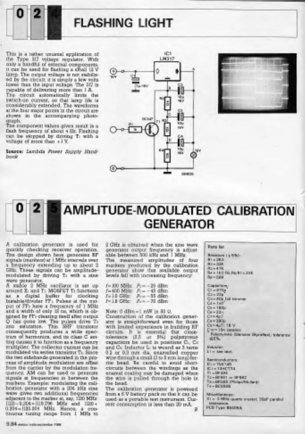
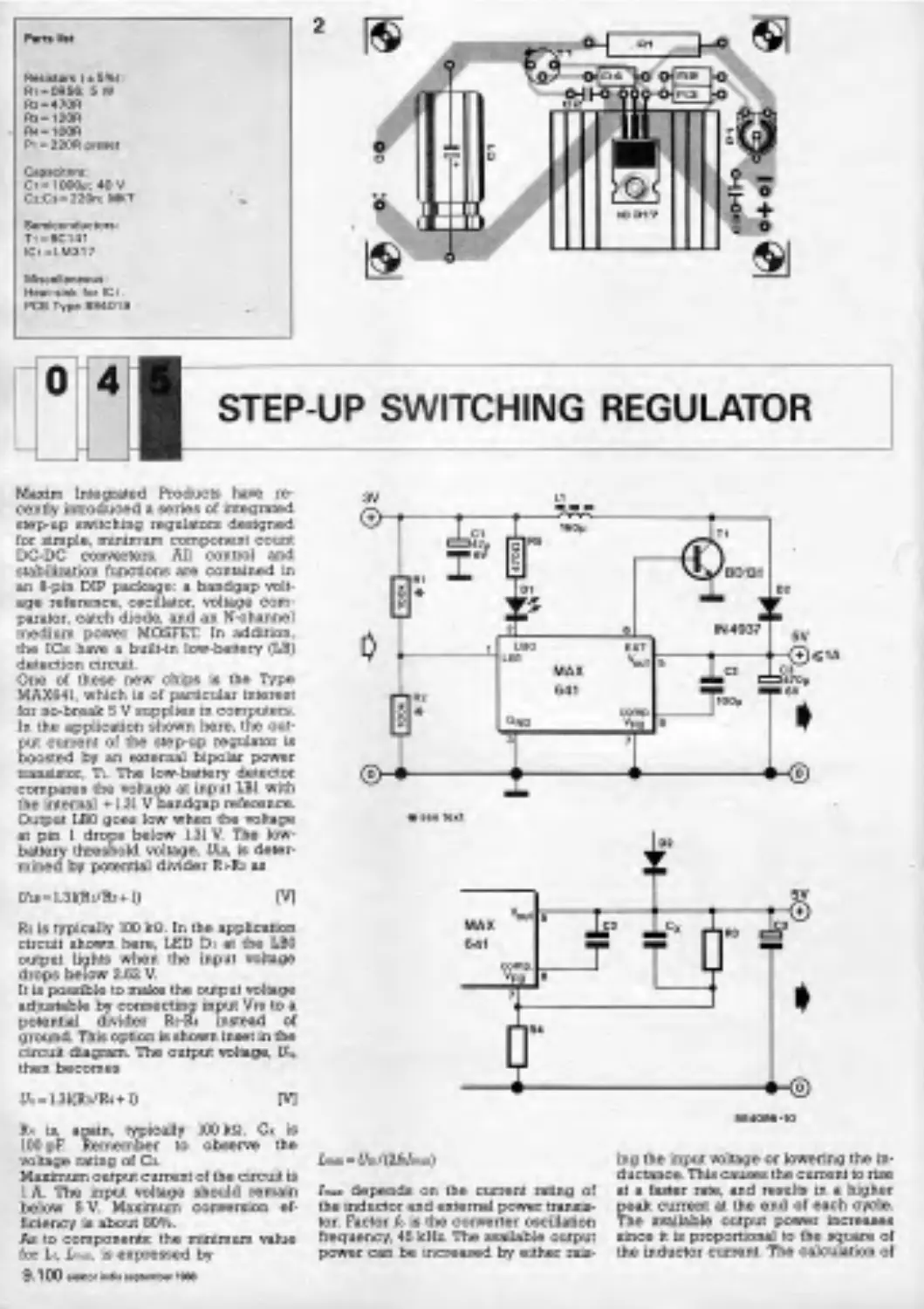
This is a rather unusual application of
the Type 317 voltage regulator. With
IC1
04317
on y a handful of external components,
it can be used for flashing a &Stall 12 V
lamp. The output voltage is not stabilized by the circuit, it is simply a few volts
lower than the input voltage. The 317 is
capable of delivering more than 1 A.
The circuit automatically limits the
switch -on current, so that lamp life is
considerably extended. The waveforms
at the four major points in the circuit are
shown in the accompanying photo-
Thecomponent values given result in a
flash frequency of about 4 Hz. Flashing
can be stopped by driving Ti with a
voltage of more than *I V.
Source: Lambda Power Supply Handbook
0 2 'AMPLITUDE -MODULATED CALIBRATION
GENERATOR
A calib Orion generator is used for
quCkly checking receiver operation.
The deagn shown ege
RF
signals (merkero)et 1 MHz intervals over
a frequency extending up to about 2
GHz. These signals can be amplitude -
modulated by driving Ti with a sine
wave generator.
A stable 2 MHz oscillator is set up
around XI and TI. MOSFET Ta functions
as a digital buffer for clocking
bistable/divider FF1. Pulses at the out
of FF2 have a frequency of 1 MHz
and a width of only 12 ns, which is obtained by FF2 clearing itself after output
CI has gone low. The pulses drive Tr
into saturation. This SHF hensiator
consequently produces a wide spec-
trum of harmonics, and its class C setting causes it to function as a frequency
multiplier. The collector current can be
modulated via series transistor Ti. Since
the two sidebands generated in the process of amplitude modulation are offset
from the carrier by the modulation fre-
quency, AM can be used to generate
signals at frequencies in between the
markers. Example: modulating the calibration generator with a 204 kHz sine
wave gives two additional frequencies
adjacent to the marker at, say, 1120 MHz:
1120-0.204=1119.796 MHz and 1120*
0.204=1120.204 MHz. Hence, a continuous tuning range from I MHz to
9.84 n
Indic
nu
2 CHz is obtained when the sine wave
generator output frequency is adjustable between 500 kHz and I MHz.
The measured amplitudes of four
markers produced by the calibration
generator show that available output
levels fall with increasing frequencV,
Pans Ilst
nenstors In 5961:
11,21,2
F1,33K
1336.1.7K
114-1K0 lis:IPHIP7= 22K
Pe- 66111
f=100 MHz: Pp= -28 dBm
=4-top'
1,400 MHz: Pi= -45 dem
1=1.0 Gliz,
6=1.8 GHz,
CFn22,3
Pp= -55 dBm
Po= -70 dBm
Ca-60p
sino'.foil
Construction of the calibration generator is straightforward even for those
with limited experience in building RF
circuits.
It
is
(2.5
essential
or SV)
ear
Ca.180p
Note: 0 dBm= I raW in 50 g.
that close -
tolerance
polystyrene
capacitors be used in positions CI, Ca
and
Inductor Li is wound as 3 turns
0.2 or 0.3 mm dia. enamelled copper
wire through a small (3 to 5 mm long) fen
g3
68.360p
Ce-ant; 16V
91o.,10n cermic
Larneea Mercer. Stan:Meat tolerance
lodKnoK
L, see ten.
rite bead. Be careful to avoid shortcircuits between the windings as the
Semiconductors:
01611401PS
the wire is pulled through the hole in
the bead.
The calibration generator is powered
1,,F961 or 8F9132
from a 6 V battery pack so that it can be
used as a portable test instrument Current consumptiOn is less than 20 mA.
Miscellaneous:
enamel coating may be damaged when
1,-PFG651Philips/Mullardl
T66365503
quartz crystal: 30pF parallel
resonance.
Type 8840541
PCB
6V
20mA
11
-SIMPLE PHONO PREAMPLIFIER
Th's circa t shows that a preamplifier for
magneto-dynam c cartridges can be
relatively simple without seriously compromising compliance to the IEC stan-
dard in respect of frequency response.
Compared to the RIAA standard, the
IEC frequency curve has an additional
roll -off point at 20 Hz-see Fig. I.
The circuit diagram of Fig. 3 shows that
input and output of the preamplifier
based around the Type TL071 operational amplifier are direct coupled,
of the preamplifier is about 3 my. Output
capacitor C4 can be fined if this offset
voltage can not be handled by the input
of the line or power amplifier..
For optimum compliance with the IEC
For
frequency curve it is recommended to
polystyrene
use close tolerance
(Siemens Styroffex) capacitors in Positions CI and Ca, and an MKT capacitor
in position Cs. Resistors are preferably
high -stability metal film types from the
E48 or E98 series, although less expensive and commonly available types from
making it possible to accurately define
the previously mentioned roll -off by the Elf series may
may also be used with
when selected for
means of network Ra-Cs. Output offset reasonable
the required resistance with the aid of a
digital ohmmeter. It was with this in
mind that Rs has been dimensioned at
5K62 (Elk 5K6). This value gives a roll off at 18.9 Hz instead of the required
20.0 Hz,.. so that the low -frequency
responseAup to 50 Hs) of the preamplifier deviates slightly from the IEC curve.
The deviation, it, of the amplification
with respect to the values set by the IEC
is shown as a function of frequency hr
Fig. 2.
A prototype of the preamplifier built
with the component values given in the
circuit diagram gave the following test
asap aas Hwy ea, i sw 9. E5
CHIP MIS
'EIMER MnO
=It
IMINII
I MINIM EN111
MIMI
NEW UII
man monn
broom minI
MIMI II =II MINI =MI
=1111 MEI I
P
IIIMM1111111=111111
10111111
1 EMPITI
111E11
I
I
I
::11.
=11111
1111.1111
MIMI
I
1=11111 ONI11111=111111.101111
ME111111M111111111111111111111111111=101
results: voltage gain 39 dB at
1 kHz;
signal-to-noise ratio greater than 70 dB
at I kHz and 100 mV output signal (up to
80 Hz: greater than 60 dB). The input
was connecmd to a test generator which
supplied 1 mVvu at an output impedance of I kg.
The circuit should be fed from a well regulated
symmetrical
supply
(preferably -F15 V, but ±12 V or +8 V
should also work). A suitable supply is
simple to build around two integrated
regulators such as the 78Lxx and 79Lxx
types, which can step down supply
voltages already available in the line or
power amplifier. Current consumption
of the preamplifier is only 2 mA.
0 2
IALTERNATING CURRENT SOURCE
One of the less known properties of
tied effect transistors is that some of
these are electrically symmetrical,
which means that the drain and source
may be interchanged under certain con-
ditions. This circuit is based on this
phenonemenon, and feeds a constant
alternating current through Ps when
connected to an alternating voltage
source.
The operation is best explained with
reference to the curves of Fig. 2, and by
assuming that a sinusoidal voltage is applied to terminals A and B.
no voltage difference between the gate
and the source, so that the FET functions
as a current source as shown above.
The constant alternating current sup -
plied bythe circuit can be defined by
fitting small resistors in the drain and
source lines, so that Vos is set to values
other than 0 V. The input voltage range
of the current source is 6 Ihn. to 18 V...
2
When the drain of Ti is negative with
respect to the source, DI blocks, and
forms a resistance that is considerably
higher than that of Rt. This has virtually
no voltage on it, so that Vos=0 V. This
means that in is constant at about 19 mA
when Vivs>8 V (see Fig. 2a). It should
..
....--1
.
...
.
be noted that the curves and values of
and Vos are typical, and may deviate
depending on the FET used (A, B or C
suffix). When the drain of T1 is positive
with respect to the source, DI conducts.
It
.. .....
Provided PI is adjusted such that the
voltage on it equals VE, there is, again,
9.86 okkto.nsaseatemeor lace
681041 .11
B
880041 -10
VOLTAGE -CONTROLLED
SHF OSCILLATOR
Th's osc Bator supplies an output level
between -10 dBm and -F3 dim, and
can be uned between 1250 MHz and
1800 MHz simply by varying the supply
voltage. Operation of the circuit is
based on the fact that the transition fre-
quency fr, of the BFG65 is reduced
when the collector current rises above
10 mA. The oscillation frequency is also
determined by the physical layout of in-
ductor La, which is a strip line made
from two parallel running lengths of
1 mm die. silver plated wire. The length
is established experimentally, starting
from 13 mm. Chokes Lt and La are 3
turns of thin enamelled copper wire
(dia. 0.2 or 0.3 mm) through a small
(3 mm) ferrite bead. Capacitors Ca and
Cr are leadless ceramic types (rectangular or disc).
The SHF test oscillator is ideal for
quickly finding the maximum usable input frequency of, for instanc a frequency meter specified to reache, up to
1.2 CH. In addition, it can be used for
testing fir input sections in indoor units
for satellite TV reception.
19
20
30
COMPUTER -DRIVEN
POWER CONTROLLER
This cirou t enables a computer to contaro the power supplied to a mains operated device (lamp, heater. drill, etc) in
255 steps. Variation of power is achieved
by controlling the voltage supplied to
the load (AL in the circuit diagram of
Fig. 2). A.conventional power regulator
1
--
is used here, composed of a trine and a
simple associated circuit to control the
phase angle at which the true is triggered.
The power supply and mains trigger cir-
al _CS
114400
cuitry are shown in Fig. I. The circuit
around Tt...0.1 incl. and ICI is a zero crossing detector which produces an
1
active high pulse every time the mains
voltage is zero. Opto-coupler ICI insulates the rest of the circuit from the
mains.
With reference to Fig. 2, Schmitt -trigger
NI inverts the zero -crossing pulses,
causing 8 -bit binary down counter ICs
to load the 8 -bit word applied to counter
preset (jam) inputs tae. .17. The counter
ot11,11,
is debremented one count by each
clock pulse supplied by -.Cilia.
When counter state nought is reached,
output ZD goes low, and Na
further docking of ICs. Simultaneously,
Na produces an output pulse, so that Ts
conducts and fires the mien
As the [rise
only fired when ICs
counts to zero,is the instant at which this
happens depends on the value of the 8 -
1, la a 13055713
2,
T3=1.478
40
;
bit control word received from a com- 2
purer. Hence, the time that lapses between the zero crossing instant and the
triac firing instant is a function of the
magnitude of the control word. The
greater the 8 -bit word, the greater the
phase angle, and the less power is
delivered to the load.
Inductor It suppresses RF interference
used by the triac, and should be able
to carry at least 8 A. The triac M this circuit can be a TIC206D (4 A) of aCIC216D
(5 A). Other types may be used if these
are known to trigger at a gate current of
less than 10 mA. The value of Rid is determined empirically, and should bees
high as possible without causing the
disappearance, on poi. A, of poises
with an amplitude of 5 V0
The only adjustment required is that of
9:. If complete switching off of the load
0required, this preset is adjusted Inc
V indicated by an AC voltmeter con-
nected instead of the load, with data
FFs (255w) written to the power con-
troller. If regulation from 0 V onwards is
not desired, Pt W adjusted so that the
meter reads the required minimum
voltage. When writing programmes for
the power controller, it should be
that the power delivered
re
to the
the load is an inverse function of the
value written into the computer's output
port.
Safety precautions:
The shaded parts in the circuit diagrams
me operated at mains potential, and
ust never be touched while the unit is
being powered. Great attention should
be paid to proper insulation in the
selecting and mounting of the parts
within the shaded areas. It is strongly
recommended to bend the pins of the
optocoupler away from the package to
ensure an insulation distance of at least
mm.
0
Finally, it should be noted that the cir-
saine result as FFe, namely minimum
cult may not operate correctly with voltage applied to the load. Regulation
loads below about 40 W, and that efectively starts with data 01.
writing 000 to the data input has the
IFIVE -BAND STEREO
GRAPHIC EQUALIZER
This design of a stereo equalizer is fairly
other four are set to maximum gain. In
this condition, top measurements
circuit around opamp At would provide
1.5%, which is certainly tolerable given
the simplicity of the circuit. Signal-to-
unusual because it is based on inductive feedback. In theory, the feedback
15 dB amplification or attenuation of
each frequency range, but in practice
only about 13 dB is attainable owing to
losses in the inductors. A virtually Her
frequency response is obtained when
all five potentiometers Fl to Peare set to
the ozone position (0 dB). Total control
range of the unit is about 33 dh
The TI,072 dual opamp in each channel
is a trade-off between cost and perform respect of noise and distortion.
Set toin 0 dB gain, a prototype of the
equalizer produced 0.04% distortion at
an input signal of 1 kHz; I V, and 0.13%
at 5 and 10 kHz. Distortion is highest
when the test frequency lies within one
band that is fully attenuated while the
9.88
resulted in a maximiun distortion of
noise ratio is greater than 90 dB at an in-
put amplitude of) V.
The frequency response curves were
obtained with the following settings:
curve I: all controls set to maximum;
curve 2: 4 controls set to 0 dB and I to
maximum;
curve 3: 4 controls set to 0 dB and I to
minimum:
curve 4: all controls set to minimum.
Due attention should be paid to the DC
resistance of the inductors. The total resistance of the inductor and series
resistors in each feedback network
should remain 680 a, so that Rs to Ria
incl. may have to be dimensioned dif-
r
.
5
.
I-
4'
.
. .
.
..
.
.
.
Pens list
flealslors It 5162
HOW arIVK
3K3
Pr ...Ps Inc1.1K0 mimeo linear pa
O
tiometer for PCB mounting.
The fallowing values are given as
4V:74' Mee teen:
,ri
3
II
I
trife!_ilttEl
8.5115,Pains. a KO
NOP
11.11,
11 a 12K
Reille. a MP
elimPto. a 3K9
27K
Capachorin
Cr:CC:CM...180 MKT
Hip
C.C2.88: bead tanrelum
CMC.4',2Cm
11111
115 1.1.5i11111
Ifnic6,
onnct,
r,
(42 c
I
0.0CIV220
CarCriCMC8.100n
11.1,, .1 H. e.g. Toko Type 2832V-10
Kkut stock no. 30-105131.
3,
3,
MaJIEWMILIZIWIIMAir
12:1'=080 mil, se. Toko Type 26011-604
larkit stock no. 30.884131.
150 rnH, e.g. Toko Type 2931y-154
P.M sleek no. 30-154131.
4M'=88 mN, e.g. To. Type 18121-583
fa. stock o. 30.8822
te,- 10 reit 5. g. Tok30o Type 17120208
CAB stork ma. 34-103021.
ferently than shown in the circuit
diagram. Always measure the resistance
of the inductors used, and then
calculate the value of the resistor reguired to obtain a total of 680 Q.
Example: a Type 239LY-154 160 mH in-
MIT :74o.
doctor from Itiko was found to have a
DC resistance of 37 0, requiring a series
resistor of 680-37=643 4. This value is
approximated with the aid of a 6808
and 12187 resistor in parallel (liti-R5 in
the
circuit
diagram).
Ferriteencapsulated inductors are recmmended to reduce magnetic coup ling. and to keep crosstalk at relatively
high frequencies down to an acceptable
level (.< -GO d13 at 10 Ms).
swoons. mini= tee 9.89
.
0 3
IJIZ TIMER
Here is a simple 'who's the first' circuit
that can be used in quiz games with up
to eight participants or groups of participants. The circuit indicates the first
one to press his key by a glowing LED
against his number or any other identification used in the quiz or game. At the
same time, the circuit gives an audible
indication that some key has been
pressed. The RESET key enables the quiz
master to restore the circuit's original
state before updating the score and pro-
O
ceeding with the next question or
assignment.
After error has been pressed, the eight
11-S bistables in ICI and (Cr are reset.
The Q outputs all go logic low and,
consequently, the output of Its goes
logic high. The circuit is now ready to
be operated. For example, if Si is
pressed first, the first bisteble is ant and
output 01 goes high. The output of Its
puns the common line of keys Sr.
Se
incL logic low to prevent more bistables
being set Hence, 01 is the only output
that is logic high. This condition is indicated by LED Dr. Simultaneously, Tr is
biased and switches on the buzzer to at-
C)
tract the attention of the quiz master.
Capacitors Cr to Cs incl. prevent the
bistables being set permanently if a key
is kept pressed for a long time. Finally,
Se is pressed to reset the circuit. This
causes all Q outputs to be made logic
low, and the common key line high,
returning the circuit to its original con -
0 3
1 mA, while less than 25 mA is drawn
The circuit is not critical in respect of when one of the LEDs is illuminated.
supplyvoltage,
voltage, which is preferably the The supply voltage need not be
working voltage of the active Inez°. regulated, making it possible to use an
buzzer (8 V or 12 V). Current consump- inexpensive mama adapter of the DC
don in the de -activated state is lees than
IHEADLIGHTS INDICATOR
t is neve
advisable to leave a car's
headligh son to long periods when the
engine is not running. Yet, especially
during the winte months, many of us in-
advert.. ly do his. The indicator de-
The buzzer should then not sound, of
C011111e.
to
scribed here helps to prevent you suf-
fering the consequent and inevitable fiat
battery.
In its simplest form, the indicator con-
about 10 mA when energized.
(St closed), the interior light (1,,) does
not come on until one of the front doors
At the same lime, the buzzer is caner-
gized and sounds Either closing the
door or switching off the headlights (St)
turns the buzzer off.
The diode in series with the buzzer is
necessary because B is normally at
+12 V via L. and A at ground via the
headlights (L:-only one shown here).
the driver's door, is shown in Fig. lb
(where it is assumed that 5, is the rel.
The buzzer draws a current of only
shown in Mg. la. With the headlights on
is opened (when eithercloses).
A slight modification to the circuit, enabling it to operate only on the switch in
avant switch).
sists of a do. buzzer and a diode as
9.90 mon.. wottti)wr
type.
la
3
POWER MULTIVIBRATOR
simple multivibrator circuit M
remarkable for its high efficiency and
ability to drive relatively heavy loads.
The circuit supplies a symmetrical recThis
tangular signal that floats with respect to
the supply voltage, An astable
multivibrator is famed by Ts, Ts, Er Ra,
Ci and Cs. The collector currents of Ts
and Ts drive Ti and Ti respectively,
while the emitter currents drive Ti and
Ti respectively. Current limiting may be
dimensioned to requirement by changing Rr It should be noted, however, that
the transistors may carry relatively high
currents. Then current amplification,
hrE, is, therefore, fairly low, so that the
current limit point can be approximated
with Inom.iii(Ue-1.4)/121. With R1=68
as shown in the circuit diagram, the
multivibrator can be used for switching
loads up to about 3 A.
Output frequency of the oscillator is
approximated by 0.7/(RiC), and is
about
53 Hz
with
Ra=68 k4,
C Ci= Ca =220 tiF and fle=12 V (14 V:
50 Hs). One of the many applications of
the power multivibrator is a battery operated mains converter. Its outputs
are then connected to the low -voltage
secondary winding of a mains trans,
former. A prototype of the multivibrator
was dimensioned for relatively high output current at 60 Hz by fitting Ri=33 a;
Ra =2 x68 k4
in
parallel,
and
C =2 x220 nE in parallel. Connected to a
9.5 V, 5 A mains transformer, it powered
a 40 W mains Milo with a rectangular
voltage of nearly 240 V... Supply
voltage and current consumption were
14 V and 6 A respectively, yielding an
acceptable efficiency of about 40%.
Quiescent current consumption of the
circuit is determined by RI, and was
0.3 A in the test set-up.
When the multivibrator is used for driving an inductive load, as in the above application, each output transistor must be
protected from inductive voltage peaks
by two fast high -current diodes fitted in
reverse across the collector and emitter
terminals.
TOUCH SENSITIVE LIGHT SWITCH
Th's low-cost circuit enables turning 1
room lights on and off simply by
touching a round metal sensor. The light
is turned on by briefly touching the
sensor, and off again by touching it
slightly longer. With reference to the
circuit diagram, when the snsor is
briefly touched, hum and noise induced
on the body are amplified by cascaded
gates Ny Na and Na. A pulse train with a
swing of nearly the supply voltage
(4.7 V) and a frequency equal to that of
the mains voltage (50 or 60 Hz) is applied to a bistable set up around Ns and
Ca is charged via Da, and the
bistable latches in a high output state.
Triac Trit is triggered via driver Ti, so
that the lamp lights.
When the sensor is touched for about
Ns.
2 seconds or longer, the pulse train
charges Ci via Rs and Dr Inverter Ns
pulls the input of Ni low when the
voltage on
CI
is
sufficiently high.
Bistable Ni-Ns toggles and Ti breaks
the gate current for the niac, so that the
lamp is turned off. The circuit also
The effect of this on the bistable
and triac circuit is similar to that outlined above.
A suggested co/1st:motion of the sensor
and LED is shown in the accompanying
drawing. The LED is fitted in a plastic
holder, and in the dark indicates the lo-
cation of the light switch. The LED
holder (C) isured in the side or top
panel (A) ofsec the ABS enclosure that
houses the light switch circuit. The LED
is located in a thin aluminium or brass
washer (B), which is cemented to lir
and glued onto the outside surface of
the plate. In the interest of safety, it is
recommended to observe a minimum
distance of 7 mm between the LED and
In this contein, constructors are
urgently advised not to use a metal or
metallized LED holder as the sensor.
Rt.
Also, neyer
replace Ri and Rs with a
single 4107 resistor.
Since this circuit is connected direct to
the mains, it must be fitted in a safe and
sound ABB enclosure that is impossible
works in a relatively noise -free environment. When the user forms a relatively
to open without it being deliberately
damaged. Once more we advise that
the presence of the mains voltage is a
serious somce of danger, so that the
whose total resistance is low relative to
first and foremost concern of every constructor should be absolute safety.
low resistance to ground, the input of
Ni is effectively pulled low by R-Ri,
alAtor indle septamber INS 9.91
2
0 3
IPRINTER SHARING BOX
Th's simp e circuit makes it possible to
connect two computers to
a single
printer. Toggle switch Sr selects the relevant computer by applying the appro.
Arista logic level to the enable inputs,
G,
of
octal bus transceivers Type
741E641 11Ci...IC. incL). The direction
input. DIR, of these is hand -wired to +5
V so that the data direction is from An to
Bit. When G is logic high, the buffers
Input BUSY of the non -used computer is
held logic high to prevent this machine
should the
pulse
user find out that the wrong file is being
TRITT:PRINIE
attempting to send data when the other
computer is accessing the printer. The
7415641 was chosen because it has
open -collector °Mons - the reason for
this should be clear when it is
remembered that the Centronics standard climates the presence of pull-up
resistors in the printer. The 7415641s, of
printed. This reset option is definitely
and Rt.
A RESET switch, Si is provided to clear
the printer buffer by means of an
used pins 15 and 34 also to distribute the
neater than switching off the printer
completely to correct the error.
The circuit is conveniently powered
hem the S V supply in the printer. In
most cases, this supply voltage is
available on pin 18 of the 36 -way Gen -
honks input connector, but this would
have to be ascertained by measuring
to the printer manual. It is
and refere
formed by resistor networks R3, Itc, Re recommended to connect +5 V to non -
are switched to the high impedance course need pull-up resistors at the
state, so that chip outputs can be con- computer side also, and these axe
nected to forma bus structure With this
in mind it is relatively simple to see that
the circuit is the electronic equivalent of
a 16 -way toggle switch.
Pend get
Pealstors t 5961:
131,112,11e036-108
813:13.01.11,- 8 -way SO resistor network
ION
SP- INO
Capacitors:
CoC2:C3= 22n
Semiconductors:
ICI ...ICe
Miscellaneous:
= miniature toggle switch.
S3= miniature toggle switch.
KIACK3 38 -way terminal strip block.
PCB Type 884030,
9.92 elektor Inc. umber INS
current over several wires in the Centronics cable. Once again, check the
"nsgsgsassgssussup
1
Printer manual to see whether these
O
O
pins are actually available for this purpose.
The printer sharing box will generally
located close to the printer. PCB con-
nectors Hi, Ha and Hs axe 36 -way straight
headers. Three cables are required for
connecting the completed PCB between the computers and the printer.
Two 10-15 cm long adaptor cables are
made from Hateable with IDC (press -on)
cnnectors
ominated at either end. One end is terin a 36 -way IDC socket for plug-
ging onto the PCB header, the other in a
female IDC Centronics socket (blue rib.
bon type)
for
receiving the printer
cable.
The short printer output cable is comCentronics
PRINTER
posed of a female 36 -way IDC socket as
above, and a 36 -way male Centronics
plug.
iomn of the
Cui
switch is aboutenfnsz
printer
C often
COMP.
O
1.111102
WTI
TIME
STANDARD RECEIVER
V)MA-2500
OMA-2500 is a 1 kW time standard transmitter on 2500 kHz. The station is
located in Liblice, Czechoslovakia, and
is operated by the Astronomical Institute of the Chechoslovak Academy of
Sciences.
Contrary to time standard transmitters in
the VLF band (DCF77, HBF), modulation
is pure AM instead of a combination of
AM and PS% or PBX. This means that the
seconds pips transmitted by OMA-25011
are free from phase noise, which is a
must for some types of PLL, particularly
in communications equipment, where
the 2500 kHz signal supplied by a time
standard receiver is used for generating
or deriving other frequencies of equal
stability.
Transistor
Ti is
configured as a
regenerative buffet which acts as an active filter with an effective Q (quality)
factor of about 1,000 at a 3 dB bandwidth
of 2.5 kHz. The received signal is further
raised in amplifier Ta-Tt before it is ap-
plied to active crystal filter Ts -X1 which
ensures, 3 dB bandwidth of about
500 Hz. Output amplitude of the receiver is sufficient for driving almost
any type of simple PLL. The receiver is
powered via the downlead cable at the
output to enable it to be mounted in a
noise -free environment.
Inductor L is wound as
2
turns
(primary) and 50 turns (secondary) of
0.3 trim dia. enamelled copper Wire On a
Type T50-2 core. Quartz crystal Xi is a
.
2800 kHz type for series resonance
Construction of the receiver should
follow the standard rules for RF circuits:
keep all connections as shoe as poss-
ible, and use ample screening and
decoupling.
Adjustment: set a function generator to
2.8 MHz at Me 10 V. Connect the output to CI. Connect an AC -coupled oscilloscope to the source of Ti, and peak
Cc. It may be necessary to reduce or increase the number of windings of the
secondary of Li to obtain resonance at
11
reception. when OMA-2600 is received
with high field strength throughout
Europe. Daytime reception in western
and northern Europe will mostly range
from poor to just usable, depending on
propagation conditions and location of
but make sure that this is not greater the receiver.
than 800 my. Remember that Ti is a The circuit is fed from 12 V. and conregenerative stage, so that the settings sumes about 10 mA. Finally, bear in
of Ca and Cs interact. If necessary, re- mind that a good aerial (long wire or
adjust the trimmers to ensure that the rhombic quad) is imperative for reliable
signal at the collector of T3 is stable, reception.
and not clipped during night-time
PROGRAMMABLE
SWITCHING SEQUENCE
The proposed control circuit is shown
n the diagram as containing two relays,
but this number may be increased if
necessary, The switching sequence is
determined by the time delay of an RC
network at the input of a gate that is
used to energize a relay via a dartington
transistor.
When Si is connected to the supply
voltage (as shown in the diagram), the
input capacitor, CI, Cs,..., begins to
charge via a resistor, Sit, Rio...., and diode Di. After a given time, depending
on the time constant of the relevant RC
combination, the voltage across the capacitor has reached a value sufficient to
toggle the gate. The relevant transistor is
then switched on, and the relay is energised.
By giving the input of each gate a differ-
ent time constant, the sequence of
switching is determined.
When St is switched to ground, the opposite happens. Diode Di is reverse -
biased and the capacitors, CI, Ca,...,
9.94 wok-tor...61.0.er ten
2.5 MHs. Reduce the signal amplitude
and redo the adjustment of the trimmer.
Disconnect the function generator, and
connect the aerial. Connect the scope
to the output of the circuit. Peak Cs for
optimum amplitude of the AM signal,
discharge via resistors Rot, Roa' ..., and
diode Da. The discharge time constant
determines how fast the capacitors can
practical energizing current for the
relays is 200 mA.
The values of resistors Ri ad Ro may lie
determined by time constants. The gate
between 1 I? and 10 Mg; the value of
capacitors CI,
between 10 pF
and 100 pl.. Time constants exceeding
always toggle first.
The supply voltage may lie between 5 V
and 15 V, but must, of course, be equal
electrolytic capacitors then becomes
comparable with the charging current
discharge and retoggle the gates. So,
here again the switching sequence is
with the shortest time constant will
to the operating voltage of the relays.
Furthermore, the BC5I6s must not
switch more than 400 mA, and this again
influences the choice of relay. A good,
1,000 seconds create problems in practice, because the leakage current of the
In general, choose the time constants so
that two consecutive ones always differ
by at least 0.1 s.
IBURST GENERATOR
A burst genera or is indispensable for
testing the dynamic response of
loudspeakers, and, in some cases, AF
amplifiers. The fact that a number of
cycles of a sinewave are applied to the
loudspeaker under test, and not a continuous signal. eliminates the adverse
effects of reverberation, reflection and
echoes which are otherwise caused by
the test room, and are almost inevitably
picked up by the test microphone. In
addition, the burst provides a good indi-
cation of the loudspeaker's performance in respect of voice coil transient
response, resonance, ad ringing.
The test signal provided by a external
wave generator is switched on ad
off at or around the zero crossing, de-
pending on the setting of phase control
Pt. The pause amplitude can be set by
Pa, while controls P3 and P9 are used for
adjusting the duration of the pause ad
the burst respectively. It should be
noted that the savings of these potentiometers interact, so that an oscilloscope is required for correct alignment.
The duration of pause and burst is not
related to the input signal. This means
that the number of cycles supplied by
the generator increases with the frequency of the sinewave applied to the
input, unless, of course, Ps and Ps are
re -adjusted.
Comparator IC1 converts the sinewave
at the input into a rectangular signal.
The switching takes place at a specific
instantaneous
amplitude
of the
sinewave, set by PI. The timing of the
switching instant is arranged by astable
mulitivibrator ICs, and is copied in
bistable ICs on the fest positive edge of
the sinewave, since this corresponds to
the rising edge of the clock signal. Output o goes high, so that the pole of electronic toggle switch ICs is connected to
pin 12, and hence carries the attenuated
sinewave burst.
The burst generator is not critical in
respect of supply voltage, as long as this
remains between 16 V and *9 V. Do
not exceed }9 V on penalty of damaging ICs.
9.95
01-3
I/O EXTENSION FOR AMIGA 500
The Commodore Amiga -is claimed to
be a computer with plenty of lacilities
for emension circuits. The model 500,
for instance, comes with no fewer than
twelve connectors and sockets. There
are, however, awkward constraints to
the practical use of all these extension
facilities.
The
SERIAL
CONNECTER
O
sc
is
cumbersome to use with TIT circuits
because of the ±12 V logic levels on it.
The use of the 86-6m con/Nampa on the
machine is complex and risky because
of the unbuffered connection to many
internal signals. The one remaining option is the PARALLEL coanamaa, which
can be extended to a maximum of 86
I/O lines es shown here, with the possibility to realize a bidirectional port.
The circuit was designed and built for
the Amiga 500 computer. It is likely to
work equally wall on models 1000 and
2000, but this has not been tested in
practice.
Output lines BUSY, P -OUT and SEL on
the PAMLLEL CONNECTOR CRT be pro-
grammed to supply a 3 -bit address
selection code which is applied to
binary decoder ICL Octal bus buffer
IC2 is the input pod at address 2, latch
ICa the output port at address 3, and
transceiver ICs the bidirectional port at
addresses 0 (read) and I (uvri). The remaining 3 addresses (lines E4, ES and
E6) can be used for 3x8=24 additional
I/O lines. Pine 7 on ICI may not be used
for selecting an input of output port, and
is used instead for driving nanny LED
Di when none of the ports on the I/O
extension is being selected. It should
be noted that IC3 is note latch, which
means that it can only output data for as
long as it is written to by the micropro-
cad b
con Output port IC., does have a lathing function, so that datawords are
g
4y 4
0000000
kept stable on the outputs until overwrit-
ten by the microprocessor.
The accompanying listing is intended as
a guide to writing software for the I/O
extension. As an example of the practical use of the subroutines, instruction
Init:
POKE 125711366,199
POKE 125706266,255
POKE 125754896,0
'call once after power -on
'BUSY, P -OUT and SEL = output bits
'select address 7 (light READY LED)
'set port to input
RETURN
a= an=123:GOSUB Wr <CR>
sends damword 123to to ICs, which then
functions as an output pod. Conversely,
instruction
a=2:GOSUB Rd:PRINT n <CR>
reads the dataword applied to IC, and
prints it on screen.
Subroutine
POKE 125764898,0
POKE 126706246,248+a
n=PEEK(125749776)
POKE 125706246,255
in
RETURN
need only be called
once at the
of the programming session. Input ports must not be
wrinen to. The I/O extension should be
fed from a separate 8 V supply.
Wr:
POKE 125706240,241300
POKE 155754898,255
POKE 125749778,n
POKE 125706240,255
RETURN
9.96 elefaor
'load contents of address a
set port to input
select address a
'read value
'light READY LED
'store variable n in address a
'select address a
'set port to output
'write value
'light READY LED
variable n
IUNIVERSAL SMD:10-DIL ADAPTORS
An increasing number of electronic
omponents, and in particular in te--
20, 24 and 28 pin types in a 'wide enclosure.
rated circuits, is now only available as
surface -mount devices (SMDs). Circuit
The printed circuit board shown here
allows making multiple adaptors that
design on the basis of these leadless,
can be used for fining:
tiny, components invariably poses problems to many because there is no way to
go round making a printed circuit board
for building and testing prototypes.
Making PCBs for SMD based designs is
Narrow SMD ICs with a maximum of
16 pins. For 8 and 14 pin types, the
PCB can be cut to the required
length.
Wide SMD ICs with a maximum of 28
cumbersome and time-consuming. In
many cases it will, therefore, be
desirable to develop the circuit as it
would have been done using ICs and
components of standard size. The PCB
pins. PCB sections are cut off to the
required length as above
transistors, capacitom and
SMA
adaptom introduced here make this
possible. With the exception of the
resistors. These are arranged in a DIL
configuration on a general-purpose
larger than ICs of normal size but still fit
in the generally adopted 0.1 in. raster.
circuit sections an complete modules on
a standard prototyping board. The size
of this adaptor does not exceed that of a
standard 16 -pin integrated circuit.
adaptor to enable fining networks and
general-purpose type, they are slightly
The adaptor PCBs effectively enable a
range of SMD ICs to be handled just as
their normal -size equivalents, and so
alleviate the plight of designing and etching a new PCB for every experiment
or minor change to the circuit.
Suitable lengths of terminal strip are
pushed through the holes at the under-
side of the boards to create pins for fitting the modules in standard IC sockets.
SMD ICs with 6, 14 or 16 pins are usually
e e ...ea...0.s
I
TW
housed in a 'narrow enclosure, and 16,
WIPER DELAY
This two -key wiper delay circuit
is
1
remarkab e for its simplicity and ease of
use. The wipe is started by pressing the
SET switch which also serves to adjust
the length of the wipe interval. The circuit is turned off by pressing the RESET
button.
The wiper delay shown in Fig. I consists
of three opamps and a
ostable
multivibrator (MMV). Opamp Ai is set
up as a triangular wave generator, controlled by the output of the MMV. When
this is low, a slowly rising sawtooth
voltage appears at the output of AL The
-
rise time of the sawtooth depends on
Rz-Cs. Opamp A3 compares the voltage
across C9 to the instantaneous sawtooth
amplitude. The output of As drops from
8 V to 0 V when the sawtooth voltage ex-
ceeds Ilan. This change in the output
voltage of As is delayed by Rs -Cs and
passed to As, so that the MMV is triggered somewhat later. The wipers are
switched on via Ti and Re when pin 3
on the 555 goes high. Also, Ca is rapidly
discharged via Di and RI, while Ds
prevents the voltage across Cs becom-
ing positive. When the MMV output
goes low, AI generates a new sawtooth
period.
september 19.9.97
When the circuit is first switched on, Cat
is discharged, and the output of Al is
slightly higher than 0 V due to Vr.st of
the
internal output transistor.
This
causes the outputs of As and As to remain low, so that the wiper relay remains energised initially. When RESET is
pressed, C9 is charged via Re, causing
the the output of As to go high, and the
MVP/ to be stopped. The delay circuit
around An is necessary to prevent Ca
being discharged completely after
pressing the sm. button,
The relay contacts should be wired
such that the dashboard switch is bypassed when the relay is energised, and
that the hold switch, H, for the wiper
motor is opened-see Fig. 2. Due atten-
tion should be given to the correct connection of the hold switch on penalty of
short-circuiting the car hatter,
WIRELESS HEADPHONES
(TRANSMITTER)
A circuit for the transmission, with good
quality, of the sound output of a TV re
ceiver over a couple of metres.
The input signal for the circuit is taken
from the headphone or video recorder
output of the TV receiver. If these are
not available, NEVER ATTEMPT TO FIT
ONE YOURSELF: THE CHASSIS OF THE
TV SET MAY BE AT A LETHAL HIGH
VOLTA AGE.
The
dio signal is amplified by IC:,
150mA
which has been given some extra
'body' by the addition of an output
buffer, Ti Capacitor Ca has a potential
that is equal to half the supply voltage
(via Its -120, on to which the amplified
audio signal is superimposed. The
resulting varying direct voltage is used
as the supply voltage for emit transistor
Ta via the primary of La. The carrier oscillaton also formed by T2, can oscillate
between 1,750 kHz and 3,500 kHz. The
consequent
amplitude -modulated
/WM
NMI
O
signal across the secondary of Lz is
MA161-10
strong enough to span a few metres. A
ferrite rod is used as transmit antenna.
Diode DI serves two functions: it indicates that the transmitter is 'on' and it
stabilizes the direct voltage (about 1.5 V)
for the oscillator. The supply voltage for
the oscillator is thus independent of the
12-18 V hne.
The inductors are easily made. A T50-2
toroid with SO turns of 0.2 mm die. enam-
ailed copper wire is used for Li. A fee9.98 alattor India MCce10019.11
rite rod of IO to 20 cm is needed for la:
0.5 rum dia. enamelled copper wire.
be wound at the ground side of Lan This
secondary winding consists of 30 turns
of up to 150 rriA may be drawn.
Ian consists of three turns of 0.6 mm It is recommended to power the circuit
dia. enamelled copper wire and should from a mains adaptor, because a current
0 4
IWIRELESS HEADPHONES
(RECEIVER)
To aroma at a uitable headphone re
ceiver that meets the requirements of
being light, battery -powered, and offering good -quality reproduction, a Ferranti ZN415 was chosen.
This IC contains a complete AM detec-
tor, an output amplifier, and operates
from a single 1.5 V battery.
The circuit shows the ZN415 in its stan-
dard application as a medium wave receiver. Circuit CI-L1 is, however, tuned
to a frequency above the medium wave
band. The output stage drives a high -
impedance headphone without any
problems. The circuit draws a current
not greater than 5 mA, which ensures a
good battery life.
The tuned circuit, CI-L1, receives the
signal from the transmitter described in
the preceding article. The inductor consists of 40 turns 0.2 mm dia. enamelled
copper wire close -wound on a 20 mm
dia. ferrite rod. For optimum reception,
C, must be adjusted with a non-metal
screwdriver. Note that the transmit frequency lies somewhere between 1,700
BSI 68-10
and 3,400 kHz.
0 4
ILEAD -ACID -BATTERY CHARGER
Modern sealed lead -acid batteries are
simplicity itsel in use. In contrast to
NiCd batteries, they may be charged by
connecting them to a constant voltage
(at the correct level). The charging current then gives a pretty good indication
of the state of charge.
These batteries may also be charged at
a rapid rate, as long as the charging current is limited at the onset of the charging process. Dependent on the make, a
charging current of several times one
tenth of the capacity in Ah is permiss-
ible. For instance, a 5 Ah battery may be
charged with an onset charging cum.
of I A. The charging voltage may then
be 2.45 V per cell. At such a (relatively)
high voltage, the current has to be
limited, otherWise the onset charging
current through a fiat battery may be as
high as 10 A.
The proposed charger, whose circuit is
shown in Fig. I, incorporates a 'standard' voltage regulator, IC,, and a variable current limiter consisting of T,, R,,
and Or. As soon as the current through
R, becomes too large, T, switches on
and the output voltage drops. The output voltage is given by: 1.2(P,R,R3)/
Ivoltsl.
The current limiter becomes operative
804019-10
at a current of 0.6/1Z, !amperes).
The charging voltage fora 6-V battery
that is required to be charged rapidly is
3x2.45=7.35 V. The total effective value
of
should then be 585 ohms. In
practice, this value may be slightly different.
For charging 12-V batteries, the value of
16+P, needs to be about 1290 ohms.
The Mont voltage should be not less
than 3 V higher than the output voltage.
The LM317 needs a heat sink, not
because it is easily damaged, but
because it cannot deliver its full output
at high temperatures.
It is, of course, possible to use the proIt
posed circuit as a common supply unit.
,
2
Parts Bert
Resistors 1,54,11
R14011514 5 W
RX -47OR
0-11-0
Rxel2OR
Pgset
MKora
OPPati 40 V
GE:CP=220a MKT
Senise44nnswi
eiBC141
IC,L51317
Miscellen ow,
Heetgink for ICI.
PCB Type 884019
4
Maxim
ISTEP-UP SWITCHING REGULATOR
n egrated Products have re-
cently in roduced a series of integrated
step-up switching regulators designed
for simp e minimum compone. count
converters. All control and
stabilizaf on functions are contained in
an 8 -pin DIP package: a bandgap voltage reference, oscillator, voltage comparator, catch diode, and an N -channel
medium power MOSFET. In addition,
the ICs have a built-in low -battery
detection circuit.
DC -DC
One of these new chips is the Type
MAX64I, which is of particular interest
for no -break 5 V supplies in computers.
In the application shown here, the out-
put current of the step-up regulator is
hooded by an external bipolar power
transistor, Ti. The low -battery detector
compares the voltage at input LBI with
the internal +I.31 V bandgap reference.
Output LOU goes low when the voltage
at pin I drops below 1.3l V. The low battery threshold voltage, Cka is deter-
...se text
mined by potential divider 121-122 as
Ms= I.31(RdR,D
[VI
Ra is typically 100 kg. In the application
circuit shown here, LED Di at the LBO
output lights when the input voltage
drops below 2.62 V.
It is possible to make the output voltage
adjustable by connecting input yes roe
potential divider Rs -12,1 instead of
ground. This option is shown inset in the
circuit diagram. The output voltage, 11;
then becomes
Um=1.31(123/R4 +1)
Oa4006-10
Ti is, again, typically l00 kg. Cs is
100 pr. Remember to observe the
voltage rating of C3.
Maximum output current of the circuit is
IA. The input voltage should remain
below 5V. Maximum conversion officiency is about 80%.
As to components: the minimum value
for IA. L.., is expressed by
(11./(2.foL...)
I,mms depends on the current rating of
the inductor and external power.transistor. Factor L. is the converter oscillation
frequency, 45 kHz. The available output
power 'can be increased by either vets-
ing the input voltage or lowering the in ductance. This causes the current m rise
at a faster rate, and results iota higher
peak current at the end of each cycle.
The available output power increases
since it is proportional to the square of
the inductor current The calculation of
the maximum inductance of Li is, unto,
tunately, relatively complex, and falls
outside the scope of this introduction to
the MAX641. The inductor should be
able to handle the required peak cur-
rents whilst having acceptable series re-
sistance and core losses. The inductor
in this application circuit should be
rated at 2.5 A minimum.
Due account should be taken of the rola-
4
AI hough this event is fairly easy to
signal with electronic means, the circuit
is relatively extensive to ensure that it
can be powered from a 9 V battery.
The circuit is based on a slotted optocoupler Type CNY37, and a home made
notched wheel Unfortunately, the current amplification of slotted optocouplers is very low (0.02 min.), requir-
ing considerable current to be fed
through the LED before a usable volley current flows in the phototransistor.
To avoid rapidly exhausting the battery,
MMV, pulses the LED at about 250 Hz
and a duty factor of 0.05. MMVa detects
the presence of these pulses. When a
fish pulls at the bait, the notched wheel
revolves in the slot, and intermittent
pulse bursts are received at the trigger
input of MMVa . Green LED Di lights,
buzzer Hz sounds, and bistable
is
set, so that red LED Da flashes eta 1.5 Hz
rate. D, and the buzzer are turned off
when the fish gets off after nibbling the
bait, but Da continues to flash. The circuit around N,, Ti and Ca then serves to
keep the current consumption as low as
possible The circuit cm be reset by
pressing S,.
Preset P, enables adjusting the
fre-
quency of the buzzer oscillator between
600 and 2500 Hz. When several fishing -
rods ke being used, each can be assigned a particular signal tone. The
buzzer can besmirched off by means of
Sa.
A suggested construction of the light
barrier and the notched wheel is shown
in Fig. 2. A small shaft is used in combi-
nation with a reel around which the
fishing line revolves. The slob cut into
the detection wheel should Oct be too
wide: 1 mm is a good starting value. The
detection sensitivity is determined by
the number of slots in combination with
reel diameter. The light barrier
should be screened from daylight
In the stand-by condition, the circuit
consumes no more than 4 mA, which
goes mainly on account of the LED in
the opto-coupler. In the actuated state,
the current consumption rises to aboM
12 mA.
Finally, Da should be a fast Schottky di-
ode. Alternatives to the type shown in
the circuit diagram are the Types
IN5817 (I A), 1N5621 (3 A), or the IIVV27
(2 A). General purpose rectifiers from
FISHING AID
This obey t provides audible and visible
warning when a fish is nibbling the bait.
the
lively high ripple amplitude at the output of the conceder. The ripple voltage
is composed of high (45 kHz) and low frequency components, and is practically impossible to suppress further.
1
1N400x series are not recommended because their slow him -on
the
Owe results in excessive losses and
efficiencY
Source: Fixed Output 10 VVatt CMOS
Step -Up Switching Regulate.. Maxim
Integrated Products.
of
1 Wideband RF signal tracer
This simp e and versatile circuit can aid
in troubleshooting defective RF amplifie
circuits. The usable frpquency
range of the tracer is about lOn kHz to
30 MHz. Measured signals (0.5 any to
500 mV) are amplified, detected and
made audible with the aid of a small
loudspeaker.
MOSFET Ti functions as an amplifier
with a high input impedance to avoid
loading the signal source. Transistors
Tr,
To
and Ti form a high -gain
logarithmic amplifier that drives AM
demodulator Ts -Ds. A single chip AF
power amplifier, IC, is included to
make detected signals audible. Testing
of RF equipment is carried out simply
by "probing around" at suitable
lo-
cations in the circuit and listening to the
detected signal, whose relative amplitude can provide an indication of poss-
ible sources of malfunction. The tracer's
logarithmic amplifier obviates the need
for frequent re -adjustment of the volume
control, Pi. The unit is so sensitive that it
produces audible output when the input is only held near the circuit section
under test.
As to construction of the tracer, this is
best fitted in a short length of ABS tubing to make a probe with three connecting wires for the supply voltage and the
loudspeaker. Constructors are advised
to strive far ample RF decoupling and
short connections in Mew of the relatively large bandwidth. Current consumption of the tracer is about 100 mA
from a regulated 6 V supply.
0
11
DRIVER FOR BIPOLAR
STEPPER MOTORS
Fo
some applications, the Universal
control for stepper motors (see U) may
L.(1A-0.7)/0.86R irnA]
be considered oo emensive a circuit.
Many small moors with limited speed
range can be equally well controlled by
a relatively simple circuit, based on, for
where R is given in ko. The above relation between L and R is valid as long as
the output transistors are not operated
in the saturated area. The saturation
instance, the Type SAA1027 or TEA1012
Most commercially available controllers are, however, intended for driving unipolar stepper motors, which are
t.
now gradually superseded by bipolar
types of similar size. In practice, the latter can provide a larger torque, but require a different type of controller.
The recently introduced Type MC34791,
from Motorola requires a minimum of
external components for controlling a
bipolar stepper motor. The maximum
quiescent stator current, I, depends on
the value of resistor R between pin 6
and ground:
9.102 0,...,6.
point is reached sooner at low levels of
the supply voltage, or when the ohmic
resistance of the stator winding is fairly
high. The manufacturers state a maximum current of 350 mA per stator.
The supply voltage for the motor (pin If)
depends on the ohmic resistance of the
stator windings, and is allowed to vary
between 7.2 and 16.5 V. When a high
supply voltage is used, it must be
remembered that the output transistors
will not operate in the saturated area to
prevent exceeding the set stator current, L. The current control used here
allows a fairly high step rate at the cost
of an increase in the dissipation of the
driver IC, particularly when the motor is
held stationary. If necessary, the
MC34791, can be cooled by connecting
the 4 central ground terminals to a relatively large copper surface on the PCR
The integrated controller has 4 TTL and
CMOS compatible inputs (see Fig. 0:
CM{ (pin 7): every rising edge of the
clock signal causes the motor to revolve
one fug or one half step, depending on
the level at pin 9. The maximum step
rate and the minimum pulse width are
50 kHz and 10µs respectively.
CW/CCW (pin 10): the logic level applied here determines the motor's
direction of travel.
F/I1 step (pin 9): this input allows selec-
on between full (0) or half step
peration-see Fig. 3.
(I)
1
lIe
115
caw ar
NI N2 I/2IC
87504 .1
OI (pin 8), tbis output impedance selec-
tion input is only effective in the half
step mode It determines whether the
stator winding is effectively cliscom
nected from the driver (0), or connected
to the positive supply at both ends (I).
The latter option improves the damping
of the motor in the half step mode, and
0
3
517.4453
11.1 0;
5/503
=
8 511054485
[ill
will prove useful at relatively low step
rates.
Pin II
of the driver IC is an open.
collector output with a current capacity
of 8 mA, activated during period A in
Fig. 3. A LED connected to this output
ou
will flash rhytmically when the motor is
rnning.
Transistor Ti was added to obtain a
reset function. No stator current flows,
and the logic circuitry in the driver is
reset, when the stand by input is driven
low. When a logic
I
gver
2ZZE sm.
is applied, the
motor is energized starting from state A.
The addition of Rs makes it possible to
masa
switch the driver to the power -down
state, rather than the reset state The
stator current is reduced to the value set
with It, as shown in the above formula.
The motor driver is probably best controlled by a computer output port. The
circuit in Fig. 2 is intended for standalone applications. It is composed of a
supply, Be -flu, an oscillator, Ni-Cs-RePs,
md a re-triggerable monostable multivibrator, Na-Cs-Ao-Dx. When Si is opened,
the oscillator is enabled, and the motor
CV,Ccw. Laa:.
a
8/504-3
senors. waesssmoss 9.103
will Hart running. The clock frequency,
be., the step rate, is adjustable with Pr.
The monostable will remain set via D2,
and Ti will conduct, as long as clock
Pulses are applied to the motor driver.
The amount of ever reversing stator current is limited by the stator inductance,
but can still be increased with the aid of
FL When the motor stops, Ti is turned
0 4
off, and the stationary stator current is
reduced to the value set with 112. The
above ar.gement keeps the died.
nation of the motor and the driver within
reasonable limits.
The current consumption of the com-
plete circuit is practically that of the
motor alone (700 mai max.). The motor
driver IC consumes about 70 mA.
INON -INTERLACED
PICTURE FOR ELECTRON
Owners o the Acorn Electron home
computer may well object to its interlaced, and therefore slightly instable, pie.
turn There is a trace of display flicker in
non-moving areas on the screen, and
this is mainly due to the internal video
procesing circuitry operating on the
-"Ir-=1..".21:0065mils
basis of interlacing, a technique used in
conventional TV transmission for
smoothing the appear.oe of moving
picture areas. Arguably, interlacing is
not very useful in computers, slates
these work with text in most applications. Special displays with a rela-
tively long afterglow time are no
remedy for this awkward problem, and
that is why the present circuit was designed. It effectively switches off the interlace function, and so ensures a restful
display, albeit that the individual lines
that make up the characters become
slightly more prominent.
Figure I shows that a TV picture is composed of 625 lines divided between 2
rasters of 312.5 lines each. In an interlaced picture. these rasters are vertically shifted by one line. This is done by
starting the second raster a and a half
time later than the first raster. Interlacing can thus be rendered ineffective
by starting the second raster half a line
period earlier (i.e., after 312 lines rather
=
first
raster
2
than 312.5). To retain the normal number
of lines (625), the second raster is arranged to comprise 313 lines.
The IRA chip (Uncommitted Logic An
ray) in the Electron computer provides a
horizontal and a composite synchronization signal, which are shown in Figs. 3a
(HS) and 3b (CSThiC) respectively With
WIC
reference to Fig. Sr. and the circuit
diagram in Fig. 2 MMVI forms a new
vertical synchronisation pulse, VS, with
the aid of the CSYNC signal. The period
of pulse VS is different for the thst and
second raster, so that MNIV2 is needed
to make VSYNC equally long in both.
IHMV2 is triggered on the first line
pulse (HS) that occurs when VS is active,
.d is retriggered when VS goes lowsee Fig. 3d. The length of the VSYNC
pulse so made is about 160 pa, or about
2.5 times the line time (II eel The ES
and the new VS signal are combined in
XOR gate Ns for driving the video
modulator. Gate Ni serves to buffer the
HS output of the ULA.
The final results obtained with the circuit depend mainly on the type of TV
9.100 ......mtna
ilwirp.
ii....maimp)
D
IM D
.1
CSYNC
MMV1
CNT'14C
= IC 1
...NO
.1C213,11.5116
123
YNC
3
set or display used, and may not be optimum when the TV is driven via its RF input. On an older type monochrome set,
a) ULA es
the central area of the picture was
ULA
stable, but the upper and lower areas
gave a less favourable look. Good
results were obtained, however, from
the use of Type TX chassis, which are
Zet
CSYNC =
mrrently the basis of TV sets sold under
C)
any different names and licenses.
Even better performance can be expected from a video monitor, whose
tli
NNW
(TTL compatible) H and V synchronisation inputs can be driven by Hr and N3
respectively. The polarity of the sync
signals can be selected with the aid of
0/16.1M2
wire jumpers. Connections c and c'
result in VSYNC and HSYNC. The
e) 4/N2 CSYNC
choice between jumper a or b depends
on the type of display used. Preset Pi is
adjusted until the picture appears vertically synchronised: the adjustment is
fairly critical when jumper a is used.
The final results obtained with the circuit can be judged from looking ate few
characters in the upper and lower area
of the screen. The modest current con-
4
sumption of the circuit, 10 mA, makes it
possible to power it direct hem the
Electron computer.
ULA
CSYNC
MMV1 /1
CSYNC
N2/6
main PCB Circuit Diagram
HS
0
87485-4
N1/1
II
FRUIT MACHINE
This is one of the very few one-armed
bandits' to which the maxim the sole
way to win is not to gamble' iz not aP-
output state of the counters
does not have a slot for inserting coins:
every play is free.
Actuation and release of the 'PLAY' but-
combinations, i.e., LED Da lights, and 13z,
plicable. In other words, this circuit
ton,
Si, causes the circuit to become
is not
predictable because of the inconstant
delay between the disable instants.
is sounded, when 3 identical counter
outputs are activated. Note that diodes
Da -Ds loan a 3 -input OR gate, and that
into saturation by Ti, which is con-
the buzzer also produces sound when
the LEDs are flashing, since the pulses
arid Nto go high in succession, and
intermittently.
Ns, and reset by the pulse at their Or
across Cr is high enough for gate Nv ta
change state. Ta is turned off, and rfl no
operative. Series regulator
1P1
is driven
trolled by Na-N7. The outpum 0th. Nu,
at output Or of ICs enable the oscillator
disable counters ICs, 1O4 and [Ca,
which are all clocked by oscillator Ni
The play is ended when the voltage
output. The 3 LEDs driven by each of the
counters, therefore, lights cyclically.
longer powers the circuit. An on/off
When a counter is disabled by the high
level at its CE input, one oldie LEDs in
the 3 groups remains illuminated. The
Parts list
NAND gates NI,Nis detect the winning
switch is not required for the fruit
machine, thanks to its very low current
consumption in the de -activated state.
Capacitors:
CKC, =s1p7; 113 V; axial
Cs:Cs:Cop tOn
CsK 10: 19 V: axial
CasCs:Csv 100n
t; 0.
kirpi
111;111112=2?191
11113X.P1
11132720
ICC= COSS
nis
9.106 awancsets watmcwas
2
Semiconductor.:
01:13mOmDse 184148
I
0_0
-/-,-
o e 0-11±0
t1/4 0-11+0
OS 044-0
,
D eDmODOtie LED iredi
D inClimDi I - LED 17.6otel
DIDOmithe -LED 41..
let:lex-00106
,_,...
!MC:DTI- '"
-BC557
°-1.°'g.--.
°--9
T. -13C567
C - I.-.
4-cl c,i
iscellaneous:
2, i at
a
i= momentary action push tenon.
.- P132720 buzzer Keen note no.
,S,
c-,-,-''''
' ko o.Frlo
T
occiVerro
63-272011
PCB Type 87076
WIDEBAND LEVEL -INDEPENDENT
TRIGGER PREAMPLIFIER
This circuit eliminates the difficulty in
re -adjusting the bigger level of an oscilloscope or frequency meter any time
the amplitude of the input signal
changes. The block diagram shows that
the trigger pulses are supplied by a fast
comparator that compares the instantaneous input signal amplitude with a
reference voltage deduced from the difference between the peak amplitude of
the positive and negative half cycles of
the rectified input signal. The circuit is
fast enough to handle input signals with
direct -coupled chain of °pampa IC,
ICr-ICr. The signal rectifier and direct
voltage amplifier are formed by 114-1)a.
lia-C/ and IQ. The relatively weak
signal is raised further in direct -coupled
opamps IC,
d IQ for comparison
with the amplifiedn measuring signal in
opamp ICs. Schmitt-trigger/inverter ICs
cleans the trigger signal before it is applied to the teat instrument. The trigger
sensitivity is set by potentiometer Pc
Choke Li is wound as 4 turns of 0.2 mm
dia. enamelled copper wire through a
small ferrite bead. MOSFET Ti may be
replaced by a Type BF991 or BF966 if
either of these is easier to obtain locally.
The circuit should be constructed with
due attention paid to the relatively high
frequencies it ran handle
this context. it is recommended to use a large
COPPer area as an effective ground
plane onto which the parts are fitted.
The shortest possible connections, ample screening, and effective decoupling
a frequency of up to 100 MHz, and has a
sensitivity of 100 Vpp
With reference to the circuit diagram,
the input signal is raised Ina wideband
preamplifier based around a UHF dual gate MOSFET, Tl, fed by constant current source Tr. Presets Pt and Pr define
the potential at the source of Tl, and
hence form the fine and coarse offset
compensation adjustments
11T- ItZ-
for
the
T-c).
*rm.,* wes9.107
jesting Pi, Ps and Pa for lowest offset
measured at the output of ICs. These
adjustments are carried out after a
warming -up period of a few minutes,
of the supply vohage at various point in
the circuit are also a must to ensure cor-
red operation.
Optimum sensitivity is achieved by ad-
0 5
and with the input of the preamplifier
temporarily shorteircuited.
1 FAST STARTING WIPER DELAY
A wiper delay is essentially a bistable
multivibra or whose off.time is adjustable with a potentiometer. Many wiper
1
n.
,
delay circuits are based on the Type 555
timer in its standard application circuit.
which hs the disadvantage of introducing a delay of about Id times the set ire
terval before the first wiper action takes
place. This is especially annoying when
an interval of, say, ten or more seconds
has been set. This circuit is also 555
based, but is unique in that it arranges
for the wipers to be activated immediately at powevon.
The circuit diagram of Fig. 1 shows the
internal organization of the 555 timer to
aid in clarifying the operation of the
present circuit When SI is closed, pin 6
is immediately pulled to +12 V because
(see also Fig.
C, is discharged as
2b). The bidable in the 555 is reset, the
output goes low, and Re, is energized.
This forms the basic difference with the
standard application of the 855, where
connected as shown in Fig. 2a,
delays the relay action until charged to
Vs of 'the supply voltage. Returning to
Fig. 1. Ci is charged via Rz and he 555k
internal transistor when the output is ac-
relay alone Note that the coil current
may not exceed 200 mA.
2
fivated. The bistable is reset when the
voltage at pin 2 drops below %Wu,
ceasing the relay to be de -energised,
The
and C, to be discharged via
discharge time, and hence the wipe interval, is defined by the setting of Pi.
When this is set to the shortest delay, the
wiper motor is constantly powered via
be,, since C, is not charged via P+Ra
only, but effectively via voltage divider
PelleRa also. The wiper delay is fed
from the 12 V car battery, and its caned
consumption is practically that of the
0
TEST -VOLTAGE SUPPLY
For testing senter diodes, base -emitter
breakdown, discs, and so on, a fairly
high voltage is needed. The usual type
of
laboratory power supply
is
not
suitable, because its output is normally
of the order of only about 30 V. lithe re-
quired current does not exceed 10 to
15 mA, it is possible to make a shortcircuit -proof power OLIPOY with
able output voltage from 0 to 50 V from
a handful of components as shown In the
accompanying diagram.
Circuit ICI amplifies a direct voltage set
by Pa by a factor of about 5. Its output
voltage should be about .25 V with
respect to junction Ci-Ca. This voltage
is inverted by ICs, whose carpal is thus
-25 V. There is then available either a
symmetrical ±20 V potential with
respem to junction C+Ca, or 50 V asym-
metrical across the outputs of the ICs.
The actual value of the voltage is set
with Pi.
The maximum current is limited by the
ICs to about 20 ntA, so that the
likelihood of damage to a component
under test is very small. The output is
tro
max. 50V
15mA
1.=
IN0160
ee see text
884003-10
short -circuit -proof
for an indefinite
period.
To avoid common -mode problem, and
also to make it possible to vary the output voltage to 0, the supply voltages to
ICI and IC2 overlap to some extent,
tor; that to ICa is decoupled adequately
by Cs and Cr.
The mains transformer may conveniently (and inexpensively) consist of
two 18 V types, otherwise a single 36 V
unit is required. The secondary must be
which is arranged by Ds and Dr. Zener able to provide a current 01 20 to 30 mA.
Ds also functions an the voltage refer- If two transformers in series are used,
ence. The supply to ICI must be make sure that they are in phase,
decoupled separately bye 100 n capaci- Before inserting the ICs into their
0 5
sockets, check the voltage at pins 4 and
7: this should be not higher than 36 V if
7410 is used, or 44 V for other types
(741A, 741E, and 741). If the voltage is too
high, a transformer with a lower rated
secondary (2 x15 V or 30 V) should be
used. If, however the voltage at pins 4
and 7 becomes lower than 27 V, it may
be impossible to obtain an output
voltage of 50 V
IPOWER SWITCH FOR CARS
Motorist are generally well aware that
car fuses do not blow just like that None
la
the less, when something appears lobe
amiss in the electrical circuit, a new
fuse is nearly always fitted prior to investigating the possible cause for the
malfunction, which then, of 000m.,
cants two fuses. The circuits shown here
are short circuit proof power switches,
or elechordc fuses with switch control
dimensioned for relatively heavy (lamp)
loads in a car. Both circuit are com-
posed of a power switch, T,, and a current limiter, L. The circuit is fully shortcircuit and overload resistant, provided
Ti is adequately cooled, and the whole
unit is constructed in a sturdy enclosure. The ciranit in Fig. la han the lower
voltage drop of the two, while that in
Fig. lb is used when a TO -218 style Type
MJE2955T or TIP2955 is not obtainable.
It is interesting to note that the plastic
TO -218 package is mechanically interchangeable with the wellknown TO -3
outline, and enables ready mounting of
trassne
elektormeisiessumbecoseD.109
2
Valet
Application
m (WI
I (Al
lit 141
Bs 141
Coaling Tr -Ts
lighting
1
0.08
5.6
3300
not required
Courtesy light
2
0.17
2.7
1500
not required
5
51.42
1.2
680
25 cm.
18
1.5
0.3315 WI
180 11 WI
225 cmk
1.75
0.2716 W1
150 11 W1
225 gm.
Bear rent or
Perking light
gyake light
Resistors 13663:
11,13. see text
Semiconductors:
Dashboard
Tr-313E2855T. TIP2865 151g. 1e1
Tr-313E3055T or TIP3065
116
olas or 86140 (Fig. 181.
Ts,13135 or B13138 Fog. 10/.
iscellaneous:
Si- see text
PCB Type I37467
Rog light or
tratficator
21
he transistor onto a flat surface using an
nsulating washer-see Fig. 2. The use
of a die-cast enclosure and TO -3 style
transistors is illustrated in Fig. 3. This
unit houses two power switches, one of
which has its contacts at the rear side
Pay great attention to the correct electrical insulation between the transistors
0
and the enclosure, and, if required, the
between the enclosure and the ca
body. Switch Si is the existing contro
for the relevant lamp in or on the vehicle Note the difference in respect o
the connection of St in Fig. la and lb.
Table I shows how At and Rt are dimen
requirement of the load, and also gives
a suggested area of the cooling surface.
Finally, when the printed circuit board
is used, Tr should be a TIP2955 or a
Mill2955T, not a MJE2955, since this has
its outer terminals (B -E) reversed.
sioned in accordance with the current
I48 MHz CLOCK GENERATOR
Currently, 48 Mils quarts crystals are
widely available at relatively low cost
thanks to their use in computer systems.
In diem there is often a need for several
clock frequencies that can be derived
from a central oscillator. When this supplies a buffered 48 Mils signal, it is relatively simple to add a divider circuit that
provides lower, phase-synchronons,
clock signals of, say, 6, 8, 12, 16 or
24 Mlis. Obviously, this obviates the
need for separate quarts crystals and associated oscillators, and so economizes
on hardware expenses.
A reliable 48 MEW oscillator is fairly dif-
ficult to make with HC or HCT gates.
The oscillator shown here is, therefore,
built around discrete RF transistors. It
operates with inexpensive, third overtone serWs resonanCe quarts Maria in
the range between 44 MHz and about
52 Wis. A parallel L -C network may be
9.110 iviniriviti rim. iess
connected in series with the crystal as
shown in the circuit diagram for accurate setting of the oscillation fre-
1
quency to 48.000 MHz, but also for 'pullinn' the oscillator a few kilohertz around
this frequency if it is used for driving a
frequency multiplier (local oscillator
chains in 2 m, 70 cm, or 23 cm amateur
radio equipment).
DIGITAL ATTENUATOR
Digitally controlled attenuators almos
invariably use some kind of tapped re
sistor network to simulate a poten
tiometer. This solution is fine as long as
the number of steps required is small.
When finer control is required, how
ever, the normal tapped resistor net
work is hardly ever used because of the
large number of components that would
be required. The circuit shown here of
fers relatively high resolution (attenu
ation range: 48 dB) whilst requiring few
components only.
The technique used is similar to that o
multiplying DACs (cllgital-to-analogue
converters). In a conventional 8-28 lad
der DAC, the output voltage is given by
(U.r/384)1V where N is the binary
number applied to the inputs. The
direct dependance of the output voltage on Tel makes it easy to obtain a
variable attenuator by substituting the
input for Ur.. The output will then be
(Um/384W.
The R -2R ladder network used here is
composed of resistors RI to Re inch,
while electronic switches ES1 to ESB
form the switching elements.
These are of the two-way type (SPDT),
connecting either the input voltage or
ground to the inputs of the ladder network. Buffer ICI presents a constant impedance to the source. Pin 7 of ICI, ICB
incl.
and la should be grounded unless the
circuit is operated with bipolar signals.
In that case, pin 7 of all three ICs is connected to -8 V.
The circuit can handle signals of up to
400 kHv with a maximum amplitude of
about 4 Von With signals of lower level,
higher frequency response should be
obtainable. The high frequency limit is
due friar buffer at the input-the electronic switches by themselves
handle signals up to 10 MHv.
can
The fixed attenuation of the circuit is
about -3.5 dB. Signal-to-noise ratio is
more than 100 dB at an input signal of
I V00. The output offset voltage is com-
pensated by adjusting Pi. Current consumption of the circuit is about 6 mA at
Ube ±8 V. Finally, it should be noted
that TTL circuits can not drive the circuit
direct, unless 47 kg pull-up resistors are
fitted at 000001 inputs DO to 07 incl.
IC4=1,356
IC,
ESZ ES1.1C3
,1053
131...1310.2215,1%
1111...1117.11k,11,
Toes
Es
deeormeaamese9.111
0 5
IELECTRONIC SAND -GLASS
This electronic version of the reversible
sand -glass uses a set of LEDs to simulate
the passing of sand grains from the up-
1
per to the lower bulb. The sanple to
build circuit is accurate enough for
most domestic timing applications.
The circuit diagram appears in. Fig. I.
On power -up, shift registers IC, and IC.,
are reset by the low pulse from network
ftm-C, A few seconds later, the sand -
glass is started. The oscillator in IC,
generates a clock signal for the shift
registers. The clock frequency is adjustable with F, Switch Si enables selecting
one of the three timing periods stated in
the circuit diagram. 5, is a small mercury or ball changeover switch
"
mounted inside the sand -glass. When
this is reversed, the switch toggles and
so .lec. the odd or even numbered
-
LEDs. Assuming that S, is set as shown in
the circuit diagram, every clock pulse
causes a logic high level to be shifted
into IC, for . long as pin 13 of IC., re
mains logic low. The MS bit of IC, (out
put Q7) is shifted into the second shift
register, IC.. Controlled by the shift
egister outputs, transistors T, to T,
mcl. switch off the odd numbered LEDs,
and light the even numbered ones
Parts
Resistors ,596/:
-.100K
2=Ior;2 -.
Capacitors:
CI =.10
V; axial
Cap.Co:Co16 100t,
C4.202; 16 V; radial
Cs = 220n
2
Semiconductors:
I
NNNNNNNNNNNNNHH
4 1-1CT16,1
Cea,41305
****************
,,4#4,1Vgip,(44gfd,T,J,Ti
MiscellaneousMO ;
BD= PO
Iroko; Cirkit stack no.
0.3-272011.
St = SPOT mercury, ball or tilt switch. e.g.
3 -position rotary switch
&TYPO 87,1,06:
rg[te'rstclreCt!"u".
9.112 Weldor India eaptember1888
o'o0?
14 I -e
I 51'
sequentially. When pin 13 of IC. goes
high, counter IC: is reset via
is
while oscillator N. is started. Buser
w
seconds (C.41.1). The pitch of the tone
is actuated and sounds for about 2
can be .t with Pi.
When the sand -glass is reversed, S.
toggles, ending the reset state of IQ.
Logic low levels are shifted into IC.
because pin 13 of IC. is logic high. The
n numbered LEDs go out one by
one, and the odd numbered ones light,
until pin 13 of IC. goes low again. ICI is
reset, 1.1 produces a short beep, and
the sand -glass can be reversed for a
new timing period. LED Do indicates
that the sand -glass is operative. The cir-
cuit is fed horn a small mains adaptor
capable of supplying about 200 mA et
an output voltage between 7.5 and
12 VDC
Construction
of the sand -glass is
straight -forward using PCB Type
87406-see Fig. 2. The position of the
LEDs on the front panel of the enclosure
is shown in Fig. 3. Make sure that each
LED is connected to the corresponding
soldering island on the PCB. SPDT
Switch 5, is made from two SPST mercury or ball switches, fitted together but
mutually reversed at a suitable position
in the enclosure. The action of the
switches. Meted by reversing the sand -
glass and measuring the switch configuration with the aid of a continuity
tester or an ohm meter. All parts in the
sand -glass enclosure should be fitted
securely in view of the reversibility of
the enclosure. The socket for connecting the adaptor, and rotary switch Sr, are
type of the electronic sand -glass
is
shown in Fig. 4. The detachable host
panel that holds the LEDs was cut born
perspex sheet.
5
STEPPER MOTOR DRIVER
Tote stepper motor driver is simple
without compromising versatility. It has
1
a conventional computer interface, an
optional on -board clock generator, and
integrated motor control and driver
stages. The board can drive dual -stator
motors, i.e., motors with two bipolar, or
four unipolar, phases. Maximum current
per phase is 2A.
The circuit diagram of Fig. 2 shows that
'he circuit is designed around chip set
'5297-L298 from SGS.
the block diagram of the 7297 is given
n Fig. L This IC generates control
ignals for a dual -stator motor, and
cables selecting direction of travel and
all
or half-step operation by appro.
fiats programming of its TLLsmpatible inputs. One full or half step
performed on the trailing edge of the
final applied to the clock input (CLIC).
'hen the enable input, E, is held logic
w, the motor is not energised, so that
e spindle can be rotated freely. Driv-
884076 -11
awskowaiwwww, isis 9.113
2
gv®
ci
,(12
3
Inhibit chopping, pin 11,aw
phase chopping, 5511. high
11
5
ID ail
51
RECIRC51.55.
°
:WV=
tffst IZ=LOV
9.114 m.o. odo 000nnonilons
2EZ
4
Pans Pa
Resistors
596,
I
1111,11xy1P0i
4W
Bril3nOr
1111.15K
.25K or 22K preset H
P2=250K or 220K preset H
Pr
Capacitors:
Cie3n2
Cte220iff 40
V
CsiCsiCse 100n
Semiconductors:
Di
.0e
B ee
LED
IP11111ps Components,
ICI
IC3.4024
1:22
5
6
Miscellaneous:
Jffre 3 -way mrminel strip (or.: 0.1 in 1r
1
Wrminal stripe Witte 0.1
tr-T.
In.li 1 jumper.
14 off solder pins Ws. 1.3 mm.
PCB Type 0114079
mg the reset input logic low causes the the stator winding is slightly higher than
motor to remain halted in the home pod the supply voltage. When MODE is held
logic low, one transistor in the bridge
tion (LED De is quenched).
Power driver Type L298 supports con- circuit internal to the L298 remains on
stant current drive of the stator win- during the free -wheeling period. This
dings. Current drive gives good results causes the free -wheeling voltage on the
became it allows stepper motors to be stator winding to remain relatively low,
here. The maximum attainable step -rate
increme with supply voltage, but 40 V
stator field strength and, therefore, reduced ripple (phase chopping, see Fig.
3). This option is offered to enable efficient current control of motors with a
the current drive. This effect can be
remedied by either re -adjusting the
connected to a voltage that is higher
than specified for voltage drive. Current
improves the
drive considerably
motor's dynamic characteristics (start
frequency and maximum step -rate). An
internal oscillator sets a bistable at the
start of each period, when the stator
windings are connected to the supply
voltage. Due to the stator inductance,
output current will initially rise linearly,
revolting in a linear voltage on current
sensing resistors Pt and Ra. When the
measured voltage reaches a certain
usec-defined peak value, VW, two internal comparators reset the bistables, and
the stator current is interrupted. Free-
wheeling diodes then reduce the induced stator field. From the above it is clear
that current drive works by peak detection. The resultant average current
depends on Mut (adjustable with Pd. the
oscillator frequency (adjustable with Pa)
and the values of the sensing resistors.
Ripple amplitude on the stator current
depends on stator self-inductance and
the logio level at the MODE input. When
resulting in slower reduction of the
relatively low stator self-inductance.
Synchronisation of the oscillators in the
L297s is required when multiple drivers
and motors are used in a single system.
This g simpleto accomplish by atilt
parts Pa, En and Cr on one driver board
only, and feeding the signal available at
the SYNC output to the SYNC terminal
on the other boards.
An on -board divider, ICa, is provided to
supply the clock signal when the relevant computer output line cannot be
programmed to toggle at the required
step -rate. The divider is clocked with
the SYNC signal of the L297, and jumper
block Kr allows selecting I of 7
mailable clock frequencies (step -rates).
CM -board clocking via ICa can be
disabled by driving input CATE logic
should not be exceeded.
The chopper frequency (refer to Fig. 3),
and hence the step -rate in stand-alone
applications, is set with Pr. Stator current is set with Pt. Lisping sounds produced by the motor point to instability of
chopper frequency, or by selecting the
other logic level at the MODE input of
ICI. When this still fails to stabilize the
current drive, the supply voltage must
be reduced until the motor operates
with voltage instead of current drive.
Stand-alone use of the driver is simple to
accomplish by connecting three external switches as shown in Fig. 5. Figure 6
shows how to connect the driver board
to a unipolar motor. The oscillator inside
ICI
is used only for generating the
clock signal required in stand-alone up Nicene= of the driver. When it is used,
the step -rate can be set by fitting a
jumper in the appropriate position on
Kt, and adjusting Ps.
ICa is purposely located at the
edge oftthe printed circuit board to enable it to be bolted on a metal surface
for cooling.
low. The CLOCK input then functions as
an output, enabling the computer to
is high, the outputs of IC2 are keep track of the number of steps perswitched to high impedance during the formed. When external clock pulses are
free -wheeling period. The stator field is applied to the board, ICs is simply omitthis
reduced fairly rapidly via the free- Md.
wheeling diodes which conduct The 5-40 V supply rail need not be
because the instantaneous voltage on regulated - smoothing is adequate
at...a...mm.6i 9.115
VIDEO DISTRIBUTION AMPLIFIER
The Type TEA5114 from Thomson-CSF
comprises three electronic switches fol-
lowed by a buffer/amplifier. Normally
the voltage amplification is% (6 dB).
When the input voltage exceeds
1.2 VliA or when the output voltage ex ceeds 1.5 Vet, an internal selector
reduces the amplification to unity (0 dB).
The threshold of 1.2 VPs is created with
the aid of voltage divider 12n -Re, which
also forms the input termination of 75 C.
Series resistors 11, -lb ensure 75 4 output
impedance for driving video equipment via standard coax cable. The
TEA5114 can be used as a video source
selector also, provided each input has
its own 75 c termination network. The
non -connected inputs should then be
fitted with a coupling capacitor. Channel selection is effected by controlling
the logic level at pins 10, 12 and 15. Note
that the logic 1 (high) level corresponds
to +2.5 V here.
IC I
TEA 5114
Zeno
input
0
2
Parts Hat
Resistors I* 6961:
flr
incI. 61511
n4 =
4713
R56261
Capacitors:
Semiconductor:
is
6T.65114.
Miscellaneous:
PCB
TYPe 87.5
9.116 6666.6.6,6,66e6
0
DISCRETE +5 to -15 V CONVERTER
This negative voltage converter differs
from a host of other designs in not being
se up around the latest integrated vim
mut. The circuit diagram shows that only
a handful of commonly available parts
are required to build an efficient +5 to
-15 V converter.
ICI functions as a seltoscffiating multfvibrator that supplies an output signal
with a relatively high duty factor. The
LIME is designed to operate from a
single 3 V supply, and has a high output
current capability for driving switching
transistor Ti. Duty factor of the output
signal is determined mainly by voltage
divider 112-12t, and frequency of oscillation by Ca -124. Transistor Ts forms part
of a regulation loop that modifies the oscillator duty Motor to maintain -15 Vat
the output of the converter.
The output volume, U.. is calculated
from
Us= -(Uni+ Uswrit(Ra/Rs +I)
The component values shown give the
following design data:
Efficiency (Pr/E0:
Oscillator frequency:
Duty factor:
max. 75%
8 Ms
approx. 0.8
Output ripple voltage:
100 mV at 11,200 mA
200 mA
Maximum load current:
Ti should be fitted with a small heat.
sink.
Source: National Semiconductor Linear
Brief la
OVER VOLTAGE PROTECTION
t happen from three to time that very
(lightning;
voltage
spikes
witching of large loads) are superim.'
arge
posed on the mains. Although these
pikes are of very short duration, they
may have disastrous consequences for
mains -operated equipment. A mains
power supply can be effectively pro.
tamed from such spikes with the aid of
varistors. These components can
handle but only for a few microsec-
onds, currents of thousands of amperes.
In the proposed promotion circuit.
three varistors are used: one between
L(ive) and hffeutralb one between L en
E(arth and one between Need E. The
varistors are preceded by fuses, so that
only the equipment connected via the
circuit is protected. If these fuses were
omitted, the entire household supply
would be protecMd with the risk that
one of the main fuses blows during an
over -voltage.
The circuit is best built into a small manmade -fibre enclosure with integral plug
and socket. The mains -carrying bare
wires should be kept separated by at
least 3 rem.
IFROM ALTIMETER TO VARIOMETER
altimeter published some 18
months ago Bi can be adapted to funcThe
tion as a variometer by the following cir-
cuit. The difficulty in the design of the
circuit is, of course, that it has to work
with very small input voltages.
It is
based on the fact that differentiating the
absolute height gives as result the rate
of change of altitude.
In the diagram, ICI is the differentiator
that operates with a time constant RIC,
of 1 s. Since this type of differentiator inverts, it is followed by an inverter.
If the amplification is arranged at 60
set to 60 k), the eventual read-out shows
the rate of change of altitude in ni/min,
assuming, of course, that the altimeter
has been calibrated as prescribed in
Ref. I.
Because of the very low levels of signal
input, the choice of components is
critical. For instance, CI must be an
MKT, not an electrolytic, type. The differentiator is a CMOS opamp that not
only has a very high input impedance,
but also extremely small drift of offset
voltage with temperature. This drift is so
small only if the opamp is used in the
low -bias mode (pin 8 connected to
This has the additional benefit of very
low current (typically 104A). It also has
a disadvantage in that the slew rate is
only 0.04 Yips, but that does not matter
here, since for all practical purposes the
stage functions as a d.c. amplifier.
Offset voltages are also undesirable in
ICs, because they are added to those of
ICI and appear amplified at the output.
Therefor, Pi has been incorporated to
voltages.
all
offset
compensate
Preferably, ICz should also operate in
the low -bias mode, but it may be found
necessary to cect pin 8 to pin 3
(medium bias) oronn even pin 4 (high bias)
to obtain full offset compensation. This
has to be tried out in each and every individual unit Simply adjust Pa for a display reading of 000 when the unit is at
rest.
The terminals should be connected to
the corresponding ones in the alginater.
The switch at terminal F allows selection
between altimeter and variometer use.
The add-on circuit may conveniently be
mounted above or under the altimeter
PCB and should be well screened.
When the unit is used as variorneter, the
multiturn potentiometer (Ps) in the
altimeter must not be tuned. If the unit
is used as barometer, the switch should
be set to the altimeter position.
Readers should note that the circuit has
been tested in laboratorium conditions
only and NOT in practical use.
BACKGROUND -NOISE SUPPRESSOR
Hiss, crackling, and aher discordant
loud passages,
The input signal is taken direct to the
output terminals via Rn and Ria respect-
lovers. Unfortunately, the sources of this
not easy to
background n oise
ively.
sounds are disconcerting and frequent
sources of annoyance to most music
eliminate, but the circuiare t proposed here
will be of help. It should be ap-
preciated, however, that the suppression of noise is always a last resort: the
best way of getting rid of it at source.
The circuit is based on the fact that
background noise is always at its most
annoying during quiet music passages.
It attenuates the output signal by some
45 dB when there is no or very low
music signal input. When the input
rises, the attenuation decreases proportionally, becoming 0 dB with normal to
9.118
leas
At the same
time, they are
summed via RI and Rs and applied to
non -inverting amplifier ICI via potentiometer Pi. The cross -over point in the
gain characteristic of ICI is determined
by Rs and Ci. Frequencies above the
cross -over point are not amplified, and
so do not contribute to the suppression.
The output of ICI is rectified by DI-Di
and used to switch off TI. This enables
Ti and Ts to short-circuit the output and
thus suppress the noise signal.
When Ti begins to conduct, the base
voltage of both Ts and T, decreases and
the output attenuation is reduced: noise
signals are thus suppressed to a lesser
degree.
The sensitivity of the circuit may be
varied by Pi: the higher the sensitivity,
the sooner the
lessens.
be matched
pionsuppre
This allows the sensitivity
to different music somces.
The peak signal level the circuit can
handle is about 210 my. Distortion at that
level is not greater Main 0.01%.
The delay before the circuit operates is
determined by time constant RiCi. With
values as shown, it is about 1 s but can,
of course, be altered to individual taste.
The circuit operates from a 12-30 V
supply and draws a current of 2 to
3 mA.
1.1
0
6
1
D.C. DETECTOR
The d.c. component of a signal can only
be detected by separating it from the
a.c. component. This is most con-
veniently done by Filtering the a.c. com-
ponent. In the proposed circuit this is
effected with the aid of the common mode rejection ratio (CMRR) of an
opamp. (The CMRR is a measure of the
ability of the opamp to produce a zero
output for the inputs).
The complete signal is applied to the Mverting input of opamp At, and only the
Capacitors C3 and C9 serve to smooth
Capacitors
signals so as to prevent
clattering of the relay.
The relay is driven by a BC547B which
can switch currents up to 100 mA. The
supply to the relay should be not higher
than 18 V
If the circuit is powered by a not entirely
themsmetrical supply, it may happen that
travel of Pt is insufficient the value
of It should then be altered as required.
to the non - When the circuit is used in an active
inverting input. The lowest frequencY
that can be detected is determined by
ac. component, via
Ci,
loudspeaker system, each output stage
should have its own detector, consisting
of Ai and associated components up to
points A and B in the diagram. The outputs of these detectors are then connected in parallel to A and B.
For mid- and high -frequency sections of
the loudspeaker system the time con-
stant of the input to At may be made
smaller to obtain a faster reaction to dc.
omponents.
Finally, the current drawn by the circuit
is determined primarily by the relay.
time constant (Az +Ra)Ci. With values as
shown, az. suppression amounts
to
about 50 dB at 20 Hz.
The output of At is fed to a low-pass
further attenuate high frequencies. This is necessary because the
CMRR of an opamp decreases at higher
filter to
frequencies. The difference signal is
then applied to comparator Az. Diodes
Di and Dr ensure that As reacts only to
voltages greater than ±300 V.
A negative direct voltage at the input of
the circuit results in a positive potential
at
the inverting input of As, which
causes the relay to be deactuated (it is
normally energized as long as the 12 V
supply is on). A positive direct voltage
at the input results in a negative potential at the non -inverting input of As, so
that, again, the relay is deactuated.
In normal operation, the voltage et the
non -inverting input of Az is arranged by
potential divider R] -Pt -Rs -Rs, so that the
relay is energized. Because of Cs, the
relay is energized a few seconds after
the supply has been switched
on.
instes-.0.
ISTEPPED VOLUME CONTROL
The circui consists of three distinct sec.
dons. The first consists of a straightfor-
ward amplifier, len and IC. The sec-
ond is a chgital counter. ICs, which con-
verts a binary code into a used
value vM Ca. That value is used to control the degree of amplification. Finally,
there is a pulse shaper, let, which
enables le3 to count up or down.
Amplifier ICia has a switch -controlled
gain of 0 dB or 24 dB. The control
switch, Ss, is an electronic type driven
from output Qa of ICs.
The gain of len can be set between
0 dB and 21 dB in steps of 3 d13. The total
gain of the two amplifiers can thus be
set between 0 dB and 45 dB.
The bandwidth of the amplifier extends
from 10 Hz to 90 kHz. The peak value of
the anglified signal should not rise
above 8 Ver with a supply voltage of
5 V.
The pulse shaper, formed by bistable
111-N3 and network es-Ris, indicates to
ICs whether it should count up or
down. The RC networks suppress
spurious pulses
The delay introduced by the RC networks before N3 ensures that the clock
pulse can not appear at the clock input
of ICs before the direction of counting
has been set. The count position can,
therefore, be increased or reduced by
switches Si or Si respectively.
Inputs Ca and D/13 of les may be used
to connect a software potentiometer a
two -who connection per control is sufficient An 8 -bit user port can thus accommodate four of such digital potentiometers.
A standard CD4051 must be used for
ICs, because HC or HeT types do not
allow the use of a negative supPlY
voltage on pin 7. The other ICs may be
HC or NCI' types. If an tel type is used
for les, 4k7 pull-up resistors are
necessary at the outputs of this circuit to
match the voltage levels of the two logic
families.
Note that Ca, Cs, and Cl are bipolar
electrolytic types.
The total current drawn by the circuit is
saaoas
about 10 ritA.
IINOSTALGIC SINE WAVE GENERATOR
As far as young engineers and techniclans are concerned, a sine wave genet-
ator is something you make from an
XR2206. In the pre -IC em, sine wave
generators were designed around
discrete components. The generator
9.120 elator inOlfigern
described here has, however, more than
just nostalgic value: it is also educational
(and perhaps suitable for writers of the
history of electronics).
The (fixed) output frequency is fairly
stable at I IcHs, and the distortion, alter
proper adjustment, below 1%. The gen
orator is suitable for use as an audio tea
generator or as a morse code traine
and costs only ac ouple of pounds to
make.
The generator is of
the so-called
double -T type, which has the advantage
of not needing any inductors. The oscil-
lator proper, Tt, is followed by . emitterfollower, Ta, which ensures a sufficiently low output impedances
The frequency is .t to I kHz by Pi, .d
Pa minimizes the distortion of the wave-
form. With Pa set for minimum resistance, the amplitude of the output signal
will be maximum, but the distortion will
be quite appreciable. Increasing the resistance will reduce the distortion, but it
may happen that when Pa is nearing its
maximum value oscillations stop Setting
is thus finding a compromise between acceptable distortion and rePa
liable oscillations. The output level also
depends on the setting of Pa: it lies between 1.5 Vs, and 3 Ws.
The circuit may be powered by a 6 to
18 V euPPIY: a PP3 battery (9 V) is
perfect. Power consumption is about
48 mW.
FOUR -CHANNEL STEREO SWITCH
The circun described here enables a
choice to be made from four different
stereo channels with only one switch.
Internal switching is effected by CMOS
devices to obviate crackling, bounce,
and other annoyances associated with
mechanical switches.
The two D -type Notables in ICs are con-
nected as binary dividers by linking
their Q output to the 1) input The 0 output of FFt is also linked to the clock in-
put of FF2, which results in a kind of
tour -bit counter.
The push-button is connected to the
clock input of FF1. The four OR gates,
Ni to Na, decode the output states of the
bistables, so that at all times only one
gate has a high output
The outputs of the gates drive the
CMOS switches in ICs and IC4. The out-
puts of the four electronic switches in
the. ICs are strapped together.
The input of each switch incorporates a
potential divider, ensuring that the
switches operate in their linear regions
This arrangement ensures minimum distortion of the audio signals: the negative
parts of these signals would otherwise
be distorted, since the switches work
from an asymmetrical supply.
The circuit draws a current of only
about I mA at a supply voltage of 5 V.
The supply voltage may be increased to
about 15 V.
sm9.121
0
6 VULSE
An alternative to a two-way (or three-
way) switch is the so-called pulse relay.
This has the advantage that fewer wires
are required and simpler switches may
RELAY
set again. Since the
bistable thenis has a set and a reset signal,
RrCrl, FFi
the Qoutput goes high and clocks FFs.
as required; a type should thus be
chosen that ran switch HO V as at
The circuit is powered by a simple about IA. The separation of cod and
power supply that must provide not less switch contacts should be at least 6 mm.
than 14 to IS V and a current of at least Because the operating switches are
be used.
Such a relay functions as a bistable:
each input pulse changes its state. The
when the relevant switch is released.
is FF4 which functions as a FIC type.
100 mA.
relevant bistable in the proposed circuit
Resistor Si limits the supply to the
changes from 0 to I, the state at pin 15 bistables to 12 V.
changes and causes the Ti -driven relay Since Ti is connected as an emitter
follower, the operating voltage of the
to be energized or deactuated.
Bistable FFi serves as contact de - relay will stabilise at some 11 V. The
BC107 then operates in its linear region
bouncer. When any one of switches St
FFi
and its dissipation will depend on the
to So is pressed, the reset inpdt of
goes high, and so does the 0 output. voltage across C; and the current
After a short time (=time constant drawn by the relay. In some cases, it may
Every time the logic state at pin 13
be necessary to mount the transistor on
a small heat sink.
The relay will switch the mains voltages
The 0 output will go low again only
completely isolated from the mains,
light -duty, low -voltage types may be
sed.
Readers should note that it is not allowed to place the connecting wires to
the switches in the same conduit as
mainsmanying cables
CRYSTAL FILTER FOR RTTY
Excellen , small band-pass filters may
be built with the aid of inexpensive
2,457.6 kHz crystals. A number of prototypes has proved the excellent
reproducibility of these filters.
The input and output impedance of the
filter lies between 470 and 820 ohms.
The 6 -dB bandwidth is 160 Hz, and the
bandwidth at -60 dB is
CW. RTTY, and (AM) TOR.
Since the insertion loss of the filter is
only 3 dB, it is possible to cascade a
number of them. The 5-41B bandwidth is
then 120 He and the -60dB bandwidth
is about 240 Hz. Operating with RTTY, it
is then attractive to work with 85 Hz
9.122 eeemme mar Ma
®I
BOO Hz. The
filter is eminently suitable for use On
shift.
070. 5200
4)0.3200
/Op Tee Tp
17c
Xl...X4
2457.6kHz
8134100 10
CONTROL FOR
DIGITAL POTENTIOMETER
UP/DOWN
Utt
= 5...15V
.P.LS13
ICe
g 4029
o
ok 0
OD
CO
D. aD.
1N6108
N1...N0 =1C1=6093
N5...N8 = IC2 .= 4011
.elOoma
u'c'LL1ILI.
ICI
IC2
0029 Oa
IC3
IT 7" TT
OD 2
0.6
to
6.1001 10
This circuit enables a digital poten- Carry outputs (CO) of the counters are
tiometer to be controlled manually with connected to an OR network Di-Ra-Ns to
the aid of up/down buttons.
prevent the digital word at the output
The clock signal and count up/down jumping from 0 to 255 or from 255 to 0
selection for cascaded counters ICs -ICs when the lowest or highest volume setare supplied by R -C oscillators Ph -Ns ting is reached. When either IC) or ICs
and the gate network at their outputs. reaches its highest or lowest count, Ns
The 8 -bit control wend at the output of inhibits further counting by blocking
the circuit is applied to the correspond- the clock pulses from Ns. Counting
ing inputs of the analogue switches in down is, of course, still possible from
the digital potentiometer. When all the highest count, 255, and counting up
eight bits are used, the control circuit from the lowest count, O. The volume is
gives a resolution of 1/255th pan of the set to nought by pressing RESET button
maximum attenuation of the digital po- Ss.
tentiometer.
Evidently, the circuit can have more ap-
plications than that discussed here. It is,
for instance, also suitable as a word generator in computer systems.
@wow... .mm -0609.123
PO
EIGHT -BIT ANALOGUE I/O SYSTEM
Analog Devices have in their catalogue
a complete 8 -bit analogue I/O system on
a smgle chip, the Type AD7569. This IC
comprises an analogue -to -digital converter with 2 ps conversion., time, a
digital -to -analogue converter with I ps
conversion time, a reference voltage;
and a bus interface for direct coupling
to a microprocessor system. With an
asymmetrical supply voltage of 517, the
input and output voltage range from 0 to
L25 V of 0 to 2.5 V respectively (dependent on the logic level at the RANGE input; widest range available when
RANGE= I). When a
symmetrical
supply is used, voltages of ±1.25 V or
+2.5 V respectively can be processed.
All that needs to be added is an address
decoder as shown in the diagram. Here,
the AD7569 is connected to output port
0 of a 280 microprocessor. Gates NI to
decode I/O address 0 to I/O at a
read or write instruction. When this
Na
happens, the output of 1,19 goes low and
ICs is selected. At a write instruction,
the data are read into the data bus and
convened to an analogue output
voltage. At a read instruction, the convemion is started and the processor
placed in the wait state via the BUSY
output of the AD7589. When the BUSY
pin goes high again, the data can be
read and stored by the processor.
A simple example in MSX
10
OUT 0, INP (0),GOTO 10
This program immediately retransmits
(via the DAC) the signal that is being
written via the ADC. This shows how
easy it is to work with the IC.
The AD7569 is manufactured in CMOS
and it therefore draws a current of only
12 mA.
TRAIN DETECTOR
model railways, reed switches are in-
var'ably used to the detection of approaching trains These glass tubes do
Either way, the complete circuit is small
and simple enough to be bat in quantity so that all sections of the track can
no look very natural and the corre- be supplied with one.
sponding magnets are also relatively
large, particular y when N- or 2 -scale
trains are used. The detection system
proposed here offers a much more
elegant solution. Trains are detected by
ascertaining from which pan of the
railway track current is drawn.
The circuit is suitable for a.. and dc.
systems,
as
well
as
for
digitally -
controlled model railways. It can be
built in two versions. The firm one is
simple design with LED indicators and a
digital output. The second offers the additional facility of powering a given aecdon of track via a digital control input.
The economy version consists of the extreme lefthand part of the diagram. In-
dependent of its polarity, the engine
cuwent flows through Da or D9 and
caues a pd. of about 1 V across the di-
ode.s Either Ti will then be switched on
via RI, or Tr Ma its. This results in the
output going logic low and D2 lighting.
Diode Di serves to prevent the output
is triggered by the current through Di
The engine current is measured by the
pd. across the at and at pins of the
triac. When the input goes high, T3 is
switched on and the gate of the mac is
at ground potential. The triac will then
switch off. If a locomotive is present in
the relevant section of the track, it wil
stop. It is interesting that the presence
of this stationary engine can also be
detected, because either Ti or Ta will
get a base current via the engine.
voltage dropping below 0 V when Ti
The cMcuit needs an auxiliary supply for
the logic section. If this is chosen at 5 V
The more sophisticated version is
shown at the right-hand side of the
CMOS compatible and may, therefore,
be processed by a computer.
onducts.
diagram. In this, the two IN4001s are replaced by a mac. Normally, this device
the signals generated are TTL and
111111111111
11111111111111111111111111111111111111111111
11111111111
13.4713.
A = trains..
INSTRUMENT AMPLIFIER
An excellent instrument amplifier with
differential input may be built from a
single, inexpensive Type NER5I4 quadopamp. The circuit shown is a development of the well-known arrangement in
the data books of, among others, PMI,
Bus Brown, and Analog Devices.
The input stages, At and Az, amplify the
difference signal from inputs Ua and
while the common -mode signal, Us, is
not amplified. U all components are assumed ideal, the output voltages of the
input amplifiers are
[la
5000
c
PE
KIM
Ui (I 0 2Ra/R1.)-r Uca
NI
Ueallz(11-2Ra/Rr)d-Uca
The difference voltage is then
UaaUr-Uaa(UI-U2X11-2Rx/Ri')
This voltage is amplified x1 in At. If a
symmetrical output is required, inverter
At should be added. Unfortunately, this
symmetrical output is not of good quality at higher frequencies, sinceAa introduces appreciable phase shifts.
To obtain good common -mode suppression, it is essential that Re, lir, and Ra to
Re are 0.1% types. It is also possible to
use a small preset potentiometer between A, B. and C (as shown inset) with
which the common -mode suppression
can be optimized.
The
may be controlled
within certain limits by potentiometer
The supply voltage should not exceed
16 V at which the current drawn
amounts to about6 mA.
a1...04= IC1= NE5514
0801040
tamsee9.125
MANUAL SLIDE FADER
Readers who have built the computer controlled slide fader published a few
months agoO, may add a manual fader
at the cost of a few extra components. It
is assumed that he projectorlas been
hued with a new DIN chassis -mounting
socket. If a 7- o 5 -way socket is used,
there are at least two spare pins for connecting the manual fader. It should be
noted that a 7- or 8 -way socket accepts a
normal 5 -pin plug.
Potentiometers Ps and Pe are connected
to the free pins of the DIN sockets as
shown in the diagram. These potentiometers control the brightness of the
lamps in the projectors. The control
voltage should be 2.5 to 6 V, and this
may be derived from the dimmer PCB
as shown in the diagram. lb do that, two
further preset potentiometers are required in each projector. The additional
presets are connected across CI in the
dimmer circuit, which has a stabilized
potential of 12 V. Preset Pi (Ps) is adjusted so that the projector lamp is at full
brightness with Ps (Ps) fully clockwise.
Presets Pa and Pa are then adjusted so
that the projector lamp is just not out
with Ps (Ps) fully anticlockwise. These
adjustments should be repeated a
couple of times as the presets affect one
another.
The photograph shows how the circuit
may be built in a small enclosure. The
projector selector 'mobs are located at
that side of the potentiometers the slider
points to when the associated projector
is dimmed. With this arrangement it is
seen at a glance which projector is in
9.126 Blektor mdieseptornber IBBEI
LOGARITHMIC READ-OUT
When
the
volt:mete
well-known
Type
LCD
7109
C is connected as shown in
the diagram, the display shows the
logarithmic ratio of the steady input
voltages, lit and Us (where
pressed es a formula:
U Us). Ex-
read-out .log(Ua/U0.
The value of Ui may be 20 mV to 3 V,
while that of Ua must lie between U:
and Ut/100.
For accurate operation of the circuit, the
ratio RI:R2 must be exactly 1:9.
The circuit is set up by applying a direct
voltage of I V to input Ui and one of
100 my to input Us, and setting PI to a
position whereby the display reads
exactly 1.000 (.1og1/0.1).
The circuit draws a current of a few
9 V (a PPS battery is
rnillamperes
perfect).
.
0 7
(Maxim Apphcatianf
1 POWER MALFUNCTION ALARM
Applications, of the well-known Type lighting. As soon as the supply voltage
555 timer have still not been exhausted drops below a certain value (set by YO,
as shown in this circuit. It is based on the 555 is triggered and pin 3 goes high.
the voltage monitor published some After about 7 s, Da lights to indicate the
years agoR The difference between malfunction. At the same time, relay Re:
the two is, however, that the present one is energised, and [Ms switches on
measures its own supply voltage and astuates a busses which continues to
buner Bm. because of the high value of
the
electrolytic capacitor across the
and for
buster, this will continue to
The ClICIDI may be added to an existing about 30 s after the supply has failed.
sound after a complete supply failure.
sated by the reservoir capacitors in the
equipment being monitored. If it is
desired to detect them as well, Ca must
be omitted.
The alarm delay may be altered to individual taste by giving a different value
to Rs Or Cr (mono time =1.111sCi).
Dr J. Devasundaram and
Dr Cariappa Annaiah
equipment to detect if and when a Brief supply variations are not indicated
because of the high -value electrolytic
The 555 functions as a munstable. capacitor between the wiper of Pi and
When the supply is normal, pin 3 of the ground. Such brief variations in the
timer is 0 and this is indicated by DI supply voltage are normally compenpower failure occurs.
eledar India me.n.c. IBM 9.127
0
II
VOLTAGE MONITOR
ted direct to the Rinput of the
p5 rocessor. The Power Pail Output (PPO) of
the IC is connected to the NMI input of
microprocessor. The EFC'
the
may
senre to forecast a mains failure since, it
the value of RI is correct, this output
goes low a few milliseconds before the
supply voltage begins to decay.
A reset is given it the supply voltage
drops below 4.65 V. The Watch Dog
Input-VVDI-may be connected to an
I/O line of the microprocessor. This input must get a leading or trailing edge
at leant once every LS s, otherwise the
A output of the IC is activated. If this
function is not required, pin 6 is left unconnected.
The Power Phil Input (RFD is connected
to the junction of potential divider 111 -Rs
across the unstabilted power supply.
With values as shovm, the
is
ac-
tivated when the unstabilized supply
The MRX680 from Maxim M a monitor
IC for computer PhDs that offers the folloWing facilities.
Resetting of the processor system by
switching the supply voltage on and
off.
Switch -over to back-up battery (for
RAM, ROM, or other logic circuits) at
mains failure.
Generating a reset pulse it the onboard timer does not receive a pulse
for more than L6 s.
Giving a warning of low supply or
battery voltage.
The diagram shows atypical application
of the MAX690. The supply voltage is
contacted to the I- terminal (pin 2) and
then suppled to the CMOS RAM in the
microprocessor via output pin 1. The
back-up battery is connected to pin El.
The IC can switch a current of maximum
voltage drops below 8.25 it. If a different
level is required, the value of R: may be
calculated from
Ili=RXU-1.2.5)/1.25 ohms
where U is
the required level of
unstabilised supply voltage.
The IC draws a current of 4 to 10 mA, depending on the output current. When it
operates from the back-up battery, it
draws a mere I oA.
100 mA.
The Iles.) output of the IC is corner-
(Maxim Application)
VERSATILE CONTINUITY TESTER
Thus simple continuity tester has 4 resist -
ranges for quick and reliable
faultfinding in electronic equipment
Used with care, the instrument also
allows testing diodes, LEDs and electrolytic capacitors.
The four resistance ranges indicated by
LEDs are:
VLO = very low resistance = green
LED Resistance between test clips is
smaller than 5 0. Seater sounds.
LO = low resistance = yellow JELL
Resistance between test clips is between 5 4 and 100 kg.
HO = high resistance = orange LED
Resistance between test clips is between 100 kg and 15 Mg.
9.128 *tom:sea
VHO = very high resistance = red
LED Resistance between test clips is
higher than 15 Mg.
The continuity tester can be used for an
initial check on the following components:
Diodes: conductive direction: yellow
LED:
non-conductive direction, red
LED The test current is high enough to
enable testing LEDs also.
Capacitors: depending on capacitance,
the yellow LED will flash briefly, followed by the red LED lighting continuouslY.
Electrolytic capacitors: first, the yellow
LED lights briefly, then the orange one.
The red LED lofts when the capacito
is fully charged. With some skill and ex
dedante,
the
capacitance
can be
uced from the charge time. The
bower produces a continuous or a brie
sound when the electrolytic capacitor is
faulty.
The circuit dilfgram shows that three op-
erational amplilers compare the drop
across the test leads to a fixed voltage,
and indicate which of the two is highest
by switching their outputs M the
positive supply level or ground - see
the accompanying Table. The fourth
opamp, At, functions as a rectangular wave generator for driving the busier.
The generator is switched on by D7,
because it is only allowed to operate
when the output of At is low and Di
lights (VLO).
After completion of the continuity tester
on the PCB shown, ranges VLO and LO
are adjusted with PI and Pa. Clip the
test leads to a 511 resistor, and adjust PI
so that Di just goes out, and Da just
lights. Similarly, use a 100 kg resistor for
adjusting Pa until Da and Da Nag go out
and light respectively.
Current consumption of the tester is less
than 20 mA from a 9 V PPS battery,
which should last for 10 to IS hours of
operation. The tester can, of course, also
be powered from a mains adaptor. It is
recommended to decouple Rs with a
22
electrolytic capacitor when the
supply voltage is relatively low. To boost
the sound output of the boner, Rie can
be replaced with a preset - adjust this
until the buzzer resonates.
VLO
LO
HO
VHO
Oa
Da
Os
Parts IHt
Semiconductors:
DI - green LED
D2= yellow LED
DS - orange or amber LED
09- red LED
OBOAD1,14-1412
ICrt,TL079,
Miscellaneous:
SI
Cuell-teemake MAIM.
BM= piezo buzzer, e.g. Toko
larkitt.
Clip for PP3 amen,.
Sweatt ABS enclosure.
PCB Type 12.1029
POMO
COMPUTER- OR SENSORCONTROLLED DIMMER
pi L.,
gni
II
rirmait
:0
oc
13E4131111
1
SU
ms). Depending on the type of controller used, applied power is then
maximum (LS7331), or equal to the last
set value (L57332). The next touch on the
sensor switches off the load. When the
se.or is touched longer than 339 ms,
ICI slowly varies the lamp intensity between maximum and minimum. Lamp
intensity is selected - and retained -
imply by releasing the sensor in the appropriate instant. All control operations
are synchronized to the mains
fre-
quency by a phase -locked loop in the
controller chi,
Inputs I and 2 are functionally equiva9.130
elagar intlie september
nee
,
c:
The central dimmer chip in the circuit,
an L97331 or 1.57332, accepts control
commands from a sensor (number I or
2) and from a computer (input A).
The load is powered when the sensor is
briefly touched (between 39 and 339
on
lent, but the use of input 2 is preferred
over input) when the sensor is connected to the circuit by mea. of a .cable.
Input A makes it possible to control all
functions by means of a computer. The
dimmer chip sends it status to the com-
the 4N25 are .ed. To prevent the
failure; minimum phase angle; dimmer
is provided by the computer via ter-
puter via outputs B, C and D (mains
active).
Operation of the circuit
relatively
simple. Components DI -Ds -is RI -Rs -Cs -C3
forma 15 VDC supply for IC) Capacitor
C7 ensures that this supply continues to
operate when relatively light loads
(< 25 W) are controlled at large phase
angles. In the interest of safety, series connected resistors 1215.-Ris and Rt-Rs
may not be replaced with single 4M7
and 10M types respectively. The value
of Re,
fits and Rn may have to be
changed when other optocouplers than
supply voltage for ICI dropping below
15 V, these resistors must not be made
smaller than 6505. The total current consumption of the LEDs in the optocouplets should remain below 25 mA. The
5 V supply for the associated transistors
minals +5 V and O.
Finally, an important note on safety: the
necessary insulation between the user
.d the mains can only be ensured if the
dimmer is fitted in a sealed ABS enclos-
0 8
LSYNCHRONISATION SEPARATOR
The Type LMI881 from National Semiis
a
synchronisation
conductor
separator that has already found its way
in numerous commercial applications.
Practical use of the chip is straightfor-
ward, because the number of external
components is kept to a minimum. The
R -C network at pin 6 connote the the in-
ternal tinting of the chip, and the width
of the synchronisation pulses at the outputs. In the sample circuit, the R -C constant is dimensioned fora TV line frequency of 15,825 He. The input of the circuit can be driven with composite video
levels between 0.8 V. and 2 Van Gates
Na and N4 are provided to enable driving monitor inputs that require inverted
sync signals. The amplitude of these is
determined by the supply voltage -
when 5 V Is used, TTL-compatible inputs can be driven direct.
0
BURN -IN PROTECTION
FOR PC SCREENS
Many computer users are in the habit of
abandoning their machine for several
hours without turning it off, or at least reducing the display intensity. This
negligence readily leads to M. or irn-
ages permanently burned
into
the
phosphor layer of the screen. There exist memory -resident programs that
detect the prolonged absence of
keyboard actions, but compatibility with
the main program is often a problem.
The hardware solution presented here
is reliable, and should work with most
IBM PC -XTs and compatddes.
The circuit effeclively sits between the
keyboard and the computer, and be-
tween the computer and the monitor. A
CMOS switch breaks the connection
between the computer and the monitor
when no keyboard action is detected
for some time. To prevent having to cut
existing cables, the circuit is mounted in
a small box fitted with the appropriate
sockets and connectors. The supply
voltage is obtained from the keyboard.
Counter ICt is reset by data from the
4T°9
ciL9-
--
keyboard. When the data flow stops. the
count output of ICi goes high after a
predetermined period. This causes ICs
to switch to high -impedance, so that
keyboard data is blocked by Na. When
any key is pressed, ICt is reset, and the
connection between video output and
® ylowa Inpul
act m.81.1...1088 9.131
'
monitor is restored. The first keyboard
code is not transferred to the computer,
because Ni blocks data as long as CI is
not discharged. This arrangement ensures the suppression, on the monitor,
of the first, arbitrary, character typed on
the keyboard to restore the video conection.
The screen saver was tested on an
Amstrad PC1640SD and a monochrome
monitor (Hercules -compatible video
mode). For computers with a EGA, it is
probably necessary to break the intensity, rather than the video, signal. With
PC compatibles other than the Amstrad,
the logic levels on the keyboard data
inverted. To be able to use the
circuitare with these machines, insert inverter Ni between the output of Na and
line
the keyboard input of the computer.
The display -off' delay can be selected
PG-kr: pinning of keyboard connector
Pin
as follows:
011 (pin 1)
Q10 (pin 15)
Q9 (pin 14)
QB (pin 12)
Q7 (pin 13)
Assignment
l't:3:'11 Ctrs'
11 min.
,
0 8
5 min. 30 s
2 min. 48 s
1 min. 22 s
3
:
mouse button 1
ground 5
PC -Xi: pinning of video connector
PIM
Assignment
2
3
secondary red or ground
4
primary red IR,
primary green (GI
5
primary blue 161
=I'ary rt7;ntTno:Wo"IVI
rno'uVse hunon 2
42 s
9
H -sync
V -sync
LDISCRETE VOLTAGE REGULATOR
Low -drop voltage regulators can aid in
saving energy by keeping dissipation in
power supplies low. Unfortunately, integrated low -drop regulaters with an out-
I
put current capability of more than
about 0.4 A are hardly found on the
5V
market. The low -drop series regulator
IA
shown here is intended for all applications where more than 0.4 A is required, and supply dissipation is to be
kept as low as possible.
Constant -cure. source Tkth-Dx-Ra ensures high amplification and adequate
suppression of hum and noise on the
Ts and Ti form a lined
darlington transistor. This is driven by
ofw input voltage.
Ti, whose base and emitter terminals
are connected to the output voltage.
When this rises, the emitter potential
rises above that of the base. The transistor blocks, so that the control voltage for
Tr -Tr, and with it the output voltage, is
reduced. Diodes D3 to Deserve to
supply the start voltage for this regulator
circuit.
The output voltage is determined by Dr
and RrtIth Resistor lh can be replaced
with a BICO preset to compensate the
(usually fairly large) tolerance on the
senor diode. It should be remembered
that the circuit has no current limiter, so
that it is not short-circuit resistant.
D1...D6 = I N4148
9.132 eleRtof inalesepterneer
884055
WATER ALARM
This circui gives a loud warning when
even the tiniest a mou humidity
of water is
detected on a special
sensor.
When this is installed in a...suitable location, the circuit provides an early war-
ning before a defective pump, leaking
drainage system, water supply, washing
machine or dishwasher can flood the
bathroom, cellar or kitchen floor. There
exist self-locking valves and automatic
switch -off systems to prevent flooding,
but these are, in the main, not sensitive
enough to afford the degree of protection required, Le., they are not actuated
until the domestic calamity is actually
taking place.
The circuit is an application of the low -
ar
Type LMI801 from
National Semiconductor. The reference
voltage for this IC is set with Rs. When
the voltage at pin 4 of the chip exceeds
the set threshold due to the sensor
becoming wet or humid, the chip drives
the active piezoelectric buzzer with a
current of no less than 24 mA.
Stand-by current consumption of the circuit is about 10 yA, so that a 9 V PP3 battery should last for about I year. Finally,
it -is,
of course, possible to connect
multiple sensors in parallel.
SOFT -START FOR HALOGEN LAMPS
This simple circuit mends the life of
halogen lamps in slide or film projectors
by eliminating the sudden temperature
increase in the lamp filament when this
is still cold, and forms a very low resist -
Capacitor Ca is discharged yet when
the lamp is switched on. This means that
Tt conducts, Ta blocks, and the
optocoupler-triac is not activated. The
initial filament -heating current is limited
to a safe 4 A or so by resistor Rs, which
shunts the triac. Meanwhile, Ca is
charged, so that the base voltage of TI
drops. This transistor is turned off, so
that Ta starts to conduct The cmx of the
circuit is that the LED in the opto.triac
causes the [rise to be fired only during
the zero -crossings of the alternating
supply voltage. Shunt resistor & is then
effectively short-circuited, and the lamp
lights at full intensity.
The opto-triac should be fitted on to a
large heat -sink. Maximum output current of the ckcuit is about 8 A.
T3
1-T I
T MR .3 335 73
13 = SliARP .02333
BISNO, ntlie SOP.M.119089.133
ELECTRONIC SIGNAL DIVIDER
4(
00
0
0
6.0011100
11}1....1= 4066
The problem is well-known, the more
signal soulces, the higher and more
tangled the heap of interconnecting
wires, and the more hum on recordersThis
circuit can aid in avoiding these difficulties and the awkward situations that
arise from them. The modular structure
of the signal divider allows it to be laid
out to individual requirement (the cu cult diagram shown is but a suggested
configuration),
The signal divider shown should be
capable of mastering relatively complex
equipment set-ups thanks to its two tape
recorder inputs, echo input, and auxili-
merits no further discussion. The inter- send socket. Amplification of the
nal structure of 'black boxes' ES) to ESs opamps is defined by the feedback reis shown in the top right-hand corner of sistor (Rs to Ria).
the diagram. Each channel comprises
two pairs of electronic switches which
signal divider (20mA), makes it possible
to replace the mains supply with a pair
of 8 V batteries it the unit is not used frequently.
horizontal (series) switches are closed,
and the vertical (shunt) switches opened. This situation is reversed when input
Switch
S is made negative (S. closed), Pm-
totypes of the switching units achieved a
cross -talk level of -135 dB and a channel
separation of more than 76 dB. Signal -to -
ary input. In the sample circuit, six
ratio was more than 100 dB, and
switches are used for routeing the distortion less than 0.01%.
signals. The function of these switches
is summarised in Table 1.
The symmetrical 8 V power supply of
the circuit is a conventional design that
9.134
Th low current consumption of the
are controlled in complementary
fashion by the logic level applied to input S. When this is driven positive, the
The left and right channel of the auxiliary input are joined with Rr sad Re. The
monaural signal so obtained is then
amplified in As and fed to the echo
Sx
Sa
Sa
SE
SE
Function
Input to taps I (reward)
Input to taps 2 (reword,
Tape I (playback, to tals, 2 (Mood,
Echo (moot, to tape 2 (record,
Tape 2 pl,backl, to tape (record,
Echo hopull to tape
(record,
1
1
-o
81 ALTERNATIVE VOLUME CONTROL
Tracking o many types of inexpensive
logarithmic stereo (dual -axis) potentiometer is usually very poor, and gives.
rise to audible volume differences in
stereo
AF
amplifiers.
This
article
presents two alternatives for making a
stereo logarithmic volume control with
adequate tracking characteristics
To begin with, linear stereo poten-
tiometers may be used. Plotting resistance as a function of spindle position,
the single elements in linear stereo
potentiomemeters give a straight line,
marked l in the accompanying graph.
Curve 2 is obtained when the indidual
88403241
Uo
and curve 3 when they are connected .
shown in Fig. la. The latter One curves
,
Ui
0.9
correspond to a pleasant and natural
sounding volume control: with the goteMiometer set to the centre of its travel,
the attenuation is about 6, against about
10 for a standard stereo logarithmic goteMiometer.
The response of the volume control is
also improved by the use of a stereo
logarithmic potentiometer connected as
shown in Fig. lb. This configuration
enables an additional attenuation of
about 6 dB to be achieved in the first
part of the control range This attenuation decreases gradually as the spindle
is advanced.
0.1
0.2
0.3
0
0.5
04
0.7
o
0:9
potentiometer position
0040.2
0 8
ULOW -VOLTAGE CONTINUITY TESTER
The sire o this continuity tester can be
kept very small hanks to the use of a
1.5 V pent ght battery. The miniature
loudspeaker sounds when the resistance between the test clips (or probes)
is between 0 and 100 a. Differences of
6 R are translated in a corresponding
change of the output volume.
The battery has a relatively long life expectancy because current consumption
of the continuity tester is only 30 mA
when the test inputs are short-circuited.
.whar,,,a.,,ww..,,ass 9.135
o 8
1
SYMMETRICAL VOLTAGE DOUBLER
Many circuits based on operational
amplifiers and comparators require an
symmetrical
auxiliary,
low -power,
power supply. The circuit shown hem is
an asymmetrical-to-syrnmetrical step-up
convener, which is ideal for use in
digital equipment, whether battery powered or with a large 5 V supply, but
lacking symmetrical rails for feeding
°pampa. Cost and space requirement of
should
compare
the
converter
favourably with an add-on symmetrical
supply requiring a separate trans-
former, rectifier, smoothing and regulation parts.
The circuit diagram demonstrates the
simplicity of the voltage doubler, which
is an application of the recently in-
troduced Type MAYABO from Maidin In-
tegrated Products Inc.
Output impedance of each symmetrical
rail is about 200 g, and maximum current about IO mil. In the quiescent con-
88405B-10
dition, the chip C0118110105 hardly any
current at all, and ripple on the output
lines is then only 40 inVer.
Vcc 5V
tam -1.5 kHz
load -1 k0
efficiency
condition
ripple
V+ and V-
40 mVpp isplkas)
30 mVoe Ispik001
ot loaded
:0 Vat (spike.)
V- notloaded
loaded
not totaled
BO
V- loaded
V., ...V-
V+
+7.53 V
loaded
82%
60 ralro
7416
100 raVee
80 mVan
rola
864056-11
AUTOMATIC VOLUME LIMITER
Tlus circui limits the output power of an
AF amplfier when predefined levels of
amplitude and frequency of the output
signal, o current consumption, are exceeded.
Current consumption of the amplifier is
sured with 11r. Transistor Ti c n-
actsoand drives the volume limiter, 'fa,
when the drop across R. exceeds 0.86
V. The limiter reduces the amplitude of
the AF input signal by shunting this with
a variable resistance formed by a light dependent resistor (LDR), which is it laminated by LED Da.
The T -filter connected to the loudspeaker output of the amplifier can also
actuate the volume limiter via preset P1,
9.136 O.. .dia september INS
which thus allows setting the onset point
lights to indicate that the onset level o
of the limiter as a function of output the limiter has been reached. When Da
signal amplitude and frequency. The lights at maximum brightness, it is imTable shows the configuration of the possible to use the relevant control on
filter for three ranges of amplifier output the amplifier for taming up the volume
power. Capacitor Ci is a bipolar type. further.
The filter is laid out to respond to low The LED and LDR are fitted in a small,
and high frequencies to prevent the light-resistafit, enclosure, e.g. s him con.
woofer and tweeter in the loudspeaker miner. A single LED (Da) enables an attenuation of IS dB to be achieved. This
box being overloaded.
The emitter of Ta is held at a reference can be increased to 20 or 23 dB by fitpotential that follows the supply voltage ting one or two LEDs in series with Da.
of the amplifier. Supply voltage fluctua- Distortion of the input signal is low, and
tions thus have a direct effect on the feedback problems that often arise in
bias setting of Ti. This does not con- FET-based circuits should not be enduct until the threshold of 0.6 V between countered. Series resistor A is dimenbase and emitter is exceeded. LED De
sioned in accordance with the required
omitting the filter section, and applying
the loudspeaker signal direct to PI.
Current consumption of the limiter with
response of the limiter, and the signal
level and impedance at the input of the
amplifier.
It should be noted that the proposed Ds and D8 on is about 35 rnA at a supply
limiter is relatively slow. This disadvam
CI
CC
of 40 V.
rage is caused by its response delay of
ms. The circuit can be
about 100
simplified to limit voltage peaks only by
0 9
11 NOISE -RESISTANT 5 V POWER SUPPLY
recently introduced integrated
voltage regulate Type TEA7034 from
CSF-Thomson has been specifically designed for use in microprocessor -based
The
circuits whose operation can be ex-
pected to suffer from noise, spikes and
digital interference.
6..28V
TEA7034
After pow2L-_,on the regulator supplies a
delayed RESET pulse to the mi-
croprocessor. The timing of this pulse
depends on the values of RI and Ca. In
the application shown, the delay
RESET
gl
is
about 0.6 s. The regulator is capable of
withstanding input voltage peaks of up
to SO V. When the output voltage drops
below 4.75 V. shunt regulator Ti is
switched on, and Co acts as a current
buffer that temporarily feeds the load.
Once the regulator is powered -up, the
raw input voltage is allowed to drop to
6 V without affecting the stability of the
output voltage. It should be noted, however, that the RESET output does
not toggle properly unless the itiptLit
D1 =1N4148
G2
only 0.6 Vat the maximum output current of 500 rnA (the shorficiremit output
current is 800 mA). Voltage regulation at
with I. functioning as a pull-up resistor. the 8 V output is to within 2.5%. Revers The circuit introduces a voltage drop of ed input voltages of up to -18 Vat the
voltage is greater than about 8 V. RESET
remains low at lower input voltages,
Cs
too
input do not harm the IC, which is short -
circuit resistant as well as protected'
against thermal overloading.
,
9.137
0 9
PRESELECTOR FOR SW RECEIVERS
The low input capacitance of modern
dual -gate MOSFETs makes it possible to
realize negative feedback by means of a
non-decoupled source resistor.jf prop-
erly applied, this technique enables
making an RF input stage with a relatively high dynamic range. No short radio amateur needs to be told that
good large signal handling capabilities
are a must these days to prevent re
and
overloading
ceiver
cross -
interference caused by very strong
signals.
Unlike input sections in many top -class
SW receivers, this circuit has no problems handling RF input signals of on to
2.5 \ 0, (not uncommon during nighttime reception, and when a good aerial
is used). The output then supplies 3 1A,
when terminated in 50 4.
Tuning capacitor CI determines the
overall gain, which is mostly due to
resonance in the L -C network at the input of the circuit. The maximum drain
current that may be set by 1,1 is 12.7 mA,
corresponding to 2.29 V on Rs. The
minimum
drain
current
is
10 mA
(Ms =1.8 V).
The six input inductors are wound on
high-quality ceramic formers with a
diameter of at least 10 mm. The ferrite
bead is slid direct onto the gate 1 tan
oscil-
lation in the VHF or UHF band. Output
inductor Lt is wound as 20 turns (A) and
4 toms (13) on a. Type G2-3/FT16 ferrite
ring core.
0 9
The freguencY rang. Of the active
put selector are,
ie-
I: 30...100 kHz
2:100...300 kHz
3: 300...900 kHz
4: 900...2700 kHz
5: 2700...9000 kHz
6: 9000...30 000 kHz
ISINGLE -CHIP RS232 TRANSCEIVER
There are many applications in which
only one 09232-C line is perfectly adequate for serial communication between computer equipment. In them
noise
use of the well-known integrated circuits Type 1488 and 1489, which ace a
quadruple 09232-C line driver and re -
deduced born the curves in Fig. 2. It is
seen that R. allows the input threshold
of the receiver to be shifted over about
6 V to ensure correct response to the received signal:
cases, it is often tempting to resort to the
respectively (the equivalent
types born Texas Instruments are
SN75188 and 9071189). This solution
uneconomical, however, because two
chips are required, in which no fewer
than six line interfacing devices remain
filtering
and
optimizing the
response for relatively high bauclrates
and non-standard swings of the input
signal. Dimensioning data for the re-
sistor, 5, connected to pin 6 can be
left-hand
receiver
input
threshold with R. -curve: 10 Ics fitted between
unused. Also +5 V is required in ad-
pin 8 and pin I;
centre curve: response input not con-
driver, a receiver and a 5 V converter,
right-hand curve: receiver input
threshold with Ro =20 ko fitted between
pin 6 and pin 8.
dition to +12 V.
The new Type SN75156 from Texas Instruments houses an RS232 -C line
which makes it possible to feed the chip
from a symmetrical 12 V supply. The re-
eted;
fs provided with a response in-
Noise rejection of the receiver can be
sistor, or a resistor and a bias voltage, for
response input. The curves in Fig. 3
put, which can be connected to a re9.138 eleldor
speernber1898
defined by fitting a capacitor, Co, at the
2
to
TM.= 22
2E8, -HIV
T
2.225.0
2821227 11
show the input threshold volMge, ihr (y aids), as a function of pulse duration 212
3
1E1E1 1111111MIN 11 II
IMM111111 MIL 111111.01111
IIMM111111 MIL ' 1131111111
(x-axis), with Cc as a parameter. It is
seen that C. effectively raises the input
threshold for pulses with a relatively
short duration. Hence, needle pulses
(noise) superimposed on the received
INE11
Otr i
causing digital pulses at the output of
the line receiver.
=M111111 01101
1101111IP./1
The input of the line driver in the
I 11U11111M11111
=M14111, iI0111111 1.11011111111
=1111ho'IMM101110111511.1211111 II
ShI75155 is TTL compatible. The line
driver has a current -limited output
(Inn= IO ruAl Clamant consumption of
the chip is 10 mA typical, exclusive of
the line current.
The nem. is
KIM !
MEN III MU 10111 cc.",
di MIMI I
MUNI !I MW1111
R5232 -C signal can be prevented from
0
IMM1 11111 IM111111
111E111111 11111111
=M111111 INII111111111111111mm.
=M111111 =MIIIIIIIM111111 II
ME111111 =NO11111111111111 II
MINIMIIIIIIMM211111111M111111
DECEPTIVE CAR ALARM
tended to trick car
burglars into beheving that the vehicle
is fired wi h an alarm system. A LED fitted as a suitable lucerne on the
dashboard flashes at very high
brilliance. This is achieved by feeding it
with a pulsating 821=018 of about
100 mA, which is far more than permissi-
ble for continuous operation. The circuit is based on a relaxation oscillator
2812686
set up around unijunction transistor
Ti which supplies repetitive
pulses with a duration of a few
milliseconds to darlington transistor Ts.
(MT)
Via Ts, the LED flasher is turned off
when the ignition is switched on.
Due to the low duty factor of the
pulsating current, the circuit has an
avenge current consumption of only 2
mA. Resistors Ri and RI may have to be
redirnensioned to compensate the rela-
tively high production tolerance on
High -efficiency LEDs are not
suitable for use in this circuit, and care
should be taken not to exceed a peak
1.11Ts.
current of 250 mA.
Finally, it may be a good idea to fit the
LED near the car radio and to secure
adhesives on the side windows of the
vehicle warning of the presence of an
alarm system.
retonwsimmwtissit9.139
0 9
ELECTRONIC MOUSETRAP
This is an animal -friendly design, whose
operation is apparent from the drawing
and the circuit diagram. A piece of
cheese is put on a piezoelectric homer
mousetrap. When the
mouse approaches the cheese, and
fitted in the
trips on the buzzer, an electric signal is
generated. This signal is raised in a
high -gain amplifier, ICt, whose rectified output signal is used for controlling
relay. When a predefined sound level
is exceeded, the relay is energised, a
spring -operated lever is released, and
the door of the mousetrap is closed. The
complete box can then be taken out of
doom to release the animal.
The sensitivity of the sensor can be in-
creased by fitting a small screw and
metal plate on to the crystal element.The
metal plate should have some play
to ensure a soft rattle on the buzzer sur-
face when this is tipped on by the
mouse's feet Preset Pi is the sensitivity
control.
ITWO -WIRE REMOTE CONTROL
This circuit enables 4 devices to be
remote -controlled via a two -wire cable
installed, for instance, between the
cellar and the attic in the home. Operation is simple: pressing switches St to
Sc selects the corresponding output, Al
to A4, at the receiver side.
The regulated voltage supplied by ICs
is carried by one of the wires (A) in the
9.140 elelOgipuliesepternber ISM
cable. At the 'transmitter' side, this
voltage is reduced by the drop across
two, four, or six diodes, and fed back to
the receiver via wire B, when Sr, Sr or Si
is pressed respectively. When SI
is
pressed, wire B carries the full output
voltage of ICs. Circuit ICI translates the
returned voltage into a corresponding
bit combination at outputs Al to A4.
The circuit is adjusted by pressing S.
and turning Pi until output A4 just
toggles. A number of pin -compatible
CMOS ICs can be used in position ICI
- see the Table for the resulting configurations of switches and outputs. Outputs Al to A4 can sink 1.1 mA (logic low),
and supply 0.4 mA (logic high). The
relay driver shown can handle coil cur-
rents of up to 50 mA.
In spite of its simplicity, the circuit en reliable 4 -way remote control with
cable lengths up to SO m.
.70
.11
11,1,
1+2+3+4
Output
9
9 -CHANNEL
TOUCH -SENSITIVE SWITCH
Th's circui exploits some of the technical charac eristics of the 74HC series of
CMOS integrated circui.. Contrary to
standard CMOS devices, those in the
74HC se ies are
TTL-compatible.
Another benefit is that they are less prone to oscillation.
The El -way touch -sensitive
switch is
simple to build from only 3 ICs and a
handful of resistors. Circuit ICI is a 10 to -4 channel priority encoder. By virtue
of its high input impedance, the
74HCI47 allows 4M7 resistors to be used
for creating a logic high level at the
sensor inputs. When one of these is
touched, the resultant low resistance to
the circuit ground causes ICI to read a
logic low level.
When several sensors are touched simultaneously the priority encoder supplies the 9 -bit code that corresponds to
the sensor with the highest number. In
the de -activated state, all outputs are
logic I.
The output code of the priority encoder
is latched in quad bistable ICs - the
latch pulse is supplied by NAND gate
IC. When none of the sensors W touched, ICs supplies a logic low level
because the input pattern is 1111. When
supplWs at least one logic 0, the
NAND output toggles, and the 4 -bit
ICS
code is latched in 1Ca. The state of the
bistable is not changed until the encoder is returned to the de -activated
state, and a sensor is touched afterwards.
8840611p
arena.iro septernber
me 9.141
0 9
IF
AUTOMATIC 50/60 HZ SWITCH
OR MONITORS
It sometimes happens that a computer
program can not be used in a particular
country because it supplies the wrong
field frequency for the TV setd?r moni-
tor. Unfortunately, it is not always possible to change the field frequency from,
say, 60 Hz (American standard) to SO Hz
(European standard) by using a conver-
sion patch in the video driver. A possible, but not particularly elegant,
solution to this problem is to re -adjust
the field synchronisation control in or
on the TV set to stop the picture from
rolling vertically The circuit shown
here performs tNs task automatically.
The field frequency switch can be built
into the monitor or TV set, BUT ONLY IF
THIS HAS A BUILT-IN POWER TRANSFORMER THAT GUARANTEES COMPLETE
INSULATION
FROM THE
MAINS. The circuit has a current con-
sumption of only 30 mA, and is conveniently fed from the supply in the TV
set The input signal can be composite
video or just composite sync. The
preset drawn near the relay shunts the
field frequency control m the TV set
when the relay is energized following
the detection of 60 Hz field synchronisation pulses. It may not be possible in all
cases to simply shunt the existing control in the TV set but this problem can
be resolved by the use of a relay with
one or more change -over contacts.
The two transistors at the input of the
circuit forma differential amplifier that
functions as a comparator. The base
potentials are, in principle, equal when
PI is set to 0 4. Parts CI and DI cause
the blanking level of the video signal to
be shifted such that the synchronisation
pulses are at 0.6 V below the base reference potential (switching threshold). lb
allow the circuit to work with video
signals of 1 Vse the switching threshold
can be adjusted with PI. The amplitude
Well-known among radio amateurs, the
fox hunt has nothing to do with chasing
an innocent animal, but is the search by
a number of radio hunters fora hidden
transmitter.
The 'fox' proposed here is a small transmitter emitting a code in the 80-m band.
It is powered by a 9 -volt PP3 battery;
during operation it draws a current of
not more than 30 mA.
In Fig. I, when the output of gate N1 D
high and that of Na is low, Na generates
a pulse stream with a duty factor of
about 5%. The pulse repetition frequency is about 1 kHz.
9.142
of the sync pulses is 30% of the full
swing of the composite video signal, ie.,
0.3 V, so that the switching threshold is
optimum when set to 0.5 x 0.3-0.1S V.
The. comparator is followed by an integrating network that eliminates the
horizontal sync pulses. The next stage in
the circuit is a differentiator for the vertical sync pulses (SO or 60 H.), which are
given a fixed width.
When the pulsetrain so obtained is inte-
grated further, the average amplitudes
can be arranged to lie just under and
above the switching threshold of a
plies 50 Hz pulses, or a direct voltage
when the circuit is driven with a 60 H.
signal. This arrangement alleviates the
difficulty in accurately setting the
switching threshold, and requires only
one more integrator to eliminate the 00
Hz pulses. The digital signals so obtained are simple to use for controlling
a relay.
Adjustment of the circuit is simple, app-
ly a 60 Hz video signal and adjust the
threshold (SOO kg preset) until the relay
is actuated. Then adjust the additional
field frequency preset until the picture
Schmitt -trigger. In practice, it is more
is
the integrator, so that the output sup -
types, eg. IN814 or 1N4148.
The bursts of pulses are used
to
quired for tuning the transmitter - see
which operates on a frequency be-
Fig. 2.
Terminate the transmitter with a SO -ohm
favourable to use a low time -constant for
modulate the carrier generated by
tween 3.3 MHz and 4.3 MHz. Note that
Ti can work only when the output 0E1,12
steady. Diodes marked PUS are
general-purpose, small signal, silicon
is low.
resistor, connect the auxiliary circuit to
the junction of La and aerial socket, and
adjust Cr for maximum deflection of the
meter
filter Li -La -Ca -Cs. The shape of the
filter response is sufficiently sharp to
metres of suitable wire suspended ver-
The AM tone burst is amplified in
Ns -Ns and then fed to an aerial via
ensure adequate suppression of harmonics. The power transferred to the
aerial is about 200 mW
A small auxiliary circuit, consisting of a
small VU meter and two diodes, is re,
Theantenna is made from 13
tically for instance, from a tree - see
Fig. 2. The base of the antenna is formed
by three 4 -metre long wires laid on the
ground to form a suitable earth -plane,
The inductor for the tuned aerial circuit
consists of 42 turns (tapped at 4 [urns)
SWG30 (0.3 mm die) enamelled copper
wire wound on a Type T50-2 toroidal
I
former.
The antenna is tuned by adjusting the
300 pF trimmer for maximum deflection
of the meter connected to the antenna
as shown in Fig. 2.
2
I-
Parts list
lo4.p
01
W
'
CP1-3'
6-1_761
Q TIO1
ec
2
Resistors 1,5961:
R1=1010
4,S,2=0.700K
1,00S
aorog_1!
n'a:110
Capacitors:
C1.100
Co..0
Co= 330p
Co=470p
CetC,,100n
CO= 2n2
C7= 80p trimmer
Ce-e 150p
Inductors:
LI =270i
Lo=1501
Le
wenn
Lin .38 turns
07001
Semiconductors:
11
0,0.2;0,11491.
hon re.
Tt .8F661
IC1..106
Nliscellanaeue:
one. crystal 3.3 to 0.3 MHz.
= miniature SPST switch.
PCS Type 684036
0 9
1 LIGHT -TO -FREQUENCY -CONVERTER
Siemens's Type TFA1001W integrated 100 kHz, depending upon the light
circuit makes it possible to convert light intensity (supply voltage =23 V). The
intensity into frequency. The IC contains oMput signal has a peak value of 2 tp 4 V
a photo diode and an amplifier. It (depending on the supply voltage). The
delivers a current into its open -collector output load should not be smaller than
output that is directly proportional with 50 Id).
the light incidence on to the photo di- The supply voltage may be between
ode. The pinout of the IC is shown. on 2.5 V and 15 V. A current of not more
the circuit diagram.
than 1 mA is drawn with no light falling
A capacitor connected between the on to the photo diode; it increases (to an
amplifier output and the frequency - extent that depends on the output load)
compensation connection ensures that when the photo diode is illuminated.
the amplifier oscillates.
With a capacitance of I nfi the output Siemens Application
frequency varies between 100 Hz and
'
0
ISLIDE FADER FOR C64
This slide fader is an adaptation of that
published earlier in this magazine.. It
Lines A6 and AZ are used to control forward and reverse transport of the slides
port of a C64. In contrast to the earlier
version, it can, however, control only
two data
The data provided by the user port of
the C64 are buffered by latches ICI and
ICa. For which projector the data are intended is determined by PA2 and SP2.
The latches are followed by a switching
The dimmer is the same circuit as used
in the earlier version,(see Fig. 2). It is
may be connected direct to the user via relays Rot and Res (Rea and Reef.
section and a D -to -A converter, ICs and
vidrespectively.
ICs
The converter pro es the voltage for controlling the
light intensity.
Then follows a stage, IC3 (ICs), that
transforms data 000000 (AO to AS) into a
voltage of 2.5 V (lamp extinguished) and
data 111111 into a potential of 5 V (lamp at
full brightness).
9.144 Mor India seplembat 1988
built into the projector, note that the
trig c needs some cooling.
The control signals are transmitted via a
5 -core cable terminated into DIN connectors. This means that the projectors
should also be provided with a 5 -way
DIN connector wired in accordance
with the circuit diagram.
Presetting is carried out with all inputs
of the D -to -A converters at logic low: Pi
and Pr are then adjusted until the pro-
jector lamps just (visibly) light. This improves the life expectancy of the lamps.
The circuit board contains the control
section for the projectors, and this may
be cut off. The connector for the user
port is soldered to the track side of the
control board. Two wires must also be
soldered on the component side from
terminals 2 and Tto the corresponding
pins on the connector.
After the PCB has been populated and
fitted in a suitable enclosure, it is inserted (with components side uppermost) into the connector on the user
port. The supply voltage is taken from
this connector also.
A sample program for the forward and
reverse transport of slides via the
keyboard, including automatic fade in
or out, is given in Fig. 3. The space bar
and R -key are pressed for forward and
reverse transport respectively
Pa. Ilat
2
CONTROL BOARD:
111/(Pe-.....t" "(PT'
ReSiStOIS
1,11;R2,R,R6.=120/(
R3:11,07;Re 6K 6
Rvc,,P1...t,,d
Rs= 2E3
PuP,-.250E. preset H
lc?.? 121;,Ima-2-A
.F-gsp"
Capacitors:
"vi
agC=IT
.;Le (73112,!.ga--2-el..1
CuC2=1n0
C3,4=100
C5=100n
,
16 V
BerniCOrductOrs,
O 1...08 incl. =1N414,6
TI...T4 incl. = BC54713
IC1,1C4=74HOT57.4
IC2,1C5=2,1436L Irma.
C3:1C8=CA3130
Miscellaneous,
Rel. Lica incl.= 12 V PCB mount relay:
e.g. Siemens V.23101-0.00038101.
2,
PCB connector for C64 User
1,
Po,
PCB Type 864096
DIMMER BOARD:
Iparts given for ono board,
Cap8.Itors
16V
11000220n,
C3=1n5
SemicondoctOrs:
=1N4001
Tril.TIO236 Ito 150 WI or TIC246 Ito
50 WI
IC-,TCA2130
3
10 R.
ELEKTOR C64 SLIDE CONTROLLER
:10) 211.Wr2581,0 ,P.O. 58580.1
22
mrow fur
40 POKE B0: PONE 0,128
1X11,142:POKE A. 14, POKE, 1511p0E...123
2 SSIIS*
44.0550S00
LDE
14
.2.L
DATA, ,X.
150 PRINT'
FORWARD
REVERSE
[
R
ERNEMD M=o
C0R
ECT.,OR
EEROTJORE
120 PRINT..
[ SPACE
r
2
4590 MORN
PROECTOR,
MMN C06B 8000
5000 REM
X . ', OFF
5030 rola.,
PORI' B. 197,01(EA 151,00.5 10000
22 411.:7_1:=
M:11.
5080 END
8000 RBI
6010 PON 1=1 T0,59
X OF, Y ON
.1.S.V0e1ILTONF13050
STSSI(MISe=8S0)81 'c08 "
SIO°
ErTABI
10000
'""
Itt20=42111!T?""
10010 PRII.ITTABCTI:M,PEBRIDI RETURN
3009 REM
erektorinam....-Ieea9.145
110
PRESCALER FOR FREQUENCY METER
The purposes of the prescaler, which is
primarily intended as a prestage for the
frequency meter in, say, an SSB receiver,
are to lower the frequency to be
oscillator the diode will not conduct, so
that there is only a small capacitance to
earth. When the relevant oscillator
operates, the diode conducfr and
presents only a relatively small resist -
The circuit consists of a number of
oscillators, a mixer and an output
Three oscillators are sufficient for most
measured and to prevent the frequent
switching on the counter preset.
buffer/filter. Its operation ensures that
the output frequency is equal to the input frequency minus the oscillator frequency. Since the oscillator frequency
can be altered readily, the output frequency is easily adapted to make the
meter read the received frequency.
The oscillator frequency is altered
simply but effectively by switching the
supply voltage only to the required oscillator. The advantage of this arrangers that the inoperative oscillators
can not cause any interference.
To prevent the inoperative oscillators
having any effect on the required oscillator frequency, the oscillator signal is
fed to the mixer via one of diodes D, to
D5. This is because with an inoperative
applications, but for some receive. it
may benecessary to add one or tvvo:
this may be done without any problems.
The crystal frequencies may be
calculated as shown in the following
examples.
Ina simple receiver with a range of
16004400 kHz and an IF of 5200 kHz, the
local oscillator runs between 6800 kHz
and 9600 kHz. If the counter input frequency is 3 MHz max, the prestage frequency must not cause the output frequency of the mixer to be higher than
3 MHz. An oscillator frequency of
1600 kHz would, therefore, be suitable.
This would result in crystal frequencies
1600+5200=6800 kHz
In practice, this would mean three identAM:
ical crystals that are pulled to the required frequency with the aid of a trim -
The SSB receiver in Ref. 1 has ranges of
3500-4000 kHz and 14000-14500 kHz,
and an IF of 9 MHz. Frestage oscillator
frequencies of 3 MHz for range I and
13 MHz for range 2 would give crystal
frequencies of:
range I um 8998.5-3000=5998.5 kHz
range 1 LSB: 9001.5-3000=6001.5 kHz
range 2 USB: 13000-8998.5=4001.5 kHz
range 2 LSB: 13000-9001.5=3993.5 kHz
of
USB:
LSB:
1600+6198.6=6798.5 kHz
1600+5201.5=6801.5 kHz
POWER SUPPLY MONITOR
The Type MB3773 IC from Fujitsu can
be used to give a reset when (a) the
supply is switched on; (b) the level of
the supply voltage has dropped below a
certain value; and (c) the program has
run into difficulties
9.146 am...a.m... isee
Operation of the IC is best seen from
Fig. I, rather than from the circuit in Fig.
The upper two graphs show the
voltages monitored by the IC: the
supply voltage and a pulse -shaped
2.
signal that is generated continuously by
the program being run (for instance, via
an 1/0 gate).
The points of origin of the graphs cone -
spend with the switching on of the
supply voltage.
3
ICENTRONICS RELAY DRIVE
This circus enab es up to eight relays to
be controlled via a Cennonics printer
interface. Since the computer Sees' the
circuit as a printer, the relays are driven
by 'printing' characters.
In essence, the circuit consists of eight
bistables (IC,) functioning as memory
and eight relay drivers (ICs). The open -
collector outputs of IQ can cope with
up to 500 mA.
When the relay coils are connected between +5 V and a driver output, a I in
the printed byte corresponds to an energized relay. Bistables Fri and FFa
keep the data stream from the computer
under control.
When a byte is written to the circuit, the
data ate put on to the data lines DO to D7,
and the computer renders the STROBE -
line low. This causes Fri to be set and
-
monostable FFa is started. Because F -Ft
is set, the computer is given the
message that the circuit is BUSY. The ()output of FFs transmits an ACK-signal to
the computer. Subsequently, the
STROBE will go high, upon which the
data in the bistables of ICI are clocked.
Finally, when the pulse duration of Ha
lapses, FF1 is reset, after which the next
byte may be written.
special precautions (machine language
Although the computer 'sees' the circuit routine) It is not possible to leave the
as a printer, there are one or two prob- program without a change in the state of
Isms. For instance, GYVBASIC transmits the relays.
a CR/LF to the painter on teimination of Another problem is posed by con+
the program. To many primers, this peters that work with the 7 -bit code:
signifies 'erase print buffer', but with the only up to seven relays can then be con present circuit It means that without trolled.
eleesr Indl Upternber tees 9.147
AUTORANGING VU METER
9148 mamma
Using only 16 LEDs, this VU meter can
indicate74 different signal levels, which
makes it very suitable for use as a peak
detector.
The input signal is amplified by An
(10-100 times, depending on the setting
of Pa), and rectified by DI8. The potential across CI is, therefore, equal to the
rectified peak value of the input signal.
This voltage is applied to the non -
to the inputs if ICt. This circuit is an 8 -
means that the upper eight LEDs have a
digital.code at inputs DG to DI to an 3 -bit
lower LEDs.
number, Q0 to 02. This binary number
is used to drive a dual 8 -channel multiplexer, ICs
The output voltages of the multiplexers
stages are supplied with the reference
voltages for the first eight comparators
(always with a voltage -step difference
off -set voltage.
bit priority encoder that converts the
Since the inputs of the multiplexing
inverting inputs of comparators Ai to between two identical inputs), the referAg. Comparators At to Ag are provided ence level of the second set of eight
with a fixed reference voltage that is de-
rived from the supply voltage via the
potential divider formed by Pt and
comparators is automatically matched to
the signal level at the input.
The step -difference between the reference voltage to comparators As to Au is
resistors Rt to Rs.
The outputs of Ai to As not only drive one eighth that between the reference
LEDs DI to Do, but are also connected voltages to Al to A8. In practice, this
resolution eight times better than the
are buffered by Ate and As. the two
sections of a dual 13ParnI, Type 1E412.
This type was chosen because of its low
Dependent on the level of the input
signal, some or all of the LEDs Di to Da
light. The bar formed by Do to D. divide the next voltage range (one eighth of
the scale) in eight sections The advantage of this arrangement is that the resolution is virtually independent of the
level of the input signal, and remains
good even for low input levels.
SMALL LIGHT METER
Many electronic components are intended nowadays for the camera industry.
One
of
2
Photo ur ent
(Ej
them is Siemens's
TFA1001W. This bipolar IC contains,
apart from a photo diode, an amplifier
and a 1.36 V voltage reference. Possible
applications include light meters, electronic flashing equipment, smoke
detectors, linear optocouplers, and so
The light meter presented here is very
sensitive and has good linearity and low
power consumption. It is housed in a
compact case with six terminals.
Other than the TFAHMIW, the circuit
contains only two other components.
The supply voltage may vary from 2.5 to
15 V.
The output current, IQ, (in essence the
circuit is a light -controlled currentsource)is a measure of the incident light
flux - see Fig. 8.
The circuit may be preset for optimal
linearity in the lower region of its range
by Pt. lithe unit is used M a dark- room,
its linearity may be set simply with the
aid of the diaphragm in the enlarger.
Every time the diaphragm is 'stopped',
the light flux changes by a factor of 2. In
111111 NNW
other cases, comparison with an existing light reefer is the simplest way of
presetting.
If the circuit is used as a stand-alone
11111
MIMI
I II
I
light meter, a MA -meter must be connec-
ted between the positive supply line
In"
and output IQ.
output
to°
A
stabs y men
of
lama a enc ng
5
iti°
5
10'
5 t2
°
5
to° Iv
SU 13.11
a
moro riss89.149
0
I/O -BUS ADAPTOR FOR IBM PCs AND
COMPATIBLES
CO
CO
16
10
561
arm
FS.
g°
SY
6 ICS o 71116.00
This I/O bus is based on those pub-
lished earlier in this magazine mfor the
C64 and MSX computers.
It is possible with only five ICs to make
the signals of the extension slots on the
IBM PC compatible with the timing and
levels required by the I/O bus.
Circuits ICi, ICs and IC, provide buffering of the data bus and address bus The
benefit of this is that the extension
modules do not load the internal PC
bus; it is also safer and more reliable.
Circuit ICs, a programmable array logic
(PAL) device, is used for decoding the
addresses.
9.150 616ktor Indio septoinher1686
ci J.
1-7-7-7-1
The I/O bus consists of four slots, each
of which has been allocated four
adresses. Each slat has its own, active
low, slot -select signal (351 b 664). Since
in the IBM PC addresses 0300mr to
0310ina may be used for I/O extensions,
the adaptor card, which uses 16 places)
may be placed at two different ad-
dresses. When wire link WI is used, as
shown in the diagram, the card Is at address 0300am. It link jPe is used, it is
located at 0310sm.
The software for communicating with
the card may remain very simple as
shown in these Pascal examples:
writing: Portf$3061: outPm
reading: Input:=Portl$302]
Advice for using the cards is given in
for MSX computers
In normal use, the card may remain in
Ref.
1
the computer without any problems:
conflicts with existing PC cards, such as
hard disk or video, are impossible. Howwhenve several extension cards are
used, care should be taken with parallel
addressing.
55
55 vS Ia rib
S3
0
ICAR -LOCK DEFROSTER
The defroster consists basically of a
small hea ing element that is fined
around the barrel of the door lock.
Some add'tional components arrange
the switching on (and off) of the el Switch
S
in
the
diagram
is
a
microswitch that is connected to the
door handle in such away that when the
handle is moved the switch is pressed.
It would have been possible to use the
switch to operate a timer, but this would
have actuated the heating element also
in the summer months. Therefor, Si is
followed by a charge pump (IC4Every
time the door handle is moved, SI is
closed and CI discharges via Si which
cuases the potential across Ca to rise
slightly. Because of the ratio CzCa, capacitor Cs is (theoretically) fully
charged after St has been operated ten
times. Circuit ICle is connected as a
Schmitt
trigger that has substantial
hysteresis. After Si has been presred
seven times, ;ICie energizes the relay
via Ti. Capacitor C2 then discharges
slowly via Its. After a short time fling
minutes, Preset by PI), the potential at
the output of IQo has decayed to a level
where the heating element is switched
off.
The quiescent current is smaller than
1 mA, so that the circuit may be connec-
ted permanently to the car battery.
The heating element may consist of two
5 -wan resist°ne that are clamped to the
barrel with a metal strap. Heat generation is dependent on the value of the
If the control circuit is also fitted in the
car door, it should be contained in a
waterproof enclosure, because there is
always a danger of water entering the
door via the window.
resistors: to prevent damage to the
paint, it should not be too high.
mum... mann mos.9.151
I-
1r 0
L
1
GIANT LED DISPLAY
Kingbrigh 's giant LED displays are
ently suitable for u se in score
boards, counter, large digital clocks,
and so on.
Each display segment contains four
LEDs in sodas (two for the decimal
point). Because of this arrangement and
the colour, the operating voltage is fairly
high. For safety considerations, it is ad-
visable to use a transformer in the
power supply. Full -wave rectification is
recommended, otherwise the display
flickers just visibly. The rectified voltage
need not be smoothed, however.
A resistor of about 220 ohms (depend-
1_0
ing to some degree on the supply
voltage) may be connected in series
with each segment to limit the current to
about 20 mA per segment. if the number of operating segments is always the
same, only one common resistor
is
necessary in the anode or cathode circuit; the segments must then be con-
1
1
!
1
I
nected in parallel. The value of this
single resistor, and its power rating,
easOse10
must, of course, be in accordance with
the number of operating segments.
colour
red
sr
green
wavelength
660
625
505
2,0
2,2
2,8
2,8
2,8
max. average
current
20
30
30
30
mA
max. peak
150
150
150
150
mak
100
100
100
100
AA
forward voltage Illy,/
Ilr- 20 ruAl
yr
forward voltage lnlask
= 20 mu)
The displays are available in common anode and common -cathode versions:
the second letter in the type number (A
or C respectively) indicates which version. Both versions come in four colours.
A letter on the display (C to M) indicates
the efficacy CM to 5600 eCd per 10 mA -
um values). Displays of Type K
(minimum 2200 VCd per 10 mA) are
current It 5 10 As/
max. reverse voltage
reverse current
upe
red
595
nm
V
2,8
Va
(Ms = 5 VI
bright enough to be seen clearly in
good daylight.
0
6:1-0-12 V CONVERTER
Owners of vintage cars and motorcycles
fitted with a 6 V battery will find the converter described here useful for
operating modern accessories such as a
radio, revolution counter, and others.
The converter raises the battery voltage
to 12 M its maximum output current is
2 A. It may be used with positive -earth
9.152 MAIM Indium...m.1M
or negative earth chassis. This is made
possible by wire links as shown in the
circuit diagram.
The circuit operates on the flyback prin
ciple, for winch use is made of an elec.
Ironic power switch in ICI that operates
at a frequency of 40 kHz. At each operation of the switch, energy is stored in
Li and subsequently trans
ferred to capacitor Cs via Dr. A filter
(le - Ch) has been provided at the out
put to, suppress switch -generated
pulses on the output line.
inductor
With negative -earth batteries, wire link
A should be used, and an additional link
should be fitted between the collector.
BYW 29-100
A*
Bit
n4009-10
LT 1070CT
12345
and emitter connections of Ti (Ti is not
used).
With positive -earth batteries, Ti is used
and wire link B should be fined. The input to the circuit is then as shown in the
brackets.
The efficiency at hill load (6 A in; 2 A
out) is around 70%; with smaller output
currents, it may be a little higher.
9
Pa. fit
Resistors/
nt e 242
11-1524F
534125F
O-
e:
Cindligat t5v
C4.470n
C3-10004; 25 V
Ce-4700; 23 V
2171=911
TineC5675
ICI-L1/1070CT iLinear Technology/
Inductors/
1.1415001; 3 A
Lc .4001: 3 A
MiacelMneous:
Anna= tneey terminal Mock.
Heenaink for 01 and ICI.
PCB Type 894009'
°K4
NEW PRODUCTS NEW PRODUCTS NEW
Terminal Blocks
such as misalignment, imbalance abnor-
Electra Service (India) 232 Russa Road
ilEC-Vej ay' Clip -on type Terminal
Blocks offer a versatile method of elec-
mal bearings or gears, automatically.
South First Lane Calcutta. 700 033.
The analysis unit has the frequency large
from 10 Hz to 20 KHz, a built-in unit, a
built-in graphics printer, built in memory
unit and an RS 232C output standard.
trical cable connection. Any number of
terminals can be assembled on a standard mounting rail with a choice of diffe-
rent ratings and sizes. Terminal Blocks
are available to suit Electrical installations upto 650- volts AC or DC and can
accommodate cables from 1.5 s.q. mm
Rocker Switches
"IEC" offers a line of Snap -Fix type
Rocker Switches in 6 Amps & 16 Apms,
250 Volts AC or 26 Volts DC. The range
includes single pole and double pole with
ON -OFF or changeover or momentary
contacts. A choice of terminals, viz., solder, screw or quick connect plug-in type
are available. The switches are available
in both illuminated and non -illuminated
upto 35 sq. mm
type. The illuminated Rocker switch
with a choice of Red, Green or Amber
tense can also be offered as 'Pilot' lamp.
Kalar
Electric Company
Mansion 132 A Dr. Annie Besant Road
Asia
Worn Bombay 400 018.
Mecord Marketing Pvt. Ltd. 304 Hill
Cable Stripper
The TOR -IC Coaxial Cable Stripper and
the TOR -1F Dual Line Stripper are an
deal complement to the electrical and
electronic technicians tool kit.
View Industrial Estate, Ghatkopa
(West)
588552.
Bombay -400
086.
Phone:
Inverter Transformer
MU-NETIC Inverter Transformers are
essentially inverter cum charger Transformers available in 150 VA, 250 VA,
500 VA and 1 KV A models, with 12V-
0-I2V or 24V -0-24V at Primary and
10V -0-190-210-230-250V at Secondary.
Indian Engineering Company Post Box
16551 Worli Naka Bombay -400 018.
These are air cooled, double wound
Dante Tech Inc. 2-05 Banta Place
pair Lawn New Jersey 07410.
base mounted, Class A, 50 Hz. Transfor
mers provided with appropriate termina
lion arrangements.
MU-NETIC Inverter Transformer
manufactured by Electra Service (India
are tested to meet the routine test re
quirement of IS -6297 (Part -II).
Non-standard Inverter Transformers are
also manufactured against Customer's
Vibration Analyzer
Machine Analyzer MK 300 is the portable analyzer (about 6 kg.) with built-in
soft we prograrnmes for automatic
machineardiagnosis, for on the spot determination of causes and location of
machine problems. This instrument,
with built-in programmes based on vibration frequency analysis technology
analyzes the vibration data and displays
the resultant diagnostic information,
9.154 ai.ue, India September nes
specification.
Screws
PIC Manufactures a large range of fas
teners fora variety of applications.
tiftititti
lgTthIfff V'
HeiiiCAiiii
Precision Industrial Components F
Marine House 11-A Navroji Hill Road
Magri PB No. 5153. Near San
dburst Road Rly Station (W) Bombay
400 009. Phone: 861213 - 8553750 8724815.
NEW PRODUCTS NEW PRODUCTS N
Hi -Tech Materials
M/s. A.A. Technology 2000 Pvt. Ltd.
represents five leading companies in the
field of semiconductor technology and
Barrier terminal blocks are provided at
the back side, for external electrical connections.
related services. Metal Finishing Engineers (H.K.) Ltd. - Experts in lead
frame plating technology, Alphasem
Modular Terminal Blocks
G. H. Industries introduces Linear Plug
Connector with Screw connection. The
Male part can be soldered on PCB and
wires are screwed on the Female Terminal Block. Pitch 5-0 mm OR 5.08 mm,
Pin Dia 1 mm.
Current capacity 5 AMPS. Operating
Voltage 250 Volts
Breakdown 2 KV. Contact resistance
Less than 15 milli ohms.
AG -Leading manufacturers of die bondors and wire bonders, Sumitomo Metal
Mining Co. Ltd. - Manufacturers of
alloy preforms, bonding wires, lead
frames, crystals, laser rods, thick film
paste and Samarium -Cobalt alloys, Fos-
sehl Hong Kong Precision Machining
Ltd. - Experts in precision machining,
moulds and dies, CAD/CAM International - Experts in CAD/CAM for the
Electronics Industry and Semiconductor
Industry.
M/s. A.A. Technology 2000 Pvt. Ltd.
have already set up an office near the In
temational Airport, Delhi, and will be
soon setting up a sophisticated laborat-
ION Electricals 1/1 Mahalaxmi En
G.
ory for, providing technical service to the
custome customers.
gineering Estate, 571, L .1 Cross Road I
Mahim (W) Bombay 400 016 Tel.
Government Industrial Estate Kandivr
For further information, write to: A.A.
46 77 35, 46 81 57
Technology 2000 Pet. Ltd. A-11-8
Palam Vyapar Kendra, Palam Vihar,
P.O. Cartel- Puri, Gurgaon-122 001
Modular Computer
Count -Down Timer
The Unit comes compplete with two 51/
4" Floppy Drive. Video monitor
alongwith keyboard is all that is required
to complete the system. This is available
play and is presettable by two decade
switches. Four different ranges are available: 0.1 to 9.9 seconds, 1 to 99 seconds,
0.1 to 9.9 minutes or 1 to 99 minutes.
INDUSTRIES
84-B,
Bombay -400
067
Phone: 605 0097, 605 3277
Relimate Connectors
Haryana.
This new timer provides automatic electrical cut-off after a pre-set duration. It
has a two -digit, 12.5 mm red LED dis-
H.
(west)
in standard 19" Rack with all Eurobus
boards. A printer of required capacity
and specification can be connected to the
Rack. Additional 3 Slots are provided
for user defined expansion, such a system can be used as development system
M/s. HARISONS introduces Relimate
Connectors in Pitch 2.5 mm, Pin Dia
0.8 mm. Range available 2 to 22 way.
The connector can be directly replaced
to Imported Type of connector without
changing PCB Hole dimensions. It can
withstand wave soldering temp. The
wires are soldered by semiautomatic soldering machine. Current Rating 3
AMPS. Operating Voltage 50 Volts.
for programme development and debugging.
The timer works on 220 ± 15% volts
A.G. mains supply and provides a set of
Change -over relay contacts, rated 5
amps (resistive) at 220 volts A.C. When
the supply is connected, the relay activates instantly and the display reads the
set time. It then counts downwards,
showing the remaining time. When the
reading reaches zero, the relay cuts -of.
This is sequence type 'DDE', Alterna-
tive sequence 'DE' can be provided
where the relay energies when the set
interval elapses. The timer can be restarted by interrupting the supply
momentarilly, or simply by pressing the
'PRESET' button on the front.
9.156 oekm
em
Arun Electronics Pet. Limited 0/125
126 Ansa Industrial Estate Saki Vihar
Road Bombay 400 072. Tel: 58 33 54
58 7101.
Governer
84-A,
Industrial Estate Kandivli (West)
HARISONS
Bombay -400
605 0097
067
Tel.
605 3277,
NEW PRODUCTS NEW PRODUCTS N
Alarm Annunciator
ICA Alarm Annunciator is a centralised
fault indicator for diverse applications
including Power Generation, Fertilizers,
Chemical & Petrochemical Complexes
and variety of process Industries.
Type tested from Government approved
laboratories like CPRI, Bangalore &
IDEMI Bombay the unit uses CMOS In-
jumps to the original setting, ready for
the next use. At the same time instant, a
buzzer beeps for 10 seconds. The count
down can be 'held' or resumed by the
pressing the start/stop switch.
ChMonograph function is also available
in MQT 86. This mode is useful for
measuring time intervals upto 12 hours.
Resolution is 1/100 seconds for first 30
minutes.
tegrated Chips. Any sequence can be
31/2 digit, 7 segment RED LED display, 7
Measurement rages with lowest range of
2 ohm with 1 milli ohm resolution and
highest range of 2M ohm with K ohm resolution. Other ranges 20 ohm, 200 ohm,
2K ohm, 20K ohm and 200K ohm. 4 wire
sur
meaement.
Accuracy ± .1% of range
± .1% of reading ± I digit.
Economy Electronics IS Sweet Home
Plot No. 442 2nd Floor Pitamber
Lane Off Tulsi Pipe Road Mahim
Bombay 400 016.
given with the help of EPROM. Various
types of inputs like voltage, current, can
be accepted. Inputs are optoisolated.
Dual lamp indication for each Alarm is
provided with cold current bias. Additional outputs are provided fo mimic indication or interlocking.
Tetracon system
Tetra -CON is a universal microprocessor based control system, introduced by
TETRATECH ELECTRONICS. It can
be used for industrial control and automation applications, either directly by
the user or by manufacturers of control
The system is available in Integral and in
split architecture with modular design.
panels and automation systems as an
OEM module. Tetra -CON can also be
used in various types of machine control
applications and for automation of existing machinery.
Promotion Blk. # 4, Flr. M I 10, Sub
hash Cross Lane Bombay -400057.
Digital Ohmmeter
M/s. Industrial Controls & Appliances
Pvt. Ltd. 47-49A, Chakala Road, Andheri (East) Bombay -400 093.
ECONOMY has introduced Bench type
instrument for the measurement of various resistors in manufacturing pros of
Electrical Heaters, coils, relays.ces Also
useful for the electronic industries for inspection of proper values of resistances
Quartz timer
before these are stored for production
department, testing laboratories and
This battery operated hand-held timer is
designed for laboratory, Sports, industrial engineering and many other timing
applications, and can be also used as an
alarm time piece. It features a low power
C-MOS LSI Chip, 6 digits LCD display
and quartz control for precision timing.
Rugged construction, use of standard
penlite dry battery and ease of opeation
make MQT 86 an ideal choice for constant use.
The count -down timer is adjustable upto
11 hours and 59 minutes. Once set, it can
be started by presetting button. The display then counts down to 00: 00/00 and
9.158.
ie septa.. Ism
R&D centres.
The Tetra -CON system consists of two
standard cards, one CPU card and one
Keyboard/Display card. Custom built interface cards can be used for system expansion. The basic system provides 32
Input/Output lines, one Rs 232 compatible serial channel, display upto 8 digits
and keyboard unto 20 SPST keys.
Analog, Optoisolated Input/Output,
Relay output and other interfaces can be
provided on interface cards as per customer requirements.
TETRATECH ELECTRONICS 10
Usha, Opposite Central Bank, Hann.
4an Road, Vile Earle (East), Bombay.
00 057
NEW PRODUCTS NEW PRODUCTS NEW
Digital Temperature Indicator/
Industrial Controls & Appliances Pvt.
Ltd. 47-49A, Chakala Road Andheri
tEugo Bombay -000093.
Controllers
'MECO' Digital Temeprature Indicator
has been designed for inputs from
Thermo couples RTD (Pt
100) or
Semiconductor. Depending upon the
Microsequencer
sensor used, the indicator can be calib-
Micronix offers a fully programmable
microsequencer for use in automatic
control of standard hydraulic presses.
rated from -200°C to 1600°C. The cut off
temperature can be set by thumb wheel
switches, potentiometer or push button.
The control Accuracy is ± CC. Indication Accuracy depends on the type of indicator used ± 0.1% FS to 1% FS). The
output is thoroughly relay contacts (Po-
The unit has a lot of flexibility in design
of press control circuitry which is not offered by conventional contactor logic de-
sign. The unit also has all Timers and
counters build -in.
tential free) rated to 5 Amps at 230V
AC. The instrument is provided with
Automatic cold junction compensation.
Bright Red 0.5" LED's display the temperature. The Dimension confirm to DIN
standard 96 x 96 mm.
Salient features include:
Extremely easy programming method to
M/s. Panel Industries H-230, Ansa In
allow even an unskilled operator to
Bombay -400072.
ing.
dustrial Estate Saki Vihar Road
handle the system without special trainMembrane -touch panel Keyboard.
Programmable Sequencer
ICA Programmable Sequencer Model
1155PS is a microprocessor based time
control unit for any kind of timing and
sequencing requirement. The applicationsqu range from batch processing in
chemical plants, Foods processing Water
Treatment Plant, Automation of Process
and other Cyclic operations, Operations
Cycle of the Sequencer is divided in
Number of Stages (M..94). Each stage
Gujarat Electrical Instruments Plot
No. 624 G.I.D.C. Estate Phase IV,
Naroda Ahmedabad -382330.
Digital Panel Meters
PUNEET make Digital Panel Meters
are made in standard DIN size of 96 x 96
mm. and in the open card Types for measurements of 57 parameters like AC/DC
Voltages and 'currents, frequency, wattage, resistances, temperature, PH etc.
It is operated on Mains or + 5 VDC and
measures upto 2000 V and 2000 A. They
are suitable for use in Controls Panel and
industries like electronic, chemicals,
pharmaceuticals, power generation,
cable & transformer Manufacturing instrumentation, and by hobyists, servicing personnels, R & D and laboratories
on line Programmable upto 99 hrs, 59
MM, 59 second with programmable output combination. Maximum capacity of
96 outputs in Multiple of 16 (Modular
design).
4 -digit multipurpose display alongsvith
status indicators to monitor full system
status at all times.
Fully modular construction with optoisolated card designs.
Optional battery back-up to retain prog-
rammed data during power failures.
Mode of operation include Manual,
single cycle or fully automatic cycles with
all the required interlocks.
It accepts a variety of inputs such as microswitch, optical or proximity sensors. It
provides change over contacts for control outputs. The unit works on 230 VAC
and is enclosed in DIN standard enclosures suitable for panel mounting.
The Sequencer can be programmed for
single run or Cyclic Operation. Upto 8
Programmable inputs for interlocking or
for remote operation of sequence are
provided. Total Manual Control for each
output. Outputs is provided in the form
of Potential free contracts, rated at
230V, 5A.
M/s. Micronix D-70, Taunt Industrial
Estate Udyambag Karnataka -590
008.
ASS/ST WEST - 225
R.N. No 39881183
LIC No. St
OSCILLOSCOPES
AAAAA
VV V V V
Unique 3 Terminal Component Tester
lmV/diva Sensitivity, Z -Modulation
X -Y Operation, X -Y Magnifiers, X -Y Variable Controls
TV Line & TV Frame. Trigger Indicator
DIGITAL
METER
For direct measurement of Inductance
Capacitance & Resistance with the highest possible
ranges and Simultaneous display of Tan Delta
VLCRI is the only instrument in India covering
the Widest ranges of 0.1 pf/uH/m ohm (i.e. 0.0001 ohm.)
to 20,000 of/2000H/20 M ohm.
V
A
A
V
VASAVI
ELECTRONICS
=TZLILIT