/


Теги: electronics


Текст
LG
DVD/VCR COMBI RECEIVER
Combi Receiver System
SERVICE MANUAL
LG Electronics Inc
MODELS: LH-CX245(LH-CX245X)/LH-CX246(LH-CX246X)
LH-CX247(LH-CX247X)/LH-CX640(LH-CX640X)
CAUTION
BEFORE SERVICING THE UNIT, READ THE “SAFETY PRECAUTIONS”
IN THIS MANUAL
P/NO : 3829RGP015N
DECEMBER, 2004
LH-CX640(LH-CX640X)
LH-CX245(LH-CX245X)
LH-CX247(LH-CX247X)
LH-CX246(LH-CX246X)
SECTION 1 .
SECTION 2 .
SECTIONS .
SECTION 4 .
SECTIONS .
SECTIONS .
CONTENTS
. . .SUMMARY
. . . CABINET & MAIN CHASSIS
. . . ELECTRICAL
. . . MECHANISM OF VCR PART
. . . MECHANISM OF DVD PART
. . . REPLACEMENT PARTS LIST
SECTION 1
SUMMARY
CONTENTS
PRODUCT SAFETY SERVICING GUIDELINES FOR VIDEO PRODUCTS.........1-3
SERVICING PRECAUTIONS..........................................1-4
* General Servicing Precautions
* Insulation Checking Prodedure
* Electrostatically Sensitive Devices
SERVICE INFORMATION FOR EEPROM IC SETTING(VCR)...............1-5
SERVICE INFORMATION FOR EEPROM (DVD).........................1-6
SPECIFICATIONS...............................................1-7
1-2
PRODUCT SAFETY SERVICING GUIDELINES FOR VIDEO PRODUCTS
IMPORTANT SAFETY NOTICE
This manual was prepared for use only by properly trained audio-video service
technicians.
When servicing this product, under no circumstances should the original
design be modified or altered without permission from LG Electronics
Corporation. All components should be replaced only with types identical to
those in the original circuit and their physical location, wiring and lead dress
must conform to original layout upon completion of repairs.
Special components are also used to prevent x-radiation, shock and fire haz-
ard. These components are indicated by the letter “x” included in their compo-
nent designators and are required to maintain safe performance. No deviations
are allowed without prior approval by LG Electronics Corporation.
Circuit diagrams may occasionally differ from the actual circuit used. This way,
implementation of the latest safety and performance improvement changes
into the set is not delayed until the new service literature is printed.
CAUTION: Do not attempt to modify this product in any way. Never perform
customized installations without manufacturer's approval. Unauthorized modi-
fications will not only void the warranty, but may lead to property damage or
user injury.
Service work should be performed only after you are thoroughly familiar with
these safety checks and servicing guidelines.
GRAPHIC SYMBOLS
The exclamation point within an equilateral triangle is intended to
alert the service personnel to important safety information in the
service literature.
The lightning flash with arrowhead symbol within an equilateral tri-
angle is intended to alert the service personnel to the presence of
noninsulated “dangerous voltage” that may be of sufficient magni-
tude to constitute a risk of electric shock.
The pictorial representation of a fuse and its rating within an equi-
lateral triangle is intended to convey to the service personnel the
following fuse replacement caution notice:
CAUTION: FOR CONTINUED PROTECTION AGAINST RISK
OF FIRE, REPLACE ALL FUSES WITH THE SAME TYPE AND
RATING AS MARKED NEAR EACH FUSE.
SERVICE INFORMATION
While servicing, use an isolation transformer for protection from AC line shock.
After the original service problem has been corrected, make a check of the fol-
lowing:
FIRE AND SHOCK HAZARD
1. Be sure that all components are positioned to avoid a possibility of adjacent
component shorts. This is especially important on items trans-ported to and
from the repair shop.
2. Verify that all protective devices such as insulators, barriers, covers, shields,
strain reliefs, power supply cords, and other hardware have been reinstalled
per the original design. Be sure that the safety purpose of the polarized line
plug has not been defeated.
3. Soldering must be inspected to discover possible cold solder joints, solder
splashes, or sharp solder points. Be certain to remove all loose foreign par-
ticles.
4. Check for physical evidence of damage or deterioration to parts and compo-
nents, for frayed leads or damaged insulation (including the AC cord), and
replace if necessary.
5. No lead or component should touch a high current device or a resistor rated
at 1 watt or more. Lead tension around protruding metal surfaces must be
avoided.
6. After reassembly of the set, always perform an AC leakage test on all
exposed metallic parts of the cabinet (the channel selector knobs, antenna
terminals, handle and screws) to be sure that set is safe to operate without
danger of electrical shock. DO NOT USE A LINE ISOLATION TRANS-
FORMER DURING THIS TEST. Use an AC voltmeter having 5000 ohms per
volt or more sensitivity in the following manner: Connect a 1500 ohm, 10
watt resistor, paralleled by a .15 mfd 150V AC type capacitor between a
known good earth ground water pipe, conduit, etc.) and the exposed metal-
lic parts, one at a time. Measure the AC voltage across the combination of
1500 ohm resistor and .15 mfd capacitor. Reverse the AC plug by using a
non-polarized adaptor and repeat AC voltage measurements for each
exposed metallic part. Voltage measured must not exceed 0.75 volts RMS.
This corresponds to 0.5 milliamp AC. Any value exceeding this limit consti-
tutes a potential shock hazard and must be corrected immediately.
Good Earth Ground
such as the Water
Pipe, Conduit, etc.
A.C. Voltmeter
0.15uF
—I I------
1500 OHM
Place this probe
on each exposed
metal part.
10 WATT
TIPS ON PROPER INSTALLATION
1. Never install any receiver in a closed-in recess, cubbyhole, or closely fitting
shelf space over, or close to, a heat duct, or in the path of heated air flow.
2. Avoid conditions of high humidity such as: outdoor patio installations where
dew is a factor, near steam radiators where steam leakage is a factor, etc.
3. Avoid placement where draperies may obstruct venting. The customer
should also avoid the use of decorative scarves or other coverings that
might obstruct ventilation.
4. Wall- and shelf-mounted installations using a commercial mounting kit must
follow the factory-approved mounting instructions. A product mounted to a
shelf or platform must retain its original feet (or the equivalent thickness in
spacers) to provide adequate air flow across the bottom. Bolts or screws
used for fasteners must not touch any parts or wiring. Perform leakage tests
on customized installations.
5. Caution customers against mounting a product on a sloping shelf or in a tilt-
ed position, unless the receiver is properly secured.
6. A product on a roll-about cart should be stable in its mounting to the cart.
Caution the customer on the hazards of trying to roll a cart with small cast-
ers across thresholds or deep pile carpets.
7. Caution customers against using extension cords. Explain that a forest of
extensions, sprouting from a single outlet, can lead to disastrous conse-
quences to home and family.
1-3
SERVICING PRECAUTIONS
CAUTION: Before servicing the HOME THEATER COMBI
covered by this service data and its supplements and
addends, read and follow the SAFETY PRECAUTIONS.
NOTE: if unforeseen circumstances create conflict between
the following servicing precautions and any of the safety pre-
cautions in this publications, always follow the safety pre-
cautions.
Remember Safety First:
General Servicing Precautions
1. Always unplug the HOME THEATER COMBI AC power
cord from the AC power source before:
(1) Removing or reinstalling any component, circuit board,
module, or any other assembly.
(2) Disconnecting or reconnecting any internal electrical
plug or other electrical connection.
(3) Connecting a test substitute in parallel with an elec-
trolytic capacitor.
Caution: A wrong part substitution or incorrect
polarity installation of electrolytic capacitors may result
in an explosion hazard.
2. Do not spray chemicals on or near this HOME THEATER
COMBI or any of its assemblies.
3. Unless specified otherwise in this service data, clean
electrical contacts by applying an appropriate contact
cleaning solution to the contacts with a pipe cleaner,
cotton-tipped swab, or comparable soft applicator.
Unless specified otherwise in this service data, lubrication
of contacts is not required.
4. Do not defeat any plug/socket B+ voltage interlocks with
whitch instruments covered by this service manual might
be equipped.
5. Do not apply AC power to this HOME THEATER COMBI
and/or any of its electrical assemblies unless all solid-state
device heat sinks are correctly installed.
6. Always connect the test instrument ground lead to an
appropriate ground before connecting the test instrument
positive lead. Always remove the test instrument ground
lead last.
Insulation Checking Procedure
Disconnect the attachment plug from the AC outlet and turn
the power on. Connect an insulation resistance meter (500V)
to the blades of the attachment plug. The insulation resis-
tance between each blade of the attachment plug and acces-
sible conductive parts (Note 1) should be more than 1M-
ohm.
Note 1: Accessible Conductive Parts include Metal panels,
Input terminals, Earphone jacks,etc.
Electrostatically Sensitive (ES) Devices
Some semiconductor (solid state) devices can be damaged
easily by static electricity. Such components commonly are
called Electrostatically Sensitive (ES) Devices. Examples of
typical ES devices are integrated circuits and some field
effect transistors and semiconductor chip components.
The following techniques should be used to help reduce the
incidence of component damage caused by static electricity.
1. Immediately before handling any semiconductor compo-
nent or semiconductor-equipped assembly, drain off any
electrostatic charge on your body by touching a known
earth ground. Alternatively, obtain and wear a commer-
cially available discharging wrist strap device, which
should be removed for potential shock reasons prior to
applying power to the unit under test.
2. After removing an electrical assembly equipped with ES
devices, place the assembly on a conductive surface such
as aluminum foil, to prevent electrostatic charge buildup or
exposure of the assembly.
3. Use only a grounded-tip soldering iron to solder or unsolder
ES devices.
4. Use only an anti-static solder removal device. Some
solder removal devices not classified as “anti-static" can
generate electrical charges sufficient to damage ES
devices.
5. Do not use freon-propelled chemicals. These can
generate an electrical charge sufficient to damage ES
devices.
6. Do not remove a replacement ES device from its protec-
tive package until immediately before you are ready to
install it. (Most replacement ES devices are packaged with
leads electrically shorted together by conductive foam,
aluminum foil,or comparable conductive material).
7. Immediately before removing the protective material from
the leads of a replacement ES device, touch the protective
material to the chassis or circuit assembly into which the
device will be installed.
Caution: Be sure no power is applied to the chassis or
circuit, and observe all other safety precautions.
8. Minimize bodily motions when handling unpackaged
replacement ES devices. (Normally harmless motion such
as the brushing together of your clothes fabric or the lifting
of your foot from a carpeted floor can generate static elec-
tricity sufficient to damage an ES device.)
1-4
SERVICE INFORMATION FOR EEPROM IC SETTING(VCR)
EEPROM option code No. setting
EEPROM option code No. setting procedure
NAME HEX BINARY
OPT1 00 00000000
OPT2 00 00000000
OPT3 00 00000000
OPT4 00 00000000
OPT5 00 00000000
OPT6 00 00000000
WR : OK EDIT : Al J : EXIT MOVE: ◄ ►
MASKROM : R00
EEPROM : R00 LG CODE
MODEL NAME HEX BINARY
LH-CX246 OPT1 38 00000000
OPT2 ED 00000000
OPT3 20 00000000
OPT4 8A 00000000
OPT5 41 00000000
OPT6 AF 00000000
LH-CX245 OPT1 38 00000000
OPT2 ED 00000000
OPT3 20 00000000
OPT4 8A 00000000
OPT5 41 00000000
OPT6 AF 00000000
LH-CX247 OPT1 38 00000000
OPT2 ED 00000000
OPT3 20 00000000
OPT4 8A 00000000
OPT5 41 00000000
OPT6 AF 00000000
LH-CX640 OPT1 38 00000000
OPT2 ED 00000000
OPT3 A0 00000000
OPT4 8A 00000000
OPT5 61 00000000
OPT6 AF 00000000
WR : OK I : EXIT MOVE : ◄ ►
EDIT : AV
1. DETECT NEW EEPROM (OPTION EDIT
SCREEN)
- Eeprom EDIT screen automatically appears if
replacing Eeprom.
- Setup option data using the cursor Up/Down key
of a remote control.
(Setup upon BOM depending on OPT1~OPT6
model)
Since an initial remote control is set to LG for LG
model, appropriately set optiona data using the
cursor Up/Down key.
2. EEPROM WRITED COMPLETE SCREEN
- Writes data on EEPROM by using REMOCON
"OK".
- If completing the option data screen with a menu
key, Powering Off is automatically done and the
option edit screen is arranged.
3. PG ADJUST
- Plays PAL SP TAPE for adjusting the AUTO PG.
- A 0:00:00 is played in the field if pressing the
front play with Remocon number "1" key played
during PAL SP.
- The 0:00:00 in the field represents position of the
TRACKING PRESET.
- "OFF" is displayed in the field if pressing the front
play key with the remocon number "1" in the sta-
tus of the tracking preset pressed, and "ON" is
displayed in the field if AUTO PG operation is
automatically performed and completed.
- DECK STOP > plays if above operation is com-
pleted. Set operation is performed depending on
changed PG values. These values are stored in
the EEPROM area.
4. EEPROM INITIAL
- SETUP is displayed in the field if pressing the
FRONT REC KEY with the remocon number
"CLEAR" key pressed in the status of powering
Off.
- AUTO SEARCH is done since the initial screen
of ACMS is serviced if powering On.
- Check basic operation (PLAY/RECORD...)
1-5
SERVICE INFORMATION FOR EEPROM (DVD)
DETECT NEW EEPROM (OPTION EDIT SCREEN)
NAME MODEL OPT 1 OPT 2 OPT 3 OPT 4 OPT 5 OPT 6 OPT 7 OPT 8 OPT 9 OPT A OPT В OPT c OPT D OPT E OPT F OPT G
LH-CX245 00 F7 87 05 FC 22 00 00 00 0A 00 00 00 00 00 00
LH-CX246 00 F7 87 05 FC 22 00 00 00 0A 00 00 00 00 00 00
LH-CX247 00 F7 87 05 FC 22 00 00 00 0A 00 00 00 00 00 00
LH-CX640 00 F7 87 05 FC A2 00 00 00 00 00 00 00 00 00 00
* OPTION
• NTSC model doesn’t have VCR option and use DVD option B~F as VCR option, (only DVD exist)
• PAL model has another separate VCR option. (Both VCR and DVD exist)
1-6
SPECIFICATIONS
General Power requirements Power consumption Dimensions (approx.) Mass (approx.) Operating temperature Operating humidity Timer Refer to main label Refer to main label 430 X 81 X 360 mm (w/h/d) 5.8 kg 5°Cto 40° C (41°Fto 95° F) 5 % to 90 % 24 hours display tape
DVD Section Laser Signal system Frequency response Semiconductor laser, wavelength 650 nm PAL/NTSC DVD (PCM 96 kHz): 8 Hz to 44 kHz DVD (PCM 48 kHz): 8 Hz to 20 kHz CD: 8 Hz to 20 kHz
Signal-to-noise ratio Harmonic distortion Dynamic range More than 70 dB (analog out connectors only) Less than 1.0% More than 60 dB (DVD, CD)
Outputs S-VIDEO OUT (Y) 1.0 V (p-p), 75 ohms, negative sync, Mini DIN 4-pin x 1 (C) 0.3 V (p-p) 75 ohms
VCR Section Tape speed PAL/MESECAM; 23.39 mm/s (SP), 16.69 mm/s (LP) NTSC (Playback only); 35.35 mm/s (SP), 16.67 mm/s (LP), 11.12 mm/s (EP)
Maximum recording time Rewind time Input level SP: 4 h (E-240 tape), LP: 8 h (E-240 tape) About 180 min (E-180 tape) VIDEO:1.0 V(p-p), 75 ohms, unbalanced AUDIO: -6.0 dBm, more than 10 kohms (SCART) -6.0 dBm, more than 47 kohms (RCA)
Output level Signal-to-noise ratio VIDEO:1.0 V(p-p), 75 ohms, unbalanced VIDEO: More than 43 dB AUDIO: More than 72 dB (Hi-Fi) More than 42 dB (Mono)
Dynamic range AUDIO: More than 85 dB
Tuner Section Tuning range FM: 87.5 - 108.0 MHz AM: 522 - 1611 kHz
Intermediate frequency FM: 10.7 MHz AM: 450 kHz
Amplifier(LH-CX245/LH-CX247)
Stereo mode Surround mode 25W + 25W (6 ohm at 1 kHz, THD 10%) Front: 25W + 25W (THD 10%) Centre: 25W Surround: 25W + 25W (6 ohm at 1 kHz, THD 10%) Subwoofer: 60W (8 ohm at 30 Hz, THD 10%)
Speaker Section(LH-CX245/LH-CX247)
Satellite Speaker (LHS-CX245T/LHS-CX247T) Passive Speaker (LHS-CX245W/LHS-CX247W)
Type Impedance Frequency Response Sound Pressure Level Rated Input Power Max Input Power Net Dimensions (W x H x D) Net Weight 1 Way 1 Speaker 1 Way 1 Speaker 80 80 130 - 20,000 Hz 50 - 1,500 Hz 85dB/W(1m) 82dB/W(1m) 25W 60W 50W 120W 90 x 138.5 x 100 mm 160 x 350 x 345 mm 0.9 kg 4.5 kg
1-7
Amplifier(LH-CX246)
Stereo mode Surround mode 25W + 25W (6 ohm at 1 kHz, THD 10%) Front: 25W + 25W (THD 10%) Centre: 25W Surround: 25W + 25W (6 ohm at 1 kHz, THD 10%) Subwoofer: 60W (8 ohm at 30 Hz, THD 10%)
Speaker Section(LH-CX246)
Type
Impedance
Frequency Response
Sound Pressure Level
Rated Input Power
Max Input Power
Net Dimensions (W x H x D)
Net Weight
Satellite Speaker (LHS-CX246T)
1 Way 1 Speaker
8 Q
130 - 20,000 Hz
85 dB/W (1 m)
25W
50W
89 x 130 x 114 mm
0.54 kg
Passive Speaker (LHS-CX246W)
1 Way 1 Speaker
8 Q
50 - 1,500 Hz
82 dB/W (1m)
60W
120W
160 x 350 x 333 mm
4.5 kg
Amplifier(LH-CX640)
Stereo mode
Surround mode
Speaker Section(LH-CX640)
90W + 90W (6 ohm at 1 kHz, THD 10%)
Front: 90W + 90W (THD 10%)
Centre: 90W
Surround: 90W + 90W (6 ohm at 1 kHz, THD 10%)
Subwoofer: 150W (4 ohm at 30 Hz, THD 10%)
Satellite Speaker Centre speaker Passive Subwoofer
(LHS-CX640T) (LHS-CX640C) (LHS-CX640W)
Type 2 Way 2 Speaker 2 Way 2 Speaker 1 Way 1 Speaker
Impedance 6 Q 6 Q 4 Q
Frequency Response 120 - 20,000 Hz 120 - 20,000 Hz 40 - 1,500 Hz
Sound Pressure Level 82 dB/W (1m) 82 dB/W (1 m) 83 dB/W (1m)
Rated Input Power 90W 90W 150W
Max Input Power 180W 180W 300W
Net Dimensions (W x H x D) 104 x 233 x 120 mm 220 x 114 x 110 mm 195 x 380 x 419 mm
Net Weight TO kg 1.0 kg 6.6 kg
• Design and specifications are subject to change without notice.
Manufactured under license from Dolby Laboratories. “Dolby” and the double-D symbol are trademarks of Dolby
Laboratories. Confidential unpublished works. Copyright 1992-1997 Dolby Laboratories. All rights reserved.
“DTS” and “DTS Digital Surround” are trademarks of Digital Theater Systems, Inc.
1-8
SECTION 2
CABINET & MAIN CHASSIS
CONTENTS
EXPLODED VIEWS............................................................2-2
1. Cabinet and Main Frame Section.......................................2-2
2. Woofer Speaker Section (LHS-CX245W/LHS-CX247W)......................2-3
3. Woofer Speaker Section (LHS-CX246W) ................................2-4
4. Woofer Speaker Section (LHS-CX640W) ................................2-5
5. Setellite & Center Speaker Section (LHS-CX245T/LHS-CX247T)..........2-6
6. Setellite & Center Speaker Section (LHS-CX246T).....................2-7
7. Setellite Speaker Section (LHS-CX640T)..............................2-8
8. Center Speaker Section (LHS-CX640C).................................2-9
9. Packing Accessory Section..........................................2-10
2-1
5
3
2
EXPLODED VIEWS
1. Cabinet and Main Frame Section
A | В | C | D
2-2
2. Woofer Speaker Section (LHS-CX245W/LHS-CX247W)
LOCA. NO. PART NO. DESCRIPTION SPECIFICATION
951 3720RMF085A PANEL,FRONT SPK LHS-D6245W MOLD STANDARD
952 4766RM0097A FELT INSIDE 65 MM, OUTSIDE 85MM.THI
953 3091RMW099A CABINET ASSEMBLY SPK LHS-D6245W STANDARD FINE
954 5208RM0056A DUCT SPK LHS-D6245W OTHER PAPER PIP
955 6400WTTJ03A SPEAKER,WOOFER F65C-D365 TOPTONE WOOFER LHS-6
956 3701RM0104A NET ASSEMBLY SPK LHS-D6245W SP-8505
957 4766RM0005A FELT Audio WF,FE-3500SW,470X7X1T BL
959 353M050C SCREW,DRAWING BH 3.5X16 FBK
960 3610RM0046A FOOT SPK LHS-D6245W OTHER FOOT RUBB
961 6871RU9271F PWB(PCB) ASSEMBLY,SUBSET(AUDIO LHS-D6230W SUB WOOFER 2.5M, OR
2-3
3. Woofer Speaker Section (LHS-CX246W)
LOCA.NO. PART NO DESCRIPTION SPECIFICATION REMARKS
951 3720RMF081A PANEL,FRONT SPK LHS-D6240W MOLD FRONT PANE
952 4766RM0084A FELT 1T BLACK EVA
953 3091RMW094D CABINET ASSEMBLY SPK LHS-D6240W CABINET ASSY
955 6400WTTJ03A SPEAKER,WOOFER CW-165B40L SAMMI WOOFER LHS-D6
956 4766RM0005A FELT Audio WF,FE-3500SW,470X7X1T BL
959 353M050C SCREW,DRAWING BH 3.5X16 FBK
960 3610RM0024A FOOT SPK LMS-230/530 OTHER (EVA) PH
961 6871RU9271F PWB(PCB) ASSEMBLY, SUBSET(AUDIO LHS-D6230W SUB WOOFER 2.5M, OR
2-4
4. Woofer Speaker Section (LHS-CX640W)
s AL LOCA. NO. PART NO. DESCRIPTION SPECIFICATION REMARKS
A900 6401RM0160A SPEAKER ASSEMBLY CW-210B150L-1 SAMMI LHS-C640W
950 5208RM0059A DUCT SPK LHS-T6540W MOLD CHROME PLA
951 3720RMM013A PANEL,AUDIO SPK LHS-T6540W MOLD FRONT (SIL
952 3701RM0110A NET ASSEMBLY SPK LHS-T6540W NET ASSY
953 6400WSMK03A SPEAKER,WOOFER CW-210B150L-1 SAMMI WOOFER 4 0
954 3091RMW107A CABINET ASSEMBLY SPK LHS-T6540W CABINET ASSY
955 4766RM0110A FELT 63*115*2T BLACK DUCT EVA
956 6871RU9251A PWB(PCB) ASSEMBLY,SUBSET(AUDIO ASSY FE-5000WE ROUND 2P TERMIN
957 3610RM0009A FOOT LXS-330, EVA(BLACK) PHI15X1T,
2-5
5. Setellite & Center Speaker Section (LHS-CX245T/LHS-CX247T)
LOCA. NO. PART NO. DESCRIPTION SPECIFICATION
850 3701RM0103A NET ASSEMBLY SPK LHS-D6245T SP 8505
851 6400WTTC04A SPEAKER,FULLRANGE F30C-D366-2 TOPTONE WOOFER 6OH
852 4930RM0025A HOLDER AIR COVER LH-6230TE
853 3110RMP044A CASE LHS-D6245T MOLD STANDARD
854 6871RU4116B PWB(PCB) ASSEMBLY,SUBSET(AUDIO FE-3620TE 2P NEW TERMINAL 150M
860 353M025C SCREW,DRAWING TAPTITE, 3X10 FBK
861 353M025W SCREW,DRAWING + 2 D3.0 L14.0 MSWR3/FZB
862 353M025V SCREW,DRAWING + 2 D3.0 L6.0 MSWR3/FZB
2-6
6. Setellite & Center Speaker Section (LHS-CX246T)
LOCA.NO. PART NO DESCRIPTION SPECIFICATION REMARKS
850 3701RM0093A NET ASSEMBLY SPK LHS-D6240T SP-8505
851 6400WTTC04A SPEAKER,WOOFER MSF-80SB20L-1 SAMMI WOOFER 6OH
852 4930RM0046A HOLDER SPK LHS-D6240T MOLD PREVENTION
853 3110RMP042A CASE LHS-D6240T MOLD REAR CASE
854 6871RU4116B PWB(PCB) ASSEMBLY, SUBSET(AUDIO FE-3620TE 2P NEW TERMINAL 150M
860 353M025G SCREW,DRAWING TAPTITE, 3X10 FZMY
861 353M025H SCREW,DRAWING TAPTITE, 3X16 FZMY
2-7
7. Setellite Speaker Section (LHS-CX640T)
s AL LOCA. NO. PART NO. DESCRIPTION SPECIFICATION REMARKS
A800 6401RM0158A SPEAKER ASSEMBLY MSF-90SB90L SAMMI LHS-C640T SV
850 3530RMP044A GRILLE LHS-E6740T PRESS BK 0.6T
851 3720RMM015A PANEL,AUDIO SPK LHS-E6740T/C MOLD FRONT
852 6400DSMX02A SPEAKER,TWEETER DT-11ND-1 SAMMI TWEETER(DOME)
853 6400WSMC05A SPEAKER,WOOFER MSF-90SB90L SAMMI WOOFER 6 OHM
854 3110RMP073A CASE LHS-E6740T MOLD REAR
855 6871RU0038A PWB(PCB) ASSEMBLY,SUBSET(AUDIO LHS-C640/T6745/E740 STANDARD 2
856 3040RMP037A BASE LHS-E6740T MOLD BOTTOM STAND
857 3610RM0044A FOOT SPK LHS-T6540T/C OTHER EVA PHI
2-8
8. Center Speaker Section (LHS-CX640C)
s AL LOCA. NO. PART NO. DESCRIPTION SPECIFICATION REMARKS
A700 6401RM0159A SPEAKER ASSEMBLY MSF-90SB90L SAMMI LHS-C640C SV
750 3530RMP044B GRILLE LHS-E6740C PRESS BK 0.6T
751 3720RMM015A PANEL,AUDIO SPK LHS-E6740T/C MOLD FRONT
752 6400DSMX02A SPEAKER,TWEETER DT-11ND-1 SAMMI TWEETER(DOME)
753 6400WSMC05A SPEAKER,WOOFER MSF-90SB90L SAMMI WOOFER 6 OHM
754 3110RMP072A CASE LHS-E6740C MOLD REAR
755 6871RU0038A PWB(PCB) ASSEMBLY,SUBSET(AUDIO LHS-C640/T6745/E740 STANDARD 2
756 3040RMP036A BASE LHS-E6740C MOLD BOTTOM STAND
757 3610RM0044A FOOT SPK LHS-T6540T/C OTHER EVA PHI
2-9
9. Packing Accessory Section
★ OPTIONALPARTS
2-10
SECTION 3
ELECTRICAL
CONTENTS
OVERALL WIRING DIAGRAM...................3-2
VCR PART
ELECTRICAL ADJUSTMENT
PROCEDURES...............................3-3
ELECTRICAL TROUBLESHOOTING
GUIDE....................................3-4
1. POWER(SMPS) CIRCUIT................3-4
2. SYSTEM/KEY CIRCUIT.................3-6
3. SERVO CIRCUIT......................3-7
4. Y/C CIRCUIT.......................3-10
5. Hi-Fi CIRCUIT.....................3-14
6. TUNER/IF CIRCUIT..................3-17
BLOCK DIAGRAMS..........................3-19
1. POWER(SMPS) BLOCK DIAGRAM 1.......3-19
2. POWER(SMPS) BLOCK DIAGRAM 2.......3-21
3. TU/IF, NICAM & A2 BLOCK DIAGRAM...3-23
4. VPS BLOCK DIAGRAM.................3-24
5. Y/C BLOCK DIAGRAM.................3-25
6. Hi-Fi BLOCK DIAGRAM...............3-27
7. SYSTEM BLOCK DIAGRAM..............3-29
CIRCUIT DIAGRAMS........................3-31
1. POWER(SMPS) CIRCUIT DIAGRAM 1_200W....3-31
2. POWER(SMPS) CIRCUIT DIAGRAM 1_400W....3-33
3. POWER(SMPS) CIRCUIT DIAGRAM 2.....3-35
4. TU/IF, NICAM & A2 CIRCUIT DIAGRAM.3-37
5. A/V CIRCUIT DIAGRAM...............3-39
6. HI-FI CIRCUIT DIAGRAM.............3-41
7. SCART(JACK) CIRCUIT DIAGRAM.......3-43
8. SYSTEM CIRCUIT DIAGRAM............3-45
9. TIMER CIRCUIT DIAGRAM_OTOOL.......3-47
10. TIMER CIRCUIT DIAGRAM_5TOOL / 7TOOL ..3-49
11. TIMER CIRCUIT DIAGRAM_6TOOL......3-51
WAVEFORM & VOLTAGE SHEET...........3-53
• CIRCUIT VOLTAGE CHART..............3-55
PRINTED CIRCUIT DIAGRAMS................3-59
1. MAIN P.C.BOARD....................3-59
2. KEY(LEFT) P.C.BOARD...............3-61
3. KEY(RIGHT) P.C.BOARD..............3-63
4. SMPS P.C.BOARD ...................3-65
DVD PART
ELECTRICAL TROUBLESHOOTING
GUIDE...................................3-67
1. SYSTEM OPERATION FLOW.............3-67
2. SYSTEM TEST FLOW..................3-68
2. SDRAM CLOCK....................3-76
3. TRAY OPEN/CLOSE SIGNAL.........3-76
4. SLED CONTROL RELATED SIGNAL
(NO DISC CONDITION)...............3-77
5. LENS CONTROL RELATED SIGNAL
(NO DISC CONDITION)...............3-77
6. LASER POWER CONTROL RELATED
SIGNAL(NO DISC CONDITION).........3-78
7. DISC TYPE JUDGEMENT WAVEFORM...3-78
8. FOCUS ON WAVEFORM..............3-80
9. SPINDLE CONTROL WAVEFORM
(NO DISC CONDITION)................3-81
10. TRACKING CONTROL RELATED
SIGNAL(SYSTEM CHECKING)............3-82
11. MT1389 AUDIO OPTICAL AND COAXIAL
OUTPUT(SPDIF)....................3-83
12. MT1389 VIDEO OUTPUT WAVEFORM..3-83
13. MT1389 AUDIO OUTPUT TO AUDIO DAC.3-84
14. AUDIO OUTPUT FROM AUDIO DAC...3-85
15. DVD & AMP WAVEFORMS...........3-86
BLOCK DIAGRAMS......................3-87
1. OVERALL BLOCK DIAGRAM_200W.....3-87
2. OVERALL BLOCK DIAGRAM_400W.....3-88
3. SERVO BLOCK DIAGRAM............3-89
4. MPEG & MEMORY BLOCK DIAGRAM....3-90
5. VIDEO & AUDIO BLOCK DIAGRAM....3-91
6. DVD & AMP BLOCK DIAGRAM........3-92
CIRCUIT DIAGRAMS....................3-93
1. MPEG CIRCUIT DIAGRAM...........3-93
2. RF & SERVO CIRCUIT DIAGRAM.....3-95
3. AUDIO, p_COM
CIRCUIT DIAGRAM(DVD & AMP)........3-97
4. DIGITAL AMP CIRCUIT DIAGRAM
(DVD & AMP)_200W..................3-99
5. DIGITAL AMP CIRCUIT DIAGRAM
(DVD & AMP)_400W.................3-101
6. PWM & CODEIC CIRCUIT DIAGRAM
(DVD & AMP)_200W.................3-103
7. PWM & CODEIC CIRCUIT DIAGRAM
(DVD & AMP)_400W.................3-105
8. INTERFACE CIRCUIT DIAGRAM
(DVD & AMP)_200W.................3-107
9. INTERFACE CIRCUIT DIAGRAM
(DVD & AMP)_400W.................3-109
CIRCUIT VOLTAGE CHART_200W.....3-111
• CIRCUIT VOLTAGE CHART_200W.....3-115
PRINTED CIRCUIT DIAGRAMS...........3-119
1. DVD & AMP P.C.BOARD_200W......3-119
2. DVD & AMP P.C.BOARD_400W......3-121
DETAILS AND WAVEFORMS ON SYSTEM
TEST AND DEBUGGING..............3-74
1. SYSTEM 27MHZ CLOCK, RESET,
FLASH R/W SIGNAL..............3-74
3-1
GO
ГО
TIMER
BOARD
KEY BOARD
VCR
DECK
MPEG BOARD
PMD02
VCC(HF)
RF
DVD-LD
DVD-PD
VOL(DVD)
GND
VC-INPUT
vcc
A
D
PSW01 PN901
SMPS BOARD
1 32VA 1
2 32VA 2
3 GND 3
4 GND 4
5 5VA 5
20
21
22
23
PICK-SEL
GND
CD-LD
CD-PD
VOL(CD)
PMD03
SPM+
SPM-
fm(+)
FM(-)
LM(-)
___LWi)____
SW(OPEN)
SW(CLOSE)
GND
SWfLEAD IN)
GND
AMP BOARD
OVERALL WIRING DIAGRAM
VCR PART
ELECTRICAL ADJUSTMENT PROCEDURES
1. Servo Adjustment
1) PG Adjustment
• Test Equipment
a) OSCILLOSCOPE
b) PAL MODEL : PAL SP TEST TAPE
• Adjustment And Specification
MODE MEASUREMENT POINT ADJUSTMENT POINT SPECIFICATION
PLAY V.Out H/SW(W373, W374) 6.5 ± 0.5H
• Adjustment Procedure
a) Insert the SP Test Tape and play.
Note - Adjust the distance of X, pressing the Tracking(+) or Tracking(-) when the “ATR” is blink after the
SP Test Tape is inserted.
b) Connect the CH1 of the oscilloscope to the H/SW(W373, W374) and CH2 to the Video Out for the VCR.
c) Trigger the mixed Combo Video Signal of CH2 to the CH1 H/SW(W373, W374), and then check the dis-
tance (time difference), which is from the selected A(B) Head point of the H/SW(W373, W374) signal to
the starting point of the vertical synchronized signal, to 6.5H ± 0.5H (416/vs, 1H=64jUs).
* PG Adjustment Method
a-1) Payback the SP standard tape
b-2) Press the “OK” key on the Remote controller and the “REC” key on the Front Panel the same time,
then it goes in to Tracking initial mode.
c-3) Repeat the above step(No.b-2), then it finishes the PG adjusting automatically.
d-4) Stop the playback, then it goes out to PG adjusting mode after mony the PG data.
• CONNECTION
• WAVEFORM
OSCILLOSCOPE
H/SW V.out
(W373, W374)
H/SW
Composite
VIDEO
6.5H(416us)
3-3
ELECTRICAL TROUBLESHOOTING GUIDE
1. Power(SMPS) CIRCUIT
(1) No 5.3VA (SYS/Hi-Fi/TUNER)
(2) No 5.0VA
(3) No 3.3VA
(4) No 12VA
3-4
(5) No 32VA
3-5
2. SYSTEM/KEY CIRCUIT
(1) AUTO STOP
(2) The unstable loading of a Cassette tape
Caution : Auto stop can occur because Grease or Oil is dried up
3-6
3. SERVO CIRCUIT
(1) Unstable Video in PB MODE
3-7
(3) When the Capstan Motor doesn’t run,
3-8
(4) KEY doesn’t working
3-9
4. Y/C CIRCUIT
(1) No Video in EE Mode,
3-10
(2) When the Y(Luminance) signal doesn’t appear on the screen in PB Mode,
3-11
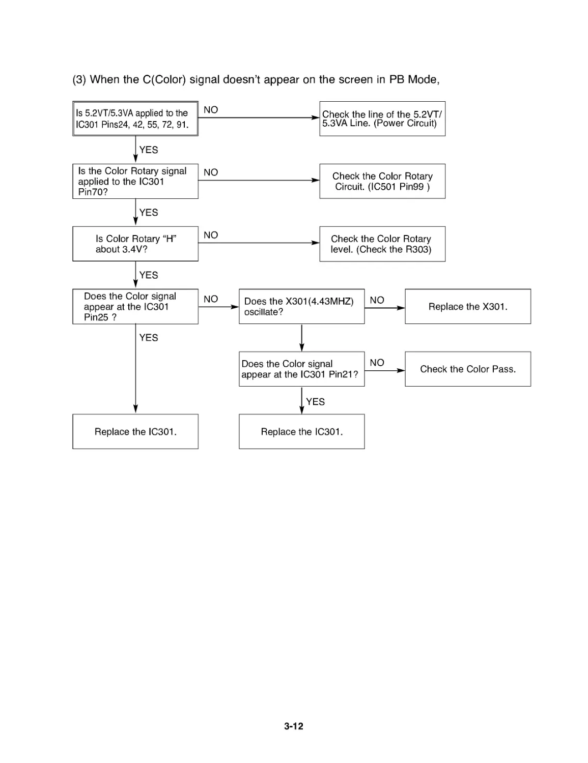
(3) When the C(Color) signal doesn’t appear on the screen in PB Mode,
Is 5.2VT/5.3VA applied to the IC301 Pins24, 42, 55, 72, 91. NO ► Check the line of the 5.2VT/ 5.3VA Line. (Power Circuit)
YES <
Is the Color Rotary signal applied to the IC301 Pin70? NO >• Check the Color Rotary Circuit. (IC501 Pin99 )
YES <
Is Color Rotary “H” about 3.4V? NO >• Check the Color Rotary level. (Check the R303)
YES <
Does the Color signal appear at the IC301 Pin25 ? NO Does the X301(4.43MHZ) oscillate? NO Replace the X301.
YES
Does the Color signal appear at the IC301 Pin21 ? NO ► Check the Color Pass.
t YES
Replace the IC301. Replace the IC301.
3-12
(4) When the Video signal doesn’t appear on the screen in REC Mode,
3-13
5. Hi-Fi CIRCUIT
(A) No Sound(EE Mode)
3-14
(В) Hi-Fi Playback
3-15
(С)
3-16
6. Tuner/IF CIRCUIT
(A) No Picture on the TV screen
3-17
(В) No Sound
3-18
BLOCK DIAGRAMS
1. POWER(SMPS) BLOCK DIAGRAM 1
3-19
3-20
2. POWER(SMPS) BLOCK DIAGRAM 2
3-21
TO SYS
FD(+) У
TO SYS
FD(-) У
TO SYS
-29VA У
TO SYS
TIMER'H'
3-22
3-23 3-24
3. Tu/IF, NICAM & A2 BLOCK DIAGRAM 4. VPS BLOCK DIAGRAM
3-25 3-26
5. Y/C BLOCK DIAGRAM
(PB MODE) (REC MODE)
(To Drum)
(To Drum)
6. Hi-Fi BLOCK DIAGRAM
3-27
3-28
7. SYSTEM BLOCK DIAGRAM
PMC01
CFG 1
CAP,Vcc(l 3/24VA 2
5.4VA 3
CAR.REV ”H" 4
l-Limlt 5
MOTOR GND 6
S.GND 7
DRUM(L/M) Vcc 8
CAP,CONTROL 9
L/M CONTROL 10
DPG/DFG 11
DRUM CTL 12
DRUM MOTOR CONTROL BLOCK
DRUM CTL SIGNAL FILTER,
R563,579,569,535,544,545 D509
DPG/DPG INPUT EILTER |
R512
Ain VSS
CAP ACCElg g о ”
CAPSTAN MOTOR CONTROL BLOCK
CAPSTAN CTL SIGNAL FILTER,
R546.547 0543,551
CEG INPUT EILTER
0567
CAPSTAN REVERSETT
l-LIMIT____________
R521,528,523,0566,0547
R505
L/M CONTROL
R525, R526
END SENSOR BLOCK
T-UP END SENSOR R557.5C5 0534
LD501 DECK IR LEE R564.5C7 0535
R550 ES502 SUPPLY END SENSOR
J”l
IC501
HD6432197A
SECAM DET'H'(y
SCART'H'
C.ROT
H.AMP SW
comp iN
CTL GAIN ADJ
DPG
DFG
V.H/SW
MAIN VCC(5£
DAV
A.MUTE'H'®
csyNcjN <§>
R/C IN(2W) W
P.FAlL QzF
A/D Vcc 6a
DRUM PWM
CAP.PWM
DV.SYNC
VSS
C.SYNC IN in
vcc»=
l-LIMIT
S.M0NITDR2
S.M0NIT0R1
CST SW
RX
TX
BBE'L’
SUP.REEL
TU.SEC VL'H'
4)TU.SEC’H‘
95) end sensor
LP REC MUTE’H’
MODE SWITCH
REEL SENSOR BLOCK
R555,558,559,564 0515 0582
c I J2 3
J RS502 SUP.REEL
c 1 J2 3 R553,556,560,5B3 0514 0581
RS501 T-UP REEL
CST SWITCH
CS501
cst sw
R544.548.5C6
C552
(53|
(52)
TOP SENSOR(50
cap.rev*h’ww
T/UP REEL®
OTPB LED ’H®
RECH' ©
®
CANAL DET 'H'®
S.Conol (44}
R/C IN©
SE/MESECAM’H@
CTL AMP BLOCK
R561,562,567,568,513
R591
0533,523,524,527,596
0564,511,512
CTL( + ) CTL(-)
|a/c head|
CST
KEYlfe
RESET
IC504
KIA7031P
OSD BLOCK
R5A2,5A5,5S1
C5A5.5A4.5S1
L5S1.Q5S1
POWER FAIL
EEPROM
R531.5C9,
0502,508
IC505
KIA7042P
R504.570
0520
L-) GND
@ GND
M GND
(5)GND IC503
T ATC24C16
R 501,502
C516
C.SYNC INPUT BLOCK
VCC INPUT BLOCK
OSD VCC|
L503,C504,C5S3
SERVO VCC]
L505.C561
AD/ЕТС VCC]
L504,C505,C506,ZD503
SYSCON VCC]
gndC,
CLK@
DATA (2
OSC BLOCK
10MHZ |
X501,0570,0571
~2fsc |
R520.509
0578,589
0502
R583.R529.R542
0501,503,0510
C500(BACK-UP)
R524, R514, R518,
R516, R589 0577
C576, L501, Q504
32.768KHZ|
X502.C514.C515
CHARACTER OSC|
C518,0509,R51 7,L506
3-29
3-30
CIRCUIT DIAGRAMS
1. POWER(SMPS) CIRCUIT DIAGRAM 1_200W
IMPORTANT SAFETY NOTICE
WHEN SERVICING THIS CHASSIS, UNDER NO CIR-
CUMSTANCES SHOULD THE ORIGINAL DESIGN BE
MODIFIED OR ALTERED WITHOUT PERMISSION
FROM THE LG ELECTRONICS CORPORATION. ALL
COMPONENTS SHOULD BE REPLACED ONLY WITH
TYPES IDENTICALTO THOSE IN THE ORIGINAL CIR-
CUIT. SPECIAL COMPONENTS ARE SHADED ON THE
SCHEMATIC FOR EASY IDENTIFICATION.
THIS CIRCUIT DIAGRAM MAY OCCASIONALLY DIF-
FER FROM THE ACTUAL CIRCUIT USED. THIS WAY,
IMPLEMENTATION OF THE LATEST SAFETY AND
PERFORMANCE IMPROVEMENT CHANGES INTO
THE SET IS NOT DELAYED UNTIL THE NEW SERVICE
LITERATURE IS PRINTED.
NOTE :
1. Shaded(B) parts are critical 1or safety. Replace only
with specified part number.
2. Voltages are DC-measured with a digital voltmeter
during Play mode.
A | В | C | D | Ё | F | G
J | К | L | M | N | О | P | Q | R | S | T
3-31
3-32
2.
12
11
10
9
8
7
6
5
4
3
2
1
POWER(SMPS) CIRCUIT DIAGRAM 1_400W
IMPORTANT SAFETY NOTICE
CUIT. SPECIAL COMPONENTS ARE SHADED ON THE NOTE :
No power._______________
BD101,TH101 are defective.
WHEN SERVICING THIS CHASSIS, UNDER NO CIR-
CUMSTANCES SHOULD THE ORIGINAL DESIGN BE
MODIFIED OR ALTERED WITHOUT PERMISSION
FROM THE LG ELECTRONICS CORPORATION. ALL
COMPONENTS SHOULD BE REPLACED ONLY WITH
TYPES IDENTICALTO THOSE IN THE ORIGINAL CIR-
SCHEMATIC FOR EASY IDENTIFICATION.
THIS CIRCUIT DIAGRAM MAY OCCASIONALLY DIF-
FER FROM THE ACTUAL CIRCUIT USED. THIS WAY,
IMPLEMENTATION OF THE LATEST SAFETY AND
PERFORMANCE IMPROVEMENT CHANGES INTO
THE SET IS NOT DELAYED UNTILTHE NEW SERVICE
LITERATURE IS PRINTED.
1. Shaded(B) parts are critical for safety. Replace only
with specified part number.
2. Voltages are DC-measured with a digital voltmeter
during Play mode.
Cl 07
No 32VA.
D122 is defective.
DP/1KV
F20U20S
С136
1u/50V
R126
180
R100
A
rboi
A T101
& TF?ANS
470P/1KV
1SS133
IC102
KA431AZ
IOOK
DI 23
EUO1W
Ji 24
5.3VA
GND
L123
2l)uH
HOT CIRCUIT
Switching Error
R114
IOOK
LI 01
30m H
LINE FILTER
GND
PSV01
PSWQ1
32VA
A
0.1U/275V
Digitron Error.
D123, ZD121. D124 are defective.
LI 02
30mH
LINE FILTER
BD1O1 T11„,
PRI |R I f TH01
GBUbJ THERMISTOR
GND
5.3VA
13VA
GND
3.8VA
3.8V A
w
WT
- 29 VA
GND
33VA
GND
32VA
32VA
32VA GND
32VA GND
32VA GND
NC
NO
PWR SENSE
0.1U/275V
1.5M/0.5W
SVC681D
3.15A
250V
PW1Q1
(BK) (WH)
NOTES) Symbol denotes AC ground.
rlzSymbol denotes DC chassis ground.
R115
I00K
R116
IOOK
R117
IOOK
R119
100K
R107
TOOK
RI 08
TOOK
FEED-BACK
ICKH
<A5Q156§Rf
FEED-BACK
Switching Error.
IC101 is defective.
D108
ERA22-1O
D103
R102
Switching Error.
IC104 is defective.
IC104
FS6M07652RC
No Power.________
F101 is defective.
NOTE) Д Warning
Parts 1ha1 are shaded are crilicaI
With respect to risk of fire or
eledricial shock.
D105
EU01W
ERA22—10
Atr^ns
A IG105
^LTV-817B
IC106
KA431A2
IC105, 106 are defective.
D122
R121
2.7K
R123
1.0K
20uH
GND
D’SCHEMATIC POWER 1
< LH-440S/P/Y/l(400W))
3854R13800A
A | В | C | D | Ё | F | G | H | i | j | К | L | M | N | О | P | Q | R | S | T
3-33
3-34
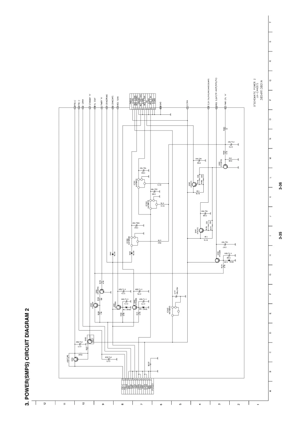
3. POWER(SMPS) CIRCUIT DIAGRAM 2
12
11
10
9
□ ’SCHEMATIC POWER 2
LH —C440SS
3854R1 3801A
A | В | C | D | Ё | F | G | H | i | j | К | L | M | N | О | P | Q | R | S | T
3-35
3-36
4. TU/IF, NICAM & A2 CIRCUIT DIAGRAM
11
10
TU V.OUT (У
TU A(R) (jfe)
TU A(L)
OAV
GND
IIC DATA ®
5 3VA (T
5 2VT (Щ
5 2V (Si
33VT (Йё>
MOD. A IN
MOD VIN
TU.SECAM'H' rtF
TU SE VL’H'
AFT
1 S/P/Y
R7V2 100K 82K
J701 J7O2
s 0 0
GKI 1.5K 1 5K
C752 и 001U r-
L701 11 к C751 47u/16V
151 5 3VA 100uH(K035) tLI к
I C7M5 R7M1 W/MOD DPTIDN 1 B71 MOD. A IN । ,, 1 OK ' 1
/ 1 lu CM || 774 p 1 si
60 ||C DATA | 220 " c 1 «
/ —_ —
160 52VT L7°2 C702 *И470и/6 3Vk
/ 10uH(K035) C703 и OOlu r
59 IIC CLK —
/ । R7M2 I 220 C7M4 II p 1
872MOO VIDEO | ... — " c 1
/ | R7U4 1 OK C7M6 1127P r |
158 33VT R715 I
8
6
3
D’SCHEMATIC TU.IF/NICAM/VPS
—EE MODE(VIDEO) LH-C440S'S
3854R13805A
TU MODE (AUDIO)
A | В | 0 | D | Ё | F | G | H | i | j | К | L | M | N | О | P | Q | R | S | T
3-37
3-38
5. A/V CIRCUIT DIAGRAM
Q305 is defective.
(TO DECK)
P3DO3
FULLERASE
(FROM/TO SYS.AVCP)
P30Q2
SPIN
A/E (~)
A/E ( + )
A REC
A PB
SP REC
SP В PB
LP A PB
HI-FI A PB
2Esc QT
TUNER V.IN (731)
EU2 V.IN (§3^.
compoutCioD-
MONO.A OUT (38i)-
MONO A IN (§3$-
5 2Vg59)-
5 3VA(15i}-
REG 5 2VT®)-
H AMP SW(lW
C.R0TARY(£9>
IIC DATA (60)-
iic clk (5g>
C SYNC (tTD-
HI-FI REC
HI-FI В PB
LP В PB
LP REC
P3DO1
SP A PB
________2P1N
GND | Г
(TO SYSTEM)
V. ENV (24)
REC'H' (47)
А.МЦТЕ'Н'ЙГ)
FL301, Q301, Q306 are defective.
SECAM OPTION
HIFI PB В
HIFI REC(83>
OSD V IN (1
si v out
S2.V.OUT-
Q302. Q303, Q314
are defective.
No mono Audio Sii
in PB MODE.'
Normal Audio signal is not recorded.
ф PB Y+C
—|ф— PB Y
PB C
—PB SECAM COLOR
A | B-
REC Y+C
—ф— REC Y
REC C
—REC SECAM COLOR
1 c | “
> REC AUDIO
-c>- PB AUDIO(MONO)
WAVEFORM
□’SCHEMATIC AVCP/SECAM
LH —C440'S
3854R13803A
J | К | L | M | N | О | P | Q | R | S | T
3-39
3-40
6. Hi-Fi CIRCUIT DIAGRAM
DVD G (§81
AUDIO'R'
A.GNQ
DVD В
PMDO2
OVD VIDEO
GND
(VCR => DVD)
DVD A 'L'
GND
AUDIO'L'
DVD G
DVD R
DVD A.'R'
GND
IIC DATA
IIC CLOCK
A ENV
HIFI REC (831)—Ф-
HIFI P8 8 $84)--ф-
ф-^Sag) RGB CONTROL
A MUTE ’H’
DVO/Fr VIN
A.OUT.L
A.OUT.R
A OUT R
A OUTL
OPTION
CANAL 2SCART
JSOl X 0
J802 X D
J803 X 0
J8O4 0 X
J805 X 0
J806 0 X
C887 D X
C888 0 X
R89O 75 560
D'SCHEMATIC HIEl/SWITCH
LH —C440S’S
3854R13804A
PB
> REC
A | В | C | D | Ё | F | G | H | i | j | К | L | M | N | О | P | Q
3-41
3-42
7. SCART(JACK) CIRCUIT DIAGRAM
12
\SPEC N0\ S/P/l Y ONLY
C915 X 1000P
C916 X 1000P
C921 X 1000P
C923 X 1000P
C9A1 X 1000P
C9A6 X 1000P
\ SPEC NO \ CANAL 2-SCART
D901 X 0
R901 0 X
5
KTC3875S
12
W/0 1 SCART
C9Aj
lOOutA
2.
3.
8
9
IOOu(AJ
input2(R)
outputl(L)
earth
earth
input1(L)
SCART Pm connwction
1 Audio output2(R)
Audio
Audio
Audio
Blude
Audio
Blue signal
Switching voltage
Green earth
Data2
Green signal
Dotal
Red earth
Doto earth
Red signal
15
16. Blanking signal
1 7 Video earth
18 Blanking signal earth
19 Video output
Video input
Plug screen earth
20
21.
A | В | C | D | Ё | F | G | H
L91U
100u(A)
1905^ lOOu(A)
1907^ lOOu(A)
L906~r, iQQu(A)
SC901
SCART
JACK
L90J
IOOu(A)
D'SCHEMATIC SCART/SWITCH
LH-C440S’S
3854R13806A
J | К | L | M | N | О | P | Q | R | S | T
3-43
3-44
8. SYSTEM CIRCUIT DIAGRAM
GND
10
AMP ENA
AMP DATA OUT
9
8
PMCD1
CFG
7
DPG/DFG
DRUM CTL
VCR will not operate.
IC505 is defective.
CAP CONTROL
L/M CONTROL
AMP CLK
GND
DVD RESET
AMP DATA IN
(F/T A/V) CTL ( + )
(F/T A/V)
CTL (-)
MOTOR GND
S.GND
12VA(DRUM)
PMJ01
DATA IN
DATA OUT
MDO
FWE
12VA(CAP)
5 3VA
CAR REV 'IT
5 3VA 1 SI
ES501, ES502, LD501 are
defective.
4ESE1
OUT
C5O5
IA7042P
(VCR
PmD01
DVD ENA
GND
DVD DATA OUT
DVD DATA IN
DVD CLK
_A_MP RESET
(FROM/TO DECK
МЯ5П1
GND
MODE SI
MODE S2
MODE S3
MODE S4
Deck will not operate
R575, R576, R577,
R578 are defective.
Auto stop occures.
RS501 ,RS502,Q514,
Q515 are defective.
Auto Rew will not working.
L501
27P{CC) '2uH
(FROM TO POWER)
67) STAND BY'H'
-CIDtimer 'H'
Vcc(DSD)
L503 5.2 VT 160
-ОПТ—
IDOuH
-cdDsjvA
4® REG 5 2VT
Ф—(T52) -27VA
ф—(156) 1 2VA(CAP)
ф—(£57) 1 2VA(DRUM)
-(§§§) GND
WAVEFORM
< TA (2 73
BACK UP TIME
C500 : 0.047F/5.5V(1 OMIN
p-CQM is unstable.
Q501, Q503 are defective
□ 'SCHEMATIC SYSTEM
LH —C440S'S
3854R13802A
3-45
3-46
9. TIMER CIRCUIT DIAGRAM.OTOOL
11
KEY BOARD
10
s
8
6
3
D’SCHMATIC KEY/TIMER
LH-C440
3854R13807B
A | В | C | D | Ё | F | G | H | i | j | К | L | M | N | О | P | Q | R | S | T
3-47
3-48
10. TIMER CIRCUIT DIAGRAM_5TOOL/7TOOL
11
10
KEY BOARD
TIMER
F- NPNP 1G 2G 3G 4G 5G 6G 7G8G 9G10G11G12GNX NX NX NXNXNX NX pi P2 РЗ P4 P5P6 P7 P8 P9 P10P11P12P13pi«Pi5Pl6 NP NPF+
R601... t.OK
-----VA-----
R603w^ 1 0K
8
6
3
D’SCHMATIC KEY/TIMER
LH-C445
3854R13807A
A | В | 0 | D | Ё | F | G | H | i | j | К | L | M | N | О | P | Q | R | S | T
3-49
3-50
11. TIMER CIRCUIT DIAGRAM_6T00L
KEY BOARD
D’SCHMATIC KEY/TIMER
LH-C246
3854R13807C
A | В | C | D | Ё | F | G | H | i | j | К | L | M | N | О | P | Q | R | S | T
3-51
3-52
WAVEFORM & VOLTAGE SHEET
★ IC301 Oscilloscope Waveform
IC301 Pin @ IC301 Pin ® IC301 Pin @ IC301 Pin @
REC mode PB mode PB mode PB mode
340mVp-p
300mVp-p
400mVp-p
3.6Vp-p
3-53
IC501 Waveform Photographs
V.HSW
(IC501 Pin 105)
1V/10mS
REC/PB MODE
DV.SYNC
(IC501 PIN 109)
1V/100uS
QUE/REV MODE
CTL(+)
(IC501 Pin 3)
1V/10mS
CTL(-)
(IC501 Pin4)
1V/10mS
DFG/FG
(IC501 PIN 103,104)
1V/10mS
REC/PB MODE
CFG
(IC501 Pin9)
1V/10mS
V.IN
(IC501 Pin 17)
500mV/20uS
V.OUT
(IC501 Pin 19)
500mV/20uS
EE/PB MODE
C.SYNC
(IC501 Pin 111)
1.0V/100uS
EE/PB MODE
3-54
• CIRCUIT VOLTAGE CHART
\MODE PIN N0\ EE PB REC
IC201
1 2.4 2.4 2.4
2 2.3 2.4 2.4
3 3.4 3.4 3.4
4 2.5 2.4 2.4
5 0 0 0
6 0.5 3.7 0.5
7 0 0 0
8 0 0 0
9 2.9 2.9 2.9
10 2.4 2.4 2.4
11 2.1 2.4 2.4
12 3.1 1.8 2.3
13 4 4 3
14 2.4 2.4 4
15 3.0 1.8 2.4
16 3.2 3.1 3.2
17 0 4 0
18 0 3.3 0.12
19 2.2 2.2 2.2
20 2.1 2.5 2.3
21 1.9 2.3 2.3
22 0 0 0
23 4.8 4.8 4.8
24 4.8 4.8 4.8
25 2.3 2.2 1.5
26 2.3 2.2 2.4
27 2.9 2.7 2.9
28 0.1 0.18 0.18
29 0.19 0.3 3.8
30 2 2 2
IC301
1 4.9 4.9 1
2 0 0 0.8
3 2.2 2.2 2.3
4 pulse pulse 0.6
5 2.1 2.1 2.3
6 2.2 2.1 2.2
7 2.1 2.1 2.2
8 2.1 2.1 2.2
9 2.1 2.1 2.9
10 2.2 2.1 2.2
11 2.2 2.2 2.2
12 0 0 0
13 2.1 2.1 2.2
14 0 0 1
15 2.1 2.1 2.2
16 4.9 0.1 4.8
17 2.1 2.1 2.2
18 4.9 4.9 4.9
19 4.0 3.8 2.8
20 0 0 0
21 3.1 1.8 2
22 2.7 2.6 3.4
23 2.7 2.6 3.4
\MODE PIN NO\ EE PB REC
24 4.9 4.9 4.9
25 0.1 3.3 0.12
26 1.5 2.2 1.2
27 2 2.0 2
28 4 4 4
29 2.6 2.6 2.6
30 0 0 0
31 4.5 4.4 4.5
32 4.4 4.4 4.5
33 2.9 2 1.9
34 0 0 1.8
35 1.8 1.8 1.8
36 2.9 3.5 3.6
37 1.8 1.8 1.8
38 2 2 2
39 9 9 9
40 0 0 0
41 0 0 0
42 4.9 4.9 4.9
43 2.4 2.2 2.3
44 0 3.9 2.8
45 2.4 2.4 2.5
46 2.6 2.5 2.6
47 4 4 4
48 4.2 4.2 4.2
49 2.9 3.6 3
50 1.9 1.9 1.95
51 0 0 0
52 1.9 1.9 1.95
53 2.3 2.2 2.3
54 1.9 1.9 2.2
55 5.2 5.2 5.2
56 2.2 2.0 2
57 1.9 2.3 1.6
58 3.6 1.3 2.2
59 2.8 2.8 2.8
60 1.5 1.5 1.4
61 1.8 1.3 1.3
62 0 0 0
63 1.8 1.3 1.6
64 0 0 0
65 1.7 1.1 1.1
66 0 0 0
67 0.2 3.7 0.4
68 4.8 4.9 4.8
69 4.7 4.8 4.8
70 0 pulse 2.6
71 3.3 0 0
72 4.9 4.8 4.8
73 2 3.3 2.2
74 2.4 1.6 2.3
75 2.3 0.6 2.3
76 2.3 0.7 2.3
77 1.5 1.5 1.5
78 2.5 3.3 2.5
\MODE PIN NO\ EE PB REC
79 1.8 1.7 2.5
80 0.9 0.9 4.6
81 1.0 1 1
82 0 0 0
83 pulse 0 0
84 0.5 2.6 0
85 0 0 1.3
86 0.27 0.3 2
87 0.7 0.7 0.7
88 0.7 0.7 0.7
89 0.7 0.7 0.7
90 0.7 0.7 0.7
91 4.9 4.9 4.8
92 0 0 0
93 1.7 1.7 4
94 1.7 1.7 4
95 1.7 1.7 4
96 1.7 1.7 4
97 0 0 0
98 2.2 2.2 2.2
99 2.2 2.2 2.2
100 2.2 2.2 2.2
IC501
1 0 0 0
2 2.6 2.6 2.6
3 2.6 2.6 3.5
4 2.6 2.6 1.3
5 2.6 2.6 2.6
6 2.6 2.6 2.6
7 2.7 2.7 2.7
8 2.58 2.5 2.5
9 4.52 2.2 2.2
10 5.2 5.2 5.2
11 1.8 1.8 1.7
12 1.8 1.8 0
13 2.0 2.1 2
14 0.26 3.9 0.4
15 0.27 pulse 0.16
16 1.9 1.9 1.8
17 2.47 1.4 2.4
18 4.93 0 4.8
19 2.26 0 1.7
20 0 0 0
21 2.3 0 2.3
22 2.3 2.3 2.2
23 0 0 0
24 0.52 2.6 0
25 0.078 3.1 0.16
26 5.2 0 5.2
27 4.5 4.5 4.5
28 0 5.2 5.2
29 0 0 0
30 0 0 0
31 0 0 0
32 0 0 0
\MODE PIN NO\ EE PB REC
33 0.18 0.18 0.16
34 0.26 0 0.16
35 5.2 5.2 5.2
36 5.2 5.2 5.2
37 4.8 0 0
38 4.8 4.8 4.8
39 0.21 0 2.3
40 5.18 0 0
41 3.1 0 0
42 0 0 0
43 0 4.8 4.8
44 0 0 0
45 0 0 0
46 0 0 0
47 0 0 5.1
48 0 0 0
49 0 pulse 0
50 0 0 0.1
51 0 0 0.1
52 pulse 0 0.26
53 pulse 0 0.26
54 5.2 0 5.1
55 pulse 0 0
56 5.2 5.2 0
57 0 0 0
58 0 0 0
59 4.9 0 0
60 4.7 0 4.7
61 5.1 5.1 5.1
62 5.1 0.2 5.1
63 5 5 5
64 3.58 3.5 3.6
65 2.8 pulse 0
66 5.1 5.1 0.2
67 0 0 5.1
68 0 5.2 0
69 0 5.2 5.2
70 5.2 5.2 5.2
71 5.2 0 5.2
72 0 0 0
73 0.3 5.1 5.1
74 0 0 0
75 0 0 1.6
76 1.36 1.3 1.3
77 0 0 0
78 0 0 2.5
79 0 0 0
80 0 0.15 0
81 3.3 3.3 3.3
82 5.2 5.2 0
83 0 2.5 2.5
84 0 2.7 2.7
85 0 3.5 3.6
86 pulse pulse 2.8
87 0 pulse 3.1
\MODE PIN NO\ EE PB REC
88 4.8 4.8 4.8
89 0 0 0
90 0 4.9 0
91 4.95 0 0
92 0 0 pulse
93 0 0 0
94 0 0 0
95 0 0 0
96 0 0 0
97 0 0 0
98 0 5.1 5.2
99 0 2.5 2.6
100 0 0 0
101 0 0 0.29
102 0 0 0
103 0 1.4 1.38
104 0 pulse 1.39
105 0 2.5 2.6
106 0 2.5 2.6
107 0 0 0
108 0 0 2.7
109 pulse 0 0
110 pulse 0 0
111 0.26 0 0
112 5.2 0 0
IC751
1 5.1 5.1 5.1
2 1.5 1.5 1.5
3 1.5 1.5 1.5
4 0 0 0
5 2.4 2.4 2.4
6 2.3 2.3 2.3
7 0.2 pulse pulse
8 0 0 pulse
9 0 0 pulse
10 0 0 0
11 5.1 5.1 5.1
12 4.8 4.8 4.8
13 4.7 4.7 4.8
14 2.5 2.5 pulse
15 2.5 2.5 pulse
16 0 0 pulse
17 pulse pulse pulse
18 0.23 pulse pulse
19 5.14 5.1 5.1
20 0 0 0
21 pulse pulse pulse
22 5.1 5.1 5.1
23 0 0 0
24 0 0 0
25 0 0 0
26 0 0 0
27 0 0 0
28 0 0 0
29 0 0 0
\MODE PIN NO\ EE PB REC
30 2.8 2.8 2.8
31 2.8 2.8 2.8
32 0 0 0
33 5.1 5.1 5.1
34 4.2 4.2 4.2
35 0 0 0
36 2.8 2.8 2.8
37 0 0 0
38 0 0 0
39 0 0 0
40 2.8 2.8 2.8
41 2.8 2.8 2.8
42 2.5 2.5 2.6
43 2.4 2.4 2.4
44 0 0 0
IC801
1 3.8 3.8 3.8
2 3.8 3.8 3.8
3 3.8 3.8 3.8
4 3.8 3.8 3.8
5 3.8 3.8 3.8
6 3.8 3.8 3.8
7 3.8 3.8 3.8
8 3.8 3.8 3.8
9 3.8 3.8 3.8
10 3.8 3.8 3.8
11 3.8 3.8 3.8
12 0 0 0
13 3.87 3.87 3.8
14 0 0 0
15 0 0 0
16 6 6 6
17 6 6 6
18 0 0 0
19 6 6 6
20 6 6 6
21 4.57 4.5 4.5
22 3.82 3.8 3.8
23 3.86 3.8 3.8
24 3.87 3.8 3.8
25 3.87 3.8 3.8
26 0.8 0.8 0.8
27 0 0 0
28 3.84 3.8 3.8
29 3.86 3.8 3.8
30 0.79 0.7 0.8
31 3.87 3.8 3.9
32 3.87 3.8 3.9
33 3.86 3.8 3.9
34 12 12 12
35 0.6 0.6 4.2
36 0.63 0.6 4.2
37 0.63 0.6 4.2
38 0 0 4.2
39 0 0 0
\MODE PIN NO\ EE PB REC
40 5 5 5
41 0 0.9 0.9
42 4.7 4.7 4.8
43 4.8 4.6 4.8
44 0 3.3 0.7
IC802
1 3 3.1 2.9
2 12 12 12
3 2.7 2.7 2.7
4 12 12 12
5 2.9 2.9 3
6 5.7 5.7 5.7
7 5.7 5.7 5.7
8 0 5.6 5.7
9 5.1 0 0
10 5.6 5.6 5.7
11 11.4 11.4 11.5
12 5.7 5.7 5.7
13 0 0 1.6
14 5.6 5.6 2.7
15 0.1 0.1 5.7
16 5.6 5.6 0
17 0 0 0
18 0 0 0
19 0 0 5.7
20 5.7 5.7 5.7
21 5.7 5.7 5.7
22 5.7 5.7 5.7
23 5.6 5.6 5.7
24 5.7 5.7 5.7
25 5.7 5.7 5.7
26 5.7 5.7 5.7
27 5.6 5.6 5.2
28 5.2 5.2 2.3
29 1.4 1.4 1.8
30 2.1 2.3 3.5
31 3.5 3.5 3.5
32 4.7 4.7 4.8
33 4.8 4.8 4.9
34 0 0 0
I C90 1
1 3.6 3.1 1.5
2 0.1 0.1 2.6
3 0.8 0.8 0.85
4 0 0 0
5 0.7 0.7 0.85
6 0.7 0.7 0.79
7 0.1 0.1 2.6
8 1.4 1.4 1.5
9 3.0 2.8 1.5
10 0 0 0
11 1.4 1.5 0
12 0.1 0.1 2.6
13 5.2 5.2 5.2
14 2.6 2.6 1.6
3-55
3-56
\MODE PIN N0\ EE PB REC
15 0 0 0
16 1.5 1.5 1.6
Tran- sistor EE Mode PB Mode REC Mode
E C в E C в E c в
Q110 -22 -22 -21 -21.8 -21.8 -21 -22 -22 -21
Q111 5.23 5.1 0 5.24 5.1 0 5.23 5 0
Q112 12.1 13.9 12.7 12 13.5 12.7 12.1 13.4 12.7
Q113 5.24 5.18 4.46 5.24 5.18 4.46 5.24 5.17 4.47
Q114 33.6 33.5 32.8 33.4 33.2 32.4 33.5 33.3 32.5
Q115 0 0 0.74 0 0 0.74 0 0 0.74
Q116 5.24 5.2 4.48 5.2 5.2 4.49 5.2 5.2 4.48
Q117 5 5.23 5.7 5 5.24 5.7 5 5.2 5.7
Q118 0 0 0.68 0 0 0.67 0 0 0.68
Q301 0 4.9 0 0 4.9 0 0 1.6 0.8
Q302 4.9 0 4.9 4.9 4.86 4.25 4.9 -14.4 4.9
Q303 0.2 0 0 0 0 0.7 -7.8 0 -14.3
Q304 0.13 0 -0.13 0 0 0.7 -7.8 0 -14.3
Q305 2.5 0 1.8 2.7 0 2 3 0 2.3
Q306 4.9 4.9 4.9 4.9 4.9 4.9 1.9 4.6 2.2
Q308 2.6 0 1.9 2.8 0 2.1 3 0 2.4
Q309 2.9 0 2.3 3.2 0 2.5 3.5 0 2.8
Q501 0 0 0.68 0 0 0.68 0 0 0.67
Q502 0 3.7 0.23 0 2.4 0.23 0 2.4 0.2
Q503 5.2 5.2 4.5 5.23 5.2 4.5 5.2 5.2 4.5
Q504 0 3.8 0.62 0 3.8 0.6 0 3.7 0.6
Q514 0 5.2 0 0 Pulse Pulse 0 Pulse Pulse
Q515 0 0 4.95 0 Pulse Pulse 0 Pulse Pulse
Q5S1 0.36 2.52 0 0 2.5 0 0.5 3 0
Q751 0 3.8 0 0 3.8 0 0 3.7 0
Q804 2.6 0 1.9 2.8 0 2 3.1 0 2.4
3-57
3-58
PRINTED CIRCUIT DIAGRAMS
1. MAIN P.C.BOARD
3-59
3-60
2. KEY(LEFT) P.C.BOARD
(0 TOOL)
(5 TOOL/7 TOOL)
(6 TOOL)
3-61
3-62
3. KEY(RIGHT) P.C.BOARD
(0 TOOL)
(5 TOOL/7 TOOL)
(6 TOOL)
3-63
3-64
3-65 3-66
KJ I GJ | Г' I <J1 I CT)
4. POWER P.C.BOARD (5 TOOL/6 TOOL/7 TOOL)
(0 TOOL) f <SOLDERIN^
~I ( 1 LOCATION GUIDE N
DVD PART
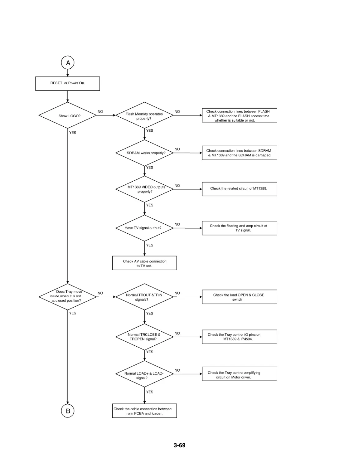
ELECTRICAL TROUBLESHOOTING GUIDE
1. System operation flow
3-67
2. SYSTEM Test flow
3-68
3-69
3-70
3-71
3-72
3-73
DETAILS AND WAVEFORMS ON SYSTEM TEST AND DEBUGGING
1. SYSTEM 27MHz CLOCK, RESET, FLASH R/W SIGNAL
1) MT1389 main clock is at 27MHz(X501)
FIG 1-1
2) MT1389 reset is low active
3-74
3) RS232 waveform during procedure(Downloading)
9-Dec-02
17:18:23
FIG 1-3
4) Flash R/W enable signal during download(Downloading)
FIG 1-4
3-75
2. SDRAM CLOCK
DCLK = 128MHz, Vp-p=2.2, Vmax=2.7V
FIG 2-1
3. TRAY OPEN/CLOSE SIGNAL
1) Tray open/close waveform
TRIN
TROUT
TROPEN
TRCLOSE
FIG 3-1
3-76
4. SLED CONTROL RELATED SIGNAL (NO DISC CONDITION)
FMSO(2.0V/1.4V/1.0V)
STBY(3.3V)
SL+(4.7V/4.0V/2.6V)
SL-(5.3V/4.0V/3.0V)
FIG 4-1
5. LENS CONTROL RELATED SIGNAL(NO DISC CONDITION)
FOSO(1.5V/1.4V/1.3V)
F+(4.0V/3.6V/3.2V)
F-(4.0V/3.6V/3.2V)
FIG 5-1
3-77
6. LASER POWER CONTROL RELATED SIGNAL(NO DISC CONDITION)
MDI1 (0V/180mV)
LD01 (5.0V//3.5V)
LD02(5.0V/3.6V)
FIG 6-1
7. DISC TYPE JUDGEMENT WAVEFORM
2-1 V QC Й 100 kS/s
@ - 1 v DC й _______I 2 00 1-40 V
4 .2 V 0СЙ □ STOPPED
FIG 7-1 (DVD)
3-78
10-0ес-О2
10:08:54
2.1 V ОС й 100 kS/s
@ - 1 V ОС й _____| 2 ОС 1.40 V
4 -2 V ОС Й □ STOPPED
FIG 7-2 (DVD)
2.1 v DC Й
@ . 1 V ОС й ______I 2 ОС 1.40 V
4 .2 V ОС й □
FE
RFL
100 kS/s
STOPPED
FIG 7-3 (CD)
3-79
10-Оес-02
10: 16:16
2-1 V DC io
@ - 1 V ОС J ______I 2 06 1,40 V
4 .2 v ос Й □
F+
FE
RFL
100 kS/s
5TOPPED
FIG 7-4 (CD)
8. FOCUS ON WAVEFORM
10-Oec-02
10:29:08
5.1 v uu ю _______ UL 1. 4U v
4 .2 v ос Й □
FE
FOSO
F+
F-
100 kS/s
STOPPED
FIG 8-1 (DVD)
3-80
10-Оес-02
10:28:35
3-1 V DC й ___________I 2 ОС 1-40 V
4 .2 V ОС й □
FE
FOSO
F+
F-
100 kS/s
STOPPED
FIG 8-2 (CD)
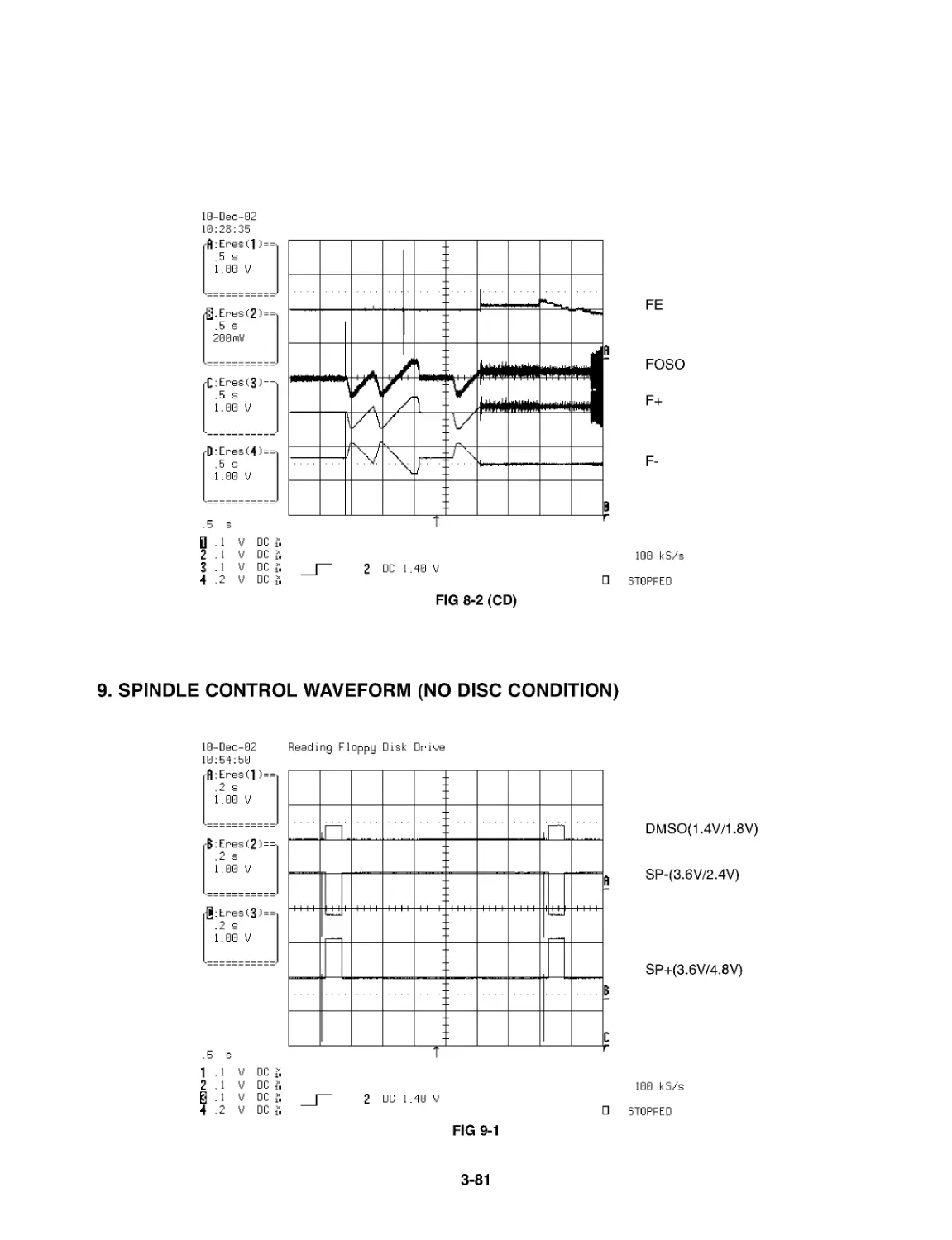
9. SPINDLE CONTROL WAVEFORM (NO DISC CONDITION)
2.1 v ос й
@ .1 V DC й I 2 DC 1.40 V
4 .2 V DC й П
DMSO(1.4V/1.8V)
SP-(3.6V/2.4V)
SP+(3.6V/4.8V)
100 kS/s
STOPPED
FIG 9-1
3-81
10. TRACKING CONTROL RELATED SIGNAL(System checking)
10-Oec-02
11:05:00
FIG 10-1 (DVD)
ТЕ
TRSO
T-
T+
100 kS/s
STOPPED
FIG 10-2(CD)
ТЕ
TRSO
T-
100 kS/s
STOPPED
3-82
11. МТ1389 AUDIO OPTICAL AND COAXIAL OUTPUT(SPDIF)
26-Sep-02
18:36:50
(Я-------
.5 ps
1.00 V
734 sweeps: average low high signs
Freq(1) ПП 2.36821 MHz 1.E236E З.Е77ЭЕ 0.68974
.5 ps
Q 100 mV DC й
2 trig only
3 1 V DC й
4 trig only
1 DC 1.64 V
1 GS/s
A0TD
FIG 11-1
12. MT1389 VIDEO OUTPUT WAVEFORM
1) 100%
26-Sep-02
20:02:11
2 trig only
3 1 V DC й ________| 1 DC 0.72 V
4 trig only □
500 kS/s
AUTD
FIG 12-1
3-83
2) COMPOSITE VIDEO SIGNAL
26-Sep-02
20:08:07
2 trig only 500 kS/s
3 1 V DC й _|— 1 DC D.72 V
4 trig only □ AUTD
FIG 12-2
13. MT1389 AUDIO OUTPUT TO AUDIO DAC
23-Jan-02
10:52:51
r1--------
5 ps
2.00 V
p
ALRCK 48KHZ
ASDATO
2-------
5 ps
2.00 V
ABCK 2.304MH2
DC 1.88 V
DC
DC
DC
AC
500 MS/s
STOPPED
5 ps
1 .2 V
2.2 V
@ .2 V
4 50 mV
FIG 13-1
3-84
14. AUDIO OUTPUT FROM AUDIO DAC
23-Jan-02
20:03:39
3 .2 V DC й ________I 1 DC 0.00 V
4 50 nV AC й □
25 MS/s
STOPPED
FIG 14-1
3-85
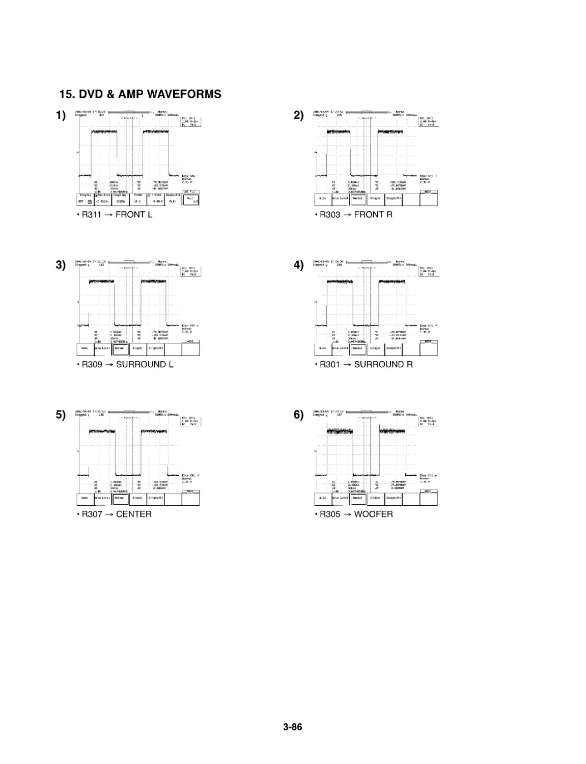
15. DVD & AMP WAVEFORMS
• R311 -> FRONT L
• R303 -> FRONT R
5)
• R301 SURROUND R
• R307 CENTER
6)
3-86
3-87
BLOCK DIAGRAMS
1. Overall Block Diagram_200W
3-88
2. Overall Block Diagram_400W
3-89
Х601 I □ I
27MHz I
X-TAL
3. SERVO Block Diagram
3-90
VIDEO
Interface
AUDIO
Interface
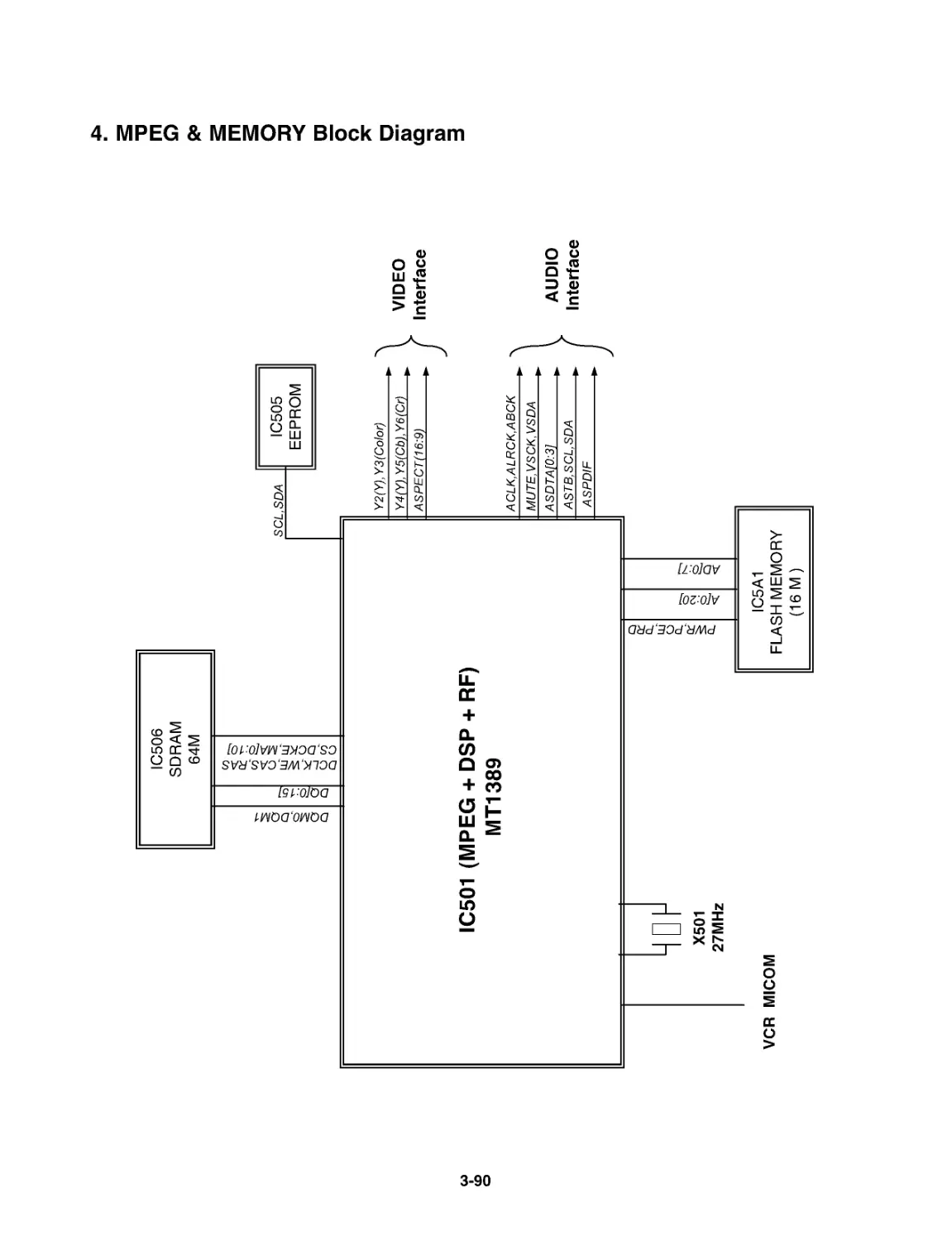
MPEG & MEMORY Block Diagram
3-91
S' (R.G.B) / (Y.Pb.Pr) МРГП I / IC507 VIDEO 6dB Amp
(Y/C) I >
MPEG J
ACLK
ABCK
ALRCK
ADATA3
IC206 AUDIO DAC (2CH) —
♦ CVBS
COMPONENT (R.G.B)/(Y.Pb.Pr)
SUPER VIDEO (Y/C)
INTERFACE
IC205 (OP Amp)
LPF&Buffer
AUDIO ‘R’
> AUDIO ‘R’
5. VIDEO & AUDIO Block Diagram
3-92
6. DVD & AMP Block Diagram
CIRCUIT DIAGRAMS
1. MPEG CIRCUIT DIAGRAM
12
11
10
8
6
A | В | C | D | Ё | F | G | H
3-93
MPEG & VIDEO
XH-CW644
2004. D0. IB
3B54R14740A
3-84
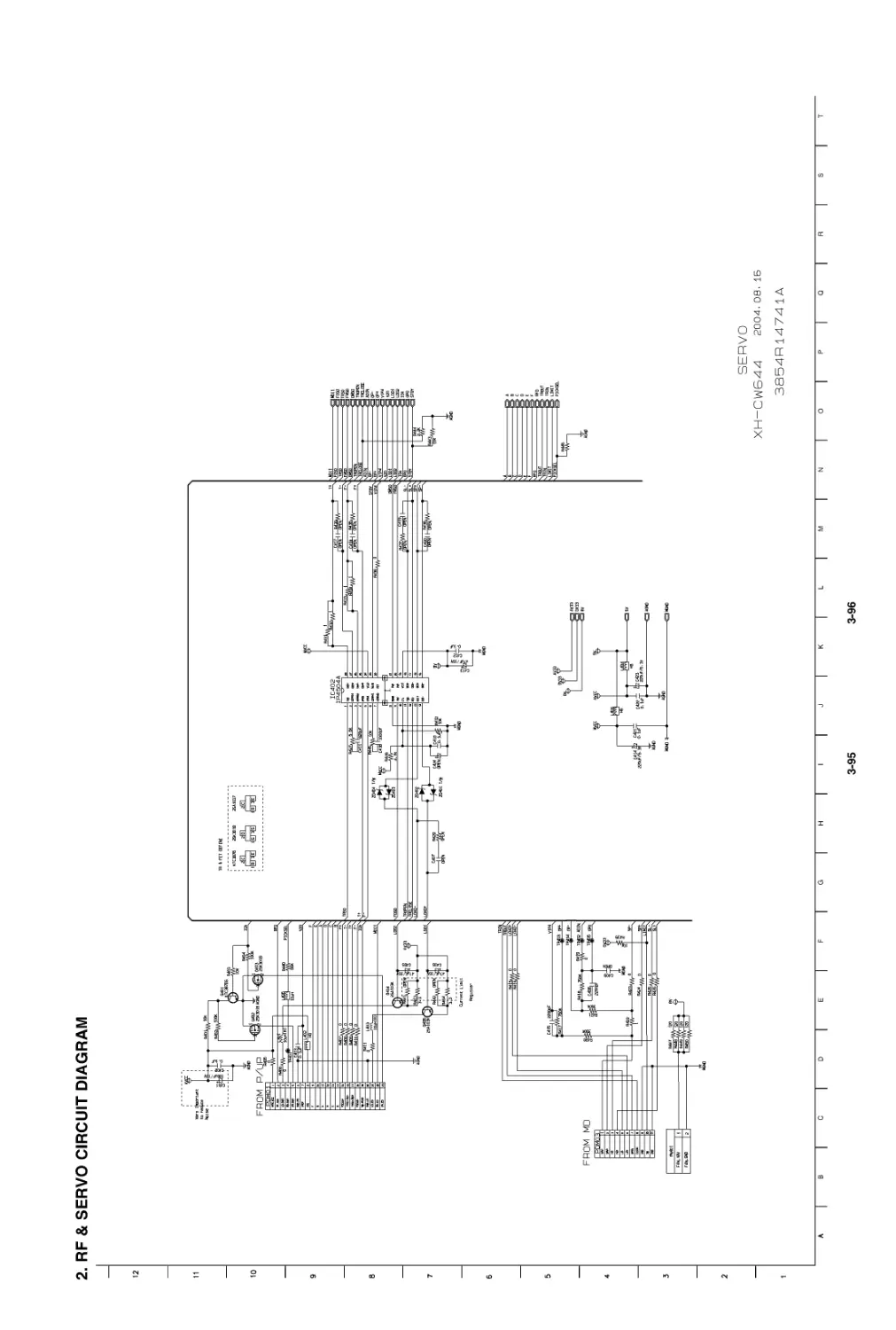
2. RF
12
11
10
9
8
7
6
5
4
3
2
1
& SERVO CIRCUIT DIAGRAM
SERVO
XH-CW644 2004.08. 1Б
3854R 14741Д
A | В | C | D | Ё | F | G | H | i | j | К | L | M | N | О | P | Q | R | S | T
3-95
3-96
3. AUDIO, p_COM CIRCUIT DIAGRAM(DVD & AMP)
* RADIO TUNER OPTION TABLE(TU101)
RDS 19KHZ FILTER FM TUNER AREA BAND FREQ. RESP. FM Mod. FM ANT. knangsuNg PART NO. LG PART NO.
X X 2/3GANG/FCC USA/S. AMERICA FM/Mff 75uS 75KHZ 750hm kst-MloooMvo-ool 6700FM0091A
X X 2/3GANG/FCC AUS. /ASIA fM/Мц BOuS AOKHz 750hm KST-ML000MV1-60L B700FM0092A
X X 3GANG/G0ST RUS./CIS I AX 1 FM/Mw 50uS AOKHz 750hm KST-ML002MV1-60L 6700FM0094A
X X 4GANG TURKEY I ADI fM/M^/lw 50uS 75KHz 750hm KST-ML004MV1-60L 6700FM0095A
0 X 4GANG/CE EUlADl FM/Mff 50uS AOKHz 750hm KST-Ml10AMV1-B0L 6700FM009BA
X X 3GANG JAPAN 1 AX 1 fM/Mk 75uS AOKHz 750hm KST-ML005MV0-61L 6700FM0097A
X X A GANG CANARRYlAD 1 FM/Mff 50uS 75KHz 750hm KST-Ml004Mv1-60L 6700FM0098A
X X A GANG KOREA I AX 1 fM/Мц 75uS 75KHz 750hm KST-ML00JMV0-61L B700FM0099A
5WS01
A 5 BW <4>
B ftG-WAIICI
*
10
AUDIO MICOM
XH —CW6AA 2004. OB. 15
385AR1U7A2A
A | В | C | D | Ё | F | G | H | i | j | К | L | M | N | О | P | Q | R | S | T
3-97
3-98
4. DIGITAL AMP CIRCUIT DIAGRAM (DVD & AMP)_200W
11
8
6
L712
33uH
R725
4.7K 1/6W
" । ^C734
4741M)/63V
WV--------------
+ C745
Ф 330u
R719
4-7K 1/6W
С72Б
R720 103(2012)
1.512012)
—II—
C791
102(20121
"—VW-----------
R729
4.7K 1/6W
C736
R730 103(2012)
-
1-5(2012)
R739
4-7K 1/6W
С74Б
R740 103(20121
1.5(2012)
C792
102(2012)
C793
102(2012)
102(2012)
102(2012)
—a WOOFER
CHASSIS-GO
XH-CW246
AUDIO MICOM
2004.07. 05
3854R14263A
A | В | C | D | Ё | F | G | H | i | j | К | L | M | N | О | P | Q | R | S | T
3-99
3-100
4. DIGITAL AMP CIRCUIT DIAGRAM (DVD & AMP)_400W
* AMP POWER OPTION
400^160/100) 500«(90/1501
R719- TSO X 47132161
R7S1. 722- 7ББ- 7Б7 X 12(2012)
R792 793 X 0120121
C7S0 X 330PI2012I
C722- 723 X 104(2012)
0724. 7ББ X 104lUl
IC71Q. 730. 7Б0- 770 STA505-6C STA50B
L71J. 722. 73b 742. 7Б2 221H i&H
L751 X 1БШ
L771. 701 1Б1Н i&H
* SPEAKER TERMINAL OPTION
LAN TYPE gxnh® type
0^701 - 4,706 UN
4® 1 • одаоэ X nN
«701 • 706 TIN tin
JKS01
LAN TYPE SPK TERM
DIGITAL AMP
XH-CW644 2004.06.30
3854P14743A
A | В | C | D | Ё | F | G | H | i | j | К | L | M | N | О | P | Q | R | S | T
3-101
3-102
5. PWM & CODEIC CIRCUIT DIAGRAM (DVD & AMP)_200W
12
6
2
PWM & CODEC
ХН-СМ24Б 2004.07.30
3854R14264Д
A | В | C | D | Ё | F | G | H | i | j | К | L | M | N | О | P | Q
3-103
3-104
5. PWM & CODEIC CIRCUIT DIAGRAM (DVD & AMP)_400W
7
6
чТ(Кя
\TlX.L
\AUDIO-R
\AUDIO-L
-СТтиИ-Я
-QtiKl
-адишрл
-4S1AUOIO-L
DVO.R
OVO.L
vrarce-traj----q РЯ70г.И1Т
------aPS97D2.raN
—О PS9702-CLK
I497O2.DATA
\1гзьс11----Ql23i.C7R.
-------OETO-ENA
------OW-EENS
Ndaa^ihis-----Quinto
NiMfijtoi-----o> 4M6.IN1(
\4ЗД$.ГО 45B6.0D
--------O4586.DI
^№CLK---------С 4506-CLK
--------O45B6.CS
sdastRsi------O4606
RST
-o OPTICAL. IN
\AMCLK
\Alrcx
\ABCK
\AdAta
\FROJT_
\FEAB
\&Й_
\CH-UIX
\OABCK
XDALRCK
-Е» AMQ.K
-4^ ALRCK
-Q> AKK
-B. AoATA
-O FRONT
-O Rear
-О С/И
-O ON-Wix
-^=il ПАШУ
-OOALRCK
-OHG.9Y
-^3ffG_BvA
-O|feg.3- 3vA
-€IceNO
-<Oagno
PWM & CODEC
XH —CW644 2004-08-16
3854P1474ИД
J | К | L | M | N | О | P | Q | R | S | T
3-105
3-106
6. INTERFACE CIRCUIT DIAGRAM (DVD & AMP)_200W
PWM & CODEC
AUDIO MICOM MPEG & VIDEO
DIGITAL AMP
AUDIO MICOM
PWM & CODEC
MPEG & VIDEO
SERVO
2
INTERFACE
XH —CW2R6 2004.07.02
За54П142Б5Д
A | В | C | D | Ё | F | G | H | i | j | К | L | M | N | О | P | Q | R | S | T
3-107
3-108
6. INTERFACE CIRCUIT DIAGRAM (DVD & AMP)_400W
2
PWM & CODEC
AUDIO MICOM
MPEG & VIDEO
MPEG & VIDEO
SERVO
DIGITAL AMP
AUDIO MICOM
PWM & CODEC
INTERFACE
XH —CW6RR 2004. OB. 1Б
3Q54R1A7A5A
A | В | C | D | Ё | F | G | H | i | j | К | L | M | N | О | P | Q | R | S | T
3-109
3-110
• CIRCUIT VOLTAGE CHART(200W)
\MODE PIN NO\ STOP PLAY \MODE PIN NO\ STOP PLAY \MODE PIN NO\ STOP PLAY
IC1 01 (AUDIO. MICOM, LC875700B) 55 2.52 2.52 6 2.29 2.29
1 5.13 5.13 56 0.00 0.00 7 0.48 0.48
2 0.00 0.00 57 2.44 2.50 8 0.00 0.00
3 5.00 5.00 58 2.22 2.21 9 0.00 0.00
4 0.00 0.00 59 4.94 4.94 10 3.18 3.18
5 0.00 0.00 60 2.54 2.57 11 0.00 0.00
6 5.17 5.17 61 2.51 2.62 12 0.00 0.00
7 3.08 2.78 62 0.00 0.00 13 2.31 2.31
8 3.05 2.97 63 4.94 4.94 14 0.00 0.00
9 4.95 4.95 64 5.12 5.12 15 0.00 0.00
10 0.00 0.00 IC103 (RESET IC, KIA7031) 16 0.00 0.00
11 4.95 4.95 1 3.79 3.79 17 0.00 0.00
12 0.00 0.00 2 0.00 0.00 18 0.00 0.00
13 0.00 0.00 3 4.94 4.94 19 1.62 1.62
14 0.00 0.00 IC203 (AUDIO SW, MM1231) 20 1.62 1.62
15 0.00 0.00 1 5.07 5.02 21 0.00 0.00
16 0.00 0.00 2 0.00 0.01 22 3.18 3.18
17 0.00 0.00 3 4.35 4.34 23 1.18 1.18
18 0.00 0.00 4 0.00 0.00 24 0.00 0.00
19 4.94 4.94 5 4.35 4.34 25 0.00 0.00
20 2.50 2.50 6 4.35 4.34 26 1.19 1.19
21 0.00 0.00 7 4.35 4.34 27 0.00 0.00
22 2.54 2.54 8 5.08 5.03 28 0.00 0.00
23 0.00 0.00 9 5.06 5.02 29 3.18 3.18
24 0.00 4.94 10 0.00 0.00 30 1.37 1.37
25 2.54 2.42 11 5.07 5.03 31 1.52 1.52
26 4.94 4.94 12 4.34 4.34 32 1.58 1.58
27 3.27 3.27 13 9.10 9.10 33 0.99 0.99
28 2.22 2.22 14 5.05 5.01 34 2.33 2.33
29 3.27 3.27 15 0.00 0.00 35 0.00 0.00
30 2.22 2.22 16 5.05 5.01 36 1.56 1.56
31 4.54 4.54 IC204 (OP AMP, MC4580) 37 1.56 1.56
32 4.94 4.94 1 4.88 4.88 38 0.00 0.00
33 0.00 4.86 2 4.59 4.59 39 3.18 3.18
34 4.94 4.94 3 4.59 4.59 40 1.56 1.56
35 0.00 0.00 4 0.00 0.00 41 1.56 1.56
36 4.94 4.94 5 4.59 4.59 42 2.32 2.32
37 4.91 4.91 6 4.59 4.59 43 0.00 0.00
38 4.94 4.94 7 4.89 4.89 44 0.00 0.00
39 4.83 4.40 8 9.21 9.21 45 1.56 1.56
40 3.27 2.97 IC205 (OP AMP, NJM4560) 46 1.56 1.56
41 0.00 0.00 1 4.30 4.30 47 3.18 3.18
42 1.72 0.37 2 4.30 4.30 48 1.56 1.56
43 0.00 0.00 3 4.30 4.30 49 1.56 1.56
44 2.51 0.32 4 0.00 0.00 50 0.00 0.00
45 2.51 0.34 5 4.30 4.30 51 1.55 1.55
46 4.93 4.93 6 4.30 4.30 52 1.54 1.54
47 2.53 0.41 7 4.30 4.30 53 0.00 0.00
48 2.48 0.40 8 0.00 0.00 54 1.55 1.55
49 4.93 4.93 IC301 (PWMIC, PS9818) 55 1.55 1.55
50 2.50 2.43 1 0.00 0.00 56 3.18 3.18
51 4.93 4.93 2 0.00 0.00 57 0.00 0.00
52 0.00 0.00 3 2.31 2.31 58 1.54 1.54
53 4.91 4.91 4 4.98 4.98 59 1.54 1.54
54 2.56 2.56 5 3.18 3.18 60 0.00 0.00
\MODE PIN NO\ STOP PLAY
61 1.54 1.54
62 1.54 1.54
63 0.00 0.00
64 0.00 0.00
65 3.18 3.18
66 2.32 2.32
67 1.54 1.54
68 1.54 1.54
69 0.00 0.00
70 1.52 1.52
71 1.52 1.52
72 3.18 3.18
73 0.00 0.00
74 1.52 1.52
75 1.52 1.52
76 3.14 3.14
77 3.18 3.18
78 2.87 2.87
79 4.16 4.16
80 2.34 2.34
81 0.00 0.00
82 3.19 3.19
83 3.19 3.19
84 0.00 0.00
85 0.00 0.00
86 1.60 1.60
87 3.19 3.19
88 1.54 1.54
89 1.38 1.38
90 0.00 0.00
91 2.33 2.33
92 0.00 0.00
93 1.28 1.28
94 3.19 3.19
95 0.00 0.00
96 4.93 4.93
97 0.07 0.07
98 0.06 0.06
99 0.12 0.12
100 0.20 0.20
IC402 (MD DRIVE, IP4504A)
1 1.37 1.37
2 2.65 2.65
3 2.64 2.64
4 2.65 2.65
5 2.72 2.72
6 2.69 2.69
7 2.67 2.67
8 0.00 0.00
9 1.35 1.35
10 3.58 3.58
11 0.00 0.00
12 0.00 0.00
13 3.94 3.94
14 3.94 3.94
\MODE PIN NO\ STOP PLAY
15 2.47 2.47
16 5.46 5.46
17 3.72 3.72
18 4.20 4.20
19 8.00 8.00
20 1.37 1.37
21 1.81 1.81
22 1.37 1.37
23 3.23 3.23
24 5.20 5.20
25 2.54 2.54
26 2.73 2.73
27 2.62 2.62
28 2.65 2.65
IC501 (MPEG, MTK1389)
1 0 0
2 1.67 1.67
3 1.67 1.67
4 1.67 1.67
5 1.67 1.67
6 1.67 1.67
7 1.67 1.67
8 1.99 1.99
9 2.0 2.0
10 2.0 2.0
11 2.0 2.0
12 1.40 1.40
13 1.47 1.41
14 1.47 1.47
15 1.44 1.44
16 1.53 1.53
17 1.54 1.43
18 1.96 2.10
19 1.96 2.06
20 0.00 0.18
21 1.05
22 3.24 2.34
23 3.24 3.21
24 3.24 3.22
25 1.51 1.55
26 0.71 1.93
27 0.00 0
28 2.70 2.71
29 1.96 1.96
30 1.37 1.37
31 1.40 1.32
32 1.27 1.33
33 1.27 1.33
34 2.96 2.80
35 3.24 2.78
36 3.03 2.34
37 1.37 2.04
38 1.37 1.33
39 0.00 0
40 1.37 1.37
\MODE PIN NO\ STOP PLAY
41 1.37 1.37
42 1.37 1.4
43 0.00 0
44 1.57 1.57
45 1.57 1.57
46 3.28 3.28
47 2.96 2.84
48 3.28 3.28
49 0.00 0.00
50 3.26 3.24
51 0.00 0.00
52 1.80 1.80
53 1.97 2.12
54 2.00 1.89
55 1.92 1.76
56 2.14 1.45
57 2.02 1.72
58 2.04 2.23
59 1.39 1.50
60 1.12 0.02
61 0.00 0.00
62 0.00 0.00
63 1.89 1.96
64 0.00 0.00
65 3.16 3.15
66 3.28 3.27
67 1.35 0.27
68 1.41 0.62
69 1.14 0.65
70 2.59 3.00
71 0.33 1.30
72 2.19 1.80
73 3.28 3.27
74 1.72 1.71
75 1.99 2.51
76 0.00 0.00
77 0.00 0.00
78 2.00 2.08
79 0.00 0.00
80 3.27 3.27
81 1.27 1.53
82 1.58 1.52
83 0.86 1.23
84 0.69 0.96
85 0.00 0.00
86 1.49 1.30
87 1.69 1.68
88 1.40 1.32
89 0.00 0.00
90 1.17 1.17
91 1.43 1.34
92 0.31 0.31
93 2.05 1.88
94 0.00 0.00
95 3.15 2.61
\MODE PIN NO\ STOP PLAY
96 3.25 3.22
97 1.80 1.80
98 2.51 2.51
99 2.51 2.51
100 3.25 3.25
101 3.25 3.25
102 3.27 3.27
103 3.27 3.27
104 2.58 2.50
105 1.30 1.30
106 2.51 2.51
107 3.27 3.27
108 3.27 3.27
109 0.00 0.00
110 5.18 5.18
111 3.35 2.52
112 2.60 2.60
113 2.40 1.93
114 0.00 0.02
115 0.84 1.00
116 0.00 0.00
117 0.68 1.25
118 0.99 1.07
119 0.00 0.00
120 0.93 1.82
121 1.32 2.35
122 1.80 1.80
123 1.35 1.14
124 0.99 1.13
125 1.13 1.27
126 0.68 1.33
127 3.27 3.27
128 1.46 1.30
129 1.25 1.40
130 1.00 1.30
131 1.34 1.20
132 0.80 0.90
133 0.83 0.95
134 0.00 0.00
135 1.00 1.00
136 3.29 3.28
137 2.39 2.00
138 3.19 3.10
139 2.93 2.70
140 3.12 3.10
141 3.27 3.27
142 2.57 2.57
143 1.54 1.54
144 0.00 0.00
145 1.60 1.60
146 0.06 0.06
147 0.60 0.60
148 0.00 0.00
149 2.36 1.95
150 2.24 2.00
\MODE PIN NO\ STOP PLAY
151 1.42 1.46
152 1.80 1.80
153 0.60 0.37
154 1.48 1.48
155 3.27 3.27
156 1.66 1.66
157 1.23 1.70
158 0.00 0.00
159 0.07 0.00
160 0.05 0.00
161 0.00 0.00
162 1.24 1.43
163 0.00 0.00
164 1.38 1.45
165 1.55 1.59
166 1.43 1.43
167 3.27 3.27
168 3.27 3.27
169 0.77 0.77
170 0.00 0.00
171 2.75 2.90
172 2.75 2.90
173 1.80 1.80
174 3.27 3.27
175 0.00 0.00
176 2.90 2.90
177 3.27 3.27
178 0.00 0.00
179 2.89 2.89
180 0.00 0.00
181 0.00 0.00
182 3.28 3.28
183 0.00 0.00
184 0.00 0.00
185 0.00 0.00
186 0.00 0.00
187 0.00 0.00
188 0.00 0.00
189 3.27 3.27
190 1.23 1.23
191 1.23 1.23
192 2.30 2.30
193 0.00 0.00
194 0.48 0.48
195 3.28 3.28
196 0.69 0.69
197 0.00 0.00
198 2.90 2.90
199 3.27 3.27
200 0.50 0.50
201 0.00 0.00
202 0.70 0.71
203 0.62 0.69
204 3.28 3.28
205 2.90 2.90
\MODE PIN NO\ STOP PLAY
206 3.90 4.20
207 2.90 2.90
208 1.48 1.48
209 1.30 1.30
210 1.64 1.64
211 1.58 1.58
212 3.28 3.28
213 1.63 1.63
214 1.63 1.63
215 1.63 1.63
216 0.00 0.00
217 0.00 1.21
218 0.00 1.15
219 0.00 1.20
220 0.00 0.07
221 1.82 1.82
222 0.00 1.20
223 0.00 0.00
224 0.00 0.00
225 1.64 1.64
226 0.00 0.00
227 1.82 1.82
228 0.67 0.67
229 0.83 0.84
230 1.40 1.40
231 1.41 1.41
232 0.00 0.00
233 0.03 0.00
234 3.24 3.24
235 1.81 1.81
236 1.52 1.66
237 1.76 1.66
238 1.56 1.56
239 3.24 3.24
240 1.36 1.36
241 0.00 0.00
242 1.68 1.68
243 1.11 1.11
244 3.24 3.24
245 1.59 1.59
246 1.37 1.37
247 1.51 1.51
248 1.90 1.90
249 0.00 0.00
250 1.39 1.39
251 1.46 1.46
252 1.52 1.52
253 1.47 1.47
254 1.26 1.26
255 0.90 0.90
256 3.24 3.24
IC505 (EEPROM)
1 0.00 0.00
2 0.00 0.00
3 0.00 0.00
\MODE PIN NO\ STOP PLAY
4 0.00 0.00
5 3.27 3.27
6 3.27 3.27
7 0.00 0.00
8 3.27 3.27
IC506 (67MB DRAM)
1 3.26 3.26
2 1.08 1.48
3 3.27 3.27
4 1.01 1.61
5 1.02 1.60
6 0.00 0.00
7 1.33 1.40
8 0.91 1.02
9 3.26 3.26
10 0.98 0.80
11 0.69 0.73
12 0.00 0.00
13 0.82 0.80
14 3.26 3.26
15 2.39 2.38
16 3.19 3.22
17 2.93 2.95
18 3.12 3.17
19 2.78 2.90
20 1.37 2.87
21 1.64 0.96
22 0.07 0.06
23 0.39 0.61
24 2.35 2.04
25 2.35 2.05
26 1.44 1.46
27 3.27 3.26
28 0.00 0.00
29 0.99 1.40
30 1.46 0.60
31 1.63 1.47
32 1.13 1.42
33 0.02 0.00
34 0.03 0.00
35 0.00 0.00
36 0.07 0.00
37 0.67 0.00
38 1.06 1.68
39 2.73 1.91
40 0.10 0.00
41 0.00 0.00
42 1.40 1.09
43 3.26 3.26
44 1.48 0.94
45 1.44 0.80
46 0.00 0.00
47 1.51 1.34
48 1.50 1.07
49 3.27 3.26
3-111
3-112
\MODE PIN N0\ STOP PLAY
50 1.71 1.10
51 2.27 1.26
52 0.00 0.00
53 0.11 1.05
54 0.00 0.00
IC507 (SW, MN1623)
1 5.18 5.18
2 2.46 2.46
3 5.19 5.19
4 1.31 1.31
5 0.00 0.00
6 1.55 1.55
7 0.00 0.00
8 2.51 2.51
9 0.00 0.00
10 1.55 1.55
11 0.00 0.00
12 2.46 2.46
13 5.19 5.19
14 2.46 2.46
15 0.00 0.00
16 2.52 2.52
17 0.00 0.00
18 2.52 2.52
19 0.00 0.00
20 2.09 2.09
21 2.06 2.06
22 0.00 0.00
23 2.00 2.00
24 0.00 0.00
25 0.00 0.00
26 2.47 2.47
27 0.00 0.00
28 5.19 5.19
IC5A1 (16MB FLASH)
1 1.31 0.27
2 1.44 0.7
3 1.25 0.7
4 2.62 3
5 0.46 1.2
6 2.1 1.9
7 1.74 1.82
8 1.96 2.52
9 0 0
10 0 0
11 3.27 3.26
12 5.17 5.17
13 3.27 3.27
14 3.27 3.27
15 2.63 2.63
16 0 0
17 1.05 0
18 1.4 1.63
19 2.05 2.25
20 2.04 1.73
\MODE PIN NO\ STOP PLAY
21 0.81 1.54
22 0.8 1.75
23 2.36 1.9
24 2.21 2.12
25 1.98 2.09
26 0 0
27 0 0
28 0 0
29 1.45 1.74
30 1.64 1.14
31 0.47 1.48
32 0.85 1.24
33 0.26 0.88
34 1.06 1.08
35 0.7 0.97
36 1.27 1.00
37 3.27 3.26
38 1.49 1.3
39 1.12 1.1
40 1.64 1.72
41 1.18 1.1
42 1.4 1.3
43 1.04 1.17
44 1.42 1.33
45 2.04 1.88
46 0 0
47 0 0
48
IC730 (AMP, STA505)
1 0.00 0.00
2 17.27 17.27
3 17.27 17.27
4 35.31 35.31
5 0.00 0.00
6 0.00 0.00
7 35.31 35.31
8 17.29 17.29
9 17.29 17.29
10 17.27 17.27
11 17.27 17.27
12 35.31 35.31
13 0.31 0.31
14 0.33 0.33
15 35.31 35.31
16 35.31 35.31
17 35.31 35.31
18 0.00 0.43
19 0.00 0.00
20 0.02 0.00
21 4.98 4.98
22 4.98 4.98
23 3.27 3.27
24 0.00 0.00
25 2.27 2.27
26 2.27 2.27
\MODE PIN NO\ STOP PLAY
27 2.27 2.27
28 3.27 3.27
29 0.30 0.30
30 1.55 1.55
31 1.55 1.55
32 1.55 1.55
33 30.11 30.11
34 30.11 30.11
35 35.31 35.31
36 35.31 35.31
IC750 (AMP, STA505)
1 0.00 0.00
2 17.27 17.27
3 17.27 17.27
4 35.31 35.31
5 0.00 0.00
6 0.00 0.00
7 35.31 35.31
8 17.29 17.29
9 17.29 17.29
10 17.27 17.27
11 17.27 17.27
12 35.31 35.31
13 0.31 0.31
14 0.33 0.33
15 35.31 35.31
16 35.31 35.31
17 35.31 35.31
18 0.00 0.43
19 0.00 0.00
20 0.02 0.00
21 4.98 4.98
22 4.98 4.98
23 3.27 3.27
24 0.00 0.00
25 2.27 2.27
26 2.27 2.27
27 2.27 2.27
28 3.27 3.27
29 0.30 0.30
30 1.55 1.55
31 1.55 1.55
32 1.55 1.55
33 30.11 30.11
34 30.11 30.11
35 35.31 35.31
36 35.31 35.31
IC6V1 (REGULATOR, LD1117A)
1 0.00 0.00
2 1.80 1.80
3 3.30 3.30
3-113
3-114
• CIRCUIT VOLTAGE CHART(400W)
\MODE PIN NO\ STOP PLAY
IC1 01 (AUDIO. MICOM, LC875700B)
1 5.13 5.13
2 0.00 0.00
3 5.00 5.00
4 0.00 0.00
5 0.00 0.00
6 5.17 5.17
7 3.08 2.78
8 3.05 2.97
9 4.95 4.95
10 0.00 0.00
11 4.95 4.95
12 0.00 0.00
13 0.00 0.00
14 0.00 0.00
15 0.00 0.00
16 0.00 0.00
17 0.00 0.00
18 0.00 0.00
19 4.94 4.94
20 2.50 2.50
21 0.00 0.00
22 2.54 2.54
23 0.00 0.00
24 0.00 4.94
25 2.54 2.42
26 4.94 4.94
27 3.27 3.27
28 2.22 2.22
29 3.27 3.27
30 2.22 2.22
31 4.54 4.54
32 4.94 4.94
33 0.00 4.86
34 4.94 4.94
35 0.00 0.00
36 4.94 4.94
37 4.91 4.91
38 4.94 4.94
39 4.83 4.40
40 3.27 2.97
41 0.00 0.00
42 1.72 0.37
43 0.00 0.00
44 2.51 0.32
45 2.51 0.34
46 4.93 4.93
47 2.53 0.41
48 2.48 0.40
49 4.93 4.93
50 2.50 2.43
51 4.93 4.93
52 0.00 0.00
53 4.91 4.91
54 2.56 2.56
\MODE PIN NO\ STOP PLAY
55 2.52 2.52
56 0.00 0.00
57 2.44 2.50
58 2.22 2.21
59 4.94 4.94
60 2.54 2.57
61 2.51 2.62
62 0.00 0.00
63 4.94 4.94
64 5.12 5.12
IC103 (RESET IC, KIA7031)
1 3.79 3.79
2 0.00 0.00
3 4.94 4.94
IC202 (CODEC, AK4586VQ)
1 2.77 2.71
2 1.64 1.64
3 4.94 4.86
4 0.00 0.00
5 3.27 3.27
6 0.00 0.00
7 1.46 1.47
8 0.00 1.63
9 0.00 1.60
10 0.00 1.21
11 2.30 2.41
12 0.00 0.86
13 0.00 0.61
14 0.00 0.00
15 0.00 0.00
16 1.40 0.75
17 0.00 0.00
18 0.00 0.00
19 4.94 4.93
20 0.00 0.00
21 0.00 0.00
22 4.95 4.94
23 4.95 4.94
24 2.47 2.45
25 0.00 0.00
26 2.47 2.41
27 2.49 2.40
28 2.50 2.46
29 2.50 2.46
30 2.50 2.46
31 2.50 2.46
32 2.70 2.46
33 3.16 2.46
34 4.95 4.91
35 0.00 1.19
36 0.00 0.00
37 0.00 2.42
38 0.00 0.00
39 0.00 2.42
40 0.00 0.00
\MODE PIN NO\ STOP PLAY
41 0.00 2.42
42 0.00 0.00
43 0.14 0.14
44 4.94 4.94
IC203 (AUDIO SW, MM1231)
1 5.07 5.02
2 0.00 0.01
3 4.35 4.34
4 0.00 0.00
5 4.35 4.34
6 4.35 4.34
7 4.35 4.34
8 5.08 5.03
9 5.06 5.02
10 0.00 0.00
11 5.07 5.03
12 4.34 4.34
13 9.10 9.10
14 5.05 5.01
15 0.00 0.00
16 5.05 5.01
IC204 (OP AMP, MC4580)
1 4.88 4.88
2 4.59 4.59
3 4.59 4.59
4 0.00 0.00
5 4.59 4.59
6 4.59 4.59
7 4.89 4.89
8 9.21 9.21
IC205 (OP AMP, NJM4560)
1 4.30 4.30
2 4.30 4.30
3 4.30 4.30
4 0.00 0.00
5 4.30 4.30
6 4.30 4.30
7 4.30 4.30
8 0.00 0.00
IC301 (PWM IC, PS9818)
1 0.00 0.00
2 0.00 0.00
3 2.43 2.43
4 4.94 4.94
5 3.28 3.28
6 2.41 2.41
7 1.08 1.08
8 0.00 0.00
9 0.00 0.00
10 3.28 3.28
11 0.00 0.00
12 0.00 0.00
13 2.43 2.43
14 0.00 0.00
15 0.00 0.00
\MODE PIN NO\ STOP PLAY
16 0.00 0.00
17 0.00 0.00
18 0.00 0.00
19 1.62 1.62
20 1.61 1.61
21 0.00 0.00
22 3.28 3.28
23 0.00 1.20
24 0.00 0.00
25 0.00 0.59
26 0.00 1.20
27 0.00 0.00
28 0.00 0.00
29 3.28 3.28
30 1.50 1.50
31 1.59 1.59
32 1.62 1.62
33 0.06 0.06
34 2.44 2.44
35 0.00 0.00
36 1.60 1.60
37 1.60 1.60
38 0.00 0.00
39 3.28 3.28
40 1.61 1.61
41 1.61 1.61
42 2.44 2.44
43 0.00 0.00
44 0.00 0.00
45 0.00 0.00
46 0.00 0.00
47 3.28 3.28
48 0.00 0.00
49 0.00 0.00
50 0.00 0.00
51 1.60 1.60
52 1.60 1.60
53 0.00 0.00
54 1.60 1.60
55 3.28 3.28
56 0.00 0.00
57 0.00 0.00
58 1.60 1.60
59 1.60 1.60
60 0.00 0.00
61 1.60 1.60
62 1.60 1.60
63 0.00 0.00
64 0.00 0.00
65 3.28 3.28
66 2.42 2.42
67 1.60 1.60
68 1.60 1.60
69 0.00 0.00
70 1.60 1.60
\MODE PIN NO\ STOP PLAY
71 1.60 1.60
72 3.28 3.28
73 0.00 0.00
74 1.60 1.60
75 1.60 1.60
76 3.24 3.24
77 3.28 3.28
78 2.95 2.95
79 4.33 4.33
80 2.42 2.42
81 0.00 0.00
82 3.27 3.27
83 3.27 3.27
84 0.00 0.00
85 0.00 0.00
86 1.64 1.64
87 3.27 3.27
88 1.61 1.61
89 1.55 1.55
90 1.21 1.21
91 2.43 2.43
92 0.00 0.00
93 1.48 1.48
94 3.28 3.28
95 0.00 0.00
96 4.89 4.89
97 0.00 0.00
98 0.00 0.00
99 0.00 0.00
100 0.00 0.00
IC402 (MD DRIVE, IP4504A)
1 1.37 1.37
2 2.65 2.65
3 2.64 2.64
4 2.65 2.65
5 2.72 2.72
6 2.69 2.69
7 2.67 2.67
8 0.00 0.00
9 1.35 1.35
10 3.58 3.58
11 0.00 0.00
12 0.00 0.00
13 3.94 3.94
14 3.94 3.94
15 2.47 2.47
16 5.46 5.46
17 3.72 3.72
18 4.20 4.20
19 8.00 8.00
20 1.37 1.37
21 1.81 1.81
22 1.37 1.37
23 3.23 3.23
24 5.20 5.20
\MODE PIN NO\ STOP PLAY
25 2.54 2.54
26 2.73 2.73
27 2.62 2.62
28 2.65 2.65
IC501 (MPEG, MTK1389)
1 0 0
2 1.67 1.67
3 1.67 1.67
4 1.67 1.67
5 1.67 1.67
6 1.67 1.67
7 1.67 1.67
8 1.99 1.99
9 2.0 2.0
10 2.0 2.0
11 2.0 2.0
12 1.40 1.40
13 1.47 1.41
14 1.47 1.47
15 1.44 1.44
16 1.53 1.53
17 1.54 1.43
18 1.96 2.10
19 1.96 2.06
20 0.00 0.18
21 1.05
22 3.24 2.34
23 3.24 3.21
24 3.24 3.22
25 1.51 1.55
26 0.71 1.93
27 0.00 0
28 2.70 2.71
29 1.96 1.96
30 1.37 1.37
31 1.40 1.32
32 1.27 1.33
33 1.27 1.33
34 2.96 2.80
35 3.24 2.78
36 3.03 2.34
37 1.37 2.04
38 1.37 1.33
39 0.00 0
40 1.37 1.37
41 1.37 1.37
42 1.37 1.4
43 0.00 0
44 1.57 1.57
45 1.57 1.57
46 3.28 3.28
47 2.96 2.84
48 3.28 3.28
49 0.00 0.00
50 3.26 3.24
\MODE PIN NO\ STOP PLAY
51 0.00 0.00
52 1.80 1.80
53 1.97 2.12
54 2.00 1.89
55 1.92 1.76
56 2.14 1.45
57 2.02 1.72
58 2.04 2.23
59 1.39 1.50
60 1.12 0.02
61 0.00 0.00
62 0.00 0.00
63 1.89 1.96
64 0.00 0.00
65 3.16 3.15
66 3.28 3.27
67 1.35 0.27
68 1.41 0.62
69 1.14 0.65
70 2.59 3.00
71 0.33 1.30
72 2.19 1.80
73 3.28 3.27
74 1.72 1.71
75 1.99 2.51
76 0.00 0.00
77 0.00 0.00
78 2.00 2.08
79 0.00 0.00
80 3.27 3.27
81 1.27 1.53
82 1.58 1.52
83 0.86 1.23
84 0.69 0.96
85 0.00 0.00
86 1.49 1.30
87 1.69 1.68
88 1.40 1.32
89 0.00 0.00
90 1.17 1.17
91 1.43 1.34
92 0.31 0.31
93 2.05 1.88
94 0.00 0.00
95 3.15 2.61
96 3.25 3.22
97 1.80 1.80
98 2.51 2.51
99 2.51 2.51
100 3.25 3.25
101 3.25 3.25
102 3.27 3.27
103 3.27 3.27
104 2.58 2.50
105 1.30 1.30
\MODE PIN NO\ STOP PLAY
106 2.51 2.51
107 3.27 3.27
108 3.27 3.27
109 0.00 0.00
110 5.18 5.18
111 3.35 2.52
112 2.60 2.60
113 2.40 1.93
114 0.00 0.02
115 0.84 1.00
116 0.00 0.00
117 0.68 1.25
118 0.99 1 .07
119 0.00 0.00
120 0.93 1.82
121 1.32 2.35
122 1.80 1.80
123 1.35 1.14
124 0.99 1.13
125 1.13 1.27
126 0.68 1.33
127 3.27 3.27
128 1.46 1.30
129 1.25 1.40
130 1.00 1.30
131 1.34 1.20
132 0.80 0.90
133 0.83 0.95
134 0.00 0.00
135 1.00 1.00
136 3.29 3.28
137 2.39 2.00
138 3.19 3.10
139 2.93 2.70
140 3.12 3.10
141 3.27 3.27
142 2.57 2.57
143 1.54 1.54
144 0.00 0.00
145 1.60 1.60
146 0.06 0.06
147 0.60 0.60
148 0.00 0.00
149 2.36 1.95
150 2.24 2.00
151 1.42 1.46
152 1.80 1.80
153 0.60 0.37
154 1.48 1.48
155 3.27 3.27
156 1.66 1.66
157 1.23 1 .70
158 0.00 0.00
159 0.07 0.00
160 0.05 0.00
\MODE PIN NO\ STOP PLAY
161 0.00 0.00
162 1.24 1.43
163 0.00 0.00
164 1.38 1.45
165 1.55 1.59
166 1.43 1.43
167 3.27 3.27
168 3.27 3.27
169 0.77 0.77
170 0.00 0.00
171 2.75 2.90
172 2.75 2.90
173 1.80 1.80
174 3.27 3.27
175 0.00 0.00
176 2.90 2.90
177 3.27 3.27
178 0.00 0.00
179 2.89 2.89
180 0.00 0.00
181 0.00 0.00
182 3.28 3.28
183 0.00 0.00
184 0.00 0.00
185 0.00 0.00
186 0.00 0.00
187 0.00 0.00
188 0.00 0.00
189 3.27 3.27
190 1.23 1.23
191 1.23 1.23
192 2.30 2.30
193 0.00 0.00
194 0.48 0.48
195 3.28 3.28
196 0.69 0.69
197 0.00 0.00
198 2.90 2.90
199 3.27 3.27
200 0.50 0.50
201 0.00 0.00
202 0.70 0.71
203 0.62 0.69
204 3.28 3.28
205 2.90 2.90
206 3.90 4.20
207 2.90 2.90
208 1.48 1.48
209 1.30 1.30
210 1.64 1.64
211 1.58 1.58
212 3.28 3.28
213 1.63 1.63
214 1.63 1.63
215 1.63 1.63
\MODE PIN NO\ STOP PLAY
216 0.00 0.00
217 0.00 1.21
218 0.00 1.15
219 0.00 1.20
220 0.00 0.07
221 1.82 1.82
222 0.00 1.20
223 0.00 0.00
224 0.00 0.00
225 1.64 1.64
226 0.00 0.00
227 1.82 1.82
228 0.67 0.67
229 0.83 0.84
230 1.40 1.40
231 1.41 1.41
232 0.00 0.00
233 0.03 0.00
234 3.24 3.24
235 1.81 1.81
236 1.52 1.66
237 1.76 1.66
238 1.56 1.56
239 3.24 3.24
240 1.36 1.36
241 0.00 0.00
242 1.68 1.68
243 1.11 1.11
244 3.24 3.24
245 1.59 1.59
246 1.37 1.37
247 1.51 1.51
248 1.90 1.90
249 0.00 0.00
250 1.39 1.39
251 1.46 1.46
252 1.52 1.52
253 1.47 1.47
254 1.26 1.26
255 0.90 0.90
256 3.24 3.24
IC505 (EEPROM)
1 0.00 0.00
2 0.00 0.00
3 0.00 0.00
4 0.00 0.00
5 3.27 3.27
6 3.27 3.27
7 0.00 0.00
8 3.27 3.27
IC506 (67MB DRAM)
1 3.26 3.26
2 1.08 1.48
3 3.27 3.27
4 1.01 1.61
3-115
3-116
\MODE PIN N0\ STOP PLAY
5 1.02 1.60
6 0.00 0.00
7 1.33 1.40
8 0.91 1.02
9 3.26 3.26
10 0.98 0.80
11 0.69 0.73
12 0.00 0.00
13 0.82 0.80
14 3.26 3.26
15 2.39 2.38
16 3.19 3.22
17 2.93 2.95
18 3.12 3.17
19 2.78 2.90
20 1.37 2.87
21 1.64 0.96
22 0.07 0.06
23 0.39 0.61
24 2.35 2.04
25 2.35 2.05
26 1.44 1.46
27 3.27 3.26
28 0.00 0.00
29 0.99 1.40
30 1.46 0.60
31 1.63 1.47
32 1.13 1.42
33 0.02 0.00
34 0.03 0.00
35 0.00 0.00
36 0.07 0.00
37 0.67 0.00
38 1.06 1.68
39 2.73 1.91
40 0.10 0.00
41 0.00 0.00
42 1.40 1.09
43 3.26 3.26
44 1.48 0.94
45 1.44 0.80
46 0.00 0.00
47 1.51 1.34
48 1.50 1.07
49 3.27 3.26
50 1.71 1.10
51 2.27 1.26
52 0.00 0.00
53 0.11 1.05
54 0.00 0.00
IC507 (SW, MN1623)
1 5.18 5.18
2 2.46 2.46
3 5.19 5.19
4 1.31 1.31
\MODE PIN NO\ STOP PLAY
5 0.00 0.00
6 1.55 1.55
7 0.00 0.00
8 2.51 2.51
9 0.00 0.00
10 1.55 1.55
11 0.00 0.00
12 2.46 2.46
13 5.19 5.19
14 2.46 2.46
15 0.00 0.00
16 2.52 2.52
17 0.00 0.00
18 2.52 2.52
19 0.00 0.00
20 2.09 2.09
21 2.06 2.06
22 0.00 0.00
23 2.00 2.00
24 0.00 0.00
25 0.00 0.00
26 2.47 2.47
27 0.00 0.00
28 5.19 5.19
IC5A1 (16MB FLASH)
1 1.31 0.27
2 1.44 0.7
3 1.25 0.7
4 2.62 3
5 0.46 1.2
6 2.1 1.9
7 1.74 1.82
8 1.96 2.52
9 0 0
10 0 0
11 3.27 3.26
12 5.17 5.17
13 3.27 3.27
14 3.27 3.27
15 2.63 2.63
16 0 0
17 1.05 0
18 1.4 1.63
19 2.05 2.25
20 2.04 1.73
21 0.81 1.54
22 0.8 1.75
23 2.36 1.9
24 2.21 2.12
25 1.98 2.09
26 0 0
27 0 0
28 0 0
29 1.45 1.74
30 1.64 1.14
\MODE PIN NO\ STOP PLAY
31 0.47 1.48
32 0.85 1.24
33 0.26 0.88
34 1.06 1.08
35 0.7 0.97
36 1.27 1.00
37 3.27 3.26
38 1.49 1.3
39 1.12 1.1
40 1.64 1.72
41 1.18 1.1
42 1.4 1.3
43 1.04 1.17
44 1.42 1.33
45 2.04 1.88
46 0 0
47 0 0
48
IC710 (AMP, STA508)
1 0.00 0.00
2 15.60 15.60
3 15.60 15.60
4 31.59 31.59
5 0.00 0.00
6 0.00 0.00
7 31.59 31.59
8 15.62 15.62
9 15.62 15.62
10 15.62 15.62
11 15.62 15.62
12 31.59 31.59
13 0.00 0.00
14 0.00 0.00
15 31.59 31.59
16 15.61 15.61
17 15.61 15.61
18 NC NC
19 0.00 0.00
20 0.02 0.02
21 5.02 5.02
22 5.02 5.02
23 3.24 3.24
24 0.00 0.00
25 3.15 3.15
26 3.15 3.15
27 3.15 3.15
28 3.24 3.24
29 1.58 1.58
30 1.58 1.58
31 1.58 1.58
32 1.58 1.58
33 26.30 26.30
34 26.30 26.30
35 31.58 31.58
36 31.58 31.58
\MODE PIN NO\ STOP PLAY
IC730 (AMP, STA508)
1 0.00 0.00
2 15.60 15.60
3 15.60 15.60
4 31.59 31.59
5 0.00 0.00
6 0.00 0.00
7 31.59 31.59
8 15.62 15.62
9 15.62 15.62
10 15.62 15.62
11 15.62 15.62
12 31.59 31.59
13 0.00 0.00
14 0.00 0.00
15 31.59 31.59
16 15.61 15.61
17 15.61 15.61
18 NC NC
19 0.00 0.00
20 0.02 0.02
21 5.02 5.02
22 5.02 5.02
23 3.24 3.24
24 0.00 0.00
25 3.15 3.15
26 3.15 3.15
27 3.15 3.15
28 3.24 3.24
29 1.58 1.58
30 1.58 1.58
31 1.58 1.58
32 1.58 1.58
33 26.30 26.30
34 26.30 26.30
35 31.58 31.58
36 31.58 31.58
IC750 (AMP, STA508)
1 0.00 0.00
2 15.60 15.60
3 15.60 15.60
4 31.59 31.59
5 0.00 0.00
6 0.00 0.00
7 31.59 31.59
8 15.62 15.62
9 15.62 15.62
10 15.62 15.62
11 15.62 15.62
12 31.59 31.59
13 0.00 0.00
14 0.00 0.00
15 31.59 31.59
16 15.61 15.61
17 15.61 15.61
\MODE PIN NO\ STOP PLAY
18 NC NC
19 0.00 0.00
20 0.02 0.02
21 5.02 5.02
22 5.02 5.02
23 3.24 3.24
24 0.00 0.00
25 3.15 3.15
26 3.15 3.15
27 3.15 3.15
28 3.24 3.24
29 1.58 1.58
30 1.58 1.58
31 1.58 1.58
32 1.58 1.58
33 26.30 26.30
34 26.30 26.30
35 31.58 31.58
36 31.58 31.58
IC770 (AMP, STA508)
1 0.00 0.00
2 15.60 15.60
3 15.60 15.60
4 31.59 31.59
5 0.00 0.00
6 0.00 0.00
7 31.59 31.59
8 15.62 15.62
9 15.62 15.62
10 15.62 15.62
11 15.62 15.62
12 31.59 31.59
13 0.00 0.00
14 0.00 0.00
15 31.59 31.59
16 15.61 15.61
17 15.61 15.61
18 NC NC
19 0.00 0.00
20 0.02 0.02
21 5.02 5.02
22 5.02 5.02
23 3.24 3.24
24 0.00 0.00
25 3.15 3.15
26 3.15 3.15
27 3.15 3.15
28 3.24 3.24
29 1.58 1.58
30 1.58 1.58
31 1.58 1.58
32 1.58 1.58
33 26.30 26.30
34 26.30 26.30
35 31.58 31.58
\MODE PIN NO\ STOP PLAY
36 31.58 31.58
IC6V1 (REGULATOR, LD1117A)
1 0.00 0.00
2 1.80 1.80
3 3.30 3.30
3-117
3-118
PRINTED CIRCUIT DIAGRAMS
1. DVD & AMP P.C.BOARD_200W
7
6
5
4
3
2
1
LOCATION GUIDE
C10I F7 C2I8 13 0322 06 C510 D5 0562 5 0507 02 0755 N3 10507 F7 L604 1 R151 П5 R231 37 R328 H6 R440 64 R547 V. R707 J3 R75B N7
C102 7 0219 H3 0323 06 С511 lib С56Э b C5B8 02 0756 NJ 10509 4 L701 3 R152 lib R232 b R329 H R441 G1 R540 2. R7O0 ,12 R759 N3
C103 7 C220 H3 0324 H7 0512 Ub 0564 b C5E1 IIZ 0761 L2 10510 2 L702 2 R153 lib R233 7 R330 17 R442 G4 R549 4 R7D9 J2 R760 N3
C104 / 0221 13 0325 06 C513 lb 0565 b 0601 G2 0762 L2 IC5AI lb L7II b R154 lib R234 7 R331 17 R443 G3 R550 4 R710 .12 R761 N4
C108 *. pyyj H3 0326 b6 C514 lib C567 b 0602 02 0763 N2 1C6VI 2 L7I2 4 R155 lib R235 6 R332 1/ R44Z h3 R551 2 R711 lb R7Q2 N4
C109 0223 13 0327 06 C515 Cb 0568 5 0603 11 0764 N2 10730 C4 L713 4 R156 lib R236 b R351 Hb R445 G4 R553 3 R712 Lb R763 L3
C1I0 b 0224 1,1 0328 b6 0516 hb 0569 b 0604 04 0765 N2 10750 13 L7I4 2 R157 Kb R237 b R352 lb R446 F3 R554 4 R713 1 b R764 L3
C1I9 ГУ/*, (b 0329 b6 СБ17 lb 0570 b 0606 12 0766 NJ J50I J. L7I5 R158 Ih R238 h R353 lb R501 lb R555 2 R714 lb R765 M4
C120 *5 0226 Gb 0330 bf/ C510 Cb 0571 b 06V1 bl 0771 1 3 J 502 b L7I6 3 R163 Kb R239 h R354 Jh R5Q2 I lb R556 1 R715 Mb R766 М3
C12I b 0227 K7 0331 bb C519 Cb 0572 b 0701 J3 0772 M4 JK60I II PO101 4 R164 1 h R240 b R355 Jb R503 Ub R557 1 R716 Nb R767 И4
C122 6 0220 K7 0332 lb C520 05 0573 b 0702 J4 0773 № JK501 '4 PO103 2 R165 lib R241 b R356 Jb R504 lib R550 '2 R717 Nb R760 из
C124 6 0229 lb 0333 1/ 0521 C4 0574 b 0703 JJ C774 М3 L10I 6 PDV01 1 R16S II/ R242 h R357 Ih R505 I lb R559 4 R710 Nb R769 из
0125 *5 0230 K7 0334 Ih 0522 04 0575 b 0704 J4 0775 М3 L102 b PDV02 1 R167 lib R243 b R401 G4 R506 Ub R560 4 R719 Nb R770 М3
C126 *. 0231 Jb 0335 Ih C523 C4 C576 h 0705 J4 0777 N4 L103 16 PDV03 1 R168 lib R244 b R402 H4 R507 l)h R5C7 2 R720 Ub RE5ETB L2
C127 b 0232 Kb 0336 Ih 0524 C4 0577 b 0706 KA 0770 N4 L104 7 PNIB2 7 R169 lib R254 4 R403 Gb R508 I lb R5D1 b R721 L4 TP401 64
C126 b 0233 J6 0337 Ih 0525 C4 0578 J. 0707 K4 0760 Uh L20I К PW501 1 R170 (,/ R255 4 R404 Gb R509 lib R5D2 b R722 L4 TP540 lib
C129 b i t\t. кь 0338 Ih C526 01 0579 4 0700 КЗ 0781 Ub L202 h 0401 R17I II/ R256 4 R405 G,1 R510 r,b R5E1 1 R723 14 TP542 lib
C130 b 0235 J7 0339 lb 0527 IH 0580 3 0709 КЗ C7B2 04 L203 <7 0402 4 R172 Cb R257 4 R406 G3 R511 04 R5E2 1 R724 Lb TP562 Bb
C13I lb 0236 КБ 0401 G3 C520 IH 0581 4 0710 02 0703 (B L210 4 0403 b R170 Lb R25B 4 R407 G4 R512 04 R5E3 1 R725 Mb ТР5Б7 u
C132 b 0237 Кб 0402 63 0529 IB C5B2 3 0711 J2 0784 (B L21I 4 0404 J. R180 Mb R259 4 R408 64 R513 04 R5E4 2 R726 Nb TP571 04
C133 h 0238 Jb 04 03 H4 C530 IH 0563 J 0712 J3 0790 N1 L212 <7 0405 J. R181 II/ R260 4 R409 G4 R514 04 R5F1 2 R727 Mb TP5B2 E3
C134 ь 0239 .16 0405 F3 0531 IH 0584 J 0713 J2 0791 06 L30I 6 0607 2 R201 lb R261 4 R410 G4 R515 04 R5F2 2 R728 N5 TP5B3 03
C135 b 0240 Kb 04 06 64 0532 bb 0505 4 0714 ,13 0792 Ub L302 h 0608 2 R202 Ih R262 3 R411 64 R516 04 R5F3 2 R729 Nb TP5A7 04
0136 lb 0241 Jb 0407 02 0533 E3 0506 4 0715 J3 0793 04 L303 b 0615 2 R203 lb R263 ГЗ R412 h3 R517 04 R5F4 J R730 Ub TP5AB E4
CUI 7 0242 13 0400 G2 0534 pi 0507 4 0716 КЗ 0794 NJ L304 h R104 7 R204 bb R301 7 R413 G3 R51B 0h R5F5 2 R731 L4 TP5F1 Cb
0142 7 0243 13 0409 w 0535 HZ 0508 b 0717 КЗ 0795 N2 L305 b R105 I R205 Ih R302 6 R414 GZ R519 04 R5F6 2 R732 L4 TP5F2 Lb
сиз 7 0250 14 0410 Hl 0536 02 0509 4 0710 K2 0796 Gb L306 lb R1I0 I R206 H R303 1 R415 (>? R520 IB R5F7 2 R733 LA TP5HB 1.2
CU4 7 C251 14 0411 03 0537 02 0590 3 0719 K2 0797 02 L307 h R1I4 7 R207 13 R304 6 R416 G2 R521 113 R5FB '2 R734 LA TUI01 НГ/
C145 7 0252 H4 0412 G2 0538 1)2 0591 b C720 Ml C79B 04 L308 b RII5 1 R208 13 R305 h R417 G4 R523 H2 R5F9 J R735 M4 X101 i;7
C146 5 0253 № 0413 GZ 0539 Ul 0592 b 0721 lb 0799 N4 L40I в R1I8 1 R209 H3 R306 1 R41B (>? R524 04 R5G1 2 R736 №. X201 Gb
C147 I/ 0301 lb 0414 H3 0540 E3 0593 1 0722 Lb СВ7Б N4 L402 •J. R1I9 7 R2I0 13 R307 6 R419 G2 R525 F4 R5G2 J R737 M4 X501 E3
C150 1b 0302 Jb 0415 0,3 0541 03 C594 2 0723 Mb CN501 A? L403 14 R120 1 R2I1 13 R30B b R420 H2 R526 F5 R5G3 2 R73B N4 X502 i:i
C15I *. 0303 Jb 0416 0J 0542 04 0595 1 0724 Mb D301 bb L404 13 R12I R2I2 H R309 h R421 (>? R527 bb R56Z > R739 Nb 2D40I 02
0152 I/ 0304 Jb 0417 (53 0543 E4 0597 2 0725 Nb D503 12 L405 •J. R123 1 R2I3 13 R3I0 b R422 H2 R526 Bb R5G5 R74 0 04 2D402 02
C201 5 0305 Jb 0410 G3 0544 E4 0598 1 0726 06 D504 12 L406 13 R124 5 R2I4 12 R3I1 b R423 G2 R529 Hh R5G6 2 R741 L3 ZD4 03 02
0202 4 0306 J6 0419 GZ C545 III 0599 2 0731 L4 F604 Ul L50I lb R126 6 R2I5 12 R3I2 b R424 G2 R530 Bb R5G7 3 R742 1 2 ZD404 02
C203 5 0307 Jb 0420 G2 0546 E2 C5A1 4 0732 L4 F605 01 L502 :j R127 b R2I6 H3 R3I3 b R425 G2 R531 A4 R5G8 3 R743 L2 ZD5E1 Bl
0204 4 0300 lb 0421 G3 0547 1)2 C5A2 4 0733 Mb 10101 L503 4 R129 6 R2I7 H3 R3I4 b R426 G2 R532 A4 R5h6 b R744 1 2 ZD5E2 Bl
C205 4 0309 lb 0422 G3 0549 lib C5A3 3 0734 №. 10102 E7 L504 5 R130 b R2I8 H3 R3I5 b R427 03 R533 HZ R5h6 b R745 М3
0206 14 C3I0 lb C423 (S3 0550 04 C5A4 4 0735 Nb 10103 H L505 b R132 b R2I9 13 R3I6 b R42B h.l R534 H2 R5H7 3 R746 N7
C207 I4 0311 lb 0424 03 0551 04 C5A5 3 0736 Ob 10104 Lb L507 J R135 b R220 13 R3I7 b R429 h2 R535 112 R553 2 R747 N2
C208 14 0312 15 0500 III 0552 04 C5A6 2 0741 L3 IC202 14 L508 2 R136 h R221 13 R3I0 b R430 G3 R537 H2 R601 b R740 N3
0209 4 C3I3 lb 0501 bb 0553 04 C5A7 .2 C742 L4 10203 ,1b L509 il R137 7 R222 H3 R3I9 b R431 G3 R538 H2 R607 2 R749 N3
C2I0 3 0314 lb 0502 02 0554 E4 C5A8 2 0743 NA 10204 Jb L510 2 R139 7 R223 12 R320 ь R432 G3 R539 E2 R6D8 2 R750 N3
0211 3 0315 06 0503 hb C555 04 C5A9 2 C744 N4 10205 13 L51I .1 R139 7 R224 12 R321 b R433 G3 R540 U2 R6D9 2 R751 1 2
0212 4 0316 Hb 0504 bb 0556 bl C5B1 2 0745 Nb 10206 1/ L512 1 R140 7 R225 1/ R322 h R434 G3 R541 1)2 R651 1 R752 L2
C2I3 3 C3I7 06 0505 bb 0557 Eb C5Q2 2 0746 1)4 10301 lb L513 2 R14I 7 R226 J7 R323 b R435 G3 R542 Ul R652 1 R753 I 1
0214 3 0318 06 0506 hb 0558 04 0503 1 0751 L2 10402 L3 L5U 12 R142 7 R227 ,17 R324 b R436 G3 R543 Ul R701 3 R754 I 1
C2I5 1 0319 06 0507 lib 0559 bb C5B4 2 0752 1 2 10501 114 L515 2 R143 6 R228 J7 R325 b R437 G2 R544 III R7Q2 ,1 R755 М2
0216 3 0320 Lb 0500 lb 0560 hb 0505 2 0753 М3 10505 04 L602 2 R144 h R229 ,1/ R326 b R438 G2 R545 112 R703 3 R756 М2
0217 3 0321 06 0509 hb 0561 E4 0506 2 0754 ИЗ 10506 BJ L603 12 R147 b R230 K7 R327 b R439 G2 R546 02 R704 4 R757 М2
p T”o T”n Г"м ГТ Г“к I j I I Г~Н r~G Г“р ГЁ r~D Г”с Г“в Г~А
LOCATION GUIDE
Ci 01 E7 0218 13 0322 -6 C510 05 C562 5 0587 02 C755 N3 1C507 E2 L604 R15I D5 R23I R328 -6 R440 G4 R547 02 R707 J3 R758 N2
0102 E7 0219 H3 0323 lb 0511 Ub C563 b 0588 C2 0756 N3 IC509 F4 0701 J3 RI52 D5 R232 । R329 7 R441 G3 R548 U2 R70B J2 R759 N3
0103 C7 0220 H3 0324 Г/ 0512 Ub 0564 b C5E1 H2 0761 L2 1C5I0 C2 0702 J2 RI53 05 R233 K7 R330 7 R442 G4 R549 F4 R709 J2 R760 N3
CIQ4 L7 0221 13 0325 h 0513 Ub C5S5 b 0601 GZ C762 L2 IC5AI Bb 0711 05 RI54 05 R234 7 R33I 7 R443 G3 R550 E4 R710 J2 R76I N4
CIOS Mb C222 Hl C326 Б C514 Ub C567 h (W 0/ С7БЗ М2 [C6VI 02 0712 04 RI55 05 R235 1 5 R332 7 R444 03 R55I 0Z R711 1 5 R762 N4
CI09 Nb 0223 1.1 0327 h 0515 Cb 0568 b Chll.l 11 0764 М2 10730 K4 0713 04 RI56 05 R236 1 R351 6 R2.A5 G4 R553 0.1 R7I2 1 b R763 03
C110 0b 0224 H 0328 h 0516 0b 0569 b Chl>4 04 C765 N2 10750 КЗ 0714 L2 R157 K6 R237 1 R352 b R446 F3 R554 0Z R713 1 5 R764 03
C119 Mb 0225 Gb 0329 h C5I7 lib 0570 b Chllh IZ C766 N3 J501 A4 0715 R158 06 R238 R353 b R501 lib R555 02 R7U 1 b R765 N4
0120 Mb 0226 Gb 0330 I7 0518 Cb 0571 b OhVl 01 0771 L3 J502 Ab 0716 03 R163 K6 R239 R354 6 RbllZ l)h R556 111 R715 Mb R766 N3
0121 Ih 0227 K7 0331 Б 0519 05 0572 b 0701 J3 0772 M4 JK601 01 PDH01 H4 R164 06 R240 R355 b RblH l)h Rbb/ 111 R716 Nb R767 N4
C122 Lb 0220 K7 0332 b 0520 Cb C573 b 0702 J4 0773 M4 JKS01 P4 PCH03 H2 R165 05 R241 1 R356 6 R504 l)h R55B 02 R717 Nb R768 N3
0124 Lb 0229 15 0333 1 0521 14 0574 b 0703 J3 0774 ИЗ 0101 F6 PDV01 R166 07 R242 R357 b RbOb l)h R559 H4 R718 Nb R769 NJ
i:i2h Mb 0230 K7 0334 6 0522 C4 C575 b 0704 J4 0775 МЭ 0102 0b PDV02 R167 05 R243 1 R401 14 Rbllb Ub Rbhll H4 R719 Nb R770 М3
0120 M6 C231 lb 0335 b 0523 C4 C576 b U705 J4 0777 N4 0ЮЗ Mb PDV03 1 R168 05 R244 > R402 14 Rbll/ Ub R5C7 IIZ R7Z0 Gb RESETS C2
С12/ Lb 0232 Kb 0336 b C524 C4 C577 b (,/llh K4 0778 N4 LIB4 0/ PNI02 E7 RI69 05 R254 R403 lb RbllH Ub Rblll Г.5 R721 04 TP40I G4
CI28 Lb 0233 J6 0337 b 0525 C4 C578 4 0707 K4 0780 06 0201 Gb PW501 ( RI70 C7 R255 R404 lb RbllM Ih RbUZ (A R7ZZ 04 TP540 06
0129 Lb 0234 Kb 0338 6 0526 C„3 0579 4 0708 КЗ 0781 05 0202 If. 0401 65 RI7I 07 R256 R405 в «bill Cb ЧЬИ 111 R7Z)1 1 4 TP542 06
0130 Lb 0235 J/ 0339 6 0527 IH 0580 1 0,709 КЗ 0782 04 0203 K7 Q4Q2 H4 RI72 C6 R257 R406 в R51I (.4 4b0Z 111 R724 bb TP562 B6
0131 Kb 0236 K6 0401 в 0528 IH 0581 4 1)710 112 C783 03 0210 14 0403 G5 RI78 L6 R258 R407 14 RM? B4 Rbb.l Ul R/Zb P6 TP567 A4
0132 L6 0237 Kb 04 02 в 0529 IH 0582 3 0711 J2 0784 03 02H 14 0404 G4 RIBO M6 R259 R408 14 Rb14 B4 4bb4 U2 R7Zh Mb TP57I 04
С13Э Cb 0238 Jb C403 14 C530 из C583 3 0’712 J3 0790 Ni 0212 K7 0405 G4 R18I 07 R260 R409 14 RblA B4 ЧЬИ U2 R727 Mb TP582 E3
C134 Cb C239 Jb 0405 3 C53I IH 0584 3 0713 J2 0791 06 0301 06 0607 R20I I R26I R410 14 R515 R4 R5F2 U2 R72B N5 TP583 E3
C135 06 C240 Kb C406 4 C532 bb 0585 t 0714 J3 0792 05 L302 H6 0608 H2 R202 I R262 1 3 R411 U R516 B4 R5F3 C2 R729 N5 TP5A7 E4
C136 Ub 0241 J5 0407 2 0533 03 0586 4 0715 J3 0793 04 0303 Hb G615 R203 I R263 1 i R412 3 R517 B4 R5F4 C2 R730 Ob TP5A8 E4
0141 L7 0242 13 C408 ,2 0534 pl 0587 t 0716 КЗ 0794 N3 L304 06 R1Q4 R204 l R30I R413 в R518 B6 R5F5 U2 R731 L4 TP5FI 05
0142 1 / C243 IJ 0409 0535 0/ 0588 5 0717 KI 0795 N2 0305 H6 R105 R205 1 R302 R414 14 «519 04 4bbh D2 H73Z L4 TP5F2 06
0143 1 / 0250 14 0410 ,1 0536 02 0589 4 0718 KZ C796 06 0306 Hb R110 R206 1 R303 1 R4I5 7 RbZIl IB R5F7 IIZ R733 04 TP5H8 02
0144 1 / 0251 14 0411 1 0537 112 0590 3 0719 K2 0797 02 0307 Hb R114 R207 1 R304 i R4I6 Z RbZl IB ЧЫВ CZ R734 04 TUI 01 M7
0145 1 / 0252 H4 0412 1? 0538 D2 0591 b ()7?0 Ml 0798 04 0308 06 R115 R208 1 R305 > R4I7 В RbZl HZ 4509 C2 R735 №. XIOI 07
(.14b Kb 0253 H4 0413 2 C539 III 0592 b 0721 1 b C799 N4 0401 GJ R118 R209 l R306 1 R4I8 >z R524 C4 R5C1 U2 K73h № X20I G6
C147 и/ C301 lb CZ14 ГЗ 0540 01 0593 1 1 b 0876 N4 0402 64 R119 R210 13 R307 3 R4I9 2 RhZb F4 45I1Z C2 R737 № X50I E3
t;ibo Mb 0302 Jb 0415 В 0541 01 0594 ? Mb CN50I A2 0403 64 R120 R2II 13 R308 R420 IZ RbZb F5 R5G3 C2 Н7ЭН N4 X5Q2 Cl
С1Ы M6 0303 Jb C416 3 0542 04 0595 1 Mb D30I H5 0404 H3 R121 R212 13 R309 R421 2 RbZ/ bb ЧЫ14 C2 R739 Nb 20401 F2
C152 U7 0304 Jb 0417 13 0543 04 0597 2 0725 Nb 0503 12 0405 G4 R123 R213 13 R3I0 R422 2 Rb28 H6 RbGb C2 H740 04 20402 F2
0201 lb C305 Jb 0410 в C544 04 C598 El 0726 06 D504 12 L406 H3 R124 | 5 R214 12 R3II R423 2 R529 HH R5G6 C2 R741 L3 20403 F2
0202 14 C306 Jb 0419 12 C545 Ul C599 2 0731 L4 F604 01 0501 Ub R126 L6 R215 12 R3I2 R424 2 R530 H6 R5G7 U3 R742 L2 20404 F2
0203 15 0307 Jb C420 12 0546 E2 C5AI 4 0732 L4 F605 01 L502 C3 R127 C6 R216 нз R3I3 R425 2 R531 A4 R5GB из R743 L2 2D5EI 81
0204 14 0300 lb 0421 в C547 U2 C5A2 4 0733 Mb 10101 06 0503 04 R129 06 R217 H3 R3I4 1 > R426 2 R532 A4 R5H5 Ab R744 L2 2D5E2 Bl
0205 14 C309 Ih 0422 в 0549 Ub C5A3 3 0734 M5 10102 E7 0504 05 R130 L6 R21S нз R3I5 1 > R427 .1 R.b.1.1 HZ ЧЬНЬ A5 R745 М3
C2l)b H4 C310 Ih 0423 в 0550 04 C5A4 4 <:73b N5 10103 E7 0505 Ab R132 C6 R219 13 R3I6 I > R428 .1 Rb.14 HZ R5H7 03 R7A6 N2
0207 H4 0311 Ih 0424 3 0551 04 C5A5 1 0736 <lb [0104 L6 0507 bl R135 M6 R220 13 R3I7 1 > R429 2 Rb4b HZ 4bS3 IIZ R747 N2
0200 H4 0312 lb C500 )i 0552 04 C5A6 2 0741 03 10202 14 0508 02 R136 N6 R22I 13 R3I8 1 > R430 В R537 HZ R601 Ub R74B Nl
0209 14 C313 lb C501 5 0553 04 C5A7 2 0742 04 10203 J5 0509 G1 R137 K7 R222 нз R3I9 1 > R431 В R538 HZ R607 IZ R749 NJ
C21U 13 0314 lb C502 2 0554 04 C5A8 7 I) 743 M4 102 04 J6 0510 EZ R138 K7 R223 12 R320 1 5 R432 В R539 02 R608 12 R750 NJ
(“211 13 0315 P6 0503 h 0555 04 С5Л9 7 0744 N4 10205 13 0511 01 R139 K7 R224 12 R32I 1 R433 в Rb4(l U2 ЧЫ19 HZ R751 L2
(712 14 C316 P6 0504 h 0556 01 0581 7 Г.745 Nb 10206 J7 0512 hl R140 K7 R225 J7 R322 R434 в R541 l)Z 4bhl 11 R7W L2
(713 13 C3I7 P6 C505 h 0557 0h 0582 7 0746 04 10301 16 0513 C2 R141 K7 R226 J7 R323 I > R435 в 9b4Z 111 4bbZ II R7h:i 01
0214 13 0318 bb 0506 b 0558 04 0583 1 0751 L2 10402 F3 0514 U2 R142 07 R227 J7 R324 1 > R438 S3 Hb43 Ul 4701 J3 R7b4 01
0215 13 C3I9 h6 C507 >5 C559 bb C584 7 0752 L2 1C501 04 0515 C2 RI43 L6 R228 J7 R325 I > R437 2 R544 DI R702 J3 R755 М2
0216 13 C320 h6 0508 lb С5Б0 hb 0585 7 1)753 М3 10505 04 L602 G2 RI44 L6 R229 J7 R326 1 5 R438 2 R545 02 4703 J3 R756 М2
0217 13 C32I h6 0509 b С5Б1 E4 0586 2 0754 М3 10506 03 L603 02 RI47 D5 R230 K7 R327 1 7 R439 22 R546 0Z R704 J4 R757 М2
TV-I ЕГП СГП ЕГП ГП F I СГП FH I I J I К I ГП FT-! РГП СГП P I
3-119
3-120
2. DVD & AMP P.C.BOARD_400W
SOLDERING
3-121
3-122
MEMO
MEMO
SECTION 4 MECHANISM OF VCR PART (D-37)
CONTENTS
POSITION DRAWING OF DECK
MECHANISM PARTS
• Top View..................4-1
• Bottom View...............4-1
DISASSEMBLY AND
ASSEMBLY OF DECK MECHANISM
01. Assembly and disassembly of Drum...4-2
02. Plate Top disassembly.............4-4
03. Holder Assembly CST...............4-4
04. Disassembly of Gear Assembly
Rack F/L...........................4-4
05. Opener Door.......................4-4
06. Arm Assembly F/L..................4-4
07. Lever Assembly S/W................4-4
08. Motor Assembly L/D................4-5
09. Gear Wheel........................4-5
10. Arm Assembly Cleaner..............4-5
11. Head F/E..........................4-5
12. Base Assembly A/C Head............4-5
13. Brake Assembly T..................4-6
14. Arm Assembly Tension..............4-6
15. Reel SZ Reel T....................4-6
16. Base Assembly P4..................4-7
17. Opener Lid........................4-7
18. Arm Assembly Pinch................4-7
19. Arm T/up..........................4-7
20. Supporter, Capstan................4-8
21. Belt Capstan/Motor Capstan........4-8
22. Lever F/R.........................4-8
23. Clutch Assembly D37...............4-8
24. Gear Drive/Gear Cam...............4-9
25. Gear Sector.......................4-9
26. Brake Assembly Capstan............4-9
27. Plate Slider......................4-9
28. Lever Tension.....................4-9
29. Lever Spring......................4-9
30. Lever Brake.......................4-9
31. Gear Assembly P2/Gear Assembly P3 ...4-10
32. Base Assembly P2/Base Assembly P3...4-10
33. Base Loading.....................4-10
34. Base Tension.......................4-11
35. Arm Assembly Idler Jog...........4-11
DECK MECHANISM ADJUSTMENT
• Fixtures and tools for service......4-12
1. Check of Mechanism Assembly Mode....4-13
2. Previous Preparation for
Deck Adjustment...................4-14
3. Torque Measuring..................4-14
4. Adjustment of Guide Roller Height..4-15
4-1. Prior Adjustment.............4-15
4-2. Fine Adjustment..............4-15
5. Adjustment of Audio/Control (A/C) Head..4-16
5-1. Prior Adjustment................4-16
5-2. Check of Tape Path between Pinch
Roller and Take-up Guide......4-17
5-3. Fine Adjustment
(Azimuth Adjustment)..........4-17
6. X-distance Adjustment.............4-17
7. Adjustment of Drum Assembly
(Video Heads)........................4-18
8. Tachometer Adjustment of
Deck Assembly........................4-18
8-1. Check of Audio, RF Normalization
Time (Locking Time) in Play after
CUE or REV....................4-18
8-2. Check of Tape Curl and
Jam Status.....................4-18
MAINTENANCE AND CHECK OF
VIDEO FUNCTION
1. Checking Points before Repair.....4-19
2. Essential Check and Maintenance...4-20
3. Regular Check and Maintenance.....4-20
4. Tools for Check and Maintenance...4-20
5. Maintenance Course................4-20
5-1. Removal of Foreign Materials.4-20
5-2. Grease Application...........4-21
GUIDE FOR TROUBLESHOOTING
1. Deck Mechanism....................4-23
2. Front Loading Mechanism...........4-26
EXPLODED VIEWS
1. Front Loading Mechanism Section.4-28
2. Moving Mechanism Section(1).......4-29
3. Moving Mechanism Section(2).......4-30
POSITION DRAWING OF DECK MECHANISM PARTS
• Top View
• Bottom View
NOTE : Assembly order is a reverse of
disassembly order.
(1) For assembly, check the assembly mode is accurate.
(2) Parts firstly disassembled indicate parts firstly disassem-
bled in disassembly of related parts.
'\Order 0 \qsserr Parts firstly^ Disassembled Dis- bled Part Fixing Type Ret Draw- ings Posi tion
1 Drum Assembly 3 screws A-1 T
2 Plate Top 2 hooks A-2 T
2 3 Holder Assembly CST 6 chasses A-2 T
2,3 4 Gear Assembly Rack F/L 1 hook A-2 T
2,3,4 5 Opener Door Chassis Hole A-2 T
2,3,4,5 6 Arm Assembly F/L Chassis Hole A-2 T
7 Lever Assembly S/W Chassis Hole, 1 hook A-2 T
8 Motor Assembly L/D 1 screw A-3 T
9 Gear Wheel 2 hooks A-3 T
10 Arm Assembly Cleaner Chassis Embossing A-3 T
11 Head F/E Chassis Embossing A-3 T
12 Base Assembly A/C Head 1 screw A-3 T
2,3 13 Brake Assembly T 1 hook A-4 T
2,3 14 Arm Assembly Tension 1 hook A-4 T
2,3,13,14 15 Reel S / Reel T Shaft A-4 T
16 Base Assembly P4 Chassis Embossing A-5 T
17 Opener Lid Chassis Embossing A-5 T
17 18 Arm Assembly Pinch Shaft A-5 T
17 19 Arm T/up 1 hook A-5 T
20 Supporter, capstan Chassis Hole A-6 В
17,18 21 Belt Capstan/Motor Capstar 3 screws A-6 В
22 Lever F/R Locking Tab A-6 в
21,22 23 Clutch Assembly D37 Washer A-6 в
24 Gear Drive/Gear Cam Washer/Hook A-7 в
25 Gear Sector Hook A-7 в
21 26 Brake Assembly Capstan Chassis Hole A-7 в
21,22.23, 24,2526 27 Plate Slider Chassis Guide A-7 в
21,22.23, 24,2526,27 28 Lever Tension 1 Hook A7 в
21,22,23, 24,2526,27 29 Lever Spring 1 Hook A-7 в
21,22,23, 24,2526,27 30 Lever Brake 1 Hook A-7 в
25 31 Gear Assembly Р2/ Gear Assembly P3 Bass A-8 в
2, 3,14, 25, 31 32 Base Assembly P2 /Base Assembly P3 6 Chasses A-8 в
25, 31 33 Base Loading 3 Hooks A-8 в
2,3,14 34 Base Tension Chassis Embossing A-9 т
35 Arm Assembly Idler Jog Locking Tab A-9 т
T:Top, B:Bottom
4-1
DISASSEMBLY AND ASSEMBLY OF DECK MECHANISM
Fig. A-1
1. Disassembly of Drum Assembly
(Figure A-1)
1) Separate cable flat from the Drum FPC and the Capstan
Motor.
2) Release 3 screws (S1) on the bottom side of the chassis,
and separate the drum assembly.
3) Release the hooks (H1, H2) and separate both the holder
FPC and the Cap FPC (disassemble if necessary).
Cautions in assembly of FPC
Assembly shape seen in the reverse direction
4-2
DISASSEMBLY AND ASSEMBLY OF DECK MECHANISM
Fig. A-2
4-3
DISASSEMBLY AND ASSEMBLY OF DECK MECHANISM
2. Disassembly of Plate Top (Fig. A-2-1)
1) Separate the right part while leaning back the (B) part of
the plate top toward the arrow direction.
2) Separate the left part while leaning back the (B’) part of
the plate top toward the arrow direction.
(Tool used: Tool such as (-) driver, auger, etc with point-
ed or flat end)
CAUTIONS
Assemble while pressing the (С), (C’) part after correspond-
ing them as in drawing.
3. Holder Assembly CST (Fig. A-2-2)
1) Firstly separate the left part from the groove on the (D)
part of chassis while moving the holder assembly CST
toward the arrow direction.
2) Separate the right part from each groove of chassis
CAUTIONS
Assemble by inserting the left part after firstly inserting the
(E) part of the holder assembly CST into the groove on the
(E') part of chassis.
4. Disassembly of Gear Assembly
Rack F/L (Fig. A-2-3)
1) Separate the hook (H3) while leaning ahead the hook (3)
after moving the gear assembly rack F/L toward the arrow
(A) direction.
2) Separate the gear assembly rack F/L toward the arrow (B)
direction.
CAUTIONS
For the assembly, correspond the gear part of gear assem-
bly rack F/L to the gear drive.
5. Opener Door (Fig. A-2-4)
1) Separate the opener door ahead from the guide hole of
chassis while turning it clockwise.
6. Arm Assembly F/L (Fig. A-2-5)
1) Firstly separate the left part of the arm assembly F/L from
the groove of chassis while pushing the arm assembly F/L
toward the arrow direction.
2) Separate the right part from the groove of chassis.).
7. Lever Assembly S/W (Fig. A-2-6)
1) Separate the lever assembly S/W while pushing it toward
the arrow direction after removing the hook (4) on the left
side of chassis.
4-4
DISASSEMBLY AND ASSEMBLY OF DECK MECHANISM
Fig. A-3
8. Motor Assembly L/D (Fig. A-3-1)
1) Take the connector (C1) connected to the Capstan motor
PCB out.
2) Remove a screw (S4) of the chassis (S4) and step back-
ward, and disassemble it while holding it up.
9. Gear Wheel (Fig. A-3-2)
1) Release the hook (H5) of the gear wheel and disassemble
it upward.
10. Arm Assembly Cleaner (Fig. A-3-3)
1) Separate the (A) part of Fig. A-3-1 from the embossing of
chassis, and hold it up while turning it anti-clockwise.
11. Head F/E (Fig. A-3-4)
1) Separate the (A) part of the head F/E from the emboss-
ing of chassis, and hold it up while turning it anti-clock-
wise.
12. Base Assembly A/C Head (Fig. A-3-5)
1) Release a screw (S5) and disassemble while holding it up.
4-5
DISASSEMBLY AND ASSEMBLY OF DECK MECHANISM
Fig. A-4
13. Brake Assembly T (Fig. A-4-1)
1) Release the spring tension from the lever spring hook
(H6).
2) Disassemble the brake assembly T while holding it
upward.
14. Arm Assembly Tension (Fig. A-4-2)
1) Release the spring tension the hook (H7) from the arm
assembly tension.
2) After releasing the hook (H8) of the base tension, sepa-
rate it while holding it up.
CAUTIONS
Spring used for both brake assembly T and arm assembly
tension is used (2EA used).
15. Reel S/Reel T (Fig. A-4-3)
1) Disassemble the reel S/ reel T while holding it up (com-
parison between Reel S and Reel T)
4-6
DISASSEMBLY AND ASSEMBLY OF DECK MECHANISM
16. Base Assembly P4 (Fig. A-5-1)
1) Release the (A) part of the base assembly P4 from the
embossing of chassis.
2) Hold the base assembly P4 up while turning it anti-clock-
wise.
17. Opener Lid (Fig. A-5-2)
1) Release the (B) part of the opener lid from the embossing
of chassis.
2) Disassemble the opener lid upward while turning it anti-
clockwise.
18. Arm Assembly Pinch (Fig. A-5-3))
1) Hold the arm assembly pinch up.
19. Arm T/up (Fig. A-5-4)
1) Turn the arm T/up to release the anchor jaw (H9) part of
chassis and then hold it upward.
CAUTIONS
For the assembly, check the (C) part of the arm assembly
pinch is assembled as in drawing.
- REVERSE THE MECHANISM.
4-7
DISASSEMBLY AND ASSEMBLY OF DECK MECHANISM
Fig. A-6
20. Supporter, Capstan (Fig. A-6-1)
1) Turn the supporter and Capstan by 90 deg. clockwise
with a driver for disassembly.
21. Belt Capstan (Fig. A-6-2) /
Motor Capstan (Fig. A-6-3)
1) Separate the belt Capstan.
2) Undo 3 screws (S6) on the bottom side of chassis and dis-
assemble it upward.
22. Lever F/R (Fig. A-6-4)
1) Release the locking tab (L1) and then disassemble it
upward.
23. Clutch Assembly D37 (Fig. A-6-5)
1) Remove the washer (W1) and then disassemble it
upward.
4-8
DISASSEMBLY AND ASSEMBLY OF DECK MECHANISM
24. Gear Drive (Fig. A-7-1)/
Gear Cam (Fig. A-7-2)
1) Remove the washer (W2) and then disassemble the
gear drive.
2) Release the hook (H10) of the gear cam and then disas-
semble it upward.
CAUTIONS
For the assembly, adjust both the gear driver hole (A) and
the gear cam hole (B) straightly and then correspond the
gear cam hole (C) to the chassis hole.
25. Gear Sector (Fig. A-7-3)
1) Release the hook (H11) of the gear sector and then hold
the gear sector upward.
26. Brake Assembly Capstan (Fig. A-7-4)
1) Release the locking tab (L2) on the bottom side of the
plate slider and then disassemble it upward.
27. Plate Slider (Fig. A-7-5)
1) Disassemble the plate slider while holding it up.
28. Lever Tension (Fig. A-7-6)
1) Release the lever tension from the guide (A) of chassis
while turning it anti-clockwise.
2) Disassemble the lever tension while holding it up.
29. Lever Spring (Fig. A-7-7)
1) Release the (B) part of the lever spring from the guide
(A) of chassis while turning it anti-clockwise.
2) Disassemble the lever tension while holding it up.
30. Lever Brake (Fig. A-7-8)
1) Disassemble the lever brake while holding it up.
4-9
DECK MECHANISM DISASSEMBLY
31. Gear Assembly P2 (Fig. A-8-1)/
Gear Assembly P3 (Fig. A-8-2)
1) Hold the gear assembly P2 upward.
2) Hold the gear assembly P3 upward.
CAUTIONS
For the assembly, check the holes of both the gear assem-
bly P2 and the P3 are adjusted straightly, and then corre-
spond the gear section groove (A) to the plate slider hole (B).
32. Base Assembly P2 (Fig. A-8-3)/
Base Assembly P3 (Fig. A-8-4)
1) Disassemble the base assembly P2 downward while mov-
ing it toward the arrow (A) direction along with the guide
hole of chassis.
2) Disassemble the base assembly P2 downward while mov-
ing it toward the arrow (B) direction along with the guide
hole of chassis.
33. Base Loading (Fig. A-8-5)
1) Release 3 hooks (H12, 13, 14) of the base loading, and
then disassemble them upward.
- Reverse the mechanism.
4-10
DISASSEMBLY AND ASSEMBLY OF DECK MECHANISM
Base Tension
Fig. A-9
34. Base Tension (Fig. A-9-1)
1) Release the (A) part of the base tension from the
embossing of chassis.
2) Hold the base tension upward while turning it anti-clock-
wise.
35. Arm assembly Idler Jog (Fig. A-9-2)
1) Push both (В), (C) parts in Fig. A-9-2 toward the arrow
direction.
2) Disassemble the arm assembly idler upward.
CAUTIONS
Take care to ensure that the (D) part in the drawing is not
hung to chassis in disassembly.
4-11
DECK MECHANISM ADJUSTMENT
* Fixtures and Tools for Service
1. Cassette Torque Meter
SRK-VHT-303(Not SVC part)
Part No:D00-D006
2. Alignment tape
Part No NTSC:DTN-0001
PAL:DTN-0002
3. Torque gauge
600g.Cm ATG
Part No:D00-D002
4. Torque gauge adaptor
Part No:D09-R001
5. Post height adjusting driver
Part No:DTL-0005
6. + Type driver (05)
4-12
DECK MECHANISM ADJUSTMENT
1. Mechanism Assembly Mode Check
Purpose of adjustment : To make tools normally operate by positioning tools accurately.
Fixtures and tools used VCR (VCP) status Checking Position
• Blank Tape (empty tape) • Eject Mode (with cassette withdrawn) • Mechanism and Mode Switch
1) Turn the VCR on and take the tape out by pressing the
eject button.
2) Separate both top cover and plate top, and check both
the hole (A) of gear cam and the hole (A’) of chassis cor-
respond (Fig. C-2).
3) If it is done as in the paragraph 2): Turn the gear cam as
in No.2) after mantling the motor assembly L/D.
4) Undo the screw fixing the deck and the main frame, and
separate the deck assembly. Check both the hole (A) of
gear cam and the hole (A’) of chassis correspond (Fig.
C-1).
5) Check the mode SA/V on the main P.C. board locates at
a proper position as in (B) of the Fig. (C-1).
6) Connect the deck to the main P.C. board and perform all
types of test.
Fig. C-1
4-13
DECK MECHANISM ADJUSTMENT
2. Previous Preparation for Deck Adjustment
(Preparation to load the VCR (VCP) with cassette tape not inserted)
1) Take the power cord from the consent.
2) Separate the top cover and the plate assembly top.
3) Insert the power cord into again.
4) Turn the VCR (VCP) on and load the cassette while push-
ing the lever stopper of the holder assembly CST back-
ward. In this case, clog both holes on the housing
rail part of chassis to prevent detection of the end sensor.
If doing so, proceeding to the stop mode is done. In this
status, input signals of all modes can be received.
However, operation of the Rewind and the Review is
impossible since the take-up reel remains at stop status
and so cannot detect the reel pulse (however, possible for
several seconds).
3. Torque Measuring
Purpose of Measuring : To measure and che< supply part that perf< smoothly forwarding Measure and check f wound or the tape ve
Fixtures and tools used VCR (VCP) status
• Torque Gauge (600 g.cm ATG) • Torque Gauge Adaptor • Cassette Torque Meter SRK-VHT-303 • Play (FF) or Review (REW) Mode
Item Mode Instri
Fast forward Torque Fast Forward Torque G
Rewind Torque Rewind Torque G
Play Take-Up Torque Play VHT-303
Review Torque Review VHT-303
NOTE
Adhere the torque gauge adaptor to the torque gauge for me • Torque Gauge (600g.cm ATG)
П:=-. Torque Gauge
| 1 lurque oauye у у Adaptor Reel Table Fig. C-3-1
ck the reel torque on the take-up part and the orms basic operation of the VCR (VCP) for the tape. ollowings when the tape is not smoothly Hocity is abnormally proceeded:
Measuring method
• Try to operate the VCR (VCP) per mode with the tape not inserted (See ‘2. Prior Preparation for Deck Adjustment). • Measure after adhering and fixing the torque gauge adaptor to the torque gauge (Fig. C-3-1) • Read scale of the supply or take-up part of the cassette torque meter (Fig. C-3-2).
jments Reel Measured Measuring Value
auge Take-Up Reel More than 400g°cm
auge Supply Reel More than 400g°cm
Take-Up Reel 40~100g°cm
Supply Reel 120~210g°cm
sasuring the value. • Cassette Torque Meter (SRK-VHT-303)
к кг, I >Q) Fig. C-3-2 /
4-14
DECK MECHANISM ADJUSTMENT
4. Guide Roller Height Adjustment
Purpose of adjustment: To ensure that the bottom surface of the tape can travel along with
the tape lead line of the lower drum by constantly and adjusting
and maintaining the height of the tape.
4-1. Prior Adjustment
Fixtures and tools used VCR (VCP) status Adjustment position
• Post Height Adjusting Driver • Play or Review Mode • The guide roller height adjusting screw on the supply guide roller and the take-up guide roller
Adjustment Procedure 1) Travel the tape and check the bottom surface of the tape travels along with the guide line of the lower drum. 2) If the tape travels toward the lower part of guide line on the lower drum, turn the guide roller height adjusting screw to the left 3) If it travels to the upper part, turn it to the right. 4) Adjust the height of the guide roller to ensure that the tape is guided on the guide line of the lower drum at the inlet/outlet of the drum. (Fig. C-4-1) ADJUSTMENT DIAGRAM L । |g Fig. C- Г GUIDE ROLLER * HEIGHT В ADJUSTMENT SCREW 4-1
4-2. Fine Adjustment
Fixtures and tools used Measuring tools and connection position
• Oscilloscope • Standard test tape • Post height adjusting driver • CH-1: PB RF Envelope • CH-2: NTSC : SW 30Hz PAL : SW 25Hz • Head switching output point • RF Envelope output point
1) Play the standard test tape after connecting the probe of oscilloscope to the RF envelope output point and the head switching output point. 2) Tracking control (playback) : Locate it at the center (Set the RF output to the maximum value via the track- ing control when such adjustment is completed after the drum assembly is replaced.) 3) Height adjusting screw: Flatten the RF waveform. (Fig. C-4-2) 4) Move the tracking control (playback) to the right/left. (Fig. C-4-3) 5) Check the start and the end of the RF output reduction width are constant.
CAUTIONS
There must exist no crumpling and folding of the tape due to excess adjustment or insufficient adjustment.
VCR (VCP) status Adjustment position
• Play the standard test tape. Guide roller height adjusting screw
Waveform P2 POST ADJUSTMENT P3 POST ADJUSTMENT ' Fig. C-4 I lllllllllllllllllllli hi* Flatten the waveform by lightly turning the guide roller height adjust- ~ ment screw. -2
’ И
When the tracking control W locates at the center. cc Fig. C-4 Connection Diagram RF ENVELOPE OUTPUT POINT HEAD RF SWITCHING OUTPUT POINT nen turning the tracking ntrol to both sides. 2 OSCILLOSCOPE CH-1 CH-2 ~i l—L? t
4-15
DECK MECHANISM ADJUSTMENT
5. Audio/Control (A/C) Head Adjustment
Purpose of adjustment: To ensure that audio and control signals can be recorded and
played according to the contract tract by constantly maintaining
distance between tape and head, and tape tension between the P3
post and the P4 post.
5-1. Prior Adjustment (performed only when no audio output appears in play of the standard test tape)
Fixtures and tools used VCR (VCP) status Adjustment position
Blank Tape (Empty Tape) • Driver (+) Type о 5 • Play the blank tape (empty tape). • Tilt adjusting screw (C) • Height adjusting screw (B) •Azimuth adjusting screw (A)
Adjustment Procedure/Adjustment Diagrams
1) Basically use the A/C head assembly adjusted as in
SPEC.
2) Check there is crumpling and folding of the tape around
the A/C head. If it is, Turn and adjust the tilt adjusting
screw to ensure that the tape corresponds to the bottom
guide of the P4, and recheck the tape path after pro-
ceeding play for 4-5 seconds.
3) Where the tape bottom is not equal to Fig. C-5-3, Adjust
the height by using the height adjusting screw (B) and
then readjust it by using the tilt adjusting screw (C).
CAUTIONS
Always check the height of the A/C head since most ideal
height of A/C head can be obtained when the bottom part
of the tape is away 0.2 ~ 0.25mm from the bottom part of
the A/C head.
Fig. C-5-3
A/C Head Assembly
Fig. C-5-2
4-16
DECK MECHANISM ADJUSTMENT
5-2. Tape Path Check between Pinch Roller and
Take up Guide (Check in the Rev Mode)
1) Check the tape pass status between the pinch roller and
the take-up guide.(Check there is crumpling of the tape
pass and folding of the take-up guide.)
(1)When holding of the take-up guide bottom occurs
Turn the tilt adjusting screw (C) clockwise and travel it
stably to ensure there is no crumbling or folding of the
tape.
(2) When holding of the take-up guide top occurs
Turn the tilt adjusting screw (C) anti-clockwise and
travel it stably to ensure there is no crumbling or fold-
ing of the tape.
2) Check there is folding of the tape at the bottom or top
of the take-up guide in cutting-off the REV mode
CAUTIONS
If the RF waveform is changed after adjusting the A/C head,
perform fine adjustment to ensure the RF waveform is flat-
tened.
5-3. Fine Adjustment (Azimuth Adjustment)
Fixtures and tools used Connection position VCR (VCP) status Adjustment position
• Oscilloscope • Standard test tape (only for SP) • Driver (+) Type 0 4 •Audio Output Jack • Play the standard test •Tape, 1KHz, 7KHz. •Azimuth Adjusting Screw (A) • Height Adjusting Screw (B)
Adjustment Procedure 1KHz 7KHz
1) Connect the probe of Oscilloscope to the audio output jack. 2) Ensure that Audio 1 KHz, 7KHz output is flattened at the maximization point by adjusting the Azimuth adjusting screw (A). I\ \ I\ (\ I A A A A A A A и U V и и U и
A: Maximum B: Minimum Fig. C-5-4
6. X-distance Adjustment
Purpose of adjustment: To maintain compatibility with other VCR (VCP).
Fixtures and tools used Connection position VCR (VCP) status Adjustment position
• Oscilloscope • Standard test tape (only for SP) • Driver (+) Type 0 4 • CH-1: PB RF Envelope • CH-2: NTSC ; SW 30Hz PAL:SW 25Hz • Head switching output point • RF Envelope output point • Play the standard test tape. Left Grove of Base A/C
/xX Right
Adjustment Procedure 1) After releasing the auto tracking, lightly turn the fixing screw. Turn the (+) type driver (0 3 ~ 0 4) on the X-dis- tance adjusting hole to the right or left. Adjust the RF envelope level to the maximum point and then fix the fix- ing screws. 2) For the 31 mm head, adjust it with the SP tape recorded in the width of 31 mm since the head travels on the tape track only for SP with the width of 58mm. Connection Diagram X-distance Adjusting Hole—. \ rKn Fixing Screw— Musting Screw (C) Adjustment \\ U Screw(A) Height Adjusting Screw (B) Fig. C-6 OSCILLOSCOPE
RF ENVELOPE OUTPUT POINT HEAD RF SWITCHING OUTPUT POINT CH-1 CH-2 ® ©
J -J I
4-17
DECK MECHANISM ADJUSTMENT
7. Adjustment after Drum Assembly (Video Heads)
Purpose of adjustment: To adjust and stabilize the height change, X-distance change, etc depending on the guide roller after assembling the drum.
Fixtures and tools used Connection position VCR (VCP) status Adjustment position
• Oscilloscope • Standard test tape (only for SP) • Post Height Adjusting Driver • Driver (+) Type 0 5 • CH-1: PB RF Envelope • CH-2: NTSC : SW 30Hz PAL:SW 25Hz • Head switching output point • RF Envelope output point • Play the blank tape. • Play the standard test tape. • Fine adjustment of guide roller • Switching Point •Tracking Preset • X-distance
Checking/Adjustment Procedure 1) Play the blank tape (empty tape) and check whether the guide roller crumbles or wrinkles the tape and adjust it if necessary. 2) Check that the RF envelope output waveform is flat, and adjust the height of the guide roller while playing the standard test tape. 3) Adjust the switching point. 4) Check the RF envelope output is the maximum when the tracking control locates at the center. If not maxi- mum, set up to ensure that RF envelope output becomes the maximum by turning the (+) type driver (0 3 ~ 0 4) on the base A/C groove. Connection Diagram RF ENVELOPE OUTPUT P HEAD RF SWITCHING OUTPUT P Waveform V1/V MAX = 0.7 Ш V1/V MAX = 0.8 V1 V1 RF ENVELOPE OUTPUT osc DINT Bffi CH-1 DINT |_ f V2 LLOSCOPE CH-2 =f-r
8. Check of Traveling Device after Deck Assembly
8-1. Audio, RF Normalization Time (Locking Time) Check in Play after CUE or REV
Fixtures and tools used Measuring standard Connection position VCR (VCP) status
• Oscilloscope • 6H 3KHz Color Bar Standard Test tape Stop Watch • RF Locking Time: Within 5 seconds •Audio Locking Time : Within 10 seconds • CH-1: PB RF Envelope • CH-2: Audio output • RF Envelope output point •Audio output jack • Play the 6H 3KHz Color Bar Standard Test tape.
Checking Procedure 1) Check that locking time of the RF and Audio waveform is 2) Readjust the paragraph 5 and 6 if it deviates from the fallen within the measuring standard in conversion of the standard. play mode from the CUE or the REV mode.
8-2. Check of Tape Curl and Jam Status
Fixtures and tools used Fixtures and tools used Fixtures and tools used
• T-160 Tape • T-120 Tape • There must be no jam or curl at the first, middle and end position of tape. • Travel the tape at the position of its first and end.
Checking Procedure occurrence of folding of the bottom tape. There must be 1) Check there is no abnormality of every traveling post not abnormality of audio signal in damage of the top tape. status. 3) If there is abnormality, readjust the adjustment para- 2) There must be no abnormal operation of the counter in graph 4 and 5.
4-18
PROTECTION, MAINTENANCE AND CHECK OF VIDEO FUNCTION
1. Checking Points prior to Repair
Following abnormal phenomena may be repaired by
removal of foreign materials and oil supply. Check oiling is
required at the checking set or cleaning status is complete.
Determine that necessity of checking and repair the set
exists after checking the using period of the set together
with the user. In this case, followings must be checked:
Phenomena Checking Points and Cause Replace- ment
Color beat Pollution of Full-Erase Head 0
S/N, Color Faded Pollution of Video Head 0
Horizontal, Vertical Jitte Pollution of Video Head or Tape Transport System 0
Poor Sound, Low Sound Pollution of Audio/Control Head 0
No tape wound or tape wound loosely. FF or REW impossible, or slow turning Pollution of Pinch Roller or Belt Capstan Belt 0
Tape loosely wound in REV or Unloading Deterioration of Clutch Assembly D37 Torque 0
Pollution of Drum and Traveling Device Fig. C-9-3
CAUTIONS
Video Head
If operation of the position with (O) mark is abnormal even
after removing cause, replace it with substitute product since
it shows damage or wearing.
F/E Head
A/C Head
Pinch Roller
Belt Capston
Clutch
Assembly A37
Fig. C-9-1 TOP VIEW
Fig. C-9-2 BOTTOM VIEW
* No. (1) ~ (12) shows sequence that the tape moves from the supply reel to the take-up reel.)
(3) F/E Head
(5) Drum Assembly
(Video Head)
(4) Base Assembly P2
(2) Tension Post
(1) Supply Reel
Fig. C-9-3 Tape Transport System
(6) Base Assembly
P3
(7) A/C Head
(8) P4 Post
(10) Pinch Roller
(11) Take-up Guide
Post
(9) Capstan Shaft
(12) Take-up Reel
4-19
PROTECTION, MAINTENANCE AND CHECK OF VIDEO FUNCTION
2. Essential Check and Repair
Recording density of the video is far higher than the audio.
Therefore video parts are very precise so as to allow only
error of 1/1000mm or so in order to maintain compatibility
with other videos.
If one of these parts is polluted or old, same phenomena will
appear as they are damaged.
To maintain clear screen, regular check, replacement of old
and damaged parts and oil supply, etc are essential.
3. Regular Check and Repair
Check and repair schedule is not constant since they vary
depending on method that the consumer uses video and
environment where the video is installed at.
However, for the video used by common household, good
screen will be maintained if regular check and repair per
1,000 hour is performed. The following chart shows relation-
ship between using time and checking time:
4. Tools for Check and Repair
(1) Grease: Floil G-3114 (KANTO) or equivalent grease
(Green)
(2) Grease: Kanto G-754, PL-433 (Yellow)
(3) Alcohol (Isopropyl Alcohol)
(4) Cleaning Patch (cloth)
5. Maintenance Process
5-1) Removal of Foreign Material
(1) Removal of foreign material from video head (Fig. C-9-4)
Firstly try to use a cleaning tape.
Use a cleaning patch if foreign materials are not removed
with the cleaning tape due to severe dirty of the head.
Soak the cleaning patch in alcohol and put it to the head
tip. Smoothly turn the drum (turning cylinder) to the right
or left (In this case, the cleaning patch must not be
moved vertically).
After completely drying the head, test the traveling status
of the tape.
If alcohol (Isopropyl Alcohol) remains at the video head,
the tape may be damaged when this solution touches
with the head surface.
Never use a cloth bar (commercial sale)
(2) Wipe the tape transport system and the drive system
with the cleaning patch soaked in alcohol (Isopropyl
Alcohol) when removing foreign materials from them.
1) The part touched with the traveling tape is called as
tape transport system. The drive system consists of
parts to travel the tape.
2) Care must be exercised so that unreasonable force
to change the pattern will be applied to the tape trans-
port system during removal of foreign materials.
Cleaning Patch
(Cloth)
(Isopropyl Alcohol).
Drum
cylinder) touching the soft surface
to the head tip surface.
Fig. C-9-4
4-20
PROTECTION, MAINTENANCE AND CHECK OF VIDEO FUNCTION
5-2) Grease Applications
(1) Grease Application Method
Apply grease by using a cloth swab or brush. Care must
be exercised so that excess quantity should not be
used. If the excessive quantity is applied, wipe it with
the gauze soaked in alcohol (Isopropyl Alcohol).
(2) Regular Grease Application
Apply grease to the designated application position
every 500 hour.
NOTE: POSITION OF GREASE APPLICATION
(1) Inner Side Surface and Top
Surface of Loading Path
(2) Stable Adhesion Part of Base
P2, P3
(3) Arm Pinch Shaft
(4) Gear Wheel Shaft
(5) Reel S. T. Shaft
(1) (2) (3) (4): KG-684G
(Green)
(5): PL-433 (Yellow)
(1) Inner Side Surface and Top
Surface of Loading Path
(2) Stable Adhesion Part of Base
P2, P3 Coil
(3) Gear Cam Shaft
(4) Gear Drive Shaft
(5) Clutch Shaft Groove
(6) Guide Part on the Plate Slider
Side Wall (Left)
(7) Guide Part on the Plate Slider
Side Wall (Right)
(1) (2) (3) (4) (5) (6) (7): KG-
684G (Green)
Chassis (TOP)
Chassis (Bottom)
Plate Slider
4-21
PROTECTION, MAINTENANCE AND CHECK OF VIDEO FUNCTION
Lever, F/R, Base, Tension
GEAR AY, P2 & P3
4-22
MECHANISM TROUBLESHOOTING GUIDE
1-Deck Mechanism
A.
Check the Syscon power supply.
Is voltage at both ends of the
IR LED 0.8V-1.5?
YES |
NO
Replace the LED.
Is the Syscon checked?
B.
NO
Check the Servo, Power
circuit.
4-23
MECHANISM TROUBLESHOOTING GUIDE
c.
D.
4-24
MECHANISM TROUBLESHOOTING GUIDE
E.
Check the Servo, power circuit.
Hang the Capstan belt.
Check the Syscon circuit.
Check the Syscon circuit.
YES
Replace the drum motor.
4-25
MECHANISM TROUBLESHOOTING GUIDE
2. Front Loading Mechanism
A.
No cassette insert is done.
B.
No cassette eject is done.
NO
Does the L/D motor turn in reverse? Check the L/D motor and the drive IC.
YES | NO
Does the lever assembly switch operate?
Replace the lever assembly switch.
YES | NO
Does the arm assembly F/G operate? Replace the arm assembly F/L
YES | NO
Does the opener door operate? Replace the opener door.
4-26
MECHANISM TROUBLESHOOTING GUIDE
c.
4-27
exploded views__________
t. Front Loading Mechanism Section
4-28
EXPLODED VIEWS
2. Moving Mechanism Section (1)
★ OPTIONAL PART
4-29
EXPLODED VIEWS
3. Moving Mechanism Section (2)
41Q.
4-30
01Л1В1Л1
SECTION 5 MECHANISM OF DVD PART
CONTENTS
DECK MECHANISM PARTS
LOCATIONS
• Top View........................5-1
• Top View(without Tray Disc).....5-1
• Bottom View.....................5-1
DECK MECHANISM
DISASSEMBLY
1. Holder Clamp.....................5-2
1-1. Clamp Assembly Disc..........5-2
1-1-1. Plate Clamp............5-2
1-1-2. Magnet Clamp...........5-2
1-1-3. Clamp Upper............5-2
2. Tray Disc........................5-2
3. Base Assembly Sled...............5-3
3-1. Gear Assembly Feed...........5-3
3-2. Gear Assembly Middle.........5-3
3-3. Gear Assembly Rack...........5-3
4. Rubber Rear......................5-3
5. Frame Assembly Up/Down.....5-4
6. Belt Loading...............5-4
7. Gear Pulley................5-4
8. Gear Loading...............5-4
9. Guide Up/Down..............5-4
10. PWB Assembly Loading......5-4
11. Base Main.................5-4
EXPLODED VIEW
1. Deck Mechanism Exploded View....5-5
DECK MECHANISM PARTS LOCATION
• Top View (With Tray)
• Top View (Without Tray)
P raced u Starting No. re Parts Fixing Type Disass embly Fig- ure
1 Holder Clamp 2 Screws, 2 Locking Tabs 5-1
1 2 Clamp Assembly Disc 5-1
1,2 3 Plate Clamp 5-1
1,2,3 4 Magnet Clamp 5-1
1,2,3, 4 5 Clamp Upper 5-1
1 6 Tray Disc 5-2
1,6 7 Base Assembly Sled 4 Screws, 5-3
1,2,6 8 Gear Assembly Feed 5-3
1,2, 6, 8 9 Gear Middle 5-3
1,2, 6, 8, 9 10 Gear Assembly Rack 1 Screw 5-3
1,2,7 11 Rubber Rear 5-3
1,2,7 12 Frame Assembly Up/Down 1 Screw Bottom 5-4
1,2 13 Belt Loading 1 Locking Tab 5-4
1,2,13 14 Gear Pulley 5-4
1,2,13,14 15 Gear Loading 1 Locking Tab 5-4
1,2,7,12,13,14 16 Guide Up/Down 5-4
1,2,13 17 PWB Assembly Loading 1 Locking Tab 1 Hook 2Screw Bottom 5-4
1,2,7,12,13. 14,15.16.17 18 Base Main 5-4
• Bottom View
Note
When reassembling, perform the procedure in
reverse order.
The “Bottom” on Disassembly column of above
Table indicates the part should be disassembled
at the Bottom side.
5-1
DECK MECHANISM DISASSEMBLY
BOTTOM SIDE VIEW
Fig. 5-2
1. Holder Clamp (Fig. 5-1)
1) Release 2 Screws(S1).
2) Unhook 2 Locking Tabs(L1).
3) Lift up the Holder Clamp and then separate it from the
Base Main.
1-1. Clamp Assembly Disc
1) Place the Clamp Assembly Disc as Fig. (A)
2) Lift up the Clamp Assembly Disc in direction of
arrow(A).
3) Separate the Clamp Assembly Disc from the Holder
Clamp.
1-1-1. Plate Clamp
1) Turn the Plate Clamp to counterclockwise direction and
then lift up the Plate Clamp.
1-1-2. Magnet Clamp
1-1-3. Clamp Upper
2. Tray Disc (Fig. 5-2)
1) Insert and push a Driver in the emergency eject
hole(A) at the right side, or put the Driver on the
Lever(B) of the Gear Emergency and pull the Lever(B)
in direction of arrow so that the Tray Disc is ejected
about 15~20mm.
2) Pull the Tray Disc until it is separated from the Base
Main completely.
5-2
DECK MECHANISM DISASSEMBLY
3.Base Assembly Sled (Fig. 5-3)
1) Release 4 Screw(S2).
2) Disconnect the FFC Connector(CI)
3-1. Gear Assembly Feed
3-2. Gear Middle
3-3. Gear Assembly Rack
1) Release the Scerw(S3)
4. Rubber Rear (Fig. 5-3)
5-3
DECK MECHANISM DISASSEMBLY
5. Frame Assembly Up/Down (Fig. 5-4)
Note
Put the Base Main face down(Bottom Side)
1) Release the Screw(S4)
2) Unlock the Locking Tab(L3) in direction of arrow and
then lift up the Frame Assembly Up/Down to separate
it from the Base Main.
Note
When reassembling move the Guide Up/Down in direction
of arrow(C) until it is positioned as Fig.(C).
When reassembling insert (A) portion of the Frame
Assembly Up/Down in the (B) portion of the Guide
Up/Down as Fig.(B)
6. Belt Loading(Fig. 5-4)
Note
Put the Base Main on original positionffbp Side)
7. Gear pulley (Fig. 5-4)
1) Unlock the Locking Tab(L4) in direction of arrow(B) and
then separate the Gear Pulley from the Base Main.
8. Gear Loading (Fig. 5-4)
9. Guide Up/Down (Fig. 5-4)
1) Move the Guide Up/Down in direction of arrow(A) as
Fig.(A)
2) Push the Locking Tab(L5) down and then lift up the
Guide Up/Down to separate it from the Base Main.
Note
When reassembling place the Guide Up/Down as Fig.(C)
and move it in direction arrow(B) until it is locked by the
Locking Tab(L5). And confirm the Guide Up/Down as Fig.(A)
10. PWB Assembly Loading (Fig. 5-4)
Note
Put the Base Main face down(Bottom Side)
1) Release 2 Screws(S5)
2) Unlock the Loading Motor (C2) from the Hook (H1) on
the Base Main.
3) Unlock 2 Locking Tabs(L6) and separate the PWB
Assembly Loading from the Base Main.
11. Base Main(Fig. 5-4)
5-4
MEMO
EXPLODED VIEWS
1. Deck Mechanism Exploded View
5-5
5-6
MEMO
MEMO