/


Текст
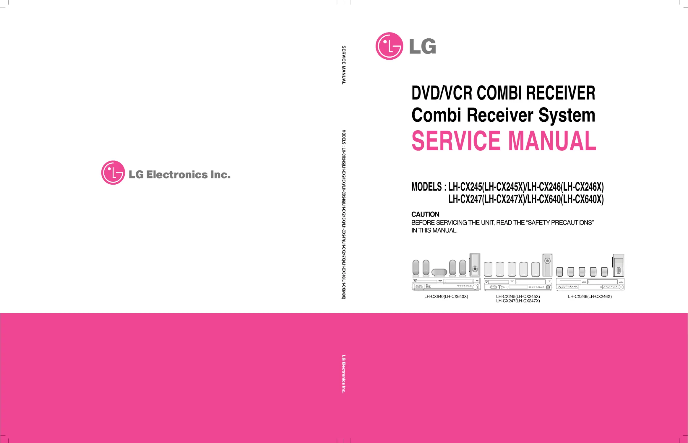
DVD/VCR COMBI RECEIVER
Combi Receiver System
SERVICE MANUAL
MODELS : LH-CX245(LH-CX245X)/LH-CX246(LH-CX246X)
LH-CX247(LH-CX247X)/LH-CX640(LH-CX640X)
CAUTION
BEFORE SERVICING THE UNIT, READ THE "SAFETY PRECAUTIONS"
IN THIS MANUAL.
LH-CX640(LH-CX640X)LH-CX245(LH-CX245X)
LH-CX247(LH-CX247X)
LH-CX246(LH-CX246X)
MODELS : LH-CX245(LH-CX245X)/LH-CX246(LH-CX246X)/LH-CX247(LH-CX247X)/LH-CX640(LH-CX640X)
SERVICE MANUAL
PROG./
PRESET
PROG.
CONTENTS
SECTION 1 . . . . SUMMARY
SECTION 2 . . . . CABINET & MAIN CHASSIS
SECTION 3 . . . . ELECTRICAL
SECTION 4 . . . . MECHANISM OF VCR PART
SECTION 5 . . . . MECHANISM OF DVD PART
SECTION 6 . . . . REPLACEMENT PARTS LIST
1-2
SECTION 1
SUMMARY
CONTENTS
PRODUCT SAFETY SERVICING GUIDELINES FOR VIDEO PRODUCTS ............. 1-3
SERVICING PRECAUTIONS .................................................................................................. 1-4
• General Servicing Precautions
• Insulation Checking Prodedure
• Electrostatically Sensitive Devices
SERVICE INFORMATION FOR EEPROM IC SETTING(VCR) .......................................1-5
SERVICE INFORMATION FOR EEPROM (DVD) ...............................................................1-6
SPECIFICATIONS ...................................................................................................................... 1-7
1-3
IMPORTANT SAFETY NOTICE
This manual was prepared for use only by properly trained audio-video service
technicians.
When servicing this product, under no circumstances should the original
design be modified or altered without permission from LG Electronics
Corporation. All components should be replaced only with types identical to
those in the original circuit and their physical location, wiring and lead dress
must conform to original layout upon completion of repairs.
Special components are also used to prevent x-radiation, shock and fire haz-
ard. These components are indicated by the letter "x" included in their compo-
nent designators and are required to maintain safe performance. No deviations
are allowed without prior approval by LG Electronics Corporation.
Circuit diagrams may occasionally differ from the actual circuit used. This way,
implementation of the latest safety and performance improvement changes
into the set is not delayed until the new service literature is printed.
CAUTION: Do not attempt to modify this product in any way. Never perform
customized installations without manufacturer's approval. Unauthorized modi-
fications will not only void the warranty, but may lead to property damage or
user injury.
Service work should be performed only after you are thoroughly familiar with
these safety checks and servicing guidelines.
GRAPHIC SYMBOLS
The exclamation point within an equilateral triangle is intended to
alert the service personnel to important safety information in the
service literature.
The lightning flash with arrowhead symbol within an equilateral tri-
angle is intended to alert the service personnel to the presence of
noninsulated "dangerous voltage" that may be of sufficient magni-
tude to constitute a risk of electric shock.
The pictorial representation of a fuse and its rating within an equi-
lateral triangle is intended to convey to the service personnel the
following fuse replacement caution notice:
CAUTION: FOR CONTINUED PROTECTION AGAINST RISK
OF FIRE, REPLACE ALL FUSES WITH THE SAME TYPE AND
RATING AS MARKED NEAR EACH FUSE.
SERVICE INFORMATION
While servicing, use an isolation transformer for protection from AC line shock.
After the original service problem has been corrected, make a check of the fol-
lowing:
FIRE AND SHOCK HAZARD
1. Be sure that all components are positioned to avoid a possibility of adjacent
component shorts. This is especially important on items trans-ported to and
from the repair shop.
2. Verify that all protective devices such as insulators, barriers, covers, shields,
strain reliefs, power supply cords, and other hardware have been reinstalled
per the original design. Be sure that the safety purpose of the polarized line
plug has not been defeated.
3. Soldering must be inspected to discover possible cold solder joints, solder
splashes, or sharp solder points. Be certain to remove all loose foreign par-
ticles.
4. Check for physical evidence of damage or deterioration to parts and compo-
nents, for frayed leads or damaged insulation (including the AC cord), and
replace if necessary.
5. No lead or component should touch a high current device or a resistor rated
at 1 watt or more. Lead tension around protruding metal surfaces must be
avoided.
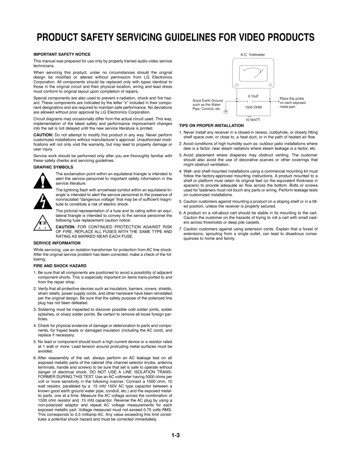
6. After reassembly of the set, always perform an AC leakage test on all
exposed metallic parts of the cabinet (the channel selector knobs, antenna
terminals, handle and screws) to be sure that set is safe to operate without
danger of electrical shock. DO NOT USE ALINE ISOLATION TRANS-
FORMER DURING THIS TEST. Use an AC voltmeter having 5000 ohms per
volt or more sensitivity in the following manner: Connect a 1500 ohm, 10
watt resistor, paralleled by a .15 mfd 150V AC type capacitor between a
known good earth ground water pipe, conduit, etc.) and the exposed metal-
lic parts, one at a time. Measure the AC voltage across the combination of
1500 ohm resistor and .15 mfd capacitor. Reverse the AC plug by using a
non-polarized adaptor and repeat AC voltage measurements for each
exposed metallic part. Voltage measured must not exceed 0.75 volts RMS.
This corresponds to 0.5 milliamp AC. Any value exceeding this limit consti-
tutes a potential shock hazard and must be corrected immediately.
TIPS ON PROPER INSTALLATION
1. Never install any receiver in a closed-in recess, cubbyhole, or closely fitting
shelf space over, or close to, a heat duct, or in the path of heated air flow.
2. Avoid conditions of high humidity such as: outdoor patio installations where
dew is a factor, near steam radiators where steam leakage is a factor, etc.
3. Avoid placement where draperies may obstruct venting. The customer
should also avoid the use of decorative scarves or other coverings that
might obstruct ventilation.
4. Wall- and shelf-mounted installations using a commercial mounting kit must
follow the factory-approved mounting instructions. Aproduct mounted to a
shelf or platform must retain its original feet (or the equivalent thickness in
spacers) to provide adequate air flow across the bottom. Bolts or screws
used for fasteners must not touch any parts or wiring. Perform leakage tests
on customized installations.
5. Caution customers against mounting a product on a sloping shelf or in a tilt-
ed position, unless the receiver is properly secured.
6. Aproduct on a roll-about cart should be stable in its mounting to the cart.
Caution the customer on the hazards of trying to roll a cart with small cast-
ers across thresholds or deep pile carpets.
7. Caution customers against using extension cords. Explain that a forest of
extensions, sprouting from a single outlet, can lead to disastrous conse-
quences to home and family.
A.C. Voltmeter
1500 OHM
10 WATT
Place this probe
on each exposed
metal part.
Good Earth Ground
such as the Water
Pipe, Conduit, etc.
0.15uF
PRODUCT SAFETY SERVICING GUIDELINES FOR VIDEO PRODUCTS
1-4
SERVICING PRECAUTIONS
CAUTION: Before servicing the HOME THEATER COMBI
covered by this service data and its supplements and
addends, read and follow the SAFETY PRECAUTIONS.
NOTE: if unforeseen circumstances create conflict between
the following servicing precautions and any of the safety pre-
cautions in this publications, always follow the safety pre-
cautions.
Remember Safety First:
General Servicing Precautions
1. Always unplug the HOME THEATER COMBI AC power
cord from the AC power source before:
(1) Removing or reinstalling any component, circuit board,
module, or any other assembly.
(2) Disconnecting or reconnecting any internal electrical
plug or other electrical connection.
(3) Connecting a test substitute in parallel with an elec-
trolytic capacitor.
Caution: Awrong part substitution or incorrect
polarity installation of electrolytic capacitors may result
in an explosion hazard.
2. Do not spray chemicals on or near this HOME THEATER
COMBI or any of its assemblies.
3. Unless specified otherwise in this service data, clean
electrical contacts by applying an appropriate contact
cleaning solution to the contacts with a pipe cleaner,
cotton-tipped swab, or comparable soft applicator.
Unless specified otherwise in this service data, lubrication
of contacts is not required.
4. Do not defeat any plug/socket B+ voltage interlocks with
whitch instruments covered by this service manual might
be equipped.
5. Do not apply AC power to this HOME THEATER COMBI
and/or any of its electrical assemblies unless all solid-state
device heat sinks are correctly installed.
6. Always connect the test instrument ground lead to an
appropriate ground before connecting the test instrument
positive lead. Always remove the test instrument ground
lead last.
Insulation Checking Procedure
Disconnect the attachment plug from the AC outlet and turn
the power on. Connect an insulation resistance meter (500V)
to the blades of the attachment plug. The insulation resis-
tance between each blade of the attachment plug and acces-
sible conductive parts (Note 1) should be more than 1M-
ohm.
Note 1: Accessible Conductive Parts include Metal panels,
Input terminals, Earphone jacks,etc.
Electrostatically Sensitive (ES) Devices
Some semiconductor (solid state) devices can be damaged
easily by static electricity. Such components commonly are
called Electrostatically Sensitive (ES) Devices. Examples of
typical ES devices are integrated circuits and some field
effect transistors and semiconductor chip components.
The following techniques should be used to help reduce the
incidence of component damage caused by static electricity.
1. Immediately before handling any semiconductor compo-
nent or semiconductor-equipped assembly, drain off any
electrostatic charge on your body by touching a known
earth ground. Alternatively, obtain and wear a commer-
cially available discharging wrist strap device, which
should be removed for potential shock reasons prior to
applying power to the unit under test.
2. After removing an electrical assembly equipped with ES
devices, place the assembly on a conductive surface such
as aluminum foil, to prevent electrostatic charge buildup or
exposure of the assembly.
3. Use only a grounded-tip soldering iron to solder or unsolder
ES devices.
4. Use only an anti-static solder removal device. Some
solder removal devices not classified as "anti-static" can
generate electrical charges sufficient to damage ES
devices.
5. Do not use freon-propelled chemicals. These can
generate an electrical charge sufficient to damage ES
devices.
6. Do not remove a replacement ES device from its protec-
tive package until immediately before you are ready to
install it. (Most replacement ES devices are packaged with
leads electrically shorted together by conductive foam,
aluminum foil,or comparable conductive material).
7. Immediately before removing the protective material from
the leads of a replacement ES device, touch the protective
material to the chassis or circuit assembly into which the
device will be installed.
Caution: Be sure no power is applied to the chassis or
circuit, and observe all other safety precautions.
8. Minimize bodily motions when handling unpackaged
replacement ES devices. (Normally harmless motion such
as the brushing together of your clothes fabric or the lifting
of your foot from a carpeted floor can generate static elec-
tricity sufficient to damage an ES device.)
1-7
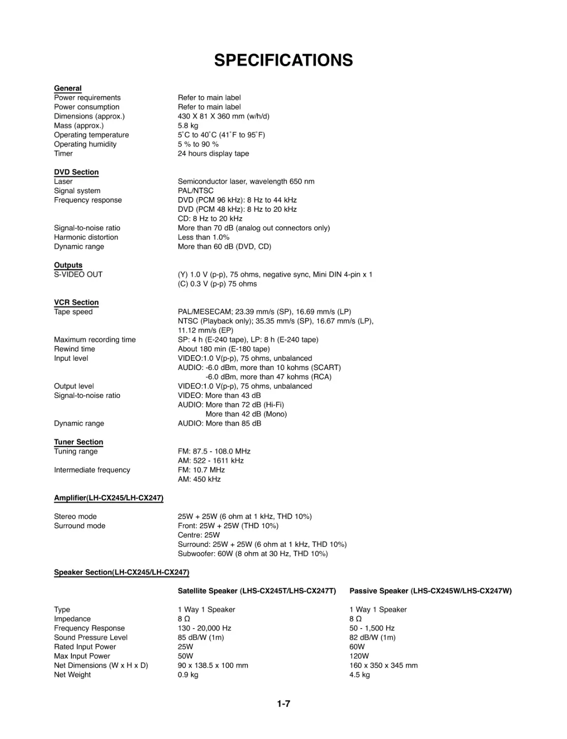
SPECIFICATIONS
General
Power requirements
Refer to main label
Power consumption
Refer to main label
Dimensions (approx.)
430 X 81 X 360 mm (w/h/d)
Mass (approx.)
5.8 kg
Operating temperature
5˚C to 40˚C (41˚F to 95˚F)
Operating humidity
5%to90%
Timer
24 hours display tape
DVD Section
Laser
Semiconductor laser, wavelength 650 nm
Signal system
PAL/NTSC
Frequency response
DVD(PCM96kHz):8Hzto44kHz
DVD(PCM48kHz):8Hzto20kHz
CD:8Hzto20kHz
Signal-to-noise ratio
More than 70 dB (analog out connectors only)
Harmonic distortion
Less than 1.0%
Dynamic range
More than 60 dB (DVD, CD)
Outputs
S-VIDEO OUT
(Y) 1.0 V (p-p), 75 ohms, negative sync, Mini DIN 4-pin x 1
(C) 0.3 V (p-p) 75 ohms
VCR Section
Tape speed
PAL/MESECAM; 23.39 mm/s (SP), 16.69 mm/s (LP)
NTSC (Playback only); 35.35 mm/s (SP), 16.67 mm/s (LP),
11.12 mm/s (EP)
Maximum recording time
SP: 4 h (E-240 tape), LP: 8 h (E-240 tape)
Rewind time
About 180 min (E-180 tape)
Input level
VIDEO:1.0 V(p-p), 75 ohms, unbalanced
AUDIO: -6.0 dBm, more than 10 kohms (SCART)
-6.0 dBm, more than 47 kohms (RCA)
Output level
VIDEO:1.0 V(p-p), 75 ohms, unbalanced
Signal-to-noise ratio
VIDEO: More than 43 dB
AUDIO: More than 72 dB (Hi-Fi)
More than 42 dB (Mono)
Dynamic range
AUDIO: More than 85 dB
Tuner Section
Tuning range
FM: 87.5 - 108.0 MHz
AM: 522 - 1611 kHz
Intermediate frequency
FM: 10.7 MHz
AM: 450 kHz
Amplifier(LH-CX245/LH-CX247)
Stereo mode
25W+25W(6ohmat1kHz,THD10%)
Surround mode
Front: 25W + 25W (THD 10%)
Centre: 25W
Surround: 25W + 25W (6 ohm at 1 kHz, THD 10%)
Subwoofer: 60W (8 ohm at 30 Hz, THD 10%)
Speaker Section(LH-CX245/LH-CX247)
Satellite Speaker (LHS-CX245T/LHS-CX247T) Passive Speaker (LHS-CX245W/LHS-CX247W)
Type
1 Way 1 Speaker
1 Way 1 Speaker
Impedance
8Ω
8Ω
Frequency Response
130 - 20,000 Hz
50 - 1,500 Hz
Sound Pressure Level
85 dB/W (1m)
82 dB/W (1m)
Rated Input Power
25W
60W
Max Input Power
50W
120W
Net Dimensions (W x H x D)
90x138.5x100mm
160x350x345mm
Net Weight
0.9 kg
4.5 kg
1-8
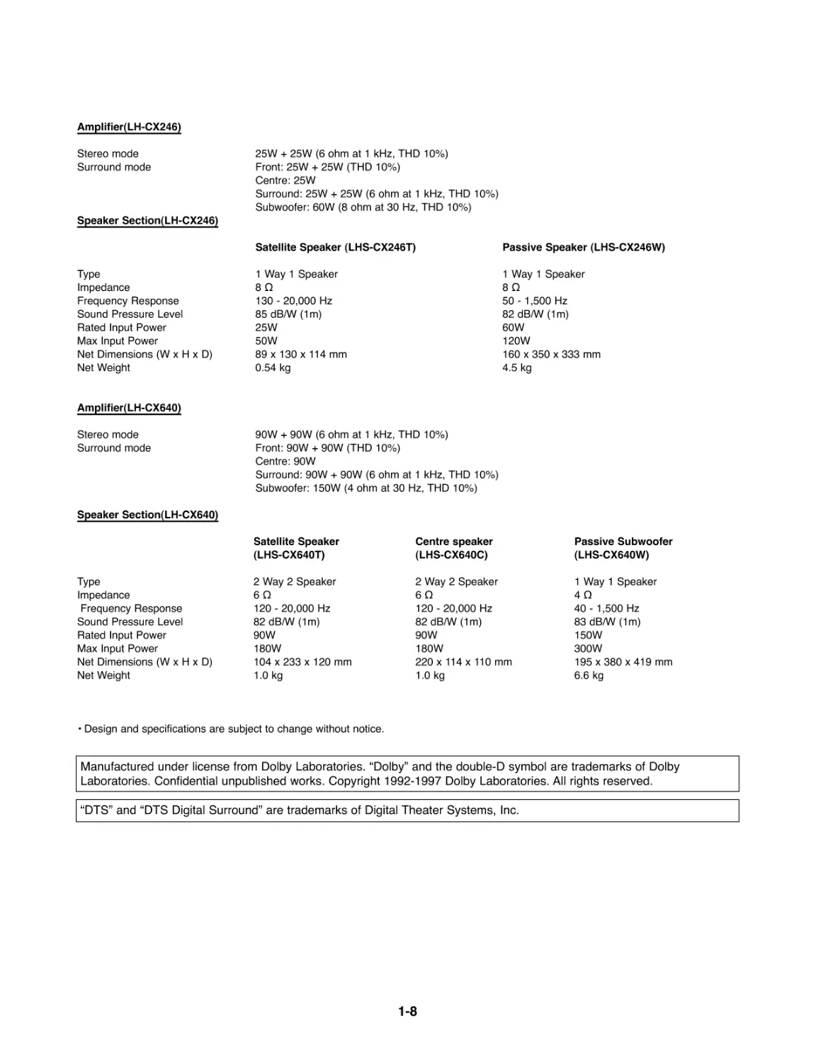
Amplifier(LH-CX246)
Stereo mode
25W+25W(6ohmat1kHz,THD10%)
Surround mode
Front: 25W + 25W (THD 10%)
Centre: 25W
Surround: 25W + 25W (6 ohm at 1 kHz, THD 10%)
Subwoofer: 60W (8 ohm at 30 Hz, THD 10%)
Speaker Section(LH-CX246)
Satellite Speaker (LHS-CX246T)
Passive Speaker (LHS-CX246W)
Type
1 Way 1 Speaker
1 Way 1 Speaker
Impedance
8Ω
8Ω
Frequency Response
130 - 20,000 Hz
50 - 1,500 Hz
Sound Pressure Level
85 dB/W (1m)
82 dB/W (1m)
Rated Input Power
25W
60W
Max Input Power
50W
120W
Net Dimensions (W x H x D)
89x130x114mm
160x350x333mm
Net Weight
0.54 kg
4.5 kg
Amplifier(LH-CX640)
Stereo mode
90W+90W(6ohmat1kHz,THD10%)
Surround mode
Front: 90W + 90W (THD 10%)
Centre: 90W
Surround: 90W + 90W (6 ohm at 1 kHz, THD 10%)
Subwoofer: 150W (4 ohm at 30 Hz, THD 10%)
Speaker Section(LH-CX640)
Satellite Speaker
Centre speaker
Passive Subwoofer
(LHS-CX640T)
(LHS-CX640C)
(LHS-CX640W)
Type
2 Way 2 Speaker
2 Way 2 Speaker
1 Way 1 Speaker
Impedance
6Ω
6Ω
4Ω
Frequency Response
120 - 20,000 Hz
120 - 20,000 Hz
40 - 1,500 Hz
Sound Pressure Level
82 dB/W (1m)
82 dB/W (1m)
83 dB/W (1m)
Rated Input Power
90W
90W
150W
Max Input Power
180W
180W
300W
Net Dimensions (W x H x D)
104x233x120mm
220x114x110mm
195x380x419mm
Net Weight
1.0 kg
1.0 kg
6.6 kg
• Design and specifications are subject to change without notice.
Manufactured under license from Dolby Laboratories. "Dolby" and the double-D symbol are trademarks of Dolby
Laboratories. Confidential unpublished works. Copyright 1992-1997 Dolby Laboratories. All rights reserved.
"DTS" and "DTS Digital Surround" are trademarks of Digital Theater Systems, Inc.
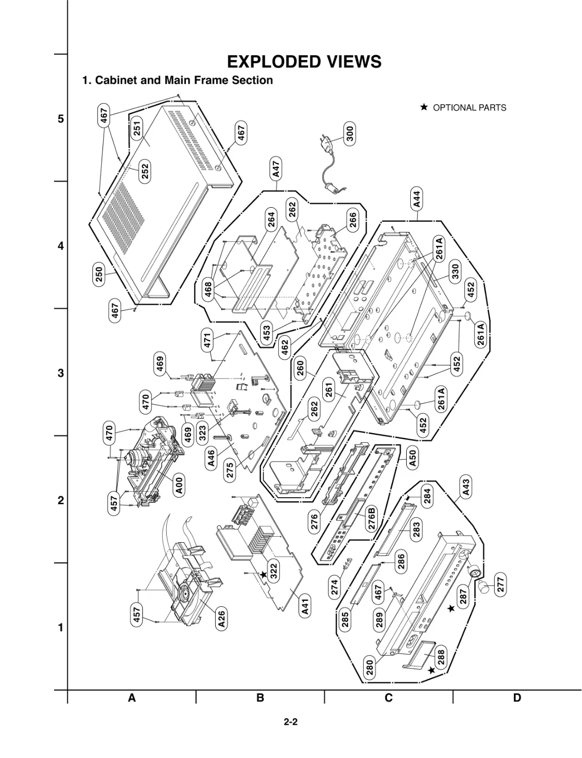
2-1
SECTION 2
CABINET & MAIN CHASSIS
CONTENTS
EXPLODED VIEWS .....................................................................................................................2-2
1. Cabinet and Main Frame Section ...........................................................................................2-2
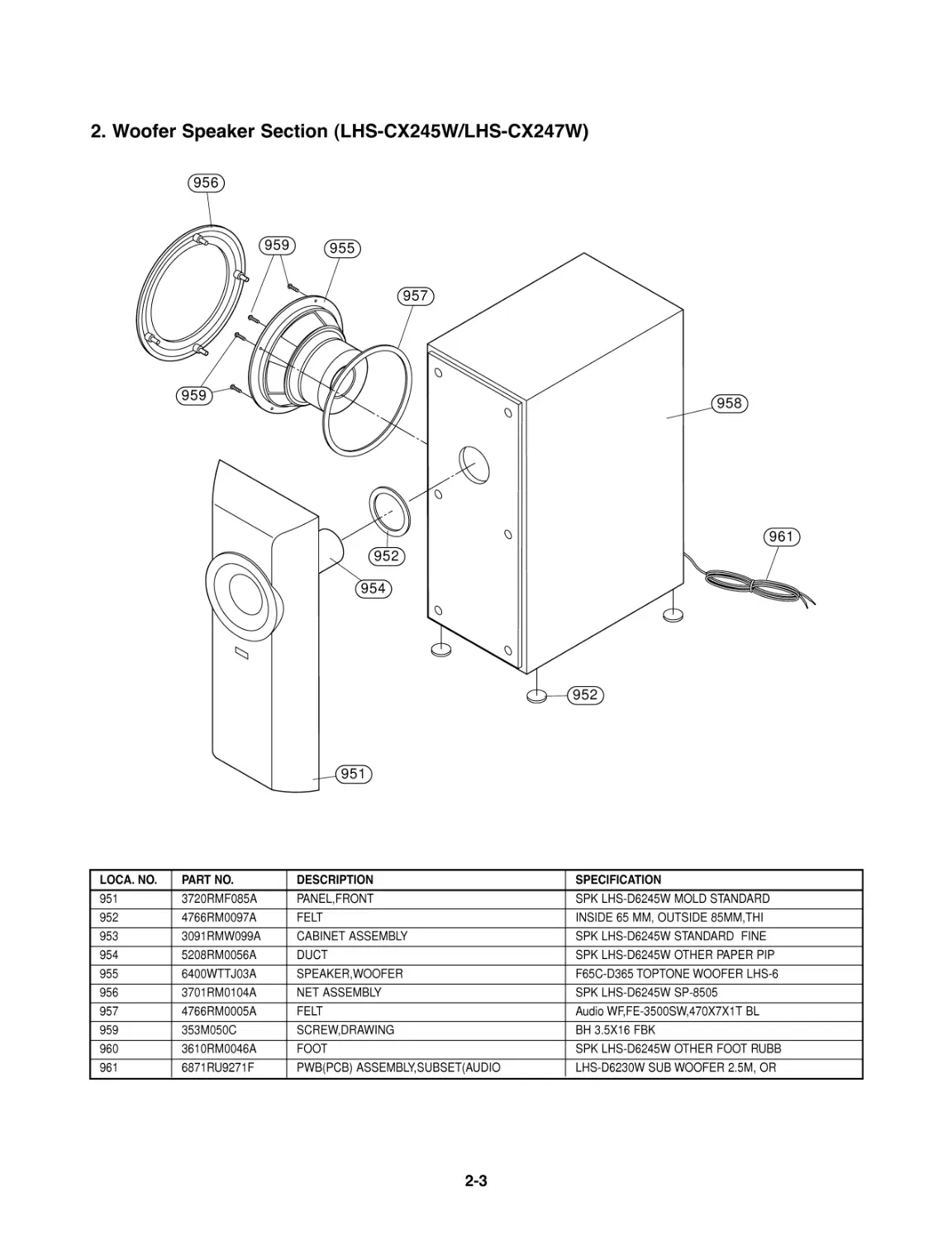
2. Woofer Speaker Section (LHS-CX245W/LHS-CX247W) .......................................................2-3
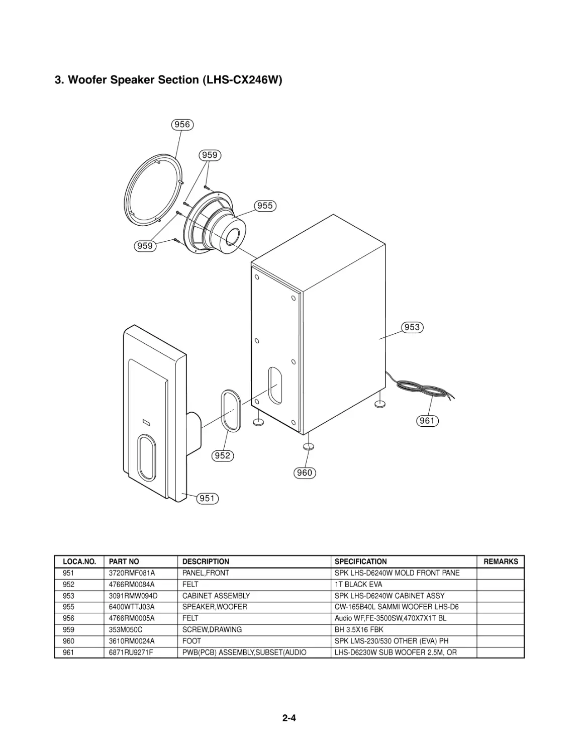
3. Woofer Speaker Section (LHS-CX246W) ..............................................................................2-4
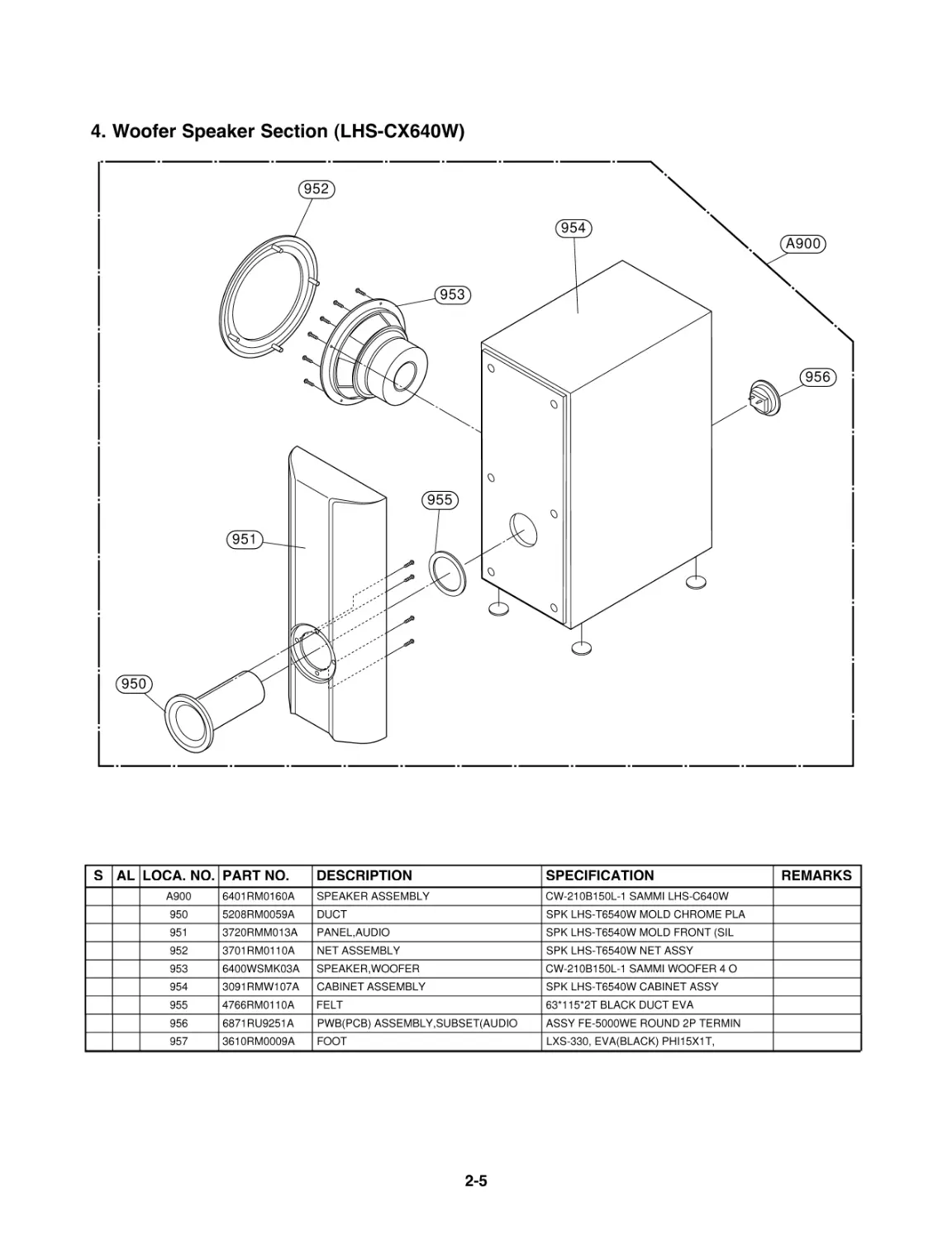
4. Woofer Speaker Section (LHS-CX640W) ..............................................................................2-5
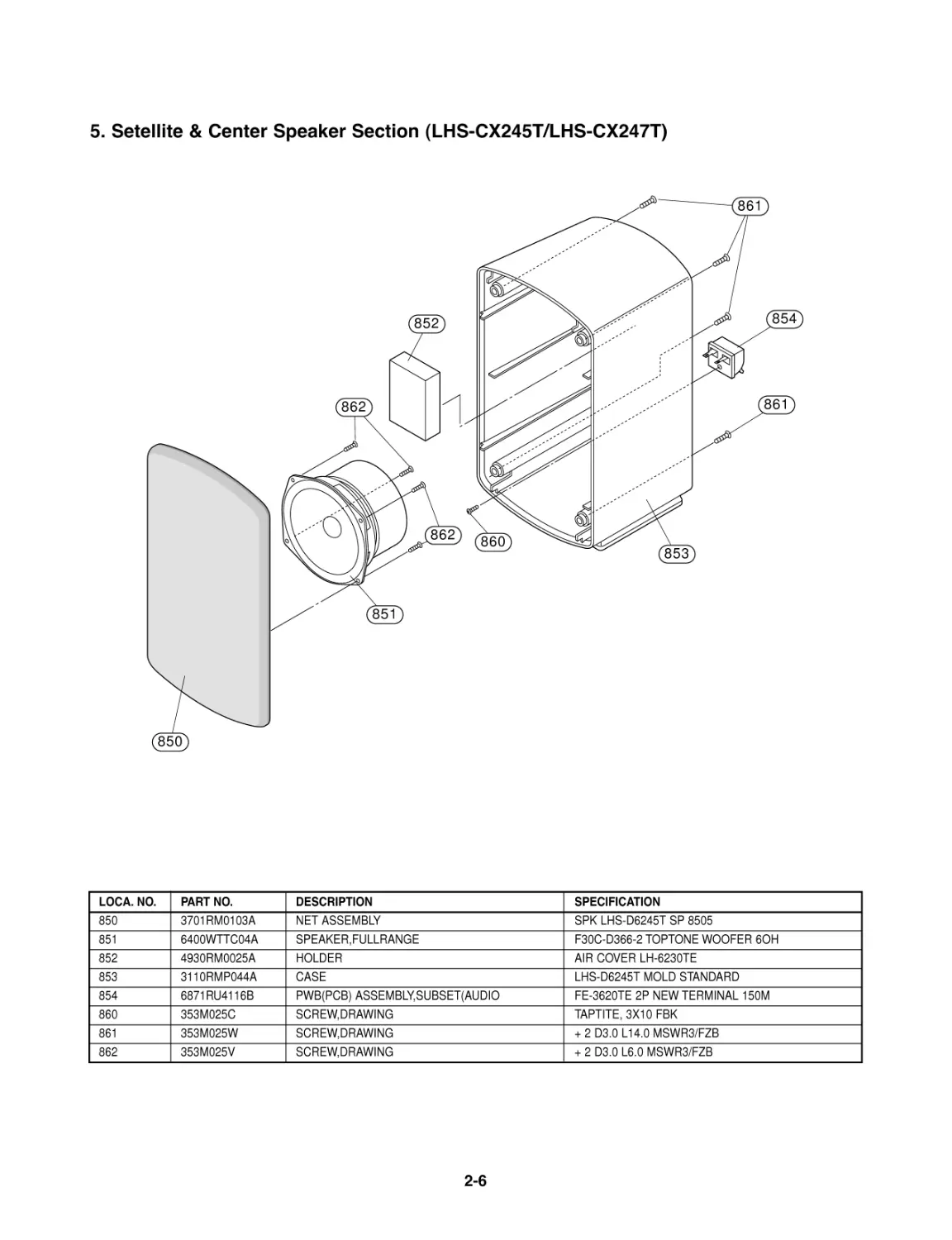
5. Setellite & Center Speaker Section (LHS-CX245T/LHS-CX247T) ........................................2-6
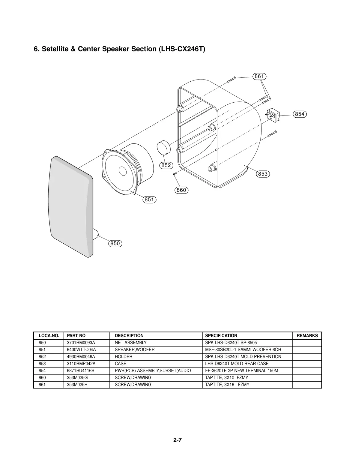
6. Setellite & Center Speaker Section (LHS-CX246T)...............................................................2-7
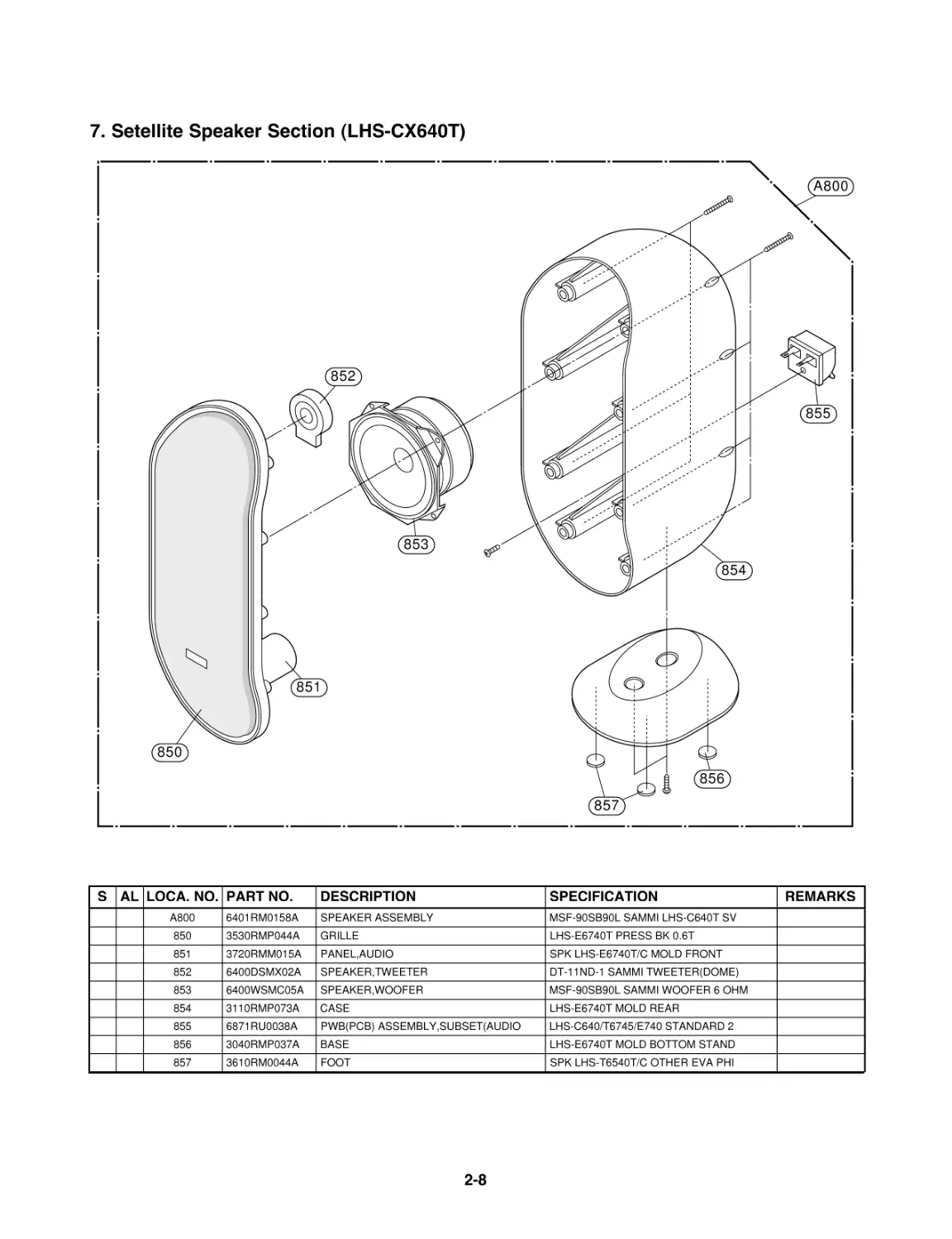
7. Setellite Speaker Section (LHS-CX640T)...............................................................................2-8
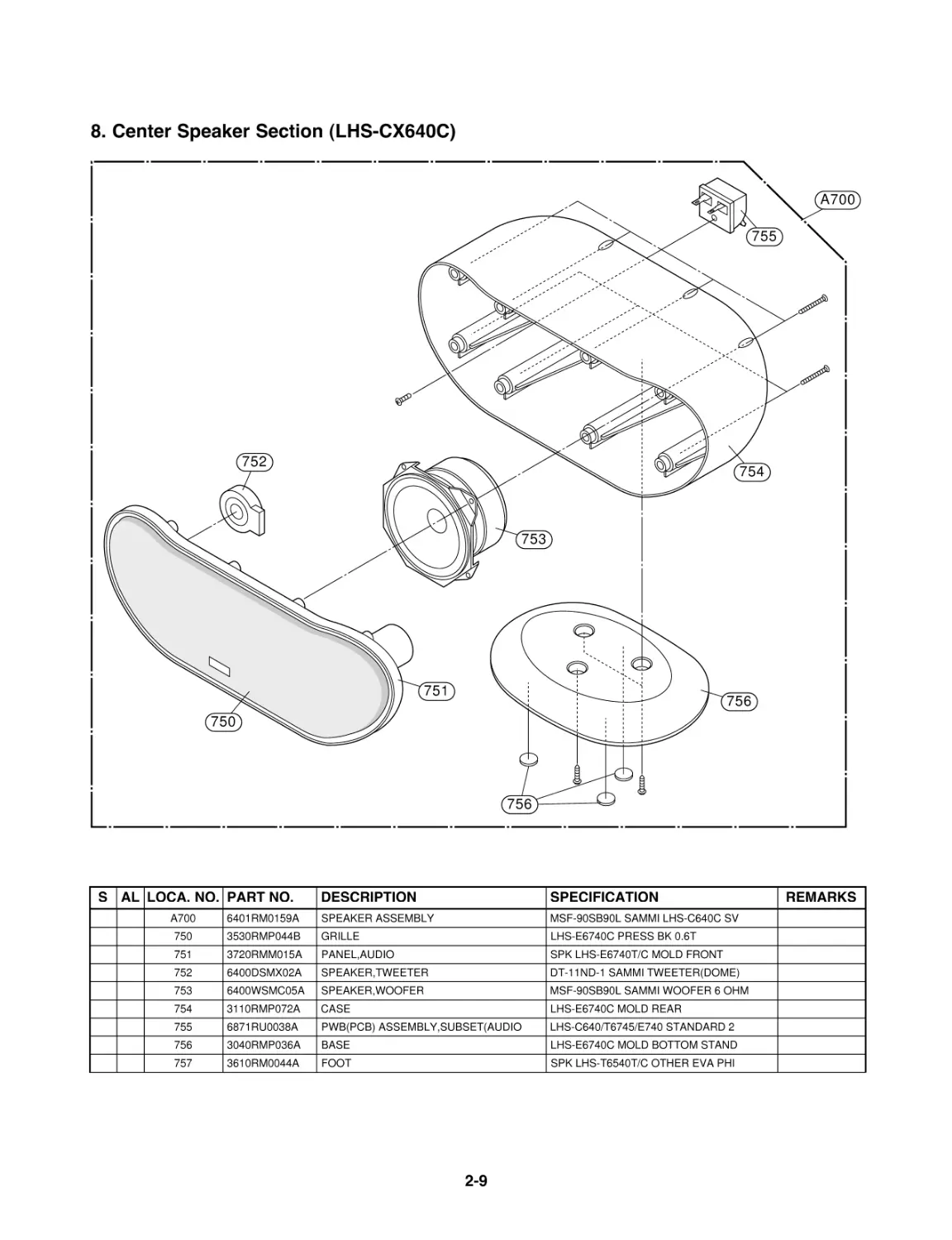
8. Center Speaker Section (LHS-CX640C).................................................................................2-9
9. Packing Accessory Section ..................................................................................................2-10
2-2
EXPLODED VIEWS
1. Cabinet and Main Frame Section
A26
A41
A50
A44
A43
A47
322
A00
457
470
470
471
469
467
250
252
251
467
467
323
275
261
262
260
452
452
462
453
266
300
262
264
452
330
276
274
285
286
289
280
288
287
277
467
283 284
276B
261A
261A
261A
A46
469
457
468
OPTIONAL PARTS
A
5
4
3
2
1
BCD
2-3
956
959
959 955
957
952
954
951
952
961
958
LOCA. NO. PART NO.
DESCRIPTION
SPECIFICATION
951
3720RMF085A
PANEL,FRONT
SPK LHS-D6245W MOLD STANDARD
952
4766RM0097A
FELT
INSIDE 65 MM, OUTSIDE 85MM,THI
953
3091RMW099A CABINET ASSEMBLY
SPK LHS-D6245W STANDARD FINE
954
5208RM0056A
DUCT
SPK LHS-D6245W OTHER PAPER PIP
955
6400WTTJ03A
SPEAKER,WOOFER
F65C-D365 TOPTONE WOOFER LHS-6
956
3701RM0104A
NET ASSEMBLY
SPK LHS-D6245W SP-8505
957
4766RM0005A
FELT
Audio WF,FE-3500SW,470X7X1T BL
959
353M050C
SCREW,DRAWING
BH 3.5X16 FBK
960
3610RM0046A
FOOT
SPK LHS-D6245W OTHER FOOT RUBB
961
6871RU9271F
PWB(PCB) ASSEMBLY,SUBSET(AUDIO
LHS-D6230W SUB WOOFER 2.5M, OR
2. Woofer Speaker Section (LHS-CX245W/LHS-CX247W)
2-4
956
959
959
955
953
961
960
952
951
LOCA.NO. PART NO
DESCRIPTION
SPECIFICATION
REMARKS
951
3720RMF081A
PANEL,FRONT
SPK LHS-D6240W MOLD FRONT PANE
952
4766RM0084A
FELT
1T BLACK EVA
953
3091RMW094D
CABINET ASSEMBLY
SPK LHS-D6240W CABINET ASSY
955
6400WTTJ03A
SPEAKER,WOOFER
CW-165B40L SAMMI WOOFER LHS-D6
956
4766RM0005A
FELT
Audio WF,FE-3500SW,470X7X1T BL
959
353M050C
SCREW,DRAWING
BH 3.5X16 FBK
960
3610RM0024A
FOOT
SPK LMS-230/530 OTHER (EVA) PH
961
6871RU9271F
PWB(PCB) ASSEMBLY,SUBSET(AUDIO
LHS-D6230W SUB WOOFER 2.5M, OR
3. Woofer Speaker Section (LHS-CX246W)
2-5
S AL LOCA. NO. PART NO. DESCRIPTION
SPECIFICATION
REMARKS
A900 6401RM0160A SPEAKER ASSEMBLY
CW-210B150L-1 SAMMI LHS-C640W
950
5208RM0059A DUCT
SPK LHS-T6540W MOLD CHROME PLA
951
3720RMM013A PANEL,AUDIO
SPK LHS-T6540W MOLD FRONT (SIL
952
3701RM0110A NET ASSEMBLY
SPK LHS-T6540W NET ASSY
953
6400WSMK03A SPEAKER,WOOFER
CW-210B150L-1 SAMMI WOOFER 4 O
954
3091RMW107A CABINET ASSEMBLY
SPK LHS-T6540W CABINET ASSY
955
4766RM0110A FELT
63*115*2T BLACK DUCT EVA
956
6871RU9251A PWB(PCB) ASSEMBLY,SUBSET(AUDIO ASSY FE-5000WE ROUND 2P TERMIN
957
3610RM0009A FOOT
LXS-330, EVA(BLACK) PHI15X1T,
952
953
954
956
955
951
950
A900
4. Woofer Speaker Section (LHS-CX640W)
2-6
850
851
862
852
862
860
853
861
854
861
5. Setellite & Center Speaker Section (LHS-CX245T/LHS-CX247T)
LOCA. NO. PART NO.
DESCRIPTION
SPECIFICATION
850
3701RM0103A
NET ASSEMBLY
SPK LHS-D6245T SP 8505
851
6400WTTC04A SPEAKER,FULLRANGE
F30C-D366-2 TOPTONE WOOFER 6OH
852
4930RM0025A
HOLDER
AIR COVER LH-6230TE
853
3110RMP044A
CASE
LHS-D6245T MOLD STANDARD
854
6871RU4116B
PWB(PCB) ASSEMBLY,SUBSET(AUDIO
FE-3620TE 2P NEW TERMINAL 150M
860
353M025C
SCREW,DRAWING
TAPTITE, 3X10 FBK
861
353M025W
SCREW,DRAWING
+ 2 D3.0 L14.0 MSWR3/FZB
862
353M025V
SCREW,DRAWING
+ 2 D3.0 L6.0 MSWR3/FZB
2-7
850
851
860
852
854
861
853
6. Setellite & Center Speaker Section (LHS-CX246T)
LOCA.NO. PART NO
DESCRIPTION
SPECIFICATION
REMARKS
850
3701RM0093A
NET ASSEMBLY
SPK LHS-D6240T SP-8505
851
6400WTTC04A
SPEAKER,WOOFER
MSF-80SB20L-1 SAMMI WOOFER 6OH
852
4930RM0046A
HOLDER
SPK LHS-D6240T MOLD PREVENTION
853
3110RMP042A
CASE
LHS-D6240T MOLD REAR CASE
854
6871RU4116B
PWB(PCB) ASSEMBLY,SUBSET(AUDIO
FE-3620TE 2P NEW TERMINAL 150M
860
353M025G
SCREW,DRAWING
TAPTITE, 3X10 FZMY
861
353M025H
SCREW,DRAWING
TAPTITE, 3X16 FZMY
2-8
A800
851
852
853
850
857
856
854
855
7. Setellite Speaker Section (LHS-CX640T)
S AL LOCA. NO. PART NO. DESCRIPTION
SPECIFICATION
REMARKS
A800 6401RM0158A SPEAKER ASSEMBLY
MSF-90SB90L SAMMI LHS-C640T SV
850
3530RMP044A GRILLE
LHS-E6740T PRESS BK 0.6T
851
3720RMM015A PANEL,AUDIO
SPK LHS-E6740T/C MOLD FRONT
852
6400DSMX02A SPEAKER,TWEETER
DT-11ND-1 SAMMI TWEETER(DOME)
853
6400WSMC05A SPEAKER,WOOFER
MSF-90SB90L SAMMI WOOFER 6 OHM
854
3110RMP073A CASE
LHS-E6740T MOLD REAR
855
6871RU0038A PWB(PCB) ASSEMBLY,SUBSET(AUDIO LHS-C640/T6745/E740 STANDARD 2
856
3040RMP037A BASE
LHS-E6740T MOLD BOTTOM STAND
857
3610RM0044A FOOT
SPK LHS-T6540T/C OTHER EVA PHI
2-9
A700
752
750
751
753
756
754
755
756
8. Center Speaker Section (LHS-CX640C)
S AL LOCA. NO. PART NO. DESCRIPTION
SPECIFICATION
REMARKS
A700 6401RM0159A SPEAKER ASSEMBLY
MSF-90SB90L SAMMI LHS-C640C SV
750
3530RMP044B GRILLE
LHS-E6740C PRESS BK 0.6T
751
3720RMM015A PANEL,AUDIO
SPK LHS-E6740T/C MOLD FRONT
752
6400DSMX02A SPEAKER,TWEETER
DT-11ND-1 SAMMI TWEETER(DOME)
753
6400WSMC05A SPEAKER,WOOFER
MSF-90SB90L SAMMI WOOFER 6 OHM
754
3110RMP072A CASE
LHS-E6740C MOLD REAR
755
6871RU0038A PWB(PCB) ASSEMBLY,SUBSET(AUDIO LHS-C640/T6745/E740 STANDARD 2
756
3040RMP036A BASE
LHS-E6740C MOLD BOTTOM STAND
757
3610RM0044A FOOT
SPK LHS-T6540T/C OTHER EVA PHI
2-10
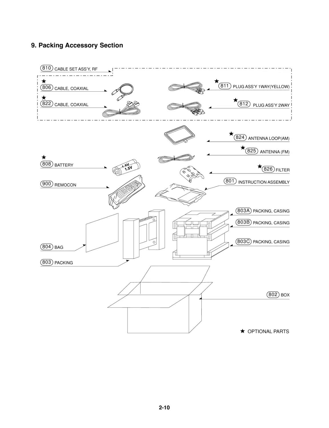
BATTERY
CABLE, COAXIAL
CABLE SET ASS'Y, RF
OPTIONAL PARTS
INSTRUCTION ASSEMBLY
BOX
REMOCON
BAG
PACKING
PLUG ASS'Y 1WAY(YELLOW)
ANTENNA LOOP(AM)
ANTENNA (FM)
PLUG ASS'Y 2WAY
PACKING, CASING
PACKING, CASING
PACKING, CASING
810
811
812
824
825
826
801
802
806
CABLE, COAXIAL
822
808
900
804
803
803A
803B
803C
FILTER
9. Packing Accessory Section
3-1
SECTION 3
ELECTRICAL
CONTENTS
OVERALL WIRING DIAGRAM .............................3-2
VCR PART
ELECTRICAL ADJUSTMENT
PROCEDURES ...........................................................3-3
ELECTRICAL TROUBLESHOOTING
GUIDE ............................................................................3-4
1. POWER(SMPS) CIRCUIT.......................................3-4
2. SYSTEM/KEY CIRCUIT..........................................3-6
3. SERVO CIRCUIT ....................................................3-7
4. Y/C CIRCUIT .........................................................3-10
5. Hi-Fi CIRCUIT.......................................................3-14
6. TUNER/IF CIRCUIT ..............................................3-17
BLOCK DIAGRAMS ...............................................3-19
1. POWER(SMPS) BLOCK DIAGRAM 1 .................3-19
2. POWER(SMPS) BLOCK DIAGRAM 2 .................3-21
3. TU/IF, NICAM & A2 BLOCK DIAGRAM ..............3-23
4. VPS BLOCK DIAGRAM .......................................3-24
5. Y/C BLOCK DIAGRAM ........................................3-25
6. Hi-Fi BLOCK DIAGRAM ......................................3-27
7. SYSTEM BLOCK DIAGRAM ...............................3-29
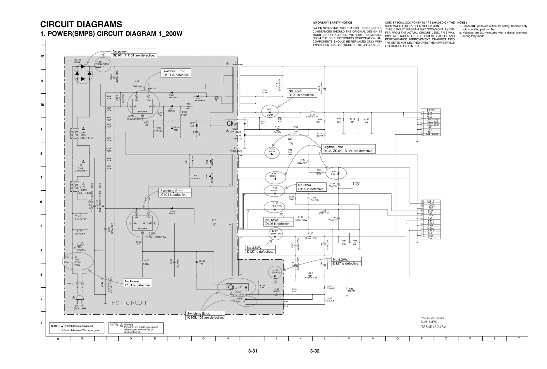
CIRCUIT DIAGRAMS .............................................3-31
1. POWER(SMPS) CIRCUIT DIAGRAM 1_200W....3-31
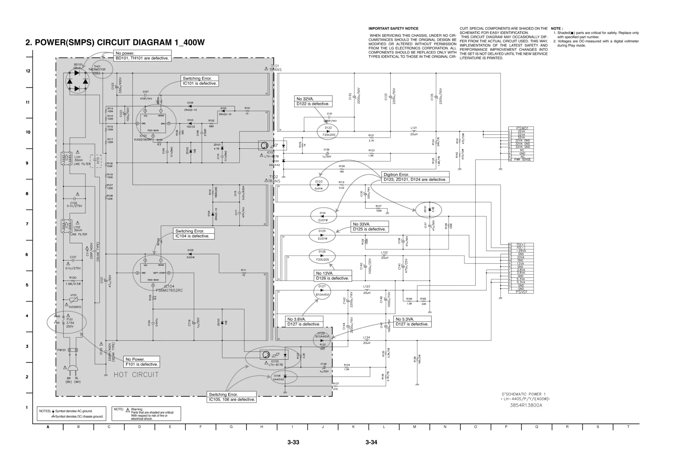
2. POWER(SMPS) CIRCUIT DIAGRAM 1_400W....3-33
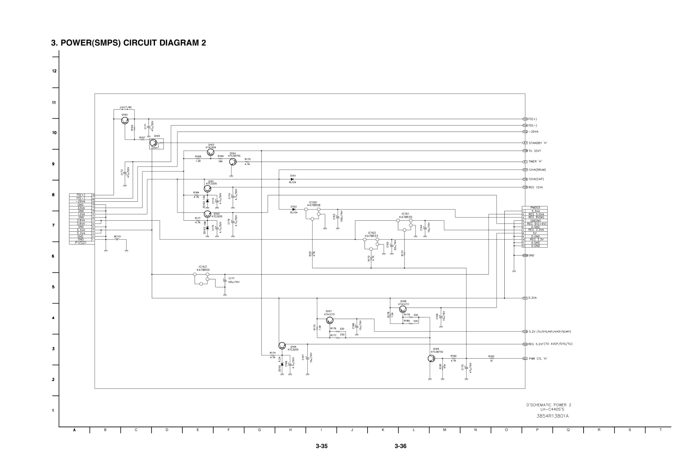
3. POWER(SMPS) CIRCUIT DIAGRAM 2 ...............3-35
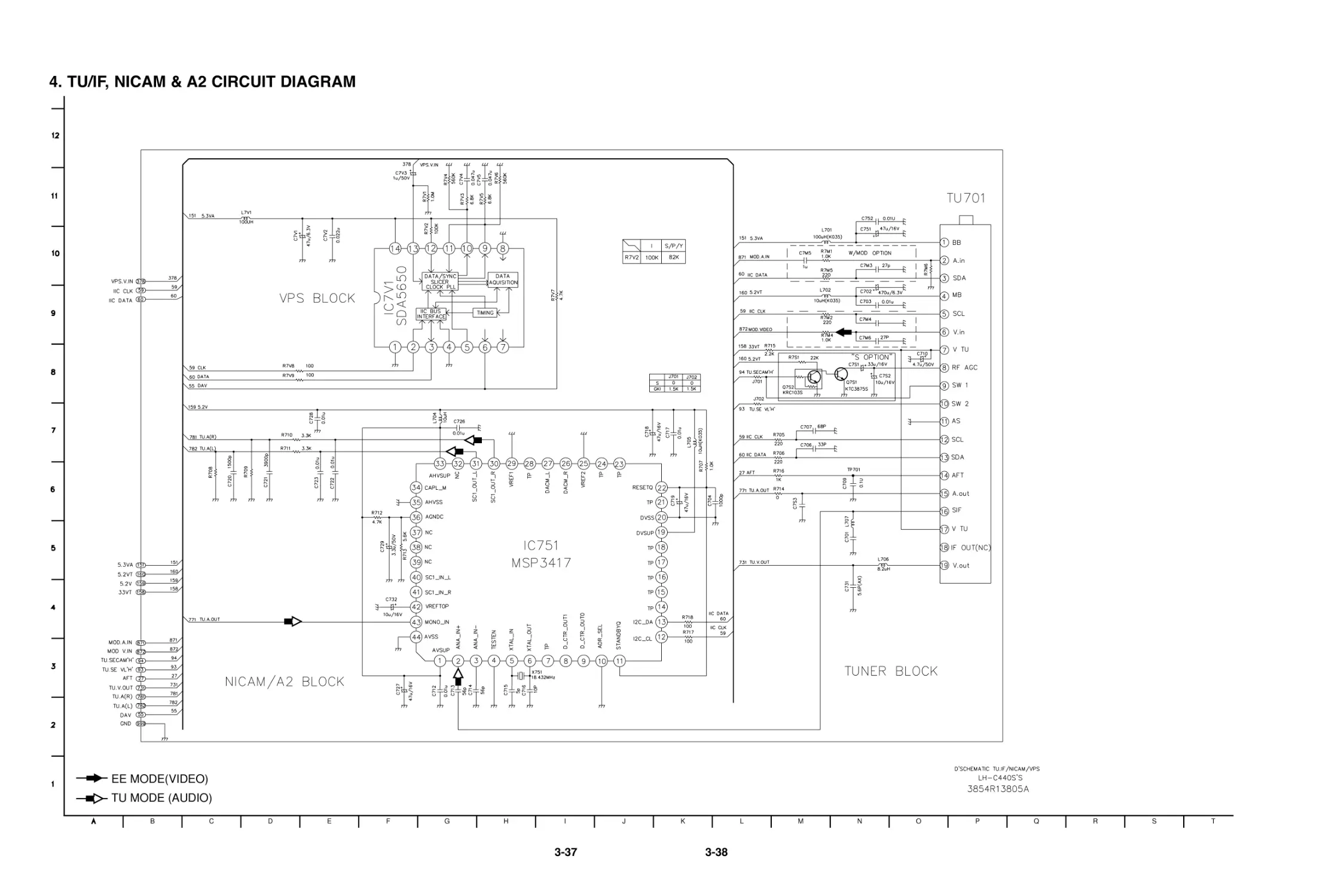
4. TU/IF, NICAM & A2 CIRCUIT DIAGRAM.............3-37
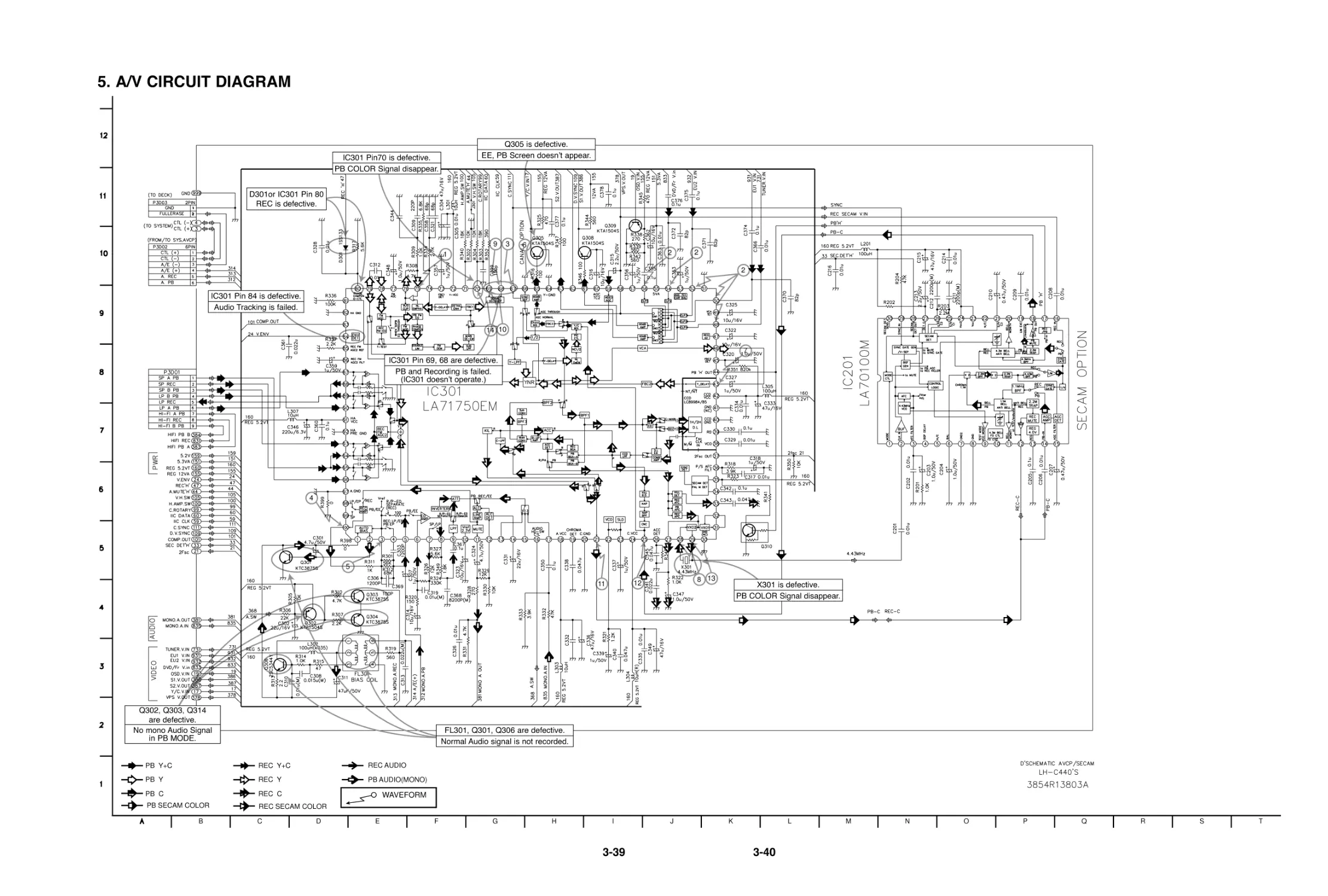
5. A/V CIRCUIT DIAGRAM.......................................3-39
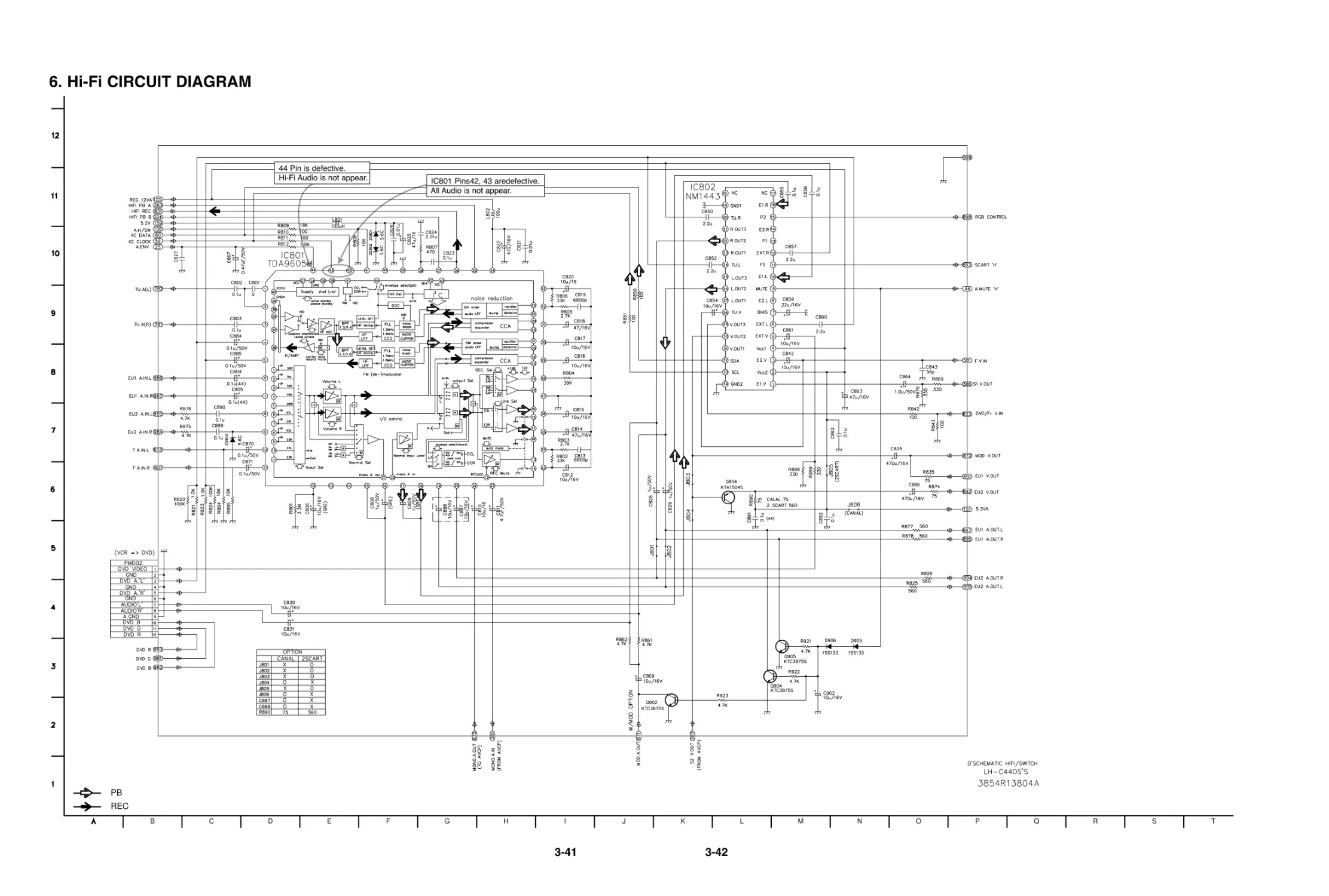
6. HI-FI CIRCUIT DIAGRAM ....................................3-41
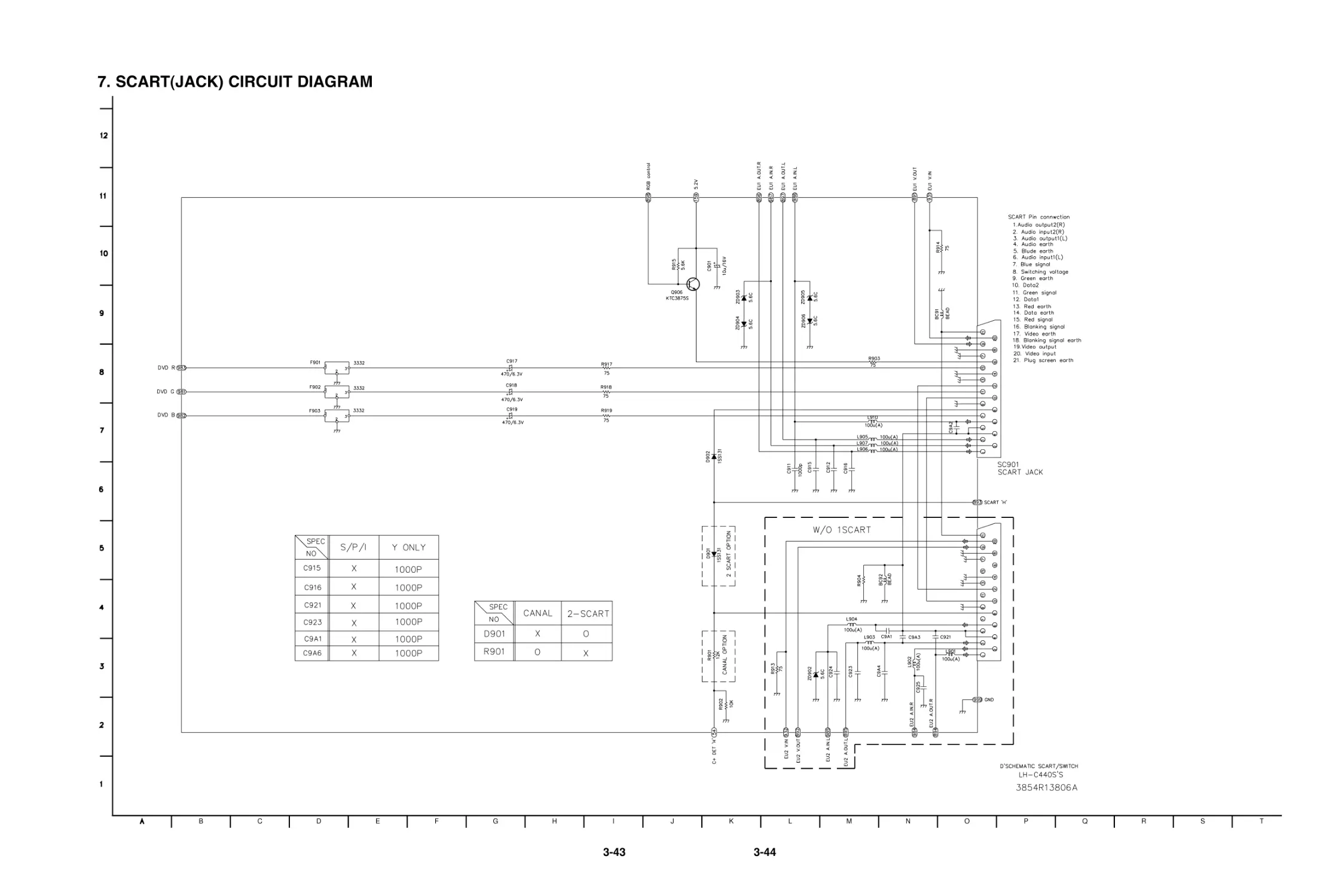
7. SCART(JACK) CIRCUIT DIAGRAM ....................3-43
8. SYSTEM CIRCUIT DIAGRAM..............................3-45
9. TIMER CIRCUIT DIAGRAM_0TOOL ...................3-47
10. TIMER CIRCUIT DIAGRAM_5TOOL / 7TOOL ..3-49
11. TIMER CIRCUIT DIAGRAM_6TOOL..................3-51
• WAVEFORM & VOLTAGE SHEET ........................3-53
• CIRCUIT VOLTAGE CHART ..................................3-55
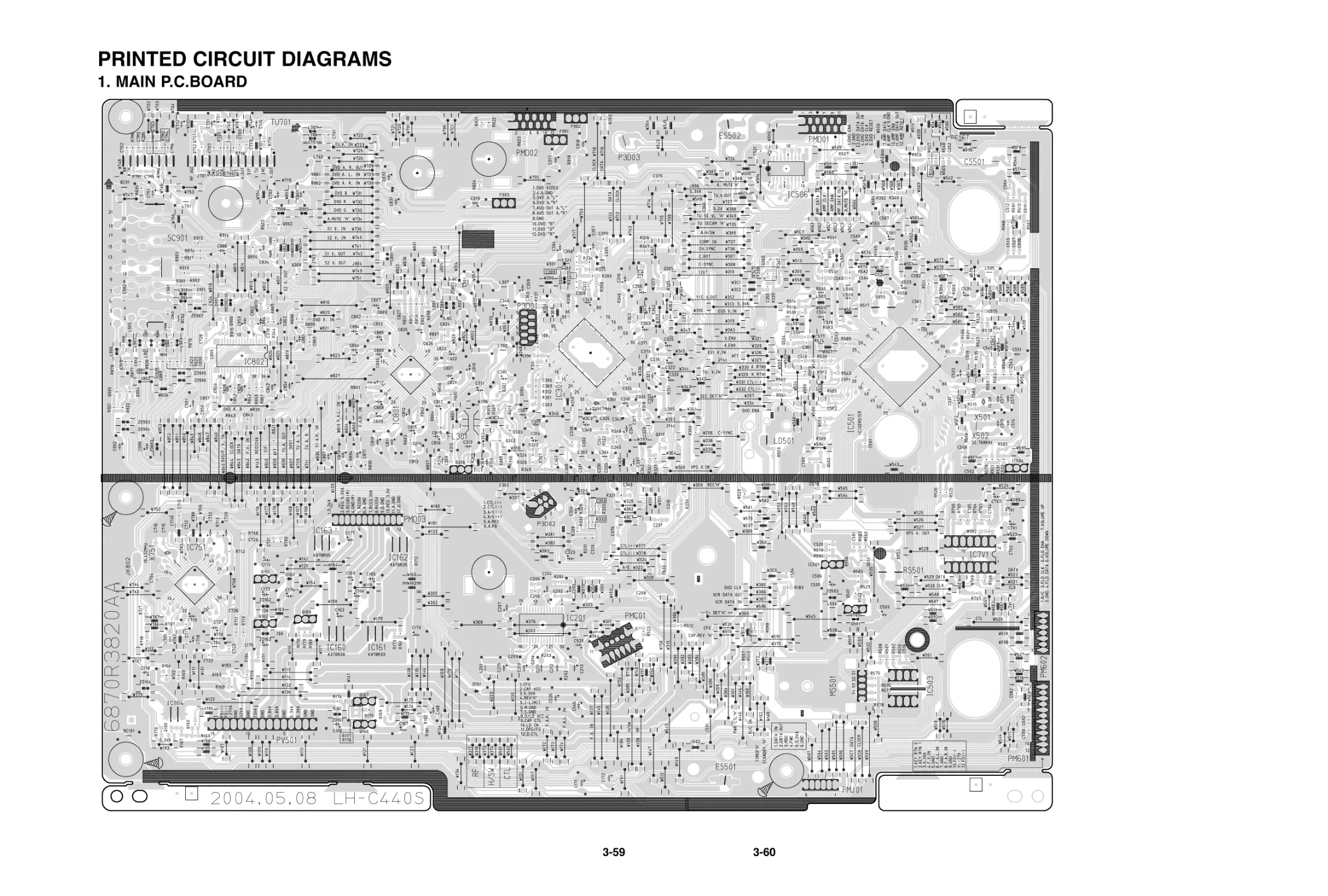
PRINTED CIRCUIT DIAGRAMS ........................3-59
1. MAIN P.C.BOARD ................................................3-59
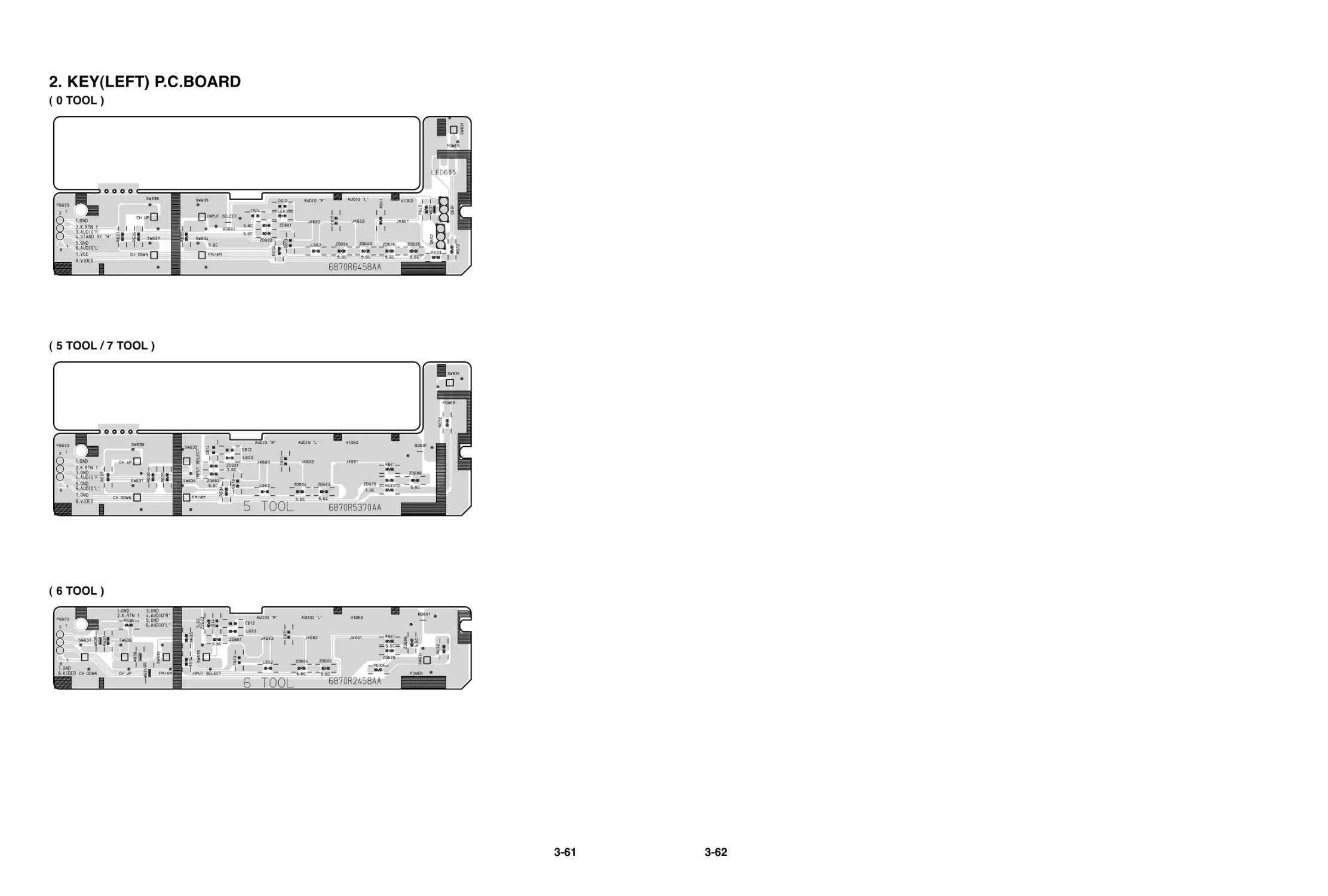
2. KEY(LEFT) P.C.BOARD ......................................3-61
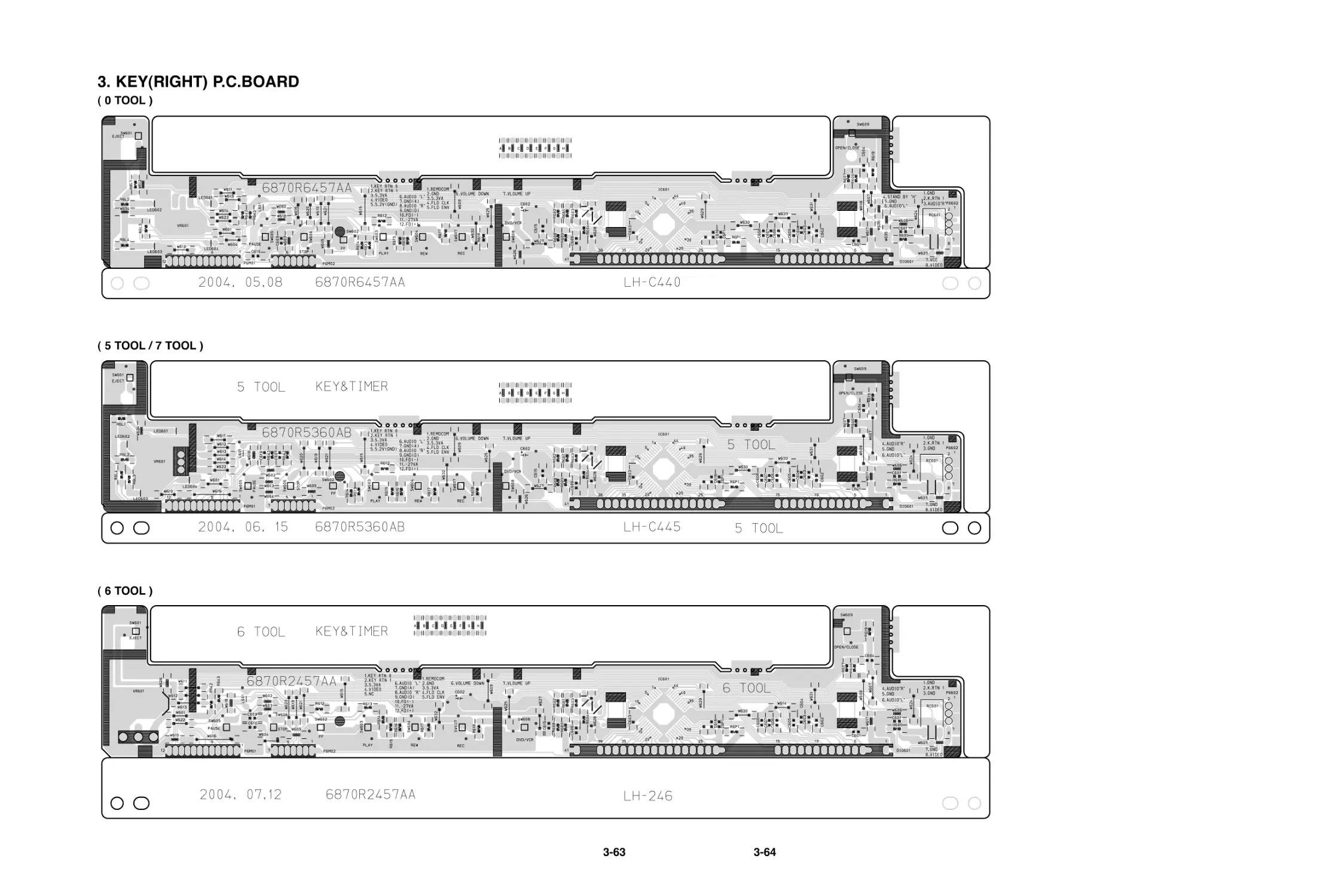
3. KEY(RIGHT) P.C.BOARD.....................................3-63
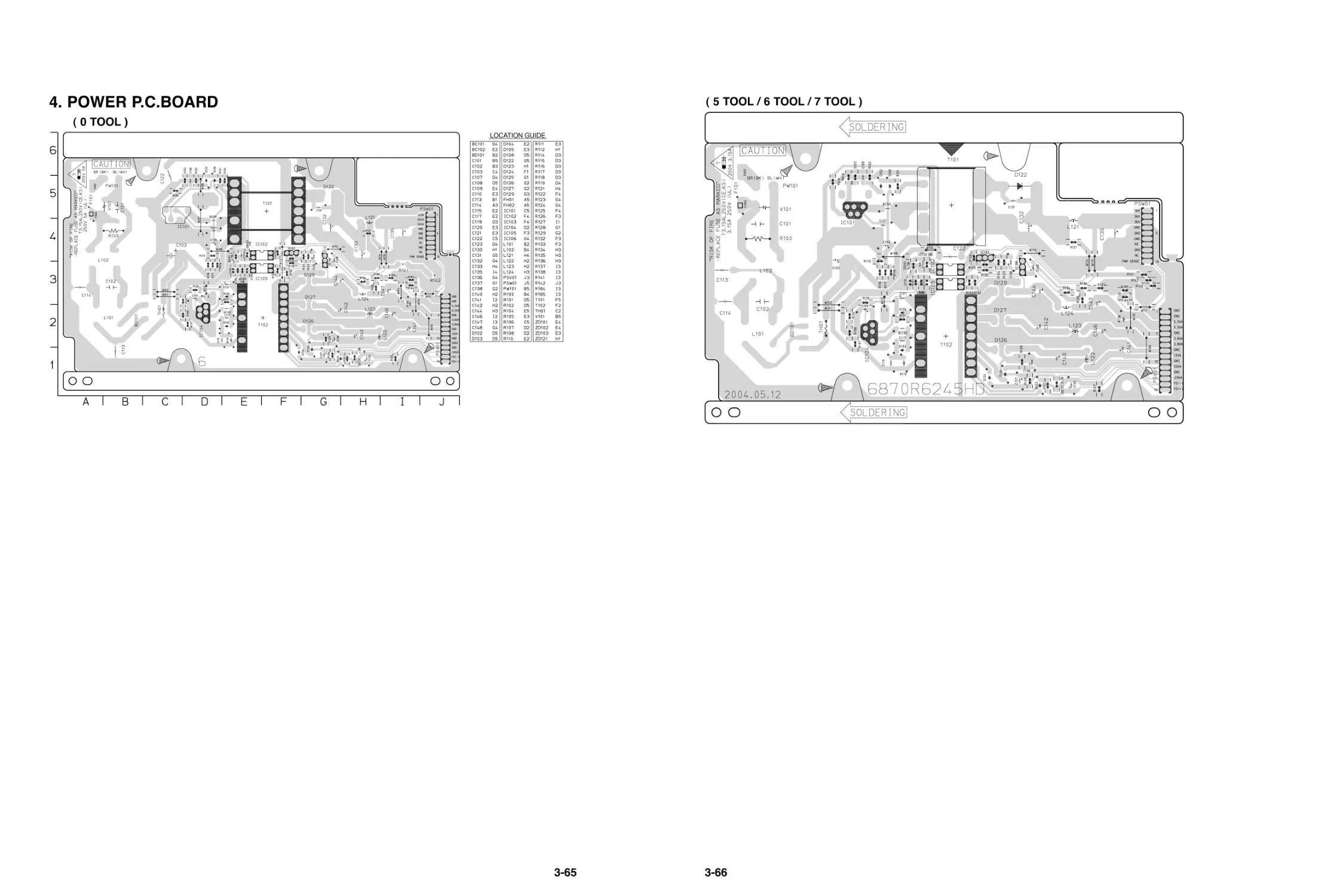
4. SMPS P.C.BOARD ..............................................3-65
DVD PART
ELECTRICAL TROUBLESHOOTING
GUIDE ..........................................................................3-67
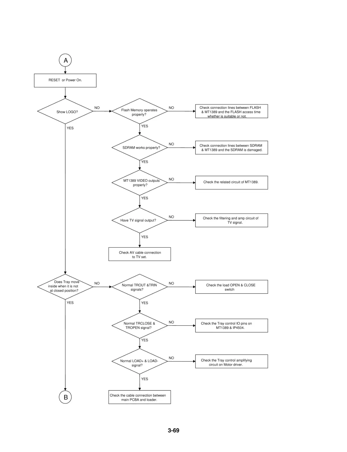
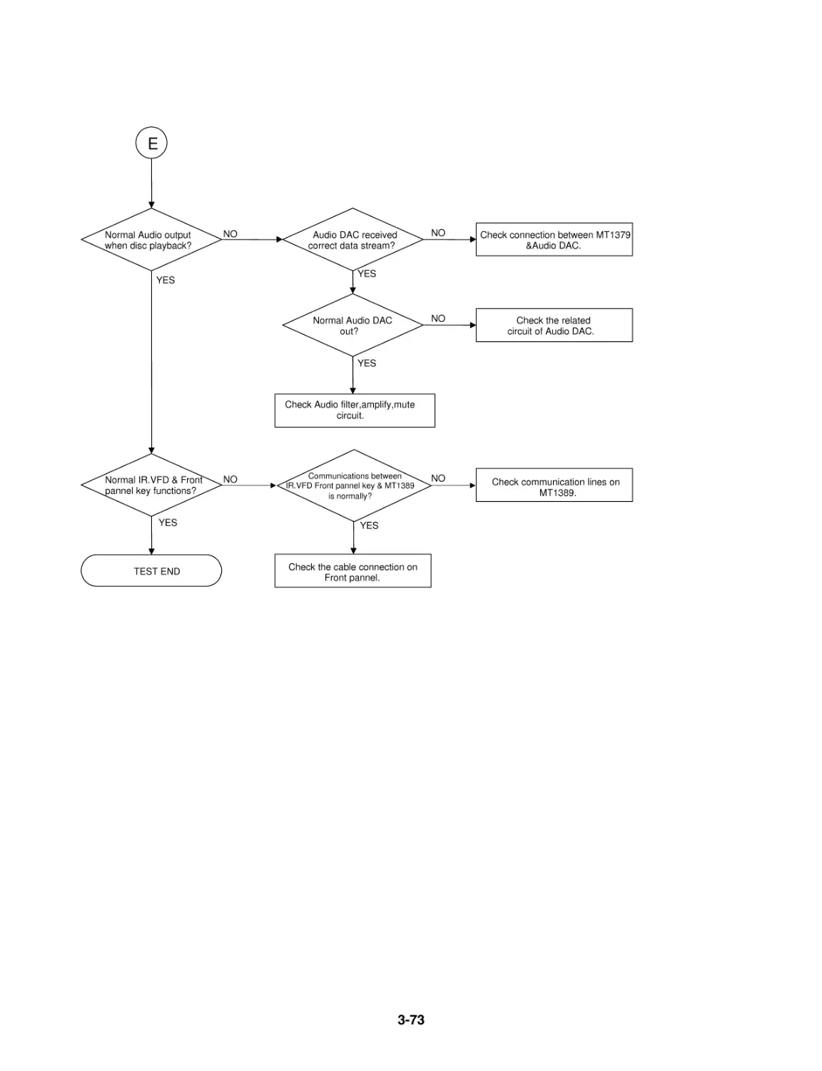
1. SYSTEM OPERATION FLOW..............................3-67
2. SYSTEM TEST FLOW..........................................3-68
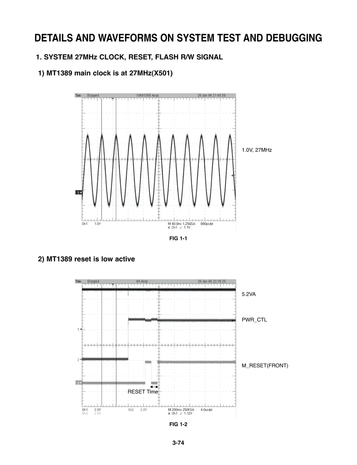
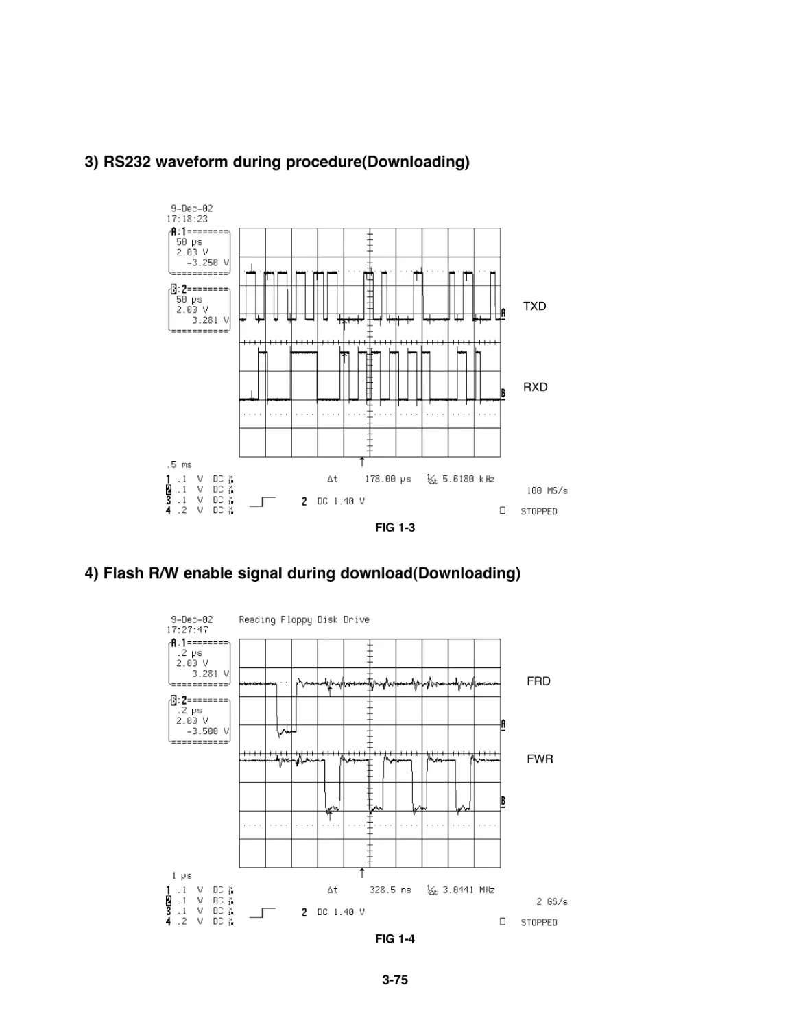
DETAILS AND WAVEFORMS ON SYSTEM
TEST AND DEBUGGING......................................3-74
1. SYSTEM 27MHZ CLOCK, RESET,
FLASH R/W SIGNAL............................................3-74
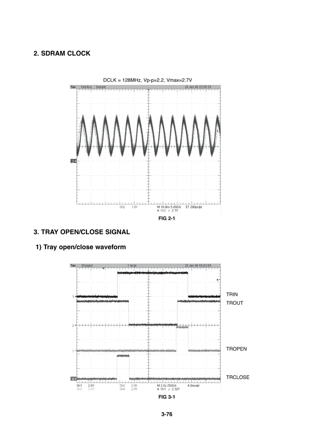
2. SDRAM CLOCK ...................................................3-76
3. TRAY OPEN/CLOSE SIGNAL..............................3-76
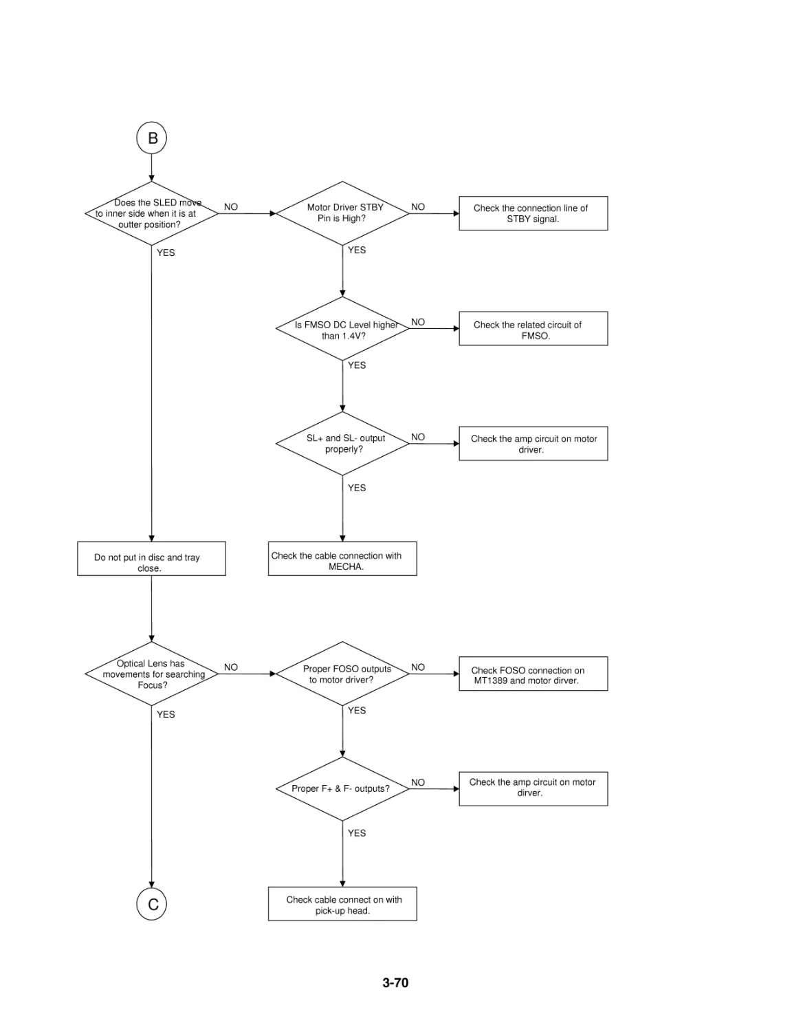
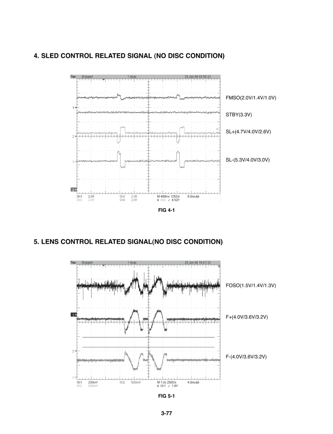
4. SLED CONTROL RELATED SIGNAL
(NO DISC CONDITION)........................................3-77
5. LENS CONTROL RELATED SIGNAL
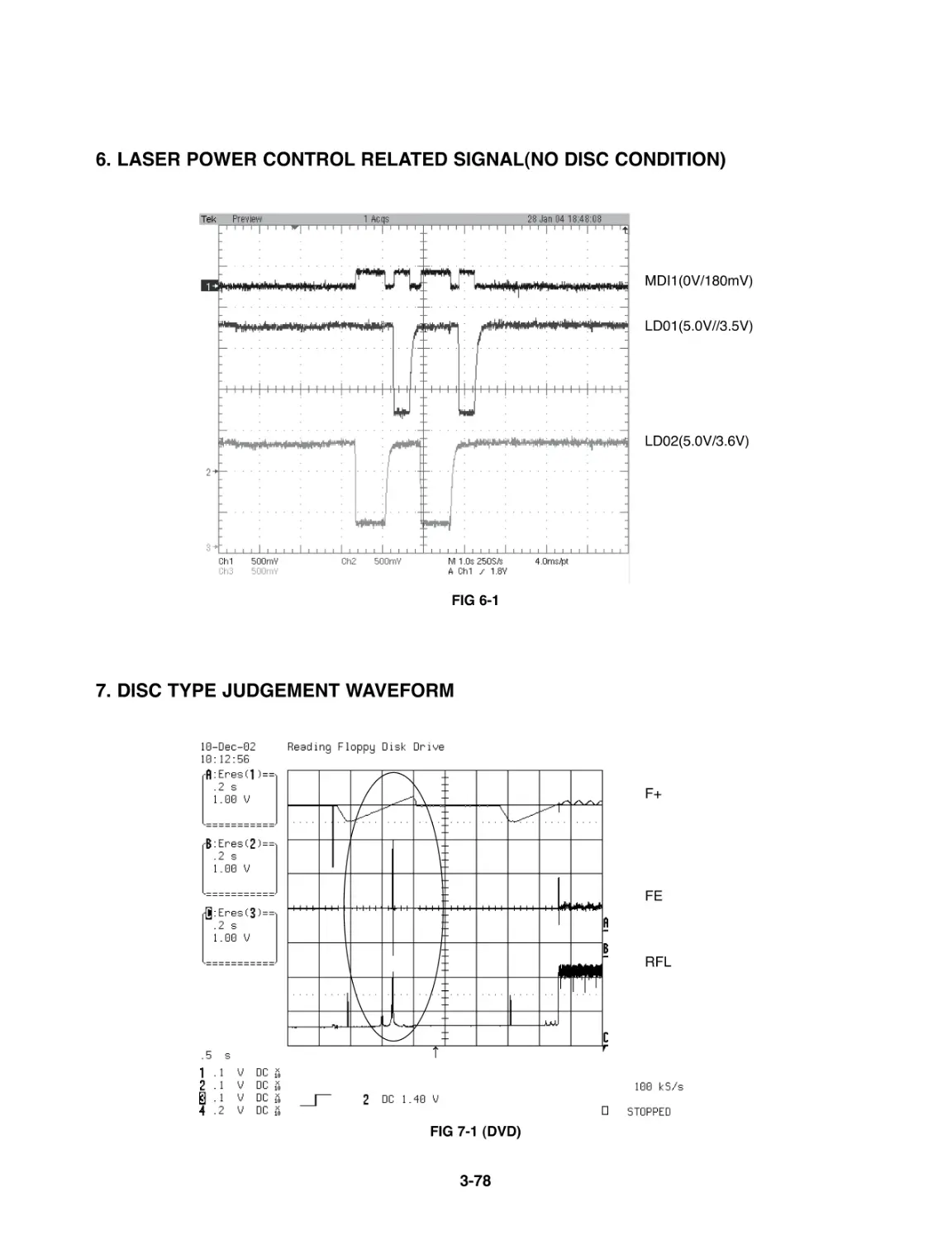
(NO DISC CONDITION)........................................3-77
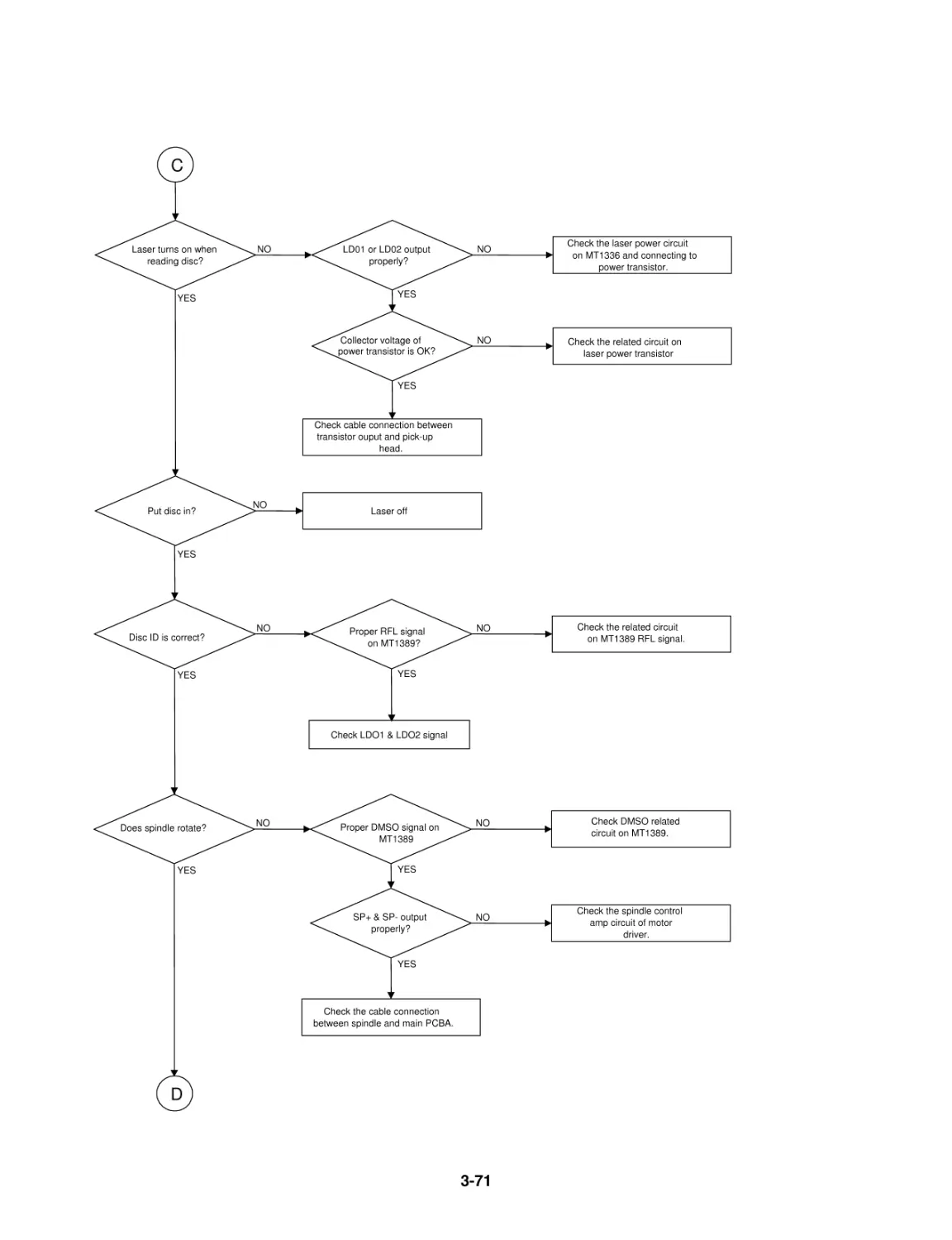
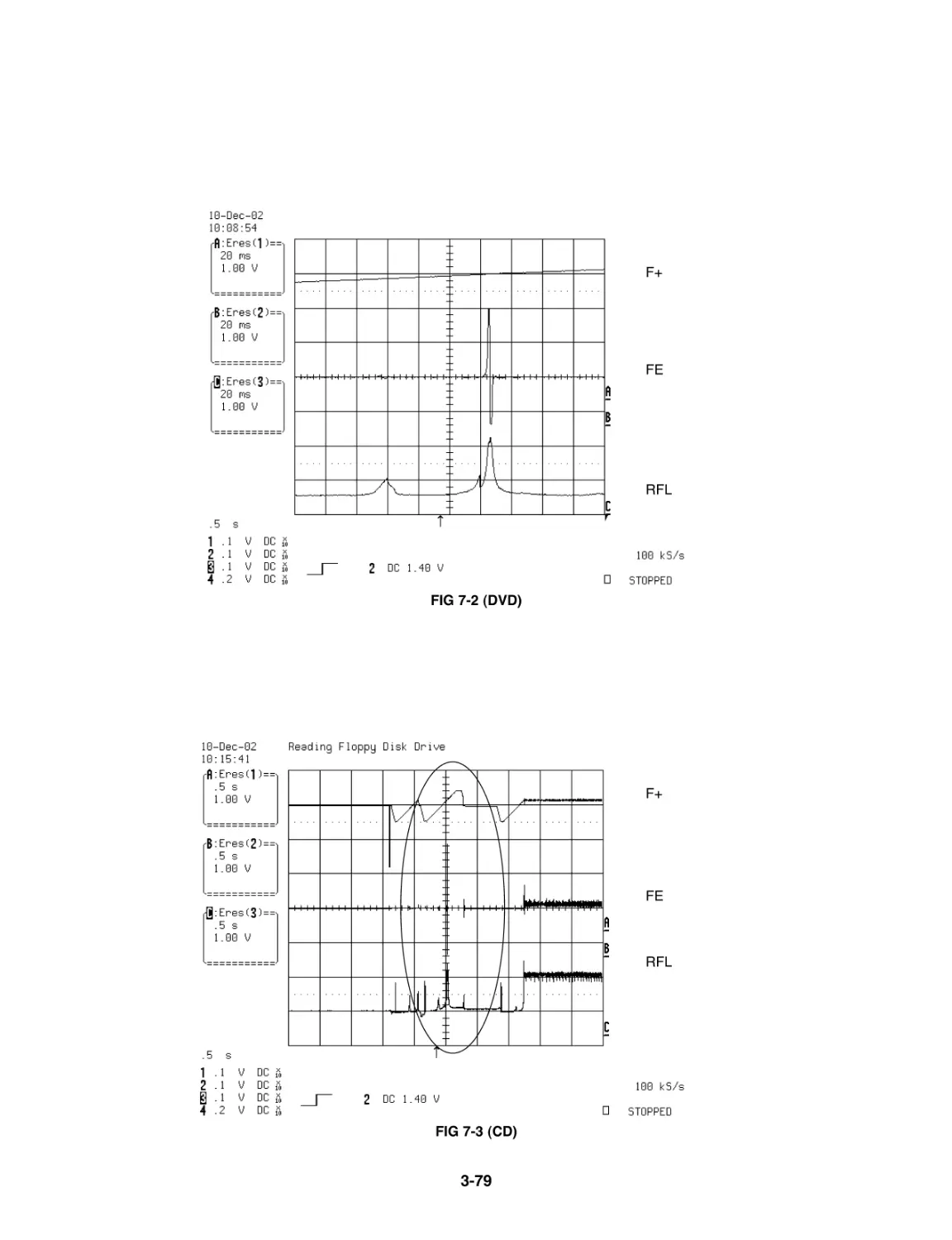
6. LASER POWER CONTROL RELATED
SIGNAL(NO DISC CONDITION) ..........................3-78
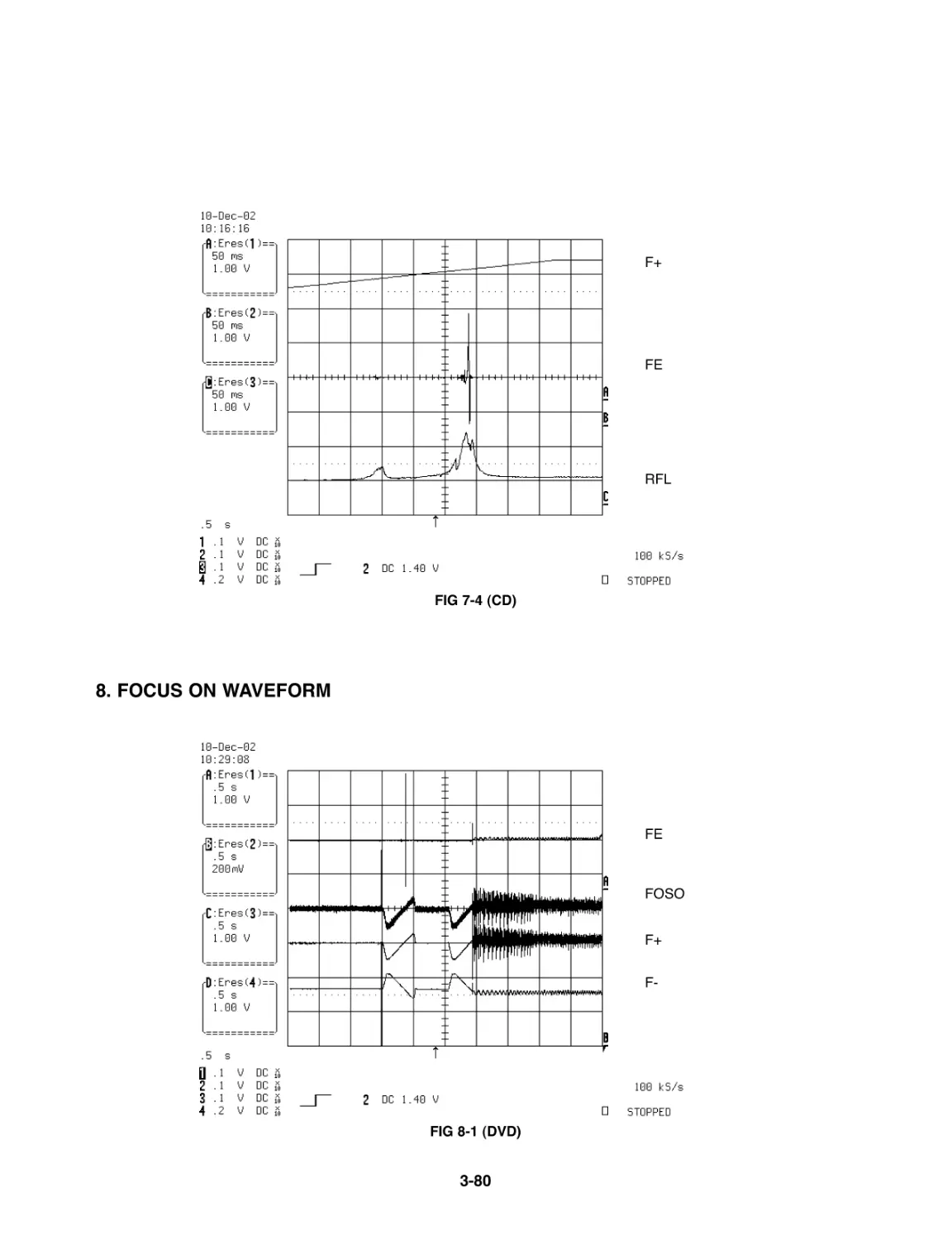
7. DISC TYPE JUDGEMENT WAVEFORM..............3-78
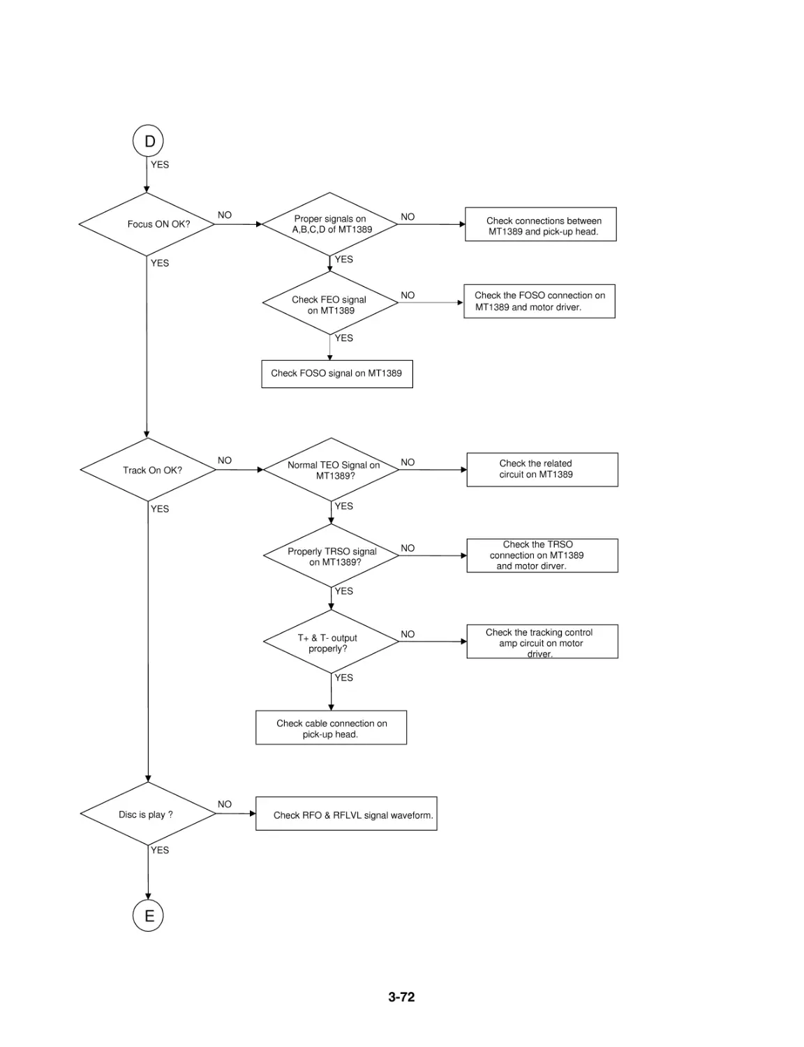
8. FOCUS ON WAVEFORM .....................................3-80
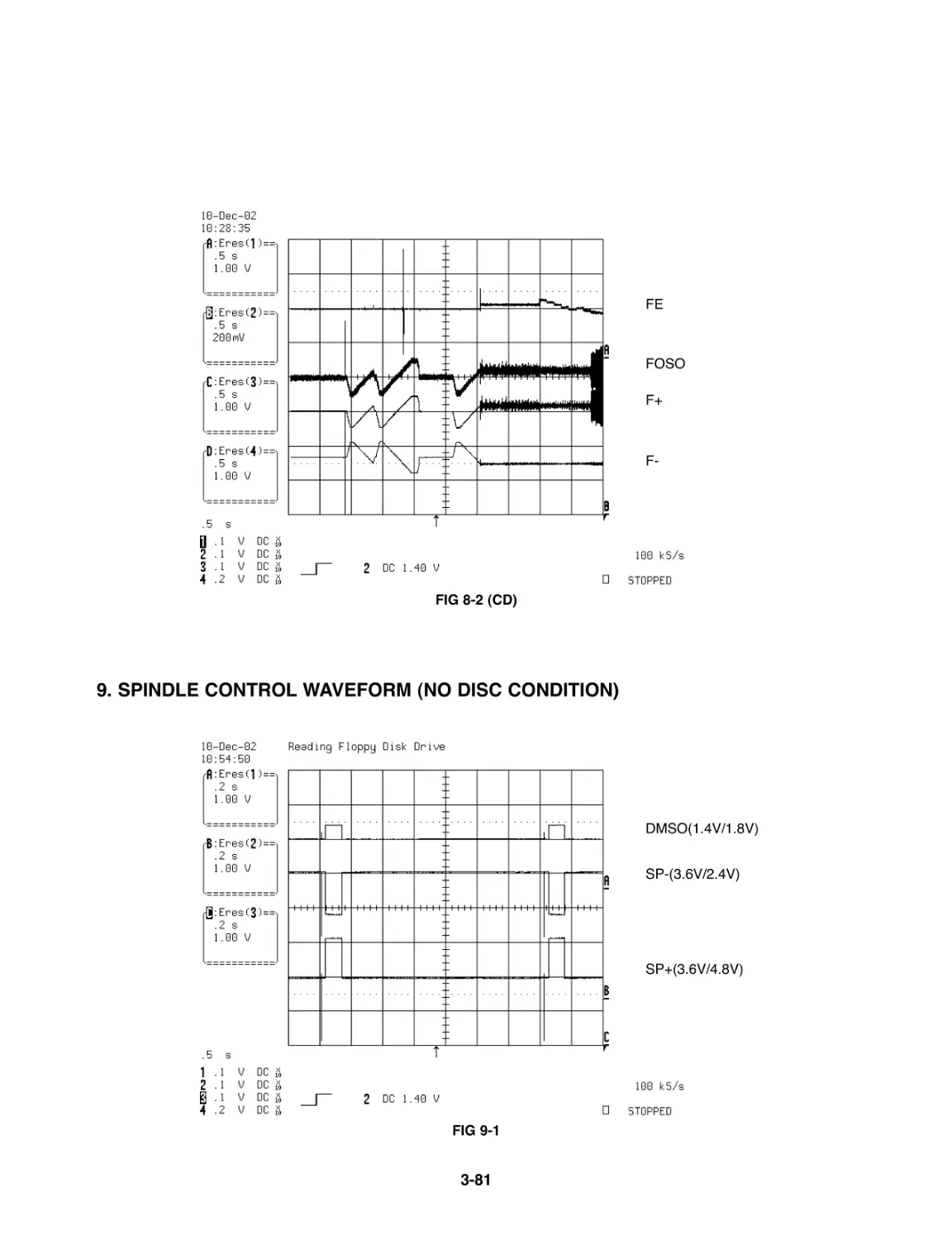
9. SPINDLE CONTROL WAVEFORM
(NO DISC CONDITION)........................................3-81
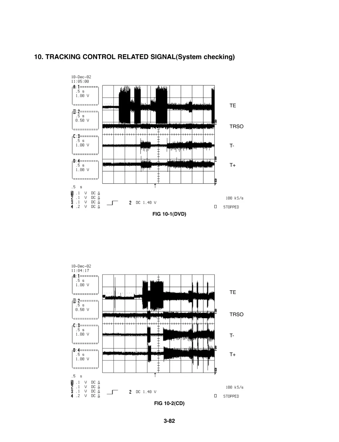
10. TRACKING CONTROL RELATED
SIGNAL(SYSTEM CHECKING) .........................3-82
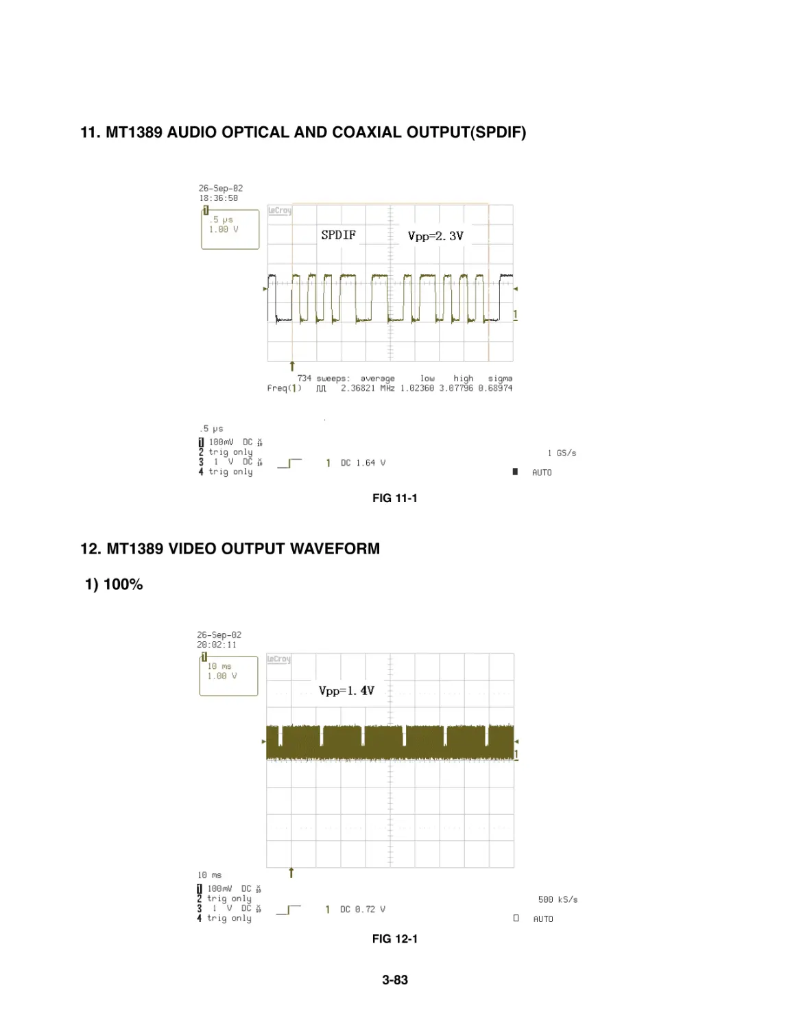
11. MT1389 AUDIO OPTICAL AND COAXIAL
OUTPUT(SPDIF) .................................................3-83
12. MT1389 VIDEO OUTPUT WAVEFORM .............3-83
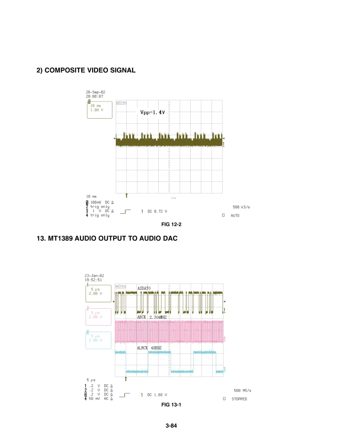
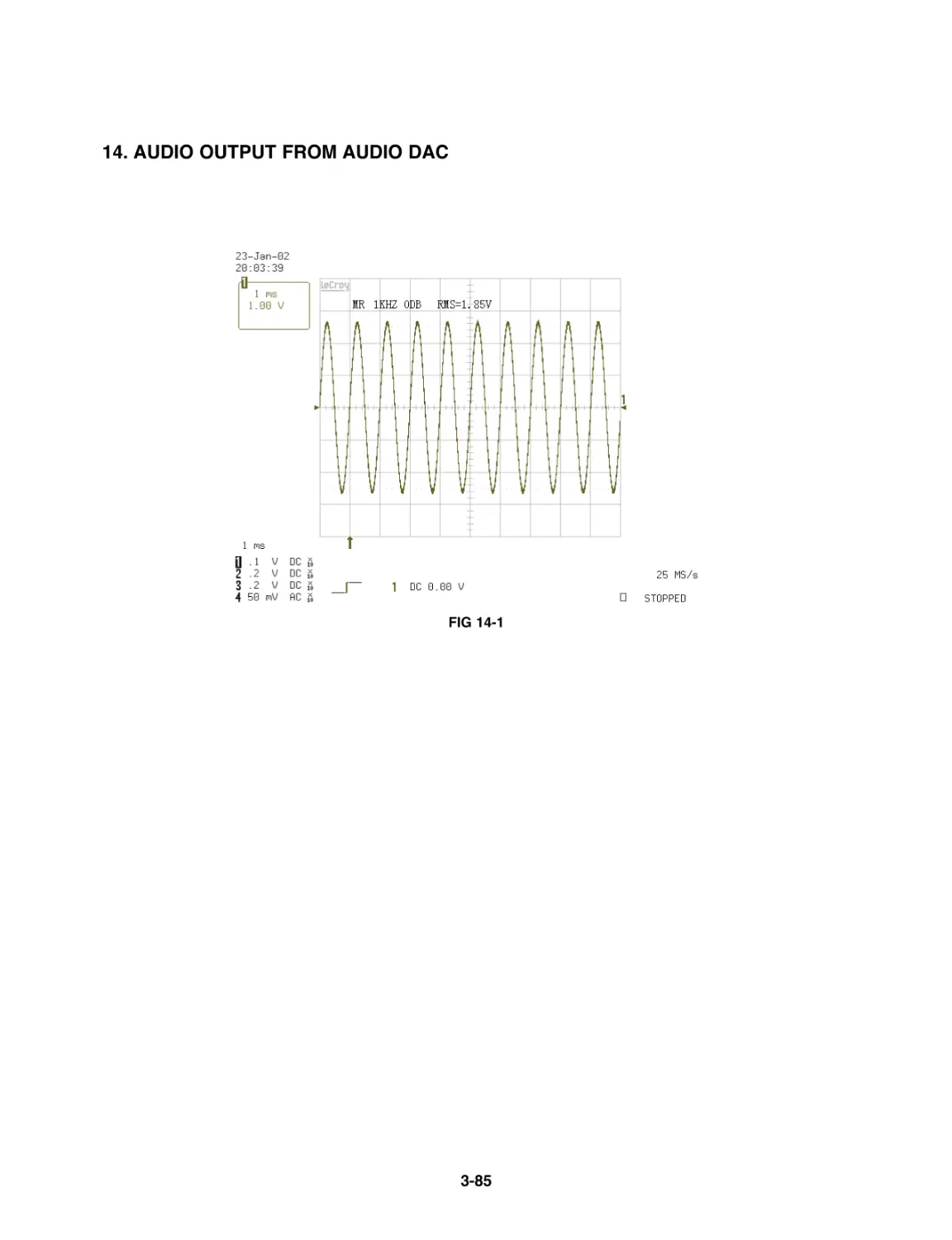
13. MT1389 AUDIO OUTPUT TO AUDIO DAC .......3-84
14. AUDIO OUTPUT FROM AUDIO DAC ................3-85
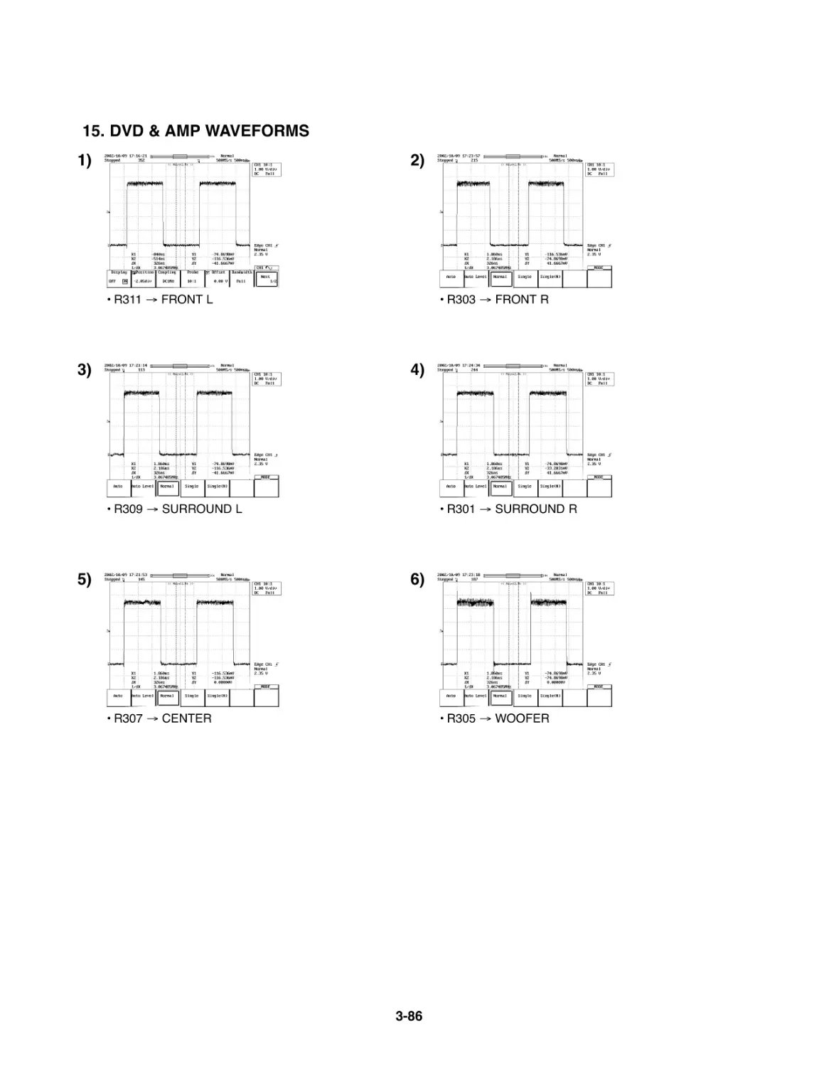
15. DVD & AMP WAVEFORMS................................3-86
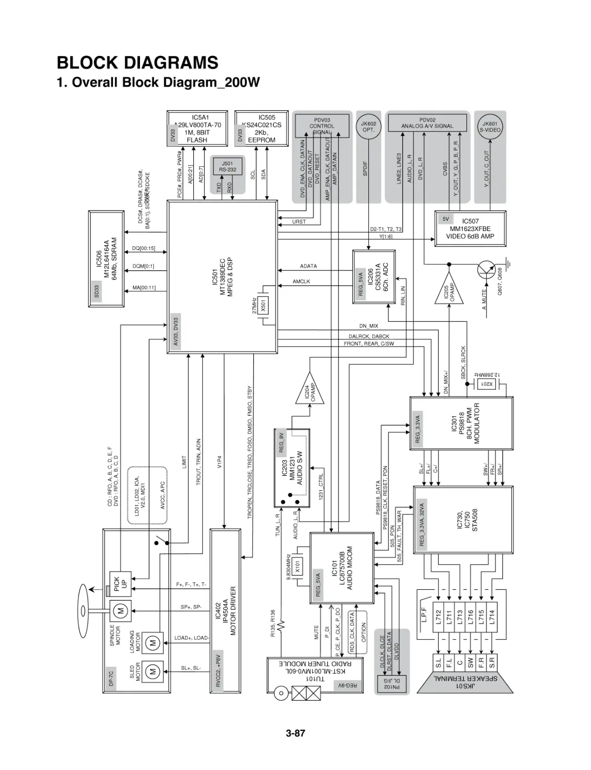
BLOCK DIAGRAMS ...............................................3-87
1. OVERALL BLOCK DIAGRAM_200W..................3-87
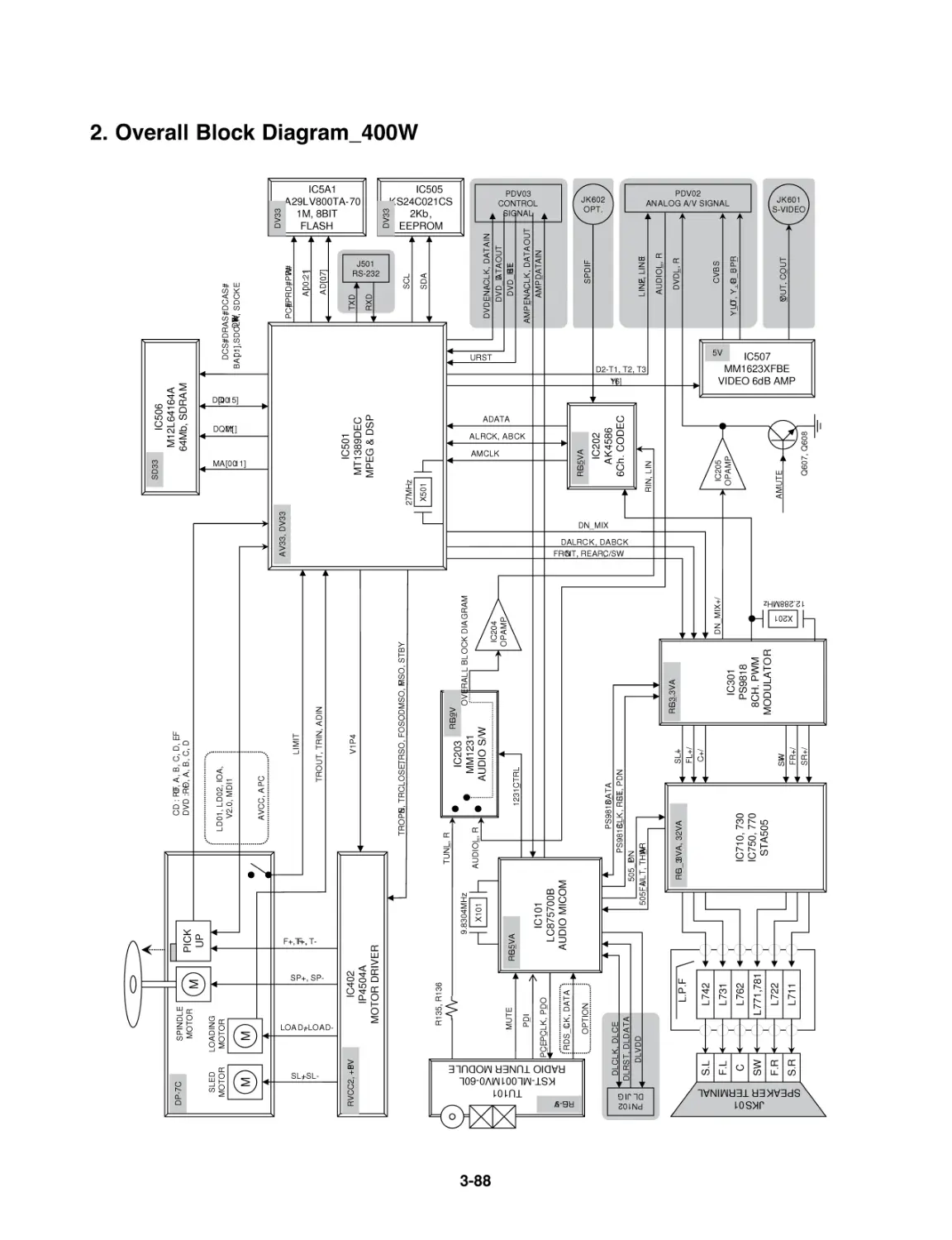
2. OVERALL BLOCK DIAGRAM_400W..................3-88
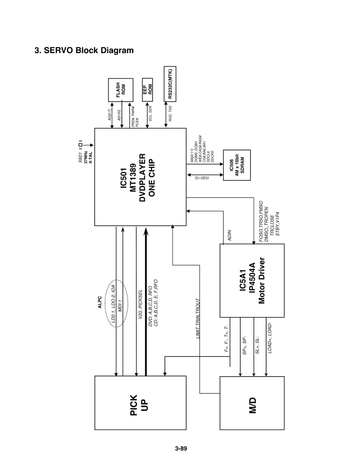
3. SERVO BLOCK DIAGRAM..................................3-89
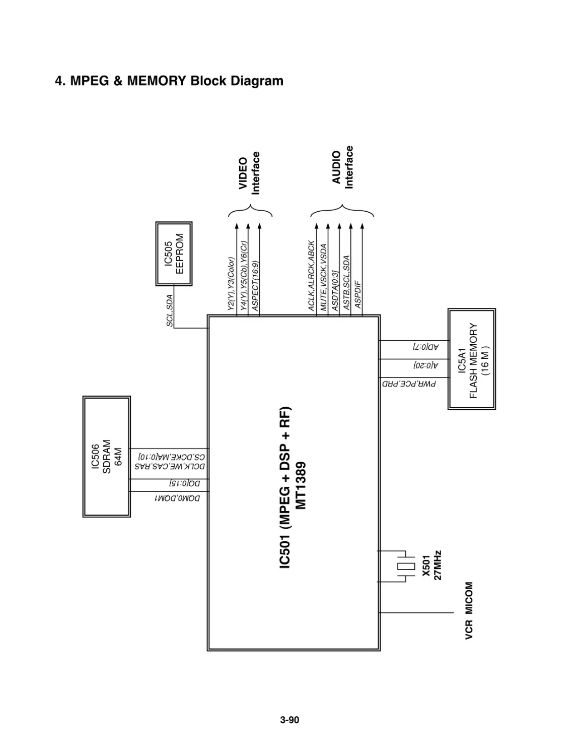
4. MPEG & MEMORY BLOCK DIAGRAM ...............3-90
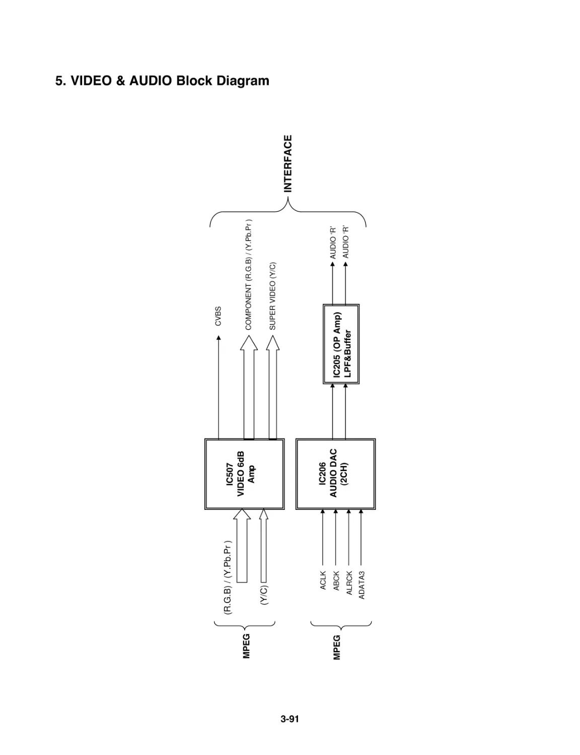
5. VIDEO & AUDIO BLOCK DIAGRAM...................3-91
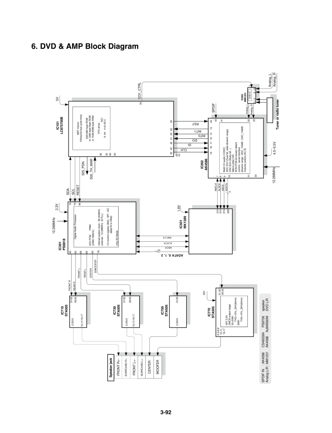
6. DVD & AMP BLOCK DIAGRAM ..........................3-92
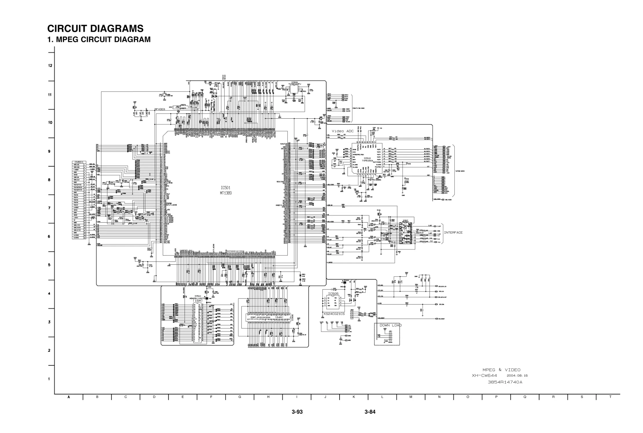
CIRCUIT DIAGRAMS .............................................3-93
1. MPEG CIRCUIT DIAGRAM ..................................3-93
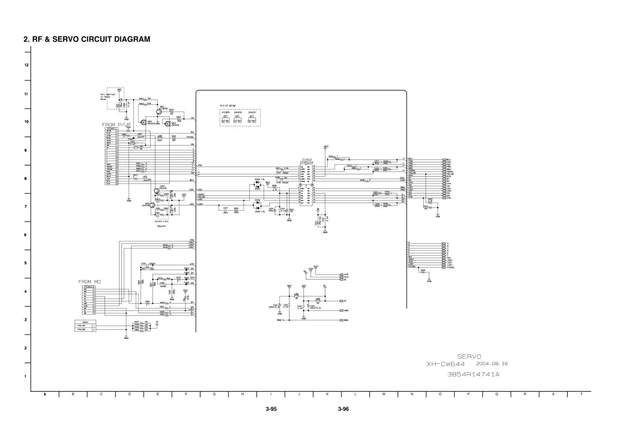
2. RF & SERVO CIRCUIT DIAGRAM ......................3-95
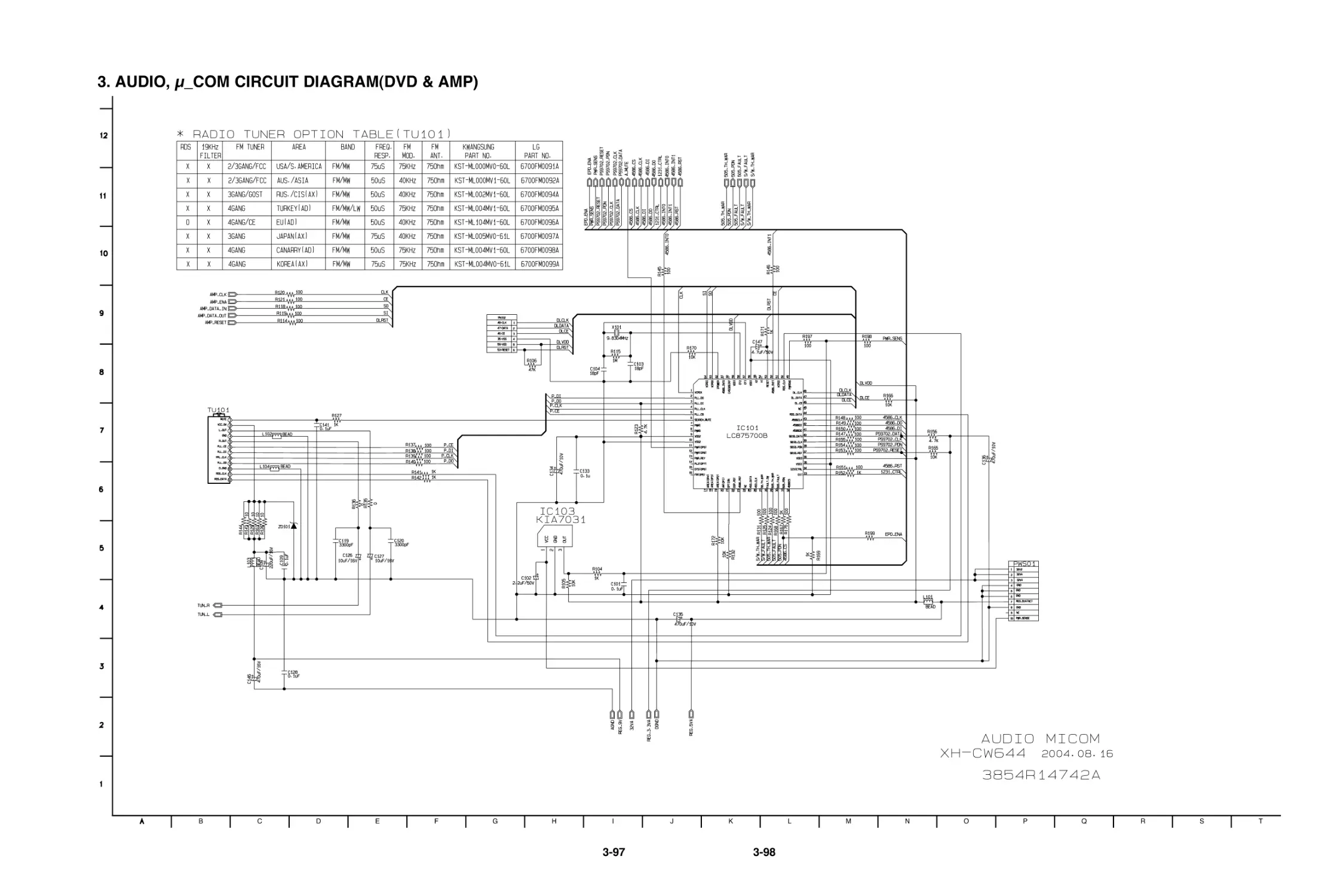
3. AUDIO, μ_COM
CIRCUIT DIAGRAM(DVD & AMP) .......................3-97
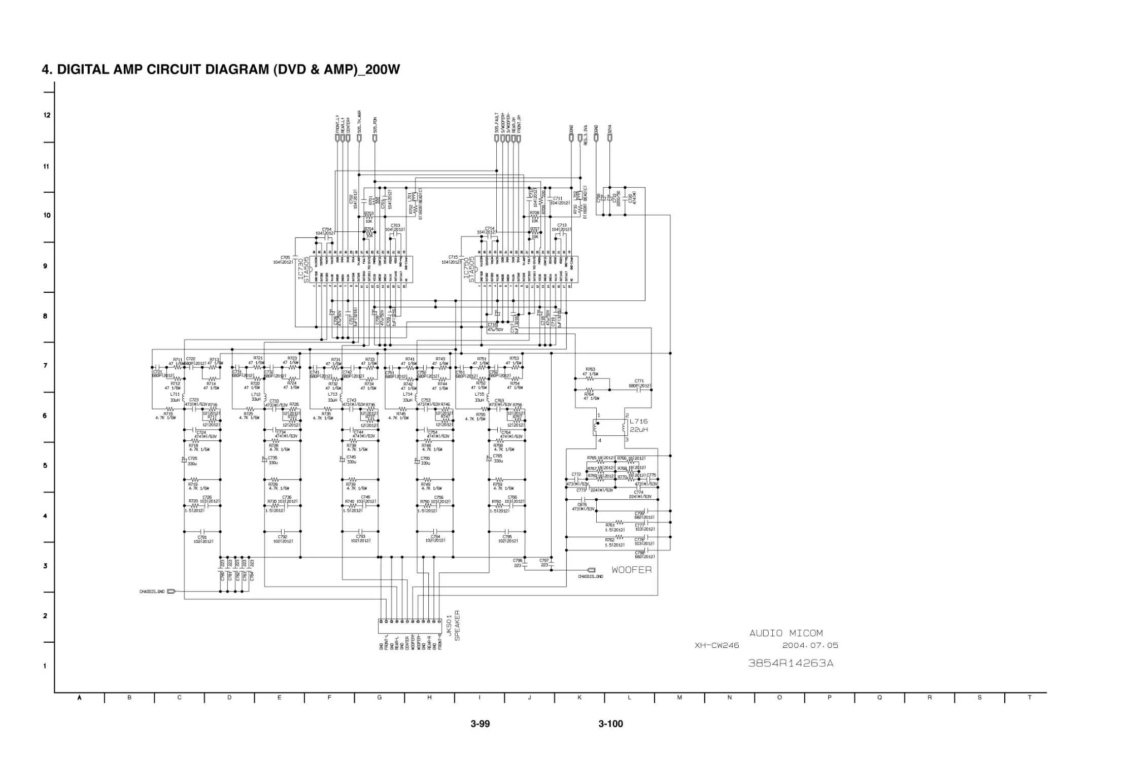
4. DIGITAL AMP CIRCUIT DIAGRAM
(DVD & AMP)_200W ............................................3-99
5. DIGITAL AMP CIRCUIT DIAGRAM
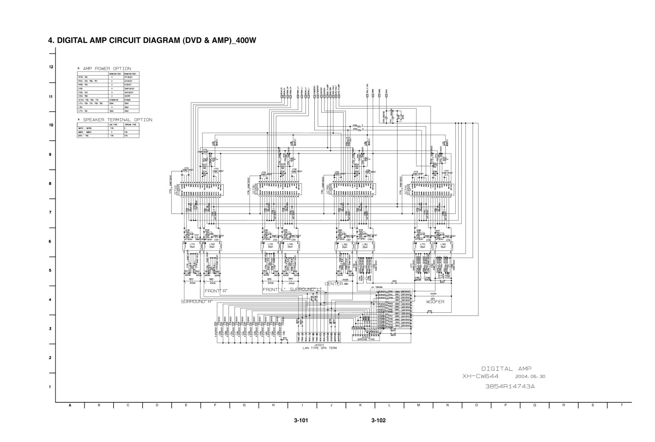
(DVD & AMP)_400W ..........................................3-101
6. PWM & CODEIC CIRCUIT DIAGRAM
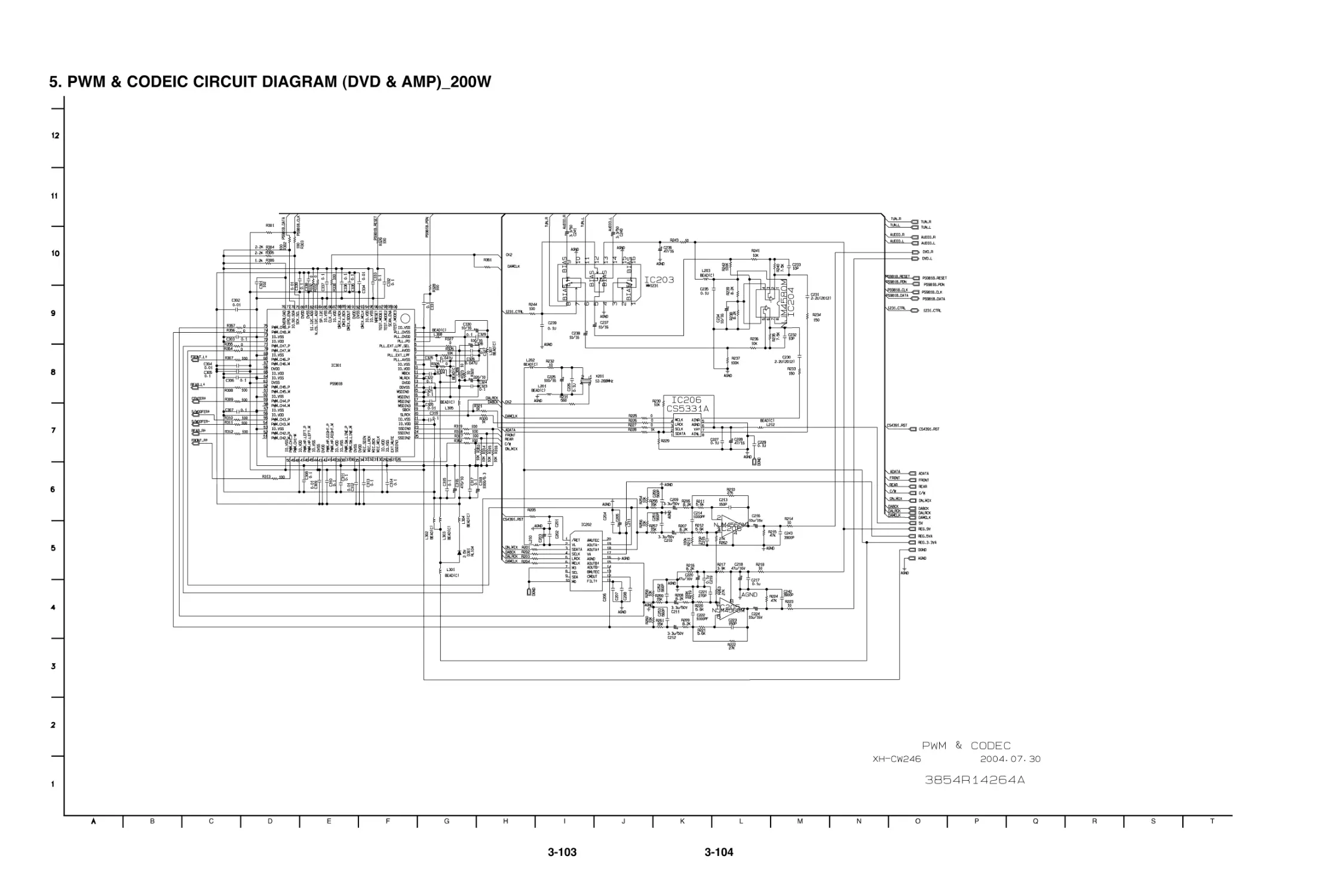
(DVD & AMP)_200W ..........................................3-103
7. PWM & CODEIC CIRCUIT DIAGRAM
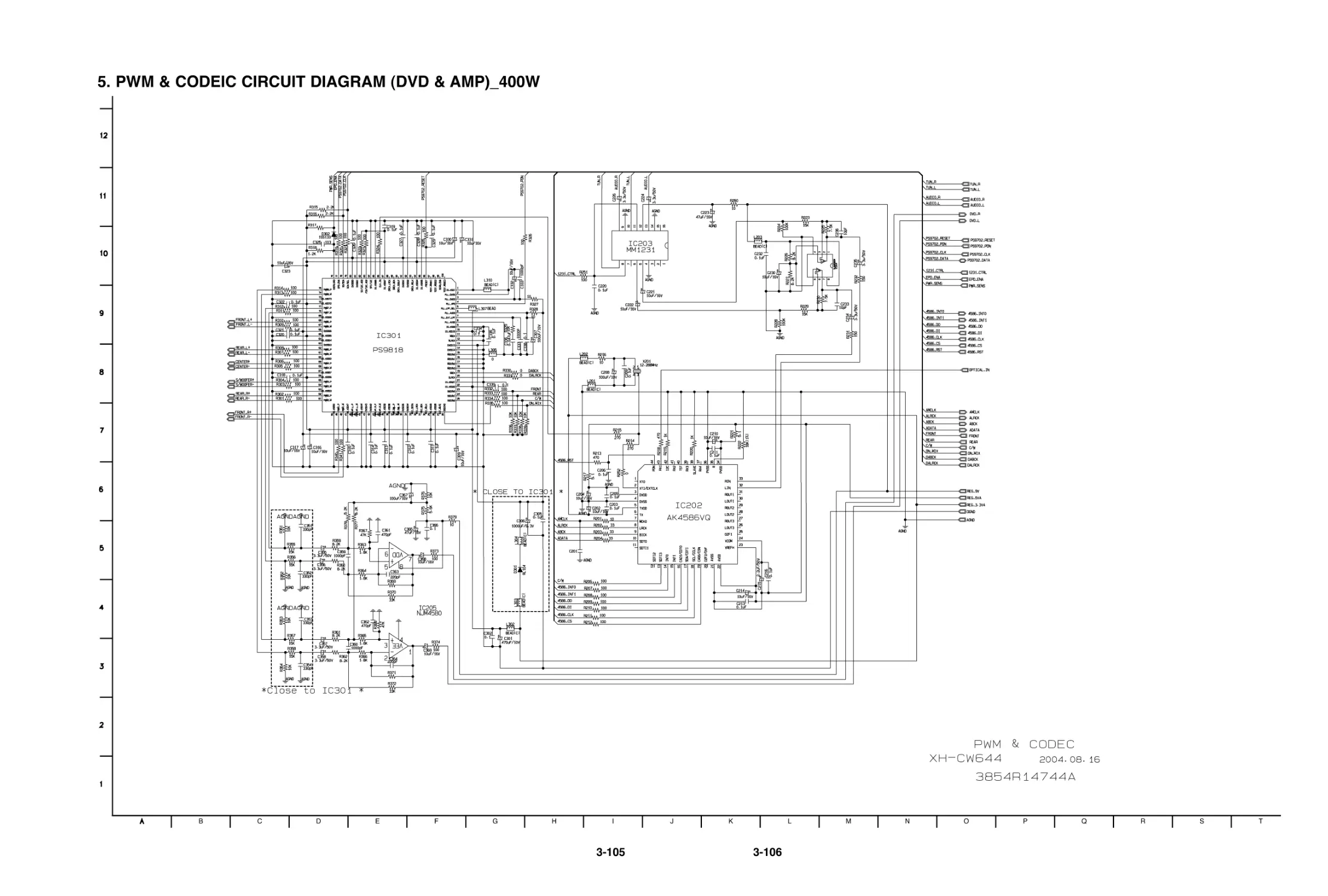
(DVD & AMP)_400W ..........................................3-105
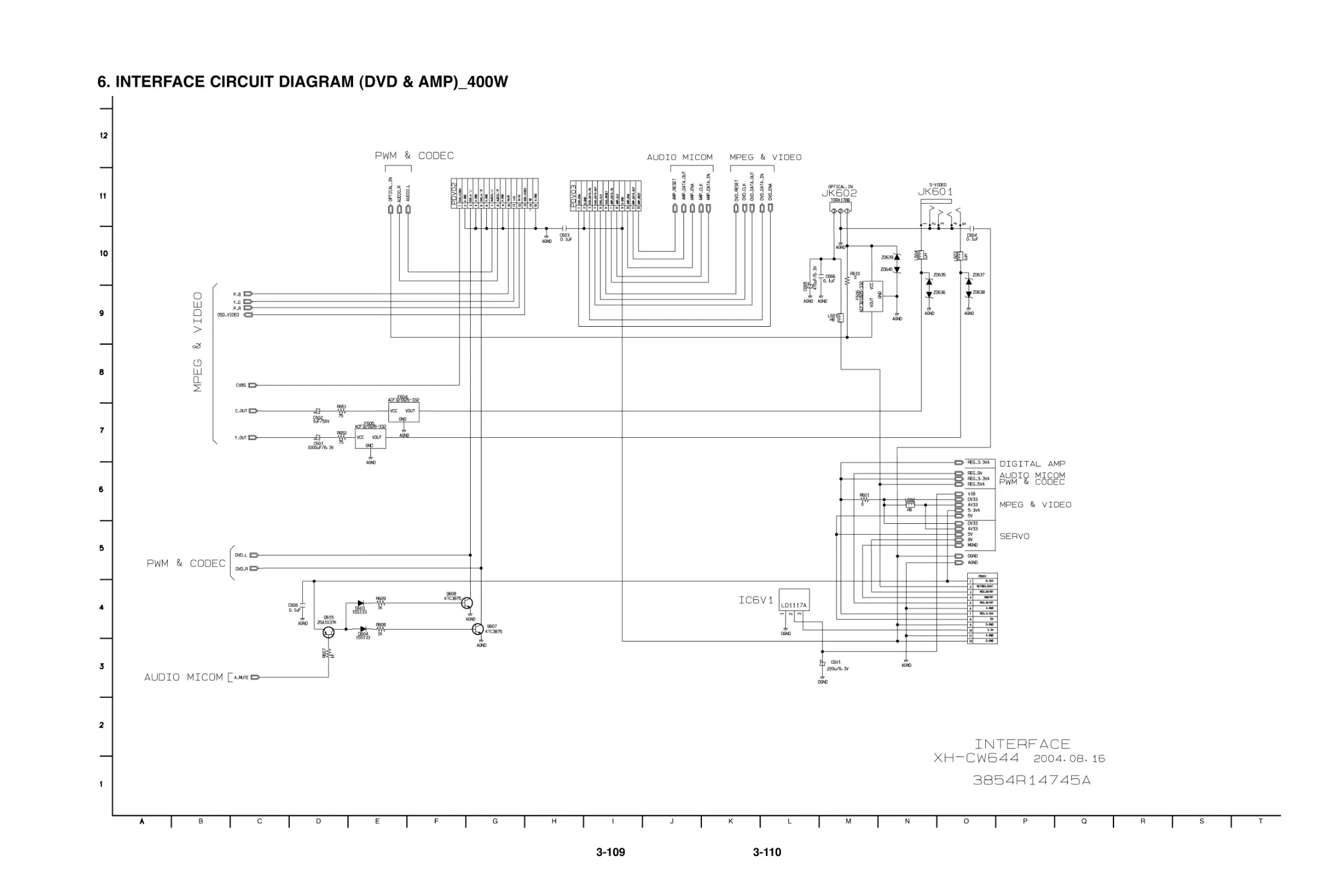
8. INTERFACE CIRCUIT DIAGRAM
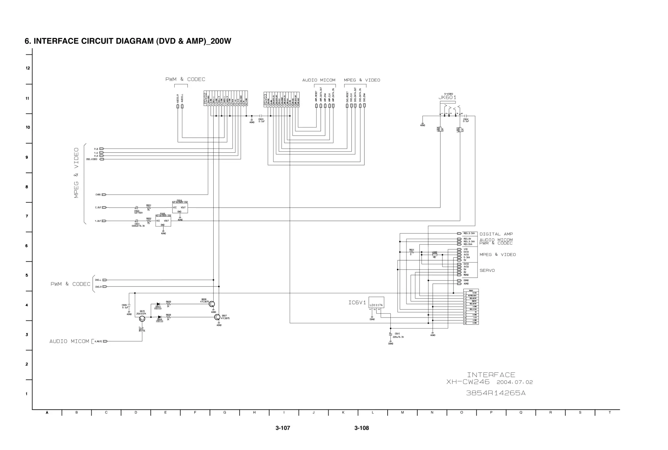
(DVD & AMP)_200W ..........................................3-107
9. INTERFACE CIRCUIT DIAGRAM
(DVD & AMP)_400W ..........................................3-109
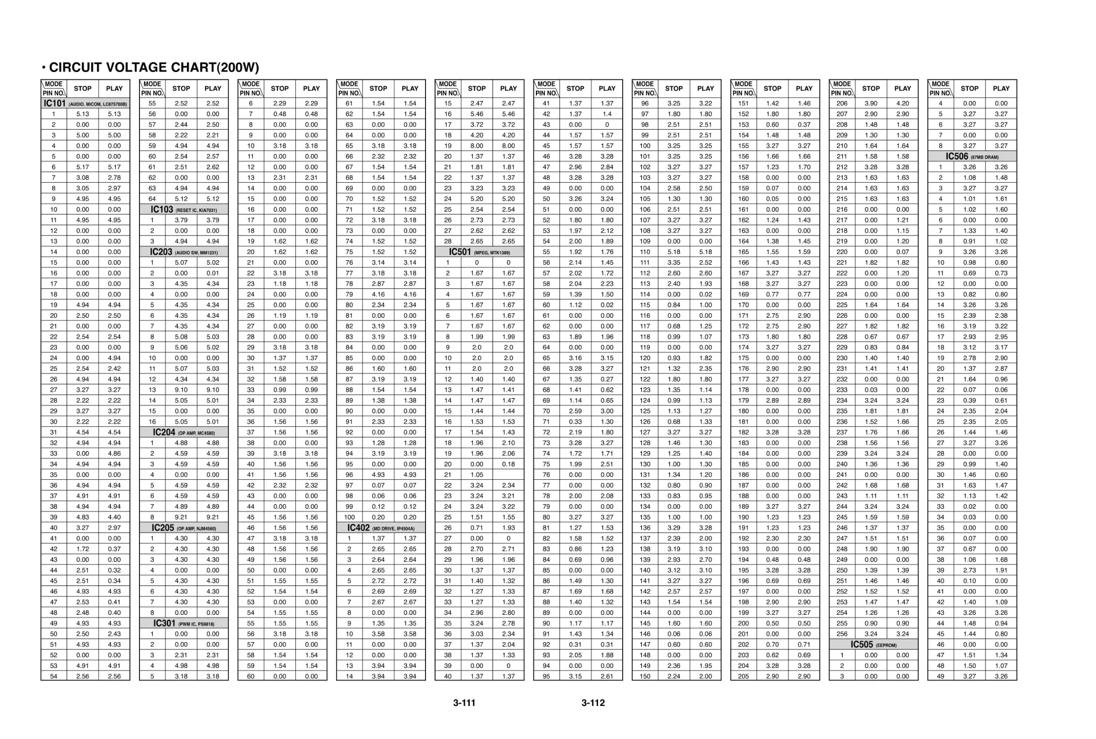
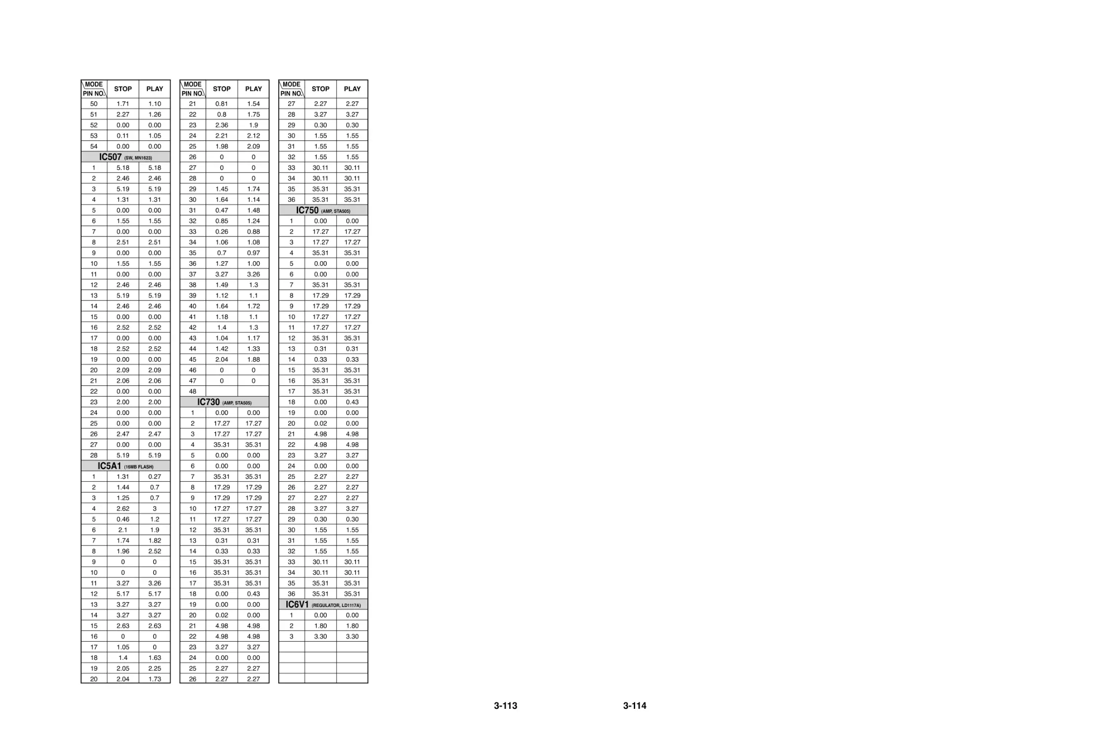
• CIRCUIT VOLTAGE CHART_200W .....................3-111
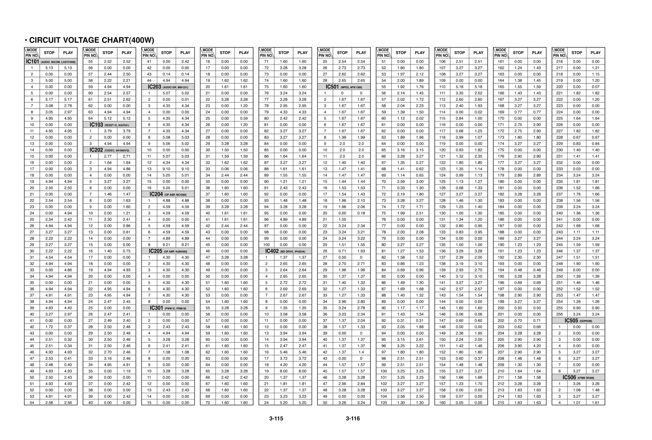
• CIRCUIT VOLTAGE CHART_200W.....................3-115
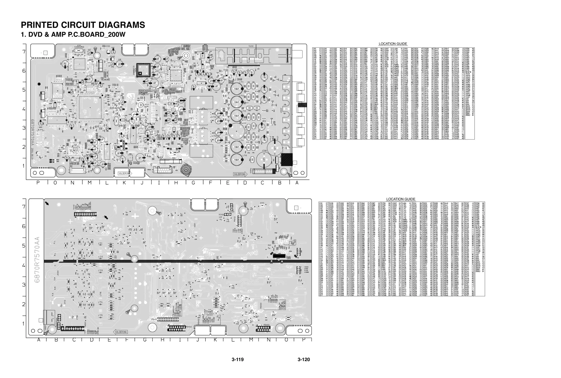
PRINTED CIRCUIT DIAGRAMS.......................3-119
1. DVD & AMP P.C.BOARD_200W ........................3-119
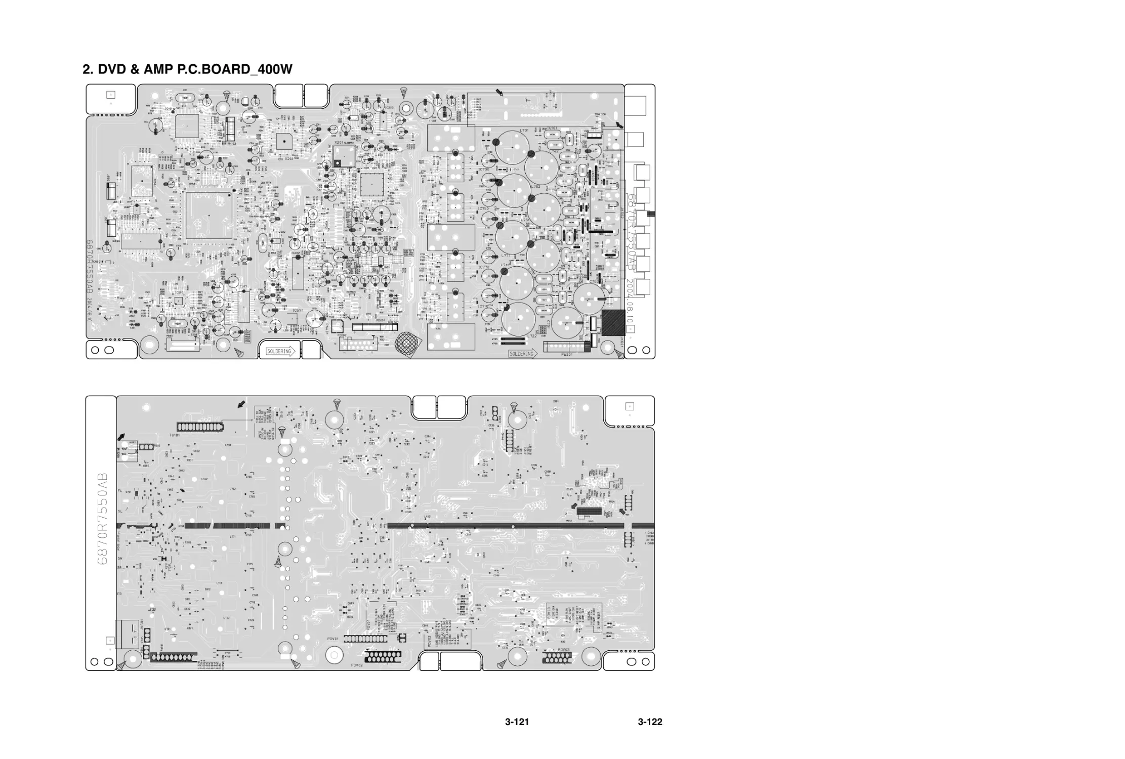
2. DVD & AMP P.C.BOARD_400W ........................3-121
3-2
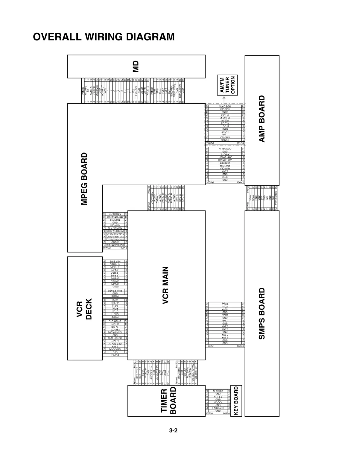
OVERALL WIRING DIAGRAM
123456789
10
11
12
KEY RTN 0
KEY RTN 1
5.3VA
VIDEO IN
GND
AUDIO "L" IN
GND
AUDIO "R" IN
GND
FD(-)
-29VA
FD(+)
1
23456789
10
11
12
P6M01
PM601
123456789
10
11
12
DVD VIDEO
A.GND
DVD A, 'L'
A.GND
DVD A, 'R'
A.GND
AUDIO 'L'
AUDIO 'R'
A.GND
DVD B
DVD G
DVD R
123456789
10
11
12
PMD02
PDM02
123456789
10
11
12
13
14
15
16
17
18
19
20
21
22
23
VCC(HF)
RF
DVD-LD
DVD-PD
VOL(DVD)
GND
VC-INPUT
VCC
F
E
A
D
C
B
F(+)
T(-)
T(+)
F(-)
PICK-SEL
GND
CD-LD
CD-PD
VOL(CD)
123456789
10
11
12
13
14
15
16
17
18
19
20
21
22
23
PMD02
123456789
10
11
SPM+
SPM-
FM(+)
FM(-)
LM(-)
LM(+)
SW(OPEN)
SW(CLOSE)
GND
SW(LEAD IN)
GND
123456789
10
11
PMD03
123456789
10
32VA
32VA
GND
GND
5VA
GND
NC
GND
NC
PWR SENSE
123456789
10
PSW01
PN901
123456789
10
11
12
CFG
12VA(CAP)
5.2VA
CAP REV 'H'
I-LIMIT
MOTOR GND
GND
12VA(DRUM)
CAP CTL
L/M CTL
DFG/PG
DRUM CTL
123456789
10
11
12
PMC01
123456789
SPAPB
SP REC
SPBPB
LPRPB
LP REC
LPAPB
Hi-Fi A PB
Hi-Fi REC
Hi-Fi B PB
123456789
P3D01
12345678
GND
KEY RTN 1
GND
F.A.R.IN
GND
F.A.L.IN
GND
VIDEO IN
12345678
P6603
P6602
123456789
10
11
12
GND
SPDIF
GND
5.2VA
AMP-CLK
AMP-ENA
M-RESET
AMP-DATA 0
AMP DATA 1
A-MUTE
GND
OPTICAL IN
123456789
10
11
12
CN901
PVD04
123456789
10
11
12
13
TUNED
STEREO
12VA
L-OUT
AGND
R-OUT
PLL-CE
PLL-DI
PLL-CLK
PLL-D0
DGND
RDS-CLK
RDS-DATA
123456789
10
11
12
13
PN101
PVD04
123456789
10
11
12
13
14
15
GND
GND
5.3VA
5.3VA
GND
3.8VA
3.8VA
GND
13VA
GND
33VA
GND
-29VA
FD(-)
FD(+)
123456789
10
11
12
13
14
15
PSV01
PVS01
123456789
10
11
12
DVD ENA(M-REC)
A.GND
DVD DATA OUT(RXDO)
DVD DATA IN(TXDO)
DVD CLK(SCKO)
DVD RESET(M-RESET)
AMP DATA IN
AMP CLK
GND
AMP ENA
AMP DATA OUT
A-MUTE 'H'
123456789
10
11
12
PMD01
PDM01
123456
CTL(+)
CTL(-)
A/E(+)
A/E(-)
A.REC
A.PB
123456
P3D02
12
GND
FULL ERASE 12
P3D03
1234567
REMOCON
GND
FLD CLK
FLD DATA
FLD ENV
VOLUMN DOWN
VOLUMN UP
1
234567
P6M02
PM602
VCR
DECK
VCR MAIN
KEY BOARD
TIMER
BOARD
SMPS BOARD
AMP BOARD
MD
AM/FM
TUNER
OPTION
MPEG BOARD
3-3
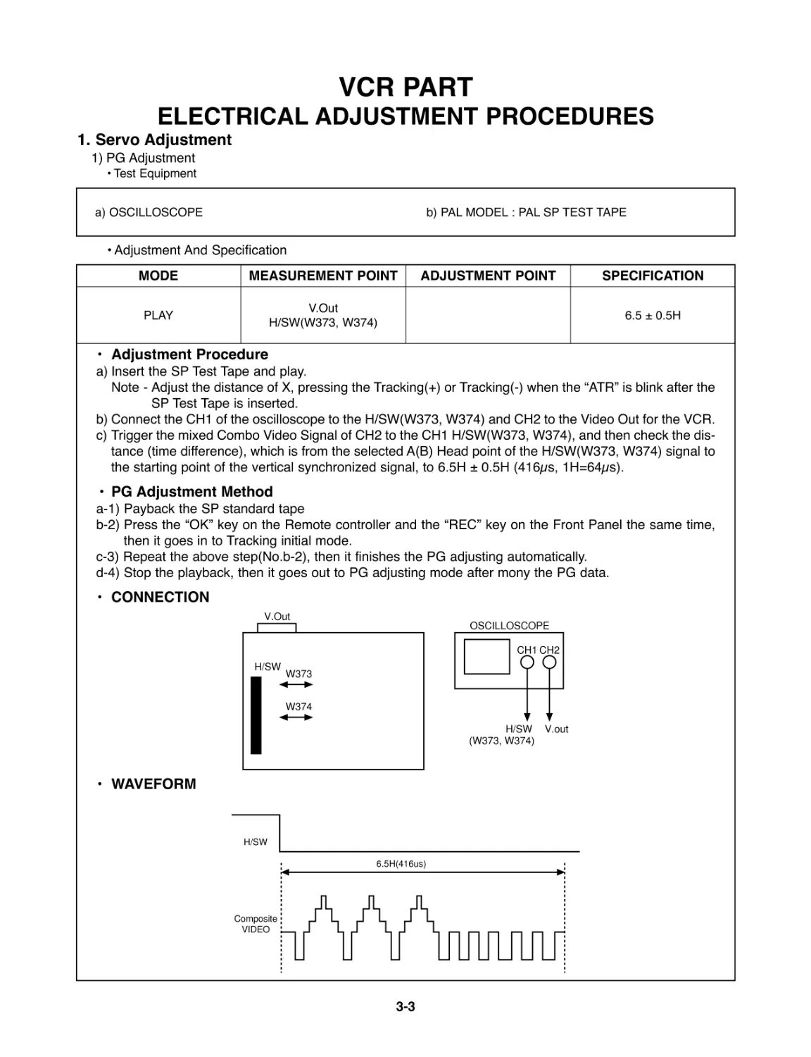
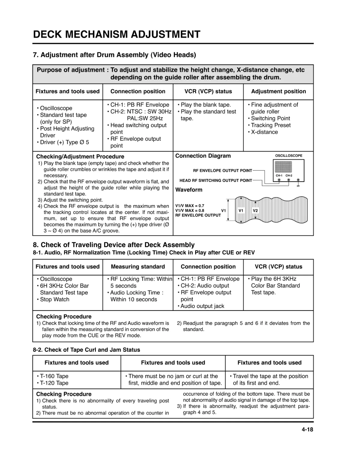
ELECTRICAL ADJUSTMENT PROCEDURES
1. Servo Adjustment
1) PG Adjustment
• Test Equipment
• Adjustment And Specification
a) OSCILLOSCOPE
b) PAL MODEL : PAL SP TEST TAPE
MODE
PLAY
• Adjustment Procedure
a) Insert the SP Test Tape and play.
Note - Adjust the distance of X, pressing the Tracking(+) or Tracking(-) when the "ATR" is blink after the
SP Test Tape is inserted.
b) Connect the CH1 of the oscilloscope to the H/SW(W373, W374) and CH2 to the Video Out for the VCR.
c) Trigger the mixed Combo Video Signal of CH2 to the CH1 H/SW(W373, W374), and then check the dis-
tance (time difference), which is from the selected A(B) Head point of the H/SW(W373, W374) signal to
the starting point of the vertical synchronized signal, to 6.5H ± 0.5H (416μs, 1H=64μs).
• PG Adjustment Method
a-1) Payback the SP standard tape
b-2) Press the "OK" key on the Remote controller and the "REC" key on the Front Panel the same time,
then it goes in to Tracking initial mode.
c-3) Repeat the above step(No.b-2), then it finishes the PG adjusting automatically.
d-4) Stop the playback, then it goes out to PG adjusting mode after mony the PG data.
• CONNECTION
• WAVEFORM
V.Out
H/SW(W373, W374)
6.5 ± 0.5H
MEASUREMENT POINT ADJUSTMENT POINT
SPECIFICATION
V.Out
H/SW W373
W374
OSCILLOSCOPE
CH1 CH2
V.out
H/SW
(W373, W374)
H/SW
Composite
VIDEO
6.5H(416us)
VCR PART
3-4
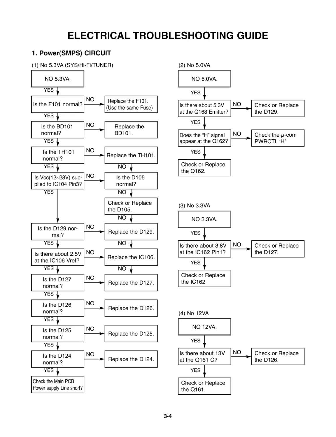
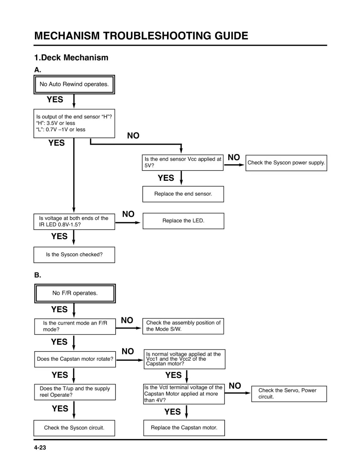
ELECTRICAL TROUBLESHOOTING GUIDE
1. Power(SMPS) CIRCUIT
NO 5.3VA.
Replace the F101.
(Use the same Fuse)
Is the F101 normal?
Is the TH101
normal?
Is the BD101
normal?
NO
NO
NO
NO
NO
NO
NO
NO
NO
NO
Replace the
BD101.
Replace the TH101.
Is the D105
normal?
Check or Replace
the D105.
Replace the D129.
Replace the IC106.
Replace the D127.
Replace the D126.
Replace the D125.
Replace the D124.
YES
YES
YES
YES
YES
YES
YES
YES
YES
YES
YES
Is Vcc(12~28V) sup-
plied to IC104 Pin3?
Is the D129 nor-
mal?
Is there about 2.5V
at the IC106 Vref?
Is the D127
normal?
Is the D126
normal?
Is the D125
normal?
Is the D124
normal?
Check the Main PCB
Power supply Line short?
(1) No 5.3VA(SYS/Hi-Fi/TUNER)
NO 5.0VA.
Check or Replace
the D129.
Is there about 5.3V
at the Q168 Emitter?
Does the "H" signal
appear at the Q162?
Check or Replace
the Q162.
NO
Check the μ-com
PWRCTL 'H'
NO
YES
YES
YES
(2) No 5.0VA
NO 3.3VA.
Check or Replace
the D127.
Is there about 3.8V
at the IC162 Pin1?
Check or Replace
the IC162.
NO
YES
YES
(3) No 3.3VA
NO 12VA.
Check or Replace
the D126.
Is there about 13V
at the Q161 C?
Check or Replace
the Q161.
NO
YES
YES
(4) No 12VA
NO
NO
NO
NO
NO
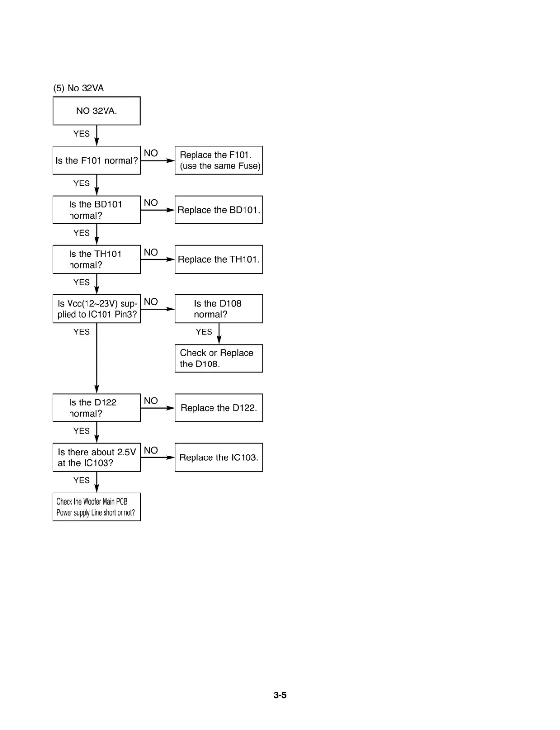
3-5
NO 32VA.
Replace the F101.
(use the same Fuse)
Is the F101 normal?
Is the TH101
normal?
Is the BD101
normal?
NO
NO
NO
Replace the BD101.
Replace the TH101.
NO
NO
NO
Is the D108
normal?
Check or Replace
the D108.
Replace the D122.
Replace the IC103.
YES
YES
YES
YES
YES
YES
YES
Is Vcc(12~23V) sup-
plied to IC101 Pin3?
Is the D122
normal?
Is there about 2.5V
at the IC103?
Check the Woofer Main PCB
Power supply Line short or not?
(5) No 32VA
YES
3-6
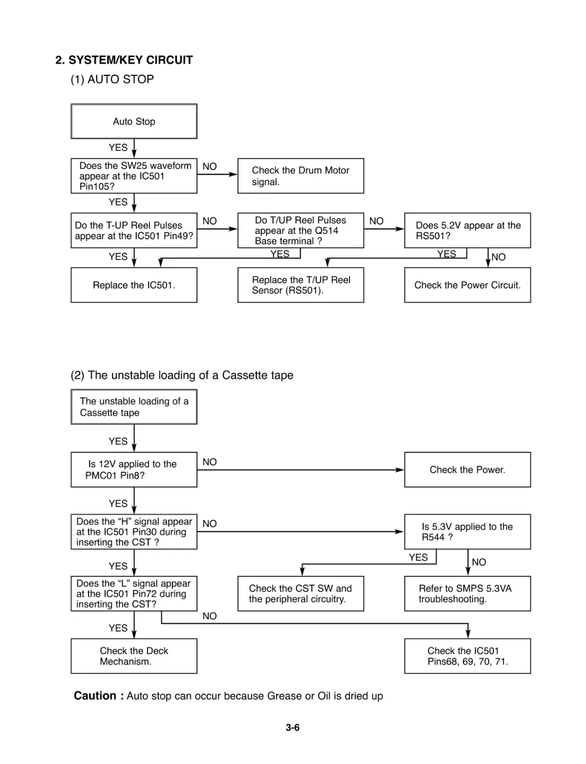
2. SYSTEM/KEY CIRCUIT
(1) AUTO STOP
(2) The unstable loading of a Cassette tape
Auto Stop
Does the SW25 waveform
appear at the IC501
Pin105?
Do the T-UP Reel Pulses
appear at the IC501 Pin49?
Is 12V applied to the
PMC01 Pin8?
Check the Drum Motor
signal.
Does 5.2V appear at the
RS501?
Check the Power Circuit.
Check the Power.
Is 5.3V applied to the
R544 ?
Refer to SMPS 5.3VA
troubleshooting.
Check the IC501
Pins68, 69, 70, 71.
Do T/UP Reel Pulses
appear at the Q514
Base terminal ?
Replace the T/UP Reel
Sensor (RS501).
Check the CST SW and
the peripheral circuitry.
Replace the IC501.
The unstable loading of a
Cassette tape
Does the "H" signal appear
at the IC501 Pin30 during
inserting the CST ?
Does the "L" signal appear
at the IC501 Pin72 during
inserting the CST?
Check the Deck
Mechanism.
Caution : Auto stop can occur because Grease or Oil is dried up
YES
YES
YES
NO
YES
YES
YES
YES
NO
NO
NO
NO
NO
NO
NO
YES
YES
YES
3-7
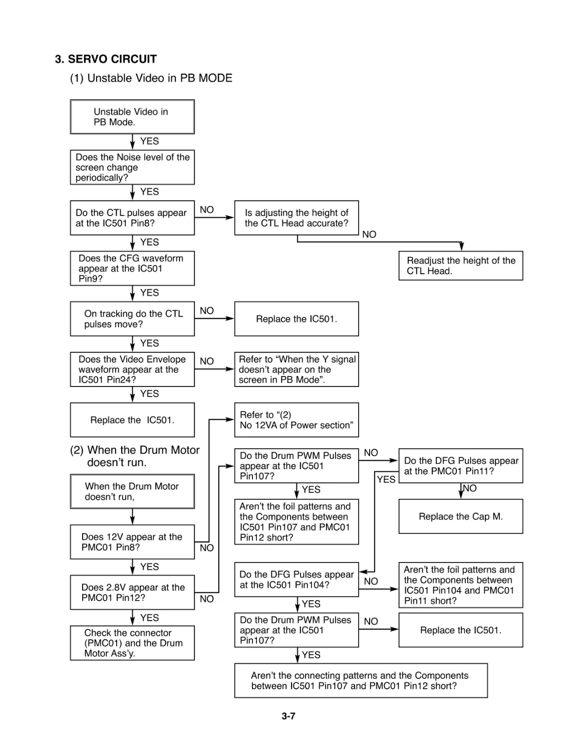
3. SERVO CIRCUIT
(1) Unstable Video in PB MODE
Unstable Video in
PB Mode.
Does the Noise level of the
screen change
periodically?
Do the CTL pulses appear
at the IC501 Pin8?
Is adjusting the height of
the CTL Head accurate?
Readjust the height of the
CTL Head.
Replace the IC501.
Refer to "When the Y signal
doesn't appear on the
screen in PB Mode".
Does the CFG waveform
appear at the IC501
Pin9?
On tracking do the CTL
pulses move?
Does the Video Envelope
waveform appear at the
IC501 Pin24?
Replace the IC501.
YES
YES
YES
YES
YES
YES
NO
NO
NO
NO
(2) When the Drum Motor
doesn't run.
Do the DFG Pulses appear
at the PMC01 Pin11?
Replace the Cap M.
Aren't the foil patterns and
the Components between
IC501 Pin104 and PMC01
Pin11 short?
Replace the IC501.
Refer to "(2)
No 12VAof Power section"
Do the Drum PWM Pulses
appear at the IC501
Pin107?
Aren't the foil patterns and
the Components between
IC501 Pin107 and PMC01
Pin12 short?
Do the DFG Pulses appear
at the IC501 Pin104?
Do the Drum PWM Pulses
appear at the IC501
Pin107?
Aren't the connecting patterns and the Components
between IC501 Pin107 and PMC01 Pin12 short?
When the Drum Motor
doesn't run,
Does 12V appear at the
PMC01 Pin8?
Does 2.8V appear at the
PMC01 Pin12?
Check the connector
(PMC01) and the Drum
Motor Ass'y.
NO
YES
YES
YES
NO
NO
NO
NO
NO
YES
YES
YES
3-8
Does the CFG signal appear at the
PMC01 Pin1?
Does the PWM signal appear at the
IC501 Pin108?
Does 2.8V appear at the PMC01?
Check the PMC01 and the Capstan
Motor Ass'y.
Does the Capstan PWM signal appear at
the IC501 Pin108?
Aren't the foil patterns and Components
between IC501 Pin108 and PMC01
Pin9 short?
Does the CFG signal come into the
IC501 Pin9?
Aren't the foil patterns and Components
between IC501 Pin108 and PMC01
Pin9 short?
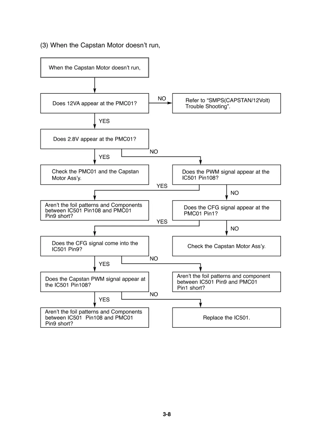
(3) When the Capstan Motor doesn't run,
NO
NO
NO
YES
YES
YES
When the Capstan Motor doesn't run,
Does 12VAappear at the PMC01?
YES
Replace the IC501.
YES
NO
NO
YES
Refer to "SMPS(CAPSTAN/12Volt)
Trouble Shooting".
Aren't the foil patterns and component
between IC501 Pin9 and PMC01
Pin1 short?
Check the Capstan Motor Ass'y.
NO
3-9
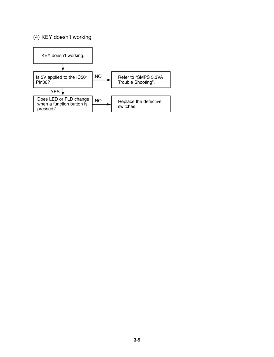
(4) KEY doesn't working
KEY doesn't working.
Is 5V applied to the IC501
Pin36?
Does LED or FLD change
when a function button is
pressed?
Refer to "SMPS 5.3VA
Trouble Shooting".
Replace the defective
switches.
YES
NO
NO
3-10
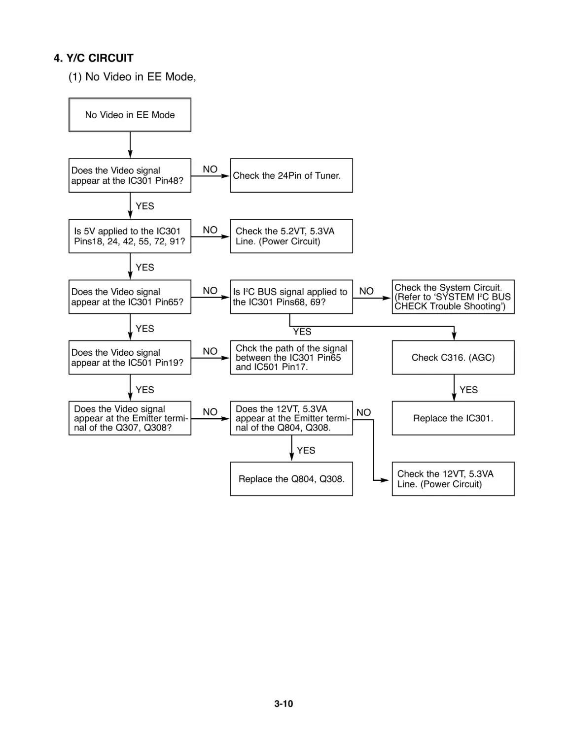
4. Y/C CIRCUIT
(1) No Video in EE Mode,
No Video in EE Mode
Check the 24Pin of Tuner.
Does the Video signal
appear at the IC301 Pin48?
Is 5V applied to the IC301
Pins18, 24, 42, 55, 72, 91?
Does the Video signal
appear at the IC301 Pin65?
Does the Video signal
appear at the IC501 Pin19?
Does the Video signal
appear at the Emitter termi-
nal of the Q307, Q308?
Check the 5.2VT, 5.3VA
Line. (Power Circuit)
Is I2C BUS signal applied to
the IC301 Pins68, 69?
Check C316. (AGC)
Chck the path of the signal
between the IC301 Pin65
and IC501 Pin17.
Replace the IC301.
Does the 12VT, 5.3VA
appear at the Emitter termi-
nal of the Q804, Q308.
Replace the Q804, Q308.
Check the 12VT, 5.3VA
Line. (Power Circuit)
Check the System Circuit.
(Refer to 'SYSTEM I2C BUS
CHECK Trouble Shooting')
YES
YES
YES
YES
YES
YES
YES
NO
NO
NO
NO
NO
NO
NO
3-11
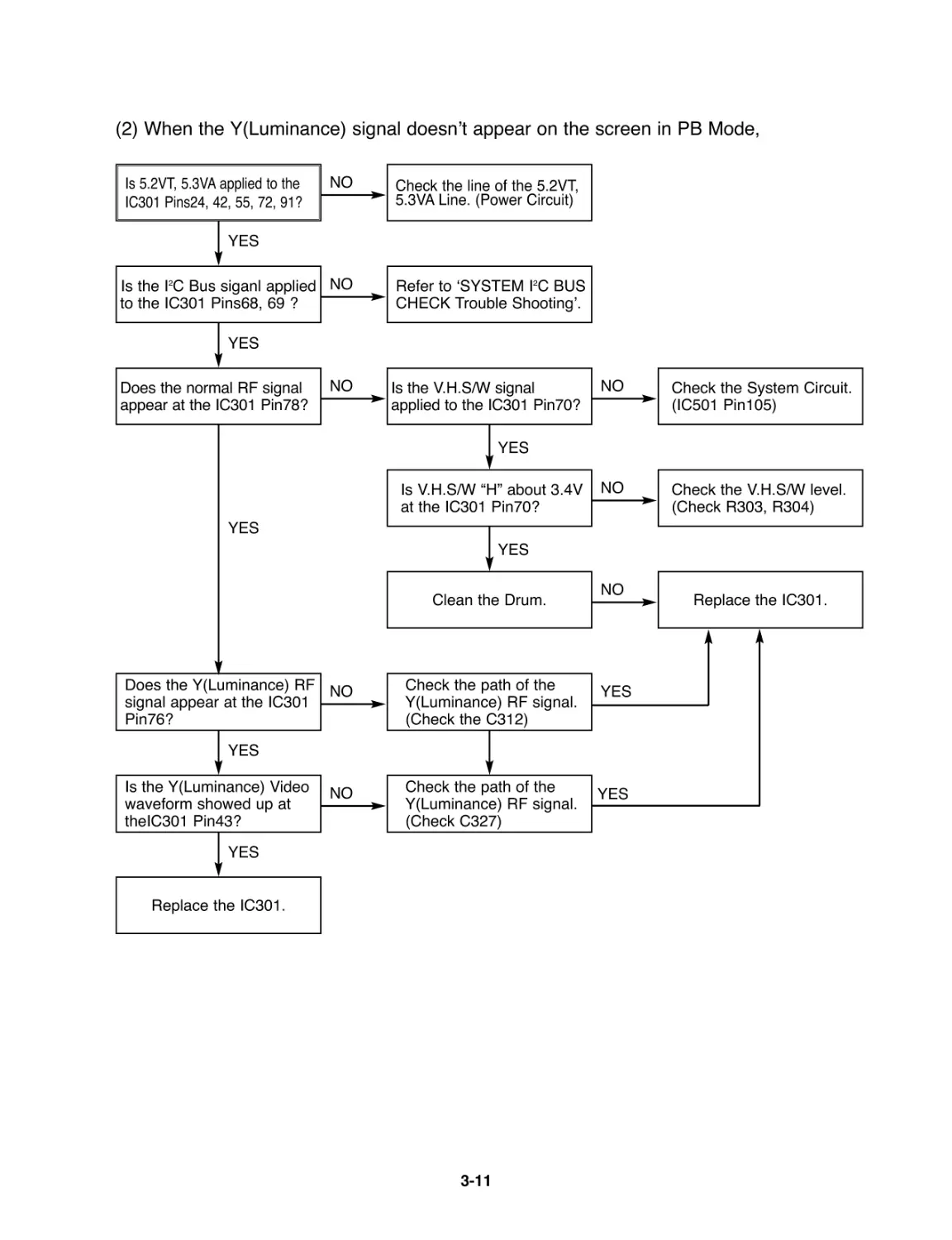
(2) When the Y(Luminance) signal doesn't appear on the screen in PB Mode,
Is 5.2VT, 5.3VAapplied to the
IC301 Pins24, 42, 55, 72, 91?
Is the I2C Bus siganl applied
to the IC301 Pins68, 69 ?
Does the normal RF signal
appear at the IC301 Pin78?
Check the line of the 5.2VT,
5.3VALine. (Power Circuit)
Check the System Circuit.
(IC501 Pin105)
Check the V.H.S/W level.
(Check R303, R304)
Replace the IC301.
Refer to 'SYSTEM I2C BUS
CHECK Trouble Shooting'.
Is the V.H.S/W signal
applied to the IC301 Pin70?
Is V.H.S/W "H" about 3.4V
at the IC301 Pin70?
Clean the Drum.
Check the path of the
Y(Luminance) RF signal.
(Check C327)
Check the path of the
Y(Luminance) RF signal.
(Check the C312)
Does the Y(Luminance) RF
signal appear at the IC301
Pin76?
Is the Y(Luminance) Video
waveform showed up at
theIC301 Pin43?
Replace the IC301.
NO
NO
NO
NO
NO
NO
NO
NO
YES
YES
YES
YES
YES
YES
YES
YES
YES
3-12
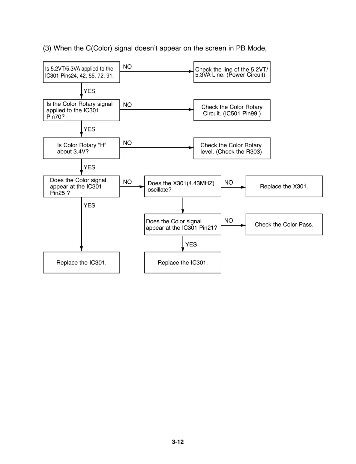
(3) When the C(Color) signal doesn't appear on the screen in PB Mode,
Is 5.2VT/5.3VAapplied to the
IC301 Pins24, 42, 55, 72, 91.
Is the Color Rotary signal
applied to the IC301
Pin70?
Check the line of the 5.2VT/
5.3VALine. (Power Circuit)
Replace the X301.
Check the Color Pass.
Check the Color Rotary
Circuit. (IC501 Pin99 )
Check the Color Rotary
level. (Check the R303)
Does the X301(4.43MHZ)
oscillate?
Replace the IC301.
Does the Color signal
appear at the IC301 Pin21?
Is Color Rotary "H"
about 3.4V?
Replace the IC301.
NO
NO
NO
YES
YES
YES
YES
NO
NO
NO
YES
Does the Color signal
appear at the IC301
Pin25 ?
3-13
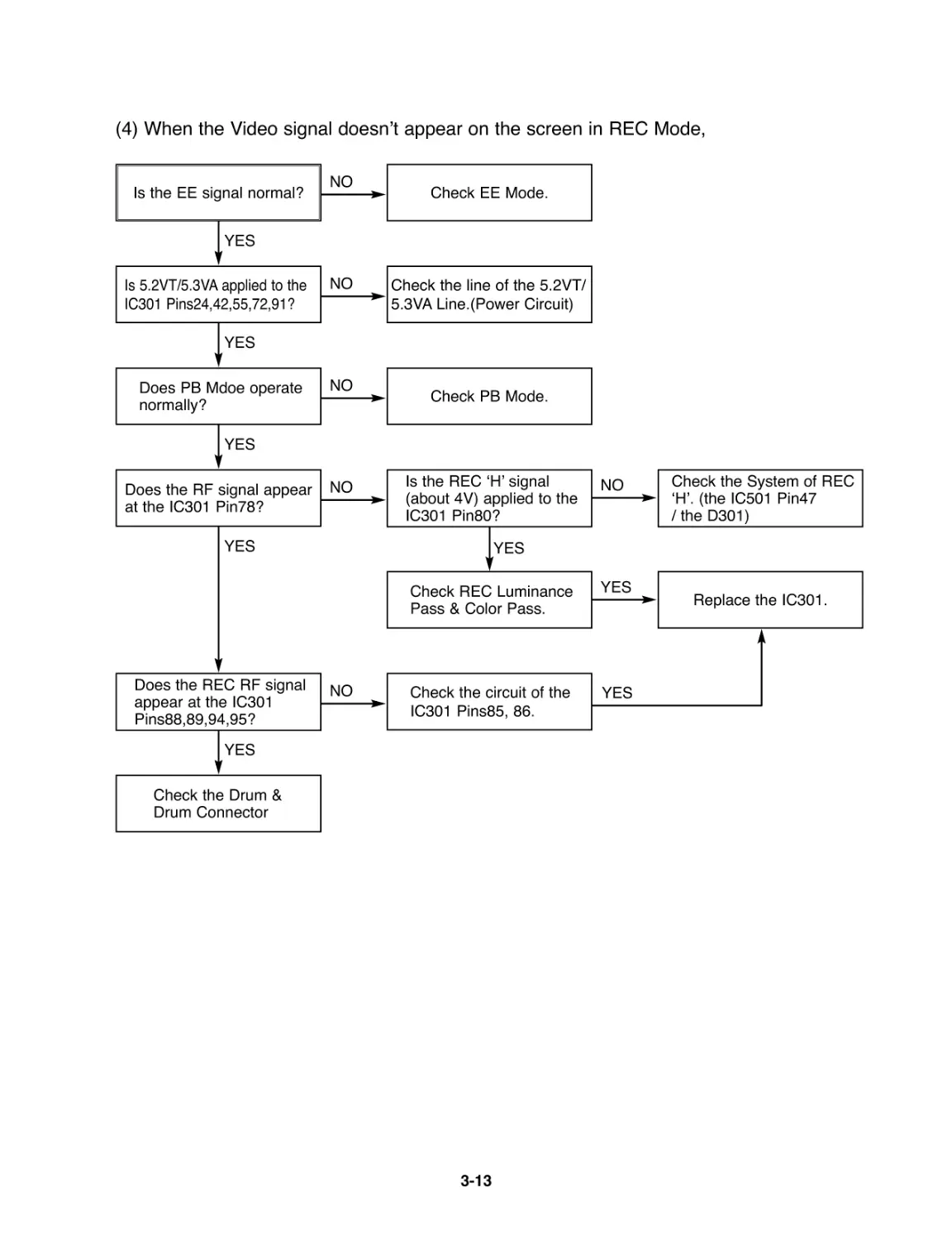
(4) When the Video signal doesn't appear on the screen in REC Mode,
Is the EE signal normal?
Is 5.2VT/5.3VAapplied to the
IC301 Pins24,42,55,72,91?
Does the RF signal appear
at the IC301 Pin78?
Check EE Mode.
Check the System of REC
'H'. (the IC501 Pin47
/ the D301)
Replace the IC301.
Check the line of the 5.2VT/
5.3VALine.(Power Circuit)
Check PB Mode.
Is the REC 'H' signal
(about 4V) applied to the
IC301 Pin80?
Check the circuit of the
IC301 Pins85, 86.
Check REC Luminance
Pass & Color Pass.
Does PB Mdoe operate
normally?
Does the REC RF signal
appear at the IC301
Pins88,89,94,95?
Check the Drum &
Drum Connector
YES
YES
YES
YES
YES
NO
NO
NO
NO
NO
NO
YES
YES
YES
3-14
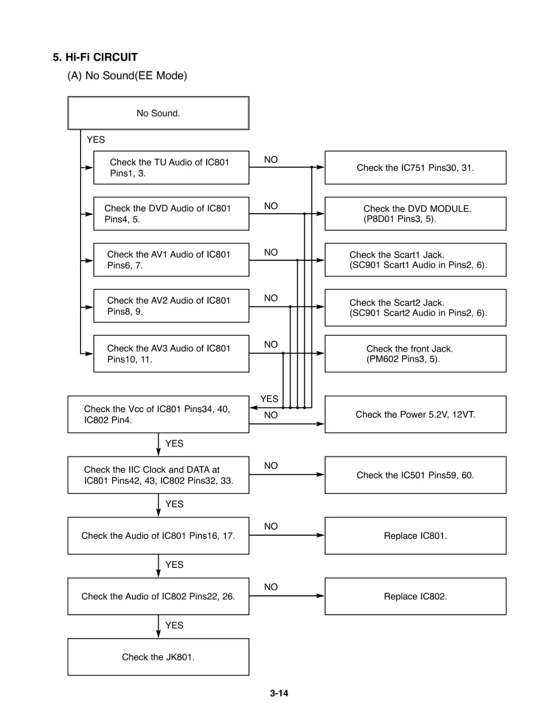
5. Hi-Fi CIRCUIT
(A) No Sound(EE Mode)
YES
No Sound.
Check the TU Audio of IC801
Pins1, 3.
Check the DVD Audio of IC801
Pins4, 5.
Check the AV1 Audio of IC801
Pins6, 7.
Check the AV2 Audio of IC801
Pins8, 9.
Check the AV3 Audio of IC801
Pins10, 11.
Check the Vcc of IC801 Pins34, 40,
IC802 Pin4.
YES
Check the IIC Clock and DATA at
IC801 Pins42, 43, IC802 Pins32, 33.
YES
Check the Audio of IC801 Pins16, 17.
YES
Check the Audio of IC802 Pins22, 26.
YES
Check the JK801.
Check the IC751 Pins30, 31.
NO
Check the DVD MODULE.
(P8D01 Pins3, 5).
NO
Check the Scart1 Jack.
(SC901 Scart1 Audio in Pins2, 6).
NO
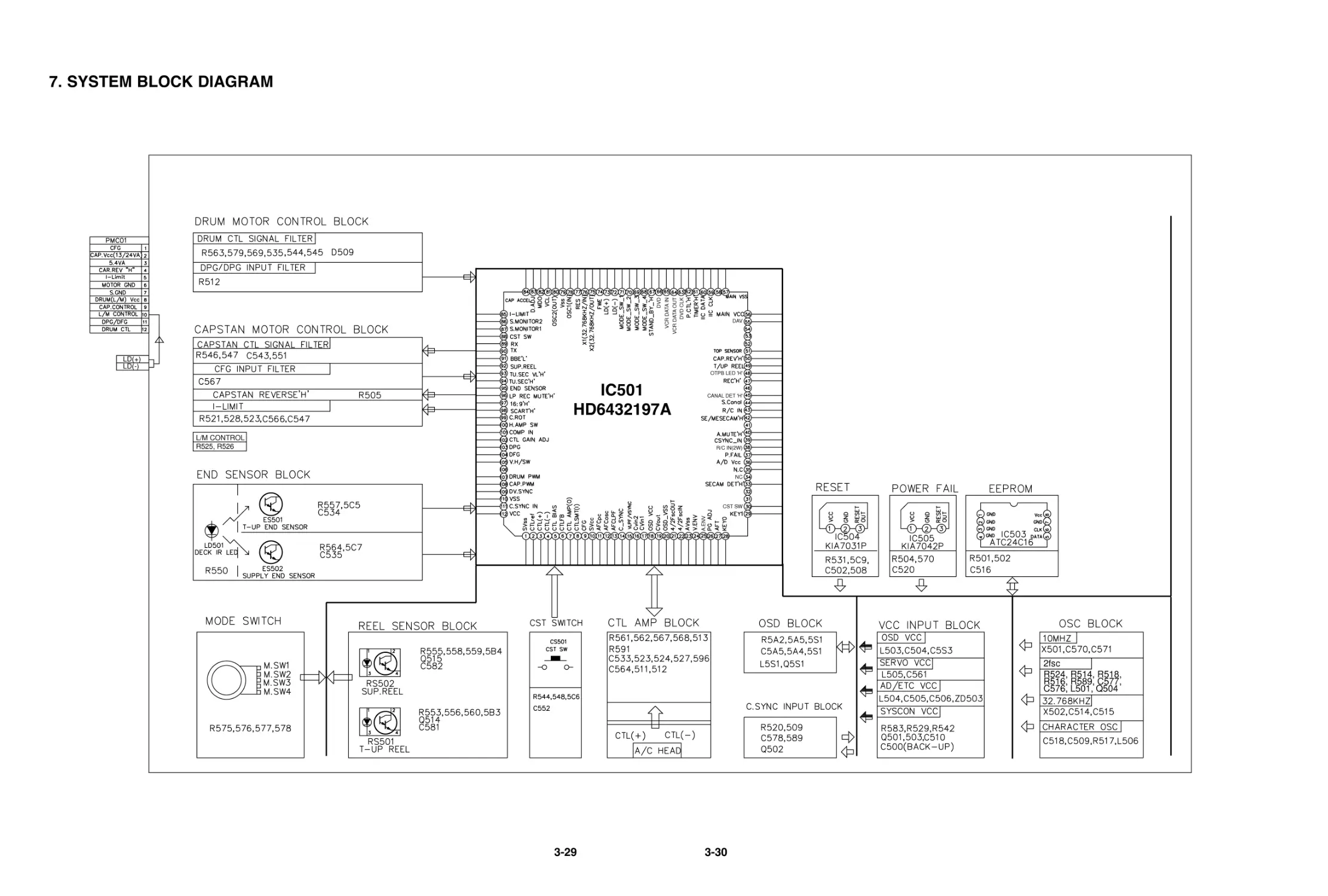
Check the front Jack.
(PM602 Pins3, 5).
Check the Scart2 Jack.
(SC901 Scart2 Audio in Pins2, 6).
NO
NO
Check the Power 5.2V, 12VT.
YES
NO
Check the IC501 Pins59, 60.
NO
Replace IC801.
Replace IC802.
NO
NO
3-15
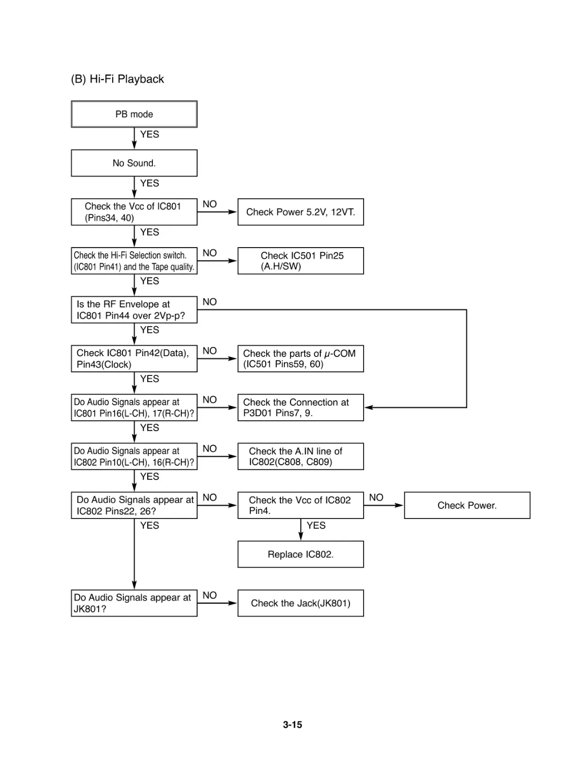
(B) Hi-Fi Playback
YES
YES
YES
YES
PB mode
No Sound.
Check the Vcc of IC801
(Pins34, 40)
Check the Hi-Fi Selection switch.
(IC801 Pin41) and the Tape quality.
Is the RF Envelope at
IC801 Pin44 over 2Vp-p?
YES
Check IC801 Pin42(Data),
Pin43(Clock) YES
Do Audio Signals appear at
IC801 Pin16(L-CH), 17(R-CH)?
YES
Do Audio Signals appear at
IC802 Pin10(L-CH), 16(R-CH)?
YES
YES
YES
Do Audio Signals appear at
IC802 Pins22, 26?
Do Audio Signals appear at
JK801?
Check Power 5.2V, 12VT.
NO
Check IC501 Pin25
(A.H/SW)
NO
NO
Check the parts of μ-COM
(IC501 Pins59, 60)
NO
Check the Connection at
P3D01 Pins7, 9.
NO
Check the A.IN line of
IC802(C808, C809)
NO
Check the Vcc of IC802
Pin4.
Replace IC802.
Check the Jack(JK801)
NO
NO
Check Power.
NO
3-16
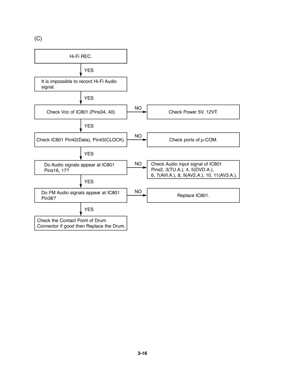
(C)
Hi-Fi REC.
It is impossible to record Hi-Fi Audio
signal.
Check Vcc of IC801.(Pins34, 40)
YES
YES
Check IC801 Pin42(Data), Pin43(CLOCK).
YES
Do Audio signals appear at IC801
Pins16, 17?
YES
Do FM Audio signals appear at IC801
Pin36?
YES
Check the Contact Point of Drum
Connector if good then Replace the Drum.
YES
Check Power 5V, 12VT.
NO
Check ports of μ-COM.
Check Audio input signal of IC801
Pins2, 3(TU.A.), 4, 5(DVD.A.),
6, 7(AVI.A.), 8, 9(AV2.A.), 10, 11(AV3.A .).
NO
Replace IC801.
NO
NO
3-17
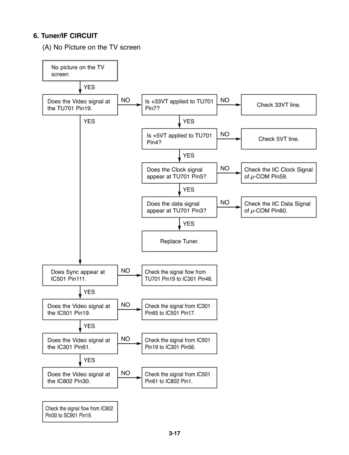
6. Tuner/IF CIRCUIT
(A) No Picture on the TV screen
No picture on the TV
screen
Does the Video signal at
the TU701 Pin19.
YES
YES
YES
Is +33VT applied to TU701
Pin7?
YES
Is +5VT applied to TU701
Pin4?
NO
Does Sync appear at
IC501 Pin111.
NO
Does the Video signal at
the IC501 Pin19.
YES
NO
Does the Video signal at
the IC301 Pin61.
YES
NO
NO
Does the Video signal at
the IC802 Pin30.
Check the signal flow from IC802
Pin30 to SC901 Pin19.
YES
Check 33VT line.
NO
Check 5VT line.
NO
YES
Does the Clock signal
appear at TU701 Pin5?
Check the lIC Clock Signal
of μ-COM Pin59.
NO
YES
Does the data signal
appear at TU701 Pin3?
Replace Tuner.
Check the signal flow from
TU701 Pin19 to IC301 Pin48.
Check the signal from IC301
Pin65 to IC501 Pin17.
Check the signal from IC501
Pin19 to IC301 Pin56.
Check the signal from IC501
Pin61 to IC802 Pin1.
Check the lIC Data Signal
of μ-COM Pin60.
NO
3-18
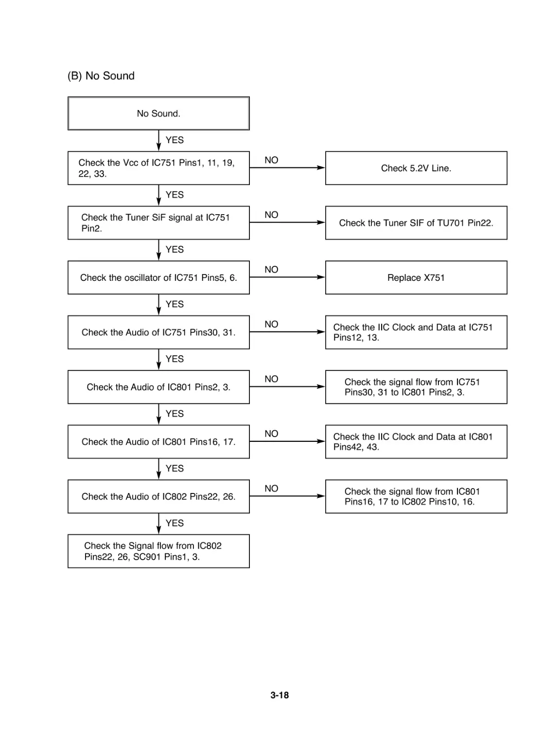
(B) No Sound
No Sound.
Check the Vcc of IC751 Pins1, 11, 19,
22, 33.
YES
Check 5.2V Line.
NO
Check the Tuner SiF signal at IC751
Pin2.
YES
Check the oscillator of IC751 Pins5, 6.
YES
Check the Audio of IC751 Pins30, 31.
YES
Check the Audio of IC801 Pins2, 3.
YES
Check the Audio of IC801 Pins16, 17.
YES
Check the Audio of IC802 Pins22, 26.
YES
Check the Signal flow from IC802
Pins22, 26, SC901 Pins1, 3.
YES
Check the Tuner SIF of TU701 Pin22.
NO
Replace X751
NO
Check the IIC Clock and Data at IC751
Pins12, 13.
NO
Check the signal flow from IC751
Pins30, 31 to IC801 Pins2, 3.
NO
Check the IIC Clock and Data at IC801
Pins42, 43.
NO
Check the signal flow from IC801
Pins16, 17 to IC802 Pins10, 16.
NO
3-19
3-20
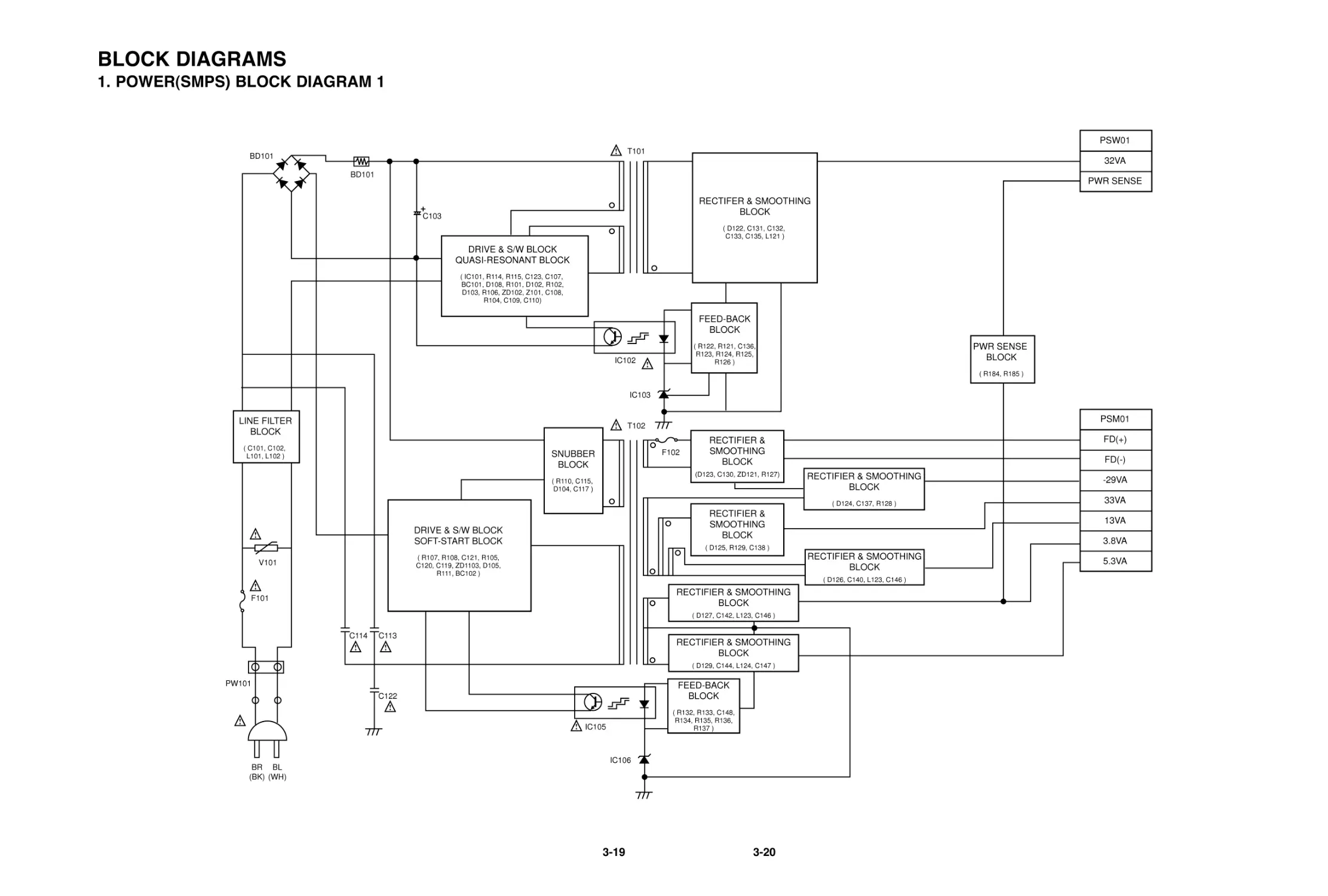
BLOCK DIAGRAMS
1. POWER(SMPS) BLOCK DIAGRAM 1
BD101
BD101
PW101
BR
(BK) BL
(WH)
V101
F101
!
!
IC105
F102
IC106
!
IC102
T102
IC103
!
!
T101
!
C103
C113
C114
C122
!
!
!
!
PSW01
32VA
PWR SENSE
PSM01
FD(+)
FD(-)
-29VA
33VA
13VA
3.8VA
5.3VA
LINE FILTER
BLOCK
( C101, C102,
L101, L102 )
RECTIFIER & SMOOTHING
BLOCK
( D129, C144, L124, C147 )
FEED-BACK
BLOCK
( R132, R133, C148,
R134, R135, R136,
R137 )
RECTIFIER &
SMOOTHING
BLOCK
(D123, C130, ZD121, R127)
RECTIFIER & SMOOTHING
BLOCK
( D126, C140, L123, C146 )
RECTIFIER &
SMOOTHING
BLOCK
( D125, R129, C138 )
FEED-BACK
BLOCK
( R122, R121, C136,
R123, R124, R125,
R126 )
PWR SENSE
BLOCK
( R184, R185 )
RECTIFIER & SMOOTHING
BLOCK
( D124, C137, R128 )
DRIVE & S/W BLOCK
QUASI-RESONANT BLOCK
( IC101, R114, R115, C123, C107,
BC101, D108, R101, D102, R102,
D103, R106, ZD102, Z101, C108,
R104, C109, C110)
RECTIFER & SMOOTHING
BLOCK
( D122, C131, C132,
C133, C135, L121 )
SNUBBER
BLOCK
( R110, C115,
D104, C117 )
DRIVE & S/W BLOCK
SOFT-START BLOCK
( R107, R108, C121, R105,
C120, C119, ZD1103, D105,
R111, BC102 )
RECTIFIER & SMOOTHING
BLOCK
( D127, C142, L123, C146 )
3-21
3-22
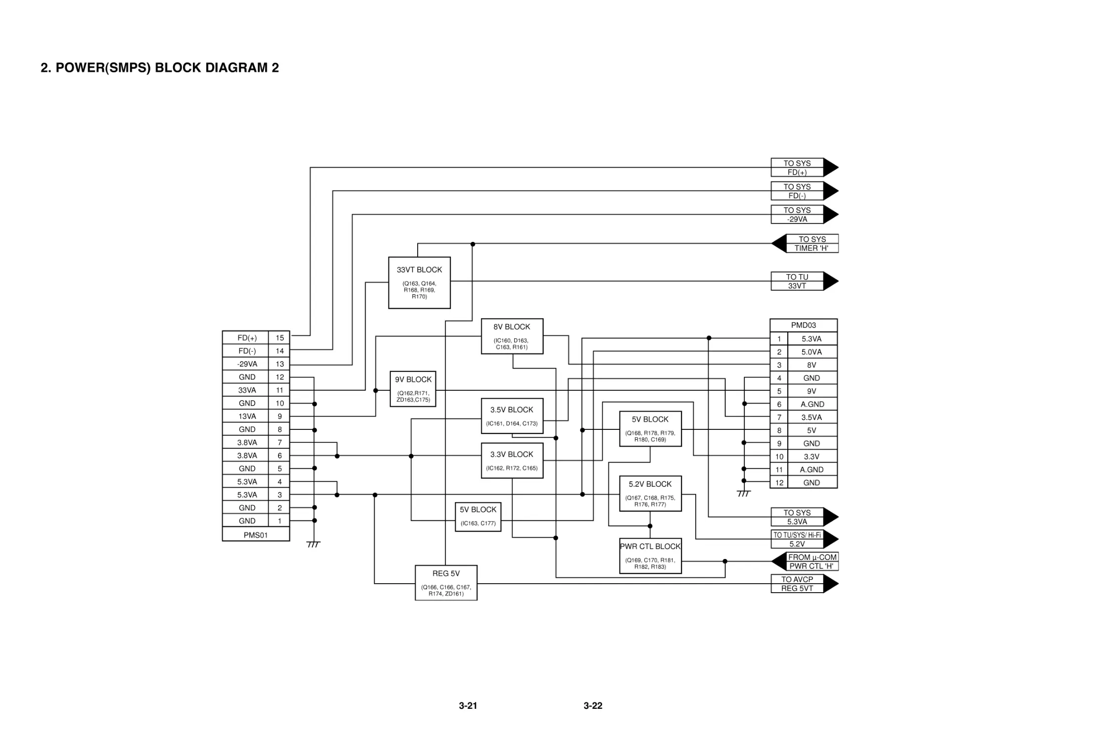
2. POWER(SMPS) BLOCK DIAGRAM 2
FD(+)
FD(-)
-29VA
GND
33VA
GND
13VA
GND
3.8VA
3.8VA
GND
5.3VA
5.3VA
GND
GND
15
14
13
12
11
10
9
8
7
6
5
4
3
2
1
TO SYS
FD(+)
TO SYS
FD(-)
TO SYS
-29VA
TO TU
33VT
TO SYS
5.3VA
TO TU/SYS/ Hi-Fi
5.2V
TO AVCP
REG 5VT
TO SYS
TIMER 'H'
FROM μ-COM
PWR CTL 'H'
PMS01
5.3VA
5.0VA
8V
GND
9V
A.GND
3.5VA
5V
GND
3.3V
A.GND
GND
1
2
3
4
5
6
7
8
9
10
11
12
PMD03
33VT BLOCK
(Q163, Q164,
R168, R169,
R170)
8V BLOCK
(IC160, D163,
C163, R161)
9V BLOCK
(Q162,R171,
ZD163,C175)
3.5V BLOCK
(IC161, D164, C173)
3.3V BLOCK
(IC162, R172, C165)
REG 5V
(Q166, C166, C167,
R174, ZD161)
5V BLOCK
(IC163, C177)
5.2V BLOCK
(Q167, C168, R175,
R176, R177)
PWR CTL BLOCK
(Q169, C170, R181,
R182, R183)
5V BLOCK
(Q168, R178, R179,
R180, C169)
3-23
3-24
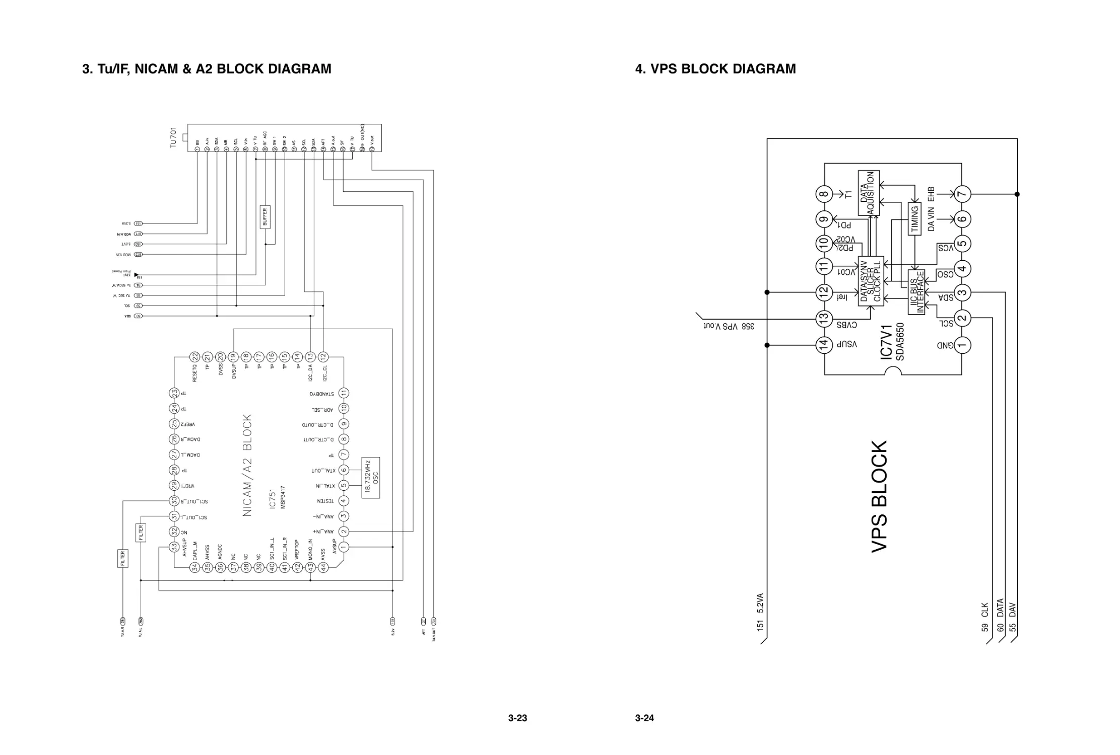
4. VPS BLOCK DIAGRAM
14
111098
1
456
DATA/SYNV
SLICER
CLOCK PLL
DATA
AQUISITION
IIC BUS
INTERFACE
TIMING
VPS BLOCK
IC7V1
SDA5650
151 5.2VA
358 VPS V.out
59 CLK
60 DATA
55 DAV
VSUP
CVBS
Iref
VC01
VCS
CSO
SDA
SCL
GND
PD1
EHB
DA VIN
T1
PD2/
VC02
23
7
13 12
3. Tu/IF, NICAM & A2 BLOCK DIAGRAM
(From Power)
159
27
731
60
59
93
94
158
872
160
871
151 5.3VA
5.2VT
MOD V.IN
MSP3417
3-25
3-26
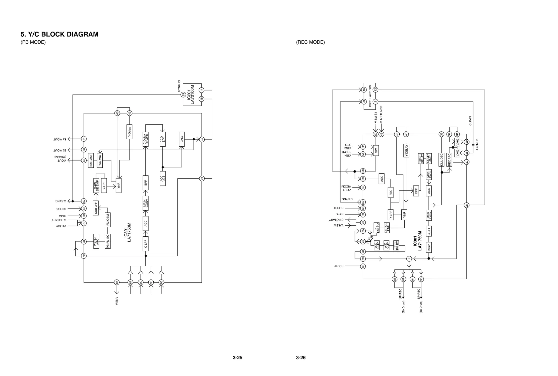
5. Y/C BLOCK DIAGRAM
(PB MODE)
90
93
96
84
V.ENV
87
70
V.H.SW
C.ROTARY
DATA
CLOCK
C.SYNC
V.OUT
(MICOM)
S2 V.OUT
S1 V.OUT
SYNC IN
696867
C-Delay
(1H/2H)
BPF
MAIN
CONV
ACC
C LPF
CCD
LPF
ACC
DET
CNC
25
21
IC201
LA70100M
IC301
LA71750M
29
18 14
PBFMEQ
FM OEM
PB FM
AGC
MAIN
DE EMP
Y-LPF
YNR
SUB LPF
60dB AMP
Y/C MIX
656361
46
43
Y-Delay
79
78
(REC MODE)
80
REC'H'
V.H.SW
C.ROTARY
D ATA
CLOCK
C SYNC
V.OUT
MICOM
V.IN4
FRONT
V.IN3
DEC
7978 76 7570696867
655958
54 52
50
V.IN2 S1
V.IN1 TUNER
48
46
43
33
32
31
CLK-IN
29
28
4.43MHz
27
21
95
94
89
88
Killer
C-LPF
ACC
BPF
Main
Conv
Main
Conv
DETAIL
ENH
NL
EMPHA
W/D
CLIP
IC301
LA71750M
UP REC
SP REC
(To Drum)
(To Drum)
W/D
CLIP
REC
FM EQ
Y-LPF
FBC
AGC
SW
Y-DELAY
KILL DEC
REC APC
VX02 VX02
COMP
AMP
1H/2H
DELAY
YNR
29
16
2
12
IC201 LA70100M
3-27
3-28
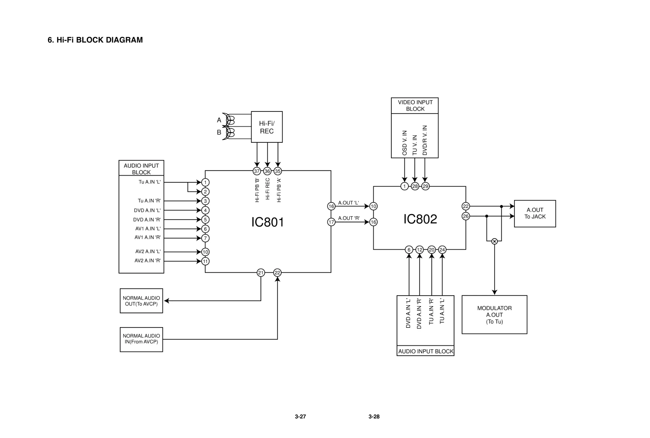
6. Hi-Fi BLOCK DIAGRAM
IC802
A
B
Hi-Fi/
REC
10
22
16
6
12
82
9
122024
26
IC801
A.OUT
To JACK
37
Hi-Fi PB 'B'
Hi-Fi PB 'A'
Hi-Fi REC
1
2
3
4
5
6
7
10
11
21 22
36 35
16 A.OUT 'L'
A.OUT 'R'
17
AUDIO INPUT
BLOCK
VIDEO INPUT
BLOCK
AUDIO INPUT BLOCK
OSD V. IN
TUV.IN
DVD/R V. IN
DVD A.IN 'L'
DVD A.IN 'R'
TU A.IN 'R'
TU A.IN 'L'
NORMAL AUDIO
OUT(To AVCP)
NORMAL AUDIO
IN(From AVCP)
Tu A.IN 'L'
Tu A.IN 'R'
DVD A.IN 'L'
DVD A.IN 'R'
AV1 A.IN 'L'
AV1 A.IN 'R'
AV2 A.IN 'L'
AV2 A.IN 'R'
MODULATOR
A.OUT
(To Tu)
3-29
3-30
7. SYSTEM BLOCK DIAGRAM
2fsc
R524, R514, R518,
R516, R589, C577,
C576, L501, Q504
LD(+)
LD(-)
L/M CONTROL
R525, R526
IC501
HD6432197A
DVD
VCR DATA IN
VCR DATA OUT
DVD CLK
DAV
OTPB LED 'H'
R/C IN(2W)
NC
CST SW
A.ENV
CANAL DET 'H'
3-31
3-32
NOTES) Symbol denotes AC ground.
NOTES) Symbol denotes DC chassis ground.
NOTE) Warning
NOTE) Parts that are shaded are critical
NOTE) With respect to risk of fire or
NOTE) electricial shock.
A
B
C
D
E
F
G
H
I
J
K
L
M
N
O
P
Q
R
ST
CIRCUIT DIAGRAMS
1. POWER(SMPS) CIRCUIT DIAGRAM 1_200W
Switching Error.
IC101 is defective.
Switching Error.
IC104 is defective.
Switching Error.
IC105, 106 are defective.
No Power.
F101 is defective.
No 5.3VA.
D127 is defective.
No 3.8VA.
D127 is defective.
No 13VA.
D126 is defective.
No 33VA.
D125 is defective.
No 32VA.
D122 is defective.
Digitron Error.
D123, ZD121, D124 are defective.
No power.
BD101, TH101 are defective.
IMPORTANT SAFETY NOTICE
WHEN SERVICING THIS CHASSIS, UNDER NO CIR-
CUMSTANCES SHOULD THE ORIGINAL DESIGN BE
MODIFIED OR ALTERED WITHOUT PERMISSION
FROM THE LG ELECTRONICS CORPORATION. ALL
COMPONENTS SHOULD BE REPLACED ONLY WITH
TYPES IDENTICAL TO THOSE IN THE ORIGINAL CIR-
CUIT. SPECIAL COMPONENTS ARE SHADED ON THE
SCHEMATIC FOR EASY IDENTIFICATION.
THIS CIRCUIT DIAGRAM MAY OCCASIONALLY DIF-
FER FROM THE ACTUAL CIRCUIT USED. THIS WAY,
IMPLEMENTATION OF THE LATEST SAFETY AND
PERFORMANCE IMPROVEMENT CHANGES INTO
THE SET IS NOT DELAYED UNTIL THE NEW SERVICE
LITERATURE IS PRINTED.
NOTE :
1. Shaded( ) parts are critical for safety. Replace only
with specified part number.
2. Voltages are DC-measured with a digital voltmeter
during Play mode.
3-33
3-34
NOTES) Symbol denotes AC ground.
NOTES) Symbol denotes DC chassis ground.
NOTE) Warning
NOTE) Parts that are shaded are critical
NOTE) With respect to risk of fire or
NOTE) electricial shock.
A
B
C
D
E
F
G
H
I
J
K
L
M
N
O
P
Q
R
ST
2. POWER(SMPS) CIRCUIT DIAGRAM 1_400W
Switching Error.
IC101 is defective.
Switching Error.
IC104 is defective.
Switching Error.
IC105, 106 are defective.
No Power.
F101 is defective.
No 5.3VA.
D127 is defective.
No 3.8VA.
D127 is defective.
No 13VA.
D126 is defective.
No 33VA.
D125 is defective.
No 32VA.
D122 is defective.
Digitron Error.
D123, ZD121, D124 are defective.
No power.
BD101, TH101 are defective.
IMPORTANT SAFETY NOTICE
WHEN SERVICING THIS CHASSIS, UNDER NO CIR-
CUMSTANCES SHOULD THE ORIGINAL DESIGN BE
MODIFIED OR ALTERED WITHOUT PERMISSION
FROM THE LG ELECTRONICS CORPORATION. ALL
COMPONENTS SHOULD BE REPLACED ONLY WITH
TYPES IDENTICAL TO THOSE IN THE ORIGINAL CIR-
CUIT. SPECIAL COMPONENTS ARE SHADED ON THE
SCHEMATIC FOR EASY IDENTIFICATION.
THIS CIRCUIT DIAGRAM MAY OCCASIONALLY DIF-
FER FROM THE ACTUAL CIRCUIT USED. THIS WAY,
IMPLEMENTATION OF THE LATEST SAFETY AND
PERFORMANCE IMPROVEMENT CHANGES INTO
THE SET IS NOT DELAYED UNTIL THE NEW SERVICE
LITERATURE IS PRINTED.
NOTE :
1. Shaded( ) parts are critical for safety. Replace only
with specified part number.
2. Voltages are DC-measured with a digital voltmeter
during Play mode.
3-35
3-36
3. POWER(SMPS) CIRCUIT DIAGRAM 2
A
B
C
D
E
F
G
H
I
J
K
L
M
N
O
P
Q
R
ST
3-37
3-38
A
B
C
D
E
F
G
H
I
J
K
L
M
N
O
P
Q
R
ST
EE MODE(VIDEO)
TU MODE (AUDIO)
4. TU/IF, NICAM & A2 CIRCUIT DIAGRAM
3-39
3-40
5. A/V CIRCUIT DIAGRAM
1
4
5
2
7
813
11
12
2
3
9
10
6
2
14
A
B
C
D
E
F
G
H
I
J
K
L
M
N
O
P
Q
R
ST
PB SECAM COLOR
REC AUDIO
PB Y+C
PBY
PBC
REC Y+C
REC Y
REC C
REC SECAM COLOR
PB AUDIO(MONO)
WAVEFORM
Audio Tracking is failed.
IC301 Pin 84 is defective.
EE, PB Screen doesn't appear.
Q305 is defective.
PB COLOR Signal disappear.
IC301 Pin70 is defective.
PB COLOR Signal disappear.
X301 is defective.
D301or IC301 Pin 80
REC is defective.
PB and Recording is failed.
(IC301 doesn't operate.)
IC301 Pin 69, 68 are defective.
Normal Audio signal is not recorded.
FL301, Q301, Q306 are defective.
No mono Audio Signal
in PB MODE.
Q302, Q303, Q314
are defective.
3-41
3-42
6. Hi-Fi CIRCUIT DIAGRAM
A
B
C
D
E
F
G
H
I
J
K
L
M
N
O
P
Q
R
ST
PB
REC
44 Pin is defective.
Hi-Fi Audio is not appear.
IC801 Pins42, 43 aredefective.
All Audio is not appear.
3-43
3-44
7. SCART(JACK) CIRCUIT DIAGRAM
A
B
C
D
E
F
G
H
I
J
K
L
M
N
O
P
Q
R
ST
3-45
3-46
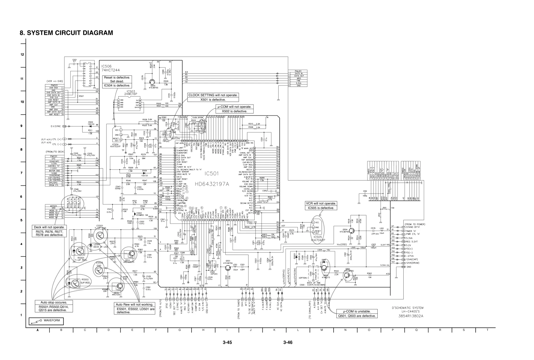
8. SYSTEM CIRCUIT DIAGRAM
8
7
6
34
55
1
2
9
WAVEFORM
A
B
C
D
E
F
G
H
I
J
K
L
M
N
O
P
Q
R
ST
Q501, Q503 are defective.
μ-COM is unstable.
IC505 is defective.
VCR will not operate.
X501 is defective.
CLOCK SETTING will not operate.
X502 is defective.
μ-COM will not operate.
ES501, ES502, LD501 are
defective.
Auto Rew will not working.
RS501,RS502,Q514,
Q515 are defective.
Auto stop occures.
R575, R576, R577,
R578 are defective.
Deck will not operate.
IC504 is defective.
Reset is defective.
Set dead.
3-47
3-48
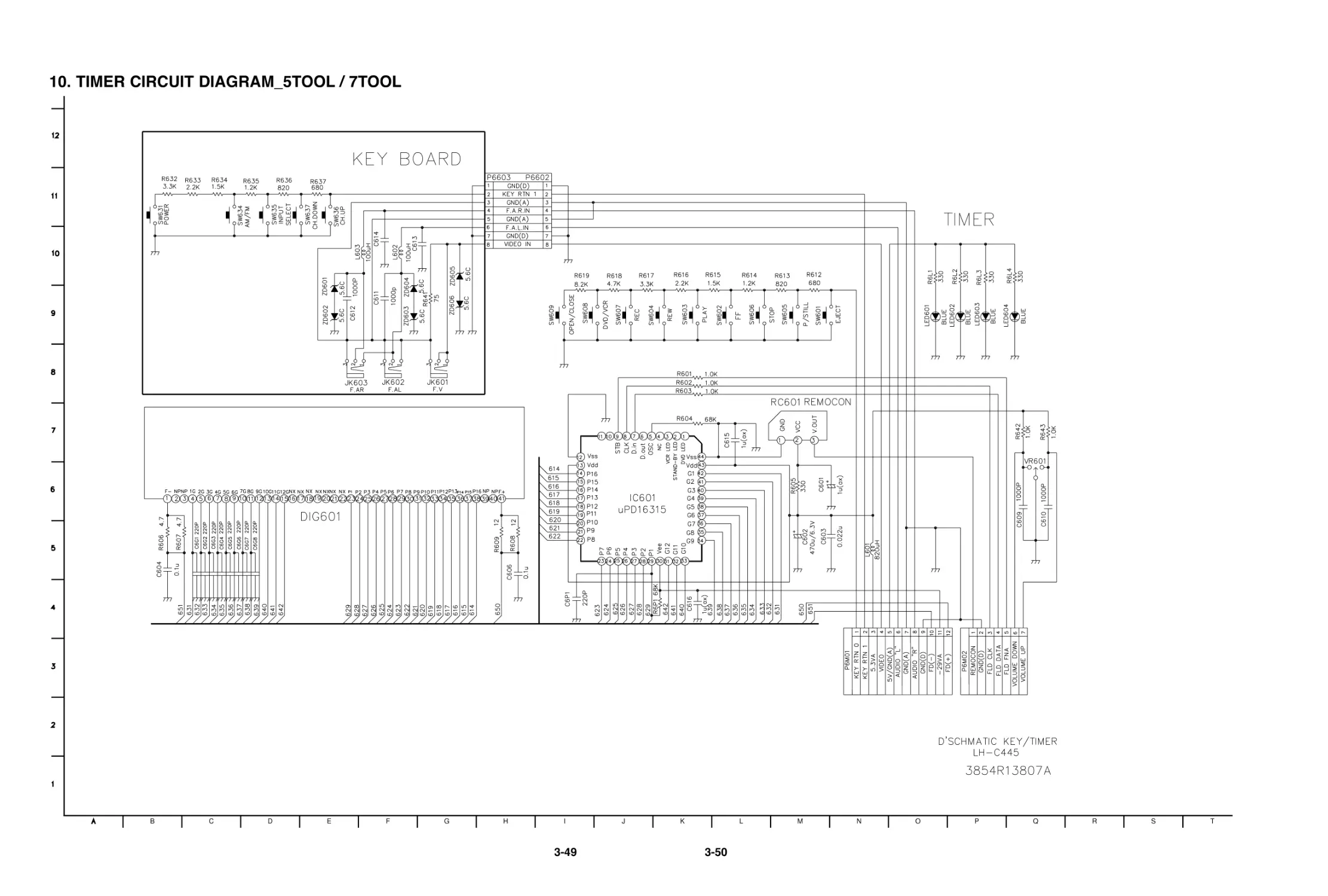
9. TIMER CIRCUIT DIAGRAM_0TOOL
A
B
C
D
E
F
G
H
I
J
K
L
M
N
O
P
Q
R
ST
3-49
3-50
10. TIMER CIRCUIT DIAGRAM_5TOOL / 7TOOL
A
B
C
D
E
F
G
H
I
J
K
L
M
N
O
P
Q
R
ST
3-51
3-52
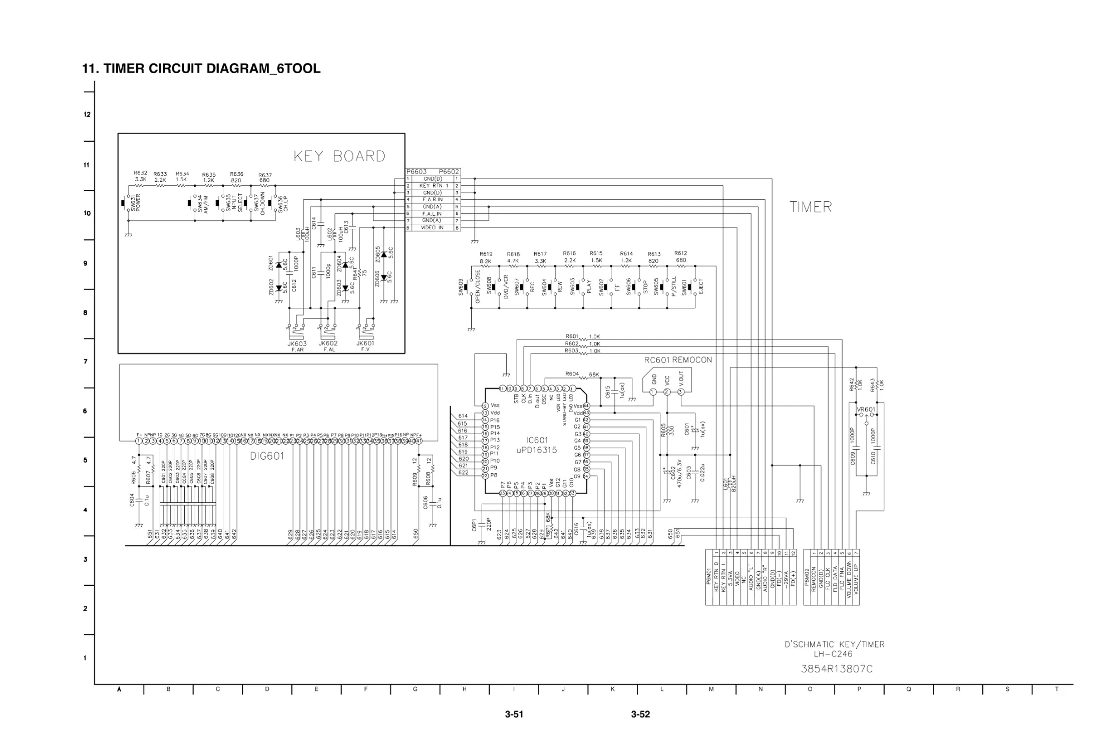
11. TIMER CIRCUIT DIAGRAM_6TOOL
A
B
C
D
E
F
G
H
I
J
K
L
M
N
O
P
Q
R
ST
3-53
3-54
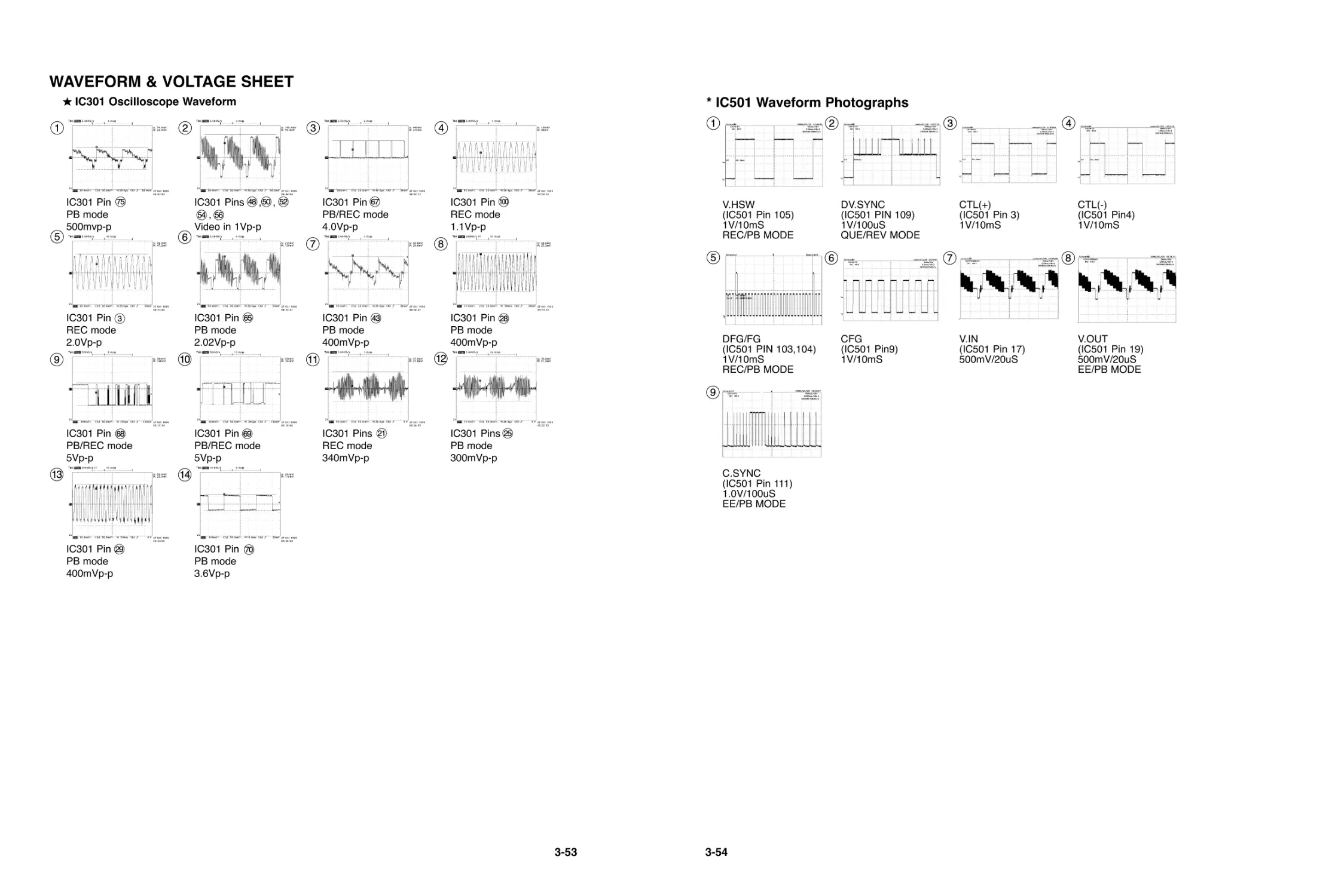
WAVEFORM & VOLTAGE SHEET
IC301 Pin 20
PB mode
500mvp-p
IC301 Pins 38,32,31
38, 38
Video in 1Vp-p
IC301 Pin 28
PB/REC mode
4.0Vp-p
IC301 Pin 7
REC mode
1.1Vp-p
IC301 Pin 6
REC mode
2.0Vp-p
IC301 Pin 29
PB mode
2.02Vp-p
IC301 Pin 41
PB mode
400mVp-p
IC301 Pin 64
PB mode
400mVp-p
IC301 Pin 23
PB/REC mode
5Vp-p
IC301 Pin 24
PB/REC mode
5Vp-p
IC301 Pins 71 72
REC mode
340mVp-p
IC301 Pins 51 54
PB mode
300mVp-p
IC301 Pin 63
PB mode
400mVp-p
IC301 Pin 11
PB mode
3.6Vp-p
_ IC301 Oscilloscope Waveform
* IC501 Waveform Photographs
V.HSW
(IC501 Pin 105)
1V/10mS
REC/PB MODE
DV.SYNC
(IC501 PIN 109)
1V/100uS
QUE/REV MODE
CTL(+)
(IC501 Pin 3)
1V/10mS
CTL(-)
(IC501 Pin4)
1V/10mS
DFG/FG
(IC501 PIN 103,104)
1V/10mS
REC/PB MODE
CFG
(IC501 Pin9)
1V/10mS
V.IN
(IC501 Pin 17)
500mV/20uS
V.OUT
(IC501 Pin 19)
500mV/20uS
EE/PB MODE
C.SYNC
(IC501 Pin 111)
1.0V/100uS
EE/PB MODE
3-55
3-56
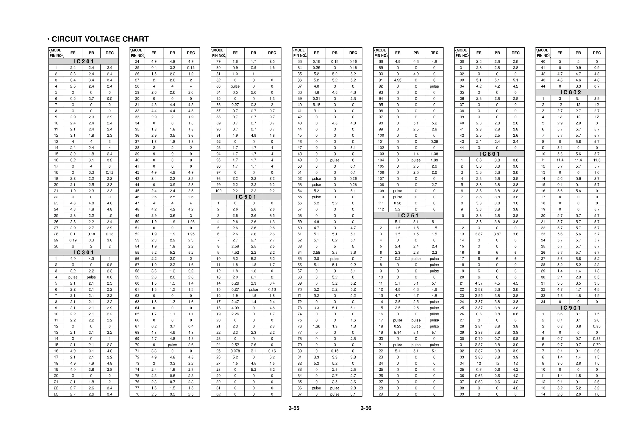
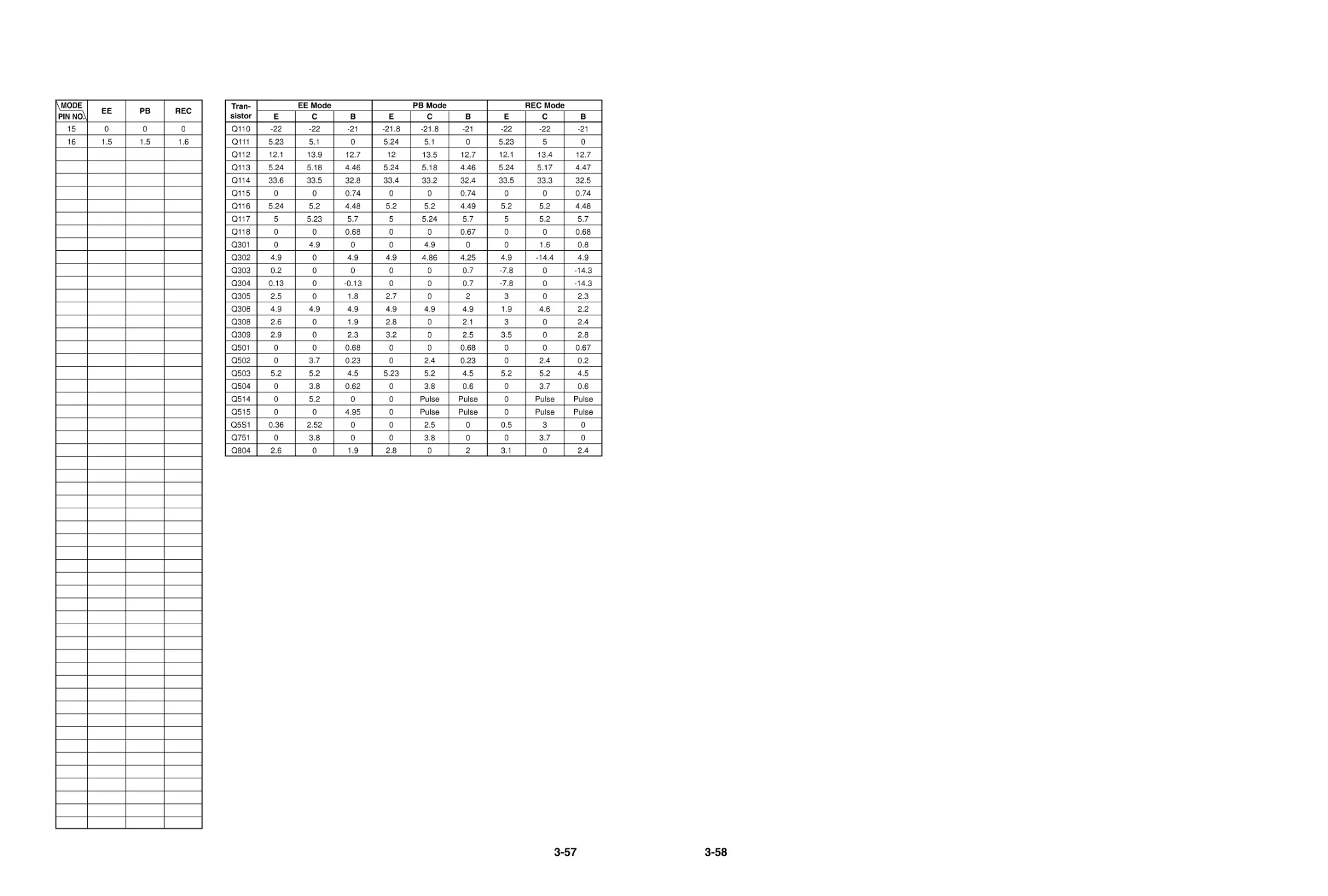
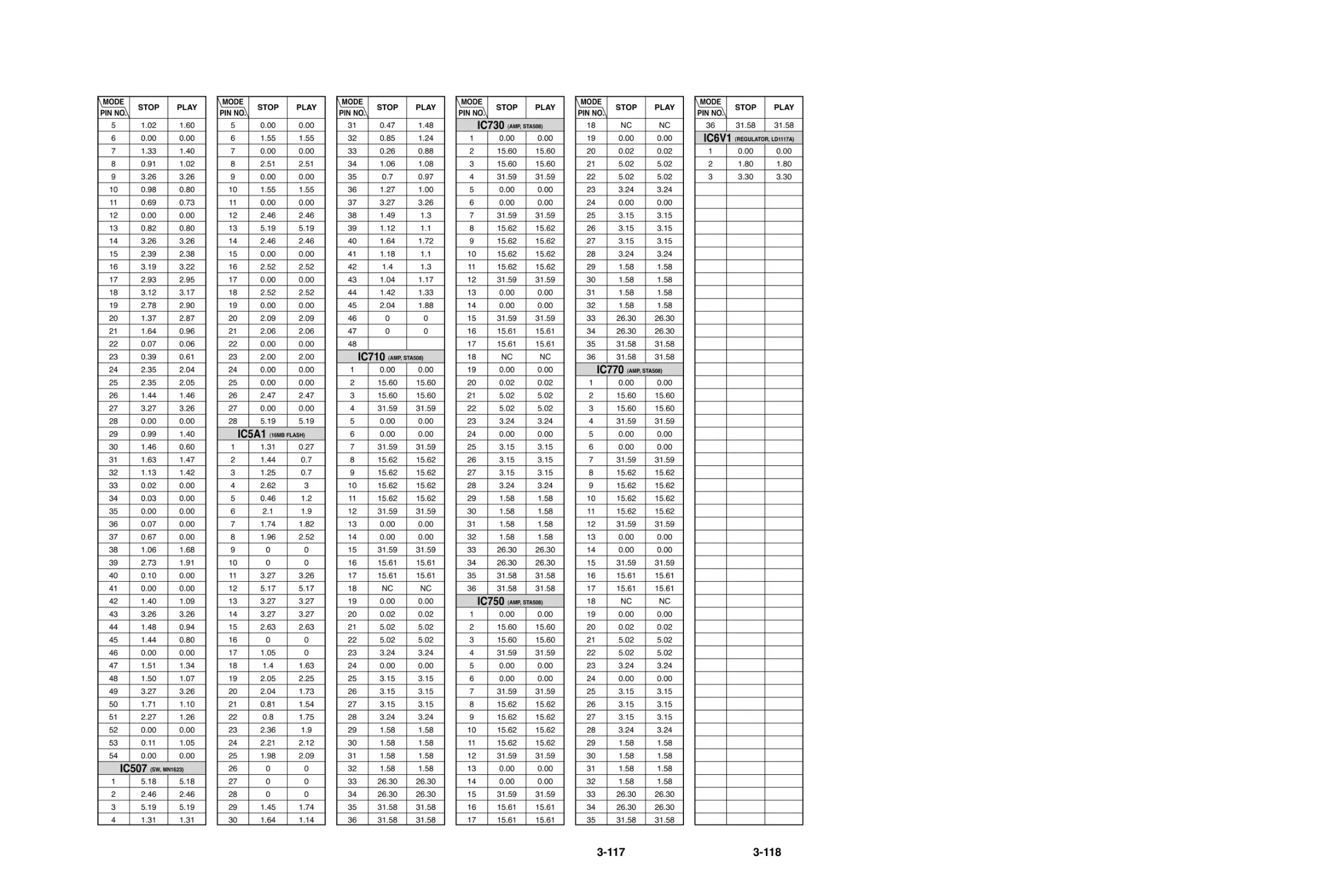
• CIRCUIT VOLTAGE CHART
EE
PB
REC
MODE
PIN NO.
1
2
3
4
5
6
7
8
9
10
11
12
13
14
15
16
17
18
19
20
21
22
23
24
25
26
27
28
29
30
1
2
3
4
5
6
7
8
9
10
11
12
13
14
15
16
17
18
19
20
21
22
23
2.4
2.3
3.4
2.5
0
0.5
0
0
2.9
2.4
2.1
3.1
4
2.4
3.0
3.2
0
0
2.2
2.1
1.9
0
4.8
4.8
2.3
2.3
2.9
0.1
0.19
2
4.9
0
2.2
pulse
2.1
2.2
2.1
2.1
2.1
2.2
2.2
0
2.1
0
2.1
4.9
2.1
4.9
4.0
0
3.1
2.7
2.7
2.4
2.4
3.4
2.4
0
3.7
0
0
2.9
2.4
2.4
1.8
4
2.4
1.8
3.1
4
3.3
2.2
2.5
2.3
0
4.8
4.8
2.2
2.2
2.7
0.18
0.3
2
4.9
0
2.2
pulse
2.1
2.1
2.1
2.1
2.1
2.1
2.2
0
2.1
0
2.1
0.1
2.1
4.9
3.8
0
1.8
2.6
2.6
2.4
2.4
3.4
2.4
0
0.5
0
0
2.9
2.4
2.4
2.3
3
4
2.4
3.2
0
0.12
2.2
2.3
2.3
0
4.8
4.8
1.5
2.4
2.9
0.18
3.8
2
1
0.8
2.3
0.6
2.3
2.2
2.2
2.2
2.9
2.2
2.2
0
2.2
1
2.2
4.8
2.2
4.9
2.8
0
2
3.4
3.4
IC201
IC301
EE
PB
REC
MODE
PIN NO.
24
25
26
27
28
29
30
31
32
33
34
35
36
37
38
39
40
41
42
43
44
45
46
47
48
49
50
51
52
53
54
55
56
57
58
59
60
61
62
63
64
65
66
67
68
69
70
71
72
73
74
75
76
77
78
4.9
0.1
1.5
2
4
2.6
0
4.5
4.4
2.9
0
1.8
2.9
1.8
2
9
0
0
4.9
2.4
0
2.4
2.6
4
4.2
2.9
1.9
0
1.9
2.3
1.9
5.2
2.2
1.9
3.6
2.8
1.5
1.8
0
1.8
0
1.7
0
0.2
4.8
4.7
0
3.3
4.9
2
2.4
2.3
2.3
1.5
2.5
4.9
3.3
2.2
2.0
4
2.6
0
4.4
4.4
2
0
1.8
3.5
1.8
2
9
0
0
4.9
2.2
3.9
2.4
2.5
4
4.2
3.6
1.9
0
1.9
2.2
1.9
5.2
2.0
2.3
1.3
2.8
1.5
1.3
0
1.3
0
1.1
0
3.7
4.9
4.8
pulse
0
4.8
3.3
1.6
0.6
0.7
1.5
3.3
4.9
0.12
1.2
2
4
2.6
0
4.5
4.5
1.9
1.8
1.8
3.6
1.8
2
9
0
0
4.9
2.3
2.8
2.5
2.6
4
4.2
3
1.95
0
1.95
2.3
2.2
5.2
2
1.6
2.2
2.8
1.4
1.3
0
1.6
0
1.1
0
0.4
4.8
4.8
2.6
0
4.8
2.2
2.3
2.3
2.3
1.5
2.5
EE
PB
REC
MODE
PIN NO.
79
80
81
82
83
84
85
86
87
88
89
90
91
92
93
94
95
96
97
98
99
100
1
2
3
4
5
6
7
8
9
10
11
12
13
14
15
16
17
18
19
20
21
22
23
24
25
26
27
28
29
30
31
32
1.8
0.9
1.0
0
pulse
0.5
0
0.27
0.7
0.7
0.7
0.7
4.9
0
1.7
1.7
1.7
1.7
0
2.2
2.2
2.2
0
2.6
2.6
2.6
2.6
2.6
2.7
2.58
4.52
5.2
1.8
1.8
2.0
0.26
0.27
1.9
2.47
4.93
2.26
0
2.3
2.3
0
0.52
0.078
5.2
4.5
0
0
0
0
0
1.7
0.9
1
0
0
2.6
0
0.3
0.7
0.7
0.7
0.7
4.9
0
1.7
1.7
1.7
1.7
0
2.2
2.2
2.2
0
2.6
2.6
2.6
2.6
2.6
2.7
2.5
2.2
5.2
1.8
1.8
2.1
3.9
pulse
1.9
1.4
0
0
0
0
2.3
0
2.6
3.1
0
4.5
5.2
0
0
0
0
2.5
4.6
1
0
0
0
1.3
2
0.7
0.7
0.7
0.7
4.8
0
4
4
4
4
0
2.2
2.2
2.2
0
2.6
3.5
1.3
2.6
2.6
2.7
2.5
2.2
5.2
1.7
0
2
0.4
0.16
1.8
2.4
4.8
1.7
0
2.3
2.2
0
0
0.16
5.2
4.5
5.2
0
0
0
0
EE
PB
REC
MODE
PIN NO.
33
34
35
36
37
38
39
40
41
42
43
44
45
46
47
48
49
50
51
52
53
54
55
56
57
58
59
60
61
62
63
64
65
66
67
68
69
70
71
72
73
74
75
76
77
78
79
80
81
82
83
84
85
86
87
0.18
0.26
5.2
5.2
4.8
4.8
0.21
5.18
3.1
0
0
0
0
0
0
0
0
0
0
pulse
pulse
5.2
pulse
5.2
0
0
4.9
4.7
5.1
5.1
5
3.58
2.8
5.1
0
0
0
5.2
5.2
0
0.3
0
0
1.36
0
0
0
0
3.3
5.2
0
0
0
pulse
0
0.18
0
5.2
5.2
0
4.8
0
0
0
0
4.8
0
0
0
0
0
pulse
0
0
0
0
0
0
5.2
0
0
0
0
5.1
0.2
5
3.5
pulse
5.1
0
5.2
5.2
5.2
0
0
5.1
0
0
1.3
0
0
0
0.15
3.3
5.2
2.5
2.7
3.5
pulse
pulse
0.16
0.16
5.2
5.2
0
4.8
2.3
0
0
0
4.8
0
0
0
5.1
0
0
0.1
0.1
0.26
0.26
5.1
0
0
0
0
0
4.7
5.1
5.1
5
3.6
0
0.2
5.1
0
5.2
5.2
5.2
0
5.1
0
1.6
1.3
0
2.5
0
0
3.3
0
2.5
2.7
3.6
2.8
3.1
EE
PB
REC
MODE
PIN NO.
88
89
90
91
92
93
94
95
96
97
98
99
100
101
102
103
104
105
106
107
108
109
110
111
112
1
2
3
4
5
6
7
8
9
10
11
12
13
14
15
16
17
18
19
20
21
22
23
24
25
26
27
28
29
4.8
0
0
4.95
0
0
0
0
0
0
0
0
0
0
0
0
0
0
0
0
0
pulse
pulse
0.26
5.2
5.1
1.5
1.5
0
2.4
2.3
0.2
0
0
0
5.1
4.8
4.7
2.5
2.5
0
pulse
0.23
5.14
0
pulse
5.1
0
0
0
0
0
0
0
4.8
0
4.9
0
0
0
0
0
0
0
5.1
2.5
0
0
0
1.4
pulse
2.5
2.5
0
0
0
0
0
0
5.1
1.5
1.5
0
2.4
2.3
pulse
0
0
0
5.1
4.8
4.7
2.5
2.5
0
pulse
pulse
5.1
0
pulse
5.1
0
0
0
0
0
0
0
4.8
0
0
0
pulse
0
0
0
0
0
5.2
2.6
0
0.29
0
1.38
1.39
2.6
2.6
0
2.7
0
0
0
0
5.1
1.5
1.5
0
2.4
2.3
pulse
pulse
pulse
0
5.1
4.8
4.8
pulse
pulse
pulse
pulse
pulse
5.1
0
pulse
5.1
0
0
0
0
0
0
0
EE
PB
REC
MODE
PIN NO.
30
31
32
33
34
35
36
37
38
39
40
41
42
43
44
1
2
3
4
5
6
7
8
9
10
11
12
13
14
15
16
17
18
19
20
21
22
23
24
25
26
27
28
29
30
31
32
33
34
35
36
37
38
39
2.8
2.8
0
5.1
4.2
0
2.8
0
0
0
2.8
2.8
2.5
2.4
0
3.8
3.8
3.8
3.8
3.8
3.8
3.8
3.8
3.8
3.8
3.8
0
3.87
0
0
6
6
0
6
6
4.57
3.82
3.86
3.87
3.87
0.8
0
3.84
3.86
0.79
3.87
3.87
3.86
12
0.6
0.63
0.63
0
0
2.8
2.8
0
5.1
4.2
0
2.8
0
0
0
2.8
2.8
2.5
2.4
0
3.8
3.8
3.8
3.8
3.8
3.8
3.8
3.8
3.8
3.8
3.8
0
3.87
0
0
6
6
0
6
6
4.5
3.8
3.8
3.8
3.8
0.8
0
3.8
3.8
0.7
3.8
3.8
3.8
12
0.6
0.6
0.6
0
0
2.8
2.8
0
5.1
4.2
0
2.8
0
0
0
2.8
2.8
2.6
2.4
0
3.8
3.8
3.8
3.8
3.8
3.8
3.8
3.8
3.8
3.8
3.8
0
3.8
0
0
6
6
0
6
6
4.5
3.8
3.8
3.8
3.8
0.8
0
3.8
3.8
0.8
3.9
3.9
3.9
12
4.2
4.2
4.2
4.2
0
IC751
IC801
EE
PB
REC
MODE
PIN NO.
40
41
42
43
44
1
2
3
4
5
6
7
8
9
10
11
12
13
14
15
16
17
18
19
20
21
22
23
24
25
26
27
28
29
30
31
32
33
34
1
2
3
4
5
6
7
8
9
10
11
12
13
14
5
0
4.7
4.8
0
3
12
2.7
12
2.9
5.7
5.7
0
5.1
5.6
11.4
5.7
0
5.6
0.1
5.6
0
0
0
5.7
5.7
5.7
5.6
5.7
5.7
5.7
5.6
5.2
1.4
2.1
3.5
4.7
4.8
0
3.6
0.1
0.8
0
0.7
0.7
0.1
1.4
3.0
0
1.4
0.1
5.2
2.6
5
0.9
4.7
4.6
3.3
3.1
12
2.7
12
2.9
5.7
5.7
5.6
0
5.6
11.4
5.7
0
5.6
0.1
5.6
0
0
0
5.7
5.7
5.7
5.6
5.7
5.7
5.7
5.6
5.2
1.4
2.3
3.5
4.7
4.8
0
3.1
0.1
0.8
0
0.7
0.7
0.1
1.4
2.8
0
1.5
0.1
5.2
2.6
5
0.9
4.8
4.8
0.7
2.9
12
2.7
12
3
5.7
5.7
5.7
0
5.7
11.5
5.7
1.6
2.7
5.7
0
0
0
5.7
5.7
5.7
5.7
5.7
5.7
5.7
5.7
5.2
2.3
1.8
3.5
3.5
4.8
4.9
0
1.5
2.6
0.85
0
0.85
0.79
2.6
1.5
1.5
0
0
2.6
5.2
1.6
IC802
IC901
IC501
3-57
3-58
EE
PB
REC
MODE
PIN NO.
15
16
0
1.5
0
1.5
0
1.6
EEE
EE Mode
PB Mode
REC Mode
CCC
BBB
Tran-
sistor
Q110
Q111
Q112
Q113
Q114
Q115
Q116
Q117
Q118
Q301
Q302
Q303
Q304
Q305
Q306
Q308
Q309
Q501
Q502
Q503
Q504
Q514
Q515
Q5S1
Q751
Q804
-22
5.23
12.1
5.24
33.6
0
5.24
5
0
0
4.9
0.2
0.13
2.5
4.9
2.6
2.9
0
0
5.2
0
0
0
0.36
0
2.6
-21.8
5.24
12
5.24
33.4
0
5.2
5
0
0
4.9
0
0
2.7
4.9
2.8
3.2
0
0
5.23
0
0
0
0
0
2.8
-22
5.23
12.1
5.24
33.5
0
5.2
5
0
0
4.9
-7.8
-7.8
3
1.9
3
3.5
0
0
5.2
0
0
0
0.5
0
3.1
-22
5.1
13.9
5.18
33.5
0
5.2
5.23
0
4.9
0
0
0
0
4.9
0
0
0
3.7
5.2
3.8
5.2
0
2.52
3.8
0
-21.8
5.1
13.5
5.18
33.2
0
5.2
5.24
0
4.9
4.86
0
0
0
4.9
0
0
0
2.4
5.2
3.8
Pulse
Pulse
2.5
3.8
0
-22
5
13.4
5.17
33.3
0
5.2
5.2
0
1.6
-14.4
0
0
0
4.6
0
0
0
2.4
5.2
3.7
Pulse
Pulse
3
3.7
0
-21
0
12.7
4.46
32.8
0.74
4.48
5.7
0.68
0
4.9
0
-0.13
1.8
4.9
1.9
2.3
0.68
0.23
4.5
0.62
0
4.95
0
0
1.9
-21
0
12.7
4.46
32.4
0.74
4.49
5.7
0.67
0
4.25
0.7
0.7
2
4.9
2.1
2.5
0.68
0.23
4.5
0.6
Pulse
Pulse
0
0
2
-21
0
12.7
4.47
32.5
0.74
4.48
5.7
0.68
0.8
4.9
-14.3
-14.3
2.3
2.2
2.4
2.8
0.67
0.2
4.5
0.6
Pulse
Pulse
0
0
2.4
3-59
3-60
PRINTED CIRCUIT DIAGRAMS
1. MAIN P.C.BOARD
3-61
3-62
2. KEY(LEFT) P.C.BOARD
(0TOOL)
(5TOOL/7TOOL)
(6TOOL)
3-63
3-64
3. KEY(RIGHT) P.C.BOARD
(0TOOL)
(5TOOL/7TOOL)
(6TOOL)
3-65
3-66
4. POWER P.C.BOARD
(0TOO
L
)
(5TOOL/6TOOL/7TOOL)
LOCATION GUIDE
3-67
ELECTRICAL TROUBLESHOOTING GUIDE
1. System operation flow
Power On
No
Yes
Yes
Yes
No
No
No
Show LOGO
Tray Closed?
Tray Close to Closed position
SLED Moves to Inner Position
Recieve
OPEN/ CLOSE
Key?
Receive
CLOSE Key?
1. Stop Playback & Open Tray
2. Display tray open message & LOGO
1. Execute Pressed Key & IR Key
2. Systemoperati on Routine Loop
1. Judge whether have disc and disc type
2. Jump to related disc reading procedure
SLED at Inner
Side?
1. 8032 initializes SERVO, DSP & RISC registers
2. Write RISC code to SDRAM
3. Reset RISC
DVD PART
3-68
2. SYSTEM Test flow
TEST
Check the AC Voltage
Power PCBA(110V or 220V)
Replace power PCBA or
AC transformer.
Switch on the Power PCBA
Is the DC Voltage
outputs OK?
(5V,1.8V,3.3V,8V,12V)
Repair or Replace Power PCBA
Make sure the main PCBA don't
short on VCCs and switch it on.
Is 3.3V and 1.8V DC
outputs normal on main
PCBA?
Check the regulators or related diodes.
Connect to PC RS232 Cable and
update the FLASH memory code.
Update FLASH
successfully?
A
1. Check 27MHz system clock.
2. Check system reset circuit.
3. Check FLASH R/W enable signal PRD,RWR.
4. Check RS232 SIGNALS.
5. Check FLASH Memory related circuit.
NO
NO
NO
NO
YES
YES
YES
YES
3-69
A
RESET or Power On.
YES
YES
YES
YES
B
YES
YES
YES
YES
YES
Show LOGO?
Flash Memory operates
properly?
Check connection lines between FLASH
& MT1389 and the FLASH access time
whether is suitable or not.
SDRAM works properly?
Check connection lines between SDRAM
& MT1389 and the SDRAM is damaged.
MT1389 VIDEO outputs
properly?
Check the related circuit of MT1389.
Have TV signal output?
Check the filtering and amp circuit of
TV signal.
Check AV cable connection
to TV set.
Does Tray move
inside when it is not
at closed position?
Normal TROUT &TRIN
signals?
Check the load OPEN & CLOSE
switch
Normal TRCLOSE &
TROPEN signal?
Normal LOAD+ & LOAD-
signal?
Check the cable connection between
main PCBA and loader.
Check the Tray control IO pins on
MT1389 & IP4504.
Check the Tray control amplifying
circuit on Motor driver.
NO
NO
NO
NO
NO
NO
NO
NO
NO
3-70
B
NO
NO
YES
NO
NO
YES
YES
YES
Does the SLED move
to inner side when it is at
outter position?
Motor Driver STBY
Pin is High?
Check the connection line of
STBY signal.
Is FMSO DC Level higher
than 1.4V?
Check the related circuit of
FMSO.
SL+ and SL- output
properly?
Check the amp circuit on motor
driver.
Check the cable connection with
MECHA.
Do not put in disc and tray
close.
NO
NO
YES
NO
YES
YES
C
Optical Lens has
movements for searching
Focus?
Proper FOSO outputs
to motor driver?
Check FOSO connection on
MT1389 and motor dirver.
Proper F+ & F- outputs?
Check the amp circuit on motor
dirver.
Check cable connect on with
pick-up head.
3-71
D
C
NO
NO
NO
Does spindle rotate?
Proper DMSO signal on
MT1389
Check DMSO related
circuit on MT1389.
SP+ & SP- output
properly?
Check the spindle control
amp circuit of motor
driver.
Check the cable connection
between spindle and main PCBA.
NO
NO
Laser turns on when
reading disc?
NO
NO
NO
NO
LD01 or LD02 output
properly?
Check the laser power circuit
on MT1336 and connecting to
power transistor.
Collector voltage of
power transistor is OK?
Check the related circuit on
laser power transistor
Check cable connection between
transistor ouput and pick-up
head.
Put disc in?
Laser off
Disc ID is correct?
Proper RFL signal
on MT1389?
Check the related circuit
on MT1389 RFL signal.
Check LDO1 & LDO2 signal
YES
YES
YES
YES
YES
YES
YES
YES
YES
3-72
D
E
Normal TEO Signal on
MT1389?
Check the related
circuit on MT1389
Track On OK?
Properly TRSO signal
on MT1389?
T+ & T- output
properly?
Check the TRSO
connection on MT1389
and motor dirver.
Check the tracking control
amp circuit on motor
driver.
Check cable connection on
pick-up head.
Disc is play ?
Check RFO & RFLVL signal waveform.
Focus ON OK?
Proper signals on
A,B,C,D of MT1389
Check connections between
MT1389 and pick-up head.
Check FEO signal
on MT1389
Check FOSO signal on MT1389
Check the FOSO connection on
MT1389 and motor driver.
YES
YES
YES
YES
YES
YES
YES
YES
YES
NO
NO
NO
NO
NO
NO
NO
NO
3-73
Normal IR.VFD & Front
pannel key functions?
Communications between
IR.VFD Front pannel key & MT1389
is normally?
Check communication lines on
MT1389.
NO
YES
Check the cable connection on
Front pannel.
TEST END
YES
Normal Audio output
when disc playback?
Audio DAC received
correct data stream?
Check connection between MT1379
&Audio DAC.
Normal Audio DAC
out?
Check the related
circuit of Audio DAC.
Check Audio filter,amplify,mute
circuit.
NO
NO
NO
YES
YES
YES
E
NO
DETAILS AND WAVEFORMS ON SYSTEM TEST AND DEBUGGING
1. SYSTEM 27MHz CLOCK, RESET, FLASH R/W SIGNAL
1) MT1389 main clock is at 27MHz(X501)
1.0V, 27MHz
FIG 1-1
2) MT1389 reset is low active
PWR_CTL
5.2VA
M_RESET(FRONT)
RESET Time
FIG 1-2
3-74
3-75
3) RS232 waveform during procedure(Downloading)
TXD
RXD
FIG 1-3
4) Flash R/W enable signal during download(Downloading)
FRD
FWR
FIG 1-4
3-76
2. SDRAM CLOCK
DCLK = 128MHz, Vp-p=2.2, Vmax=2.7V
FIG 2-1
3. TRAY OPEN/CLOSE SIGNAL
1) Tray open/close waveform
TRIN
TROUT
TROPEN
TRCLOSE
FIG 3-1
3-77
4. SLED CONTROL RELATED SIGNAL (NO DISC CONDITION)
FMSO(2.0V/1.4V/1.0V)
STBY(3.3V)
SL+(4.7V/4.0V/2.6V)
SL-(5.3V/4.0V/3.0V)
FIG 4-1
5. LENS CONTROL RELATED SIGNAL(NO DISC CONDITION)
FOSO(1.5V/1.4V/1.3V)
F+(4.0V/3.6V/3.2V)
F-(4.0V/3.6V/3.2V)
FIG 5-1
3-78
6. LASER POWER CONTROL RELATED SIGNAL(NO DISC CONDITION)
MDI1(0V/180mV)
LD01(5.0V//3.5V)
LD02(5.0V/3.6V)
FIG 6-1
7. DISC TYPE JUDGEMENT WAVEFORM
F+
FE
RFL
FIG 7-1 (DVD)
3-79
F+
FE
RFL
FIG 7-2 (DVD)
F+
FE
RFL
FIG 7-3 (CD)
3-80
F+
FE
RFL
FIG 7-4 (CD)
8. FOCUS ON WAVEFORM
FE
FOSO
F+
F-
FIG 8-1 (DVD)
3-81
FE
FOSO
F+
F-
FIG 8-2 (CD)
9. SPINDLE CONTROL WAVEFORM (NO DISC CONDITION)
DMSO(1.4V/1.8V)
SP-(3.6V/2.4V)
SP+(3.6V/4.8V)
FIG 9-1
3-82
10. TRACKING CONTROL RELATED SIGNAL(System checking)
TE
TRSO
T-
T+
FIG 10-1(DVD)
TE
TRSO
T-
T+
FIG 10-2(CD)
3-83
11. MT1389 AUDIO OPTICAL AND COAXIAL OUTPUT(SPDIF)
FIG 11-1
12. MT1389 VIDEO OUTPUT WAVEFORM
1) 100%
FIG 12-1
3-84
13. MT1389 AUDIO OUTPUT TO AUDIO DAC
2) COMPOSITE VIDEO SIGNAL
FIG 12-2
FIG 13-1
3-85
FIG 14-1
14. AUDIO OUTPUT FROM AUDIO DAC
3-86
1)
•R311→FRONTL
2)
•R303→FRONTR
3)
• R309 → SURROUND L
4)
• R301 → SURROUND R
5)
• R307 → CENTER
6)
• R305 → WOOFER
15. DVD & AMP WAVEFORMS
3-87
BLOCK DIAGRAMS
1. Overall Block Diagram_200W
TU101
KST-ML001MV0-60L
RADIO TUNER MODULE
AVCC, A PC
M
M
PICK
UP
SPINDLE
MOTOR
SLED
MOTOR
M
LOADING
MOTOR
DP-7C
IC402
IP4504A
MOTOR DRIVER
SL+, SL-
LOAD+, LOAD-
SP+, SP-
F+, F-, T+, T-
RVCC2, +P8V
LD01, LD02, IOA,
V2.0, MDI1
CD:RFO,A,B,C,D,E,F
DVD:RFO,A,B,C,D
TROUT, TRIN, ADIN
LIMIT
V1P4
IC501
MT1389DEC
MPEG & DSP
TROPEN, TRCLOSE, TRSO, FOSO, DMSO, FMSO, STBY
IC5A1
A29LV800TA-70
1M, 8BIT
FLASH
DV33
IC506
M12L64164A
64Mb, SDRA M
SD33
AD[0:7]
A[00:21]
PCE#, PRD#, PWR#
MA[00:11]
DQ[00:15]
DQM[0:1]
DCS#, DRAS#, DCAS#,
DWE#
BA[0:1], SDCLK, SDCKE
IC505
KS24C021CS
2Kb ,
EEPROM
DV33
SDA
SCL
J501
RS-232
X501
27MHz
TXD
RXD
AV33, DV33
PDV03
CONTROL
SIGNAL
DVD_ENA, CLK, DATAIN
DVD_RESET
URST
DVD_DATAOUT
IC507
MM1623XFBE
VIDEO 6dB AMP
5V
AMP_ENA, CLK, DATAOUT
AMP_DATAIN
PDV02
ANALOG A/V SIGNAL
AUDIO_L, R
LINE2, LINE3
DVD_L, R
CVBS
Y_OUT, Y_G, P_B, P_R
JK601
S-VIDEO
Y_OUT, C_OUT
Y[1:6]
D2-T1, T2, T3
IC101
LC875700B
AUDIO MICOM
REG_5VA
X101
9.8304MHz
IC730,
IC750
STA508
REG_3.3VA, 32VA
L.P.F
S.L
F.L
C
SW
F.R
S.R
L712
L711
L713
L716
L715
L714
JKS 01
SPEAK ER TERMINAL
505_FAULT, TH_WAR
505_PDN
IC301
PS9818
8CH. PWM
MODULATO R
REG_3.3VA
SL+/
FL+/
C+/
SW+/
FR+/
SR+/
X201
12.288MHz
PS9818_CLK, RESET, PDN
PS9818_DATA
REG-9V
RDS_CLK, DATA
OPTION
P_CE, P_CLK, P_DO
P_DI
MUTE
PN102
DL JIG
DLCLK, DLCE
DLVDD
DLRST, DLDATA
IC205
OPAMP
A_MUTE
FRONT, REAR, C/SW
DALRCK, DABCK
DN_MIX
IC203
MM1231
AUDIO S/W
IC204
OPAMP
IC206
CS5331A
6Ch. ADC
AMCLK
ADATA
Q607, Q608
REG_5VA
TUN_L, R
AUDIO_L, R
1231_CTRL
REG_9V
R135, R136
DN_MIX+/
JK602
OPT.
SPDIF
RIN, LIN
SBCK, SLRCK
3-88
2. Overall Block Diagram_400W
TU101
KST-ML001MV0-60L
RADIO TUNER MODULE
AVCC, A PC
M
M
PICK
UP
SPINDLE
MOTOR
SLED
MOTOR
M
LOADING
MOTOR
DP-7C
IC402
IP4504A
MOTOR DRIVER
SL+
, SL-
LOA D+
, LOAD-
SP+, SP-
F+, F-,
T+, T-
RVCC2, +P8V
LD01, LD02, IOA,
V2.0, MDI1
CD:RF
O,A,B,C,D,E
,F
DVD:RFO,A,B,C,D
TROUT, TRIN, ADIN
LIMIT
V1P4
IC501
MT1389DEC
MPEG & DSP
TROPE
N, TRCLOSE,TRSO, FOSO
, DMSO, F
MSO, STBY
IC5A1
A29LV800TA-70
1M, 8BIT
FLASH
DV33
IC506
M12L64164A
64Mb, SDRA M
SD33
AD[0:7]
A[00:21]
PCE
#, PRD#, PW
R#
MA[00:11]
DQ
[00:15]
DQM[
0:1]
DCS#, DRAS#, DCAS#,
DW
E
#
BA [0:1],SDCLK, SDCKE
IC505
KS24C021CS
2Kb ,
EEPROM
DV33
SDA
SCL
J501
RS-232
X501
27MHz
TXD
RXD
AV33, DV33
PDV03
CONTROL
SIGNAL
DVD_ENA
, CLK, DATAIN
DVD_RE
SE
T
URST
DVD_DATAOUT
IC507
MM1623XFBE
VIDEO 6dB AMP
5V
AMP_ENA,CLK, DATA OUT
AMP_DATAIN
PDV02
ANALOG A/V SIGNAL
AUDIO_L, R
LINE
2, LINE
3
DVD_L, R
CVBS
Y_O
UT, Y_G
, P_B, P_R
JK601
S-VIDEO
Y
_OUT, C_OUT
Y[
1:6]
D2-T1, T2, T3
IC101
LC875700B
AUDIO MICOM
RE
G_5VA
X101
9.8304MHz
IC710, 730
IC750, 770
STA505
RE
G_3.3VA, 32VA
L.P.F
S.L
F.L
C
SW
F.R
S.R
L742
L731
L762
L771,781
L722
L711
JKS 01
SPEAK ER TERMINAL
505_FAULT, TH_W
AR
505_PDN
IC301
PS9818
8CH. PWM
MODULATO R
RE
G_3.3VA
SL+/
FL+/
C+/
SW
+/
FR+/
SR+/
X201
12.288MHz
PS9818_
CLK, RE
SE
T, PDN
PS9818_
DATA
RE
G-9V
RDS_CLK, DATA
OPTION
P_CE
, P_CLK, P_DO
P_DI
MUTE
PN102
DL JIG
DLCLK, DLCE
DLVDD
DLRST, DLDATA
IC205
OPAMP
A_MUTE
FRO
NT, REAR,C/SW
DALRCK, DABCK
DN_MIX
IC203
MM1231
AUDIO S/W
IC204
OPAMP
IC202
AK4586
6Ch. CODEC
AMCLK
ALRCK, ABCK
ADATA
Q607, Q608
RE
G_5VA
TUN_L, R
AUDIO_L, R
1231_CTRL
RE
G_9V
R135, R136
DN_MIX+/
JK602
OPT.
SPDIF
RIN, LIN
OVERAL L BL OCK DIA GRAM
3-89
IC5A1
IP4504A
Motor Driver
DVD: A,B,C,D, RFO
CD: A,B,C,D, E, F,RFO
SP+, SP-
M/D
PICK
UP
X601
IC501
MT1389
DVDPLAYER
ONE CHIP
FOSO,TRSO,FMSO
DMSO,,TROPEN
ADIN
F+, F-, T+, T-
SL+, SL-
LOAD+, LOAD-
27MHz
X-TAL
LD0 1, LDO 2, IOA
MDI 1
ALPC
V20, PICKSEL
LIMIT,TRIN,TROUT
TRCLOSE
STBY,V1P4
IC506
4M x 16bit
SDRAM
MA[0:11]
DQM0 ,DQM1
WE#,CAS#,RAS#
CS#,BA0,BA1
SDCLK
SDCKE
DQ[0:15]
FLASH
ROM
PRD#, PWR#
PCE#
AD[0:7]
A[0:20]
EEP
ROM
SCL, SDA
RS232C(MTK)
RXD, TXD
3. SERVO Block Diagram
3-90
4. MPEG & MEMORY Block Diagram
IC505
EEPROM
IC501 (MPEG + DSP + RF)
MT1389
IC5A1
FLASH MEMORY
(16M)
VIDEO
Interface
AUDIO
Interface
VCR MICOM
IC506
SDRAM
64M
DCLK,WE,CAS,RAS
CS,DCKE,MA[0:10]
DQM0,DQM1
DQ[0:15]
X501
27MHz
SCL,SDA
Y2(Y),Y3(Color)
Y4(Y),Y5(Cb),Y6(Cr)
ASPECT(16:9)
ACLK,ALRCK,ABCK
MUTE,VSCK,VSDA
ASDTA[0:3]
ASTB,SCL,SDA
ASPDIF
PWR,PCE,PRD
A[0:20]
AD[0:7]
3-91
5. VIDEO & AUDIO Block Diagram
IC507
VIDEO 6dB
Amp
IC206
AUDIO DAC
(2CH)
IC205 (OP Amp)
LPF&Buffer
CVBS
COMPONENT (R.G.B) / (Y.Pb.Pr )
SUPER VIDEO (Y/C)
(R.G.B) / (Y.Pb.Pr )
(Y/C)
INTERFACE
MPEG
MPEG
AUDIO 'R'
AUDIO 'R'
ACLK
ABCK
ALRCK
ADATA3
3-92
6. DVD & AMP Block Diagram
FRONT R+-
SURROUND R+-
FRONT L+-
SURROUND L+-
CENTER
WOOFER
IC710
STA505
IC730
STA505
IC750
STA505
IC770
STA505
IC301
PS9818
IC501
MK1389
IC101
LC875700B
SDA
SCL
RESET
ADATA 0, 1, 2
8BIT micom
100ns(min bus cycle time)
64K/48K-byte ROM
or 128K-byte flash ROM
or 1536/4096-byte RAM
VFD driver SIO
8-bit 4chADC
Digital Audio Processor
6CH PCM PWM
(24Bit,192kHz)
internal system clock : 98.304MHz
external : 12.288MHz (8 PLL)
I/O control register (8bit) : SPI , I2C
data(16 or 24bit)
only AD Mode
Speaker jack
505_PDN
505_TH_WAR
IC202
AK4586
Multi CH audio CODEC
ADC 2CH (Dual bit_wide dinamic range)
DAC 6CH (Multy bit ..)
96kHz,24bit DIR
NON-PCM bit stream detect
control : serial interface
dinamic range : ADC_100dB , DAC_106dB
Volume control (AC-3)
40V 3.5A
DMOS output stage
50+50W :
THD=10%_30V(8ohm)
80W :
THD=10%_36V(8ohm)
96
78
79
31/32
29/30
2,3/8,9
10,11/16,17
2,3/8,9
10,11/16,17
31/32
29/30
31/32
31,32/
29.30
2,3,8,9/
10,11,
16,17
2,3/8,9
49
52
68
62
55
59
DO
CS
CLK
DI
INT0
INT1
RST
26
25
22
60
32
34
4342412352
19
17
18 161415 44
AMCLK 7
ALRCK
ABCK
ADATA
8
9
10
REAR R
FRONT R
FRONT L
REAR L
CENTER
S/WOOFER
31
30
Analog_L
Analog_R S/W IC
SPDIF
3
12.288MHz
12.288MHz
AMCLK
ALRCK
ABCK
3
Analog_L
Analog_R
SPDIF IN : AK4586 CS493264 PS9706 speaker
Analog L/R : MM1231 AK4586 NJM4560M DVD L/R
5V
32V
3.3V
1.8V
4.5~5.5V
IC203
MM1231
1231_CTRL
33
114 914
7
43
41
33
32
215
213
214
209
Tuner or radio tuner
A
B
C
D
E
F
G
H
I
J
K
L
M
N
O
P
Q
R
ST
3-93
3-84
CIRCUIT DIAGRAMS
1. MPEG CIRCUIT DIAGRAM
A
B
C
D
E
F
G
H
I
J
K
L
M
N
O
P
Q
R
ST
3-95
3-96
2. RF & SERVO CIRCUIT DIAGRAM
A
B
C
D
E
F
G
H
I
J
K
L
M
N
O
P
Q
R
ST
3-97
3-98
3. AUDIO, μ_COM CIRCUIT DIAGRAM(DVD & AMP)
A
B
C
D
E
F
G
H
I
J
K
L
M
N
O
P
Q
R
ST
3-99
3-100
4. DIGITAL AMP CIRCUIT DIAGRAM (DVD & AMP)_200W
4. DIGITAL AMP CIRCUIT DIAGRAM (DVD & AMP)_400W
A
B
C
D
E
F
G
H
I
J
K
L
M
N
O
P
Q
R
ST
3-101
3-102
5. PWM & CODEIC CIRCUIT DIAGRAM (DVD & AMP)_200W
A
B
C
D
E
F
G
H
I
J
K
L
M
N
O
P
Q
R
ST
3-103
3-104
5. PWM & CODEIC CIRCUIT DIAGRAM (DVD & AMP)_400W
A
B
C
D
E
F
G
H
I
J
K
L
M
N
O
P
Q
R
ST
3-105
3-106
6. INTERFACE CIRCUIT DIAGRAM (DVD & AMP)_200W
A
B
C
D
E
F
G
H
I
J
K
L
M
N
O
P
Q
R
ST
3-107
3-108
6. INTERFACE CIRCUIT DIAGRAM (DVD & AMP)_400W
A
B
C
D
E
F
G
H
I
J
K
L
M
N
O
P
Q
R
ST
3-109
3-110
3-111
3-112
• CIRCUIT VOLTAGE CHART(200W)
STOP PLAY
MODE
PIN NO.
IC101 (AUDIO. MICOM, LC875700B)
1
5.13
5.13
2
0.00
0.00
3
5.00
5.00
4
0.00
0.00
5
0.00
0.00
6
5.17
5.17
7
3.08
2.78
8
3.05
2.97
94.9
5
4.9
5
10
0.00
0.00
11
4.95
4.95
12
0.00
0.00
13
0.00
0.00
14
0.00
0.00
15
0.00
0.00
16
0.00
0.00
17
0.00
0.00
18
0.00
0.00
194.9
4
4.9
4
20
2.50
2.50
21
0.00
0.00
22
2.54
2.54
23
0.00
0.00
24
0.00
4.94
25
2.54
2.42
26
4.94
4.94
27
3.27
3.27
28
2.22
2.22
293.27
3.27
30
2.22
2.22
31
4.54
4.54
32
4.94
4.94
33
0.00
4.86
34
4.94
4.94
35
0.00
0.00
36
4.94
4.94
37
4.91
4.91
38
4.94
4.94
394.83
4.40
40
3.27
2.97
41
0.00
0.00
42
1.72
0.37
43
0.00
0.00
44
2.51
0.32
45
2.51
0.34
46
4.93
4.93
47
2.53
0.41
48
2.48
0.40
494.9
3
4.9
3
50
2.50
2.43
51
4.93
4.93
52
0.00
0.00
53
4.91
4.91
54
2.56
2.56
STOP PLAY
MODE
PIN NO.
IC103 (RESET IC, KIA7031)
IC203 (AUDIO SW, MM1231)
IC204 (OP AMP, MC4580)
IC205 (OP AMP, NJM4560)
IC301 (PWM IC, PS9818)
55
2.52
2.52
56
0.00
0.00
57
2.44
2.50
58
2.22
2.21
59
4.94
4.94
60
2.54
2.57
61
2.51
2.62
62
0.00
0.00
63
4.94
4.94
64
5.12
5.12
1
3.793.79
2
0.00
0.00
3
4.94
4.94
1
5.07
5.02
2
0.00
0.01
3
4.35
4.34
4
0.00
0.00
5
4.35
4.34
6
4.35
4.34
7
4.35
4.34
8
5.08
5.03
95.06
5.02
10
0.00
0.00
11
5.07
5.03
12
4.34
4.34
13
9.10
9.10
14
5.05
5.01
15
0.00
0.00
16
5.05
5.01
1
4.88
4.88
2
4.594.59
3
4.594.59
4
0.00
0.00
5
4.594.59
6
4.594.59
7
4.894.89
8
9.21
9.21
1
4.30
4.30
2
4.30
4.30
3
4.30
4.30
4
0.00
0.00
5
4.30
4.30
6
4.30
4.30
7
4.30
4.30
8
0.00
0.00
1
0.00
0.00
2
0.00
0.00
3
2.31
2.31
4
4.98
4.98
5
3.18
3.18
STOP PLAY
MODE
PIN NO.
6
2.292.29
7
0.48
0.48
8
0.00
0.00
90.00
0.00
10
3.18
3.18
11
0.00
0.00
12
0.00
0.00
13
2.31
2.31
14
0.00
0.00
15
0.00
0.00
16
0.00
0.00
17
0.00
0.00
18
0.00
0.00
191.62
1.62
20
1.62
1.62
21
0.00
0.00
22
3.18
3.18
23
1.18
1.18
24
0.00
0.00
25
0.00
0.00
26
1.191.19
27
0.00
0.00
28
0.00
0.00
293.18
3.18
30
1.37
1.37
31
1.52
1.52
32
1.58
1.58
33
0.99
0.99
34
2.33
2.33
35
0.00
0.00
36
1.56
1.56
37
1.56
1.56
38
0.00
0.00
393.18
3.18
40
1.56
1.56
41
1.56
1.56
42
2.32
2.32
43
0.00
0.00
44
0.00
0.00
45
1.56
1.56
46
1.56
1.56
47
3.18
3.18
48
1.56
1.56
491.56
1.56
50
0.00
0.00
51
1.55
1.55
52
1.54
1.54
53
0.00
0.00
54
1.55
1.55
55
1.55
1.55
56
3.18
3.18
57
0.00
0.00
58
1.54
1.54
591.54
1.54
60
0.00
0.00
STOP PLAY
MODE
PIN NO.
IC402 (MD DRIVE, IP4504A)
61
1.54
1.54
62
1.54
1.54
63
0.00
0.00
64
0.00
0.00
65
3.18
3.18
66
2.32
2.32
67
1.54
1.54
68
1.54
1.54
690.00
0.00
70
1.52
1.52
71
1.52
1.52
72
3.18
3.18
73
0.00
0.00
74
1.52
1.52
75
1.52
1.52
76
3.14
3.14
77
3.18
3.18
78
2.87
2.87
794.16
4.16
80
2.34
2.34
81
0.00
0.00
82
3.193.19
83
3.193.19
84
0.00
0.00
85
0.00
0.00
86
1.60
1.60
87
3.193.19
88
1.54
1.54
891.38
1.38
90
0.00
0.00
91
2.33
2.33
92
0.00
0.00
93
1.28
1.28
94
3.19
3.19
95
0.00
0.00
96
4.93
4.93
97
0.07
0.07
98
0.06
0.06
99
0.12
0.12
100 0.20
0.20
1
1.37
1.37
2
2.65
2.65
3
2.64
2.64
4
2.65
2.65
5
2.72
2.72
6
2.692.69
7
2.67
2.67
8
0.00
0.00
91.35
1.35
10
3.58
3.58
11
0.00
0.00
12
0.00
0.00
13
3.94
3.94
14
3.94
3.94
STOP PLAY
MODE
PIN NO.
IC501 (MPEG, MTK1389)
15
2.47
2.47
16
5.46
5.46
17
3.72
3.72
18
4.20
4.20
198.00
8.00
20
1.37
1.37
21
1.81
1.81
22
1.37
1.37
23
3.23
3.23
24
5.20
5.20
25
2.54
2.54
26
2.73
2.73
27
2.62
2.62
28
2.65
2.65
100
2
1.67
1.67
3
1.67
1.67
4
1.67
1.67
5
1.67
1.67
6
1.67
1.67
7
1.67
1.67
8
1.99
1.99
92.0
2.0
10
2.0
2.0
11
2.0
2.0
12
1.40
1.40
13
1.47
1.41
14
1.47
1.47
15
1.44
1.44
16
1.53
1.53
17
1.54
1.43
18
1.96
2.10
191.9
6
2.06
20
0.00
0.18
21
1.05
22
3.24
2.34
23
3.24
3.21
24
3.24
3.22
25
1.51
1.55
26
0.71
1.93
27
0.00
0
28
2.70
2.71
29
1.96
1.96
30
1.37
1.37
31
1.40
1.32
32
1.27
1.33
33
1.27
1.33
34
2.96
2.80
35
3.24
2.78
36
3.03
2.34
37
1.37
2.04
38
1.37
1.33
390.00
0
40
1.37
1.37
STOP PLAY
MODE
PIN NO.
41
1.37
1.37
42
1.37
1.4
43
0.00
0
44
1.57
1.57
45
1.57
1.57
46
3.28
3.28
47
2.96
2.84
48
3.28
3.28
490.00
0.00
50
3.26
3.24
51
0.00
0.00
52
1.80
1.80
53
1.97
2.12
54
2.00
1.89
55
1.92
1.76
56
2.14
1.45
57
2.02
1.72
58
2.04
2.23
591.391.50
60
1.12
0.02
61
0.00
0.00
62
0.00
0.00
63
1.891.9
6
64
0.00
0.00
65
3.16
3.15
66
3.28
3.27
67
1.35
0.27
68
1.41
0.62
691.14
0.65
70
2.593.00
71
0.33
1.30
72
2.191.80
73
3.28
3.27
74
1.72
1.71
75
1.99
2.51
76
0.00
0.00
77
0.00
0.00
78
2.00
2.08
790.00
0.00
80
3.27
3.27
81
1.27
1.53
82
1.58
1.52
83
0.86
1.23
84
0.690.9
6
85
0.00
0.00
86
1.491.30
87
1.691.68
88
1.40
1.32
890.00
0.00
90
1.17
1.17
91
1.43
1.34
92
0.31
0.31
93
2.05
1.88
94
0.00
0.00
95
3.15
2.61
STOP PLAY
MODE
PIN NO.
96
3.25
3.22
97
1.80
1.80
98
2.51
2.51
99
2.51
2.51
100 3.25
3.25
101 3.25
3.25
102 3.27
3.27
103 3.27
3.27
104 2.58
2.50
105 1.30
1.30
106 2.51
2.51
107 3.27
3.27
108 3.27
3.27
1090.00
0.00
110 5.18
5.18
111 3.35
2.52
112 2.60
2.60
113 2.40
1.93
114 0.00
0.02
115 0.84
1.00
116 0.00
0.00
117 0.68
1.25
118 0.99
1.07
1190.00
0.00
120 0.93
1.82
121 1.32
2.35
122 1.80
1.80
123 1.35
1.14
124 0.99
1.13
125 1.13
1.27
126 0.68
1.33
127 3.27
3.27
128 1.46
1.30
1291.25
1.40
130 1.00
1.30
131 1.34
1.20
132 0.80
0.90
133 0.83
0.95
134 0.00
0.00
135 1.00
1.00
136 3.293.28
137 2.392.00
138 3.193.10
1392.9
3
2.70
140 3.12
3.10
141 3.27
3.27
142 2.57
2.57
143 1.54
1.54
144 0.00
0.00
145 1.60
1.60
146 0.06
0.06
147 0.60
0.60
148 0.00
0.00
1492.36
1.9
5
150 2.24
2.00
STOP PLAY
MODE
PIN NO.
151 1.42
1.46
152 1.80
1.80
153 0.60
0.37
154 1.48
1.48
155 3.27
3.27
156 1.66
1.66
157 1.23
1.70
158 0.00
0.00
1590.07
0.00
160 0.05
0.00
161 0.00
0.00
162 1.24
1.43
163 0.00
0.00
164 1.38
1.45
165 1.55
1.59
166 1.43
1.43
167 3.27
3.27
168 3.27
3.27
1690.77
0.77
170 0.00
0.00
171 2.75
2.90
172 2.75
2.90
173 1.80
1.80
174 3.27
3.27
175 0.00
0.00
176 2.90
2.90
177 3.27
3.27
178 0.00
0.00
1792.89 2.89
180 0.00
0.00
181 0.00
0.00
182 3.28
3.28
183 0.00
0.00
184 0.00
0.00
185 0.00
0.00
186 0.00
0.00
187 0.00
0.00
188 0.00
0.00
1893.27
3.27
190 1.23
1.23
191 1.23
1.23
192 2.30
2.30
193 0.00
0.00
194 0.48
0.48
195 3.28
3.28
196 0.69
0.69
197 0.00
0.00
198 2.90
2.90
199 3.27
3.27
200 0.50
0.50
201 0.00
0.00
202 0.70
0.71
203 0.62
0.69
204 3.28
3.28
205 2.90
2.90
STOP PLAY
MODE
PIN NO.
IC505 (EEPROM)
206 3.90
4.20
207 2.90
2.90
208 1.48
1.48
2091.30
1.30
210 1.64
1.64
211 1.58
1.58
212 3.28
3.28
213 1.63
1.63
214 1.63
1.63
215 1.63
1.63
216 0.00
0.00
217 0.00
1.21
218 0.00
1.15
2190.00
1.20
220 0.00
0.07
221 1.82
1.82
222 0.00
1.20
223 0.00
0.00
224 0.00
0.00
225 1.64
1.64
226 0.00
0.00
227 1.82
1.82
228 0.67
0.67
2290.83
0.84
230 1.40
1.40
231 1.41
1.41
232 0.00
0.00
233 0.03
0.00
234 3.24
3.24
235 1.81
1.81
236 1.52
1.66
237 1.76
1.66
238 1.56
1.56
2393.24
3.24
240 1.36
1.36
241 0.00
0.00
242 1.68
1.68
243 1.11
1.11
244 3.24
3.24
245 1.591.59
246 1.37
1.37
247 1.51
1.51
248 1.90
1.90
2490.00
0.00
250 1.391.39
251 1.46
1.46
252 1.52
1.52
253 1.47
1.47
254 1.26
1.26
255 0.90
0.90
256 3.24
3.24
1
0.00
0.00
2
0.00
0.00
3
0.00
0.00
STOP PLAY
MODE
PIN NO.
IC506 (67MB DRAM)
4
0.00
0.00
5
3.27
3.27
6
3.27
3.27
7
0.00
0.00
8
3.27
3.27
1
3.26
3.26
2
1.08
1.48
3
3.27
3.27
4
1.01
1.61
5
1.02
1.60
6
0.00
0.00
7
1.33
1.40
8
0.91
1.02
93.26
3.26
10
0.98
0.80
11
0.690.73
12
0.00
0.00
13
0.82
0.80
14
3.26
3.26
15
2.392.38
16
3.193.22
17
2.93
2.95
18
3.12
3.17
192.78
2.9
0
20
1.37
2.87
21
1.64
0.96
22
0.07
0.06
23
0.390.61
24
2.35
2.04
25
2.35
2.05
26
1.44
1.46
27
3.27
3.26
28
0.00
0.00
290.9
91.40
30
1.46
0.60
31
1.63
1.47
32
1.13
1.42
33
0.02
0.00
34
0.03
0.00
35
0.00
0.00
36
0.07
0.00
37
0.67
0.00
38
1.06
1.68
392.73
1.9
1
40
0.10
0.00
41
0.00
0.00
42
1.40
1.09
43
3.26
3.26
44
1.48
0.94
45
1.44
0.80
46
0.00
0.00
47
1.51
1.34
48
1.50
1.07
493.27
3.26
3-113
3-114
STOP PLAY
MODE
PIN NO.
IC507 (SW, MN1623)
IC5A1 (16MB FLASH)
50
1.71
1.10
51
2.27
1.26
52
0.00
0.00
53
0.11
1.05
54
0.00
0.00
1
5.18
5.18
2
2.46
2.46
3
5.195.19
4
1.31
1.31
5
0.00
0.00
6
1.55
1.55
7
0.00
0.00
8
2.51
2.51
90.00
0.00
10
1.55
1.55
11
0.00
0.00
12
2.46
2.46
13
5.195.19
14
2.46
2.46
15
0.00
0.00
16
2.52
2.52
17
0.00
0.00
18
2.52
2.52
190.00
0.00
20
2.092.09
21
2.06
2.06
22
0.00
0.00
23
2.00
2.00
24
0.00
0.00
25
0.00
0.00
26
2.47
2.47
27
0.00
0.00
28
5.195.19
1
1.31
0.27
2
1.44
0.7
3
1.25
0.7
4
2.62
3
5
0.46
1.2
6
2.1
1.9
7
1.74
1.82
8
1.96
2.52
900
10
0
0
11
3.27
3.26
12
5.17
5.17
13
3.27
3.27
14
3.27
3.27
15
2.63
2.63
16
0
0
17
1.05
0
18
1.4
1.63
192.05
2.25
20
2.04
1.73
STOP PLAY
MODE
PIN NO.
IC730 (AMP, STA505)
21
0.81
1.54
22
0.8
1.75
23
2.36
1.9
24
2.21
2.12
25
1.98
2.09
26
0
0
27
0
0
28
0
0
291.45
1.74
30
1.64
1.14
31
0.47
1.48
32
0.85
1.24
33
0.26
0.88
34
1.06
1.08
35
0.7
0.97
36
1.27
1.00
37
3.27
3.26
38
1.491.3
391.12
1.1
40
1.64
1.72
41
1.18
1.1
42
1.4
1.3
43
1.04
1.17
44
1.42
1.33
45
2.04
1.88
46
0
0
47
0
0
48
1
0.00
0.00
2
17.27 17.27
3
17.27 17.27
4
35.31 35.31
5
0.00
0.00
6
0.00
0.00
7
35.31 35.31
8
17.2917.29
917.2917.29
10 17.27 17.27
11 17.27 17.27
12 35.31 35.31
13
0.31
0.31
14
0.33
0.33
15 35.31 35.31
16 35.31 35.31
17 35.31 35.31
18
0.00
0.43
190.00
0.00
20
0.02
0.00
21
4.98
4.98
22
4.98
4.98
23
3.27
3.27
24
0.00
0.00
25
2.27
2.27
26
2.27
2.27
STOP PLAY
MODE
PIN NO.
27
2.27
2.27
28
3.27
3.27
290.30
0.30
30
1.55
1.55
31
1.55
1.55
32
1.55
1.55
33 30.11 30.11
34 30.11 30.11
35 35.31 35.31
36 35.31 35.31
1
0.00
0.00
2
17.27 17.27
3
17.27 17.27
4
35.31 35.31
5
0.00
0.00
6
0.00
0.00
7
35.31 35.31
8
17.2917.29
917.2917.29
10 17.27 17.27
11 17.27 17.27
12 35.31 35.31
13
0.31
0.31
14
0.33
0.33
15 35.31 35.31
16 35.31 35.31
17 35.31 35.31
18
0.00
0.43
190.00
0.00
20
0.02
0.00
21
4.98
4.98
22
4.98
4.98
23
3.27
3.27
24
0.00
0.00
25
2.27
2.27
26
2.27
2.27
27
2.27
2.27
28
3.27
3.27
290.30
0.30
30
1.55
1.55
31
1.55
1.55
32
1.55
1.55
33 30.11 30.11
34 30.11 30.11
35 35.31 35.31
36 35.31 35.31
1
0.00
0.00
2
1.80
1.80
3
3.30
3.30
IC750 (AMP, STA505)
IC6V1 (REGULATOR, LD1117A)
3-115
3-116
• CIRCUIT VOLTAGE CHART(400W)
STOP PLAY
MODE
PIN NO.
IC101 (AUDIO. MICOM, LC875700B)
1
5.13
5.13
2
0.00
0.00
3
5.00
5.00
4
0.00
0.00
5
0.00
0.00
6
5.17
5.17
7
3.08
2.78
8
3.05
2.97
94.9
5
4.9
5
10
0.00
0.00
11
4.95
4.95
12
0.00
0.00
13
0.00
0.00
14
0.00
0.00
15
0.00
0.00
16
0.00
0.00
17
0.00
0.00
18
0.00
0.00
194.9
4
4.9
4
20
2.50
2.50
21
0.00
0.00
22
2.54
2.54
23
0.00
0.00
24
0.00
4.94
25
2.54
2.42
26
4.94
4.94
27
3.27
3.27
28
2.22
2.22
293.27
3.27
30
2.22
2.22
31
4.54
4.54
32
4.94
4.94
33
0.00
4.86
34
4.94
4.94
35
0.00
0.00
36
4.94
4.94
37
4.91
4.91
38
4.94
4.94
394.83
4.40
40
3.27
2.97
41
0.00
0.00
42
1.72
0.37
43
0.00
0.00
44
2.51
0.32
45
2.51
0.34
46
4.93
4.93
47
2.53
0.41
48
2.48
0.40
494.9
3
4.9
3
50
2.50
2.43
51
4.93
4.93
52
0.00
0.00
53
4.91
4.91
54
2.56
2.56
STOP PLAY
MODE
PIN NO.
IC103 (RESET IC, KIA7031)
IC203 (AUDIO SW, MM1231)
IC204 (OP AMP, MC4580)
IC205 (OP AMP, NJM4560)
IC301 (PWM IC, PS9818)
IC202 (CODEC, AK4586VQ)
55
2.52
2.52
56
0.00
0.00
57
2.44
2.50
58
2.22
2.21
59
4.94
4.94
60
2.54
2.57
61
2.51
2.62
62
0.00
0.00
63
4.94
4.94
64
5.12
5.12
1
3.793.79
2
0.00
0.00
3
4.94
4.94
1
2.77
2.71
2
1.64
1.64
3
4.94
4.86
4
0.00
0.00
5
3.27
3.27
6
0.00
0.00
7
1.46
1.47
8
0.00
1.63
90.00
1.60
10
0.00
1.21
11
2.30
2.41
12
0.00
0.86
13
0.00
0.61
14
0.00
0.00
15
0.00
0.00
16
1.40
0.75
17
0.00
0.00
18
0.00
0.00
19
4.94
4.93
20
0.00
0.00
21
0.00
0.00
22
4.95
4.94
23
4.95
4.94
24
2.47
2.45
25
0.00
0.00
26
2.47
2.41
27
2.492.40
28
2.50
2.46
292.50
2.46
30
2.50
2.46
31
2.50
2.46
32
2.70
2.46
33
3.16
2.46
34
4.95
4.91
35
0.00
1.19
36
0.00
0.00
37
0.00
2.42
38
0.00
0.00
390.00
2.42
40
0.00
0.00
STOP PLAY
MODE
PIN NO.
41
0.00
2.42
42
0.00
0.00
43
0.14
0.14
44
4.94
4.94
1
5.07
5.02
2
0.00
0.01
3
4.35
4.34
4
0.00
0.00
5
4.35
4.34
6
4.35
4.34
7
4.35
4.34
8
5.08
5.03
95.06
5.02
10
0.00
0.00
11
5.07
5.03
12
4.34
4.34
13
9.10
9.10
14
5.05
5.01
15
0.00
0.00
16
5.05
5.01
1
4.88
4.88
2
4.594.59
3
4.594.59
4
0.00
0.00
5
4.594.59
6
4.594.59
7
4.894.89
8
9.21
9.21
1
4.30
4.30
2
4.30
4.30
3
4.30
4.30
4
0.00
0.00
5
4.30
4.30
6
4.30
4.30
7
4.30
4.30
8
0.00
0.00
1
0.00
0.00
2
0.00
0.00
3
2.43
2.43
4
4.94
4.94
5
3.28
3.28
6
2.41
2.41
7
1.08
1.08
8
0.00
0.00
90.00
0.00
10
3.28
3.28
11
0.00
0.00
12
0.00
0.00
13
2.43
2.43
14
0.00
0.00
15
0.00
0.00
STOP PLAY
MODE
PIN NO.
IC402 (MD DRIVE, IP4504A)
16
0.00
0.00
17
0.00
0.00
18
0.00
0.00
191.62
1.62
20
1.61
1.61
21
0.00
0.00
22
3.28
3.28
23
0.00
1.20
24
0.00
0.00
25
0.00
0.59
26
0.00
1.20
27
0.00
0.00
28
0.00
0.00
293.28
3.28
30
1.50
1.50
31
1.591.59
32
1.62
1.62
33
0.06
0.06
34
2.44
2.44
35
0.00
0.00
36
1.60
1.60
37
1.60
1.60
38
0.00
0.00
393.28
3.28
40
1.61
1.61
41
1.61
1.61
42
2.44
2.44
43
0.00
0.00
44
0.00
0.00
45
0.00
0.00
46
0.00
0.00
47
3.28
3.28
48
0.00
0.00
490.00
0.00
50
0.00
0.00
51
1.60
1.60
52
1.60
1.60
53
0.00
0.00
54
1.60
1.60
55
3.28
3.28
56
0.00
0.00
57
0.00
0.00
58
1.60
1.60
591.60
1.60
60
0.00
0.00
61
1.60
1.60
62
1.60
1.60
63
0.00
0.00
64
0.00
0.00
65
3.28
3.28
66
2.42
2.42
67
1.60
1.60
68
1.60
1.60
690.00
0.00
70
1.60
1.60
STOP PLAY
MODE
PIN NO.
IC501 (MPEG, MTK1389)
71
1.60
1.60
72
3.28
3.28
73
0.00
0.00
74
1.60
1.60
75
1.60
1.60
76
3.24
3.24
77
3.28
3.28
78
2.95
2.95
794.33
4.33
80
2.42
2.42
81
0.00
0.00
82
3.27
3.27
83
3.27
3.27
84
0.00
0.00
85
0.00
0.00
86
1.64
1.64
87
3.27
3.27
88
1.61
1.61
891.55
1.55
90
1.21
1.21
91
2.43
2.43
92
0.00
0.00
93
1.48
1.48
94
3.28
3.28
95
0.00
0.00
96
4.89
4.89
97
0.00
0.00
98
0.00
0.00
99
0.00
0.00
100 0.00
0.00
1
1.37
1.37
2
2.65
2.65
3
2.64
2.64
4
2.65
2.65
5
2.72
2.72
6
2.692.69
7
2.67
2.67
8
0.00
0.00
91.35
1.35
10
3.58
3.58
11
0.00
0.00
12
0.00
0.00
13
3.94
3.94
14
3.94
3.94
15
2.47
2.47
16
5.46
5.46
17
3.72
3.72
18
4.20
4.20
198.00
8.00
20
1.37
1.37
21
1.81
1.81
22
1.37
1.37
23
3.23
3.23
24
5.20
5.20
STOP PLAY
MODE
PIN NO.
25
2.54
2.54
26
2.73
2.73
27
2.62
2.62
28
2.65
2.65
100
2
1.67
1.67
3
1.67
1.67
4
1.67
1.67
5
1.67
1.67
6
1.67
1.67
7
1.67
1.67
8
1.99
1.99
92.0
2.0
10
2.0
2.0
11
2.0
2.0
12
1.40
1.40
13
1.47
1.41
14
1.47
1.47
15
1.44
1.44
16
1.53
1.53
17
1.54
1.43
18
1.96
2.10
191.9
6
2.06
20
0.00
0.18
21
1.05
22
3.24
2.34
23
3.24
3.21
24
3.24
3.22
25
1.51
1.55
26
0.71
1.93
27
0.00
0
28
2.70
2.71
29
1.96
1.96
30
1.37
1.37
31
1.40
1.32
32
1.27
1.33
33
1.27
1.33
34
2.96
2.80
35
3.24
2.78
36
3.03
2.34
37
1.37
2.04
38
1.37
1.33
390.00
0
40
1.37
1.37
41
1.37
1.37
42
1.37
1.4
43
0.00
0
44
1.57
1.57
45
1.57
1.57
46
3.28
3.28
47
2.96
2.84
48
3.28
3.28
490.00
0.00
50
3.26
3.24
STOP PLAY
MODE
PIN NO.
51
0.00
0.00
52
1.80
1.80
53
1.97
2.12
54
2.00
1.89
55
1.92
1.76
56
2.14
1.45
57
2.02
1.72
58
2.04
2.23
591.391.50
60
1.12
0.02
61
0.00
0.00
62
0.00
0.00
63
1.891.9
6
64
0.00
0.00
65
3.16
3.15
66
3.28
3.27
67
1.35
0.27
68
1.41
0.62
691.14
0.65
70
2.593.00
71
0.33
1.30
72
2.191.80
73
3.28
3.27
74
1.72
1.71
75
1.99
2.51
76
0.00
0.00
77
0.00
0.00
78
2.00
2.08
790.00
0.00
80
3.27
3.27
81
1.27
1.53
82
1.58
1.52
83
0.86
1.23
84
0.690.9
6
85
0.00
0.00
86
1.491.30
87
1.691.68
88
1.40
1.32
890.00
0.00
90
1.17
1.17
91
1.43
1.34
92
0.31
0.31
93
2.05
1.88
94
0.00
0.00
95
3.15
2.61
96
3.25
3.22
97
1.80
1.80
98
2.51
2.51
99
2.51
2.51
100 3.25
3.25
101 3.25
3.25
102 3.27
3.27
103 3.27
3.27
104 2.58
2.50
105 1.30
1.30
STOP PLAY
MODE
PIN NO.
106 2.51
2.51
107 3.27
3.27
108 3.27
3.27
1090.00
0.00
110 5.18
5.18
111 3.35
2.52
112 2.60
2.60
113 2.40
1.93
114 0.00
0.02
115 0.84
1.00
116 0.00
0.00
117 0.68
1.25
118 0.99
1.07
1190.00
0.00
120 0.93
1.82
121 1.32
2.35
122 1.80
1.80
123 1.35
1.14
124 0.99
1.13
125 1.13
1.27
126 0.68
1.33
127 3.27
3.27
128 1.46
1.30
1291.25
1.40
130 1.00
1.30
131 1.34
1.20
132 0.80
0.90
133 0.83
0.95
134 0.00
0.00
135 1.00
1.00
136 3.293.28
137 2.392.00
138 3.193.10
1392.9
3
2.70
140 3.12
3.10
141 3.27
3.27
142 2.57
2.57
143 1.54
1.54
144 0.00
0.00
145 1.60
1.60
146 0.06
0.06
147 0.60
0.60
148 0.00
0.00
1492.36
1.9
5
150 2.24
2.00
151 1.42
1.46
152 1.80
1.80
153 0.60
0.37
154 1.48
1.48
155 3.27
3.27
156 1.66
1.66
157 1.23
1.70
158 0.00
0.00
1590.07
0.00
160 0.05
0.00
STOP PLAY
MODE
PIN NO.
IC505 (EEPROM)
161 0.00
0.00
162 1.24
1.43
163 0.00
0.00
164 1.38
1.45
165 1.55
1.59
166 1.43
1.43
167 3.27
3.27
168 3.27
3.27
1690.77
0.77
170 0.00
0.00
171 2.75
2.90
172 2.75
2.90
173 1.80
1.80
174 3.27
3.27
175 0.00
0.00
176 2.90
2.90
177 3.27
3.27
178 0.00
0.00
1792.89 2.89
180 0.00
0.00
181 0.00
0.00
182 3.28
3.28
183 0.00
0.00
184 0.00
0.00
185 0.00
0.00
186 0.00
0.00
187 0.00
0.00
188 0.00
0.00
1893.27
3.27
190 1.23
1.23
191 1.23
1.23
192 2.30
2.30
193 0.00
0.00
194 0.48
0.48
195 3.28
3.28
196 0.69
0.69
197 0.00
0.00
198 2.90
2.90
199 3.27
3.27
200 0.50
0.50
201 0.00
0.00
202 0.70
0.71
203 0.62
0.69
204 3.28
3.28
205 2.90
2.90
206 3.90
4.20
207 2.90
2.90
208 1.48
1.48
2091.30
1.30
210 1.64
1.64
211 1.58
1.58
212 3.28
3.28
213 1.63
1.63
214 1.63
1.63
215 1.63
1.63
STOP PLAY
MODE
PIN NO.
IC506 (67MB DRAM)
216 0.00
0.00
217 0.00
1.21
218 0.00
1.15
2190.00
1.20
220 0.00
0.07
221 1.82
1.82
222 0.00
1.20
223 0.00
0.00
224 0.00
0.00
225 1.64
1.64
226 0.00
0.00
227 1.82
1.82
228 0.67
0.67
2290.83
0.84
230 1.40
1.40
231 1.41
1.41
232 0.00
0.00
233 0.03
0.00
234 3.24
3.24
235 1.81
1.81
236 1.52
1.66
237 1.76
1.66
238 1.56
1.56
2393.24
3.24
240 1.36
1.36
241 0.00
0.00
242 1.68
1.68
243 1.11
1.11
244 3.24
3.24
245 1.591.59
246 1.37
1.37
247 1.51
1.51
248 1.90
1.90
2490.00
0.00
250 1.391.39
251 1.46
1.46
252 1.52
1.52
253 1.47
1.47
254 1.26
1.26
255 0.90
0.90
256 3.24
3.24
1
0.00
0.00
2
0.00
0.00
3
0.00
0.00
4
0.00
0.00
5
3.27
3.27
6
3.27
3.27
7
0.00
0.00
8
3.27
3.27
1
3.26
3.26
2
1.08
1.48
3
3.27
3.27
4
1.01
1.61
3-117
3-118
STOP PLAY
MODE
PIN NO.
IC507 (SW, MN1623)
IC5A1 (16MB FLASH)
IC710 (AMP, STA508)
5
1.02
1.60
6
0.00
0.00
7
1.33
1.40
8
0.91
1.02
93.26
3.26
10
0.98
0.80
11
0.690.73
12
0.00
0.00
13
0.82
0.80
14
3.26
3.26
15
2.392.38
16
3.193.22
17
2.93
2.95
18
3.12
3.17
192.78
2.9
0
20
1.37
2.87
21
1.64
0.96
22
0.07
0.06
23
0.390.61
24
2.35
2.04
25
2.35
2.05
26
1.44
1.46
27
3.27
3.26
28
0.00
0.00
290.9
91.40
30
1.46
0.60
31
1.63
1.47
32
1.13
1.42
33
0.02
0.00
34
0.03
0.00
35
0.00
0.00
36
0.07
0.00
37
0.67
0.00
38
1.06
1.68
392.73
1.9
1
40
0.10
0.00
41
0.00
0.00
42
1.40
1.09
43
3.26
3.26
44
1.48
0.94
45
1.44
0.80
46
0.00
0.00
47
1.51
1.34
48
1.50
1.07
493.27
3.26
50
1.71
1.10
51
2.27
1.26
52
0.00
0.00
53
0.11
1.05
54
0.00
0.00
1
5.18
5.18
2
2.46
2.46
3
5.195.19
4
1.31
1.31
STOP PLAY
MODE
PIN NO.
5
0.00
0.00
6
1.55
1.55
7
0.00
0.00
8
2.51
2.51
90.00
0.00
10
1.55
1.55
11
0.00
0.00
12
2.46
2.46
13
5.195.19
14
2.46
2.46
15
0.00
0.00
16
2.52
2.52
17
0.00
0.00
18
2.52
2.52
190.00
0.00
20
2.092.09
21
2.06
2.06
22
0.00
0.00
23
2.00
2.00
24
0.00
0.00
25
0.00
0.00
26
2.47
2.47
27
0.00
0.00
28
5.195.19
1
1.31
0.27
2
1.44
0.7
3
1.25
0.7
4
2.62
3
5
0.46
1.2
6
2.1
1.9
7
1.74
1.82
8
1.96
2.52
900
10
0
0
11
3.27
3.26
12
5.17
5.17
13
3.27
3.27
14
3.27
3.27
15
2.63
2.63
16
0
0
17
1.05
0
18
1.4
1.63
192.05
2.25
20
2.04
1.73
21
0.81
1.54
22
0.8
1.75
23
2.36
1.9
24
2.21
2.12
25
1.98
2.09
26
0
0
27
0
0
28
0
0
291.45
1.74
30
1.64
1.14
STOP PLAY
MODE
PIN NO.
31
0.47
1.48
32
0.85
1.24
33
0.26
0.88
34
1.06
1.08
35
0.7
0.97
36
1.27
1.00
37
3.27
3.26
38
1.491.3
391.12
1.1
40
1.64
1.72
41
1.18
1.1
42
1.4
1.3
43
1.04
1.17
44
1.42
1.33
45
2.04
1.88
46
0
0
47
0
0
48
1
0.00
0.00
2
15.60 15.60
3
15.60 15.60
4
31.5931.59
5
0.00
0.00
6
0.00
0.00
7
31.5931.59
8
15.62 15.62
915.62 15.62
10 15.62 15.62
11 15.62 15.62
12 31.5931.59
13
0.00
0.00
14
0.00
0.00
15 31.5931.59
16 15.61 15.61
17 15.61 15.61
18
NC
NC
190.00
0.00
20
0.02
0.02
21
5.02
5.02
22
5.02
5.02
23
3.24
3.24
24
0.00
0.00
25
3.15
3.15
26
3.15
3.15
27
3.15
3.15
28
3.24
3.24
291.58
1.58
30
1.58
1.58
31
1.58
1.58
32
1.58
1.58
33 26.30 26.30
34 26.30 26.30
35 31.58 31.58
36 31.58 31.58
IC750 (AMP, STA508)
IC730 (AMP, STA508)
STOP PLAY
MODE
PIN NO.
1
0.00
0.00
2
15.60 15.60
3
15.60 15.60
4
31.5931.59
5
0.00
0.00
6
0.00
0.00
7
31.5931.59
8
15.62 15.62
915.62 15.62
10 15.62 15.62
11 15.62 15.62
12 31.5931.59
13
0.00
0.00
14
0.00
0.00
15 31.5931.59
16 15.61 15.61
17 15.61 15.61
18
NC
NC
190.00
0.00
20
0.02
0.02
21
5.02
5.02
22
5.02
5.02
23
3.24
3.24
24
0.00
0.00
25
3.15
3.15
26
3.15
3.15
27
3.15
3.15
28
3.24
3.24
291.58
1.58
30
1.58
1.58
31
1.58
1.58
32
1.58
1.58
33 26.30 26.30
34 26.30 26.30
35 31.58 31.58
36 31.58 31.58
1
0.00
0.00
2
15.60 15.60
3
15.60 15.60
4
31.5931.59
5
0.00
0.00
6
0.00
0.00
7
31.5931.59
8
15.62 15.62
915.62 15.62
10 15.62 15.62
11 15.62 15.62
12 31.5931.59
13
0.00
0.00
14
0.00
0.00
15 31.5931.59
16 15.61 15.61
17 15.61 15.61
STOP PLAY
MODE
PIN NO.
IC770 (AMP, STA508)
STOP PLAY
MODE
PIN NO.
36 31.58 31.58
1
0.00
0.00
2
1.80
1.80
3
3.30
3.30
IC6V1 (REGULATOR, LD1117A)
18
NC
NC
190.00
0.00
20
0.02
0.02
21
5.02
5.02
22
5.02
5.02
23
3.24
3.24
24
0.00
0.00
25
3.15
3.15
26
3.15
3.15
27
3.15
3.15
28
3.24
3.24
291.58
1.58
30
1.58
1.58
31
1.58
1.58
32
1.58
1.58
33 26.30 26.30
34 26.30 26.30
35 31.58 31.58
36 31.58 31.58
1
0.00
0.00
2
15.60 15.60
3
15.60 15.60
4
31.5931.59
5
0.00
0.00
6
0.00
0.00
7
31.5931.59
8
15.62 15.62
915.62 15.62
10 15.62 15.62
11 15.62 15.62
12 31.5931.59
13
0.00
0.00
14
0.00
0.00
15 31.5931.59
16 15.61 15.61
17 15.61 15.61
18
NC
NC
190.00
0.00
20
0.02
0.02
21
5.02
5.02
22
5.02
5.02
23
3.24
3.24
24
0.00
0.00
25
3.15
3.15
26
3.15
3.15
27
3.15
3.15
28
3.24
3.24
291.58
1.58
30
1.58
1.58
31
1.58
1.58
32
1.58
1.58
33 26.30 26.30
34 26.30 26.30
35 31.58 31.58
3-119
3-120
LOCATION GUIDE
LOCATION GUIDE
PRINTED CIRCUIT DIAGRAMS
1. DVD & AMP P.C.BOARD_200W
3-121
3-122
2. DVD & AMP P.C.BOARD_400W
POSITION DRAWING OF DECK
MECHANISM PARTS
• Top View......................................................4-1
• Bottom View ...............................................4-1
DISASSEMBLY AND
ASSEMBLY OF DECK MECHANISM
01. Assembly and disassembly of Drum .........4-2
02. Plate Top disassembly ..............................4-4
03. Holder Assembly CST ...............................4-4
04. Disassembly of Gear Assembly
Rack F/L ....................................................4-4
05. Opener Door .............................................4-4
06. Arm Assembly F/L .....................................4-4
07. Lever Assembly S/W .................................4-4
08. Motor Assembly L/D ..................................4-5
09. Gear Wheel ...............................................4-5
10. Arm Assembly Cleaner..............................4-5
11. Head F/E ...................................................4-5
12. Base Assembly A/C Head .........................4-5
13. Brake Assembly T .....................................4-6
14. Arm Assembly Tension ..............................4-6
15. Reel S / Reel T..........................................4-6
16. Base Assembly P4 ....................................4-7
17. Opener Lid ................................................4-7
18. Arm Assembly Pinch .................................4-7
19. Arm T/up ...................................................4-7
20. Supporter, Capstan ...................................4-8
21. Belt Capstan/Motor Capstan .....................4-8
22. Lever F/R ..................................................4-8
23. Clutch Assembly D37 ................................4-8
24. Gear Drive/Gear Cam ...............................4-9
25. Gear Sector ...............................................4-9
26. Brake Assembly Capstan ..........................4-9
27. Plate Slider ................................................4-9
28. Lever Tension ............................................4-9
29. Lever Spring ..............................................4-9
30. Lever Brake ..............................................4-9
31. Gear Assembly P2/Gear Assembly P3 ...4-10
32. Base Assembly P2/Base Assembly P3 ...4-10
33. Base Loading ..........................................4-10
34. Base Tension ...........................................4-11
35. Arm Assembly Idler Jog ..........................4-11
DECK MECHANISM ADJUSTMENT
• Fixtures and tools for service ................4-12
1. Check of Mechanism Assembly Mode ....4-13
2. Previous Preparation for
Deck Adjustment .....................................4-14
3. Torque Measuring ...................................4-14
4. Adjustment of Guide Roller Height..........4-15
4-1. Prior Adjustment...............................4-15
4-2. Fine Adjustment ...............................4-15
5. Adjustment of Audio/Control (A/C) Head..4-16
5-1. Prior Adjustment...............................4-16
5-2. Check of Tape Path between Pinch
Roller and Take-up Guide ................4-17
5-3. Fine Adjustment
(Azimuth Adjustment).......................4-17
6. X-distance Adjustment ............................4-17
7. Adjustment of Drum Assembly
(Video Heads) .........................................4-18
8. Tachometer Adjustment of
Deck Assembly........................................4-18
8-1. Check of Audio, RF Normalization
Time (Locking Time) in Play after
CUE or REV.....................................4-18
8-2. Check of Tape Curl and
Jam Status .......................................4-18
MAINTENANCE AND CHECK OF
VIDEO FUNCTION
1. Checking Points before Repair ...............4-19
2. Essential Check and Maintenance..........4-20
3. Regular Check and Maintenance............4-20
4. Tools for Check and Maintenance...........4-20
5. Maintenance Course ...............................4-20
5-1. Removal of Foreign Materials ..........4-20
5-2. Grease Application ...........................4-21
GUIDE FOR TROUBLESHOOTING
1. Deck Mechanism.....................................4-23
2. Front Loading Mechanism.......................4-26
EXPLODED VIEWS
1. Front Loading Mechanism Section...........4-28
2. Moving Mechanism Section(1) .................4-29
3. Moving Mechanism Section(2) .................4-30
SECTION 4 MECHANISM OF VCR PART (D-37)
CONTENTS
POSITION DRAWING OF DECK MECHANISM PARTS
4-1
5
4
3
2
6
9
10
8
12
18
16
19
17
13
15
11
1
33
14
7
15
35
• Top View
• Bottom View
21
21
24
23
22
31
32
31
32
25
34
28
27
29
20
26
30
24
1 Drum Assembly
3 screws
A-1 T
2 Plate Top
2 hooks
A-2 T
2
3 Holder Assembly CST 6 chasses
A-2 T
2,3
4 Gear Assembly Rack F/L 1 hook
A-2 T
2,3,4 5 Opener Door
Chassis Hole
A-2 T
2,3,4,5 6 Arm Assembly F/L
Chassis Hole
A-2 T
7 Lever Assembly S/W Chassis Hole,
A-2 T
1 hook
8 Motor Assembly L/D
1 screw
A-3 T
9 Gear Wheel
2 hooks
A-3 T
10 Arm Assembly Cleaner Chassis Embossing A-3 T
11 Head F/E
Chassis Embossing A-3 T
12 Base Assembly A/C Head 1 screw
A-3 T
2,3
13 Brake Assembly T
1 hook
A-4 T
2,3
14 Arm Assembly Tension 1 hook
A-4 T
2,3,13,14 15 Reel S / Reel T
Shaft
A-4 T
16 Base Assembly P4
Chassis Embossing A-5 T
17 Opener Lid
Chassis Embossing A-5 T
17
18 Arm Assembly Pinch Shaft
A-5 T
17
19 Arm T/up
1 hook
A-5 T
20 Supporter, capstan
Chassis Hole
A-6 B
17,18 21 Belt Capstan/Motor Capstan 3 screws
A-6 B
22 Lever F/R
Locking Tab
A-6 B
21, 22 23 Clutch Assembly D37 Washer
A-6 B
24 Gear Drive/Gear Cam Washer/Hook
A-7 B
25 Gear Sector
Hook
A-7 B
21
26 Brake Assembly Capstan Chassis Hole
A-7 B
21,22,23, 27 Plate Slider
Chassis Guide
A-7 B
24,2526
21,22,23, 28 Lever Tension
1 Hook
A7B
24,2526,27
21,22,23, 29 Lever Spring
1 Hook
A-7 B
24,2526,27
21,22,23, 30 Lever Brake
1 Hook
A-7 B
24,2526,27
25
31 Gear Assembly P2/
Bass
A-8 B
Gear Assembly P3
2, 3, 14, 32 Base Assembly P2
6 Chasses
A-8 B
25, 31
/Base Assembly P3
25, 31 33 Base Loading
3 Hooks
A-8 B
2,3,14 34 Base Tension
Chassis Embossing A-9 T
35 Arm Assembly Idler Jog Locking Tab
A-9 T
Parts firstly
Disassembled
Order Of Dis-
assembled
Part
Fixing Type
Ref.
Draw-
ings
Posi
tion
NOTE : Assembly order is a reverse of
disassembly order.
(1) For assembly, check the assembly mode is accurate.
(2) Parts firstly disassembled indicate parts firstly disassem-
bled in disassembly of related parts.
T:Top, B:Bottom
4-2
DISASSEMBLY AND ASSEMBLY OF DECK MECHANISM
Cap, FPC
Drum Assembly
Cable Flat
(S1) (S1)
(S1)
Holder FPC
H1
H2
1. Disassembly of Drum Assembly
(Figure A-1)
1) Separate cable flat from the Drum FPC and the Capstan
Motor.
2) Release 3 screws (S1) on the bottom side of the chassis,
and separate the drum assembly.
3) Release the hooks (H1, H2) and separate both the holder
FPC and the Cap FPC (disassemble if necessary).
Fig. A-1
Cautions in assembly of FPC
Holder FPC
Drum FPC
Cap FPC
Assembly shape seen in the reverse direction
(Fig. A-1-1)
DISASSEMBLY AND ASSEMBLY OF DECK MECHANISM
4-3
(B)
(E)
(C)
Plate Top
Arm Assembly F/L
Gear Assembly Rack F/L
Opener Door
Holder Assembly CST
(B')
(H3)
(A) (B)
Lever Assembly S/W
(H4)
(E)
Fig. A-2
(Fig. A-2-1)
(Fig. A-2-2)
(Fig. A-2-5)
(Fig. A-2-6)
(Fig. A-2-3)
(Fig. A-2-4)
2. Disassembly of Plate Top (Fig. A-2-1)
1) Separate the right part while leaning back the (B) part of
the plate top toward the arrow direction.
2) Separate the left part while leaning back the (B') part of
the plate top toward the arrow direction.
(Tool used: Tool such as (-) driver, auger, etc with point-
ed or flat end)
CAUTIONS
Assemble while pressing the (C), (C') part after correspond-
ing them as in drawing.
3. Holder Assembly CST (Fig. A-2-2)
1) Firstly separate the left part from the groove on the (D)
part of chassis while moving the holder assembly CST
toward the arrow direction.
2) Separate the right part from each groove of chassis
CAUTIONS
Assemble by inserting the left part after firstly inserting the
(E) part of the holder assembly CST into the groove on the
(E') part of chassis.
4. Disassembly of Gear Assembly
Rack F/L (Fig. A-2-3)
1) Separate the hook (H3) while leaning ahead the hook (3)
after moving the gear assembly rack F/L toward the arrow
(A) direction.
2) Separate the gear assembly rack F/L toward the arrow (B)
direction.
CAUTIONS
For the assembly, correspond the gear part of gear assem-
bly rack F/L to the gear drive.
5. Opener Door (Fig. A-2-4)
1) Separate the opener door ahead from the guide hole of
chassis while turning it clockwise.
6. Arm Assembly F/L (Fig. A-2-5)
1) Firstly separate the left part of the arm assembly F/L from
the groove of chassis while pushing the arm assembly F/L
toward the arrow direction.
2) Separate the right part from the groove of chassis.).
7. Lever Assembly S/W (Fig. A-2-6)
1) Separate the lever assembly S/W while pushing it toward
the arrow direction after removing the hook (4) on the left
side of chassis.
4-4
DISASSEMBLY AND ASSEMBLY OF DECK MECHANISM
(B')
(C')
(C)
(B)
(D)
Holder Assembly CST
Chassis
Chassis
(H4)
Gear Rack F/L
Gear Drive
DISASSEMBLY AND ASSEMBLY OF DECK MECHANISM
4-5
8. Motor Assembly L/D (Fig. A-3-1)
1) Take the connector (C1) connected to the Capstan motor
PCB out.
2) Remove a screw (S4) of the chassis (S4) and step back-
ward, and disassemble it while holding it up.
9. Gear Wheel (Fig. A-3-2)
1) Release the hook (H5) of the gear wheel and disassemble
it upward.
10. Arm Assembly Cleaner (Fig. A-3-3)
1) Separate the (A) part of Fig. A-3-1 from the embossing of
chassis, and hold it up while turning it anti-clockwise.
11. Head F/E (Fig. A-3-4)
1) Separate the (A) part of the head F/E from the emboss-
ing of chassis, and hold it up while turning it anti-clock-
wise.
12. Base Assembly A/C Head (Fig. A-3-5)
1) Release a screw (S5) and disassemble while holding it up.
Arm Assembly Cleaner
Motor Assembly L/D
Gear Wheel
Base Assembly A/C Head
(S4)
(S5)
Head F/E
(A)
(C1)
(H5)
(A)
Fig. A-3
(Fig. A-3-3)
(Fig. A-3-5)
(Fig. A-3-4)
(Fig. A-3-2)
(Fig. A-3-1)
4-6
DISASSEMBLY AND ASSEMBLY OF DECK MECHANISM
Brake Assembly T
Reel T
Spring Tension
Arm Assembly Tension
Spring Tension
Reel S
(H7)
(H8)
(H6)
Fig. A-4
13. Brake Assembly T (Fig. A-4-1)
1) Release the spring tension from the lever spring hook
(H6).
2) Disassemble the brake assembly T while holding it
upward.
14. Arm Assembly Tension (Fig. A-4-2)
1) Release the spring tension the hook (H7) from the arm
assembly tension.
2) After releasing the hook (H8) of the base tension, sepa-
rate it while holding it up.
CAUTIONS
Spring used for both brake assembly T and arm assembly
tension is used (2EA used).
15. Reel S/Reel T (Fig. A-4-3)
1) Disassemble the reel S/ reel T while holding it up (com-
parison between Reel S and Reel T)
Reel S
Reel T
(Fig. A-4-3)
(Fig. A-4-2)
(Fig. A-4-1)
(Fig. A-4-3)
DISASSEMBLY AND ASSEMBLY OF DECK MECHANISM
4-7
Opener Lid
Arm Assembly Pinch
Base Assembly P4
Arm T/up
(A)
(B)
(C)
Chassis
(C)
(H9)
Fig. A-5
16. Base Assembly P4 (Fig. A-5-1)
1) Release the (A) part of the base assembly P4 from the
embossing of chassis.
2) Hold the base assembly P4 up while turning it anti-clock-
wise.
17. Opener Lid (Fig. A-5-2)
1) Release the (B) part of the opener lid from the embossing
of chassis.
2) Disassemble the opener lid upward while turning it anti-
clockwise.
18. Arm Assembly Pinch (Fig. A-5-3))
1) Hold the arm assembly pinch up.
19. Arm T/up (Fig. A-5-4)
1) Turn the arm T/up to release the anchor jaw (H9) part of
chassis and then hold it upward.
CAUTIONS
For the assembly, check the (C) part of the arm assembly
pinch is assembled as in drawing.
- REVERSE THE MECHANISM.
(Fig. A-5-2)
(Fig. A-5-1)
(Fig. A-5-3)
(Fig. A-5-4)
4-8
DISASSEMBLY AND ASSEMBLY OF DECK MECHANISM
Chassis
(S6)
Belt Capstan
Motor Capstan
Washer(W1)
Lever F/R
Clutch Assembly D37
(L1)
(L1)
Suppoter Capstan
Fig. A-6
20. Supporter, Capstan (Fig. A-6-1)
1) Turn the supporter and Capstan by 90 deg. clockwise
with a driver for disassembly.
21. Belt Capstan (Fig. A-6-2) /
Motor Capstan (Fig. A-6-3)
1) Separate the belt Capstan.
2) Undo 3 screws (S6) on the bottom side of chassis and dis-
assemble it upward.
22. Lever F/R (Fig. A-6-4)
1) Release the locking tab (L1) and then disassemble it
upward.
23. Clutch Assembly D37 (Fig. A-6-5)
1) Remove the washer (W1) and then disassemble it
upward.
(Fig. A-6-1)
(Fig. A-6-2)
(Fig. A-6-3)
(Fig. A-6-4)
(Fig. A-6-5)
DISASSEMBLY AND ASSEMBLY OF DECK MECHANISM
4-9
Gear Drive
Washer (W2)
Gear Cam
Plate Slider
Lever Tension
Lever spring
Base Loading
Gear Sector
(B)
(A)
(H10)
(W2)
(L2)
(H11)
Chassis
Gear Cam Hole(C)
Gear Cam Hole(B)
Gear Drive Hole(A)
Brake Assembly Capstan
Lever Brack
Fig. A-7
24. Gear Drive (Fig. A-7-1)/
Gear Cam (Fig. A-7-2)
1) Remove the washer (W2) and then disassemble the
gear drive.
2) Release the hook (H10) of the gear cam and then disas-
semble it upward.
CAUTIONS
For the assembly, adjust both the gear driver hole (A) and
the gear cam hole (B) straightly and then correspond the
gear cam hole (C) to the chassis hole.
25. Gear Sector (Fig. A-7-3)
1) Release the hook (H11) of the gear sector and then hold
the gear sector upward.
26. Brake Assembly Capstan (Fig. A-7-4)
1) Release the locking tab (L2) on the bottom side of the
plate slider and then disassemble it upward.
27. Plate Slider (Fig. A-7-5)
1) Disassemble the plate slider while holding it up.
28. Lever Tension (Fig. A-7-6)
1) Release the lever tension from the guide (A) of chassis
while turning it anti-clockwise.
2) Disassemble the lever tension while holding it up.
29. Lever Spring (Fig. A-7-7)
1) Release the (B) part of the lever spring from the guide
(A) of chassis while turning it anti-clockwise.
2) Disassemble the lever tension while holding it up.
30. Lever Brake (Fig. A-7-8)
1) Disassemble the lever brake while holding it up.
(Fig. A-7-4) (Fig. A-7-5)
(Fig. A-7-8)
(Fig. A-7-7)
(Fig. A-7-6)
(Fig. A-7-1)
(Fig. A-7-2)
(Fig. A-7-3)
4-10
DECK MECHANISM DISASSEMBLY
Gear Assembly P3
Gear Assembly P2
Base Assembly P2
Base Assembly P3
(A)
(B)
(H14)
(H12)
(H13)
Chassis
Gear assembly P2 Hole
Gear assembly P3 Hole
Lever Tension Boss
Plate slider Hole(B)
Base Loading
Fig. A-8
31. Gear Assembly P2 (Fig. A-8-1)/
Gear Assembly P3 (Fig. A-8-2)
1) Hold the gear assembly P2 upward.
2) Hold the gear assembly P3 upward.
CAUTIONS
For the assembly, check the holes of both the gear assem-
bly P2 and the P3 are adjusted straightly, and then corre-
spond the gear section groove (A) to the plate slider hole (B).
32. Base Assembly P2 (Fig. A-8-3)/
Base Assembly P3 (Fig. A-8-4)
1) Disassemble the base assembly P2 downward while mov-
ing it toward the arrow (A) direction along with the guide
hole of chassis.
2) Disassemble the base assembly P2 downward while mov-
ing it toward the arrow (B) direction along with the guide
hole of chassis.
33. Base Loading (Fig. A-8-5)
1) Release 3 hooks (H12, 13, 14) of the base loading, and
then disassemble them upward.
- Reverse the mechanism.
(Fig. A-8-1)
(Fig. A-8-2)
(Fig. A-8-5)
(Fig. A-8-4) (Fig. A-8-3)
DISASSEMBLY AND ASSEMBLY OF DECK MECHANISM
4-11
(A)
(B) (C)
Arm Assembly Idler Jog
Base Tension
Chassis
(D)
Fig. A-9
34. Base Tension (Fig. A-9-1)
1) Release the (A) part of the base tension from the
embossing of chassis.
2) Hold the base tension upward while turning it anti-clock-
wise.
35. Arm assembly Idler Jog (Fig. A-9-2)
1) Push both (B), (C) parts in Fig. A-9-2 toward the arrow
direction.
2) Disassemble the arm assembly idler upward.
CAUTIONS
Take care to ensure that the (D) part in the drawing is not
hung to chassis in disassembly.
(Fig. A-9-1)
(Fig. A-9-2)
DECK MECHANISM ADJUSTMENT
4-12
• Fixtures and Tools for Service
1. Cassette Torque Meter
SRK-VHT-303(Not SVC part)
Part No:D00-D006
4. Torque gauge adaptor
Part No:D09-R001
5. Post height adjusting driver
Part No:DTL-0005
6. + Type driver (ø5)
2. Alignment tape
Part No NTSC:DTN-0001
PAL:DTN-0002
3. Torque gauge
600g.Cm ATG
Part No:D00-D002
SRK
VIDEO
CASSETTE
TORQUE
METER
VHT-303
SRK-VHT- S
SRK-VHT-T
300 250200
150
50
0
300 250
200
150
50
0
100
Purpose of adjustment : To make tools normally operate by positioning tools accurately.
DECK MECHANISM ADJUSTMENT
4-13
1) Turn the VCR on and take the tape out by pressing the
eject button.
2) Separate both top cover and plate top, and check both
the hole (A) of gear cam and the hole (A') of chassis cor-
respond (Fig. C-2).
3) If it is done as in the paragraph 2): Turn the gear cam as
in No.2) after mantling the motor assembly L/D.
4) Undo the screw fixing the deck and the main frame, and
separate the deck assembly. Check both the hole (A) of
gear cam and the hole (A') of chassis correspond (Fig.
C-1).
5) Check the mode S/W on the main P.C. board locates at
a proper position as in (B) of the Fig. (C-1).
6) Connect the deck to the main P.C. board and perform all
types of test.
Gear Cam
Gear Drive
(C)
Mode S/W
(B)
Motor Assembly L/D
Gear Cam
Chassis Hole Gear Cam Hole
(A)
(A')
Fixtures and tools used
VCR (VCP) status
Checking Position
• Blank Tape (empty tape)
• Eject Mode
(with cassette withdrawn)
• Mechanism and Mode Switch
Fig. C-1
Fig. C-2
CHECK DIAGRAM
BOTTOM VIEW
TOP VIEW
Correspondence of the gear cam hole (O)
and the gear drive hole (O)
1. Mechanism Assembly Mode Check
Purpose of Measuring : To measure and check the reel torque on the take-up part and the
supply part that performs basic operation of the VCR (VCP) for
smoothly forwarding the tape.
Measure and check followings when the tape is not smoothly
wound or the tape velocity is abnormally proceeded:
4-14
• Torque Gauge
(600 g.cm ATG)
• Torque Gauge Adaptor
• Cassette Torque Meter
SRK-VHT-303
• Play (FF) or Review
(REW) Mode
• Try to operate the VCR (VCP) per mode with the
tape not inserted (See '2. Prior Preparation for
Deck Adjustment).
• Measure after adhering and fixing the torque
gauge adaptor to the torque gauge (Fig. C-3-1)
• Read scale of the supply or take-up part of the
cassette torque meter (Fig. C-3-2).
DECK MECHANISM ADJUSTMENT
1) Take the power cord from the consent.
2) Separate the top cover and the plate assembly top.
3) Insert the power cord into again.
4) Turn the VCR (VCP) on and load the cassette while push-
ing the lever stopper of the holder assembly CST back-
ward. In this case, clog both holes on the housing
rail part of chassis to prevent detection of the end sensor.
If doing so, proceeding to the stop mode is done. In this
status, input signals of all modes can be received.
However, operation of the Rewind and the Review is
impossible since the take-up reel remains at stop status
and so cannot detect the reel pulse (however, possible for
several seconds).
2. Previous Preparation for Deck Adjustment
(Preparation to load the VCR (VCP) with cassette tape not inserted)
3. Torque Measuring
NOTE
Adhere the torque gauge adaptor to the torque gauge for measuring the value.
SRK
VIDEO
CASSETTE
TORQUE
METER
VHT-303
SRK-VHT- S
SRK-VHT-T
300 250200
150
50
0
300 250
200
150
50
0
100
Fig. C-3-2
Fig. C-3-1
Torque Gauge
Torque Gauge
Adaptor
Reel Table
Item
Fast forward Torque
Rewind Torque
Play Take-Up Torque
Review Torque
Fast Forward
Rewind
Play
Review
Torque Gauge
Torque Gauge
VHT-303
VHT-303
Take-Up Reel
Supply Reel
Take-Up Reel
Supply Reel
More than 400g°cm
More than 400g°cm
40~100g°cm
120~210g°cm
Mode
Instruments
Reel Measured Measuring Value
• Cassette Torque Meter (SRK-VHT-303)
• Torque Gauge (600g.cm ATG)
VCR (VCP) status
Measuring method
Fixtures and tools used
Adjustment Procedure
1) Travel the tape and check the bottom surface of the
tape travels along with the guide line of the lower drum.
2) If the tape travels toward the lower part of guide line on
the lower drum, turn the guide roller height adjusting
screw to the left
3) If it travels to the upper part, turn it to the right.
4) Adjust the height of the guide roller to ensure that the
tape is guided on the guide line of the lower drum at the
inlet/outlet of the drum. (Fig. C-4-1)
DECK MECHANISM ADJUSTMENT
4-15
Fig. C-4-1
GUIDE ROLLER
HEIGHT
ADJUSTMENT SCREW
ADJUSTMENT DIAGRAM
Purpose of adjustment : To ensure that the bottom surface of the tape can travel along with
the tape lead line of the lower drum by constantly and adjusting
and maintaining the height of the tape.
4. Guide Roller Height Adjustment
Fixtures and tools used VCR (VCP) status
Adjustment position
• Post Height Adjusting
Driver
• Play or Review Mode
• The guide roller height adjusting screw on the
supply guide roller and the take-up guide roller
4-1. Prior Adjustment
1) Play the standard test tape after connecting the probe of
oscilloscope to the RF envelope output point and the
head switching output point.
2) Tracking control (playback) : Locate it at the center
(Set the RF output to the maximum value via the track-
ing control when such adjustment is completed after the
drum assembly is replaced.)
3) Height adjusting screw: Flatten the RF waveform.
(Fig. C-4-2)
4) Move the tracking control (playback) to the right/left.
(Fig. C-4-3)
5) Check the start and the end of the RF output reduction
width are constant.
CAUTIONS
There must exist no crumpling and folding of the tape due
to excess adjustment or insufficient adjustment.
Fig. C-4-2
Fig. C-4-2
P2 POST ADJUSTMENT
P3 POST ADJUSTMENT
CH-1 CH-2
RF ENVELOPE OUTPUT POINT
HEAD RF SWITCHING OUTPUT POINT
Flatten the waveform by
lightly turning the
guide roller height adjust-
ment screw.
When turning the tracking
control to both sides.
OSCILLOSCOPE
When the tracking control
locates at the center.
Waveform
Connection Diagram
Fixtures and tools used Measuring tools and
connection position
VCR (VCP) status
Adjustment position
• Oscilloscope
• Standard test tape
• Post height adjusting
driver
• CH-1: PB RF Envelope
• CH-2: NTSC : SW 30Hz
PAL : SW 25Hz
• Head switching output
point
• RF Envelope output
point
• Play the standard test
tape.
• Guide roller height
adjusting screw
4-2. Fine Adjustment
4-16
DECK MECHANISM ADJUSTMENT
8.3
Fig. C-5-1
A/C Head Base
Fig. C-5-2
Height Adjustment
Screw(B)
Tilt Adjustment
Screw(C)
Azimuth
Adjustment
Screw(A)
X-Value Adjustment
Hole
Fig. C-5-3
A/C Head
Tape
Tape
0.2~0.25mm
P4
A/C Head Assembly
Purpose of adjustment : To ensure that audio and control signals can be recorded and
played according to the contract tract by constantly maintaining
distance between tape and head, and tape tension between the P3
post and the P4 post.
5. Audio/Control (A/C) Head Adjustment
Adjustment Procedure/Adjustment Diagrams
1) Basically use the A/C head assembly adjusted as in
SPEC.
2) Check there is crumpling and folding of the tape around
the A/C head. If it is, Turn and adjust the tilt adjusting
screw to ensure that the tape corresponds to the bottom
guide of the P4, and recheck the tape path after pro-
ceeding play for 4-5 seconds.
3) Where the tape bottom is not equal to Fig. C-5-3, Adjust
the height by using the height adjusting screw (B) and
then readjust it by using the tilt adjusting screw (C).
CAUTIONS
Always check the height of the A/C head since most ideal
height of A/C head can be obtained when the bottom part
of the tape is away 0.2 ~ 0.25mm from the bottom part of
the A/C head.
Fixtures and tools used VCR (VCP) status
Adjustment position
• Blank Tape
(Empty Tape)
• Driver (+) Type ø 5
• Play the blank tape
(empty tape).
• Tilt adjusting screw (C)
• Height adjusting screw (B)
• Azimuth adjusting screw (A)
5-1. Prior Adjustment (performed only when no audio output appears in play of the standard test tape)
Fixed Screw
Adjustment Procedure
1) After releasing the auto tracking, lightly turn the fixing
screw. Turn the (+) type driver (Ø 3 ~ Ø 4) on the X-dis-
tance adjusting hole to the right or left. Adjust the RF
envelope level to the maximum point and then fix the fix-
ing screws.
2) For the 31mm head, adjust it with the SP tape recorded
in the width of 31mm since the head travels on the tape
track only for SP with the width of 58mm.
DECK MECHANISM ADJUSTMENT
4-17
5-2. Tape Path Check between Pinch Roller and
Take up Guide (Check in the Rev Mode)
1) Check the tape pass status between the pinch roller and
the take-up guide.(Check there is crumpling of the tape
pass and folding of the take-up guide.)
1) (1) When holding of the take-up guide bottom occurs
Turn the tilt adjusting screw (C) clockwise and travel it
stably to ensure there is no crumbling or folding of the
tape.
1) (2) When holding of the take-up guide top occurs
Turn the tilt adjusting screw (C) anti-clockwise and
travel it stably to ensure there is no crumbling or fold-
ing of the tape.
1) 2) Check there is folding of the tape at the bottom or top
of the take-up guide in cutting-off the REV mode
CAUTIONS
If the RF waveform is changed after adjusting the A/C head,
perform fine adjustment to ensure the RF waveform is flat-
tened.
Adjustment Procedure
1) Connect the probe of Oscilloscope to the audio output
jack.
2) Ensure that Audio 1KHz, 7KHz output is flattened at the
maximization point by adjusting the Azimuth adjusting
screw (A).
Fig. C-5-4
Fixtures and tools used Connection position
VCR (VCP) status
Adjustment position
• Oscilloscope
• Standard test tape
(only for SP)
• Driver (+) Type Ø 4
• Audio Output Jack
• Play the standard test
• Tape, 1KHz, 7KHz.
• Azimuth Adjusting
Screw (A)
• Height Adjusting Screw
(B)
5-3. Fine Adjustment (Azimuth Adjustment)
1KHz
A: Maximum
7KHz
B: Minimum
Fig. C-6
Fixtures and tools used Connection position
VCR (VCP) status
Adjustment position
• Oscilloscope
• Standard test tape
(only for SP)
• Driver (+) Type Ø 4
• CH-1: PB RF Envelope
• CH-2: NTSC ; SW 30Hz
PAL:SW 25Hz
• Head switching output
point
• RF Envelope output
point
• Play the standard test
tape.
6. X-distance Adjustment
Left
X-distance Adjusting Hole
Tilt Adjusting Screw (C)
Fixing Screw
Height Adjusting
Screw (B)
Right
Grove of Base A/C
Purpose of adjustment : To maintain compatibility with other VCR (VCP).
RF ENVELOPE OUTPUT POINT
HEAD RF SWITCHING OUTPUT POINT
OSCILLOSCOPE
Connection Diagram
CH-2
CH-1
Azimuth
Adjustment
Screw(A)
Checking/Adjustment Procedure
1) Play the blank tape (empty tape) and check whether the
guide roller crumbles or wrinkles the tape and adjust it if
necessary.
2) Check that the RF envelope output waveform is flat, and
adjust the height of the guide roller while playing the
standard test tape.
3) Adjust the switching point.
4) Check the RF envelope output is the maximum when
the tracking control locates at the center. If not maxi-
mum, set up to ensure that RF envelope output
becomes the maximum by turning the (+) type driver (Ø
3~Ø4)onthebaseA/Cgroove.
4-18
DECK MECHANISM ADJUSTMENT
8-2. Check of Tape Curl and Jam Status
Fixtures and tools used Connection position
VCR (VCP) status
Adjustment position
• Oscilloscope
• Standard test tape
(only for SP)
• Post Height Adjusting
Driver
• Driver (+) Type Ø 5
• CH-1: PB RF Envelope
• CH-2: NTSC : SW 30Hz
PAL:SW 25Hz
• Head switching output
point
• RF Envelope output
point
• Play the blank tape.
• Play the standard test
tape.
• Fine adjustment of
guide roller
• Switching Point
• Tracking Preset
• X-distance
7. Adjustment after Drum Assembly (Video Heads)
Purpose of adjustment : To adjust and stabilize the height change, X-distance change, etc
depending on the guide roller after assembling the drum.
RF ENVELOPE OUTPUT POINT
V2
V1
V1
V1/V MAX = 0.7
V1/V MAX = 0.8
RF ENVELOPE OUTPUT
HEAD RF SWITCHING OUTPUT POINT
OSCILLOSCOPE
Connection Diagram
Waveform
CH-2
CH-1
Checking Procedure
1) Check that locking time of the RF and Audio waveform is
fallen within the measuring standard in conversion of the
play mode from the CUE or the REV mode.
2) Readjust the paragraph 5 and 6 if it deviates from the
standard.
Fixtures and tools used Measuring standard Connection position
VCR (VCP) status
• Oscilloscope
• 6H 3KHz Color Bar
Standard Test tape
• Stop Watch
• RF Locking Time: Within
5 seconds
• Audio Locking Time :
Within 10 seconds
• CH-1: PB RF Envelope
• CH-2: Audio output
• RF Envelope output
point
• Audio output jack
• Play the 6H 3KHz
Color Bar Standard
Test tape.
8. Check of Traveling Device after Deck Assembly
8-1. Audio, RF Normalization Time (Locking Time) Check in Play after CUE or REV
Checking Procedure
1) Check there is no abnormality of every traveling post
status.
2) There must be no abnormal operation of the counter in
occurrence of folding of the bottom tape. There must be
not abnormality of audio signal in damage of the top tape.
3) If there is abnormality, readjust the adjustment para-
graph 4 and 5.
Fixtures and tools used
Fixtures and tools used
Fixtures and tools used
• T-160 Tape
• T-120 Tape
• There must be no jam or curl at the
first, middle and end position of tape.
• Travel the tape at the position
of its first and end.
PROTECTION, MAINTENANCE AND CHECK OF VIDEO FUNCTION
4-19
(3) F/E Head
(5) Drum Assembly
(Video Head)
(4) Base Assembly P2
(2) Tension Post
(1) Supply Reel
(6) Base Assembly
P3
Phenomena
Replace-
ment
Checking Points and
Cause
Color beat
Pollution of Full-Erase Head o
S/N, Color Faded
Pollution of Video Head
o
Horizontal, Vertical Jitte
o
CAUTIONS
If operation of the position with (O) mark is abnormal even
after removing cause, replace it with substitute product since
it shows damage or wearing.
(7) A/C Head
(8) P4 Post
(10) Pinch Roller
(11) Take-up Guide
Post
(9) Capstan Shaft
(12) Take-up Reel
* No. (1) ~ (12) shows sequence that the tape moves from the supply reel to the take-up reel.)
Fig. C-9-1 TOP VIEW
Fig. C-9-2 BOTTOM VIEW
F/E Head
Video Head
A/C Head
Pinch Roller
Belt Capston
Clutch
Assembly A37
Fig. C-9-3 Tape Transport System
Pollution of Video Head or
Tape Transport System
Poor Sound, Low Sound
o
Pollution of Audio/Control
Head
o
Pollution of Pinch Roller or
Belt Capstan Belt
No tape wound or tape
wound loosely.
FF or REW impossible,
or slow turning
Deterioration of Clutch
Assembly D37 Torque
Pollution of Drum and
Traveling Device
Tape loosely wound in
REV or Unloading
o
Fig. C-9-3
1. Checking Points prior to Repair
Following abnormal phenomena may be repaired by
removal of foreign materials and oil supply. Check oiling is
required at the checking set or cleaning status is complete.
Determine that necessity of checking and repair the set
exists after checking the using period of the set together
with the user. In this case, followings must be checked:
PROTECTION, MAINTENANCE AND CHECK OF VIDEO FUNCTION
4-20
2. Essential Check and Repair
Recording density of the video is far higher than the audio.
Therefore video parts are very precise so as to allow only
error of 1/1000mm or so in order to maintain compatibility
with other videos.
If one of these parts is polluted or old, same phenomena will
appear as they are damaged.
To maintain clear screen, regular check, replacement of old
and damaged parts and oil supply, etc are essential.
3. Regular Check and Repair
Check and repair schedule is not constant since they vary
depending on method that the consumer uses video and
environment where the video is installed at.
However, for the video used by common household, good
screen will be maintained if regular check and repair per
1,000 hour is performed. The following chart shows relation-
ship between using time and checking time:
4. Tools for Check and Repair
(1) Grease: Floil G-3114 (KANTO) or equivalent grease
(Green)
(2) Grease: Kanto G-754, PL-433 (Yellow)
(3) Alcohol (Isopropyl Alcohol)
(4) Cleaning Patch (cloth)
5. Maintenance Process
5-1) Removal of Foreign Material
(1) Removal of foreign material from video head (Fig. C-9-4)
Firstly try to use a cleaning tape.
(1) Use a cleaning patch if foreign materials are not removed
with the cleaning tape due to severe dirty of the head.
Soak the cleaning patch in alcohol and put it to the head
tip. Smoothly turn the drum (turning cylinder) to the right
or left (In this case, the cleaning patch must not be
moved vertically).
(1) After completely drying the head, test the traveling status
of the tape.
(1) If alcohol (Isopropyl Alcohol) remains at the video head,
the tape may be damaged when this solution touches
with the head surface.
Never use a cloth bar (commercial sale)
(2) Wipe the tape transport system and the drive system
with the cleaning patch soaked in alcohol (Isopropyl
Alcohol) when removing foreign materials from them.
1) The part touched with the traveling tape is called as
tape transport system. The drive system consists of
parts to travel the tape.
(2) 2) Care must be exercised so that unreasonable force
to change the pattern will be applied to the tape trans-
port system during removal of foreign materials.
About
1 year
One hour
Table 1
Two hours
Three hours
Time
Requiring
Checking
Average
hours used
per day
About
18 months About
3 years
Fig. C-9-4
Drum
(Turning Cylinder)
Head Tip
Soak alcohol
(Isopropyl Alcohol).
Cleaning Patch
(Cloth)
Smoothly turn the drum (turning
cylinder) touching the soft surface
to the head tip surface.
PROTECTION, MAINTENANCE AND CHECK OF VIDEO FUNCTION
4-21
5-2) Grease Applications
(1) Grease Application Method
Apply grease by using a cloth swab or brush. Care must
be exercised so that excess quantity should not be
used. If the excessive quantity is applied, wipe it with
the gauze soaked in alcohol (Isopropyl Alcohol).
NOTE: POSITION OF GREASE APPLICATION
(2) Regular Grease Application
Apply grease to the designated application position
every 500 hour.
5
4
2
1
3
(1) Inner Side Surface and Top
Surface of Loading Path
(2) Stable Adhesion Part of Base
P2, P3
(3) Arm Pinch Shaft
(4) Gear Wheel Shaft
(5) Reel S. T. Shaft
(1) (2) (3) (4): KG-684G
(Green)
(5): PL-433 (Yellow)
Cam Part
(PL-433.Yellow)
Gear Part
(PL-433.Yellow)
Boss Part Side Wall
(PL-433.Yellow)
Gear Part Side Application
(PL-433.Yellow)
Cam Part Side Application
(KG-684G.Green)
Gear Sector
Gear Cam
Base Loading
Gear Drive
Inner Surface of
Guide Rail
(KG-684G.Green)
Chassis (L)
Chassis (R)
Gear Part
1
2
3
4
6
5
7
(1) Inner Side Surface and Top
Surface of Loading Path
(2) Stable Adhesion Part of Base
P2, P3 Coil
(3) Gear Cam Shaft
(4) Gear Drive Shaft
(5) Clutch Shaft Groove
(6) Guide Part on the Plate Slider
Side Wall (Left)
(7) Guide Part on the Plate Slider
Side Wall (Right)
(1) (2) (3) (4) (5) (6) (7): KG-
684G (Green)
Chassis (TOP)
Chassis (Bottom)
Cam Part
(KG-684G , GREEN)
Cam Part
(KG-684G , GREEN)
Gear Rack F/L
Lever, Brake Driving Cam Part
Side Wall Guide Part
Lever F/R Driving Part
Side Wall Guide Part
Lever, Spring Driving Part
Lever Tension Driving Cam Part
Gear Sector Driving Part
Plate Slider
PROTECTION, MAINTENANCE AND CHECK OF VIDEO FUNCTION
4-22
Lever, F/R, Base, Tension
GEARAY,P2&P3
LEVER, F/R
Clutch Contact Part
(PL-433, Yellow)
Tension Arm Party
Hinge Part (PL-433, Yellow)
BASE, TENSION
PL-433
MECHANISM TROUBLESHOOTING GUIDE
4-23
No Auto Rewind operates.
Is output of the end sensor "H"?
"H": 3.5V or less
"L": 0.7V --1V or less
Is voltage at both ends of the
IR LED 0.8V-1.5?
Replace the LED.
Is the end sensor Vcc applied at
5V?
Check the Syscon power supply.
Replace the end sensor.
Is the Syscon checked?
NO
YES
YES
YES
YES
NO
NO
1.Deck Mechanism
A.
NO
NO
NO
No F/R operates.
Is the current mode an F/R
mode?
Check the assembly position of
the Mode S/W.
Is normal voltage applied at the
Vcc1 and the Vcc2 of the
Capstan motor?
Is the Vctl terminal voltage of the
Capstan Motor applied at more
than 4V?
Check the Servo, Power
circuit.
Replace the Capstan motor.
Does the Capstan motor rotate?
Does the T/up and the supply
reel Operate?
Check the Syscon circuit.
YES
YES
YES
YES
YES
YES
B.
4-24
MECHANISM TROUBLESHOOTING GUIDE
Auto Stop operates.
(PLAY/CUE/REV)
Does the T/UP or the supply
reel pulse occur?
Does the pinch roller attached to
the Capstan shaft turn in opera-
tion of the Play/Cue/Rev.
Replace the reel sensor.
Is output of the DFG, DPG
normal?
Check the assembly mode.
Check the spring pinch.
Replace the drum motor.
Check the Servo, Syscon.
Check the Syscon, μ-com.
No cassette loading is done.
Insert the cassette.
Check the holder assembly CST.
Does output of the CST IN S/W
change?
(In insertion of the REC tape:
"L"_"H"_ "L")
(In insertion of the REC preven-
tion tape:
"L"_ "H"_ "L"_ "H")
Is the CST IN S/W normal?
Is operation of the lever
assembly S/W normal?
Check the Syscon circuit.
Check the Syscon circuit.
Replace the CST IN S/W.
YES
YES
YES
YES
YES
YES
NO
NO
NO
NO
NO
NO
NO
YES
C.
D.
4-25
MECHANISM TROUBLESHOOTING GUIDE
No tape winding is done in
play.
Is the pinch roller attached to the
Capstan shaft in operation of play?
Check the assembly mode?
Does the T/up reel operate?
Hang the Capstan belt.
Is the Capstan belt hung?
Does the drum motor turn?
Is the DPG, DFG normal?
Are the T/up and the reel sensor
normal?
Check the Syscon circuit.
Check the Syscon circuit.
Check the Syscon circuit.
Does the Capstan motor turn?
Is the Vctl terminal voltage of the
drum motor at more than 2.3V?
Replace the drum motor.
Is the Vcc voltage of the drum
motor normal?
Check the clutch and the idler
assembly.
YES
YES
YES
YES
YES
YES
YES
YES
NO
NO
NO
NO
NO
Is the Vctl terminal voltage of
the Capstan motor applied at
more than 4V?
Replace the Capstan motor.
Is normal voltage applied to the
capstan motor Vcc1, Vcc2?
YES
YES
YES
Check the Servo, power circuit.
NO
NO
NO
E.
MECHANISM TROUBLESHOOTING GUIDE
4-26
No cassette insert is done.
Does the lever assembly
switch operate?
Is the lever assembly switch
spring normal?
Does the CST IN switch
operate normally?
Add or replace the lever
assembly switches spring.
Is the Vcc of the main P.C.B
assembly?
YES
YES
Check the Syscon circuit.
YES
Check the power circuit.
NO
Is voltage between the cassette
switch terminal and the GND on
the main P.C.B assembly?
YES
Is there short between the cassette switch terminal
and the GND on the main P.C.B assembly?
Replace the main P.C.B assem-
bly or remove the short part.
NO
Check the mode switch position
and the Syscon circuit.
Replace the CST IN switch.
YES
NO
YES
NO
NO
Replace the F/L switch.
NO
NO
No cassette eject is done.
Does the L/D motor turn in reverse?
Check the L/D motor and the drive IC.
Replace the lever assembly switch.
Does the lever assembly switch operate?
YES
NO
NO
Does the arm assembly F/G operate?
YES
NO
Does the opener door operate?
YES
Replace the arm assembly F/L
Replace the opener door.
2. Front Loading Mechanism
A.
B.
MECHANISM TROUBLESHOOTING GUIDE
4-27
No safe adherence of tape is done.
Is cassette insert done?
Does the opener lid operate?
Check the assembly status of the
opener door.
Replace the opener lid.
Replace the arm assembly F/L.
Check power supply of the L/D motor.
Check the assembly status of the
holder assembly cassette.
Replace the gear rack F/L.
Does the gear rack F/L operate?
Does the opener door operate?
Does the arm assembly F/L operate?
Does the L/D motor operate?
Does the holder assembly cassette move
same as the arm assembly F/L?
Replace the front loading mechanism
assembly.
YES
YES
YES
YES
NO
NO
NO
YES
NO
YES
NO
YES
NO
C.
4-28
EXPLODED VIEWS
100
A21
A23
A24
032
109
A22
054A
054
115
116
110
112
113
114
103
105
102
106
107
1. Front Loading Mechanism Section
EXPLODED VIEWS
4-29
008
011
031
079
017
032
024
406
031
021
028
029
026
A03
027
022
003
004
006
007
014
015
009
409
013
016
012
OPTIONAL PART
A01
405
2. Moving Mechanism Section (1)
EXPLODED VIEWS
4-30
052
517
061
056
518
052A
055
410
032
077
076
078
060
051
064
A11
A12
067
066
065
068
069
070
023
080
058
3. Moving Mechanism Section (2)
DECK MECHANISM PARTS
LOCATIONS
• Top View..................................................5-1
• Top View(without Tray Disc) .................5-1
• Bottom View ...........................................5-1
DECK MECHANISM
DISASSEMBLY
1. Holder Clamp....................................5-2
1-1. Clamp Assembly Disc .......................5-2
1-1-1. Plate Clamp ..................................5-2
1-1-2. Magnet Clamp ..............................5-2
1-1-3. Clamp Upper.................................5-2
2. Tray Disc ...........................................5-2
3. Base Assembly Sled ........................5-3
3-1. Gear Assembly Feed ........................5-3
3-2. Gear Assembly Middle......................5-3
3-3. Gear Assembly Rack........................5-3
4. Rubber Rear......................................5-3
5. Frame Assembly Up/Down ..............5-4
6. Belt Loading......................................5-4
7. Gear Pulley .......................................5-4
8. Gear Loading ....................................5-4
9. Guide Up/Down.................................5-4
10. PWB Assembly Loading ................5-4
11. Base Main........................................5-4
EXPLODED VIEW
1. Deck Mechanism Exploded View....5-5
CONTENTS
SECTION 5 MECHANISM OF DVD PART
5-1
DECK MECHANISM PARTS LOCATION
Starting No.
1
1,2
1,2,3
1,2,3,4
1
1,6
1,2,6
1,2,6,8
1,2,6,8,
9
1,2,7
1,2,7
1,2
1,2,13
1,2,13,14
1,2,7,12,13,14
1,2,13
1,2,7,12,13,
14, 15, 16, 17
1
2
3
4
5
6
7
8
9
10
11
12
13
14
15
16
17
18
Holder
Clamp
Clamp Assembly
Disc
Plate Clamp
Magnet Clamp
Clamp Upper
Tray Disc
Base Assembly Sled
Gear Assembly
Feed
Gear
Middle
Gear Assembly
Rack
Rubber Rear
Frame Assembly
Up/Down
Belt Loading
Gear Pulley
Gear Loading
Guide Up/Down
PWB Assembly
Loading
Base Main
2 Screws,
2 Locking Tabs
4 Screws,
1 Screw
1 Screw
1 Locking Tab
1 Locking Tab
1 Locking Tab
1 Hook
2Screw
5-1
5-1
5-1
5-1
5-1
5-2
5-3
5-3
5-3
5-3
5-3
5-4
5-4
5-4
5-4
5-4
5-4
5-4
Bottom
Bottom
Procedure
Parts
Fixing Type
Fig-
ure
Disass
embly
Note
When reassembling, perform the procedure in
reverse order.
The "Bottom" on Disassembly column of above
Table indicates the part should be disassembled
at the Bottom side.
• Top View (Without Tray)
• Bottom View
• Top View (With Tray)
5-2
DECK MECHANISM DISASSEMBLY
1. Holder Clamp (Fig. 5-1)
1) Release 2 Screws(S1).
2) Unhook 2 Locking Tabs(L1).
3) Lift up the Holder Clamp and then separate it from the
Base Main.
1-1. Clamp Assembly Disc
1) Place the Clamp Assembly Disc as Fig. (A)
2) Lift up the Clamp Assembly Disc in direction of
arrow(A).
3) Separate the Clamp Assembly Disc from the Holder
Clamp.
1-1-1. Plate Clamp
1) Turn the Plate Clamp to counterclockwise direction and
then lift up the Plate Clamp.
1-1-2. Magnet Clamp
1-1-3. Clamp Upper
2. Tray Disc (Fig. 5-2)
1) Insert and push a Driver in the emergency eject
hole(A) at the right side, or put the Driver on the
Lever(B) of the Gear Emergency and pull the Lever(B)
in direction of arrow so that the Tray Disc is ejected
about 15~20mm.
2) Pull the Tray Disc until it is separated from the Base
Main completely.
Fig. 5-1
Fig. 5-2
5-3
DECK MECHANISM DISASSEMBLY
3. Base Assembly Sled (Fig. 5-3)
1) Release 4 Screw(S2).
2) Disconnect the FFC Connector(C1)
3-1. Gear Assembly Feed
3-2. Gear Middle
3-3. Gear Assembly Rack
1) Release the Scerw(S3)
4. Rubber Rear (Fig. 5-3)
Fig. 5-3
5-4
DECK MECHANISM DISASSEMBLY
5. Frame Assembly Up/Down (Fig. 5-4)
Put the Base Main face down(Bottom Side)
1) Release the Screw(S4)
2) Unlock the Locking Tab(L3) in direction of arrow and
then lift up the Frame Assembly Up/Down to separate
it from the Base Main.
• When reassembling move the Guide Up/Down in direction
of arrow(C) until it is positioned as Fig.(C).
• When reassembling insert (A) portion of the Frame
Assembly Up/Down in the (B) portion of the Guide
Up/Down as Fig.(B)
6. Belt Loading(Fig. 5-4)
Put the Base Main on original position(Top Side)
7. Gear pulley (Fig. 5-4)
1) Unlock the Locking Tab(L4) in direction of arrow(B) and
then separate the Gear Pulley from the Base Main.
8. Gear Loading (Fig. 5-4)
9. Guide Up/Down (Fig. 5-4)
1) Move the Guide Up/Down in direction of arrow(A) as
Fig.(A)
2) Push the Locking Tab(L5) down and then lift up the
Guide Up/Down to separate it from the Base Main.
When reassembling place the Guide Up/Down as Fig.(C)
and move it in direction arrow(B) until it is locked by the
Locking Tab(L5). And confirm the Guide Up/Down as Fig.(A)
10. PWB Assembly Loading (Fig. 5-4)
Put the Base Main face down(Bottom Side)
1) Release 2 Screws(S5)
2) Unlock the Loading Motor (C2) from the Hook (H1) on
the Base Main.
3) Unlock 2 Locking Tabs(L6) and separate the PWB
Assembly Loading from the Base Main.
11. Base Main(Fig. 5-4)
Note
Note
Note
Note
Note
Fig. 5-4
EXPLODED VIEWS
1. Deck Mechanism Exploded View
429
429
026
010
018
013 014
017
015
015A
011
430
431
011A
012
004
001
002003
A01
A02
020
430
430
430
430
012
021 433
433
012
012
028
022
432
024
A03
A26
025
030
015B
015C
435
029
431
431
431
024A
024A
024B
5-5
5-6