/


Текст
SEMICONDUCTORS
AND SEMIMETALS
Edited by R. K. WILLARDSON
BELL AND HOWELL ELECTRONIC MATERIALS DIVISION
PASADENA, CALIFORNIA
ALBERT C. BEER
BATTELLE MEMORIAL INSTITUTE
COLUMBUS LABORATORIES
COLUMBUS, OHIO
VOLUME 8
Transport and Optical Phenomena
1972
ACADEMIC PRESS New York and London
Copyright © 1972, by Academic Press, Inc.
all rights reserved
no part of this book may be reproduced in any form,
by photostat, microfilm, retrieval system, or any
other means, without written permission from
the publishers.
ACADEMIC PRESS, INC.
Ill Fifth Avenue, New York, New York 10003
United Kingdom Edition published by
ACADEMIC PRESS, INC. (LONDON) LTD.
24/28 Oval Road, London NW1 7DD
Library of Congress Catalog Card Number: 65-26048
PRINTED IN THE UNITED STATES OF AMERICA
List of Contributors
Numbers in parentheses indicate the pages on which the authors' contributions begin.
H. Barry Bebb, Texas Instruments, Inc., Dallas, Texas (181, 321)
Herbert Piller, Department of Physics, Louisiana State University, Baton
Rouge, Louisiana (103).
Richard J. Stirn, Jet Propulsion Laboratory, Pasadena, California (1)
Roland W. Ure, Jr., Division of Materials Science and Engineering and
Department of Electrical Engineering, University of Utah, Salt Lake City,
Utah (67)
E. W. Williams, Ministry of Aviation Supply, Royal Radar Establishment,
Malvern, Worcestershire, England (181, 321)
vii
Preface
The extensive research that has been devoted to the physics of
semiconductors and semimetals has been very effective in increasing our understanding
of the physics of solids in general. This progress was made possible by
significant advances in material preparation techniques. The availability of
a large number of semiconductors with a wide variety of different and often
unique properties enabled the investigators not only to discover new
phenomena but to select optimum materials for definitive experimental and
theoretical work.
In a field growing at such a rapid rate, a sequence of books which provide
an integral treatment of the experimental techniques and theoretical
developments is a necessity. The books must contain not only the essence of
the published literature, but also a considerable amount of new material.
The highly specialized nature of each topic makes it imperative that each
chapter be written by an authority. For this reason the editors have obtained
contributions from a number of such specialists to provide each volume with
the required detail and completeness. Much of the.information presented
relates to basic contributions in the solid state field which will be of permanent
value. While this sequence of volumes is primarily a reference work covering
related major topics, certain chapters will also be useful in graduate study.
In addition, a number of the articles concerned with applications of specific
phenomena will be of value to workers in various specialized areas of device
development.
Because of the important contributions which have resulted from studies
of the III-V compounds, the first few volumes of this series have been devoted
to the physics of these materials: Volume 1 reviews key features of the III-V
compounds, with special emphasis on band structure, magnetic field
phenomena, and plasma effects. Volume 2 emphasizes physical properties,
thermal phenomena, magnetic resonances, and photoelectric effects, as
well as radiative recombination and stimulated emission. Volume 3 is
concerned with optical properties, including lattice effects, intrinsic
absorption, free carrier phenomena, and photoelectronic effects. Volume 4 includes
thermodynamic properties,—phase diagrams, diffusion, hardness, and
phenomena in solid solutions as well as the effects of strong electric fields,
IX
X
PREFACE
hydrostatic pressure, nuclear irradiation, and nonuniformity of impurity
distributions on the electrical and other properties of III-V compounds.
Volume 5, which is devoted to infrared detectors, is the first of a number of
volumes to deal specifically with applications of semiconductor properties.
Volume 6 is concerned with injection phenomena in solids, including
current injection and filament formation, double injection, internal photo-
emission, and photoconductor-metal contacts. The next volume is again
devoted to devices (issued in two parts, 7A and 7B) and includes applications
of bulk negative resistance phenomena as well as effects due to barriers and
junctions. The present volume, concerned with transport and optical
properties, consists of two chapters on photoluminescence, as well as articles on
Faraday rotation, thermal emf, and galvanomagnetic effects in III-V
compounds with indirect gaps.
Subsequent volumes of Semiconductors and Semimetals will include
further work on infrared detectors and a variety of fundamental phenomena
such as lattice dynamics, transport properties, nonlinear optical phenomena,
and electro-, piezo-, thermo-, and magnetooptical effects.
The editors are indebted to the many contributors and their employers
who made this series possible. They wish to express their appreciation to
the Bell and Howell Company and the Battelle Memorial Institute for
providing the facilities and the environment necessary for such an endeavor.
Thanks are also due to the U.S. Air Force Offices of Scientific Research
and Aerospace Research and the U.S. Navy Office of Naval Research,
whose support has enabled the editors to study many features of compound
semiconductors. The assistance of Crystal Phillips, Martha Karl, and Inez
Wheldon in handling the numerous details concerning the manuscripts and
proofs is gratefully acknowledged. Finally, the editors wish to thank their
wives for their patience and understanding.
R. K. WlLLARDSON
Albert C. Beer
Semiconductors and Semimetals
Volume 1 Physics of III-V Compounds
C. Hilsum, Some Key Features of III-V Compounds
Franco Bassani, Methods of Band Calculations Applicable to III-V Compounds
E. O. Kane, The k -p Method
V. L. Bonch-Bruevich, Effect of Heavy Doping on the Semiconductor Band Structure
Donald Long, Energy Band Structures of Mixed Crystals of III-V Compounds
Laura M. Roth and Petros N. Argyres, Magnetic Quantum Effects
S. M. Puri and T. H. Geballe, Thermomagnetic Effects in the Quantum Region
W. M. Becker, Band Characteristics near Principal Minima from Magnetoresistance
E. H. Putley, Freeze-Out Effects, Hot Electron Effects, and Submillimeter Photoconductivity
in InSb
H. Weiss, Magnetoresistance
Betsy Ancker-Johnson, Plasmas in Semiconductors and Semimetals
Volume 2 Physics of III-V Compounds
M. G. Holland, Thermal Conductivity
S. /. Novikova, Thermal Expansion
U. Piesbergen, Heat Capacity and Debye Temperatures
G. Giesecke, Lattice Constants
J. R. Drabble, Elastic Properties
A. U. Mac Rae and G. W. Gobeli, Low Energy Electron Diffraction Studies
Robert Lee Mieher, Nuclear Magnetic Resonance
Bernard Goldstein, Electron Paramagnetic Resonance
T. S. Moss, Photoconduction in III-V Compounds
E. Anionlik and J. Tauc, Quantum Efficiency of the Internal Photoelectric Effect in InSb
G. W. Gobeli and F. G. Allen, Photoelectric Threshold and Work Function
P. S. Pershan, Nonlinear Optics in III-V Compounds
M. Gershenzon, Radiative Recombination in the III-V Compounds
Frank Stern, Stimulated Emission in Semiconductors
Volume 3 Optical Properties of III-V Compounds
Marvin Hass, Lattice Reflection
William G. Spitzer, Multiphonon Lattice Absorption
D. L. Stierwalt and R. F. Potter, Emittance Studies
H. R. Philipp and H. Ehrenreich, Ultraviolet Optical Properties
Manuel Cardona, Optical Absorption above the Fundamental Edge
Earnest J. Johnson, Absorption near the Fundamental Edge
John O. Dimmock, Introduction to the Theory of Exciton States in Semiconductors
B. Lax and J. G. Mavroides, Interband Magnetooptical Effects
XI
xii
CONTENTS OF PREVIOUS VOLUMES
H. Y. Fan, Effects of Free Carriers on the Optical Properties
Edward D. Palik and George B. Wright, Free-Carrier Magnetooptical Effects
Richard H. Bube, Photoelectronic Analysis
B. O. Seraphin and H. E. Bennett, Optical Constants
Volume 4 Physics of III-V Compounds
N. A. Goryunova, A. S. Borschevskii, and D. N. Tretiakov, Hardness
N. N. Sirota, Heats of Formation and Temperatures and Heats of Fusion of Compounds A'"BV
Don L. Kendall, Diffusion
A. G. Chynoweth, Charge Multiplication Phenomena
Robert W. Keyes, The Effects of Hydrostatic Pressure on the Properties of III-V Semiconductors
L. W. Aukerman, Radiation Effects
N. A. Goryunova, F. P. Kesamanly, and D. N. Nasledov, Phenomena in Solid Solutions
R. T. Bate, Electrical Properties of Nonuniform Crystals
Volume 5 Infrared Detectors
Henry Levinstein, Characterization of Infrared Detectors
Paul W. Kruse, Indium Antimonide Photoconductive and Photoelectromagnetic Detectors
M. B. Prince, Narrowband Self-Filtering Detectors
Ivars Melngailis and T. C. Harman, Single-Crystal Lead-Tin Chalcogenides
Donald Long and Joseph L. Schmit, Mercury-Cadmium Telluride and Closely Related Alloys
E. H. Putley, The Pyroelectric Detector
Norman B. Stevens, Radiation Thermopiles
R. J. Keyes and T. M. Quist, Low Level Coherent and Incoherent Detection in the Infrared
M. C. Teich, Coherent Detection in the Infrared
F. R. Arams, E. W. Sard, B. J. Peyton, and F. P. Pace, Infrared Heterodyne Detection with
Gigahertz IF Response
H. S. Sommers, Jr., Microwave-Biased Photoconductive Detector
Robert Sehr and Rainer Zuleeg, Imaging and Display
Volume 6 Injection Phenomena
Murray A. Lampert and Ronald B. Schilling, Current Injection in Solids: The Regional
Approximation Method
Richard Williams, Injection by Internal Photoemission
Allen M. Barnett, Current Filament Formation
R. Baron and J. W. Mayer, Double Injection in Semiconductors
W. Ruppel, The Photoconductor-Metal Contact
Volume 7 Applications and Devices: Part A
John A. Copeland and Stephen Knight, Applications Utilizing Bulk Negative Resistance
F. A. Padovani, The Voltage-Current Characteristic of Metal-Semiconductor Contacts
P. L. Hower, W. W. Hooper, B. R. Cairns, R. D. Fairman, andD. A. Tremere, The GaAs Field-
Effect Transistor
Marvin H. White, MOS Transistors
G. R. Antell, Gallium Arsenide Transistors
T. L. Tansley, Heterojunction Properties
CONTENTS OF PREVIOUS VOLUMES
xiii
Volume 7 Applications and Devices: Part B
T. Misawa, IMPATT Diodes
H. C. Okean, Tunnel Diodes
Robert B. Campbell and Hung-Chi Chang, Silicon Carbide Junction Devices
R. E. Enstrom, H. Kressel, L. Krassner, High-Temperature Power Rectifiers of GaAs!,.^
CHAPTER 1
Band Structure and Galvanomagnetic Effects
in III-V Compounds with Indirect Band Gaps*
Richard J. Stirn
I. INTRODUCTION 1
II. Relation of Galvanomagnetic Effects to Band Structure . . 3
1. Conduction Band 3
2. Valence Band 14
Hi. Experimental Results 22
3. Aluminum Antimonide 22
4. Gallium Phosphide 38
5. Aluminum Arsenide 54
6. Aluminum Phosphide 58
7. Aluminum Nitride 61
8. Boron Nitride 62
9. Boron Phosphide 64
I. Introduction
The subject material in earlier volumes of this series has been
predominantly concerned with III-V compounds with a "direct band gap."
These compounds have both the valence-band maxima and the lowest
conduction band minima located at or near1 the center of the Brillouin
zone (T). In this chapter, attention will be fixed upon those III-V compounds
which do not have their conduction-band minima located at k = 0. Instead
these minima, which are ellipsoids of revolution in momentum space, are
apparently located along the [100]-axes (A). These compounds, as well as
the direct-gap compounds, appear to have nearly the same type of valence
band structure.2,2a This structure is very similar to that found in germanium
and silicon,1 and will be described in some detail below.
* This chapter was prepared at the Jet Propulsion Laboratory, a center operated by the
California Institute of Technology with the support of the National Aeronautics and Space
Administration.
1 The slight lifting of the valence-band degeneracy near k = 0 for the upper two valence bands in
compounds with the zinc-blende lattice will not be of concern in this chapter.
2 R. Braunstein and E. O. Kane, J. Phys. Chem. Solids 23, 1423 (1962).
2*F. Bassani and M. Yoshimine, Phys. Rev. 130, 20 (1963).
1
2
RICHARD J. STIRN
Theories relating band structure to galvanomagnetic effects for minima
of ellipsoidal symmetry and warped maxima of near spherical symmetry are
reviewed in Part II. The experimental data available for the indirect gap
compounds are presented in Part III, with emphasis on more recent results.
Most of the evidence for the band structure in these compounds comes from
recent theoretical and optical studies. Since these studies have not been
presented in detail in other reviews, pertinent results from them have also
been included.
High carrier mobilities and homogeneous single crystals of high purity
are important in the type of experiments which can give band parameters
directly, such as cyclotron resonance and magnetoresistance. Single crystals
of the indirect-gap III-V compounds are generally more difficult to grow
with fewer impurities than is possible with most of the direct gap compounds.
This is due to the fact that the former have much higher melting point
temperatures, and hence, have considerably more chemical reaction with the
surroundings. Three of the indirect-gap compounds, AlAs, A1P, and AlSb
are unstable as crystals when left exposed to moist atmosphere. In addition,
electron mobilities in the indirect-gap compounds are substantially lower
than those of the direct-gap compounds, due in part, to the fact that carriers
in minima away from the zone center have higher effective masses than
carriers in the central minimum.
For such reasons as these, experimental measurements of the transport
properties are comparatively rare for the compounds of interest in this
chapter.
Most of the knowledge about effective masses has been obtained from
optical and magnetooptical measurements. Values of the energy gaps and
assignment of the various minima in k space have also been derived, for the
most part, by optical absorption and reflectance studies and their pressure
dependence.
Despite certain fabrication difficulties, there is great interest in the indirect-
gap III-V compounds from a device standpoint. Their large band gaps,
and consequently, their ability to operate at higher ambient temperatures is
one reason for this interest. As an example, GaP has shown some promise
as a power rectifier at temperatures as high as 500°C.3
Higher photovoltages can be obtained with semiconductors having larger
band gaps. However, the ability to generate electron-hole pairs is fixed by
the gap energy and the spectral distribution of the light to be used. In the case
of sunlight in the absence of an atmosphere, an ideal solar cell using material
with a gap energy (£g) of 1.5-1.6 eV would yield the highest theoretical
3 R. E. Davis, Metallurgical Society Conference, "Properties of Elemental and Compound
Semiconductors" Vol. 5, p. 295. Wiley (Interscience). New York, 1960.
1. BAND STRUCTURE AND GALVANOMAGNETIC EFFECTS 3
efficiency (rj x 24 %).A Thus AlSb would appear to be the most likely
candidate for a solar battery operating in outer space, if one does not consider
fabrication or purity problems. In practice, because of these problems and
the effect of the atmosphere, which shifts the maximum of the r\ — £g curve
toward lower gap energies, more attention is being devoted to the compounds
GaAs and InP.
The field of electrooptical modulation5 is currently of great interest,
since electrooptical crystals can be used to modulate the intensity of light
beams, shift the beam's position, and vary the pass band of a filter element.
GaP could be useful as an electrooptical modulator since it is transparent
to a large portion of the long wavelength region of the visible spectrum.
It is cubic and therefore would have fewer alignment problems. It has a
relatively low dielectric constant, which reduces capacitance effects. Finally,
GaP can be used in the transverse electric-field mode, which allows a longer
path length to be used without increasing the applied voltage excessively.
Stimulated light emission is not expected to be exhibited in the indirect-
gap compounds because of their small radiative recombination cross
section for band-to-band transitions. However, alloying a compound that
does give stimulated light emission with the appropriate indirect-gap
compound enables the frequency of the emission to be shifted to a higher
frequency. For example, the alloy (GaAs! _XPX), in which this shift was first
observed by Holonyak and Bevacqua,6 is receiving much attention.
The growth and preparation of single-crystal, indirect-gap III-V
compounds has been reviewed elsewhere.7 Some references to more recent
improved growth techniques for GaP are given in the section on GaP.
II. Relation of Galvanomagnetic Effects to Band Structure
1. Conduction Band
Conduction electrons in a solid subjected to a magnetic field H while an
electric field E is present experience a Lorentz force. The manner in which
they react is much different from the corresponding situation in a vacuum.
In a solid, the nature of the scattering mechanisms and the anisotropy of the
energy minima in momentum space modify the electrical current. This
4 J. J. Loferski, J. Appl. Phys. 27, 777 (1956).
5 For good review articles see, e.g„ I. P. Kaminow and E. H. Turner, Appl. Opt. 5, 1612 (1966);
A. R. Johnston, AGARD Optoelectron. Components Conf. p. 129. Technical Editing and
Reproduction Ltd. London, 1965.
6 N. Holonyak and S. F. Bevacqua, Appl. Phys. Lett. 1, 82 (1962).
7 R. K. Willardson and H. L. Goering, eds., "Preparation of III-V Compounds." Reinhold,
New York, 1962
4
RICHARD J. STIRN
electrical current can be described in a completely general form in tensor
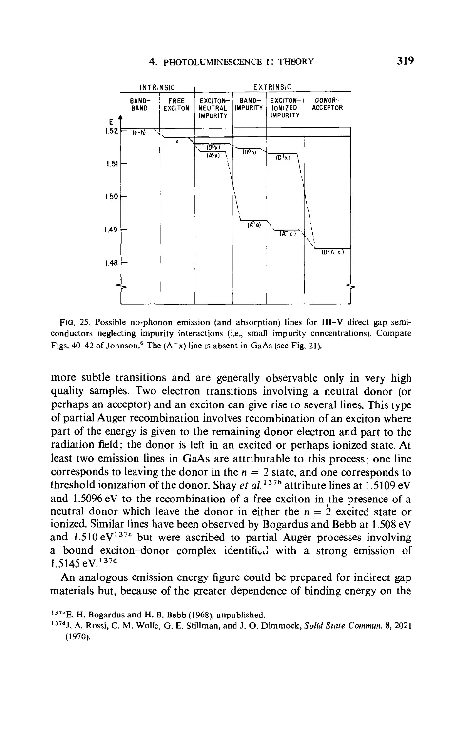
notation as
jt = atJEj + OijiEjHi + <jijlmE}HtHm. (1)
In writing Eq. (1), we have explicitly assumed weak magnetic fields by
retaining only terms to second order in magnetic field.
The coefficients defined in Eq. (1) are elements of a generalized
conductivity tensor. An element of the second rank conductivity tensor
ffy = (Sji/8E})H = 0
describes the current in the absence of a magnetic field. In a cubic system,
this conductivity is a scalar, i.e., 0y = a0^ij where 3^ is the Kronecker delta,
equal to zero when i # j and equal to one otherwise.
An element of the third rank conductivity tensor
Ctjt^dtjJdEjdH,
is associated with the Hall effect. It is also nondirectional in a cubic system,
i.e.,
where R0 is the Hall coefficient in the limit of zero magnetic field and e^-, is
the permutation tensor, defined in the usual manner, ej23 = e231 = e312 = 1,
e2i3 = ei32 = e32i = — 1> with au other components being zero.
The last coefficient, an element of the fourth rank conductivity tensor
Vijto^dW.dEjdHjH*
gives the weak-field magnetoresistance, or more properly, magnetocon-
ductivity. Now, however, the values of <jiJlm depend upon the directions
ijlm even for a cubic system. Even more important, the values are also
dependent on the system of conduction minima present in the material. It is
for this reason that directional magnetoresistance measurements can provide
us with information as to the direction of the minima in k space.
The coefficients in Eq. (1) can be expressed as transport integrals, which
can be solved in a closed form under certain conditions. Abeles and
Meiboom8 and Shibuya9 obtained expressions for the coefficients for the
case of a scalar relaxation time and an arrangement of the minima consisting
of either: (a) 3 or 6 ellipsoids of revolution (my* = m2* # m3*) with major
axes along the [100] directions, or (b) 4 or 8 ellipsoids of revolution with
major axes along the [111] directions. The case of [110] ellipsoids of
revolution was also treated by Shibuya9 and that of [110] ellipsoids with all three
8 B. Abeles and S. Meiboom, Phys. Rev. 95, 31 (1954).
9 M. Shibuya, Phys. Rev. 95, 1385 (1954).
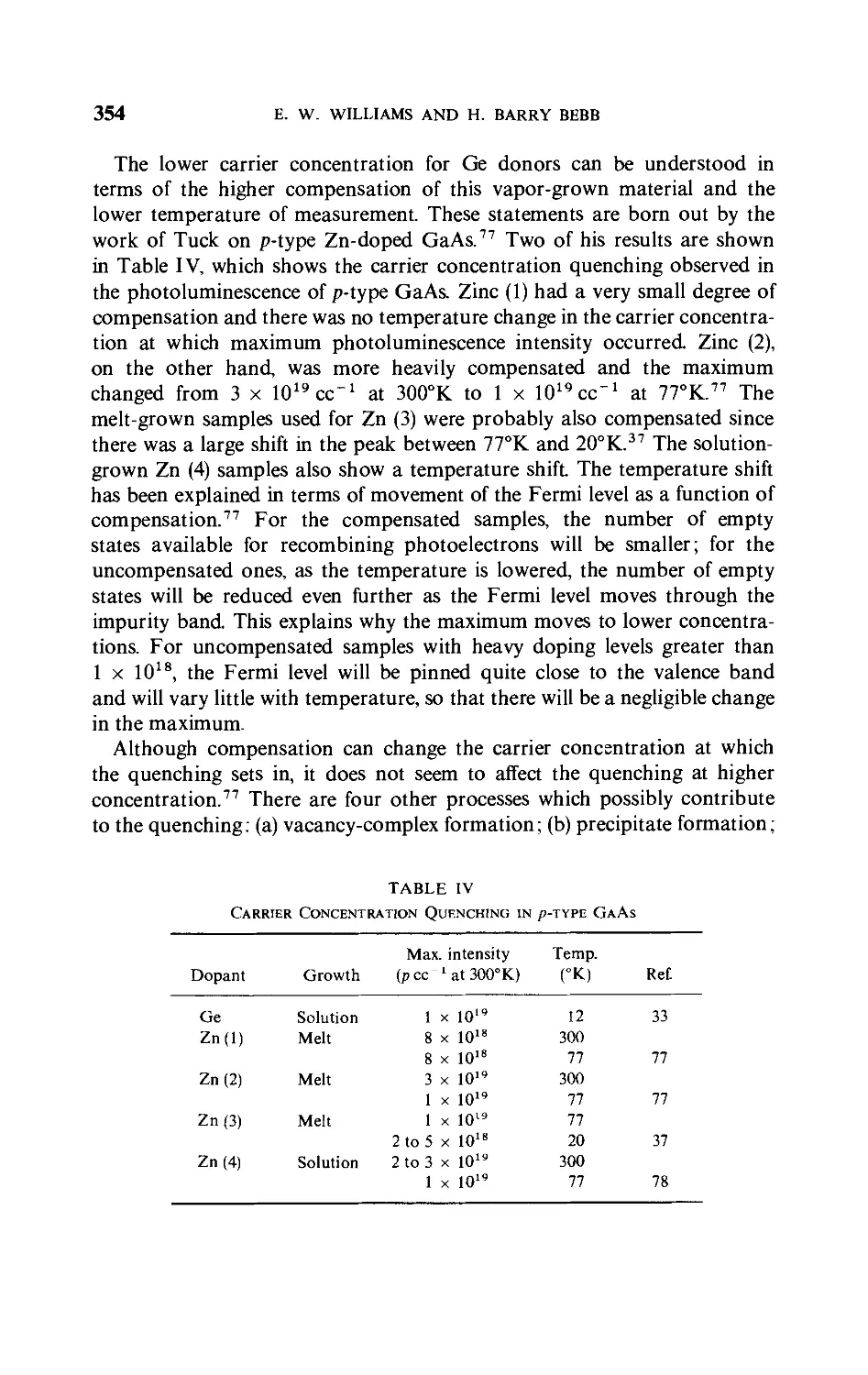
1. BAND STRUCTURE AND GALVANOMAGNETIC EFFECTS 5
effective masses unequal by Allgaier.10 Later, Herring and Vogt11 extended
the results to include an anisotropic relaxation time when x has the same
symmetry as the energy ellipsoids. Their treatment is applicable to scattering
processes which either conserve energy or randomize velocity. These
include intervalley and deformation-potential intravalley scattering, which
are usually the dominant scattering mechanisms in indirect III-V
compounds. The assumption is not good for polar mode, piezoelectric, and
charged center scattering, which in practice, play a minor role.
In the cases where the Herring-Vogt anisotropic-relaxation time
treatment is valid, the transport properties are described by expressions identical
with those for isotropic scattering, except that each component of the
reciprocal effective mass tensor is weighted by. the corresponding relaxation
time component. Thus, the combinations xjm^* = x2/m2* # ^3/^3* always
occur.
A parameter that will describe the anistropy in an ellipsoid of revolution
(valley) is the effective-mass anisotropy parameter K = (»J||*/»>±*)(t±/t||),
where we have chosen the indices such that mf = m2* = m±* and m3* =
»i||. The subscripts || and _L denote directions parallel and perpendicular,
respectively, to the axes of revolution of the ellipsoids. When one sums over
all valleys, the parameter K can be used in the final expressions11 for the
coefficients in Eq. (1), when tjj and xL have the same energy dependence.
These expressions are presented next.
a. Electrical Conductivity
The carrier concentration in the (nondegenerate) rth valley is
«(r) = 2(2nkTlh2fl\mL*2m^)ll2e-E'lkT.
The contribution of the rth valley to the electrical conductivity, in the
principal-axis system of the valley, is given by
oft = h<V«t1>M*)5,j, (2)
where
<t,> = e3/2T,.(e) d/o/de & / e3/2 df0/8ede, (3a)
10 R. S. Allgaier, Phys. Rev. 115, 1185 (1959).
11 C. Herring and E Vogt, Phys. Rev. 101, 944 (1956).
6
RICHARD J. STIRN
f0 being the zero-field Fermi distribution function. The relaxation time is
assumed to have the form
t = r0e5. (3b)
The total contribution is then obtained by summing over all valleys :
(70=i«e2«T||>/m||*)(2X + l), (4)
where n is the total carrier concentration.
The expression for the electron conductivity mobility (at zero magnetic
field) follows immediately from Eq. (4) as
A*o 4««T||>/m||*)(2JK + 1). (5)
b. Hall Effect
As was the case for c0, the Hall constant is independent of direction in a
cubic crystal. The contribution of the rth valley, in the principal-axis system
of the valley, is
4! = -«<r,-%W (6)
J c m*m*
Summing over all axially symmetric valleys yields
e3 <t„2> K(K + 2)
<?tjt = -n L g (7)
c m\ 3
The zero-field Hall mobility is denned as fi0H = R0<?oc, where c is the
velocity of light.12 Then
ffyi = <?o2Ro£iji = ffo(MoH/c)eu(- (8)
It follows from Eqs. (4), (5), (7), and (8) that
r n0 <th>2 (2K+1)2' U
The fundamental quantity r = Rq/R^, = — necK0, in Eq. (9), where Rx is
the Hall constant at infinite magnetic field, is of particular interest.
Averaging over the relaxation time in Eq. (9) by use of Eq. (3) gives
<T||2>/<T||>2 = 37t/8 = 1.18 for acoustical mode scattering (s=-j),
3157i/512 = 1.94 for ionized impurity scattering and electron-hole scattering
(s = |), and 1.00 for neutral impurity scattering (s = 0). For the case of polar
mode scattering, the value of <T||2>/<T||>2 as a function of temperature has
12 When lab units are used, c is replaced by unity. The units of fiH, R0, and rr0 are then
(cm2 V"' sec"'), (cm3 coul"'), and (ohm-cm)"1, respectively.
1. BAND STRUCTURE AND GALVANOMAGNETIC EFFECTS 7
OJ
A
OJ
V
A
ro
1-
V
III
<
1.30
1.25
1.20
1.15
1. 10
1.05
1.00
1
/3
<r
-^^
i
i I l I mi
2>/<r>2
A
in
i i i i 11in i i i 111in i ii
(3—«►»
<r2>/<r>2—M.94
A —»-l.58/
—*"' l8 //
—**1'27 //
-A //
/—<r2>/<r>2 //
i i i 11 in i i ii
ii'ii
If
-
'
-
-
11 ii
1.60
1.50
1.40
- 1.30
-1.20
-1.10
A
I-
A
I-
0.01 0.04 0.1
0.4 1.0
4.0 10
40 100
/3 = 6K //i,
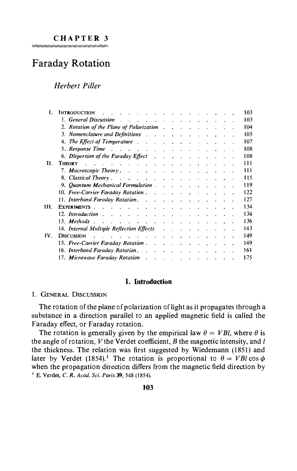
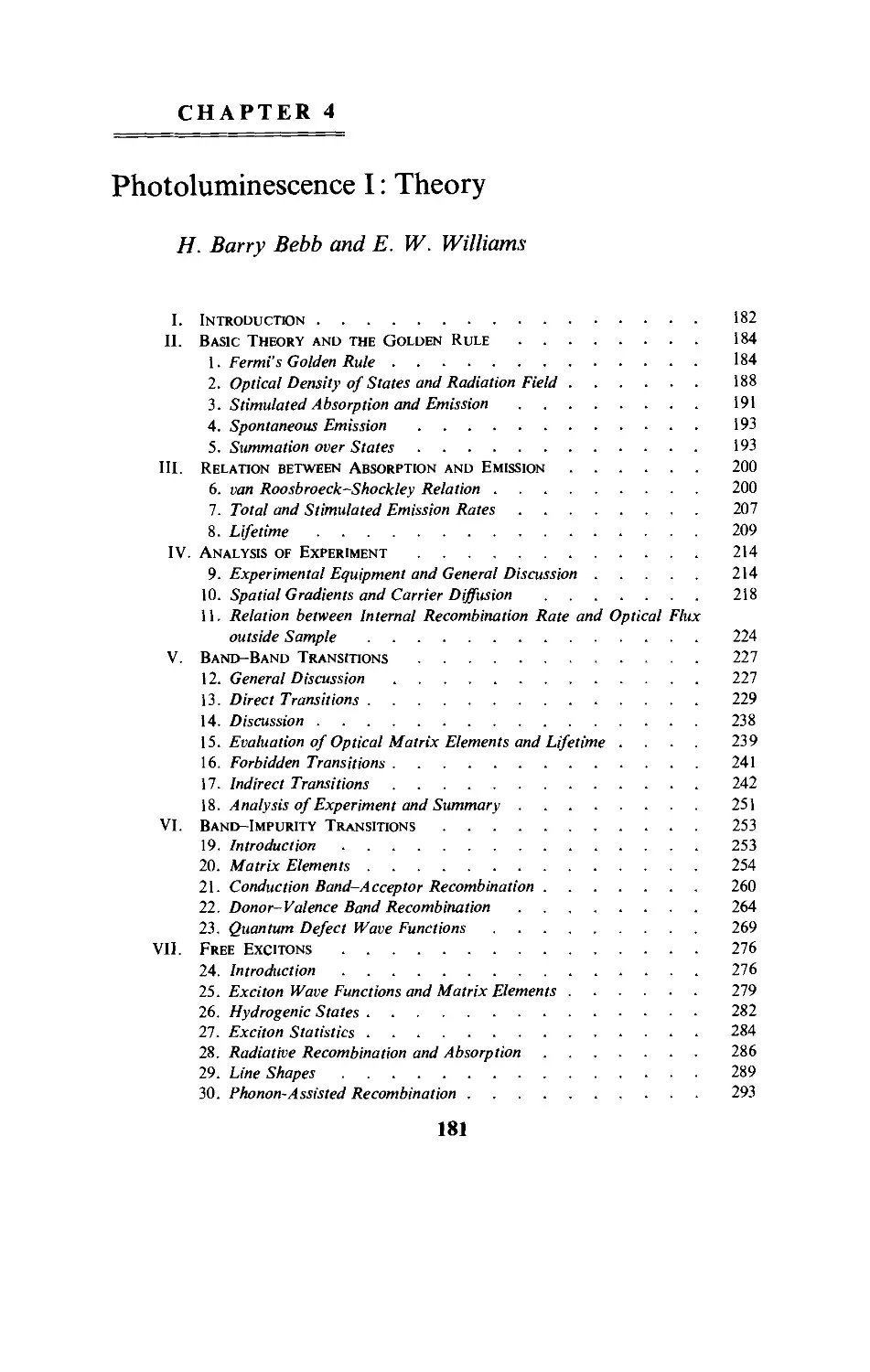
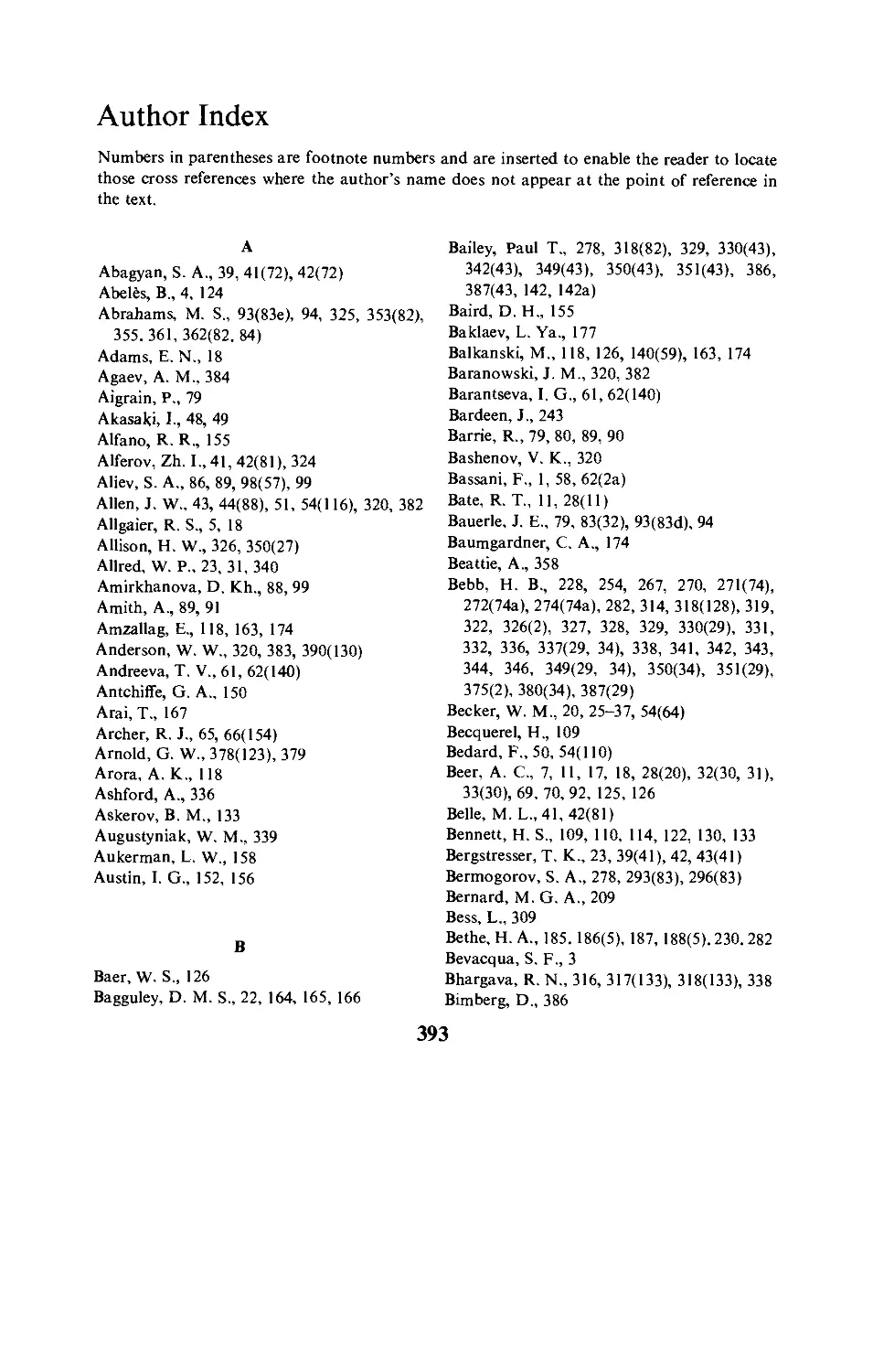
Fig. 1. Relaxation-time averages <t2>/<t>2 and <t3><t>/<t2>2 as a function of the ratio
f! = (>njn\ for admixtures of acoustic phonon and ionized impurity scattering.
been calculated by variational techniques in the weak-field region.13'13a'13b
The value at a given temperature depends upon the characteristic
temperature 9L associated with the longitudinal optical frequency and the amount
of degeneracy, but never becomes greater than about 1.3. Stillman et al.13c
have compared their experimental results for r versus temperature with the
theory 13,13d for the case of polar scattering in GaAs (K = 1).
In actual practice, of course, the true value of <T||2>/<T||>2 will be
determined by a combination of scattering mechanisms. Since the mobility
due to polar scattering is nearly exponential in temperature dependence, it
would be a reasonably good approximation to consider only ionized impurity
and acoustical scattering at temperatures below about 0J2. By adding the
reciprocal relaxation times and dropping the slowly varying logarithmic
factor in the ionized impurity relaxation time, one can obtain a total
relaxation time14
3x/7t m~ x
3/2
P + x2
(10)
13 B. F. Lewis and E. H. Sondheimer, Proc. Roy. Soc. (London) A227, 241 (1955).
13aH. Ehrenreich, J. Phys. Chem. Solids 8, 130 (1959); 9, 129 (1959).
13bD. J. Olechna and H. Ehrenreich, J. Phys. Chem. Solids 23, 1513 (1962).
13cG. E. Stillman, C. M. Wolfe, and J. O. Dimmock, J. Phys. Chem. Solids 31, 1199 (1970).
13dS. S. Devlin, in "Physics and Chemistry of II-VI Compounds" (M. Aven and J. S. Prener, eds.)
p. 561. North-Holland Publ., Amsterdam and Wiley (Interscience), New York, 1967.
14 See, e.g., A. C. Beer, Solid State Phys. Suppl. 4, 145 (1963).
8
RICHARD J. STIRN
where //L is the acoustical lattice mobility, /x, the mobility due to ionized
impurity scattering, x = e/kT, and fi = 6/xL//i, is a measure of the amount of
ionized impurity scattering. The results of calculating <T||2>/<T||>2 as a
function of fi are given in Fig. 1.
Since the contribution of the band structure in Eq. (9) lowers r by 13-21 %
(for K values from 5 to 20) the usual (and sometimes inappropriate)
approximation r = 1 is actually quite reasonable for many-valley semiconductors.
c. Weak Field Magnetoresistance
The contribution of the rth valley to the magnetoconductivity, in the
principal-axis system of the valley, is
<*$« = «<r)(e4/2c4) £ «TiTjTq>/mi*mj*mq*)(eqlJeqim + e,mje,i(). (11)
As was mentioned earlier, the total contribution from all valleys depends
upon the arrangement of valleys in the Brillouin zone. Values for the [100]
and [111] systems have been given by Herring and Vogt11 and are reproduced
in Table I, which is to be used in conjunction with the following expression
obtained by summing over all axially symmetric valleys:
<riJlm = n(e4/c2)«T || 3>/mf )K[g30K2 + g21K + g12]. (12)
The coefficients g30, g21, and g12 are the tabulated quantities given in Table I
for each set of valleys.
TABLE I
Low-Field Magnetoconductivity Components for Cubic Crystals
with Axially Symmetric Valleys Referred to the Crystal Axes '
Type of valleys (direction of k)
Component, referred to
crystal axes'- [100] [111]
tfini = -o0{b + c + d)
"mi = °ob - <t0(MoH/02
<J,2i2 = -2-<70e + 2-<*o(MoH/c)2
° From Herring and Vogt."
b The quantities b, c, and d are defined in Eqs. (16), (20H27).
c Tabulated quantities are the coefficients g30, g21, and g12, respectively,
inEq. (12).
Direct application of Eq. (12) to experiment, i.e., prediction of the
magnitude of the magnetoresistance effect, is usually not feasible because of the
o, o, o'
0,T,0
2 4 2
~9i9i —9
111
9' 9* 9
1 _3_ i
9* 18» 9
1. BAND STRUCTURE AND GALVANOMAGNETIC EFFECTS 9
lack of knowledge about the magnitude and energy dependence of t. This
is particularly true for the III-V compounds, for which a relaxation time is
not even definable in the temperature range where polar scattering is
dominant.13
A phenomenological theory applicable to cubic crystals, which was first
given by Seitz,15 proves to be a very convenient way of analyzing magneto-
resistance. Seitz expressed the current density in an equation that included
second-order terms in magnetic field strength as
j = <70E + a(E X H) + PH2E + y(E • H)H + 3TE, (13)
where Tis a diagonal tensor with elements H^, H22, and H32 (the coordinate
axes 1,2, and 3 being taken along the crystal axes). The coefficient a, which is
related to the Hall constant, and the magnetoresistance coefficients f$, y,
and 3 were given by Seitz in terms of transport integrals. These coefficients
and the zero-field conductivity <j0 are related to the basic conductivity
components of Eq. (1) as follows:
ff0 = ffll, « = Cl23> P = ffll22>
(14)
7 — fl212 + fl221 — 2ff1212> # — Cim — Cll22 ~~ 2ff12i2-
Experimentally the current is kept constant rather than the electric field,
thus the inverted form of the Seitz equation16 is more useful for analysis.
To second order in H,
E = PoU + a(\ X H) + bH2\ + c(j • H)H + dTj], (15)
where
p0 = l/ff0, a = -ap0, b = -(/S + p0oc2)p0,
(16)
c = -(y- p0a2)p0, d=-dp0.
The coefficients b, c, and d are known as the inverted Seitz coefficients. The
magnetoresistance follows immediately from Eq. (15):
M'T = ([p - Pol/PoH2)'^" = (E - EH = 0). j/(EH = 0 • \)H2
= b + c[(j • H)2/j2H2] + dUSHS + j22H22 + j32H32)/j2H2, (17)
which can be rewritten as
M|7 = b + c{Tiri)2 + dYx2r\2, (18)
where i and r\ are the direction cosines of the current and magnetic-field
vectors with respect to the cubic axes. The sub- and super-indices of the
15 F. Seitz, Phys. Rev. 79, 372 (1950).
16 G. L. Pearson and H. Suhl, Phys. Rev. 83, 768 (1951).
10
RICHARD J. STIRN
magnetoresistance coefficient, M, indicate the directions of the current and
magnetic-field vectors, respectively. In the case of isotropic materials
(K = 1),
b + c = 0, d = 0. (19)
In the case of many-valley semiconductors, expressions for b, c, and d
can be obtained by manipulating Eqs. (4), (5), (9), (12) and using the
information given in Table I. These expressions are dependent only upon the
anisotropy parameter K, the zero-field Hall mobility n0H, and the dimension-
less quantity
A EE <T3><T>/<T2>2.17
The results are12 :
System of[ 100]-type spheroids11*
b = (n0H/c)2{A[(K2 + K+ l)(2K + l)/K(K + 2)2] - 1}, (20)
c = -(fi0H/c)2{A{3(2K + 1)/(K + 2)2] - 1}, (21)
d = -(fi0"/c)2{A[(K - l)2(2K + l)/K(K + 2)2]}, (22)
b + c= -d, d <0. (23)
System of [11 l]-type spheroids11*
b = (ii0"lc)2{A[(2K + l)2/3K(K + 2)] - 1}, (24)
c = -{ii0"lc)2{A[(2K + 1)2/3K(K + 2)] - 1}, (25)
d = (Li0H/c)2{A[2(K - l)2(2K + l)/3K(K + 2)2]}, (26)
b + c = 0, d>0. (27)
The symmetry relations Eqs. (19), (23), and (27) are independent of the
particular form of the relaxation time.
Values of the inverted Seitz coefficients can be obtained experimentally
by a minimum of three magnetoresistance measurements with the current
and magnetic field along certain high-symmetry directions. From Eq. (18), it
17 We may replace rn with t in the quantity A, if we maintain the assumption that both tn and tL
have the same energy dependence.
I7aNote that the Seitz coefficient c is not to be confused with the speed of light c. The latter
occurs in the ratio (/*0H/c).
1. BAND STRUCTURE AND GALVANOMAGNETIC EFFECTS 11
follows that
Mj}° = b + d/2, M??1 = M%°0 = b,
MWo = MfJ? = b + d/3, M\\l = b + d/6,
(28)
M112 = M110 = b + c + d/2, M100 = b + c + d,
Mm = b + c + d/3.
The absence of a superscript implies that the current and magnetic field
are collinear. The longitudinal magnetoresistance vanishes when the
magnetic field is along the cubic axes of a crystal having [100]-type minima.
The longitudinal effect is a maximum when the field is along a < 111> direction
for the [100] system of spheroids, and when the field is in a <100> direction
for the [111] system.
The values of b, c, and d enable one to determine the anisotropy of a valley,
in addition to identifying the system of valleys by use of the symmetry
relations. The energy dependence of the relaxation time, i.e., A, can be
eliminated from Eqs. (20H22) or Eqs. (24)-{26) by solving two of the
equations from each set simultaneously. A convenient parameter to use,
which requires only two transverse measurements, is q = [b + (fi0H/c)2]/d.
We then obtain
q100 = 1 + 3K/(K - l)2 [100 valleys], (29)
(K±).oo = Uq ~ 1)"1[(2« + 1) ± (I2q - 3)1'2], (30)
and
4m = 1 + 9K/2(K - l)2 [111 valleys], (31)
(K±)m = & - l)^[(4q + 5) ± 3(Sq + l)1'2]. (32)
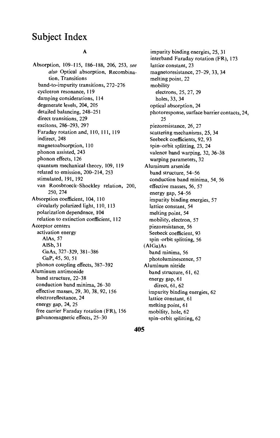
The parameter q is plotted in Fig. 2 for both systems as a function of
K+ and K_, where K+(>1) corresponds to the value of the effective
mass-relaxation-time anisotropy for prolate spheroids (m^ > m±) and
K_(<1) is the value for oblate spheroids (m^ < mj. It is interesting to
note that the value of K+ is relatively insensitive to errors in b, d or the
Hall mobility for the case of semiconductors with low anisotropy (K < 5).
However, when the anisotropy is high, careful measurements and the
elimination of spurious magnetoresistance effects due to contact shorting18'19
and the presence of various types of inhomogeneities20'20a are required in
order to obtain a reasonable certainty in the value of K+ .
18 J. R. Drabble and R. Wolfe, J. Electron. Control 3, 259 (1957).
19 R. F. Broom, Proc. Phys- Soc. (London) 71, 500 (1958).
20 A. C. Beer,14 p. 308.
20aR. T. Bate, in "Semiconductors and Semimetals" (R. K. Willardson and A. C. Beer, eds.),
Vol. 4, p. 459. Academic Press, New York, 1968.
12
RICHARD J. STIRN
q=[b+U»2]/MI
Fig. 2. Anisotropy parameters K+ and K. versus q.
The choice between the prolate and oblate spheroidal model rests upon
the magnitude of A, which can now be calculated by substituting the value
of K + or K _ into any one of the equations for b, c, or d for the appropriate
system of valleys. The parameter A cannot be less than 1, since <t3><t> is
greater than or equal to <t2>2 by Schwarz's inequality. Values of A are
given in Fig. 1 for a range of admixtures of acoustic phonon and ionized
impurity scattering.
d. Effective Masses
Because of interaction between the electron and the crystal lattice, the
electron effective mass m* is different from the free-electron mass m0. In
addition, when the energy surfaces are ellipsoids of revolution, the effective
mass of the electron varies, depending upon its position in momentum
space. In general,
(m*-% = (\lh1)d1E(k)ldkidkJ
(33)
if there is no degeneracy.
1. BAND STRUCTURE AND GALVANOMAGNETIC EFFECTS 13
The coordinate system is usually chosen so that the reciprocal mass tensor
of Eq. (33) is reduced to principal axes. In this system, the quadratic
relationship between energy and wave number becomes
e(k) = M*!2/"!!* + fe22A"2* + k32/m3*], (34)
where we have chosen the energy zero to be at the minimum.
Because of differences in the method of averaging the mass components,
it is important to distinguish between several types of effective masses in
the case of multi-ellipsoidal bands. Thus, by comparing Eq. (4) with the
usual expression for the zero-field conductivity, a0 = ne2-c/m0, a
conductivity effective mass m* is defined as
(m,*)"1 = ftl/mS + l/m2* + l/m3*) = (2K + l)/3mn*. (35)
This mass is used in relationships concerning infrared reflectivity and free
carrier absorption, for example.
It is conceptually useful to define a parameter which is a measure of the
density of states available in a given energy range irrespective of the shape
of the energy surface. The density of states is proportional to the volume of
phase space, so that if we replace the volume of the sphere of radius k/(2m*)112
used for spherical energy bands with the corresponding volume of an
ellipsoid with semimajor axes dk1/(2m1)112, dk2/{2m2)112, and dk3/(2m3)112, the
final calculation will include a density-of-states effective mass md, where for
each valley
md = (m1 m2 m3)1/3. (36)
If v is the total number of equivalent valleys, then the expression for the total
carrier density will be of the form
n x v(m1 m2 m3)112 x md*3/2,
where md* here refers to all of the equivalent valleys. The density-of-states
effective mass for the multivalley system is then given by
m* = v2/3(mi m2 m3)1/3 = v2/3K1/3mx* (36a)
This mass is applicable to thermoelectric-power theory and is required when
relating the carrier concentration to the Fermi level.
An additional type of effective mass is one that appears in high-frequency
Faraday rotation theory for many-valley semiconductors.21 If the amount of
rotation per unit length per unit magnetic field is expressed using the zero-
field Hall coefficient rather than the free-carrier concentration, a Faraday
effective mass can be defined as
mF* = (2K + l)m1*/(K + 2). (37)
21 M. J. Stephen and A. B. Lidiard, J. Phys. Chem. Solids9, 43 (1958).
14
RICHARD J. STIRN
A reliable determination of any two of these three effective masses would
uniquely give the two mass components m^* and mL*. Alternatively, a value
of just one of the effective masses would be sufficient if the anisotropy K can
be determined from cyclotron resonance or magnetoresistance
measurements. Requirements of crystal purity are less stringent for the latter type of
measurement. However, an additional uncertainty in the value of K is
introduced by anisotropy of the relaxation time.
2. Valence Band
In presenting the effect of conduction-band structure on galvanomagnetic
phenomena, we had need only to consider single-band conduction for the
compounds of interest here. This is because of their large band gaps(> 1.6 eV)
and the fact that higher-lying bands appear to be at least 0.30 eV above the
[100] minima (Part III). However, in p-type material, the presence of multi-
band conduction greatly affects galvanomagnetic phenomena, complicating
the interpretation of experimental data. This multiband conduction occurs
in the II I-V compounds, as it does in germanium and silicon, because of the
presence of two bands degenerate (excluding spin) at k = 01, having very
different curvature: V2-band (heavy holes) and F3-band (light holes).22'23
In addition, there is a third band lying lower in energy, split off from the other
two because of spin-orbit interaction. In the III-V compounds, however,
the split-off band is thought to be far enough removed in energy so that its
contribution to the conductivity is negligible.
An additional factor that makes the interpretation of galvanomagnetic
properties for p-type material much more complicated than for n-type
material is the fact that the bands V2 and V3 are warped from spherical
symmetry for some distance away from the zone center.23 It is for this reason
that closed expressions for the galvanomagnetic coefficients ain and oijlm
are not possible, unlike the case for minima of spheroidal symmetry. Instead,
the expressions must include the anisotropy in the form of a rapidly
converging infinite series.
For degenerate valence bands, the carrier energy dependence on the
wave vector k was first given by Dresselhaus et al.23 for germanium and
silicon by the function
e(k) = -(h2/2m0){Ak2 ± [B2kA + C2{k2k2 + k2k2 + k2kx2)f12}, (38)
for a k-coordinate system along the cube axes. A, B, arid C are warping
parameters which determine the curvature and deviation from sphericity of
the energy bands away from k = 0. This expression is applicable to III-V
22 F. Herman and J. Callaway, Phys. Rev. 89, 518 (1953).
23 G. Dresselhaus, A. Kip, and C. Kittel, Phys. Rev. 95, 368 (1954).
1. BAND STRUCTURE AND GALVANOMAGNETIC EFFECTS 15
compounds if we neglect the very small effect of the linear terms in k near the
zone center, which is due to the lack of inversion symmetry.2
Lax and Mavroides have described a method for carrying out calculations
which deal with problems related to the hole densities, conductivities,
effective masses, and Hall coefficients,24 as well as magnetoconductivities.2 5
The calculations are valid for weak magnetic fields and assume an isotropic
relaxation time. The key to these calculations was the rewriting of Eq. (38)
so that the expressions under the radical were expanded in powers of an
anisotropy term, in such a way that the series converged rapidly for typical
degrees of warping. Thus
e(k) = -(h2k2/2m0)(A + B'){1 - T[(kx2k2 + k2k2 + kz2kx)/k4] + •••},
(39)
where
T = + C2/[2B'(A + B')], (40)
B' = (B2 + C2/6)1/2. (41)
The upper sign in Eqs. (38H40) and in forthcoming expressions is associated
with the holes of smaller effective mass. Equations (38) and (39) reduce to
the usual quadratic dependence of energy upon k when the amount of
warping becomes vanishingly small (C -> 0). In this case, the effective masses are
given by m* = (A ± B)~ 1m0.
The wave-vector dependence in Eq. (39) was then represented in spherical
coordinates,24 after which integrations could be performed. The resulting
expressions for the hole density, conductivity, Hall coefficient, and magneto-
conductivity coefficients, which are presented in the following subsections
should be applicable to all of the III—V compounds.
a. Electrical Conductivity and Hole Density
The number of holes per unit volume is given by
Pn = Aa6)n, (42)
for a Maxwellian distribution, where
ps = 2[2nm0kT/h2{A ± B')fl2e^-E")lkT (43)
is the carrier concentration for a spherical energy surface, k is the Boltzmann
constant, and £v is the valence-band energy at k = 0. The anisotropy part is
{ad)„ = 1 + 0.05r„ + 0.01635r„2 + 0.000908 r„3 + • • •, (44)
where n = 2, 3 denotes the heavy- and light-hole bands, respectively.
24 B. Lax and J. G. Mavroides, Phys. Rev. 100, 1650 (1955).
25 J. G. Mavroides and B. Lax, Phys. Rev. 107, 1530 (1957); 108, 1648 (1957).
16
RICHARD J. STIRN
The ratio of light- to heavy-hole carrier concentration is then given by
PzlPi = ([A - B']/[A + B'])3l2(ad)3/(ad)2. (45)
The electrical conductivity in either band can be written as
on = Pse2KA + B'ymoXxya,, 6i}, (46)
= f\e\li0salldij, (47)
where
an = 1 + 0.01667r + 0.041369r2 + 0.00090679r3
+ 0.00091959r4 + 0.00002106r5 + • • •, (48)
and the zero-field conductivity mobility for a spherical energy band is
Ho' = kl<T>(^4 ± B')/m0 {B -» B). (49)
From Eqs. (43) and (47), it is seen that the ratio of the zero-field conductivity
mobility in a warped band, n0, to that in a spherical band is
/*o//V = «n/«d- (50)
The total conductivity c0, which is isotropic, is simply the sum of the
individual conductivities:
<?o = \e\[{psti0sa11}2 + {pWuhL (51)
Thus, the total drift mobility, n0, is
Mo = [(/*o)2 + Ps/PiMsVll + P3/P2], (52)
if we neglect the anisotropy parameters a11 and a6.
A useful quantity is the light- to heavy-hole lattice mobility ratio since it is
a measure of the effect of light holes on galvanomagnetic phenomena. This
ratio can be written as
A4.3/A4.2 = 04 + B')/(A - B'), (53)
if the relaxation times of both holes are equal. The scattering rate of a carrier
is proportional to the density of final states. If the scattering of the light hole
is predominantly interband, as it is in Ge,26 then the assumption of equal
relaxation times should hold since the final state would be the same for both
the light and heavy holes, namely, the heavy-hole band.
26 See, e.g., H. Brooks, Advan. Electron. Electron Phys. 7, 152 (1955).
1. BAND STRUCTURE AND GALVANOMAGNETIC EFFECTS 17
b. Hall Coefficient
The coefficient for the Hall term in Eq. (1) for warped degenerate bands
has been given by Lax and Mavroides24 and can be written for either band as
ffy« = (psk3|/m02c)<T2>(^ + B')2a12etjl, (54)
= p^eWin^/cfr^j,, (55)
where
a12 = 1 - 0.01667r + 0.0l7956r2
(56)
-0.0069857r3 + 0.0012610r4 + •••
and /i"'s is the Hall mobility at zero-magnetic field for a spherical energy
surface.
The weak-field limit of the Hall coefficient, R0, is obtained by summing
the contributions from each band:
#o = \e\[{fLios(»"-s/c)a12}2 + {fn0s($-s/c)a12}3]/<j02. (57)
The addition of low-mass, high-mobility holes greatly influences the
weak-field Hall coefficient even though such holes are present in relatively
small amounts. Since the mobility weighting factor enters as the square, the
Hall coefficient is increased by a factor of almost 2 in the III—V compounds.27
An expression analogous to Eq. (9), which explicitly gives the effect of
band structure and scattering on R0 can also be derived from Eqs. (8), (43),
(46), and (53). The result for one band is
r = R0/Rx = fi0"/fi0 = «T2>/<T>2)(adtf ^A*2!) - (58)
From this we see that the ratio of zero-field Hall mobility in a warped band
to that in a spherical band is
A*oW = «i2/«n. (59)
The infinite-field Hall coefficient, Rx, is simply given by
Rao = V\e\c{p2 + p3). (60)
At intermediate field strengths, the Hall coefficient is found to be a
complicated function of the magnetic field strength in p-type materials that have
the Ge-like valence-band structure. This occurs at temperatures where
27 The actual increase is also dependent on the warping of the bands and on the scattering
mechanisms involved. See Beer and Willardson30 Eq. (22), in the limit of vanishing magnetic
field.
18
RICHARD J. STIRN
cocx = \e\Hx/m*c > 1 for one or both carriers. In such a case, a series solution
of the Boltzmann equation in powers of H is no longer possible. Instead,
McClure28 has introduced the field dependence by a representation
involving Fourier series expansions in harmonics of the frequency of the carrier
around the hodograph determined by the intersection of a surface of constant
energy in k space with a plane normal to the magnetic field. Closed
expressions for the components of the conductivity tensor are impossible except
for limiting cases—for example, when the energy surfaces are spheres or
polyhedra.28a Goldberg et al.29 have attempted to account for the field
dependence of the Hall coefficient and resistivity in p-Ge by this technique,
assuming a spherical light-hole surface, and a cubic heavy-hole surface, but
without complete success.
Excellent agreement with experiment was obtained by Beer and Willard-
son30'31 for Ge when the warped nature of the energy bands and scattering
by acoustical phonons and ionized impurities were taken into account. The
final equations are rather cumbersome and will not be presented here.
c. Weak-Field Magnetoresistance
The weak-field magnetoconductivity coefficients in Eq. (1) for warped
degenerate bands were derived by Mavroides and Lax25 with techniques
similar to those used to obtain the conductivity and Hall coefficient. From
symmetry considerations it can be shown that there may be a maximum of
four different nonvanishing components for any cubic crystal.9 In practice,
however, two of them, axyyx and axyxy, always occur in pairs, so that
measurements are determined by at most three independent components. These
can be expressed for each band as:
ffLcx = -(pse>03c2)<T3>(,4 ± B')3^(D, (61)
clxyy = -(p?eVm03c2Kt3)(A ± B')3axxyy, (62)
0 _ 0
®xyyx vXyxy
= (pseVm03c2Kx3}(A ± B')3[KW + \®(T)], (63)
where the anisotropy parameters are given by
axxyy = 1 - 0.2214r + 0.3838r2 - 0.0167r3
+ 0.00755r4 + 0.00066ir5 - 0.000190r6 • • •, (64)
28 J. W. McClure, Phys. Rev. 101, 1642 (1956).
28aR. S. Allgaier, Phys. Rev. 158, 699 (1967); 165, 775 (1968).
29 C. Goldberg, E. N. Adams, and R. E. Davis, Phys. Rev. 105, 865 (1957).
30 A. C Beer and R. K. Willardson, Phys. Rev. 110, 1286 (1958).
31 For additional detail, see Beer14 pp. 189-212.
1. BAND STRUCTURE AND GALVANOMAGNETIC EFFECTS 19
a*yxy = 1 - 0.0500r - 0.0469r2 + 0.0040r3
- 0.00063r4 + 0.000114r5 + 0.000004r6 + • • •, (65)
£(D = (16/1155)r2(l - 0.4295r + 0.0188r2 + 0.0103r3
+ 0.00249r4 + 0.000474r5 + 0.000085r6 + •••)• (66)
It can be assumed that the total magnetoconductivity can be given by
coefficients £°-,m, which represent the sum of the individual <jf]lm coefficients
for the two kinds of holes present.
The weak-field magnetoconductivity is extremely sensitive to the addition
of high-mobility holes since the mobility weighting factor enters as the cube.
Thus, the magnetoresistance coefficients are strongly field dependent and
it is imperative that these be measured in the zero-field limit at all
temperatures.
Expressions for the directional weak-field magnetoresistance coefficients,
Mjjjt", can be written as relations involving the magnetoconductivity
coefficients. The results are25
M100 = (Ap/p0H2)l00 = -(1/<j0)X°xxxx, (67)
Ml% = -(IWS,,, - (KJ°o)2, (68)
A^UO = — (2°o)l?xxxx + ^xxw + Piwi + ^xw)]' (69)
M110 = -{jGol&xxxx + Sxxw> - (^wx + Sx,.x>>)] - C^xyz/^o)2 ■ (70)
The term (E,xyJtj0) is the zero-field Hall mobility, n0H = R0<?0 for both
bands, when c0 is given by Eq. (51).
As was the case for n-type materials earlier, it is convenient to analyze the
anisotropy in the magnetoresistance phenomenologically by use of the
inverse Seitz coefficients. The magnetoconductivity coefficients can be
expressed as functions of b, c, and d by combining Eqs. (67H70) with Eq. (18):
Z°Xxxx= ~(b + c + d)a0, (71)
Z»w= -[H(I>0)2]5o, (72)
yO _ yO
^xyyx ^xyxy
= -Kc-(£2,>o)2>o. (73)
From these relations and Eqs. (55H57), expressions for the inverse Seitz
coefficients can now be written. Additional expressions can be obtained
which contain only parameters of the energy bands and the energy
20
RICHARD J. STIRN
dependence of the relaxation times, by forming the following ratios32
b + (MoH)2
d
b + c
(74)
(75)
b + (n0
where
b + (/i0H)2 =(A- B')3/2(axxw)2<T3>2/<T3>3 + (A + Bf'2(axxyy)3,
d = (A- B')V\\® - axxyy + axw)2<T3>2/<T3>3
+ (A + Bf'2(l@ - axxyy + axyxy)3,
b + c=(A- B'fl\axxyy - axyxy - ^)2<t3>2/<t3>3
+ {A + B'fl\axxyy - axyxy - &)3.
Similar ratios can be formed using the Sy(m coefficients.32 Note that in the
limit of spherical bands (r„ -> 0), (b + c) and d -> 0 as expected.
Unfortunately, knowledge of these ratios or of the values of b, c, and d
does not enable one to determine the band anisotropy as is possible with
many-valleyed semiconductors, even with the assumption of only heavy-hole
conduction. In principle, one should be able to obtain the warping
parameters by determining A and B' independently, and then choosing a value for
C (and thus T) which yields the measured values of the anisotropy ratios in
Eqs. (74) and (75). The parameters A and B' can be obtained from Eq. (45)
(neglecting the small correction for anisotropy) and the expressions m* =
(A ± B')~ lm0 if any two of the three quantities p3/p2, m2, and m3 are known.
The carrier concentration ratio can be roughly determined by analyzing
the magnetic-field dependence of the magnetoresistance.32'33 However,
uncertainty in the value of <t3>2/<t3>3 at a given temperature and carrier
concentration is too great to make this approach practical. Also, anisotropy
in the scattering cannot be separated from the band anisotropy. To the
author's knowledge, theoretical studies of scattering anisotropy are
nonexistent for the case of warped energy bands. It has been shown34 that the
scattering anisotropy is greater for ionized impurity scattering than it is for
intravalley lattice scattering, at least for electrons in silicon. Hence, it may
not be unreasonable to assume isotropic relaxation times for the heavy and
light holes at temperatures and carrier concentrations where ionized impurity
32 R. J. Stirn and W. M. Becker, Phys. Rev. 148, 907 (1966).
33 C. H. Champness, Phys. Rev. Lett. 1, 439 (1958).
34 D. Long and J. Myers, Phys. Rev. 120, 39 (1960).
1. BAND STRUCTURE AND GALVANOMAGNETIC EFFECTS 21
scattering is expected to be unimportant. In this case, the ratios (b + c)/
[b + (At0H)2] and [b + (^oH)2W should be temperature independent over a
range of temperature small enough that changes in the band shape should
not occur. If theoretical values of the warping parameters A, B, and C2 are
available from Kane-band calculations,35,36 the predicted values of the ratios
in Eqs. (74) and (75) can be compared with experiment. Conversely, if reliable
values of A, B, and C2 are available from cyclotron resonance experiments,
information about the relative values of t2 and t3 as a function of temperature
can be obtained, with the assumption that the energy dependence of both
relaxation times are the same.
Up to this point, we have ignored the possible effects of nonparabolicity
of the light-hole band. This would introduce a temperature dependence (as
the distribution spreads in k space) into the galvanomagnetic properties as
the ratio of light to heavy holes rises. The effects would be insignificant at
temperatures much below room temperature. Even at higher temperatures,
the presence of optical-phonon scattering would minimize any alteration
of the predicted properties due to nonparabolicity because the contribution
of the higher energy holes to the conductivity is decreased. Any attempt to
incorporate this effect into the previous discussion is beyond the scope of
this chapter.
d. Effective Masses
As we have already noted, holes in the III—V compounds are normally
located at the center of the Brillouin zone in a pair of bands which are
degenerate near the point k = 0. Since the constant energy surfaces are
warped spheres, the masses are not scalar and the specific value to be used
in the simple equations describing the electrical properties depends on the
particular property being considered. One example is the density-of-states
effective mass md which has been denned by Lax and Mavroides from Eqs.
(42) and (43) and given to be24
mdn = [m0/{A ± F)][l + 0.03333r„ + 0.01057 Y2 - 0.00018r„3
-0.00003r„4+ •••]. (76)
Since the total carrier concentration is p = p2 + p3,
B,3/2=B,3/2+m3/2> (77)
or
md*md2{l-f[md3/md2]3/2}. (78)
35 O. E. Kane, /. Phys. Chem. Solids 1, 82 (1956); in "Semiconductors and Semimetals" (R. K.
Willardson and A. C. Beer, eds.), Vol. 1, Chapter 3. Academic Press, New York, 1966.
36 M. Cardona, J. Phys. Chem. Solids 24, 1543 (1963).
22
RICHARD J. STIRN
Another "type" of effective mass is the conductivity effective mass denned
from the relation
a = pe2(T)/mc. (78a)
For the warped band, it has been calculated to be24
™m = [m0/(A ± B')] [1 + 0.03333r„ - 0.01057r„2 - 0.00095r„3
+ 0.0011ir„4 + •••]■ (79)
Referring to Eq. (52), we have
1 _ 1
mc p
Pi
m,7
Pi
(80)
if we assume equal relaxation times for both holes.
From Eqs. (77) and (80), we obtain
mc = mc2
m.
1
m,
3/2
d3
m,
a
m.
3/2
m;
m;
3/2
™c3.
m.
1 +
m,
.3/2"
d3
ml?
a
- 1
m.
c3
(81)
The amount of valence-band warping (and hence the value of T) has been
found to be relatively small in Ge,23 Si,23 InSb,37 and GaSb.38 Theoretical
calculations predict a similar situation in the other III—V compounds.36
Hence differences in the effective masses mc and md are very small.
Actually, the linear terms in the energy of the heavy holes are of importance,
as well as the effect of higher lying bands on the light-hole mass. Because of
these effects, the effective masses have a dependence on temperature and the
Fermi-level position. This has led to some confusion about the interpretation
of experimental results in p-InSb, for instance. The reader is referred to the
reference of Kolodziejczak et al.39 for theoretical calculations of the effective
masses in III—V compounds and the influence of the aforementioned effects
on them.
III. Experimental Results
3. Aluminum Antimonide
a. Band Structure
Aluminum antimonide (AlSb) is a high-energy-gap intermetallic
compound semiconductor with a melting point of 1060°C. It crystallizes into a
37 D. M. S. Bagguley, M. L. A. Robinson, and R. A. Stradling, Phys. Lett. 6, 143 (1963).
38 R. A. Stradling, Phys. Lett. 20, 217 (1966).
39 J. Kolodziejczak, S. Zukotyriski, and H. Stramska, Phys. Status Solidi 14, 471 (1966).
1. BAND STRUCTURE AND GALVANOMAGNETIC EFFECTS 23
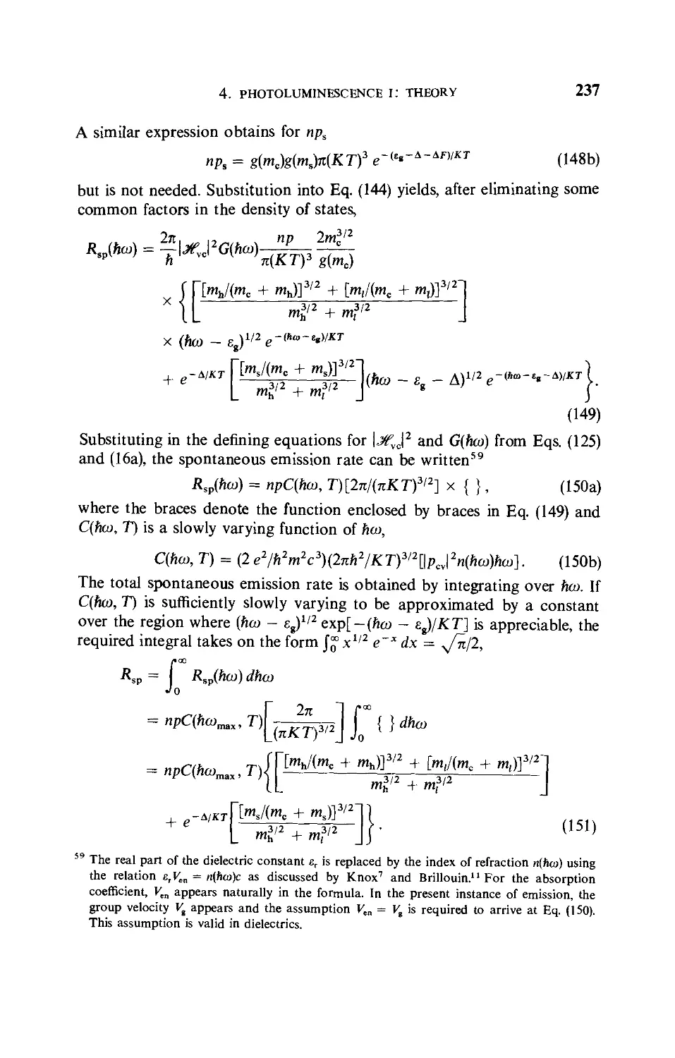
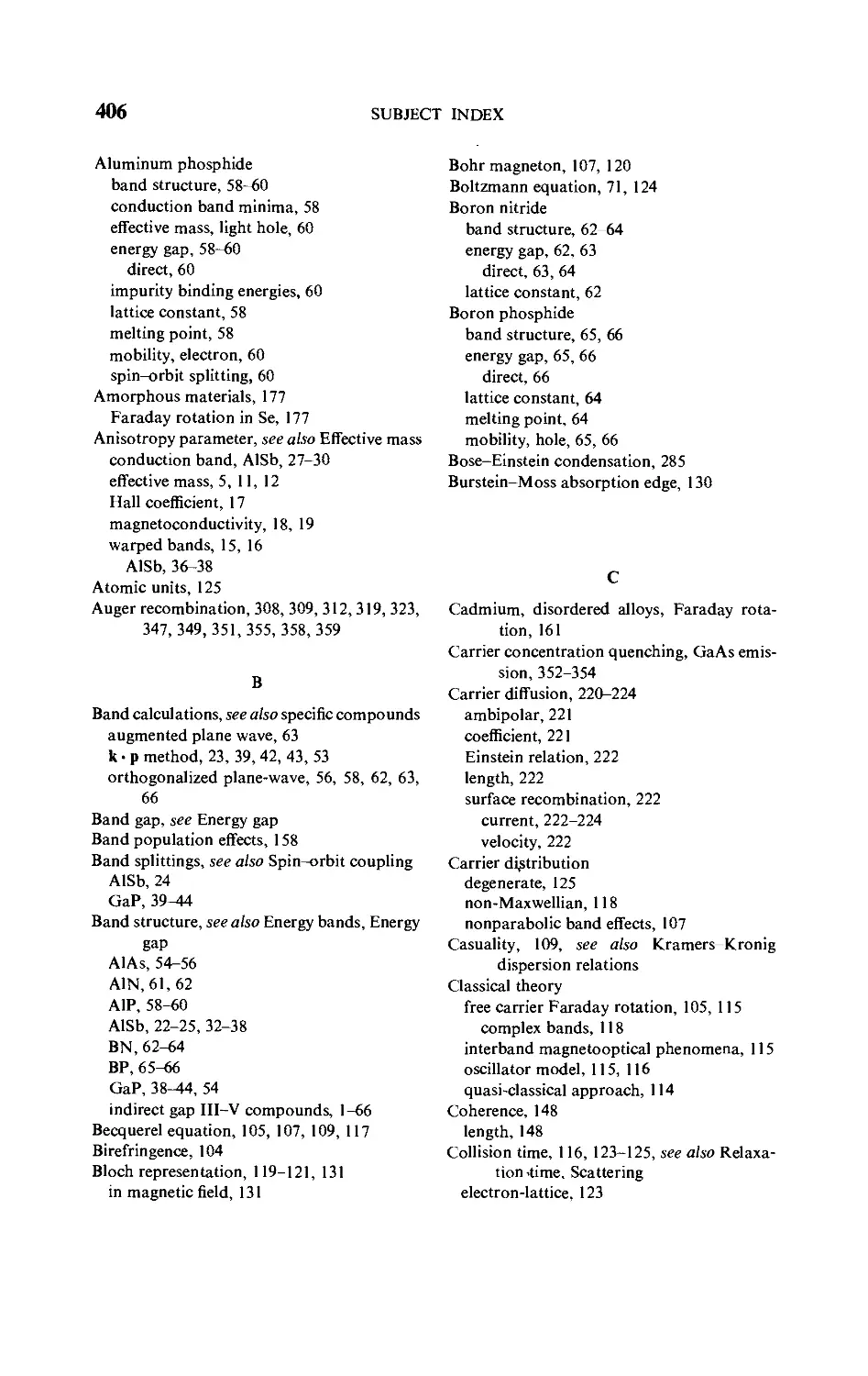
k= -ir/a (III) k=(000) k=2Wa(IOO)
Fig. 3. Energy bands of AlSb, including spin-orbit splitting, in the [100] and [111] directions.
(After Pollak et al.*2)
cubic zinc-blende structure with a lattice constant of 6.14 A. The preparation
and growth of AlSb crystals, which are unstable in the presence of moist
air, have been reviewed by Allred.40
Calculations of the band structure for AlSb throughout the reduced
zone have recently been made using the pseudopotential method41 and the
k • p method.42 Both methods are empirical in nature inasmuch as
experimental values of some interband transitions are required.
In the k • p method, 6 independent matrix elements of an antisymmetrical
potential are added to the k ■ p Hamiltonian of the isoelectronic group IV
element. The antisymmetric potential comes about because of the two
dissimilar atoms in the unit cell. The group IV "element" chosen was the
hypothetical IV-IV compound Si-a-Sn, since the lattice constant of AlSb
is about midway between that of Si and a-Sn.
The results of the k • p band calculations for AlSb are shown in Fig. 3.
Values for the transitions indicated in the figure have been given by Cardona
et al.,4'3A4' and are reproduced in Table II. These values were obtained from
40 W. P. Allred, in Willardson and Goering,7 p. 187.
41 M. L. Cohen and T. K. Bergstresser, Phys. Rev. 141, 789 (1966).
42 F. H. Pollak, C. W. Higginbotham, and M. Cardona, J. Phys. Soc. Japan 21, Suppl. (Proc. Int.
Conf. Phys. Semiconduct., Kyoto, 1966) p. 20.
43 M. Cardona, F. H. Pollak, and K. L. Shaklee, Phys. Rev. Lett. 16, 644 (1966).
44 M. Cardona, K. L. Shaklee, and F. H. Pollak, Phys. Rev. 154, 696 (1967).
24
RICHARD J. STIRN
TABLE II
Energy Splittings for AlSb (300°K)
Transition
E0
£1
Eo'
E2
Energy (eV)
2.22
2.86
3.72
4.25
Transition
Ao
A,
A„'
6
Energy (eV)
0.75
0.40
0.27
0.36
electroreflectance measurements,45'46 which give more resolution than
ordinary reflectivity measurements.46"
The value of the minimum energy gap £g was first determined from optical
absorption data by Blunt et al.*1 who reported a value for £g of (1.63—
3.5 x 10"4T)eV. These authors also obtained a 0°K value of 1.60eV
from a linear extrapolation of the intrinsic resistivity (above 750°C) as a
function of temperature. Turner and Reese48 obtained a similar temperature
coefficient from their optical absorption measurements, but their value for
£g was 0.1 eV higher. Blunt et al.*7 detected an absorption band at 0.75 eV
(1.6 n) in p-type material, which was observed and correctly interpreted by
Braunstein49 as due to transitions between the split-off valence band and
the uppermost valence band (A0).
An absorption band present at about A\i (0.3 eV) in n-type material47
was thought by Blunt et al. to be caused by a deep donor level, while Turner
and Reese48 attributed it to transitions from the lowest-lying conduction-
band minima to a higher band at k = 0. Paul50 ruled out indirect transitions
as the explanation for the 4 \i band on the basis of pressure measurements on
an analogous band occurring at 3 \i in GaP. It is now believed43,51 that this
infrared peak is due to Xx-X3 transitions (S).
The presence of higher-lying conduction minima can be detected under
some circumstances by measuring the photoresponse of surface barrier
contacts on the semiconductor. Mead and Spitzer52 resolve such data into
45 A. Frova and P. Handler, Phys. Rev. 137, A1857 (1965); Phys. Rev. Lett. 14, 178 (1965).
46 B. O. Seraphin, R. B. Hess, and N. Bottka, J. Appl. Phys. 36, 2242 (1965).
46aSee, e.g., B. O. Seraphin, in "Semiconductors and Semimetals," (R. K. Willardson and A. C.
Beer, eds.), Vol. 9. Academic Press, New York, 1972.
47 R. F. Blunt, H. P. R. Frederikse, J. H. Becker, and W. R. Hosier, Phys. Rev. 96, 578 (1954).
48 W. J. Turner and W. E. Reese, Phys. Rev. 117, 1003 (1960).
49 R. Braunstein, Bull Amer. Phys. Soc. 4, 133 (1959).
50 W. Paul, J. Appl. Phys. 32, 2082 (1961).
51 R. Zallen and W. Paul, Phys. Rev. 134, A1628 (1965).
52 C. A. Mead and W. G. Spitzer, Phys. Rev. Lett 11, 358 (1963).
1. BAND STRUCTURE AND GALVANOMAGNETIC EFFECTS 25
three different valence-to-conduction-band transitions with threshold
energies of 1.50, 1.85, and 2.10 eV. On the basis of these results and a re-
evaluation of (AlxGai_x)Sb alloy data,52" Mead and Spitzer identify the
band minima, in order of ascending energy, as [100], [111], and k = 0.
The absolute values of the energies above the valence-band maxima should
not be taken strictly since the interpretation of their data involves the
assumption of an unproven model for the photoinjection from the metal
contact.
b. Galvanomagnetic Effects: n-Type
When grown without any intentional doping, AlSb is always p-type, with
an acceptor concentration of about 1016 cm"3 for the purest material grown
to date. Selenium, or more commonly Te, is added to the melt in order to
obtain n-type material.
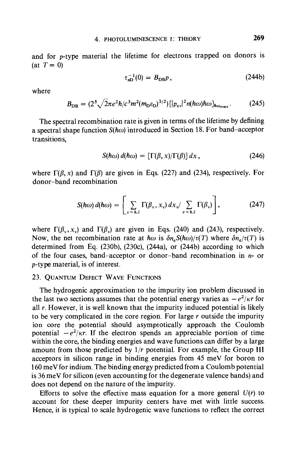
The Hall coefficient and resistivity as a function of temperature are given
in Fig. 4 for Te-doped AlSb. The donor activation energy eD, extrapolated
to 0°K, is 0.068 ± 0.001 eV.53-54 The Hall mobility versus temperature for
the same sample used for Fig. 4 and for a more highly compensated sample
is shown in Fig. 5. The calculated temperature dependence of the mobility,
assuming combined polar optical, acoustical mode, and ionized impurity
scattering, was found55 to be in reasonable agreement with the measured
dependence. However, there is a growing realization that intervalley
scattering is the dominant mechanism limiting electron lattice mobilities in the
indirect gap compounds, while polar mode optical phonon scattering
remains dominant in direct gap compounds.55" Consequently, the role
of acoustical mode scattering is reduced, and thus also, the need for
deformation potentials higher than what seem reasonable.
Besides the photoresponse measurements by Mead and Spitzer,52 there is
additional indirect evidence that the conduction-band minima in AlSb are
not at the zone center. Edwards and Drickamer56 found a red shift of the
absorption edge under pressure with a pressure coefficient of —1.6 x 10"6
eV kg"' cm"2. From an analogy with silicon, the authors concluded that the
optical transitions near the absorption edge were due to [100] conduction-band
52aI. I. Burdiyan, Fiz. Tverd. Tela 1, 1360 (1959) [English transl.: Sot). Phys.-Solid State 1, 1246
(I960)].
53 F. J. Reid, in Willardson and Goering,7 p. 158.
54 R. J. Stirn and W. M. Becker, Phys. Rev. 141, 621 (1966).
55 R. J. Stirn and W. M. Becker, J. Appl. Phys. 37, 3616 (1966).
55aD. L. Rode, private communication; see also reference 97a.
56 A. L. Edwards and H. G. Drickamer, Phys. Rev. Ill, 1149 (1961).
26
RICHARD J. STIRN
I01'
10"
10"
o
\
ro
E
o
£
O
O
<
I
500 295
J I L
B4II n-AI Sb(Te)
H = 25Kg
J L
2 3 4 5 6 7 8 9 10 I I 12 13
1000/T, °K "'
Fig. 4. Hall coefficient, resistivity, and nT 3/2 versus reciprocal temperature for AlSb. (After
Stirn and Becker.54)
minima. Piller and Patton57 found no change in sign of the interband
Faraday rotation throughout the range of wavelengths used. This and the
fact that the Faraday rotation shifts to shorter wavelengths with decreasing
temperature, as in silicon, indicated that the transitions were indirect.
The first direct evidence of the [100]-type conduction band minima
in AlSb was obtained from piezoresistance studies.58 It was found that the
values of the elastoresistance coefficients for n-AlSb were similar to those
57 H. Piller and V. A. Patton, Phys. Rev. 129, 1169 (1963).
58 K. M. Ghanekar and R. J. Sladek, Bull. Amer. Phys. Soc. 10, 304 (1965).
1. BAND STRUCTURE AND GALVANOMAGNETIC EFFECTS 27
1000
400
I
o
£ 200
E
o
t 100
_J
o
s
_J
_J
<
x 40
20
10
20 40 100 200 400
TEMPERATURE, °K
Fig. 5. Hall mobility versus temperature for AlSb of two different carrier concentrations.
(After Stirn and Becker.54)
values found for w-Si and that the symmetry relations expected in the
deformation-potential theory of electron transfer between [100] ellipsoids
were approximately satisfied. However, when Ghanekar and Sladek
calculated the anisotropy parameter K from the piezoresistance and piezo-Hall
effect data, they obtained a value of 18,59 which is near the value for Ge.
One would expect a value of K closer to 5, considering the analogy of AlSb
with Si.
Magnetoresistance measurements have now been reported54 that give
more reasonable values of the valley anisotropy. The angular variation of
the magnetoresistance for some representative crystal orientations is given
in Fig. 6. The magnetoresistance is very small because of the low electron
mobility, but the data points have little scatter. The horizontal curve shows
the transverse magnetoresistance for a sample with current flow along the
cubic axes. Inspection of Eq. (17) indicates that M[fJ01 (transverse) is equal to
i i—i—rn
\ Z
n - Al Sb (Te)
O B4II n300.|< =5XI016 cm"3
O D 211 njoo-K =2XI017 cm"3
I I I I
59 K. M. Ghanekar and R. J. Sladek, Phys. Rev. 146, 505 (1966).
28 RICHARD J. STIRN
n-AISb (Te) • D 211 HI <110> 1 T= 195 °K
H-25 Kg x D21I HI <IIO> J III <IIO>
H !!<ll0>
1 J 1 I I I
0° 20° 40° 60° 80° 100° 120° 140° 160° 180°
[H]
Fig. 6. Angular variation of magnetoresistance in n-AISb for two samples at different
temperatures. The upper curve for sample D211 represents transverse to longitudinal changes in
orientation. (After Stirn and Becker.54)
the inverted Seitz coefficient b, independent of magnetic-field direction.
Thus the data of sample D311 in Fig. 6 show the absence of spurious
magnetoresistance effects due to contact shorting18'19 and inhomogeneities.20'20"
The magnetoresistance was reported to be proportional to the square of
the magnetic field up to at least 30 kG.
Values of the inverted Seitz coefficients b, c, and d were reported by
Stirn and Becker.54 The symmetry relations b + c = -d, d < 0 [Eq. (23)]
for [100]-type spheroids were obtained for samples from two ingots of
different carrier concentration and for temperatures ranging from 77 to 295°K.
Application of Eq. (29) and choice of the prolate spheroidal model (since
A > 1) gave values of the anisotropy parameter K+ at the different bath
temperatures (Fig. 7). The decrease in K+ with decreasing temperature is
expected since the ratio T||A± is >1 for ionized impurity scattering34 in
many-valley semiconductors. Similar behavior has been observed in
n-Ge.60 This explanation is supported by the fact that K+ is consistently
lower for sample D211, which has greater ionized impurity scattering as
0.0030
0.0025
0.0020
<
0.0015
0.0010
0.0005
R. A. Laff and H. Y. Fan, Phys. Rev. 112, 317 (1958).
1. BAND STRUCTURE AND GALVANOMAGNETIC EFFECTS 29
i—i—m 1 1 r
n-AISb (Te)
• B4II j T
x D 211 1—¥
J I I l_l I I I
60 80 DO 200 300 400
TEMPERATURE, °K
Fig. 7. Anisotropy parameter (K + )l00 versus temperature for n-AISb. At room temperature,
n(B411) = 5 x 1016cm"3andn(D211) = 2 x 1017 cm"3. The data points for D211 have been
shifted slightly to the right for purposes of clarity. (After Stirn and Becker.54)
determined from Hall effect and mobility data.54 The extrapolated value of
K + for lattice scattering is 7 + 1, which is comparable to the value of 5 for Si.
The electron effective mass in AlSb is commonly quoted as 0.39m0. This
value was determined by Moss et a/.61 from Faraday rotation of free carriers.
If we assume that T||/t± = 1 in AlSb at temperatures above 300°K where
K+ = 7, application of Eq. (37) yields effective-mass component values of
my = 1.64m0, m± = 0.23m0. (82)
The conductivity effective mass mc* [Eq. (35)] is then O.33m0 and the density-
of-states effective mass md* [Eq. (36a)] is 1.5m0, if one assumes six valleys
as in silicon. The value of mc* agrees well with that obtained from infrared
reflectivity measurements48 (0.30m0). The density-of-states effective mass
can be obtained from thermoelectric-power measurements if the scattering
mechanism is specified. Nasledov and Slobodchikov62 determined an
average value of md* equal to (1.2 + 0.4)m0 by assuming acoustical-mode
scattering in their Se-doped AlSb samples. Stirn and Becker55 have made
calculations of the electron mobility temperature dependence in AlSb, based
61 T. S. Moss, A. K. Walton, and B. Ellis, in Proc. Int. Conf. Phys. Semiconduct. Exeter p. 295.
Inst. Phys. Phys. Soc, London, 1962.
62 D. N. Nasledov and S. B. Slobodchikov, Fiz. Tverd. Tela 1, 748 (1959) [English transl.: Sov.
Phys.-Solid State 1, 681 (1959)].
§ 5
4
30
RICHARD J. STIRN
on a combination of ionized-impurity, acoustical-mode, and polar-optical-
mode scattering, that suggested a value for md* of 1.5m0 if no additional
scattering mechanisms are present.
It should finally be noted that the calculated effective-mass values above
assumea value of m^/m1 = 7, i.e., T||/t± = 1. If the latter equality is somewhat
different because of the presence of lattice scattering anisotropy above
300°K, all values quoted would be reduced by a small amount.
Pollak, et al.A2 calculated mass parameters at a number of points in
the Brillouin zone with eigenvectors of the Hamiltonian used to obtain
Fig. 3. These parameters are given in Table III. There are no experimental
values for the mass parameters in the higher-lying minima. Their calculated
value of m± in the [100]-minima agrees well with that reported by Stirn and
Becker,54 but the my* value of 0.95m0, which is substantially lower, makes
their mass anisotropy parameter in the lowest minima equal to 3.8. The
actual value is probably somewhere between 3.8 and 7. Because of the
uncertainties in the experimental values of m* and mF* and their relative
insensitivity to K for low values of K, cyclotron-resonance measurements
will be required to resolve the difference.
c. Galvanomagnetic Effects: p-Type
The lowest room-temperature carrier concentrations in p-AlSb grown to
date are about 1016 cm"3. Hall coefficient and resistivity data32 as a function
TABLE III
Electron Effective-Mass Parameters for AlSb in Units of the
Free Electron Mass
m*(r,)
m,, *(!-,)
m±*(M
m|l*(*„A,)
m^i.A,)
mF*
mc*
md*
0.121
1.357
0.123
0.95
1.64
0.25
0.23
0.39
0.33
1.5
Pollak et al.A1
Pollak et al."
Pollak et al. "
Pollak et al.12
Stirn and Becker54
Pollak et al.i2
Stirn and Becker54
Moss et a/.61
Eq. (35) with K = l, mL*(Xu A,)
Eq. (36) with K = l, m^*,, A,)
six valleys
= 0.23
= 0.23,
1. BAND STRUCTURE AND GALVANOMAGNETIC EFFECTS
31
4xlOB 4xl04
2X10
400
2x10 200 —
107 T, °K
Fig. 8. Hall coefficient, resistivity, and pT 3'2 versus reciprocal temperature for p-AlSb.
(After Stirn and Becker.32)
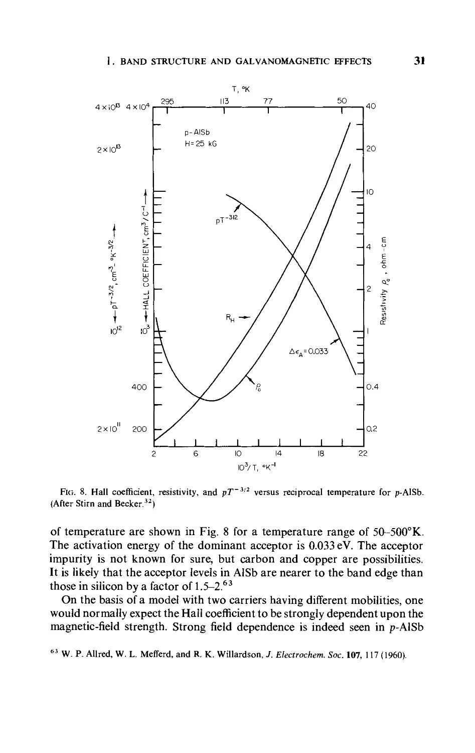
of temperature are shown in Fig. 8 for a temperature range of 50-500°K.
The activation energy of the dominant acceptor is 0.033 eV. The acceptor
impurity is not known for sure, but carbon and copper are possibilities.
It is likely that the acceptor levels in AlSb are nearer to the band edge than
those in silicon by a factor of 1.5-2.63
On the basis of a model with two carriers having different mobilities, one
would normally expect the Hall coefficient to be strongly dependent upon the
magnetic-field strength. Strong field dependence is indeed seen in p-AlSb
63 W. P. Allred, W. L. Mefferd, and R. K. Willardson, J. Electrochem. Soc. 107, 117 (1960).
32
RICHARD J. STIRN
1.16
1 1.14
CVJ
or
°? 1.12
iCTOR
5
t-
u 1.08
o
U-
g 1.06
o
< 1.04
1.02
1
-
-
1
1 1 1 1 1 1
* t * ---
50 °K
77 °K
»
II3°K
1 1 1 1 1 1
1 1 1 1 1 1 1 1 1
*\. p-AISb
Nv I || <!I0>
\ HIKlT0>
i i i i 111 n
I
-
-
-
^ I
2 4
MAGNETIC FIELD, kG
20
40
Fig. 9. Hall coefficient factor Rh/Ri^g versus magnetic field strength for p-AISb at T = 50,
77, and 113°K. (After Stirn and Becker.32)
as shown in Fig. 9. The monotonic decrease in Hall coefficient with increasing
magnetic field is also observed in p-Ge and very pure p-Si.30'31
The theory developed for this behavior in Ge and Si,30'31 which was
described briefly in an earlier section, has been applied to p-AISb.32 The results
are shown in Fig. 10. A measure of the amount of ionized impurity scattering
is given by ft. = 6nLJnhi. The values of the carrier concentration ratio
P3/P2 [Eq. (45)] and the lattice mobility ratio ^,3/^,2 [El- (53)] were
calculated to be 0.085 and 5, respectively, using warping parameter values64 of
A = 5.96, B = 3.36,
23.2.
(83)
More recent calculations42 give a value for C2 which is reduced by nearly
a factor of 2 from that given above. However, the latest value would not
predict the observed field dependence of the Hall coefficient because we would
obtain p3/p2 = 13 % and hU3/lil,2 = 3.7. The dashed curve in Fig. 10 shows
a calculation for /iLr3//iL,2 = 3, the value for Si. A strong maximum is seen
to occur with increasing field strength. Initially, RH increases as H increases
because of the warping of the heavy-hole band; at higher fields, the light hole
Private communication to R. J. Stirn and W. M. Becker by M. Cardona.
1. BAND STRUCTURE AND GALVANOMAGNETIC EFFECTS
33
MAGNETIC FIELD, kG
25 5 0
Mih I i i i mil I KM 11111
0.04 0.1 I 10
(/j) =(9tt/I6) hlz H
Fig. 10. Comparison of theoretical Hall coefficient factor RH/R„ with experimental data for
p-AlSb at a temperature of 77°K. (After Stirn and Becker.32)
enters the strongfield region and produces a decrease in RH. Except for ultra-
pure material, this latter behavior has also been observed in p-type Si.30
Since the shape of the field dependence of RH is so sensitive to the value of
HLt3/nu2, and to a lesser extent, to the value of p3/p2, the larger value of C2
seems to be more appropriate.643
The Hall mobility temperature dependence for p-type AlSb is shown in
Fig. 11. The temperature dependence is given by a T~ U9S law above 200°K.
Because of the magnetic-field dependence of RH, very high magnetic fields
are required in order to accurately measure the temperature dependence of
RH and fiH at lower temperatures. Fields in excess of 100 kG seem to be
necessary for p-AlSb with room-temperature carrier concentrations of about
1016cm-3 (see Fig. 10).
64aA recent calculation641" supports this contention. The results of the k • p calculation, which
used pseudopotential formalism to calculate the required matrix elements, gave a value of
20.9 for C2.
64b R. L. Bowers and G. D. Mahan, Phys. Rev. 185, 1073 (1969).
34
RICHARD J. STIRN
o
s
0.4
0.2
T
"1—I I I I I I
"i r
p-AlSb
H = 25 kG
J I I I I I I
20
40 100
TEMPERATURE °K
200
400
Fig. 11. Hall mobility versus temperature for p-AlSb. (After Stirn and Becker.32)
The lattice mobility of holes in III-V compounds was recently examined by
Wiley and DiDomenico.64c They conclude that the polar mode mobility
expressions derived for nondegenerate s-like bands are not applicable to the
degenerate p-like valence bands, and that the temperature dependence of
the hole mobility can be better explained by combining acoustic and non-
polar optical mode scattering alone as has been shown in Ge and Si. Their
calculations, which included AlSb, use the acoustical deformation potential
as an adjustable parameter.
The magnetoresistance coefficients in p-AlSb show a strong magnetic-
field dependence at lower temperatures as shown in Fig. 12. The angular
variation of the magnetoresistance is shown in Fig. 13 for the current along
:J. D. Wiley and M. DiDomenico, Phys. Rev. B2, 427 (1970).
1. BAND STRUCTURE AND GALVANOMAGNETIC EFFECTS
36
35
32 -
28
> 24
e
20
> 16
J I I I I I I
4 10 20
MAGNETIC FIELD, kG
40
Fig. 12. Transverse magnetoresistance divided by H1 versus magnetic-field strength for p-AlSb
at T = 50, 77, and 113°K. (After Stirn and Becker.32)
"b
< r -
H IKII0>
• HI <00l>
x HI <II0>
HIK00l>
p-AISb FROM ING0T#52
I II <II0>
H = 25 kG
T=77 °K
H II <II0> ■
-LONGITUDINAL
—I I I L
_L_I
0° 20° 40° 60° 80° 100° 120° 140° 160° 180°
[H]
Fig. 13. Angular variation of magnetoresistance in transverse and longitudinal position for
p-AISb at T = 77°K. (After Stirn and Becker.32)
36
RICHARD J. STIRN
a [110] direction. A ratio of transverse to longitudinal magnetoresistance
(extrapolated to zero magnetic field) of about 7 has been reported.32 The
existence of a nonzero longitudinal magnetoresistance is consistent with
warping of the heavy-hole band.
TABLE IV
Experimental Values of Some Weak-Field Magnetoresistance Coefficients FORp-AlSb"
50°K 77°K 113°K 195°K 245°K 295°K
M??J(cm4V-2sec-2)
Miig(cm4V-2sec-2)
M110(cm4V-2sec-2)
b (cm4 V"2 sec"2)
c(cm4 V-2 sec-2)
d(cm4V"2sec-2)
x 10"4
x 10"4
x 10"4
x 10"4
x 10"4
x 10~4
348
338
46
348
-292
-20
238
216
31
238
-185
-44
135
118
21
135
-97.0
-34
34.0
29.0
6.3
34.0
-22.7
-10
19.4
16.3
3.6
19.4
-12.7
-6.2
12.1
10.3
2.0
12.1
-8.4
-3.5
" After Stirn and Becker.32
The weak-field inverted Seitz coefficients (Table IV) were found to obey
the relations
(b + c) x -d, d <0, (84)
in the higher temperature range. The magnitudes of (b + c) and d diverge
more the lower the temperature. Frequently, the equality (b + c) = — d,
(d < 0) is reported in the literature for p-type materials that have valence
bands similar in nature to those of germanium. For a multivalley-band
model, this equality indicates [100] valleys. However, piezoresistance
measurements on such p-type material give results indicating [111] valleys.
Since the same results are observed in p-type Ge, this seemingly contradictory
observation is interpreted to mean that the material under investigation
has a Ge-like valence band. However, an inspection of Eqs. (74) and (75)
shows why the symmetry relation (b + c) = -d is approximately correct
for a model of warped valence bands. In the limit of negligible 0&n (actually
38„ is about two orders of magnitude smaller than the other anisotropy
parameters aijkl [see Eqs. (64H66)]), it is seen that the ratio (b + c)/(-d)
approaches unity.32
The anisotropy factor 0&n is proportional to the square of V whereas the
other factors aljkl are near unity. It would appear that changes in T reflect
the discrepancy in Eq. (84) at lower temperatures. Changes in r would
signify changes in the band parameters with temperature. However, such
changes would not be significant in the temperature range reported. The
1. BAND STRUCTURE AND GALVANOMAGNETIC EFFECTS 37
TEMPERATURE, °K
0 200 400 600 800
fj-l cr, I04cm3 V-sec"2Q"'
Fig. 14. Weak-field magnetoconductivity coefficients for p-AlSb versus Ho2o0. (After Stirn
and Becker.32)
theory of Mavroides and Lax25 assumes an isotropic relaxation time, and
hence, assumes that r is only dependent on the band warping parameters
(e.g., the effective mass). Since magnetoresistance measurements do not
separate the anisotropic effects of mass and relaxation time, it is more likely
that the above observed behavior at lower temperatures reflects large changes
in the relaxation-time anisotropy, rather than changes in the band parameters.
This argument was strengthened by further manipulation of the expressions
for the magnetoconductivity coefficients.32 The absolute values of the
relaxation times can be eliminated if it is assumed that the energy dependence
of both relaxation times is the same.65 The coefficients Sy(m are then found
to be directly proportional to A(ji02o0), where A = <t> <t3>/<t2>2, and the
proportionality constants contain the anisotropy factors (aijkl) and 0&n.
Figure 14 shows the dependence of the magnetoconductivity coefficients
on Oi02ffo)> where the latter quantity was varied by changing the temperature.
All of the data points lie on a straight line, except those for £xxxx at the three
65 P. J. Kemmey and E. W. J. Mitchell, Proc. Roy. Soc. (London) A263, 420 (1961).
38
RICHARD J. STIRN
lowest temperatures. Since changes in A with temperature should be the
same for all three coefficients, and since only £xxxx is proportional to $„
and thus to T2 [see Eqs. (61H63)], the above argument concerning aniso-
tropy in the relaxation times appears pertinent.
Use of Eq. (79) and the warping parameters in Eq. (83) gives values of the
conductivity effective mass for the heavy hole (0.48m0) and the light hole
(0.10m0). The density-of-states effective masses [Eq. (76)] are (0.52m0) and
(0.10m0), respectively. The amount of warping of the heavy-hole band is
small enough that there is little difference between the two types of effective
masses.
The light- and heavy-hole masses can also be estimated directly36 from the
E0 and E0' gaps given in Table II. Cardona et al.*3 obtained m2* — 0.52m0
and m3* = 0.1 lm0.
Experimental determinations of the hole masses are scarce and in
disagreement. The effective mass of heavy holes in AlSb has been estimated by Reid
and Willardson66 from the variation of mobility with carrier concentration.
With the assumption of acoustical-mode scattering for the lattice mechanism,
they obtained a value of 0.4m0.
However, higher values have been reported on the basis of thermoelectric-
power measurements. Sasaki et al.61 obtained a room-temperature value of
1.8 ± 0.8 for (m2*/m0)g213, where g is the degeneracy of the band edge.
With g = 4, we get m2* = (0.7 + 0.3)m0. Nagledov and Slobodchikov68
report a value of m2* = (0.9 + 0.1)m0 from thermoelectric-power
measurements between 400 and 700°K. Both groups assumed the lattice scattering
mechanism to be acoustical mode.
4. Gallium Phosphide
a. Band Structure
Gallium phosphide (GaP), with its considerably higher melting-point
temperature of 1470°C, is more difficult to prepare in the crystalline form
than AlSb. Some methods used in the growth of GaP, which crystallizes into
a cubic zinc-blende structure with a lattice constant of 5.45 A, have been
reviewed by Miller.69 Many of the crystals used in the investigations
reported below were grown by vapor-transport techniques.69a'69b
66 F. J. Reid and R. K. Willardson, J. Electron. Control 5, 54 (1958).
67 W. Sasaki, N. Sakamoto, and M. Kuno, J. Phys. Soc. Japan 9, 650 (1954).
68 D. N. Nasledov and S. V. Slobodchikov, Zh. Tekh. Fiz. 28, 715 (1958) [English transl.: Sov.
Phys.-Tech. Phys. 3, 669 (1958)].
69 J. F. Miller, in Willardson and Goering,7 p. 194.
69aC. J. Frosch, J. Electrochem. Soc. Ill, 180 (1964).
69bA. S. Epstein and W. O. Groves, Advan. Energy Conversion 5, 161 (1965).
1. BAND STRUCTURE AND GALVANOMAGNETIC EFFECTS 39
Calculations of the band structure for GaP have been performed
recently,41'42 with the same techniques as for AlSb. The group IV "element"
used as a basis for the crystal potential was the hypothetical compound
Ge-Si. The results of the k ■ p band calculations for GaP are shown in Fig. 15.
The electroreflectance spectrum of GaP at room temperature is shown in
Fig. 16. Values for the transitions indicated in Fig. 15 are given in Table V.
References to these and additional values are given below.
TABLE V
Energy Splittings for GaP (300°K)
Transition
£o
£i
Eq
E2
Energy (eV)
2.78
3.7
4.77
-5.3"
Transition
Ao
A,
Ao'
S
Energy (eV)
0.082
-0.08
-0.06
-0.28°
° See text.
Values for the energy of the indirect gap were first reported by Folberth
and Oswald,70 who obtained a room-temperature value of 2.24 eV from
optical absorption data. Similar values have since been reported.51'71-73
Recently, the optical absorption edge has been measured in exceptionally
good single crystals for temperatures between 1.6 and 300°K.74 Absorption
components associated with four different phonon energies were resolved,
enabling the authors to derive precise values for the indirect gap of 2.259 ±
0.003 eVat300°K75 and 2.339 ± 0.002eVat 1.6°K. A similar type of
measurement has been made more recently by Lorenz et al.15a at temperatures up to
900°K. The authors obtained a value of 2.261 eV at 300°K.
The indirect-gap temperature coefficient A£g/AT has been commonly
70 O. G. Folberth and F. Oswald, Z. Naturforsch. 9a, 1050 (1954).
71 M. Gershenzon, D. G Thomas, and R. E. Dietz, Proc. Int. Conf. Phys. Semiconduct. Exeter,
p. 752. Inst. Phys. Phys. Soc, London, 1962.
72 W. K. Subashiev and S. A. Abagyan, in "Physics of Semiconductors" (Proc. 7th Int. Conf.)
p. 225. Dunod, Paris, 1964.
73 D. N. Nasledov, V. V. Negreskul, S. I. Radautsan, and S. V. Slobodchikov, Sod. Phys.-Solid
State 7, 2965(1966).
74 P. J. Dean and D. G. Thomas, Phys. Rev. 150, 690 (1966).
75 This value has since been raised by approximately 3 meV on the basis of measurements of
the temperature shift of the absorption band due to indirect excitons weakly bound at
nitrogen impurities (Dean et al.11)
75,M. R Lorenz, G D. Pettit, and R. G Taylor, Bull. Amer. Phys. Soc. 13, 453 (1968); Phys. Rev.
171,876(1968).
40
RICHARD J. STIRN
k = ir/a (III)
k = (000)'
k=2ir/a(lOO)
Fig. 15. Energy bands of GaP, including spin-orbit splitting, in the [100] and [111] directions.
(After Pollak et al.iz)
-4(-
-8
GaP
i
| E0+A0 \
E0
1
|e,(2!
/
E°~\
e6+ao
E|(l)
1
I
\ /e2+b
E2
1
3 4 5
PHOTON ENERGY, eV
Fig. 16. Electroreflectance spectrum of n-type GaP at room temperature. (After Thompson
et al. 19)
1. BAND STRUCTURE AND GALVANOMAGNETIC EFFECTS 41
stated in the literature to be -5.2 x 10"4eV°K-1.51'76 However, recent
measurements77 (see reference 75) have indicated a substantially lower
room-temperature coefficient of — (2.36 ± 0.01) x 10_4eV°K""1. This
dependence is linear only down to about 140°K. A general form of the energy
gap temperature dependence [£g(0) — aT2/(T + /?)] has been proposed by
Varshni773 on the basis of electron-phonon interactions rather than lattice
dilation being the cause for the temperature shift. Empirical values of
a = 6.2 x 10"4eV°K"2 and jS = 460°K for GaP have been derived very
recently77b from absorption measurements taken from room temperature
up to 127 3°K. The functional relationship also fits the lower temperature data
of Lorenz et al.15a quite well down to 6°K.
The very weak reflectivity peak associated with the direct transition
Eo(F\5 -> r,c) was first detected by Zallen and Paul,51 who reported a value
for E0 given by 2.78^1.6 x 10"4(T- 300°) eV at temperatures above 80°K.
Nelson et a/.78 obtained similar results from photoconductivity-response
measurements, deducing a value of 2.895 + 0.002 at 0°K. A quadratic form
for the temperature dependence of -(1.17 + 0.01) x 10"6T2 eV°K_1 was
reported, however, Neither the linear nor quadratic form appears to describe
the temperature variation of the direct gap for the entire range of 0-300°K.
Later studies72'73,79 have given values of the direct gap comparable to those
above. Recently, however, extremely thin crystals of GaP (< 1 n) have been
grown, enabling Dean et al. to make very precise measurements of the
intrinsic optical absorption.77 They deduced a value for the direct-exciton
energy gap at 25°K of 2.8725 ± 0.0005 eV. At 295°K the energy gap has a
value of 2.780 eV and has a temperature coefficient of —(5.2 ±0.1) x
10-4eV°K-1. This temperature coefficient and the value of the indirect-
gap coefficient reported by Dean et al.,11 which is more than one half less
than previously reported values, means that the energy of the [100]-minima
in GaP shifts upwards with decreasing temperature less rapidly than that
of the zone center r\ minimum, contrary to previous belief.
A more energetic absorption band at 2.954 eV was also detected by Dean
et al.11 at low temperatures. Assuming that this is due to direct transitions
from the split-off component of the valence band, the spin-orbit splitting A0
is 0.082 eV. Previous estimates of this splitting, 0.10 eV72-79 and 0.127 eV,80-8 1
76 F. Oswald, Z. Naturforsch. 10a, 927 (1955).
77 P. J. Dean, G. Kaminsky, and R. B. Zetterstrom, J. Appl. Phys. 38, 3551 (1967).
77aY. P. Varshni, Physica 34, 149 (1967).
77bM. B. Panish and H. C. Casey, Jr., J. Appl. Phys. 40, 163 (1969).
78 D. F. Nelson, L. F. Johnson, and M. Gershenzon, Phys. Rev. 135, A1399 (1964).
79 A. G. Thompson, M. Cardona, K. L. Shaklee, and J. C. Woolley, Phys. Rev. 146, 601 (1966).
80 J. W. Hodby, Proc. Phys. Soc. (London) 82, 324 (1963).
81 M. L. Belle, Zh. I. Alferov, V. S. Grigor'eva, L. V. Kardinova, and V. D. Prochukhan, Fiz.
Tverd. Tela 8, 2623 (1966) [English transl.: Sov. Phys.-Solid State 8, 2098 (1967)].
42
RICHARD J. STIRN
are higher. Since the splitting is not expected to be appreciably
temperature dependent, the reason for the discrepancy is unknown at this time.
There has been considerable controversy about the source of the strong
absorption peak and reflectance structure at 3.7 eV. The peak, previously51
assigned to E0' (F\5 -> r\5), has been reinterpreted as £j (A3 -> Aj) on the
basis of GaAs-GaP alloy data,72'79'81-83 pseudopotential band
calculations,41 and photoelectric-emission studies.84 The linear temperature
coefficient of Ey between 80° and 300°K is about -3.5 x lO^eVK-1.81,85
A discussion of the £j peak and the associated spin-orbit splitting Aj is
given by Thompson et al.,19 who report the only experimental value for
A!(~0.08 eV), in agreement with the calculated value of 0.072 eV obtained
from the k • p method (Fig. 15).
Various investigators79,81-85 have given values for the E0' {V1S -> n5)
transition ranging from 4.75 to 4.8 eV. This transition has a linear
temperature coefficient of about — 3.4 x 10"4eV°K_1 between 80 and
295°K.82'85 Thompson et al.19 point out that the main contribution to £0'
and E0' + A0' probably comes from a region of k space in the [100] direction
near k = 0. However, since the corresponding conduction and valence bands
are nearly parallel in this region, the energy at which E0' occurs should well
represent the value of the rv15->rc15 gap. The spin-orbit splitting A0'
associated with the E0' peak is approximately 0.06 eV.79
Values for the transitions E2(X5V -> Xf) and E2 + 5(X5V -> X3C) are
very difficult to deduce accurately from the various optical measurements
in the literature. In fact, assigning any peak in the reflectance spectrum to
the E2 or Ey + d transition is hazardous in any of the III-V compounds,
judging from the results found in GaAs.86 The problem would seem to
come from interband transitions associated with a much larger region of the
reduced zone, which dominate in their contribution to the main reflectivity
peak (or photoemissive dip). In addition, the determination of absorption
thresholds of transitions to X3C from the zone center are imprecise, partly
because of phonon interactions and low density-of-states. Interpretations of
the well-known infrared absorption band, which is related to d and discussed
below, have also been confused because of the effects of free carrier absorption
and photoionization of occupied donor levels. A peak in the reflectance
(and electroreflectance) spectrum of GaP at about 5.3 eV has been identified
with the E2 transition at room temperature.44'79,82'83,85,87 A similar
82 J. C. Woolley, A. G. Thompson, and M. Rubenstein, Phys. Rev. Lett. 15, 670 (1965).
83 T. K. Bergstresser, M. L. Cohen, and E. W. Williams, Phys. Rev. Lett. 15, 662 (1965).
84 T. E. Fischer, Phys. Rev. 147, 603 (1966).
85 A. G. Thompson, J. C. Woolley, and M. Rubenstein, Can. J. Phys. 44, 2927 (1966).
86 F. Herman and W. E. Spicer, Phys. Rev. 174, 906 (1968).
87 H. Ehrenreich, H. R. Philipp, and J. C. Phillips, Phys. Rev. Lett. 8, 59 (1962).
1. BAND STRUCTURE AND GALVANOMAGNETIC EFFECTS 43
identification has been made from photoelectric-emission measurements.84
The transition has a linear temperature dependence82,85 of
-4.5 x 10_4eV°K-1.
Pollak et al.A2 derived a value of 4.92 eV for the E2 gap (Fig. 15) from their
k-p calculations, and suggest that the 5.3eV peak is due to the saddle-
point transitions £2 -> 2^ (110 axes), which was calculated to be 5.40 eV.
They further suggest that the E0' and E2 transitions are almost degenerate
at about 4.8-4.9 eV. The most recent theoretical calculation,873 using an
empirically adjusted OPW band calculation, assigns to the E2 gap a value of
4.6 eV. However, band calculations have not demonstrated the accuracy
necessary for a meaningful comparison with the optical results above. The
above calculations of Pollak et al.42 also do not account for the presence
of a 5.74 eV peak in the electroreflectance spectrum44,79 (5.66 eV dip in the
photoemissive response84) at room temperature. These maxima were
identified with the Xsv -> X3C transition, thus giving a value of 0.46 eV44,79
and 0.38 eV84 to d, the conduction band splitting at X. However, these
values would be expected to be larger than the true X^ -> X3C gap because
of the problem of broadened response due to multiple transitions.
That this is so seems to be confirmed by measurements of the infrared
absorption band due to the direct Xf -> X3C transition. The peak of the
infrared band in this region occurs at 3.0 n (0.40eV).87b,8S This energy has
often been quoted erroneously for the value of d, perhaps influenced by an
early published theoretical value of 0.40 eV.41 More accurate, of course, is
the extrapolated threshold of this band. First estimates of this value gave
0.31 eV87b and 0.30 eV.51 However, the total infrared absorption includes
absorption due to free carriers, which must be properly subtracted. This in
turn involves a knowledge of the dominant scattering mechanisms at the
temperature of measurement. The result of subtracting a linear extrapolation
of the free carrier absorption (FCA) at longer wavelengths, where the FCA
is proportional to wavelength, was 0.33 eV.88a Most recently a nonlinear
subtraction of the theoretical FCA utilizing acoustic and nonpolar optical
deformation-potential scattering was performed on the experimental
absorption and a value for d of 0.276 + 0.007 eV was obtained.89
87aF. Herman, R. L. Kortum, C. D. Kuglin, and J. P. Van Dyke, "Methods in Computational
Physics" (B. Adler, S. Fernback, and M. Rotenberg, eds.), Vol. 8, p. 193. Academic Press,
New York, 1968.
87bW. G. Spitzer, M. Gershenzon, C. J. Frosch, and D. F. Gibbs, J. Phys. Chem. Solids 11, 339
(1959).
88 J. W. Allen and J. W. Hodby, Proc. Phys. Soc. (London) 82, 315 (1963).
88*Yu. V. Shmartsev and A. D. Remenyuk, Fiz. Tekh. Poluprov.3, 1697 (1969) [English transl.:
Sod. Phys.-Semicond. 3, 1425 (1970)].
89 J. D. Wiley and M. DiDomenico, Phys. Rev. Bl, 1655 (1970).
44
RICHARD J. STIRN
The values for 3 quoted above were all obtained from room-temperature
absorption data. The absorption threshold data at lower temperatures,
where most of the free carriers are frozen out into the donor levels, do not
require the subtraction procedure. However, one would expect to get
photoionization of the dominant donors, and hence, obtain a somewhat
higher value for 3 from the absorption data. This has indeed been observed
with the additional energy being about 40-60 me V.87b'88-90 Thus the
X3C -> Xf transition appears to be nearly temperature independent as might
be expected. One further confirmation of the lower value of d is the direct
measurement of the optical absorption due to transitions from the zone
center T to X^ and X3C individually (at low temperature) with the resulting
difference in energy of 0.29 eV.77
Two small, but distinct, peaks with energies of 6.67 and 6.90 eV were
observed in the reflectance of GaP.85 These were identified as £/ and £/ +
A/ peaks attributable to L3V -> L3C transitions (not shown in Fig. 15). Unlike
the splitting at k = 0 (A0), the spin-orbit splitting of the L point was found to
vary little with x. This fact suggests that the splitting of L is due mainly to
the gallium cation.
b. Galvanomagnetic Effects: n-Type
Most electrical measurements on GaP are performed on crystals grown
epitaxially by open-tube vapor transport. These can be grown w-type by
intentionally doping with Se, Te, or S. The choice of the substrate is quite
crucial according to a very recent investigation by Taylor et al.9i Samples
grown on 111A faces of either GaP or GaAs crystals are always
high-resistivity p-type even when doped with S or Se, whereas samples grown on 111B
faces are always w-type, including those intentionally undoped. The residual
impurity in the undoped crystals was shown to be sulfur at a concentration
of 2-3 x 1016cm~3. In addition, it was found that samples grown on a
GaAs substrate (which is the usual choice because of the scarcity of GaP
crystals of adequate size) are less uniform in carrier concentration and have
somewhat lower Hall mobilities. The observation about the effect of the 111A
face on the type of conductivity would explain the findings of Kamath and
Bowman92 who always obtained p-type conduction in their undoped GaP
crystals.
Hall-effect measurements were performed on crystals prepared and doped
by the floating-zone process for one of the earlier systematic determinations
90 A. D. Remenyuk, L. G. Zabelina, Yu. I. Ukhanov, and Yu. V. Shmartsev, Fiz. Tekh. Poluprov.
2, 666 (1968) [English transl.: Sod. Phys.-Semkond. 2, 561 (1968)].
91 R. C. Taylor, J. F. Woods, and M. R. Lorenz, J. Appl. Phys. 39, 5404 (1969).
92 G. S. Kamath and D. Bowman, J. Electrochem. Soc. 114, 192 (1957).
1. BAND STRUCTURE AND GALVANOMAGNETIC EFFECTS 45
of donor activation energies in GaP.93 The samples had varying degrees
of compensation and showed considerable scatter in their extracted
activation energies. The average values of activation energies (for a donor
concentration of 1018 cm"3) were taken to be 0.089,0.078, and 0.076 eV(±0.020 eV)
for S, Si, and Te, respectively. The values are expected to be larger for lower
donor concentrations. Montgomery94 has reported Hall measurements on
Te-doped GaP with improved homogeneity. The results gave a binding
energy of 80 ± 5 meV for Te at a concentration ND ~ 3 x 1017cm"3.
When the binding energy was plotted versus Njj/3, an extrapolation to zero
concentration resulted in a value of 95 meV. Other measurements95 on Te-
doped crystals with higher mobilities (170cm2 V"1 sec"1 at room
temperature) led to an activation energy of 0.11 eV for Te as deduced from Hall
measurements.
Greatly improved values of donor (and acceptor) ionization energies
have been deduced from the recombination luminescence spectra of ex-
citons bound to neutral donors in GaP95a>95b: S, 0.102eV; Te, 0.0875 eV;
Se, 0.100eV; Si (donor), 0.080eV, and more recently, Sn, 0.0655 eV.95c
The technique gives very precise values for the donor-acceptor pair energy
separation, which is not sensitive to the relatively high impurity
concentrations in GaP. However, the absolute values for the ionization energies do
depend upon proper interpretation of the spectra, in particular, a correct
assignment to the transition involved.
As a result of observation of infrared absorption due to excitation of
electrons bound to S and Si donors95d and Te donors95e in GaP, correct
values for the ionization energies of these impurities were directly obtained.
As a consequence, it was determined that the excited states in the two-
electron spectrum are s-like rather than p-like. The effect of stress on the
two-electron spectrum956 was found to be consistent with the new
interpretation, which was first suggested by Faulkner.95f The revised values are:
S, 104.1 ±0.3meV; Te, 89.8+0.3meV; Se, 102.8 ± 0.6meV; and Si
(donor), 82.1 ± 0.3 meV. The above value for Sn already reflects the new
interpretation.
93 H. C. Montgomery and W. L. Feldmann. J. Appl. Phys. 36, 3228 (1965).
94 H. C. Montgomery, J. Appl. Phys. 39, 2002 (1968).
95 D. N. Nasledov, V. V. Negreskul, and S. V. Slobodchikov, Fiz. Tverd. Tela 7, 1912 (1965)
[English transl.: Sov. Phys.-Solid State 7, 1549 (1965)].
951 P. J. Dean, J. D. Cuthbert, D. G. Thomas, and R. T. Lynch, Phys. Rev. Lett. 18, 122 (1967).
95bP. J. Dean, C. J. Frosch, and C. H. Henry, J. Appl. Phys. 39, 5631 (1969).
95cP. J. Dean, R. A. Faulkner, and S. Kimura, Phys. Rev. B2, 4062 (1970).
95dA. Onton, Phys. Rev. 186, 786 (1969).
95eA. Onton and R. C. Taylor, Phys. Rev. Bl, 2587 (1970).
95fR. A. Faulkner, Phys. Rev. 184, 713 (1969).
46
RICHARD J. STIRN
E
o
i
0 1 2 3 4 5 6 7 8 9 10 II 12 13 14
I OOOA °K "'-
Fig. 17a. Hall effect and resistivity as a function of temperature for n-type GaP. (After Epstein.'
The temperature dependence of the Hall constant and resistivity for w-type
GaP is shown in Fig. 17a for an epitaxially grown crystal with a total
impurity concentration of 3.1 x 1016cm3. Room-temperature values of the
Hall mobility of about 150 cm2 V"1 sec-1 and a temperature dependence
T~x with x ca 1.9 at the higher temperatures are typical of the purest crystals
grown to date, although values up to 180-190cm2 V"i sec"i for the room-
temperature mobility have been reported recently.91,97
The temperature dependence of the electron mobility in several samples
of Te-doped GaP has been analyzed by Toyama et a/.97a for various scattering
mechanisms (Fig. 17b). The authors found that intervally scattering with
LA phonons near the X-point with a characteristic temperature of 300°K
96 A. S. Epstein, J. Phys. Chem. Solids 27, 1611 (1966).
91 T. Miyauchi, H. Sonomura, and N. Yamamoto, Jap. J. Appl. Phys. 6, 1409 (1967).
97aM. Toyama, M. Naito, and A. Kasami, Jap. J. Appl. Phys. 8, 358 (1968).
1. BAND STRUCTURE AND GALVANOMAGNETIC EFFECTS
47
10"
10"
CM
E
3 _
10'
^AC+IV
^SC+piezo
O OBS
— CALC
50
70
100
200
T, °K
300
J L
500 700
Fig. 17b. Analysis of electron mobility versus temperature for GaP with various scattering
mechanisms. (After Toyama et a/.97*)
was the principle mechanism limiting the mobility from 200 to 400°K.
They were able to fit the experimental data within that temperature range by
combining intervalley scattering with acoustical-mode, piezoelectric, and
polar-mode scattering. Continued good fit with experiment down to a
temperature of 77°K was achieved by including space-charge region (hard
48
RICHARD J. STIRN
sphere) scattering.98 Other authors have also incorporated this latter type
of scattering in GaP.95,96'99 As pointed out in the section on AlSb, the role
of polar-mode scattering of electrons is apparently of little importance in
indirect gap III-V compounds, in agreement with the work of Toyama.97"
Ionized impurity scattering appears to play only a minor role in limiting
the electron mobility at lower temperatures. It has been reported97'99 that
impurity conduction sets in at temperatures around 60°K, depending upon
the impurity concentration. The usual phenomena associated with impurity
conduction, e.g., a maximum in the Hall constant, a change in slope of the
resistivity curve, and the appearance of a negative magnetoresistance, were
observed in both undoped and doped GaP near the temperature mentioned
above. In addition, a transition from phonon-assisted hopping process to
metallic conduction occurred at a critical concentration of 2 x 1018cm"3.
However, the samples used in these investigations were not removed from
their GaAs substrates and such behavior was not observed by Taylor et a/.91
in their crystals grown on GaP substrates even at doping levels greater than
1018cm"3.
No magnetoresistance measurements for w-type GaP have been reported
up to this time. As in AlSb, Ap/p0 will be very small because of the large
amount of impurity scattering present in the crystals that are available
now. The only experimental evidence concerning the location of the
conduction minima in k space is indirect, albeit convincing. Measurements on
GaAs-GaP alloys reveal a nonlinear variation of energy gap with
composition.100 This fact and the functional form of the dependence of absorption
coefficient upon photon energy above threshold8 7 indicate that the transition
is indirect. This conclusion is supported by the large electron effective mass,
which is discussed below. That the minima lie along the [100] directions in
k-space was suggested by the pressure dependence of the band gap, which
shifts to lower energies, as in silicon.51'101
The electron effective mass in GaP has been determined to be mF* =
(0.35 ± 0.02)m0 from measurements of the Faraday rotation.61102 The
conductivity effective mass has recently been obtained from infrared
reflectivity measurements on heavily doped GaP (Te)103: mQ* - (0.32 + 0.02)m0
with n = 8.9 x 1018 cm"3 and m* = (0.36 + 0.03)m0 with n = 1.4 x 10¹⁹
98 L. R. Weisberg, J. Appl. Phys. 33, 1817 (1962).
99 T. Hara and I. Akasaki, J. Appl. Phys. 39, 285 (1968).
100 O. G. Folberth, Z. Naturforsch. 10a, 502 (1955).
,0' A. L. Edwards, T. E. Slyhouse, and H. G. Drickamer, J. Phys. Chem. Solids 11, 140 (1959).
102 Yu. I. Ukhanov and Yu. V. Mal'tsev, Fiz. Tverd. Tela 5, 1548 (1963) [English transl.: Sov.
Phys.-Solid State 5, 1124 (1963)].
103 U. Zhumakulov, Fiz. Tverd Tela 8, 3099 (1966) [English transl.: Sov. Phys.-Solid State 8,
2476 (1967)].
1. BAND STRUCTURE AND GALVANOMAGNETIC EFFECTS 49
cm"3, and from reflectivity measurements on heavily doped GaP (S)104:
m* = 0.35m0 with n = 8.5 x 1018cm"3. Unfortunately, no experimental
value for the anisotropy parameter K is available. If we assume a value of
K = 5 as in silicon, application of Eq. (37) yields effective-mass component
values of
my* = 1.12m0, m±* = 0.22m0.
The calculated value of mc* [Eq. (35)] is then 0.31m0, in good agreement with
the experimental value. The density-of-states effective mass md* [Eq.
(36a)] is 1.25m0, if we assume six valleys in the conduction band in the [100]
direction occurring at a value of k somewhat less than that at the zone edge
(see Fig. 15).
Pollak et al.42 calculated mass parameters at a number of points in the
Brillouin zone for GaP. Their results and the values just discussed are given
in Table VI. Note that if K = 7, as it may be for AlSb, the second value for
ffili^A-!, Ai) is in agreement with the calculated value.42 [The component
wi*(-^i>^i) is nttle affected, decreasing by 0.01m0.] In this case, we get
mc* = 0.29m0 and md* = 1.33m0.
A fitting of Faulkner's effective-mass calculations for donor states9 5d to the
observed levels in the infrared excitation spectra of GaP yielded electron
mass parameters of my* = (1.7 + 0.2)m0 and m±* = (0.191 + 0.005)m0 for
Si and S donors,95b and m,,* = (1.5 + 0.2)m0 and tn±* = (0.180 ± 0.005)m0
for Te donors.95c However, both sets of parameters yield low values of
mF* (0.31m0) and m* (0.26m0).
TABLE VI
Electron Effective-Mass Parameters for GaP in Units of the
Free Electron Mass
m*(r,)
m || *(£.,)
m^L,)
my *(*,,*,)
m^X^A,)
mF*
mc*
md*
0.135
1.184
0.150
1.51
1.12
0.28
0.22
0.35
0.31
1.25
Pollak et al.A2
Pollak et al.i2
Pollak et al.i2
Pollak et al.A1
Eq. (37) with K = 5 and mF* below
Pollak et al.A2
Eq. (37) with K = 5 and mF* below
Moss et al61
Eq. (35) with K = 5, m±*(X,, A,) = 0.22
Eq. (36) with K = 5,m±*(Xi,A,) = 0.22
six valleys
M. Hashimoto and I. Akasaki, Phys. Lett. 25A, 38 (1967).
50
RICHARD J. STIRN
Taylor et al.91 combined their Hall data with that of Montgomery and
Feldmann93 to derive a mean value for the density-of-states effective mass
per valley of 0.42m0. With the assumption of six valleys, the total mass
md* is 1.39m0, in good agreement with the calculations above for 5 < K < 7.
c. Galvanomagnetic Effects: p-Type
Gallium phosphide which exhibits hole conduction is often made by
doping crystals with Zn. Additional dopants which act as acceptors are
Mg, Cd, C, and Ge at concentrations below 1018 cm"3.105 Copper diffusion
has been used to obtain high-resistivity GaP106'107 crystals which were
used for photoconductivity measurements. The presence of a "sensitizing"
hole trap at about 0.7 eV was attributed to the copper acceptor.
Hall measurements have given conflicting activation energies for the
various acceptors; probably due to the presence of varying amounts of
compensation, neglect of the T3/2 factor, in some cases, and neglect of the
magnetic-field dependence of the Hall coefficient which is due to light-hole
conduction and heavy-hole band warping. As an example, the activation
energy for Zn has been reported to be 0.031,97 0.040,108-109 0.051,110 and
0.060 ± 0.002 eV,111 while the luminescence study by Dean et al.,953 which
was referred to earlier in regard to donor levels, resulted in a value for eA of
0.062 ± 0.002 eV.112 Also reported953 were the acceptor binding energies
of 0.095 eV for Cd and 0.046 eV for Si. Silicon is known to be an
amphoteric impurity in III—V compounds. Thus, in GaP, Si will be a donor when
substituted on a Ga site and will be an acceptor when substituted on a P site.
A luminescence study by Lorenz and Pilkuhn114 first suggested that Si was
a donor in GaP with a level between the Te and Se donor levels, and also, that
105 F. A. Trumbore, H. G. White, M. Kowalchik, C. L. Luke, and D. L. Nash, J. Electrochem.
Soc. 112, 1208 (1965).
106 B. Goldstein and S. S. Perlman, Phys. Rev. 148, 715 (1966).
107 D. Bowman, J. Appl. Phys. 38, 568 (1967).
108 H. G. Grimmeiss and H. Koelmans, Phys. Rev. 123, 1939 (1961).
109 M. Gershenzon and R. M. Mikulyak, Solid State Electron. 5, 313 (1962).
110 M. M. Cohen and F. D. Bedard, J. Appl. Phys. 39, 75 (1968).
111 H. C. Casey, Jr., F. Ermanis, and K. B. Wolfstirn, J. Appl. Phys. 40, 2945 (1969).
112 very recent Hall-effect studies on zinc-doped GaP111"3, seen to indicate an excess hole
concentration as compared to the Zn concentration. The ratio of free holes to added Zn
was as much as 1.5 throughout the concentration range (5 x 10¹⁶ to 1019 cm-3) when hole
concentrations were calculated from p = l/RHe. The effect, important for an understanding
of one of the predominate luminescent processes (Cd or Zn-O) in GaP, may be caused by
additional acceptor defects which are introduced simultaneously with the Zn, or more
likely, is caused by valence band warping, making the Hall factor r < 1.
113 L. M. Foster, J. F. Woods, and J. E. Lewis, Appl. Phys. Lett. 14, 25 (1969).
114 M. R. Lorenz and M. H. Pilkuhn, J. Appl. Phys. 38, 61 (1967).
1. BAND STRUCTURE AND GALVANOMAGNET1C EFFECTS 51
o
o
E
O
.0 >
Fig. 18. Carrier concentration ( x ) and resistivity (O) as a function of temperature for p-type
GaP. (After Cherry and Allen.116)
Si was a deep acceptor of about 0.25 eV when substituted on a P site. These
observations were affirmed recently by Dean et al.95b who show that the
0.046 eV level115 is actually due to carbon and that there is a deep acceptor
level at 0.204 (+0.002) eV due to Si. Recently pair spectra involving the
acceptors Be and Mg have been observed in GaP and binding energies of
0.0535 eV for Mg115a and 0.050 eV for Be115b were reported.
The temperature dependence of the carrier concentration and resistivity
in p-type GaP is given in Fig. 18. The highest room-temperature hole
mobilities reported to date have been 14092 and 150116 cm2 V"l sec"l. The
temperature dependence of the mobility has been calculated111 with the
115 The acceptor ionization energies quoted in the text for Dean et al.9S" have been revised95b
upward by 2 meV because of the use of an updated value for the dielectric constant. Thus,
£A(C) = 0.048 eV, £A(Zn) = 0.064 eV, and £A(Cd) = 0.097 eV.
115*P. J. Dean, E. C. Schonherr, and R. B. Zetterstrom, J. Appl. Phys. 41, 3475 (1970).
115bP. J. Dean and M. Ilegems, Bull. Amer. Phys. Soc. 15, 1342 (1970).
116 R. J. Cherry and J. W. Allen, J. Phys. Chem. Solids 23, 163 (1962).
52 RICHARD J. STIRN
assumption of polar mode optical phonon scattering and ionized and
neutral impurity scattering. Only fair agreement with the mobility of a sample
having a room-temperature mobility of 120 cm2 V"1 sec"1 was found (Fig.
19a) for m*/m0 = 1.0. However, as discussed earlier for p-AlSb, it is now
believed that polar scattering is not significant in p-type III-V compounds.
A combination of acoustic and nonpolar optical mode (NPO) scattering
has been shown to give a much better temperature dependence fit as well as
a more realistic mobility value.64c The difference in temperature dependence,
particularly for T > 0.66, where 6 is the optical phonon characteristic
temperature (580°K for GaP), between the polar mobility and the mobility
resulting from combined acoustic and NPO mode scattering is clearly seen
io4
6
4
2
IO3
- 6
(J
o>
:> 4
CM
£
i 2
>
g io2
6
4
2
IO1
D1 2 4 6 IO2 2 4 6 IO3
TEMPERATURE T, °K
Fig. 19a. Calculated temperature dependence (dashed line) of the hole mobility in GaP. (After
Casey et al.111)
c
0
o
o
O EXPE
t<TO<
L6'
^IMEI*
Lj
u
JTAL
A
3
{
1 /J-IN
) \y°p
° \\
o \\
°\\
°\^
C
K
\
o \
o
<q
/
/
o
o
0
\
3
O
1. BAND STRUCTURE AND GALVANOMAGNETIC EFFECTS 53
100
UJ
<
o
05
>-
DC
<
DC
>-
5 10
oc
I
1.0
0.1 1.0 10
T/e
Fig. 19b. Comparison between the temperature dependence of the polar mobility and the
mobility resulting from combined acoustic and nonpolar optical mode scattering. (After Wiley
and DiDomenico.64")
in Fig. 19b. Bowman107 derived an electron-to-hole mobility ratio of about
1.2 from correlation of photoconductance and photo-Hall data in p-type
GaP, in good agreement with experimental values.
Limited magnetoresistance measurements for p-type GaP have been
reported.117 At T = 128°K, the magnetoresistance was proportional to the
square of the magnetic field for fields between 1 and 8 kG. In analogy with
p-type AlSb (Fig. 12), deviation from this dependence because of two-carrier
conduction would be expected at higher fields. The authors also observed a
large increase in Ap/p0 as tne temperature decreased and attempted to
compare the magnitude with predictions118 based on pure polar-mode
scattering. However, the incorporation of impurity scattering and light-hole
conduction is crucial to any quantitative comparison. In any case, the
contribution of polar scattering to the lattice mobility of holes is thought to
be negligible.64c
Experimental details of the valence-band structure are not available up
to this time. We can estimate some features by using warping parameters
which have been derived from k • p calculations.36 We will take for these
117 D. N Nasledov and S. V. Slobodchikov, Fiz. Tverd. Tela 4, 2755 (1962) [English transl.: Sov.
Phys.-Solid State 4, 2021 (1963)].
118 B. F. Lewis and E. H. Sondheimer, Proc. Roy. Soc. (London) 227A, 241 (1955).
\ /-POLAR OPTICAL
ACOUSTIC AND
NONPOLAR OPTICAL
■
54
RICHARD J. STIRN
parameters64 those values obtained from the calculations used to derive
the corresponding values for AlSb [Eq. (83)]:
A = 4.5, B = 2.1, and C2 = 20.1. (85)
More recent calculations42 give a value for C2 which is reduced by nearly a
factor of three from that given here.
The parameters in Eq. (85) indicate somewhat more warping of the heavy-
hole band than in AlSb. If one neglects the small differences between the
density-of-states and conductivity masses, use of the above parameters gives
a heavy-hole effective mass of 0.58m0 and a light-hole effective mass of 0.14m0.
The ratio of light-to-heavy holes [Eq. (45)] is 0.094 and the corresponding
lattice mobility ratio /iLj3//iL,2 is 4.2 [Eq. (53)]. All of these values are not too
unlike those of AlSb. There have been no experimental determinations of
the effective masses; however, values of the (heavy) hole mass of 0.5'l6 and
0.6m0110 have been used in hole-mobility studies, and a density-of-states
mass of approximately 0.5 m0 has been estimated from the temperature
dependent hole concentration.111
5. Aluminum Arsenide
The knowledge of the properties of aluminum arsenide (AlAs) and of the
compounds still to be discussed is scarce indeed, even when compared
to AlSb and GaP, due to extreme difficulties in preparing high-purity material.
These difficulties are: (1) very high melting-point temperatures, (2) high
chemical reactivity with the melt containers, and (3) high decomposition
pressure at the melting point.
AlAs has a melting-point temperature of 1700°K. It crystallizes into small
crystallites with a cubic zinc-blende structure of lattice constant 5.66 A.
The preparation of AlAs has been reviewed by Stambaugh.119 AlAs and the
other Al III-V compounds react with moist air.
Because of the general systematic trend of the relative energies of the three
conduction-band minima with average atomic number, extrapolation from
silicon suggests that the lowest minima in AlAs are [100] valleys.50 No
experimental evidence about the nature of the band structure is presently available.
The band gap obtained from earlier optical absorption data at room
temperature is 2.16 eV.120'121 The photovoltaic response of surface barrier
contacts on AlAs as reported by Mead and Spitzer52 is shown in Fig. 20.
The solid circles give the square root of the photovoltaic response as a
function of photon energy. At energies below the band gap, the photoresponse is
due to photoinjected electrons from the metal contact. By extrapolating this
119 E. P. Stambaugh, in Willardson and Goering,7 p. 184.
120 P. H. Keck, private communication to F. Herman (1955).
121 G. A. Wolff, R. A. Hebert, and J. D. Broder, Phys. Rev. 100, 1144 (1955).
1. BAND STRUCTURE AND GALVANOMAGNETIC EFFECTS 55
20
■» l5
E
3
i5
~ " 10
LU
en
O
o.
en
LU
or
o 5
I-
o
X
0.
0
1.4 1.6 1.8 2.0 2.2 2.4 2.6 2.8 3.0
hj/,ev
Fig. 20. Photovoltaic response of surface barrier contacts on AlAs. The straight lines are the
result of the subtraction procedure described in the text. (After Mead and Spitzer.52)
response to energies greater than the band gap and subtracting from the total
response, the data shown by the open circles are obtained, representing
valence-to-conduction-band-minima transitions. The 2.1-eV value for the
indirect transition is in good agreement with the optical results given above.
A higher transition at 2.9 eV, identified by the authors as the direct one, is
obtained by subtracting off the indirect response and the metal-contact
response.
More recent optical absorption data have been reported for AlAs over
a wide temperature range.121a'121b The absorption edge was found to be
dominated by indirect optical transitions consistent with the conduction
band minima at or near X. The value of the indirect band gap was measured
to be 2.16 eV at 300°K, 2.223 eV at 77°K, and 2.238 eV at 0°K.121a
For the first time p-n junctions have been formed in AlAs by diffusing Zn
into n-type vapor-grown AlAs layers.1210 The devices were found to emit
visible light peaking at 2.146 eV at room temperature with forward biasing.
An independent estimate of the band gap was made by extrapolating the
p-n photovoltage as a function of the incident light energy to zero voltage.
121"M. R. Lorenz, R. Chicotka, G. D. Pettit, and P. J. Dean, Solid-State Commun. 8, 693 (1970).
121bW. M. Yim, J. Appl. Phys. 42, 2854 (1971).
121cC. J. Nuese, A. G. Sigai, M. Ettenberg, J. J. Gannon, and S. L. Gilbert, Appl. Phys. Lett. 17,
90(1970).
1 1 1
AlAs
-
-
-
-
_
■*\ i l
1 1 1 1 1
• -
• "
• ,
• /I
/ j:
56
RICHARD J. STIRN
Energy gaps determined in this manner were 2.15 eV at room temperature
and 2.23 eV at 77°K.
Herman et al. made a nonrelativistic OPW band calculation using the
Kohn-Sham exchange approximation.122 The computations were
performed at the zone points T, X, and L and used the experimental values of the
indirect and direct gap to empirically refine the first-principles approach.
Their results for AlAs gave splittings of 4.8 eV for E0' (F\5 -> r\5), 4.2eV
for E2 {X5V -► Xtf, 4.9 eV for E2 + 5[X5" -> X3C), 3.6 eV for £,' (L3V -> L/),
and 6.0eV for £/ -I- &i(L3v -> L3C), using the empirical values of 2.2 and
3.0 eV for the indirect and direct gap, respectively. In these values, the spin-
orbit splittings are represented by their weighted means.
Stukel and Euwema122a have also performed a first principles
nonrelativistic OPW band calculation for AlAs. However, their calculation used Slater's
free-electron-exchange approximation and was done in a self-consistent
manner using only the lattice parameter as an adjustable parameter. The
values for the splittings agree with those given above122 within a few tenths
of an electron volt. In addition, the computed values for the room temperature
indirect and direct gaps, are 2.26 and 2.40 eV, respectively.
Evidence of the indirect nature of the minimum energy gap has recently
been reported on the basis of optical absorption123 and piezoresistance1233
studies on the AlxGaj_xAs system. The piezoresistance measurements
indicated electron conduction in <100> minima for x > 0.4, and hence, by
inference in AlAs. In the absorption study an abrupt change of slope between
the two linear regions of the gap versus composition curve occurred at
2.0 eV and 50 mole % AlAs, and the extrapolated value for the direct
transition in AlAs was 2.6 eV. However, the authors concluded that the gap in this
system does not follow a linear interpolation between the direct transition
minima.
While no detailed calculation of the valence-band structure has been
attempted, it can be assumed that the valence band is not unlike that of the
other III-V compounds. By using a simple model which employs the free
atom spin-orbit splittings of the constituent atoms of AlAs, Braunstein
and Kane2 have estimated the spin-orbit splitting to be 0.29 eV and the
light-hole effective mass to be 0.22m0 in AlAs.
Very little has been reported on the electrical properties of AlAs. Carrier
concentrations on the order of 1019cm~3 and resistivities of 10"2 to 10"4
122 F. Herman, R. L. Kortrum, I. B. Ortenburger, and J. P. Van Dyke, Final Rep., Contract
No. F33615-67-C-1793. Project No. 7885, Wright-Patterson Air Force Base, Ohio.
122aD. J. Stukel and R. N. Euwema, Phys. Rev. 188, 1193 (1969).
123 J. F. Black and S. M. Ku, J. Electrochem. Soc. 113, 249 (1966).
123M. C. McGroddy, M. R. Lorenz, and J. E. Smith, Jr., J. Appl. Phys. 42, 1852 (1971).
1. BAND STRUCTURE AND GALVAN0MAGNET1C EFFECTS 57
1000
u
a>
>
CVJ
E
£ 100
_J
CD
O
10 100 1000
TEMPERATURE, °K
Fig. 21. Temperature dependence of the Hall mobility of n-type AlAs. (After Whitaker.125)
Q-cm have been measured124 in rather impure material, which exhibited
p-type conductivity.
More recent measurements, made between 59 and 400°K on single-
crystal epitaxially grown layers, indicated n-type conductivity125 and
showed no magnetic-field dependence upon the Hall voltage. However,
there was evidence of impurity band conduction at temperatures below
100°K. An analysis of the carrier concentration at temperatures higher than
this value was made125 using the relation
n(n + NA)/(ND - NA-n)= (2/g){2nm*kT/h2)3/2e~ED'kT. (86)
The activation energy obtained from the Hall data was 0.018 eV and the
level associated with this value was tentatively attributed to Si. The best fit
of Eq. (86) to the data was made when the value ND — Nx = 1.7 x
1018 cm-3 and m* = 0.5m0(g = 2) were used. The rough estimate of the
electron effective mass is consistent with conduction in [100]-type minima.
Because of the high doping, the value of 0.018 eV obtained for the Si donor
activation energy should be low. Recent photo luminescence measurements
on AlxGa1_xAs (0.8 < x < 0.95)125a indicate that ionization energies of the
shallow donors Te and Sn are about 0.060 eV. The data also gave an
ionization energy of 0.056 + 0.005 eV for the acceptor Zn.
The temperature dependence of the electron mobility125 is given in
Fig. 21. The highest mobility (180 cm2 V"1 sec-1) was measured on the
sample used in the analysis above.
124 V. N. Vertoprakhov and A. G. Grigor'eva, Izv. Vysshikh. Vcheb. Zaved. Fiz. 1958 (5), 133 (1958).
125 J. Whitaker, Solid State Electron. 8, 649 (1965).
125*H. Kressel, F. H. Nicoll, F. Z. Hawrylo, and H. F. Lockwood, J. Appl. Phys. 41, 4692 (1970).
58
RICHARD J. STIRN
6. Aluminum Phosphide
Aluminum phosphide crystallizes into the zinc-blende lattice with a
lattice parameter of 5.45 A. It has a melting-point temperature of more than
2000°C. Methods of reacting the components at these high temperatures and
at the high phosphorus vapor pressures required have been reviewed by
Rabenau.126
Since AlP is isoelectronic with Si, whose band structure is well known,
several authors have attempted to relate the band structure of AlP to that of
Si. The first such attempt was by Herman,127 who developed a semiempirical
perturbation scheme neglecting the spin-orbit interaction. He found that
the conduction-band minima lie along the <100> axes as in Si. A similar
conclusion was reached by Bassani and Yoshimine,2a who applied the
orthogonalized plane-wave (OPW) method128 and obtained a value of 4.7 eV
for the band gap. Three recent OPW band calculations place the value of
the forbidden band width near 2.4 eV, a value which, as we will see later, has
also been obtained experimentally. The first of these three calculations129
used an expansion of 70 plane waves obtained by perturbing the silicon
potentials, and resulted in a band-gap value of 2.4 eV. The other two
calculations are first-principles OPW-band calculations. In one,130 no adjustable
parameters are used, although the lattice constant is needed. Stukel and
Euwema obtained good convergence using 229 plane waves, finding that the
Slater exchange model yielded more accurate results when compared to
experiment than did the Kohn and Sham exchange model. Some energy
eigenvalues are shown in Table VII, where it is seen that the indirect gap
[100] was found to be 2.1 eV and the direct gap 3.3 eV. The other first-
principles band calculation,122 not done in a self-consistent manner, found
that the Kohn and Sham exchange approximation gave more accurate
results than did the Slater approximation, contrary to the conclusions of
Stukel and Euwema.130 The computed energy levels are shown in Table VII
where it is seen that the two sets of calculations agree within 0.1 to 0.4 eV.
Herman et al}22 have also empirically refined the first principle computations
by assuming an exact value for the indirect gap (Vl5 -> X^) of 2.7 eV, but
the resulting energy-level values show less agreement with the values in the
first column. These empirically modified values are not presented here since
126 A. Rabenau, in Willardson and Goering,7 p. 181.
121 F. Herman, J. Electronics 1, 103 (1955).
128 See also F. Bassani, in "Semiconductors and Semimetals" (R. K. Willardson and A. C.
Beer, eds.), Vol. 1, p. 64. Academic Press, New York, 1966.
129 A. S. Poplavnoi, Fiz. Tverd. Tela 8, 2238 (1966) [English transl.: Sov. Phys.-Solid State 8,
1179(1967)].
130 D. J. Stukel and R. N. Euwema, Phys. Rev. 186, 754 (1969).
1. BAND STRUCTURE AND GALVANOMAGNETIC EFFECTS 59
TABLE VII
Energy-Level Structure of A1P Based on OPW-Band Calculations
Level
n5(£0')
rv(£0)
n.
ry
**'
X,' (indirect gap)
x5-
X/
X,"
xy-xy(£a + s)
Xi'-Xi"(E1)
w
L3
V
W
W
W
W-LS(Ey- + A,')
W-Li(E\)
Slater exchange"
4.8
3.3
0.0
-11.5
2.9
2.1
-2.1
-5.3
-9.2
5.0
4.2
8.8
5.3
3.0
-0.8
-5.5
-9.8
6.1
3.8
Kohn-Sham exchange*
5.2
3.7
0.0
-11.4
3.1
2.3
-2.0
-5.0
-9.2
5.1
4.3
8.9
5.6
3.4
-0.7
-5.2
-9.8
6.3
4.1
° From Stukel and Euwema.130
* From Herman et a/.122
there now seems to be good experimental data pointing to a forbidden band
width of 2.4 eV at room temperature.
These data, which have been reported by Grimmeiss et al.,131 were
obtained from optical reflectance measurements and gave a band-gap value
of (2.54-4 x 10~4T)eV. The room-temperature gap of 2.42 eV also
corresponds to a peak in the spectral curve of the photoconductivity which they
measured in the same crystals. In addition, the authors found
electroluminescence in bands centered at 5550 A (2.25 eV) and 6150 A (2.03 eV) and
calculated activation energies of 0.15 and 0.37 eV from the conductivity
temperature dependence (Fig. 22). If we assume that the latter levels (near
the valence band) are responsible for the electroluminescence bands, and
neglect the Franck-Condon principle, a band gap of 2.40 eV follows from
the data.
131 H. G. Grimmeiss, W. Kischio, and A. Rabenau, J. Phys. Chem. Solids 16, 302 (1960).
60
RICHARD J. STIRN
I03 "K"1
Fig. 22. Conductivity versus temperature in undoped p-type A1P. (After Grimmeiss et a/.131)
Earlier optical absorption data gave a value of 3.0 eV for the band gap,
perhaps due to the use of highly impure crystals.120'121,127'132 It should be
noted that the value of 2.4 eV, rather than 3.0 eV, most closely follows the
empirical rule that the band gap of the zinc-blende crystal is twice that of its
corresponding diamond-type analog. The lower value of 2.4 eV has been
corroborated very recently by two independent measurements of optical
absorption. 121a'132a Also luminescence studies of InAlP alloys have given an
estimate of 3.6 eV for the direct gap of AlP.132b
As in other III-V compounds, the valence-band structure is assumed to
be similar to that of Ge and Si. Braunstein and Kane2 have estimated the
spin-orbit splitting A0 to be 0.05 eV, whereas Stukel and Euwema130
obtained 0.023 eV (compared to the value of 0.044 eV for Si). The light-hole
effective mass has been calculated to be 0.392m0.2
Small crystals of undoped A1P were grown by Grimmeiss et al.131 as
both n-type and p-type. Their activation energies for the dominant acceptor
levels have already been given (Fig. 22), while the value obtained in n-type
A1P was reported to be <0.02 eV. No Hall measurements were made.
Other crystals of A1P were grown epitaxially on Si and GaAs substrates
with vapor transport techniques.133 The samples were always n-type and
carrier concentrations from 5 x 10¹⁸ to 5 x 1019 cm"3 were obtained from
Hall measurements. The highest Hall mobility was 60 cm2 V-1 sec-1 at
room temperature. The mobility decreased with decreasing temperatures
down to 77°K, while the Hall coefficient remained constant.
132 H. J. Hrostowski, Bell. Lab. Rec. 34, 246 (1956).
,i2'B. Monemar, Solid-State Commun. 8, 1295 (1970).
132bA. Onton and R. J. Chicotka, J. Appl. Phys. 41, 4205 (1970).
133 F. J. Reid, S. E. Miller, and H. L. Goering, J. Electrochem. Soc. 113, 467 (1966).
1. band structure and galvanomagnetic effects 61
7. Aluminum Nitride
Aluminum nitride (AIN), the last of the four aluminum compounds
discussed here, is the most difficult of the four to grow in a crystalline form
suitable for fundamental investigations.134,135 The principal measurement
problems are absorbed oxygen and the very small size of the crystallites.
AIN is different from the other compounds discussed so far in that its crystal
structure in hexagonal wurtzite (a = 3.111 A, c = 4.978 A), and also, in that
it appears to be quite stable in moist air and does not oxidize at temperatures
below 700°C.
AIN does not form a melt; rather, it sublimes at a temperature somewhere
near 2400°C. Thus, the preparation of AIN crystals involves some type of
vapor process or sintering. Two types of crystals are found to be formed,
depending upon the processing temperature, platelets and six-sided prismatic
needles.135 These are always colorless or some shade of blue. The coloration
of the blue crystals is caused by the presence of aluminum oxycarbide
(Al2OC) which is amorphous with AIN.135,136 Epitaxial growth of AIN on
substrates of hexagonal silicon carbide with thicknesses up to 25 fi has also
been reported.137
Optical absorption data indicate an indirect band gap; however, because
of additional absorption, apparently due to oxygen, the value of the gap
energy is not well known. The centers of these oxygen absorption bands
were found to lie at 4.53 and 4.80 (±0.08) eV, and the indirect gap was
estimated to be equal to or greater than 3.5 eV in one investigation.138
Lagrenaudie139 reported Eg = 3.8 eV based on absorption measurements.
Andreeva et a/.140 determined a gap width of 4.26 eV from the temperature
dependence of the resistivity between 1100 and 1470°K. These data can be
compared with a semiempirical estimate of 4.3 eV for the band gap by Wang
et a/.,141 who compared AIN to the corresponding group IV-IV material
(0-SiQ.
The absorption edge due to the direct transition is much more discernible
and has been measured to be about 5.8 eV at room temperature.138,142
134 A. Rabenau, in Willardson and Goering,7 p. 174.
135 K. M. Taylor and Camille Lenie, J. Electrochem. Soc. 107, 308 (1960).
136 G. Long and L. M. Foster, J. Amer. Ceram. Soc. 42, 53 (1959).
137 T. L. Chu, D. W. Ing, and A. J. Noreika, Solid-State Electron. 10, 1023 (1967).
138 J. Pastrfiak and L. Roskovcova, Phys. Status Solidi 26, 591 (1968).
139 J. Lagrenaudie, J. Chim. Phys. 53, 222 (1956).
140 T. V. Andreeva, I. G. Barantseva, E. M. Dudnik, V. L. Yupko, Teplof. Vysok. Temp. 2, 829
(1964).
141 C. C. Wang, M. Cardona, and A. G. Fischer, RCA Rev. 25, 159 (1964).
142 G. A. Cox, D. O. Cummins, K. Kawabe, and R. H. Tredgold, J. Phys. Chem. Solids 28, 543
(1967).
62
RICHARD J. STIRN
Pastrnak and Roskovcova138 also estimate a spin-orbit splitting (rv15) of
about 0.14eV from their polarized light absorption spectrum.
Experimental results regarding more energetic transitions and theoretical
calculations of band structure have not been published for A1N. There is no
reason to believe, however, that the band structure is any different
qualitatively from that of the other III-V compounds discussed in this chapter
and that the [100] minima are not the lowest conduction-band minima.
Resistivities of the colorless crystals of AlN range from 1011 to 1013 Q-cm
at room temperature.140'142,143 An activation energy of 1.4 +0.1 eV
(300° < T < 450°K) was obtained from the temperature dependence of the
resistivity,142'143 which could be associated with the level responsible for a
small increase of optical absorption at 2.8 eV.142 This level also gives rise to
photoconduction at 2.8 eV and has been shown to be due to interstitial
aluminum.142 Because of the high resistivity, no Hall measurements have
been reported.
The bluish crystals of AlN (Al2OC) mentioned earlier have resistivities
varying between 103 and 105 Q-cm and from Hall measurements were found
to be p-type with Hall mobilities of about 10 cm2 V-1 sec-1 at room
temperature.143 Since these values indicate carrier concentrations of 1012 to
1014 cm-3, the crystals must be highly compensated.
8. Boron Nitride
Cubic boron nitride (BN) was first synthesized in 1957 by Wentorf144
from boron nitrogen catalyst systems. Later, the compound was obtained by
direct transformation from the hexagonal form.145 The lattice constant is
3.615 A, close to that of diamond with which BN is isoelectronic.
Optical data are very meager, since only small crystallites of BN have been
prepared to date. No electrical or galvanomagnetic measurements have been
reported at all for this material. Philipp and Taft146 report some rough
reflectance data that indicate structure in the region 9 to 10 eV and a peak
near 14.5 eV, and take these to support evidence of a larger band gap in
BN as compared to diamond (5.2 eV).
More definitive measurements would be very interesting, since different
types of band calculations have yielded quite different values for the band gap.
One of these values, from an a priori band calculation using the OPW
method,23 is about 1 eV less than that calculated for the diamond band gap.
The band gap in BN is expected to be larger than that for diamond since,
in general, the gap increases (usually doubles), going from group IV to the
143 J. Edwards, K. Kawabe, G. Stevens, and R. H. Tredgold, Solid-State Commun. 3, 99 (1965).
144 R. H. Wentorf, Jr., J. Chem. Phys. 26, 956 (1957).
145 F. P. Bundy and R. H. Wentorf, Jr., J. Chem. Phys. 38, 1144 (1963).
146 H. R. Philipp and E. A. Taft, Phys. Rev. 127, 159 (1962).
1. BAND STRUCTURE AND GALVANOMAGNETIC EFFECTS 63
corresponding III—V compounds. Also, the ionicity of BN is relatively large, as
evidenced by the electronegativity difference (1.0 eV) and the large difference
between the static and high-frequency dielectric constants (e0 — ex =
7.1 — 4.5)147 implying a larger band gap because of the tighter binding
between the ions.
A larger value for the band gap was calculated by Kleinman and Phillips,148
who, using a self-consistent crystal potential, applied a first-order
perturbation on diamond (the bands of which have also been calculated by the
OPW method). Their result, perhaps fortuitous, was 10 eV or about twice the
value for diamond. That the value of band gap is smaller in the first
calculation mentioned is due principally to a much larger splitting of the conduction
states X{ and X3, as compared with the decrease in the top valence state
obtained going from diamond to boron nitride.
The augmented-plane-wave-method (APW) was applied to cubic BN and
eigenvalues at 256 different points in the first Brillouin zone were obtained.'49
The general shape and configuration of the energy bands resembled those
obtained in the previous calculations mentioned above. The resulting band
structure along the principal symmetry directions is shown in Fig. 23. In this
calculation, the earlier OPW calculations were used to obtain an estimate of
the direct energy gap and thereby to fix the value of the constant potential
between the APW spheres, and also, to fix the value of the Madelung
correction to the crystal potential which is required because of the large ionic
contribution. These two values were then used as adjustable parameters in
the theory. Choosing as a value of the direct gap V15 — rcl5 = 8.8 eV, the
authors obtained an indirect gap of 7.2 eV (All three calculations place the
minimum gap along the X direction in k space [100].)
A communication by Phillips150 and an answer to it by Keown151 discuss
the reliability of the APW method as used on BN in light of the reflection
structure around 10 eV and the reflectance peak near 14.5 eV which was
experimentally found in BN.'46
More recently, the pseudopotential method was applied to BN using
form factors scaled from ones employed previously in a calculation on BP.'5'a
The conduction band minima occurred at X and a value of 7.6 eV was
obtained for the indirect gap. The direct gap at T was calculated to be
147 P. J. Gielisse, S. S. Mitra, J. N. Plendl, R. D. Griffis, L. C. Mansur, R. Marshall, and E. A.
Pascoe, Phys. Rev. 155, 1039 (1967).
148 L. Kleinman and J. C. Phillips, Phys. Rev. 117, 460 (1960).
149 D. R. Wiffand R. Keown, J. Chem. Phys. 47, 3113 (1967).
150 J. C. Phillips, J. Chem. Phys. 48, 5740 (1968).
151 R. Keown, J. Chem. Phys. 48, 5741 (1968).
15 UL. A. Hemstreet, Bull. Amer. Phys. Soc. 15, 1379 (1970).
64
RICHARD J. STIRN
Fig. 23. Band structure of BN along principal symmetry directions. (After Wiff and Keown.149)
10.7 eV. The latter value could well account for the reflectance structure
around 10 eV, which might be expected to be due to direct transitions.
9. Boron Phosphide
Cubic boron phosphide (BP) has a melting point greater than 3000°C,
but decomposes into B6P and P2 at much lower temperatures. Hence,
zone-refined crystals are not attainable. However, single crystals of sufficient
size and purity for optical and electrical measurements have been prepared.
Methods of growing crystalline BP have been reviewed by Williams.152
BP has a lattice parameter of 4.537 A and is remarkably inert chemically.
It has a hardness comparable to that of SiC.
The first optical transmission measurements were made by Stone and
Hill153 on amorphous BP. A large, abrupt decrease in the transmittance
152 F. V. Williams, in Willardson and Goering,7 p. 171.
153 B. Stone and D. Hill, Phys. Rev. Lett. 4, 282 (1960).
1. BAND STRUCTURE AND GALVANOMAGNETIC EFFECTS 65
200
100
50
>
CVJ
E
u
b
cr
10
I 2 3 4 5 6 8 10 15
000/T, °K"'
Fig. 24. Temperature dependence of the Hall mobility of p-type BP. (After Stone and Hill.153)
of 6 eV was taken to indicate a band gap of that width. However, now it
is quite certain that the band-gap energy is only 2 eV. The first report of this
lower value was by Archer et a/.,154 who obtained agreement within 50 meV
from measurements of optical absorption, injection electroluminescence,
and photoelectric response of surface barrier contacts. At about the same
time, Wang et a/.141 reported an absorption edge at 2.0 eV in BP. The low
value of the band gap in BP is somewhat surprising when the usual empirical
rules are considered. For example, the usual doubling of £g over the value
found in the corresponding diamond-type analog (jS-SiC, in this case, with
a band gap of 2.2 eV)is not followed. An explanation of this fact is apparently
that BP is very much covalent, as evidenced by its small electronegativity
difference of 0.1 eV. Hence, one has an opposite effect from that of BN with
its high ionic character and large band gap. The low ionicity in BP explains
the lack of a reststrahlen spectrum.141 The covalent nature of BP is also
shown by the infrared reflectivity in its vibrational region,147 which suggests
an extremely low effective ionic charge.
A linear relationship holds when the square root of the absorption
154 R. J. Archer, R. Y. Koyama, E. E. Loebner, and R. C. Lucas, Phys. Rev. Lett. 12, 538 (1964).
^ I i I r t^
66
RICHARD J. STIRN
coefficient in BP is plotted versus photon energy.154'141 This fact and the
similarity of the absorption coefficients with those of GaP and SiC suggest
that the absorption edge is indirect. The band structure of BP is discussed
and compared to the band structure of jS-SiC by Wang et a/.,141 who also
associate the structure of the reflection spectrum (maxima at 5.0, 6.9, and
7.9 eV) with direct interband transitions at high-symmetry points in k space
(£„', E2, and £/, respectively). A first principles self-consistent OPW
calculation by Stukel155 has very recently been published and, despite a lack
of complete convergence (459 OPW's used at T), appears to give reasonable
results. The calculation confirms the experimental measurements indicating
a band gap of 2 eV and places the conduction band minimum along the A
line 0.81 of the distance from r to X rather than at X itself. Stukel suggests
that the 6.9 eV main reflectivity peak141 is due to transitions in the outer
part of the zone (U-K region) rather than due to the X-point transition. He
also suggests that the 5.0 eV weak reflectivity maximum should not be
assigned to Tv15 - Tc15 (£0')>141 but rather to the L3V - L^ transition.
Electrical measurements on crystals of BP show that most samples are
p-type, although needle-shaped crystals that are n-type have also been
grown.153 Stone and Hill153 measured carrier concentrations of 1-5 x
1018 cm"3 in their p-type crystals, which showed a constant Hall coefficient
from about 900° down to about 160°K. The shape of the resistivity curve at
low temperatures suggested that their material was still in the exhaustion
range at 78°K. The Hall mobility for holes as a function of temperature is
shown in Fig. 24. It is seen that impurity scattering is dominant even at room
temperature. Crystals grown by Wang et a/.141 were apparently more pure
as hole mobilities up to 500 cm2 V-1 sec-1 at room temperature were
obtained. The resistivity was about 10" 2 Q-cm at 300°K, while Hall
measurements showed that the carrier concentration was 1018 cm"3 at 300°K, and
1017cm-3at78°K.
Acknowledgments
I would like to express my appreciation to Drs. W. M. Whitney and W. M. Becker for reading
this work and for helpful suggestions, and to Dr. F. Herman for stimulating conversations and
for sending me unpublished reports. It is also a pleasure to express my indebtedness to Miss M.
Brandenberg for her careful typing of the manuscript.
155 D. J. Stukel, Phys. Rev. Bl, 4791 (1970).
CHAPTER 2
Thermoelectric Effects in III-V Compounds
Roland W. Ure, Jr.
I. Introduction 67
II. Theory of Thermoelectric Effects 69
1. Conduction by Carriers in a Single Band 70
2. Boltzmann Equation 71
3. Conduction by Both Holes and Electrons 73
4. Electron Scattering Mechanisms 74
5. Determination of Effective Mass 75
6. Optical Mode Scattering and Nonparabolic Bands 76
III. Experimental Results 79
7. Indium Antimonide 79
8. Indium Arsenide 83
9. Indium Phosphide 86
10. Gallium Antimonide 88
11. Gallium Arsenide 89
12. Aluminum Antimonide 92
13. Other III-V Compounds 93
14. Alloys 93
15. Liquid III-V Compounds 94
IV. Low Temperature Thermoelectric Effects 95
16. Phonon Drag Effects 95
17. Scattering by Localized Spins 99
V. Conclusions 101
I. Introduction
Thermoelectric phenomena in semiconductors are interesting for several
reasons. The size of the effect is related to the type of scattering of the charge
carriers in the crystal and to the density-of-states effective mass of the charge
carriers. The Seebeck effects are easily measured. Hence if the type of
scattering is known, measurements of the Seebeck effect give information on the
effective mass in the crystal. Conversely, if the effective mass is known, the
Seebeck effect can give information on the type of scattering. Information
on the non-parabolicity of the bands has also been obtained by measuring
the Seebeck coefficient as a function of carrier concentration in the crystal.
67
68
ROLAND W. URE, JR.
The thermoelectric effects form the basis for thermoelectric heat pumps
and thermoelectric power generation devices.l The Peltier effect at the
junction between the liquid and the solid phases has been used to remove the
latent heat of crystallization in crystal growth.2-4 The thermoelectric effects
are also interesting in themselves, there being considerable interest in the
phonon drag effects in the last few years.
There are three thermoelectric phenomena in zero magnetic field. The
Seebeck effect involves the voltage produced in a circuit consisting of two
different materials when the two junctions between the materials are at
different temperatures. The Seebeck coefficient a is defined as the limit of
the quotient of the voltage generated in the circuit divided by the temperature
difference as the temperature difference approaches zero. The second
thermoelectric effect is called the Peltier effect and is related to the heat which is
absorbed or given off when a current passes through a junction between two
different materials. In such a situation there is also Joule heat produced.
However, the Joule heat varies as the square of the current through the
junction while the Peltier heat varies linearly with the current. The Peltier
coefficient n is defined as the quotient of the heat absorbed by the junction
divided by the current flowing through the junction. The third effect is the
Thomson effect which is related to the absorption or evolution of heat from
a material which has an electric current flowing through it and a temperature
gradient along it. In this case also there is Joule heat present simultaneously,
but the Thomson heat is the part of the total heat which varies linearly with
the current and linearly with the temperature gradient. The Thomson
coefficient t is the quotient of the rate of heat absorption per unit volume
divided by the product of the current density times the temperature gradient.
The Seebeck and Peltier effects involve two materials. The Seebeck
coefficient of a couple aab is positive if the Seebeck voltage would produce a
current flow from material a to material b at the cold junction. The Peltier
coefficient of a couple n„fc is positive if Peltier heat is absorbed by the junction
when current flows across the junction from material b to material a. The
three thermoelectric coefficients are related by the Kelvin relations which are
«„„ = njT, (1)
1 R. R. Heikes and R. W. Ure, Jr., "Thermoelectricity: Science and Engineering." Wiley (Inter-
science), New York, 1961; H. J. Goldsmid, "Application of Thermoelectricity." Methuen,
London, 1960.
2 J. R. O'Connor, J. Electrochem. Soc. 108, 713 (1961).
3 S. A. Semenkovich, L. A. Kolomoets, and N. V. Kolomoets, Fiz. Tverd. Tela 3, 1597 (1961)
[English transl.: Sov. Phys.—Solid State 3, 1159 (1961)].
4 B. B. Mogilevskii and A. F. Chudnovskii, Fiz. Tverd. Tela 5, 366 (1963) [English transl.: Sov.
Phys.—Solid State 5, 267 (1963)].
2. THERMOELECTRIC EFFECTS IN III-V COMPOUNDS 69
daJdT = (tfl - xb)/T, (2)
where T is the absolute temperature.
There are two methods of defining the Seebeck and Peltier coefficients of a
single material. The relative coefficients are defined as the coefficients of a
couple composed of the material and a standard reference material, such as
platinum or lead. The absolute Seebeck a„ is defined by extending Eq. (2) to
apply to a single material. In the integrated form, this becomes
«.(T)= [\iJT)dT. (3)
Jo
The Thomson coefficient is difficult to measure and can be derived from
the Seebeck coefficient. For these reasons, measurements of the Thomson
coefficient are usually made only to check the validity of the Kelvin relations
or to establish a scale of absolute Seebeck and Peltier coefficients. In this
review we will not be concerned with the Thomson coefficient.
Similarly, the Peltier coefficient is difficult to measure directly and can be
derived from measurements of the Seebeck coefficient. The Peltier coefficient
is easier to deal with conceptually, so much of the theory is developed in
terms of the Peltier coefficient. However, almost all of the experimental
measurements of the thermoelectric effects are determinations of the Seebeck
coefficient since it is by far the easiest of the three coefficients to measure.
There are two contributions to the thermoelectric effects—the normal
electron diffusion part and the phonon drag part. With the exception of the
work of Puri and Geballe5,6 which has been discussed in detail in a chapter
in this series,7 there has been no detailed analysis of phonon drag effects in
the III-V compounds. The normal electron diffusion part will be discussed
in Sections 1-15 and 17 and the phonon drag part will be discussed in
Section 16.
II. Theory of Thermoelectric Effects
Extensive reviews of the theory of transport effects in semiconductors
have been published.8"1' We will give here only a brief outline of the theory
5 S. M. Puri and T. H. Geballe, Phys. Rev. 136, A1767 (1964).
6 S. M. Puri, Phys. Rev. 139, A995 (1965).
7 S. M. Puri and T. H. Geballe, in "Semiconductorsand Semimetals" (R. K. Willardson and A. C.
Beer, eds.), Vol. I, p. 232. Academic Press, New York, 1966.
8 V. A. Johnson, in "Progress in Semiconductors" (A. F. Gibson, R. E Gurgess, and P. Aigrain,
eds.), Vol. 1, p. 63. Hey wood, London, 1956.
9 D. K. C. MacDonald, "Thermoelectricity: An Introduction to the Principles," Wiley, New
York, 1962.
10 J. Tauc, "Photo and Thermoelectric Effects in Semiconductors," Pergamon Press, Oxford,
1962.
11 A. C. Beer, "Galvanomagnetic Effects in Semiconductors." Academic Press, New York, 1963.
70
ROLAND W. URE, JR.
necessary to interpret the experimental results. For discussions of the
theoretical limitations and extensions of the theory, Beer11 should be
consulted.
The Seebeck coefficient is much easier to measure experimentally than the
Peltier coefficient so the discussion of experimental results is centered on
the Seebeck coefficient. However, from the theoretical standpoint, a
temperature gradient is somewhat more difficult to deal with than an energy flow
in an isothermal situation. Hence in the theoretical calculation we will
consider the Peltier coefficient and derive expressions for the Seebeck coefficient
by the Kelvin relations.
1. Conduction by Carriers in a Single Band
Consider the Peltier coefficient of the couple composed of materials a and
b. The heat absorbed at the junction can be written as the difference between
the heat flux in the two materials when the same current flows in the two
materials. Thus the Peltier coefficient Ylab is defined by the relation
nafcJ = Jqa - 3qb, (4)
where J, is the heat flux density and J is the electric current density. The heat
flux density must be measured from the same reference level in the two
materials. Since the Fermi level is continuous across the boundary, it is
convenient to measure J, from the Fermi level. The Peltier coefficient of a
single material can be denned as
n^v (5)
For convenience we will consider an n-type material and we will thus refer
to the charge carriers as electrons and to the band in which conduction
takes place as the conduction band. The expressions for a p-type material are
similar and are given at the end of this section.
In a semiconductor it is convenient to write the Jq as the sum of two
parts—(1) a part due to the difference between the Fermi energy and the edge
of the band and (2) the energy flux of the carriers in the band with respect
to the band edge.
The heat flux density from the first part is simply the particle flux density
times the negative of the Fermi energy, — e,Je where Je is the number of
electrons crossing unit area per unit time and ef is the Fermi energy measured
from the edge of the conduction band. If we denote the energy flux of the
carriers in the band with respect to the band edge by w', the total heat flux
is then
Jq — W — £fje.
(6)
2. THERMOELECTRIC EFFECTS IN III-V COMPOUNDS 71
The electric current density is J = — eJe. Upon defining the parameter 3 as
3i = -eW/kT, (7)
where e is the absolute magnitude of the electron charge and k is Boltzmann's
constant, the Peltier coefficient can be written
n = (-kT/e)(6-Q- (8)
Here £ is the reduced Fermi energy defined as £ = st/kT. The Seebeck
coefficient a is given by
a = (-k/e)(6-Q- (9)
In order to derive an explicit expression for 3, it is necessary to consider
the Boltzmann equation describing the distribution function for the electrons
in the presence of a field. This is done in the next section.
For a p-type material the derivation proceeds in a similar fashion. The total
heat flux measured with respect to the Fermi level is given by
J, = wp' + (eg + ef)Jep, (10)
where eg is the energy gap and Jep is the number of holes crossing unit area
per unit time under the influence of the electric field E. The parameter 3 is
defined as
3pJp = ewp'/kT (11)
and the electric current is given by Jp = eJep. The Peltier coefficient then is
given by
n = {kT/e){3p + Zg + £), (12)
where <Jg is the reduced energy gap defined as eJkT.
2. Boltzmann Equation
Consider the case of a homogeneous, isothermal n-type material. For the
steady state case, the transport properties are described by a distribution
function for the electrons f(k) defined as follows. The number of electrons
in the volume element dV having a wave vector k in the element dVk of
k space is
(4n3ylf(k)dVdVk. (13)
The Boltzmann equation for the distribution function is
(e/h)E-Vkf(k) = [df/dtlou, (14)
where h is Planck's constant divided by 2n, E is the electric field and Vk is
the gradient in k space.
72
ROLAND W. URE, JR.
The term [df/dt]mll is the rate of change of the distribution function due to
collisions of the electrons with phonons, imperfections, or with other
electrons or holes. The term on the left-hand side of Eq. (14) is the rate of change
of the distribution function caused by the electric field. The general form of
[df/dt]coll is complicated and the solution of Eq. (14) with this general
formulation is involved.
Fortunately several of the more important scattering mechanisms can be
described by a relaxation time which considerably simplifies the solution
of Eq. (14). In this case, the collision term is written
W/dt]con = {f0-f)/T, (15)
where t is the relaxation time and f0 is the equilibrium distribution function
(i.e., for zero electric field). In many cases the relaxation time can be written
t = r0es, (16)
where s is a constant which may be different for different scattering
mechanisms, e is the electron energy, and t0 is a function of temperature but is
independent of e.
Equation (14) is now solved by expanding the distribution function / in
a power series in the electric field and retaining only the constant and linear
terms, i.e.,
f=f0+E-f1 +0(e2). (17)
The higher order terms describe nonohmic effects which we shall not
consider in this chapter. The solution of Eqs. (14) and (15) is
f, = e(df0/de)xv, (18)
where the electron velocity v is
v = fc_1Vke. (19)
A more general form for the electron scattering term will be discussed in
Section 6.
The electric current density is equal to the velocity of the charge carriers
times their charge summed over all carriers in unit volume, i.e.,
J = (-e/4n3) J yfdVk = (-e2/4n3) j tv(E • y)(8f0/8s)dVk (20)
since there is no current due to f0.
Similarly, the energy which the charge carriers transport across unit area
per unit time is equal to the velocity of the charge carriers times their energy
2. THERMOELECTRIC EFFECTS IN III-V COMPOUNDS 73
summed over all the carriers in unit volume. If the energy is measured from
the edge of the band, this energy flux is
w' = (1/4t:3) f evfdVk
= (e/4n3)jery(E-y)(df0/ds)dVk.
(21)
If the constant energy surfaces for the band have a spherical shape and the
electric field is in the x direction, the current and heat flux are
Jx = e2ExK1, wx'=-eExK2, (22)
where the transport integral Kj is denned as
Kj = (- 1/47T3) j xvx\'~ \dfJds)dVk. (23)
The parameter 3 is
3 = K2/kTK1. (24)
If the relaxation time can be written as Eq. (16) and the band is parabolic
with an effective mass tn„, the transport integral Kj is
Kj = [l6n{2muyi2T0/3h3]{s + j + ^){kTr+'^Fs+j.^), (25)
where Fm is the Fermi integral
Fm{^) = jV </*/[!+exp(x-£)]-
(26)
For this case the parameter 3 is
3 = {s+ })F,+4(0/(s + f)F,+i(0. (27)
In the nondegenerate case (i.e., <J < - 2) the Fermi function is given by
Fm = m!e« (28)
and the parameter 5 becomes
3 = s + l. (29)
3. Conduction by Both Holes and Electrons
The Peltier coefficient for the case of conduction by both holes and
electrons is derived by summing the electric and heat currents for the holes and
electrons. For materials having an isotropic mobility, the total electric
current is
J = J„ + J., J„ = nen„E, J = penpE, (30)
74
ROLAND W. URE, JR.
Vp(5p + £, + £)- nb(5n -
nb + p
-a]
where /x„ and /xp are the electron and hole mobilities and n and p are the
electron and hole densities. The total heat current is the sum of the electron
heat current Eq. (6) and the hole heat current Eq. (10). From Eqs. (5), (7), and
(11), the Seebeck coefficient can be written
ms - r\l
(31)
e\_ no ■+• p
where b = fijfip.
An expression commonly used in interpreting the Seebeck coefficient for
III-V compounds is derived by assuming (1) the material is intrinsic, i.e.,
n — p; (2) dn = dp = d; and (3) both the hole and electron distributions are
nondegenerate. In this case the electron and hole concentrations are given by
n = Aml'2e\ p = Am\'2 e~ ^~ ^. (32)
The Seebeck coefficient becomes
-k
e
b - 1/ eg \ 3 m„
(33)
4. Electron Scattering Mechanisms
Any deviation from the perfect periodicity of the lattice will scatter
electrons. These deviations can be divided into two classes—vibrations of the
lattice and imperfections in the lattice structure. There are also a number of
mechanisms that couple these deviations to the electrons. For bands having
a multivalley structure, there are two types of charge carrier scattering—
intra valley scattering in which the initial and final states of the charge carrier
lie in the same valley and intervalley scattering in which the initial and final
states are in different valleys.
a. Acoustic Mode Intravalley Lattice Scattering
For intravalley scattering of the electrons by the acoustic mode of the lattice
vibrations, the scattering can be represented by a relaxation time of the form
of Eq. (16). The parameter s has the value — j. For a parabolic band with a
nondegenerate electron distribution the mobility of electrons varies with
temperature as T"3/2. These results are for scattering by longitudinal phonons.
For a cubic crystal with a single valley at k = 0 the transverse acoustic modes
of the lattice vibrations do not scatter the electrons. However, for multivalley
electron energy surfaces, the transverse modes may scatter the electrons.
b. Optical Mode Intravalley Lattice Scattering
In compound semiconductors such as the III-V compounds, the atoms
carry a charge and the optical mode vibrations of the lattice produce an
2. THERMOELECTRIC EFFECTS IN III-V COMPOUNDS 75
electrical polarization which scatters the electrons. For this type of scattering
the relaxation time approximation is not valid except at high temperatures.
The calculation of the thermoelectric effects with this type of scattering at
temperatures where the relaxation time approximation is not valid will be
considered in Section 6. At high temperatures the relaxation time has the
form of Eq. (16) with s = +\. Values for the parameter 3 at lower
temperatures where the relaxation time approximation is not valid have been
calculated by Howarth and Sondheimer12 and Delves.13
c. Intervalley and Interband Lattice Scattering
Herring14 has considered the theory of intervalley scattering. This type
of scattering can be represented by a relaxation time but the relaxation time
does not have the simple form given by Eq. (16). The parameter 5 is reduced
when intervalley scattering and other scattering mechanisms are of equal
importance.
d. Ionized Impurity Scattering
Scattering of the electrons by the ionized donors or acceptors is usually
important at low temperatures. It can be represented by a relaxation time
but the relaxation time has the form of Eq. (16) only for low carrier
concentrations. In this case the value of the parameter s is f. Mansfield15 has
calculated values of the parameter 3 as a function of the carrier concentration.
He finds values in a range from 2.2 to 4.
5. Determination of Effective Mass
The Seebeck coefficient as given by Eq. (9) is a function of the Fermi level
and the type of scattering of the charge carriers. Thus if the type of scattering
is known, the reduced Fermi energy £ in a sample can be obtained from
measurements of the Seebeck coefficient. For extrinsic semiconductors with
a parabolic band, the £ is related to the charge-carrier density n by
n = An~ 'l2{2nmnkTlh2fl2Fll2{H), (34)
where mn is the density-of-states effective mass. The charge-carrier density
can be obtained from the Hall coefficient RH as
n = rB/eRH. (35)
The constant r is close to 1 and depends on the degree of charge-carrier
degeneracy and on the scattering mechanism. B is a parameter which depends
on the band structure and is one for a spherical band.
12 D. J. Howarth and E. H. Sondheimer, Proc. Roy. Soc. (London) A219, 53 (1953).
13 R. T. Delves, Proc. Phys, Soc, (London) 73, 572 (1959).
14 C. Herring, Bell Syst. Tech. J. 34, 237 (1955).
15 R. Mansfield, Proc. Phys. Soc. (London) B70, 240 (1957).
76
ROLAND W. URE, JR.
Thus, from measurements of the Seebeck coefficient and the Hall
coefficient on the same sample plus some knowledge of the scattering
mechanism, the density-of-states effective mass can be determined. Unfortunately,
the question of the predominant scattering mechanism is difficult to answer.
In principle, different scattering mechanisms usually give a different
temperature dependence to the carrier mobility. Thus, one might hope to
determine the type of scattering by measuring this temperature dependence of the
mobility. However, in many materials several different scattering
mechanisms are important simultaneously and it becomes extremely difficult to
determine the relative amounts of each scattering mechanism.
6. Optical Mode Scattering and Nonparabolic Bands
For optical mode scattering, the relaxation time approximation is not
valid and other methods must be used to solve the Boltzmann equation. For
semiconductors of arbitrary degeneracy but having parabolic bands, this
problem has been considered by Howarth and Sondheimer.12
In the general case, the collision term in the Boltzmann equation can be
written
[df{k)/dtlM = j {TT(k', k)/(k')[l - /(k)]
- W(k, k')/(k)[l - f(k')]} dk'. (36)
Here W{k, k') is the probability per unit time for an electron to make a
transition from state k to state k' and the factors f(k) and [1 - f(k')] give
the number of electrons in the initial state and the number of vacant levels
in the final state, as required by the exclusion principle.
In a collision involving a lattice phonon with wave vector q, the only
transitions which can occur are those satisfying the relation k' = k ± q.
The electron either emits or absorbs a phonon of energy fcco(q). For optical
mode scattering all phonons have approximately the same frequency co0.
The transition probability used by Howarth and Sondheimer is
"T(k, k ± q) = (e4^(q)/7:a3|q|2M^co0)Q[£(k ± q) - s(k) - h<o0], (37)
where a is the interatomic distance, M is the reduced mass of the ions
(M~l = ^M^1, where Ms are the masses of the ions in the unit cell),
jV is the number of lattice quanta in the modeq, and
Q(x) = (h/x)sin{xt/h),
which is significantly different from zero only for x = 0. Howarth and
Sondheimer assume the external fields to be in the x direction and expand/
in a series retaining only the first terms, f = f0 — kxc{e)df0lde. Using Eqs.
2. THERMOELECTRIC EFFECTS IN III-V COMPOUNDS 77
(14), (36), and (37), they integrate over the final states and find that the
Boltzmann equation can be written in the form
As = Fc(e + hco0) + Gc(e) + Hc(s - hco0), (38)
where A, F, G, and H are given functions of a, M, a>0, mn (the effective mass),
Jf, and e. This is a linear, finite difference equation giving c(e + ha>0) in
terms of c(e — ha>0) and c(e). Howarth and Sondheimer solve this equation
by using a variation principle introduced by Kohler.16 This principle states
that the solution of Eq. (38) maximizes a given integral. A solution is obtained
by expanding c(e) in a power series in e and adjusting the coefficients to
maximize the integral. The parameter d in the Seebeck coefficient can be written
as the ratio of several of these coefficients. Delves13 has solved Eq. (38) by
direct numerical integration on an electronic computer.
Another approximation used in the previous sections which is not valid
for some of the III-V compounds is the assumption of a parabolic band in
which the relation between the electron energy e and the wave vector k
is given by
e = h2k2/2m*. (39)
Kane17 has derived a theory for the bands in InSb. In the limit of infinite
spin orbit splitting and large excited state energies, the electron energy for
the conduction band is
e = (h2k2/2m0) + K(eg2 + 8/c2P2/3)1/2 - eg], (40)
where P is the matrix element coupling the conduction band to the light-
mass valence band. The value of P can be determined from the experimental
cycloton resonance mass. For InSb and other III-V compounds which have
small energy gaps, the deviation of the conduction band from parabolic
shape is quite significant.
Ehrenreich18-23 has considered the theory of the transport properties in
several of the III—IV compounds in some detail. In two papers on InSb18,19
he calculates the electron mobility and Seebeck coefficient in the temperature
range from 200 to 700°K. In these calculations he takes into account a
number of phenomena :
16 M. Kohler, Z. Phys. 125, 679 (1949). See also A. H. Wilson, "The Theory of Metals," 2nd ed.,
Chapter 10. Cambridge Univ. Press, London and New York, 1953.
17 E. O. Kane, J. Phys. Chem. Solids 1, 249 (1957); "Semiconductors and Semimetals" (R. K.
Willardson and A. C. Beer, eds.), Vol. 1, p. 75. Academic Press New York, 1966.
18 H. Ehrenreich, J. Phys. Chem. Solids 2, 131 (1957).
19 H. Ehrenreich, J. Phys. Chem. Solids 9, 129 (1959).
20 H. Ehrenreich, J. Phys. Chem. Solids 12, 97 (1959).
21 H. Ehrenreich, Phys. Rev. 120, 1951 (1960).
22 H. Ehrenreich, J. Appl. Phys. 32, 2155 (1961).
23 D. J. Olechna and H. Ehrenreich, J. Phys. Chem. Solids 23, 1513 (1962).
78
ROLAND W. URE, JR.
(1) He uses the nonparabolic band shape for the conduction band as given
by the theory of Kane including modifications to take into account the change
in shape of the band structure with temperature.
(2) Calculations are made for acoustic-mode lattice scattering, optical-
mode lattice scattering, and electron-hole scattering. For polar optical-
mode scattering, the Boltzmann equation is solved by the variational
procedure discussed above which Ehrenreich modifies to improve its accuracy
and to treat two different scattering mechanisms operating simultaneously.
The calculation for optical-mode scattering includes the effects due to
screening of the lattice polarization by the conduction electrons.
(3) The wave function of the conduction electrons has pure ^-symmetry
for the state at the band edge, but has some p-function mixed in for states
having energies above the band edge. The correct wave function, including
the admixed p-function, is used in the calculation of electron scattering.
The values of all of the parameters which occur in the theory are taken
from experimental data on other properties of the material besides the
mobility and Seebeck coefficient. Thus, there are no adjustable parameters
in the final results. Ehrenreich finds that acoustic mode scattering is much
too weak to have any effect on the electron mobility in InSb. The electron
mobility and Seebeck coefficient calculated assuming simultaneous scattering
by polar optical modes and electron-hole scattering agrees well with the
experimental values as discussed in Section 7.
Olechna and Ehrenreich23 have extended the theory of the Seebeck
coefficient with polar, optical-mode lattice scattering to the case that the
constant energy surfaces are many-valley ellipsoids of revolution.
i.o
s 0
-1.0
10 I "" ' 10
"fiu^/kT
Fig. 1. Parameter s obtained by equating variational solutions for polar optical-mode lattice
scattering for mobility ^, Seebeck coefficient a and Hall coefficient RH with the corresponding
expressions in the relaxation time approximation (t = ToE1). Boltzmann statistics and a simple
parabolic band were assumed. (After Ehrenreich.22)
2. THERMOELECTRIC EFFECTS IN III-V COMPOUNDS 79
Ehrenreich22 has defined an empirical relaxation time for polar, optical-
mode scattering by equating two expressions for the same transport
coefficient. One expression is the result of the simple theory assuming a
relaxation time of the form x - r0es. The other is the correct expression for polar,
optical-mode scattering. The value of s = s(T) which satisfies this equation
is calculated at various temperatures. The values of s derived in this way
from expressions for the Seeback coefficient, Hall coefficient, and the
carrier mobility are shown on Fig. 1. As expected, the values of s calculated
for the three parameters are reasonably close to each other at high
temperatures. For the Seebeck coefficient the relaxation time can be defined in this
way at any temperature. However, there is no value of s which satisfies the
equation for carrier mobility with temperatures in the range 1.3 < hcoJkT <
3.5 where co, is the angular frequency of the longitudinal optical phonons.
III. Experimental Results
7. Indium Antimonide
The Seebeck coefficient of InSb has been measured by many
investigator 5,6,24-45 jhg seebeck coefficient for n-type samples is negative. At low
24 R. Barrie and J. T. Edmond, J. Electron. 1, 161 (1955).
25 J. Tauc and M. Matyas, Czech. J. Phys. 5, 369 (1955).
26 H. Weiss, Z. Naturforsch. 11a, 131 (1956).
27 H. Weiss, Ann. Phys. Ser. 7 4, 121 (1959).
28 R. P. Chasmar and R. Stratton, Phys. Rev. 102, 1686 (1956).
29 P. Aigrain, C. Rigaux, and J. M. Thuillier, C. R. Acad Sci. Paris 242, 1145 (1956).
30 M. Rodot, P. Duclos, F. Kover, and H. Rodot, C. R. Acad Scl. Paris 242, 2522 (1956).
31 V. A. Presnov and V. F. Synorov, Zh. Tekhn. Fiz. 27, 123 (1957) [English transl.: Sov. Phys.—
Tech. Phys. 2, 104(1957)].
32 R. Bowers, R. W. Ure, Jr., J. E. Bauerle, and A. J. Cornish, J. Appl. Phys. 30, 930 (1959).
33 G. Busch and E. Steigmeier, Helv. Phys. Acta. 34, 1 (1961).
34 Z. Kopec, Bull. Acad. Polon. Sci. Ser. Sci. Math. Astron. Phys. (Poland) 8, No. 2, 105 (1960).
35 J. Ginter and W. Szymanska, Bull. Acad. Polon. Sci. Ser. Sci. Math. Astron. Phys. (Poland) 9,
419(1961).
36 J. Ginter and W. Szyamska, Phys. Status Solidi 3, 1398 (1963).
37 O. V. Emel'yanenko, F. P. Kesamanly, and D. N. Nasledov, Fiz. Tverd. Tela 3, 1161 (1961)
[English transl.: Sov. Phys.—Solid State 3, 845 (1961)].
38 H. Wagini, Z. Naturforsch. 19a, 1541 (1964).
39 R. P. Khosla and R. J. Sladek, Phys. Rev. Lett. 15, 521 (1965).
40 A. I. Blum and G. P. Ryabtsova, Fiz. Tverd. Tela 1, 761 (1959) [English transl.: Sov. Phys.—
Solid State 1,692(1959)].
41 S. Porowski, A. Duracz, and S. Zukotynski, Phys. Status Solidi3, 1555 (1963).
42 V. V. Galavanov, O. V. Emel'yanenko, and F. P. Kesamanly, Fiz. Tverd. Tela 5, 616 (1963)
[English transl.: Sov. Phys.—Solid State 5, 448 (1963)].
43 H. P. R. Frederikse and E. V. Mielczarek, Phys. Rev. 99, 1889 (1955).
44 P. Byszewski, M. Gronkowska, and J. Kolodziejczak, Phys. Status Solidi 12, 329 (1965).
45 S. S. Shalyt and P. V. Tamarin, Fiz. Tverd. Tela 6, 2327 (1964) [English transl.: Sov. Phys —
Solid State 6, 1843(1965)].
80
ROLAND W. URE, JR.
temperatures the magnitude of the Seebeck coefficient increases with
increasing temperature and increases with decreasing carrier concentration.
At a temperature depending on the carrier concentration and in the vicinity
of room temperature, the material becomes intrinsic. At higher temperatures
the Seebeck coefficient decreases with increasing temperature, the decrease
being linear with 1/T, as predicted by Eq. (33). For p-type material the
Seebeck coefficient is positive at sufficiently low temperature. As the temperature
increases beyond a certain value, depending on the hole concentration, and
lying in the region from 140 to 200°K, the Seebeck coefficient decreases
rapidly, becomes negative and soon reaches the same intrinsic curve as for
n-type samples.
We will not discuss all of the measurements which have been reported
on indium antimonide. Some of these measurements were made for the
purpose of determining the thermoelectric figure of merit for the material
and the authors have made little or no attempt to interpret their
measurements in terms of the theory. Barrie and Edmond24 measured the Seebeck
coefficient at room temperature on 12 n-type samples having electron
concentrations in the range from 2 x 10¹⁶ to 8 x 10¹⁸ and as a function of
temperature between 20 and 140°C for several samples at both ends of the
concentration range. They analyzed their data for 5 of the most heavily
doped samples using the theory for the degenerate case and assuming mixed
lattice and ionized impurity scattering. They found that mjm0 at 300°K
varied from 0.19 to 0.23 as the carrier concentration varied from 1.3 x 10¹⁸
to 7.4 x 10¹⁸. They also analyzed the temperature dependence of the
Seebeck coefficient for a sample containing 1.7 x 10¹⁶ electrons cm-3,
again assuming acoustic mode lattice scattering with small corrections for
ionized impurity scattering. They find that mjm0 varied from 0.023 at 20°C
to 0.032 at 140°C. However, Barrie and Edmond state that this variation of
effective mass with temperature was within the analytical and experimental
errors caused principally by difficulty in correcting for the small amount of
impurity scattering.
Tauc and Matyas25 measured 2 n-type and 2 p-type samples in the
temperature range from 100 to 700°K. They determined the Fermi level in their
samples from Eq. (9) assuming acoustic mode lattice scattering and correcting
for the small contribution of the holes in the intrinsic range. The carrier
concentration was determined from the Hall coefficient and then the density
of states effective mass was calculated from the Fermi level and carrier
concentration. They found mjm0 = 0.036 independent of temperature in
the range from 150 to 700°K. For p-type samples, mp increased with increasing
temperature. Assuming an energy gap from optical measurements and the
hole density determined from Hall effect measurements on p-type samples,
they calculated mjm0 =0.13.
2. THERMOELECTRIC EFFECTS IN III-V COMPOUNDS
81
400
200
0
200
400
600
800
-
-
-
i
(1 )""\
1 1 1
\ InSb
4 ___^<2)
1 1
_
-
—
-
-
-
-
^
1
10 /T,°K
Fig. 2. Absolute Seebeck coefficient for 2 p-type samples of InSb. Carrier concentrations:
(1) 1.1 x l016cm_3;(2) 1.0 x 10¹⁵. (After Weiss.26)
Weiss26'46 measured 2 p-type samples over the temperature range from
120 to 700° K (Fig. 2). He analyzed the data in the intrinsic range only, since
he felt that acoustic mode scattering would be predominant there, whereas
some other scattering mechanism might be important at lower temperatures.
Using Eq. (33) and the relation
n2 = np = 4(2nk/h2)3(mnm„)3/2e- **lkT, (41)
which is valid for the nondegenerate case, and neglecting (1/fc2) compared
to 1, Weiss showed that the effective masses are given by
,2\ 1/3
2nkT
exp
4 2e 8 2eB
3 3Jt ~ 3b 3(b + l)kT
(42)
where the upper signs are used for m„ and the lower for mp. If eg < 10/cT
and b » 1, it was not necessary to know either eg or b accurately in order to
obtain accurate values for the effective masses. Values for n% were obtained
from the relations n,2 = np and n = p + Nt where TV, was the difference
between the donor and acceptor concentrations. The Hall coefficient in the
low temperature extrinsic range gave N, and the Hall coefficient in the high
temperature intrinsic range gave n. The second statement was strictly true
only for b approaching infinity. At 333°K, Weiss26,46 found that the effective
masses were
mn = 0.037m0;
mp = 0.18m0.
H. Welker and H. Weiss, Solid State Phys. 3, 1 (1956).
82
ROLAND W. URE, JR.
-500
> -400
c
0)
I -300
o-
o
Cl>
-Q
Cl>
a>
<° -200
1000/T, °K '
Fig. 3. Seebeck coefficient of InSb in the intrinsic region: (I) Ehrenreich's'9 theoretical values
for combined polar lattice scattering and electron hole scattering; (2) Weiss's26 and (3) Busch and
Steigmeier's33 experimental measurements. (After Ehrenreich19 and Busch and Steigmeier.33)
Weiss' data for the Seebeck coefficient showed a step near 500°K which gave
a temperature dependence to the electron effective mass. Seebeck coefficient
measurements by other authors have not shown this step, though Busch
and Steigmeier's33 results showed some deviations from a linear 1/Trelation
in this same temperature range.
A number of investigators have assumed that acoustic mode lattice
scattering was the most important scattering mechanism in InSb near room
temperature and above. However, Keyes47 has calculated the mobility of the
electrons in InSb due to acoustic-mode lattice scattering. The parameters
in the theory were estimated from pressure and other experiments. He found
that the calculated mobility due to this scattering mechanism was much
larger than the experimental mobility, indicating that other scattering
mechanisms were important in this material.
As discussed in Section 6, Ehrenreich has calculated some of the transport
parameters for indium antimonide using the nonparabolic band shape and
assuming combined polar-mode lattice scattering and electron-hole
scattering. His theoretical calculations are compared to experimental measurements
in Fig. 3. The excellent agreement which is shown here, the excellent
agreement between Ehrenreich's theoretical values and the experimental values for
the electron mobility, and the evidence for the nonparabolic band obtained
from other experiments shows conclusively that optical-mode scattering and
-
\''S
J/2
i i i
3
I
47 R. W. Keyes, Phys. Rev. 99, 490 (1955).
2. THERMOELECTRIC EFFECTS IN III-V COMPOUNDS 83
electron-hole scattering are the most important scattering mechanisms in
InSb in the temperature range from 300 to 600°K.
Porowski et a/.41 have measured the effect of pressure up to 16,000 atm
on the Seebeck coefficient for 2 n- and 3 p-type samples of InSb at room
temperature. The main effect they considered was the increase in the energy
gap with pressure. For n-type samples the Seebeck coefficient showed a
20-30 % increase at 12,000 atmospheres due to the increase in m„ as the energy
gap increased with pressure. The p-type samples with acceptor concentrations
of less than 1017 cm~3 had a negative Seebeck coefficient at zero pressure
because of the intrinsic electrons present. As the pressure was increased the
energy gap increased, the electron concentration decreased, and the Seebeck
coefficient became positive.
8. Indium Arsenide
A number of investigators have measured the Seebeck coefficient of
InAs.26,28,32'48-52 The general behavior of the Seebeck coefficient is very
similar to that of InSb. Because of the slightly larger energy gap of InAs,
p-type samples changed to a negative Seebeck coefficient at a higher
temperature than for InSb.
Weiss26 has measured 5 n-type samples having a carrier concentration in
the range from 3 x 10¹⁶ to 1.6 x 10¹⁸ and 3 p-type samples in the range
from 1.4 x 10¹⁷ to 6 x 1018 cm-3 over the temperature range from 120 to
1000°K. His data are shown on Figs. 4 and 5. He has analyzed his data in
the intrinsic temperature range as discussed in Section 7 and obtained
m„ = 0.064m0 and mp = 0.33m0.
The agreement between his experimental values and his theory is shown on
Fig. 6.
Gashimzade and Kesamanly48 have measured the Seebeck coefficient
for 5 n-type specimens in the range 4 x 10¹⁷ to 8 x 1019cm~3 at 300°K
only. They reverse the usual analysis, i.e., they take effective mass data from
previous measurements of other parameters and deduce the scattering
mechanism from their Seebeck coefficient data. They use expressions which
are valid for the Kane nonparabolic band model discussed in Section 6.
48 F. M. Gashimzade and F. P. Kesamanly, Fiz. Tverd. Tela 3, 1255 (1961) [English transl.:
Sov. Phys —Solid State 3, 910 (1961)].
49 S. S. Shalyt, Fiz. Tverd. Tela 3, 2887 (1961) [English transl.: Sov. Phys—Solid State 3, 2108
(1961)].
50 N. V. Zotova and D. N. Nasledov, Fiz. Tverd. Tela 4, 681 (1962) [English transl.: Sov. Phys —
Solid State 4, 496(1962)].
51 H. Wagini, Z. Naturforsch. 20a, 921 (1965).
52 S. G. Shul'man and Yu. I. Ukhanov, Fiz. Tverd. Tela 7, 952 (1965) [English transl.: Sov. Phys.—
Solid State 7, 768(1965)].
84
ROLAND W. URE, JR.
400
200
0
200
400
600
1
— % \
- \ \
*
1
1 l
5+0-00- 3
^^a-2
1 1
1
InAs
1
1 1 1
' o^-B
-
-
-
,-.a 1
^^' —o o-
I 1 1
10 /T,°K
Fig. 4. Absolute Seebeck coefficient of InAs for 2 n-type and 3 p-type samples. Carrier
concentrations: (□) B - 4 x 10¹⁶; («) D - 7 x 10¹⁷; (O) 1 - 1.4 x 10"; (A) 2 - 5 x 10¹⁷;
(O) 3 - 6 x 1018 cm"3. (After Weiss.26)
For m„ « m0 and /? = kT/sg « 1, the carrier concentration18 and the
parameter 3 in the Seebeck coefficient were obtained from
and
n = 4n-v\2nmnkTlh2)il2[Fij2{Z) + f/?F3/2(Q]
{s + %WM + 5/2(Z) + (s + j)F, + 3/2(Q
{s + i)PF, + 3l2(Q + (s + *;)F,+ ll2(Zy
(43)
(44)
1200 r-
0 5 I
50 100
500 1000
Hall coefficient, cm5 C"
Fig. 5. Absolute value of Seebeck coefficient of InAs at 333°K as a function of the Hall
coefficient. Experimental data given by the points. The upper curve was calculated for mp — O.33m0
and ionized impurity scattering (s = |) while the lower curve was calculated for m„ = 0.064m0
and acoustic mode lattice scattering (s = — j). (After Weiss.26)
2. THERMOELECTRIC EFFECTS IN III-V COMPOUNDS 85
°C
, 600 400 200 100 50 20
InAs
I03/T,°K '
Fig. 6. Comparison of theory and experiment for the Seebeck coefficient of InAs in the
intrinsic range. Carrier concentrations: (V) A: 3.4 x 10¹⁶ n type; others same as Fig. 4. Points:
Experimental measurements. Lines: Theoretical results. (After Weiss.26)
Here m„ is the effective mass at the bottom of the band. These expressions
reduce to those for a parabolic band when fi -> O.GashimzadeandKesamanly
then denned a parameter m* such that
n = 4n-ll2(2nm*kT/h2)3/2Fl/2(£). (45)
From Eqs. (43) and (45), the authors showed that, for the case of strong
degeneracy, m* and m„ were related by
m* = >„[1 + (1 + h2(3n/7t)2l3/2m„eg)112]. (46)
The results of their measurements are shown on Fig. 7. Curves 1 and 2
were derived from their experimental measurements of the Seebeck coefficient
and carrier concentration using Eqs. (44) and (45) and assuming ionized
impurity scattering and acoustic mode lattice scattering, respectively. Curve
3 was derived from Eq. (46) assuming m„ = 0.02lm0.53 From these results
the authors conclude that ionized impurity scattering was predominant at
low carrier concentrations and that acoustic-mode scattering became
relatively more important as the carrier concentration was increased. This is
opposite to what one would expect, unless their samples were compensated.
In an effort to avoid the problem of unknown or complex scattering
mechanisms, Shalyt49 has measured the Seebeck coefficient of one sample of
InAs at 77°K in a magnetic field. Consider the case of large magnetic fields B,
53 F. Matossi and F. Stern, Phys. Rev. Ill, 472 (1958).
86
ROLAND W. URE, JR.
0 10
E 0.05
17 18 19 20
10 10 10 10
n,crrT'
Fig. 7. Effective mass as a function of carrier concentration for electrons in InAs: (1)
Calculated from experimental Seebeck coefficient data assuming pure ionized impurity scattering
(s = |); (2) Calculated from experimental Seebeck coefficient data assuming pure acoustic mode
lattice scattering (s = — |); and (3) Theoretical for nonparabolic band model. (After Gashim-
zade and Kesamanly.48)
fiB/c » 1 where \i is the carrier mobility, and temperatures high enough
that kT is large compared to the quantum level separation, kT» ehB/m„c.
The Seebeck coefficient is then given by Eqs. (9) and (27) with s = 0
independent of the scattering mechanism. The measurements were made at 77°K
in order to have a mobility large enough to satisfy the first condition and yet
have a temperature high enough to satisfy the second. Using this procedure,
Shalyt found m„ = 0.025m0 for a sample with 3 x 10¹⁶ electrons cm-3. This
is in good agreement with other measurements of the effective mass at this
carrier concentration.
9. Indium Phosphide
Four measurements of the Seebeck coefficient in InP have been
reported.54^57 The energy gap for InP (1.40eV) is much larger than in
InSb (0.22 eV) or InAs (0.43 eV). For this reason, the decrease in the Seebeck
coefficient with increasing temperature as the material goes intrinsic is not
observed in InP.
54 1. Kudman and E. F. Steigmeier, Phys. Rev. 133, A1665 (1964).
55 F. P. Kesamanly, E. E. Klotyn'sh, Yu. V. Mal'tsev, D. N. Nasledov, and Yu. I. Ukhanov, Fiz.
Tverd. Tela 6, 134 (1964) [English transl.: Sov. Phys—Solid State 6, 109 (1964)].
56 S. V. Slobodchikov, Fiz. Tverd. Tela 6, 2175 (1964) [English Transl: Sov. Phys.—Solid State
6, 1714(1965)].
57 S. A. Aliev, A. Ya. Nashel'skii, and S. S. Shalyt, Fiz. Tverd. Tela 7, 1590 (1965) [English transl.:
Sov. Phys.—Solid State 7, 1287 (1965)].
2. THERMOELECTRIC EFFECTS IN III—V COMPOUNDS 87
Kudman and Steigmeier54 measured 2 n-type samples with carrier
concentrations of 7 x 10¹⁵ and 2 x 10¹⁷ in the temperature range 325 to 780°K.
Their samples were extrinsic over this temperature range. They compared
their experimental data to theoretical values calculated from Eq. (9) using a
relaxation time given by Eq. (16). The value of the scattering parameter s
was taken from the calculations of Ehrenreich22 for polar optical mode
scattering discussed in Section 6 (Fig. 1). Good agreement was obtained between
the theoretical and experimental values as shown on Fig. 8. A temperature
independent effective mass of O.073m0 was assumed.
300 400 500 600 700 800
Temperature, °K
Fig. 8. Absolute Seebeck coefficient of InP samples as a function of temperature. The points
are the experimental data. The curve P was calculated for polar scattering using values of s
given in Fig. 1 with © = hwjk = 504°K and m„ = 0.073m0. Curves I and A were calculated
for ionized impurity (s = §) and acoustic mode (s = — j) scattering. (After Kudman and
Steigmeier.54)
Kesamanly et al.,ss measured the Seebeck coefficient of n-type specimens
with carrier concentrations of 8.2 x 10¹⁶ and 2.4 x 10¹⁷ over the
temperature range from 100 to 700°K. In the region of temperature in which the two
measurements overlap, their experimental values are in rough agreement with
those of Kudman and Steigmeier.54
Slobodchikov56 measured the Hall and Seebeck coefficients for 2 n-type
samples of carrier concentration 8 x 10¹⁷ and 2 x 10¹⁸ in the temperature
range between 100 and 800°K. Both the Hall and the Seebeck coefficients
started to decrease with increasing temperature above 500°K. Measurements
88
ROLAND W. URE, JR.
of Kudman and Steigmeier54 and Kesamanly etal.55 did not show this
behavior.
10. Gallium Antimonide
Kopec58 [3 p-type samples having carrier concentrations in the range
5 x 10¹⁷ to 2 x 1018 cm"3 over the temperature range from 4 to 400°K],
Blum59 [2 p-type samples with carrier concentrations of 9 x 10¹⁷ and
1.8 x 1018cm"3 over the temperature range from 175 to 750°K], and
Ivanov-Omskii et al.60 [9 p-type samples with carrier concentrations in the
range 1.5 x 10¹⁷ to 2.7 x 10¹⁹ measured at room temperature only]
measured the Seebeck coefficient of p-type GaSb samples. Using various
assumptions about the scattering mechanisms they derived values for the
effective mass of the holes in the range from 0.045m0 to 0.62m0.
Sagar and Miller61 measured 3 n-type samples with electron
concentrations in the range 6 x 10¹⁶ to 1.4 x 10¹⁸ over the temperature range
from 77 to 780°K. They also measured the effect of pressure on the Seebeck
coefficient in a more restricted temperature range. They find that the Seebeck
coefficient increased with pressure for pressures below 12,000 atm. At higher
pressures the Seebeck coefficient became independent of pressure. This
behavior was explained on the basis of the shift in the energy bands with
pressure. At zero pressure the (000) band was the lowest and the (111) band
lay about 0.075 eV above it. With increasing pressure the (111) band moved
down with respect to the (000) minima. At pressures greater than 12,000
atm, all of the electrons were transferred to the (111) band. Thus the
saturation Seebeck coefficient for pressures greater than 12,000 atm was the value
of the Seebeck coefficient for the (111) band.
Measurements of the Seebeck coefficient have also been published by
the following people, but the measurements were incidental to measurements
of thermal conductivity or Nernst effect and no interpretation of the Seebeck
coefficient data was made: Amirkhanova62 [4 p-type samples with carrier
concentrations in the range 5 x 10¹⁵ to 5 x 1017cm"3 over the
temperature range from 100 to 800°K], Silverman et al.63 [4 n-type samples
in the carrier concentration range from 6 x 10¹⁶ to 2.2 x 10¹⁸ measured
over the temperature range from 60 to 850°K], Wagini64 [one p-type
58 Z. Kopec, Acta, Phys, Polon. 17, 265 (1958).
59 A. I. Blum, Fiz. Tverd, Tela 1, 766 (1959) [English transl,: Sov. Phys.—Solid State 1, 696 (1959)].
60 V. I. Ivanov-Omskii, B. T. Kolomiets, and Chou-huang, Fiz. Tverd. Tela 4,283 (1962) [English
Transl.: Sov. Phys.—Solid State 4, 276 (1962)].
61 A. Sagar and R. C. Miller, J. Appl. Phys. 32, 2073 (1961).
62 D. Kh, Amirkhanova, Fiz. Tverd. Tela 2, 1125 (1960) [English transl.: Sov. Phys.—Solid State 2,
1019 (I960)].
63 S. J. Silverman, R. O. Carlson, and H. Ehrenreich, J. Appl. Phys. 34, 456 (1963).
64 H. Wagini, Z. Naturforsch. 20a, 1317 (1965).
2. THERMOELECTRIC EFFECTS IN III—V COMPOUNDS 89
800
'* 700
I 200
0)
0)
"0 100 200 300 400 500 600 700 800
Temperature, °K
Fig, 9, Seebeck coefficient of four Te-doped n-type GaSb samples. The extrinsic carrier
concentration (at 0°K) is shown in upper left. (After Silvermann et o/,63)
sample containing 1.2 x 10¹⁷ holes cm"3 over the temperature range
from 300 to 725°K], and Steigmeier and Kudman65 [1 n-type sample with
1.2 x 10¹⁸ electrons cm-3 and onep-type sample with 6 x 10¹⁹ holes cm"3
over the temperature range from 330 to 900°K]. Seebeck coefficient data are
shown on Fig. 9.
11. Gallium Arsenide
Measurements of the Seebeck coefficient of GaAs have been made on both
n- and p-type material.66"76 Because of its larger energy gap, GaAs does not
65 E. F. Steigmeier and I. Kudman, Phys, Rev. 141, 767 (1966).
66 R. Barrie, F. A. Cunnell, J. T. Edmond, and I. M. Ross, Physica 20, 1087 (1954).
67 J. T. Edmond, R. F. Broom, and F. A. Cunnell, Rep. Meeting Semiconduct., Rugby, 1956,
p. 109. Phys. Soc, London, 1956.
68 O. V. Emel'yanenko and D. N. Nasledov, Zh. Tekhn. Fiz. 28, 1177 (1958) [English transl.:
Sov. Phys.—Tech. Phys. 3, 1094 (1958)].
69 O. V. Emel'yanenko and F. P. Kesamanly, Fiz. Tverd. Tela 2, 1494 (1960) [English transl.:
Sov. Phys.—Solid State 2, 1356 (1961)].
70 D. N. Nasledov, J. Appl. Phys. 32, 2140 (1961).
71 A. F. Kravchenko and H. Y. Fan, Proc. Int. Conf. Phys. Semicond., Exeter, 1962, p. 737. Inst,
of Phys. and Phys. Soc., London, 1962.
72 O. V. Emel'yanenko, F. P. Kesamanly, D. N. Nasledov, V. G. Sidorov, and G. N. Talalakin,
Phys. Status Solidi 8, K155 (1965).
73 O. V. Emel'yanenko, E. E. Klotinsh, D. N. Nasledov, and V. G. Sidorov, Phys. Status Solidi
12, K89(1965).
74 O. V. Emel'yanenko, D. N. Nasledov, V. G Sidorov, V. A. Skripkin, and G N. Talalakin,
Phys. Status Solidi 12, K93 (1965).
75 S. A. Aliev and S. S. Shalyt, Fiz. Tverd. Tela 7, 3690 (1965) [English transl.: Sov. Phys.—Solid
State 7, 2986(1966)].
76 A. Amith, I. Kudman, and E. F. Steigmeier, Phys. Rev. 138, A1270 (1965).
t I i I—i I—i |—I—|—i—|—I—|—i—I—r
90
ROLAND W. URE, JR.
go intrinsic until much higher temperatures are reached than in the case of
InSb. For this reason, most of the measurements have been made in the
extrinsic region. For temperatures greater than 150°K, the Seebeck coefficient
increases almost linearly with increasing temperature. We consider n-type
material first.
Barrie et al.66 measured the Seebeck coefficient on 3 n-type samples at
room temperature. They assumed that ionized impurity scattering was
predominant (s = f) since the mobility was almost independent of
temperature for temperatures below 100°C. They find m„ = 0.03, a value about
one-half that presently accepted. In more detailed work by Edmond et al.,67
the Seebeck coefficient was measured over the temperature range from — 160
to 150°C for 2 n- and 2 p-type specimens. These authors did not attempt to
pick a particular scattering mechanism for n-type material, but simply pointed
out that m„ should lie in the range 0.03 to 0.16m0 depending on the particular
scattering mechanism assumed. Their data suggested that mn increases with
increasing carrier concentration. The effective mass also appears to increase
with increasing temperature unless ionized impurity scattering was assumed.
Kravchenko and Fan71 measured the Seebeck coefficient on one sample
of n-type GaAs, which had an electron concentration of 8 x 10¹⁴, over the
temperature range from 290 to 380°K. In contrast to behavior discussed
previously, they found that the Seebeck coefficient decreased with increasing
temperature. This behavior was a result of the fact that the carrier
concentration in this sample increased with increasing temperature. The sample used
here had a much lower carrier concentration than the samples discussed
previously. This was confirmed by measurements of the Hall coefficient
which show that the carrier concentration increased with temperature due
to the increasing ionization of donors as the temperature was increased.
They calculated mn = 0.068m0 assuming s = —0.5, derived from data on
the Nernst effect.
Emel'yanenko et al.1A measured the Seebeck and Hall coefficients of four
samples with carrier concentrations in the range from 6 x 10¹⁵tol.8 x 1017
over the temperature range from 110 to 310°K in strong magnetic fields (up
to 31 kG). They took into account the nonparabolic band shape of Kane and
found m„ = 0.070m0 independent of temperature for carrier concentrations
less than 1.4 x 10¹⁶. For samples with higher carrier concentrations, m„
appeared slightly larger, m„ = 0.080m0.
There have been relatively few measurements on p-type material. Edmond
et al.67 measured samples with hole concentrations of 8 x 10¹⁶ and 7.5 x
1017 over the temperature range from - 167 to 115°C. Assuming that ionized
impurity scattering was predominant at — 167°C for the specimen with a
hole concentration of 7.5 x 1017 cm"3 and that lattice scattering (s = -0.5)
was predominant at 127°C for the specimen with a hole concentration of
2. THERMOELECTRIC EFFECTS IN III-V COMPOUNDS 91
8 x 1016cm"3, they found 0.44m0 < mp < 0.5m0. Emel'yanenko et al.12
measured the Seebeck coefficient at room temperature for a number of
samples having hole concentrations from 2 x 10¹⁷ to 3 x 1020cm~3
produced by doping with Zn, Cd, Cu, Mn, or Ti. They found that the Seebeck
coefficient was about 5% higher for Zn-doped samples than for samples
doped with the other materials listed. They calculated mp = l.lm0. The
differences between the values of mp given in Edmond et al.67 and
Emel'yanenko et al.11 appear to be in the experimental values for the Seebeck
and Hall coefficients, and not in the method of interpretation of the results.
Amith et al.16 measured the Seebeck coefficient over the temperature range
from 400 to 750°K for 1 p-type sample containing 6 x 10¹⁹ holes cm"3 and
2 n-type samples containing 3.5 x 10¹⁷ and 7.6 x 10¹⁸ electrons cm"3. They
compared their data with the simple theory which assumes x = x0ff for
ionized impurity scattering (s = f) and for polar optical mode scattering
using the values of s given by Ehrenreich22 (Fig. 1). Their data fell between
the curves for these two scattering mechanisms with ionized impurity
1
I
coeffi
-Si
Seebec
500
400
300
200
100
0
-100
-200
-300
-400
-500
Temperature, °K
Fig. 10. Seebeck coefficient for 1 p-type sample and 2 n-type samples of GaAs. The points are
experimental data. Curve P is the theoretical curve for pure polar mode scattering with s given
by Fig. 1. Curve I is the theoretical curve for pure ionized impurity scattering. The effective
masses were taken to be 0.07m0, O.083m0, and 0.7m0 for samples 1, 2, and 3, respectively. (After
Amith et al.16)
GaAs
-I n=3.5xlo'7crrf3
-2 n = 7.7x|0l8cm~3
-3p = 6.4xlo'9crrf3
92
ROLAND W. URE, JR.
scattering becoming less important with increasing temperature. Their data
are shown on Fig. 10.
Ehrenreich21 calculated the Seebeck coefficient for GaAs and compared
the theoretical numbers with the experimental results of Edmond et al.67
The theoretical results were calculated from tables given by Delves,13 which
were calculated for purely optical-mode polar scattering, parabolic bands,
and Fermi statistics. The theoretical results agreed with the experimental
values within about 10%.
12. Aluminum Antimonide
Measurements of the Seebeck coefficient on both n- and p-type AlSb have
been reported.31,77~81
Sasaki et a/.78 measured a p-type sample of AlSb with 2.5 x 10¹⁸ holes
cm"3 over the temperature range from 20 to 90°C and found mp = (1.8 +
0.8)m0 using the standard analysis. The stated uncertainty covered results
assuming both acoustic-mode lattice scattering and ionized impurity
scattering.
Nasledov and Slobodchikov79'80 measured both 3 p-type and 2 n-type
samples over the temperature range from 200 to 1200°K. They used the
standard analysis assuming acoustic mode lattice scattering which they
justify by the fact that their measured mobility varies with temperature as
T"3/2. They find mp = (0.9 ± 0.1 )m0 in the temperature range from 400 to
700°K and m„ = 1.2m0 for temperatures from 600 to 900°K. At lower
temperatures the mobility varies less rapidly with temperature, indicating the
presence of ionized impurity scattering as well as acoustic mode scattering.
At higher temperatures the samples start to go intrinsic. For temperatures
greater than 500°K, they get good agreement between their experimental
measurements and the theory taking into account the fact that both holes and
electrons were simultaneously present in the crystal.
Kover8' measured the Seebeck coefficient of 2 p-type samples in the
temperature range from 75 to 350°K. He used the standard theory to calculate
the effective mass for both acoustic mode lattice scattering and ionized
impurity scattering. He obtained effective masses in the range from 0.0025m0
to 0.05m0 at 200°K depending on the sample and the scattering mechanism
assumed. The difference between these results and those of Nasledov and
77 R. K. Willardson, A. C. Beer, and A. E. Middleton, J. Electrochem. Soc. 101, 354 (1954).
78 W. Sasaki, N. Sakamoto, and M. Kuno, J. Phys. Soc. Japan 9, 650 (1954).
79 D. N. Nasledov and S. V. Slobodchikov, Zh. Tekhn. Fiz. 28, 715 (1958) [English transi:
Sov. Phys.—Tech. Phys. 3, 669 (1958)].
80 D. N. Nasledov and S. V. Slobodchikov, Fiz. Tverd. Tela 1, 748 (1959) [English transi: Sov.
Phys.—Solid State 1, 681 (1959)].
81 F. Kover, in "Solid State Physics in Electronics and Telecommunications" (M. Desirant and
J. L. Michiels, eds.), p. 768. Academic Press, New York, 1960.
2. THERMOELECTRIC EFFECTS IN III-V COMPOUNDS 93
Slobodchikov79 was in the experimental values of the Seebeck coefficient.
Kover8 i found a lower Seebeck coefficient for samples having a higher Hall
coefficient. This was just the opposite from what one would expect.
13. Other III-V Compounds
Vertoprakhov and Grigor'eva82 measured a Seebeck coefficient of 60 to
70/jV°C_1 on p-type samples of AlAs having an electrical resistivity of
about 10~4Q-cm. No data on the Seebeck coefficient of GaP or AlP has
been found in the literature.
14. Alloys
Measurements of the Seebeck coefficient have been made on a number of
alloys of III-V compounds. A listing of the alloys which have been measured
together with the temperature, composition, and carrier concentration
range of the samples which were measured is given in Table I.
TABLE I
Reported measurements of the Seebeck Coefficient on Alloys of the III-V Compounds.
Composition Range Is in Mole % of Second Constituent
Alloy
InSb-GaSb
InSb-GaSb
InSb-NiSb
InSb-CdTe
InSb-In2Se3
InAs-InP
InAs-InP
InAs-GaAs
InAs-GaAs
InAs-CdSnAs2
InAs-CdSnAs2
InAs-CdTe
InAs-In2Se3
InAs-In2Te3
GaSb-AlSb
GaAs-Ga2Se3
Composition
range
50
33-84
1-3
0-1.7
15,20,40
0-40
0-100
24-68
0-100
0-100
1-20
0-75
0-100
0-60
0-100
No. of
samples
and
type
In
An
3p
In
3n
5n
lln
3p
5n
6n
9p
lln
4n
8n
lOn
26n
5p
13
2
2.6
4
4
1.6
1.2
6
1.8
1.0
1.5
1.7
1.6
1.0
Carrier
concentration
X
X
X
X
X
X
X
X
X
X
X
X
X
1C
range
(cm"3)
2 x 101:
10l7-l.l
1019-5
1018-2
1018-8
1016-1.2
1018-6
1016-5
10l7-1.5
l019-7
1018-1.0
1018-4
1018 1.2
10">-6
X
X
X
X
X
X
X
X
X
X
X
X
X
1018
1019
1019
1018
1018
1018
1017
1019
1019
1019
1018
1019
10!9
>12-5 x 10¹⁹
Temp.
range
(°K)
90-500
300-800
300-775
100-600
300
300-870
300-1070
300
300-800
300
100-600
300-675
300
90-320
100-1000
300
Reference
82a
83
83a
83b
83c
27
83d
83e
83f
83g
83h
83i
83c
83j
83k
831
12 V. N. Vertoprakhov and A. G. Grigor'eva, Izv. Vyssh. Ucheb. Zaved. Fiz. No. 5, 133 (1958).
Quoted by J. Whitaker, Solid State Electronics 8, 649 (1965).
i2aV. I. Ivanov-Omskii and B. T. Kolomiets, Fiz. Tverd. Tela 2, 388 (1960) [English transl.: Sov.
Phys.—Solid State 2, 363 (I960)].
94
ROLAND W. URE, JR.
Kudman et al.83 have measured the Seebeck coefficient for InSb-GaSb
alloys over the temperature range from 300 to 800°K. They compare their
data on an n-type, 83 mole% GaSb sample with the theory for ionized
impurity scattering and for polar optical mode scattering. Assuming all
carriers are in a single (000) band, the data at the low end of the temperature
range was close to the theory for polar optical mode scattering, while at
700°K it was close to the theory for ionized impurity scattering. They
attributed this behavior, which was opposite to what one expected, to the
scattering of carriers from the (000) to the (111) valleys.
15. Liquid III—V Compounds
Blum and Ryabtsova40 measured the Seebeck coefficient for InSb and
GaSb near their melting temperatures and into the liquid state. For "pure"
specimens, the absolute value of the Seebeck coefficient of both compounds
dropped sharply on melting. The Seebeck coefficient of the liquid was
relatively independent of the purity of the specimen. For InSb it was
— 35/iV°C_1 and independent of temperature over the range from the
melting point (530°C) to 700°C. For GaSb, the Seebeck coefficient was
-35 to -40/xV°K_1 at the melting point (706°C) and changed to -20
to — 30 /xV °C~1 at 825°C. These measurements confirmed earlier
measurements of the Hall coefficient84 which indicated that these materials were
metallic in the liquid state.
83 I. Kudman, L. Ekstrom, and T. Seidel, J. Appl. Phys. 38, 4641 (1967).
83"H. Wagini and H. Weiss, Solid State Electron. 8, 241 (1965).
83bE. N. Khabarovand P. V. Sharavskii, Dokl. Akad. Nauk. SSSR 155, 542(1964) [English transl.
Sov. Phys—Dokl. 9, 225 (1964)].
83cJ. C Woolley and P. N. Keating, Proc. Phys. Soc. {London) 78, 1009 (1961).
83dR. Bowers, J. E. Bauerle, and A. J. Cornish, J. Appl. Phys. 30, 1050 (1959).
83eM. S. Abrahams, R. Braunstein, and F. D. Rosi, J. Phys. Chem. Solids 10, 204 (1959).
83fE. F. Hocking, I. Kudman, T. Seidel, C. M. Schmelz, and E. F. Steigmeier, J. Appl. Phys.
37,3879(1966).
83sP. Leroux-Hugon, C. R. Acad. Sci. Paris 255, 662 (1962).
83hD. N. Nasledov, S. Mamaev, and O. Emel'yanenko, Fiz. Tverd. Tela 5, 147 (1963) [English
transl.: Sov. Phys.—Solid State 5, 104 (1963)].
83,A. D. Stuckes and R. P. Chasmar, J. Phys. Chem. Solids 25, 469 (1964).
83jJ. C. Woolley, B. R. Pamplin, and J. A. Evans, J. Phys. Chem. Solids 19, 147 (1961).
83kI. I. Burdiyan, Ya. A. Rozneritsa, and G. I. Stepanov, Fiz. Tverd. Tela 3, 1879 (1961) [English
transl.: Sov. Phys.—-Solid State 3, 1368 (1961)].
831D. N. Nasledov and I. A. Feltin'sh, Fiz. Tverd. Tela 1, 565 (1959); 2, 823 (1960) [English transl.:
Sov. Phys.—Solid State 1, 510 (1959); 2, 755 (I960)]; I. A. Feltin'sh, Law. PSR Zinat. Akad.
Vestis 12 (149), 61 (1959); I. A. Feltin'sh, ibid. 9 (158), 73 (1960); I. A. Feltin'sh, Tr. Inst. Energ.
Elektrotekh. Akad. Nauk Law. SSR No. 11, 5(1961).
84 G. Busch and O. Vogt, Helv. Phys. Acta 27, 241 (1954).
2. THERMOELECTRIC EFFECTS IN III-V COMPOUNDS 95
IV. Low Temperature Thermoelectric Effects
16. Phonon Drag Effects
Considered from point of view of the Peltier coefficient, the theory
presented in Sections 1-6 takes into account the heat flux carried by the electrons
only. However, in an electron-phonon collision, momentum in the direction
of the charge carrier velocity is transferred to the phonons. If the phonons
which interact with the electrons have a sufficiently long relaxation time,
these phonons will carry an appreciable amount of momentum and energy
in the direction parallel to the electric current. This energy transport by the
phonons contributes to the Peltier heat. Under the proper conditions, the
energy flux of the phonons can be larger than the electron energy flux. Thus,
this contribution to the Peltier coefficient can be larger than the contribution
of the electrons themselves discussed in Sections 1-6. This effect is called the
"phonon drag" effect. As will be discussed below, this effect has a maximum
at temperatures below room temperature in samples with relatively low
carrier concentrations. In the most favorable cases, it gives a spectacular
increase to the Seebeck coefficient as the temperature is lowered below room
temperature.
The interpretation of this effect was first developed by Gurevich,85
Herring,86"88 and Frederikse.89
With the exception of the work of Puri and Geballe5'6 which has been
discussed in detail in another paper in this series,7 no analysis of the data on
phonon drag effects in III-V compounds has been published. Therefore,
we will discuss only an elementary theory of these effects here. Our
presentation follows closely the work of Herring88 and Keyes.90 Because of the
conservation of momentum in the scattering of electrons by phonons, the
phonons which interact with the electrons in normal intravalley scattering
are phonons with small wave vector (or long wavelength) only. Roughly
speaking, the wavelength of the phonon must be no greater than the
wavelength of the thermal electron. These long wavelength phonons may have a
relaxation time for loss of momentum which is very long compared to the
relaxation timeof the thermal phonons of average wavelength. The relaxation
time of the average phonon determines the lattice thermal conductivity. We
will assume that the relaxation time for these long wavelength phonons can
85 L. Gurevich, J. Phys. (USSR) 9, All (1945); 10, 67 (1946).
86 C Herring, Phys. Rev. 95, 954 (1953).
87 C. Herring, Phys. Rev. 96, 1163 (1954).
88 C. Herring, in "Semiconductors and Phosphors" (M. Schon and H. Welker, eds.), p. 184.
Wiley (Interscience), New York, 1958.
89 H. P. R. Frederikse, Phys. Rev. 91, 491 (1953); 92, 248 (1953).
90 R. W. Keyes, in "Thermoelectricity: Science and Engineering" (R. R. Heikes and R. W.
Ure, Jr., eds.), p. 394. Wiley (Interscience), New York, 1961.
96
ROLAND W. URE, JR.
be described by a single, average relaxation time f. The principal mechanism
which determines this f is phonon-phonon scattering in which the long
wavelength phonons transfer their momentum to phonons of shorter
wavelength and higher energy. The short wavelength phonons lose their
momentum rapidly by Umklapp processes and point defect scattering. Thus,
the relaxation time for the short wavelength phonons is much shorter than
the relaxation time for the long wavelength phonons. For this reason, the
rate at which the phonon system loses the momentum which it receives from
the electrons is essentially the rate at which momentum is transferred from
the long wavelength phonons to the short wavelength phonons.
An estimate of the phonon drag contribution to the Peltier coefficient
can be derived by considering the flow of momentum through the electron-
phonon system. The electrons receive momentum from the electric field E at
a rate neE where n is the electron concentration. If a fraction/of the electron
momentum is transferred to the long wavelength phonons, the phonons
receive momentum at a rate neEf. The remaining fraction (1 — /) of the
electron momentum is transferred directly to the short wavelength phonons by
the scattering of electrons by impurities or other imperfections. The
parameter/is always less than 1. The phonon momentum is the product of the
rate of receiving momentum multiplied by the phonon momentum relaxation
time, namely neEfx per unit volume. The energy flux density associated with
this momentum is neEfiv2, where v is the velocity of sound. Since the electric
current density is nefiE where fi is the electron mobility, the Peltier coefficient
is nd = fxv2/n and the Seebeck coefficient is
zA0=fTV2l»T. (47)
The theory above is valid for small carrier concentrations. In deriving
the above relations it has been assumed that the probability of scattering
of an electron by a phonon is the same as if the phonon distribution were in
thermal equilibrium with no net momentum in any direction. The following
argument, due to Herring,87 shows that the phonon drag effect decreases
when this assumption breaks down. Consider the case that the electrons are
drifting in the positive x direction under the influence of an electric field.
Because of the phonon drag effect, there will be a net flux of long wavelength
phonons in the positive x direction. Thus there will be more phonon-electron
scattering processes in which the x component of the velocity of the electron
is increased than would be the case if the phonon distribution was in thermal
equilibrium. Conversely, there will be fewer electron scattering events in
which the x component of electron velocity is decreased. The momentum
of the phonon distribution in the positive x direction is increased only in
those scattering events in which thex component of velocity of the electron
is decreased. Since the number of these events is smaller with the actual
2. THERMOELECTRIC EFFECTS IN III—V COMPOUNDS 97
phonon distribution than with an equilibrium phonon distribution, the
phonon drag effect will be smaller when the actual phonon distribution is
taken into account than when an equilibrium phonon distribution is assumed.
The importance of this effect depends on the ratio of carrier density to the
"long wavelength phonon" density. As discussed above, the momentum of
the phonons varies linearly with n. If n «nm, where nm is the density of
phonons which interact with the electrons, the phonon distribution changes
only slightly from its equilibrium value when an electric current is present.
However, if n as nm, the phonon distribution changes significantly when an
electric current is turned on. This large change in the phonon distribution
means that the phonon drag effect will be much smaller.
A simple theory of this "saturation" effect has been given by Herring,88
who finds that the phonon drag Seebeck coefficient is
ad = ad0[l + 3ad0(e//c)(n/nm)]-l, (48)
where ad0 is given by Eq. (47) and
nm = (3/4n)(2mnkT/h2)3'2. (49)
Thus we find that large phonon drag effects will be observed only in samples
having low defect concentration so that f and/are large. The existence of the
phonon drag effect in a material is often established from the temperature
dependence of the Seebeck coefficient. The phonon drag effect is small at
very low temperatures. With increasing temperature it increases rapidly,
passes through a maximum and then decreases. The temperature of the
maximum is in the range from 20 to 200°K depending on the carrier
concentration in the sample. The small value at low temperatures is caused by a
small f produced by boundary scattering, a small/resulting from impurity
scattering of the electrons and a small nm. At temperatures above the
maximum the effect is reduced because f decreases as phonon-phonon scattering
becomes stronger. The ordinary Seebeck coefficient has a similar temperature
dependence except that the temperature of the maximum is usually much
larger. The temperature of the maximum in the ordinary Seebeck coefficient
can be calculated if the energy gap of the material is known. If the phonon
drag effect is not large, it is hard to identify unless all of the parameters which
enter the ordinary Seebeck coefficient are well established. In this case the
ordinary Seebeck coefficient can be calculated and subtracted from the
measured Seebeck coefficient to give the phonon drag part.
The phonon drag effects have been observed in the following III-V
compounds. Frederikse and Mielczarek43 observed a large increase in the
Seebeck coefficient for a p-type sample of indium antimonide when the
temperature was lowered below 100°K, the Seebeck coefficient reaching
1.4 mV °K~* at 60°K. The authors attributed this behavior to phonon drag
98
ROLAND W. URE, JR.
effects. No anomalous effects were observed in n-type material. Both the
n- and p-type samples contained about 7 x 10¹⁵ carriers cm-3. There are
several reasons why phonon drag effects are weak in n-type InSb. The
mobility \i is much larger in n-type than in p-type. The electron scattering is
predominantly by ionized impurities in the temperature regions where the
maximum phonon drag effect is expected, and thus the value of/is smaller
for n- than p-type.
Puri and Geballe5'6 measured the Seebeck coefficient for n-type InSb
in a magnetic field. In agreement with other observers, they found that the
phonon drag effects were small in small magnetic fields, the maximum
phonon drag effect being about 50 fi\ °K "l near 20°K. At high fields,
however, they found large phonon drag effects. From a careful analysis of the
data they were able to obtain numerical information on electron-phonon
and phonon-phonon interactions. These measurements have been discussed
in detail in a paper in this series7 and will not be considered further here.
Shalyt and Tamarin45 measured one n-type sample of InSb having a
carrier concentration of 7 x 1013cm~3. They assumed acoustic mode
scattering for the normal Seebeck coefficient and found a phonon drag
contribution with a peak of 150/iV°K_1 at 20°K. However, the work of
Puri and Geballe5 shows quite conclusively that ionized impurity scattering
is important at this temperature. The presence of ionized impurity scattering
will increase the calculated normal contribution to the Seebeck coefficient
and thereby decrease the estimated phonon drag contribution.
Byszewski et al.AA measured the Seebeck coefficient for three p-type InSb
samples with carrier concentrations in the range from 1.2 x 10¹⁶ to
7 x 1017cm"3 over the temperature range between 90 and 350°K. By
assuming acoustic mode scattering of the holes, they found a phonon drag
contribution to the Seebeck coefficient of about 100-200/xV °K_1 at 100°K.
The most interesting part of their data was the rapid increase in the Seebeck
coefficient with decreasing temperatures below 100°K. However, they
dismissed this data with the statement that their experimental accuracy was
very low in this temperature range.
Aliev et al.51 measured the Seebeck coefficient of polycrystalline n-type
InP over the temperature range from 2 to 300°K. They found a large peak
in the Seebeck coefficient at 15°K. They estimated that the phonon drag
contribution to the Seebeck coefficient in their samples was about 300 fN °K "l
at 16°K. Their data are shown on Fig. 11.
Phonon drag effects have been observed in p-type GaSb, but not in n-type.
Kopec58 measured the Seebeck coefficient on one n- and one p-type sample
over the temperature range from 4 to 300°K. The n-type sample showed an
almost linear increase in the Seebeck coefficient with temperature, thus
giving no evidence of strong phonon drag effects. However, the p-type
2. THERMOELECTRIC EFFECTS IN III-V COMPOUNDS 99
600
' 500
I 400
%
o
Z 300
0)
.Q
0)
c/> 200
'"0 100 200 300
Temperature, °K
FIG. 11. Seebeck coefficient of a polycrystalline, n-type InP sample with carrier concentration
2 x 1016 cm-3. The peak at the low temperature end is caused by phonon drag effects. (After
Aliev et al.51)
sample showed a very rapid rise of the Seebeck coefficient from 4 to 100°K,
followed by a very slow increase from 100 to 300°K. This behavior would
seem to indicate some phonon drag effects in p-type GaSb.
Amirkhanova62 measured 4 p-type samples at temperatures down to
80°K. Several samples with hole concentrations less than about 2 x 10¹⁷
showed an increase in the Seebeck coefficient as the temperature decreased
below 150°K.
Sagar and Miller61 measured an n-type sample with 6 x 10¹⁶ electrons
cm-3 at pressures sufficiently high that all the electrons were in the (111)
band. Over the temperature range from 200 to 400°K they found that the
Seebeck coefficient decreased with increasing temperature which they
suggested might be due to a phonon drag contribution which is decreasing
rapidly with temperature.
Two brief reports of phonon drag effects in GaAs have been published.
Aliev and Shalyt75 measured a single crystal n-type sample with 2 x 10¹⁶
electrons cm"3 over the temperature range from 3.5 to 300°K. They found a
large maximum in the Seebeck coefficient of 800 /*V °K~1 at 18°K indicating
a strong phonon drag effect. Emel'yanenko et al.13 measured a p-type, single
crystal sample containing 2.2 x 10¹⁶ holes cm-3 over the temperature range
from 100 to 375°K. The Seebeck coefficient increased with decreasing
temperature over the entire temperature range, and reached more than 3mV°K_1
at 100°K, thus showing a strong phonon drag effect.
17. Scattering by Localized Spins
Khosla and Sladek39 measured the Seebeck coefficient over the
temperature range from 1.6 to 4.9°K for a number of samples of n-type InSb
T i i i i | r-
, I i i
-J 1 I L_
100
ROLAND W. URE, JR.
having electron concentrations of 7 x 10¹³ to 5.4 x 10l8cm~3. In this
temperature range the Seebeck coefficient should be linear with temperature
since the samples were degenerate. However, these authors found that the
Seebeck coefficient as a function of temperature went through a maximum
at about 3.3°K. They calculated the normal Seebeck coefficient assuming
ionized impurity scattering with s = § and the nonparabolic conduction
band of Kane. They subtracted this contribution from the experimental
measurements to find the excess Seebeck coefficient. This excess Seebeck
coefficient is shown by the points on Fig. 12. The general behavior of this
excess Seebeck coefficient is similar to that of the phonon drag effect.
However, Khosla and Sladek39 found experimentally that the excess Seebeck
coefficient did not depend on the cross-sectional area of the sample. The
phonon drag effects are size-dependent in this temperature range, since
boundary scattering is important and therefore a reduction in the sample
size reduces the t of Eq. (47). Khosla and Sladek found that the thermal
conductivity of their samples was size-dependent as expected, A second
argument that this behavior is not caused by phonon drag effects is the result
of Puri and Geballe that the phonon drag part of the Seebeck coefficient
was less than 50 fiV °K~1 in n-type InSb in the temperature range 10-30°K
and was smaller outside this temperature range.
-140
- -120
>
^ -100
a>
I -80
a>
"S -60
a>
CO
(Si
at
8 -40
UJ
-20
I 2 3 4 5 6
Temperature,°K
Fig. 12. Excess Seebeck coefficient in n-type InSb. The points are the experimental data while
the curves are theoretical curves for Kasuya's theory of exchange scattering.93 The figures on
the right give the carrier concentration in the sample. (After Khosla and Sladek.39)
2. THERMOELECTRIC EFFECTS IN III—V COMPOUNDS 101
Khosia and Sladek39 attributed the behavior of their specimens to
electron scattering by the electrons localized in magnetic states around
donor impurities. Some confirmation of this picture comes from two sources:
(1) Khosia and Sladek91 measured the magnetoresistance of their samples
in the same temperature range and find a negative magnetoresistance, in
agreement with the theory of Toyozawa92 for localized spin scattering.
(2) Khosia and Sladek39 fit their Seebeck coefficient data to a theory of
Kasuya93 for the Seebeck coefficient in transition metal alloys involving
s-d exchange interactions. The theoretical fit to the data is shown on Fig.
12.
V. Conclusions
As we have summarized in this chapter, a number of investigators have
attempted to derive information on the effective mass or on scattering
mechanisms from Seebeck coefficient data. Some of this work shows that,
with sufficiently careful analysis, excellent agreement between the theory
using experimental effective masses from other types of data and the
experimental values of the Seebeck coefficient can be obtained. In many cases
however, the effective mass derived from the Seebeck coefficient data does
not agree with commonly accepted values derived from other experiments.
There are several reasons for this:
(1) If the band is nonparabolic, an erroneous value will be obtained if the
effective mass is derived from the simple theory of the Seebeck coefficient
in which a parabolic band is assumed.
(2) It is difficult to establish which scattering mechanism is predominant—
and in some cases several mechanisms are simultaneously important. If the
wrong scattering mechanism is assumed, erroneous values for the effective
mass will be obtained. In the past insufficient evidence has been used to
establish which mechanism is predominant. If data on only the Seebeck
coefficient is used, agreement between the experimental data and the theory
has not proved to be sufficient evidence that the correct scattering mechanism
has been assumed. This is true even for good agreement over a wide
temperature and carrier concentration range. One can be relatively certain that the
correct scattering mechanism has been assumed only in cases where good
agreement between the theory and experiment is obtained for several
different transport properties in addition to the Seebeck coefficient.
91 R. P. Khosia and R. J. Sladek, Proc. Int. Conf. Phys. Semicond., Kyoto, 1966 (J. Phys. Soc.
Japan 21, Suppl.) p. 557. Phys. Soc. Japan, Tokyo, 1966.
92 Y. Toyozawa, J. Phys. Soc. Japan 17, 986 (1962).
93 T Kasuya, Progr. Theor. Phys. (Kyoto) 22, 227 (1959).
102
ROLAND W. URE, JR.
(3) In some cases phonon drag effects contribute to the Seebeck coefficient.
If these effects are small or if the measurements are not taken over a
sufficiently wide temperature range, they may not be recognized. An effective
mass derived from the theory which neglects these effects will be erroneous.
Thus we see that information on the effective mass of the carriers in a
material can be obtained easily from measurements of the Seebeck coefficient.
However, work on other parameters of the material must be done in order
to confirm the correctness of the interpretation of the data.
CHAPTER 3
Faraday Rotation
Herbert Piller
I. Introduction 103
1. General Discussion 103
2. Rotation of the Plane of Polarization 104
3. Nomenclature and Definitions 105
4. The Effect of Temperature 107
5. Response Time 108
6. Dispersion of the Faraday Effect 108
II. Theory Ill
7. Macroscopic Theory Ill
8. Classical Theory 115
9. Quantum Mechanical Formulation 119
10. Free-Carrier Faraday Rotation 122
11. fnterband Faraday Rotation 127
III. Experiments 134
12. Introduction 134
13. Methods 136
14. Internal Multiple Reflection Effects 143
IV. Discussion 149
15. Free-Carrier Faraday Rotation 149
16. Interband Faraday Rotation 161
17. Microwave Faraday Rotation 175
I. Introduction
1. General Discussion
The rotation of the plane of polarization of light as it propagates through a
substance in a direction parallel to an applied magnetic field is called the
Faraday effect, or Faraday rotation.
The rotation is generally given by the empirical law 6 = VBl, where 6 is
the angle of rotation, V the Verdet coefficient, B the magnetic intensity, and /
the thickness. The relation was first suggested by Wiedemann (1851) and
later by Verdet (1854).1 The rotation is proportional to 6 = VBl cos <f>
when the propagation direction differs from the magnetic field direction by
1 E. Verdet, C. R. Acad. Sci. Paris 39, 548 (1854).
103
104
HERBERT PILLER
an angle <j>. The Verdet coefficient is generally described by microscopic
theory; it is temperature-, wavelength-, and sometimes field-dependent.
The Faraday effect is a dispersion effect, and can be understood in terms of
the space anisotropy introduced by the magnetic field. The effect of the
magnetic field upon the right and the left circularly polarized component
is different. The refractive indices and the propagation constants are therefore
different for each sense of polarization, and a rotation of the plane of
polarization of the linearly polarized wave is observed. If there is absorption in the
medium, then the absorption coefficient will also be different for each sense
of circular polarization, and the emerging beam will then be elliptically
polarized.
2. Rotation of the Plane of Polarization
According to Faraday's observations, in contrast to natural rotation, the
sense of rotation depends on the direction of the magnetic field or the
direction of the magnetization current. Consequently, reflecting a beam to and fro
through the specimen progressively increases the Faraday rotation. For this
reason, when measuring Faraday rotation care must be taken to avoid
errors caused by multiple reflection. As in the case of natural optical activity,
Faraday rotation may be considered as birefringence of circularly polarized
light.
In 1825, Fresnel showed that for natural optical rotation the plane-
polarized wave could be considered as right and left circularly polarized
waves traveling through the medium at different velocities. The rotation of
the plane of polarization for light passing through a material of length /
is given by the angle2
0 = M/2c)(n_-« + ), (1)
where n+ and n_ are the refractive indices of the right and left components
and c is the velocity of light. Since this description does not depend on the
manner in which the differing velocities arise, it is also applicable to magnetic
rotation.3
Rotation arises through the coupling of radiation with the electrons or
bound oscillators. The magnetic field can be taken into account by using a
moving coordinate system which precesses with the Larmor frequency
<jol = eH/2mc, where e and m are, respectively, the magnitude of the charge
and the mass of the electron. The two components of the radiation then have
2 B. Brace, Phil. Mag. 1, 464 (1902).
3 R. Ladenburg, "Mueller-Pouillet's Lehrbuch der Physik," Vol. II, Chapter 36. Vieweg,
Braunschweig, 1929.
3. FARADAY ROTATION
105
the angular frequencies co - coL and <o + coL. From the equation for the
rotation given above, 9 is then given by
6 = [n(co - ioL) - n(io + coL)]col/2c ~ (col<oL/c)(dn/dto), (2)
which is called the Becquerel equation (1897).
All of the electrons in the solid (so-called bound electrons as well as the
conduction electrons) plus the nuclei contribute to the Faraday effect. In the
optical and infrared region the largest contribution usually comes from the
conduction electrons, but in the optical region interband effects become
more important. In the case of the free-carrier Faraday rotation with an
effective mass being assumed for the electron, the classical theory gives a
good description of the phenomenon.
In the case of interband Faraday effect, the rotation associated with the
interaction of radiation with the valence electrons which belong to states
of quasi-continuous energy bands is important.
3. Nomenclature and Definitions
To characterize the magneto optical activity of materials, one uses the
amount of the magnetic rotation for single pass or the Verdet constant. The
following equation defines the Verdet constant.
n., = 0JBltcos4> or BXM'B-dl, (3)
where Vxt = Verdet constant at the wavelength / and the temperature t;
9Kt = angle of rotation in the material at the wavelength X and the
temperature t; /, = length of the light path in the material at the temperature t;
B = intensity of the homogeneous magnetic field (in tesla in the MKSA
system); <j> = angle between I and B.
If polarized light is passed through an absorbing material with the
magnetic field parallel to the direction of propagation, the electric vector of the
transmitted light wave describes an ellipse with an ellipticity e (ratio of the
major to minor axis), whose major axis is rotated by an angle 6 from the plane
of the incident light. The Verdet constant or Verdet coefficient defined by
Eq. (3) is the single-pass volume Faraday rotation per unit magnetic field
and unit thickness, neglecting surface effects. In the absorbing region, it is
usually correct to apply the formula given above to interpret experimental
results, but for thin absorbing samples, surface rotation can be important
also.
In regions of small absorption the surface rotation can be neglected;
however, the expression must be modified in order to account for the effects
of multiple internal reflections.
106
HERBERT PILLER
Most theories of Faraday rotation are written for the case of the single
transmission, neglecting surface and multiple internal reflection rotation.
Furthermore, ellipticity and depolarization produced by multiple internal
reflections of coherent and incoherent light, respectively, in the low absorbing
regions are much larger than intrinsic or single pass volume ellipticity and
depolarization. Usually, the corresponding correction terms are available
only for the two extreme cases of coherent and incoherent light.4 In the
microwave region, in the case of free carriers, in general no attempt is made
to reduce data including multiple reflection effects to the Verdet coefficient.
A general treatment of this problem has been given by Donovan and Med-
calf.5 The theories will be discussed in Section 14. However, most
measurements in the optical and near infrared regions are interpreted by theories
in terms of the single pass rotation. It is therefore necessary to determine the
correction terms due to internal multiple reflection in order to be able to
compare experiments properly with theory.
For rotation and direction of the magnetization current in the same
direction, the sign of the Verdet coefficient is defined as positive.53
There is also a dependence on the density of the substance which is
especially important for gases, where under normal conditions the coefficient is
defined for a pressure of 760 mm of mercury at a temperature of 20°C.
Verdet coefficients for many materials are listed in Landolt-Boernstein6
and in the International Critical Tables.7 In solids, in the region of free-
carrier absorption, the Verdet coefficient for a single band is given by
V = e3N/2cne0m*2w2, (4)
where TV is the number of the charge carriers per cubic centimeter, co the
angular frequency of the incident light, n the refractive index for that
frequency, e0 the dielectric constant of vacuum, and m* the effective mass of the
carriers. Near the absorption edge, the Verdet coefficient is approximately
given by a leading term of the form8
V k Ayto~ \to% - coy112 (co<cog), (5)
4 H. Piller, J. Appl. Phys. 37, 763 (1966).
5 B. Donovan and T. Medcalf, Brit. J. Appl. Phys. 15, 1139 (1964).
5*Left and right circular polarization are sometimes denned also for observation against the
propagation direction of light; see, for example, F. A. Jenkins and H. E. White,
"Fundamentals of Optics," McGraw-Hill, New York, 1960.
6 H. Landolt and R. Bornstein, "Zahlenwerte und Funktionen aus Physik, Chemie, Astronomie,
Geophysik und Technik," Vol. II, Pt. 9, p. 5. Springer, Berlin, 1952.
7 National Research Council, "International Critical Tables" (E. W. Washburn, ed.). McGraw-
Hill, New York, 1926.
8 H. Piller and R. F. Potter, Phys. Rev. Lett. 9, 203 (1962).
3. FARADAY ROTATION
107
where A is a constant determined by band parameters, cog is the frequency
corresponding to the energy gap, and
y = (gc + «vW2ft. (6)
Here nB is the Bohr magneton, and gV;C are the g factors for the valence and
conduction bands, respectively. These equations are only approximations.
See Section 10 for a more detailed description of Eq. (4), and Section 11 for
Eq. (5).
4. The Effect of Temperature
The effect of temperature on the diamagnetic Faraday rotation in
semiconductors is relatively small. According to the Becquerel equation (2), it
should be determined by the temperature dependence of the optical
properties. Qualitative agreement of this behavior has been found in liquids. The
temperature dependence of the intrinsic Faraday rotation in solids is usually
positive in the nonabsorbing region. The temperature dependence of the
interband Faraday rotation in semiconductors and insulators is mainly
determined by the temperature dependence of the energy gap.8 Ehrenreich9
first distinguished between the thermal effective gap and the optical gap in
a paper investigating scattering in InSb. The measured optical energy gap
is given by the forbidden energy gap plus the energy of the electron phonon
interaction.10-103 For the interpretation of the temperature dependence of
the free carrier Faraday rotation in III—V compounds in terms of a band
model, this forbidden energy gap has to be used.11 In some semiconductor
alloys the energy gap £g between the conduction and valence bands is a
strong function of the alloy fraction and the sample temperature T. As T
varies for certain alloys, £g goes to zero and then increases again as the
conduction and valence band edges cross and the two bands interchange
their roles according to the band-inversion model of Dimmock et al.lla
Anomalous temperature dependence of the effective mass was also observed
in SnTe by Bis and Dixon.1 Ib In a nonparabolic band there is also the effect
of the distribution of the carriers in the band, which changes the temperature
dependence of the measured free-carrier Faraday rotation. At higher
temperatures, there are more electrons at energies with larger mass. The
measured Faraday rotation will, therefore, decrease according to Eq. (4).
9 H. Ehrenreich, J. Phys. Chem. Solids 2, 131 (1957).
10 H. M. James, in "Photoconductivity Conference" (Proc. Atlantic City Conf.) (R. G. Brecken-
ridge, B. R. Russell, and E. E. Kahn, eds.), p. 204. Wiley, New York, 1956.
(0aJ. Sak, Phys. Status Solidi 25, 155 (1968).
11 W. M. DeMeis, Rep. HP-15. Harvard Univ., Cambridge, Massachusetts, 1965.
1UJ. O. Dimmock, I. Melngailis, and A. J. Strauss, Phys. Rev. Lett. 16, 1193 (1966).
"bR. F. Bis and J. R. Dixon, Bull. Amer. Phys. Soc. 15, 388 (1970).
108
HERBERT PILLER
5. Response Time
Faraday found in his first investigations of the rotation of the plane of
polarization that there was a time delay in the appearance of the Faraday
rotation in an electromagnet. He could not observe the same effect in an
iron free coil. Faraday concluded that the increase of the current was slow
because of the large induction in the electromagnet and that this was why
the delay in the Faraday effect was observed. This explanation is,
without doubt, the correct answer but it also aroused interest in the questions
of how rapidly the Faraday effect changes in a changing magnetic field, and
how such delay can be investigated. Bohr12 discussed the question of the
necessity of a full Larmor precession of the particle for the appearance of a
magnetorotation in full strength, when the Larmor precession time is given
by
t = Anmc/eH. (7)
Later it was shown by Hanle13 that the amount of the diamagnetic rotation
in the region of the mercury resonance line (2537 A) does not depend on the
ratio of the Larmor frequency to the frequency of the applied magnetic field
for magnetic field changes in the range of 1-10 G in a frequency region
between 106 and 6 x 10⁷ Hz. When the frequency of an applied field is
higher than the relaxation frequency, the system will not follow or respond
to the field. By measuring the Faraday rotation 8 and the Voigt phase shift
d (birefringence measured with the magnetic field perpendicular to the
propagation direction of light) in semiconductors, Nishina et al.1*
determined from the line shape of the Faraday rotation a phenomenological
interband relaxation time of about 10"12 sec. The combination of rotation
0max and Voigt phase shift £max at resonance yields
^max/^max = COnSt. X yBt, (8)
where y is given by Eq. (6).
Wide-band infrared magneto optical modulation has been performed at
room temperature with band widths larger than 200 MHz operating in the
range of 1.15-5 fim. wavelength.15
6. Dispersion of the Faraday Effect
The normal magnetic rotation in the nonabsorbing region in most
materials decreases with increasing wavelength. The dispersion is described by a
12 N. Bohr, Naturwissenschaften 12, 1115 (1925).
13 W. Hanle, Z. Phys. 85, 304 (1933).
14 Y. Nishina, J. Kolodziejczak, and B. Lax, in "Physics of Semiconductors" (Proc. 7th Intern.
Conf.), p. 867. Dunod, Paris and Academic Press, New York, 1964.
15 R. C. LeCraw, IEEE Trans. Magn. Mag-2, 304 (1966).
3. FARADAY ROTATION
109
wavelength inverse square dependence.8 Deviations from that behavior are
described as anomalous dispersion. Sometimes the rotation in the range of
the absorption line is called selective rotation. One distinguishes between
paramagnetic and diamagnetic effects. An extensive discussion of these
effects is presented in Schuetz,16 "Magnetooptik." The dispersion of the
diamagnetic Faraday effect is symmetric, while paramagnetic rotation is
asymmetric around the absorption line. Becquerel17 derived the following
equation, which describes the diamagnetic Faraday effect as shown in
Section 2,
B = ((ol/c)n0(dn/da>). (9)
Darwin and Watson18 compared the Becquerel equation with a large
amount of experimental data by introducing the factor y (the ratio of the
calculated splitting Jl0 to the normal Zeeman splitting n0). Consequently,
with consideration of all resonance frequencies, the rotation is then given by
0 = M/c)AioX>lk(3i!lk/d<B). (10)
Quantum mechanical theories describe absorption effects in terms of
transitions between energy states of electrons. The relationship between refractive
index and absorption is used to describe dispersion effects. The real and
imaginary parts of the complex dielectric constant are interrelated by the
so-called dispersion relations known as the Kramers-Kronig dispersion
relations.19,193'20 The application of first order time dependent perturbation
theory to the Schrodinger equation leads to the Kramers-Heisenberg
dispersion expression (the derivation is given, for example, by Slater21 and
by Seitz22).
The relationship between displacement and force in a substance as a
function of frequency must satisfy the requirements of causality. This
condition implies that the real and imaginary parts of the complex refractive
index n and k satisfy the Kramers-Kronig relations. The dispersion relations
are quite general and may be applied to any system, classical and quantum
16 W. Schuetz, "Magnetooptik," p. 211. Akademische Verlagsgesellschaft, Leipzig, 1936.
17 H. Becquerel, C. R. Acad. Sci. Paris 125, 679 (1897).
18 C. G. Darwin and w. H. Watson, Proc. Roy. Soc. London A114, 474 (1927).
19 1. M. Boswarva, R. E. Howard, and A. B. Lidiard, Proc. Roy. Soc. London A269, 125 (1962).
19aH. S. Bennett, M.Sc. Thesis, Univ. of Maryland, College Park, Maryland, 1960.
20 H. S. Bennett and E. A. Stern, Phys. Rev. 137, A448 (1965).
21 3.C. Slater, "Quantum Theory of Atomic Structure," Vol. I, p. 154. McGraw-Hill, New York,
1960.
22 F. Seitz, "Modern Theory of Solids," p. 642. McGraw-Hill, New York. 1940.
110
HERBERT PILLER
mechanical. As presented by Boswarva et al.19 (see also Bennett and Stern20)
the relations are given in terms of the dielectric constant by the expressions
1
ef/o)) - 6^ = ~(l/n)P e]j(co') dco'/(co' - to)
(11)
and
e}j(<B) = (l/n)P f [efra>')-d,j\do>'/(a>'-a>). (12)
J — QO
The superscripts R and I indicate real and imaginary parts, and P represents
the principal value of the integrals. According to Eqs. (1), (11), and (12),
the relation between Faraday rotation and magnetoabsorption is
Jo
= —(<o2l/2nn) (n-<x- — n+oc+)do}'/(o'(co'2 — oj2).
(13)
Here a_ and a+ represent the absorption coefficients for left and right
circularly polarized waves. The rotation tends to zero with frequency co.
In order to calculate correctly the rotation given by Eq. (13), the whole
absorption spectrum has to be used. Neglecting certain absorption lines
away from the considered frequency will result in a change in the absolute
value of rotation 8. According to Eqs. (11), (12), and (13), singularities in the
absorption give singularities also in the dispersion and Faraday rotation.
In this way, the Faraday rotation is also affected by excitons through the
dispersion relation. Figure 1 shows the dispersion of the index of refraction
Fig. 1. Dispersion of the refractive indices for left (-) and right ( + ) circularly polarized light
and of the circular double refraction (n- — n + ) in the magnetic field. Zeeman components are
of (a) equal intensity, (b) unequal intensity; u>o represents resonance frequency for H = 0; a>,
angular frequency of light. (After Schuetz,16 Fig. 41.)
3. FARADAY ROTATION
111
and Faraday rotation in a magnetic field. Figure 1(a) shows equal intensity
Zeeman components, and Fig. 1(b) nonequal Zeeman components. The +
indices correspond to left and right circularly polarized light, n_ — n+
represents the dispersion of Faraday rotation, co0 is the resonance frequency
of the substance for H = 0, and to is the frequency of light.
II. Theory
7. Macroscopic Theory
Faraday rotation involves a change of the polarization state of the incident
light. The angle of rotation of the plane of polarization is given by half of the
phase shift that is introduced by the sample between the right and left
circularly polarized components of the incident light. Upon transmission
through a sample of thickness /, the rotation is given by Eq. (1); therefore,
the phase shift for rotation is determined by the difference between the
refractive indices for the left and right circularly polarized waves. Absorption
in the sample introduces a change in the amplitude of the circularly polarized
waves and results in an elliptically polarized wave, but does not change the
angle of rotation. In an absorptive region, the amplitudes of the two circularly
polarized components will be reduced by the factors exp — (k+<al/c) and
exp -(fc_co//c), respectively. The ellipticity is then determined by the
difference of the extinction coefficients k± of the left and right circularly polarized
waves, as approximately given by
A = (o>//2c)(Jt_ - Jt + ) (14)
for a small extinction coefficient. The ellipticity is defined as the ratio of the
minor to the major axis of the ellipse.
a. Rotation in Terms of Complex Dielectric Tensor
For the explanation of the rotation of the plane of polarization in terms of
complex dielectric tensor, we need the solutions of Maxwell's equations for a
plane wave propagating in the medium. For a nonmagnetic medium we may
write Maxwell's equations in MKSA units
V x E = -dBJdt, (15)
V x H = (3D/3t) + J, (16)
where
B = /i„H, D = eE, and J = aE. (16a)
By elimination of H, we have
V(V • E) - V2E = -ju0 33/dt - Ho d2D/Bt2. (17)
112
HERBERT PILLER
Writing the electric field as a traveling wave,
E(<o) = E0(co) e\p(i(cot - k • r)), (18)
where k is the propagation vector. For a wave propagating in the z direction
E0(co) = (E0x + iE0y). (19)
The + signs give the right and left circularly polarized modes for the observer
viewing along the direction of propagation. In Eq. (16a), o and £ are, in
general, tensor quantities.
The response of the system to harmonic disturbances can be represented
by a complex permittivity tensor or a complex conductivity tensor since both
J and dD/dt are currents proportional to E but 90° out of phase. The relation
between £ and o is
ia>£ = a. (20)
For uniform media, we obtain then the following equation for propagation
vector k in terms of co by substitution of Eq. (18) into Eq. (17), which gives
- k(E0 • k) + k2E0 = <o2ix0zE0. (21)
A similar equation in terms of o can be obtained by using Eq. (20). For a
system having at least threefold rotational symmetry about the z axis and
subject to a magnetic field along the z direction, the dielectric constant
tensor may be found from symmetry to have the form19
{F F 0 \
CXA; cx>> u I
-exy exx 0 . (22)
0 0 ej
The reality of field and displacement requires that
Siji-co) = sfj(co) (23)
for all components of the tensor £. The propagation vector k may be written
k = (<o/c)Nk = (co/c)(n - ik)k, (24)
where N is the complex refractive index and k is a unit vector in the direction
of propagation; n and k are real quantities; n is the real refractive index of the
material and k is the extinction coefficient; k is related to the absorption
coefficient a by
a = 2cok/c.
(25)
3. FARADAY ROTATION
113
The real refractive index n is related to the phase velocity in the medium vp
by the relation vp = c/n. For circularly polarized waves propagating in the
z direction having E0x = +iE0y, we obtain from Eqs. (21) and (22)
(n+ - ik±)2 = s±(io), (26)
where
e± = e*x + iexy (27)
The permittivity e± describing the propagation of right and left circularly
polarized modes is determined by the components of the tensor exx and
exy. The absorption coefficients of the circularly polarized wave which appear
right (or left) handed to an observer looking along the direction of
propagation are given by a +. According to Eq. (26) and (27), the absorption of these
circularly polarized waves is given by
oc+ = —a>e±l/cn± , (28)
where e±' is the imaginary part of e+. The plane-polarized waves do not
propagate unchanged in the z direction because they are made up of right
and left circularly polarized components and these propagate with different
velocities. The velocity of propagation is governed by e+. In the Faraday
configuration (field direction same as propagation direction) only right
circularly polarized radiation is observed for electrons. The absorption is
given by
a+ = — (co/cn + )e+l.
From Eq. (26),
s±K = n±2 -k±2 = s*x±sxy, (29)
where the superscripts R and I correspond to the real and imaginary parts,
respectively. And from Eq. (1), with n — ^{n+ + n_) equal to the refractive
index in the absence of the field,
6 = (-co//4nc)(n + 2 - nJ). (30)
For frequencies away from absorption lines, the rotation is given by
9 = (-eo//4nc)(e + R - e_R) = ~(col/2nc)exy = a%lj2nc. (31)
Kielich22a has shown theoretically that light intensity-dependent changes
in natural and magnetooptical rotation should be detectable with present
laser techniques. These new nonlinear effects would provide information
on the electronic band structure and interactions in solids.
22aS. Kielich, Phys. Lett. 25A, 517 (1967).
114
HERBERT PILLER
b. Dispersion Relations
Quantum mechanical calculations of the Faraday effect have been
primarily derived on the basis of the Kramers-Heisenberg dispersion
equations,23 which describe the induced electric moment as a function of the
electric vector of the incident light wave. A discussion of this method is
given by Schuetz.16 The application of that method to Faraday rotation
consists of three steps: first, the calculation of the electric moment induced
by the light wave on the particle; second, the relating of this moment to the
refractive index according to classical Maxwell theory; and third, the
consideration of the reaction of the emitted radiation on the atom and
introduction of the damping for absorption. For crystals, the theory was first
developed through a quasi-classical approach and then related to the
quantum mechanical treatment through the Kramers-Heisenberg
relations.23-24 Boswarva et al}9 use time-dependent perturbation theory to
develop the quantum mechanical formula for the dielectric constant tensor
with the following result:
p o g2 yy 1 (Vj)kA»j)k-k (Vj)kAv;)k'k
hioe0 k k. wk,k u) + wk.k cok.k - co
ie2 ° " 1
-1—-IE—[("iU^'j^ + ™kk)
h(OE0 k k- Wk.k
+ (Vj)kAvt)k'k ^kk' - <»)], (32)
where
v = (l/m)(p + eA) + (l/2m2)(S X VV) (33)
is the velocity operator, V(r) is the one-electron potential, S the spin orbit
operator, and m the free electron mass. In the summations, k runs over all
occupied states, and k' runs over all unoccupied states. The last term in
Eq. (32) determines the energy absorption; the velocity operator is related to
the position operator by (v)k.k = icokk(r)kk.
Most theoretical work on magnetooptical phenomena was done on
magnetoabsorption. Therefore, the first calculations of Faraday rotation
using absorption theory were carried out by the use of Kramers-Kronig
relations.25 According to Bennett and Stern,20 Eqs. (IIH'3), the general
dispersion relations, can be used to calculate Faraday rotation in such cases
23 H. A. Kramers and W. Heisenberg, Z. Phys. 31, 681 (1925).
24 J. Halpern, B. Lax, and Y. Nishina, Phys. Rev. 134, A140 (1964).
25 B. Lax. Proc. Int. Conf. Semicond. Phys., Prague. I960, p. 321. Czech. Acad. Sci., Prague and
Academic Press, New York, 1961.
3. FARADAY ROTATION
115
where the absorption coefficients a+ and a_ are known. The expression for
the rotation obtained from the conductivity tensor is given by
9" = (-l/2nn) co'(n + a+ - n_a_)do//(o/2 - to2). (34)
Jo
The difference between rotation 9" and 9C [Eq. (13)] is zero when a+ and a_
are known at all frequencies, but in cases where a + and a_ are not known at all
frequencies, the two expressions will generally not be identical; in particular,
Eq. (34) will not go to zero necessarily as co goes to zero, though Eq. (13)
approaches zero.
8. Classical Theory
The Faraday rotation in semiconductors can be divided into two main
categories: intraband and interband rotation. In the former, the transitions
which occur are within a given band; in the latter, the transitions are across
an energy gap. The intraband effects, which are usually observed in extrinsic,
doped material, are associated with absorption and dispersive properties of
quasi-free carriers. Although one can analyze the intraband effect on the
basis of a quantum mechanical model, a perfectly adequate analysis can be
made by calculating classically the complex conductivity using the Drude-
Zener treatment. Interband effects are associated with the absorptive and
dispersive properties of bound electrons. Therefore, the experiments are
usually performed on pure samples. An explanation of Faraday rotation
experiments necessitates a treatment of the dispersion coefficients analogous
to that of the absorption coefficient. Darwin and Watson18 used the classical
oscillator model to represent the bound electron and therefore to predict the
singularity in the Faraday rotation near the energy gap. Kolodziejczak et
al,26 developed a phenomenological semiclassical theory, based on a model
of an oscillator with appropriate oscillator strength, which exhibits correctly
both the symmetry properties and the long wavelength behavior. A similar
calculation was performed by Korovin and Kharitonov27 and applied to the
oscillatory effect of Faraday rotation. Stephen and Lidiard28 also described
band-to-band transitions by a simple model of bound electrons with a
resonance frequency corresponding to the energy gap.
The interband magnetooptical phenomena can be approached classically
by considering two simple bands as a collection of complementary bound
states, with energy states distributed over the bands according to the following
26 J. Kolodziejczak, B. Lax, and Y. Nishina, Phys. Rev. 128, 2655 (1962).
27 L. I. Korovin and E. V. Kharitonov, Fiz. Tverd. Tela 4, 2813 (1962) [English transl.: Sov.
Phys.—Solid State 4, 2061 (1963)].
28 M. J. Stephen and A. B. Lidiard, J. Phys. Chem. Solids 9, 43 (1959).
116
HERBERT PILLER
relations between energy and momentum for conduction and valence bands:
Ec = h2k2/2mc, (35)
£v= -fig- hk2/2mv. (36)
An electron in the valence band under the influence of the electromagnetic
field and a dc magnetic field H can be described with this model in terms of a
classical oscillator by the following equation of motion26:
d2rk /1 \drk , eE . ,
at \tk j at m
where tok is the oscillator frequency corresponding to the energy associated
with a particular interband transition, rk is the displacement vector, coc is
the cyclotron frequency (a>c = eB/m), E is the electric vector of the incident
radiation, and xk is the collision time. Solving Eq. (37) for the dc magnetic
field in the z direction, one obtains for cubic materials the complex
conductivity tensor as given by29
°xx °xy 0 \
Oyx Oyy 0 , (38)
\ 0 0 aj
where axx = oyy = %p+ + ff_), axy = -ayx = %p+ - a_\ and azz = a0.
Also, c0 is the conductivity at zero magnetic field, and <r± corresponds to
circularly polarized waves. With
ff± = <?xx + icrxy, (39)
we have, by solving Eq. (37) for the conductivity,
ff+ = (e2/m) Y, iu>Nk/(cok2 - <o2 + <a<ac + i(o/xk). (40)
k
The quantity Nk is the number of transitions corresponding to the wave
vector k, and it depends on the product of the oscillator strength and the
combined density of states. To a first approximation, one can ignore the losses
for dispersive effects. In this case, \jxk = 0, and Eq. (40) can be written as the
sum of transitions between any two states k and k' with oscillator strength
Jkk' '•
a±= (ie2co/m) £ X/tty(<ojk - co2 + 2<oykk,B). (41)
k k-
Here cokk. = <og + k2/2jxh (ju is the reduced mass of the two bands involved
in the transition) and 2ykk,B = coc, thereby taking into account the properties
29 B. Lax and L. M. Roth, Phys. Rev. 98, 548 (1955).
3. FARADAY ROTATION
117
of the energy band in the effective mass model; the splitting depends on the
electron effective mass and the spin orbit coupling which is represented
phenomenologically by the parameter ykk.. The oscillator strength fkk, is
given by fkk. = (l/mh)\Pkk.\2/2cokk, with the momentum matrix element
Pkk- = <k|p • a|k'>. For to » coc, Eq. (41) can be expanded to give
ie2aj „ „ \Pkk,\2 / 2ioykk,B \
nrh h k- oJhk.(coih. - co )\ (o£k. - coz j
From the relation for the dielectric tensor (Eq. (20) and Eqs. (27) and (31)),
the Faraday rotation 9 is given in the low field limit by
(43)
The phenomenological parameter ykr can be expressed in terms of band
parameters for each set of magnetic levels in materials of complex bands such
as III-V compounds. This has been done by Roth30 and Boswarva and
Lidiard.31
The classical theory is, in general, inadequate to describe properly Faraday
rotation, but it is very useful for the free-carrier effect. Mitchell32 showed in
1955 that there would be a contribution from the free carriers to the
dispersion term dn/deo in the Becquerel equation by considering a medium
containing n carriers of effective mass m*, charge e, and the damping
frequency cog subjected to the external field Eelml and magnetic field B. The
Faraday rotation associated with this free-carrier dispersion can be found by
evaluating the components of the dielectric constant tensor, Eq. (22), yielding
the Verdet coefficient given by Eq. (4) for <o » <oc. The Faraday rotation
can also be calculated from the transport theory by the assumption that the
solution of the transport equation for a constant field remains valid for an
oscillating field, provided that one also replaces the scattering time t by
(t_1 -I- iio)'1, Stephen and Lidiard28 found by this method an equation
similar to Eq. (4) for a> » 1/t, but with the effective mass m* replaced by the
average effective mass mF* which is given by
1 1 CdfdEldE 82E 8E B2E\ Jt
mf 4nlh*N) dEdkx\dkydkxdky dkx dk2) ' v '
averaged for all equivalent ellipsoids (where / is the Fermi distribution
function and N the carrier density). More detailed discussions of the classical
treatments of the free-carrier model are given in section 10 and in the papers
30 L. M. Roth, Phys. Rev. 133, A542 (1964).
31 I. M. Boswarva and A. B. Lidiard, Proc. Roy. Soc. London A278, 588 (1964).
32 E. W. J. Mitchell, Proc. Phys. Soc. London B68, 973 (1955).
118
HERBERT P1LLER
by Moss,33 Cardona,34 Palik and Wright,35 Smith,36 and Balkanski and
Amzallag.36a Expressions for the Faraday rotation in arbitrary magnetic
fields and radiation frequencies have been given for a constant isotropic
effective mass and energy independent relaxation times by Furdyna and
Broersma,37 Furdyna and Brodwin,38 and Donovan and Webster.39
Detailed investigations of the Faraday effect for complex bands in the
classical approximation giving information about different types of carriers,
effective masses, and mechanisms of scattering have been made by Kosinskaya
and Uritsky.40 The effect of a constant electric field on the Faraday effect
in semiconductors has been investigated by Subashiev,41 Gulyaev,42
Arora,43 and Ipatova et a/.43a
The theoretical work related to the effect of an electric field on the
microwave Faraday rotation has been reviewed by Conwell.43b Recently Arora and
Gupta430 investigated the hot electron Faraday effect in piezoelectric
semiconductors. The electric field produces heating of the equilibrium
carriers in homogeneous semiconductors. Hot carriers is the term used for
nonequilibrium carriers whose energy exceeds the equilibrium temperature
of the lattice. Such a nonequilibrium state can arise when carriers are
supplied with an additional energy either by an external or internal electric
field, or if they are transferred far into the conduction band by photons or
other types of excitation. Here the energy distribution function of carriers is
essentially non-Maxwellian. In the case, however, of a semiconductor whose
electron density is sufficiently large that the energy exchange between
electrons is more frequent than the energy exchange with the lattice the
33 T. S. Moss, "Optical Properties of Semi-Conductors," p. 83. Butterworth, London and
Washington, D.C., 1961.
34 M. Cardona, in "Festkoerper Probleme I" (F. Sauter, ed.), p. 72. Vieweg, Braunschweig, 1962.
35 E. D. Palik and G. B. Wright, in "Semiconductors and Semimetals" (R. K. Willardson and
A. C. Beer, eds.), Vol. 3, p. 421. Academic Press, New York, 1967.
36 S. D. Smith, in "Encyclopedia of Physics" (S. Fluegge, ed.), Vol. 25/2a, p. 234. Springer,
Berlin, 1967.
36"M. Balkanski and E. Amzallag, Phys. Status Solidi 30, 407 (1968).
37 J. K. Furdyna and S. Broersma, Phys. Rev. 120, 1995 (1960).
38 J. K. Furdyna and M. E. Brodwin, Phys. Rev. 124, 740 (1961).
39 B. Donovan and J. Webster, Proc. Phys. Soc. London 78, 120 (1961).
40 A. I. Kosinskaya and S. I. Uritsky, Phys. Status Solidi 23, 57 (1967).
41 A. V. Subashiev, Fiz. Tverd. Tela 7, 936 (1965) [English transl: Sov. Phys.—Solid State 1,
751 (1965)].
42 Yu. V. Gulyaev, Zh. Eksp. Teor. Fiz. Pis'ma Red. 1, No. 3, 11 (1965) [English transl.: Sov.
Phys.—JETP Lett. 1, 81 (1965)].
43 A. K. Arora, Brit. J. Appl. Phys. II 1, 521 (1968).
43aI. P. Ipatova, R. F. Kazarinov, and A. V. Subashiev, Sov. Phys.—Solid State 7, 1714 (1966).
43bE. M. Conwell, "High Field Transport in Semiconductors," Academic Press, New York,
1967.
43cA. K. Arora and B. M. Gupta, Brit. J. Appl. Phys. (J. Phys. D) 1, 1603 (1968).
3. FARADAY ROTATION
119
Maxwellian approximation may not be too bad, even at relatively strong
electric fields, and an electron temperature concept can be introduced. For
high values of electric field, in a nondegenerate semiconductor with isotropic
effective mass m* and relaxation time t, with only the acoustic scattering of
carriers considered, the rotation is inversely proportional to the heating
electric field. Up to the present, the hot electron Faraday effect in
semiconductors in nonparabolic conduction bands has not been studied
theoretically.
9. Quantum Mechanical Formulation
There are two types of absorption which contribute to the rotation in the
infrared region. The Faraday rotation is caused by the dispersion associated
first with the magnetooptical interband absorption between electron energy
levels, and second with the cyclotron resonance absorption by free carriers
in the bands. In very pure crystals, the absorption by free carriers is generally
very small, and the interband rotation is observed.
In the Bloch approximation the Hamiltonian is, including spin orbit
interaction and magnetic field effects, of the form
H = (l/2m)(p + eA)2 + V(r) + (l/2m2)(S X VK)(p + e\) + (e/m)(S- B)
(45)
where V(r) is the one-electron potential, B the external magnetic intensity of
the vector potential A, S the spin operator, and m the free-electron mass. The
effect of the magnetic field can be understood by considering the Shrodinger
equation in the effective mass approximation, taking the potential V = 0
and also neglecting the spin term
(l/2m*)(p + eA)V = Eij/. (46)
The solutions of Eq. (46) for the eigenvalues for the magnetic field along the
z direction are
En.k = h2kz2/2m* + (n + i)fccoc. (47)
The energy levels in the field B are known as Landau levels.44 Here n > 0
is the magnetic quantum number, and coc = eB/m* is the cyclotron
frequency of the electrons in the band. An equation similar to Eq. (47) can be
derived for the holes in the valence band. Upon introducing electron spin, the
energy levels become
£c = £c0 + (h2k2l2m*) + (n + %ha>ec + gJBMj, (48)
£v = £v0 - (h2kz2/2mv*) - (n + ±)hcocv + gJBMj, (49)
L. Landau, Z. Phys. 64, 629 (1930).
120
HERBERT PILLER
giving the relationship between the energy and the momentum k for the
conduction band and valence band. Here gc and gv are the effective g factors
of the conduction and valence bands, /? is the Bohr magneton, and M} is the
spin quantum number having values of ±%. The allowed transitions between
such simple spherical bands satisfy the selection rules AMj = +1, An = 0,
Afc. = 0. Properties of these bands are discussed in detail by Dingle.45 A
detailed theory of the valence band in the magnetic field in the "effective
mass" approximation was developed by Luttinger and Kohn.46
The electron states in semiconductors in the absence of the magnetic field
are described by Bloch functions:
i/r(k) = uke\p(ik-r). (50)
In the absence of the magnetic field, the germanium-like semiconductors have
their three highest valence bands with maxima at k — 0, two being degenerate
at zero momentum and the third, known as the split off band, being lower in
energy. By expansion in terms of Bloch functions at k = 0, the wave function
is given by
Mr) = L\dk A.CkK.oOr) exp(ik • r), (51)
where ua0(i) are the band edge functions. The A^k) are found by substitution
of Eq. (51) into the Hamiltonian Eq. (45) and require the evaluation of all the
matrix elements of the Hamiltonian between pairs of states (a, k). For
degenerate bands which are of interest for zinc blende structure and diamond
structure semiconductors, the wave functions at zero magnetic field at the
band edge are, according to Shockley,47
<A = XX"ao(r)exp(ik.r). (52)
The u are Bloch functions at k = 0. The a^ in Eq. (52) are constants
determined by the matrix equation J.p [Da/)(k) - Ea0\a = 0. Ignoring the electron
spin, the D matrix has the following form:
Akx2 + B(ky2 + kz2) Ckxky Ckxkz
Ckxky Aky2 + B{k2 + k2) Ckykz
Ckxkz Ckykz Ak2 + B(kx2 + k
(53)
where A, B, C are constants which can be determined from experiment.
45 R. B. Dingle, Proc. Roy. Soc. London A212, 38 (1952).
46 J. M. Luttinger and W. Kohn, Phys. Rev. 97, 869 (1955).
47 W. Shockley, Phys. Rec. 78, 173 (1950).
3. FARADAY ROTATION
121
In the magnetic field case, the wave functions are again written as in
Eq. (51). The zero-order functions are
EWUr), (54)
the Fa being solutions of the following equation:
E [B.,( - 'V + eA/h) - E3^]Fp(r) = 0. (55)
In the case of two spherical energy surfaces degenerate at k = 0 (as in the
case of Ge and some III-V compounds), and if the spin-orbit splitting is
large compared with the energy level separation, the approximate solution
of Eq. (55) has been derived by Luttinger.48 The magnetic field causes
mixing of the two bands, giving wave functions for valence band states of
zero order in k and B:
Yn,l = a\Fn-2,l + 2,0UH2 + a2pn,l,0U- 1/2 >
(56)
•An,2 = blFn-2,l+2,0Ul/2 + t>2F„l0U_3l2,
where uMj are the Bloch functions, and F„, fc are linear harmonic oscillator
type wave functions, / being the orbital angular momentum and at, bs the
mixing coefficients. The coefficients a, are determined by the following
relations:
[(Vi +?)(« - I) + Ma.Hn) - y[3n(n - l)]1'2*^) = e^n^n),
(57)
-y[3n(n - l)]1'2*^) + [(Vl - y)(n + ft - frfo^n) = e1±(ii)fl2±(fi).
The coefficients bt are obtained from Eq. (57) by replacing y by —y,al by
by, and a2 by — b2. The energies are given by
EiHn) = Vin - (i>'i +7-?k)
± {[yn - (?! + 27 - ^)]2 + 3y2n(n - 1)}1/2,
e2-(n) = vin - (i?! - 7 + ?k)
±{[fn+ (7i-k- M2 + 3?2n(n - 1)}1/2-
The parameters A, B, and C in Eq. (53) for the magnetic field free case are
related to the parameters for the magnetic field case 7i, 7, k in Eqs. (57)
and (58) by
7i/2m = -(A + 2B)/3, y2/2m = -(X - B)/6, y3/2m = -C/6. (59)
48 J. M. Luttinger, 7%s. /tew. 102, 1030 (1956).
122
HERBERT PILLER
For spherical bands: y2 = 7.1 = 7; Dresselhaus et al.A9 derived the following
relation for the parameter k :
k = 73 +(2y2/3)-(7i/3)-(2/3). (60)
From each valence state there are two allowed transitions to the conduction
band giving negative and positive contributions to the rotation. The
amplitudes of these contributions are proportional to the square of the mixing
coefficients. By summing up all the contributions to the total rotation, one
can determine the sign of the interband Faraday rotation.31 The resultant
Faraday rotation depends on the small difference in magnitude of negative
and positive components. It is, therefore, necessary to sum up contributions
from valence states with quantum numbers n up to 100 or more.
Considering the selection rules given by Elliot et al.50 the angular
frequencies of the transitions from the valence band to the conduction band
for left circularly polarized light are given by
^„±(1) = ^g + (eB/m)[(gJ4) + (m/mc)(n + i) + 8l±(n)], (61)
fi* ,2) = ffl8 + (eB/m) [ - (gc/4) + (m/mc) (n + ±) + e2 ± (n)], (62)
and the angular frequencies for right circularly polarized light are given by
^„±<3) = ^g + (eB/m) [(gc/4) + (m/mc)(n + ±) + e, ±(n + 2)], (63)
Q„±w = at, + (eB/m)[~(gJ4) + (m/mc)(n + j) + ^(n + 2)], (64)
where cog is the frequency corresponding to the energy gap. The notation
used is taken from Boswarva and Lidiard.31 The theory shows that from
the mixing of the states, the spacing of the levels is irregular for small values
of quantum number n; only at high values of n do the levels become equally
spaced as described by Eqs. (48) and (49). The sets of energy levels often
called "ladders," defined by Eqs. (57) and (58), are derived from so-called
light hole valence states and from heavy hole states. The anomalous behavior
with increasing n of the "heavy hole ladders" was investigated in a more
detailed treatment by Wallis and Bowlden.51
10. Free-Carrier Faraday Rotation
The Faraday rotation associated with dispersion by free carriers can be
found by evaluating the components of the complex conductivity tensor.
The conductivity contributed by electron transitions from states |/c> to \k'}
was given by Bennett and Stern.20 They discuss the effect of the field
49 G. Dresselhaus, A. F. Kip, and C. Kittel, Phys. Rev. 98, 368 (1955).
50 R. J. Elliot, T. P. McLean, and G. G. MacFarlane, Proc. Phys. Soc. London 72, 553 (1958).
51 R. F. Wallis and H. J. Bowlden, Phys. Rev. 118, 456 (1960).
3. FARADAY ROTATION
123
dependence of the matrix elements in detail and obtain the following from
Eqs. (32) and (20):
axy = (e2/Snhm2VE0)^^[Kk\n-\k'y\2
k k'
- |</c|t:+|/c'>|2]«, - co2)~l{fk, - fk). (65)
Here k, k' are summed over all states; fk is the occupation factor of the state
|/c>; hcokk, is the energy difference between the states |/c> and \k'); and
n± = nx ± iny. The operator FI includes a spin term and, in the electric
dipole approximation with k = 0, is given by
n = P + eA + (h/4m)[S X W(r)]. (66)
In semiconductors, the occupation factor is determined by the Fermi function
and, except for the states within kT of the Fermi surface, is not changed by
a magnetic field. In the high field case, only a few Landau levels take part
in any free-carrier process because of the occupancy of the quantized levels
which, in this case, is restricted to a few Landau levels only. The effects are
dominated, in fact, by one transition between n and n + 1, where n is the
occupied state and n + 1 is the unoccupied state. Full quantum mechanical
treatment of the free-carrier Faraday effect is necessary under these conditions.
In the low field case, many Landau levels occur in the range of distribution
change with energy, and many Landau levels are therefore populated. The
wave packet approach can be used, introducing the band structure
parameters through the group velocity of the electron waves according to the
following equation:
dco/dk = (l/h)(dE/dk). (67)
Expression (65) does not give consideration to electron lattice collisions.
In order to take account of the dependence on scattering, one introduces a
relaxation time t by replacing co with co — i/t and then uses the real part of
<Jxy(co - i/t) for the calculation of Faraday rotation.24 For quasi-free
particles with an effective mass m*, the wave function in an applied magnetic
field45 is given by exp[i(/cxx -I- kzz)]f„(y). The only nonvanishing matrix
elements of n+ and n~ are between states n and n + 1 :
\(kx,kz,n + l|7r+|fex,fez,n>|2 = 2fc2s(n + 1),
\{kx,kz,n - l|7i-|fex,/cz,n>|2 = 2h2sn,
where s = \e\H/ch.
With |co„ — cli„±1| = coc for N charged particles, co » toc, and co » 1/t,
one obtains Eq. (4),30 which is the well-known classical expression derived
for the first time by Mitchell.32 Rotation is proportional to the magnetic
124
HERBERT P1LLER
field and to the square of the wavelength. Stephen and Lidiard28 calculated
expressions for the rotation due to free carriers for the general case of
nonspherical energy surfaces and/or nonparabolic bands. Formulation of
the Faraday rotation for arbitrary energy surfaces for the small magnetic
field case excludes conditions close to the cyclotron resonance absorption.
The assumption of small fields assumes that quantization of the electron
orbit can be neglected and a quasi-classical wave packet approach may be
used (where the average electron energy is larger than hcoc). For small
magnetic fields, one may use the tensor notation by Abeles and Meiboom,52
in which case the current density is written
Ji = Y.t]Ej + T.ijkEjHk. (68)
The cubic crystal symmetry requires Sy = c<50 and Y.i}k = a'zijk, where di}
is the Kronecker symbol and sijk is the substitution tensor in which
£i23 = £231 = £312 = 1, £213 = £132 = £321 = -!* all others = 0.
With the approximation for cubic crystals in Eq. (68) the Faraday rotation
will be independent of crystal orientation. The c and c' are complex quantities
a = cR + iff1, ff' = c'R + iff'1,
and were obtained by solving the Boltzmann transport equation. (Compare
Wilson53 with Abeles and Meiboom.52) It is necessary to generalize the
results of these authors to the case of alternating fields, which is done simply
by replacing the relaxation time t by (t" l + ico)~l. At high frequencies,
cot » 1; the rotation is then determined by
9/1 = axy/2nc = a'R/2riE0c (31a)
according to Eq. (31). The general expression for a'R for a single energy surface
with cubic symmetry is
BE B2E\
C 8f 8ES8E 82E _ 8E 82E\
J 8~e dTx[dk~y 8kjky ~~ Wx afe/) (69)
where/is the Fermi distribution function and k the wave vector. Equation (69)
corresponds to an effective mass given by Eq. (44). Equation (44) can be
applied to the case of parabolic bands, and one finds an average effective
mass mF* given by
mf2 = 3m,m,2/(m, + 2m,), (70)
52 B. Abelfe and S. Meiboom, Phys. Rev. 95, 31 (1954).
53 A. H. Wilson, "The Theory of Metals," 2nd ed. Cambridge Univ. Press, London and New
York, 1953.
3. FARADAY ROTATION
125
where m, is the longitudinal and m, the transverse effective mass. For spherical
energy surfaces and nonparabolic bands, Eq. (44) becomes
i _ i r° 4^,ldE\2
mf * 3n2h*N J0 dEk\~dk) dE' (?1)
where k = |k|. If the carrier concentration and temperature are such that
df/dE is finite at the Fermi level, £F, and negligible for other energies, and
the Fermi level lies in the conduction band,33,33a,b then the carrier
distribution is said to be degenerate. In this case, the effective mass is given by the
expression
\jm* = (l/h2kF)(dE/dk)kF. (72)
Here feF is the wave vector at the Fermi surface and is defined by the following
relation as a function of carrier density: fcF3 = 3n2N. The convenient system
of units employed in these calculations is that in which e, m, and h are unity.
These so called atomic units are described for example in the book by
Shockley.53c Thus the Faraday rotation measures at the Fermi surface
dE/dk rather than the second derivative d2E/dk2. The Hall coefficient RH
is under the same conditions, given by RH = — l/Ne. In this case of complete
degeneracy the relaxation time t is independent of the electron energy E.
When t is a function of E and the bands are not spherical,5 3de
RH = -rF/Ne,
where r = <t2>/<t>2, F = 3K(K + 2)/(2K + l)2, K = mf/mf, and m,* and
m* are the longitudinal and transverse effective masses, respectively. By
using these relations, information about the energy dependence of the
electron on the momentum k can be obtained. The explicit expression for
the nonparabolic energy dependence can beobtained from Kane's calculation
of the shape of the conduction band.54 According to Kane, the conduction
band energy is E = E' + (h2k2/2m), where E' is one of the roots of the
equation
E'(E' - Eg)(E' + A) - k2P2(E' + |A) = 0, (73)
53aE. Burstein, Phys. Rev. 93, 632 (1954).
53bF. Stern and R. M. Talley, Phys. Rev. 100, 1638 (1955).
53cW. Shockley, "Electrons and Holes in Semiconductors." Van Nostrand, Princeton, New-
Jersey, 1950.
53dR. A. Smith, "Semiconductors." Cambridge Univ. Press, London and New York, 1959.
53eA. C. Beer, "Galvanomagnetic Effects in Semiconductors." Academic Press, New York,
1963.
54 E. O. Kane, J. Phys. Chem. Solids 1, 249 (1957).
126
HERBERT PILLER
where £g is the energy gap; P is the magnitude of the matrix element of
the linear momentum between conduction and valence band at k = 0;
£P = (2m/h)P2; and A is the spin orbit splitting for the valence band at
k = 0. According to Ehrenreich,55 £P is of the order of 20eV for III-V
compound semiconductors. For £g » A, £', the average effective mass
becomes56
_i_=±r1_iofei^/iW"i! (74)
mF* m*[_ 3£g Fi/2(>7)J'
where m* is the effective mass at the bottom of the conduction band, and
F3l2(r]) and F1/2(>j) are the Fermi integrals which have been tabulated by
Beer et al.51 and McDougall and Stoner,57a and others,57b'c rj = EF/kT,
where £F is the Fermi energy.
At high magnetic fields, the high field extension of the k • p theory would
apply. In that case, the quantum conditions of populating only two levels
are fulfilled, and the transitions occur from n to n ± 1. The Faraday effect
in semiconductors due to free carriers in a strong magnetic field using a
quantum-mechanical treatment has been calculated by Gurevich and
Ipatova.58
In polar crystals, the carrier effective mass is influenced by the interaction
between the free carriers and the longitudinal optical phonons. Free-carrier
absorption is influenced by the scattering from longitudinal optical
phonons,59'60 but the effect of scattering on the Faraday rotation at high
frequencies may be neglected because the Faraday rotation measures the
difference in the indices of refraction for right and left circular polarization;
therefore, the free-carrier Faraday rotation remains an accurate method of
measuring effective masses even in strongly polar materials.
In the discussion so far it is assumed that the frequency of radiation co is
much higher than the collision frequency and the cyclotron resonance
frequency ojc.
The Faraday effect of free carriers can also be derived from the classical
oscillator model described by Eq. (37). In the case of free-carrier absorption,
we put cok = 0 in Eq. (37). The conductivity tensor is then given by Eq. (38),
55 H. Ehrenreich, J. Appl. Phys. Suppl. 32, 2155 (1961).
56 M. Cardona, Phys. Rev. 121, 752 (1961).
57 A. C. Beer, M. N. Chase, and P. F. Hoquard, Helv. Phys. Acta 28, 529 (1955).
57aJ. McDougall and E. C. Stoner, Phil. Trans. Roy. Sot: {London) A237. 67 (1938).
57bJ. S. Blakemore, "Semiconductor Statistics." Pergamon Press, Oxford, 1962.
57cO. Madelung, in "Encyclopedia of Physics," Vol. 20, p. 58. Springer, Berlin. 1957.
58 I. E. Gurevich and I. P. Ipatova, Zh, Eksp. Teor. Fiz. 37, 1324 (1959) [English transl.: Sov.
Phys.—JETP 37, 943 (I960)].
39 M. Balkanski and J. J. Hopfield, Phys. Status Solidi 2, 623 (1962).
60 W. S. Baer, Phys. Rev. 154, 785 (1967).
3. FARADAY ROTATION
127
which, for co close to the cyclotron frequency coc, gives a Faraday rotation
which is nonisotropic and not proportional to the magnetic field. At very
high magnetic fields (coc » 1), the effect becomes inversely proportional to
the magnetic field and, again, isotropic in a cubic crystal. Here the Faraday
rotation is given for a single passage of waves by
B/l = UN/4l2)(e/B); (75)
N is the carrier concentration and s0 the dielectric constant of free space.
For small magnetic fields, small losses, and co « 1/t, one obtains
6/1 = ^anB/m^12, (76)
where ft is the Hall mobility and a the dc conductivity. Equation (76) was
first derived by Rau and Caspari.61 Both Eqs. (75) and (76) assume energy-
independent relaxation time and isotropic effective mass. Donovan and
Webster62 have extended the treatment of the free-carrier rotation to the
case of an energy-dependent scattering time.39 General expressions for the
Faraday rotation were given which are valid for all frequencies from the
microwave region to the infrared and for all magnetic field strengths within
the limitations of the Boltzmann equation. Rotation changes sign at the
cyclotron resonance frequency in strong fields, and at a lower frequency which
is determined by the relaxation time in weak fields. The calculations are
based on the simple, quasi-free electron model for which the surfaces of
constant energy are spherical and the density of states has normal parabolic
form. An extension of the quasi-free electron theory to ellipsoidal energy
surface has been discussed by Lax and Roth.29 The theory of the Faraday
effect in anisotropic semiconductors has been discussed by Donovan and
Webster.62
11. Interband Faraday Rotation
Interband Faraday rotation can be explained in terms of the dispersion
of the two circularly polarized waves into which a plane polarized wave can
be decomposed. In the presence of the magnetic field, the right-handed and
the left-handed circularly polarized waves interact differently with the charge
carriers in the material. The Faraday rotation per unit length is defined by
Eq. (1) in terms of the relative change of the refractive indices. The refractive
indices n± and the extinction coefficient k± are given by19
n±2 = ±{& ± £, + [(& ± 4)2 + (4, + 4)2]1/2}, (77)
k±2 = HK& ± O2 + (4 + 4>211/2 - (& ± 4,)}, (78)
61 R. R. Rau and M. E. Caspari, Phys. Rev. 100, 632 (1955).
62 B. Donovan and J. Webster, Proc. Phys. Soc. London 81, 90 (1963).
128
HERBERT PILLER
where the superscripts R and I indicate the real and imaginary parts of the
dielectric constant tensor elements ^. For frequencies away from the
absorption edge, Eq. (1) reduces to Eq. (31). Thus if one considers only
frequencies co « cog (cog being the circular frequency of the direct absorption
edge), then the approximate formula (31) is appropriate to calculate the
Faraday rotation from the tensor element Jxy. The calculation can be carried
out by substituting the derived velocity operator matrix elements for the
transition frequencies into the imaginary part of exy given by Eq. (32). The
real and imaginary parts are related by the Kramers-Kronig dispersion
relations, Eqs. (11) and (12). Therefore, the same result as before can be
obtained by use of the real part of exy and the dispersion relations. This
method enables one to introduce damping phenomenologically and to
calculate the Faraday rotation through the absorption edge.63 For a cubic
crystal the relationship is exy = — eyx. Boswarva et al. (BHL)19 have
calculated the Faraday rotation from Eqs. (31) and (32) for this case, neglecting
damping and ^-function terms in Eq. (32). For frequencies much smaller
than the gap frequency, in terms of the velocity matrix elements for right
and left circular polarized waves v( +) and v( —), they obtain
— e
AntiE^c
0 v f ,,2
ills-
' (c
'k'k
(79)
In order to apply the expression to a specific energy band model, some
assumptions have to be made. For parabolic bands, with the energy picture
described by Eqs. (48) and (49), and assuming v{ + ) = u( —), and using the
sum rule on vx and vy, they obtain
2ey/2|p;v|2yii
4nm2h5l2ncE0
[to l(u> — to)
-1/2
<o~l(<o„ + co)U2 - co7il2]
(80)
Halpern et al. (HLN)24 assume the relationship between the momentum
matrix elements for each pair of transitions kk' to be:
\P&\/">n- = IJVrlMlk = \Pa-\/aikk.,
(81)
where co^. = <akW ± yB. They obtain
■KZZ\\Pkk.
™kk'
1
(cofcV) - co (cou.)
(82)
where K is independent of co. In order to obtain line shapes near transitions,
it is necessary to introduce damping. From Eq. (82) HLN obtain the following
63 I. M. Boswarva, Proc. Phys. Soc. London 84, 389 (1964).
3. FARADAY ROTATION
129
expression for the resonance line shapes as a function of relaxation time x
for each exciton absorption peak rotation:
= A
Xk+ Yk
Xk ~~ Yk
yk)2 +1.
(83)
JXk + Yk)2 + 1 (Xk
and the following expression for the resonance line shape at Landau levels:
[{Xn + Ynf + l]"2 + Xn + Y„
(X„ + Yf + 1
1/2
[(xn - Ynf + l]1'2 + xn - y„
(Xn - Ynf + 1
1/2
(84)
where Xkn = (cokn — co)tfc„ and xk„ is a phenomenological relaxation time;
co is the photon frequency; cok „ is the frequency of the exciton or electron in
state k, n; Yk „ = 7fc>„B • ta „, where yk „ is an effective gyromagnetic constant;
and A is a constant. Figure 2 shows the line shape for the direct transition
Faraday rotation between a given pair of Landau levels as a function of
frequency for different values of yHx. Halpern et al. calculated also the line
shapes for indirect transitions and the background contribution to the
Faraday rotation for the direct and indirect transition case. The results
presented by HLN make it possible to distinguish from line shape studies
the contributions to dispersion due to transitions between free Landau
states and those due to transitions between exciton states.
Boswarva and Lidiard31 analyze the Faraday rotation spectrum in
semiconductors by considering the detailed band structure properties of the
0.8
04
■i o
O
"o
01
-0 4
- /
/
"
-
~
-
\ '^
\ / ' •';
■X ■'■< A
V \ ■ \
\~_\ ii
xT
1
i i
-2 -■■
= 5 --
,' ' S'
'>' 1
-^// f
V \ I \ /
w v
--
--
-5
Fig. 2. Direct-transition Faraday rotation between a pair of Landau levels as a function of
frequency for different values oiyHz. The constant K of Eq. (82) has been normalized to unity.
(After Halpern et al.,2A Fig. lb, p. A!44.)
130
HERBERT PILLER
degenerate valence band, neglecting warping. The analysis shows that the
interband rotation is determined by competition between transitions from
the heavy valence states and the light valence states. The contribution of
the split-off valence band can be ignored in most III-V compound
semiconductors. The virtual transitions from heavy valence states give the
positive contributions and the ones from light valence states give the negative
contributions. A small energy gap semiconductor with a light valence band
mass will show the light valence state's negative contribution. Boswarva and
Lidiard also take into account the field dependence of the velocity matrix
elements. Bennett and Stern20 discuss the effect of the field dependence of
the matrix elements in more detail; with the result derived from Eq. (32),
they get Eq. (65). The change of the matrix elements with magnetic field
will only become important for low frequencies where it affects the zero
frequency limit of the interband effect. In the region close to the gap, the
matrix element term represents so small an effect that the main results of
Boswarva and Lidiard and HLN are basically unchanged. The effect of
population in the interband Faraday effect was studied by Mitchell, Palik,
and Wallis.64 They conclude that the effect of the electrons in the conduction
band changes the interband rotation in such a way as to give a nonzero low
frequency limit. More recently Dyakonov et al.6*3 investigated theoretically
the magnetooptical effects in extrinsic semiconductors, especially the
modified interband Faraday effect and ellipticity near the Burstein-Moss
absorption edge. The general expression for the Faraday rotation 9 is
complex, but can be approximated in the following form for <o < <o0
^(fl>o-fl>r1,2MO-l], (84a)
where co is the light frequency, co0 is the frequency of the absorption peak in
the pure material, and (j>(Q is the probability integral 2(ny 1/2 J* exp(— f2) dt;
£ = n/T; n is the chemical potential and T is proportional to the mean
square potential of electrons in the field of the impurities. If there is band
filling \i » r » T. Here, T can be determined optically by an additional
measurement of the interband ellipticity. Pershan65 discusses magneto-
optical effects in solids, and indicates that there are three distinct mechanisms
to obtain finite values66 of sxy, and therefore of Faraday rotation: First,
"the time-conjugate states" which would be equally populated in the absence
of a magnetic field contributing nonequal and opposite terms; second, the
change in energy with magnetic field; and third, the field dependence of the
current matrix elements. A realistic model with an s-like conduction band
64 D. L. Mitchell. E. D. Palik. and R. F. Wallis, Phys. Rev. Lett. 14, 827 (1965).
64aM. I. Dyakonov, A. L. Efros, and D. L. Mitchell, Phys. Rev. 180, 819 (1969).
65 P. S. Pershan, J. Appl. Phys. 38, 1482 (1967).
66 Y. R. Shen, Phys. Rev. 133, A5l 1 (1964).
3. FARADAY ROTATION
131
and a spin-orbit split valence band as in some III-V compounds has been
treated by Roth.30 The rotation in this case is a complex mixture of the
second and third mechanisms.
Predicting the sign of the Faraday rotation is one of the important
problems in the theory of Faraday rotation. Calculations have been made by
Roth30 and Boswarva and Lidiard.31 Roth uses a modified Bloch
representation developed for the problem of a Bloch electron in a magnetic field
and expands the conductivity tensor to the first order in the magnetic field.
Her result can be separated into intraband and interband effects. For a
semiconductor with an s-like conduction band and spin-orbit split valence
band, Roth obtains the following result for the interband Faraday effect:
where
and
6 = OoBFiico/iOg) with co<cog, (85)
F1(x) = x^1[(l-x)"1/2-(l +*r1/2]
- 4x"2[2 - (1 - x)1/2 - (1 + x)1/2] (86)
90 = {(5.17//ny7g)[(rt>)3/2 + (H,Mil2]}ge(( (deg/cm-kG). (87)
fih and \ix are the reduced masses involving the conduction band and the
heavy and light hole band, respectively; sg is the energy gap in eV; and the
effective g value is given by
_ -(gc + l(k) + 10y(r3- 1) 4(yi - y - K)(r3 - l)(r - 1)
r5 + 1 (r3 + l)(r + 1)
where r = (a^/aO1'2, ar>d 7i, y, k are determined by Eqs. (57)-(60) and from
the following expressions:30
y, = (/ + 2g + 2hl - 3)/3, y = (5/ + g + /t,)/30,
K = (f-g-hl -2)/6,
(89)
P2 = mejLf/2), ac = 1 + /[3£g + 2A/3(£g + A)],
gc = 2-/[2A/3(eg + A)],
where ac and (yy ± 2y) are the reciprocal masses of the conduction and valence
bands, respectively. One can see that the geff can be either sign, depending
on which parameters predominate. Faraday rotation has also been calculated
by Roth for a model of two simple interacting bands, an s-like conduction
132
HERBERT PILLER
2 -
CD
CD
F(cj/£,)
F2(cj/£,)
—
/
/
--' ^^^^^^
1 1
/
//
1
II
1
1
i!
'f
'I1
<"
< i
y //
//
/ /
I
05
0.6
0.7
0.9
Fig. 3. Comparison of frequency functions F1. F2, and F. (After Roth.30)
band and a p-like valence band in which the spin contribution of the g factor
is neglected. Frequency dependence in this case is determined by a function
F(x) given by
F(x) =
1
lU(l
-2\l/2
tan"
1
1/2
[x(l - x)]
1
Mi + x)Y12
tan"
(1
1/2
,2U/2
ln[(l + xY'2 + x1/2]
(90)
A comparison of different frequency dependence functions is given in Fig. 3.
Fx(x) is the same expression as that obtained by Kolodziejczak, Lax, and
Nishina (KLN) based on a semiclassical argument.26 An earlier treatment
by Lax and Nishina67 and Suffczynski68 gave the wrong low frequency
behavior due to an error in applying the Kramers-Kronig relations. However,
the singularities were correctly determined [see Eq. (5)]; F2(x) is the
corresponding function [compare Eq. (80)] determined by BHL.19 All these
functions fall off very rapidly below the gap. At low frequency, F2(x) is twice
B. Lax and Y. Nishina, Phys. Ret: Lett. 6, 464 (1961).
M. Suffczynski, Proc. Phys. Soc. London 77, 1042 (1961).
3. FARADAY ROTATION
133
as large as F^x). The difference between these various functions is small
in the intermediate region. All treatments in the calculation of frequency
dependence assume transitions between free Landau states neglecting the
contribution of bound exciton transitions to the Faraday rotation. The
contribution of exciton transitions has been discussed by Suffczynski,68
Mitchell and Wallis,69 and Zhilich and Monozon.70 Nedoluha71
determined the nonresonant Faraday rotation (cog — co « cog) for many electron
systems in weak magnetic fields by a perturbation theoretical method. The
calculation is based on the property of internal localization of both the density
matrix and a certain two-particle Green's function of the system and is
performed in an independent particle approximation. The expressions for
the rotation so obtained are in agreement with the results Roth derived for
the Faraday rotation in crystals.30 The method offers computational
advantages for the interband Faraday rotation in such electron systems. The
approach is general enough to be applied to more complicated systems like
impurity atoms in crystals.
Askerov and Gashimzade72 calculated the interband Faraday effect in
strong crossed electric and magnetic fields by using Green's function
technique, starting from general dispersion relations. The Faraday effect was
calculated for direct interband transitions.
Faraday rotation in p-type samples resulting from transitions between
Landau levels of the three branches of the valence band has been discussed
by Walton and Mishra7 3 on the basis of the theory of HLN.24 They introduce
relaxation time to include the effect of damping in the vicinity of the Landau
transition. Intravalence band transitions are considered as being quasi-free.
Lee and Fan74 investigated the Faraday rotation in p-type semiconductors
in terms of intraband and intervalence band transitions. They find that the
intervalence band transitions are responsible for pronounced structures in
the Faraday rotation spectrum depending upon the life time of the hole
states. They calculate the valence band in the presence of a magnetic field
and find that for a field of 30 kG, the hole energy is close to the energies
calculated by Kane.75 The calculation of the Faraday rotation is performed
by using Eq. (65), which was given by Bennett and Stern.20 Computer
calculations were performed for several different values of relaxation time x
69 D. L. Mitchell and R. F. Wallis, Phys. Rev. 131, 1965 (1963).
70 A. G. Zhilich and B. S. Monozon, Fiz. Tekh. Poluprov. 1, 1757 (1967) [English transl.: Sov.
Phys.—Semiconduct. 1, 1457 (1968)].
71 A. Nedoluha, Phys. Rev. 139, A1489 (1965).
72 B. M. Askerov and F. M. Gashimzade, Fiz. Tverd. Tela, 7, 3631 (1965) [English transl.:
Sov. Phys.—Solid State 7, 2926 (1966)].
73 A. K. Walton and U. V. Mishra, Proc. Phys. Soc. London 90, 1111 (1967).
74 T. H. Lee and H. Y. Fan, Phys. Rev. 165, 927 (1968).
75 E. O. Kane, J. Phys. Chem. Solids 1, 82 (1956).
134
HERBERT PILLER
for, first, the intraband effect, second, for interband transitions between
heavy hole and light hole states, and, third, transitions involving the spin-
orbit split-off band. The use of constant relaxation time for all transitions
may be an oversimplification. At higher photon energy, the Faraday rotation
due to light to heavy hole transitions is approximately proportional to A2
and its magnitude is comparable with the magnitude of the intraband effect.
The difficulty in separating these effects actually can prevent the precise
determination of the intraband Faraday effect and thus the effective mass from
experimental data.
III. Experiments
12. Introduction
The typical experimental setup for measuring Faraday rotation (Fig. 4)
consists of the source, focusing optics, light chopper, monochromator,
polarizer, sample chamber, magnet, analyzer, and detector. A Hall generator
or rotating coil is used to provide an accurate magnetic field measurement.76
With a dewar having appropriate windows, it is possible to investigate
rotation in a wide temperature region. The Faraday rotation can be measured
in two ways: first, by compensating for the intensity by rotating the polarizer;
second, by intensity measurements with fixed polarizers. In the compensatory
method, the instrument is balanced with the magnetic field in the forward
direction, and the field is reversed with the polarizer rotated to obtain a
balanced condition. The amount of polarizer rotation necessary to achieve the
balanced condition is then twice the Faraday rotation. Errors can be
introduced by this method of measurement if the intensity or intensity distribution
of the light transmitted by the polarizer depends on the orientation or if
mirrors are used at nonnormal incidence between the polarizer and analyzer.
The first error is prevented by the intensity method where the positions of the
polarizers are unchanged. Rotation can be calculated from the measured
intensities corresponding to the opposite field directions and corrected for
the incomplete polarization of polarizers.11,77,V8 In order to have sufficient
transmitted energy to make the measurements in absorbing samples, thin
samples must be used having thicknesses of the order of l/rj, where >j is the
absorption coefficient.
Two basic polarizing components for the optical experiments are the
linear polarizers producing plane or partially plane-polarized radiation, and
the quarter wave plate. These two components may be used to produce or
7t> H. Piller and V. A. Patton, Phys. Rev. 129, 1169 (1963).
77 L. R. Ingersoll, Phys. Rev. 23, 489 (1906).
78 B. Johnson, Brit. J. Appl. Phys. 18, 1001 (1967).
3. FARADAY ROTATION
135
Hall
Sample MgO Window
chamber
Hall
Liquid
nitrogen
Dewar
Fig. 4. Schematic of the optical arrangement. The Hall generator was used to measure the
magnetic field. (After Pillerand Patton.76)
measure any degree of linear polarization or elliptical polarization, including
circular polarization. An excellent discussion of various linear polarizers
and quarter wave plates used in magnetooptical studies, especially in
semiconductors, is given by Palik79 and Shurcliff.80 Newly developed
indium-antimonide-nickel-antimonide polarizers can be used in the
wavelength region between 7.8 and 24 nm. These polarizers can easily be
inserted into the optical path, being less than about 100 nm thick.81
Magnetic fields up to 30 kG are easily available from iron core magnets
with relatively small gaps. Higher fields are more efficiently available by other
techniques. There are three basic techniques for dc magnetic field generation:
(1) normal conductors are used at room temperature and cooled with water
or other liquids; (2) normal conductors such as copper are used and cooled
with a cryogenic liquid such as nitrogen or hydrogen; (3) superconductors are
used at liquid helium temperature.82'83 Direct current magnetic fields up to
100 kG are available with improved superconductive wires. Fields between
50 and 250 kG can be produced by using Bitter-type solenoids. Magnetic
fields of short duration (typically, a few milliseconds) obtained, for example,
by using a capacitor discharge through the field coil, are very inexpensive
79 E. D. Palik, Appl. Opt. 6, 660 (1967).
80 W. A. Shurcliff, "Polarized Light." Harvard Univ. Press, Cambridge. Massachusetts, 1962.
81 B. Paul. H. Weiss, and M. Wilhelm, Solid State Electron. 7. 835 (1964).
82 H. Kolm, B. Lax, F. Bitter, and R. Mills, "High Magnetic Fields." M.l.T. Press, Cambridge,
Massachusetts, and Wiley, New York, 1962.
83 D. H. Parkinson, "The Generation of High Magnetic Fields." Plenum Press, New York,
1967.
136
HERBERT PILLER
to produce.833 Very high fields approaching 103 kG can be generated this
way. The implosion technique83b has been used to produce fields as high as
107 G for about 2 fjsec.
The detector circuit consists of a detector and the amplifier. A variety of
detectors are available for the visible and infrared wavelength regions.79'84'843
The detector is the essential element in the detection system, being the
device that transfers the energy from the electromagnetic radiation falling
upon it into an electrical signal. Phase-sensitive detection85 is used to
improve the linearity of the system as such and for narrow bandwidth
detection. In the case of repetitive signals, a signal averaging computer can
be used in the detection system. The experiments usually demand a certain
slit width of the monochromator to assure sufficient light for the
measurement. Care must be taken to decrease the amount of scattered light, especially
in the regions where there is a large change in the measured Faraday rotation.
Checks should be made of the slit width dependence of the measured Faraday
rotation, and the slits should be reduced until the slit width dependence
disappears.
For the absolute measurement of the Faraday rotation, the sample
preparation is of great importance because the thickness measurement is, in general,
the limiting factor in the experiment.
13. Methods
a. Visible and Infrared Regions
The conventional methods of measurement of Faraday rotation are
described in detail by Schuetz16 and Shurcliff.80 In the standard technique,
a variation of the compensation method, the analyzer is rotated from a
parallel to a crossed position for the two directions of the magnetic field. The
shift in the position of the minimum or maximum of intensity determines the
Faraday rotation. It is difficult to measure this shift very accurately. Figure 5
shows the transmission of two plane polarizers, one perfect and one imperfect,
giving the usual sinusoidal trace (1) for H = 0. The rotation of the plane of
polarization in the sample for H =£ 0 produces the dashed curve (2). The
difference between traces (2) and (3) in Fig. 5(a) shows the effect of ellipticity.
In Fig. 5(b), (1) and (2) show the effect of an imperfect polarizer.853 An
improvement in sensitivity with the advantage that the source fluctuations
83aR. O. Roth and J. R. Gilleland, Rev. Sci. Instr. 39, 1696 (1968).
83bF. Herlach, Rep. Prog. Phys. 31, Pt. 1. 341 (1968).
84 R. F. Potter and W. L. Eisenman. Appl. Opt. 1. 567 (1962).
84"P. W. Kruse, L. D. McGlauchlin, and R. B. McQuistan, "Elements of Infrared Technology,
Generation, Transmission, and Detection." Wiley, New York, 1962.
85 C. J. Gabriel and H. Piller, Appl. Opt. 6, 661 (1967).
85aE. D. Palik, Appl. Opt. 2, 527 (1963).
3. FARADAY ROTATION
137
0 90 180 270 360
Rotation angle of polarizer
(a)
Rotation angle of polarizer
(b)
Fig. 5. Transmission of two plane polarizers, illustrating Faraday rotation, (a) Perfect
polarizers: (1) H = 0, (2) H # 0 (rotation but no ellipticity), (3) H i= 0 (rotation and ellipticity);
(b) imperfect polarizers:(1) H = 0, (2) H # 0 (rotation and ellipticity). (After Palik,79 Fig. 9.)
introduce only a relative error in the measurement of rotation can be made
by introducing a polarizing beam splitter—for example, a Wollaston prism,
oriented so that the planes of polarization of the transmitted beams are 45°
to the plane of polarization of the incident beam and 90° to each other. The
two transmitted beams are each focused on separate detectors and the
system adjusted so that both the sum of the two beams and the difference
between them can be measured.85 Such a double beam system is less sensitive
to the errors introduced by the intensity fluctuations than the single beam
method. Faraday rotation is obtained in the following manner from an
intensity measurement: For the double beam system, let the intensities of the
two beams be
/, = /max cos2(0 -y) + /min sin2(0 - y), (91)
12 = /max sin2(0 - y) + /min cos2(0 - y), (92)
where 7max and 7min are, respectively, the maximum and minimum intensities
observed as the analyzer is rotated 180°, 6 is the angle between the analyzers
138
HERBERT PILLER
and the polarizer, and y is the measured rotation. The rotation y is then
obtained from the expression
/l( + )~/2( + ) /l(-)-/2(-) , • ia ■ -
JJWVi^) - /FH^H = 2»sin 2B sin 2? • W)
where p = (/max - /min)/(/max + /mln), and the ( + ), (-) arguments of /
indicate the forward and reversed magnetic fields. For the single beam method,
one obtains
/( + )-/(-) psin20sin2y
J:—I 1—L = —i 1—. (94)
/( + ) + /(-) 1 + p cos29cos 2y ;
Therefore, if the intensity measurement technique is used to obtain the
intrinsic Faraday rotation 9 from the measured rotation y, corrections for the
deviation from linear polarization must be applied before corrections for surface
rotation and multiple internal reflections can be made. In situations where the
errors introduced through inaccurate knowledge of p and y cannot be
tolerated, an alternate method is available. In this method, intensity
measurements are made for a series of incremented values of 9. Let these values be
written 9t = (p + 1 - 2i)(A0/2) + n/4 - £, where i = 1,2, 3,..., p, and £
represents the deviation from the desired 45° balance condition. From
Eqs. (91) and (92), we obtain the relationship
I(ptanA0 -tanpAfl)
tan2y = "flan Mfl tan aV (95)
where
2= E /,-'„ (96)
l
2'= I (p+l-2Z)(/l + rf), (97)
in which /,. = V( + ) - /2'( + ) and r, = V(-) - I2l{-). Equation (95) is
valid for both the single beam and double beam instruments. For use with
the single beam instrument, I2 is set to zero. The quantities <J and p do not
appear in Eq. (95); however, the precision of measurement increases as £,
approaches zero and p approaches unity. Another technique which can be
used in the infrared region (not limited by transmission of the Wollaston
prism) has been developed by Pidgeon and Smith.86 Figure 6 shows the
schematic diagram of their double beam Faraday effect system. Rotations on
the order of 0.01° can be measured with this system. The method can be
C. R. Pidgeon and S. D. Smith, Infrared Phys. 4, 13 (1964).
3. FARADAY ROTATION 139
Recorder
Chopper, I2-I/2HZ !
1 Spectrometer
Flo. 6. Schematic diagram of double-beam Faraday effect system. (After Pidgeon and Smith,86
Fig. 3, p. 19.)
extended to the measurement of Voigt effect and Faraday ellipticity. The
Faraday ellipticity is given by Eq. (14). The Voigt effect is measured in a
configuration where the light propagation direction is perpendicular
to the magnetic field direction and ellipticity arises from the differential
dispersion of the parallel and perpendicular components of the refractive
index. The Voigt phase shift 5 is given by
8 = (27t//A)(n„ - n±). (98)
In the case of free carriers, the ellipticity involves the relaxation time z. The
ratio of the rotation 9 and ellipticity A for free carriers86 is given by
0/A = cot/2 . (99)
The chopper in Fig. 6 is made of polished stainless steel, which makes it
possible to observe both the beam reflected back from the chopper blade and
the normal transmitted beam. The two beams are 180° out of phase and are
both focused on the same detector. The intensity in the secondary beam can
be adjusted to balance the signal of the main beam to zero detector output.
When applying the magnetic field, one observes a change in intensity on the
detector. The rotation 6 can be determined from
A//2/d = sin 28/b. (100)
Here Id is the effective intensity of the main beam, with no field applied; A/
is the change in intensity obtained by applying the magnetic field first in one
direction and then in the other; and b is a constant determined by direct
measurement and calibration of the rotation. With this technique the output
signal is, to a first order, independent of the source intensity fluctuations. The
sign of rotation can be determined by putting the polarizer at 45° with
respect to the analyzer.
140
HERBERT PILLER
Other systems have been designed to measure rotation by using a
continuously rotating polarizer which intercepts the plane polarized
beam.59,69,87 With such a system, Griffith88 found an optimum signal-to-
noise ratio with a PbS detector at a frequency of about 100 Hz. The accuracy
of rotation measurement can be increased to +0.01° by averaging multiple
readings.
Another experimental method for measuring the magnetoabsorption and
Faraday rotation simultaneously in a single sweep of a pulsed magnetic field
has been developed by Nishina et al.89 The Faraday rotation angle 6 can be
obtained in this case from the following relation:
(/„ + A/ + )/(/0 - A/-) = cos2(0 - 45°)/cos2(0 + 45°). (101)
The analyzer is set at 45° with respect to the polarizer, and the magnetic
field directions are both parallel and inverse parallel (designated as +) to
the direction of light; I0 is the light intensity without the magnetic field, and
A/+ and A/~ are the increments in the magnetic field of the + and —
directions, respectively. Pulsed field experiments require the response time
of the detector in the spectrometer and the relaxation time of the optical
absorption to be small compared to the period of the field pulse. The minimum
detectable Faraday angle was about 10 min in this case. Another double beam
Faraday spectrometer has been developed by Yoshimoto and Mochida.90
In this recent method, the beams pass through a rotating analyzer and a
monochromator. The precision is about 0.01° in the wavelength range
between 2.5 and 25 fim. By using the variation of the magnetic field in
connection with lock-in techniques, Stern et al.91 and McGroddy et al.9i3
developed a method by which they were able to measure very small angles of
rotation in reflection. A similar technique was also used by Gobrecht et
ai91b to measure the reflection Faraday effect in selenium single crystals.
Schnatterly91c developed another technique by modulating the polarization
which enables such measurements to be carried out at higher modulation
frequencies. This method can be used on samples with low reflectivity with
no reduction in signal to noise ratio.
87 J. Mort, F. Liity, and F. Brown, Phys. Rev. 137, A566 (1965).
88 R. C. Griffith, Appl. Opt. 6, 772 (1967).
89 Y. Nishina, S. Kurita, and S. Sugano, Proc. Int. Conf. High Magn. Fields, Grenoble, p. 417.
Centre Nacional de la Recherche Scientifique, Paris, 1967.
90 H. Yoshimoto and Y. Mochida, Sci. Light (Japan) 14, 73 (1965).
91 E. A. Stern, J. C. McGroddy, and W. E. Harte, Phys. Rev. 135, A1306 (1964).
9"J. C. McGroddy, A. J. McAllister, and E. A. Stern, Phys. Rev. 139, A1844 (1965).
91bH. Gobrecht, A. Tausend, and J. Hertel, Z. Phys. 178, 19 (1964).
9US. E. Schnatterly, Phys. Rev. 183, 664 (1969); S. N. Jasperson and S. E. Schnatterly, Rev. Sci.
Instr. 40,761 (1969).
3. FARADAY ROTATION
141
b. Microwave Region
The measurement of the rotation of the plane of polarization in the
microwave region when a small magnetic field is applied along the direction of
propagation is, to a first approximation, proportional to the product of the
dc conductivity and the Hall mobility, and indirectly proportional to the
static dielectric constant in the material, as expressed in Eq. (76). The
relaxation time of the carriers and also the effective mass can be obtained from the
measurement of the phase shift or the degree of ellipticity in the transmitted
beam.61 In general, the method can also be used to measure the Faraday
rotation and phase shift as a function of the orientation of the applied
field.92 Although this method is not so accurate as the cyclotron resonance
method, it has the advantage of being usable at higher temperatures and on
substances where the cyclotron resonance technique cannot be used.
Different techniques have been used to measure Faraday rotation and
ellipticity in semiconductors. The first successful measurement of Hall
mobility at microwave frequencies by using Faraday rotation at room
temperature was made in 1955 by Rau and Caspari.61 The rotation of the plane
of polarization of the microwave signal was measured as the wave was
transmitted through a sample mounted in a circular waveguide. Figure 7
Magnet /
Sample
chamber
Circular guide
/
G3TH
Sample
Rectangular guide
(b)
Flo. 7. Microwave measuring equipment, (a) Experimental setup, (b) Detail drawing of
sample chamber. (After Rau and Caspari,61 Fig. 1, p. 636.)
142
HERBERT PILLER
shows the experimental setup. The arrangement is very similar to an optical
system. The rectangular guide acts as a polarizer and is coupled to a circular
guide where the sample is placed. Another rectangular guide at the end of the
circular guide is used as an analyzer. This second waveguide can be rotated
around its axis until a maximum or minimum electric field can be detected.
The theoretical analysis has been made for a plane wave. The authors
conclude that the plane wave solutions are good approximations in
determining the angle of rotation of the plane of polarization. The degree of
measured ellipticity in the transmitted radiation will be more influenced
than the rotation will be by deviations from the strictly plane polarized
incident wave. Rau and Caspari measured in the 3-cm wavelength region. A
similar arrangement to measure Faraday rotation in the 8.5-mm region as a
function of temperature was described by Furdyna and Broersma,37 and a
technique which uses a rectangular cavity and a cylindrical waveguide was
developed by Nishina and Spry.93 Bouwknegt and Volger94 used a method
in which two sections of waveguide are placed with their axes perpendicular.
The plane parallel sample is mounted between the two halves of the coupler.
The electromagnetic field from the primary guide penetrates the crystal and
can thus be radiated into the secondary guide. Only the electric field
component perpendicular to the direction of the secondary waveguide couples
with the field in it. The energy at the detector is zero when the two guides are
perpendicular to each other and no external magnetic field is present. In the
presence of a magnetic field, the detected signal is entirely due to the Faraday
rotation. By adjusting the secondary guide with respect to the primary one,
the rotation and the ellipticity can be derived as in the case of the circular
waveguide system.
Various cavity methods were used to measure Faraday rotation. Portis95
used a bimodal cavity, where the incident radiation excites one mode of the
cavity and the rotated radiation excites the second mode. The rotation can
be determined by the amount of excitation of the second mode. In this cavity
technique, a part of the microwave cavity wall is replaced by a semiconductor
sample. In the system by Nishina and Danielson,96 the rectangular sample
occupies the center part of the wall of the rectangular cavity, which is doubly
degenerate in the TE101 and TE01 j modes at a single resonance microwave
frequency. The external magnetic field and the microwave field associated
with one of the two modes gives rise to the other mode of oscillation,
92 H. Suhl and G. L. Pearson, Phys. Rev. 92, 858 (1953).
93 Y. Nishina and W. J. Spry, J. Appl. Phys. 29, 230 (1958).
94 A. Bouwknegt and J. Volger, Physica 30, 113 (1964).
95 A. M. Portis, J. Phys. Chem. Solids 8, 326 (1959).
96 Y. Nishina and G. C. Danielson, Rev. Sci. Instr. 32, 790 (1961).
3. FARADAY ROTATION
143
Seifert97 determined microwave Faraday effect by using two modified TE102
resonators with a circular opening instead of a square one to secure circular
symmetry. The resonator is rotated in order to analyze the current
distribution from which Faraday rotation and ellipticity can be determined,
A discussion of the effects of boundary in a waveguide has been given by
Champlin98 and Donovan and Ruscoe." The Faraday rotation in a stratified
medium as in semiconductors is examined by Datta and Nag.100 The change
in rotation due to the deviation of the equivalent homogeneous carrier
distribution is studied for some experimental conditions in semiconductors.
If the thickness of the sample is larger than the skin depth problems, associated
multiple internal reflection effects are eliminated. For thinner samples, the
effect of internal multiple reflections can be quite important.
14. Internal Multiple Reflection Effects
In the usual treatment of the Faraday effect, the rotation of the plane of
polarization of transmitted radiation is derived without taking explicit
account of the waves reflected from the surfaces of the specimen. But, as in
all transmission and reflection experiments, the effect of multiple internal
reflections presents a significant contribution to the total measured effect.
A linearly polarized wave that is internally reflected n times will be rotated
by an angle (n + 1)6, where 8 is the single-pass rotation. However, by
choosing the right thickness or by wedging11,76101 the sample, one can
succeed in measuring only the effect of a single transmission of the beam.
Tilting the sample a slight angle off the perpendicular position with respect
to the light propagation has also been done to achieve the same result.102
The importance of multiple internal reflection effects has been discussed by
Champlin,98 Furdyna and Brodwin,38 Voigt,103 Miloslavskii,104 Donovan
and Medcalf,5 Bouwknegt and Volger,94 Seifert,97 Piller,4 Palik and
Henvis,105 Palik, Stevenson and Webster,106 and Gabriel and Piller.85
Most treatments have been concerned with microwave measurements.
Only recent papers discuss measurements in the infrared frequency re-
97 F. Seifert, Proc. IEEE 53, 752 (1965); Acta Phys. Austr. 20, 347 (1965).
98 K. S. Champlin, Physica 28, 1143 (1962).
99 B. Donovan and Y. Ruscoe, Brit. J. Appl. Phys. 18, 621 (1967).
100 A. N. Datta and B. R. Nag, IEEE Trans. Antennas Propagat. AP-16, 209 (1968).
101 A. K. Walton and T. S. Moss, Proc. Phys. Soc. London 78, 1393 (1961).
,02 F. Kohlrausch, "Praktische Physik," Vol. 1, p. 655. Teubner, Stuttgart, 1960.
103 W. Voigt, "Magneto- and Electro-Optics," p. 13. Teubner, Leipzig, 1908.
104 V. K. Miloslavskii, Opt. Spektrosk. 14, 532 (1963); 17, 413 (1964) [English transl.: Opt.
Spectrosc. (USSR) 14, 282 (1963); 17, 220 (1964)].
105 E. D. Palik and B. W. Henvis, U.S. Naval Research Laboratory, Washington, D.C. 20390,
private communication (1966).
106 E. D. Palik, J. R. Stevenson, and J. Webster, J. Appl. Phys. 37, 1982 (1966).
144
HERBERT PILLER
gion,4,85,105,106 Exact expressions for the Faraday rotation and the ellipticity
have been derived by Donovan and Medcalf.5 Their method is especially of
importance in investigations in the microwave region where a microscopic
theory of free carriers is available which enables one to calculate the necessary
parameters theoretically. In degenerate semiconductors one can make use
of the free electron model which, to a first approximation, describes the
spectral variation of the optical constants. Yet significant deviations from
theoretical frequency dependence of the absorptions have been reported107
for some degenerate semiconductors. The precision in the experimental
determination of these parameters is not sufficiently high to evaluate them
with the necessary accuracy at the present time. In order to properly compare
the quantum mechanical theory of Faraday rotation for interband and
intraband transitions with experiment, it is necessary to develop a model
which describes the Faraday rotation in terms of the single-pass rotation,
which can be determined theoretically, and then compute the correction
terms due to multiple internal reflections.4,85
a. Coherent Beams
Another distinction must be made in terms of coherent and incoherent
radiation. Many measurements of infrared Faraday rotation with normal
sources are actually experiments to be determined on the basis of incoherent
beams. Expressions have been derived for the incoherent radiation case.4,85
If the incident coherent radiation is propagated along the magnetic field
perpendicular to the sample surface, then, because of multiple internal
reflections, the emitted wave consists of an infinite series of terms whose
amplitudes form a geometrical progression. This emitted wave is elliptically
polarized. The inclination of the major axis is defined as the Faraday angle y,
and the ratio of the minor to the major axis is defined as the ellipticity e. The
observed rotation y is given by5
yd = -±-[(/? + - P-)d + tm~l(K + 'KJ - KJ'K + ")/(K + 'KJ + K + "KJ')]
(102)
and the ellipticity by
_ \KJ exp(-a+d) - |K_| exp(-a_d)
£ |K + |exp(-a+rf) + |X_|exp(-a_d)' '
K+ is given by
K± = K±' + iK±" = T±/[l - R± exp(-2n±d)], (104)
107 F. Stern, J. Appl. Phys. 32, 2166S (1961).
3. FARADAY ROTATION
145
where d is the thickness of the sample and fi± is the complex propagation
constant, given by
H± = a+ + ifi± = (ico/c)(n± — ifc+), (105)
with n± and k± the real and imaginary part of the complex refractive index.
R± = r±2 and T± = 1 — R± are the normal reflection and transmission
coefficients where r± = (n± — n0)/(n± + n0), and fi0 is the propagation
constant in vacuum, denned as n0 = ico/c. The first term in Eq. (102) is the normal
Faraday rotation, and the second term represents the contribution due to
multiple internal reflections in terms of the propagation constants for left and
right circularly polarized waves. To study interband or intraband Faraday
rotation, the corresponding components of the dielectric tensor or
conductivity tensor [Eq. (22)] can be used. Similar exact expressions have been derived
for the amplitude and phase of the transmitted wave.
The first approximate calculation of the effect of multiple internal
reflections on Faraday rotation for incoherent light was made by Voigt103
for the optical half-shadow method; however, he considered only the
contribution of the intensity of the twice-reflected beam, neglecting the beams
reflected four or more times.
Associated with multiple internal reflections and surface rotation is the
ellipticity of coherent light. The ellipticity produced by multiple internal
reflections in insulators or semiconductors in the low absorbing region is
usually much larger than the single-pass volume ellipticity.104 For this
reason the ellipticity resulting from multiple reflections plays the essential
role. It should be pointed out that with models where the effect of internal
multiple reflections is treated as a correction term, one can separate the
single-pass Faraday rotation and the single-pass ellipticity from the total
measured rotation and ellipticity and compare these with the quantum
mechanical theory for the single-pass effects. This cannot be done
conveniently in the case of the exact solutions described by Eqs. (102) and (103),
which include in one expression the intrinsic Faraday rotation and ellipticity
and the Faraday rotation and ellipticity due to multiple internal reflections.
Therefore, in order to solve the problem more accurately in terms of band
parameters, one must describe the corrections in terms of the optical
constants and the Verdet coefficient of the material, which can be determined
experimentally and theoretically.
The following model is used to discuss the effects of multiple internal
reflections.4'103'105 A collimated linearly polarized light beam is normally
incident upon a slab shaped sample. The amplitude of the transmitted beam
of light is the sum of the amplitudes of the light beams produced by internal
reflections on the sample surfaces. The intrinsic ellipticity produced in the
single pass through the sample is neglected. The effect of the magnetic
146
HERBERT PILLER
field is introduced in the form of Eq. (31), where the Faraday rotation is given
by the real part of the conductivity 6 = a^Jlnc, which can be determined by
quantum mechanical calculations.
After a beam has passed through an analyzer oriented at an angle a to the
polarizer, its transmitted amplitude, considering all multiple internal
reflections within the sample, is given by4
t1t2eid[cos(a + fl) + rir2e'i2d cos(« - fl)]
1 + rir2e~2id(2cos2e + rxr2e~2ib) '
where r1, r2, tl, t2 are the Fresnel coefficients for normal incidence, which
are denned by
r, = (JV, - N2)/{Ni + N2), tl = 2Nl/(N1 + N2),
(107)
r2 = (N2 - N3)/(N2 + N3), t2 = 2N2/(N2 + N3).
Here JV, = «! - iky, N2 = n2 — ik2, and N3 = n3 — ik3 are, respectively,
the complex indices of refraction of the incidence medium, the sample
material, and the transmission medium. The complex phase shift in the sample
material S is given by d = 2nN2d/A, where d is the sample thickness and X is
the wavelength in vacuum. Two techniques are generally used to measure
the Faraday rotation. In the intensity method the polarizer and the analyzer
are fixed and the Faraday rotation is calculated from the measured intensities.
In the compensation method, the polarizer or analyzer is rotated until
the signal is compensated on the detector, and the rotation is read directly
on the dial of the polarizer or analyzer. In the case of the fixed polarizer
method and a = 45°, the measured rotation y is given by Eq. (94) and the
following expression:
i(_i_\ it \ I K2R2
/( + ) + /(-) = Sm 2° 1 + K2R2 + 2K(a cos(p + b sin>)cos29' (1°8)
where
K = e~"d, ri = 4nk/k, $ = fid, /? = Ann/k- (108a)
The quantities a and b are the real and imaginary parts, respectively, of the
rxr2 given by the following equation (for Nx = N3 = 1, N2 = n — ik):
(n2 - l)2 + k2(2n2 + k2 - 6) _ 4k(n2 + k2 - 1)
"~ [(n + l)2 + k2]2 ' ~[(n+ \)2 + k2f
(108b)
Here a2 + b2 = R2 with the reflectivity R given as
R = [(n- l)2 + k2]/[(n + l)2 + k2]. (108c)
3. FARADAY ROTATION
147
-•-X (/j.m )
Fig. 8. Free-carrier Faraday effect in n-type GaAs; JV = 5 x 10¹⁷/cm3, d = 2fim, and
H = 20 kOe; y is the measured rotation and B the intrinsic rotation. (After Piller.4)
In the case of compensation, the condition d(zz*)/da = 0 gives the
expression
tan2y = (1 - c2)sin20/[(l + c2)cos20 + cj, (109)
where
Cj = 2(a cos <j> + b sin cj>) exp( — rjd) (109a)
and
c2 = R2exp(-2^). (109b)
Because of multiple internal reflections, the transmitted beam becomes
elliptically polarized. The ellipticity e is denned by e2 = /min//max, where
/min and 7max are the minimum and maximum intensities obtained when
a = y + 7t/2 and a = y, respectively. For the relationship between the
measured rotation y and the ellipticity e, the following result is obtained85:
P = [1 + (4c2 - Cl2)/(1 - c2f sin2 2y]
-1/2
(110)
where p = (1 — e2)/(l + e2). The ellipticity given by Eq. (110), caused by the
multiple internal reflection, is in general much larger than the intrinsic or
single-pass ellipticity in low absorbing samples. Figure 8 shows, as an example,
the measured Faraday rotation y for the coherent radiation with respect to
the intrinsic free-carrier rotation 9 in n-type GaAs. An extension of this model
to multilayer systems has been discussed.108-110 A comparison of these
108 H. Piller, Proc. IX Intern. Conf. Phys. Semicond., Moscow, 1968, Vol. 1, p. 353. Nauka,
Leningrad, 1968.
109 M. L. Knotek and D. J. White, NWCCL Tech. Memo C612-2. Naval Weapons Center,
Corona, California, October 1968.
110 D. J. White, Effects of Multiple Reflections on the Transmission Properties of Multilayer
Gyrotropic Systems, in NWCCL TP 815. Naval Weapons Center, Corona, California,
December 1968.
148
HERBERT PILLER
approximate equations with the exact expressions by Donovan and Medcalf5
and with experiments has been made.85'105'109 Palik and Henvis105
compared the results on a digital computer for k = 0, and Knotek and White109
performed an analytical comparison. The comparisons show that for the
condition in general prevalent in semiconductors where k is much smaller
than n, the approximations are appropriate in the optical and infrared
wavelength region.
b. Incoherent Beams
The interference effects described so far can only be observed directly if the
wavelength X and the thickness d are well denned and the optical path length
is shorter than the coherent length1 ll I x X2/AX. The dimension of the
emitting element a and the solid angle of the beam u have to fulfill the condition
asinu « X/2.102 In the case where these conditions are not fulfilled, an
average value of the rotation will be measured112 over a phase region
A(j) » In. In this case of completely incoherent beams, the intensity of the
transmitted beam is given by4
Ta = ^\ 7i<ty=— xx*d4>
2nJ0 2nJ0
= r1£2£1*£2*e~'"Vcos2(a + 0)
CO ~j
+ E (r1r2r1*r2*e~2"d)n cos2[a + (2n + 1)0] I. (Ill)
n=l J
The cross terms are zero because of the integration over one period. Again,
in the case of fixed polarizers where the intensities are measured, one gets
the measured Faraday rotation y from Eq. (94) and the following expression:
/( + )-/(-)^ (l-c22)sin2«sin2g
/( + ) + /(-) (1 - c22) cos 2a cos 20 + 1 - 2c2 cos 40 + c22'
For the compensation method, the condition d(Ta)/da — 0 yields
tan2y = 1 + R2exp(-2^)
tan 20 1 - R2exp(-2^)" ' '
The transmitted beam is partially depolarized. The depolarization factor
has the same form as the quantity used to describe the ellipticity and is
given by
1/2
(114)
4c2
(1 + c:
wsin2 2y
1" M. Born and E. Wolf, "Principles of Optics." Pergamon Press, Oxford, 1959.
112 F. R. Kessler, "Festkorperprobleme," Vol. II, p. 6. Vieweg, Braunschweig, 1963.
3. FARADAY ROTATION
149
The modification in the measured rotation y by multiple internal reflections
for incoherent beams can be quite large in materials with large refractive
indices (around 20%), and always results in an increase in the measured
rotation.
IV. Discussion
15. Free-Carrier Faraday Rotation
a. Faraday Rotation and Effective Mass
In order to predict or interpret many of the electronic properties of
semiconductors, it is necessary to have a detailed picture of the energy band
structure. An important parameter in the energy band structure is the
effective mass m*. Faraday rotation in the free-carrier region, with the rotation
proportional to the square of the wavelength according to Eq. (4), has
emerged as a very useful technique for the determination of the effective mass.
Simultaneous measurements of magnetooptical properties, transport
properties, and optical properties can be used to obtain the fundamental
parameters of semiconductors with complex band structures. The combined
analysis of the experimental data obtained from Faraday rotation—spectral
emittance and Hall effect, for example—enables one to determine the
concentration and distribution of the carriers and the energy band parameters
of a semiconductor. Magnetooptical dispersive effects thus complement
cyclotron resonance measurements, especially at high temperatures and
high carrier concentrations. These magnetooptical dispersion effects can be
measured under less stringent conditions than cyclotron resonance and
magneto absorption. The free-carrier Faraday rotation gives accurate
values for the electron effective mass. The interpretation of experimental
intraband Faraday rotation is somewhat restricted at short wavelengths by
the fact that transitions between energy bands contribute to the rotation,
(1) Indium Antimonide. The first measurements of free-carrier Faraday
rotation were made in n-type InSb by Smith and Moss''3 and by Brown,''4
The free-carrier Faraday effect is caused by the dispersion associated with
cyclotron resonance absorption of the charge carriers. The equation of the
free-carrier Faraday rotation (4) does not contain the relaxation time. It was
first shown by Smith and Moss1'3 that the rotation is accurately proportional
to the magnetic field and to the wavelength squared, as given in Eq. (4) and
predicted by Mitchell.32 The free-carrier Faraday rotation has been studied
113 S. D. Smith and T. S. Moss, in "Solid State Physics in Electronics and Telecommunications"
(M. D6sirant and J. L. Michiels, eds.), Vol. 2, p. 671. Academic Press, New York, 1960.
114 R. N. Brown, Master's Thesis, M.I.T., Cambridge, Massachusetts, 1958; R. N. Brown and
B. Lax, Bull. Amer. Phys. Soc. 4, 133 (1959).
150
HERBERT PILLER
Fig. 9. Free-carrier Faraday rotation in n-type InSb. Inset: Fermi levels in variously doped
specimens. (After Smith et a/-,115 Fig. 1, p. 133; Fig. 5, p. 136.)
as a function of doping at liquid nitrogen temperature by Smith et al.il5 The
effect of interband transitions in InSb is of opposite sign from the free-carrier
Faraday rotation. At liquid nitrogen temperature, all the samples investigated
were degenerate and Eq. (72) can be used to determine from the measured
rotation the corresponding average effective mass mF*, which is the effective
mass at the Fermi level. Measurements as a function of the carrier
concentration in differently doped samples give the shape of the energy-momentum
curve. Figure 9 shows the free-carrier Faraday rotation in n-type InSb
according to Smith et al.115 The inset shows the energy of the electrons as
a function of the wave vector as determined by the Faraday rotation and
Hall effect measurements. These results can be compared with the k • p
perturbation calculations by Kane.54 [See Eq. (73).] The average effective
mass mF* at a given temperature and Fermi level is given by Eq. (74), in
which m* is the effective mass at k — 0. In InSb, the energy surfaces for
electrons are spherical (a small deviation of a few percent has been reported
recently by Antchiffe and Stradling116 for high carrier concentrations of
more than 1018cm3). The spin-orbit splitting A, the momentum matrix
element P, and the energy gap £g can be determined by a curve fitting
115 S. D. Smith, T. S. Moss, and K. W. Taylor, J. Phys. Chem. Solids 11, 131 (1959).
116 G. A. Antchiffe and R. A. Stradling, Phys. Lett. 20. 119 (1966).
3. FARADAY ROTATION
151
procedure. By this technique, Pidgeon117 and Smith et a/.118 obtained for
InSb the values P2 = 0.395 atomic units (a.u.) and m* = 0.0145 me (at
k — 0). Faraday rotation through the region of cyclotron resonance has been
measured in n-type InSb by Palik.79 In the region where cyclotron resonance
absorption occurs, the Faraday rotation changes sign, and the Faraday
rotation is indirectly proportional to the magnetic field for coc > to and is
given by Eq. (75). Palik determined the effective mass, m*, and carrier
concentration N by fitting the high and low field region using an effective mass
which is field independent, but he points out that the calculations indicate
that even better results can be obtained if the magnetic field dependence of
the effective mass can be included.119 Reviews on magnetooptical effects in
III-V compounds have been written by Moss,120 Lax,121 and Palik and
Wright.35 A comprehensive bibliography of magnetooptics of solids has
been given by Palik and Henvis.122 The variation of the conduction band
effective mass of InSb with carrier concentration has been compared with
detailed calculations involving the Kane k • p equation by Kolodziejczak
et al.12i and Palik and Wright.35 The influence of a strong external electric
field on the free-carrier Faraday effect in InSb has been studied by
Vorob'ev et al.l2A They observed that in InSb, because of the strong nonpara-
bolicity of the conduction band, a change occurs in the Faraday rotation
when the electron gas becomes heated and the electron temperature becomes
higher than the lattice temperature. Liceal24a calculated the hot electron
mobility in nonparabolic bands. A theoretical investigation on the basis of
this model of the InSb results of Vorob'ev et a/.124 would provide important
information on the band structure. Woodl24b calculated the free-carrier
magnetooptical properties of semiconductors in an external electric field for
a parabolic band, considering acoustic scattering for low (M W) and high (IR)
light frequencies. The calculated effect of the electric field on the Faraday
effect is compared with the infrared experiments on InSb.124 The decrease in
Faraday rotation of about 1 % for a field of 300 V/cm and a mobility of
117 C. R Pidgeon, Ph.D. Thesis, Univ. of Reading, Reading, England, 1962.
118 S. D. Smith, C. R. Pidgeon, and V. Prosser, Proc. Int. Conf. Phys. Semicond., Exeter, 1962,
p. 301. Inst, of Phys. and Phys. Soc, London, 1962.
119 E. D. Palik and R. F. Wallis, Phys. Rev. 130, 41 (1963).
120 T. S. Moss, Phys. Status Solidi 2, 601 (1962).
121 B. Lax, Proc. Int. School Phys. "Enrico Fermi," Varenna, 1961, Vol. 22. Academic Press,
New York, 1963.
122 E. D. Palik and B. W. Henvis, Appl. Opt. 6, 603 (1967).
123 J. Kolodziejczak, S. Zukotynski, and H. Stramska, Phys. Status Solidi 14, 471 (1966).
124 L. E. Vorob'ev, V. I. Smirnov, V. B. Soltamov, V. I. Stafeev, and A. V. Shturbin, Fiz. Tekh.
Poluprov. 1, 145 (1967) [English transl.: Sov. Phys.—Semicond. 1, 114 (1967)].
124*I. Licea, Phys. Status Solidi 26, 115 (1968).
124bVan E. Wood, J. Appl. Phys. 40, 3740(1969).
152
HERBERT PILLER
105 cm2/V-sec is found in agreement with experiment. Measurements on
InSb in a wide temperature region have been reported by Moss et al.125 and
Ukhanov and MaPtsev.126 No Faraday rotation measurements on quasi-
free holes have been reported for InSb.
(2) Indium Arsenide. The first free-carrier Faraday rotation measurements
in n-type InAs were reported by Austin127 and Cardona.56 The interband
Faraday rotation has the same sign as in InSb, being negative and thus
corresponding to negative effective g-factors. Cardona measured the change
in free-carrier Faraday rotation with temperature, and found a 5 % increase
in the average effective mass in the temperature region between 100-296° K
in a sample with N — 4.9 x 10I6cm3. The change of the effective mass
with temperature is described by Eq. (44). If the Kane band model is used,
Eq. (73), the change in effective mass is described by Eq. (74), which takes into
account the distribution of the carriers in the band and the change in the
forbidden energy gap with temperature.128,129 The relationship between the
energy and the momentum of the electron has been determined by measuring
the Faraday rotation for samples of different doping levels. Summers and
Smith130 measured the free-carrier and interband Faraday rotation in
n-type InAs samples at 77 and 300°K. The free-carrier results have been
analyzed by using k • p theory and the Boltzmann method previously
developed for InSb by Smith et a/.118 In this way they obtained the energy
momentum relationship up to 0.15 eV above the minimum of the conduction
band and obtained the effective mass values at k — 0 of m* = 0.024me at
77° K and m* = 0.022me at 300° K. Figure 10 shows the free-carrier Faraday
rotation in InAs at these two temperatures for different carrier concentrations
N. The effect of multiple internal reflection was properly accounted for in
these measurements according to Eq. (112). The effective mass has been
determined as a function of carrier concentration at these two temperatures
and compared with the data by Palik and Wallis,131 and Cardona,56 and
Austin.127 The analysis gave a good fit to the experimental data with the
matrix element P2 = 0.36 a.u., £g = 0.36 eV, and spin-orbit splitting
A = 0.44 eV.
125 T. S. Moss, S. D. Smith, and K. W. Taylor, J. Phys. Chem. Solids 8, 323 (1959).
126 Yu. I. Ukhanov and Yu. V. Mal'tsev, Fiz. Tverd. Tela 4, 3215 (1962) [English transl.: Sov.
Phys.—Solid State 4, 2354 (1963)].
127 I. G. Austin, J. Electron. Control 8, 167(1960).
128 Yu. I. Ukhanov and Yu. V. Mal'tsev, Fiz. Tverd. Tela 5, 1548 (1963) [English transl.: Sov.
Phys.—Solid State 5, 1124 (1963)].
129 S. G. Shul'man and Yu. I. Ukhanov, Fiz. Tverd. Tela 7, 952 (1965) [English transl.: Sov.
Phys.—Solid State 7, 768 (1965)].
130 C. J. Summers and S. D. Smith, Proc. Phys. Soc. London 92, 215 (1967).
131 E. D. Palik and R. F. Wallis, Phys. Rev. 123, 131 (1961).
3. FARADAY ROTATION
153
X (^m )
Fig. 10. Free-carrier Faraday rotation in InAs; O = 296°K; A = 77°K. (After Summers
and Smith,130 Fig. 1, p. 219; Fig. 4, p. 221.)
The infrared Faraday effect in p-type InAs has been measured by Mishra
and Walton132 and Lee and Fan.74 At long wavelengths, the Faraday
rotation estimated on the basis of the quasi free-carrier model is much larger
than the experimental rotation. The experimental result is apparently the
effect of intervalence band transitions and remains negative. In heavily doped
p-type samples, Mishra and Walton determined the specific Faraday rotation
in excess of the intrinsic contribution at 300° K by subtraction of the specific
rotation of a lightly doped sample from that of a heavily doped sample. On
the basis of Eq. (4), they obtained an average effective mass of mF* = 0.324me.
Further detailed studies seem to be necessary to determine the exact
contribution due to intraband and interband transitions in p-type samples. Lee
and Fan74 extended the measurements to p-type Ge, GaSb, GaAs, and ZnTe.
The dependence of Faraday rotation on carrier relaxation times has been
studied for Ge from the intrinsic absorption edge up to 20 fim. The
calculations for Ge show that in the whole wavelength region, it is difficult to separate
interband from intraband transitions experimentally. A classical treatment
on the basis of two kinds of holes is difficult to evaluate because of the effect
on the total measured rotation of intervalence band transitions having a
similar frequency dependence. Relaxation times of the order of 10""14 to
10""'3 have been used to fit experimental data. The magnitude of rotation is
132 V. K. Mishra and A. K. Walton, Phys. Status Solidi 24, K87 (1967).
154
HERBERT PILLER
found to decrease with decreasing relaxation time. Measurements have
also been made by Walton and Mishra73 on p-type GaSb and GaAs. The
contribution of the free hole is extracted for each material and combined
with Hall effect data; this allows calculation of the effective masses, which are
found to be 0.089me and 0.51me for GaAs and 0.056me and 0.33me for GaSb.
(3) Gallium Antimonide. The free-carrier Faraday effect in III-V
compounds has been interpreted on the basis of spherical bands at k = 0 except
in the GaSb case, where it has been established that the lowest conduction
band minimum is in the center of the Brillouin zone and a set of four other
minima are at the zone boundary in the < 111 > direction. In GaSb, the Faraday
rotation at photon energies below the absorption edge is dependent upon
the free charge carriers present in all conduction bands, but the low Fermi
level precludes the use of more than the <111 > and [000] conduction bands
for the calculation of the free-carrier effects. In GaSb, the free-carrier Faraday
rotation is therefore the sum of the rotations resulting from the carriers of
both conduction bands, according to Eq. (4).133
6 = (e3Brf/co22nc£o)[(n0/<2) 4- (n,/m*2)], (115)
where n0 and nl are the carrier concentrations in the [000] and <111>
conduction bands, respectively. The effective mass in the <111 > band m,* is
much larger than the effective mass in the [000] band m0*. An increase in
temperature will result in an increase in nl with respect to n0 because the
energy separation between the two conduction band minima is of the order
of kT. Equation (115) shows that in this case Faraday rotation decreases. The
Faraday rotation in n-type GaSb has also been measured by Cardona34 and
by Palik134 at 77°K and liquid He temperatures. By analyzing data, Piller
obtains133 an effective mass m* = (0.049 ± 0.004)me for a carrier
concentration of n0 = 3.8 x 10I7/cm3 in the [000] band. In the < 111 > band the
transverse mass is m, = 0.14me and the longitudinal mass is m, = 1.2me. The
ratio of electron mobilities at the two bands is nJn0 = £, and the separation
between the two conduction band minima increases with temperature at the
rate of 1.1 x 10~4eV/°K, being 80meV at 300°K.
A combined analysis of experimental data of «-type GaSb samples was
obtained from Faraday rotation, spectral emittance, and Hall effect
measurements by Liang et a/.135 and by Liang.136 The separation of the energy
minima between the conduction bands, the energy gap, as well as the
133 H. Piller, J. Phys. Chem. Solids 24, 425 (1963).
134 E. D. Palik, Naval Research Laboratory, Washington, D.C., unpublished measurements
(1963).
135 C. Y. Liang, H. Piller, and D. L. Stierwalt, Appl. Phys. Lett. 12, 49 (1968).
136 C. Y. Liang, J. Appl. Phys. 39, 3866 (1968).
3. FARADAY ROTATION
155
transverse and longitudinal masses,137 I37b are in good agreement with
recent band structure calculations by Zhang and Callaway.138
(4) Gallium Arsenide. The Faraday rotation of the free carriers in GaAs
has been measured for n-type samples in a wide range of carrier
concentrations.11'56'137'I39~I42a The best agreement of theory with the
experimental data is obtained for an effective mass m0* = (0.066 ± 0.002)me at the
bottom of the Tlc conduction band at T = 300°K. Stradling and WoodI42b
derived the effective masses of pure GaAs from magnetophonon resistance
oscillations. The effective mass at the bottom of the conduction band of
GaAs was found to be 0.0653me at 280°K and 0.0675me at 70°K in excellent
agreement with the values determined from Faraday rotation
measurements,1 I'142 cyclotron resonance1420 and interband magnetooptic
measurements.142'' The nonparabolic energy band leads to an effective mass variation
with carrier concentration, which is given by Eq. (74). The Fermi energy can
be determined from the following expression for carrier concentration:
N = [,/2(/cT)3/2m*3/2/7i:2fc3]
Since lattice vibrations are ignored in the derivation of Eq. (116) and Eq. (74),
only the dilational change in the energy gap £g is to be introduced in
calculating the carrier concentration and the effective mass. The experimental
values of the effective masses as a function of carrier concentration are in
good agreement with theoretical values determined on the basis of Kane's
k • p calculations, assuming P and A independent of temperature. The
energy gap is £g = 1.52 eV at room temperature. The infrared Faraday
rotation associated with the intervalley electron transfer in GaAs in the
presence of a high electric field has been examined by Mukhopadhyay and
Nag.I42e
137 H. Piller, in "Physics of Semiconductors" (Proc. 7th Intern. Conf.), p. 297. Dunod, Paris
and Academic Press, New York. 1964.
137aH. B. Harland and J. C. Woolley, Can. J. Phys. 44, 2715 (1966).
137bE. H. Van Tongerloo and J. C. Woolley, Can. J. Phys. 47, 241 (1969).
138 H. I. Zhang and J. Callaway, Phys. Rev. 181, 1163 (1969).
139 T. S. Moss and A. K. Walton, Proc. Phys. Soc. London 74, 131 (1959).
140 Yu. I. Ukhanov, Fiz. Tverd. Tela5, 108 (1963) [English transi: Sov. Phys.—Solid State5, 75
(1963)].
141 W. M. DeMeis and W. Paul, Bull. Amer. Phys. Soc. 10, 344 (1965).
142 H. Piller, J. Phys. Soc. Japan Suppl. 21, 206 (1966).
142,R. R. Alfano and D. H. Baird, J. Appl. Phys.39, 2931 (1968).
I42bR. A. Stradling and R. A. Wood, J. Phys. C (Proc. Phys. Soc.) 1, 1711 (1968).
142cE. D. Palik, G. S. Picus, S. Teitler, and R. F. Wallis, Phys. Rev. Ill, 475 (1961).
142dQ. H. F. Vrehen, J. Phys. Chem. Solids 29, 129 (1968).
'42eD. Mukhopadhyay and B. R Nag, Phys. Lett. 29A, 648 (1969).
SkT
(116)
156
HERBERT PILLER
(5) Gallium Phosphide, Indium Phosphide, and Aluminum Antimonide. The
free-carrier Faraday rotation has also been measured in inp.127.14^14*
In materials with relatively large energy gaps, not much variation in the
optical effective mass with doping and temperature is to be expected. Effective
masses between 0.073me and 0.066me have been determined for different
carrier concentrations in InP. The free-carrier concentration in GaP has been
investigated by Moss et a/.I45'146 An effective mass of 0.35me was found for a
carrier concentration of 3 x 10¹⁸ at 300° K; they also investigated the free-
carrier Faraday rotation in AlSb and found 0.39me for the effective mass in
the k = 0 conduction band for a carrier concentration of 2 x 10l8/cm3 at
300°K. Austin127 found in InP an effective mass of 0.1me. Because these
materials have very low mobility, of the order of 50 cm2/V-sec, the
assumption that to » 1 no longer holds, and Eq. (4) must be multiplied by the factor
(1 — co~2t~2)/(1 4- cq~2t~2) to get a proper interpretation of the
experimental results. Therefore, both the effective mass m* and the relaxation time t
can be determined from the experiment.
(6) Indium Arsenide-Indium Antimonide. Free-carrier Faraday rotation
has been measured in InAs-InSb alloys by Van Tongerloo and Woolley147
in the wavelength region between 6 /xm and 25 Lim. The samples were
polycrystalline «-type alloys with carrier concentrations on the order of
N = 1017/cm3. The conduction band effective masses as well as values of P2,
the square of the momentum matrix element, have been determined as a
function of the alloy concentration. Both the effective mass and P2 vary with
the concentration and show a minimum at about equal parts of InSb and
In As. The minimum effective mass is 0.0 lme and the minimum of P2 is
~ 18 eV. Their measurements for InSb and InAs are in good agreement with
Smith et a/.118 (InSb: P2 = 0.395 a.u., or 21.5 eV), and Pidgeon et a/.148
(InAs: P2 = 0.36 a.u., or 19.6 eV). For the energy gap, an average value was
taken between the one determined from the optical absorption data and the
one determined from Hall coefficient data, in order to fit the variation of P2
with alloy concentration. In all compositions, the band gap is the direct one,
and the effective masses are for the k = 0 band.
143 F. P. Kesamanly, E. E. Klotyn'sh, Yu. V. Mal'tsev, D. N. Nasledov, and Yu. I. Ukhanov,
Fiz. Tverd. Tela 6, 134 (1964) [English transl.: Sov. Phys.—Solid State 6, 109 (1964)].
144 T. S. Moss and A. K. Walton, Physica 25, 1142 (1959).
145 T. S. Moss, A. K. Walton, and B. Ellis, Proc. Int. Conf. Phys. Semicond., Exeter, 1962, p. 295.
Inst, of Phys. and Phys. Soc, London, 1962.
146 T. S. Moss and B. Ellis, Proc. Phys. Soc. London 83, 217 (1964).
147 E. H. Van Tongerloo and J. C. Woolley, Can. J. Phys. 46, 1199 (1968).
148 C. R. Pidgeon, D. L. Mitchell, and R. N. Brown, Phys. Rev. 154, 737 (1967).
3. FARADAY ROTATION
157
b. Temperature Dependence
In a III—V semiconductor, the temperature variation of rotation can be
interpreted in terms of changes in the effective masses, the energy gap, the
separation of minima, and the populations in the bands. A review of the
infrared Faraday effect in III-V compounds has been given by Madelung.I49
In the case of a single conduction band at k = 0, as in InSb and InAs, only
the changes in energy gap and in the effective mass due to population changes
are considered. These two effects compete. As the energy gap decreases with
increasing temperature, the effective mass decreases. In a nonparabolic
band, more electrons are found at higher energy and momentum at higher
temperature so that the mass increases.
The first measurements and calculations of the temperature dependence
of intraband Faraday rotation were performed by Cardona for n-type GaAs
and InAs for a temperature range between 77 and 300°K.56 Cardona finds
an increase in the effective mass of 2% in GaAs and 6% in InAs between
77 and 300°K, in good agreement with theory using Eqs. (73) and (74).
Later measurements by Summers150 have shown that the change is larger,
being about 12% in the same temperature range. His measurements were
performed at longer wavelengths where the perturbing effect of interband
transitions is not as important as in the early measurements by Cardona
near the absorption edge.130 A 10% increase in the effective mass with
temperature is observed for the purest samples in the temperature range of
77to300°K. For higher carrier concentrations of about l018/cm3 thechange
is approximately 4%. The effective mass for InAs at the bottom of the
conduction band was found to be 0.024me at 77° K, which is in excellent
agreement with cyclotron resonance data and interband magnetooptical
measurements. '5' The temperature dependence of the effective mass was not found
to be consistent with the use of an effective energy gap. This contradiction
could be due to discrepancies in the theoretical band shape of InAs. The
effective mass at 300° K has been found to be 0.022me. The expansion
E = Ak2 4- B/c4 is not sufficiently accurate for InSb. Therefore Smith
et a/-118 developed a new method with a more general band shape. Their
method is sensitive to the momentum matrix element square P2. Fitting to
the experimental data indicates that a better fit can be obtained using an
effective energy gap in Kane's equation, which has only the small temperature
dependence arising from thermal expansion.
149 O. Madelung, "Physics of III-V Compounds." Wiley, New York, 1961.
150 C. J. Summers, Ph.D. Thesis, Univ. of Reading, Reading, England, 1965.
151 E. D. Palik and J. R. Stevenson, Phys. Rev. 130, 1344 (1963).
158
HERBERT PILLER
Ukhanov and MaPtsev152 measured the free-carrier Faraday rotation in
the III-V compound semiconductors InSb, InAs, and GaAs, as well as in
Ge and Si, in the temperature region from 117 to 600° K. The effective mass
was plotted using Eq. (4). They found that the electron effective mass increases
monotonically with increasing temperature in all materials except InAs in
which the effective mass decreases when heated above 400° K. DeMeis11
discussed the effect of temperature on the effective mass in GaAs in the
temperature range between 77 and 300° K. The change in the effective mass
varies between 2.5 and 4.5 % in this temperature range, depending on carrier
concentration. Agreement with experiments could only be obtained with a
forbidden energy gap corrected for lattice expansion only. Calculations
with the optical gap cannot be fitted to the data. Later measurements by
Piller108 extended the investigation to higher temperatures and considered
a two-band model. The free-carrier Faraday rotation in GaAs is, in this
case, the sum of the rotation of the carriers from both conduction bands
considering the minima at k = 0 and in the [100] direction, respectively, as
given in Eq. (115). The carrier concentrations in the two bands were
determined by Hall effect measurements with a density of states mass in the [100]
band of md = 1.2me. With the assumption that the separation between the
conduction band minima is temperature independent149 and has the value
A£ = 0.36 eV, and using an energy gap of Eg = 1.51 eV at room temperature
and a carrier concentration of 1.2 x 10I7/cm3, the Faraday rotation gives
a change of 7.6 % in the effective mass in the region between 300 and 500° K.
With the parameters mentioned before, the theoretical change is 7.2% in
the same temperature region for the same carrier concentration, which is
in very good agreement with experiment. The observed change in effective
mass with temperature decreases with increasing carrier concentration. The
temperature change of the effective mass in GaAs is mainly determined by
the change of the distribution of the carriers in the k = 0 band. The effect
of the temperature dependence of the energy gap seems to be very small in
n-type GaAs. The GaAs conduction band parameters proposed by Aukerman
and Willardson153 on the basis of Hall effect measurements at high
temperatures are in good agreement with the free-carrier Faraday rotation data.
There is a very large change with temperature of the free-carrier Faraday
rotation in n-type GaSb133'137,137a which is mainly determined by band
population effects. The energy band structure of GaSb has been investigated
by many authors by using infrared Faraday rotation and Hall effect measure-
ments.34'I33_I37b A two-band model is used in the analysis. The impurity
levels which may be present are assumed to have merged with the conduction
152 Yu. I. Ukhanov and Yu. V. Mal'tsev, Fiz. Tverd. Tela 5, 2926 (1963) [English transl.: Sov.
Phys.Solid State 5, 2144 (1964)].
153 L. W. Aukerman and R. K. Willardson, J. Appl. Phys. 31, 293 (1960).
3. FARADAY ROTATION
159
o.io
? 0.08
0.06
0.04
50 100 150 200 250 300 350
Temp (°K)
Fig. 11. Fermi energy £FO and conduction-band minimum separations A of n-type GaSb as
a function of temperature. (After Liang,136 Fig. 6, p. 3869.)
band. The total rotation is again given by Eq. (115) with the average effective
mass of nonparabolic bands with ellipsoidal energy surfaces given by Eq. (70).
Empirical relations for the temperature dependence of the carrier
concentrations and the separation of the conduction band minima have been
deduced. Also, the ratio of the electron mobilities of the two bands and the
temperature dependence of the separation between the [000] and the <111>
minima with temperature, as well as the density of states mass ratio and
Fermi energy of the electrons in the conduction band, have been determined.
It is found that the ratio of the mobilities is 9 at 77° K and 5.6 at 273° K. The
temperature-dependent separation between the conduction band minima is
found to be equal to A£ = (0.084 + 5.9 x 10~5T)eV. This separation A£
was found to be very dependent on doping.'37b Van Tongerloo and Woolley
determined the value of A£ at 4.2° K for an intrinsic sample as 0.078 eV
(d&E/dt as —2 x 10"5). The density of states effective mass was found to
be 0.226 ± 0.02. The optical constants necessary for the interpretation of
the multiple internal reflection corrections in the Faraday rotation have been
measured by determining the spectral emittance of the sample.154 As an
example, Fig. 11 shows the Fermi energy and the conduction band minima
separation A (A£) of n-type GaSb as a function of temperature. The
measurements have been corrected for multiple internal reflections according to
Eq. (109). The transverse effective mass, n\, changes with carrier
concentration. For low carrier concentration with a mobility ratio of 1/6, it is
mt ^ 0.10me. The ratio K = m^tn, has been determined to be 8.6.137 The
transverse effective mass for the < 111 > band of GaSb is in good agreement
with theory. The separation of the minima is approximately 0.08 eV at
154 D. L. Stierwalt, Appl. Opt. 5, 1911 (1966).
160
HERBERT PILLER
77°K for a small carrier concentration, and is also in good agreement with
theory.138 Heinrich1543 investigated the infrared Faraday effect and hot
electron transfer to the higher conduction band in GaSb.
Magnetooptical effects in InSb have been discussed by Kolodziejczak;155
Zawadzki et a/.156 assumed general Fermi-Dirac integrals. The
determination of complex energy band parameters from free-carrier Faraday rotation,
Voigt effect, and transport properties has been discussed by Prosser and
Kuzel.157 Ellis and Moss157a measured the infrared Faraday effect in silicon
carbide. The propagation direction of radiation was along the axis of
symmetry in specimens belonging to the 6H and 15R poly types. Data could be
fitted best for conduction-band extrema located on the symmetry axis; the
effective mass appropriate to directions perpendicular to it is 0.25 ± 0.02m0
in the 6H and 0.28 ± 0.02m0 in the 15R polytype of silicon carbide. References
on specific problems with respect to free-carrier magnetooptical effects—for
example, Faraday effect in a relativistic electron gas and Faraday effect in
anisotropic semiconductors—can be found in the extensive bibliography by
Palik and Henvis.122
c. Pressure Dependence
The effect of pressure on the electron effective mass of GaAs has been
investigated by DeMeis.'' As in the case of the temperature dependence, the
data could be fitted best by using the Kane k • p theory at finite temperature
with the energy gap for zero temperature corrected for lattice expansion only,
not considering the temperature dependence of the electron-phonon
interaction part which is included in the optical energy gap. The energy around the
k = 0 can be found from Eq. (73) by expanding in powers of k and retaining
only terms of k2. For small k = 0 effective mass m0*, one can neglect 1/m2
in comparison with 1/mg2, where the effective mass at k = 0 is given by
~2P2
3h2
1
m0*
1/2
(117)
The theoretical calculations of the pressure dependence were obtained by
using Eqs. (117) and (74). The best fit was obtained with an energy gap of
£g = 1.51 eV in the range between 0 and 10 kbar pressure. The experimental
results were corrected for the pressure change of interband rotation as well
as thickness change with pressure and the change of the refractive index with
154aH. Heinrich, Phys. Lett. 32A, 331 (1970).
155 J. Kolodziejczak, Acta Phys. Pol. 21, 637 (1962).
156 W. Zawadzki, R. Kowalczyk, and J. Kolodziejczak, Phys. Status Solidi 10, 113 (1965).
157 V. Prosser and R. Kuzel, Phys. Status Solidi 12, 697 (1965).
157a
B. Ellis and T. S. Moss, Proc. Roy. Soc. A299, 383 (1967).
3. FARADAY ROTATION
161
pressure. The carrier concentration is assumed to be constant, as well as the
P and A; A was taken to be 0.35 eV. The results of the temperature
dependence and the pressure dependence indicate that the effective masses are
very little affected by electron-phonon interactions. The effect of uniaxial
stress on the free carrier Faraday rotation has been investigated by Walton
and Everett.l57b Tracy and Sternl57c measured the polar reflection Faraday
effect in disordered alloys of silver (a-phase alloys of Mg and Cd). The observed
rotation decreases with increasing disorder (increasing concentration of
solute atoms), which is related to an increase in the diameter of the necks of
the Fermi surface.
16. Interband Faraday Rotation
a. Direct Transition
The Faraday rotation near the absorption edge of an intrinsic
semiconductor is dominated by the direct interband transitions from the
uppermost Landau levels in the light and heavy hole ladders to the lowest Landau
levels in the conduction band. There is also interband Faraday rotation
associated with indirect and direct forbidden transitions. In the case of direct
transitions in a magnetic field, the first direct transitions for the left circularly
polarized radiation are from light hole levels and for the right circularly
polarized radiation, from the heavy hole levels. In absorption experiments
in Ge, the light hole transitions dominate.158 Therefore the direct transition
rotation in Ge is negative.
The first measurements of interband Faraday rotation in semiconductors
were made by Kimmel159 in 1957 in GaP, Si, and InP. His results showed
that the interband Faraday effect is a large effect and therefore very useful
for the investigation of semiconductors. It is possible to investigate Faraday
rotation in a given energy region with only negligible influence from other
transitions. The interband Faraday effect for frequencies smaller than the
frequency corresponding to the energy gap arises from the dispersion
associated with the interband magnetoabsorption and represents the summation
of the tails of the dispersion resonances. This effect is approximately described
by Eq. (5). The frequency dependence of the interband Faraday rotation for
that frequency range is described in detail by Eqs. (80) and (85H90). The
equations have been derived with the assumption of a small magnetic field
so that the splitting is small compared with the lifetime broadening. In these
157bA. K. Walton and C. R. Everett, Solid State Commun. 4, 211 (1966).
157cJ. M. Tracy and E. A. Stern, Bull. Amer. Phys. Soc. 15 (1970).
158 E. Burstein, G. S. Picus, R. F. Wallis, and F. Blatt, Phys. Rev. 113, 15 (1959); L. M. Roth,
B. Lax, and S. Zwerdling, Phys. Rev. 114, 90 (1959).
159 H. Kimmel, Z. Naturforsch. 12a, 1016 (1957).
162
HERBERT PILLER
theories, besides other simplifications, the Coulomb interaction between
electron and hole is neglected. The agreement between the existing theories
and between theories and experiments is so far mostly qualitative. Only the
energy gap and its temperature dependence and pressure dependence have
been determined quantitatively with this technique.
For frequencies equal to or larger than the frequency corresponding to
the energy gap, the Faraday rotation is dominated by the nearest magneto-
optical transition. The interband Faraday effect in that frequency region
shows oscillatory behavior like the magnetoabsorption. This resonance
interband Faraday effect is theoretically easier to interpret. Spectra can be
analyzed in terms of Landau transitions between free hole and electron
states, following the theories concerning interband Faraday effect, Eqs. (83)
and (84),24 or according to other treatments.63 The Faraday effect for excitons
has been also investigated by Ipatova and Kazarinov,159" Zhilich and
Makarovl59b and recently by Suzuki and Hanamura.l59c The oscillatory
interband Faraday effect is sensitive to the difference between n~ and n+ at
a characteristic dispersion resonance, and one is therefore able to distinguish
between different types of transitions (compare Fig. 1). From the frequency
dependence of Faraday rotation and line shape studies, one can distinguish
discrete exciton transitions from Landau transitions.' *■'5 9d The rotation due
to transitions between a pair of Landau levels produces an asymmetric peak,
whereas the exciton Faraday effect shows a symmetric peak. For the same
amount of broadening, a second weaker transition giving a negative
contribution to the rotation and having a transition frequency slightly lower can make
the main peak appear symmetric for Landau transitions. For the same amount
of broadening, transitions between the second pair of levels will not appear
in the magnetoabsorption spectra. For example, the exciton line in Ge
appears broad in magnetoabsorption and is not resolved. However, the
detailed structure of the line can be resolved by the Faraday rotation
technique. The combination of Faraday rotation data with magnetoabsorption
data permits the identification of individual transitions in terms of Landau
quantum numbers. The positions and relative sizes of the peaks in the
experimental Faraday rotation data agree with those predicted by the
Kohn-Luttinger band model. A study of the oscillatory interband Faraday
rotation and Voigt effect in semiconductors has been made by Nishina
et al.160 Excellent reviews on magnetooptical effects in semiconductors have
159aI. P. Ipatova and R. F. Kazarinov, Zh. Eksp. Teor. Fiz. 41, 209 (1961) [English transl.:
Sov. Phys.—JET P 14, 152 (1962)].
159bA. G. Zhilich and V. P. Makarov, Fiz. Tverd. Tela 6, 2058 (1964) [English transl.: Sov.
Phys.—Solid State 6, 1624 (1965)].
159cK. Suzuki and E. Hanamura, J. Phys. Chem. Solids 30, 749 (1969).
i59dY Nisnina and B Lax j Phys_ chem Solids 30 739 (1969).
160 Y. Nishina, J. Kolodziejczak, and B. Lax, Phys. Rev. Lett. 9, 55 (1962).
3. FARADAY ROTATION
163
been given recently by Lax and Mavroides,161 by Smith,36 and by Balkanski
and Amzallag.36"
(1) Indium Antimonide. Interband Faraday rotation in InSb was first
observed experimentally by Smith et al.115 and by Brown and Lax.'14 In low
magnetic fields, for frequencies smaller than the frequency corresponding
to the energy gap, the Faraday rotation has a negative sign. This effect can
be interpreted as follows: small band gap materials have small valence band
masses resulting in preferred light hole transitions and therefore, according
to Boswarva and Lidiard,31 a negative contribution to 9. The Faraday
rotation through the absorption edge region has been measured by Smith
et al.118 The effect of the interband transitions is of opposite sign to the free-
carrier effect and increases at wavelengths close to the absorption edge. The
dependence of the sign of the interband rotation near the absorption edge
upon the sum of the effective g factors has been pointed out by Smith and
Pidgeon162 and Cardona56 as expressed in Eq. (6),67 where gc and gv are
the effective g factors of the conduction band and valence band, respectively.
The effective g factor which determines the sign of Faraday rotation,
according to Roth,30 is given by Eq. (88). In the theory by Boswarva and Lidiard,3'
the sign of rotation is determined by the relative magnitude of contributions
from the light and heavy valence states. These contributions arising from the
light and heavy hole levels are of opposite sign. Smith et al.118 interpret their
interband Faraday rotation data by using the theory of Boswarva et al.19
In this case, the rotation is given by Eq. (80). The agreement is very good
in the frequency range between |cog and \<ar The theory considers only
direct transitions near the zone center and does not consider transitions at
other points at the Brillouin zone which may give significant contributions
to the Faraday rotation. The so-called nonresonant Faraday rotation, in
particular, could be strongly affected by this restriction. Boswarva and
Lidiard have estimated the effect of transitions near the L-point and predict
that these effects are unimportant, correcting calculations presented in an
earlier paper.163 Smith et a/.118 have studied the interband oscillatory
Faraday rotation in the absorption region at low magnetic fields, at 77°K.
The structure is analogous to that in Ge observed by Nishina et al.1*
Figure 12 shows the resonant interband Faraday rotation according to
Smith et al.118 Contrary to the situation in Ge, exciton effects are not so
important in InSb with an exciton binding energy of about 10" 4 eV.
161 B. Lax and J. G. Mavroides, in "Semiconductors and Semimetals" (R. K. Willardson and
A. C. Beer, eds.), Vol. 3, Chap. 8. Academic Press, New York, 1967.
162 S. D. Smith and C. R. Pidgeon, Proc. Int. Conf. Semicond. Phys,, Prague, I960. Czech. Acad.
Sci., Prague, and Academic Press, New York, 1961.
163 I. M. Boswarva and A. B. Lidiard, Proc. Int. Conf. Phys. Semicond., Exeter, 1962, p. 308.
Inst, of Phys. and Phys. Soc, London, 1962.
164
HERBERT PILLER
Fig. 12. Resonant interband Faraday rotation in InSb (solid line) and, for comparison, the
interband magnetooptical absorption spectrum (dotted line). Inset: resonant Faraday rotation
at a simple pair of transitions. (After Smith et a/.,118 Fig. 3, p. 307.)
The effect of excitons on the Faraday rotation spectrum was discussed
by Mitchell and Wallis69 and by Nishina et al.lA The effect of exciton
transitions on the interband oscillatory Faraday effect can be understood in terms
of the dispersion relation, Eq. (13). Mitchell and Wallis found that the
frequency dependence of the Faraday rotation shows reasonable agreement
with the expected frequency dependence on the basis of discrete exciton
transitions. They observed saturation at fields greater than 30 kG at the
absorption edge, which is also in agreement with exciton effects. Using a
phenomenoiogical relaxation time x based on the Kohn-Luttinger band
model (discussed in Sections 9 and 11), Boswarva63 has demonstrated that
the positions and relative sizes of the peaks of the experimental Faraday
rotation data for InSb, shown in Fig. 12, agree with the theory of Faraday
rotation due to interband transitions. He used the parameters derived from
cyclotron resonance experiments by Bagguley and Stradling164 and
Zwerdling et a/.165 based on magnetoabsorption data. Figure 13 shows the
Faraday rotation as measured by Smith et al.i18 compared with the energies
164 D. M. S. Bagguley and R. A. Stradling, Phys. Rev. Lett. 6, 143 (1963).
165 S. Zwerdling, W. H. Kleiner, and J. P. Theriault, Proc. Int. Conf. Phys. Semicond., Exeter,
1962, p. 455. Inst, of Phys. and Phys. Soc, London, 1962.
3. FARADAY ROTATION 165
/
1
8 6
1 1
1
7
8 6
1 ,
1
7
D
5
1
5
1
C
\
1
3
4
4
k L
n
2
I
1
1 '
2
1
1
1 1
1 1
0.24 0.23
Energy (eV)
Fig. 13. (a) Faraday rotation through the absorption edge region in InSb at 77°K using
H = 14kG. (After Smith et a/.118) (b) Energies and strengths of allowed transitions, at k = 0,
computed from Kohn-Luttinger model, using the band parameters of Bagguley and Stradling.'64
(c) Similar to (b), using band parameters of Zwerdling et al165 (After Boswarva,63 Fig. 1, p. 393.)
and strengths of allowed transitions at k = 0 computed from the Kohn-
Luttinger model (a) using the band parameters of Bagguley and Stradling,164
and (b) for the band parameters of Zwerdling et al.165 Boswarva pointed
out that small variations of the effective mass in the conduction band mc or
the g value in the conduction band gc produce large fluctuations in the values
of Vi, y, k [see Eq. (89)]. Although the method is not conclusive with this
limited amount of experimental data, on the basis of the available data and
the experimental Faraday rotation spectrum, he concludes that better
agreement is obtained with the parameters of Bagguley and Stradling.
The high-field oscillatory Faraday rotation in InSb has been measured by
Pidgeon and Brown.166 Using a modification of the method of Luttinger
and Kohn,46 they base their interpretation of the Faraday rotation and
interband magnetoabsorption on the theory of the magnetic levels in the
valence and conduction bands at the zone center. The coupling between the
conduction and valence bands is included exactly, also the effect of higher
bands to order k2. The electron states are calculated according to the
166 C. R. Pidgeon and R. N. Brown, Phys. Rev. 146, 575 (1966).
166
HERBERT PILLER
Luttinger and Kohn method, but with the modification that they treat the
conduction band together with the degenerate valence band set. The effective
mass Hamiltonian is given as an 8 x 8 matrix D which is written in two parts,
D = D0 + D1. The allowed transitions may be separated into two types:
the dominant ones (An = 0,-2) arise from D0, and the weaker ones from
Dl. The Dl -induced transition is shown in the Faraday rotation spectrum
as well as in the magnetoabsorption spectra. Pidgeon and Brown obtained
the energy gap £g = 0.2355 + 0.0005 eV and the following values of effective
masses for T ~ 20°K: The conduction band mass is equal to mc = 0.0145me;
the light hole mass m,h = 0.0160me; the heavy hole masses mhh[l 11] = 0.44me,
mhh[H0] = 0.42me, mhh[100] = 0.32me. The conduction band g factor is
gc = — 48; mc and gc are in good agreement with the results of Zwerdling
et a/165; the hole masses agree well with the results of Bagguley and
Stradling.164 Figure 14 shows the oscillatory Faraday rotation spectrum of
the first few transitions in pure InSb, with the Dx -induced transition indicated
by an arrow.
-10
o -20 -
-30 -
0.23 0.24 0.25 0.26 0.27 0.28
Photon energy (eV)
Fig. 14 The Faraday rotation spectrum for the first few transitions. The strong Drinduced
transition shows up in Faraday rotation (double-headed arrow) as a characteristic dispersion
shape. (After Pidgeon and Brown,166 Fig. 6, p. 581.)
3. FARADAY ROTATION
167
Faraday rotation in the highly absorbing region of InSb was measured
in reflection by Nishina and Lax.167 No fine structure was observed in these
measurements, but in the region of the 2-eV transition at the L-point, they
observed a rotation spectrum associated with the spin orbit splitting. Pidgeon
et al. measured the effect of uniaxial strain on Faraday rotation in Ge and
InSb.168
(2) Indium Arsenide. The interband Faraday effect in InAs has been
studied by Cardona56 and by Summers and Boswarva169 at 100 and 300°K.
As in InSb, the rotation due to the interband effect was found to be of opposite
sign to that due to the free carriers. Boswarva and Summers included damping
and obtained the best quantitative fit to the experimental data by using the
theory of Boswarva and Lidiard.31 The rotation changes sign around 0.2 eV,
being negative at high energy. Summers and Smith130 investigated the
interband Faraday effect in a pure sample, N = 2.95 x 10¹⁶/cm3, at 77 and
300°K, and found the interband Faraday effect negative at all frequencies.
Their measured rotation was corrected for the effect of multiple internal
reflections according to Eqs. (112) and (113). There is a small change in the
interband rotation due to the temperature dependence of the energy gap,
but the frequency dependence is unchanged, which indicates that the line
width in the interband magnetooptical transitions has little effect on the
interband Faraday rotation. The experimental data were compared first
with the Boswarva and Lidiard31 theory with BL parameters, Eq. (80);
second, with the BL theory with Roth parameters; and third, with Roth's30
theory as given in Eq. (85), using Fi(X), Eq. (86) and 60, Eq. (87). At both
temperatures, 77 and 300°K, the best fit in magnitude and frequency
dependence was obtained with Roth's theory. The following band parameters
were used in the calculations of the interband Faraday effect using Roth's
theory. At 300°K, £g = 0.36eV; yy = 20; y = 8.7; k = 7.17; the effective
mass in the conduction band, m* = 0.22me; gc* = —17.7; geff = —22.5;
0„ = -12. At 77°K, £g = 0.41 eV and mc* = 0.024me; the other parameters
remain the same. The effect of electron population on the interband Faraday
effect was studied at the same temperatures. The measured rotation was
obtained by subtracting from the total effect the large free-carrier effects
present (see Fig. 15). The results seem to indicate that there is a nonzero
low frequency limit in the interband Faraday rotation. Mitchell et al6i
found that the effect of populating the conduction band of PbS with electrons
is to change the interband rotation in such a way that a nonzero low frequency
limit is obtained.
167 Y. Nishina and B. Lax, J. Appl. Phys. 32, 2128 (1961).
168 C. R. Pidgeon, C. J. Summers, T. Arai, and S. D. Smith, in "Physics of Semiconductors"
(Proc. 7th Intern. Conf.), p. 289. Dunod, Paris and Academic Press, New York, 1964.
169 C. J. Summers and I. M. Boswarva (to be published); see Smith,36 p. 309.
168
HERBERT PILLER
0.05
-0.05
-0.15 -
Flo. 15. Effect of electron population on the interband Faraday effect in InAs at 77°K:
(x)JV = 2.59 x 10¹⁶/cm3;(O)N = 8.1 x 10¹⁶/cm3;(A)N = 3.8 x 10¹⁷/cm3;(«)N = 8.9 x
10»7/cm3. (After Summers and Smith,130 Fig. 1, p. 219; Fig. 4, p. 221.)
Lee and Fan74 have investigated interband effects resulting from electron
transitions between various sets of Landau levels which are associated with
two degenerate hole bands {Vx, V2) and the spin-orbit band K3. In a p-type
sample, they found that the rotation remains negative and increases rapidly
in magnitude at the energy gap. Beyond 7 n, the rotation is produced mainly
by holes. Because the spin orbit splitting is much larger than the band gap,
no structure is seen that is due to spin orbit band transitions. Beyond 7 ft,
200
Fig. 16. Verdet constant of p-type InAs. The dashed line gives the free-carrier effect calculated
classically. (After Lee and Fan.74)
3. FARADAY ROTATION 169
E
o
I
CD
T3
O
in
O
x
"o
<D
O
O
<D
Fig. 17. Verdet constant of GaSb. (After Piller and Patton,76 Fig. 8, p. 934.)
the magnitude increases toward longer wavelengths and is apparently the
effect of Vi to V2 transitions. Figure 16 shows the Verdet coefficient of ap-type
sample of InAs. The dashed line shows the free-carrier effect calculated on
the basis of the two-band model, Eq. (115); in this case the symbols n0, n±
represent the light and heavy hole concentration, and m0*, m, * the effective
masses of the light hole and the heavy hole, with m, = 0.025me, mh = 0.14me,
and p ~ l/(RHe) = 3.5 x 10¹⁷/cm3. The observed positive rotation at long
wavelengths is therefore far below the free hole effect expected on the basis
ofEq. (115).
(3) Gallium Antimonide. The Faraday rotation in intrinsic GaSb is different
from that in InSb or in InAs. Figure 17 shows the Verdet coefficient of GaSb
at 77 and 296°K as a function of wavelength near the direct energy gap.
The interband Faraday rotation observed in GaSb is similar to that in
intrinsic Ge,76 having a large negative value at frequencies near the absorption
edge. Using the approximate equation for the interband direct Faraday
rotation, Eq. (5), the following direct gap energies have been calculated:
£g = 0.74 + 0.02 eV at 296°K and £g = 0.82 + 0.02 eV at 77°K, with the
temperature coefficient of the direct gap being -3.7 x 10"4eV/°K. In GaSb,
the indirect gap is much higher than the direct gap so that the contribution
of indirect transitions is negligible near the direct gap. The correct
interpretation is, therefore, that the total rotation is due to direct transitions
alone, with possibly a small contribution from other transitions at higher
bands at such points in the Briilouin zone as L and X. The agreement of the
theories of Roth30 and Boswarva and Lidiard31 with the experimental data
for InSb and InAs seems to prove that the interpretation of the Ge data by
-10
-On
1.0 I ;2.0 3.0 4.0 5.0
Wavelength (microns)
x 296°K
• 77 °K
_J l I l_
170 HERBERT PILLER
I i_i I I 1
0.1 0.2 0.4 0.8
Photon energy (eV)
Fig. 18. Verdet constant versus photon energy for Zn doped p-type GaSb. The absorption
spectra, log a, of p-type GaSb are shown for comparison. The intrinsic rotation curves are the
data of Piller and Patton.76 (After Lee and Fan,74 Fig. 7, p. 931.)
Lax and Nishina67 claiming that the positive rotation in Ge is due to indirect
transitions and the negative rotation due to direct transitions, is incorrect.
The oscillatory Faraday rotation direct transition of GaSb has been
investigated by Halpern170 in experiments carried out in magnetic fields up
to 103 kG. The rotation in the vicinity of 810 meV is due to direct transitions
to the lowest exciton level, and at high energies the rotation is due to direct
transitions between Landau levels. The relative amplitudes of the
corresponding peaks exhibit approximately H2 behavior, in good agreement with
the Landau level model and a magnetic field independent relaxation time.
A plot of the positions of the peaks of the rotation as a function of magnetic
field shows that the lower lines represent the exciton rotation peaks and are
attributed to the zero field strain splitting of the exciton, whereas the upper
lines converge to the zero field energy gap value which is in agreement with
the one determined from the magnetoabsorption data.
The Verdet coefficient for p-type GaSb due to interband transitions between
valence bands has been measured by Lee and Fan.74 Figure 18 shows the
170 J. Halpern, Bull Amer. Phys. Soc. 10, 594 (1965); Lincoln Lab. Quart. Prog. Rep. 1965:
Vol. 2, p. 49, May 1-July 31, 1965.
3. FARADAY ROTATION
171
!5r
5
E '°-
O
I 5-
o
Z °"
<u
| -5-
o
o
- -10 '
<u
<u
> -15-
-20 -
0.6 1.0 15 2.0 2 5
Wavelength l^m)
Fig. 19. Interband Faraday rotation in GaAs. (After Piller.137)
Verdet coefficient of p-type GaSb; the absorption spectra and the intrinsic
rotation are shown for comparison. Here, as in InAs, the spin-orbit splitting
A is larger than the band gap £g,and the absorption due to interband
transitions V3-V\ and V3-V2 is masked by a strong intrinsic absorption. V2 is the
light hole band, Vx is the heavy hole band, and V3 is the spin-orbit band.
The Vi-V2 transitions determine the minima and maxima in the rotation
spectrum.
(4) Gallium Arsenide. The interband Faraday effect in GaAs shows a
behavior similar to that in GaSb, having a positive rotation at long wavelengths and
a negative rotation near the energy gap, but showing a slightly different
temperature dependence of the interband rotation. Figure 19 shows the
interband Faraday rotation in GaAs at 77 and 298°K. Applying Roth's
theory for experimental value of rotation near the gap, and using Eq. (87),
one obtains 0„ = - l°/cm-kG and gtff = - 2.6, in comparison with the
theoretical values of B0 = -1.4 and geU = -3.7. The interband Faraday
rotation was determined precisely in a wedged sample by DeMeis.11 Wedging
of the sample prevented multiple reflection effects from being seen in the
measurement. Measurements of the interband Faraday rotation in doped
samples by Cardona,56 Piller,137 and Thielemann and Rheinlander171 show
a dependence of the interband Faraday rotation on doping. Thielemann and
Rheinlander investigated this effect in detail. The explanation is, according
to Boswarva and Lidiard, that for strong doping several Landau levels in
171 W. Thielemann and B. Rheinlander, Phys. Status Solidi 14, K205 (1966).
T I I T
172
HERBERT PILLER
the conduction band are occupied by electrons blocking the electronic
transitions from the three valence bands into these levels. Thus the balance
between positive and negative contributions to the rotation arising from
the valence band is disturbed, causing the absence of the change of the
sign of the rotation. Thielemann has investigated experimentally and
theoretically [by applying Eq. (57) to Eq. (64)] the relationship of the
interband Faraday rotation and absorption for right circularly polarized
and left circularly polarized waves as a function of doping.172'1723 The
energy gap temperature dependence of GaAs and GaP at high temperatures
in undoped crystals was determined by Panish and Casey172b by absorption
measurements. The direct gap in GaAs was found to be £g = 1.522 — 5.8 x
10"4T2/(T+ 300). Byszewski et al.113 determined the interband Faraday
rotation and ellipticity in GaAs. The interband Faraday rotation extending
beyond the energy gap was measured by Gabriel and Piller85 in a 32/x thick
n-type sample with a carrier concentration of 3.2 x 10¹⁶/cm3. The interband
effect has also been studied recently by Zvara.174 The line shape observed
at the energy gap was partly determined by the background rotation which
adds to the first singularity caused by the first Landau transition. This
contribution of the background is proportional to (co0x)~ 1 and seems,
therefore, important in small magnetic fields only.24 A major singularity of
rotation is at 1.43 + 0.02 eV, which corresponds to the energy gap of 1.43 eV
at room temperature. Zvara measured on a thin sample of d = 6.3/* which
was mounted strain-free in a cryostat. The measurements were performed at
two temperatures, 77 and 297°K. The experimental curve is very similar to
that obtained for direct transitions between a single pair of Landau levels,24
Eq. (84). The best fit was obtained with £„ = 1.4212 eV and x = 9.3 x 10~l4
sec at 297°K, and £„ = 1.5058 eV and x = 1.74 x KT13 sec at 77°K. The
observed shift of the magnetoabsorption peaks is related to the exciton
magnetoabsorption on the first Landau level.
The oscillatory interband magnetoabsorption and Faraday rotation in
GaAs have been measured by Narita et al.115 The oscillatory interband
Faraday rotation has been investigated as a function of impurity and has been
analyzed by means of a modification of the theory of Boswarva and Lidiard31
obtained by introducing a relaxation time t. The angular transition
frequencies from the valence band to the conduction band for left and right
172 W. Thielemann, Phys. Status Solidi 26, K29 (1968).
172,,W. Thielemann, Phys. Status Solidi 34, 519 (1969).
172bM. B. Panish and H. C Casey, Jr., J. Appl. Phys. 40, 163 (1969).
173 P. Byszewski, B. Kaliriska, and J. Kolodziejczak, Phys. Status Solidi 23, K53 (1967).
174 M. Zvara, Phys. Status Solidi 27, K157 (1968).
175 S. Narita, M. Kobayashi, and N. Koike, in Proc. IX Int. Conf. Phys. Semicond., Moscow,
1968, Vol. 1, p. 347. Nauka, Leningrad, 1968.
3. FARADAY ROTATION
173
circularly polarized light are determined according to Eqs. (61H64). For
the purpose of comparing the experimental values with the theory of
Luttinger,48 the energies have been calibrated by adding the exciton binding
energy. From these calculations, they obtain the following band parameters
for GaAs: ^ = 6.38, y = 1.82, k = 0.82, £g = 1.516 eV, mc = 0.069me,
mhh = 0.38me, m,h = 0.10me. The value of the effective mass for the
conduction band is consistent with that determined from free-carrier Faraday
rotation.142
The intervalence band Faraday rotation has been measured by Walton
and Mishra73 and Lee and Fan.74 The intervalence band transitions are
responsible for the pronounced structures in the Faraday rotation spectrum.
The structure in GaAs is associated with transitions between the spin orbit
band and the light and heavy hole bands. For longer wavelengths, structure
is observed due to heavy hole to light hole transitions. These transitions
contribute to the Faraday rotation with a frequency dependence
approximately proportional to X2, just as in the case of the free-carrier Faraday
rotation, and with a comparable magnitude. Therefore, it is doubtful that a
two-band quasi-free carrier model is applicable for p-type GaAs.
(5) Aluminum Antimonide, Gallium Phosphide, and Indium Phosphide. The
interband Faraday rotation in AlSb has been studied by Piller and Patton76
and by Moss and Ellis.146 GaP has been investigated by Moss et a/.145 and
Moss and Ellis.146 Both materials show a positive interband Faraday effect in
the entire wavelength range. No oscillatory effect has been observed in these
materials. Interband Faraday rotation in InP has been investigated by
Kimmel159 showing positive Faraday rotation as in the other cases. The
positive sign of the interband Faraday rotation in these large gap materials
can be understood on the basis of Boswarva and Lidiard's analysis31
according to which, in this case, contributions of the light holes are negligible
as compared to heavy hole contributions. Faraday rotation data of AlSb
show structure at long wavelengths. No related magnetoabsorption
experiment has been reported.
b. Indirect Transitions
Halpern176 has observed interband oscillatory Faraday effect due to
indirect transitions in Ge at high magnetic fields up to 103 kG. The amplitude
of the oscillations of the indirect transition Faraday rotation represents
only ~ 2 % of the total background rotation, which is mainly determined by
the direct interband transitions. The measurements have been performed at
8°K. The oscillatory Faraday rotation due to indirect transitions corresponds
to both the exciton absorption and to the Landau steps.
176 J. Halpem, J. Phys. Chem. Solids 27, 1505 (1966).
174
HERBERT PILLER
c. Exciton and Other Transitions
Mitchell and Wallis69 have investigated the oscillatory interband Faraday
effect in Ge. In the strong field region where hcoc » hcoex, exciton effects
have been investigated in terms of line shape and saturation of the rotation
as a function of magnetic field. Nishina et al.lA observed Faraday rotation
singularities showing exciton effects in Ge. The line shape of the Faraday
dispersion curve is nearly symmetrical, as described by Eq. (83). Nishina
et al}11 also observed exciton effects in the interband Faraday effect of GaSe
in pulsed magnetic fields up to 201 kG at liquid nitrogen temperature. Their
interpretation of the Faraday rotation spectra in terms of exciton transitions
was consistent with the nonlinear increase with respect to the magnetic field.
The gap energy was found to be 2.133 eV, and the exciton binding energy in
the absence of an external field was 20.0 meV at the 4.2°K temperature.
The effect of an electric-field-induced current flow on the optical absorption
in a semiconductor has been calculated by Baumgardner and Woodruff177"
specifically for InSb. It would be interesting to extend this method to calculate
the related effect on the interband Faraday rotation. The Faraday effect
for localized electrons in insulators has been investigated by Munav and
Ebina.178 The Faraday rotation in color centers has been observed by Ingels
and Jacobs.179 In this case the Faraday rotation is more sensitive than the
Zeeman splitting in the absorption. The dispersion of an electron trapped
at a negative ion vacancy, as is the case in the F center, has been interpreted
in terms of the electronic structure of color centers, including spin-orbit
splitting. Other measurements of interband and intraband Faraday rotation
in group IV materials and II-VI compounds have been discussed by Smith,36
and recently in the review article by Balkanski and Amzallag.36" The band-
structure parameters of PbTe have been determined by Ukhanov179"
by optical reflectivity, transmission and Faraday effect measurements.
Courtens179b estimated the so-called giant Faraday rotation for systems
with self-induced transparency. Such systems are characterized by
continuous absorption and reemission of radiation in such a manner that steady
state optical pulses propagate. A very large Faraday effect accompanied by
no energy loss is predicted. Faraday rotation in a He-Ne laser has been
investigated by Burrell et al.179" The authors show theoretically and experi-
177 V. Nishina, S. Kurita, and S. Sugano, J. Phys. Soc. Japan 21. 1609 (1966).
177aC. A. Baumgardner and T. O. Woodruff, Phys. Rev. 173, 746 (1968).
178 T. Munav and A. Ebina, J. Phys. Soc. Japan 20, 997 (1965).
179 J. Ingels and G. Jacobs, Phys. Status Solidi 30, 163 (1968).
179aYu. I. Ukhanov, J. Phys. Coll. C4, 99 (1968).
179bE. Courtens, Phys. Rev. Lett. 21, 3 (1968).
179cG. J. Burrell, A. Hetherington, and T. S. Moss, J. Phys. B (Proc. Phys. Soc.) 1, 692
(1968).
3. FARADAY ROTATION
175
mentally that this "negative" Faraday rotation is directly attributable to
negative absorption. A similar effect should be observable in solid state
lasers and semiconductor injection lasers.
17. Microwave Faraday Rotation
Microwave Faraday rotation has been observed in Ge by Rau and
Caspari61 in the 3-cm wavelength region. Measurements were made on n-
and p-type samples. Furdyna and Broersma37 determined the microwave
Faraday rotation in Ge at room temperature and liquid nitrogen temperature
at wavelengths of 3 cm and at 8.5 mm. For high fields in which coc » co, x~1
and (uc > (UP2/(U, where cop is the plasma frequency, and where the sample
is thick enough so that multiple internal reflection can be neglected, the
rotation is given by Eq. (75). In the low field case, the Faraday rotation in the
microwave region is given by Eq. (76). At low temperatures the microwave
Faraday rotation, which depends upon the square of the relaxation time,
gives information about the mobility rather than the mass of the carriers.61
If the samples are thin compared to the penetration depth, multiple internal
reflection effects must be considered in the measurement (see Section 14).
Measurements of the microwave Faraday rotation in InSb have been reported
by Furdyna180 in the high field case, and by White et a/.181 and by White182
for low fields in thin InSb films. An energy-independent relaxation time was
assumed for the interpretation of the measurements. In the high field region,
the Faraday rotation varies inversely with the magnetic field in contrast to
the better known behavior in the infrared region and low field microwave
rotation. Beyond the plasma edge, the dissipation losses decrease with
increasing magnetic fields. The Faraday rotation observed beyond the plasma
edge is extremely large, which might be of importance for practical devices.
Figure 20 shows the Faraday rotation observed by Furdyna180 at 77°K in
n-type InSb. In thin InSb films, White et a/.181 observed rotations of 30-40°
in a magnetic field of 2 kG. The interpretation of this large rotation is based
on multiple internal reflection and can be described by Eq. (102). The
agreement between theory and experiment is good below 2 kG. Discrepancies
between theory and experiment are partly due to the assumption of free
space, plane wave propagation in a circular waveguide, and the presence of
an iris in the waveguide. Bouwknegt and Volger183 found in n-type
germanium that an energy-independent relaxation time t gives a better fit to
180 J. K. Furdyna, Appl. Opt. 6, 675 (1967).
181 D. J. White, R. J. Dinger, and H. H. Wieder, J. Appl. Phys. 38, 1371 (1967).
182 D. J. White, J. Appl. Phys. 39, 5083 (1968).
183 A. Bouwknegt and J. Volger, in "Physics of Semiconductors" (Proc. 7th Intern. Conf.),
p. 281. Dunod, Paris and Academic Press, New York, 1964.
176
HERBERT PILLER
5 7.5 10 25 50 75 100
Magnetic field (KG)
Fig. 20. Summary of Faraday rotation data observed at 77° K and 35 GHz for two n-type
InSb samples. The heavy lines are drawn with the slope of ( —1). Good linearity with B~l is
observed in the case of the thicker sample. The data for the thinner sample depart from linearity,
probably due to multiple internal reflections. The low field values of 8, where multiple reflections
should be least effective, are, in this case, smaller by about 15% than the single-passage value
calculated with the parameters n = 0.95 x 10¹⁴/cm3, e = 19.3. (After Furdyna,180 Fig. 12.)
the data than a x dependent on the energy, such as x oc E~1/2. The reason
may be that there is not only acoustical phonon scattering, but ionized
impurity scattering present. For mixtures of these types of scattering, the
Hall effect of the semiconductor can be described more closely using an
energy independent relaxation time. Furdyna and Galeener183" developed
a theoretical model describing the propagation and scattering of
electromagnetic waves by a semiconducting particle in a magnetic field and found
good agreement with experiment in grains of high mobility materials.
Note Added in Proof
Here most recent important developments in Faraday rotation will be
included in order to update this report.
l83M. K. Furdyna and F. L. Galeener, in Proc. IX Int. Conf. Phys. Semicond., Moscow, 1968, Vol.
2, p. 870, Nauka, Leningrad, 1968.
1440°
■360°i
3. FARADAY ROTATION
177
Dennis et a/.184 reported measurements of the nonresonant interband
Faraday rotation in n-type InSb and PbTe. They observe an oscillatory
contribution to the Faraday rotation at very low temperatures. The positions
of the oscillations are determined by the position of the Fermi level with
respect to the conduction-band Landau levels. By analogy with the de
Haas-van Alphen effect, this optical effect could be particularly useful for
quantitative determinations of band-structure parameters and the position
of the Fermi level.
Gabriel185 extended the measurement by Piller and Potter8 of the non-
resonant interband Faraday rotation in silicon to 2.05 eV. He interprets the
data in terms of a major contribution from direct interband transitions
and only a small contribution from indirect interband transitions. The direct
gaps obtained from this interpretation are significantly lower (KLN26
theory: 3.07 eV, BHL19 theory: 2.80 eV) than the direct gap energy obtained
by other optical measurements. Further measurements in the photon energy
region near the gap energy would clarify which transitions represent the
most important contribution to the measured interband Faraday rotation.
The Faraday rotation at the absorption edge in amorphous Se has been
studied by Mort and Scher186 using an ac technique. Best fit to the observed
data was obtained by using a dispersion formula for amorphous materials.
In this case, they considered the transitions as modified direct transitions
in which, because of disorder, the usual k-selection rule is relaxed for a
limited range of energies.
Levkov et a/.187 investigated the interband Faraday rotation in n- and
p-type InP using the usual single-beam method. The authors found that
InP exhibits a positive rotation maximum followed by an inversion of the
sign of rotation near the fundamental absorption edge (such as in GaAs,
GaSb). A considerable influence of the temperature and doping level on the
rotation can be predicted for this material. Another detailed study of the
interband Faraday rotation in GaAs has been reported by Baklaev et a/.188
in several n- and p-type samples. The shift of the positive peak position of
the interband rotation has been determined accurately for all samples.
The shift is interpreted as being due to the complex structure of the valence
band.
184 R. B. Dennis, S. D. Smith, and C. J. Summers, Proc. Roy. Soc. London, Series A 321, 303
(1971).
185 C. J. Gabriel, Phys. Rev. B2, 1812 (1970).
186 J. Mort and H. Scher, Phys. Rev. B3, 334 (1971).
187 A. N. Levkov, L. Ya. Baklaev, and Yu. Ya. Umrilov, Fiz. Tekh. Poluprov 3, 1248 (1969)
[English Transl.: Sov. Phys.-Semicond. 3, 1045 (1970)].
188 L. Ya. Baklaev, A. N. Levkov, and Yu. Ya. Umrilov, Fiz. Tekh. Poluprov 4, 2015 (1970)
[English Transl.: Sov. Phys.-Semicond. 4, 1730 (1971)].
178
HERBERT PILLER
Tsitsishvili189 made a calculation of the magnitude of the interband
Faraday effect in heavily doped semiconductors in the quasi-classical
approximation. It is assumed that the average distance between the impurity
atoms is small compared with the radius of the Bohr orbit for carriers
trapped at the impurity atoms. It is shown that a strong negative (or positive,
in the case of an acceptor impurity) rotation is possible in donor-doped
degenerate samples with gc + gv ~ 0 (in the case of lead salts \ge\ ~ \gv\).
He also made a calculation of the interband rotation in crossed quantizing
fields. In this case, additional resonances occur which are due to transitions
that are forbidden for zero electric field. If the quasi-classical approximation
does not hold in one or both of the bands, the oscillatory dependence of the
interband Faraday rotation is smeared out.
Gabriel190 investigated the effect of multiple internal reflection on the
Faraday rotation of a system of thin layers containing a thick layer. The
problem is treated in a more rigorous fashion on the basis of the existence of
a frequency distribution in the incident radiation. For nonmagnetic materials
in low magnetic fields and for frequencies away from resonance frequencies,
Gabriel's more exact expression would be expected to yield results in
agreement with the Voigt model,4'85 and the experiment.4
White191 applied the concept of multiply internally reflected
electromagnetic waves to a system involving layered structures containing both
birefringent and gyrotropic materials for the case of coherent waves. He
calculated the transmission and reflection coefficients for this multilayered
system for the case of perpendicular incidence. The calculation includes the
requirement of the impossibility of an ideal, nonabsorbing, Faraday plate.
The magnitude of the Faraday rotation in GaSb under hot-electron
conditions has been measured by Heinrich.192 The measurements have been
performed at a wavelength of 3.39 nm using a He-Ne laser. He observed a
14% decrease in Faraday rotation at a field strength of l.lkV/cm. This
decrease is mainly related to electron transfer between the conduction band
minima. The effect of the multiple internal reflection effects is considered
in the calculation in terms of incoherent light. For extremely well prepared
optical plane parallel surfaces the coherent approximation [Eq. (109)] would
give better agreement with experiment.
Mukhopadhyay and Nag193 calculated the hot-electron Faraday effect
for Ge and Si. The electric field dependence of the rotation has been calculated
189 E. G. Tsitsishvili, Fiz. Tekh. Poluprov 4, 461 (1970) [English Transl.: Sov. Phys.-Semicond.
4, 386 (1970)].
190 C. J. Gabriel (to be published in J. Appl. Opt., Oct. 1971).
191 D. J. White (to be published in J. Appl. Opt).
192 H. Heinrich, Phys. Rev. B3, 416 (1971).
193 D. Mukhopadhyay and B. R. Nag. Phys. Rev. B3, 360 (1971).
3. FARADAY ROTATION
179
for large collision frequency (cut » 1). Knowledge of the electron population
in the different conduction band valleys at various electric fields would
enable one to determine the anisotropy factor for the effective mass and the
intervalley relaxation rates.
Acknowledgments
The author would like to express his appreciation to Drs. A. Nedoluha and C. J. Gabriel
for many helpful discussions concerning this work.
CHAPTER 4
Photoluminescence I: Theory
H. Barry Bebb and E. W. Williams
I. Introduction 182
II. Basic Theory and the Golden Rule 184
1. Fermi's Golden Rule 184
2. Optical Density of States and Radiation Field 188
3. Stimulated Absorption and Emission 191
4. Spontaneous Emission 193
5. Summation over States 193
III. Relation between Absorption and Emission 200
6. van Roosbroeck-Shockley Relation 200
7. Total and Stimulated Emission Rates 207
8. Lifetime 209
IV. Analysis of Experiment 214
9. Experimental Equipment and General Discussion 214
10. Spatial Gradients and Carrier Diffusion 218
11. Relation between Internal Recombination Rate and Optical Flux
outside Sample 224
V. Band-Band Transitions 227
12. General Discussion 227
13. Direct Transitions 229
14. Discussion 238
15. Evaluation of Optical Matrix Elements and Lifetime .... 239
16. Forbidden Transitions 241
17. Indirect Transitions 242
18. Analysis of Experiment and Summary 251
VI. Band-Impurity Transitions 253
19. Introduction 253
20. Matrix Elements 254
21. Conduction Band-Acceptor Recombination 260
22. Donor-Valence Band Recombination 264
23. Quantum Defect Wave Functions 269
VII. Free Excitons 276
24. Introduction 276
25. Exciton Wave Functions and Matrix Elements 279
26. Hydrogenic States 282
27. Exciton Statistics 284
28. Radiative Recombination and Absorption 286
29. Line Shapes 289
30. Phonon-Assisted Recombination 293
181
182
H. BARRY BEBB AND E. W. WILLIAMS
31. Other Broadening Mechanisms 296
32. Free Exciton (Band-Band) Recombination 297
33. Indirect Exciton Emission 299
VIII. Bound Excitons 299
34. Introduction 299
35. Exciton-Impuriiy Complexes 303
36. Auger Nonradiative Recombination 308
37. Exciton-Exciton and Exciton-Free Carrier Complexes . 309
38. Donor-Acceptor Pairs 312
IX. Discussion of Theory 317
I. Introduction
Photoluminescence is the optical radiation emitted by a physical system
(in excess of the thermal equilibrium blackbody radiation) resulting from
excitation to a nonequilibrium state by irradiation with light. Three processes
can be distinguished: (i) creation of electron-hole pairs by absorption of the
exciting light, (ii) radiative recombination of electron-hole pairs, and (iii)
escape of the recombination radiation from the sample. Since the exciting
light is absorbed in creating electron-hole pairs the greatest excitation of the
sample is near the surface; the resulting carrier distribution is both inhomo-
geneous and nonequilibrium. In attempting to regain homogeneity and
equilibrium, the excess carriers will diffuse away from the surface while being
depleted by both radiative and nonradiative recombination processes.
Most of the excitation of the crystal is thereby restricted to a region within a
diffusion length (or absorption length) of the illuminated surface. Since the
recombination radiation is subject to self-absorption, it will not propagate
far from this region. It follows that recombination radiation most readily
escapes through the nearby illuminated surface. Consequently, the vast
majority of photoluminescence experiments are arranged to examine the
light emitted from the irradiated side of the sample. This is often called
front surface photoluminescence. In thin samples with relatively low
absorption of the recombination light, the back surface or transmission
luminescence can also be examined.
Of what advantage is an experimental technique that involves such a
complexity of competing phenomena? Most obvious is the close connection
of photoluminescence to a number of radiative devices as the semiconductor
lasers, light diodes electroluminescence panels cathodoluminescence of
CRT'S, and many others. However, photoluminescence is also rapidly evolving
into a major basic research tool comparable to absorption measurements
in importance. Two reasons for this stand out as significant. First is the
sensitivity of the technique. It often happens that features which are just
discernible in absorption will completely dominate the luminescence spectra.
The converse is also sometimes true, making luminescence and absorption
4. PHOTOLUMINESCENCE i: THEORY
183
complementary techniques. Second is the simplicity of data collection.
Absorption measurements require tedious sample preparation. Samples
must be cleaved or polished to the proper thickness with parallel front and
back surfaces. In contrast, front surface photoluminescence measurements
can be made on bulk materials or thin epitaxial layers with equal ease.
A disadvantage of photoluminescence techniques is the increased
remoteness of the raw data from the physical phenomena of principal interest.
Sometimes considerable analysis is required to infer the spectral dependence
or magnitude of the internal recombination rate from the radiation observed
outside the sample. Consequently, in addition to treating the basic physical
phenomena, a portion of the following sections is devoted to the perhaps
less exciting and often neglected task of data analysis.
Every topic of physics must be met for the first time. In rapidly developing
areas, textbooks and monographs often do not become available for a number
of years. Thus, a worker undertaking a study of the field finds his only
introduction to the subject is published journals, a difficult path for grasping
a new subject even for seasoned scientists. A major purpose of the present
article is to provide an introduction to the theoretical and experimental
aspects of the photoluminescence at the research level. Theoretical results
are developed in what is hoped to be a coherent and pedagogical manner.
In order to maintain self-consistency throughout the article, our development
of a subject will often differ in notation and form from the original literature.
In some cases the final results also differ. On the experimental side our
purpose is to bring together all of the important independent empirical
results and take an overview of the collection of findings to establish what is
actually known and what needs additional experimental or theoretical work.
To attain these goals, it is intended that this article be studied in close
conjunction with the cited literature. It is not intended as a self-contained
treatise.
Particular attention is called to Gershenzon's earlier review in Volume 2
of this series, which provides a knowledgeable, nonmathematical, extensive
survey of recombination in III-V compounds. Gershenzon covers a number
of topics with brief but very physical summaries emphasizing experimental
results. In contrast, the present article presents rather extensive theoretical
discussions of a limited number of topics. It is hoped and intended that the
two articles complement each other.
Additionally, Johnson's review of near band edge absorption (in Volume 3
of this series) investigates a number of the same physical processes that are
of interest in photoluminescence. It cannot be overemphasized that
photoluminescence and absorption are really only experimental techniques for
studying physical processes as are, for example, x-ray analysis electro-
reflectance, photoconductivity, etc.; in our quest to understand these physical
184
H. BARRY BEBB AND E. W. WILLIAMS
processes, the more evidence that is studied, the more certain are our
conclusions. Absorption and luminescence are especially complementary.
Liberal reference should be made to Johnson's review in the course of
reading the present article.
Certain aspects of the presentation are unique. Typically, radiative
recombination rates are inferred from the absorption coefficient using
detailed balance arguments. The reason for this is clear: Spontaneous
emission does not occur in the semiclassical formalism, i.e., classical radiation
field and quantized atomic system. A proper treatment of spontaneous
emission requires quantization of the radiation field. Often the researcher
interested in photoluminescence views quantum electrodynamics as an
unnecessary complication to his life brought about by unmerciful theorists.
In order to minimize this unpleasant situation, a compromise between rigor
and simplicity is attempted. The semiclassical formalism is retained but
modified to include spontaneous emission in a natural if nonrigorous manner.
An effort is made to write the results in a form that can be transcribed by
inspection to a full quantum electrodynamical formalism. Within this
conglomerate formalism, formulas to describe recombination processes
are developed on equal footing with absorption processes without recourse
to detailed balance. Detailed balance is also recognized as a powerful tool
in its own right and is accorded "equal time."
In addition, Part III presents an expanded discussion of optical transitions
involving "effective mass" impurities with degenerate states, and in Part VI
the "quantum defect" technique is applied to determine good approximate
wave functions for deep impurity levels which, in turn, are used to calculate
the dependence of band impurity transition rates on binding energy.
Obviously, the content and scope of any review article is weighted toward
the areas of interest and expertise (if any) of the authors. A major interest of
the authors at the time of writing was photoluminescence of high purity
and lightly doped GaAs.
II. Basic Theory and the Golden Rule
1. Fermi's Golden Rule
The interaction energy between the radiation field and atomic system
can be written in either of two ways,1
Ht = X - (e/mc)Aj • p + (e2/2mc2)Aj2 (la)
J
1 E. A. Power and S. Zienau, Phil. Trans. Roy. Soc, London 251A, 54 (1959), consider the
equivalence of the two forms of the interaction in great detail.
4. PHOTOLUMINESCENCE I: THEORY
185
or
H^Z-eSj-rj, (lb)
j
where the sum is over all the electrons of the system. The second form of
#! is often used for treating problems in quantum electronics, e.g., two-photon
absorption, harmonic generation, etc. to avoid the complications introduced
by the Ay2 term when calculating higher-order processes. However, the
first form is more commonly found in the literature of optical properties
of solids though it is formally less satisfactory.2
Observing the dictates of convention, we adopt the A • p formalism and
make two simplifying observations: (i) the one electron approximation is
assumed and (ii) contributions from the A72 term are neglected. Then the
interaction term reduces to
Hx = -(e/mc)A-p. (2)
To maintain the desired analogy with a full quantum treatment, the vector
potential is explicitly expanded into a set of plane waves
A = Y, lAox$xexp[i(kA • r - coxt)] + A%xexexp[-i(kx-r - ioxt)]], (3)
x
where the sum index X includes the two polarization directions and tx is a unit
vector denoting one of the two orthogonal polarization directions. The
interaction Hamiltonian becomes
Hx = -(e/mc)A ■ p = £ [Hx'e'io"-' + Hx + eic'x'], (4a)
x
where
HXT = -(e/mc)A0Xexp[±frx- r]ix- p. (4b)
From time dependent perturbation theory, it is found that the first term
involving e~""'f leads to energy conserving transitions for photon absorption
and the second term involving e1""-' gives photon emission. [In the quantum
formalism, e±ia"-' go over to photon annihilation and creation operators qx
and qx* for photon absorption and emission.3]
The results of time dependent perturbation theory are conveniently
summarized by Fermi's golden rule for the number of transitions per
second4,5
2 F. Stern, Solid State Phys. 15, 299 (1963). See in particular p. 364.
3 W. Heitler, "The Quantum Theory of Radiation," 3rded., p. 56. Oxford Univ. Press, London
and New York, 1957.
4 W. H. Louisell, "Radiation and Noise in Quantum Electronics," Chap. 5. McGraw-Hill,
New York, 1964.
5 H. A. Bethe, "Intermediate Quantum Mechanics," Chap. 12. Benjamin, New York, 1964.
186
H. BARRY BEBB AND E. W. WILLIAMS
^b,em =yl E K/|H,b-emIOI2 8(Et.x - E,J ■ (5)
n X i.f
Here W, the total transition rate between atomic energy levels £; and £f,
is obtained by summing over all the degenerate components of the initial
|i> and final \f) states as well as the radiation modes X. The energies £; k
and £M appearing in the delta function are the total energies of the initial
and final states, atomic plus radiation field,
Ej^^Ej + NjJuo,. (6)
Photon absorption involves transitions from a lower initial atomic state |/>
in the presence of Nu photons to an upper final atomic state \u) with
£|,a = Ei + W(,A^,
K,x = Ea + (N^ - \)h<ak.
Conservation of energy of the total system atomic plus radiation field requires
that the total initial and final energies are equal. Energy is only interchanged
between the radiation field and the atomic system undergoing a change in
state. This is expressed by the delta function in Eq. (5) requiring £u = £M.
Hence for absorption
1V3b = (2n/h) X £ \{u\H\h|/>|2 S(£u - £, - ho,,) (7a)
and emission
#;m = (2n/h) £ E l</|H!»|2 W - £u + tuoj. (7b)
;. u,i
In emission the initial atomic state is the higher energy state |«> and the
final atomic state is |/>.
A familiar semiclassical expression is obtained by separating out the
field from the momentum matrix element5'6
^b..™, = ±^-frEK,l2Emb,eml2^(£u, - M, (8a)
h m2c2 a „,
where
(Ku\exp[ + ikx-r]£x-o\l}\2,
\P$.««\ = (8b)
l|</|exp[-/k,.r]e/l.p|M>|2.
Still pursuing the traditional development of the transition rate, the next
6 E. J. Johnson, in "Semiconductors and Semimetals" (R. K. Willardson and A. C. Beer, eds).
Vol. 3, p. 153. Academic Press, New York, 1967. Compare in particular Eqs. (38) and (39).
4, PHOTOLUMINESCENCE V. THEORY
187
step is to evaluate the vector potential in terms of the radiation density
Ux = Nxha>x or the photon occupation N\ of mode X. The time average
radiation density, recalling S = -dk/dt = (ico/c)A,7 is easily obtained from
the following steps,
Ux = (er/47:)<[Re S x]2) = (ercox2/47ic2){[Re AJ2>
= (erco,2/4Tic2)<[2A0,cos(co,t)]2) = (erco,2/27rc2p0/•
Hence Aox can be expressed in terms of Nx or Ux by,
|X0jJ2 = (27:c2/erco,2)[/, = (2nhc2/ercox)Nx. (9)
Here er is the real part of the complex dielectric constant er + tei; er is given
in terms of the complex index of refraction, n + Ik, by er = n2 - k2.
It is clear from these semiclassical results that both the absorption and
emission transition rates vanish as \A0X\2 (or Nx) approaches zero. In order to
include the spontaneous emission term which remains when the applied
electromagnetic field is zero, the quantum electrodynamic result, giving the
emission probability as proportional to (Nx + 1) rather than Nx, must be
incorporated into the formulas. This can be done in a rather natural way by
taking the vector potential effective in inducing emission as8
\AZ\2 =(2nhc2/ercox)(Nx + 1). (10)
The portion of the vector potential remaining when Nx is zero gives rise to
spontaneous emission. It may be interpreted as arising from the zero point
fluctuations introduced by quantizing the field. The zero point field produces
only photon emission. This relation between the fields effective in inducing
absorption and emission MoTI2/MoaI2 = (Nx + l)/Nx can also be obtained
from Einstein's detailed balance arguments relating emission and absorption
probabilities in thermal equilibrium.9'10
Incorporating the correct quantum results for \A0X\2 into the "golden
rule" gives the absorption and emission rates as
iKb = (2ne2/hm2c2)Y.(2nhc2/atcox)Nx £|Ptf|2 3(Eul - hcox)
A l.u
or
1V3b = {2n/h) £ ^ \^\2N, 3(Eal - htoj <! la)
A /,U
7 R. S. Knox, "Theory of Excitons," p. 105. Academic Press, New York, 1963.
8 H. J. Zeiger, J. Appl. Phys. 35, 1657 (1964), also adopted this approach.
9 The result follows trivially from Eqs. (12-35) and (12-36) of Bethe.5 However, some care is
required in establishing the relation between the radiation energy p(co) and photon occupation
number Nx since p(<u) and the Einstein B coefficient always appear as a product involving
units which can be absorbed in either p(co) or B without changing the units of A and p(<x>) B.
10 See also Heitler3 (p. 179).
188
H. BARRY BEBB AND E. W. WILLIAMS
and
HTm=- (2n/h) £ £ \#X\2(NX + 1) <5(£u, - fco,), (lib)
where we have denned the interaction energy for one photon, N* = 1, as
«l2 = (2nhe2/erm2co,Ku\ exp[ikA • r] ea -p|/>|2 (lie)
and
|jf?um!2 = (2^e2/erm2coJ</| expf-fk, . r] £A -p|M>|2. (lid)
Equations (11) form a convenient set of starting equations for many
calculations involving the interaction of radiation and matter. They will be
referred to repeatedly in the following pages.
In order to transcribe these equations into expressions for the absorption
coefficient or recombination rate, certain aspects of the radiation field must
be considered. In the next section, we therefore digress slightly to discuss
several useful descriptions of the photon field.
2. Optical Density of States and Radiation Field
A photon beam in general will not be described by one radiation mode,
X, but will be made up of a number of modes contained in some spectral
range and direction of propagation.4'5 Consider a beam of photons with
energies between hco and hco + dhco and wave vector k contained within the
solid angle dQk. Since we are usually not interested in the number of photons
in each particular radiation mode, we define the average number of photons
per mode as Nx. Then the total number of photons contained in the energy
interval dhco and solid angle d£lk is clearly just the number of modes
contained in dQk dhco times the average number of photons, N^, in each of the
modes. The number of modes (of one polarization) in dQkdhco is the optical
density of states Gn(hco) given from (first, writing k in spherical coordinates),
dkxdkydkj(2nf = k2 dQkdk/(2n)3 = (n2(hco)(hco)2/(2nh)3c2Vg)dQkdhco
= Gn(hco)dQkdhco, (12)
where
k = n(hco)(co/c) and 1/Kg = dk/dco. (13)
By this definition, G^(hco) gives the number of photon states per unit volume
per steradian per unit energy interval for photons of wave vector k and energy
hco. We can now express the sum over the occupation numbers Nx of the
radiation modes X contained within the frequency interval co, co + dco and
4. PHOTOLUMINESCENCE I: THEORY
189
within the solid angle dQk (say, about the direction of propagation of the
center of the beam of photons), in a convenient way,
£ Nx = N(k, hoo) dQk dhoo = NxGn(hoo) d£lk dhoo. (14)
x
By this definition, N(k, hto) is the number of photons per unit volume per
steradian per unit energy interval for photons of wave vector k and energy
ha>.
Another quantity of interest is the spectral photon intensity, F(k,ha>).
By comparing the relations for energy density U = (er/47t)<[Re<?]2> and
energy propagation (Poynting's vector) S = (c/47t)<Re& x Re J*0 for
electromagnetic waves, we find
F(k, hoo) = Ven(hoo)N(k, hoo) (15)
where Ve„(hoo) is the energy propagation velocity. In dielectrics the energy
velocity is equal to the group velocity, Vg(hoo).7'11'12 The spectral radiant
intensity (Poynting's vector) S(k, hoo), defined in optics, is related to the
photon intensity by S(k, hoo) = hooF(k, hoo) where S(k, hoo) has units of energy/
cm2/sec/sr/eV and F(k, hoo) dhoo has units of photons/cm/sec/sr/eV assuming
in both cases d(hoo) is in electron volts.
Integrating over hoo or Qk yields other needed quantities:
spectral photon flux: F(hoo) = F(k, hoo) dQk (photons/cm2/sec/eV)
photon intensity: F(k) = F(k, hoo) d(hoo) (photons/cm2/sec/sr)
photonflux: F = \\ F{k, hoo) dVk dhoo (photons/cm2/sec)
and similarly,
spectral photon density: N(hoo) = N(k, hoo) dQk (photons/cm3/eV)
photon density per steradian: N(k) = N(k, hoo) dhoo (photons/cm3/sr)
photon density: N = \ N(k, hoo) dQkdhoo (photons/cm3).
11 L. Brillouin, "Wave Propagation and Group Velocity." Academic Press, New York, 1959,
discusses the relation of the four velocities: phase, group, energy, and signal.
12 J. A. Stratton, "Electromagnetic Theory." McGraw-Hill, New York, 1951.
190
H. BARRY BEBB AND E. W. WILLIAMS
Analogous definitions follow for the energy density U(k, hco) dQk dhco =
hcoN(k, hco) dQk dhco contained in dhto for photons with wave vectors k
within the solid angle dQk.
Returning to the optical density of states, several additional definitions
are recorded for reference. We have already defined the density of states for
a restricted number of wave vectors with directions contained within the
solid angle dQk. Summing over all directions of k and the two polarization
states,
G(hco) = 2 j Gn(hco) dQ = n2(hco)(hco)2/(nc)2h3 Kg; (16a)
hence
2Gn(hco) dQ = [dG(hco)/dQ] dQ = G(hco) dQ/An. (16b)
We have included both polarization states in the definition of the total
density of states G(hto) for later convenience in writing formulas for
spontaneous emission. The density of states either Gn(hco) or G(hco), has the
usual meaning in relating a summation to an integral as in Eq. (14). For
example, the sum over all radiation modes X with frequencies between
co, co + dco is
£ 1 x = 2 f Gn(k, hco) dQk dhco = G(hco) dhco (17)
and similarly for the spectral photon density
£ 7VA = Nfi(hco) dhco = N{hco)d{hco), (18)
for the photon density,
N = Y.N*:= \Nfi(hco)dhco = f N(hco)dhco, (19)
or for the photon flux,
F = E F, = £ Vta,,Nx = f Fen,^G(M dhco = h(hco) d(hco), (20)
with identical relations holding also for the energy flux (Poynting's
vector) S = J hcoF(hco) dhco = SA hcoxFx and the energy density U =
§hcoN(hco) dhco = T,lhcoiNl.
4. PHOTOLUMINESCENCE i: THEORY
191
Of particular interest is the differential photon flux F(k, hco) dQk dhco
contained in dQk dhco which is defined in analogy with Eq. (14),
£ Fx = FxGn(hco) dQk d(hco) = F(k, hco) dQk dhco. (21)
x
It should be clear from these examples how to transform any desired quantity
from a sum over radiation modes to an integral utilizing the correct form
of the optical density of states, Gil(hco)dQh or G(ha>).
3. Stimulated Absorption and Emission
The optical transition rate involving photons within a narrow spectral
region is usually of more interest than the total transition rate attained by
summing over all radiation modes X. Thus, we define a differential transition
diV = \_drW/d(hco)] d(hco) obtained by summing only over modes X, satisfying
co < cox < co + dco.13 For absorption,
^b = 7ll \^\2Nkd(Eal - hco)
" X u,l
2n
= — Y, I -^1 2N{k, hco) dQh d(hco) &(Eal - hco), (22a)
" u,l
where we are assuming the incident photon beam is restricted to dQk. The
stimulated emission rate is analogously given
«**£..m = -Tlra^MArflN^.! - hco). (22b)
" u,l
These formulas for the transition rates are valid if every initial state is
occupied and every final state is empty. In most cases some portion of the
initial states will be empty and some of the final states filled.8 Let P} be the
probability that state |j> is filled and P'} be the probability that it is empty.
The rate, R, at which transitions occur is the probability per unit time for
transitions occurring from a filled state to an empty state times the
probability that the initial state is filled, P}, and the final state empty, P/. For
absorption, |/> is the initial state and \u) is the final state:
Kb{hco) dhco = dif^Pfv'; (23a)
and for emission, \u) is the initial state and |/> is the final state:
#st.em(M dhco = - d*r^mPuPl'. (23b)
13 Knox7 (p. 116) reminds us that only the integrated transition rate is independent of time.
The delta function £(x) in the differential transition rate is an approximate replacement of
{jilt) sin2(xt/2)/(x/2)2 and strictly has meaning only under an integral.
192
H. BARRY BEBB AND E. W. WILLIAMS
Combining the stimulated absorption and emission terms into a single
expression for the net transition rate (for photon generation),
Rst(hco) dhco
= (2yfc)X[|jf?um|2PuP/ - |jf^2P,Pu']7v-(k,M^^co^(£u, - hco)
= (2n/h) £ I tfj 2N(k, hco) dQk dhco (PaP,' - PtPa') d(Eal - hco). (24)
In the last line the simplifying approximation that absorption and emission
matrix elements are equal has been made. Well-known conditions under
which this is not valid have been discussed by Fowler and Dexter.14
Numerous definitions of the absorption coefficient in terms of the transition
rate are given in the literature. Two of these definitions are compared by
Knox.7 A third approach is reviewed by Johnson in an earlier volume of
this series.6 We will follow this latter approach with minor modifications.
Let the notation of the spectral photon flux and spectral photon density be
shortened to F and N for the moment. The absorption coefficient is the rate
of decrease in F per unit distance in the direction of propagation £,
a(hco)=-(\/F) (dF/dx). (25)
The derivative dF/dx can be related to the transition rate through the
continuity equation,
V-F + (dN/dt) = 0. (26)
Taking V • F = dF/dx,
hence
a(hco) = — Rst(hco) dhco/F(k, hco) dQk dhco (per cm)
= (2n/h) £ \JtfJ2 K„~ l(hco)(P,Pa' - PaPt') &(Eal - hco). (28)
u.l
The negative sign occurs because Rsl{hco) is defined as the rate of photon
generation into dQh dhco. In obtaining Eq. (28), the relation between photon
density and flux N(k, hco)Ve„(hco) = F(k, hco) given in Eq. (16) has been used.
If we are considering impurity ions, it may be that the photon field at
the impurity center effective in inducing the transitions, Ne([(hco), differs
from the average field in the medium, F0(hco), then NeH(hco)/F0(hco) =
^en^^eff/^o) = ^en^^eff/^)2)- In this case the Eqs. (28) and (29) below, for
both absorption and spontaneous emission must be multiplied by the
14 W. B. Fowler and D. L. Dexter, Phys. Rev. 128, 2154 (1962).
4. PHOTOLUMINESCENCE I: THEORY
193
effective field ratio (/e2ff/<?02)-14 However, these effects are largest in the
ionic alkali halide crystals. For the more covalent III-V compounds it is
expected that Se((/S0 wiH be near unity.
4. Spontaneous Emission
The spontaneous emission rate has no connection with the incident
photon beam. An atomic system in an excited state can emit a photon in
any direction with any polarization and any frequency. The total spontaneous
emission rate is obtained by summing over all radiation modes X. However,
the spectral dependence of the spontaneous emission rate is usually of more
interest than the total rate, so we will again restrict the summation over X
to tot between co and co + dco. Again letting Pu be the probability the upper
state is occupied and P{ be the probability the lower state is empty, we have
from Eqs. (lib) and (17),
Rsp(hco) dha>
w + dio
= - dwsppap; = (2n/h) £ EI ^u,i21 xpap; d(Eal - m
= (2n/h) £ 13#>J2G(h(o)PaP; d{Eal - hw) dhco. (29)
U.I
In this derivation of the spontaneous emission rate, we did not explicitly
perform the average over polarization directions £A contained in Jifal. This
average is carried out in most standard texts.4 However, for isotropic
systems, the transition rate cannot depend on the direction of k or tx, and
J£, must be independent of direction, i.e., independent of X for all modes of
the same frequency. This argument circumvents the necessity of explicitly
averaging over all photon directions since the average overall £ must equal
any given tx component.
5. Summation over States
The sums over the total number of upper and lower energy states u and
/ can be redefined in terms of sums over energies Ea and Eh and sums over
all of the degenerate components, Da and D,, of the energy states; then
u.l EU,E, du,d,= l
Here D3 (j = u, I) refers to the total number of states at energy £, in the sample.
For example, consider an effective mass impurity. Suppose the ground state
of each impurity is g(-fold degenerate and there are JVj impurity centers per
unit volume. Then the total degeneracy Dt is D, = g,Ni, the total number of
electronic states per unit volume at energy £,.
194
H. BARRY BEBB AND E. W. WILLIAMS
The motivation for breaking the sums over states u and I into two sums is
predicated on the assumption that the probability that a state is occupied P}
(or empty P/) depends only on the energy E-s of the state and is independent
of the particular dj component of the degenerate set of D} states. In the
circumstance this assumption is valid, the sums over d} (j = u, I) involve
only the interaction Hamiltonian. Then we can define an average interaction
Hamiltonian,
<W>.v = (1/AA) l' \^J2- (3D
dnA = 1
In this notation the spontaneous recombination rate can be expressed as
Rsp(fuo)
Du,D,
= (2n/ft) E [(1/*V>«) E |Ja2]G(M*WVVa(E»j-M
= {2n/h) E <|JJSJ2>.vG(Mn(£>'(^^u«-M. (32)
En-El
where clearly the number of occupied upper states n(Ea) at energy £u is
given by the product of the number of states Du with the probability they
are occupied Pu and similarly for the number of unoccupied lower states
ri(Et). The absorption coefficient can similarly be written in this simplified
notation.
These definitions are valid for both discrete (say, impurity) states or
continuum (say, band) states. If we are interested in n7- = NjPj occupied
discrete states at energy Ep then n(E/) reduces to a delta function n{Ej) =
tij d(Ej' - £j) and
E «(£/) = nj f d(EJ - Ej) dE/ = ny (33)
If the energy state of interest belongs to a continuum set of energy states,
the number of states at energy EJ is expressed in terms of density of states,
p(Ej)dEj'. The number of occupied states at £/ within the interval dE/ is
then
n(£/) dEf = p(Ej')P(Ej') dE/. (34)
The total number of states is
nj = J n(£/) dE/ = J p(E/)P(E/) dE/. (35)
Three situations are of particular interest: (a) the upper and lower energy
levels are both discrete, (b) one level is discrete and the other is continuous,
4. PHOTOLUMINESCENCE r. THEORY
195
e.g., transitions between impurity levels and one of the bands, and (c) both
levels are continuous, e.g., band-band transitions.
a. Discrete-Discrete
The number of states at energies other than £u or £, is zero, hence,
nu(£u') = na 5{Ea' - £u) and n,'(£,') = n{ 5(E,' - £,) and the sums over
energies in Eq. (32) are reduced to a single term,
E <K<l2>av"u S{EU' - Ea)n,' W- £,) <5(£u, - hco)
Eu'El'
= <I^J2>av"X<H£u,-M- (36)
If the number of states nu and n[ refers to Nu and N, impurity atoms with
degeneracies of gu and g, then nu = guNuPu and n{ = giNtP,',
Substituting Eq. (36) into Eq. (32) and integrating over hco, we obtain the
total spontaneous emission rate
#sp = #sp(M dhco
= (27:/fc)<|jfu,|2>avG(fcco)"X
= (2V^)<l^uJ2>avG(^co)gug,NuN,PuP,'. (37)
In general, even discrete lines possess a finite width so that all of the photons
are not emitted at hco = £u(. Let A(Eal — hco) represent the line shape
normalized to unity,
/*Q0
A(Eal - hco) dhco = 1 ; (38)
Jo
then
Rsp(hco) = i?sp^l(£u, - hco) = (2n/h)<\J^J2-)3fi{hco)nan;A(Eal - hco). (39)
The line shape function A(Eal — hco) is often adequately approximated by
Lorentian or Gaussian curve. We note that Eq. (39) follows from Eq. (32)
by replacing the delta function with a shape function of finite spectral width.
The appearance of the product of the number of upper and lower states
may at first appear surprising. However, the average Hamiltonian <|^,|2>av
contains selection rules which eliminate some of the terms. Consider
transitions between impurity states. Two cases can be distinguished; namely,
transitions between two states of the same impurity and transitions between
different impurities, say donor-acceptor recombination (see Fig. 1). For
intraimpurity transitions, J^, is taken as zero for u and / on different impurity
196
H. BARRY BEBB AND E. W. WILLIAMS
E = €„
ED=€g-eD U
E» = €a
E = 0
,p"u VeractTon" of occupied" donor '
IONS (NEGLECTING EXCITED STATES)
)1iaJ-Eu-E£ + (INTERACTI0N ENERGY)
= €g-€D-€A+ (INTERACTION ENERGY)
-ACCEPTOR
P, = FRACTION OF ACCEPTORS
OCCUPIED WITH HOLES
(NEGLECTING EXCITED STATES)
Rsp ~NDPDNAPA
(a)
DONOR
EXCITED
-5 STATE
-Pi
DONOR
GROUND
STATE
Pu'FRACTION OF DONOR
IONS IN EXCITED STATE u.
:*SP~NDPU
(b)
FIG. I. Discrete-discrete transitions; comparison of (a) inter- and (b) intraimpurity transitions.
ions, then only the terms over the g, degenerate components of a given
impurity survive:
du.di = 1
= (i/gf*w Y i^uj2
</|,</u=l
= (l/N,)(l/g!gu) Y |JTU,|2
(40)
In addition, the occupation of the upper and lower states are interdependent
for a set of independent atomic systems. For each atomic system (impurity
ion) in an excited state there exists an empty ground state. Thus, the
probability that the lower state is empty is always unity, P\ = 1. Collecting
these results into Eq. (37), the recombination rate takes on a form familiar
in atomic physics,
Rsp = (27:/fr)<| jg2>avG(MguNuPug,N,P,'
= (2Vfc)<I^J2>*u,*,G(Mg(gu^u
= (2n/h)gagl(\J^J2)gUiglG(hco)na, (41)
4. PHOTOLUMINESCENCE I: THEORY
197
where nu is the total number of impurity ions in excited states. On the other
hand, for interimpurity transitions, all gaNug,N, terms can contribute, and
Eq. (37) is correct, i.e., the recombination rate increases as the square of the
impurity concentration.
b. Discrete-Continuum
Consider conduction band-acceptor recombination illustrated in Fig. 2
as an example. Then the lower state is discrete and n,'(£,') = n(d{El' — E,)
as above. The number of occupied states in the conduction band is given
by the density of energy states p{Eu) times the probability they are occupied
n(Ea) = p(Ea)P(Ea),
where P(£u) is just the Fermi-Dirac distribution {exp[(£u
and for a parabolic band £c(k) = (h2k2/2mc) + e the density of states is
(42)
F)/KT] + I}"1
Pu -P(Eu)-p[Ec(k)]
ti2k2
9 2nu
eg + €c(k)
•fiaj = Ec(k) -EA
- f - e + fi2k2
ACCEPTOR
Rsp ~ P[tcW] P[Ec(k)] f{
■Hw'/Z.-^KTpi
Fig. 2. Discrete-continuum transitions; band-acceptor recombination.
198
H. BARRY BEBB AND E. W. WILLIAMS
p(Ea) = p{EQ) = (2ny2(2mc/h2)3i2EM112- In general,
E <I^J2>av"u(£>W - £,)£(£„, - tuo)
Eu'.E,'
= f <l^u(|2>avP(£u')^(£u>/^(£u' - £, - M
J£u'
= <l^u,|2>avP(£u)^(£u)n/ = <l^ul|2>avn(£uM', (43)
where £u = £( + fcca If the upper level is a continuum,
Rsp(ha>) = (27:/fc)<| jg2>avG(fca;H£uK
= (27:/^)<|jru,|2>avG(^)p(£u)g,N,P(£u)P'(£,). (44a)
If the lower level is the continuum level, then
Rsp(h<o) = (2V^)<l^u,|2>avG(^)nun'(£,)
= (27:/^)<|jru,|2>avG(^)guiVup(£,)P(£u)P'(£,). (44b)
In either example, the principal spectral variation of Rsp(tno) is contained
in the product of the density of states with the probability of
occupation, p(E)P(E). Since for parabolic bands, p(E) ~ £1/2, and normally
P(E)~e-EIKT,
Rsp(hco) ~ Elf2e-E>KT (45)
where £ = hco — eg — ej. Here eg is the band gap and ej is the impurity
binding energy. This result is nearly always valid for £ near zero. However,
for increasing £, the energy dependence of interaction Hamiltonian, jVu1,
cannot be neglected. Detailed calculations of Rsp(hco) for band impurity
transitions form the subject matter of Part VI.
c Continuum-Continuum
The case of band-to-band transitions illustrated in Fig. 3 is somewhat
more involved because of the appearance of k selection rules. Here, we
only briefly sketch the results and defer the more detailed treatment to
Part V. If wavefunctions of the Bloch-type form eikj'ruJk{r) appropriate to
the periodic lattice are assumed for both the upper and lower states, it is
possible to show that the momentum matrix element <u|e'k'r£ • p|/> vanishes
unless ku = k + k,. Normally for optical radiation the photon wave vector k
can be neglected ku = k,, then
\l=#ull )av _ (.\-^ul\ )av^ku,k,
(46)
4. PHOTOLUMINESCENCE i: THEORY
199
p[ec(w]
1i2k2
= €g + €c(k)
*aj = Ec(k)-Ev(k)
'■ €g + €c(k) + €v(k)
•fi2 k2
P'[Ev(k)]
E»(k) =
2m„
= -€v(k)
«sp " /Ved<E> P[Ec(k)] P'[E»(k)]
~(Haj-€g)l/2e-(^-€g»/kT
Fig. 3. Continuum-continuum transitions; band-band recombination.
and assuming that the relation between f/k,-) and kj(j = /, u) is known
E <W>av<H£u - £« - ^)nu(£u)n,'(£,)
Eu.E,
= E <l^u(l2>av^„,^[£u(ku)-£((ku)-Mnu(kuK(k()- (47)
ku,k,
This integral is well known and will be discussed in detail in Part V. For now,
let it suffice to quote the result,
<I^J2>avPred(£)^u(£u)JY(£,),
where the reduced density of states is given by,
1
Pr*a(E) = r-2
2n2 \(d/dk)[Ea(ka) - £,(k,)]|£u=£,+fta
For parabolic bands,
pred(E) = (W^)2)Wfi2)3l2(hco - s/'2
(48)
(49a)
(49b)
200
H. BARRY BEBB AND E. W. WILLIAMS
where n is the reduced mass, 1/n = l/mu + 1/m,. The spontaneous
recombination rate for band to band transitions becomes (nondegenerate
parabolic bands),
Rsp(hco) = (2n/hK\JifJ2)avG(^)PUE)P(Ea)P'(El). (50)
Again assuming |JfJ independent of energy,
Rsp(hco) ~ Ell2eE'KT, (51)
where £ = hco — eg.
In the three examples considered, the spontaneous emission rate is given
by a single term. The sums over energies are eliminated by energy conserving
delta functions. However, this reduction to a single term does not always
obtain. An important exception occurs in calculating band-band transitions
for direct gap III-V semiconductors taking into account the complex valence
band structure of the light hole, heavy hole, and split off bands. This case is
treated in detail in Part V where it is shown that to a good approximation
the transition rates can in fact again be put into the form of Eq. (50) by
redefining the reduced density of states.
In discussing the three cases, specific examples (such as band-impurity or
band-band transitions) were used as vehicles. The final results are obviously
not restricted to these examples. On the other hand the examples chosen are
important and are considered in detail in Parts III, V, and VI. Of course,
other cases could have been discussed such as non k-conserving band-band
transitions.15 For situations not satisfying the selection rules assumed or
other assumptions made, we must return to the more general results of
Eqs. (28) and (29).
III. Relation between Absorption and Emission
6. van Roosbroeck-Shockley Relation
In the earlier work on optical properties of semiconductors, the normal
concern was with the creation of electron-hole pairs by absorption of optical
radiation. In 1952, Haynes and Briggs16 reported observation of the inverse
process for germanium. Two years later van Roosbroeck and Shockley17
derived the well-known relation between the absorption coefficient a(hco)
and the recombination rate Rsp(hu>) using detailed balance arguments
assuming thermal equilibrium. Subsequently, it has been recognized that
their result is quite general. From the "golden rule" approach outlined
above, Rsp{hco) and <x,(hco) can be related almost by inspection. Writing the
15 G. Lasher and F. Stern, Phys. Rev. 133, A553 (1964).
16 J. R. Haynes and H. B. Briggs, Phys. Rev. 86, 647 (1952).
17 W. van Roosbroeck and W. Shockley, Phys. Rev. 94, 1558 (1954).
4. PHOTOLUMINESCENCE i: THEORY
201
corresponding expressions explicitly
Rsp(hco) = (2n/h) £ <W2)avG(to)nu«,. <5(£u, - h<o) (52)
Eu,E|
and
a(frco) = (2*/*) E <l^u(l2>av{(n(nu' - nXyv.r,} 8{Eul - M (53)
Eu.El
and taking cognizance of the elimination of the sums over £u and £, in the
specific cases treated in the last section, we find
Rsp(hco) = KenG(Ma(MI>un,'/(n,nu' - "u"/)L (54)
Since various forms and ramifications of this result are widely used in photo-
luminescence literature, some discussion of it is warranted. Again several
cases occur involving transitions between continuum band states or discrete
impurity states. Two examples are considered explicitly: (a) radiative
recombination of an electron in the conduction band with a hole in the valance
band and (b) radiative recombination of a conduction band electron with a
hole trapped on an acceptor. Other cases are summarized in tabular form.
a. Band-Band Recombination
Consider first simple parabolic conduction and valence bands. Then the
number of occupied conduction band states at energy £c is given by the
product of the density of states p(Ec) times the Fermi distribution/(£c),18
nu = n(£c) = p(£c)/(£c). (55)
The number of unfilled conduction band states is
nu' = n'(Ec) = p(Ec)[\-f(EQ)], (56)
where
/(£c) = {^-F-"" + l}-1. (57)
with Fn being the Fermi level for electrons.
The number of empty states in the valence band is proportional to the
distribution function for holes,/p'(£v) = {eiFp-E-<)iKT + l}-1,
n{ = n'(£v) = p(Ev)f'(Ev), (58)
and the number of occupied (with electrons) valence band states is
proportional to one minus the probability of being occupied with a hole
n, = n(£v) = p(£v)[l-/'(£»)]• (59)
18 R. A. Smith, "Semiconductors." Cambridge Univ. Press, London and New York, 1961.
202
H. BARRY BEBB AND E. W. WILLIAMS
Since the probability a state is occupied with an electron /(£) plus the
probability it is empty f'(E) must be unity
f(E)+f'(E)= 1, (60)
the relevant expressions simplify as follows:
f(Ee)f'{Ev)
[l-/'(£v)][l-/(£c)]-/(£c)/'(£v)
/(£c)[l -/(£v)]
/(£v)-/(£c) • ( }
Substituting in the definitions for the distribution functions, this reduces to
[ ] = [e(*»-AF)/xr _ 1]-i> (62)
where hco = £c — £v and A£ = Fn — Fp is the difference in the so-called
"quasi-Fermi levels" for electrons, £„, and holes Fp. In thermal equilibrium
A£ = 0. Bube19 has discussed the use of quasi-Fermi levels in considerable
detail. In photoluminescence experiments excess carriers are created by
irradiating the sample with light with photon energy exceeding the band
gap. The generated electrons and holes normally establish an equilibrium
distribution within the band very quickly through phonon processes, etc.,
while the processes which tend to deplete the excess carriers, e.g., radiative
and nonradiative recombination, occur at a much slower rate. When the
thermalization rate greatly exceeds the recombination rate, the degree of
excitation of the system can be represented by the deviation of Fn and Fp from
their thermal equilibrium value, i.e, raising the "quasi-Fermi level" for
electrons increases the number of electrons in the conduction band and
lowering the quasi-Fermi level for holes increases the number of holes in the
valence band.20 For example, assuming f(Ec) can be approximated by
e(F„-ec)ikt^ ^g number of electrons in the conduction band is
n= jn(Ec)dEc = jp(Ec)f(Ec)dEc
= gK)^(XT)3'2r(i'-f-"*r, (63)
where the density of states is taken as p(£c) = 2g(mc)ec1/2. The quantity
ec( = £c — Gg) is the energy as measured from the conduction band edge,
the energy at which point is designated by eg as illustrated in Fig. 3. Using
19 R. H. Bube, "Photoconductivity of Solids," Wiley, New York, 1960.
20 J. S. Blakemore, "Semiconductor Statistics," Chap. 4. Pergamon Press, New York, 1962,
gives a clear discussion and warning on the use of quasi-Fermi levels in this context.
nan{
KiK - nan{
4. PHOTOLUMINESCENCE i: THEORY
203
this relation to define e (£e F-)/xr) the distribution function becomes
f(Ec) = {nMmc)^iKT)^]}e-^KT. (64)
Equation (63) gives the correspondence between the number of electrons
in the conduction band n and the "quasi-Fermi energy" Fn. Similar relations
exist for holes.
b. Band-Impurity Recombination
The statistical distribution functions appropriate to electrons and holes
trapped on localized impurity centers require a different treatment because
the probability a particular state is occupied depends on the occupation of
other states. For example, an acceptor may give rise to gA levels but no
more than one may be occupied with a hole. Below we examine this statement
more fully using band to acceptor transitions as a working example. In the
effective mass approximation the acceptor levels are regarded as being
formed from valence band wave functions. In group IV elemental and III-V
compound semiconductors there are three valence bands each with two
fold spin degeneracy, the light and heavy hole bands which are degenerate
at k = 0, and the spin orbit split off band. If the spin orbit splitting is greater
than the binding energy of the acceptor, then only the light and heavy hole
bands are required to represent the acceptor; in these materials the ground
state degeneracy of the acceptor is gA = 4. If the spin orbit splitting is small
compared to the acceptor binding energy, gA = 6.21
For degenerate impurity states the number of occupied and empty
(electron) states must be argued rather carefully. It is here that a number of
errors can be found in the literature.
To describe a monovalent acceptor in the one particle approximation,
it is necessary to refer to trapped holes. The probability that an acceptor at
energy £A with a ground state degeneracy gA is neutral (occupied with a
hole) is20-22
f'(EA) = gJ{gA+e^-E^T} (65)
and the probability it is ionized (not occupied with a hole) is 1 — f'(Ex).
Hence, the number of neutral acceptors is
Nao = NAf'(EA) (66)
and the number of ionized acceptors is
Nx- = Nx[l - f'(EA)], (67)
where 7VA is the total number of acceptor impurities at EA.
21 W. Kohn, Solid State Phys. 5, 297 (1957).
22 See Smith18 (p. 87).
204
H. BARRY BEBB AND E. W. WILLIAMS
However, in considering optical transitions, the quantity of importance
is the number of filled or empty states which must be summed over in
calculating the transition rates, not the number of filled or empty impurity ions.
Each ionized acceptor that has not captured a hole possesses gA electrons
available to participate in optical transitions. The number of filled (with
electrons) acceptor states is
n, = nA = gANA- = gA[l - f'(EA)]NA (68)
or gA times the number of ionized acceptors. The number of empty lower
electron states, n{, is given by the number of neutral acceptors, i.e., each
neutral acceptor possesses a hole or one empty electron state,
n{ = nA' = NAQ = NAf'(EA). (69)
Collecting these results, the factor involving the number of states in
Eq. (54) can be reduced to
nan{
riina' — nan{
The two fold spin degeneracy, gc ( = 2), of the conduction band occurs in
both numerator and denominator and hence cancels. However, in (70) we
have written the factor (gjgc) to maintain all of the factors in both the
numerator and denominator to facilitate their use separately. While the
denominator of (70) cannot be put in the common form involving a difference f(EA) —
f(EQ) as in Eq. (61), the entire expression can nevertheless again be reduced
to the form of a Boltzmann distribution
^-AFVKT _ jj-l^ (?1)
where AF = Fn — Fp and hco = EQ — EA is the photon energy.
Lasher and Stern treated the problem of optical transitions involving
degenerate impurity levels in the appendix of their paper.15 They define
distribution functions appropriate to individual states of the impurity
P'(EA) = f'(EA)/gA = {gA + ^-B^Kryx (72)
and argue upward transitions cannot occur from a monovalent acceptor if
any of the gA levels are occupied with a hole (since the removal of a second
electron would certainly require a different energy than the removal of the
first electron). As above the number of electron states available to participate
in optical absorption is
"a = gA[l - gAP'(EA)]NA, (73)
which is equivalent to Eq. (68). However, it is cautioned that these distribution
functions do not obey an equation like Eq. (60), that is the probability an
f(Ec)f'(EA) &
gA[l -f'(EA)][l -f{Ee)] -f(Ec)f'(EA)g<
(70)
4. PHOTOLUMINESCENCE I: THEORY
205
individual state is full plus the probability it is empty is not unity, P'(EA) +
P{EA) # 1, though of course the probabilities for the acceptor impurity
being ionized or neutral do add to unity f'{EA) + f(EA) = 1. Analogous
considerations follow for donors.
The important point to be emphasized here is that the effective number of
degenerate levels g of an effective mass impurity is actually different for
absorption and emission processes. Figure 4 illustrates the situation for
transition involving donors and acceptors. Emission occurs between a
neutral donor and a neutral acceptor. A monovalent neutral donor possesses
one electron, and a neutral acceptor possesses one hole. Clearly, the number
of electrons in the upper donor state is just the number of neutral donors,
and the number of empty lower states is just the number of neutral acceptors.
Hence, the recombination rate varies as Rem ~ NDaNAa. On the other hand,
absorption occurs between ionized acceptors and ionized donors. An ionized
acceptor has gA electrons available, and an ionized donor has gD empty
electron states. Hence, the electron-hole generation rate, GR (absorption),
varies as the number of ionized acceptors NA- times the number of electrons
gA per acceptor and similarly for the donors, i.e., GR ~ gDgAND + NA-.
Transitions between donors and acceptors obviously involve a number of
complexities that we have ignored. We mean only to use this case to illustrate
in one example the effects of degeneracy for both donors and acceptors.
EMISSION
nD = NDo
Rem ~VA
= ND,NA,
pa' na°
ABSORPTION
Pd = «DND+
GR ~ nApD
' Qd9aND+NA"
nA=9ANA"
Fig. 4. Change in degeneracy of impurity level between absorption and emission processes
(see text).
206
H. BARRY BEBB AND E. W. WILLIAMS
Other specific examples are presented in Table I. The numerator refers to
spontaneous emission and the denominator to the difference between
stimulated absorption and stimulated emission [see Eqs. (52H54)]. It is
easy to show that for the examples involving independent levels the ratio
reduces to {eih°>-&F)iKT — l}_1 as illustrated for band-acceptor transitions
in Eqs. (70) and (71). However, for transitions between levels of a given
impurity, the occupation of the upper and lower states are not independent
fojif'xj represents the fraction of donors (acceptors) in an excited state.
For one electron (hole) transition, the lower state is guaranteed to be empty.
Hence, the last two examples in Table I for transitions between states of a
given impurity take on a slightly modified form (see discussion in Section
5.a).
Last, we are reminded that in contrast to dependent impurity states,
the degeneracy factors involving independent band states enter in emission
table l
Dependence of Emission and Absorption on Occupational Distribution
Functions of States
Transition
_nun,
n,nj - nun{
Conduction band-acceptor
Donor-valence band
Donor-acceptor
Conduction band-donor
Acceptor-valence band
Donor^uJ-donor^/)
Acceptori(u)-acceptor2(/)
Donor .(uj-donor^/)
Acceptor^u^acceptor^/)
J'Ja /gel
gA(i -A')(i -D-fJAaJ
(1 -Jv')gD(l -'/d)-/d/v'U
Jdja
gA(l -A')gD(l -./d)-/d/a'
/cgD<' -Id) /gc\
/dC -/c)-/cgD(l -fD)\gJ
gAC -AU' _/gv\
(1 -"./T')/A'-gA(l -AU'Uv/
/pugp,(l - /d,) _
/d,«D„(1 - /d„) - ./D„gD,(' - /d,)
gA„(! - /a„)./a,
gA,d - /'a,)/a„ - gAuC - /a„)./a,
_ /pugp,
./D7gDu — 7DugD,
./A„gD,
j A,gAu — J AugA,
4. PHOTOLUMINESCENCE I: THEORY
207
and absorption processes in the same manner and hence cancel. For example,
the conduction band states are two fold degenerate due to spin, gc = 2.
The number of occupied states is proportional to gc/c and the number of
empty states is proportional to gc(l - fc). Hence, gc appears in both instances.
However, the number of occupied donor states is proportional to /D, i.e.,
only one of the interacting states can accept an electron, while the number of
empty states is gD(l — fD). Thus the degeneracy of independent band states
appears in both the numerator and denominator and cancels while the
degeneracy factors of interacting states remain. Of course, when absorption
and emission are considered separately, no cancellation occurs and the band
degeneracies must be properly included.
Collecting the results of this section into Eq. (54) we obtain a generalized
form of the van Roosbroeck-Shockley relation2'15
KSp(M = FOTG(Ma(M/{e,to"Af,/xr - 1}, (74a)
which in most cases of interest can be approximated,
= FenG(fcco)a(Me~*M/xVf/xr (74b)
Substituting for the optical density of states and noting that in a dielectric
medium the energy velocity FOT is equal to the group velocity Vt,11
Rsp(hco) = [eAf/xV(*c)2fc3]n2(M«(M(M2 e"*M/xr. (74c)
This relation between R(hco) and tx(haj) is particularly useful in analyzing
experimental results for which adequate theory is not available, as for the
rather broad emission lines frequently observed in bulk grown GaAs.
In simpler situations amenable to direct theoretical predictions, e.g., band to
band emission in InSb or band to acceptor emission in epitaxial GaAs, the
expressions for R(hco) and tx(hco) can be utilized directly. Of course, the relation
between them is still often useful.
7. Total and Stimulated Emission Rates
As remarked in the introduction, the spontaneous recombination rate,
Rsp, may have little relation to the luminescence radiation observed outside
the sample. Indeed, photoluminescence is only that radiation in excess of the
thermal equilibrium black body radiation. To make these remarks more
quantitative, the total radiative recombination rate, stimulated plus
spontaneous, is examined. From Eq. (28), the net stimulated emission rate is given
by multiplying the negative of the absorption coefficient tx(hco) by the photon
flux F(hco) dhco within dhco. Then,
Rst(hco) dhco = —ct(hco)F(hco)dhco
= (2n/h) £ <\^J2\Mhco)N(nX - n,nu'),5(£u( - ha,),
208
H. BARRY BEBB AND E. W. WILLIAMS
where we have used Eqs. (16) and (18) to relate F(hco) with the average
number of photons per radiation mode, N. The total recombination rate, RT,
is the sum of the stimulated and spontaneous rates obtained from Eqs.
(75) and (52),
RT(hco) dhco = [Rsp(hco) + RJhco)] dhco
= (2n/h) £ <|^u(|2>avG(M<5(£u( - ha>)[nX
EU,E,
+ N(nunt' - ntna')] dhco
= Rsp(hco)[l + JV(nun,' - nln^)lnvtn[\ dhco. (76)
From Eq. (62) the factor (nunt' - np^/nji; reduces to _{e<»<»-A*')/*r _ ^
giving,
RT(hco) = Rsp(hco)(l - N{e^-AF),KT - 1}). (77)
This result compares with Eq. (36.8) of Stern.2
In thermal equilibrium, the average number of photons per radiation
mode is given by the Bose-Einstein distribution, N = [e*ra/xr — 1]~1 and the
difference in quasi-Fermi levels is zero, AF = 0. Substituting into Eq. (77),
it is clear that the total radiative recombination rate R^hco) vanishes in
thermal equilibrium as required by detailed balance. Thus, in a
straightforward manner, we have arrived at the very result which is often assumed as the
starting point to derive the spontaneous emission rate, namely in thermal
equilibrium the number of upward transitions just balances the number of
downward transitions.
In photoluminescence experiments, a number of electron-hole pairs are
created in excess of the thermal equilibrium number by an external exciting
light. Excess carriers alter Eq. (76) in two respects. First, AF becomes non-
vanishing, and second, the occupational factor nji{ contained within
Rsp(hco) increases. In addition, the photon occupation number per mode N
is changed in spectral content and magnitude. Thus, the external optical
excitation causes RT(hco) to increase from zero giving rise to observable
radiation in excess of the thermal equilibrium blackbody radiation. This
excess radiation is the photoluminescence.
Now Dumke23 has conjectured that the excess spontaneous emission
[due to the first term of Eq. (76) or (77)] will tend to be reabsorbed producing
another electron-hole pair [due to the second term of Eq. (76) or (77)]. When
this occurs, the system does not give up any of its energy. The energy is
simply repeatedly exchanged between the radiation field and atomic system.
If the experimental conditions are such (say a large sample homogeneously
23 W. Dumke, Phys. Rev. 105, 139 (1957).
4. PHOTOLUMINESCENCE I: THEORY
209
excited) that this reabsorption is important, the actual decay of excess
carriers is largely controlled by processes other than radiative recombination,
such as escape of radiation through the sample surfaces or nonradiative
recombination processes. On the other hand, if the sample is excited only
near one of its surfaces as is commonly the case, much of the recombination
will escape through that surface with only some small portion being
reabsorbed to maintain the excess carrier densities. Of course, neither extreme
is ever completely satisfied. The intermediate problem likely to arise in the
laboratory is treated in Part IV.
To this point in the discussion, we have implicitly assumed that the sample
deviates only slightly from thermal equilibrium and that stimulated emission
is negligible. In commenting on Dumke's conjecture, Blakemore24 noted,
among other things, that the reabsorption rate was diminished as the
excitation of the sample increased sufficiently for stimulated emission to become
important. In fact, he noted that "if the excess densities are large enough to
make the differences of electrochemical potentials, AF = F„ — Fp,
comparable with the intrinsic gap, excess radiation provokes almost as many
downward as upward transitions." With this observation Blakemore came
tantalizingly close to uncovering the now well known condition for optical
gain or laser action (in semiconductors) at an early date. Had he successfully
pursued the argument, he would have found that the stimulated
recombination rate becomes positive as the second factor in Eq. (77),
jY|e(ftcu-AF)/xr _ u
becomes negative which can only happen if the difference in the quasi-
Fermi levels AF (Blakemore's electrochemical potentials) exceeds the
photon energy hco and, thereby causes e<*ro-Af>/*r to become less than unity.
However, as history has it, this condition for optical gain (or laser action) is a
simplified statement of what is known as the Bernard-Duraffourg condi-
tion25,25a
8. Lifetime
The simplest treatment of recombination obtains when stimulated
recombination and absorption are neglected. Then the rate of radiative
recombination of electrons and holes is determined by the spontaneous
recombination Rsp(haj). Integrating over all the photon energies, we obtain
"See Blakemore20 (p. 201).
25 M. G. A. Bernard and G. Duraffourg, Phys. Status Solidi 1, 699 (1961); J, Phys. Radium 22,
836 (1961).
25aF. Stern, in "Semiconductors and Semimetals" (R. K. Willardson and A. C. Beer, eds.),
Vol. 2, p. 371, Academic Press, New York, 1966, reviews stimulated emission processes in
semiconductors.
210
H. BARRY BEBB AND E. W. WILLIAMS
the number of electron-hole pairs that recombine per unit time,
/•ao
Rsp = Rsp(hco)d(hco). (78)
Jo
Even when stimulated processes are important, it is still meaningful to
discuss the rates for separate processes such as spontaneous emission. Thus,
we can define the spontaneous emission lifetime x even though the total
carrier lifetime may be quite different due to contributions from other
processes as nonradiative recombination or stimulated emission.
It is conventional to denote the number of filled upper states nu and the
number of empty lower states n,' by the number of electrons n and holes p,
respectively. Let n0 and p0 be the thermal equilibrium values of n and p.
Then the spontaneous emission rate can be written
K = (KP/noPo)np = Bnp, (79)
where R°p is the thermal equilibrium value of Rsp. This equation defines
the new quantity B. Since by definition Rsp is the rate of electron hole
recombination due to spontaneous emission
-dn/dt = -dp/dt = Bnp = R°p(np/n0p0). (80)
Even in this very simplified example the differential equation is nonlinear.
Two cases are distinguished, namely, intrinsic materials where n = p and
extrinsic materials where the concentration of the majority carrier greatly
exceeds the number of photoexcited carriers.
For intrinsic materials np = n2, then integration of Eq. (80) gives
n(t) = n(0)/[l + Bn(0)t], (81)
where n(0) is the number of carriers at t = 0. Now we can define a lifetime
for electrons by
l/x(n) = -(\/n)(dn/dt) = Bn = Bn(0)/[1 + Bn(0)t]. (82)
However, in this case the lifetime is not constant but rather varies with n
or t. Thus, it only has meaning as the instantaneous lifetime.
in contrast the lifetime for extrinsic material takes on a more conventional
form. In a strongly extrinsic material, say, p-type, there exist a number of
holes p0 prior to excitation. After external excitation, at t = 0, n electrons
are generated leaving behind p holes where p = p0 + Sp; the number of
added holes 5p is equal to the number of electrons n. Assuming Sp « p0,
dn/dt = -Bnp ^ -Bnp0, (83a)
giving a lifetime which is independent of n or t,
1/t = -(l/n)(dn/dt) = Bp0. (83b)
4. PHOTOLUMINESCENCE I: THEORY
211
The familiar exponential time dependence for the decay of the excess electron
is recovered,
n(t) = n(0)e(-'/t). (84)
This exponential variation is of such familiarity that it is often unquestioned;
however, the form obtained for n(t) for intrinsic material serves ample
warning that nonexponential dependences can occur even in the simplest
circumstances.
Realistically, the decay rate of excess carriers is determined by a number
of factors in addition to the spontaneous recombination rate. Most obvious
is the presence of finite carrier densities n0 and p0 required to satisfy the
conditions of thermal equilibrium. External excitation generates a number
of carriers in excess of the thermal equilibrium values. The radiative lifetime
is then denned in terms of the return to equilibrium. Hence, when n and p
approach their equilibrium values, the time derivative must vanish. Equation
(80) is replaced by
dn/dt = -B(np - noPo) = -(R%/n0p0)(np - n0p0). (85)
Mathematically, the replacement is obvious from the steady state boundary
condition that dn/dt = 0 when n = n0 and p = p0. Physically, Eq. (85)
takes cognizance of the detailed balance requirement that in thermal
equilibrium the number of upward transitions must equal the number of
downward transitions. An important observation here is that the radiative
carrier lifetime is not determined by the optical transition rate alone but
depends also on the equilibrium carrier densities even if other, say, non-
radiative decay mechanisms are neglected.
In many instances Eq. (85) adequately approximates reality and conse-
sequently is commonly quoted in the literature.13'23 Its range of validity
and physical meaning is put in perspective with the more general result by
integrating Eq. (76) over photon energies,
/•0O
dnjdt = dnljdt = — RT(hco) d(hco)
Jo
= -B[nji,'(N + 1) - n,nu'(JV)]. (86)
Here dnjdt is the rate of change in the number of occupied upper states and
dn(ldt the rate of change in the number of empty lower states due to radiative
recombination. Equation (86) is usefully summarized
dnjdt = dnildt = -(Rm - GR), (87)
where Rem contains both stimulated and spontaneous contributions and
GR is the conventional notation for generation or stimulated absorption rate
for electron-hole pairs. In thermal equilibrium R°m = GR°.
212
H. BARRY BEBB AND E. W. WILLIAMS
Equation (87) yields a rather general definition for the carrier lifetime.
Returning to the notation n = nu and p = n,', the electron and hole densities
are conventionally expressed in terms of deviations 8n and dp away from
the equilibrium values n0 and p0, that is n = n0 + 8n and p = p0 + 8p.
Physically, the rate of change in the excess carrier density (say, electron
density 8n) rather than the total carrier density n is of interest. The "lifetime"
for the excess carrier density can be defined,26
j_ _ 1 d(8n) _ (Rem - GR)
tr 8n dt Sn '
where use is made of the completely obvious fact that dn/dt = d(8n)/dt,
since dnjdt = 0. It is perhaps worthwhile remarking that the seemingly
natural definition of lifetime in terms of the total electron density n = n0 + 8n,
tr = (— l/n)(dn/dt) yields an incorrect result unless n0 = 0 [compare Eqs. (82)
and (83b)]. Even when the carrier lifetime tr due to radiative recombination
is determined by Eq. (88), the lifetimes in Eqs. (82) and (83b) nevertheless
retain a valid meaning in describing the spontaneous emission rate. Clearly,
care must always be taken to distinguish between the different "lifetimes."
In practice, experimental conditions are arranged so that most of the
electrons are distributed in or near the ground states (i.e., valence bands and
acceptor levels) with only a small portion of the excited states (i.e., conduction
band and donor levels) being occupied. External optical excitation normally
generates an excess carrier density which is small compared with the number
of electrons in the ground state. Thus, the absorption coefficient is not
significantly changed by the excitation. If the change in the photon occupation
number N is also neglected, then we can take GR equal to its thermal
equilibrium value, GR° = R°m, giving in a certain approximation,
dn/dt = -(Rm - GR°) = -(Rem - R°cm)
em\noPoj ^
o/n/^noPoj
\ "oPo }
Unless the degree of excitation is large, stimulated emission will be
unimportant, then,
Rem = Bnp{N + l)~Bnp^ Rsp.
Certainly, taking N « 1 is a much better approximation than assuming that
N retains its thermal equilibrium value in the generation rate, GR = Bn,nu'N.
26 Compare the definition of lifetime given in Blakemore's Eq. (512.1).
4. PHOTOLUMINESCENCE I: THEORY 213
However, both approximations are necessary to recover the commonly
accepted result quoted in Eq. (85).23,27'28 Neglecting the increase in GR due
to the increase in the recombination radiation within the material is
equivalent to assuming the reabsorption process discussed by Dumke23 and
reviewed briefly in the previous section is insignificant. It would seem that
this assumption is probably not often satisfied under laboratory situations.
In order to make progress rapidly, we return to the conventional position
summarized by Eq. (85) or (89). Again measuring n and p in terms of their
deviation Sn and 8p from equilibrium, n = n0 + Sn and p = p0 + 8p and
noting that Sn = 8p, we obtain
d(Sn) _ 0 ln0Sp + p0Sn + SnSp\
~dT~ sp\ noPo J
= _Ro(no±Il±Sp\dn
\ "oPo I
From Eq. (88) we can define the radiative lifetime tr in what is sometimes
referred to as the short time approximation,20
t» = -
1 d(Sn)
Sn dt
(n0 + p0 + 8p)R*
In the standard small signal approximation.18,20 we further restrict the
degree of excitation to satisfy the condition that dp « (n0 + p0) and thereby
recover a time constant independent of dp (or time t),
R ~ (n0 + Po)R°P' m
Three cases of frequent interest are:17 (i) intrinsic material n0 = p0 = nh
xR = (ni/2)/R°p = (2Bniy1,
(ii) strongly p-type material p0 » n0,
TR = (n0/R°p) = (BPor\
(iii) strongly n-type material n0 » p0,
TK = (Po/R%) = (Bnoyl.
With these approximations, we have reduced the lifetime to its simplest
form as originally introduced at the beginning of the section [compare, for
example, Eq. (83b)].
27 See discussion preceding Eq. (11) of Brillouin.15
28 R. N. Hall, Proc. Inst. Elec. Eng. Suppl. 17 B106. 923 (1960).
214
H. BARRY BEBB AND E. W. WILLIAMS
More generally,
d(8n)/dt = -R°p([n0 + p0 + 8p]/noPo)dn
= - [(Oo/>o)K + Po) $n - (R^noPo)](8n)2. (93)
At low temperatures (KT« e^) in relatively pure semiconductors, the
number of thermal equilibrium carriers present may be quite small in which
case 8n may greatly exceed n0 or p0. Then the second term (the so-called
bimolecular process) will be dominant, giving [compare Eq. (82)],
d(8n)
~dT
where 8n(0) is the value of 8n(t) at t = 0. It follows that the emitted photo-
luminescence flux F is initially proportional to the square of the excess
carrier density 8n(0).
At the other extreme, the small signal approximation may be appropriate
8n « (n0 + p0), say, at elevated temperatures or in sufficiently extrinsic
materials; then the first term (the so-called monomolecular process) provides
the time derivative evaluated after time t,
d(8n)
= -(l/TR)<5n(0)exp(-r/TR), (95a)
dt
where
(1/tr) = [(*,> oPo)(»o + Po)\ ■ (95b)
In this instance the photoluminescence decays with the traditional
exponential time dependence.
In this section the discussion has been restricted to an idealized model
where the carrier densities and radiation fields are envisioned as
homogeneous and isotropic. In the following sections, we bring the treatment of
radiative recombination closer to reality by reviewing typical experimental
conditions under which photoluminescence data is recorded and by
attempting to account for the "real world" deviations from our idealized model.
IV. Analysis of Experiment
9. Experimental Equipment and General Discussion
a. Optical Equipment
Conventional equipment for observing the photoluminescence of GaAs
is shown in Fig. 5. A 200 W dc mercury lamp is used to provide the exciting
radiation. It is filtered with a saturated copper sulfate solution to eliminate
4. PHOTOLUMINESCENCE T. THEORY
215
\ LIGHT
CHOPPER
Go As SAMPLE
LIGHT EMISSION-
SCREEN
MERCURY LAMP
Fig. 5. Conventional experimental equipment for performing photoluminescence experiments.
all infrared. The resulting photoluminescence is collected from the same
sample surface upon which the exciting light was incident and is referred to
as front surface photoluminescence. This method is preferable to back surface
or transmission luminescence because it reduces the self-absorption of the
luminescence. This is shown in Fig. 6 for n-type selenium-doped and p-type
zinc-doped GaAs.29 The full line is for front surface and the dashed line
for back surface luminescence. As expected the absorption cutoff is much
larger for n-type GaAs because the emission is very close to the band edge.
For thin epitaxial layers front-surface photoluminescence is the only
method that can be used. This method makes the elimination of any exciting
light at the input slit of the spectrometer more difficult and the directly
reflected beam must be avoided since the infrared leakage through the
CuS04 filter is larger than the sample luminescence. The incorporation of
another filter just in front of the input slit of the spectrometer eliminates the
scattered mercury light.
29 D. E. Hill, Phys. Rev. 133, A866 (1964).
216
H. BARRY BEBB AND E. W. WILLIAMS
0.843
n-TYPE GaAs
9.4xlO,7Se
0.9 0.8 0.9
WAVELENGTH IN MICRONS
Fig. 6. Comparison of front (solid curve) and back (dashed curve) surface photoluminescence
spectra for n- and p-type GaAs.
The closeness of the collecting lens is obviously important. For this reason,
metal or glass tail dewars with the lens as one of the windows are preferable.
Alternatively, some experimenters have used glass dewars at 77°K and have
collected the emitted light with a light pipe immersed in the liquid nitrogen
and positioned as close as possible to the sample surface.29'30
A photomultiplier detector is located at the output slit of the grating
spectrometer. The particular detector that is used depends upon the spectral
range required. Above 1.0 eV photomultipliers are by far the best, but below
1.0 eV semiconducting solid state detectors or thermopiles must be used.
For GaAs in the range 1.5 eV to 1.0 eV the SI response photomultipliers are
best. Because of the low signal level, the best signal-to-noise ratios are
obtained by reducing the dark current of the photomultiplier to a minimum.
This can be done by cooling with dry ice or nitrogen gas or by using a
photomultiplier with a very small slit-shaped cathode. An increase in noise
level can be prevented by taking the output of the photomultiplier to a low
noise FET preamplifier31 situated just a few inches away. The output from
the preamplifier then goes to a phase sensitive amplifier.
30 B. Tuck, Phys. Status Solidi 18, 541 (1966).
31 W. N. Carr, E. A. Miller, and J. F. Leezer, Rev. Sri. Instrum. 37, 83 (1966).
4. PHOTOLUMINESCENCE I: THEORY
217
The degree of excitation can be increased by using a pulsed mercury
source giving a peak power of up to several kilowatts.32 The pulses can be
used as a reference eliminating the need for a mechanical light chopper.
An even better source for most III-V compounds, those with energy gaps
below 2.0 eV, is a He-Ne gas laser operating at 6328 A with a power in the
range 10 to 100 mW.33 A spike filter must be used to eliminate the small
laser background gas emission lines in the infrared.
Temperature measurements in the 2O-300°K range can be accomplished
in a standard cryogenic "cold finger" dewar by mounting the samples on a
heat sink in vacuum. A calibrated iron-constantin thermocouple and a
germanium resistance thermometer are mounted in the heat sink close to
the sample. The sample is cooled to approximately 20°K when the dewar is
filled with liquid helium. After expelling the helium, the dewar is allowed to
warm up to room temperature. If the vacuum in the dewar is below 1 x 10" 6
Torr, the warmup time from 20 to 300°K is over five hours. This means that
measurements every 3 or 4°K can be made with reasonable accuracy. The
variation of temperature during the measurements never exceeds one
degree.34
Several precautions should be observed. The difficulty of obtaining
accurate measurements of the true sample temperature at cryogenic
temperatures cannot be overemphasized. If, as described above, thermometers are
mounted on the heat sink, then obviously it is necessary to assure good
thermal contact between the sample and heat sink and for that matter the
heat sink and thermometer. Adequate thermal contact to dissipate the
energy absorbed by the sample from the excitation light is difficult to attain
without creating new, equally undesirable problems. Vacuum grease is
commonly used to "stick" samples to the cold finger. This appears partially
satisfactory for reasonably thick samples but can cause unpredictable
stresses on thinner samples (less than 1 mm) which in turn can lead to
significant changes in the photoluminescence spectra. Other means such as
mounting the thermometers directly on the samples or construction of
mechanical mounts are also often accompanied with various difficulties and
inconveniences.. Our purpose here is only to encourage a proper skepticism
rather than provide a cookbook recipe for design of the experimental
apparatus. Hence, we leave this discussion by mentioning that a simple test
of the temperature measurements can be made by simultaneously monitoring
the heat sink and sample temperatures while changing the intensity of the
32 A. Mooradian and H. Y. Fan, Phys. Rev. 148, 873 (1966); and A. Mooradian, Thesis, Purdue
University, January 1966.
33 R. C. C. Leite, J. E. Ripper, and P. A. Guglielmi, Appl. Phys. Lett. 5, 188 (1964).
34 E. W. Williams and R. A. Chapman, J. Appl. Phys. 38, 2547 (1967).
218
H. BARRY BEBB AND E. W. WILLIAMS
excitation lamp, say, by the expedient of adding neutral density filters. It is
more difficult to ensure that the samples are not stressed.
Recently, temperature controlled, exchange gas, optical dewars have
become available eliminating some of the problems of the "cold finger"
dewars. Also, in many instances measurements can be satisfactorily made
at certain temperatures with the sample immersed in the coolant, thereby
reducing (but not necessarily eliminating) the uncertainty in temperature.
b. Sample Preparation
Single crystal samples should be used whenever possible since poly-
crystalline specimens have impurity precipitates at their grain boundaries,
and powdered specimens are heavily oxidized and have irregular surfaces.
The condition of the sample surface is very important for front surface
photoluminescence. The requirements are somewhat similar to those of
reflectivity. The surface must be as free as possible of oxide layers and strain.
Mechanical polishing should be avoided whenever possible. However,
sometimes an oxide layer has to be mechanically polished before the etchant
will react. In this case the finest particle size of alumina should be used and
followed by a polish etch which removes several microns. As-grown epitaxial
surfaces should be avoided since the reactor shut down procedure can
produce deposits on the surface. In particular, with alloys, the composition
of the as-grown surface can be different from the bulk.35
A review of polish etches for the III-V compounds is given elsewhere.36 38
Etching with a few drops of bromine in 20 cc of methyl alcohol was found
to be particularly satisfactory for GaAs and InAs.
Surfaces cleaved in vacuum should be the best for bulk material. A
comparison of cleaved, etched, and mechanically polished surfaces has not been
made for photoluminescence, but in reflectivity measurements the cleaved
surfaces were always the best.39
10. Spatial Gradients and Carrier Diffusion
a. Introduction
It is difficult to imagine an experiment where the excitation and the
radiation flux are uniform throughout the sample. With the experimental
35 R. W. Conrad, C. E. Jones, and E. W. Williams, J. Electrochem. Soc. 113, 287 (1966).
36 M. Cardona, K. L. Shaklee, and F. H. Pollak, Phys. Rev. 154, 696 (1967).
37 H. G. Gatos and M. C. Lavine, Progr, Semicond. 9, 36 (1965).
38 J. W. Faust, in "Compound Semiconductors—Preparation of 11IV Compounds" (R. K.
Willardson and H. L. Yaering, eds.), p. 445. Van Nostrand (Reinhold), Princeton, New
Jersey, 1964.
39 M. Cardona, in "Physics of Semiconductors" (Proc. 7th Intern. Conf.), p. 196. Dunod,
Paris and Academic Press, New York, 1964.
4. PHOTOLUMINESCENCE I: THEORY
219
setup illustrated schematically in Fig. 5 a sample of finite dimensions is
irradiated on one of its surfaces with light of photon energy exceeding the
band gap of the material so that electron hole pairs are created in excess of
their equilibrium numbers near the surface of the sample. Since the carriers
are mobile, they may diffuse further into the bulk of the sample before
recombining with the emission of a photon. To be detected outside the
sample, the emitted photon must penetrate a portion of the sample faced
with the prospect of being reabsorbed producing another electron-hole pair.
If the photon survives to reach the surface, it is faced with a decision of either
escaping or being reflected back into the sample. Therefore, to correlate the
luminescence measured outside the sample with the recombination rate
R(hco), we must account for carrier diffusion, penetration of the exciting
light, and self-absorption and reflection of the recombination radiation. A
number of approximate treatments have been given. Smith18 and
Blakemore20 both provide excellent introductions to the problem. Blakemore
goes on to discuss some of the more sophisticated considerations as does
Moss40 in Volume 2 of this treatise. Williams and Chapman34 and Vilms
and Spicer41 develop approximate relations between the observed
luminescence and the spontaneous recombination within the sample taking into
account the penetration of the exciting light and carrier diffusion. They
apply their results to the analysis of photoluminescence in GaAs.
b. Generation of Carriers
Excess carriers are created by absorption of the exciting band gap radiation.
The photon flux F of the exciting light decreases exponentially as it penetrates
into the sample. If each absorbed photon is assumed to create an electron-
hole pair, then the carrier generation rate G should also be exponential.
Below the mathematical form of the generation rate is formulated from both
(i) elementary physical arguments and (ii) a somewhat more sophisticated
approach using the continuity equation.
(1) Elementary Discussion. The exponential dependence of the photon
flux F(x) = F(0) e~fix results if the absorption coefficient ft is assumed
constant in the general definition given in Eq. (25)
-(l/F)(dF/dx) = p. (96)
Here we use fi rather than a to distinguish the absorption coefficient of the
band gap excitation light (with /? ~ 104/cm) from the self-absorption of the
recombination radiation (with a ~ 10/cm to 1000/cm). Relating the flux to
40 T. S. Moss, in "Semiconductors and Semimetals" (R. K. Willardson and A. C. Beer, eds.),
Vol. 2, p. 205. Academic Press, New York, 1966.
41 J. Vilms and W. E. Spicer, J. Appl. Phys. 36, 2815 (1965).
220
H. BARRY BEBB AND E. W. WILLIAMS
the photon density F(hco) = V^Nihco) and converting to a time derivative
x= Vmt
-(l/NVJidN/dt) = p (97a)
or again using F = VenN,
-dN/dt = PF = pF(0)e~llx. (97b)
Of course, the flux inside the sample at x = 0 is reduced by the reflectivity,
^. Taking F(0) as the incident flux, the time rate of change in the number
of photons is given by
-dN/dt = (1 - ^)PF(0)e~Px. (98)
In most circumstances it is reasonable to assume that each photon removed
from the exciting light generates an electron-hole pair—unit quantum
efficiency; then the carrier generation rate G is given by,
G = dn/dt = dp/dt = -dN/dt. (99)
(2) Use of Continuity Equation. Use of the continuity equation provides
a more elegant approach to Eq. (99). Let S = hcoF be the Poynting vector
and Us = hcoNs be the energy density. Then the well-known equation of
continuity gives42
W-S + dUJdt = 0. (100)
Assuming F is in the x direction, we can write the flux inside the sample as
F(x) = (1 - m)F(0)e-^x, then from Eq. (100),
dNJdt = -dF/dx = /?(1 - £)F(0)e-". (101)
The difference ^n sign from Eq. (98) occurs because dUjdt refers to the
change in energy stored in the differential volume element dx dy dz while
before dN/dt was regarded as the energy removed from the photon beam,
which is clearly the negative of (hco)~l dUjdt. Hence,
dNJdt = dn/dt = dp/dt = -dN/dt, (102)
and we recover our previous result.
c. Diffusion of Carriers
Since photoexcitation generates a spatially inhomogeneous carrier
distribution near the surface, the carriers will tend to diffuse into the sample in
an effort to again establish a uniform distribution. The diffusion process
42 M. Born and E. Wolf, "Principles of Optics," p. 2. Pergamon Press, New York, 1959.
4. PHOTOLUMINESCENCE I: THEORY
221
generates a current J, which depends on the gradient in the carrier
distribution Vn(x). The current and gradient are related by a diffusion coefficient.
Referring specifically to electrons
J=-DeWqn(x), (103)
where q is the charge and De is the diffusion coefficient for electrons. The
current must satisfy an equation of continuity similar to Eq. (100). Noting
that qn(x) is the charge density, the continuity equation is written
VJ + d[qn(x)]/dt = 0. (104)
In many circumstances, factors in addition to carrier diffusion also influence
the time rate of change in n(x\ for example photoexcitation or recombination.
Letting G and R denote generation or loss rates for carriers, the time rate of
change of the election density becomes
dn/dt = -q~l VJ + G- R (105)
with an analogous relation existing for holes. Here G refers to all types of
carrier generation and may contain terms arising from the external excitation
GE as well as self-absorption of the recombination radiation, GR. Also the
recombination rate R contains both radiative and nonradiative terms.
Continuity equations involving only one type of carrier, electrons or holes,
are adequate for treating materials sufficiently n- or p-type so that the
majority carrier distribution is not significantly altered by the external
excitation. For example, in p-type material we require 8p = 8n « p0, then
the simple continuity Eq. (105) is adequate for determining the distribution
of minority carriers n(x) = n0 + Sn(x). The more complex problem of
ambipolar diffusion is discussed by Moss in Volume 2 of this series.40 Also
an early paper by van Roosbroeck provides a useful introduction and
references.43
In order to make headway toward solving Eq. (105), a number of
approximations are necessary. The standard ones involve assuming a semi-infinite
solid with the photoexcited carriers generated by radiation incident upon
the surface. Further, it is assumed that the loss of carriers due to radiative
and nonradiative recombination can be described in terms of a lifetime, as
discussed in the previous section [see Eq. (88)],
d(8n)/dt]loss = -&i/t =-(/?- GR). (106)
Here t is the total lifetime. If a number of processes are involved,
t-1 =;>>-'. (io7)
i
43 W. van Roosbroeck, Phys. Rev. 91, 282 (1953).
222
H. BARRY BEBB AND E. W. WILLIAMS
Finally, the generation of carriers due to the external radiation is
d(Sn)/dt\ener„ion = (1 - #)/JF(0)e-'* = GE(0)e'^, (108)
where GE(0) is the generation rate at the surface x = 0. Incorporating these
approximations along with the trivial observation that the derivatives of n
are equal to the derivatives of 6n since the equilibrium value n0 is a constant,
e.g., dn/dt = (d/dt)(n0 + 8n) = (d(8n)/dt),
d(Sn)/dt = De[d2{8n)/dx2] + GE - (R - GR)
= De[d2(<5n)/dx2] + GE(0)e~'* - dn/t. (109)
Last, we will only be concerned with the steady state solutions d(6n)/dt = 0.
Diffusion length: Neglecting the generation of carriers away from x = 0,
a simple equation results:
De(d2(8n)/dx2) - (dn/x) = 0 (110)
which is immediately solved:
Sn = Sn\x=0e-*/L, (111)
where
L2=Dex. (112)
Hence L = (Det)1/2, the diffusion length, is the distance required for 8n to
decay to 1/e of its value. The diffusion coefficient De is related to the mobility
fie through the Einstein relation qDe = fieKT. Hence
L2 =(/itKT/q)T. (113)
Surface recombination: It has been recognized since the earliest
experiments on excess carrier motion that electron-hole recombination occurs on
sample surfaces as well as in the bulk. Shockley characterizes the current
flow toward the surface resulting from surface recombination in terms of a
velocity S called the surface recombination velocity.44,45 For excess electrons
in p-type material, the current at the surface is given by
Je,s = q<5nS. (114)
Surface current is directed toward the surface in the negative x direction;
hence S = S • x, where x is the unit factor normal to the surface. This then
gives the boundary condition that the diffusion current J = — De V(q Sn)
44 W. Shockley, "Electrons and Holes in Semiconductors." Van Nostrand, Princeton, New
Jersey, 1950.
45 E. F. Pulver and J. P. McKelvey, Phys. Rev. 158, 779 (1967).
4. PHOTOLUMINESCENCE I". THEORY
223
equals surface current Jes at x = 0; equating Eqs. (103) and (114),
DeV«5n|x=0= -<5nL=oS. (115)
Since the value of S depends on the physical conditions of the surface of
the sample, it cannot be assigned a number characteristic to a given material
as it will vary between samples. It is therefore highly desirable to arrange
for its effect to be small.
With these approximations, the distribution of carriers is determined by
De[d2(Sn)/dx2] + GE(0) e~*x - (8n/x) = 0 (116a)
together with the boundary conditions
De[d(Sn)/dx]x=0 = S8n\x=0 at x = 0, (116b)
Sn = 0 as x -» oo. (116c)
The solution to this differential equation subject to these particular boundary
conditions is straightforward. Following Williams and Chapman,34
8n =
GE(0)L2/De
(1 - fl2L2)
e-f* _
pL + g
-xjL
(117)
where, collecting the parameters, £ = SL/De = reduced recombination
velocity, GE(0) = (1 - ^)/?F(0) s generation rate at surface, and
L = (Dei)1/2 s diffusion length.
Figure 7 shows the correspondence between the generation and the
resulting profile of excess carriers. A large surface recombination velocity
reduces the excess carrier density Sn near the surface causing the maximum
to be well within the sample, say, near a diffusion length L from the surface.
g SAMPLE SURFACE
LIGHT '
Wide"**
~~~\~—-—8nj£-f0)
■^'^iS^l
^-8n(£»/9L)
^—r"""-~--
I//3
Fig. 7. Profiles for carrier generation rate and steady-state carrier distributions for small
and large surface recombination rates. Note depression of Sn near x = 0 due to surface
recombination.
224
H. BARRY BEBB AND E. W. WILLIAMS
As S (or C) goes to zero, the maximum moves toward the surface. In fact,
from Eq. (116b) we find that if S = 0, then d(dn)/dx = 0 at x = 0. A very
similar situation is encountered in cathodoluminescence where the excitation
is produced by a beam of electrons.46
11. Relation between Internal Recombination Rate and Optical
Flux outside Sample
The external luminescence flux is determined by internal radiative
recombination Sn/tR, say in a layer a distance x from the surface, and the prospects
that the radiation can escape without being reabsorbed or reflected. The
photon flux contained in the solid dQ which is emitted from each unit area
of sample surface at an angle 9 from the normal (i.e., in the direction ke) is
/•ao
F(kg) dQ = (dF/dQ) dQ = (dQ/4n)[l - #(0)] (<5n/tR) e-" dx (118)
•'o
where 01(9) is the reflectivity for the recombination radiation emitted from
the sample at the angle 9. Internally, radiation is emitted into 4n sr. The
photon flux in 1 sr F(ke) is correctly referred to as flux intensity expressed in
terms of photons/cm2/sec/sr. The photon flux F in photons/cm2/sec
contained in dQ. is F = F(k„) dQ (see Section 2).
Inserting the result for Sn into Eq. (118), Williams and Chapman obtain
{with the minor correction of replacing their r by [1 - 01(8)]},
[1 - 0t(9)]GEL3[ («L + pL + 0
F(K) =
TRDe47T
(C + l)(aL + pL)(<xL + 1)(/?L + 1)_
(119a)
It is cautioned that tr is the radiative recombination lifetime and may be
quite different from the carrier lifetime t.
Three simplifications of (119a) are useful. If the recombination involves
impurity levels (say band-acceptor) and occurs below the band gap energy,
then the corresponding absorption coefficient a should be small compared
to that for the exciting light /?. In this approximation,
_ [1 - ®(9)]G^
(PL + C)/(l + 0
(pL)(pL + 1)
for a«j8. (119b)
For band-to-band (or exciton) recombination, a and ft are of the same order
of magnitude so simplification must be performed with care. Williams and
Chapman assume a = ft for this case,
FW = [1 - m]G^
47tTRDe
2aL + C
2(C + l)(2oL)(«L + 1)
for « = /?. (119c)
46 D. B. Wittry and D. F. Kyser, J. Appl. Phys. 38, 375 (1967 ; and H. Strack, Electrochemical
Society Meeting, Chicago, October 1962.
4. PHOTOLUMINESCENCE i: THEORY
225
Finally, for band-to-band recombination, it may be more appropriate to
assume ccL + /?L » £, then
ii — rsi,\ l/i iut-i
F(k,
[1 - ^(9)}GEL2
47tTRDe
1 -ML + !)"
(C + 1)(/JL + l)v
for t«<xL + PL. (119d)
This assumption has been utilized by Mooradian and Fan.32
If the emission line width is significant compared to the dispersion of
the absorption coefficient cc(ha>), then Eqs. (119) must be generalized. The
modification required to determine the spectral photon flux F(hco, kg)
rather than "total" flux F(kg) involves simply the replacement of the radiative
electron-hole recombination rate by the spectral photon emission rate at
hoi, SnjT(hoj), then the photon flux within d(hoj) is given by
/•OO
F(hco, kg) dfia dQ. = (da/An) [1 - £(0)] [SnJrR(haj)] e~a^m)x dx, (120a)
Jo
where
1/tr(M = S(MAR (120b)
and S(hco) is a spectral shape function normalized to unity,
f
Jo
S(hoj)d(hoj)=l. (120c)
Again we are reminded that the temptation to regard dnjTR(hco) as just the
spontaneous emission rate Rsp(haj) is to be avoided; 1/tr and Rsp are related
by Eqs. (90) and (91). Integrating over x in Eq. (120a), we obtain
™, , , ,,-> cosfldfi Sihco)
F(hco, k^ dil = _JL_J_/ 000,)^ £L, C , (i2ia)
7t[n(ncu) + 1] n(ncu)TR
where
/•QO
7[o(feo)L,/JL, £] = &ie(x)e-"<*B>*dx (121b)
Jo
GE(0)L3f [a(feo)L +/?L + £]
D [(C + l)[a(hco)L + £Z/j[a(fao)^ + 1]()5-L + 1)
and where [1 - &(0)] has been replaced by
[1 - #(0)] = 4cos(0)/n(M(»(M + I)2- (121c)
The diffusion coefficient D refers to either electrons De or holes Dh, whichever
is appropriate.
226
H. BARRY BEBB AND E. W. WILLIAMS
The reduction of the factor [1 - &(0j] involves some features which are
independently useful. Vilms and Spicer reduced [1 - 0t(O)] to geometrical
factors using the Fresnel equations familiar in optics.47 The reflectivity
at the surface is dependent upon the polarization of the light and St(9)
must be regarded as the average of two polarization directions [&J8) +
#,l(0)]/2.
Detailed calculation of the average (over optical polarizations) reflectivity
yields a rather cumbersome expression which to a certain approximation
discussed below simplifies to
[1 - #(0)] = (4/n(n + l)2)cos(0),
where n is the index of refraction at the emission wavelength. The
approximations contained in Eq. (121) are most readily grasped from the physical
meaning of the various terms. The factor 4/(n + l)2 is just the ratio of the
square of the electric field internal and external to the sample at normal
incidence $U$2n ■ The presence of cos(0)/n occurs because of the relation
between F and S2 given by Poynting's vector.47 For large index of
refraction, the deviation of the direction of propagation from the normal is small
even when 9 -* 90° for the external beam (where total internal reflection
occurs), then from Poynting's vector hcoFs = (c/An)(S X Jff),
hcoFin=(cn/4n)£?n. (122)
For the external beam, the energy flux per unit area is
hcoFex(9) = (c/4n)£2xs • x = (c/An)ilx cos(0), (123)
where x is the unit vector normal to the surface and s • x is the projection
of the area of the sample in the 9 direction. Hence,
Fex(9) _ cos(0)/«?2x\ cos(0)
which compares with Eq. (121). It seems that many materials approach a
Lambert radiator [i.e., the emission intensity varies as cos(0)] to a surprisingly
good approximation.
Equation (119) or (121) has been applied to interpret the dependence of
front surface photoluminescence in GaAs on temperature34 and on the
penetration depth of the excitation light.41
Though we have carried through the entire discussion in terms of p-type
material (the minority carriers are electrons and the majority carriers are
holes), the results are immediately applicable to n-type material. For closely
compensated or intrinsic material, the diffusion of both types of carriers
(n + l)2
(124)
See Born and Wolf42 (p. 40).
4. PHOTOLUMINESCENCE i: THEORY
227
must be included40; further, the radiative recombination becomes a
bimolecular process and cannot be approximated with a lifetime independent
of 8n (or 8p).
V. Band-Band Transitions
12. General Discussion
In this part we review the derivation of quantum mechanical formulas
for optical transitions between conduction and valence bands. Absorption
and emission processes are treated on equal basis without recourse to
detailed balance; emphasis is given to emission processes. Exciton effects
form the subject matter of Part VII and are neglected here. Formally, of
course, it is appropriate to regard all optical transitions in terms of
elementary excitations (excitons). However, experimental situations occur which
minimize the Coulomb interaction between electrons and holes so that they
may be regarded as moving independently in their respective bands. Then
the carriers can be described to a good approximation by one particle
Bloch functions. As a rough criterion, the neglect of Coulomb interactions
between electrons and holes is a good approximation in impure samples at
high temperatures. In high purity samples, Coulomb interactions are
observable (exciton effects) and must be taken into account.
In the simplest approximation, the conduction and valence bands are
assumed to be parabolic. Measurements of absorption edge of III-V
compounds, however, reveal deviations from theoretical predictions based on
parabolic bands suggesting the need for a more sophisticated band model.48
Kane49 has applied the k • p perturbation theory to account for the warping
of the energy bands and associated effects on the density of states and matrix
elements. He reviews the method in Chapter 3, Volume 1 of this series.
Corrections introduced by the k • p technique bring theoretical predictions
into excellent accord with the measured absorption coefficient.
Luminescence experiments are much less sensitive than absorption
measurements to deviations of the energy bands away from simple parabolic
E versus k curves. The reason for this is the weighting factor introduced by
the thermal distribution of carriers active in producing the recombination
radiation. Under ordinary experimental conditions, most of the carriers in
the bands are distributed near the band minimum (say near k = 0 in direct
gap semiconductors). More specifically, we see from Eq. (74) that the spectral
dependence of the recombination radiation is modified from that of the
absorption coefficient by the Boltzmann factor, e-*<u/*:r, which causes the
See Johnson6 (p. 171).
E. O. Kane, J. Phys. Chem. Solids I, 249 (1957).
228
H. BARRY BEBB AND E. W. WILLIAMS
recombination intensity to decrease rapidly as the photon energy increases
beyond the band gap (illustrated in Fig. 8). It is in this region above the band
gap where discrepancies between the parabolic approximation and the
empirical absorption edge occur. Since this region does not make a significant
contribution to the luminescence spectra, use of the parabolic band
approximation is often completely adequate to describe radiative recombination
though it may prove deficient in predicting the absorption edge. As we are
principally concerned with luminescence, we assume the parabolic band
approximation in the following derivations. However we nevertheless make
use of k • p perturbation theory in evaluating optical matrix elements at the
band minima, say, k = 0.
Band warping can become important in very narrow-band gap materials
or very degenerate materials. Calculations of the radiative recombination
processes in (Hg^Cd^JTe with a band gap of 0.1 eV have recently been
performed which take account of band warping using k • p theory and take
account of degeneracy by using the Fermi-Dirac statistics.49" In general,
it happens that the radiative lifetime increases with decreasing band gap;
consequently, in narrow-gap materials, recombination processes other than
radiative tend to dominate. Thus, in materials with sufficiently small band
gap to cause concern about band warping, luminescence experiments are
difficult to perform.
io4-
CCL
o
o
o
uu
10
10*-
10 -
200
expT=90°_K
S(tlw-€g)l/2
\ f»p[-(nw-€g)/KT]
n-2
S(tiw-€g)l/2 exp[-(nw-€g)/KT]
T = 90°K
I
300
400
500
600
•naifmeV)
Fig. 8. Comparison of band edge absorption and luminescence. The thermal carrier
distribution restricts luminescence to photon energies within a few K T of the band edge. Deviation
of the density of states from the simple square root of energy is apparent in absorption (dashed
line) but does not significantly influence the luminescence spectra.
49aR. A. Reynolds, C. G. Roberts, R. A. Chapman, and H. B. Bebb, in "Proceedings of the Third
International Conference on Photoconductivity" (Erick M. Pell, ed.), p. 217. Pergamon
Press, Oxford, 1971; H. B. Bebb, to be published.
4. PHOTOLUMINESCENCE I: THEORY
229
13. Direct Transitions
Direct calculations of absorption and emission processes naturally
involve many common aspects. Absorption calculations have received by far
the most attention in the literature. A very useful and tutorial review of
fundamental (band-band) absorption has been given for elemental
semiconductors by McLean.50 Most of his discussion applies as well to III-V
compounds. References to the original literature and additional review
articles can be found in McLean's article. Few direct "first principle"
calculations of radiative recombination in semiconductors are to be found
in the literature. Dumke23 has developed the theory for band to band
recombination by direct calculation starting from the quantum electro-
dynamical result for spontaneous emission. He treats both direct and indirect
transitions in semiconductors where the minimum band gap is indirect,
in particular, silicon and germanium. The treatment given below is in the
spirit of Dumke's calculation but refers specifically to direct gap rather than
indirect gap semiconductors. It is interesting that apparently a quantum
mechanical calculation of this simpler case of band to band radiative
recombination in direct gap semiconductors has not been reported per se in the
literature although it differs only trivially from Dumke's23 excellent
discussion of direct transitions in indirect gap materials. Of course, the final result
for direct gap materials is well known from detailed balance considerations.
Stern2 and Lasher and Stern15 provide excellent discussions of this approach.
In the latter paper they also consider the case of no momentum selection rule.
We initiate our derivation with the usual optical matrix element between
one electron Bloch functions. It is perhaps worth recalling that in fact we
are dealing with an N (~ 1023/cm3) electron system and that the initial and
final states are in reality many-body wave functions which differ only in that
one of the N electrons occupies a different energy level. In order to reduce
the optical matrix element, the many-body function is approximated by a
product of one electron Bloch functions appropriately antisymmetrized,
i.e., determinantal wave function.5' This reduction of the many-body matrix
element to the simple one-electron matrix element is sketched by Johnson.6
An earlier treatment by Seitz52 is also well worth consulting.
Reduction of the many-body problem leads to the concept of a hole with
optical transitions being viewed as electron-hole creation and annihilation.
The notion of holes is introduced at such an early stage in physics that its
50 T. P. McLean, Progr. Semicond. 5, 53 (1960).
51 It is this assumption of a product of one electron functions which eliminates the possibility
of taking account of the Coulomb interaction of the excited electron with the remaining
electrons (in the valence band), i.e., exciton effects. At least two particle wave functions are
required to describe exciton formation.
52 F. Seitz, "The Modern Theory of Solids," p. 325. McGraw-Hill, New York, 1940.
230
H. BARRY BEBB AND E. W. WILLIAMS
real character becomes submersed by familiarity. In the electron-hole
picture the number of particles is not conserved. Creation (annihilation) of a
photon involves annihilation (creation) of an electron-hole pair. The proper
description of such processes involving changes in the number of particles
(electrons in the conduction band and holes in the valence band) requires
the introduction of annihilation and creation operators through the agency
of the Second Quantization Formalism. This approach is touched upon by
Dimmock53 in this series and discussed more extensively by Kittel.54 Both
discussions concern excitons where the Coulomb interaction between the
electron and hole is included; the simplification occurring in the absence of
the Coulomb interaction is obvious. Using either determinantal wave
functions or electron-hole creation and annihilation operators, it can be shown
that the matrix element governing optical transitions between the conduction
and valence bands takes on the familiar form
| JTCV|2 = (2nhe2/£rm2co)Kc, kc| exp[(k • r]z • p\v, kv>|2
= \KAKf ako,kv+k <125)
where \n, k> = exp(j'k • r) u„jk(r) are one-particle Bloch functions appropriate
to electrons in the conduction band |c, kc> and holes in the valence band
\v, kv>. Here £r is the real part of the complex dielectric constant. The delta
function is the Kronecker delta. It arises in evaluating the momentum
matrix element between Bloch functions where unM(r) is periodic in the
lattice.55 Although the delta function arises from the unsquared matrix
element, one can nevertheless show that the momentum conserving delta
function appears only once upon squaring to obtain Eq. (125).56
The Kronecker delta 8kk. is readily converted to the Dirac delta function
(5(k - k') by proper normalization with respect to the density of states
p(k') = (2n)~~3 which enters in transforming from a summation over discrete
values of k' to an integral over a quasi-continuum set of k' values,
£ -* f dk'/(2n)3 = f p(k') d3k. (126a)
Clearly, then, it is required that
<5k,k- - (2n)3S(k - k') = p-\k')8(k - k') (126b)
53 J. O. Dimmock, in "Semiconductors and Semimetals" (R. K. Willardson and A. C. Beer, eds.),
Vol. 3, pp. 270, 273. Academic Press, New York, 1967.
54 C. Kittel, "Quantum Theory of Solids," p. 301. Wiley, New York, 1963.
55 A clear proof of the momentum selection rule is given by Seitz52 (p. 326).
56 H. Bethe, S. Schweber, and F. de Hoffman, "Mesons and Fields," Vol. 1. Harper and Row,
New York, 1955.
4. PHOTOLUMINESCENCE I: THEORY
231
in order to retain the proper normalization; i.e.,
£8kk. = f p~ipWk - k>(k')d3k'. (126c)
k' J
Some authors choose to display the density of states (2n)'3 explicitly in
certain equations57; others do not. Consistent application of Eqs. (126) can
prevent confusion in comparing results from different sources.
Substituting the matrix element (125) into Eq. (32) for the spontaneous
emission rate and specializing to the band structure for direct gap III-V
compounds, we obtain
RJhai) = (2n/h) £ £ <KJ2>aAv,kcG(M
v = htlts kc,kv
x nc(kcK(kv)<5[£c(kc) - £v(kv) - hco]
= (2n/h) £ f <|^vc|2>avG(M^c/c(kvkv/;(kv)
x <5[£c(kv) - £v(kv) - hco]p(kv) d%. (127)
The matrix element <|J^vc|2>av is averaged over spins. The sums over the
heavy hole, light hole, and splitoff bands (i; = h, I, s) are not included in the
average over degenerate states defined in Eq. (31) because they are in fact
not degenerate for a given photon energy. The situation is illustrated in
Fig. 9. It is easily seen that conservation of momentum kv = kc and energy
£c(kv) - £v(kv) = hco, for v = h,l, and s, requires £h(kh) ^ £,(k() ^ £s(ks).
Performing the average of <|=^,c|2>av over spins yields the trivial result
[from Eq. (31)],
<W2>av = (Vgcgv) "f W2 = iW2; (128)
dc.«iv=l
since the spin degeneracy is two, gc = gv = 2 and of the gcgv = 4 possible
transitions two are forbidden because spin flips are not allowed. In this
notation, the number density of states n(k) at k must include the two fold
spin degeneracy.
Last, we note that the precise meaning of n(k) depends upon whether it
appears under a summation or integral. When the summation over the
countable values of the "quasi-continuous" variable k [or £(k)] is
considered, n(k) becomes (neglecting degeneracy for the moment) just the
57 See for example, J. Callaway, Pure Appl. Phys. 16, 284 and Appendix 2 (1964).
232
H. BARRY BEBB AND E. W. WILLIAMS
FIG. 9. Relation of band structure to absorption and luminescence spectra. For a specified
photon energy, energy and momentum differ for the three valence bands. Thus the energies
Ey for v - h,l, and 5 are in fact not degenerate.
probability the state k is occupied, /(k). On the other hand, if k is regarded
as a continuous variable, then n(k) = p(k)/(k). The density of states
p(k) = (2n)~3 is automatically included in converting to an integral. For
example,
£ n(k) ee £/(k) = f p(k)/(k) d3k s f n(k) rf3/c = N (129a)
or analogously
£n(k) = f P(E)f(E)dE = f n(£)rf£ = AT, (129b)
giving the total number of electrons N. Thus we can convert sums over
k or E into integrals without ambiguity.
Two methods of evaluating the energy delta function are common in
the literature.573 We shall adopt the approach which proceeds by converting
the integral over k to an integral over energy E. Writing the volume element
d3k as a differential surface element dSk times a differential thickness dkL
perpendicular to Sk, we have,
d3k = dSk dk± = dSk (dkJdE) dE. (131a)
57aOne method is to perform the integral over k, making use of the well-known relation
&g{x)6[f(x)]dx = Y.xoS(xo)/W{x)ldx\xo where the sum over x0 includes all of the roots of
f(x) between a and b. Using this result, the delta function is easily evaluated if the dependence
of E(k) on k is known.
4. PHOTOLUMINESCENCE I: THEORY 233
From vector analysis, the differential perpendicular to a surface is the
gradient
dE(k)/dk± = |Vk£(k)|, (131b)
then
[l/(2nf]d3k = [l/(2n)3][dSJ\AkE(k)\]dE(k)
= PdSk[E(k)]dSkdE(k). (131c)
Here pdSk is the density of energy states in the differential surface dSk and
energy dE. The energy density of states is obtained by summing over all
states within dE,
p[£(k)] dE(k) = (l/(2n)3) f (dSJ\VkE(k)\) dE(k). (Old)
->s
Returning to Eq. (127), we define £c(kv) - £v(kv) = £(kv). Then
Rsp(hco) = ^ £ [ <\Kc\2\,gJc(K)gJ',(K)G(hco)6[E(kv) - feo]
" v J£(kv)
x pred[£(M] dE(K)
= (27r/ft)G(ME<l^vc|2>avPred[£(kv) = Wik,^), (132)
V
which compares with Eq. (50). The subscript "red" on the "reduced" energy
density of states pred(E) is redundant if the variable is specified. The density
of energy states can always be defined by Eq. (Old) whether in reference to
£c(k), £v(k), or the "reduced" energy £(k) = £c(k) - £v(k).
To proceed, we must specify the band structure. As already stressed in
the introduction, it is a good approximation in calculating luminescence
processes to assume simple parabolic bands.
£c(kv) = 6g + (h2ky2/2mc), (133a)
£v(kv) = -h2kv2/2mv, v = h,l, (133b)
£s(kv) = -V - h2kv2/2ms, v = s, (133c)
£c(kv)-£v(kv) = 6g + fc2fcv2/2/iv;
(134a)
l//iv = l/wc + l/wv; v = h,l,
£c(ks)- £s(ks) = 6g + A + h2ks2/2ns; v = s. (134b)
E(K) =
E(K) =
234
H. BARRY BEBB AND E. W. WILLIAMS
Then the energy density of states becomes
pred[£(kv) = hco]
(2nf Js
1 4nkv2 1
(2nf (fc2//js)/cvJ
dSk 1
|V4v£(kv)|J
£(kv) = *ro
£(kv) = *ro
(2n)
£(kv) = *ro
(135)
and from Eq. (134),
pred[£(kv) = hco] = [l/(2n)2](2fiJh2f'2(hco - e,)1'2
= g(Hv)(hco - 6,
-<g1/2,
m,
A)
1/2
(136a)
(136b)
pred[£(ks) = hco] = g(ns)(hco - s,
The last three lines define the function, g(x) = (2n)~2(2x/h2)3/2.
From the k • p perturbation theory,49'58 it can be shown that in a certain
approximation, the momentum matrix elements (averaged over the x, y, and
z directions) of the light hole, heavy hole, and splitoff valence bands are equal
<IPc||2>av = <IPch!2>av = <l/>cs|2>av,
where
<l/>|2>av = i(l/>J2+W2+l/>z|2)-
Later we make the additional observation that
<lp|2>av = IP,!2,
(137a)
(137b)
(137c)
valid in cubic symmetry. This average over polarizations is implied in
Eq. (22) and in all subsequent relations. However, in cubic crystals x, y,
and z are equivalent directions so that we can always choose the z axis along
the optical polarization direction tx; then \(c\ex • p|f>|2 = <|pcvl2)av f°r anv
direction of t^ thereby obviating the necessity of explicitly averaging over
polarization directions. Hence, no ambiguity arises. In the following
equations |pcv|2 is most conveniently interpreted as the average over x, y, and z
defined in Eq. (137), but the subscript "av" will not be explicitly displayed.
Using Eq. (137a), the summation over valence bands simplifies to
Ksp(M = (27r/fc)<|,?fvc|2>avG(Mgcgv
x {[g(rt,)/c(kh)/h(kh) + gaO/c(k,)/i(k«)](feo - hV2
+ tg(Hs)MK)f's(K)](tico - eg - A)111} ■ (138)
The function x1/2 is defined to be zero for negative x. Most of the spectral
W. P. Dumke, Phys. Rev. 132, 1948 (1963).
4. PHOTOLUMINESCENCE I-. THEORY ■«-
dependence of the recombination radiation is contained in the braces { }.
The spectral variation is made more explicit by writing distribution functions
in terms of the photon energy. Assuming the quasi-Fermi levels are removed
from both bands by more than KT,
fc(K) * exp{ - [£c(kv) - Fn]/KT}, (139a)
/v'(kv) ~ exp{[£v(kv) - Fp]/KT}, (139b)
then
/c(kv)/v'(kv) * exp{-[£c(kv) - £v(kv) - (Fn - Fp)]/KT}
=,exp[(-fao- AF)/KT], (140a)
which can also be written
/c(kv)/v'(kv) = exp[ - (hco - sg)/KT] exp[- (sg - AF)/KT], v = h,l
= exp[-(hco - eg - A)/KT]exp[-(sg + A - AF)/KT],
v = s. (140b)
Here hco = £c(kv) - £v(kv) and AF = Fn - Fp. It is useful to note that
fcfy' is independent of which valence band is considered, v = h, /, or s even
though the final state energy for each of the bands is different (see Fig. 9).
Here we interrupt our general development of interband recombination
and digress to discuss detailed balance relations involving a complex band
structure. Factoring out fcfv' =* exp[(-fra> - AF)/KT], the spontaneous
emission rate can be written in a simple way, noting <|^|2>avgcgv =
m2g2gv/2 = m2gspin
Ksp(M = (2n/h)UJ2G(hco)fJv'ptotal(E) (141)
where p,ma,(£) is the total reduced density of states due to all of the valence
bands and both spins,
PtotJE) = £ gspinPred[£(kv) = hco]
= 2[g(/xh) + z(Hi)Wo) - sj1'2 + 2g(fis)(hco - e, - A)1'2. (142)
In the usual circumstance that the ground states are not sufficiently
depopulated to alter the absorption (or cause stimulated emission) the
absorption coefficient is immediately determined from the spontaneous
emission by applying detailed balance arguments! Substituting Eq. (141)
into Eq. (74), we have
ot(fao) = (Rsp(hco)/G(hco)VJ e(»»-Af)/Kr
= (2n/h)UJ2PtoJVcn, (143)
236
H. BARRY BEBB AND E. W. WILLIAMS
which is the result that is obtained by direct calculation. This verifies again
the relation between a(hco) and R(hco) even in the more complicated case of
degenerate valence bands. It is perhaps surprising that the correct answer
for either recombination or absorption involving a number of degenerate
bands (or even nondegenerate bands) is obtained from the result for a simple
two-band model by defining the density of energy states as the total density
of states, ptotal(£) = 2>¥[£(k) = tool-
Returning to our main topic, the contribution from the various bands is
conveniently displayed by inserting Eqs. (140) into Eq. (138),
Rsp(hco) = (2n/h)\j?J2G(haj)e~(e*-AF)/KT
x {2[g(fih) + g^Mhco - 6g)1/2 e-*-«»KT
+ e'AIKT2[g(ns)](fio} - sg - A)1/2 e-(»»-«.-A)/KT} (144)
If A » KT the last term is negligible. In III-V compounds A usually exceeds
0.1 eV so this condition is satisfied even at room temperature. The spectral
dependence is just what might have been anticipated, namely the density of
states £1/2 times the Boltzmann factor, exp(-£/XT). Figure 9 schematically
shows the relation between <x(hco) and Rsp(hco) and the band structure.
Another form for Rsp(hco) is obtained by expressing the quasi-Fermi levels
in terms of the number of electrons and holes. Taking the zero of energy as
the top of the valence band, the number of electrons in the conduction band
including both spins is
n = gc J" fc[Ec(K)]p[Ec(K)] dEc(ky)
= g(mc)^n(KTr>2e^~F^>KT
= 2(mcKT/2nh2)3'2e'^'F")lKT (145a)
and similarly,
Pv = gW^(XT)3'2 e'F"'KT, v = h,l, (145b)
Ps = g(ms)jn(KTfi2 e-*+wr, „ = s. (145c)
It follows that
pjg(mh) = Pl/g(md = Pjg(ms) e*'*T = fyKTf12 e-F*>KT. (146)
Let the sum of holes in the light and heavy hole bands be denoted p,
P = Ph + Pt= [gK) + g(md]^(KTf2 e-F*/KT. (147)
Then forming the product np yields an expression for the quasi-Fermi level
separation AF,
np = g(mc)[g(mh) + g(mi)]n(KT)3 e~^'^IKT (148a)
4. PHOTOLUMINESCENCE I: THEORY
237
(148b)
A similar expression obtains for nps
nPs = g(mc)g(mMKTf e-iH-&-*m*T
but is not needed. Substitution into Eq. (144) yields, after eliminating some
common factors in the density of states,
~[mj(mc + mh)]3/2 + [mj(mc + mt)]3/2"
m3h'2 + r,
x(fift)-6g)^e-(to-^T
m3'2 + m?>2
+ e
-A/KT
~[mj(mc + ms)]
m3'2 + m?/2
3/2"
(too - e. - A)112 e-o°-
-aj/xt!
(149)
Substituting in the defining equations for I^J2 and G(hco) from Eqs. (125)
and (16a), the spontaneous emission rate can be written59
Rsp(hco) = npC(hco, T)[2n/(nKT)312] x { }, (150a)
where the braces denote the function enclosed by braces in Eq. (149) and
C(hco, T) is a slowly varying function of hco,
C(hco, T) = (2 e2/h2m2c3)(2nh2/KT)3/2[\pJ2n(hco)hco]. (150b)
The total spontaneous emission rate is obtained by integrating over hco. If
C(hco, T) is sufficiently slowly varying to be approximated by a constant
over the region where (hco - sg)1/2 exp[-(fca> - e.g)/KT] is appreciable, the
required integral takes on the form Jjx1/2 e~x dx = y/n/2,
/•oo
^sp = Rsp(hco) dhco
Jo
= npCihco^, T)
= npC(hcom3x,T)
2n
/•OO
J {}
•>0
dhco
(nKT)312
~[mj(mc + mh)]3'2 + [mjfa + m,)]3/2"
m
3/2
+ m.
3/2
+ e
-A/KT
~[mj(mc + ms)]3/2"
m3/2 + m3'2
(151)
' The real part of the dielectric constant £r is replaced by the index of refraction n{tuo) using
the relation E,Vm = n(hco)c as discussed by Knox7 and Brillouin.1' For the absorption
coefficient, Ven appears naturally in the formula. In the present instance of emission, the
group velocity Vt appears and the assumption Vcn = Vt is required to arrive at Eq. (150).
This assumption is valid in dielectrics.
238
H. BARRY BEBB AND E. W. WILLIAMS
The photon energy at which (hco - sg)1/2 e-<*">-WT is a maximum is
h(°max = eg + XT/2. Neglecting the contribution from the splitoff band,
this result compares with Lasher and Stern's15 Eq. (5e) or Dumke's Eq. (13).23
14. Discussion
Still neglecting the splitoff band, the spectral dependence of Rsp(ha>) can
be written in a simple manner
Rsp(hoo) = Rsp(2n/(nKT)3'2)(hco - s/'2 «"<»-«."", (152a)
where
RJnp = Bsp = C(fcaw, T)[ ]
2e2 l2nh2\312
[\pj2n(hco)hco]h
j- ™.Yl3/2l
(152b)
h2m2c3\ KT I UFcv' "v"lw''' J*w'
~[mj(mc + mh)]3/2 + [w,/(wc + w,)]3/2
mh3/2 + m,3'2
The approximation involved in neglecting the slowly varying energy
dependent factors in C(haj, T), namely lpcvl2, n(fco), and hco to simplify the
integral in Eq. (151) is standard and usually acceptable. Should it become
necessary, the energy dependence of C(hto, T) can be estimated. Of the three
factors, the photon energy hco is probably the most rapidly varying and
consequently provides a reasonable measure of the error introduced by
taking C(hto, T) constant. The spectral dependence of the index of refraction
can be estimated from published tables as those by Seraphin and Bennett in
Volume 3 of this series. In very narrow band gap materials at elevated
temperatures, some contribution to the radiative recombination may occur
for photon energies sufficiently greater than the band gap that deviations
in the matrix elements |p,.v|2 and the energy density of states p(s) from their
band edge values may become significant. In this case the three matrix
elements lp,.v|2 for v = h, /, and s are no longer equal, and one must retreat
to Eq. (132). However, the possibility that this refinement is required to
describe photoluminescence experiments in III-V compounds seems remote
indeed.
We are again reminded that most of the carriers participating in radiative
recombination are within approximately KT of the band edge. Few
luminescence experiments are sufficiently accurate in other details to warrant
concern over the effects of nonparabolicity of the bands. Clearly, because
photoluminescence is insensitive to these details, it is not a suitable
experimental technique for their study either.
4. PHOTOLUMINESCENCE I: THEORY
239
15. Evaluation of Optical Matrix Elements and Lifetime
In Eq. (91) of Section 8, the lifetime was defined in what is commonly
known as the short time approximation,
*r ' = (R°JnoPo)(no + Po + <5"e)
= BJn0 + p0 + <5ne), (153)
where
8n = dp = (5ne.
Substituting Bsp from Eq. (152b)
2a
tr1 = (n0 + p0 + <5ne)r-T^[l/>cvl2n(MMAawx
he m
2nh2\3!2([mJ(mc + mh)]3-'2 + /»,/(/«. + mh)]3/2
xt) V
ml'2 + mf12
(154)
where a0 is me fine structure constant e2/hc = 1/137. Our result for Tr1 is
basically in agreement with Dumke's comparable Eq. (15). An obvious and
trivial error in the number of times the index of refraction enters in most of
Dumke's equations is corrected.
Several general aspects of the lifetime should be noted. First, it is interesting
to compare the contributions from the light and heavy hole bands. Very
roughly, the effectiveness masses of the III-V compounds are in the ratios
mc ~ ml ^ ms ~ wh/10. Thus, over 90% of the holes in the valence bands
are in the heavy hole band. This is often used as an argument that the heavy
hole contribution will dominate. However, comparison of (154) with the
result obtained by putting w, = 0 (i.e., setting w, = 0 is equivalent to
neglecting the light-hole band) reveals that the recombination rate (or for
that matter the absorption rate) is increased by a factor of 1.4 due to the
contribution of the light-hole band.
Second, the lifetime varies with temperature as T3/2. This is determined
by the spectral dependence of Rsp(hco). In general, if Rsp(hco) ~ (hoi — sg)m
exp[ — (hco — sg)/KT], the temperature dependence is tr1 ~ Tm"2.
Finally, if the average momentum matrix element |pcv|2 is assumed
independent of sg, then tr i scales as the band gap sg ^ ha>m.M. To check the
validity of this assumption, we must evaluate the momentum matrix element.
For details in evaluating the matrix elements, the reader is referred to
the chapters by Kane and by Johnson in Volumes 1 and 3 of this series.
Here we consider some elementary but quite useful relations between the
matrix elements, the effective masses and Kane's mass parameters. From
240 H. BARRY BEBB AND E. W. WILLIAMS
the "/sum rule"60,61 the conduction band effective mass at k = 0 is
l/mc = (1/m) + (2/m2) £ |Pcv(0)|2/(£c(0) - £v(0)), (155)
v = h,l,s
where lpcv(0)l2 is the average matrix element defined by Eq. (137b). Only
a k • p interaction between the lowest conduction band and the valence
bands is assumed nonzero. Summing over v and making use of Eq. (137a),
[(m/mc) - 1] = (2/m)|/>cv(0)|2!(l/6g) + (l/sg) + [l/(sg + A)]}. (156)
Then,
IPcv(0)l2 = (m/mc - l)(msg/6)([sg + A]/[sg + |A]). (157a)
This is often expressed in terms of the interband matrix element P =
— i(h/m)(S)pz)Zy and band parameter fnc introduced by Kane,49
|/>cv(0)|2 = m2P/3h2 = (sgm2/6mc)([sg + A]/[sg + |A]). (157b)
If 6g » A, Eq. (157b) simplifies to
iPcv(0)|2 = 6gm2/6mc (157c)
which compares with Stern's Eq. (37.7),2 after redefining his mc as mc. The
band parameter fnc is frequently denoted mc and is easily confused with the
effective mass. It is related to the effective mass mc by
m/mc = m/mc — 1 or l/wc = l/wc + 1/m. (158)
It is now possible to give a general expression for the lifetime tr [or
Rsp(hui)] for band-to-band recombination in terms of the band parameters
which is valid for all direct-gap III-V compounds as well as other
semiconductors with similar band structures:
-i , x >o/27tfc2\3/3r ,. >. ,
tr = (n0 + Po + 5n^J^\^f) Wna,)na,]*cm„
Z»=*.i [mv/(mc + mv)]3'2} sg I sg + A
mi12 + mf'2 J 6wc\6g + fA
(159)
where a0 = e2/hc is the fine structure constant.
Unfortunately, mc and sg are related through Eq. (156) or (157b), which
prevents us from determining how tr depends on sg without further
information. Madelung62 has pointed out that examination of the empirical values
60 See Seitz52 (p. 650).
61 A. H. Wilson, "The Theory of Metals," 2nd ed., p. 47. Cambridge Univ. Press, London and
New York, 1953.
62 O. Madelung, "Physics of III-V Compounds," p. 357. Wiley, New York, 1964.
4. PHOTOLUMINESCENCE I: THEORY 241
of wc and sg for all III-V compounds describable by Kane's theory yields
the same value (to within 20%) for P2, namely, (h2P2/2m) = 20 eV. This
requires sjmc remain constant for all sg. Within the validity of Madelung's
assertion that P2 does remain constant, we find Tr 1 oc £g oc faumax.
Before concluding this section, it is of interest to compare this result with
spontaneous emission between discrete atomic states3 [which incidentally is
straightforwardly obtained from Eq. (41)],
t.V = 4{oc0/hc2)hcoco2\rJ2.
It is well known that t^1 increases as co3 in contrast to our result, tr 1 oc co.
The difference arises because )/•„,) is considered independent of energy with
respect to atomic states while \pul\ is more nearly independent of energy with
respect to Bloch states. The correspondence is made by the relation between
matrix elements,
Pui = - io3almral;
hence, p2 ~ co2r2.
16. Forbidden Transitions
If the matrix element Jfcv(k) vanishes at k = 0 (taking the direct band
edge at k = 0), the transitions are said to be forbidden. This can occur if,
for example, the periodic portions of the Bloch functions u„ k(r) possess
similar symmetries for both the conduction and valence bands at k = 0,
say, both s-like. Away from k = 0, the symmetry is usually lowered causing
some admixture of, say, p-like symmetry.63 Then, Jfcv(k) for k # 0 is
nonvanishing.
For k near k = 0, ^v(k) can be expanded in powers of k,
JT„(k) = JTJO) + [VtJfcv(k)]t=0k + ■ • ■. (160)
Since tfcv(0) = 0 and k2 = (2fiJh2)(hco - sg) [see Eq. (134)], we have
|^Tcy(k)|2 = \VkjrcM=o(2»Jti2)(tico - sg). (161)
Differences introduced into Rsp(hco) and tR by the additional factor
(2nJh2)(ha) — sg) are almost obvious. From Eq. (132),
Rsp(ho>) = ~G(haj) X Wk^(k)\Lo(2fiv/h2)(hco - gg)
X /c/v'gSp!nPred[£(k) = M
= R'sp[2n2/3(nKT)5/2](hoj ~ sf'2 e'^-^KT, (162a)
See Johnson6 [Eqs. (58H62)].
242
H. BARRY BEBB AND E. W. WILLIAMS
where
l2mc\(3KT/2)jj:v = JVkpcv(k)\2=o[mv/(mc + m^'2)
Ksp~Rsp\ *2l^rnx zt,,,k/(mc^r r (162b)
with Rsp given by Eq. (152b). The corresponding lifetime 1/tr' = (R's°p/n0p0) x
K + Po + <5"e) is,
1/tr' = ("o + Po + Sne)(\2naJhc2m2)(2nh2IKT)ll2[n(foo)h(o\h
I KPcMLotf12)
= h,l
I (mjmcf2
= h.l
(163)
where /iv5/2 = (l/wc + l/wv)~5/2 = [mcmj(mc + mv)]5/2. In Eqs. (162) and
(163), the matrix elements |Vkpcy(k)|k = 0 for the light- and heavy-hole bands
are not in general equal and are, therefore, explicitly included in the sum
over v (= h, I).
Expressing the matrix element lvkpcv(k)|k=0 in terms of known effective
mass parameters is rather more difficult than in the case of allowed
transitions. Since, in fact, the relevant transitions in the III-V compounds are
allowed, we have little need for the forbidden transition case and will not
pursue the answer. However, the nature of the problem is elucidated by
examining Eq. (82) of Johnson's article.6
17. Indirect Transitions
a. Introduction
In some III-V semiconductor compounds (e.g., GaP, AlSb), the minimum
band gap corresponds to conduction and valence band extrema located at
different points in k space. The schematic band structure of GaP in Fig. 10
shows the valence band maximum at kv= 0 and the conduction band
minima at kc = k0. Direct optical transitions between the extrema are
forbidden by momentum conservation kv = kc. Lattice vibrations relax this
selection rule and provide a means for momentum changes by allowing a
phonon to supply additional momentum. Indirect transitions occur, then,
through a two step process involving the interaction of an electron
simultaneously with a photon and a phonon. Let the phonon be characterized
by an energy K0q and momentum q. Conservation of momentum requires
that for phonon assisted emission
kc + q=ky. (164)
Since q can assume a continuum of values around the band edge value k0
(i.e., near the Brillouin zone edge), momentum conservation ceases to be a
limiting selection rule.
4. PHOTOLUMINESCENCE I: THEORY
243
k(ioo)
Fig. 10. Schematic band structure of GaP.
The theory of phonon assisted absorption was first developed by Hall
et al.6* and by Cheeseman65 and reviewed in detail by McLean50 and
briefly by Johnson.6 The radiative lifetime for phonon assisted emission has
been calculated directly by Dumke23 and inferred from detailed balance by
Hall.28 In the following, expressions for the spectral dependence of the
recombination radiation, as well as the lifetime, are presented. Our
development most closely parallels that of Dumke.23 In section 17c we consider
some aspects of detailed balance.
b. Indirect recombination
The two-step phonon assisted transitions are most easily studied in
second-order perturbation theory according to which the usual interaction
matrix element is replaced by66
H^ = I
Em' - £f"
(165)
where i and f denote the initial and final states respectively and m denotes
the intermediate state. The energies £„,',£/ are the total energies of the
system (atomic + radiation field + lattice energy) as previously defined in
Part II. The interaction Hamiltonian consists of two parts, the electron-
photon interaction H0 and the electron-lattice interaction Hel,
H = Hm + He
(166)
64 L. H. Hall, J. Bardeen, and F. J. Blatt, Phys. Rev. 95, 559 (1954).
65 I. C. Cheeseman, Proc. Phys. Soc, London A65, 25 (1952).
66 See Heitler3 (p. 141).
244
H. BARRY BEBB AND E. W. WILLIAMS
Initially, the total energy of the system with an electron in the electronic
energy level E-, is,
E{ = £( + nqKBq + Nhco,
(167a)
where nqK6q is the lattice vibrational energy and Nhco is the radiation field
energy. The final state energy after the emission of a photon and emission
or absorption of a phonon is (assuming, of course, E{ > E{ for emission)
Et' = E{ + (nq ± 1) K8q + (N + \)hco.
(167b)
The intermediate state results from "mixing" either a photon or a phonon
with the electronic system. If the photon is first "mixed" with the atomic
system, the intermediate state energy is
£m' = £ro + nqK8q +(N + l)hco
(167c)
and the final state is achieved by a subsequent phonon annihilation or
creation to give Ef. If the intermediate state represents the phonon
interaction, then
Em' = £m + (n, ± 1) KBq + Nhco
(167d)
with the final state resulting from a subsequent photon emission. These
two cases are automatically included upon inserting H = Hop + Hsl into
(165) because the appearance of terms like H2 = HclHop + HopHcl. Terms
providing for two-photon (Hop)2 or two-phonon (//e,)2 transitions are not
considered.
In analogy to Eq. (29), the spontaneous emission rate becomes
Rsp(hco) = -Gihco^mVWdiE/ - Et)
= TG(M§{
+ Z
("el )im(W op)mf
Em- E6+ KB
- (Hop)im(H-,
E-, + hco
PiPfS(E{ - E{ + KB + hco)
(H~i)im(H0)m{ I2
+ I
^Em-Ei + K8
x PiPf'SiEf - Ef- KB + hco)
m Em
E. - KB
(168)
where Hel = H^ + HcX. The first two terms of (168) correspond to phonon
emission H~x and the second two to phonon absorption H^. It is again
4. PHOTOLUMINESCENCE I: THEORY
245
useful to denote the electron-lattice interaction energy in terms of the energy
corresponding to a single quantum by a script Hamiltonian,
(H^ = («*/,(»,+ l)1/2> <169a)
and
(tfeiW = (^iW"q)1/2 • (169b)
For spontaneous emission the electron-photon interaction energy is
(tf„pW = (^PW- (170)
Restricting our attention to recombination between one of the equivalent
conduction band minima at k0 and the valence band maxima at k = 0, we
can write
"" spin
x f f {(nq + l)exp[-(£¥ - £c - AF)/XT]
•>EV JEC
x <5(£v - Ec + hco + K9q)
+ nqexp[-(£v - Ec - AF)/KT]8(E, - Ec + hco
x Pc(Ec)Py(Ev)dEcdE,,
where we have taken
W = /c/v' = exp[-(£c - £¥ - AF)/XT]
and
,ko;m,kolc^ el /m,k0;v,kv
*0,)}
(171a)
(171b)
can
^sp/c,l
+
EJK) - -Ec(k0) + hco
y P*el )c,ko;m,o(^p)m,0;v,0
£m(0) - Ec(k0)
(171c)
Several simplifications are incorporated into (171c). The summation over
k,,, of the intermediate states is eliminated by the selection rule 8kcK
contained in the optical matrix element p^p)aj8. Only the sum over trie band
index m survives. In addition, the phonon energy K9q is assumed small
compared to £m(0) - £c(k0). Within the validity of this assumption the
second order matrix elements for phonon emission and absorption in
Eq. (168) are equal. In reality these simplifications are mostly academic as
the infinite sum over m still remains difficult to evaluate. It is normally
necessary to rely on empirical data to estimate iJ^'p.
246
H. BARRY BEBB AND E. W. WILLIAMS
The form of the energy density of states Pc(Ec) is determined by £c(kc)
in accordance with Eq. (13Id). Assuming the energy dependence near k0 is
given by18 [where the primes are added to x', y', z' to indicate a possible
principal axis rotation depending on whether k0 is along (001) or (111)]
£c(kc) = sg + —
k\. + k\, + (kz, - k0z,f
(172)
the corresponding density of states becomes
Pc(Ec) = t g[(mhmT2fl3](Ec - sg)"2
c=l
N° m1/2m I 2 \ 3/2
where Nc is the number of equivalent minima.18 The valence band density
of states is as before
pT(£T)= £ gf/fOf-E,)1'2. (174)
v = h,l
Substituting the density of states functions into Eq. (171a) gives an integral
of the form
f f e-(£c-£v-AF)/xr(£c _ gg)>/2(_£y)>/^(£y - Ec + ha) ± K9)dEydEc
(175a)
to be evaluated. Using the sifting property of the delta function gives us the
result
/•Acoitfl
e-<*w±X9-AF)/Xr(£c - sg),/2(fico ± K9 - Ec)"2 dEc. (175b)
Changing variables to x = sJ(hco ± K9 — sg), where 6C = £c - 6g, yields
the final functional form,
g-ttoiM-AFvKiflto + K9 - 6g)2 x f x1/2(l - x)1/2 dx, (175c)
Jo
with the remaining integral over x being a constant given by the beta function
integral,67 B(m,n) = J0xm_1(l - x)""1 rfx = r(m)r(n)/r(m + n); in partic-
67 P. M. Morris and H. Feshbach, "Methods of Theoretical Physics," Vol. 1, p. 425. McGraw-
Hill, New York, 1953.
4. PHOTOLUMINESCENCE I: THEORY 247
ular B(l/2,1/2) = 7t/8. Collecting results, we have for Eq. (171a)
Rsp(hco) = ^(Ml^vlj I /"[(^mx2)"3] X g(mv)je-^-^r
O l c=l » = *.( J
x ji^^expt-^ + K9 - ej/KT]
{[I - exp(-0/T)]
+ ^"^"-n-^-^ - Kd ' S^/KT]\ ' (176)
[exp(0/T) - 1] J
where the function (A")2 is denned to be zero for X < 0 (i.e., ha> < sg + K0).
In (176), the phonon occupation numbers nq are assumed to obey a Boltzmann
distribution
nq=[exp(0JT)- I]'1; (177a)
then also,
nq+ 1 =[1 -expt-fyr)]"1. (177b)
Equation (176) is put into final form upon substitution of the defining
relations
G(h(o) = n2(hco)(hco)2/(nc)2h3Vg, (16a)
t g[(mLmT2)113] £ g(mv)e-(^AF>/*r = n/V7r(KT)3, (178)
c=l d = M
and
|jf<2>| = (2nhe2/stm2coMV\2, (179)
where /42) is given by (171c) with J^p replaced by the momentum operator.
After some simplification,
Rsp(ha>) = «p(2a0/fe2m2)[|^»|2n(te)Hi(Kr)-3{ }, (180)
where the braces denote the enclosed function in Eq. (176) and a0 is the
fine structure constant e2/hc. The similarity between Rsp(hco) for indirect
transitions, Eq. (180), and direct transitions, Eq. (150), is striking.
The integral over two to give Rsp = $Rsp(hco) dhco is again evaluated using
the gamma function integral $™ xne~xdx = T(n + 1), where n = 2. The
lifetime is then immediately obtained:
*r ' = (R%/n0p0)(n0 + p0 + <5ne)
= ("o + Po + Sne)(2x0/hc2m2)[\p$\2n(hco)hco]hO)max
x[(ee/T+l)/(ee/T -1)], (181)
which compares with Dumke's Eq. (8).23
248
H. BARRY BEBB AND E. W. WILLIAMS
In lieu of the difficult task of evaluating |/><2>|2, information about tr can
be obtained from absorption edge data. The indirect absorption edge is
described within the present approximation by
aihco) = B{hco}
(hco - K9- eg)2 (feo + K9- eg)2
(182)
1 -expi-9/T) exp(0/D- 1
where the first term corresponds to phonon emission and the second to
phonon absorption. Analysis of the absorption edge data yields the slowly
varying function B(hco) which in turn is related to |/^2)|2 by
B(M = (nV%2c)K»|/n(MNi8[(%%2)"3] I g(wv). (183)
e=l v = h,l
Dumke has used this approach to estimate the lifetime tr for Ge and Si.
c. Detailed Balance
Dumke's procedure of estimating tr from the absorption data is closely
related to detailed balancing. However, the problem of establishing an
analytical relation between absorption and emission is complicated by the
fact that the phonon energies K9 appear with opposite signs in the formulas
for a{hco) and Rsp(hco), i.e., compare Eqs. (176) and (182). Consequently, the
photon energies which conserve energy in absorption and emission
transitions between two specified energy levels Ec and Ev are different. Referring
to Fig. 11, photon absorption assisted by phonon emission requires
hco3 - K9 = EC- £v; (184a)
the corresponding photon emission energy is,
hcoe + K9 = Ee- Ev
^^Vi^L^
(184b)
T
fiClJp
t)(il(
tico,
1
-KB
(a)
(b)
FlG. 11. Comparison of indirect absorption and emission processes showing origin of 2KB
shift between absorption and emission photon energies involving either phonon emission (a)
or phonon absorption (b).
4. PHOTOLUMINESCENCE i: THEORY
249
Clearly hcoe = hcoa - 2K9; i.e., the photon emission energy which occurs
with phonon emission is shifted to lower energy from the photon absorption
energy by twice the phonon energy. To apply detailed balancing to the
transition rates between Ec and £v, we must associate R~p(hwe) and a±(ftcua)
where the superscripts denote the terms corresponding to phonon emission
( + ) and absorption (-). Comparing Eqs. (182) and (176), we can arrive at
n(hoja)(h(oa)
or alternatively,
x Ven(hoJa)G(hoJa)(x±(hoja)e-{',<0' + Ke-£')/KT (185a)
n(hcoa)(ha)a)
-\F)/KT
n(fccoe)(fooe)
x Ven(hoje)G(hcoe)a±(hcoa)e-(h'a'±Ke'^iKT, (185b)
where fioje = hcoa + 2K9. The validity and significance of these relations
are most easily understood by substituting in for the various terms. Keeping
only the energy dependent terms in Ven(ha>)G{ha>) and a±(ftcu), Eq. (185a)
reduces to (for phonon emission)
, ,,. , n(hcQ.)(hco.) , ,
n(hoja)(hcoa)
x^-^Zi^e-o—»-^r (186)
n(hcoa)(ha)a)
with a similar result for phonon absorption. Upon substituting hcoa =
hcoe + 2K9, Eq. (186) compares with the previously derived expression for
recombination accompanied by phonon emission given by Eqs. (180) and
(176). The correlation between absorption and emission processes is easily
confused. Construction of sketches analogous to Fig. 11 is invaluable in
sorting out the proper energies to be related. The essential observation is
that photon energies which conserve energy in indirect transitions differ for
absorption and emission processes by 2K9.
Figure 12 schematically illustrates the relation between the absorption
and emission edges. Transitions involving phonons of two different energies,
K9, and K92, are shown; for example, these might be the two transverse
acoustical phonon branches. In reality, additional contributions from
longitudinal acoustic, and longitudinal and transverse optical phonons
might also occur.68 The transition probabilities for the different phonons
See, for example, Johnson6 (Fig. 15).
250
H. BARRY BEBB AND E. W. WILLIAMS
€gt<fl2
PHOTON ENERGY—►
FIG. 12. Relation between indirect (a) absorption and (b) emission edges assuming that
phonons of two different energies are participating (see Fig. 11).
may be different due to changes in IpiVl2- In Fig. 12, coupling strengths are
assumed so that B{ > B2. To apply detailed balancing to determine Rsp(hcoe),
each phonon type must be treated separately with the sum over the phonon
branches being performed after Rsp(ha>) has been formed for each individual
branch.
Except at elevated temperatures radiative recombination via phonon
emission is much more probable than via phonon absorption. Phonon
emission varies as nq + 1 while phonon absorption goes as nq. At low
temperatures n, is small compared to unity [see Eqs. (177)] so that only
the "spontaneous" phonon emission contribution is significant. Should
phonon absorption become important, the recombination is given by
summing the two terms in (185a) or (185b).
Equation (185a) can be simplified to give a relation analogous to Eq. (74c)
for zero phonon transitions,
KP(ftoJe) =
exp(AF/KT)"
n(fca>e)fca>en(fca>a)fca>a
(nc)2h3
x a+(faoa)e9/Te~'to*/XT. (187)
Comparing the two equations, it is seen that the phonon assisted
recombination rate is obtained from the usual van Roosbroeck-Shockley relation by
multiplying with the factor
[n(hcoe)hcoe][n(hoja)hco,r' e°IT
and noting the emission is shifted to lower energy by twice the phonon
4. PHOTOLUMINESCENCE I: THEORY
251
energy. Often, the modification factor is quoted with the square of the index
of refraction-photon energy ratio [n(fca>e)fca>e]2[n(fca>a)fca>a]~2 to correct for
the change in the density of states G(hco).69 However, this neglects the factor
of [n{ha)a)huiay' contained in the absorption coefficient cc(hcoa).
18. Analysis of Experiment and Summary
The measured band-band radiative recombination outside the sample is
related to the "net radiative recombination rate," SnJtR, by equations set
forth in Section 10. For convenience, we rewrite the working equations here.
The spectral emission rate is conveniently described by a shape function (120b)
1/tr(M = S(ho))/xR, (188)
where S(hco) is normalized to unity (120c),
•>o
S(hco)d(hco) = 1. (189)
We are again cautioned that 8n/TR(hco) is not just the spontaneous emission
rate Rsp(hco); 1/tr and Rsp are related by Eqs. (90) and (91). The spectral
photon flux F(hco, kg) outside the sample is given by (121a)
cos 9 dD. S(hco)
n[n(hco) + l]2 n(hco)rR
where (121b)
F(hco, k0)dQ.= _r_/fc^ , n2 ^~-~rIMhoj)L, pL, Q, (190)
I [tx(hco)L, pL, Q = Sne(x) e ~a[hw)x dx
Jo
GE(0)L3 j [tx(hco)L + PL + Q
D HZ + \)[o(fuo)L + pL\[a(h(o)L + \]{pL + I)
(191)
maintaining the same notation as in Section 10. The diffusion coefficient D
refers to either electrons £>e or holes £>h, whichever is appropriate. This
rather cumbersome expression can usually be simplified by making
reasonable assumptions about the relative order of magnitude of the quantities
cc(hco)L, PL, and £, as illustrated in Section 10.
For indirect band-band recombination effects of self-absorption are
reduced because of the downward shift in the emission energy as illustrated
in Fig. 12. In this case, the assumption a(fao) « p is probably valid.
Below, the discussion of band-band recombination is summarized by
recording derived formulas giving S(hco) and tr ' for allowed direct, forbidden
69 J. R. Haynes and N. G. Nilson, in "Radiative Recombination in Semiconductors" (Proc.
7th Int. Conf.), p. 21. Dunod, Paris and Academic Press, New York, 1964.
252
H. BARRY BEBB AND E. W. WILLIAMS
direct, and indirect transitions. Let y = (hco — sg)/KT, y = 9/T, and
Kg = (n0 + Po + ^e)(2a0/nc2m2)[|pc°v>|2n(n(U)n(U]toinax, (192)
where j = 1 refers to the usual momentum matrix element and j = 2 the
second-order phonon assisted matrix element defined by (171c) and (179).
With these definitions, we have:
(1) allowed-direct transitions:
S(hco) d(hco) = (2/Tt"V' e~ydy
Tr1
K\
(i)
2nh2\312
KT
L=*.i^
3/2
m:
.3/2
Z.-w«?/aJ
(2) forbidden-direct transitions:
S(hco)d(hco) = (^tl'2)y3/2e'ydy
TR — ^cv
'2ntS\112
, KT
. Ipct(0)IV3/2L=mwi*3/2.
(193)
(194)
(195)
(196)
(3) allowed-indirect transitions:
S(hco) d(hco) = -
ey - 1
ev + 1
(y + y)2
1 -e-'
TR — A.cv
,-(y+y)
+
0> - y)2
ey - 1
,-(y-y)
dy,
ey + 1'
eT -T
(197)
(198)
The spectral variation S(hco) can usually be experimentally measured to a
much higher degree of accuracy than the lifetime tr. For broader emission
lines it may be desirable to account for the dispersion in the factor n(hco)hco
by defining
S'(ntu) = n(ha>)hcoS(hco)l[n(hco)hco]h(0
(199)
so that S'(hco) still satisfies the normalization condition Eq. (190). Then,
for example, the recombination rate due to allowed-direct transitions is
given by
Sne Tr l(hco) d(hco) = 8ne Tr lS'(hco) d(hco)
= (2<5ne tr- V/2[n(MM*WmJ(K7T 3'2
x n(hm)hco(hco - sg)1/2exp[-(hco) - sg)/KT]d(hco), (200)
4. PHOTOLUMINESCENCE I: THEORY
253
with similar replacements obtaining for the other cases. It is well to
remember that, in general, formulas for emission processes contain a term
n(hco)hco while formulas for absorption processes always contain the factor
[n{haj)ha>Y '.14 In (200), the dependence of |pcv(k)|2 on energy is still neglected.
In most cases, it is probable that the variation of |pcv(k)|2 and n{ha>) are of
comparable magnitude; therefore, correcting for only one of the two factors
while neglecting the other is not altogether reasonable. The variation of hco
is probably also of similar magnitude, but its simplicity encourages retaining
it as a variable. In this spirit one might for example write
1/tr(M ~ haihco - 6g)1/2 exp[-(feo - eJ/KT]
or
1/tr(M ~ {hco)2tx{hco)exp[-{hco - sg)/KT]
for allowed-direct recombination.
In view of the greater difficulty in accurately determining the lifetime tr,
explicit inclusion of the spectral variation of the slowly varying factors
|pcv(k)|2, n{hco\ and hco into the integral over hco to obtain Rsp [e.g., see
Eq. (151)] is even less justifiable than considering their contribution to
S{hto). Changes introduced by these factors must be regarded as small
compared to the probable error due to other uncertainties. Only in narrow
band gap semiconductors at higher temperatures are such considerations
warranted. It is often, therefore, reasonable to retain all of the energy
dependent factors in the spectral dependence of the recombination radiation
and at the same time neglect slowly varying terms in estimating the absolute
magnitude of the photon flux, i.e., the radiative lifetime.
VI. Band-Impurity Transitions
19. Introduction
Optical transitions of the type illustrated in Fig. 2 involving impurity
levels in direct gap semiconductors have been treated by Eagles,70 Dumke,58
Bowlden,71 Calloway,72 and Zeiger.73 All of these authors assumed the
impurity wave functions were adequately described by hydrogenic envelope
functions and that only the ground state of the impurity is significantly
involved in band to impurity transitions. They do not consider excitons
trapped on impurities. Experimentally, emission due to band impurity
70 D. M. Eagles, J. Phys. Chem. Solids 16, 76 (1960).
71 H. J. Bowlden, Phys. Rev. 106, 427 (1957).
72 J. Callaway, J. Phys. Chem. Solids 24, 1063 (1963).
73 H. J. Zeiger, J. Phys. Chem. Solids 35, 1657 (1964).
254
H. BARRY BEBB AND E. W. WILLIAMS
transitions as well as emission due to bound excitons have been observed.
Exciton emission is discussed in Parts VII and VIII.
Kohn21 has reviewed the solution of the impurity-level problem in the
case that the effective mass approximation is valid, with emphasis on the
hydrogenic approximation. In many cases, however, the binding energy of
impurity ions are considerably greater than predicted assuming a Coulomb
potential —e2/«r is valid for all r. Often the principal error is due to the
deviation of the potential from 1/r in the neighborhood of the impurity ion
ion core. The potential U(r) in the core region is generally very complicated
and is not known. Recently the quantum defect technique has been applied
to derive approximate wave functions which correctly reflect the core
effects.2''74,74a'74b These wave functions are discussed and used to calculate
band impurity transitions in Section 23.
20. Matrix Elements
a. Ground State
In the simplest approximation the envelope function due to an impurity
ion is given as the solution to the hydrogenic effective mass equation,
[-(fc2/2m,)V2 - (e2/Kr) - E]F(r) = 0, (201)
where w, is the effective mass appropriate to the impurity (not necessarily
the mass of the adjacent band) and k is the dielectric constant. For definiteness
we refer to acceptor states. The complete impurity wave function is the
product of the envelope function F(r), with the band edge Bloch function,
<Pv.k = o(rX
Mr) = P..o(r)F(r) = uv,0{x)F{r) (202)
where <pv,k(r) = eik'uvk(r). The eigenfunctions and eigenenergies of Eq. (201)
are just scaled hydrogenic results,
En = -(e2/2/caA)(l/n2) = - R^/n2 (203)
where
«a = h2/[mA(e2/K)-] = P2/2mA)/6A]"2 (204)
and for the ground state Is function with En=l = — £A,
FiJj) = R ls(r)Y0°(9, cp) = (naA3)' "2e-^. (205)
The excited state solutions are similarly given; they will be discussed in
Section 206.
74 H. B. Bebb and R. A. Chapman, J. Phys. Chem. Solids 28, 2087 (1967).
74aH. B. Bebb, Phys. Rev. 185, 1116 (1969).
74bH. B. Bebb and R. A. Chapman, "Proceedings of the Third International Conference on
Photoconductivity" (Erik M. Pell, ed.), p. 245. Pergamon Press, Oxford, 1971.
4. PHOTOLUMINESCENCE I: THEORY
255
Two approaches have been taken in the evaluation of the optical matrix
elements.
(1) Dumke's Approach.56 Dumke took a very direct approach of assuming
the initial state as a hole on an acceptor and the final state as a hole in the
conduction band, i.e., recombination of a conduction band electron with a
hole trapped on an acceptor. The optical matrix element becomes
pu, = <c,/c|e-pM>
= JV,kXkfc,PA(r)dT, (206a)
where p-e is the momentum operator in the i direction. The impurity
function t^A(r) is a product function t^A(r) = uv0(r)FA(r). Operating with pt on a
product function gives two terms
j e-^'FiTftuJrfr&ddx + J e-k-r[(p4F(r)]uck(r)uv>0(r)rfT. (206b)
This integral is troublesome to handle in general. The standard
approximation is to assume that F(r) and e~'kr are slowly varying functions with respect
to the periodicity of the Bloch functions u(r + Rm) = u(r). Then the integral
breaks into a sum of integrals over unit cells, J -» £„m Jn. A sufficiently
slowly varying function f(t) can be assumed constant within a unit cell Q
with the value taken at the center of the cell f{Rm), then73
£ <rM-F(RJ f uck(r)ptuv,0(r)dT
+ £ e-'-"-"™[p,F(r)]Bin f uck(rK>0(r)rfT. "(206c)
"m •'«
The second line vanishes by the orthogonality of the Bloch functions.
The summation in the first line is replaced by an integral over unit volume
Z»m-J^A
R
where
or
Pu( = <c, k|£ • pU> = JV*-,F(r) dx pcv = a(k)/>cv, (207a)
pjk) = (1/fi) f uck(T)PiuVr0(T)dT (207b)
'si
PJP)* [uc,o(r)piH,,0(r)(it. (207c)
J v
256
H. BARRY BEBB AND E. W. WILLIAMS
We are reminded that the momentum matrix element pcv(k) varies slowly
with k for allowed transitions and is to a good approximation given by its
band edge value pcv(0). Its evaluation in terms of effective mass parameters
has been discussed in connection with interband transitions and is given
by Eq. (157). Also, because of the periodicity of urk(r) in Rm, the integral can
be taken over one unit cell or the entire crystal (of unit volume v = l).74c
The integral a(k) is easily performed:
■»-/«-"■
F(r) dx
3T1/2 (" e'ikrcose e'rl"Ar2 sin 6 d6 dq> dr
= 87tI/2ai/2/[l + (/caA)2]2. (208)
(2) Eagles' Approach.10 Eagles expressed the impurity wave function in
terms of a linear combination of the complete set of Bloch functions. For a
shallow acceptor impurity only the valence band functions are needed.
Denoting the acceptor state \A},
U> = uv,0(r)F(r), (209)
and the valence band Bloch function |f, k>,
M>=<pv,k(r) = e'kX,k(r), (210)
we can write the acceptor state in terms of the linear combination,
U> = £>,k'>a(k'). (211a)
k'
Multiplying from the left by <f, k'| and using <f, k|f, k'> = (5kk- we find
a(k) = <t;,kU>,
M> = £kk'><i;,k'U>, (211b)
k'
where as before
a(k') = <i;,k'U> = |e-ik-rF(rK,k(rK.0(r)rft
= |V*-'F(r)dT = 87rI/2a|/2/[l + (fcaA)2]2. (212)
The last line again follows by breaking the integral into a sum over unit
cells.
74cCompare this normalization with that given by Callaway57" (p. 287).
4. PHOTOLUMINESCENCE I: THEORY
257
In this approximation the expansion really reduces to an expansion
into plane waves |k> = e*-'. This leads to a slightly different view of the
matrix element which gives additional insight. It is perhaps useful to
consider a more formal approach using the closure relation £n |n> <n| = 1 for a
complete set. Then |F(r)> is expanded into a plane wave Fourier expansion
simply by inserting unity, £|k><k| = 1,
|F(r)> = £|k><k|F(r)> = X|k>a(k)
k k
= (1/(2tt)3) fa(k)eik-rd3&. (213)
This defines the Fourier coefficient
a(k) = <k|F(r)> = f e'ik''F{r)dx, (214)
which is again given by Eq. (208).
In the final analysis the approximations involved in the treatments of
Eagles and Dumke are similar. However, since both formalisms are common
in the literature, it seems interesting to compare them. Collecting results,
the acceptor wave function is given by Dumke as
U> = k.0(r)>lF(r)> (215a)
or by Eagles as
U> = k»>2»a(k). (215b)
k
The two forms are related by (213). Hence F(r) and a(k) bear the normal
Fourier relation to each other. The extent of k space over which a(k) is
appreciable is determined by the compactness of F(r) as measured by,
say, aA. From Eq. (208), a(k) remains constant until {kaA) approaches unity.
This is just the uncertainty principle relation ApAx>h where Ap = hk
and Ax = aA; while this correspondence is completely obvious and
elementary, it is quite useful to keep freshly at hand in considering qualitative
aspects of optical transitions involving impurities.
The momentum matrix element is simply evaluated in Eagles' notation
<c,k|ftU> = £<c,k|fckk'>a(k')
k'
= I <e-''k-rMrfe|eik'Xo(r)>«(k')
k'
= />Cvfl(k), (216)
yielding our earlier answer given in Eq. (207a).
258
H. BARRY BEBB AND E. W. WILLIAMS
b. Generalization and Excited States
The Fourier coefficient
a(k) =
e'!k''F{x)dx (214)
is readily calculated for any of the hydrogenic functions. For the more
complicated excited state functions, the integral is simplified by expanding
the exponential into a series of spherical Bessel functions.75
ao m
-ik-r
e-«k-' = 4n£ £ (-ifjr(kr)YT'(e,4>)Y?'(k), (217a)
(' = 0 tri = - V
where k denotes the angles (9k, <j>k) specifying the direction of k. Upon writing
F(r) as a product function
we have
where
F(r) = .Rn,,(r) Y/"(0,<£), (217b)
a(k) = 4tt X (~i)''Yf(k){jr(kr)Rnl(r)r2dr
V ,tri J
x J" Yf{9,(j))Yim{e,(j))dD.
= 4n( - i)lY,m{k) < k, q n, l>, (218a)
<fc, l\n, /> = f 7,(kr)Kn((r)r2 ^ ■ (218b)
The sums over /' and tri are eliminated by the orthogonality conditions of
the spherical harmonics.
In order to calculate a(k) it is only necessary to perform the well-known
integral (218b) for examples of interest.
(1) Is-Hydrogenic State. In atomic units the radial functions are
Jo(fer) = sin(fer)/fer = lm{eikr/kr), (219a)
Ru0(r)=2e-r, (219b)
and the integral is
</c,0|l,0> = Im f 2r2e~r{eikr/kr)dr
= 4/{l+k2)2. (219c)
75
A. J. Messiah, "Quantum Mechanics," Vol. 1, p. 359. Wiley, New York, 1962.
4. PHOTOLUMINESCENCE I: THEORY 259
Since y0°(k) = (An)' 1/2,
|als(fc)|2 = 647r/(l + fc2)4. (219d)
In cgs units, |als(/c)|2 = 647ta*3/[l + (ka*)2]A with similar conversions from
atomic to cgs units obtaining in the following examples.
(2) 2s-Hydrogenic State. The 2s-hydrogenic radial function is
R2» = (2v/2)-1(2-r)e-/2 (220a)
and the s-wave spherical Bessel function is given by Eq. (219a). The integral
is again easily evaluated
</c,0|2, 0> = (2^/2)-' Im f(2 - r)r2e-rl2{e'kr/kr)dr
= (25/y2) [(2k)2 - 1]/[1 + (2k)2 f (220b)
yielding
\a2s(kj2 = 2lln[(2k)2 - 1]2/[1 + (2fc)2]6 (220c)
(3) 2p-Hydrogenic State. The p-functions are
j,(fer) = sin(kr)/(kr)2 - cos{kr)/kr (220d)
R2Ar) = (Zj6)-lre-«2. (220e)
The integral is readily worked out to give
</c, 112,1 > = (26/>) (2k/[\ + (2k)2]3). (2200
Substituting into (218a), we obtain
|a2p(k)|2 = (47r)2|yim(fc)|2|<fc, 1|2,1>|2. (220g)
Since y,m(k) depends on fc, |a2p(k)|2 is not independent of the direction of k
as was the case for s-functions. The optical transition rate depends on the
matrix elements averaged over degenerate states including all possible
directions of k. The average over k yields
J (rffi,/47r)|a2p(k)|2 = 2137r(2fc)2/3[l + (2fc)2]6 (220h)
which is conveniently independent of w; hence, the average over m — +1,0
is also given by (220h).
Averages over possible directions of k are actually implied for the \s and
2s cases but are trivial because the \ans(k)\2 are spherically symmetric.
260
H. BARRY BEBB AND E. W. WILLIAMS
21. Conduction Band-Acceptor Recombination
a. Ground State Lifetimes
The radiative recombination from the conduction band to a neutral
acceptor simplifies immediately,
Kba(M = (2n/h) £ <|=?fc,k:A|2>avG(MncnA'<5(£c,A - M
= (27r/fc)<|<c, k| je\Ay\2yavG(hco)gcp(Ec)f(Ec)Nj'(EA)
= (27r/^|jfcv|2|a(k)|2G(to)gcp(£c)/(£c)iVA/'(£A), (221)
where
|jfj2 = (27tfce2/srm2co)|/>cv|2 (125)
and |a(k)|2 is given by Eq. (219d). The factor of \ results from spin conservation
upon averaging over the degenerate states according to Eq. (31). Actually,
Eq. (221) could be considered a final answer in that all of the quantities
are simply defined. We will, however, consider other useful forms.
The distribution functions can be expressed either in terms of the quasi-
Fermi levels or in terms of the number of electrons and holes. The
distribution of electrons in the conduction band is given in analogy with Eq. (64)
but with the spin degeneracy gc explicitly included,
2ne'£jKT
m = exP[-(sc + s8 - FJ/XT] = gcg(m>1/2(xTp> (222a)
where
6C = hco - (sg - 6A) = h2k2/2mc, (222b)
gc = 2 = spin degeneracy of conduction band, (222c)
and
g(mc) = (l/(27r)2)(2mc/fc2)3/2,
(222d)
me — conduction band effective mass.
The number of holes trapped on acceptors is just the number of neutral
acceptors
Pa. = ■'»a = NAj (sA) = - - =— wirTn
5 + (VgA)exp[(Fp - eA)/KT]
- iVAgA exp[(6A - Fp)/K T]. (223)
4. PHOTOLUMINESCENCE I: THEORY
261
Other factors are also usefully recorded individually for reference.
Uul* 26na*3 2M(ft2/2)/(mAsA)]3'2
|a(k)l =(TT^ = (TTtf ' ( a)
where
and
and
x = wc6c/wA6A, (224b)
G(M = n2(M(M2/(nc)2»3K, (16a)
p(ec) = g(wc)6cI/2. (225)
Substitution of these quantities into Eq. (221) yields
RBA(ho))dha) = [25^2ne2h/c3m2(mAsA)3>2]
x [\pvc\2n(hoj)hco]npAr(li,x)dx, (226)
where the function T(/J, x) contains the major spectral information,
r(p,x)dx = 2n(/}/n)3/2(xI/2e~'7[l + x]4)dx (227)
and
P = (mAejJmeKT). (228)
For low temperatures /? is large and e~9x becomes small before x approaches
unity; consequently [1 + x]4 remains near unity for all values of x of
importance, simplifying the integral over x to
T{fi,x)T^0dx = 2n{pln)3i2\ x^e'^dx = 1. (229)
Jo Jo
For arbitrary /?, the integral of T(fi, x) is more difficult. At low temperatures,
the lifetime for electrons in the conduction band recombining with pA
holes trapped on acceptors is, from Eq. (92) with n0 -» 0 (i.e., p-type material),
l/T„(r-> 0) = (1/n) RBA(hca, T-» 0)d{tUo), (230a)
Jo
or
i/T„(r^o) = BBApA
= pA[25^ne2h/c3mHmAeAn\pJ2n(hco)hco]h<0m„. (230b)
262
H. BARRY BEBB AND E. W. WILLIAMS
For n-type material the lifetime for holes trapped on acceptors recombining
with electrons is (at low temperatures),
l/tPA(7^0) = £BAn. (230c)
Comparing Eqs. (230b) and (230c) indicates that band acceptor
recombination can occur with comparable magnitude in n- and p-type material.
Equation (230b) compares with Dumke's Eq. (15).58 He does not consider
recombination involving acceptors in n-type material. The lifetime in this
case is given by (230c).
The quantity r(/J, x) contains the spectral dependence of the radiative
recombination
RBA(hco) dhco = npABBAX(P, x) dx. (231)
As already noted in Eq. (229), for low temperatures
r(p,x)~£1>2e-E>KT, (232)
which is the same spectral dependence as band-to-band recombination. As
T increases and p decreases, the denominator [1 + x]4 may begin to deviate
from unity before e~px becomes small causing the spectral dependence to
deviate from Eq. (232). However, since the limit of small p is not likely to be
important because impurity ionization will occur when KT~£A, the
spectral region of x » 1 is not of great interest. Thus, we can usefully expand
the denominator
[1 +xr4= [1 -4x+ 10x2-]- (233)
Following Dumke, we define
r(fi) = P r(/J, x) dx = 2n{p/n)3'2 f" (x1'V'7[l + x]4) dx, (234)
Jo Jo
which gives the lifetime for T > 0,
x~\T) = t~\0)r(P) = (1/t(0)[1 - (6//J) + (75/2£2) -••■]. (235a)
Dumke has tabulated r(/J) for values of /? between 100 and 0.2. For (1 greater
than 20 the first two terms give a good approximation. To obtain a feel for
the temperature dependence of x(T) consider GaAs with mjmc ~ 10 and
6A = 30meV, P = mAsJmcKT ~ 300/XT
X-\T) = t-'(0)(1 - {KT/50), (235b)
where K ~ 0.086 meV/°K. Thus, x(T) deviates from t(0) by less than 10%
for T up to 60°K. For higher temperatures F(p) becomes a more rapidly
varying function and must be reckoned with.
4. PHOTOLUMINESCENCE I: THEORY
263
Much of the experimental work has been performed at temperatures of
77°K or below. Thus, it is often valid to regard the lifetime as independent
of temperature and assume a frequence dependence of sc1/2e~£c/XT where
ec = hco — (sg — 6A). Johnson has pointed out the analogous conclusion
with respect to absorption [see Eq. (159) of Johnson6].
b. Excited State Lifetimes
The radiative lifetime for band-impurity recombination involving excited
states is most readily calculated by generalizing Dumke's function t(/J).
Accordingly, we define a new function, Zn((/?n() = Tls(oo)/Tni(/?n() where /?n( =
m1sni/m2KT and m1(m2) refers to the valence (conduction) band for acceptors
and to the conduction (valance) band for donors. The generalization follows
from Eq. (234) giving
Z„,(/y = (PU2/26nr(3/2)) J 3>1/2k,Wl V"'" dy, (236a)
where the variable of integration becomes y = mQe2lmlenl. For truly
hydrogenic energy levels sn( = els/n2. Of particular interest are the Is, 2s,
and 2p functions. For convenience in presenting the results, we define a new
variable common to all functions of interest, y = /?ls = m1su/m2KT. Then
z^-^3/l W' (236b)
7 m 26 M3'2 ryll2(y-^-(y")ydy
Z*M = —4 J0 dT# ' (236c)
and
n:
r:
Z^) = wzi -TT^^- (236d)
lyy,2 r* y3l2e-W4)y dy
3^14/ Jo (l + yf
For shallow impurities, the 2s and 2p levels are degenerate but can be
occupied by only a single electron; therefore, we also need the average of
Z2sandZ2p,
Z2(y)=[Z2s(y) + Z2p(y)]/2. (236e)
Analytical approximations can be obtained for Zn,(y) in the limits of large
and small y. However, the approximate expressions are not accurate over
all values of y of physical interest. Thus, the integrals for Znl(y) have been
numerically integrated on a digital computer.
The results for Tls(oo)/Tn((y) = Znl(y) are shown in Fig. 13a for y between
0.1 and 10,000.0. As T-» 0, y -» 00 and Zls(y) -» 1 in accordance with our
normalization. The general form of the Z2s(y) curve is similar to the Zls(y)
curve but it approaches a maximum 32 times greater as y -» 00. In contrast
264
H. BARRY BEBB AND E. W. WILLIAMS
Fig. 13a. Temperature dependence of radiative lifetimes for band-impurity transitions
involving the Is, 2s, and 2p impurity levels. The curves were obtained by numerical integration
of Eqs. (36).
Z2p(y) has a maximum for y near 30 and decreases for both larger and smaller
values of y. This means the reciprocal lifetime of the 2p level could be small
for both low and high temperatures. The average values of the 2s and 2p
functions is similar to the 2s function approaching a maximum of 16 in the
limit of large y.
In III-V compounds the ratio wv/wc is characteristically of the order of 6,
e.g., as in GaAs. For mass ratios of this order emission from the n = 2
effective mass acceptor state will be energetically similar to the n = 1 donor
states and exciton donor complexes. Thus emission from excited acceptor
states can easily be confused with donor-band emission. In GaAs, the
acceptor effective mass binding energy is ~ 30 meV and the n = 2 state
binding energy is about 7.5 eV leading to a possible emission line near 1.513 eV
taking eG = 1.521 eV). Actually, the complex valence band structure in
GaAs causes the 2s and 2p acceptor states to split. Thus, separate emission
lines could arise for the 2s and 2p energy levels.
Figure 13b plots the intensity ratio of excited to ground state acceptor
emission lines I2/Ii for the 2s and 2p states as well as their average, should
they be assumed degenerate. Thermal equilibrium population distributions
are assumed. Apparently, the emission due to the n = 2 acceptor level
should be observable even at reasonably low temperatures, say, above
30°K, but its presence has not yet been experimentally verified.
22. Donor-Valence Band Recombination
The recombination rate of donor electrons with valence band holes is
obtained directly from Eq. (226) by interchanging the acceptor parameters
4. PHOTOLUMINESCENCE i: THEORY
265
80 60 50 40 35 30 25 20
n 1 1 1 1 1 1 n
(KT) '/meV
FlG. 13b. Calculated ratio of excited state to ground state emission intensity for the 2s and
2p band-acceptor recombination. The increase in the ratio I2/h for the average of the 2s and
2p levels arises from the changes in the degeneracy ratio g2/g, upon assuming the levels are
degenerate.
wA and sA for donor parameters mD and sD and the conduction band mass
mc with the valence band mass wv. However, the result is slightly more
complicated because of the presence of the degenerate valence bands.
Again noting that |pj2 for v = h,l,s are equal [Eq. (137)].
RDB{hco) dhco = (2sy27te2fc/c3m2(mDsD)3/2)[|pJ2n(MMnD
x £ Pvr(py,xy)dxy (237)
v = h.l.s
where r(£v,xv) is given by Eq. (227) and xv = mysJmDsD. This is put in a
convenient form in the same manner as band-to-band recombination.
Recalling from Eq. (147)
P = Ph + Pi (238)
and g(w*) = g(wh) + g(w(), then
pv = P{g(my)/g(m*)} = p(mv)3'2/[(mh)312 + (™,)3/2], v = h,l, (239a)
Ps = pve-^IKT{g{ms)lg{mw)}\v = hA = pe~*>KT{gims)/g(m*)}, v = s, (239b)
266
H. BARRY BEBB AND E. W. WILLIAMS
where A is the energy separation of the split-off band from the light and
heavy hole bands. Then
£ pyT{fiy, xv) dxy = (p/g(m*)) [g(mh)r(£h, xh) dxh + g(m,)r(&, x() dxt
+ g(ms)r(Ps,xs)dxse-*KT]. (240a)
If KT « A, the split-off band can be neglected. In III-V compounds, A
is normally much greater than the donor binding energy sD. Thus, the donors
will all be ionized long before K T approaches A.
Because of the ratio of effective masses mjmy = 0.1 characteristic of III-V
compounds, the factor (1 + x)~4 cannot be neglected for donor-band
transitions to the same degree of accuracy as for band-acceptor transitions.
In addition, the contributions from the light and heavy hole bands differ
from each other according to the mass ratio mh/w(. Figure 14 illustrates
these comments using parameters roughly characteristic of III-V
compounds which conveniently give simple relations; namely, assume sD = 10
meV, mh/mD = 10, mt/mD = 1, then xh = mhsJmDsD = sh and similarly
x, = 0.16,. In the standard approximation that the donor energy is
independent of k, conservation of energy requires eh = e, = sv = hco — (sg — sD).
The significance of these parameters is emphasized by writing out the terms
i i i i i i i i i ]
,Ki i i i i i i i i l I " ~_~. L
0 0-5 1 2 3
ev(meV)
Fig. 14a.
4. PHOTOLUMINESCENCE I: THEORY
267
80
60
£40
20
1111111111 r
I0°K
\
V
HEAVY X/\^
HOLE Ns. \.
1
-
1
0.5
2
ev(meV)
FIG. 14b.
100
I II I I I I I I I
20° K
Fig. 14c.
Fig. 14. Relative contribution of light and heavy hole bands to donor-band absorption (a)
and luminescence (b and c). The solid curve denotes sum of contributions. The light hole band
contributes more in absorption than emission. Its contribution in emission increases with
temperature but is always less than its percentage contribution to absorption. The curve marked
v = 0 corresponds to Lucovsky's delta-function model.7*b
268
H. BARRY BEBB AND E. W. WILLIAMS
in (240) explicitly,
Y, Pvr(/?v,xv)rfxv = {nKT)3/2 (m3/2 + ^/2)
ml12 mf'2
+ -
d+xhr (i+x,)'
eme^iKTds^ (240b)
noting that for our parameters, xh = 10x, = sv. The spectral dependence
of emission is contained essentially in (240b). The absorption line shape is
given by (240b) without the Boltzmann factor e~Ev/XT. Figure 14a
schematically shows the resolution of the absorption spectra into contributions from
the heavy and light hole valence bands. Figures 14b and c compare the
total emission with the heavy hole component at two temperatures 10°K
and 20°K. The portion of the recombination due to the light hole band is
indicated by the shaded area. The broad light hole spectral function
e'/2/(l + x,)4 is greatly reduced by the exponential e~tv,KT at the lower
temperature 10°K, but contributes a noticeable high energy tail to the
emission spectra at the higher temperature 20°K.
As the ratio of (mjmt) approaches unity, the two components become
more nearly equal. Dumke58 assumed wh = 0.5 m, ml = 0.12 m, and sD = 6.2
meV as suitable for GaAs and noted that although only 10% of the holes
are in the light hole band at 20°K, they contribute about 34% to the
recombination lifetime. We must add, however, that at lower temperatures the
portion of the recombination attributable to the light hole band is decreased.
In general, the lifetime for donor-band recombination is given by
integrating Eq. (237) over hco,
!
Rdb = RDB(hco)d(hco) = nDpBDB. (241)
Then for arbitrary temperature T,
T- i(T) = t" HO) £ [gK)/g(m*)]r03v), (242)
v = h,l
where
r(j3v)=f r{py,xy)dxv, v = h,l, (243)
Jo
as given in Eqs. (234) and (235). For n-type material, the lifetime for holes
in the valence band is (at T = 0),
Tp"1(0) = BDBnD, (244a)
4. PHOTOLUMINESCENCE I: THEORY
269
and for p-type material the lifetime for electrons trapped on donors is
(at T = 0)
^(0) = BDBp, (244b)
where
BDB = (25^2ne2h/c3m2(mDsD)3'2) [\PJ2n(hco)hco]tl0)_. (245)
The spectral recombination rate is given in terms of the lifetime by denning
a spectral shape function S{hco) introduced in Section 18. For band-acceptor
transitions,
S{hco) d{hco) = [W, x)/r{p)] dx, (246)
where T(/J, x) and F{0) are given in Eqs. (227) and (234), respectively. For
donor-band recombination
S{hoj) d(hoj) =
X rm,xv)rfxv/ £ r(/?¥)
(247)
where r(/?v,xv) and r(/?v) are given in Eqs. (240) and (243), respectively.
Now, the net recombination rate at hco is 5neS(haj)/T(T) where 6nJx(T) is
determined from Eq. (230b), (230c), (244a), or (244b) according to which
of the four cases, band-acceptor or donor-band recombination in n- or
p-type material, is of interest.
23. Quantum Defect Wave Functions
The hydrogenic approximation to the impurity ion problem discussed in
the last two sections assumes that the potential energy varies as — e2//cr for
all r. However, it is well known that the impurity induced potential is likely
to be very complicated in the core region. For large r outside the impurity
ion core the potential should asymptotically approach the Coulomb
potential — e2/xr. If the electron spends an appreciable portion of time
within the core, the binding energies and wave functions can differ by a large
amount from those predicted by \jr potential. For example, the Group III
acceptors in silicon range in binding energies from 45 meV for boron to
160 meV for indium. The binding energy predicted from a Coulomb potential
is 36 meV for silicon (even accounting for the degenerate valence bands) and
does not depend on the nature of the impurity.
Efforts to solve the effective mass equation for a more general U(r) to
account for these deeper impurity centers have met with little success.
Hence, it is typical to scale hydrogenic wave functions to reflect the correct
270
H. BARRY BEBB AND E. W. WILLIAMS
potential by adjusting the effective Bohr radius a* to reproduce the measured
binding energy
els= -e2/2Ka*. (248)
However, this scaling does not change the functional form of the wave
functions and is only partially successful.
The quantum defect method (QDM) provides a more general but still
simple means of obtaining good approximate wave functions which are
sensitive to the core potential. Qualitatively, the binding energy depends
strongly on the impurity ion core region. On the other hand, most of the
wave function lies outside the core region where the potential varies as
— e2//cr and thus must be a Coulomb function in this region. The Coulomb
function must also be continuous with the core function which is unknown.
It is through the continuity requirement that the exterior Coulomb function
reflects the core potential. The QDM provides a means for estimating core
effects with just a knowledge of the binding energy. In a sense, absence of
knowledge of the potential U(r) is replaced by empirical information about
the binding energy.
The quantum defect method is a standard and well-known technique in
atomic physics and certain areas of solid-state physics. Recently, Bebb
et a/.74,74a76 have applied the QDM to calculate impurity induced optical
properties of semiconductors.
The quantum defect wave functions are solutions of
[~h2V2/2m* - e2/Kr - s(OBS)]Fv(r) = 0 (249)
valid in the region of large r. Since the observed energy s(OBS) is not in
general an eigenvalue of the differential equation, we cannot require the
function to remain finite at the origin. However, divergence of the solution
at r = 0 does not affect its validity away from the origin. The general
solution is a Whittaker function.74 Specializing to the ground state s-state
Fv(r)=Pv(r)Yo°(0,<p)- (250)
The radial function can be approximated,
Pv(r) = JVv(2r/va*)v-Vr/va\ (251a)
jVv = (va*)1/2/[2vr(v)]. (251b)
The quantity v is referred to as the effective principal quantum number.
It is determined from the observed binding energy
s(OBS)= -R*/v2, (252)
76 H. B. Bebb and E. W. Williams, Bull. Am. Phys. Soc. 13, 26 (1968).
4. PHOTOLUMINESCENCE I: THEORY
271
where R* is the hydrogenic Rydberg e2/2;ca*. This result is more familiar
in the context of the alkali atoms. In the early days of atomic spectroscopy
it was noted that the emission line energies of the alkali atoms were given
by assuming
6n(OBS)= -R*l{n-n)2- (253)
The parameter \i is called the quantum defect. Its significance accrues from
the fact that it remains nearly constant over a series of n values of a given
angular momentum. Equations (252) and (253) imply the relation
v = n - /i. (254)
From the QD point of view, the wave functions are scaled from the
binding energy in terms of v rather than in terms of the effective mass
parameters a* or R*. Formally this is more acceptable since a* and R* are in
principle determined by host crystal parameters, e.g., effective masses and
dielectric constant, and should not be a function of the chemical species of
the impurity. In applying the QDM, R* is obtained as a solution of the
effective mass equation assuming a Coulomb potential e2//cr. Deviations of
the true potential U(r) from the Coulomb potential in the core region are
taken into account by adjusting v to reproduce the empirical binding energy.
Quantum defect wave functions have been used to calculate the infrared
photoionization of Group III acceptors in silicon.74 The theory was found
to be capable of predicting the rather dramatic changes that are observed
to accompany the different binding energies; this test of the theory provides
some confidence that the core effects are correctly manifested.
Few effective mass-like deep centers have been identified in direct gap III—V
compounds. Thus, we will have limited application for the QDM in analyzing
experimental data. Perhaps we should also emphasize that it is not expected
that deep complex centers as transition metal ions or vacancy complexes
can be described by these functions. The theory in its present form is
applicable only to "effective mass" substitutional impurities. Deep effective
masslike centers have been identified in indirect band gap III-V's, e.g., oxygen
acceptor in GaP,77 but the theory for indirect band impurity transitions is
not developed here.
It is hoped that some deep centers in direct gap III-V's can also be found,
perhaps mercury doped GaAs (GaAs: Hg) in analogy with Ge: Hg center.78
77 See M. Gershenzon, in "Semiconductors and Semimetals" (R. K. Willardson and A. C. Beer,
eds.), Vol. 2, p. 316, Academic Press, New York, 1966, for a discussion of deep centers of
GaP and for references.
78 R. A. Chapman and W. G. Hutchinson, Phys. Rev. 157, 615 (1967).
272
H. BARRY BEBB AND E. W. WILLIAMS
Because of the limited applicability of the QD method to luminescence in
III V compounds, we will only briefly summarize modifications introduced
by the theory.
k(k)|:
J e-ik-'Fv(r)dx
22\Anva*) sin2[(v + 1) tan~ \vka*)]
k\\ + v'k'a
2r 2„*2\v+l
(255)
The integral is straightforward. For hydrogenic impurities v = 1 and
Eq. (255) reduces to Eq. (224a). To convert the formulas of Sections 21 and
22 into formulas valid in the quantum defect theory, replace the function
x1/2/(l + x)4 by
v222v sin2[(v + l)tan~V/2)]
16 x1/2(l + x)'
S(V' *) = TZ „i/2/, , ^v+i * (256a)
where for band acceptor transitions,
x = mcsc(k)/mAsA, (256b)
and for donor band transitions,
x = mvsv(k)/mDsD. (256c)
For completeness, we record rather general expressions for both band-
impurity absorption and recombination.742 Rather than referring to donors
or acceptors, we consider an impurity with binding energy ex associated with
a band of effective mass m1. The mass of the opposite band is denoted m2 ■
For absorption
™-iM¥\'££&'»**'''*■>
' '<->2 2i"\i^,5^V.» ,257)
n(M\ &M\ m2c 'Fcv' m,K* ' hco
where S(v, x) and x have been previously defined. The first new quantity is
i/ = (2n)2g(m2)/(2m2/h2)3'2, (258)
which is equal to unity for parabolic bands but which may depend on energy
away from k = 0 if band warping becomes important, say, as determined,
for example, by Kane's k • p calculation.49 The momentum matrix element
may likewise vary with k. The second new quantity depends on the probability
that the upper and lower states are occupied and is different for donor-
4. PHOTOLUMINESCENCE I: THEORY
273
band (DB) and acceptor band (BA) transitions. It is given directly from
Table I (Section 6),
«a(1 -A')gc(l -L) - g././A'. (BA),
259
«¥( 1 - /v')gD( 1 - /D) - 8v/d/v', (DB).
Neglecting the emission term, this can be put in a simpler form by noting
the number of ionized acceptors is NA = NA(1 — //) and the number of
ionized donors is JVD+ = ND(1 — fD), then including the impurity
concentration iV,,
*,* .;«•"-•' ~a- <BA>- (260,
U^DND+(l - /v% (DB).
Further/, and/' are usually neglected. Thus, NMb reduces to the number of
impurity ions times the degeneracy of both the initial and final states.
Equation (257) contains a factor of one half to account for spin conservation.
The bands are two fold spin degenerate, gc = gv = 2. In III—V compounds
2a = 4> 8d = 2 as before.
The third new quantity is the effective field ratio (<%ff/<f0)2 which may differ
from unity if the field effective in inducing the optical transitions <fefr is not
the average field in the media <f0- Normally, in the effective mass
approximation impurity centers are assumed diffuse minimizing local field effects.
However, in the quantum defect case some cognizance is taken of the
impurity core, and if the wave functions become sufficiently localized,
(<feff/<f0)2 may tend to exceed unity. Whether or not local field effects can be
consistently incorporated into the effective mass approximation, which
implies relatively "delocalized" impurity envelope functions, becomes a
surprisingly subtle question needing additional investigation.
The companion expression to Eq. (257) for recombination is
(i \2 4e2hco 1
-jr) ^flipjPlJ2g(m2)sl2l2N^t
em
= Hf )2^wl/,cJ25r^S(v'x)iV^m- (261)
The only undefined quantity is J%m which is again different for donors and
acceptors as given in Table I,
gcgA/c/A'5 (BA),
(262)
gDgv/D/v', (DB).
Other approximate forms for J%m have been extensively discussed earlier.
274 H. BARRY BEBB AND E. W. WILLIAMS
The spontaneous emission rate and absorption coefficients are easily verified
to satisfy the generalized van Roosbroeck-Shockley relation [Eq. (74a)].
*.p(M= FemG(Ma(M[^em/^ab], (263)
where
[^em/^ab] = [e^~^KT - I]"'. (264)
The new results introduced by the quantum defect method are contained
in the function S(v, x), plotted in Fig. 15a for several values of v. For v = 1,
S(v = l,x) reduces to Eagles'/W = x1/2/(l + x)4. In the limit of very deep
impurities, v -»0, S (v = 0, x) reduces to Lucovsky's delta function model,
S [(l/a),x] = (l/8a2)x1/2/(l + xf where a = l/v.74a'78a From the figure, it is
seen that the maximum value of S(v, x) decreases dramatically as the binding
energy of the impurity center increases (and v decreases correspondingly).
This decrease together with a weaker energy dependence act to make
experimental observation of extrinsic band edge absorption more difficult for
deeper "effective mass" centers, contrary to what might be expected. The
Fig. 15a. Plot of normalized spectral function S(v, x) defined by Eq. (256) as a function of
the normalized energy x for several values of the effective principal quantum number v;
S(v, x) is essentially proportional to the absorption coefficient.
!aG. Lucovsky, Solid State Commun. 3, 299 (1965).
4. PHOTOLUMINESCENCE I: THEORY
275
problem is less severe in emission because of the dominance of the carrier
distribution function on the spectral dependence.
To illustrate the difference in the behavior of the absorption edge for
donors and acceptors, S(v, x) is plotted in Fig. 15b for the parameters typical
of GaAs. The top scale refers to donors and the bottom scale to acceptors.
For acceptors band edge absorption begins to dominate before the impurity
absorption S(v, x) reaches its maximum value and thus to a good
approximation S(v, x) ~ 61/2, as in the hydrogenic model. However, the donor
absorption appears as a narrow line well resolved from the band edge and thus its
dependence on v is observable as illustrated in Fig. 16.
Qualitative features of the emission spectra follow from the discussion of
S(v, x) by noting Rsp(ha>) ~ S(v, x)e"E/XT. As an example of the influence of
binding energy on the emission spectra, Fig. 17 compares the temperature
dependence of band-impurity emission line widths for a shallow and deep
donors with the width predicted from ^i2e-£iKT appropriate to acceptors
Energy fiaj— EG + ED (meV )
Donor-Valence Band Transitions
0 100 200 300 400 500 600 700 800 900 1000
Energy fiuj-EG+ EA(meV)
Acceptor —Conduction Band Transitions
Fig. 15b. Normalized spectral function S(v, x) versus energy, assuming parameters appropriate
to GaAs. The upper scale refers to donor-band transitions and the lower scale to band-acceptor
transitions. The arrows indicate the onset of band-band transitions in relation to band-acceptor
transitions (bottom scale). The band gap is well off the figure on the top scale. Consequently,
band-acceptor absorption appears as a weak step on the fundamental absorption edge even
for rather large acceptor binding energies (see Fig. 20 of Knox7) while donor-band absorption
appears as a sharp line spectrum just below the free exciton line for shallow donors but broadens
considerably as the ionization energy increases (see Fig. 16).
276
H. BARRY BEBB AND E. W. WILLIAMS
in GaAs. For shallow donors the emission width is restricted to less than
0.5 meV by S (v = 1, x) for all temperatures. Of course for T > 20°K most
of the shallow donors will be ionized so this region is not of great interest.
For deeper donors the temperature dependence approaches but never quite
attains that predicted from £1/2e~CIKT even though the donor binding energy
approaches the acceptor binding energy. In the hydrogenic model, donor
and acceptor emissions would be identical in this instance, i.e., they would
be completely determined by their measured binding energies irrespective of
the effective Rydberg R*.
T
T
3
10 —
ED= 9.0 meV
v = 0.7
ED=45.0meV
v = 0.3
_L
I
1.48 1.50 1.52
to (eV)
Fig. 16. Dependence of donor absorption coefficient on binding energy.
VII. Free Excitons
24. Introduction
The theory of excitons has recently been reviewed by several authors,
Gershenzon,7 7 Dexter and Knox,7 9 Elliot,80 and Dimmock.5 3 All of these
discussions are exceptionally lucid with each emphasizing somewhat different
aspects of the problem. The reader is referred to these works for an
introduction to the exciton problem and references. Here only those topics pertinent
to photoluminescence in III-V compounds will be touched upon.
79 D, L. Dexter and R. S. Knox, "Excitons." Wiley (Interscience), New York, 1965.
80 R. J. Elliot, Theory of Excitons I, in "Polarons and Excitons" (C. G. Kuper and G. D.
Whitfield, eds.), p. 269. Plenum Press, New York, 1963.
4. PHOTOLUMINESCENCE I: THEORY
277
6
5
>
E
-~ 4
UJ
©
v> 3
<n
2
UJ
u.
o
£ 2
Q
*
I
0
20 40 60 80
TEMPERATURE (°K)
Fig. 17. Temperature dependence of band-impurity emission line width for shallow donors,
shallow acceptors, and deep donors (eD ~ £A) for GaAs.
Both free excitons and excitons bound to impurities have been identified
in photoluminescence. However, the detailed analysis of the observed
exciton emission has not reached the same degree of maturity in the III-V
compounds as in the II-VI compounds or alkali halides. This is at least
in part due to the limited availability of sufficiently pure material to reveal
exciton emission. Typically, the emission spectra are completely dominated
by impurity involved transitions. Apparently extrinsic transitions compete
much more effectively with excitons in emission than in absorption. For
example, the exciton structure dominates the absorption edge of GaAs at
low temperatures as was first analyzed in bulk grown material by Sturge in
1962.81 It was not until 1967 that GaAs of sufficient purity could be prepared
by epitaxial techniques to allow observation of the free exciton emission
1
—
—
n
i i
ACCEPTOR
//
//
//
//
//
//
1 1
r '
/ ^
/ /
/ /
' / DEEP DONOR
/ EpIOxRj
/
/
SHALLOW DONOR
EI:RI
1 1
—
—
1 M. D. Sturge, Phys. Rev. 127, 768 (1962).
278
H. BARRY BEBB AND E. W. WILLIAMS
by Gilleo et al.82 Dimmock53 has briefly reviewed the considerations of
impurity concentrations under which excitons can exist. We wish to
emphasize that even in materials of sufficient purity to allow exciton formation
and their observation in absorption, extrinsic emission processes may still
obscure exciton emission.
It is hoped that the quality of III-V compound materials will improve
to the point that excitons will provide the dominant radiative decay
mechanism. In anticipation of these improved materials, we will devote somewhat
more space to the review of exciton emission than can be justified by the
experimental situation at the time of writing. In this section free exciton
recombination is reviewed, drawing heavily on theory developed in reference
to II-VI compounds. In Part VIII, bound exciton-impurity complexes are
discussed.
A principal feature of free excitons is their ability to move through the
crystal. Gross et al.S3 have emphasized the importance of this new degree of
freedom on the emission and absorption spectrum of free excitons. Regarding
the exciton as an electron-hole pair, the energy consists of two parts, the
Coulomb interaction energy between the electron and hole and the trans-
lational kinetic energy of the system. The kinetic energies of the excitons
should establish some thermal equilibrium distribution which might be
expected to manifest itself in the luminescence spectrum as thermal
broadening. However, this expectation is modified by momentum conservation.
Only excitons with momentum equal to the photon momentum can radiate.
Since the photon momentum is nearly zero, only transitions involving
nearly zero momentum excitons are allowed. Hence, the kinetic energy does
not explain the observed thermal broadening of the exciton emission, and
other processes must be considered. If the complete interacting system of
excitons, phonons, and photons is considered, then some relaxation of the
momentum selection rules occurs such that the kinetic energy broadening
is manifested in the optical phonon replica lines. However, momentum
conservation still renders this kinetic energy broadening inoperative for
the zero phonon line, and one must look elsewhere for the cause of its
broadening. Toyozawa84'85 has shown that the zero phonon-exciton line
is "lifetime broadened" due to the short time the exciton remains in the
k = 0 state before being scattered to another momentum state by a phonon
collision. Phonon interactions are discussed in Sections 29, 30, and 33.
82 M. A. Gilleo, D. E. Hill, and F. V. Williams, Bull. Am. Phys. Soc. 12, 656 (1967); Paul T.
Bailey, M. A. Gilleo, and D. E. Hill, Bull. Am. Phys. Soc. 13, 497 (1968).
83 E. F. Gross, S. A. Bermogorov, and B. S. Razbirin, Fiz. Tverd. Tela 8, 1483 (1966) [English
Transl: Soviet Phys.-Solid State 8, 1180 (1966)]; J. Phys. Chem. Solids 27, 1647 (1966).
84 Y. Toyozawa, Progr, Theor. Phys. 20, 53 (1958).
85 Y. Toyozawa, Progr. Theor. Phys. 27, 89 (1962).
4. PHOTOLUMINESCENCE K THEORY
279
25. Exciton Wave Functions and Matrix Elements
In view of Dimmock's recent review53 of the various approximate exciton
wave functions and techniques for evaluating optical transition matrix
elements, only a very brief discussion of the results of immediate use will be
given here. Attention will be drawn to Dimmock's corresponding equations
where appropriate.
The description of the exciton wave function in the effective mass
approximation differs from the impurity function only in that we must consider
both the electron and hole on equal footing. The slowly varying envelope
function for the exciton depends on the coordinates of both particles. It is
given as the solution to [compare Eq. (46) of Dimmock53]
h2 h2 e2
_ -^-Ve2 - —— Vh2 -
2me e 2mh /c|re - rh|
The total exciton wave function is [compare Eq. (44) of Dimmock53]
4>(re,rh)=0. (265)
** = «K«"e«,h)«c.o(«,e)"v,o(«"h)-
Making the usual center-of-mass transformation
r = re - rh, R = (mere + mhrh)/M, (267a)
where
M = me + mh, (267b)
the equation separates into translational and Coulombic interaction terms.
Upon substitution of [compare Eqs. (51)—(53) of Dimmock53]
we obtain
with
4>(rerh) = e**F(r), (268)
[-fc2V2/2M - e2//cr-6„]F(r) = 0, (269)
s = sn + h2K2/2M. (270)
Equation (269) is identical to the corresponding Eq. (201) for the impurity
problem. In the hydrogenic approximation
Fn(r) = RJr)Yr(e,(p). (271a)
or for the Is ground state
FIS(r) = (7rO-"2e-^. (271b)
280
H. BARRY BEBB AND E. W. WILLIAMS
Still following the analogy with the impurity problem, the exciton envelope
function is conveniently expanded into a Fourier series [compare Eq. (37)
of Dimmock53],
l*>= I lkekh><kekh|4)>
kekh
= £ |kekh>a(kekh), (272)
where |kekh> = e''ke-reelkh°rh an(j
a(kekh) = <kekh|4>>
= J J e-'k'r'e-'kh-rh<D(rerh)rfrerfrh. (273)
Expressing re and rh in the center of mass coordinates r and R, re = R +
(mJM)r, rh = R - (mJM)r,
a(kekh) = f e'<K-k«-kh)-R dR f e"k'rF(r) dx (21 A)
where k = (mh/M)ke — (me/M)kh. The first integral is just the delta function
<5Kke+kh and the second has already been evaluated in Section 20 for the
impurity problem [compare also Eq. (55) of Dimmock53],
a(KK) = \e-ik'F{r)dr5K^ + v
= (87r"2a3/2/[l + (K)2]2)<Wkh- (275)
In most cases we are interested in excitons which participate in optical
transitions and thus conserve momentum with the photon. Therefore k is
usually quite small. Letting K = 0, ke = — kh reduces k to k,, and,
<D(r, R) = e*"RF(r) = F(r), (276)
hence
|4>> = |F(r)> = £ |kekh>a(kekh)<50,ke + kh
kekh
= Z ei,k«+kh,ra(kekh)<5ke,_kh
kekh
= £ e'k'a(k) = £ |k>a(k) = £ |k><k|F> . (277)
k k k
We will also need the expansion of the wave function F(r) evaluated at r = 0.
The exponential e'k-r is unity at r = 0 and a(k) is independent of r, hence,
|F(0)>=£a(k) = X<k|F>. (278)
4. PHOTOLUMINESCENCE I: THEORY
281
Finally, the total exciton wave function can be written in a number of
different forms [compare Eqs. (21) and (42) of Dimmock53],
*i«-e«-h) = l*> = ^("•el-hKoO-eKoM
= "co(»-eK,o(»-h)Ze*-ra(k)
k
= £ |c,ke;i;,kh>a(kekh)<5ke>_kh, (279a)
kekh
where
\c, ke; v, kh> = eik^uCi0(re)e'-k»-'»uV;0(rh). (279b)
Now we come to a rather different consideration. The exciton state |x>
is an excited state of the crystal arising from the removal of an electron from
the valence band leaving behind a hole. The ground state of the system is
the absence of an exciton, say |0>. Further, the exciton state is not properly
described by assuming product one electron functions because of the
Coulomb interaction between the electron and hole (note |x> cannot be
written as a product function). Thus, the familiar Hartree-Fock
approximation is not adequate and recourse to many body techniques becomes
necessary.
Rather than delve into the details of treating the many body problem,
the reader is referred to the standard texts.7'54'79 Often the evaluation of the
optical matrix element is suppressed with little comment. However, it is not
a trivial problem either conceptually or in its execution though in the proper
formalism it is straightforward. On the other hand, the final result is quite
similar to the impurity matrix element, and we will lean on this analogy in
preference to a detailed treatment. The momentum matrix element between
the vacuum state |0> and the creation of an exciton |x> is [compare Eqs.
(96)-(98) of Dimmock53],
<x|e • p|0> = £ a(k)< «v,0(r)|£ • p|«c,0(r)>
k
= Z «(k)/>cv
k
= F(0)Pcv. (280)
It might be instructive to compare the form of the exciton matrix element
with the analogous band impurity matrix element. Considering the hydro-
genic Is state,
\<*\pt\0>\2 = I £ a(k)\2\pj2 = \F(0)\2\pJ2, (281)
and from Eq. (207a)
|</Wn,k>|2 = |a(k)l2l/>CV|2, (282)
282
H. BARRY BEBB AND E. W. WILLIAMS
where |a(k)|2 is given by Eq. (208) or (275). The difference in the form of the
exciton and impurity matrix elements arises from differences in energy and
momentum selection rules. Band impurity transitions involve one localized
state (described by a sum over all k states) and a band state where k is a good
quantum number. Thus, the band Bloch state In, k> couples only the a(k)
Fourier coefficient eliminating the sum over k. In the exciton case both the
electron and hole must be simultaneously Fourier transformed. Since both
particles are localized, k is not a good quantum number for either particle,
and the sum over k remains though the double sum over ke and kh is reduced
to a single sum by the requirement ke = — kh.
Since the exciton is an electron-hole complex, each excited state, namely
the exciton itself, must be associated with a ground state, the absence of an
exciton, i.e., the excited state and the ground state are mutually exclusive.
Therefore, the emission probability is just proportional to the number of
excitons, Nx (number of electron-hole pairs) rather than the product of the
number of electrons and holes np. Accordingly, the spontaneous emission
rate is, from Eqs. (32) and (281),
Ksp(M = (27r/fc)XI<*M0>|2G(MiVx(£x)<5(fou - £x)
= n(hco)(4e2hco/m2h2c3)\pJ2 £ |F(0)|2N(£x) 6(hco - Ex) <5K,k, (283)
where k is the photon wave vector and hK is the momentum of the exciton
with kinetic energy
6kin(K) = h2K2/2M, M = me + mh. (284)
Assuming that the photon momentum is negligible, only zero kinetic energy
excitons K = 0 can recombine. Before going on to discuss the replacement
of the energy delta function by a line shape in order to account for the finite
line widths, let us return for a more general discussion of the function F(r).
26. Hydrogenic States
In this section we briefly treat the general solution of the hydrogenic
equation to emphasize the commonality of the different states. The radial
solution of the hydrogenic equation can be written in a unifying way for
both positive and negative energies as86~89
Rnl(r) = Nple-pl2F(l + 1 - r]\2l + 2|p), (285)
86 A. Messiah, "Quantum Mechanics," Vol. 1. Wiley, New York, 1962.
87 H. A. Bethe and E. Salpeter, "Quantum Theory of One and Two Electron Atoms," p, 21.
Academic Press, New York, 1957.
88 H. B. Bebb, J. Math. Phys. 7, 955 (1966).
89 R. J. Elliot, Phys. Rev. 108, 1384 (1957).
4. PHOTOLUMINESCENCE I: THEORY
283
where r\ is an energy parameter,
r]2=(-RJs\ Rx = h2/2nax2 (286)
and 6 is the energy eigenvalue in Eq. (269). Two cases are distinguished, the
negative energy discrete states and the positive energy continuum states.
The parameters p, N, and r\ and the s-state solutions |F(0)|2 at r = 0 are
quoted for the two cases.
(1) Discrete States (s < 0). Here r] is just the principal quantum number n,
sn = -RJn2, (287a)
p = 2r/nax, (287b)
N = {(2/nax)/(2/ + 1)!} [(n + /)!/(" - I ~ l)!2n], (287c)
and
|F(0)|2 = (7raxV)-1. (287d)
Only s-states are nonzero at r = 0.
(2) Continuum States (s > 0). For the energy 6 to become positive, r\ must
go over to an imaginary number, r\ = iy = i/kax, then
6(/c) = -RJ(iy)2 = Rx(kax)2 = h2k2/2fx, (288a)
p = -2ikr, (288b)
N = ((7(2' + 1)!)|T(/ + 1 - iy)\enyl2, (288c)
and
|F(0)|2 =zez/sinhz, z = ny. (288d)
From (288a),
s(k) = RJy2 = ha> - 6g; y = [RJ(haj - 6g)]1/2. (288e)
It should be noted that k (or y) is nothing more than a quantum number;
although the energy e(k) = h2k2/2p. has the familiar appearance of kinetic
energy, it actually contains both potential and kinetic energy contributions of
the relative motions of the electron and hole (but not the translational energy
of the exciton as a whole).
Substituting the results back into Eq. (283) and noting that
Ex = eg - Rxjn2, (289)
we see that the emission from the discrete states occurs below the band gap
energy at
ha = eg - RJn2 for n= 1,2,3,.... (290)
284
H. BARRY BEBB AND E. W. WILLIAMS
In the III-V compounds the conduction mass is typically very small
mc ~ 0.01 m, and the exciton Rydberg is correspondingly small, Rx ~ 4 meV.
Hence, all of the exciton states except n = 1 are within 1 meV of the band
gap energy and are not easily distinguished from band gap emission. At low
temperatures the n = 1 exciton line should dominate the emission spectrum
and will occupy most of our attention. At increased temperatures the exciton
states for n > 1 as well as the continuum states may contribute to the
recombination spectrum.
27. Exciton Statistics
Excitons are generally regarded as obeying Bose-Einstein statistics. For
most purposes this assumption is probably sound. It breaks down, certainly,
if the number of excitons present begins to approach the number of unit
cells in the crystal.90 However, for exciton densities attainable with modest
excitations representative of photoluminescence experiments we can
confidently neglect exciton-exciton interactions (Bose-Einstein statistics
assume noninteracting particles) and assume the number of excitons of
momentum K is given by the Bose distribution91
P(K) = {exp[(£x(K) - FX)/KT] - l}"1
= {exp[(6kin(K) - fx)/KT] -I}-1, (291)
where £X(K) is the total energy of the exciton,
£X(K) = (h2K2/2M) + 6g - (RJn2). (292)
The Bose distribution is normally written in terms of the chemical potential
fi. However, it is convenient to define a new quantity Fx = £x(0) + fx which
is more nearly analogous to the quasi-Fermi level, and express the exciton
kinetic energy distribution in terms of the total exciton energy £X(K). The
chemical potential fx and its partner Fx are determined by requiring the sum
of P(K) over K to yield the total number of excitons, Nx ,90-9'
£P(K) = A/X. (293)
K
For bosons, fx is negative or zero. At a fixed temperature, increasing Nx
corresponds to [x approaching zero and Fx = £x(0) + /x approaching the
exciton energy Ex(0).
Actually, for destructible bosons (e.g., photons, phonons, magnons, and
excitons) fx is always zero, Eq. (293) need not hold, and (291) reduces to
90 R. C. Casella, J. Phys. Chem. Solids 24, 19 (1963); also see earlier considerations of J. M.
Blatt, K. W. Boer, and W. Brandt, Phys. Rev. 126, 1691 (1962), and S. A. Moskalenko, Fiz.
Tverd. Tela 4, 294 (1962) [English Transl: Soviet Phys.-Solid State 4, 212 (1962)].
91 C. Kittel, "Elements of Statistical Physics," Wiley, New York, 1958.
4. PHOTOLUMINESCENCE II THEORY
285
Planck's law. For example, for photons, P{hco) = [e'"alKT - l]"1 is the
number of photons per radiation mode. Such a system is said to be in the
(Bose-Einstein) condensed state. That is, the number of oscillators in the
ground state hoi -» 0 is infinite —but not observable.
Excitons are destructible, but for physical reasons are not always (and
are perhaps never) in the condensed state. In thermal equilibrium the total
number of excitons Nx is near zero, assuming sg » KT. It is therefore
unreasonable to assume a priori that /j. = 0 for excitons. Casella, in his
investigation of the possibility of Bose-Einstein condensation of excitons90
assumed the validity of Eqs. (291)—(293) to describe the exciton distribution
under quasi-equilibrium conditions. In order for (291) to hold, the time
required for thermalization (of kinetic energy) must be short compared to
the radiative annihilation lifetime. As we shall see, this requirement cannot
be met if "polariton" effects are important.
Another view of the dependence of the distribution on Fx is gained by
denning £ = e"IKT, then
P(K) = l/{rl exp[6kln(K)/KT] - 1}. (294)
Since n is restricted to /* < 0, £ falls in the range 0 ^ £ ^ 1. The condensed
state corresponds to £ -* 1. If £ « 1, the classical Boltzmann distribution
provides a good approximation
P(K)-£exp[-6kin(K)/Xr]
= £ exp{ - [£X(K) - Ex(0)]/KT}. (295)
Then in exact analogy with Eq. (63), letting 6 = skin,
Nx = £ N(K) = £ P(K) = f p(s)P(s) ds
K K J
= t(\/2)g(M)^z(KT)3<2
= (1 /2)g(M)v^(K T)3/2e[F*" e*<wt . (296)
It follows that for £ « 1,
P[£X(K)] = £e-i^(K)-£x(o))/xr5 (29?a)
where
£ = 2[NJg(M)^z(KT)3'2]. (297b)
Momentum conservation requires that only near zero kinetic energy excitons
radiatively recombine. Since the density of states p(ekin) = g(M)6k[„ is zero
286
H. BARRY BEBB AND E. W. WILLIAMS
at 6kin = 0, it appears that the number of excitons satisfying the selection
rules is zero. In reality skin is a quasi-continuous variable over a countable
set of states. Hence at skin = 0, there is at least one state; the density of states
can be written91
P(eki„) = <5(ekin) + g(M)6k^, (298)
giving
NX[£X(K)] = [<5(skin) + g(M)ek£]P[£x(K)]. (299)
When P(EX) can be approximated by classical statistics, the delta function
term is small leaving most of the excitons in nonzero kinetic energy states.
Nevertheless, our elementary theory has restricted radiative recombination
to originate only from £kin = 0 states.
28. Radiative Recombination and Absorption
It appears that the momentum selection rule which allows only those
excitons with nearly zero kinetic energy to decay into photons, together
with the small density of kinetic energy states at K = k, combine to reduce
exciton radiative recombination to nearly zero. While the elementary
assumptions that have led to this conclusion are weakened by various
perturbations such as lattice vibrations and inhomogeneous line broadening
due to impurities, strain fields, and other crystal imperfections, it is
nevertheless true that the radiative decay is largely controlled by the density of states
near K = k = 0.
Surprisingly, a general theory for free exciton emission (or absorption)
has not been given. Calculations have been made in certain limiting cases of
special interest, but the general theory remains to be developed. The difficulty
arises because true absorption (emission) cannot occur in a perfect crystal
by excitons (photons) alone. Excitons created by photon annihilation soon
decay back into photons with momentum (direction) preserved in all
processes. Thus, some energy sink must be present in order for the excitation
energy to decrease. Lattice vibrations, localized defects, and crystal surfaces
provide the needed sink. However, the energy loss in the photon beam is
determined in this view by the rate at which energy is lost to the sink, not by
the photon exciton interaction strength. If the exciton-photon interaction is
weak, then it, rather than the energy sink, can become the factor limiting
the energy loss rate.
If the exciton-photon interaction is strong, the propagation of
electromagnetic waves through a medium is correctly regarded as a mixture of
electronic polarization and electromagnetic waves. The new mixed energy
packet of what we normally call excitons and photons separately is called
4. PHOTOLUMINESCENCE I: THEORY
287
a "polariton." Polariton theory has in large part been developed by Hop-
field92 and is discussed by him in two recent papers.93,94 Fano95 gave an
early treatment of polaritons, and Dexter and Knox7'79 give a very physical
discussion of polaritons as well as numerous references. Toyozawa84
also provides an enlightened review of polariton effects.
Since the general theory of polaritons is complex and not well developed,
it is all the more important to know when polariton effects can be
neglected.953 The situation is most readily understood by considering the
interaction of photons and excitons in terms of their dispersion curves E versus K
shown in Fig. 18 by the solid lines. Conservation of energy and momentum
Fig. 18. Dispersion curves for photons, free excitons (no radiation field), and polaritons
(dashed curves). (After J. J. Hopfield.94)
require that energy is interchanged between photons and excitons only
where their dispersion curves cross. Here the system (radiation field + ex-
citon) is degenerate in energy. We know from degenerate perturbation theory
that degenerate levels will split by an amount determined by their
interaction strength and each of the new energy levels will be made up of a mixture
of the unperturbed states, excitons, and photons. The resulting mixed
polariton level is shown by the dashed curve. Hopfield94 identifies three energies
92 J. J. Hopfield, Phys. Rev. 112, 1555 (1958).
93 J. J. Hopfield, Proc. Int. Conf. Phys. Semicond., Kyoto, 1966, (J. Phys. Soc. Jap. Suppl. 21)
p. 77. Phys. Soc. Japan, Tokyo, 1966.
94 J. J. Hopfield, in "II-VI Semiconducting Compounds" (Proc. Int. Conf.), p. 800. Benjamin,
New York and Amsterdam, 1967.
95 U. Fano, Phys. Rev. 103, 1202 (1956); 118, 451 (1960).
""Calculations of "polariton absorption" have been presented by W. C. Tait and R. L. Weiher,
Phys. Rev. 166, 769 (1968) and A. A. Demidenko and S. I. Pekar, Fiz. Tverd. Tela 6, 2771
(1964) [English Transl.: Soviet Phys.-Solid State 6, 2204 (1965)].
288
H. BARRY BEBB AND E. W. WILLIAMS
as relevant to the problem of when polariton effects are important, namely,
the "exciton" emission (or absorption) line width KT and the exciton-
photon interaction energy. The latter is conveniently measured by the
splitting where the exciton and photon dispersion curves intersect and is
of the order of a millivolt in II-VI compounds and somewhat smaller in
III-V compounds. If the exciton (or more precisely, polariton) line width
exceeds this exciton-photon interaction energy, then polariton effects are
"washed out" and one can apply simple perturbation theory (or detailed
balance arguments). However, in II-VI compounds, the exciton line width
can be considerably narrower than the interaction energy. "When KT is
also smaller than the interaction energy, polariton effects are bound to
take over." A major consequence of the polariton picture is that the dispersion
curve does not have a true minimum (as does the free exciton without a
radiation field). It is no longer possible for the excitons to come to an
equilibrium distribution like that of Eq. (291) before they reradiate if, in fact,
fluorescence is seen near the exciton energy. Consequently, detailed
balancing arguments are no longer valid in this regime.
In III-V compounds the polariton splitting is probably less than the line
width under many experimental conditions. Therefore, polariton effects
can often be ignored and the elementary theory of optical transitions becomes
useful. In the hope that this remark is indeed valid, we return to our
elementary result for the spontaneous recombination rate given in Eq. (283). In
view of the momentum selection rule and exciton kinetic energy distribution
given in Eq. (299), we obtain
Rsp(hco) = (4e2/m2h2c3)[\pJ2n(hco)]\F(0)\2P[Ex(0)]S[hco - £x(0)]. (300)
A more meaningful result obtains upon replacing the delta function with a
shape function S[ha> — Ex(0)]. Presumably this also reduces the restriction
on the energy appearing in the distribution function. To allow P[£x(0)]
to account for the exciton distribution over the width of the line, we replace
£x(0) by the actual photon energy ha>. Dropping slowly varying factors of
proportionality for the moment,
Rsp{ha>) ~ P(ho))S[h(o - £x(0)]
~ S[hco - £x(0)]/exp[(fcct> - FJ/KT] - 1. (301)
Before turning to the specific form of the shape function, we can compare (301)
with the detailed balance result obtained from the absorption coefficient
given by Dimmock's53 Eq. (104),
a(M = {4n2e2h/m2c)[\pJ2/n(ha>)ha>]\F{0y2S[ha> - £x(0)] (302)
4. PHOTOLUMINESCENCE I: THEORY
289
again replacing the delta function with a shape function. From Eq. (74a),
*sP(M = VenG(hcD)[a(hw)/e*°>-*F)IKT-l]
= {4e2/m2h2c3)[\pJ2n{hco)hco]\F{0)\2{S[hoj - £x(0)]/e,ftw-AF)/xr - 1}
(303)
which, upon identifying Fx = AF, compares with Eqs. (300) and (301).
Hence, our elementary development of the theory of exciton fluorescence is
equivalent to detailed balance arguments and has the same range of validity.
It is of peripheral interest to consider the implications of Bose-Einstein
statistics on stimulated emission. It has been recognized for some time that
laser action cannot be realized in a system which strictly obeys Bose-Einstein
statistics.96 The total exciton recombination can easily be shown to be given
by Eq. (77) with AF replaced by Fx. For the total stimulated emission rate
— JV{eftc"~Fx)/XT — 1} to become positive (which occurs when the number of
downward transitions exceeds the number of upward transitions), Fx must
exceed ha> ~ £x(0) in exact analogy with the arguments at the end of Section
7 for AF. Since Fx = Fx(0) + n, the condition that Fx » Fx(0) requires the
chemical potential fx to become positive, which is not allowed for bosons,
i.e., n > 0 corresponds to a negative probability P(K) for some K states being
occupied. Thus, an isolated system of excitons obeying Bose Einstein
statistics cannot exhibit laser action. This does not preclude exciton laser
action in the presence of other interactions. For example, phonon assisted
exciton recombination can lead to laser action.97
29. Line Shapes
The shape function S(ha> — £x) has been calculated in several
approximations by Toyozawa.84 He assumes that the line width is essentially determined
by the lifetime of K = 0 excitons before they are scattered to other momentum
states K # 0 by phonons. It is well known that an eigenstate can be perfectly
sharp only if its lifetime is infinite. If its lifetime is finite, then, according to
the uncertainty principle AFAt > h, some uncertainty in its energy is
necessary. In this way, the width of the exciton line S(ha> — Fx) is determined
in part by all of the processes which limit the time that the exciton spends in
K = 0 state, including phonon scattering.
Toyozawa obtained analytical expressions for the line shapes in the two
limiting cases of weak and strong phonon coupling. For weak coupling, a
Lorentzian curve is obtained
S{tuo - Fx) = (hr/2n)/{[hoj - (£x + A)]2 + (hr/2)2}, (304)
96 D. G. Thomas and J. J. Hopfield, J. Appl. Phys. 33, 3243 (1962).
97 J. R. Packard, D. A. Campbell, and W. C. Tait, J. Appl. Phys. 38, 5255 (1967).
290
H. BARRY BEBB AND E. W. WILLIAMS
where T is the reciprocal of the lifetime t ~l and A is the shift in the resonant
position due to the phonon interaction. For strong exciton-phonon coupling
a Gaussian curve obtains
S{hm - £x) = (l/(27t)1/2<7)exp[-(fcw - £x)2/2<r2], (305)
where a may depend on temperature according to a familiar formula98
a1 = a02 + X2 coth{ha>pJ2KT) where ha>ph is the phonon energy.
These symmetrical line shapes result from assuming a smooth density
of states about K = 0. Clearly, however, the absorption below K = 0 should
be very weak since there are no eigenstates there (except as modified by
polariton effects as shown in Fig. 18). In his later paper, Toyozowa85 takes
into account the absence of states below the exciton band minimum at
K = 0. Qualitatively, the effect is to cut off the low energy tail of the shape
function (a Lorentzian in the weak coupling limit). Thus, the absorption line
shape is asymmetrical rising sharply just below £x = sg — Rx reaching a
maximum at ha> ~ £x and then decreasing more slowly for ha> > £x.
In the III-V compounds, weak exciton phonon coupling should prevail.
The coupling will be somewhat larger in II-VI compounds and increase still
further in the alkali halides. Other effects may obscure the expected line
shape. Crystal imperfections, impurities, and strains can cause inhomogen-
eous broadening of the exciton line. If this type of broadening prevails, then
the observed line will probably approximate a Gaussian no matter what line
shape is anticipated for a perfect crystal.
In view of this prospect, let us examine the emission line shape assuming
the Gaussian curve for S(ha> — £x). From Eq. (301), the emission is
proportional to
Rsp{hco) ~ P{hco)S{hco - £x)
~S{hco - Ex)e~ h°*KT. (306)
It happens that a Gaussian absorption line gives rise to a Gaussian emission
line since an exponential times a Gaussian is a displaced Gaussian. In
particular
Rsp{ha>) ~ exp[-ha>/KT]exp[-{ha> - £x)2/2<r2]
= exp[-(£x - <j2/2KT)/KT]exp{-[ha) - (£x - a2/KT)]/2<r2}.
(307)
Thus the peak energy of the emission line is lowered by a2jKT from the
absorption peak with the greatest displacement occurring at low
temperatures. The shift is schematically illustrated in Fig. 19. We are reminded
that a2 may also be temperature dependent and must be reckoned with.
98 C. C. Klick and J. H. Schulman, Solid State Phys. 5, 97 (1957).
4. PHOTOLUMINESCENCE I: THEORY
291
Similar shifts between absorption and emission peaks are also expected
for other line shapes, e.g., Lorentzian. For other than Gaussian shape
functions, some skewness is introduced into the emission line shape by the
exponential e~h0"KT.
The lifetime broadening mechanisms of the zero phonon exciton emission
line can be made more explicit by an elementary but direct calculation.
We simply regard an exciton in a vibrating host lattice characterized by a
set of phonon occupation numbers n(q7) as having a finite lifetime with
respect to transitions to other phonon states n(q7) involving momentum
changes in the motion of the exciton. The transition rate is determined by
the electron lattice coupling energy Jfe, in exact analogy with the radiation
field interaction energy. From Fermi's Golden Rule the transition rate or
reciprocal lifetime is
(2n/h) £ !<K!^eI|0>|2{[n(q;) + 1] <S[skin(0) - skin(K) - tuofa)]
+ n(qj)S[skin(0) ~ ekiB(K) + too/ty)]},
(308)
where <K|jfe,|0> is the matrix element for scattering from an exciton with
K = 0 to a momentum state K = q^ by a phonon of energy hco/qj) in branch
of j of momentum q^. The first term arises from phonon creation (emission),
E.)
Fltlli))
~€3/!exp(-e/KT)
S(tl(i)-Ej
x exp[-(tlW-Ej/KT]
FlG. 19. Shifts of zero-phonon and LO-phonon absorption and emission lines away from
Ex(0) and £,(0) — ha>LO, respectively. The zero-phonon emission line is shifted simply by the
Boltzmann factor to the lower portion of its natural line width. The LO-phonon line is shifted
by exciton kinetic energy. Both in absorption and emission the phonon replicas occur above
Ex(k = 0) — ha>LO (see Segall and Mahan102). However, in absorption, the phonon replica
near Ex — fia>LO arises from phonon absorption and is very weak at low temperatures, while
in emission this replica arises from phonon emission and is comparatively strong.
292
H. BARRY BEBB AND E. W. WILLIAMS
the second from phonon annihilation (absorption). Bleil and Gay"
considered a very approximate form of Eq. (308) to analyze exciton emission in
CdS successfully. Following their arguments, we assume that the electron-
lattice matrix element is appreciable for only two modes, longitudinal
acoustic (LA) and longitudinal optical (LO) phonons, then
Tph = lB(qLA)l2n(qLA) + lB(qLo)l2n(qLo), (309)
where qLA and qLO are the momenta for the acoustic and optical phonons
satisfying the energy delta function and the coefficients |B(q,-)l2 are
proportional to the electron lattice matrix elements. The phonon emission terms in
Eq. (308) are eliminated because there are no states below K = 0. The phonon
occupation numbers are
n(qj) = [eh^KT - 1]"\ j = LA, LO. (310)
Denote the energy in terms of a characteristic temperature
K0j = hcoj, BJT = hojj/KT, (311)
then in an intermediate temperature region 0LA « T and 9LO » T. Inserting
these approximations into Eqs. (309) and (310) gives
Tph = lB(qLA)l2(770LA) + \B(qLore-^T. (312)
In principal 0LA and 9LO are known from the phonon spectrum. In order
of magnitude, 0LA ~ 1°K and 9LO ~ 500°K; their precise values depend on
the material. At low temperature T might approach 0LA, then T/9LA can
be replaced by the exact expression for n(qLA) given in (310).
In addition to the phonon broadening, some nearly temperature
dependent broadening of the exciton emission is introduced by crystal
imperfections, strains, and impurities. These can be lumped together into a width
due to imperfections rimp. The total full width at the half-power point
becomes
hr = hrph + hrimp. (313)
As we have already remarked, when the broadening due to imperfections
becomes significantly larger than the phonon broadening, the emission
line may become Gaussian even though weak phonon coupling prevails. If
crystal imperfections cause the peak energy of the emission line to shift
99 C. E. Bleil and J. C. Gay, in "1I-VI Semiconducting Compounds" (Proc. Int. Conf.) p. 360.
Benjamin, New York and Amsterdam, 1967.
4. PHOTOLUMINESCENCE I: THEORY
293
and the shifts vary from point to point in the crystal, the observed emission
is a superposition of a number of, say, Lorentzian lines with slightly different
resonances. The composite line is thus inhomogeneously broadened and is
often adequately described by a Gaussian. In this circumstance the observed
line width is difficult to predict qualitatively. Fluorescence ascribed to free
exciton recombination has been extensively studied in CdS providing a
basis for the detailed type of analysis outlined above. Bleil and Gay" were
able to fit the temperature dependence of free exciton emission in CdS quite
satisfactorily with Eqs. (312) and (313). However, much less is known about
free exciton emission in direct-gap III-V's. It is hoped that our transcription
to the III-V literature of some of the theory developed for II-VI compounds
will encourage (and perhaps even aid) the study of free exciton emission in
the continually improved materials that are becoming available. In the
following section we continue in the same spirit with a discussion of phonon
replication emission lines.
30. Phonon-Assisted Recombination
Momentum selection rules require that only zero kinetic energy excitons
can radiatively recombine. However, this condition does not prevent
excitons from possessing kinetic energy. Exciton emission at other than zero
kinetic energy can occur through phonon participation. Phonons provide
additional means of satisfying the momentum selection rules and thereby
reduce the restriction on the exciton momentum allowing excitons of finite
K to annihilate.
Gross et al. have treated phonon-assisted transitions of excitons from a
very physical though qualitative viewpoint in two closely related papers.83
Rather than entering into a discussion of second-order perturbation theory
with the attendant necessity of developing notation for discussing phonon
transitions, we will follow the arguments of Gross et al.83
Phonon energies and momenta are denoted hcoph and qph. When it is
necessary to distinguish between acoustic and optical phonons, the subscript
"ph" will be replaced by "A" or "O", e.g., qA or q0. If even further distinction
is required as to transverse or longitudinal modes, the subscripts will read
TA, TO, LA or LO.
Now let us consider a number of paths for exciton annihilation. Let k
be the photon wave vector and £x be the exciton energy £x = eg — Rx +
6kin(k). Photon emission can occur together with
(1) Zero-phonon emission
K = k = 0, (314a)
hco = Ex;
(314b)
294
H. BARRY BEBB AND E. W. WILLIAMS
(2) One-phonon emission,
K = k + qph, (315a)
hco = Ex — hcoph ; (315b)
(3) Multiple-phonon emission,
K = k + Xfe)ph, (316a)
I
too = Ex - £ (fto.-)Ph • (316b)
i
First, we consider the longitudinal optical (LO) phonon replication lines.
The optical phonon energies are usually nearly independent of momentum.
Thus hcoLO is the same for all qLo-10° ^ follows that the phonon replica is not
significantly broadened by phonon dispersion and occurs at a photon
energy of
hco = £x — hcoL0. (317)
While hcoLO might be assumed independent of qLO, the total exciton energy
£x contains the kinetic energy of exciton motion
£X(K) = £g - (RJn2) + (h2K2/2M) (292)
and thus depends on the value of K. According to (315a), K = qLO, The
density of phonon states is independent of qLO since hcoLO is independent
of qL0. Hence, the intensity distribution of the LO phonon replica can be
estimated from the number of excitons NX(K) at wave vector K and the
transition probability W(qLO) for a phonon assisted transition. That is, the
emitted photon flux should vary as
F(hco)~ X Nx(K)W(qLO)dK^0d(hco - Ex)
K,qLO
~ Nx(ekin)W(skin), (318)
where, from (284) and conservation of energy (assuming n = 1 for simplicity),
ekin = hco - (sg - Rx) = hco- £X(K = 0). (319)
We have previously discussed the exciton distribution in Section 27. From
Eq. (299),
Nx(6kin) ~ eii2nexp(-ekJKT). (320)
Substitution into (318) gives for the spectral photon flux F(hco) a Maxwellian
100 W. G. Spitzer, in "Semiconductors and Semimetals" (R. K. Willardson and A. C. Beer, eds.),
Vol. 3, p. 48. Academic Press, New York, 1967.
4. PHOTOLUMINESCENCE I: THEORY
295
distribution modified by the transition probability rate W(skin),
F(hco) ~ bKI exp(-6kIn/XT) W(ekin). (321)
At low temperatures, (say below 80°K), the exciton kinetic energy provides
wave vectors extending out only about 10% of the Brillouin zone. In this
region of small qLO, electron lattice coupling (for the optical branch) can be
assumed linear in lqLOl = qLO- The transition probability is proportional to
the square of the coupling coefficient and thus varies as qlQ, which in turn
is proportional to the kinetic energy 6kin; hence,
F(M ~ 6k3/n2 exp(-skJKT) (322)
for the one LO phonon line. Similar arguments give F(hco) ~ s^2
exp( — 6kin/KT), for the two LO phonon line.
Mahan and Segall101,102 have recently given a detailed calculation of
the zero-, one-, and two-phonon exciton emission line shapes. Their results
in large part corroborate the qualitative arguments of Gross et al. For the
one-phonon (w = 1) and the two-phonon (m = 2) assisted emission lines,
they find
F(M~e[,5/2)-mle-£/XT, (323)
where
s = hco - EJK = 0) + mhcoLO, (324)
in agreement with Eq. (322) upon setting m = 1.
Of special experimental interest is the change in the separation of the
zero phonon and (say, LO) phonon replication line due to exciton kinetic
energy. The peak of the phonon replication line is no longer separated from
the zero phonon line by exactly one longitudinal optical phonon energy.
Rather the peak of the phonon line is somewhat increased in energy by the
kinetic energy distribution of the excitons. It is given by
hco = sg — Rx — hcoLO + uKT, (325)
where u normally ranges from j to §, depending on the functional form of
W(e). For example, by differentiating F{hco) of Eq. (322), it is easily found
that the maximum of F(hco) is at smax = jKT; hence u = § in this instance.
In addition, we have already pointed out in Section 29 that the zero
phonon is usually shifted to lower energies than the absorption peak (or
exciton energy £x). In the case of a Gaussian line the shift is about a2\KT.
It is not unreasonable that a should be of the order of KT, then a2jKT ~ KT.
The resulting energy positions are summarized in Fig. 19.
101 G. D. Mahan and B. Segall, in "II-VI Semiconducting Compounds" (Proc. Int. Conf.)
p. 349. Benjamin, New York and Amsterdam, 1967.
102 B. Segall and G. D. Mahan, Phys. Rev. 171, 935 (1968).
296
H. BARRY BEBB AND E. W. WILLIAMS
31. Other Broadening Mechanisms
We have reviewed some of the causes of broadening of the zero phonon
exciton emission, in particular phonon scattering of the exciton out of the
K = 0 state, and perturbations due to crystal defects. We do not wish to
imply that these are the only mechanisms. A number of other processes can
be important under certain circumstances. In particular, we mention in the
following phonon-assisted transitions involving acoustic phonons and
dissociation into a free electron and free hole from thermal motion.
Acoustical phonon assisted transitions are completely analogous to the
optical phonon assisted case just discussed. Of course, the acoustical phonon
energies are small so that the acoustical phonons act to broaden the "zero
phonon emission" rather than generate a separate, observable emission line.
Nevertheless, the presence of acoustic phonons relaxes the momentum
selection rules so that excitons of any kinetic energy can be annihilated.
In fact, the transition rate due acoustic phonon participation should vary
as W{ekJ ~ |qLA| ~ e££, giving
F(to) ~ Nx(ekJW(ekJ ~ ekin exp(-skln/KT), (326)
where
ekin = hco- £X(K = 0) + fct>LA(qLA), (327)
which again is a modified Maxwellian distribution. Apparently the magnitude
of acoustic phonon assisted transitions is small under most conditions.
Gross et al.83 argue that because acoustic phonon participation leads to
asymmetrical emission lines, the process cannot be responsible for
broadening of the zero phonon line in CdS as it is observed to be symmetric. This
argument is misleading. As we have already discussed, asymmetry is
introduced into the zero phonon line by the absence of exciton states below
ekln(K = 0) = 0 for most mechanisms which have been calculated in detail.
Curiously, Gross et al. go on to give as a possible explanation for broadening
Toyozawa's calculation of phonon scattering, which in fact also predicts an
asymmetric line shape.85 A more accurate perspective of the problem is
reflected in a remark by Knox upon completion of reviewing several different
explanations of asymmetrical exciton line shapes,103 "One would be harder
pressed, it would seem, to explain the line shape if it were perfectly
symmetrical." It seems to the present authors that inhomogeneous broadening
by crystal imperfections is the only important process expected to yield a
symmetric zero phonon emission line. There is considerable evidence that
this "defect" broadening is significant at low temperatures104 and is
103 See Knox7 (p. 152).
104 D. G. Thomas and J. J. Hopfield, Phys. Rev. 116, 573 (1959).
4. PHOTOLUMINESCENCE I: THEORY
297
probably responsible for the symmetrical nature of the observed emission
in CdS. In any case, other broadening mechanisms are apparently larger than
the contributions of acoustic phonon assisted recombination.
Dissociation of a free exciton into a free electron and a free hole is another
process capable of shortening the lifetime of an exciton. Dissociation can
occur when the kinetic energy of the exciton exceeds its binding energy.
Toyozawa84 calculates the lifetime due to dissociation involving absorption
or emission of a phonon assuming the excitons are distributed according to
the Maxwell Boltzmann law. This process is of particular interest because
its inverse leads to the formation of excitons from free electrons and holes
which might be generated in a photoluminescence experiment by the
excitation light. Toyozawa calculates the rate of formation of excitons from
detailed balance arguments,
Nxr = npW, (328)
where T is the exciton dissociation rate and n (and p) are the number of
electrons (and holes) in the conduction (and valence) bands. He finds, for
temperatures such that KT is less than the exciton binding energy, that
formation of n = 1 excitons is more probable than band to band radiative
recombination of the electron and hole. On the other hand, the tendency to
form excitons which are then annihilated by radiative recombination does
not necessarily eliminate the possibility of observing band-to-band
recombination even at low temperatures.
32. Free Exciton (Band Band) Recombination
Recombination occurring at the band edge ha> ^ sg is complicated by
the unresolved bound exciton states |Fn(0)|2 = {nax3n3)~l of large n which
adjoin the true continuum exciton states |F(0)|2 = zez/sinh(z), at the band
edge. Johnson6 and Dimmock53 both discuss exciton absorption in this
region and find for the quasi-continuum of bound states (i.e., hco < sg)
<x(fao) = 2ny/RxB(hco) (329)
and for the true continuum (i.e., ha> > sg)
a(feo) = 2ny/RxB(tuo)f[l - e~2ny], (330)
where
y = [RJ(hm - eg)Y>2,
(331)
298
H. BARRY BEBB AND E. W. WILLIAMS
and B(hco) is the slowly varying coefficient of {hco — sg)1/2 in the absorption
coefficient for band-band transitions in the absence of exciton effects,
ctB_B{hco) = B{hco)(hco — eg)1/2. For photon energies near the band gap, y is
large and (330) reduces to (329). Thus, the absorption coefficient is nearly
independent of hco very near the band edge. On the other hand for hco » eg,
y -» 0. We can then expand [1 — e~2ny] into a series keeping only the first
term 2ny. In this limit, <x(hco) goes to B(hco)(hco — sg)1/2 and exciton effects
cease to be important; however, this limit is not reached until hco — sg
exceeds about 20RX and is therefore of little interest in luminescence
experiments.
At low temperatures, we find that a,(hco) is essentially constant over the
region where e~h<°IKT is appreciable. From detailed balance [Eq. (74a)],
RsJhco) = VenG{hco)a.{hco)[exp(hco - FJ/KT - l]"1
m V^Gifi^n^/R.Bi^expl-ihco - FX)/KT].
(332)
the spontaneous emission is seen to vary exponentially [i.e., Rsp(ha>) ~
exp( — hco/KT)] for hco ~ sg. Since this variation persists slightly below sg,
it is difficult to determine the band gap from the position of the peak of
what we might call band-band recombination. The absorption and emission
spectra are schematically compared in Fig. 20 assuming that both the n = 1
and n = 2 exciton states are resolvable.6
-I -1/4 0
Fig. 20. Schematic comparison of absorption and emission spectra of free excitons assuming
then = 1 and n = 2 discrete exciton states are resolved. Because of the continuity of unresolved
discrete states and true continuum states, the onset of band-band transitions {ha> 3: cg) is not
reflected in the absorption or emission spectra (see text).
4. PHOTOLUMINESCENCE I: THEORY
299
33. Indirect Exciton Emission
Dimmock53 reviews the theory for indirect exciton absorption in some
detail. With some slight notational changes to bring his expressions into
accord with the present conventions, he obtains
a+(toa) = (4n2e2h/m2c)g(M)[\pi2y}\2/n(haJa)hajJ
x [n(q) + 1] X |Fn(0)|2[toa - £g + RJn2 - K9(q)Y'2 (333)
n
for the absorption coefficient due to indirect exciton transitions associated
with phonon emission. The total absorption coefficient is given by summing
(333) over all possible phonon branches together with the corresponding
phonon absorption terms. The calculation of indirect exciton emission is
completely analogous to that of band-band recombination discussed in
Section 17. However, for simplicity we shall revert to a detailed balance
argument. The emission rate R^p{ha>e) corresponding to the emission of a
phonon of branch j is related to the corresponding absorption coefficient
a+(7toa) by Eq. (185). Summing over the phonon branches and dropping
constants of proportionality
R;p(hae) ~ n(hcoe)hcoe^ HVU)\2[n(qj) + 1]
j
x ElF„(0)l2[fc«e - £g + RJn2 + Ke(qj)y>2
n
x exp[-(fcwe - eg + RJn2 + K9(q.))/KT]}, (334)
where we have used hoje = 7toa — 2K9(qj).
Since |Fn(0)|2 decreases asn"3 and emission from higher energy exciton
states is further reduced by the Boltzmann factor, it is likely that only the
n = 1 exciton state will make a large contribution to (334). It is important
to note that even though the n = 1 exciton state is sharp, the indirect
absorption and emission spectra are smooth depending on square root of the
energy. Steps are introduced into the spectra by the various phonon branches.
For example see Fig. 8 of Dimmock.53 The second-order matrix element
IPcv'U)!2 is included under the sum over j because the electron-lattice coupling
strengths for the different phonon branches are not equal.
VIII. Bound Excitons
34. Introduction
Under certain circumstances, the binding energy of an exciton is increased
by the presence of a point defect, say, a neutral or ionized impurity. Energy
is the fundamental criterion that determines whether or not an exciton can
300
H. BARRY BEBB AND E. W. WILLIAMS
be trapped on an impurity. If the total energy of the system is reduced
(corresponding to an increase in the binding energy of the exciton) when the
exciton is in the vicinity of an impurity, then it is energetically favorable for
the exciton to remain near the defect; the exciton becomes "bound" to the
impurity. Obviously, if the energy of the system is increased when the exciton
is near the defect, the exciton will choose to remain free.
Within the effective mass approximation, the fundamental criterion of
energy can be translated into restrictions on the effective mass parameters
for the electrons and holes. In the following, we discuss the variation of the
binding energies of excitons bound to impurities as a function of the ratio
of the electron and hole masses a = mjmh. In addition we briefly consider
exciton complexes such as an exciton molecule consisting of two excitons
in association (analogous to the hydrogen molecule H2)- Before proceeding
to these detailed calculations, several introductory remarks are in order.
An exciton x bound to an ionized donor D+ forms a complex consisting
of a donor ion, ©, an electron, —, and a hole, +. Several notations are
commonly found in the literature. The exciton-ionized-donor complex
might be denoted
(D+,x), 0 - +, or D+eh. (335)
The companion complex of an exciton bound to an ionized acceptor is
denoted,
(A",x), 0 + -, or A"eh. (336)
The notation reveals the makeup of the complex and should be carefully
considered.
Another complex of interest is the exciton bound to a neutral donor
which consists of a donor ion D°, two electrons, , and a hole, +,
denoted,
(D°,x), 0--+, or D+eeh. (337)
The exciton-neutral acceptor complex is indicated by
(A°,x), 0++-, or A"hhe. (338)
We will also discuss a rather different complex arising from overlap of
wave functions of two different impurities on different lattice sites in the
crystal. If the wave function of a donor overlaps the wave function of an
acceptor on a different lattice site, we must take cognizance of the interaction
and consider the complex as a whole made up of a donor ion D+, an acceptor
ion A", an electron —, and a hole +,
(D°,A°), (D+A"x), ©e_+, D+A"eh. (339)
4. PHOTOLUMINESCENCE I: THEORY
301
This complex is best regarded as an exciton bound to an ionized donor-
acceptor pair D+A~. The binding energy of the exciton depends on the
separation between D+ and A" which can take on a multiplicity of values.
The different binding energies arising from a random distribution of donors
and acceptors in the crystal is manifested in the recombination spectra.
Lampert105 first considered the possible formation of exciton complexes
involving effective mass particles in semiconductors. Drawing an analogy
with the hydrogen molecule H2 and hydrogen molecule ion H2+, he estimated
the binding energy of a number of possible exciton complexes in terms of
the effective mass ratio a. In addition to the exciton-impurity complexes,
he discussed the possible formation of exciton molecules (x, x) consisting of
+ h , and excitons bound to free electrons, 1—, or free holes,
+ H . Subsequently, more detailed calculations have been given by
Hopfield,106 Sharma and Rodriguez,107 Sharma,108 and Kasamanyan.109
Several different energies are of physical interest in the discussion of
excitons and exciton complexes, namely, the "binding energy," the
"excitation energy" or energy required to create the complex from the ground state
of the system, and the photon "emission" (or absorption) energy. All of
these energies can differ. In order to fix the definitions firmly, let us retreat
to the familiar free exciton.
The binding energy sx of the free exciton is the solution of the Hamiltonian
given in Eq. (265). It is useful to shorten the notation writing the Hamiltonian
as
H(x) =Te+Th- J/(re - rh), (340)
where Tt = — h2Y2/2m,, i = e,h, is the kinetic energy operator and
V(r) = e2/K|r| is the potential energy operator defined to be always positive.
The binding energy is given by the expectation value of H(x). For the Is state,
6X = -<H(x)> = Rx - h2K2/2M, (341)
where Rx is the exciton Rydberg and h2K2/2M is the kinetic energy of the
exciton. Obviously, if the kinetic energy exceeds Rx, the exciton dissociates
into a free electron and hole as we have already discussed.
Excitation energy is the energy necessary to create the exciton from the
ground state of the crystal when all electrons are in the valence band. It is
really the difference in the energy of the crystal system of ~ 1023 electrons
105 M. A. Lampert, Phys. Rev. Letters 1, 450 (1958).
106 J. J. Hopfield, in "Physics of Semiconductors" (Proc. 7th Int. Conf.) p. 725. Dunod, Paris
and Academic Press, New York, 1964.
107 R. R. Sharma and S. Rodriguez, Phys. Rev. 153, 823 (1967); 159, 649 (1967).
108 R. R. Sharma, Phys. Rev. 170, 770 (1968).
109 Z. A. Kasamayan, Fiz. Tekh. Poluprov 1, 415 (1967) [English Transl.: Soviet Phys.-Semicond.
1, 341 (1967)].
302
H. BARRY BEBB AND E. W. WILLIAMS
when no excitons are present and the excited state when an exciton is
present. The minimum excitation energy to create a free electron-hole pair
is 6g. However, as we have already elaborated, the Coulomb interaction
between the excited electron and the hole left behind act to lower the
minimum excitation energy by the binding energy of the exciton eg. Thus,
the excitation energy £(x) is
E(x) = sg-ex. (342)
If we wish to think of the excited states of a solid as "elementary excitations,"
then £(x) can be identified as one of the eigenenergies of an "elementary
excitation" resulting from the creation of an electron-hole pair. From this
view, the exciton Hamiltonian H(x) in Eq. (340) is just a very approximate
tool for estimating £(x); it results from a series of approximations starting
from the complete many body Hamiltonian of the entire solid. In fact, in
the absence of an exciton, H(x) does not even exist since the electron and
hole which make up H(x) do not exist.
In this simple case of a free exciton the recombination emission energy hco
is equal to the excitation energy £(x). In fact, when hco = E(x) the photon
and exciton are not really separable and we must regard the excitation as a
polariton, i.e., the energy is in part contained in the electronic polarization
and in part in the radiation field. The polariton problem has already been
encountered in Section 28. In the present context, we can crudely think of
a polariton as arising from an exciton emitting a photon hco which is readily
reabsorbed forming an exciton £(x) with the cycle being often repeated.
In more complex excitonic systems, the excitation energy and the photon
emission energy are not necessarily equal. Of particular importance are the
exciton molecule + H — and the exciton-neutral impurity complex.
Our point is most easily made with respect to the exciton molecule. Assuming
the interaction energy — D0 between the two excitons is small, the excitation
energy of the crystal is very nearly two exciton energies 2£(x) and is in fact
given by 2£(x) reduced by the interaction energy — D0 due to their association
E(x1x2) = E(x1)+E(x2)-D0. (343)
If the exciton molecule radiatively decays, presumably only one of the
excitons is annihilated leaving behind a free exciton of energy £(x2) and a
photon hco. Since the final state energy hco + E(x2) must equal the initial
state energy £(x, x)
hco = £(xx) - D0 = eg - sx - D0; (344)
the crystal still contains an excitation energy of £(x2) which could
subsequently be given up as a second photon of energy hco' = sg — ex. Other
decay processes are also possible and will be mentioned later. Since the
4. PHOTOLUMINESCENCE I: THEORY
303
photon energy defined by (344) for the radiative decay of the exciton molecule
is not equal to the free exciton excitation energy, polariton effects do not
enter; the photon is free to propagate to the crystal surface.
35. EXCITON-lMPURITY COMPLEXES
a. Exciton-Ionized Donor
Hopfield106 and Sharma and Rodriguez107 have estimated the binding
energy of excitons bound to ionized impurities as a function of the effective
mass ratio a = we/wh.109a Hopfield takes a quantum chemistry approach
using Teller's wave function and effective potential for the hydrogen molecule
ion H2 + . He concludes that an exciton can be bound to an ionized donor if
wh/we > 1-4 or equivalently a = mjmh < 0.71. Sharma and Rodriguez,
on the other hand, carry out a detailed variational calculation and find that
the (D+x) complex is stable if a < 0.2. This rather large discrepancy obtains
only for the limiting values of a for which binding can occur. For smaller
values of a (say a < 0.15) good agreement is found. In Fig. 21 binding
energy is plotted (in units of the impurity ionization energy) as a function
vu 0.4
-^ 0.35
?-. 0.2
Ci 0.05 5-
EXCITON—NEUTRAL IMPURITY
COMPLEX
0.35
(D°,0
(A°,«> '
0.055-
1.0
0.8
0.6
0.4
0.2
0
J 0.2 0.4 0.6 0.8 1.0 2.0
4.0 6.0 8.0 10.0
EXCITON-IONIZED IMPURITY
COMPLEX
0.2l/(D+'°
^-—/ <r.= l/2.6~0.38 a = |.4
N^ <r--|/l.4~0.72 ||
26
(A",«) ____
0.21
0.2 0.4 0.6 0.8 1.0 2.0 4.0 6.0 8.0 10.0
tr = me/mh
Fig. 21. Dissociation energies of exciton complexes (measured in units of impurity ionization
energies) as a function of the effective mass ratio a. The dashed curves are from Hopfield106
and the solid curves from Sharma and Rodriguez.'07 For exciton-ionized-impurity complexes
the dissociation energy D0 is the energy required to remove a hole (electron) leaving a neutral
donor (acceptor). For exciton-neutral-impurity complexes the dissociation energy is the
energy required to remove the exciton to infinity, leaving a neutral impurity.
,09aSee also: M. Suffczynski and W. Gorzkowski, in "II—VI Semiconducting Compounds"
(Proc. Int. Conf.), p. 384. Benjamin, New York and Amsterdam, 1967; and A. A. Frost,
M. Inokuti, and J. P. Lowe, J. Chem. Phys. 41, 482 (1964).
304
H. BARRY BEBB AND E. W. WILLIAMS
of a for several exciton complexes. Comparing Hopfield's results (dashed
lines) with those of Sharma and Rodriguez for the exciton-ionized donor
complex reveals good agreement below a ~ 0.15. Hopfield finds very weak
binding continues for a greater than 0.2 where Sharma and Rodriguez
cease to obtain binding. The more detailed calculations of Sharma and
Rodriguez are presumably more reliable.
It is possible to contemplate two different dissociation paths for the
(D+x) complex, either dissociation into an ionized donor and free exciton
or into a neutral donor and a free hole. Since the donor binding energy sD
should always exceed the exciton binding energy sx [in the simple two band
model eD = (1 + <r)ex], the energy difference between the (D+x) complex
and a neutral donor plus a free hole is less than the energy difference between
(D+,x) and an ionized donor plus a free exciton. Thus (D+x) is thermally
stable with respect to the smaller energy of binding a hole to a neutral donor
but reflects the larger energy required to dissociate the exciton from the
ionized donor in optical processes involving exciton annihilation or creation.
The details of the exciton-ionized-donor complex are most readily
understood in terms of the effective mass Hamiltonian for the energy
H(D+x) = Te + Th - J/(re - rh) + [V(RD - rh) - V(RD - re)], (345)
where 7J = —h2 V2/2m; is the kinetic energy of particle i and V(r) is the
potential energy function e2/«;|r| defined to be positive. In this form the
first three terms are attributed to the exciton H(x) and the remaining two
terms arise from the interaction energy of the donor ion with the exciton
u(D+x).
On the other hand, we can also rearrange the terms writing
H(D+x) = Te - J/(RD - re) + [V(RD - rh) - V{tt - rh) + Th], (346)
so that the first two terms describe a neutral donor H(D°) and the remaining
terms (in brackets) result from the presence of a hole adding the energy
m(D°, h).
We can thus view the complex as an exciton bound to a donor ion,
H(D+x) = H(x) + u(D+x) (347)
or a hole bound to a neutral donor
H(D+x) = H(D°) + w(D°h). (348)
If the complex is to be stable, the binding energy sD + x = —<H(D+,x)>
must be greater than the binding energy of either the free exciton or the
4. PHOTOLUMINESCENCE I: THEORY
305
neutral donor. The energy required to dissociate the complex into a free
exciton and a donor ion is simply the difference in binding energies,
D0(D+x)= -<H(D+x)> + <H(x)>
= sD+x-sx. (349)
The energy required to dissociate the complex into a free hole and a neutral
donor is
D0(D°h)= -<H(D+,x)> + <H(x)>
= eD+x-eD. (350)
This dissociation energy can be identified with the affinity of a donor for
a hole
D0(D°h) = £a+ff(D°) (351)
in analogy with the affinity of a hydrogen atom for an electron to form H~.
Obviously, since sD > sx, we have D0(D+x) > D0(D°h) verifying that it
is energetically easier for the complex (D+x) to decay into a neutral donor
and a free hole than an ionized donor and an exciton. In terms of D0(D°h),
the binding energy of the complex is
6D + X = 6D + D0(D°h). (352)
In the limit of a -»0, the dissociation energy can be estimated from the
hydrogen molecule ion. The energy required to separate H2+ into H and H +
is 0.21sH. Identifying the mobile hole with H+, we immediately have that
in the limit mjmh -> 0, D0(D°h) = 0.21sD.7'105 While this limiting case
of a -» 0 can probably be taken as reliable within the other approximations
made, the estimates of D0(D°h) shown in Fig. 21 as a function of a should
not be regarded as quantitatively precise.106'107
The excitation energy for the (D + x) complex is clearly
£(D+x) = eg - 6D+X
= 6g-6D-D0(D°h). (353)
The bound exciton can radiatively decay emitting a photon of energy
hco = sg — 6D+X and leaving behind an ionized donor.
b. Exciton-Ionized Acceptor
A crude estimate of the binding energy of excitons bound to ionized
acceptors is obtained from the calculation for (D + x) by interchanging the
electron and hole masses (which is roughly equivalent to reversing the
charges of the particles). This approach was taken by Hopfield106 and
indicates that the exciton ionized acceptor complex is stable if mjm^. < 0.72.
Since this restriction is just the reverse of that for (D + x), Hopfield concludes
306
H. BARRY BEBB AND E. W. WILLIAMS
that excitons cannot be bound to both ionized donors and acceptors in the
same crystal and further if a falls between 0.72 and 1.4, excitons cannot be
bound to either ionized donors or acceptors.
Sharma and Rodriguez107 argue that Hopfield's result neglects certain
dynamical effects of the hole. Their variational calculation shows that
excitons can be bound to ionized acceptors for values of a = mjmh less
than 0.25 as well as for values exceeding 4. Levy-Leblond,109b however,
has recently supported Hopfield's original argument that excitons cannot
be bound to both ionized donors and ionized acceptors in the same material.
Specifically, he challenges the result of Sharma and Rodriguez that excitons
can be bound to ionized acceptors in the region of a ^ 0.25. The intuitive
argument for this result given by Hopfield and repeated by Levy-Leblond
is that when the electron and hole masses are very different, the more massive
particle will move quite close to the ionized impurity so that the remaining
lighter particle which is more remote will see only a neutral impurity and
cannot be bound. Levy-Leblond finds for a > 0.38 (a ^ 1/0.38 = 2.6) that
an ionized donor (acceptor) cannot bind an exciton. In light of this result,
it appears that the best estimate of the exciton-ionized impurity binding
energy can be obtained by modifying Hopfield's results shown in Fig. 21,
to require a > 2.6 for existence of the (A_x) complex and a ^ 0.38 for
existence the (D+x) complex.
c. Exciton-Neutral Donor
Sharma and Rodriguez107 have calculated the dissociation energy of an
exciton bound to neutral donor, but they have not yet considered the exciton
neutral acceptor complex. Hopfield106 has given results which can be
applied to estimate the binding energy of either system. Haynes110 observed
empirically that the dissociation energy of exciton-neutral-impurity
complexes is about 10% of the impurity binding energy. His observation is now
often referred to as "Haynes' rule" and is to a considerable extent
substantiated by more detailed calculations as shown in Fig. 21.
The exciton-neutral donor complex consists of four particles, © — h ■
The Hamiltonian is conveniently organized into terms corresponding to a
neutral donor, an exciton, and four interaction terms, two repulsive and two
attractive,
H(D°x) = Tei - V(RD - rei) = H(D°)
+ Te2 + 7h - J/(re - rh) + H(x)
+ V(RD - rh) + V(Ttl - r,2)
- J/(RD - re2) - J/(rei - rh)
+ u(D°x).
(354)
109bJ.-M. Levy-Leblond, Phys. Rev. 178, 1526 (1969).
110 J. R. Haynes, Phys. Rev. Lett. 4, 361 (1960).
4. PHOTOLUMINESCENCE I: THEORY
307
This complex apparently is most easily dissociated into a free exciton and
a neutral donor. The dissociation energy D0(D°x) required to remove the
exciton to infinity is
D0(D°x) + <ff(D°x)> = <H(x)> + <ff(D°)> (355)
or in terms of the binding energies
eDox = ex + eD + D0(U°x). (356)
As we have already cautioned in the introduction, the emission energy
associated with the radiative annihilation of multiparticle complexes must
be carefully argued. In the case of the (D°, x) complex even the definition
of the excitation energy is not unique. For example, in p-type material, the
donor is presumably ionized prior to excitation and the excitation energy
must include the energy sg — sD to neutralize the donor. In n-type material,
this energy is absent. Perhaps the most physical view is to define the
excitation energy as the energy required to form an exciton in the vicinity of a
neutral donor. The binding energy of the bound exciton is increased by
D0(D°x) from the free exciton binding energy sx. Hence, the excitation
energy is reduced by D0(D°x),
£(D°x)=6g-[6x + £>0(D0x)]. (357)
Radiative annihilation of the bound exciton yields a photon energy of
hco = £(D°x) = 6g - 6X - D0(D°x). (358)
If we restrict our attention to radiative emission and absorption processes
of only the exciton, we need not consider the donor energy. We can
unambiguously define the exciton binding energy without regard to whether
it is free sx or bound to a neutral impurity ex(D°) = sx + D0(D°x) or for
that matter an ionized impurity sx(D+) = sx + D0(D+x).
On the other hand, it is possible to conceive of other decay processes
such as, say, one of the electrons of the (D°x) complex recombining with a
free hole, giving up a photon, and leaving behind an exciton bound to an
ionized donor (D+x). This case is most easily illustrated by assuming that
ground state energy of the crystal corresponds to an ionized donor and no
holes in the valence band. Then the excitation energy to create £(D°x) is
clearly the energy required to excite an electron from the valence band to
the donor level £(D°) + ekin(h) where ekin(h) is the kinetic energy of the
hole left behind, together with the energy required to form an exciton bound
on D°, D0(D°x). Upon recombination of the donor electron with the free
308
H. BARRY BEBB AND E. W. WILLIAMS
hole, the energy of the system is given in part to the emitted photon hco and
in part to the remaining complex (D+x). From conservation of energy
£(D°) + 6kin(h) + £(D°x) = hco + £(D+x) (359)
or
hco = sg - sD + 6kin(h) + D0(D°x) - D0(D+x). (360)
In most instances skin(h) + D0(D°x) - D0(D+x) will be very small so that
hco ~ sg — 6D. Hence, the photon energy for recombination of a donor
electron and valence band hole is nearly the same for isolated donors as for
donors with excitons bound to them. Exciton annihilation is probably much
more likely than electron-free hole recombination involving (D°x).
Nevertheless such radiative decay processes might occur and should not be
overlooked. Other energy cycles and definitions can be utilized to arrive at
Eq. (360). Also other decay paths can be considered involving nonradiative
or partially nonradiative processes. We shall leave these possibilities to the
reader. However, in a later section we shall consider certain Auger
recombination processes for the (D°x) complex.
d. Exciton-Neutral Acceptor
The exciton-neutral acceptor complex is also stable for all values of a.
Hopfield's estimate of the binding energy of the (A°x) complex is shown in
Fig. 20. The photon energy accompanying exciton annihilation is [compare
Eq. (358)],
hco = sg -6X - I>o(A0x). (361)
In order of magnitude D0(A°x) ~ 0.1eA in accordance with Haynes' rule.
Thus, excitons bound to both neutral acceptors and donors provide emission
energies just below the free exciton line even if the donor and acceptor
binding energies differ significantly from each other.
36. Auger Nonradiative Recombination
Multiple complexes such as excitons bound to neutral impurities provide
ideal circumstances for the occurrence of Auger nonradiative recombination.
Referring to the exciton-donor complex, Auger recombination occurs
through the Coulomb interactions of three particles eeh. When the electron-
hole pair eh recombine, the energy can be imparted to the remaining electron,
injecting it deep into the conduction band. Since all three particles are
localized on the impurity, their mutual interaction is assured. We might
therefore anticipate that the Auger nonradiative decay of exciton-neutral
impurity complexes will be an important process competing effectively with the
radiative decay. This situation is contrasted with the more familiar Auger
recombination involving free carriers. Free carrier Auger recombination
4. PHOTOLUMINESCENCE I: THEORY
309
requires the simultaneous interaction of three carriers and thus increases
in probability n2p (or np2) where n and p are the electron and hole densities.20
Accordingly, the free carrier Auger process is only important for relatively
large free carrier concentrations.
On the other hand, the existence of the exciton-neutral impurity complex
is continually threatened by Auger nonradiative decay. The importance of
the Auger process for bound carriers was first recognized by Dexter and
Heller111 for excitons bound to the F center in alkali halides. Subsequently,
several calculations have been made.112~118 Relatively detailed calculations
have been performed for the F center118 and filled Cu ion vacancies in
Cu02.116'117 Apparently, a detailed calculation for Auger recombination
in the comparatively simple "effect mass" approximation applicable to the
III-V compounds has not been attempted. Nelson et al119 estimate the
ratio of Auger to radiative recombination of (D°x) complexes for GaP and
Si by adapting a formula for internal conversion from nuclear physics. They
find for these indirect materials that Auger recombination is roughly 103
times more probable than (zero phonon) radiative recombination. Similar
ratios are expected for other semiconductors such as GaAs. It would seem
that the much higher radiative rate in the direct-gap materials would more
effectively compete with Auger recombination, but the simple "conversion
formula"119 does not explicitly distinguish between direct and indirect
materials.
37. EXCITON-EXCITON AND EXCITON-FREE CARRIER COMPLEXES
The exciton molecule is closely related to the exciton-neutral impurity
complex consisting of two electrons and two holes. It differs in that all of
the constituents are mobile; the exciton molecule is therefore mobile and
should exhibit some of the kinetic energy features familiar for free excitons.
Possible notations for the exciton molecule are
(xx), + + , or hhee. (362)
'"D.L. Dexter and W. R. Heller, Phys. Rev. 84, 377 (1951).
112 L. Bess, Phys. Rev. 105, 1469 (1957).
113 P. T. Landsberg, C. Rhys-Roberts, and P. Lai, Proc. Phys. Soc. 84, 915 (1964).
114 M. K. Sheinkman, Fiz. Tverd. Tela 5, 2780 (1963); 7, 28 (1965). [English Transl: Soviet
Phys.-Solid State 5, 2035 (1964); 7, 18 (1965)].
115 E. I. Tolpygo, K. B. Tolpygo, and M. K. Sheinkman, Fiz. Tverd. Tela 7, 1790 (1965)
[English Transl.: Soviet Phys.-Solid State 7, 1442 (1965)].
116 M. Trlifaj, Czech. J. Phys. B15, 780 (1965).
117 Z. Khas, Czech. J. Phys. B15, 568 (1965).
118 R. Fuchs, Phys. Rev. Ill, 387 (1958).
119 D. F. Nelson, J. D. Cuthbert, P. J. Dean, and D. G. Thomas, Phys. Rev. Lett. 17, 1262 (1966).
310
H. BARRY BEBB AND E. W. WILLIAMS
The Hamiltonian is conveniently viewed in terms of two interacting excitons,
+ H(x2)
+ "(XiX2).
(363)
tf(xx) = Ttl + rhl - V(rei - rhi)
+ Te2 + Th2 - V(re - rh2)
+ V{ihl - rh2) + V(rei - re2)
- V(fhl - re2) - V(rei - rh2)
Similar to the exciton-neutral impurity, the dissociation energy can be
defined as the energy necessary to separate the two excitons to infinity.
£»0(xx) + <H(xx)> = <//(Xl)> + <tf(x2)>. (364)
In terms of the excitation energy of the crystal,
£(xx) = £(xx) + £(x2) - D0(xx). (365)
In analogy with the exciton-neutral impurity complex, the dissociation
energy is expected to be of the order of 10 % of the exciton binding energy.
Sharma's108 calculation, reproduced as Fig. 22, predicts binding for values
0.4
0.3 -
t—i—i—i—i—i—r
-0.1
J I L
_I_
J I L
1.6
0 0.4 0.8 1.2
<r-me/mh
Fig. 22. Dissociation energy of exciton molecule in units of free exciton Rydberg Rx. (After
R. R. Sharma.108)
4. PHOTOLUMINESCENCE I: THEORY
311
of a not in the range 0.2 < a < 0.4. This is unfortunate since a number of
direct-gap III-V compounds possess values of a falling within or very near
this range. Consequently, the excitonic molecule is probably not an important
complex except in the narrow-band-gap III-V compounds where a tends
toward smaller values of the order of 0.1. For indirect-gap semiconductors
(elemental or III-V), a is often near unity. Due to the large number of
annihilation paths and degrees of freedom for the exciton molecule, the
photon emission energy is not well defined. If we assume one of the two
excitons radiatively decays, leaving the other exciton intact, and that the
change in the kinetic energy of the complex upon photon emission is A£kin,
then
hco = E(x) - D0(xx) + A£kin. (366)
Other radiative processes are also possible. Haynes120 noted that the
exciton molecule in silicon decayed by electron-hole recombination with
the remaining electron and hole being ejected into the bands carrying away
kinetic energy as well as the binding energy of the exciton sx. Hence, we must
generalize A£ to include both potential and kinetic energy contributions
hco = sg - 6X - D0(xx) + A£. (367)
The energy utilized to dissociate the second exciton is — ekin(h) — sk!n(e) — sx.
Under these assumptions, the photon energy is
hco = eg - 2sx - D0(xx) - 6kin(h) - 6kin(e) + skin(xx), (368)
where ekin(xx) is the kinetic energy of the molecule before emission. In
indirect materials such as silicon, the recombination occurs with the emission
of a phonon so that the phonon energy hcoph must also be subtracted from
the right-hand side of Eq. (368).
In either direct or indirect gap materials it is clear that the exciton molecule
can decay through a rather broad continuum of photon energies. Presumably
the spectral dependence of the transition probability establishes an intensity
distribution with a peak near hco = sg — sx — D0(xx) [or hco = sg — ex —
D0(xx) — fcoph]. At the time of this writing, the only experimental
observation of the exciton molecule has been in silicon. Haynes identified a
comparatively broad peak Aswidth ~ 20 meV near 1.08 eV at 3°K as excitonic
molecule emission. The uncertainties in the anticipated emission energy
prevent sufficiently quantitative evaluation of the dissociation energy to
distinguish the 10% rule110 from more detailed calculations.108'109
The fact that the radiative decay of the exciton molecule is accompanied
by ejection of the remaining electron-hole pair into the bands reflects the
Coulomb coupling between the interacting particles which gives rise to
Auger processes. Apparently, then the annihilation of the xx complex is
120 J. R. Haynes, Phys. Rev. Lett. 17, 860 (1966).
312
H. BARRY BEBB AND E. W. WILLIAMS
only partially radiative with the remaining energy imparted to the second
electron-hole pair through the Auger process. Presumably totally non-
radiative Auger recombination is also an important competing process as
discussed earlier.
Other exciton complexes involving only mobile carriers have been
discussed by Lampert,105 in particular excitons bound to free carriers,
(xe) or eeh (369)
and
(xh) or ehh. (370)
However, these cases have not yet been established as experimentally
important.
38. Donor-Acceptor Pairs
a. Discussion
Donor-acceptor pair complexes differ in certain obvious respects from
exciton complexes bound to point defects and the exciton molecule, but they
also retain many similarities. Like the exciton-neutral impurity complex,
the donor-acceptor (D-A) pair complex consists of four point charges. It
differs in that two of them are immobile, the donor ion D+ and the acceptor
ion A-. The remaining two charges are mobile leading to the notations
(D+A"x), ©G+-, or D+A'eh. (371)
The Hamiltonian is most easily arranged into terms consisting of a
neutral donor, a neutral acceptor, and their interaction terms
tf(D + A-x) = Te - V(RD - re)
+ Th- V(RA - rh)
+ V(RD - rh) + V(RA - re)
- V(RD - RA) - V{it - rh)
Because the separation of the donor and acceptor ions is fixed by their
positions in the crystal lattice, a constraint is introduced which eliminates
R = |RD — RA| as a degree of freedom. Thereby, in the computation of the
binding energy, R is not a conjugate variable (or operator) of the system but
is reduced to a parameter which can be specified in the classical sense
(neglecting small oscillations in R due to lattice vibrations). Accordingly, the
binding energy of the complex is determined by minimizing the expectation
value of the energy for a fixed R. Two cases are distinguished: (i) distant
donor-acceptor pairs when the separation R between the donor and acceptor
ions is much greater than the internal dimensions (say the Bohr radii a*}
= H(U°)
+ H(A°)
+ u(D°A°).
(372)
4. PHOTOLUMINESCENCE I: THEORY
313
of either the neutral donor or neutral acceptor and (ii) when R is comparable
to or smaller than the dimensions of either the donor or acceptor.
b. Distant Donor-Acceptor Pair Recombination
The recombination energy of a distant donor-acceptor pair is given by
a well known and often quoted formula,
hco(R) = eg - (sA + 6D) + e2JKR
= hw{<x>) + e21 kR . (373)
This equation is easily understood from simple conservation of energy
arguments. Consider a donor which has been compensated by an acceptor
so that both are charged D+ and A-. Take this as the zero of energy. Now
the energy required to form the complex is the energy sg required to excite
an electron to the conduction band leaving behind a hole in the valence
band, reduced by the energy gained by binding the electron on D+ in the
presence of A- at a distance R away, — eD + e2JKR, and then binding the
hole on A in the presence of D°, — eA. In other words, the binding energy of
the donor sD is reduced by the repulsive potential — e2jicR arising from the
ionized acceptor at a distance R, but the subsequent process of placing a
hole on the acceptor is not greatly altered by the presence of the distant
neutral donor and hence involves only the acceptor binding energy sA.
Small energy contributions due to the polarizabilities of the neutral donor
and acceptor can be included as a correction term f(R), hence hoi = sg -
(6a + 6d) + e2JKR + f(R). Other energy cycles can also be followed to
arrive at Eq. (373). In the interest of brevity we do not correlate the simple
energy cycles with the Hamiltonian. We leave this to the reader (or refer
him to a recent review article by Williams121), noting only that we have
taken the zero of energy such that the interaction energy between the D+
and A- ions, ^(Rd - RA) is zero. This is in fact the lowest energy state of a
crystal containing a single donor-acceptor pair. The excitation energy
£(D+A~x) is the energy required to form (A-, D+,x) from A-, D+ which
of course is also the energy available for photon emission hco given by
Eq. (373).
Recombination due to distant donor-acceptor pairs in GaP was first
unambiguously analyzed in terms of Eq. (373) by Hopfield et al.122
Numerous references to papers appearing prior to November 1966 can be
found in Gershenzon's review.123 Recently, sharp line spectra attributed to
121 F. Williams, Phys. Status Solidi 25, 493 (1968).
122 J. J. Hopfield, D. G. Thomas, and M. Gershenzon, Phys. Rev. Lett. 10, 162 (1963).
123 M. Gershenzon, in "Semiconductors and Semimetals" (R. K. Willardson and A. C. Beer,
eds.), Vol. 2, p. 289. Academic Press, New York, 1965.
314
H. BARRY BEBB AND E. W. WILLIAMS
distant donor-acceptor pair recombination have been identified in BP124
and AlSb,125 both indirect-gap semiconductors similar to GaP. Similar
multicomponent spectra have recently been observed in direct-gap II—VI
compounds,1253 but they have not yet been seen in any direct-gap III-V.
In this connection, some features of the distant pair recombination are of
interest. Since the donor and acceptor impurities can be only on well defined
lattice sites, R can assume only certain discrete values. For relatively small R
corresponding to say 10 to 50 lattice spacings, the change in the energy
e2JKR between lattice shells can be resolved and the spectrum fioj(R) =
hco(co) + e2JKR [where fao(oo) = 6g — 6A — sD] appears as a discrete set of
emission lines corresponding to the allowed values of R. As R increases,
e2JKR -»0 and the emission lines from neighboring lattice shells become
increasingly close together, eventually merging to form a broad band of
emission energies with the low energy limit occurring for fey(oo) =
6g — 6D — 6A as R approaches infinity. The intensities of the various portions
of the spectrum hco(R) are determined by the overlap of the donor and
acceptor wave functions and the number of interacting pairs. Generally,
the number of acceptors contained in a shell of thickness dR at a distance R
from a donor at say R = 0 increases as R2. However, for smaller values of R,
the discreteness of the lattice causes violent fluctuations in the intensities of
the discrete emission lines. The intensity fluctuations can be used as an aid
to identifying the spectra since they are predictable from the geometry just
by counting the available lattice sites corresponding to a given R. Over
300 sharp lines corresponding to a single donor-acceptor pair spectrum
have been identified in GaP. The merging of the discrete lines to form the
broadband emission as R -» oo is also observed in GaP.
However, the conditions required to observe all of these features of pair
spectra are not met in all materials. For example, in GaAs the sum of the
(shallow) donor and (shallow) acceptor binding energies is typically rather
small. Emission energies of sharp isolated pair lines all lie above the band
gap energy in GaAs because e2jicR > sD + sA for the corresponding values
of R. Only the unresolved broadband portion of the pair spectra is expected
to be observable. Recently, experimental evidence for broadband donor-
acceptor emission has been reported by Leite and DiGiovanni,126 Yee and
Gondas,127 and Bogardus and Bebb128 for GaAs, and by Leite129 for InP.
124 F. M. Ryan and R. C. Miller, Phys. Rev. 148, 858 (1966).
125 M. R. Lorentz, T. N. Morgan, G. D. Pettit, and W. J. Turner, Phys. Rev. 168, 902 (1968).
125aC. H. Henry, R. A. Faulkner, and K. Nassau, Phys. Rev. 183, 798 (1969). This article contains
numerous references to pair spectra.
126 R. C. C. Leite and A. E. DiGiovanni, Phys. Rev. 153, 841 (1967).
127 J. H. Yee and G. A. Condas, J. Appl. Phys. 39, 351 (1968).
128 E. H. Bogardus and H. B. Bebb, Phys. Rev. 176, 993 (1968).
129 R. C. C. Leite, Phys. Rev. 157, 672 (1967).
4. PHOTOLUMINESCENCE I: THEORY
315
However, sharp line spectra attributable to the discrete values of R have
not yet been identified in any direct-gap III-V compound, presumably
because of the small impurity binding energies associated with the light
electron and hole masses.
c. Associated Donor-Acceptor Pair Recombination
Conceptually, it is perhaps easier to think of optical transitions between
the ground and excited states of a molecule-like complex formed from a donor
and acceptor on nearest-neighbor lattice sites than transitions "between"
donors and acceptors separated by many lattice sites. The first treatments of
donor-acceptor interactions by Reiss130 and Prener and Williams131 in
1956 stressed (but were not restricted to) nearest-neighbor pairs. It was not
until later (1963) that the distant donor-acceptor pairs were unambiguously
shown to give rise to important physical processes, e.g., the radiative
recombination discussed above.
Associated pairs of oppositely charged impurities (donor and acceptor
ions) are expected to form during the growth of the crystal. At elevated
temperatures of crystal growth, ionized impurities diffuse freely through the
melt. Under the proper conditions, the Coulomb attraction energy — e2//c/?
between the ions can dominate their thermal motion leading to the formation
of associate pairs at nearest neighbor sites. Normally, associate formation
is enhanced by slow cooling of the crystal. Quenching (rapid cooling) from
high temperatures tends to "freeze" the impurities into a random
distribution.
Williams has performed the most detailed theoretical analysis of donor-
acceptor associates (as well as more distant pairs) adopting the Heitler-
London121'132 analysis of the hydrogen molecule to the Hamiltonian given
in Eq. (372). We will not review his general results as they are rather
complicated and we have no explicit need for them.
However, one set of circumstances yields a simple result which has
recently become of considerable physical and experimental interest, namely,
the case when the donor and acceptor binding energies differ by a large
amount. For definiteness, assume that the donor binding energy sD is much
greater than that of the acceptor, sA. It follows that the acceptor orbit will
be much larger than the donor orbit as shown schematically in Fig. 23.
Under these conditions, a donor impurity is not shielded from the nearest
neighbor acceptor ion by the trapped hole. Thus, the electron energy of the
donor is raised by the repulsive Coulomb interaction e2/KopR between the
130 H. Reiss, J. Chem. Phys. 25, 400 (1956).
131 J. S. Prener and F. E. Williams, Phys. Rev. 101, 1427 (1956); J. Electrochem. Soc. 103,
342 (1956); J. Phys. Radium 17, 667 (1956).
132 F. Williams, J. Phys. Chem. Solids 12, 265 (1960).
316 H. BARRY BEBB AND E. W. WILLIAMS
DONOR
ACCEPTOR
eD>>eA
Fig. 23. Relative orbital size of deep donor and shallow acceptor, suggesting the acceptor
is not greatly perturbed by compact neutral donor and the donor is not well shielded from the
acceptor core (see text).
electron e and the acceptor ion A-. The binding energy of the donor in the
presence of an acceptor becomes sD — e2/KopR. Use of the optical dielectric
constant Kop instead of the static dielectric constant k is appropriate if the
orbital frequency eD/h of the donor exceeds the longitudinal optical phonon
frequency coLO (polar lattice vibrations). In order of magnitude this
corresponds to donor orbits of less than 10 lattice constants. We will assume
/cop is the correct coefficient to use in recognition of the requirement
6D » 6A. If, however, it happens that the donor energy can be less than fcoLO
and still satisfy this requirement, i.e., hajLO > sD » sA, the static dielectric
constant k should be used since the polar lattice modes can then respond
to the donor electron motion.
Turning to the acceptor, it is clear that since the small neutral donor
occupies only a small portion of the volume of the large neutral acceptor
wave function, the acceptor binding energy sA will not be greatly altered by
the donor. Thus, the excitation energy (or emission energy) necessary to
create an electron-hole pair x, bound to the dipole field of a donor-acceptor
ion pair (A~D+), is
hco = sg - ea - sD + e2/ KopR, (374)
which differs from the result for distant pairs only in the replacement of
k by kop. Photoluminescence emission spectra (and excitation spectra)
from GaP containing Cd and O impurities has recently been interpreted as
arising from associate donor-acceptor pair complexes by Morgan et a/.133
133 T. N. Morgan, B. Welber, and R N. Bhargava, Phys. Rev. 166, 751 (1968).
®
4. PHOTOLUMINESCENCE I: THEORY
317
Corroborating results were simultaneously reported by Henry et a/.134
Similar but broader lines are also identified for Zn-O complexes. Both
Cd-O and Zn-O nearest-neighbor complexes satisfy the requirements
necessary to validate the simple model above. Following Morgan et a/.,133
we assume the unperturbed substitutional (on a P site) oxygen donor has
a large binding energy of ~ 1 eV compared to the substitutional Cd (on a
Ga site) which possesses a binding energy of only 0.095 eV. The energy
increase of the donor due to the associated acceptor is
e2/KopR ~ 0.7 eV
taking the optical dielectric constant as /cop = 8.46 and a nearest-neighbor
distance of R = 2.36 A.133 Combining the observed zero-phonon emission
tua ~ 1.907 eV and the band gap for GaP at 2°K of sg = 2.338 eV, Morgan
et a/.133 obtain an associated donor binding energy sD — e2/KopR of 0.336 eV.
This places the isolated oxygen ionization energy at ~ 1 eV—about midway
in the gap.
An interesting feature of nearest-neighbor associates is their "axial
symmetry" along (111)134 suggesting their close analogy to diatomic
molecules and use of the attendant molecular notation for Cx.135 In reality the
symmetry is somewhat lowered in the solid to a threefold rotational
symmetry C3v but the molecular notation continues to be useful as indicated
in Fig. 24.
Of course, the complete photoluminescence spectra contains phonon
replicas and numerous lines due to distant donor-acceptor pairs in addition
to the zero-phonon lines attributable to associates. More detailed
measurements of the temperature dependence 136 and quantum efficiencies137 of
the luminescence due to Cd-O and Zn-O pairs were reported while this
article was in the final stages of preparation.
IX. Discussion of Theory
In the preceding sections we have reviewed the theory for electron-hole
radiative recombination with principal emphasis on those processes which
dominate the recombination spectra in GaAs and presumably other direct
gap III-V compounds. Where theoretical results are sufficiently simple to be
of general use in analyzing empirical data, they are developed in some detail,
e.g., carrier diffusion and self-absorption, or band-band, free exciton, and
band-impurity recombination rates. In the more complex processes, e.g.,
134 C. H. Henry, P. J. Dean, and J. D. Cuthbert, Phys. Rev. 166, 754 (1968).
135 G. Herzberg, "Spectra of Diatomic Molecules." Van Nostrand, Princeton, New Jersey, 1950.
136 B. Welber and T. N. Morgan, Phys. Rev. 170, 767 (1968).
137 J. D. Cuthbert, C. H. Henry, and P. J. Dean, Phys. Rev. 170, 739 (1968); J. M. Dishman,
Phys. Rev. 3, 2588 (1971) and references cited therein.
318 H. BARRY BEBB AND E. W. WILLIAMS
MOLECULAR
NOTATION
(C<ov)
NO COUPLING! AXIAL FIELD | j-j COUPLING
Fig. 24. Energy levels of associated donor-acceptor pair (Cd-O) assuming axial symmetry
Cm. The actual symmetry is C3v but trigonal interaction is weak so molecular notation (C„v)
remains valid. Dipole allowed transitions are marked with solid lines, i.e., X -» X and X -» n
with accompanying n(AMj = 0) and <r(AMj = ± 1) optical polarizations. The X -> A
transitions are forbidden (AMj # ±2) except for trigonal mixing. (After Morgan et a/.133)
bound exciton recombination, only principles and general features are
discussed. Detailed calculations of transition rates have not been published
and in many cases the anticipated complexity would obviate much of their
usefulness.
Figure 25 roughly indicates the relative emission energies for a number
of zero-phonon recombination processes possible in direct-gap III-V's. The
energies indicated are appropriate to GaAs containing one species of donor
and one species of acceptor impurity. We emphasize that, in principle, it is
possible to observe all of these lines simultaneously in one sample at relatively
low temperatures. The relative strengths of the lines depend on temperature,
impurity content, excitation intensity, etc. Eight of the nine lines indicated
have been at least tentatively identified in GaAs.82'128 Additional emission
lines due to excited states,721373 two electron transitions,137b and
acoustical82 and optical phonon126 replicas are also expected and observed.
While the nine lines indicated in Fig. 25 should represent the dominant
lines in GaAs, approximately 20 sharp lines have been observed in just the
region above 1.5 ev.82'104'126'128'l37a>137b These additional lines arise from
137aJ. Shah, R. C. C. Leite, and J. P. Gordon, Phys. Rev. 176, 938 (1968).
137bJ. L. Shay, R. E. Nahory, and C. K. N. Patel, Phys. Rev. 184, 809 (1969).
4. PHOTOLUMINESCENCE I: THEORY
INTRINSIC EXTRINSIC
319
BAND-
BAND
E
1.52
1.51
1.50
1.49 -
1.48
FREE
EXCITON
EXCITON-
NEUTRAL
IMPURITY
mi
(APx) \
BAND-
IMPURITY
(D°h>
(?e)
"T~
EXCITON-
IONIZED
IMPURITY
(D+x)
(«"x) '•
DONOR-
ACCEPTOR
(D+A-x)
J
FlG. 25. Possible no-phonon emission (and absorption) lines for III-V direct gap
semiconductors neglecting impurity interactions (i.e., small impurity concentrations). Compare
Figs. 40-42 of Johnson.6 The (A~~x) line is absent in GaAs (see Fig. 21).
more subtle transitions and are generally observable only in very high
quality samples. Two electron transitions involving a neutral donor (or
perhaps an acceptor) and an exciton can give rise to several lines. This type
of partial Auger recombination involves recombination of an exciton where
part of the energy is given to the remaining donor electron and part to the
radiation field; the donor is left in an excited or perhaps ionized state. At
least two emission lines in GaAs are attributable to this process; one line
corresponds to leaving the donor in the n = 2 state, and one corresponds to
threshold ionization of the donor. Shay et al.137b attribute lines at 1.5109 eV
and 1.5096 eV to the recombination of a free exciton in the presence of a
neutral donor which leave the donor in either the n = 2 excited state or
ionized. Similar lines have been observed by Bogardus and Bebb at 1.508 eV
and 1.510 eV137c but were ascribed to partial Auger processes involving
a bound exciton-donor complex identifivJ with a strong emission of
1.5145 eV.137d
An analogous emission energy figure could be prepared for indirect gap
materials but, because of the greater dependence of binding energy on the
137cE. H. Bogardus and H. B. Bebb (1968), unpublished.
137dJ. A. Rossi, C. M. Wolfe, G. E. Stillman, and J. O. Dimmock, Solid State Commun. 8, 2021
(1970).
320
H. BARRY BEBB AND E. W. WILLIAMS
chemical species and increased phonon participation, it has less
correspondence to the luminescence spectra actually observed. Excitons bound
to neutral or ionized impurities or to donor-acceptor pairs can decay without
phonon participation (linear momentum is not a good quantum number
for localized carriers so that momentum conserving phonons are not
required to participate in bound exciton transitions). Of course phonon
assisted lines are also present.138 On the other hand, indirect transitions
involving "free carriers" necessarily include momentum conserving phonons.
Consequently, the band-band, free exciton, and band impurity emission
energies are shifted by the energy of the momentum conserving phonons
while the bound exciton emission energies remain roughly as illustrated
(appropriately scaled) in Fig. 25.
Phonon and no-phonon lines can be distinguished by comparing their
absorption and luminescence energy positions. At low temperature, phonon
emission is much more probable than phonon absorption. Phonon (emission)
assisted lines fall K9q above the zero-phonon line in absorption. Thus,
while zero-phonon lines occur at the same energy in absorption and
emission, phonon assisted lines shift by 2K9q as illustrated for band-band
transitions in Fig. 12. At higher temperatures, phonon absorption can become
comparable to phonon emission rates. Then phonon wings can occur both
K9q above and K9q below the zero-phonon line (which may be absent) in
absorption and emission.
A number of topics of considerable experimental importance have not
been touched upon. The theory has been restricted to "effective mass"
(but not necessarily hydrogenic) substitutional impurities, free carriers, and
excitons. Luminescence involving lattice vacancies139 139b and transition-
metal ions140-143 together with a number of other topics are treated in
Chapter 5 surveying experimental results.
Acknowledgments
We should like to thank Drs. R. A. Chapman and E. H. Bogardus and Professor J. S.
Blakemore for helpful discussions and suggestions, and for critically reading major portions
of the manuscript. Special thanks are due to Mrs. Kay Collins for her assistance in the preparation
of the manuscript.
138 P. J. Dean, Phys. Rev. 157, 655 (1967).
139 E. W. Williams, Phys. Rev. 168, 922 (1968).
139aC. J. Hwang, Phys. Rev. 180, 827 (1969).
i39bE w Williams and C. T. McLean, to be published.
140 T. C. Lee and W. W. Anderson, Solid State Commun. 2, 265 (1964).
141 K. Sugiyama, Jap. J. Appl. Phys. 6, 601 (1967).
142 J. M. Baranowski, J. W. Allen, and G. L. Pearson, Phys. Rev. 160, 627 (1967); 167, 758
(1968).
143 V. K. Bashenov, S. P. Fedotov, and V. A. Presnov, Phys. Status Solidi 21, K91 (1967).
CHAPTER 5
Photoluminescence II: Gallium Arsenide
E. W. Williams and H. Barry Bebb
I. General Introduction 321
II. Comparison of Different Growth Techniques 323
III. Extrinsic Radiative Recombination—Simple Centers .... 327
1. Introduction 327
2. Line Shape and Temperature Dependence of Band-to-Acceptor
Recombination 330
3. Donor-Acceptor Pair Recombination 335
4. Exciton Complexes 341
5. Concentration Quenching 351
IV. Extrinsic Radiative Recombination—Complex Centers .... 359
6. Introduction 359
7. Gallium Vacancy Complexes 359
8. Arsenic Vacancy Complexes 377
9. Transition Metals 382
10. Tin and Lead 385
V. Intrinsic Radiative Recombination 386
11. Free-Carrier Recombination 386
12. Free-Exciton Recombination 387
VI. Phonon Coupling 387
I. General Introduction
Over the last ten years GaAs has been used in many new device
applications. The discovery of the injection laser in 1962 was particularly significant,
and the development of GaAs microwave devices and two-photon phosphor
lamps was a further stimulus to those studying the properties of this III-V
semiconducting compound. The direct result has been an enormous increase
in the volume of scientific papers published on GaAs and a correspondingly
smaller increase in our understanding of the properties of this compound.
The purpose of this chapter is to review the photoluminiscence properties
of GaAs that have been under investigation since the publication of Ger-
shenzon's excellent review in an earlier volume of this series.1 Most of the
1 M. Gershenzon, in "Semiconductors and Semimetals" (R. K. Willardson and A. C. Beer, eds.),
Vol. 2, p. 316. Academic Press, New York, 1966.
321
322
E. W. WILLIAMS AND H. BARRY BEBB
experimental techniques were covered in the first chapter of this two-part
series.2 Since the writing of the first chapter, the laser has become the most
commonly used excitation source. Use of a 100 mW helium-neon laser has
increased the sensitivity of photoluminescence measurements on GaAs so
that they are now on an equal footing with cathodoluminescence. For
example, microphotoluminescence using a laser has proved to be an
invaluable tool for the study of compositional inhomogeneities in thin epitaxial
layers of mixed crystals such as Ga(As, P).3
Photoluminescence has proved itself to be very useful for the assessment
of semiconductor materials. Impurities and native defects which are present
in concentrations as low as about 1 x 10¹⁵cc_1 can be detected without
the destruction of the sample, and any surface irregularities are unimportant.
By calibrating with known impurity concentrations, it is possible to calculate
any unknown carrier concentration from the half width of the spectral line
associated with a particular impurity.4'5 Only one micron thickness of
material is required, making photoluminescence particularly suitable for
the study of thin epitaxial layers. From the lineshapes and half widths as a
function of temperature it is possible to distinguish between simple and
complex centers and between simple donors and acceptors if the effective
masses of the electrons and holes are different By simple donors and acceptors
are meant those centers which give rise to luminescence lines whose line
shapes can be fitted by the effective mass theory for hydrogenic levels.
Complex levels cannot be fitted by the hydrogen model and they usually
have larger activation energies and line widths than the simple hydrogenic
centers.
Besides being able to calculate carrier concentrations at a fixed
temperature or the concentration change as a function of temperature, it is also
possible on combining absorption and luminescence measurements to
work out the lifetime and the diffusion length of minority carriers.6 In
addition, threshold currents of diffused GaAs lasers have been related to
the near-band-edge photoluminescence intensity of the n-type substrate
which has been diffused with p-type impurities.7
The largest unsolved problem is the role of nonradiative recombination.
2 H. Barry Bebb and E W. Williams, Chap. 4 of this volume.
3 G. B. Stringfellow and P. E. Greene, J. Appl. Phys. 40, 502 (1969).
4 J. I. Pankove, J. Appl. Phys. 39, 5368 (1968). Shows half width versus carrier concentration for
GaAs using cathodoluminescence.
5 B. D. Joyce and E. W. Williams, Int. Symp., 3rd, on GaAs and Related Compounds, Aachen,
Germany, 1970, p. 57. Photoluminescence half width versus carrier concentration for InP
compared with GaAs.
6 C. J. Hwang, J. Appl. Phys. 40, 3731 (1969).
7 C. J. Hwang and J. C. Dyment, in "Gallium Arsenide" (Proc. 2nd Intern. Symp., Dallas, Texas,
1968). Inst. Phys and Phys. Soc, London, 1969. [See also J. Appl. Phys. 40, 3587 (1969).]
5. PHOTOLUMINESCENCE II: GALLIUM ARSENIDE
323
There is no doubt that it is extremely important since all III-V compounds
show a considerable enhancement of luminescence intensity on being cooled
to low temperatures. This increase in intensity can only partially be related
to the change in the position of the Fermi level and the consequent emptying
of traps. Auger transitions involving free carriers alone and free carriers
and impurities must be taken into account as well as additional nonradiative
recombination at localized centers and at dislocations and radiative
recombination via deep impurities.8
II. Comparison of Different Growth Techniques
Photoluminescence measurements have shown that epitaxial GaAs
grown either from vapor or from a Ga solution exhibits much stronger
near-band-edge luminescence than melt-grown GaAs produced by the
Bridgman or Czochralski methods. This finding is confirmed by the high
external quantum efficiency of epitaxial diodes. The highest efficiencies
that have so far been obtained have been from epitaxial diodes prepared
by silicon doping from a Ga solution.9"11
Photoluminescence spectra at 20°K of melt grown and expitaxial un-
doped and lightly doped n-type GaAs are shown in Fig. 1.'2 The only sample
that was intentionally doped was the vapor epitaxial one, which was
lightly doped with Ge. The solution-grown material displays the least
deep impurity induced luminescence. Both the vapor epitaxial and the
melt-grown material show low energy peaks C and D due to the presence
of complex centers, whereas solution grown material shows none; C was
identified as Cu by comparison with the spectrum of Cu-diffused GaAs
whereas D was thought to be Ga vacancy-donor complex; this will be
discussed in Section 7. Shallow acceptor impurities, A, were also observed.
These were thought to be Si in the solution epitaxial and melt-grown samples
since the line shape and activation energy was very near to that of the simple
Si acceptor center (see Sections 1 and 2). In vapor epitaxial GaAs, it was
proposed that A was not a simple acceptor but a native defect and perhaps an
As vacancy complex or a Ga interstitial.13 That it might be an As vacancy
8 It has recently been shown that impurity Auger recombination produces carrier concentration
quenching in GaP [J. C. Tsang, P. J. Dean, and P. T. Landsberg, Phys. Rev. 173, 814 (1968)].
9 H. Rupprecht, J. M. Woodall, K. Konnerth, and G. D. Pettit, Appl. Phys. Lett. 9, 221 (1966).
10 H. Rupprecht, in "Gallium Arsenide" (Proc. Intern. Symposium, Reading, 1966), p. 57.
Inst. Phys. and Phys. Soc, London, 1967, obtained 8% external quantum efficiency for Si-
doped solution grown diodes at 300° K.
11 Texas Instruments Incorporated, Dallas, have made solution-grown diodes with the order of
30% external efficiency at 300° K.
12 E. W. Williams and D. M. Blacknall, Trans. Met. Soc. AIME 239, 387 (1967).
13 E. W. Williams, Solid State Commun. 4, 585 (1966).
324
E. W. WILLIAMS AND H. BARRY BEBB
<
a.
CO
a.
ENERGY (eV)
Fig. 1. Comparison of growth techniques for undoped and lightly doped M-type GaAs at
20°K. Solid curves: vapor epitaxial, n = 2 x 1016cm~3; dashed curves: solution epitaxial,
n= 1 x 1016 cm-3; dot-dashed curves: melt-grown, n = 1 x 10'6 cm ~ 3. (After Williams and
Blacknall.12)
complex appeared to be confirmed by the fact that the emission disappears
with heat treatment with excess As pressure.14 The line B at 1.518 eV is
just below the band gap; studies at temperatures below 20°K have shown
that it consists of exciton-associated recombination as well as donor-to-
valence-band recombination. The total integrated luminescence was always
at least twenty times smaller in the melt-grown GaAs than in the epitaxial
material and at 77° K there was usually no emission near the band gap in
melt-grown material.1 s
These differences in material are a direct consequence of the lower growth
temperature used in the epitaxial techniques. This reduces the
concentration of native defects such as vacancies and interstitials. The concentration
of contaminating impurities is reduced because of the smaller distribution
C. J. Hwang, J. Appl. Phys. 39, 1654 (1968).
These results were confirmed by Alferov et al. [Zh. I. Alferov, D. Z. Garbuzov, Yu. V. Zhilyaev,
E. P. Morozov, and E. L. Portnoi, Fiz. Tekh. Poluprov 2, 1441 (1969)] [English transl.: Sov.
Phys.-Semicond. 2, 1204(1969)].
5. PHOTOLUMINESCENCE II: GALLIUM ARSENIDE 325
coefficients for impurities and, as a consequence, the lattice perfection will
also be better. This was demonstrated in a unique way by a comparison of
the photoluminescence at 80°K of undoped solution-grown GaAs and the
GaAs source which had a carrier concentration of 3 x 10¹⁶cc-1.16 The
peaks C and D were present in the source material but were completely
eliminated in the solution-grown epitaxial layer. Mobility measurements
have also confirmed that compensating defects are present in much smaller
levels in epitaxial material than in melt-grown material.16-21 The highest
mobility reported so far for epitaxial GaAs was just over 340,000
cm2 V"1 sec"1 at40°K.21 Russian authors22 have shown by a
photoluminescence study that epitaxial n-type GaAs becomes purer on heat treating the
Ga melt. They found that deep levels at 1.02 eV and 1.30 eV at 77°K are
eliminated after 10 hr heat treatment.
So far we have been considering undoped n-type GaAs, but in material
that is heavily doped n-type, the concentration of native defects of one type
would be expected to be higher than in the undoped samples. Early
luminescence measurements at 77°K implied that lines C and D are absent in
solution-grown GaAs doped with Te to the region of 1 x 10¹⁸, whereas they are
present in melt-grown material grown by floating-zone or Bridgman
techniques.23 Hence, this implies line D is associated with Ga vacancies since
their concentration would be small in GaAs grown from a Ga solution.
Subsequent luminescence measurements indicate that line D is present
in GaAs doped with group VI elements like Te in the doping range
5.5 x 10¹⁷ to 2 x 10¹⁸ electronscc_1 regardless of whether it is solution-,
epitaxially, or melt-grown.24 However, in the case of group IV elemental
doping, the D level was never observed in the solution-grown material,
whereas it was always observed in melt-grown material. Further work
needs to be undertaken in order to understand group VI doping in solution-
grown GaAs in order to resolve the conflicting luminescence measurements.
Luminescence studies of p-type doping with Zn or Cd to a level of 1 to
4 x 10¹⁶cc_1 indicate that vapor epitaxial GaAs has an acceptor line A
16 C. S. Kang and P. E. Greene, Appl. Phys. Lett. 11, 171 (1967).
17 J. Whitaker and D. E Bolger, Solid State Commun. 4, 181 (1966).
18 R. W. Conrad, R. A. Reynolds, and M. W. Jeffcoat, Solid State Electron. 10, 507 (1967).
19 A. R. Goodwin, J. Gordon, and C. D. Dobson, Brit. J. Appl. Phys. Ser. 21, 115 (1968).
20 M. Maruyama, S. Kikuchi, and O. Miyuno, J. Electrochem. Soc. 116, 413 (1969).
21 C. M. Wolfe and G. E. Stillman, Int. Symp., 3rd, on GaAs and Related Compounds, Aachen,
Germany, 1970. [See also H. G. B. Hicks and D. F. Mauley, Solid State Commun.4,181 (1969).]
22 A. T. Gorelenok, D. N. Nasledov, V. V. Negreskul, and B. V. Tsarenkov, Fiz. Tekh Poluprov.
2, 659 (1968) [English transl.: Sov. Phys.-Semicond. 2, 551 (1968)].
23 M. B. Panish, H. J. Queisser, L. Derick, and S. Sumski, Solid State Electron. 9, 311 (1966).
24 H. Kressel, F. Z. Hawrylo, M. S. Abrahams, and C. J. Buiocchi, J. Appl. Phys. 39, 5139 (1968).
326
E. W. WILLIAMS AND H. BARRY BEBB
whose integrated intensity is two orders of magnitude larger than the same
line in melt-grown GaAs.12 The difference in line A as a function of
preparation techniques is much smaller for heavier doping levels, but the deep-
defect intensity is always much higher in the melt-grown material. A Cu
peak is often observed in the melt-grown material but is not usually seen in
epitaxial material.
For heavier p-type doping levels, the effects of stoichiometry are quite
large. (Stoichiometric, in this instance, means that the number of Ga atoms
on Ga lattice sites is equal to the number of arsenic atoms on As lattice
sites.) Photoluminescence studies of Zn-doped solution-grown GaAs in the
doping range 5 x 10" to 5 x 10¹⁹ have shown that greater luminescence
efficiency is observed in Ga-rich solutions than in As-rich solutions.25 This
gives additional evidence for Ga vacancy associates acting as traps since
these will be much more predominant in As-rich solutions.
Further evidence for Ga vacancies or Ga-vacancy associates was also
observed for horizontal-Bridgman-grown p-type crystals heated in excess
As pressure at 800°C for 24 hr.14 For heavily doped crystals with a Zn
acceptor concentration of 5 x 10¹⁸ cc_1, the intensity of the Zn line, A, is
independent of the arsenic pressure, PAS4, from pressures of 10-9 to 7 atm. For
more lightly doped crystals with a total concentration NA + ND ~ 8
x 1016cm""3, the intensity / (/ivj of line A is proportional to (PAS4)~1/4 for
^as4 > 2 x 10_1atm. The decrease in intensity for the low doping was
attributed to Ga vacancies or Ga-vacancy associates which dominate the
nonradiative recombination at low acceptor concentrations
Finally, photoluminescence studies of the effects of heat treatment on
undoped horizontal Bridgman crystals grown in silica boats have shown
what effects are responsible for thermal conversion of the "as-grown"
n-type material to p-type.26 It was originally thought that the conversion
was caused by Cu contamination during the annealing process (Copper
was identified from Hall measurements.27) Photoluminescence studies, which
were interpreted with a theoretical model based on the diffusion model
described earlier,2,28 clearly show that at temperatures of 870°C and below,
Cu acceptors are solely responsible for the conversion. For temperatures
of 900°C and above, it is concluded that Si acceptors as well as Cu acceptors
result in the conversion. Further, it was thought that the Si atoms produce
the conversion by transferring from donor sites to acceptor sites during
the rapid quenching of the samples after the anneal.
25 M. B. Panish, J. Phys. Chem. Solids 29, 409 (1968).
26 C. J. Hwang, J. Appl. Phys. 39, 5347 (1968).
27 C. S. Fuller, K. B. Wolfstirn, and H. W. Allison, J. Appl. Phys. 38, 2873 (1967).
28 E. W. Williams and R. A. Chapman, J. Appl. Phys. 38, 2547 (1967).
5. PHOTOLUMINESCENCE II: GALLIUM ARSENIDE 327
III. Extrinsic Radiative Recombination—Simple Centers
1. Introduction
A simple center is defined as an impurity which sits on the Ga or the As
lattice site and which contributes only one additional carrier to the binding.
It is analogous to hydrogen in that only s electrons take part in the binding.
Consequently, the activation energy of the single carrier bound to the
substitutional impurity is close to that calculated from the hydrogen model.
For an acceptor this energy is 34meV, whereas for a donor it is 5.2 meV.29
Since they are hydrogenic, for lightly doped samples the spectral lines
associated with them have a shape which is fitted by Eagles' hydrogen model
calculation30 and the temperature dependence can be predicted.
The optical activation energies for simple acceptor centers in GaAs,
which are summarized in Table I, all have a value close to the hydrogenic
value of 0.034 eV. In most cases the activation energy was obtained by
subtracting the peak energy from the band gap at the temperature of the
measurement For Si and Cd, however, the activation energy was determined
more accurately by fitting the experimentally determined luminescence line
to the theoretically predicted one (see Section 2). In most cases the
activation energy was determined on lightly doped samples with doping levels
below about 6 x 10¹⁷ holes cc~1 before the onset of banding of the impurity
level. For the Be-doped sample, the hole concentration was 8 x 10¹⁷ so
that the true activation energy was slightly above 0.030 eV. The C-doped
samples were not intentionally doped with C but were found to be
contaminated with C by a mass spectrograph analysis.
There is reasonable agreement in the literature for all the group II optical
activation energies and for C and Si acceptors, but for Ge acceptors two
activation energies have been reported. The larger energy of 0.042 eV is
very close to that reported for a luminescence line observed with vapor-
grown GaAs which was undoped, or Ge- or S-doped13 and for melt-grown
Zn-doped GaAs.14 Heating at 800°C with an excess As pressure of 0.14 atm
completely removes the line, implying that it is due to a native defect. This
implication is confirmed by the fact that it has been observed in GaAs
either undoped or doped with 3 different dopants The 0.042 eV level,
which was attributed to Ge, was observed in lightly Ge-doped n-type vapor-
grown GaAs with ND - JVA in the range 2 x 10¹⁴ to 1 x 10l6cc-1,31
whereas in p-type Ge-doped GaAs, two activation energies of 0.030 eV32 and
0.038 eV33 have been reported. (Hall measurements on p-type Ge-doped
29 E. H. Bogardus and H. B. Bebb, Phys. Rev. 176, 993 (1968).
30 D M. Eagles, J. Phys. Chem. Solids 16, 76 (1960).
31 W. Schairer and W. Graman, J. Phys. Chem. Solids 30, 2225 (1969).
32 H. Kressel, F. Z Hawrylo, and P. Le Fur, J. Appl. Phys. 39, 4059 (1968).
33 F. E. Rosytoczy, F. Ermanis, I. Hayashi, and B. Schwartz, J. Appl. Phys. 41, 264 (1970).
328
E. W. WILLIAMS AND H. BARRY BEBB
GaAs that showed the 0.038 eV level gave an electrical activation energy of
0.035 eV in good agreement with optically measured activation energy.33)
TABLE I
Simple Acceptor Centers in GaAs
Impurity
Cadmium, CdGa
Zinc, ZnGa
Magnesium, MgGa
Beryllium, BeGa
Carbon, CAs
Silicon, SiAs
Germanium, GeAs
Optical activation
energy
0.0345°
0.034b
0.030c
0.034°
0.032<
0.030°'/
0.030/
0.020*
0.025°
0.030°
0.030*
0.030'
0.042j
0.038'
Activation energy
(resistivity and Hall
measurements)41
0.021 eV
0.024
0.012
0.019
0.026
(0.08)
0.035'
"Williams and Bebb.34
'Grosser a/.35
' Williams and Blacknall.12
"Williams.36
"Hwang.37
^ Kressel and Hawrylo.38
f Queisser and Fuller.39
* Kressel et a/.40
' Kressel et al32
' Schairer and Graman.31
' Rosytoczy et a/.33
The electrical activation energies shown in Table I were all taken from
one review article.41 In each case, the electrical activation energy for the
acceptor is lower than the optical activation energy. There is probably
34 E. W. Williams and H. B. Bebb, J. Phys. Chem. Solids 30, 1289 (1969).
35 E. F. Gross, V. I. Safarov, and V. E. Sedov, Tiz. Tverd. Tela 7, 2217 (1966) [English transl.:
Sou. Phys. Solid State 7, 1785 (1966)].
36 E. W. Williams, unpublished data.
37 C. J. Hwang, J. Appl. Phys. 38, 4811 (1967).
38 H. Kressel and F. Z. Hawrylo, J. Appl. Phys. 41, 1865 (1970).
39 H. J. Queisser and C. S. Fuller, J. Appl. Phys. 37, 4895 (1966).
40 H. Kressel, J. U. Dunse, H. Nelson, and F. Z. Hawrylo, J. Appl. Phys. 39, 2006 (1968).
41 S. M. Sze and J. C. Irvin, Solid State Electron. 11, 599 (1968).
5. PHOTOLUMINESCENCE II: GALLIUM ARSENIDE
329
no physical significance in this difference.42 The electrical measurements
were all performed on the first available poor quality GaAs which was
grown from the melt and contaminated with several impurities and are
subject to many uncertainties, whereas the luminescence measurements were
made at a later date on better quality epitaxial or melt-grown layers. The
electrical activation energy of 0.08 eV for Ge has been placed in brackets
since its value is close to that of the Ge complex, which is discussed in Section
8, and is not the correct value for the simple substitutional acceptor center.
The binding energies of simple, substitutional donors in GaAs have been
estimated from several types of experiments. Table II summarizes the results
from band-edge photoluminescence experiments,29'43,44'45'45" far infrared
absorption and photoconductivity measurements,45'45"-46 and analysis of
Hall and resistivity measurements.41'45" The values determined from the
far infrared absorption and photoconductivity experiments are the most
definitive.
TABLE II
Simple Donor Centers in GaAs
Activation energy (meV)
Impurity Absorption- Photoluminescence Resistivity and
photoconductivity Hall measurements
5.81° 6.80" 2.0'
6.08" — —
6.10° — —
5.89" 6.10' 5.V
— — l.V
5.87° — —
5.86c — 5.52c
° Summers et a/.46
° Kaplan et a/.45—The unknown impurity is probably silicon.
' Stillman et al.*5'
d Bogardus and Bebb.29
« Gilleo et a/.43
'Szeandlrvin.41
42 This statement represents a change of mind by one of the authors who had previously reported
that there appeared to be a trend in the difference; see E. W. Williams, Brit. J. Appl. Phys. 18,
253 (1967). Note added in proof: Hill has now found that the electrical activation energy of
Zn acceptors is close to the optical value arfd is 29.1 meV for NA = 1.65 x 10'5 cm~3. As
the doping is increased to 3.08 x 1017cm~3, the electrical activation energy progressively
decreases to 16.2meV;see D E. Hill, J. Appl. Phys.41, 1815 (1970).
43 M. A. Gilleo, P. T. Bailey, and D. E. Hill, Phys. Rev. 174, 898 (1968).
44 J. Shah, R. C. C. Leite, and R. E. Nahory, Phys. Rev. 184, 811 (1969).
45 R. Kaplan, M. A. Kinch, and W. C. Scott, Solid State Commun., 7, 883 (1969).
45aG. E. Stillman, C. M. Wolfe, and J. O. Dimmock, Solid State Commun. 7, 921 (1969).
46 C. J. Summers, R. Dingle, and D. E. Hill, Phys. Rev. B 1, 1603 (1970).
Silicon, SiGa
Germanium, Ge,
Sulfur, SAs
Selenium, SeAs
Tellurium, TeAs
Unknown
Unknown
330
E. W. WILLIAMS AND H. BARRY BEBB
The recent availability of high purity epitaxial n-type GaAs apparently
stimulated several investigations of donor levels in GaAs. Summers et a/.46
studied the absorption and photoconductivity spectra of n-type epitaxial
GaAs with carrier concentrations in the range 1014-1016 cm-3. Samples
were deliberately doped with Si, Ge, S, or Se. The ionization energies inferred
from spectra taken at 4.2°K are summarized in Table II. In addition, Kaplan
et a/.45 and Stillman et a/.45a investigated the magnetophotoconductivity
spectra of residual donors of unknown chemical species (likely to be Si) in
GaAs. These experiments establish that the onset of photoconductivity
corresponds to transitions from the Is ground state to the 2p excited discrete
level of the impurities. Unambiguous assignments of the transitions were
made by observing the splitting of degenerate levels in the presence of a
magnetic field. Both groups45,45a reported that the photoconductivity peak
due to ls-2p transitions occurs at 4.4 meV which implies an ionization
energy of 5.86 meV.
Estimates of donor ionization energies (which are very small compared to
the band gap) from photoluminescence data are made uncertain by the
remoteness of the data from the desired quantity, £D. Relevant photo-
luminescence lines are normally identified to be excitons bound to neutral
and ionized donors. Determining the donor ionization energy from such
data requires knowledge of some rather imprecisely known quantities such
as the exciton disassociation energy and the band gap. Thus the accuracy
of such estimates is inherently less than the more direct far infrared
measurements. It is nevertheless of interest to compare the results of the two
experiments to ensure consistency (cf. Table II). Of the photoluminescence data,
the more reliable is that shown for Se since it was calculated for the ionized
donor-exciton line dominant in Se doped GaAs.43 The silicon result was
obtained from similar measurements on undoped vapor-grown epitaxial
samples which were believed to be contaminated with residual traces of
Si donors and acceptors.29
The earlier, often quoted, electrical activation energies for donors in
GaAs41 are not believed to be very meaningful. Earlier samples of GaAs
contained heavier doping concentrations which can shift the activation energies
to lower values.17 Recent, careful analysis of resistivity and Hall data taken
from higher purity material yields results consistent with other data.45b
2. Line Shape and Temperature Dependence of Band-to-Acceptor
Recombination
The spectral line shape for conduction band to simple acceptor
recombination has been predicted from a direct calculation30'47 and from detailed
47 W. P. Dumke, Phys. Rev. 132, 1998 (1963).
5. PHOTOLUMINESCENCE II: GALLIUM ARSENIDE
331
balance considerations.48 Eagles30 was the first to make a direct calculation
that did not require a knowledge of the experimental absorption coefficient
variation with energy. His hydrogen model calculation results in the following
energy dependence for the recombination spectrum:
R(hco) oc (hco - 6G + 6A)1/2 exp[-(hco - eG + sA)/kT]
(1)
[see Eqs. (231) and (232) of Chapter 4 and Williams and Bebb34].
This equation fits the experimentally observed spectrum for lightly doped
GaAs, doped with Cd,34 Si29,34 and Ge.31 Figure 2 shows the photo-
luminescence spectrum of Cd-doped GaAs (NA = 4 x 10¹⁶cc_1) at 20°K
and 80°K.34 The solid lines are those predicted by Eq. (1). Matching the
peaks of the calculated line shapes to the experimental values yields the
binding energy of the acceptor. Assuming a band gap sG = 1.521 eV at
T = 20°K,49 the binding energy of the Cd acceptor is found to be
eA = 34.5 meV. Now, by using this binding energy, the position and shape
of the emission band can be predicted for other temperatures provided that
the band-gap temperature variation is known. The predicted curve for
80°K is shown in Fig. 2 using the band gap of 1.512 eV.49 Excellent
agreement between experiment and theory was obtained for the peak and higher
100
80
W 60
=> 40
■* 20
. f (e,T)= /e/KTe~
_1_
146 1465 147 1,475 1.48
PHOTON ENERGY (eV)
1.485
1.49
1.495
Fig. 2. Comparison of the photoluminescence line shape observed from GaAs:Cd with that
calculated from Eq. (1) for 20°K and 80°K. Sample I: O, 20°K; •. 80°K. Sample 2: A, 20°K.
(After Williams and Bebb.34)
W. Van Roosbroech and W. Shockley, Phys. Rev. 94, 1558 (1954).
M. D. Sturge, Phys. Rev. 129, 768 (1962).
332
E. W. WILLIAMS AND H. BARRY BEBB
EXCITON-IONIZED BAND-
ACCEPTOR ACCEPTOR
1.482 1.484 1.486 1488 1.490 1.492 1.494 1.496 1498
PHOTON ENERGY (eV)
Fig. 3. Comparison of observed and calculated band-acceptor recombination in GaAs:Si.
At 20°K : , theory; •. experimental. At 2°K: A, experimental. (After Williams and Bebb.34)
energy portion of the spectral line for all temperatures in the range 15°K
to 80°K. At low temperatures, other broadening mechanisms dominate.
The broadening is in the most part due to the presence of a weaker emission
line, of the order of 3.0 meV below the band-acceptor emission. A distinct
shoulder was observed at 20°K in the photoluminescence spectrum of
epitaxial Si-doped GaAs. The shoulder becomes a distinct line at 2°K as
shown in Fig. 3. Equation (1) has again been fitted to the experimental
results at 20°K shown in Fig. 3. The strongest line at 2°K was thought
to be due to bound exciton recombination, and this will be described in
detail in Section 4.
Equation (1) can also be used to predict the temperature variation of the
conduction-band-to-acceptor emission. Using the band-gap variation
determined by Sturge,49 the theoretical and experimental peak energies are
shown in Fig. 4 for the Cd- and Si-doped samples shown in Figs. 2 and 3.
At finite temperatures the emission-peak energy variation differs from the
band-gap variation as the temperature increases. The good agreement of
experiment with the simple hydrogen model theory shows that
photoluminescence provides a direct measure of the carrier distribution in the
conduction band.
The temperature variation of the intensity of the emission associated
with conduction-band-to-acceptor emission FBA can be related to the
radiative lifetime tba by diffusion analysis. Referring to Eq. (119a) of
5. PHOTOLUMINESCENCE II: GALLIUM ARSENIDE 333
1.52
>-
(si
w 1.51
z
o
z
Ul
w 1.50
z
S
ID
<
tu 1.49
<
>-
ID
^ 1.48
ui
z
o
o
5 1.47
0 20 40 60 80
TEMPERATURE (°K)
Fig. 4. Temperature dependence of the predicted and measured values for the position of
the peak intensity of the band-to-acceptor emission bands in GaAs:Cd and GaAs:Si. Solid
lines, theory; dashed lines, band gap (Sturge49); A, GaAs.Si; O, GaAs:Cd (After Williams
and Bebb.34)
Chapter 4 and assuming that /?L » 1, £, and that L = (Dt)1/2,
where x is the total lifetime for the electrons considering all recombination
paths, including nonradiative ones (t_1 =Yjxi1) an(^ A tne diffusion
coefficient, is related to the mobility, n, of the minority carriers by the
Einstein relation eD = fikT. At low temperatures both t and D will usually
increase with temperature, which reduces the temperature dependence of
(t/D); the temperature dependence (t/D)1/2 will be even less. Hence,
Fba <* Tba1 (2)
. . __ BAND GAP
^=4=^—
rO—--o-
is a reasonable approximation.
334
E. W. WILLIAMS AND H. BARRY BEBB
The lifetime can also be related to the number of neutral acceptors NA°
by the expression28 [see Eq. (235) of Chapter 4]
tBA * i/r(/?)NA°, 0)
where r(/J) is a factor which corrects for the velocity distribution of the
thermalized minority carriers; and any terms which do not vary with
temperature have been ignored. Combining (2) and (3),
*iiA«:*BA <*n/i)ArA0.
(4)
That this is a reasonable approximation is shown in Fig. 5, where the
reciprocal of FBA is fitted to [NA°r(P)] ~J for two Cd-doped GaAs samples
over the temperature range 40 to 120°K.28 The fit is better for the high
carrier concentration sample because the intensity was several times larger
and the Cd peak was clearly resolved from the near band-edge peak at the
heavier doping level.
Before we pass on to donor-to-acceptor recombination, it should be
mentioned that the radiative rate constant for band-to-acceptor
recombination has been determined from a comparison of time-dependent bulk
electroluminescent spectra in compensated GaAs with a simple theoretical
n r
Fig. 5. The reciprocal of the observed intensity of band-to-acceptor recombination fitted to
(NA0r)-' as a function of \03/T. «. NC6 x 2.6 x 1017cm-3; O, NCi * 3.5 x 1016cm-3.
(After Williams and Chapman.28)
5. PHOTOLUMINESCENCE II: GALLIUM ARSENIDE 335
model.50 The value of 1 to 2 x 10"10 cm3 sec"1 is in fairly close agreement
with that derived from theory of 8 x 10"10cm3 sec-1 by Dumke47 for a
30-meV level.
3. Donor-Acceptor Pair Recombination
When a donor and an acceptor impurity form a pair, the normal
ionization energy £D (or EJ of an isolated donor (or acceptor) is reduced due to
the coulombic interaction between the electron and the hole bound to
the impurities. The recombination energy of pair-band luminescence is,
therefore, given by the equation
hv = Ea- (£A + ED) + e2/Kr, (5)
where EG is the band gap, r is the separation between the impurities, and k
is the dielectric constant. For substitutional impurities, the donors and
acceptors in the pairs must be on lattice sites, so the separation r takes
discrete values, with a distribution depending on the statistical arrangement
of donors and acceptors. Consequently, a series of sharp luminescence
lines corresponding to individual pairs are observed at low temperatures.
As many as 300 lines have been observed simultaneously in GaP within
0.2 eV of the band gap, and Gershenzon has given a very readable account of
their properties.1
Gershenzon1 proposes that sharp pair lines will not be observed for
hydrogenic centers in GaAs because the activation energies are so much
smaller than for GaP and the pair lines would, consequently, all be above
the band gap. For complex deep-level centers it may be possible to observe
the sharp pair lines since Dean has recently observed such lines in the
infrared emission associated with the deep oxygen donor in GaP.51 At the
time of writing, however, there has been no report of sharp pair lines in
GaAs.
Sharp pair lines give the convincing evidence of donor-acceptor, D-A,
pair recombination. In their absence, more indirect evidence of D-A pair
recombination must be pursued. Lucovsky et al.52 were the first to suggest
that the 1.49-eV emission at 77°K in Zn-doped compensated GaAs was
due to transitions between donors and acceptors. Subsequently, Gershenzon
suggested that the 1.49-eV line observed in undoped and 02-doped melt-
grown GaAs in the temperature range 77°K to 4.2°K might be a D-A pair
band.1 This suggestion led Leite and Di Giovanni to conduct a thorough
50 P. D. Southgate. J. Phys. Chem. Solids 31, 55 (1970).
51 P. J. Dean, C. H. Henry, and C. J. Frosch. Phys. Rev. 168, 812 (1968).
52 G. Lucovsky, A. J. Varga, and R. F. Schwartz, Solid State Commun. 3, 9 (1965).
336
E. W. WILLIAMS AND H. BARRY BEBB
investigation of the 1.49-eV line in undoped n-type melt-grown GaAs.53
They observed five characteristics of the 1.49-eV line which they considered
to be evidence for D-A emission:
(1) A shift of the line to higher energies as the excitation intensity
increases.
(2) Appreciable narrowing of the emission band with increasing
intensity.
(3) A band shift towards higher energies as the donor concentration
increases.
(4) A rapid decrease in intensity as the temperature increases from 25
to 35°K.
(5) A shift to higher energies over the same temperature range as (4).
The first two characteristics are caused by the saturation of the
longdistance pairs with high r values.54 Equation (5) shows that this will result
in a shift to higher energies to the region where nearer pairs dominate, with
a resultant narrowing of the line. This saturation has been observed at He
temperatures for pairs in GaP,54 InP,55 (Al, Ga)P,56 and (In, Ga)P.57 For
indirect-gap semiconducting compounds and alloys, the energy shift is
large and of the order of 8 to 9 meV per decade of excitation intensity. The
direct-gap semiconductors show a much smaller energy shift In GaAs,53
it was found that the shift was only about 1 meV per decade of excitation
intensity. This was subsequently confirmed by other authors31'58'59 (who
also observed the simultaneous narrowing of the 1.49-eV line). Figure 6
shows the shift and line narrowing at 4.2°K.58 Dingle explains the slower
rate of shift in terms of (a) the higher transition rate in direct-gap
semiconductors makes saturation more difficult, and (b) the GaAs crystals are
much purer than the GaP crystals, and this higher purity means a larger
average separation for the D-A pairs and a consequent smaller variation in
the e2JKr term.58
The band shift to higher energies with increasing donor doping level
has been confirmed by Bogardus and Bebb.29 With decreasing impurity
concentration, the average D-A separation, r, increases, and the emission
energy shifts to lower energy, approaching
(Miimh = EG- (EA +ED) as R -> co.
53 R. C. C. Leite and A. E. Di Giovanni, Phys. Rev. 153. 841 (1967).
54 K. Maeda, J. Phys. Chem. Solids 26, 595 (1965).
55 R. C. C. Leite, Phys. Rev. 157, 672 (1967).
56 J. L. Merz and R. T. Lynch, J. Appl. Phys. 39, 1988 (1968).
57 E. W. Williams, A. Ashford, P. Porteous, and A. M. White, Solid State Commun. 8,501 (1970).
58 R. Dingle, Phys. Rev. 184, 788 (1969).
59 J. H. Yee and G. A. Condas, J. Appl. Phys. 39, 351 (1968).
5. PHOTOLUMINESCENCE II: GALLIUM ARSENIDE 337
8250 8300 8350 (A)
1.5027 1.4937 1.4847 (eV)
Fig. 6. Effect of excitation density upon the 1.49-eV band in lightly doped p-type GaAs at
4.2°K, laser excitation; n ~ 1 x 1015cm"3. The fractional pumping densities are shown on
each curve. (After Dingle.58)
As expected, the intensity of D-A pair emission also decreases with
decreasing impurity concentration.29 Figure 7 shows both the energy shift and the
intensity change as a function of doping.29 These properties as a function
of doping constitute strong evidence for D-A pair recombination in GaAs.
The temperature variation of the 1.49 eV line is undoubtedly complicated
by the presence of several recombination mechanisms which are not readily
resolved in relatively impure GaAs. In high purity GaAs, the 1.49 eV line
can be resolved into several components.29*34*58*60 As the impurity
concentration is increased, the spectral components begin to merge into a single
broader emission line (see Fig. 7). Thus the explanation of the temperature
dependence of the broadened line characteristic of impure GaAs is
complicated by contributions from the presence of several unresolved
components ; it probably cannot be explained by the temperature dependence of
D-A transitions as suggested by Leite et at.53
J. Shah, R. C. C. Leite, and J. P. Gordon, Phys. Rev. 176, 938 (1968).
338
E. W. WILLIAMS AND H. BARRY BEBB
fi<u= E.-IE +E J + e/KRrjr
G D A H
m(77°K)=82xI0
TEMPERAtURE=2°K
N =2xlOl6/cm5
D 4
M(77°K)=32xlO
(D-A)
1.4857 eV
J5 3
imd—10 /cm
M(77°K) = l8x104
M(77°K)=76xl0
8150 8250 8350
WAVELENGTH (A)
Fig. 7. Concentration dependence of D-A pair recombination in n-type GaAs. (After Bogardus
and Bebb.29)
Bogardus and Bebb29 show that for low doping levels there is little
energy shift with temperature but at higher doping levels there is a small
line shift to higher energies as a result of the smaller r values for heavier
doping levels. They also show that D-A pair line decreases rapidly with
temperature for a doping level ND = 2 x 10¹⁶cc_1 in a manner similar
to that shown by Leite et a/., and at the same time, electrons from the exciton
bound to shallow neutral donors (D°, X) funnel into the band to acceptor
(BA) peak. The BA peak was not resolved by Leite et al.53
The stress dependence of the 1.49-eV line has also been studied, and this
indicates that an acceptor state is involved but does not verify that it is
D-A recombination.61 Stronger evidence for the donor-acceptor origin of
the line has recently been obtained from studies of lifetimes and time-
61 R. N. Bhargava and M. I. Nathan, Phys. Rev. 161, 695 (1967).
5. PHOTOLUMINESCENCE II: GALLIUM ARSENIDE
339
' F
>-
H
(/>
^ „2
ui 10 -
H
Z
)ISS
5
>-
or
^BITRA
< .„
10
o
o
_]
i
\ \
\ \
\ \
\ \
\ 8320 A
\ ~t 49 eV -
\ /
\>s
V
\
8200-8250 A\
1 50-1 51 eV \
y \
i i
1.6"K- CRYSTAL 50-2 + 6
14 3
n = 2.3x10 /cm
/x= 1250 cm2/V-sec
N2 LASER
( ^\
51-4 + 6 , ^
„'5 3
i n= 1 xlO /cm
•s^^ u=2000 cm2/V-sec
\ v
\
\
\
1 \ 1 1
0 5 1.0 1.5 2 0
T (/isec)
25
Fig. 8. Decay curves for the main emission bands in undoped n-type GaAs at 1.6°K. (After
Dingle and Rodgers.62)
resolved spectroscopy.58,62 Figure 8 shows a comparison of the decay
curves of the 1.49-eV line and the 1.51-eV line in n-type GaAs at 1.6°K.62
The 1.51-eV line that is associated with excitons decays very rapidly with a
lifetime of less than 15nsec. The 1.49-eV line has a longer nonexponential
decay which is expected for D-A pairs but not for B-A recombination.
The rate for D-A recombination is63
W(r)= W(0)e-2rla,
(6)
where W(Q) is a constant for the material, a is the donor Bohr radius, and
r is the separation of the D-A pair. As shown in Fig. 8, the decay curve of
62 R. Dingle and K. F. Rodgers, Appl. Phys. Lett. 14, 183 (1969).
63 D. G. Thomas, J. J. Hopfield, and W. M. Augustyniak, Phys. Rev. 140, 202 (1965).
340
E. W. WILLIAMS AND H. BARRY BEBB
| I I UL. I 1 o
8275 8300 8325 8350 (A)
1,4982 1.4937 14892 1.4847 (eV)
FlG, 9, Time-resolved spectra for the 1.49-eV band in undoped M-type GaAs at 1.6°K. (After
Dingle,58)
the 1.49-eV line varies dramatically with doping. Dingle has shown that as
the doping level is increased to the point where the donor states merge
with the conduction band, the decay curve is very similar to the 1.51 eV
curve.5 8 The time-resolved spectra shown in Fig. 9 of the high-purity material
give even stronger evidence for D-A recombination.58 The shift of the peak
with time can be understood in terms of Eq. (5). The close-spaced pairs
which have higher emission energies have a higher transition probability
and, therefore, they decay first. The more distant pairs which have lower
emission energies will consequently dominate the spectrum for a longer
time and cause the peak to shift to lower energies with time.
The D-A line at 1.49 eV has been identified with Si donors (SiGa) and
acceptors (SiAs) because it is always observed in Si-doped GaAs (see Fig. 3)
and it increases in line width as the Si doping concentration increases.36
(The lattice position of the Si donor and acceptor atoms has been verified
from local mode absorption studies.)64
W. G. Spitzer and W. Allred, J. Appl. Phys. 39, 4999 (1968).
5. PHOTOLUMINESCENCE II: GALLIUM ARSENIDE 341
However, more recently, Rossi et a/.64a have shown that the multiplet of
emission lines involving acceptors could be interpreted by assuming that two
acceptors participate in the photoluminescence spectra of GaAs. Since the
work of Rossi et al. reflects on the interpretation of the spectral lines identified
with exciton-ionized acceptor complexes, a more detailed review of their
results is delayed until exciton complexes are discussed in the next section.
Lifetime measurements on a line at 1.477 eV in Ge-doped GaAs (p-type)
show that it is similar to the 1.49-eV line and is probably due to Geoa-Ge^
pairs (although SiGa-Gesi and GeGa-SiAs pairs are also possible).58 The
line shifts to higher energies as the excitation intensity increases3*58 but
the subsequent line broadening,31 rather than the line narrowing observed
for Si, indicates that other lines with a similar energy were unresolved from
the GeQa-GeAs pair line.
4. Exciton Complexes
The general theoretical treatment has already been outlined in Part VIII
of the preceding chapter. In the particular case of GaAs, Sharma and
Rodriguez assumed an effective mass ratio a = mjmh = 0.15 and predicted
a binding energy for an exciton X trapped on an ionized donor, D+, of
£Xd+ = 106£D, where ED is the binding energy of the isolated donor D°;
for an exciton trapped on an ionized acceptor A" they find EXa- = 1.4£A.65
The binding energy for excitons bound to neutral impurities is usually
expressed in terms of the dissociation energy D0, i.e., the energy required
to separate the complex into a neutral impurity and a free exciton, For
excitons bound to neutral donors D°, Sharma and Rodriguez calculate a
dissociation energy of D0 = 0.13£D, giving a binding energy of £Xdo =
Ex + 0.13£D in reasonable agreement with Hopfields66 estimate of
Ex + 0.19£D. Here Ex is the binding energy of the free exciton. Sharma
and Rodriguez have not considered the exciton-neutral-acceptor complex.
Hopfield gives EXA„ = Ex + 0.07£A for this case. Collecting the results,
Bogardus and Bebb estimated the photon emission energy hco of radiative
annihilation of the exciton complexes (D°,X), (D + ,X), (A0, X), and (A",X)
M^D«) = EG - Ex - 0.13£D, (7)
hco(XD+) = EG- ED - 0.06£D, (8)
M*Ao) = £G-£x-0.07£A, (9)
MXA-) = £G-£A-0.4£A. (10)
64aJ. A. Rossi, C. M. Wolfe, and J. O. Dimmock, Phys. Rev. Letters, 25, 1614 (1970).
65 R. R. Sharma and S. Rodriguez, Phys, Rev, 153, 823 (1967); 159, 649 (1967).
66 J, J, Hopfield, m "Physics of Semiconductors" (Proc. 7th Int. Conf.), p. 725. Dunod, Paris
and Academic Press, New York, 1964,
342
E. W, WILLIAMS AND H, BARRY BEBB
meV
0.0
10
20
30
40
-(D°,X)—^D°+1W (X0°)
-(D , X)^D +fiui (XQ )
-(A°, X)^A°+fiui (X °)
■ (A,, e ) —A, + tiui (hA-e)
(D+A~,X)— D+A ,"+*<« (XM()
(A°, e )—A2- + tiuj (hAre)'
■(D+A2'X) —► D+A2" + tiui (X )-
15205
1,5145
1.5137
1.5133
1.5125
1.4926
1.4896
f.4886
I 4857
Fig, 10. Exciton complexes in GaAs, The band gap is estimated to be 1.5205 eV at 2°K from
the observed position of the free exciton at 1.5161 eV, (After Bogardus and Bebb.29) Other
authors estimate the band gap close to 1,5202 eV.43 [Note the absence of the (A", X) emission,]
From effective-mass arguments based on the hydrogenic model, we have
Ex = 4.4 meV, ED = (1 + a)Ex = 5.2 meV, and £A = ED/<r = 34meV,
assuming a = 0.15 for GaAs. In view of the complexity of the valence band structure,
these estimates are not quantitatively accurate, For Si in melt-grown GaAs,
£D = 6,8meV and £A = 29.7meV. Using these values together with
£x = 4.4meV, Eqs. (7)-(10) give 1,515, 1.5133, 1,491, and 1,481 eV,
respectively, for the emission energies. Rather than specify these estimated energies
in Fig. 10, the experimentally observed lines are shown,29 There are three
exciton complexes at 1,5145(D°, X), 1,5133(D + , X), and 1,5125(A°,X),
The line near 1,4886 eV, frequently attributed to the (A", X) emission, has
recently been reinterpreted in terms of a second impurity and the (A",X)
emission is not observed (see below),
a. Donor-Exciton Complexes
The low-temperature luminescence spectra of relatively pure n-type melt-
grown GaAs with Si being the only dominant impurity consist of a very weak
free exciton line at 1,5156 eV, and the (D°, X) and (D+,X) lines, These two
5. PHOTOLUMINESCENCE II: GALLIUM ARSENIDE 343
(A) ND = 7xld4/cm3 (C) ND = 2xid6/cm3 (D) ND~10!7/cm3
TTi~tt I | i || I I tf| i 1 II i I h I I i I
Fig, 11. The temperature and doping dependence of exciton complexes in n-type GaAs,
(After Bogardus and Bebb,29)
exciton complexes dominate the emission, Sometimes a weak line is also
observed at 1,5125eV; in p-type melt-grown material, this line becomes
the dominant emission, suggesting that it is associated with a neutral
acceptor,
The two bound exciton-donor complexes are shown in Fig. II,29 This
figure also shows the temperature dependence of the emission for 3 different
doping levels, The dependence of the emission intensity on temperature
and compensation gives additional evidence for the assignment of bound
exciton lines. The temperature dependences of the 1,5145(D°, X)-eV and
l,5133(D + ,X)-eV emission lines are quite different over the temperature
range 2-16° K. The (D°, X)-emission decreases rapidly as the temperature
is increased from 2 to 16°K, while the (D + , X) line remains essentially constant
over this temperature region. Quantitative results are difficult to obtain
because of the obvious interaction between the two lines. However, it is
possible to estimate the intensities of the two lines by approximating the
line shapes with triangles adjusted to the proper half widths,
Figure 1229 shows the intensity-temperature variation of the (D + ,X)
line for sample A shown in Figs. 7(A) and 11(A), The temperature dependence
of the (D + , X) emission line can be described by67
F(T) = F(T = 0)/[l + Cexp(-ET/kT)] (11)
67 P. J. Dean, Phys. Rev. 157, 655 (1967),
344
E. W. WILLIAMS AND H. BARRY BEBB
10
-
-
-
-
-
1
1
1
1
1/
i r
\j
ml
1— €
1 i
_ ■
** ■ *
I - ^
1T
ItCe"'
= 7.0±0.5meV
I
/XT
(D+,X) a
SAMPLE A
To= 72
C= 750
e = 7 0meV
K= 0.0863 meV (°K_1)
i I
0.1
0.2
0.3
0.4
0.5
l/T I'K )
Fig, 12, Comparison of the measured temperature dependence (filled squares) of the 1.5133-eV
(D+, X) emission and the temperature dependence predicted (solid line) from Eq, (11), assuming
a single activation energy of e = 7,0 meV, which is approximately equal to the donor binding
energy, (After Bogardus and Bebb,29)
over the temperature range 2 to 30°K; F(T = 0) is the intensity as T
approaches 0°K, and C is a temperature-independent constant related to the
Fermi level,68 The thermal binding energy ET is given by the slope of the
straight-line portion of Fig. 12 as 7,0 meV,
Three dissociation paths are available to the (D+,X) complex, each
involving a different activation energy D0:
(D+,X)-D° + h,
D0(D0,h) = £Xr
0,4 meV;
(12)
J, S, Blakemore, "Semiconductor Statistics," p, 130, Pergamon Press, Oxford, 1962,
5. PHOTOLUMINESCENCE II: GALLIUM ARSENIDE 345
(D + ,X)->D + + X,
D0(D+, X) = £Xd+ - Ex ~ 2.8 meV; (13)
(D + ,X)->D + + e- h,
D0(D + ,e-h) = £XD+ ~7.2 meV. (14)
The dissociation energies D0 are obtained directly from Fig. 10. Hence,
if the 1.5133-eV line is ascribed to the (D+,X) complex, it appears that
the complex thermally dissociates into an ionized donor (D+) and a free
electron-hole pair (e-h) with an activation energy of 7.2 meV. The liberation
of free carriers can be expected for neutral-donor-exciton complexes under
certain conditions but is more difficult to explain for the ionized-donor-
exciton system. Perhaps it is more meaningful to consider the temperature
dependence of the capture rate of excitons by ionized donors or holes by
neutral donors involved in forming the exciton-impurity complexes. In
particular, if the (D+,X) complex is formed through the agency of neutral
donors trapping holes, then the number of (D+, X) complexes formed would
be proportional to the number of neutral donors (D°); the number of
neutral donors at temperature T should obey a relation like Eq. (11). This
still does not explain why the small dissociation energies, D0(D°,h) ~ 0.4meV
and D0(D+,X) ~ 2.8 meV, do not appear as thermal activation energies.
Alternatively, the observed temperature dependence is easily understood
if the 1.5133-eV emission line is a band-to-neutral-donor impurity transition
D° -)- h -» hoi + D+ rather than (D + , X) -» hco + D+ since, again, the
number of neutral donors should follow the temperature dependence of
Eq. (11). Further, assignment of the 1.5133-eV line to (D°,h) actually brings
the energy relations in Eqs. (7)—(10) into better accord than the (D + ,X)
assignment It might be argued that thermal broadening arising from the
kinetic energy of the free carriers should be apparent in band-to-impurity
transitions. However, the very shallow donors in GaAs are diffuse and
hence possess nonvanishing Fourier coefficients over a very small portion
of k space around k = 0.69 Assuming momentum-conserving transitions,
only-holes near k = 0 (small kinetic energy) can optically recombine with
the electrons trapped on the donor. Within the hydrogenic model this limits
the thermal broadening to about 0.5 meV for donors in GaAs (kT ~ 0.5 meV
at about 6°K). Thus, the line width anticipated for the (D°, h) emission is
comparable to that of the "sharp" bound-exciton lines. The data is
consistent with either assignment of the 1.5133-eV line and the temperature
W. Kohn, Solid State Phys. 5, 281 (1957).
346
E. W. WILLIAMS AND H. BARRY BEBB
dependence favors the (D°, h) assignment which is just an excited
(continuum) state of the (D+, X) system.
Figure 13 compares the temperature dependence of the exciton-neutral-
donor complex (D°, X) and the band-acceptor (A°,e) recombination for
sample A.29 It is apparent that two separate processes appear to be active
in determining the temperature dependence of the 1.5145 eV (D°, X) emission
line. In the low temperature region below 10°K, the temperature dependence
of the emission can again be described by Eq. (11), taking an activation
energy of ET ~ 1 meV. Above 10°K, a second process with an activation
energy of about 7.0 meV becomes dominant Like the (D + ,X) system, the
(D°, X) complex can thermally dissociate by several processes involving
\o
(D\X)
Fig. 13. Temperature dependence of the exciton-neutral-donor complex (D°, X) and band-
acceptor (A0, e) recombination. (After Bogardus and Bebb.29)
5. PHOTOLUMINESCENCE II: GALLIUM ARSENIDE 347
different dissociation energies:
(D°,X)->D° + X,
£»0(D°, X) = £Xd0 - Ex ~ 1.0 meV, (15)
(D°,X)-(D+,X) + e,
D0(e) = Ex + D0(D°, X) - D0(D°, h) ~ 6.0 meV; (16)
(D°,X)->D + + e,
D0 (Auger recombination) ~ ? (17)
Hamilton et al. have considered the first two dissociation paths in SiC.70
Dean found that in GaP the (D°, X) complex dissociated with the liberation
of a free electron, as expected from comparing bound and free-exciton
binding energies in GaP.67 In GaAs, (D°, X) is expected to dissociate into
a free exciton and neutral donor with a thermal activation energy equal
to the dissociation energy r>0(D°, X) ~ 1.0 meV. From Eq. (16), D0(e) can
be smaller than D0(D°, X) only if D0(D°, h)/£x > 1, which is far from the
situation in GaAs. Comparing Eqs. (15) and (16), D0(e) » D0(D°, X), we
see that it is not plausible that the (D°, X) complex should thermally liberate
a free electron.
Nevertheless, in the low-temperature region below 10°K, a rapid decrease
of the intensity of the (D°, X) line with increasing temperature is accompanied
by just as rapid an increase in the emission line identified as conduction
band to neutral acceptor (A0, e). The intensity changes indicate that the
(D°, X) complex thermally dissociates by ejecting into the conduction band
a free electron which subsequently recombines with a neutral acceptor.
From Fig. 13 this process involves a thermal activation energy of 1 meV.
Nonradiative Auger recombination provides a mechanism for this process.
The (D°, X) complex involves two electrons and a hole localized at the
donor ion. One of the electrons can recombine with the hole, giving energy
to the remaining electron rather than to the radiation field; the remaining
electron is consequently ejected deep into the conduction band. These
ejected electrons should thermalize very rapidly, attaining a thermal
distribution before optically recombining with the acceptors. It is emphasized
that at these low temperatures, the only electrons in the conduction band
come from either the exciting light source or by (Auger) ionization of the
(D°, X) complexes. Hence, the increase in the number of electrons in the
conduction band by Auger recombination of the (D°, X) systems can be
significant.
D. R. Hamilton, W. J. Choyke, and L. Patrick, Phys. Rev, 171, 127 (1968).
348
E. W. WILLIAMS AND H. BARRY BEBB
For temperatures above 10°K, the emission intensities of the (D°, X),
(D+, X), and (A°,e) lines all decrease at the same rate, corresponding to an
activation energy of ET(= 7.0 + 0.5 meV) equal to the donor binding energy.
In n-type material, these three emission intensities therefore all appear to
depend on the number of neutral donors present at temperature T before
optical excitation. The temperature variation of the number of neutral
donors is given by an equation of the same form as Eq. (11), with the intensity
F replaced by the concentration of donors.
More recently Rossi et a/.70a performed very nice photoluminescence
experiments in the presence of a magnetic field which substantially aided
in unraveling the near band-edge spectra. Their data, shown in Fig. 14,
to
>
<
Go As PHOTOLUMINESCENCE
4.2 °K
Hg ARC EXCITATION
TWO-ELECTRON PARTIAL
AUGER RECOMBINATION
ie'
x20
-||-0.07meV
0.05 meV
+
.5075 1.5095 1.5115 1.5135
ENERGY (eV)
1.5155
FlG, 14. Near band edge photoluminescence of high purity GaAs at 4.2° K. The insert shows a
repeated scan of the lower energy portion at higher gain and signal level. (Data from Rossi
et a/.70*) The labels X, (D°,X), (D+,X), and (A°,X) have been added by the present authors.
Although the lines h and g were not interpreted by Rossi et a/.,70" the other identifications are
consistent with the original publication.,0a
70aJ. A. Rossi, C M. Wolfe, G. E. Stillman, and J. O. Dimmock, Solid State Commun. 8, 2021
(1970).
5. PHOTOLUMINESCENCE IK GALLIUM ARSENIDE 349
clearly resolve 1.5145 and 1.5125 eV into several components as well as
clearly distinguishing the free exciton line at 1.5154eV and the 1.5133eV
line discussed above. Rossi et al. labeled the lines a-h and a'-e'. The notation
X, (D°,X), (D+,X), and (A0, X) has been added by the authors to suggest
a correspondence with other workers.
Rossi et a/.70a associated the lines b, c, d, and e with the recombination
of excitons bound to neutral donors (D°, X) in agreement with previous
work.29 They identify the line labeled a as free exciton recombination, also
in agreement with previous work.29'43 Rossi et al. did not attempt to interpret
the emissions at f, g, and h. The identification of the f line at 1.5133 eV as
(D+, X) and g and h lines near 1.5125 eV as (A0, X) is suggested by the present
authors; these assignments are consistent with the data and interpretations
given by other workers.29'43'71
The identifications of Rossi et al. are based on the combination of partial
Auger recombination spectra and magnetic field experiments. They observed
a series of lines a-e' which are replicas of the lines a-e removed by 4.4 meV
(i.e., the ls-2p excitation energy previously discussed45'453). The a'-e' lines
are interpreted as arising from two electron transitions involving the
recombination of an exciton in the presence of a neutral donor which leaves the
donor in the n = 2 excited state. This interpretation is consistent with the
existence of the completely nonradiative Auger recombination discussed
previously.29 The lower energy lines f, g, and h are not replicated; it is
therefore reasonable to assume that exciton-neutral donor transitions are
not involved. The assignments suggested in Fig. 14 for the f, g, and h lines
appear to be consistent with the data reported by other authors29,43 as well
as that of Rossi et a/.70a
b. Acceptor-Exciton Complexes
In relatively high purity GaAs, several luminescence lines involving
acceptors occur at energies 25 to 40 meV below the band edge (cf. Fig. 11).
Several workers have associated one or more of these lines with exciton-
ionized acceptor (A",X) transitions.29'34'43'58-60-62'71'72 However, the
assignments were difficult to substantiate conclusively from the available
data and considerable disagreement existed among researchers. More
recently Rossi et al.64" have shown that the multiplet of emission lines
involving acceptors could be interpreted by assuming that two acceptors
were participating in the photoluminescence. They attributed the four
71 D. E Hill, Phys. Rev. Bl, 1863 (1970).
72 J. Shah, R. C C. Leite, and R. E. Nahory, Phys. Rev. 184, 811 (1969).
350
E. W. WILLIAMS AND H. BARRY BEBB
SAMPLE A
eV
*- oi to
iO Oi ro
CO GO 0*)
ND--4.6x10,3cm 3
NA = 3.0 x10,3cnT3
li{77°K) =195,000cm2/Vsec
SAMPLE B
V
eV
2.3 x10<4cm 3
N, = 2.1 x10,4cm 3
^(77"K) = 112,000 cmVVsec
Fig. 15. Photoluminescence spectra from two epitaxial layers of GaAs at two temperatures
4.2 and 10° K. (Data from Rossi et al.6*') These spectra are typical of those reported by several
workers for high purity GaAs. Rossi et al.64" interpret the spectra as band-acceptor and donor-
acceptor recombination, involving two different acceptor levels giving a total of four lines:
l^eVfBAJ, l^OeVfDAJ, 1.489 eV (BA2), and 1.486eV (DA2).
observed lines to band-acceptor and donor-acceptor recombination
corresponding to two different acceptors. The assignments are shown in Fig. 15.
None of the lines is attributed to an exciton-acceptor complex (A~,X).
The emission lines at 1.493 and 1.490 eV are identified as band-acceptor
(BAJ and donor-acceptor (DAJ recombination involving acceptor (1)
while the lines at 1.489 and 1.486 eV are identified as (BA2) and (DA2)
recombination involving a second acceptor (2).
It is the authors' opinion that Rossi et al.6*" have interpreted the photo-
luminescence data correctly. Furthermore, the data presented by other
authors27'34'43'58,60'62'71 are also consistent with the interpretation given
by Rossi et al. The key to sorting out the rather troublesome spectra correctly
was the utilization of a magnetic field in the photoluminescence studies.
5. PHOTOLUMINESCENCE II: GALLIUM ARSENIDE 351
We must therefore conclude that in GaAs the existence of the exciton-
ionized acceptor complex (A-, X) has not been demonstrated. In view of the
high frequency with which the (A-, X) interpretation71 has been involved,
it is anticipated that this will not be a popular conclusion; it is, however,
believed to be a correct one.
This conclusion is consistent with recent calculations of the range of
values of a = mjmb for which an exciton can be bound to an ionized
acceptor.73"74 Theory indicates that for the exciton-ionized acceptor complex
to be stable, a'1 must be less than unity and probably less than ~0.4.74
(See Fig. 21 of Chapter 4.) Since in GaAs a'1 ~ 6.67, one would not expect
ionized acceptors to bind excitons.
The identification of the exciton-neutral acceptor complex (A0, X) is
complicated because its emission line is grouped in energy with a number of
near band-edge emission lines associated with donors (cf. Fig. 10). Since,
however, the (A0, X) complex should occur most strongly in p-type material
(neutral acceptors are not present in large quantities in n-type material),
interference from donor lines can be minimized.
The existence of the (A0, X) complex is predicted by theory for all a.
Since (A0, X) is a multiple particle complex consisting of two p-like holes and
an s-electron, it is predicted to be split into a multiplet emission line.74a
Near band-edge emission lines at ~ 1.5125 eV have been attributed to the
(A0, X) complex by several authors.29,43'71'72
The spectral lines attributed to (A0, X) often appear similar to lines h and g
in Fig. 15 although Rossi et al. did not interpret these lines. The (A0, X)
assignment is suggested by the present authors as a reasonable but certainly
unproved possibility.
Recently Schairer and Yep74a identified luminescence lines in GaAs
with two-electron partial Auger transitions involving the exciton-neutral
acceptor complex (A0, X) in exact analogy to the (D°, X) two-electron
transitions previously discussed. The identification of the two-electron
lines supports the identification of the (A0, X) emission.
5. Concentration Quenching
In the manufacture of GaAs diodes it is essential to know what majority-
carrier concentrations are required in the n and the p region of the device
" P. T. Landsberg, Phys. Status Solidi 41, 457 (1970).
"■M. Suffczynski, W. Gorzkowski, and R. Kowalczyk, Phys. Lett. 24A, 453 (1967).
"bW. Gorzkowski and M. Suffczynski, Phys. Lett. 29A, 550(1969).
74 M. Suffczynski and W. Gorzkowski, in "II—VI Semiconducting Compounds" {Proc. 1967
Int. Con}., Providence) (D. G. Thomas, ed), p. 384. Benjamin, New York and Amsterdam, 1967.
,4"W. Schairer and T. O. Yep, Solid State Commun. 9, 421 (1971).
352
E. W. WILLIAMS AND H. BARRY BEBB
0 18
0.16
0.14
o 0.12
z
UJ
<_)
t 0.10
LU
0.08
0.06
0.04 <*
A
/ \
/ \
/ o o\
/ 8 ^
/ 0 0
/
/
/
/ o
/ u 0
/ o
_1 I I I I I
10
Jsl
10
10 10
CARRIER CONCENTRATION (cm-5)
Fig. 16. Effect of carrier concentration on external quantum efficiency of GaAs diodes. All
diodes are Sn doped and diffused with ZnAs2 at 870°C for 15 min. (After Herzog.75)
to give maximum efficiency. Figure 16 shows a plot of diode efficiency against
Sn donor concentration.75 This clearly shows that there is a critical donor
concentration of 5 x 10¹⁷cc_1 above which the efficiency decreases. A
similar study of efficiency as a function of silicon acceptor concentration
in Si-Si solution-grown diodes has shown that the peak efficiency is attained
at 1 x 10¹⁸ holes cc_1, and above this, carrier concentration quenching
sets in and the efficiency rapidly falls off.76
In an attempt to further understand this carrier concentration quenching
in diodes, several studies of photoluminescence as a function of carrier
concentration in both n- andp-type GaAs have been carried out.12'33'37'77-81
Table III summarizes the results for n-type GaAs. With the exception of
germanium doping, the maximum photoluminescence intensity occurs at
a concentration of 2 x 10¹⁸ donors cc_ 1. After this concentration is reached,
the intensity falls off very rapidly. This is shown for Si- and Te-doped GaAs
in Fig. 17.79 Comment will be made later in Section 7 on the annealing
results shown in the figure.
75 A. H. Herzog, Solid State Electron. 9, 721 (1966).
76 T. Moriiyumi and K. Takahashi, Jap. J. Appl. Phys. 8, 348 (1969).
77 B. Tuck, J. Phys. Chem. Solids 28, 2161 (1967).
78 H. J. Queisser and M. B. Panish, J. Phys. Chem. Solids 28, 1177 (1967).
79 C. J. Hwang, J. Appl. Phys. 40, 4591 (1969).
80 C. J. Hwang, J. Appl. Phys. 40, 1983 (1969).
81 H. Kressel and H. von Philipsborn, J. Appl. Phys., 41, 2244 (1970).
5. PHOTOLUMINESCENCE II: GALLIUM ARSENIDE 353
TABLE III
Carrier Concentration Quenching in «-type GaAs
Dopant
Tellurium
Silicon
Silicon
Germanium
Tellurium
Selenium
Growth
Solution
Melt
Vapor
Vapor
Melt
Solution
Max. intensity
(ncc"1)
2 x 10¹⁸
2 x 10¹⁸
2 x 10¹⁸
3 x 10n
2 x 10¹⁸
2 x 10¹⁸
Temp.
(°K)
77
77
300
77
20
77
300
77
Ref.
82
79
81
12
79
80
82
2
~ *0
o->
r-
UNI
>-
or
<
or
r-
GQ
or
<t
,—.
x
i^-
^- ,~
— 10
cT
>
r-
</>
UJ
1—
—
Q
UJ
<
or
UJ
^ 1.0
_
_
—
~
-
_
—
_
-
—
i i
A
o Si
A Te
• Si
a Te
1 1 1
1 4-
A
A
A
I
1 1 1
*\ A 77
"T-TI
°K
IT
_
■>so\ MEASUREMENTS
A\\
a \
i \
i\
\ \
\ \
A i
*^v
aV'
>W
K
fBEFORE ANNEALING |
J
1
1
] AFTER ANNEALING
f AT 800
C FOR
J 3 HOURS
Mil
i I i
V
0
\
\
i
i
i
i i
i i'i
—
—
_
-
—
_
—
~
-
—
-
—
1 1
3xto" 10'° 10"
ELECTRON CONCENTRATION (cm~3 )
Fig. 17. Integrated edge emission intensity Q^ at 77°K before (solid curve) and after (dashed
curve) annealing as a function of room temperature carrier concentration for Si- and Te-doped
melt-grown GaAs. (After Hwang.79)
354
E. W. WILLIAMS AND H. BARRY BEBB
The lower carrier concentration for Ge donors can be understood in
terms of the higher compensation of this vapor-grown material and the
lower temperature of measurement. These statements are born out by the
work of Tuck on p-type Zn-doped GaAs.77 Two of his results are shown
in Table IV, which shows the carrier concentration quenching observed in
the photoluminescence of p-type GaAs. Zinc (1) had a very small degree of
compensation and there was no temperature change in the carrier
concentration at which maximum photoluminescence intensity occurred. Zinc (2),
on the other hand, was more heavily compensated and the maximum
changed from 3 x 10¹⁹cc_1 at 300°K to 1 x 10¹⁹cc_1 at 77°K.77 The
melt-grown samples used for Zn (3) were probably also compensated since
there was a large shift in the peak between 77°K and 20°K.37 The solution-
grown Zn (4) samples also show a temperature shift The temperature shift
has been explained in terms of movement of the Fermi level as a function of
compensation.77 For the compensated samples, the number of empty
states available for recombining photoelectrons will be smaller; for the
uncompensated ones, as the temperature is lowered, the number of empty
states will be reduced even further as the Fermi level moves through the
impurity band. This explains why the maximum moves to lower
concentrations. For uncompensated samples with heavy doping levels greater than
1 x 10¹⁸, the Fermi level will be pinned quite close to the valence band
and will vary little with temperature, so that there will be a negligible change
in the maximum.
Although compensation can change the carrier concentration at which
the quenching sets in, it does not seem to affect the quenching at higher
concentration.77 There are four other processes which possibly contribute
to the quenching: (a) vacancy-complex formation; (b) precipitate formation;
TABLE IV
Carrier Concentration Quenching in /j-type GaAs
Dopant
Ge
Zn(l)
Zn(2)
Zn(3)
Zn(4)
Growth
Solution
Melt
Melt
Melt
Solution
Max. intensity
(pec"'at SOCK)
1 x 10"
8 x 10¹⁸
8 x 10¹⁸
3 x 10¹⁹
1 x 10¹⁹
1 x 10¹⁹
2 to 5 x 10¹⁸
2 to 3 x 10¹⁹
1 x 10¹⁹
Temp.
(°K)
12
300
77
300
77
77
20
300
77
Ret
33
77
77
37
78
5. PHOTOLUMINESCENCE II: GALLIUM ARSENIDE 355
(c) increasing absorption; and (d) band-to-band and impurity Auger
recombination.
a. Vacancy-Complex Formation
The onset of quenching of the near-band-edge emission occurs when the
rate of increase of intensity with carrier concentration begins to slow down.
This occurs in the region of 5 x 10¹⁷ cc_1 at 77°K for n-type GaAs.80 For
p-type GaAs, it occurs in the region of 5 x 10¹⁸ to 1 x 10¹⁹ cc_1 at 77°K.78
There is evidence to show that in n-type GaAs, Ga vacancy complexes begin
to form at 5 x 10¹⁷ cc_1 and the low energy emission associated with them
effectively begins to quench the near-band-edge emission. This is a
particularly strong quenching at higher temperatures since nonradiative
recombination between the excited state and the ground state of the center
is the dominating mechanism at room temperature. (Vacancy-complexes
and their role in carrier concentration quenching will be discussed in more
detail in Section 7.)
b. Precipitate Formation
Precipitate formation does not cause the onset of quenching. No
precipitates are formed at these low doping levels and the carrier concentration
is directly proportional to impurity concentration in the melt83 or solution.76
At higher concentrations which are above the maximum precipitates have
been shown to cause some of the quenching.82'84 Bright-field transmission
electron micrographs and electron-diffraction patterns of a sample
containing 5 x 10¹⁸Te atoms (donor concentration 3 x 10¹⁸ electrons cc_1)
clearly show that Ga2Te3 precipitates are present But, when the donor
concentration was just below 3 x 10¹⁸ cc_1, no precipitates were observed.
The degree of nonradiative recombination associated with precipitation
has not been measured with photoluminescence and will obviously vary
from impurity to impurity and as a function of the growth conditions.
Cathodoluminescence does show that nonradiative recombination is
associated with striations observed in photomicrographs of Te-doped melt-grown
GaAs.85 These striations are possible due to Ga2Te3 precipitates at the
high doping levels. The nonradiative recombination is particularly strong
at doping levels above 5 x 10¹⁸ donors cc_1, as is shown in Fig. 18.85
82 H. Kressel, F. Z. Hawrylo, M. S. Abrahams, and C. J. Buiocchi, J. Appl. Phys. 39, 5139 (1968).
83 L. J. Vieland and I. Kudman, J. Phys. Chem. Solids 24, 437 (1963).
84 H. Kressel, H. Nelson, S. H. McFarlane, M. S. Abrahams, P. Le Fur, and C. J. Buiocchi, J.
Appl. Phys. 40, 3587(1969).
85 H. C. Casey, Jr., J. Electrochem. Soc. 114, 149 (1967).
356
E. W. WILLIAMS AND H. BARRY BEBB
O
10
10
to
to
1
11 1
1 1 I I I 11
to to
DONOR CONCENTRATION (cm"
10
Fig. 18. The relative cathodoluminescence quantum efficiency as a function of free electron
concentration in Te-doped melt-grown GaAs. The open circles represent the efficiency in the
bright regions near dislocations and the solid circles represent the efficiency in the dark bands
of the striations. (Data taken from Casey.85)
c. Absorption
Hill correlated the photoluminescence highest energy peak with an
absorption coefficient of 300 cm-1 as a function of carrier concentration.86
His results for n-type GaAs, shown in Fig. 19, show that at 77°K absorption
of the luminescence is stronger at low doping levels (below 2 x 10¹⁷cc_1).
This means that absorption is not a dominant process in the quenching of
uncompensated n-type GaAs luminescence at higher concentrations. Similarly
for uncompensated p-type GaAs, Fig. 20 demonstrates that the
absorption quenches at the lower concentrations but not at the higher
concentrations.
86
86 D. E. Hill, Phys. Rev. 133, A866 (1964).
5. PHOTOLUMINESCENCE II: GALLIUM ARSENIDE 357
1 bU
OTON ENERGY (eV)
en
O
a.
* 4D
1
-
i
i i i i 11
* ■
• Te-doped
» Se-doped
♦ Sn- doped
■ Si - doped
♦ S - doped
i i i i i i
1
•
1
1
X
i
1 1 1
_—^"
■
i i i
1 1 I 1 |
i l i i 1
1 1
//
6/
• •
I '
1 1
y
X
•
1
11 1
• —
• —
_
1 1 1
to to
ELECTRON CONCENTRATION (cm":
10
Fig. 19. Correlation of the highest energy photoluminescence line in n-type GaAs with an
absorption coefficient of 300 cm"l as a function of carrier concentration. (After Hill.86)
Absorption of the luminescence is much more important in compensated
material.52 It has already been explained how the maximum of the quenching
curve shifts with temperature if the compensation is high. Since we are more
concerned with the quenching in uncompensated samples here, we will not
discuss this further but will pass on to discuss one of the most important
quenching processes.
1.50
UJ
2
O
O
£ 1.40 -
• Zn doped
< Cd doped
_i I i I i i i i i
10
10 10
HOLE CONCENTRATION (cm-3)
10
Fig. 20 Correlation of energy of the photoluminescence line association with hydrogenic
acceptors in p-type GaAs with an absorption coefficient of 300 cm" ' as a function of carrier
concentration. (After Hill.86)
358
E. W. WILLIAMS AND H. BARRY BEBB
d. Band-to-Band and Impurity Auger Recombination
Figures 19 and 20 show how the luminescence peak energy shifts with
doping for both p- and n-type GaAs. In both cases the shift is due to the
impurity electron, or hole, wave functions overlapping and causing
broadening of the impurity level within the energy gap into an impurity band. For
n-type GaAs the carrier concentration at which this banding begins is
about 5 x 10¹⁶ cc_1 and merging of the impurity band with the conduction
band is at about 1 x 10¹⁷cc-1.87'88 For simple hydrogenic acceptors,
the banding begins at 5 x 10¹⁷ and merger with the valence band occurs
at 2 or 3 x 1018.87>88 The luminescence line shifts to higher energies for
donors as the states at which the electron transitions originate follow the
Fermi level into the conduction band. As pointed out by Gershenzon, the
rate of energy shift is less than the Burstein-Moss shift of the Fermi level
in the conduction band as measured by absorption1 (see Fig. 19).
Luminescence due to band-to-acceptor recombination in p-type GaAs shifts to
lower energies because the electron transitions observed in luminescence
terminate at holes at the top of the impurity band. Since the top of the
impurity band goes deeper into the forbidden gap, the emission line energy
is reduced.
All of the foregoing applies only to uncompensated samples and in highly
compensated samples, as expected, dependence of the luminescence peak
as a function of the carrier concentration can change sign.77
The carrier concentration at which the simple donor or acceptor band
merges with conduction or valence band in uncompensated GaAs is smaller
than the onset of quenching. This means that band-to-band Auger
recombination which is nonradiative may be an important process in the quenching
region.
According to the model of Beattie and Landsberg,89 the probability for
Auger transitions from the bottom of the conduction band to the top of
the valence band is large when the effective mass ratio is very much less than
one. Hence for GaAs with a = 0.15, Auger recombination must be considered.
In the region in which Auger processes dominate, one expects / oc n'2. In
uncompensated samples at high doping levels (greater than 1 x 10¹⁸), the
fall off with carrier concentration is greater than n_2.78~80 This indicates
that Auger recombination is not the only mechanism, and in view of the
onset of precipitation at higher doping levels this is hardly surprising.
In conclusion, the onset of quenching in n-type GaAs is believed to be
due to the creation of vacancy complexes whereas the rapid decrease in
87 G. Lucovsky and A. J. Varga, J. Appl. Phys. 35, 3419 (1964).
88 M. I. Nathan. G. Burns. S. E. Blum, and J. C. Marinace, Phys. Rev. 132,1482 (1963).
89 A. Beattie and P. T. Landsberg, Proc. Roy. Soc. London A249, 16 (1959).
5. PHOTOLUMINESCENCE II: GALLIUM ARSENIDE 359
intensity at higher doping levels is due to nonradiative recombination
associated with Auger recombination and precipitates. In p-type GaAs, on
the other hand, Auger recombination is probably the dominant process
over the whole carrier concentration range in which quenching is important,
with precipitates becoming important at doping levels of about 1 x 10¹⁹ cc_ 1
and above.
IV. Extrinsic Radiative Recombination—Complex Centers
6. Introduction
Deep levels are observed in the photoluminescence spectra of nearly
all melt-grown crystals of n-type GaAs, even when the doping level is as
low as 1 x 10¹⁶ donors cc_1. These levels are too broad and too low in
energy to be hydrogenic centers so they are referred to as "complex" centers.
The most common deep-level luminescence in n-type GaAs is at 1.2 eV and
has a half width of about 0.2 eV at 80°K. (This compares with half width of
about 0.02 eV for a simple hydrogenic acceptor center at 80°K.) The 1.2 eV
line is believed to be a Ga vacancy-donor complex.
In p-type GaAs, complex levels are relatively rare although lines associated
with what are thought to be arsenic vacancies have been observed. The
arsenic vacancies form arsenic vacancy-acceptor complexes, or nearest
neighbor pairs, and have very similar luminescence properties to the Ga
vacancy complexes. They can be characterized by their lineshape, their
Unique temperature dependence, and their photoluminescence excitation
spectra Heat-treatment studies and departure from stoichiometry can be
used to differentiate between the various types of vacancy complexes.
As well as vacancy complexes, deep levels associated with Cu, Mn, and
some of the other transition metals have been identified, and their properties
will be briefly discussed. Many other deep levels have been recorded but
only those whose origin is known will be mentioned.
7. Gallium Vacancy Complexes
The 1.2-eV line has been a subject of much interest in recent years because
it is so common in n-type GaAs. Five different approaches all lead to the
conclusion that the luminescence line is associated with a localized vacancy
complex: (a) solubility of donor impurities; (b) annealing studies; (c)
stoichiometry considerations; (d) luminescence studies; and (e) excitation
spectroscopy.
The two types of Ga vacancy-donor complex that are proposed are shown
in Fig. 21.90 In one case, the Ga vacancy-group VI donor complex (say,
E. W. Williams, Phys. Rev. 168, 922 (1968).
360
E. W. WILLIAMS AND H. BARRY BEBB
Si-DOPED Te-DOPED
Fig. 21. The two different types of localized Ga vacancy-donor complex for group IV and VI
doping in GaAs. (After Williams.90)
VGa-TeAs) is a nearest neighbor complex; in the other case, the Ga vacancy-
group IV donor complex (say, VGa-SiGa) is a next-nearest-neighbor complex.
We will assume that the Ga vacancy is an acceptor and that it is only
singly charged. Both of these assumptions explain by the Ga vacancy
complex should form pairs with donors, since the coulombic force between
them will bring them together and keep them together as localized donor-
acceptor pairs. The fact that the Ga vacancy is an acceptor is borne out by the
experiments outlined below, but the assumption of only a single charge
state is more tentative and the possibility of donors complexing with two
or three vacancies cannot be ruled out.
a. Solubility of Impurities
The vacancy complex was successfully postulated to explain the electrical
properties of the InAs-In2Te3 and In As-In2Se3 alloy systems as the
composition of the alloy was varied.91 The kind of behavior observed is shown in
Fig. 22; Cs is the concentration of Te or Se impurity in the solid and n is
the net Hall carrier concentration ND - NA. There are four regions in which
different slopes are observed. These different slopes can be explained by the
law of mass action if three types of vacancy complexes are postulated:
V-Se, V-2Se and V-3Se. This reasoning can be easily extended to GaAs
and in Fig. 22 the case of Se in GaAs is considered. In the first region Se
on As sites, Se^ or simple substitutional selenium donors dominate and the
carrier concentration is directly proportional to the number of Se atoms in
the solid. yGa-SeM complexes begin to form at the critical point A, and at B
at the end of the second regime, they dominate over SeAs. From the law of
mass action the slope in the second regime II is j. In III, vacancy complexes
with two Se atoms form and the slope is expected to be zero if one assumes
91 D. B. Gasson, I. C. Jennings, J. E. Parrott, and A. W. Penn, Proc. 6th Int. Cortf. Semicond.,
Exeter, 1962 p. 681. Inst, of Phys. and Phys. Soc, London, 1962.
5. PHOTOLUMINESCENCE II: GALLIUM ARSENIDE
361
log Cs/cm
Fig. 22. Proposed model for GaAs for the variation of n — ND — NA with Cs the concentration
of Se in the solid.
that these complexes are singly charged acceptors which completely
compensate the SeAs donors and so give no increase in carrier concentration.
In the final regime at point C, SeM donors are no longer found and all of the
Se atoms are taken up into complexes so that VGa-3SeAs neutral complexes
occur. In practice this means that in this final regime either alloying of
Ga2Se3 (or Ga2VGaSe3) with GaAs occurs or Ga2Se3 precipitates are found.
In the case of GaAs doped with Se, alloys are to be expected since Ga2Se3
forms a complete solid solution with GaAs.92
This latter statement contradicts earlier work on GaAs which postulated
Ga2Se3 precipitates.93 A diffraction pattern of Ga2Se3 was not observed,
however, and it is perhaps even possible that the "particles" they observed
by transmission electron microscopy were associated with Ga vacancy-Se
complexes. The orientation of the "particles" along the < 111 > planes is
consistent with this.
The data of Vieland and Kudman83 is also consistent with vacancy
complexes. Their data are plotted in Fig. 23. The slope of j expected for
single complexes VGa-SeAs is observed. The selenium is only fully electrically
active at concentrations below 4 x 10¹⁷ cc~1. Above this there is an
intermediate region (2) in between (1) and (3) and then at a Se concentration in
92 J. C. Woolley and B. A. Smith, Proc. Phys. Soc. 72, 867 (1958).
93 M. S. Abrahams, C. J. Buiocchi, and J. J. Tietjen, J. Appl. Phys. 38, 760 (1967).
362
E. W. WILLIAMS AND H. BARRY BEBB
10
10 —
to
-
-
_
r
/
/
/-»—
/
/
/
^ -^
/J*
— SLOPE 1
1
SLOPE % --.
'P/g
1
^-^o
1
-- (3)
(2)
(t)
1
-
~
_
_
to
to
to to
Cs otoms /cm
10
Fig. 23. Net carrier concentration ND — NA against C5 the concentration of selenium in the
solid (taken from experimental data for melt-grown GaAs). (Data taken from Vieland and
Kudman.83)
the solid Cs of about 8 x 10¹⁸ cc~' the slope becomes ^. These results are
consistent with vacancy complexes beginning to form at 4 x 10¹⁷cc-1
and not with alloying with Ga2Se3 as proposed by Vieland and Kudman.
Studies of the photoluminescence of melt-grown Se-doped GaAs show
that the 1.2-eV line begins to dominate at donor concentrations above
4 x 10¹⁷ cc_1 and at 1 x 10¹⁸cc-1 it is the strongest luminescence line.36
This is consistent with the 1.2-eV line being caused by a Ga vacancy-
selenium complex.
There is also some evidence for the ^ rule in p-type GaAs doped with
Ge.33 At the carrier concentration critical point A in Fig. 22, a low energy
peak which may be associated with complexes can first be observed; low
energy peaks completely dominate the luminescence at higher carrier
concentrations.
Similarly in p-type GaAs doped with Si, a critical point like A can be
observed, but there are insufficient data points to verify a ^ rule.76
Obviously, the critical carrier concentration at point A will be
characteristic of the impurity and the stoichiometry or conditions of growth. In other
words, because the solubility of group VI impurities Te, S, and Se is greater
when Ga solution growth is used in preference to melt growth, the point A
will be at a higher concentration for the solution-grown layers. The smaller
solubility of Te in melt-grown GaAs is borne out by the observation of
precipitates of Ga2Te3 at carrier concentrations of 3 x 10¹⁸ donors cc_1 and
above.82-84
5. PHOTOLUMINESCENCE II: GALLIUM ARSENIDE 363
§ 0.6 x(0
~r
~~r
O ELECTRON CONCENTRATION
• 300°K PHOTOLUMINESCENCE
▲ 77°K PHOTOLUMINESCENCE
12
TIME (HOURS)
*--a—r
*--*-
Fig. 24. A fit of reciprocal intensity to the decrease in electron concentration as a function
of annealing time at 800°C. (After Hwang.80)
b. Annealing Studies
Hwang has shown that the edge emission intensity of Te-doped melt-
grown GaAs decreased with heat treatment above 650°G This decrease
only occurs when the sample has a carrier concentration of greater than
2 x 10¹⁷cc_1. It is caused by the capture of the photoexcited holes by a
large concentration of defects which are formed during the annealing. The
defects were associated with Te precipitates or complexes involving Te
since a decrease in electron concentration was also observed which was
directly proportional to the decrease in intensity of the edge emission
or to the concentration of defects created in the annealing. This is shown in
Fig. 24 for an annealing temperature of 800°C.80
A more detailed study of tellurium-doped GaAs showed that as the edge
emission intensity decreased with annealing, the 1.2 eV luminescence band
increased as shown in Fig. 25.94 The near-band-edge emission decreased
by 132 times but band 2 at 1.2 eV increased by only 6.7 times. From time
decay studies of the 1.2 eV band, van der Does de Bye has shown that the
acceptors associated with this band are very efficient hole traps and that
holes trapped at these centers have a lower probability of radiative
recombination than the free holes.95 Furthermore, the model presented in
Section (d), which shows evidence for the 1.2 eV luminescence being associated
with a localized transition at a Ga vacancy-Te complex, is consistent with
this lower probability of recombination.
94 C. J. Hwang, J. Appl. Phys. 40, 4584 (1969).
95 J. A. W. van der Does de Bye, J. Phys. Chem. Solids 28, 1485 (1967).
364
E. W. WILLIAMS AND H. BARRY BEBB
BAND 2
11 "K MEASUREMENTS
\*~ X200
v2i n Xa nm r?~
1.22 1.54 1.56
PHOTON ENERGY (eV)
Fig. 25. The 77°K photoluminescence spectra from a melt-grown Te-doped (3 x 10'8 donors
ccT1) GaAs sample before (solid curve) and after (dashed curve) annealing at 800°C for 3 hr.
(After Hwang.94)
The hole trap density at time t, Nx(t), was calculated from Hwang's
result to follow the equation94
Nx(t) = Nx(oo){l - exP[-(t/R)"]},
(18)
where Nx(oo) is the trap density at equilibrium, R is the time constant for the
formation process, and v is a constant, which for Te-doped GaAs was
calculated from the annealing data to be 0.44 + 0.06. The fractional value of
v proves that the defects are not increasing in size as the annealing proceeds,
since that would give a value of v off.96 This small value of v combined
with the small activation energy of 0.8 eV of defect formation rules out the
possibility of precipitates. (It has been shown that the formation of
precipitates by annealing requires an activation energy of more than 4eV.)97
The small activation energy is consistent with the diffusing of a gallium
vacancy to one of the nearest Te atom neighbors to form the Te+-Voa
complex as described by the reaction:
Te+ + V;
Te+V
Ga ■
(19)
96 F. S. Ham, J. Phys. Chem. Solids 6, 335 (1958); J. Appl. Phys. 30, 1518 (1959).
97 B. Goldstein, Phys. Rev. 121, 1305 (1961).
5. PHOTOLUMINESCENCE II: GALLIUM ARSENIDE 365
This is also consistent with the small migration energy of about 1 eV for
an As vacancy in GaAs.98
Logan has successfully fitted Hwang's annealing results on Te-doped
GaAs with a theoretical thermodynamic calculation. The expression derived
for the concentration of VGaTeAs complexes fits the dependence on the
initial electron concentration, and by assuming a reasonable value for the
binding energy of the complex (0.31 eV), the temperature dependence that
Hwang observed can also be fitted."
Further evidence for the Ga vacancy-donor complex was obtained from
a study of Si-doped n-type melt-grown GaAs.79 In this case dissociation of
the VGaSiQa complex is expected to occur at lower temperatures than the
VGaTeAs complex because of the larger pair separation and consequent
weaker bonding. The decrease in intensity of the 1.2-eV band in Si-doped
GaAs upon annealing at 800°C is consistent with this since at the same
temperature in Te-doped GaAs the 1.2-eV line increased in intensity with
time of anneal.
There are several other annealing experiments which support the
importance of Ga vacancies in GaAs.14'100-102 Some of these will be described
in the following section since, as well as changing the annealing temperature,
the stoichiometry of the system was changed by changing the As pressure
in the annealing ampul.
c. Stoichiometry Considerations
Tuck100 has studied the effect of a change in As pressure upon the 1.2-eV
line when a constant annealing temperature is used. An increase in pressure
at 1000°C of 1000 times from the dissociation pressure (10~4 atm) to 0.1 atm
of As in the ampul caused an increase of 2 to 3 times in the intensity of the
1.2-eV level. At equilibrium, if it is assumed that As4 molecules are formed
in the vapor, it follows that
[V]Ga oc [PAs]1/4
This increase in intensity implies that the 1.2-eV line is associated with
Ga vacancies.
We have mentioned already three experiments which give indirect evidence
for Ga vacancies [see (b)], and for completeness they will be listed here:
(a) Zinc-doped material grown from Ga-rich solutions is more luminescent
than material grown from As-rich solutions.
98 H. R. Potts and G. L. Pearson, J. Appl. Phys. 37, 2098 (1966).
99 R. Logan, J. Phys. Chem. Solids32,1755 (1971); R. Logan and D. Hurle, J. Phys. Chem. Solids
32,1739(1971).
100 B. Tuck, Phys. Status Solidi 29, 793 (1968).
101 M. Toyama, Jap. J. Appl. Phys. 8, 1000 (1969).
102 H. Ikoma and M. Toyama, Jap. J. Appl. Phys. 9, 376 (1970).
366
E. W. WILLIAMS AND H. BARRY BEBB
(b) Annealing of lightly doped Zn-doped melt-grown GaAs shows a
decrease in intensity of the Zn acceptor line as the arsenic pressure is
increased.
(c) With one exception, solution growth under Ga-rich conditions
eliminates the 1.2-eV line.
The stoichiometry of the system is obviously also affected by doping.
We have just discussed above the production of Ga vacancy complexes when
one dopes with group VI impurities, and conversely one expects the
elimination of Ga vacancy complexes when one dopes with group II impurities
which are substitutional on Ga sites. The fact that the 1.2-eV line is never
observed in heavily doped Cd or Zn-doped GaAs is confirmation of this
latter statement.12 Further confirmation was found by Queisser and Fuller39
when they observed that Cu diffusion into Te-doped GaAs completely
eliminates the 1.2-eV emission. Since Cu goes preferentially onto Ga lattice
sites, the number of Ga vacancies would be reduced by Cu diffusion.
d. Luminescence Studies
A semiconductor is self-compensated when it is self-doped by vacancies
to make it p- or n-type. Self-compensation is a reasonably well understood
phenomenon in II-VI compounds and explains why these compounds cannot
be made both p- or n-type.
Vacancy complexes are readily formed in II-IV compounds, and
luminescence associated with group II vacancies was first observed in 1956 by
Prener and Williams.103 This luminescence was called self-activated (SA)
luminescence Prener and Williams proposed that the center responsible for
the luminescence in ZnS was of a complex nature and consisted of a Zn
vacancy in association with a group III(Ga) or group VII(Cl) substitutional
donor which was situated on one of the nearest-neighbor zinc of sulphur
lattice sites, respectively. Since the zinc vacancy (V)Zn is an acceptor, there is a
coulombic attraction between it and the donor (say Cls); and the stable,
localized center (V)Zn-Cls is formed in the lattice. The localized electron
transition from the excited state to the ground state of this molecularlike
center produces the characteristic SA luminescence.
Numerous luminescence measurements were carried out on ZnS and
ZnSe in an attempt to substantiate this model. The shift in emission peak
between donors from different groups in the periodic table could be thought
of as due to the different lattice positions of the donors and their consequent
different separations from the zinc vacancy in ZnS and ZnSe to which they
103 J. S. Prener and F. E. Williams, J. Chem. Phys. 25, 261 (1956). [See also J. S. Prener and
D. J. Weil, J. Electrochem. Soc. 106, 409 (1959).]
5. PHOTOLUMINESCENCE II: GALLIUM ARSENIDE 367
were bound.103'104 The temperature dependence of the half width could
be explained in terms of a localized molecular model.105 107 The one-
dimensional configuration coordinates curve108 was successfully constructed
by a combination of temperature, pressure, absorption, and excitation
measurements on ZnS doped with CI by Koda et al.109 Polarization
experiments on single-crystal samples confirmed the symmetry of the center and
were in complete agreement with the proposed model.110
The symmetry was further confirmed by electron-paramagnetic-resonance
experiments on photoexcited ZnS:Alnl~114 and ZnS:Cl.106'115 The
resonance experiments of Schneider et al.113 were the most conclusive, and
could only be explained in terms of the Prener-Williams model. They
observed hyperfine structure which was characteristic of the different donor
impurities in ZnS doped with either a group III impurity (Al or Ga) or a
group VII impurity (CI, Br, or I).
Since III-V compounds are related both in structure and semiconducting
properties to the zinc blende II-VI compounds, it is possible that self-
activated luminescence might occur in them if the excited state were stable. A
comparison of the luminescent properties of the 1.2-eV line in GaAs with SA
luminescence in ZnS and ZnSe shows that this possibility is a strong one.
(1) General Characteristics. The spectral distribution of the 1.2-eV line in
GaAs is shown for six donors in Fig. 26. The emission-peak energy, half width,
and temperature of these spectra are specified in Table V. All of the emission-
line peaks lie in the energy range 1.17-1.22 eV and have a similar shape. They
are very broad and do not have any fine structure, and their half widths are
all of the same order. The lines appear to be approximately symmetrical
104 W. C. Holton, M. de Wit, and T. L. Estle, in Proc. Int. Symp. Luminescence, Munich, 1965
p. 454 (unpublished) and references therein. Available from W. C. Holton, Texas Instruments
Inc., Dallas.
105 H. Samelson and A. Lempicki, Phys. Rev. 125, 901 (1962).
106 S. Shionoya, T. Koda, K. Era, and H. Fujiwara, J. Phys. Soc. Japan Suppl. 2 18, 299 (1963).
107 S. Shionoya, T. Koda, K. Era, and H. Fujiwara, J. Phys. Soc. Japan 19, 1157 (1964).
108 C. C. Klick and J. H. Schulman, Solid State Phys. 5,100(1957), give a review of the application
of the configurational-coordinate model to luminescence.
109 T. Koda, S. Shionoya, M. Ichikawa, and S. Minomura, J. Phys. Chem. Solids 27,1577 (1966).
110 T. Koda and S. Shionoya, Phys. Rev. 136, A541 (1964).
111 J. Schneider, W. C. Holton, T. L. Estle, and A. Rauber, Phys. Lett. 5, 322 (1963).
112 A. Rauber and J. Schneider, Phys. Lett. 2, 230(1963).
"3 J. Schneider, A. Rauber, B. Dischler, T. L. Estle, and W. C. Holton, J. Chem. Phys. 42, 1839
(1965).
114 R. S. Title, G. Mandel, and F. F. Morehead, Phys. Rev. 136, A300 (1964).
115 R. S. Title, in "Physics and Chemistry of II-VI Compounds" (M. Aven and J. S. Prener, eds.)
pp. 303-308, North-Holland Publ, Amsterdam, 1967, gives a review of the electron
paramagnetic experiments.
368
E. W. WILLIAMS AND H. BARRY BEBB
TABLE V
Description of GaAs Samples Discussed in the Text in Which Gallium Vacancy-Donor
Complexes Were Observed"
Sample
No.
1
2
3
4
5
6
7
8
Crystal
orientation
111
100
111
111
100
111
100
100
Type
n
n
n
n
n
n
n
n
Carrier
concentration6
2.3 x 10¹⁸
5 x 10¹⁸
1 x 10¹⁸
1 x 10¹⁸
2 x 10¹⁸
5 x 10¹⁸
2 x 10¹⁸
5 x 10¹⁸
Dopant
Si
Ge
Sn
Sn
S"
Se
Te
Te
Emission peak
energy (eV)
1.179 + 0.004
1.199 + 0.004
1.196 +0.004
1.200 + 0.006
1.197 + 0.004
1.224 ± 0.004
1.216 + 0.004
1.200 ± 0.004
Half width
W(eV)
0.171
0.185
0.205
e
0.165
0.175
0.165
0.181
Temp.
(°K)
74
78
74c
IT
74
74
76"
74
° This table is taken from Williams.90 The C-doped sample is omitted because local-mode
absorption spectra taken by R. Newman and F. Thompson show that Si and Al are the dominant
impurities in this sample.
b Hall measurements at 77°K.
' Temperature runs made on these samples.
' Epitaxial samples; the rest were melt-grown.
e The emission intensity was so weak that the half width could not be measured.
about the peak energy. Three pairs of curves have been plotted to compare
the donor elements that lie within the same period of the periodic table. For
each pair of curves, a similar sample doping level and temperature were
I 20 I 25
PHOTON ENERGY (eV)
Fig. 26(a)
5. PHOTOLUMINESCENCE II: GALLIUM ARSENIDE 369
t 1 1 r
(10 115 120 125 130 135 140
PHOTON ENERGY (eV)
Fig. 26(b)
t i 1 1 1 1 r
0 01 1 1 1 1 1 I I—
HO 115 1.20 125 130 1.35 !"3
PHOTON ENERGY (eV)
Fig. 26(c)
Fig. 26. The 1.2 eV luminescence line in (a) GaAs: Si at 74°K and GaAs:S at 74°K (separation
between the peaks is 0.018 eV); (b) GaAs: Ge at 78°K and GaAs :Se at 74°K (separation between
the peaks is 0.025eV); (c) GaAs:Sn at 74°K and GaAs:Te at 76°K (separation between the
peaks is 0.020eV). (After Williams.90)
370 E. W. WILLIAMS AND H. BARRY BEBB
chosen since these parameters affect the line width and peak position to some
extent A comparison of the half width and peak energy of samples 7 and 8
in Table V shows that doping affects the emission. This was not fully
investigated, but the detailed changes in the spectra with temperature are
outlined in the following subsection.
Figure 26 shows that the emission-peak energy at a constant doping level
and temperature varies with the element used as the dopant. In every case
the group IV element lies below the group VI element emission peak for
each pair. The separation of the lines was very similar for all three pairs and
only varied from 0.018 eV for Si and S in Fig. 26(a) to 0.025 eV for Ge and
Se in Fig. 26(b) and 0.020 eV for Sn and Te in Fig. 26(c).
(2) Variations with Temperature. The temperature dependence of the half
width, W, appears to follow the configurational-coordinate108 model
equation:
W = ^(coth hw/lkT)1'2. (20)
0 28
0 26
0 24
0.22
- 0 20
CD
0.18
0 16
0 14
0 12
O.m— ■
0 2 4 6 8 10 12 14
TV2(°KV2,
Fig. 27. Variation of the half width W with the square root of the temperature Tfor the 1.2-eV
line in GaAs :Sn. The theoretical curve is a plot of Eq. (20) with hv = 0.022 eV and A = 0.20 eV.
(After Williams."0)
Ga As ■■ Sn
-THEORY
5. PHOTOLUMINESCENCE II: GALLIUM ARSENIDE 371
Here, A is a constant whose value is equal to Was the temperature approaches
0°K and hco is the energy of the vibrational mode of the excited state.
In Fig. 27, Eq. (20) has been fitted to the experimental values for the
GaAs.Sn sample. The value of hco used was 0.022eV and this appears to
fit quite well. The value of the constant A was 0.20 eV for Sn. The
measurements of the half width were not continued above 200°K because of the
reduced intensity of the emission.
The temperature shift of the emission peak is shown for Sn- and Te-doped
GaAs in Fig. 28; Sn(l) is sample No. 3 in Table V and is that shown in Fig. 27;
Sn(2) is a second Sn-dopJ sample that was cut from the same crystal as
Sn(l) and is sample No. 4 in Table V. The value of the peak energy at 0°K
was found by extrapolation of a plot of the peak energy against temperature.
The peak shift represents the change from this zero value. Both Sn and Te
show an increase in energy as the temperature increases. This is the opposite
of the band-gap change which is also shown in Fig. 28.49 The error in Sn(2)
was larger than for the other curves and this may partly account for its
departure from the Sn(l) curve. The variation of Sn(l) and Sn(2) are
approximately the same, however, since they both show a rapid change below 90°K
and then remain approximately constant above this temperature.
The intensity variations with temperature, plotted in Fig 29, were
remarkably similar for all of the above samples. The intensities at a given
0 03
0 02
Jj 0 01
U.
to 0
UJ
^ -0 01
-0.02
-0.03
-0 04
0 40 80 120 160 200
TCK)
Fig. 28. Peak shift from 0°K as a function of temperature for the 1.2-eV line in GaAs:Sn
sample (1), GaAs:Sn sample (2), and GaAs:Te. The curve £g shows the change in band gap.
(After Williams.90)
I I I I L
372
E. W. WILLIAMS AND H. BARRY BEBB
200
100
T(°K)
70
50
40
80
60
40
20
3
m
0 8
0 6
xx Ga As- Sn
44 Ga As- Te
a E = 018 eV
12 16
ioVt
20
24
Fig. 29. Variation of intensity with the reciprocal temperature for the 1.2-eV line in GaAs.Sn
and GaAs:Te. A£ is the activation energy for the thermal quenching as derived from Eq. (21).
(After Williams.90)
temperature were different, but the curves were brought into coincidence by
multiplying by a constant In the range 20-70°K, the intensity changes
very little. The values below 40°K are not shown, but they differed very little.
For example, for GaAs:Sn at 20°K the intensity was 69.7 compared to
64.7 at 43°K. Above 70°K, the intensity decreases at a larger rate until it is
dominated by a quenching process above 200°K. The activation energy A£
for this thermal quenching process is 0.18eV. This is derived from the
equation
F = Aexp(AE/kT), (21)
where F is the intensity and A is a constant.
The quenching was so efficient that the luminescence was only detected
in the Sn sample at room temperature, where the intensity was more than
ten times smaller at 300°K than the lowest value shown in Fig. 29 (260°K).
(3) Conclusions. The possibility of SA luminescence in n-type GaAs is
strongly supported by a comparison of the experimental observations given
above with those of ZnS. The center predicted by Prener and Williams for
SA luminescence in ZnS has been strongly established. The analogous
5. PHOTOLUMINESCENCE II: GALLIUM ARSENIDE
373
CONDUCTION BAND
sss/ss/////////////
D
VALENCE BAND
Fig. 30. The one-electron configurational coordinate model for vacancy complexes in GaAs.
Also shown is the band gap, and donor-like (D) and acceptor-like (A) levels of the zero-point
energies of the ground state and excited states, respectively, which lie within the band gap.
£abs, the absorption energy, is greater than £ems, the emission energy, and the difference is the
Stokes shift. The electron transitions are vertical because of the Franck-Condon principle.
(After Williams.90)
center in GaAs was shown in Fig. 21. It is assumed that the Ga vacancy is an
ionized acceptor and that one Si or Te donor atom is bound to the vacancy
by a coulombic force to form the (V)GaSiGa and (V)GaTeAs centers, respectively,
where (V) means a vacancy.
Since the configurational-coordinate (CC) model was so successful in
explaining the behavior of the luminescence associated with such a localized
center in ZnS, it will also be applied here. Figure 30 shows the model.
Following the ZnS work let us assume that the ground state of the localized center is
derived from the Ga vacancy-acceptor level, that the excited state originates
from the donor D, and that the zero point of both states lies within the band
gap. The separation of A and D from the bands will be different from the
isolated donor and acceptor because the coulombic attraction between them
modifies the separation. The fact that the bonding between atoms in GaAs is
more covalent than ionic means that the displacement X of the minima is
small, so there would only be a small difference (or Stokes' shift) between the
energy of absorption transitions £abs and the energy of emission Eems. The
electron transitions between the ground state and excited state are vertical
because the Franck-Condon principle holds.
It is to be expected that there should be a difference in the CC curves for the
(V)GaSioa and (V)GaTeAs-type centers shown in Fig. 21. The binding energy of
a hole to the center will be less the closer the donor impurity is to the Ga
374
E. W. WILLIAMS AND H. BARRY BEBB
vacancy. The ground state of the (V)GaTeAs-type center should be nearer to
the valence band than the (V)GaSiGa-type center. Therefore, the emission-peak
energy should be greater for the former center.
The expected difference in the CC curves for the two types of center is
implied by the emission-peak shift of approximately 0.02 eV between all
group IV and group VI pairs in Fig. 26. A comparison with ZnS and ZnSe
shows that in both cases for the analogous center there is a similar, though
somewhat larger energy shift Just as in GaAs, when (V)Ga(IV)Ga lies below
the (V)Ga(Vl)As emission line in ZnS (or ZnSe), the (V)Zn(III)Zn lies below the
(V)Zn(VII)s [or VZn(VII)Se] line. The shift was 0.04eV for ZnS.Al and
ZnS:Cl,103 0.04eV for ZnS:Ga and ZnS:Br,103 and 0.05eV for ZnSe:Al
and ZnSe:CI.104
It can be assumed in the classical CC model that the electron density in the
vibrational-state continuum of both ground and excited states is given by a
Boltzmann distribution This means that the shape of the emission on
absorption spectra will be Gaussian provided that the displacement between
the minima is sufficiently large. The emission lines observed for GaAs did
have a shape which was close to Gaussian.
The quantum-mechanical modification of the configurational-coordinate
model predicts that the half width Wis given by Eq. (20), where v for emission
is the frequency of the excited-state quantized vibrational levels.108 The good
fit to this equation that was found for GaAs: Sn shows the validity of applying
the CC model here. The vibrational energy hv of 0.022 eV is somewhat
smaller than the longitudinal-optical-phonon energy of 0.036 eV116 This is
reasonable, since it can be assumed that an electron trapped on the center will
interact with both optical and acoustic phonons and that the value of 0.022 eV
should be less than the maximum value of 0.036 eV for these phonons. That
many phonons were involved is shown both by the width and the lack of fine
structure on the curves. The curves (see Fig. 26) were always at least nine or
ten longitudinal optical phonons wide.
It is interesting to note that the SA center in ZnS:CI also had an hv value
which was below the longitudinal-optical-phonon energy and that the
comparative width, shape, and lack of fine structure were all similar when the
larger phonon energy was taken into account.106,107
The peak shift with temperature that was observed for GaAs was similar
to that observed for ZnS. The GaAs:Sn and GaAs:Te curves shown in
Fig. 28 were the same as those observed for the SA luminescence from a
ZnS:Cl powder phosphor.107 For both emission lines, the shift changed
rapidly at first and then became constant above a certain temperature. But
for ZnS this temperature is 200°K compared to 100°K for GaAs. This
116 E. W. Williams, Brit. J. Appl. Phys. 18, 253 (1967).
5. PHOTOLUMINESCENCE II: GALLIUM ARSENIDE
375
flattening off of the curve is not understood, and for some reason it was not
observed for a single-crystal sample of ZnS: CI, which showed a linear increase
as a function of temperature.107,109 The direction of the linear temperature
variation and the magnitude has been calculated with the CC model for
ZnS and the agreement between theory and experiment was very good.109
The magnitude of the shift from 0-200°K of about 0.02-0.03 eV was the same
for both GaAs and ZnS.
The change in intensity with temperature that was observed for the two
centers in GaAs is similar to the ZnS :C1 center.110 The activation energy for
the quenching shown in Fig. 29 is much smaller, being 0.18eV for GaAs
compared to 0.64 eV for ZnS, and the onset of the quenching occurs at a lower
temperature for GaAs. A similar behavior which was observed for a
KC1:T1 F center was explained in terms of the CC model.117 When the
temperature was such that some electrons were A£ above the minimum of
the excited state (see Fig. 30), then, because of the proximity of the ground
and excited states at this energy, electrons can go directly into the ground
state without the emission of light An equation similar to Eq. (21) was used to
determine the activative energy for the nonradiative recombination.
There are two other explanations. The first is that electron recombination
from the ground state into the valence band becomes more rapid at higher
temperatures than recombination from the excited to the ground state of the
center. This could be verified by luminescence and lifetime measurements in
the 6 \i wavelength region where the ground-state-to-valence-band transitions
will be observed. The second explanation is that other centers may be
involved. These centers would have to be beyond the spectral range measured
here and be less than 1.0 eV. The only other luminescence that was observed
was near the band edge of GaAs but this also decreased as the temperature
increased. It was not rapidly quenched and appeared to be unrelated to the
SA luminescence.
e. Excitation Spectroscopy
The apparatus used for excitation, shown in Fig 31, is a simple modification
of the photoluminescence apparatus shown in the first chapter.2'118 A narrow
band of wavelengths selected by the pump monochromator (M.C.I) is
incident on the sample and excites photoluminescence. The incident beam is
chopped at 230 Hz by a miniature Bulova tuning fork optical chopper
mounted on the exit slit of M.C. 1. The sample luminescence is filtered out by
the second monochromator (M.C.2) and is detected by a cooled S.I. photo-
multiplier. It is essential to arrange that the specularly reflected beam does
117 P. D. Johnson and F. E. Williams, J. Chem. Phys. 20, 124 (1952).
1 !8 A. M. White, E. W. Williams, P. Porteous, and C. Hilsum, Brit. J. Appl. Phys. (J. Phys. D) 3,
1322 (1970).
376
E. W. WILLIAMS AND H. BARRY BEBB
P M
M C 2
(FILTER)
SAMPLE
230 Hz CHOPPER
150 W (TUNGSTEN)
COLOR TEMP
3300 °K
Fig. 31. Photoluminescence excitation equipment. (After White et al.'
not enter the filter monochromator, otherwise the ability to examine the
effects of excitation at wavelengths near to the luminescence wavelength is
seriously impaired.
For observation of the excitation spectrum of the Ga vacancy-donor
complex, M.C.2 is set at 1.2 eV and the wavelength of M.C.1 is varied from
1.2 eV up to 2 eV. In the first experiments at 80°K only one of the samples
shown in Table V, the Ge-doped one, showed a distinct peak in the excitation
spectra For the other samples the absorption edge was observed with evidence
of a shoulder near the edge in the Si- and Sn-doped samples. This distinct
peak observed for the Ge-doped sample is the absorption transition £abs
associated with the complex and is shown in the configurational coordinate
diagram in Fig. 30. Figure 32 compares the emission and absorption
spectrum observed for what is thought to be the VGa-GeGa complex. The Stokes'
shift, £abs-£ms, or the difference in the peak energies is 0.28 eV. The shape of
the high energy portion of the excitation peak was difficult to estimate
because the peak was not completely resolved from the absorption edge.
In conclusion, excitation spectra show that the 1.2-eV line is a localized
complex associated with Ge. These spectra, together with the luminescence
behavior as a function of temperature, have been used to calculate the
5. PHOTOLUMINESCENCE II: GALLIUM ARSENIDE 377
j i i i i ;
110 120 130 1,40 1.50 1.60
PHOTON ENERGY (eV)
FlG. 32. Excitation and emission spectra due to the localized Ga vacancy-donor complex in
Ge doped GaAs. (After Williams and White."9)
conflgurational coordinate curves.119 The relatively large separation of the
ground state and excited state minima of 5.33 x 10"locm in the curves
explains the approximate Gaussian shape of the emission spectrum.
8. Arsenic Vacancy Complexes
Following Kroger,120 it is assumed that arsenic vacancies act as donors.
With this assumption one would expect localized donor-acceptor pairs of
arsenic vacancies with substitutional acceptors like Cd and Zn to exist in
p-type GaAs. These centers will be expected to have similar properties to the
Ga vacancy-donor complex: a large line width, a half width change that fits
the conflgurational coordinate model, a temperature dependence of the peak
energy which does not follow the band gap variation, and a Stokes' shift
between the absorption and emission peaks.
All of the above properties have indeed been observed for p-type GaAs.
Centers associated with Zn, Cd, and Ge have been extensively studied and
there is some evidence of Si and Cu associates also.
a. Zinc and Cadmium
The group II impurities, Zn and Cd, when used to dope melt-grown GaAs
produce, as well as the simple acceptor luminescence line discussed in
Section 2, a complex line near 1.37 eV. Figure 33 compares the 1.37 eV peak of
Cd- and Zn-doped samples at 20°K.121 The peak position varies little with
119 E. W. Williams and A. M. White, Solid State Commun., 9, 279 (1971).
120 F. A. Kroger, "Chemistry of Imperfect Crystals," p. 703. Wiley (1964).
121 C. J. Hwang, Phys. Rev. 180, 827 (1969).
378
E. W. WILLIAMS AND H. BARRY BEBB
( 0
0 8
0 6
0.4
0 2
n
!
1
1 1 1
20 °K SPECTRA U
• GAUSSIAN CURVE 11
GaAs. Cd •41
1 1 1
1 1
U *
\\ *
\\ .•GaAs-Zn
U •
\\ *
Yi *
\ •
\ *
1 ^
1
1
(.21
1.25
(.30
(35U
(,363(J M
(.40
(.3676
PHOTON ENERGY (eV)
( 45
t.50
Fig. 33. The 1.37 eV arsenic vacancy-acceptor complex luminescence line in GaAs:Zn and
GaAsCd at 20° K. The solid circles are points of a Gaussian curve computed to get the best
fit of the GaAs:Zn curve. (After Hwang.121)
doping for a range of Zn-doped samples with doping levels of 4 x 10¹⁶ to
2 x 10¹⁹ holes cc-1 and a range of Cd-doped samples with 1 x 10¹⁶ to
2 x 10¹⁷ holes cc"1. The intensity or half width does increase with doping
however.
An annealing study of Zn-doped GaAs gave evidence that the line near
1.37 eV was associated with As vacancy-Zn acceptor pair (V^ZriQ.,).122
Annealing in vacuum above 650°C and below 1100°C eliminates the line,
but if the heat treatment is carried out in the presence of Ga at 800°C the
line remains. Diffusion with Cu at 500°C for 24 hr replaces the line with
one of similar shape at a slightly higher energy. This new Cu-associated line
has sharp structure with a zero phonon line at 1.429 eV followed at intervals
of 0.011 eV by vibronic lines.1223 The diffusion kinetics showed that this
122 C. J. Hwang, J. Appl. Phys. 39, 4307 (1968).
122aThis sharp line structure has also been observed in electron-irradiated Zn-doped (3.8 x
1017 holescc"1) samples.123 Electron irradiation of 0.6 MeV was used, followed by 15-
minute anneals at 190,200, and210°C. The zero-phonon line was at 1.441 eV, slightly higher
5. PHOTOLUMINESCENCE II: GALLIUM ARSENIDE
379
new sharp line band cannot be due to interstitial Cu nor due to any effect
produced by the interstitial Cu on the centers responsible for the 1.37-eV
band.121 From the above and the fact that the 1.37 eV line is never observed
in heavily doped n-type melt-grown GaAs in which the arsenic vacancy
concentration would be low, Hwang proposed that VAsZnGa complexes
were responsible. Copper diffusion then produces VAsCuGa which has sharp
line vibronic structure.
A similar sharp line band was observed at the same energy when Cd-doped
GaAs was saturated with Cu in the same way as the Zn-doped sample. This
implied that the Cu was replacing the Cd in the complex.
The luminescence properties of the 1.37-eV line for Zn and Cd were
remarkably similar.121 This is hardly surprising since the activation energies
of the simply isolated Cd and Zn acceptor are so similar (see Table I). As
with the Ga vacancy complex, the half width fits the configurational
coordinate model Eq. (20) with nve = 0.011 eV. The temperature shift of the
peak of the emission is opposite to the band-gap shift and about half as
much as the shift observed for the gallium vacancy complex.121
The activation energy for the thermal quenching is 0.087 eV and the peak
of the photoluminescence excitation was at about 1.46 eV for both centers.
From all of these parameters, H wang was able to calculate the configurational
coordinate model for the center. The vibrational energy of the ground state
was calculated to be 0.034 eV, and the separation of the minima was 0.0414 A.
This smaller separation than for the Ga vacancy center accounts for the
departure from the Gaussian shape shown in Fig. 33.
b. Germanium and Silicon
Broad bands have also been observed for Ge and Si in GaAs, but the
experimental evidence is not as complete as for the Zn and Cd. Germanium
doping has been more extensively studied than Si doping. Both p- and n-type
than that observed by Hwang for Cu-saturated samples.122124 The line shape and the
phonon spacing of 0.011 eV and phonon strength were the same as the Cu-induced line, so
this line may also be an As-vacancy associate. The phonon spacing is exactly equal to the
phonon spacing found by Hwang for Cu and also equal to the vibrational quantum energy of
the excited state of the CdGaVAs center.121 The sharp line structure only appears after
irradiation, even though the strength of the broad line emission is unchanged before and
after the emission. The reasons for this are not understood. Mitchell and Norris125 have
also observed the As vacancy-Zn center in Zn-doped (7.8 x 10¹⁷ holes cc"1) material, both
before and after electron irradiation; but in this case no fine structure was observed because
the strength of the luminescence line was reduced by the irradiation and no annealing was
carried out.
123 G. W. Arnold, Phys. Rev. 149, 679 (1966).
124 C. J. Hwang, J. Appl. Phys. 39, 4313 (1968).
125 E. W. J. Mitchell and C. Norris, Proc. Int. Conf. Phys. Semicond., Kyoto, 1966 (J. Phys. Soc.
Japan Suppl. 21, p. 292). Phys. Soc. Japan, Tokyo, 1966.
380
E. W. WILLIAMS AND H. BARRY BEBB
Ge-doped GaAs have been studied.32'126 In p-type material a very weak
deep level is observed over the doping range 8 x 10¹⁶ to 3.4 x 10¹⁷ cc"1,
but in n-type material this deep level at about 1.45 eV at 20°K is observed
as a strong line in samples where the doping level is above 8 x 10¹⁶ donors
cc"1. For doping levels of about 3 x 10¹⁷, the new line can be completely
resolved, and Fig. 34 shows a spectrum at 20°K from a sample with a doping
level of 2.7 x 10¹⁷ cc"1. The half width and peak energy of this line are
compared with the Zn and Cd complexes in Table VI. This line was never
observed in samples which did not contain Ge.
The peak energy shifts rapidly to lower energies as the temperature is
raised. Figure 35 compares the temperature shift of the emission peak with
Cd-34 and Mn-doped116 GaAs and the band gap49 variation with
temperature. This temperature dependence cannot be explained by a single deep
acceptor as proposed by Kressel32 for three reasons :
First, the rapid variation of the peak in comparison with deep levels
associated with Mn (see Fig. 35).
Second, no longitudinal optical phonon replicas were observed. For a
single level, the strength of the phonon coupling would be expected to lie
90
| 80
CO
5 70
1 60
LU
INT
lu 50
o
LU
O
in 40
rOLUMINE
o
O
a. 20
10
-
! I
GaAs ■ Ge
ND-Na=2x1o"
MELT GROWN
1 1
, 3
/Cm
1.454 eV
1
1
1
1
20 °K
W=0 046 eV
i E
6
_
-
-
-
"
-
-
40 145 1.50
PHOTON ENERGY (eV)
Fig. 34. The Ge complex line in GaAs at 20°K(ND- NA = 2.7 x 10" cm"3).(After Williams
and Elliott.126)
126 E. W. Williams and C. T. Elliott, Brit. J. Appl. Phys. (J. Phys. D.) 2, 1657 (1969).
5. PHOTOLUMINESCENCE II: GALLIUM ARSENIDE
381
TABLE VI
The Arsenic Vacancy-Acceptor Centers in GaAs"
Dopant
Zn
Cd
Ge
Si
Cu
Carrier
type
P
P
n
Pb
P
Carrier
concentration
4 x 10¹⁶
to 2 x 10¹⁹
1 x 10¹⁶
to 2 x 10"
3 x 10"
~1 x 10¹⁸
not known
Emission
peak energy
(eV)
1.368
1.363
1.454
1.417
1.429c
Half width
(eV)
0.092
0.095
0.046
0.055
0.095
Ref.
121
121
126
126
124
' Temperature, 20°K.
b The only epitaxial sample (solution grown).
' Zero-phonon peak energy.
between that of Mn and Cd, and the phonon replicas would be easily observed
for these doping levels of Ge. Also, the half width should lie between that of
Cd, which is about 0.005 eV, and that of Mn, which is about 0.020 eV at
20°K, for doping levels below 5 x 10¹⁷ cc~\ The half width is however over
twice the Mn value.
Third, the change in the half width with temperature is much more rapid
O 140 -
1 35
GaAs BAND GAP (STURGE) ___
Cd
Ge COMPLEX 0--0
0v
lb) -—*J® x
' " Mn .4.
la)
Ill
i l II
20
40 50 60 70
TEMPERATURE (°K)
Fig. 35. Temperature shift of the emission peak energy of the Ge complex compared with
Cd- and Mn-doped GaAs. The deep level Ge peaks observed by (a) Hill86 and (b) Kressel et al.32
are also shown. (After Williams and Elliott.126)
382
E. W. WILLIAMS AND H. BARRY BEBB
than A + kT, the approximate variation found for single Cd and Si acceptor
levels.126
The change in half width as a function of temperature could not be fitted
to the configurational coordinate model, Eq. (20), because it could not be
completely resolved from the near-band-edge emission lines for temperatures
above 60°K.
However, the fact that the line was absent in Ge-doped GaAs grown under
As-rich conditions and present in samples grown under Ga-rich solutions
led to the suggestion of a Ge acceptor-As vacancy donor pair being
responsible. This is further confirmed by the weakness of the line in heavily doped
p-type materials when the As vacancy concentration would be suppressed
by the Ge atoms or As sites.
Preliminary studies on Si-doped GaAs show a very similar luminescence
line (see Table VI) and this may be associated with a SiAs-VAs complex.126
9. Transition Metals
With the exception of Ag, which is 4d, the transition metals mentioned
below all belong to the 3d group. The 3d and 4d transition metals have the
property that they can participate in the bonding in two ways. First, the 2s
electrons can be contributed to the bonding so that the metal acts as an
acceptor center just like the hydrogenic centers Cd or Zn. Second, Id electron
and 2s electrons can participate and so give full bonding, that is, a full
conduction band and valence band. In practice both of these occur at the
same time and there is a so-called configurational interaction between the
two states.
This means that the half width of the luminescence line associated with
transitions to a level caused by a transition metal will be larger than the half
width of a hydrogenic center because of the d-shell interaction. The depth
of the level will also depend on the interaction and will be generally quite
deep. The magnitude of the interaction has not been calculated for
transition metals in GaAs so we will not be able to compare the half width of
the luminescence lines with theory. The fact that the d shell electrons are
important has been proved by the observation of d-level transitions
in the absorption spectrum of III-V compounds doped with transition
metals.127
In Table VII the activation energy determined from photoluminescence,
electroluminescence, and Hall measurements are compared. The photo-
luminescence and electroluminescence activation energies were calculated
by subtracting the peak energy of the luminescence from the band gap at
the temperature of measurement.
127 J. M. Baranowski, J. W. Allen, and G. L. Pearson, Phys. Rev. 160, 627 (1967).
5. PHOTOLUMINESCENCE II: GALLIUM ARSENIDE
383
TABLE VII
Transition Metals in GaAs
Dopant
Cr
Mn
Fe
Co
Ni
Cu
Ag
Photoluminescence
at20°Kor4°K12
0.85
0.114, 0.112130
approx. 0.5 and 0.2
0.58
—
Activation
energy (eV)
Electroluminescence
0.170, 0.155,39 0.165122
0.239131
at 77°K128
—
—
0.36
0.345
0.35
—
—
Electrical129
0.79
0.094
0.37,132 0.52
0.16
0.21
0.14539
0.235131
a. Chromium
There are only two reports of photoluminescence associated with Cr in
GaAs. One at 20°K gives an activation energy of 0.85 eV12 and the other
at 77°K gives 0.80 eV.133 The line is extremely broad and near Gaussian in
shape with a half width of about 0.2 eV at 20°K. It is not known whether
this line is due to a single Cr substitutional atom or if a complex is involved.
The activation energy found from electrical measurements is also
approximately 0.8 eV.129
No phonon structure was observed and more measurements are required
before the exact role of Cr in GaAs can be understood.
b. Manganese
Manganese acts like Zn and Cd in that it goes onto a Ga site and forms
an acceptor. The electrical and optical activation energies shown in Table VII
both lie in the vicinity of 0.1 eV. The d-shell interaction is also important
since the half width (0.020 eV at 20°K) is about four times that observed for
the hydrogenic center (0.005 eV) in the lower doping range before overlapping
of the impurity electron wave functions occurs. Phonon coupling was also
observed and this will be discussed below.
128 H. Strack, Trans. Met. Soc. AIME 239, 381 (1967).
129 R. W. Haisty andG. R. Cronin, in "Physics of Semiconductors" (Proc. 7th Int. Conf.), p. 1161.
Dunod, Paris and Academic Press, New York, 1964.
130 T. C. Lee and W. W. Anderson, Solid State Commun. 2, 265 (1964).
131 M. Blatte, W. Schairer, and F. Willman, Solid State Commun. 8, 1265 (1970).
132 F. A. Cunnell, J. T. Edmond, and W. R. Harding, Solid State Electron. 1, 97 (1960).
133 W. J. Turner and G. D. Pettit, Bull. Amer. Phys. Soc. 9, 269 (1964).
384
E. W. WILLIAMS AND H. BARRY BEBB
Electron paramagnetic resonance experiments134 have confirmed that a
single Mn atom sits substitutionally on the Ga lattice site and shows that
manganese forms complexes with Li impurities.
The temperature measurements shown in Fig. 35 imply also that Mn
behaves as a single acceptor level in that it follows the band-edge variation.
The excited states of the Mn center have also been observed by absorption
measurements and these confirmed that manganese is an acceptor impurity
and that its ionization energy is 0.108 + 0.002 eV.135
c. Iron
The "iron level" with an activation energy of 0.37 eV from
electroluminescence,128 0.36 eV from "tunnel spectroscopy,"136 and 0.37 eV from Hall
measurements132 was not observed in photoluminescence. Two levels with
optical activation energies of 0.5 and 0.2 eV were observed in both photo-
luminescence,12 electroluminescence,128 and in thermally stimulated current
measurements.137 Deep levels at 0.59 eV from tunnel spectroscopy136 and
0.52 eV from Hall measurements129 have also been attributed to Fe.
It is not known which, if any, of these levels are due to a substitutional Fe
impurity, and complexing may be occurring.
d. Cobalt
"Tunnel spectroscopy"136 and photoluminescence12 both give activation
energies near to 0.55 eV but electroluminescence (0.345 eV)128 and electrical
measurements (0.16 eV)129 differ widely from this.
e. Nickel
As with Co, the experimental results for Ni all give different activation
energies. Electroluminescence at 0.35 eV128 is again much higher than the
electrical result of 0.21 eV129 and the "tunnel spectroscopy" value of 0.53 eV136
is higher than either of them.
/ Copper
Copper, in contrast to Co and Ni, appears to be more predictable and
always gives an energy level in the vicinity of 0.15 eV and this has been
confirmed many times in photoluminescence12,39'122'138 and electrical
134 R. S. Title, J. Appl. Phys. 40, 4902 (1969).
135 R. A. Chapman and W. G. Hutchinson, Phys. Rev. Lett. 18, 443 (1967).
136 V. I. Fistul and A. M. Agaev, Sov. Phys. Solid State 7, 2975 (1966).
137 J. Blanc, R. H. Bube, and L. R. Weisberg, Phys. Rev. Lett. 9, 252 (1962).
138 K. Mettler [Solid State Commun.l', 1713 (1969)] also confirms from studies of the quenching
of 1.35-eV Cu luminescence that the quenching is caused by thermal emission of holes from
the acceptors into the valence band and that the ionized Cu acceptor is singly charged.
5. PHOTOLUMINESCENCE II: GALLIUM ARSENIDE 385
measurements.39 This also shows luminescence phonon structure as does
the Mn center.
Many other levels associated with Cu have been reported varying from
0.023 eV to 0.51 eV.41 This is hardly surprising since it has been shown that
Cu readily complexes with other impurities and vacancies. Copper-arsenic
vacancy pairs have already been mentioned, and there is evidence for Si
donor-Cu acceptor pairs36 and Te donor-Cu acceptor pairs.39
g. Silver
Silver, like Cu and Mn, acts as an acceptor in GaAs. The photoluminescence
activation energy of 0.239 eV at 4.2°K agrees well with the Hall measurement
value of 0.235 eV and with absorption measurements of 0.240 eV.131 Again,
as with Cu and Mn, phonon structure is observed, but in this case the TA
phonon coupling is much stronger. Two other emission lines at 1.442 eV
and 1.4783 eV have been tentatively assigned to a complex center connected
with Ag and a bound exciton.131
10. Tin and Lead
Kressel et al.139 observed a deep level in the region of 1.3 eV associated
with Sn in samples grown from a Ga solution. In one sample, with NSn =
4 x 10¹⁶cc_1, phonon structure was seen at 4.2°K. The phonons were
separated by approximately 33 meV. Although this is close to the longitudinal
optical phonon energy, the ratio of the phonon strengths of the successive
phonon "replicas" does not follow the Poisson distribution expected for
single substitutional impurities. (See the section below on phonon coupling.)
The shape of the luminescence line resembles more the vibronic structure
seen for the Cu-As vacancy complex. Since the samples were grown under
Ga-rich conditions, and hence excess As vacancy conditions, the formation
of SnAs-VAs pairs will be very favorable and may well be the cause of the
luminescence line.
Schairer has also reported a slightly different luminescence line in the
region of 1.3 eV, which he attributes to Sn acceptors.140 At 4.2°K in a
solution grown sample with n = 2 x 10¹⁶ cc~1, he sees much sharper
structure than that observed by Kressel et al. A "zero" phonon line is observed
at 1.34 eV and is followed by phonon replicas in which both LO and TA
phonons are involved. The phonon pattern resembles the Poisson distribution
to some extent, implying that this may be a simple substitutional acceptor
and not a complex. However the strength of the TA phonon coupling is
much stronger than has been observed for a substitutional acceptor like
139 H. Kressel, H. Nelson, and F. Z. Hawrylo, J. Appl. Phys. 39, 5647 (1968).
140 W. Schairer, Solid State Commun., 8, 2017 (1970).
386
E. W. WILLIAMS AND H. BARRY BEBB
Mn. The zero-phonon line is shifted about 0.02 eV below the structure
observed by Kressel et al. at 4.2°K. This is the same direction of energy shift,
although smaller, than the shift observed between the Cu acceptor and the
Cu acceptor-As vacancy complex. Hence it is possible that in one case140
the Sn acceptor was observed and in the other139 the Sn acceptor-As
vacancy complex was observed.
Although shallow levels were observed at about 1.48 eV, the energy
expected for simple hydrogenic acceptors, they did not vary as a function
of the Sn doping and were thought to be due to other impurities of unknown
origin.140,141 The reason for the large depth of the Sn energy level (activation
energy 171 meV at T < 20° K) is not understood but may be due to both p
and s electrons participating in the bonding.
Since the exact behavior of Sn is not understood, it was not considered in
the earlier section on simple centers. It ought to be mentioned, however, that
a bound exciton line was also observed at 1.507 eV, which is associated with
deep acceptors caused by Sn doping. Zeeman studies showed that the lowest
bound exciton state had an angular momentum J = ^.141
A level which has been correlated with lead has been observed at 1.407 eV
at 4.2°K in solution-grown GaAs.139 Once again phonon structure was
observed; and the phonon coupling is very similar to Mn, implying that
this is the lead acceptor level.
It is a strange coincidence that the optical activation energy for Pb is
identical to that of Mn, and Queisser has pointed out in a letter to one of the
authors that he believes it to be more than a coincidence because he has
never been able to obtain Pb without traces of Mn and he has always observed
luminescence at 1.41 eV from his Pb-doped liquid epitaxial GaAs, which he
attributes to Mn impurities in the Pb.
V. Intrinsic Radiative Recombination
11. Free-Carrier Recombination
Free-carrier recombination has not yet been observed at helium
temperatures. The reports of free-carrier recombination by Gilleo et al.4'3-14'2,14'2*
have subsequently been verified to be grating ghosts.142b The ghost lines are
as follows: 1.5202eV, associated with free-carrier recombination and
1.5206 eV, originally thought to be due to recombination of free electrons
of nonzero k with free holes in the linear-k valence-band maxima.
There is little doubt that free-carrier recombination will be observed in
141 D. Bimberg, W. Schairer, and M. Sondergeld, J. Luminescence, 3, 175 (1970).
142 M. A. Gilleo and P. T. Bailey, Phys. Rev. 187, 1181 (1969).
142aM. A. Gilleo, P. T. Bailey, and D. E. Hill, J. Luminescence, 1, 2, 562 (1970).
142bD. E. Hill, private communication (1971).
5. PHOTOLUMINESCENCE II: GALLIUM ARSENIDE
387
the future as the purity of GaAs improves to the point where impurities no
longer dominate the photoluminescence spectrum at helium temperature.
12. Free-Exciton Recombination
Annihilation of a free electron-free hole exciton results in an emission
line at 1.5156 eV at 2°K.29'43 The emission is independent of impurities and
is observed in n, p and high-resistivity GaAs. The 1-meV width and line shape
at 2°K are consistent with theory. The identification is further confirmed
by the independence of the half-width over the temperature range 4.18 to
1.37°K.
The line at 1.5193 eV, which was associated with the n = 2, first excited
state transition,142 has been found to be a ghost.142b
The effects of uniaxial strain on the n = 1 free-exciton line at 4.2°K have
been studied by Gilleo et al.142* A small (100) stress splits the exciton X line
into three components. Consistent with theory, one of the components
Xla is 7i polarized while the other two Xlb and X2 are a polarized. The change
of energy with (100) stress is very rapid and linear for X2, but much smaller
for Xla and Xlb, and there is a quadratic component with curvature
downward. The deformation potential coefficient for the Xla and X2 lines is
calculated to be a = -9.76 + 0.03 eV and b = -1.52 + 0.06 eV.
The exchange splitting of the free exciton was found to be 0.37 ± 0.04 meV
and the binding energy of the n = 1, T5 free exciton was 4.4 + 0.04 meV.
This value of the binding energy is the same as that calculated from the
hydrogen model which was given in Section 4.
The n = 1 free exciton line has more recently been observed in
photoconductivity spectra at 2°K and the peak energy of 1.5156 eV has been
confirmed.44
In historic context, it should be noted that Sturges' absorption exciton
peak,49 which is about 7-meV wide, was too wide to be just the free exciton
line but must also consist of exciton-impurity complexes which were
unresolved from the free exciton. Since the doping level was in the region of
3 x 10¹⁶ to 3 x 1017cm~3, this is hardly surprising.
VI. Phonon Coupling
As the binding energy of an electron or a hole bound to a single
substitutional impurity increases, the interaction of the electron with the lattice
vibrations or the electron-phonon coupling gets stronger. In this particular
case the longitudinal optical (LO) phonon coupling is by far the strongest
because of the polarization field associated with it. These two statements
are substantiated for GaAs in Fig. 36.116 This shows the photoluminescence
388 E. W. WILLIAMS AND H. BARRY BEBB
CO
Z)
>-
cc
<I
or
m
or
<I
>-
CO
UJ
O
CO
CO
S
UJ
ENERGY
Fig.36. The LO phonon coupling observed for four acceptors: Zn, Cd, Mn, and Cu in GaAs
at 20°K. (After Williams.116)
spectra associated with four acceptor centers at 20°K. For the shallow simple
hydrogenic centers, Zn or Cd, the phonon coupling is quite weak and often
only one LO phonon replica can be observed. For the deeper centers like
Mn and Cu the phonon coupling is much stronger and three or four LO
phonon replicas can often be seen. The separation of the phonon lines shown
in Fig. 36 is equal to 36meV ( + 2meV).116 This is exactly the LO phonon
energy £LO at q = 0.143 The small shoulder just below the zero-phonon Mn
line in the figure was observed as a peak at 2°K. It is about 9 meV below the
zero-phonon line, and this corresponds to the transverse acoustic (TA)
phonon energy in GaAs.144 The coupling is weak for the TA phonon so it
will be ignored in the discussion below on the strength of the phonon
coupling.
The strength of the LO phonon coupling was calculated for GaAs116 by
143 S. J. Fray, F. A. Johnson, J. E. Quarrington, and N. Williams, Proc. Phys. Soc. 77, 215 (1961).
144 F. A. Johnson, Progr. Semicond. 9, 181 (1965).
COPPER
MANGANESE
CADMIUM DR
ZINC
5. PHOLOTOLUMINESCENCE II: GALLIUM ARSENIDE 389
D8D
D,6D
D.4D
D 3D
D.2D —
D ID
D.D8
D.D6 1—
D.D4
D.D3
D.D2t-
CDBALT
12 5
J L
_LL
ZINC \ CADMIUM
SILICON •
J L_L
4 6 8 ID
RADIUS r (A)
2D
3D 4D
Fig. 37. The radius of the hole orbit for six acceptor centers in GaAs. The quantity ac is the
interatomic spacing. (After Williams116)
applying the theory which Hopfield145 developed for CdS for an electron
bound to an unknown impurity with a binding energy of 0.12 eV.
Since this binding energy is three times larger than the energy of a
longitudinal optical phonon, the Born-Oppenheimer approximation can be
applied. This means that the wave function of the crystal can be written as a
product of the electron (or hole) wave function and the lattice wave
function.146 Using this, Hopfield calculates that the probability for the emission
of 1 photon and n phonons is given by
Wn = c\ H\2 exp( - N)N"/n!, (22)
where
iV = £lA|2, n = 0,l,2,...,
k
c is a proportionality constant, and
\h\2 = \{<j>:\M\<s>jy\2.
J. J. Hopfield, J. Phys. Chem. Solids 10, 110 (1959).
K. Huang and A. Rhys, Proc. Roy. Soc. A 204, 406 (1950).
390
E. W. WILLIAMS AND H. BARRY BEBB
(j)c is the wave function of the carrier, the superscripts i and f referring to the
initial (free carrier) and final (trapped carrier) states, and M is an operator.
The quantity fk is given by
/k=_^-£l.)1/2[I_±)1/2^! (23)
\ v hoj0J \k k0J \k\
where e is the electron charge, ha>0 the longitudinal optical phonon energy,
k the high-frequency dielectric constant, and k0 the static dielectric constant;
pk* is the /cth Fourier coefficient of the charge density, k represents the state
k of the hole, and v is the direct volume. The interaction with the acoustical
phonons is very small and has been ignored.
From Eq. (22), it can be shown that N is the mean number of emitted
phonons, and from Eq. (23) its similarity to the free electron-phonon coupling
constant a can be noted. The value of N for a given photoluminescence
spectrum is obtained by taking the ratio of the zero-phonon peak to the first
phonon peak. The good fit to the Poisson distribution for phonon peaks
predicted by Eq. (22) can be shown to be true for Mn130 and Cu.36
Hopfield goes on to calculate the radius of the trapped carrier. If a Gaussian
charge distribution is assumed for the trapped carrier, that is,
p(r) = (7r'/2a)-3exp(-r2/a2),
where a is the hole (or electron) orbit radius, then the average number of
phonons N is given by
- _e2 _L l I{ _ _L
a ha)0 (In)1'2 \k k0
If the binding energy of the trapped carrier is known, the radius can be
calculated from the basic hydrogen-model equation
A£ = Ze2/2Ka.
In this case the atomic number Z is unity, and
a = e2/2KAE. (25)
The radii predicted for six acceptor centers, the activation energies of which
have been determined from photoluminescence spectra at 20°K,12 are shown
in Fig. 37. For the centers deeper than 0.1 eV, the high-frequency dielectric
constant was used, but when the activation energy was of the order of £LO,
the static dielectric constant was used. The critical radius ac = 2.44 A is the
interatomic spacing of the Ga and As lattice sites calculated from the sum
of the tetrahedral radii of the atoms.147
147 C. Hilsum and A. C Rose-Innes, "Semiconducting III-V Compounds," p. 6. Pergamon,
Oxford, 1961.
(24)
5. PHOTOLUMINESCENCE II: GALLIUM ARSENIDE
391
By substituting these values of a into Eq. (24) and using values
ELO = hoj0 = 0.036 eV, k= 10.9,
and
12.5,
148
the value of N was calculated for Mn, Cu, Zn or Cd, and Si. These values of
N are plotted against A£ in Fig. 38 and compared with the experimental
values of N found from the ratio of the zero-phonon and first-phonon peak
intensities. The agreement is remarkably good for Mn and Cu but not so
good for the shallow centers Zn, Cd, Si and an unknown center13 seen in
n-type GaAs. The error bars represent the spread obtained from over 20
measurements on two of the shallow centers. The other points are taken
from the best of two or three different samples and are not average values.
The disagreement for the shallow centers is to be expected since the Born-
Oppenheimer approximation starts to break down when £LO ~ A£. The
quantum-mechanical approximations are no longer valid, and the calculation
becomes much more complex.
D.6D —
D.4D —
D 3D
D2D
o
5 D.ID
^ D.D8
D D6
D.D4
D D3
D D2 —
EXPERIMENTAL
• THEORETICAL N
_ , „2 w , \
>2tt
(Z ec '
Z n „ >* UNKNOWN
Cd «'
Cu Om'S
• OMn
/
J I 1 I I I III I I I I 1 I 111
D.Dl
D.I
AVERAGE NUMBER DF PHDNDNS N
Fig. 38. Comparison of the experimentally measured and theoretically predicted average
number of emitted phonons in GaAs as a function of the activation energy of defect centers.
(After Williams.116)
K. G. Hambleton, C. Hilsum, and B. R. Holeman, Proc. Phys. Soc. 77, 1147 (1961).
392
E. W. WILLIAMS AND H. BARRY BEBB
The theoretically predicted variation of N is N oc A£, as can be seen by
combining Eqs. (24) and (25). This predicts that the phonon strength should
continue to increase as A£ increases and should be greater than 1 for
activation energies above 0.35 eV.
Silver,131 tin,140 and lead139 centers have not been mentioned in the
above discussion about phonon coupling to substitutional centers because
more work needs to be done to verify that they are substitutional centers.
In the case of Pb, only LO phonon coupling is observed and the coupling
strength approximately fits on Fig. 38. Tin and silver, however, show strong
TA phonon coupling as well as strong LO phonon coupling so the above
theory cannot be applied since it was assumed that TA phonon coupling
was weak. In the case of Sn, the TA phonon coupling is not understood
because its activation energy is close to Cu, which shows no TA phonon
coupling. In the case of Ag the large activation energy could account for
the strong TA phonon coupling.
Acknowledgments
The authors are grateful to the following for helpful discussions and preprints: G. W. Arnold,
R. Bhargava, R. Dingle, D. E. Hill, C. J. Hwang, H. Kressel, J. E. Parrott, H. J. Queisser,
W. Schairer, A. M. White, J. W. Allen, and P. J. Dean.
This chapter is communicated with the permission of the Director, Royal Radar
Establishment, Malvern, Worcestershire, England.
Author Index
Numbers in parentheses are footnote numbers and are inserted to enable the reader to locate
those cross references where the author's name does not appear at the point of reference in
the text.
A
Abagyan, S. A., 39, 41(72), 42(72)
Abeles, B., 4, 124
Abrahams, M. S., 93(83e), 94, 325, 353(82),
355.361,362(82.84)
Adams, E. N., 18
Agaev, A. M., 384
Aigrain, P., 79
Akasaki, I., 48, 49
Alfano, R. R., 155
Alferov, Zh. I., 41, 42(81), 324
Aliev, S. A., 86, 89, 98(57), 99
Allen, J. W., 43, 44(88), 51, 54(116), 320, 382
Allgaier, R. S., 5, 18
Allison, H. W., 326, 350(27)
Allred, W. P., 23, 31,340
Amirkhanova, D. Kb.., 88, 99
Amith, A., 89, 91
Amzallag, E., 118, 163, 174
Anderson, W. W., 320, 383, 390(130)
Andreeva, T. V., 61,62(140)
Antchiffe, G. A., 150
Arai, T., 167
Archer, R. J., 65, 66(154)
Arnold, G. W., 378(123), 379
Arora, A. K., 118
Ashford, A., 336
Askerov, B. M„ 133
Augustyniak, W. M., 339
Aukerman, L. W., 158
Austin, I. G., 152, 156
B
Baer, W. S„ 126
Bagguley, D. M. S., 22, 164, 165, 166
Bailey, Paul T., 278, 318(82), 329, 330(43),
342(43), 349(43), 350(43), 351(43), 386,
387(43, 142, 142a)
Baird, D. H., 155
Baklaev, L. Ya., 177
Balkanski, M., 118, 126, 140(59), 163, 174
Baranowski, J. M., 320, 382
Barantseva, I. G„ 61, 62(140)
Bardeen, J., 243
Barrie, R., 79, 80, 89, 90
Bashenov, V. K., 320
Bassani, F., 1, 58, 62(2a)
Bate, R. T„ 11, 28(11)
Bauerle, J. E., 79, 83(32), 93(83d), 94
Baumgardner, C. A., 174
Beattie, A., 358
Bebb, H. B., 228, 254, 267, 270, 271(74),
272(74a), 274(74a), 282, 314, 318(128), 319,
322, 326(2), 327, 328, 329, 330(29), 331,
332, 336, 337(29, 34), 338, 341, 342, 343,
344, 346, 349(29, 34), 350(34), 351(29),
375(2), 380(34), 387(29)
Becker, W. M., 20, 25-37, 54(64)
Becquerel, H„ 109
Bedard, F., 50, 54(110)
Beer, A. C, 7, 11, 17, 18, 28(20), 32(30, 31),
33(30), 69, 70, 92, 125, 126
Belle, M. L., 41,42(81)
Bennett, H. S., 109, 110, 114, 122, 130, 133
Bergstresser, T. K., 23, 39(41), 42, 43(41)
Bermogorov, S. A., 278, 293(83), 296(83)
Bernard, M. G. A., 209
Bess, L., 309
Bethe,H. A., 185. 186(5), 187, 188(5). 230. 282
Bevacqua, S. F., 3
Bhargava, R. N., 316, 317(133), 318(133), 338
Bimberg, D„ 386
393
394
AUTHOR INDEX
Bis, R. F., 107
Bitter, F.. 135
Black, J. F., 56
Blacknall, D. M., 323, 324, 326(12), 328,
352(12), 353(12), 366(12), 383(12), 384(12),
390(12)
Blakemore, J. S., 126, 202, 203(20), 209, 212,
'213(20), 309(20), 344
Blanc, J., 384
Blatt, F. J., 161,243
Blatt, J.M., 284
Blatte, M., 383, 385(131), 392(131)
Bleil, C. E., 292, 293
Blum, A. I., 79, 88, 94
Blum, S. E., 358
Blunt, R. F., 24
Boer, K. W., 284
Bogardus, E. H, 314, 318(128), 319, 327. 329,
330(29), 331(29), 336, 337(29), 338, 341,
342, 343, 344, 346, 349(29), 351(29), 387(29)
Bohr, N„ 108
Balger, D. E., 325, 330(17)
Born, M., 148,220,226
Bornstein, R., 106
Boswarva, I. M., 109, 110, 112(19), 114, 117,
122, 128, 129, 131, 132(19), 162(63), 163,
164, 165, 167, 169, 172, 173, 177(19)
Bottka, N., 24
Bouwknegt, A., 142, 143, 175
Bowers, R., 79, 83(32), 93(83d), 94
Bowers, R. L., 33
Bowlden, H.J., 122,253
Bowman, D., 44, 50, 51(92), 53
Brace, B„ 104
Brandt, W, 284
Braunstein, R., 1, 15(2), 24, 56, 60, 93(83e). 94
Briggs, H. B„ 200
Brillouin, L., 189, 207(11), 213. 237
Broder, J.D., 54, 60(121)
Brodwin, M. E., 118, 143
Broersma, S., 118, 142, 175
Brooks, H.. 16
Broom, R. F„ 11, 28(19), 89, 90(67), 91(67).
92(67)
Brown, F., 140
Brown, R. N., 149, 156, 163, 165, 166
Bube, R. H., 202, 384
Buiocchi, C. J., 325, 353(82), 355, 361, 362(82,
84)
Bundy, F. P., 62
Burdiyan, 1. 1.. 25, 93(83k). 94
Burns, G., 358
Burrell, G. J., 174
Burstein, E., 125, 161
Busch, G., 79, 82, 94
Byszewski, P., 79,98, 172
C
Callaway, J., 14, 155, 160(138), 231, 253, 256.
318(72)
Campbell, D. A., 289
Cardona, M., 21, 22(36). 23, 24(43), 30(42),
32, 38, 39(42), 40(42, 79), 41, 42(44, 79),
43(42, 44, 79), 49(42), 53(36), 54(42, 64),
61, 65(141), 66(141), 118, 126, 152, 154,
155(55), 157, 158, 163, 167, 171, 218
Carlson, R. O., 89
Carr, W. N., 216
Casella, R. C, 284
Casey, H. C, Jr., 41, 50, 52, 54(111), 172,
355, 356
Caspari, M.E., 127, 141, 175
Champlin, K. S., 143
Champness, C. H., 20
Chapman, R. A., 217, 219, 223, 226(34), 228,
254, 267, 270(74), 271, 326, 334, 384
Chase, M. N., 126
Chasmar, R. P., 79, 83(28), 93(83i), 94
Cheeseman, I. C, 243
Cherry, R. J., 51, 54(116)
Chicotka, R.. 55, 60
Choyke, W. J., 347
Chou-huang, 88
Chu, T. L., 61
Chudnovskii, A. F., 68
Cohen, M., 50, 54(110)
Cohen, M. L., 23, 39(41), 42, 43(41)
Condas, G. A., 314, 336
Conrad, R. W„ 218, 325
Conwell, E. M., 118
Cornish, A. J., 79. 83(32), 93(83d). 94
Courtens, E., 174
Cox, G. A., 61,62(142)
Cronin, G. R., 383, 384(129)
Cummins, D. O., 61, 62(142)
Cunnell, F. A., 89, 90(66, 67), 91(67), 92(67),
383
Cuthbert. J. D..45, 50(95a). 51(95a). 309. 317
AUTHOR INDEX
395
D
Danielson, G. C, 142
Darwin, C. G., 109, 115
Datta, A. N., 143
Davis, R. E., 2, 18
Dean, P. J., 39, 41, 44(77), 45, 49(95b, 95c),
50, 51, 55, 60(121a), 309, 317, 320, 323, 335,
343
de Hoffman, F., 230
Delves, R. T., 75, 77, 92
DeMeis, W. M., 107, 134(11), 143,(11), 155,
158, 160, 171
Demidenko, A. A., 287
Dennis, R. B., 177
Derick, L., 325
Devlin, S. S., 7
de Wit, M., 367, 374(104)
Dexter, D. L., 192, 193(14), 253(14), 276,
281(79), 287, 309
DiDomenico, M., 34, 43, 50(89), 51(89),
52(64c), 53
Dietz, R. E., 39
DiGiovanni, A. E., 314, 318(126), 336,
337(53), 338(53)
Dimmock, J. O., 7, 107, 230, 276, 278, 279,
280, 281, 288, 297, 299, 319, 329, 330(45a),
341, 348, 349(45a, 64a, 70a), 350(64a)
Dinger, R. J., 175
Dingle, R., 329, 330(46), 336, 337, 339, 340,
341(58), 349(58, 62), 350(58, 62)
Dingle, R. B., 120, 123(45)
Dischler, B., 367
Dishman, J. M„ 317
Dixon, J. R., 107
Dobson, C. D., 325
Donovan, B., 106, 118, 127, 143, 144, 148
Drabble, J. R., 11,28(18)
Dresselhaus, G., 14, 22(23), 122
Drickamer, H. G., 25, 48
Duclos, P., 79
Dudnik, E. M., 61, 62(140)
Dumke, W., 208, 211(23), 213, 229, 234,
238(23), 243, 247, 253, 255, 262, 330,
335
Dunse, J.U., 328
Duracz, A., 79, 83(41)
Duraffourg, G., 209
Dyakonov, M. I., 130
Dyment, J.C., 322
E
Eagles, D. M., 253, 256, 327, 330(30), 331
Ebina, A., 174
Edmond, J. T., 79, 80. 89-92. 383
Edwards, A. L„ 25, 48
Edwards, J., 62
Efros, A.L., 130
Ehrenreich, H., 7, 42, 48(87), 77, 78, 82,
84(18), 87, 88, 92, 107, 126
Eisenman, W. L., 136
Ekstrom, L., 93(83), 94
Elliott, C.T., 380, 381,382
Elliot, R. J., 122,276,282
Ellis, B., 29, 30(61), 48(61), 49(61), 156, 160,
173
Emel'yanenko, o. V., 79, 89, 90, 91, 93(83h),
94
Epstein, A. S„ 38, 46, 48(96)
Era, K., 367, 374(106, 107), 375(107)
Ermanis, F., 50, 52(111), 54(111), 327, 328(33),
353(33), 354(33), 362(33)
Estle, T. L., 367, 374(104)
Ettenberg, M., 55
Euwema, R. N., 56, 58, 59, 60
Evans, J. A., 93(83j), 94
Everett, C. R., 161
F
Fan, H. Y., 28, 89, 90(71), 91(71), 133, 153,
168, 170, 173,217,225
Fano, U., 287
Faulkner, R. A., 45, 49(95c), 314
Faust, J. W., 218
Fedotov, S. P., 320
Feldman, W. L., 45, 50
Feltin'sh, I. A., 93(831), 94
Feshbach, H., 246
Fischer, A. G., 61, 65(141), 66(141)
Fischer, T. E., 42, 43(84)
Fistul, V. I., 384
Folberth, O. G., 39, 48
Foster, L. M., 50,61
Fowler, W. B., 192, 193(14), 253(14)
Fray, S. J., 388
Frederikse, H. P. R„ 24, 79, 95, 97
Frosch, C. J., 38, 43, 44(87b), 45, 49(95b),
51(95b), 335
Frost, A. A., 303
Frova, A., 24
Fuchs, R., 309
396
AUTHOR INDEX
Fujiwara, H., 367, 374(106, 107), 375(107)
Fuller, C. S, 326, 328, 350(27), 383(39),
384(39), 385(39)
Furdyna, J. K., 118, 142, 143, 175, 176
G
Gabriel, C. J., 136, 137(85). 143, 144(85),
148(85), 172, 177, 178
Galavanov, V. V., 79
Galeener, F. L., 176
Gannon, J. J., 55
Garbuzov, D. Z., 324
Gashimzade, F. M., 83, 86, 133
Gasson, D. B., 360
Gatos, H.G., 218
Gay, J. C, 292, 293
Geballe, T. H., 69, 95, 98
Gershenzon, M., 39, 41, 43, 44(87b), 50. 271,
276,313,321,335,358(1)
Ghanekar, K. M., 26, 27
Gibbs, D. F., 43, 44(87b)
Gielisse, P.J., 63, 65(147)
Gilbert, S. L., 55
Gilleland, J. R., 136
Gilleo, M. A., 278, 318(82), 329, 330(43),
342(43), 349(43), 350(43), 351(43), 386,
387(43, 142, 142a)
Ginter, J., 79
Gobrecht, H., 140
Goering, H. L., 3, 23, 38, 54, 60, 64
Goldberg, C, 18
Goldsmid, H. J., 68
Goldstein, B., 50, 364
Goodwin, A. R., 325
Gordon, J., 325
Gordon, J. P., 318, 337, 349(60)
Gorelenok, A. T., 325
Gorkowski, W., 303
Gorzkowski, W., 351
Graman, W., 327, 328, 331(31), 336(31),
341(31)
Greene, P. E., 322, 325, 341(3)
Griffis, R. D., 63, 65(147)
Griffith, R. C, 140
Grigor'eva, A. G., 57, 93
Grigor'eva. V. S., 41.42(81)
Grimmeis, H. G., 50, 59, 60
Gronkowska, M., 79, 98(44)
Gross, E. F., 278, 293, 296, 328
Groves, W. O., 38
Guglielmi, P. A., 217
Gulyaev, Yu. V., 118
Gupta, B. M., 118
Gurevich, I. E., 126
Gurevich, L., 95
H
Haisty. R. W., 383, 384(129)
Hall, L. H., 243
Hall, R. N., 213, 243
Halpern, J., 114, 123(24), 128, 129, 133(24),
162(24), 170, 172(24), 173
Ham, F. S., 364
Hambleton, K. G., 391
Hamilton, D. R., 347
Hanamura, E.. 162
Handler, P., 24
Hanle, W., 108
Hara, T., 48
Harding, W. R., 383
Harland, H. B., 155, 158(137a)
Harte, W. E., 140
Hashimoto, M., 49
Hawrylo, F. Z., 57, 325, 327, 328, 353(82),
355, 362(82), 380(32), 381 (32), 385, 386( 139)
392(139)
Hayashi, I., 327, 328(33), 352(33), 354(33),
362(33)
Haynes, J. R., 200, 251, 306, 311
Hebert, R. A., 54, 60(121)
Heikes, R. R., 68
Heinrich, H., 160, 178
Heisenberg, W., 114
Heitler, W., 185, 187, 241(3), 243
Heller, W. R., 309
Hemstreet, L. A.. 63
Henry. C. H„ 45, 49(95b), 51(95b), 314, 317.
335
Henvis, B. W., 143, 144(105), 145(105), 148,
151, 160
Herlach, F., 136
Herman, F., 14, 42, 43, 56, 58, 59, 60(127)
Herring, C, 5, 8, 75, 95, 96, 97
Hertel, J., 140
Herzberg, G., 317
Herzog, A. H., 352
Hess, R. B., 24
Hetherington, A., 174
Hicks, H. G. B., 325
AUTHOR INDEX
397
Higginbotham, C. W., 23, 30(42), 32(42),
39(42), 40(42), 43(42), 49(42), 54(42)
Hill, D. E., 64, 65, 66, 215, 216(29), 278,
318(82), 329, 330(43, 46), 342(43), 349,
350(43, 71), 351(43, 71), 356, 357, 381,
386, 387(43, 142a, 142b)
Hilsum, C, 375, 376(118), 390, 391
Hocking, E. F., 93(83f), 94
Hodby, J. W., 41,43, 44(88)
Holeman, B. R., 391
Holonyak, N., 3
Holton, W. C, 367, 374(104)
Hopfield, J. J., 126, 140(59), 287, 289, 296,
301, 303, 305, 306, 313, 318(104), 339, 341,
389
Hoquard, P. F., 126
Hosier, W. R„ 24
Howard, R. E., 109, 110(19), 112(19), 114(19),
128(19), 132(19), 163(19), 177(19)
Howarth, D. J., 75, 76
Hrostowski, H. J., 60
Huang, K., 389
Hurle, D., 365
Hutchinson, W. G„ 271, 384
Hwang, C. J., 320, 322, 324, 326, 327(14),
328, 352, 353, 354(37), 358(79, 80), 363,
364, 365(14, 79), 377, 378, 379, 381(121,
124), 384(124)
I
Ichikawa, M., 367, 375(109)
Ikoma, H., 365
Ilegems, M., 51
Ing, D. W„ 61
Ingels, J., 174
Ingersoll, L. R„ 134
Inokuti, M„ 303
Ipatova, I. P., 118, 126, 162
Irvin, J. C, 328, 329, 330(41), 385(41)
Ivanov-Omskii, V. I., 88, 93
J
James, H. M., 107
Jasperson, S. N., 140
Jeffcoat, M. W., 325
Jenkins, F. A., 106
Jennings, I. C, 360
Johnson, B., 134
Johnson, E. J., 186, 192, 227, 229, 241, 242,
243, 249,263,297, 298(6), 319
Johnson, F. A., 388
Johnson, L. F., 41
Johnson, P. D., 375
Johnson, V. A., 69
Johnston, A. R., 3
Jones, C. E., 218
Joyce, B. D., 322
K
Kaliriska, B., 172
Kamath, G. S., 44, 51(92)
Kaminow, I. P., 3
Kaminsky, G., 39(77), 41, 44(77)
Kane, E. O., 1, 15(2), 21, 56, 60, 77, 125, 133,
150, 227, 234(49), 240, 270
Kang, C. S., 325
Kaplan, R., 329, 330, 349(45)
Kardinova, L. V., 41
Kasamayan, Z. A., 301, 311(109)
Kasami, A., 25(97a), 46, 47(97a), 48(97a)
Kasuya, T., 100(93), 101
Kawabe, K., 61,62
Kazarinov, R. F., 118, 162
Keating, P. N, 93(83c), 94
Keck, P. H., 54, 60(120)
Kemmey, P. J., 37
Keown, R., 63, 64
Kesamanly, F. P., 79, 83, 86, 87, 88, 89,
91(72), 156
Kessler, F. R„ 148
Keyes, R. W., 82, 95
Khabarov, E. N., 93(83b), 94
Kharitonov, E. V., 115
Khas, Z., 309
Khosla, R. P., 79, 99, 100, 101
Kielich, S., 113
Kikuchi, S„ 325
Kimmel, H., 161, 173
Kimura, S., 45, 49(95c)
Kinch, M. A., 329, 330(45), 349(45)
Kip, A. F., 14, 22(23), 122
Kischio, W., 59, 60(131)
Kittle, C, 14, 22(23), 122, 230, 281(54), 284,
286(91)
Kleiner, W. H., 164, 165(165), 166(165)
Kleinman, L., 63
Klick, C. C, 290, 367, 370(108), 374(108)
398
AUTHOR INDEX
Klotinsh, E. E., 89, 99(73)
Klotyn'sh, E. E., 86, 87(55), 88(55), 156
Knotek, M. L., 147, 148
Knox, R. S., 187, 189(7), 191, 192, 237, 275,
276, 281(7, 79), 287, 296, 305
Kobayshi, M., 172
Koda, T., 367, 374(106, 107), 375(107, 109,
110)
Koelmans, H., 50
Kohler, M.. 77
Kohlrausch, F., 143, 148(102)
Kohn, W., 120, 165, 203, 254(21), 345
Koike, N., 172
Kolm, H., 135
Kolodziejczak, J., 22, 79, 98(44), 108, 115,
116(26), 151,160,162, 164(14), 172, 174(14).
177(26)
Kolomiets, B. T„ 88, 93
Kolomoets, L. A., 68
Kolomoets, N. V., 68
Konnerth, K., 323
Kopec, Z., 79, 88, 98
Korovin. L. I., 115
Kortum, R. L., 43, 56, 58(122), 59(122)
Kosinskaya, A. I., 118
Kover, F„ 79, 92. 93
Kowalchik, M., 50
Kowalczyk, R , 160, 351
Koyama, R. Y, 65, 66(154)
Kramers, H. A., 114
Kravchenko, A. F., 89, 90, 91
Kressel, H., 57, 325, 327, 328, 352, 353(81, 82),
355, 362(82, 84), 380(32), 381, 385, 386,
392(139)
Kroger, F. A., 377
Kruse, P. W., 136
Ku, S. M„ 56
Kudman, I., 86, 87, 88, 89, 91(76), 93(83, 83f),
94,355,361,362
Kuglin, C. D., 43
Kuno, M, 38, 92
Kurita, S., 140, 174
Kuzel, R., 160
Kyser, D. F„ 224
L
Ladenburg, R.. 104
Laff. R. A., 28
Lagrenaudie, J, 61
Lampert, M. A., 301, 305(105), 312
Landau, L., 119
Landolt. H., 106
Landsberg, P. T., 309, 323, 351, 358
Lasher, G„ 200, 204(15), 207(15), 211(15), 229
Lavine. M.C.. 218
Lax, B., 15, 17, 18, 19(25), 21, 22(24), 37, 108,
114,115,116,123(24), 127, 128(24). 129(24),
132, 133(24), 135, 149, 151, 161, 162, 163,
164(14), 167, 170, 172(24), 174(14), 177(26)
LeCraw, R. C, 108
Lee, T. C, 320, 383, 390(130)
Lee, T. H., 133, 153, 168, 170, 173
Leezer, J. F., 216
Le Fur, P., 327, 328(32), 355, 362(84), 380(32),
381(32)
Leite, R. C. C, 217, 314, 318, 329, 336, 337,
338, 349,351(72), 387(44)
Lempicki, A., 367
Lenie. Camille, 61
Leroux-Hugan, P.. 93(83g). 94
Levkov. A. N., 177
Levy-Leblond, J.-M., 306
Lewis, B. F., 7, 9(13), 53
Lewis, J. E., 50
Liang, C. Y., 154, 158(135, 136), 159
Licea, I., 151
Lidiard, A. B., 13, 109, 110(19), 112(19),
114(19), 115, 117, 122, 124, 128(19), 129,
131,132(19), 163,167,169, 172,173,177(19)
Lockwood, H. F., 57
Loebner, E. E„ 65, 66(154)
Loferski, J. J., 3
Logan, R., 365
Long, D., 20, 28(34)
Long, G., 61
Lorenz. M. R . 39. 44. 46(91), 48(91), 50, 55.
56, 60(121a), 314
Louisell, W. H., 185, 188(4), 193(4)
Lowe, J. P., 303
Lucas, R. C, 65, 66(154)
Lucovsky, G., 270, 335, 357(52), 358
Liity, F., 140
Luke, C. L., 50
Luttinger, J. M., 120, 121, 165, 173
Lynch, R.T.,45, 336
M
McAllister, A. J, 140
McClure, J. W„ 18
MacDonald, D. K. C, 69
AUTHOR INDEX
399
McDougall, J., 126
MacFarlane, G. G., 122
McFarlane, S. H., 355, 362(84)
McGlauchlin, L. D„ 136
McGroddy, J. C, 56, 140
McKelvey, J. P., 222
McLean, C. T„ 320
McLean, T. P., 122,229,243
McQuistan, R. B„ 136
Madelung, O., 126, 157,240
Maeda, K.; 335
Mahan, G. D., 33, 291, 295
Makarov, V. P., 162
Mal'tsev, Yu. V., 48, 86, 87(55), 88(55), 1
156, 158
Mamaev, S., 93(83h), 94
Mandel, G., 367
Mansfield, R., 75
Mansur, L. C, 63, 65(147)
Marinace, J. C, 358
Marshall, R., 63, 65(147)
Maruyama, M„ 325
Matossi, F., 85
MatyaS, M., 79, 80
Mauley, D. F., 325
Mavroides, J. G., 15, 17, 18, 19(25), 21, 22(2
37, 163
Mead, R., 24, 25, 54, 55
Medcalf, T., 106, 143, 144, 148
Mefferd, W. L., 31
Meiboom, S„ 4, 124
Melngailis, I., 107
Merz, J.L., 336
Messiah, A. J., 258, 282
Mettler, K., 384
Middleton, A. E„ 92
Mielczarek, E. V., 79, 97
Mikulyak, R. M„ 50
Miller, E. A., 216
Miller, J. F., 38
Miller, R. C, 88, 99, 314
Miller, S. E., 60
Mills, R., 135
Miloslavskii, V. K., 143, 145(104)
Minomura, S., 367, 375(109)
Mishra, U. V., 133, 154, 173
Mishra, V. K., 153
Mitchell, D. L., 130, 133, 140(69), 156, 164
167, 174
Mitchell, E. W. J., 37, 117, 123, 149, 379
Mitra, S. S., 63, 65(147)
Miyauchi, T., 46, 48(97), 50(97)
Miyuno, O., 325
Mochida, Y., 140
Mogilevskii, B. B„ 68
Monemar, B., 60
Monozon, B. S., 133
Montgomery, H. C, 45, 50
Mooradian, A., 217, 225
Morehead, F. F., 367
Morgan, T. N., 314, 316, 317, 318
Moriiyumi, T., 352, 355(76), 362(76)
Morozov, E. P., 324
Morris, P. M„ 246
Mort, J., 140, 177
Moskalenko, S. A., 284
Moss, T. S., 29, 30, 48(61), 49, 118, 125(33),
143, 149, 150, 151, 152, 155, 156, 160,
163(115), 173, 174, 219, 221, 227(40)
Mukhopadhyay, D., 155, 178
Munav, T., 174
Myers, J., 20, 28(34)
N
Nag, B. R„ 143, 155, 178
Nahory, R. E., 318, 319(137b), 329, 349,
351(72), 387(44)
Naito, M., 25(97a), 46, 47(97a), 48(97a)
Narita, S., 172
Nash, D. L„ 50
Nashel-skii, A. Ya., 86, 98(57), 99(57)
Nasledov, D. N., 29, 38. 39, 41(73), 45,48(95),
53, 79, 83, 86, 87(55), 88(55), 89, 90(74),
91(72), 92, 93(79, 83h, 831), 94, 99(73), 156,
325
Nassau, K., 314
Nathan, M. I., 338, 358
Nedoluha, A., 133
Negreskul, V. V., 39, 41(73), 45, 48(95), 325
Nelson, D. F.,41,309
Nelson, H., 328, 355, 362(84), 385. 386(139),
392(139)
Nicoll, F. H., 57
Nilson, N. G„ 251
Nishina, Y., 108, 114, 115, 116(26), 123(24),
128(24), 129(24), 132, 133(24), 140, 142,
162, 163, 164,167,170, 172(24), 174,177(26)
Noreika, A. J., 61
Norris, C, 379
Nuese, C. J., 55
400
AUTHOR INDEX
O
O'Connor, J. R., 68
Olechna, D. J., 7, 77, 78
Onton, A., 45, 49(95d), 60
Ortenburger, I. B., 56, 58(122), 59(122)
Oswald, F, 39, 41
P
Packard, J. R„ 289
Palik, E. D., 118, 130, 135, 136, 137, 143, 144,
145(105), 148, 151, 152, 154, 155, 157,
158(134), 160, 167(64)
Pamplin, B. R., 93(83j), 94
Panish, M. B., 172, 325, 326, 352, 354(78),
355(78), 358(78)
Pankove, J. I., 322
Parkinson, D. H„ 135
Parrott, J. E., 360
Pascoe, E. A., 63, 65(147)
Pastrfiak, J., 61,62
Patel, C. K. N., 318, 319(137b)
Patrick, L., 347
Patton, V. A., 26, 134, 135, 143(76), 169, 170,
173
Paul, B , 135
Paul, W, 24, 39(51), 41,42(51), 43(51), 48(51),
54(50), 155
Pearson, G. L., 9, 141(92), 320, 365, 382
Pekar, S. I., 287
Penn, A. W., 360
Perlman, S. S., 50
Pershan, P. S„ 130
Pettit, G. D., 39, 55, 60(121a), 314. 323, 383
Philipp, H. R„ 42, 48(87), 62, 63(146)
Phillips, J. C, 42. 48(87), 63
Picus, G.S., 155, 161
Pidgeon, C. R., 138, 139, 151, 152(118), 156,
157(118), 163, 164(118), 165, 166, 167
Pilkuhn, M. H„ 50
Piller, H., 26, 106, 107(8), 109(8), 134, 135,
136, 137(85), 143, 144(4, 85), 145(4), 147,
148(4, 85), 154, 155, 158, 159(137), 169,
170, 171, 172, 173, 177, 178(4,85)
Plendl, J. N., 63, 65(147)
Pollack, F. H., 23, 24(43), 30, 32(42), 38(43),
39(42), 40, 42(44), 43, 49, 54(42), 218
Poplavnoi, A. S., 58
Porowski, S„ 79, 83
Porteous, P., 336. 375, 376(118)
Portis. A. M., 142
Portnoi, E. L., 324
Potter, R. F., 106, 107(8), 109(8), 136, 177
Potts, H. R., 365
Power, E. A., 184
Prener, J. S., 315, 366, 367(103), 374(103)
Presnov, V. A., 79, 320
Prochukhan, V. D., 41
Prosser, V., 151, 152(118), 157(118). 160,
163(118), 164(118). 165(118)
Pulver, E. F., 222
Puri, S. M.,69, 79(5, 6), 95, 98
Q
Quarrington, J. E., 388
Queisser, H. J., 325,328, 352, 354(78), 355(78),
358(78), 383(39), 384(39), 385(39)
R
Rabenau, A., 58, 59, 60(131), 61
Radautsan, S. I., 39, 41(73)
Rau, R. R., 127, 141, 175
Rauber, A., 367
Razbirin, B. S., 278, 293(83), 296(83)
Reese, W. E.. 24, 29(48)
Reid, F. J., 25, 38, 60
Reiss, H., 315
Remenyuk, A. D., 43, 44, 51(90)
Reynolds. R. A., 228, 325
Rheinlander, B. 171
Rhys, A., 389
Rigaux. C, 79
Ripper. J. E., 217
Roberts, C. G., 228
Robinson, R. A.. 22
Rode. D. L„ 25
Rodgers, K. F., 339, 349(62), 350(62)
Rodot, H„ 79
Rodot, M„ 79
Rodriguez, S., 301, 303, 305(107), 306, 341
Rose-Innes, A. C, 390
Rosi, F. D., 93(83e). 94
Roskovcova, L., 61, 62
Ross, I. M., 89, 90(66)
Rossi. J. A., 319, 341, 348, 349, 350
Rosytoczy, F. E., 327, 328, 352(33), 354(33),
362(33)
Roth. L. M.. 116. 117. 127, 131, 132, 133(30),
161, 163. 167. 169
AUTHOR INDEX
401
Roth, R. O., 136
Rozneritsa, Ya. A., 93(83k), 94
Rubenstein, M,, 42, 43(82, 85), 44(85)
Rupprecht, H., 323
Ruscoe, Y., 143
Ryabtsova, S., 79, 94
Ryan, F. M., 314
S
Safarov, V. I., 328
Sagar, A., 88, 99
Sak,J., 107
Sakamoto, N., 38, 92
Salpeter, E., 282
Samelson, H., 367
Sasaki, W., 38, 92
Schairer, W., 327, 328, 331(31), 336(31),
341(31), 351, 383, 385, 386, 392(131, 140)
Scher, H., 177
Schmelz, C. M., 93(83f), 94
Schnatterly, S. E., 140
Schneider, J., 367
Schonherr, E. C, 51
Schuetz, W., 109, 110, 114, 136
Schulman, J. H., 290, 367, 370(108), 374(108)
Schwartz, B., 327, 328(33), 352(33), 354(33),
362(33)
Schwartz, R. F., 335, 357
Schweber, S., 230
Scott, W. C, 329, 330(45), 349(45)
Sedov, V. E., 328
Segall, B., 291, 295
Seidel, T., 93(83, 83f), 94
Seifert, F., 143
Seitz, F., 9, 109,229,230,240
Semenkovich, S. A., 68
Seraphin, B. O., 24
Shah, J., 318, 329, 337, 349, 351(72), 387(44)
Shaklee, K. L., 23, 24(43), 38(43), 40(77), 41,
42(44, 79), 43(44, 79), 218
Shalyt, S. S., 79, 83, 85, 86, 89, 98, 99
Sharavskii, P. V., 93(83b), 94
Sharma, R. R., 301, 303, 305(107), 306, 310,
311(108), 341
Shay, J. L., 318.319
Sheinkman, M. K., 309
Shen, Y. R., 130
Shibuya, M., 4, 18(9)
Shionoya, S., 367, 374(106, 107), 375(107,
109, 110)
Shmartsev, Yu. V., 43, 44, 51(90)
Shockley, W., 120, 125, 200, 213(17), 222, 331
Shturbin, A. V., 151
Shul'man, S. G., 83, 152
Shurcliff, W. A., 135, 136
Sidorov, V. G., 89, 90(74), 91(72), 99(73)
Sigai, A. G., 55
Silverman, S.J.,88, 89
Skripkin, V. A., 89, 90(74)
Sladek, R. J., 26, 27, 79, 99, 100, 101
Slater, J. C, 109
Slobodchikov, S. B., 29, 38, 39, 41(73), 45,
48(95), 53, 86, 92, 93
Slyhouse, T. E., 48
Smirnov, V. I., 151
Smith, B. A., 361
Smith, J. E., Jr., 56
Smith, R. A., 125, 201, 203, 213(18), 219,
246(18)
Smith, S. D., 118, 138, 139, 149, 150, 151, 152,
153, 157, 163, 164, 165, 167, 168, 174, 177
Soltamov, V. B., 151
Sondergeld, M., 386
Sondheimer, E. H., 7, 9(13), 53, 75, 76
Sonomura, H., 46, 48(97), 50(97)
Southgate, P. D., 335
Spicer, W. E., 42, 219, 226(41)
Spitzer, W. G., 24, 25, 43, 44(87b), 54, 55,
294, 340
Spry, W.J., 142
Stafeev, V. I., 151
Stambaugh, E. P., 54
Steigmeier, E. F., 79, 86, 87, 88, 89, 91(76),
93(830, 94
Stepanov, G. I., 93(83k), 94
Stephen, M.J., 13, 115, 117, 124
Stern, E. A., 109, 110, 114, 122, 130, 133, 140,
161
Stern, F., 85, 125, 144, 185, 200, 204(15),
207(2, 15), 208, 209, 211(15), 229, 240
Stevens, G., 62
Stevenson, J. R., 143, 144, 157
Stierwalt, D. L., 154, 158(135), 159
Stillman, G. E., 7, 319, 325, 329, 330, 348,
349(45a, 70a)
Stirn, R. J., 20, 25-37, 54(64)
Stone, B., 64, 65, 66
Stoner, E. C, 126
Strack, H., 224, 383. 384(128)
Stradling, R. A., 22, 150, 155, 164, 165, 166
402
AUTHOR INDEX
Stramska, H, 22, 151
Stratton, J. A„ 189
Stratton, R., 79, 83(28)
Strauss, A. J., 107
Stringfellow, G. B., 322, 341(3)
Stuckes, A. D., 93(83i), 94
Stukel, D. J., 56, 58, 59, 60, 66
Sturge, M. D., 277, 331, 332, 333, 371(49),
380(49), 387(49)
Subashiev, A. V, 118
Subashiev, W. K., 39, 41(72), 42(72)
Suffczynski, M., 132, 133, 303, 351
Sugano, S., 140, 174
Sugiyama, K., 320
Suhl, H.,9, 141(92)
Summers, C. J., 152, 153, 157, 167, 168, 177,
329, 330
Sumski, S., 325
Suzuki, K., 162
Synorov, V. F., 79
Sze, S. M„ 328, 329, 330(41), 385(41)
Szyamska, W„ 79
T
Taft, E. A, 62, 63(146)
Tait, W. C, 287, 289
Takahashi, K., 352, 355(76), 362(76)
Talalakin, G. N., 89, 90(74), 91(72)
Talley, R. M., 125
Tamarin, P. V., 79, 98
Tauc, J.. 69, 79,80
Tausend, A, 140
Taylor, K. M„ 61
Taylor, K. W., 150, 152, 163(115)
Taylor, R. C, 39, 44, 45, 46(91), 48(91), 50
Teitler, S., 155
Theriault, J. P., 164, 165(165), 166(165)
Thieleman. W., 171. 172
Thomas, D. G., 39, 45, 50(95a), 51 (95a), 289,
296. 309. 313, 318(104), 339
Thompson. A. G., 40(79), 41, 42, 43(79. 82,
85), 44(85)
Thuillier, J. M., 79
Tietjen.J.T.. 361
Title, R. S.. 367, 384
Tolpygo, E. 1., 309
Tolpygo, K. B., 309
Toyama, M.. 25(97a), 46, 47, 48(97a), 365
Toyozawa, Y., 101, 278, 287, 289, 290, 296,
297
Tracy, J. M., 161
Tredgold, R. H, 61,62
Trlifaj, M., 309
Trumbore, F. A., 50
Tsang, J. C, 323
Tsarenkov, B. V., 325
Tsitsishvili, E.G., 178
Tuck, B., 216, 352, 354(77), 358(77), 365
Turner, E. H., 3
Turner, W. J.. 24, 29(48), 314, 383
U
Ukhanov, Yu. I.,44,48,51(90), 83, 86. 87(55),
88(55), 152, 155, 156, 158, 174
Umrilov, Yu. Ya., 177
Ure, R. W., Jr., 68, 79, 83(32)
Uritsky, S. I., 118
V
van der Does de Bye, J. A. W., 363
Van Dyke, J. P., 43, 56, 58(122), 59(122)
van Roosbroeck, W., 200, 213(17), 221. 331
Van Tongerloo, E. H., 155, 156, 158(137b),
159
Varga, A. J., 335, 357(52), 358
Varshni, V. P., 41
Verdet, E., 103
Vertoprakhov, V. N.. 57, 93
Vieland, L. J., 355, 361, 362
Vilms,}., 219, 226(41)
Vogt, E„ 5, 8
Vogt, O., 94
Voigt, W., 143, 145
Volger, J., 142, 143, 175
von Philipsborn, H., 352, 353(81)
Vorob'ev, L. E., 151
Vrehen, Q. H. F., 155
W
Wagini, H., 79, 83, 88, 93(83a), 94
Wallis, R. F„ 122, 130, 133, 140(69), 151, 152,
155, 161. 164, 167(64), 174
Walton, A. K , 29, 30(61), 48(61), 49(61), 133,
143, 153. 154. 155, 156, 161, 173
Wang.C.C, 61,65, 66
Watson, W. H„ 109, 115
Webster, J., 118, 127, 143, 144
Weiher. R. L.. 287
AUTHOR INDEX
403
Weil, D. J., 366, 367(103), 374(103)
Weisberg, L. R., 48, 384
Weiss, H., 79, 81, 82, 83, 84, 85, 93(27, 83a),
94,135
Welber, B., 316,317, 318(133)
Welker, H., 81
Wentorf, R. H., Jr., 62
Whitaker. J., 57, 93, 325, 330(17)
White, A. M., 336, 375, 376, 377
White, D. J., 147, 148, 175, 178
White, H.E., 106
White, H. G., 50
Wieder, H. H.. 175
Wiff, D. R„ 63, 64
Wiley, J. D., 34, 43, 52(64c), 53
Wilhelm, M., 135
Willardson, R. K., 3, 17, 18, 23, 31, 32(30),
33(30), 38, 54, 64, 92, 158
Williams, E. W, 42, 217, 218, 219, 223,
226(34), 270, 320, 322, 323, 324, 326,
327(13), 328, 329, 331, 332, 334, 336,
337(34), 349(34), 350(34), 352(12), 353, 359,
360, 362(36), 366(12), 368, 369, 370, 371,
372, 373, 374, 375, 376(118), 377, 380, 381,
382(126), 383(12), 384(12), 387(116), 388,
389, 390(12, 36), 391
Williams, F. E., 313, 315, 366, 367(103),
374(103), 375
Williams, F. V., 64, 278, 318(82)
Williams, N„ 388
Willman, F., 383, 385(131)
Wilson, A. H., 77, 125, 240
Wittry, D. B., 224
Wolf, E., 148, 220, 226
Wolfe, C. M., 7, 319, 325, 329, 330(45a), 341,
348, 349(45a, 64a, 70a), 350(64a)
Wolfe, R., 11,28(18)
Wolff, G. A., 54, 60(121)
Wolfstirn, K. B., 50, 52(111), 54(111), 326,
350(27)
Wood, R. A., 155
Wood, Van E„ 151
Woodall, J. M., 323
Woodruff, T. O., 174
Woods, J. F., 44, 46(91), 48(91), 50
Woolley, J. C, 40(79), 41, 42, 43(79, 82, 85),
44(85), 93(83c, 83j), 94, 155, 156, 158(137a,
137b), 159, 361
Wright, G. B„ 118, 151
Y
Yamamoto, N., 46, 48(97), 50(97)
Yee, J. H., 314, 336
Yep, T. O., 351
Yim, W. M., 55
Yoshimine, M., 1, 58, 62(2a)
Yoshimoto, H., 140
Yupko, V.L., 61,62(140)
Z
Zabelina, L. G., 44, 51(90)
Zallen, R„ 24, 39(51), 41, 42(51), 43(51),
48(51)
Zawadzki, W., 160
Zeiger, H.J., 187, 191(8), 253
Zetterstrom, R. B., 39(77), 41, 44(77), 51
Zhang, H. I., 155, 160(138)
Zhilich, A. G., 133, 162
Zhilyaev, Yu. V., 324
Zhumakulov, U., 48
Zienau, S„ 184
Zotova, N. V., 83
Zukotynski, S., 22, 79, 83(41), 151
Zvara, M., 172
Zwerdling, S., 161, 164, 165, 166
Subject Index
A
Absorption, 109-115, 186-188, 206, 253, see
also Optical absorption,
Recombination, Transitions
band-to-impurity transitions, 272-276
cyclotron resonance, 119
damping considerations, 114
degenerate levels, 204, 205
detailed balancing, 248-251
direct transitions, 229
excitons, 286-293, 297
Faraday rotation and, 110, 111, 119
indirect, 248
magnetoabsorption, 110
phonon assisted, 243
phonon effects, 126
quantum mechanical theory, 109, 119
related to emission, 200-214, 253
stimulated, 191, 192
van Roosbroeck-Shockley relation, 200,
250, 274
Absorption coefficient, 104, 110
circularly polarized light, 110, 113
polarization dependence, 104
relation to extinction coefficient, 112
Acceptor centers
activation energy
AlAs, 57
AlSb, 31
GaAs, 327-329, 381-386
GaP,45, 50, 51
phonon coupling effects, 387-392
Aluminum antimonide
band structure, 22-38
conduction band minima, 26-30
effective masses, 29, 30, 38, 92, 156
electroreflectance, 24
energy gap, 24, 25
free carrier Faraday rotation (FR), 156
galvanomagnetic effects, 25-30
impurity binding energies, 25, 31
interband Faraday rotation (FR), 173
lattice constant, 23
magnetoresistance, 27-29, 33, 34
melting point, 22
mobility
electrons, 25, 27, 29
holes, 33, 34
optical absorption, 24
photoresponse, surface barrier contacts, 24,
25
piezoresistance, 26, 27
scattering mechanisms, 25, 34
Seebeck coefficients, 92, 93
spin-orbit splitting, 23, 24
valence band warping, 32, 36-38
warping parameters, 32
Aluminum arsenide
band structure, 54-56
conduction band minima, 54, 56
effective masses, 56, 57
energy gap, 54-56
impurity binding energies, 57
lattice constant, 54
melting point, 54
mobility, electron, 57
piezoresistance, 56
Seebeck coefficient, 93
spin-orbit splitting, 56
(AlGa)As
band minima, 56
photoluminescence, 57
Aluminum nitride
band structure, 61, 62
energy gap, 61
direct, 61,62
impurity binding energies, 62
lattice constant, 61
melting point, 61
mobility, hole, 62
spin-orbit splitting, 62
405
406
SUBJECT INDEX
Aluminum phosphide
band structure, 58-60
conduction band minima, 58
effective mass, light hole, 60
energy gap, 58-60
direct, 60
impurity binding energies, 60
lattice constant, 58
melting point, 58
mobility, electron, 60
spin-orbit splitting, 60
Amorphous materials, 177
Faraday rotation in Se, 177
Anisotropy parameter, see also Effective mass
conduction band, AlSb, 27-30
effective mass, 5, 11, 12
Hall coefficient, 17
magnetoconductivity, 18, 19
warped bands, 15, 16
AlSb, 36-38
Atomic units, 125
Auger recombination, 308, 309, 312, 319, 323,
347,349,351,355,358,359
B
Band calculations, see also specific compounds
augmented plane wave, 63
k • p method, 23, 39, 42, 43, 53
orthogonalized plane-wave, 56, 58, 62, 63,
66
Band gap, see Energy gap
Band population effects, 158
Band splittings, see also Spin-orbit coupling
AlSb, 24
GaP, 39-44
Band structure, see also Energy bands, Energy
gap
AlAs, 54-56
A1N, 61,62
A1P, 58-60
AlSb, 22-25, 32-38
BN, 62-64
BP, 65-66
GaP, 38-44, 54
indirect gap III-V compounds, 1-66
Becquerel equation, 105, 107, 109, 117
Birefringence, 104
Bloch representation, 119-121, 131
in magnetic field, 131
Bohr magneton, 107, 120
Boltzmann equation, 71, 124
Boron nitride
band structure, 62-64
energy gap, 62, 63
direct, 63, 64
lattice constant, 62
Boron phosphide
band structure, 65, 66
energy gap, 65, 66
direct, 66
lattice constant, 64
melting point, 64
mobility, hole, 65, 66
Bose-Einstein condensation, 285
Burstein-Moss absorption edge, 130
C
Cadmium, disordered alloys, Faraday
rotation, 161
Carrier concentration quenching, GaAs
emission, 352-354
Carrier diffusion, 220-224
ambipolar, 221
coefficient, 221
Einstein relation, 222
length, 222
surface recombination, 222
current, 222-224
velocity, 222
Carrier distribution
degenerate, 125
non-Maxwellian, 118
nonparabolic band effects, 107
Casuality, 109, see also Kramers-Kronig
dispersion relations
Classical theory
free carrier Faraday rotation, 105, 115
complex bands, 118
interband magnetooptical phenomena, 115
oscillator model, 115, 116
quasi-classical approach, 114
Coherence, 148
length, 148
Collision time, 116, 123-125, see also
Relaxation .time. Scattering
electron-lattice, 123
SUBJECT INDEX
407
Complexes
Auger recombination, 308, 309, 312, 319,
347, 349, 351
dissociation energy, 306, 307, 344-347
donor-acceptor pairs, 312
pair recombination, 313-317, 350
exciton, 300-312, 341-351
ionized acceptor, 305, 349-351
ionized donor, 303, 342-347
neutral acceptor, 308, 351
neutral donor, 306, 342-347
Conduction band characteristics
energy-momentum relationship, 116, 125
g factor, 107
indirect gap III—V compounds, 3-14
many valley, 5-14
minima
AlAs, 54
AlSb, 26-30
GaP, 39^11,48
Conductivity, see also Hall effect, Galvano-
magnetic effects, Magnetoconductivity
effective mass, 13, 22, see also Effective mass
AlSb, 29
GaP, 48, 49
valence band anisotropy parameters, 16
Conductivity tensor, 112, 114, 122
complex form, 115-117, 122
Configurational coordinate model, 370
vacancy complexes in GaAs, 373
Crystal growth technique, effect on photo-
luminescence, 323-326
Cyclotron frequency, 116, 119
D
Damping, 114, 128
phenomenological presentation, 128
Damping frequency, 114, 117
Density of states
anisotropy parameters, 15, 16
combined, 116
effective mass, 13, see also Effective mass
AlSb, 29
GaP, 49, 50
from Seebeck coefficient, 75
warped bands, 21
optical, 188-190
reduced, 199
warped bands, 15, 16
Depolarization, 106, 198
multiple reflection effects, 106, 148
single pass volume, 106
Detector circuit, Faraday rotation, 136
Dielectric constant, 109, 110
imaginary part, 109
real part, 109
Dielectric tensor, 111, 112, 114, 127, 128
complex, 111, 127, 128
Faraday rotation, 111
components, 112, 127
quantum mechanical derivation, 114
Diffusion, 220-224, see also Carrier diffusion
Disordered alloys, 161
Faraday rotation, 161
Disordered materials, Faraday rotation, 177
Dispersion, 104
anomalous, 109
Faraday effect, 108, 132
free carrier effect, 117, 122
Kramers-Heisenberg, 109, 114
Kramers-Kronig relations, 109, 110, 114,
128
in magnetic field, 110
Distribution, electron, 71, 107
degenerate, 125
non-Maxwellian, 118
Donor centers, activation energy
AlAs, 57
AlSb, 25
GaAs, 329, 330, 368, 381
GaP, 45
E
Effective mass, 12-14, 21, 22, 104-106, 117,
123, see also specific materials
AlAs, 56, 57
AlSb, 27-30, 38, 156
from Seebeck coefficient, 92
anisotropy parameter, 5, 10-12
average, 117, 124, 126
conductivity, 13, 22
AlSb, 29
warped bands, 22
density-of-states, 13,21
AlSb, 29, 30, 38
GaP, 49, 54
GaSb, 159
warped bands, 21
408
SUBJECT INDEX
Effective mass—continued
electron, 12-14
AlAs, 57
AlSb, 29, 30
GaP, 48-50
Faraday, 13,48,49, 117, 124-126, 149, 153
AlSb, 29
GaP, 48
GaAs, 154, 155, 157, 158, 160, 173
pressure dependence, 160
from Seebeck coefficient, 190
GaP, 48-50, 54, 156
hole, 15,21-22
AlSb, 38
A1P, 60
GaP, 54
InAs, 152, 153, 157, 158, 167, 169
from Seebeck coefficient, 83-86
In(AsSb), 156
InP, 156
carrier concentration dependence, 156
from Seebeck coefficient, 87
InSb, 151, 157, 158, 166
from Seebeck coefficient, 80-82
longitudinal, 125
nonparabolic bands, 125, 126, 160
SiC, 160
temperature dependence, 107, 156-158
transverse, 125
Effective mass approximation, Schrodinger
equation, 119
Einstein relation, 222
Electric dipole approximation, 123
Electric moment, 114
induced, 114
Electron(s), see also Conduction band
characteristics
bound, 104, 105, 115
conduction, 104, 105, 115
hot, see Hot electrons
hot-electron Faraday effect, 118
quasi-free carriers, 115
spin, 119
states in semiconductors, 120, 123
temperature concept, 119
valence, 105, 116
Electroreflectance
AlSb, 24
GaP, 41-44
Ellipticity, 105, 106, 111, 147
from absorption, 111
near Burstein-Moss edge, 130
effect on Faraday rotation, 136
Faraday, 139
free carrier, 139
interband, 130
multiple internal reflection, 106, 143-149
sample pass volume, 106, 145
Emission, 186-188, 206, 253, see also Photo-
luminescence, Recombination,
Transitions
carrier concentration quenching, 352-355
n-type GaAs, 352-354
p-type GaAs, 352-354
conduction band to acceptor, 330-335
temperature variation, 333
degenerate levels, 204, 205
direct transitions, 229, 231-237
donor-acceptor
characteristics, 336
GaAs, 314, 335-341
GaP, 314, 316
InP, 315
excitons, 282, 286-293, 341-351
indirect, 299
indirect transitions, 243-245, 248
phonon assisted, 243
phonon coupling effects, 387-392
quenching, InAs, 352-359, 372
related to absorption, 200-214, 253
spontaneous, 193-207, 209-214, 231, 237,
238
excitons, 282
indirect transitions, 244
stimulated, 191, 192, 207-209
Bose-Einstein statistics, 289
van Roosbroeck-Shockley relations, 200,
250, 274
zero phonon, 318-320
Energy bands, see also Band structure
degenerate, 120, 121
ellipsoidal model, 117
energy-momentum relation, 13-15, 77, 116,
119, 120, 125, 157
linear terms, 22
many valley, 5-14
mixing coefficient, 121, 122
mixing of states, 121, 122
SUBJECT INDEX
409
nonparabolic, 77, 83-85, 100, 105, 125, 227
spherical, 121, 122
splitting factor, 117
warped, 14-22
Energy density of states, 233, 234, 246
reduced, 233
Energy flux, 70
Energy gap, see also Band splittings, specific
materials
AlAs, 54-56
direct, 55
A1N, 61
direct, 61,62
A1P, 59, 60
direct, 60
AlSb, 24
direct, 25
BN, 62, 63
direct, 63, 64
BP, 65, 66
direct, 66
band inversion, 107
GaAs, 155, 158, 172, 173
GaP, 39^*1
GaSb, 169
GaSe, 174
InAs, 152, 157, 167
In(AsSn) alloys, 156
InSb, 166
optical, 107
Si, direct gap, 177
thermal, 107
temperature dependence, effect on Faraday
rotation, 107
Epitaxial growth
AlAs, 57
A1N, 61
A1P, 60
GaP, 44
substrate effect, 44
Exciton(s)
binding energy, 163
bound, 299-312
Auger recombination, 308, 309, 312, 319,
347, 349
binding energy, 301, 341, 344
capture rate, 345
complexes, 300, 302-312, 341-351
dissociation energy, 306, 307, 341, 345
exciton-exciton, 309
exciton-impurity, 303-308, 342, 357
GaAs, 341-351
excitation energy, 301-303
molecule, 300, 309, see also Exciton
molecule
recombination emission energy, 302
effect on Faraday rotation, 110, 133, 162,
164,174
free, 276-299
absorption coefficient, 288
annihilation process, 293
band-to-band recombination, 297, 298,
387
Bose-Einstein condensation, 285
GaAs, 387
binding energy, 387
strain effects, 387
hydrogenic states, 279, 282-284
indirect emission, 299
phonon-assisted recombination, 293-297
polariton effects, 285-288
radiative recombination and absorption,
286-293, 387
lifetime broadening, 291
line shapes, 289-293
other broadening, 296
recombination emission energy, 302, 387
spontaneous emission rate, 282, 288
spontaneous recombination rate, 288
statistics, 284-286
strain effects, 387
wave functions, 279-281
transitions, 162, 174
Exciton molecule, 300, 309-312
dissociation energy, 310
Extinction coefficient, 111, 112, 129
/ sum rule, 240
FR, see Faraday rotation
Faraday configuration, 113
Faraday effective mass, 13, 117, 124-216, see
also Effective mass
GaP, 48, 49
InAs, 153
Faraday ellipticity, 139, 145-148
410
SUBJECT INDEX
Faraday rotation, 103ff., see also Interband
Faraday rotation, Intraband Faraday
rotation
absorption effects, 111
allowed transitions contribution, 122
spin-orbit split-off band, 134
classical theory, 115-119
diamagnetic, 107-109
direct forbidden transitions, 161
direct transitions, 129, 161-173
line shape, 129
dispersion, 108, 109
electric field effect, 118
exciton effects, 110, 129, 162, 164, 174
experimental arrangement, 134-136
extrinsic semiconductors, 115, 130
field dependence of matrix elements, 123
free carrier, 105-107,115,122-127,149-161,
see also Intraband Faraday rotation
absorption effects, 110, 111
anisotropic materials, 124, 127
classical theory, 115-119
complex bands, 118, 124, 127
cubic symmetry, 124
cyclotron resonance region, 151
electric field dependence, 117, 118, 151
energy-dependent scattering time, 118,
127, 157
hot-electron effects, 118, 151
interband transitions, effect, 150
low mobility materials, 156
nonparabolic bands, 124, 157
nonspherical energy surfaces, 124
polar materials, 126
pressure effects, 160
quantum mechanical theory, 119-122,
126
scattering effects, 126
strong magnetic fields, 126
temperature dependence, 107, 157-159
two-band effects, 158, 159
uniaxial stress, 161
hot-electron effects, 118, 119
indirect, 129, 173
interband, 115, 131, 161, 175
internal reflection effects, 143-149
intraband (free carrier), 115, 149-161
temperature dependence, 157
intrinsic, 107
Kramers-Heisenberg relation, 109
Kramers-Kronig relations, 115
light intensity dependence, 113
line shape, 108, 129, 162
localized electrons, 174
color centers, 174
macroscopic theory, 111-115
magnetoabsorption, 110, 114, 162
measurement, 134-149
coherent light, 144-148
compensation method, 146-148
double beam system, 137-139
fixed polarizer method, 146-148
incoherent light, 148, 149
intensity method, 146-148
intrinsic rotation, 138
microwave region, 141-143
multiple internal reflection effects, 138,
143-149
polarization modulation, 140
pulsed magnetic field, 140
reflection, 140
single beam system, 138
standard technique, 136-139
microwave, 175, 176
nonresonant, 163
oscillatory effects, 115, 163
parabolic bands, 128
paramagnetic, 109
Ge, 153
polar materials, 126
polar reflection, 161, 167
pressure effects, 160
quantum mechanical formulation, 119-122
relation to conductivity tensor, 114-119
relation to dielectric tensor, 128
response time, 108
sign, 106, 122, 127, 130, 131, 163, 173, 177
single pass, 105
surface rotation, 105
Fermi's golden rule, 184-188
Fresnel coefficients, 146
G
g-factors, effective, 119, 120, 131, 163, 167,
see also g-values
InAs, 167
InSb, 163, 166
sign, 131
SUBJECT INDEX
411
g-values, effective, 131, 167
GaAs, 171
InAs, 167
sign, 131
Gallium antimonide
direct gap, 169
temperature dependence, 169
electron-band mobility ratios, 154
electron effective masses, 154, 159
exciton effect in Faraday rotation, 170
Fermi energy, 159
free carrier Faraday rotation, 153, 154,
158-160
hole effective masses, 88, 154
hot-electron Faraday rotation, 160, 178
laser excitation, 178
interband Faraday rotation, 169-171
oscillatory effects, 170
Verdet coefficient, 169-171
Nernst effect, 88
Seebeck coefficient, 88, 89, 98, 99
liquid state, 94
phonon drag, 98
pressure effect, 88, 99
spin-orbit splitting, 171
subsidiary band separation, 154, 159
doping dependence, 159
temperature dependence, 159
Gallium arsenide
acceptor activation energies, 327-329
band parameters, 155, 158, 173
direct gap, 155, 160, 172
temperature dependence, 172
donor-acceptor emission, 314
donor activation energies, 329, 330
effective g values, 171
electron effective masses, 90, 155, 160, 173
pressure dependence, 160
temperature dependence, 157, 158
emission quenching, 352-359
free carrier Faraday rotation, 147, 153-155,
157-161
gallium vacancy-donor complexes, 368
hole effective masses, 154, 173
hot-electron Faraday rotation, 155
interband Faraday rotation, 171-173, 177
doping dependence, 171
oscillatory effects, 172
sign, 171, 172
intervalence band transitions, 173
k- p theory, 160
mobility, electron, 325
nonparabolic conduction band, 90, 160
phonon coupling effects, 387-392
photoluminescence, 32 Iff., see also Photo-
luminescence data, GaAs
scattering mechanisms
from Seebeck coefficient, 91, 92
Seebeck coefficient, 89-92, 99
phonon drag, 99
self-activated luminescence, 367-375
simple centers, 327
spin-orbit splitting, 161
thermal conversion, 326
Si acceptors, 326
Ga(AsP) alloys
band minima, 48
detection of compositional inhomogeneities,
322
energy gap, 48
pressure effects, 48
Gallium phosphide
absorption edge, 39
band structure, 38-44
conduction band minima, 48
donor-acceptor emission, 314, 316
effective masses, 48-50, 54, 156
electron reflectance, 39-44
energy gap, 39—41
direct, 41
energy splittings, 39^3
free-carrier Faraday rotation, 156
galvanomagnetic effects, 44-54
Hall effect, 45, 46
impurity band conduction, 48
impurity binding energies, 45, 50, 51
interband Faraday rotation, 161, 173
lattice constant, 38
magnetoresistance, 48, 53
melting point, 38
mobility
electrons, 46^*8
holes, 51-53
scattering mechanisms, 46^*8, 52
spin-orbit splitting, 41, 42
valence band warping, 53, 54
Gallium selenide
energy gap, 174
exciton binding energy, 174
interband Faraday rotation, 174
412
SUBJECT INDEX
Galvanomagnetic effects, see also Hall effect,
Magnetoresistance, Seitz coefficients
AlSb
n-type, 25-30
p-type, 30-38
GaP
n-type, 44-50
p-type, 50-53
indirect gap III—V compounds, Iff.
Germanium
free carrier Faraday rotation, 153, 158
relaxation time, 153
hot electron Faraday rotation, 178
interband Faraday rotation, 167, 173
direct transition, 161
exciton lines, 162, 174
indirect transitions, 171
microwave Faraday rotation, 175
Gyromagnetic constant, effective, 129
H
Hall coefficient, 4, 6, 17, 125
AlSb, 26, 31-33
anisotropy parameter, 17
GaP, 44-47, 50
Hall effect, 4, 6-8, 17, 18, see also specific
materials
AlAs, 57
A1N, 62
A1P, 60
AlSb, 25, 26, 30-32
BP, 60
GaP, 44-46, 50, 51
many valley bands, 6-8
Hall mobility, 6, 17, see also Mobility
AlAs, 57
A1P, 60
AlSb, 27
Hamiltonian, 119, 120
Bloch approximation, 119
InSb, 166
Heat flux, 70
Holes
contribution to Faraday rotation, 152-154
light, 14-17,20,22
density, 15
effective mass, see Effective mass
mobility, 16
light-heavy hole states, 122
heavy, 14-16,20,22
density, 15
effective mass, see Effective mass
mobility, 16
valence band levels, 119
Hot electrons
Faraday rotation, 118, 151
GaAs, 155
InSb, 151, 152
mobility, nonparabolic bands, 151
I
Impurity band conduction, 48, 57
Impurity binding energies, see Impurity levels,
specific materials
Impurity levels, see also Acceptor centers,
Donor centers, Complexes
complex centers, 359
GaAs, 359-386
deep, 359
degenerate
effective number, 205
optical transitions, 205, 206
excited states, 258, 259
GaAs
arsenic vacancy complexes, 377-382
with Ge and Si, 379-382
with In and Cd, 377-379
with Sn and Pb, 385, 386
gallium vacancy complexes, 359-377
phonon-coupling effects, 387-392
simple centers, 327-330
Te precipitates, 363-365
transition metal impurities, 382-385
hydrogenic effective mass equation, 254
self-compensation, 360
simple centers, 327
GaAs, 327-330
Indirect gap III V compounds, 1-66
conduction band properties, 3-14
experimental data, 22-64
AlAs, 54
A1N, 61
A1P, 58
AlSb, 22
BN, 62
BP, 64
GaP, 38
valence band properties, 14-22
SUBJECT INDEX
413
Indirect transitions, see Transitions, indirect
Indium antimonide
band parameters, 151, 166
electron effective mass, 151, 166
deduced from Seebeck coefficient, 80-82
magnetic-field dependence, 151
temperature dependence, 157, 158
energy gap, 166
exciton binding energy, 163
free-carrier Faraday rotation, 149-152,158,
160
hot-electron effects, 151
temperature dependence, 157
g-factor, 166
hole effective masses, 166
interband Faraday rotation, 163-167
nonresonant, 177
uniaxial strain, 167
magnetooptical effects, 160
microwave Faraday rotation, 175
mobility, 77, 78
hot electron, 151
nonparabolic bands, 77, 100
phonon drag, 97, 98
reflection Faraday rotation, 167
scattering mechanisms
deduced from Seebeck coefficient, 80-83
localized spins, 99-101
Seebeck coefficient, 77, 79-83, 99, 100
liquid state, 94
magnetic field effects, 98
Indium arsenide
band parameters, 152, 167
effective g-factor, 167
electron effective masses, 152, 153, 157, 158,
167
deduced from Seebeck coefficient, 83-86
temperature dependence, 157, 158
energy gap, 152, 167
free carrier Faraday rotation, 152, 153, 157,
158
infrared region, 153
temperature dependence, 157
g-factor, 167
hole effective masses, 169
interband Faraday rotation, 167-169
electron density effects, 167
sign, 167
valence band transitions, 168
Seebeck coefficient, 83-85
spin-orbit splitting, 152
Verdet coefficient, 168
In(AsSb) alloys, 156
effective mass, 156
energy gap, 156
free carrier Faraday rotation, 156
matrix elements, 156
Indium phosphide, 173
donor-acceptor emission, 315
effective masses, 87
free carrier Faraday rotation, 156
interband Faraday rotation, 161, 173, 177
Seebeck coefficient, 86-88, 98, 99
phonon drag, 98, 99
Infrared region, Faraday rotation, 105, 106,
119
method of measurement, 136
p-type InAs, 153
Inhomogeneities, compositional, detection by
microphotoluminescence, 322
Interband Faraday rotation, 105, 110, 115,
117, 119, 122, 127-134, 161-175, see
also specific materials
absorption edge effects, 30
crossed electric and magnetic fields, 133,178
direct transitions, 129, 161-173
electron concentration dependence, 130
exciton transitions, 175, 176
frequency dependence, 132
GaAs, 171-173, 177
GaSb, 169-171
heavy doping, 178
InAs, 167-169
InSb, 163-167
indirect transitions, 129, 173, 174
intervalence band transitions, 133, 153
oscillatory, 162
reflection, 167
sign, 122, 130, 131, 163, 173, 177
Intraband Faraday rotation, 119, 122-127,
149-161, see also Faraday rotation,
free carrier
effect of interband transitions, 150
infrared region, 153
sign, 127
temperature dependence, 157
Intervalley scattering, 25, see also Scattering
AlSb, 25
GaP, 25
Intrinsic conduction, 73, 74
414
SUBJECT INDEX
Inverse Seitz coefficients, 9-11,19-21
AlSb, 28, 36
Inverted Seitz coefficients, see Inverse Seitz
coefficients
K
k-p theory, 125, 126
comparison with Faraday rotation results,
150,155
Kramers-Heisenberg dispersion relation, 109,
114
Kramers-Kronig dispersion relation, 109,
110, 114, 128
Kelvin relations, 68
L
"Ladders," 122, 161
heavy hole, 122
Landau levels, 119, 123, 172
transitions, 162
Larmor frequency, 104
Larmor precession, 108
Laser action, see also Optical gain condition
effect of Bose-Einstein statistics, 289
Laser techniques
Faraday rotation, 178
magnetoopticai effects, ! 13
Lattice constant
AlAs, 54
A1N, 61
A1P, 58
AlSb, 23
BN, 62
GaP, 38
Lead sulfide, band population effects, 167
Lead telluride
band parameters determination, 174
interband Faraday rotation, 177
oscillatory behavior, 177
Lifetime
extrinsic materials, 210, 211
holes in valence band, 268
intrinsic materials, 210
radiative recombination, 209-214
band-to-band recombination, 240
conduction band to acceptor, 260-264
excited state, 263, 264
ground state, 260-263
temperature dependence, 264
detailed balancing, 248-251
short time approximation, 213, 239
small signal approximation, 213
spectral shape function, 225, 251
Line shapes
damping, 128
exciton transitions, 129, 162
GaAs interband Faraday rotation, 172
indirect transitions, 129
interband Faraday rotation
GaAs, 172
oscillatory, 162
Landau transitions, 129, 162
resonance, 129
M
Magnesium alloys, Faraday rotation, 161
Magnetoconductivity, see also Magnetoresist-
ance
AlSb, 37
anisotropy parameters, 18, 19, 36
many-valley bands, 8, 9
Seitz coefficients, 9
warped bands, 18, 19
Magnetoopticai phenomena
absorption, 114, 119
classical theory, 115
definitions, 105, 106
mechanisms, 130
modulation, 108
Magnetoresistance, 8-12, 18-21
AlSb, 27-29, 34-38
GaP, 53
many-valley bands, 8-12
Seitz coefficients, 9
inverted form, 9-11, see also Inverse
Seitz coefficients
Mass, see Effective mass
Matrix elements, 117, 120, 123, 150, 151
exciton states, 279-282
magnetic field dependence, 123, 130
magnitude
InAs-InSb alloys, 156
HIV compounds, 126, 161
optical, 239
forbidden transitions, 241. 242
impurity-to-band transitions, 254-257
velocity, 128
SUBJECT INDEX
415
Maxwell's equations, 111
solutions for nonmagnetic media, 111-114
Melting point
AlAs, 54
A1N, 61
A1P, 58
AlSb, 22
GaP, 38
Microwave Faraday rotation, 106, 175, 176
comparison with cyclotron resonance, 141
electric field effects, 118
measurement, 141-143
Mobility
AlAs, 5-7
A1N, 62
A1P, 60
AlSb, 27, 33, 34
BP, 65, 66
conductivity, 6, 16
drift, 16
GaAs, 325
GaP, 46-48
Hall, 6, 17
Momentum matrix element, see Matrix
elements
Multiple reflections, 104-106, 143-149, 178
N
Nonlinear optical effects, 113
Nonparabolic bands, 77, 83-85, 100, 105, 125,
227, see also specific materials
O
Occupation factor, 123
Optical absorption, see also Absorption
AlAs, 54-56
A1N, 61
A1P, 60
AlSb, 24, 25
BP, 65, 66
GaP, 39, 41^45
Optical gain condition, 209
Oscillator strength, 116, 117
P
Peltier effect
definition, 68, 70
phonon drag effects, 95-99, see also Phonon
drag
Permittivity tensor, 112, 113
complex, 112
Phase velocity, 113
related to refractive index, 113
Phonon(s), longitudinal optical, effect on free
carrier absorption, 126
Phonon-assisted transitions, see Transitions
Phonon coupling, acceptors in GaAs, 387-392
Phonon drag, 95-99
GaAs, 99
GaSb, 98, 99
InP, 98, 99
InSb, 98
magnetic field effects, 98
saturation effect, 97
Photoluminescence data, GaAs, 32 Iff., see
also Recombination
arsenic vacancy complexes, 377-382, 385
with Ge and Si, 379-382
with Sn and Pb, 385, 386
with Zn and Cd, 377-379, 381
carrier concentration quenching, 352-354
conduction-band-to-acceptor
recombination, 330-335
line shape, 331
temperature dependence, 332
donor-acceptor pair recombination, 335-
341
characteristics of emission, 336
decay curve, 339
doping dependence, 336-338
stress dependence, 338
temperature variation, 337
time revealed spectra, 340
effect of crystal growth method, 323-327
emission quenching
absorption, 356
effect of compensation, 357
Auger recombination, 358, 359
band-to-band recombination, 358
carrier effect, 352-354
precipitate formation, 355
thermal, 371, 372
vacancy complex formation, 355
exciton complexes, 341-351
with acceptor, 349-351
binding energy, 341
dissociation energy, 341
416
SUBJECT INDEX
Photoluminescence data—continued
exciton complexes—continued
with donor, 342-349
effective mass ratio, 341
extrinsic radiative recombination
complex centers, 359-386
simple centers, 327-358
Ga vacancy-donor complex, 323, 325, 326,
359-377
configurational coordinate model, 370-
375
intrinsic radiative recombination, 386
magnetic-field effects, 348, 349
phonon coupling effects, 387-392
Si acceptor, 326
thermal conversion, 326
Photoluminescence experiments
back surface, 215
carrier diffusion, 220-224
equipment, 214-218, 375, 376
excitation apparatus, 375, 376
external luminescence flux, 224
in magnetic field, 348
front surface, 215
sample preparation, 218
spatial gradients, 218-220
carrier generation, 219, 220
transmission, 215
Photoluminescence theory, 181ff„ see also
Radiation field interactions, Emission
absorption and emission relationships, 200
analysis of experiments, 214
back surface, 182
band-to-band transitions, 227
band-to-impurity transitions, 253
basic theory, 184
bound excitons, 299
free excitons, 276
front surface, 182
general discussion, 182
transmission, 182
Photoresponse, see also Photoluminescence
AlAs, 54, 55
AlSb, 24, 25
Photon density, 189, 190
spectral, 189
Photon flux, 189-191
spectral, 189
Photon intensity, 189
Piezoresistance
AlAs, 56
AlSb, 26, 27
Polariton, 285-288
Polarization, 104, 111
circular, 104, 111, 135
elliptical, 104, 111, 135, 136
incomplete, 136, 137
linear, 135, 136
Polarization plane, angle of rotation, 105, 111
Pressure effects
AlSb, 25
effective mass, 160
free carrier Faraday rotation, 160
interband corrections, 160
GaSb, 88, 99
InSb,83
refractive index, 160, 161
Propagation constant, complex, 145
Propagation vector, 112
Q
Quantum defect method, 269-276
Quantum mechanical theory
absorption effects, 109
band-impurity transitions, 254
dielectric constant tensor, 114
direct transitions, 229
Faraday rotation, 114, 119-124
indirect transitions, 243
spontaneous emission, 187
Quasi-Fermi levels, 202, 235, 236
R
Radiation field interactions, 184-200, see also
Transitions, radiative associated,
Absorption, Emission
electron-phonon, 243
energy conservation, 186
Fermi's golden rule, 184, 185
optical density of states, 188-190
photon density, 189, 190
spectral, 189
photon flux, 189-191
photon intensity, 189
transition rate, 186
spontaneous emission, 193
stimulated processes, 192
SUBJECT INDEX
417
Recombination, see also Absorption, Photo-
luminescence, Emission, Lifetime,
Transitions
Auger, 308, 309, 312, 319, 347, 349, 351,
355, 358, 359
band-band, 201-203, 227-253, 386
band-impurity, 203-207, 253-276
bimolecular process, 214
conduction bands to acceptor, 260-264
GaAs, 330-335
continuum-continuum states, 198-200
detailed balance relations, 235
discrete-continuum states, 197, 198
discrete-discrete states, 195-197
donor-acceptor pair, 313-317
GaAs, 335-341
donor to valence band, 264-269
exciton emission energy, 302
excitons, 282, 286-293
phonon-assisted, 293-297
external luminescence flux, 224
free carrier, GaAs, 386
free exciton
band-to-band, 297, 298
binding energy, 387
GaAs, 387
strain effects, 387
indirect, 243-248
absorption edge, 248
spontaneous emission rate, 244
lifetime, excess carrier density, 209-214
monomolecular process, 214
spontaneous, 193-207, 209-214
stimulated, 191, 192, 207-209
surface, 222
velocity, 222
total, 207-209
van Roosbroeck-Shockley relation, 200,
207, 250, 274
zero-phonon, 318-320
Reduced mass, two-band processes, 116
Reflection, multiple, see Multiple reflection
Reflection coefficient, 145
Reflection Faraday rotation, 167
Reflectivity, 146
Refractive index, 104, 106, 107, 112
complex, 112, 145-148
imaginary part, 109, 112
left and right polarized light, 111, 113, 127
phase velocity and, 113
real part, 109, 112
Relaxation time, 5-8, 72, 123-125, see also
Collision time, Scattering
electron-lattice, 117-119, 123-125
effect on Faraday rotation, 153, 156
empirical, polar scattering, 79
energy dependent, 72
experimental determination, 156
Faraday rotation, 108
interband, 108
phenomenological damping, 128, 129
Rotation, plane of polarization, 104, 108, 109
diamagnetic, 109
light intensity dependence, 113
nonabsorbing region, 108
paramagnetic, 109
related to dielectric tensor, 111
response time, 108
selective, 109
single pass volume, 105
surface contribution, 105
wavelength dependence, 109, 110
Response time, Faraday rotation, 108
S
Scattering, see also Relaxation time
acoustic phonon (deformation potential),
5-8, 12, 18,34, 74, 119
AlSb, 25, 29, 30, 34, 38
GaP, 43, 47, 52
AlSb, 25, 34
electromagnetic waves, semiconducting
particles, 176
electron-hole, 6
energy dependent, 72
effect on Faraday rotation, 127, 176
Faraday rotation, 117-119, 123
GaP, 46-48, 52-54
intervalley, 25, 75
ionized impurity, 5-8, 12, 18, 20, 75
AlSb, 25, 28, 30, 72
BP, 66
GaP, 48, 52, 53
intervalley, 5
AlSb, 25
GaP, 46, 47
longitudinal optical phonons, 126
418
SUBJECT INDEX
Scattering—continued
mixed, 7
neutral impurity, 6
GaP, 52
nonpolar optical mode, 34
optical phonon, 21
AlSb, 34
GaP, 43, 52
piezoelectric, 5
GaP, 47
polar, 34, 58, 74-79
AlSb, 25, 30
GaP, 47, 48, 52, 53
from Seebeck coefficient
GaAs,91,92
InAs, 83-85
InSb, 80-83
space charge (hard sphere), GaP, 47,48
Schrodinger equation, 109
in effective mass approximation, 119
Second quantization formalism, 230
Seebeck coefficient, 71
AlAs, 93
AlSb, 92, 93
effective mass determination, 75
GaSb, 88, 89, 98
InAs, 83-86
InP, 86-88, 98
InSb, 77-83, 98
magnetic-field effects, 98
pressure effects, 83
intrinsic conduction, 74
liquid III—V compounds, 94
localized spin scattering, 99-101
magnetic-field effects, 98
phonon-drag effects, 95-99, see also Phonon
drag
single band, 71
III-V compound alloys, 93, 94
Seebeck effect, 68, 69, see also Seebeck
coefficient
Seitz coefficients, 9-11, 19-21, see also Inverse
Seitz coefficients
AlSb, 28
inverted, 9-11, 19-21
[100] spheroids, 10
[111] spheroids, 10
symmetry relations, 10, 11
Selection rules, 120, 122
relaxed, in disordered material, 177
simple spherical bands, 120
Selenium, amorphous, Faraday rotation, 177
Silicon
direct energy gap, 177
free carrier Faraday rotation, 158
hot-electron Faraday rotation, 178
interband Faraday rotation, 161, 177
Silicon carbide
effective mass, 160
infrared Faraday effect, 160
Spectral shape function, 225, 251
Spin-orbit coupling, 117, 119, see also Spin-
orbit splitting
Spin-orbit splitting, 121, 126, 150-161, 168,
see also specific materials
Split-off band, 14, see also Spin-orbit
coupling, Spin-orbit splitting
Splitting, see Spin-orbit splitting, Split-off
band, Zeeman splitting
Spontaneous emission, 193-207, 209-214,
231, see also Emission, Absorption
Stimulated absorption and emission, 191-193,
207-209
Bose-Einstein statistics, 289
transition rate, 192
Stokes shift, 376
Surface recombination, 222, 223
Symmetry relations
many-valley bands, 10-12
Seitz coefficients, 10
T
Thermal transport, 70ff., see also Seebeck
coefficient, Phonon drag
intrinsic conduction, 73, 74
single band, 70-73
Thermoelectric phenomena, 67ff., see also
Seebeck coefficient, Phonon drag
definitions, 67-69
theory, 69-79
Thermoelectric power, see Seebeck coefficient
Thomson effect, definition, 68
Transitions, see also Selection rules
allowed, 120, 122
associated energy, 116
band-to-band, 201-203, 227-253
direct, 229-242, 252
energy density of states, 233, 234
forbidden, 241, 242
general discussion, 227
SUBJECT INDEX
419
indirect, 229, 242-253
absorption edge, 248
detailed balancing, 248-251
self-absorption effects, reduction, 251
spontaneous emission rate, 244
van Roosbroeck-Shockley relation,
250
optical matrix elements, 239-241
second quantization formalism, 230
spontaneous emission rate, 231, 237, 238
band-to-impurity, 203-207, 253-276
conduction band to acceptor, 260-264
donor to valence band, 264-269
light- and heavy-hole contributions,
267
excitons, 253, see also Excitons
impurity level excited states, 258, 259
momentum matrix element, 257
optical matrix element, 254-257
quantum defect functions, 269-276
spontaneous recombination rate, 273
conductivity contribution, 122
contribution to Faraday rotation, 122
corresponding frequencies, 122
density, 116
exciton, 162, 174, see also Exciton
indirect, 173
Faraday rotation, 173
line shapes, 129
interband, 150
Landau, 162, 172
light-hole band, 163
near /.-point, 163
phonon-assisted, 243, 293
radiative associated, see also
Recombination, Radiation field interactions
absorption, 186-188, see also Absorption
band-to-band, 227-253, see also
Transitions, band-to-band
degenerate impurity levels, 204-206
emission, 186-188, see also Emission
energy conservation, 186
external luminescence flux, 224
Fermi's golden rule, 184-188
forbidden, 241,242
occupational distribution dependence,
206
rate, 186
spontaneous emission, 93
stimulated processes, 192
summation over states, 193-200
continuum-continuum states, 198-200
discrete-continuum states, 197, 198
discrete-discrete states, 195-197
Transmission, 145-148
coefficient, 145, 146
Transport theory, 117, 124, see also
Conductivity, Galvanomagnetic effects, Hall
effect, Magnetoresistance
Faraday rotation, 117
Two-band conduction, 73, 158, 159, see also
Intrinsic conduction
free carrier Faraday rotation, 158, 159, 169
V
Valence band characteristics, see also Energy
bands
degeneracy, optical transitions, 265
light- and heavy-hole contributions, 267
energy-momentum relation, 15, 77, 116,
119, 120, 125
indirect gap III-V compounds, 13-22
magnetic-field effects, 120
split-off band, 120, see also Spin-orbit
splitting
warping parameters, 14-22
AlSb, 32
GaP, 53, 54
wave functions, 121
Valence band warping, 14, 15, 22, see also
Warping parameters
AlSb, 32, 36
GaP, 50, 54
van Roosbroeck-Shockley relation, 200, 207,
250, 274
Verdet coefficient, 103-106
Voigt effect, 139, 160
Voigt model, 178
multiple internal reflection effects, 178
Voigt phase shift, 108, 139
W
Warping parameters, 14-18, 20-21
AlSb, 32, 36-38
GaP, 53-54
Wave-packet approach, free carrier Faraday
rotation, 123
Waves
circularly polarized, 113
420
SUBJECT INDEX
Waves—continued
electron, group velocity,
plane polarized, 113
Wollaston prism, 137
123
Zeeman components, 111
Zeeman splitting, 109, 174
Zinc sulfide
self-activated luminescence, 366, 367, 373
self-compensation, 366
Zinc telluride, Faraday rotation, 153