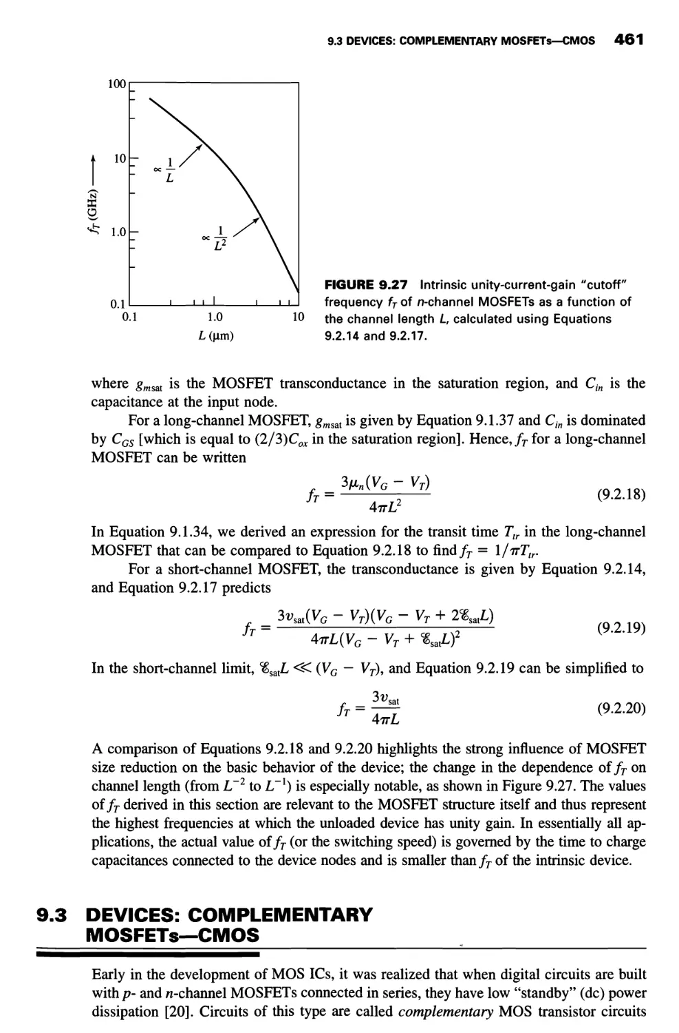
/


Теги: integrated circuits


Текст
CONTENTS
1. SEMICONDUCTOR ELECTRONICS
1.1 Physics of Semiconductor Materials 2
Band Model of Solids 2
Holes 7
Bond Model 8
Donors and Acceptors 10
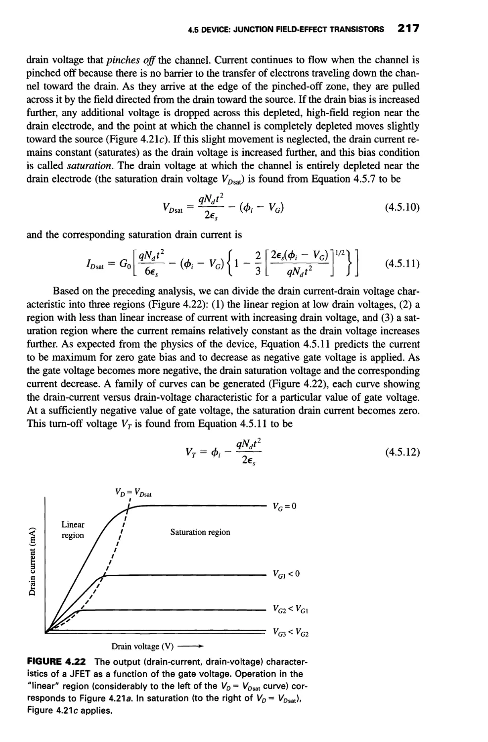
Thermal-Equilibrium Statistics 14
1.2 Free Carriers in Semiconductors 26
Drift Velocity 27
Mobility and Scattering 29
Diffusion Current 35
1.3 Device: Hall-Effect Magnetic Sensor 38
Physics of the Hall Effect 39
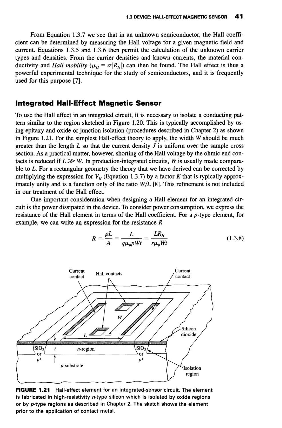
Integrated Hall-Effect Magnetic Sensor 41
Summary 43
Problems 45
Appendix 47
Electric Fields, Charge Configuration, and Gauss' Law 47
2. SILICON TECHNOLOGY
2.1 The Silicon Planar Process 56
2.2 Crystal Growth 62
2.3 Thermal Oxidation 66
Oxidation Kinetics 68
2.4 Lithography and Pattern Transfer 74
2.5 Dopant Addition and Diffusion 80
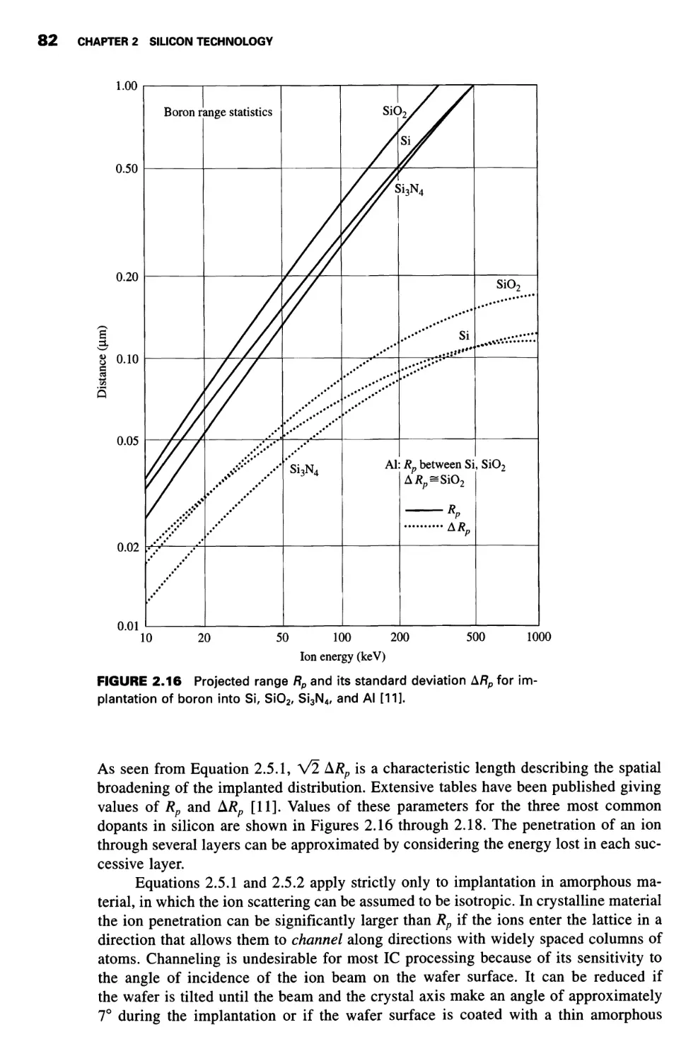
Ion Implantation 80
Diffusion 84
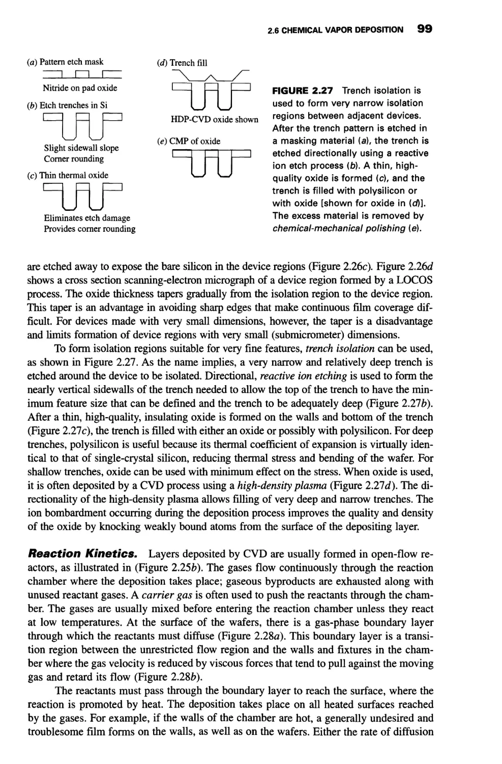
2.6 Chemical Vapor Deposition 95
Epitaxy 95
Nonepitaxial Films 96
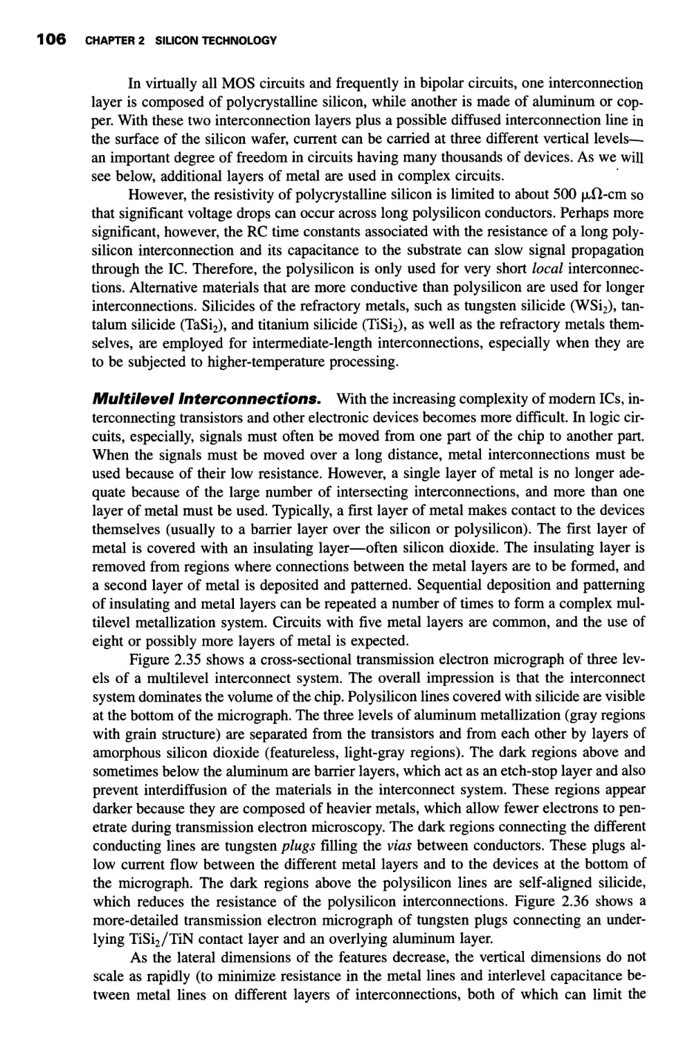
2.7 Interconnection and Packaging 104
Interconnections 104
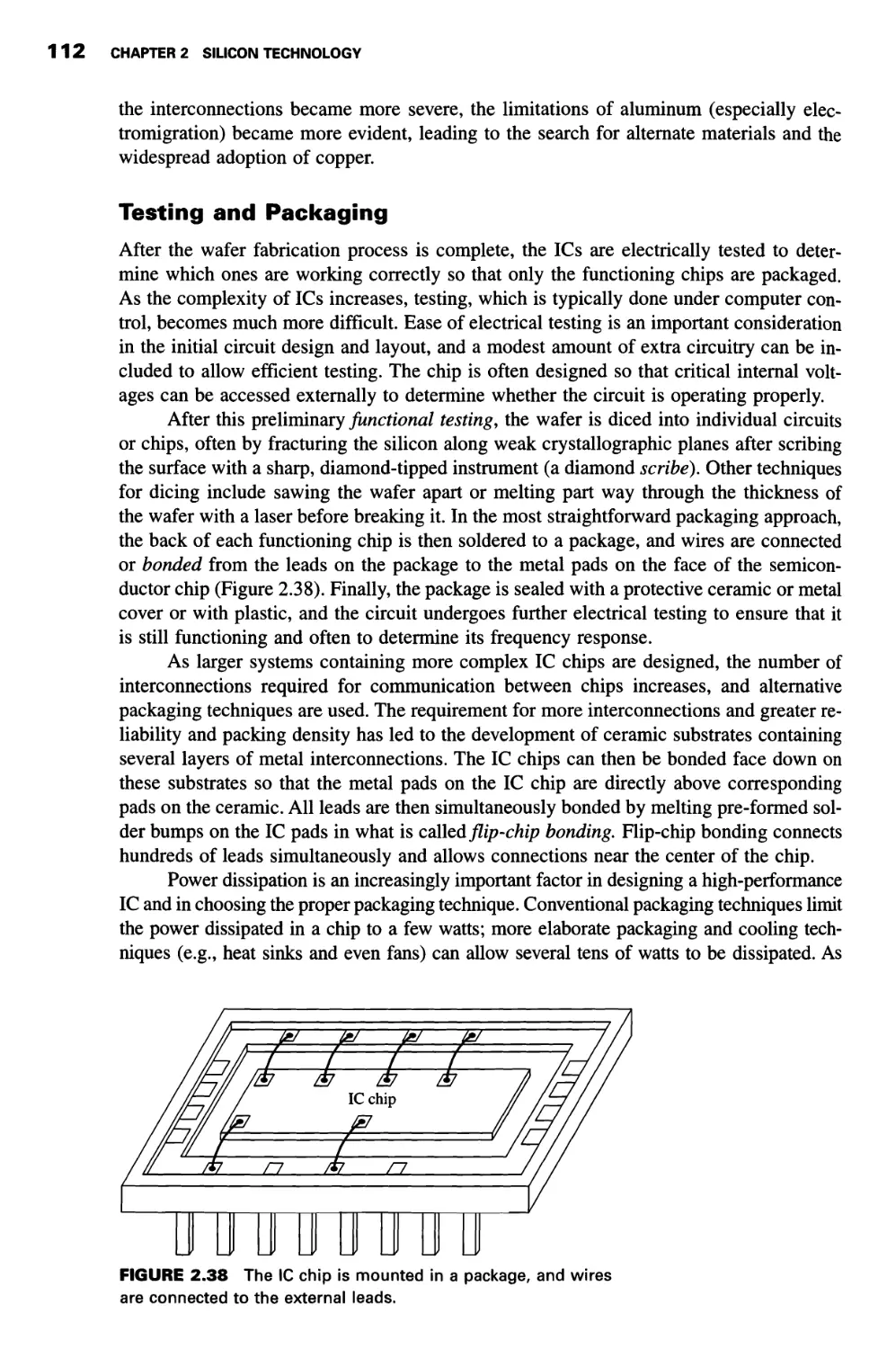
Testing and Packaging 112
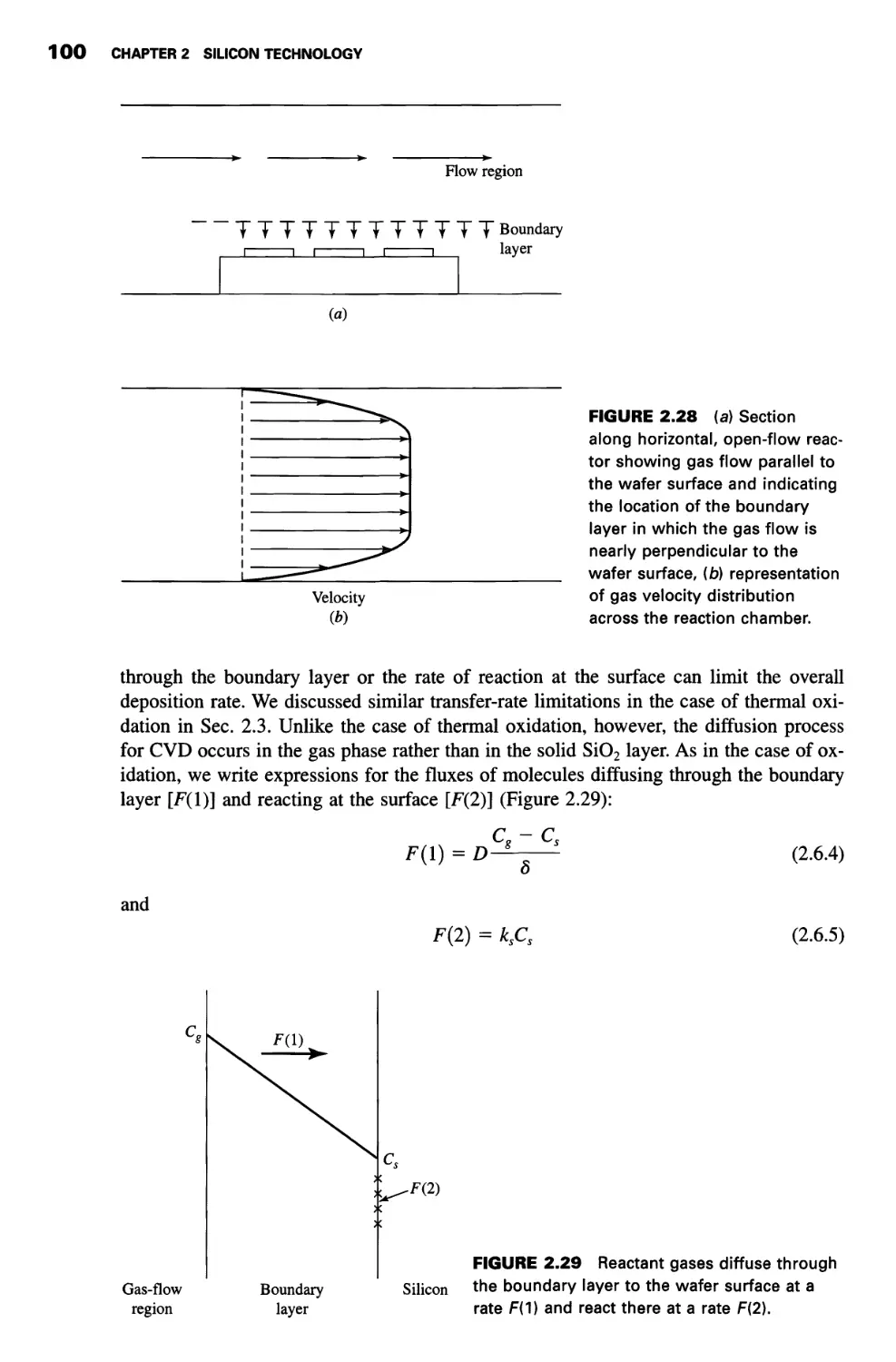
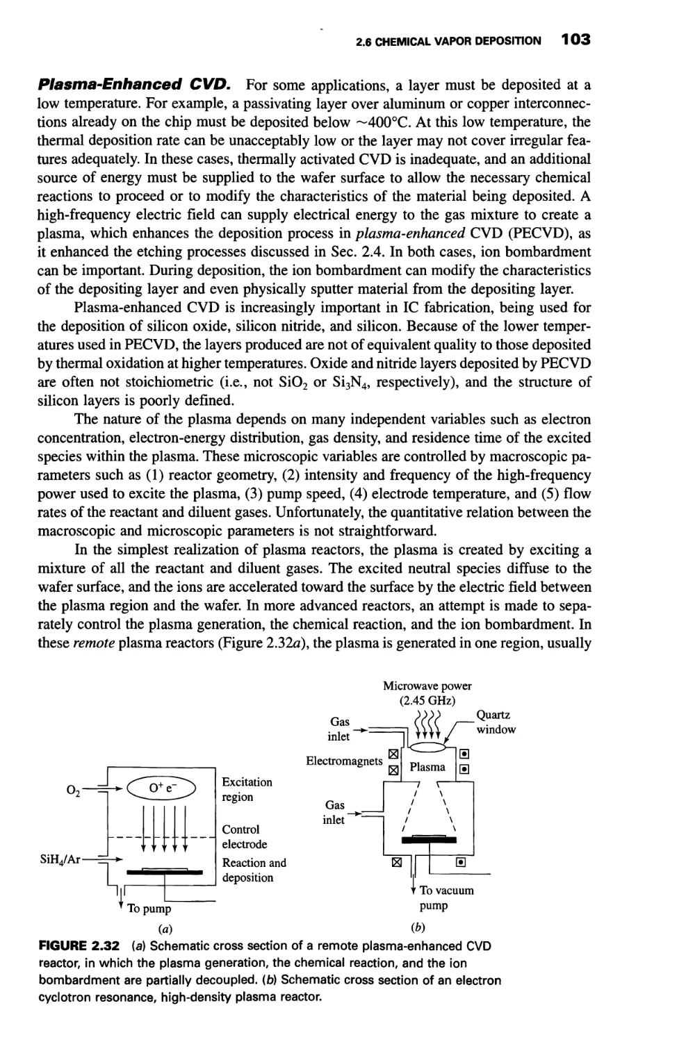
Contamination 113
xiii
xiv
CONTENTS
2.8 Compound-Semiconductor Processing 113
2.9 Numerical Simulation 117
Basic Concept of Simulation 117
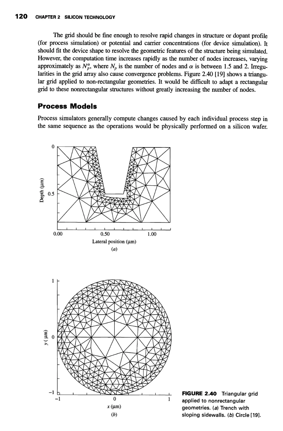
Grids 119
Process Models 120
Device Simulation 127
Simulation Challenges 128
2.10 Device: Integrated-Circuit Resistor 128
Summary 133
Problems 135
3. METAL-SEMICONDUCTOR CONTACTS
3.1 Equilibrium in Electronic Systems 140
Metal-Semiconductor System 140
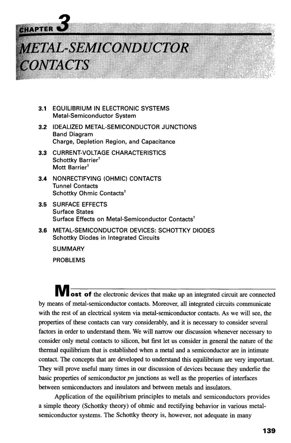
3.2 Idealized Metal-Semiconductor Junctions 141
Band Diagram 141
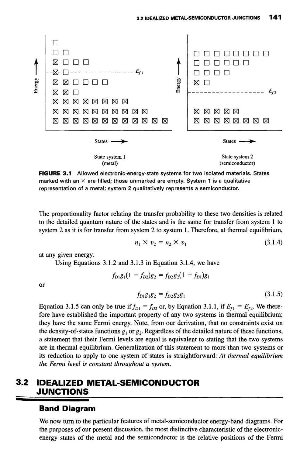
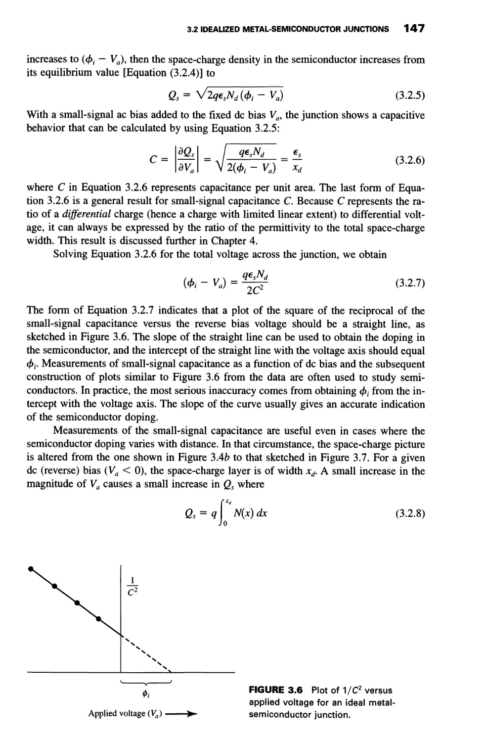
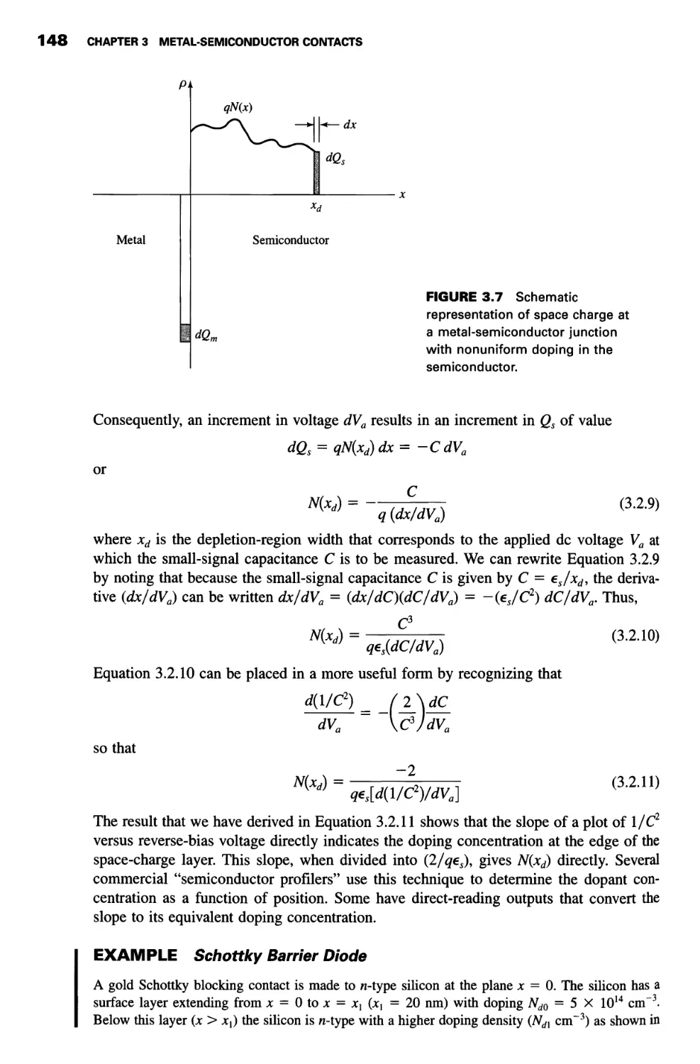
Charge, Depletion Region, and Capacitance 145
3.3 Current-Voltage Characteristics 152
Schottky Barrier1 153
Mott Barrier1 155
3.4 Nonrectifying (Ohmic) Contacts 158
Tunnel Contacts 158
Schottky Ohmic Contacts1 159
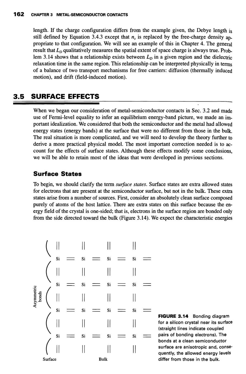
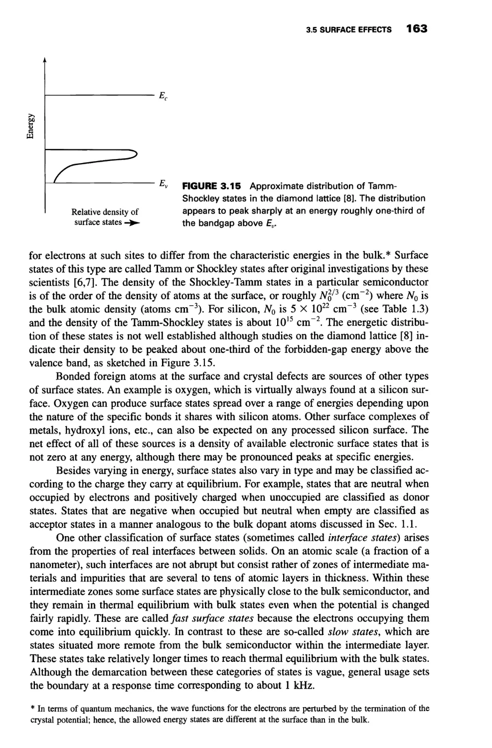
3.5 Surface Effects 162
Surface States 162
Surface Effects on Metal-Semiconductor Contacts1 164
3.6 Metal-Semiconductor Devices: Schottky Diodes 166
Schottky Diodes in Integrated Circuits 167
Summary 169
Problems 171
4. pn JUNCTIONS
4.1 Graded Impurity Distributions 175
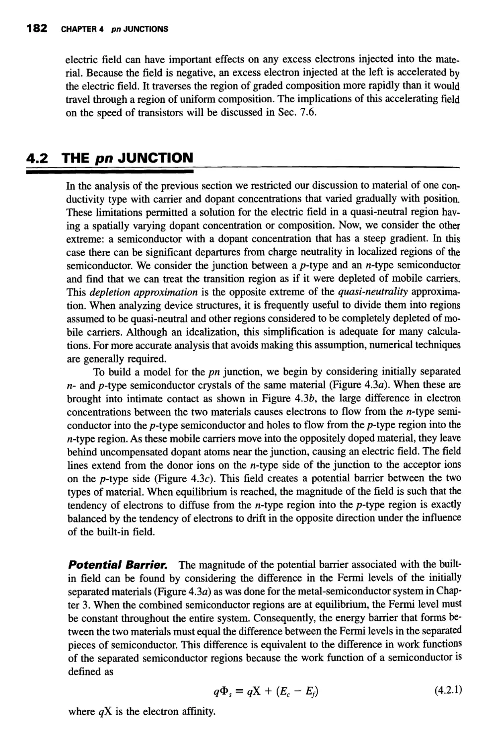
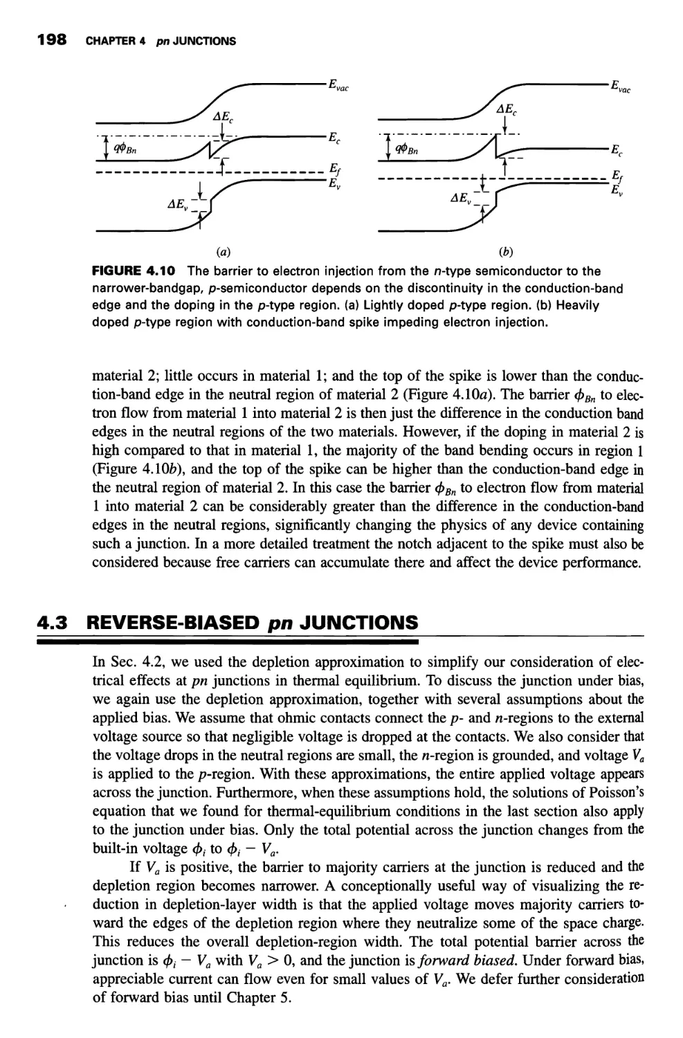
4.2 The /m Junction 182
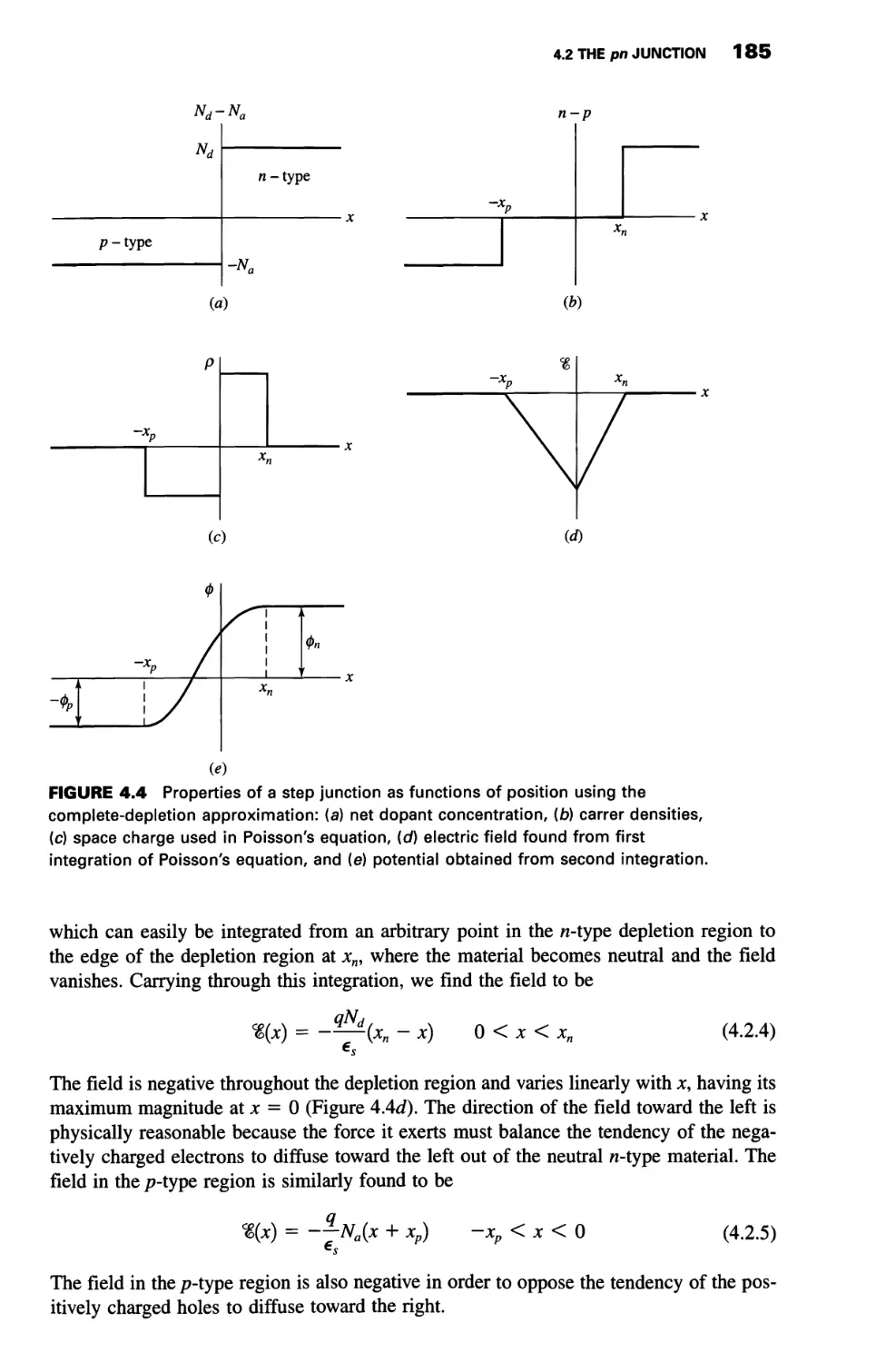
Step Junction 184
Linearly Graded Junction 191
Heterojunctions 194
4.3 Reverse-Biased pn Junctions 198
4.4 Junction Breakdown 203
Avalanche Breakdown1 204
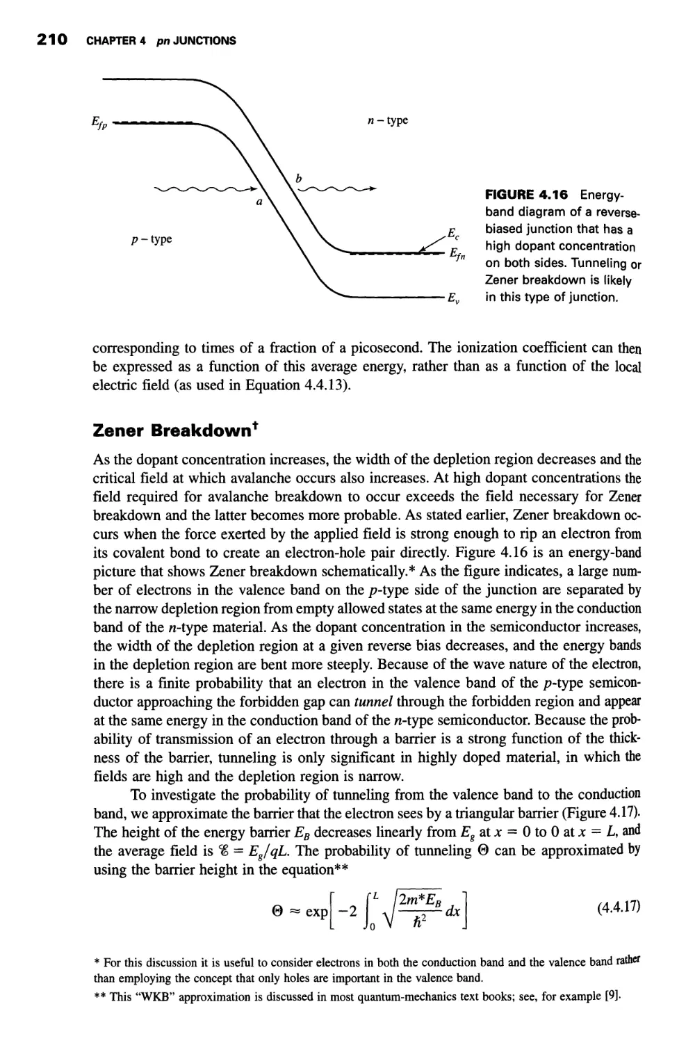
Zener Breakdown1 210
CONTENTS XV
4.5 Device: Junction Field-Effect Transistors 212
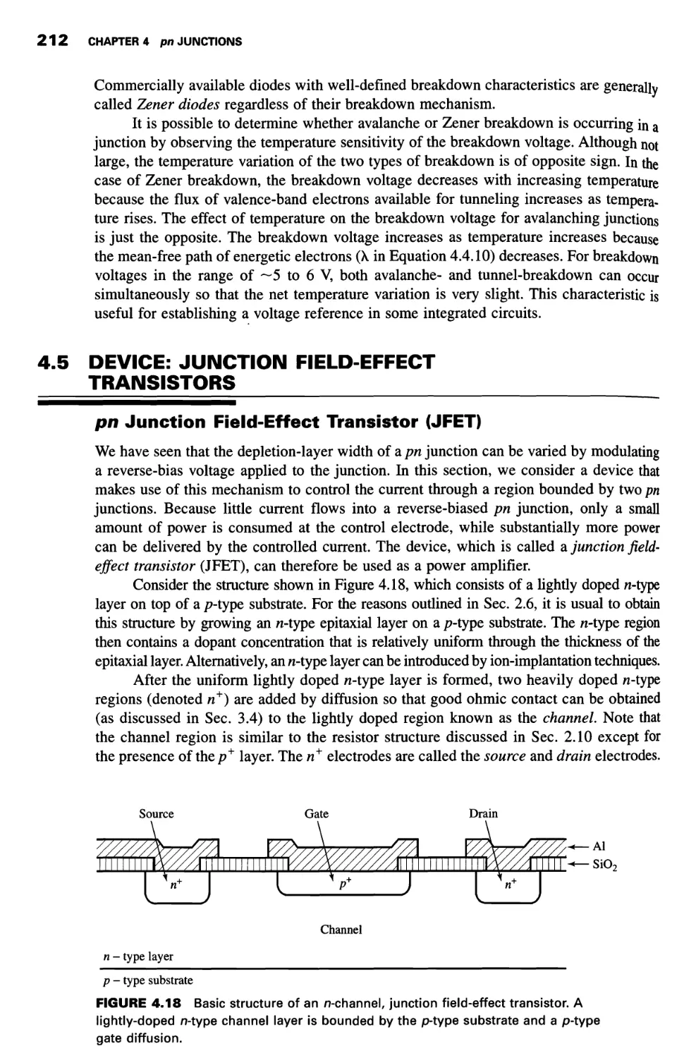
pn Junction Field-Effect Transistor (JFET) 212
Metal-Semiconductor Field-Effect Transistor (MESFET) 219
Summary 221
Problems 222
5. CURRENTS IN pn JUNCTIONS
5.1 Continuity Equation 227
5.2 Generation and Recombination 228
Localized States: Capture and Emission 229
Shockley-Hall-Read Recombination1 231
Excess-Carrier Lifetime 233
5.3 Current-Voltage Characteristics of pn Junctions 238
Boundary Values of Minority-Carrier Densities 239
Ideal-Diode Analysis 240
Space-Charge-Region Currents1 247
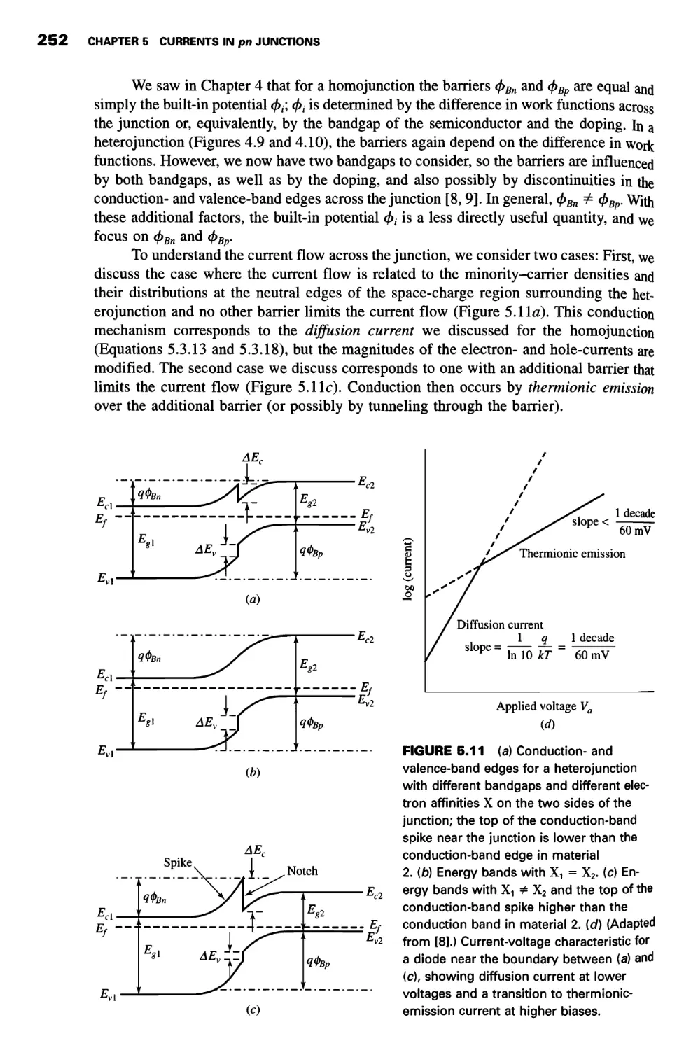
Heteroj unctionsf 251
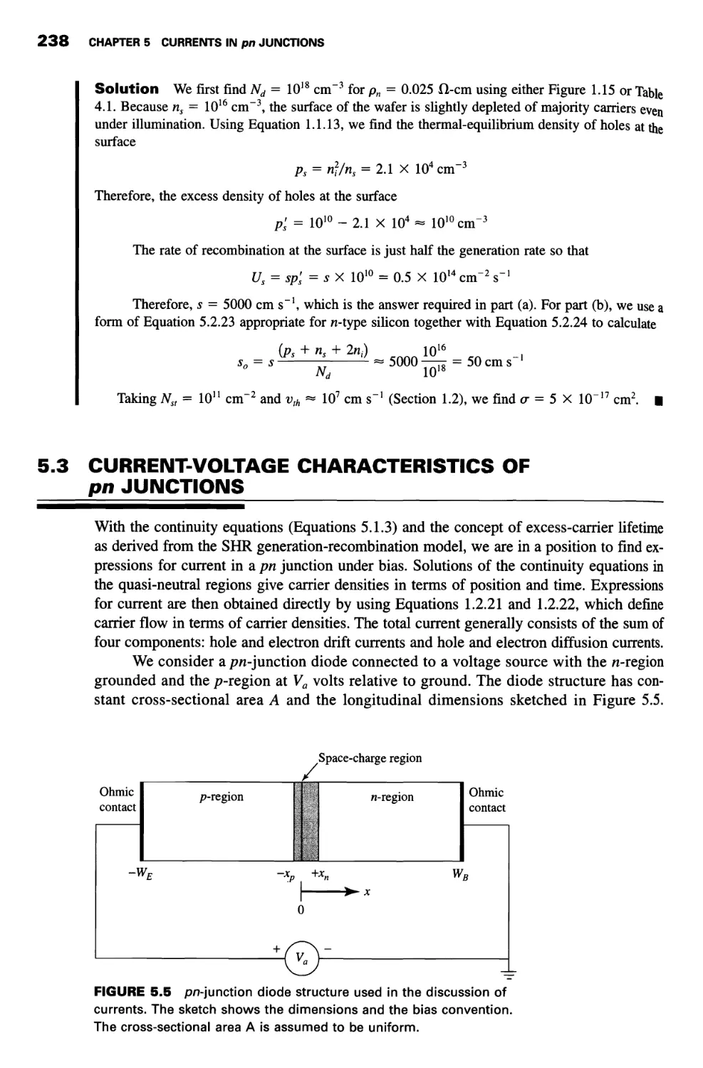
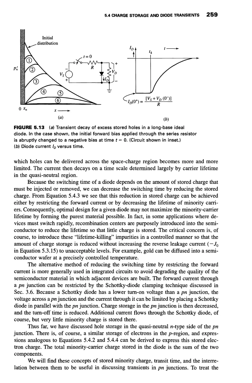
5.4 Charge Storage and Diode Transients 256
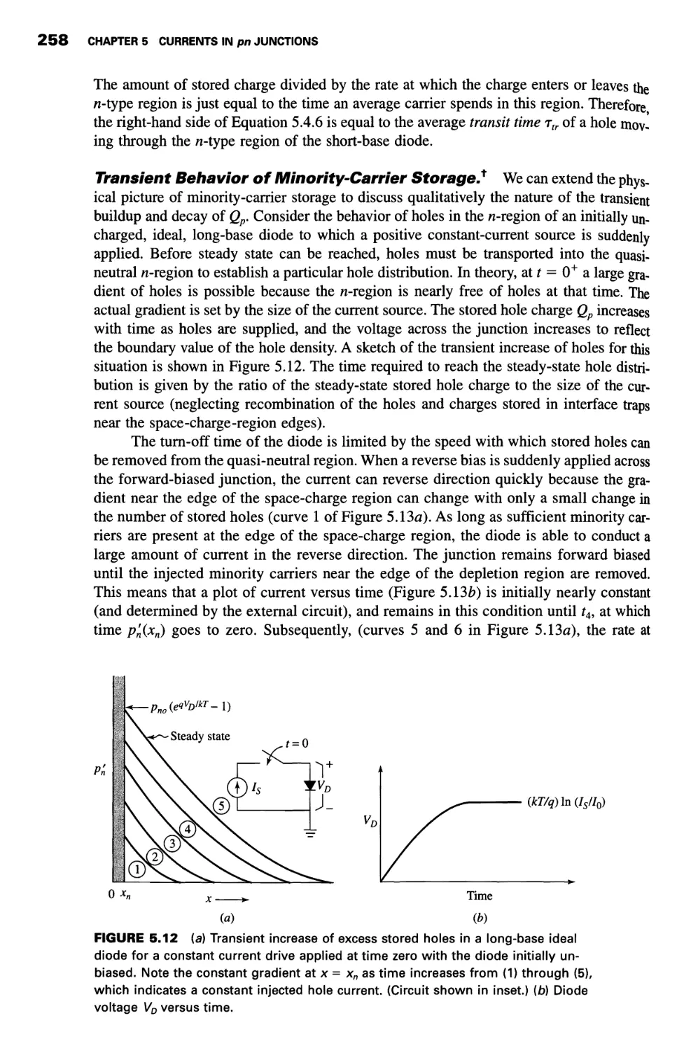
Minority-Carrier Storage 257
5.5 Device Modeling and Simulation 262
Lumped-Element Model 262
Distributed Simulation1 264
5.6 Devices 268
Integrated-Circuit Diodes 268
Light-Emitting Diodes 272
Summary 273
Problems 274
6. BIPOLAR TRANSISTORS I: BASIC PROPERTIES
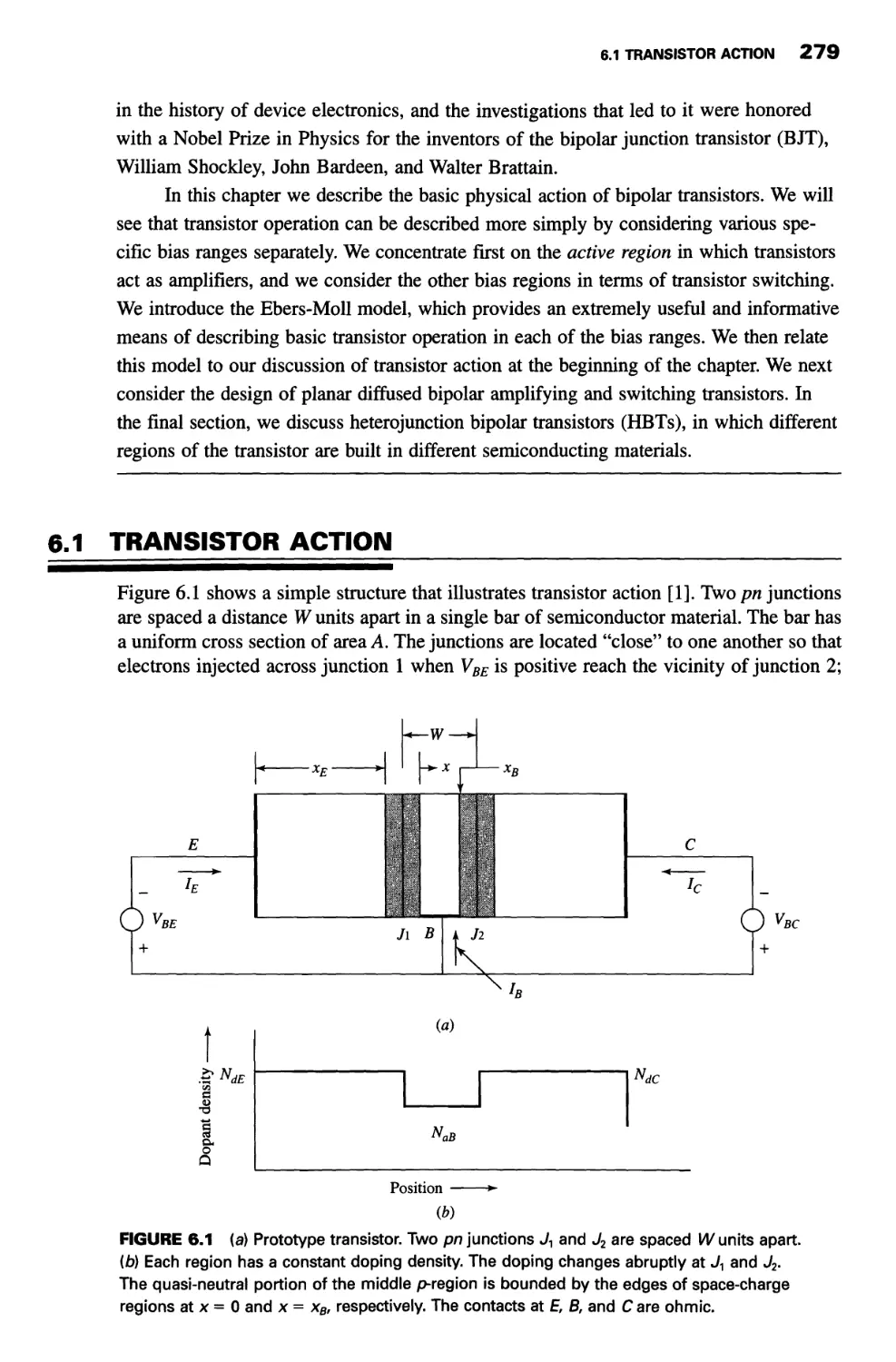
6.1 Transistor Action 279
Prototype Transistor 282
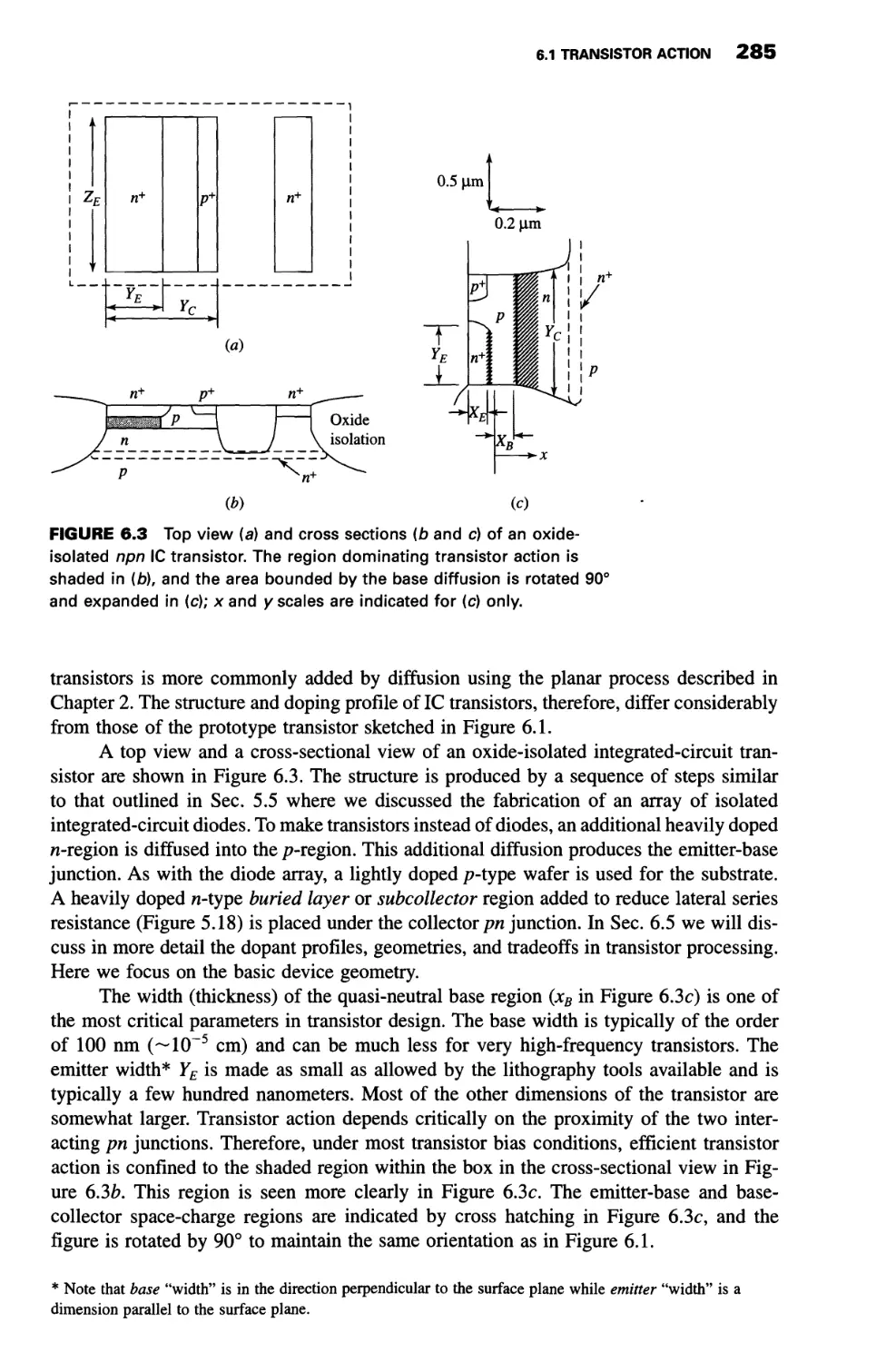
Transistors for Integrated Circuits 284
6.2 Active Bias 286
Current Gain 288
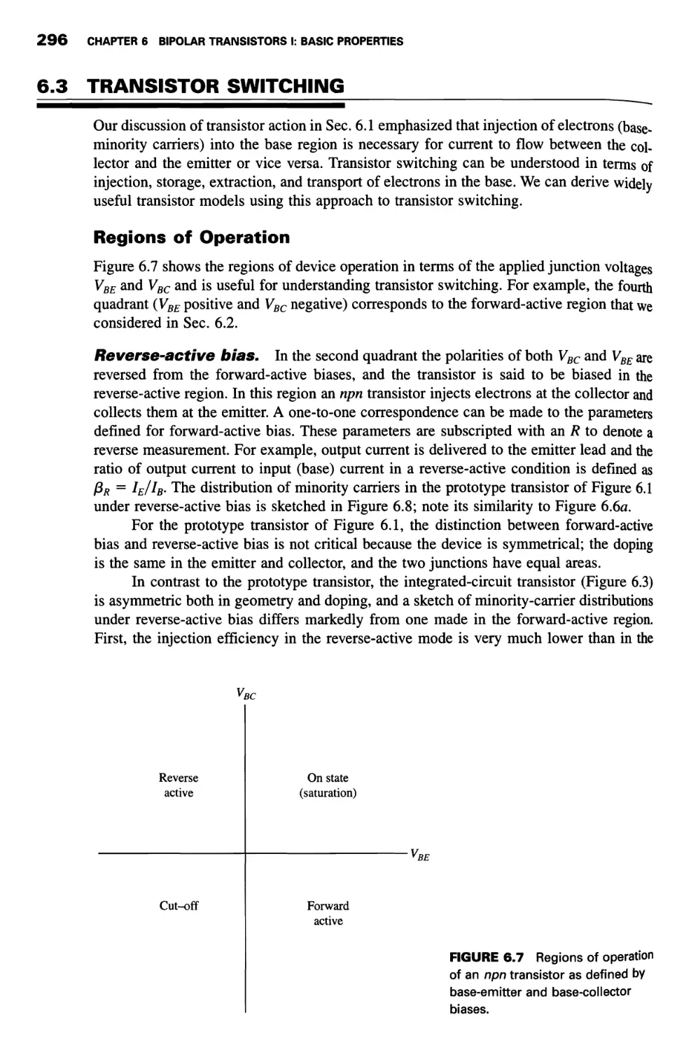
6.3 Transistor Switching 296
Regions of Operation 296
6.4 Ebers-Moll Model 300
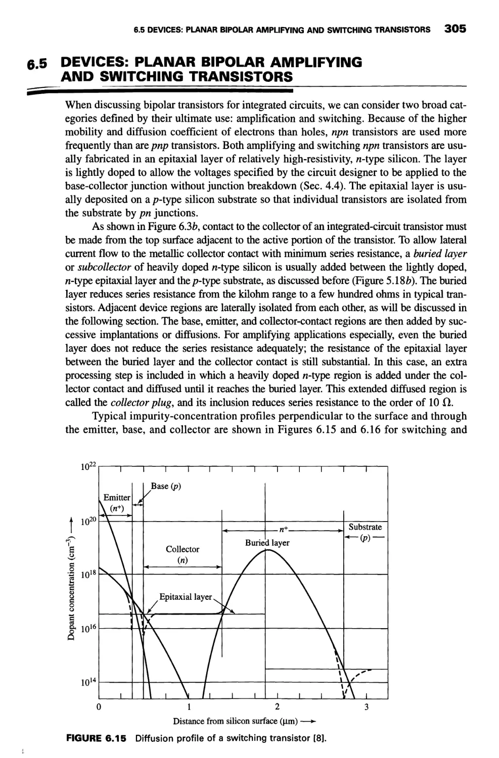
6.5 Devices: Planar Bipolar Amplifying and Switching Transistors 305
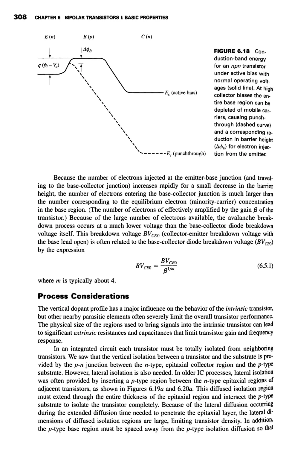
Process Considerations 308
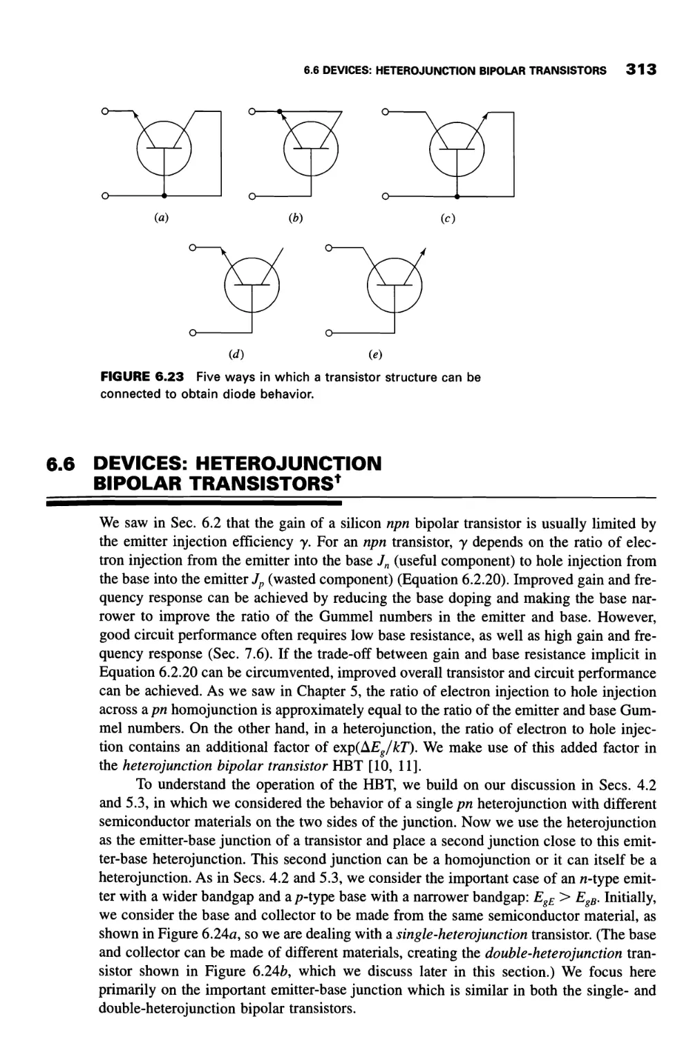
6.6 Devices: Heterojunction Bipolar Transistors1 313
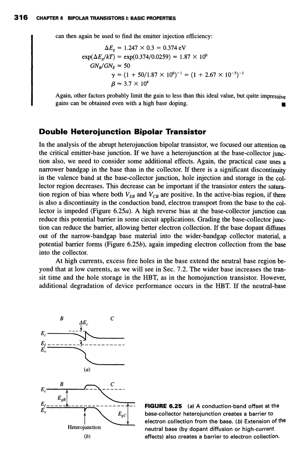
Double Heterojunction Bipolar Transistor 316
XVi CONTENTS
Bandgap Grading in Quasi-Neutral Base Region 317
Summary 320
Problems 321
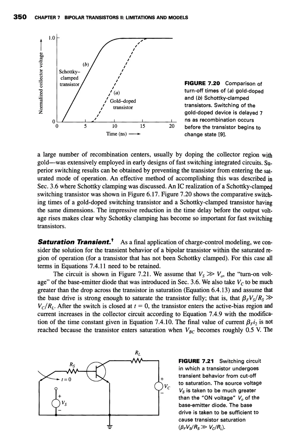
7. BIPOLAR TRANSISTORS II: LIMITATIONS AND MODELS
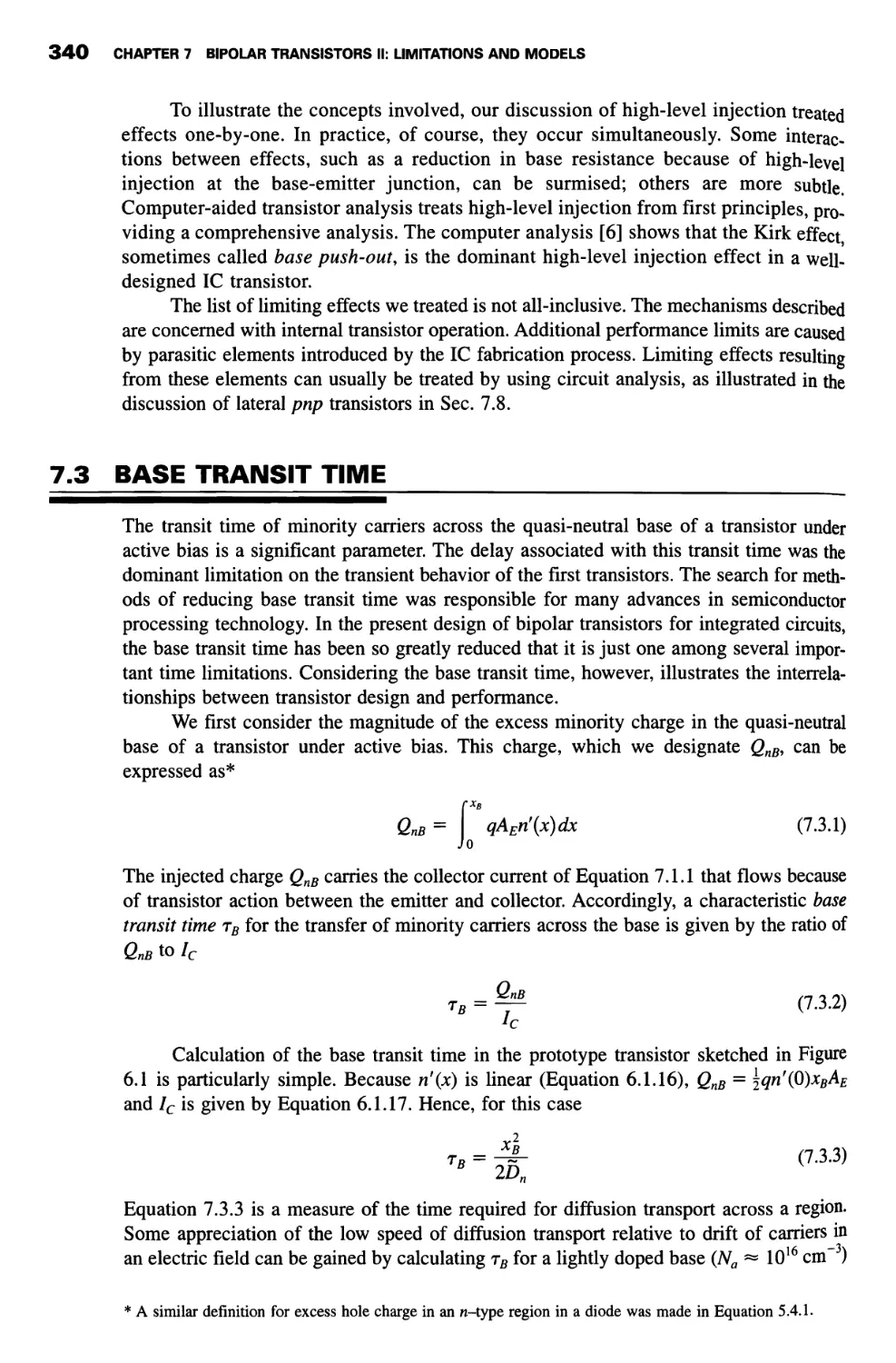
7.1 Effects of Collector Bias Variation (Early Effect) 325
7.2 Effects at Low and High Emitter Bias 328
Currents at Low Emitter Bias 329
High-Level Injection 330
Base Resistance 335
7.3 Base Transit Time 340
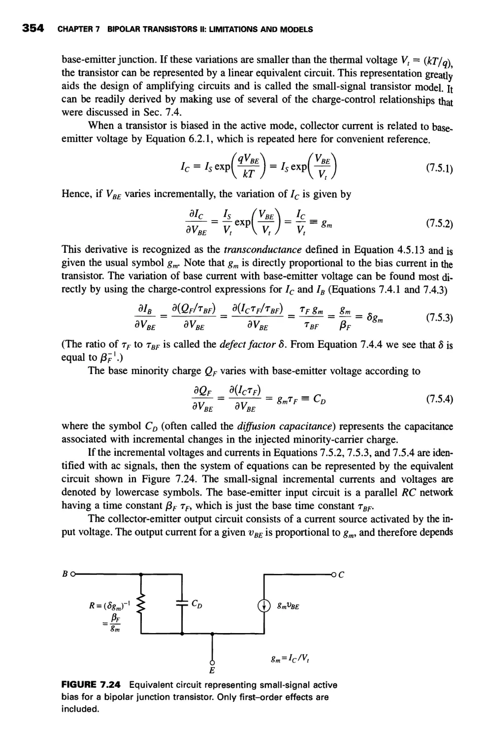
7.4 Charge-Control Model 342
Applications of the Charge-Control Model 345
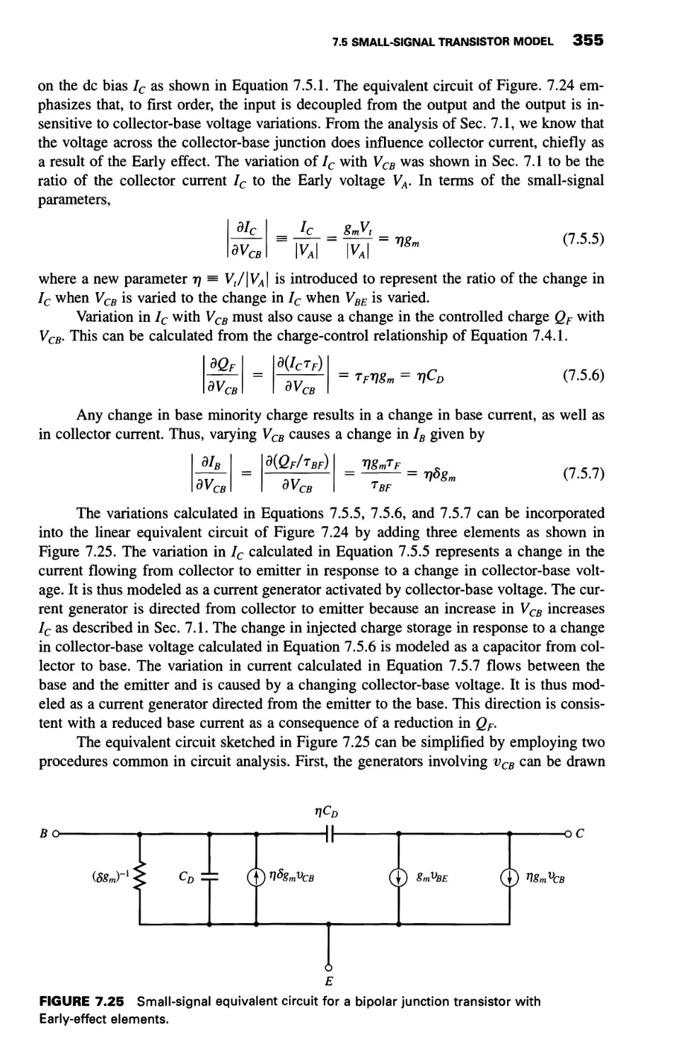
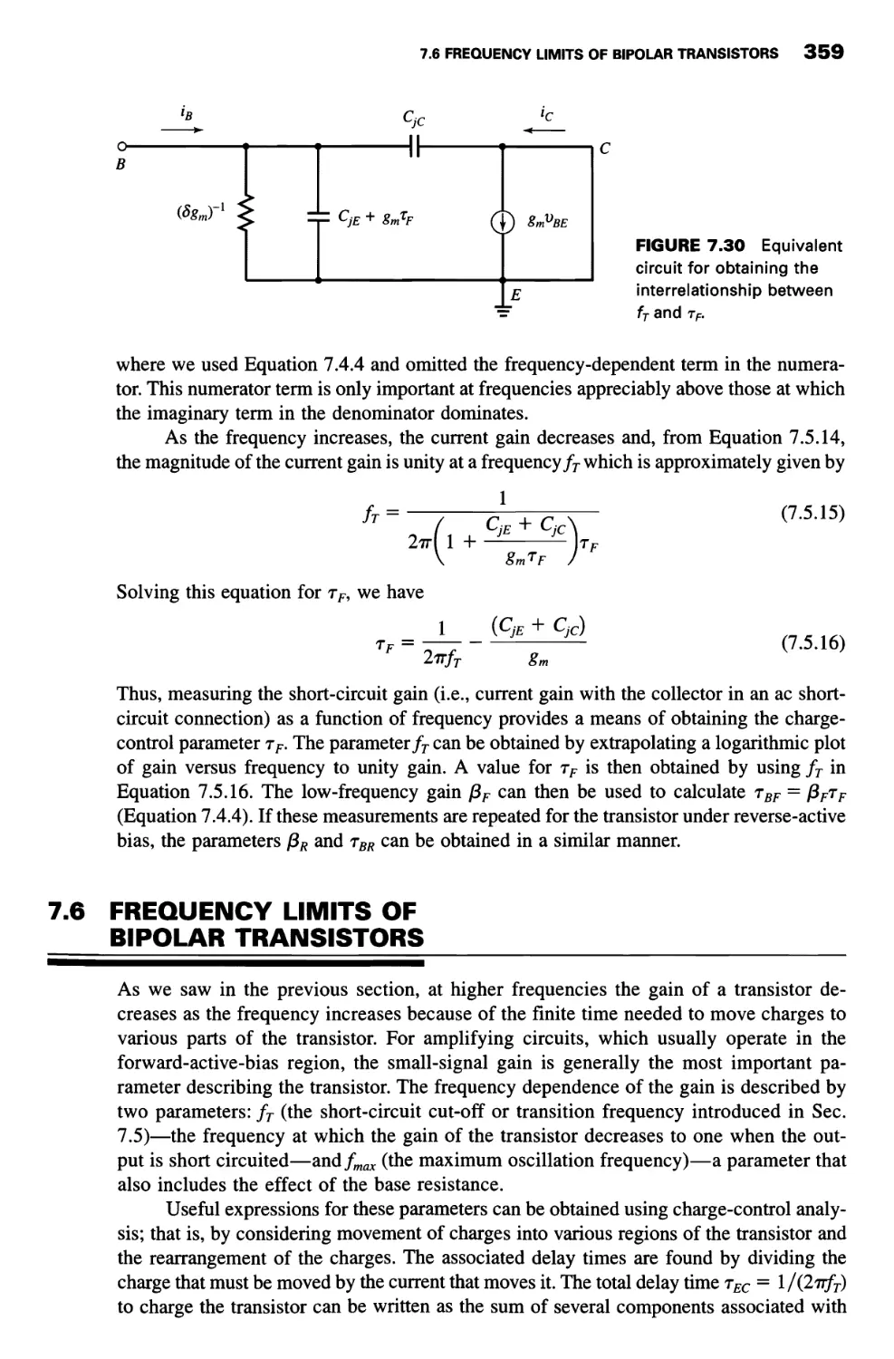
7.5 Small-Signal Transistor Model 353
7.6 Frequency Limits of Bipolar Transistors 359
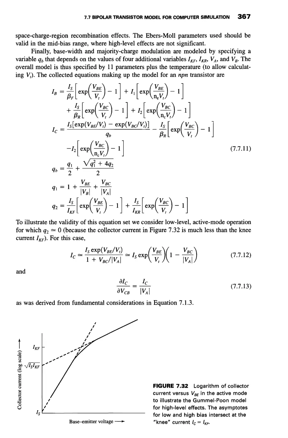
7.7 Bipolar Transistor Model for Computer Simulation1 364
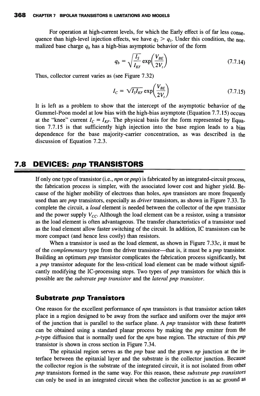
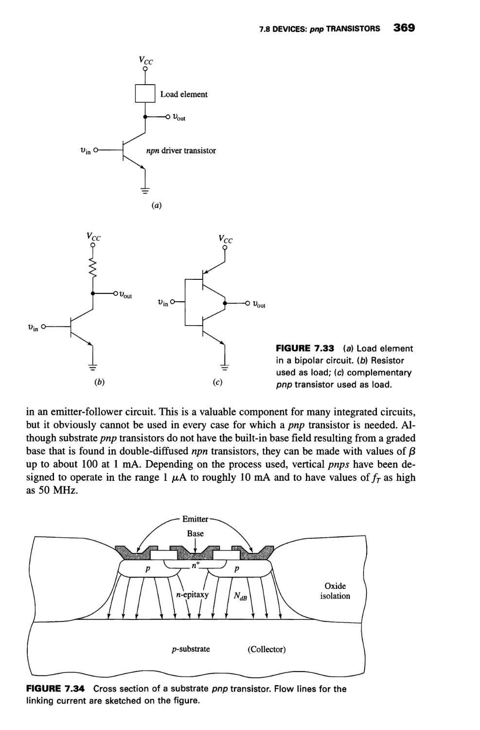
7.8 Devices: pnp Transistors 368
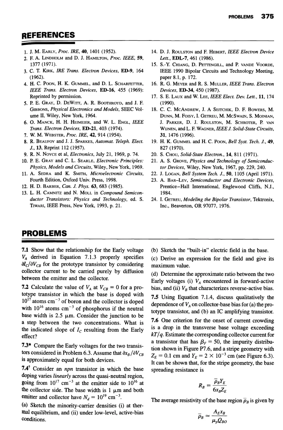
Substrate pnp Transistors 368
Lateral pnp Transistors 370
Summary 374
Problems 375
8. PROPERTIES OF THE METAL-OXIDE-SILICON SYSTEM
8.1 The Ideal MOS Structure 381
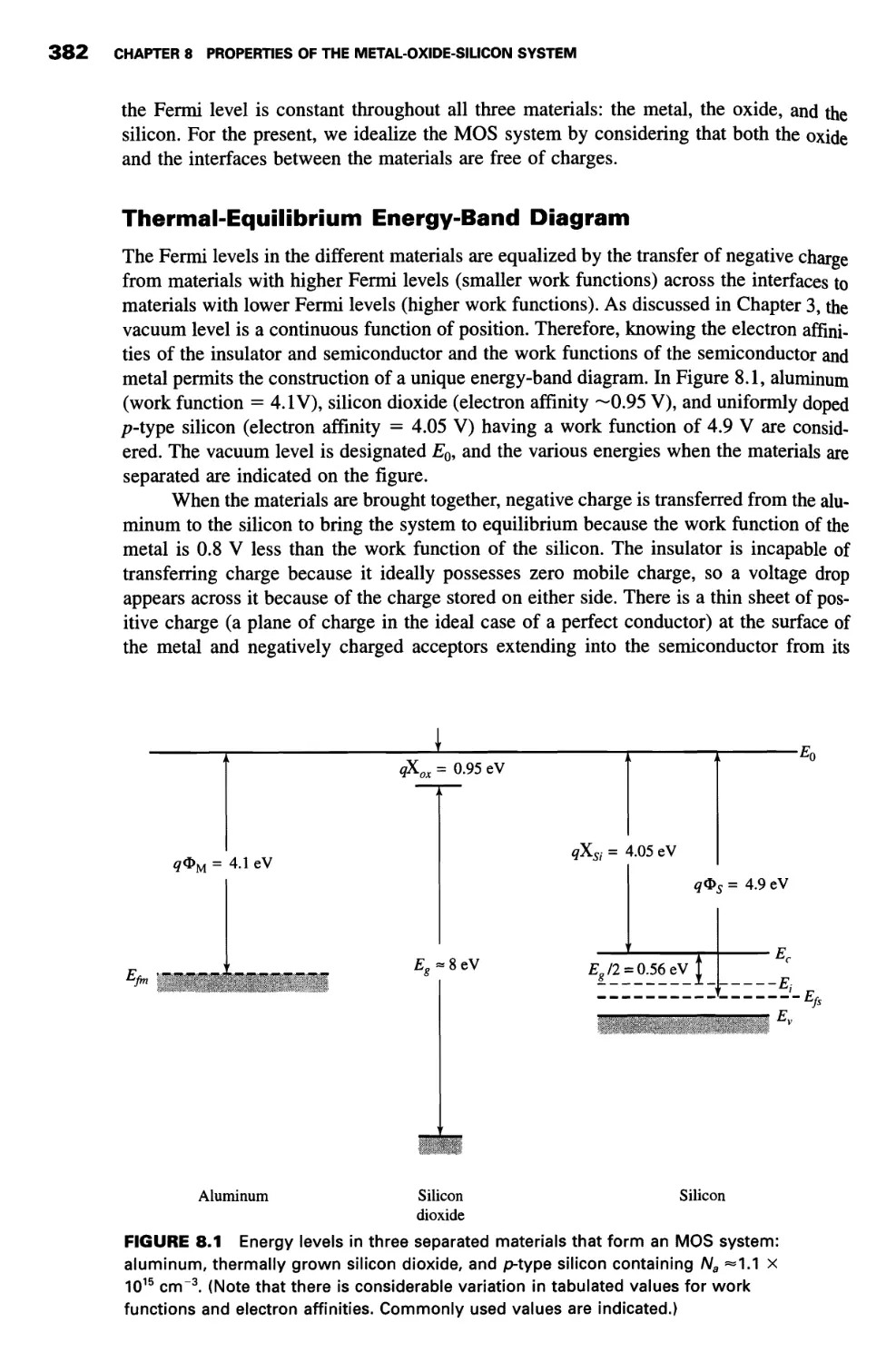
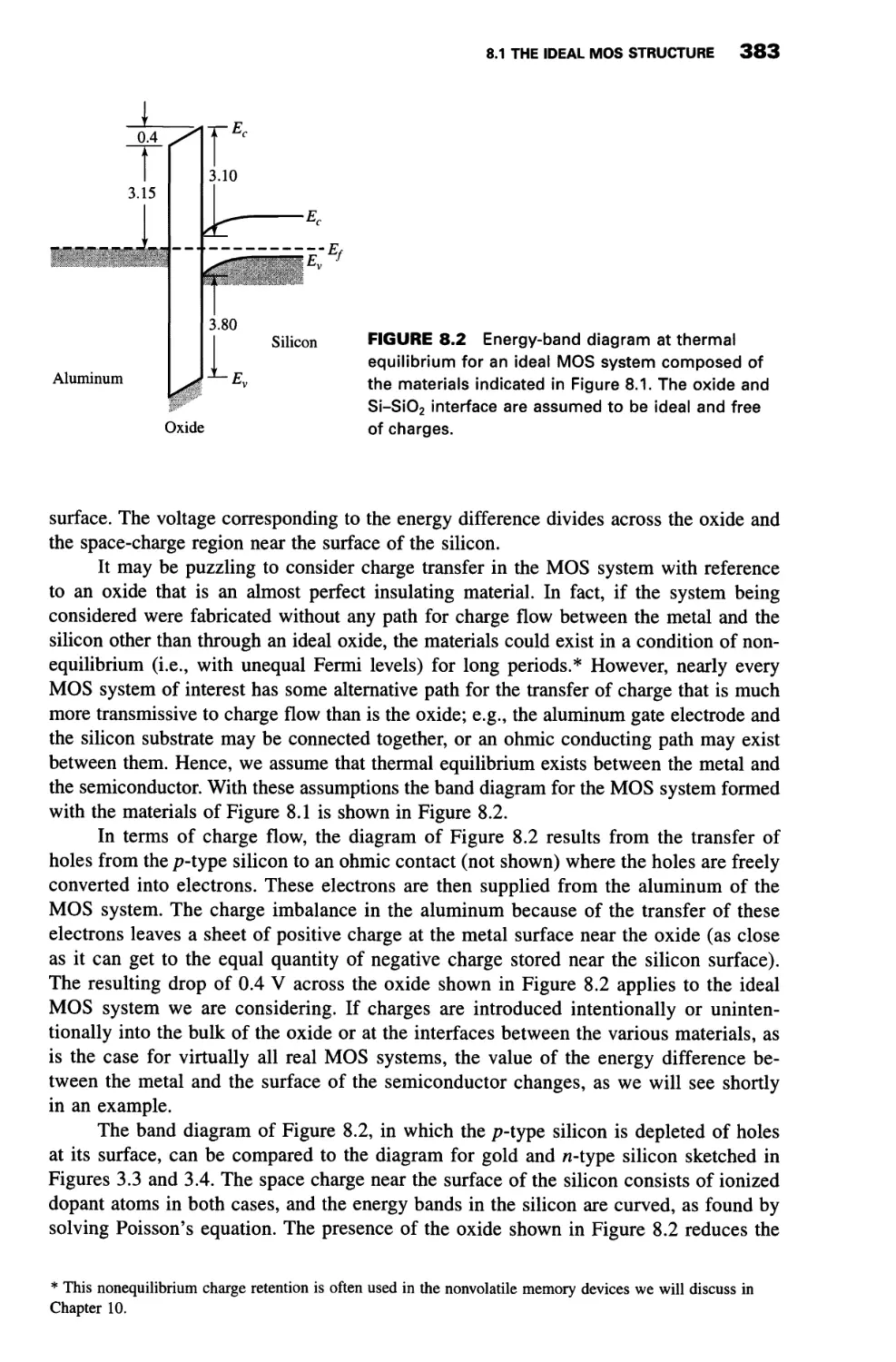
Thermal-Equilibrium Energy-Band Diagram 382
Poly silicon and Metals as Gate-Electrode Materials 385
The Flat-Band Voltage 385
8.2 Analysis of the Ideal MOS Structure 387
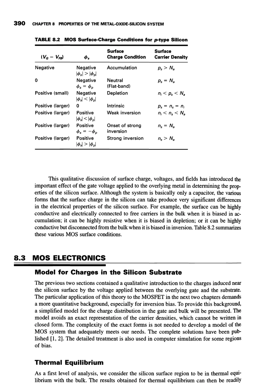
Qualitative Description 387
8.3 MOS Electronics 390
Model for Charges in the Silicon Substrate 390
Thermal-Equilibrium 390
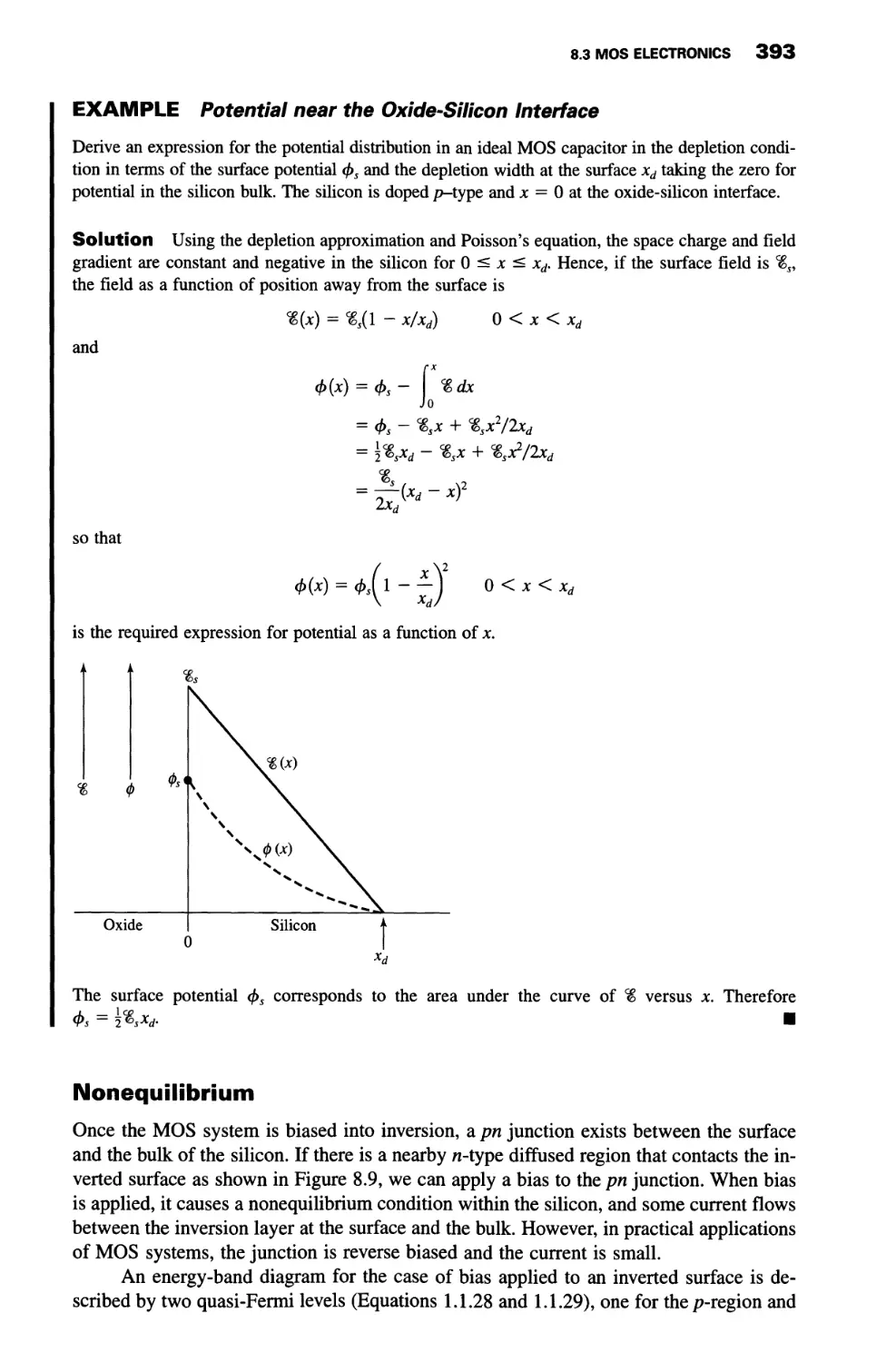
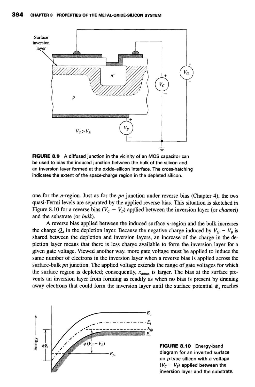
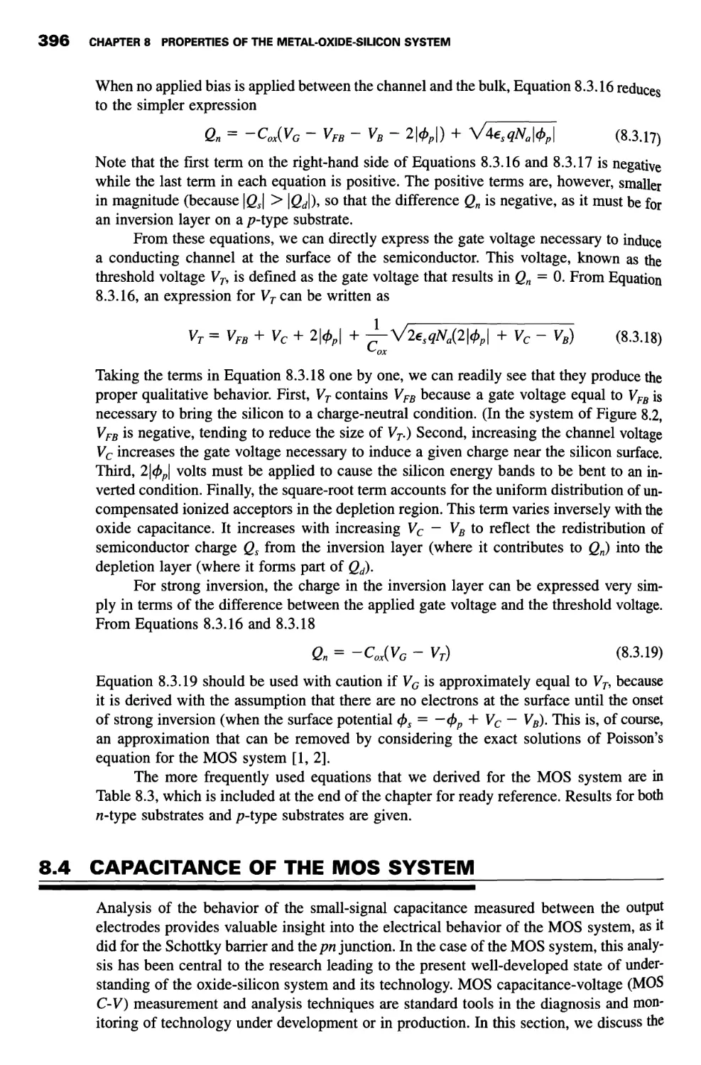
Nonequilibrium 393
8.4 Capacitance of the MOS System 396
C-V Behavior of an Ideal MOS System 397
Practical Considerations in C-V Measurements 400
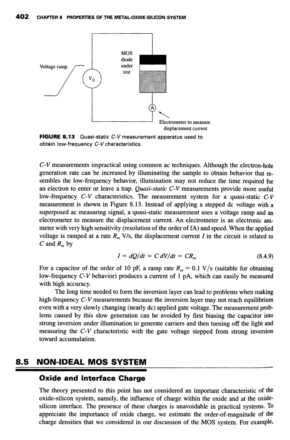
Quasi-Static (Low-Frequency) C- V Measurements 401
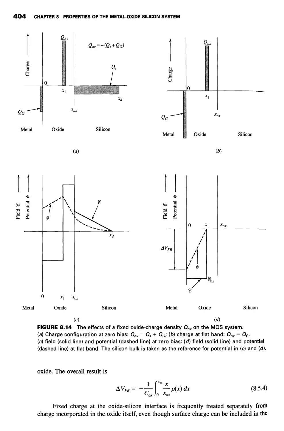
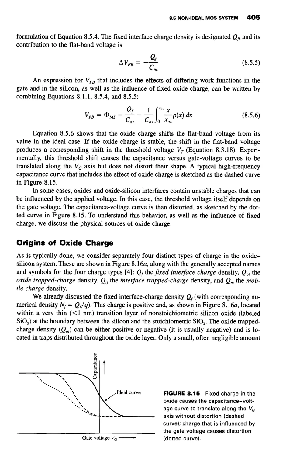
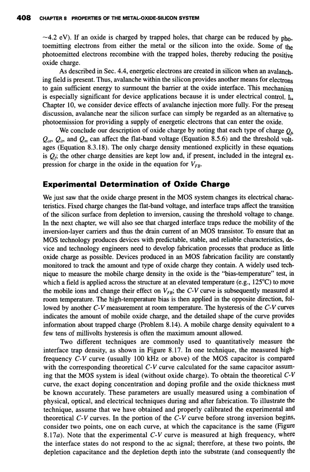
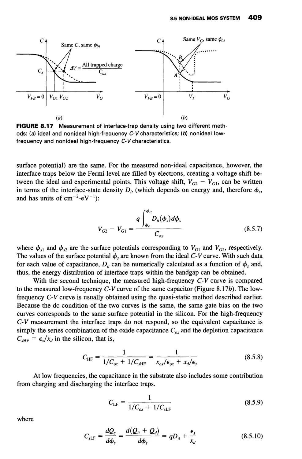
8.5 Non-Ideal MOS System 402
Oxide and Interface Charge 402
Origins of Oxide Charge 405
Experimental Determination of Oxide Charge 408
contents xvii
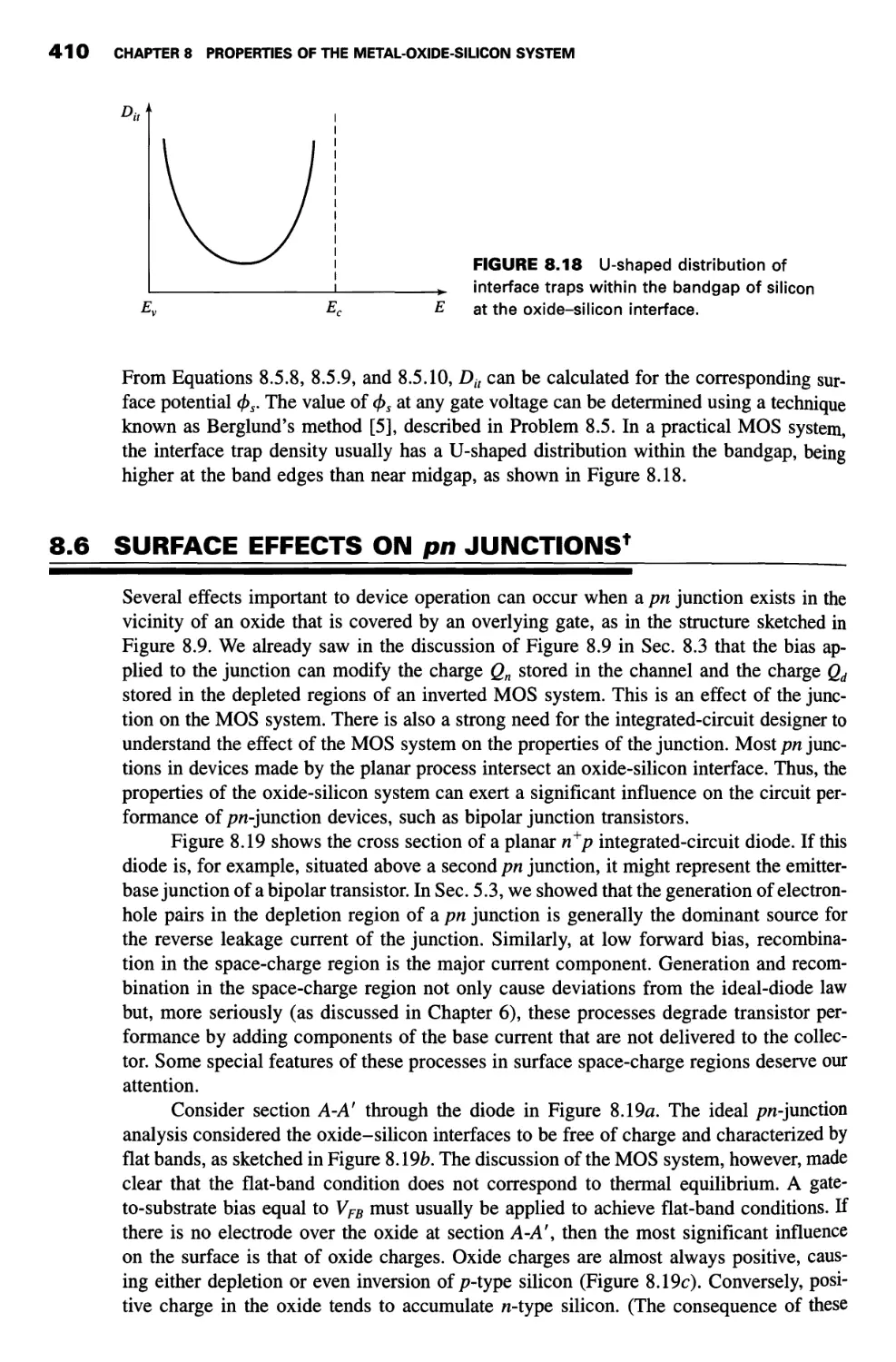
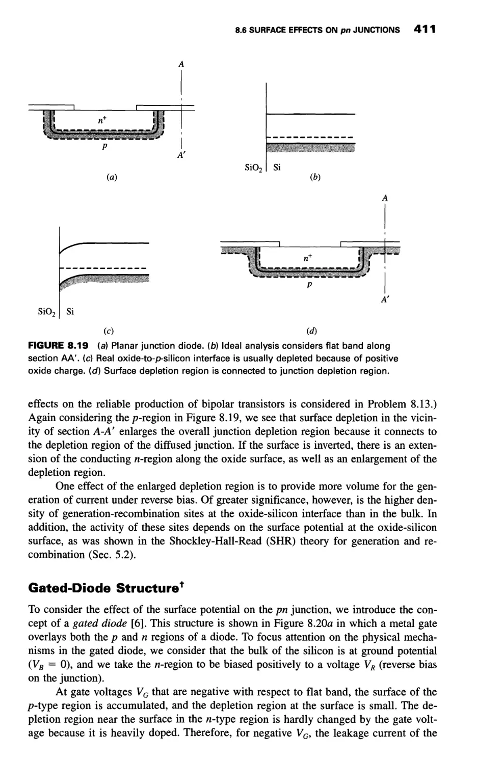
8.6 Surface Effects on pn Junctions1 410
Gated-Diode Structure 411
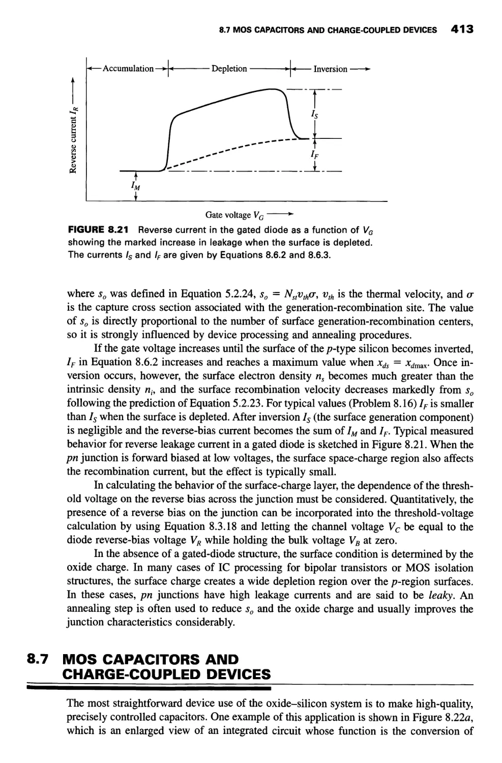
8.7 MOS Capacitors and Charge-Coupled Devices 413
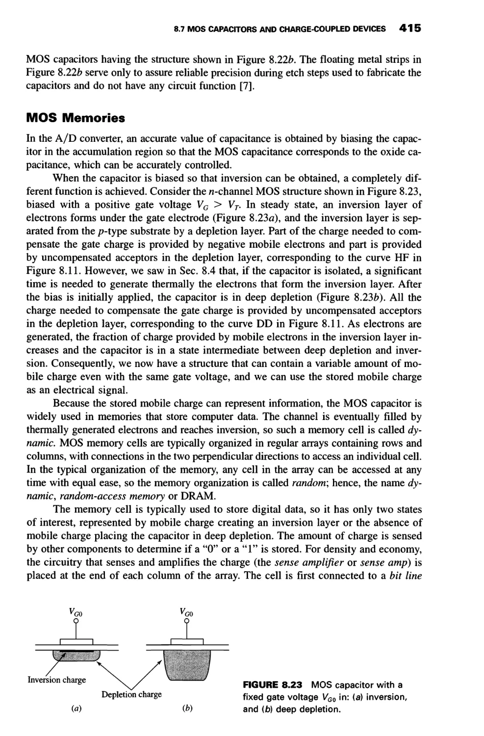
MOS Memories 415
Charge-Coupled Devices 417
Summary 421
Problems 422
9. MOS FIELD-EFFECT TRANSISTORS I: PHYSICAL
EFFECTS AND MODELS
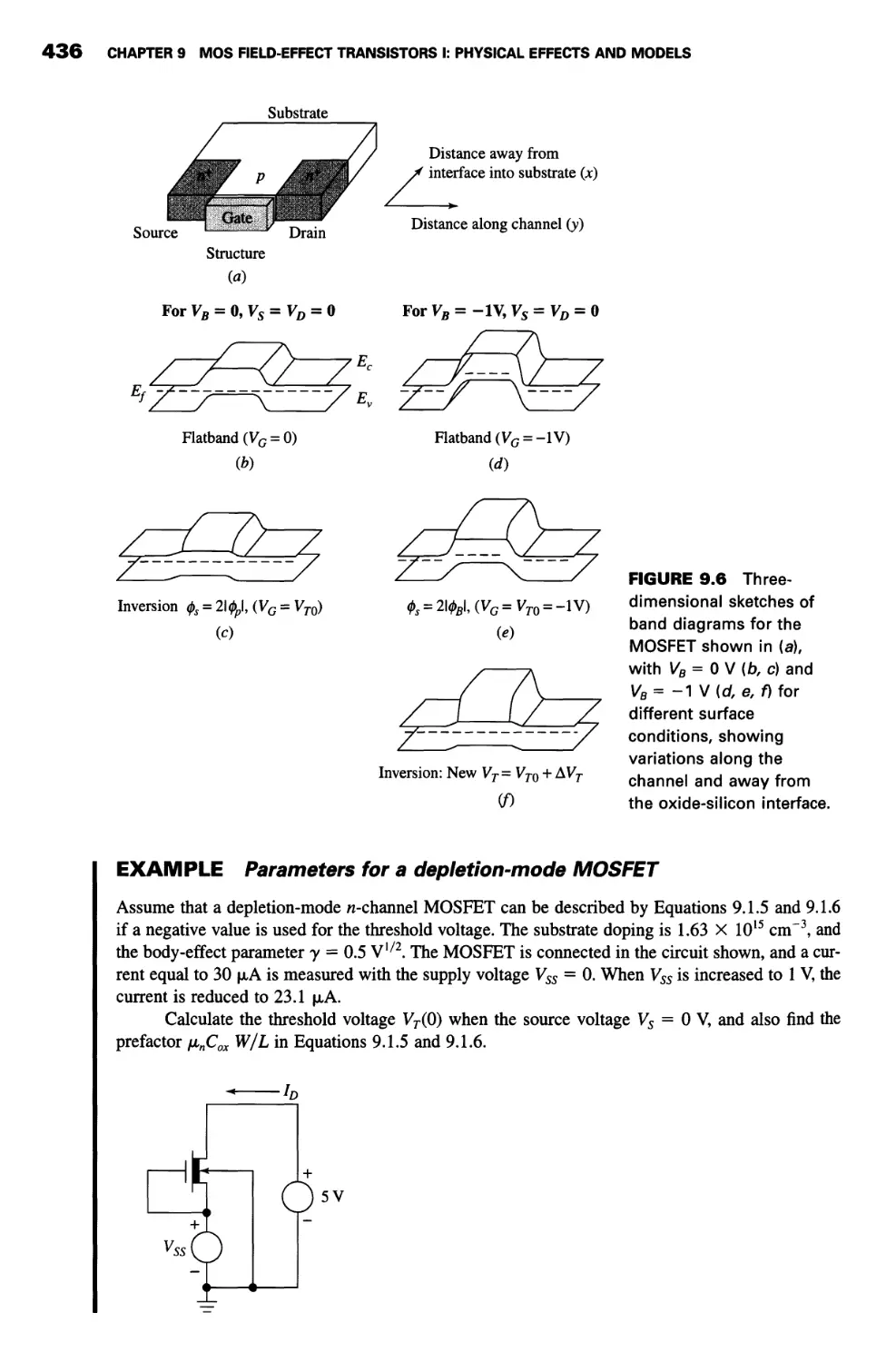
9.1 Basic MOSFET Behavior 429
Strong Inversion Region 431
Channel-Length Modulation 433
Body-Bias Effect 435
Bulk-Charge Effect 437
Threshold-Voltage Adjustment by Ion Implantation 438
Depletion-Mode MOSFETs 442
Subthreshold Conduction 443
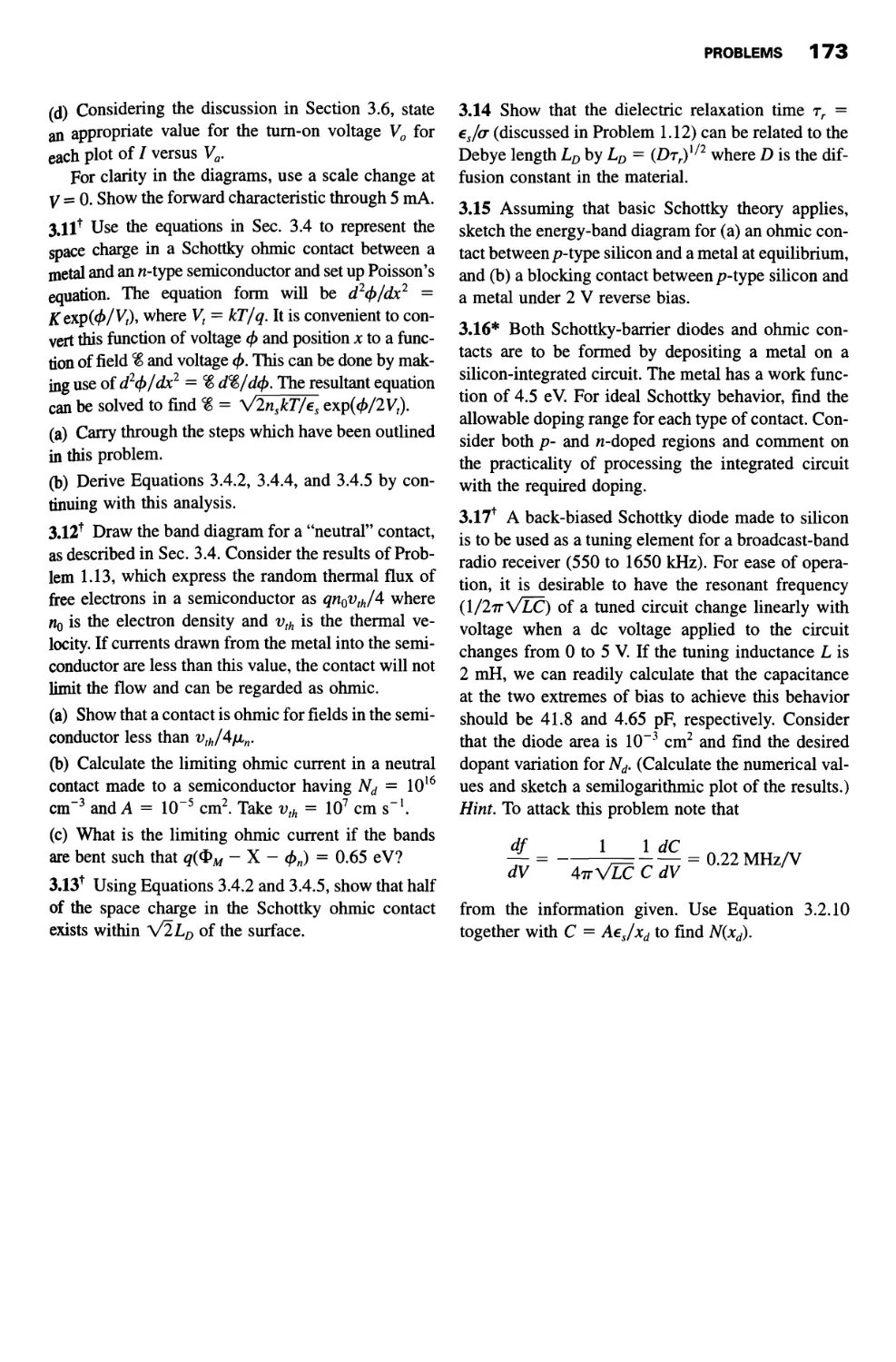
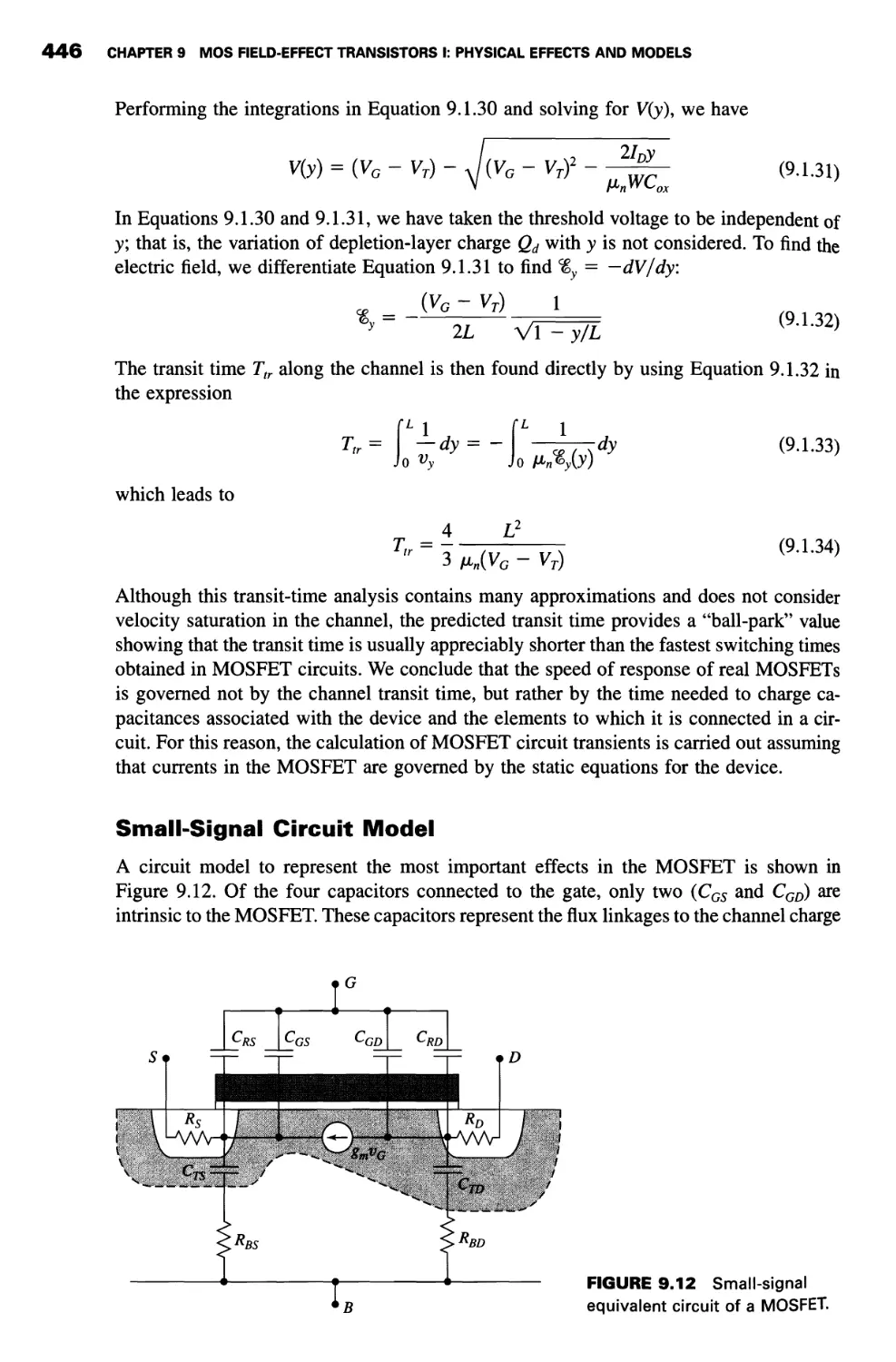
Small-Signal Circuit Model 446
9.2 Improved Models for Short-Channel MOSFETs 447
Limitations of the Long-Channel Analysis 447
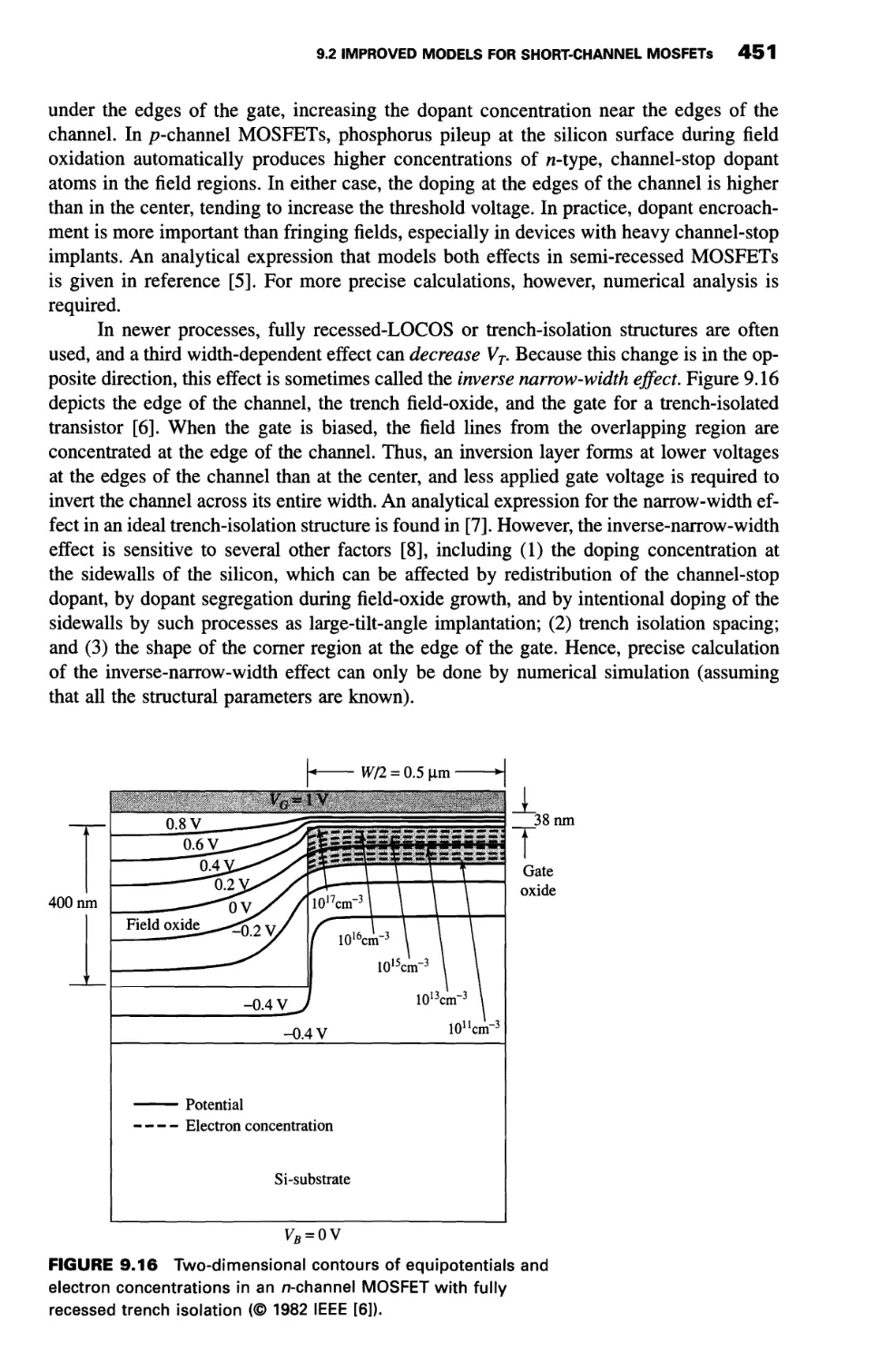
Short-Channel Effects 448
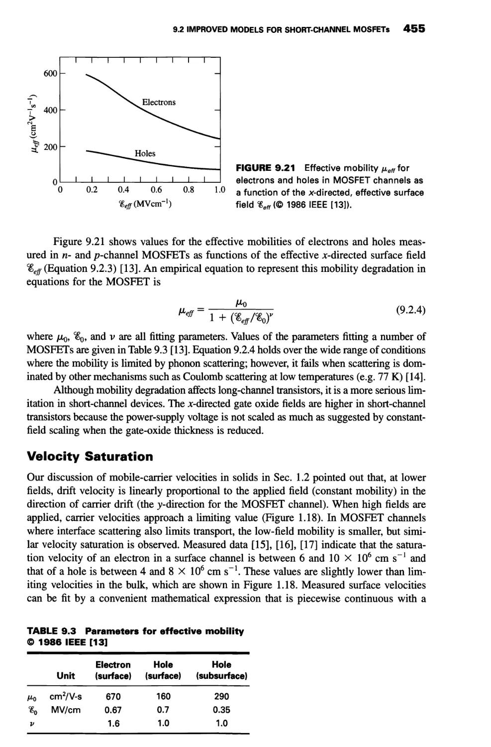
Mobility Degradation 453
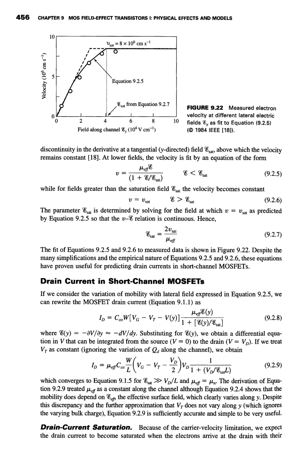
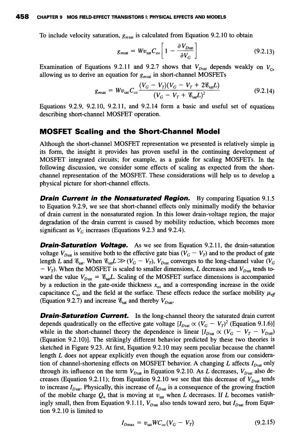
Velocity Saturation 455
Drain Current in Short-Channel MOSFETs 456
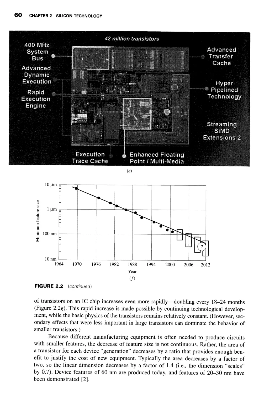
MOSFET Scaling and the Short-Channel Model 458
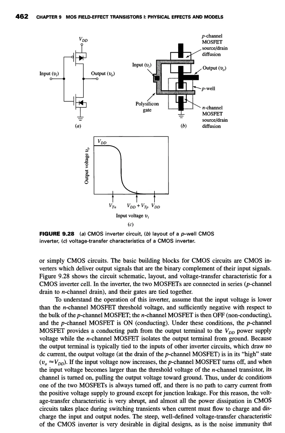
9.3 Devices: Complementary MOSFETs—CMOS 461
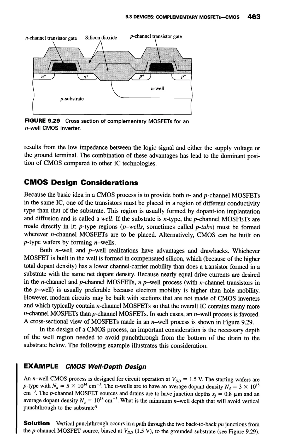
CMOS Design Considerations 463
MOSFET Parameters and Their Extraction 464
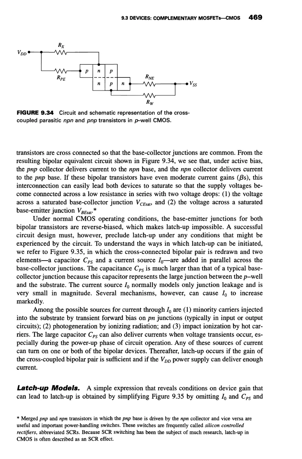
CMOS Latch-upf 468
9.4 Looking Ahead 472
Scaling Goals 472
Gate Coupling 473
Velocity Overshoot 474
Summary 475
Problems 477
10. MOS FIELD-EFFECT TRANSISTORS II:
HIGH-FIELD EFFECTS
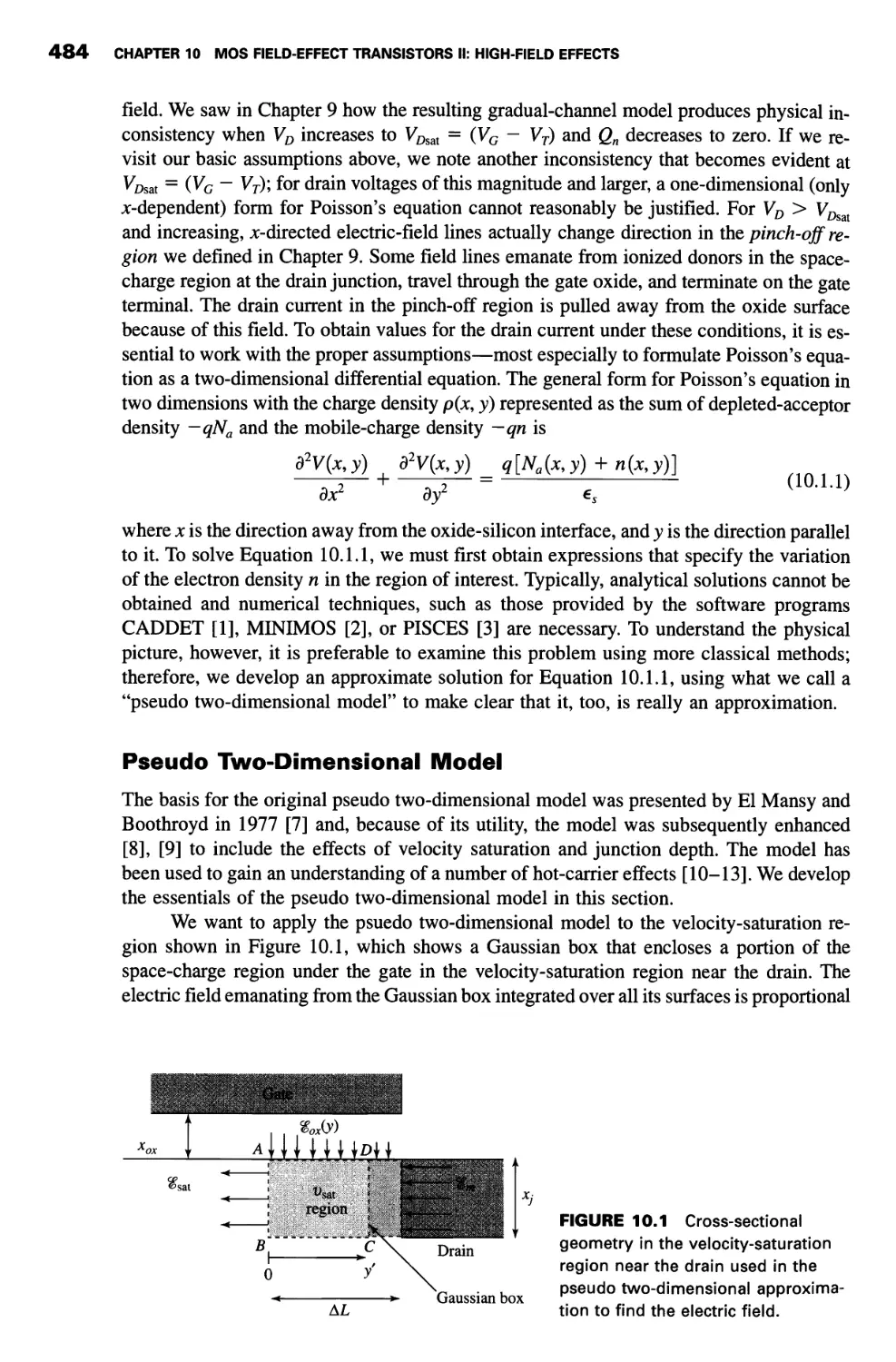
10.1 Electric Fields in the Velocity-Saturation Region 483
Pseudo Two-Dimensional Model 484
xviii
CONTENTS
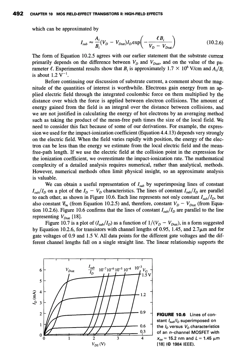
10.2 Substrate Current 490
Hot-Carrier Effects 490
Substrate-Current Model 491
Effect of Substrate Current on Drain Current 494
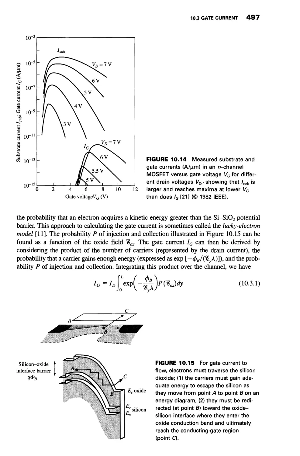
10.3 Gate Current 496
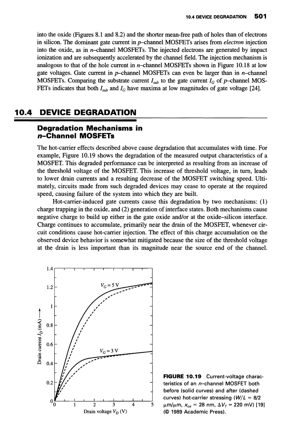
Lucky-Electron Model 496
Carrier Injection at Low Gate Voltages 499
Gate Current in p-Channel MOSFETs 500
10.4 Device Degradation 501
Degradation Mechanisms in n-Channel MOSFETs 501
Characterizing n-Channel MOSFET Degradation 502
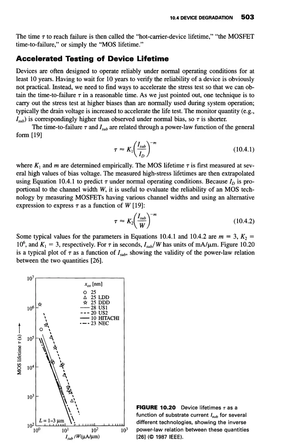
Accelerated Testing of Device Lifetime 503
Structures that Reduce the Drain Field 504
p-Channel MOSFET Degradation 506
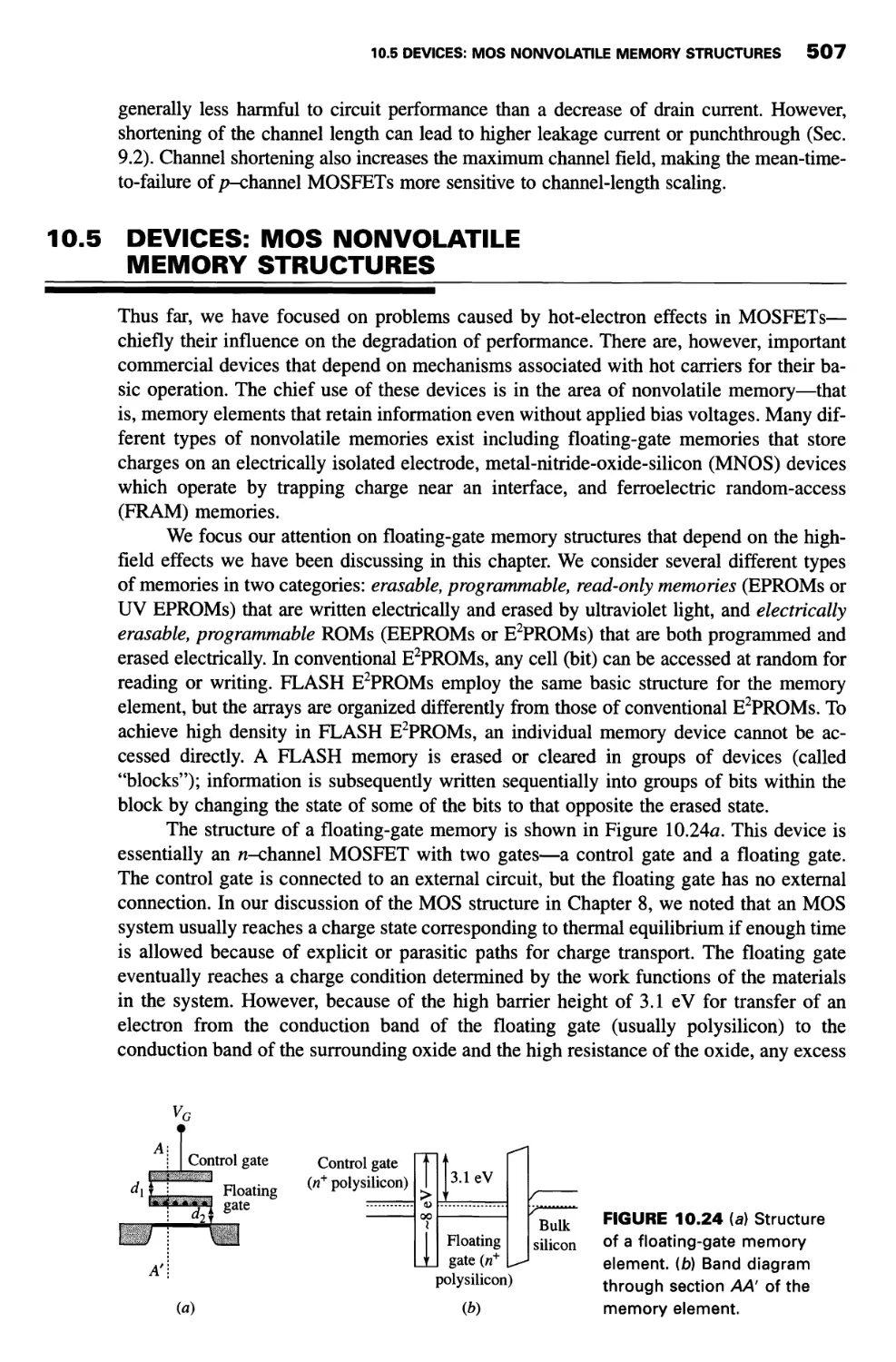
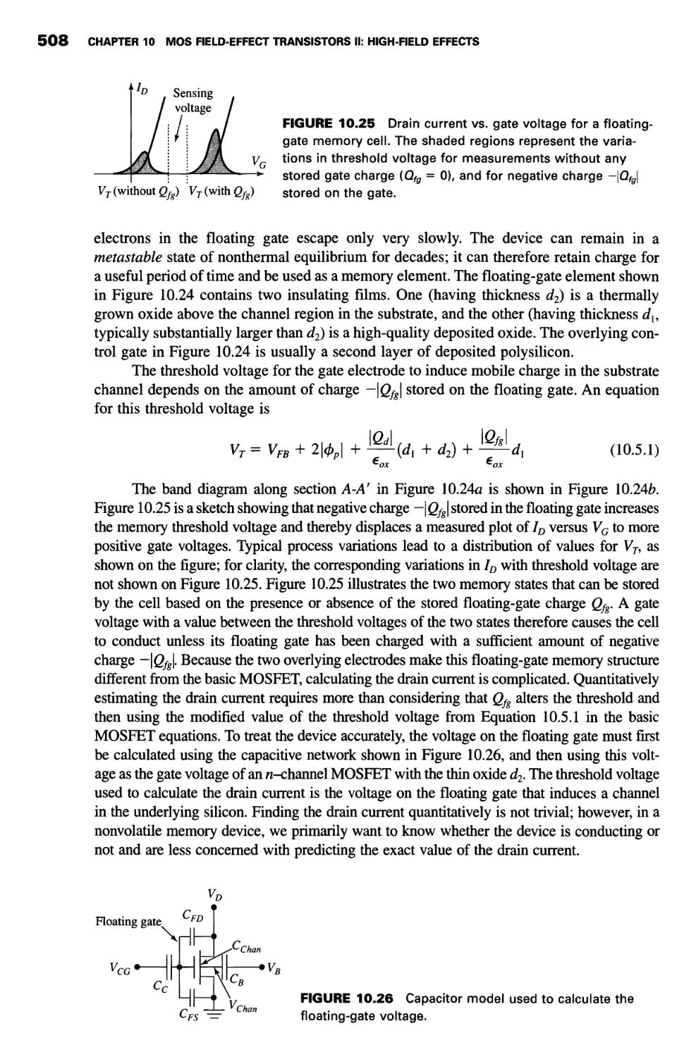
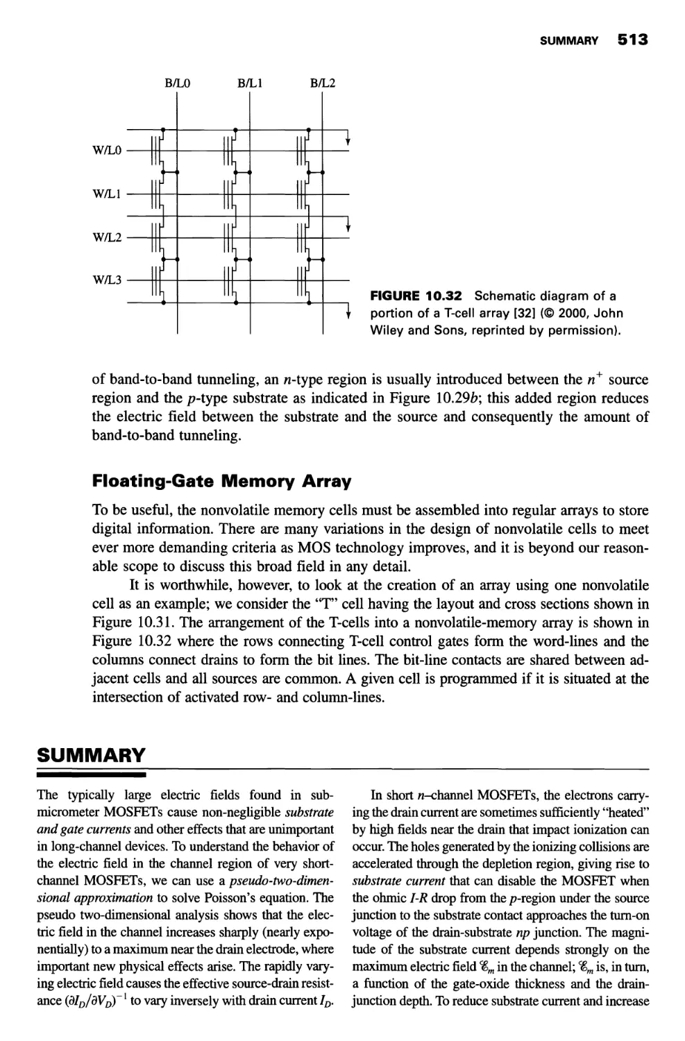
10.5 Devices: MOS Nonvolatile Memory Structures 507
Programming Floating-Gate Memory Cells 509
Erasing Floating-Gate Memory Cells 511
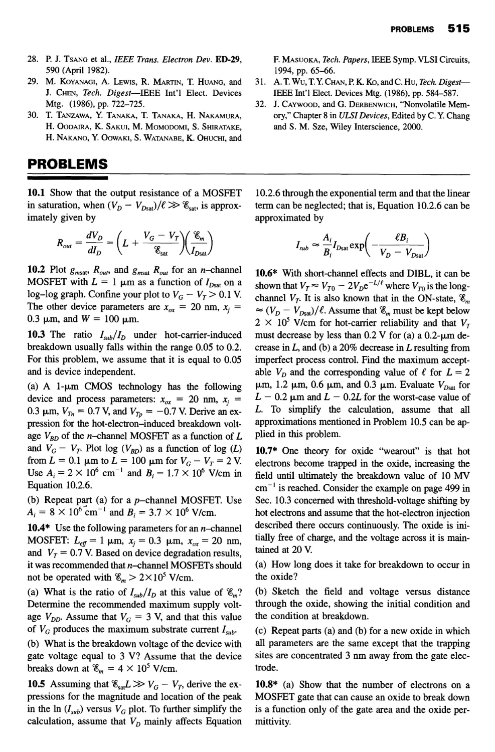
Floating-Gate Memory Array 513
Summary 513
Problems 515
ANSWERS TO SELECTED PROBLEMS 517
SELECTED LIST OF SYMBOLS 519
INDEX 523
Device Electronics for
Integrated Circuits
•CHAPTER.
МБШС€твШМйЁ1ШШШЫЮ&
1.1 PHYSICS OF SEMICONDUCTOR MATERIALS
Band Model of Solids
Holes
Bond Model
Donors and Acceptors
Thermal Equilibrium Statistics
1.2 FREE CARRIERS IN SEMICONDUCTORS
Drift Velocity
Mobility and Scattering
Diffusion Current
1.3 DEVICE: HALL-EFFECT MAGNETIC SENSOR
Physics of the Hall Effect
Integrated Hall-Effect Magnetic Sensor
SUMMARY
PROBLEMS
■ rom everyday experience we know that the electrical properties of
materials vary widely. If we measure the current / flowing through a bar of
homogeneous material with uniform cross section when a voltage V is applied across it, we can
find its resistance R = V/L The resistivity p—a basic electrical property of the material
comprising the bar—is related to the resistance of the bar by a geometric ratio
P = *| (1.1)
where L and A are the length and cross-sectional area of the sample.
The resistivities of common materials used in solid-state devices cover a wide
range. An example is the range of resistivities encountered at room temperature for the
materials used to fabricate typical silicon integrated circuits. Deposited metal strips,
made from very low-resistivity materials, connect elements of the integrated circuit;
aluminum and copper, which are most frequently used, have resistivities at room
temperature of about 10~6 fl-cm. On the other end of the resistivity scale are insulating
materials such as silicon dioxide, which serve to isolate portions of the integrated
circuit. The resistivity of silicon dioxide is about 1016 (1-cm—22 orders of magnitude
higher than that of aluminum. The resistivity of the plastics often used to encapsulate
integrated circuits can be as high as 1018 (1-cm. Thus, a typical integrated circuit can
1
4 CHAPTER 1 SEMICONDUCTOR ELECTRONICS
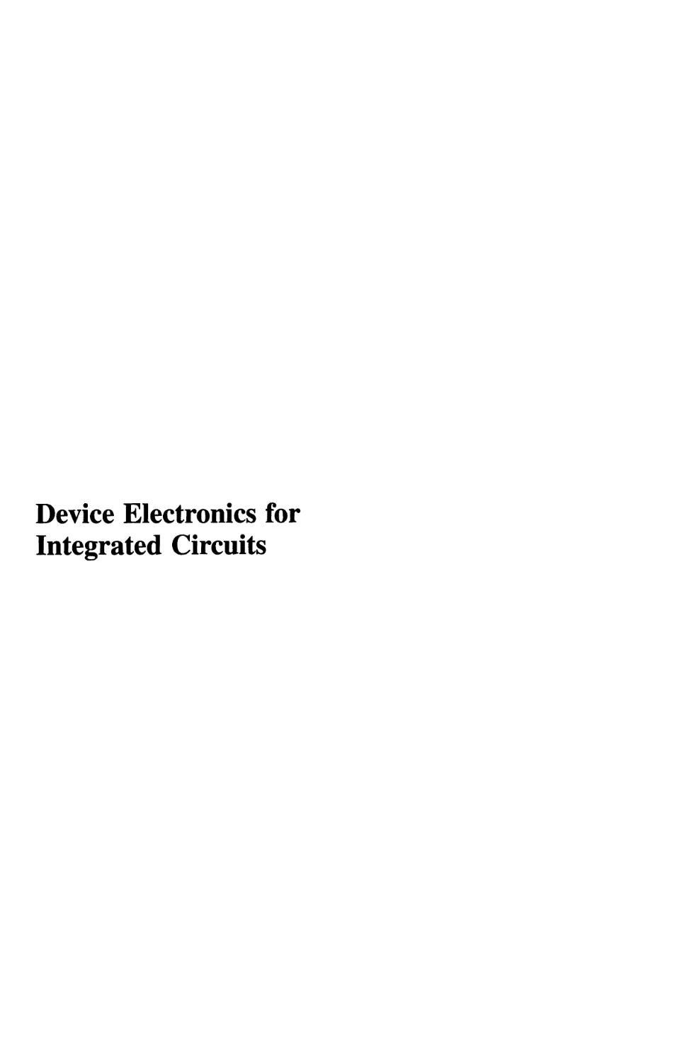
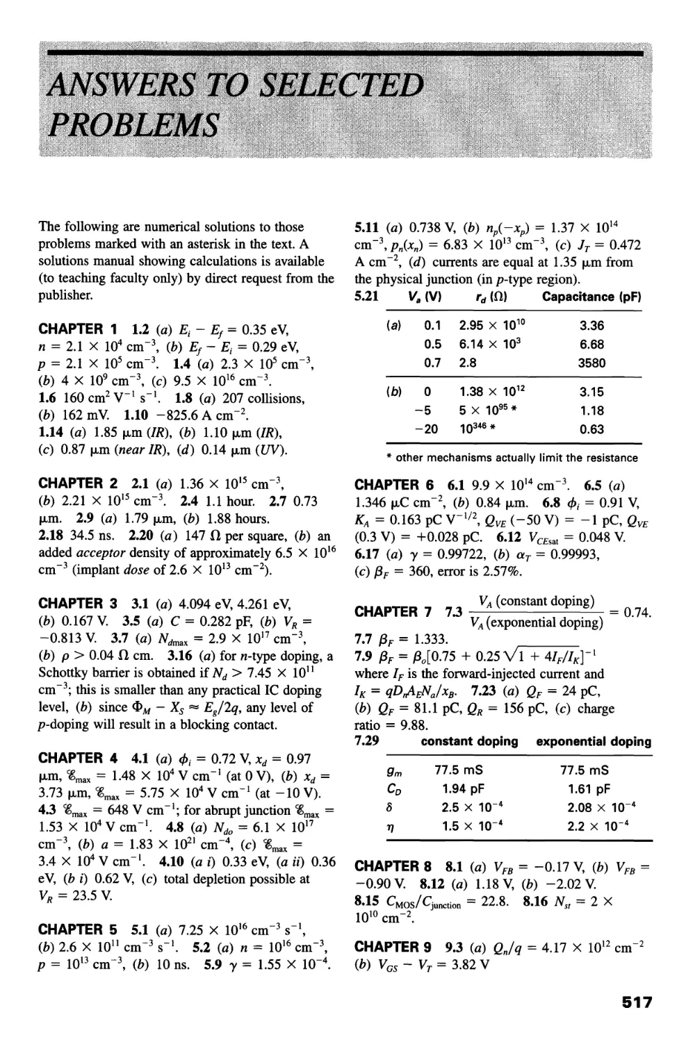
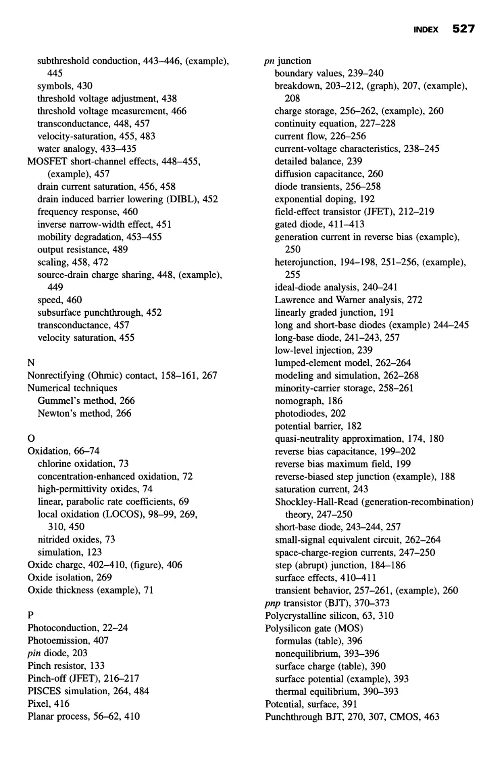
As more atoms are added to form a crystalline structure, the forces encountered by
each electron are altered further, and additional changes in the energy levels occur. Again,
the Pauli exclusion principle demands that each allowed electron energy level have a
slightly different energy so that many distinct, closely spaced energy levels characterize
the crystal. Each of the original quantized levels of the isolated atom is split many times,
and each resulting group of energy levels contains one level for each atom in the system.
When N atoms are included in the system, the original energy level En splits into N
different allowed levels, forming an energy band, which may contain at most 2N electrons
(because of spin degeneracy). In Figure 1.1ft the splitting of two discrete allowed energy
levels of isolated atoms is indicated in a sketch that shows what the allowed energy levels
would be if the interatomic distances for a large assemblage of atoms could be varied
continuously. Under such conditions, the discrete energies that characterize isolated atoms split
into multiple levels as the atomic spacing decreases. When the atomic spacing equals the
crystal-lattice spacing (indicated in Figure 1.1ft), regions of allowed energy levels are
typically separated by a forbidden energy gap in which electrons cannot exist. An analogue
to atomic energy-level splitting exists in mechanical and electrical oscillating systems
which have discrete resonant frequencies when they are isolated, but multiple resonance
values when a number of similar systems interact.
Because the number of atoms in a crystal is generally large—of the order of 1022
cm"3—and the total extent of the energy band is of the order of a few electron volts, the
separation between the N different energy levels within each band is much smaller than
the thermal energy possessed by an electron at room temperature (~l/40 eV), and the
electron can easily move between levels. Thus, we can speak of a continuous band of
allowed energies containing space for 2N electrons. This allowed band is bounded by
maximum and minimum energies, and it may be separated from adjacent allowed bands
by forbidden-energy gaps, as shown in Figure 1.2a, or it may overlap other bands. The
detailed behavior of the bands (whether they overlap or form gaps and, if so, the size of
the gaps) fundamentally determines the electronic properties of a given material. It is the
essential feature differentiating conductors, insulators, and semiconductors.
fc*2i
I
->~x
(a)
Ф)
FIGURE 1.2 Broadening of
allowed energy levels into allowed
energy bands separated by
forbidden-energy gaps as more
atoms influence each electron in a
solid: (a) one-dimensional
representation; (b) two-dimensional
diagram in which energy is plotted
versus distance.
1.1 PHYSICS OF SEMICONDUCTOR MATERIALS 5
Although each energy level of the original isolated atom splits into a band
composed of 2N levels, the range of allowed energies of each band can be different. The higher
energy bands generally span a wider energy range than do those at lower energies. The
cause for this difference can be seen by considering the Bohr radius rn associated with
the nth energy level:
П2€Л2 П2
rn = —^—2 = - X 0.0529 nm (1.1.2)
Z7rm0q Z
For higher energy levels (larger n) the electron is less tightly bound and can wander
farther from the atomic core. If the electron is less tightly confined, it comes closer to the
adjacent atoms and is more strongly influenced by them. This greater interaction causes
a larger change in the energy levels so that the wider energy bands correspond to the
higher energy electrons of the isolated atoms.
We represent the energy bands at the equilibrium spacing of the atoms by the one-
dimensional picture in Figure 1.2a. The highest allowed level in each band is separated by
an energy gap Eg from the lowest allowed level in the next band. It is convenient to extend
the band diagram into a two-dimensional picture (Figure 1.2b) where the vertical axis still
represents the electron energy while the horizontal axis now represents position in the
semiconductor crystal. This representation emphasizes that electrons in the bands are not
associated with any of the individual nuclei, but are confined only by the crystal boundaries.
This type of diagram is especially useful when we consider combining materials with
different energy-band structures into semiconductor devices. In this brief discussion of the
basis for energy bands in crystalline solids, we implicitly assumed that each atom is like its
neighbor in all respects including orientation; that is, we are considering perfect crystals.
In practice, a very high level of crystalline order, in which defects are measured in parts
per billion or less, is normal for device-quality semiconductor materials.
The formation of energy bands from discrete levels occurs whenever the atoms of
any element are brought together to form a solid. However, the different numbers of
electrons within the energy bands of different solids strongly influence their electrical
properties. For example, consider first an alkali metal composed of N atoms, each with one
valence electron in the outer shell. When the atoms are brought close together, an energy
band forms from this energy level. In the simplest case this band has space for 2N
electrons. The N available electrons then fill the lower half of the energy band (Figure 1.3a),
(a) (b)
FIGURE 1.3 Energy-band diagrams: (a) N electrons filling half of the 2/V allowed
states, as can occur in a metal, (b) A completely empty band separated by an
energy gap Eg from a band whose 2Л/ states are completely filled by 2Л/ electrons,
representative of an insulator.
6 CHAPTER 1 SEMICONDUCTOR ELECTRONICS
(а) (b)
FIGURE 1.4 Electron motion in an allowed band is analogous to fluid motion in a
glass tube with sealed ends; the fluid can move in a half-filled tube just as electrons
can move in a metal.
and there are empty states just above the filled states. The electrons near the top of the
filled portion of the band can easily gain small amounts of energy from an applied electric
field and move into these empty states. In these states they behave almost as free
electrons and can be transported through the crystal by an externally applied electric field. In
general, metals are characterized by partially filled energy bands and are, therefore, highly
conductive.
Markedly different electrical behavior occurs in materials in which the valence
(outermost shell) electrons completely fill an allowed energy band and there is an
energy gap to the next higher band. In this case, characteristic of insulators, the closest
allowed band above the filled band is completely empty at low temperatures as shown
in Figure 1.3b. The lowest-energy empty states are separated from the highest filled
states by the energy gap Eg. In insulating material, Eg is generally greater than 5 eV
(~8-9 eV for Si02),* much larger than typical thermal or field-imparted energies
(tenths of an eV or less). In the idealization that we are considering, there are no
electrons close to empty allowed states and, therefore, no electrons can gain small
energies from an externally applied field. Consequently, no electrons can carry an electric
currrent, and the material is an insulator.
An analogy may be helpful. Consider a horizontal glass tube with sealed ends
representing the allowed energy states and fluid in the tube representing the electrons in a
solid. In the case analogous to a metal, the tube is partially filled (Figure 1.4). When a
force (gravity in this case) is applied by tipping the tube, the fluid can easily move along
the tube. In the situation analogous to an insulator, the tube is completely filled with fluid
(Figure 1.5). When the filled tube is tipped, the fluid cannot flow because there is no
empty volume into which it can move; that is, there are no empty allowed states.
Both electrical insulators and semiconductors have similar band structures. The
electrical difference between insulators and semiconductors arises from the size of the
forbidden-energy gap and the ability to populate a nearly empty band by adding conductivity-
enhancing impurities to a semiconductor. In a semiconductor the energy gap separating
the highest band that is filled at absolute zero temperature from the lowest empty band
is typically of the order of 1 eV (silicon: 1.1 eV; germanium: 0.7 eV; gallium arsenide:
1.4 eV). In an impurity-free semiconductor the uppermost filled band is populated by
electrons that were the valence electrons of the isolated atoms; this band is known as the
valence band.
The band structure of a semiconductor is shown in Figure 1.6. At any
temperature above absolute zero, the valence band is not entirely filled because a small
number of electrons possess enough thermal energy to be excited across the forbidden gap
* Specifying band gaps in amorphous materials may cause anxiety to theorists, but short-range order in such
materials leads to effects that can be interpreted with the aid of an energy-band description.
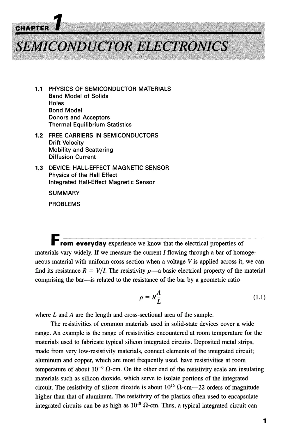
1.1 PHYSICS OF SEMICONDUCTOR MATERIALS 7
(a) (b)
FIGURE 1.5 No fluid motion can occur in a completely filled tube with sealed ends.
into the next allowed band. The smaller the energy gap and the higher the
temperature, the greater the number of electrons that can jump between bands. The electrons
in the upper band can easily gain small amounts of energy and can respond to an
applied electric field to produce a current. This band is called the conduction band
because the electrons that populate it are conductors of electricity. The current density J
(current per unit area) flowing in the conduction band can be found by summing the
charge (-q) times the net velocity (vf) of each electron populating the band. The
summation is then taken over all electrons in the conduction band in a unit volume of the
material.
Jcb = д = S(~4)0/
(1.1.3)
cb
Since only a small number of electrons exist in this band, however, the current for a given
field is considerably less than that in a metal.
Holes
When electrons are excited into the conduction band, empty states are left in the
valence band. If an electric field is then applied, nearby electrons can respond to the field
by moving into these empty states to produce a current. This current can be expressed
by summing the motion of all electrons in the valence band of a unit volume of the
material.
vb
■q)Vi
(1.1.4)
Conduction band
Valence band
Allowed
states
Forbidden
band gap
Allowed
states
FIGURE 1.6 Energy-
band diagram for a
semiconductor showing
the lower edge of the
conduction band Ec, a
donor level Ed within the
forbidden gap, the Fermi
level Ef, an acceptor level
Ea, and the top edge of
the valence band Ev.
8 CHAPTER 1 SEMICONDUCTOR ELECTRONICS
Because there are many electrons in the valence band, but only a few empty states, it is
easier to describe the conduction resulting from electrons interacting with these empty
states than to describe the motion of all the electrons in the valence band. Mathematically,
we can describe the current in the valence band as the current that would flow if the band
were completely filled minus that associated with the missing electrons. Again, summing
over the populations per unit volume, we find
vb Filled band Empty states
since no current can flow in a completely filled band (because no net energy can be
imparted to the electrons populating it), the current in the valence band can be written as
Jvb = 0- 2 (-4)4= 2 M (1-1-6)
Empty states Empty states
where the summation is over the empty states per unit volume. Equation 1.1.6 shows that
we can express the motion of charge in the valence band in terms of the vacant states by
treating the states as if they were particles with positive charge. These "particles" are
called holes', they can only be discussed in connection with the energy bands of a solid
and cannot exist in free space. Note that energy-band diagrams, such as those shown in
Figures 1.3 and 1.6, are drawn for electrons so that the energy of an electron increases as
we move upward toward the top of the diagram. However, because of its opposite charge,
the energy of a hole increases as we move downward on this same diagram.*
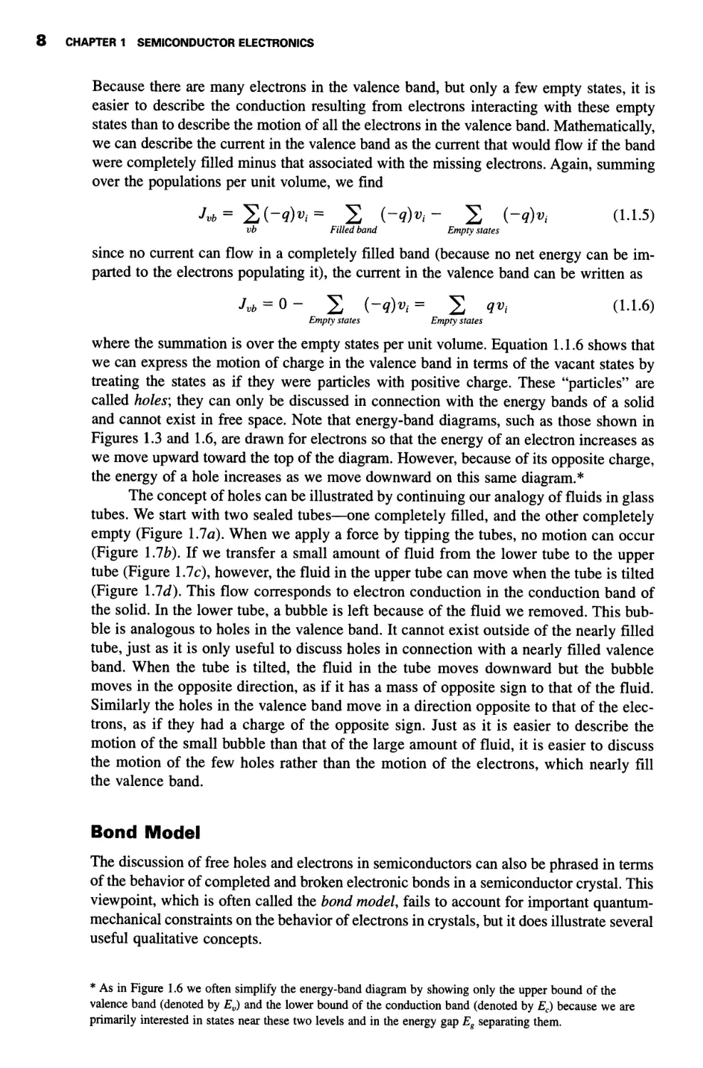
The concept of holes can be illustrated by continuing our analogy of fluids in glass
tubes. We start with two sealed tubes—one completely filled, and the other completely
empty (Figure 1.7a). When we apply a force by tipping the tubes, no motion can occur
(Figure I .lb). If we transfer a small amount of fluid from the lower tube to the upper
tube (Figure 1.7c), however, the fluid in the upper tube can move when the tube is tilted
(Figure I.Id). This flow corresponds to electron conduction in the conduction band of
the solid. In the lower tube, a bubble is left because of the fluid we removed. This
bubble is analogous to holes in the valence band. It cannot exist outside of the nearly filled
tube, just as it is only useful to discuss holes in connection with a nearly filled valence
band. When the tube is tilted, the fluid in the tube moves downward but the bubble
moves in the opposite direction, as if it has a mass of opposite sign to that of the fluid.
Similarly the holes in the valence band move in a direction opposite to that of the
electrons, as if they had a charge of the opposite sign. Just as it is easier to describe the
motion of the small bubble than that of the large amount of fluid, it is easier to discuss
the motion of the few holes rather than the motion of the electrons, which nearly fill
the valence band.
Bond Model
The discussion of free holes and electrons in semiconductors can also be phrased in terms
of the behavior of completed and broken electronic bonds in a semiconductor crystal. This
viewpoint, which is often called the bond model, fails to account for important quantum-
mechanical constraints on the behavior of electrons in crystals, but it does illustrate several
useful qualitative concepts.
* As in Figure 1.6 we often simplify the energy-band diagram by showing only the upper bound of the
valence band (denoted by Ev) and the lower bound of the conduction band (denoted by Ec) because we are
primarily interested in states near these two levels and in the energy gap Eg separating them.
1.1 PHYSICS OF SEMICONDUCTOR MATERIALS 9
(a) (b)
(c) (d)
FIGURE 1.7 Fluid analogy for a semiconductor, (a) and (b) No flow can occur in either the
completely filled or completely empty tube, (c) and (d) Fluid can move in both tubes if some of
it is transferred from the filled tube to the empty one, leaving unfilled volume in the lower tube.
To discuss the bond model, we consider the diamond-type crystal structure that is
common to silicon and germanium (Figure 1.8). In the diamond structure, each atom has
covalent bonds with its four nearest neighbors. There are two tightly bound electrons
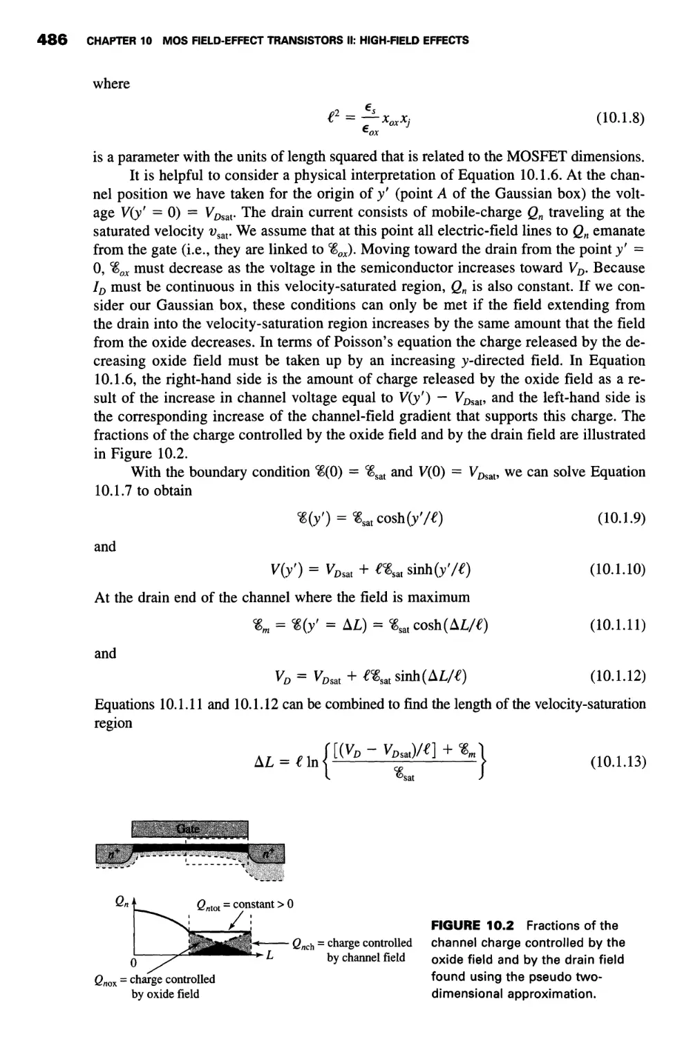
associated with each bond—one from each atom. At absolute zero temperature, all
electrons are held in these bonds, and therefore none are free to move about the crystal in
response to an applied electric field. At higher temperatures, thermal energy breaks some
of the bonds and creates nearly free electrons, which can then contribute to the current
under the influence of an applied electric field. This current corresponds to the current
associated with the conduction band in the energy-band model.
After a bond is broken by thermal energy and the freed electron moves away, an
empty bond is left behind. An electron from an adjacent bond can then jump into the
vacant bond, leaving a vacant bond behind. The vacant bond, therefore, moves in the
opposite direction to the electrons. If a net motion is imparted to the electrons by an applied
field, the vacant bond can continue moving in the direction opposite to the electrons as if
it had a positive charge.* This vacant bond corresponds to the hole associated with the
valence band in the energy-band picture.
A crystal lattice with many similarities to the diamond structure is the zincblende
lattice which characterizes several important compound semiconductors composed of
* A positive charge is associated with the vacant bond because there are insufficient electrons in its vicinity to
balance the proton charges on the atomic nuclei.
10 CHAPTER 1 SEMICONDUCTOR ELECTRONICS
FIGURE 1.8 The diamond-crystal lattice characterized by four covalently bonded
atoms. The lattice constant denoted by a0, is 0.356, 0.543 and 0.565 nm for
diamond, silicon, and germanium, respectively. Nearest neighbors are spaced (V3a0/4)
units apart. Of the 18 atoms shown in the figure, only 8 belong to the volume a03.
Because the 8 corner atoms are each shared by 8 cubes, they contribute a total of
1 atom; the 6 face atoms are each shared by 2 cubes and thus contribute 3 atoms,
and there are 4 atoms inside the cube. The atomic density is therefore 8/a03, which
corresponds to 17.7, 5.00, and 4.43 x 1022 cm"3, respectively. (After W. Shockley:
Electrons and Holes in Semiconductors, Van Nostrand, Princeton, N.J., 1950.)
atoms in the third and fifth columns of the periodic table (called III-V semiconductors).
Some III-V semiconductors, particularly gallium arsenide (GaAs) and gallium phosphide
(GaP), have important device applications. Many properties of the elemental and
compound semiconductors are given in Table 1.3, which appears at the end of this chapter.
Table 1.3 also includes data for some insulating materials used in the manufacture of
integrated circuits. A second table at the end of the chapter (Table 1.4) contains additional
properties of the most important semiconductor, silicon.
Donors and Acceptors
Thus far we have discussed a pure semiconductor material in which each electron excited
into the conduction band leaves a vacant state in the valence band. Consequently, the
number of negatively charged electrons n in the conduction band equals the number of
positively charged holes p in the valence band. Such a material is called an intrinsic
semiconductor, and the densities of electrons and holes in it (carriers cm-3) are usually
subscripted i (that is, щ andp,). However, the most important uses of semiconductors arise
from the interaction of adjacent semiconductor materials having differing densities of the
two types of charge carriers. We can achieve such a structure either by physically joining
1.1 PHYSICS OF SEMICONDUCTOR MATERIALS 11
two materials with different band gaps (as we will discuss in Sec. 4.2) or by varying the
number of carriers in one semiconductor material (as we consider here).
The most useful means for controlling the number of carriers in a semiconductor is
by incorporating substitutional impurities; that is, impurities that occupy lattice sites in
place of the atoms of the pure semiconductor. For example, if we replace one silicon atom
(four valence electrons) with an impurity atom from group V in the periodic table, such
as phosphorus (five valence electrons), then four of the valence electrons from the
impurity atom fill bonds between the impurity atom and the adjacent silicon atoms. The fifth
electron, however, is not covalently bonded to its neighbors; it is only weakly bound to
the impurity atom by the excess positive charge on the nucleus. Only a small amount of
energy is required to break this weak bond so its the fifth electron can wander about the
crystal and contribute to electrical conduction. Because the substitutional group V
impurities donate electrons to the silicon, they are known as donors.
In order to estimate the amount of energy needed to break the bond to a donor atom,
we consider the net Coulomb potential that the electron experiences because of the core
of its parent atom. We assume that the electron is attracted by the single net positive charge
of the impurity atom core weakened by the polarization effects of the background of silicon
atoms. The energy binding the electron to the core is then
m*q4 13.6 m*
E = —rr-r =——-^tV (1.1.7)
where er is the relative permittivity of the semiconductor and m* is the effective mass of
the electron in the semiconductor conduction band. The use of an effective mass accounts
for the influence of the crystal lattice on the motion of an electron. For silicon with
€r = 11.7 and m* = 0.26 m0, E « 0.03 eV, which is only about 3% of the silicon band-
gap energy (1.1 eV). (More detailed calculations and measurements indicate that the
binding energy for typical donors is somewhat higher: 0.044 eV for phosphorus, 0.049 eV for
arsenic, and 0.039 eV for antimony.) The small binding energies make it much easier to
break the weak bond connecting the fifth electron to the donor than to break the silicon-
silicon bonds.
n-type Semiconductors. According to the energy-band model, it requires only a
small amount of energy to excite the electron from the donor atom into the conduction
band, while a much greater amount of energy is required to excite an electron from the
valence band to the conduction band. Therefore, we can represent the state corresponding
to the electron when bound to the donor atom by a level Ed about 0.05 eV below the
bottom of the conduction band Ec (Figure 1.6). The density of donors (atoms cm-3) is
generally designated by Nd. Thermal energy at temperatures greater than about 150 К
is generally sufficient to excite electrons from the donor atoms into the conduction band.
Once the electron is excited into the conduction band, a fixed, positively charged atom
core is left behind in the crystal lattice. The allowed energy state provided by a donor
{donor level) is, therefore, neutral when occupied by an electron and positively charged
when empty.*
If most impurities are of the donor type, the number of electrons in the conduction
band is much greater than the number of holes in the valence band. Electrons are then
called the majority carriers, and holes are called the minority carriers. The material is
said to be an n-type semiconductor because most of the current is carried by the negatively
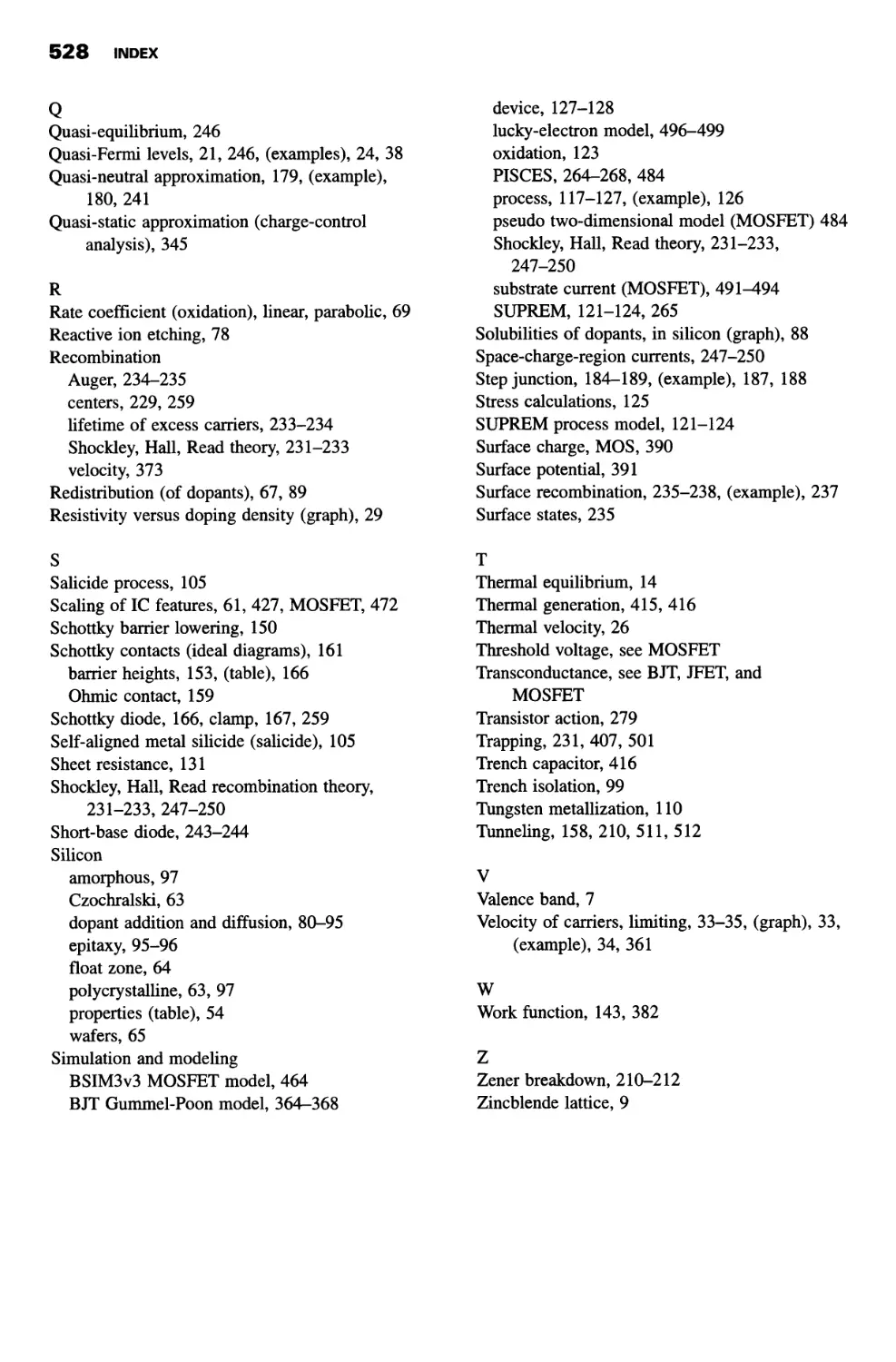
charged electrons. A graph showing the conduction electron concentration versus temperature
* Other fields of study, such as chemistry, define a donor differently, possibly leading to some confusion.
12 CHAPTER 1 SEMICONDUCTOR ELECTRONICS
FIGURE 1.9 Electron
concentration versus
temperature for two
n-type doped
semiconductors: (a) Silicon
doped with 1.15 x 10¹⁶
arsenic atoms cm~3[1],
(b) Germanium doped
with 7.5 x 10¹⁵ arsenic
atoms cm~3[2].
for silicon and germanium is sketched in Figure 1.9. Because the hole density is at most
equal to nh this figure shows clearly that electrons are far more numerous than holes when
the temperature is in the range sufficient to ionize the donor atoms (about 150 K) but not
adequate to free many electrons from silicon-silicon bonds (about 600 K).
p-type Semiconductors. In an analogous manner, an impurity atom with three
valence electrons, such as boron, can replace a silicon atom in the lattice. The three
electrons fill three of the four covalent silicon bonds, leaving one bond vacant. If
another electron moves to fill this vacant bond from a nearby bond, the vacant bond is
moved, carrying with it positive charge and contributing to hole conduction. Just as a
small amount of energy was necessary to initiate the conduction process in the case of
a donor atom, only a small amount of energy is needed to excite an electron from the
valence band into the vacant bond caused by the trivalent impurity. This energy is
represented by an energy level Ea slightly above the top of the valence band Ev (Figure 1.6).
An impurity that contributes to hole conduction is called an acceptor impurity because
it leads to vacant bonds, which easily accept electrons. The acceptor concentration
(atoms cm"3) is denoted as Na. If most of the impurities in the solid are acceptors, the
material is called a p-type semiconductor because most of the conduction is carried by
positively chargedholes. An acceptor level is neutral when empty and negatively charged
when occupied by an electron.
Semiconductors in which conduction results primarily from carriers contributed by
impurity atoms are said to be extrinsic. The donor and acceptor impurity atoms, which
are intentionally introduced to change the charge-carrier concentration, are called dopant
atoms.
In compound semiconductors, such as gallium arsenide, certain group IV impurities
can be substituted for either element. Thus, silicon incorporated as an impurity in gallium
arsenide contributes holes when it substitutes for arsenic and contributes electrons when it
substitutes for gallium. This amphoteric doping behavior can be difficult to control and is
not found for all group IV impurities; for example, the group IV element tin is incorporated
almost exclusively in place of gallium in gallium arsenide and is therefore a useful w-type
2xl016 h
1 x 10¹⁶ h
100 200 300 400 500 600 700
Г(К)
1.1 PHYSICS OF SEMICONDUCTOR MATERIALS 13
dopant. Impurities from group VI that substitute for arsenic, such as tellurium, selenium, or
sulfur, are also used to obtain n-type gallium arsenide, whereas group II elements like zinc
or cadmium have been used extensively to obtain /?-type material.
Other impurity atoms or crystalline defects may provide energy states in which
electrons are tightly bound so that it takes appreciable energy to excite an electron from a
bound state to the conduction band. Such deep donors may be represented by energy levels
well below the conduction-band edge in contrast to the shallow donors previously
discussed, which had energy levels only a few times the thermal energy kT below the
conduction-band edge. Similarly, deep acceptors axe located well above the valence-band
edge. Because deep levels are not always related to impurity atoms in the same
straightforward manner as shallow donors and acceptors, the distinction between the terms donor
and acceptor is made on the basis of the possible charge states the level can take. A deep
level is called a donor if it is neutral when occupied by an electron and positively charged
when empty, while a deep acceptor is neutral when empty and negative when occupied
by an electron.
Compensation. The intentional doping of silicon with shallow donor impurities, to
make it л-type, or with shallow acceptor impurities, to make it p-type, is the most
important processing step in the fabrication of silicon devices. An especially useful feature of
the doping process is that one may compensate a doped silicon crystal (for example an n-
type sample) by subsequently adding the opposite type of dopant impurity (ар-type dopant
in this example). Reference to Figure 1.6 helps to clarify the process. In Figure 1.6 donor
atoms add allowed energy states to the energy-band diagram at Ed, close to the conduction-
band energy En whereas acceptor atoms add allowed energy states at Ea, close to the
valence-band energy Ev. At typically useful temperatures for silicon devices, each donor atom
has lost an electron and each acceptor atom has gained an electron. Because the acceptor
atoms provide states at lower energies than those either in the conduction band or at the
donor levels, the electrons from the donor levels transfer (or "fall") to the lower-energy
acceptor sites as long as any of these remain unfilled. Hence, in a doped semiconductor,
the effective dopant concentration is equal to the magnitude of the difference between the
donor and acceptor concentrations \Nd - Na\; the semiconductor is n-type if Nd exceeds Na
and p-type if Na exceeds Nd. Although in theory one can achieve a zero effective dopant
density through compensation (with Nd = Na\ such exact control of the dopant
concentrations is technically impractical. As we will see in Chapter 2 (where technology is
discussed), compensation doping usually involves adding a dopant density that is about an
order-of-magnitude higher than the density of dopant that is initially present.
EXAMPLE Donors and Acceptors
A silicon crystal is known to contain 10~4 atomic percent of arsenic (As) as an impurity. It then
receives a uniform doping of 3 X 1016 cm"3 phosphorus (P) atoms and a subsequent uniform
doping of 1018 cm-3 boron (B) atoms. A thermal annealing treatment then completely activates all
impurities.
(a) What is the conductivity type of this silicon sample?
(b) What is the density of the majority carriers?
Solution Arsenic is a group V impurity, and acts as a donor. Because silicon has 5 X 10²² atoms
cm"3 (Table 1.3), 10~4 atomic percent implies that the silicon is doped to a concentration of
5 X 1022 X 1(Г6 = 5 X 10¹⁶ As atoms cm"3
CHAPTER 1 SEMICONDUCTOR ELECTRONICS
The added doping of 3 X 10¹⁶ P atoms cm 3 increases the donor doping of the crystal to 8 X
1016 cm'3.
Additional doping by В (a group III impurity) converts the silicon from n-type to p-type
because the density of acceptors now exceeds the density of donors. The net acceptor density is,
however, less than the density of В atoms owing to the donor compensation.
(a) Hence, the silicon is p-type.
(b) The density of holes is equal to the net dopant density:
p = Na(B) - [Nd(As) + Nd(P)]
= 1018 - [5 X 10¹⁶ + 3 X 10¹⁶]
= 9.2 X 10,7cm-3 ■
Thermal-Equilibrium Statistics
Before proceeding to a more detailed discussion of electrical conduction in a
semiconductor, we consider three additional concepts: first, the concept of thermal equilibrium;
second, the relationship at thermal equilibrium between the majority- and minority-carrier
concentrations in a semiconductor; and third, the use of Fermi statistics and the Fermi
level to specify the carrier concentrations.
Thermal Equilibrium. We saw that free-carrier densities in semiconductors are
related to the populations of allowed states in the conduction and valence bands. The
densities depend upon the net energy in the semiconductor. This energy is stored in crystal-
lattice vibrations (phonons) as well as in the electrons. Although a semiconductor crystal
can be excited by external sources of energy such as incident photoelectric radiation, many
situations exist where the total energy is a function only of the crystal temperature. In this
case the semiconductor spontaneously (but not instantaneously) reaches a state known as
thermal equilibrium. Thermal equilibrium is a dynamic situation in which every process
is balanced by its inverse process. For example, at thermal equilibrium, if electrons are
being excited from a lower energy E} to a higher energy E2, then there must be equal
transfer of electrons from the states at E2 to those at Ev Likewise, if energy is being
transferred into the electron population from the crystal vibrations (phonons), then at thermal
equilibrium an equal flow of energy is occurring in the opposite direction. A useful thought
picture for thermal equilibrium is that a moving picture taken of any event can be run
either backward or forward without the viewer being able to detect any difference. In the
following we consider some properties of hole and electron populations in semiconductors
at thermal equilibrium.
Mass-Action Law. At most temperatures of interest to us, there is sufficient
thermal energy to excite some electrons from the valence band to the conduction band. A
dynamic equilibrium exists in which some electrons are constantly being excited into
the conduction band while others are losing energy and falling back across the energy
gap to the valence band. The excitation of an electron from the valence band to the
conduction band corresponds to the generation of a hole and an electron, while an electron
falling back across the gap corresponds to electron-hole recombination because it
annihilates both carriers. The generation rate of electron-hole pairs G depends on the
temperature T but is, to first order, independent of the number of carriers already present.
We therefore write
G=A(T)
(1.1.8)
1.1 PHYSICS OF SEMICONDUCTOR MATERIALS 15
where f{{T) is a function determined by crystal physics and temperature. The rate of
recombination R, on the other hand, depends on the concentration of electrons n in the
conduction band and also on the concentration of holes p (empty states) in the valence band,
because both species must interact for recombination to occur. We therefore represent the
recombination rate as a product of these concentrations as well as other factors that are
included in f2(T):
R = npf2(T) (1.1.9)
At equilibrium the generation rate must equal the recombination rate. Equating G and R
in Equations 1.1.8 and 1.1.9, we have
npf2(T)=A(T)
or
f (T)
np=MT)=m (U-10)
Equation 1.1.10 expresses the important result that at thermal equilibrium the product of
the hole and electron densities in a given semiconductor is a function only of temperature.
In an intrinsic (i.e., undoped) semiconductor all carriers result from excitation
across the forbidden gap. Consequently, n = p = nh where the subscript i reminds us
that we are dealing with intrinsic material. Applying Equation 1.1.10 to intrinsic material,
we have
niPi = nj=f3(T) (1.1.11)
The intrinsic carrier concentration depends on temperature because thermal energy is the
source of carrier excitation across the forbidden energy gap. The intrinsic concentration
is also a function of the size of the energy gap because fewer electrons can be excited
across a larger gap. We will soon be able to show that under most conditions nj is given
by the expression
nj = NcNvtxV(-^) (1.1.12)
where Nc and Nv are related to the density of allowed states near the edges of the
conduction band and valence band, respectively. Although Nc and Nv vary somewhat with
temperature, щ is much more temperature dependent because of the exponential term in
Equation 1.1.12. For silicon with Eg = 1.1 eV, щ doubles for every 8°C increase in
temperature near room temperature. Because the intrinsic carrier concentration nt is constant
for a given semiconductor at a fixed temperature, it is useful to replace /3(Г) by nj in
Equation 1.1.10. Therefore the relation
np = n] (1.1.13)
holds for both extrinsic and intrinsic semiconductors; it shows that increasing the
number of electrons in a sample by adding donors causes the hole concentration to decrease
so that the product np remains constant. This result, often called the mass-action law, has
its counterpart in the behavior of interacting chemical species, such as the concentrations
of hydrogen and hydroxyl ions (H+ and OH) in acidic or basic solutions. As we see from
our derivation, the law of mass action is a straightforward consequence of equating
generation and recombination, that is, of thermal equilibrium.
In the neutral regions of a semiconductor (i.e., regions free of field gradients), the
number of positive charges must be exactly balanced by the number of negative charges.
16 CHAPTER 1 SEMICONDUCTOR ELECTRONICS
Positive charges exist on ionized donor atoms and on holes, while negative charges are
associated with ionized acceptors and electrons.* If there is charge neutrality in a region
where all dopant atoms are ionized,
Nd + p = Na + n (1.1.14)
Rewriting Equation 1.1.14 and using the mass-action law (Equation 1.1.13), we obtain the
expression
n]
n--^ = Nd-Na (1.1.15)
which may be solved for the electron concentration n:
Nd~Na ,
П = h
Nd~Na, 2
+ nf
1/2
(1.1.16)
In an n-type semiconductor Nd > Na. From Equation 1.1.16 we see that the electron
density depends on the net excess of ionized donors over acceptors. Thus, as we saw in the
previous example, a piece of p-type material containing Na acceptors can be converted
into n-type material by adding an excess of donors so that Nd > Na. In Chapter 2 we will
see how this conversion is carried out in fabricating silicon integrated circuits.
For silicon at room temperature, щ is 1.45 X 1010 cm-3 while the net donor density
in и-type silicon is typically about 1015 cm"3 or greater: Hence (Nd - Na) ^> nt and
Equation 1.1.16 reduces to n « (Nd - Na). Consequently, from Equation 1.1.13,
•i »?
'-Ц-йГк <U17)
Thus, for Nd — Na= 1015 cm-3 we have p = 2 X 105 cm-3, and the minority-carrier
concentration is nearly 10 orders of magnitude below the majority-carrier population. In
general, the concentration of one type of carrier is many orders of magnitude greater than
that of the other in extrinsic semiconductors.
Fermi Level. The numbers of free carriers (electrons and holes) in any macroscopic
piece of semiconductor are relatively large—usually large enough to allow use of the
laws of statistical mechanics to determine physical properties.** One important
property of electrons in crystals is their distribution at thermal equilibrium among the
allowed energy states. Basic considerations of ways to populate allowed energy states
with particles subject to the Pauli exclusion principle leads to an energy distribution
function for electrons that is called the Fermi-Dirac distribution function. It is denoted
by fD(E) and has the form
/p(£)-i+e4,[(i-3y*r| (LU8)
where Ef is a reference energy called the Fermi energy or Fermi level From Equation
1.1.18, we see thatfD(Ef) always equals \. The Fermi-Dirac distribution function, often
* When we speak of electrons in our discussion of devices in subsequent chapters, we generally refer to
electrons in the conduction band; exceptions are explicitly noted. The term holes always denotes vacant states
in the valence band.
** However, in some devices made with submicrometer dimensions, the number of dopant atoms in the active
regions is so small that statistical fluctuations in the number of dopant atoms can affect device characteristics.
1.1 PHYSICS OF SEMICONDUCTOR MATERIALS 17
/d(£)
g(E)
(»
[l-fD(E)]g(E)
fD(E)g(E)
(c)
FIGURE 1.10 (a) Fermi-
Dirac distribution function
describing the probability
that an allowed state at
energy E is occupied by
an electron, (b) The
density of allowed states for
a semiconductor as a
function of energy; note
that g{E) is zero in the
forbidden gap between
Ev and Ec. (c) The product
of the distribution
function and the density-of-
states function.
called simply the Fermi function, describes the probability that a state at energy E is
filled by an electron. As shown in Figure 1.10a, the Fermi function approaches unity at
energies much lower than Ef, indicating that the lower energy states are mostly filled.
It is very small at higher energies, indicating that few electrons are found in high-energy
states at thermal equilibrium—in agreement with physical intuition. At absolute zero
temperature all allowed states below Ef are filled and all states above it are empty. At
finite temperatures, the Fermi function does not change so abruptly; there is a small
probability that some states above the Fermi level are occupied and some states below
it are empty.
The Fermi function represents only a probability of occupancy. It does not contain
any information about the states available for occupancy and, therefore, cannot by itself
specify the electron population at a given energy. Applying quantum physics to a given
system provides information about the density of available states as a function of energy.
We denote this function by g(E). A sketch of g(E) for an intrinsic semiconductor is shown
in Figure 1.10b. It is zero in the forbidden gap (Ec> E> Ev), but it rises sharply within
both the valence band (E < Ev) and the conduction band (E > Ec). The actual
distribution of electrons as a function of energy can be found from the product of the density of
allowed states g(E) within a small energy interval dE and the probability fD(E) that these
states are filled. The total density of electrons in the conduction band can be obtained by
18 CHAPTER 1 SEMICONDUCTOR ELECTRONICS
multiplying the density-of-states function g(E) in the conduction band by the Fermi
function and integrating over the conduction band:
Jcb
(E)g(E)dE
(1.1.19)
Similarly, the density of holes in the valence band is found by multiplying the density-of-
states function in the valence band by the probability [1 -fD(E)] that these states are
empty and integrating over the valence band.
In и-type material that is not too highly doped, only a small fraction of the allowed
states in the conduction band are filled. The Fermi function in the conduction band is very
small, and the Fermi level is well below the bottom of the conduction band. Then
(Ec - Ef) ^> kT, and the Fermi function given by Equation 1.1.18 reduces to the
mathematically simpler Maxwell-Boltzmann distribution function:
fM(E) = exp
kT
(1.1.20)
This thermal-equilibrium distribution function can also be derived independently by
omitting the limitations imposed by the Pauli exclusion principle; that is, the Boltzmann
function applies to the case that any number of electrons can exist in an allowed state. At
energies well above the Fermi level, the fraction of available states that are occupied is
so small that the exclusion-principle limitation has no practical effect, and Maxwell-
Boltzmann statistics are applicable.
Using Equation 1.1.20 in the integration described in Equation 1.1.19 and making
several approximations, we express the carrier concentration in the conduction band in
terms of the Fermi level by
n = Nc exp
(Ec - Ef)
kT
(1.1.21)
Similarly, in moderately doped p-type material, the Fermi level is significantly above the
top of the valence band, and
p = Nv exp
(Ef-Ev)
kT
(1.1.22)
where (Ec — Ef) is the energy between the bottom edge of the conduction band and the
Fermi level, and (Ef - Ev) is the energy separation from the Fermi level to the top of the
valence band. The quantities Nc and Nv, called the effective densities of states at the
conduction- and valence-band edges, respectively, are given by the expressions
and
/2тгт*£Г\3/2
/2ттт*кТ\У1
"•-2hH
(1.1.23)
(1.1.24)
where m* and m* are the effective masses of electrons and holes. These effective masses
are related to m* as introduced in Equation 1.1.7 but differ somewhat from it because of the
details of the energy band structure. As we see from Equations 1.1.21 and 1.1.22, the
quantities Nc and Nv effectively concentrate all of the distributed conduction- and valence-band
1.1 PHYSICS OF SEMICONDUCTOR MATERIALS 19
states at Ec and Ev. They can be used to calculate thermal-equilibrium densities whenever
the Fermi level is a few kT or more removed from a band edge.
Except for slight differences in the values of m*, all terms in Equations 1.1.23 and
1.1.24 are equal so that Nc — Nv. Hence, in an n-doped material for which n^>p,
(Ec - Ef) <SC (Ef — Ev); this means that the Fermi level is much closer to the conduction
band than it is to the valence band. Similarly, the Fermi level is nearer the valence band
than the conduction band in a jP-type semiconductor.
In an intrinsic semiconductor n = p. Therefore, (Ec - Ef) « (Ef - Ev) and the Fermi
level is nearly at the middle of the forbidden gap [Ef = (Ec + Ev)/2]. We denote this
intrinsic Fermi level by the symbol Et. Just as the quantity щ is useful in relating the carrier
concentrations even in an extrinsic semiconductor (Equation 1.1.13), Et is frequently used
as a reference level when discussing extrinsic semiconductors. In particular, because
щ = Nc exp
~(EC ' Et)
kT
= Nv exp
-(£,• ~ Ev)
kT
(1.1.25)
the expressions for the carrier concentrations n and p in an extrinsic semiconductor
(Equations 1.1.21 and 1.1.22) can be rewritten in terms of the intrinsic carrier concentration and
the intrinsic Fermi level:
and
n = щ exp
p = щ exp
(щ-
E.)
kT
№-
Щ)
kT
(1.1.26)
(1.1.27)
Thus, the energy separation from the Fermi level to the intrinsic Fermi level is a measure
of the departure of the semiconductor from intrinsic material. Because Ef is above E{ in
an n-type semiconductor, n> щ> p, as we found before.
When the semiconductor contains a large dopant concentration [Nd —> Nc or Na -> Nv
(~1019 cm"3 for Si)], we can no longer ignore the limitations imposed by the Pauli
exclusion principle. That is, the Fermi-Dirac distribution cannot be approximated by the
Maxwell-Boltzmann distribution function. Equations 1.1.21-22 and 1.1.26-27 are no
longer valid, and more exact expressions must be used or the limited validity of the
simplified expressions must be realized. Very highly doped semiconductors (Nd ^ Afc or
Na — Nv) же called degenerate semiconductors because the Fermi level is within the
conduction or valence band. Therefore, allowed states for electrons exist very near the
Fermi level, just as is the case in metals. Consequently, many of the electronic properties
of very highly doped semiconductors degenerate into those of metals.
EXAMPLE Thermal-Equilibrium Statistics
Find the equilibrium electron and hole concentrations and the location of the Fermi level (with
respect to the intrinsic Fermi level £,) in silicon at 300 К if the silicon contains 8 X 1016 cm-3 arsenic
(As) atoms and 2 X 1016 cm-3 boron (B) atoms.
Solution Because the donor (As) density exceeds the acceptor (B) density, the crystal is n-type.
The net doping concentration is the difference between the donor dopant density (8 X 10¹⁶) and the
acceptor dopant density (2 X 10¹⁶) and is 6 X 1016 cm-3.
The electron density equals the net dopant concentration.
20 CHAPTER 1 SEMICONDUCTOR ELECTRONICS
The hole density is (from Equation 1.1.13)
p = — = 3.5 X 103 cm-3
n
From Equation 1.1.26,
Ef- Et = kT\n{n/n)
= 0.0258 ln(6 X 10¹⁶/1.45 X 1010)
= 0.393 eV
Note that the Fermi level can be specified with respect to the conduction band by using
Equation 1.1.21:
Ec- Ef=kT\n(Nc/n)
= 0.0258 ln(2.8 X 10¹⁹/6 X 1016)
= 0.159eV
The sum of these two energies is 0.55 eV, half the bandgap energy of Si.
ЮЛ59 _
""$0.393 Ef
Inhomogeneously Doped Semiconductors. At thermal equilibrium, electrons
are distributed in energy according to the Fermi-Dirac distribution function, which at a given
temperature is determined by the Fermi energy (Equation 1.1.18). The Fermi energy,
furthermore, must have the same value throughout a system to assure the detailed balance
required at thermal equilibrium for electron transfers. This very important requirement is
discussed more fully in Sees. 3.1 and 4.1; at this point we consider the effect on the
semiconductor energy-band structure of the constancy of the Fermi level throughout a system.
As we found in the example, the Fermi energy is in the middle of the forbidden
energy gap in an undoped (intrinsic) semiconductor. For extrinsic (doped) semiconductors,
the Fermi level is closer to one of the bands [to the conduction band in a semiconductor
doped with donors (и-type material) and to the valence band in a semiconductor doped
with acceptors (p-type material)].
Drawing the energy-band diagram for a piece of semiconductor with nonuniform
doping illustrates some useful concepts. Consider, for example, silicon in which the doping in
the region x < a is Ndx donors cm"3. At x = a the doping decreases abruptly to Nd2 donors
cm-3, as shown in Figure 1.11a. When the two regions of the semiconductor are in intimate
contact, the entire piece of semiconductor corresponds to a single system of states. An energy-
band diagram for this crystal can be drawn by noting first that the Fermi level must be
constant at thermal equilibrium and then drawing the conduction and valence band edges around
the Fermi level by using other constraints. In the present case we know that the silicon doping
establishes the electron concentrations far from the interface at x = a. In the region jc«a
л « Ndb and for x ^> a, n « Nd2. The electron density changes between these two values
over a small region near the interface plane at x = a.
We sketch an energy-band diagram for this inhomogeneously doped system in
Figure I Alb. As described above, we start constructing this diagram by first drawing a
constant horizontal line to represent the constant Fermi level. Away from the interface,
we can then locate the conduction-band edge in each region where the electron density
is equal to the donor density. The energy interval between the Fermi level and the
1.1 PHYSICS OF SEMICONDUCTOR MATERIALS 21
с
0)
1
1 >.
0 a jc
(a) («
FIGURE 1.11 (a) Dopant density in a silicon crystal, (b) Band diagram at thermal
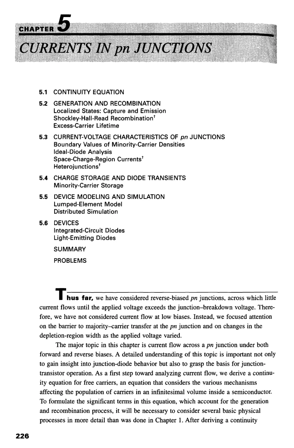
equilibrium for an п-type semiconductor having doping Nd^ for 0 < x < a and Nd2 for
x> a where (A/d1 > Nd2).
conduction-band edge is calculated using Equation 1.1.26 to find Ec - Ef at each end. We
then draw a smooth transition through the interface plane at x = a to connect the two end
regions. The detailed variation of the band edges in the transition region will be discussed
in detail in Chapter 4 after further physical theory is developed. Because the energy gap
is constant throughout the piece of semiconductor, we can draw the valence-band edge
parallel to the conduction-band edge.
As we see in Figure 1.11b, the conduction and valence band edges in the silicon are
not constant along jc, but rather move to higher energies when the donor density decreases.
The energy difference between the conduction and the valence band (the forbidden-gap
energy) is a property of the silicon lattice that is not changed by lightly or moderately
doping the crystal. (The case of heavy doping is considered later in this section.) The
increase in energies associated with the silicon band edges represents an increased
potential energy for electrons in the less heavily doped region*. We will return to consider this
and other points about Figure 1.1 lb in Chapter 4. For the present, our emphasis is on the
constancy of the Fermi level and on the use of the thermal-equilibrium principle to
construct the energy-band diagram shown in Figure 1.11b.
Quasi-Fermi Levels.* We have already found the Fermi level to be a useful concept
to explain the behavior of semiconducting materials; we will see many further
applications as we extend our discussion to devices. The Fermi level arises from the statistics of
an ensemble of electrons at thermal equilibrium, and in fact only for thermal equilibrium
is there a fundamental physical definition for the Fermi energy. Often, however, thermal
equilibrium is disturbed by excitation such as incident radiation or the application of bias
to pn junctions. To analyze these nonequilibrium cases, it is useful to introduce two
related parameters called quasi-Fermi levels**
We define the quasi-Fermi levels in a manner that preserves the relationship between
the intrinsic-carrier density and the electron and hole densities as expressed for thermal
equilibrium in Equations 1.1.26 and 1.1.27. Under nonequilibrium conditions similar
* Dopants for electrons provide localized positive charges that are attached to donor-atom sites. Higher
densities of donors (and hence of positively charged ions) in a region tend to attract electrons to that region and,
therefore, lower the potential energy of an electron.
** Some authors also use the term Imref, which can be taken to mean "imaginary reference" as well as being
Fermi spelled backwards, instead of quasi-Fermi level.
CHAPTER 1 SEMICONDUCTOR ELECTRONICS
equations can only be written if two different quasi-Fermi levels are defined, one for
electrons and one for holes.
These conditions are met if we define the quasi-Fermi level for electrons Efn (and
its corresponding quasi-Fermi potential ф^ = -E^/q), and the quasi-Fermi level for holes
Efp (and corresponding potential ф/р = —E^q), by
kT
Е^ = Et + кТ\п(п/щ) and ф^ = фп Щп/щ) (1.1.28)
and
кТ
Ef^Ei-кТНр/п) and фГр = фп + —\ъ(р/п) (1.1.29)
ч
where ф^ is the potential associated with E{ and ф/( = —Ejq. Under nonequilibrium
conditions, the np product is not equal to the thermal equilibrium value n] but is a function of the
separation of the two quasi-Fermi levels. From Equations 1.1.28 and 1.1.29, we can derive
np = n] exp[ (Efn - Efp)/kT] (1.1.30)
The separation between the two quasi-Fermi levels is, therefore, a measure of the deviation
from thermal equilibrium of the semiconductor free-carrier populations, and is identically
zero at thermal equilibrium.
The concept of quasi-Fermi levels is especially useful when considerating photo-
conduction, in which excess electrons and holes are generated by light. In general, it is
helpful to use quasi-Fermi levels to discuss generation and recombination, as we will see
in more detail in Chapter 5.
Photoconductiori* The covalent bonds holding electrons at atomic sites in the
lattice can be broken by incident radiant energy (photons) if the photon energy is sufficient.
When the bonds are broken, both the freed electrons and the vacant bonds left behind are
able to move through the semiconductor crystal and act as current carriers. In terms of
the energy-band picture this process of free-carrier production, called photogeneration, is
equivalent to exciting electrons from the valence band into the conduction band, leaving
free holes behind. The required photon energy for photogeneration is thus at least equal
to the bandgap energy, and the number of holes created equals the number of generated
electrons. The band gap in silicon (1.1 eV) is energetically equivalent to photons in the
far infrared portion of the electromagnetic spectrum (1.1 |xm wavelength).
The radiation incident on the semiconductor surface is absorbed as it penetrates into
the crystal lattice. The amount of energy Д/ absorbed in each small increment of length
Д* along the path of the radiation is described by an absorption coefficient a:
M = 1{х) - 1{х + Д*) = I{x) X аДх (1.1.31)
where I(x) is the energy reaching the position x. Treating Дд: as an infinitesimal quantity,
Equation 1.1.31 can be rewritten as a differential equation whose solution is
I{x) = /Oexp(-o!jc) (1.1.32)
where I0 is the energy that enters the solid at x = 0.
The absorption coefficient is typically a strong function of photon energy, as
can be seen in the plot of a versus wavelength (and photon energy)* for silicon shown
* Electromagnetic wavelength A is related to photon energy E by the equation A = hc/E, where he is the product
of Planck's constant and the speed of light. For A in (xm, and E in eV, the conversion equation is A = 1.24/E.
1.1 PHYSICS OF SEMICONDUCTOR MATERIALS 23
Photon energy (electron volts)
3.0 2.75 2.5 2.25 2.0 1.75
0.2 0.3 0.4 0.5 0.6 0.7
Wavelength (|im)
FIGURE 1.12 Absorption coefficient of light in silicon.
in Figure 1.12. High-energy ultraviolet (UV) light is absorbed with a characteristic length
(equal to a~l) that is less than 10 nm, while light of 1 |xm wavelength (in free space) is
not efficiently absorbed and penetrates about 100 fxm into silicon before decaying
appreciably. Absorption of photons having energies greater than the bandgap is almost entirely
due to the generation of holes and electrons. The specific shape of the light-absorption
curve is related to the details of the energy-band picture for silicon, but a full discussion
of this important topic is better reserved for a fundamental course in solid-state physics.
When photogeneration occurs in silicon, the incident radiation supplies energy which
adds to the thermal energy of the crystal. Hence, the silicon is not at thermal equilibrium,
and quasi-Fermi levels are appropriate measures for the free-carrier densities.
CHAPTER 1 SEMICONDUCTOR ELECTRONICS
EXAMPLE Photogeneration and Quasi-Fermi Levels
A silicon wafer is doped with 1015 cm-3 donor atoms.
(a) Find the electron and hole concentrations and the location of the Fermi level with respect to
the intrinsic Fermi level.
(b) Light irradiating the wafer leads to a steady-state photogenerated density of electrons and
holes equal to 1012 cm-3. We assume that the wafer is thin compared to the absorption depth
for the light so that the free carriers are generated uniformly throughout its volume. Find the
overall electron and hole concentrations in the wafer and calculate the positions of the quasi-
Fermi levels for the two carrier types.
(c) Repeat the calculations of (b) under the condition that the light intensity is increased so that
the photogeneration produces 1018 cm"3 electron-hole pairs.
Solution
(a) n=Nd= 1015 cm"3
p = — = 2.1 X 105cm"3
n
Ef - £, = kT ln(#i/nf.) = 0.29 eV
(b) n = 1015 + 1012 « 1015 cm"3
p = 2.1 X 10⁵+ 1012~ 10l2cnT3
Efr, - Ei = кТ\п{п/щ) = 0.29 eV
Ei ~Efp = кТ\п(р/п() = 0.11 eV
(c) n = 1015 + 1018 « 1018 cm"3
p = 2.1 X 10⁵ + 1018~ 1018cm"3
Е^ - Ei = кТЩп/щ) = 0.47 eV
£, -Ер = кТ\ъ(р/п) = 0.47 eV
In part (b), photogeneration is shown to change the minority-carrier concentration by seven
orders of magnitude without causing any appreciable variation in the majority-carrier density.
Consequently, the electron quasi-Fermi level is close to the thermal-equiUbrium Fermi level, but the hole
quasi-Fermi level is displaced by 0.40 eV. When the light intensity increases as in part (c), both the hole
and electron densities are affected, and both quasi-Fermi levels are strongly displaced from the thermal-
equilibrium position. The two carrier densities in this case are nearly equal, as in an intrinsic
semiconductor at high temperatures. Most instances of photogeneration in doped semiconductors are similar
to case (b) in the example; that is, the minority-carrier densities are greatly changed by the incident
radiation while the majority-carrier concentrations are essentially unaffected. ■
Heavy Doping* In much of our discussion, we simplified the statistical expressions
for the densities of holes and electrons in semiconductors by assuming that only a small
fraction of the available electron states in the conduction band were full and only a small
fraction of valence-band states were empty. Under these assumptions, for example, we
were able to make approximations for the integral in Equation 1.1.19 to define the
"effective density of conduction-band states" Nc and to approximate the Fermi-Dirac
statistics for electron density by the simpler Maxwell-Boltzmarm statistics (Equation 1.1.21).
However, these approximations become invalid when a crystal is doped with impurities
at densities that approach Nc. In addition to expressing the free-carrier statistics correctly,
other, more basic, effects need to be considered when a semiconductor is heavily doped.
If moderate concentrations of dopant impurities are present (for example, the bulk
doping in a silicon wafer), the individual impurity atoms do not interact with one another,
and they do not perturb the band structure of the host crystal. For example, a dopant
1.1 PHYSICS OF SEMICONDUCTOR MATERIALS 25
density of 5 X 1015 cm-3 represents only about one atom of dopant in 107 atoms of
silicon. Each of the dopant atoms then adds a discrete allowed donor energy level in the
silicon bandgap. If the dopant density is increased sufficiently to become a significant fraction
of the silicon-atom density, however, the band structure itself begins to be perturbed.
The most significant perturbation is a reduction in the size of the silicon bandgap.
The reduced bandgap energy causes the product of the free-carrier densities p and n to
increase. This effect is usually expressed in terms of a value for the pn product in the form
pn = nj exp(A£JkT) = n}e
(1.1.33)
where AEg expresses the effective bandgap narrowing caused by heavy doping, and nie is
an effective value of the intrinsic-carrier density. Measurements of bandgap narrowing
indicate that this effect is negligible for dopant densities less than 1018 cm-3, but at higher
dopant densities it can become sizable. Some experimental data showing &Eg as a
function of the free-electron density n in silicon are plotted in Figure 1.13. Heavy doping
250
225
200
t
§ 175
с
150
«
125
100
75
1 1 1 1—
• Diodes
A Transistors
г
•
i i i i
1 r
•
1 i
1
•
i
n—n~
•
_j u_L
1 1—1
•
J
•
A
i i 1
10"
101'
1020
Electron concentration (cm ) —►
FIGURE 1.13 Energy-gap narrowing AEg as a function of electron
concentration. [A. Neugroschel, S. C. Pao, and F. A. Lindholm, IEEE Trans. Electr. Devices,
ED-29, 894 (May 1982).]
26
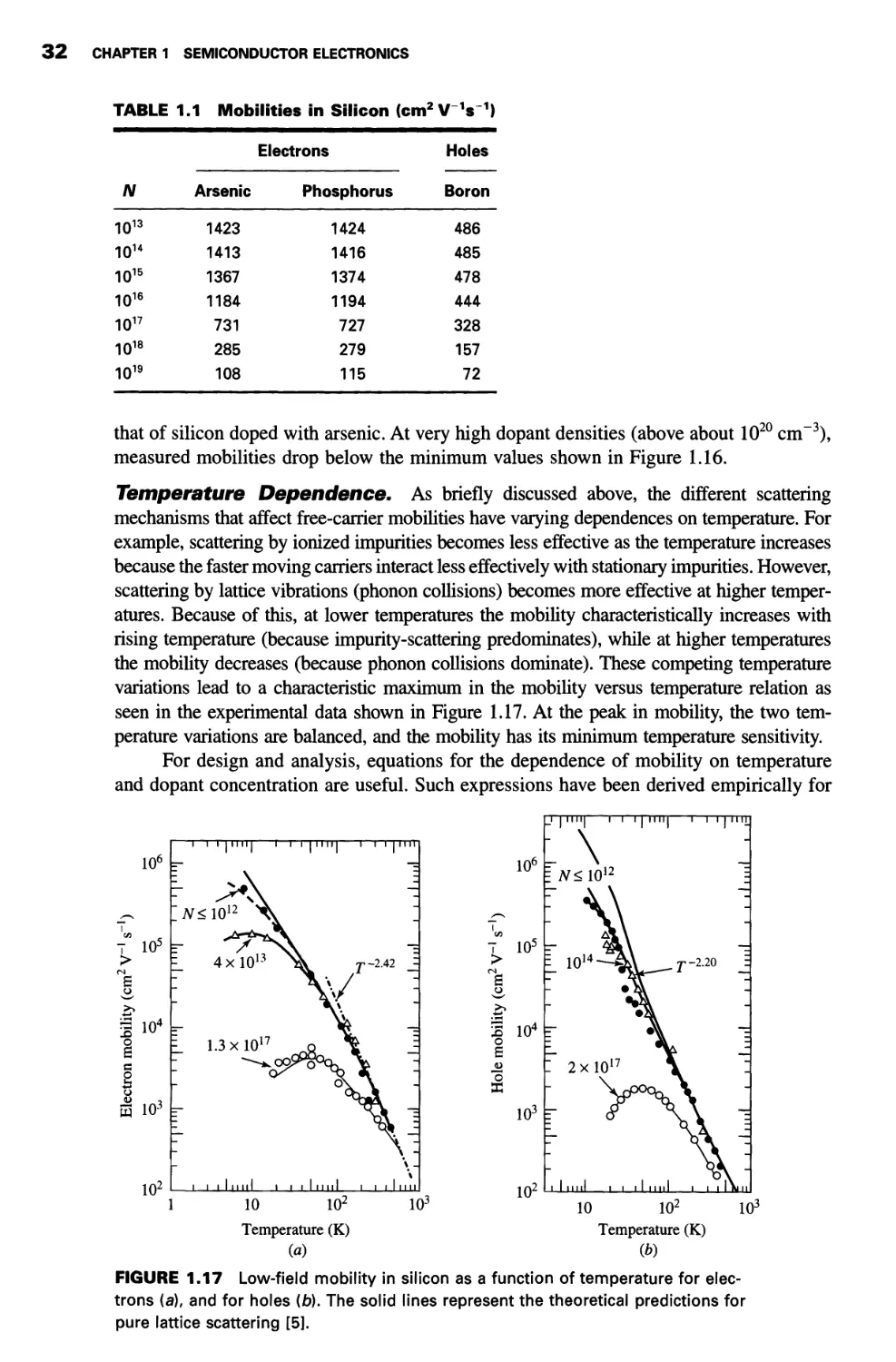
CHAPTER 1 SEMICONDUCTOR ELECTRONICS
effects begin to be noticeable between 1018 and 1019 electrons cm-3; at an electron
concentration of 1019cm~3, AEg is more than 10% of the bandgap energy.
A detailed study of the effect of heavy doping on the semiconductor band structure
shows that as the dopant densities increase, the energy levels they introduce are no longer
distinct, but instead broaden into bands. These impurity bands can overlap the adjacent
conduction or valence bands so that no energy is required to ionize the dopant atoms and
provide free carriers. Therefore, under heavy doping conditions, the formulas derived
earlier in this chapter for silicon doping need modification.
The most important device effect of heavy doping is to limit the achievable current
gain of bipolar transistors. It can also increase undesired leakage current in both bipolar
and MOS transistors.
1.2 FREE CARRIERS IN SEMICONDUCTORS
Our first reference to the electronic properties of solids earlier in this chapter was to
the familiar linear relationship that is often found between the current flowing through
a sample and the voltage applied across it. This relationship is known as Ohm's law:
V = IR. Although a thorough derivation of the physics of ohmic conduction can be
quite complex, an approximate representation of the process provides adequate
background for our purposes. To accomplish this we first develop a picture of the kinetic
properties of free electrons without any external fields. We then consider the addition
of low to moderate fields, characteristic of many device applications, and finally we
discuss the high-field case.
We begin by recalling that electrons (and holes) in semiconductors are almost "free
particles" in the sense that they are not associated with any particular lattice site. The
influences of crystal forces are incorporated in an effective mass that differs somewhat from
the free-electron mass. Using the laws of statistical mechanics, we can assert that
electrons and holes have the thermal energy associated with classical free particles: \kT units
of energy per degree of freedom where к is Boltzmann's constant and T is the absolute
temperature. This means that electrons in a crystal at a finite temperature are not
stationary, but are moving with random velocities. Furthermore, the mean-square thermal velocity
vth of the electrons is approximately* related to the temperature by the equation
|w*^ = |tr (1.2.1)
where m* is the effective mass of conduction-band electrons. For silicon m* = 0.26 m0
(where m0 is the free electron rest mass), and vth is calculated from Equation 1.2.1 to be
2.3 X 107 cm s"1 at T = 300 K. The electrons may be pictured as moving in random
directions through the lattice, colliding among themselves and with the lattice. At thermal
equilibrium the motion of the system of electrons is completely random so that the net
current in any direction is zero. Collisions with the lattice result in energy transfer
between the electrons and the atomic cores that form the lattice. The time interval between
collisions averaged over the entire electron population is тси, the mean scattering time for
electrons. These considerations all apply to the field-free, thermal-equilibrium crystal.
* The formulation of Equation 1.2.1 is slightly in error because of improper averaging. However, we are only
concerned with the order-of-magnitude of the result. At 300 K, vth is typically taken to be 107 cm s-1 for
electrons or holes in silicon.
1.2 FREE CARRIERS IN SEMICONDUCTORS 27
(a)
FIGURE 1.14 (a) The motion
of an electron in a solid under
the influence of an applied
field, (b) Energy-band
representation of the motion, indicating
the loss of energy when the
electron undergoes a collision.
Drift Velocity
Let us now apply a small electric field to the lattice. The electrons are accelerated along
the field direction during the time between the collisions. Figure 1.14л is a sketch of
the motion typical of a crystal electron in response to a small applied field %. Note in
the figure that the field-directed motion is a small perturbation on the random thermal
velocity. Therefore тсп, the mean scattering time, is not altered appreciably by the applied
field.
In Figure 1.14b electron motion in a small applied field is schematically
represented on a band diagram. A constant applied field results in a linear variation in the
energy levels in the crystal. Electrons (which move downward on energy-level
diagrams) tend to move to the right on the diagram, as is appropriate for a field directed
in the negative x direction. The electrons exchange energy when they collide with the
lattice and drop toward their thermal-equilibrium positions. If the field is small, the
energy exchanged is also small, and the lattice is not appreciably heated by the
passage of the current. The slope of the energy bands and the energy losses associated
with lattice collisions are exaggerated in Figure 1.14ft to show the process
schematically. In fact, the energy lost in each collision is much less than the mean thermal
energy of an electron. An electron at rest in the conduction band is at the band edge Ec.
The kinetic energy of an electron in the conduction band is therefore measured by
(E - Ec), and the mean value at thermal equilibrium is just (E - Ec) = \kT or about
0.04 eV at 300 K. This is less than 4% of the bandgap energy.
The net carrier velocity in an applied field is called the drift velocity, vd. It can be
found by equating the impulse (force X time) applied to an electron during its free flight
between collisions with the momentum gained by the electron in the same period. This
equality is valid because steady state is reached when all momentum gained between
collisions is lost to the lattice in the collisions. The force on an electron is —q% and the
CHAPTER 1 SEMICONDUCTOR ELECTRONICS
momentum gained is m*vd. Thus (within the statistical limitations mentioned in the
footnote to Equation 1.2.1),
-q%rcn = m*vd (1.2.2)
or
m*
Equation 1.2.3 states that the electron drift velocity vd is proportional to the field with a
proportionality factor that depends on the mean scattering time and the effective mass of
the nearly free electron. The proportionality factor is an important property of the
electron called the mobility and is designated by the symbol /nn.
Wen
»n = — (1.2.4)
Because vd — —/лп% the mobility describes how easily an electron moves in response to
an applied field.
From Equation 1.2.3 the current density flowing in the direction of the applied field
can be found by summing the product of the charge on each electron times its velocity
over all electrons n per unit volume.
n
Л = 2 " <F>i = ~n(lvd = M^ (1.2.5)
Entirely analogous arguments apply to holes. A hole with zero kinetic energy
resides at the valence-band edge Ev. The kinetic energy of a hole in the valence band is
therefore measured by (Ev — E). If a band edge is tilted, the hole moves upward on an
electron energy-band diagram. The hole mobility /xp is defined as \lp — qrcp/m*. The
total current can be written as the sum of the electron and hole currents:
J = Jn + JP = (nqfin + pqiip)% (1.2.6)
The term in parentheses in Equation 1.2.6 is defined as the conductivity a of the
semiconductor:
a = qfinn + qfxpp (1.2.7)
In extrinsic semiconductors, only one of the components in Equation 1.2.7 is generally
significant because of the large ratio between the two carrier densities. The resistivity,
which is the reciprocal of the conductivity, is shown as a function of the dopant
concentration in Figure 1.15 for phosphorus-doped, н-type silicon and for boron-doped, p-type
silicon. There are slight variations in the resistivities obtained for different dopant species,
particularly in the heavy-doping range. In most practical cases, however, Figure 1.15 can
be used for any dopant species.
A property of a solid that is closely related to its conductivity is its dielectric
relaxation time. The dielectric relaxation time is a measure of the time it takes for charge
in a semiconductor to become neutralized by conduction processes. It is small in metals
and can be large in semiconductors and insulators. The magnitude of the dielectric
relaxation time can be used to obtain qualitative insight. Several device concepts can be
readily interpreted according to the relative sizes of the charge transit time through a
material and the dielectric relaxation time in the same material. Problem 1.12 provides
further introduction to the dielectric relaxation time.
1.2 FREE CARRIERS IN SEMICONDUCTORS 29
10"4 10"3 10~2 10"1 10° 101 102 103 104
Resistivity (Q-cm)
FIGURE 1.15 Dopant density versus resistivity at 23°C (296 K) for silicon
doped with phosphorus and with boron. The curves can be used with little
error to represent conditions at 300 K. [W. R. Thurber, R. L. Mattis, and Y. M.
Liu, National Bureau of Standards Special Publication 400-64, 42 (May 1981).]
Mobility and Scattering
Quantum-mechanical calculations indicate that a perfectly periodic lattice does not scatter
free carriers; that is, the carriers do not interchange energy with a stationary, perfect lattice.
However, at any temperature above absolute zero the atoms that form the lattice vibrate. These
vibrations disturb periodicity and allow energy to be transferred between the carriers and the
lattice.* The interactions with lattice vibrations can be viewed as collisions with energetic
"particles" called phonons. Phonons, like photons, have energies quantized in units of hv,
where v is the lattice-vibrational frequency and h is Planck's constant. The theories of thermal
* Because this energy is supplied to the carriers by the applied field, scattering processes lead to heating of
the semiconductor. The dissipation of this heat is often a limiting factor in the size of semiconductor devices.
A device must be large enough to avoid heating to temperatures at which it no longer functions.
CHAPTER 1 SEMICONDUCTOR ELECTRONICS
and electrical conduction can often be simplified when formulated in terms of phonon
interactions. For silicon at room temperature and moderate electric fields, the lowest vibrational
mode for the lattice corresponds to a phonon energy of 0.063 eV, and the energy of an electron
is changed by this amount when it interacts with these lowest-energy phonons. At higher
temperatures lattice vibrations are larger, and collisions between electrons and the lattice
vibrations are more important. Theoretical analysis indicates that the mobility should decrease with
increasing temperature in proportion to T~n with n between 1.5 and 2.5 when lattice scattering
dominates. Experimentally, values of n range from 1.66 to 3, with n = 2.5 being common.
In addition to lattice vibrations, dopant impurities also cause local distortions in the
lattice and scatter free carriers. However, unlike scattering from lattice vibrations, scattering
from ionized impurities becomes less significant at higher temperatures. Because the
carriers are moving faster at higher temperatures, they remain near the impurity atom for a shorter
time and are therefore less effectively scattered. Consequently, when impurity scattering
dominates, the mobility increases with increasing temperature. Scattering can also be caused by
collisions with unintentional impurities and with crystal defects. These defects can arise from
poor control of the quality of the semiconductor, or they can be related to boundaries
between grains of a polycrystalline material. An example of the latter is the thin films of poly-
crystalline silicon used to form portions of many MOS integrated circuits (Chapters 2 and
9). The grain boundaries and defects in polycrystalline material can reduce the mobility to a
small fraction of its value in single-crystal material with the same dopant concentration.
Two or more of the scattering processes discussed above can be important at the same
time, and their combined effect on mobility must be assessed. To do this we consider the
number of particles that are scattered in a time interval dt. The probability that a carrier is
scattered in a time dt by process i is dt/Tt where т,- is the average time between scattering
events resulting from process /. The total probability dtJTc that a carrier is scattered in the
time interval dt is then the sum of the probabilities of being scattered by each mechanism:
T = 2 7 (1-2.8)
7 с i Ъ
This is a reasonable way to combine the scattering probabilities because the
average scattering time resulting from all of the processes acting simultaneously is less than
that resulting from any one process and is dominated by the shortest scattering time.
Because the mobility fx equals qTc/m*9 we can write
i - ^
The mobility of a carrier subjected to several different scattering mechanisms can thus
be found by combining the reciprocal mobilities corresponding to each type of scattering;
the resulting mobility is smaller than that determined by any of the individual scattering
mechanisms. Because of the reciprocal relation for combining mobility components
(Equation 1.2.9), the overall mobility is dominated by the process for which rt is smallest.
We can apply these considerations to the mobilities of electrons and holes in silicon
at room temperature which are plotted in Figure 1.16. The figure represents a "best fit"
to measured data reported in a number of different sources. In lightly-doped material, the
mobility resulting from ionized impurity scattering is higher than that due to lattice
scattering. Hence, for silicon having impurity concentrations less than about 1015 cm-3, the
mobilities both for holes and electrons remain nearly constant as the dopant
concentration varies. At higher dopant concentrations, however, scattering by ionized impurities
becomes comparable to or greater than that resulting from lattice vibrations, and the total
mobility decreases.
1.2 FREE CARRIERS IN SEMICONDUCTORS 31
о
1400
1200
1000
800
600
400
200
0
1 1 1 II III
-
r
L
г
г
L
1 1 1 II III
1 1 1 II III
i I i 11 in
1 1 1 II III
N
\
\
1 1 1 11 III
1 1 1 II III
•••• Arsenic
4
\
\
\
V
1 1 1 11111
\
V
\
1 1 1 11 1II
4
1 1 Ml III
1 1 1 II III
J
•us
-
-
-
-
-
1 1
1 II III
H 30
20 |
о
s
H io
1013 1014 1015 1016 1017 1018 1019 1020
Total impurity concentration (atoms cm-3)
FIGURE 1.16 Electron and hole mobilities in silicon at 300 К as functions of the total
dopant concentration. The values plotted are the results of curve fitting measurements
from several sources. The mobility curves can be generated using Equation 1.2.10 with
the following values of the parameters [3].
Parameter
Mmin
Mmax
Nref
а
Arsenic
52.2
1417
9.68 x 10¹⁶
0.680
Phosphorus
68.5
1414
9.20 X 10¹⁶
0.711
Boron
44.9
470.5
2.23 x 10¹⁷
0.719
An important practical consequence of the dependence of mobility on total impurity
concentration is observed if a semiconductor is converted from one type to the other (p to
n or n to p) by compensating the dopant impurity atoms already present. While the
carrier densities depend on the difference between the concentrations of the two types of
dopant impurities (Nd — NJ (Equations 1.1.16 and 1.1.17), the scattering depends on the
sum of the ionized impurity concentrations (Nd + Na). Thus, the mobilities in a
compensated semiconductor can be markedly lower than those in an uncompensated material with
the same net carrier density.
The equation used in Figure 1.16 to represent the measured electron and hole
mobilities in silicon is [3]
H> = Mrr
+
^
AV
(1.2.10)
1 + (N/Nref)a
where N is the total dopant concentration in the silicon and the four parameters /xmax, /i^,
N^f, and a have different values for each dopant species. Values of these parameters for the
most common dopants in silicon are included in the caption for Figure 1.16. Table 1.1 gives
numerical values of the mobility (as calculated from Equation 1.2.10) at decade values of N.
The dependence of electron mobility on dopant species is seen, from Figure 1.16,
to be slight for total impurity concentrations less than 1019 cm-3. In the high doping range
(for N > 1019 cm-3), the mobility of phosphorus-doped silicon is 10 to 20% greater than
CHAPTER 1 SEMICONDUCTOR ELECTRONICS
TABLE 1.1 Mobilities in Silicon (cm2V 1s ')
N
1Q13
1014
1Q15
1Q16
1017
1018
1019
Arsenic
1423
H13
1367
1184
731
285
108
Electrons
Phosphorus
1424
1416
1374
1194
727
279
115
Holes
Boron
486
485
478
444
328
157
72
that of silicon doped with arsenic. At very high dopant densities (above about 1020 cm 3),
measured mobilities drop below the minimum values shown in Figure 1.16.
Temperature Dependence. As briefly discussed above, the different scattering
mechanisms that affect free-carrier mobilities have varying dependences on temperature. For
example, scattering by ionized impurities becomes less effective as the temperature increases
because the faster moving carriers interact less effectively with stationary impurities. However,
scattering by lattice vibrations (phonon collisions) becomes more effective at higher
temperatures. Because of this, at lower temperatures the mobility characteristically increases with
rising temperature (because impurity-scattering predominates), while at higher temperatures
the mobility decreases (because phonon collisions dominate). These competing temperature
variations lead to a characteristic maximum in the mobility versus temperature relation as
seen in the experimental data shown in Figure 1.17. At the peak in mobility, the two
temperature variations are balanced, and the mobility has its minimum temperature sensitivity.
For design and analysis, equations for the dependence of mobility on temperature
and dopant concentration are useful. Such expressions have been derived empirically for
106
S-*\
1
СЛ
т io5
>
в
>,
iw4
1
e
о
Ь
о
s io3
1П2
-I
—
г
I i | ii ii | i~г
->\
~_N<10n Ч^
—
z
=-
:
-
—
'^Xs
4xl013 \
1.3 xlO17
^•^QQp
1 1 1 mil 1 1
q Г1ТП- "1 T 1 "-| 11 IT 1
4
H
j
-j
V 1
•l \ n
tL 1
пЯ *. -3
^0°Ck jN 1
ОчД J
^\Jb -3
\ J
11 1 Ч
1 1 Mill 1 1 1 1 IIU
1
10
io2
io3
10 10z
Temperature (K) Temperature (K)
(a) (b)
FIGURE 1.17 Low-field mobility in silicon as a function of temperature for
electrons (a), and for holes (b). The solid lines represent the theoretical predictions for
pure lattice scattering [5].
1.2 FREE CARRIERS IN SEMICONDUCTORS 33
silicon and can be written as [4]
Mn = 88 770-57 +
1250 r:233
and
/*, = 54.3 7V-57 +
1 + [N/(1.26 X 1017 7^4)]0.88 Т;°146
407 t:2-23
1 + [#/(2.35 X 1017 Г„24)]0.88 T~
-0.146
(1.2.11)
where Tn = T/300 with Г measured in К (Kelvin), and N is the total dopant density in the
silicon. Equation 1.2.11 is useful up to dopant densities of 1020 cm-3 and for temperatures
between 250 and 500 K.
Velocity Limitations. In the simplified treatment presented thus far, we assumed (by
taking rc to be insensitive to %) that the velocity imparted to the free carriers by the applied
field is much less than the random thermal velocity, which we found from Equation 1.2.1
to be approximately 107 cm s_1 at room temperature in silicon. For electrons in silicon with
fjun « 1400 cm2 V"1 s"1 the drift velocity at a typical field of 100 V cm-1 is roughly 1.5%
of the thermal velocity, and the applied field does not appreciably change the total velocity
or energy of the carrier. At high fields, however, the drift velocity becomes comparable to
the random thermal velocity, and can no longer be considered as a small increment to the
thermal motion. The total energy of the carrier then increases significantly as the field
increases. When carriers reach energies above the ambient thermal energy, they are often called
hot carriers and characterized by an effective temperature Te that rises with increasing field
and corresponds to the increased kinetic energy of the carriers [6].
At high electric fields, the energy of the hot electrons reaches a critical value at
which an additional scattering process (collisions with high energy "optical" phonons)
becomes important, and the mobility decreases from its low-field value. Because optical-
phonon scattering is very effective in transferring energy from the hot carriers to the lattice,
the carriers cannot gain significant additional net energy, and the drift velocity approaches
a limiting or saturation value v} or vsat at high fields. Figure 1.18 shows measured values
n 1—i—I—ГТ
I ' ' "I
-I 1—I—I I I I I I
Electrons 77 К
-i—i—i—i i i i
I • ■ "I
Holes 300 К
, I
103 104 105
Electric field (V cm"1)
FIGURE 1.18 Drift velocities of electrons (at 77 К and 300 K) and holes (at 300 K) in silicon
as functions of the applied field, showing velocity saturation at high fields. The presence of
several curves indicates the variation in reported data. An empirical "best fit" to these curves
is given in Equation 1.2.12 and Table 1.2 [5].
CHAPTER 1 SEMICONDUCTOR ELECTRONICS
TABLE 1.2
Parameter
V[ cm s-1
%c V cm"1
P
Parameters for Field Dependence of Drift Velocity
Electrons
Expression at 300 К
1.53 X 10⁹ Г"087 1.07 X 10⁷
1.01 Г155 6.91 X 10³
2.57 X 10"2 Г066 1.11
Holes
Expression
1.62 x 10⁸ Г-052
1.24 Г68
0.46 T°A1
at 300 К
8.34 X 10⁶
1.45 X 10⁴
2.637
of drift velocity for electrons (at 77 К and 300 K) and holes (at 300 K) in silicon as
functions of the applied field. At low voltages, the curves are linear, indicating a constant
mobility. At fields above a few thousand volts per centimeter, however, there are noticeable
deviations from constant mobility. Because fields of this magnitude are frequently present
in integrated-circuit devices (equivalent to a few hundred millivolts across a micrometer),
velocity saturation must be considered in analyzing many practical devices.
As a useful approximation, the data shown in Figure 1.18 can be modeled empirically
by the expression [5]
Ы = VUF
1
l + (%/%cy\
WP
(1.2.12)
The parameters vh %c, and /3 in Equation 1.2.12 are given (as a function of the absolute
temperature T) in Table 1.2.
EXAMPLE Velocity Limitations
Use Equation 1.2.12 to find the field (at 300 K) at which the effective electron mobility (defined as
the ratio of the drift velocity to the field) is reduced to half its low-field value.
Solution At low fields, the drift velocity vd is proportional to the field (Equation 1.2.3) and
Ы = M«^- Applying Equation 1.2.12 at low fields (%/% <C 1), we find that the low-field mobility
can be expressed in terms of %c and vt\ уьп = \vd/%\ = |г;//^с|. Using the values from Table 1.2 in
this expression, we calculate fjin = 1548 cm2 V-1 s_1 for the low-field mobility, which is about 10%
higher than the value shown in Figure 1.16. This lack of correspondence is not unusual when
parameters are obtained by curve-fitting.
To find the field at which the effective mobility fin(%) is reduced by 50% from the low-field
value, we note that fxn(%) = \vj%\ = (1/2) X \vt/%c\. Hence, from Equation 1.2.12
1
Li + (W%)li\
I/?
where p = 1.11 and %c = 6.91 X 10³ V cm-1. Solving this equation, we find %/% = 1.142 or
^ = 7.89 X 10³Vcm-'. ■
Before leaving the topic of carrier transport at high fields, we make a final point
about hot electrons. The hot-electron temperature Ге, introduced earlier in our discussion,
describes an ensemble of electrons that is interchanging energy by colliding with the lattice.
Some electrons may, by chance, avoid collisions for relatively long times, and thus achieve
velocities exceeding vl and kinetic energies corresponding to temperatures greater than Te.
1.2 FREE CARRIERS IN SEMICONDUCTORS 35
Although these electrons are few in number, they can have important physical effects
because of their very high energies and the long distances that they have traveled without
scattering. When the distance that a significant number of "lucky" electrons travel before
scattering is comparable to a device dimension, the charge transport by these carriers is
said to be ballistic (unscattered).
Diffusion Current
In the previous section we discussed drift current, which flows when an electric field is
applied and which follows Ohm's law. Ohmic behavior is observed in metals and
semiconductors and is probably familiar from direct experience. In semiconductors, an
additional important component of current can flow if a spatial variation of carrier energies
or densities exists within the material. This component of current is called diffusion
current. Diffusion current is generally not an important consideration in metals because metals
have very high conductivities. The lower conductivity and the possibility of nonuniform
densities of carriers and of carrier energies, however, often makes diffusion an important
process affecting current flow in semiconductors.
To understand the origin of diffusion current, we consider the hypothetical case
of an n-type semiconductor with an electron density that varies only in one dimension
(Figure 1.19). We assume that the semiconductor is at a uniform temperature so that
the average energy of electrons does not vary with x\ only the density n(x) varies. We
consider the number of electrons crossing the plane at x = 0 per unit time per unit
area. Because they are at finite temperature, the electrons have random thermal
motion along the single dimension, but we assume that no electric fields are applied. On
the average, the electrons crossing the plane x = 0 from the left in Figure 1.19 start
at approximately x = — Л after a collision where Л is the mean-free path of an
electron, given by Л = vthTcn. The average rate (per unit area) of electrons crossing the
plane x = 0 from the left, therefore, depends on the density of electrons that started
at x = —Л and is
I"(-AK (1.2.13)
FIGURE 1.19 Electron
concentration n versus
distance x in a hypothetical
one-dimensional solid.
Boundaries are demarcated
A units on either side of the
origin where A is a collision
mean-free path.
CHAPTER 1 SEMICONDUCTOR ELECTRONICS
The factor (5) appears because half of the electrons travel to the left and half travel to the
right after a collision at x = -Л. Similarly, the rate at which electrons cross the plane
x = 0 from the right is given by
\n{k)vth (1.2.14)
so that the net rate ox flux of particle flow per unit area from the left (denoted F) is
F = \vth[n{-k) - Л(А)] (1.2.15)
Approximating the densities at x = ±A by the first two terms of a Taylor-series expansion,
we find
4[n(o)"fA]-[n(o)+fA]}=^AS (L2-i6)
Because each electron carries a charge -q9 the particle flow corresponds to a current
Jn = ~qF = ^,„£ (1.2.17)
We see that diffusion current is proportional to the spatial derivative of the electron density
and arises because of the random thermal motion of charged particles in a concentration
gradient. For an electron density that increases with increasing jc, the gradient is positive,
as is the current. Because we expect electrons to flow from the higher density region at
the right to the lower density region at the left and current flows in the direction opposite
to that of the electrons, the direction of current indicated by Equation 1.2.17 is physically
reasonable.
We can write Equation 1.2.17 in a more useful form by applying the theorem for
the equipartition of energy to this one-dimensional case. This allows us to write
\m*vl = \kT (1.2.18)
We now use the relationship Л = vthrcn together with Equation 1.2.4 to write Equation
1.2.17 in the form
The quantity in parentheses on the right side of Equation 1.2.19 is defined as the
diffusion coefficient Dn and our short derivation has established that
A, = (y)^ (1-2.20)
Equation (1.2.20) is known as the Einstein relation. It relates the two important
coefficients that characterize free-carrier transport by drift and by diffusion in a solid. Its
validity can be established rigorously by considering the statistical mechanics of solids in
detail. Our derivation is aimed at intuition, not physical exactness.
If a field is present, drift, as well as diffusion, occurs. The total current is then the
sum of the drift and diffusion currents.
Jnx = 4№% + 4Dnfa (1.2.21)
where %x is the component of the electric field in the ^-direction.
1.2 FREE CARRIERS IN SEMICONDUCTORS 37
A similar expression can be found for the hole diffusion current so that the total
hole current is written as
Jpx = <№pP%
фр
dp
dx
(1.2.22)
where the negative sign arises because of the positive charge of a hole. The Einstein relation
(Equation 1.2.20) also relates Dp to \xp.
Our discussion of diffusion current has been framed in terms of nonuniform carrier
concentrations. Although this is the most frequent situation encountered in device
analysis and Equations 1.2.21 and 1.2.22 are usually adequate, diffusion also occurs if carriers
are equal in density in a semiconductor but are more energetic in one region than in
another. In this case, other formulations must be used. Problem 1.16 considers a practical
situation where carriers have unequal energies.
EXAMPLE Diffusion Current
An electric field has a non-zero value at plane xx (perpendicular to the jc-axis) inside a silicon
crystal. At xb the electron density is 106 cm-3 and the electron density is nonuniform in the x direction.
We observe that no electron current flows across the plane.
(a) Explain why no current is flowing.
(b) If the electric field is -103 V cm-1 (i.e., 103 V cm-1 in the negative ^-direction), what is the
electron gradient perpendicular to the plane?
Solution
(a) An electric field % would result in a drift current of magnitude Jn = qy^nn% according to
Equation 1.2.5. Because no current flows, there must be a diffusion-current component that
is equal in magnitude but opposite in direction. The balance of these two components leads
to zero electron current.
(b) Using Equation 1.2.21, we have
dn l*n
— = -—n%
ax D„
kT
106X (-103)
0.0258
= 3.88 X 10¹⁰
cm
ё
106
% = 103 V cm"1
Jn drift current
Jn diffusion current
gradient = 3.88 xl010cnT
38 CHAPTER 1 SEMICONDUCTOR ELECTRONICS
Total Currents and Quasi-Fermi Levels.* Quasi-Fermi levels (defined in
Equations 1.1.28 and 1.1.29) are useful in the analysis of semiconductors that are not at
thermal equilibrium. A semiconductor in which a current is flowing is such a nonequi-
librium case, and the quasi-Fermi levels can be used to define both drift and diffusion
currents in a compact form.
To illustrate this, we first develop an expression for the electric field in a
semiconductor in terms of the electron energy. The presence of an electric field causes charged
particles to have position-dependent energies. Consequently, when a field is present, the
energy bands for electrons slope away from the horizontal (constant energy), as seen in
Figure 1.14. It is convenient to express the field in terms of the intrinsic Fermi level Et
by observing that the electron energy is obtained by multiplying the potential by the charge
—q. The field % which is the negative derivative of the potential, can therefore be written
(in one dimension) as
1 dE( <1фл
% = --1 = -—- (1.2.23)
q dx dx
where the quasi-Fermi potential <j}fi = —Ejq was introduced in Equation 1.1.28. The
electron and hole concentrations are expressed in terms of the quasi-Fermi levels by
n = щ exp(£/w - Et)/kT = щ exp q{$fi - ф^/кТ
p = щ exp(£, - E^/kT = щ exp q{$fp - фл)/кТ (1.2.24)
Using Equations 1.2.23 and 1.2.24 in Equation 1.2.21 together with the Einstein
relation (Equation 1.2.20), we obtain
dEfn dfyfr
Jn = ^nn~dx = ~mnn~dx~ (1.2.25)
A similar derivation for holes leads to
dEfp d<$>fp
J* = ^PHx~ = ~qfXpP~dx~ (L2'26)
Equations 1.2.25 and 1.2.26 show that the total current (the sum of both drift and
diffusion components) for each carrier is proportional to the gradient of the quasi-Fermi
level of that carrier type. This compact representation can be very helpful in using energy-
band diagrams to visualize the total current in a device. The equations are also useful for
mathematical analysis, and their form simplifies a number of complex problems.
1.3 DEVICE: HALL-EFFECT MAGNETIC SENSOR
As is our pattern throughout the book, we conclude this chapter with a discussion of an
integrated-circuit device, in this case a Hall-effect sensor for magnetic fields. Although
Hall-effect sensors are unconventional integrated-circuit devices, they are commercially
important. Hundreds of millions of integrated Hall circuits are in use, mainly as contact-
less switches (e.g. in computer-terminal keyboards) and as mechanical proximity
detectors. Hall-effect, magnetic sensing, integrated circuits are highly successful examples of
integrated sensors, that is, integrated circuits having intentional sensitivity to
nonelectrical signals. This sensitivity is achieved by incorporating sensing elements on a silicon chip
together with bias, amplifying, and signal-processing circuitry. The field of integrated
sensors is developing rapidly because it capitalizes on the extraordinary refinements
1.3 DEVICE: HALL-EFFECT MAGNETIC SENSOR 39
already achieved by purely electrical integrated circuits and economically applies these
circuits when the input signals are not electrical quantities. For example, microprocessors
integrated with nonelectrical sensors are powerful components in control systems. In
addition to magnetic fields, other nonelectrical inputs for which integrated sensors show
appreciable promise include visible and infrared radiation, temperature, pressure, force,
acceleration, chemical vapors, and humidity.
Physics of the Hall Effect
The Hall effect, named for American physicist E. H. Hall who discovered it in 1879, is a
direct consequence of the force exerted on charged carriers moving in a magnetic field.
The force on a particle having charge q and moving in a magnetic field В with velocity
v (both variables being vector quantities) is written
F = qvX В
(1.3.1)
where the vector cross product (X) signifies the product of the vector magnitudes times
the sine of the angle between them.
The resulting Hall effect is illustrated schematically in Figure 1.20. The Hall effect
is usually used with an extrinsic semiconductor so that one carrier dominates and the other
has a negligible density. To aid our discussion, however, both electrons and holes are
shown in Figure 1.20.
As expressed in Equation 1.3.1, the current carriers (electrons or holes) in a
conductor experience a force in a direction perpendicular to both the magnetic field and the
carrier velocity. In the steady state, this force is balanced by an induced electric field that
results from a slight charge redistribution. These forces must balance because there can
be no net steady-state motion of the carriers in the transverse direction. The induced
electric field is called the Hall field %H. Integrating the Hall field with respect to position
across the width of the conductor produces the Hall voltage VH, which can be detected by
FIGURE 1.20 Schematic of the Hall effect. A current flows along the positive
x-direction. A magnetic field В along the positive z-direction deflects holes and
electrons along the negative /-direction. This leads to a Hall field %H along the positive
/-direction for holes and along the negative /-direction for electrons.
40 CHAPTER 1 SEMICONDUCTOR ELECTRONICS
contacts placed at opposite sides of the conductor. For a uniform conductor and a uniform
magnetic field, the magnitude of the Hall voltage is just the product of the Hall field and
the conductor width W: VH = %HW.
In Figure 1.20, current in the positive Jt-direction can be carried either by holes
flowing toward positive x or else by electrons moving in the opposite direction. Because both
the charge and the velocity are of opposite signs for the two carrier types, the magnetic
force on both holes and electrons has the same sign for a given current direction. The
charge separation caused by this force and the resulting Hall voltage is, therefore, of
opposite polarity for holes and electrons. The sign dependence of the Hall voltage can thus
be used to determine whether a semiconductor is p- or n-type.
We can derive the basic theory for the Hall effect using the quantities shown in
Figure 1.20. In the figure, current flow is in the positive ^-direction, the magnetic field is in
the positive г-direction, and the Hall field is therefore along the y-direction. The magnetic
force deflects both holes and electrons in the negative y-direction and induces a Hall field
toward positive у for holes, and in the opposite direction for electrons. Consider the drift
velocity vd of the current carriers. Equating the magnitudes of the magnetic and Hall-field
forces, we have q%H = qvdB. The velocity vd is related in magnitude to the current by
vd = Jjqp for holes or by vd = —Jjqn for electrons. Thus, the Hall field can be written
in terms of the current and the applied magnetic field as
JrB
%H = -±- (1.3.2)
qp
for holes, and
JYB
%H = -^- (1.3.3)
qn
for electrons. Both Equations 1.3.2 and 1.3.3 can be expressed as
%H = RHJXB (1.3.4)
where RH, the Hall coefficient, is equal to l/qp for holes and to - l/qn for electrons in
this simplified derivation. In practice, Equation 1.3.4 predicts the Hall field accurately if
the Hall coefficient is modified to account properly for statistical variations in the
velocities of free carriers. This modification introduces a new factor r into the expression for
the Hall coefficient which now becomes
RH = rlqp (1.3.5)
for holes, and
RH = -r/qn (1.3.6)
for electrons. The factor r is typically between 1 and 2 (theoretically 1.18 for lattice
scattering and 1.93 for ionized impurity scattering).
The Hall voltage VH is given by the product of %H and W, which can be written in
terms of the total current / as
RHIB
v»=1k (L3-7)
with RH measured in cm3 C_1, / in amperes, В in Gauss, t in cm, and VH in volts. (The
factor 108 is needed to convert the MKS units meter and Tesla (or Webers m~2) to more
conventional semiconductor units centimeter and Gauss.)
1.3 DEVICE: HALL-EFFECT MAGNETIC SENSOR 41
From Equation 1.3.7 we see that in an unknown semiconductor, the Hall
coefficient can be determined by measuring the Hall voltage for a given magnetic field and
current. Equations 1.3.5 and 1.3.6 then permit the calculation of the unknown carrier
types and densities. From the carrier densities and known currents, the material
conductivity and Hall mobility (fMH = сг|/?я|) can then be found. The Hall effect is thus a
powerful experimental technique for the study of semiconductors, and it is frequently
used for this purpose [7].
Integrated Hall-Effect Magnetic Sensor
To use the Hall effect in an integrated circuit, it is necessary to isolate a conducting
pattern similar to the region sketched in Figure 1.20. This is typically accomplished by
using epitaxy and oxide or junction isolation (procedures described in Chapter 2) as shown
in Figure 1.21. For the simplest Hall-effect theory to apply, the width W should be much
greater than the length L so that the current density J is uniform over the sample cross
section. As a practical matter, however, shorting of the Hall voltage by the ohmic end
contacts is reduced if L » W. In production-integrated circuits, W is usually made
comparable to L. For a rectangular geometry the theory that we have derived can be corrected by
multiplying the expression for VH (Equation 1.3.7) by a factor К that is typically
approximately unity and is a function only of the ratio W/L [8]. This refinement is not included
in our treatment of the Hall effect.
One important consideration when designing a Hall element for an integrated
circuit is the power dissipated in the device. To consider power consumption, we express the
resistance of the Hall element in terms of the Hall coefficient. For a /?-type element, for
example, we can write an expression for the resistance R
R =
LR„
pL L
A " qfJLppWt " riLpWt
(1.3.8)
Current
contact
Hall contacts
Isolation
region
FIGURE 1.21 Hall-effect element for an integrated-sensor circuit. The element
is fabricated in high-resistivity л-type silicon which is isolated by oxide regions
or by p-type regions as described in Chapter 2. The sketch shows the element
prior to the application of contact metal.
42 CHAPTER 1 SEMICONDUCTOR ELECTRONICS
For a supply voltage Vs, we can write / = Vs/R or
RHL
/-^5 d.3.9)
which allows us to write Equation 1.3.7 as
W
VH = rfxpVs—B X Ю"8 (1.3.10)
where, as in Equation 1.3.7, В is measured in Gauss and length is measured in cm.
EXAMPLE Hall Element Figure of Merit
(a) Derive a figure of merit MH for a Hall element that expresses the Hall voltage per unit of
magnetic field per unit of power dissipation. Consider a p-type element having RH = 8 X
103 cm3 C1, W/L = 1, r = 1.2, and t = 8 |xm.
(b) Calculate the resistance of the element and the value of MH if В = 500 Gauss and the power
dissipated in the element is 1.43 mW.
Solution
(a) From Equation 1.3.10, we have VH in terms of the supply voltage Vs. The dissipated power
PH is equal to Vs X /.
Therefore,
_ rV2sfipWt
Ph~ RhL
and
VH RH X lO'8 r X 10~8
MH =
PHB Vst qpVst
in units of volts per Gauss-watt. From this derived result, we see that MH is improved by
decreasing the supply voltage and reducing both the dopant density and the thickness of
the Hall element.
(b) Calculating the parameters, we have
1. p = r/qRH = 9.38 X 10¹⁴
2. From Figure 1.16, /xp = 475 cm2 V-1 s"1
3. From Equation 1.3.8, R = 17.5 kft
4. Because PH = V2S/R, Vs = VF^R or Vs = 5 V
8 X 103 X 10"8
5. Hence, MH = r- or MH = 0.02 ■
5 X 8 X 10"4
As seen in this example, the performance of the Hall sensor is improved by
decreasing the dopant density. As the dopant density is reduced, the mobilities of both holes
and electrons increase (Figure 1.16), leading to an increased Hall voltage for a given bias
(Equation 1.3.10). Most 1С Hall sensors are fabricated in и-type Si doped with about 1015
donors cm-3. From Figure 1.16, we see that at this concentration we are below the region
in which the mobility varies strongly with the impurity density. Hence, for this dopant
concentration, unintentional processing variations in the dopant density lead to only small
variations in mobility, and thus in the Hall coefficient. Typical sensitivities obtained for
Hall elements are of the order of 30 |xV per Gauss with excellent linearity up to tens of
kiloGauss.
SUMMARY 43
FIGURE 1.22 A precision, linear-output, Hall-sensor chip. The integrated
circuit contains bias elements, temperature-compensation circuitry, and on-chip
amplification. The chip area is 1.12 by 1.98 mm2 and the Hall element (large
pattern on the lower right-hand side) measures 230 by 335 (xm2. (Courtesy:
G. B. Hocker, Honeywell Corporation)
The major use of integrated Hall circuits is for sensing the position of a device or
element. Most of the circuits produced are used in contactless keyboard switches. In a
typical keyboard switching application, a permanent magnet on a plunger is activated by
depressing a key. This action introduces a magnetic field of the order of 500 Gauss near
the sensing Hall element, producing a Hall voltage of roughly 15 mV which is easily
detected by an on-chip amplifier. Integrated Hall sensors are also produced for
magnetometer applications, in which a signal proportional to the magnetic field is desired. Figure
1.22 shows a commercial Hall-effect integrated sensor which has been designed for
magnetometer use.
SUMMARY
One of the cornerstones of solid-state electronics is
the band structure of solids. This key concept is
related to the quantized energy levels of isolated atoms.
Huge differences in the electrical conductivities of
metals, semiconductors, and insulators result from
basic differences in the band structures of these three
classes of materials.
By considering the band structure of
semiconductors, we can deduce the existence of two types of
current carriers, holes and electrons. In most cases of
practical interest, holes and electrons can be
considered as classical free particles inside the
semiconductor crystal. The motion of the holes and electrons
and the statistical distributions that characterize their
energies can be calculated if their effective masses are
modified from those of truly free particles. The
populations of holes and electrons can be controlled by
adding impurities to otherwise pure semiconductor
crystals. In this process, known as doping, extra holes
can be added to single-crystal silicon, for example,
by introducing ions with valence three, which are
incorporated in the lattice in place of silicon, which
has valence four. The resultant crystal is known as
p-type silicon. To add electrons and thereby obtain n-
type silicon by doping, impurities with valence five
can be substituted for silicon atoms in the lattice.
An understanding of many electronic properties
can be gained by applying the laws of statistical
physics to the populations of electrons and holes in
semiconductors. The Fermi level is an important
44 CHAPTER 1 SEMICONDUCTOR ELECTRONICS
parameter used to describe the concentrations of free
carriers in a crystal at thermal equilibrium. Under
usual conditions, the Fermi level in a semiconductor
exists within a forbidden gap of energies that is
ideally free of any allowed energy states for electrons.
Semiconductors in this condition are described as
nondegenerate. If the Fermi level lies within a band
of allowed electronic states, the semiconductor is
called degenerate because its conduction properties
degenerate towards those of a metal. When thermal
equilibrium does not apply, it is useful to define two
quasi-Fermi levels, which are different for holes and
electrons. The separation of the two quasi-Fermi
levels is a measure of the degree to which thermal
equilibrium in the semiconductor is disturbed. When the
semiconductor returns to thermal equilibrium, the
hole and electron quasi-Fermi levels merge into a
single Fermi level that characterizes both carrier
densities. Quasi-Fermi levels are useful in considering
photogeneration of electrons and holes in
semiconductors, and in simpUfying the representation of free-
carrier diffusion and drift.
In the basic theory of electrons and holes in
semiconductors, it is assumed that only very low
concentrations of dopants are present and that they do not
influence the band structure of the host crystal. At
heavy-doping concentrations, the impurity atoms are
no longer situated far apart from one another, and their
presence modifies the band structure. One of the most
important effects of heavy doping is that nie, the
effective value of the intrinsic-carrier density, increases
with increasing doping density.
When free carriers in a semiconductor are
subjected to a low or moderate electric field, they move
with a constant drift velocity. The ease of carrier mo-
REFERENCES
1. (a) F. Morin and J. P. Maita, Phys. Rev. 96, 28 (1954).
(b) A. S. Grove, Physics and Technology of
Semiconductor Devices, Wiley, New York (1967).
2. P. P. Debye and E. M. Conwell, Phys. Rev. 93, 693
(1954).
3. (a) D. M. Caughey and R. F. Thomas, Proc. IEEE 55,
2192 (December 1967).
(b) G. Masettt, M. Severi, and S. Solmi, IEEE Trans.
Electr. Devices ED-30, 764 (July 1983).
4. N. D. Arora, J. R. Hauser, and D. J. Roulston, IEEE
Trans. Electr. Devices ED-29, 292 (February 1982).
5. C. Jacoboni, C. Canali, G. Ottaviani, and A. A. Quara-
nta, Solid-State Electronics 20, 77 (February 1977).
6. J. L. Moll, Physics of Semiconductors, McGraw-Hill,
New York (1964), p. 198.
tion in response to the field expressed as the velocity
per unit field is known as the mobility and denoted
by /л. The magnitude of the mobility is determined
by the nature of the scattering events experienced by
free carriers as they interact with the lattice. The
thermal energy of free carriers in solids causes them to
move randomly and results in a net flux of carriers if
either the carrier densities or their energies are not
homogeneous in space. The net motion resulting from
this process is called diffusion. When the crystal is at
a uniform temperature, diffusion occurs from regions
where the carriers are more dense to regions where
their density is lower. In nondegenerate
semiconductors, the diffusion coefficient D for a given type of
carrier is related to the mobility jjl by the Einstein
relation, D/ix = kT/q.
At high electric fields, scattering of electrons and
holes is no longer determined mainly by the thermal
velocity, and the drift motion is no longer proportional
to the applied field. Mobility, instead of being
constant, begins to decrease as the field increases. At
fields in the range of 104 to 105 V cm"1, additional
modes of free-carrier scattering must be considered,
leading to upper limits for hole and electron drift
velocities.
The force on a moving charged particle in a
magnetic field gives rise to the Hall effect when
a semiconductor carries a current perpendicular to
a magnetic field. Hall-effect experiments provide a
powerful means of studying free-carrier properties in
semiconductors. Integrated-sensor circuits in which
Hall elements, together with bias circuits, temperature-
compensating circuits, and amplifiers are all
fabricated on a single silicon chip, are important
commercial products.
7. E. H. Putley, The Hall Effect and Related Phenomena,
Butterworths, London (1960).
8. J. T. Maupin and M. L. Geske, The Hall Effect in
Silicon Circuits, Symposium on the Hall Effect, Johns
Hopkins University, Baltimore, Md. (1981), p. 421.
9. S. Wang, Solid-State Electronics, McGraw-Hill, New
York (1966), p. 263.
10. S. M. Sze and J. С Irvin, Solid-State Electronics 11,
599 (1968).
11. J. L. Moll, Physics of Semiconductors, McGraw-Hill,
New York (1964), p. 99.
12. R. B. Adler, A. С Smith, and R. L. Longini, SEEC,
Vol. 1, Introduction to Semiconductor Physics, Wiley,
New York (1964).
PROBLEMS 45
BOOKS
p. G. Streetman and S. Banerjee Solid-State Electronic
Devices, 5th ed. Prentice-Hall, Simon and Schuster Co.,
N.J. (2000).
R. F. Pierret, Semiconductor Fundamentals, Vol. I, Modular
Series on Solid-State Devices, Addison-Wesley, Reading,
Mass. (1983).
PROBLEMS
1.1 Phosphorus donor atoms with a concentration of
Ю16 cm-3 are added to a pure sample of silicon.
Assume that the phosphorus atoms are distributed
homogeneously throughout the silicon. The atomic
weight of phosphorus is 31.
(a) What is the sample resistivity at 300 K?
(b) What proportion by weight does the donor
impurity comprise?
(c) If 1017 atoms cm-3 of boron are included in
addition to the phosphorus, and distributed uniformly,
what is the resultant resistivity and conductivity type
(i.e., p- or n-type material)?
(d) Sketch the energy-band diagram under the
condition of (c) and show the position of the Fermi level.
1.2* Find the equilibrium electron and hole
concentrations and the location of the Fermi level for silicon
at 27°C if the silicon contains the following
concentrations of shallow dopant atoms:
(a) 1 X 1016 cm"3 boron atoms
(b) 3 X 1016 cm"3 arsenic atoms and 2.9 X 1016 cm"3
boron atoms
1.3 An n-type sample of silicon has a uniform density
Nd = 1016 atoms cm"3 of arsenic, and a p-type silicon
sample has Na — 1015 atoms cm-3 of boron. For each
semiconductor material determine the following:
(a) The temperature at which half the impurity atoms
are ionized. Assume that all mobile electrons and
holes come from dopant impurities. [Hint. Use
Equations 1.1.21 and 1.1.22 together with the fact that
fD(Ef) = i]
(b) The temperature at which the intrinsic
concentration nt exceeds the impurity density by a factor of
10. See Table Х.ЫотЦТ).
(c) The equilibrium minority-carrier concentrations
at 300 K. Assume full ionization of impurities.
(d) The Fermi level referred to the valence-band edge
Ev in each material at 300 K. The Fermi level if both
types of impurities are present in a single sample.
J. P. Mckelvey, Solid-State and Semiconductor Physics.
Original publisher Harper & Row, New York
(1966), reprinted by Dover Publications, New York (1984).
W. E. Beadle, J. С. С. Tsai, and R. D. Plummer, Editors,
Quick Reference Manual for Silicon Integrated-Circuit
Technology, Wiley-Interscience, New York (1985) (for
silicon properties).
1.4* A piece of n-type silicon has a resistivity of 5
fl-cm at 27°C. Find the thermal-equilibrium hole
concentrations at 27, 100, and 500°C. (Refer to the tables
and figures for needed quantities.)
1.5f Grain boundaries and other structural defects
introduce allowed energy states deep within the
forbidden gap of polycrystalline silicon. Assume that
each defect introduces two discrete levels: an
acceptor level 0.51 eV above the top of the valence
band and a donor level 0.27 eV above the top of
the valence band. (Note that Ea > Ed and that these
are not shallow levels.) The ratio of the number of
defects with each charge state (+, —, or neutral) at
thermal equilibrium is given by the relation (see
Ref. 11)
Е^ — Ej- Ef — Ea
N$:Nq\N~ =exp :l:exp
(a) Sketch the densities of these three species as the
Fermi level moves from Ev to Ec. Which species
dominates in heavily doped p-type material? In w-type
material?
(b) What is the effect of the defects on the majority-
carrier concentrations?
(c) Using the above information, determine the
charge state of the defect levels and the position of
the Fermi level in a silicon crystal containing no
shallow dopant atoms. Is the sample p- or n-type?
(d) What are the electron and hole concentrations and
the location of the Fermi level in a sample with 2 X
1017 cm"3 phosphorus atoms and 5 X 1016 cm-3
defects?
1.6* Two scattering mechanisms are important in a
piece of semiconductor. If only the first scattering
process were present, the mobility would be 800 cm2
(Vs)"1. If only the second were present, the mobility
would be 200 cm2 (Vs)"1. What is the mobility
considering both scattering processes?
* Answers to problems marked by an asterisk appear at the end of the book.
46 CHAPTER 1 SEMICONDUCTOR ELECTRONICS
1.7 Find the mobility of electrons in aluminum with
resistivity 2.8 X 10"6 П-cm and density 2.7 g cm"3.
The atomic weight of aluminum is 27. Of the three
valence electrons in aluminum, on the average 0.9
electrons are free to participate in conduction at room
temperature. If m* = m0, find the mean time between
collisions and compare this value to the
corresponding value in lightly doped silicon.
1.8* An electron is moving in a piece of lightly doped
silicon under an applied field at 27°C so that its drift
velocity is one-tenth of its thermal velocity. Calculate
the average number of collisions it will experience in
traversing by drift a region 1илп wide. What is the
voltage applied across this region?
1.9 In an experiment the voltage across a uniform, 2
(xm-long region of 1 ft-cm, w-type silicon is doubled,
but the current only increases by 50%. Explain. (The
silicon remains neutral at both current levels.)
1.10* The electron concentration in a piece of uniform,
lightly-doped, и-type silicon at room temperature varies
linearly from 1017 cm"3 at x = 0 to 6 X 1016 cm"3 at
x = 2 |xm. Electrons are supplied to keep this
concentration constant with time. Calculate the electron
current density in the silicon if no electric field is present.
Assume /лп = 1000 cm2 V"1 s"1 and T = 300 K.
1.11+ Silicon atoms are added to a piece of gallium
arsenide. The silicon can replace either trivalent
gallium or pentavalent arsenic atoms. Assume that
silicon atoms act as fully ionized dopant atoms and that
5% of the 1010 cm"3 silicon atoms added replace
gallium atoms and 95% replace arsenic atoms. The
sample temperature is 300 K.
(a) Calculate the donor and acceptor concentrations.
(b) Find the electron and hole concentrations and the
location of the Fermi level.
(c) Find the conductivity of the gallium arsenide
assuming that lattice scattering is dominant.
See Table 1.3 for properties of GaAs.
1.12+ (Dielectric relaxation in soUds.) Consider a
homogeneous one-carrier conductor of conductivity <r and
permittivity e. Imagine a given distribution of the
mobile charge density p(x, y, z; t = 0) in space at / = 0.
We know the following facts from electromagnetism,
provided we neglect diffusion current:
-dp
V • D = p; D = e%\ J = <j%\ V • J = ~-
dt
(a) Show from these facts that p(x, y, z\ t) = p(jc, y, z\
t = 0) exp [—t/(e/a)]. This result shows that
uncompensated charge cannot remain in a uniform
conducting material, but must accumulate at discontinuous
interfaces, surfaces, or other places of nonuniformity.
(b) Compute the value of the dielectric relaxation
time e/сг for intrinsic silicon; for silicon doped with
1016 donors cm"3; and for thermal Si02 with a =
10"16(n-cm)_1 [12].
1.13+ Because of their thermal energies, free carriers
are continually moving throughout a crystal lattice.
While the net flow of all carriers across any plane is
zero at thermal equilibrium, it is useful to consider
the directed components that balance to zero. The
component values are physically significant in that
they measure the quantity of current that can be
delivered by diffusion alone. This is relevant if, for
example, one is able to unbalance the thermal
equilibrium condition by intercepting all carriers flowing in
a given direction. By considering that Jx = —qn0vx,
show that the current in a solid in any random
direction resulting from thermal processes is
-qn0vth
J 4
where vth is the mean thermal velocity and n0 is the
free-electron density. (Hint. Consider the flux through
a solid angle of 2тг steradians.) [12]
1.14* Calculate the wavelengths of radiation needed
to create hole-electron pairs in intrinsic germanium,
silicon, gallium arsenide, and Si02. Identify the
spectrum range (e.g., infrared, visible, UV, and X ray) for
each case.
1.15+ The relation between D and jjl is given by
p = l Щ
fi q d(ln n)
for a material that may be degenerate. (That is, the
Fermi-Dirac distribution function must be used
because the Fermi level may enter an allowed energy
band.) Show that this relation reduces to the simpler
Einstein relation D/p, = kT/q if the material is non-
degenerate so that Boltzmann statistics can be used.
1.16 A hot-probe setup is a useful laboratory
apparatus. It is used to determine the conductivity type of
a semiconductor sample. It consists of two probes and
an ammeter that indicates the direction of current
flow. One of the probes is heated (most simply, a
soldering iron tip is used), and the other is at room
temperature. No voltage is applied, but a current flows
when the probes touch the semiconductor.
Considering the role of diffusion currents, explain the
operation of the apparatus and draw diagrams to indicate
the current directions for p- and n-type
semiconductor samples.
1.17 Consider a simple model for diffusion in one
dimension. Assume that all particles must move only
at discrete, regularly spaced times, one time unit
APPENDIX 47
apart. When they move, each particle can only jump
one space unit either to the left or to the right, with
equal probability. Start with 1024 particles at x = 0,
t = 0, and build up, step by step, the pattern of
particles in space after 10 time units. Plot the
distribution in space after each jump and measure the
corresponding width W between points of one-half
maximum concentration. Then plot W2 versus time.
What does your result suggest about the rate of
"spread" of particles by the diffusion process (in one
dimension at least)? [12]
1.18 The values in Tables 1.3 and 1.4 are not entirely
consistent. To see that this is the case,
(a) Calculate Eg (T = 300 K) using the equation in
Table 1.4 and compare the result with Eg in Table 1.3.
(b) Use both values of Eg to calculate щ from
Equation 1.1.25 with Nc and Nv as given in Table 1.3.
(c) Calculate щ at 300 К using the temperature-
variation formula in Table 1.4.
[The calculated inconsistencies reflect the fact that
values in the tables are determined from measurements
using a variety of experimental methods. Based on
many experiments, a value of щ equal to 1.45 X 10¹⁰
cm"3 for silicon at 300 К is widely used. The degree
of precision of many parameters is unknown.]
1.19+ In a nearly intrinsic material, the motions of
both electrons and holes are significant for the Hall
effect. Show that the Hall coefficient in the case that
both holes and electrons are present becomes
Rh =
i4p
l4n
jxb q(v<pP + м«")2
Prove that this result is consistent with the simpler
theory derived in Section 1.3.
APPENDIX
Electric Fields, Charge Configuration,
and Gauss' Law
As discussed in Sec. 1.2, an internal electric field in a solid moves electrons and holes and thereby
causes a drift current. If we know the size and direction of the field, we can predict the drift
current in terms of material properties. This is but one of many circumstances in which knowledge of
the electric field in a solid has crucial importance. Although electric-field analysis is typically taught
in basic physics courses, the analysis techniques have so many important applications to device
electronics that we review them briefly here. Readers who require amplification of these ideas can
consult any of the many excellent physics texts that discuss electricity and magnetism in greater detail.
For device analysis, the most useful fundamental relationship is that between electric charge
and the electric field. Expressed in one dimension (which very often suffices for device analysis),
the differential equation relating a charge density p(x) to the field % is
d{€%)ldx = p
(1A.1)
In Equation 1A.1, e = er€Q is the permittivity of the material which is, in turn, equal to the product
of the relative permittivity €r and the permittivity of free space e0.
Michael Faraday (1791-1867), the famous English engineer-scientist, provided an extremely
useful interpretation of Equation 1A.1 by introducing the concept of electrical lines of force that act
on charges and that emanate from positive charges and terminate on negative charges. The lines of
force are always parallel to the electric field and the densities of the lines of force throughout a
region are proportional to the local magnitude of the electric field in the same region. Faraday's
concept provides a straightforward means to visualize the correctness of Gauss' Law which states that
the integrated electric field over a closed surface is equal to the net electric charge contained within
that surface divided by the permittivity within the closed surface.
To develop these ideas in a useful manner for device electronics, we can integrate Equation
1A.1 along x to write a one-dimensional form of Gauss' Law (assuming the usual case that € is not
a function of x).
<% -%)= P(x)dx
Jx,
(1A.2)
48 CHAPTER 1 SEMICONDUCTOR ELECTRONICS
Equation 1A.2 is readily interpreted using Faraday's concept of lines of force because it states
mathematically that the product of the permittivity and the electric field at the boundaries of a
region (between x2 and л:,) changes by an amount equal to the total charge contained in that region.
Field lines are added by positive charges and subtracted by negative charges; hence, the change in
field between two boundaries (xx and x2) multiplied by the permittivity equals the sum of the charges
contained in the region between these two boundaries. The special case of charge cr distributed
uniformly in density on a planar surface within a bounded volume (therefore at a single value of
x = *0) leads, from Equation 1A.2, to a stepwise change in the field % at x = x0 such that A% at
x = x0 is a/e. Not evident in Equation 1A.2 is the effect of a change in the permittivity, for
example at a boundary between two different materials. Because a material's permittivity e
represents the polarizing effect of an electric field on its molecules, a change in € at a boundary results
in an effective surface charge at that boundary. As a result, if the permittivity changes from ea to
eb at x = xb the field must also change from its value %a in region a to %b in region b at x = jcj
such that ea% = eb% .
The force F on an electron in a field % is the product of its charge —q and the field.
F = -q% (1A.3)
The work dW needed to move the charge an incremental distance dx is
dW = -q%dx = qd<l> (1A.4)
where the field % is related to the electric potential ф by
% = -d</>/dx (1A.5)
Equation 1A.5 can be used together with Equation 1A.1 to write Poisson's Equation.
d^/dx2 = -pie (1A.6)
In Equation 1A.6, we have assumed that the permittivity € does not depend on x.
Equation 1 A.6 is a second-order linear differential equation for the potential ф, and hence its
solutions have two constants that need to be evaluated using boundary conditions. Because
Equation 1A.6 is linear, its solutions can be added; i.e., a potential ф{ that is a solution corresponding
to a charge density p{ can be added to a potential ф2 that is a solution corresponding to a charge
density p2 so mat Ф = Ф\ + Фг represents the potential for a charge density p = px + p2. This
additive property of solutions for potential, known as the superposition principle, is often a valuable
problem-solving aid.
EXAMPLE Capacitor Electronics Using Gauss' Law
(a) Consider two parallel perfectly conducting plates of area A that are separated a distance W
in air and connected to electrodes to form a capacitor. A voltage V0 is applied between the
two plates. Sketch and label plots showing (i) the field, (ii) charges, and (iii) the potential as
functions of the distance x between the two conducting plates (0 ^ x ^ W).
(b) A perfectly conducting plate of area A and thickness W/2, having no electrical connections,
is inserted midway between the plates. Repeat the calculations requested in part (a).
(c) Instead of the conducting plate of part (b), a dielectric layer with relative permittivity eT = 2
and thickness W/2 is inserted midway between the plates. Repeat the sketches requested in
part (a).
(d) What capacitance would be measured between the two conducting plates in parts (a), (b), and
(c) of this example?
APPENDIX 49
Field ^(Vcnr1)
W
W
Potential (V)
<N^
E
О
U
£»|
(Й
С
w
T3
«0^0 1
w 1
1
w
«oVb
[ w
(b)
Field ^(Vcnr1)
-Area
-H h- -H И
W/4 W/4
4
4 W
"2^
t
s
о
у
2«o-
V0
-2^
Potential (V)
W
(c) Call the field in air %a and the field in the dielectric %d.
At the boundary (x = W/4), we have e0% = €re0%di hence
%d = «fl/«r = «e/2
The voltage between the plates = V0
and
4V0
Charge on the plates = €0\ = e0——
Field ^(Vcm-1)
€,= 2
-2%
3 W
I
w
w
3 w
4 _ V0 ,
12 e V0
-2 V0
3e°vv
41$,
3VV
Potential (V)
Vo
(d) Capacitance С = Q/V. For (a) Q = €0V0/W, С = e0/W;
(b) Q = 2e0V0/W, С = 2e0/W; (c) Q = |€0V0/W, С = |e0/W.
50 CHAPTER 1 SEMICONDUCTOR ELECTRONICS
APPENDIX PROBLEMS
Al.l The charge distribution shown below is that of
an idealized metal-semiconductor contact. A thin sheet
(delta function) of positive charge with charge/(unit
area) Q' = px X xd is located at x = 0 to balance the
uniformly distributed negative charge in the
semiconductor. The permittivity of semiconductor is €r
t
и
и
ч
-Pi
(a) Derive an expression for %{x) from —» < x <
+ oo and sketch %(x).
(b) Derive the expression for ф(х) from —» < x <
+oo and sketch ф(х).
(c) Find the potential difference A<£(i.e., ф(х = 0) -
ф(хё)) between x = 0 and x = xd.
t
(d) Sketch %{x) and ф(х) for the charge distribution
shown below. Your intuition should tell you that you
don't have to repeat the previous calculations.
ALL of your sketches must be to the proper
proportions.
Pl/2
¥ -2*w
A1.2 The following metal-semiconductor-contact
charge distribution has two regions of different charge
concentrations in the semiconductor. The thin sheet
of negative charge at x = 0 balances the total
positive charge in the semiconductor. The permittivity
inside the semiconductor is e5.
(a) Derive an expression for ^(jc) from —» < x <
+ oo and sketch %(x).
t
В
О
U
I Pi
(b) Derive the expression for ф(х) from — oo < * <
+oo and sketch ф(х).
(c) Find the potential differences Ac^ (i.e., ф(0) -
Ф(*сн)) between x = 0 and x = xdu and A<£2 (i.e.,
ф(0) — ф(х({2)) between x = 0 and x = xd2.
|2Pi
xd\
xd2
APPENDIX 51
A1.3 The charge distribution shown is related to
semiconductor pn junctions. The total positive charge
in the w-type semiconductor balances the total
negative charge in the /Mype semiconductor (i.e., p2 X
xd2 = p\ X xdi). The permittivity in both regions of
the semiconductor is es.
(a) Derive an expression for %{x) from — oo < x <
+00 and sketch %(x).
(b) Derive an expression for ф(х) from — °° < x <
+00 and sketch ф(х).
(c) Find the potential difference Аф (i.e., ф(х(12) -
Ф(~xd\)) between x = x^ and x = -xdi.
(d) Use the superposition principle and the results
of Problem A 1.1 to solve for %{x) and ф(х).
t
xi
V
~xd\
-Pi
Pi
xdl
A1.4 The figure represents the charge distribution
of a metal-oxide-semiconductor (MOS) structure. The
oxide has a permittivity eox and the semiconductor
has a permittivity es. There is a thin sheet of charge
at x = 0 in the metal, balancing the total
semiconductor charge of concentration p and thickness xd.
Note that p(x) = 0 inside the oxide.
(a) Derive an expression for ^(jc) from — oo < x < +oo
and sketch ^(jc).
(b) Derive an expression for ф(х) from —& <x< +°°
and sketch ф{х).
(c) Find the potential difference A</>0 (i.e., ф(0) —
ф(х0)). This is the voltage drop across the oxide.
(d) Find the potential difference A<£d (i.e., ф(х0) —
ф(х0 + xd)). This is the voltage drop across the
semiconductor.
(e) Use the superposition principle to solve for %{x)
and ф(х) by decomposing the charge in a convenient
way to make use of the previous results.
1
CI
1
и
>»
с
"3
1
1
1
5"*
Semiconductor
P
и
со
00
CN Ю
^ о р:
^- sj- ^
г- t- О
X
00 •*
^ -<t Гч.
^ СП ^
о
о
со
1Л О t-
Г>* CN 1
г-*
О
Ю
00
о*
csT
го
о
X
00
csi
О
ел
з
О
-С
а
о а
£ "
ж 00
go о
г- со
со
о
О) **
«- 00
CN CN I
X
О
О
о
со г-
О) *t г-
СО г-' I
о
о
о
сэ
X
87
О.
ГС
CD
■а
с
_ф
о
с
N
ю
о
г*
^ о
«- о
00 СО т-
- S х
сэ csi
со ^о t
«- CN < Ю
4t CN CN I
О О
Г> CN
i -«t О О
X
со
ю
о о
о о
СО f-
<
се
CD
-о
с
_ф
.Q
О
с
N
со
50
со
*•
со
г—
СО
Ш
СО
LO
О
х
CN
CN
СО
т—
СО
ю
X
CN CN °.
*t 1Л Ю
г- х— 1
СО
О
^ CN
О CN
/« СО Г" О и
°? CN ^ О ^
Г0 г г г О
LO
О
о
X
О)
in
X
о
о>
о
о о
00 о
оо •*■
ф
о
-а
с
о
£
со
О
LD
Г»
О) Ю
О О
Ю 00
Г^ 00
lfl(ONMN^tp:OhK?,r
.: Lft ««* л"» ю n. m .«• я» Сг ' L
00 СО Г*- О "*
СО СО Г»; СО
ш об I
со
S
со
со
О) «- *- о
о о
о о
О) О)
СО 1-
0)
■а
с
о
£
со
г**
о х
ш со
о ■«■ о
об Ю °-
CN
о о о
О CN
X г с
cNCN°r^r-.'«*£!rrl?
СОг-г-С^^^^ОО
Ю N г г I г П г г г
CN
5
X
csi
X
ю
1- «tf
с
D
О «о
? 7 £ *
-5? £ £ ° >>>
ОС О G> CD CD CD
О)
X
£~b
-Ьо *
о
Р £
^
£
о
5
-
СО
РЧ
£
о
со со
> >
£ £
о
£
О)
N §
<
^ U4 Uj <J
с кс
Э. =1
f
а
о
с?
о
.t: cd
с .Q
3 £
3
с
CD
а
со .ii
£ £
о о
О)
'ф
v.
_С0
3
о
ф
о
£
о
со
с
CD
_С0
СО О
со Е
о
о
со
Q.
СО
О)
с
CD
"О
С
ф
а
ф
-о
со
i S *
ф
со >
со
£
ф о
О со
а ф
о» о. .$£ со
S to S £ о - с
со
Q Ш DC £ 2 > (ЛЬ И
>
'со
3
*=
^
О
4-»
С
ф
'о
it
ф
о
о
1_
ф
■м
и.
СО
ф
с
с
о
"со
с
со
Q.
X
ф
со
и
"со
4-»
_с
со
1_
с
ф
о
с
о
о
о
£
ф
о
ь
со
—1
с
2
ф
ш
ф
о
52
X
О)
I
со
LO
О
LO
О
О О О
XXX
г*, о ю
^ г^ со
vr о
X
о о
г^ СО
X
(30
00
со
о ю
о о
ю см
LO t- со
odd
о
о
2Г.
X °
х * -
ооо х
см t-1 со
? ? £
£ Е °
о о >
X СО г- 00
О СМ 00 со
О О О "fr
Ю
со
о
о
8
о
2
о
о
со со
LO LO
со со
см ю
со **
Е
6
>
Ф
S
>
ф
Е £
с с
о?
с <=
в о
с
о
"О
со
-Q
-о ^
с со
ф ®
О Н-
С о
ф
* с .2 с
9 О m +-
_Ф j£
ш ш
■I о
о Ф
Ф Гм
с
о -с
|| it
m i_ С
Ф Q. ф
5 о 8
<
о 8
(О ш о ф
о ф ф о
а £ ш х
■о -К 2
® Р 3
"° Е
с > .Е
ф v о:
as»
a £-*
■§ *
С Ф
Я 2
о
.о
.Is
•s §
ф? = ?
СО О) ^ о?
• с ^ w
2 Г $ £
со 2 о о
§ it I
ел 3 £ -о
^£.ts S
**: 3<
5 w •- -с
* о -а г
ф о ф о.
22 5 с
£§ J15
> с с d
> о *: .
8~ |тз
• 5 <о ~
и. -~- <а о
I ё s "g
1ц*
л 6 | с
х о Qc ,_
■2 /а «^ О.
о ff э ТО
со
^н
о
О)
о>
^>
CD
СМ
6.
Г>-
СО
О
>
г
.с
0_
а
а
<
~^
с
ф
ф
(5
<
§
(Л
к.
ф
а
го
а
с
ф
о
ф
>
.Е
го
го
ф
>
ф
<л
^с
м
о
О
СМ
^
ь.
о
>
$
ф
z
5^
Ф
§
"О
Ф
■о
С
СМ
Ьч
0>
О
О
С
-с
о
£
■о
с
«0
К
.о
1
-с
а.
8
3
§
тз
с
.8
Е
.*
со
ф
N
со
Е5
о
о
со
W.
ф
-С
t
3
ч-
-о
С
ТО
(Л
Е
ф
О
к.
а
с
с
ф
.*
ТО
ф
3
ТО
>
ф
-С
СО
тз
с
га
ф
СО
3
ф
"D
S
С
5
Ф
£
О
-С
„
.J2
w
Е
о
о
о -а :
_ -: ю
^ г- «*
с с II
то ^ ^
тз 00 аз
&^
Е .2
со С з .ti
СО
J2 С
3 О
О -^
то J2
о 3
с
о
О
'от
С
с"
^
"5
<л
>
.с
0.
•
о.
а
<
->
ф
>
'Б
ф
£
то
£1
%
Ф то ^
о Q •- с
йро|
СО S CJ fi
< ^ "* со
•s :>
с с
Ф О
№
" > °«-"
О Ф . з
СО Z Ш X
D D Н
5 О о .
то< 1 О
О • -с °
AS |-°
ф ^, ,Е о)
0 то ^:
w - Н с
1 1^: §
00 . о
. а.<2
< атз
53
54 CHAPTER 1 SEMICONDUCTOR ELECTRONICS
TABLE 1.4 Additional Properties of Silicon (Lightly Doped, at 300 К Unless
Otherwise Noted)
Property
Tetrahedral radius
Pressure coefficient of
energy gap
Intrinsic carrier density3
Bandgap
Temperature coefficient
of lattice mobility
Electron
Hole
Diffusion coefficient
Electron
Hole
Hardness
Elastic constants
Young's modulus
(<111> direction)
Surface tension
(at 1412°C)
Latent heat of fusion
Expansion on freezing
Cut-off frequency of
lattice vibrations
Symbol
AEff/Ap
Л/
E9
AijlJAT
A/VAT
Dn
DP
H
cii
c12
c44
Y
o-o
HF
VQ
Units
nm
eV (atm)'1
(Tin K)
eV
cm2(V s КГ1
cm2(V s КГ1
cm2 s~1
cm2 s"1
Mohs
dyne cm-2
dyne cm-2
dyne cm2
eV
%
Hz
Values
0.117
-1.5 x 1СГ6
3.87 x 10¹⁶ T3/2 exp
-7014'
T
4.73 X 1ГГ47"2
1.17
7+651
-11.6
-4.3
34.6
12.3
7.0
1.656 X 10¹²
0.639 X 10¹²
0.796 x 10¹²
1.9 X 10¹²
720
0.41
9.0
1.39 x 10¹³
Main Source: H. F. Wolf, Semiconductors, Wiley, New York (1971), p. 45.
Li
Sb
Energy Levels of Elemental Impurities in Sib
As Bi Ni S Mn
Ag Pt Hg
SiS
0.033
0.039
0.044
°049 0Ю69
0.35
0.18
0.37
0.54
Gap center
0.55 0.53
0.33 0.37
0.33
0.045
0.55
0.52
0.26
0.40
0.39 031 037 035 D
0.24 0.22
0.16
0.065
0.34
0.36
0.057
0.03
В Al Ga In Tl Co Zn Cu Au Fe О
aa plot of /?, versus Г at higher temperatures is given in Figure 2.10.
bThe levels below the gap center are measured from the top of the valence band and are acceptor levels unless
indicated by D for donor level. The levels above the gap center are measured from the bottom of the conduction
band and are donor levels unless indicated by A for acceptor level [10].
APTiR
2
WlLlCONTECHNOLOGY
2.1 THE SILICON PLANAR PROCESS
2.2 CRYSTAL GROWTH
2.3 THERMAL OXIDATION
Oxidation Kinetics
2.4 LITHOGRAPHY AND PATTERN TRANSFER
2.5 DOPANT ADDITION AND DIFFUSION
Ion Implantation
Diffusion
2.6 CHEMICAL VAPOR DEPOSITION
Epitaxy
Nonepitaxial Films
2.7 INTERCONNECTION AND PACKAGING
Interconnections
Testing and Packaging
2.8 COMPOUND-SEMICONDUCTOR PROCESSING
2.9 NUMERICAL SIMULATION
Basic Concept of Simulation
Grids
Process Models
Device Simulation
Simulation Challenges
2.10 DEVICE: INTEGRATED-CIRCUIT RESISTOR
SUMMARY
PROBLEMS
^9uccessful engineering rests on two foundations. One is a mastery of
underlying physical concepts; a second foundation, at least of equal importance, is a
perfected technology—a means to translate engineering concepts into useful structures.
In Chapter 1 we reviewed the physical principles needed for integrated-circuit
electronics. In this chapter we discuss the technology to produce devices in silicon, a
technology now so powerful that the entire modern world has felt its impact. In addition to
describing 1С technology as it is now practiced, we attempt to provide a perspective on
continuing developments in this fast-moving area.
Technological evolution toward integrated circuits began with development of an
understanding of diode action and the invention of the transistor in the late 1940s. At
55
56 CHAPTER 2 SILICON TECHNOLOGY
that time the semiconductor of greatest interest was germanium. Experiments with
germanium produced important knowledge about the growth of large single crystals having
chemical purity and crystalline perfection that were previously unachievable.
Germanium is an element that crystallizes in a diamond-like lattice structure, in
which each atom forms covalent bonds with its four nearest neighbors. The crystal
structure is shown in Figure 1.8. Germanium has a band gap of 0.67 eV and an intrinsic
carrier density equal to 2.5 X 1013 cm-3 at 300 K. Because of the relatively small band
gap in germanium, its intrinsic-carrier density increases rapidly with increasing
temperature, growing roughly to 1015 cm"3 at 400 К (see Figure 1.9).
Because most devices are no longer useful when the intrinsic-carrier
concentration becomes comparable to the dopant density, germanium devices are limited to
operating temperatures below about 70°C (343 K). As early as 1950, the temperature
limitations of germanium devices motivated research on several other semiconductors
that crystallize with similar lattice structures but can be used at higher temperatures. In
the intervening decades technological development for integrated circuits has focused
on the elemental semiconductor silicon (Eg = 1.12 eV) and the compound
semiconductor gallium arsenide (Eg = 1.42 eV). Silicon is used in the overwhelming majority of
integrated circuits, while compound semiconductors, such as gallium arsenide, find
application in specialized, high-performance circuits. Compound semiconductors are
especially useful in optical devices that rely on the efficient light emission from direct-
bandgap compound semiconductors.
Most of this chapter deals with silicon technology, but the technology associated
with compound semiconductors will be briefly discussed later in this chapter. Properties
of germanium, silicon, gallium arsenide, and several other useful electronic materials
are summarized in Table 1.3 (page 52-53). Table 1.4 (page 54) lists some additional
properties of silicon.
2.1 THE SILICON PLANAR PROCESS
In addition to the good semiconducting properties of silicon, the major reason for its
widespread use is the ability to form on it a stable, controllable oxide film (silicon
dioxide Si02) that has excellent insulating properties. This capability, which is not
matched by any other semiconductor-insulator combination, makes it possible to
introduce controlled amounts of dopant impurities into small, selected areas of a silicon
sample while the oxide blocks the impurities from the remainder of the silicon. The ability
to dope small regions of the silicon is the key to producing dense arrays of devices in
integrated circuits.
Two chemical properties of the Si-Si02 system are of basic importance to silicon
technology. First, selective etching is possible using liquid or gaseous etchants that attack
only one of the two materials. For example, hydrofluoric acid dissolves silicon dioxide
but not silicon. Second, silicon dioxide can be used to shield an underlying silicon
crystal from dopant impurity atoms brought to the surface either by high-energy ion beams
or from a high-temperature gaseous diffusion source.
2.1 THE SILICON PLANAR PROCESS 57
Using these features, dopant atoms can be introduced into areas on the silicon that
are not shielded by thick silicon dioxide. The shielded regions can be accurately defined
by using photosensitive polymer films exposed with photographic masks. The polymer
pattern protects selected oxide regions on the silicon surface when it is immersed in a
hydrofluoric-acid bath, or exposed to a gas-phase etchant, forming a surface consisting of
bare silicon windows in a silicon-dioxide layer. This selective etching process, originally
developed for lithographic printing applications, permits delineation of very small
patterns. When the silicon sample is placed in an ambient that deposits dopant atoms on the
surface, these atoms enter the silicon only at the exposed silicon windows.
Proper sequencing and repetition of the oxidation, patterning, and dopant-addition
operations just described can be used to introduce p- and n-type dopant atoms selectively
into regions having dimensions ranging down to the few hundred nanometer range. These
steps are the basic elements of the silicon planar process, so called because it is a process
that produces device structures through a sequence of steps carried out near the surface
plane of the silicon crystal.
In addition to providing a means of limiting the area of dopant introduction, a well-
formed oxide on silicon improves the electrical properties at the surface of the silicon substrate.
Because of the termination of the crystal lattice of the silicon substrate, uncompleted or
dangling bonds exist at an ideal free surface. As we will see in Chapter 4, these broken bonds can
introduce allowed states into the energy gap of the silicon substrate at its surface and degrade
the electrical behavior of device regions near the surface. However, a well-formed silicon-
dioxide layer on the silicon surface electrically passivates almost all of these surface states,
allowing nearly ideal behavior of the surface region of the silicon. Although the area density
of bonds at the silicon surface is about 1015 cm-2, the number of electrically active bonds
can be reduced to less than 1011 cm"2 by properly growing a silicon-dioxide layer on the
surface. The ability to remove virtually all the electrically active states at the silicon surface
allows the successful operation of the ubiquitous silicon metal-oxide-semiconductor (MOS)
transistor, which is the basis of most large-scale integrated circuits today.
The silicon crystals used for the planar process consist of slices (called wafers) that
are made from a large single crystal of silicon. Dopant atoms are typically added to the
silicon by depositing them in selected regions on or near the wafer surface, and then
diffusing them into the silicon. Because dopant atoms are introduced from the surface and
typical diffusion dimensions are very small, the active regions of the planar-processed
devices are themselves within a few micrometers* of the wafer surface. The remaining
thickness (generally several hundred micrometers) serves simply as a mechanical support for
the important surface region.
A major advantage of the planar process is that each fabrication step (prior to
packaging) is typically applied to the entire wafer. Hence, it is possible to make and
interconnect many devices with high precision to build an integrated circuit (1С). At present,
individual ICs typically measure up to 20 mm on a side, so that a wafer (most often
20-30 cm in diameter) can contain many ICs. There is clear economic advantage to
increasing the area of each wafer and, at the same time, reducing the area of each integrated
circuit built on the wafer.
The most important steps in the planar process, shown in Figure 2.1, include (a)
formation of a masking oxide layer, (b) its selective removal, (c) deposition of dopant
atoms on or near the wafer surface, and (d) their diffusion into the exposed silicon
regions. These processes determine the location of the dopants which, in turn, determines
the electrical characteristics of the devices and ICs.
* 1 micrometer = 1 fxm, sometimes called a micron, equals 10"4 cm = 103 nm = 104 A (angstrom).
CHAPTER 2 SILICON TECHNOLOGY
„^.^ Si02
(a)
Si02 selectively removed
/_
Dopant atoms deposited
/\ on exposed surfaces
(c)
FIGURE 2.1 Basic
fabrication steps in the silicon
planar process: (a) oxide
formation, (b) selective oxide
removal, (c) deposition of
dopant atoms on wafer,
(d) diffusion of dopant
atoms into exposed regions
of silicon.
Refinements of the planar process and, along with it, the growth of silicon-based
electronics has been amazingly rapid and continuous. Figure 2.2 gives some perspective
to the development of silicon integrated-circuit technology over the past 40 years.
The minimum feature size on an integrated circuit has continued to evolve at a rapid
rate, decreasing from 8 fxm in 1969 to 130 nm* today. The rate of evolution can be
appreciated by plotting the minimum feature size (on a logarithmic scale) versus year of first
commercial production, as shown in Figure 2.2/. The straight line on this plot indicates
the exponential decrease in the minimum feature size. The exponential change was first
quantified by Gordon Moore of Intel Corporation and is known as "Moore's Law."
(Moore's law is so well recognized and frequently cited that it has even been mentioned
in the cartoon "Dilbert" [1]. Along with the rapid decrease in minimum feature size, the
size of the 1С chip continues to increase, although less rapidly than the minimum feature
size decreases. Because of the combination of smaller features and larger chips, the number
* 1 nanometer (nm) = 10~9 m = 10~7 cm = 10~3 fim.
Dopant atoms diffuse into Si
but not appreciably into Si02
id)
2.1 THE SILICON PLANAR PROCESS 59
aitiin >\ >- :;:.e:f liifii ■ s^mwm- -&. ш
FIGURE 2.2 Evolution of 1С technology, (a) First commercial silicon planar transistor (1959)
(outer diameter 0.87 mm), (b) Diode-transistor logic (DTL) circuit (1964) (chip size 1.9 mm
square), (c) 256-bit bipolar random access memory (RAM) circuit (1970) (chip size 2.8 x 3.6
mm), (d) VLSI central-processor computer chip containing 450,000 transistors (1981). The
different functions carried out by the 1С are labeled on the figure (chip size 6.3 mm square).
1(a), (b), (c) courtesy of B.E. Deal—Fairchild Semiconductor, (d) Courtesy of Hewlett-Packard
Co.] (e) Block diagram of Pentium 4 processor with 42 million transistors (2000); the
corresponding chips photo is shown on the book cover. (Courtesy of Intel Corporation.) (f)
Minimum feature size versus year of first commercial production, (g) Another embodiment of
Moore's law shows that the number of transistors per chip has doubled every 18-24 months
for approximately 30 years, (h) Along with decreasing feature size, the number of electrons
in each device decreases, [(f)-(h) adapted from Mark Bohr, Intel; Howard Huff, Sematech;
Joel Bimbaum, Hewlett-Packard; Motorola.]
60 CHAPTER 2 SILICON TECHNOLOGY
42 million transistors
Advanced
Transfer
Cache '.'
»:й$£й£:
Hyper
~* Pipelined
Technology.
-Streaming
SI'MD
Extensions 2
10 цт
1 цт
100 nm
Execution ,
Trace Cache
Enhanced Floating
Point / Multi-Media
(e)
lOnm
PtrU
1964
1970
1976 1982
1988
Year
(/)
1994 2000 2006 2012
FIGURE 2.2 (continued)
of transistors on an 1С chip increases even more rapidly—doubling every 18-24 months
(Figure 2.2g). This rapid increase is made possible by continuing technological
development, while the basic physics of the transistors remains relatively constant. (However,
secondary effects that were less important in large transistors can dominate the behavior of
smaller transistors.)
Because different manufacturing equipment is often needed to produce circuits
with smaller features, the decrease of feature size is not continuous. Rather, the area of
a transistor for each device "generation" decreases by a ratio that provides enough
benefit to justify the cost of new equipment. Typically the area decreases by a factor of
two, so the linear dimension decreases by a factor of 1.4 (i.e., the dimension "scales"
by 0.7). Device features of 60 nm are produced today, and features of 20-30 nm have
been demonstrated [2].
2.1 THE SIUCON PLANAR PROCESS 61
109I
108
f 107
8.
1
106t
£ 105 t
10«
103
i
-
=
-
=
-
1
:
I
P
I
80286
•^
^У%Ш
^•8080
4004
Pentium 4 ^/^
Pentium Ш *^r
Pentium л^
80486 >^ Pentium П
^^80386
ii i i i i
С 9 J
i i
1972 1976 1980 1984 1988 1992 1996 2000 2004 2008
Year
Or)
8.
СЛ
С
i
10«i
103
102
101
10°
10
1^
=
16M
=
F
p
64М\
256M
Transistoi
jlG
4G
s per chip
\16G
^—s ^
\,
b.
■I
1988
1992
1996
2000
2004
Year
(Л)
2008
2012
2016 2020
FIGURE 2.2 (continued)
Once Moore's law was well accepted, it became almost a self-fulfilling prophecy.
By extrapolating from the past evolution of feature size shown in Figure 2.2/, a target
value for minimum feature size is determined for each future year. Projections for feature
size and other physical and electrical characteristics have been quantified in an
"International Technology Roadmap for Semiconductors" (ITRS) [3], which is updated
frequently. Semiconductor manufacturers then devote the resources needed to develop the
technology required to produce features of the predetermined size. In fact, the changes
can sometimes exceed the predicted rate of improvement. If the predetermined size is
typical for the industry, then each company tries to develop the technology more rapidly than
predicted to give it a competitive advantage in the market.
Device scaling cannot continue indefinitely, however. It will be limited by two
factors. First, as the device features scale to smaller dimensions, the number of electrons
within each transistor decreases, as shown in Figure 2.2h. As the number of electrons n
62 CHAPTER 2 SILICON TECHNOLOGY
decreases, the statistical fluctuations in the number (~Vn) becomes an increasing
fraction of the total, limiting circuit performance and making circuit design more difficult.
Several years ago, these statistical fluctuations began to impact the performance of
analog circuits. Within a few years, similar fluctuations will influence digital circuit design.
Considerably after statistical fluctuations become important, we will reach the time
at which each transistor contains only one electron (perhaps about 2015). At that point,
the entire concept of electronic devices must change. A number of different alternatives
are being investigated in advanced research laboratories, but no favored approach has
yet emerged.
Second, even in the shorter term with conventional devices, each generation of
technology becomes more difficult and more expensive. The lithography needed to define
increasingly small dimensions is often limiting. Eventually, the cost of technology
development and manufacturing equipment is likely to limit the further evolution of 1С
technology. A modern 1С manufacturing facility can cost several billion U.S. dollars today,
and the cost is continuing to increase. The high cost of the manufacturing facilities limits
the number of companies that can afford to manufacture ICs. In fact, many companies
have the circuits they design manufactured by "foundries" that specialize in high-volume
manufacturing of ICs for other companies.
However, even with these future limitations, the planar process will continue to
dominate electronics for a number of years. The benefits it has provided for computers,
communications, and consumer products have led to the continuing huge investment in
research and development and manufacturing facilities. The planar process is the
foundation for the production of silicon integrated circuits and continually evolves to allow
production of increasingly complex circuits. Making the best use of its many degrees of
freedom in understanding and designing devices requires a fairly thorough understanding
of the basic elements of silicon technology. Much of the remainder of this chapter is
directed toward providing such an understanding and a basis for the discussion of devices
in the following chapters.
2.2 CRYSTAL GROWTH
Silicon used for the production of integrated circuits consists of large, high-quality,
single crystals [4]. What is meant by "high quality" can be better understood from a brief
consideration of the ultimate requirements placed on the silicon.
Typical 1С applications require dopant concentrations ranging from roughly 1015 to
1020 atoms cm-3. To control device properties, any unintentional or background
concentrations of electrically active impurity atoms should be at least two orders of magnitude
lower than the minimum intentional dopant concentration—that is, about 1013 cm-3 or
lower. Because silicon contains roughly 5 X 10²² atoms cm-3, the presence of only about
one unintentional, electrically active, impurity atom per billion silicon atoms can be
tolerated. This high purity is well beyond that required for the raw material in virtually any
other industry; the routine production of material of this quality for the manufacture of
integrated circuits demonstrates the extraordinary refinement of silicon technology.
High-purity silicon is obtained from two common materials: silicon dioxide (found
in common sand) and elemental carbon. In a high-temperature (~2000°C) electric-arc
furnace, the carbon reduces the silicon dioxide to elemental silicon, which condenses as about
90% pure, metallurgical-grade silicon—still not pure enough for use in semiconductor
devices. The metallurgical-grade silicon is purified by converting it into liquid trichlorosi-
lane (SiHCl3), which can be purified. Selective distillation (fractionation) separates the
2.2 CRYSTAL GROWTH 63
trichlorosilane from any other chloride complexes. The purified trichlorosilane is then
reduced by hydrogen to form high-purity, semiconductor-grade, solid silicon. At this point,
the silicon is poly crystalline, composed of many small crystals with random orientations.
This elemental polycrystalline silicon, also called polysilicon, is usually deposited on a
high-purity rod of semiconductor-grade silicon to avoid contamination.
The silicon is then formed into a large (about 20-30 cm diameter), nearly perfect,
single crystal because grain boundaries and other crystalline defects degrade device
performance. Sophisticated techniques are needed to obtain single crystals of such high
quality. These crystals can be formed-by either the Czochralski (CZ) technique or the
float-zone (FZ) method.
Czochralski Silicon. In the Czochralski technique, which is most widely used to
form the starting material for integrated circuits, pieces of the polysilicon rod are first
melted in a fused-silica crucible in an inert atmosphere (typically argon) and held at a
temperature just above 1412°C, the melting temperature of silicon (Figure 2.3).
A high-quality seed crystal with the desired crystalline orientation is then lowered
into the melt while being rotated, as indicated in Figure 23a. The crucible is
simultaneously turned in the opposite direction to induce mixing in the melt and to minimize
temperature nonuniformities. A portion of the seed crystal is dissolved in the molten
silicon to remove the strained outer portions and to expose fresh crystal surfaces. The seed
is then slowly raised (or pulled) from the melt. As it is raised, it cools, and material from
the melt solidifies on the seed, forming a larger crystal, as shown in Figure 2.3b. Under
the carefully controlled conditions maintained during growth, the new silicon atoms
continue the crystal structure of the already solidified material. The desired crystal diameter
is obtained by controlling the pull rate and temperature with automatic feedback
mechanisms. In this manner cylindrical, single-crystal ingots of silicon can be fabricated. As
crystal-growing technology has developed, the diameter of the cylindrical crystals has
increased progressively from a few mm to the 20 or 30 cm common today.
I
<i±P
crystal
Molten
silicon
о Heating
coils
(a) (b)
FIGURE 2.3 Formation of a single-crystal semiconductor ingot by the Czochralski
process: (a) initiation of the crystal by a seed held at the melt surface, (b) withdrawal
of the seed "pulls" a single crystal.
CHAPTER 2 SILICON TECHNOLOGY
For many integrated-circuit processes, an initial dopant density of about 1015 cm-3
is desired in the silicon. This dopant concentration is obtained by incorporating a small,
carefully controlled quantity of the desired dopant element, such as boron or
phosphorus, into the melt. Typically, dopant impurities weighing about one-tenth milligram
must be added to each kilogram of silicon. For accurate control, small quantities of
heavily doped silicon, rather than the elemental dopant, are usually added to the un-
doped melt. The dopant concentration in the pulled crystal of silicon is always less
than that in the melt because dopant is rejected from the growing crystal into the melt
as the silicon solidifies. This segregation causes the dopant concentration in the melt
to increase as the crystal grows, and the seed end of the crystal is less heavily doped
than is the tail end. Slight dopant-concentration gradients can also exist along the crystal
radius in Czochralski silicon.
Czochralski silicon contains a substantial quantity of oxygen, resulting from the
slow dissolution of the fused-silica (silicon dioxide) crucible that holds the molten
silicon. Oxygen does not contribute significantly to the net dopant density in the moderately
doped wafers used for silicon integrated circuits. However, the typical inclusion of about
1018 cm"3 oxygen atoms (the solid solubility of oxygen in silicon at the solidification
temperature) in silicon crystals produced by the Czochralski process can be used to control
the movement of unintentional impurities (typically metals) in 1С wafers. At the
temperatures used in integrated-circuit processing, oxygen can precipitate, forming sites on which
other impurities tend to accumulate. If the oxygen precipitates are located within an
active device, they degrade its performance. However, if they are remote from active
devices, precipitates can function as gettering sites for unwanted impurities, attracting them
away from electrically active regions and improving device properties. Control of the
location and size of the oxygen precipitates is important in determining the uniformity of
device properties in high-density integrated circuits.
Convective flow of the molten silicon accelerates erosion of the crucible,
increasing the oxygen content in the melt and in the solidifying crystal. The convective flow can
also contribute to instabilities in the crystal growth process, degrading the structure of the
growing crystal. The convective flow can be suppressed by superposing magnetic fields
on the melt. This magnetically confined Czochralski growth technique offers the possibility
of improved control over the crystal-growth process and increased purity of the resulting
crystal.
A small fraction of the included oxygen, about 0.01% of the total, can act as donors
after moderate-temperature heat treatments. This small concentration (about 1014 cm-3)
does not appreciably alter the resistivity of most integrated-circuit silicon. However, for
the high-resistivity (20-100 fl-cm) silicon used to produce power devices and for other
specialized applications, oxygen can become a problem. For this reason, high-resistivity
silicon is usually formed by the float-zone process.
Float-Zone Silicon. In the float-zone process, a rod of cast polycrystalline silicon
is held in a vertical position and rotated while a melted zone (between 1 and 2 cm long)
is slowly passed from the bottom of the rod to the top, as shown in Figure 2.4. The melted
region is heated [usually by a radio-frequency (RF) induction heater] and moved through
the rod starting from a seed crystal that initiates crystallization. The impurities tend to
segregate in the molten portion so that the solidifying silicon is purified. In contrast to
Czochralski-processed silicon, oxygen is not introduced into float-zone silicon because
the silicon is not held in an oxygen-containing crucible. Although it is a more costly
process and limited to smaller-diameter ingots, the silicon produced by the float-zone
process typically contains about 1% as much oxygen as that produced by the Czochralski
2.2 CRYSTAL GROWTH 65
Rotate
Polycrystalline
cast rod
Movement
Molten zone '
Holder
Heating coil
Single-crystal silicon
FIGURE 2.4 The float-zone
process. A molten zone passes
through a polycrystalline-silicon
rod, and a single crystal grows
from a seed at the bottom end.
method, and other impurity concentrations are also reduced. Multiple passes of the molten
zone can be used to produce silicon with resistivities above 104 ft-cm.
Wafer Production. Once the single-crystal ingot is grown and ground to a precise
diameter, it is sliced with a diamond saw into thin, circular wafers. The wafers are
chemically etched to remove sawing damage and then polished with successively finer
polishing grits and chemical etchants until a defect-free, mirror-like surface is obtained. The
wafers are then ready for device fabrication.
Before slicing, index marks are placed on the wafer to facilitate the orientation of
processed circuits along specific crystal directions. In particular, edges of an area on the
wafer called a die or a chip are typically aligned in directions along which the wafer
readily breaks so that the dice can be separated from one another after planar processing is
completed. This separation is often accomplished by scribing between them with a sharp
stylus and breaking them apart, so the orientation of the easy cleavage planes is
important. On smaller wafers the crystal directions are indicated by grinding aflat on the wafer,
usually perpendicular to an easy cleavage direction. In most cases, the primary flat is
formed along a (llO) direction. A smaller secondary flat is sometimes added to identify
the orientation and conductivity type of the wafer, as shown in Table 2.1. On larger wafers,
using wafer flats would appreciably decrease the wafer area and the number of chips on
the wafer. Therefore, the wafer flats are omitted on larger wafers, and the crystal axes are
indicated by a small notch placed at the edge of the wafer.
66 CHAPTER 2 SILICON TECHNOLOGY
TABLE 2.1 Location of Secondary
Wafer Flat
Secondary Flat
Crystal Conductivity (Relative to
Orientation Type Primary Flat)
(100) n 180°
(100) p 90°
(111) n 45°
(111) p No secondary flat
After slicing, a unique wafer number is often marked on the wafer surface by
vaporizing small spots of silicon with a laser. The marks identify the manufacturer, ingot,
dopant species, and crystal orientation. Other digits are unique to a wafer, allowing each
wafer to be identified at any point in the wafer-fabrication process. The laser marks can
be read both manually by equipment operators and also by automated process equipment.
The laser marks are added before the wafer is etched and polished so that strain from the
marking process can be removed by chemical etching and stray spattered material does
not contaminate the fine surface finish after polishing.
2.3 THERMAL OXIDATION
An oxide layer about 2 nm thick quickly forms on the surface of a bare silicon wafer in
room-temperature air. The thicker (typically 8 nm to 1 fxm) silicon dioxide layers used to
protect the silicon surface during dopant incorporation can be formed either by thermal
oxidation or by deposition. When silicon dioxide is formed by deposition, both silicon
and oxygen are conveyed to the wafer surface and reacted there (Sec. 2.6). In thermal
oxidation, however, there is a direct reaction between atoms near the surface of the wafer
and oxygen supplied in a high-temperature furnace. Thermally grown oxides are
generally of a higher quality than deposited oxides. Although their structure is amorphous, they
typically have an exact stoichiometric ratio (Si02), and they are strongly bonded to the
silicon surface. The interface between silicon and thermally grown Si02 has stable and
controllable electrical properties. As we will see in Chapter 8, the quality of this
excellent semiconductor-insulator interface is fundamental to the successful production of
metal-oxide-semiconductor (MOS) transistors.
To form a thermal oxide, the wafer is placed inside a quartz tube that is set within
the cylindrical opening of a resistance-heated furnace. This furnace can be oriented
horizontally, as shown in Figure 2.5, or vertically. The wafer surface is usually
perpendicular to the main gas flow. Temperatures in the range of 850 to 1100°C are typical, the
reaction proceeding more rapidly at higher temperatures. Silicon itself does not melt until
the temperature reaches 1412°C, but oxidation temperatures are kept considerably lower
to reduce the generation of crystalline defects and the movement of previously introduced
dopant atoms. In addition, the quartz furnace tube and other fixtures start to soften and
degrade above 1150°C.
The oxidizing ambient can be dry oxygen, or it can contain water vapor, which is
generally produced by reaction of oxygen and hydrogen in the high-temperature furnace.
Use of such pyrogenic steam requires careful safety procedures to handle explosive
hydrogen gas, and a slight excess of oxygen is generally introduced to avoid having unreacted
2.3 THERMAL OXIDATION 67
О,
Quartz
tube
Furnace
FIGURE 2.5 An insulating layer of silicon dioxide is grown on silicon wafers by
exposing them to oxidizing gases in a high-temperature furnace.
hydrogen in the furnace. A steam environment can also be formed by passing high-purity,
dry oxygen or nitrogen through water heated almost to its boiling point. The overall
oxidation reactions are
and
Si(s) + 02(g)-+Si02(s)
si(s) + m2o(g)^sio2(s) + m2{g)
(2.3.1a)
(2.3.1b)
Oxidation proceeds much more rapidly in a steam ambient, which is consequently
used for the formation of thicker protective layers of silicon dioxide. Growth of a thick
oxide in the slower, dry-oxygen environment can lead to undesirable movement
(redistribution) of impurities introduced into the wafer during previous processing.
Oxidation takes place at the Si-Si02 interface so that oxidizing species must
diffuse through any previously formed oxide and then react with silicon at this interface
(Figure 2.6). At lower temperatures and for thinner oxides, the surface reaction rate at the
Si-Si02 interface limits the growth rate, and the thickness of the oxide layer increases
linearly with increasing oxidation time.
At higher temperatures and for thicker oxides, the oxidation process is limited by
diffusion of the oxidizing species through the previously formed oxide. In this case the
grown oxide thickness is approximately proportional to the square root of the oxidation
time. This square-root dependence is characteristic of diffusion processes and sets a
practical upper limit on the thickness that can be conveniently obtained.
Gas stream
F(l)
.s
\
\F(2)
-*—K-
F(3)'
I Silicon dioxide film
i Silicon wafer
FIGURE 2.6 Three fluxes that
characterize the oxidation rate: F(1)
the flow from the gas stream to the
surface, F{2) the diffusion of
oxidizing species through the already
formed oxide, and F(3) the reaction
at the Si-Si02 interface. The
concentration of the oxidizing species
varies in the film from C0 near the
gas interface to C, near the silicon
interface.
68 CHAPTER 2 SILICON TECHNOLOGY
Oxidation Kinetics
For most of the oxidation process (after formation of a thin layer which obeys different
oxidation kinetics), the relation between the grown oxide thickness xox, oxidation time t,
and temperature T can be found by equating the rates at which oxygen atoms (1)
transfer from the gas phase to the growing oxide, (2) move through the already formed oxide,
and (3) react according to Equations 2.3.1 at the Si-Si02 interface (Figure 2.6). These
considerations form the basis of the classic Deal-Grove model [5] which is outlined below.
First, consider transfer of the oxidizing species (either oxygen or water vapor) from
the gas phase to the outer layer of the already formed oxide. This transfer rate is
proportional to the difference between the actual concentration C0 of the oxidizing species in the
solid at its surface and C*, the concentration that would be in equilibrium with the gas-
phase oxidizing species:
F(l) = Л(С* - C0) (2.3.2)
where h is the gas-phase, mass-transfer coefficient, and the concentrations C* and C0 are
related to corresponding gas-phase partial pressures p by the ideal gas law С = p/kT.
Transport of the oxidizing species across the growing oxide to the Si-Si02
interface occurs by diffusion, a process analogous to the hole and electron diffusion discussed
in Sec. 1.2 (Equation 1.2.15). The flux of the diffusing species can be written as the product
of the concentration gradient across the oxide (C0 — C^)/xox (Figure 2.6) and the diffu-
sivity D, which describes the ease of diffusion of the oxidizing species through the
already formed oxide. Ct is the concentration of the oxidizing species in the oxide near the
Si-Si02 interface. The diffusing flux is therefore
F{2) = D— - (2.3.3)
*ox
Reaction of the oxidizing species at the Si-Si02 interface is characterized by a rate
constant ks so that the reaction rate F(3) of the oxidant is
F(3) = ksQ (2.3.4)
In steady state, F(l) = F(2) = F(3) = F. The oxidation rate can be found from the
flux and expressed in terms of Nox, the density of oxidant molecules per unit volume of
oxide. Eliminating C0 and C, from Equations 2.3.2-2.3.4, we find the oxide growth rate
R to be
r -**<*._ F = KC*/Nox
dt Nox (1 + ks/h + ksx0X/D)
Equation 2.3.5 can be solved to find the oxide thickness grown in a time t (Problem 2.6) [5].
A
1 + v ,, J - 1
A2/4B
(2.3.6)
[1
u
+
ll
—
h\
where
A = 2D| f- + 7 | (2.3.7)
and
2DC*
В = —— (2.3.8)
2.3 THERMAL OXIDATION 69
The parameter т depends mainly on the thickness of the oxide initially present on the
surface. For short oxidation times the surface reaction rate F(3) limits oxide growth, and
Equation 2.3.6 can be approximated by a linear relationship between xox and t:
-!<«+'>
(2.3.9)
The proportionality factor B/A in Equation 2.3.9, called the linear rate coefficient, is
related to breaking bonds at the Si-Si02 interface [F(3)], and therefore depends on crystal
orientation. The most commonly used crystals for ICs are (100)- or (lll)-oriented. The
linear rate coefficient is larger for the (111) orientation, which has fewer bonds between
adjacent planes than does (lOO)-oriented silicon.
For long oxidation times a square-root relationship is obtained from Equation 2.3.6:
xox = VB(t + r) « VBi (2.3.10)
The coefficient В in Equation 2.3.10, called the parabolic rate coefficient, depends on
diffusion across the already formed oxide [flux F(2)], and is independent of the orientation
of the silicon crystal. Experimental values for the linear rate coefficient B/A and the
parabolic rate coefficient В are shown in Figures 2.7a and 2.1b.
100
50
20
10
a 5.o
5
2 2.0
1 1-0
В
2 0.5
Д 0.2
0.1
0.05
0.02
Temperature (°C)
# # # j? £ <§> £
"v s >ч 0\ 0\ Qo °0
-i 1 1 1 1 r-
20 atm
> atm
Pyrogenic steam ч Xmn
(100)0 Q^\un;
(HI)* (100)
\Q1 atm
_l I I L_
0.75 0.80 0.85 0.90 0.95
Inverse oxidation temperature
1000/T (K"1)
(a)
10
5.0
2.0
1.0
0.5
& 0.2
Я
o.i
0.05
0.02
Temperature (°C)
# # # £ £ £ £
1 1 1
4
4
>»
ч 4^
■b^4-
- N S
i 1 1 1 1
J
*\4
\\4
V 4 \ 20 atm
Ж \ %
_ m4EA= 18kcal/mole 4N \^
r N
r
1 Pyrogenic steam
Г (100), (111) Si
i i
\ 10 atm
s -
l5atm_
EA = 27kcal/mole
\
\ .
i
1 atm
_j i i
0.75 0.80 0.85 0.90 0.95
Inverse oxidation temperature
1000/T (КГ1)
(b)
FIGURE 2.7 (a) Linear rate coefficient B/A versus 1000/rfor (100)- and (111)-oriented
silicon oxidized in pyrogenic steam at 1, 5, and 20 atm. (b) Parabolic rate coefficient В
versus 1000/Tfor (100)- and (111)-oriented silicon oxidized in pyrogenic steam at 1, 5, 10,
15, and 20 atm [6].
70 CHAPTER 2 SILICON TECHNOLOGY
In practice, values of A, B, and r are determined experimentally from measurements
of oxide thickness versus time at various temperatures. Oxide thicknesses as a function of
oxidation time are shown in Figures 2.8я (for dry oxidation) and 2.8b (for steam oxidation).
10
-5
■8
io-
10"
y<yS
^Wyy
^y ' s^
уул
\y У
^y^
У*?'' /
У*' У s
y^ *
^y^ *
У J
У
^
•
•
У
П 1 "П 4i
(100) Si
10
102 103
Oxidation time (min)
(a)
104
10
10"
10"
УУ/
УУ--
' У ' у
У /,'у/.
S 'У ' >
У • У г У
У * У^ * у
' У ' У
У 'У *'л
У 'У ' У
S 'У ' У
У 'У ' У '
'У ' У '
'У ' У '
* У ' у *
У * у '
* у *
* У *
У *
У s
***£*■
^0?,
f'^yyУ У
w
у *
у *
•
'У' ^
у У ^
У '
/1114 с:
(100) Si
1
10
1<У
ю2
Oxidation time (min)
Ф)
FIGURE 2.8 (a) Oxide thickness as a function of oxidation time in dry oxygen for
several commonly used oxidation temperatures for (111)- and (100)-oriented silicon,
(b) Oxide thickness xox as a function of time in a steam ambient for (111)- and
(100)-oriented silicon (typically obtained by reacting hydrogen and oxygen near the
entrance to the oxidation furnace). Adapted from [7].
104
2.3 THERMAL OXIDATION 71
The data in both figures apply to oxides grown on (111)- and (lOO)-oriented Si. The oxide
thicknesses is somewhat less for (lOO)-oriented material, especially for thin oxides and at
lower oxidation temperatures at which growth is limited for a longer time by the surface
oxidation rate [F(3)]. As an example of the use of Figures 2.8a and b, we can compare the
time it takes to grow 300 nm (0.3 |xm) of oxide in dry oxygen at 1100°C on Si(100) (4.4 h
from Figure 2.8a) to the growth time in steam (17 min from Figure 2.8b). Oxide thicknesses
of a few hundred nanometers are often used, with 1 to 2 fxm being the upper practical limit
when conventional oxidation techniques are employed.
In 1С fabrication we must frequently determine the thickness added to an already
formed oxide layer during additional oxidation. To do this, we can use the parameter r in
Equation 2.3.6 as the time needed to grow an oxide of the thickness already present under
the conditions of the additional oxidation. The final thickness is then determined by
adding the oxidation time t and calculating the oxide thickness corresponding to the total
time (t + r).
EXAMPLE Calculation of Oxide Thickness
Find the final oxide thickness on Si(l 11) after an additional oxidation in dry oxygen for 2 hours at
1000°C of a region that is covered initially by 100 nm of Si02.
Solution From Figure 2.8a,
xt = 100 nm r = 120 min
(t + t) = 240 min xox = 153 nm
Note that the oxide thickness increases less than linearly with time. The initial 100 nm of Si02
would have grown in 2.0 h at 1000°C, whereas another 2 h of oxidation only forms an additional
53 nm of oxide. ■
Although Equation 2.3.5 describes the oxidation rate over a wide range of oxide
thicknesses, the initial stage of oxidation is more rapid than described by Equation 2.3.5.
This accelerated growth of thin oxides can be incorporated by adding a term to Equation
2.3.5 of the form [8]
where L is a characteristic length of the order of 7 nm and К depends on temperature [8].
The rapid initial oxidation is possibly related to an altered layer near the silicon surface
containing additional sites for oxidation. For thicker oxides, the accelerated initial oxide
growth can be approximately incorporated into the experimentally determined parameter
т shown in Equation 2.3.6.
During thermal oxidation, silicon is consumed from the wafer and incorporated in
the growing oxide. Because Si02 contains 2.2 X 10²² molecules cm-3 (and an equal
number of silicon atoms), while pure silicon contains 5.0 X 10²² atoms cm-3, the thickness
of silicon consumed is 0.44 times the thickness of Si02 formed. This relation holds for
all orientations of silicon and also for polycrystalline silicon because it depends only on
volume densities.
High-Pressure Oxidation. Growth of thick oxides is time consuming because the
thickness of thick oxides increases only as the square root of time (Equation 2.3.10).
Excessive movement of dopant atoms during extended oxidation often makes more rapid
oxide formation desirable. This rapid formation can be accomplished by using high
pressures of the oxidizing species.
72 CHAPTER 2 SILICON TECHNOLOGY
Although atmospheric-pressure oxidation processes are described by Equation 2.3.6
with well-known values of A and B, the same equation is also valid at other pressures
(with different values of A and B). The oxidation rate for thick oxides (Equation 2.3.10)
is determined by the parameter B. As seen from Equation 2.3.8, В increases when C*, the
concentration of oxidizing species in equilibrium with the gas phase increases. C* can be
increased by supplying the oxidant at a high pressure. Typical elevated pressures are 10
to 20 atmospheres, causing a 10- to 20-fold increase in the parameter B. Although the
diffusivity D of the oxidant in oxide depends somewhat on pressure, the major effect on
oxidation rate is through the increased concentration C*.
High-pressure oxidation allows formation of a desired oxide thickness at the same
temperature in a shorter time than at one atmosphere; alternatively, a desired thickness
can be formed in the same time at a lower temperature. Using a lower oxidation
temperature can reduce the number of crystal defects introduced during thermal oxidation.
Concentration-Enhanced Oxidation? Heavily doped n-type silicon oxidizes
more rapidly than does lightly doped silicon (Figure 2.9). The different oxidation rates of
heavily and lightly doped regions of an 1С can be used for selective definition of desired
areas; conversely, the different oxide thicknesses can make uniform etching of oxides
grown on different parts of the circuit difficult.
High concentrations of some dopants cause isolated point defects in the silicon
lattice consisting of missing silicon atoms {vacancies) or extra silicon atoms (silicon inter-
stitials). These point defects affect the surface reaction rate (and therefore the linear rate
coefficient В/A) if their concentration is greater than the intrinsic carrier concentration щ
at the oxidation temperature. As shown in Figure 2.10, the value of щ increases rapidly
with increasing temperature and is 1019 cm"3 at 1000°C.
The parabolic rate coefficient В depends on properties of the Si02, so it is not
directly affected by point defects in the silicon. However, В does depend on the diffusivity
of the oxidizing species in the oxide. Because some dopant from the silicon can enter the
10-
10-
10-
BIA (цт/min)
0
_L
101
101!
1019
CfiC(cm-3)
102'
102
FIGURE 2.9 Linear {B/A) and parabolic (B) rate coefficients as
functions of the initial phosphorus concentration in the substrate
for oxidation at 900°C [9].
2.3 THERMAL OXIDATION 73
Temperature T (°C)
FIGURE 2.10 The intrinsic carrier density n, in silicon between 300 and
1200°C[10].
oxide during oxidation and weaken its structure, the diffusivity (and hence the parabolic
rate coefficient B) can increase. This increase, however, is small compared to the increase
in the linear rate coefficient B/A. Thus, for thicker oxides, oxidation-rate enhancement
resulting from high concentrations of dopant in the silicon is small.
Chlorine Oxidation* The oxidation rate also increases (typically by 10-20%) when
a chlorine-containing species is added to the oxidant. The chlorine, usually obtained from
HC1, Cl2, or organic compounds, is incorporated near the Si-Si02 interface where it can
improve the electrical properties of devices, especially the MOS devices discussed in
Chapter 8. The addition of chlorine to the oxidant to improve the properties of the Si-Si02
system must be done very carefully. Only a small improvement occurs when the
concentration is too low, but it is easy to provide an excess concentration that can etch the silicon
surface or form gas bubbles at the Si-Si02 interface and rupture the oxide.
Nitrided oxides. Although oxides of a moderate thickness effectively block
diffusion of dopant species, dopant atoms—especially boron—can penetrate very thin oxides
(<5 nm-thick).
74 CHAPTER 2 SILICON TECHNOLOGY
As the gate oxides of MOS transistors become thinner, this unwanted dopant
penetration can change the electrical behavior of the transistor. The dopant diffusion can be
reduced by adding nitrogen to a portion of the oxide by a thermal treatment in a nitrogen-
containing gas such as ammonia (NH3) after the oxide is grown. Nitrogen-rich layers form
at the top and perhaps at the bottom of the oxide layer, increasing its resistance to dopant
penetration.
High-permittivity oxides. As the requirement for better capacitive coupling of a
gate electrode of an MOS transistor or memory cell to the channel or storage region
becomes more stringent, silicon dioxide and silicon nitride cannot provide the required
capacitance, and insulators with a higher permittivity are needed. Materials such as
tantalum oxide (Ta205) can be used, and oxides of zirconium and hafnium may be useful.
Materials such as barium-strontium titanate (BST), with its even higher permittivity have
also been suggested. To take advantage of the higher permittivity of these advanced
oxides, they must be in intimate contact with the conducting electrode. Because of the
stability of silicon dioxide, a thin layer of Si02 often forms between a silicon electrode and
the high-permittivity oxide. The associated parasitic series capacitance decreases the total
capacitance below that expected from the advanced oxide alone.
2.4 LITHOGRAPHY AND PATTERN TRANSFER
Photolithography. Once the protective layer of Si02 has been formed on the
silicon wafer, it must be selectively removed from those areas in which dopant atoms are
to be introduced. Selective removal is usually accomplished by using a light-sensitive
polymer material called a resist. The oxidized wafer is first coated with the liquid resist
by placing a few drops on a rapidly spinning wafer. After drying the resist, a glass plate
with transparent and opaque features (called a mask or photomask) is placed over the
wafer as shown in Figure 2Л la, and aligned using a microscope. The resist is then exposed
to ultraviolet light that changes its structure. For a positive resist, molecular bonds are
broken where the resist is illuminated, while the molecules of a negative resist are cross
linked (polymerized) in areas that are exposed to light. The weakly bonded or unpoly-
merized areas of the resist are then selectively dissolved using a solvent, so that the
remaining, acid-resistant, hardened coating reproduces the mask pattern on the Si02
(Figure 2.1 lb). Similarly, resist patterns can be formed on top of other layers used in the
1С process.
In the most straightforward implementation of planar processing, the patterns on all
the dice on a wafer are exposed simultaneously. However, as device dimensions become
smaller, not only does the minimum feature size that must be resolved decrease, but the
registration of one patterned layer to another must become more exact. During heat
cycles, the wafer can be slightly distorted by thermal stress or by stress from incorporated
dopant atoms or added layers of material. Thus, a subsequent photomask may not exactly
match a pattern previously formed on the wafer. This distortion can limit the accuracy of
registration from one masking level to another. One tool used to improve the registration
accuracy is the optical wafer stepper (Figure 2.1 lc), which exposes one die on a wafer at
a time. After one die is exposed, the wafer is moved or stepped to the next die, which is
then exposed. Although this technique is mechanically more complex and slower than full-
wafer exposure, it allows improved registration. In addition, by demagnifying the pattern
(about five or ten times) from a large mask or reticle containing the pattern for a single
die, smaller device features can be defined.
2.4 LITHOGRAPHY AND PATTERN TRANSFER 75
Photomask
Photoresist
Si02
Si
(a)
(b)
A
Light source
Mask(5-10X)
Wafer
(c)
FIGURE 2.11 (a) The areas from which the
oxide is to be etched are defined by exposing
a light-sensitive resist through a photographic
negative {mask), (b) The hardened resist
protects the oxide in the masked areas from
chemical removal, (c) In a stepper-type lithography
system, exposure light passes through features
on a mask. The image of each feature is
reduced and focused on one die on the wafer,
and all features on the die are exposed
simultaneously. The wafer is then moved {stepped) to
the next die position where the exposure
process is repeated.
Advanced Lithography. To place more transistors on an integrated circuit, the
minimum size of the features to be defined by lithography must continuously be reduced.
Diffraction limits the size of features defined by straightforward exposure techniques to
approximately the wavelength of the exposing illumination. Because of diffraction, the
electric field and intensity of the illumination reaching the wafer surface vary gradually over
a distance related to the wavelength of the exposing illumination (Figure 2.12a), making
definition of sharp edges difficult. Consequently, finer features can be defined if shorter-
wavelength light is used. To obtain intense illumination, light from mercury arc lamps is
often used. Three strong emission wavelengths in the UV wavelength range occur at 436 nm
(G-line), 405 nm (H-line), and 365 nm (I-line). Finer features can be defined by using
shorter-wavelength I-line illumination, instead of G-line illumination. Even shorter
wavelengths can be obtained by using light emitted by laser sources, such as a KrF or ArF laser;
commonly used wavelengths with these laser sources are 248 and 193 nm, and using an
F2 source at 157 nm is being explored. Reducing the wavelength further is more difficult
because most materials used for lenses and masks become opaque at shorter wavelengths.
Consequently, reflective optics must be used, complicating the design and use of the tools.
However, considerable effort is being devoted to developing very short wavelength,
extreme ultraviolet (EUV) exposure systems operating at a wavelength of 13 nm (in the soft
x-ray regime) while still simultaneously exposing all features within a sizable exposure
76 CHAPTER 2 SILICON TECHNOLOGY
Mask
\
wswrn шш
'штш in ilia
(a)
(b)
] п ттш^щ
J L.,< I t£-:4,z:*i.'>v.>2^..b.u*\
(c) id)
FIGURE 2.12 (a) The illumination intensity varies gradually near the edge of a
fine feature because of diffraction, (b) The intensity between two closely spaced
features does not reach zero. Shifting the phase of the electric field by 180° by
locally changing the path length through the mask (c) allows the intensity to
become zero between the features id).
field (usually the size of one or more chips). In addition to developing the complex optics,
obtaining a high-intensity source at a short wavelength is a major challenge.
In addition to using shorter wavelengths, smaller features can be defined by using more
complex processing of the resist system on the wafer. Multiple reflections can be reduced by
anti-reflection coatings below the resist layer. Sharper edges of a defined resist feature can
be obtained by using phase-shift masks. As shown in Figure 2.12a, the illumination varies
gradually near the edges of fine features and does not reach zero if the spacing between two
features is small (Figure 2.12b). However, the illumination intensity is proportional to the
square of the electric field associated with the light used. If the sign of the electric field can
be changed from one feature to the next, then the field must be zero at some point between
the features (Figure 2.12c), and its square (the illumination intensity) must also be zero
(Figure 2.12d). The sign of the electric field can be changed by changing (shifting) its phase by
180° by adding a coating to parts of the mask so that the light passing through the clear
regions of the mask must travel an extra half wavelength in some features, but not in adjacent
ones. The electric field associated with adjacent features then differs in sign, as desired.
Nonlinear contrast-enhancement techniques can also be used so that a small change in the fight
intensity near the edge of a feature produces a large chemical change in the resist layer.
The uniformity of a fine line can also be limited by the nonplanar surface of the
partially fabricated 1С chip. A line crossing a high step formed by previous processing may be
poorly defined because of the limited depth over which the exposing beam can be focused.
Better line definition can be obtained with a multilayer resist structure consisting of two or
three layers. The thick first layer fills in the recessed portions of the chip, producing a more
uniform level surface. Fine features can then be exposed in a thin resist layer on top, and
the features can be transferred into the thicker underlying layer by directional etching.
By a combination of shorter wavelength illumination and more complex resist
systems, "optical" lithography can form features as small as 130 nm. The major advantage
2.4 LITHOGRAPHY AND PATTERN TRANSFER 77
FIGURE 2.13 (a) Cross-sectional transmission electron micrograph of a polysili-
con gate approximately 180 nm across, the gate oxide under the polysilicon, and
the surrounding shallow junctions in the silicon substrate. {Courtesy ofAccurel
Systems International Corp.) (b) Anisotropically etched lines 500 nm wide spaced
1.5 |xm apart. Resist covers the double-layer structure consisting of 180 nm TaSi2
over 260 nm of polycrystalline silicon. Note the uniformity of the vertical surface
through the various layers. (Courtesy of G. Dorda, Siemens Corporation).
of optical lithography remains its ability to simultaneously expose all the features within
a sizable area. Figure 2.13a shows the cross section of a polysilicon gate approximately
180 nm across formed by optical lithography and anisotropic etching.
Alternatives to optical lithography are also being considered to form features with
even smaller sizes. Electron beams, x-rays, or ion beams can be used to expose the resist.
CHAPTER 2 SILICON TECHNOLOGY
In electron-beam lithography a focused stream of electrons delivers energy to the resist and
exposes it. Rather than exposing all features of a complex pattern simultaneously, as is
done in optical lithography, the electron beam is deflected to expose the elements of the
desired pattern sequentially. The information necessary to guide the electron beam is stored
in a computer and no mask is needed. Electron-beam lithography is most frequently used
to fabricate fine-geometry masks, which are then used with more-conventional
photolithographic exposure techniques. The electron beam can be finely focused to a size much
smaller than the minimum feature size and moved across the die, with each feature
composed by multiple, slightly offset scans of the electron beam. Alternatively, the beam can
be formed into a rectangular shape and the pattern built up by repeated block-like
exposures. In either case the sequential nature of electron-beam exposure limits the speed with
which a wafer can be processed. The increased time needed to expose a wafer is, however,
at least partially compensated by the higher circuit density that can be obtained.
With x-ray lithography, a beam of x rays passes through a mask to expose a resist
layer. X-ray lithography, like optical lithography, exposes many features simultaneously,
but the short x-ray wavelengths allow finer features to be formed. X-ray lithography is
less well developed than either optical lithography or electron-beam lithography and is
limited by the demanding requirements of x-ray sources and masks. Most common x-ray
sources are point sources which cause the beam to diverge as it travels to the mask and
wafer, limiting the possible mask-to-wafer spacing. Synchrotrons, which produce partially
collimated beams of x-rays, are possible, but expensive, alternative high-intensity x-ray
sources.
X-ray masks are also difficult to fabricate. Because the beam must readily penetrate
the "transparent" sections of a mask, a thin membrane is generally used, making handling
difficult. A more fundamental limitation to the use of x rays is that the area exposed at
one time may be limited by wafer distortion during processing. Any large-area exposure
technique suffers from this limitation. As with optical exposure, single-die exposure may
allow adequate registration of fine features between layers, even when a small amount of
wafer distortion is present. Finally, possible damage to the active device regions in the
silicon by high-energy x-rays must be considered.
Pattern Transfer. After the pattern is formed in the resist, the unprotected regions
of the Si02 or other material are etched to transfer the pattern to the chip. If Si02 is
being defined, the exposed layer can be dissolved in a hydrofluoric-acid (HF) containing
liquid etchant to expose the bare silicon surface. The resist is then removed from the
remaining areas where it protected the oxide from etching. At this point, portions of the
wafer are protected by Si02, and bare silicon is exposed at windows in the oxide
(Figure 2.11) through which the dopant impurities are subsequently introduced). There
are a large number of different liquid chemical solutions that etch materials selectively
with very little attack of underlying materials. This high selectivity is an advantage of
liquid-based or wet etching.
Dry Etching. As the dimensions to be defined on an 1С die decrease, several
limitations of the wet-etching process become apparent. One major problem is that wet
etching is usually isotropic, proceeding laterally under the masking layer as well as vertically
toward the silicon surface (Figure 2.14a). Thus, the etched features are generally larger
than the dimensions on the mask. Dry (plasma or reactive-ion) etching techniques can be
anisotropic and minimize this difficulty (Figure 2.14b). (Reactive-ion etching is a special
case of plasma etching, in which the conditions are optimized to produce a highly
anisotropic etch profile.)
2.4 LITHOGRAPHY AND PATTERN TRANSFER 79
FIGURE 2.14 (a) Isotropic wet etching or dry
etching that is dominated by chemical reactions
cause significant undercut of the masking layer.
(b) Anisotropic, ion-assisted, dry etching
creates a near-vertical profile, retaining the
dimensions of the masking layer.
A plasma is a nearly neutral mixture composed of excited neutral species
(radicals,) ions, and electrons created in a high-frequency electric field. Because less energy is
required to create excited neutral species than to ionize molecules, radicals are more
numerous than ions. Although the plasma itself is essentially neutral, it is often physically
separated from the wafer surface, and a substantial electric field between the plasma region
and the wafer can accelerate ions toward the surface.
For dry etching an etching gas is chosen that reacts with the material to be
removed. One dominant consideration in chosing the etching gas is that the reaction
products must be volatile. Silicon and its compounds are effectively etched by gases
containing fluorine, while aluminum is removed with chlorine-containing species. The
etch products of copper are generally not volatile at room temperature, making copper
difficult to etch; the alternative Damascene process used to define copper patterns will
be discussed in Sec. 2.7. Organic resists are dry etched in oxygen plasmas to produce
water vapor and carbon dioxide. Non-reactive diluent gases are often added to aid the
gas flow.
In dry etching, the masked wafer is exposed to the plasma. The excited neutral
species interact chemically with exposed regions of the material to be etched, while the
ions in the plasma bombard the surface and physically remove exposed material.
However, the vertical etch rate is more than just the sum of individual chemical and
physical material removal rates. The ions bombarding horizontal surfaces can assist reaction
products to desorb so that fresh reactant can reach the surface more readily, increasing
the etch rate. Alternatively, excited species striking horizontal surfaces can create
lattice damage, weakening bonds and allowing chemical removal to proceed more easily.
When the ratio of ions to excited neutral species reaching the surface increases, as in a
"high-density plasma," physical sputtering of material from the surface also becomes
important.
By proper choice of the reactant gases, electric field, and reactor geometry, the
etching reaction can be made anisotropic so that nearly vertical sidewalls are formed
in the etched material at the edges of the mask, as shown in Figure 2.14b. During
directional dry etching, reactant species, partially decomposed species, and reaction
products can deposit on the sidewalls of features being etched. Few ions strike the
nearly vertical surfaces, so these deposits remain on the surface to inhibit lateral
etching and allow highly anisotropic etching. Directional electric fields and low pressures
(less ion scattering) tend to enhance vertical ion bombardment and anisotropic etching.
By varying the importance of chemical and ion-assisted removal, the amount of
anisotropy be varied.
Although highly anisotropic etching is possible, the chemical selectivity of dry-
etching processes is not as great as that of wet etching and degrades as the process
(a)
] С
1 I
Ф)
80 CHAPTER 2 SILICON TECHNOLOGY
becomes more anisotropic (i.e., ion bombardment becomes more important). The masking
material can be significantly attacked during the etching process. The limited selectivity
also causes attack of the material under the layer being etched; therefore, dry etching
processes must be terminated soon after the desired layer has been removed. This can be
done effectively by monitoring the characteristic light emitted by the reaction.
Alternatively, we can observe changes in the reflection of a laser beam incident on the wafer
resulting from changes in the optical interference as the thickness of the material being
etched decreases. When the material is completely removed, the characteristics of the
reflected signal change, allowing the etch process to be terminated after the desired amount
of overetching.
Etching multiple layers of materials is especially challenging. The differing
anisotropy of the etching of different materials can create notches and undercut,
complicating subsequent processing. Figure 2.13b shows a uniform profile etched through layers
of different materials.
The effect of the energetic environment in which dry etching occurs must also be
considered; the excited ions and high-energy photons in the reactor bombard the
silicon surface and can damage the devices being fabricated. Plasma-enhanced processes
will be discussed further in Sec. 2.6, where we consider plasma-enhanced chemical
vapor deposition.
2.5 DOPANT ADDITION AND DIFFUSION
The distribution of the dopant atoms added to the silicon (dopant profile) is generally
determined in two steps. First, the dopant atoms are placed on or near the surface of
the wafer by ion implantation, gaseous deposition, or possibly by coating the wafer with
a layer containing the desired dopant impurity. This step is followed by a drive-in
diffusion that rearranges the dopant atoms within the wafer. The shape of the resulting
dopant distribution is determined primarily by the manner in which the dopant is placed
near the surface, while the diffusion depth depends chiefly on the temperature and time
of the drive-in diffusion. Because the characteristics of semiconductor devices depend
strongly on the dopant profiles, we discuss the processes used for dopant addition in
some detail.
Ion Implantation
Ion implantation is a highly controlled method of introducing dopant atoms into
semiconductors. The desired dopant atoms are first ionized and then accelerated by an
electric field to a high energy (typically from 25 to 200 keV). A beam of these high-energy
ions strikes the semiconductor surface (Figure 2.15) and penetrates into exposed regions
of the wafer. The masking material can be an oxide or other layer used in the 1С
Ions
FIGURE 2.15 In ion implantation, a
beam of high-energy ions strikes selected
regions of the semiconductor surface,
penetrating into these exposed regions.
masking
"material
Silicon
2.5 DOPANT ADDITION AND DIFFUSION 81
structure itself. Because ion implantation only heats the wafer moderately, photoresist
can also be used to block the implant from selected regions of the chip. Higher density
materials block the implant more effectively, allowing a thinner layer to be used.
The ions typically penetrate less than 1 илп below the surface, and considerable
damage is done to the crystal during implantation. Consequently, an annealing step is
necessary to restore the lattice quality and to ensure that the implanted dopant atoms are
located on substitutional sites, where they act as donors or acceptors. After the ions are
implanted they may be redistributed by a subsequent diffusion if desired.
Ion implantation makes possible precise control of the area density (atoms cm-2)
of dopants entering the wafer. Because the dopants are transported as electrically charged
ions, they can be counted during the implantation by a relatively simple charge-sensing
apparatus placed adjacent to the beam path. The beam can then be turned off when the
desired number of ions has been introduced.
Dopant doses (number of dopant atoms cm-2) ranging from mid-1011 to more than
1016 cm-2 can be introduced into a wafer with fine control by ion implantation. The
lowest doses permit precise tailoring of device properties, while very high doses can provide
the dopant concentrations needed to make low-resistance ohmic contact to the silicon.
The upper limit is comparable to the quantity of dopant that can be introduced by a
gaseous deposition. Typical ion-beam currents in an implanter are of the order of 1 mA,
which corresponds to a flux of 6.25 X 10¹⁵ singly charged ions s_1. For high doses,
implanters capable of much higher currents are used to reduce the time needed for an
implantation.
Besides controlling the total dose very exactly, ion implantation also allows
introduction of extremely pure dopant species. This purity is achieved by using a mass
spectrometer near the dopant source to sort ionic species and allow only the desired dopant
species to reach the wafer.
Because the implanted ions penetrate beneath the exposed surface, ion
implantation can be used to introduce dopant atoms into silicon through an overlying layer of
another material such as Si02. This capability is useful for adding the implanted atoms
after the high temperature heat cycles needed to form a thermal oxide. The location of
the dopant atoms is then determined by the energy of the implant, rather than by
diffusion during an extended thermal oxidation. Only a mild heat cycle is needed to
remove the implantation damage and to activate the dopant. The lateral spread of the
dopant atoms is, therefore, also reduced. However, as the ion beam travels through the
oxide layer, it transfers energy and momentum to the oxygen atoms. Some oxygen atoms
can be pushed ("knocked") into the underlying silicon, where they can interfere with
device operation.
The distribution of implanted ions in an amorphous layer is nearly Gaussian in shape
[i.e., having the form A exp — (x/X)2]. The Gaussian distribution has a maximum value
beneath the surface at a mean penetration depth called the projected range Rp. The width
of the distribution is described by its projected standard deviation or straggle ARp. The
total distribution as a function of the depth x below the surface is
C(x) = Cpexp
(*-я„Г
V2
3\
2ДЯР
(2.5.1)
where Cp the peak dopant concentration (atoms cm 3) is related to the implanted dose N'
(atoms cm-2) by
82 CHAPTER 2 SILICON TECHNOLOGY
0.01 I 1 1 1 1 1 1
10 20 50 100 200 500 1000
Ion energy (keV)
FIGURE 2.16 Projected range Rp and its standard deviation ARP for
implantation of boron into Si, Si02, Si3N4, and Al [11].
As seen from Equation 2.5.1, V2 &Rp is a characteristic length describing the spatial
broadening of the implanted distribution. Extensive tables have been published giving
values of Rp and ARp [11]. Values of these parameters for the three most common
dopants in silicon are shown in Figures 2.16 through 2.18. The penetration of an ion
through several layers can be approximated by considering the energy lost in each
successive layer.
Equations 2.5.1 and 2.5.2 apply strictly only to implantation in amorphous
material, in which the ion scattering can be assumed to be isotropic. In crystalline material
the ion penetration can be significantly larger than Rp if the ions enter the lattice in a
direction that allows them to channel along directions with widely spaced columns of
atoms. Channeling is undesirable for most 1С processing because of its sensitivity to
the angle of incidence of the ion beam on the wafer surface. It can be reduced if
the wafer is tilted until the beam and the crystal axis make an angle of approximately
7° during the implantation or if the wafer surface is coated with a thin amorphous
2.5 DOPANT ADDITION AND DIFFUSION 83
FIGURE 2.17 Projected range Rp and its standard deviation ДЯР for
implantation of phosphorus into Si, Si02, Si3N4 and Al [11].
layer such as Si02. When either of these measures is taken, the range parameters for
amorphous implantation can be used. The many different orientations in a polycrys-
talline material make it impossible to avoid channeling in all crystallites by tilting
the wafer.
Although masks for ion implantation can be made of thick layers of Si02, it is also
possible to use metals or organic resists because the increase of the wafer temperature can
be limited during the implantation. The use of resist is convenient, but care must be taken
to insure that the implant itself does not heat the organic materials sufficiently to make them
flow and lose definition. This is a special hazard for high-current implants, and the
equipment must be designed to remove heat from the wafer during the implantation. The energy
in the implant beam may also change the resist structure so that it cannot subsequently
be removed easily with wet chemicals. In this case it necessary to etch the resist in an
oxygen plasma.
The excellent control over the quantity, purity, and position of implanted dopant
atoms has made ion implantation the dominant method of introducing dopant atoms into
CHAPTER 2 SILICON TECHNOLOGY
1.00
0.50
0.20
I
0.10
0.05
0.02
0.01
Arsenic range statistics
S
i02:Rp=Si
Al:A/^ = SiO
Rp
ляР
2
//
/*/'
••"'/ /
J
/' /
Si
Al
SbN4
Si
Si02
Si,N4
10
20
50 100 200
Ion energy (keV)
500
1000
FIGURE 2.18 Projected range Rp and its standard deviation ARP for
implantation of arsenic into Si, Si02, Si3N4 and Al [11].
selected regions of an integrated circuit. We discuss implantation further in Chapter 9 and
show that it is an essential part of advanced MOS processing.
Diffusion
Dopant atoms in a silicon wafer can migrate through the crystal if they have enough
thermal energy. They can move from the region of high concentration where they are first
deposited toward regions of lower concentration, usually deeper in the wafer. The diffusion
of dopant atoms is similar to the diffusion flow of free carriers discussed in Sec. 1.2. The
primary difference between the two cases is the temperature necessary to cause
appreciable motion to occur. Dopant atoms must typically make their way through the lattice
by meeting point defects (generally silicon vacancies or interstitial silicon atoms) while
free carriers in the valence or conduction band can move without interacting with point
defects. Temperatures of the order of 800-1000°C are required before appreciable diffusion
of typical dopant atoms occurs.
2.5 DOPANT ADDITION AND DIFFUSION 85
Semiconductor
surface
C(x)-
F(x)-
-+F(x + dx)
I <**h—
FIGURE 2.19 The increase in dopant
concentration in a region dx is related
to the net flux of atoms into the region:
F(x) - F(x + dx).
The change in the concentration С of the dopant atoms with time in a narrow region
of width dx at a depth x from the surface (Figure 2.19) can be written as the difference
between the flux of dopant atoms per unit area entering the region from the left and that
leaving at the right
dC
— dx = F(x) - F(jc + dx)
dt
(2.5.3)
We can approximate the last term by the first two terms of a Taylor-series expansion.
/dF\
+ dx) « F(x) + —
to obtain
F(x + dx) « F(x)
dC(x)
dt
dx/
\dx
dx
(2.5.4)
(2.5.5)
As we saw in Sec. 1.2, the first-order expression for the flux density is proportional to
the concentration gradient
F= -D-
dC
dx
(2.5.6)
The parameter Д called the diffusivity, describes the ease with which the dopant atoms
move in the lattice and is a strong function of temperature. The diffusivities of several
common dopant impurities are shown in Figure 2.20. The simple model considered here
neglects many aspects of diffusion that become important at higher dopant concentrations.
Consequently, the values given in Figure 2.20 are only valid at low and moderate dopant
concentrations. They must be used with caution when the dopant densities become high
(^щ) because the diffusivity itself is then a function of the dopant concentration.
Phosphorus is especially troublesome in this respect. More details of these second-order
considerations are discussed later. Combining Equations 2.5.5 and 2.5.6, we find that
dC л d2C
dt dx2
(2.5.7)
Equation 2.5.7 (sometimes called Fick's second law) can be solved explicitly for C(x,t).
CHAPTER 2 SILICON TECHNOLOGY
1300 1200
T(°C)
1100 1000
900
6.0 7.0 8.0 9.0
104r-i(K-]}
FIGURE 2.20 Temperature dependence of the diffusivities (at low concentrations)
of commonly used dopant impurities in silicon [12].
Solutions of Equation 2.5.7 are obtained in specific cases by considering relevant
boundary conditions. For the diffusion conditions most common in semiconductor
processing, two different boundary conditions for Equation 2.5.7 are widely used, providing
two solutions to this equation. A complementary error function is obtained for diffusion
with a fixed surface dopant concentration (atoms cm-3), and a Gaussian distribution
describes the redistribution of a constant total number of diffusing atoms (atoms cm-2); these
two distributions are shown in Figure 2.21.
Gaseous Deposition. When a gaseous deposition source is used to introduce
dopant atoms into a semiconductor, the patterned wafer is placed in a diffusion furnace
similar to the furnace used for oxidation, and a gas containing the desired dopant
impurity—typically phosphorus or boron—is passed over it. The quantity of dopant that enters
the wafer is limited to values less than or equal to the solid solubility of the dopant in
silicon at the furnace temperature.
2.5 DOPANT ADDITION AND DIFFUSION 87
ю-1
t
С
с.
1(Г
10"J b
ю--
10"
5^"-J->-^ ' '
-
\-
r
1 1 1 1
-I— 1 1
Erfc\
i .„„ i i
i i i
Gaussian
i i i
1 L. 1 ,_L. 1 1 L_jJ
1
"
"
1 1 1 1 1 1 1 1
FIGURE 2.21 Complementary-error-function and Gaussian distributions; the
vertical axis is normalized to the peak concentration Cs, while the horizontal axis is
normalized to the characteristic length L = 2VDi.
The best way to control the number of dopant atoms entering the silicon is to
adjust the gas flows so that the dopant concentration at the silicon surface reaches its solid
solubility. The solid solubilities in silicon for several common dopant species are shown
in Figure 2.22.
Relatively low temperatures and short times are usually used for gaseous deposition
to limit the number of dopant atoms introduced (atoms cm-2) to the values needed for
proper device operation. The penetration of the dopant atoms during this deposition step
is generally small, and a drive-in diffusion is subsequently used to distribute the deposited
atoms over the desired depth.
88 CHAPTER 2 SILICON TECHNOLOGY
:
-
-^^
-
-
L.—
P
f
h
i
p
As
В
Sb
1
~~gT~
Al
° ^^
1
i j
1
i
H
ч
~~ ^v 1
>d
\ Л
J
1111 i i i i
700
800
900
1200
1300 1400
1000 1100
T(°C)
FIGURE 2.22 Temperature dependence of the solid solubilities of several elements in
silicon [13].
During gaseous deposition, the silicon surface is exposed to a constant
concentration of dopant atoms. The relevant solution of Equation 2.5.7 shows that the dopant atoms
have a complementary-error-function distribution along x (the dimension measured away
from the surface) after deposition.
C{x,t) = Cserfcy=) = i| \^M-J)dv
where Cs is the surface concentration of dopant atoms. Note that
2 Г
erfc(r/) = 1 - erf(17) =1 -1= exp(-v2)dv
V7T Jo
(2.5.8)
(2.5.9)
2.5 DOPANT ADDITION AND DIFFUSION 89
Thus, erfc (0) = 1, and the complementary error function decreases rapidly with increasing
values of its argument rj (Figure 2.21).
The complementary error function is a solution to Equation 2.5.7 for any method
of dopant introduction that provides a constant value of dopant at the surface throughout
the process [C(0,0 = CJ. The combination of parameters 2Л/Ш used to normalize the
jc-axis of Figure 2.21 represents the characteristic diffusion length L associated with a
particular diffusion cycle and describes the depth of penetration of the dopant. Note that the
depth increases only as the square root of the diffusion time t.
If we know the surface concentration, the solid solubility, the diffusivity, and the
diffusion time, we can calculate the impurity distribution from Equation 2.5.8. More
important for the deposition cycle, we can find the total density N' of dopant atoms per unit
surface area introduced by the diffusion. This quantity is calculated by integrating C(x,t)
over x to find
Nf = C(x,t)dx = iVDthrC, (2.5.10)
Jo
for the complementary-error-function distribution. Equation 2.5.10 shows that the area
density of impurities, like the diffusion depth, increases as the square root of the diffusion
time /.
Dopant Redistribution. Dopant atoms are redistributed by subsequent heat
treatments after deposition.
After ion implantation, dopants have a Gaussian distribution (Equation 2.5.1). The
subsequent drive-in diffusion broadens this initial distribution, reducing the peak
concentration because the total number of dopant atoms is fixed. The new distribution is also
Gaussian, but it is described by a new characteristic length that is a function of both the
initial characteristic length V2 ARp and the further dopant spread described by the
diffusion length 2VDr. These quantities are combined in a root-mean-square (rms) fashion
to obtain a new characteristic length V
V = Vl AR2P + 4Dt (2.5.11)
The new peak concentration is found by replacing the initial characteristic length V2 ДЛр
by Z/, so that the final dopant distribution is
- (4^)2] (2-5.12)
Redistributing dopant atoms added by gaseous deposition also leads to a Gaussian
distribution. Because a typical drive-in diffusion often produces an impurity distribution
much deeper than that resulting from a gaseous deposition step, we often approximate the
distribution at the beginning of the drive-in diffusion by a sheet of dopant at the
semiconductor surface with a total concentration N' per unit area determined by the deposition
cycle. We then assume that the drive-in diffusion simply redistributes this fixed amount
of dopant impurity. With this boundary condition, the solution of the diffusion equation
is again a Gaussian distribution
c(*'') = ^exp(-£) (2-5ЛЗ)
where the characteristic diffusion length 2 \fDt is now determined by the temperature and
the time of the drive-in diffusion.
C(x) =
N'
L'Vir
exp
90 CHAPTER 2 SILICON TECHNOLOGY
When the dopant is successively redistributed by two or more diffusion steps, the
over-all characteristic length is determined by an rms combination of the characteristic
lengths associated with each process. For example, for m steps
/ m \l/2 / m \l/2
L' = (2L<2) ={^щу (2-5Л4)
where the diffusivities are evaluated at the temperature corresponding to each heat cycle.
(Note from Equation 2.5.14 that the squares of the diffusion lengths, not the lengths
themselves, are summed, but that the individual Df{ products are added.) In this manner, an
approximation to the dopant distribution can be found after a number of different heat
cycles, such as those needed to carry out a complete 1С fabrication process.
For a given area density of dopant atoms added to a wafer, the peak concentration
is twice as large when a gaseous predeposition is used as when the atoms are added by
ion implantation. This is the case because the dopant concentration is a maximum at the
silicon surface for gaseous predeposition, permitting diffusion only into the wafer
(assuming we prevent evaporation of dopant from the surface). The ion-implanted dopant,
on the other hand, has a maximum concentration beneath the silicon surface so that
diffusion proceeds both toward the surface and into the bulk, spreading the fixed number of
dopant atoms over a larger volume.
As device performance improves, shallower junctions are needed. In some cases
the depth associated with ion implantation and the subsequent anneal needed to remove
the lattice damage is too large. To obtain very shallow junctions, a material with a very
high diffusivity is placed over the single-crystal silicon. Dopant is implanted into the
material with high diffusivity, and then diffused from this material into the underlying
single-crystal silicon. Because of the high diffusivity in the overlayer, the dopant
readily spreads through it, achieving a nearly constant concentration in it. In addition, as
dopant diffuses from the overlayer into the single-crystal silicon, it is readily transported
within the overlayer to the interface to replenish dopant diffusing into the single-crystal
silicon. The overlying material thus acts as a dopant source providing a constant surface
concentration in the single-crystal silicon, and the dopant profile in the single-crystal
silicon is described by a complementary-error-function distribution. Although the
implantation process damages the overlayer, little of the damage propagates into the
underlying single-crystal silicon.
Polycrystalline-Silicon Doping Sources. One convenient material for this
application is the polycrystalline silicon that we will discuss in Sec. 2.6. The grain
boundaries in polycrystalline silicon allow dopant atoms to diffuse much more readily than in
single-crystal silicon. Its rapid dopant diffusivity, coupled with its compatibility with
silicon processing, makes polycrystalline silicon nearly ideal as a dopant diffusion source.
Oxide Doping Sources. In an alternate method of dopant addition, a layer of
oxide containing the dopant impurity can be deposited on the wafer surface. The dopant
atoms are then diffused into the silicon from this glassy layer. One convenient method of
forming the doped oxide layer is chemical vapor deposition (CVD) of Si02 with a dopant
species added to the oxide during its deposition. We discuss the CVD process in greater
detail in Sec. 2.6. It is also possible to incorporate the dopant within particles of glass
dispersed in an organic solvent. This material can be "spun-on" the wafer, dried, and the
organic residue then driven off by heating the film to about 200°C. After the doped oxide
has been deposited on the wafer by either of these two methods, the impurity must be
diffused into the silicon with a drive-in diffusion step.
2.5 DOPANT ADDITION AND DIFFUSION 91
When a doped oxide is used, the concentration of dopant atoms at the silicon
surface generally remains constant during the entire drive-in diffusion at a fixed fraction of
the concentration of dopant in the oxide. This condition leads once again to a
complementary-error-function distribution after the drive-in step (Equation 2.5.8 and Figure 2.21).
Unlike the case of the polycrystalline silicon diffusion source, the diffusivity of
dopant in the glasses is low. The constant concentration source approximation is valid
because the dopant concentration in the glass is so high (up to tens of percent) that only a
very small fraction of the dopant is transported into the silicon, and the concentration in
the oxide remains approximately constant.
Diffusivity Variations. Because dopant diffusion occurs through the interaction
of the diffusing species and point defects (chiefly silicon vacancies or interstitial silicon
atoms), any factor that changes either the density of point defects or the charges
associated with them can modify the diffusion process. We briefly consider two important cases
in which this occurs: (1) oxidation-enhanced diffusion and (2) concentration-dependent
diffusion of a dopant species.
If the point-defect concentration varies with position in the crystal, the diffusivity
also depends on position. In this case Equations 2.5.5 and 2.5.6 can be combined to
express the diffusion equation as
dt дх\ dxj
instead of the simpler form of Fick's Law (Equation 2.5.7).
The solutions to Equation 2.5.15 are more complicated than the simple Gaussian or
complementary-error-function distributions discussed previously. The exact profiles
cannot usually be written in closed mathematical form and are found from Equation 2.5.15
using numerical techniques. A few qualitative comments can, however, provide useful
insight into this more complex diffusion process.
Localized charge is present in the crystal near a silicon vacancy or interstitial. The
charge state of these point defects depends on the position of the Fermi level in the crystal
and thus depends on the dopant concentration and the temperature. Because the diffusing
dopant atoms move by interacting with charged, as well as neutral, point defects, this
dependence on the Fermi level affects the dopant diffusivity. The diffusivity in this case can
be written as the sum of components that account separately for interactions of the dopant
atoms with different charge states of the point defects [14]. For example, for diffusion
dominated by interaction with vacancies, the effective diffusivity Deff can be written
Deff=h
m + m-) +
«®\
(2.5.16)
where h is a parameter that accounts for the effect of electric field on the diffusivities,
and each D term is associated with a different charge state of a point-defect site.
From Equation 2.5.16 we see that the diffusivity depends on the dopant concentration
when the terms involving the charged vacancies are comparable to the neutral vacancy term
D®. Because the various Д values are of comparable magnitudes, this occurs when n/nt
becomes of order unity at the diffusion temperature. For example, consider diffusion at 1000°C;
Figure 2.10 shows that щ « 9 X 1018 cm"3. Hence, for dopant densities above this value,
we expect to observe an increase in Deff. Concentration-dependent diffusion can multiply the
diffusivity by a factor of 10 or 20, greatly enhancing the diffusion rate in regions of high-
dopant concentration. The resultant dopant profile then differs from the Gaussian or
complementary error functions which apply to low-concentration doping profiles.
CHAPTER 2 SILICON TECHNOLOGY
Shown in SEM -+ ' ^Emitter
push
Ф)
FIGURE 2.23 (a) Scanning electron micrograph showing cross section
through a bipolar transistor, (b) sketch identifying the regions shown. The
boron-doped base region has been pushed ahead (emitter push) by the
concentration-dependent diffusion effects associated with heavy phosphorus
doping in the emitter [15].
An example of concentration-dependent diffusion, often observed in bipolar
integrated circuits, is called the emitter-push effect. It occurs when the point defects associated
with the heavy phosphorus or arsenic doping used to form the emitter region increases
the diffusivity of the boron base dopant. This emitter push of the base dopant occurs
primarily directly under the emitter region, but it also enhances diffusion a short distance to
the sides. The details of bipolar transistor design and operation are described in Chapter 6.
Figure 2.23 is a scanning electron microscope (SEM) picture showing the cross section
of a transistor in which emitter push of the base is seen under the emitter region. Bulging
dopant profiles caused by effects similar to emitter push can appear in other regions of
some ICs.
In addition to concentration-dependent diffusion, interaction with point defects
created by other mechanisms can also increase the diffusion rate. When silicon is oxidized,
many bonds are broken at the surface, and point defects are generated. Some of these point
defects migrate into the underlying silicon until they meet a different type of point defect
that is capable of annihilating them. For example, a vacancy can recombine with (be
annihilated by) an interstitial in similar fashion to the recombination of an electron and a hole.
Before recombining, however, the point defects can migrate significant distances into the
silicon, modifying the diffusion rate of any dopants in this region. This effect causes oxidation-
enhanced diffusion, which is readily observed when portions of a silicon wafer are covered
with a nonoxidizing layer while other regions are oxidized (Figure 2.24). Diffusion under
the oxidizing regions of a wafer can be considerably greater than that under portions that
are not oxidized (and consequently do not contain large densities of point defects).
2.5 DOPANT ADDITION AND DIFFUSION 93
Silicon
section
Wafer surface
Protected
from
oxidation
p-region
n -region
FIGURE 2.24 Section of a silicon wafer
showing deeper diffused n-type region (dark
area) under oxidized silicon surface (bottom)
than underneath a surface protected from
oxidation (top) [16].
In addition to enhancement by oxidation, diffusion can be greatly enhanced by lattice
damage created during ion implantation. During a subsequent heat treatment the lattice
damage is removed, but, at the same time, the dopant atoms diffuse. During the early
stages of the annealing process, the lattice damage promotes rapid dopant migration
{transient-enhanced diffusion), but the diffusion slows as the damage is removed. A
quantitative description of the combined effects is extremely complex and must be treated by
computer modeling. This interaction of lattice damage and dopant motion is especially
severe when using rapid thermal processing (RTP) techniques, in which the wafer is heated
to a high temperature by radiation for only a few seconds to remove lattice damage and
activate the implanted dopant, while trying to minimize diffusion. The effect of lattice
damage and point defects on dopant motion varies widely at different temperatures. By
properly removing the lattice damage (and the point defects) before the major portion of
the dopant activation process, transient-enhanced diffusion can be minimized.
Solid Solubility. The amount of dopant entering the silicon surface by gaseous
deposition is limited by thermodynamics to the solid-solubility concentration (Figure 2.22).
When dopant atoms are introduced by ion implantation, however, the impurity
concentration can exceed the solid-solubility value because thermodynamic equilibrium is not
involved. During the subsequent damage-removal and dopant-activation anneal, however,
the amount of dopant entering substitutional sites is limited to the solid solubility at the
annealing temperature. Excess dopant can form clusters or precipitates. As seen in
Figure 2.22, the solid solubility increases with increasing temperature for typical dopants over
temperature ranges of interest. Hence, a dopant concentration that is at its solid-solubility
limit at high temperatures may exceed the limit during a subsequent, lower-temperature
anneal. When this occurs, the excess dopant tends to move out of electrically active,
substitutional sites. If the temperatures are sufficiently low (e.g., room temperature), however,
expulsion of excessive dopant from the lattice can be very slow. In practice, doping
concentrations can remain higher than the room-temperature solubility limits indefinitely if
the dopants have been introduced at elevated temperatures and the wafer is cooled rapidly.
CHAPTER 2 SILICON TECHNOLOGY
Segregation, During thermal oxidation, silicon is consumed, and any dopant in the
wafer must redistribute between the silicon and the growing oxide. At equilibrium, a
constant ratio exists between the dopant concentrations on the two sides of the Si-Si02
interface. The segregation coefficient (m) describes this ratio:
m = —- (2.5.17)
<-Si02
The n-type dopants phosphorus and arsenic tend to segregate into the silicon (m > 1)
and to be pushed ahead of a growing layer of Si02. Boron tends to deplete from the surface
regions of silicon into the growing oxide layer (m < 1). However, because the boundary
between silicon and Si02 is moving during thermal oxidation, equilibrium at the interface
is only approached at very low oxidation rates. For typical processing conditions, the
amount of segregation differs significantly from that predicted by thermal-equilibrium
considerations. Dopant segregation also depends on the diffusion rate of the dopant species
in the oxide. Equilibrium is approached only if the dopant diffuses slowly in the oxide so
that any loss at the Si02-gas interface does not affect the Si-Si02 interface. Dopant
transport from the silicon bulk to the interface by diffusion must also be considered. The ratio
of the dopant concentration at the interface to its value in the bulk is primarily determined
by the relative rates of oxidation and diffusion; the less able is the dopant to transfer
between the bulk and the interface, the greater is the accumulation or depletion of dopant
near the silicon surface.
Thus, the three important parameters that must be considered when determining the
amount of surface segregation are (1) the segregation coefficient m, (2) the ratio of the
oxidation rate to the square root of the dopant diffusivity in the silicon (which measures
diffusion in the silicon), and (3) the ratio of the dopant diffusivities in silicon and in Si02.
Rapid Thermal Processing and Single-Wafer Processing. Although 1С
technology is based on "batch processing" of a substantial number of wafers (often 25)
at one time, two conflicting trends are encouraging the development and implementation
of single-wafer processing (i.e., processing one wafer at a time). As wafer diameters
increase, less thermal stresses can be tolerated by the wafer before permanent crystal damage
occurs. In conventional furnaces this requires that the wafers be heated more slowly; in
addition, the thermal heat capacity associated with the wafers and fixtures delay
achieving thermal equilibrium at the process temperature. These considerations place a lower
limit on the duration of a heat cycle because the wafers must reach their steady-state
temperature in a time short compared with the total heat cycle. On the other hand, the longest
time allowed at a given temperature is limited by diffusion of previously introduced dopant
atoms. The allowable time can be increased by using lower temperatures, but some
processes produce better results at higher temperatures; for example, the quality of oxides
grown at higher temperatures is better than that of oxides grown at lower temperatures.
To achieve the quality associated with high temperatures and the corresponding short
times allowed at high temperatures, rapid thermal processing is becoming more popular. In
this technique a wafer is inserted into a processing system at a low temperature and held on
a support with very low thermal mass (e.g., 3 quartz posts). Lamps are then used to increase
the wafer temperature rapidly, with typical heating rates of 50-100°C/sec. The heating must,
of course, be very uniform to avoid crystal damage from thermal stress. Heat loss from the
edges of the wafer make uniform heating a challenging task. If the heating is uniform,
however, the wafer can be heated to a reasonably high temperature (perhaps 1000°C) in about
10-20 sec. Processing times of a few tens of seconds become practical, allowing processing
to occur at higher temperatures without excessive dopant diffusion.
2.6 CHEMICAL VAPOR DEPOSITION 95
Although using single-wafer processing seems to sacrifice the advantages gained by
batch processing, a short cycle time per wafer can be used (and is required) to offset the
disadvantages of processing one wafer at a time. For example, if a single-wafer process
can be completed in one minute, the throughput can be similar to a batch process in which
100 wafers are processed in 100 minutes—a time typical for a batch furnace process. In
addition, when small quantities of specialized products are processed, single-wafer
processing is especially attractive because enough wafers to fill a large furnace are not
available, limiting the economic benefits of batch processing.
Single-wafer processing offers advantages even when rapid heating is not critical. As
layers become thinner in more advanced circuits, control of interfaces between layers
becomes more critical, and keeping the wafer in a well controlled, inert ambient between
process steps is advantageous. With single-wafer processing, various process chambers can
readily be clustered around a central automated wafer handler (a non-anthropomorphic
"robot"). The wafer is transported between process chambers in a vacuum or inert gas
ambient. Because related process steps can be completed without exposing the wafer surface
to air, better control of interfaces can be achieved. For example, the wafer surface may be
cleaned in one chamber before a chemical vapor deposition or physical vapor deposition
process in another chamber. Although reliability of complex equipment remains a concern,
cluster tools are now common in 1С processing.
2.6 CHEMICAL VAPOR DEPOSITION
Although the basic elements of an integrated circuit can be formed by oxidation, lithography,
and diffusion, more advanced structures require the flexibility of adding a conducting,
semiconducting or insulating layer on top of a partially formed integrated circuit. Deposited
insulators can be used to avoid high-temperature oxidation after dopant atoms have been
introduced, while lightly doped, single-crystal silicon layers or polycrystalline-silicon films may
be useful in other locations. These added layers can be formed by chemical vapor deposition
(CVD) or by physical vapor deposition (PVD). In CVD all constituents forming the deposited
layer are introduced into the reactor in the vapor phase; none come from the silicon wafer
itself. The structure of a CVD film depends on the substrate on which it is deposited
(amorphous or crystalline) and on the deposition conditions (mainly temperature, deposition rate,
and gas pressure). CVD layers can be formed over a wide temperature range. The deposition
reactions are usually promoted by heating the substrate, but energy can also be introduced
into the system electrically by generating a plasma within the deposition chamber.
Epitaxy
We have described how impurities can be added to a wafer by ion implantation or by
gaseous deposition and diffusion. These processes can be used to increase the dopant
concentration in a layer near the surface. They do not, however, permit us to produce a layer
that is less heavily doped near the surface than it is underneath. In theory this could be
done by adding an approximately equal concentration of impurities of the opposite
conductivity type, using compensation as described in Sec. 1.1. However, limited control of
the accuracy of the diffusion process generally makes it impractical to achieve nearly
balanced compensation of dopants. An additional drawback to using a balanced
compensation is that the carrier mobility in such a layer is degraded because the mobility is limited
by scattering from the total number of ionized impurities Nd + Nai rather than by the net
number of impurities |Л^ - Na\, which determines the carrier concentration.
CHAPTER 2 SILICON TECHNOLOGY
(a)
Lightly doped
" epitaxial layer
Heavily doped
substrate wafer
Load
lock
Transfer
chamber
Г
Deposition chamber
- Heating lamps
П
Cassette
Reactant and carrier gas flow
у Wafer
F<— Support plate
L!
••••«•••••
Reflector-
CLL2 Rotation
(«
FIGURE 2.25 (a) Lightly doped
epitaxial layer grown on heavily
doped silicon substrate, (b) Single-
wafer, epitaxial deposition system
showing silicon wafer on support
plate that is heated by infrared
lamps located outside the quartz
deposition chamber.
We can fabricate the desired lightly doped layer above a heavily doped region by
the process of epitaxy (Figure 2.25), which is the controlled growth of single-crystal
silicon on a single-crystal wafer or substrate. To grow an epitaxial layer, the wafer is
placed in a heated chamber where a gas such as silane (SiH4) or dichlorosilane (SiH2Cl2)
passes over its surface. The gas decomposes on the surface of the wafer, and a layer
of silicon is deposited there. Silane decomposes pyrolytically, that is, by the addition of
heat alone
SiH4(s)->Si(*) + 2H2(s)
(2.6.1)
with the byproduct H2, while the decomposition of dichlorosilane creates the corrosive
byproduct HC1:
SiH2Cl2(*)-*Si(j) + 2HClte)
(2.6.2)
Note that all the incoming species in reactions 2.6.1 and 2.6.2 are gases, which accounts
for the name chemical vapor deposition (CVD).
To make the CVD of silicon an epitaxial deposition on single-crystal silicon, it is
necessary to heat the wafer sufficiently so that the depositing silicon atoms gain enough
thermal energy to move into low-energy positions where they form covalent bonds to the
substrate and extend the single-crystal lattice before they become buried and immobilized
by subsequently arriving atoms. Single-crystal growth or epitaxy is usually carried out at
temperatures between 850 and 1200°C. The epitaxial film can be more lightly doped than
the substrate; therefore, epitaxy provides a means for obtaining a low concentration of
dopant above a high-concentration region. This capability is especially important in
optimizing the structure of bipolar transistors. Dopant atoms can be aded to the growing film
during its deposition by introducing dopant-containing gases such as arsine (AsH3), phos-
phine (PH3), or diborane (B2H6) into the reactor along with the silicon-containing gas.
Nonepitaxial Films
In addition to epitaxial silicon, a number of other CVD films are useful for 1С
applications. For example, in any 1С, conducting layers are needed to interconnect devices. These
layers must, of course, be isolated from the substrate. Aluminum is very often used for
2.6 CHEMICAL VAPOR DEPOSITION 97
these conducting layers, but its low melting point (660°C) and its reactivity with other
elements generally precludes heating it higher than 500°C after it is deposited. If, as an
alternative, a thin layer of silicon is used as an interconnecting path, subsequent heat
treatments can be carried out at 1000°C or higher. This high-temperature capability is extremely
important in a number of 1С applications.
Polycrystalline Silicon. To deposit silicon for interconnections, methods similar
to those used for epitaxy are often employed. However, because these layers are not
deposited directly on the single-crystal silicon wafer, but usually over an amorphous Si02
layer, they cannot grow epitaxially. These CVD films are typically composed of many
small crystallites (often with ~50-100 nm dimensions) and are therefore called
polycrystalline silicon, or simply polysilicon.
Polysilicon has special importance in MOS processing where it is used as a
transistor electrode in silicon-gate MOSFETs, which are described in Chapter 9. Polysilicon
is also found in bipolar ICs where it is used as a diffusion source, as discussed in Sec.
6.5. For this application, polysilicon is formed over the single-crystal substrate by
lowering the CVD temperature to about 600-700°C. The limited thermal energy of the
silicon atoms available for surface migration at these temperatures and the residual
oxide on the silicon surface favor forming a polycrystalline, rather than a single-crystal,
layer. The behavior of the layer during subsequent processing depends critically on the
thin oxide layer (—1 atom-layer thick) between the polysilicon and the underlying
single-crystal silicon.
Amorphous Silicon. When CVD silicon is deposited at still lower temperatures
(below about 600°C), an amorphous film forms regardless of the nature of the substrate.
Amorphous silicon has only very short-range order (typically over only a few atomic
spacings), and no crystalline regions can be observed. During heat treatments at moderate
temperatures (>600°C), silicon deposited in an amorphous form crystallizes to become
polycrystalline silicon. Depositing silicon in an amorphous form and subsequently
crystallizing it is becoming increasingly important in a number of applications, such as the
active transistor matrix used in liquid-crystal displays.
Somewhat below 600°C amorphous silicon can be deposited by thermal
decomposition of silane. However, at markedly lower temperatures in the 300°C range, additional
energy in the form of a plasma is used to decompose the silane and produce an amorphous
silicon layer. At this lower temperature, significant amounts of hydrogen from the
decomposition of the silane remain in the deposited layer and modify its electrical properties.
Insulating Films. Insulating, as well as conducting, films can be formed by CVD.
Especially important to 1С processing are CVD films of silicon dioxide (Si02) and
silicon nitride (Si3N4) formed by reacting a gas such as silane (SiH4) or dichlorosilane
(SiH2Cl2) with oxygen or nitrous oxide (N20) (for Si02) or with ammonia (NH3) (for
Si3N4). Although CVD oxides are not usually as pure nor of equivalent electrical quality
as thermally grown oxides, they do not require the high-temperature processing needed
for thermal oxidation. For example, CVD oxide can be used above a polysilicon
interconnection layer before aluminum or copper is deposited to avoid the dopant diffusion
that would occur during a thermal oxidation. CVD oxide deposited at even lower
temperatures can be used above aluminum or copper layers to separate different conducting
layers that interconnect active devices and also to protect the finished integrated circuit
from contamination. In the latter case, the oxide is usually doped with phosphorus to
impede the migration of any contaminant through the oxide to the circuit. A deposited
CHAPTER 2 SILICON TECHNOLOGY
oxide commonly used between conducting layers is formed by the reaction of silane and
oxygen at about 400°C. The reaction
siH4(s) + o2(s)->sio2(,) + m2(g)
(2.6.3)
produces an oxide that is less dense and less chemically resistant than thermally grown
oxide, but is very useful when high temperatures must be avoided.
Because silicon-nitride (Si3N4) layers do not oxidize as readily as does silicon, silicon-
nitride layers are useful for limiting the regions where thermal oxide is grown in a local
oxidation (LOCOS) process used for device isolation in integrated circuits [17]. In the LOCOS
process, a layer of silicon nitride is deposited on the silicon substrate and lithographically
defined to retain the nitride in the device regions (Figure 2.26л). The nitride is removed from
the area between the devices where a thick, isolating oxide layer is to be grown. A thin, stress-
relief Si02 layer is usually inserted between the nitride and the silicon wafer to prevent stress
from the nitride from creating defects in the silicon wafer. After the nitride is defined, the
wafer is inserted into an oxidation furnace, and a thick oxide is grown in the exposed silicon
regions, usually in a steam or pyrogenic (H2:02) ambient (Figure 2.26b). The nitride prevents
oxidation of the device regions. A layer of Si02 more than one /im thick can be grown on
exposed silicon while only a few tens of nm of Si3N4 are converted to Si02. After the
oxidation, the thin oxide over the nitride is removed, and the nitride and thin stress-relief oxide
Si3N4
SiO,
Si
(a)
,Si,N4
^~
SiO,
№)
Si
(c)
SiO,
FIGURE 2.26 LOCa\ Oxidation of Silicon (LOCOS), (a) Defined pattern
consisting of stress-relief oxide and Si3N4 covering the area over which further oxidation
is not desired, (b) thick oxide layer grown over the bare silicon region, (c) stress-
relief oxide and Si3N4 removed by etching to permit device fabrication, id)
scanning electron micrograph (5000 x) showing LOCOS-processed wafer at step (b).
2.6 CHEMICAL VAPOR DEPOSITION 99
FIGURE 2.27 Trench isolation is
used to form very narrow isolation
regions between adjacent devices.
After the trench pattern is etched in
a masking material (a), the trench is
etched directionally using a reactive
ion etch process (b). A thin, high-
quality oxide is formed (c), and the
trench is filled with polysilicon or
with oxide [shown for oxide in (d)}.
The excess material is removed by
chemical-mechanical polishing (e).
are etched away to expose the bare silicon in the device regions (Figure 2.26c). Figure 226d
shows a cross section scanning-electron micrograph of a device region formed by a LOCOS
process. The oxide thickness tapers gradually from the isolation region to the device region.
This taper is an advantage in avoiding sharp edges that make continuous film coverage
difficult. For devices made with very small dimensions, however, the taper is a disadvantage
and limits formation of device regions with very small (submicrometer) dimensions.
To form isolation regions suitable for very fine features, trench isolation can be used,
as shown in Figure 2.27. As the name implies, a very narrow and relatively deep trench is
etched around the device to be isolated. Directional, reactive ion etching is used to form the
nearly vertical sidewalls of the trench needed to allow the top of the trench to have the
minimum feature size that can be defined and the trench to be adequately deep (Figure 221b).
After a thin, high-quality, insulating oxide is formed on the walls and bottom of the trench
(Figure 2.27c), the trench is filled with either an oxide or possibly with polysilicon. For deep
trenches, polysilicon is useful because its thermal coefficient of expansion is virtually
identical to that of single-crystal silicon, reducing thermal stress and bending of the wafer. For
shallow trenches, oxide can be used with minimum effect on the stress. When oxide is used,
it is often deposited by a CVD process using a high-density plasma (Figure 2.21 d). The
directionality of the high-density plasma allows filling of very deep and narrow trenches. The
ion bombardment occurring during the deposition process improves the quality and density
of the oxide by knocking weakly bound atoms from the surface of the depositing layer.
Reaction Kinetics. Layers deposited by CVD are usually formed in open-flow
reactors, as illustrated in (Figure 225b). The gases flow continuously through the reaction
chamber where the deposition takes place; gaseous byproducts are exhausted along with
unused reactant gases. A carrier gas is often used to push the reactants through the
chamber. The gases are usually mixed before entering the reaction chamber unless they react
at low temperatures. At the surface of the wafers, there is a gas-phase boundary layer
through which the reactants must diffuse (Figure 2.28л). This boundary layer is a
transition region between the unrestricted flow region and the walls and fixtures in the
chamber where the gas velocity is reduced by viscous forces that tend to pull against the moving
gas and retard its flow (Figure 2.28b).
The reactants must pass through the boundary layer to reach the surface, where the
reaction is promoted by heat. The deposition takes place on all heated surfaces reached
by the gases. For example, if the walls of the chamber are hot, a generally undesired and
troublesome film forms on the walls, as well as on the wafers. Either the rate of diffusion
(a) Pattern etch mask
(d) Trench fill
Nitride on pad oxide
(b) Etch trenches in Si
Slight sidewall slope
Comer rounding
(c) Thin thermal oxide
Eliminates etch damage
Provides corner rounding
HDP-CVD oxide shown
(e) CMP of oxide
100 CHAPTER 2 SILICON TECHNOLOGY
How region
TTTTTTTTTTTT Boundary
-i i i , layer
(a)
Velocity
(b)
FIGURE 2.28 (a) Section
along horizontal, open-flow
reactor showing gas flow parallel to
the wafer surface and indicating
the location of the boundary
layer in which the gas flow is
nearly perpendicular to the
wafer surface, (b) representation
of gas velocity distribution
across the reaction chamber.
through the boundary layer or the rate of reaction at the surface can limit the overall
deposition rate. We discussed similar transfer-rate limitations in the case of thermal
oxidation in Sec. 2.3. Unlike the case of thermal oxidation, however, the diffusion process
for CVD occurs in the gas phase rather than in the solid Si02 layer. As in the case of
oxidation, we write expressions for the fluxes of molecules diffusing through the boundary
layer [F(l)] and reacting at the surface [F(2)] (Figure 2.29):
F(l) = D-
Cg - С
(2.6.4)
and
F(2) = ksCs
(2.6.5)
F(l)
Gas-flow
region
Boundary
layer
-F{2)
FIGURE 2.29 Reactant gases diffuse through
Silicon tne boundary layer to the wafer surface at a
rate F(1) and react there at a rate F(2).
2.6 CHEMICAL VAPOR DEPOSITION 101
In Equation 2.6.4, D is the gas-phase diffusivity of the reactant (only weakly temperature
dependent), 8 is the boundary-layer thickness, and the concentrations Cg and Cs occur at the
outer edge of the gaseous boundary layer and in the gas phase near the solid surface,
respectively. In Equation 2.6.5. ks is the surface reaction-rate coefficient, which depends
exponentially on the reciprocal of temperature, with an activation energy Ea [ks = kso cxp(-Ea/kT)].
In steady state, F(l) = F(2) = F, and the overall deposition rate Rd can be written
F Cg/N
Rd = N~ 8/D + 1/K (2A6)
where N is the number of atoms per unit volume in the deposited film. The first term
in the denominator of Equation 2.6.6 represents the impedance to gas-phase diffusion,
while the second term is the impedance to the surface reaction. Reactions limited by
surface processes depend strongly on ks and typically dominate CVD processes at low
temperatures and low pressures (p <SC 1 atm). However, ks increases rapidly with
increasing temperature so that the surface reaction no longer limits the overall process
at higher temperatures; gas-phase diffusion through the boundary layer then becomes
limiting. Typical temperature behavior is shown in Figure 2.30. Gas-phase diffusion
becomes more difficult as pressure increases (toward one atmosphere) so that higher-
pressure operation also tends to cause gas-phase diffusion to limit the overall deposition
process.
Choice of the appropriate limiting process is influenced by the geometry of the CVD
reactor. In reactors operating near atmospheric pressure with the gas flow nearly parallel
to the wafer surface, such as that shown in Figure 2.25b, the gas-flow is readily controlled,
while the temperature is difficult to control. Consequently, the temperature-insensitive,
gas-phase diffusion process is generally designed to be the limitation of the overall CVD
process. In the horizontal reactor, throughput is very limited, especially in single-wafer
reactors, where only one wafer is processed at a time.
to
о
Diffusion-
limited region
Surface-reaction-
limited region
\ Slope =$Ea
1/Г-
FIGURE 2.30 Typical dependence of overall deposition rate Rd
as a function of reciprocal temperature 1/7; the surface reaction
rate limits the deposition at low temperatures, and gaseous
diffusion (mass transport) limits at high temperatures.
102 CHAPTER 2 SILICON TECHNOLOGY
Gas
H
Reactor walls'
(a)
-Wafers
FIGURE 2.31 (a) Gases in
a high-capacity reactor flow
through the annular space
between the wafers and
reactor wall and then diffuse
between the closely spaced
wafers, (b) The basic
elements of a LPCVD reactor.
Wafer
load
end cap
H I I I I
Closely spaced wafers sp~**—[ • )
toTw
Pump
Gas control
system
Source
gases
(b)
For high wafer capacity, wafers are closely spaced, as in a diffusion or oxidation
furnace (Figure 2.5). With this geometry, however, the gas flow is difficult to control
because the gases first flow through the annular space surrounding the wafers and then
into the narrow spaces between wafers (Figure 2.31л). Consequently, diffusion-limited-
operation leads to very nonuniform film thicknesses. On the other hand, the temperature
in this type of furnace can be well controlled so that operation in the surface-reaction-
limited region is feasible. Hence, high-capacity reactors with closely spaced wafers are
generally operated at lower temperatures where the surface reaction limits the deposition
rate. The diffusion limitation is further eased by operating at a reduced pressure (~ 1 Torr).
Because the gas-phase diffusivity is inversely proportional to the pressure, the first term
in the denominator of Equation 2.6.6 then becomes even less of a limitation.
High-capacity, low-pressure CVD (LPCVD) reactors are routinely used to deposit
polysilicon and silicon nitride. The basic elements of an LPCVD system are shown in
Figure 2.31b. The chamber can be oriented as shown in Figure 2.31b, with the main gas
flow in the horizontal direction and the wafers held vertically. Alternatively, the
reactor can be rotated by 90° so that the chamber and main gas flow are vertical and the
wafers are held horizontally. The latter arrangement is more amenable to automated
wafer handling.
This type of reactor has not been widely used for silicon epitaxy because of the higher
temperatures generally needed to assure single-crystal growth. Using higher temperatures
conflicts with avoiding a diffusion limitation, as mentioned above. However, ultra-high purity
reactors of this geometry can be used for specialized epitaxial deposition at lower temperatures.
2.6 CHEMICAL VAPOR DEPOSITION 103
Plasma-Enhanced CVD. For some applications, a layer must be deposited at a
low temperature. For example, a passivating layer over aluminum or copper
interconnections already on the chip must be deposited below ~400°C. At this low temperature, the
thermal deposition rate can be unacceptably low or the layer may not cover irregular
features adequately. In these cases, thermally activated CVD is inadequate, and an additional
source of energy must be supplied to the wafer surface to allow the necessary chemical
reactions to proceed or to modify the characteristics of the material being deposited. A
high-frequency electric field can supply electrical energy to the gas mixture to create a
plasma, which enhances the deposition process in plasma-enhanced CVD (PECVD), as
it enhanced the etching processes discussed in Sec. 2.4. In both cases, ion bombardment
can be important. During deposition, the ion bombardment can modify the characteristics
of the depositing layer and even physically sputter material from the depositing layer.
Plasma-enhanced CVD is increasingly important in 1С fabrication, being used for
the deposition of silicon oxide, silicon nitride, and silicon. Because of the lower
temperatures used in PECVD, the layers produced are not of equivalent quality to those deposited
by thermal oxidation at higher temperatures. Oxide and nitride layers deposited by PECVD
are often not stoichiometric (i.e., not Si02 or Si3N4, respectively), and the structure of
silicon layers is poorly defined.
The nature of the plasma depends on many independent variables such as electron
concentration, electron-energy distribution, gas density, and residence time of the excited
species within the plasma. These microscopic variables are controlled by macroscopic
parameters such as (1) reactor geometry, (2) intensity and frequency of the high-frequency
power used to excite the plasma, (3) pump speed, (4) electrode temperature, and (5) flow
rates of the reactant and diluent gases. Unfortunately, the quantitative relation between the
macroscopic and microscopic parameters is not straightforward.
In the simplest realization of plasma reactors, the plasma is created by exciting a
mixture of all the reactant and diluent gases. The excited neutral species diffuse to the
wafer surface, and the ions are accelerated toward the surface by the electric field between
the plasma region and the wafer. In more advanced reactors, an attempt is made to
separately control the plasma generation, the chemical reaction, and the ion bombardment. In
these remote plasma reactors (Figure 2.32a), the plasma is generated in one region, usually
Oo
^CjD+e^
SiH4/Ar—=r+>
\
♦lb
pump
(A)
Excitation
region
Control
electrode
Reaction and
deposition
Microwave power
(2.45 GHz)
Gas
inlet
Electromagnets
Gas
inlet
«г-
Quartz
window
FIGURE 2.32 (a) Schematic cross section of a remote plasma-enhanced CVD
reactor, in which the plasma generation, the chemical reaction, and the ion
bombardment are partially decoupled, (b) Schematic cross section of an electron
cyclotron resonance, high-density plasma reactor.
104 CHAPTER 2 SILICON TECHNOLOGY
by exciting a gas which does not form a deposit by itself (e.g., oxygen). The plasma is
then transported toward the wafer surface. Near the wafer surface, it is mixed with the
more reactive gas (e.g., silane), so that the desired layer (e.g., Si02) forms on the wafer
surface. This remote generation of the plasma allows more flexibility and control of the
process. It reduces premature reaction (and particles), and very importantly it allows
controlled ion bombardment of the surface.
When the mean free path of the ions approaches a characteristic dimension of the
reactor, few ions are scattered, and most approach the surface in the direction of the applied
electric field. They can dislodge weakly bound atoms from the depositing layer,
increasing its density and quality, and they can physically sputter overhanging deposits that would
prevent good filling between closely spaced features. A plasma that contains enough ions
to significantly modify the characteristics of the depositing layer is called a high-density
plasma (HDP). Figure 2.32b shows a cross section of one type of HDP reactor. In this
electron cyclotron resonance (ECR) reactor, an interaction between the electric and
magnetic fields confines much of the plasma, allowing efficient power absorption and plasma
generation.
2.7 INTERCONNECTION AND PACKAGING
Interconnections
To build an integrated circuit, the individual devices formed by the planar process must
be interconnected by a conducting path, as shown in Figure 2.33. This procedure is
usually called interconnection or metallization. As the performance of individual transistors
improves, the overall circuit performance can be limited by the interconnections between
the transistors, rather than by the transistors themselves.
The simplest and most widely employed interconnection method is the subtractive
process. First, the Si02 is removed from areas where a contact is to be made to the silicon.
Then a layer of metal is deposited over the surface, usually by physical vapor deposition
(PVD). A solid source of the material to be deposited is vaporized by electron-beam (EB)
bombardment in an evacuated chamber or by ion bombardment (sputtering) in a
low-pressure ambient. The vaporized metal atoms travel to the wafer where they condense to form
a uniform film. The metal, often aluminum or an aluminum alloy (such as aluminum with
a few percent of silicon or copper), is then removed from areas where it is not desired by
lithography and etching operations similar to those already discussed. The aluminum is
usually etched by anisotropic, dry etching techniques, although it can be etched in
aqueous phosphoric-acid solutions when the feature sizes are large.
With shallow junctions, penetration of the metal even slightly into the silicon
cannot be tolerated. Silicon is slightly soluble in aluminum so a small amount of silicon from
the substrate dissolves into pure aluminum to satisfy the solid-solubility requirement. The
resulting voids in the substrate are then filled by aluminum. When this "spiking" occurs,
Diffusions nect various doped regions of
a semiconductor device.
2.7 INTERCONNECTION AND PACKAGING 105
the aluminum can penetrate through a pn junction, creating a high leakage-current path.
In the past, silicon dissolution into the aluminum was prevented by purposely including
a few percent of silicon in the aluminum film during deposition. With very fine features,
however, the use of silicon-doped aluminum is less attractive. Any silicon in excess of the
solid-solubility limit can precipitate in the very small contacts, occupying an appreciable
fraction of the area and significantly increasing the contact resistance. For this reason, an
additional layer is often inserted between the main aluminum metallization and the
silicon. As discussed below, contacts are often made to silicide layers, which are needed to
lower series resistance of diffused regions. In other cases, thin conducting barrier layers
are included between the silicon and the aluminum. Alloys of titanium and tungsten or
titanium and nitrogen are widely used.
As junctions become shallower, the resistivity of diffused regions increases, and the
current through a device can be limited by the lateral resistance of a diffused region in
series with the active region of the device, rather than by the active region itself. To reduce
this series resistance, lower-resistance materials can be placed on top of (in parallel with)
diffused regions. In one method a self-aligned metal silicide (a salicide) is formed on top
of exposed silicon, as shown in Figure 2.34a. A metal layer, such as titanium, is deposited
over the entire wafer. The wafer is then heated so that the titanium reacts with silicon in
the exposed silicon regions to form TiSi2, while no reaction occurs where the titanium is
over oxide. The unreacted metal is then removed from the oxide by wet etching in a
solution that removes the metal, but not its silicide. A further heat treatment converts the
silicide to its low resistivity form, so that a low-resistance silicide (p ~ 15 |xfi-cm) remains
over the exposed silicon while no conducting material remains over the insulating oxide
regions. By using this self-aligned silicide formation process, no additional area is needed
for aligning photomasks, providing a very compact arrangement. Other metals, such as
cobalt, can also be used to form self-aligned silicide regions. The salicide process is
especially valuable for forming low-resistance layers over the electrodes of MOS transistors.
The silicide forms over the single-crystal source and drain regions and also over the
polycrystalline-silicon gate electrode, as shown in Figure 2.34b.
Salicide Process
FIGURE 2.34 (a) In the salicide process Ti
is deposited over the entire wafer and
annealed to form TiSi2 over the exposed
silicon. The unreacted Ti over the oxide is then
removed by wet chemical etching, (b)
Cross-sectional transmission electron
micrograph of silicide formed by the salicide
process over the gate, source, and drain
regions of an MOS transistor. (Courtesy of
Accurel Systems International Corp.)
106 CHAPTER 2 SILICON TECHNOLOGY
In virtually all MOS circuits and frequently in bipolar circuits, one interconnection
layer is composed of polycrystalline silicon, while another is made of aluminum or
copper. With these two interconnection layers plus a possible diffused interconnection line in
the surface of the silicon wafer, current can be carried at three different vertical levels—
an important degree of freedom in circuits having many thousands of devices. As we will
see below, additional layers of metal are used in complex circuits.
However, the resistivity of polycrystalline silicon is limited to about 500 uXl-cm so
that significant voltage drops can occur across long polysilicon conductors. Perhaps more
significant, however, the RC time constants associated with the resistance of a long
polysilicon interconnection and its capacitance to the substrate can slow signal propagation
through the 1С. Therefore, the polysilicon is only used for very short local
interconnections. Alternative materials that are more conductive than polysilicon are used for longer
interconnections. Silicides of the refractory metals, such as tungsten silicide (WSi2),
tantalum silicide (TaSi2), and titanium silicide (TiSi2), as well as the refractory metals
themselves, are employed for intermediate-length interconnections, especially when they are
to be subjected to higher-temperature processing.
Multilevel Interconnections. With the increasing complexity of modern ICs,
interconnecting transistors and other electronic devices becomes more difficult. In logic
circuits, especially, signals must often be moved from one part of the chip to another part.
When the signals must be moved over a long distance, metal interconnections must be
used because of their low resistance. However, a single layer of metal is no longer
adequate because of the large number of intersecting interconnections, and more than one
layer of metal must be used. Typically, a first layer of metal makes contact to the devices
themselves (usually to a barrier layer over the silicon or polysilicon). The first layer of
metal is covered with an insulating layer—often silicon dioxide. The insulating layer is
removed from regions where connections between the metal layers are to be formed, and
a second layer of metal is deposited and patterned. Sequential deposition and patterning
of insulating and metal layers can be repeated a number of times to form a complex
multilevel metallization system. Circuits with five metal layers are common, and the use of
eight or possibly more layers of metal is expected.
Figure 2.35 shows a cross-sectional transmission electron micrograph of three
levels of a multilevel interconnect system. The overall impression is that the interconnect
system dominates the volume of the chip. Polysilicon lines covered with silicide are visible
at the bottom of the micrograph. The three levels of aluminum metallization (gray regions
with grain structure) are separated from the transistors and from each other by layers of
amorphous silicon dioxide (featureless, light-gray regions). The dark regions above and
sometimes below the aluminum are barrier layers, which act as an etch-stop layer and also
prevent interdiffusion of the materials in the interconnect system. These regions appear
darker because they are composed of heavier metals, which allow fewer electrons to
penetrate during transmission electron microscopy. The dark regions connecting the different
conducting lines are tungsten plugs filling the vias between conductors. These plugs
allow current flow between the different metal layers and to the devices at the bottom of
the micrograph. The dark regions above the polysilicon lines are self-aligned silicide,
which reduces the resistance of the polysilicon interconnections. Figure 2.36 shows a
more-detailed transmission electron micrograph of tungsten plugs connecting an
underlying TiSi2/TiN contact layer and an overlying aluminum layer.
As the lateral dimensions of the features decrease, the vertical dimensions do not
scale as rapidly (to minimize resistance in the metal lines and interlevel capacitance
between metal lines on different layers of interconnections, both of which can limit the
2.7 INTERCONNECTION AND PACKAGING 107
FIGURE 2.35 Cross-sectional transmission electron
micrograph of three levels of a multilevel interconnection system.
Three levels of aluminum metallization and associated barrier
layers are visible, along with the tungsten-filled (black) vias
between metal layers. Polysilicon lines are visible just above
the substrate. (Courtesy of Rudolph Technologies, Inc.)
FIGURE 2.36 Cross-sectional transmission electron micrograph
showing a more detailed view of tungsten plugs connecting the
underlying silicide layer and the overlying aluminum first
metallization layer. {Courtesy ofAccurel Systems International Corp.)
108 CHAPTER 2 SILICON TECHNOLOGY
frequency response of the circuit). Therefore, the "aspect ratio" (height/width) of the vias
that must be filled with metal and the gaps between metal lines that must be filled with
insulators increases, making fabrication more difficult. Advanced deposition techniques,
such as the directional "high-density plasma" deposition discussed above have been
developed to aid the filling of these small spaces.
With smaller features and more metal layers, the difference in the vertical elevation
of the different regions of the 1С becomes a concern. As the resolution of lithographic
tools improves, their depth of focus decreases. On the other hand, with a complex
metallization system, contacts must be patterned at several different levels. To reduce
this incompatibility, several techniques are being used to achieve a more level (planar)
surface.
One planarization technique polishes the deposited dielectric layers at each step of
the interconnection process to provide a smooth and level surface for subsequent layers
of metal. This "chemical-mechanical" polishing (CMP) acts by a combination of chemical
and mechanical removal of material to provide a very smooth surface with minimum
damage to the underlying structures. CMP is especially useful for providing the flat surface
that aids formation of a subsequent layer of interconnections in a multilevel metal system.
It is similarly valuable to remove the rough topography (Figure 2.21 d) formed by the high-
density plasma oxides used to fill narrow gaps between adjacent metal lines. The CMP
technique produces a flat surface over arrays of fine features, but does not produce a level
surface between widely spaced features because of the "dishing" of a softer material
during the final stages of polishing when both softer and harder materials are being removed.
In a less frequently used planarization technique, a thick oxide is deposited by CVD
and a photoresist layer is applied to a spinning wafer in the conventional manner. The
photoresist tends to fill spaces between nearby features and creates a more level surface
locally. The combination of photoresist and oxide is then etched by a dry etching
technique that removes both resist and oxide at approximately the same rate. The smooth
surface of the resist is replicated in the oxide after the etching removes all the resist and some
of the oxide.
Copper. As device dimensions decrease, the requirements on the metallization system
become more severe. For example, we show in Chapter 9 that the most usual technique
for systematically reducing (scaling) the feature sizes in an 1С results in an increased
current density in the interconnections. If device dimensions on the surface are reduced by
a factor K, the scaled current should also decrease by the same factor (Table 9.1).
However, the interconnection cross section decreases by K2 so that the current density
flowing through the interconnection increases by K. This increase results in a larger voltage
drop in the interconnections so that a smaller fraction of the externally applied voltage is
effective in activating an 1С device. To minimize this effect, it is important to reduce the
resistivity of the interconnecting conductor.
During most of the evolution of integrated-circuit technology, aluminum was the
dominant interconnecting metal. As we have discussed, small amounts of silicon were
often added to prevent interaction with the underlying silicon contact region, and small
amounts of copper were added to reduce electromigration, as will be discused below.
However, the basic material was aluminum with its low resistivity of 3 jxft-cm (in bulk form).
As the interconnection system with its associated RC time constants becomes an increasing
limitation on the overall integrated-circuit performance, metals with even lower resistivity
are needed. The resistivity of copper is about 1.7 jxll-cm (in bulk form). This low
resistivity makes copper attractive for use in the 1С metallization system despite the difficulty
of integrating it into an 1С fabrication process.
2.7 INTERCONNECTION AND PACKAGING 109
A major concern is that copper introduces allowed deep levels in the bandgap of
silicon, as we saw in Table 1.4. These deep levels increase the leakage current and
degrade transistor gain. Therefore, care is needed to ensure that no copper can diffuse into
the silicon itself and that it is all confined to the metallization system. The problem is
compounded by the rapid movement of copper through silicon dioxide. Therefore, the
copper must be surrounded by diffusion barriers, complicating the fabrication process. In
addition, copper is difficult to etch using the anisotropic, reactive ion etching needed for
very fine lines; the reaction products of the etching process are not volatile, so they do
not leave the surface, and the etching effectively stops. Therefore an alternative to the
conventional etched-metal interconnection system is used for copper.
After an insulating layer (usually silicon dioxide) is formed, grooves or trenches are
etched into the insulator, and suitable barrier layers are formed on the bottom and sides
of the grooves. The remainder of each groove is filled with copper. The barrier material
and copper also deposit on the surface of the insulator outside the trench. This excess
material is removed by chemical-mechanical polishing, which also produces a fiat surface
that aids forming the next metallization layer. This Damascene process (named after the
inlaid jewelry-making technique associated with Damascus, Syria) can be refined to form
vias between metal lines (the dual Damascene process), as well as the lines themselves.
When the overall circuit performance is limited by the RC time constant of the
interconnection system, reducing the capacitance, as well as the resistance, is beneficial.
Consequently materials with lower relative permittivities (er) than the common silicon
dioxide are increasingly attractive. The relatively permittivity can be reduced from the
3.9-4.1 of silicon oxide to about 3.5 by adding fluorine to the oxide. However, the
decreasing stability of the oxide as more fluorine is added, limits the amount that can
be included. Other materials with lower permittivities include mixtures of silicon, oxygen,
and carbon, and also amorphous carbon or carbon-fluorine mixtures. Organic materials
with reduced permittivities are also used. With any change of the materials, however, the
overall process used to form the interconnection system must be modified to ensure that
the interconnection system can be produced with high yield on chips with millions of lines
and vias and also is reliable for many years of normal operation.
EXAMPLE Interconnection Delay
Consider a device with a time constant Td of 10 ps driving a metal interconnection line with a
capacitance С and a resistance R. The width W of the interconnection is 0.3 jxm and its thickness
tM is 0.2 |xm. The metal line is separated from an underlying conductor by an insulator with
thickness tt = 0.3 |xm. Find the total time constant for the device and a line length 1 mm long and
also the interconnection length at which the interconnection delay equals the device delay for the
following cases.
(a) the metal is aluminum and the insulator is silicon dioxide
(b) the metal is aluminum and the insulator has a relative permittivity of 2.5
(c) the metal is copper and the insulator is silicon dioxide
(d) the metal is copper and the insulator has a relative permittivity of 2.5
Assume the following material properties:
pAJ = 3.2 jxfl-cm
pCu =1.7 uil-cm
€r-sio2 = 3.9
and use the formula for a simple parallel plate capacitor.
110 CHAPTER 2 SILICON TECHNOLOGY
Solution The RC time constant of the metal line is
fpL \(e0erWL\ ,
T = {wJ{—) + T<
(a) т = 18 ps + 10 ps = 28 ps
(b) r = 12 ps + 10 ps = 22 ps
(c) т = 9.8 ps + 10 ps = 19.8 ps
(d) т = 6.3 ps + 10 ps = 16.3 ps
Length at which the interconnection delay equals the device delay:
(a) 0.74 mm
(b) 1.01 mm
(c) 0.92 mm
(d) 1.26 mm ■
Electromigration. Electromigration is an 1С interconnection reliability problem that
can cause a circuit to fail when an interconnection become discontinuous after hundreds
of hours of successful operation. Electromigration refers to the movement of atoms of the
conducting material as a result of momentum exchange between the mobile carriers and
the atomic lattice. The moving electrons in the metal collide with atoms and push them
toward the positively biased electrode (Figure 2.37). As a result, the metal piles up near
this electrode and is depleted from other parts of the conductor, especially from the
regions near the intersection of grain boundaries in a polycrystalline metal film. This
transfer of material eventually causes voids in the film and a discontinuous interconnection.
Electromigration occurs more rapidly at higher current densities and in severe
temperature gradients.
Electromigration is a major concern with aluminum, where current density is often
restricted by design to be less than 105 A cm"2. Electromigration can be reduced by adding
small quantities of a second metal, such as copper, to the aluminum to inhibit the
movement of aluminum atoms along the grain boundaries. The addition of 2-3% copper can
increase the long-term, current-handling capability by two orders of magnitude without
greatly increasing the resistivity of the film. Copper metallization is more resistant to
electromigration than is aluminum metallization, and the higher current-handling capability
of copper is another motivation to use copper instead of aluminum. Alternatively, higher-
temperature metals, such as tungsten, which are also more electromigration resistant, can
be used for metallization.
After the metal interconnection layer is deposited and defined, the wafer is placed
in a low-temperature furnace (at about 450°C for aluminum) to improve the interface
between metals in the interconnect system and ensure good ohmic contact. This heat
treatment also improves the quality of the Si-Si02 interfaces. With the completion of the
interconnection patterning, the processing of the 1С wafer is complete.
In addition to resistivity and electromigration, other points to consider in choosing
an interconnection material include the following: (1) ability to make ohmic contacts to
both n- and/7-type silicon; (2) stability in contact with silicon after the circuit is completed;
(3) adhesion to both silicon and silicon dioxide; (4) ability to be patterned using available
lithography and etching (especially dry etching) or polishing techniques; (5) resistance to
corrosion by reaction with the environment; (6) ability to be bonded to make connection
2.7 INTERCONNECTION AND PACKAGING 111
Electron scattering force
Atom flux
'
r
Void formation
r
Crack propagation
t
Continuity failure
1 ЦЛ1
FIGURE 2.37 Electromigration mechanism in a conducting stripe. Directions of
electron flux Fe, electrostatic force cf& and resultant atomic flux FA (upper left).
Scanning electron micrograph showing void formation to the left of the break and
accumulation of material in the form of hillocks to the right of the break (lower figure).
The steps leading to electromigration failure are indicated at the upper right [18].
to a suitable package; (7) coverage of steps in the 1С; and (8) ability to be deposited
without degrading the characteristics of devices already present. While no single
interconnection material is optimum for all these requirements, aluminum and its alloys satisfied
enough criteria to become widely used for many years. However, as the requirements on
112 CHAPTER 2 SILICON TECHNOLOGY
the interconnections became more severe, the limitations of aluminum (especially elec-
tromigration) became more evident, leading to the search for alternate materials and the
widespread adoption of copper.
Testing and Packaging
After the wafer fabrication process is complete, the ICs are electrically tested to
determine which ones are working correctly so that only the functioning chips are packaged.
As the complexity of ICs increases, testing, which is typically done under computer
control, becomes much more difficult. Ease of electrical testing is an important consideration
in the initial circuit design and layout, and a modest amount of extra circuitry can be
included to allow efficient testing. The chip is often designed so that critical internal
voltages can be accessed externally to determine whether the circuit is operating properly.
After this preliminary functional testing, the wafer is diced into individual circuits
or chips, often by fracturing the silicon along weak crystallographic planes after scribing
the surface with a sharp, diamond-tipped instrument (a diamond scribe). Other techniques
for dicing include sawing the wafer apart or melting part way through the thickness of
the wafer with a laser before breaking it. In the most straightforward packaging approach,
the back of each functioning chip is then soldered to a package, and wires are connected
or bonded from the leads on the package to the metal pads on the face of the
semiconductor chip (Figure 2.38). Finally, the package is sealed with a protective ceramic or metal
cover or with plastic, and the circuit undergoes further electrical testing to ensure that it
is still functioning and often to determine its frequency response.
As larger systems containing more complex 1С chips are designed, the number of
interconnections required for communication between chips increases, and alternative
packaging techniques are used. The requirement for more interconnections and greater
reliability and packing density has led to the development of ceramic substrates containing
several layers of metal interconnections. The 1С chips can then be bonded face down on
these substrates so that the metal pads on the 1С chip are directly above corresponding
pads on the ceramic. All leads are then simultaneously bonded by melting pre-formed
solder bumps on the 1С pads in what is called flip-chip bonding. Flip-chip bonding connects
hundreds of leads simultaneously and allows connections near the center of the chip.
Power dissipation is an increasingly important factor in designing a high-performance
1С and in choosing the proper packaging technique. Conventional packaging techniques limit
the power dissipated in a chip to a few watts; more elaborate packaging and cooling
techniques (e.g., heat sinks and even fans) can allow several tens of watts to be dissipated. As
/ / / /
1С chip
_£Z_
FIGURE 2.38 The 1С chip is mounted in a package, and wires
are connected to the external leads.
2.8 COMPOUND-SEMICONDUCTOR PROCESSING 113
device dimensions decrease, the heat generated within a given size chip remains constant at
best and often increases. Larger chip sizes increase the power dissipation per chip even more.
Therefore, power dissipation (and supplying the required power) can limit the complexity
of an 1С chip (especially for handheld applications) and can lead to the choice of one type
of circuit technology in preference to another.
Bipolar circuits generally dissipate more power than do MOS circuits, and single-
channel MOS circuits dissipate more than complementary MOS (CMOS) circuits, in which
little dc power flows. However, even in CMOS circuits, power dissipation is an
increasing constraint. Even though little dc power flows in most CMOS ICs, the ac power to
charge interconnecting lines and drive transistors can be large. The ac power is
Pac = \CV2f (2.7.1)
where С is the capacitance, V is the voltage change (typically almost the entire supply
voltage for a CMOS circuit), and/is the frequency. Reducing the supply voltage decreases the
power, but increasing the frequency (as required in high-performance circuits) increases
the power greatly. The various 1С technologies are discussed further in the following
chapters.
Contamination
As the die size increases and the feature size decreases, the damage caused by stray
particles or "dirt" becomes more serious. With larger chips fewer particle can be tolerated.
With smaller feature sizes the size of particle that can destroy the chip decreases. Wafer
fabrication facilities and equipment are designed to minimize the number of particles near
the wafer. Class 10 (10 particles per cubic foot) clean rooms and class 1 (1 particle per
cubic foot) areas are widely used, although at a high cost.
2.8 COMPOUND-SEMICONDUCTOR
PROCESSING
Our discussion in this chapter focuses on the well-developed silicon technology, which is
used for the vast majority of semiconductor devices. In specialized applications, however,
other semiconductors must be used. Extremely high speed transistors benefit from the
better transport properties available in selected compound semiconductors. Materials
composed of column III and column V elements of the periodic table, such as gallium arsenide,
can be used in specific 1С applications where high carrier mobility is critical; II-VI
materials are less frequently used. In addition, of course, direct-bandgap compound
semiconductors, such as GaAs and GaN, are used for efficient light emission in optical emitters
such as light-emitting diodes (LEDs) and semiconductor lasers. Silicon with its indirect
bandgap is unlikely to become suitable for these applications.
Because of their importance for high-speed and optoelectronic devices, we briefly
consider some of the processing associated with compound semiconductors. We focus our
discussion on GaAs because it is the most widely used compound semiconductor
material and illustrates some of the differences in processing between silicon and compound
semiconductors.
The limited volume of the specialized applications for which GaAs excels has
restricted development of GaAs technology, and less attention has been paid to achieving
high levels of integration for GaAs integrated circuits than for silicon ICs. Consequently,
114 CHAPTER 2 SILICON TECHNOLOGY
the number of transistors in GaAs ICs is several orders of magnitude lower than that of
silicon ICs. The focus of compound-semiconductor technology has been on achieving high
performance with very fine feature sizes or accomplishing functions not realizable with
silicon, rather than achieving high levels of integration.
Compound-semiconductor technology evolved along different lines than silicon
technology, leading to somewhat different approaches to processing. However, the investment
in silicon processing technology is so much greater than that possible for the lower-volume
compound semiconductors that much of compound-semiconductor processing is evolving
toward silicon technology. This convergence allows leveraging the extensive processing
knowledge developed for silicon technology. Conversely, as thermal budgets for silicon
processing become more limited, the use of thick thermally grown oxides is decreasing, and
silicon technology is adopting some of the characteristics of the processing used for
compound-semiconductor technology. Consequently, some of the previous differences between
silicon and compound-semiconductor processing are becoming less important.
Because GaAs is the most common compound semiconductor, we focus on it in this
discussion. Several fundamental characteristics of GaAs distinguish its processing from
silicon processing. First, GaAs is a compound so that slight deviations from equal amounts
of Ga and As can create deviations from an ideal stochiometric material, which lead to
defects that degrade its electrical properties. Second, a stable oxide does not readily form
on GaAs, making control of surface properties difficult.
Crystal Growth. Like silicon, GaAs can be grown by the Czochralski technique.
However, the task is more complex when growing a compound semiconductor because the
stoichiometry of the semiconductor, as well as its crystal quality, must be controlled. Slight
deviations from equal amounts of Ga and As can lead to electrically active species.
Because arsenic is much more volatile than is gallium, arsenic rapidly evaporates from the
melt, leading to a gallium-rich crystal. To prevent the evaporation of arsenic from the molten
material, the crystal growth apparatus can be contained in a sealed chamber containing a
high vapor pressure of arsenic. The complexity and hazards of this approach led to the idea
of covering the surface of the melt with another liquid which floats on the molten GaAs
and blocks the evaporation of arsenic. This liquid-encapsulated Czochralski (LEC)
technique has gained wide acceptance for forming GaAs crystals of larger diameter.
Single-crystal GaAs can also be grown by a float-zone technique similar to the one
used for silicon. This horizontal Bridgman technique is sometimes used for smaller
diameter wafers. Because the ingot is horizontal during crystal growth, it is not cylindrical,
and slices from the ingot are more D-shaped than circular. As with silicon, float-zone
growth became less popular as the control of the Czochralski process improved and wafer
diameters increased.
Because controlling the growth of a multi-element material is more difficult than
dealing with a single element, growth of GaAs and other compound semiconductors lags
that of silicon. Wafers are generally markedly smaller and more expensive. The compound
semiconductors also are more fragile than silicon, requiring more careful mechanical
handling (especially important for automation). Thermal shock must also be minimized by
controlling the heating and cooling rates more carefully than required for silicon. The
compound semiconductors are less chemically robust than silicon and are attacked by
many chemicals that do not damage silicon.
High Resistivity. GaAs has a wider bandgap than silicon, so its intrinsic resistivity is
markedly higher. From Equation 1.1.25 we remember that to achieve the highest resistivity
the Fermi level should be located near midgap to reduce the free-carrier concentrations.
2.8 COMPOUND-SEMICONDUCTOR PROCESSING 115
While it is difficult to place the Fermi level near mid-gap in silicon, GaAs can be purposely
grown with a high concentrations of specific impurities, such as Cr, which have deep
energy levels near the middle of the band gap. The Fermi level is then located near mid-gap,
far from either band edge to produce semi-insulating material.
The resulting high resistivity reduces the vertical capacitance between the substrate
and devices built above it. This reduced capacitance is a significant advantage for high-
performance GaAs devices compared to silicon devices. For silicon devices, the active
device regions are separated from the substrate only by a pn junction of limited thickness,
preventing the device-to-substrate capacitance from being significantly reduced.
Although insulating oxide can be grown on silicon to separate metal
interconnections from the conducting substrate, the limited thickness of the oxide layer makes
capacitance between the substrate and the interconnections significant. The thick, high-
resistivity substrate possible with GaAs reduces this component of the capacitance also.
For silicon devices, an insulating oxide can be grown to laterally separate adjacent
device regions. For GaAs the substrate can be virtually insulating, so that isolation
between devices can be achieved by adding dopant by ion implantation only into the active
device areas, and retaining the semi-insulating regions between devices. If
semiconductor layers are grown over the entire semi-insulating wafer, good isolation can be obtained
by etching these layers from the regions between devices. The resistivity of GaAs can also
be increased in specific locations by disrupting the crystal lattice with a hydrogen ion
implantation and not subsequently annealing to remove the purposely introduced damage.
The high resistivity thus achieved can be useful for lateral isolation between devices.
Although these techniques provide dc isolation between adjacent devices, the lateral
capacitance between device islands can still be significant because of the high relative
permittivity of GaAs.
Epitaxial Deposition, Because other compound semiconductors can be grown epi-
taxially on GaAs, well-controlled epitaxial growth techniques have been more extensively
developed for the compound semiconductors than for silicon. Because of the large
number of compound semiconductors, materials with different bandgaps can be combined (to
improve electrical performance of devices) while still retaining the same lattice constant
(to limit strain and the resulting crystal defects), as shown in Figure 2.39. For example,
the lattice constant of Al^Ga^Asis virtually the same as that of GaAs while its bandgap
is considerably greater. Thus, unstrained epitaxial layers of Alj_^GaxAs can be grown on
GaAs by epitaxial techniques similar to those discussed for silicon. (A fraction x of the
Ga is replaced by Al, so the composition is indicated by the formula Alj^Ga^As. Pure
FIGURE 2.39 Electrical device
performance can be improved by
combining two semiconductors
with different bandgaps. However,
InSb lattice mismatch and the associ-
i * ated strain limit the useful
0.64 heteroepitaxial combinations
of materials.
2.4
1.6
0.8
о
A1P
GaP
• Si
AlAs
GaAs
>Ge
InP
InAs*
_i_
_i_
_]_
AlSb
• GaSb
J_
0.54 0.56 0.58 0.60 0.62
Lattice constant (nm)
116 CHAPTER 2 SILICON TECHNOLOGY
AlAs has an indirect bandgap, so the Al fraction is usually limited to a value that retains
the direct bandgap). By using different materials for different parts of a device, we can
take advantage of the difference in bandgaps between the two materials to build useful
electronic and optoelectronic devices. These heterojunction devices, which use the
purposely formed discontinuities in the bandgap at the interfaces, will be briefly discussed
in Chapters 4 through 7. After general discussion of heterostructure devices, we will
focus on the example of heterojunction devices composed of silicon and alloys of silicon
and germanium both because of their importance and to stay close to our focus on
silicon ICs. (Note however, that the Si/Si] -xGtx system is not lattice matched; the resulting
strain limits the thickness of the layers than can be used.)
Because the interfaces between the epitaxial layers of heterojunction devices strongly
influence the electrical behavior, good control of the transition region between the
different materials is needed. Techniques have been developed to control the interfaces within
a few nanometers, providing much finer control than typically used for conventional
silicon devices. Conversely, processing of compound semiconductors after epitaxial growth
is more difficult.
For device fabrication of structures with layers of different semiconducting
materials, specific layers must often be removed from parts of the device by etching without
attacking very thin underlying layers of other materials. To obtain high selectivity, wet
chemical etching techniques have been well developed for GaAs and related materials.
Dielectrics, One significant difficulty with GaAs and other compound
semiconductors is the lack of a stable thermally grown oxide to form isolation between the
semiconductor and overlying metal layers and also to provide an electrically stable semiconductor
interface. As we will see in Chapter 8, the Si02 that readily grows on silicon terminates
most of the broken bonds at the silicon surface. This oxide reduces the number of allowed
states within the forbidden gap at the silicon surface that would otherwise be formed by
the disruption of the periodic crystal structure. Without an analogous oxide for GaAs,
these surface states make controlling interface properties much more difficult, and they
can dominate device operation. Thin epitaxial layers of wider bandgap materials, such as
Alj-^-Ga^As, can be grown on the GaAs to provide more stable surfaces.
The lack of a stable thermally grown oxide for GaAs and other compound
semiconductors also complicates controlled introduction of dopant into selected small regions
of the surface, dictating extensive use of CVD dielectrics for compound semiconductor
fabrication. Plasma-enhanced chemical vapor deposition is especially popular because the
low temperatures suitable for plasma deposition minimize evaporation of the constituents
of the compound semiconductors. Silicon oxides and nitrides are typically used, often
taking advantage of the flexible composition of material formed by PECVD.
Dopant Addition. Within limits, dopant can be added to GaAs by gas-phase
diffusion techniques. Alternatively, as for silicon, ion implantation is increasingly being used
to add dopant atoms to selected regions of a device. As in silicon technology, photoresist
can be used to define the areas into which the the dopant is implanted.
However, the low solid solubility of many dopants in GaAs often makes obtaining
high concentrations of electrically active dopant species difficult, thus limiting device
options to the few for which GaAs is suitable and enables devices with significantly better
electrical performance than silicon devices. The limited solid solubility also makes difficult
achieving the high dopant concentrations needed to form good ohmic contacts.
Annealing to remove crystal damage from ion implantation and activate dopant
atoms is more difficult for GaAs than for silicon because of the limited thermal stability
2.9 NUMERICAL SIMULATION 117
of GaAs. Arsenic tends to evaporate from GaAs at temperatures above about 600°C. If
temperatures in this range are needed for implant annealing, the surface must be well
protected by a deposited layer to prevent arsenic evaporation and the resulting loss of
stochiometry near the surface. Nonstoichiometric silicon nitride layers deposited by
plasma-enhanced CVD at a low temperature (~300°C) can block the evaporation, while
oxides are less effective. Alternatively, an unprotected surface can be annealed in an
overpressure of arsenic—a difficult processing requirement.
Interconnections. Once dopant atoms are in place and activated, additional layers
of deposited dielectrics can be used to isolate the overlying conductors from the active
device regions. After the dielectrics are formed, contact windows are opened, as for silicon,
and metal layers are deposited. To make good electrical contact to GaAs, metal systems
containing several different layers are usually employed. In the past this multilayer
metallization was a drawback compared to the simpler metallization systems used for silicon,
but silicon metallization is now more complex also, with intermediate layers used between
the main aluminum or copper metallization system and the silicon.
For high performance with compound semiconductors, as with silicon, considerable
attention must be paid to the interconnection system. For highest performance, low
resistivity metals and low permittivity dielectrics should be used in the interconnection
system. Because of the lower level of integration of GaAs ICs, the metallization system is
more flexible. In addition to aluminum, gold is often used as the main conductor. Because
gold does not make an ohmic contact, intermediate layers of metal are used between the
gold and the semiconductor.
To reduce the capacitance, low-permittivity dielectrics are used between the metal
and the conducting region; organic materials are sometimes used, as they are for silicon
ICs. In extreme cases, the dielectric between the metal and the device can be removed by
wet chemical etching after the metal is defined. Although the relative permittivity of the
air between the metal and the semiconductor is unity, such "air bridges" are fragile and
only suitable for specialized and small ICs.
To take advantage of the high performance of compound-semiconductor devices,
the packages in which they are placed must not seriously degrade the overall
performance. Specialized packages with very low capacitance and inductance are available for
high-frequency devices. For optoelectronic applications, packaging has different
requirements. If light must be able to leave the chip, parts of the package must be transparent
while still providing adequate protection to the electronics inside. The light must also be
reflected and focused so that it leaves the chip and package, rather than being reabsorbed
in various regions of the chip or in the packaging material.
2.9 NUMERICAL SIMULATION
Basic Concept of Simulation
As integrated-circuit processes and devices become more complex, solving the
analytical equations associated with device physics or processing becomes more difficult.
Devices with finer dimensions and shallower junctions require second-order physical
and electrical effects to be considered. At the same time that predicting the device
and process behavior is becoming more complex, the difficulty of conducting
meaningful experiments is also increasing. The experimental control needed to clearly
reveal the effects being studied can exceed that possible with even carefully designed
118 CHAPTER 2 SILICON TECHNOLOGY
experiments, and the cost of experiments is increasing as process equipment becomes
more expensive. At the same time, the decreasing flexibility of increasingly automated
equipment makes experiments more difficult to perform. The overwhelming number
of possible variations preclude experimentally studying all the relevant combinations
of variables.
In contrast, numerical simulation becomes increasingly attractive as readily
available computers become more powerful, and simulation is increasingly being used in place
of extensive experimentation. Both physical fabrication processes and electrical device
behavior can be numerically simulated with increasing accuracy. The ability to rapidly
simulate many process and device variations allows the most promising ones to be identified
and experimental work to focus on these limited number of possibilities. In addition,
modern devices require that the structural parameters and dopant profiles be known more
accurately than previously. Device performance depends increasingly on these parameters
and on more accurate understanding of the behavior of carriers under electric fields in
these structures.
The simulation techniques can be strictly numerical or they can combine
numerical methods with analytical expressions. When analytical expressions are available,
their use aids the designer by providing better insight into the process chemistry and
device physics, as well as decreasing the computer time required. However, using
more accurate representations of the process or device (e.g., using the more complex
diffusion equation of Equation 2.5.15 in place of the simpler Fick's-law expression
of Equation 2.5.7) typically leads to equations that can only be solved by numerical
techniques.
The numerical simulation tools available are increasing in capability. Process and
device simulators are incorporating more realistic physical models and can consider two
and even three dimensions. As device dimensions decrease, the influence of the device
edges extends over a significant fraction of the device and noticeably modifies device
fabrication and behavior. Lateral effects between adjacent device elements are also
becoming increasing important. Consequently, including two-dimensional effects is
critical for simulation of modern processes and devices. As the dimensions of the
simulation increase, however, the numerical computing power needed increases rapidly, and
multi-dimensional simulators typically cannot include as detailed models as can one-
dimensional simulators. Considering effects at corners is also becoming more important,
requiring three-dimensional simulation, with its increased computational complexity.
Because the computer capability needed increases rapidly when two and
three-dimensional effects are included, numerically evaluated analytical models are attractive when
they can be used. When two-dimensional effects are considered, the shape of the features
and dopant distributions near the edges should be considered. For example, the shape
of chemically vapor deposited layers in deep features is important and should be
modeled. Etching of fine features also requires considering edge profiles and, therefore,
two-dimensional effects.
The computer simulation programs perform computation based on physical
models and numerical parameters and are only as accurate as the values of the
parameters used. Accurate simulation requires accurate knowledge of the large number
of parameters that enter into the models. Knowing these parameters is a major
challenge. Default values are usually built into the simulation program based on the model
developers' "best guess" from the literature or experiments. Because the values of the
parameters can be refined as more accurate experimental values become available, many
of the programs are written so that the numerical parameters can be modified by the
user. In addition to the limited knowledge of the parameters, some must be modified
2.9 NUMERICAL SIMULATION 119
for particular fabrication facilities; for example, oxidation depends on the oxygen
pressure, which is significantly lower at higher elevations (e.g., Colorado, compared
to California).
Grids
Numerical simulation is based on calculating properties at a number of points or nodes
in the device regions of interest. The properties are calculated based on time variations
and values at neighboring nodes. The nodes are the intersection points of a grid
superposed on the device. Grid generation is one of the most difficult tasks in computer
simulation. The grid must be fine enough to capture details of interest, which may vary rapidly
with position in the internal regions of active devices, without requiring excessive
computation time in regions with less-rapid spatial variations. The grid spacing depends on
the dimensions of the physical features and also on the characteristic lengths of moving
species. Simultaneously simulating species moving fractions of a micrometer (e.g., dopant
atoms) and species moving hundreds of micrometers (e.g., point defects) is difficult
because of the different length scales involved. When boundaries between regions move
during the simulation, as during oxidation or silicide formation, specifying the grid is
especially troublesome. The boundaries separating regions of different materials no longer
remain at the same distances from nodes, and a node may physically move into a
different material. When species with widely varying time constants must be considered in the
same simulation, specifying time increments is also difficult.
In one-dimensional simulation, the physical separation of nodes is chosen consistent
with the size of the expected spatial variations. The distance between grid lines can vary so
that the nodes can be closely spaced in regions of expected rapid variation of structural or
electrical parameters; they can be more widely spaced in regions with slowly varying
properties to reduce computational time. In two dimensions, specifying the grid is more
complex. To avoid excessively long computation times, the number of nodes should be reduced
as much as possible. A regular set of equally spaced grid lines provides more nodes than
needed, and nonuniform grids are again used so that the nodes can be concentrated in
regions of rapidly varying physical features or electrical properties. The capability of
including arbitrary geometries becomes especially important as device dimensions decrease and
the actual shapes of various regions of the device have more influence on the device
behavior. However, the need to handle arbitrary shapes makes grid generation more difficult.
To use a typical two-dimensional simulator, the user initializes the grid by
specifying a nonuniform rectangular grid. The lines of the rectangular grid can be nonuniformly
spaced to place more nodes in regions of rapidly changing features, and portions of some
grid lines can be removed. The modified coarse rectangular grid is then automatically
converted into a triangular grid by adding diagonals. With a triangular grid, a node exists
wherever three or more line segments meet. The area of each triangle is shared by the
three nodes that form the triangle. The simulator can increase the grid density in regions
with rapidly varying parameters. For example, the grid can be refined near the edges of
the source and drain regions of an MOS transistor where the doping changes rapidly. In
device simulation, after Poisson's equation is solved for a specific bias condition, the grid
can be refined in regions where potential or charge density change rapidly.
As the structure changes during processing, the grid must also change. For
example, during oxidation the Si/Si02 interface can move through existing nodes. These nodes
must be removed from the silicon, and additional nodes must be added to the growing
oxide. Similarly, deposition and etching processes require that nodes be added and removed.
These modifications are done by the simulation program itself.
120 CHAPTER 2 SILICON TECHNOLOGY
The grid should be fine enough to resolve rapid changes in structure or dopant profile
(for process simulation) or potential and carrier concentrations (for device simulation). It
should fit the device shape to resolve the geometric features of the structure being simulated.
However, the computation time increases rapidly as the number of nodes increases, varying
approximately as N%, where Np is the number of nodes and a is between 1.5 and 2.
Irregularities in the grid array also cause convergence problems. Figure 2.40 [19] shows a
triangular grid applied to non-rectangular geometries. It would be difficult to adapt a rectangular
grid to these nonrectangular structures without greatly increasing the number of nodes.
Process Models
Process simulators generally compute changes caused by each individual process step in
the same sequence as the operations would be physically performed on a silicon wafer.
0.00
0.50
Lateral position (jxm)
(a)
1.00
FIGURE 2.40 Triangular grid
applied to nonrectangular
geometries, (a) Trench with
sloping sidewalls. (b) Circle [19].
2.9 NUMERICAL SIMULATION 121
SUPREM FLOW
Output
Generation
FIGURE 2,41 Block flow diagram for the SUPREM process-modeling computer program.
In addition to predicting the final dopant profiles, the process simulators calculate some
simple electrical parameters. The calculated dopant profiles can also be used as the input
to a device-modeling program for more extensive device simulation.
At the same time that more accurate models are needed for process and device
design, the simulators are also moving from the realm of research and development into
manufacturing-oriented engineering. In this environment, the complexity of simulation
tasks grows, with the need to simulate complete device-fabrication process sequences and
the resulting device characteristics. To aid simulation of long process sequences, shorter
modules containing a limited number of related process steps are first developed. These
are then tied together to allow simulation of the entire device-fabrication process.
Modules describing a group of process steps are first defined. Then, the modules are linked
together (often by moving icons representing the individual modules on a graphical
interface) to simulate a complete process flow. Parameters can then be varied within each
module without rewriting the entire specification.
When simulation moves into manufacturing environments, the effect of expected
process variations on device characteristics must be considered. The effect of statistical
distributions of the results of individual process steps on device performance is needed to
design a process and device with economically acceptable yield. That is, the process and
device parameters must be chosen so that the device characteristics are not overly
sensitive to the normal fluctuations of parameters from any process step. Simulations provide
a practical way of studying the effect of the process variations on device characteristics.
SUPREM. One widely used process modeling program is called SUPREM (for
Stanford University Process Engineering Model) [20].* The program input for SUPREM is a
description of the individual processing steps. This input specifies a sequence of times,
temperatures, ambients, and other parameters for diffusion, oxidation, implantation,
deposition, and etching. The output is the impurity profile in the silicon substrate and the
overlying layers, such as Si02 or polysilicon. The basic structure of the SUPREM
program, illustrated in Figure 2.41, is designed so that process steps can be simulated either
individually or sequentially, with the dopant profile predicted at the end of one process
* Several commercial derivatives and variations of SUPREM are available.
Determine
Step Type
& Call
Appropriate
Subroutine
(Use Current
Models &
Impurity
Profiles)
QstoT)
Predeposition
Ion Implantation
Epitaxy
Oxide Deposition
Oxide Etching
Oxidation/Diffusion W
Silicon Etching L-*J
122 CHAPTER 2 SILICON TECHNOLOGY
step used as the input for the next. This program includes detailed models for nonlinear
diffusion, dopant segregation during oxidation, evaporation at the solid-gas interface,
effects of the moving Si-Si02 boundary beneath a growing Si02 layer, impurity
clustering during diffusion, concentration-enhanced oxidation, epitaxy, and ion implantation, as
well as several other models that go beyond the first-order descriptions that can be treated
analytically. Complex point-defect models are included because of the importance of point
defects on dopant diffusion for shallow junctions.
To find the dopant concentrations at each point and each time, SUPREM considers
the dopant redistribution and other processes occurring during each process step. Values
at each node are calculated based on initial conditions at the boundaries of the simulated
region or the values known at each node from the previous process step. The process
step being simulated is then divided into small time intervals At, and the changes occurring
in each time interval are calculated from the equations governing the behavior. For
example, in its simplest form diffusion is governed by Fick's second law (Equation 2.5.7):
дС{х) d2C
-T1 = Я—у (2.9.1)
Bt dx2
in one dimension. The spatial derivatives can be replaced by differences between
concentration values at nearby nodes; and the time derivative, by the time interval At:
Д2С
Дф) = D—^At (2.9.2)
The concentration at a node at time t + Д/is then found from the values at the same node
and nearby nodes at time t:
C{x, t + At) = C(x, t) + AC(x) (2.9.3)
In the example above, finding the value of the second derivative requires using
concentrations at more than the nearest nodes [C(x — Ax, t) and C(x + Ax, t)] so that the curvature
of the concentration profile can be determined. In numerical simulators, more complex
models of the diffusion process can be included, and approximation by a constant diffu-
sivity is not required; the diffusion coefficient D can be a function of the concentrations
C, as in Equation 2.5.15.
Deposition, etching, impurity deposition, oxidation, and out-diffusion occur at the
exposed surfaces; ion implantation occurs near the top surface; and diffusion occurs
throughout the structure. The structure is composed of regions of single-crystal silicon,
polycrystalline silicon, silicon dioxide, silicon nitride, silicon oxynitride, aluminum, and
photoresist. These layers can be deposited or removed and oxide can flow under stress at
high temperatures. Therefore, during each process step, several different physical process
must be considered. For example, during oxidation we must consider diffusion of dopant
in the substrate, transfer of dopant from the substrate into the growing oxide, and possibly
viscous flow of the growing oxide, as well as the growth of the oxide itself. At points where
two or more materials meet, there are multiple nodes, one for each material at that point,
so that multiple values of the parameters can be represented. There is also an extra node
at each point on an exposed boundary to represent concentrations in the ambient gas. The
coordinate system is fixed to the substrate, rather than the surface of the wafer, to avoid
problems when the location of the surface changes during oxidation or etching.
Diffusion. Typically considered dopant species in silicon include boron, phosphorus,
arsenic, and antimony. Diffusion of dopant atoms occurs during heat cycles in either an
inert or an oxidizing ambient. In the latter case, both the dopant atoms and the surface of
2.9 NUMERICAL SIMULATION 123
the silicon move with respect to the fixed substrate. As we saw in Sec. 2.5 the diffusion
coefficient can depend on the dopant concentration and the point defects (silicon intersti-
tials and vacancies) caused by oxidation or implantation. A concentration-dependent
diffusion coefficient precludes general analytical solutions, but can readily be treated by
numerical simulation techniques. Oxidation injects excess silicon atoms (self-interstitials)
from the oxidizing interface into the underlying silicon. These point defects can diffuse
long distances and affect the diffusion of nearby dopant atoms. Similarly, the damage caused
by ion implantation can create excess interstitials and vacancies and greatly change the
diffusion of nearby dopant atoms. The effect of point defects on the diffusion must be
included in the models to obtain reasonable accuracy. The effect of built-in electric fields
on dopant diffusion can also be included; this electric field couples the diffusion equations
for the different dopant species present.
To include the effect of point defects, the diffusion coefficient is modeled by
D =
& + D+(*) + D-(») + D-(!L
IV
(2.9.4)
The components of D were discussed in Sec. 2.5; not all are used for each element. FIV
models the amount of enhancement or retardation by nonequilibrium concentrations of
point defects and is related to the fraction of the diffusion that occurs by vacancy or
interstitial mechanisms. At high dopant concentrations, the electrically active dopant
concentration can be less than the total concentration physically present, and this effect can
also be included, as can the segregation of dopant atoms across a Si/Si02 boundary.
Oxidation. Oxidation can be simulated using the Deal-Grove model with the
increment of oxide grown in a time At given by the rate (Equations 2.3.5-2.3.8) times the time
increment. Because numerical technique are being used and closed-form analytical
solutions are not required, the rate expression of the basic Deal-Grove model can be modified
to include a term expressing the initial oxidation rate for thin oxides, which decays
exponentially with increasing oxide thickness (Equation 2.3.11) [8]:
AxnY =
+ £exp \~f
A + 2xnY \ Ln
X At
(2.9.5)
Different values of the parameters can be used for differently oriented single-crystal
silicon and also for polysilicon. In two-dimensional models the gradual variation between an
oxidizing region and a region protected from oxidation (e.g., by a silicon nitride layer)
can be specified by considering lateral transport of the oxidizing species. The shape of
the resulting oxide region formed is shown in Figure 2.42.
Ion Implantation. Ion implantation can be modeled either by using the analytical
methods described in Sec. 2.5 or by Monte Carlo techniques. In the former case, the
Gaussian distributions can be modified by using different values for the projected standard
deviation or straggle ARp in the region between the surface and the peak concentration than
in the region beneath the peak concentration and also by including higher-order moments.
Some limited capability to model channeling of ions along open crystal directions in the
lattice can also be included. Two-dimensional effects are included by considering lateral
straggle (y-direction), as well as vertical straggle (^-direction), so that the implanted profile
can be written as
C(x,y) = Cpexp
Rn
2ARn
[rrfc(
V2ARr
(2.9.6)
124 CHAPTER 2 SILICON TECHNOLOGY
0.5 h
-0.5
-i 1 r
~i 1 1 r
-i 1 1 r
и 1 1 Г"
_L
_L
0.0
0.5
1.5
1.0
Lateral position (цт)
FIGURE 2.42 Two-dimensional shape of the oxide formed by lateral transport of
the oxidizing species near the boundary between an oxidizing region and a region
protected from oxidation by silicon nitride. [К. M. Cham, et al., Computer-Aided
Design and VLSI Device Development (Kluwer Academic Publishers, Boston 1986),
[21], used by permission.]
2.0
for у > |л|, where Cp is the peak concentration in the unmasked region, and a is the half
width of the mask opening.
Alternatively, Monte Carlo techniques can be used. The paths of many individual
particles are considered until a general picture of the behavior caused by the sum of the
individual particles emerges. Monte Carlo techniques are especially valuable if the
implanted species must travel through a number of layer of different materials. For each
implanted ion the energy loss and direction change by each scattering event is found so that
the energy and direction of the ion is known as it enters the next layer. The ion reaches
its final stable position when its energy approaches zero, and the distribution is found by
counting the number of ions stopping within each depth interval after the trajectories of
a large number of ions are calculated. Both nuclear and electronic energy-loss
mechanisms are generally included. Because the calculations are repeated for a large number of
ions to determine the expected distribution, Monte Carlo techniques are time consuming
and are used only when the computationally more efficient analytical models do not give
adequate accuracy. To reduce the computational time, the combination of parameters can
sometimes be reduced to a single variable, and the solution computed for values of this
variable and stored in a table so that the solution for a given value of the variable can be
found from the table, rather than computed each time it is needed.
By properly combining models, the dopant concentration near complex transition
regions can be modeled in two dimensions after implantation and annealing. Figure 2.43
shows lines of constant dopant concentration near the transition between a device region
and an isolation region.
Deposition and Etching. During deposition processes at elevated temperatures
(e.g., epitaxy), dopant already present in the structure diffuses. Consequently, the diffusion
of all dopant species must be calculated, in addition to adding the desired layer to the
structure being simulated. For lower temperature depositions, diffusion can be neglected
to save computational time. Etching can also be specified. In basic models, the material
2.9 NUMERICAL SIMULATION 125
-0.4
0.8
0.0
yj i i l l I
Depletion edge
p-substrate
1E16
_L
_i i i i i i i i i_
0.5
1.5
1.0
Lateral position (urn)
FIGURE 2.43 Lines of constant dopant concentration near the edge of a LOCOS
oxide isolation region, such as that shown in Figure 2.42. [Cham, et al., [223, used by
permission.]
2.0
is simply removed to a given depth with simple assumptions about the profile of the edges
of the remaining material. Separate, detailed models have been developed to describe the
shape of etched edges (and also the shape of layers deposited on irregular surfaces and
into trenches).
Stress. Calculating stress can be important. If the stresses become too great during a
processing step (e.g., thermal oxidation), crystal defects can be generated. For example,
during LOCOS oxidation (Sec. 2.6), large amounts of stress can be generated in the silicon
if the stress-relief oxide separating the silicon and the silicon nitride is not sufficiently
thick. These stresses can create linear crystal defects (dislocations) that degrade the
electrical properties of junctions through which they pass. [The defects caused by these stresses
are the reason the stress-relief oxide (also called the pad oxide) is used even though it
allows lateral expansion of the oxidizing region and makes control of fine dimensions
difficult.] Stresses are calculated using Young's modulus, Poisson's ratio, and the linear
coefficients of thermal expansion for each material. Intrinsic stresses resulting from
deposition processes can also be included.
The calculated stress during oxidation is used to modify the oxidation reaction-rate
coefficient and the diffusion coefficient of the oxidizing species through the already formed
oxide. At high temperatures, Si02 can flow viscously, and this flow can be included in
models. The viscous flow is especially important when considering oxidation of a surface
partially covered with a masking layer because viscous flow can change the shape of the
transition region. The models can also predict the residual stress remaining in the film
after the sample cools. Because of the different thermal coefficients of expansion of
silicon, Si02, and other materials present, the stress can increase as the sample cools even if
the sample was stress free at the oxidation temperature.
Surfaces. Purely numerical simulations are useful for studying the concentrations of
dopant atoms within silicon and their changes during processing. Changes at a point are
usually dominated by the conditions at neighboring points at a previous time step.
However, near a surface, changes at a point are dominated by species arriving from distant
126 CHAPTER 2 SILICON TECHNOLOGY
locations. For example, both deposition and vapor etching are influenced by species within
a mean free path in the gas phase, a distance often large compared to the device features.
In some such cases, Monte Carlo techniques are useful. The trajectory and effect of
individual particles arriving at the wafer with random velocity and direction is simulated by
considering their behavior under the known laws of physics and chemistry that affect them.
After a large number of particles is considered, the average behavior is determined;
however, the computational resources needed for extensive Monte Carlo simulations, limits
their use to specific detailed studies.
For more general use, quasi-analytical solutions are often attractive. For example,
the deposition or etching rate at a given point can be determined by integrating the effect
of particles (ions, radicals, etc.) arriving at the point from the distant gas-phase source
(e.g., a physical vapor deposition source or a chemical species for CVD) and from all
other nearby surfaces from which species are reflected after arriving from the distant gas-
phase source. The changes at other points on the surface are then similarly calculated to
determine the time evolution of the surface.
Postprocessing. Once the simulation is complete, the data are often sent to a
separate postprocessing program which allows plotting and manipulation of the data to aid
in understanding the results of the simulation.
EXAMPLE Process Modeling: One-Dimensional Boron Diffusion [23]
Use the modeling program SUPREM to investigate a silicon wafer that is (1) ion implanted with
boron (B) and (2) subjected to several subsequent high-temperature process steps. Find the
distribution of the boron after processing is completed.
Solution The input to SUPREM includes several lines of computer code. First, a title such as
the following is assigned to identify the analysis.
TITLE: BORON IMPLANT AND REDISTRIBUTION
Next, the silicon substrate is described. The dopant species and concentration are specified together
with the crystal orientation.
SUBS ELEM = P, CONC = 2E15, ORNT = 100
In this example the substrate is doped with phosphorus (P) to a concentration Nrf = 2X 1015 cm-3
and has a (100) crystal orientation.
Parameters relating to the grid spacing in the vertical direction are then described. The
vertical dimension in the silicon is divided into two portions, a high-resolution region just
beneath the surface, and a lower-resolution region farther from the surface. The grid spacing, depth
of the high-resolution region, and total depth to be simulated are specified by the user. There
are typically 350 to 400 grid points along the vertical dimension. Those points not specified for
the high-resolution region are automatically distributed throughout the lower-resolution region.
GRID DYSI = 0.005, DPTH = 1.5, YMAX = 2.5
This line specifies the grid spacing А У to be 0.005 илп in the high-resolution region, which is 1.5 fxm
deep (thus using 300 points in this region). The total region to be simulated extends to 2.5 (xm
beneath the silicon surface, so the lower resolution region can contain 50 to 100 grid points.
At this point, details of the output format for printing and plotting results can be entered. In
addition, process models that are not included in the basic SUPREM program can be specified. If
they are not, built-in models are used in the calculations.
2.9 NUMERICAL SIMULATION 127
-0.06
t
I
0.50
a, i
v 1
1.50
14
Final profile
г °—c>
1 ^J 1
ЛЗ Si02
Y~~^~ Phosphorus
1 1 1
1 1
Silicon
Boron
1 1
-
-
15
18
16 17
Concentration (log atoms cm-3) ►
FIGURE 2.44 Boron and phosphorus profiles at the end of processing as
calculated by SUPREM.
19
After these initial parameters are entered, the actual implantation, diffusion, and oxidation
operations are specified. A line is included for each operation or step.
STEP TYPE = IMPL, ELEM = B, DOSE = 3.2E13, AKEV
380
In this example, boron is to be implanted with a dose of 3.2 X 1013 cm 2 at an implant energy of
380 keV. Subsequent heat-treatment steps are then specified. One step might be the following:
STEP TYPE = 0XID, TEMP = 1000, TIME = 30, MODL
DRY1
Here an oxidation at 1000°C for 30 min is specified. The oxidation kinetics are described by the
model called DRY1, which has been previously entered. It describes the dilute-oxygen ambient used
during insertion of the wafers into the furnace. Other oxidation and inert-ambient heat treatments
are then specified.
At the end of the sequence of steps, parameters calculated by the program are printed and
the final dopant profile is plotted. In this case the relevant parameters are the fraction of the boron
dose remaining in the silicon, the portion in the oxide, and the dopant concentration at the surface.
Figure 2.44 shows the SUPREM prediction for the impurity profile representing boron subjected to
the two process steps described above followed by four subsequent heat treatments similar to those
used during fabrication of an MOS transistor. ■
Device Simulation
Process simulation provides the essential first step in the overall simulation of an electronic
device. It can tell us the detailed physical structure and the dopant profiles in one, two,
or three dimensions. These attributes are then used as the starting point for detailed
simulation of the electrical behavior of the device. The output of the process-simulation program
is usually saved in a computer file that can be directly used as the input to the device-
simulation program. This coupling of process and device simulation greatly enhances our
ability to predict the behavior of a device from the processing sequence. Automatic
128 CHAPTER 2 SILICON TECHNOLOGY
optimization of the process sequence to obtain desired device characteristics is the next
logical step, but much harder.
As for process simulation, device simulation can also be one-dimensional or
multidimensional. One-dimensional models can simulate more sophisticated physical effects;
inclusion of such effects is limited by the available computer capability in two and three
dimensions. Device-simulation programs can provide information about behavior in both
steady state and during transient conditions. The more general models consider both
electrons and holes and are based on solution of Poisson's equation and the continuity
equations. The physical structure to be simulated can be specified directly as the input
to the device simulator. This structure can be estimated from nominal dimensions and
analytical models or approximations for dopant profiles, or the structure predicted by
the output of a process simulator can be used as the input of a device simulator. Device
simulation will be discussed in more detail in Chapter 5 after additional device concepts
are introduced.
Simulation Challenges
Process and device simulation is becoming ever more essential as devices dimensions
decrease and higher-order physical effects must be considered in designing advanced
processes and devices. As devices become smaller, however, the detailed physical
models for process and device behavior become increasingly complex and, in some cases,
are still not completely understood. Although models are continually being improved,
having the appropriate physical models available when needed for advanced process
and device simulation is a major challenge. Simulating tomorrow's processes, devices,
and circuits with yesterday's, or even today's, physical models does not provide
adequate insight. Accurate computation based on inadequate physical models can be
misleading, especially as the user is shielded more and more from the details included
in the models.
Because of these practical limitations, simulation cannot be used to replace
understanding of the physical mechanisms involved. Instead, it is useful for gaining better
understanding than can be obtained by experiments alone. It can also provide more
information than analytical computation by reducing the need for approximations imposed
by the limited number of equations that can be solved analytically. Even when some
parameters are not known accurately, carefully used simulation can provide insight by
revealing trends in the behavior. In addition, process models must often be simplified so
that the calculations can be completed in a reasonable amount of time. When many
sequential process steps are simulated, the small errors introduced in approximating each
step typically compound so that details of the final predicted behavior can be
considerably in error. Experimental measurements are essential to confirm computer predictions
at critical points, to determine model parameters, and to point the way to improved models.
Ideally, simulation provides the tools to couple our physical understanding of the
mechanisms with experimental results.
2.10 DEVICE: INTEGRATED-CIRCUIT RESISTOR
Resistors are simple electronic elements that are important in many integrated circuits.
There are several different ways to fabricate them using the processing steps discussed in
this chapter. We describe resistor fabrication techniques after a general discussion of the
electrical behavior of diffused 1С resistors.
2.10 DEVICE: INTEGRATED-CIRCUIT RESISTOR 129
In Chapter 1 we noted that the resistance of a bar of uniform conducting solid
material is given by the equation
pL
R = —
A
(2.10.1)
where the resistivity p is the reciprocal of the conductivity given by Equation 1.2.7, which
is repeated here:
a = p = ^пП + qfMpP^
(2.10.2)
A frequently used method for forming an integrated-circuit resistor is to define an
opening in a protective Si02 layer above a uniformly doped silicon wafer and to introduce
dopant impurities of the opposite conductivity type into the wafer, as shown in Figure 2.45.
In Chapter 4 we will see that the junction between two regions of opposite conductivity
type presents a barrier to current flow. Therefore, if contacts are made near the two ends
of the p-type region and a voltage is applied, a current flows parallel to the surface in this
region. It is not possible to use Equation 2.10.1 to calculate the resistance of this resistor
because it is not a uniform bar. As shown in Figure 2.21, the dopant concentration
resulting from the processing described above decreases from a maximum near the surface
as one moves into the silicon. To calculate the resistance in this case, it is useful to
consider the conductance parallel to the surface.
Silicon _ Ш>ШШ
dioxide
Metal contacts..
(a)
т
dx
1 Diffused p-type
J resistive region
(b)
FIGURE 2.45 (a) An 1С resistor defined by diffusing acceptors into
selected regions of an л-type wafer. The p+-regions are highly doped to
assure good contact between the metal electrodes and the p-type resistor
region, (b) The dimensions of a thin region in the resistor having
conductance dG given by Equation 2.10.3.
130 CHAPTER 2 SILICON TECHNOLOGY
Conductance. Consider a p-type resistor made by introducing a p-type dopant into
an w-type wafer as shown in Figure 2.45. The differential conductance dG of a thin layer
of the /?-type region of thickness dx parallel to the surface and at a depth x (shown in
Figure 2.452?) is
W
dG(x) = qnfl (jc) — dx (2.10.3)
We can find the conductance G of the entire /?-type region by summing the conductance
of each thin slab from the surface down to the bottom of the layer. This sum becomes an
integral in the limit of many thin slabs.
W [Xj
= "H ЯРрР(х.
)dx (2.10.4)
where Xj is the depth at which the hole concentration becomes negligible (close to the
point where Na = Nd).
If thep-region was formed by a gaseous deposition cycle followed by a drive-in
diffusion, we can approximate the dopant profile Na(x) by a Gaussian distribution (Equation
2.5.13). As shown in Sec. 2.5, the total density of dopant N' per unit area diffused into
the wafer is determined by the nature of the deposition process, while the characteristic
length of the diffused region 2^/Dt is associated with the drive-in diffusion. The hole
concentration at any depth into the wafer is approximately given by the net concentration of
p-type dopant atoms in excess of the original и-type dopant concentration of the starting
wafer. In practice, most of the current in the diffused area is carried in the regions with
the highest dopant concentration, which is usually of the order of 1018 cm-3 or greater.
Because the starting wafer often has a dopant concentration of about 1015 cm-3, we can
neglect the background concentration and assume that/?(;c) = Na(x).* Substituting
Equation 2.5.13 into Equation 2.10.4 we obtain
o- qK
expfe
dx (2.10.5)
The mobility fip in Equation 2.10.5 is a function of the dopant concentration (Figure 1.16)
and, therefore, a function of the distance from the surface. Consequently, we cannot move
it outside the integral.
The most straightforward and accurate means of evaluating Equation 2.10.5 is by
numerical integration using a computer. An alternative technique that is often valuable is
to approximate various regions of the curve of Figure 1.16 by analytical expressions that
can then be used in Equation 2.10.5. Both of these techniques produce results of high
accuracy within the limits of the original assumptions. However, as described in Sec. 2.5,
real diffused profiles can deviate from a simple Gaussian distribution. For this reason,
detailed numerical analysis is only warranted when the nature of the diffusion profile has
been investigated experimentally for the particular dopant species under consideration or
more accurate process models, such as those discussed in Sec. 2.9, are available.
We can obtain an approximate value of the conductance by using an average value ~jxp
for the mobility. Because much of the current is carried in a region with a dopant
concentration close to the maximum, selecting a value of mobility corresponding to perhaps half the
maximum dopant concentration is reasonable and consistent with the use of simplified diffused
* We have assumed here that the holes and the acceptor atoms have the same depth distribution. In Sec. 4.1
we show that this assumption is slightly inaccurate. In the present case, however, the small difference
between Na and p can be ignored.
2.10 DEVICE: INTEGRATED-CIRCUIT RESISTOR 131
t
w
.
L
l I 1
1 1 1
1 1 1
1 1 1
1 1 1
1
1
1
1
1
\+-w
w
w
w
w
w
w
w-+\
FIGURE 2.46 The number
of squares describing the
surface dimensions of a
resistor is given by the ratio
L/W.
dopant profiles. The expression for the conductance (Equation 2.10.4) then reduces to
_W W
= Q
G = N'qnp- = g-
(2.10.6)
where g = N'qjTp is the conductance of a square resistor pattern (L = W). The
conductance, in turn, is determined by the product of the average mobility JTp and the total dopant
density per unit surface area N' (Equation 2.5.10). The resistance R is therefore
G Wg
(2.10.7)
Generally many resistors in an integrated circuit are fabricated simultaneously by
defining different geometric patterns on the same mask. Because the same diffusion cycle
is used for all of these resistors, it is convenient to separate the magnitude of the
resistance into two parts; the ratio L/W determined by the mask dimensions, and l/g
determined by the diffusion process.
Sheet Resistance. Any resistor pattern on the mask can be divided into squares of
dimension W on each side (Figure 2.46). The number of squares in any pattern is just
equal to the ratio L/W. The value of a resistor is thus equal to the product of the number
of squares into which it can be divided and the parameter l/g, which is usually denoted
by the symbol Rn (or sometimes Rs), called the sheet resistance. The sheet resistance has
units of ohms, but it is conventionally specified in units of ohms per square (Л/П) to
emphasize that the value of a resistor is given by the product of the number of squares times
the sheet resistance. For example, a resistor 100 jxm long and 5 jxm wide contains
20 squares (20 □). If the diffusion process used produces a diffused layer with a sheet
resistance of 200 ft/П, the value of the resistor is 20 □ X 200 ft/П = 4.0 Ш.
Controllable values of sheet resistance are such that resistors in the kilohm range
and higher require patterns containing many squares. Because the width of the pattern is
determined by the ability to mask and etch very narrow lines, the length of the resistor
can become large to obtain the required number of squares for a high-value resistor. The
large area needed for high-value resistors is a practical limitation in an integrated circuit,
and circuits are usually designed to avoid large-value resistors. Transistors are usually
used in place of high-value resistors whenever the circuit allows because transistors are
less "expensive" (i.e., occupy less surface area). When a resistor containing a large
number of squares must be used, it is generally designed to minimize area by using a
serpentine pattern, as shown in Figure 2.47. The current flow across the corner square of
FIGURE 2.47 A serpentine
pattern can be used when a long,
high-value resistor must be
designed.
132 CHAPTER 2 SILICON TECHNOLOGY
I -\'i
<
< w—
w—
>•
Xj ^—
J
p-
FIGURE 2.48 Lateral diffusion
changes the dimensions of the
resistor from the nominal mask
dimensions.
such a pattern is not uniform. The resistance contributed by a corner square is estimated
by taking it to be approximately 65% of the straight-path value.
For large-area resistors, the dimensions L and W are simply determined by the mask
dimensions. However, for very narrow resistors (small W) the effective width Weff can
differ substantially from the mask dimension because impurities diffuse laterally under
the oxide, as well as vertically (Figure 2.48). If Wis much greater than the diffusion depth
Xj, we can neglect this effect. However, W is often made as small as masking tolerances
allow so that a given number of squares fit into the smallest area. In this case x} can be
an appreciable fraction of W, and an effective value Weff must be used for the width of the
resistor to account for the lateral diffusion.
EXAMPLE Diffused Resistor
A p-type resistor pattern is laid out for an 1С with two highly conducting p-type regions contacting
a resistive stripe that extends 4 fxm between contacts and is 1 jxm wide. The stripe has a junction
depth Xj of 1 \xm. The desired value of the resistance is 1Ш.
Determine the sheet resistance and the average resistivity required to meet the specifications
given. (Neglect lateral diffusion in this example.)
Solution The number of squares in the resistor pattern is
L/W = 4/1 = 4
Hence, the sheet resistance R is
R = 1000/4 = 250 П/П
From Equation 2.10.6 and the relationship RD = (1/g), we calculate the required dopant
density per unit area N'a:
N'a = (#Mp#a) ' dopant atoms cm-2
The average volume density of impurity atoms Na is related to the area density N'a through the equation
— К
N= —
and the average resistivity in the p-doped diffused resistor is (from Equation 2.10.2):
P = (WpNa) ' =
q^pK
= RnXj = 250 X 1 X 10~4 = 0.025 П-cm
Precision of Resistance Values, An important point should be made before
leaving the subject of diffused resistors. As seen in Equation 2.10.7 the resistance is a
function of two factors L/W, which is controlled by the lithography used, and the sheet
resistance l/g or /?D, which depends on the dopant deposition and redistribution. Control
SUMMARY 133
of the sheet resistance is usually the most limiting factor in the design of a precision
resistor. Although the value of Rn obtained in a process may vary somewhat, it will be nearly
constant over a typical die area. Thus, two nearby resistors in an 1С can be expected to
have the same value of sheet resistance, and the resistance ratio between them is
determined by their relative dimensions. With suitable processing care these dimensions can
be controlled accurately, and significantly greater precision can be maintained in the ratios
of paired resistors than in the resistance values themselves. For this reason, ICs are often
designed so that their critical behavior depends on the ratio of two resistor values rather
than on the absolute value of a specific resistor in the circuit.
Diffused resistors are commonly used in silicon ICs because of their compatibility
with the remainder of the planar process. They are usually formed at the same time as
other circuit elements and, therefore, do not add to the fabrication cost. Instead of
diffusion, however, it is also possible to make resistors in ICs by patterning epitaxial material
that forms an isolating ри-junction with the underlying substrate. Bipolar transistor ICs
typically are built with this type of epitaxial layer. Because the epitaxial material has the
highest resistivity of the silicon used to form the circuit, we can obtain sheet resistances
by this method that are several times larger (~1000 ft/П) than those normally attainable
in p-type diffused resistors (~200 ft/П). For even higher values of sheet resistance, a
double-diffused structure is sometimes used in which an «-region is formed over the p-
region to reduce the vertical dimension of the diffused resistor. Resistors of this type,
known as pinch resistors, can increase the sheet resistance by a factor of roughly 40 or
50. Making pinch resistors is clearly more complicated, and reproducibility of the sheet
resistance is typically poor.
If a particular circuit requires large or accurate values of resistance, alternative
techniques can be used. Instead of forming a resistor by adding dopant atoms to the wafer, a
resistive film can be deposited on top of the insulating silicon dioxide that covers most of
the circuit. This film is then defined by masking and connected to the rest of the circuit
by metal interconnections. The use of deposited resistors provides flexibility in the design
of circuits. Sometimes these resistors can be formed in a layer of material that is already
included in an 1С process. An example is the use of polysilicon that is deposited as part
of the production process for silicon-gate MOS ICs. If a usable resistive layer is not a part
of a given 1С process, the added cost of depositing and patterning another layer of
resistive material must be carefully considered.
In this discussion of 1С resistors we have seen that particular constraints imposed
by technology influence circuit design. We will see this pattern repeated when we
consider other 1С devices in subsequent chapters.
SUMMARY
The overwhelming importance of silicon to
electronics is a result of both its advantageous material
properties and the superb control that has been achieved
over its technology. The ability to produce on silicon
a highly insulating oxide with excellent, repeatable
properties and with a well-controlled interface
between the element and its oxide is unique. The planar
process used to fabricate silicon integrated circuits
is the basis for the accurate delineation of small-
geometry devices. It makes possible the simultaneous
fabrication of many devices, and thus is the key to
uniformity, reliability, and economy in 1С production.
Large, single crystals of silicon are usually grown
by the Czochralski method to provide the starting
material for 1С production. Float-zone refining is used
when the oxygen content must be low. The single
crystals are sliced into wafers before beginning the planar
process. The oxidation of silicon to produce Si02 can
be carried out in a dry ambient at temperatures near
1000°C or (at a significantly faster rate) in a steam
134 CHAPTER 2 SILICON TECHNOLOGY
ambient at similar temperatures. Production of the
intricate patterns for an 1С requires the definition of
patterns in polymer resist films by lithographic
techniques. Selective removal of oxide layers and other
materials in ICs is accomplished using the patterned
resist as a mask. Dopant impurities that can alter the
conductivity (changing its magnitude as well as
conductivity type) can then be added in patterns defined
in the resist on through patterns defined by the resist
in other materials. Both ion implantation and gaseous
deposition are used to deposit the dopant atoms in the
desired areas of the 1С. Subsequent diffusion of the
dopant atoms into the wafer can be modeled most
simply by Fick's Law, which is a partial differential
equation having two analytic solutions (Gaussian and
complementary error function) that apply to 1С
diffusion processes. Fick's Law, however, does not account
for several more complex aspects of diffusion, and
computer modeling is necessary to predict the
diffusion process for more accurate 1С design. Chemical
vapor deposition is an important 1С technology for
producing single-crystal silicon on a single-crystal
substrate (epitaxy) as well as for depositing polycrys-
talline silicon and insulating films.
Interconnection of the devices in an 1С is an
important step, which places severe requirements on the
conducting material used. Aluminum is susceptible to
electromigration, which becomes more important as
device and conductor dimensions decrease. Copper,
with its lower electrical resistivity and greater
resistance to electromigration, is used in high-
performance circuits.
REFERENCES
1. Dilbert by Scott Adams, United Features Syndicate,
7/15/1997.
2. R. Chau, et al., Tech. Digest Int'l. Electron Devices Mtg.
(San Francisco, December 10-13,2000), pp. 45-48; 2001
Silicon Nanoelectronics Workshop, Kyoto, June 10,2001.
3. International Technology Roadmap for
Semiconductors: http://public.itrs.net; 2001 update: http://public.
itrs.net/Files/2001 ITRS/Home.htm.
4. W. С O'Mara, R. B. Herring, and L. P. Hunt, eds.,
Handbook of Semiconductor Silicon Technology,
(Noyes Publications, Park Ridge NJ, 1990).
5. B. E. Deal and A. S. Grove, J. Appl. Phys. 36, 3770
(1965).
6. R. R. Razouk, L. N. Lie, and B. E. Deal, J. Elec-
trochem. Soc. 128, 2214 (October 1981).
7. D. Hess and B. E. Deal, J. Electrochem. Soc. V2A, 735
(1977); J. J. Barnes, J. M. DeBlasi, and В. E. Deal,
J. Electrochem. Soc. 126, 1779 (1979); В. E. Deal, J.
Electrochem. Soc. 125, 576 (1978); F. Shimura and
Compound semiconductors, often composed of
elements from Columns III and V of the periodic table,
are used in specialized devices. Selected compound
semiconductors are especially useful for optical
devices because their direct bandgap allows efficient
light emission when electrons and holes recombine.
They are also useful for high-frequency devices
because of their high mobility. Combinations of
different semiconductors in a device are most readily
achieved and useful when they have the same lattice
constant, but different bandgaps.
Process and device simulation using sophisticated
computer programs provides an essential tool for the
engineer to investigate and design physical structures
and impurity profiles and to make predictions about
the device behavior that can be expected without
carrying through all the increasingly expensive
processing steps. Powerful numerical techniques allow
an increasing number of physical effects to be
included in the models. As devices become smaller, the
importance of these effects increases.
Diffused resistors are widely used in ICs. They are
typically fabricated by employing the planar process
to delineate patterns that define the current path for
drifting carriers. Resistance values can be calculated
from the sheet resistance, which is measured in ohms
per square ((!/□), and given the symbol RD. The
sheet resistance represents the resistance across the
opposite edges of a square pattern; therefore, the
resistance of a diffused resistor is obtained by
multiplying Лп by the number of squares making up the
resistor pattern.
H. R. Huff in VLSI Handbook (ed. N. G. Einspruch),
Academic Press, Orlando, FL (1985), Chapter 15.
8. H. Z. Massoud, J. D. Plummer, and E. A. Irene,
J. Electrochem. Soc. 132, 2685 (1985).
9. С Ho, J. D. Plummer, and J. D. Meindl, J.
Electrochem. Soc. 125, 665 (April 1978).
10. M. C. H. M. Wouters, H. M. Eijkman, and L. J. van
Ruyven, Philips Research Rep. 31, 278 (1976).
11. J. F. Gibbons, W. S. Johnson, and S. W. Mylroie,
Projected Range Statistics, 2nd Ed. Dowden,
Hutchinson, and Ross, New York (1975).
12. Research Triangle Institute, Integrated Silicon Device
Technology, Vol. IV, Diffusion (ASD-TDR-63-316).
Research Triangle Institute, Durham N. С (1964).
Reprinted by permission of the publisher.
13. F. A. Trumbore, Bell System Tech. J. 39, 205 (1960);
G. Masetti, D. Nobili, and S. Solmi, Semiconductor
Silicon 1977, Electrochemical Society (1977), p. 648; A.
Armigliato, D. Nobili, P. Ostoja, M. Servidori, and
PROBLEMS 135
S. Solmi, Semiconductor Silicon 1977, Electrochemical
Society (1977), p. 638; D. Nobili, A. Carabelas,
G. Celotti, and S. Solmi, J. Electrochem. Soc. 130,922
(April 1983); R. A. Craven, Semiconductor Silicon
1981, Electrochemical Society (1981), p. 254.
14. R. B. Fair, Semiconductor Silicon 1977.
Electrochemical Society (1977), p. 968.
15. E. S. Meieran and T. I. Kamins, Solid-State Electr. 16,
545 (1973).
16. В. Swaminathan, Doctoral dissertation, Department of
Elect. Eng., Stanford University (April 1983).
17. J. A. Appels, E. Kooi, M. M. Paffen, J. J. H. Schatorje,
and W. H. С G. Verkuylen, Philips Research Rep. 25,
118(1970).
18. P. P. Merchant, Hewlett-Packard Journal, 33, 28
(August 1982).
19. P. Vande Voorde, S.-Y. Oh, and R. W. Dutton, private
communication.
20. D. A. Antoniadis and R. W. Dutton, IEEE J. Solid-
State Circuits SC-14, 412 (April 1979); R. W. Dutton
and Z. Yu, Technology CAD: Computer Simulation of
1С Processes and Devices, Kluwer Academic
Publishers, Boston (1993).
21. K. M. Cham, S. Y. Oh, D. Chin, and J. L. Moll,
Computer-Aided Design and VLSI Device Development,
Kluwer Academic Publishers, Boston, 1986, p. 60.
PROBLEMS
2.1* A crystal of silicon is to be grown using the
Czochralski technique. Prior to initiating the crystal
growth, 1 mg of phosphorus is added to 10 kg of
melted silicon in the crucible.
(a) What is the initial dopant concentration in the
solid at the beginning of the crystal growth?
(b) What is the dopant concentration at the surface
of the silicon crystal after 5 kg of the melt has
solidified?
Г с
The segregation coefficient s°l
L (-'liquid
for phosphorus in silicon is 0.3.
2.2 A Czochralski-grown silicon wafer is heated in a
nitrogen ambient at a high temperature to evaporate
oxygen from the regions of the wafer near the surface.
It is then heated at a low temperature to cause the
remaining oxygen to precipitate in "clumps." Explain
how and why this process improves the electrical
properties of devices subsequently fabricated in the wafer.
23 A (lll)-oriented silicon wafer is oxidized
several times during an 1С process. Find the total
thickness of silicon dioxide after each of the following
steps, which are carried out in sequence.
22. Cham, et al., p. 221.
23. R. D. Rung, "Silicon 1С Technology Series: Computer
Simulation of Silicon Processing," Videotape No.
90862, Hewlett-Packard Co. (1979).
24. F. M. Smits, Bell System Tech. J. 37, 711 (1958).
BOOKS
S. M. Sze, Semiconductor Devices: Physics and Technology,
second edition, Wiley, New York (2002).
J. D. Plummer, Silicon VLSI Technology: Fundamentals,
Practice, and Modeling, Prentice Hall, 1999.
S. Wolf and R. N. Tauber, Silicon Processing for the VLSI
Era: Vols. 1-3, Lattice Press, Sunset Beach CA
(1990-2000).
S. K. Ghandhi, VLSI Fabrication Principles: Silicon and
Gallium Arsenide, second edition, Wiley-Interscience,
New York (1994).
W. E. Beadle, J. С. С. Tsai, and R. D. Plummer (Editors),
Quick Reference Manual for Silicon Integrated-Circuit
Technology, Wiley-Interscience, New York (1985).
S. M. Sze Physics of Semiconductor Devices, second edition,
Wiley, New York (1981).
S. M. Sze (Editor), VLSI Technology, McGraw-Hill, New
York (1983).
R. A. Colclasser, Microelectronics, Processing, and Device
Design, Wiley, New York (1980).
(a) 60 min at 1100°C in dry 02 and HC1 (enough HC1
is added to enhance the oxidation rate by 10% over
the rate in pure 02).
(b) 2 h at 1000°C in pyrogenic steam (at 1 atm).
(c) 6 h at 1000°C in dry 02.
2.4* A silicon wafer is covered with a 200-nm-thick
layer of silicon dioxide. What is the added time
required to grow an additional 100 nm of silicon
dioxide in dry 02 at 1200°C?
2.5 (a) How long does it take to grow 1 |xm of
silicon dioxide in steam at 1000°C and one atm?
Consider (111) orientation for parts (a) through (d)].
(b) How long does it take to grow 1 |xm of silicon
dioxide in steam at 1000°C and 10 atm?
(c) How long does it take to grow 1 |xm of silicon
dioxide in steam at 800°C and 1 atm?
(d) How long does it take to grow 1 |xm of silicon
dioxide in steam at 800°C and 10 atm?
[This problem shows that a thick oxide (1 илп) can
be grown at a reduced temperature (800°C) by using
elevated pressures.]
2.6 Carry out a derivation of Equation 2.3.6 using
Equation 2.3.5.
136 CHAPTER 2 SILICON TECHNOLOGY
2.7* In a LOCOS process (as described in Sec. 2.6),
an 8-h oxidation in a steam ambient (at 1 atm and
1000°C) is carried out after a 50-nm layer of silicon
nitride has been deposited and patterned. After the
oxidation, the nitride layer is removed, exposing the
original silicon surface. How far above the silicon
surface is the top of the grown oxide layer? [About 24 nm
of the silicon nitride is converted to silicon dioxide
during the 8-h steam oxidation.] Calculate for a (100)-
oriented wafer.
2.8 Calculate the thickness of silicon dioxide
produced on the surface of a silicon-nitride layer for
every nm of silicon nitride that is oxidized in the
LOCOS process.
2.9* A deep vertical groove 1 jiun wide and several
micrometers deep is etched in a silicon substrate. The
grooved surface is bare silicon, but the plane silicon
surface is covered with a thin layer of silicon nitride
which serves as an oxidation mask (Figure P2.9). The
wafer is then oxidized in steam at 1 atm and 1100°C
to fill the groove with oxide.
(a) What is the width of the stripe of silicon
dioxide that results when the groove is completely
filled?
(b) How long does it take to fill the groove with
silicon dioxide?
[Hint: Note, for part a that an oxide stripe x units wide
is formed from (x — 1) units of silicon. Do part b by
applying Equation 2.3.6 with r = 0 and the data for
(100) silicon in Figures 2.1a and b.]
2.10+ A dose of phosphorus ions equal to 3 X 10¹⁶
cm"2 is implanted into a silicon wafer at an energy
of 50 keV (Rp = 63 nm, ARp = 27 nm) to form
contacts to a transistor.
(a) If the wafer is now oxidized, is it important to
consider the effects of concentration-enhanced
oxidation?
(b) The phosphorus is now diffused for 60 min at
1000°C prior to an oxidation step. Is concentration-
enhanced oxidation important in this case?
(c) Reconsider parts a and b if phosphorus is
implanted at 150 keV (Rp = 180 nm, &Rp = 64 nm).
2.11 After a high concentration of boron is added
near the surface of an n-type silicon wafer, a portion
of the wafer is covered with a layer of polycrystalline
silicon containing a high concentration of crystalline
defects. The wafer is then oxidized, and the junction
depth is found to be much greater in the regions which
were not covered with polysilicon during the
oxidation. Explain this result.
2.12 The linear coefficient of expansion of glass is
9 X 10"6 per°C. Assume that there is а ГС increase
in the mask temperature between two
photolithography steps but that the wafer temperature stays the same.
A wafer 20 cm in diameter is processed under these
conditions with its center prefectly aligned. What is the
minimum misalignment at the edges of the wafer?
2.13 Phosphorus is added to a silicon wafer from a
gaseous source at 975°C for 30 min. Determine the
junction depth for
(a) a 0.3 П-cm p-type substrate,
(b) a 20 fl-cm p-type substrate.
Assume that the diffusion coefficient of phosphorus
is 10"13 cm2 s"1 and that its solid solubility is
1021 cm"3 at 975°C.
2.14f Boron atoms with an area concentration of 1015
cm-2 are introduced into an n-type wafer from a BC13
source in a carrier gas. The starting wafer has a
uniform donor concentration of 5 X 1015 cm-3. The
subsequent drive-in diffusion is carried out at 1100°C in
a nitrogen ambient. The desired junction depth is 2 jim.
(a) How long should the drive-in diffusion be
continued?
(b) Sketch the resulting boron distribution on log Na
and linear Na versus x plots.
(c) It is required to lay out a 500 П resistor. The
minimum mask dimension is 4 (xm. What is the length
of the resistor as indicated on the mask? What is the
silicon surface area used? An exact, closed form
solution to this part of the problem is not possible, but
the sketches of part b should indicate the method of
solution. State your approximations.
(d) Qualitatively describe the effect of doubling the
time of the drive-in diffusion. Note that the net num-
1 um
Silicon
Silicon nitride
FIGURE P2.9
PROBLEMS 137
0 0 0 0
Wafer
FIGURE P2.15
ber of acceptor impurities Na — Nd can contribute to
the conduction. Also note that the mobility decreases
as the impurity concentration increases above about
1016 cm"3 for Si.
2.15 A. four-point probe can be used to measure the
sheet resistance without making ohmic contact to
the semiconductor. The four probes are spaced
along a line (as shown in Figure P2.15) and a
current is passed through the two end probes. The
resulting voltage drop between the inner two probes
is measured using a high-impedance meter which
draws negligible current. The sheet resistance is
given by
** v . м У
*° = ^x7 = 4-53x7
if the probe spacing is large compared to the
thickness of the sample, but small compared to its surface
dimensions. (A correction factor can be used for small
or thick samples. [24])
If the four-point probe current 1=1 mA, what
probe voltage V would be measured on a region in
which a density N' = 1012 phosphorus atoms cm-2
has been diffused into a very high resistivity /?-type
wafer? Assume that the junction depth Xj = 1 |xm and
that /Z„ is the mobility associated with the average
phosphorus density.
2.16 A dose of boron ions equal to 1012 cm-2 is
implanted into a 5 П-cm n-type silicon wafer at 100 keV
(Rp = 290 nm, Mlp = 70 nm) and then diffused for
2 h at 1000°C (D = 2 X 10"M cm2 s-1).
(a) What is the peak boron concentration and how
wide is the p-type region immediately after the
implant?
(b) What is the peak boron concentration after the
subsequent diffusion?
2.17* A dose N' cm-2 of a dopant is implanted into
silicon with a background dopant concentration CB to
create a pn junction.
(a) Show that the vertical junction depth is
Xj = Rp + ARp
2 In
N'
/2тг ARpC£
1/2
(b) Calculate Xj for a dose of 1015 As atoms cm-2
implanted at 60 keV into a wafer doped with Na =
1016 cm-3 boron atoms.
2.18* A polycrystalline silicon interconnection line
having a resistivity of 500 |хП-ст is 5 jxm wide and
0.5 |xm thick. Current is supplied through a 1 mm
length of this line to charge a capacitor that measures
0.1 X 0.5 mm2 on its surface and which has plates
spaced on either side of a silicon-dioxide layer that
is 100 nm-thick. What is the RC time constant for the
resulting resistor-capacitor series connection? [The
resistivity for polysilicon given in this problem is
about the minimum attainable; hence, this problem
indicates a limitation to the use of polysilicon for
interconnections in VLSI.]
2.19 Assume that uniform concentrations of 6.55 |xm
thickness can be imbedded in silicon of the opposite
conductivity type to form an integrated-circuit
resistor (Figure P2.19).
Make calculations for two cases: (i) for Nd =
1016 cm"3 and (ii) for Na = 1016 cm-3 to obtain:
(a) The relationships between L and W for
resistances of 100 П, 1 kfl, and 10 Ш between contacts
at 25°C.
(b) The actual dimensions if the resistors should
dissipate 10 mW of power each and the maximum power
dissipation is 1 |xW/|xm3.
Contact
Contact
6.55 um
FIGURE P2.19
138 CHAPTER 2 SILICON TECHNOLOGY
\Nd(x)
1018crrT3
lCTcm"
17^m-3
0 1 um
FIGURE P2.20A
g2
x = 0
p-substrate
3 um
jc (depth from surface)
\Nd{x)
3 x 1017 cm"3
FIGURE P2.20B
2 um
4 um
(с) The temperature coefficients of the resistors
(TCR) around 25°C. The TCR for a resistor R is
defined by (\/R)(dR/dT) X 100 (in % per degree).
2.20* Assume that the stepped doping profile shown
in Figure P2.20a is attained at the surface of a
silicon wafer.
(a) Calculate the sheet resistance without using an
average mobility.
After some further processing steps, assume that
the dopant profile along x changes to the shape shown
in Figure P2.206.
(b) Assume that it is somehow possible to introduce
extra dopant atoms uniformly between x = 0 and
x = 4 илп. What type of dopant (donor or acceptor)
and what concentration should be added to make
the sheet resistance for a constant dopant profile
(Figure P2.20&) equal to the sheet resistance
obtained in part a?
2.21f An acceptor diffusion is carried out,
introducing an acceptor profile Na = Ns erfc (jc/Л) with Ns =
1018 cm-3 and A = 0.05 |xm in to a lightly doped n-
type silicon crystal. This diffusion will form a
resistor in an integrated circuit.
(a) Show that the resistance across any square pattern
on the surface of the resistor is approximately given
by
*°44o"<erfc(i)
dx
State clearly where the approximation is made. This
expression can be integrated by parts and the value
for RD written as
Rn =
Vtt
(b) Derive this form.
(c) What is the approximate resistance if the resistor
is made 4 |xm wide and 200 jim long?
(d) What is the largest resistance that can be
fabricated in a surface area that measures 20 by 7 |xm if
1 (xm line widths and 1 |xm spacings are the
minimum dimensions? Sketch the resistor pattern.
(Consider each corner square to be 65% effective.) Neglect
lateral diffusion in this problem.
APTER & ' : -. .' •-, , '
•ETAL-SEMICONDUCTOR
'ШТАСП
3.1 EQUILIBRIUM IN ELECTRONIC SYSTEMS
Metal-Semiconductor System
3.2 IDEALIZED METAL-SEMICONDUCTOR JUNCTIONS
Band Diagram
Charge, Depletion Region, and Capacitance
3.3 CURRENT-VOLTAGE CHARACTERISTICS
Schottky Barrier1
Mott Barrier1
3.4 NONRECTIFYING (OHMIC) CONTACTS
Tunnel Contacts
Schottky Ohmic Contacts1
3.5 SURFACE EFFECTS
Surface States
Surface Effects on Metal-Semiconductor Contacts1
3.6 METAL-SEMICONDUCTOR DEVICES: SCHOTTKY DIODES
Schottky Diodes in Integrated Circuits
SUMMARY
PROBLEMS
ost of the electronic devices that make up an integrated circuit are connected
by means of metal-semiconductor contacts. Moreover, all integrated circuits communicate
with the rest of an electrical system via metal-semiconductor contacts. As we will see, the
properties of these contacts can vary considerably, and it is necessary to consider several
factors in order to understand them. We will narrow our discussion whenever necessary to
consider only metal contacts to silicon, but first let us consider in general the nature of the
thermal equilibrium that is established when a metal and a semiconductor are in intimate
contact. The concepts that are developed to understand this equilibrium are very important.
They will prove useful many times in our discussion of devices because they underlie the
basic properties of semiconductor pn junctions as well as the properties of interfaces
between semiconductors and insulators and between metals and insulators.
Application of the equilibrium principles to metals and semiconductors provides
a simple theory (Schottky theory) of ohmic and rectifying behavior in various metal-
semiconductor systems. The Schottky theory is, however, not adequate in many
м
139
CHAPTER 3 METAL-SEMICONDUCTOR CONTACTS
cases: most notably not for metal-silicon systems without further consideration of the
real nature of solid interfaces. The important influence of surface states and the origins
of these states are therefore discussed. Several applications are then described, but
special emphasis is given to the Schottky-diode clamp that has been so widely used in
fast logic circuits.
3.1 EQUILIBRIUM IN ELECTRONIC SYSTEMS
Metal-Semiconductor System
We will find it very profitable to construct an energy-band representation for a metal-
semiconductor contact. To do so we employ at first a general viewpoint and consider the
metal and the semiconductor as representing two systems of allowed electronic energy
states. Using the concepts developed in Chapter 1, we recognize that these systems of
allowed states can be regarded as being almost entirely populated at energies less than the
Fermi energy and nearly vacant at higher energies. When the metal and the semiconductor
are remote from one another and therefore do not interact, both the systems of electronic
states and their Fermi levels are independent. Let us designate the metal as state-system
number 1 and the semiconductor as state-system number 2. Each system has a density of
allowed states g(E) per unit energy. Of these g(E) states, n(E) are full and v(E) are empty.
(The variables are all functions of energy; hence, the use of E in parentheses.) Our
terminology is indicated in Figure 3.1. The Fermi-Dirac distribution functions
fmi = 1 + exp[(£ - Efh2)/kT] (ЗЛЛ)
allow us to relate vl2(E), nl2(E)9 and gi.2(£).* The filled state density is
"1,2 = #1.2 X/DK2 (3-1.2)
and the vacant state density is
Vi,2 = ^X(l-/DU) (3.1.3)
In Equations 3.1.1 through 3.1.3 we have omitted the unnecessary parentheses that have
served only to emphasize the dependence on energy.
We now consider that the two remote systems are brought into intimate contact. The
systems then begin interacting, and electrons transfer between them. Equilibrium is reached
when there is no net transfer of electrons at any energy. As we noted in Sec. 1.1, this does
not mean a cessation of all processes; rather it means that every process and its inverse
are occurring at the same rate. To make this point clear, we consider transfer in space of
electrons that are at a given energy Ex. Equilibrium can be expressed mathematically by
noting that the transfer probability is proportional to the population of electrons n(Ex)
available for transfer at a given energy and also proportional to the density of available
states v(Ex) to which the electrons can transfer. Because of the Pauli exclusion principle,
the available state density is not g(Ex), the state density, but v(Ex), the vacant-state density.
* A more complete discussion of Fermi-Dirac statistics would show that/D may have slightly altered forms
depending upon specific properties of the allowed electronic states. The alternate forms for/D typically have
factors of 2 or 5 preceding the exponential in Equation 3.1.1. We will not be concerned with this refinement.
3.2 IDEALIZED METAL-SEMICONDUCTOR JUNCTIONS 141
t
Д
□
□
F7I
|Л1
И
И
п
□
о-
и
и
п
п
п
п
п п
□
ся
t
с
W
й й EI й
п
п
п
и
и
и
□
□
□
□
и
и
□
□
□
и
к
□ □
□ □
□
Н EI
И И
□
□
И
□
□
□
/S/2
И
States
States
State system 1
(metal)
State system 2
(semiconductor)
FIGURE 3.1 Allowed electronic-energy-state systems for two isolated materials. States
marked with an x are filled; those unmarked are empty. System 1 is a qualitative
representation of a metal; system 2 qualitatively represents a semiconductor.
The proportionality factor relating the transfer probability to these two densities is related
to the detailed quantum nature of the states and is the same for transfer from system 1 to
system 2 as it is for transfer from system 2 to system 1. Therefore, at thermal equilibrium,
nx X v2 = n2 X Vj
at any given energy.
Using Equations 3.1.2 and 3.1.3 in Equation 3.1.4, we have
(3.1.4)
or
/di£i(1 -fm)g2 = fm8i(\ _/di)Si
fD\g\82 =/ш#2#1
(3.1.5)
Equation 3.1.5 can only be true iffD{ = fD2 or, by Equation 3.1.1, if Efl = Ef2. We
therefore have established the important property of any two systems in thermal equilibrium:
they have the same Fermi energy. Note, from our derivation, that no constraints exist on
the density-of-states functions gx oxg2. Regardless of the detailed nature of these functions,
a statement that their Fermi levels are equal is equivalent to stating that the two systems
are in thermal equilibrium. Generalization of this statement to more than two systems or
its reduction to apply to one system of states is straightforward: At thermal equilibrium
the Fermi level is constant throughout a system.
3.2 IDEALIZED METAL-SEMICONDUCTOR
JUNCTIONS
Band Diagram
We now turn to the particular features of metal-semiconductor energy-band diagrams. For
the purposes of our present discussion, the most distinctive characteristic of the electronic-
energy states of the metal and the semiconductor is the relative positions of the Fermi
142 CHAPTER 3 METAL-SEMICONDUCTOR CONTACTS
t
t
w
Semiconductor
/<' v Й = alloNved states = g(£)
= filled states =fD(E) g(E)
FIGURE 3.2 (a) Allowed electronic-energy states g(£) for an ideal metal. The states
indicated by cross-hatching are occupied. Note the Fermi level En immersed in the
continuum of allowed states, (b) Allowed electronic-energy states g{E) for a semiconductor.
The Fermi level Ef2 is at an intermediate energy between that of the conduction-band edge
and that of the valence-band edge.
levels within the densities of allowed states g(E). In the metal, the Fermi level is immersed
within a continuum of allowed states, while in a semiconductor, under usual circumstances,
the density of states is negligible at the Fermi level. Plots of g(E) versus energy for
idealized metals and semiconductors are shown in Figures 3.2a and 3.2b.
These points, which were made in general in our discussion of Figure 1.3, are
apparent in the specific cases of the allowed energy states for gold and for silicon shown
in Figures 3.3a and 3.3b, respectively. Note that these sketches differ from those in
?Фм(4.75еУ)
дф5
qX (4.05 eV)
Ec
Au Si
(a) (b)
FIGURE 3.3 Pertinent energy levels for the metal gold and the
semiconductor silicon. Only the work function is given for the metal, whereas the
semiconductor is described by the work function с/Ф5/ the electron affinity qXs, and the
band gap (Ec - Ev).
3.2 IDEALIZED METAL-SEMICONDUCTOR JUNCTIONS 143
Figure 3.2 in that they represent allowed energies in the bulk of the material versus
position and not the density of allowed energy states versus energy. These two types of sketches
are both frequently used and are sometimes confused.
New quantities also appear in these figures. First, a convenient reference level for
energy is taken to be the vacuum or free-electron energy E0. E0 represents the energy that
an electron would have if it were just free of the influence of the given material. The
difference between E0 and Z^is called the work function, usually given the symbol qФ in
energy units and often listed as Ф in volts for particular materials. In the case of the
semiconductor, the difference between E0 and Ef is a function of the dopant concentration of
the semiconductor, because ^changes position within the gap separating Ev and Ec as the
doping is varied. The difference between the vacuum level and the conduction-band edge
is, however, a constant of the material. This quantity is called the electron affinity, and is
conventionally denoted by qX in energy units. Tables of X in volts exist for many materials.
(The symbol X is a Greek capital letter chi.)
The choice of E0 as a common energy reference makes clear that if Фм is less than
Ф5 and the materials do not interact, an electron in the metal has, on average, a total
energy that is higher than the average total energy of an electron in the semiconductor. On
the contrary, if Фм is greater than Ф5, the average total energy of an electron in the
semiconductor is higher than it is in the metal. For the sake of discussion, we consider the
latter case where Фм > Ф5. When an intimate contact is established, the disparity in the
average energies can be expected to cause the transfer of electrons from the semiconductor
into the metal.
Another way of looking at the establishment of equilibrium for this case where
Фм > Ф5 is t0 make use of the concepts developed in Section 3.1. The left-hand side
of Equation 3.1.5 in that section is proportional to the flow of electrons from state-
system 1 to state-system 2 while the right-hand side of the same equation is proportional
to the inverse flow. The net flow is easily seen to be in the direction 2 to 1 if fD2 > fD\
or, therefore, if Ef2 > Ef]. The charge transfer continues until equilibrium is obtained,
and a single Fermi level characterizes both the metal and the semiconductor. At
equilibrium, the semiconductor, having lost electrons, is charged positively with respect to
the metal.
To construct a proper band diagram for the metal and the semiconductor in thermal
equilibrium, we need to note two additional facts. The first is that the vacuum level E0
must be drawn as a continuous curve. This is because E0 represents the energy of a "just-
free" electron and thus must be a continuous, single-valued function in space. If it were
not, one could conceive of means to extract work from an equilibrium situation by
emitting electrons and then reabsorbing them an infinitesimal distance away where E0 had
changed value. Second, we note that electron affinity is a property associated with the
crystal lattice like the forbidden-gap energy. Hence, it is a constant in a given material.
Considering these three factors: constancy of Ef, continuity of E0, and constancy of X in
the semiconductor, we can sketch the general shape of the band diagram for the metal-
semiconductor system. The sketch is given in Figure 3.4a for an n-type semiconductor for
which Фм > Ф5.
We see from Figure 3.4a that there is an abrupt discontinuity of allowed energy
states at the interface. The magnitude of this step is q$E electron volts with
Яфв = я(Фм ~ X) (3.2.1)
Figure 3.4a indicates that electrons at the band edges (Ec and Ev) in the vicinity of the
junction in the semiconductor are at higher energies than are those in more remote
regions. This is a consequence of the transfer of negative charge from the semiconductor
144 CHAPTER 3 METAL-SEMICONDUCTOR CONTACTS
T Г~со
Я®м
<7<&s
qX
-Ef
*=0
(a)
■t
*d
FIGURE 3.4 (a) Idealized equilibrium band diagram (energy versus distance) for a metal-
semiconductor rectifying contact (Schottky barrier). The physical junction is at x = 0.
(b) Charge at an idealized metal-semiconductor junction. The negative charge is
approximately a delta function at the metal surface. The positive charge consists entirely of ionized
donors (here assumed constant in space) in the depletion approximation, (c) Field at an
idealized metal-semiconductor junction.
into the metal. Because of the charge exchange, there is a field at the junction and a net
increase in the potential energies of electrons within the band structure of the
semiconductor. The free-electron population is thus depleted near the junction, as indicated by the
increased separation between Ec and Ef at the surface compared to that in the bulk.
3.2 IDEALIZED METAL-SEMICONDUCTOR JUNCTIONS 145
Before considering the electrical properties of the metal-semiconductor junction we
note that our development thus far has relied on the important idealization that the basic
band structures of the two materials are unchanged near their surfaces. We shall gain some
useful results by working with this idealized model, but it will be necessary to consider
conditions at the surfaces more carefully later, and then to construct a nonidealized band
picture.
Charge, Depletion Region, and Capacitance
The charge and field diagrams for an ideal metal-semiconductor junction are sketched
in Figures 3.4b and 3.4c. To the extent that the metal is a perfect conductor, the charge
transferred to it from the semiconductor exists in a plane at the metal surface. In the
idealized n-type semiconductor, positive charge can consist either of ionized donors or
of free holes while electrons make up the negative charge. We have made several
assumptions about the semiconductor charge in drawing Figures 3.4b and 3.4c. First, the
free-hole population is assumed to be everywhere so small that it need not be
considered; second, the electron density is much less than the donor density from the
interface to a plane at x = xd. Beyond xd, the donor density Nd is taken to be equal to n.
These assumptions make up what is usually called the depletion approximation.
Although they are not precisely true, they are generally sufficiently valid to permit the
development of very useful relationships. We will reconsider the space-charge distributions
at a junction in equilibrium in Chapter 4 and consider the depletion approximation in
more detail there.
Under the depletion approximation, the extent of the space-charge region is exactly
xd units, and the magnitude of the field (for this case of a constant doping in the
semiconductor) is a decreasing linear function of position (Figure 3.4c). The maximum field
^max is located at the interface and, by Gauss' law, its value is given by
-qNdxd
where e5 is the permittivity of the semiconductor. The voltage across the space-charge
region, which is represented by the negative of the area under the field curve in Figure 3.4c,
is given by
<Pi = " j *m«*rf = 2 —— (3.2.3)
It is also frequently useful to express xd in terms of ф{. From Equation 3.2.3, we can write
xd = y/2<f>jEjqNd. From Figure 3.4a, the built-in voltage ф1 is also seen to be Фм — Ф5 =
Фм - X — (Ec — Ef)/q. The space charge Qs (per unit area) in the semiconductor is
Qs = 4Ndxd = V2qesN^ (3.2.4)
Applied Bias. Up to this point, we have been considering thermal equilibrium
conditions at the metal-semiconductor junction. Now we add an applied voltage and consider
the resulting nonequilibrium condition. We saw in Figure 3.4a that there is an abrupt step
in allowed electron energies at the metal-semiconductor interface. This step makes it more
difficult to cause a net transfer of free electrons from the metal into the semiconductor
than it is to obtain a net flow of electrons in the opposite direction. There is a barrier of
qфв electron volts between electrons at the Fermi level in the metal and the conduction-
band states in the semiconductor near its surface (Figure 3.4a). To first order this barrier
CHAPTER 3 METAL-SEMICONDUCTOR CONTACTS
height is independent of bias. Referring to Figure 3.4c, we see that the voltage drop across
the near delta function of space charge in the metal (equivalent to the area between the
Afield curve and the axis) is effectively zero in equilibrium; that is, no voltage drop can
be sustained across the metal. The total voltage drop across the space-charge region (ф.)
occurs within the semiconductor, as can be seen in Figure 3.4a. An applied voltage is
similarly dropped entirely within the semiconductor and alters the equilibrium-band diagram
(Figure 3Aa) by changing the total curvature of the bands, modifying the potential drop
from ф{. Thus, electrons in the bulk of the semiconductor at the conduction-band edge are
impeded from transferring to the metal by a barrier that can be changed readily from its
equilibrium value #<£, by an applied bias. The barrier is reduced when the metal is biased
positively with respect to the semiconductor, and it is increased when the metal is more
negative. Energy-band diagrams for two cases of bias are shown in Figures Ъ.5а and 3.5b.
Because these diagrams correspond to nonequilibrium conditions, they are not drawn with
a single Fermi level. The Fermi energy in the region from which electrons flow is higher
than is the Fermi energy in the region into which electrons flow. Currents, of course, move
in the direction opposite to the electron flow.
To investigate bias effects on the barrier, we consider the semiconductor to be
grounded and take forward bias to correspond to the metal electrode being made positive.
The applied voltage is called Va9 and the bias polarity is indicated in Figure 3.5c. Under
reverse bias the metal is negatively biased (Va < 0). If the metal-semiconductor junction
is placed under reverse bias so that the voltage drop across the space-charge region
va>o va<o
(a) ib)
Metal
+ r.
к
Semiconductor
7\-
fJ
(c)
FIGURE 3.5 Idealized band diagrams (energy versus distance) at a metal-semiconductor
junction (a) under applied forward bias (Va > 0) and (b) under applied reverse bias {Va < 0).
The semiconductor is taken as the reference (voltage ground) as shown in (c). The vacuum
levels for the two cases are not shown.
3.2 IDEALIZED METAL-SEMICONDUCTOR JUNCTIONS 147
increases to (</>, — VJ, then the space-charge density in the semiconductor increases from
its equilibrium value [Equation (3.2.4)] to
й = адМ
(3.2.5)
With a small-signal ac bias added to the fixed dc bias Va9 the junction shows a capacitive
behavior that can be calculated by using Equation 3.2.5:
C =
BQS
dVn
qesNd
2(Ф/ " Va) *d
(3.2.6)
where С in Equation 3.2.6 represents capacitance per unit area. The last form of
Equation 3.2.6 is a general result for small-signal capacitance C. Because С represents the
ratio of a differential charge (hence a charge with limited linear extent) to differential
voltage, it can always be expressed by the ratio of the permittivity to the total space-charge
width. This result is discussed further in Chapter 4.
Solving Equation 3.2.6 for the total voltage across the junction, we obtain
{<t>i ~ У a) =
q*sNd
1С2
(3.2.7)
The form of Equation 3.2.7 indicates that a plot of the square of the reciprocal of the
small-signal capacitance versus the reverse bias voltage should be a straight line, as
sketched in Figure 3.6. The slope of the straight line can be used to obtain the doping in
the semiconductor, and the intercept of the straight line with the voltage axis should equal
<f>i. Measurements of small-signal capacitance as a function of dc bias and the subsequent
construction of plots similar to Figure 3.6 from the data are often used to study
semiconductors. In practice, the most serious inaccuracy comes from obtaining ф1 from the
intercept with the voltage axis. The slope of the curve usually gives an accurate indication
of the semiconductor doping.
Measurements of the small-signal capacitance are useful even in cases where the
semiconductor doping varies with distance. In that circumstance, the space-charge picture
is altered from the one shown in Figure 3.4b to that sketched in Figure 3.7. For a given
dc (reverse) bias (Va < 0), the space-charge layer is of width xd. A small increase in the
magnitude of Va causes a small increase in Qs where
Is = q \ '
Jo
N(x) dx
(3.2.8)
Applied voltage (Va) ►-
FIGURE 3.6 Plot of 1/C2 versus
applied voltage for an ideal metal-
semiconductor junction.
148 CHAPTER 3 METAL-SEMICONDUCTOR CONTACTS
FIGURE 3.7 Schematic
representation of space charge at
a metal-semiconductor junction
with nonuniform doping in the
semiconductor.
Consequently, an increment in voltage dVa results in an increment in Qs of value
dQs = qN(xd) dx = ~CdVa
or
N(xd) = -
(3.2.9)
q (dx/dVa)
where xd is the depletion-region width that corresponds to the applied dc voltage Va at
which the small-signal capacitance С is to be measured. We can rewrite Equation 3.2.9
by noting that because the small-signal capacitance С is given by С = e5/xd> the
derivative (dx/dVa) can be written dx/dVa = (dx/dC)(dC/dVa) = -(es/C2) dC/dVa. Thus,
N(xd) =
qes(dC/dVa)
(3.2.10)
Equation 3.2.10 can be placed in a more useful form by recognizing that
d(l/C2) = Jl\dC_
dVa \C3)dVa
so that
N^ = хмл/^млил (3*2Л1)
q€s[d(l/C2)/dVa]
The result that we have derived in Equation 3.2.11 shows that the slope of a plot of 1/C2
versus reverse-bias voltage directly indicates the doping concentration at the edge of the
space-charge layer. This slope, when divided into (2/qes), gives N(xd) directly. Several
commercial "semiconductor profilers" use this technique to determine the dopant
concentration as a function of position. Some have direct-reading outputs that convert the
slope to its equivalent doping concentration.
EXAMPLE Schottky Barrier Diode
A gold Schottky blocking contact is made to w-type silicon at the plane x = 0. The silicon has a
surface layer extending from jc = 0 to x = Xj (jc, =20 nm) with doping A^0 = 5 X 1014 cm-3.
Below this layer (x> x{) the silicon is л-type with a higher doping density (Nd] спГ3) as shown in
3.2 IDEALIZED METAL-SEMICONDUCTOR JUNCTIONS 149
the accompanying sketch. The built-in potential across the metal-silicon junction <£, is 0.50 V. Assume
that the work function for gold #ФМ is 4.75 eV.
(a) What is the value of NdU the dopant density in the interior of the silicon?
(b) Sketch the charge density and the electric field in the diode at thermal equilibrium (Va = 0).
(c) Calculate the maximum field assuming that the voltage A V5 across the thin surface layer
is negligible. Using this calculated maximum field, estimate the voltage between x = 0 and
x = jcj to determine if AVS is negligible.
о
и
о
N,
5 x 10¹⁴
Г
N,
do
20 nm
Solution The surface layer is thin and very lightly doped. We assume that it is fully depleted
and that the space-charge region extends into the bulk of the silicon crystal. If this assumption is
incorrect our calculations will reveal it. From Figure 3.4,
Hence,
Again, from Figure 3.4,
or
and
so that
*(Ф*-Ф5) = **■ = 0.50 eV
$Ф5 = 4.75 - 0.50 = 4.25 eV
дФ5 = qX + (Ee - Ef)
(Ec - Ef) = 4.25 - 4.05 = 0.20 eV
(Ef-E) = (EC-E)-(EC-Ef)
(Ef - E) = 0.562 - 0.20 = 0.362 eV
(a) Using Equation 1.1.26, we calculate
n = Nd
( 0.362
= 1.8 X 10¹⁶cnT
The calculated density Ndl is much higher than Л^0, supporting our assumption that the
surface layer is fully depleted.
150 CHAPTER 3 METAL-SEMICONDUCTOR CONTACTS
(b) The charge and field diagrams should appear as sketched below.
0 *
N,
&
Nm
0 *i
Position
Xd
(c) If we neglect the voltage drop across the surface layer, we have, from Equation 3.2.3, £max =
-bf>Jxd where xd = Vl^JqNd = 190 nm. Hence, %{x = 0) = %тйх = -5.27 X 10⁴
V cm"1. To estimate the voltage across the thin surface layer, we note that the change in the
field in this region can be found from Gauss' Law.
Д<£ = 4^0 Дл = щх = y_ щ^ = j^ у cm_l
Thus the field can be considered essentially constant across the surface layer, and we can
calculate AVS = -^max X jc, = 0.105 V. Thus, AV5 is about 20% of фь sufficiently high to
make it reasonable to consider redoing the problem without assuming that the voltage drop
is negligible across the surface layer. ■
Schottky Barrier Lowering.* We now reconsider our earlier statement that the
barrier to electron flow from the metal into the semiconductor is "to first order" unchanged
by an applied bias. The small dependence on applied voltage of this barrier height can be
observed particularly under reverse bias. The dependence corresponds to an effect that was
explained many years ago by Walter Schottky when electron emission into a vacuum was
studied.
In our derivation we consider that within the semiconductor close to the interface it
should be possible to approximate the electron energy by using the free-electron theory
and by treating the metal as a plane conducting sheet. In this model we take account of
the semiconductor in two ways: (1) by assigning the electron an effective mass m*, and
(2) by using a relative permittivity that differs from unity (er =11.7 for Si). A sketch of
the appropriate energy picture is given in Figure 3.8 under equilibrium conditions and also
for the case of an applied field that tends to move electrons away from the metal surface.
The function Ex{x) that represents electron energy in the figure is derived by the classical
technique; the conducting metal plane has the same effect on the electron as an image
charge of opposite sign placed equidistant behind the plane x = 0. In the presence of a
field —% tending to move electrons away from the metal surface into the semiconductor,
the electron energy E2(x) is
E> =
l6lT€<X
— q%x
(3.2.12)
3.2 IDEALIZED METAL-SEMICONDUCTOR JUNCTIONS 151
t
с
<№b
r r\
дАф
1Ш.
Е^х) for zero field
Е2(х) for
constant applied
field -%r
0 xm
FIGURE 3.8 Classical energy diagram for a free electron near a plane metal surface
at thermal equilibrium [E|(x)l, and with an applied field -%x[E2{x)\.
From studies of metal-vacuum systems, Equation 3.2.12 has been shown to be
accurate for distances greater than a few nanometers. The plane at which E2 is a maximum
is easily found, as is the energy дАф in Figure 3.8:
дАф =
дъ%
Aire,
(3.2.13)
According to this model the height of the barrier дфв to electron flow out of the metal
decreases as дАф increases. The current flow depends exponentially on this height because
only that fraction of the Boltzmann-distributed electrons in the metal with energies above
the barrier maximum can pass across it. We therefore expect the current emitted from the
metal under reverse bias to vary as
J = Jo exp
Vg3%/47T€S
kT
(3.2.14)
Using the depletion approximation, we can relate the field % to the bias Va and built-in
potential ф( by
2gNd
(4>l ~ Va)
(3.2.15)
Equations 3.2.14 and 3.2.15 show that, because of Schottky barrier lowering, the current
emitted over a reverse-biased blocking contact depends exponentially on the fourth root
of voltage at higher biases. Although this type of an exponential dependence is
sometimes observed in practice, reverse currents that result from the generation of free
carriers in the space-charge region may be larger than the component of current that we have
considered here. In that case, the dependence on bias is more gradual. We will consider
generation as a source of reverse current when we discuss current flow in pn junctions
in Chapter 5.
152 CHAPTER 3 METAL-SEMICONDUCTOR CONTACTS
3.3 CURRENT-VOLTAGE CHARACTERISTICS
The basic dependence of current on voltage in a Schottky-barrier diode can be deduced
from qualitative arguments. These arguments provide fundamental insight into the nature
of the equilibrium behavior of the metal-semiconductor system, and we therefore consider
them before calculating the I-V characteristic more rigorously.
The band diagram at thermal equilibrium shown in Figure 3.4 is the starting point for
the derivation. At equilibrium, the rate at which electrons cross over the barrier into the
semiconductor from the metal is balanced by the rate at which electrons cross the barrier into
the metal from the semiconductor. From the discussion of diffusion in Chapter 1, we know
that free carriers in crystals are constantly in motion because of their thermal energies. In
Problem 1.13, for example, this fact was used to show that a density n0 of free carriers in
thermal motion can be considered to cause a current density equal to —qn0vth/4 in an
arbitrary direction. At thermal equilibrium, of course, this current density is balanced by an equal
and opposite flow, and there is zero net current. Applying this concept to the boundary plane
of the band diagram in Figure 3.4, we see that there is a tendency of electrons to flow from
the semiconductor into the metal and an opposing balanced flux of electrons from the metal
into the semiconductor. These currents are proportional to the density of electrons at the
boundary. In the semiconductor, this density ns (from Equation 1.1.21) is
ns = Nccxp(-^ (3.3.1)
which can be written in terms of the bulk density n = Nd by applying Equation 1.1.21 in
the bulk of the semiconductor and noting from Figure 3.4 that q(f>B = q$x + Ec - Efin
the semiconductor.
ns = Ndexp(-^ (3.3.2)
Thus, equilibrium at the junction corresponds to
\Jms\ = \Jsm\ = KNdexp(-^ (3.3.3)
where JMS and JSM are the thermally induced current densities (current per area) directed
from the metal toward the semiconductor and vice versa, and К is a proportionality factor.
When a bias Va is applied to the junction as in Figure 3.5, the potential drop within
the semiconductor is changed, and we can expect the flux of electrons from the
semiconductor toward the metal to be modified. If we assume that the surface and the bulk of
the semiconductor remain nearly at thermal equilibrium under bias, then the equation for
ns is modified from Equation 3.3.2 to
ns = Nd exp
kT
(3.3.4)
The current arising from the electron flow out of the semiconductor is therefore altered
by the same factor. The flux of electrons from the metal to the semiconductor, however, is
not affected by the applied bias because the barrier (q(t>B) remains at its equilibrium value.
Subtracting these two components, we obtain an expression for the net current from
the metal into the semiconductor under applied bias:
J = Jms ~~ Jsm
= KNdcxp
Я(Ф1 ~ Va)
кТ
KNdav[-^) (3.3.5)
3.3 CURRENT-VOLTAGE CHARACTERISTICS 153
which can be written
J = JQ[exp(qVa/kT) - 1] (3.3.6)
where J0 = KNd exp(—дф{/кТ) is a new constant.
Equation 3.3.6 is often called the ideal diode equation. As this derivation makes
clear, the ideal diode equation applies when a barrier to electron flow affects the thermal
flux of carriers asymmetrically. Although more detailed analysis modifies the current
equation slightly, the essential dependence of current on voltage for metal-semiconductor
barrier junctions is contained in Equation 3.3.6. The ideal diode equation predicts a
saturation current -J0 for Va negative and a very steeply rising current when Va is positive
(Problem 3.10).
We will again meet the ideal-diode behavior (Equation 3.3.6) when we consider
currents across junctions made between p- and n-type semiconductor regions in
Chapter 5. To build the arguments for the pn junction, we will find it useful to consider the
interrelationships between energy bands, voltages, and doping levels in semiconductors
as is done in Chapter 4. Readers may wish to go from this point directly to Chapter 4
and to complete Chapters 4 and 5 before returning to finish our discussion of metal-
semiconductor junctions in the remainder of Chapter 3. Neither logic nor text continuity
will be interrupted by this seemingly circuitous route; it merely provides an alternative
path that may better accomodate specific reader interests.
More detailed consideration of the J-V characteristics at metal-semiconductor
barrier junctions shows that the saturation current J0 is not completely independent of
applied voltage. Analyses that lead to this result are carried out in the remainder of this
section.
Schottky Barrier*
The dependence of current on applied voltage in a metal-semiconductor junction can be
obtained by integrating the equations for carrier diffusion and drift across the depletion
region near the contact. This approach, which was first used by Schottky [1], assumes that
the dimensions of this space-charge region are sufficiently large so that the use of a
diffusion constant and a mobility are meaningful—basically, that the width of the region is
at least a few electronic mean-free paths and that the field strength is less than that at
which the drift velocity saturates. An alternative physical approach, adopted first by
Bethe [2a,b] and based on carrier emission from the metal, is valid even if these constraints
are not met, and it leads to the same J-V dependence [3].
If we refer to the metal-semiconductor contact under bias as shown in Figure 3.9
and consider one-dimensional electron flow through the barrier region, then (as shown by
Equation 1.2.21) we can write
& ъ dn
nfx„% + Dn —
dx
(3.3.7)
If we denote potential in the region as ф, then by using %x = —d^ldx and the Einstein
relation (Equation 1.2.20), we can write
Л = Фп
^qnaty dn
kT dx dx
(3.3.8)
Figure Ъ.9Ь is a sketch of ф with the metal taken as ground.
We next rewrite Equation 3.3.8 in an integrated form that can be evaluated at the
two ends of the depletion region (x = 0 and x = xd in Figure 3.9). Multiplying both sides
154 CHAPTER 3 METAL-SEMICONDUCTOR CONTACTS
t
__J_.
<?(f-v„)
HF-
4
-*~x
,
t
1
i
•
/
/
/ X
I /
l/
l/
,_ /-л т/ л
CP* *J
*d
(Я) (fc)
FIGURE 3.9 (a) Band diagram of a rectifying metal-semiconductor junction under
forward bias. The applied voltage Va displaces the Fermi levels: qVa = Efs - Efm. (b) The
potential across the surface depletion layer is decreased to ф} - Va.
of Equation 3.3.8 by an integrating factor QXp(-q<f)/kT) permits direct integration of the
right-hand side. Using the limits of the depletion region, we obtain
^\oCXP(~w)dX = qDn
nexp
-дФ
кТ
(3.3.9)
In writing Equation 3.3.9 we have assumed that the particle current represented by Jx is
not a function of position and can be placed outside the integral. This assumption has
wide validity. Since the reference for potential is adjacent to the metal, the boundary
conditions on voltage for use in Equation 3.3.9 are
ф(0) = 0 and ф(х,) = (ф, - Va) (3.3.10)
As we see from Figure 3.9a, ф(ха) can also be written as
ФЫ = (<t>B ~ Фп ~ Va) (3.3.11)
where дфп is (Ec — Ef) in the semiconductor bulk. Boundary conditions for n are also
necessary in order to evaluate Equation 3.3.9. Using Equation 1.1.21, we can express these
boundary conditions as
~чФв^
n(0) = ЛГГ expl
kT
and
n(xd) = Nd = Nc expl
m
(3.3.12)
Substituting the boundary values into Equation 3.3.9, we find
,,. m£t)[„P(f) - .]/|>(^)* <з.з..з,
To obtain current as a function of voltage, the functional dependence of ф on x must
be inserted into the integrand in the denominator of Equation 3.3.13 and the integration
must be carried out. This functional dependence of ф on x is determined by the doping
profile in the semiconductor near the contact.
The contact that we have been considering, a barrier to electron flow from a metal
into a semiconductor of constant doping, is called a Schottky barrier in recognition of its
initial analysis by Walter Schottky [1]. For the Schottky barrier we can use the depletion
3.3 CURRENT-VOLTAGE CHARACTERISTICS 155
approximation, as in Sec. 3.2, to derive an expression for the potential in the depletion
region.
ф(х)
qHd (
(0 < x < xd)
(3.3.14)
When Equation 3.3.14 is inserted into Equation 3.3.13 and the integration is performed,
an explicit solution for Jx as a function of Va is obtained.
Jx ~ /s
expl^l-1
where
Js =
q2DnNc
kT
2*(Ф, ~ Va)Nd
1/2
expi
kT
(3.3.15)
(3.3.16)
Equation 3.3.16 shows that Js is not independent of voltage; hence, some of the voltage
dependence in Equation 3.3.15 is implicit in У5. The square-root dependence of /5 on
voltage is, however, weak compared to the term that depends exponentially on voltage in
Equation 3.3.15. We can, therefore, approximate the current-voltage characteristic by
writing, instead of Equation 3.3.15:
Jx ~ Js
еХРШ "
(3.3.17)
where J's is independent of voltage and n is taken to be a parameter having a value that
is usually found experimentally to be between 1.02 and 1.15. (See Problem 3.9).
Experimental measurements for a forward-biased, aluminum-silicon Schottky barrier are shown
in Figure 3.10. The good fit between the measured data in Figure 3.10 and Equation 3.3.17
with n = 1.07 is typical.
The analyses that we have just carried out have made use of a number of
assumptions, several of which have been explicitly noted. One important implicit assumption,
however, should be mentioned before proceeding because it is very frequently used in
first-order device analysis. This is the assumption that the system is in quasi-equilibrium
(that is, almost at thermal equilibrium) even though currents are flowing. Quasi-equilibrium
was implicitly invoked at a number of points in our analysis; for example, in writing
Equation 3.3.4 and in using the Einstein relationship to write Equation 3.3.8. Logically we
expect quasi-equilibrium to be more valid under low-bias conditions when currents are
small—and, in fact, this is the case. Often, a quasi-equilibrium analysis suffices or else
the analysis can be extended to cover all currents within the range of interest by making
slight modifications to the theory. The ultimate test of any assumption is, of course, good
agreement between measurements and predictions, as seen in Figure 3.10.
Mott Barrier*
Our derivation thus far has been for a metal-semiconductor junction in which the
semiconductor doping is constant throughout the space-charge region; that is, for a
Schottky barrier. To derive the current-voltage characteristic for other dopant profiles, we
can use the equations through 3.3.13, but we must modify the expression for voltage
in the depletion region (Equation 3.3.14). One case of doping that is useful for some
metal-semiconductor junctions is known as the Mott barrier after N.F. Mott, who
analyzed it in connection with studies of diodes composed of oxide compounds [4].
156 CHAPTER 3 METAL-SEMICONDUCTOR CONTACTS
т 1 1 г
«=1.066
/s = 8.371xl0~12A
A = 4.2xl0"6cm2
j i i i I
0.1 0.15 0.2 0.25 0.3 0.35 0.4 0.45
Voltage (volts) —►
FIGURE 3.10 Measured values of current (plotted on a logarithmic scale)
versus voltage for an aluminum-silicon Schottky barrier. Values for /s = J&A
and n are obtained from an empirical fit of the data to Equation 3.3.17.
In the Mott-barrier approximation, the semiconductor is characterized by an abrupt
change in doping from a low value near the metal interface to a high value a very short
distance from the surface. The distance is short in the sense that essentially no field lines
terminate in the lightly doped region. (This condition can be discussed by saying that the
distance is much shorter than a Debye length LD, where LD is discussed in Sec. 3.4.) An
electron-energy diagram for this situation is sketched in Figure 3.11. Because the length
of the lightly doped region is very short, the electric field can be assumed to be constant
throughout it. The field lines are assumed not to penetrate into the highly doped region
because the donor density there is so high. This condition might model a case in which
the doping near the contact is altered during the fabrication of the junction. It might also
represent the situation in which the metal contact is made to a thin, lightly doped,
epitaxial film above a highly doped region in the crystal; this latter case is encountered in
the design of bipolar integrated circuits.
To obtain the dependence of current on voltage for the Mott barrier, we proceed as
for the Schottky barrier, first expressing the potential ф as a function of x and then
performing the integration indicated in Equation 3.3.13. Because the field in the lightly doped
t
1UU
10
1
0.1
0.01
0.001
:
r
-
/ i
3.3 CURRENT-VOLTAGE CHARACTERISTICS 157
t
8
t
(a)
(b)
FIGURE 3.11 Electron-energy diagram for a Mott barrier (near-insulating
region at the surface with a sharp transition at x = xd to a highly conducting
region). The solid line indicates thermal equilibrium; the dotted line, a forward
bias of Va volts with the metal held at ground potential, (b) Potential diagram
for the Mott barrier.
region is constant, ф depends linearly on x:
ф(х) = (</>,- - Ve)- (0<x< xd)
Xd
(3.3.18)
Using Equation 3.3.18 in 3.3.13, we obtain a result that can be written in the form of
Equation 3.3.15
Jx ~~ J К
CXP(^) "
(3.3.19)
where JM depends more strongly on Va than does the parameter Js, derived for the Schottky
barrier (Equation 3.3.16)
<72ДДС(4>,. - Va)exp
JM —
kT
xdkT\ 1 - exp
'-Я{Ф,-УаУ
kT
(3.3.20)
158
CHAPTER 3 METAL-SEMICONDUCTOR CONTACTS
Mott and Schottky barriers represent idealized metal-semiconductor rectifiers. In
many cases, these idealizations suffice. To derive the J-V characteristic in cases for which
they are not adequate, an accurate representation for potential throughout the barrier
region must be found and used in place of Equation 3.3.14 or 3.3.18. In general, the major
dependence on voltage is contained in an exponential form, as we derived in both
Equations 3.3.15 and 3.3.19. An empirical fit to measured data is generally possible using a
form similar to Equation 3.3.17 with a value of n that is nearly unity.
Both equations that have been derived for saturation current (Js in Equation 3.3.16
and JM in Equation 3.3.20) become physically unreasonable as Va approaches </>,. In
practice, if Va were to equal фь there would be no barrier at the junction and very large currents
could then flow. However, when a large forward bias is applied to a practical diode, a
significant fraction of the voltage is dropped across the resistance of the semiconductor
regions in series with the junction so that the actual forward voltage applied to the Schottky
barrier is never as large as the built-in voltage. The effect of series resistance will be
discussed in more detail when currents in pn junctions are described in Chapter 5.
3.4 NONRECTIFYING (OHMIC) CONTACTS
In our discussion of metal-semiconductor contacts, we have thus far considered cases in
which the semiconductor near the metal has a lower majority-carrier density than the bulk
and in which there is a barrier to electron transfers from the metal. In such cases any
applied voltage is dropped mainly across the junction region, and currents are contact
limited. The inverse case, in which the contact itself offers negligible resistance to current
flow when compared to the bulk, defines an ohmic contact. Although this definition of an
ohmic contact may sound awkward, it emphasizes one essential aspect: when voltage is
applied across a device with ohmic contacts, the voltage dropped across the ohmic
contacts is negligible compared to voltage drops elsewhere in the device. Thus, no power is
dissipated in the contacts, and the ohmic contact can be described as being at thermal
equilibrium even when currents are flowing. An important and useful consequence of this
property is that all free-carrier densities at an ohmic contact are unchanged by current
flow; the densities remain at their thermal-equilibrium values.
Tunnel Contacts
The metal-semiconductor contacts that we have considered in the previous section can,
for example, be made ohmic if the effect of the barrier on carrier flow can be made
negligible. In practice this is accomplished by heavily doping the semiconductor so that the
barrier width xd is very small. To see this, we refer to Equation 3.2.4 and solve for xd:
The space-charge region, therefore, narrows as Nd increases. When the barrier width
approaches a few nanometers, a new transport phenomenon, tunneling through the barrier,
can take place.
Figure 3.12a is a schematic illustration of the tunneling process through a very thin
Schottky barrier. When the barrier is of the order of nanometers and the metal is biased
negatively with respect to the semiconductor, electrons in the metal need not be energetic
enough to surmount the barrier (qcj)B units above the Fermi energy) to enter the
semiconductor. Instead, they can tunnel through the barrier into the conduction-band states in the
3.4 NONRECTIFYING (OHMIC) CONTACTS 159
bfm
Ul
Tunneling
electrons
К
c/wj
ЯФв
Tunneling
electrons
~Efs
{a) (b)
FIGURE 3.12 Metal-semiconductor barrier with a thin space-charge region through
which electrons can tunnel, (a) Tunneling from metal to semiconductor, (b) Tunneling
from semiconductor to metal.
semiconductor. Likewise, when the semiconductor is biased negatively with respect to the
metal, electrons from the semiconductor can tunnel into electronic states in the metal
(Figure 3.12b). Many electrons are available to take part in these processes and currents
rise very rapidly as bias is applied. Hence, a metal-semiconductor contact at which
tunneling is possible has a very small resistance. It is virtually always an ohmic contact.
Ohmic contacts are frequently made in this way in practice. To assure a very thin barrier,
the semiconductor is often doped until it is degenerate (i.e., until the Fermi level enters
either the valence or the conduction band).
In modern devices the conductivity of the semiconducting regions is higher than in
previous device generations. Consequently, ohmic contacts must have even lower
resistance so that no appreciable voltage drop occurs across them.
Schottky Ohmic Contacts*
Another method of obtaining an ohmic contact is to cause the majority carriers to be more
numerous near the contact than they are in the bulk of the semiconductor. An ohmic
contact of this type results if the semiconductor surface is not depleted when it comes into
equilibrium with the metal, but rather has an enhanced majority-carrier concentration.
Using the ideal Schottky theory that we described in Sec. 3.2, we see that this condition
occurs in a metal-semiconductor junction between a metal and an n-type semiconductor
with a larger work function than that of the metal. In this case, electrons are transferred
to the surface of the semiconductor and the metal is left with a skin of positive charge.*
The relevant energy diagram is sketched in Figure 3.13a, and the corresponding charge
and field diagrams are given in Figures 3.13b and 3.13c. There is a qualitative similarity
between these figures and Figures 3.4a to 3.4c that referred to a rectifying contact; the
important distinction between the two situations is that the semiconductor charge consists
of free electrons in the case of the ohmic contact, but it is fixed (on positive donor sites)
in the barrier case. The charge distribution, field, and potential for such a contact can be
calculated using techniques similar to those employed for the rectifying contact [5]. Details
of this procedure are considered in Problem 3.11. The results are summarized as follows.
To find a solution for the distribution of the space charge in the semiconductor, we
take the reference for potential ф in the metal. We assume that the excess electrons in the
* For an ohmic contact to a p-typc semiconductor, the relative sizes of the work functions in the two regions
need to be reversed to achieve a net positive charge in the semiconductor and, thereby, an enhanced hole
density near the contact.
160 CHAPTER 3 METAL-SEMICONDUCTOR CONTACTS
Фм
qX
#S
I I
Ey
0 LD
(a)
*d
p
-чК -
T
I LD
I :i:'-<--
*d
Ф)
0 LD
(c)
^
FIGURE 3.13 (a) Idealized
equilibrium energy diagram
for a Schottky ohmic contact
between a metal and an л-type
semiconductor, (b) Charge at
an ideal Schottky ohmic
contact. A delta function of
positive charge at the metal
surface couples to a
distributed excess-electron density
n'{x) in the semiconductor.
(c) Field, and (of) potential at
an idealized Schottky ohmic
contact. The Debye length
LD is a characteristic measure
of the extent of the charge
and field.
3.4 NONRECTIFYING (OHMIC) CONTACTS 161
semiconductor surface region (denoted as n') are Boltzmann-distributed in energy so that
n' = ns exp(—q\<f>\/kT) where ns represents the excess concentration in the
semiconductor at the metal-semiconductor interface. We can write an integrable form of Poisson's
equation if we represent the space-charge density in the semiconductor by qn' (which
neglects the space charge contributed by donor ions). This approximation is reasonable for
the major extent of the space-charge region (until the potential is within a few кТ/q of
the built-in value ф(). Solving Poisson's equation, we find p(x) the space-charge density.
pW = -*,,/(l + ^-J (3.4.2)
where
\l/2
-Ш"
(3.4.3)
is known as the Debye length at the surface. We will discuss the Debye length in more
detail after completing our analysis of the contact.
The field varies with distance according to the equation
V2kTf x Y1
and the space-charge layer extends into the semiconductor a distance
xd = V2LD
ХМ)
exP ~^7^ ~ 1
(3.4.5)
The built-in voltage ф1 is seen from Figure 3.13a to be
Ш =Фп~ (Фи - X) (3.4.6)
where q$n = (Ec — Ef) in the bulk. The condition Фм — X = фп defines what can be
called a neutral contact: that is, a contact with no built-in voltage and a surface that has
the same density of free electrons as the bulk. In Problem 3.12 we show that a neutral
contact can be considered to be "ohmic" for currents less than qn0vth/4 where щ is the
electron density and vth is the thermal electron velocity. For Фм - X Ф фп, the current
limit for ohmic behavior at the contact differs from qn0vth/4 by a factor exp {д[(Фм ~~
X) — фп]/кТ). Thus, contacts to я-type material are properly divided into ohmic
behavior for cases in which the surface bands bend down and into blocking behavior for cases
in which the bands bend up. The inverse conditions apply for contacts to p-material.
In summary, we repeat the essential condition for ohmic behavior: an unimpeded
transfer of majority carriers between the two materials forming the contact. At ohmic
contacts there are generally built-in potentials. Unless penetrable barriers exist, majority
carriers must be more numerous at an ohmic contact than they are in the bulk.
Debye Length. The expressions that we derived for charge density (Equation 3.4.2),
field (Equation 3.4.4), and space-charge-layer width (Equation 3.4.5) all contain the
characteristic length LD. Figures 3.13a through d show that LD is an appropriate qualitative
measure of the spatial extent of electrical effects at the boundary. The result of Problem
3.13 confirms this quantitatively by showing that 50% of the space charge in the
semiconductor lies within V2LD units of the surface.
Considering a wider scope than this particular problem, we find that the solution of
Poisson's equation in the presence of free charges always leads to a characteristic Debye
162
CHAPTER 3 METAL-SEMICONDUCTOR CONTACTS
length. If the charge configuration differs from the example given, the Debye length is
still defined by Equation 3.4.3 except that ns is replaced by the free-charge density
appropriate to that configuration. We will see an example of this in Chapter 4. The general
result that LD qualitatively measures the spatial extent of space charge is always true.
Problem 3.14 shows that a relationship exists between LD in a given region and the dielectric
relaxation time in the same region. This relationship can be interpreted physically in terms
of a balance of two transport mechanisms for free carriers: diffusion (thermally induced
motion), and drift (field-induced motion).
3.5 SURFACE EFFECTS
When we began our consideration of metal-semiconductor contacts in Sec. 3.2 and made
use of Fermi-level equality to infer an equilibrium energy-band picture, we made an
important idealization. We considered that both the semiconductor and the metal had allowed
energy states (energy bands) at the surface that were no different from those in the bulk.
The real situation is more complicated, and we will need to develop the theory further to
derive a more practical physical model. The most important correction needed is to
account for the effects of surface states. Although these effects modify some conclusions,
we will be able to retain most of the ideas that were developed in previous sections.
Surface States
To begin, we should clarify the term surface states. Surface states are extra allowed states
for electrons that are present at the semiconductor surface, but not in the bulk. These extra
states arise from a number of sources. First, consider an absolutely clean surface composed
purely of atoms of the host lattice. There are extra states on this surface because the
energy field of the crystal is one-sided; that is, electrons in the surface region are bonded only
from the side directed toward the bulk (Figure 3.14). We expect the characteristic energies
Si = Si = Si = Si
Si = Si = Si = Si
6*2
Si = Si = Si = Si =
FIGURE 3.14 Bonding diagram
II || || || for a silicon crystal near its surface
(straight lines indicate coupled
Si sj sj si pairs of bonding electrons). The
/ bonds at a clean semiconductor
/|| II M || surface are anisotropic and, conse-
\ " " " " quently, the allowed energy levels
Surface Bulk differ from those in the bulk.
3.5 SURFACE EFFECTS 163
Ее
FIGURE 3.15 Approximate distribution of Tamm-
Shockley states in the diamond lattice [8]. The distribution
appears to peak sharply at an energy roughly one-third of
the bandgap above Ev.
for electrons at such sites to differ from the characteristic energies in the bulk.* Surface
states of this type are called Tamm or Shockley states after original investigations by these
scientists [6,7]. The density of the Shockley-Tamm states in a particular semiconductor
is of the order of the density of atoms at the surface, or roughly Nq/3 (cm-2) where N0 is
the bulk atomic density (atoms cm-3). For silicon, iV0 is 5 X 1022 cm"3 (see Table 1.3)
and the density of the Tamm-Shockley states is about 1015 cm"2. The energetic
distribution of these states is not well established although studies on the diamond lattice [8]
indicate their density to be peaked about one-third of the forbidden-gap energy above the
valence band, as sketched in Figure 3.15.
Bonded foreign atoms at the surface and crystal defects are sources of other types
of surface states. An example is oxygen, which is virtually always found at a silicon
surface. Oxygen can produce surface states spread over a range of energies depending upon
the nature of the specific bonds it shares with silicon atoms. Other surface complexes of
metals, hydroxyl ions, etc., can also be expected on any processed silicon surface. The
net effect of all of these sources is a density of available electronic surface states that is
not zero at any energy, although there may be pronounced peaks at specific energies.
Besides varying in energy, surface states also vary in type and may be classified
according to the charge they carry at equilibrium. For example, states that are neutral when
occupied by electrons and positively charged when unoccupied are classified as donor
states. States that are negative when occupied but neutral when empty are classified as
acceptor states in a manner analogous to the bulk dopant atoms discussed in Sec. 1.1.
One other classification of surface states (sometimes called interface states) arises
from the properties of real interfaces between solids. On an atomic scale (a fraction of a
nanometer), such interfaces are not abrupt but consist rather of zones of intermediate
materials and impurities that are several to tens of atomic layers in thickness. Within these
intermediate zones some surface states are physically close to the bulk semiconductor, and
they remain in thermal equilibrium with bulk states even when the potential is changed
fairly rapidly. These are called fast surface states because the electrons occupying them
come into equilibrium quickly. In contrast to these are so-called slow states, which are
states situated more remote from the bulk semiconductor within the intermediate layer.
These states take relatively longer times to reach thermal equilibrium with the bulk states.
Although the demarcation between these categories of states is vague, general usage sets
the boundary at a response time corresponding to about 1 kHz.
Relative density of
surface states -►
* In terms of quantum mechanics, the wave functions for the electrons are perturbed by the termination of the
crystal potential; hence, the allowed energy states are different at the surface than in the bulk.
164 CHAPTER 3 METAL-SEMICONDUCTOR CONTACTS
Surface Effects on Metal-Semiconductor
Contacts*
The presence of surface states can modify the contact theory that we have presented. If the
semiconductor surface states are not neutral or if they change their charge state when
the contact is formed, then the charge configurations that we obtain by applying Schottky
theory are not valid. A theory for metal-semiconductor systems with interface states has
been developed [9]. We will not discuss this theory in detail, but rather give a summary
and show the agreement of theory with experimental results.
To account for interface effects, the metal-semiconductor contact is treated as if it
contained an intermediate region sandwiched between the two crystals. The intermediate
region ranges from several to about ten atomic dimensions in thickness. This layer
contains the impurities and added interface states. It is too thin to be an effective barrier to
electron transfer (which can occur by tunneling), but it can sustain a voltage drop. Extra
allowed electronic states are postulated to be distributed in energy at the assumed planar
boundary between the interfacial layer and the semiconductor. The band structure and the
surface states are sketched in Figure 3.16. In the figure, the states are assumed to be
acceptor type and to have a density Ds states cm-2 eV_1. Note in Figure 3.16 the thin layer
of width S, which sustains a voltage drop of Д volts. Because this layer is thin enough
for electron tunneling, the metal-semiconductor barrier height is measured between the
Fermi level and the conduction band at the semiconductor surface. A surface layer should
be associated with the semiconductor even when the metal is not present (Figure 3.17).
When acceptor surface states are present as in Figure 3.17, the n-type semiconductor is
depleted of electrons near its surface, and negative charge exists in the acceptor surface
states.
Consider the formation of a blocking contact to a semiconductor with surface
states such as that shown in Figure 3.17. Such a contact has an energy diagram
similar to that in Figure 3.16. To draw this diagram we note that from Schottky theory a
blocking contact is formed if contact is made to a metal having Фм greater than Ф5,
because electrons are transferred from the semiconductor into the metal. Transfer of
electrons from the semiconductor bends the conduction band away from the Fermi level.
Tunneling possible here
4 Interfacial layer
FIGURE 3.16 Band
structure near a metal-
semiconductor contact
according to the model
of Cowley and Sze [9].
The model considers a
thin interfacial layer of
thickness 8 that sustains
a voltage A at
equilibrium. Acceptor-type
surface states distributed in
energy are assumed
to be described by a
distribution function
Ds states cm-2 eV"1.
3.5 SURFACE EFFECTS 165
FIGURE 3.17 Band diagram for
a semiconductor surface showing
a thin surface layer containing
acceptor-type surface states
distributed in energy. A surface-depletion
region is present because of charge
in the surface states.
For the semiconductor in Figure 3.17 this removes charge from some of the surface
states by lifting them above Ef. The larger is Ds, the greater is the charge removed for
each incremental energy increase in Ec near the contact. If Ds is large, therefore, a
negligible movement of the Fermi level at the semiconductor surface transfers sufficient
charge to equalize the Fermi levels. In this case, the Fermi level is said to be pinned
by the high density of states. Note that pinning of the Fermi level is not exclusively
associated with the surface states being acceptor type. Any electronic states clustered
near the Fermi energy cause the Fermi level to be pinned when the state density
becomes very large because slight changes in the Fermi energy result in very sizable
charge transfer.
When the Fermi level is pinned, the barrier height q$B becomes [9]
q$B = (Eg - q<f>0) (3.5.1)
where q<f>0 is (Ef — Ev) at the surface when the semiconductor is not covered by metal,
as shown in Figure 3.17. As Ds approaches zero, the barrier height q$B approaches the
height predicted by the basic Schottky theory given in Equation 3.2.1 and repeated here
for reference.
Яфв = 1(®M ~ X) (3.5.2)
Whether a metal-semiconductor barrier height is predicted by Equation 3.5.1 or by
Equation 3.5.2 or has an intermediate value depends on the magnitude of Ds at energies near
the Fermi level and also on specific properties of the boundary layer, such as its precise
thickness and permittivity [9].
In practice, most Schottky barrier heights for important semiconductors are
predicted more accurately by Equation 3.5.1 than by Equation 3.5.2; there is only a small
dependence on the metal work function. This is true for silicon, germanium, and
especially for gallium arsenide and other III-V semiconductors. For silicon, as for
germanium, gallium arsenide, and gallium phosphide, the quantity qc/)0 is found experimentally
to be about equal to \Eg so that the barrier height q$B from Equation 3.5.1 is typically
close to § of the band gap or roughly 0.75 eV for silicon. The reason for this consistency
may be the characteristic very high density of states that appears to be common to the
diamond-type lattice and which pins the Fermi level at this energy (Figure 3.15). Some
measured barriers for various metals contacting n- and p-type silicon crystals are shown
in Table 3.1.
Vacuum
4 Surface layer
166 CHAPTER 3 METAL-SEMICONDUCTOR CONTACTS
TABLE 3.1 Schottky Barriers to Silicon [10]
(qX for Silicon = 4.05 eV)
>n Type
n
P
n
p
n
n
p
Metal
Al
Al
Pt
Pt
W
Au
Au
q<&MW)
4.1
—
5.3
—
4.5
4.75
—
<*MeV)
0.69
0.38
0.85
0.25
0.65
0.79
0.25
3.6 METAL-SEMICONDUCTOR DEVICES:
SCHOTTKY DIODES
The industrial use of metal-semiconductor barrier devices, generally designated as
Schottky diodes, is widespread. The area of greatest application is that of digital logic
circuits, that is, circuits that perform binary arithmetic. Schottky diodes are often used in
these circuits as fast switches that can be made on integrated-circuit chips within very
small dimensions on the surface. There is also an increasing interest in Schottky-diode
power rectifiers because large-area devices with an excellent thermal path through the
contact metal allow operation at high currents. These high currents flow with lower voltage
drops across the junction than in the diffused pn junction diodes to be discussed in
Chapters 4 and 5.
Schottky diodes are also used as variable capacitors that can be operated
efficiently in the microwave region of the spectrum. For variable capacitance applications,
the diode is continuously kept under reverse bias. Voltage changes across it are then
able to modulate the depletion-region width and capacitance in the manner discussed
in Sec. 3.2.
Another application that makes use of modulation of the depletion width is the
Schottky-barrier, field-effect transistor* also called the MEtal-Semiconductor Field-Effect
Transistor (MESFET). This device, pictured in Figure 3.18, consists of a barrier junction
at the input that acts as a control electrode (or gate), and two ohmic contacts through
which output current flows (described as the source and drain electrodes). The output
current varies when the cross section of the conducting path beneath the gate electrode is
changed. This device is a special form of a junction field-effect transistor (JFET), an
amplifying device in which the control electrode is usually made from a reverse-biased pn
junction. Substituting a Schottky barrier for the injunction is especially useful with
semiconductor materials in which the fabrication of pn junctions is not practical. The major
application of Schottky barriers to MESFETs is to make high-frequency, gallium-arsenide
devices. We will discuss the operation of JFETs and MESFETs in more detail after we
have considered pn-junction operation in Chapter 4.
* Since this is the first point at which we meet the term transistor, it is appropriate to point out that the word
is an amalgamation of the descriptive terms transfer resistor. It was coined by W. Shockley and co-workers
at the Bell Telephone Laboratories where the junction field-effect transistor and the bipolar transistor, to be
discussed in Chapters 6 and 7, were both invented.
3.6 METAL-SEMICONDUCTOR DEVICES: SCHOTTKY DIODES 167
Schottky-barrier gate (under reverse bias)
Drain /
+ Vn
Lightly doped n type region
Conducting region
FIGURE 3.18 Schottky-barrier-gate, field-effect transistor. Current lD flowing
from drain to source is modulated by gate voltage VGthat controls the
dimensions of the depletion region. This, in turn, modulates the cross-sectional
conducting area for lD. The source and drain contacts are ohmic because they are
made to highly doped material.
Schottky Diodes in Integrated Circuits
Two fortuitous designers' choices, made for reasons having nothing to do with Schottky
barriers, combine to allow very simple fabrication of Schottky diodes in silicon digital
integrated circuits. These choices are the use of high resistivity n-type silicon in which to
build npn bipolar transistors and the use of evaporated aluminum metal to form the "wire"
interconnections in integrated circuits. The aluminum forms a blocking contact to the
lightly doped, n-type silicon if the silicon surface has been thoroughly cleaned. It is only
necessary that the doping of the silicon be sufficiently low so that the barrier cannot be
penetrated by tunneling electrons, as was described in Sec. 3.4. Practically, this limits the
doping to less than about 1017 cm-3 (Problem 3.7).
The barrier height between n-type silicon and aluminum is about 0.70 eV, and
diodes made by depositing aluminum onto the silicon surface in a vacuum have
characteristics that approximate theoretical predictions quite well (Figure 3.10). Because of the
concentration of electric-field lines near the corners, however, reverse breakdown is not
an abrupt function of voltage and occurs at a relatively low bias (~15 V). Several
techniques, such as the use of diffused guard rings (Figure 3.19a) or field plates (Figure 3.19Z?),
have been developed to improve the reverse characteristics. Because they complicate
circuit processing, however, these techniques are avoided unless especially needed.
Excellent Schottky diodes with high barriers can be made using refractory metals; platinum,
in particular, is frequently employed. Because of their high vaporization temperatures,
refractory metals are difficult to deposit by evaporation, and they are often deposited by
Metal
Oxide
Depletion region
Metal
Oxide
Depletion
region
(«
FIGURE 3.19 Special processing techniques improve the performance
of Schottky diodes shown here in cross section, (a) The diffused p-type
guard ring leads to a uniform electric field and eliminates breakdown at
the junction edges and corners, (b) The metal field plate is an alternative
means for achieving the same effect.
168 CHAPTER 3 METAL-SEMICONDUCTOR CONTACTS
FIGURE 3.20 Linear plot of current
versus voltage for a Schottky diode
illustrating the concept of a diode
"turn-on voltage/'
sputtering.* More easily deposited metals are also frequently deposited by sputtering
because of the high deposition rates possible. If sputtering is included in the
manufacturing process, the silicon surface can be cleaned thoroughly by bombarding it with high-
energy ions (sputter-etching). After sputter-etching, the subsequent sputter-deposition of
platinum forms an excellent Schottky diode. Although Schottky diodes can be made to
p-type silicon, the barrier heights are inherently smaller (roughly 5 of the band gap or
0.36 V), and the yield and electrical performance are correspondingly poorer.
Designers who use Schottky diodes for digital logic circuits often call them clamps
because they fix or clamp the voltage across one junction of a transistor and improve circuit
performance. We will see the reasons in Chapter 6, but at this point we merely assert that
the speed of a digital logic circuit can be substantially improved if clamps are put between
the collector and base of a switching transistor to keep its collector-base junction from
being forward biased. Schottky diodes are nearly ideal for this purpose.
To place this topic in context, we first discuss the concept of a turn-on voltage. This
term refers to the forward voltage drop that must be placed across a diode to "turn-it-on";
that is, to cause it to pass substantial current. The current-voltage equations for metal-
semiconductor barriers (Equations 3.3.17 and 3.3.19) show, however, a continuous
dependence of current on voltage with no abrupt change of characteristics to identify as a
turn-on voltage. From an engineering point of view, however, there is a threshold for
conduction that becomes apparent when we plot the current-voltage characteristics of a
Schottky diode using linear scales (Figure 3.20 ). The linear current scale permits only a small
range of current to be plotted meaningfully. The strong dependence of current on voltage
allows the data to be fit fairly well by two straight lines, one nearly horizontal at J = 0
and one nearly vertical. The intersection of the nearly vertical line with the voltage axis
defines a turn-on voltage V0. When digital circuits are designed, V0 is a good
approximation to the voltage drop across any diode that is conducting. From Equation 3.3.17, at a
given forward current density JF, V0 is given by
* Sputtering is a technique for laying down thin films of materials in which a source, or target, is bombarded
with high-energy gaseous ions (often argon).
1
I
3
•a
0
s
1
1
1
1
1
i
V
^ mA scale
^ jX A scale
7
0
Diode voltage ■
SUMMARY 169
Thus, from the designer's point of view, V0 depends most strongly on J's. For diodes
designed to pass currents in the milliamp range, aluminum Schottky diodes fabricated on
л-type silicon typically have a V0 of about 450 mV. Because this number is about 200 mV
smaller than V0 for a comparable pn junction (Chapter 5), a Schottky diode placed in
parallel with a ри-junction diode will not permit the forward bias to rise sufficiently for the
junction diode to conduct. In the case of a Schottky-clamped collector junction, the
bipolar transistor is kept out of a condition called saturation, in which switching transients are
inherently slowed. Thus, digital circuits using Schottky clamps are faster by several
nanoseconds than are undamped circuits.
The only penalty paid in electrical performance for using the Schottky diode is the
small amount of extra capacitance with which the reverse-biased Schottky diode loads the
circuit. The clamped transistor takes up only slightly more surface area on the silicon chip
than does the undamped transistor, a big advantage for an integrated-circuit device. There
is, however, generally some loss in fabrication yield when Schottky processing is used
because metallization and surface preparation are more critical than in circuits that do not
use Schottky barriers.
SUMMARY
An ensemble of electrons at thermal equilibrium is
characterized by a single Fermi energy. The Fermi
energy is therefore the appropriate reference for a
diagram of allowed energy states versus position. It
is particularly useful in drawing the appropriate
thermal-equilibrium diagram for an inhomogeneous
material and for systems of materials in intimate
contact. If two materials, characterized by different Fermi
energies (and therefore not in thermal equilibrium
with each other) are brought sufficiently close to
interact with one another, electrons will be transferred
from the material with the higher Fermi energy to the
material with the lower Fermi energy. Application of
these principles to metals and semiconductors, under
the idealized conditions that the bulk energy-state
configuration continues to the surface and that the
semiconductor is homogeneous, is the basis for
Schottky, metal-semiconductor contact theory. This
theory predicts blocking contacts and rectifying
behavior for w-type semiconductors if the metal work
function Фм exceeds the semiconductor work
function Ф3 and ohmic behavior if Ф5 is greater than Фм.
The inverse is true for metal contacts to /?-type
semiconductors. Diagrams for ideal Schottky contacts are
shown in Figure 3.21. If the space-charge regions at
a Schottky barrier become thin enough for
substantial electron tunneling (resulting from highly doping
the semiconductor), the contacts are also ohmic.
To develop a theory of metal-semiconductor
contacts, it is necessary to make use of Poisson's equation
in conjunction with the thermal-equilibrium band
diagram. Simplifying assumptions such as the
depletion approximation and quasi-equilibrium make the
theory tractable. Basic Schottky theory predicts a
number of observed properties successfully. Among
these are the major dependences of the current-
voltage characteristics and the reverse-bias
capacitance behavior of the Schottky barrier. Contacts to a
semiconductor having a high-resistivity region on top
of a low-resistivity bulk are analyzed by the same
techniques to give results for a Mott barrier. A
similar analysis applied to the Schottky ohmic contact
introduces the Debye length, a characteristic measure
of the extent of electric-field penetration in a region
having significant free charge. Although basic
Schottky theory provides much useful information about
metal-semiconductor contacts, it does not
successfully predict barrier heights to silicon. A major
inadequacy of the theory lies in the treatment of surface
effects. Surface states originate from the termination
of the lattice and from imperfect and impure surfaces.
Theory for metallic blocking contacts to real silicon
surfaces is based upon the assumption of a thin in-
terfacial layer of imprecise composition, but of well-
specified electronic behavior. The applications of
metal-semiconductor contacts in the form of
Schottky diodes are widespread. Schottky diodes have
special relevance to integrated circuits because they are
relatively easy to obtain using standard silicon planar
technology.
i
v
J.
В
О
¥-
i
ел
О
-с
S
Q.
.
-г
i
5
е
л
i
&э
о
V
L
Ч
ЬГ"
Л
Ё
м-
—d
ё
v
bj* ьГ ttf
8
5
■а.
л /
Ч
О
Э
■о
с
о
о
£
ф
(Л
75
%
Е
я
ф
■о
Е
л
О)
со
N
Э
el
•fi Q
о* «J
Ш PQ
1 III
P ffl и о
•c
•2 -p
11
43
REFERENCES
PROBLEMS 171
1. W. Schottky, Naturwissenschaften 26, 843 (1938).
2. (a) H. A. Bethe, Theory of the Boundary Layer of
Crystal Rectifiers, MIT Radiation Laboratory Report 43-12
(1943).
(b) S. M. Sze, Physics of Semiconductor Devices,
2nd Edition, Wiley-Interscience, New York (1981),
pp. 255-258.
3. H. K. Henisch, Rectifying Semiconductor Contacts,
Oxford at the Clarendon Press (1957), p. 172.
4. N. F. Мотт, Proceedings Cambridge Philosophical
Society 34, 568 (1938).
5. A. Rose, Concepts in Photoconductivity and Allied
Problems, Wiley-Interscience, New York (1963).
6. I. Tamm, Phys. Z Sowjetunion 1, 733 (1933).
7. W. Shockley, Phys. Rev. 56, 317 (1939).
8. D. Pugh, Phys. Rev. Lett. 12, 390 (1964).
9. A. M. Cowley and S. M. Sze, J. Appl. Phys. 36, 3212
(1965).
10. S. M. Sze, Physics of Semiconductor Devices, 2nd
Edition, Wiley-Interscience, New York (1981).
BOOKS
S. M. Sze, Physics of Semiconductor Devices, 2nd Edition
Wiley-Interscience, New York (1981).
A. G. Milnes, Semiconductor Devices and Integrated
Electronics, Van Nostrand Reinhold, New York (1980).
PROBLEMS
3.1* Draw a diagram similar to Figure 1.11 for
silicon in which the doping changes abruptly from 5 X
Ю18 donors cm-3 to 8 X 10¹⁵ donors cm"3.
(a) What are the work functions associated with the
two regions of the crystal?
(b) What is the potential difference between the two
regions of silicon?
3.2 The energy-band diagrams for a metal and a
semiconductor are sketched to the same scales in
Figure P3.2a. Three possible band diagrams for a contact
between these materials are sketched in Figures P3.2£
to d. Assume thermal equilibrium.
(a) Explain why each figure is incorrect.
(b) Draw a correct diagram, assuming that basic
Schottky theory applies.
Metal
Semiconductor
(а)
Ф)
FIGURE P3.2
(с)
172 CHAPTER 3 METAL-SEMICONDUCTOR CONTACTS
Ef
(d)
FIGURE P3.2 (continued)
3.3 Consider metal-semiconductor junctions that
behave according to simple Schottky theory.
(a) Draw the theoretical energy-band diagram for
copper (work function 4.5 eV) in contact with silicon
having a work function of 4.25 eV.
(b) If light were to shine on this junction and create
hole-electron pairs:
(i) Which way would current flow within the device
if the junction were connected into a circuit?
(ii) What would be the maximum voltage that could
be measured across the junction (zero output current)?
(c) Draw the energy-band diagram for copper in
contact with silicon having a work function of 4.9 eV.
(d) Compare the electrical behavior of the metal-
semiconductor systems described in (a) and (c).
3.4 The accompanying data were obtained on metal
contacts to silicon of equal area (Figure P3.4). If
Schottky theory applies, which metal probably has
the higher work function? Which data were taken on
1 П-cm silicon and which on 5 (1-cm silicon? Justify
your answers and explain the use of "probably."
(Consider Sec. 3.5.)
3.5* (a) Calculate the small-signal capacitance at
zero dc bias and at 300 К for an ideal Schottky
barrier between platinum (work function 5.3 eV) and
silicon doped with Nd = 1016 cm"3. The area of the
Schottky diode is 10~5 cm2.
(b) Calculate the reverse bias at which the
capacitance is reduced by 25% from its zero-bias value.
3.6f (a) Find the location xm of the plane at which
the barrier to emitted electrons [E2(x) in Figure 3.8]
is a maximum and prove Equation 3.2.13.
(b) For an applied field of 105 V cm"1, calculate jc
and <?Дф.
3.7* Consider an aluminum Schottky barrier made to
silicon having a constant donor density Nd. The barrier
height qfyB is 0.65 eV. The junction will pass high
currents under reverse bias by tunneling from the metal if
the barrier presented to the electrons is thin enough, as
described in the following. We assume that the onset
of efficient tunneling occurs when the Fermi energy in
the metal is equal to the edge of the conduction band
(Ec) at a distance 10 nm into the semiconductor.
(a) If this condition is reached at a total junction bias
(Ф| ~~ Va) °f 5 V, what is the maximum value of Ndl
(b) What limit does this place on the resistivity of the
epitaxial layers used in Schottky-clamped circuits?
(c) Draw a sketch of the energy-band diagram under
the condition of efficient tunneling.
3.8f Carry through the steps needed to derive
Equation 3.3.13.
3.9f Consider Equation 3.3.16 under conditions of low
forward bias. Show that Equation 3.3.17 can be derived
by using (1 - Уа/ф()1/2 = ехрЙ ln(l - VJ<№ and by
approximating the resultant expression for Js. This
approach leads to Equation 3.3.17 with n = (1 +
кТ/2дф,Х which is generally smaller than observed
values. Other effects such as rounding of the barrier
contribute to values for n in Equation 3.3.17 that are
somewhat higher than those found from the expression
derived in this problem.
3.10 Using linear scales, plot / versus Va for a diode
that obeys the ideal-diode law (Equation 3.3.6) under
the condition that:
(a) /0 = 1 pA and T = 150 K.
(b) /0 = 1 nA and T = 300 K.
(c) /0 = 1 /xA and T = 450 K.
Metal 1
Metal 2
-1.0 0 1.0
Metal-silicon voltage (volts) —
FIGURE P3.4
1/C2 (x 10~18)
(farads)-2
PROBLEMS 173
(d) Considering the discussion in Section 3.6, state
an appropriate value for the turn-on voltage V0 for
each plot of / versus Va.
For clarity in the diagrams, use a scale change at
у = 0. Show the forward characteristic through 5 mA.
3.11f Use the equations in Sec. 3.4 to represent the
space charge in a Schottky ohmic contact between a
metal and an n-type semiconductor and set up Poisson's
equation. The equation form will be d24>/dx2 =
Кехр(Ф/УХ where Vt = kT/q. It is convenient to
convert this function of voltage ф and position x to a
function of field % and voltage ф. This can be done by
making use of (Рф/сЬс1 = % <1%1<1ф. The resultant equation
can be solved to find % = V2nskT/es ехр(ф/2 V,).
(a) Carry through the steps which have been outlined
in this problem.
(b) Derive Equations 3.4.2, 3.4.4, and 3.4.5 by
continuing with this analysis.
3.12f Draw the band diagram for a "neutral" contact,
as described in Sec. 3.4. Consider the results of
Problem 1.13, which express the random thermal flux of
free electrons in a semiconductor as qn0vth/4 where
n0 is the electron density and vth is the thermal
velocity. If currents drawn from the metal into the
semiconductor are less than this value, the contact will not
limit the flow and can be regarded as ohmic.
(a) Show that a contact is ohmic for fields in the
semiconductor less than vth/4fi„.
(b) Calculate the limiting ohmic current in a neutral
contact made to a semiconductor having Nd = 1016
cm"3 and Л = 10"5 cm2. Take vth = 107 cm s"1.
(c) What is the limiting ohmic current if the bands
are bent such that <?(ФМ -Х-ф„) = 0.65 eV?
3.13* Using Equations 3.4.2 and 3.4.5, show that half
of the space charge in the Schottky ohmic contact
exists within V2LD of the surface.
3.14 Show that the dielectric relaxation time тг =
eja (discussed in Problem 1.12) can be related to the
Debye length LD by LD = (Z)rr)1/2 where D is the
diffusion constant in the material.
3.15 Assuming that basic Schottky theory applies,
sketch the energy-band diagram for (a) an ohmic
contact between p-type silicon and a metal at equilibrium,
and (b) a blocking contact between p-type silicon and
a metal under 2 V reverse bias.
3.16* Both Schottky-barrier diodes and ohmic
contacts are to be formed by depositing a metal on a
silicon-integrated circuit. The metal has a work
function of 4.5 eV. For ideal Schottky behavior, find the
allowable doping range for each type of contact.
Consider both p- and n-doped regions and comment on
the practicality of processing the integrated circuit
with the required doping.
3.17+ A back-biased Schottky diode made to silicon
is to be used as a tuning element for a broadcast-band
radio receiver (550 to 1650 kHz). For ease of
operation, it is desirable to have the resonant frequency
(l/27rVZC) of a tuned circuit change linearly with
voltage when a dc voltage applied to the circuit
changes from 0 to 5 V. If the tuning inductance L is
2 mH, we can readily calculate that the capacitance
at the two extremes of bias to achieve this behavior
should be 41.8 and 4.65 pF, respectively. Consider
that the diode area is 10~3 cm2 and find the desired
dopant variation for Nd. (Calculate the numerical
values and sketch a semilogarithmic plot of the results.)
Hint. To attack this problem note that
from the information given. Use Equation 3.2.10
together with С = Aes/xd to find N(xd).
\ с " - :к1 -;--'/:> ' т. ' ':. >>: V-;,; 'V . /"'V "'. • , ,.:.. /Л' - Лч;>-:.--->'';—О. ■ - . '-Vv
4.1 GRADED IMPURITY DISTRIBUTIONS
4.2 THE pn JUNCTION
Step Junction
Linearly Graded Junction
Heterojunction
4.3 REVERSE-BIASED pn JUNCTIONS
4.4 JUNCTION BREAKDOWN
Avalanche Breakdownt
Zener Breakdown1
4.5 DEVICES: JUNCTION FIELD-EFFECT TRANSISTORS
pn Junction Field-Effect Transistor (JFET)
Metal-Semiconductor Field-Effect Transistor (MESFET)
SUMMARY
PROBLEMS
w e saw in Chapter 3 that a system of electrons is characterized by a
constant Fermi level at thermal equilibrium. This principle was initially used to deduce the
energy-band diagram of a semiconductor having two doping levels. Systems that are
initially not in thermal equilibrium approach equilibrium as electrons move from
regions with a higher Fermi level to regions with a lower Fermi level. The transferred
charge causes the buildup of barriers against further electron flow, and the potential
drop across these barriers increases to a value that just equalizes the Fermi levels.
These concepts were the foundation for an extensive analysis of metal-semiconductor
contacts.
In this chapter we consider similar phenomena in a single crystal of
semiconductor material containing regions having different dopant concentrations. We will
find it useful to employ two important approximations that are frequently
encountered in device analysis. One, the depletion approximation, has already been
introduced in Chapter 3. The second, the quasi-neutrality approximation, serves the same
simplifying purpose as the depletion approximation; it makes complicated problems
tractable by focusing on the dominant physical effects in a given region of a device.
The quasi-neutrality approximation is employed in a region of a semiconductor
containing a slowly varying dopant concentration, while the depletion approximation is
useful in the important case of a semiconductor containing adjacent p- and n-type
regions.
4.1 GRADED IMPURITY DISTRIBUTIONS 1 75
We discuss in some detail the transition region at a pn junction and the barrier
associated with this transition region. We next consider the influence of an applied
reverse voltage on the transition region and show that changes in this applied voltage
lead to capacitive behavior. We then extend the concepts to a system containing two
different semiconducting materials. Limitations on the magnitude of the reverse bias
imposed by two important breakdown mechanisms are then discussed. Because most
semiconductor devices contain one or more pn junctions, our results are directly
applicable to the analysis of practical devices. As examples of the use of the concepts
developed for a reverse-biased pn junction, we conclude this chapter by discussing junction
field-effect transistors.
Our focus in this chapter is on pn junctions at equilibrium and under reverse bias.
We consider currents to be negligible except when junction fields are large enough to
lead to breakdown. Current flow in pn junctions is discussed in Chapter 5.
4.1 GRADED IMPURITY DISTRIBUTIONS
In this section we consider equilibrium in a semiconductor with a dopant concentration
that varies in an arbitrary manner with position (Figure 4.1 я). We assume that initially the
majority-carrier concentration equals the dopant concentration at every point in the
material—a nonequilibrium condition. Then, we investigate the means by which the system
approaches thermal equilibrium. From Equation 1.2.17 we note that a gradient in the
FIGURE 4.1 (a) Net dopant concentration as a function of position
in an arbitrarily doped semiconductor, (b) Corresponding energy-
band diagram versus position, indicating the potential ф. Locations
a, b, and с are discussed in the text.
176 CHAPTER 4 pn JUNCTIONS
mobile carrier concentration leads to diffusion of carriers from regions of higher
concentration to regions of lower concentration. As the carriers move from their initial locations,
they leave behind uncompensated, oppositely charged dopant ions. This separation of
positive and negative charges creates a field that opposes the diffusion flow. Equilibrium is
eventually reached when the tendency of the carriers to diffuse to regions of lower
density is exactly balanced by their tendency to move in the opposite direction because of the
electric field created by the charge separation. Thus, the equilibrium situation is
characterized by a mobile carrier distribution that does not coincide exactly with the fixed dopant
distribution, and also by a built-in electric field that keeps the two charge distributions
from separating further. The space charge resulting from the mechanism just described is
typically a small fraction of the dopant density,* but the field arising from it can
significantly influence device behavior.
We next consider how the built-in electric field affects the energy-band diagram.
Because the system is at thermal equilibrium, the Fermi level is constant throughout the
system. However, the variation of the dopant density and carrier concentration with
position causes the separation between the Fermi level and the valence- and conduction-band
edges to vary with position. Figure 4.1b shows the energy-band diagram corresponding
to the dopant distribution of Figure 4.1a. The separation between the Fermi level and the
band edge is less in regions of high carrier density than in regions of lower density, and
the intrinsic Fermi level Et crosses the Fermi level Ef where the net dopant concentration
Nd — Na is zero.
Potential, The presence of an electric field can be seen directly from this energy-
band diagram, as well as from the particle model discussed above. Since Figure 4Ab
represents the energy-band diagram of an electron, the energy of an electron is measured by
its distance above the Fermi level on the band diagram. The separation of the conduction-
band edge from the Fermi level represents the potential energy of an electron while the
energy above the conduction-band edge represents kinetic energy. Because the electric
potential ф at any point is related to the potential energy by the charge —q, the potential can
be written
фс=~{Ес-Щ) = ^{Щ-Ес) (4.1.1)
where the subscript с implies reference to the conduction-band energy. The reference for
potential energy is arbitrary, however, and we may shift it from Ec to Et. Because Et is
usually used for the reference, we will not subscript the symbol ф for potential which now
is written
ф=-^-Е/) = ^(Е/-Е1) (4.1.2)
as shown in Figure 4.1b. According to this definition the potential is positive for an л-type
semiconductor (Ef > E^ and negative for p-type material (Ef < Et).
Field. Because the electric field is the negative of the spatial gradient of the potential,
the field %x is found from Equation 4.1.2 to be
%=J±=\_dEi (4U)
dx q dx
* This assertion is considered further in an example in Section 4.2.
4.1 GRADED IMPURITY DISTRIBUTIONS 177
Thus, a spatial variation of the band edges (and the intrinsic Fermi level) implies that a
non-zero electric field exists in the semiconductor. At point b of Figure 4.1b, dEjdx is
negative, and the field is directed toward the left. The resulting force on negatively charged
electrons is toward the right; consequently, the field provides a force that opposes the
tendency of electrons to diffuse from the high-concentration region at с to the low-
concentration region at a. The situation in a /?-type semiconductor is analogous, with the
proper changes in signs and notation.
We now try to relate the electric field to the graded impurity distribution. Once the
system is in thermal equilibrium, no current flows at any point in the semiconductor. In
addition, because thermal equilibrium requires that every process and its inverse are in
balance, the electron current and the hole current must each be zero at thermal equilibrium.
In Sec. 1.2 we found that the total electron current is given by
dn
Jn = qixnn%x + qDn— (4.1.4)
This expression is applicable both in n-type material, where the electrons are majority
carriers, and in a p-type semiconductor, where they are minority carriers.
The first term of Equation 4.1.4 represents the drift current, and the second, the diffusion
current. When the total electron current is zero, the two terms are exactly balanced. No current
actually flows; the drift tendency balances the diffusion tendency at each point. Because
Jn = 0, we can solve for the field in terms of the electron concentration and its gradient
Д.1Л, = _kTl_dn
Hn n dx q n dx
where we have used the Einstein relation defined in Equation 1.2.20. Similarly, the field
can be expressed in terms of the hole concentration by either considering the expression
for hole current (Equation 1.2.22) or using the mass-action law (Equation 1.1.13) in
Equation 4.1.5:
q p dx
Equations 4.1.5 and 4.1.6 show that, if we can find the mobile carrier concentrations and
their gradients, we know the fields in the semiconductor.
In developing this concept we can gain some physical insight by considering the
relation between the electron density and the position of the band edge (or equivalently
the intrinsic Fermi level) with respect to the Fermi level. Consider an electron at x2 in
Figure 4.2a with an energy E. A portion E — Ec of this energy is kinetic energy; the remainder
is potential energy. The electron can move freely in the region between x{ and xA because
it has energy greater than the potential energy associated with this region. The electron
would require more potential energy than its total energy to enter the region to the left of
xx or to the right of x4. Consequently, it is classically forbidden to enter these regions, and
there is a potential barrier to the motion of the electrons.
We can relate the number of carriers at any two points in the material to the energy-
band structure. We know that the electron density at x2 is less than that at x3 because the
separation between the conduction-band edge and the Fermi level is greater at x2. We can
relate the carrier densities to the potential ф through the use of Equation 4.1.5. Because
%x = —dfyldx, we have
kT dn , „ « -4
<1ф = (4.1.7)
q n
178 CHAPTER 4 pn JUNCTIONS
E
1.1 eV
(a)
0.9 eV
«o
100 nm
Ф)
100 nm
FIGURE 4.2 (a) Energy-band diagram of an arbitrarily doped semiconductor, showing
that an electron with energy E is constrained to remain in the region between хл and x4
where E > Ec. (b) Energy-band diagram for a p-type material with position-dependent
bandgap Eg and corresponding electron concentration.
at any point in the semiconductor. Integrating this equation between any two points—for
example, from x2 to x3—we obtain
Фз — фу — — In —
q n2
Rewriting Equation 4.1.8 in exponential form, we find
n2
= exp
рФз ~ Фг)
(4.1.8)
(4.1.9)
The ratio of the carrier densities depends on the potential difference фв = ф3 — ф2
between the two points. Physically, we can consider that a fraction ехр(—дфв/кТ) of the
electrons at x3 has enough energy to reach x2.
Poisson's Equation. Equation 4.1.9 is often useful when the variation of carrier
concentrations with position must be found. As is often the case, we start such an analysis
4.1 GRADED IMPURITY DISTRIBUTIONS 179
by writing Poisson's equation:*
^ = "7 = ~j(P -n + Nd-Na) (4.1.10)
CbC €s €s
where p is the space-charge density and the dopant atoms are assumed to be completely
ionized. Using our definition of potential (Equation 4.1.2) in Equation 1.1.26, we can
relate the carrier concentration n to the potential function ф:
n = n,«p(|£) (4.1.П)
Poisson's equation can then be rewritten in the form
d2<t> q(- . uq<t>
= —[ 2#i,sinhT^ + Na-Nd) (4.1.12)
Equation 4.1.12 is the differential equation for the potential distribution in an arbitrarily
doped semiconductor. Unfortunately, this equation cannot be solved in the general case,
and approximations must be made to obtain analytical solutions appropriate to specific
situations; alternatively, numerical techniques can be used.
To proceed, we consider two special cases. In the first, the dopant concentration varies
gradually with position as, for example, the donor distribution within a diffused n-type region.
The second case is just the opposite and involves abrupt spatial variations of dopant
concentration as, for example, in the junction between p-type and n-type semiconductor regions.
Quasi-Neutrality. For the gradual-variation case we consider л-type silicon in which
the dopant concentration varies from about 1018 to 1016 cm-3 within several hundred
nanometers, as for a typical dopant diffusion. This change in dopant concentration
corresponds to a potential difference of about 0.1 V and a field (Equation 4.1.5) of the order
of 104 V cm-1 or less. If we take a specific case in which the field varies from zero to
104 V cm-1 in 0.5 jxm, the average field gradient is 2 X 10⁸ V cm-2. Using this value in
Poisson's equation (Equation 4.1.10) and neglecting the minority-carrier density p, we
find that the difference between n and Nd must be less than about 1015 cm-3. Because this
number is only a small fraction of the donor concentration over most of the region under
consideration, it is reasonable to approximate n by Nd in order to proceed with the analysis.
In essence the approximation means that the majority-carrier distribution does not differ
much from the donor distribution so that the semiconductor region is nearly neutral or
quasi-neutral. This quasi-neutrality approximation is more valid for slowly varying dopant
densities. Under the assumption of quasi-neutrality, the field in the n-type semiconductor
is found directly from the donor concentration by using Equation 4.1.5:
kT 1 dNd
%x= — —- (4.1.13)
q Nd dx
In a p-type semiconductor under quasi-neutral conditions, the field is similarly
CD kT 1 dNa
% = —ТГ-Г (4.1.14)
q Na dx
* Because much of semiconductor device analysis is concerned with the spatial variations of carriers and
potentials from one region of a device to another, Poisson's equation is often encountered, as we have
already seen in Chapter 3. Together with approximations that place it in mathematically tractable form, it
is one of the most useful principles in semiconductor device analysis.
180 CHAPTER 4 pn JUNCTIONS
Because Equations 4.1.13 and 4.1.14 depend on the quasi-neutrality approximation, they
are not valid if the dopant concentration has a steep gradient.
One frequently considered case in which the quasi-neutrality approximation is useful
is that of an exponential dopant distribution
Nd = N0txp^YJ (4.1.15)
where Л is the characteristic length describing the decrease of donor atoms away from the
semiconductor surface at x = 0. Typical Gaussian or complementary-error-function
diffusion profiles (Sec. 2.5) are often approximated by exponential distributions for
mathematical simplicity. Because of the relationship of an exponential function and its derivative,
the field has a constant value kT/qk throughout the region of exponential doping. As we
will see in Chapter 6, the approximation of a constant field simplifies some useful cases
of device analysis. The exponential approximation may, however, obscure important
implications of real diffusions that become apparent when more detailed dopant distributions
are considered.
EXAMPLE The Quasi-Neutrality Approximation
Investigate the assumption of quasi-neutrality for n-type silicon with nonuniform doping by
considering the density of space charge present in a region where the dopant density Nd(x) changes
from 1016 to 1018 cm-3 over a length A = 1 jxm. Assume that the dopant varies as
Nd(x) = 1016 X exp{ln(100)|j - ± ап(^*)] } (° < f < !)
(This mathematical form is a smooth differentiable function with the proper end values.) [1]
x
Calculate the field and charge distribution in the region 0 < — < 1.
A
Solution Because the donor-dopant density increases with increasing jc, we expect the free-
electron density gradient to be positive. Hence, electrons tend to diffuse in the negative x
direction. At thermal equilibrium, this diffusion tendency must be balanced by an electron drift tendency
toward positive jc, requiring a built-in field in the negative x direction. Associated with this field
is a space charge so that the graded-dopant region is not truly charge neutral. In this example we
calculate the density of charge present to investigate quantitatively the departure from charge
neutrality.
Using Equation 4.1.8, we calculate the total potential difference across the region Аф as
kT
Аф = |^avg|A = — ln(100) = 0.12 V
ч
where %avg = —1.19 X 10³V cm-1 is the average field in the variable doping region. The field as
a function of л; is (from Equation 4.1.13)
kT 1 dNd ( 2тг \
To find the charge density we use Poisson's equation p(x) = €s d%/dx. Normalizing p(x) by
the electronic charge, we have
P(X) €$
q q\
2tt sin I
Чт*)]
The maximum charge density {\p/q\\ occurring at jc/A = 1/4, and x/\ = 3/4, is 4.8 X 1014 cm 3,
which is appreciably smaller than the minimum dopant density (Nd — 1016 cm-3). Hence, we
4.1 GRADED IMPURITY DISTRIBUTIONS 181
о
X
I
4.5
3.0
1.5
0.0
-1.5
-3.0
-4.5
-Ml
A /
- Y/l
1 Д -
/ V
-_
-_
Ml"
.2 .4
х/Я-
.6 .8
—►
conclude that quasi-neutrality is a reasonable approximation in the region over which the dopant
density varies. The accompanying figures show the dopant density, field, and charge density in the
region of the doping gradient. ■
Heterogeneous Material. Up to this point, our analysis has assumed that the
basic properties of the semiconductor material itself do not vary with position. However, in
some cases the composition (and bandgap) of the semiconductor can be purposely varied
with position to enhance device performance. Even when the dopant concentrations are
constant throughout the system, the variation of the bandgap creates an electric field that
can aid or retard movement of free carriers.
As an illustration, we consider a /?-type semiconductor with a bandgap that varies
linearly from 1.1 eV to 0.9 eV over a distance of 100 nm, as shown in Figure A.2b. The
hole and electron concentrations can be written as
and
p = Nv exp
n = Nc exp
-(Ef~Ev)
kT
-(Ec - Ef)
kT
(4.1.16)
(4.1.17)
where Nv and Nc (Equations 1.1.23 and 1.1.24) can be functions of position. However, if
the band structures of the materials involved are not too different from each other, Nv and
Nc do not vary significantly with composition or position.
For p-type material, p « Na. Because Ef - Ev «* (kT/q) ln(Na//Vy), the valence
band edge is approximately parallel to the constant Fermi level. However, the conduction
band edge and, consequently, the electron concentration, varies with position because of
the varying bandgap. Using Equations 4.1.16 and 4.1.17 in our example with a bandgap
variation of 0.2 eV, we find that
n « щ exp
0.2 eV
0.026 eV 100 nm
= n0 exp
13 nm
(4.1.18)
where n0 is the electron concentration at the point where Eg = 1.1 eV. As expected, the
electron concentration is higher where the bandgap is smaller.
Analogous to doping gradients, the bandgap gradient introduces an electric field that
balances the tendency of the electrons to diffuse from regions of higher electron
concentration to regions of lower concentration. The field is in the direction that pushes
electrons back toward regions of higher concentration and therefore must be negative. This
182
CHAPTER 4 pn JUNCTIONS
electric field can have important effects on any excess electrons injected into the
material. Because the field is negative, an excess electron injected at the left is accelerated by
the electric field. It traverses the region of graded composition more rapidly than it would
travel through a region of uniform composition. The implications of this accelerating field
on the speed of transistors will be discussed in Sec. 7.6.
4.2 THE pn JUNCTION
In the analysis of the previous section we restricted our discussion to material of one
conductivity type with carrier and dopant concentrations that varied gradually with position.
These limitations permitted a solution for the electric field in a quasi-neutral region
having a spatially varying dopant concentration or composition. Now, we consider the other
extreme: a semiconductor with a dopant concentration that has a steep gradient. In this
case there can be significant departures from charge neutrality in localized regions of the
semiconductor. We consider the junction between a /?-type and an и-type semiconductor
and find that we can treat the transition region as if it were depleted of mobile carriers.
This depletion approximation is the opposite extreme of the quasi-neutrality
approximation. When analyzing device structures, it is frequently useful to divide them into regions
assumed to be quasi-neutral and other regions considered to be completely depleted of
mobile carriers. Although an idealization, this simplification is adequate for many
calculations. For more accurate analysis that avoids making this assumption, numerical techniques
are generally required.
To build a model for the pn junction, we begin by considering initially separated
n- and /?-type semiconductor crystals of the same material (Figure 43a). When these are
brought into intimate contact as shown in Figure 43b, the large difference in electron
concentrations between the two materials causes electrons to flow from the и-type
semiconductor into the p-type semiconductor and holes to flow from the p-type region into the
n-type region. As these mobile carriers move into the oppositely doped material, they leave
behind uncompensated dopant atoms near the junction, causing an electric field. The field
lines extend from the donor ions on the n-type side of the junction to the acceptor ions
on the p-type side (Figure 4.3c). This field creates a potential barrier between the two
types of material. When equilibrium is reached, the magnitude of the field is such that the
tendency of electrons to diffuse from the n-type region into the p-type region is exactly
balanced by the tendency of electrons to drift in the opposite direction under the influence
of the built-in field.
Potential Barrier. The magnitude of the potential barrier associated with the built-
in field can be found by considering the difference in the Fermi levels of the initially
separated materials (Figure 43a) as was done for the metal-semiconductor system in
Chapter 3. When the combined semiconductor regions are at equilibrium, the Fermi level must
be constant throughout the entire system. Consequently, the energy barrier that forms
between the two materials must equal the difference between the Fermi levels in the separated
pieces of semiconductor. This difference is equivalent to the difference in work functions
of the separated semiconductor regions because the work function of a semiconductor is
defined as
<?Ф5 = qX + (Ec - Щ) (4.2.1)
where qX is the electron affinity.
4.2 THE pn JUNCTION 183
p-type
(a)
n
4p
P
n - type
(c)
FIGURE 4.3 (a) л-type and p-type semiconductor regions separated
and not in thermal equilibrium, (b) The two regions brought into
intimate contact allowing diffusion of holes from the p-region and
electrons from the л-region. (c) Transfer of free carriers leaves
uncompensated dopant ions, which cause a field that opposes and balances the
diffusion tendencies of holes and electrons.
Far from the junction, the carrier concentrations have the same values as in the
isolated semiconductor crystals. The electron concentration in the w-type material is equal to
the donor concentration, and the hole density is given by nf/Nd. Similarly, in the /?-type
material far from the junction, the hole concentration is equal to Л^ and the electron
concentration is given by nf/Na. Because we know the carrier concentrations far from the
junction, we can solve for the potential defined in Equation 4.1.2 by using Equation 4.1.11.
Close to the junction, we cannot readily specify the free-carrier concentrations. However,
Figure 4.3c shows that \ф\ is small in this region. From Eq. 4.1.11 we see that the carrier
184 CHAPTER 4 pn JUNCTIONS
concentrations decrease rapidly as ф becomes small and are, consequently, much less in
the transition region than in the neutral regions. Thus, the transition region is often
described as a depletion region in which the space charge is overwhelmingly made up of
dopant ions.
In the depletion approximation we assume that the semiconductor can be divided
into distinct zones that are either neutral or completely depleted of mobile carriers. These
zones join each other at the edges of the depletion or space-charge region, where the
majority-carrier density is assumed to change abruptly from the dopant concentration
to zero. The depletion approximation appreciably simplifies the solution of Poisson's
equation (Equation 4.1.10).
Because the carrier concentrations are assumed to be much less than the net ionized
dopant density in the depletion region, the second derivative of the potential is proportional
to the net dopant concentration in the depletion region:
d2<b -a
In the general case, Nd and Na may be functions of position, and we cannot solve Equation
4.2.2 explicitly. However, considering several idealized dopant configurations for which
Equation 4.2.2 can be solved provides useful insight into the behavior of real/m-junctions.
We first consider the step junction. Step junctions (sometimes called abrupt junctions) are
characterized by a constant w-type dopant density on one side of the junction that changes
abruptly to a constant p-type dopant density at a certain position. An abrupt junction can
be formed, for example, by epitaxial deposition of a constant-doped n-type region on a
p-type substrate, as was described in Chapter 2.
Next, we consider a linearly graded junction, in which the dopant concentration varies
linearly with position between an n-type region with constant dopant concentration and a
/7-type region with constant dopant concentration. Over a limited range, some junctions
formed by diffusion can be approximated as linearly graded junctions.
The final junction type we consider is a heterojunction between an n-type region
of one semiconductor material and a p-type region of a semiconductor with a different
energy gap. Heterojunctions are important in high-speed transistors and in optical devices.
They can be formed between different column IV materials or between different compound
semiconductor materials composed of column III and column V elements.
Heterojunctions are usually formed by epitaxial deposition of one semiconductor material onto a
different semiconductor material with a similar lattice constant (to allow epitaxial growth of
unstrained layers), as discussed in Sec. 2.8.
Step Junction
Approximate Analysis. We can solve Equation 4.2.2 for the step junction shown
in Figure 4.4, where the dopant concentration changes abruptly from Na to Nd at x = 0.
Using the depletion approximation, we assume that the region between — xp and xn is
totally depleted of mobile carriers, as shown in Figure 4Ab9 and that the mobile majority-
carrier densities abruptly become equal to the corresponding dopant concentrations at the
edges of the depletion region. The charge density is, therefore, zero everywhere except in
the depletion region, where it equals the ionized dopant concentration (Figure 4.4c). In
the n-type material (x > 0) Equation 4.2.2 becomes
d^_=_d% = _qN, 3)
dx2 dx es
4.2 THE pn JUNCTION 185
Nd-
Nd
p-type
■".
n - type
-к
-*p
n-
-p
*n
(a)
Q>)
(c)
FIGURE 4.4 Properties of a step junction as functions of position using the
complete-depletion approximation: (a) net dopant concentration, (b) carrer densities,
(c) space charge used in Poisson's equation, (d) electric field found from first
integration of Poisson's equation, and (e) potential obtained from second integration.
which can easily be integrated from an arbitrary point in the и-type depletion region to
the edge of the depletion region at xn, where the material becomes neutral and the field
vanishes. Carrying through this integration, we find the field to be
9t \ qNd( \
Цх) = ——{xn - x)
0 < x < x„
(4.2.4)
The field is negative throughout the depletion region and varies linearly with x, having its
maximum magnitude at x = 0 (Figure 4 Ad). The direction of the field toward the left is
physically reasonable because the force it exerts must balance the tendency of the
negatively charged electrons to diffuse toward the left out of the neutral n-type material. The
field in the p-type region is similarly found to be
%(x) = -fNa(x + *,)
-xp < x < 0
(4.2.5)
The field in the p-type region is also negative in order to oppose the tendency of the
positively charged holes to diffuse toward the right.
186 CHAPTER 4 pn JUNCTIONS
At x = 0, the field must be continuous, so that
Naxp = Ndxn (4.2.6)
Thus, the width of the depleted region on each side of the junction varies inversely with
the magnitude of the dopant concentration; the higher the dopant concentration, the
narrower the space-charge region. In a highly asymmetrical junction where the dopant
TABLE 4.1 Nomograph for silicon uniformly doped, one-sided, step junctions
(300 K). (See Figure 4.15 to correct for junction curvature.) {Courtesy Bell
Laboratories),
Total reverse
bias voltage
-
1000 —
500 -
_I
_
-
100 —
50 ^
_
-
-
10 —
5 -_
1 —
—
0.5 -m
■
0.1 —
Depletion
depth {xj)
(micrometers)
100 —
50 -
■
-
Example "~
VR = 20 V;/V = 1015cm-3:-
xd = 5 цт ю-
С = 2050pF cm"2
pn = 4.9 П—cm -
pp= 13 ft—cm «S-"^
BV = 350V ^*~^ ™
_^
^'*
1 —
0.5 -f
.
0.1 —
0.05 -j
0.01 —i
Capacitance
(picofarads cm"2)
<C-es/xd)
-
-
-
- 50
I
— 100
500
— 1,осю\.
=^.^
^-^
--.«*"
1*
'- 5,000
— 10,000
I
—
— 100,000
-
Г 500,000
Ionized
impurities cm-3
Wo or Ыл)
^"'
Resistivity (ohm cm)
я-type (pn)
p-type (pp)
_
[-5 X 10¹³
— 10'4
_
Г5 X 10¹⁴
— Ю15
Г5 X 10¹⁵
— 1016
Г5 X 10¹⁶
z
— ю17
—
_
-
-
—
Г5 X 10¹⁷
—1018
-
— 100
z.
"- 50
1
— 10
^-5
-—1
- 0.5
i—o.i
Г
- 0.05
_
_
-
Breakdown
:_
~7 500
-
-
=7- 100
E-
'- 50
ЕГ10
7 5
_
j—1
2_
- 0.5
-
'
1—0.1
^_
- 0.05
voltage
(BV)
— 1000
1_
-_
'- 500
.
-
-
— 100
1
-
- 50
— 10
-
- 5
-
Pn Pp
4.2 THE pn JUNCTION 187
concentration on one side of the junction is much higher than that on the other side, the
depletion region penetrates primarily into the lightly doped material, and the width of the
depletion region in the heavily doped material can often be neglected. The charge, field,
and potential at this type of junction, called a one-sided step junction, are identical to the
results obtained for the ideal Schottky barrier, and the sketches of these quantities shown
in Figure 4.4 reduce to the equivalent sketches in Figure 3.4. The properties of one-sided,
abrupt, planar junctions are so frequently used that it is worthwhile to collect them as a
nomograph in Table 4.1.
The expressions for the field can be integrated again to obtain the potential variation
across the junction. In the n-type material
Ф(х) = фп~ ^(xn -xf 0<x<xn (4.2.7)
as shown in Figure 4.4e, where фп is the potential at the neutral edge of the depletion
region obtained from Equation 4.1.11:
kT Nd
фп = —\п-± (4.2.8)
q щ
Similarly, in the p-type material
qN
Ф(х) = ФР + ^(x + xp)2 -xp<x<0 (4.2.9a)
-kT Na
ф= In— (4.2.9b)
P Я Щ
where фр < 0 is the potential at the neutral edge of the depletion region in the p-type
material.
The total potential change ф( from the neutral p-type region to the neutral n-type
region is фп - фр (фр < 0) and depends on the dopant concentration in each region:
кТл Nd кТл Na кТл NdNa
Фг = Фп~ ФР = —In— + —In— = —ln^y^ (4.2.10)
p q щ q Щ q n]
Note that the built-in potential ф{ is positive (that is, the л-side is at a higher potential than the
p-side), which is proper to obtain a balance between drift and diffusion across the junction.
The major portion of the potential change occurs in the region with the lower dopant
concentration, and the depletion region is wider in the same region. Note that the potential at the
junction plane (x = 0) is not exactly zero unless the junction is symmetrical (i.e., Na = Nd).
EXAMPLE Built-in Voltage at a pn Junction
A lightly doped, w-type sample of silicon has a resistivity of 4 П-cm. It is used to make a pn
junction with a p-region in which the dopant density Na is 1000 times higher than that in the л-type
silicon. What is the built-in voltage ф, of the junction?
Solution Equation 4.2.10 expresses фг as a function of the dopant densities Na and Nd on either
side of the junction. From Figure 1.15, for a resistivity of 4 П-cm, Nd = 1015 cm"3. Because
the p-region dopant density is 1000 times higher, Na = 1018 cm-3.
q Л n] ) q nV(i.4f
X 101'
45 X 1010)2
ф{ = 0.753 V
This voltage, equivalent to roughly 2/3 of Ejq, is a typical value for ф( in many 1С pn junctions. ■
188 CHAPTER 4 pn JUNCTIONS
At very high dopant concentrations, Equation 4.2.10 is no longer valid because it is
based on Maxwell-Boltzmann statistics (e.g., Equation 4.2.8). When the dopant density
approaches the effective density of states Nc or Nv (« 1019 cm-3), Fermi-Dirac statistics
should be used in any derivations. When calculating the potential at a /?n junction, however,
we do not need to consider Fermi-Dirac statistics in detail because at high dopant
concentrations the Fermi level lies very near the band edge, and the potential in the heavily
doped silicon is approximately equal to Eg/2q or 0.56 V. Thus, the built-in potential across
a pn junction composed of heavily doped p-type silicon (usually denoted as p+ silicon)
and lightly doped ю-type silicon is
A similar result with Na in place of Nd applies to junctions between n+ silicon and lightly
doped /7-type silicon.
For the step pn junction with arbitrary dopant concentrations, the total depletion-
region width is found from Equations 4.2.6 through 4.2.10 to be
6f /1 l\11/2
2-
Xn T" Xp
д^\Ма NdJ\
(4.2.11)
From Equation 4.2.11, we see that the depletion-region width depends most strongly on
the material with the lighter doping, and varies approximately as the inverse square root
of the smaller dopant concentration.
EXAMPLE Reverse-Biased Step Junction
Consider a pn junction with constant doping concentrations Na on the p-type side and Nd on the
w-type side.
Derive an expression for the percentage Pn of the total reverse-bias voltage that is dropped
across the «-type region if an external voltage Va = -5 V is applied. Evaluate PnforNa = 1017 cm-3
in the following three cases: (a) Nd = 10"' Na, (b) Nd = 10"2 Na9 and (c) Nd = 10~3 Na.
Use a modified form of Equation 4.2.11 to obtain the total depletion-layer width for each of
these cases. Compare the calculated depletion-layer width xd to values obtained by using Table 4.1
for a one-sided step junction having a dopant density Nd in each of these three cases.
Solution A plot of the field for this problem is shown in Figure 4Ad. If we designate the
maximum field by %max, the voltage Vp dropped across the p-region is
» p ,-y ^max -*n
'"max -^p
while that dropped across the n-region Vn is
' /1 ~ ^maY ли
^max ли
From these two equations, we have Vp/Vn = xp/xn. The total reverse-bias voltage is VR = Vp + Vn.
Therefore, the required percentage Pn is
X 100
1 + x /xn
4.2 THE pn JUNCTION 189
Using Equation 4.2.6, we obtain
P» = 1 + l /Л7 X 100
i + лулга
The percentages (P„ values) for the three junctions described above are
(a) Nd = 1016 Pn = 91%
(b) Nd = 1015 Pn = 99%
(c) Nd = 1014 Pn = 99.9%
Hence, we see that an order-of-magnitude ratio in dopant density between the two sides of
a step junction results in more than 90% of the total reverse bias being dropped across the more
lightly doped region. As the dopant ratio increases, the junctions becomes more and more one-sided.
In the second part of this example, we consider the total depletion-layer width when the
junction is at 5 V reverse bias. To apply Equation 4.2.11 we replace фь the built-in potential, with the
total reverse voltage VR = ф, + |Ve| (measured in the p-region with respect to the n-region). From
Equation 4.2.10, we find ф, for cases (a), (b), and (c) to be
(a) ф{ = 0.753 V for Na = 1017, Nd = 1016 cm-3
(b) ф1 = 0.694 V for Na = 1017, Nd = 1015 cm-3
(c) ф1 = 0.634 V for Na = 1017, Nd = 1014 cm"3
Because Va = —5 V, VR = 5.753, 5.694, and 5.634 V for cases (a), (b), and (c),
respectively. Using these values in the modified form of Equation 4.2.11, and also in Table 4.1, we find
for xd:
Equation 4.2.11 Table 4.1
(a) 0.91 fxm 0.85 fxm
(b) 2.73 ц-т 2.7 \xm
(c) 8.54 juim 8.6 |xm
From this example, it is apparent that one-sided behavior is observed in a reverse-biased pn
junction, even with relatively small ratios of the dopant densities. Table 4.1 can be useful for rough
estimates of the depletion-layer width even when dopant densities differ by only one order of
magnitude. ■
The analysis of the abrupt pn junction has employed the depletion approximation
to solve Poisson's equation and to specify the boundary conditions. Before proceeding
further we briefly discuss the more exact solution and consider the consequences of the
depletion approximation. We again look at a junction with a step-function change in dopant
concentration at x = 0 (Figure 4.5a). However, we no longer assume an abrupt change
from neutral regions to completely depleted regions at xn and -xp; instead, we consider
transition regions that are only partially depleted near these boundaries (Figure 4.5b).
Because the net charge densities in the transition regions (Figure 4.5c) are less than the dopant
concentrations, the fields change more gradually than predicted by the depletion
approximation. The solid line of Figure 4.5d indicates the field found from the more exact
solution, while the dashed line represents the field found using the depletion approximation.
In the more exact analysis the field extends further into the semiconductor interior and
the space-charge region is wider.
Debye Length.* Although an exact solution of the step junction can be obtained
without making use of the depletion approximation, we will not carry out this more detailed
analysis, but rather consider an analytical approximation for the potential near the edges
190 CHAPTER 4 pn JUNCTIONS
Nd-Na
-Nn
(a)
Transition
region
n,p
(b)
FIGURE 4.5 Properties of a step junction as functions of position considering a
gradual transition between neutral and depleted regions: (a) net dopant
concentration, (b) carrier densities, (c) space charge, id) electric field, (e) potential. (Compare
with Figure 4.4).
of the space-charge region (near xn and — xp) to investigate the validity of the depletion
approximation. If we consider only small variations of potential from фп near x — xn, we
can rewrite Equation 4.1.10 by neglecting the minority-carrier concentration p and letting
Ф' = Фп ~~Ф in Equation 4.1.11:
ax* es es
"7*
1
exp
Nd - щ expi
kT
д{фп - Ф')
кТ
(4.2.12)
Because we are restricting ф' to be small, we can expand the exponential term in
Equation 4.2.12 in a Taylor series, retaining only the first two terms so that the equation
reduces to
аф' _ q N дФ' _ Ф'
dx2 es " кТ L2D
(4.2.13)
4.2 THE pn JUNCTION 191
where LD, the extrinsic Debye length given by
Ln =
q2Nd
1/2
(4.2.14)
is a characteristic length associated with the spatial variations of potential.* We met a
similar form for the Debye length in Equation 3.4.3 in our discussion of Schottky ohmic
contacts. The solution of Equation 4.2.13 is of the form ф' = В exp(jc/LD) with В a constant
of integration. Hence, the potential ф' varies exponentially with distance near the edges
of the space-charge region with a characteristic length equal to the extrinsic Debye length.
Because the carrier concentration itself depends exponentially on the potential, the
carrier concentration changes rapidly from the dopant concentration to essentially zero within
a few Debye lengths. Therefore, the depletion approximation is questionable only within
a few extrinsic Debye lengths of the edges of the space-charge region, xn and —xp. For
symmetric junctions with typical dopant densities of 1016 cm-3, LD equals 40 nm while
xn is found from simultaneous solutions of Equations 4.2.6 and 4.2.11 to be approximately
210 nm. Consequently, for this case the depletion approximation is reasonable, but clearly
still an approximation.
Linearly Graded Junction
Frequently, the step or abrupt junction is not an adequate representation for a pn junction
made by diffusion. It is especially inapplicable to most practical cases of double-diffused
junctions, that is, junctions formed by two successive diffusions of opposite type dopant
atoms. A general analytical solution of Poisson's equation (Equation 4.1.12) is not possible,
but approximate analytic solutions can be obtained by making simplifying assumptions
for the form of the dopant profile. If more accurate results are needed, numerical techniques
are used.
One approximation to a diffused/?n junction than can be treated exactly is the linearly
graded junction.
In a linearly graded junction the net dopant concentration varies linearly from the
p-type material to the и-type material. This type of junction is characterized by a constant
a, which is the gradient of the net dopant concentration (with units of cm-4). The net
dopant concentration can be written
Nd-Na = ax (4.2.15)
throughout the space-charge region (Figure 4.6a). The field and potential are readily found
from Poisson's equation by using the depletion approximation. Because the space
* More rigorously, the Debye length LD describes the screening of electric fields by the rearrangement of
mobile carriers and depends on the total (hole and electron) free-carrier concentrations in the region.
LD =
eJcT
lq2(n+p)l
1/2
For an extrinsic «-type semiconductor, the minority-carrier density is negligible and LD takes the form of
Equation 4.2.14. The Debye length increases as carrier density decreases. The maximum length is the
intrinsic Debye length LDi given by the expression
At room temperature, LDi = 24 |лт.
e±T
124% 1
192 CHAPTER 4 pn JUNCTIONS
Nd~Na
FIGURE 4.6 Properties of a linearly graded junction using the depletion
approximation: (a) net dopant concentration: Nd - Na = ax, (b) space charge, (c) electric field,
(d) potential.
charge varies linearly with position in the depletion region, the field varies quadratically
and the potential varies as the third power of position in the space-charge region (Figure
4.6). (The details of the analysis are considered in Problem 4.6.)
Although linearly graded junctions are not realized physically, many practical cases
can be approximated by a linearly graded junction over at least a limited voltage range.
If an abrupt junction is heated so that the dopant atoms diffuse across the junction, the
junction becomes less abrupt and can be approximated by a linearly graded junction as
long as the space-charge region is narrow compared to the diffusion length of the
impurity atoms. Even diffused junctions are sometimes approximated by linearly graded
junctions over a limited distance as shown in Figure 4.7a for an и-type diffusion into a /?-type
wafer. On the other hand, a diffusion into a uniformly doped wafer can be approximated
by a one-sided step junction if the diffusion length is short compared to the width of the
space-charge region (Figure 4.1b) or if nonideal diffusion behavior produces a profile that
is "box-like."
Exponential Doping. Although more realistic junctions cannot be treated
analytically, we can make some qualitative comments about their behavior. We can
approximate either a complementary-error-function or Gaussian diffusion profile by an
exponential function over a considerable distance. Within this approximation the net
dopant concentration after an n-type diffusion into a uniformly doped p-type wafer can
be written
Nd- Na = N0e~x/X - Na (4.2.16)
as shown in Figure 4.8a. In Equation 4.2.16, Л is the characteristic length associated
with the diffusion, and Na is the dopant concentration in the p-type wafer. As we saw in
Section 4.1, an electric field exists in the exponentially doped, quasi-neutral, n-type side
4.2 THE pn JUNCTION 193
Linear approximation
Nd-Nt
J Step-junction
\\/l\ approximation
-Nn
(a) (b)
FIGURE 4.7 (a) A diffused junction can be approximated by a linearly graded
junction if the diffusion length 2VDi is much longer than the space-charge
region, (b) A "one-sided" step junction is more appropriate if the space-charge
region is much greater than the diffusion length 2VDi.
of the junction to balance the tendency of carriers to diffuse to regions of lower carrier
density. There is no field in the uniformly doped p-type neutral region. The absence of
mobile carriers in the depletion region on the и-type side of the junction requires that the
field there be higher than in the quasi-neutral «-type region; the field throughout the
structure is indicated schematically in Figure 4.Sb. The space charge is found by
differentiating the field. Because the field is constant in the quasi-neutral region, the space charge
there is zero, although there is a sheet of charge at the surface (Figure 4.8c). The remainder
of the space charge is confined to the depletion region.
\0f>\Nd-Na
FIGURE 4.8 Properties of an exponential junction as functions of position: (a) net
dopant concentration (semilogarithmic scale), (b) electric field, (c) space charge.
194 CHAPTER 4 pn JUNCTIONS
'-'vac i
F .
Гл
Efl
f . :
*
0ФцП
L
i
■
'ES2 ,
'
'
(a)
qXx
q<PW]
1
^T
** AE^
(*)
c/2
£v2
qX2
-fi
4<*>m
< *-H *•
-Ev
(c)
FIGURE 4.9 Energy-band diagrams for a
heterojunction: (a) Separated regions of a
wider bandgap, n-type material and a
narrower bandgap p-type material, (b) The
system after the regions are brought into
intimate contact and charge flows to bring the
system to equilibrium. The vacuum level
remains continuous, but the conduction-band
and valence-band edges can be
discontinuous, (c) The energy bands when X-i = X2.
Heterojunction
In advanced semiconductor devices, junctions between two different semiconductor
materials can be formed to improve device performance. We will briefly consider some
of the characteristics of these heterojunctions as we continue our discussion of diodes
and bipolar transistors, although a thorough analysis is beyond the scope of this book
[2]. Some of the same concepts will also apply when we consider the Si-Si02 interface
in Chapter 8.
For our analysis of the heterojunction system, we consider two pieces of
semiconductor material 1 and 2, each with uniform composition and doping. Analogously to the homo-
junction* shown in Figure 4.3, we can draw the energy-band diagram of the two isolated
pieces of semiconductor (Figure 4.9a). In the heterojunction case, however, Eg] Ф Eg2i and
the electron affinities X of the two materials can also be different. We consider the case where
material 1 is n-type with a dopant density Ndl, a bandgap Egl9 and an electron affinity Xj;
material 2 is p-type with a dopant density Na2, a bandgap Eg2, and an electron affinity X2.
We consider only the "straddling" band alignment shown in Figure 4.9a, in which
the conduction-band edge of the wider-gap material is at a higher energy than that of the
narrower-gap material and the valence band edge of the wider gap material is at a lower
energy than that of the narrower bandgap material. Although interesting properties of an
isotype junction (same conductivity type in the two materials) can be explored, we discuss
only a pn heterojunction. In particular, we consider the heterojunction formed between a
wide gap n-type material on the left and a narrower gap p-type material on the right. This
combination of materials is especially relevant to the technologically important
heterojunction bipolar transistors to be discussed in Chapters 6 and 7.
In our analysis we draw on our discussion of the pn homojunction formed between
p- and n-type regions of the same semiconductor material. Now, assume that we can bring
* A homojunction contains the same material on both sides of the junction.
4.2 THE pn JUNCTION 195
the two pieces of semiconductor into intimate contact with no interface states forming at
the junction between the two materials. As for a homojunction, when we bring the two
materials together (Figure 4.9b), charge flows to establish equilibrium, and potential
barriers form to create electric fields that oppose the diffusion of carriers to regions of lower
concentration. At equilibrium, the Fermi level is constant throughout the system.
However, the conduction- and valence-band edges, Ec and Ev, are not necessarily continuous
at the boundary between the two materials. Because Egl Ф Egb at least one of the band
edges must be discontinuous. The relative positions of the band edges across the
boundary depend on the magnitude of the electron affinities and the bandgaps.
For the case we are considering, a "spike" and a "notch" appear in the conduction
band. The importance of these features depends on the magnitude of Д£с and the doping
in the two semiconductors. For example, free charge can accumulate in the notch,
degrading both the dc and ac performance of a device. However, for the case shown in
Figure 4.9fe, the bottom of the notch is well above the Fermi level, so little charge is stored
there, and we will neglect it in our discussion.
We make the usual assumption that the vacuum level is continuous across the
junction. Then the change in the vacuum level, which we define as the built-in potential фь
can be found from the material properties in the neutral regions on the two sides of the
junction as the difference in the work functions <£w of the two semiconductors:
/X2 + Ec2 - EA /X, + Ecl - ЕЛ ,А*Лъ
Ф, = Фт -Фт=[ — 4 - [ - - l ] (4.2.17)
Ecl-Ef=kT\n(^\ (4.2.18)
Ndx
Ec2 -Ef= Eg2 - (Ef - Ev2) = Eg2 - kTlni -^ 1 (4.2.19)
Na2
1 2 ' Я q \Na2J q \Ndh
where
and
Then,
-X!-X,+fe-f,„№) (4.2.20,
q q \NdlNa2J
In our analysis we need to remember that two separate material properties are changing:
The band gaps (which relate minority- and majority-carrier properties in each separate piece
of semiconductor) and the electron affinities (which relate properties across the junction). To
help understand the influence of each of these two factors, we introduce them one at a time
in the following discussion. We first consider the electron affinities to be the same in the two
pieces of material (X{ = X2) so that the conduction band is continuous, as shown in Figure
4.9c. In this case the valence band must be discontinuous at the interface because Eg2 Ф EgV
With X! = X2, Equation 4.2.20 becomes
. E82 кТл Nv2 кТл NcX
ф{ = In — In —
q q Na2 q Ndl
Eg2 кТ л (NcXNv2\
= — ЩТГТГ) (4.2.21)
q q \NdlNa2J
196 CHAPTER 4 pn JUNCTIONS
Thus, the built-in potential of a heterojunction has the same general form as for a homo-
junction except that the bandgap included in the expression is that of material 2 with the
smaller bandgap (for the particular case we consider here of a wider bandgap, n-type
material and a smaller bandgap p-type material).
With Xj = X2, ф, = Фвю Ле barrier to electron flow from the material with the
larger bandgap (material 1) into the material with the smaller bandgap (material 2). From
either inspection of Figure 4.9c or a derivation similar to that above, we find that the
barrier to hole flow from material 2 to material 1 is
similar to the expression for a homojunction of material 1. From Equation 4.2.22,
ФвР = Фвп + Eg\ ~ Eg2 = Фвп + A£g- The different barriers to majority-carrier and
minority-carrier flow will be important when we consider current flow across a
heterojunction in Chapter 5 and especially when we discuss heterojunction bipolar transistors
in Chapter 6.
Now, let's relax our constraint that the two materials have the same electron affinity
to see the additional effect of varying this parameter. We keep the other material
properties the same as before so that we can focus on the effect of the change in electron
affinity. To analyze the problem, we continue assuming that the vacuum level is
continuous at the interface even though the electron affinity is not. For the vacuum level to
remain continuous at the interface, the conduction band must be discontinuous there, with
a discontinuity Д£с = X2 — Xh The discontinuity in the valence band generally also
changes. (Note that in our notation AEC is the difference in electron affinities and
therefore the discontinuity in the conduction-band edge at the interface. Ec2 — EcX is the
difference in the conduction band energies in the neutral regions far from the interface.)
The discontinuities at the interface affect the nearby space-charge regions. In the
neutral region of each material, the separation between the conduction band edge and the
Fermi level is determined by the doping in that material (Equations 4.2.18 and 4.2.19).
Therefore, the total difference in the conduction band edge between the neutral regions
in the two pieces of material does not depend on the difference in electron affinities and
remains from Equations 4.2.18 and 4.2.19
Ec2 ~ Eel = Eg2 - *TIn(^) (4.2.23)
even when Xx Ф X2. To retain the same value of Ec2 - Ecl between the neutral regions
with nonzero Д£с at the interface, the total bending of the energy bands must increase by
AEC (when Д£с > 0, as shown in Figure 4.9b). The change in the vacuum level (which
we defined as the built-in potential ф() also increases when AEC > 0 because Фт or Фт
changes. However, because of the discontinuity of the band edges in the heterojunction,
it no longer equals the difference in the conduction band energies of the two materials far
from the junction and is, therefore, a less useful quantity than in a homojunction.
The greater bending of the energy bands when Xx Ф X2 implies that the depletion
region widens for the heterojunction shown in Figure 4.9fc, compared to a
heterojunction with X! = X2. The width of the depletion region can be found from Poisson's equation.
Within each piece of semiconductor, the analysis is identical to that for the homojunction;
the differences arise from the different boundary conditions at the interface. From Gauss'
law, we obtain the electric field in the depletion region within each piece of material. The
solutions are identical to Equations 4.2.4 and 4.2.5 with the exception that the permittivities
4.2 THE pn JUNCTION 197
in the two materials can be different; we denote the permittivities as e{ and e2. At the interface
the S-field is continuous (assuming that no sheet charge exists there), and
*i«i(0) = €2%2(0) (4.2.24)
Consequently, when ex Ф e2, the electric field is not continuous at the interface. Let xn
and xp be the widths of the depletion regions on the two sides of the junction. Then,
using the expressions ^(0) = {q/e\)Ndxn and ^(O) = (q/€2)Naxp in Equation 4.2.24, we
obtain the expression Ndxn = Naxp, as in the case of a homojunction (as required by charge
neutrality).
As for the homojunction, the potentials can be obtained by integrating the fields on
each side of the heterojunction and adding the potential changes on each side of the
junction to obtain
<fo(-°°) " ФМ = 7TKd(\x\ - xnf (4.2.25)
and
ф2{х) - ф2(со) = ^-Na(xp - xf (4.2.26)
With our definition of фь the sum of the band bending in the two materials is simply ф(.
From
Фг = </>i(-°°) " <M°°) (4.2.27)
and
*i(0) = Ф2(0) (4.2.28)
we find that
sM + чк4
2ej 2б2
As we noted before, ф( increases when AEC > 0, implying that the depletion region widths
also increase.
Solving for the potential drop on each side of the junction, we obtain
** = & M \ AT <4-2-30)
exNd + e2Na
and
e{Nd + e2Na
As in a homojunction, more of the built-in voltage is dropped across the material
with the lighter doping, with the exact fraction being modified by the different
permittivities. However, the fraction of the built-in potential ф{ dropped across each
semiconductor is more important for a heterojunction than for a homojunction. Because the band
edges Ec and Ev can be discontinuous, irregularities, such as the spike shown in Figure
4.9b, can impede the flow of carriers across the junction. The importance of the spike as
a barrier to electron flow from material 1 to material 2 depends on the fraction of the
potential dropped on each side. If the acceptor concentration in material 2 is low
compared to the donor concentration in region 1, the majority of the band bending occurs in
198 CHAPTER 4 pn JUNCTIONS
(a) ib)
FIGURE 4.10 The barrier to electron injection from the л-type semiconductor to the
narrower-bandgap, p-semiconductor depends on the discontinuity in the conduction-band
edge and the doping in the p-type region, (a) Lightly doped p-type region, (b) Heavily
doped p-type region with conduction-band spike impeding electron injection.
material 2; little occurs in material 1; and the top of the spike is lower than the
conduction-band edge in the neutral region of material 2 (Figure 4.10a). The barrier фВп to
electron flow from material 1 into material 2 is then just the difference in the conduction band
edges in the neutral regions of the two materials. However, if the doping in material 2 is
high compared to that in material 1, the majority of the band bending occurs in region 1
(Figure 4.10£), and the top of the spike can be higher than the conduction-band edge in
the neutral region of material 2. In this case the barrier фВп to electron flow from material
1 into material 2 can be considerably greater than the difference in the conduction-band
edges in the neutral regions, significantly changing the physics of any device containing
such a junction. In a more detailed treatment the notch adjacent to the spike must also be
considered because free carriers can accumulate there and affect the device performance.
4.3 REVERSE-BIASED pn JUNCTIONS
In Sec. 4.2, we used the depletion approximation to simplify our consideration of
electrical effects at pn junctions in thermal equilibrium. To discuss the junction under bias,
we again use the depletion approximation, together with several assumptions about the
applied bias. We assume that ohmic contacts connect the p- and n-regions to the external
voltage source so that negligible voltage is dropped at the contacts. We also consider that
the voltage drops in the neutral regions are small, the n-region is grounded, and voltage Va
is applied to the p-region. With these approximations, the entire applied voltage appears
across the junction. Furthermore, when these assumptions hold, the solutions of Poisson's
equation that we found for thermal-equilibrium conditions in the last section also apply
to the junction under bias. Only the total potential across the junction changes from the
built-in voltage </>, to ф( — Va.
If Va is positive, the barrier to majority carriers at the junction is reduced and the
depletion region becomes narrower. A conceptionally useful way of visualizing the
reduction in depletion-layer width is that the applied voltage moves majority carriers
toward the edges of the depletion region where they neutralize some of the space charge.
This reduces the overall depletion-region width. The total potential barrier across the
junction is ф1 — Va with Va > 0, and the junction is forward biased. Under forward bias,
appreciable current can flow even for small values of Va. We defer further consideration
of forward bias until Chapter 5.
4.3 REVERSE-BIASED pn JUNCTIONS 199
If negative voltage is applied to the p-region, the barrier to majority-carrier flow
increases. Again the total potential drop can be expressed as <£, - Va except that now Va is
negative and the junction is reverse biased. Under reverse bias, majority carriers are pulled
away from the edges of the depletion region, which therefore widens. Very little current
flows because the bias polarity aids the transfer of electrons from the /?-side to the и-side
and holes from the n-side to the /7-side. Because these are minority carriers in each region,
their densities are low. We discuss further the small currents that do flow in a reverse-
biased pn junction in Chapter 5.
Depletion Width, Maximum Field. For an abrupt pn junction we find the
depletion-region width as a function of voltage by replacing the built-in potential ф, in
Equation 4.2.11 by <fo - Va so that
xd — xn +
Ш+ £><*-<
When the magnitude of Va becomes considerably larger than фь the depletion region begins
to vary as the square root of the reverse bias for a step junction. Expressions for xd for
other dopant profiles are similarly modified from the thermal-equilibrium result. For
example, the depletion-region width is given by
xd =
12€,(0, - Va)
qa
1/3
(4.3.2)
in a linearly graded junction with a doping gradient a (Equation 4.2.15).
It is often important to know the maximum field at the junction %max and its
relationship to applied voltage. The step-junction case is particularly simple because the field
varies linearly with distance (Equations 4.2.4 and 4.2.5). Hence, the area under the field
curve that represents the potential can be written by inspection as one-half the maximum
field times the depletion-layer width:
&-Л = (Ф,- " У a)
so that
2(ф,. - Va)
xd
(4.3.3)
in a step junction. For the linearly graded junction, the results of Problem 4.5 can be used
to find that the maximum field is
%. = 3J^ (4-3.4)
LXd
Capacitance. In Sec. 3.2, we analyzed capacitive behavior in a metal-semiconductor
junction resulting from modulation of the stored charge in the junction depletion region
as the applied voltage is changed. Analogous behavior occurs in pn junctions except that
the depletion region varies with bias in two directions. In the general case for a step
junction with dopant concentrations Na and Nd on its two sides, we find the small-signal
capacitance per unit area by using the expression for the charge Qs (per unit area) in the
depletion region on either side of the junction
Qs = qNdxn = qNaxp (4.3.5)
200 CHAPTER 4 pit JUNCTIONS
in the definition of the small-signal capacitance С (per unit area)
n dQ dxn dxp
c = wa = qNddVa = qNawa
Because x„ = (Nd/Na)xn and xd = x„ + xp, we find from Equation 4.3.1 that
dxn = 1
dV„
1/2
(4.3.6)
(4.3.7)
and
C =
qes
чк+к)«<-к)
1/2
(4.3.8)
Thus, for | Va\ much greater than фь the capacitance of a pn step junction varies
approximately inversely with the square root of the reverse bias. Using Equation 4.3.1 in
Equation 4.3.8, we obtain the expression С = ejxd, the general relationship for small-signal
capacitance.
As the dopant concentration on one side of the pn junction increases, the
depletion region on that side of the junction narrows. At high dopant concentrations the
width of the depletion region on the heavily doped side becomes a negligible part of
the total space-charge-layer width, and the field- and space-charge-configurations
for the pn junction become very similar to those at a rectifying metal-semiconductor
contact.*
Although we presented a heuristic proof for the general equation С = es/xd in
Chapter 3, the meaning of the result is important enough to be reinforced at this point by
deriving the expression carefully. We consider an arbitrarily doped pn junction having a
depletion region that extends from —xp to xn (Figure 4.11a). The charge per unit area Q
stored between a point x and the edge of the depletion region at xn is
Q = q \ Ndx
(4.3.9)
where N = Nd — Nais the net dopant density. Because %(xn) = 0, the electric field at x
is found from Gauss' law to be
-ад = 7 Г
fc5 JX
qNdx = —
(4.3.10)
and is illustrated in Figure 4.1 lb. As the applied voltage Va is changed by a small amount
dVa, the width of the «-type side of the depletion region changes by dxn and the charge
stored between x and the edge of the depletion region changes by
dQ = qN(xn)dxn
(4.3.11)
* Considered another way, as charge becomes more concentrated and finally approaches a 5 function in
space, fields are terminated more and more abruptly. Thus, the heavily doped semiconductor assumes the
properties associated with idealized metals; in particular, all charge is confined to its surface.
4.3 REVERSE-BIASED pn JUNCTIONS 201
-xp
m
;
Jw
l-«r
t ►
t
Ф)
FIGURE 4.11 (a) Dopant
concentration in an arbitrarily doped
junction, showing modulation of the
carrier densities at the edges of the
space-charge region by an applied
voltage, (b) Electric-field
distributions for two slightly different
applied voltages.
Consequently, the field at x changes by
-d% = — = — N(xn) dxn
(4.3.12)
as the voltage changes. Because the area under the %x versus x curve corresponds to the
total potential ф, — Va, the differential change in voltage corresponds to the change in
area under the curve (the shaded region of Figure 4.1 lb)
dVa~ -xdd%x = —dQ
(4.3.13)
Using Equation 4.3.13 in the definition of the small-signal capacitance (Equation 4.3.6),
we find
C =
dQ
dVn
(4.3.14)
Thus, we have proven this simple relationship for an arbitrarily doped junction. The
voltage dependence of the depletion-region width xd and of the capacitance depends, of course,
on the actual dopant profile.
As in the case of the metal-semiconductor junction, measurement of the variation
with applied voltage of the small-signal capacitance of a /гл-junction can be used to
determine the dopant concentration as a function of position. However, an additional
202 CHAPTER 4 pn JUNCTIONS
complication arises in the pn junction because the depletion region extends in both
directions from the junction plane where N = Nd — Na = 0. To investigate this further, we
differentiate Equation 4.3.14 and write xd = xn + xp to find
dC _ €s ( dxp\
dxn (xn + xp)2 \ dxj
Because the changes in charge on either side of the junction are equal in magnitude,
\dQ\ = \qN(-xp)dxp\ = qN(xn)dxn (4.3.16)
and
* _£(1+"Ш (4.,17)
dxn es \ N(-xp)J
Combining this expression with Equation 4.3.11 and the definition of the capacitance, we
obtain
If the p-type side of the junction is much more heavily doped than the w-type side, the
factor on the right of Equation 4.3.18 reduces to unity, and the equation simplifies to the
same form as Equation 3.2.10, for the metal-semiconductor junction. Physically, this is
reasonable because a depletion region scarcely extends into a highly doped
semiconductor, just as it extends a negligible amount into the metal side of a metal-semiconductor
junction. In the more general case, however, the presence of the factor [1 + N(xn)/N(-xp)]
in the expression for N(xn) complicates the interpretation of capacitance measurements in
terms of dopant concentrations. The use of iterative techniques and measurements of other
quantities are then required to obtain the dopant distributions. In practice, an additional
complication is the derivative dC/dVa in Equation 4.3.18. Differentiation of a potentially
noisy experimental signal requires more complex shielding of the experimental equipment
and suitable numerical averaging techniques.
For a heterojunction, the capacitance is modified from that of a homojunction by
the different permittivities on the two sides of the junction and the different built-in
potential. An expression for capacitance analogous to Equation 4.3.18 is
1 xn t xp 24>i exNd + e2Na
± = ?1 + Л /fg»*i"rf *2"„ (43 19)
С с, €2 V q exNde2Na
Photodiodes. In Sec. 1.1 we discussed photoconduction, in which the
conductivity of a piece of semiconductor increases when carriers are generated by light incident
on the semiconductor. When pn junctions are present, light interacts with
semiconductors in additional ways. The electric field in the depletion region of the pn junction
separates electron-hole pairs created there before they can recombine and accelerates
the carriers toward the neutral regions, where they can contribute to the current flow.
Holes are directed toward the p-type region, and electrons are directed toward the
n-type region.
If no external bias is applied, the additional carriers in the neutral regions move the
Fermi level toward midgap, decreasing the potential across the injunction below the
equilibrium built-in potential and generating a photovoltage along with the photocurrent. This
photovoltaic mode of operation allows power to be generated and is the basis of solar
cells that directly convert light to electric power.
4.4 JUNCTION BREAKDOWN 203
When a reverse-biased /w junction is illuminated, the photogenerated carriers greatly
increase the reverse current. In the dark, few carriers are present in the depletion region,
and the reverse current is very low. When electron-hole pairs are generated by incident
light, the number of carriers in the depletion region increases greatly, with a corresponding
increase in the reverse current. The ratio of the photocurrent to the dark current in a
reverse-biased junction can be many orders of magnitude. Although carriers are photo-
generated throughout the structure of the pn diode if its depth is less than or comparable
to the absorption length of the light, they are most efficiently collected when they are
generated in the depletion region. The high electric field there separates the photogenerated
electron-hole pairs before they can recombine and accelerates the carriers toward the
neutral regions where they are majority carriers and contribute to the current. The applied
bias also enlarges the depletion region, allowing the incident light to generate additional
photocurrent.
To increase the efficiency, the depletion region should be made as wide as
practical. In specialized photodiodes, a lightly doped, nearly intrinsic (/) layer is placed between
the heavily doped p- and л-type regions to form a p-i-n diode. This i layer can be readily
depleted by a modest reverse bias on the terminals of the diode, so that the region which
leads to efficient carrier collection is larger, as is the corresponding photocurrent. Because
the carriers are accelerated by the electric field within the depletion region, pin diodes
respond rapidly to changes in the light intensity. By contrast, minority carriers generated
in neutral regions travel to collecting regions by diffusion, a much slower process. Although
pin diodes are efficient and fast, adding a lightly doped layer within the diode is not
readily compatible with conventional integrated-circuit processing. Consequently, pin diodes
are used for specialized applications, while pn diodes are used for more routine photo-
sensing because they can be more readily integrated with other functions on an integrated
circuit.
4.4 JUNCTION BREAKDOWN
In the previous sections we saw that the depletion-region width and the maximum
electric field in a /ш junction increase as reverse bias increases. Intuitively, we know that there
must be physical limitations to these increases. At high voltages, some of the materials
making up the device structure, such as the insulating layers of silicon dioxide or packaging
materials, may rupture, or else the current through the pn junction itself may increase
rapidly. In the first case, irreversible damage usually occurs, and the device is destroyed. The
second case—breakdown of the barrier to current flow within the junction itself—is
generally not destructive (unless the high currents involved melt a portion of the junction)
and is of practical importance. The voltage at which breakdown occurs depends on the
structure of the junction and the dopant concentrations in a reasonably well-defined
manner, and junctions can be constructed with predictable breakdown characteristics.
At high fields in a semiconductor, one of two breakdown processes can occur. In
one process, the field is so high that it exerts sufficient force on a covalently bound
electron to free it. This creates two carriers—a hole and an electron to contribute to the
current. In the energy-band picture of this breakdown process, an electron makes a transition
from the valence band to the conduction band without the interaction of any other
particles. This type of breakdown is called Zener breakdown and involves electron tunneling
through energy barriers, a phenomenon introduced in our discussion of ohmic contacts in
Sec. 3.4. In the other breakdown process, free carriers are able to gain enough energy
from the field between collisions that they can break covalent bonds in the lattice when
204 CHAPTER 4 pn JUNCTIONS
they collide with it. In this process, called avalanche breakdown, every carrier colliding
with the lattice creates two additional carriers. All three carriers can then participate in
further avalanching collisions, leading to a sudden multiplication of carriers in the space-
charge region when the maximum field becomes large enough to cause avalanching.
One or the other of these two breakdown processes predominates in a given pn
junction. The factors that determine which process occurs will be more evident after details
of the breakdown processes have been considered. We first discuss the more common
avalanche breakdown. Then we consider Zener breakdown and, finally, we contrast these
two processes.
Avalanche Breakdown*
We consider an electron traveling in the space-charge region of a reverse-biased pn
junction. The electron travels, on the average, a distance X, its mean free path, before
interacting with an atom in the lattice and losing energy. The energy AE gained from the field
% by the moving electron between collisions is
Д£
Jo
%-dx
(4.4.1)
The boldface letters in Equation 4.4.1 denote a vector product. If the electron gains
sufficient energy from the field before colliding with an atom, it can break the bond
between the atom core and one of the bound electrons during the collision so that three
carriers—the initial electron and the hole and electron created by the collision—are free
to leave the region of the collision. This process is indicated schematically in Figure 4.12.
If all three carriers are assumed to have equal mass, conservation of energy and
momentum requires that the original electron possess kinetic energy of at least \Eg to break the
bond (Problem 4.11).
For simplicity, we assume an abrupt junction in which the n-type region is much
more heavily doped than the p-type region. In this case, as will be shown in Chapter 5,
most of the carriers entering the depletion region under moderate reverse bias are
electrons from the p-type region. The few holes entering from the п-type region can be
neglected in our analysis. Near the edges of the space-charge region, the electric field is low
and essentially no carriers can gain enough energy from the field to create a hole-electron
pair before they lose their kinetic energy in a collision with the lattice. Consequently,
avalanche is confined to the central portion of the space-charge region where the field is
P ~ type
Depletion
region
• Electron
о Hole
n - type
FIGURE 4.12 Schematic representation of the avalanche process. An
incident electron (wavy arrow) gains enough energy from the field to excite an
electron out of a silicon-silicon bond during a lattice collision, creating an
additional electron-hole pair.
4.4 JUNCTION BREAKDOWN 205
- dx
п0 + щ
Pi
FIGURE 4.13 {a) Ionization occurs in the high-field portion x, of the space-charge region,
(b) Carrier pairs are created in the region dx at x by electrons flowing from the left and by
holes flowing from the right.
sizable. This central region is labeled xl in the plot of field versus distance for this case
shown in Figure 4ЛЗа.
We consider the number of carriers created by avalanche in a small volume of width
dx located within xx at position x (Figure 4.13b). Let the density of electrons entering xx from
the left at xa be n0. Avalanching increases this density between xa and x so that the electrons
entering the volume A dx at x from the left have a density n0 + щ. The probability that
electrons create electron-hole pairs while traveling through dx is given by the product of a
proportionality factor an9 called the ionization coefficient, times the length dx. Because the
electrons gain energy more rapidly when the field is higher, we expect the ionization
coefficient to be a function of electric field and, hence, of position. The added density of electrons
(and the added density of holes) created in dx by the electrons entering from the left is
dn' = dp = ann dx = an(n0 + nx)dx
(4.4.2)
Because we assumed that no holes enter the ionization region at xc, any holes entering the
infinitesimal volume at x from the right were created between x and xc. We designate the
density of these holes as p2. The holes are also avalanche-multiplied within dx to create
added hole and electron densities.
dn" — dp = app dx = app2 dx
(4.4.3)
where ap is the ionization coefficient for holes. The total increase in electron density
created within dx is equal to the sum {dn' + dn") (Equations 4.4.2 and 4.4.3)
dn = an(n0 + nx)dx + app2 dx
If we let Hf be the density of electrons that reaches xc,
nf=nQ + nx + n2
(4.4.4)
(4.4.5)
where n2 is the density of electrons created between x and xc; n2 = p2 because electrons
and holes are created in pairs. We can then write
dn
dx
= {<xn - ар)(п0 + щ) + apnf
(4.4.6)
To proceed further, we must have additional information about the ionization
coefficients an and ap. We can gain some useful perspective about avalanche breakdown by
206 CHAPTER 4 pn JUNCTIONS
taking an = ap, although this is only approximately true. Making that assumption and
letting a = an = ap, we can integrate Equation 4.4.6 subject to the boundary conditions
n(xa) = n0 and n(xc) = itf. The result of this integration is
nf— n0 = nf adx (4.4.7)
Jxa
We denote the ratio of the density of electrons nf leaving the space-charge region to the
density щ entering as the multiplication factor M:
M = — =
Jxa
n° ,. ' л (4-4-8)
dx
As the integral in the denominator of Equation 4.4.8 approaches unity, the multiplication
factor increases without bound. Hence, avalanche breakdown can be defined to occur when
a dx = 1 (4.4.9)
J xa
Had we not taken an = ap, there would be a more complicated integral than that in
Equation 4.4.9, but a form similar to Equation 4.4.8 in which the denominator vanishes could
be derived.
As stated earlier, the ionization coefficient is a strong function of the electron
energy which, in turn, depends on the electric field because the energy necessary for
an ionizing collision is imparted to the carrier by the field. For slowly varying electric
fields we can obtain a plausible expression for the ionization coefficient a by the
following arguments. The density of ionizing collisions at x is proportional to n*, the
density of excited electrons arriving at jc with sufficient energy to create electron-
hole pairs. The density n*9 in turn, is just the total electron density n times the
probability that an electron has not collided in the distance d necessary to gain adequate
energy, that is,
л* = иехр(~) (4.4.10)
where Л is the mean-free path. The length d can be found from Equation 4.4.1 by letting
E{ be the minimum energy necessary for an ionizing collision and % be the average field
that accelerates the electron:
d = 4 (4-4Л1>
q%
The number of ionizing collisions in the distance dx is also proportional to dx/d if we
assume that the electron collides soon after gaining sufficient energy to ionize an atom.
Then
dn = An* ~
d E]
eXP^
ndx (4.4.12)
where A is a proportionality constant. Comparing Equations 4.4.2 and 4.4.12, we obtain
a reasonable expression for the ionization coefficient of the form
o = A:*«pf—) (4A13)
4.4 JUNCTION BREAKDOWN 207
Because the ionization coefficient depends strongly on the electric field, the
multiplication factor also increases rapidly with field. Thus, a small increase in field as the voltage
approaches breakdown causes a sharp increase in current, a behavior that is dramatically
confirmed in practical diodes.
Not only does the ionization coefficient vary with field, and consequently with
position in the space-charge region, but the width of the space-charge region also varies
with voltage. Therefore, the evaluation of M in Equation 4.4.8 is difficult, and an empirical
approximation of the form
M =
1 - (\VR\/BV)n
{2<n<6)
(4.4.14)
is often used, where VR < 0 is the applied (reverse) bias and BV is the breakdown voltage,
at which the current is observed to increase rapidly.
To relate the breakdown voltage to the material parameters, we consider a one-sided
step junction with Na <^C Nd and assume that breakdown occurs when the maximum field
in the junction reaches a critical value %x that causes the integral in Equation 4.4.8 to
approach unity. Because the maximum field is approximately given by
2qNa\VR\\/*
the breakdown voltage has the approximate form
BV =
2qNa
(4.4.15)
(4.4.16)
Equation 4.4.16 shows that the breakdown voltage decreases as the dopant concentration
increases, although the decrease is not quite as rapid as indicated. In practical diodes the
breakdown voltage generally varies with doping as N~2/3, The more gradual variation with
doping in the practical case is a consequence of the more efficient avalanche
multiplication injunctions having wider depletion regions. At higher dopant concentrations, a slightly
higher critical field %x is needed (Figure 4.14).
Our comments thus far have been in terms of one-dimensional geometry. In a
practical planar junction, the finite lateral dimension of the junction can significantly reduce
the breakdown voltage. In Sec. 2.1 we considered a planar junction formed by diffusion
through an opening in a silicon dioxide layer. The impurities diffuse laterally beneath
io7
г—i 1—rq 1 1—r~q 1 1—n-| 1 1—гт-] 1 1—гт
10
10
1011
10
1016 1017
Concentration N (cm-3)
FIGURE 4.14 The critical electric fields for avalanche and Zener breakdown in
silicon as functions of dopant concentration [3,4,5].
19
208 CHAPTER 4 pn JUNCTIONS
10 I I l I l 1 I I I I I
1014 1015 1016
Concentration N (cm-3)
FIGURE 4.15 Breakdown voltage of one-sided, planar, silicon step
junction, showing the effect of junction curvature [6,7].
the Si-Si02 interface, as well as vertically into the silicon, creating a rounded region of
the junction beneath the edge of the Si02 (Figure 2Ad). The field in this corner region
can be markedly higher than the field in the remainder of the junction, causing
breakdown to occur there at unexpectedly low voltages. The reduction in breakdown voltage
is especially severe for a shallow junction with a small radius of curvature. It becomes
less serious as the junction depth jcy increases. The influence of junction curvature
on the breakdown voltage is shown in Figure 4.15 for a one-sided silicon planar step
junction.
EXAMPLE pn-Junction-Diode Breakdown
Diodes are to be made in a boron-doped silicon wafer that has a resistivity p = 1.5 fl-cm. The
processing sequence consists of
1. A deposition of phosphorus atoms on the surface with a concentration TV' = 5 X 10
cm-2.
2. A drive-in diffusion at 1000°C for 27 min.
(a) What value is expected for the breakdown voltage BV if the entire silicon surface is
exposed to the phosphorus doping?
(b) What value is expected for the breakdown voltage ВV if the wafer is oxidized and
windows are opened through the oxide to the silicon surface at selected areas before the
phosphorus is deposited so that separated diode regions are formed?
4.4 JUNCTION BREAKDOWN 209
Solution The process described produces n/?-junction diodes. For part (a), a large diode is
formed, with the junction consisting of a single plane. For part (b), many diffused regions are
created, each having a cross section similar to that shown in Figure 2.Ы. The diodes in part (b)
therefore have enhanced fields in the corner regions and we can expect them to have a lower breakdown
voltage than the diode formed in part (a).
The 27 min. diffusion at 1000°C redistributes a fixed total quantity of phosphorus, and
therefore results in a Gaussian distribution of the n-type dopant. From Figure 2.20, the diffusion
coefficient of phosphorus at 1000°C is 1.6 X 10"13 cm2 s"1. Hence, Voi = 0.16 дт.
To decide whether or not the diodes can be considered to be one-sided, we determine the density
of phosphorus after redistribution. The surface concentration for this Gaussian distribution is
obtained from Equation 2.5.13 at x = 0 as Cs = N'/iVirVDi) = 1.76 X 1020 cm"3. We find the doping
density Na in the 1.5 ft-cm wafer to be 1016 cm-3, either from Figure 1.15 or Table 4.1. The ratio NjCs
is therefore 5.7 X 10~5, and the diodes can be considered to be one-sided step junctions.
The junction depth x} can be determined from Figure 2.21 by finding x/L such that C/Cs =
Na/Cs. Using the results for a Gaussian in Figure 2.21, we find Xj = 3.1 X 2V5r = 1.0 цт.
(a) The breakdown voltage BV for the plane junction is now found either from Figure 4.15 or
Table 4.1 to be 63 V.
(b) From Figure 4.15, the individual diffused diodes have a breakdown voltage BV equal to 26 V.
This example shows that field concentration at the corners of diffused junctions can have
important practical consequences. From Figure 4.15 we see that the breakdown voltage increases
rapidly as the junction is diffused deeper into the wafer. ■
Because the carrier gains energy continuously as it travels between collisions, the
exact expression for the ionization coefficient must consider the "nonlocal" nature of the
energy transfer caused by the variation of the electric field within the distance over which
the electron gains energy between collisions.
In high-performance integrated-circuit devices, the electric field can vary extremely
rapidly with position, with the peak electric field extending over only a few tens of
nanometers. Such rapid variations in the electric field cause impact ionization models that depend
only on the local electric field to overestimate the amount of impact ionization. When the
electric field increases rapidly with position, the electron gains part of its energy in lower
field regions so it has less energy than that corresponding to the high local electric field. (We
can say that the electron energy lags the electric field.) When the high-field region is very
narrow, electrons cannot acquire sufficient energy while within this high-field region to cause
impact ionization, and breakdown occurs at a higher voltage. Thus, models which assume
that an electron at a position x has an energy corresponding to the local electric field at the
same point x can overestimate the currents resulting from impact ionization by orders of
magnitude. These effects are very significant in understanding breakdown in high-performance
bipolar transistors and in estimating the substrate current in MOS transistors.
An alternate approach to modeling impact ionization calculates the average electron
energy and then determines the impact ionization corresponding to the energy that the
electron has gained since its last collision, rather than that corresponding to the local
electric field. The electron energy at a position x can be found from the electric field
distribution by energy-balance arguments as the convolution of the electric field and the
exponential decay length \e [8]
E = Ц- [ Щи) exp (!LY^) du (4.4.17)
where \e is the energy relaxation length associated with the distance required for
equilibration of the energy with the electric field. Typical values of \e are about 60-80 nm,
210 CHAPTER 4 pn JUNCTIONS
n - type
p-type
FIGURE 4.16 Energy-
band diagram of a reverse-
biased junction that has a
high dopant concentration
on both sides. Tunneling or
Zener breakdown is likely
in this type of junction.
corresponding to times of a fraction of a picosecond. The ionization coefficient can then
be expressed as a function of this average energy, rather than as a function of the local
electric field (as used in Equation 4.4.13).
Zener Breakdown*
As the dopant concentration increases, the width of the depletion region decreases and the
critical field at which avalanche occurs also increases. At high dopant concentrations the
field required for avalanche breakdown to occur exceeds the field necessary for Zener
breakdown and the latter becomes more probable. As stated earlier, Zener breakdown
occurs when the force exerted by the applied field is strong enough to rip an electron from
its covalent bond to create an electron-hole pair directly. Figure 4.16 is an energy-band
picture that shows Zener breakdown schematically.* As the figure indicates, a large
number of electrons in the valence band on the p-type side of the junction are separated by
the narrow depletion region from empty allowed states at the same energy in the conduction
band of the я-type material. As the dopant concentration in the semiconductor increases,
the width of the depletion region at a given reverse bias decreases, and the energy bands
in the depletion region are bent more steeply. Because of the wave nature of the electron,
there is a finite probability that an electron in the valence band of the p-type
semiconductor approaching the forbidden gap can tunnel through the forbidden region and appear
at the same energy in the conduction band of the л-type semiconductor. Because the
probability of transmission of an electron through a barrier is a strong function of the
thickness of the barrier, tunneling is only significant in highly doped material, in which the
fields are high and the depletion region is narrow.
To investigate the probability of tunneling from the valence band to the conduction
band, we approximate the barrier that the electron sees by a triangular barrier (Figure 4.17).
The height of the energy barrier EB decreases linearly from Eg at x = 0 to 0 at x = L, and
the average field is % = EjqL. The probability of tunneling © can be approximated by
using the barrier height in the equation**
© » exp
'L \2m*EB ,
-2 J—^dx
(4.4.17)
* For this discussion it is useful to consider electrons in both the conduction band and the valence band rather
than employing the concept that only holes are important in the valence band.
** This "WKB" approximation is discussed in most quantum-mechanics text books; see, for example [9].
4.4 JUNCTION BREAKDOWN 211
x = 0
x = L
FIGURE 4.17 The probability of
tunneling across the junction can be
approximated by considering
tunneling through a triangular barrier.
Carrying through the integration, we find the tunneling probability to be
® =exp( -^J = exp
where
_qBL\
(4.4.18)
В =
3qh
(4.4.19)
Thus, the probability of tunneling decreases rapidly as the electric field decreases or the
tunneling distance increases.
We can roughly estimate the field necessary to obtain appreciable tunneling from the
above approximations. The current is the product of the area, the electron charge, the
number of valence-band electrons in the p-region arriving at the barrier per second that "see"
empty states across the barrier, and the probability that each electron tunnels through the
barrier. The number of electrons arriving at the barrier can be expressed as the density N
of electrons in the valence band times their velocity v, and the current can be written as
/ = qANv® (4.4.20)
As an indication of appreciable tunneling, we consider a current of 10 mA flowing across
a junction 10~5 cm2 in area. The density of electrons in the valence band that are at
energies corresponding to empty allowed states in the conduction band across the barrier is
comparable to the atomic density of about 1022 cm-3. We assume that the electrons are
moving with their thermal velocity of about 107 cm s_1 so that 1029 electrons cm~2 s_1
strike the barrier. The tunneling probability corresponding to this current is found from
Equation 4.4.18 to be about 10~7. Using this value and a semiconductor band gap of 1 eV,
we find the corresponding tunneling distance and electric field to be about 4 nm and 106 V
cm-1, respectively. That is, for appreciable current to flow by tunneling or Zener
breakdown, the effective barrier must be less than about 4 nm wide and the electric field in the
depletion region must be greater than about 106 V cm"1, corresponding to a dopant
concentration of >1018 cm-3 on the lightly doped side of the pn junction. These values are
consistent in order-of-magnitude with observations.
As the dopant concentrations decrease, the width of the space-charge region
increases and the probability of tunneling decreases rapidly. Avalanche breakdown then
becomes more likely than Zener breakdown. Thus, Zener breakdown is only expected for
the most heavily doped junctions, while more lightly doped junctions break down by the
avalanche mechanism.
Devices exhibiting Zener breakdown generally have breakdown voltages lower than
those that break down by avalanching. In silicon, pure Zener breakdown is usually found
in diodes having ВV < 5 V. At higher voltages, avalanche breakdown usually predominates.
212
CHAPTER 4 pn JUNCTIONS
Commercially available diodes with well-defined breakdown characteristics are generally
called Zener diodes regardless of their breakdown mechanism.
It is possible to determine whether avalanche or Zener breakdown is occurring in a
junction by observing the temperature sensitivity of the breakdown voltage. Although not
large, the temperature variation of the two types of breakdown is of opposite sign. In the
case of Zener breakdown, the breakdown voltage decreases with increasing temperature
because the flux of valence-band electrons available for tunneling increases as
temperature rises. The effect of temperature on the breakdown voltage for avalanching junctions
is just the opposite. The breakdown voltage increases as temperature increases because
the mean-free path of energetic electrons (K in Equation 4.4.10) decreases. For breakdown
voltages in the range of ~5 to 6 V, both avalanche- and tunnel-breakdown can occur
simultaneously so that the net temperature variation is very slight. This characteristic is
useful for establishing a voltage reference in some integrated circuits.
4.5 DEVICE: JUNCTION FIELD-EFFECT
TRANSISTORS
pn Junction Field-Effect Transistor (JFET)
We have seen that the depletion-layer width of a pn junction can be varied by modulating
a reverse-bias voltage applied to the junction. In this section, we consider a device that
makes use of this mechanism to control the current through a region bounded by two pn
junctions. Because little current flows into a reverse-biased pn junction, only a small
amount of power is consumed at the control electrode, while substantially more power
can be delivered by the controlled current. The device, which is called a junction field-
effect transistor (JFET), can therefore be used as a power amplifier.
Consider the structure shown in Figure 4.18, which consists of a lightly doped n-type
layer on top of a p-type substrate. For the reasons outlined in Sec. 2.6, it is usual to obtain
this structure by growing an «-type epitaxial layer on a p-type substrate. The л-type region
then contains a dopant concentration that is relatively uniform through the thickness of the
epitaxial layer. Alternatively, an и-type layer can be introduced by ion-implantation techniques.
After the uniform lightly doped и-type layer is formed, two heavily doped и-type
regions (denoted n+) are added by diffusion so that good ohmic contact can be obtained
(as discussed in Sec. 3.4) to the lightly doped region known as the channel. Note that
the channel region is similar to the resistor structure discussed in Sec. 2.10 except for
the presence of thep+ layer. The n+ electrodes are called the source and drain electrodes.
Source Gate Drain
Channel
n - type layer
p - type substrate
FIGURE 4.18 Basic structure of an л-channel, junction field-effect transistor. A
lightly-doped n-type channel layer is bounded by the p-type substrate and a p-type
gate diffusion.
4.5 DEVICE: JUNCTION FIELD-EFFECT TRANSISTORS 213
The source supplies majority carriers to the channel. Consequently, conventional current
flows from drain to source in an л-channel JFET. If the doping type is changed in all
regions of the structure shown in Figure 4.18, the sketch would represent ар-channel JFET.
In the /7-channel device, conventional current flows from source to drain.
The pn junction above the channel in Figure 4.18 serves as the control element when
reverse bias is applied to the p-type region which is called the gate. The channel is defined
as the neutral region bounded from above by the depletion region at the gate and from
below by the depletion region at the substrate pn junction. The substrate is usually at ground
potential. If the drain of the n-channel JFET is biased positively, current flows from it to the
source through the channel. If we now ground the source and apply a negative voltage to
thep+ electrode, the junction depletion region widens and the channel narrows. As the
channel narrows, its resistance increases, and less current flows from drain to source. In this way,
a voltage applied to the gate controls the current flowing through the channel.
With this qualitative explanation of JFET operation, we will find it straightforward
to develop a quantitative theory for the device. Many of the ideas that we develop will
apply directly to the GaAs metal-semiconductor field-effect transistor (MESFET) and will
also be useful in our discussion of the metal-oxide-semiconductor field-effect transistor
(MOSFET) (Chapters 9 and 10).
Device Analysis of the JFET. To analyze the JFET, we first consider a small bias
VD applied to the drain electrode while the source is grounded and the voltage at the gate is
VG. With this small drain voltage, the gate-channel bias and therefore the width of the gate
depletion region is uniform along the channel. An expanded view of the channel region is
shown in Figure 4.19. We assume a one-dimensional structure with a gate length L between
the source and drain regions and a width W perpendicular to the plane of the paper. (Usually
W ^> L.) Drain current flows along the dimension y. We assume a one-sided step junction
at the gate with Na in the p-region much greater than Nd in the channel. Therefore, the
depletion layer extends primarily into the w-channel. The distance between the p-type gate and
the substrate is t, the thickness of the gate depletion region in the n-type channel is xd9 and
the thickness of the neutral portion of the channel is xw. To focus on the role of the gate, we
assume that the depletion region at the substrate junction extends primarily into the substrate
so that xw « (t - xd). This approximation is valid when the substrate is lightly doped.
The resistance of the channel region can be written as
pL
x„W
^ШШ1Л2Ш^^Ш^
■+-У I
p y=0 y=L
FIGURE 4.19 Channel region of a JFET with gate length L Depletion
regions are cross hatched.
214 CHAPTER 4 pn JUNCTIONS
where p = (q^xNd) ] is the resistivity of the channel. The drain current is then
Id = Yr= (х)(<^Л*Л) (4-5-2>
The dependence on gate voltage is incorporated in Equation 4.5.2 by expressing xw = t - xdi
where xd (from Equation 4.3.1) is
4
lU<*-"=>
1/2
(4.5.3)
and ф, is the built-in potential. The current can now be written as a function of the gate
and drain voltages.
W f Г 2e 11/21
h = iqvJtdty ' [^2 to - Vc)J J V* (4-5'4)
The factor in front of the bracketed terms is equal to the conductance G0 of the «-region
when it is completely undepleted (the so-called metallurgical channel). Equation 4.5.4
can be rewritten in terms of G0, as
h = G0{i - ["^2 (^ - Vg)\} V» (45-5)
At a given gate voltage, we find a linear relationship between ID and VD as a consequence
of our assumption of a small applied drain voltage. The square-root dependence on gate
voltage in Equation 4.5.5 arises from our assumption of an abrupt gate-channel junction.
Equation 4.5.5 shows that the current is maximum at zero applied gate voltage and
decreases as | VG| increases. The equation predicts zero current when the gate voltage is large
enough to deplete the entire channel region.
EXAMPLE Source and Drain Resistance in a JFET
As seen in the JFET cross section in Figure 4.18, the heavily doped source and drain electrodes are
typically set apart from the channel region. This separation adds undesirable resistance in series
with the JFET channel. Consider an «-channel JFET with L = 5 fxm and W = 10 jim in which the
channel region is separated from the source and drain diffusions by 5 |xm. The JFET channel is
formed by diffusing ap-type gate region 0.5 fxm into a 1.5-|xm-thick, n-type, epitaxial layer doped
with Nd = 5 X Ю15 cm-3. Assume that the gate diffusion forms a step junction with a dopant
concentration Na = 1 X 1019 cm-3, and neglect the depletion layer at the junction between the
channel and the substrate. Let VG = 0.
Find the percentage increase in resistance between the source and drain contacts (for the JFET
in the linear region of operation) caused by the separation from the channel compared to the resistance
of the channel alone.
Solution The conductance of the channel is given by Equation 4.5.4. We use Equation 4.2.10
to calculate ф, = 0.854 V. Either from Table 4.1 or from Figure 1.15, we find pn = 1 П-cm in the
channel region, where pn = (qfxNd)~l. Using these values in Equation 4.5.4, together with W/L = 2
and t = 1 |xm, we calculate the channel conductance Gc
Gc = (2.08 X 10"4)(1 - 0.472) = 1.1 X 10~4П-1 = 0.11 mS
where the conductance unit S is a Siemen.
The conductance of the series resistance near the source and drain regions Gsd is
W
GsJ = —q^Ndte = 3.1 X 10"4 (Г1 = 0.31 mS
where tei the epitaxial layer thickness, is 1.5 fxm.
4.5 DEVICE: JUNCTION FIELD-EFFECT TRANSISTORS 215
The channel resistance is \/Gc = 9.1 Ш. The source and drain series resistors are each
\jGs4 = 3.2 Ш, so the total resistance is 15.5 Ш. The percentage increase is 6.4/9.1 X 100 = 70%.
The extra resistance is parasitic, and reduces the achievable gain of the JFET because it is
connected in series with the output voltage. The parasitic resistors have a maximum effect under
the conditions of this problem (maximum current with zero applied gate voltage). Their effect is
reduced as the gate becomes reverse biased, causing Gc to decrease. ■
Now that we can see the physics behind the device, we remove the restriction of
small drain voltages and consider the problem for arbitrary values of VD and VG (with
the restriction that the gate must always remain reverse biased). With VD no longer
necessarily small, the voltage between the channel and the gate is a function of position
y. Consequently, the depletion-region width and the channel cross section also vary
with position. The voltage across the depletion region is higher near the drain than near
the source, and the depletion region is consequently wider near the drain as shown in
Figure 4.20.
We now use the gradual-channel approximation. This approximation assumes that
the channel- and depletion-layer widths vary slowly from source to drain so that the
depletion region is influenced only by fields in the vertical direction and not by fields
extending laterally from drain to source. In other words, the field in the y-direction is much
less than that in the x-direction in the depletion regions. With this approximation we can
find the depletion-region width from a one-dimensional analysis.
We write an expression for the increment of voltage across a small section of the channel
of length dy at у as
дф = IDdR =
IDdy
WqtinNd(t - xd)
(4.5.6)
The width xd of the depletion region is now controlled by the voltage ф{ - VG + ф(у)
where ф{у) is the potential in the channel at point y, so that
xd =
%«, - Vo + Ф(У))
1/2
(4.5.7)
^^Щ^^^^ШШ^^^Ш^^^
->~y
dy-
y = 0
0 = 0
y = L
FIGURE 4.20 Channel region of a JFET showing variation of the
width of depletion regions along the channel when the drain voltage
is significantly higher than the source voltage.
216
CHAPTER 4 pn JUNCTIONS
This expression can be used in Equation 4.5.6, which is then integrated from source to
drain to obtain the current-voltage relationship for the JFET
bk-n,-[
-л Jo I L
WqfL.
2*,
qNc
■{ф, -Va + Ф)
1/24
#
(4.5.8)
After integrating and rearranging, we find
Id = G0{vD - |(^),/2[«>. ~Vo+ VD)i/2 ~ (Ф, - Vc)3*]} (4.5.9)
At low drain voltages, Equation 4.5.9 reduces to the simpler expression of Equation 4.5.5,
and the current increases linearly with drain voltage. However, at higher drain voltages,
the current increases more gradually.
At large drain voltages, Equation 4.5.9 indicates that the current reaches a maximum
and begins decreasing with increasing drain voltage, but this maximum corresponds to the
limit of validity of our analysis. From Figure 4.21 we see that, as the drain voltage
increases, the width of the conducting channel near the drain decreases, until finally the
channel is completely depleted in this region (Figure 4.21b). When this occurs, Equation 4.5.6
becomes indeterminate (xd —> t). The equations are, therefore, only valid for VD below the
ШШШШШТ
(a)
(b)
(c)
FIGURE 4.21 Behavior of the depletion regions in a JFET. (a) For small drain
voltage, the channel is nearly an equipotential and the dimensions of the
depletion regions are uniform, (b) When VD is increased to VDsav the depletion regions
on both sides of the channel meet at the pinch-off point (at у = L). (c) When
Vq> VDsat, the pinch-off point (at у = U) moves slightly closer to the source [10].
4.5 DEVICE: JUNCTION FIELD-EFFECT TRANSISTORS 217
drain voltage that pinches off the channel. Current continues to flow when the channel is
pinched off because there is no barrier to the transfer of electrons traveling down the
channel toward the drain. As they arrive at the edge of the pinched-off zone, they are pulled
across it by the field directed from the drain toward the source. If the drain bias is increased
further, any additional voltage is dropped across this depleted, high-field region near the
drain electrode, and the point at which the channel is completely depleted moves slightly
toward the source (Figure 4.21c). If this slight movement is neglected, the drain current
remains constant (saturates) as the drain voltage is increased further, and this bias condition
is called saturation. The drain voltage at which the channel is entirely depleted near the
drain electrode (the saturation drain voltage VDsa!) is found from Equation 4.5.7 to be
Vn«at
qNdt2
2e,
~ (Ф1 ~ V0)
and the corresponding saturation drain current is
^Dsat — &0
*£-<*-«{.-!
ЫФг ~ VG)
qNdt2
1/21
(4.5.10)
(4.5.11)
Based on the preceding analysis, we can divide the drain current-drain voltage
characteristic into three regions (Figure 4.22): (1) the linear region at low drain voltages, (2) a
region with less than linear increase of current with increasing drain voltage, and (3) a
saturation region where the current remains relatively constant as the drain voltage increases
further. As expected from the physics of the device, Equation 4.5.11 predicts the current
to be maximum for zero gate bias and to decrease as negative gate voltage is applied. As
the gate voltage becomes more negative, the drain saturation voltage and the corresponding
current decrease. A family of curves can be generated (Figure 4.22), each curve showing
the drain-current versus drain-voltage characteristic for a particular value of gate voltage.
At a sufficiently negative value of gate voltage, the saturation drain current becomes zero.
This turn-off voltage VT is found from Equation 4.5.11 to be
vT = 4>t -
qNdt2
2ec
(4.5.12)
Vn=Vn
Saturation region
Vr = 0
Vr.i<0
VG2<VG]
Уел < Vn
Drain voltage (V) ►
FIGURE 4.22 The output (drain-current, drain-voltage)
characteristics of a JFET as a function of the gate voltage. Operation in the
"linear" region (considerably to the left of the VD = VDsat curve)
corresponds to Figure 4.21a. In saturation (to the right of VD= VDsaX),
Figure 4.21c applies.
218 CHAPTER 4 pn JUNCTIONS
The drain current actually increases slightly as the drain voltage increases beyond
VDsat because the end point for the integration in Equation 4.5.8 now becomes L' rather
than L, where V is the point at which the channel becomes completely depleted [ф(Ь') =
VDsat] (Figure 4.21). For VD > VDsat, the expression for /Dsat in Equation 4.5.11 is multiplied
by the ratio L/L' (which is greater than unity).
Although most JFETs exhibit characteristics with well-defined saturation regions as
shown in Figure 4.22, significant departures can be seen in devices with short channel
lengths. In a device with a donor density of 1016 cm-3 in the channel region, an excess
of 5 V beyond VDsat depletes an additional 1.0 |xm. Thus, for a channel length of 8 jxm,
the ratio L/L' « 8/7, and the deviation from simple theory is not severe. For devices with
channel lengths of the order of 2 jxm, however, important deviations occur.*
Field-effect transistors are often operated in the saturation region where the output
current is not appreciably affected by the output (drain) voltage but is controlled
primarily by the input (gate) voltage. For this bias condition, the JFET is almost an ideal current
source controlled by an input voltage. The transconductance gm of the transistor expresses
the effectiveness of the control of the drain current by the gate voltage. It is defined by
the relation
BID
dVG
(4.5.13)
VD = const
and can be found by differentiating Equation 4.5.9.
/ 2e Y/2
gm = g%nJ2) [{<t>i ~Vg* Vd)1/2 ~ {<t>i" Vg)1/2] (4,5,14)
In the saturation region, gm reaches a maximum value, which is found from Equation
4.5.14.
£msat ^C
qNdt
l-X-^&i-Va)
(4.5.15)
Our analysis included several simplifying assumptions. In practical devices some
of these assumptions may not be sufficiently valid to obtain a good match between
theory and experiment. One such assumption is that the depletion-layer width is controlled
by the gate-channel junction and not by the channel-substrate junction. However, the
potential across the channel-substrate junction does vary along the channel, with the
maximum potential and depletion-layer thickness near the drain. Consequently, the
channel becomes completely depleted at a lower drain voltage than indicated by Equation
4.5.10. A bias applied between the source and substrate is sometimes used to control
the characteristics of a JFET. The effect of such a bias can be readily calculated by
including the effect of substrate bias in the expression for the undepleted channel
thickness in Equation 4.5.6.
The presence of lightly doped regions between the active channel and the heavily
doped source and drain contacts can be more troublesome. Because of photomasking
limitations and breakdown-voltage requirements, the n+ contact diffusions are usually
separated from the /?-type gate diffusion. As we saw in the example, the series resistance of
the intermediate regions can cause deviations from the ideal characteristics, especially at
high currents, and must be considered when analyzing or designing practical devices.
* Channel-length modulation is discussed further in connection with metal-oxide-semiconductor field-effect
transistors in Chapter 9 along with other short-channel effects.
4.5 DEVICE: JUNCTION FIELD-EFFECT TRANSISTORS 219
We have seen that the characteristics of the JFET are highly sensitive to the
thickness of the channel region t and to its dopant concentration. The n-type region in which
the channel is formed can be made with excellent control by epitaxial deposition. The
more crucial fabrication step is diffusion of the /?-type gate. This diffusion can introduce
troublesome variations in the effective channel thickness. To improve control, ion
implantation is often used to introduce the gate impurities. JFETs can also be fabricated
using two implantations, one for the n-type channel dopant and one for the p-type gate. This
eliminates the need for epitaxial deposition in cases where it is not required for other
devices in the same integrated circuit.
Figure 4.23 shows an integrated circuit in which several JFETs are used (type 355
operational amplifer). The interdigitated structures on the lower edge of the circuit are
large input JFETs. To obtain low resistance (large W/L), the sources and drains are made
in a comb-like pattern. The gate electrode snakes back and forth between the comb
electrodes that contact the source and drain.
Metal-Semiconductor Field-Effect
Transistor (MESFET)
In silicon integrated circuits, pn junctions can readily be formed by ion implantation or
epitaxial deposition. We saw in the previous section that the depletion region associated
with a pn junction can be used to modulate the thickness of a conducting region and
control the current flowing in a channel, forming a useful transistor.
In other material systems, forming /ж junctions is not always as easy. In these cases,
a voltage-variable depletion region can be formed by using a Schottky barrier, rather than
a pn junction, as shown in Figure 4.24. A voltage applied to the Schottky barrier controls
the current in the channel of this metal-semiconductor ./ield-effect fransistor (MESFET).
We can consider the Schottky barrier to be the limiting case of a one-sided pn
junction so that much of our analysis for the JFET applies to the MESFET. The primary
modification in the analysis is contained in the built-in voltage ф{. In Figure 3.4 we saw that
the built-in voltage at an ideal metal-semiconductor interface is
<*>,, = Фм - Ф5 = Фд, - X - ^—-1 (4.5.16)
ч
In practice, surface states at the metal-semiconductor interface cause ф( to depart from its
ideal value, and it must often be determined empirically, as discussed in Sec. 3.5.
When a circuit contains a large number of MESFETs, the power consumption
can be considerable, and dissipation of this power can limit the number of transistors
that can be placed on the chip. To reduce the power dissipation, the threshold voltage
can be adjusted so that no current flows when the gate voltage is zero. The channel
thickness and dopant concentration for these normally off devices are chosen so that
the channel is fully depleted when VG = 0. To obtain ID = 0 when VG = 0, Equation
4.5.5 shows that
Ndt2 = —^ (4.5.17)
A small forward gate bias (positive for an n-channel transistor) is then applied to
turn on the channel and produce useful drain current. The positive gate bias must be
limited to a small value (significantly less than </>,) to prevent significant gate current from
flowing. Because of the narrow operating range of gate voltage allowed for these devices,
the thickness and doping in the channel must be very well controlled.
220 CHAPTER 4 pn JUNCTIONS
FIGURE 4.23 An integrated circuit (operational amplifier) that employs JFETs to obtain
high input resistance. {Courtesy National Semiconductor Corp.)
SUMMARY 221
Semiconductor channel / ^ ®
V&-
^-^шш»
FIGURE 4.24 Schematic cross section
of a metal-semiconductor field-effect
transistor (MESFET), showing the
depletion regions below the metal gate
and at the channel-substrate interface.
MESFETs are particularly useful in GaAs integrated-circuit technology. Schottky
barriers are much more readily obtained in this materials system than are pn junctions.
The high electron mobility in GaAs makes it attractive for very-high-frequency
transistors. The use of a metal as the gate electrode is also advantageous because of its low
resistance, which aids high-frequency performance. Unlike silicon, GaAs can be formed
with very high resistivity, so that the region under the conducting channel can have very
high resistance. Consequently, the capacitance associated with the channel-substrate
junction can be very low, further improving the frequency response of the transistor. In
addition, the larger value of ф( in GaAs than in silicon allows a wider variation of VG in
normally off MESFETs in the GaAs system.
SUMMARY
As was the case for metal-semiconductor contacts, a
basic understanding of some important properties of
inhomogeneously doped semiconductors can be gained
by applying the principles of thermal equilibrium. If
the doping in a semiconductor is nonuniform but of
one type, a built-in electric field is created that
balances the diffusion tendency of free carriers with an
opposing drift tendency. Often, the space charge
associated with this field is small and the semiconductor
can be treated as quasi-neutral so that the majority-
carrier concentration equals the net dopant
concentration. The quasi-neutral approximation becomes less
valid as the gradient of the dopant concentration
increases. At pn junctions, dopant gradients are
generally large and quasi-neutrality does not apply.
Effects at a pn junction are usually analyzed by
making use of the depletion approximation. In the
depletion approximation, the space charge is assumed
to be composed of uncompensated dopant ions and
its edge is assumed to be abrupt. The use of this
approximation leads to predictions for field and
potential that are inaccurate within a region that is roughly
an extrinsic Debye length from each neutral
boundary. A built-in voltage exists at a pn junction in
equilibrium just as in a metal-semiconductor junction. In
a homojunction the built-in voltage equals the
difference that the Fermi levels of the p- and «-regions
would have if they were isolated. In a heterojunction,
discontinuities of the band edges Ec and Ev must also
be considered.
Little current flows when the voltage applied to
the junction has a polarity that increases the built-in
potential; e.g., a positive voltage connected to the n-
type region with the p-type region grounded. This
reverse bias causes the junction space-charge region to
widen. Depletion-region widening can be detected
readily by small-signal capacitance measurements
made at different dc reverse biases. The behavior of
a series of capacitance-voltage measurements can
provide useful information about the dopant
concentration in the junction region.
At high fields, semiconductors can suddenly
become highly conductive because of the internal
generation of extra free carriers. When this occurs in a
reverse-biased junction the current suddenly
increases. Therefore, the phenomenon is called
breakdown. Either of two mechanisms can be responsible
for breakdown: (1) avalanching or (2) tunneling (Zener
breakdown). One use of reverse-biased pn junctions
in integrated circuits is for the gate of a junction field-
effect transistor (JFET). Operation of a JFET depends
directly on the modulation of the depletion-layer
width xd in a reverse-biased pn junction. This reverse-
bias voltage can modulate a current if that current is
made to flow through a region having a cross section
that depends on xd.
222 CHAPTER 4 pn JUNCTIONS
REFERENCES
1. Courtesy W. G. Oldham.
2. R. People, Phys. Rev. В 32, 1405 (1985); R. People,
IEEE J. Quantum Electronics QE-22, 1696 (1986).
3. A. S. Grove, Physics and Technology of
Semiconductor Devices, Wiley, New York, 1967, p. 193. Reprinted
by permission of the publisher.
4. A. G. Chynoweth, W. L. Feldman, С A. Lee, R. A.
Logan, G. L. Pearson, and P. Aigrain, Phys. Rev. 118,
425 (1960).
5. S. L. Miller, Phys. Rev. 105, 1246 (1957).
6. A. S. Grove, ibid., p. 197.
7. H. L. Armstrong, IRE Trans. Electron Devices ED-4,
15 (1957). Reprinted by permission of the publisher.
8. J. W. Slotboom, G. Streutker, M. J. v. Dort, P. H.
Woerlee, A. Pruijmboom, and D. J. Gravesteun,
PROBLEMS
4.1* An abrupt silicon pn junction has dopant
concentrations of Na = 1 X 1015 cm"3 and Nd = 2 X
1017 cm"3.
(a) Evaluate the built-in potential ф( at room
temperature.
(b) Using the depletion approximation, calculate the
width of the space-charge layer and the peak electric
field for junction voltages Va equal to 0 V and —10 V.
4.2 Consider abrupt silicon pn junctions that are very
heavily doped on one side and have dopant
concentrations of (a) 1015 cm-3, (b) 1016 cm"3, (с) 1017 cm"3,
and (d) 1018 cm"3 on the less heavily doped side. Find
as a function of dopant concentration the length that
can be depleted of mobile carriers before the
maximum electric field reaches the breakdown field shown
in Figure 4.14. What are the corresponding applied
voltages?
4.3* Calculate the magnitude of the built-in field in
the quasi-neutral region of an exponential impurity
distribution:
ЛГ = #0ехр(-£)
Let the surface dopant concentration be 1018 cm"3
and A = 0.4 |xm. Compare this field to the maximum
field in the depletion region of an abrupt pn junction
with acceptor and donor concentrations of 1018 cm"3
and 1015 cm"3, respectively, on the two sides of the
junction.
4.4 Find an expression for the potential in the
example of Sec. 4.2 as a function of position within the
region of variable doping. Assume that the doping is
constant on either side of the transition region and
Tech. Digest International Electron Devices Meeting,
(Washington, DC, December 8-11, 1991), paper 5.4
pp. 127-130.
9. E. Merzbacher, Quantum Mechanics, 2nd edition
Wiley, New York, 1970.
10. A. S. Grove, ibid., p. 244.
BOOKS
D. A. Fraser, The Physics of Semiconductor Devices, 2nd
Edition, Oxford at the Clarendon Press, 1979.
G. W Neudeck, The PN Junction Diode, Vol П Modular
Series on Solid-State Devices, Addison-Wesley, Reading,
Mass., 1983.
make a plot of the potential and a sketch of the
energy bands.
4.5 (a) Find and sketch the built-in field and
potential for a silicon pin junction with the doping profile
shown in Figure P4.5. Indicate the length of each
depletion region. (The symbol i represents a very lightly
doped or nearly intrinsic region.)
(b) Compare the maximum field to the field in a pn
junction that contains no lightly doped intermediate
region, but has the same dopant concentrations as in
part (a) in the other regions.
(c) Explain physically what is happening in the
intrinsic region. (That is, what does the depletion
approximation mean here?)
(d) Discuss how the depletion capacitance for this
structure varies with voltage, comparing it with the
depletion capacitance of a structure with no intrinsic
region but with the same dopant concentrations in the
other regions. Sketch 1/C2 versus applied reverse bias
for the two cases; use the same axes so that the two
cases can be directly compared.
4.6 Use the depletion approximation to study a
linearly graded junction with (Nd - Na) = ax
throughout the depletion region. Assume that the equilibrium
space-charge region is xdQ units wide. In terms of the
parameters given, derive expressions for (a) the built-
in potential, (b) the electric field as a function of
applied voltage and distance, and (c) the depletion
capacitance as a function of voltage.
4.7+ We know that the capacitance of an abrupt pn
junction varies as V~l/2 for Va ^> фь where ф( is the
built-in potential and Va is the reverse bias applied
across the junction. The capacitance of a linearly
PROBLEMS 223
h 0.5 xlO16
101
1 x 10¹⁶
t
Nd- Na(cm-l)
FIGURE P4.5
0.5 1.5
x (um)
graded junction varies as V~l/3. In a TV tuning
circuit we need a capacitance that varies as V^l for Va ^>
ф{. Qualitatively, discuss the general form of doping
profile needed, indicating in each of the three cases the
variation of the depletion-region width with voltage.
4.8f* Assume that the dopant distributions in a piece
of silicon are as indicated in Figure P4.8.
(a) If a pn junction is desired at xQ = 1 |xm, what
should be the value of the surface dopant density Nd0l
(b) Assume the depletion approximation and make a
sketch of the space charge near the junction.
Approximate this space charge as if this were a linearly
graded junction. Choose an appropriate value for the
doping gradient a.
(c) Under the approximation of part (b), take ф1 =
0.7 V and use Equations 4.3.2 and 4.3.4 to calculate
%тйх at thermal equilibrium. Then, sketch the fields
at thermal equilibrium throughout the regions. (Take
NaQ = 1018 cm-3, x0 = 10"4 cm, \a = 10"4 cm, and
Xd = 2X 10"4 cm.)
4.9 The small-signal capacitance Cd of a pn
junction diode with area 10-5 cm2 is measured. A plot
of (1/C2,) vs. the applied voltage Va is shown in
Figure P4.9.
(a) If the diode is considered as a one-sided step
junction, find the indicated doping level on the lower
conductivity side (use the slope of the curve).
(b) Sketch the doping density on the low
conductivity side of the junction. Calculate the location of any
point at which the dopant density changes.
(c) Use the intercept on the (1/0 plot to find the
doping density on the highly doped side.
-Na(x)=Na0exip(-x/?ia)
Nd0exp(-x/Xd)
xQ >- x
FIGURE P4.8
224 CHAPTER 4 pn JUNCTIONS
-*-X * *—x-^*
-3 -2 -1
Ve (volts)
FIGURE P4.9
11.5X1026
1.0 xlO26
0.5 x 1026 -f \ 1/C/ (farads"2)
0.8 V
4.10* All parts of the following question refer to the
system shown in Figure P4.10. The sketch shows the
cross section of a silicon wafer fabricated by a
planar process. It consists of a p substrate of resistivity
10 fl-cm and an epitaxial layer 2.5 fxm thick having
5 X 10¹⁵ donors cm-3. At A, a platinum (Pt) contact
is made directly to the epitaxial Si surface. At B, an
n+ contact is diffused 1.5 |xm deep into the epitaxial
material. Assume the donor density throughout the n+
region to be 3 X 1018 cm"3. Ignore all edge effects
in the following analysis.
(a) What is the energy interval between the Fermi
level and the mid-gap energy (£;): (i) In the
epitaxial «-region? (ii) In the substrate p-region?
(b) The barrier height (energy difference between the
conduction-band edge and the Fermi level) at the Pt-
Si junction is measured to be 0.85 eV.
(i) What is the built-in voltage for the Pt-Si junction?
(ii) Is the 0.85 eV barrier consistent with idealized
Schottky theory? Comment intelligently.
(c) Show whether or not it would be possible to
deplete fully the n~ layer below the Pt contact without
reaching a breakdown field of 3 X 10⁵ V cm-1.
(Consider that contact В is shorted to contact С and that
both are held at ground while voltage is applied to
contact A.) What voltage is required to accomplish
this depletion?
(d) Sketch the equilibrium energy-band diagram
along axis 1-1 (through the Pt-Si junction and into
the substrate). Make the diagram qualitatively correct;
show the vacuum level and assume that ideal
Schottky theory does apply.
4.11 To treat avalanche from first principles,
consider that an incident electron collides with the
lattice and frees a hole-electron pair. Assume that
after the interaction, the three particles each have
equal kinetic energies. Also assume that all three
have equal masses. Use conservation of energy and
momentum principles to find that the threshold for
avalanche occurs when the incident electron
possesses (3/2) Eg units of kinetic energy. (Despite the
many approximations made in this problem, this
energy is a useful first-order measure of what is found
in practice.)
4.12 Is Zener breakdown more likely to occur in a
reverse-biased silicon or germanium ри-junction
diode if the peak electric field is the same in both
diodes? Discuss. (Consider the size of the bandgap of
each material.)
4.13+ Carry through the analysis following Equation
4.4.20 and show that the tunneling distance and field
derived are the proper values. The coefficient В given
in Equation 4.4.19 is 7.87 X 10⁷ V cm"' for a bandgap
of 1.1 eV if m* is taken to be the rest mass of the
Pt contact
(Nonohmic) - A
V////////&
p substrate
(10 Лет)
Al contact
(Ohmic)
Epitaxial Si
Л^ = 5х1015спГ3
(2.5/an-thick)
FIGURE P4.10
PROBLEMS 225
electron. Use the conductivity effective mass in the
calculations.
4.14 For a JFET derive an expression for the major
temperature variation of the conductance in the
linear region at a fixed gate voltage. Assume that the
mobility varies as T~3/2.
4.15* F°r a JFET derive an expression for the drain
conductance g = dID/dVD at a given gate voltage in
the saturation region. Assume that this conductance
results from the widening of the depletion region
near the drain and approximate the latter by a one-
dimensional step junction with very heavy doping in
the drain region.
4.16+ Figure P4.16 shows a JFET made in an
annular geometry. The junctions shown can be
approximated as being linearly graded with a doping gradient
dN/dx = a. Series resistance at the source and drain
is negligible.
(a) What is the value of the gate turn-off voltage VT
in terms of the properties of the device?
(b) Write a differential equation that can be
integrated to find the dependence of ID on VD, VG, and
device properties. Do not solve this differential
equation, but place it in a form that involves definite
integrals.
(c) How does the transconductance (dI/dVG) for this
structure depend upon the radii rx and r2?
Specifically, if a device is made with rx = 10 цлп and r2 =
40 |xm and it has a gm value of 10 mS, what value
of gm is expected for a device made with all
parameters the same except that r2 is made 60 jxm in
length?
Vq о о
Gate
m
^^^^г-~:г::::Г~^
^Ш
P
'
n
'
d
'
P
ттжщтшж
КМ-УЖ,
FIGURE P4.16
'■idShi.
~~ ~~ ^"-~—*^~-^
n
r2
P
Source
Ш>?^пУж;ъття
"1
\
В
**""^
С
Drain
5
CURRENTS IN pn JUNCTIONS
CHAPTER
5.1 CONTINUITY EQUATION
5.2 GENERATION AND RECOMBINATION
Localized States: Capture and Emission
Shockley-Hall-Read Recombination
Excess-Carrier Lifetime
5.3 CURRENT-VOLTAGE CHARACTERISTICS OF pn JUNCTIONS
Boundary Values of Minority-Carrier Densities
Ideal-Diode Analysis
Space-Charge-Region Currents1
Heterojunctions*
5.4 CHARGE STORAGE AND DIODE TRANSIENTS
Minority-Carrier Storage
5.5 DEVICE MODELING AND SIMULATION
Lumped-Element Model
Distributed Simulation
5.6 DEVICES
Integrated-Circuit Diodes
Light-Emitting Diodes
SUMMARY
PROBLEMS
I hus f ar, we have considered reverse-biased pn junctions, across which little
current flows until the applied voltage exceeds the junction-breakdown voltage.
Therefore, we have not considered current flow at low biases. Instead, we focused attention
on the barrier to majority-carrier transfer at the pn junction and on changes in the
depletion-region width as the applied voltage varied.
The major topic in this chapter is current flow across a pn junction under both
forward and reverse biases. A detailed understanding of this topic is important not only
to gain insight into junction-diode behavior but also to grasp the basis for junction-
transistor operation. As a first step toward analyzing current flow, we derive a
continuity equation for free carriers, an equation that considers the various mechanisms
affecting the population of carriers in an infinitesimal volume inside a semiconductor.
To formulate the significant terms in this equation, which account for the generation
and recombination process, it will be necessary to consider several basic physical
processes in more detail than was done in Chapter 1. After deriving a continuity
226
5.1 CONTINUITY EQUATION 227
equation that treats generation and recombination, we will be able to characterize the
minority-carrier distributions in the quasi-neutral regions of a pn junction under bias.
We will consider in detail the solutions for two especially simple cases ofpn junctions
and carry out what is known as the ideal-diode analysis. Then, to relate this result to
real silicon diodes, we will discuss generation and recombination in the space-charge
region. The physical model developed for the steady-state current-voltage relationship
will then help us to consider charge storage and diode transients. Finally, we assess the
role of pn junctions in integrated circuits and give a practical perspective to the theory
in a concluding section.
5.1 CONTINUITY EQUATION
To discuss current flow in a pn junction, we write an equation that basically accounts for
the flux of free carriers into and out of an infinitesimal volume in space. Such a
continuity equation can be written both for majority carriers and for minority carriers in
semiconductors. Solutions of the minority-carrier continuity equation in semiconductors have
special importance in many practical device applications.
To derive a one-dimensional continuity equation for electrons, we consider an
infinitesimal slice of thickness dx located at x (Figure 5.1). The number of electrons in the
slice can increase because of net flow into the volume and from net carrier generation in
the slice. The overall rate of electron increase equals the algebraic sum of
(1) the number of electrons flowing into the slice, minus
(2) the number flowing out, plus
(3) the rate at which electrons are generated, minus
(4) the rate at which they recombine.
The first two components are found by dividing the currents at each side of the slice by
the charge on an electron; for the present we denote the last two by G and R, respectively.
The rate of change in the number of electrons in the slice is then
Rn)Adx (5.1.1)
FIGURE 5.1 The increase
in the electron density in
an infinitesimal slice of
thickness dx is related to
the net flow of electrons
into the slice and the
excess of generation over
recombination.
on . . / Jn\x) Jn{x -r OX)
Adx =
ot \ ~q
\A + (Gn
©
Jn(x+dx)
x +dx
228 CHAPTER 5 CURRENTS IN pn JUNCTIONS
where A is the cross-sectional area of the slice and Gn and Rn represent the generation and
recombination rates per unit volume for electrons. Expanding the second term on the right-
hand side in a Taylor series,
dJn
Jn(x + dx) = Jn(x) + —dx + ••• (5.1.2)
we derive the basic continuity equation for electrons
dn 1 dJn
A similar continuity equation applies to holes except that the sign of the first term on the
right-hand side of Equation 5.1.3a is changed because of the charge associated with a hole
dp 1 dJp
* = -?* + (G'-^ (513b>
To obtain equations that can be solved, we must relate the quantities on the right-
hand side of Equations 5.1.3 to the carrier densities n and p. This is straightforward for
the current terms because Jn and Jp have been written in terms of carrier densities in
Equations 1.2.21 and 1.2.22. When these equations are inserted, we obtain
дп Щх) дп(х) д2п(х)
- = м.Ф) -^ + МЛ*)-^ + Dn-±> + (G. - *„) (5.1.4a)
and
dp ,\d%W <*( \др(*К n *p(*K (Г ^ /«пил
Note that we assume that mobility \x and diffusion coefficients D are not functions of x.
Although this assumption is not valid in a number of important cases, the major physical
effects are included in Equations 5.1.4, and more exact formulations can be considered
by numerical simulation.
If the electric field is zero or negligible in the region under consideration, the first
two terms on the right-hand side of Equations 5.1.4 can be neglected, and the analysis is
greatly simplified. Even if the field is not negligible, some of the terms in Equations 5.1.4
may be unimportant. For example, if the field is constant, the first term in each equation
drops out. As we saw in Section 4.1, a constant field is present in an exponentially graded
semiconductor. It is rarely necessary to deal with the full complexity of Equations 5.1.4.
It is worthwhile to recall some basic facts of calculus before we seek specific solutions
to the continuity equations. The continuity equations (Equations 5.1.4) are partial differential
equations because they are functions of time and position. Thus, they have an infinity of
solutions, one of which applies to a given problem because it matches boundary and initial
conditions. The continuity equations simplify to ordinary differential equations if, for example,
we are interested in steady-state solutions. In that case, the time dependence on the left-hand
side of the equations disappears, and only position-dependent derivatives remain.
5,2 GENERATION AND RECOMBINATION
To formulate correct expressions for generation and recombination in terms of free-carrier
densities, we need to develop the physics of semiconductors beyond the discussion of
Chapter 1. In Chapter 1, we noted that an electron can be excited by thermal energy from the
5.2 GENERATION AND RECOMBINATION 229
Xt
FIGURE 5.2 Free carriers can interact with localized states by
four processes: r, electron capture, r2 electron emission, r3 hole
capture, and r4 hole emission. The localized state shown is
acceptor type and at energy Et within the forbidden-energy gap.
valence band to the conduction band, leaving behind a hole in the valence band. Both the
hole and the electron can contribute to conduction. In thermal equilibrium, this generation
rate equals the rate of the inverse process—the direct transfer of an electron into a valence-
band site. These processes describe one means for free-carrier generation and
recombination; there are, however, other processes by which generation-recombination can take place.
Direct transitions between the valence band and the conduction band occur in all
semiconductors. Direct transitions are the most important generation-recombination mechanisms
in many of the compound semiconductors, such as gallium arsenide (GaAs) and indium
phosphide (InP), composed of elements from columns Ш and V of the periodic table.
However, in silicon and germanium the details of the crystal structure make direct
transitions unlikely except when very high densities of holes and electrons are present. In silicon
and germanium, electrons at the lowest energy in the conduction band have nonzero
"momentum." Because the holes at the valence-band maximum do have zero momentum, a direct
transition that conserves both energy and momentum is impossible without a lattice (phonon)
interaction occurring simultaneously. Thus, in silicon or germanium, direct transitions across
the forbidden-energy gap require simultaneous interaction of three particles: the electron,
the hole, and a phonon that represents the lattice interaction (refer to Section 1.2).
Three-particle interactions are far less likely than two-particle interactions, such as
those between a free carrier and a phonon, that can take place if there are localized allowed
energy states into which electrons or holes can make transitions. In practice, localized
states at energies between Ev and Ec are always present because of lattice imperfections
caused by misplaced atoms in the crystal or, more usually, because of impurity atoms.
Furthermore, they are always present in sufficient numbers to dominate the generation-
recombination process in silicon and germanium. These localized states act as stepping
stones. In a recombination event, for example, an electron falls from the conduction band
to a state that we logically call a recombination center* and then it falls further into a
vacant state in the valence band, thus recombining with a hole.
Localized States: Capture and Emission
The four processes through which free carriers can interact with localized states are
indicated in Figure 5.2. The illustration shows a density Nt of states at an energy Et within
the forbidden gap. The states shown are acceptor type—that is, neutral when empty and
negative when full—but the processes described apply also to donor-type states.
* Because the states behave symmetrically as interim sites either for generation or recombination of free
carriers, they are properly called generation-recombination centers. For brevity, however, this is usually
shortened to "recombination centers."
О
230 CHAPTER 5 CURRENTS IN рл JUNCTIONS
In the first process, electron capture, an electron falls from the conduction band into
an empty localized state. The rate at which this process occurs is proportional to the
density of electrons n in the conduction band, the density of empty localized states, and the
probability that an electron passes near a state and is captured by the state. The density
of empty localized states is given by their total density Nt times one minus the
probability/(Д) that they are occupied. When thermal equilibrium applies,/is just/D, the Fermi
function as given by Equation 1.1.18. In the nonequilibrium case, / differs from/D, but
we need not specify it further for this discussion.
The probability per unit time that an electron is captured by a localized state
is given by the product of the electron thermal velocity vth and a parameter an called
the capture cross section. The capture cross section describes the effectiveness of the
localized state in capturing an electron. This product vthan can be visualized as the
volume swept out per unit time by a particle with cross section an. If the localized
state lies within this volume, the electron is captured by it. The capture cross section
is generally determined experimentally for a given type of localized state. A typical
size for an effective recombination center is about 10"15 cm2 for gold or iron [1]. An
abnormally large cross section, 10"10 cm2, is associated with beryllium [2].
Combining the factors discussed above, we write the total rate of capture of electrons by the
localized states as
r, = n{Nt[l - f(Et)]}vthan (5.2.1)
The second process is the inverse of electron capture: that is, electron emission. The
emission of an electron from the localized state into the conduction band occurs at a rate
given by the product of the density of states occupied by electrons Ntf(Et) times the
probability en that the electron makes this jump.
r2=[Ntf(Et)]en (5.2.2)
The emission probability can be expressed in terms of the quantities already defined in
Equation 5.2.1 by considering the capture and emission rates in the limiting case of
thermal equilibrium. At thermal equilibrium, the rates of capture and emission of carriers must
be equal, and the probability function f(E) is given by the Fermi function fD(E)
(Equation 1.1.18). Thus, we can write
rx = r2 = nNt[\ ~ fD(Et)]vthan = NtfD(Et)en (5.2.3)
and
en = vthan щ expf '^ 4 (5.2.4)
The right-hand side of Equation 5.2.4 can be used to replace en in the general case
described by Equation 5.2.2. From Equation 5.2.4, we see that electron emission from the
localized state becomes more probable when its energy is closer to the conduction band
because Et — Et is then greater.
Corresponding relationships describe the interactions between the localized states
and the valence band. For example, the third process, hole capture, is proportional to
the density of localized states occupied by electrons Ntf(Et), the density of holes and a
transition probability. This probability can then be described by the product of the hole
thermal velocity vth and the capture cross section ap of a hole by the localized state.
Thus,
>з = [Ntf(Et)]pvthap
(5.2.5)
5.2 GENERATION AND RECOMBINATION 231
The fourth process, hole emission, describes the excitation of an electron from the
valence band into the empty localized state. By arguments similar to those for electron
emission, hole emission is given by
r4 = {N,[l-f{E,)]}ep (5.2.6)
The emission probability ep of a hole can be written in terms of ap by considering the
thermal-equilibrium case, for which r3 = r4, and is given by
ep = vth<rpni expl ^ J (5.2.7)
Analogously to Equation 5.2.4, the probability of emission of a hole from the localized
state to the valence band becomes much greater as the energy of the state approaches the
valence-band edge.
Before making use of Equations 5.2.1, 5.2.2, 5.2.5, and 5.2.6 for the kinetics of
interactions between the valence and conduction bands through the localized states at Et, it
is worthwhile to consider qualitatively the physics that they represent. First, we recognize
that at thermal equilibrium rx = r2 and r3 = r4 because thermal equilibrium requires every
process to be balanced by its inverse. When we have a nonequilibrium situation, rx Ф r2
and r3 Ф r4. To gain insight about these rates, imagine specifically that the number of holes
in an n-type semiconductor is suddenly increased above its thermal-equilibrium value. This
causes r3 to increase. The effect of this rate increase is to increase r4 and r, (both of which
eliminate holes at Et). If most of the holes disappear from Et via гъ they remove electrons
from the conduction band, and the localized states are effective recombination centers. If
the holes are removed from the level at Et predominantly by an increase in r4, they return
to the valence band, and the sites are effective as hole traps. A given localized state is
generally effective in only one way: either as a trap or as a recombination center. If it is near
the middle of the band gap, it is likely to be an effective recombination center; if it is closer
to a band edge, it is likely to be a carrier trap rather than a recombination center. In the
following section, we consider the action of recombination centers in more detail.
Shockley-Hall-Read Recombination*
The equations describing generation and recombination through localized states or
recombination centers were originally derived by Shockley and Read [3] and by Hall [4],
and the process is frequently called the Shockley-Hall-Read (or SHR) recombination.
According to the SHR model, when nonequilibrium occurs in a semiconductor, the overall
population of electrons and holes in the recombination centers is not greatly affected. The
reason for this nearly constant population is that the recombination centers quickly
capture majority carriers (there are so many of them around) but have to wait for the arrival
of a minority carrier. Thus, the states are nearly always full of majority carriers, whether
under thermal-equilibrium conditions or in nonequilibrium.
To illustrate this behavior, consider a typical example: acceptor-like recombination
centers in an n-type semiconductor. At thermal equilibrium, the Fermi level is near Ec and,
therefore, above the energy of the recombination centers. Hence, they are virtually all
filled with electrons and rx and r2 are both much greater than r3 or r4. When equilibrium
is disturbed by low-level excitation, which increases the number of holes and electrons
by the same amount, the electron concentration changes only by a small fraction, while
the hole concentration changes by a large fraction. In this case, rx has to exceed r2 by only
a very slight amount to accommodate the increased rate of hole capture represented by r3.
Thus, the population of the localized states remains nearly constant, and the net rate of
232 CHAPTER 5 CURRENTS IN pn JUNCTIONS
electron capture r} — r2 equals the net rate of hole capture by the states. These net rates
are, in turn, just the net rate of recombination that we define by the symbol U.
U = Rsp- Gsp = rx- r2 = r3 - r4 (5.2.8)
where the subscript sp stands for spontaneous, that is, recombination and generation that
respond only to deviation from thermal equilibrium.* Inserting the expressions for rx
through r4 into Equation 5.2.8, we can eliminate/and solve for U to obtain
Ntvthanap(pn - n?)
p + щ exp
Ej ~ Et
kT
+ o-„
n + щ exp
(^)l
' no
U»
(Ei-EX
ч - щ)
+ Tpo
„ + И|Иф(^_^)]
(5.2.9a)
(5.2.9b)
where rno = (Ntvthan) ] and rpo = (Ntvthcrp) \
Equation 5.2.9 shows that U is positive, and there is net recombination if the pn
product exceeds n]. The sign changes and there is net generation if the pn product is less
than n2t. The term {pn — nf) represents the restoring "force" for free-carrier populations
in a nonequilibrium condition.
The dependence of U on the energy level of the recombination centers in
Equation 5.2.9 can be more easily grasped by considering the case of equal electron and
hole capture cross sections. For ap
therefore,
U =
ап = <7-0, we can define т0 = (Ntvtha0) and,
(pn - nj)
p + n + 2nt cosh
(Et - ЕД]
(5.2.10)
The dependence on the energy level of the recombination center is contained in the
hyperbolic cosine term in Equation 5.2.10. This term is symmetric around Et = Eh
reflecting a symmetry in the capture of holes and electrons by the center. The denominator has
its minimum value at Et = Eh so that U is maximum for recombination centers having
energies near the middle of the gap. In Figure 5.3 (solid curve), U normalized to its
maximum value has been plotted versus (Et - Et)/kT from Equation 5.2.10 for a reasonable
case of recombination in an n-type semiconductor. The conditions used for the figure are:
p < n,n = 1016 cm"3, (pn - л?) = 1.5 X 1031 cm"6, and r0 = 10"7 s. We will find
shortly that these values are appropriate in the quasi-neutral region near a forward-biased
pn junction. As a second illustration of Equation 5.2.10, Figure 5.3 (dashed curve) shows
the dependence of U (normalized to its maximum value) on (Et — Е()/кТ for a case
involving generation. Again, reasonable values have been used for the other terms in
Equation 5.2.10: (pn - nj) = -2.1 X 1020 cm"6, p and n being much less than nh and r0 =
10"7 s. These conditions might fit the region near the center of a pn junction depletion
region under reverse bias. The results sketched in Figure 5.3 show that the dependence of
the rate U on recombination-center energy is more pronounced for the case of generation
in a depleted semiconductor than for recombination in an undepleted region. This
behavior occurs because the energy level plays a greater role in equalizing the rates of transfer
between the recombination center and the conduction and valence bands when all carrier
* In contrast to the spontaneous recombination and generation transitions are those caused by stimulation, for
example, by a radiative source.
5.2 GENERATION AND RECOMBINATION 233
-4 0
{Et-E^/kT-
FIGURE 5.3 Recombination rate (solid curve) and
generation rate (dashed curve) as functions of the difference
between the energy of the recombination center Et and the
intrinsic Fermi energy E,. The curves are normalized to the
rates for Et = Eu and have been drawn using Equation 5.2.10
with values listed in the text.
densities are small. However, in either generation or recombination, the most effective
recombination centers have Et close to E(. As practical examples, gold and copper give rise
to two effective recombination centers. The values of (Et - E{) in silicon for these
elements are 0.03 and 0.01 eV, respectively [5]. Energy levels for a number of elements in
silicon are given in Table 1.4.
Equations 5.2.9 and 5.2.10 are the major results of the SHR recombination analysis.
They show that U, the net recombination rate through a recombination center, is a function
of the free-carrier densities as well as the specific properties of the recombination site. The
equations usually can be simplified for a particular problem. The predictions of material and
device behavior based on these equations have been generally corroborated by experiments.
Excess-Carrier Lifetime
To understand the physical significance of the net recombination rate U, we consider a
semiconductor with no current flow, in which thermal equilibrium is disturbed by the
sudden creation of equal numbers of excess electrons and holes. These excess carriers
then decay spontaneously as the semiconductor returns to thermal equilibrium. Solutions
of the continuity equations (Equations 5.1.3) for this case give the excess electron
density as a function of time. We consider this problem under an assumption that is
frequently satisfied in practice: that the disturbance of equilibrium corresponds to low-level
injection. In this condition the external disturbance does not appreciably change the
total free-carrier density from its equilibrium value. If we call the extra injected electron
density n' and the extra hole density /?', then low-level injection implies that n' and pf
are both much less than (n0 + p0) where n0 and p0 represent the thermal-equilibrium
densities of carriers in the semiconductor. From these definitions, n' = n — n0 and p' =p — p0,
where n' = /?'.*
* Because electron and hole densities increase or decrease at the same rate, the excess densities ri and p' are
equal to one another.
234 CHAPTER 5 CURRENTS IN pn JUNCTIONS
If an = ap, then the recombination rate U is given by Equation 5.2.10 and the
continuity equation 5.1.3a can be written
dt
= G-R= -U =
~K + РоУ
no + Po + 2nf- cosh
Et ~ Ex
kT
%
(5.2.11)
Solving for n', we find that the excess carrier density decays exponentially with time:
л'(0 = л'(0)ехр(-г/тй) (5.2.12)
where the lifetime тп is given by
т„ =
noJrPo^r 2w/ cosh
kT
К + Po)
To
(5.2.13)
As we noted in the previous section, for recombination centers to be effective, the term
(Et - Ej) is relatively small, and, therefore, the third term in the numerator of Equation
5.2.13 is negligible compared to the sum of the first two terms. Equation 5.2.13 then
reduces to
Tn = TO
1
Ntvtha0
and
U =
(5.2.14)
(5.2.15)
Equation 5.2.14 shows that the excess-carrier lifetime is independent of the majority-
carrier concentration for recombination through recombination centers under low-level
injection. We can understand this behavior physically by considering the kinetics of the
recombination process. For example, in a p-type semiconductor, most of the
recombination centers are empty of electrons because Ef < Et (assuming traps near midgap). The
recombination process is therefore limited by the capture of electrons from the
conduction band. Once an electron is captured by a recombination center, one of the many holes
in the valence band is quickly captured. Thus, the rate-limiting step in the recombination
process is the capture of a minority carrier by the recombination center; this is
insensitive to the majority-carrier population.
Minority-carrier lifetimes can vary widely, depending on the density and type of
recombination centers in the semiconductor. For devices such as radiation detectors that
require long lifetimes for minority carriers, special care can yield silicon having
millisecond lifetimes or greater. For integrated circuits, typical values range from a fraction
of a microsecond to hundreds of microseconds.
Auger Recombination* In the previous section, we considered Shockley-Hall-Read
recombination, in which excess carriers recombine by interacting through intermediate
centers. An excess carrier is trapped at this center until a carrier of the opposite
conductivity type interacts with the center and the two carriers recombine. The SHR
recombination centers dominate at low-to-moderate carrier concentrations because
carriers are more likely to interact with these centers than with the low concentrations
of mobile carriers.
5.2 GENERATION AND RECOMBINATION 235
However, at high carrier concentrations, direct interaction of electrons and holes
can lead to Auger recombination.* In Auger recombination, an electron in the
conduction band falls into an empty state (hole) in the valence band. The energy emitted by
this transition is absorbed by another carrier, which also helps conserve momentum.
Auger recombination is the inverse of the avalanche pair-production process discussed
in Sec. 4.4, in which the energy and momentum of an incoming carrier create a hole
and an electron.
Auger recombination requires three carriers: the recombining electron and hole, and
the carrier to which energy is transferred. For Auger recombination to occur, the
probability of three carriers interacting must be reasonably high; therefore, it is only likely in
highly doped material or when a very large number of excess carriers is present. In и-type
material, two electrons and one hole interact, while in p-type material, two holes and one
electron interact. Because two majority carriers are involved, the recombination rate U is
proportional to the square of the majority carrier concentration. The Auger recombination
rate UA is given by the expression
UA = RA- GA = cnn(pn - nf) + cpp(pn - nf) (5.2.16)
where cn and cp are the Auger recombination coefficients.
The reciprocal of the Auger lifetime can be written as
— = cnN2a (5.2.17)
Та
for electron recombination in heavily doped p-type material. The coefficient cn for
electrons in silicon is approximately 1 X 10~31 cm-6 s"1. The Auger lifetime for holes in
n-type material is about one-half to one-third that for electrons in /?-type material. The
effective lifetime r, which considers both SHR and Auger recombination, is the sum of
the recombination rates of the two processes so that
T TSHR TA
Because п-type regions are generally more heavily doped (e.g., the emitter of a bipolar
transistor or the source- and drain-regions of an «-channel MOSFET) than /?-type regions,
Auger recombination is usually more important in n-type material.
Surface Recombination* Thus far, we have considered generation-recombination
centers that are uniformly distributed throughout the bulk of the semiconductor material.
As discussed in Section 3.5, a semiconductor surface can be the location of an abundance
of extra localized states having energies within the forbidden gap. The presence of a pas-
sivating layer of silicon dioxide over the semiconductor surface, as is usual in devices
made by the planar process, ties up many of the bonds that would otherwise contribute to
surface states and protects the surface from foreign atoms. A passivating oxide can reduce
the density of surface states from about 1015 cm-2 to less than 1011 cm-2. Even with pas-
sivated surfaces, however, surface states provide generation-recombination centers in
addition to those present in the bulk. Because the properties of many practical
semiconductor devices are affected by generation and recombination at the surface, a brief
discussion is appropriate.
The kinetics of generation-recombination at the surface are similar to those
considered for bulk centers with one significant exception. While we considered the volume
* Named for physicist P. Auger and pronounced "oh-zhay."
236 CHAPTER 5 CURRENTS IN pn JUNCTIONS
density Nt(cm~3) of bulk centers, we must discuss the area density Nst(cm~2) of surface
centers.* Although the Nst surface centers can be distributed over a thickness of several
atomic layers, the poorly defined microscopic structure near the semiconductor surface
makes useful a description in terms of an equivalent number of states located at the
surface. We can write an expression for the recombination rate U per unit area at the surface
analogous to Equation 5.2.9:
U =
Nstvth<rn<Tp(psns - nt)
ps + щ exp
№)]
+ <ги
ns + щ exp v kT
(5.2.19)
where the subscript s denotes concentrations and conditions near the surface and Est is the
energy of the surface generation-recombination centers. To stress the physical significance
of surface recombination, we again simplify the mathematics by considering the most
efficient centers, which are located near midgap, and equal capture cross sections for
electrons and holes. With these assumptions, Equation 5.2.19 reduces to
(psns - nf)
Us = Nstvtha ^ j- -г- (5.2.20)
Ps + ns + 2/i/ coshl
(ElL
\ kT
We saw in Chapter 3 that the surface of a semiconductor is often at a different
potential than the bulk so that surface carrier concentrations can differ from their values in
the neutral bulk region. Even in the case of oxide-passivated surfaces, a space-charge
region generally forms near the surface of the semiconductor, as shown in Figure 5.4 for
p-type silicon. As described in Chapter 2, dopant segregation at the oxide-silicon
interface causes silicon surfaces to be less strongly p-type or more strongly n-type than the
bulk. If we assume that the pn product remains constant throughout the space-charge
region, the product at the surface psns can be expressed in terms of quantities at the neutral
edge of the space-charge region:
Psns = PP(xd)np(xd) « Nanp{xd) (5.2.21)
in a/7-type semiconductor.** Equation 5.2.20 can then be written
Na[np(xd) — npo] Na
Us = Nstvtha-— = Nstvtha-— —— n'(xd) (5.2.22)
(ps + ns + In) (ps + ns + 2n()
where we have assumed Est « Et. In Equation 5.2.22 we have expressed the surface
recombination rate Us in terms of the deviation np of the minority-carrier (electron)
concentration from its equilibrium value at the interior boundary of the surface space-
charge region.
The coefficient of n'p on the right side of Equation 5.2.22 is usually defined as a
parameter j, which describes the characteristics of the surface recombination process:
s = Nstvtha-— a (5.2.23)
(Ps + ns + 2H;)
The value of s depends on the physical nature and density of the surface generation-
recombination centers as well as on the potential at the surface. If the surface region is
* The density Л^, represents interface trapping states that are active as generation-recombination sites. These
states are discussed further in Section 8.5.
** The subscripts p and n are used generally to denote carrier concentrations inp- and и-type material, respectively.
5.2 GENERATION AND RECOMBINATION 237
Ec
Ef
Ev
(a)
FIGURE 5.4 (a) Sketch of
the energy-band diagram
near the surface of p-type
silicon covered with a pas-
sivating oxide, (b) Hole
density near the surface.
depleted of mobile carriers, ns and ps are small and s is large. If the surface is neutral,
Ps ~ Na\ s is small and is given by
s = s0 = Nstvtha (5.2.24)
where the subscript о denotes that the surface and bulk are at the same potential; that is,
the surface region is neutral. The dependence of s on surface potential is important in
silicon integrated circuits.
The dimensions of s are cm s_1, and s is consequently called the surface
recombination velocity, although it is not directly related to an actual velocity. A physical
interpretation of s can be obtained by comparing Equation 5.2.24 to Equation 5.2.14 for the
minority-carrier lifetime; s is related to the rate at which excess carriers recombine at the
surface, just as l/т is related to the rate at which they recombine in the bulk.
EXAMPLE Surface Recombination Velocity
An n-type silicon wafer with resistivity p„ = 0.025 fl-cm at room temperature is illuminated through
a passivating layer of Si02 so that the hole and electron densities exceed their thermal-equilibrium
values. Assume that the surface electron density ns = 1016 cm"3 at thermal equilibrium, the photo-
generation rate of carriers is 1014 cm-2 s-1, and the surface hole density under illumination increases
top5 = 1010cnT3.
(a) Find a value for the surface recombination velocity s such that 50% of the excess carriers
recombine at the surface.
(b) If the surface recombination is due to the presence of a density of surface recombination
centers Nst = 1011 cm-2, determine the interaction cross section cr giving rise to the recombination
rate described in part (a).
. Surface recombination centers
SiQ2
Щ «
43
<1>
о
X
<л
00
о
w
Distance
Ф)
238 CHAPTER 5 CURRENTS IN рл JUNCTIONS
Solution We first find Nd = 1018 cm"3 for pn = 0.025 fl-cm using either Figure 1.15 or Table
4.1. Because ns = 1016 cm"3, the surface of the wafer is slightly depleted of majority carriers even
under illumination. Using Equation 1.1.13, we find the thermal-equilibrium density of holes at the
surface
ps = nj/ns = 2.1 X 104cm"3
Therefore, the excess density of holes at the surface
p's = 1010 - 2.1 X 10⁴ « 1010cm"3
The rate of recombination at the surface is just half the generation rate so that
Us = Sp's = s X 1010 = 0.5 X 1014 cm"2 s"1
Therefore, s = 5000 cms"1, which is the answer required in part (a). For part (b), we use a
form of Equation 5.2.23 appropriate for w-type silicon together with Equation 5.2.24 to calculate
(Ps + ns + 2л,-)
1016
5000—jr = 50 cms"1
1018
Taking Nst = 1011 cm"2 and vth « 107 cm s"1 (Section 1.2), we find a = 5 X 10"17 cm2.
5.3 CURRENT-VOLTAGE CHARACTERISTICS OF
pn JUNCTIONS
With the continuity equations (Equations 5.1.3) and the concept of excess-carrier lifetime
as derived from the SHR generation-recombination model, we are in a position to find
expressions for current in a pn junction under bias. Solutions of the continuity equations in
the quasi-neutral regions give carrier densities in terms of position and time. Expressions
for current are then obtained directly by using Equations 1.2.21 and 1.2.22, which define
carrier flow in terms of carrier densities. The total current generally consists of the sum of
four components: hole and electron drift currents and hole and electron diffusion currents.
We consider a pn-junction diode connected to a voltage source with the n-region
grounded and the p-region at Va volts relative to ground. The diode structure has
constant cross-sectional area A and the longitudinal dimensions sketched in Figure 5.5.
Ohmic
contact
p-region
-WF
Space-charge region
Mb
Щ
w-region
->-jc
^>
Ohmic
contact
WR
FIGURE 5.5 рп-junction diode structure used in the discussion of
currents. The sketch shows the dimensions and the bias convention.
The cross-sectional area A is assumed to be uniform.
5.3 CURRENT-VOLTAGE CHARACTERISTICS OF pn JUNCTIONS 239
The junction is not illuminated, and carrier densities within the diode are only
influenced by the applied voltage. The applied voltage Va is dropped partially across the
quasi-neutral regions and partially across the junction itself. Because the voltage drops
across the quasi-neutral regions are ohmic (current times resistance), they are typically
small in 1С devices at low and moderate currents. However, for small device cross
sections, such as those used in some ULSI circuits, ohmic voltage drops can limit device
performance.
For our analysis we neglect ohmic drops and assume that Va appears entirely across
the junction. Then, the total junction voltage is ф{ — Va under bias, where фг is the built-
in voltage. If Va is positive (forward bias), the applied voltage reduces the barrier to the
diffusion flow of majority carriers at the junction. The reduced barrier, in turn, permits a
net transfer of holes from the /?-side into the n-side and of electrons from the n-side into
the/?-side. When these transferred carriers enter the quasi-neutral regions, they are minority
carriers and they are quickly neutralized by majority carriers that enter the quasi-neutral
regions from the ohmic contacts at the ends. This neutralization of injected carriers is just
the dielectric-relaxation process that we considered in Chapter 1. Once the minority carriers
are injected across the space-charge region, they tend to diffuse away from the junction
into the neutral region.
If Va is negative (reverse bias), the barrier height to diffusing majority carriers
increases. Equilibrium is disturbed, and minority carriers near the junction space-charge
region tend to be depleted. The majority-carrier concentration is similarly reduced by the
process of dielectric relaxation.
These brief comments suggest that the minority-carrier densities deserve special
attention because they determine what currents flow in a pn junction. The majority
carriers act only to supply the injected minority-carrier current or to neutralize charge in the
quasi-neutral regions. It is helpful to consider the majority carriers as willing "slaves" of
the minority carriers. Accordingly, we will seek solutions of the continuity equations for the
minority-carrier densities in each of the quasi-neutral regions.
Boundary Values of Minority-Carrier Densities
To write these solutions in a useful fashion, it is necessary to relate the boundary values
of the minority-carrier densities to the applied voltage Va. The most straightforward
way of doing this is to make two additional assumptions: first, that the applied bias
leads to low-level injection and, second, that the applied bias is small enough so that
the detailed balance between majority and minority populations across the junction
regions is not appreciably disturbed. The first of these assumptions, low-level injection,
was considered in Sec. 5.2. Briefly, it implies that the majority-carrier populations are
not significantly changed at the edges of the quasi-neutral regions by the applied bias.
The assumption that detailed balance nearly applies allows the use of Equation 4.1.9
across the junction where the potential difference is known to be ф, — Va.
Both of these assumptions are certainly valid when Va is small (\Va\ <^i </>,). Their
validity at higher biases deserves more careful consideration, but we defer this
consideration until the analysis is completed.
By the assumption of low-level injection, the electron density at the quasi-neutral
boundary in the л-region next to the pn junction is equal to the dopant density whether at
equilibrium or under bias. As in Chapter 4, we call this position xn (Figure 5.5), and we
denote the thermal equilibrium density with an extra subscript o.
Likewise, the boundary of the quasi-neutral p-region is at —xp and the hole density
there is equal to the acceptor dopant density at equilibrium, as well as under bias.
240 CHAPTER 5 CURRENTS IN pn JUNCTIONS
Summarizing these statements with equations, we have
= ВДехр(^)
PnoM = Ppo(-Xp) expf -^rJ
= Na(-xP) exP
-ЧФх
and
nP{-*p) = #</(*„) exp
Pn(*n) = Na(-xp)txp
kT
kT
(5.3.1)
(5.3.2)
(5.3.3)
(5.3.4)
These four equations can be combined to express the excess minority-carrier densities
at the boundaries in terms of their thermal-equilibrium values. We define the excess
densities by
and
Then
and
n = n — nn
P -P-Po
n'p(-xP) = npo(-xp)
exp
kT
- 1
Pn(Xn) = Pno(xn)
exp
gVa
kT
- l
(5.3.5)
(5.3.6)
(5.3.7)
(5.3.8)
Equations 5.3.7 and 5.3.8 are extremely important results that we will use to obtain
specific solutions for the continuity equations for minority carriers in the quasi-neutral
regions near a pn junction. The equations show that the minority-carrier density depends
exponentially on applied bias while the majority-carrier density is assumed to be
insensitive to it (to first order). Because the minority-carrier density at thermal equilibrium is
typically 11 or 12 orders of magnitude below the majority-carrier density, Equations 5.3.7
and 5.3.8 do not conflict with the low-level injection assumption until the exponential
factor is typically of the order 1010 or 1011. We will consider the second assumption (quasi-
equilibrium of carrier fluxes) after we obtain the relationships describing the voltage
dependence of the currents.
Ideal-Diode Analysis
In the discussion above we reviewed the reasons for our focus on the minority
carriers and obtained the bias dependence of excess minority carriers. With this
information we are ready to consider solutions of the continuity equations (Equation 5.1.4) in
5.3 CURRENT-VOLTAGE CHARACTERISTICS OF pn JUNCTIONS 241
the quasi-neutral regions. We first solve the continuity equations under a series of
idealizations that comprise the ideal-diode analysis.
First, we consider excess holes injected into the w-regions, where bulk
recombination through generation-recombination centers dominates. Thus, the term (Gp — Rp) in
Equation 5.1.4 can be expressed through Equation 5.2.9. Because of our assumption of
low-level injection, the arguments used in the discussion of excess-carrier lifetime that led
to Equation 5.2.15 also apply to this case. Therefore, the continuity equation for holes in
the quasi-neutral approximation discussed in Sec. 5.1 becomes
(5.3.9)
where the subscripts n emphasize that the holes are in the w-region.
Fortunately, the simplest case of impurity doping, that of a constant donor density
along x, is frequently encountered in practice. Taking this case and considering steady
state (др/dt = 0), we can rewrite Equation 5.3.9 as a total differential equation in terms
of the excess density //, which was defined in Equation 5.3.6. This equation
tyn
at
„d2pn
= Dn—z-
p dx2
Pn ~ Pno
—
tp
d^n Pn
dx2
0 = Dp-fy-— (5.3.10)
has the simple exponential solution
^тЛвч{^щ)+"^щ) <5'311)
where A and В are constants determined by the boundary conditions of the problem. The
characteristic length VDpTp in Equation 5.3.11 is called the diffusion length and denoted
by Lp. (The diffusion length of an electron in a p-type region is denoted by Ln.) For
specific applications of Equation 5.3.11, we consider two limiting cases based on the length
WB of the n-region from the junction to the ohmic contact (Figure 5.5).
Long-Base Diode. If WB is long compared to the diffusion length Lp, essentially all
of the injected holes recombine before traveling completely across WB. This case is known
as the long-base diode. For the long-base diode, Lp is the average distance traveled in the
neutral region before an injected hole recombines (Problem 5.8). Because p'n must
decrease with increasing x, the constant В in Equation 5.3.11 must be zero. The constant A
in the solution is determined by applying Equation 5.3.8, which specifies p'n{xn) as a
function of applied voltage. The complete solution is therefore
P'n(x) = Pno(e"VJkT ~ 1) exp(-^) (5.3.12)
as shown in Figure 5.6. Using the expression for the excess hole density in Equation
5.3.12, we obtain in a straightforward manner an expression for the hole current. The hole
current flows only by diffusion, because we assumed that the field is negligible in the
neutral regions; therefore, from Equation 1.2.22
242 CHAPTER 5 CURRENTS IN pn JUNCTIONS
-pl(xn)=pno[exp(qVa/kT)-l}
{x-xn)/L
FIGURE 5.6 Spatial variation of holes in the quasi-neutral п-region of a long-
base diode under forward bias Va. The excess density p'n is calculated from
Equation 5.3.12.
The hole current is therefore maximum at x = xn and decreases away from the junction
(Figure 5.7) because the hole gradient decreases as carriers are lost by recombination.
Because the total current must remain constant with distance from the junction in the steady-
state case, the electron current must increase as we move away from the junction. This
electron current supplies the electrons with which the holes recombine.
The total current is entirely carried by electrons at the ohmic contact at WB.
Moving toward the junction, the electron current decreases as electrons recombine with the
injected holes. At the junction, the only electron current flowing is the one injected across
the junction into the p-region. The electrons injected into the /7-region constitute the
t
и
'i
& !
■4|
, Total current
\
\ •
X •
• ч.
/ >v
/ \
/ >v
/
/
/
/
1
1
^^ Recombining
electron current
^v^Hole current
i i ■—
0 12 3 4
{x-xn)/Lp ►
FIGURE 5.7 Hole current (solid line) and recombining electron current
(dashed line) in the quasi-neutral л-region of the long-base diode of
Figure 5.5. The sum of the two currents J (dot-dash line) is constant. The
hole current is calculated from Equation 5.3.13.
5.3 CURRENT-VOLTAGE CHARACTERISTICS OF pn JUNCTIONS 243
minority-carrier current there. Thus, the total current is obtained by summing the two
minority-carrier injection currents: holes into the n-side plus electrons into the /?-side.
The minority-carrier electron current that is injected into the p-region is found by a
treatment analogous to the analysis used to obtain Equation 5.3.13. If the ohmic contact
is at -WE where WE ^> Ln = VDnTn, then
h = &n^(e'W - 1) exp(^) (5.3.14)
Because we chose the origin for x at the physical junction (Figure 5.5), x is a
negative number throughout the p-region. Therefore, Jn decreases away from the junction as
did Jp in the n-region. To obtain an expression for the total current /„ we sum the minority-
carrier components at — xp and +jc„, as expressed in Equations 5.3.13 and 5.3.14:
j, - w+«-*> - *(£+£>** - ■) (5,.15)
where J0 is the magnitude of the saturation current density predicted by this theory when
a negative bias equal to a few kT/q volts is applied. Equation 5.3.15 is identical in form
to Equation 3.3.6, which was derived for a metal-semiconductor Schottky-barrier diode.
The similar dependence on voltage arises from the application in both cases of quasi-
equilibrium assumptions, which led to Equations 5.3.7 and 5.3.8.
Short-Base Diode. A second limiting case occurs when the lengths WB and WE of
the n- and p-type regions are much shorter than the diffusion lengths Lp and Ln. In this
case, little recombination occurs in the bulk of the quasi-neutral regions. In the limit, all
injected minority carriers recombine at the ohmic contacts at either end of the diode
structure. We can obtain solutions most easily in this case by approximating the exponentials
in Equation 5.3.11 by the first two terms of a Taylor series expansion so that
рД*)=А'+в'^Ц^ (5.3.16)
Lp
Because of the ohmic contact at x = WB, p'n(WB) = 0. The boundary condition at x = xn
is given by Equation 5.3.8 as before, so that the solution for the excess hole density in
the n-region becomes
Pn(x) = pJfP-l" ~ l)(l - ^r1) (5-3.17)
where WB = WB — xn is the length of the quasi-neutral n-type region (Figure 5.5). From
Equation 5.3.17, we see that the excess hole density decreases linearly with distance across
the n-type region (Figure 5.8). The approximation Lp ^> WB is equivalent to stating that all
the injected holes diffuse across the n-type region before recombining. The assumption that
no recombination occurs in the n-type region is equivalent to letting the lifetime rp approach
infinity in Equation 5.3.10. The differential equation that results has a linear solution.
A linearly varying concentration indicates that the hole current remains constant
throughout the n-type region, and that no electron current is needed to compensate for
recombining holes. Therefore,
Jp = -ф± = фМ*.* - 1) = qD,-g-y»'i« - 1) (5.3.18)
244 CHAPTER 5 CURRENTS IN pn JUNCTIONS
-pi(xn)=pn0[exp(qVa/kT)-l]
-►*
FIGURE 5.8 Hole density in the quasi-neutral n-region of an ideal
short-base diode under forward bias of Va volts. The excess hole
density p'n is calculated from Equation 5.3.17.
Comparing Equations 5.3.18 and 5.3.13 for the hole currents in short- and long-base
diodes, we see that the solutions obtained are similar except for the characteristic length
associated with each geometry. In the long-base diode, the characteristic length is the
minority-carrier diffusion length. In the short-base diode, it is the length of the quasi-
neutral region. As in the long-base diode, the total current in the short-base diode is made
up of electrons injected into the p-region and of holes injected into the n-region. Hence,
for the short-base diode with WE <$C Ln = VDnrn and WB <£ Lp = VDprp,
Of course, a given diode can be approximated by a combination of these two limiting
cases; that is, it may be short-base in the p-region and long-base in the n-region or vice
versa. Handling these cases is straightforward.
Both diode cases (Equations 5.3.15 and 5.3.19) predict a large current flow under
forward bias and a small saturation current under reverse bias. Physically, this marked
asymmetry results because forward bias aids the injection of majority carriers from each
region across the junction. These carriers are replaced at the end ohmic contacts. Under
reverse bias, the net flow across the junction is composed of minority carriers from each
region. These are few in number and not replaced at the end contacts. Hence, only a small
saturation current flows under reverse bias (Problem 5.7).
We see from Equations 5.3.15 and 5.3.19 that the most lightly doped side of the
junction determines the reverse saturation current. For example, if the dopant concentration on
the n-side of the junction is much less than that on the p-side, the hole current injected across
the junction into the n-side is much greater than the electron current injected into the p-region.
This situation characterizes a heavy p-type diffusion into a Ughtly doped n-type wafer.
EXAMPLE
(a)
Long- and Short-Base Diodes
A silicon diode is formed by diffusing a high concentration of boron into a 700-|xm-thick,
phosphorus-doped wafer having resistivity p = 4.5 fl-cm. Contacts are made to the diffused
boron region and to the backside of the wafer. The pn junction, 0.5 |xm below the surface
with a plane area = 10~4 cm2, can be considered to be a one-sided step junction. Find the
saturation current in the diode if the hole lifetime Tps in the substrate is 1 |xs.
5.3 CURRENT-VOLTAGE CHARACTERISTICS OF pn JUNCTIONS 245
(b) In a different process, a similar diffusion schedule is used to form ap+n junction in a 3-|xm-
thick, phosphorus-doped, epitaxial layer having a resistivity p = 4.5 fl-cm. The epitaxial
layer is deposited on a heavily doped (Nd > 1019 cm-3) w-type substrate. The lifetime тре in
the epitaxial layer is 1 \xs. In the substrate, the lifetime is short {rps «100 ps). The pn
junction, formed 0.5 цлп below the surface with a plane area = 10~4 cm2, can be considered to
be a one-sided step junction. Find the saturation current in the diode.
Solution
(a) Either from Figure 1.15 or Table 4.1, we find that for 4.5 П-ст n-type material, Nd = 1 X
1015 cm-3. The diffusion coefficient Dp is found from Figure 1.16 to be 12 cm2 s-1. Therefore,
the diffusion length Lp = ^/DpTp is 34.6 |xm. Because Ln is much less than the thickness of
the silicon wafer (700 |xm), the device is a long-base diode. The saturation-current density J0
is therefore given by Equation 5.3.15, and the saturation current /0 = J0A = 1.2 X 10",4 A.
(b) In process b, the pn junction is formed in an epitaxial layer having a thickness much
smaller than Lp. Therefore, almost all injected holes diffuse to the substrate where they
rapidly recombine. This structure is therefore a short-base diode, and J0 is given by Equation
5.3.18. The effective neutral base width is 1.5 |xm (the thickness of the epitaxial layer minus
the junction depth minus the »1 u,m depletion region thickness in the lightly doped w-type
region). Using Equation 5.3.18, we calculate the diode saturation current /0 = J0A = 2.7 X
КГ13А.*
From this example we see that the short base increases the saturation current because
the gradient of the minority-carrier density increases. ■
Validity of Approximations. Before taking a more detailed look at the physics
of /?n-junction diodes, we return to consider two of the initial assumptions used to carry
out the analysis. These assumptions are, first, that ohmic voltage drops in the quasi-neutral
regions are small so that Va is sustained entirely across the junction space-charge region
and, second, that applied bias does not greatly alter the detailed balance between drift and
diffusion tendencies that exists at thermal equilibrium.
To consider these assumptions, we consider the fairly typical case of Nd = 5 X 10¹⁵
and Na = 5 X 1018 cm-3. If we first take a short-base diode with WB = WE = 3 |xm, then
from Equation 5.3.19 we calculate a saturation current of approximately 10~9 A cm-2.
For a typical cross-sectional area of 10~5 cm2 and a typical forward-bias voltage of ~0.65
V, this leads to a current of ~1 mA or 100 A cm-2. This current consists almost entirely
of holes injected into the п-side because the first term in the saturation current of
Equation 5.3.19 far exceeds the second. Thus, the ohmic voltage drop only exists in the highly
conducting /7-region that has a resistivity of 0.03 fl-cm. The field in this region is just 3
V cm-1 and, hence, the voltage dropped in the 3 pum length is approximately 1 mV, which
is certainly negligible compared to the applied 0.65 volts. Note that there is essentially no
ohmic voltage drop in the и-region for this case because there is only a negligible flow
of electron current.
If we consider a long-base diode with lower doping on either side, the assumption is
on shakier grounds. To see this, assume that Na = Nd= 1016 cm-3 and that we are considering
a long-base diode of cross-sectional area 10~5 cm2 with 0.65 V applied bias. With Ln — Lp =
30 fxm, Equation 5.3.15 shows that such a diode passes approximately 32 X 10"6 A. If the
p and n regions are each 100 jxm long, the ohmic voltage drops are about 0.03 V in the
* More precisely, the reverse current for the short-base diode increases as the applied reverse bias increases
because the depletion region of the pn junction extends farther into the neutral region in the lightly doped
epitaxial layer. The significantly narrower neutral region increases the minority-carrier gradient and the
reverse current of the diode.
246 CHAPTER 5 CURRENTS IN pn JUNCTIONS
p-region and 0.02 V in the n-region. To first order these can again be considered negligible
compared to the 0.65 V applied. These results are typical of many practical cases, and we
conclude that it is reasonable to assume that the entire applied voltage changes the height
of the potential barrier at the pn junction for low-to-moderate current densities.
If the applied forward voltage is nearly as large as the built-in potential, however,
the barrier to majority-carrier flow is substantially reduced and large currents can flow.
In that case a significant portion of the applied voltage is dropped across the neutral
regions, and the series resistance of the neutral regions must be considered. The effect of
series resistance can easily be included using circuit analysis, and we do not consider it
further here.
To determine the validity of the quasi-equilibrium assumption, we compare the
magnitude of typical currents to the balanced drift and diffusion tendencies at thermal
equilibrium. For a typical integrated-circuit pn junction, in which the hole concentration
changes from 1018 to 104 cm-3 across a depletion region about 10~5 cm wide, the hole
diffusion current for the average gradient is of the order of 105 A cm-2. As we saw in
Chapter 4, at thermal equilibrium this tendency of holes to diffuse is exactly balanced
by an opposite tendency to drift under the influence of the electric field in the depletion
region. We already argued that typical forward-bias diode currents are roughly 102 A
cm-2—only 0.1% of the two current tendencies in balance at thermal equilibrium. Thus,
it is reasonable to treat the case of small and moderate biases by considering only slight
deviations from thermal equilibrium. This means that we can relate the carrier
concentrations on either side of the junction space-charge region by considering the effective
barrier height to be (</>,- — Va) and by using Equations 5.3.7 and 5.3.8. These two
equations also depend on the validity of the low-level injection assumption. The current
tendencies at pn junctions that are in detailed balance at thermal equilibrium are so large
relative to currents that flow in practice that a more general relationship than
Equations 5.3.7 and 5.3.8 is valid.
The more general relationship can be deduced by referring to the quasi-Fermi levels
defined in Equations 1.1.28 and 1.1.29. The quasi-Fermi levels (ф^ and ф^) express the
densities of free carriers under nonequilibrium conditions. At thermal equilibrium, there
is a single Fermi level that defines both electron and hole densities, while under non-
equilibrium conditions, each carrier density is represented by a different quasi-Fermi level.
From our discussion of the pn junction under forward bias, we expect that the two
quasi-Fermi levels are separated in the region near the biased junction where injection
markedly changes the minority-carrier densities, while far from the junction, ф^ and ф^
merge with one another. Because the majority-carrier densities are only negligibly affected
(for the low- and moderate-bias condition discussed so far), the quasi-Fermi levels for
the majority-carrier densities are essentially unchanged, while those for the minority-
carrier densities are modified.* The applied bias Va is therefore equal to the offset
Ф/Р(х = ~xp) ~ Ф/п(х = +*Д that is, the difference between the quasi-Fermi level for
holes on thep-side and that for electrons on the л-side. Applying Equation 1.1.30 to the
space-charge region of a pn junction (—xp < x < +*„), we find
Я(ФР ~ Фп)
pn = n] exp
kT
2 <qVa
= n2exp(^) (5.3.20)
* Another way to visualize the near constancy of the quasi-Fermi levels for the majority carriers is through
Equations 1.2.25 and 1.2.26, which represent total currents in terms of the products of the carrier densities
and the gradients of the quasi-Fermi levels. For a given current, the higher the carrier density, the lower is the
necessary gradient—hence, the gradients of the quasi-Fermi levels for minority carriers are much larger than
those for majority carriers.
5.3 CURRENT-VOLTAGE CHARACTERISTICS OF pn JUNCTIONS 247
Equation 5.3.20 is consistent with the boundary values for low-level injection
derived for minority-carrier densities in Equations 5.3.3 and 5.3.4 and is valid within the
space-charge region [6]. It is also useful in cases where injected carrier densities approach
the thermal-equilibrium concentrations of majority carriers (Chapter 7).
Space-Charge-Region Currents*
The analysis of/?и junctions that led to the diode equations (Equations 5.3.15 and 5.3.19)
was based on events in the quasi-neutral regions. The space-charge region was treated
solely as a barrier to the diffusion of majority carriers, and it played a role only in
establishing minority-carrier densities at its boundaries (Equations 5.3.7 and 5.3.8). This is a
reasonable first-order description of events, and the equations derived from it (Equations
5.3.15 and 5.3.19) are called the ideal-diode equations. Over a significant range of
useful biases, however, the ideal-diode equations are inaccurate, especially for silicon
injunctions, and we must consider corrections to these equations that arise from events occurring
in the space-charge region at the junction.
As we noted in Chapter 4, the space-charge region typically has a length of the order
of 10~4 cm. Like the quasi-neutral regions of the diode, it contains generation-recombination
centers; unlike the quasi-neutral zones, it is a region of steep impurity gradients and rapidly
changing populations of holes and electrons. Because the carriers injected under forward
bias must pass through this region, some carriers are lost by recombination. Conversely,
under reverse bias, generation of carriers in the space-charge region leads to excess current
above the saturation value predicted by the ideal-diode equations.
To find expressions for generation-recombination in the space-charge region, we use
the Shockley-Hall-Read theory. For simplicity, we take the case of equal hole and
electron capture cross sections (Equation 5.2.10) and evaluate the expression in the space-
charge region with an applied bias Va. The pn product there is given by Equation 5.3.20,
and thus the overall recombination-generation rate U = —dn/dt = —dp/dt is
n}{e^kT - 1)
u = 7 " Фщ- (53'21)
I p + n + 2^ cosh———I t0
The recombination rate is thus positive for forward bias and negative under reverse bias
(i.e., carriers are generated under reverse bias). The total current arising from generation
and recombination in the space-charge region is given by the integral of the recombination
rate across it:
Jr = q\ Udx (5.3.22)
J-xD
Although this integral is not easily evaluated, a qualitative discussion permits us to
determine the dependence of current on voltage. First, consider forward bias and, as in
Sec. 5.2, note that recombination centers located near the middle of the forbidden gap are
the most effective (Figure 5.3). Thus, we consider Et « Et in Equation 5.3.21. From this
equation, we see that the recombination rate is maximum when the sum p + n is
minimum. If we consider this sum as a function of p and n with the constraint that the
product of p and n is given by Equation 5.3.20, we can easily show (Problem 5.15) that U is
maximum when
(qVa\
p = n = nltxpij-=) (5.3.23)
248 CHAPTER 5 CURRENTS IN pn JUNCTIONS
For typical forward-bias conditions, the sum p + n is much greater than щ within the
space-charge region. If the dominant contribution to the integral in Equation 5.3.22 is
given by this maximum value of U extending across a portion x' of the space-charge
region, the recombination current can be expressed as
_ qx'r$(<*v-/kr
Jr —
i)
2ni(e"v'/2kT + 1)t0
qx'rii (qVa
к2кТ
(5.3.24)
where r0 = \/Ntcrvth is again the lifetime associated with the recombination of excess carriers
in a region with a density Nt of recombination centers. Unlike current arising from carrier
recombination in the quasi-neutral regions, the current resulting from recombination in the
space-charge region varies with applied voltage as exp (qVjlkT) (assuming x' is only a weak
function of voltage). This different exponential behavior can be observed in real diodes,
especially at low currents. Because terms like r0 are not known with high precision, space-
charge-region recombination is usually not given more elaborate analysis than our treatment
and x\ in particular, is often approximated by the entire space-charge-region width xd. If we
make this approximation and express the ratio between the ideal-diode current Jt (Equation
5.3.15) and the space-charge-region recombination current Jr under forward bias, we find
2л,
xd
Na Nd_
exp
2£Г
(5.3.25)
Thus, space-charge recombination current Jr becomes less significant relative to ideal-
diode current as bias increases. Also, as the defect density decreases, the diffusion length
increases, and the relative importance of Jr compared to Jt decreases. Taking values for
typical (one-sided) silicon diodes of Ln = 60 |xm, xd = 0.25 fim, and Na = 1016 cm"3,
we see that Jt exceeds Jr for Va greater than about 0.375 V.
Under reverse bias, the numerator of Equation 5.3.21 approaches —n]. Therefore U
is negative, indicating net generation in the space-charge region. From Equation 5.3.20
the pn product becomes vanishingly small, and the maximum value of U again occurs
when both p and n are equal; in this case both are much less than щ. More detailed
analysis than we carry out here shows that p and n are both substantially less than щ over a
portion of the space-charge region x{ bounded by the points at which the intrinsic Fermi
level Ei crosses the quasi-Fermi levels [7]. This region can be considerably smaller than
the total space-charge region width xd. Outside xt either p or n is greater than nh and the
generation rate falls rapidly. The net generation rate in the space-charge region can be
approximated by the product of the maximum generation rate and the width xt:
Jo =
2t0
(5.3.26)
where we have again assumed that the most effective centers are located at Et. For a
onesided pn junction with a heavily doped p-type side, virtually all of the space-charge
region extends into the lightly doped n-type semiconductor, and we can solve for the width
of the total space-charge region xd and for the region xt with maximum generation rate:
xd =
2*s ,
— (<&
2eskT
1/2
-va)
, NdNa qVX\
(5.3.27)
1/2
5.3 CURRENT-VOLTAGE CHARACTERISTICS OF pn JUNCTIONS 249
and
Xi =
2eskT\?2
q2Nd
M-qW-№T
(5.3.28)
where Va is the applied voltage (Va < 0 for reverse bias). Both xd and xt depend on the
square root of the applied voltage for large reverse bias, and the difference between the
two quantities becomes small at high reverse bias. Figure 5.9 shows the ratio xjxd as a
function of voltage for several donor concentrations in a one-sided step junction. Because
the density of recombination centers in practical diodes can vary with position and is
generally not well known, it is often not worthwhile to distinguish between xt and xdJ and the
latter is frequently used in Equation 5.3.26.
From Equations 5.3.26 and 5.3.28, we see that the generation current in the space-
charge region is only a weak function of the reverse bias, varying roughly as the square
root of applied voltage. We can estimate the relative importance of the contributions
to the reverse current from the quasi-neutral regions and from the space-charge region
for a long-base diode by taking the ratio of Equation 5.3.15 under reverse bias to
Equation 5.3.26:
JL=2ni
Jo xt
,Na
(5.3.29)
Values of the parameters for practical diodes are such that Jt/Jg is much less than unity,
and the current in reverse-biased silicon diodes is generated primarily in the space-
charge region. Generation-recombination centers in the space-charge region are also
responsible for excess currents in reverse-biased Schottky diodes (Chapter 3). In that
case, however, the dominant currents are associated with recombination centers at the
metal-semiconductor interface.
q\Va\
104
kT
FIGURE 5.9 The ratio of
generation-region width x,
to space-charge-region
width xd as a function of
reverse voltage for several
donor concentrations in a
one-sided step junction [7].
250 CHAPTER 5 CURRENTS IN pn JUNCTIONS
EXAMPLE Generation Currents in a Reverse-Biased Diode
(a) Compare the importance of neutral-region generation and space-charge-region generation in
a reverse-biased, diffused silicon diode at room temperature. Assume that the diode is formed
by introducing a high concentration of boron atoms into a thick, 5 fl-cm, n-type wafer. The
lifetime in both the neutral and space-charge regions is 10 fxs, and 5 V of reverse bias is
applied.
(b) Determine the relative importance of the two current components at 125°C. Assume that the
lifetime and diffusion coefficient vary with temperature as T]/2 and 7^22 (Figure 1.17),
respectively.
Solution
(a) Either from Figure 1.15 or Table 4.1, we find that Nd = 9 X 1014 cm"3 for 5 П-ст и-type
silicon. Using Figure 1.16, we find Dp = 12 cm2 s"1. Hence, at 300 К the diffusion length
Lp = ^Dptp = 110 \xm. For a p+n junction, the generation current in the charge-neutral
region Jt is (from Equation 5.3.15)
A,
Л « qn2iT7^r = 4.1 X 10~n A cm-2 = 41 pA cm"2.
NdLp
To calculate the current due to generation in the space-charge region, we first use
Equation 5.3.28 to determine the width jc,- over which generation takes place. For the values given,
we find x( = 2.12 jim. From Equation 5.3.26 we calculate Jg = 24.6 nA cm"2. Comparing
these results, we see that almost 600 times as much current is produced by generation in the
space-charge region as is produced in the charge-neutral regions.
(b) At 125°C, the diffusion coefficient Dp is reduced:
/300\22
ЯД398 К) = ЯД300 K) X f — J = 12 X 0.534 = 6.44 cm2 s"1.
The lifetime is also reduced to 8.68 [is. Using the formula in Table 1.4, we calculate
щ = 6.5 X 1012 cm"3 at 125°C. With these values, we find Lp = 75 \xm and Jt = 6.45 uA
cm"2 for generation in the charge-neutral region. The generation width in the space-charge
region xt is 2.24 ц,т, and Jg is 13.4 цА cm"2. Hence, at 125°C, the ratio of the two currents
Jg/Jt = 2.1. The two currents are almost equal at the higher temperature because one increases
as nj while the other varies linearly with nt. Ш
In our discussion of carrier generation in the space-charge region, we assumed
uniform properties across the entire area of the diode. However, pn junction diodes are
usually bounded by insulating regions of silicon dioxide. The discontinuities in the crystal
structure of the silicon at this boundary can create high concentrations of generation-
recombination centers. In practice, carrier generation in the space-charge region where
it intersects the edge of the diode usually dominates the leakage current in modern
integrated-circuit diodes. Careful control of the processing is necessary to reduce the
edge component of the space-charge leakage current when low leakage currents are
critical to device operation. This surface (or interface) generation will be discussed in more
detail in Chapter 8.
Summary- Our analysis of current flow in pn junctions touched on several points and
was rather lengthy. It is worthwhile to summarize the results at this point and to make
several comments about them.
We considered solutions of the continuity equation for two cases of uniformly
doped step-junction diodes. Both of these led to a dependence of current on voltage
(Equations 5.3.15 and 5.3.19) that is the same as found earlier for Schottky-barrier diodes.
5.3 CURRENT-VOLTAGE CHARACTERISTICS OF pn JUNCTIONS 251
Total current
FIGURE 5-10 The current
components in the quasi-neutral regions of
a long-base diode under moderate
forward bias: J(1) injected minority-
carrier current, J{2) majority-carrier
current recombining with J(1), J{3)
majority-carrier current injected
across the junction, J(4) space-
charge-region recombination current.
This behavior is generally known as the ideal-diode law [J = J0 (exp (qVjkT) - 1)]. In
practical diodes, currents arising from events in the space-charge region must be added to
the ideal behavior to obtain the overall current-voltage relationship. These added currents
dominate in silicon diodes under reverse bias and under low forward bias. A sketch of the
currents flowing in a long-base diode at moderate forward bias is shown in Figure 5.10. The
total current close to the junction in each of the quasi-neutral regions consists of (1) injected
minority carriers diffusing away from the junction, (2) majority carriers drifting toward the
junction to recombine with minority carriers injected into the quasi-neutral regions, (3)
majority carriers drifting toward the junction to be injected into the opposite quasi-neutral region,
(4) majority carriers drifting toward the junction space-charge region where they recombine
with injected carriers entering the junction region from the opposite side. Far from the junction
in either region, the entire current is carried by drifting majority carriers.
A next logical step is to analyze pn junctions in which the dopant densities are
nonuniform in the quasi-neutral regions. We expect nonuniform dopant distributions in
diffused junctions and in implanted junctions. Nonuniform doping is, however, best
considered by using numerical techniques, as we will discuss in Sec. 5.5, or by using
approximation techniques, which we will develop in Chapter 6 when we discuss transistors.
In Chapter 6 we will see that the ideal-diode law is again obtained in practical cases of
nonuniform doping, but that the expression for the saturation current J0 is different. As in
the case of uniformly doped diodes, generation-recombination in the space-charge regions
leads to added current components. The observed steady-state dependence of current on
voltage is obtained by summing the ideal-diode current and these added components.
Heterojunctions*
In the previous section, we saw that the ratio of electron injection to hole injection across
a silicon pn homojunction with current flow depends inversely on the dopant
concentrations. To minimize the charge injection on one side of the junction, the dopant
concentration there must be much higher than that on the other side of the junction. If the dopant
concentration is limited by other constraints, the opportunity for controlling the ratio of
injected currents, which often determines the gain of a transistor, is restricted.
However, if we can make the semiconductor materials on the two sides of the junction
from materials with different electronic properties, we have another method of controlling
the injected charge. The possibility of unequal barriers for electron injection фВп and for
hole injection фВр across a heterojunction provides an additional parameter that we can use
to control the behavior of diodes and, more importantly, transistors, as we will discuss in
Chapters 6 and 7.
252 CHAPTER 5 CURRENTS IN pn JUNCTIONS
We saw in Chapter 4 that for a homojunction the barriers фВп and фВр are equal and
simply the built-in potential </>,; ф1 is determined by the difference in work functions across
the junction or, equivalently, by the bandgap of the semiconductor and the doping. In a
heterojunction (Figures 4.9 and 4.10), the barriers again depend on the difference in work
functions. However, we now have two bandgaps to consider, so the barriers are influenced
by both bandgaps, as well as by the doping, and also possibly by discontinuities in the
conduction- and valence-band edges across the junction [8,9]. In general, фВп Ф фВр. With
these additional factors, the built-in potential ф1 is a less directly useful quantity, and we
focus on фВп and фВр.
To understand the current flow across the junction, we consider two cases: First, we
discuss the case where the current flow is related to the minority-carrier densities and
their distributions at the neutral edges of the space-charge region surrounding the
heterojunction and no other barrier limits the current flow (Figure 5.11a). This conduction
mechanism corresponds to the diffusion current we discussed for the homojunction
(Equations 5.3.13 and 5.3.18), but the magnitudes of the electron- and hole-currents are
modified. The second case we discuss corresponds to one with an additional barrier that
limits the current flow (Figure 5.11c). Conduction then occurs by thermionic emission
over the additional barrier (or possibly by tunneling through the barrier).
(a)
ЧФвп jf
£*.
^f
%
1
чФвр
—Ki
— - Fr
j*f
Ev2
(b)
К л
Ef —•
J
Ev\—^
AEC
Spike 1
ЯФвп JS]/^'
, }-_
^ Notch
i
Egl
ЯФвр
p
t^cl
..Ef
Ki
t
/
t
/
/
/
/
/
/ ^
/ ^/^
y\ 1 decade
slope <
v 60 mV
i Thermionic emission
/ Diffusion current
/ slope=huo*?:
1 decade
= 60 mV
(c)
Applied voltage Va
(d)
FIGURE 5.11 (a) Conduction- and
valence-band edges for a heterojunction
with different bandgaps and different
electron affinities X on the two sides of the
junction; the top of the conduction-band
spike near the junction is lower than the
conduction-band edge in material
2. (b) Energy bands with Хт = X2. (c)
Energy bands with X, Ф X2 and the top of the
conduction-band spike higher than the
conduction band in material 2. (d) (Adapted
from [8].) Current-voltage characteristic for
a diode near the boundary between (a) and
(c), showing diffusion current at lower
voltages and a transition to thermionic-
emission current at higher biases.
5.3 CURRENT-VOLTAGE CHARACTERISTICS OF pn JUNCTIONS 253
We start our discussion with the first case (Figure 5.11a), where diffusion current
dominates and the conduction-band spike (resulting from the curvature of Ec in the n-type
material) does not limit carrier transport across the junction. In this case, the barriers are
determined by the properties in the neutral regions of the two semiconductors (i.e., at
thermal equilibrium the Fermi level must be constant throughout the system), as we saw in
Sec. 4.2. For electrons
Er\ Erf
Фвп = — " (5.3.30)
and for holes
EcX - Ec2 + AEg
ФвР = (5.3.31)
where Ec{ and Ec2 are the energies of the conduction-band edges in the neutral regions of
materials 1 and 2, respectively.
We can also express the barriers in terms of the built-in potential by considering the
algebraic sum of the band bending in the two pieces of semiconductor (the built-in potential
</>i) and the discontinuities in the conduction- and valence-band edges at the interface AEC
and AEV, respectively. Thus, фВп = ф1 — AEjq and фВр = ф{ + AEjq. However, these
expressions are somewhat misleading because ф1 itself depends on AEC. Although the
barriers appear to depend on the individual band-edge discontinuities, Equation 4.2.20 showed
that the built-in potential increases by the conduction-band discontinuity, so фВп = ф( —
AEjq does not depend on AEC, and фВр = ф1 + AEjq depends on the total bandgap
discontinuity AEg.
To find expressions for the diffusion currents, we need to relate the minority-carrier
concentrations in the neutral regions to the material properties, especially to the bandgaps
of the two semiconductors. As in Sec. 4.2, we again consider the particularly important
case of an /t-type material 1 with a bandgap EgX and a /?-type material 2 with a smaller
bandgap Eg2, as shown in Figure 5.11a. We can relate the carrier concentrations on the
two sides of the junction in terms of the barrier heights or directly in terms of the
material properties and doping concentrations.
First, we consider the electron concentrations with no voltage applied across the
junction. The majority-carrier electron concentration in the neutral region on the n-side
of the junction in material 1 is
Nd = nnol = Nc] exp(^ ^J (5.3.32)
and the minority-carrier electron concentration in the neutral region on the p-side of the
junction in material 2 is
/ Ec2-Ef\
np02 = #c2exp( ——I (5.3.33)
The majority- and minority-electron concentrations across the junction are related by the
barrier height фВп (Equation 5.3.30).
We use the expressions for the minority-carrier concentrations to find the current
flowing across the pn heterojunction when a forward bias Va is applied. We assume that
little voltage is dropped in the neutral regions of the semiconductors, so that the barrier
heights фВп and фВр are each reduced by the total applied bias Va. The minority-carrier
concentrations at the edges of the neutral region are then enhanced by the factor exp(qVa/kT),
254 CHAPTER 5 CURRENTS IN pn JUNCTIONS
as in a homojunction (Equation 5.3.3). From the electron concentration at the edge of the
neutral region in the p-type semiconductor, we find the minority-carrier electron current
there for a long-base diode (Equation 5.3.14) to be
dnp2 qDn
exp
kT
- 1
' К Na2
exp
qVa
kT
- 1
(5.3.34)
Thus, the injected electron current is the same as for a homojunction made from the smaller
bandgap material 2. Looking ahead to our interest in heterojunction bipolar transistors,
we want to express the current in terms of the intrinsic carrier density in material 1:
qDn n\
Jn = —Г~ТГехР
/A£e
kT
exp
ЯК
kT
- l
(5.3.35)
which emphasizes that the electron current flowing across the heterojunction is greater
than for a homojunction made from material 1, as we expect because of the lower barrier
height фВп for electron injection. For a short-base diode, we obtain a similar expression
except that Ln is replaced by W'p, the length of the quasi-neutral p-type region.
We can write an analogous expression for the hole current in terms of the intrinsic
concentration in material 1 as
JP =
-qDP
dpnx
dx
qDp
exp
kT
1
LP Nd]
fqVa\
ехрЫ
1
(5.3.36)
Equation 5.3.36 shows that the hole current injected from material 2 into material 1 is the
same as that in a homojunction of material 1, consistent with the barrier height фВр being
equal for the homojunction and the heterojunction. As expected, Equations 5.3.35 and
5.3.36 are independent of the conduction-band discontinuity and only depend on the
bandgaps and doping of the two materials. Equivalently, we can express the current
injection in terms of the barrier heights фВп and фВр for injection of electrons and holes,
respectively, across the junction.
The consequences on the current of the different barriers for electron and hole
injection can best be illustrated by examining a particular case. We consider a
heterojunction with n-type silicon on one side and a p-type semiconductor composed of an alloy of
silicon and germanium (Si^GeJ on the other side, where x is the atomic fraction of
germanium in the alloy. The alloy has a bandgap several tenths of an electron volt smaller
than that of silicon. The electron affinity of Si^Ge^ is similar to that of silicon, so the
conduction-band discontinuity is small, and we neglect it here, as shown in Figure 5Alb.
Virtually all the bandgap difference appears as a discontinuity in the valence-band edge.
When the two materials are joined, charge transfer equalizes the Fermi levels on the
two sides of the junction (Figure 5.1 lb). The Fermi level in the isolated/?-type Si]_xGex
is closer to the vacuum level than in similarly doped Si because of its equal electron
affinity and smaller bandgap. Therefore, the displacement of the Fermi level as the two pieces
of semiconductor are joined is less for the heterojunction than for a similarly doped
homojunction. Consequently the barrier for electrons moving from the л-type Si into the p-
type Si^Ge^ is lower than its equivalent in a homojunction. However, for holes, the
barrier is the same as in a homojunction; the valence-band discontinuity (by definition)
identically compensates the reduced work function.
When a bias is applied, the barrier to carrier injection across the junction decreases;
the electron density in the p-type material increases; and current flows. The smaller barrier
for electrons in the heterojunction than in a homojunction allows electron current to be
injected more readily, reducing the turn-on or threshold voltage at which a given current flows
below that of a similarly doped Si /?n-junction diode. The hole current, however, is similar
5.3 CURRENT-VOLTAGE CHARACTERISTICS OF pn JUNCTIONS 255
to that in a homojunction. Thus, the important ratio of the electron- to the hole-current
increases. Conversely, a given electron current is obtained at a lower applied bias, and the hole
current injected into the n-type region at this bias is lower than in a homojunction.
EXAMPLE: Current in a Heterojunction
Consider a heterojunction composed of heavily doped n-type silicon and moderately doped p-type
Sij-jGe^. For simplicity, assume (somewhat incorrectly) that the bandgap of the Si^Ge^ varies
linearly with composition as the germanium content increases. On a semilogarithmic plot, sketch the
current flowing for x = 0, 0.1, 0.2, and 0.3 (0, 10, 20, and 30% germanium in the alloy). Assume
that the current for the homojunction is 1 mA at 1 V applied bias.
Solution For the band structure shown in Figure 5.1 lb, diffusion current dominates. For a
heterojunction with a heavily doped «-type region in the wider bandgap semiconductor, the
overwhelming majority of the current is electron current. We thus find the current using Equation 5.3.35,
which shows that the current increases exponentially with increasing bandgap difference:
I = ехрЫ
The bandgap in the Sij.^Ge^ alloy decreases with increasing germanium content as
Eg = 1.12 - jc(1.12 - 0.67)(eV) = 1.12 - 0.45*(eV)
and
X
0
0.1
0.2
0.3
A^(eV)
0
0.045
0.090
0.135
£g(eV)
1.12
1.08
1.03
0.99
0.9 1 1.1
Applied voltage Va (V)
Note that the same current flows in the heterojunction diode as in the Si homojunction diode at a
voltage reduced by kEjq. ■
Now, we broaden our consideration to move toward the other limiting case of current
flow. The situation of Figure 5.11b that we just considered is the optimum case. The entire
applied bias is effective in reducing the barrier height and allowing carriers to flow across
the junction; in addition, having kEc = 0 avoids difficulties with electron trapping and
scattering in the notch. The situation becomes less advantageous as AEC increases or the
doping in the/?-type region increases. (Higher doping in thep-region is needed to reduce series
resistance when this region is the base of a transistor, as we will see in Chapters 6 and 7.)
The consequences of electron trapping in the notch become more important as AEC increases.
More seriously, when the spike in the conduction-band edge becomes higher than the
conduction-band edge in the neutral region of semiconductor 2, as shown in Figure 5.11c,
the analysis presented above fails. Electron transport from the п-type side of the heterojunction
llh
1
5.6
32
180
1000
^ 100
1
и
10
"^
Q>V
"/
V
<\
o»y
ft/
V
*ч/ ^s/
*/ 4/
7 W
V
256 CHAPTER 5 CURRENTS IN pn JUNCTIONS
is now limited by thermionic emission of electrons over the energy barrier created by this
spike, and Jn <* exp(-q(f>Bn/kT), where фВп is now greater than (Ec2 - EcX)/q. When a
forward bias is applied, part of this voltage is dropped across the space-charge region in
each piece of semiconductor. Only the portion of the applied bias dropped in material
1 reduces the barrier фВп to electron flow from n-type material 1 to /?-type material 2, and
the current increases more slowly than exp(qVa/kT) as the applied voltage increases. The
improvement in device performance obtained by using the heterojunction then corresponds
only to a fraction of the total bandgap difference.
The conditions at which the spike becomes limiting depend on the doping in the n-
and p-type regions and also on the bias across the junction. As we saw in Sec. 4.2, the
spike becomes more limiting when thep-region is heavily doped because most of the
bending in the energy bands then occurs in the n-type material (Equations 4.2.30 and 4.2.31).
Even if the spike does not limit the current flow at low forward bias, it can become
limiting as the bias increases, depending on the relative decrease of the band bending on the
two sides of the junction. A semilogarithmic plot of current versus voltage can show
diffusion current at lower forward voltages and thermionic-emission-Umited current at higher
voltages [Figure 5.1 Id (adapted from [8] Figure 1.4)]. In practice, the spike and notch can
be minimized at the expense of more complex fabrication by varying the composition
between the two materials gradually (grading the junction) over an appropriate distance.
In this brief discussion of current flow across a heterojunction, we saw that the
heterojunction gives us additional parameters that can be used to manipulate the ratio of
electron- and hole-currents injected across the junction under forward bias. This additional
control is very useful when designing heterojunction bipolar transistors, as we will
discuss in Chapters 6 and 7. In particular, we will see in Sec. 7.6 that the reduction in hole
current can increase the high-frequency performance of a heterojunction bipolar transistor
well above that of a similarly doped homojunction bipolar transistor.
5.4 CHARGE STORAGE AND DIODE TRANSIENTS
In the previous section we saw that forward bias across a pn junction causes the injection
of electrons from the п-type region into the p-type region and of holes in the opposite
direction. After injection across the junction, these minority carriers move into the quasi-
neutral regions. The resulting distribution of minority carriers leads both to current flow
and to charge storage in the junction diode. In this section we consider the stored charge,
its relation to the current, and its effect on the transient response of the pn junction to a
change in diode bias.
On a fundamental level, the time-dependent behavior of minority carriers is included
in the continuity equations (Equations 5.1.4). Because these partial differential equations
are functions of time and position, they can be solved for various forcing functions and
initial conditions to yield the transient behavior of minority carriers. This is generally not
done in practice for several reasons. First, explicit solutions can be obtained only in
special cases and for idealized forcing functions that can only approximate the real circuit
conditions. It therefore makes little sense to carry out the exact mathematics of a solution
when that solution will only apply approximately to the real problem. A second reason
for not carrying out the solution of the partial differential equation is that the diode
transient is not only governed by the minority charges stored in the quasi-neutral regions, but
is also a function of charge storage in the depletion region. Thus, one must assess the
changes in both charge stores simultaneously. The best way to look at the transient problem
is to consider the physical behavior of these charges directly.
5.4 CHARGE STORAGE AND DIODE TRANSIENTS 257
Minority-Carrier Storage
The total injected minority-carrier charge per unit area stored in the quasi-neutral n-type
region can be found by integrating the excess hole distribution across the quasi-neutral
region.
rwB
= q\ p'n
Jxn
Qp = q\ Pn(x)dx (5.4.1)
Jxn
Because the region is quasi-neutral, the «-region contains Qp/q extra electrons per unit
area above the thermal-equilibrium value to balance the +Qp charge of the holes.
We first consider the long-base diode, in which all of the injected minority carriers
recombine before they reach the end of the n-type region. For simplicity, we also assume
that each region of the semiconductor is uniformly doped. From Equation 5.3.12, we know
that the minority-carrier distribution decays exponentially as the holes diffuse farther into
the n-type region. Inserting Equation 5.3.12 into Equation 5.4.1 and integrating from the
edge of the space-charge region across the quasi-neutral region, we find the charge Qp
resulting from holes stored in the л-type region to be
QP = qLpPno(e"Va/kT ~ 1) (5.4.2)
The stored charge, like the current, depends exponentially on applied bias. This
behavior is expected because the exponential term arises from the magnitude of the excess
minority-carrier density at the edge of the space-charge region for both the current and the
stored charge. We can gain further insight into the physical behavior by expressing the stored
charge in terms of the corresponding hole current. By using the expression for the hole
current (Equation 5.3.13) at x = xn in Equation 5.4.2, we find the simple equation
Ll
QP = тгМхп) = V,W (5-4-3)
up
Thus, the stored charge is the product of the current and the lifetime for this case of the
ideal long-base diode. This relationship is reasonable because the injected carriers diffuse
farther into the n-type region before recombining if their lifetime is greater; more holes
are then stored.
The situation in the ideal short-base diode is slightly different. To treat it, we use
the expression for the hole distribution (Equation 5.3.17) in Equation 5.4.1 to obtain the
stored hole charge as
QP = q(WB~ Xn) Pno{e^kT ~ 1) (5.4.4)
where WB is the length of the n-type region (Figure 5.5). Again, we can express the stored
hole charge in terms of the hole current (Equation 5.3.18) as
(WB - xnf
Qp = 2Dp JP (5-4-5)
Although the group of constants in front of Jp in Equation 5.4.5 has the dimensions of
time, it is not the lifetime, as was found in Equation 5.4.3 for the long-base diode. To see
the physical significance of this group of constants, we rewrite Equation 5.4.5 as
£-2£*£ (5.4.6,
258 CHAPTER 5 CURRENTS IN pn JUNCTIONS
The amount of stored charge divided by the rate at which the charge enters or leaves the
л-type region is just equal to the time an average carrier spends in this region. Therefore
the right-hand side of Equation 5.4.6 is equal to the average transit time rtr of a hole
moving through the и-type region of the short-base diode.
Transient Behavior of Minority-Carrier Storage* We can extend the
physical picture of minority-carrier storage to discuss qualitatively the nature of the transient
buildup and decay of Qp. Consider the behavior of holes in the л-region of an initially
uncharged, ideal, long-base diode to which a positive constant-current source is suddenly
applied. Before steady state can be reached, holes must be transported into the quasi-
neutral п-region to establish a particular hole distribution. In theory, at t = 0+ a large
gradient of holes is possible because the /г-region is nearly free of holes at that time. The
actual gradient is set by the size of the current source. The stored hole charge Qp increases
with time as holes are supplied, and the voltage across the junction increases to reflect
the boundary value of the hole density. A sketch of the transient increase of holes for this
situation is shown in Figure 5.12. The time required to reach the steady-state hole
distribution is given by the ratio of the steady-state stored hole charge to the size of the
current source (neglecting recombination of the holes and charges stored in interface traps
near the space-charge-region edges).
The turn-off time of the diode is limited by the speed with which stored holes can
be removed from the quasi-neutral region. When a reverse bias is suddenly applied across
the forward-biased junction, the current can reverse direction quickly because the
gradient near the edge of the space-charge region can change with only a small change in
the number of stored holes (curve 1 of Figure 5.13a). As long as sufficient minority
carriers are present at the edge of the space-charge region, the diode is able to conduct a
large amount of current in the reverse direction. The junction remains forward biased
until the injected minority carriers near the edge of the depletion region are removed.
This means that a plot of current versus time (Figure 5.13b) is initially nearly constant
(and determined by the external circuit), and remains in this condition until t4, at which
time Pn(xn) goes to zero. Subsequently, (curves 5 and 6 in Figure 5.13a), the rate at
-рпо{еяЪ1кТ-\)
(kT/q) In (/s//0)
0 xn
(a)
FIGURE 5.12 (a) Transient increase of excess stored holes in a long-base ideal
diode for a constant current drive applied at time zero with the diode initially
unbiased. Note the constant gradient at x = xn as time increases from (1) through (5),
which indicates a constant injected hole current. (Circuit shown in inset.) (b) Diode
voltage VD versus time.
5.4 CHARGE STORAGE AND DIODE TRANSIENTS 259
FIGURE 5.13 (a) Transient decay of excess stored holes in a long-base ideal
diode. In the case shown, the initial forward bias applied through the series resistor
is abruptly changed to a negative bias at time f = 0. (Circuit shown in inset.)
(b) Diode current lD versus time.
which holes can be delivered across the space-charge region becomes more and more
limited. The current then decays on a time scale determined largely by carrier lifetime
in the quasi-neutral region.
Because the switching time of a diode depends on the amount of stored charge that
must be injected or removed, we can decrease the switching time by reducing the stored
charge. From Equation 5.4.3 we see that this reduction in stored charge can be achieved
either by restricting the forward current or by decreasing the lifetime of minority
carriers. Consequently, optimal design for a given diode may not maximize the minority-carrier
lifetime by forming the purest material possible. In fact, in some applications where
devices must switch rapidly, recombination centers are purposely introduced into the
semiconductor to reduce the lifetime so that little charge is stored. The critical concern is, of
course, to introduce these "lifetime-killing" impurities in a controlled manner so that the
amount of charge storage is reduced without increasing the reverse leakage current (—/0
in Equation 5.3.15) to unacceptable levels. For example, gold can be diffused into a
semiconductor wafer at a precisely controlled temperature.
The alternative method of reducing the switching time by restricting the forward
current is more generally used in integrated circuits to avoid degrading the quality of the
semiconductor material in which adjacent devices are built. The forward current through
a pn junction can be restricted by the Schottky-diode clamping technique discussed in
Sec. 3.6. Because a Schottky diode has a lower turn-on voltage than a pn junction, the
voltage across a/w junction and the current through it can be limited by placing a Schottky
diode in parallel with the pn junction. Charge storage in the pn junction is then decreased,
and the turn-off time is reduced. Additional current flows through the Schottky diode, of
course, but very little minority charge is stored there.
Thus far, we have discussed hole storage in the quasi-neutral n-type side of the pn
junction. There is, of course, a similar storage of electrons in the p-region, and
expressions analogous to Equations 5.4.2 and 5.4.4 can be derived to express this stored
electron charge. The total minority-carrier charge stored in the diode is the sum of the two
components.
We will find these concepts of stored minority charge, transit time, and the
interrelation between them to be useful in discussing transients in pn junctions. To treat the
260 CHAPTER 5 CURRENTS IN pn JUNCTIONS
transient problem, we can neglect changes in the majority-carrier concentrations because
majority carriers respond to changes in fields within a dielectric relaxation time rr = ejo-
which is of the order of 10"l3 s (0.1 picosecond) for 0.1 П-cm silicon. This time is much
shorter than the lifetime (Equation 5.4.3) or the transit time (Equation 5.4.6) of minority
carriers. For integrated-circuit devices these times are typically between 10"l2 and 10~3s.
Total Junction Storage. In Section 4.3 we examined one mechanism of charge
storage in a pn junction. We saw that majority carriers near the edges of the depletion
region move as the depletion region expands or contracts in response to a changing reverse
bias. We saw that this charge storage in the depletion region can be modeled by a small-
signal capacitance. Capacitance arising from charge storage in the depletion region is
usually denoted by C,. An example is the abrupt-junction depletion capacitance derived in
Equation 4.3.8.
Similarly, the variation of stored minority-carrier charge in the quasi-neutral regions
under forward bias can be modeled by another small-signal capacitance. This capacitance
is usually called the diffusion capacitance (denoted Q), because the minority carriers
move across the quasi-neutral region by diffusion. We can find the contribution to Cd from
the stored holes in the п-region by using the definition Cd = dQp/dVa in Equation 5.4.2
for the long-base ideal diode or in Equation 5.4.4 for the short-base diode. (Because Q
represents charge per unit area, Cd denotes capacitance per unit area.) Because both diodes
have the same voltage dependence, we find that, in general,
c- = -V- (5A7>
where
Qpo = JpoTp = WnoLp (5.4.8)
for the long-base diode (where Jp0 = qDppno/Lp), and
Qpo = JPoTtr = qPno(WB ~ xn)/2 (5.4.9)
for the short-base diode (where Jp0 = qDppno/(WB - xn)).
Again, it is straightforward to add components to Cd to represent electron storage
in the p-region in cases where that storage is significant. As expected, Equation 5.4.7
shows that Cd is negligible under reverse bias because the minority-carrier storage is very
small. Under forward bias, both Qp and Cd increase exponentially with increasing voltage.
From the foregoing we see that the relative significance of charge storage in the
space-charge region (as represented by Cj) and charge storage in the quasi-neutral regions
depends strongly on the junction voltage. Under reverse bias, storage in the quasi-neutral
regions is negligible and the storage represented by the junction capacitance dominates.
Under forward bias, although C, increases (because xd decreases), the exponential factor
in the formula for Cd generally makes diffusion capacitance and its associated charge
storage dominant. For accurate solution of practical problems, however, it is frequently
necessary to account for both types of charge storage in the forward-bias region.
EXAMPLE Junction and Free-Carrier Storage
An abrupt, pw-junction, long-base diode in which Lp = 20 fxm is doped with Na = 1019 cm-3 in
the p-region and with Nd = 1016 cm-3 in the n-region. Plot the charge Qp as a function of applied
voltage Va for -3 < Va < 0.6 V. On the same axes plot Qv, the charge added to the n-region to
change the depletion-region charge storage when the junction is biased.
5.4 CHARGE STORAGE AND DIODE TRANSIENTS 261
Solution For this p+n diode we neglect electron injection into the heavily doped p-region and
use Equation 5.4.8 to calculate Qpo = 6.7 X 10~18 С cm-2. Qp is obtained by multiplying by the
diode factor
= Qpoi exp
kT
Qv is just the negative of the difference in the charge stored in the depletion region at V — Va
and the charge stored there at V = 0. Hence, using Equation 4.3.1,
Qv = -qNd(xd - xd0) = -У2^Щ(ф; - Va)l/1 - ф1/2]
where we find ф1 = 0.872 V from Equation 4.2.10.
We use these two expressions to calculate the values of Qp and Qv plotted in the
accompanying figure. For all values of negative bias, we find that Qp is negligible compared to Qv.
Both charge storages are negative. At a forward bias between 0.5 and 0.6 V, the two charge
densities are equal. At 0.6 V, Qp is 84.3 nC cm"2, about 3.4 times as large as Qv, and at higher
voltages Qp is far larger than Qv. This example emphasizes that under reverse bias, charge storage
at the depleted junction (Qv) is most important, while under forward bias, minority-carrier storage
(QP) dominates.
h20/
2
(nC cm"2)
-20
-40
-60
VJV
Before we conclude this section, we briefly discuss charge storage in a heterojunc-
tion. We again consider a wider bandgap n-type semiconductor and a narrower bandgap
/7-type semiconductor and assume that diffusion current dominates. We saw earlier in this
section that the number of excess holes Qp (per unit area) stored in the n-type neutral
region of a junction under forward bias is proportional to the excess hole density at the edge
of the neutral region (Equation 5.4.2). Because the excess hole density there is
proportional to the current, the number of excess stored holes is also proportional to the current
(Equations 5.4.3 and 5.4.5).
We saw in Sec. 5.3 that the ratio of electron current injected into the p-type region
to hole current injected into the n-type region is significantly different in a heterojunction
262 CHAPTER 5 CURRENTS IN pn JUNCTIONS
than it is in a homojunction. For a given electron current, the hole current is significantly
reduced. Consequently, the number of holes (per unit area) stored in the ю-type region of
the heterojunction is markedly smaller than the number stored in a homojunction. The
reduced hole storage allows faster response of the diode. The reduced charge storage and
faster response of the heterojunction become especially beneficial when the
heterojunction is used in a heterojunction bipolar transistor (HBT); we will discuss the frequency
response of HBTs in Sec. 7.6.
5.5 DEVICE MODELING AND SIMULATION
The nature of charge storage at the pn junction strongly complicates the use of equivalent
circuits for hand calculations involving transient problems. For example, the most frequent
use of diodes in integrated circuits is as switches, which are sequentially forward- and
reverse-biased during circuit operation. In this application, the dominant charge storage
shifts during the transient itself between the diffusion and depletion-layer charges. To make
hand calculations in such situations, the most successful technique is, first, to determine
the total charge storage at the beginning and end of the transient. Then, the time required
for switching is calculated by dividing the change in stored charge AQ by the driving
current / that causes the diode to switch (Problem 5.18).
This technique does not, of course, give an accurate picture of the current and
voltage of the diode as functions of time. For many applications, such detail is not of
interest, but if it is important, the diode can be piecewise-linearly approximated. The phrase
"piecewise linear" means that the nonlinear charge-storage effects can be approximated
to first order by linear elements over a small voltage range. If the voltage increment is
made small enough, this approximation is accurate, and an arbitrary precision can be
obtained by joining together a sufficient number of piecewise-linear approximations to
represent the entire voltage variation in a given transient problem.
Lumped-Element Model
Although we did not label them as such, the small-signal capacitances C, and Cd in
Equations 4.3.8 and 5.4.7 are piecewise-linear approximations because they represent an overall
nonlinear charge-storage effect in terms of linear circuit elements (capacitors). A complete
piecewise-linear model for a pn junction must include a conductance as well as a
capacitance to represent the real current through the diode. The conductance (per unit area) in
the ideal diode is (from Equation 5.3.15)
*-^-5*«ft")-£e+*> <5-51>
The total piecewise-linear circuit for the diode consists of gd in parallel with C, and Cd
(Figure 5.14). Because we have discussed only basic junction processes, the circuit in
Figure 5.14 does not include elements that are inherent to the planar technology used for
1С fabrication. We will discuss these in Sec. 5.5.
For specialized applications such as the low-voltage sinusoidal excitation of a diode
that is biased quiescently (at dc) at an operating point, analysis with the circuit shown in
Figure 5.14 provides adequate accuracy. It is, therefore, called the diode small-signal
equivalent circuit. The diode small-signal equivalent circuit is especially useful for analysis
of a wide range of communication and linear amplification circuits.
5.5 DEVICE MODELING AND SIMULATION 263
FIGURE 5.14 Diode small-signal equivalent circuit—a piece-
wise-linear representation for the nonlinear current-voltage
relation of a junction diode. Element values (per unit area) for a
long-base ideal diode are given by Eqs. 4.3.8 for Cjf 5.4.7 for
Cd, and 5.5.1 for gd. This equivalent circuit is only valid for
small excursions from the operating point at which the values
of Cj, Cdr and gd are calculated.
Hand calculations using the small-signal equivalent circuit in a piecewise-linear
fashion to analyze a large change in voltage quickly become cumbersome. Because of
the complexity, the problem is rapidly and gratefully given to a computer in all cases
except exercises for university students. To carry out the analysis on a computer, an
initial state is specified, for which starting values of the currents, voltages, and
capacitances are found. Conditions are then allowed to change a small amount, and new values
are calculated.
To illustrate this approach, consider thp circuit in Figure 5.15. The initial state is
taken to correspond to an initially unbiased circuit (Vs = 0 in Figure 5.15). At time t = 0,
the source voltage V5 is changed. Because the voltage across a capacitor cannot change
instantaneously, the size of the capacitor and the value of the current source that represents
the diode can be calculated from the initial state (at t = 0"). The elements in the circuit
are assumed to keep these values for a time increment Ar. At the end of Дг, the voltage
across the diode has changed to a new value VD. This new voltage VD is then used to
compute new values for the components of the equivalent circuit, and the procedure is repeated
in an iterative manner until the diode reaches its final state.
®/D=/0(6W*r-i)
FIGURE 5.15 Circuit illustrating a typical diode switching problem. The source
voltage Vs changes from zero to Vy at t = 0. The analysis of this problem is
discussed in the text.
264 CHAPTER 5 CURRENTS IN pn JUNCTIONS
If the circuit of Figure 5.15 is analyzed by a computer program in a piecewise-linear
manner, the sequence of operations might be the following:
Computer Operation Parameter Values
Initialize /D, C, and VD, for steady
state with Vs = 0. VD = 0, ID = 0, С = C0
Set time t = 0. t = 0
Set Vs to new value. Vs = Vj
Increment time. t = Г + A*
Vs- VD
Compute currents /# and /c. /д = —
Ic = h ~ Id
IcAt (IR - ID)
Compute change in voltage VD during At. AVD = —— = — At
Calculate new voltage. VD = VD + AVD = VD + -^-——-At
Calculate new diode current. ID = 10(едУ°/кТ - 1)
Test whether ID has reached its
steady-state value.
No. Continue.
Yes. Exit from loop.
гЛ\
q
Calculate new capacitance. q
(An abrupt junction is assumed). С = , = + tz,tId
Go to beginning of loop for next D' Ф*
time increment.
STOP
The analysis continues until the diode current approaches its steady-state value
within some predetermined precision. The computer instructions may also include output
commands so that any variable, such as voltage or current, can be plotted to give the user
an indication of the circuit behavior as a function of time.
This piecewise-linear numerical approach can be utilized in any nonlinear circuit
where computer simulation is the only reasonable means for studying the behavior of the
total circuit. It is one of several alternative computational approaches (or algorithms) that
enable the computer solution of nonlinear problems. Models for diodes and other
nonlinear circuit elements based either on piecewise-linear approximations or on other
techniques are typically included as subroutines in more elaborate computer-analysis programs
for integrated circuits. The use of these computer-simulation programs is essential when
designing and analyzing integrated circuits.
Distributed Simulation*
The piecewise-continuous analysis discussed above introduces the idea of calculating
device behavior by iterative solution. In that case, we considered lumped elements to help
visualize the concept, but more-detailed device-simulation programs that use iterative
solutions to study the complex physics of electronic processes within a device can provide
more detailed insight into the device operation.
To discuss device simulation we use as an example a popular device simulator,
PISCES [10]. PISCES is widely available as free university software or as a commercially
obtainable "industrial strength," supported-software package. Other simulators share many
of the basic elements described here. PISCES solves Poisson's equation (Equation 4.1.10)
5.5 DEVICE MODELING AND SIMULATION 265
and the current-continuity equations (Equations 5.1.3) for one or two carriers in two
dimensions at each point of a nonuniform grid to simulate the electrical characteristics of
semiconductor devices under either steady-state or transient conditions. By solving these
governing equations with few approximations, the simulator is very useful in the early
stages of process- and device-development to design fabrication experiments, to understand
device operation, and to find potential problems [11].
Poisson's equation describes the electrostatic potential in terms of the fixed and
mobile charges in the device and can be written
V2^ = _£ = _i(p _ n + jq _ N:) _ PL (5>5>2)
where Nj and N~ are the ionized impurity concentrations (Nj ^ Nd and N~ ^ Na),
and pF is the fixed charge density (especially useful when insulators are being
considered).
The electron and hole continuity equations describe the carrier concentrations:
^ = \vjn - Un (5.5.3a)
Bt q
dp 1
- = --VJ, - U, (5.5.3b)
The quantities Un and Up are the net electron- and hole-recombination rates and can include
both Shockley-Hall-Read generation-recombination (Equation 5.2.9) and Auger
recombination (Equation 5.2.16). The lifetimes тп and тр used in the expressions for the
recombination rates can be functions of the carrier concentrations.
As for the process simulators discussed in Sec. 2.8, a grid is first established; the
grid is usually nonuniform (often triangular) and includes doping profiles obtained from
analytical functions or from a process simulator such as SUPREM (Sec. 2.8). Three
equations are associated with each grid point: Poisson's equation and one continuity
equation for each of the two carrier types. In a full solution of Poisson's equation and the two
current-continuity equations, the simulator solves the three partial-differential equations
self-consistently for the potential ф and the electron and hole concentrations n and p,
throughout a structure that can contain several regions with different electronic material
properties.
The continuous analytical differential equations must first be described at discrete
locations in space ("discretized") by converting them to difference equations at each of
the N nodes of the simulated structure. Each node represents the small volume
surrounding it. The net flux of charge entering the volume is considered, along with the sources
and sinks inside it, to conserve charge and current. The behavior of each node depends
primarily on immediately surrounding nodes. The potential and carrier density are then
calculated at each node. The current is calculated along each line segment of each
triangle, and the potential gradient (electric field) along each line segment is calculated as the
difference in the potentials at the two end points divided by the length of the line segment
connecting them.
However, the set of 3N algebraic equations to be solved (one for Poisson's
equation and two for the continuity equations) is coupled and nonlinear, and cannot be directly
solved. Solutions need to be obtained by a nonlinear iteration method starting from some
initial "guess." Each available numerical technique involves solving several large systems
of equations, with the total number of equations approximately equal to 1-3 times the
number of nodes.
266 CHAPTER 5 CURRENTS IN pn JUNCTIONS
In some cases, analysis can be simplified and computation time can be reduced. For
example, when current is not flowing, solving only Poisson's equation is adequate (N
equations). In other cases, the behavior of only one carrier needs to be obtained so that Poisson's
equation can be solved together with one continuity equation (2N equations). This type
of simulation can be useful for limited analysis of majority-carrier devices such as MOS
transistors (MOSFETs) (Chapters 9 and 10), JFETs (Sec. 4.5), and MESFETs (Sec. 4.5),
and also for devices without forward-biased junctions (e.g., charge-coupled devices and
capacitors). However, minority-carrier effects are becoming increasingly important even
in majority-carrier devices, such as MOSFETs. For example, substrate current and hot-
carrier injection into (and degradation of) the gate oxide (Chapter 10) can greatly
influence the design of MOSFETs. Therefore, for careful MOSFET analysis, both carrier types
need to be considered (3N equations). For bipolar transistors (Chapters 6 and 7), both
carrier types must be included.
When using iteration, the rate of convergence of the calculation is important to
reduce the number of iterations. Some solutions converge at a linear rate, with the error
decreasing by about the same factor for each iteration. Other methods converge more
rapidly. Two common numerical techniques are Gummel's method and Newton's method.
In Gummel's method the equations are solved sequentially. Poisson's equation is
solved assuming fixed carrier densities. Then the new potential is substituted into the
continuity equations, which are linear and can be solved directly. The resulting carrier
concentrations are then substituted back into the charge term of Poisson's equation and used
in the next iteration of Poisson's equation. Because only one equation is being solved at
any time, the matrix being solved contains N rows and N columns. Solving each
equation separately works best when the coupling between equations is small. The most
important coupling is the drift-current term. Therefore, Gummel's method converges quickly
when the currents are small (e.g., in device isolation structures). It converges only slowly,
if at all, when currents are large (e.g., in a resistor).
In Newton's method all the variables are allowed to change during each iteration,
and the coupled algebraic equations are solved at the same time by matrix inversion.
Newton's algorithm is very stable, and the convergence rate is nearly independent of the
bias conditions. However, because potential, electrons, and holes are all being considered
simultaneously, the matrix which must be inverted has three times as many columns and
rows as for a single variable. The 3N X 3N matrix can take twenty times as long to
invert as an N X N matrix using the same grid. For Poisson's equation and one carrier type,
a 2N X 2N matrix is solved. Newton's method is preferred for solving one-carrier
problems with current flow. For two-carrier problems, Newton's method is favored, but the
time and required computer memory can be large for complex device structures. On the
other hand, Gummel's method becomes progressively slower as the current increases and
may not even converge for large currents.
Although the size of the matrix to be inverted is large, the matrix contains many
zero elements. If each node depends only on immediately adjacent nodes, the matrix
contains elements corresponding to coupling of each node to itself and to the four adjacent
nodes (for a rectangular grid). The number of matrix elements is then 5N for Gummel's
method. For Newton's method, the number of matrix elements increases by a factor of
4 (2 X 2) for a one-carrier solution and 9 (3 X 3) for a two-carrier solution. Adding
more physical effects or a nonrectangular grid increases the number of matrix elements.
However, the complexity of the matrix increases only linearly with the number of nodes,
rather than as the square of the number of nodes because many of the nondiagonal
elements are zero.
5.5 DEVICE MODELING AND SIMULATION 267
As in the case of process simulation, the time-dependent solution is obtained by
solving the coupled set of equations in discrete time increments. The continuity equations
(Equations 5.5.3) can be approximated by considering the incremental changes occurring
during a time interval Atk and relating these changes to the values of the variables at only
one preceding time step:
nk+l — nk
^ = /п(Фь пь Pk) (5.5.4)
and
~^\t " = fp№* nb Pk) (5-5*5)
where fn mdfp are the functions described in Equations 5.5.Ъа and 5.5.3b, respectively.
More complex algorithms can also be used, with the increments depending on the values
of the variables at more than one previous time step.
Convergence can be difficult when the parameters vary rapidly in space or time.
Numerical problems often arise when applied voltages are changed abruptly; for
example, by applying a step-function voltage change directly to a contact. To make
the solutions converge more rapidly, the starting conditions for the calculations should
be "guessed" intelligently. For example, this guess can be a previous solution for
slightly different bias, an extrapolation from the previous solution, or the solution for
zero bias.
When regions of dissimilar material are modeled, the boundary conditions at the
interfaces must be specified. Several types of boundaries can be used, including ohmic
contacts, Schottky contacts, insulating boundaries, and reflecting boundaries. At ohmic
contacts the surface potential and electron and hole concentrations are fixed; the quasi-
Fermi levels are fixed at the applied bias at that electrode; and no space charge can exist
there. Schottky contacts are defined by the work-function difference between the
electrode metal and the semiconductor and possibly by an optional surface-recombination
velocity. Insulating boundaries are described by a work function, which determines the
surface potential. Reflecting boundaries are used at noncontacted edges of simulated
regions so that current only flows out of the device through the contacts. At the reflecting
boundary the difference between the normal components of the electric displacements
must be equal to the surface charge density along the interface.
As devices become smaller, second-order physical effects must be considered, as
we will see in the remainder of this book. To depict the behavior of devices accurately,
simulation must also incorporate models of these physical effects. In addition, as the
number of devices on an integrated circuit increases, the interconnections between
devices become increasingly important. For example, as interconnections are placed closer
together, the capacitance between them becomes a larger fraction of the overall
capacitance and cannot be neglected. In some circuits, the resistances and capacitances of the
interconnections are as important as the properties of the active devices themselves.
Therefore, simulation tools are available for simulating the behavior of integrated-cir-
cuit interconnection systems, in addition to programs for analyzing the active devices
themselves.
As we saw in Sec. 2.8, correctly allocating the nodes (grid points) is critical in
device simulation because it affects both the simulation time and the memory
requirements. The number of computations increases faster than linearly with the number of
grid points, often as a power in the range 1.5-2. For effective allocation of grid points,
268 CHAPTER 5 CURRENTS IN pn JUNCTIONS
it is desirable to place more nodes in regions with rapidly varying properties, and fewer
in regions with slowly varying properties. Similarly, for small and nonplanar device
geometries, the grid must fit the device shape reasonably well (Fig. 2.40). An irregular
grid structure permits the analysis of arbitrarily shaped devices and allows the grid to
be refined in some regions without unnecessarily increasing the number of grid points
in other regions.
However, an irregular grid is harder to specify than a rectangular grid, and
automatic refining of the grid ("regridding") is useful in regions where key variables change
rapidly. The initially specified grid can be a coarse rectangular mesh. The coarse grid
is then automatically refined and perhaps converted to a triangular grid until it is fine
enough to represent the structure accurately. This regridding is especially valuable when
the device has a complicated doping profile. Initially, the grid can be refined in regions
where the doping changes rapidly and rapid changes in the potential are expected.
During the simulation, spatial variations in quantities such as charge density or potential
may increase, decreasing the numerical accuracy. Advanced simulators can
automatically redistribute the grid points to improve the accuracy during the simulation. For
example, a coarse grid may first be refined based on abrupt changes in doping. Later in
the simulation, the grid may be refined based on abrupt changes in potential.
With the increasing power of computers, a combination of process, device, and
circuit simulation is increasingly being used to provide the insight needed to design advanced
devices and circuits while minimizing the exorbitant processing costs of extensive
experiments. In addition, very small devices and complex fabrication processes make it difficult
to obtain from experimental structures physical insight and quantitative understanding of
the factors governing device operation.
Because many of the elements of simulation, such as node refinement and graphical
output, are common to process, device, and interconnection simulation, coupled
simulators can provide efficient use of computer resources to provide an overall understanding
of the factors governing device operation. A process simulator incorporates models used
to find the geometrical structure and impurity distributions in the device. These outputs
of the process simulator are used as the input of the device simulator, which provides
information about the internal state of the device, as well as electrical terminal characteristics.
The internal distributions of potentials, fields, and carrier concentrations provide
understanding of the device behavior and allow improvement of the device structure (e.g.,
reducing peak electric fields). Device parameters extracted from the terminal characteristics
and device layout are used in circuit simulators to predict circuit switching characteristics
and other circuit performance parameters.
5.6 DEVICES
Integrated-Circuit Diodes
To form the simplest pw-junction diode using integrated-circuit technology, it is only
necessary to diffuse a p-type region into an w-type wafer and make contact to the front
and back of the wafer (Figure 5.16). If the diode is part of an integrated circuit,
however, many pn junctions are typically formed on the same wafer, and simple diffusion as
described above results in all of the n-regions being electrically connected. This, of course,
would generally prevent the desired circuit operation. Unwanted dc interconnections
between diodes, or more generally between devices in an integrated circuit, can be avoided
by surrounding them with a combination of insulating oxide and pn junctions that are
5.6 DEVICES 269
Al
С
-^1
I
*'\\;i;!:'4\
P
^
n
-Si02
~J
FIGURE 5.16 A diffused pn junction: a
p-region is diffused into an л-type wafer;
the surface is passivated with silicon
dioxide, and ohmic contacts are made to
the front and back of the wafer.
kept under reverse bias at all times. The oxide is usually used at the sides of the diode
and the pn junction isolation is used beneath the diode to separate it from the
underlying silicon substrate. This combination of oxide and junction isolation is frequently used.
We illustrate some aspects of diode structures in integrated circuits by considering an
array of diodes.
To achieve an isolated array of diodes, we usually start with a p-type wafer on which
a thin л-type epitaxial silicon layer is grown, as shown in Figure 5.17a. An "epi layer" is
typically 0.5-5 илп thick for a digital logic switching circuit and as thick as 5-20 илп for
a linear circuit (because of the higher operating voltages). The pn junction at the epi-
substrate interface provides electrical isolation in the vertical direction as long as it is
reverse biased. The substrate is usually relatively lightly doped /?-type material (typically
20 ft-cm with Na = 7 X 1014 cm-3) to provide a wide depletion region, which reduces
undesired or "parasitic" junction capacitance between the active region and the substrate
and maintains a high breakdown voltage.
w-epi n ^SiC^/ и-epi ^SiC^ n
p-substrate p-substrate
(a) (b)
'
Si02
/ n-epi
~ r-
uu
1
Ui02
ч
p-substrate p-substrate
(c) (d)
FIGURE 5.17 Planar process steps used to form an isolated junction diode
in an integrated circuit: (a) substrate junction formed by n-type epitaxial
layer on p-type substrate; (b) local oxidation (LOCOS) through thickness of
n-type epitaxial layer to form lateral isolation; (c) shallow p-type diode
diffusion into epitaxial layer; (d) highly doped, n-type diffusion into л-type
epitaxial layer to provide ohmic contact to п-type region. (Vertical scale
expanded in parts с and d.)
CHAPTER 5 CURRENTS IN pn JUNCTIONS
After the epitaxial layer is grown, the following sequence of steps includes pho-
tomasking, etching, and oxide growth to form the isolating web of oxide regions. The
oxide can be formed by the local oxidation of silicon (LOCOS) process described in
Sec. 2.6, perhaps combined with some etching of the silicon in the isolation regions
before the oxide is grown. Because the oxide must penetrate completely through the
thickness of the epitaxial layer (Figure 5.17b), the LOCOS process can only provide
isolation for epitaxial layers up to approximately 1 |xm thick. For thicker epitaxial layers,
the "trench isolation" process (also described in Sec. 2.6) can be used. Trenches are
etched through the entire thickness of the epitaxial layer (plus slightly into the substrate
to accommodate process variations) in the isolation regions. A thin oxide is grown on
the walls of the trench, and then the remainder of the trench is filled by chemical vapor
deposition of either oxide or polycrystalline silicon. The excess deposited material
outside the trenches is removed by polishing. This combination of oxide isolation and pn-
junction isolation creates a "well" or "tub" in which the integrated-circuit device is then
fabricated.
After isolation, the next step in producing a pn junction diode is to introduce a
diffused p-region, keeping the diffusion time relatively short so that a pn junction is
formed within the n-type tub (Figure 5.17c). It is important at this point to keep the two
space-charge regions—one from the diode junction and one from the substrate
isolation junction—from coming into contact. Proper design must insure that they do not
touch, regardless of the voltages that will be applied on the diode and substrate
junctions during "worst case" circuit operation. Because higher reverse bias widens space-
charge regions, the thickness and dopant concentrations are chosen to be compatible
with the highest reverse-bias conditions. If the two space-charge regions do meet, the
condition is described by the term punch-through because the quasi-neutral n-region
separating the two /^-regions is "punched through." Under this condition the p-region
for the diode and the p-type substrate are no longer isolated, and large currents can flow
between them (Problem 5.20).
The next step is to make electrical connection to both sides of the diode from the
top of the wafer. First, a highly doped n+ contact diffusion is added to the и-type region
(Figure 5Aid) to achieve good ohmic contact. (As we saw in Chapter 3, aluminum does
not make ohmic contact to lightly doped «-type silicon.) After contact areas are opened,
the diode is completed by covering the wafer with aluminum, defining the aluminum
pattern by selective etching, and alloying the aluminum to make good contact with the silicon
substrate. (In Figure 5.17, as in most sketches of 1С cross sections, the vertical dimension
has been exaggerated for clarity.)
An integrated-circuit diode made by the process outlined above suffers from a
serious disadvantage, however. To obtain a relatively large current-carrying area, it is
desirable to have the current flow vertically through the diode. However, this requires that
majority-carrier electrons flow to the junction region through a path that includes the
long, thin «-region between the two pn junctions. This is a path very like the pinch resistor
described at the end of Chapter 2. For a typical epitaxial-layer resistivity of 0.5 ft-cm and
typical integrated-circuit dimensions, the series resistance introduced by this path is
several kilohms. Such a high series resistance would produce sufficient ohmic drop, even at
relatively low forward currents, to cause the pn junction bias to vary along its length.
Because current depends exponentially on the junction voltage under forward bias, there
would be current crowding toward the regions of the junction nearest the n+ contact, as
shown in Figure 5.18a. The effective area of the diode would be reduced from its geometric
area, leading to many undesirable effects.
5.6 DEVICES 271
T^S^
(a)
I Isolation
1 Isolat
Isolation
Ф)
FIGURE 5.18 (a) A high series resistance in
the epitaxial layer causes the current to
"crowd" toward the portion of the pn junction
nearest the n+ ohmic contact, (b) A low-
resistance buried layer allows uniform current
flow across the entire diode area.
To eliminate this problem, a heavily doped и-type region is formed on the substrate
before growing the epitaxial layer (Figure 5.19a). This region is usually included beneath
each junction region. After the epitaxial layer is grown and the oxidation and diffusion
discussed above are carried out, the structure appears as shown in Figure 5.\9b. By
using this buried layer of и-type material, the series resistance is reduced to a few ohms,
which is generally quite acceptable, and current flows relatively uniformly across the entire
diode area (Figure 5.18/?). An added advantage of the buried layer is that it reduces the
possibility of punch-through between the /7-region at the surface and the substrate because
the added donors in the buried layer inhibit the extension of the space-charge region into the
л-type region. Although punch-through is inhibited, the breakdown voltage of the
junction diode may be reduced by the presence of the buried layer because it confines the
space-charge region and thus increases the maximum field.
Incorporating a buried layer does add some fabrication complications to integrated-
circuit production. First, because the buried-layer impurities are added before the
epitaxial growth, these impurities go through the temperature cycling needed for the growth and
also for all the subsequent processing steps. This means that a slow-diffusing, relatively
nonvolatile impurity must be used. The slow diffusion is required to maintain the desired
dimensions for the devices; nonvolatility is necessary to avoid autodoping the epitaxial
layer during its growth. In practice, relatively good results are obtained by using arsenic
or antimony for the buried-layer dopant. The /?-type diffusions are then carried out with
boron, which diffuses much faster. Arsenic is used for subsequent shallow, «-type
diffusions. The lack of a p-type dopant with the desirable slow-diffusing properties of arsenic
or antimony makes it difficult to fabricate practical p-type buried layers.
w-epi
p-substrate
(a) (b)
FIGURE 5.19 (a) A heavily doped buried layer can be diffused into the p-type
substrate before the epitaxial layer is grown; this reduces resistance in series with
the diode, (b) An integrated-circuit diode incorporating a buried layer.
272 CHAPTER 5 CURRENTS IN pn JUNCTIONS
Because the и-type buried layer narrows the space-charge region between the «-type
region and the p-type substrate, it adds to the parasitic capacitance between the epitaxial
layer and the substrate. This is one reason that the buried layer is usually introduced only
beneath the active regions. One unavoidable disadvantage of the incorporation of a buried
layer is that the strain associated with its high impurity density can reduce the lifetime
and mobility in the epitaxial region above it. Because this is the critical region for device
performance, the drawback can be severe, but it is less with arsenic than with antimony.
Optimum design requires choosing a buried-layer doping that balances these
disadvantages with the advantages that motivated the inclusion of the buried layer.
As a final topic concerned with the practical aspects of junction diodes for inte-
grated-circuits, we give some perspective to the widespread use of tables and nomographs
for design and analysis. Properties of pn junctions formed by (1) a Gaussian diffusion
profile into a constant background doping and (2) a complementary-error function profile
into a constant background doping have been published by Lawrence and Warner [12].
These authors obtained their results by finding exact solutions of the junction equations
using computer routines. Their calculations permit the determination of junction
capacitance, total depletion-layer thickness, and the width of the depletion layer on either side
of the junction. Reference [12] presents the data in especially useful fashion. To make use
of the Lawrence and Warner results, it is necessary to know the background dopant
density of the region of constant doping as well as the density of the dopant at the surface
from which diffusion is taking place. These data specify a family of curves that are plots
of the output data as functions of total junction voltage. Because it is a closely related
calculation, the Lawrence-Warner analysis also provides curves of the maximum junction
field versus total voltage across the junctions. Reference to these results can provide a
major, time-saving aid to the designer of an integrated circuit and can be a useful prelude
to detailed numerical device simulation.
Finally we note that although the LOCOS isolation technique that we described in
this section is frequently employed in 1С design, newer techniques are often used for
small-geometry circuits. For example, the trench isolation process described in Sec. 2.6
produces regions of insulating silicon dioxide between devices without the gradual
transition of the LOCOS process. This newer technology significantly reduces the area needed
for the isolation regions.
Light-Emitting Diodes
In an efficient forward-biased diode (i.e., one with little recombination in the space
charge region), carriers are injected from the neutral region on one side of the diode
across the narrowed space-charge region into the neutral region, where they are
minority carriers. They diffuse in the neutral region and recombine with majority carriers. In
an indirect-bandgap semiconductor, such as silicon, recombination of an electron and a
hole requires a change in momentum, as well as a loss of energy. Therefore, direct
recombination is unlikely, and the carriers recombine through midgap centers, as discussed
in Sec. 5.1.
However, in direct-bandgap semiconductors, such as gallium arsenide, no change
in momentum is needed and electrons and holes can recombine directly, with the
electron falling from the conduction band to fill the hole in the valence band. The energy
derived from this transition is often emitted as a photon of light, which can escape from
a properly designed semiconductor structure. Such light-emitting diodes (LEDs) are
widely used. Red LEDs are routinely used in indicators and in small displays in
common household appliances (e.g., for clocks). The color emitted is related to the bandgap
SUMMARY 273
of the semiconductor, and most common direct-bandgap semiconductors emit photons
corresponding to red or near infrared light (Eg «* 1.5-1.8 eV). To cover the
higher-energy, blue-to-green portion of the spectrum, wider-bandgap semiconductors based on
gallium nitride and related compounds have been developed. The availability of LEDs
covering the entire visible spectrum has increased applications for these energy-efficient
LEDs to include traffic lights. In this application, not only does the energy efficiency of
LEDs reduce the cost of the electric power used but their long lifetimes (years) greatly
reduce the labor needed to change lamps that fail.
EXAMPLE: Efficiency of LEDs
Calculate the efficiency of an LED (light power out/electrical power in) for an LED that produces
2 X 10¹⁵ photons/sec with a wavelength of 0.8 fxm when a current of 1 mA is supplied at 1 V.
Solution The energy of each photon is 1.24 eV/Л (jxm) = 1.24 eV/0.8 = 1.55 eV = 2.48 X
10"19 joules. The corresponding power of the total light emitted is then 2.48 X 10"19 X 2 X 1015
joules/sec = 5 X 10~4 watts. The electrical power into the LED is 10~3 watts, so the efficiency is
0.5 = 50%. ■
SUMMARY
The continuity equation for free carriers, a partial
differential equation that accounts for the mechanisms
causing an increase or a decrease in carrier densities,
is a powerful tool for semiconductor device analysis.
By solving the continuity equation for minority carriers
in the quasi-neutral regions near a pn junction, we can
obtain the carrier densities. Boundary values for
minority-carrier densities at the edges of the
quasi-neutral regions can be written as functions of applied
junction bias. Using these boundary values and the defining
relationships for current as a function of free-carrier
density, it is possible to obtain current-voltage
characteristics in the steady state for several simple cases with
important practical applications. These solutions lead
to the ideal-diode equation J = J0[exp(qVa/kT) — 1].
Solutions to the time-dependent continuity equation
can be carried out in simple cases to give meaning to
the concept of the lifetime of excess carriers. In most
cases of interest, the recombination rate, which
determines the carrier lifetime, is a function of the
properties of recombination centers. These recombination
centers consist of localized electronic states having energies
within the forbidden gap, typically close to the
intrinsic Fermi level. The theory for recombination through
localized centers is called Shockley-Hall-Read (SHR)
recombination theory. Generation and recombination
through recombination centers located inside the space-
charge region are responsible for significant currents,
especially under reverse and low forward bias, in
silicon junction diodes. Auger recombination occurs when
there are very high densities of carriers present. In Auger
recombination the energy and momentum released by
recombination are carried away by a third free particle.
Because there are extra localized states at a silicon
surface and also because a space-charge region is usually
present, surface recombination can be an added
important effect. Surface recombination is usually described
by a parameter s known as the surface-recombination
velocity.
The transient behavior of junction diodes is
governed by the charge and discharge of stored minority
carriers, as well as by the variation of stored depletion-
layer charge. These components of charge are
nonlinear functions of voltage, and a linear circuit
representation is only approximately valid for small bias
variations. A small-signal equivalent circuit can be
developed with capacitors representing the charge
storage. This circuit can be used in piecewise fashion
to make accurate calculations for large-signal
transients. Any practical problems are usually carried out
by computer analysis.
Thepn-junction diode is a basic building block for
integrated circuits. There is widespread use of oxide
regions as isolating elements to avoid unintentional
interactions between the devices making up an
integrated circuit. Series resistance between surface
contacts and forward-biased pn junctions can be reduced
by adding buried layers of donor dopant atoms below
diffused junctions. Many of the properties of /?w
junctions for integrated circuits can be obtained by
reference to curves of published results obtained from
numerical solutions of the junction equations.
274 CHAPTERS CURRENTS IN pn JUNCTIONS
REFERENCES
1. K. Thiessen and G. Zech, Phys. Stat. Sol. (a) 10, К 133
(1972).
2. W. Fahrner and A. Goetzberger, /. Appl. Phys. 44,
725 (1973).
3. W. Shockley and W. T. Read. Phys. Rev. 87, 835 (1952).
4. R. N. Hall, Phys. Rev. 87, 387 (1952).
5. E. M. Conwell, Proc. IRE 46, 1281 (1958).
6. J. L. Moll, Physics of Semiconductors, McGraw-Hill,
New York, 1964, p. 117.
7. P. U. Calzolari and S. Graffi, Solid-State Electron.
15, 1003 (1972).
8. B. L. Sharma and R. K. Purohit, Semiconductor Het-
erojunctions, Pergamon Press, Oxford, 1974, Sec. 1.1.
9. H. Unlu and A. Nussbaum, Solid-State Electron. 30,
1095 (1987).
10. R. W. Dutton and Z. Yu, Technology CAD: Computer
Simulation of 1С Processes and Devices, Kluwer
Academic Publishers, Boston, 1993.
11. K. M. Cham, S.-Y. Oh, D. Chin, and J. L. Moll,
Computer-Aided Design and VLSI Device Development,
Kluwer Academic Publishers, Boston, 1986.
12. H. Lawrence and R. M. Warner, Jr., Bell Syst. Tec. I
34, 105 (1955).
13. P. E. Gray, D. DeWitt, A. R. Boothroyd, and J. F.
Gibbons, Physical Electronics and Circuit Models of
Transistors, Wiley, New York, 1964, p. 75.
BOOKS
С M. Wolfe, N. Holonyak, Jr., and G. E. Stillman,
Physical Properties of Semiconductors, Prentice-Hall,
Englewood Cliffs, NJ, 1989, Chapter 9: Heterostruc-
tures.
H. Kroemer, Chapter 4 of VLSI Electronics Microstructure
Science,Volume 10: Surface and Interface Effects in VLSI,
ed. N. G. Einspruch and R. S. Bauer, Academic Press,
Orlando, 1985.
G. W. Neudeck, The PN-Junction Diode, Volume П
Modular Series on Solid-State Devices, Addison-Wesley Inc,
Reading, MA, 1983.
PROBLEMS
5.1* A 0.6 d-cm, n-type silicon sample contains 1015
cm-3 generation-recombination centers located at the
intrinsic Fermi level with an = ap = 10"15 cm2.
Assume vth = 107 cm s"1
(a) Calculate the generation rate if the region is
depleted of mobile carriers.
(b) Calculate the generation rate in a region where
only the minority-carrier concentration has been
reduced appreciably below its equilibrium value.
5.2* Light is incident on a silicon bar doped with
1016 cm-3 donors, creating 1021 cm"3 s_1 electron-
hole pairs uniformly throughout the sample. There
are 1015 cm"3 bulk recombination centers at Ex with
electron and hole capture cross sections of 10"14 cm2,
(a) Calculate the steady-state hole and electron
concentrations with the light turned on.
(b) At time t = 0 the light is turned off. Calculate
the time response of the total hole density and find
the lifetime. The thermal velocity is 107 cm s"1, and
there is no current flowing.
5.3 (This problem is intended to provide perspective
on the concept of charge neutrality in semiconductors.)
Assume that the distribution of free electrons in
Figure Р5.3я can be maintained in a block of silicon
without any neutralizing charges. Consider that the electric
field associated with the charge vanishes at x = Wand
take щ = 101
T = 300 K.
1 cm \ W = 1 |xm, Dn = 7 cm2 s \ and
(a) Calculate the field and current at x = 0 that is
required to sustain this distribution of free charge. (Note
that both a drift and diffusion component will be
present.)
<n(x) = n](\-p
Nd(x)=Nd0(l
(a)
(b)
FIGURE P5.3
PROBLEMS 275
(b) In light of the results of (a), is the charge
configuration reasonable?
(c) If a current density of approximately 105 A cm-2
can be sustained before power dissipation in the
silicon causes irreversible damage, what is the maximum
field that can exist in silicon having a uniform
electron density equal to nxl (The current densities in
most operating 1С devices are two or more orders of
magnitude lower than this value.)
(d) If the compensating positive charge density shown
in Figure P5.3& exists in the silicon, calculate the value
of Nd0 such that the field of part (c) will be present.
Express this as a fraction of the free-electron density
nb and note thereby how close to electrical neutrality
the block of silicon is. (Use values at x = 0).
5.4f If recombination of electrons takes place
through a donorlike recombination center, the capture
cross section an for the site can be crudely estimated
by considering that the free electron enters a region
where its thermal energy \kT is less than the energy
associated with Coulombic attraction; this means that
the carrier is drawn to the center. The radius at which
this occurs describes an area that can be taken to be
equal to an.
(a) Obtain an expression for <rn based upon this
model and evaluate it for silicon at 300 K.
(b) Considering the dependence on temperature of crn
from this model together with other temperature-
dependent terms, how does the electron capture rate
for the center depend on temperature? (Assume that
the center exists in extrinsic silicon.)
5.51" The analysis of recombination through
recombination centers in Sec. 5.2 assumed low-level
injection with no current flowing so that we could
find the characteristic time in which excess carriers
decayed. Following a similar analysis, find the
"effective lifetime" in the opposite case of high-
level injection in an n-type semiconductor,
assuming that charge neutrality holds. Let n'= p' » w0,
p0, and compare the decay time or effective lifetime
to that found in the case of low-level injection for
both (тп Ф <jp and an = ap.
5.6 Consider the continuity equation for minority-
carrier holes that are injected across a pn junction into
an n-type region that is short so that recombination
of the holes takes place essentially only at the contact
at x = WB. Show by the direct use of Equation 5.3.10
that the holes are distributed linearly along x as was
found in Equation 5.3.17.
5.7 An ideal ри-junction diode has long p- and n-
*sgions and negligible generation or recombination in
the space-charge region, so that the current-voltage
characteristics are described by Equation 5.3.15.
Show that the limiting reverse-bias current predicted
by Equation 5.3.15 corresponds to the integrated
generation rate of minority carriers on either side of the
ри junction. Hint. Use Equation 5.3.12 and its
equivalent for electrons and consider that Gp - Rp =
5.8 Holes are injected across a forward-biased/?n
junction into an «-region that is much longer than Lp, the
hole diffusion length. Show, by using Equation 5.3.12,
that Lp is the average length that a hole diffuses before
it recombines in the «-region.
5.9* For forward-biased current in an ideal pn-
junction diode, show that the ratio of hole current to
total current can be controlled by varying the relative
doping on the two sides of the junction. If we call
the ratio of hole current to total current y, express у
as a function of Na/Nd. Calculate у for a silicon pn
junction for which resistivity of the л-side is 0.001
O-cm and that of the p-side is 1 (1-cm. Assume that
тр = 0.1 тп and that both neutral regions are much
longer than the minority-carrier diffusion lengths in
them.
5.10* A pw-junction diode has the configuration
shown in Figure P5.10. Assume that
1. Na = Nd = N0^>n,
2. W « L, the minority-carrier diffusion length;
3. All the diffusion coefficients = Д all lifetimes = т.
4. The space-charge-region width <$C W.
5. The external applied voltage is VB, where VB ^>
фь the built-in voltage.
6. The recombination velocity is infinite at x = + W.
If a light beam that produces G0 hole-electron pairs
per unit area per unit time in a slab of negligible width
along the x-direction is incident on the diode at the
plane x = -W/2 on thep-type side
Light
FIGURE P5.10
276 CHAPTER 5 CURRENTS IN pn JUNCTIONS
(a) Assuming low-level injection, find and sketch the
minority-carrier concentrations in the neutral regions
of the diode.
(b) Calculate the current that flows in the illuminated
diode in terms of G0 and the diode properties.
(c) In terms of the constants associated with the
diode, what current flows when the light beam is
removed (steady-state) [13]?
5.11* Consider an ideal, long-base, silicon
abrupt/injunction diode with uniform cross section and
constant doping on either side of the junction. The diode
is made from 1 П-cm p-type and 0.2 П-cm n-type
materials in which the minority-carrier lifetimes are
тп = 10"6 s and тр = 10"8 s, respectively. ("Ideal"
implies that effects within the space-charge region are
negligible and that minority carriers flow only by
diffusion mechanisms in the charge-neutral regions.)
(a) What is the value of the built-in voltage?
(b) Calculate the density of the minority carriers at
the edge of the space-charge region when the applied
voltage is 0.589 V (23 X kT/q).
(c) Sketch the majority- and minority-carrier currents
as functions of distance from the junction on both
sides of the junction, under the applied bias voltage
of part (b).
(d) Calculate the location(s) of the plane or planes at
which the minority-carrier and majority-carrier
currents are equal in magnitude for the applied bias
voltage of part (b).
5.12 Sketch the distribution of hole and electron
currents in the neutral regions of a рл-junction diode
(with forward bias) having significant recombination
in the space-charge layer. Assume that
(a) The injected hole current is twice the injected
electron current.
(b) The net rate at which pairs recombine in the
space-charge layer is equal to half of the net rate at
which electrons recombine in the p-type region.
Demonstrate that the total diode current is given
by adding a term that describes the
space-charge-region recombination current to the sum of the
diffusion currents at the edges of the space-charge region.
5.13 Consider the integrated-circuit structures shown
in cross section in Problem 4.10.
(a) Ignoring series resistance but considering all
junctions, sketch the two sets of I-V characteristics
that you expect to see for measurements of current
when (i) voltage Vc (both polarities) is applied to
contact С and contact A is grounded while contact В is
left open, (//) voltage VB (both polarities) is applied
to contact В and contact A is grounded while contact
С is left open.
(b)+ If it were possible to deplete the n~ layer fully
under the conditions of part a(i) above, what would
you expect to happen to the current flowing through
contact Al Explain the reasons for your conclusions.
5.14f A silicon diode of junction area 10~5 cm2 is
made with a uniformly doped p-type region having
5 X 10¹⁸ acceptors cm"3 and a step junction to an n-
type region doped with 1015 donors cm-3. The diode
is adequately described by the simplest theory; that
is, one-dimensional flow with dominance of bulk
recombination and transport of minority carriers under
forward bias by pure diffusion into the neutral regions
from the edge of the space-charge region.
Recombination-generation in the space-charge region is
negligible, and the minority-carrier lifetime in each region
is 100 ns.
This junction diode is to be used in a circuit that
requires a rectification ratio between forward current
IF and reverse current IR (\lF/IR\) of 104 at 0.5 V and
a maximum reverse saturation current of 100 nA.
What is the maximum temperature at which the diode
performs adequately? Consider only the major
temperature dependences (i.e., neglect changes in Д fijpi
Nn and Nv with temperature).
5.15 Prove that the recombination rate in the space-
charge region of a pn junction in which crn = ap is
maximum when p = w, as given in Equation 5.3.23.
5.16f Use the values for a silicon junction diode
given in the paragraph following Equation 5.3.25
together with the equation itself to make a semiloga-
rithmic plot of Jt/Jr versus applied voltage Va under
forward bias. The diode consists of a step junction to
a highly doped л-region (i.e., Na <^C Nd).
5.17 Consider an abrupt diode biased so that (</>, -
Va) = 5 V. The diode has the following properties: Na =
1017 cm-3, r„ = 10"6 s, Nd = 1018 cm-3, and rp =
10"8 s.
(a) Use Equation 5.3.29 to determine the ratio Jt/Jg
(take Xj = xd).
(b) Discuss the expected temperature dependence of
this ratio.
5.18f An ideal short-base diode is built with an abrupt
junction in which Nd » Na and Na = 1017 cm-3.
(Assume that the n-region is degenerately doped.) The
width of the p-region between the edge of the space-
charge region and the contact at which all
recombination takes place is 3 jxm. The area of the diode is
10-5 cm2.
(a) Calculate the charge stored in the neutral p-region
if 0.5 mA flows through the diode.
(b) Determine the charge stored in the narrowed
space-charge layer under forward bias.
PROBLEMS 277
(с) How much time does it take a current source
of 0.5 mA to cause the diode to switch from an "off"
condition (with Va = 0) to the steady state with
0.5 mA of current?
5Д9 Consider a small-signal equivalent circuit for a
Schottky diode under forward bias. Compare the
circuit to that for a pn-junction diode as sketched in
Figure 5.14. Discuss the differences and similarities
in the two circuits.
5.20* Consider qualitatively the effects of punch-
through on the structure shown in Figure 5Aid as
follows: (a) sketch a band diagram at thermal
equilibrium along an axis that passes through the middle
of the diffused p-region and runs through to the
substrate; (b) with the substrate grounded, consider that
sufficient reverse bias is applied at the upper pn
junction so that the junction between the epitaxial n-region
and the p-substrate becomes forward biased. When
this occurs, the holes in the substrate can be injected
into the upper p-region. (In steady-state, a space-
charge-limited current of holes flows.) Sketch a band
diagram for this condition.
5.21* Calculate the small-signal, incremental
resistance and capacitance for an ideal, long-base silicon
diode using the following parameters:
Nd = 1018 cm"3, Na = 1016 cm"3, rn = rp = 10"8 s,
A = 10-4 cm2, T = 300 К
(a) For 0.1, 0.5, and 0.7 V forward bias.
(b) For 0, 5, and 20 V reverse bias.
(c) What is the series resistance of the p-type quasi-
neutral region if this region is 0.1 cm long. This
resistance must be added to the elements modeling
the ideal diode when considering the response of a
real diode.
5.22 A pn junction is initially off. A step of current
is applied to the device with a polarity that turns
the device on. Explain physically why it takes much
less time for the width of the space-charge region
to change than for the minority-carrier distributions
to reach steady state in the quasi-neutral regions.
(That is, compare the physical processes in the two
situations.)
5.23 Consider the silicon integrated-circuit diode
shown in Figure P5.23. Can injected holes flowing
from the p-type diffusion to the n+ buried layer
best be described by the long-base or short-base
approximation? What about carriers flowing
sideways from the edge of the p-type diffusion to the
n+ contact region? The hole lifetime is 1 \xs in the
«-type epitaxial layer, and the n+ buried layer is
an effective sink for excess minority carriers.
Justify your answers. (Note that the figure is not
to scale.)
FIGURE P5.23
5.24 At high current densities, a significant fraction
of the voltage applied across a diode can be dropped
across the neutral regions of the device. Consider the
current-voltage relation for a one-sided step junction
with Nd donors on the lightly doped side of the
junction. Find the current and applied voltage Va at which
10% of Va appears across the «-type neutral region
for a typical integrated-circuit diode. Assume that the
cross-sectional area is 10~5 cm2, the length of the
neutral region in the n-type silicon is 10 |xm, Nd = 5 X
1015 cm"3, and тр = 1 ns.
6.1 TRANSISTOR ACTION
Prototype Transistor
Transistors for Integrated Circuits
6.2 ACTIVE BIAS
Current Gain
6.3 TRANSISTOR SWITCHING
Regions of Operation
6.4 EBERS-MOLL MODEL
6.5 DEVICES: PLANAR BIPOLAR AMPLIFYING AND SWITCHING TRANSISTORS
Process Considerations
6.6 DEVICES: HETEROJUNCTION BIPOLAR TRANSISTORSt
Double Heterojunction Bipolar Transistor
Bandgap Grading in Quasi-Neutral Base Region
SUMMARY
PROBLEMS
I n Chapter 5, we saw that apn junction, biased so that the /7-region is
positive with respect to the «-region conducts current because holes are injected from the
/7-region and electrons are injected from the n-region. The supply of these majority
carriers to the junction is plentiful. Consequently, current increases rapidly as voltage
increases and the barrier at the junction decreases. Currents are much smaller under
reverse bias because they are carried only by minority carriers generated either in the
junction space-charge region or nearby. However, the current passed by a reverse-biased
junction increases if the supply of minority carriers in the vicinity of the junction is
enhanced. This enhancement can, for example, result from the incident radiation of
energetic particles in diode photodetectors or radiation sensors.
Another means of enhancing the minority-carrier population in the vicinity of a
reverse-biased pn junction is to locate a forward-biased pn junction very close to it.
This method is especially advantageous because the minority-carrier population is then
under electrical control, that is, under the control of the bias applied to the nearby
forward-biased junction.
The modulation of the current flow in one pn junction by changing the bias on a
nearby junction is called bipolar transistor action. It is one of the most significant ideas
6.1 TRANSISTOR ACTION 279
in the history of device electronics, and the investigations that led to it were honored
with a Nobel Prize in Physics for the inventors of the bipolar junction transistor (BJT),
William Shockley, John Bardeen, and Walter Brattain.
In this chapter we describe the basic physical action of bipolar transistors. We will
see that transistor operation can be described more simply by considering various
specific bias ranges separately. We concentrate first on the active region in which transistors
act as amplifiers, and we consider the other bias regions in terms of transistor switching.
We introduce the Ebers-Moll model, which provides an extremely useful and informative
means of describing basic transistor operation in each of the bias ranges. We then relate
this model to our discussion of transistor action at the beginning of the chapter. We next
consider the design of planar diffused bipolar amplifying and switching transistors. In
the final section, we discuss heterojunction bipolar transistors (HBTs), in which different
regions of the transistor are built in different semiconducting materials.
6.1 TRANSISTOR ACTION
Figure 6.1 shows a simple structure that illustrates transistor action [1]. Two pn junctions
are spaced a distance W units apart in a single bar of semiconductor material. The bar has
a uniform cross section of area A. The junctions are located "close" to one another so that
electrons injected across junction 1 when VBE is positive reach the vicinity of junction 2;
(V*
-*£-
-W-
h
J\ B\ к J2
Qv>
ВС
•NM
ex
&
(a)
Nni
Position
К
dC
(»
FIGURE 6.1 (a) Prototype transistor. Two pn junctions J, and J2 are spaced W units apart,
(b) Each region has a constant doping density. The doping changes abruptly at J, and J2.
The quasi-neutral portion of the middle p-region is bounded by the edges of space-charge
regions at x = 0 and x = xB, respectively. The contacts at E, B, and Care ohmic.
280 CHAPTER 6 BIPOLAR TRANSISTORS I: BASIC PROPERTIES
that is, the junction spacing W is small enough that few electrons are lost by
recombination in the middle /?-region. The middle region is called the base of the transistor.
The л-type region adjacent to the injecting (or emitting) junction is called the emitter,
and the и-type region adjacent to the collecting junction is called the collector. We are
especially interested in learning how electrons are injected from the emitter into the base,
flow across the base, and reach the collector. For our initial discussion, we assume that
electron recombination or generation in the base region is not significant; we reconsider
this assumption later.
We note that in a bipolar transistor, such as that shown in Figure 6.1, there is
negligible flow of holes (base majority carriers) from junction 1 to junction 2 or from
junction 2 to junction 1. This is true under all bias conditions because the flow of holes from
either л-region into the p-type base must be very small. If we call the longitudinal
dimension x and write the expression for hole current density in the x direction (assuming
no recombination) that was derived in Equation 1.2.22, we have
JP = 0 = qixpp%x - qDp^ (6.1.1)
and
y _ Dp 1 dP
V*pP dx
kT 1 dp
= ~- 6.1.2)
q p dx
Thus, the condition of zero hole current in the base leads to Equation 6.1.2, describing
the longitudinal electric field.* The field depends both on the magnitude of the majority-
carrier (hole) density and on its gradient. In contrast to the hole current, a current of
electrons flowing between the two junctions is possible because either junction can readily
supply electrons from the «-regions to the center /?-region if that junction is forward biased.
From Equation 1.2.21, the electron current is
dn n dp dn
Jn = qtinn% + qDn— = W>„--f + qDn— (6.1.3)
dx p dx dx
Using the Einstein relation D„ = (kT/q)/jun in Equation 6.1.3, we have
qDJ dp dn\ qDn d(np)
J» = T\nb+plbc) = -p-^- (614)
Although Equation 6.1.4 is valid for spatially varying dopant concentrations, we can gain
useful insight into transistor action by considering the simple transistor structure in Figure
6.1 with abrupt junctions and constant base doping in a piece of one semiconducting
material. We call this structure the prototype transistor because it closely resembles the device
described by W. Shockley in his original discussion of the bipolar junction transistor [1].
With uniform doping in the base region, p is approximately constant. Taking the
minority carrier concentration n to be small compared to the majority carrier concentration
p, Equation 6.1.4 reduces to
Л = Фпт (615)
dx
* Strictly, Equations 6.1.1 and 6.1.2 are approximations because second-order effects to be described later can
cause small hole currents in the дг-direction.
6.1 TRANSISTOR ACTION 281
We further assume that recombination of electrons in the base is small (as in the short-base
diode of Sec. 5.3) so that n varies linearly across the base and
dn _ np(xB) - np(0)
dx xB
(6.1.6)
Expressing the minority-carrier electron concentrations in terms of the dopant concentration,
we obtain
Jn =
qDnn]
x№
aB
(qVbc\
exp
qVt
BE
kT
exp
qVt
ВС
kT
exp
qVl
BE
kT
where
Л =
XgNc
(6.1.7)
(6.1.8)
aB
From Equation 6.1.7 we see that the current Jn can be switched on and off by changing
the junction voltages. If both VBC and VBE are negative and significantly greater than kT/q,
then Jn is very small. If, on the other hand, either VBE or VCB is positive and greater than
кТ/q, Jn depends strongly on the most positive voltage.
Before continuing with the analysis of the prototype transistor, we note that the base
doping varies with position in most 1С transistors. Equation 6.1.4 can be used in the more
general case by noting that the right-hand side is a perfect differential:
Фп( dp x dn\ qDnd(pn)
P
Jn =
_ dn
dx dx
dx
(6.1.9)
We can then write an integrated form of Equation 6.1.9 with arbitrary limits x and x' and
consider recombination to be negligible so that Jn can be removed from the integral:
nL qDn L
' d{pn)
dx
dx
— p{x,)n{x') — p(x)n(x)
(6.1.10)
Equation 6.1.10 shows that the minority-carrier (electron) current in the base depends on
the difference in the hole-electron products across a region divided by the integrated
majority-carrier density in that region. If we use the junctions themselves as the two
boundaries of the region, then x = 0 becomes the lower limit and x' = xB, the upper limit for
the integrals in Equation 6.1.10. From Equation 5.3.20, Xh&pn products at the boundaries
can then be related to the junction voltages:
p(0)n(0) = n] exp
p(xB)n(xB) = nj exp
qVi
BE
kT
KT
(6.1.11)
Thus, the longitudinal electron current in the base can be expressed as a function of the
junction voltages VBE and VBC:
qrti
Jn =
exp
t) ~ ex4irJJ
fXBpdx
Jo дГ
(6.1.12)
282 CHAPTER 6 BIPOLAR TRANSISTORS I: BASIC PROPERTIES
Before we discuss the many implications of Equation 6.1.12, we modify it slightly.
First, we note that Dn is often a weak function of position in the base and can be expressed
by an average value Dn and removed from the integral in the denominator of Equation
6.1.10.* With Dn removed, the integral is just the total majority-carrier density per unit
area in the base. The charge associated with this density is called QB
Qs = q
pdx (6.1.13)
о
With these changes, we can express the electron current density flowing from the first
junction to the second junction:
where
lVBC\ fqVi
expl I — exp
kT J r\ kT
(6.1.14)
Js = ^ir1 (6.1.15)
Prototype Transistor
Equation 6.1.12, which we derived to represent transistor action, is not a function of the
base doping profile, but depends only on the integrated base majority charge. From
Equation 6.1.12, we derived Equation 6.1.14, which succinctly represents the physics of
transistor action in an arbitrarily doped semiconductor and can be used to describe more than
just switching action. Before we explore these phenomena more fully in the general case,
however, we consider the physical basis for transistor action by returning to the simpler
prototype transistor structure of Figure 6.1.
In Figure 6.2 we sketch the energy-band diagrams and electron densities (base
minority carriers) for the prototype transistor at equilibrium and under various bias
conditions. Figure 6.2a represents the transistor under equilibrium (zero bias)
conditions. Only a few electrons are in the base region, and transfer of electrons from
either end region is inhibited by energy barriers. Negative bias applied to both junctions
tends to increase these barriers and to deplete the base region of the few electrons
present at equilibrium. The band diagram and a sketch of the electron distribution for this
case are shown in Figure 6.2b. Positive bias applied to both junctions injects electrons
into the base region by lowering the built-in barriers, and the resulting huge increase
in the base electron density allows the ready flow of current between the two junctions
(Figure 6.2c)
Active Bias. In another bias condition one junction is forward biased and the other
is reverse biased. This arrangement is of greatest interest because it makes signal
amplification possible. Diagrams for this bias condition, called active bias, are sketched
in Figure 6.2d. From the figure we see that the forward-biased junction injects
electrons into the base because the barrier is reduced from its equilibrium value by the
forward bias. The reverse-biased junction, on the other hand, sweeps any nearby electrons
out of the base into the w-region at the far end. Thus electrons (base minority carriers)
'• Dn is not a direct spatial average, but rather Dn = pdx (p/Dn)dx
6.1 TRANSISTOR ACTION 283
FIGURE 6.2 Energy-band diagrams (/) and corresponding electron-
density distributions (//') for the transistor of Figure 6.1. (a) Equilibrium,
(b) both junctions reverse biased, (c) both junctions forward biased, {d) one
junction reverse biased, and one junction forward biased. The shaded
areas represent space-charge regions.
flow from the forward-biased junction, which we call the emitter junction, to the
reverse-biased junction, known as the collector junction. Electrons in the base near the
collector junction are swept rapidly through the space-charge region and into the n-type
collector region.
284 CHAPTER 6 BIPOLAR TRANSISTORS I: BASIC PROPERTIES
As an introduction to transistors under active bias and to clarify some of the
qualitative discussion that we have presented, we briefly consider the amplifying or active-
bias operation of the prototype transistor. In Figure 6.2d we sketched the minority-carrier
electron density in the base as a straight line. This electron distribution follows from our
analysis of the short-base diode in Sec. 5.3 because the electrons in the base of a
uniformly doped transistor are spatially distributed in the same way as in the ideal short-base
diode. That is, recombination in the base is negligible, and the doping density is constant.
Hence, the electron density found by solving the continuity equation is linear in x. The
electron density at the emitter edge of the base region depends exponentially on the
voltage VBE\ at the collector edge of the base, the electron density is negligible. The
distribution of excess electrons np is thus linear, as found in Equation 5.3.17 for the analogous
case of holes. Expressed for the geometry of Figure 6.1, the excess electron density n'p =
n'p = npo
eivBE/kT[ j _ *_ ) _ j
xB
0<x<xB (6.1.16)
The current of electrons through the base for VBE much greater than kT/q, as is usual for
active bias, is easily found because it is purely diffusion current. Because Jn = qDn
(dnp/dx), we can write the electron current density in the base in terms of the base
doping Na as
-qDnn] &xp(qVBE/kT) ,*лл^
Jn = nJb (6ЛЛ7)
To derive this result from Equation 6.1.14, we note from Equation 6.1.13 that QB for the
prototype transistor is
Qb = qNaxB (6.1.18)
When this value of QB is used in Equation 6.1.15 and the negligible term cxp(qVBC/kT)
in Equation 6.1.14 is dropped, we obtain the expression for current in Equation 6.1.17.
The significance of the integrated equations for transistor action (Equations 6.1.12-6.1.15)
lies in their ability to deal with transistors that are not uniformly doped. This approach to
transistor analysis was originally developed to optimize the transistor doping profile [2].
We will consider further aspects of this approach in Chapter 7.
Transistors for Integrated Circuits
Before deriving further equations for transistors under active bias, we consider some
general features of integrated-circuit transistors. We contrast 1С devices with the simple
prototype structure of Figure 6.1 and both develop theory and discuss practical applications
at the same time. The structures used in 1С transistors are considered in more detail in
Sec. 6.5.
We focused on the prototype transistor in our initial discussion because it allows us
to examine the physical phenomena important to general transistor operation without
excessive mathematical complication. The doping profile of the prototype transistor can be
achieved by the vapor-phase epitaxial techniques discussed in Sec. 2.6. [Growing a
sequence of doped layers of different semiconductors is often employed to build hetero-
junction bipolar transistors (HBTs) using compound semiconductors or, at times, column
IV semiconductors (e.g., alloys of germanium and silicon grown on silicon).] These
HBTs are discussed further in Sec. 6.6. However, the dopant in silicon integrated-circuit
6.1 TRANSISTOR ACTION 285
I i
! 2
I
E
1
n+
Ye
* *"
P+
YC
n+
0.5 Jim
0.2 цт
(a)
Oxide
isolation
Ф)
(c)
FIGURE 6.3 Top view (a) and cross sections (b and c) of an oxide-
isolated npn 1С transistor. The region dominating transistor action is
shaded in (b), and the area bounded by the base diffusion is rotated 90°
and expanded in (c); xand у scales are indicated for (c) only.
transistors is more commonly added by diffusion using the planar process described in
Chapter 2. The structure and doping profile of 1С transistors, therefore, differ considerably
from those of the prototype transistor sketched in Figure 6.1.
A top view and a cross-sectional view of an oxide-isolated integrated-circuit
transistor are shown in Figure 6.3. The structure is produced by a sequence of steps similar
to that outlined in Sec. 5.5 where we discussed the fabrication of an array of isolated
integrated-circuit diodes. To make transistors instead of diodes, an additional heavily doped
n-region is diffused into the p-region. This additional diffusion produces the emitter-base
junction. As with the diode array, a lightly doped p-typc wafer is used for the substrate.
A heavily doped n-type buried layer or subcollector region added to reduce lateral series
resistance (Figure 5.18) is placed under the collector /?n junction. In Sec. 6.5 we will
discuss in more detail the dopant profiles, geometries, and tradeoffs in transistor processing.
Here we focus on the basic device geometry.
The width (thickness) of the quasi-neutral base region (xB in Figure 6.3c) is one of
the most critical parameters in transistor design. The base width is typically of the order
of 100 nm (~10-5 cm) and can be much less for very high-frequency transistors. The
emitter width* YE is made as small as allowed by the lithography tools available and is
typically a few hundred nanometers. Most of the other dimensions of the transistor are
somewhat larger. Transistor action depends critically on the proximity of the two
interacting pn junctions. Therefore, under most transistor bias conditions, efficient transistor
action is confined to the shaded region within the box in the cross-sectional view in
Figure 6.3b. This region is seen more clearly in Figure 6.3c. The emitter-base and base-
collector space-charge regions are indicated by cross hatching in Figure 6.3c, and the
figure is rotated by 90° to maintain the same orientation as in Figure 6.1.
* Note that base "width" is in the direction perpendicular to the surface plane while emitter "width" is a
dimension parallel to the surface plane.
286
CHAPTER в BIPOLAR TRANSISTORS I: BASIC PROPERTIES
Figure 6.3c shows that transistor action is mainly confined to an area defined by Yb
the width of the emitter quasi-neutral region. Because the emitter is usually heavily doped,
the space-charge region does not extend appreciably into the emitter, and YE is nearly
equal to the emitter stripe width. Although conventional 1С processing makes the
collector width Yc much larger than the emitter width Y& the transistor behavior can be
approximated for many purposes by considering a one-dimensional device. We use this
approximation of one-dimensional current flow to specify a single area A that relates current
density J to current /. For the transistor sketched in Figure 6.3, the area A is the product
of YE and ZE. As we develop the theory of junction transistors further, we will refer to
other dimensions on Figure 6.3 and examine the constraints imposed by the 1С device
structure.
In Sec. 6.2 we consider transistor action under active bias in more detail. The
concepts involved are important for understanding both amplifying and switching applications
of the transistor.
6.2 ACTIVE BIAS
We described active bias for an npn transistor as operation with VBE positive and VBC zero
or negative.* This bias causes electron injection at the emitter-base junction and electron
collection at the base-collector junction. When VBC is zero or negative and VBE is substantially
larger than kT/q, we see from Equation 6.1.14 that an electron current
/„~-/sexp(^) (6.2.1)
flows from left to right across the collecting junction (J2 in Figure 6.1). Using the
standard convention that currents into a transistor are positive, Jn in Equation 6.2.1 is equal
to +/c, a positive collector-current density. Equation 6.2.1 shows that under active bias,
collector current depends exponentially on emitter-base voltage.
Figure 6.4 shows experimental measurements of collector current Ic plotted on
a logarithmic scale as a function of base-emitter bias voltage VBE. Over nearly the
entire range of voltage, these measurements confirm an exponential dependence.
Furthermore, after converting base-ten logarithms to natural logarithms, the slope of the
collector-current plot is just q/kT, as expected from Equation 6.2.1. This equation shows
that a decade change in |J5//n| occurs for ЬУВЕ = (kT/q) ln(10) = 60 mV at T = 300
K. Deviations from a 60 mV/decade slope indicate nonideal behavior and are
carefully watched as they can indicate fabrication problems. However, collector current
usually follows the theoretical exponential relation well enough that accurate
thermometers can be made by measuring the change in collector current with temperature
at a fixed emitter-base bias.
The intercept with the current axis at VBE = 0 of an extrapolated line drawn
through the Jc measurements provides a value for /s in Equation 6.2.1. The built-in
base charge in the quasi-neutral region can be obtained from Equation 6.1.15 once Js
is known:
Qso = ^ (6-2.2)
* In more detail, these polarities correspond to forward-active bias; if the polarities of VBE and VBC are
interchanged, the transistor is under reverse-active bias.
6.2 ACTIVE BIAS 287
10-
io-2
io-3
ю-'
io-5
I
< io-6
io-7
io-8
io-9
io-lf
"1 1 ТГ
I
I
Decade
change in
current
^
60 mV
J L
_L
0 0.2 0.4 0.6
Уве 00 ^
0.8
FIGURE 6.4 Semilogarithmic plot of collected
current versus base-emitter voltage for an 1С
npn transistor under active bias at 300 K.
Crosses designate data points. The extended
straight line indicates Js (Equation 6.2.1); Je is
the leakage component of the current.
All of the other parameters in Equation 6.2.2 are well known.* We call QB0 in Equation
6.2.2 the built-in base charge because, as shown in Equation 6.1.13, it represents the hole
charge per unit area in the quasi-neutral base at zero base-emitter bias. This charge is
determined during processing of the transistor. As we saw above, the value of QB0 can be
obtained from current-voltage measurements on the transistor. This behavior was first
described by H. K. Gummel [3], and the number of base-dopant atoms (per cm2) in the
quasi-neutral region
Na(x)dx =
Qbo qn}Dn
(6.2.3)
is sometimes called the Gummel Number GN.
Equation 6.2.3 emphasizes that Js, the multiplying factor for transistor current at a
given bias, is inversely proportional to the Gummel Number, that is, to the total base
doping. The lower the built-in base charge QB0, the higher the current at a given bias.
Therefore, one might propose to design a prototype transistor with low constant base doping.
A major disadvantage of this design is that even a small forward bias might make the low-
injection approximation invalid near the base-emitter junction in the transistor [i.e., np(0)
* A possible exception is Dn, but diffusivity is not a very strong function of concentration (Figure 1.16)
and thus can be approximated for analytic calculations. The local value of Dn can be used in numerical
simulations to avoid this approximation.
288 CHAPTER 6 BIPOLAR TRANSISTORS I: BASIC PROPERTIES
would approach Na]. As we will see in Chapter 7, high injection in a transistor degrades
its performance. It can be avoided, and QB0 can be kept small at the same time by
making the base dopant profile vary from a maximum near the base-emitter junction to a lower
value near the base-collector junction. The dopant density is then large in the region where
the injected minority-carrier density is large and small where the minority-carrier density
becomes negligible. Fortunately, 1С diffusion technology automatically provides
transistors with graded-base doping so that this advantage is obtained in 1С transistors. Other
advantages of graded-base transistors were first pointed out by Kroemer [4], and are
described in Chapter 7.
Control of Qm during transistor processing is the key step in the production of
integrated circuits. For high-gain transistors, in which the Gummel Number is below 1012 cm~2,
QB0 must be carefully controlled.
EXAMPLE Gummel-Number Calculations
Assume that the data in Figure 6.4 was measured on a prototype npn transistor with a base width
xB = 0.5 |im. Find the Gummel Number (Equation 6.2.3) for the transistor and calculate the value
of base-emitter voltage necessary to cause the electron density at the emitter edge of the base to be
1% of the base dopant density.
Solution From Figure 6.4 we have Js = 2.4 X 10"10 A cm-2. From Equation 6.2.3, the
Gummel Number GN is
qn]Dn ,, ~
GN = ^-j-1 = 1.4 X 10nD„
If we assume (Figure 1.16) that Dn is 20 cm2s_1, then GN = 2.8 X 10¹² dopant atoms cm-2, and
GN 1A ,
Na = = 5.6 X 1016 cm"3. Referring again to Figure 1.16, we see that if Na = 5.6 X 10¹⁶,
Dn « 22 instead of the value 20 which we assumed. We can redo the calculation taking Dn = 22,
leading to GN = 3.1 X 1012 cm"2 and Na = 6.2 X 1016 cm-3, which is approximately consistent
with the value of Dn used in the calculation.
The required value for the Gummel Number is, therefore, 3.1 X 10¹² dopant atoms cm"2.
The second part of the question requires a value for VBE such that
n'(* = °) = 77 exp(^T) = °01 X N* = 6*2 X 1Ql4 cm_3
The required value is VBE = 0.67 V. ■
Current Gain
Thus far, our discussion of transistor action under active bias has considered only electrons
flowing between the emitter and the collector. This represents the output current in an
active-biased transistor. Collector current is an exponential function of base-emitter voltage
(Equation 6.2.1) because forward bias on the base-emitter junction causes electron injection
into the base to vary exponentially. Under active bias, these electrons are collected
efficiently by the field in the base-collector space-charge region. The base-emitter terminals
are thus the control electrodes for the collector current under active bias. The smaller the
current that flows through the base terminal for any given positive VBE, the more effective
is the transistor as an amplifier because the input power (the product of VBE and the base
emitter current) is lower.
6.2 ACTIVE BIAS 289
в
V///////////^
Electrons flowing:
[emitter to collector]
Recombining electrons
h
FIGURE 6.5 Terminal currents and major current components in an active-biased
transistor. Not shown is the collector leakage current {J( in Figure 6.4).
Several mechanisms can cause base-emitter current in an active-biased transistor.
The most straightforward of these is recombination of injected electrons with majority-
carrier holes in the quasi-neutral base. Another component of base-emitter current is
recombination in the base-emitter space-charge region. A third component of current flows
because forward bias on the base-emitter junction not only injects electrons into the base,
but it also causes holes to be injected into the emitter. These components are indicated in
Figure 6.5. For a transistor to amplify effectively, all of these current components should
be much smaller than the collector current.
Most silicon transistors are designed so that recombination of injected electrons in
the base-emitter space-charge region is smaller than the other components mentioned
except under low current conditions. (It can be much more important in transistors built from
compound semiconductors.) We will consider recombination in the space-charge region
separately in Chapter 7 when we discuss limitations on transistor performance.
Recombination within the quasi-neutral base itself can be expressed using the
theory developed in Sec. 5.3. There we found that recombination of excess minority carriers
is directly proportional to their density (in this case n' the excess base-electron density)
so that the total base-region recombination current is
f* [n - (n}/Na)]dx
I* = q*E
f
Jo
(6.2.4)
where AE = YE X ZE in Figure 6.3 is the area of significant minority-carrier injection. To
make IrB as small as possible at a given bias, base lifetime rn should be maximum and
base width xB should be minimum.
Under active bias the injected excess electron density n' is much greater than the
equilibrium electron density (nf/Na) over most of the base. Also, lifetime does not depend
strongly on jc, and Equation 6.2.4 can be simplified to
qAE f*
= n ax
?n Jo
(6.2.5)
For the special case of a transistor with a uniformly doped base, such as the prototype
transistor sketched in Figure 6.1, л' depends approximately linearly on x. Thus, the
integration in Equation 6.2.5 is easily carried through to obtain
IrB —
qAEnfxB\
2NaTH
\ fqVBE\
1
(6.2.6)
290 CHAPTER 6 BIPOLAR TRANSISTORS I: BASIC PROPERTIES
Although Equation 6.2.6 was derived for a special case, the proportionality of base
recombination current to [exp(qVBE/kT) — 1] is obtained in general.
The loss of carriers to recombination in the base region is measured by the base
transport factor, which is usually given the symbol aT and defined by
017 = LM = l ~
hi.
InE
(6.2.7)
where InE is the electron current injected from the emitter. Using Equations 6.1.17 and
6.2.6 for a transistor with a uniformly doped base, we obtain
Although Equation 6.2.8 is not directly applicable to 1С transistors, it is sometimes used
for these devices. The equation does not apply because base doping in the 1С transistor
is not constant. Because a graded base, as obtained by diffusion technology, increases JSi
less minority-carrier injection is needed for a given output current. Thus, a graded base
improves the transport factor, and aT calculated from Equation 6.2.8 can be regarded as
a "worst-case" parameter. If we take a typical minority-carrier diffusion length of 10 (xm
and consider xB to be 0.3 |xm, we find aT = 0.9996. For the narrow base widths of high-
performance 1С transistors, the loss of minority carriers to recombination in the quasi-
neutral base is even smaller.
The injection of base majority carriers (holes) into the emitter is the
predominant cause for base current in most integrated-circuit transistors. Expressions for this
current have already been derived in Sec. 5.3 because the base-emitter junction is just
a forward-biased diode. For a given device it is necessary to determine where
recombination of the holes injected into the emitter takes place in order to write a correct
expression for the hole current. Consider first the prototype transistor shown in Figure 6.1;
it has an emitter contact spaced a distance xE from the edge of the base-emitter space-
charge region. If xE is much greater than a diffusion length for holes, virtually all
injected holes recombine before reaching the ohmic contact. Therefore, by the theory
developed in Sec. 5.3, the excess holes are distributed in the emitter according to an
exponentially decaying function (Equation 5.3.12) as sketched in Figure б.бя. The hole
current is proportional to the hole-density gradient at the edge of the emitter quasi-
neutral region.
-qAEn2iDpE/
bELpE
Ipe= M J P\e^/kT-l) (6.2.9)
If the emitter contact is close to the base (xE <^C LpE), the hole concentration is a
linear function of x (Figure 6.6b), and the hole current is
V = \r i (eqV°E/kT ~ 1) (6.2.Ю)
-qAEn2iDpE/
NdExE
For many integrated-circuit transistors, the emitter contact is closer to the base than a
diffusion length. In these devices, however, emitter doping is not constant and consequently,
injected holes in the emitter are influenced by a built-in electric field. Equations for this
condition can be derived using a nearly analogous set of arguments to those employed in
Sec. 6.1 for the transport of electrons in the base. For this case, however, a nonzero
majority-carrier (electron) current is present.
6.2 ACTIVE BIAS 291
v
< Л£ ►
E
< xB *
В
С
^^
{a)
ч—ХЕ-+
E
P"\.
/
К-.':-,
В
пр^\
С
\
ib)
FIGURE 6.6 Minority-carrier
distributions in the prototype
transistor of Figure 6.1 under
active bias, (a) xE » hole
diffusion length in emitter.
(b) xE <§C hole diffusion length.
Emitter Injection: Nonuniform Doping. To discuss nonuniform doping,
consider the 1С transistor of Figure 6.3. The impurity profile causes a built-in electric field
in the emitter at thermal equilibrium. However, as we noted in Sec. 4.1, except for the
junction space-charge region most nonuniformly doped regions can be treated as nearly
neutral or quasi-neutral. This assumption means that n0(x) « Nd(x) and the built-in field
at thermal equilibrium has the value obtained in Equation 4.1.13, which we repeat here
for reference.
kT 1 dNdE(x)
>oW qNdE(x) dx
(6.2.11)
When the emitter-base junction is forward biased, we expect that the field in the
quasi-neutral emitter is altered somewhat from the thermal-equilibrium value in Equation
6.2.11. For first-order analysis we express the field under bias as the sum of %Q plus an
added term %a that results from VBE Ф 0. This is a reasonable assumption consistent with
our consideration of low-level injection (i.e., p'n = n,J <^ n0). With these considerations,
the expressions for electron and hole currents in the emitter become
Jn = «M.K. + P'n) (So + %) + <zA.(^f + ^)
and
JP = q^piPno + P'n) (% + %) ~ Фр(^ + ^) (6-2.12)
292 CHAPTER 6 BIPOLAR TRANSISTORS I: BASIC PROPERTIES
Because the drift and diffusion components balance at equilibrium (when % =
Equations 6.2.12 can be written as
and
h = №пППо% + Фп~^ (6.2.13)
JP = WpiPno + Pn)\ + ЯН'рРпЪ ~ Фр~^ (6.2.14)
where we have neglected p'nC&a + %d compared to nno %a.
The first term in Equation 6.2.13 represents the ohmic flow of majority-carrier
electrons. As with the ideal diode, we expect that only a small field %a is necessary to
provide this ohmic current. Typically %a is less than %0. Making this assumption in Equation
6.2.14 for the minority-carrier hole current, we conclude that the second term is appreciably
larger than the first. Thus,
JP = ЧРрРпЪь ~ Фр-^ (6.2.15)
Using Equation 6.2.11 for the thermal-equilibrium field and combining terms, we derive
Фо d
J> = 1Йл№Ш (6216)
an equation similar to Equation 6.1.4 for electron current in the base.
Now we consider the important case of a short emitter region in which xE <K LpE
so that negligible recombination of holes occurs in the bulk of the n-type region. Then
the hole current is not a function of position, and Equation 6.2.16 can be integrated in the
negative x direction from an arbitrary point x within the emitter to the ohmic contact where
[* NJx')dx'
Jp\ dK' = qp'n{x)Nd{x) (6.2.17)
J x LJp
The hole current can be found by evaluating Equation 6.2.17 at the edge of the
emitter-base, space-charge region — jc„, where the minority-carrier density is related to its
thermal equilibrium value by Equation 5.3.8. The hole current in the emitter is then
found to be
qDpn}AE{e^lkT - 1)
Nddx
J -xn
For a uniformly doped emitter, Equation 6.2.18 reduces to Equation 6.2.10.
If recombination in the quasi-neutral region is not negligible and some of the
carriers recombine before traversing the emitter, Equation 6.2.16 is still valid, but it is not
possible to remove Jp from the integral for an explicit solution as in Equation 6.2.18. The hole
current increases above the value predicted by Equation 6.2.18; further approximations can
be used to obtain a solution, but we will not consider them here.
For the two cases in which surface recombination dominates in determining Ipe
(Equations 6.2.10 and 6.2.18), the proper value to use for AE may not be straightforward.
Surface recombination is almost always much greater at an ohmic contact than at an
oxide interface. Hence, IpE may be specified more accurately by using the contact area
6.2 ACTIVE BIAS 293
(YEM X ZEM in Figure 6.3) instead of the junction area for AE in Equations 6.2.10 and
6.2.18. We discuss this point further in Sec. 6.5 when we consider diffused planar
transistors in more detail.
The effectiveness of an emitter junction in injecting electrons into the base is
measured by the emitter injection efficiency, usually denoted by the symbol y.
у = jInE\ = J_-^ (6.2.19)
У \U + \IpE\ 1 + IWU
Because (\InE\ + \IpE\) is the total emitter current IE9 the electron current crossing the emitter-
base junction InE is just yIE. We can obtain an approximate expression for у for the 1С
transistor using the approach taken previously for aT. We apply the simple theory for the
prototype transistor (Figure 6.1) and take dimensions and average doping concentrations
appropriate to the 1С transistor. Then using Equations 6.1.12 and 6.2.10 in Equation 6.2.19,
we have
у « —— = X „ (6.2.20)
1+ 7^~ 1+ 7^~
xENdEDnB GNEDnB
In the second form of the equation we introduce the Gummel Numbers GN (Equation
6.2.3) both for the base and the emitter.
Equation 6.2.20 is frequently used to represent the emitter efficiency in a BJT.
Applying Equation 6.2.20 directly to 1С transistors, however, can lead to error in
predicting the emitter efficiency because two effects associated with heavy doping in the
emitter were not considered in its derivation. The first effect, described in Sec. 1.1
(Figure 1.1.3 and Equation 1.1.33), is the narrowing of the bandgap and the
corresponding increase in the intrinsic carrier density щ when dopant concentrations in
silicon exceed about 1018 cm-3. Because the hole density injected into the emitter of an
npn transistor is proportional to nf (Equation 6.2.10), bandgap narrowing in the
heavily doped emitter causes increased minority-carrier injection and a corresponding
reduction in the emitter efficiency. The second effect is the lifetime reduction that
occurs when sufficient majority carriers are present to make Auger recombination
(Equation 5.2.16) significant. The effective minority-carrier lifetime in the emitter
becomes so short that recombination cannot be neglected, as we did in deriving
Equation 6.2.10.
Because of these two effects, the derivation of Equation 6.2.10 for the reverse
injection (of holes into the emitter) is not valid for a heavily doped emitter region. An
exact analysis which includes the effects of heavy doping is not carried out here. Instead,
we compensate for these effects by reducing the emitter Gummel Number in Equation
6.2.20 below the integrated dopant concentration. The reduction is sizable; if the dopant
densities approach 1021 cm-3, the effective emitter Gummel Number is only a few percent
of the integrated dopant concentration in the emitter.
EXAMPLE Emitter Efficiency of a BJT
Use Equation 6.2.20 to calculate the emitter efficiency of an 1С transistor in which the distance from
the contact to the edge of the charge-neutral region in the emitter is 0.8 jxm and the base Gummel
Number GNB is 3 X 1012 cm"2. Assume that the emitter dopant concentration is 6 X 1020 cm-3 at
the surface and that it decreases roughly exponentially to 5 X 1016 cm-3 at x = 0.8 цлп. Assume
also that heavy-doping effects reduce the effective emitter Gummel Number (GNE) to 2% of the
integrated dopant density.
294 CHAPTER 6 BIPOLAR TRANSISTORS I: BASIC PROPERTIES
Solution We need to know the emitter Gummel Number and to estimate the ratio DpE/DnB. For
the emitter, we assume an exponential variation in dopant density with a characteristic length Л
(-Э
Nm = NdE0 expl
From the values at x = 0 and x = 0.8 fim, we solve for Л
, ln(1.2 X 10⁴)
A-1 =— j- or A = 85.2nm
0.8 X 10⁻⁴
The integrated dopant density in the emitter is therefore
NdE(x)dx « NdE0\ = 5.1 X 1015 cm"2
Jo
The effective emitter Gummel Number is 2% of the integrated dopant density or 1.02 X Ю14
cm-2. For the emitter diffusion coefficient, we find the average emitter dopant density by
dividing the effective emitter Gummel Number by the emitter depth, Ndavg = 1.28 X 1018 cm-3. From
Figure 1.16 we find DpE « 4.0 cm2 s-1. The base diffusion coefficient DnB is approximately 22
cm2 s_1 from the example considered earlier in Section 6.2. Using these numbers in Equation 6.2.20,
we find
у = 1—0 = 0.9947
3 X 1012 X 4.0
1.02 X 1014 X 22
The emitter efficiency is indeed high, but not quite as high as the base transport factor aT
(0.9996) we found in the example illustrating Equation 6.2.8. This result is typical; the base-transport
factor is closer to unity than is the emitter efficiency in 1С transistors.
The above example relied on several approximations. Using values of D at average dopant
concentrations to consider the spatial variation of D is at least plausible. However, including the
effects of bandgap narrowing and Auger recombination by assuming a 50 times reduction in the
emitter Gummel number seems quite arbitrary. Using numerical simulation to solve this example allows
these effects to be explicitly included. ■
The magnitude of the ratio of the collector current Ic to the emitter current IE under
forward active bias is frequently given the symbol aF. For our analysis, aF is the product
of the emitter injection efficiency у and the base transport factor aT:
aF = yaT (6.2.21)
Because all currents into the transistor sum to zero by Kirchhoff's current law, we have
Iв + h + I с = 0
aF
or
Ic = 77^-7 = /ЗА (6.2.22)
(1 - aF)
where j8F = IC/IB is the current gain* for the case in which input current flows between
the base and emitter and output current flows into the collector. Because aF is nearly unity,
* The dc current gain is often indicated by the symbol hFE.
6.2 ACTIVE BIAS 295
fiF is large (typically of order 100). For the case that we took as an example, aT = 0.9996
and у = 0.9947 so that aF = 0.9943 and /3F = 174. Small changes in aF caused, for
example, by process variations in fabricating the transistor are likewise magnified to large
changes in fiF [dfiF = daF/{\ - aF)2]. This means that j8F is difficult to control precisely.
Circuit designers can only be assured that fiF will be large; its value in any given process
run can vary substantially.
As indicated in the example, the emitter efficiency у is typically the factor that
limits the size of the common-emitter current gain /3F in a BJT. Furthermore, as described
above, both bandgap narrowing and Auger recombination limit the improvement in у that
can be obtained by increasing the emitter Gummel number.
We saw in the discussion leading to Equation 6.2.9 that the gain of a modern
transistor is limited by reverse injection of holes from the base into the emitter and that this
injection is proportional to the hole-density gradient at the edge of the emitter quasi-neutral
region. Figure 6.6b showed that the slope of the hole density in the emitter region
depends on the concentration at the surface of the emitter region when xE <^C Lp the hole
diffusion length. For a typical metal contact to the emitter region, the excess hole density at
the contact is virtually zero, and the hole-density gradient in the emitter is maximum,
limiting the emitter injection efficiency and the transistor gain. If the hole density at the
surface of the single-crystal emitter can be increased, the gradient decreases; the reverse hole
injection decreases, and the transistor gain increases markedly.
The desired increase in hole density can be achieved by placing a layer of n+ poly-
crystalline silicon (polysilicon—Sec. 2.6) between the metal contact and the heavily doped,
single-crystal emitter region. The hole density at the single-crystal/polysilicon interface
can be high, reducing the hole-density gradient in the emitter and the reverse hole
injection from the base. The resulting increase in emitter injection efficiency can increase the
transistor gain /3F by as much as an order of magnitude.
Several physical mechanisms have been suggested to explain this improvement. The
dominant mechanism has not been firmly determined and probably depends on the details
of the fabrication process. One mechanism suggests that a very thin barrier (< 1 nm),
probably of residual silicon dioxide, blocks the flow of holes from the single-crystal emitter
into the polysilicon, without severely impeding the flow of electrons from the polysilicon
into the single-crystal emitter. [This mechanism relies on the lower barrier for electrons
than holes (Ecoxide - EcSi < EvSi — Evoxide)]. Another explanation relies on the shorter
diffusion length of minority-carrier holes in polycrystalline silicon (with its highly imperfect
crystal structure) than in single-crystal silicon. In both cases, the gradient of the
minority-carrier hole density in the single-crystal emitter decreases, reducing hole injection from
the base into the emitter and improving the emitter injection efficiency. The fabrication
of this "polysilicon-emitter" bipolar transistor will be discussed in Sec. 6.5.
The theory that we developed in this section applies to dc bias conditions, and the
equations have been derived for total currents. For application to amplifiers, we need
equations that express the response to incremental changes in voltage around a dc bias
point. We will consider such small-signal variations in Chapter 7, where we derive several
equivalent circuits that describe transistor behavior in a way useful for circuit design. We
will also consider frequency effects in transistors at that time. Our analysis thus far has
considered only the dc (and low-frequency) case.
Before resuming our discussion of transistor action, we should point out that the
analysis of hole injection into the emitter that we carried out for the case of nonuniform
doping applies in general to pn junctions in integrated circuits. For example, the injected
hole current given by Equation 6.2.18 is analogous to the result for electron injection into
thep-type region in the diffused pn-junction diode considered in Sec. 5.6 (Figure 5.19£).
296 CHAPTER 6 BIPOLAR TRANSISTORS I: BASIC PROPERTIES
6.3 TRANSISTOR SWITCHING
Our discussion of transistor action in Sec. 6.1 emphasized that injection of electrons (base-
minority carriers) into the base region is necessary for current to flow between the
collector and the emitter or vice versa. Transistor switching can be understood in terms of
injection, storage, extraction, and transport of electrons in the base. We can derive widely
useful transistor models using this approach to transistor switching.
Regions of Operation
Figure 6.7 shows the regions of device operation in terms of the applied junction voltages
VBE and VBC and is useful for understanding transistor switching. For example, the fourth
quadrant (VBE positive and VBC negative) corresponds to the forward-active region that we
considered in Sec. 6.2.
Reverse-active bias. In the second quadrant the polarities of both VBC and VBE are
reversed from the forward-active biases, and the transistor is said to be biased in the
reverse-active region. In this region an npn transistor injects electrons at the collector and
collects them at the emitter. A one-to-one correspondence can be made to the parameters
defined for forward-active bias. These parameters are subscripted with an R to denote a
reverse measurement. For example, output current is delivered to the emitter lead and the
ratio of output current to input (base) current in a reverse-active condition is defined as
Pr = h/h- The distribution of minority carriers in the prototype transistor of Figure 6.1
under reverse-active bias is sketched in Figure 6.8; note its similarity to Figure 6.6a.
For the prototype transistor of Figure 6.1, the distinction between forward-active
bias and reverse-active bias is not critical because the device is symmetrical; the doping
is the same in the emitter and collector, and the two junctions have equal areas.
In contrast to the prototype transistor, the integrated-circuit transistor (Figure 6.3)
is asymmetric both in geometry and doping, and a sketch of minority-carrier distributions
under reverse-active bias differs markedly from one made in the forward-active region.
First, the injection efficiency in the reverse-active mode is very much lower than in the
Reverse
active
Cut-off
v*
ВС
On state
(saturation)
Forward
active
FIGURE 6.7 Regions of operation
of an npn transistor as defined by
base-emitter and base-collector
biases.
6.3 TRANSISTOR SWITCHING 297
FIGURE 6.8 Minority-carrier densities in
the prototype transistor of Figure 6.1 under
bias in the reverse-active region. (Compare
to Figure 6.6a).
forward-active region because of the ratio of dopant concentrations. Second, electrons
injected from the normal collector travel against the built-in base field as they move toward
the emitter. Third, the injecting junction is much larger than the collecting junction, and
injection from the collector results in losses at the base contact and at the passivating
oxide that are not significant in the forward-active region. These asymmetries reduce the
gain for reverse-active bias below that for forward bias and have important practical
consequences that we will discuss in Chapter 7.
Saturation, The first quadrant in Figure 6.7 is defined by positive bias on both the
base-emitter and base-collector junctions. This bias condition is called saturation* A
transistor switch in the "ON" position is biased in this region. In saturation, both
junctions inject electrons, and the minority carriers are distributed throughout the prototype
transistor as shown in Figure 6.9. In saturation the electron concentration is markedly
increased throughout the entire base region. Comparing the minority-carrier populations in
Figure 6.9 to those in Figures 6.6 and 6.8, we see that the saturation condition corresponds
to the superposition of forward-active and reverse-active operation. The physical basis is
that both junctions are injecting and collecting electrons at the same time. They inject
because the built-in potential is reduced from its equilibrium value; they collect because the
junction field is still of the proper polarity to sweep electrons from the base. This
property of the saturated state being a superposition of forward-active and reverse-active bias
conditions does not depend on transistor geometry; it is valid for the 1С transistor, as well
as for the prototype device.
The large amount of charge stored in the base of a saturated transistor must be
removed before the transistor can be turned "OFF," reducing the switching speed of the
transistor. The Schottky diode "clamp" discussed in Sec. 3.6 can be used to prevent the transistor
from entering the saturation region, increasing its switching speed.
Cut-offш When VBE and VBC are both negative or zero, the transistor is in the
cutoff state. With these bias voltages applied, the base has, at most, its equilibrium
population of electrons so that only very small currents can flow between collector and
(a)
E
В
nYy
С
ф)
FIGURE 6.9 Minority-carrier densities in the prototype transistor of Figure 6.1
under bias in the saturation region; (a) with no current between collector and emitter,
(b) with current flowing from collector to emitter.
* The term "saturation" is used because the collector current is determined by conditions in the circuit
external to the transistor, rather than by the transistor itself.
298 CHAPTERS BIPOLAR TRANSISTORS I: BASIC PROPERTIES
Pn
4
2^L
%
Pn
4
FIGURE 6.10 Minority-carrier densities in the
prototype transistor of Figure 6.1 under cut-off
conditions.
emitter. When negative bias is simultaneously applied to both junctions, portions of
the base become depleted of even the few "built-in" minority carriers and the dc
behavior of the transistor is very close to that of an open circuit. The minority-carrier
populations in all three regions of a homogeneously doped transistor biased into
cutoff are shown in Figure 6.10.
Although the cut-off transistor does not pass dc current, its behavior is not
identical to that of an open circuit. As described in Sec. 4.3, a reverse bias on a pn junction
exposes fixed donor and acceptor charges by removing the compensating free charges.
For calculations, it is useful to make a graph showing the variation in stored junction
charge, which we denote Qv, as a function of voltage. This is readily accomplished by
using the theory of Chapter 4 for step or linearly graded junctions or by using
numerical simulation. A graph of this type was developed in the example of Sec. 5.4 for an
abrupt ри-junction diode. A similar graph with Qv plotted for both an abrupt and a
linearly graded junction is given in Figure 6.11. Derivation of the graph is considered in
an example and in Problem 6.7. The inset in Figure 6.11 identifies Qv as the stored
charge, and emphasizes that only the charge in excess of the junction space charge at
thermal equilibrium is plotted.
To place a transistor in cut-off, the switching source must supply the junction with
the incremental charge to be stored in the space-charge region; thus, the cut-off device
has a capacitor-like behavior although the capacitance (dQ/dV) is not constant.
Normalized junction voltage (Уа/0{) —►
-6 -4 -2
J I L
Graded junction
^forVa = 0
\--4
g
о
-Qv \
VorVe>0
FIGURE 6.11 Normalized stored charge Qv/K versus normalized reverse-
junction bias VJ4>; in the space-charge regions of an abrupt junction and a
linearly graded junction.
6.3 TRANSISTOR SWITCHING 299
EXAMPLE Stored Charge and Transistor Switching
An npn prototype transistor similar to that shown in Figure 6.1 has a base doping Na = 1016 cm-3,
and emitter and collector doping Nd = 1019 cm-3. The transistor is biased in the cut-off mode with
Vc — 3 V, VE = 0 V, and VB = —3 V. If the junction area is 1СГ5 cm2, how much charge must be
supplied to the base to bring the base voltage to V = 0 V?
Solution From Equation 4.2.10 we find ф( = 0.872 V for both the base-emitter and
base-collector junctions. Using Equation 4.3.1 we find KA in Figure 6.11 to be
KA = V2esqN^i = 53.8 nC cm"2.
Because the junction area is 10~5 cm2, we have KA X A = 0.54 pC for the factor representing total
charge at each junction. Initially, Va = —6 V = -6.88 X ф; at the collector-base junction. From
Figure 6.11, the charge stored at the collector Qvc = -1.8 X KAA = -0.972 pC. When VB = 0 V,
Va = -3 V = -3.44 X ф„ and Qvc = -0.59 pC. The charge supplied from the base is therefore
0.38 pC. At the base-emitter junction, the bias change is from —3 to 0 V; hence, the stored charge
changes from -0.59 to 0 pC.
The total charge supplied from the base terminal is the sum of these charges or 0.97 pC. If,
for example, the source switching the base voltage can supply a maximum of 1 mA of current, it
requires 0.97 ns to switch the voltages as described in this example. This type of calculation is
frequently carried out by designers of transistor switching circuits. ■
A measure of the very small currents that flow in a cut-off transistor is available
in the active-bias data plotted in Figure 6.4. We noted there that if the collector-base
junction is reverse biased and VBE is reduced nearly to zero, the collector current begins
to deviate from the exponential relationship predicted by Equation 6.2.1. Instead, Jc
approaches a low value Je that is independent of VBE, At low base-emitter bias, the base-
emitter junction injects such a small number of electrons that transistor action between
the junctions is negligible. The collector-base junction behaves electrically like an
isolated /ж-junction diode under reverse bias, just as it would in cut-off, and the diode
leakage current J( flows from collector to base. The small size of Je (nA cm-2) indicated in
Figure 6.4 is typical.
As was discussed in Chapter 5, three separate mechanisms can be responsible for
the small current in a pn junction under reverse bias: generation of holes and electrons
in the space-charge region, generation of electrons in the p-typc base, and generation
of holes in the и-type collector. The first of these three components, generation in the
space-charge region, dominates in silicon pn junctions, as we discovered in evaluating
Equation 5.3.29.
The space-charge region generation component Ig is approximately proportional to
the width of the space-charge layer as was shown in Sec. 5.3. It depends relatively weakly
on collector-base bias (Equations 5.3.26-5.3.28), and is most often written
1 ащхЛс
h = JeAc = I8 = —^ (63.1)
where xd is the space-charge region thickness, Ac is the collector-base junction area, and
r0 is the effective lifetime in the space-charge region. Because of its small size, /€ is
negligible for silicon transistors biased in the active mode. It can be important for
transistor switches, however. In terms of the 1С transistor structure in Figure 6.3, the area Ac
is approximately Yc X Zcplus the vertical portions of the collector-base junction that meet
the surface. There is also a contribution to Ie from recombination centers at the surface
(Section 5.3); with careful processing this contribution can be made very small.
300 CHAPTER 6 BIPOLAR TRANSISTORS I: BASIC PROPERTIES
We began this section with a discussion of the regions of transistor operation, which
are summarized in Figure 6.7. A transistor switch is biased alternately in regions 1 and 3
(saturation and cut-off) and moves through regions 2 and 4 only during switching
transients. To move from saturation to cut-off, the charges stored in and near the base of a
transistor must be altered. Much of the design of transistor switching circuits consists of
assuring that these charging and discharging requirements are adequately met. Models that
account for the physical mechanisms we have discussed and that are useful for transistor
switching calculations are presented in Chapter 7. In the next section we introduce a
transistor model that has useful dc applications and that quantifies some of the physical pictures
we have developed.
6.4 EBERS-MOLL MODEL
A simple and very useful model for carrier injection and extraction in bipolar transistors
was developed in 1954 by J.J. Ebers and J.L. Moll [5]. More than four decades later, this
model provides the basic framework for complex computer-aided models of bipolar
transistors (BJTs). The Ebers-Moll Model is based on understanding the BJT in terms of
interacting diode junctions, a viewpoint already presented in Sec. 6.1, and used to derive
Equation 6.1.14. For the active-biased transistor (shown in Figure 6.5), we recognize that
Jn in Equation 6.1.14 represents the electrons flowing between the emitter and the
collector and linking these regions. We therefore call Jn (and its counterpart Jp for apnp
transistor) the linking current. The theory introduced in Sec. 6.1 treats only linking current,
and therefore does not account for the components of base current shown in Figure 6.5.
To treat the base current, we separately consider the component flowing between
the base and the emitter IBE, and that flowing between the base and the collector IBC.
Because the base-emitter junction is a pn junction diode, we can express currents through
it by the ideal-diode expression, denoting the saturation current as I0E
lBE = I0E[exp(qVBE/kT) - 1]. (6.4.1)
The total current in the emitter consists of the flow to the collector (the linking current)
minus the base-emitter diode current. For the linking current we use Equation 6.1.14,
assuming for the present a constant area A across the base and taking /s = /$А, where /5 is
given by Equation 6.1.15.* Thus, the emitter current is
IE = Is[exp(qVBC/kT) - cxV(qVBE/kT)] - IQE[^(qVBE/kT) - 1] (6.4.2)
Similarly, for the collector current, we have
Ic = Is[cxp(qVBE/kT) - cxV(qVBC/kT)] - I0C[txp(qVBC/kT) - 1] (6.4.3)
where the base-collector current is
he = /ос[ехр(^УдсДГ) - 1]. (6.4.4)
If we group the terms in Equations 6.4.2 and 6.4.3 according to their voltage
dependences, we can write
IE = -(Is + I0E)[exp(qVBE/kT) - 1] + Is[cxp(qVBC/kT) - 1] (6.4.5a)
and
Ic = -(Is + /0С)[ехр(^сЛГ) - 1] + Is[oxv{qVBE/kT) - 1]. (6.4.5b)
* The base area A need not be constant (it is not in an 1С transistor) for the Ebers-Moll model to be applicable.
6.4 EBERS-MOLL MODEL 301
We now define
IES = IS + /0£, Ics = Is + he (6.4.6a)
and
«f - y^j-, «л - ^-ГГ". (6.4.6b)
In terms of these new variables, Equations 6.4.5 become
1E = -IES[cxp(qVBE/kT) - 1] + aRIcs[cxp(qVBC/kT) - 1] (6.4.7a)
and
Ic = -/С5[ехр(^сЛГ) - 1] + aFIES[cxp(qVBE/kJ) - 1] (6.4.7b)
Equations 6.4.7 are the Ebers-Moll (E-M) equations for an npn transistor. In the
corresponding equations for a pnp transistor, the current directions are changed to account
for the polarity of the pn junctions. The diodes in a pnp BJT are under forward bias when
VEB and VCB are positive (Problem 6.10).
The Ebers-Moll equations directly predict the emitter and collector currents for the
transistor; in conjunction with Kirchhoffs current law (the sum of all current into a node
is zero), they also specify the base current. The Ebers-Moll model has four parameters
(aF, aR, IES, and /C5). From Equations 6.4.6, however, we see that only three parameters
are independent; the remaining one can be obtained from the other three by the reciprocity
relation.
aFIES = aRIcs = Is (6.4.8)
Equations 6.4.7 can be simplified by defining two new quantities, a diode current
related to forward-active bias IF, and one related to reverse-active bias IR. These currents
are expressed as
IF = IES[cxp(qVBE/kT) - 1] (6.4.9a)
and
IR = Ics[exV(qVBC/kT) - 1]. (6.4.9b)
In terms of IF and IR,
and
IE = -IF + aRIR (6.4.10a)
Ic = ~Ir + otFIF (6.4.10b)
An equivalent circuit that represents Equations 6.4.10 is shown in Figure 6.12. The
circuit consists of diodes and current sources connected between the base and the
emitter and between the base and the collector. The current sources are needed in the circuit
to represent the current components that depend on voltages across a remote junction (IR
at the emitter and IF at the collector). Applying Kirchhoffs current law to the circuit of
Figure 6.12, we solve for the base current
IB = -(IE + Ic) = IF{\ - aF) + IR(l - aR) (6.4.11)
Applications. To see how the Ebers-Moll model represents the transistor in the
various regions of operation, consider first the cut-off region in which VBE and VBC are both
negative. From Equations 6.4.9, 6.4.10, and 6.4.11, we obtain the equivalent circuit shown
302 CHAPTER 6 BIPOLAR TRANSISTORS I: BASIC PROPERTIES
>-
E 0
^
«A
IF = IES(e<*v™/kT-\)
\A
Щ,
h
i
\
i
h
i
i
4 в
■ ^j
aFIF
IR = Ics(egVBc/kT-D
w\
h
'c
ОС
FIGURE 6.12 Equivalent circuit for the Ebers-Moll model of an npn transistor.
in Figure 6.13. The model reduces to two current sources that represent the reverse
saturation currents of the two junctions.
In the forward-active region, the base-emitter junction is forward biased and the
base-collector junction is reverse biased. We can rearrange Equations 6.4.10 to express
collector current in terms of emitter current:
Ic = -aFIE - IR(l - aFaR)
which, under active-bias conditions, becomes
Ic = -aFIE + /cs(l - aFaR)
Similarly, reverse-active bias results in
h = ~aRJc + 4s(l - OLFaR)
(6.4.12)
(6.4.13)
(6.4.14)
Inspection of Equations 6.4.13 and 6.4.14 shows that the parameters of the
Ebers-Moll model, aF, aR, IES, and /C5, can be obtained by measuring Ic versus IE under
forward-active bias or IE versus Ic under reverse-active bias. If the forward-active
measurements are used, a plot of Ic versus IE should be linear with slope equal to -aF. The
intercept with IE = 0 corresponds to a measurement with open-circuited emitter, and the
current flowing in this case is usually denoted ICBQ where
IcBO — ^d/£ = 0 ~ A:s(l aFaRJ
(6.4.15)
[The notation indicates the current flowing between the connections denoted by the first
two subscripts with the third connection (the emitter in this case) open.]
£0-
(l-aF)IES
-0-
(l-aR)Ics
о
В
-ОС
FIGURE 6.13 The Ebers-Moll
representation for a transistor
biased in the cut-off region.
6.4 EBERS-MOLL MODEL 303
ceo = JcL=o = —Тл ч— = Тл \ (6.4.16)
This current can be compared to the current ICE0 in the collector when the base is open
circuited. From Equation 6.4.13 with IE = —/c, we obtain
/C5(l - aFaR) = ICB0
(1 - aF) (1 - aF)
The difference in magnitudes between ICB0 and ICE0 can be traced to the boundary
conditions determined by the bias on the emitter-base junction. When ICB0 flows, the emitter-
base junction becomes slightly reverse biased because some electrons are extracted from
the emitter without being replaced from the external circuit. In this case the collector
current is carried only by electrons generated in the base and by holes generated in the
collector. In the second case, /C£0, the base is open circuited instead of the emitter. The
base-emitter junction becomes forward biased, and the greater part of the collector
current results from electrons carried across the base from the emitter. The leakage current
Icm is therefore effectively multiplied by the transistor gain.
EXAMPLE Ebers-Moll Equations
Calculate the reverse-bias voltage present on the base-emitter junction of an npn BJT when the
emitter is open-circuited and a reverse bias is placed on the base-collector junction. Assume ctF =
0.98, aR = 0.70, /C5=1X 10"13 A, IES = 7.14 X КГ14 A.
Solution For this bias condition, the collector current is ICBQ as given by Equation 6.4.15. Because
the emitter current is zero, Equation 6.4.10a establishes that
h = olrIr « -aRIcs = IESi exP^T ~ 1 )
where we have used IR « — Ics.
Using the reciprocity relationship (Equation 6.4.8), we solve for VBE
kT
VBE = — ln(l -aF) = -0.10 V
Я
at T = 300 K.
The reverse bias on the base-emitter junction depends only on aF for this case of an open-
circuited emitter. This dependence occurs because the bias is established by balancing the linking
current with the current returned through the back-biased, base-emitter junction diode so that the
emitter current is zero. ■
It is often very useful to obtain models in which the active elements (generators)
are actuated by terminal currents. This is easily done for active bias with emitter current
as the variable using the equations we have developed. The equivalent circuit shown in
Figure 6.14л is an emitter-actuated model that is consistent with Equation 6.4.13 if the
leakage term at the collector is represented by Icm (Equation 6.4.15). It is straightforward
to derive expressions for the active-biased transistor when driven from the base and to
show the validity of the circuit sketched in Figure 6.14fr (Problem 6.11).
In saturation, the quantity of greatest interest is VC£sat, the voltage drop across the
"ON-state" switch. In this case the Ebers-Moll model allows one to derive
7
C£sat
ктл
= —ln<
Я
* i
<*/?
^
1 + lf{\ - aR)
lB J
I IB\ aF >
)]
(6.4.17)
304 CHAPTER 6 BIPOLAR TRANSISTORS I: BASIC PROPERTIES
aRlcs
—©-
>- o-
h E
-H-
-CCFIE + ICBq
—e—
С к
о
в
(а)
aF IcBO
7*r +
*~ О-
Ir В
Jf±
l-«Fifi_r l-0CF ^ j
© о
© CKrIqs
О Е
(W
FIGURE 6.14 Equivalent circuits for npn transistors actuated by terminal
currents, (a) Emitter-current actuated circuit, (b) base-current actuated circuit.
To obtain Equation 6.4.17, we recognize that the exponential terms in the expressions for
the diode currents are large compared to unity when the transistor is saturated (Problem
6.12). Because VCEsat is small, a first approximation that is often used for design purposes
is to consider it negligible. When VCEsat is not negligible, Equation 6.4.17 shows that VC£sat
changes only slowly with collector current. Hence, an equivalent circuit consisting of a
voltage source from collector to emitter or, preferably of two sources connected from base
to emitter and from base to collector, is appropriate. The Ebers-Moll equations do not take
account of any resistance in series with the junctions. The voltage drops across series
resistances, particularly in the collector regions of 1С transistors, often exceed the value of
VCE&at predicted by Equation 6.4.17; thus the "ON-state" transistor switch is often
modeled by a series voltage source and a resistor denoted by #Csat.
In this section we discussed the static Ebers-Moll model, the model for dc
conditions. Although this model can be modified to allow dynamic calculations (i.e., to solve
for transient conditions), we find it advantageous to use another technique, known as
charge-control modeling, for these calculations. The charge-control model is discussed in
Chapter 7, where we also discuss a modification of the Ebers-Moll model that accounts
for some important second-order effects.
6.5 DEVICES: PLANAR BIPOLAR AMPLIFYING AND SWITCHING TRANSISTORS 305
6.5
DEVICES: PLANAR BIPOLAR AMPLIFYING
AND SWITCHING TRANSISTORS
When discussing bipolar transistors for integrated circuits, we can consider two broad
categories defined by their ultimate use: amplification and switching. Because of the higher
mobility and diffusion coefficient of electrons than holes, npn transistors are used more
frequently than zrepnp transistors. Both amplifying and switching npn transistors are
usually fabricated in an epitaxial layer of relatively high-resistivity, n-type silicon. The layer
is lightly doped to allow the voltages specified by the circuit designer to be applied to the
base-collector junction without junction breakdown (Sec. 4.4). The epitaxial layer is
usually deposited on a p-type silicon substrate so that individual transistors are isolated from
the substrate by pn junctions.
As shown in Figure 63b, contact to the collector of an integrated-circuit transistor must
be made from the top surface adjacent to the active portion of the transistor. To allow lateral
current flow to the metallic collector contact with minimum series resistance, a buried layer
or subcollector of heavily doped n-type silicon is usually added between the lightly doped,
w-type epitaxial layer and the/7-type substrate, as discussed before (Figure 5.18£). The buried
layer reduces series resistance from the kilohm range to a few hundred ohms in typical
transistors. Adjacent device regions are laterally isolated from each other, as will be discussed in
the following section. The base, emitter, and collector-contact regions are then added by
successive implantations or diffusions. For amplifying applications especially, even the buried
layer does not reduce the series resistance adequately; the resistance of the epitaxial layer
between the buried layer and the collector contact is still substantial. In this case, an extra
processing step is included in which a heavily doped и-type region is added under the
collector contact and diffused until it reaches the buried layer. This extended diffused region is
called the collector plug, and its inclusion reduces series resistance to the order of 10 П.
Typical impurity-concentration profiles perpendicular to the surface and through
the emitter, base, and collector are shown in Figures 6.15 and 6.16 for switching and
1 2
Distance from silicon surface (|im) —►
FIGURE 6.15 Diffusion profile of a switching transistor [8].
306 CHAPTER 6 BIPOLAR TRANSISTORS I: BASIC PROPERTIES
о
Q
Emitter (n+)
1 1 1 1 1 1 1 1 1 1 1 1 Г
Buried layer (n+)
Collector (n)
Epitaxial layer
_L
_L
_L
_L
_L
2 3 4 5
Distance from silicon surface (urn) —►
FIGURE 6.16 Diffusion profile of an amplifying transistor [8].
amplifying transistors, respectively. These figures show that the major differences in
the design of switching and amplifying transistors lie in the thickness and resistivity
of the epitaxial layer. Both quantities are greater in amplifying devices than in
switching transistors; this results in increased breakdown voltage and reduces a parasitic
effect (the Early effect) that will be described in Chapter 7. For switching devices,
saturation ("ON-state") resistance must be minimized, which requires epitaxial layer
thicknesses of about one micrometer with a resistivity of the order of some tenths of
an ft-cm.* If Schottky clamping is to be used on the switching transistor (as described
in Chapter 3), the resistivity must be greater than 0.1 П-cm to obtain a good metal-
semiconductor barrier. Schottky-clamped transistors differ from undamped switching
devices only in the extended finger of metal from the base contact to the lightly doped
epitaxial region forming the collector, as shown in Figure 6.17. The base doping
concentration should be low to maximize emitter injection efficiency y. If the doping is
too low, however, lateral series resistance in the base can limit transistor performance.
If the base doping in the active portion of the transistor (the intrinsic base region) is
fairly low to obtain a reasonable emitter injection efficiency, additional p-type doping
can be added in the regions outside the active base (the extrinsic base region) to reduce
lateral series resistance and improve the metal-semiconductor contact. This additional
doping can also prevent surface inversion (described in Chapter 8), which can occur if
the surface of the /?-type region is lightly doped outside of the active portion of the
transistor.
The emitter is usually heavily doped to increase the emitter injection efficiency.
When doped above about 1020 cm"3, however, efficiency decreases because of decreased
hole lifetime in the emitter (which enhances hole injection from the base) and because of
bandgap narrowing in degenerately doped silicon (Sec. 1.1) [6].
* When the BJT is saturated, the voltage drop between the collector and the emitter is equal to VCEsat as given
by Equation 6.4.17 in series with the voltage drop across series resistance in the structure. Typically the
largest series resistance is in the epitaxial layer.
6.5 DEVICES: PLANAR BIPOLAR AMPLIFYING AND SWITCHING TRANSISTORS 307
Emitter
Aluminum
Isolation Si02
/
Buried layer'
ase p Silicon substrate
Conventional npn transistor
(a)
Epitaxial layer
Aluminum metal
extends over oxide
SiO
В
о
E
о
С
о
у п~
Schottky extended-metal transistor
(b)
FIGURE 6.17 Comparison of cross sections of (a) conventional npn
transistor, (b) Schottky-clamped, extended-metal npn transistor.
As we already noted, reducing the base width and decreasing the base doping both
increase gain. As the base width is reduced to submicrometer dimensions, however, the
applied base-collector voltage can deplete the entire width of a moderately doped neutral
base region (Figure 6.18) so that the collector-base space-charge region reaches through
to the emitter-base space-charge region at higher voltages. Because the barrier at the base-
emitter junction is reduced, this punchthrough results in a highly conductive path from
emitter to collector and can lead to damaging currents in a transistor. This is one failure
mode that is influenced by the collector-base bias.
The other failure mode that is sensitive to VCB is avalanche breakdown of the
collector junction, which was described in connection with diodes in Sec. 4.4. However, the
breakdown voltage of a bipolar transistor can be markedly lower than that of the reverse-
biased, collector-base diode. Consider an npn bipolar transistor with the base lead open.
A voltage is applied between the emitter and collector with polarity such that the base-
collector junction is reverse biased. Most of the applied voltage is dropped across the
base-collector junction. However, to supply the reverse saturation current of the base-
collector junction, a small number of holes are injected from the collector into the
base, where they are majority carriers. The holes cannot accumulate within the neutral
base where they are majority carriers; they must move to the edges of the neutral base
region, where they neutralize a portion of the space-charge region. At the emitter-base
region, the slightly narrower depletion region corresponds to a smaller barrier, which
allows some electrons to be injected into the base region, where they travel to the base-
collector space-charge region. The electrons entering the base-collector space-charge
region are accelerated by the high electric field in this reverse-biased junction and can
ionize other electrons, leading to avalanche breakdown of the junction.
308 CHAPTER 6 BIPOLAR TRANSISTORS I: BASIC PROPERTIES
E(n) B{p) С {n)
FIGURE 6.18
Conduction-band energy
for an npn transistor
under active bias with
normal operating
voltages (solid line). At high
collector biases the
entire base region can be
depleted of mobile
carriers, causing punch-
through (dashed curve)
and a corresponding
reduction in barrier height
(A<£a) for electron
injection from the emitter.
Because the number of electrons injected at the emitter-base junction (and
traveling to the base-collector junction) increases rapidly for a small decrease in the barrier
height, the number of electrons entering the base-collector junction is much larger than
the number corresponding to the equilibrium electron (minority-carrier) concentration
in the base region. (The number of electrons of effectively amplified by the gain /3 of the
transistor.) Because of the large number of electrons available, the avalanche
breakdown process occurs at a much lower voltage than the base-collector diode breakdown
voltage itself. This breakdown voltage BVCE0 (collector-emitter breakdown voltage with
the base lead open) is often related to the base-collector diode breakdown voltage (BVCB0)
by the expression
BVceo = -^r (6.5.1)
where m is typically about 4.
Process Considerations
The vertical dopant profile has a major influence on the behavior of the intrinsic transistor,
but other nearby parasitic elements often severely limit the overall transistor performance.
The physical size of the regions used to bring signals into the intrinsic transistor can lead
to significant extrinsic resistances and capacitances that limit transistor gain and frequency
response.
In an integrated circuit each transistor must be totally isolated from neighboring
transistors. We saw that the vertical isolation between a transistor and the substrate is
provided by the p-n junction between the n-type, epitaxial collector region and the /7-type
substrate. However, lateral isolation is also needed. In older 1С processes, lateral isolation
was often provided by inserting a /?-type region between the n-type epitaxial regions of
adjacent transistors, as shown in Figures 6.19a and 6.20a. This diffused isolation region
must extend through the entire thickness of the epitaxial region and intersect the p-type
substrate to isolate the transistor completely. Because of the lateral diffusion occurring
during the extended diffusion time needed to penetrate the epitaxial layer, the lateral
dimensions of diffused isolation regions are large, limiting transistor density. In addition,
the p-type base region must be spaced away from the p-type isolation diffusion so that
—t \
■ Ec (active bias)
-Ec (punchthrough)
6.5 DEVICES: PLANAR BIPOLAR AMPLIFYING AND SWITCHING TRANSISTORS 309
p' re
rP—;
.x_.
isolation
(a)
\Oxide
Oxide
isolation
"\
(b)
Trench
isolation
FIGURE 6.19 Cross sections of
structures used to isolate adjacent BJTs.
(a) pn-junction isolation; (b) LOCOS
oxide isolation; (c) trench isolation.
they are separated by a neutral и-type region and also so that carriers injected from the
normal base region (the emitter of the parasitic lateral bipolar transistor formed by the p-type
base region, w-type collector region, and p-type isolation) are not collected by the
isolation diffusion.
The lateral dimensions of the transistor can be greatly reduced by using oxide
regions to laterally separate adjacent transistors. If the epitaxial region to be isolated is only
|\N
Base
^-Collector \/\
N 0
-Emitter
-P
_Schottky
diode
/7-type
isolation
diffusions
4-b.
&/УУУУУУЛ
^ p-type
SD
-i-
4-c
r—i-
T-E
и
SD
Silicon
dioxide
S3
E
S*i-B
^4SD
ss
КпП^
(с)
id)
diffusion
^ £?*
FIGURE 6.20 Plan views and cross sections of Schottky-clamped bipolar
transistors: (a) junction-isolated BJT, ib) washed-emitter BJT with junction isolation,
(c) oxide-isolated transistor, (d) walled-emitter BJT. The p-type diffused regions
and the Schottky diode are cross hatched. The contact regions are labeled.
310 CHAPTER 6 BIPOLAR TRANSISTORS I: BASIC PROPERTIES
1
of the order of 1 jxm thick, an oxide can be grown through the entire thickness of the
epitaxial layer by the LOCOS (local oxidation of silicon) process discussed in Sec. 2.6.
Somewhat thicker layers can be isolated by first etching about half the thickness of the
subsequently grown oxide so that most of the grown oxide is recessed below the surface
(Figure 6.19fc). The isolated region then corresponds to the entire thickness of the grown
oxide, rather than about half, as obtained when oxide grows on a plane surface. (The oxide
grows about half above and half below the original surface.)
When thicker epitaxial layers need to be isolated, trench isolation can be used
(Figure 6.19c). Directional, reactive ion etching is used to etch a "trench" with nearly vertical
sides through the entire thickness of the epitaxial layer (plus a small amount to
compensate for process variations). An oxide layer is then grown on the sides and bottom of
the trench, and the remainder of the trench is rilled with undoped polysilicon to provide
a flat surface for further processing. (If the epitaxial layer is thin, the trench can be
completely filled with insulating oxide, but the stress from an oxide-filled deep trench can
cause excessive deformation of the wafer, complicating further processing.) In addition
to providing flexibility, trench isolation also increases the density by avoiding the lateral
oxidation at the transition between the device and isolation regions associated with
LOCOS isolation.
To reduce the surface area of the transistor, the emitter contact region can be
exposed without an additional mask (and the associated area needed for misalignment) by
etching the thin oxide over the emitter region without a mask. Using this washed-emitter
process (Figure 6.20ft), of course, requires that thicker oxide regions cover the elements
that must not be exposed. The metal emitter contact is then evaporated and covers the
entire emitter diffusion; the larger contact area also reduces parasitic resistance. A base-
emitter short is avoided (most of the time) because the emitter dopant diffuses laterally
under the thicker oxide covering the base.
When oxide forms the lateral isolation, the base and emitter regions need not be
spaced away from the isolation regions, and the area can be reduced further. The base and
emitter of the BJT can be placed immediately adjacent to the isolation oxide (Figure
6.20d). Because of the lower permittivity of oxide compared to silicon, parasitic sidewall
capacitance is often reduced. A narrow oxide region can also separate the emitter region
and the collector contact region, saving further space.
Polysilicon-emitter process. Most advanced BJTs are currently fabricated
using the polysilicon-contacted emitter introduced in Sec. 6.2. A double polysilicon process
is outlined in Figure 6.21. A buried layer, an epitaxial layer, and LOCOS or trench
isolation are first formed, as described previously. Then a first layer of polysilicon is deposited
and doped heavily p-type. One end of lines defined in this layer can be used to make very
small contacts to the base region in the single-crystal silicon; metal contacts to the other
end of these lines over thick, low-permittivity oxide reduce the parasitic capacitance
associated with the base contact regions. Some/?-type dopant is diffused from the polysilicon
into the extrinsic base contact region in the single-crystal silicon to form ohmic contact
between the polysilicon and the single-crystal silicon, and an oxide is formed over the
polysilicon and on its sides. The oxide is removed from the region that is to become the
intrinsic base, which can be added by implantation into the exposed single-crystal silicon
at this point or later.
A second layer of polysilicon is then deposited; this layer is separated laterally
from the first layer by only the thickness of the oxide on the side of the first layer of
polysilicon. The narrow space resulting from this self-alignment reduces the parasitic
extrinsic base resistance. If the intrinsic base dopant has not been added previously, it
6.5 DEVICES: PLANAR BIPOLAR AMPLIFYING AND SWITCHING TRANSISTORS 311
FIGURE 6.21 Two layers of polysili-
con can be used in the polysilicon-
emitter transistor, with an oxide on the
sidewall of the first layer separating
the two. (a) The extrinsic-base region
is formed by the first polysilicon layer
which extends over the field oxide.
(b) Boron is diffused from the
polysilicon into the single-crystal silicon to
make contact to the intrinsic base,
which can be added by implantation.
The polysilicon is oxidized, and the
oxide is removed from the single-crystal
region which is to become the emitter.
(c) A second layer of polysilicon is
deposited, defined, and doped n-type.
A heat treatment to form the final
emitter and base dopant profiles
follows, {d) Contact to the base region is
formed over the oxide, reducing the
area of the single-crystal, extrinsic-
base region [14].
can be implanted into the second layer of polysilicon and diffused from the
polysilicon into the single-crystal silicon. The emitter dopant is then implanted into the
polysilicon and diffused into the single-crystal silicon to form a very shallow emitter region.
By not implanting directly into the single-crystal silicon, crystal damage and the
associated damage-enhanced dopant diffusion {transient-enhanced diffusion) is avoided.
Base and emitter regions of the order of 50-100 nm thick can be formed with this
structure. Emitter and collector contacts can be located on extensions of the n-type
polysilicon over the oxide—just as the base contact is made to p-type polysilicon over
the oxide—again reducing the parasitic capacitances and improving ac device
performance.
General Considerations. The symbol used to represent a bipolar transistor is
sketched in Figures 6.22a and 6.22b. It consists of two angled lines that identify the
collector and emitter leads; these are in contact with a straight line that stands for the base.
An arrow from the p-region to the n-region of the emitter-base diode differentiates an
npn transistor (Figure 6.22a) from a pnp transistor (6.22b). In reality, npn transistors in
integrated circuits are automatically coupled to a parasitic pnp structure with the
substrate acting as a collector (Figure 6.22c). For forward-active bias on the npn transistor,
the substrate pnp is cut off. In other modes of npn operation, the pnp can become
active. It is important to be certain that the pnp transistor does not have appreciable gain
to avoid undue parasitic loss and transient misbehavior; the buried layer is valuable here.
By increasing the base charge of the parasitic pnp transistor and by reducing lifetime in
this region, the buried layer helps to reduce aF in the parasitic pnp transistor (below 0.05
in typical cases). For junction-isolated bipolar transistors, the parasitic pnp transistor
p+ polysilicon
Extrinsic base
region
(a)
Oxide
p+ polysilicon
;p.—^ Tntrinsir
Extrinsic base —^ Intrinsic base
ib)
-n+ poly
silicones
Emitter v Collector
CHAPTER 6 BIPOLAR TRANSISTORS I: BASIC PROPERTIES
E
О
I Щ •—«
x /
4 /
Substrate
(a) (b) (c)
FIGURE 6.22 Standard symbols for (a) npn transistor and (b) pnp transistor, (c) The 1С npn
transistor automatically has a parasitic pnp transistor (dashed circle) attached to it because
of its fabrication process.
also includes laterally injected holes that travel through the n-epitaxial region to be
collected at the reverse-biased, /7-isolation-region diffusion. In practice, it is necessary
to keep the outer edge of the base appreciably separated from the isolation junction to
reduce this component to an acceptable value. This constraint is removed when oxide
isolation is used.
Lateral injection of electrons can also occur from the emitter into the base. We have
not explicitly mentioned this injection loss in the discussion of transistor gain, but the
dimensions of modern 1С transistors have been so reduced that lateral injection can
contribute a significant loss. The transport factor for electrons injected laterally is
considerably lower than that for electrons injected downward because the effective lateral
base width is large and also because some of the electrons are in the vicinity of the ohmic
base contact and are lost to recombination. Lateral injection is naturally inhibited because
ф1 increases with increasing doping (Equation 4.2.10) and electron injection at a given
bias is smaller where ф} is greater. It is also inhibited by the lack of any aiding field in
the lateral direction across the base. The designer can keep lateral injection small by
keeping the emitter shallow and the lateral base dimension large or by separating the emitter
from the base contact region by a shallow oxide-isolation region.
Transistors for integrated circuits can be made in smaller surface areas than are
needed for typical 1С resistors and capacitors. It is thus advantageous to design circuits
that use primarily transistors whenever possible, and to incorporate other devices only
when absolutely necessary. If bipolar transistors are used for the active devices, they
typically make up the overwhelming fraction of total devices in an integrated circuit.
Transistors are very often used in place of the simpler ри-junction diodes described in
Chapter 5, even though they take up slightly more surface area. This is because an 1С process
needed to fabricate transistors produces diodes with lower series resistances and shorter
switching times when those diodes are made from the transistor structure in a diode
connection. There are a total of five ways to connect a transistor as a diode because only two
of three possible regions need to be accessed. Of the various diode connections, shown
in Figure 6.23, the lowest series resistance and fastest switching time are obtained in the
connection of Figure 6.23л, which is used most often [7].
Bo-
6.6 DEVICES: HETEROJUNCTION BIPOLAR TRANSISTORS 313
(a) (b) (c)
O-
(d) (e)
FIGURE 6.23 Five ways in which a transistor structure can be
connected to obtain diode behavior.
6.6 DEVICES: HETEROJUNCTION
BIPOLAR TRANSISTORS*
We saw in Sec. 6.2 that the gain of a silicon npn bipolar transistor is usually limited by
the emitter injection efficiency y. For an npn transistor, у depends on the ratio of
electron injection from the emitter into the base Jn (useful component) to hole injection from
the base into the emitter Jp (wasted component) (Equation 6.2.20). Improved gain and
frequency response can be achieved by reducing the base doping and making the base
narrower to improve the ratio of the Gummel numbers in the emitter and base. However,
good circuit performance often requires low base resistance, as well as high gain and
frequency response (Sec. 7.6). If the trade-off between gain and base resistance implicit in
Equation 6.2.20 can be circumvented, improved overall transistor and circuit performance
can be achieved. As we saw in Chapter 5, the ratio of electron injection to hole injection
across арп homojunction is approximately equal to the ratio of the emitter and base
Gummel numbers. On the other hand, in a heterojunction, the ratio of electron to hole
injection contains an additional factor of exp(AEg/kT). We make use of this added factor in
the heterojunction bipolar transistor HBT [10, 11].
To understand the operation of the HBT, we build on our discussion in Sees. 4.2
and 5.3, in which we considered the behavior of a single pn heterojunction with different
semiconductor materials on the two sides of the junction. Now we use the heterojunction
as the emitter-base junction of a transistor and place a second junction close to this
emitter-base heterojunction. This second junction can be a homojunction or it can itself be a
heterojunction. As in Sees. 4.2 and 5.3, we consider the important case of an n-type
emitter with a wider bandgap and a p-type base with a narrower bandgap: EgE > EgB. Initially,
we consider the base and collector to be made from the same semiconductor material, as
shown in Figure 6.24a, so we are dealing with a single-heterojunction transistor. (The base
and collector can be made of different materials, creating the double-heterojunction
transistor shown in Figure 6.24fr, which we discuss later in this section.) We focus here
primarily on the important emitter-base junction which is similar in both the single- and
double-heterojunction bipolar transistors.
314 CHAPTER 6 BIPOLAR TRANSISTORS I: BASIC PROPERTIES
Collector
E-B heterojunction
Emitter Base
f
дФвп-4Ув£Л?Г
Collector
^ AEV
V
яФвр-<1уВ1?
E-B heterojunction
B-C homojunction
(a)
B-C heterojunction
(b)
FIGURE 6.24 Energy-band diagrams for heterojunction bipolar transistors: (a) single-
heterojunction transistor, (b) double-heterojunction transistor.
In the case shown in Figure 6.24a, the bending of the conduction-band edge in the
base is greater than the conduction-band discontinuity at the heterojunction. Because the
conduction-band edge in the quasi-neutral base is higher than the conduction-band spike
at the emitter-base heterojunction, diffusion current dominates. As we saw from
Equations 5.3.35 and 5.3.36, when diffusion current limits, the ratio Jn/Jp increases as
cxp(AEg/kT). Consequently, if the gain of the transistor is limited by the emitter injection
efficiency, the gain increases exponentially with increasing total bandgap difference. For
typical transistors, the gain can be enhanced by several orders of magnitude in a
heterojunction bipolar transistor compared to a homojunction bipolar transistor. Alternatively,
the exponential factor containing the bandgap difference allows the base doping (and
Gummel number GNB) to be increased so that adequate gain can be achieved with a much
lower base resistance.
As the base doping increases or the emitter doping decreases, more of the band
bending occurs in the emitter and less in the base. The band bending in the base can
become smaller than AEC so that the spike at the heterojunction extends above the
conduction-band edge in the base, as shown in Figure 5.11c. In this case, electron
injection and Jn are no longer described by diffusion current, but by thermionic emission over
the conduction-band spike at the heterojunction, and the barrier фВп is greater than that
expected from Equation 5.3.30. Hole injection Jp is still described by the barrier фВр given
in Equation 5.3.31, so the ratio Jn/Jp and the gain both decrease. For a very heavily doped
base with all the bending of the energy bands in the emitter, фВп = XB — XE = AEC and
Фвп = Фь ФвР = (4>i + X£ + EgE) - (XB + EgB) = ф{ - AEC + Д£г The ratio of the
electron and hole currents depends on фВр — фВп, which is only AEg — AEC = &EV in
this case, instead of the full bandgap difference AEg obtained when the electron current
is not limited by the conduction-band spike. Therefore, we don't achieve the entire
possible benefit of the HBT. Because of the exponential dependence on energy, the gain
decreases rapidly as the conduction-band spike increases. In addition, as we saw in Figure
5.1 Ы, diffusion current can dominate at low currents while thermionic emission
dominates at higher currents if the conduction band in the base is pulled below the conduction-
band spike as the applied bias increases.
Thus, for the heterojunction bipolar transistor, the emitter injection efficiency is
У =
i +GN»
1 + ^eXP
m\
(6.6.1)
where AEX = AEg or AEvi depending on the details of the energy-band lineup at the emitter-
base heterojunction.
6.6 DEVICES: HETEROJUNCTION BIPOLAR TRANSISTORS 315
EXAMPLE: Abrupt Heterojunction Bipolar Transistor
The most commonly discussed heterojunction bipolar transistor contains a base of GaAs and a
wider bandgap emitter of an alloy of AlAs and GaAs (Al^Ga^As), often with about 30%
aluminum and 70% gallium (x = 0.3). The bandgap and other properties vary gradually between
those of AlAs and those of GaAs as the composition changes, although the variation is not quite
linear [12].
(a) We first consider the band diagram for moderate doping in the emitter and base: NdE = 2 X
1017 cm-3 and NaB = 5 X 1016 cm"3. In this case the conduction band in the base is higher
than the conduction-band spike at the heterojunction. From Equation 6.6.1 and the material
properties, we can calculate the gain of the transistor at room temperature (assuming, for
mathematical simplicity, similar diffusion coefficients for electrons and holes and equal
thicknesses of the emitter and base regions so that GNB/GNE = NaB/NdE).
£g(GaAs) = 1.424 eV
^(AlAs) = 2.168 eV
£g(Al0.3Gao.7As) = 1.424 + 1.247 X 0.3 = 1.798 eV [12]
AEg = 1.247 X0.3 = 0.374 eV
cxp(AEg/kT) = exp(0.374/0.0259) = 1.87 X 10⁶
GNB/GNE = 0.25
у = (1 + 0.25/1.87 X 106)-1 = (1 + 1.34 X lO"7)"1
/3 « 7.5 X 10⁶
However, this very high value of /3 is only obtained if the gain is solely limited by the ratio
of the injected carriers. In practice, other factors beside the emitter injection efficiency limit
the gain. Recombination in the emitter-base space-charge region is likely in transition regions
of compound semiconductor systems, and recombination in the neutral base region can also
limit the gain.
Without the heterojunction, the emitter injection efficiency would be about 0.8 (i.e.,
the reverse hole injection would be about 20% of the total current), and the gain would only
be about 4.
(b) When the base doping is increased to 1 X 1019 cm"3 to lower the base resistance, the spike in
the conduction band is higher than the conduction band in the base, as shown in Figure 5.1 lc.
Virtually all the potential drop occurs in the emitter, and у depends on LEV instead of A£r
X(GaAs) = 4.07 V
X(AlAs) = 3.5 V
X(Alo.3Gao.7As) = 4.07 - 1.1 X 0.3 = 3.74 V [12]
AEC = 0.33 eV
A£y = 0.044 eV
exp(AEjkT) = exp (0.044/0.0259) = 5.5
GNB/GNE = 50
у = (1 + 0.25 X 50)_1 = (1 + 12.5)-1
P< 1
and the transistor is not useful with these dopant concentrations.
The effect of the spike in the conduction band can be reduced or eliminated by
grading the composition from pure GaAs to the desired composition of Al/Ja^ As over
approximately the thickness of the emitter-base depletion region. This composition grading
improves the device properties at the expense of more complicated materials fabrication. If
the conduction-band spike is reduced to zero by grading the heterojunction material, the
barriers to carrier injection are determined by the bulk material properties, and the emitter
injection efficiency depends on A£r Equation 6.6.1 with the total bandgap difference AEg
316 CHAPTER 6 BIPOLAR TRANSISTORS I: BASIC PROPERTIES
can then again be used to find the emitter injection efficiency:
AEg = 1.247 X 0.3 = 0.374 eV
ехр(Д^ДГ) = exp(0.374/0.0259) = 1.87 X 10⁶
GNB/GNE = 50
у = (1 + 50/1.87 X 10V = (1 + 2.67 X Ю-5)'1
j8 * 3.7 X 104
Again, other factors probably limit the gain to less than this ideal value, but quite impressive
gains can be obtained even with a high base doping. щ
Double Heterojunction Bipolar Transistor
In the analysis of the abrupt heterojunction bipolar transistor, we focused our attention on
the critical emitter-base junction. If we have a heterojunction at the base-collector
junction also, we need to consider some additional effects. Again, the practical case uses a
narrower bandgap in the base than in the collector. If there is a significant discontinuity
in the valence band at the base-collector junction, hole injection and storage in the
collector region decreases. This decrease can be important if the transistor enters the
saturation region of bias where both VEB and VCB are positive. In the active-bias region, if there
is also a discontinuity in the conduction band, electron transport from the base to the
collector is impeded (Figure 6.25a). A high reverse bias at the base-collector junction can
reduce this potential barrier in some circuit applications. Grading the base-collector
junction can reduce the barrier, allowing better electron collection. If the base dopant diffuses
out of the narrow-bandgap base material into the wider-bandgap collector material, a
potential barrier forms (Figure 6.25b), again impeding electron collection from the base
into the collector.
At high currents, excess free holes in the base extend the neutral base region
beyond that at low currents, as we will see in Sec. 7.2. The wider base increases the
transit time and the hole storage in the HBT, as in the homojunction transistor. However,
additional degradation of device performance occurs in the HBT. If the neutral-base
Ec-
в лг c
—SN
(*)
Heterojunction
FIGURE 6.25 (a) A conduction-band offset at the
base-collector heterojunction creates a barrier to
electron collection from the base, (b) Extension of the
neutral base (by dopant diffusion or high-current
effects) also creates a barrier to electron collection.
6.6 DEVICES: HETEROJUNCTION BIPOLAR TRANSISTORS 317
region extends beyond the narrower-bandgap material into the wider-bandgap material,
a potential barrier to electron flow forms at the base-collector junction, as shown
in Figure 6.25b. We can understand the formation of this barrier by remembering that
Ef — Ev remains constant in the quasi-neutral base region. When the bandgap increases
(as we enter the silicon), the conduction-band edge must increase in energy to keep
Ef — Ev constant, forming a barrier to the desired electron flow into the collector. By
impeding electron flow, this barrier degrades the gain and frequency response of the
transistor. The base-collector bias acts to decrease this additional barrier in some
situations, but the heterojunction at the base-collector junction needs to be carefully
designed.
Bandgap Grading in Quasi-Neutral
Base Region
The possibility of varying the composition of the semiconductor materials in the quasi-
neutral regions allows further tailoring of the device properties. Grading the bandgap of
the semiconductor material in the quasi-neutral base is especially useful. The graded
bandgap can create a high electric field in the base, which can increase the electron velocity
and decrease the transit time of electrons through the base.
To understand the source and benefit of the field, we pursue the concept of bandgap
grading that we introduced in Sec. 4.1 and Figure 4.2b, which is repeated as Figure 6.26.
As described in reference [10], the forces acting on the electrons and holes in a
semiconductor are equal to the slope of the edge of the band in which the carriers reside
(except for the sign in the case of electrons). In homostructures the energy gap is constant;
therefore, the slopes of the conduction- and valence-band edges are the same, and the
forces acting on electrons and holes are equal in magnitude and opposite in sign. In a het-
erostructure the energy gap can vary with position; therefore, the slopes of the conduction-
and valence-band edges can be different, as can the forces acting on electrons and holes.
In effect, heterostructures utilize energy-gap variation, in addition to electric fields, as
forces to control the distribution and flow of electrons and holes. Varying the bandgap
Ev
ZgO
"0
Distance -
Distance -
(fl) (b)
FIGURE 6.26 (a) Energy-band diagram for a p-type material having a bandgap that varies
with position; (b) corresponding carrier concentrations.
318 CHAPTER 6 BIPOLAR TRANSISTORS I: BASIC PROPERTIES
provides an additional degree of freedom in device design that is especially useful when
the distribution and flow of both electrons and holes must be controlled, as in a bipolar
transistor.
In the present case of a bipolar transistor, the base doping is high, and the hole
concentration is approximately constant, as is Ef - Ev. The full effect of the grading then
appears in the conduction-band edge, as shown in Figure 6.26. The electric field acting on
the electrons is then dEjdx « dEjdx.
A full analysis of the bandgap grading in the base of a bipolar transistor is found
in reference [13], the results of which are summarized here. The key to the discussion
is that the material properties, conveniently represented by the intrinsic carrier
concentration, are a function of position. The conventional expressions derived earlier in
this chapter can be re-derived with this added functional dependence on position. For
low-level injection (low current or high base doping), the electron current is found to
be [13]
(qVbe
Jn = -^-— (6.6.2)
Jo Dnn\
2dx
Equation 6.6.2 is similar to the usual expression for electron current (Equation 6.1.17,
which is reproduced here):
(qVBE\
4Dnni0
^^P*"1^1 (663)
except that щ is now a function of position. Because щ decreases rapidly as the bandgap
increases, the major contribution to the integral in the denominator of Equation 6.6.2 comes
from the portions of the base with the largest bandgap.
For the important special case of a bandgap decreasing linearly as distance increases
from the emitter edge to the collector edge of the base,
«? = 4exp(-^)^ (6.6.4)
Equation 6.6.4 can be used in Equation 6.6.2 to find the electron current. For bandgap
changes much greater than kT,
-qDnnl Щ fqVBE\
We can compare Equation 6.6.5 to the corresponding expression for a uniform bandgap
equal to that at the emitter edge of the base (Equation 6.6.3) and see that the bandgap
grading increases Jn by a factor AEg/kT. We can also write Equation 6.6.5 in terms of the
built-in field %
Jn = -j—*«ф^—j (6.6.6)
Because the hole current Jp is not significantly affected by the bandgap grading, the
gain also increases by AEg/kT. Although the increase in gain can be useful, the decrease
in electron transit time through the base is much more important. We will examine the
base transit time in Sec. 7.6.
6.6 DEVICES: HETEROJUNCTION BIPOLAR TRANSISTORS 319
EXAMPLE: Abrupt and Graded-Bandgap HBTs
We can compare uniform- and graded-bandgap transistors using the silicon/Si!-^Ge^ heterojunction
transistor as an example. For a uniform bandgap base as shown in Figure 6.27a, a Si^Ge^ region
with a constant germanium content is inserted between two silicon regions. Typically, the buried
layer and the moderately doped silicon collector region are deposited by epitaxial deposition, as
described in Sec. 2.6. The Si^Ge^ layer is next formed, also by epitaxial deposition, by adding a
germanium-containing gas along with the silicon-containing gas. A layer of silicon that serves as
the emitter is deposited on top of the Sij.^Ge^. Often, all three epitaxial layers are deposited in the
same process sequence without exposing the substrate to air and the resulting native oxide
formation on the semiconductor.
The majority of the thickness of the germanium layer is doped heavily with the p-type dopant
boron to create the base region. However, undoped germanium spacer layers surround the heavily
doped region. These spacers are needed so that boron does not diffuse outside the germanium layer
during heat treatment after deposition of the Si,_^Ge^ layer. The spacer on the collector side is
especially important. As we discussed above, at high currents the flowing carriers can push the
neutral edge of the base region beyond the base-collector heterojunction, creating a barrier to electron
flow into the collector and degrading transistor performance. Thus, the p-type base region must be
well confined in the narrow-bandgap material.
The heterojunction at the emitter-base junction provides the desired benefits we discussed
before, especially reducing reverse hole injection from the base into the emitter. The base doping
can then be increased to reduce the base resistance while still maintaining a high emitter-injection
efficiency and gain. The emitter doping can even be less than the doping in the base, as shown in
Figure 6.27a. The region of the emitter near the surface is often heavily doped to allow low-resistance
contact to the emitter.
We can contrast the uniform-base HBT to the one with a graded bandgap shown in Figure
627b. The Ge content increases from the emitter edge of the base toward the collector edge. An
abrupt heterojunction is formed beyond the base-collection junction, so the same care is needed in
designing this junction as in the uniform-base HBT. The situation near the emitter-base junction is
very different, however. In this case, the barrier to reverse hole injection from the base into the
emitter is only slightly greater than that in a homojunction, so the base doping cannot be greatly
Uniform Germanium Profile
Graded Germanium Profile
Emitter
Germanium
Collector
Base
(a)
p °
§ 8
■4-i С
I 8
Emitter
Base
Collector
Ф)
FIGURE 6.27 Uniform (a) and graded (b) bandgap heterojunction bipolar transistors.
Illustrated for the silicon (emitter) - SH_xGex (base) - silicon (collector) HBT.
320 CHAPTER 6 BIPOLAR TRANSISTORS I: BASIC PROPERTIES
102
102'
.2 ^
ь В
%3
1019t
1018t
101
101
Single-crystal silicon
0
20
15
10
О
500
0
200 300
Depth below surface (nm) —*-
FIGURE 6.28 Germanium, arsenic, and boron profiles in a graded-bandgap
Si/Sh_xGex HBT with a polysilicon-contact region on top of a single-crystal
silicon emitter [15] (© 1994 IEEE).
increased without degrading the emitter injection efficiency. The major benefit of the graded base
is to provide an electric field that decreases the base transit time, as we will discuss in Sec. 7.6.
Typical dopant and germanium profiles are shown in Figure 6.28. ■
SUMMARY
An understanding of the operation of bipolar
transistors can be obtained by focusing on the behavior of
minority carriers at biased pn junctions. Because the
space-charge region in a pn junction is a barrier to
majority-carrier flow, it acts as a collector of
minority carriers. Thus, when two pn junctions are located
close together, bias on one of them can influence the
minority-carrier populations in the vicinity of the
second, and markedly alter its electronic behavior. By
using this idea, which is called bipolar transistor
action, we can build effective switches and amplifying
devices.
Equations for transistor action can be formulated
using the fact that majority-carrier currents in the
transistor base between the two junctions must be nearly
zero because a barrier to majority-carrier flow is
always encountered along this path. Therefore the
current linking the two junctions consists of minority
carriers. The size of the linking current depends
inversely on the total majority-carrier charge in the
base. Currents are strongly nonlinear functions of
terminal voltages in transistors, and practical design of
transistor circuits is frequently aided by considering
approximate equations that are valid over selected
regions of base-emitter and base-collector bias. Under
active bias, the collecting junction is continuously
maintained under reverse bias while the emitting
junction is continuously forward biased. Current gain in
the transistor in the active-bias mode depends on the
efficiency of the injection of minority carriers into the
base region, from which they can be collected, as well
as on their loss to recombination in the base. These
mechanisms depend strongly on processing
procedures and device geometry.
The Ebers-Moll model describes the operation of
bipolar transistors over all ranges of bias. It is a very
important first-order model and is the basis for more
refined descriptions of the transistor. A reciprocity
condition is part of the Ebers-Moll model. The
reciprocity condition predicts that a transistor biased in
the reverse-active mode delivers the same output
current as it does when biased in the forward-active mode
provided that the respective terminal voltages are
interchanged. This result applies to asymmetric as well
as to symmetric transistors because loss mechanisms
that reduce the current gain simultaneously increase
the junction-saturation currents. Provided that the
losses have the same voltage dependence as does the
linking current, there is an exact inverse relationship
and reciprocity is valid.
Transistors in integrated circuits for both
switching and amplification are typically built in an
epitaxial layer with buried layers beneath the collector
regions. The chief difference between devices for these
PROBLEMS 321
two applications is in the dimensions perpendicular to
the surface. Switching transistors are usually built in
thinner epitaxial regions, and more emphasis is placed
on reducing the effects charge storage in these devices
than in amplifying transistors. The engineering
tradeoffs for the two classes of devices differ. In integrated
circuits, conventional npn transistors are shunted by
parasitic pnp transistors in which the substrate is the
collector. Although the pnp transistor is cut off when
the npn transistor is under active bias, it can become
active during switching. Because they are smaller than
REFERENCES
1. W. Shockley, Bell Syst. Tech. J., 28, 435 (1949).
2. J. L. Moll and I. M. Ross, Proc. IRE, 44, 72 (1956).
3. H. K. Gummel, Proc. IRE, 49, 834 (1961).
4. H. Kroemer, Arch. Elek. Ubertrag., 8, May, August,
November (1954).
5. J. J. Ebers and J. L. Moll, Proc. IRE, 42, 1761 (1954).
6. J. W. Slotboom, Solid-State Electronics 20,279 (1977).
7. С S. Meyer, D. K. Lynn and D. J. Hamilton, Analysis
and Design of Integrated Circuits, McGraw-Hill, New
York, 1968, pp. 248-258.
8. H. Camenzind, Electronic Integrated Systems Design.
Copyright 1972 by Litton Educational Publishing, Inc.
Reprinted by permission of Van Nostrand Reinhold
Company.
9. P. E. Gray, D. DeWitt, A. R. Boothroyd, and J. F.
Gibbons, Physical Electronics and Circuit Models of
Transistors, Wiley, New York, 1964, p. 145.
10. H. Kroemer, Proc. IEEE. 70, 13 (1982).
11. H. Kroemer, "Heterostructure device physics: Band
discontinuities as device design parameters," Chapter 4
in VLSI Electronics Microstructure Science, 10: Surface
PROBLEMS
6.1* Show by using Equation 6.1.2 that there is a
constant field in a region in which the doping density
varies exponentially with distance. If a constant field
of -4000 V cm-1 exists in the base of a transistor
having a base width of 0.3 |mm and the dopant
density is 1017 cm-3 at the emitter-base edge, what is the
dopant density at the edge of the collector-base space-
charge region?
6.2 Apply Equation 6.1.10 to an npn transistor under
active bias. Consider that Ic = -JnAE and prove that
_ дАЕЪ^а(х)п{х)
J Nadf
6.3* Use the expression derived in Problem 6.2 to
find the x dependence of the electron density in the
other devices in bipolar integrated circuits, bipolar
transistors are used by circuit designers whenever
possible instead of diodes or resistors. Heterojunction
bipolar transistors offer the possibility of using band
discontinuities at the junctions between different
semiconductors to provide additional control of transistor
properties. A heterojunction at the emitter-base
junction can increase current gain or can allow lower base
resistance with the same current gain. The field in a
graded-base HBT accelerates the carriers across the
base, decreasing their transit time.
and Interface Effects in VLSI, eds. N. G. Einspruch and
R. S Bauer, Academic Press, New York, 1985.
12. Properties of AlGaAs and GaAs: S. Adachi, /. Appl.
Phys. 58, pp. R1-R29 (1985).
13. H. Kroemer, Solid-State Electronics 28, 1101 (1985).
14. T. Kamins, Polycrystalline Silicon for Integrated
Circuits and Displays, Second Edition, Kluwer Academic
Publishers, Boston, 1998, p. 272, Figure 6.10.
15. D. Vook, et al., ШЕЕ Trans. Electron Devices, 41, 1013
(1994).
BOOKS
S. M. Sze, Semiconductor Devices: Physics and Technology,
second edition, Wiley, New York, 2002.
B. G. Streetman and S. Banerjee, Solid-State Electronic
Devices, fifth edition, Prentice-Hall, Upper Saddle River,
NJ (2000).
A. Sedra and K. Smith, Microelectronic Circuits, fourth
edition, Oxford Univ. Press, 1998.
A. G. Milnes, Semiconductor Devices and Integrated
Electronics, Van Nostrand Reinhold, New York, 1980.
base of the transistor of Problem 6.1. Sketch plots of
n(x) versus x in the base under active-bias conditions
for two cases of npn transistors that are biased so that
both pass the same collector current. Use a single set
of axes for the two transistors: (i) the transistor
described in Problem 6.1, and (ii) a transistor having a
constant base doping of 1017 cm-3 but otherwise
identical to that in Problem 6.1. Note that both plots have
the same gradient at the edge of the collector space-
charge region. Why is this the case?
6.4+ Derive expressions for the total stored
minority charge in the base in the two transistors described
in Problem 6.3. Use this result to compare the
values of pF in the two devices under the assumption
that base current results only from recombination in
the base.
322 CHAPTER 6 BIPOLAR TRANSISTORS I: BASIC PROPERTIES
6.5* (a) Find QBCh the base-majority charge in the
quasi-neutral region for the transistor data plotted in
Figure 6.4.
(b) Find the base width xB if the average base doping
is 1017 atoms cm"3. (Assume that Dn = 25 cm2 s"1.)
6.6f Use approximation techniques to determine the
net number of dopant atoms per unit area between the
base-emitter junction plane and the base-collector
junction plane in the switching transistor of Figure
6.15 and the amplifying transistor of Figure 6.16.
Compare these values with the dopant atoms per unit
area in the quasi-neutral base (Gurnmel Number in
Equation 6.2.3) for the transistor of Problem 6.5 and
explain any differences between the results.
6.7 Redo the problem considered in the example of
Sec. 6.3 if both the base-emitter and base-collector
junctions are linearly graded with the grading
coefficient a = 1022 cm"4 (where Nd - Na = ax), and
<t>t = 0.872 V.
6.8* The accompanying table gives values of the net
dopant density (Nd — Na) as a function of position
relative to the junction plane between the emitter and
base on a transistor with the doping profile of
Figure 6.16.
Net dopant density Distance from base-emitter
[Nd - Na) (cm-3) junction (jmi)
7.36 X 10¹⁷ -0.125
-1.25 x 10¹⁶ +0.045
-4.0 X 10¹⁶ +0.115
-1.9 x 10¹⁶ +0.15
-6.4 X 10¹⁵ +0.205
-1.5 X 10¹⁵ +0.250
Assume that the transistor has an active area of 2 X
10"6 cm2, (a) Plot these values on a linear scale and
argue that the profile can be roughly approximated by
a one-sided step junction having Na « 2 X 1016 cm"3,
(b) Make a plot similar to that of Figure 6.11 to show
QVE versus total voltage for the junction over the bias
range from breakdown to +0.3 V. Find values for ф1
and KA as shown in Figure 6.11.
6.9 Use the result of Problem 6.1 and the data of
Problem 6.8 to estimate the size of the field in the
quasi-neutral base of the transistor having the doping
profile sketched in Figure 6.16.
6.10 Draw an equivalent circuit similar to Figure 6.12
and write equations similar to Equations 6.4.9 and
6.4.10 to represent the Ebers-Moll model for a pnp
transistor.
6.11 Show that Figure 6.14b represents the
Ebers-Moll model for a transistor driven by base
current.
6.12* Derive Equation 6.4.17 for the voltage drop
across a saturated transistor as predicted by the Ebers-
Moll model. Evaluate VC£sat f°r Ic/h = 10, aF =
0.985, and aR = 0.72.
6.13 Use the Ebers-Moll equations for a pnp
transistor (Problem 6.10) to find the ratio of the two
currents ICE0 to ICB0 where ICE0 is the current flowing in
the reverse-biased collector with the base open
circuited, and ICB0 is the current flowing in the reverse-
biased collector with the emitter open circuited.
Explain the cause for the difference in the currents in
terms of the physical behavior of the transistor in the
two situations.
6.14f Consider an npn transistor that is biased in the
active mode. At time t = 0, an intense visible light is
focused on the collector-base space-charge region.
The light produces G hole-electron pairs per unit time
inside the space-charge zone. (Consider that qG is
roughly of the same order as the dc base current IB.)
(a) If the emitter-base voltage and collector-base
voltage are both held constant, what are the values of
base, emitter, and collector currents for t > 0?
(b) Repeat part a if the base is driven by a current
source so that the illumination does not alter IB.
6.15 Near room temperature, the collector current /c
and the base current IB are both normally positive for
an npn transistor biased in the active mode. Assume
that an npn transistor is under active bias and /c is
held constant while the temperature is increased. If
we measure /B, we find that its magnitude decreases
and ultimately changes sign. What physical effects
account for this behavior? (Consider all currents at the
base lead.) [9]
6.16 Consider an npn transistor in which both the
base and emitter regions are nonuniformly doped and
in which recombination of reverse-injected holes into
the emitter takes place at the emitter contact. Show
that the emitter efficiency у can be written as
У = (1 + Ово£>реШео£>пв)~1 where QE0 is the
emitter dopant in the quasi-neutral region of the emitter,
QB0 is the base dopant in the quasi-neutral region of
the base, and DpE and DnB are the effective minority-
carrier diffusion coefficients in these regions. Show
the consistency of this result with that given for the
prototype transistor when it is subjected to the same
recombination constraints (Equation 6.2.20).
6.17* An npn transistor has a cross-sectional area of
10~5 cm2 and a quasi-neutral base that is uniformly
doped with Na = 4 X 1017 cm"3, DnB = 18 cm2 s"1,
and xB = 0.5 fxm.
(a) If conditions in the emitter are similar to those
described in Problem 6.16 and the emitter has total
PROBLEMS 323
dopant (Qeo/Ф °f 8 X 10⁹ atoms and DpE is 2 cm2
s"1, calculate y.
(b) Estimate aTj the transport factor if the base
lifetime is 10"6 s.
(c) Calculate pF for this transistor. What is the
percentage error involved in taking /3F « Qeo^hb/Qbo
j) £? This simplified form is sometimes used to
estimate pF.
6.18f Assume that the transistor of Problem 6.17 is
placed in a radiation environment where the electron
lifetime in the base decays according to the equation:
тп = т«о exP ~~ (*/*<*)• In tms equation t is measured
in days and td is 10 days. Plot fiF as a function of time
in days and determine the time interval until j8F drops
to unity. What is the base lifetime when this occurs?
6.19+ Consider the transistor structure shown in
Figure P6.19.
(a) Derive an expression for the electron
distribution in the base as a function of x assuming that
recombination takes place. (This will demand solving
an equation similar to Equation 5.3.10.)
(b) The slope of the distribution at jc = 0 is
proportional to the injected electron current, and the
slope at x = xB is proportional to the collected
electron current. The difference represents current
lost because of recombination in the base (supplied
by the base lead). Find an expression for this base
recombination current as a function of Ln and xB/Ln
[Ln = (Ял)1'2].
(с) The dopant concentrations in the emitter, base,
and collector are assumed to be uniform throughout
each region with values of 1019, 1017, and 1015 cm-3,
respectively. The hole lifetime in the emitter is 10-9
s and the electron lifetime in the base is 10~7 s. The
emitter and base widths are each 1 \xm. Calculate the
emitter efficiency and fiF. Use Figure 1.16 to obtain
values for the diffusion coefficients. [Hint: For this
problem, it is best to express solutions for the
continuity equation as the sum of the hyperbolic functions
cosh (x/Lp) and sinh (x/Lp)].
6.20f By considering collector current as charge in
transit (Ic = qnvdA\ use the known distribution of
injected electrons in the base of an npn prototype
transistor biased in the active mode to solve for the base
transit time rB. That is, formulate the transit time as
the integrated sum of incremental path lengths divided
by velocity and then carry out the integration to prove
that тв is given by тв = xB/2Dn (i.e. take тв = }ofl dx/v).
n
Emitter
np(0) = npoexp(qVBE/kT)
Nd= 1015cm"
Tn=l(T7s
FIGURE P6.19
7
CHAPTER i
BIPOLAR TRANSISTORS II: |
LIMITATIONS AND MODELS 1
7.1 EFFECTS OF COLLECTOR BIAS VARIATION (EARLY EFFECT)
7.2 EFFECTS AT LOW AND HIGH EMITTER BIAS
Currents at Low Emitter Bias
High-Level Injection
Base Resistance
7.3 BASE TRANSIT TIME
7.4 CHARGE-CONTROL MODEL
Applications of the Charge-Control Model
7.5 SMALL-SIGNAL TRANSISTOR MODEL
7.6 FREQUENCY LIMITS OF BIPOLAR TRANSISTORS
7.7 BIPOLAR TRANSISTOR MODEL FOR COMPUTER SIMULATION
7.8 DEVICES: pnp TRANSISTORS
Substrate pnp Transistors
Lateral pnp Transistors
SUMMARY
PROBLEMS
I hus far, our discussion of bipolar transistors has described their
fundamental operation. For example, the description of a transistor biased in the active mode
emphasized that carriers are injected with high efficiency from the emitter into the base.
There, the injected carriers greatly increase the minority-carrier population and flow
from the base-emitter contact toward the collector. On reaching the base-collector
space-charge region, these added free carriers are swept across to the quasi-neutral
collector region where they are majority carriers and flow as ohmic current through the
collector lead.
In real transistors this simple description is remarkably accurate over a wide
range of conditions. However, we need to consider more than this basic ideal behavior.
Real transistors are limited by processes that we have not yet considered. For example,
as described in Chapter 6, an ideal transistor has a current-source output in the active
mode; that is, output current does not depend in any way on the voltage applied
between the base and collector terminals. In real transistors, however, both output
324
7.1 EFFECTS OF COLLECTOR BIAS VARIATION (EARLY EFFECT) 325
currents and output voltages influence the device performance. Similarly, the theory
presented so far predicts a current gain in the active mode that is insensitive to bias.
But this is only a rough approximation. Therefore, a first objective of this chapter is to
investigate additional mechanisms important in real transistor operation.
A more complete picture of transistor operation must also deal with time-varying
effects, which are the second major topic to be developed in this chapter. A great
simplification in considering time-varying effects will be obtained by modeling transistors
as charge-controlled devices. This viewpoint leads very naturally into the important
topic of large-signal transient models for bipolar transistors. The combination of the
Ebers-Moll model with the charge-control model provides a powerful analysis
technique and is the basis of much of computer-based transistor modeling. It will be
straightforward to derive a small-signal ac equivalent circuit from the more general
large-signal representation. This small-signal equivalent circuit, known as the hybrid-pi
circuit, is relatively easy to characterize because it is composed of elements that relate
directly to physical mechanisms in the transistor. Charge-control concepts also lead to
physical understanding of the high-frequency limits of bipolar transistors.
The production of pnp transistors within the confines of standard 1С processing is
described in a final section. Two basic types of pnp transistors, substrate pnp and
lateral pnp transistors, are typically fabricated. The substrate pnp transistor has only
limited application because its collector is not isolated. The lateral pnp transistor has
severely limited performance compared to npn transistors. Simple models for loss
mechanisms in this device explain the limited performance.
7.1 EFFECTS OF COLLECTOR BIAS VARIATION
(EARLY EFFECT)
When we considered bipolar transistors under active bias in Chapter 6, the function of the
voltage applied across the collector-base junction was merely to insure the efficient
collection of base minority carriers and their delivery to the collector region. The
magnitude of the bias only limited the range of the permissible collector voltage swing, provided
that it was below the breakdown value. However, as we noted in Chapter 4, the width of
a reverse-biased pn junction is voltage dependent; in fact, this bias dependence makes
possible the operation of junction field-effect transistors. In the case of bipolar transistors,
a changing collector-base bias varies the space-charge layer width at the collector
junction and, consequently, the width of the quasi-neutral base region. This variation results
in several effects that complicate the performance of the transistor as a linear amplifier.
Base-width modulation resulting from variations in collector-base bias was first analyzed
by James Early [1], and the phenomenon is generally called the Early effect.
The dependence of collector current on collector-base bias can be formulated directly
by using the integral equations for active bias (npn transistor) developed in Sec. 6.2. In
particular, from Equations 6.2.1 and 6.1.15, we can write
v _ qbnn*AEcxp(qVBE/kT)
p dx
Jo
326 CHAPTER 7 BIPOLAR TRANSISTORS II: LIMITATIONS AND MODELS
where the integration is performed over xB, the width of the quasi-neutral base region and
the other terms were defined in Sec. 6.1.
Variation of the base width with voltage VCB causes a change in the collector current
that can be written
dlc -qDnnfAEcxp(qVBE/kT)p(xB) dxB
dVt
ев
Гхв
pdx
Jo
BV,
CB
(7.1.2)
Several of the terms in Equation 7.1.2 can be combined to represent collector current itself,
so that Equation 7.1.2, which represents the small-signal conductance at the collector-base
junction, can be written
dlc
wCB
=
-Icp(xB)
1 ]
pdx
L Jo J
lс _ Iс
Va |Va|
Г дхв
UvCB\
(7.1.3)
Because the collector is reverse biased, the derivative in Equation 7.1.3, dxB/dVCBi is
negative, and the Early effect results in an increase in Ic when VCB is increased. This
increase in /c is evident if we examine common-emitter output characteristic curves such
as the family shown in Figure 7.1a. These curves are actually plots of /c versus VCE, but
VCE varies similarly to VCB for bias in the active region (VCE « VCB + 0.7 V).
Equation 7.1.3 reveals that the Early effect varies linearly with collector current.
The reciprocal of the factor multiplying the current has the dimension of a voltage and
has been defined [2] as the Early voltage. The Early voltage is usually given the symbol VA.
(a) (b)
FIGURE 7.1 Measured output characteristics for an amplifying transistor:
collector current versus VCE. (a) Vertical 0.5 mA full scale, horizontal 5 V full scale.
(b) Vertical 0.5 mA full scale, horizontal 50 V full scale; tangents to the measured
curves (at the edge of saturation) are extended to the voltage axis (dashed lines)
to determine the Early Voltage VA. Extensions of lines drawn approximately
tangential to the characteristics in the active region intersect the voltage axis at Уд
(solid lines).
7.1 EFFECTS OF COLLECTOR BIAS VARIATION (EARLY EFFECT) 327
From Equation 7.1.3, VA for an npn transistor can be written as
Г
Jo
pdx
p{xB)dxB/dVCB
Again, the derivative in Equation 7.1.4 is negative and, thus, the Early voltage is negative
for an npn transistor. The analogous effect of emitter-base space-charge layer widening
when the transistor is biased in the reverse-active mode can be considered by using a
different Early voltage, usually denoted as VB.
Except for high-level effects, the three terms that define VA depend only on the
transistor manufacturing process and on collector-base voltage. In practice, the collector-base
voltage dependence of VA itself is usually treated as negligible and the Early voltage is
approximated by its value at a single bias (often at VCB = 0). With this condition to
specify VA, we expect that a series of tangents to curves of Ic versus VCB (VCE in practice),
drawn at the edge of the forward-active region where VCB is approximately zero, should
intersect the VCE axis at VA. In Figure 1.1b dashed lines drawn from the point at which
the transistor moves out of saturation intersect at a common point, indicating the Early
voltage. For circuit design and analysis, however, interest is not in an Early voltage
characterizing the edge of saturation, but rather in a parameter to use in the forward-active
region. If tangents are drawn to the curves of Ic versus VCE in the active region, they do
not, in general, intersect each other on the voltage axis. It is usual, however, to
approximate an intersection point appropriate to the range of bias of the transistor as at VA, formed
by the solid lines in Figure 7.1.
A useful alternative expression for VA can be obtained by rearranging some terms
in Equation 7.1.4. First, we use Equation 6.1.13 to express the numerator in terms of the
base majority-charge density QB in that portion of the base where transistor action is
occurring:
f* Qb
pdx = — (7.1.5)
Jo ч
We then recognize that the denominator of Equation 7.1.4 represents the derivative of base
charge QB with respect to VCB:
, N dxR dQR
ЯРЫ-jTT- = -^ (7.1.6)
dVcB "VCB
The derivative on the right-hand side of Equation 7.1.6 can be related to Cjc, the small-
signal capacitance per unit area at the collector-base junction.
(7.1.7)
Therefore, the Early voltage is
dQB
dVCB
Ш
= Cjc
Qb
(7.1.8)
To reduce the influence of collector-base voltage on collector current, the
magnitude of VA should be increased. From Equation 7.1.8 we see that this can be accomplished
by increasing the ratio of base majority-charge per unit area to the capacitance per unit
328 CHAPTER 7 BIPOLAR TRANSISTORS II: LIMITATIONS AND MODELS
FIGURE 7.2 The
influence of the Early effect
on the minority-carrier
distribution in the quasi-
neutral base region of a
prototype transistor. An
increase in VCB reduces
the base width from xBQ
to хе1, increasing the
gradient of np and
decreasing the total
minority charge in the
base.
area at the collector-base junction. Physically, this reduces the movement of the base-
collector boundary into the base region.
For computer modeling we can describe the widening of the base-collector space-
charge layer through the Early voltage VA, as we will see in Sec. 7.7. However, it helps
conceptually to consider an alternative view of the Early effect that is physically more
revealing for the prototype transistor introduced at the beginning of Chapter 6. For
homogeneous doping and active-mode bias, the minority-carrier distribution in the
base has the triangular shape shown in Figure 7.2. Increasing the collector-base
voltage from VCB to (VCB + AVCB) moves the base-collector junction edge a distance Ajcb
from xBQ. A second triangular distribution specifies the new minority-carrier profile,
and the shaded area between the two distributions represents the decrease in stored
base charge.
The collector current is thus increased in the ratio xBQ/xBl by the change in VCB. By
looking directly at stored base charge, we also see that the Early effect reduces charge
storage. This affects both the transient behavior of transistors and the dc base current
because base recombination depends directly on stored base charge. We will consider these
effects in more detail in Sec. 7.5 when we discuss BJT models for circuit applications.
7.2 EFFECTS AT LOW AND
HIGH EMITTER BIAS
Additional physical insight can be gained by studying a transistor biased into the active
region with the base and collector currents measured as functions of the base-emitter
voltage. Because of the physics of transistor action, such measurements can be more easily
interpreted when plotted semilogarithmically with junction voltage on the linear scale.
Typical data measured on an amplifying 1С npn transistor are given in Figure 7.3. The
excellent fit of the data for Ic and IB to straight lines over the midrange of currents indicates
an exponential dependence on voltage, consistent with the theory we developed in Chapter
6. However, straight lines of constant slope do not adequately represent all of the data in
Figure 7.3, for either /c or IB. The reason that the collector current is "ideal" over a wider
voltage range than is the base current will become clear during our discussion. First,
Increment
in stored
charge
Distance from BE edge
хво
7.2 EFFECTS AT LOW AND HIGH EMITTER BIAS 329
1A
100 mAb
10 mA
ImAh
100 \iA\r
| ЮцА
lllAh
100 nA
10 nA
InA
100 pA
: 1
г
г
[
F
г
F
[
b
I
F
[
i 1 r
/ 4
/ *7
/ ' 1
/ ' 1
/ / /
/ ' 1
] / /1 Z i_
1 1 1 r
77
// i
'/ /
// /
// /
'/ /
11 i
eVBE/Vt 1
III
11 1
11 1
'
1 /'
I //evBE/2vt
4 //
4 /'
4 / '
fl'
1/
1 1 1 I
|—
lh
1_
j
' 4
1
j
]
■)
-
■
-
-
-_
-
0 0.1 0.2 0.3 0.4 0.5 0.6 0.7 0.8 0.9
VBE(V) ^
FIGURE 7.3 Typical
behavior of collector and
base currents as functions
of base-emitter voltage for
bias in the forward-active
region.
however, we consider the variation in IB at very low voltages where the theory given thus
far obviously disagrees with experiment.
Currents at Low Emitter Bias
At low base-emitter voltage the slope of the log IB — VBE curve decreases. The
experimental data indicate that the base current asymptotically approaches a curve that can be
represented by
nkTj
IB = I0 exp
(7.2.1)
as VBE goes to zero. In Equation 7.2.1 the parameter n is generally between one and two.
Furthermore, the parameter /0 in Equation 7.2.1 is larger than the corresponding multiplier
for an exponential form that fits the data at intermediate biases.
The source of the added base-emitter current at low biases is clear from our discussion
of current in pn junctions in Chapter 5; recombination in the base-emitter space-charge
region causes the excess base-emitter current. Space-charge-region recombination current in
a diode structure was considered in Sec. 5.3, where the Shockley-Hall-Read theory was
used to derive Equation 5.3.24. That equation for recombination current in the space-charge
330 CHAPTER 7 BIPOLAR TRANSISTORS II: LIMITATIONS AND MODELS
region has the same voltage dependence as Equation 7.2.1 if n is taken equal to 2. Values
for n between 1 and 2 can be justified by considering possible variations of parameters
affecting recombination within the space-charge region. As we showed in Equation 5.3.25,
the importance of recombination relative to injection into the quasi-neutral regions increases
as voltage decreases. For the example used in the diode discussion that illustrated
Equation 5.3.25, recombination current dominated for junction voltages less than 0.48 V.
Recombination current in the space-charge region flows only in the base and
emitter leads. It does not affect the collector current, which consists almost entirely of electrons
that are injected at the base-emitter junction. Hence, the collector current continues to be
represented by Equation 7.1.1 as VBE decreases until injection becomes so low that the
collector current is dominated by generation in the space-charge region as expressed by
Equation 6.3.1. Thus, at low biases the collector current is a smaller fraction of emitter
current than in the intermediate bias range. This behavior is seen more clearly in a plot
of \Ic/h\ — Pf* as defined in Equation 6.2.22. The data of Figure 7.3 was used to make
the plot shown in Figure 7.4. The decrease in j8F as base-emitter bias decreases represents
a clear limitation on the use of transistors to amplify low voltages.
Maintaining large current gains at low bias levels and, therefore, reducing space-
charge recombination current is of great importance and enormous commercial
significance. Applications for transistors and integrated circuits such as hearing-aid amplifiers
and pacemaker circuits for the medical treatment of heart patients depend on achieving
adequate performance at the lowest possible currents. For circuit applications such as these,
processing efforts are usually concentrated on maintaining as high a lifetime as possible
within the base-emitter space-charge region.
High-Level Injection
The transistor theory considered thus far has relied on the low-level injection
approximation: that majority-carrier populations under bias are essentially unperturbed from their
values at thermal equilibrium. As transistors are biased more heavily in the active mode,
violations of the low-level injection assumption first become apparent either at locations
where there is a high density of injected minority carriers or where there is a low density
of dopant atoms. The first situation is expected in the region of the base nearest the emitter
т 1 i \ i 1 i \ i \ 1 \ i \ г
10"9 10"8 1(T7 10~6 10"5 10"4 10"3 10~2 КГ1
Collector current (A) ►
FIGURE 7.4 Current gain (/3F) as a function of collector current for the
transistor of Figure 7.3.
7.2 EFFECTS AT LOW AND HIGH EMITTER BIAS 331
edge, while the second can occur in an 1С transistor near the base-collector junction. Both
cases are found in practical 1С transistors. We will consider them separately,
concentrating first on high-level injection near the emitter junction.
High-Level Injection at the Base-Emitter Junction, The basic equation for
collector current under active bias (Equation 7.1.1) was derived by considering a special case
of the equation for transistor action (Equation 6.1.12). The exponential dependence of
collector current on voltage predicted by Equation 7.1.1 is seen in Figure 7.3 to be valid over
nearly eight decades of current until it deviates with high bias on the base-emitter junction.
One cause for the deviation is high-level injection into the base. If the injection of
electrons into the base is sufficient to cause a significant increase in the population of base
majority carriers, then the full dependence of current on voltage is not stated explicitly in
Equation 7.1.1. In this case, the integrated majority charge in the denominator depends
on bias. (An associated, but second-order effect is a change in Dn.) Because of quasi-
neutrality in the base, the expression for the integral of p(x) should be written
p(x)dx = [Na(x) + n'(x)]dx (7.2.2)
Jo Jo
where n'(x) is the injected electron density and Na(x) represents the base doping profile.
To proceed further, we need to specify the position dependences in the integral and,
therefore, to consider a specific dopant profile.
To continue a qualitative discussion, however, we focus on the boundary value for
the injected-electron density n'(0). Because this is the maximum density, it dominates in
the integral in Equation 7.2.2. The boundary value can be determined by using Equation
5.3.20 together with the quasi-neutrality assumption. Equation 5.3.20, which states that
the pn product at the emitter-base boundary is related to the applied bias by the expression.
p(0)n(0) = nf Qxp(qVBE/kT), remains valid* provided that the current levels remain well
below the balanced equilibrium flow tendencies (estimated at ~105 A cm-2 in Sec. 5.3).
Currents of this size do not flow in practice without causing irreparable thermal damage
to the junction.
The minority-carrier boundary value л(0), which under active bias is almost the same
as the injected electron density at the boundary n'(0), is therefore
n(0) =
ЛЦ0)
AnU4>{qVBE/kT)y _
(7.2.3)
At low or moderate injection levels, Equation 7.2.3 reduces to Equation 5.3.7 as expected.
Under high-injection conditions, however, the second term in the square root dominates
and the variation of n(0) approaches cxp(qVBE/2kT), partially cancelling the exponential
increase predicted by the numerator of Equation 7.1.1. Collector current tends likewise to
become proportional to exp(qVBE/2kT).
High-Injection Effects at the Collector (Kirk Effect).* The introductory
comments about low-level injection pointed out the weakness of this assumption in
locations where the material is lightly doped. Inspection of a typical doping profile for an
amplifying 1С transistor (Figure 6.16) shows that the region of lowest doping is in the
* The validity of Equation 5.3.20 under high-level-injection conditions is also necessary to permit the use of
the basic equation for transistor action (Equation 6.1.12) because Equation 5.3.20 was used in the derivation
of Equation 6.1.12.
332 CHAPTER 7 BIPOLAR TRANSISTORS II: LIMITATIONS AND MODELS
collector, close to the base region, where no additional dopant has been added to the
epitaxial material. This lightly doped collector region serves several useful purposes. It
significantly increases the breakdown voltage of the collector-base junction, it reduces collector
capacitance, and it reduces the widening of the base-collector space-charge layer into the
base (Early effect). In this section, we will see that several complicated and undesirable
effects also arise from this low collector doping.
Under amplifying conditions, the base-collector junction is reverse biased so that any
minority carriers that reach its edges are quickly swept across to the opposite region. We
used this physical picture to justify our assumption of essentially zero density for minority
carriers at the edges of the reverse-biased collector-base space-charge region. This
assumption is clearly an approximation, however; it must be violated if any carriers are to
flow across the space-charge region. Because free carriers are limited in their velocities, a
current density J requires a density of minority carriers at least equal to J/qvb where v, is
the scattering-limited velocity (Equation 1.2.12). This charge density is neutralized by
majority carriers in the base region, but it adds algebraically to the fixed background charge
associated with the uncompensated dopant atoms in the space-charge region. The presence
of this charge component associated with collector current modifies the theory that we
developed thus far when the density of the injected, current-carrying charge becomes
comparable to the background density of dopant ions. As the current in a transistor is increased,
this mechanism can significantly alter important transistor properties.
Qualitatively, the effect can be described as follows: the free carriers entering the
base-collector space-charge region modify the background charge in that region and thus
affect the electric field. For a constant collector-base voltage, the integral of the field across
the space-charge region is constant. Hence, any space-charge modification must be
accompanied by a change in the width of the region. We will see that the width of the
space-charge region tends to decrease and, therefore, the neutral base tends to widen. This
mechanism is often called the Kirk effect after the author of the first paper to analyze it [3].
In Figure 1.5a we show a portion of the doping profile for an 1С amplifying transistor
from Figure 6.16. We consider a case in which this device is biased in the active mode
with 10 V applied to the collector-base junction. A plot of the electric field with little or
no current flowing is sketched in Figure 7.5b; %9 the field at which free electrons reach
their limiting drift velocity v{ (Figure 1.18), is noted on Figure 1.5b. Poisson's equation
for the collector-base space-charge region of the npn transistor takes the form
dx es
^X)-*)
(7.2.4)
where N(x) is the net dopant density (Nd — Na) in the space-charge region (negative
acceptor ions in the diffused region near the base and positive donor ions in the high-
resistivity epitaxial layer and in the heavily doped buried layer). With a constant collector-
base bias VCB, we obtain a second equation involving the field %
VCB + <t>i= ~%dx (7.2.5)
JxB
where ф, is the built-in junction voltage (Equation 4.2.10). Equation 7.2.5 implicitly
specifies the width of the space-charge layer. Referring again to Equation 7.2.4, we note
that the second term on the right-hand side is negligible at low currents, but dominates at
high currents. The critical current Jx dividing the low- and high-current regions can be
found by equating the two terms:
Jx = qN(x)v(x) (7.2.6)
7.2 EFFECTS AT LOW AND HIGH EMITTER BIAS 333
Base dopant profile Na
/ Epitaxial Si Ndepi
Space - charge J
1.0 *c2.0 3.0 4.0
Distance from base-emitter edge (urn) —
(a)
5.0
6.0
-105
(b)
FIGURE 7.5 Space charge and field at the collector-base junction of the
amplifying transistor shown in cross section in Figure 6.16. (a) The space-charge
region for 10 V collector-base reverse bias, (b) the electric field in the collector-
base space-charge region. The approximate field % at which free electrons reach
limiting velocity is marked in (o).
The critical current is reached first where N(x) is minimum; that is, in the epitaxial region,
where for most biases v(x) is at its maximum value vx and N is Nepi. Thus, Jx - qNepivh
An analysis of this effect is of practical importance because in many applications the
collector current density equals and exceeds the critical current J}. For example, if AE~
10"
cm2 and Nepi = 5 X
10 cm \ the critical collector current is 0.8 mA.
To carry out the mathematical treatment, we first multiply Equation 7.2.4 by x and
then integrate between xB and xc, the boundaries of the collector-base space-charge layer.
(Xc d% , 1 (x
x — dx = —
)xR dx €s J
qN(x) -
v(x)
dx.
(7.2.7)
The left-hand side of Equation 7.2.7 can be integrated by parts and used with Equation
7.2.5 to yield
[*c [xc
xd%= -
JxB JxB
> dx = VCB + 4>i
(7.2.8)
where Щхс) and Щхв) are taken to be zero. Thus, the collector voltage can be expressed as
1 (Xc
qN(x) - -^r
dx — <f>j
(7.2.9)
334 CHAPTER 7 BIPOLAR TRANSISTORS II: LIMITATIONS AND MODELS
Oxideisolatioft
p+x n+ Xp+
p epitaxy xB ]
p+
xc
FIGURE 7.6 Cross section of an oxide-isolated npn transistor made using a p-type
epitaxial layer and polysilicon connections to the base and emitter. The collector-base space-
charge layer extending from xeto xc is shown by the (left-slanting) cross-hatching.
Applying Equation 7.2.9 to the transistor represented in Figure 7.5 is not
straightforward because of the shape of the doping profile. Mathematical complications can be
avoided and a worthwhile physical picture of the Kirk effect can be obtained by
considering first the less common structure shown in Figure 7.6. For this "epitaxial-base"
structure, the epitaxial region is a high-resistivity /?-type layer, instead of the more
commonly used л-type material. For an npn transistor made in a p-type epitaxial layer,
the base-collector space-charge region extends outward from the n+ buried layer, and the
point xc is relatively insensitive to bias changes because of the high density of donors in
the buried layer. We therefore consider xc as constant and solve Equation 7.2.9 to find the
variation with current density of xCB = xc — x& the width of the collector-base space-charge
region. For this case of constant acceptor doping, we take the charge qN(x) in Equation
7.2.9 to be a constant equal to ~qNepi up to the buried layer, and assume v = v}; then
1
Vcb = —
2es
qN{
tfrtepi +
Хсв - <t>i
epi
2€f
1 +
Jc
XCB
Ф,
which can solved for xCB.
At zero current the collector space-charge region has width xco where
xco —
2es(VCB + ф.)
qNt
epi
1/2
(7.2.10)
(7.2.11)
The variation with current of the collector-base space-charge region xCB can then be
expressed as
хсв —
xco
(1 + Jc/Jx)
1/2
(7.2.12)
This variation is shown in Figure 7.7, where we see that the Kirk effect results in a widening
of the charge-neutral base region as currents approach and exceed the critical value J\.
This base-layer widening decreases the transistor current gain at high currents and also
degrades the frequency response of the device. We consider the latter effect in later
sections, but first we return to the case of the Kirk effect in npn transistors with an w-type
epitaxial layer, the most widely used structure.
The complication in the case of an n-type epitaxial layer arises because the dopant
concentration varies considerably through the collector-base space-charge region, going
7.2 EFFECTS AT LOW AND HIGH EMITTER BIAS 335
Base width
xu
xBO
f '- .'*-,-;.' *
7.
';.-
,,, у
;' *
10
5
3
1
0.5
0.3
0.1
*c
~xco-
FIGURE 7.7 Base widening resulting
from the Kirk effect in a transistor
having the cross section sketched in
Figure 7.6. The variation shown has
been calculated using Equation 7.2.12.
from -qNa(xB), in the tail of the p-type base diffusion, to +qNepi, the fixed-donor density
in the epitaxial region and finally to +qNd(x) at the outer edge of the out-diffusing buried
layer. In this case, as the current level increases above Jx = qNtpivh the sign of the space
charge in the epitaxial layer changes from plus to minus. When current densities exceed
Ji, this sign reversal causes the electric field in the epitaxial layer to vary with position
in the opposite sense from the zero-current case. Electric flux lines that end on the
negative acceptor ions in the base when currents are very low become terminated instead on
the current-carrying free electrons when the Kirk effect dominates. The entire space-charge
region is then pushed toward the heavily doped collector region, moving from an initial
position at the pn junction formed by the base acceptor diffusion to a final position at the
edge of the buried layer at high currents. Under this high-current condition, the electric
field increases linearly with distance, and the space-charge region is compressed against
the highly doped collector edge (Problem 7.10). Computer calculations of the Kirk effect
for this case have been carried out [4] and several of the results obtained are shown in
Figure 7.8.
The doping profile of the transistor is shown in Figure 7.8a, while the field and
electron densities at various current levels are indicated in Figures 7.8b and 7.8c, respectively.
At low currents, the field in the collector-base region has the roughly triangular shape
sketched in Figure 7.5b. (Note that the negative of the field is plotted in Figure l.Sb.) The
critical current density Jx for the structure of Figure 7.8 is of the order of 500 A cm-2.
Near this current density, the high-field region is seen in Figure l.Sb to migrate toward
the highly doped buried layer. At still higher currents, the field becomes compressed against
the boundary between the epitaxial region and the buried layer. The plot of electron
concentration in Figure 7.8c has a steep gradient near the emitter to overcome the built-
in opposing field in this region. The extension of the base region with increasing current
is evident from this figure. Note that at higher currents, the electron density has a nearly
constant gradient over most of the epitaxial region.
Base Resistance
Because current gain fiF in amplifying transistors is typically so high, we may be tempted
to assume that base current is negligible and therefore that resistance in the base region
is of little consequence to transistor operation. However, even small voltage differences
in the base region are magnified by the exponential diode factor, and thus can cause much
larger differences in current densities across the emitter-base pn junction.
336 CHAPTER 7 BIPOLAR TRANSISTORS II: LIMITATIONS AND MODELS
10"
1020
!019
A
X
В 1018
w
concentration
00
e
|
О 10i6
1015
1П14
1 1 1 1 1 1 1 1
tl J
П
1
_
и+
"
-
/ J
/
/
h
■
^
к
f "
1 1 1 1 1 1 1
2 4 6 8 10 12 1415
Distance ()j.m) ►
(a)
0123456789 10 11
Distance (u.m) ►
(c)
12 13
| -2.8 xlO4
I -2.4xlO4
| -2.0xlO4
£ -1.6xlO4
1 -1.2 xlO4
| -8.0xlO3
E3 -4.0 x 10³
г-5.56 xlO3
3.39 xlO3,
-2.77 xlO3
1.95 xlO3,
-1.38 xlO3
--9.86 xlO2,
-6.95 xlO2
-•4.28 xlO2
--2.09 xlO2
--9.92x10
Jc (A cm"2)
5 10
Distance (fim)
FIGURE 7.8 (a) Doping profile
in an npn transistor for which a
computer analysis of the Kirk
effect has been carried out [4].
(b) Electric field as a function of
distance for various collector
currents in the transistor of (a).
(c) Base minority-carrier
(electron) density as a function
of distance for various collector
currents in the transistor of (a).
7.2 EFFECTS AT LOW AND HIGH EMITTER BIAS 337
Emitter lead
О
Base contact.
Emitter-base
space-charge layer
Base contact
/ I
| Isolation //> Base
Collector region
Flow of
majority
Collector-base
space-charge
layer earners
FIGURE 7.9 Cross section of a transistor under active bias. The base current is
supplied from two side base contacts and flows toward the center of the emitter,
causing the base-emitter voltage to vary with position.
Consider the cross section of the transistor shown in Figure 7.9. As VBE increases
from zero, injection of electrons from the emitter region is greatest at that part of the
junction where the base doping Na is the smallest. Because the base is diffused, this is across
the bottom plane of the emitter diffusion. Majority-carrier base current flows into this
region to supply carriers for recombination and to be injected into the emitter. A typical
base thickness, however, is much less than one micrometer and therefore a sizable
resistance is generally present between the base electrode and the active area of the transistor.
Because the emitter-base current is spread over the active region of the emitter (Figure 7.9),
the base current decreases continuously as we move toward the center line of the emitter.
Therefore, we cannot calculate a resistance value that accounts in a straightforward way
for the ohmic drop in the base region. More important, the potential dropped along the base
region decreases the base-emitter bias away from the base contact. The density of injected-
electron current therefore decreases from its highest value in the active region nearest the
base electrode to a minimum at the center of the emitter. This current crowding toward the
perimeter of the emitter increases with bias and causes localized heating at current levels
that might be tolerable if the current were distributed uniformly. The high-injection effects
that we considered earlier in this section also occur at lower currents because of the
uneven current density across the active region. To reduce base resistance, power transistors
are made with large interdigitated, comb-like base and emitter contacts.
A plot of collector current versus base-emitter voltage for a transistor in which base
resistance is significant is shown in Figure 7.10. Because base resistance reduces the
junction bias, we can try to fit the measured data from Figure 7.10 by the expression
Ic = /5exp
q(VBE - IBRB)
kT
(7.2.13)
To do so, we recognize from our discussion of current crowding that the resistance RB in
Equation 7.2.13 (called the base spreading resistance) must be variable. Using the
measurements of /c, IB, and VBE, we find that to correspond to Equation 7.2.13, RB must
decrease with increasing current (Figure 7.11). The initial reduction in base resistance
apparent in Figure 7.11 corresponds to the decreasing path length from the base electrode
to the effective region of the transistor as current increases.
If only base spreading resistance were important, an asymptotic value of RB would
be approached when all of the current had crowded toward the perimeter of the emitter and
all resistance was associated with inactive regions of the base. However, the onset of the
other high-level effects previously mentioned can cause RB to decrease to a lower value.
338 CHAPTER 7 BIPOLAR TRANSISTORS II: LIMITATIONS AND MODELS
1000
100
a 10
1.0 h
"i 1 1 г
Deviation /
caused by base —>*'
Vbe/V,
00 Xf-
0.6
0.7
VBE (volts)-
0.8
FIGURE 7.10 Collector current
as a function of base-emitter
voltage, showing the deviation
from ideal behavior at high
currents.
It is possible to analyze exactly the current-crowding effects that we described by
using a spatially distributed form of the diode equation. The mathematics become
relatively tedious, however, and can obscure the relevant physical mechanisms. Therefore, we
consider an approximate analysis in which the transistor is divided into sections. Each
section is assumed to have the same current gain as the original device and to follow the
ideal transistor equation, that is, to have negligible base resistance. Each section is
characterized by its proportional share of the overall saturation current (/5 in Equation
7.2.13) and is separated from the adjacent section by a resistance corresponding to part
10 100
Ic (milliamps)
FIGURE 7.11 Base resistance in the
transistor of Figure 7.10. Values of RB are
1000 calculated using measured data and
Equation 7.2.13.
7.2 EFFECTS AT LOW AND HIGH EMITTER BIAS 339
FIGURE 7.12 Modeling the effect of base-spreading resistance. The base region of
an 1С transistor is divided into eight sections (four on each half) and total built-in
resistance between the base contacts is divided between eight ideal transistors [5].
Network analysis allows us to determine the effective resistance seen at the base-
emitter junction as bias varies (Problem 7.12).
of the physical resistance along the base region. By increasing the number of pieces into
which the transistor is sliced, we can increase the accuracy of the analysis and ultimately
approach the exact distributed case. We use the four-section structure in Figure 7.12 to
illustrate both the physical mechanism of current crowding and the method of solution. The
calculation of base resistance from the network sketched in Figure 7.12 can be
accomplished by assuming a current in the last leg of the ladder and then applying network laws
to calculate voltage and current at the input terminal. Base resistance is then obtained by
using Equation 7.2.13 at each value of input current IB and voltage VBE. Further
consideration of base resistance is found in the problems.
In this section we considered several bias-dependent physical effects that were not
included in the basic theory of junction transistors. The effects described provide limits on
the useful range of bias for an amplifying bipolar transistor. Analysis of these effects shows
that the equation for transistor action (Equation 6.1.12) adequately describes high-level
injection at the base-emitter junction provided that the total majority charge in the base is
properly specified. The basic theory of Chapter 6 must be extended, however, to treat low-
level injection, the Kirk effect, or base resistance. Further consequences of these effects
are described in the discussion of transistor speed and transistor models that follows.
340
CHAPTER 7 BIPOLAR TRANSISTORS II: LIMITATIONS AND MODELS
To illustrate the concepts involved, our discussion of high-level injection treated
effects one-by-one. In practice, of course, they occur simultaneously. Some
interactions between effects, such as a reduction in base resistance because of high-level
injection at the base-emitter junction, can be surmised; others are more subtle.
Computer-aided transistor analysis treats high-level injection from first principles, pro-
viding a comprehensive analysis. The computer analysis [6] shows that the Kirk effect,
sometimes called base push-out, is the dominant high-level injection effect in a well-
designed 1С transistor.
The list of limiting effects we treated is not all-inclusive. The mechanisms described
are concerned with internal transistor operation. Additional performance limits are caused
by parasitic elements introduced by the 1С fabrication process. Limiting effects resulting
from these elements can usually be treated by using circuit analysis, as illustrated in the
discussion of lateral pnp transistors in Sec. 7.8.
7.3 BASE TRANSIT TIME
The transit time of minority carriers across the quasi-neutral base of a transistor under
active bias is a significant parameter. The delay associated with this transit time was the
dominant limitation on the transient behavior of the first transistors. The search for
methods of reducing base transit time was responsible for many advances in semiconductor
processing technology. In the present design of bipolar transistors for integrated circuits,
the base transit time has been so greatly reduced that it is just one among several
important time limitations. Considering the base transit time, however, illustrates the
interrelationships between transistor design and performance.
We first consider the magnitude of the excess minority charge in the quasi-neutral
base of a transistor under active bias. This charge, which we designate QnB, can be
expressed as*
CnB
T
Jo
qAEn\x)dx (7.3.1)
The injected charge QnB carries the collector current of Equation 7.1.1 that flows because
of transistor action between the emitter and collector. Accordingly, a characteristic base
transit time тв for the transfer of minority carriers across the base is given by the ratio of
QnB to Iс
тв = ^ (7.3.2)
Calculation of the base transit time in the prototype transistor sketched in Figure
6.1 is particularly simple. Because n'(x) is linear (Equation 6.1.16), QnB = \qri{Q)xBAE
and Ic is given by Equation 6.1.17. Hence, for this case
Equation 7.3.3 is a measure of the time required for diffusion transport across a region.
Some appreciation of the low speed of diffusion transport relative to drift of carriers in
an electric field can be gained by calculating rB for a lightly doped base (Na « 1016 cm )
* A similar definition for excess hole charge in an w-type region in a diode was made in Equation 5.4.1.
7.3 BASE TRANSMIT TIME 341
having a width xB of 1 илп. Using these values in Equation 7.3.3 gives rB — 144 ps. On
the other hand, when a field is present in the base, the carrier drift transit time is xB/fin%
or xl/fMnV for a constant field. The drift transit time is smaller than the diffusion time for
any voltage drop greater than about 50 mV.
For an arbitrarily doped transistor, an expression for rB can be written using
Equations 7.1.1 and 7.3.1 in Equation 7.3.2:
Tb =
rxB rxB
p dx\ n\
Jo Jo
dx
Dnn] cxV(qVBE/kT)
(7.3.4)
Equation 7.3.4 is particularly useful when considering the effects of various base dopant
profiles on тв.
Applying Equation 7.3.4 to the prototype transistor under high-level injection
conditions is also enlightening. For the prototype transistor under active bias, the carrier
densities vary linearly with position, and the integrals in Equation 7.3.4 are particularly
simple to evaluate. A plot of the minority-carrier density in the base is triangular and,
because of charge neutrality, the majority carriers have a trapezoidal distribution,
decreasing away from the edge of the base-emitter space-charge region. The carrier densities are
sketched in Figure 7.13. Under these conditions, the integrals in Equation 7.3.4 can be
evaluated, and the base transit time can be written as
[fr'(0)xMn'(0) + 2Na)xB]
XB
4Д,
Dn[n'(0)(n'(0) + Na)]
1 +
*'(0) + Na
(7.3.5)
Under low- or moderate-injection conditions, for which n'(0) is much less than Na, Equation
7.3.5 shows that rB approaches x\/2Dn. High-bias conditions reduce the base transit time,
with rB asymptotically approaching x2B/4Dn. This factor of two reduction in base transit
time for homogeneously doped transistors under high-level injection was first predicted
by W. M. Webster [7] and is frequently called the Webster effect. The physical source for
the reduction in тв is the field associated with the increased density of majority carriers
Na + n'(0)
Ь
G
FIGURE 7.13 Free-carrier
densities in the base of a
homogeneously doped
transistor. Charge neutrality
causes the hole density to
increase above the dopant
concentration Л/я.
342 CHAPTER 7 BIPOLAR TRANSISTORS II: LIMITATIONS AND MODELS
that exists throughout the base under high-level injection conditions. To balance a diffusion
tendency of these majority carriers resulting from their nonuniform distribution, an electric
field must exist between the emitter and collector. This electric field balances the
diffusion tendency and prevents majority-carrier flow toward the collector. At the same time
the field aids the flow of minority carriers and acts to reduce their transit time across the
base. In the case of uniform base doping, the transport of minority carriers changes from
pure diffusion at low biases to drift-aided diffusion at higher biases.
Although 1С transistors are typically not made with uniformly doped base regions
we saw in Sec. 7.2 that high-level injection conditions extend the base into the uniformly
doped epitaxial region (Kirk effect). For this reason, high-level injection analyses often
take тв to be x\/ADn [3, 4].
An alternative form for rB can be derived from Equations 6.1.10 and 7.3.4. If we
take the density of electrons at the collector boundary n(xB) to be zero, then Equation
6.1.10 shows that the minority-carrier density as a function of x is
n(x) =--£—['№)<% (7.3.6)
qDnp(x) Jx
Under the usual active-bias approximation that n =» и', Equation 7.3.6 can be combined
with Equation 7.3.4 to give
1 Г* 1
D„ Jo P{x) L
W)#
dx (7.3.7)
If the distance variable x in Equation 7.3.7 is normalized to xB by introducing у = x/xB,
then Equation 7.3.7 becomes
•i
tb =
4frl
{Ш1*Н*}
xB
(7.3.8)
where the factor v represents the reciprocal of the nested definite integral in the first form
of Equation 7.3.8. Equation 7.3.8 shows that the effect of an inhomogeneous base
doping on тв can be incorporated into a parameter v.
For constant base doping p(x) = Na, it is easy to use Equation 7.3.8 to show that
v = 2. When graded profiles are used, тв can be reduced from x\/2Dn by about an order
of magnitude. Limits on reducing тв are imposed by the need to maintain acceptable
injection efficiency [which constrains Na(0) to be appreciably lower than the emitter
doping] and the requirement of an extrinsic p-type doped material at x = xB [which forces
Na(xB) to be greater than A^].
7.4 CHARGE-CONTROL MODEL
The concept introduced in Equation 7.3.1 of determining time variations by relating current
to stored charge can be extended beyond calculating the base transit time. The charge-control
model can be used for more general time-dependent analysis [8]. In this model the
controlled variable is not current or voltage; instead, equations are expressed in terms of
controlled charges within regions of the device. In this section, we develop the full charge-
control model and illustrate its use. In Sec. 7.6 we use the charge-control concept to gain
insight into the physical mechanisms limiting the frequency response of bipolar transistors.
7.4 CHARGE-CONTROL MODEL 343
A typical charge-control relationship for a transistor under active bias was derived
in the previous section in Equation 7.3.2. This equation, Ic = QnB/rB, relates the
minority charge stored in the quasi-neutral base QnB to the current Ic carried by transistor
action between the emitter and the collector. The charge and current are linearly related with
тв, the transit time in the quasi-neutral base, as the proportionality factor. Because
Equation 7.3.2 represents only minority-carrier transport across the base, however, it is just one
portion of the charge-control model for a transistor.
An amplifying npn transistor is controlled by the bias on the base-emitter junction.
This bias affects not only QnB, but other charge components as well. The major additional
components to be considered are the charges represented by holes injected into the
emitter, which we designate as QpEi and the charges stored on the base-emitter and base-
collector depletion capacitances, which are given the symbols QVE and Qvo respectively.
Figure 7.14 shows these components for a prototype transistor. We first discuss the two
injection components, QnB and QpE that are responsible for steady-state base current. The
other charge components shown in Figure 7.14 influence the time-varying behavior of the
В JT and will be considered later. Because both QnB and QpE increase when the base-emitter
voltage increases, their sum (QnB + QpE) is called QF (because QF increases when the В JT
is under forward-active bias). The sign of QF is the sign of the controlling (base majority-
carrier) charge, positive for an npn transistor and negative for a pnp transistor. The steady-
state collector current can be written in terms of QF if a characteristic time rF is introduced.
The equation for current (in analogy to Equation 7.3.2) is
/c =
TF
(7.4.1)
Note that all that is formally required to make Equation 7.4.1 accurate is that Ic must be
linearly related to QF (so that rF is constant).
Because QF represents the sum of the magnitudes of the excess minority charge in
the quasi-neutral emitter and base regions, its voltage dependence is generally that of a
diode, and we can write
Qf = Qfo
expi
KT
1
(7.4.2)
FIGURE 7.14 Cross section of a prototype transistor showing the locations of the
charge components used in charge-control modeling. The charges Qv represent storage
at the edges of the space-charge regions. The cross-hatching indicates the two junction
space-charge regions at thermal equilibrium.
344 CHAPTER 7 BIPOLAR TRANSISTORS II: LIMITATIONS AND MODELS
where QF0 is a function of the dopant profiles and device geometry. Because QF is at least
somewhat greater than QnB, tf must be greater than the base transit time тв (Equation
7.3.2). We will discuss tf further after the charge-control model is developed more fully.
The steady-state current flowing in the base lead is proportional to the rate at which
QnB recombines in the quasi-neutral base plus the rate at which holes are injected
into the emitter to replenish QpE. These two rates are proportional to the diode factor
[exp(qVBE/kT) — 1], and therefore (by Equation 7.4.2) proportional to QF. It is therefore
possible to write a charge-control expression for the input (base) current of the transistor
Qf
h = — (7.4.3)
?BF
A considerable amount of physical analysis involving emitter efficiency and the
recombination processes for excess carriers in both the emitter and base is required to express
rBF or tf in terms of more fundamental parameters, and this analysis is not pursued here.
Equations 7.4.1 and 7.4.3 can be used to show that the steady-state current gain is
simply the ratio of the two characteristic times:
Ic ~ rBF
h tf
For example, Equations 7.4.1, 7.4.3, and 7.4.4 can be applied to the prototype transistor
of Figure 6.1. If the emitter efficiency is very high in the prototype device, then QF « QnB
with QnB = \qri(Q)xBAE. Because only base recombination is significant for this case,
tbf = Tn and tf = x\/2Dn as derived in Equation 7.3.3. Therefore, from Equation 7.4.4
/3/r is 2L2Jxl where Ln = vbnrn. This result for dc current gain can be compared with
earlier analysis of the same problem in Sec. 6.2. There, aF was derived as the base
transport factor to be [1 - (jt|/2L*)] in Equation 6.2.8. If we use this result for aF in the
equation /3F = aF/(\ - aF), we find j8F to be identical to the expression obtained from
the charge-control analysis.
A full charge-control model for the bipolar transistor is derived by adding terms to
represent the currents that flow because of time variations in stored charge. Clearly, if QF
increases with time, there is a component of base current equal to dQF/dt. Likewise,
changes in the charge stored at the base-emitter and base-collector junctions (QVE and
Qvc) result in added base current. An overall expression for the base current is, therefore,
. QF dQF dQVE dQvc
iR = (7.4.5)
B tbf dt dt dt K
The first three components of current in Equation 7.4.5 flow from the base to the
emitter; the last flows from the base to the collector. Combining Equations 7.4.1 and 7.4.5
and using Kirchhoff s current law, we obtain a set of charge-control equations for the
transistor under active bias:
. _ Qf dQvc
lc " rF dt
QF dQF dQVE dQvc „ A ~
iR = — + -Щ- + -^ + -^± (7.4.6)
rBF dt dt dt
• - _n (L . 1\ _ Ук _ *9ж
lE~ Q\rF + tbf) dt dt
We have thus derived a set of linear equations relating currents and charges in a bipolar
transistor. The linearity of these equations contrasts with the nonlinear expressions that
relate currents and voltages in the transistor.
7.4 CHARGE-CONTROL MODEL 345
SO-
'«-4i+i) т
■ОС
FIGURE 7.15 Charge-control representation of an npn transistor under active
bias with junction-charge storage and injected-base charge included.
The circuit diagram of Figure 7.15 represents the various terms in Equation 7.4.6.
The diode from the base to the emitter passes the steady-state current and has a
saturation current IES = Qfo[(1/tf) + (1/^bf)] as indicated by Equation 7.4.2. The elements
storing the charges QF, QVE9 and Qvc are shown as capacitors with a line across them to
indicate that they store charge (like capacitors) but depend on voltage. Now that we have
a basic set of charge-control equations for a BJT, we are better able to gain a perspective
on the useful range and the limitations of this viewpoint.
The basic premise underlying charge-control analysis is the existence of a
constant proportionality between amount of charge and current. Another way of stating this
is that the characteristic times in the charge-control equations must not themselves be
functions of charge or of bias voltages. With this premise, the characteristic times can
be derived for dc conditions and then used to express dynamic conditions. Strictly this
premise is not correct; the characteristic times are functions of the charge. For
example, to affect current at the collector, minority carriers must disperse through the base
region after being injected at the edge of the base-emitter junction. Thus, during
transient conditions, collector current does not have the same ratio to base charge as it does
in steady state.
If a dynamic problem is analyzed with the charge-control model, the solutions for
charge are constrained to be a time sequence of differing "steady-state" solutions. Hence,
these solutions are sometimes called quasi-static approximations. For the greater part of
the transient, however, the charge-control solution is usually a fair representation of the
more exact result. The time scale over which there is significant error in the charge-control
solution is of the order of the transit time in the base, that is, the order of ту. For most
applications the time scale of interest is appreciably greater than 7>, and solution by means
of the charge-control model is adequate. A specific example in the next section shows the
value and limitations of the charge-control approach.
Applications of the Charge-Control Model
Before discussing the bipolar charge-control model further, we illustrate the use of
Equations 7.4.6 in an application. A simple circuit appropriate for this purpose is shown
in Figure 7.16a, and the circuit plus charge-control model is sketched in Figure 7.16b. In
this analysis we want to find the collector-current response of an npn transistor under
active bias when driven by a current source at the base. For hand calculations, several
346 CHAPTER 7 BIPOLAR TRANSISTORS II: LIMITATIONS AND MODELS
Kt)
'fil
lB2
«') ф
Qf
Qf'*f
-©"
s Qvc
\
+ M
¥:.
4^
+ ^
QVE
QVe
FIGURE 7.16 (a) Simple circuit for illustration of charge-control model, (b) Equivalent-
circuit model. The cancelled elements carry negligible currents.
simplifications are appropriate. First, the current dQVE/dt can be considered negligible
because the base-emitter voltage varies only slightly under forward bias. This simplification
is usually made for active-bias operation. Because we have chosen a simple circuit in
which the collector voltage is constant, it is also possible to treat the current dQvc/dt
as negligible.
With these approximations the equation for the base current has only one unknown,
the controlled charge QF9 and takes the form
. = QF | dQF
lB rBF dt
(7.4.7)
Because iB{t) is specified by
*в = 1вх(*<0)
= iB2(t > 0)
the solution for QF contains terms associated with both the homogeneous and particular
forms of Equation 7.4.7. When the boundary values QF(t = 0) = im rBF and QF(t -> °°) =
4i tbf are used' the solution becomes
Qf = rBF[iB2 + (iBl - iB2) exp(-f/7v)] (7.4.8)
With the approximations that we made, the collector current is given by Qf/tf so that its
time dependence becomes (using Equation 7.4.4)
ic = Pf[*b2 + (iBi ~ in) exp(-r/rBF)] (7.4.9)
The collector current thus changes from its initial to its final value following an
exponential function with a characteristic time constant equal to rBF (Figure 7.17).
7.4 CHARGE-CONTROL MODEL 347
Distributed solution
FIGURE 7.17 Time variation of collector current in the circuit of Figure 7.16 as
calculated from the charge-control model.
As mentioned in the previous section, the transient solution given in Equation 7.4.9
is not accurate for small values of t. At zero time, for example, Equation 7.4.9 predicts
an abrupt change in the slope of the collector current equal to (iB2 - iB\)/rF, but the
collector current actually does not change until the extra electrons injected at the emitter side
of the base reach the collector. A more complete analysis that considers the distributed
nature of base charging predicts that ic does not change at all for times close to t = 0;
initially, the increments in the base and emitter currents are equal. The collector current
first begins to change when t reaches the base transit time тв\ ic then rapidly approaches
the transient solution predicted by the charge-control model and essentially matches that
result for times larger than / = rF. (See inset in Figure 7.17.)
The foregoing example may seem artificial because of the number of
simplifications that we imposed, first in the choice of circuit and second in the approximations made.
These physical simplifications, however, avoided mathematical complications that tend to
obscure the use of the model.
For example, a complication arises if the collector in Figure 7.16a is not connected
to an ac ground, but rather is connected to the source through a load resistor RL. Because
VCB varies in this case, the current required to charge Qvc is not negligible. The solution for
ic can be obtained readily if we define an effective capacitance CjC equal to the average of
dQvc/dVCB over the collector voltage interval. The solution for ic is then equal to Equation
7.4.9 provided that the time constant tbf in Equation 7.4.9 is replaced by [Problem 7.19]:
t'bf = tbf[ 1 +
Tf )
(7.4.10)
To derive Equation 7.4.10, we note that the presence of the collector capacitance affects
the base current much more than it does the collector current. Hence, we can still
approximate ic = QF/rF, but iB must now include the transient charge storage at the
collector junction dQvc/dt.
This result shows that a collector resistor lengthens the time of the current transient
by the binomial factor in Equation 7.4.10.
348 CHAPTER 7 BIPOLAR TRANSISTORS II: LIMITATIONS AND MODELS
Bo-
'«-Mi^ilT
?cs - Qro
\ TR ~BR J
-oc
FIGURE 7.18 Complete bipolar charge-control model for large-signal applications.
Large-Signal Model. The most extensive use of charge-control equations is for the
solution of large-signal transient problems, and they are especially useful when dealing
with switching between regions of operation, typically between cut-off and saturation.
Writing charge-control equations for large-signal switching is straightforward because all
regions of operation have in common the injection and extraction of charge at the two
junctions. These injection and extraction processes can be represented by adding together
two sets of charge-control equations: one set that characterizes forward-active operation
(Equations 7.4.6) and a companion set having the same form to represent operation
under reverse-active bias. The total controlled charge is a superposition of charges
representing forward-active bias QF and reverse-active bias QR.
The full set of equations for an npn transistor is*
dQF П ( l 4. M +
Or
Tr
dQ
VE
lr =
h
dQ?
dt
dQ*
dt
Qf
-<*тк +
J_
TBR
Qr
dt
dQvc
dt
(7.4.11)
dQR
Tbf dt rBR
+
dQvE , dQ
dt
+
vc
dt
A circuit model corresponding to these equations is shown in Figure 7.18. Its form clearly
indicates the superposed forward-active and reverse-active charge-control models. The dc
* Charge-control equations for a.pnp transistor are given in Problem 7.17.
7.4 CHARGE-CONTROL MODEL 349
components in the circuit of Figure 7.18 have a one-to-one correspondence to the
components of the Ebers-Moll large-signal representation sketched in Figure 6.12. The Ebers-
Moll model is also built up from superposed forward-active and reverse-active equivalent
circuits.
In Equations 7.4.11, parameters associated with the reverse-active region of bias are
defined analogously to those representing forward bias. For example, the controlled charge
QR is related to VBC by
'чУвс
Qr = Qi
RO
exp
kT
1
(7.4.12)
and this charge represents storage in both the base and collector quasi-neutral regions.
The density of dopant atoms in the collector region of an 1С transistor is normally
of the same order of magnitude or lower than the density in the base near the collector
junction. Hence, when a transistor is under reverse-active bias, the efficiency of electron
injection into the base is typically quite low (approximately 60 to 85%), and a relatively
large amount of charge is stored in the collector. In fact, because the base is so narrow,
this charge is typically the dominating component of QR. For example, Figure 7.19 is a
sketch of the components of QF and QR for two cases of saturated transistors. Figure 7.19a
shows the case of a homogeneously doped transistor with a lightly doped collector region
and Figure 7.19b shows a typical 1С transistor. The large amount of collector charge Qc
in either transistor when it is saturated must be removed to bring it out of saturation. This
can cause considerable delay. One means of speeding its removal—the incorporation of
Collector
Emitter
(a)
/ \
Emitter
Collector
Buried
V'-;':? У *
\
ф)
FIGURE 7.19 The locations of QF and QR (dashed lines) for saturated
conditions: (a) in a homogeneously doped transistor with a lightly doped
collector region and (b) in an epitaxial-collector diffused 1С transistor. The
dot-dash lines represent the total base charge QnB.
350 CHAPTER 7 BIPOLAR TRANSISTORS II: LIMITATIONS AND MODELS
FIGURE 7.20 Comparison of
turn-off times of (a) gold-doped
and (b) Schottky-clamped
transistors. Switching of the
gold-doped device is delayed 7
i ns as recombination occurs
-0 before the transistor begins to
change state [9].
a large number of recombination centers, usually by doping the collector region with
gold—was extensively employed in early designs of fast switching integrated circuits.
Superior switching results can be obtained by preventing the transistor from entering the
saturated mode of operation. An effective method of accomplishing this was described in
Sec. 3.6 where Schottky clamping was discussed. An 1С realization of a Schottky-clamped
switching transistor was shown in Figure 6.17. Figure 7.20 shows the comparative
switching times of a gold-doped switching transistor and a Schottky-clamped transistor having
the same dimensions. The impressive reduction in the time delay before the output
voltage rises makes clear why Schottky clamping has become so important for fast switching
transistors.
Saturation Transient,* As a final application of charge-control modeling, we
consider the solution for the transient behavior of a bipolar transistor within the saturated
region of operation (for a transistor that has not been Schottky clamped). For this case all
terms in Equations 7.4.11 need to be retained.
The circuit is shown in Figure 7.21. We assume that Vs ^> V0, the "turn-on
voltage" of the base-emitter diode that was introduced in Sec. 3.6. We also take Vc to be much
greater than the drop across the transistor in saturation (Equation 6.4.13) and assume that
the base drive is strong enough to saturate the transistor fully; that is, that /5FVS/RS ^
VC//?L. After the switch is closed at t = 0, the transistor enters the active-bias region and
current increases in the collector circuit according to Equation 7.4.9 with the
modification of the time constant given in Equation 7.4.10. The final value of current f3Fi2 is not
reached because the transistor enters saturation when VBC becomes roughly 0.5 V. The
FIGURE 7.21 Switching circuit
in which a transistor undergoes
transient behavior from cut-off
to saturation. The source voltage
Vs is taken to be much greater
than the "ON voltage" V0 of the
base-emitter diode. The base
drive is taken to be sufficient to
cause transistor saturation
(pFVs/Rs^>Vc/RL).
"8
о
z
10 15
Time (ns) ►
к/ МЛ-
S*^-+ / = 0
CX
7.4 CHARGE-CONTROL MODEL 351
• Pf vs/Rs
- Time constant xBF
(a)
■ VrIRj
Time
Time constant Tslow
Qf°o - *b %f - Qroo (^bf^br)
Time
Ф)
Qr
Qroo - *B TBR ~ QFoo (^BR^Bf)
Time
(c)
FIGURE 7,22 Transient behavior of (a) ic, (b) QF, and (c) QR for the
switching circuit in Figure 7.21.
collector current is then limited to VC/RL as shown in Figure 7.22л. Before the transistor
saturates, the stored charge QF increases with a time dependence similar to that of ic
(Figure 122b). Although the collector current stabilizes after the transistor saturates, the
charges QF and QR continue changing with time, and the transistor is not in a steady-state
"ON" condition until these quantities become constant. Before saturation is reached, the
collector-base junction is back biased, and QR is essentially zero. After saturation QR
increases, as does QF.
To analyze the saturated behavior, a set of independent simultaneous equations for
QF and QR must be solved. The set consists of equations for iB and ic:
Qf ^ dQF QR dQR
rBF at tbr at
TF \Tr
±\_dQR
Tbr) dt
(7.4.13)
In writing these equations, the terms representing charging currents for Qvc and QVE are
ignored as negligible because VBC and VBE are roughly constant in saturation.
Equations 7.4.13 represent simultaneous differential equations for which the
natural frequencies are solutions for s that satisfy the equation:
s + —)(s + — +
^ Tbf/ \ Tr
—) + ( s + — J— = 0 (7.4.14)
tbrJ \ Tbr/ tf
352 CHAPTER 7 BIPOLAR TRANSISTORS II: LIMITATIONS AND MODELS
The roots of this quadratic equation are approximately given by
1 /1 1 1 Г
\sx\ = = (— + — + — + —
TFAST \TF TR TBR tBF
and
1
Ы =
TSLOW
= tfastI —— + —— + г—- ) (7.4.15)
\TfTbR rRTBF TBFTBR/ '
These roots represent normal modes of the transient solution for QF and QR in
saturation. As the names imply, the root s{ is responsible for a transient solution that is
completed long before the steady state is reached, while the root s2 leads to the transient
behavior of QF and QR that dominates while the transistor remains saturated. Hence, a
good approximation to the transient behavior of QF and QR in saturation (denoted by
QFS and QR5) is
Qfs = (Qf* ~ Qfx)
Qrs = (б*» - Qri)
1 - exp'
TSLOW
1 - expl
J±ZJU)]
\ TSLOW / J
+ Qr\ (7.4.16)
where /, is the time at which saturation begins, QFoc and QRoc are the final values, and QRl
and QF] are the values of the two controlled charges at t = tx.
The total saturation charge QST = (QFS + QRS) is sometimes considered in terms of
the forward charge QF = lcrF at the edge of saturation and an added portion that enters
the channel after the transistor saturates.
Qst = h^F + Qs
where
1 - exp(
TSLOW
(7.4.17)
QS = QFoo + Qroo - ICrF
For the prototype transistor in which essentially all charge is stored in the base, these
definitions aid in understanding the physical mechanisms. They can be simply represented
as shown in Figure 7.23. The important feature, emphasized by Figure 7.23, is that
transistor switching is not completed when the collector current reaches a steady value (which
occurs at the time of saturation), but that the steady state is only reached when QR and
QF are at their final values.
We have only considered the "turn-on" transient. To calculate the "turn-off'
transient, a similar two-part analysis is carried out. We first find solutions in the saturated
region while QR and QF decrease to their values at the edge of active-mode bias and then
solve for the transient through the active region to transistor cut-off.
The above discussion helps show the physical basis of the charges in saturated
bipolar transistors and illustrates the use of charge-control analysis. The charge-control
equations are especially useful because they provide a set of simultaneous linear equations that
are readily solved by computer-aided analysis. Further applications of the model to
switching circuits are extensively described in references [10] and [11]. In the following
section, we will use the charge-control relations to develop a model useful for small-signal
transistor analysis.
7.5 SMALL-SIGNAL TRANSISTOR MODEL 353
0 xB 0 xB
(a) (b)
FIGURE 7.23 Two representations for total charge at steady state in a
saturated, homogeneously doped transistor with high emitter and collector
doping, (a) The two charge-control variables QF and QR are preserved.
(b) The total charge is divided into Ictf, which is present at the onset of
saturation, and QSl which is added during the saturation transient.
Equivalence between Models. Two models representing bipolar transistors
have now been discussed: The Ebers-Moll model in Sec. 6.4 and the charge-control model
in this section. Because these models represent the same physical devices, we expect the
parameters of the two models to be related. For example, in Problem 7.20 we find that
the Ebers-Moll parameters aF and aR are related to the charge-control parameters tf and
Тд/гЬу
aF = T*F (7.4.18)
tF + tbf
and
aR = ?* (7.4.19)
Tr + Tbr
respectively. In the dc Ebers-Moll representation, the six parameters of the basic charge-
control model (QF0, Qro* tf> tbf> t/?> and tbr) are reduced to only four parameters (aF,
aR, IES, and Ics).
Relationships such as Equation 7.4.19 are useful to obtain model parameters by
measurements and to establish properties of the models. For example, the reciprocity
condition of the Ebers-Moll model aFIES = olr1cs (Equation 6.4.8) can be used with the charge-
control model to derive
^ = ^ (7.4.20)
Tf Tr
7.5 SMALL-SIGNAL TRANSISTOR MODEL
Bipolar transistors are often used to amplify small signals, especially at high frequencies.
In this section we focus on the small-signal behavior of the transistor and its frequency
response. In the following section, we use the charge-control model to find the highest
useful frequencies at which a transistor can operate.
When transistors are biased in the active region and used for amplification, it is often
useful to approximate their behavior under conditions of small voltage variations at the
354 CHAPTER 7 BIPOLAR TRANSISTORS II: LIMITATIONS AND MODELS
base-emitter junction. If these variations are smaller than the thermal voltage Vt = (kT/q)
the transistor can be represented by a linear equivalent circuit. This representation greatly
aids the design of amplifying circuits and is called the small-signal transistor model. It
can be readily derived by making use of several of the charge-control relationships that
were discussed in Sec. 7.4.
When a transistor is biased in the active mode, collector current is related to base-
emitter voltage by Equation 6.2.1, which is repeated here for convenient reference.
Ic = Is exp
qVst
kT
= Is exp
m
Hence, if VBE varies incrementally, the variation of Ic is given by
die
=4ex (Уве
dVBE V,CXP
V, J V, 8n
(7.5.1)
(7.5.2)
This derivative is recognized as the transconductance defined in Equation 4.5.13 and is
given the usual symbol gm. Note that gm is directly proportional to the bias current in the
transistor. The variation of base current with base-emitter voltage can be found most
directly by using the charge-control expressions for Ic and IB (Equations 7.4.1 and 7.4.3)
KQf/tbf) _9(Ictf/tbf) _ _,„ „,„
= T = °gm (7.5.3)
blR
dVR
dVR
dVR
TFgm
Tbf
Pf
(The ratio of tf to tbf is called the defect factor 8. From Equation 7.4.4 we see that 8 is
equal to j3^'.)
The base minority charge QF varies with base-emitter voltage according to
*Qf d(/crF)
dV,
BE
dV,
= grn^F = Cd
(7.5.4)
BE
where the symbol CD (often called the diffusion capacitance) represents the capacitance
associated with incremental changes in the injected minority-carrier charge.
If the incremental voltages and currents in Equations 7.5.2,7.5.3, and 7.5.4 are
identified with ac signals, then the system of equations can be represented by the equivalent
circuit shown in Figure 7.24. The small-signal incremental currents and voltages are
denoted by lowercase symbols. The base-emitter input circuit is a parallel RC network
having a time constant /3F rF, which is just the base time constant rBF.
The collector-emitter output circuit consists of a current source activated by the
input voltage. The output current for a given vBE is proportional to gm, and therefore depends
Bo-
-■(8gmrl
о
E
-ОС
ф 8шЩе
8т = *СЩ
FIGURE 7.24 Equivalent circuit representing small-signal active
bias for a bipolar junction transistor. Only first-order effects are
included.
7.5 SMALL-SIGNAL TRANSISTOR MODEL 355
on the dc bias Ic as shown in Equation 7.5.1. The equivalent circuit of Figure. 7.24
emphasizes that, to first order, the input is decoupled from the output and the output is
insensitive to collector-base voltage variations. From the analysis of Sec. 7.1, we know that
the voltage across the collector-base junction does influence collector current, chiefly as
a result of the Early effect. The variation of /c with VCB was shown in Sec. 7.1 to be the
ratio of the collector current Ic to the Early voltage VA. In terms of the small-signal
parameters,
dlr
dVr
\VA\
gmYt
= Шт
(7.5.5)
where a new parameter rj = Vt/\VA\ is introduced to represent the ratio of the change in
Ic when VCB is varied to the change in Ic when VBE is varied.
Variation in Ic with VCB must also cause a change in the controlled charge QF with
VCB. This can be calculated from the charge-control relationship of Equation 7.4.1.
dQF
=
d(IcTF)
9VCB
= rF7]gm = 7}CD
(7.5.6)
Any change in base minority charge results in a change in base current, as well as
in collector current. Thus, varying VCB causes a change in IB given by
\3(Qf/tBf)\
BIr
dVt
CB
W<
CB
Tbf
= V8gm
(7.5.7)
The variations calculated in Equations 7.5.5, 7.5.6, and 7.5.7 can be incorporated
into the linear equivalent circuit of Figure 7.24 by adding three elements as shown in
Figure 7.25. The variation in Ic calculated in Equation 7.5.5 represents a change in the
current flowing from collector to emitter in response to a change in collector-base
voltage. It is thus modeled as a current generator activated by collector-base voltage. The
current generator is directed from collector to emitter because an increase in VCB increases
lc as described in Sec. 7.1. The change in injected charge storage in response to a change
in collector-base voltage calculated in Equation 7.5.6 is modeled as a capacitor from
collector to base. The variation in current calculated in Equation 7.5.7 flows between the
base and the emitter and is caused by a changing collector-base voltage. It is thus
modeled as a current generator directed from the emitter to the base. This direction is
consistent with a reduced base current as a consequence of a reduction in QF.
The equivalent circuit sketched in Figure 7.25 can be simplified by employing two
procedures common in circuit analysis. First, the generators involving vCB can be drawn
Bo
r)CD
HI-
-oC
torn)"
CD ф ф r]8gmvCB
© 8т»ВЕ ф mmVCB
О
E
FIGURE 7.25 Small-signal equivalent circuit for a bipolar junction transistor with
Early-effect elements.
356 CHAPTER 7 BIPOLAR TRANSISTORS II: LIMITATIONS AND MODELS
Ф
o3
FIGURE 7.26 Two equivalent
circuits representing the same
current flowing between nodes.
between the collector and base nodes by using the equivalence illustrated in Figure 7.26.
With this change some generators are activated by the voltage that appears across their
terminals and can be replaced by passive elements. The second procedure involves re-
expressing the activating voltages for several generators by making use of the identity:
vce — vcb + vbe- When these operations are performed and the admittance of elements
in parallel is summed, the circuit can be simplified to the form shown in Figure 7.27. This
form of the small-signal equivalent circuit is called the hybrid-pi circuit for the
transistor. The term hybrid is used because the generator is a voltage-activated current source
and therefore relates quantities of differing dimensions. The reference to pi denotes the
general geometric shape of the circuit in the form of a Greek letter П.
For accurate representation of the transistor small-signal behavior, two additional
effects remain to be considered. The first of these is base resistance, discussed in Sec. 7.2.
There we saw that current crowding causes an overall dc base resistance RB (defined
implicitly in Equation 7.2.13) that is a function of collector current. The dependence of RB
on /c for a typical npn transistor is shown in Figure 7.11. To incorporate this variation
into a small-signal equivalent circuit, the interdependences of the small-signal variations
in voltage and current must be considered. To do this properly, we consider the functional
relationships between VBE, IB, /c, and RB. Total differentiation of VBE with respect to /c,
for example, results in three terms:
dV>
BE
dVR
dlc dlc
From Equation 7.2.13 we have
av,
h'RB
BIR
lc*i
dh
dlc
+
dV,
BE
Vbe = IbRb+VMt
dR„
dRB
-IT (7.5.8)
(7.5.9)
в o-
(8gmr
cDzb
r\CD
Ф 8mVBE
6
E
-ОС
(Ц8т)~
FIGURE 7.27 Simplified small-signal equivalent circuit including Early-
effect elements. In general, 5« 1 and 17 <$c 1.
7.5 SMALL-SIGNAL TRANSISTOR MODEL 357
Therefore, using Equation 7.5.8, we obtain
dVBE Vt dIB dRB 1 dRB
dlc Ic dlc dlc gm dlc
where we have used the previously defined symbols gm and 8 while retaining the term
involving the derivative of RB. In practice this derivative can be obtained from a plot similar
to that in Figure 7.11.
To obtain an equivalent-circuit representation from Equation 7.5.10, we solve for
the base input resistance Rj where
Rj =
dVBE dVBE dlc dVBE 1
dIB dlc BIB dlc 3
Using Equation 7.5.10 in 7.5.11, we find
1 / IB dRB\
(7.5.11)
(7.5.12)
Thus, to account for base resistance, a resistor of value
dRB
rb = RB + Ic-f- (7.5.13)
dlc
must be added in series with the base-emitter resistance (Sgm)~{ that was previously
determined. This added resistance is included in the low-frequency circuit sketched in
Figure 7.28. In Figure 7.28 we simplified the equivalent circuit shown in Figure 7.27 by
omitting capacitors (valid at low frequency) and large resistors in order to focus our
attention on the effects of base resistance. As apparent from this circuit, when base resistance
is taken into account, the current generator in the output circuit is no longer actuated by
the applied base-emitter voltage, but is rather a function of an internal node voltage. It is
left as a problem to show that the current gain in the presence of base resistance is also
properly modeled when the circuit of Figure 7.28 is used.
Our consideration of base resistance has been limited to dc and low-frequency
effects. Base resistance can lead to more complex behavior at high frequencies because the
base resistance and junction capacitances behave like distributed transmission lines. These
effects can be modeled with fair accuracy by using an equivalent shunt RC network in
place of rb. A full discussion of this topic is provided in reference [5].
The last complication that we add to the hybrid-pi circuit is the capacitance
associated with the junction space-charge regions. This capacitance is in parallel with the base-
emitter and base-collector capacitors shown in Figure 7.27. The added capacitance is usually
denoted by CjE and CjC. It is calculated from the junction-capacitance equations already
derived in Chapter 4 and discussed in terms of the charge-control model in Sec. 7.4. The
BO-
4
■vVA-
(fgj-
■oc
(DSmU
FIGURE 7.28 Low
frequency, small-signal
equivalent circuit including
base resistance.
358 CHAPTER 7 BIPOLAR TRANSISTORS II: LIMITATIONS AND MODELS
BO
ОС
FIGURE 7.29 Hybrid-pi circuit with space-charge capacitances and base
resistance.
emitter-base junction capacitance is CjE = dQVE/dVEB, and the collector-base junction
capacitance is CjC = dQvc/dVCB. For increased accuracy, it is sometimes necessary to divide
the total collector junction capacitance into a portion across the base impedance element
(referred to as CsC) and a portion CjC that is returned to the intrinsic transistor base node
(the node connected to 8gm). This division implies that some parts of the collector
capacitance are not charged through the base resistance. The overall equivalent circuit including
these effects is shown in Figure 7.29.
The circuit taken in its entirety appears formidable. Fortunately, it is seldom
necessary to deal directly with the overall hybrid-pi circuit in hand calculations. Either several
elements in the circuit have negligible effect under given conditions, allowing the circuit
to be simplified, or else the calculations are carried out by computer-aided analysis.
Frequency Response, In this section, we developed a small-signal, hybrid-pi
equivalent circuit useful in active bias by considering some of the physical effects discussed
earlier. We can use this circuit to study the frequency response of the transistor, and, in
particular, the highest frequencies at which it can operate.
We start our discussion by relating the small-signal, hybrid-pi equivalent circuit to
the charge-control model and see how measuring the short-circuit current gain as a
function of frequency can determine the charge-control parameter rF. In the next section, we
extend the charge-control model to consider additional charges that must be moved within
the transistor and the delays associated with their movement. These considerations
provide a more detailed and physical measure of the frequency limits of the transistor.
We consider that only dc bias is applied to the collector so that the ac small-signal
equivalent circuit has the collector shorted to ground. Under this condition, it is usually a
good approximation to neglect the Early-effect elements in the circuit of Figure 7.29 and
also to consider base resistance as insignificant. The circuit of Figure 7.29 can then be
simplified to the form shown in Figure 7.30. The current gain ic/iB in this circuit is
jc = (l/6)(l - ja>Cjc/gm)
iB 1 + j(o[(CjE + CjC)/gm8 + rF/B]
Tbf
>(
1 +J<0\'rBF +
(Cje + Cjc)TBF
grn^F
(7.5.14)
7.6 FREQUENCY LIMITS OF BIPOLAR TRANSISTORS 359
FIGURE 7.30 Equivalent
circuit for obtaining the
interrelationship between
fT and tf.
where we used Equation 7.4.4 and omitted the frequency-dependent term in the
numerator. This numerator term is only important at frequencies appreciably above those at which
the imaginary term in the denominator dominates.
As the frequency increases, the current gain decreases and, from Equation 7.5.14,
the magnitude of the current gain is unity at a frequency fT which is approximately given by
fr =
1
2J, + SlL^V,
V 8mrF J
(7.5.15)
Solving this equation for tf, we have
i> =
1 (CJE + Cjc)
2тт/т
gn
(7.5.16)
Thus, measuring the short-circuit gain (i.e., current gain with the collector in an ac short-
circuit connection) as a function of frequency provides a means of obtaining the charge-
control parameter tf. The parameter fT can be obtained by extrapolating a logarithmic plot
of gain versus frequency to unity gain. A value for tf is then obtained by using fT in
Equation 7.5.16. The low-frequency gain j8F can then be used to calculate rBF = /3ftf
(Equation 7.4.4). If these measurements are repeated for the transistor under reverse-active
bias, the parameters (3R and rBR can be obtained in a similar manner.
7.6 FREQUENCY LIMITS OF
BIPOLAR TRANSISTORS
As we saw in the previous section, at higher frequencies the gain of a transistor
decreases as the frequency increases because of the finite time needed to move charges to
various parts of the transistor. For amplifying circuits, which usually operate in the
forward-active-bias region, the small-signal gain is generally the most important
parameter describing the transistor. The frequency dependence of the gain is described by
two parameters: fT (the short-circuit cut-off or transition frequency introduced in Sec.
7.5)—the frequency at which the gain of the transistor decreases to one when the
output is short circuited—and/mfl* (the maximum oscillation frequency)—a parameter that
also includes the effect of the base resistance.
Useful expressions for these parameters can be obtained using charge-control
analysis; that is, by considering movement of charges into various regions of the transistor and
the rearrangement of the charges. The associated delay times are found by dividing the
charge that must be moved by the current that moves it. The total delay time тЕС = l/(27rfr)
to charge the transistor can be written as the sum of several components associated with
360 CHAPTER 7 BIPOLAR TRANSISTORS II: LIMITATIONS AND MODELS
the collector, base, and emitter regions of the transistor, respectively [12-15]
1
2irfT
= TEc = тс + rB + rE (7.6.1)
Other components involving RC time constants corresponding to the resistance (both real
and "dynamic") of each region and the capacitances of the junctions must also be added.
Each of these components will be briefly discussed in the following paragraphs. Additional
terms representing movement of other charges can be added for more accurate analysis.
The first-order terms to consider are the base transit time rB (discussed in Sec. 7.3),
which describes the time for a minority carrier to move from the emitter edge of the quasi-
neutral base to the collector edge, and the times associated with moving charge at the
edges of the depletion regions surrounding the neutral base in response to the changing
voltage (i.e., the time to charge the emitter-base and base-collector capacitances).
For a uniform base region of an npn transistor, current flows primarily by diffusion
across the quasi-neutral base, and the base transit time is given by Equation 7.3.3, which
is repeated here,
Qb ЯЧПроП x\
h ФпвПро/хв 2DnB
where xB is the width of the quasi-neutral base region and DnB is the diffusion coefficient
of the minority-carrier electrons in the base. In a nonuniform base, the electric field
associated with the nonuniformity can greatly accelerate the electrons across the base, so
that drift is the most important transport mechanism. When drift dominates, the base
transit time is given by
[x°dQ [x° qnp{x)dx Хв
тв = ~Г = \ TV"^ = —^ (7.6.3)
qnp(x)ixn% цп%
where fin is the mobility of the minority-carrier electrons in the base region and % is the
electric field in the base region (assumed to be constant in this derivation).
The field can be created either by a doping gradient or by a change in the bandgap
of the semiconductor across the base region. For an exponentially decreasing dopant
concentration in the base, Equations 4.1.14 and 4.1.15 show that the field is constant and
equal to
%--*№) (7-6.4)
Q*b \NBCJ
where NBE and NBC are the dopant concentrations at the emitter and collector edges of the
quasi-neutral base, respectively.
For the highest field, the dopant concentration at the emitter edge of the quasi-neutral
base should be as high as possible, and the concentration at the collector edge should be
as low as possible. The base doping near the emitter edge is limited by the need to keep
the emitter injection efficiency high and is typically in the mid-1018 cm-3 range. The base
doping near the collector must be high enough that the base-collector depletion region
extends primarily into the collector, rather than into the base, to reduce the Early effect. For
a typical collector doping NdC = 1016 cm-3, the base doping near the collector should be
at least 1017 cm-3. Thus, the maximum electric field that can be obtained by grading the
dopant concentration is limited by constraints imposed by the dopant concentrations in
the adjacent emitter and collector regions. For a base width of 100 nm and the dopant
concentrations described above, the maximum electric field is ^ 1 X 10⁴ V/cm. Higher
7.6 FREQUENCY LIMITS OF BIPOLAR TRANSISTORS 361
electric fields can be obtained by varying the bandgap across the base region, as shown
in Figure 4.2b. For a linear variation of the bandgap AEg = 0.2 eV across a 100-nm-wide
base region, the electric field % = AEg/(qxB) is 2 X 10⁴ V/cm. The field increases
significantly as the thickness of the base region decreases.
With very thin bases, the base transit time is small enough that other delay times
significantly limit the speed of the transistor. First, carriers spend a finite length of time
traveling through the depletion region of width xdC separating the quasi-neutral base and
collector regions. With proper design and bias, the carriers travel at their limiting
velocity vl (also called the saturation velocity vsat). The transit time of carriers through the
base-collector depletion region can then be written
rc = %- (7.6.5)
(The factor of two in the denominator arises from an approximation that suggests that
roughly half of the charge is supplied through the base lead [16, 17].) rc can be reduced
by increasing the donor concentration in the collector region; however, a higher collector
doping decreases the breakdown voltage, requiring a trade-off between frequency response
and breakdown voltage.
In our discussion of the charge-control model in Sec. 7.4, we saw that the base
transit time can be viewed as the delay time to change the distribution of charge injected into
the base region and is given by the charge QB divided by the electron current InB. An
analogous delay time is associated with rearranging holes injected from the base into the
emitter region. This unwanted component of base current (discussed in Sec. 6.2) degrades the
frequency response of the transistor, as well as reducing its gain. The delay time
associated with charge storage in the quasi-neutral emitter region can be written as the hole
charge stored in the emitter divided by the charging current. Recognizing that the current
is mainly electron current in a reasonably efficient transistor and that JnB « fiJpE9 we find
Qpe x\ GNB
т* = -^Е = щЕ^Е {1в'6)
where xE is the thickness of the quasi-neutral emitter region and GN is the Gummel number
defined in Equation 6.2.3. We have also assumed that j8 « GNE/GNB and that the minority
carrier diffusion length LpE is much greater than xE. (A more thorough analysis shows that rE
is increased by bandgap narrowing in the emitter resulting from the heavy doping there.)
In addition to the components rc, rfi, and r£, we also need to consider the delays
associated with various RC products. We can group these products into two terms, one
associated with each space-charge junction capacitance:
Ti = reCjE (7.6.7)
where re is the "dynamic" emitter resistance (dIc/dVBE)~l = kT/qIc = l/gm9 and
r2 = (re + Re + Rc)CjC (7.6.8)
where RE and Rc are the geometrical resistances of the neutral emitter and collector regions,
respectively, plus the associated contact resistances. Then,
1
2тг/г
= тЕС = тс + тв + тЕ + т{ + т2 (7.6.9)
At low currents, re is large and limits fT. re decreases with increasing current until
other terms dominate. At high currents, the Kirk effect widens the base, increasing rB and
362 CHAPTER 7 BIPOLAR TRANSISTORS II: LIMITATIONS AND MODELS
decreasing fT\ other high-current effects can also limit fT. Some physical insight into the
mechanism limiting the frequency response can be obtained by plotting l/fT as a function
of l//c to find the region where re limits/r, and the region where other effects dominate.
Although fT is widely used to describe the frequency response of a bipolar transistor
it does not consider the limitations caused by the physical base resistance RB. A second
parameter fmax, the maximum oscillation frequency (the frequency at which the power gain
equals one), includes the effect of the base resistance RB, along with the parameters in/r.
Thus,/^ is a more comprehensive measure of the frequency performance of a transistor.
/~ = Vi^ (7-6Л0)
Equations 5.4.2 and 5.4.4 and the relation between minority and majority carriers
Pno = nf/N<tE snow that the number of holes injected from the base across the junction
into the emitter depends on the dopant concentration in the base. For the lowest base
resistance, the dopant concentration should be high. However, a high base dopant
concentration increases the hole injection into the emitter and the component тЕ of the transition
time rEC, as well as decreasing the emitter injection efficiency and the transistor gain.
In a heterojunction bipolar transistor, a bandgap discontinuity at the emitter-base
junction reduces the need for a trade-off between base resistance and frequency response.
For the same collector current (—electrons injected across the emitter-base junction), the
applied voltage VBE is lower for the heterojunction because of the reduced barrier to
electron injection. This lower operating voltage reduces the hole current injected into the
emitter and the charge stored there. The net effect is that the discontinuity in the bands
impedes hole injection from the base into the neutral emitter region by a factor exp(kEg/kT)
so that the emitter component тЕ of the transition time decreases from the value found in
Equation 7.6.6 to
x\ GNB /-ДЕЛ
T£=^^expb^J (7611)
Thus, the discontinuity in the bandgap at the emitter-base heterojunction eases the
trade-off between rE and base resistance inherent in a homojunction bipolar transistor.
The heterojunction allows us to reduce the delay time for a fixed dopant concentration in
the base; alternatively, the base doping can be significantly increased to improve fmax while
keeping the same delay time and/7. By varying the parameters appropriately, optimum
values of fT and fmax can be obtained. (Note that тс is not significantly different for an
HBT compared to a homojunction transistor. The collector depletion region extends
primarily into the moderately doped collector in either case, and the doping there is still
limited by the need for an adequate breakdown voltage.)
EXAMPLE Frequency Response of Bipolar Transistors
Using reasonable values of material parameters, calculate fT and fmax both for a silicon
homojunction bipolar transistor and for a heterojunction bipolar transistor with a valence-band discontinuity
of 0.1 eV at the emitter-base junction (using silicon materials properties for the other parameters).
The gain /3 of the transistor should be 200, and the emitter-collector breakdown voltage BVCE0 should
be 7 V. The transistor is biased with a collector current of 10 mA at VCB = 3V.
Solution With these design criteria, the base-collector junction breakdown voltage BVCbo ~
BVCEOp]/m [where m ~ 4 (Equation 6.5.1)] must be about 26 V, corresponding to a collector
doping NdC of 3 X 1016 cm"3. For a 3 V base-collector voltage, the base-collector depletion region width
is 0.4|xm, and from Equation 7.6.5, тс = 2.0 ps.
7.6 FREQUENCY LIMITS OF BIPOLAR TRANSISTORS 363
To reduce the base transit time in the homojunction transistor, the dopant concentration in
the base region is graded. For a graded base of width 100 nm, an electron mobility of 400 cm2/V-s,
and a field of 10 kV/cm, the base transit time тв is 2.5 ps. (The transit time across a uniformly
doped base of the same width is almost twice as long.)
For a neutral emitter region xE = 0.25 |xm deep, a hole diffusion coefficient of 3 cm2/s, and
a ratio GNE/GNB of 200 (assuming the gain is determined by the ratio of the emitter and base Gum-
mel numbers), the emitter delay rE is calculated from Equation 7.6.6 to be 0.5 ps. For a current of
10 mA, the dynamic emitter resistance re is 2.6 ft.
The other parameters in the expression for/r depend on the geometry of the transistor. As shown
in the figure, let's consider a multi-emitter transistor with 5 emitter stripes, each 20 fxm long and 1 |xm
wide for a total emitter area of 100 fxm2. With these dimensions, a reasonable value for the emitter
resistance RE (geometrical emitter resistance in the silicon plus the contact resistance) is about 1 ft.
n+ collector
contact —7 \— n+ emitters —7 y— p+ base
^— n" emitters —7 y— /
2— n+ buried layer
The emitter-base depletion-region capacitance CjE is of the order of 200 fF(lfF=10~15F).
[CjE is actually significantly higher (perhaps twice as high) when the perimeter capacitance is
included.] The collector-base depletion-region capacitance CjC can be estimated from the collector
depletion region width of 0.4 |xm found above, and an area we assume to be 3 times as large as the
emitter area; with this assumption, CjC is 80 fF.
The collector resistance depends on the details of the layout and method of making contact to
the buried layer. It's composed of the undepleted vertical portion of the epitaxial layer, the lateral
resistance in the buried layer (suitably weighted for the varying distance from each location to the
collector contacts), the vertical resistance between the buried layer and the collector contact, and the
collector contact resistance. For our purposes, we estimate the collector resistance as 7 ft (2 ft for
the buried layer and 5 ft for the contact and vertical connection from the contact to the buried layer).
With these values, we can estimate fT from Equations 7.6.1, 7.6.7, and 7.6.8. (all times in ps)
•= тс + тв + тЕ + (re + RE + Rc)CjC + reCJE
= 2.0 + 2.5 + 0.5 + (2.6 + 1 + 7) X 80 X КГ15 + 2.6 X 210 X 10"15
= 2.0 + 2.5 + 0.5 + 0.9 + 0.5
The corresponding value of fT is (2тгтЕС)~1 = 2.5 X 10ю Hz = 25 GHz. For this design, the
dominant delays are in the collector depletion region and in the base. The former is limited by the
requirement for an adequate breakdown voltage, and the latter is limited by the need for a low base
resistance to achieve a high value of/„^
To calculate fmax we also need to know the base resistance, which is composed of the intrinsic
base resistance under the emitters, the extrinsic base resistance between the active regions and the
base contact, and the base contact resistance. Reasonable values for these parameters with the
geometry being used are 8 ft for the intrinsic base resistance, 2 ft for the extrinsic base resistance, and
2 ft for the contact resistance, for a total base resistance of 12 ft. Using this value of base
resistance and the other parameters determined above in Equation 7.6.10, we fmdfmax to be 32 GHz.
For a heterojunction bipolar transistor, we can focus on improving either fT orfmax9
depending on which is most critical for the circuit application. As an example, to obtain some increase in
fT and a larger increase mfmaxi we can decrease the base width by a factor of 2 to improve the base
transit time and/r while we increase the base dopant concentration by 10 times to reduce the base
resistance and improve Z^^. The heterojunction barrier at the emitter-base junction allows us to
364 CHAPTER 7 BIPOLAR TRANSISTORS II: LIMITATIONS AND MODELS
increase the base doping without injecting a significant number of holes into the emitter and
degrading the emitter delay тЕ. In this example, the base Gummel number increases by a factor of 5
but the 0.1 eV barrier decreases the injection by a factor of 47, so тЕ decreases by almost 10 times
to a negligible value of 0.05 ps.
With these modified numbers, тЕС = 2.0 + 1.25 + 0.05 + 0.9 + 0.5 = 4.7 ps, and/r = 34
GHz, an appreciable improvement from the homojunction transistor value of 25 GHz. The
improvement infmax is even more significant. The intrinsic component of the base resistance decreases
by almost 5 times while we assume the extrinsic base resistance and contact resistance are
unchanged, so that the total base resistance decreases from 12 П to 5.6 ft. Again, using Equation
7.6.10 with the new values of/r and RB, we fmdfmax to be 55 GHz, a marked increase from/^ =
32 GHz in the homojunction transistor. Different choices of parameters allow the majority of the
improvement to be included in/r, rather than infmax, as in this example. щ
7.7 BIPOLAR TRANSISTOR MODEL FOR
COMPUTER SIMULATION"
For computer simulation of transistors, precision takes precedence over conceptual or
computational simplicity. To maximize the usefulness of computer programs, models for
transistors should be accurate for both large- and small-signal applications and they should
also be readily characterized by parameters that are relatively easy to obtain and to
verify. These requirements have been met most successfully by simulations based on the
Ebers-Moll equations, which were introduced in Sec. 6.4 [18].
The starting point for our discussion is the so-called "transport version" of the Ebers-
Moll equations. This consists of Equations 6.4.2 and 6.4.3, which specify transistor
currents in terms of the linking current between the emitter and the collector and additional
base-emitter and base-collector diode components.
In Equation 6.1.14 we derived an expression for the linking-current density Jn9 which
we write here in terms of total current /„.
h = h
(Vbc\ (VbeX
exp(^-J - exp(^-J
(7.7.1)
This equation and the forms derived in Equations 6.4.7a and 6A.lb allow the Ebers-Moll
equations to be written in the following form:
/5
Ir = -L ~ -r-
exp
Vt
If = I„
I* = it
Pf
Pf
expl
exp
уве
Vt
1
- 1
1
+t.
exp
VBC
- 1
(7.7.2)
In this formulation, the three parameters Is, /3F, and fiR characterize the basic Ebers-Moll
relationships. Additional terms must be added to the equations in this set to represent
effects not included in the Ebers-Moll model, such as the phenomena described earlier
in this chapter. Gummel and Poon [19] showed relatively straightforward methods by
which Equations 7.7.2 can be modified to incorporate three important second-order
effects: (1) recombination in the emitter-base space-charge region at low emitter-base
bias, (2) current-gain decrease under high-current conditions, and (3) effects of space-
charge-layer widening (Early effect) on the linking current between the emitter and the
collector. The consequences of these second-order effects lead to the deviations from
7.7 BIPOLAR TRANSISTOR MODEL FOR COMPUTER SIMULATION 365
LogIc
Log/д
Log/j-
Log/21
r/
t
1 /-
/
2 /
/h
Ideal
Actual
(a)
(b)
FIGURE 7.31 The results of second-order
effects on bipolar transistor characteristics
in the active mode. The numbers on the
figures refer to the effects numbered in the
text. The base current extrapolated to zero
base-emitter voltage is A, in Equation 7.7.3.
ideal performance that are seen in the sketches in Figures 7.31a and 7.3lb. Inclusion of
these effects leads to the Gummel-Poon model, which is useful for computer simulation.
Recombination in the Space-Charge Regions, As we saw in Chapter 5,
recombination in the space-charge region leads to modified diode relationships for the
junction currents. These can be modeled by adding four parameters to the Ebers-Moll model to
define base current in terms of a superposition of ideal and nonideal-diode components.
ь-t
exp
vf)-
+ /,
exp
VBE
- 1
+ —
Pr
exp
гвс
V,.
- 1
+ /,
ехрШ_1]
(7.7.3)
The new parameters /,, /2, ne, and nc are found in practice by measurements made at low
base-emitter biases. For example, Ix is obtained from the intercept of a plot of log IB
versus VBE extrapolated to VBE = 0 (Figure 7.31).
Early Effect and High-Level Operation. Both the high-current effect (2) and
the Early effect (3) can be incorporated by modifying the value of Is, the multiplier for the
linking current between the emitter and the collector. In Sec. 6.1 we showed that Js depends
inversely on the base majority-charge density QB. If we rewrite Equations 6.1.13 and 6.1.15
to represent the total base charge QBT and total saturation current /5, we have
q2A2En2iDn
Is = JSAE =
(7.7.4)
IBT
366 CHAPTER 7 BIPOLAR TRANSISTORS II: LIMITATIONS AND MODELS
where
Qbt = q&E P(x) dx
Jo
(7.7.5)
In the Gummel-Poon model, QBT is represented by components having a bias
dependence that can be readily calculated. First, there is the "built-in" base charge QBO where
Qbo = Ч&Е
f 4
Jo
(x) dx
(7.7.6)
In addition to this term, there are emitter and collector charge-storage contributions (QVE
and Qvc) plus the charge associated with forward and reverse injection of base-minority
carriers. These are all summed to represent QBT by the equation:
Qbt = Qbo + CJEVBE + CjCVBC^- + ^rFIs
лс sIbt
exp(^ I - 1
expi
v,
1
+ Qbo .
+ -^-rRIs
\Ibt
(7.7.7)
Qbt
V.BO
. Qbo
lKR~ tr'
Wb\ - ^
, Qbo
1kf ~ tf ;
Cjc Ae
By defining several parameters, Equation 7.7.7 can be put into a more manageable format.
(7.7.8)
4/£
The key variable, total base charge QBT, is normalized in Equation 7.7.8 to QB0, and its
dimensionless counterpart is designated as qb. The two-charge control time constants rF
and Тя together with QB0 define "knee currents" IKF and IKR having a significance that will
shortly become apparent. The definition of the Early voltage VA and the equivalent Early
voltage for reverse operation VB is the same as derived in Equation 7.1.8.
In terms of the normalized parameters, Equation 7.7.7 can be written in the
following form:
qb
(7.7.9)
where qx and q2 are auxiliary variables defined by
л M VBE VBC
qi =
exp
\BE
- 1
lKR
exp
ГВС
- 1
(7.7.10)
These new variables provide a convenient indication of the significance of the second-
order effects. If the Early effect is negligible, qx approaches unity. If high-level injection
effects are not important, q2 is small.
Thus, base-width modulation effects have been modeled through the introduction of
the two Early voltages while high-level bias effects are specified through the knee currents
IKF and IKR. The Gummel-Poon model thus requires specifying three variables /5, j8F, and
/Зя for the basic Ebers-Moll model and then adds four more, /b /2, ne, and nc to model
7.7 BIPOLAR TRANSISTOR MODEL FOR COMPUTER SIMULATION 367
space-charge-region recombination effects. The Ebers-Moll parameters used should be
valid in the mid-bias range, where high-level effects are not significant.
Finally, base-width and majority-charge modulation are modeled by specifying a
variable qb that depends on the values of four additional variables IKF, IKRi VA, and VB. The
overall model is thus specified by 11 parameters plus the temperature (to allow
calculating Vt). The collected equations making up the model for an npn transistor are
7 = —
(Уве
- 1
+ /i
ехр(й) -l
+
exp
^ЬЬКй)
/r =
/s[exp(VB£/V,) - cxp(VBC/V,)]
Чь
II
Pr
exp
'ВС
- 1
у ВС
ncV,
—121 exp
4\ , Vg? + 4g2
, . vBE VBC
- 1
(7.7.11)
qi =
ехрШ -
exp
y ВС
- 1
To illustrate the validity of this equation set we consider low-level, active-mode operation
for which q2 — 0 (because the collector current in Figure 7.32 is much less than the knee
current 1KF). For this case,
Isexp(VBE/Vt)
7c - , , T/ /|T/ , - ^5 exp
1 + vBC/\vA\
v vt A \v,
and
die
WCB \VA\
as was derived from fundamental considerations in Equation 7.1.3.
(7.7.12)
(7.7.13)
Base-emitter voltage -
FIGURE 7.32 Logarithm of collector
current versus VBE in the active mode
to illustrate the Gummel-Poon model
for high-level effects. The asymptotes
for low and high bias intersect at the
"knee" current lc= lKF.
368
CHAPTER 7 BIPOLAR TRANSISTORS II: LIMITATIONS AND MODELS
For operation at high-current levels, for which the Early effect is of far less
consequence than high-level injection effects, we have q2 > q\. Under this condition, the
normalized base charge qb has a high-bias asymptotic behavior of the form
^ = V^expteJ (7ЛЛ4)
Thus, collector current varies as (see Figure 7.32)
Ic= VT^exp^J (7.7.15)
It is left as a problem to show that the intercept of the asymptotic behavior of the
Gummel-Poon model at low bias with the high-bias asymptote (Equation 7.7.15) occurs
at the "knee" current Ic = IKF. The physical basis for the form represented by
Equation 7.7.15 is that sufficiently high injection into the base region leads to a bias
dependence for the base majority-carrier concentration, as was described in the
discussion of Equation 7.2.3.
7.8 DEVICES: pnp TRANSISTORS
If only one type of transistor (i.e., npn or pnp) is fabricated by an integrated-circuit process,
the fabrication process is simpler, with the associated lower cost and higher yield.
Because of the higher mobility of electrons than holes, npn transistors are more frequently
used than are pnp transistors, especially as driver transistors, as shown in Figure 7.33. To
complete the circuit, a load element is needed between the collector of the npn transistor
and the power supply Vcc. Although the load element can be a resistor, using a transistor
as the load element is often advantageous. The transfer characteristics of a transistor used
as the load element allow faster switching of the circuit. In addition, 1С transistors can be
more compact (and hence less costly) than resistors.
When a transistor is used as the load element, as shown in Figure 7.33c, it must be
of the complementary type from the driver transistor—that is, it must be a pnp transistor.
Building an optimum pnp transistor complicates the fabrication process significantly, but
a pnp transistor adequate for the less-critical load element can be made without
significantly modifying the IC-processing steps. Two types of pnp transistors for which this is
possible are the substrate pnp transistor and the lateral pnp transistor.
Substrate pnp Transistors
One reason for the excellent performance of npn transistors is that transistor action takes
place in a region designed to be away from the surface and uniform over the major area
of the junction that is parallel to the surface plane. A pnp transistor with these features
can be obtained using a standard planar process by making the pnp emitter from the
/7-type diffusion that is normally used for the npn base region. The structure of this pnp
transistor is shown in cross section in Figure 7.34.
The epitaxial region serves as the pnp base and the grown np junction at the
interface between the epitaxial layer and the substrate is the collector junction. Because
the collector region is the substrate of the integrated circuit, it is not isolated from other
pnp transistors formed in the same way. For this reason, these substrate pnp transistors
can only be used in an integrated circuit when the collector junction is an ac ground as
7.8 DEVICES: pnp TRANSISTORS 369
uino
Load element
npn driver transistor
(fl)
V\nO-
(b)
(c)
FIGURE 7.33 (a) Load element
in a bipolar circuit, (b) Resistor
used as load; (c) complementary
pnp transistor used as load.
in an emitter-follower circuit. This is a valuable component for many integrated circuits,
but it obviously cannot be used in every case for which a pnp transistor is needed.
Although substrate pnp transistors do not have the built-in base field resulting from a graded
base that is found in double-diffused npn transistors, they can be made with values of /3
up to about 100 at 1 mA. Depending on the process used, vertical pnps have been
designed to operate in the range 1 /aA to roughly 10 mA and to have values of fT as high
as 50 MHz.
FIGURE 7.34 Cross section of a substrate pnp transistor. Flow lines for the
linking current are sketched on the figure.
370 CHAPTER 7 BIPOLAR TRANSISTORS II: LIMITATIONS AND MODELS
FIGURE 7.35 Cross section of a typical lateral pnp transistor. The diffused collector
region completely surrounds the emitter. Flow lines for the linking current are
sketched on the figure.
Lateral pnp Transistors
There is a convenient way to make a pnp transistor with an isolated collector using
standard processing. The standard npn base, p-type diffusion can be used as both the emitter
and the collector by placing two p-regions close together as shown in the cross-sectional
view in Figure 7.35. The device formed by this construction is known as a lateral pnp
transistor because transistor action takes place laterally—that is, parallel to the surface
between the emitter and collector regions. This design sacrifices the advantages normally
gained by moving transistor action away from the surface region. As a result, the
performance of lateral pnp transistors is markedly inferior to that of standard, vertical npn
transistors. Nevertheless, lateral pnp transistors are frequently used in both analog and
digital integrated circuits.
The two collector regions for the lateral pnp transistor shown in Figure 7.35 are
joined; the collector typically completely surrounds the emitter region to improve current
gain in the transistor. A buried layer is also included, as shown in Figure 7.35. The buried
layer improves transistor gain and frequency response in two ways: (1) by reducing base
resistance and (2) by suppressing the collection of holes at the junction between the
epitaxial layer and the substrate. The second improvement can be understood by noting that
the built-in field resulting from the doping gradient in the buried layer repels holes
approaching from the epitaxial region. Alternatively, we can consider that including a buried
layer increases the base doping QB of the parasitic substrate pnp transistor. As seen in
Equation 6.1.15, this reduces the loss of holes to the parasitic device, thereby improving
the gain of the lateral pnp transistor.
Collector Current, The current linking the emitter and the collector in a lateral
pnp transistor follows a two-dimensional path, as seen from the flow lines sketched in
Figure 7.35. Because the epitaxial region is uniformly doped, the boundary value for the
injected hole density in the base at a given emitter-base bias is uniform along the edge
of the emitter-base junction. The carrier density gradient that causes the injected holes to
diffuse toward the collector is maximum near the surface where the spacing between
the junctions is minimum. Away from the surface along the emitter-base junction, the
gradient in the hole density decreases slowly as the distance between the diffused
7.8 DEVICES: pnp TRANSISTORS 371
p-regions increases. Thus, the base width for the lateral pnp transistor is only approximated
by the spacing between the junctions at the surface (xB in Figure 7.35), and the hole
current is nonuniform along the emitter-base junction. The flow lines for the linking
current are also influenced by the thickness of the epitaxial layer and by the geometry of
the buried layer.
An analysis of lateral pnp transistors [20] considered these effects in detail and gave
an empirical means of relating the linking current Ip to the flow in a one-dimensional
transistor of base width xB and emitting area PEXj where PE is the perimeter of the emitter and
Xj is the depth of the diffused junction. The current is written
qPEXjDpnj /qVEB\
/p = F"^TexpW (7-8Л)
where F can be shown to depend on the two dimensionless ratios: xepi/xj and xB/xj [20].
As seen in Figure 7.35, Xj is the depth of the emitter and collector diffusions, xepi is the
thickness of the epitaxial region up to the edge of the buried layer, and xB is the
separation of the emitter and collector at the oxide-silicon interface. Curves showing F(xepi/xj9
xb/xj) from [20] are given in Figure 7.36. A typical value for both of these arguments is
2, in which case F from Figure 7.36 is roughly 1.8. Thus, the total current is nearly doubled
from that predicted by a one-dimensional analysis.
The spacing xB is determined by the separation of the emitter and collector
windows in the photolithographic mask minus the lateral diffusion under the oxide toward
one another by the acceptors forming the emitter and the collector. The
photolithographic spacing is typically limited to about 0.3 |xm, and the sideways diffusion is
somewhat less than the diffusion in the vertical direction. Thus, xB is generally of the
order of 0.2 u.m, although by diffusing deeper one can attain smaller spacings. By
FIGURE 7.36 Geometry-dependent
factor F relating actual collector
current to that obtained from a
one-dimensional model [20].
372 CHAPTER 7 BIPOLAR TRANSISTORS II: LIMITATIONS AND MODELS
reducing xB, gain and frequency response improve, but reproducibility and reliability
degrade.
The epitaxial layer is typically lightly doped (~1016 donors cm"3). Hence, only
moderate forward bias at the emitter-base junction causes high-level injection in the
base (Problem 7.9). Chou [20] has shown that high-level injection decreases the gain
of lateral pnp transistors in three ways: (1) a lessened dependence of p'(0)—the excess
hole density at the emitter-base junction—on emitter-base voltage, which can be
described by writing an equation analogous to Equation 7.2.3 for holes, (2) an effective
variation in the diffusion coefficient Dp because of the Webster effect (Sec. 7.3), and
(3) voltage drops in series with the applied emitter-base bias because of resistances in
the base and emitter.
Base Current. When we discussed the npn transistor, we only needed to consider
three components of base current to obtain an accurate device model. The three
components were caused by injection of minority-carrier holes into the emitter (the
dominant source for base current under most conditions of bias for the npn transistor),
recombination of injected electrons in the base, and recombination of injected
electrons in the emitter-base depletion region (important at low emitter currents). Currents
analogous to these three components, in which the roles of electrons and holes are
interchanged, are also important in lateral pnp transistors. However, because of the
presence of the oxide-silicon interface and the lateral geometry of the device, two other
significant components of base current are present in the lateral pnp transistor. These
other components are caused by extra recombination at the oxide-silicon interface and
in the neighborhood of the buried layer. An adequate representation of base current in
the lateral pnp transistor can be obtained when these five current components are
considered. These five components of base current are indicated schematically in
Figure 7.37.
FIGURE 7.37 Schematic illustration of the physical origins of the base current in a
lateral pnp transistor [20]. /е1 represents electron injection into the emitter, I&
represents base recombination, I& represents space-charge region recombination away
from the surface, lBA accounts for recombination at the buried layer and collection by
the substrate, and /S5 represents surface recombination of holes.
7.8 DEVICES: pnp TRANSISTORS 373
The three contributions to IB that are analogous to those important in npn transistors
can generally be expressed by equations similar to those already presented. An exception
is the equation analogous to Equation 6.2.4 for base recombination. The two-dimensional
flow pattern in the lateral pnp transistor complicates the expression for the volume of the
base. Chou [20] has shown that base recombination can be written
дпПсхР(дУЕВ/кТ) - 1]
where тр is the lifetime of holes in the epitaxial region and VB (shaded region in Figure
7.37) represents the volume defined by a surface that bisects the base width xB.
It is convenient to account for the flow of holes to the buried layer (IB4) by assigning
a recombination velocity sm~ to the interface between the undoped epitaxial region and
the buried layer. As introduced in Equation 5.2.23, the recombination velocity is
multiplied by the incident excess carrier density to express the total recombination rate at a
surface. Assuming a relatively long lifetime in the epitaxial layer, we can use the
boundary value for excess holes at the base-emitter junction to write
?B4 ~~ 4Snn^^B xr
i qVEB i 1
«Ф( —J-1
(7.8.3)
where AB is the area at the lower surface of V% (Figure 7.37). In the lateral pnp
transistor, there is really no plane having the recombination velocity sm+. Rather, the
recombination velocity is an effective parameter that can be used to account for all the hole
current flowing into the buried layer. The incident holes can recombine at the interface,
recombine within the buried layer, or else be collected across the junction between the
buried layer and the substrate. Recombination at the oxide-silicon interface is also treated
by defining a recombination velocity sos and expressing current by equations similar to
Equation 7.8.3.
After all the expressions for base current are written, the current itself can be
calculated if appropriate values for snn+, sos, and the hole lifetimes in the bulk and space-
charge regions can be obtained. In general, special test structures are needed to determine
these parameters [20]. Experiments on lateral pnp transistors have shown that for
typically low values of sos (sos ~ 1-5 cm s_1), the recombination current at the oxide-silicon
surface IB5 is generally negligible. All of the other components are significant in one or
another range of useful emitter-base bias. The recombination velocity at the buried layer
snn+ varies over a fairly wide range. Values between 10 and 2000 cm s"1 have been
reported. This variation apparently arises from differing dopant densities and gradients,
buried-layer geometries, and processing schedules. When snn+ is ^100, the vertical hole
current is generally important.
The current gain /3 of lateral pnp transistors is substantially lower than that of npn
transistors. Values of 20 or less are common, although with care, values of /3 up to about
100 have been achieved. In the low microampere range, /3 is typically lower than one. It
increases with increasing current until Ic is roughly 100 jjlA (for an emitter area ~10~7
cm2). At higher currents, /3 decreases strongly as collector current continues increasing.
The increasing /3 at low biases corresponds to the decreasing importance of
recombination in the emitter-base space-charge region. The decrease in /3 at higher currents
accompanies the onset of high-level injection effects.
Figure 7.38 is a composite micrograph (enlarged ~1500 times) of a cross section
through a lateral pnp transistor. It was made by using angle-lapping and staining techniques
that delineate diffused regions in integrated circuits. Such micrographs are of great value
in assessing 1С process control and in locating defects.
374 CHAPTER 7 BIPOLAR TRANSISTORS II: LIMITATIONS AND MODELS
ИВН «янтаря 1ЛШЯ1
™ isolation W
Ш;^:-ШШтШШ'*
""r ^■«"■■«■г' ;■' /■' Д^*»л*1, r ■ 4^^^"!*,,,,N"^l^^PfI
j|jjljSubsjrate Я^^!^!^!
.e
FIGURE 7.38 Stained cross section of a lateral pnp transistor. (Courtesy Signetics
Corporation.)
SUMMARY
The basic theory of transistor action introduced in
Chapter 6 must be augmented by considering several
important physical effects to obtain the accuracy
needed for design. For transistors biased in the active
mode, one such effect is the variation in collector
current resulting from variation in collector-base bias. The
phenomenon, called the Early effect, can be
conveniently described by the introduction of an Early
voltage, which indicates the output current variation at a
given bias point. Other effects limit the use of
transistors in different bias ranges. The operation of
bipolar transistors at low currents is generally limited by
recombination within the base-emitter space-charge
region. This recombination reduces the injection of
minority carriers into the base and decreases the
current gain (pF) as the dc bias of the device is reduced.
When transistors are biased at high currents,
several additional effects become important. One of these
is a reduction in emitter efficiency when the base
minority-carrier density begins to approach the
dopant density at the edge of the base-emitter space-
charge region. Another high-current effect is the
modification of the space-charge configuration within
the collector-base depletion region. When this
high-current condition is reached, the boundaries of
the quasi-neutral base region are affected; in general,
the base region widens. To analyze this Kirk effect,
we must consider in detail the doping profile of the
transistor and obtain a consistent set of solutions of
Poisson's equation and the equations expressing
mobile space charge in terms of bias currents. Base
spreading resistance also degrades transistor
performance at higher currents. The base spreading
resistance reduces the bias of those parts of the base-
emitter junction far from the base contact because of
the ohmic voltage drop associated with the base
majority-carrier current in the active base region. In
a given device all the high-current effects can be
important simultaneously. Understanding them in detail
is more important in transistor design than in the use
of the transistors in circuits. For circuit design, an
empirical model of high-level performance is usually all
that is necessary.
An equation for the transport of injected carriers
across the quasi-neutral base of a transistor (the base
transit time) can be written for an arbitrary base
doping. An understanding of this equation and of the
steps in its derivation is useful in developing the
charge-control representation of the transistor.
Considering the effect of high-level operation on the base
transit time leads to an understanding of the Webster
effect, in which minority-carrier transit time across
the base is reduced by the field associated with excess
majority carriers introduced into the base.
The charge-control model of the transistor
comprises a set of linear differential equations that provide
an extremely useful description of the transistor for
circuit-design purposes. The model is useful when
considering the device from its terminals outward; that
is, the charge-control model does not give accurate
information about any of the distributed effects within
the device. When incremental voltages are considered,
the charge-control model can be used to derive a small-
signal equivalent circuit {hybrid-pi model) that is
especially helpful for the design of amplifying circuits.
Interrelations between the parameters of the charge-
control model, the Ebers-Moll model, and the hybrid-
pi model are useful both in gaining an understanding
about the various models and in designing experiments
to obtain model parameters. The Gummel-Poon model
successfully represents most of the significant
physical effects in bipolar transistors and is suitable for
computer analysis of circuit behavior. In this model,
several parameters are added to the basic Ebers-Moll
transistor representation. The charge-control model can
be used to study the high-frequency performance of
bipolar transistors and to determine two useful
parameters: fT, the cut-off or transition frequency; and f^
the maximum oscillation frequency. A heterojunction
bipolar transistor provides additional design flexibility
by reducing some of the conflicting constraints found
in a homojunction bipolar transistor and can also
provide an electric field that accelerates carriers across the
base region. Because of the processing requirements
for integrated circuits, lateral pnp transistors—that is,
transistors in which the separation between the
emitter and collector is parallel to the surface—are often
employed. The performance of lateral pnp transistors
is frequently dominated by effects different from those
important in npn transistors.
REFERENCES
PROBLEMS 375
1. J. M. Early, Proc. IRE, 40, 1401 (1952).
2. F. A. Lindholm and D. J. Hamilton, Proc. IEEE, 59,
1377 (1971).
3. С. T. Kirk, IRE Trans. Electron Devices, ED-9, 164
(1962).
4. H. C. Poon, H. K. Gummel, and D. L. Scharfetter,
IEEE Trans. Electron Devices, ED-16, 455 (1969):
Reprinted by permission.
5. P. E. Gray, D. DeWitt, A. R. Boothroyd, and J. F.
Gibbons, Physical Electronics and Models, SEEC
Volume II, Wiley, New York, 1964.
6. O. Manck, H. H. Heimeier, and W. L. Engl, IEEE
Trans. Electron Devices, ED-21, 403 (1974).
7. W. M. Webster, Proc. IRE, 42, 914 (1954).
8. R. Beaufoy and J. J. Sparkes, Automat. Teleph. Elect.
/.,13, Reprint 112(1957).
9. R. N. Noyce et al, Electronics, July 21, 1969, p. 74.
10. P. E. Gray and C. L. Searle, Electronic Principles:
Physics, Models and Circuits, Wiley, New York, 1969.
11. A. Sedra and K. Smith, Microelectronic Circuits,
Fourth Edition, Oxford Univ. Press, 1998.
12. H. D. Barber, Can. J. Phys. 63, 683 (1985).
13. L. H. Camnitz and N. Moll in Compound
Semiconductor Transistors: Physics and Technology, ed. S.
Tiwari, IEEE Press, New York, 1993, p. 21.
PROBLEMS
7.1 Show that the relationship for the Early voltage
VA derived in Equation 7.1.3 properly specifies
dIc/dVCB for the prototype transistor by considering
collector current to be carried purely by diffusion
between the emitter and the collector.
7.2 Calculate the value of VA at VCB = 0 for a
prototype transistor in which the base is doped with
1017 atoms cm-3 of boron and the collector is doped
with 1016 atoms cm-3 of phosphorus if the neutral
base width is 2.5 jxm. Consider the junction to be
a step between the two concentrations. What is
the indicated slope of Ic resulting from the Early
effect?
7.3* Compare the Early voltages for the two
transistors considered in Problem 6.3. Assume that dxB/dVCB
is approximately equal for both devices.
7.4* Consider an npn transistor in which the base
doping varies linearly across the quasi-neutral region,
going from 1017 cm-3 at the emitter side to 1016 at
the collector side. The base width is 1 |xm and both
emitter and collector have Nd = 1019 cm-3,
(a) Sketch the minority-carrier densities (i) at
thermal equilibrium, and (ii) under low-level, active-bias
conditions.
14. D. J. Roulston and F. Hebert, IEEE Electron Device
Lett., EDL-7, 461 (1986).
15. S.-Y. Chiang, D. Pettengill, and P. vande Voorde,
IEEE 1990 Bipolar Circuits and Technology Meeting,
paper 8.1, p. 172.
16. R. G. Meyer and R. S. Muller, IEEE Trans. Electron
Devices, ED-34, 450 (1987).
17. S. E. Laux and W. Lee, IEEE Elect. Dev. Lett., 11, 174
(1990).
18. С. С. McAndrew, J. A Seitchik, D. F. Bowers, M.
Dunn, M. Foisy, I. Getreu, M. McSwain, S. Moinian,
J. Parker, D. J. Roulston, M. Schroter, P. van
Wijnen, and L. F. Wagner, IEEE J. Solid-State Circuits,
31, 1476 (1996).
19. H. K. Gummel and H. C. Poon, Bell Syst. Tech. J., 49,
827 (1970).
20. S. Chou, Solid-State Electron., 14, 811 (1971).
21. A. S. Grove, Physics and Technology of
Semiconductor Devices, Wiley, New York, 1967, pp. 229, 240.
22. J. Logan, Bell System Tech. J., 50, 1105 (April 1971).
23. A. Bar-Lev, Semiconductor and Electronic Devices,
Prentice-Hall International, Englewood Cliffs, N.J.,
1984.
24. I. Getreu, Modeling the Bipolar Transistor, Tektronix,
Inc., Beaverton, OR 97077, 1976.
(b) Sketch the "built-in" electric field in the base.
(c) Derive an expression for the field and give its
maximum value.
(d) Determine the approximate ratio between the two
Early voltages (i) VA encountered in forward-active
bias, and (ii) VB that characterizes reverse-active bias.
7.5 Using Equation 7.1.4, discuss qualitatively the
dependence of VA on collector-base bias for (a) the
prototype transistor, and (b) an 1С amplifying transistor.
7.6 One criterion for the onset of current crowding
is a drop in the transverse base voltage exceeding
kT/q. Estimate the corresponding collector current for
a transistor that has j8F = 50, the impurity
distribution shown in Figure P7.6, and a stripe geometry with
ZE = 0.1 cm and YE = 2X 10"3 cm (see Figure 6.3).
It can be shown that, for the stripe geometry, the base
spreading resistance is
R 'PbYe
6xBZE
The average resistivity of the base region pB is given by
_ AExB
PpQbo
376 CHAPTER 7 BIPOLAR TRANSISTORS II: LIMITATIONS AND MODELS
1020
| 1019
'а Ю18
о
5 Ю"
1
a? 1016
1015
1 [ 1
1
к
Л
\
\
i
i i i i
r
1 1 1 1
1 1 1
/
/
-
1 1 1
8 10 12 14 16 18 20
x (Jim) *-
FIGURE P7.6
where fip is the mobility that corresponds to Na =
QB0/qAExB [21].
7.7* Consider арп junction having the properties
described in Problem 5.12. If the junction is to be used
as the emitter-base junction of a pnp transistor, what
is the maximum value of /3F that can be attained?
7.8f Reconsider Problems 6.17 and 6.18 in which pF
was to be found in a transistor and degradation due
to radiation was considered. In the present case,
assume that the transistor is to be used at a voltage such
that Jt/Jr = 10 in Equation 5.3.25.
(a) Compute /3F for this case.
(b) If lifetime in the space-charge region varies in the
same way as base minority lifetime resulting from the
radiation damage, calculate the information required
in Problem 6.18.
7.9* Derive an expression for and plot pF/pF0
versus collector current for an npn transistor in which
high-level injection effects at the emitter edge of the
base (as described in Sec. 7.2) degrade current gain.
The current gain /3F0 is the value obtained in the
middle bias range. Consider a prototype transistor with
AE = 5 X 10"5 cm2, Na = 5 X 1016 cm"3, D„ = 20
cm2 s~\ and xB = 5 |xm. Consider that the base
current is dominated by reverse injection into the
emitter. Under this condition, base current remains
proportional to exp (VBE/Vt). Thus, beta falls off as n(0)
begins to depart from its mid-range dependence on
VBE-
7.10f Consider the extreme case of the Kirk effect
(described in Sec. 7.2) in which the collector space-
charge region is moved to the edge of the n+ buried
layer. Take the case that the negative space charge is
completely due to electrons in transit and the positive
space charge is provided by a very high donor
concentration that starts abruptly at the edge of the buried
layer. Calculate the field and space-charge-layer
width as functions of current assuming that the
electron velocity v is given by (a) v = jx% or (b) v = vt.
These are two cases of space-charge-limited currents
in solids.
7.11 (a) Show that RB in Equation 7.2.13 can be
obtained from a plot of Ic versus VBE such as in Figure
7.10. In particular, if ICA is the actual collector
current and ICI is the collector current that would flow in
the absence of base resistance (the ideal current),
show that
lCA VCA/
(b) Use the following data for the transistor of
Figure 7.10 to plot RB versus ICA. Is = 3 X 10"14 A, Vt =
0.0252 V, pF = 100 (assumed constant).
VBE[V)
0.70
0.72
0.75
0.80
/Сд(тА)
11.25
22.4
56.2
200
7.12+ If the total resistance R in the transistor
shown in Figure 7.12 is 150 П (0.75 square at 200
П/square), and the external resistor is 20 П, use the
network in the inset of the figure to investigate the
crowding of current due to base resistance. Assume
that each of the transistor segments has | of the Is
given in Problem 7.11, but that each has fiF = 100.
(a) Assume currents of 1 and 10 mA in the innermost
transistor segment. Work through the network to
calculate the total current flowing in the overall transistor.
(b) Use the results of Problem 7.11 to calculate RB
and the total applied bias between the external base
and emitter leads.
PROBLEMS 377
(c) Assuming that base resistance is the only
important high-current effect, what value does RB approach
at the highest current levels?
(d) Show that RB approaches the sum of the external
resistance plus 11/?/128 at very low currents.
(You will need to maintain about four significant
figures for VBE to derive accurate results.)
7.13 Prove the statements made in the paragraph
containing Equation 7.3.3.
7.14f Use Equation 7.3.8 to calculate тв for a
transistor having a constant (built-in) base field resulting
from an exponential variation in base doping.
Specifically, take the case that the built-in voltage drop
between x = 0 at the emitter side and x = xB at the
collector side of the base is kV, where Vt is the thermal
voltage kT/q.
(a) Show that v = к2/(к - 1 + e~K) and that v
behaves properly as к —> 0.
(b) Calculate тв for к = 20, xB = 0.5 |xm, Dn = 20
cm2 s"1, and explain why this value of к is about as
large as can be realized practically.
7.15* Consider the influence of the Kirk-effect results
sketched in Figure 7.8 on rB. Use Equation 7.3.8 to
make a semiquantitative plot of тв versus collector
current. The indicated fall-off in high-frequency
performance is an important consequence of the Kirk
effect [3].
7.16 Find an expression for tbf (as introduced in
Equation 7.4.3) in terms of transistor geometry and
minority-carrier lifetime in the case of a prototype
transistor for which the emitter efficiency is given by
Equation 6.2.20. Formulate the conditions required in
order that tbf becomes nearly equal to тя, the
electron lifetime in the transistor base.
7.17 Show that the set of charge-control equations
for a pnp transistor is of the form:
tf dt ^R{
(±+-)
. dQF (\ 1 \
. = dQp Qf dQR
B dt tbf dt
dQvE dQvc
Tr
TBR
| dQvc
dt
dQvE
dt
dt dt
7.18 Consider the physical nature of the space
charges represented by QVE and Qvc to argue that the
signs for the derivatives of these quantities are correct
in Equation 7.4.11 and in the equation set of the
preceding problem (for a pnp transistor). Hint: Consider
the sign of the charges supplying the base current and
the sign of the Qv terms. Reference to Figure 7.14 may
be helpful.
7.19 Carry through the steps necessary to show the
validity of Equation 7.4.10.
7.20 Analyze the circuit shown in Figure 7.18 (which
corresponds to Equation 7.4.11) under dc conditions.
Show that if we define
aF =
tBf
«/?
Tf + tbf
TBR
Tr + TBR
and
hs = Qfo( 7" + T")
\tf tbfJ
\Tr tbrJ
les = Qr
\.Tr tbrJ
Equations 7.4.11 reduce to the Ebers-Moll equations
(Equations 6.4.10).
7.21f Show that tslow in Equation 7.4.15 can be
expressed by
_ (/3F + \)rBR + (pR + \)rBF
1 + pF + f*R
This form for tslow is frequently used in practice.
7.22 (a) Show that QF0 as defined in Equation 7.4.2
is linearly related to np0(0) and write its value for a
prototype transistor. Hint: Consider Equations 7.1.1
and 7.4.1
(b) Show that VCE for a saturated transistor is given
by
" Qro(Qf + Qfo)~\
IcT
VC£ = -ln
Qfo(Qr + Qro)
7.23* A transistor has the following charge-control
parameters:
tf = 12 ns, j8F = 100, tr = 36 ns, pR = 10
(a) Evaluate the forward stored charge QF if the
collector current /c = 2 mA and the transistor operates
just on the boundary of the saturation region with
Уев = 0.
(b) Determine the base-charge components QF and
QR if the base current is now changed to IB = 0.5 mA
with Ic remaining at 2 mA.
(c) Compare the charge stored for cases (a) and (b).
7.24 For a calculated variation in charge with
voltage to be modeled by a capacitance, not only must
the variation be activated by the terminal voltage
378 CHAPTER 7 BIPOLAR TRANSISTORS II: LIMITATIONS AND MODELS
associated with the charge, but also the sign of the
charge variation must be consistent with that of a
capacitor. Show that this condition is fulfilled when the
variation in QF (as calculated in Equation 7.5.6) is
modeled in the capacitor r\CD of Figure 7.27.
7.25 Show by considering the signs of vBE and
the generator that the equivalent circuit shown in
Figure 7.27 is valid either for npn or for pnp
transistors.
7.26 Discuss the limitation of the small-signal
equivalent circuit to variations in base-emitter voltage that
are less than Vr What steps in the derivation of the
circuit require this limitation?
7.27 Carry out the steps necessary to reduce the
equivalent circuit of Figure 7.25 to the form sketched
in Figure 7.27. (Make use of the fact that 8 <$C 1 and
V « i.)
7.28 An increment of emitter current dIE is applied
to a transistor under active bias with quiescent
current 1E and base-emitter voltage VBE. Assume
that the simplified hybrid-pi circuit of Figure 7.30
(with CjC negligibly small) is applicable. Show that
a time
te~tf + (CjEVt/Ic)
is required in order to bring the base-emitter voltage
to a new steady-state value. This is one of the delays
that affects the measured fT in a transistor.
7.29* (a) Obtain the hybrid-pi representations for
the two transistors described in Problems 6.1 and
6.3. Take /c = 2 mA and ф, + VCB = 10V for both
transistors. In the uniform base transistor, take
т„ = 100 ns.
(b) Comment on the relative performance of the two
transistors when they are used as small-signal
amplifiers.
7.30+ Consider an npn transistor biased in the active
mode and illuminated in the collector-base space-charge
region. The radiation produces hole-electron pairs at a
rate r pairs per unit time. Consider r to be a sinusoidal
function of time.
(a) Briefly indicate the flow of the generated carriers
(b) Indicate how the effects of radiation might be
incorporated in the low-frequency hybrid-pi circuit
(Figure 7.28) (take the Early effect to be negligible).
(c) Use the circuit of part b to compute ic produced
by the radiation if vBE is zero (base-emitter ac
shorted).
(d) Repeat part с if the base-emitter is ac open-
circuited (i.e., iB = 0).
7.31 Show that a symmetrical equivalent circuit
diagram like that in Figure P7.31 represents the
"transport version" of the Ebers-Moll equations (Equations
6.4.2 and 6.4.3), provided that we define
Iaa — hs
Irr — Irs
№
1
where IES and I'cs differ from IES and Ics in the original
Ebers-Moll equations. Advantages for this
representation over that of the more conventional Ebers-Moll
equivalent circuit (Figure 6.12) are discussed by J.
Logan [22].
7.32+ Derive Equations 7.7.2.
7.33f Derive the solution for qb in Equation 7.7.9.
7.34f Using the Gummel-Poon equations derived and
discussed in Sec. 7.7, consider active-bias and low-level
conditions to show that a decrease in /3F(/c//fl) is
predicted as current decreases. Find the variation in pF as
a function of /c at low levels. Show that the parameter
ne can be obtained from the behavior noted and plot a
reasonable sketch for pF in a transistor having /3f = 100
at currents above 0.9 mA with a dropoff asymptote that
intersects the midrange /3F at Ic = 0.5 mA. How might
the curve of /3F be used to obtain a value for /,?
PF
PR
FIGURE P7.31
PROBLEMS 379
7.35f (a) Show that the intercept of the two
asymptotic forms expressing collector current as a
function of base-emitter bias in the Gummel-
Poon model occurs at the "knee" current Ic = IKF
(Figure 7.32).
(b) Show that the Gummel-Poon model predicts that,
in the high-current region, /3F becomes proportional
to Ic'1-
7.36 Using reasonable values of material parameters,
calculate the base delay time тв: (1) for a silicon
bipolar transistor with a uniformly doped base, (2) for
a silicon bipolar transistor with an exponentially
graded dopant concentration in the base, and (3) for
a heterojunction bipolar transistor with a bandgap
change of 0.2 eV across the base region (using
silicon values for the other parameters).
CHAPTER
8
8.1 THE IDEAL MOS STRUCTURE
Thermal-Equilibrium Energy-Band Diagram
Polysilicon and Metals as Gate-Electrode Materials
The Flat-Band Voltage
8.2 ANALYSIS OF THE IDEAL MOS STRUCTURE
Qualitative Description
8.3 MOS ELECTRONICS
Model for Charges in the Silicon Substrate
Thermal Equilibrium
Nonequilibrium
8.4 CAPACITANCE OF THE MOS SYSTEM
C-V Behavior of an Ideal MOS System
Practical Considerations in C-V Measurements
Quasi-Static (Low-Frequency) C-V Measurements
8.5 NON-IDEAL MOS SYSTEM
Oxide and Interface Charge
Origins of Oxide Charge
Experimental Determination of Oxide Charge
8.6 SURFACE EFFECTS ON pn JUNCTIONS1
Gated-Diode Structure1
8.7 MOS CAPACITORS AND CHARGE-COUPLED DEVICES
MOS Memories
Charge-Coupled Devices
SUMMARY
PROBLEMS
I n our discussion of the electronics and technology of materials in Chapters 1
and 2, we saw that silicon has become the dominant semiconductor material because of
its special properties. The chief reason for its prominence among competitive
semiconductor materials is the ability to produce by compatible technologies both a
semiconductor (single-crystal-silicon) and an insulator (amorphous silicon dioxide Si02) that have
superb electrical and mechanical properties. This ability made planar technology
380
8.1 THE IDEAL MOS STRUCTURE 381
possible, and, in turn, led to the reliable production of large-scale integrated circuits.
Properties of the oxide-silicon system are fundamental to the performance of integrated-
circuit devices. Knowledge of these properties and their control has been responsible for
many advances in device design and performance. Despite years of work in the area,
research on the oxide-silicon system is still ongoing, and a better understanding is
continually being developed. A useful starting point for the consideration of the oxide-silicon
system is the construction of an energy-band diagram. The usefulness of the band
diagram is considerably enhanced by adding to the figure a third material: a metal layer
above the oxide. The metal provides an electrode at which the voltage can be fixed, and
the resulting three-component, metal-oxide-silicon (MOS) system is useful in
understanding several important integrated-circuit structures: most notably the metal-oxide-
silicon field-effect transistor (MOSFET), sometimes called the insulated-gate field-effect
transistor (IGFET).*
The MOSFET is a device of such major importance that the following two
chapters are devoted to it. The development of dense, very-large-scale integrated circuits
that can accommodate tens of millions of MOSFETs on a single chip has made the
MOSFET more important than the bipolar transistor among the devices used in
integrated circuits. The discussion of the MOS system in this chapter will greatly help us
understand the physical electronics that underlie operation of the MOSFET.
Acceptor-doped (p-type) silicon is considered throughout this chapter for
uniformity in the presentation and because of its relevance to the dominant type of MOSFET.
The oxide-silicon system with donor-doped («-type) silicon is discussed as a natural
extension and is also the subject of several problems. The results for both systems are
included in a summary of important equations at the end of the chapter.
Throughout the discussion that follows, we describe the characteristics of the
silicon dioxide-silicon system. However, as MOS technology develops and the oxides
required for high-performance ICs become thinner, insulating materials other than pure
silicon dioxide are being considered. For example, combinations of silicon dioxide and
silicon nitride, as well as insulators with high permittivities (or dielectric constants),
such as tantalum pentoxide, can be useful, despite having a less perfect insulator-silicon
interface than that between silicon dioxide and silicon. Most of our remarks about the
oxide-silicon system can be applied to these more complex systems.
8.1 THE IDEAL MOS STRUCTURE
To derive an energy-band diagram for the metal-oxide-silicon system, we apply the basic
principles that we previously used in studying systems of metals and semiconductors, and
of/7-type and n-type silicon. Our starting point is recognition that the Fermi energy is
constant throughout a system at thermal equilibrium. In this case of a three-component system,
* More precisely, IGFET denotes a broader class of devices than those made from the metal-oxide-silicon
system, although in most cases IGFET and MOSFET are used interchangeably. "MOSFET" can also be
interpreted more generally as a metel-oxide-semiconductor field-effect transistor.
382 CHAPTER 8 PROPERTIES OF THE METAL-OXIDE-SILICON SYSTEM
the Fermi level is constant throughout all three materials: the metal, the oxide, and the
silicon. For the present, we idealize the MOS system by considering that both the oxide
and the interfaces between the materials are free of charges.
Thermal-Equilibrium Energy-Band Diagram
The Fermi levels in the different materials are equalized by the transfer of negative charge
from materials with higher Fermi levels (smaller work functions) across the interfaces to
materials with lower Fermi levels (higher work functions). As discussed in Chapter 3, the
vacuum level is a continuous function of position. Therefore, knowing the electron
affinities of the insulator and semiconductor and the work functions of the semiconductor and
metal permits the construction of a unique energy-band diagram. In Figure 8.1, aluminum
(work function = 4.1V), silicon dioxide (electron affinity —0.95 V), and uniformly doped
p-type silicon (electron affinity = 4.05 V) having a work function of 4.9 V are
considered. The vacuum level is designated EQ, and the various energies when the materials are
separated are indicated on the figure.
When the materials are brought together, negative charge is transferred from the
aluminum to the silicon to bring the system to equilibrium because the work function of the
metal is 0.8 V less than the work function of the silicon. The insulator is incapable of
transferring charge because it ideally possesses zero mobile charge, so a voltage drop
appears across it because of the charge stored on either side. There is a thin sheet of
positive charge (a plane of charge in the ideal case of a perfect conductor) at the surface of
the metal and negatively charged acceptors extending into the semiconductor from its
tfXo,= 0.95eV
ЯФМ = 4.1 eV
Zfin
qXSi = 4.05 eV
дФ5 = 4.9 eV
£g«8eV
£o/2 = 0.56eV
IflPF
-E:
Aluminum
Silicon
dioxide
Silicon
FIGURE 8.1 Energy levels in three separated materials that form an MOS system:
aluminum, thermally grown silicon dioxide, and p-type silicon containing Na «1.1 x
1015 cm3. (Note that there is considerable variation in tabulated values for work
functions and electron affinities. Commonly used values are indicated.)
8.1 THE IDEAL MOS STRUCTURE 383
FIGURE 8.2 Energy-band diagram at thermal
equilibrium for an ideal MOS system composed of
the materials indicated in Figure 8.1. The oxide and
Si-Si02 interface are assumed to be ideal and free
of charges.
surface. The voltage corresponding to the energy difference divides across the oxide and
the space-charge region near the surface of the silicon.
It may be puzzling to consider charge transfer in the MOS system with reference
to an oxide that is an almost perfect insulating material. In fact, if the system being
considered were fabricated without any path for charge flow between the metal and the
silicon other than through an ideal oxide, the materials could exist in a condition of non-
equilibrium (i.e., with unequal Fermi levels) for long periods.* However, nearly every
MOS system of interest has some alternative path for the transfer of charge that is much
more transmissive to charge flow than is the oxide; e.g., the aluminum gate electrode and
the silicon substrate may be connected together, or an ohmic conducting path may exist
between them. Hence, we assume that thermal equilibrium exists between the metal and
the semiconductor. With these assumptions the band diagram for the MOS system formed
with the materials of Figure 8.1 is shown in Figure 8.2.
In terms of charge flow, the diagram of Figure 8.2 results from the transfer of
holes from the p-type silicon to an ohmic contact (not shown) where the holes are freely
converted into electrons. These electrons are then supplied from the aluminum of the
MOS system. The charge imbalance in the aluminum because of the transfer of these
electrons leaves a sheet of positive charge at the metal surface near the oxide (as close
as it can get to the equal quantity of negative charge stored near the silicon surface).
The resulting drop of 0.4 V across the oxide shown in Figure 8.2 applies to the ideal
MOS system we are considering. If charges are introduced intentionally or
unintentionally into the bulk of the oxide or at the interfaces between the various materials, as
is the case for virtually all real MOS systems, the value of the energy difference
between the metal and the surface of the semiconductor changes, as we will see shortly
in an example.
The band diagram of Figure 8.2, in which the p-typc silicon is depleted of holes
at its surface, can be compared to the diagram for gold and л-type silicon sketched in
Figures 3.3 and 3.4. The space charge near the surface of the silicon consists of ionized
dopant atoms in both cases, and the energy bands in the silicon are curved, as found by
solving Poisson's equation. The presence of the oxide shown in Figure 8.2 reduces the
* This nonequilibrium charge retention is often used in the nonvolatile memory devices we will discuss in
Chapter 10.
384 CHAPTER 8 PROPERTIES OF THE METAL-OXIDE-SILICON SYSTEM
surface field by separating the surface charges, but there is otherwise no important
difference in the band diagram within the silicon itself when the surface is depleted.
In terms of electrical characteristics, there are, of course, major differences in the
two situations. In the MOS system, electrons cannot pass freely in either direction across
the oxide. This distinction is evident on the band diagram by the presence of abrupt steps
in the energy of the allowed states for electrons in the MOS system. From Figure 8.2 we
see that electrons in the allowed states in the metal at the Fermi level are 3.15 eV lower
in energy than the allowed states in the conduction band in the silicon dioxide.* Because
of this separation of the allowed energies for free electrons, we can characterize the metal-
oxide interface by a 3.15-eV barrier for electron emission from the metal into the oxide.
By the same reasoning, a barrier of 3.10 eV exists at the oxide-silicon interface for
electrons in the conduction band of the silicon, as does a barrier of 4.20 eV for electrons in
the valence band of the silicon. The validity of these barrier heights has been confirmed
directly by measurements of the photon energies required to inject electrons from the metal
and the semiconductor into silicon dioxide.
EXAMPLE MOS Energy-Band Diagram
What is the thickness of the silicon-dioxide layer for the MOS energy-band diagram sketched in
Figure 8.2?
Solution Figure 8.2 is the energy-band diagram of the MOS system at thermal equilibrium for the
materials shown in Figure 8.1. A voltage difference exists between the metal and the silicon (because
of the differing work functions) equal to ФМ5 which is (4.9-4.1) or 0.8 V. Because Figure 8.2
indicates that 0.4 V is dropped across the oxide, the voltage drop near the silicon surface is also 0.4 V.
Because there is no charge in the Si02, the oxide field %ox is constant and the voltage across
the oxide Vox is simply %ox X xox> where xox is the oxide thickness. Therefore, xox can be found once
%ox is known.
Because we assumed the oxide-silicon interface to be charge-free, the electric displacement
D perpendicular to the interface is continuous and the field in the oxide is related to the field %0
at the surface of the silicon by the equation
A depletion layer exists at the surface of the silicon with a constant charge density qNa that extends
a distance xd away from the Si-Si02 interface. In this region, the field and voltage dependences on
x are the same as in the Schottky diode that we considered in Section 3.2. By an analysis similar
to that used to obtain Equations 3.2.2 and 3.2.3, we can write expressions for the surface field %0
in the silicon and for the depletion-layer width xd.
_ qNaxd
and
2&e/
1/2
The acceptor density Na in the silicon can be obtained by using Equation 1.1.27 with p = Na
and (Ej - Ef) as given in Figure 8.1. From Figure 8.1, we have
(Et - Ef) = (4.9 - 4.05 - 0.56) = 0.29 eV
* As mentioned previously, there are theoretical objections to describing an amorphous material like silicon
dioxide in terms of energy bands. However, within the context of our present discussion, the concept is useful.
8.1 THE IDEAL MOS STRUCTURE 385
and, from Equation 1.1.27,
p = Na = щ exp[(£, - Ef)/kT] = 1.1 X 1015 cm-3
Using the value <f>s = 0.4 V, we calculate xd = 685 nm, and %0 = 1.17 X 10⁴ V cm"1.
Therefore,
V
%ox = 3.505 X 10⁴ V cm"1 and xox = -^ = 114 nm. ■
Polysilicon and Metals
as Gate-Electrode Materials
Because the surface condition of the silicon can be controlled by the metal electrode, the
metal layer is usually called the gate, and the voltage on the metal is denoted by VG.
Aluminum was the predominant metal gate material for MOS technology until heavily doped
polycrystalline silicon (polysilicon) was introduced in the late 1970s as a better
alternative. Extremely high purity silicon can be conveniently deposited over the gate oxide by
chemical vapor deposition (CVD), as discussed in Chapter 2, immediately after the gate
oxide is grown, thus protecting the oxide from contamination in subsequent fabrication
steps. Because the silicon is deposited over amorphous silicon dioxide, it is a
polycrystalline film typically consisting of sub-micrometer-size crystallites. A very high
concentration of either n-type or p-type dopant is subsequently introduced into the polysilicon
to make it sufficiently conducting to behave electrically like a metal. One major
advantage of polysilicon is its ability to withstand high-temperature thermal treatments. It can
be deposited and defined, and then its edges can be used to precisely position (self-align)
the end of the source and drain regions of an MOS transistor, reducing unwanted overlap
capacitance and its variability.
As MOS technology entered the sub-micrometer regime in the 1990s, some of the
deficiencies of polysilicon became troublesome; its primary drawback is the high
resistance of even heavily doped polysilicon compared to that of a metal. Other materials,
especially refractory metals such as tungsten, were explored as alternatives. However, none
of these polysilicon substitutes were found to be production worthy; their use caused
contamination, and they were technologically incompatibile with other process materials.
Attempts to find attractive metals to replace polysilicon as the gate electrode are continuing.
The Flat-Band Voltage
We saw that for the idealized MOS system at thermal equilibrium, the metal and the
semiconductor form two plates of a capacitor. The capacitor is charged to a voltage
corresponding to the difference between the metal and semiconductor work functions.
Applying a bias voltage between the metal and the silicon causes the system to depart
from thermal equilibrium and changes the amount of charge stored on the capacitor. For
the case considered in Figure 8.2, a negative voltage applied to the metal with respect to
the silicon opposes the built-in voltage on the capacitor and tends to reduce the charge
stored on the capacitor plates below its equilibrium value. We can think of the negative
gate voltage as pulling positive holes toward the surface of the semiconductor to
neutralize some of the negatively charged acceptors.
At one particular value, the applied voltage exactly compensates the difference in
the work functions of the metal and the semiconductor. The stored charge on the MOS
capacitor is then reduced to zero, and the fields in the oxide and the semiconductor vanish.
In this situation, the energy bands in the silicon are level or flat in the surface region as
386 CHAPTER 8 PROPERTIES OF THE METAL-OXIDE-SILICON SYSTEM
3.15
fin T ^.^-ТЛ!
0.8
Aluminum
Oxide
3.10
Aluminum
Ec
тгё^тшашт
Silicon
Silicon
VFB = -0.8V for this MOS system
Oxide
FIGURE 8.3 Energy-band diagram of the MOS system of Figure 8.2 under flat-band
conditions. An external voltage equal to VFB = -0.8 V is applied between the metal and the silicon
to achieve this condition, which does not correspond to thermal equilibrium.
well as in the bulk (Figure 8.3). Because of the effect of the applied voltage on the band
diagram, the voltage that produces flat energy bands in the silicon is called the flat-band
voltage and usually designated VFB. The flat-band voltage varies with the dopant density
in the silicon, as well as with the specific metal used for the MOS system. Note that the
MOS system is not at thermal equilibrium at the flat-band condition; therefore, the Fermi
energy is different in the metal and in the silicon (Figure 8.3). The voltage applied to the
ideal MOS system to bring it to the flat-band condition equals the difference in the work
functions of the metal and the silicon.
Vfr = Фм - Ф* = Ф
MS
(8.1.1)
The flat-band voltages for ideal MOS systems with different gate materials are shown in
Table 8.1.
TABLE 8.1 Work Functions [Фм and Ф5) and Flat-Band
Voltages for Commonly Used Gate Materials and p-Type
Silicon with Na = 1.1 x 1015 cm"3.
Gate material n+ p+
parameter Aluminum polysilicon polysilicon Tungsten
*m(V)
<&s(V)
VFB (V)
4.1
4.9
-0.8
4.05
4.9
-0.85
5.17
4.9
0.27
4.61
4.9
-0.29
8.2 ANALYSIS OF THE IDEAL MOS STRUCTURE 387
8.2 ANALYSIS OF THE IDEAL
MOS STRUCTURE
Qualitative Description
We continue with our consideration of the system of Figure 8.2. If the silicon is held at
ground and the voltage applied to the metal is negative but increases in magnitude above
VFB, additional positively charged holes are attracted toward the silicon surface, and the
MOS capacitor begins to store positive charge there. This positive charge is made up of
an increase in the hole population at the surface, so the surface has a greater density of
holes than Na9 the acceptor density. This condition is called surface accumulation (or
simply accumulation), and the region at the surface containing the increased hole
population is known as the accumulation layer.
Because the surface accumulation layer is a space-charge layer composed of free
carriers, the solution for a Schottky ohmic contact that was discussed in Sec. 3.4
describes its spatial distribution. In Equation 3.4.2 we showed that half of the space charge
of free carriers exists within V2 times the Debye length LD that characterizes the
surface, and the total extent of the accumulation layer is, therefore, a few times the value
of LD at the surface. To grasp the order-of-magnitude of these quantities, consider a
/7-type silicon wafer with Na = 1015 cm-3 with its surface accumulated such that the
surface density is 10 times the bulk density. The Debye length at the surface for this
case is about 40 nm (from Equation 3.4.3), greater than the thickness now used for most
MOSFET gate oxides. Sketches of the energy-band diagram and of the charge
configuration for the case of MOS surface accumulation are given in Figures 8.4a and 8.4fr,
respectively.
Now we consider other biases. We already saw that the MOS system of Figure 8.2
with zero voltage applied between the metal and the silicon stores negative charge at
the silicon surface and positive charge on the metal. The negative charge in the silicon
consists of uncompensated acceptors in a region depleted of holes. This charge
configuration is consistent with a built-in positive voltage between the metal and silicon. If
this built-in voltage is aided by applying a positive gate voltage between the metal and
the silicon, the silicon becomes further depleted as more holes are repelled from its
surface and more acceptors are exposed. Correspondingly, the positive charge on the metal
^fm
%
м
о
%
В
в
II
1
м
о
(а) (Ь)
FIGURE 8.4 (a) Energy-band diagram of an MOS system with p-type silicon biased into
accumulation, (b) Charge in the same MOS system.
388 CHAPTER 8 PROPERTIES OF THE METAL-OXIDE-SILICON SYSTEM
:Efs
ff*y,' '■$'• '";',<
Г
*Na
швтишт
■ч-
r
(b)
FIGURE 8.5 (a) Energy-band diagram of an MOS system with p-type silicon biased into
depletion, (b) Charge in the same MOS system.
increases. Because mobile silicon charge is withdrawn from the surface, this condition
is called surface depletion. The energy-band diagram and the charge configuration
for depletion bias in the MOS system of Figure 8.2 are sketched in Figure 8.5. Under
depletion bias, the energy-band diagram behaves very similarly to the reverse-biased
Schottky-barrier diode. Figure 8.5a can be compared to Figure 3.5b to demonstrate this
similarity (with due allowance for the fact that the silicon is n-type in Figure 3.5 and
p-type in Figure 8.5).
If the voltage applied to the metal in the MOS system increases further, however,
behavior unlike that of a metal-semiconductor diode occurs. In the MOS case, as the
voltage on the metal increases, the field at the surface of the silicon increases and the energy
bands bend considerably away from their levels in the bulk of the silicon. In the surface
region, the majority carriers have been depleted and generation of carriers therefore
exceeds recombination (Equation 5.2.9). The generated hole-electron pairs are separated by
the field, the holes being swept into the bulk and the electrons moving to the
oxide-silicon interface where they are confined by the conduction-band barrier. If the voltage at the
metal is changed slowly enough, this generation process can bring the densities of free
carriers at the silicon surface into equilibrium with the bulk densities, Then, a constant
Fermi level can be drawn from the bulk to the oxide interface, and Fermi-Dirac statistics
can be used to calculate the concentrations of carriers in the silicon. In fact, all of the
energy-band diagrams drawn in this section assumed that equilibrium was achieved. (We
consider alternative behavior later.) If the Fermi level remains constant in the silicon while
the energy bands bend as the applied voltage changes, at sufficiently high voltages the intrinsic
Fermi level Et at the silicon surface crosses the Fermi level corresponding to the silicon
bulk. In the silicon near the oxide-silicon interface, the Fermi level is closer to the
conduction-band edge than to the valence-band edge. In terms of carrier densities, this means
that the applied voltage has created an inversion layer, so-called because the surface
contains more electrons than holes, even though the silicon was doped with acceptor
impurities. The applied voltage between the metal and the silicon has induced a pn junction
near the surface. A sketch of the energy-band diagram for the MOS system of Figure 8.2
when biased into inversion is shown in Figure 8.6a
When Et is slightly below Ef at the surface, the electron density in the inversion
layer is low (order nt), and the MOS system is said to be biased in the weak inversion
region. On the other hand, when (Ec - Ef) at the surface is smaller than (Ef - Ev) in the
bulk, the electron density in the inversion layer is greater than hole density in the bulk,
and the system is in the strong inversion region. The dividing point between the two cases
8.2 ANALYSIS OF THE IDEAL MOS STRUCTURE 389
Vn-V,
Qs = Qd + Qn
Ф)
Silicon
Oxide
(c) id)
FIGURE 8.6 (a) Energy-band diagram, (b) space-charge configuration, (c) field, and
(d) potential distribution for an MOS system with p-type silicon biased into inversion.
is conveniently taken when the electron density at the surface equals the acceptor
concentration. While this division between weak and strong inversion is somewhat arbitrary,
it is a convenient distinction for many purposes.
In the depletion and inversion regions of bias, the applied voltage gives rise to
negative charge in the semiconductor by repelling holes from the surface to create the
depletion region and then inducing electrons to form the inversion layer. Figure 8.6b shows
the charge configuration in the MOS system of Figure 8.2 when it biased into inversion.
The free-electron charge density in the inversion layer, which we call Qn (C cm-2), is
located close to the surface because of the attractive force of the surface field. The
acceptor charge is distributed throughout the depletion region, which extends away from the
surface toward the bulk of the silicon. The depletion-charge density is called Qd, as in
Chapters 3 and 4. The sum Qn + Qd is Qs, the silicon space-charge density.
Once the silicon is biased into strong inversion, the free-electron density at the
surface is nearly an exponential function of the potential at the surface, so the surface
potential changes little with increasing gate voltage after the inversion layer forms. The
charge induced by the additional gate voltage is virtually all free-electron charge just
below the oxide-silicon interface. Thus, the total potential drop across the depletion
region and the depletion-layer width in the silicon are both relatively constant after the
surface is inverted. The maximum width of the depletion layer is usually denoted xdmaxi
as in Figure 8.6b. The field and potential variations in the inverted MOS structure are
shown in Figures 8.6c and 8.6d, respectively. The field at the interface between the
oxide and the silicon is discontinuous, decreasing from %ox to %s because of the
different permittivities of the two materials. The total voltage across the structure (VG —
У в ~ Vfb) is composed of a drop across the oxide and a drop across the space-charge
region in the silicon. Equations for these two voltages are derived in Sec. 8.3.
390 CHAPTER 8 PROPERTIES OF THE METAL-OXIDE-SILICON SYSTEM
TABLE 8.2 MOS Surface-Charge Conditions for p-type Silicon
iVG-VFB)
Negative
0
Positive (small)
Positive (larger)
Positive (larger)
Positive (larger)
Positive (larger)
Ф*
Negative
\Фз\ > \Фр\
Negative
Фз = Фр
Negative
l*J < \ФР\
0
Positive
\Фз\<\Фр\
Positive
<£s = ~Фр
Positive
\Фз\ > \Фр\
Surface
Charge Condition
Accumulation
Neutral
(Flat-band)
Depletion
Intrinsic
Weak inversion
Onset of strong
inversion
Strong inversion
Surface
Carrier Density
ps> Na
Ps=Na
n, < ps< Na
Ps= ns= П,
n, < ns< Na
ns = Na
ns> Na
This qualitative discussion of surface charge, voltages, and fields has introduced the
important effect of the gate voltage applied to the overlying metal in determining the
properties of the silicon surface. Although the system is basically only a capacitor, the various
forms that the surface charge in the silicon can take produce very significant differences
in the electrical properties of the silicon surface. For example, the surface can be highly
conductive and electrically connected to free carriers in the bulk when it is biased in
accumulation; it can be highly resistive when it is biased in depletion; or it can be highly
conductive but disconnected from the bulk when it is biased in inversion. Table 8.2 summarizes
these various MOS surface conditions.
8.3 MOS ELECTRONICS
Model for Charges in the Silicon Substrate
The previous two sections contained a qualitative introduction to the charges induced near
the silicon surface by the voltage applied between the overlying gate and the substrate.
The particular application of this theory to the MOSFET in the next two chapters demands
a more quantitative background, especially for inversion bias. To provide this background,
a simplified model for the charge distribution in the gate and bulk will be presented. The
model avoids an exact representation of the carrier densities, which cannot be written in
closed form. The complexity of the exact forms is not needed to develop a model of the
MOS system that adequately meets our needs. The complete solutions have been
published [1,2]. The detailed treatment is also used in computer simulation for some regions
of bias.
Thermal Equilibrium
As a first level of analysis, we consider the silicon surface region to be in thermal
equilibrium with the bulk. The results obtained for thermal equilibrium can then be readily
8.3 MOS ELECTRONICS 391
&
FIGURE 8.7 Energy-band diagram
showing the potential as defined in
Equation 8.3.1 in the vicinity of the
silicon surface in an MOS system.
The sketch corresponds to a positive
value of surface potential (ф8).
generalized for the nonequilibrium case we will discuss shortly. We define potential in the
silicon as in Equation 4.1.2:
<j>(x) = -[Ef-Ei{x)]
4
(8.3.1)
Because we are considering thermal equilibrium, Ef is constant but Et can vary with
position. As shown in Figure 8.7, the potential фр in the neutral bulk of the silicon is
negative because the material is p-type and Ef is less than Et. At the surface, the potential ф5
is expressed as
The carrier densities are related to ф(х) by Equations 1.1.26 and 1.1.27:
-*«p(-f£)
and
n = щ exp
kT
(8.3.2)
(8.3.3)
From these equations and the definitions of фр and ф3, we can express the surface free-
carrier densities ns and ps in terms of the potential drop (ф5 — фр) across the depletion
region at the silicon surface.
Ps = Na exp
ns = -exp
я(ФР - 4>s)
kT
я(Ф5 - ФР)'
kT
(8.3.4)
As we discussed in the previous section, when the MOS system is biased in
accumulation or inversion, free carriers in the bulk pile up against the oxide-silicon interface.
Equation 8.3.4 shows that the densities of these charges depend exponentially on the
local band bending, as required by thermal statistics. As we mentioned earlier, when the
surface is biased into strong inversion or accumulation, the surface potential ф5 remains
392 CHAPTER 8 PROPERTIES OF THE METAL-OXIDE-SILICON SYSTEM
10"4
10 5
^
| ю-6
d ю-7
10"8
Accur
ю-9
mlationA
i \
\2фр\
[ Depletion
If L_ 1 1
Inversion
1 I
■ Exact solution
■ Simplified solution
-0.4
0.4 0.8 1.2
FIGURE 8.8 Total
charge Qs in the silicon
substrate as a function
of Фьз, the voltage
equivalent of the
total bending of the
energy bands from
the substrate to the
surface of the silicon.
relatively constant because ns and ps change rapidly with only a small change in ф5. An
exact solution for the silicon space-charge density Qsi including both the free carriers and
the depletion charge, is plotted (solid line) in Figure 8.8 as a function of the total band
bending, фЬх9 from the substrate to the surface (фЬ5 = \ф5 - фр\). Because of the
exponential dependence of the free charge density on the local band bending, the physical
thickness (for example, as defined by the region that contains 90% of these charges) of
either the inversion or the accumulation layer is only of the order of ~10 nm.
For a simplified model, we assume that the onset of accumulation occurs at the
flat-band condition (when the total band bending in the substrate is zero) and that
inversion starts when the surface band bending фЬ5 reaches a value 2фр. In addition, we
assume that the inversion or accumulation layer has zero thickness so that the free
charges form a charge sheet at the silicon surface, and there is no additional band
bending within this layer. When the surface potential is between the value that leads to
accumulation and the value that causes inversion, the silicon is biased in depletion, and
we assume that the only space charge that exists in the depletion region is that on ionized
impurities.
With this simplified model, we can relate the surface potential ф5 to the width of
the depletion layer xd by using the depletion approximation, as we did for the Schottky
barrier in Chapter 3 (Equation 3.2.3) to find
*d =
2е5\ф5 - фр\
qNa
(8.3.5)
The depletion-charge density Qd is given by
Qd = ~qNaxd
The maximum value that the depletion region can attain is limited by the onset of inversion
(when ф5 = \2фр\)\ thus,
xdn
4€c
qNa
(8.3.6)
and
О/max = -qNaxdmax = -\ФЩ (8.3.7)
The solution for the silicon charge density Qs as a function of the silicon surface potential
ф5 found using this model is plotted as the dotted line in Figure 8.8.
8.3 MOS ELECTRONICS 393
EXAMPLE Potential near the Oxide-Silicon Interface
Derive an expression for the potential distribution in an ideal MOS capacitor in the depletion
condition in terms of the surface potential ф5 and the depletion width at the surface xd taking the zero for
potential in the silicon bulk. The silicon is doped p-type and x = 0 at the oxide-silicon interface.
Solution Using the depletion approximation and Poisson's equation, the space charge and field
gradient are constant and negative in the silicon for 0 ^ jc ^ xd. Hence, if the surface field is %si
the field as a function of position away from the surface is
Щх) = %(l - x/xd)
0 < x < xd
and
ф(-
■х) = ф,- \ %dx
Jo
= 4>s - %sx + %x2/2xd
= \%sxd - %sx + %sx1/7xd
so that
ф(х) = фя(г - jj 0<x<
is the required expression for potential as a function of jc.
xd
Oxide
The surface potential ф5 corresponds to the area under the curve of % versus jc. Therefore
Nonequilibrium
Once the MOS system is biased into inversion, a pn junction exists between the surface
and the bulk of the silicon. If there is a nearby п-type diffused region that contacts the
inverted surface as shown in Figure 8.9, we can apply a bias to the pn junction. When bias
is applied, it causes a nonequilibrium condition within the silicon, and some current flows
between the inversion layer at the surface and the bulk. However, in practical applications
of MOS systems, the junction is reverse biased and the current is small.
An energy-band diagram for the case of bias applied to an inverted surface is
described by two quasi-Fermi levels (Equations 1.1.28 and 1.1.29), one for thep-region and
394 CHAPTER 8 PROPERTIES OF THE METAL-OXIDE-SILICON SYSTEM
Surface
inversion
layer
VC>VB
FIGURE 8.9 A diffused junction in the vicinity of an MOS capacitor can
be used to bias the induced junction between the bulk of the silicon and
an inversion layer formed at the oxide-silicon interface. The cross-hatching
indicates the extent of the space-charge region in the depleted silicon.
one for the и-region. Just as for the pn junction under reverse bias (Chapter 4), the two
quasi-Fermi levels are separated by the applied reverse bias. This situation is sketched in
Figure 8.10 for a reverse bias (Vc — VB) applied between the inversion layer (or channel)
and the substrate (or bulk).
A reverse bias applied between the induced surface «-region and the bulk increases
the charge Qd in the depletion layer. Because the negative charge induced by VG — VB is
shared between the depletion and inversion layers, an increase of the charge in the
depletion layer means that there is less charge available to form the inversion layer for a
given gate voltage. Viewed another way, more gate voltage must be applied to induce the
same number of electrons in the inversion layer when a reverse bias is applied across the
surface-bulk /?и junction. The applied voltage extends the range of gate voltages for which
the surface region is depleted; consequently, xdmax is larger. The bias at the surface
prevents an inversion layer from forming as readily as when no bias is present by draining
away electrons that could form the inversion layer until the surface potential ф5 reaches
FIGURE 8.10 Energy-band
diagram for an inverted surface
on p-type silicon with a voltage
(Vc _ VB) applied between the
inversion layer and the substrate.
8.3 MOS ELECTRONICS 395
\ФР\ + ^c ~~ ^e» instead of the unbiased inversion potential \фр\. Consequently, the change
of the surface potential between flat-band and strong inversion is 2\фр\ + Vc - VB, rather
than 2\фр\. The corresponding maximum depletion-region width xdmax and the depletion-
layer charge Qd (per unit area) become
and
Qa=- V2esqNa(2№p\ + Vc - VB) (8.3.9)
The previous discussion about charge in the MOS system showed that flat band
(VG - VB= VFB) corresponds to the condition of charge neutrality in the silicon. Therefore,
(VG — VB) — VFB is the effective voltage that charges the MOS capacitor. In this context,
the flat-band voltage VFB for the MOS system is analogous to фь the built-in voltage for
the pn junction; that is, both act like offsets of the zero level in equations relating stored
charge to an applied bias. To express the charge in terms of applied voltage, we carry out
the following analysis: The charging voltage [(VG — VB) — VFB] is the sum of a voltage
drop Vox across the oxide and a drop in the silicon (ф5 - фр), as shown in Figure 8.6d.
VG ~ VB - VFB = Vox + ф5-фр (8.3.10)
The field in the insulating oxide is constant in the absence of oxide charge. In terms of
the applied voltage and the oxide thickness, this field %ox is
%x = Vox/xox = [(VG -Vb~ Vfb) ~ (<fc " ФР)]/хох (8.3.11)
Just inside the silicon and adjacent to the oxide (before any silicon charge is encountered),
the normal displacement D is constant and the field %0 is
«,0 = ^-^ (8.3.12)
Combining Equation 8.3.12 with Equation 8.3.11 and using the definition for oxide
capacitance (per unit area) Cox = €ox/xox, we find
*Ao = Cm[(VG -VB- VFB) - (ф, - фр)] (8.3.13)
Gauss' law states that the charge contained in a volume equals the permittivity
times the electric field emanating from the volume. Applying Gauss' law to a volume
extending from just inside the silicon at the oxide-silicon interface to the field-free bulk
region, we can write
C5^50
= Qs = Qn + (h (8.3.14)
where Qs, the total charge induced in the semiconductor, is composed of the mobile
electron charge Qn and the depletion-region charge бЛ^П per unit area). These quantities are
shown in Figure 8.6Z?. Using Equation 8.3.14 in Equation 8.3.13, we can express the mobile
charge Qn as
Qn = -C0X[(Vg ~ Vfb ' VB) - (ф, - фр)} - Qd (8.3.15)
We insert the values of ф5 and Qd into Equation 8.3.15 to relate the mobile charge Qn to
the applied voltages. In strong inversion with an applied reverse bias between the channel
and the bulk, ф5 = \фр\ + (V^ — VB), and Equation 8.3.15 becomes
Qn = ~C0X(VG - VFB -Vc- 2\фр\) + V2esqNa(2№p\ + Vc - VB) (8.3.16)
396 CHAPTER 8 PROPERTIES OF THE METAL-OXIDE-SILICON SYSTEM
When no applied bias is applied between the channel and the bulk, Equation 8.3.16 reduces
to the simpler expression
Qn = -Cox(Vg ~ Vfb -Vb~ 2\ФР\) + V4esqNa\<i>p\ (8.3.17)
Note that the first term on the right-hand side of Equations 8.3.16 and 8.3.17 is negative
while the last term in each equation is positive. The positive terms are, however, smaller
in magnitude (because \QS\ > \Qd\), so that the difference Qn is negative, as it must be for
an inversion layer on a /?-type substrate.
From these equations, we can directly express the gate voltage necessary to induce
a conducting channel at the surface of the semiconductor. This voltage, known as the
threshold voltage VT, is defined as the gate voltage that results in Qn = 0. From Equation
8.3.16, an expression for VT can be written as
Vt = yFB + Vc + 2\фр\ + -^V2€sqNa(2\<l>p\ + Vc - VB) (8.3.18)
Taking the terms in Equation 8.3.18 one by one, we can readily see that they produce the
proper qualitative behavior. First, VT contains VFB because a gate voltage equal to VFB is
necessary to bring the silicon to a charge-neutral condition. (In the system of Figure 8.2,
VFB is negative, tending to reduce the size of VT.) Second, increasing the channel voltage
Vc increases the gate voltage necessary to induce a given charge near the silicon surface.
Third, 2\фр\ volts must be applied to cause the silicon energy bands to be bent to an
inverted condition. Finally, the square-root term accounts for the uniform distribution of
uncompensated ionized acceptors in the depletion region. This term varies inversely with the
oxide capacitance. It increases with increasing Vc - VB to reflect the redistribution of
semiconductor charge Qs from the inversion layer (where it contributes to Qn) into the
depletion layer (where it forms part of Qd).
For strong inversion, the charge in the inversion layer can be expressed very
simply in terms of the difference between the applied gate voltage and the threshold voltage.
From Equations 8.3.16 and 8.3.18
Qn = -C0X{VG - VT) (8.3.19)
Equation 8.3.19 should be used with caution if VG is approximately equal to Vr, because
it is derived with the assumption that there are no electrons at the surface until the onset
of strong inversion (when the surface potential ф8 = -фр + Vc - VB). This is, of course,
an approximation that can be removed by considering the exact solutions of Poisson's
equation for the MOS system [1,2].
The more frequently used equations that we derived for the MOS system are in
Table 8.3, which is included at the end of the chapter for ready reference. Results for both
и-type substrates and p-type substrates are given.
8.4 CAPACITANCE OF THE MOS SYSTEM
Analysis of the behavior of the small-signal capacitance measured between the output
electrodes provides valuable insight into the electrical behavior of the MOS system, as it
did for the Schottky barrier and the injunction. In the case of the MOS system, this
analysis has been central to the research leading to the present well-developed state of
understanding of the oxide-silicon system and its technology. MOS capacitance-voltage (MOS
C-V) measurement and analysis techniques are standard tools in the diagnosis and
monitoring of technology under development or in production. In this section, we discuss the
8.4 CAPACITANCE OF THE MOS SYSTEM 397
basic physics behind MOS C- V behavior assuming that the MOS system is ideal and that
there are no charges in the oxide or traps at the oxide-silicon interface.
C-V Behavior of an Ideal MOS System
The small-signal capacitance (per unit area) of a two-terminal device is defined as the
derivative of the charge Q on the terminals with respect to the voltage across them:
dQ
C = J (8.4.1)
From Equation 8.4.1, once Q is known as a function of V, С can easily be derived, as we
did for the Schottky diode and the pn junction in earlier chapters. In those cases, the free
electrons in the metal and the majority carriers in the silicon, both being characterized by
very small dielectric relaxation times (typically of the order of picoseconds or smaller),
can respond essentially instantaneously to the applied voltage. For the MOS structure,
however, the situation is more complicated; the charges cannot respond as quickly to a
changing voltage, and the associated capacitance can depend on the frequency of the
changing applied voltage. The various cases we consider in the following discussion are
summarized in Table 8.4.
Consider first that the MOS system is biased with a steady dc bias VG that causes
the silicon surface to be accumulated. For the p-type silicon sample shown in Figure 8.2,
this corresponds to a negative applied voltage and results in a charge configuration like
that sketched in Figure 8.4. Electrostatic forces from the gate voltage pull the excess holes
at the silicon surface very close to the oxide. When a small ac voltage vG is superposed
on the dc bias VG, it causes small variations, — dQ and +dQ, in the charges stored on
the metal gate and at the silicon surface, respectively. If the system is now connected to
an instrument that measures the small-signal capacitance associated with these variations,
the measured capacitance is nearly that of the oxide itself because the spatial extent of
the modulated charge in the silicon is small compared to the oxide thickness. The more
the surface is accumulated, the thinner is the accumulation layer; hence, the charge — dQ
in the metal gate and the charge +dQ in the silicon are separated by a distance approaching
xox, and the capacitance asymptotically approaches the capacitance associated with the
oxide. Thus, the capacitance per unit area С in accumulation approaches
Cm = J= (8.4.2)
where xox is the oxide thickness. When the gate voltage approaches the flat-band voltage,
the surface accumulation vanishes, and the capacitance decreases as the Debye length at
the surface increases. An exact analysis for the capacitance in this bias range requires
solving Poisson's equation with free electrons, free holes, and dopant atoms all contributing
to the total space charge near the surface [1]. We will not attempt to present this exact
analysis; it is important, however, to define a quantity CFB as the capacitance measured
when VG = VFB. As shown in reference [3], CFB can be expressed as
C™ = Air It i (8A3>
\/Cox + LD/es
where LD, the extrinsic Debye length, was defined in Equation 4.2.14.
When the gate voltage becomes more positive than the flat-band voltage, holes are
repelled from the surface of the silicon and the system moves into depletion. Under this
Е
ф
i
2
1
1
с
(О
с
о
.2
1
0
о
!
О
3
{*
с
D
е
g
о
и
ч—»
Equivj
Circui
Charge
Distribution
e
D
•c
D ^
W) Я
Й '3
Я СГ
и w
.a §
PQ U
о
>>
О W)
w> й
9 л
« я о
II ° ,tf
л ° ъ
о) о 5
^о сЗ ел
f
J ч
с?
1*
Til
II
i и
•
\
1 о
х> я
Я Я
3 3
О* О"
«D «D
■ё 8
g
>>
о
Й
сг
1
-J
1 U
о go
w> Й
.9 л
■чД о
«о 3 Я
II о 3
%-fi
О) О о
со се -В
TV
-L- J
^
т
J
II
5»v
1
я
ш
г ,й
1
шиш
о
9
3
Я я
£ 3
5 ^
Я а>
=5 а
а< о
<D д
о о
43 Л
>>
о
с
■±
О"
я
В
<3
о
^
73 W)
с 9
a f 1
5 ° л
о о ^
Я ТЗ »?
т
—1— ^
х
т
т
л
fill 1
s
ii
о
ЕЁ
3 з
5 г9
*з, '3
<у о<
(Ц CD
9 й
о о
с с
73 СЗ
с
.2
'а.
■8
Q
398
8.4 CAPACITANCE OF THE MOS SYSTEM 399
condition, relatively straightforward electrostatic analysis shows that the overall capacitance
С corresponds to the capacitance of a series connection of the oxide capacitance and the
capacitance Cs across the surface depletion region (Problem 8.3).
C =
1
1
\/C0X + \/Cs xox/eox + xd/es
(8.4.4)
where xd is the width of the surface depletion layer, which depends upon the gate bias as
well as the doping and the oxide properties. We can intuitively obtain Equation 8.4.4
without a detailed derivation by considering the position of the charges ± dQ in the gate and
in the silicon. Physically, they are located on the metal electrode and at the neutral edge
of the depletion region in the silicon, as if they are on the two plates of a parallel-plate
capacitor separated by the oxide with thickness xox plus the depletion width xd in the
silicon. The resulting capacitance С is a series combination of the oxide capacitance Cox and
the depletion capacitance Cs. From Equation 8.4.4, we see that the capacitance of the
system decreases as the depletion region widens.
When the gate bias is increased sufficiently to invert the surface, an additional
location for charge must be considered to describe the MOS capacitance. Mobile charge
can be located in the silicon very close to the oxide-silicon interface; the ability of this
inversion-layer charge to change in response to an applied voltage determines the
behavior of the capacitance in this region of bias. We recall that the inversion layer at the
MOS surface results from the generation of minority carriers. Hence, the population of
the inversion layer can change only as fast as carriers can be generated within the
depletion region near the surface. This limitation causes the measured capacitance to be a
function of the frequency со of the ac signal used to measure the small-signal capacitance
of the system.
The simplest case arises when both the dc gate-bias voltage VG and the small-signal
measuring voltage vG are changed very slowly so that the silicon can always approach
equilibrium and the inversion-layer population can "follow" the applied signal. In strong
inversion, the charges on the gate and those in the silicon are then separated only by the
gate oxide, and the capacitance of the MOS system approaches Cox. Under these
conditions, a plot of measured capacitance versus gate bias follows the curve labeled "LF" (for
low frequency) in Figure 8.11. The capacitance has a value Cox in the accumulation
region of bias and decreases as the surface traverses the depletion region; it then increases
toward Cox as the surface becomes inverted.
The results of Problem 8.6 show that a characteristic time rinv to form an inversion
at the surface of an MOS system biased to inversion is of the order of seconds or more
and depends on the minority-carrier lifetime r0 at the surface {rinv ~ 2NaTQ/ni). Therefore,
the small-signal measuring voltage must be changed very slowly to observe the low-
|C
Cfb
Accumulation
LF - simplified model
LF observed
Depletion
FIGURE 8.11 General behavior of C-V
curves of an ideal MOS system under
different dc bias and ac small-signal
conditions. The low-frequency (LF) C-V
curve corresponding to the simplified
model is shown as a dashed line.
400 CHAPTER 8 PROPERTIES OF THE METAL-OXIDE-SILICON SYSTEM
frequency C-V curve. We will consider this requirement again when we discuss practical
C-V measurement techniques later in this section.
When the dc bias voltage is varied slowly while the ac measuring signal is changed
rapidly, the inversion layer can "follow" the dc bias, but not the ac bias. The modulated
charge -dQ then corresponds to the movement of holes at the far edge of the depletion
region. The capacitance corresponds to the series combination of the oxide capacitance
and the depletion-region capacitance, as was true for depletion bias. Because the
depletion region reaches a maximum width ;c^max (Equation 8.3.6) when the system reaches
strong inversion, the measured capacitance approaches a minimum value C^, corresponding
to the series connection of the oxide capacitance and the capacitance associated with the
maximum depletion width:
Cmi" = x /e + x /e (8Л5)
The capacitance Cmin remains constant at the value given by Equation 8.4.5 as the gate
voltage increases further. This high-frequency (HF) C-Vcurve is also shown in Figure 8.11.
At this point we can examine how the C-V curves would behave using the
simplified model described in Sec. 8.3. A low-frequency C-V curve given by the model is shown
in Figure 8.11 as a dashed line. The simplified model assumes that the transitions between
accumulation, depletion, and inversion are abrupt, and that the inversion and
accumulation layers are infinitesimally thin. Therefore, the model overestimates the capacitances
at both the accumulation-to-depletion and the depletion-to-inversion transitions. The low-
frequency C- V curve according to the simplified model gives the inversion charge density
G«as
ft. = C0X(VG ~ VT) (8.4.6)
Equation 8.4.6 is commonly used to calculate the inversion charge in the conducting
channel of a MOSFET. This equation overestimates Qn and thus overestimates the output current
of a MOSFET. The overestimation is more significant for lower power-supply voltages
(i.e., at small VG — VT), as in an aggressively scaled MOS technology. We will return to
consider Equation 8.4.6 in Chapter 9. Note that the capacitance between the gate and the
inversion charge represents the "coupling" of the gate voltage to the current-carrying
inversion charge in a MOSFET; this capacitance is desired because higher coupling increases
the performance of the transistor.
A final capacitive behavior, called the deep-depletion capacitance is sketched in
Figure 8.11 as the "DD" curve. It corresponds to the experimental situation in which both
the gate bias voltage VG and the small-signal measuring voltage vG vary at a faster rate
than can be accommodated by generation-recombination processes in the surface
depletion region. Because the inversion layer cannot form, the depletion region becomes wider
than jcrfmax, as appropriately described by the name deep depletion. The capacitance in this
case is again given by Equation 8.4.4; however, in deep depletion xd can exceed xdm2iX, and
the capacitance does not reach a minimum.
Practical Considerations in C-V Measurements
C-V Measurement Basics. C-V measurement systems are standard tools in MOS
technology both for research and development and for production. In a typical system, the
voltage applied to the MOS diode consists of a dc voltage VG9 on which a very small,
sinusoidal ac voltage vG with frequency <o is superposed, as shown in Figure 8.12. To
make measurements at different biases, the dc voltage is programmed to step up and down
8.4 CAPACITANCE OF THE MOS SYSTEM 401
Small ac signal
at frequency (o
MOS
diode
under
test
Staircase ' ' Vector voltmeter
dc bias and ammeter
FIGURE 8.12 MOS C-V measurement system. The voltmeter and
ammeter measure both the magnitude and phase of the voltage
across the diode and the current through it.
within a certain desired range. The response is usually measured with a vector ammeter
and a vector voltmeter, which determine both the magnitude and the phase of the current
through the diode and the voltage across it, respectively. The diode capacitance С is then
extracted from either the measured impedance Z = v/i or the conductance G = i/v. The
response can be modeled as the response from either a parallel or a series combination of
capacitance С and (parasitic) resistance Rp. In the series combination,
Z = v/i = Rp+ l/ja)C (8.4.7)
For the parallel combination,
G = i/v = \/Rp + ja)C
(8.4.8)
The capacitance С can then be determined.
The series and parallel models obviously produce different values of capacitance
and resistance. The parallel model is usually more useful unless the series resistance in
the test path is significant compared to the magnitude of the impedance of the
capacitance. In general, a higher frequency ac voltage produces a larger current and thus a
better signal-to-noise ratio and higher accuracy for the measurement. However, the ac
measuring signals undergo delay and phase shifts as they travel through the cables; these become
increasingly troublesome as the frequency increases. If not properly considered, parasitic
effects from the cables can lead to errors in the interpretation of the results. Some
commercial capacitance meters have built-in corrections or compensation, but these are
usually effective only for specific measuring configurations (e.g., two-cable or four-cable
arrangements) and cable lengths. The instruction manuals for the specific measurement
instruments being used usually contain detailed measurement recommendations to
minimize any errors resulting from signal delays.
Quasi-Static (Low-Frequency)
C-V Measurements
Low-frequency C-V measurements are useful for technology diagnosis and for process
monitoring to extract information about the interface-trap densities discussed in the next
section. We described typical low- and high-frequency C- V behavior earlier. We noted that
the characteristic time to form an inversion layer is seconds or more, making low-frequency
402 CHAPTER 8 PROPERTIES OF THE METAL-OXIDE-SILICON SYSTEM
MOS ^^^^
lllplll
Electrometer to measure
displacement current
FIGURE 8.13 Quasi-static C-V measurement apparatus used to
obtain low-frequency C-V characteristics.
C-V measurements impractical using common ac techniques. Although the electron-hole
generation rate can be increased by illuminating the sample to obtain behavior that
resembles the low-frequency behavior, illumination may not reduce the time required for
an electron to enter or leave a trap. Quasi-static C-V measurements provide more useful
low-frequency C-V characteristics. The measurement system for a quasi-static C-V
measurement is shown in Figure 8.13. Instead of applying a stepped dc voltage with a
superposed ac measuring signal, a quasi-static measurement uses a voltage ramp and an
electrometer to measure the displacement current. An electrometer is an electronic
ammeter with very high sensitivity (resolution of the order of f A) and speed. When the applied
voltage is ramped at a rate Rm V/s, the displacement current / in the circuit is related to
С and Rm by
/ = dQ/dt = CdV/dt = CRm (8.4.9)
For a capacitor of the order of 10 pF, a ramp rate Rm = 0.1 V/s (suitable for obtaining
low-frequency C-V behavior) produces a current of 1 pA, which can easily be measured
with high accuracy.
The long time needed to form the inversion layer can lead to problems when making
high-frequency C-V measurements because the inversion layer may not reach equilibrium
even with a very slowly changing (nearly dc) applied gate voltage. The measurement
problems caused by this slow generation can be avoided by first biasing the capacitor into
strong inversion under illumination to generate carriers and then turning off the light and
measuring the C-V characteristic with the gate voltage stepped from strong inversion
toward accumulation.
8.5 NON-IDEAL MOS SYSTEM
Oxide and Interface Charge
The theory presented to this point has not considered an important characteristic of the
oxide-silicon system, namely, the influence of charge within the oxide and at the oxide-
silicon interface. The presence of these charges is unavoidable in practical systems. To
appreciate the importance of oxide charge, we estimate the order-of-magnitude of the
charge densities that we considered in our discussion of the MOS system. For example,
Voltage ramp
under
test
I
8.5 NON-IDEAL MOS SYSTEM 403
slightly above the threshold voltage where the system enters the inversion region, the
surface density of electrons Qjq is of the same order-of-magnitude as the density of dopant
atoms (per unit area) within the depletion layer. For homogeneously distributed dopant
atoms, the area density is N2/3 » 1010 cm-2 when Na is 1015 cm-3. Comparing this
density to the area density of silicon atoms (5 X 1022 cm"3)2/3 = 1.35 X 1015 cm-2, we see
that a surface-charge density only about 10~5 times as large as the silicon atom density
can cause the MOS system to depart from its ideal behavior. Fortunately, when they are
formed carefully, interfaces between thermally grown, amorphous silicon dioxide and
single-crystal silicon can contain charge densities of the order of 1010 cm"2 or lower. This
low charge density is unique and is one of the outstanding characteristics of the
silicon/silicon-dioxide system. We will consider specific sources of oxide charge after we discuss
its influence on MOS systems.
Theoretical Analysis. Consider that a density of charge Qox is located at the plane
x = jci within the oxide as shown in Figure 8.14a. The charges at xx induce equal and
opposite charges that are divided between the silicon and the metal gate. The closer xx is to
xox, the oxide-silicon interface, the greater is the fraction of the induced charge within the
silicon. Because this induced charge changes the charge stored in the silicon at thermal
equilibrium, it alters the flat-band voltage from the value predicted in the ideal MOS
analysis (Equation 8.1.1). The field and potential variations for the zero-bias case (Figure 8.14я)
are shown in Figure 8.14c; those for flat-band (Figure 8.14b) are shown in Figure 8.14J.
The size of the shift in the flat-band voltage is readily found by using Gauss' law
to obtain the value of gate voltage that causes all of the oxide charge Qox to be mirrored
in the gate electrode so that none is induced in the silicon. This condition is illustrated in
Figure 8.14ft. From this figure and Gauss' law, we see that the field is constant between
the metal (at x = 0) and Qox (at x{) and zero between xx and the silicon surface (at x =
xox) for flat-band conditions (Figure 8.14d). Its value %ox between the gate and xx is
%x = -— 0 < x < xx (8.5.1)
^■ox
The gate voltage resulting from the presence of Qox is the negative integral of %ox
across the oxide. Because it contributes to the flat-band voltage, we call it ДVFB [i.e., the
change in VFB from the ideal MOS case (Equation 8.1.1) because of a planar sheet of
oxide charge]. An expression for AVFB is
AVFB = xx%m = -^ (8.5.2)
^OX
Equation 8.5.2 can be rewritten by using Equation 8.4.2 to express ДVFB in terms of Cox,
the oxide capacitance per unit area.
AVra = -^ (8.5.3)
AVFB has its maximum value when Qox is located at the oxide-silicon interface (xx = xox)
because the charge induced by Qox is then contained entirely in the silicon. In contrast,
when Qox is adjacent to the gate (x} = 0), the induced charge is totally in the metal so the
oxide charge has no effect on A VF5.
The results given for the sheet of charge at x = xx can be generalized to describe
the shift in flat-band voltage by an arbitrary distribution of oxide charge p(x) by
superposing and integrating the increments that result from charges distributed throughout the
404 CHAPTER 8 PROPERTIES OF THE METAL-OXIDE-SILICON SYSTEM
Metal
Oxide
Qax = -(Qs + Qc)
Silicon
If
Qg'
Metal
Oxide
Silicon
(a)
Ф)
2 S
.2 о
И, Рц
*d
2 S
.a 3
P- Oh
ЛУ^
0 *i
Metal
Oxide
Silicon
Metal
Oxide
Silicon
(c) (d)
FIGURE 8.14 The effects of a fixed oxide-charge density Qox on the MOS system,
(a) Charge configuration at zero bias: Qox = Qs + QG; (b) charge at flat band: Qox = QG.
{c) field (solid line) and potential (dashed line) at zero bias; id) field (solid line) and potential
(dashed line) at flat band. The silicon bulk is taken as the reference for potential in (c) and id).
oxide. The overall result is
AV,
FB
= __L Гл.
("ox J 0 *ox
p(x) dx
(8.5.4)
Fixed charge at the oxide-silicon interface is frequently treated separately from
charge incorporated in the oxide itself, even though surface charge can be included in the
8.5 NON-IDEAL MOS SYSTEM 405
formulation of Equation 8.5.4. The fixed interface charge density is designated Qf, and its
contribution to the flat-band voltage is
bVFB = --j- (8.5.5)
An expression for VFB that includes the effects of differing work functions in the
gate and in the silicon, as well as the influence of fixed oxide charge, can be written by
combining Equations 8.1.1, 8.5.4, and 8.5.5:
Vfb = ®ms ~ -% ~ ^T f 7PW dx (8.5.6)
l-'ox ^oxJO лох
Equation 8.5.6 shows that the oxide charge shifts the flat-band voltage from its
value in the ideal case. If the oxide charge is stable, the shift in the flat-band voltage
produces a corresponding shift in the threshold voltage VT (Equation 8.3.18).
Experimentally, this threshold shift causes the capacitance versus gate-voltage curves to be
translated along the VG axis but does not distort their shape. A typical high-frequency
capacitance curve that includes the effect of oxide charge is sketched as the dashed curve
in Figure 8.15.
In some cases, oxides and oxide-silicon interfaces contain unstable charges that can
be influenced by the applied voltage. In this case, the threshold voltage itself depends on
the gate voltage. The capacitance-voltage curve is then distorted, as sketched by the
dotted curve in Figure 8.15. To understand this behavior, as well as the influence of fixed
charge, we discuss the physical sources of oxide charge.
Origins of Oxide Charge
As is typically done, we consider separately four distinct types of charge in the oxide-
silicon system. These are shown in Figure 8.16a, along with the generally accepted names
and symbols for the four charge types [4]: Qf the fixed interface charge density, Qot the
oxide trapped-charge density, Qit the interface trapped-charge density, and Qm the
mobile charge density.
We already discussed the fixed interface-charge density Qf (with corresponding
numerical density Nf = Qf/q). This charge is positive and, as shown in Figure 8.16a, located
within a very thin (<1 nm) transition layer of nonstoichiometric silicon oxide (labeled
SiOx) at the boundary between the silicon and the stoichiometric Si02. The oxide trapped-
charge density (Qot) can be either positive or negative (it is usually negative) and is
located in traps distributed throughout the oxide layer. Only a small, often negligible amount
FIGURE 8.15 Fixed charge in the
oxide causes the
capacitance-voltage curve to translate along the VG
axis without distortion (dashed
curve); charge that is influenced by
the gate voltage causes distortion
(dotted curve).
N \
\ \
\ \
\
"•. \
•. \
•. \
*..4
У Ideal curve
Gate voltage VG -
406 CHAPTER 8 PROPERTIES OF THE METAL-OXIDE-SILICON SYSTEM
I Filled
J Silicon
Oxide
(a) Q>)
FIGURE 8.16 (a) Four categories of oxide charge in the MOS system. The symbols
for the charge densities Q (C cm-2), and state densities N (states cm"2) or D (states
cm"2 eV~1) have been standardized [4]. (b) Energy levels at the oxide-silicon interface.
The interface trapping levels are distributed with density Dit (states cm-2 eV~1) within
the forbidden-gap energies.
of oxide-trapped charge is usually introduced by processing. This charge is fixed except
under unusual conditions (discussed in Chapter 10). We defer discussion of the mobile
ionic charge until later and consider here the fourth component shown in Figure 8.14a,
the interface trapped-charge density Qit residing in trapping levels Nit.
The trapping levels Nit (traps cm-2) are located at the oxide-silicon interface and,
like the traps considered in Chapter 5, have energy levels within the forbidden gap
(Figure 8.16fo). They are distributed with density Dit (traps cm-2 eV_I) over energies within
the energy gap. Various sources of extra allowed energy levels at a silicon surface were
discussed in Sec. 3.5, where we considered metal-semiconductor contacts. That section,
which can be usefully reviewed at this time, pointed out that even clean surfaces have
extra allowed energy levels different from those in the bulk of a crystal. The inevitable
presence of impurities and crystal defects introduced during wafer processing is a source of
additional allowed levels. Electrons in these extra levels and ions associated with them
both contribute to interface charge.
To relate the behavior of these traps to the distorted capacitance-voltage curve shown
in Figure 8.15 (dotted curve), consider an oxide-silicon interface with interface traps at an
energy Es, as shown in Figure 8.16b. If the gate voltage causes the Fermi level at the
surface to cross Es, the charge state of these traps must change. This change of trapped-charge
density introduces a voltage-dependent term QjC0X into Equation 8.5.6, causing both the
flat-band and threshold voltages (Equation 8.3.18) to vary with VG, and leads to distorted
C'VG curves. The presence of interface-trap densities that approach typical inversion-layer-
charge densities (order of 1010 cm-2 or higher) is generally unacceptable for reliable
device operation. High trap densities seemed unavoidable for many years and were a major
cause of the 30-year delay between the MOS device concept and its practical realization.
However, with modern MOS technology these trap densities can be reduced to tolerable
limits. The density of interface-trapping states is typically reduced by annealing the
oxidized silicon wafer in hydrogen or forming gas (a mixture of hydrogen and nitrogen).
Fixed charge at the interface (where some is always found) (Qf) and within the
oxide (where fixed charge is less likely) changes the threshold voltage. Therefore, high fixed-
charge densities can cause threshold voltages too high for practical circuit operation,
6?
8.5 NON-IDEAL MOS SYSTEM 407
especially when the supply voltage is reduced. The fixed charge always present at the
interface (Qf) appears to arise from incomplete silicon-to-silicon bonds. The density of atoms
at the surface of a silicon crystal depends on the crystal orientation; and thus Qf also
depends on the orientation of the silicon wafer. Because more bonds are broken in the
transition from (lll)-oriented silicon to silicon dioxide than in a similar transition for
(lOO)-oriented silicon, Qf is generally larger when (lll)-oriented silicon is used. For this
reason, essentially all commercial MOS devices are built on (lOO)-oriented silicon. The
density of fixed interface charge also depends on the high-temperature processing used,
especially in the last fabrication steps. Some of the broken bonds can be completed (and
Qf reduced) by annealing at a high temperature.
The mobile charge Qm shown in Figure 8.16a usually results from alkali-metal ions
(mainly sodium and potassium) that are readily absorbed in silicon dioxide. Sodium is
especially widely distributed in many metals and chemicals and is easily transmitted to
the oxide by human contact. Because the ions are charged, Equation 8.5.4 shows that the
distribution of the charges, as well as their total concentration, influences VFB. The alkali
ions are sufficiently mobile to drift in the oxide when relatively low voltages are applied.
Their mobility increases rapidly with increasing temperature, so the problem of flat-band
instability is more serious at higher temperatures. Because the metal ions are positively
charged, negative gate voltage causes the ions to migrate to the metal-oxide interface,
where they do not affect the flat-band voltage. However, positive voltage moves the ions
to the oxide-silicon interface, where their effect is maximum. Consequently, the
characteristics of an MOS structure with mobile ions in the oxide are unstable. For threshold
voltage stability of about 0.05 V (50 mV), less than 1 X 1011 cm-2 mobile ions can be
tolerated in the oxide if the oxide thickness is 10 nm. Mobile-ion contamination was a
serious problem that delayed development of practical MOS systems. It is avoided by
careful processing and by the introduction of impurities that immobilize the alkali ions;
chlorine and its compounds, particularly HC1, can be introduced into the thermal oxidation
process for silicon to help produce stable MOS structures (although these additions can
lead to other problems).
Charge is also introduced into the MOS system by radiation from sources such as
energetic electrons incident on the device during its fabrication or by high-energy
particles or photons encountered during operation in a space environment or emitted by
packaging materials. Both charge in the oxide Qot and in interface trapping states Dit can be
altered by irradiation. As an example, high-energy photons (those with energies greater
than the approximately 8 or 9 eV bandgap of silicon oxide) generate electron-hole pairs
in the oxide, just as light with energy greater than the bandgap of silicon creates electron-
hole pairs in the silicon. However, after electron-hole pairs are generated in the oxide,
their behavior differs from that of carriers generated in a semiconductor. Because the
oxide is thin and contains few free carriers, the probability of recombination is small.
Instead, most of the generated electrons are swept out of the oxide by any field across it.
However, the oxide typically contains a large number of hole traps, and many holes are
immobilized and increase the positive charge in the oxide. This hole trapping shifts the
flat-band voltage, as predicted by Equation 8.5.4.
As can be seen in Figure 8.2, electrons can be excited into the oxide by photons of
appreciably lower energies than that of the silicon-dioxide bandgap. These electrons can
be photoemitted from the metal or the semiconductor if the photon energy exceeds the
energy barrier (3.15 eV in the case of aluminum or 3.1 eV if the emission is from the
conduction band of the silicon). In practice, appreciable emission from the silicon only
occurs when photon energies are sufficient to excite electrons from the silicon valence
band where they are more numerous (requiring photons with energies greater than
408 CHAPTER 8 PROPERTIES OF THE METAL-OXIDE-SILICON SYSTEM
~4.2 eV). If an oxide is charged by trapped holes, that charge can be reduced by pho-
toemitting electrons from either the metal or the silicon into the oxide. Some of the
photoemitted electrons recombine with the trapped holes, thereby reducing the positive
oxide charge.
As described in Sec. 4.4, energetic electrons are created in silicon when an avalanch-
ing field is present. Thus, avalanche within the silicon provides another means for electrons
to gain sufficient energy to surmount the barrier at the oxide interface. This mechanism
is especially significant for device applications because it is under electrical control, bi
Chapter 10, we consider device effects of avalanche injection more fully. For the present
discussion, avalanche near the silicon surface can simply be regarded as an alternative to
photoemission for providing a supply of energetic electrons that can enter the oxide.
We conclude our description of oxide charge by noting that each type of charge Qf,
Qon Qm апс* Qm can affect the flat-band voltage (Equation 8.5.6) and the threshold
voltages (Equation 8.3.18). The only charge density mentioned explicitly in these equations
is Q/, the other charge densities are kept low and, if present, included in the integral
expression for charge in the oxide in the equation for VFB.
Experimental Determination of Oxide Charge
We just saw that the oxide charge present in the MOS system changes its electrical
characteristics. Fixed charge changes the flat-band voltage, and interface traps affect the transition
of the silicon surface from depletion to inversion, causing the threshold voltage to change.
In the next chapter, we will also see that charged interface traps reduce the mobility of the
inversion-layer carriers and thus the drain current of an MOS transistor. To ensure that an
MOS technology produces devices with predictable, stable, and reliable characteristics,
device and technology engineers need to develop fabrication processes that produce as little
oxide charge as possible. Devices produced in an MOS fabrication facility are constantly
monitored to track the amount and type of oxide charge they contain. A widely used
technique to measure the mobile charge density in the oxide is the "bias-temperature" test, in
which a field is applied across the structure at an elevated temperature (e.g., 125°C) to move
the mobile ions and change their effect on VFB\ the C-V curve is subsequently measured at
room temperature. The high-temperature bias is then applied in the opposite direction,
followed by another C-V measurement at room temperature. The hysteresis of the C-V curves
indicates the amount of mobile oxide charge, and the detailed shape of the curve provides
information about trapped charge (Problem 8.14). A mobile charge density equivalent to a
few tens of millivolts hysteresis is often the maximum amount allowed.
Two different techniques are commonly used to quantitatively measure the
interface trap density, as shown in Figure 8.17. In one technique, the measured high-
frequency C-V curve (usually 100 kHz or above) of the MOS capacitor is compared
with the corresponding theoretical C-V curve calculated for the same capacitor
assuming that the MOS system is ideal (without oxide charge). To obtain the theoretical C-V
curve, the exact doping concentration and doping profile and the oxide thickness must
be known accurately. These parameters are usually measured using a combination of
physical, optical, and electrical techniques during and after fabrication. To illustrate the
technique, assume that we have obtained and properly calibrated the experimental and
theoretical C-V curves. In the portion of the C-V curve before strong inversion begins,
consider two points, one on each curve, at which the capacitance is the same (Figure
8.17(2). Note that the experimental C-V curve is measured at high frequency, where
the interface states do not respond to the ac signal; therefore, at these two points, the
depletion capacitance and the depletion depth into the substrate (and consequently the
8.5 NON-IDEAL MOS SYSTEM 409
Same C, same <j>bs
( J v _ All trapped charge
q к Same VG, same ф^
VFB = 0
> 1
Vt Vc
(а) ф)
FIGURE 8.17 Measurement of interface-trap density using two different
methods: (a) ideal and nonideal high-frequency C-Vcharacteristics; (b) nonideal low-
frequency and nonideal high-frequency C-V characteristics.
surface potential) are the same. For the measured non-ideal capacitance, however, the
interface traps below the Fermi level are filled by electrons, creating a voltage shift
between the ideal and experimental points. This voltage shift, VG2 - VGb can be written
in terms of the interface-state density Dit (which depends on energy and, therefore ф5,
and has units of cm_2-eV_1):
YG2 VG\
Уел =
ГФл
Dit(<}>s)d<f>s
(8.5.7)
where ф51 and фз2 are the surface potentials corresponding to VGX and VG2, respectively.
The values of the surface potential ф5 are known from the ideal C-V curve. With such data
for each value of capacitance, Dlt can be numerically calculated as a function of ф5 and,
thus, the energy distribution of interface traps within the bandgap can be obtained.
With the second technique, the measured high-frequency C-V curve is compared
to the measured low-frequency C-V curve of the same capacitor (Figure 8.17b). The low-
frequency C-V curve is usually obtained using the quasi-static method described earlier.
Because the dc condition of the two curves is the same, the same gate bias on the two
curves corresponds to the same surface potential in the silicon. For the high-frequency
C-V measurement the interface traps do not respond, so the equivalent capacitance is
simply the series combination of the oxide capacitance Cox and the depletion capacitance
Qhf = €s/xd in the silicon, that is,
Qif —
1
1
\/Cox + 1/C5HF xje0x + xd/es
(8.5.8)
At low frequencies, the capacitance in the substrate also includes some contribution
from charging and discharging the interface traps.
Cf =
1
l/C0X + 1/C5LF
where
dQs _ d{Q„ + Qd) es
CsLF ~~AJk~ Ik = 4D« + T
(8.5.9)
(8.5.10)
410 CHAPTER 8 PROPERTIES OF THE METAL-OXIDE-SILICON SYSTEM
A,
Ec
FIGURE 8.18 U-shaped distribution of
_^ interface traps within the bandgap of silicon
E at the oxide-silicon interface.
From Equations 8.5.8, 8.5.9, and 8.5.10, Dit can be calculated for the corresponding
surface potential ф5. The value of ф5 at any gate voltage can be determined using a technique
known as Berglund's method [5], described in Problem 8.5. In a practical MOS system,
the interface trap density usually has a U-shaped distribution within the bandgap, being
higher at the band edges than near midgap, as shown in Figure 8.18.
8,6 SURFACE EFFECTS ON pn JUNCTIONS*
Several effects important to device operation can occur when a pn junction exists in the
vicinity of an oxide that is covered by an overlying gate, as in the structure sketched in
Figure 8.9. We already saw in the discussion of Figure 8.9 in Sec. 8.3 that the bias
applied to the junction can modify the charge Qn stored in the channel and the charge Qd
stored in the depleted regions of an inverted MOS system. This is an effect of the
junction on the MOS system. There is also a strong need for the integrated-circuit designer to
understand the effect of the MOS system on the properties of the junction. Most pn
junctions in devices made by the planar process intersect an oxide-silicon interface. Thus, the
properties of the oxide-silicon system can exert a significant influence on the circuit
performance of /?n-junction devices, such as bipolar junction transistors.
Figure 8.19 shows the cross section of a planar n+p integrated-circuit diode. If this
diode is, for example, situated above a second pn junction, it might represent the emitter-
base junction of a bipolar transistor. In Sec. 5.3, we showed that the generation of electron-
hole pairs in the depletion region of a pn junction is generally the dominant source for
the reverse leakage current of the junction. Similarly, at low forward bias,
recombination in the space-charge region is the major current component. Generation and
recombination in the space-charge region not only cause deviations from the ideal-diode law
but, more seriously (as discussed in Chapter 6), these processes degrade transistor
performance by adding components of the base current that are not delivered to the
collector. Some special features of these processes in surface space-charge regions deserve our
attention.
Consider section A-A' through the diode in Figure 8.19«. The ideal pn-junction
analysis considered the oxide-silicon interfaces to be free of charge and characterized by
flat bands, as sketched in Figure 8.19b. The discussion of the MOS system, however, made
clear that the flat-band condition does not correspond to thermal equilibrium. A gate-
to-substrate bias equal to VFB must usually be applied to achieve flat-band conditions. If
there is no electrode over the oxide at section A-A', then the most significant influence
on the surface is that of oxide charges. Oxide charges are almost always positive,
causing either depletion or even inversion of/?-type silicon (Figure 8.19c). Conversely,
positive charge in the oxide tends to accumulate и-type silicon. (The consequence of these
8.6 SURFACE EFFECTS ON pn JUNCTIONS 411
m^^" If i
(a)
A'
SiQ2
T^r
Si
(b)
Si09
*01ШШШМШЖ
Si
(c) (d)
FIGURE 8.19 (a) Planar junction diode, (b) Ideal analysis considers flat band along
section AA'. (c) Real oxide-to-p-silicon interface is usually depleted because of positive
oxide charge, (d) Surface depletion region is connected to junction depletion region.
effects on the reliable production of bipolar transistors is considered in Problem 8.13.)
Again considering the /7-region in Figure 8.19, we see that surface depletion in the
vicinity of section A-A' enlarges the overall junction depletion region because it connects to
the depletion region of the diffused junction. If the surface is inverted, there is an
extension of the conducting n-region along the oxide surface, as well as an enlargement of the
depletion region.
One effect of the enlarged depletion region is to provide more volume for the
generation of current under reverse bias. Of greater significance, however, is the higher
density of generation-recombination sites at the oxide-silicon interface than in the bulk. In
addition, the activity of these sites depends on the surface potential at the oxide-silicon
surface, as was shown in the Shockley-Hall-Read (SHR) theory for generation and
recombination (Sec. 5.2).
Gated-Diode Structure*
To consider the effect of the surface potential on the pn junction, we introduce the
concept of a gated diode [6]. This structure is shown in Figure 8.20a in which a metal gate
overlays both the p and n regions of a diode. To focus attention on the physical
mechanisms in the gated diode, we consider that the bulk of the silicon is at ground potential
(VB = 0), and we take the n-region to be biased positively to a voltage VR (reverse bias
on the junction).
At gate voltages VG that are negative with respect to flat band, the surface of the
p-type region is accumulated, and the depletion region at the surface is small. The
depletion region near the surface in the «-type region is hardly changed by the gate
voltage because it is heavily doped. Therefore, for negative VG, the leakage current of the
412 CHAPTER 8 PROPERTIES OF THE METAL-OXIDE-SIUCON SYSTEM
Q
Vr
О
%^Ж^'*^,Г1
йр1
р
xdb—'
yG
О
X
ШЩйШ^^Ш' у
[~Xds
Щ£*
1
(а) Ф)
FIGURE 8.20 Gated-diode structure showing depletion regions: (a) when the gate
voltage is VFB for the p-region, and (b) when the gate causes a depletion region of width
xds at the silicon surface.
diode is approximately determined by the generation of holes and electrons in the
fabricated or metallurgical junction region. From Equation 5.3.26, this current, which we
denote by IM, is
/ -Th. A
1m
(8.6.1)
where т0 is the lifetime, AM is the area of the metallurgical junction, and xt is the active
region for generation as described in Sec. 5.3. In practice, xt can be taken to be equal to the
bulk depletion-layer width xdb and therefore varies with VR in the same way as does xdb
[often as (VR + ф/),/2]. The current is nearly insensitive to VG for this bias condition.
If VG is made more positive than the flat-band voltage, the surface of the /?-region
under the gate electrode is depleted, as shown in Figure 8.20&. Two components of
current now flow, in addition to IM as given in Equation 8.6.1. First, current results from the
generation of carriers in the depletion region induced by the gate. Again from Equation
5.3.26 this component, which we can call IF (arising from the field-induced junction), is
j -SHi a
lF — 0 xdsAF
2r0
(8.6.2)
where xds, the width of the depletion region at the surface, is a function of the applied gate
voltage VG; and AF, the area of the surface depletion region, is determined by the
coverage of the gate electrode over the /?-region. The second component of current that arises
when the p-region is depleted results from the activity of surface generation sites. This
component, which we call /5, is best described in terms of the parameter called the
surface recombination velocity s that we introduced in Sec. 5.2. There, it was shown that the
surface recombination velocity is directly proportional to Nsn the density of generation-
recombination sites at the surface (Equation 5.2.23).* If we consider that the sites have
energies near Eh then (applying Equation 5.2.20 for ps and ns <$C nt) we calculate /5 as q
times the generation rate
/s =
qn^Ap
(8.6.3)
* The states Nst are a subset of the interface trapping-state density Nit introduced in Sec. 8.5. The Nst states
are characterized by energies near the intrinsic Fermi level and by nearly equal rates of interchange with
electrons and holes.
\<— Accumulation > <
г
h
__ L
—f
I i
Gate voltage VG ►
FIGURE 8.21 Reverse current in the gated diode as a function of VG
showing the marked increase in leakage when the surface is depleted.
The currents /s and lF are given by Equations 8.6.2 and 8.6.3.
where s0 was defined in Equation 5.2.24, s0 = Nstvtha9 vth is the thermal velocity, and a
is the capture cross section associated with the generation-recombination site. The value
of s0 is directly proportional to the number of surface generation-recombination centers,
so it is strongly influenced by device processing and annealing procedures.
If the gate voltage increases until the surface of the/7-type silicon becomes inverted,
IF in Equation 8.6.2 increases and reaches a maximum value when xds = xdmAX. Once
inversion occurs, however, the surface electron density ns becomes much greater than the
intrinsic density nh and the surface recombination velocity decreases markedly from s0
following the prediction of Equation 5.2.23. For typical values (Problem 8.16) IF is smaller
than /s when the surface is depleted. After inversion /5 (the surface generation component)
is negligible and the reverse-bias current becomes the sum of IM and IF. Typical measured
behavior for reverse leakage current in a gated diode is sketched in Figure 8.21. When the
pn junction is forward biased at low voltages, the surface space-charge region also affects
the recombination current, but the effect is typically small.
In calculating the behavior of the surface-charge layer, the dependence of the
threshold voltage on the reverse bias across the junction must be considered. Quantitatively, the
presence of a reverse bias on the junction can be incorporated into the threshold-voltage
calculation by using Equation 8.3.18 and letting the channel voltage Vc be equal to the
diode reverse-bias voltage VR while holding the bulk voltage VB at zero.
In the absence of a gated-diode structure, the surface condition is determined by the
oxide charge. In many cases of 1С processing for bipolar transistors or MOS isolation
structures, the surface charge creates a wide depletion region over the p-region surfaces.
In these cases, pn junctions have high leakage currents and are said to be leaky. An
annealing step is often used to reduce s0 and the oxide charge and usually improves the
junction characteristics considerably.
8.7 MOS CAPACITORS AND
CHARGE-COUPLED DEVICES
The most straightforward device use of the oxide-silicon system is to make high-quality,
precisely controlled capacitors. One example of this application is shown in Figure 8.22я,
which is an enlarged view of an integrated circuit whose function is the conversion of
8.7 MOS CAPACITORS AND CHARGE-COUPLED DEVICES 413
Depletion Л* Inversion >-
N?
414 CHAPTER 8 PROPERTIES OF THE METAL-OXIDE-SILICON SYSTEM
a
Top plate
Bottom plate lead
Floating metal
^*-
(b)
FIGURE 8.22 (a) Integrated circuit for
the conversion of analog signals to a
digital representation [7]. The circuit
makes use of many precision MOS
capacitors having the structure shown
in (b).
analog signals to digital representation [7]. The A/D conversion is accomplished by
sequential comparison of the signal to fractions of a reference voltage. The reference
voltage is divided by comparison with voltages on an array of capacitors having capacitances
that are successively reduced by factors of two.
The capacitors in the A/D conversion circuit are MOS devices visible as square
structures in Figure 8.22я. For accurate conversion of analog signals, precise control over
the ratios of the capacitance values is necessary. This control is successfully achieved with
8.7 MOS CAPACITORS AND CHARGE-COUPLED DEVICES 415
MOS capacitors having the structure shown in Figure 8.22b. The floating metal strips in
Figure 8.22b serve only to assure reliable precision during etch steps used to fabricate the
capacitors and do not have any circuit function [7].
MOS Memories
In the A/D converter, an accurate value of capacitance is obtained by biasing the
capacitor in the accumulation region so that the MOS capacitance corresponds to the oxide
capacitance, which can be accurately controlled.
When the capacitor is biased so that inversion can be obtained, a completely
different function is achieved. Consider the n-channel MOS structure shown in Figure 8.23,
biased with a positive gate voltage VG > VT. In steady state, an inversion layer of
electrons forms under the gate electrode (Figure 8.23a), and the inversion layer is
separated from the p-type substrate by a depletion layer. Part of the charge needed to
compensate the gate charge is provided by negative mobile electrons and part is provided
by uncompensated acceptors in the depletion layer, corresponding to the curve HF in
Figure 8.11. However, we saw in Sec. 8.4 that, if the capacitor is isolated, a significant
time is needed to generate thermally the electrons that form the inversion layer. After
the bias is initially applied, the capacitor is in deep depletion (Figure 8.23b). All the
charge needed to compensate the gate charge is provided by uncompensated acceptors
in the depletion layer, corresponding to the curve DD in Figure 8.11. As electrons are
generated, the fraction of charge provided by mobile electrons in the inversion layer
increases and the capacitor is in a state intermediate between deep depletion and
inversion. Consequently, we now have a structure that can contain a variable amount of
mobile charge even with the same gate voltage, and we can use the stored mobile charge
as an electrical signal.
Because the stored mobile charge can represent information, the MOS capacitor is
widely used in memories that store computer data. The channel is eventually filled by
thermally generated electrons and reaches inversion, so such a memory cell is called
dynamic. MOS memory cells are typically organized in regular arrays containing rows and
columns, with connections in the two perpendicular directions to access an individual cell.
In the typical organization of the memory, any cell in the array can be accessed at any
time with equal ease, so the memory organization is called random; hence, the name
dynamic, random-access memory or DRAM.
The memory cell is typically used to store digital data, so it has only two states
of interest, represented by mobile charge creating an inversion layer or the absence of
mobile charge placing the capacitor in deep depletion. The amount of charge is sensed
by other components to determine if a "0" or a "1" is stored. For density and economy,
the circuitry that senses and amplifies the charge (the sense amplifier or sense amp) is
placed at the end of each column of the array. The cell is first connected to a bit line
Vgo Vgo
I I I I
FIGURE 8.23 MOS capacitor with a
fixed gate voltage VG0 in: (a) inversion,
and (b) deep depletion.
Inversion charge
Depletion charge
(a) (b)
416 CHAPTER 8 PROPERTIES OF THE METAL-OXIDE-SILICON SYSTEM
(the vertical column of the array) and then detected by the sense amplifier. When the
stored charge is connected to the bit line, it is diluted by the capacitance of the bit line.
The voltage appearing at the sense amplifier is only Vcell X Ccell/(Ccell + CbitUne). As the
memory array becomes larger, the bit-line capacitance increases. To retain an adequate
ratio Ссец/(Ссец + СЫШпе) to allow sensing the state of the cell, the capacitance of a
dynamic memory remains relatively large and does not scale with the minimum
dimensions of the technology used to build it. The typical cell capacitor was only reduced in
size moderately (by a factor of ~2 from 50 pF to ~25 pF) as the minimum feature size
decreased from 2 ц,т to 250 nm. To allow more memory cells to be placed on a chip,
the projected area of each cell (the footprint) must decrease in size by using the area
more effectively.
In the early 1970s, a typical gate oxide was ~200 nm thick. As gate-oxide
thickness scaled to 4 nm, the capacitance per unit area increased by 50 X, so the required area
for the somewhat lower capacitance decreased by ~2 X 50 = 100X. However, as the
dielectric thickness decreased by 50 X, so also did the minimum linear feature on the
surface of the chip (to satisfy the scaling laws discussed in Sec. 2.1 and Chapter 9).
Consequently, the minimum area of a device feature decreased by 2500 X—much more than
the 100X reduction in the capacitor area. The area needed for the capacitor becomes
inappropriately large if only the gate-oxide thickness scales, and other techniques are
needed to reduce the area on the substrate significantly while the capacitance decreases
only slowly.
The capacitance varies as er €0A/xox, where xox is the thickness of the dielectric
and €r is its relative permittivity—often represented by the symbol к or K. Several of
the factors in the expression for the capacitance can be changed to increase the ratio
of the capacitor value to the feature size. (1) The thickness of the dielectric can be
decreased as technology is improved. Its lower limit is set by current leakage and by the
ability to form suitably sized areas of uniform, defect-free dielectric (the yield). A
thickness approaching 2-3 nm appears to be the limit for pure Si02. (2) A dielectric
with a higher permittivity can be used. Silicon nitride, with a relative permittivity of
~-7, is sometimes used in combination with silicon dioxide (€r ~4); higher
permittivity materials, such as tantalum pentoxide (Ta205 for which er —22) and more complex
materials such as alloys of barium and strontium titanate (Ba,_x SrxTi03) with a
relative permittivity of several hundred, are being considered. (3) The projected area on
the surface of the chip can be used more effectively by extending the cell in the third
dimension or by using an irregular, rough surface to increase the surface area (and
thereby the capacitance).
In some cases, a well or trench is etched in the substrate. The sides of the trench
are oxidized to form a gate dielectric and the trench is filled with a conducting counter-
electrode, as shown in Figure 8.24л. The effective area of the trench capacitor is
approximately AF X Д where F is the feature size on the surface (smallest linear surface
dimension) and D is the effective depth of the trench. The inversion layer where charge
is stored now extends laterally out from the vertical dielectric into the adjacent regions of
the substrate. Although the effective area is significantly increased, this technique soon
encounters limits. When adjacent capacitors are closely spaced, the depletion regions
surrounding the capacitors in the lateral direction can interact by "punching through" the
neutral region separating adjacent capacitors (Figure 8.24fc). The minimum separation
between adjacent capacitors is 2xd where xd is the maximum extent of the depletion region,
essentially that corresponding to deep depletion (i.e., no mobile charge stored on the
capacitor). An alternative technique places the counterelectrode, which is held at a fixed
8.7 MOS CAPACITORS AND CHARGE-COUPLED DEVICES 417
Vfp
FIGURE 8.24 (a) Cross section of
a trench capacitor showing the
feature size Fand well depth D.
(b) Interaction between two adjacent
trench capacitors when two
depletion regions touch.
voltage and common to all the cells, outside the well. The voltage-varying charge-storage
region is then inside the trench; this region is heavily doped so that its capacitance does
not vary significantly with voltage.
Charge-Coupled Devices
The MOS memory capacitor described above is used to store digital data, so only two
states are needed. Analog information can also be stored on an MOS capacitor. An MOS
capacitor biased as we discussed above, but operating anywhere between deep depletion
and inversion is the basis of the charge-coupled device (CCD) [8] which combines
analog memory with the ability to move charge from one physical location to another. Charge
transfer is achieved by building an array of capacitors that are spaced closely enough to
one another so that the mobile charge in the inversion layer (the channel) of one MOS
capacitor can be transferred to the channel of an adjacent capacitor when the electrodes
are appropriately biased.
The CCD is widely used in photo imagers to sense incoming illumination. The
ability to form a dense array of sensors allows high-resolution imaging. For this application,
a field of CCD cells or picture elements (pixels) is biased into deep depletion and exposed
to a focused image for a time interval. The incoming photons generate electron-hole pairs
in the silicon at a rate proportional to the brightness of the image. Within each cell, the
electric field in the depletion region separates the electrons and holes, sending the
electrons toward the oxide-silicon interface where they are stored. The channel under each
gate becomes charged to a level that represents the brightness of the image at its location.
As photons continue to illuminate the pixel, the surface potential eventually approaches
its inversion value, and the amount of stored charge saturates. Therefore, the cell is only
exposed for a limited period of time. After the charge is generated, the analog
information in the cell is moved along the array into sensing circuitry built on the edge of the
CCD imaging array. This design is used for integrated-circuit still cameras and television
cameras.
Because of thermal generation, there is a lower limit for the speed of CCD
operation. The charge corresponding to the optical signal must be sensed and transferred out
of the array at a rate fast compared to the background charge generation at a depleted
silicon surface. No cell of the CCD can be held for a long time in a deep-depletion
condition, and noise is added because of thermal generation over the period during which the
signal traverses the CCD array.
These constraints impose very severe requirements on the quality of the oxide-
silicon system. As we saw from the discussion of surface generation rates, the
(a) (b)
418 CHAPTER 8 PROPERTIES OF THE METAL-OXIDE-SILICON SYSTEM
requirements imposed can be met if the density of generation-recombination sites at
the surface is kept very low. Manufacturers of CCD circuits routinely hold these state
densities to values in the low 109 cm-2 range, which results in surface-generation
currents that are in the range of 1 to 10 nA cm"2. A small amount of charge is involved
in many CCD circuits. Because CCD gates are typically a few (jxm)2 in area, values
of detected charge range from roughly 10 electrons to about 107 electrons. By
comparison, the thermal generation current of 1 nA cm-2 corresponds to roughly 60
electrons s"1 under a 1 (|xm)2 gate.
EXAM PLE Charge-Coupled Devices
We want to design a charge-coupled device as an image sensor with square gates 5 \xm on a side
functioning as picture elements (pixels). The detectable charge threshold is 2500 electrons per pixel,
and the charge on each pixel is accessed and reset to zero every 10 ms. The inversion-layer charge
density for the CCD at thermal equilibrium is 1013 electrons cm-2.
If the thermal (unilluminated) generation of electrons is described by exponential time
behavior (as derived in Problem 8.6), determine the required minority-carrier lifetime т0 in 12 П-ст
p-type silicon such that less than 5% of the detectable threshold charge is created by thermal
generation.
Solution At thermal equilibrium, on each gate there are 1013 X (5 X 10~4)2 = 2.5 X 10⁶
electrons. The detectable charge threshold is 2500 electrons and the permissible number of thermally
generated electrons is 2500 times 0.05 = 125 on each gate.
Hence 2.5 X 10⁶ [1 - ехр(-г/тя)] = 125, which implies t/ra = 5 X 10"5. For a
generation time t = 10~2 s, the minimum surface-generation lifetime та that meets the requirements is
10 = 2 X 10² s.
5 X 10⁻⁵
From the analysis in Problem 8.6,
From Figure 1.15, Na = 1015 cm-3 for 12 П-cm Si; therefore, the minimum acceptable
lifetime is
1.45 X 10¹⁰ , ,
r0 = 7Г- X 2 X 102 = 1.45 X 10"3 s = 1.45 ms
0 2 X 10¹⁵
The results of this problem emphasize that the characteristic time та for surface generation
in a CCD is much longer (200 s) than the minority-carrier lifetime т0 (1.45 ms). ■
To discuss the charge transfer within a CCD, we assume that the charge generation
and transfer times are short compared with the time necessary for thermal generation of
an inversion layer. We consider the MOS system shown in Figure 8.25 in which three
capacitors are situated side by side on a silicon surface. Assume that the voltage V2 applied
to the middle gate is higher than the voltage applied to either of the side gates, and that
V2 is greater than the MOS threshold voltage. If electrons are introduced into the surface
region, they reside in the channel under the middle gate. Applying a more positive
voltage V3 to the right-hand gate causes the electrons to be transferred to the channel beneath
it (Figure 8.25b). The voltage on the middle gate can now be decreased to Vb and then
the voltage on the right-hand gate can be reduced to V2- The net result is a shift of the
channel charge one stage to the right.
8.7 MOS CAPACITORS AND CHARGE-COUPLED DEVICES 419
(a) Storage mode
V2>V{
v3>v2> vx
p-type semiconductor
(b) Transfer mode
FIGURE 8.25 Basic
transfer mechanism in a
CCD. (a) In the storage
mode, charge is held
under the center gate,
which has a channel
beneath it. (b)
Application of V3 > V2 on the
right-hand gate causes
transfer of charge to
the right.
A key factor in the production of a CCD is the spacing of adjacent gates. The gates
must be close enough to one another to permit the fringing fields to allow the charge to
be transferred when desired. Although systems have been built utilizing only metal gates,
employing silicon gates singly or in two or three levels is useful, especially for implementing
more elaborate clocking schemes than the one we described here.
A portion of a high-density, frame-transfer, imaging CCD is shown in Figure 8.26.
This CCD uses three layers of polysilicon and an n-type substrate with an implanted
p-well. The peripheral circuits to operate the CCD are implemented in CMOS
technology (described in Chapter 9).
In addition to imagers, another analog application of a CCD is its use as a delay
line. By accessing the signal after differing delay periods, various useful signal-processing
tricks, such as convolution (which involves multiplication of a time-varying signal by a
delayed version of itself) can be easily implemented with CCDs.
CCDs can also be used to store digital data. Because only two states ("0" and
"1") are stored, the requirements on noise and charge generation are somewhat
relaxed for the same number of stages. However, a desired bit of information (and all
bits in the same column) must be clocked to the sensing circuitry at the edge of the
chip to be read. The variable, sometimes long, time periods needed to access an
arbitrary bit of information, make this type of memory less flexible than a random-access
memory.
From this discussion, we see that the CCD is a very useful device for selected
applications, especially imaging. It has also been used for signal processing and digital
memories. The ability to form a CCD with very low thermal-carrier generation at the
oxide-silicon interface evolved from a detailed understanding of the technology and
electronics of the MOS system.
420 CHAPTER 8 PROPERTIES OF THE METAL-OXIDE-SILICON SYSTEM
п^^Шотй^т^^т^^^^^^^Ш^^^^^Ш^^^^^^: «*.;
S * № :< $*»■&« **»»* t*t«* 1%** i*»* t*»|« ' f*«-5|#... 1%** ■< $%|||g
^Ц*:*.-»*...*^*' .<*• . ^,«:**f'*'Si|^, Щ:*Щ*Ф Щ^Щл*- ф-' Щв*. *$■•> 'Ц!# *#**||&**- ^| ». |Ц« • •§ 'QJ!' *
:: ■■ * !' :S ? .5 ■• - = S - Л f S * .?- :V* Й-/ йГ' ■!*"' Й*" 3^ .{f- |'\ J<
(b>
FIGURE 8.26 (a) A high-density frame-transfer CCD. The sensor array is on the left
side of the chip and the light-shielded storage area is on the right. This CCD has 588
lines of 604 pixels each. The chip area is 38.22 mm2, (b) Peripheral CMOS circuitry for
the CCD. (©1984, IEEE) [11].
SUMMARY
SUMMARY 421
The electronic behavior of the oxide-silicon system
is profitably studied by considering the effects of
voltages applied to a metal-oxide-silicon (MOS)
structure. An important parameter of the MOS
structure is the flat-band voltage VFB. The
significance of VFB becomes clear when an energy-band
diagram is constructed for the MOS system. When
a voltage VFB is applied between the metal and the
substrate, there is no field or charge at the surface
of the silicon. The flat-band voltage is determined
by several parameters. For ideal (charge-free)
oxides and interfaces, VFB depends only on the
work-function difference between the metal and the
semiconductor. Practical structures, however,
contain charges both in the oxide and at the oxide-
silicon interface, so the flat-band voltage also
depends on these charges. If the quantity of charge
in the oxide is itself changed by the applied
voltage, the MOS characteristics are unstable.
Generally, variable oxide-charge densities must be kept
below a few times 1010 cm-2 to produce acceptable
MOS devices. Alkali metals, particularly sodium,
are especially troublesome oxide impurities because
they can be moved by the field applied across the
MOS oxide.
In many cases there are practical advantages to
making the "metal" electrode in an MOS device
from doped silicon. The silicon is usually formed
over amorphous silicon dioxide by chemical vapor
deposition. It is composed of many small
crystallites and is therefore known as poly crystalline
silicon.
A voltage applied across an MOS capacitor
between the metal or silicon gate and the substrate can
accumulate or deplete the silicon surface of bulk
REFERENCES
1. R. H. Kingston and S. F. Neustadter, J. Appl. Phys.
26, 718 (1955).
2. C. E. Young, J. Appl. Phys. 32, 329 (1961).
3. S. M. Sze, Physics of Semiconductor Devices, 2nd
Edition, Wiley-Interscience, New York, 1981, p. 372.
4. B. E. Deal, J. Electrochem. Soc. 127, 979 (1980).
5. С N. Berglund, IEEE Trans. Electron Devices, ED-
13, 701 (1966).
6. A. S. Grove and D. J. Fitzgerald, Solid-State
Electron. 9, 783 (1966).
7. J. L. McCreary and P. R. Gray, IEEE J. Solid-State
Circuits, SC-10, 371 (1975). Reprinted by permission.
majority carriers. It can also bias the silicon to
inversion, in which case a pn junction is induced near
the silicon surface. The charge controlled by the gate
is then distributed, partly as fixed ions in the
depletion layer, and partly as free carriers in the inversion
layer. The three conditions—accumulation,
depletion, and inversion—can be sensed by measuring the
MOS capacitance. In the inversion region, the
measured MOS capacitance depends on the frequency of
the applied voltage because of the time required to
generate the carriers that create the surface inversion
layer. For practical MOS systems with interface
traps, the measured MOS capacitance in the
depletion region can also depend on frequency because of
the time constants associated with charging and
discharging the traps.
When a surface is inverted, the inversion layer
is often called a channel. If the channel exists
adjacent to a pn junction, the induced pn junction can
be biased through the diffused pn junction. This
method of biasing can alter the distribution of gate-
induced charge between the depletion layer, where
the charge is fixed, and the inversion layer, where
it is mobile. The space-charge layer at the silicon
surface can affect the characteristics of pn junctions.
The activity of surface states depends on the
surface potential, as demonstrated by the behavior of
gated diodes.
An important direct application of the MOS
system is for the production of integrated-circuit
capacitors, often used to store charge in dynamic,
random-access memories and in analog-to-digital signal
conversion. Arrays of closely spaced MOS capacitors
are used to form charge-coupled devices (CCDs),
which can be used for optical imaging.
8. W. S. Boyle and G. E. Smith, Bell Sys. Tech. J. 49, 587
(1970).
9. C. Jund and R. Poirer, Solid-State Electron. 9, 315
(1966).
10. N. Teranishi, A. Kohno, Y Isihara, E. Oda, and K.
Arai, IEEETrans. Electr. Devices, ED-31, 1829 (1984).
11. A. J. P. Theuwissen, C. H. L. Weijtens, L. J. M. Esser,
J. N. G. Сох, H. Т. A. R. Duyvelar, and W. C. Keur,
Tech. Digest IEEE Int. Electr. Devices Mtg. (Dec. 1984),
p. 40.
422 CHAPTER 8 PROPERTIES OF THE METAL-OXIDE-SILICON SYSTEM
PROBLEMS
8.1* Sketch the energy-band diagrams (i) at thermal
equilibrium and (ii) at flat band for ideal MOS
systems made with aluminum gates (a) to 1 fl-cm w-type
silicon, and (b) to 1 П-cm p-type silicon.
8.2 Repeat the sketches required in Problem 8.1 for
an MOS system with a polycrystalline silicon gate.
Assume that the silicon gate has a band structure
similar to single-crystal silicon but that (i) the gate over
w-type silicon is doped with acceptors until it is just
at the edge of degeneracy and (ii) the gate over p-type
silicon is doped with donors until it is just at the edge
of degeneracy. (These conditions correspond to usual
silicon-gate technology for reasons to be described in
Chapter 9.)
8.3 Prove that the small-signal capacitance of an
MOS capacitor C, biased into depletion, is given by
Equation 8.4.4. That is, show that С is equal to the
capacitance of a series connection of two capacitors:
(1) a capacitor made with one plate in the bulk of the
silicon and the other plate at the oxide-silicon
interface, and (2) a capacitor that has its plates separated
by the oxide. (Hint. Use Gauss' law to express the
charge Ag = eoxA%ox. Then, show that the voltage
across the capacitor is AV = A%xxox + A%oxeoxxd/es
and evaluate С = AQ/ДV.)
8.4 Take VFB = -0.5 V and use Equation 8.4.4 to
show the behavior of the overall capacitance С for an
MOS system in the depletion region. Sketch a plot of
C/Cox versus VG. Consider that the silicon oxide is
100 nm thick and the silicon is p-type with 1 O-cm
resistivity. Locate the flat-band capacitance CFB using
Equation 8.4.3.
8.5 The value of<l)s (the surface potential) is frequently
needed for experimental studies of MOS systems.
(a) By using the results of Problem 8.3, show that
when the gate voltage VG is changed on an MOS
capacitor biased in the depletion region, it is
possible to find the corresponding change in ф5 by using
the measured capacitance of the MOS system. The
change in ф5 can be calculated from the relationship
4>s(Vc2) - <k(vcl) = £2(i - —jdvG
This technique is known as Berglund's method after its
originator [5]. It can be used conveniently if VGl is taken
to be VFBi at which point С is given by Equation 8.4.3.
(b) If VGl is taken as VFB, sketch a low-frequency
MOS capacitance curve for p-type silicon
(normalized to Cox) and indicate (by shading) an area on the
curve equal to Аф5.
8.6f Consider that an MOS system on p-type silicon
is biased to deep depletion by the sudden deposition
of a total charge QG on the gate at t = 0. Carrier
generation in the space-charge region at the silicon
surface results in a charging current for the channel
charge Qn as described in the discussion of Equation
5.3.26. This allows one to write
dQr,
dt
qn((xd - xdf)
2тп
where xd is the (time dependent) depletion-region-width
at the surface and т0 is the electron lifetime as given in
Equation 5.2.14. The quantity xd/\b the space-charge
region width at thermal equihbrium; that is, when xd =
xdp channel charging by generation goes to zero.
(a) Show that a differential equation for Qn is
(b) Solve this equation subject to Qn(t = 0) = 0 and
thus show that the characteristic time to form the
surface inversion layer is of the order of 2Мат0/щ [10].
8.7 Sketch capacitance-voltage curves of the MOS
structures shown in Figures P8.7a, P8.7&, and P8.7c.
The capacitance is the small-signal value normalized
to that of the oxide and measured at 100 kHz. In all
cases, the gate dc bias is varied slowly. Show (by
using dotted curves) what effect an increase in
positive Qf would have on the C-VG curves. Label each
и"1У?""дцй;'."/;„ияя
n-type
silicon
T
, Metal
Oxide
/
p-type
silicon
ifos;fflpftft
w-type
silicon
(a)
FIGURE P8.7
Ф)
(c)
с/сп]
PROBLEMS 423
N с
'■Э .1
£
Decreasing VG
Increasing VG
region on the curves (accumulation, depletion, and
inversion). Assume that the substrate resistivity is of the
order of 10 ft-cm in each case and make your sketches
qualitatively correct.
8.8 Sketch the curves as described in (a) through (d)
below for an MOS capacitor on an n-type substrate
that has been biased to inversion. Consider that VFB =
-2 V mainly because of the presence of fixed oxide
charge Qf. The sketches should show (a) the band
diagram, (b) all charge in the system, (c) the electric
field, and (d) the potential. (Use the silicon bulk as the
reference for potential.)
8.9 Construct a table similar to Table 8.1 to represent
the surface-charge conditions for w-type silicon.
8.10 Using the formulas in Sec. 8.3, prove that for
ns = 10 Na, ф$ is only 58 mV greater than — фр.
8.11+ Consider the dependence on (Vc - VB) of the
expressions for Qn (Equation 8.3.16) and VT
(Equation 8.3.18) in order to sketch a qualitative family of
(low frequency) curves for C/Cox versus VG as (Vc —
VB) is varied. This dependence was studied by Grove
and Fitzgerald [6].
8.12* Find the threshold voltage (a) in 1 ft-cm/?-type
silicon and (b) in 1 fl-cm п-type silicon. The MOS
system for each case is characterized by: (i) aluminum
gate for which q<&M = 4.1 eV, (ii) 100 nm silicon
dioxide, (iii) the oxide is free of charge except for a
surface density (Qf/q) = 5 X 1010 cm-2. The channel is
not biased except from the gate (Vc = VB = 0).
8.13+ Consider the effects of oxide charge on the
surfaces of n and p regions as described in Sec. 8.5.
Apply these results to the high-resistivity collector
region in a double-diffused bipolar transistor. In
particular, use sketches and develop arguments that show
why these effects make it harder to manufacture
reproducible and stable double-diffused pnp bipolar
transistors than to produce npn bipolar transistors.
8.14+ In practical MOS systems, measurements of
capacitance versus voltage sometimes show hysteresis
effects; that is, the C-VG curves look like the sketch in
Figure P8.14. The sketch refers to measurements made
when VG is swept with a very low frequency triangular
wave (~1 Hz) and the ac measurement frequency is of
the order of 1 kHz or higher. The sense of the
hysteresis on such a curve can be observed experimentally to
be either counterclockwise, as shown in the sketch, or
else clockwise. The hysteresis sense allows one to
differentiate between the two most common causes of non-
ideal behavior, (a) Show this by considering the
following nonideal effects: (i) field-aided movement of
positive ions in the insulator and (ii) trapping of free
carriers from the channel in traps at the oxide-silicon
interface Qit. (b) Using qualitative reasoning, prepare a
table with sketches of the expected C-VG plots for n-
Gate voltage VG ►
FIGURE P8.14
andp-type substrates; on each sketch indicate the sense
of the hysteresis (i.e., clockwise or counterclockwise).
8.15* Compare the maximum capacitance that can
be achieved in an area 100 X 100 jxm2 by using either
an MOS capacitor or a reverse-biased pn-junction
diode. Assume an oxide breakdown strength of 8 X
106 V cm-1, a 5 V operating voltage, and a safety
factor of two (i.e., design the MOS oxide for 10 V).
The pn junction is built by diffusing boron into n-
type silicon doped to 1016 cm-3.
8.16f* Calculate the area density of surface states
that would lead the surface generation rate Is
(Equation 8.6.3) of a fully depleted surface to equal twice
the generation rate in the surface depletion region IF
(Equation 8.6.2). Consider the states to be
characterized by a capture cross section of 10"15 cm2 and the
thermal velocity to be 107 cm s_1. Assume that the
surface depletion region is 1 |xm in width and that the
time constant r0 is 1 jjls.
8.17 The two neighboring MOS capacitors Cj and C2
shown in Figure P8.17a have identical C-V
characteristics (plotted in Figure P8.17& using the depletion
approximation) when measured between gate and
bulk. Sketch the capacitance as a function of voltage
when it is measured between the two gates with the
bulk terminal floating. Identify important features in
your sketch.
8.18 The capacitor CA shown in Figure P8.18a is an
ideal MOS capacitor; there are no interface traps at
the Si-Si02 interface and there is also no oxide
charge. Capacitors CB and Cc have the same
dimensions and substrate-conductivity type and
doping as Q, but have an oxide charge density of
10n/cm2 and interface-trap energy distribution as
shown in Figure P8.186. The C-V curve for capacitor
CA under equilibrium conditions is shown. You can
assume that xox = 100 nm and Na = 1015 cm-3.
(a) For capacitor CB sketch the high-frequency C-V
curve (at which traps cannot respond to the ac signal)
424 CHAPTER 8 PROPERTIES OF THE METAL-OXIDE-SILICON SYSTEM
SiOo
p-substrate
Bulk
(a)
FIGURE P8.17
C(CrbulkorCrbulk)
*fb
ib)
go
8
Щ
CB
(a)
■<l>f=Efp-Ev
~- Ei
-► Interface trap density (cm -eV)
Interface trap distribution for capacitors CB and Cc.
FIGURE P8.18
SiO?
Ea&a-»X.<i.wir^,»g
p substrate
T^
PROBLEMS 425
FIGURE P8.19
and low-frequency C-V curve (at which all traps can
respond to the ac signal). Superimpose them on top
of the C-V curve of capacitor CA shown in Figure
P8.18c. Point out the important features in your
sketches. Assume that the MOS system is in
equilibrium under the dc bias,
(b) Do the same for capacitor Cc.
8.19 An MOS gated diode is set up for C-V
measurements as shown in Figure P8.19. The gate voltage VG
is ramped from positive to negative values at a very
slow rate of Rm V/s, and the terminal currents /,, I2,
and /3 are monitored by three very sensitive
electrometers. Sketch /j, /2, and /3 as functions of VG on the
same graph. Explain important features in your sketch.
TABLE 8.3 Formulas for the Oxide-Silicon System
p-type substrate
(n-channel)
л-type substrate
(p-channel)
Flat-band voltage {Equation 8.4.6)
Qf 1 fx- x
VFB=<bMs--^--^\ —p(x)dx
~OX *~OXJ0 *ox
Bulk potential (Equation 4.2.9)
*'—,nra
ж kT,
(2)
Surface potential for strong inversion
Thermal equilibrium ф$ = \фр\
<t>s~ ФР = 2l0pl
{Table 3.1)
With bias(\/c- VB) = VCB
Ф8 = \ФР\ + VCB
Фв=-\Фп\
• Фп = -2|фп|
Фа=-\Фп\-\Усв\
Maximum depletion width, xdma!i (Equatic
Thermal equilibrium
V qNa
With bias VCB {Equation 8.3.8)
12е3(2\фр\ + VCB)
V qNa
Work-function difference, Фм5
Фм - (X + Eg/2q + \фр\)
ю 8.3.6)
14е*\Фп\
V qNd
12е$(2\фп\ + \VCB\)
V qNd
Фм - (X + EJ2q - \фп\)
Threshold voltage VT (arbitrary reference)
V„ +VC+ 2\фр\
+ -p-V2esg7va(2|<*>p| +Vc-l/e)
{Equation 8.3.18)
VFB+Vc-2№„\
J-V2esq/Vd(2|^n| + VB - Vd
CHAPTER
9
ртШШ тШсШшт мовШ Ш
9.1 BASIC MOSFET BEHAVIOR
Strong Inversion Region
Channel-Length Modulation
Body-Bias Effect
Bulk-Charge Effect
Threshold-Voltage Adjustment by Ion Implantation
Depletion-Mode MOSFETs
Subthreshold Conduction
Small-Signal Circuit Model
9.2 IMPROVED MODELS FOR SHORT-CHANNEL MOSFETs
Limitations of the Long-Channel Analysis
Short-Channel Effects
Mobility Degradation
Velocity Saturation
Drain Current in Short-Channel MOSFETs
MOSFET Scaling and the Short-Channel Model
9.3 DEVICES: COMPLEMENTARY MOSFETs—CMOS
CMOS Design Considerations
MOSFET Parameters and Their Extraction
CMOS Latch-up*
9.4 LOOKING AHEAD
Scaling Goals
Gate Coupling
Velocity Overshoot
SUMMARY
PROBLEMS
I he concept of the metal-oxide-semiconductor field-effect transistor
(MOSFET) was actually developed well before the invention of the bipolar transistor.
In the early 1930s patents were issued for devices that resemble the modern silicon
MOSFET, but which were made from combinations of materials not including silicon.*
The lack of a complete understanding of the physics of insulator-semiconductor
systems and poor control of insulator-semiconductor interfaces being investigated at that
time made practical use of these inventions impossible. Nonetheless, the patent
* Early patents include J.E. Lilienfeld, U.S. Patents 1,745,175 (Jan. 28, 1930), 1,877,140 (Sept. 13, 1932),
1,900,018 (Mar. 7, 1933); and O. Heil, British Patent 439,457 (Dec. 6, 1935).
426
MOS FIELD-EFFECT TRANSISTORS I: PHYSICAL EFFECTS AND MODELS 427
literature shows continuing efforts over the following decades to make the type of
device that is now called an MOS transistor.
In his classic contribution to the development of solid-state electronics, "Electrons
and Holes in Semiconductors," [1] William Shockley describes the quest at ATT Bell
Labs in the 1940s to build a device consisting of a parallel-plate capacitor in which a
layer of semiconductor forms one plate arranged with a corresponding metal plate in
close proximity to it. "With the metal plate positive, then the additional charge on the
semiconductor will be represented by an increased number of electrons" which "should
be free to move and should contribute to the conductivity of the semiconductor." The
Bell Labs effort to make this device succeeded instead in the invention of the bipolar
transistor in 1948 and only later did it produce operating field-effect transistors.
The first MOSFETs suitable for commercial use did not appear until the 1960s. In
the four decades since that time, MOSFETs have displaced bipolar transistors to become
the most extensively used active solid-state devices. MOSFETs have several advantages
over bipolar transistors for digital circuits, an application area that grew exponentially
over this same time period. MOSFETs are built with basically simpler fabrication
technologies than are bipolar transistors and it is easier to build them in dense arrays. They
also typically consume less power than do bipolar integrated circuits, especially at lower
frequencies. Because of their simpler fabrication, higher density, and lower power,
MOSFETs are widely used in memory circuits, totally displacing bipolar memories. These
same advantages also led to the dominance of MOSFETs in logic circuits, especially
high-speed microprocessors such as that shown on the cover of this book and in Figure
2.2e. The extremely high-volume production of MOSFET integrated circuits has, in turn,
financed enormous research programs to improve MOSFET performance; the ongoing
research continues to reduce the device size, allowing more devices on a chip, and
increasing the frequency response. Over a span of 30 years, the minimum feature size
available in MOS technologies has been reduced by a factor of 200—from about 20 |xm
to below 0.1 fim—and the area density of devices has increased more than 40,000 times.
The term technology scaling refers to the process of reducing the sizes of both
active devices and passive elements in order to improve both packing density and circuit
speed. In 1974, Dennard et al. [2] presented an influential systematic study of the impact
of technology scaling on circuit performance. The authors of this study proposed
constant-field scaling rules, in which dimensions are changed in such a manner that the
internal electric fields within the transistor remain (as close as is possible) unchanged in
the devices. A summary of the constant-field scaling rules is given in Table 9.1.
Instead of being strictly observed, the scaling rules have functioned more as a guide
to size reduction in integrated circuits. In fact, the scaling of both passive and active
devices has been influenced more by fabrication-technology limitations and device
functionality than by the application of algebraic scaling factors. In Table 9.2 we list some of the
past and projected scaling trends covering seven generations of MOS technology as
defined by the International Technology Roadmap for Semiconductor (ITRS) [3]. The table
shows that both the widths and thicknesses of the metal lines interconnecting devices
have been scaled less aggressively than have the gate lengths L of the MOSFETs because
428 CHAPTER 9 MOS FIELD-EFFECT TRANSISTORS I: PHYSICAL EFFECTS AND MODELS
TABLE 9.1 Scaling Rules for Constant-
Field Scaling (© 1974 IEEE [2]).
Physical Parameters
Surface Dimensions, L
Vertical Dimensions, xox/ x}
Impurity Concentrations
Currents, Voltages
Current Density
Capacitance (per unit area)
Transconductance
Circuit Delay Time
Power Dissipation
Power Density
Power-Delay Product
Scaling Factor
VK
VK
к
VK
к
к
1
VK
VK2
1
VK3
of the difficulty of patterning small-dimension, highly reflective metal lines on nonplanar
surfaces, and also because of the limit placed on the current density by electromigration
(described in Sec. 2.7). Scaling rules of the type formulated by Dennard et al. are
inherently of limited direct use because effects that can be neglected in larger devices become
first significant, and then dominant as device dimensions continue to shrink. With the sub-
micrometer-dimension channel lengths that now characterize MOSFETS, device
performance is completely dominated by high-electric-field effects that are inconsequential in
larger-dimension devices. Our discussion of MOSFETs in this chapter will need to
develop both basic- and short-channel physical models. The basic model considered
for longer-channel transistors allows us to develop analytical models that provide
physical intuition; the basic models can then be augmented to account for additional effects
that must be considered to obtain an understanding of the operation of short-channel
transistors.
TABLE 9.2 Past and Predicted Technology Scaling Trends for MOS
Technology, from International Technology Roadmap for Semiconductors
[1997-2001 editions) [3]
Year of Production
Min. dim. L (fim)
DRAM density (Gbits/cm2)
Logic Voo (V)
Equivalent xox (nm)
Junction depth xy (nm!
Local wire pitch (nm)
Metal aspect ratio
max. /Dsat rpMOS
(pA/jim) pfylOS
* Switching to copper Щ
>
lilllll
1997
0.25
0.18
2.5-1.8
4-5
50-100
600
1.8
600
280
1999
0.18
0.38
1.8-1.5
1.9-2.5
45-70
500
2
750
350
2001
0.13
0.42
1.2
2.3
30-60
350
1.6*
900
420
III Manufacturable solution yet to
2003
0.1
0.91
1.0
2.Ь
26-52
245
1.6
900
420
be found.
2006
0.07
1.85
0.9
1.9
20-40
13Gfc
1.7
900
420
2010
0.045
4.75
0,6
1,2
15-30
105
1.8
900
420
2016
0.022
28.85
0.4
0.9
10-20
30
2.0
900
420
9.1 BASIC MOSFET BEHAVIOR 429
We begin, in Sec. 9.1 by describing the basic operation of a MOSFET and
developing first-order models for the device. An improved model is given in Sec. 9.2; this
model includes mobility degradation and velocity saturation, the two most significant
second-order effects. Section 9.3 discusses CMOS circuits and circuit-design
methodology and develops techniques to determine needed parameters. Future directions for
MOSFET design are considered in Sec. 9.4. High electric fields in the MOSFET
channel regions are sufficiently important in device design that we devote Chapter 10 to
their discussion. Although much of MOSFET device analysis becomes very
complicated mathematically if treated in detail, we try to convey a physical picture, instead of
presenting rigorous mathematics, wherever possible.
9.1 BASIC MOSFET BEHAVIOR
The two types of MOS transistors are л-channel MOSFETs (in which the conducting
carriers are electrons) and /7-channel MOSFETs (where the conducting carriers are holes).
The two types of MOSFETs are sometimes called NMOSFETs and PMOSFETs,
respectively. л-channel MOSFETs are built in p-type silicon substrates so that reverse-biased pn
junctions isolate the conducting channels of nearby devices, and p-channel MOSFETs are
built in n-type silicon. For и-channel MOSFETs, positive gate voltages that are sufficiently
large create a conducting channel; for ^-channel MOSFETs, gate voltages that are
negative and of sufficient magnitude produce a conducting channel. We present our analysis
in terms of the «-channel MOSFET because of its greater importance. The theory
developed also applies to/7-channel MOSFETs, with suitable changes in the signs of appropriate
parameters.
The n-type source and drain regions of the basic MOSFET shown in Figure 9.1
are separated by a lateral distance known as the channel length L. The channel length
extends along the v-axis in the figure, while the direction into the silicon (perpendicular
to the oxide) is conventionally designated to be the x-direction as in Chapter 8. The
source-and-drain regions are electrically disconnected unless there is an я-type inversion
layer at the surface to provide a conducting channel between them. When the surface is
Gate (VA Gate insulating layer
Drain (VD)
/ г ► ?
Depletion j
region \ p-type silicon
x
Substrate (VB) 4
FIGURE 9.1 Basic elements of an л-channel MOSFET. The
source-to-drain spacing (channel length) is L, and the device width
(in the z direction perpendicular to the plane of the paper) is W.
Source
(Vi)
430 CHAPTER 9 MOS FIELD-EFFECT TRANSISTORS I: PHYSICAL EFFECTS AND MODELS
Drain (VD)
Gate (VG)
Drain
Drain
Gate
Gate
Substrate (VB)
Ф
Source (Vs)
(a)
Substrate
Drain
Gate
•HE—• «HB—• •—IE—•
I Snhctrato I Snhcfrate I Snhetr;
Source
Substrate
Substrate
Source Source
Ф) (c) (d)
FIGURE 9.2 Electrical symbols for MOSFETs: (a) p-channel enhancement
(b) p-channel depletion, (c) n-channel enhancement, (d) л-channel depletion devices.
inverted and a voltage is applied between the source and drain junctions, carriers can
enter the channel at the source and leave at the drain, resulting in current flow from drain
to source in n-channel MOSFETs and from source to drain in /7-channel MOSFETs.
MOSFETs can be fabricated in which the channel is inverted when the gate-to-source
voltage is zero. The drain current in this type of MOSFET can be reduced by changing
the gate-to-source voltage and hence it is called a depletion-mode MOSFET. MOSFETs
in which the channel region is not inverted at VGS = 0 are called enhancement-mode
MOSFETs; enhancement-mode MOSFETs are far more frequently used in circuits than
are depletion-mode devices.
Voltages at four terminals affect the electronics in a MOSFET: VG—the gate voltage,
Vs—the source voltage, VD—the drain voltage, and VB—the bulk voltage (the terms
substrate and body are often used instead of bulk). The symbols that have been adopted for
MOSFETs are sketched in Figure 9.2a and b for /7-channel enhancement and depletion
devices, and in Figure 9.2c and d for n-channel enhancement and depletion devices. In
the symbols in Figure 9.2, a diode symbol drawn from the source to the substrate
indicates the MOSFET type although the diode indication is often omitted if the transistor
type is unambiguous from the context. A thickened line along the channel indicates a
depletion-mode MOSFET.
To develop the basic theory of the MOSFET, we initially consider the case with the
source and the bulk at the same voltage (VSB = 0). In a later section, we relax this condition
and investigate the influence of a bias between the source and the bulk regions.
In circuit applications, MOSFETs typically function either as voltage-controlled
resistors in analog circuits or as ON/OFF switches in digital circuits. As discussed in
Chapter 8, when the voltage applied to the gate of an n-channel MOSFET is lower
than the threshold voltage VT, the surface region of the substrate between the source
and drain is either accumulated (many holes are present) or depleted of mobile
carriers. In either case, virtually no conduction is possible between the n-type source and
drain regions and the MOSFET is in the OFF state. When the gate voltage is increased
beyond VT, the surface region beneath the gate becomes inverted, forming a channel
that contains mobile electrons that can carry current in the channel between the drain
and the source. Increasing the gate bias strongly increases the density of channel
electrons and reduces the source-drain resistance, bringing the MOSFET to its ON
state. The threshold voltage VT is thus conveniently taken as the transition voltage at
which the MOSFET changes from OFF to ON when it is used as a switch. This
picture builds on our discussion of the MOS capacitor in Chapter 8 where we saw that
a voltage on the gate controlled the density of mobile carriers in an inversion layer
within the silicon.
9.1 BASIC MOSFET BEHAVIOR 431
Strong Inversion Region
In strong inversion (when the transistor is ON) the channel electrons move mainly by drift,
and the current, taken to be positive when it flows into the device, is
h = WQn(y)v(y) (9.1.1)
where — Qn is the inversion charge per unit area at a position у in the channel, and v(y)
is the velocity of carriers at that position. Both ID and v{y) are positive when directed
along the positive y-direction. With small y-directed fields (at low drain voltage VD), the
drift velocity v(y) = — ^л„Щу) where fxn is the mobility of the carriers in the channel and
%{y) = —dV(y)/dy. Equation 9.1.1 can be rewritten
h = WQn(y)»nW(y)/dy (9.1.2)
If we assume (1) that fxn is constant, (2) that both the channel inversion- and bulk charges
are controlled by the vertical field only (the gradual-channel approximation) so that the
one-dimensional theory introduced in Chapter 8 can be applied in the x- (vertical)
direction to calculate the inversion-charge density, and (3) that VT is not a function of the
position у along the channel, we can write for Qn(y)
Qn(y) = -Cox[VG -VT- V(y)] (9.1.3)
After substituting Equation 9.1.3 into Equation 9.1.2 and integrating along the channel
from the source (y = 0), which is taken as the voltage reference (Vs = 0), to the drain
(y = L) where V(y) = VDi we have
\LIDdy = ixnWC0X \V\vG -VT- V(y)]dV (9.1.4)
Jo Jo
which can be solved to obtain an equation for the drain current that is sometimes called
the long-channel MOSFET equation:
I - г к
ID — l^n^ox j
\Vc ~VT- ^VDJVD
(9.1.5)
(Some of the more important MOSFET equations we derive are summarized in Table 9.4
at the end of this chapter.) If we consider Equation 9.1.5 with VG > VT and increase VD from
zero while VG stays fixed, we see that drain current initially increases linearly with
increasing drain voltage, but that the slope decreases when VD/2 becomes appreciable compared
to the value of (VG — VT), as shown in Figure 9.3. Equation 9.1.5 predicts that the slope
decreases to zero and eventually becomes negative at sufficiently high VD. This nonphysical
,vDsat = vG-vT
/ ^—/
/ y^ /
/ x /
1 / /
1 / '
1 / ?'
•х/сз
V/У \Vc2 \ \
V' VGl \ \ \
Drain voltage VD
FIGURE 9.3 Drain current as a
function of drain voltage at varying
gate voltages. The dotted portions of
the curves for VD > VDsat, which are
predicted by Equation 9.1.5, are not
physical because in this region
Equation 9.1.3 predicts an electron density
less than zero, and Equation 9.1.6
must be used. The gate voltage
increases from bottom to top, and Vs
and VB are both taken to be zero.
432 CHAPTER 9 MOS FIELD-EFFECT TRANSISTORS I: PHYSICAL EFFECTS AND MODELS
x—
1 ll —Ji^111
"Г* Depletion
region
Channel
(Inversion layer)
1
(a)VG>VT,VD = 0
(b)VG>VT,VD<VG-VT
hSbtW'^A*
y = 0
L' L vn
I
(c)VG>VT,VD>VG-VT
FIGURE 9.4 MOSFET cross sections showing bias effects on the depletion regions: (a) drain
voltage small, depletion region nearly uniform along the channel, (b) drain voltage large
enough to cause significant variation in depletion-region thickness, (c) drain voltage exceeding
Vbsaf channel extends only to L < L; the channel voltage at L equals VDsat, which is {VG - VT).
negative resistance is predicted because Equation 9.1.5 depends on Equation 9.1.3, and
Equation 9.1.3 is only valid when Qn is negative [i.e., V(y) < (VG - VT)]. V(y) has its maximum
value VD at the drain; hence Equation 9.1.5 is only valid when VD ^ (VG — VT). The limit
of validity occurs when the mobile-electron density Qn in the channel at у = L decreases to
zero (a condition described as pinch-off). The channel and inversion regions with different
drain voltages including pinch-off are illustrated in Figure 9.4. When the drain voltage
exceeds the pinch-off voltage (Figure 9.4c), the conducting channel becomes separated from
the doped region of the drain and a voltage drop equal to [VD — (VG — VT)] exists between
the drain and Z/, the location in the channel where the inversion charge becomes zero (the
pinch-off point). The MOSFET is then operating in the saturation region with VD > VDsui
(where VDsat = VG — VT), and the drain current according to our simple model no longer
increases with increasing drain voltage. The current in the saturation region can readily be
calculated by substituting VD = VG - VVinto Equation 9.1.5 to obtain
W
(9.1.6)
Combining Equations 9.1.5 and 9.1.6, we obtain expressions that describe the set of ID
versus VD curves shown in Figure 9.3. The current increases according to Equation 9.1.5 until
it reaches /Dsat at VD = VDsat (which first occurs when the pinch-off point U = L) and then
remains constant at the value determined by Equation 9.1.6 as U moves toward the source
diffusion. This is the "classical" I versus Vbehavior, which gives a reasonably close prediction
to the behavior of MOSFETs made with long channels (>:10 илп), but which must be
modified considerably for MOSFETs having today's much shorter channels (^1 jxm).
9.1 BASIC MOSFET BEHAVIOR 433
At this point, we consider some simple physical implications of the equations derived
using the simple MOSFET model. Equation 9.1.5 can be regrouped as
Id = WCox(vG -VT- \vDyn^ (9.1.7)
In Equation 9.1.7, the term C0X(VG — VT — VD/2) can be interpreted as the amount of
inversion charge half way along the channel (at у = L/2) if the voltage varied linearly along
the channel. The field in this case would be VD/L, so Equations 9.1.5 and 9.1.7 represent
the current that would flow in a channel containing an "average" charge density that drifts
under the influence of a constant field. In the pinch-off region (when Qn = 0 at the drain),
our simple model predicts that the current flow is determined by the rate at which
carriers are delivered to the pinch-off point. Thinking about the MOSFET at pinch-off reveals
a troubling aspect of the simple model. Because current must be constant along the
channel length (0 :< у < L') while the density of mobile carriers Qn carrying that current
decreases (by Equation 9.1.3), the mobile-charge velocity v(y) must increase continuously
along the channel to keep ID constant (by Equation 9.1.1). Finally, the velocity needs to
become infinite at the pinch-off point where Qn becomes zero. For the long-channel
MOSFET, this physical impossibility does not invalidate the model because the drain current
is not much affected by events at and beyond the pinch-off point; the drain current is
determined by the delivery rate of electrons along the inverted channel between the source
and the pinch-off point. An easily visualized physical model provides a useful analogy to
this idealized MOSFET behavior.
Water Analogy. Physically, the operation of the MOSFET can be understood in terms
of a water analogy. The mobile carriers correspond to water droplets. The source and drain
are deep reservoirs who\se relative elevation difference is analogous to the source-to-drain
voltage difference. The channel region is like a canal with a depth that depends on the
local value of the gate-to-channel voltage as sketched in Figure 9.5.
If the drain and source are held at the same voltage, the water surface is level through
the source, canal, and drain in our analogy (Figure 9.5a). When a drain-to-source voltage
is imposed, the surface of the drain reservoir is lowered, causing a flow of water along
the canal from the source to the drain. The flow speeds up as the elevation difference
(analogous to VD) increases. Because the rate at which water flows past any cross section
of the canal is constant, the water velocity increases as the depth of water in the canal
decreases toward the drain reservoir. At first, the flow through the canal depends both on its
dimensions (as controlled by the gate) and on the elevation difference between the source
and drain (Figure 9.5b). At the condition analogous to channel pinch-off, the flow
becomes entirely limited by the flow capacity of the canal. If the drain reservoir is lowered
further, its surface becomes abruptly disconnected from the water surface at the drain end
of the canal. In this condition, the flow into the drain resembles the free fall of water over
a waterfall (Figure 9.5c). The rate of flow is equal to the delivery rate to the lip of the
waterfall and independent of the total drop over the cataract [which is analogous to (VD -
VDsat)]. Similarly, in the MOSFET, to first order it is unnecessary to consider the
transport mechanisms of carriers once they leave the channel to "fall" through the energy drop
in the high-field, space-charge region near the drain.
Channel-Length Modulation
The basic MOSFET theory that leads to Equation 9.1.5 allowed sufficiently accurate
design of MOSFETs when they were first produced and is called the long-channel MOSFET
434 CHAPTER 9 MOS FIELD-EFFECT TRANSISTORS I: PHYSICAL EFFECTS AND MODELS
FIGURE 9.5 Water analogy for a MOSFET. (a) When the source and
drain are level, there is no flow {VDS = 0). The water depth in the canal
can be varied by the gear and track {VGS). (b) When the drain is lower
than the source, water flows along the canal, (c) The flow is limited by
the channel capacity; lowering the drain further only increases the height
of the waterfall at its edge.
theory because it provides reasonable accuracy for MOSFETs with long channels; it is
especially useful when the fields causing the channel carriers to drift are low enough to
justify the assumption of constant mobility along the channel.
Although we have, thus far, only considered the dc theory for MOSFETs, it should
be evident that ac behavior (and switching) depends strongly on the length of the
channel L, improving directly as L is reduced. A smaller channel length L also increases the
drain current for given bias conditions (Equation 9.1.5). For these reasons, reducing L has
been a design objective from the earliest days of MOS design. However, as MOSFET
channel lengths decreased, improvements to the long-channel theory became essential.
With a shorter channel the drain current does not stay constant (at /Dsat as predicted by
Equation 9.1.6), but rather increases significantly when the drain voltage exceeds VDsat.
Most of this behavior results from channel-length modulation.
Channel-length modulation can be directly incorporated into the analysis as a
correction to the long-channel equations by noting that the current in Equation 9.1.6 is
inversely proportional to the channel length, which decreases as the drain voltage increases
beyond VDsat. We denote the reduction in channel length by the variable AL = L - L\
and include the effect of channel-length modulation by writing
Id{Vd ^ ^Dsat) "" ^Dsat
L- AL
«/i
Dsat
1 +
AL
(9.1.8)
9.1 BASIC MOSFET BEHAVIOR 435
where AL, the length of the pinch-off region between V and L in Figure 9.4c, increases
as (VD — VDsat) increases. The approximate form of the equation is adequate in the usual
case, where AL<^L and two terms in a Taylor's series expansion express the functional
behavior accurately. Circuit designers need to express currents in terms of voltage,
however. A voltage dependence could be derived from Equation 9.1.8 by substituting the
expression for AL obtained by solving Poisson's equation under the assumption that the
charge density is Na in the pinch-off region:
AL =
1Ж(У° ~ Vo->.
1/2
(9.1.9)
In practice, this approach is inaccurate (both in its approximation that free charge can be
neglected and in treating the problem only one-dimensionally) and cumbersome. For these
reasons, MOSFET channel-length modulation is often treated analogously to the bipolar
Early effect by writing
/Dsat = !=-^fL(Vc ~ Ут)\1 + у) (9.1.10)
where VA is the MOSFET analogue of the BJT Early voltage (Section 7.1).
Body-Bias Effect
Thus far, we have considered the MOSFET under the condition that the source and
substrate (also called the body or sometimes the bulk) are held at the same voltage (Vs = VB).
Between the source and the body is a pn junction that does not conduct appreciable
current as long as it is unbiased or under a reverse bias. Although little current flows between
the source and the substrate, the reverse bias on this junction does significantly influence
the current flowing between the source and the drain. This influence of VSB on ID is generally
described as the body-bias or substrate-bias effect. Reverse bias on the source-to-substrate
junction reduces the amount of charge in the channel for a given gate-to-source bias;
alternatively stated, it increases the gate voltage needed to induce a given number of mobile
carriers in the channel. That is, it increases the threshold voltage.
We can qualitatively understand the effect of substrate bias by considering the three-
dimensional diagrams shown in Figure 9.6, which compare the band structures at zero
substrate bias and at a negative substrate bias VB = — 1 V for different gate voltages
corresponding to flat-band, 2\фр[ and inversion. When a substrate bias is applied, the greater
amount of band bending required to invert the surface increases the threshold voltage as
seen by comparing Figures 9Ad and 9.4/.
In Chapter 8, we considered the substrate-bias effect and showed in Equation 8.3.18
that the substrate bias modifies the depletion-charge term in the expression for the
threshold voltage
AVT =
Vl^qWa
(у/2\фр\ + \VSB\ - Л/Щ
= у(у2\фр\ + \VSB\ - VSI^f) (9.1.11)
where we define a body-effect parameter у
V2^qNa
У = —zr-1 (9.1.12)
with units of VV.
436 CHAPTER 9 MOS FIELD-EFFECT TRANSISTORS I: PHYSICAL EFFECTS AND MODELS
Substrate
Source
Distance away from
interface into substrate (x)
Distance along channel (y)
/
For VB = 0, Vs = VD = 0 For VB = -1V, Vs = VD = 0
7E, S
V / v
<t
Flatband(Vc = 0)
(*)
21
7t
Inversion ф$ = 2\фр\, (VG = VT0)
(c)
~7ш. -2Z/X
Flatband(Vc = -lV)
(d)
Zl
zA^Z
0J = 2l^l,(Vc = Vro = -lV)
(e)
ZH^
Inversion: New VT= VT0 + AVT
FIGURE 9.6 Three-
dimensional sketches of
band diagrams for the
MOSFET shown in {a),
with VB = 0 V {b, c) and
VB= -1 V(d, e,f»for
different surface
conditions, showing
variations along the
channel and away from
the oxide-silicon interface.
EXAMPLE Parameters for a depletion-mode MOSFET
Assume that a depletion-mode n-channel MOSFET can be described by Equations 9.1.5 and 9.1.6
if a negative value is used for the threshold voltage. The substrate doping is 1.63 X 1015 cm-3, and
the body-effect parameter у = 0.5 Vl/2. The MOSFET is connected in the circuit shown, and a
current equal to 30 |xA is measured with the supply voltage V^ = 0. When Vss is increased to 1 V, the
current is reduced to 23.1 pA.
Calculate the threshold voltage VT(0) when the source voltage Vs = 0 V, and also find the
prefactor finC0X W/L in Equations 9.1.5 and 9.1.6.
i
+ T
Vss О
I T
о
5V
9.1 BASIC MOSFET BEHAVIOR 437
Solution Because VDS ^ 4 V for both measurements and VGS = 0 V in the circuit, we assume
that VDS > (VGS — VT) so that Equation 9.1.6 can be applied to both measurements. We will check
the calculated value of VT later to see that this assumption is true. Because the source voltage changes,
we must consider the body effect using Equation 9.1.11, and we therefore need a value for \фр\. From
the given dopant concentration in the substrate, we calculate \фр\ = 0.3 V (Equation 4.2.9b).
At V55 = 0 V, the source is at 0 V and
W
30 = /x„C0,— [0 - VT(0)f
At Vss = 1 V, the source is at 1 V and, from Equation 9.1.11,
AVT = 0.5
V0.6 + 1 - VaS
= 0.245 V
Because the body effect makes the threshold voltage less negative for this n-channel MOSFET,
VT(l) = VT(0) + 0.245. Using the measured current at Vss = 1 V, we have
23.1 = fxnCo;
W_
1L
Hence,
1/2
= 1.14 =
0 - (VT(0) + 0.245)
-Vr(0)
-VT(0) - 0.245
From this equation, we calculate Vr(0) = — 2 V. Using either measured current value, we have
IAnCoxW/L =15 |ulA V~2. The calculated value of the threshold voltge is consistent with our
assumption that the MOSFET is in saturation because VDS > (0 - VT) for either of the measured
conditions. ■
In practice, the effect on VT of a source-substrate bias predicted by Equation 9.1.11
is observed if the channel length of the MOSFET is considerably greater than the depletion
width of the reverse-biased source-substrate np junction. For shorter channel lengths, the
one-dimensional analysis used to solve Poisson's equation (which led to Equation 8.3.18)
loses validity. A two-dimensional theory for the space-charge configuration is then needed
to obtain an accurate expression for the threshold voltage.
Bulk-Charge Effect
Our derivation of the drain current for the MOSFET that led to Equations 9.1.5 and
9.1.6 was based on the assumption that the charge Qd due to ionized acceptors in the
depletion region near the surface is constant along the channel. However, because the
channel voltage increases from the source to the drain, the width of the depletion
region, and therefore this charge (which is sometimes called QB, the bulk charge) also
increases along the channel direction y, as is evident in Figure 9.4b. An expression for
Qd(y) is
QAy) = qNaxd = V2esqNa[2\<t>p\ + V(y) - VB]
(9.1.13)
The variation in bulk charge along the channel means that the threshold voltage
and, therefore, also Qn depend on ;y. Bringing this dependence into Equation 9.1.3, we
have
QJty) = C0X[VC - VFB - 2\фр\ - V(y)] + У/2еМ2\фр\ + V(y) - VB] (9.1.14)
After substituting Equation 9.1.14 into Equation 9.1.3 and integrating the current-
transport Equation 9.1.2 along the channel from source (y = 0) to drain (y = L), we obtain
438 CHAPTER 9 MOS FIELD-EFFECT TRANSISTORS I: PHYSICAL EFFECTS AND MODELS
the long-channel drain-current equation corrected for the bulk charge variation along the
channel
h = m*y{c«vc " Vfb ~ 2W " \V™)V™
(2\фр\ + VD- Vtf* - {2\фр\ + Vs - VB)^
- -V2esqNa
}
(9.1.15)
When Vs = VB = 0, Equation 9.1.15 reduces to
h = Vnj{c0X[VG - VFB - 2\фр\ - \vD)jVDs
- |Л/5Ж[(2|ФР| + VDf'2 - (2|<AP|)3/2]}
(9.1.16)
The mixed square-and-3/2-power law dependences for ID on VD makes Equation 9.1.15
clumsy to use. As a result, designers typically represent the bulk-charge effect in a
simpler way. Instead of using Equation 9.1.15, the simpler equations are modified by the
introduction of a fitting parameter a (called the bulk-charge factor) so that Equation 9.1.5
becomes
Id = WCox(vG -VT- §Vi*)m^
(9.1.17)
The bulk-charge factor a is greater than one (a typical value is 1.5) and therefore the drain
current is reduced from the value predicted without the bulk-charge effect. Using
Equation 9.1.17, we can calculate the derivative of ID with respect to VD and set it equal to zero
to obtain an expression for VDsat
vG-vT
^Dsat —
(9.1.18)
When VD = VDsat, the MOSFET enters the current-saturation region and, in place of
Equation 9.1.6, we use Equation 9.1.18 to write
Ids« = Y^Co*(Vg-Vt)2
(9.1.19)
Threshold-Voltage Adjustment by
Ion Implantation
In most CMOS integrated-circuit applications, precisely controlling the threshold
voltage VT of the MOSFETs is critical. As we saw in Chapter 8, controlling the threshold
voltage depends on the ability to adjust the local carrier densities near the surface. The
introduction of MOS ICs, and particularly CMOS ICs was delayed for many years by
the inability to achieve this control; robust threshold-voltage control was achieved in the
1980s by using precise ion implantation. Employing ion implantation (described in
Chapter 2), fabrication engineers are able to produce MOSFETs with designed concentrations
and positions of dopant atoms near the surface. Ion implantation makes use of a pure
beam of ionized dopant atoms that are accelerated in a strong electric field to energies
of the order of 100 keV and allowed to strike the wafer surface. The ions penetrate into
the silicon (or the oxide or resist film) to a depth that is usually a small fraction of a
micrometer. The ions that stop in the oxide are generally electrically inert. The ions
implanted into the silicon become active donors or acceptors when the wafer is annealed
9.1 BASIC MOSFET BEHAVIOR 439
at a moderate temperature. With properly limited annealing temperatures and times, the
junction profiles obtained in previous diffusion steps are not greatly altered by the ion-
implantation process.
The implantation can be used either to increase or to decrease (by compensation)
the net dopant concentration at the silicon surface. In an и-channel MOS process, a
heavy implant of boron is used to increase the surface dopant density and, thereby, the
threshold voltage in the field regions outside the areas of the chip containing the
active transistor channels. Using a lighter implant dose, the threshold voltage can be
adjusted in the channel regions to inhibit subsurface punchthrough (as will be explained
in Sec. 9.2).
Figure 9.7 shows the distribution of dopant atoms from a typical implant as a
function of depth into the wafer. After the implant, the atoms are distributed with a Gaussian
profile (solid line in the figure). The implant concentration Nt(x) is
N,{x) =
N'
exp
(*-/g2n
' 2(A/y2
(9.1.20)
where Nf is the number of implanted atoms per unit area (the dose), Rp is the average
distance an implanted atom penetrates into the solid (the range), and ARp is the rms or
standard deviation that describes the "width" of the distribution. Both the range and the width
of the implant depend on the energy of the implanting ion beam, as well as on the
implanted species. Values for Rp and ARp for the most common dopants in silicon are given
in Figures 2.16, 2.17, and 2.18.
After the activating anneal, the implanted distribution becomes slightly broader, as
shown by the dashed curve in Figure 9.7. Calculating the effect of this implant on the
о
lOxlO16
8
6
Nai
4
2
«* p
Rp
-
,
/1
/ 1
/ 1
• /
— • /
• 1
1
•
/
_l
1
J
^1
4 \
ч \
\ \
J L
\\
\ \
\ \
\ \
\ \
\ \
\
\
\
\
\
ч
\ ч
\ ч
L
\ 4
\ s
>*» I
0.1 0.2
Implantation depth (Jim)
0.3
FIGURE 9.7 Distribution of
the implanted dopant (solid
curve) immediately after the
implant, and after activating
anneal and diffusions (dashed
curve). The dotted "box"
curve shows the distribution
used to calculate the threshold
voltage.
440 CHAPTER 9 MOS FIELD-EFFECT TRANSISTORS I: PHYSICAL EFFECTS AND MODELS
MOSFET threshold voltage is greatly simplified by approximating the actual distribution
by the "box" distribution (dotted lines in Figure 9.7). In this approximation, the implanted
dopant is assumed to have a constant density Nai from the surface to a depth xt. The
total dose N' per unit area is related to Nai and xt by the equation N' = Nai xt. The dopant
concentration in the region nearest the surface is (Nai + Na) where Na is the background
acceptor concentration in the substrate. For x > xh the effective acceptor concentration
istfe.
To calculate VT with the adjustment implant, two different cases must be
considered. In the first case, the effective depth of the implant is greater than the width of the
depletion region at threshold. The threshold voltage is then given by Equation 8.3.18, with
Na replaced by (Nai + Na). However, this type of impurity profile has several drawbacks.
The increased doping near the substrate edge of the depletion region increases the
substrate capacitance and lowers the breakdown voltage in the channel region, as well as
causing greater sensitivity of the threshold voltage to the source-substrate bias (i.e., a more
troublesome body effect).
In the second case the implanted ions are all contained within the surface space-
charge region. Calculating the threshold voltage in this case is more complicated, but it
follows the same basic pattern that we used previously. The first step is to find a solution
for Poisson's equation when the space charge changes abruptly, as in the approximate
"box" distribution. When the solution is found, and the depletion approximation is used,
an expression for the depletion-layer width xd can be written in terms of the surface
potential ф;.
Real solutions of Equation 9.1.21 are only possible if the second term in the square
root is smaller than the first, consistent with our assumption that the highly doped,
implanted region is contained within the depletion region. To find the threshold voltage, ф8
in Equation 9.1.21 must be set to the inversion value appropriate to the heavier doped
surface region: <pps = (kT/q) In [(Nai + NJ/nJ. This leads to an expression for xdimx that
can be used to find the depletion-charge density Qd at inversion.
Qd = -qNaiXi - qNaxdmax
= ~qNaiXi - л/2дМае5(\фр5\ + \фр\ + VSB) - q2x}NaNai (9.1.22)
Equation 9.1.22 can easily be expressed in terms of the implanted dose by using the
expression Nai = N'/xi where N' is the density of atoms per unit area penetrating into the
silicon. As in Sec. 8.3, the gate voltage is then related to Qdi and the threshold voltage
can be written as
VT = VFB +VS+ \фр\ + \<f>ps\ + ~- + -^V2qNaes(\<!>ps\ + \фр\ + VSB) - q2XiNJ1'
(9.1.23)
As expressed in Equation 9.1.23, the threshold voltage has an arbitrary reference point.
The zero for potential can be taken at any electrode.
By comparing Equation 9.1.23 to Equation 8.3.18, we see that the nonuniform
doping from the ion implantation affects the threshold voltage VT in three ways: (1)
The voltage drop across the surface-depletion region at inversion is (\фр5\ + \фр\ + VSb)
instead of (2\фр\ + VSB); (2) the threshold voltage depends linearly on dose through
the term qN /Cox; and (3) the square-root expression for the depletion-charge term is
9.1 BASIC MOSFET BEHAVIOR 441
FIGURE 9.8
Dependence of the threshold
voltage on the
implantation depth Xj as predicted
by Equation 9.1.23 for a
MOSFET with an 87-nm-
thick gate oxide, Qf/q =
1011 cm-2, Л/' = 3.5 x 10¹¹
cm"2, and Na = 2x 10¹⁵
cm-3. Both Vs and VB are
assumed to be zero.
altered principally by the added term -q2XiNaN'. Of these three changes, the first
depends on the dose only logarithmically and is not of much consequence. The second
change, which depends linearly on the dose N\ is the dominant effect. It enters the
expression for VT as a direct addition to the term representing fixed surface charge Qf as
is evident from the expression for the flat-band voltage (without distributed oxide
charge) VFB = ФМ5 — Qf/Cox. The third change in the threshold-voltage expression is
the only one that depends on xh the implantation depth. The dependence is not strong,
as we can see by inspecting Figure 9.8 which shows the threshold voltage as a
function of implantation depth. The values of VT plotted in Figure 9.8 were calculated from
Equation 9.1.23 for the process parameters given in the figure caption. Because the
dependence on xt is weak, a reasonable estimate of VT can be obtained by
disregarding the effect of the implant on the square-root term, and this is often done in
practice. For the MOSFET of Figure 9.8 without implantation, the threshold voltage is
nominally —0.19 V, too close to zero for reliable fabrication of «-channel MOSFETs,
emphasizing the importance of the ion-implantation process in producing useful
«-channel transistors.
The effectiveness both of ion implantation and of body bias in adjusting the
threshold voltage of «-channel MOSFETs is illustrated in Figure 9.9. The data points on the
figure represent the threshold voltages measured as the body bias VSB is varied for a series
of «-channel MOSFETs implanted with varying doses of the p-type dopant boron. The
solid curves on the figure were calculated using Equation 9.1.23 with Vs taken as the
reference. The x-axis in Figure 9.9 corresponds to the magnitude of the square root in
Equation 9.1.23, so the curves are linear. The substrate material is (lOO)-oriented silicon doped
with 1.2 X 10¹⁶ boron atoms cm-3. The MOSFETs have an oxide thickness of 100 nm,
an oxide-charge density Qf/q = 8 X 1010 cm"2, and Фш = -0.92 V. From the figure,
we see that, as the implanted dose increases, a higher body bias VSB is needed to cause
the depletion region to penetrate completely through the implanted silicon, a condition we
assumed in our analysis.
2
"o
0.25
442 CHAPTER 9 MOS FIELD-EFFECT TRANSISTORS I: PHYSICAL EFFECTS AND MODELS
15 r
^У5В + \фр5\ + \фр\-дМ%/2е5 (V)1'
FIGURE 9.9 Dependence
of the threshold voltage
(referred to the source
electrode) for ion-implanted
л-channel MOSFETs. The
dots represent experimental
values measured as VSB is
varied. The solid lines are
plotted from Equation 9.1.23.
The properties of the
MOSFETs are given in the
text. (Courtesy of Hewlett-
Packard Company).
Depletion-Mode MOSFETs
In depletion-mode MOSFETs, a conducting channel exists between the source and the
drain when the gate and source are at the same potential (VGS = 0). The zero-bias
channel is especially useful if a MOSFET serves as a load element in a digital inverter stage
because it permits fast switching, a maximum voltage swing for a given supply voltage,
and well-defined waveforms to represent binary ones and zeros. Because the switching
transistor in an inverter circuit should be an enhancement device, using a depletion-mode
load requires fabricating MOSFETs with two different threshold voltages in the same 1С.
Selective ion implantation allows enhancement-switch, depletion-load (E/D) MOSFET
circuits.
Looked at most simply, a depletion-mode MOSFET is created by shifting the
threshold voltage sufficiently to change its sign. For example, the positive threshold
voltage of an n-channel enhancement-mode MOSFET decreases in magnitude and
ultimately changes to a negative value as the donor-implant dose is continuously increased.
Considering only the threshold-voltage change, we model drain current in the depletion
MOSFET by merely changing the sign of VT in the equations derived earlier in this
chapter. This model accurately represents the transistor provided that the donors
implanted into the silicon are located in a very thin sheet near the Si-Si02 interface.
Under these conditions, the implant has the same effect as modifying the fixed
interface-charge density Qf. For n-channel MOSFETs with implanted donors, the change in
VTn is negative:
A W„ = -qN7Co:
(9.1.24)
For /7-channel MOSFETs, implanted acceptors cause VTp to increase from its initial
negative value:
AVTp = +qN'/Ca
(9.1.25)
9.1 BASIC MOSFET BEHAVIOR 443
Although Equations 9.1.24 and 9.1.25 are approximate, modeling depletion-mode
MOSFETs in terms of only a threshold-voltage shift is often adequate for circuit design,
especially when they are used in the less-critical load elements of the circuit.
Subthreshold Conduction
Our first-order view of the MOSFET as a device in which the gate voltage must reach VT
before any drain current can flow provides a very useful picture for many MOSFET
applications. There are, however, important applications in which even very low currents are
important. For example, a MOSFET is usually used to access the storage capacitor of the
dynamic RAM cell discussed in Sec. 8.7. Even a small current flowing through the
MOSFET allows the storage capacitor to discharge, destroying the stored information. In these
cases, we need to reexamine our assumption of an abrupt channel turn-off when VG is
reduced to VT. The small drain current that flows when VG < VT is called the subthreshold
current.
Our discussion in Chapter 8 showed that the mobile-charge density Qn at the MOS
surface changes exponentially as the surface potential ф5 changes. Therefore, instead of
decreasing to zero and remaining at zero when the gate voltage decreases below the
threshold voltage, the mobile charge density and consequently the drain current enter a region
where both decrease exponentially. We can use the theory of Chapter 8 to find
expressions for currents in this region, but these expressions are too cumbersome for routine
circuit design. Fortunately, the functional form of subthreshold current ID can be derived
intuitively by making appropriate approximations.
In the subthreshold bias region, the drain voltage drops almost entirely across the
reverse-biased, drain-substrate depletion region. As a result, the drift-current component is
negligible. On the other hand, the gradient of the free-carrier density along the channel can
be relatively large. Consequently, subthreshold current is carried predominantly by
diffusion, analogously to current in the base of a uniformly doped bipolar transistor in which
the current depends on the gradient of the carrier density across the base. The applied gate
voltage causes greater band bending ф5 at the surface which reduces the size of the barrier
q$B to electron transport from the heavily doped source region to the channel, as illustrated
in the band diagram of Figure 9.10. Electrons are injected from the source (which acts like
a bipolar emitter region) into the p-type surface region (which acts under these conditions
like the base region of a BJT). Most of these emitted electrons are collected at the drain
(which now behaves like a BJT collector region). Because of the effect of the barrier q$B,
at gate voltages approximately 0.2 V below VTi the drain current ID begins to vary
exponentially with gate voltage VG, and the subthreshold drain current can be written as
/D«/ix>exp(^f) (9.1.26)
FIGURE 9.10 Band diagram along the
channel region of an л-channel MOSFET
under bias, indicating that the barrier q<l>B
at the source depends on the gate voltage.
Source
444 CHAPTER 9 MOS FIELD-EFFECT TRANSISTORS I: PHYSICAL EFFECTS AND MODELS
The variation of subthreshold drain current with VGS is linear on a semilog plot down to
a very low-current "noise" region, in agreement with Equation 9.1.26. Despite the
analogous physics, there are major differences between the behavior of a MOSFET in the
subthreshold region and that of a bipolar transistor. First, the injection occurring in MOSFET
subthreshold conduction is very localized (at the surface). Second, the analogous "base-
emitter bias VBE" is not applied from an external connection as is the case in a BJT, but
is instead the difference between the surface band-bending ф5 at the source end of the
channel and the source voltage Vs.
We express the relationship between the gate voltage and the surface potential by
using a parameter tj that we define as
1
V =
d$s = 1
dVGS 1 + (dVox/d<t>s) 1 + (Cd/Cox)
(9.1.27)
where Cd is the surface depletion-layer capacitance (es/xd). Comparing Equation 9.1.27
with Equation 9.1.26, we see that the "efficiency" factor tj relating ф5 and VGS equals 1/n,
so the subthreshold current increases exponentially as 77 increases. Measurements of
subthreshold currents, such as those plotted in Figure 9.11, can be used to obtain a value of
the slope in the straight-line region of a semilog plot. We denote the reciprocal of the
slope by the parameter 5, the inverse subthreshold slope (often simply called the
subthreshold slope), which is usually specified in units of mV of applied gate voltage VGS per
decade of subthreshold current change. An equation for S is
„ 1*T _ кТл <л rgx mV
S = lnlO = n— lnlO « 60n- —
rj q q decade
at25°C
(9.1.28)
where
n= 1 +
(9.1.29)
for an ideal interface (free of surface trapping). If interface traps are present, an additional
term is included in Equation 9.1.29 to account for the slower variation of surface potential
with gate voltage discussed in Sec. 8.5.
At room temperature (25°C), the range of S for a MOSFET in a typical modern
technology is between 70 and 120 mV/decade of drain current. The value of S is
important to the designer because it determines the gate bias needed to assure an OFF condition
<
1
xox= 10.4 nm
L=1.2um
W=50\im
-0.5
0.0
1.0
Gate voltage VG (V)
2.0
FIGURE 9.11 Measured
subthreshold characteristics of an MOS
transistor with a 1.2 fxm channel length.
The inverse slope of the straight-line
portion of this semilogarithmic plot
is called the drain-current
subthreshold slope S (measured in mV/decade
of drain current).
9.1 BASIC MOSFET BEHAVIOR 445
in a MOSFET switch. For example, a criterion might be that an OFF transistor biased at
VG = 0 should not pass more than 10~5 (0.001%) times the drain current that flows when
Vg = Vt- Meeting this requirement places a lower limit on VT for a given value of 5.
EXAMPLE Subthreshold Current
An и-channel MOSFET process is to be built in a/?-type region doped with 8 X 1016 cm-3 acceptors
using an rC polysilicon gate. The oxide thickness is 15 nm, and the gate length is 0.8 илп. What is
the ratio of the leakage current that flows at VG = VT to that at VG = 0?
Solution For an n+ polysilicon gate, «-channel MOSFET doped with Na = 8 X 10¹⁶ acceptors
cm-3, the flat-band voltage and фр are estimated from Table 8.1 and the discussion in Sec. 8.3 to
be -0.9 V and 0.36 V, respectively.
The gate-oxide capacitance Cox is 2.3 X 10"7 F cm-2, and the threshold voltage is calculated
to be 0.41 V from Equation 8.3.18.
We calculate xdmaK = 1.28 X 10~5 cm = 0.128 |xm from Equation 8.3.6, and therefore Q =
8.2 X 10"8 F cm-2.
From Equation 9.1.29, n = 1.36, and S = 82 mV/decade.
For a threshold voltage of 0.41 V, the current is (0.41/0.082) decades lower at VG = 0 than
at VT. That is, the current at VG = VT is 105 times that at VG = 0. ■
In MOS digital design, requirements for a specific ON/OFF current ratio often
limit the minimum allowable value of the threshold voltage that can be used. The
minimum threshold voltage, in turn, places a lower limit on the required power-supply
voltage and therefore the required power for the circuit. To meet the required performance
of some circuits, more elaborate processing is used to fabricate two types of л-channel
MOSFETS having different threshold voltages. In these cases, most of the transistors
have a higher threshold voltage to limit their OFF current and the resulting standby
power dissipation, while a smaller number that must provide maximum current when
turned on (usually for high-speed operation) are designed to have a lower threshold
voltage. The higher OFF current of these MOSFETs is a penalty for their higher
performance. To reduce the leakage current of these transistors, a substrate bias can be applied
to increase their threshold voltage when the portion of the circuit in which they are
located is not active.
There are two intrinsic limits on the speed of response of a MOSFET. First, as in
all current amplifiers, a basic limit is set by the time for charge transport along the
channel: that is, the transit-time limitation (described for the bipolar transistor in Sec. 7.3). The
second limit is the time required to charge capacitors inherent in the device structures
(capacitors shown in the small-signal model). In practical applications, a third (often
troublesome) limit on speed arises from the need to charge the unavoidable parasitic
capacitors that are not inherent in the device itself. Limitations arising from these effects are
usually modeled by adding circuit elements at nodes external to the device itself; we will
consider the parasitic elements later in this chapter.
Analysis of the speed limitation of the intrinsic MOSFET itself depends on the
operating region in which it is biased. We only consider the saturation region, which
dominates for most applications. We start by finding an approximate solution for the field %{y)
along the channel, which is straightforward in the long-channel case. From Equation 9.1.4,
we have
\yiDdy = finWC0X [Vg - VT - V(y)]dV (9.1.30)
Jo Jo
446 CHAPTER 9 MOS FIELD-EFFECT TRANSISTORS I: PHYSICAL EFFECTS AND MODELS
Performing the integrations in Equation 9.1.30 and solving for V(y), we have
v(y) = {vG-vT)-J(vc-vTy
2IDy
n„wca
(9.1.31)
In Equations 9.1.30 and 9.1.31, we have taken the threshold voltage to be independent of
v; that is, the variation of depletion-layer charge Qd with у is not considered. To find the
electric field, we differentiate Equation 9.1.31 to find %y = -dV/dy:
(VG ~ VT) 1
The transit time Ttr along the channel is then found directly by using Equation 9.1.32 in
the expression
[L 1 [L 1
JO Vy Jo lLn%y{y)
which leads to
T =*
3 iLn{VG - VT)
(9.1.33)
(9.1.34)
Although this transit-time analysis contains many approximations and does not consider
velocity saturation in the channel, the predicted transit time provides a "ball-park" value
showing that the transit time is usually appreciably shorter than the fastest switching times
obtained in MOSFET circuits. We conclude that the speed of response of real MOSFETs
is governed not by the channel transit time, but rather by the time needed to charge
capacitances associated with the device and the elements to which it is connected in a
circuit. For this reason, the calculation of MOSFET circuit transients is carried out assuming
that currents in the MOSFET are governed by the static equations for the device.
Small-Signal Circuit Model
A circuit model to represent the most important effects in the MOSFET is shown in
Figure 9.12. Of the four capacitors connected to the gate, only two (CGS and CGD) are
intrinsic to the MOSFET. These capacitors represent the flux linkages to the channel charge
FIGURE 9.12 Small-signal
equivalent circuit of a MOSFET.
9.2 IMPROVED MODELS FOR SHORT-CHANNEL MOSFETs 447
that allow the basic operation of the MOSFET and are the "good" capacitances. Their
values depend on the bias. If VDS is small, each is equal to CoxWL/2. When the MOSFET is
saturated, CGS becomes (2/3)CoxWL, and CGD approaches zero, indicating that few
electric flux lines link the gate to the drain. The speed limitations associated with charging
CGS and CGD are fundamentally related to the transit time of charge along the channel.
Capacitors CRS and CRD between the gate and the source and between the gate and
the drain, respectively, are parasitic elements that result from overlap of the gate with the
source and drain diffusions. The two capacitors connected between the substrate and the
source and between the substrate and the drain (CTS and CTD) are depletion-region
capacitances at the reverse-biased pn junctions in these regions. The resistors Rs and RD
represent the series resistances from the external electrodes to the MOSFET channel. Resistors
RBS and RBD account for ohmic resistance between the edges of the depletion regions and
the contact to the substrate.
The transconductance gm relates the output and the input of the transistor because
the output (drain) current typically varies in response to a changing input (gate) voltage.
We find gm by differentiating the drain current given by Equation 9.1.5 or 9.1.6 with respect
toVG
gm = dID/dVG (9.1.35)
For VD < VDsat, we use Equation 9.1.5 to find
gm = lxnCox{W/L)VDS (9.1.36)
In this region of operation, gm increases linearly with increasing drain voltage, but is
independent of gate voltage. The transconductance is also proportional to the ratio of the
channel width to length, the mobility, and the oxide capacitance per unit area because an
increase in any of these quantities increases the output current for a given change in gate-
to-source voltage. When VD > VDsat (from Equations 9.1.35 and 9.1.6) the transconductance
is, to first order,
ft** = UnCjW/L) (VG - VT) = 2I^\ (9.1.37)
In the saturated region, gwsat is independent of VDi but depends linearly on VG.
9.2 IMPROVED MODELS FOR
SHORT-CHANNEL MOSFETs
Limitations of the Long-Channel Analysis
The channel lengths of the first commercial MOSFETs were more than 20 |xm. These
MOSFETs are fairly well modeled by the long-channel theory with its successive
approximations and the resulting nonphysical consequences (such as infinite carrier
velocities near the drain). As we found in our analysis and illustrated with the water analogy,
the long-channel theory predicts drain currents to increase with increasing drain voltages
(when the applied gate voltage is higher than the threshold voltage) as mobile electrons
in the channel move faster in the increasing field along the channel. According to this
theory, sufficiently high drain voltages lead to a "pinch-off' condition, in which the
channel mobile-carrier density becomes zero near the drain. The channel current must,
however, be constant and therefore the pinch-off condition requires an infinite carrier velocity
to maintain a constant current with a vanishing carrier density. Despite this physical
448 CHAPTER 9 MOS FIELD-EFFECT TRANSISTORS I: PHYSICAL EFFECTS AND MODELS
impossibility, the basic assumptions stated above apply fairly well when channel lengths
are greater than about 10 |xm, much larger than those in most MOSFETs now being
fabricated. In these smaller MOSFETs, other physical effects need to be considered to
understand device behavior; these effects are qualitatively discussed in the following sections.
Short-Channel Effects
The term short-channel effects is a bit fuzzy, sometimes referring to secondary effects such
as mobility degradation and velocity saturation, both of which also occur in long-channel
devices. A stricter definition of short-channel effects limits this term to behavior observed
only in short-channel devices. We can differentiate between the terms short and long by
comparing the channel length L with the thickness of the drain space-charge region. In
short-channel MOSFETs the two lengths are the same order of magnitude. In this context,
a short-channel effect refers to the decrease in VT that occurs when L decreases and the
drain bias increases. The reduction in VT results from the combination of three effects:
(a) source/drain charge sharing, (b) drain-induced barrier lowering, and (c) subsurface
punchthrough. In the following paragraphs, we consider these three effects separately in
the order listed.
Source/Drain Charge Sharing. Figure 9.13 represents a short-channel MOSFET
biased with Vs = VB, VD small (close to V5), and VG biased at the threshold voltage. At
the threshold voltage, we know from Chapter 8 that the fixed substrate-depletion charge
Qdin the device is -qNaxdmsJVL, where Wis the MOSFET width in the third (z) dimension
and L is the channel length. This charge is indicated in the cross section of Figure 9.13 [28]
by the cross-hatched region under the gate. Where the shaded region overlaps the cross-
hatched regions, we see two pieces of the rectangular-charge region that are also parts
of the depletion regions of the source- and the dmn-pn junctions. Therefore, no gate
voltage is required to deplete the mobile charge from these regions. For long-channel
MOSFETs the total volume of these two depletion regions, which are roughly triangular
in cross section, is insignificant compared to the rectangular depletion region, but they
clearly become increasingly important as the channel length is reduced. Because some of
the bulk charge in short-channel MOSFETs is supplied by the source and drain depletion
regions, the amount that must be induced by the gate decreases, consequently reducing
the magnitude of the gate voltage needed to invert the silicon surface (i.e., the threshold
voltage of the MOSFET), as indicated in Figure 9.14. This short-channel effect is more
serious for MOSFETs with thicker oxides, in which the coupling of the gate to the channel
is weaker so that the ratio of the oxide capacitance to the source or drain junction
capacitance is lower. From a rigorous solution of Poisson's equation, we can show that VT varies
Small VD
Depletion charge
required at VT
Depletion charge
provided by source/drain
FIGURE 9.13 The depletion
charge at threshold. The cross
hatched rectangle represents the
depletion charge Qd required to
achieve threshold. Part of this
charge is coupled to the source and
drain; therefore less charge needs
to be induced by the gate voltage
VG, reducing the gate voltage
needed to achieve threshold
(© 1983 IEEE [28]).
9.2 IMPROVED MODELS FOR SHORT-CHANNEL MOSFETs 449
FIGURE 9.14 Simulated values of the
threshold voltage versus channel lengths
in MOSFETs having different gate-oxide
thicknesses.
exponentially with L when L is sufficiently small. The derivation is mathematically
complicated [4], and we omit it here. However, we can gain a semi-quantitative feeling for
short-channel effects from an approximate geometrical analysis [28] discussed in the
following example.
EXAMPLE Charge Sharing
Consider the idealized cross section of a short-channel transistor shown in the accompanying
figure. The maximum depletion width away from the source and drain junctions is xdma„ r^ is the
junction radius, and r2 is the radial distance to the corner of the trapezoid shown in the figure. W is the
width of the channel and Na is the dopant density.
Considering the reduced depletion-region charge that needs to be induced by the gate
electrode, derive an approximate expression for the threshold voltage for small values of VDS.
Solution For small values of VDS, we consider the charge induced by VG to be approximately
contained in a volume whose cross section is the trapezoid of width xdmax and length varying from
L at the surface to Ц at the substrate side of the depletion region. The cross-sectional area is shown
cross-hatched on the figure. If this charge is called Qdh then
L + L>
(1)
LA
±±
p
substrate
П „+ tr,-
450 CHAPTER 9 MOS FIELD-EFFECT TRANSISTORS I: PHYSICAL EFFECTS AND MODELS
The charge Qdl in Equation 1 is approximately the depletion-layer charge that must be induced by
the gate to bring the channel to the threshold condition. If the channel is long so that the space-
charge regions at the source and drain are much smaller than Lb then Ц approaches L. In that case,
from Equation 1, Qdl equals Qd = q xdmax Na WL, as was assumed in the first-order theory of Sec.
9.1. For shorter channels, L, becomes appreciably less than L, and Qdl is therefore less than Qd, as
expected from our qualitative arguments.
For a useful theory, Lx must be related to the geometry of the MOSFET. This can be done
approximately by assuming that when VG = VT, the depletion layer is xdmax units wide both in the
x-direction (perpendicular to the Si-Si02 interface) and along the radius of the diffused source and
drain junctions. With this approximation r2 = ry- + xdmax. From the geometry of the structure, we
obtain
'-t—K)/^-1)
(2)
The parameter/is therefore a function of the MOSFET geometry. The expression for the threshold
voltage is written directly from Equation 8.3.18:
fQc
VT=VFB + 2\<t>p\ + Vs-J-f^
f
= VFB + 2\фр\ +VS + f-V2e/iNJi2^p\ + Vs - VB)
(3)
Despite the approximate nature of its derivation, Equation 3 is useful in predicting trends in the
behavior of VT for MOSFETs with short channel lengths.
The analysis leading to Equation 3 did not consider the difference between the space-charge
dimensions at the source and at the drain and, therefore, represents VT for small values of VDS.
Because VDS is typically much larger than the source-substrate bias VSB, VT is sensitive to VD in
short-channel MOSFETs. More elaborate geometric analyses include this effect. ■
If the width of a MOSFET decreases until it becomes comparable to the space-
charge-region width xdmax near the drain, the threshold voltage becomes dependent on W.
The detailed dependence of the device behavior on this narrow-width effect depends
strongly on the specific isolation technology employed in the MOS fabrication process.
In raised field-oxide or semi-recessed LOCOS isolation structures (Figure 9.15), two
effects cause the threshold voltage VT to increase as W decreases.
First, because of the fringing field at the edge of the depletion region in the width
direction, some of the gate-induced space charge lies outside the channel region. As a
consequence, more gate voltage must be applied to induce a conducting channel under
the gate, and the threshold voltage increases. The second effect arises from the higher
dopant concentrations in the isolation regions than in the channel. In «-channel MOSFETs,
boron channel-stop dopant atoms are usually implanted into the isolation regions between
devices to prevent inversion there. During continued processing, these atoms can diffuse
Polysilicon
Channel-stop
encroachment
FIGURE 9.15 Schematic diagram of the narrow-
channel effects in semi-recessed LOCOS isolation
technology.
9.2 IMPROVED MODELS FOR SHORT-CHANNEL MOSFETs 451
under the edges of the gate, increasing the dopant concentration near the edges of the
channel. In /^-channel MOSFETs, phosphorus pileup at the silicon surface during field
oxidation automatically produces higher concentrations of «-type, channel-stop dopant
atoms in the field regions. In either case, the doping at the edges of the channel is higher
than in the center, tending to increase the threshold voltage. In practice, dopant
encroachment is more important than fringing fields, especially in devices with heavy channel-stop
implants. An analytical expression that models both effects in semi-recessed MOSFETs
is given in reference [5]. For more precise calculations, however, numerical analysis is
required.
In newer processes, fully recessed-LOCOS or trench-isolation structures are often
used, and a third width-dependent effect can decrease VT. Because this change is in the
opposite direction, this effect is sometimes called the inverse narrow-width effect. Figure 9.16
depicts the edge of the channel, the trench field-oxide, and the gate for a trench-isolated
transistor [6]. When the gate is biased, the field lines from the overlapping region are
concentrated at the edge of the channel. Thus, an inversion layer forms at lower voltages
at the edges of the channel than at the center, and less applied gate voltage is required to
invert the channel across its entire width. An analytical expression for the narrow-width
effect in an ideal trench-isolation structure is found in [7]. However, the inverse-narrow-width
effect is sensitive to several other factors [8], including (1) the doping concentration at
the sidewalls of the silicon, which can be affected by redistribution of the channel-stop
dopant, by dopant segregation during field-oxide growth, and by intentional doping of the
sidewalls by such processes as large-tilt-angle implantation; (2) trench isolation spacing;
and (3) the shape of the corner region at the edge of the gate. Hence, precise calculation
of the inverse-narrow-width effect can only be done by numerical simulation (assuming
that all the structural parameters are known).
И72 = 0.5цт
-0.4 V 10ист:
Potential
Electron concentration
Si-substrate
v*=ov
FIGURE 9,16 Two-dimensional contours of equipotentials and
electron concentrations in an л-channel MOSFET with fully
recessed trench isolation (© 1982 IEEE [6]).
452 CHAPTER 9 MOS FIELD-EFFECT TRANSISTORS I: PHYSICAL EFFECTS AND MODELS
Source
barrier
Vc = 0\
^short
\ \
Mong
vn = o
High VD
Source
Drain
Gate voltage VG
(a) (b)
FIGURE 9,17 (a) Conduction band of a long-channel and a short-channel MOSFET
at VD = 0 V (dotted lines) and high VD (solid lines). The source barrier of the short-
channel device is reduced at high drain voltage, (b) Subthreshold conduction
characteristics of a MOSFET with drain-induced barrier lowering (DIBL), measured at three
different drain voltages.
Drain-Induced Barrrier Lowering. The second short-channel effect, drain-
induced barrier lowering (DIBL), refers to the influence of the drain voltage on <f>st the
barrier to electron flow at the np junction near the oxide surface at the source. The density of
electrons entering the channel from the source increases exponentially when the barrier to
electron flow from the source into the channel is lowered linearly. In the long-channel
theory, only the gate-to-drain voltage VGS lowers the source barrier. However, with short
channel lengths, a sufficiently high drain voltage can "pull down" the electron barrier, as sketched
in Figure 9.17a, causing the observed threshold voltage to depend on VD as well as on VG.
The subthreshold current is most sensitive to DIBL, and when barrier lowering occurs, one
can most easily detect it by measuring the dependence of subthreshold current on VD. In
contrast, subthreshold current is independent of the drain voltage in long-channel devices.
As seen in Figure 9.17b, DIBL can significantly increase the subthreshold current, degrading
the behavior of circuits containing short-channel MOSFETs [9].
Subsurface Punchthrough. Like drain-induced barrier lowering, subsurface
punchthrough refers to the influence of the drain voltage on the source n/7-junction electron
barrier. The distinction between DIBL and subsurface punchthrough is that the latter occurs
in the substrate away from the surface. The physics of subsurface punchthrough is
essentially equivalent to the punchthrough effect we described in our discussion of 1С diodes
in Sec. 5.6. In short-channel w-channel MOSFETs, the surface p-region is more heavily
doped than the bulk, making the junction-depletion region wider below the surface than
in the channel region. Consequently, it is possible for the drain-substrate depletion region
to reach the source-substrate depletion region at a sufficiently high drain bias. As shown
in Figure 9.18, this effect can provide a punchthrough region where increasing drain bias
lowers the source-substrate barrier, leading to undesirable, typically destructive, drain
currents. Figure 9.19 sketches the unacceptable MOSFET ID - VD and subthreshold-region
characteristics of a device exhibiting subsurface punchthrough.
Both, DIBL and subsurface punchthrough degrade MOSFET operation in integrated
circuits, most notably by leading to unacceptably high and variable leakage currents in
normally OFF devices. These problems become more severe as channel dimensions decrease
9.2 IMPROVED MODELS FOR SHORT-CHANNEL MOSFETs 453
FIGURE 9.18 Cross sections of a
short-channel MOSFET with its source
contact grounded, gate voltage VG
above the threshold voltage VT and
held constant as the drain voltage VD
is successively increased from (a) to
(c). The space-charge region is shaded
and equipotentials are shown as
dotted lines. At punchthrough, indicated
in (c), a new subsurface path for drain
current is shown by a solid arrow.
and the density of devices increases. Designers typically seek ways to minimize these effects
by increasing the substrate doping as much as possible, by thinning the silicon dioxide as
much as feasible, and by reducing the depth of the source and drain junctions.
Mobility Degradation
The drain current in a MOSFET is carried by a mobile-charge density Qn that moves in
a region near the surface under the influence of varying fields. The electrons are scattered
by collisions with the interface as well as with charged acceptor sites and thermal phonons
[10]. An exact theory for the influence of these effects on carrier mobility is not feasible,
but an approximate treatment [11] that leads to a simplified mobility formulation uses an
effective jc-directed electric field ^near the surface to write a simple field-dependent
expression for carrier mobility. Experiments have validated this formulation for mobility for
both holes and electrons and for gate oxides as thin as 4 nm [12, 13]. The effective field
•a
Drain voltage VD
(a)
Gate voltage VG
(b)
FIGURE 9.19 (a) lD - VD characteristics and (b) subthreshold
conduction characteristics of a MOSFET with punchthrough.
454 CHAPTER 9 MOS FIELD-EFFECT TRANSISTORS I: PHYSICAL EFFECTS AND MODELS
^is the average jc-directed field experienced by all the mobile carriers at the MOS surface
%eff= n(x)%x(x)dx / \ n(x)dx (9.2.1)
We derive a simplified and useful expression for fusing the relation in calculus for the
integral of a product of functions, and (as in Sec. 8.3) definitions for the total charge density at
the surface Qs which is the sum of the charge stored on the depleted acceptors Qd in the
surface space-charge region and the mobile-electron density Qn in the region. As in Equation
8.3.14, Qs = Qn + Qd = -бДо where %& is the field at the oxide-silicon interface. The
mobile-electron density Qn is, in turn, the integral of -qn(x) over all x, Qn = -q^n{x)cbc.
From these definitions, we can write Equation 9.2.1 as
°eff
= ~T [Qd +
f)
(9.2.2)
A physical picture can help us understand Equation 9.2.2. To develop this picture, we
consider Figure 9.20 which shows an electron moving in the MOS surface-space-charge
region. Electric field lines in this region terminate either on mobile electrons or on ionized
acceptors. Because most of the mobile electrons are close to the oxide-silicon interface,
essentially all of them are influenced by the field lines that terminate on all of the acceptors,
as indicated by the term Qd in Equation 9.2.2. Only half the charge represented by the
mobile electrons Qn/2 appears in Equation 9.2.2 because field lines that terminate on
mobile charges near the interface do not affect carriers that are moving below them. The
"average" electron within the spatial distribution is located with half the carriers above and
half below so that only half the electron density contributes to the effective field. Thus
%eff is determined by the sum of Qd and half of <2„, as shown in Equation 9.2.2.
Equation 9.2.2 can be manipulated further to bring it into a more useful form. From
Sec. 8.3 and Equation 8.3.19 we have Qn = -Cox (VG - VT) and Qd = -Cox (VT - VFB -
2\фр\). To simplify further, we note that, as MOSFET dimensions have been repeatedly
decreased, the sum (VFB + 2\фр\) has remained fairly constant at a value we represent by
an empirical constant Vz, where Vz is roughly 0.5 V. Using the equations for Qn and Qd
as well as the definition of Vz and recognizing that €s/eox = 3, we can write a useful form
of Equation 9.2.2
%eff~
6xn
VT) + (VT + Vz)
3xn
(9.2.3)
Edge of inversion layer
Interface traps
Inelastic collisions
Si-Si02 interface
10-20 nm
FIGURE 9.20 Motion of inversion electrons under the influence of
lateral electric field %y and vertical electric field %x.
9.2 IMPROVED MODELS FOR SHORT-CHANNEL MOSFETs 455
>
e
600
400
200
n
1 1 1 1 1 1 1 1
\. Electrons
1 1 1 1 1 1 1 1
1
-
1
0.2
0.4 0.6
^(MVcnT1)
0.8
1.0
FIGURE 9.21 Effective mobility fjLeff for
electrons and holes in MOSFET channels as
a function of the x-directed, effective surface
field %eff(© 1986 IEEE [13]).
Figure 9.21 shows values for the effective mobilities of electrons and holes
measured in n- and /7-channel MOSFETs as functions of the effective jc-directed surface field
^(Equation 9.2.3) [13]. An empirical equation to represent this mobility degradation in
equations for the MOSFET is
/V:
Mo
(9.2.4)
1 + (%ff/%r
where /Xq, %, and v are all fitting parameters. Values of the parameters fitting a number of
MOSFETs are given in Table 9.3 [13]. Equation 9.2.4 holds over the wide range of conditions
where the mobility is limited by phonon scattering; however, it fails when scattering is
dominated by other mechanisms such as Coulomb scattering at low temperatures (e.g. 77 K) [14].
Although mobility degradation affects long-channel transistors, it is a more serious
limitation in short-channel devices. The jc-directed gate oxide fields are higher in short-channel
transistors because the power-supply voltage is not scaled as much as suggested by constant-
field scaling when the gate-oxide thickness is reduced.
Velocity Saturation
Our discussion of mobile-carrier velocities in solids in Sec. 1.2 pointed out that, at lower
fields, drift velocity is linearly proportional to the applied field (constant mobility) in the
direction of carrier drift (the y-direction for the MOSFET channel). When high fields are
applied, carrier velocities approach a limiting value (Figure 1.18). In MOSFET channels
where interface scattering also limits transport, the low-field mobility is smaller, but
similar velocity saturation is observed. Measured data [15], [16], [17] indicate that the
saturation velocity of an electron in a surface channel is between 6 and 10 X 106 cm s_1 and
that of a hole is between 4 and 8 X 106 cm s"1. These values are slightly lower than
limiting velocities in the bulk, which are shown in Figure 1.18. Measured surface velocities
can be fit by a convenient mathematical expression that is piecewise continuous with a
TABLE 9.3 Parameters for effective mobility
© 1986 IEEE [13]
Unit
Electron Hole Hole
(surface) (surface) (subsurface)
Mo
cm2/V-s
MV/cm
670
0.67
1.6
160
0.7
1.0
290
0.35
1.0
456 CHAPTER 9 MOS FIELD-EFFECT TRANSISTORS I: PHYSICAL EFFECTS AND MODELS
10
e
о
NO
о
>»
'о
О
Uar = 8 x 106 cm s"1
Equation 9.2.5
from Equation 9.2.7
_| I
2 4 6 8
Field along channel % (104 V cm-1)
10
FIGURE 9.22 Measured electron
velocity at different lateral electric
fields %y as fit to Equation (9.2.5)
(© 1984 IEEE [18]).
discontinuity in the derivative at a tangential (v-directed) field ^sat, above which the velocity
remains constant [18]. At lower fields, the velocity is fit by an equation of the form
H>eff%
V =
<
(9.2.5)
(l + %№J>
while for fields greater than the saturation field ^sat the velocity becomes constant
v = vSut % > %at (9.2.6)
The parameter %at is determined by solving for the field at which v = vsat as predicted
by Equation 9.2.5 so that the v-% relation is continuous. Hence,
Vejf
(9.2.7)
The fit of Equations 9.2.5 and 9.2.6 to measured data is shown in Figure 9.22. Despite the
many simplifications and the empirical nature of Equations 9.2.5 and 9.2.6, these equations
have proven useful for predicting drain currents in short-channel MOSFETs.
Drain Current in Short-Channel MOSFETs
If we consider the variation of mobility with lateral field expressed in Equation 9.2.5, we
can rewrite the MOSFET drain current (Equation 9.1.1) as
xW[Va-VT-V(y)]- ^#W
Id ~ С a
(9.2.8)
1 + [%)Aa,]
where %{y) = -dV/ду «* -dV/dy. Substituting for %(y), we obtain a differential
equation in V that can be integrated from the source (V = 0) to the drain (V = VD). If we treat
VT as constant (ignoring the variation of Qd along the channel), we obtain
1
lD — Pejf^ox j
Vg~
2JVdI +
(9.2.9)
(Vd/%«L)
which converges to Equation 9.1.5 for %ш ^> VD/L and /x^ = /v The derivation of
Equation 9.2.9 treated /i^as a constant along the channel although Equation 9.2.4 shows that the
mobility does depend on %ep the effective surface field, which clearly varies along y. Despite
this discrepancy and the further approximation that VT does not vary along у (which ignores
the varying bulk charge), Equation 9.2.9 is sufficiently accurate and simple to be very useful.
Drain-Current Saturation. Because of the carrier-velocity limitation, we expect
the drain current to become saturated when the electrons arrive at the drain with their
9.2 IMPROVED MODELS FOR SHORT-CHANNEL MOSFETs 457
limiting velocity vsat. If we designate the drain voltage at which this occurs as VDsat, the
electron charge per unit area at the drain QnD can be written as QnD = - WC0X(VG - VT -
VDm). Because this charge is moving at vsat, the resulting drain current is given by
/Dsat = WCox(VG ~VT- VDsatKat (9.2.10)
The drain saturation voltage (VDsat) is calculated by inserting Equation 9.2.10 into
Equation 9.2.9 to obtain
^sat^C - VT)
As expected, the value predicted for VDsat by Equation 9.2.11 converges to (VG — VT) when
%sat becomes very large so that velocity saturation is not important.
In the following example, we investigate use of the short-channel model.
EXAMPLE Short-Channel Model
Use the short-channel model to find values for VDsat and /Dsal for a MOSFET with the following
parameters: xox = 20 nm, W = 50 |mm, L = 0.5 |xm, VT = 0.7 V when its source is at zero potential,
and with bias voltages VG = 3 V and VD = 1.5 V. Compare these results to the predictions of the
long-channel model.
Solution From Equation 9.2.3 with Vz = 0.5 V,
(vG - vT) (VT +vz) _
% = ^ TL + ^_L z± = 3.92 x 10⁵ VcnT1
л 6x 3jc
\>л,ох ^-^ox
From Equation 9.2.4 and Table 9.3
Mo
Ы'-
1 + (V*o)'
4 Ы
Taking vSul = 8 X 106 cm s_1, we calculate ^sat = 2— = 3.4 X 10⁴ Vcm"1
%MvG - vT)
From Equation 9.2.11, VDsal = " -f- = 0.98 V
Because the applied drain voltage is 1.5 V (>V£,sat), the MOSFET is in the saturated-drain-current
region; hence, using Equation 9.2.10,
^sat = WC0X(Vg -Vt- VDsat)vsa{ = 9 mA
To compare these results to those from the long-channel theory, we first calculate VDsal = VG —
VT = 2.3 V so that the MOSFET is operating below the saturation region. From Equation 9.1.5 we find
W
[{vG -VT- IVb)fi>] or ID = 24 mA
using a typical low-field mobility value of 600 cm2V_1s_1. The very different results obtained using
these two models show the degree to which the MOSFET behavior is influenced by short-channel
effects. ■
Transconductance. When MOSFETs are used as amplifiers, the transconductance
in the saturation region gwsat = dIDsSii/dVG is an important parameter. For the long-channel
theory, we found gwsat by differentiating Equation 9.1.6 with respect to VG (Equation 9.1.37,
which is repeated here):
£msat ~~ ~7\r t/ \ (y.Z.iZ)
458 CHAPTER 9 MOS FIELD-EFFECT TRANSISTORS I: PHYSICAL EFFECTS AND MODELS
To include velocity saturation, gmsat is calculated from Equation 9.2.10 to obtain
£msat ^^sat^o;
1 -
Wr.
(9.2.13)
Examination of Equations 9.2.11 and 9.2.7 shows that V£>sat depends weakly on VG,
allowing us to derive an equation for gwsat in short-channel MOSFETs
(VG ~ Vt)(Vg ~Vt+ 2%atL)
(VG -VT+ %J$
Equations 9.2.9, 9.2.10, 9.2.11, and 9.2.14 form a basic and useful set of equations
describing short-channel MOSFET operation.
Smsat = WvsatCox _ 2 (9.2.14)
MOSFET Scaling and the Short-Channel Model
Although the short-channel MOSFET representation we presented is relatively simple in
its form, the insight it provides has proven useful in the continuing development of
MOSFET integrated circuits; for example, as a guide for scaling MOSFETs. In the
following discussion, we consider some effects of scaling as expected from the short-
channel representation of the MOSFET. These considerations will help us to develop a
physical picture for short-channel effects.
Drain Current in the Nonsaturated Region. By comparing Equation 9.1.5
to Equation 9.2.9, we see that short-channel effects only minimally modify the behavior
of drain current in the nonsaturated region. In this lower drain-voltage region, the major
degradation of the drain current is caused by mobility reduction, which becomes more
significant as VG increases (Equations 9.2.3 and 9.2.4).
Drain-Saturation Voltage. As we see from Equation 9.2.11, the drain-saturation
voltage VDsat is sensitive both to the effective gate bias (VG — VT) and to the product of gate
length L and %ш. When %satL ^> (VG - VT), VDsat converges to the long-channel value (VG
— VT). When the MOSFET is scaled to smaller dimensions, L decreases and VDsat tends
toward the value VDsat = %atL. Scaling of the MOSFET surface dimensions is accompanied
by a reduction in the gate-oxide thickness xox and a corresponding increase in the oxide
capacitance Cox and the field at the surface. These effects reduce the surface mobility fieff
(Equation 9.2.7) and increase %at and thereby VDsat.
Drain-Saturation Current. In the long-channel theory the saturated drain current
depends quadratically on the effective gate voltage [7Dsat oc (V^ - VT)2 (Equation 9.1.6)]
while in the short-channel theory the dependence is linear [7Dsat oc (VG — VT - VDsat)
(Equation 9.2.10)]. The strikingly different behavior predicted by these two theories is
sketched in Figure 9.23. At first, Equation 9.2.10 may seem peculiar because the channel
length L does not appear explicitly even though the equation arose from our
consideration of channel-shortening effects on MOSFET behavior. A changing L affects /Dsat only
through its influence on the term VDsat in Equation 9.2.10. As L decreases, VDsat also
decreases (Equation 9.2.11); from Equation 9.2.10 we see that this decrease of VDsat tends
to increase /Dsat. Physically, this increase of /Dsat is a consequence of the growing fraction
of the mobile charge Qn that is moving at vsat when L decreases. If L becomes vanish-
ingly small, then from Equation 9.1.11, VDsat also tends toward zero, but /Dsat from
Equation 9.2.10 is limited to
/Dmax = VsatWC0X(VG " VT) (9.2.15)
9.2 IMPROVED MODELS FOR SHORT-CHANNEL MOSFETs 459
vD = vG-vT
•
/
/
/
/
/
/
i/Cl-
p/
•' / \ _ _Long
• \ channel
/Vo-VyW short
/ / channel
)V0-VT = 2V
-a
Ij/jf* ^VG_w=iv
Drain voltage VD
FIGURE 9.23 Drain-current
characteristics of MOSFETs as predicted by
the long-channel theory (dashed) and
by the short-channel theory (solid).
In contrast to this result, the long-channel theory predicts (Equation 9.1.6) that 4>sat grows
toward infinity as channel length is reduced to zero (/Dsat oc L"1). Figure 9.24 compares
these two results.
The current /Dmax calculated in Equation 9.2.15 is a useful benchmark to be
considered when MOSFETs are scaled to smaller dimensions. We can define an ideality
factor Kj that compares /Dsat as measured for a scaled MOSFET to the limiting value /Dmax-
Using Equations 9.2.10 and 9.2.15, we obtain an expression for Kj
Kj =
/Dsat (VG -VT- VDsai)
i£)max
(Vg ~ VT)
(9.2.16)
It is clear that Kj is always less than unity; not apparent is that Kj has different values for
different MOSFET processes. As an example, consider a MOSFET with xox = 40 nm and
L = 1 |xm that is observed to saturate at VDsat = 1.3 V when (VG - VT) = 4.3 V. The
ideality factor Kj is therefore (4.3 - 1.3)/4.3 = 0.72, indicating that reducing the channel
length further can at best increase the device driving current by roughly 40%. The factor
Kj given by Equation 9.2.16 is plotted against L for two different oxide thicknesses (7 and
20 nm) in Figure 9.25. Figure 9.25 shows that Kj for the thicker-oxide MOSFET varies
more gradually with L than it does for the thinner-oxide MOSFET. Thus, reducing the
size of the MOSFET more favorably affects the drain current of the device with the
thinner oxide, and this improvement becomes stronger as the channel length decreases. The
Without velocity saturation
,With velocity saturation
/Dmax = WQ,*>sat(VG-Vr)
Channel length L
FIGURE 9.24 Predicted MOSFET
saturation drain current as a function of
channel length without velocity
saturation (dashed) and with velocity
saturation (solid).
460 CHAPTER 9 MOS FIELD-EFFECT TRANSISTORS I: PHYSICAL EFFECTS AND MODELS
0.8
f 0.6
*? 0.4
0.2
\
\
\
I— \
xnr = 20 nm
xnx = 7 nm ^ *
1
Channel length L (цт)
FIGURE 9.25 The calculated
drain-current ideality factor K,
versus channel length L for two
different gate-oxide thicknesses.
increased gate capacitance of the thin-oxide MOSFET tends to dominate all other effects,
and MOSFET design emphasizes minimizing xox, thereby maximizing Cox. Measured data
for very short-channel MOSFETs, presented in Figure 9.26 [19], show the marked
improvement obtained by decreasing xox, supporting this conclusion. Ultra-thin oxides,
however, pose major reliability and yield problems, requiring a compromise on the best choice
for xox that balances these competing factors.
Speed of Short-Channel MOSFETs. The speed of short-channel MOSFETs
can be derived in a manner similar to that we used to obtain Equation 9.1.34, but the
resulting theoretical expression is overly complicated for effective use as an intuitive guide.
In short-channel MOSFETs, the velocity-saturation region between V and L in Figure 9.4c
is often a large fraction of the channel length. We defer finding a solution for this length
until Chapter 10, opting at this point to present a more qualitative discussion of MOSFET
switching speed.
The maximum switching speed of an electronic device can be obtained by
measuring the amplifying behavior of that device as a function of frequency and recording the
cut-off frequency fT at which the gain decreases to one. The expression ioxfT in a MOSFET,
as derived from the small-signal model of Sec. 9.1, is
/r =
6msat
2ttC,„
(9.2.17)
1.5
1
3.6 nm = x.
W=10um
0.5 1.0
Channel length L (jxm)
1.5
FIGURE 9.26 Measured and
calculated saturation drain
currents /Dsat for an array of deep
submicrometer (short-channel)
л-channel MOSFETs with four
different gate-oxide thicknesses
(© 1987 IEEE [19]).
9.3 DEVICES: COMPLEMENTARY MOSFETs—CMOS 461
100
10 h
X
О
1.0
0.1
-
-
-
V
~b \
1 III 1 II
0.1
1.0
L(\im)
10
FIGURE 9.27 Intrinsic unity-current-gain "cutoff"
frequency fTof п-channel MOSFETs as a function of
the channel length L, calculated using Equations
9.2.14 and 9.2.17.
where gmsat is the MOSFET transconductance in the saturation region, and Cin is the
capacitance at the input node.
For a long-channel MOSFET, gmsat is given by Equation 9.1.37 and Cin is dominated
by CGS [which is equal to (2/3)Cox in the saturation region]. Hence, fT for a long-channel
MOSFET can be written
3»n(vG - vT)
fr =
AttL2
(9.2.18)
In Equation 9.1.34, we derived an expression for the transit time Ttr in the long-channel
MOSFET that can be compared to Equation 9.2.18 to find/r = l/irTtr.
For a short-channel MOSFET, the transconductance is given by Equation 9.2.14,
and Equation 9.2.17 predicts
fr =
*vjyG - vT)(vG -vT + 2ад
(9.2.19)
4ttL(Vg -Vt+ %atL)2
In the short-channel limit, %atL <$C (VG - VT), and Equation 9.2.19 can be simplified to
fr =
3^sat
AttL
(9.2.20)
A comparison of Equations 9.2.18 and 9.2.20 highlights the strong influence of MOSFET
size reduction on the basic behavior of the device; the change in the dependence of fT on
channel length (from L~2 to L"1) is especially notable, as shown in Figure 9.27. The values
of fT derived in this section are relevant to the MOSFET structure itself and thus represent
the highest frequencies at which the unloaded device has unity gain. In essentially all
applications, the actual value of fT (or the switching speed) is governed by the time to charge
capacitances connected to the device nodes and is smaller than/r of the intrinsic device.
9.3 DEVICES: COMPLEMENTARY
MOSFETs—CMOS
Early in the development of MOS ICs, it was realized that when digital circuits are built
withp- and n-channel MOSFETs connected in series, they have low "standby" (dc) power
dissipation [20]. Circuits of this type are called complementary MOS transistor circuits
462 CHAPTER 9 MOS FIELD-EFFECT TRANSISTORS I: PHYSICAL EFFECTS AND MODELS
H
Input (!>,)
VDD
p-channel
MOSFET
source/drain
diffusion
Input (t>,
Output (v0)
—o
¥
Polysilicon
gate
(a)
* «-channel
MOSFET
~ source/drain
(b) diffusion
3s
В
о
>
3
*
3
О
vDD
,L ,
Input voltage i>,
(c)
FIGURE 9.28 (a) CMOS inverter circuit (b) layout of a p-well CMOS
inverter, (c) voltage-transfer characteristics of a CMOS inverter.
or simply CMOS circuits. The basic building blocks for CMOS circuits are CMOS
inverters which deliver output signals that are the binary complement of their input signals.
Figure 9.28 shows the circuit schematic, layout, and voltage-transfer characteristic for a
CMOS inverter cell. In the inverter, the two MOSFETs are connected in series (p-channel
drain to и-channel drain), and their gates are tied together.
To understand the operation of this inverter, assume that the input voltage is lower
than the л-channel MOSFET threshold voltage, and sufficiently negative with respect to
the bulk of the p-channel MOSFET; the n-channel MOSFET is then OFF (non-conducting),
and the p-channel MOSFET is ON (conducting). Under these conditions, the p-channel
MOSFET provides a conducting path from the output terminal to the VDD power supply
voltage while the n-channel MOSFET isolates the output terminal from ground. Because
the output terminal is typically tied to the inputs of other inverter circuits, which draw no
dc current, the output voltage (at the drain of the p-channel MOSFET) is in its "high" state
(v0 ^VDD). If the input voltage now increases, the p-channel MOSFET turns off, and when
the input voltage becomes larger than the threshold voltage of the «-channel transistor, its
channel is turned on, pulling the output voltage toward ground. Thus, under dc conditions
one of the two MOSFETs is always turned off, and there is no path to carry current from
the positive voltage supply to ground except for junction leakage. For this reason, the
voltage-transfer characteristic is very abrupt, and almost all the power dissipation in CMOS
circuits takes place during switching transients when current must flow to charge and
discharge the input and output nodes. The steep, well-defined voltage-transfer characteristic
of the CMOS inverter is very desirable in digital designs, as is the noise immunity that
9.3 DEVICES: COMPLEMENTARY MOSFETs—CMOS 463
«-channel transistor gate Silicon dioxide P-channel transistor gate
FIGURE 9.29 Cross section of complementary MOSFETs for an
n-well CMOS inverter.
results from the low impedance between the logic signal and either the supply voltage or
the ground terminal. The combination of these advantages has lead to the dominant
position of CMOS compared to other 1С technologies.
CMOS Design Considerations
Because the basic idea in a CMOS process is to provide both n- and p-channel MOSFETs
in the same 1С, one of the transistors must be placed in a region of different conductivity
type than that of the substrate. This region is usually formed by dopant-ion implantation
and diffusion and is called a well. If the substrate is /t-type, the p-channel MOSFETs are
made directly in it; p-type regions (p-wells, sometimes called p-tubs) must be formed
wherever «-channel MOSFETs are to be placed. Alternatively, CMOS can be built on
p-type wafers by forming n-wells.
Both n-well and p-well realizations have advantages and drawbacks. Whichever
MOSFET is built in the well is formed in compensated silicon, which (because of the higher
total dopant density) has a lower channel-carrier mobility than does a transistor formed in a
substrate with the same net dopant density. Because nearly equal drive currents are desired
in the и-channel and p-channel MOSFETs, a p-well process (with л-channel transistors in
the p-well) is usually preferable because electron mobility is higher than hole mobility.
However, modern circuits may be built with sections that are not made of CMOS inverters
and which typically contain n-channel MOSFETs so that the overall 1С contains many more
«-channel MOSFETs than p-channel MOSFETs. In such cases, an «-well process is favored.
A cross-sectional view of MOSFETs made in an «-well process is shown in Figure 9.29.
In the design of a CMOS process, an important consideration is the necessary depth
of the well region needed to avoid punchthrough from the bottom of the drain to the
substrate below. The following example illustrates this consideration.
EXAMPLE CMOS Well-Depth Design
An л-well CMOS process is designed for circuit operation at VDD = 1.5 V. The starting wafers are
p-type with Na = 5 X 1014 cm-3. The л-wells are to have an average dopant density Nd = 3 X 10¹⁵
cm-3. The p-channel MOSFET sources and drains are to have junction depths Xj = 0.8 jim and an
average dopant density Na = 1018 cm"3. What is the minimum «-well depth that will avoid vertical
punchthrough to the substrate?
Solution Vertical punchthrough occurs in a path through the two back-to-backpn junctions from
the p-channel MOSFET source, biased at VDD (1.5 V), to the grounded substrate (see Figure 9.29).
464 CHAPTER 9 MOS FIELD-EFFECT TRANSISTORS I: PHYSICAL EFFECTS AND MODELS
I The source to n-well junction is essentially one-sided with a built-in voltage <£, « 0.78 V.
I From Table 4.1 or Equation 4.3.1, the depletion-layer width extends into the n-well 0.58 |xm. The
I np junction to the substrate has a built-in voltage ф( « 0.58 V, and the total depletion width at 1.5 V
I bias is found from Equation 4.3.1 to be 2.51 |xm. Applying Equation 4.2.6, we see that one seventh
I of the depletion width (0.36 |xm) is in the w-well. The n-well must therefore be thick enough to
I accommodate the depth of the drain junction (0.8 |xm), as well as the total 0.94 илп (0.58 + 0.36)
I depleted width to avoid vertical punchthrough from the source to the substrate. Thus, the minimum
I well depth is 1.74 (xm. Good engineering design makes it advisable to increase this dimension in
I order to allow a reasonable safety factor.
I An additional consideration is that when the p-channel MOSFET is in the OFF-state, its drain
I is essentially at ground potential. In this condition, the depletion layer from well to drain is wider than
I that from well to source because of the added VDD voltage drop at the drain junction. However, even
I if the depletion regions between drain-well and well-substrate touch one another, no high punchthrough
I currents flow because the drain and substrate are both at ground potential. Despite this, having de-
I pletion regions touch is not good design because it may cause remote sections of the well to become
I pinched off. Carrying out an analysis similar to that above shows that a well depth of 2.16 илп is
I needed to assure that there are charge-neutral regions throughout the well under all bias conditions.
I With some added margin for safety, a reasonable design might make the well 2.5 цт deep. ■
In modern CMOS technologies designed for very high performance CMOS, more elaborate
and expensive fabrication technologies are employed to obtain the highest possible
performance from both the n- and p-channel MOSFETs. Twin- or, sometimes, even triple-
well technologies have been used. The fabrication steps for a twin-well CMOS process
are indicated in Figure 9.30.
MOSFET Parameters and Their Extraction
Circuit simulation is an essential tool in the design of integrated circuits. Accurate
simulation depends on accurate models for all circuit elements, and much work has been done
to develop these models. Of the many MOSFET models proposed, we will focus our
discussion on a model developed at the University of California, Berkeley, called BSIM [21].
BSIM3v3 (Berkeley Short-channel IGFET Model 3 version 3) was selected as a standard
by the Compact Model Council [22], an organization that has members from many
leading companies in the semiconductor industry. The BSIM3v3 model is valid for MOSFETs
with gate lengths as short as 0.1 |лт and therefore includes many complicated physical
effects. The physical framework used in the BSIM3v3 model was described in Sec. 9.2.
We discuss here the technique used to determine important device parameters needed as
input to the BSIM3v3 model. The parameter-extraction technique is very useful because
it links circuit design and process technology. It starts with the production of CMOS
prototype samples at an 1С fabrication facility, such as a foundry. These samples are then
measured to extract the BSIM3v3 parameters without reference to the fabrication process
used to make the CMOS samples. There are alternate approaches that use detailed device
modeling of known or simulated device structures to compute device parameters but we
do not discuss them here.
Global Optimization, The broad objective of parameter extraction is to find a set
of parameters such that the error between the experimental data and the model prediction
is minimized over the entire range of the available data. We represent the error by a
parameter €, defined as the square root of the sum shown in Equation 9.3.1
*2 = X [D^VUs.b) ~ А/Др,,Ръ ■ ■ ■,Pn)\(Vb,D,s.B)f (9-3.1)
9.3 DEVICES: COMPLEMENTARY MOSFETs—CMOS 465
Phosphorus /Si3N4 Sip2 |phosphorusimplant|
x/x x x K< x x x j/ I (n-well) \
(a)
1 Boron implant I
(p-well) {
В Si02
xxxxxxxxx
p^R^IW^
Boron p+ Boron p+
l_l_J_ I-
p-well
"V^ Lp+^ я-well
^1>
_w^egi_
w+ substrate
(c)
Phosphorus n+
<^
Photoresist
Thermal
oxide
id)
Deposited oxide Polysilicon Al
(e)
FIGURE 9.30 A twin-well
process for CMOS VLSI
applications (© 1980 IEEE [29]).
where Д is the ith measured value at bias voltages (VlGDSB) and Af, is the prediction by
the model at the same bias point with {ph p2, . . . , pn) as parameters. The goal is to find
a set of parameters {p]9 p2,. . ., pn} such that e and, therefore, the sum in Equation 9.3.1
is minimized.
Global optimization treats the modeling purely as a minimization problem and uses
computer analysis to find one set of parameters that best fits all the experimental data.
Because this method is really empirical, any particular parameters extracted using it may
not be near the value one would estimate by carrying through focused physical modeling.
In some cases, totally unphysical implications can be drawn from the parameters, but they
466 CHAPTER 9 MOS FIELD-EFFECT TRANSISTORS I: PHYSICAL EFFECTS AND MODELS
are still very useful in the regions of operation over which they were extracted. However,
using a parameter set in bias regions outside that for which it was derived can lead to
large errors. Successful use of the €-minimization scheme therefore requires extensive
measurements over as broad a range of biases as will be encountered by ICs to be designed
with the devices being investigated.
Local Optimization. Locally optimized modeling refers to a technique in which a
selected parameter is extracted in the operating region over which it dominates device
behavior. Parameters that are locally optimized may not yield models that track
experimental data accurately over all operating regions, but they are closely related to physical
processes, in contrast to the global parameters described in the previous section. Because
of its strong connection to physical processes, locally optimized modeling is explained in
greater detail in this section. The techniques used to extract several important BSIM3v3
model parameters—oxide thickness xox, low-field threshold voltage VT, and effective
mobility fieff—are used as examples.
Gate-Oxide Thickness. The circuit used to extract the gate-oxide thickness xox is
shown in Figure 9.31a. In the circuit, the MOSFET source and drain are connected
together at the ground terminal, and the gate is biased positively. The body is left floating
and the capacitance is measured between the gate and the source/drain connection as the
gate voltage is slowly increased (quasi-dc). A typical measurement in this configuration
(which is similar to that used with the gated diode described in Sec. 8.6) shows an abrupt
transition when VG = VT, as shown in Figure 9.31b. The change in capacitance is equal
to CoxWL9 where W and L are known from the MOSFET layout; therefore, first Cox and
then xox = eox/Cox can be extracted. To minimize errors in this method, it is usual to
perform the measurements on large MOSFETs, typically having W and L greater than
10 |xm so that their values are known with high precision.
Low-Field Threshold Voltage. A circuit schematic showing the technique used
to extract the threshold voltage VT is shown in Figure 9.32a. The drain current is
measured with the drain voltage at a small, constant value (typically ~50 mV) while the gate
voltage VG is increased. Values from a series of these measurements, with three different
substrate voltages VB, are plotted in Figure 9.32b. A straight line tangent to the measured
VG + ac test signal for
C-V measurement
lCWL
CnWL
+ Vn
Substrate not connected
(а) Ф)
FIGURE 9.31 (a) Measurement apparatus, and (b) C-V characteristics used to obtain
gate capacitance and gate-oxide thickness.
9.3 DEVICES: COMPLEMENTARY MOSFETs—CMOS 467
-Vc
A
; +
/
vn - 50 mV
ur
'V
1
Slope at maximum gm
/ / /
Vb
(a)
Ф)
FIGURE 9.32 (a) Measurement apparatus and (b) lD - VG characteristics used to obtain
threshold voltage VT at low gate voltages. The threshold voltages at the three values of
substrate bias VB are found at the lD = 0 intercepts of the straight-line segments.
data at the point of maximum slope is extended to the VG axis to determine VT. Theory
that justifies this technique follows from Equation 9.2.9, which for very small values of
Vd \Уэ <^ 2(VG — VT)] can be approximated as
W
ID~»effCox-(VG-VT)VD
(9.3.2)
Equation 9.3.2 shows that ID is linearly proportional to VG for VG > VT and zero at VG =
VT as assumed in Figure 9.3lb. The decreasing slope observed on each curve at higher
values of VG indicates the mobility reduction that occurs at higher gate fields.
Effective Mobility. The circuit of Figure 932a is also used to extract the effective
mobility as a function of gate voltage VG. At very small drain voltages VD, the gate-to-source
and gate-to-drain voltages are approximately the same and the channel and bulk charge each
have an almost constant value from у = 0 to у = L. Therefore, the mobility is constant along
the length of the channel. Using Equation 9.3.2, we can solve for the effective mobility:
InL
ы c0Xw(vG - VT)VD
(9.3.3)
Obtaining an accurate value for fieff using this method depends on knowing precise
values for all terms in Equation 9.3.3. A specific problem can arise, for example, in a MOSFET
in which unknown resistance is in series with the channel (at the source and drain
contacts or in the diffused regions forming the source and drain). If series resistance is present,
the drain voltage can differ from the applied bias. Using large MOSFETs reduces this
source of error, just as it helps improve the precision in measurements of Cox.
EXAMPLE Parameter Extraction
To extract the threshold voltage and mobility of the n-channel MOSFETs obtained from a foundry,
test devices are measured by applying two different gate voltages with the drain voltage kept at
0.05 V. The measured drain currents are shown in the following table.
VC = 1V VG = 2V
VD = 0.05 V ID = 14 u,A Id = 34 цА
468 CHAPTER 9 MOS FIELD-EFFECT TRANSISTORS I: PHYSICAL EFFECTS AND MODELS
We assume that mobility degradation is not important and that the source/drain resistance is
negligibly small compared to the channel resistance. Use the measurements to obtain the low-field
threshold voltage and the mobility in the MOSFET if the known parameters describing it are xox = 45
nm, W = 10 (xm, and L = 1.0 илп.
Solution At very small drain voltages VD, Equation 9.2.9 can be used. From the values given
in the table,
W
14MA«/i^C„-(l-Vr)VD
W
34y,A^peffCox-(2- VT)VD
2-VT 34
Dividing Equation (2) by Equation (1), we have — « — =*• VT = 0.3 V
Knowing VT> we can use Equation 9.2.9 to find
(1)
(2)
*V~
WC0X(VG - VT)VD
14 X 10~6 X 1 X 10~4
л /3.9 X 8.85 X 10"14Y
10 X 10'4 X ( tt—tz^ (1 ~ 0.3)0.05
45 X 10"
= 521cm2V-,s-1
CMOS Latch-up*
A requirement in designing CMOS circuits is to avoid a condition known as latch-up, in
which regenerative bipolar-transistor action causes a clamped, low-resistance path between
the power supply and ground. To understand the basic latch-up phenomena, consider the
/7-well CMOS structure shown in Figure 9.33. Superimposed on the MOS cross sections
shown in Figure 9.33 are unwanted or parasitic npn and pnp bipolar transistors. These
FIGURE 9.33 Cross section of a p-well CMOS inverter. The parasitic pnp and npn
bipolar transistors are indicated along with associated substrate resistor Rx and well
resistor Rw. The two resistors RPE and RNE represent contact and diffused-region
resistance in the emitters.
9.3 DEVICES: COMPLEMENTARY MOSFETs—CMOS 469
-ЛЛЛг
ЛАДг
RPE
P
-г
n f—vw
vw
Rw
FIGURE 9.34 Circuit and schematic representation of the cross-
coupled parasitic npn and pnp transistors in p-well CMOS.
transistors are cross connected so that the base-collector junctions are common. From the
resulting bipolar equivalent circuit shown in Figure 9.34, we see that, under active bias,
the pnp collector delivers current to the npn base, and the npn collector delivers current
to the pnp base. If these bipolar transistors have even moderate current gains (/3s), this
interconnection can easily lead both devices to saturate so that the supply voltages
become connected across a low resistance in series with two voltage drops: (1) the voltage
across a saturated base-collector junction VCEsai, and (2) the voltage across a saturated
base-emitter junction VBEsat*
Under normal CMOS operating conditions, the base-emitter junctions for both
bipolar transistors are reverse-biased, which makes latch-up impossible. A successful
circuit design must, however, preclude latch-up under any conditions that might be
experienced by the circuit. To understand the ways in which latch-up can be initiated,
we refer to Figure 9.35, in which the cross-connected bipolar pair is redrawn and two
elements—a capacitor CPS and a current source /0—are added in parallel across the
base-collector junctions. The capacitance CPS is much larger than that of a typical base-
collector junction because this capacitor represents the large junction between thep-well
and the substrate. The current source /0 normally models only junction leakage and is
very small in magnitude. Several mechanisms, however, can cause I0 to increase
markedly.
Among the possible sources for current through /0 are (1) minority carriers injected
into the substrate by transient forward bias on pn junctions (typically in input or output
circuits); (2) photogeneration by ionizing radiation; and (3) impact ionization by hot
carriers. The large capacitor CPS can also deliver currents when voltage transients occur,
especially during the power-up phase of circuit operation. Any of these sources of current
can turn on one or both of the bipolar devices. Thereafter, latch-up occurs if the gain of
the cross-coupled bipolar pair is sufficient and if the VDD power supply can deliver enough
current.
Latch-up Models. A simple expression that reveals conditions on device gain that
can lead to latch-up is obtained by simplifying Figure 9.35 by omitting I0 and CPS and
* Merged pnp and npn transistors in which the pnp base is driven by the npn collector and vice versa are
useful and important power-handling switches. These switches are frequently called silicon controlled
rectifiers, abbreviated SCRs. Because SCR switching has been the subject of much research, latch-up in
CMOS is often described as an SCR effect.
470 CHAPTER 9 MOS FIELD-EFFECT TRANSISTORS I: PHYSICAL EFFECTS AND MODELS
FIGURE 9.35 Latch-up equivalent circuit including well-to-substrate
capacitor CPS and parasitic current source /0. The dashed lines
surround all elements connected between the well and substrate nodes.
considering RPE and RNE to be negligible (Figure 9.36). Under these conditions, the current
driving the base of the pnp transistor is equal to the base current of the npn transistor
times /3n reduced by the divider action of the input resistance of the pnp transistor base
and the substrate resistor Rx, which is in parallel with it. On a small-signal basis this is
РпКх/(гтгрпр + Rx)> where rvpnp is the reciprocal of 8gm given in Equation 7.5.3. An
analogous expression with the well resistor Rw in place of Rx applies for the base drive
to the npn transistor [23]. Thus, the overall loop gain GL for the cross-coupled pair is
GL = pn X
R*
' ттрпр
+ RX
x&x
Ru
ritnpn + ^И
(9.3.4)
For a latched condition, the loop gain must equal one; conversely, latch-up is not
possible if this loop gain is less than one. This simple calculation shows that a design that
avoids latch-up must reduce the bipolar transistor gains (j8s) and also make Rx and Rw as
small as possible. These basic guidelines underlie virtually all of the ways that have been
explored to design CMOS that is free of latch-up.
To prevent latch-up in very dense CMOS circuits, more complicated structures
may be needed in place of basic "bulk CMOS" design, in which a single well is
diffused into the substrate as shown in Figure 9.29. The most common method used to
9.3 DEVICES: COMPLEMENTARY MOSFETs—CMOS 471
fVn
FIGURE 9.36 Simplified model for
analysis of gain requirements for CMOS
latch-up.
avoid latch-up is to place the transistors in an epitaxial layer grown on a highly doped
substrate to reduce the substrate resistance. The minority-carrier lifetime is low in the
heavily doped substrate, so the gains of the parasitic bipolar transistors are also reduced.
Using an epitaxial structure reduces the tendency for latch-up, even for deep sub-
micrometer CMOS circuits. The lifetime of minority carriers can also be reduced by
irradiating the entire structure, thereby decreasing the bipolar transistor gains. However,
reducing the lifetime in the source-drain junction regions increases the leakage current,
which is contrary to the low-standby-power advantage of CMOS. Other techniques use
closed patterns with heavily doped guard rings on the surface to clamp voltages at
sensitive locations or to collect minority carriers before they can reach the well-to-substrate
junctions.
EXAMPLE Latch-up in CMOS
Use the circuit in Figure 9.35 to calculate the power-supply current IDD as a function of the
current Iw in the well, the current Ix in the substrate, and the well-substrate current source /0 at
the well junction. Assume that both transistors are active, and find conditions on the transistor
common base gains ot that cause Idd to become unbounded. Assume that any voltage changes
occur slowly.
Solution Because the voltage changes occur slowly, the capacitor CPS need not be considered.
By applying Kirchhoff's Current Law to the circuit of Figure 9.35, we have
?DD = *X "*" IpE
?DD = ?W + ?NE
Iw = apIPE - (1 - an)INE + /0
h = <*Jne ~ (1 - ap)IPE + /0
472 CHAPTER 9 MOS FIELD-EFFECT TRANSISTORS I: PHYSICAL EFFECTS AND MODELS
I Eliminating IPE and INEi we can write
I olp ap I an an J
I Solving this expression for /DD, we have
I _ /p ~ cxplx ~ <*Jw
I 1 - (an + ap)
I From this expression we see that IDD tends toward infinity (and the circuit becomes latched) when
I the sum (an + ap) approaches unity. This condition on the transistor as can be compared to the
I latch-up constraint expressed through Equation 9.3.4. Equation 9.3.4 was obtained by applying the
I small-signal equivalent circuit for bipolar transistors, and thus represents a condition on the circuit
I gain during the transient build-up to the latched condition. In this example, steady state is considered,
I and the rn resistor-divider terms are not relevant. If these terms are not considered, Equation 9.3.4
I simplifies to the condition /3„ X pp = 1, or
VI -ajvi -aj = X
| which reduces to (a„ + ap = 1) as concluded above. ■
9.4 LOOKING AHEAD
The minimum surface dimension in a MOSFET process is a key benchmark for the
density of devices that can be built in a process. This dimension, typically the MOSFET
channel length, has decreased continually for more than 35 years as subsequent new
generations of MOSFET circuits were built with ever-increasing numbers of active devices.
As briefly discussed in Chapter 2, this trend is most frequently described in terms of
Moore's Law, which was first stated by Gordon Moore in the early 1970s. Moore's Law
predicts that the number of transistors in an integrated circuit will double through
advances in technology and design every 18-24 months. Basic intuition tells us that, as
with any rapidly developing field, a limit will eventually be reached. In the early 1980s,
the minimum possible surface dimension was predicted to be approximately 0.5 |xm. Ten
years later, the predicted minimum dimension had decreased to about 0.1 jxm and now,
in the early 21st century, a frequently quoted limit is roughly 25 nm. Examples of
device parameters in the past and predictions into the future for 1С technology scaling are
shown in Table 9.2.
Scaling Goals
The main goals of scaling are (1) to reduce transistor size, (2) to increase current drive
per unit width, (3) to reduce power-supply voltage, and (4) to reduce overall load
capacitance. Progress towards these goals helps to increase the degree of functionality that can
be integrated into a given silicon area using scaled devices. All of these goals help to
improve performance, reduce power consumption, and provide a more economical product.
The constraints that need to be faced when considering methods for scaling the size of 1С
devices include (1) retaining adequately low leakage current in the OFF state; (2)
minimizing short-channel effects (as much as possible); and (3) maintaining circuit reliability.
Some common parameters such as ON-current (Ion), OFF-current (Ioff), subthreshold slope
(S), input impedance (Zin), transconductance (gm), and breakdown voltage (BV) are used
to quantify the performance of a scaled MOSFET.
9.4 LOOKING AHEAD 473
FIGURE 9.37 Cross-sectional
sketch to show that the MOSFET
gate capacitance CG is made up of
three capacitances in series: the
oxide capacitance Cox, a capacitance
due to a depletion layer in the
polycrystalline-silicon gate material
Cpd, and a capacitance due to the
finite thickness of the conducting
channel Cinv.
Gate Coupling
Reducing the gate-oxide thickness helps increase the desired coupling of the gate voltage
to the channel charge, and every new generation of CMOS technology uses a thinner gate
oxide. However, this scaling of oxide thickness is limited. When the oxide becomes
extremely thin, direct tunneling of electrons through it causes significant gate current to flow
and reduces the input impedance. The acceptable limit for gate-oxide scaling appears to
be about 2.5 nm. In addition to the limitation resulting from direct tunneling, the scaling
of gate oxide below 2.5 nm cannot effectively increase the gate coupling because of
carrier depletion in the polysilicon-gate electrode and the finite thickness of the inversion
layer (channel) in the silicon, as illustrated in Figure 9.37.
In our formulation of MOSFET theory, we made several assumptions related to the
gate-to-channel coupling. (1) We assumed that the poly silicon gate is metal-like and that
no portion of the polysilicon can be depleted of mobile carriers; if the region of the poly-
silicon near the gate oxide becomes depleted, this depleted region acts as a dielectric,
increasing the effective thickness of the gate insulator and reducing the coupling of the gate
voltage to the channel in the underlying silicon. (2) We also assumed that the inversion
layer in the silicon containing the mobile carriers is infinitesimally thin and located at the
surface of the silicon; the finite thickness of the inversion layer [30] reduces the coupling
between the gate voltage and the conducting carriers in the channel and weakens gate
control. The assumptions we made are very good when the gate oxide is thick, but can
produce substantial errors when the gate oxide becomes very thin (e.g., ^5 nm). The
combination of polysilicon depletion and inversion-layer capacitance can reduce MOSFET
current drive significantly. To increase gate coupling, some new approaches are being
investigated. High dielectric constant (high permittivity or high-к) gate dielectrics are
being actively explored, as are gates made of metal silicides. Although these new materials
and technologies have not yet become part of production processes, most engineers believe
that their use will be necessary in future CMOS technology generations.
The reason for using high-permittivity insulators is obvious. The gate-oxide
capacitance per unit area is given by eox/xox. Increasing eox, rather than continuing to reduce xox,
avoids the problem of direct tunneling. Difficulties encountered in using
high-permittivity dielectrics in the past were mainly poor uniformity of the thicknesses of the deposited
films and poor interface quality. However, recent reports have shown that fairly good
interfaces can be achieved. Some of the high-permittivity materials being investigated are
A1203 (er = 9.5), Zr02 (€r = 20 - 40), Hf02 (er = 20 - 30), Ti02 (er = 80), and Ta205
(€r = 25).
Along with the use of a high-permittivity material to increase the gate-dielectric
capacitance, metallic or metal-silicide gate electrodes can be used to reduce the effect of
474 CHAPTER 9 MOS FIELD-EFFECT TRANSISTORS I: PHYSICAL EFFECTS AND MODELS
polysilicon depletion. For n-channel MOSFETs the metal used should have a work
function that positions its Fermi level at approximately the same energy as the conduction-
band edge of silicon (as does n+ polysilicon); for /^-channel MOSFETs the metal Fermi
level should be close to the valence-band edge of silicon (as obtained with p+
polysilicon). Hence, achieving proper band alignment for CMOS requires using two different
metals, significantly increasing process complexity. A compromise is to use a metal
having a work function close to the midgap of silicon for both types of MOSFETs at the cost
of having somewhat higher threshold voltages. Some common metals that have been
investigated include double layers of W and TiN, and triple layers composed of Та, TaN,
and NiSi. In general, metal-gate processes are not compatible with polycrystalline-silicon-
gate CMOS processes [24], so replacing polysilicon with metal for the gate electrodes
will require extensive process development.
Velocity Overshoot
In Sec. 9.2, we discussed the effect of velocity saturation assuming that the mean-free
path of the carriers is short compared to the channel length. The carriers then lose excess
energy to the lattice and reach a limiting or saturation velocity, as discussed in Chapter
1. For extremely short channel lengths, free carriers can move at velocities greater than
the saturation value. This effect, called velocity overshoot, can lead to currents higher than
predicted in our previous discussion.
We can understand velocity overshoot by recalling our discussion of free-carrier
mobility in Chapter 1 where we pointed out that the energy gained by a free carrier as it
travels in an applied electric field is transferred to the lattice through collisions. At low fields
the average velocity in the field direction increases linearly with the magnitude of the
field; at relatively high fields, more efficient energy-transfer mechanisms become
important, effectively limiting the average velocity. As a result, the field-directed velocity
saturates at i>sat. The average distance the carrier travels between collisions is Л. Velocity
overshoot occurs when the channel length becomes comparable to or even shorter than
this mean-free path Л. In this case, the likelihood of energy loss from collisions with the
lattice decreases. Many electrons can travel through the entire channel without losing
energy to the lattice and the average carrier velocity can exceed vsat, increasing the drain
current.
Theoretical calculations suggest that velocity overshoot will eventually become
important. However, the carrier mean-free path is short, so velocity overshoot is only
expected in the shortest devices. Behavior observed in very-short-channel transistors has
been explained in terms of velocity overshoot [25-27]; however, uncertainties in
dimensions and other parameters in these experimental devices make a velocity-overshoot
hypothesis difficult to confirm.
Trends. CMOS technology is the dominant integrated-circuit manufacturing
technology and MOSFETs are the most widely used devices in modern integrated circuits.
For the foreseeable future, CMOS appears certain to remain the mainstream 1С
technology, and the reduction of device dimensions will continue. It is realistic to expect device
performance to increase by continuing efforts in technology scaling for the next decade;
however, fundamental materials and processing changes appear likely to be needed.
Device scaling has allowed transistors with channels shorter than 25 nm to be built
in research laboratories. However, the optimization of MOSFETs with gate lengths shorter
than 100 nm usually involves the use of complicated structures and less well-known
materials. The increasing complexity makes scaling unlikely to continue to yield the
SUMMARY 475
previous rates of improvement in circuit performance and density. More complex and
unconventional approaches now being explored by researchers throughout the world include
the use of high-permittivity (high-к) gate materials and metal gate electrodes.
SUMMARY
In a metal-oxide-silicon field-effect transistor (MOS-
FET), the conductance in the channel between the
source and drain electrodes can be modulated by a
voltage applied to the gate electrode. The MOSFET
is most often used as a gate-controlled current
switch. It can also function as an amplifier because
high power in the source-drain circuit can be
controlled by low power supplied to the gate-source
circuit. A MOSFET in which the channel can carry
current between the source and the drain when the
gate and source are at the same potential (VGS = 0)
is called a depletion-mode MOSFET. If a finite value
of gate voltage is necessary to induce a conducting
channel, the MOSFET is called an enhancement-
mode transistor.
The dependence of drain current on drain voltage
in a MOSFET (the output characteristic) can be
divided into two regions: At low drain biases, carriers
in the channel move by drift along a continuous
conducting path extending from the source to the drain.
At higher drain biases, the conducting path in the
channel does not reach the drain so that, near the
drain, the current must flow through a high-field,
space-charge region containing few mobile carriers.
First-order analysis suggests that the drain current
saturates when high drain biases are applied;
therefore this region of operation is called the current-
saturation region.
Simple, analytical models for the drain current that
assume the presence of a conducting path along the
entire length of the channel are only accurate for drain
voltages lower than VDsat, the voltage at which the free
charge in the channel becomes zero near the drain.
For VD > VDsat, the current is assumed to be
independent of VD and limited by the flow along the
channel from the source to the pinch-off point where the
conducting channel ends. Because the pinch-off point
moves toward the source as the drain-source voltage
increases, the length of the conducting channel
decreases. This channel-length modulation causes the
drain saturation current IDsat to increase as the drain-
source voltage increases above VDsav The body effect
is the variation of threshold voltage that occurs when
the bias between the source and the substrate is
changed. The body effect becomes more important as
the substrate doping increases, and it varies inversely
with the oxide capacitance.
The transconductance gm of a MOSFET increases
linearly with increasing drain voltage until saturation
occurs, but (to first order) does not depend on gate
voltage below saturation. Once saturation is reached,
gm becomes a linear function of gate voltage, but is
independent of drain voltage. The speed of response
of a MOSFET is generally determined, not by the
channel transit time, but by the charging and
discharging times of capacitances present in the device.
A circuit model for the MOSFET consists of elements
representing the dc circuit equations for the device,
together with associated capacitances and resistances.
The basic MOSFET theory contains many
approximations that are useful in providing a set of
equations for designers. An important simplification
comes from the assumption that there are no free
carriers in the channel if the magnitude of the gate
voltage is less than the magnitude of the threshold
voltage. The free-carrier densities do not, however,
change abruptly at VG = Vf, instead, they decrease
exponentially as the gate voltage decreases below the
threshold voltage. The channel free charge present
when |VG|<|W| is responsible for subthreshold
current. Subthreshold current is transported by
diffusion, unlike the drift current that dominates when
|vc|>|vr|.
A number of the approximations in the basic
MOSFET theory become increasingly weak as device
dimensions are reduced or voltages increase. One
particular limiting assumption in the basic MOSFET
theory is that free charge moves along the channel by
drift with a constant mobility. Although drift is the
dominant transport mechanism when |VC|>|VV|,
mobility is not constant in the channel. Instead, the
mobility depends on both the local field % along the
channel and the field %x normal to the Si-Si02
interface. Even in the basic long-channel theory %y
becomes very large near the drain and therefore
assuming that mobility remains constant over the
entire channel length is often questionable.
For short channels, the drift velocity saturates at
low voltages, and the velocity is nearly constant over
most of the channel length. Velocity saturation in the
channel reduces the current below that predicted for a
constant mobility. Because of velocity saturation, /Dsat
varies more slowly than (VG — VT)2, and VDsat is
smaller than (VG - VT). The threshold voltage depends
476 CHAPTER 9 MOS FIELD-EFFECT TRANSISTORS I: PHYSICAL EFFECTS AND MODELS
on both the channel length and the channel width in
MOSFETs with small dimensions. As the channel
length decreases, the magnitude of the threshold
voltage tends to decrease because of the influence of the
source and drain space-charge regions on the charge
in the channel. In addition to this charge sharing, the
characteristics can be degraded by drain-induced
barrier lowering and subsurface punchthrough. If the
channel is made narrow, the threshold voltage can
increase because of fringing fields or extra dopant atoms,
or it can decrease because of field concentration by
the isolation structure.
Threshold-voltage adjustment using ion
implantation is a key step in the processing of complementary
MOS (CMOS) circuits. In CMOS ICs, bothp-channel
and w-channel MOSFETs are fabricated on the same
1С chip, demanding the creation of a well of opposite
conductivity type to the substrate. Both p-well and
w-well technologies exist, and there are advantages
and drawbacks to each. With CMOS, digital inverter
circuits can be built that consume little dc power
because only small leakage currents flow between
the supply voltage and ground when the circuit is
not switching. This feature of CMOS is especially
important as the density of transistors increases.
However, the power dissipated during switching is a
REFERENCES
1. William Shockley, Electrons and Holes in
Semiconductors, D. Van Nostrand Co., Princeton, NJ, 1950,
p. 29.
2. R. H. Dennard, F. H. Gaensslen, H. N. Yu, V. L.
Rideout, E. Bassous, and A. R. LeBlanc, IEEE J.
Solid-State Circuits, SC-9, 256-68, 1974.
3. International Technology Roadmap for Semiconductors
(1997-2001 editions), http://public.itrs.net
4. Z. H. Liu, С. Ни, J. H. Huang, T. Y. Chan, M. С Jeng,
P. К. Ко, and Y. C. Cheng, IEEE Trans. Electron
Devices, ED-40, 86-95, January 1993.
5. L. A. Akers, M. M. E. Beguwala, and F. Z. Custode,
IEEE Trans. Electron Devices, ED-28,1490-1495, Dec.
1981.
6. J. Y. Chen and R. С Henderson, IEEE IEDM
Technical Digest, 1982, p. 233-36.
7. L. A. Akers, IEEE Electron Dev. Lett., EDL-7,419-21,
July 1986.
8. K. Ohe, S. Odanaka, K. Mariyama, T. Hori, and G.
Fuse, IEEE Trans. Electron Devices, ED-36,1110-1116,
June 1989.
9. R. R. Troutman, IEEE J. Solid-State Circuits, SC-14,
383-91, 1979.
10. Y. С Cheng and E. A. Sullivan, J. Appl. Phys. 45,187,
1974.
11. A. G. Sabnis and J. T. Clemens, Tech. Dig., Int. Electron
Devices Meeting, 1979, pp. 18-21.
significant problem in dense ICs operating at high
frequencies. A special problem in CMOS design is
avoiding latch-up, in which regenerative bipolar
action drives the parasitic bipolar transistors present in
most CMOS processes into saturation.
Scaling rules aid the design of MOSFETs as device
dimensions decrease. One set of scaling rules attempts
to keep fields in the MOSFET constant as the
dimensions are reduced. However, practical considerations
limit this constant-field-scaling technique, so that it is
not used in the form originally proposed.
Predicting the benefits and drawbacks of device
scaling requires a coherent and accurate, physics-
based, short-channel, MOS transistor model. The most
important scaling effects to include when modeling
the drain current are mobility degradation due to the
oxide field and velocity saturation. A transistor
behaves more like a long-channel device if it has a
thinner gate oxide to increase the coupling between
the gate and the channel carriers. Because the drain
current is roughly proportional to the gate capacitance,
reducing the gate-oxide thickness is especially
beneficial for deep sub-micrometer technology. For short-
channel transistors, the cutoff frequency fT increases
only linearly as the channel length decreases, instead
of quadratically, as in a long-channel transistor.
12. S. C. Sun and J. D. Plummer, IEEE Trans. Electron
Devices, ED-27, 1497-1508, 1980.
13. M. S. Liang, J. Y. Choi, P. К. Ко, and С. Ни, IEEE
Trans. Electron Devices, ED-33, 409, 1986.
14. К. K. Hung, Electrical characterization of the Si-Si02
interface for thin oxides. Doctoral thesis, Dept of
Electrical Engineering, Hong Kong University, 1987.
15. F. Fang and X. Fowler, /. Appl. Phys. 41, 1825, 1969.
16. R. Coen and R. S. Muller, Solid-State Electron. 23,
35^0, 1980.
17. J. A. Cooper and D. F. Nelson, IEEE Electron Device
Lett. EDL-2, 169-73, 1983.
18. C. G. Sodini, P. К. Ко, and J. L. Moll, IEEE Trans.
Electron Devices, ED-31, 1386, 1984.
19. M. С Jeng, J. Chung, A. Wu, J. Moon, T. Y. Chan, G.
May, P. К. Ко, and С. Ни, IEEE IEDM Tech. Digest,
1987, p. 710.
20. F. M. Wanlass and С. Т. Sah, IEEE Int. Solid-State
Circuits Conf, Philadelphia, PA (Feb. 1963).
21. B. Sheu, D. L. Scharfetter, P. К. Ко, and M. C. Jeng,
IEEE Journal of Solid-State Circuits, SC-22, p. 558-66,
April 1987.
22. The Compact Modelling Council: http://www.eigroup.
org/cmc
23. K. W. Terrill, CMOS Latch-up Modeling and
Prevention, Doctoral thesis, Department of EECS, University
of California, Berkeley, Dec. 1985.
PROBLEMS 477
24. A. Chatterjee et al., IEEE IEDM Tech. Digest, 1997,
pp. 821-824.
25. T. Kobayashi and K. Saito, IEEE Trans. Electron
Devices 32, 788-92 April 1985.
26. G. G. Shahidi, D. A. Antoniadis, and H. I. Smith, IEEE
Electron Device Letters, 9, 94-96, Feb. 1988.
27. F. Assaderaghi, P. К. Ко, and С. Ни, IEEE Electron
Device Letters, 14, 484-86, October 1993.
PROBLEMS
9.1 Construct a table showing the threshold voltage
VT (taking Vs = VB = 0) as a function of dopant
concentration for both «- and p-channel MOSFETs. Take
values of the substrate doping Na and Nd to be 1015,
1016, 1017, and 1018 cm"3 and assume that there is a
surface density of fixed positive charge Qf/q = 10n
cm-2 at the oxide-silicon interface in all cases. The
silicon dioxide is 20 nm-thick and all gates are made
of «+ poly silicon with its Fermi level at the
conduction-band edge. Indicate on the table whether the
MOSFET is a depletion-mode or an enhancement-
mode device.
9.2 Assume that under pinch-off conditions, the
pinch-off region starts at the point with voltage VDsat
in the channel and extends to the drain. Assuming the
pinch-off region is completely depleted of mobile
carriers and that the drain is much more heavily doped
than the channel, derive Equation 9.1.9.
9.3* An «-channel MOSFET for which W/L = 5, the
gate-oxide thickness is 20 nm, and the mobility is
constant with a value fin = 600 cm2 V's-1 is to be
used as a controlled resistor.
(a) Calculate the free-electron density in the channel
Qnlq that is required for the MOSFET resistance to
be 500 fl between the source and the drain at low
values of VDS.
(b) Using the long-channel theory, calculate the gate
voltage in excess of the threshold voltage (VG — VT)
needed to produce the desired resistance under the
conditions of part (a).
9.4* An «-channel MOSFET with L = 0.8 |xm, xox =
15 nm, and VT = 0.7 V is biased with VGS - VT = 3 V
and VDS = 2 V.
(a) Using the long-channel theory, determine the
velocity of the channel carriers near the source and
drain. Use цп = 670 cm2 V_,s_1.
(b) Repeat part (a) using the refined model given in
Sec. 9.2. Use vsat = 8 X 106 cm s"1.
9.5* Consider the effect of body bias on an
«-channel MOSFET connected as in the depletion-mode
28. R. J. С Chwang, et al., IEEE J. Solid-State Circuits,
SC-18, p. 457, October 1983.
29. Adapted from L. C. Parillo et al., Tech Digest,
1980 IEEE Intl. Electron Devices Mtg. (Dec. 1980),
p. 752.
30. T. I. Kamins and R. S. Muller, Solid-State Electron.
10, 423 (1967).
example in Sec. 9.1 (page 436). Calculate the
current ID with Vss = 2, 3, 4, and 4.5 V. (Note that the
MOSFET is not saturated for all of these voltages.)
9.6 Repeat Problem 9.5 with Vss = 6, 8, and 10 V.
(Note that the role of source and drain are interchanged
under these bias conditions and that VGD = 0 V.)
9.7* A series of measurements made on an «-channel
MOSFET are given in the accompanying table.
VGS(V) VDSiV) VSB{V) /D(|x,A)
3 4 0 120
3 6 0 130
3 4 4 76.8
4 4 0 270
Choose parameters [ VT(0), к = i±nC0X W/L, y, and VA]
to represent the MOSFET if it is modeled using
Equations 9.1.10 and 9.1.11. Assume that 2\фр\ = 0.6 V
(note that фр is only a weak function of Na).
9.8 (a) Compare /Dsat calculated using Equations
9.1.6 and 9.1.16 for an «-channel MOSFET for which
the oxide thickness is 50 nm, the substrate doping
Na = 2 X 1015 cm-3, the flat-band voltage VFB =
-0.2 V, and finW/L = 5 X 103 cm2/V-s. Consider
VGS = 5.5, 4.5, 3.5, and 2.5 V.
(b) For /д^ calculated using Equations 9.1.16 in part
(a), find the value of a such that Equation 9.1.19 gives
the same value as Equation 9.1.16 at VGS = 3.5 V.
Using this value of a, compare /Dsat obtained from
Equations 9.1.16 and 9.1.19 for the other values of
VGS given in part (a).
9.9 Derive Equation 9.1.21 for the depletion-layer
width for the approximate "box" dopant profile
obtained from the ion-implantation process used to
adjust the threshold voltage discussed in Sec. 9.1.
9.10 Carry through the steps indicated in the text to
obtain Equations 9.1.22 and 9.1.23 for the depletion-
charge density at inversion and the threshold voltage,
respectively, in an ion-implanted MOSFET.
478 CHAPTER 9 MOS FIELD-EFFECT TRANSISTORS I: PHYSICAL EFFECTS AND MODELS
9.11 Consider a MOSFET that is biased in strong
inversion in the linear region.
(a) Find an expression for the diffusion current at any
point v along the channel.
(b) Find an expression for the drift current at any
point v.
(c) Compare the expressions derived in (a) and (b).
Which current component dominates? [Hint: you may
need to simplify and also use Einstein's relationship
Djixn = kT/q].
9.12 In the circuit shown in Figure P9.12, the MOSFET
is described by Equations 9.1.5 and 9.1.6 with
finCoxW/L = 25 ^A/V2, VT = 1 V, and W/L = 2. The
voltage V; is varied form 0 to 4 V.
Vnn = 2V
.r^
Г
FIGURE P9.12
(a) Make a plot of V% as a function of Vh showing
any break points on the curve.
(b) Plot the MOSFET transconductance using a solid
line.
(c) On the plot of part (b), use a dotted line to indicate
the output conductance (gD = dID/dVDS).
9.13 Obtain an expression for Qn in the saturation
region from Equation 9.1.3. From this expression, show
that the small-signal capacitance between the gate and
the source under saturation conditions is
CGS =
dQ„
dV<
GS
-h
WL
9.14 Check the scaling rules in Table 9.1 to see if the
field remains constant as each of the variables is
scaled.
9.15 Show that the refined I-V model (Equations
9.2.9, 9.2.10, 9.2.11, and 9.2.14) developed in Sec.
9.2 converges to the classical long-channel model
(Equations 9.1.5, 9.1.6, and 9.1.31) for long-channels
L or thick gate oxides xox.
9.16* Company A developed a submicrometer CMOS
technology with the following specifications: xox =
15 nm, Xj = 0.2 |xm, and VT = 0.7 V for the n-channel
MOSFET with an n+ polysiUcon gate and VT = -0.7 V
for the /7-channel MOSFET with a p+ polysiUcon
gate. Estimate /Dsat and gmsat(= dIDsJdVG) for the
w-channel transistor and for the /?-channel transistor.
For both devices Leff = 0.5 |xm and W = 100 Jim. Do
the calculation both for VDD = 3.3 V and for VDD = 5.0
V. What are the percentage improvements in the values
of
^Dsat if я-channel and /7-channel transistors can be
made with Leff = 0.02 fim (with no punchthrough
problems)?
9.17 Consider the relative improvement in /Dsal in the
following two cases:
a) The saturation velocity t>sat is increased by a factor
of 2.
b) The effective mobility fieff is increased by a factor
of 2 (while vsa( remains unchanged).
Plot /z)sat(new)/4>sat(°ld) as a function of VG for the
two cases showing calculations. Use the following
device parameters: xox = 20 nm, L = 1.0 |xm, vsat(old) =
107 cms"1, fieffiold) = 500 cm2/V-s, and VT = 0 V.
Assume that jxeff does not depend on VG.
9.18 Let x be the coordinate normal to the surface in
an MOS transistor and v be the coordinate from the
source to drain. The inversion charge is given by
Qniy) = Cox [Vc ~VT- V(y)] for VD < VDsa,
(a) Find an expression for V(y) and the lateral electric
field %y(y) in the inversion layer at x = 0.
(b) From the expressions derived in part (a), obtain
equations for V(y) and %y(y) when the MOSFET is at
the edge of saturation.
(c) Using the results of (a) and (b) (irrespective of
their validity), sketch %(y) as a function of v over the
range у = 0 to у = L for VG > VT and VD = 0.5 VDsat.
On the same graph, plot the behavior when VD is
changed to VDsal.
9.19 Consider the CMOS inverter shown in Figure
9.28a.
(a) Copy the voltage-transfer characteristics (VTC)
sketched in Figure 9.28c and indicate on your copy
the state of each MOSFET as vt is changed. For
example, with v( near zero the /7-channel MOSFET is
ohmic and the «-channel MOSFET is cut off.
Indicate all points on the VTC where a MOSFET changes
its conduction state.
(b) Calculate the voltage at all points indicated in part
(a) if both MOSFETs are characterized by Equations
9.1.5 and 9.1.6 with the following parameters. For the
w-channel MOSFET: fjL„Cox W/L = 40 |xA/V2 and
VT=1V. For the p-channel MOSFET: /xp Cox W/L =
35 |xA/V2 and VT = -1 V. For both MOSFETs, take
у = l/VA = 0. The supply voltage VDD = 5 V.
9.20 The circuit shown in Figure P9.20 is an
enhancement-load inverter. Consider that both
transistors are described by Equations 9.1.5 and 9.1.6 with
PROBLEMS 479
fjLn Cox W/L = 40 X 1СГ6 A/V2 and VT = 2 V. Take
the supply voltage VDD = 8 V and ignore the body
effect and channel-length modulation (that is, take у and
l/VA to be zero). Note that the output voltage v0
cannot exceed (VDD — VT) because no current can flow in
the upper (load) device unless v0 is below this value.
> = 8V
FIGURE P9.20
(a) Construct a set of output characteristics (ID
versus VDS) for the lower MOSFET with gate voltages
equal to 0, 2, 4, and 6 V as the drain voltage varies
from 0 to 8 V.
(b) On the characteristics of part (a), plot the load
line for the circuit; that is, draw a curve connecting
the values of v0 (which is VDS for the lower MOSFET)
that correspond to each of the input gate voltages.
(c) Repeat part (b) if the upper transistor is replaced
by a 20 Ш resistor.
9.21* The circuit shown in Figure P9.21 is a depletion-
load inverter. Consider that the lower MOSFET is
described by Equations 9.1.5 and 9.1.6 with finC0X
W/L = 50 uA/V2 and VT = 1 V. Also use Equations
9.1.5 and 9.1.6 to describe the upper (depletion-mode)
MOSFET, but take /x„ Cox W/L = 10 цА/V2 and VT =
—3 V. In contrast to the inverter in Problem 9.20, the
output voltage for this inverter can reach the supply
voltage VDD = 5 V because the load MOSFET
conducts when VGS = 0 V.
fVnn = 5V
r* f
-•tJL
FIGURE P9.21
(a) If the input vt = 5 V, calculate the output voltage
v0. (In this part, do not consider the body effect or
channel-length modulation.)
(b) For this part, assume that the body-effect
parameter у is 0.4 Vl/2 and \фр\ = 0.3 V. Calculate the
threshold voltage of the load device when v0 is at its
maximum value.
(c) Use the value of у given in part (b), and repeat
the calculation called for in part (a).
9.22f Use Figure 9.36 to prove that the current IDD
that the voltage source VDD must supply to keep the
CMOS circuit in a latched condition is
Inn —
(VBE/RWW/3P + 1) + (VBE/RXW„ + 1)
(А.Д, - 1)
(This example shows that a way to keep a CMOS circuit
from latching-up is to limit the current supplied to it.)
9.23 Consider the simple geometrical model given in
the example describing charge sharing in Sec. 9.2
(page 449). Derive Equation (2) for the fractional
reduction/of the depletion region charge and Equation
(3) for the threshold voltage.
9.24+ (a) Consider Poisson's equation (Equation
4.1.10) in the channel region of a MOSFET. Using
the condition that there is charge neutrality in the
substrate, show that the impurity doping terms Nd — Na
can be written n;[exp uB — exp(—uB)] = 2w, sinh uB,
where и represents the potential normalized to (kT/q)
and uB is the substrate potential (uB = -q$p/kT) in
a p-type substrate.
(b) Using the form derived in part (a), show that
Poisson's equation can be written in terms of и as
d2u
dx2
1
[sinh(«) - sinh(wB)]
where LDi is the intrinsic Debye length
Ldi Uv
(c) Calculate LDi at 300 K.
9.25f (a) Solve the form of Poisson's equation derived
in Problem 9.24 using an integrating factor equal to
2du/dx which multiplies both sides of the equation so
that the left-hand side becomes a perfect differential for
~du~
,dx_
(b) Show that the field in the silicon at the silicon-
silicon dioxide interface %s where и = us is
%= ±——Fs{us,uB)
where the positive sign is used if (uB — us) > 0 and
the negative sign is used if (uB — us) < 0. The
function Fs is defined as the positive root in the following
expression
Fs = V2[(wfi - us)smhuB - (coshw5 - cosh«5)]1/2
480 CHAPTER 9 MOS FIELD-EFFECT TRANSISTORS I: PHYSICAL EFFECTS AND MODELS
(c) Use a band-diagram sketch to show that (uB —
us) > 0 corresponds to accumulation of the surface
and (uB — us) < 0 occurs in depletion and inversion
for a p-type substrate.
9.26f The charge Qs at the silicon surface is related
to % by G, = es%, hence
€skT
О = + ——F
where the sign choice is made as in Problem 9.25.
Consider a substrate doped with Na = 1015 cm-3 at
300 K. Sketch a semilogarithmic plot of \QS\ as the
surface potential us is changed from accumulation
(uB — us positive) through flat-band (us = uB) to
inversion (us > —uB). Make the range of us be from
-20 to +20. Identify the flat-band voltage and
conventional threshold voltage on your plot. [Problems
9.24 to 9.26 provide the basis for an exact treatment
of subthreshold currents because Poisson's equation
fully specifies the surface space change.
TABLE 9.4 MOSFET Equations
Basic Electrostatic Equations
n-channel
Depletion charge density at threshold (Equation 8.3.9)
Qd= -qf/\U,max = -V2esqNa(2^p\ + |VSS|)
p-channel
Qd = +qNaxdmax = +V2esqNa(2\<f>p\ +1 VSB\)
Flatband voltage (Equation 8.5.6)
xp(x)
Qf 1 [*-xp\
i - <»ms - ~^~ - 7- —
^ox ^ox JO лс
dx
Threshold voltage (Equation 8.3.18)
VT=V№+ Vs + 2\<f>p\ +
IQrfl
VT=VFB-Vs-2\4>n\-^
^ox
Threshold-voltage shift with body bias (Equation 9.1.11)
AVT= -
V2^Na
(У2|фр| + \Vsb\ - V2l?j)
Long-Channel Current-Voltage Equations
Linear-region drain current (Equation 9.1.5)
W
'd — Mn C0)
(VG.
VW -УМ.
Vt)Vds 2
/ - r w
{ves-vT)vDS-^f
Long-channel saturation drain voltage
Vosa, = (VGS-VT)
Saturation-region drain current (Equation 9.1.6)
W
W = vnCoxj£(vGS - vTf
Channel-length modulation (Equation 9.1.10)
/Dsat = HnCox^-(VGS - VT)2(-\ + ^)
Saturation-region transconductance (Equation 9.1.37)
л ,i r W(V m 2/°sat
Umsat — f^n^ox , \VGS VTJ ~ ,\/ l/ ^
L К VGS ~ VT)
W
fcsat = ~f^p^ox^j(^GS ~~ VT)
W ( Vns\
fcsat = -HPCox—(V6S ~ VT)2^ ~ -^J
n r W(v v\ 2'Dsat
У/Tjsat — МрЧ>х , \VGS VTJ — ,., i/\
L (Vgs~ vt)
PROBLEMS 481
Long-Channel Current-Voltage Equations with Substrate Charge
Linear-region drain current (Equation 9.1.17)
«Vis
W
'о — Мл Cox ~T
(vGS-vT)vDS-
fo = -PpC0
W
(vGS- VT)VDS
Saturation drain voltage (Equation 9.1.18)
(VGs-VT)
Saturation-region drain current (Equation 9.1.19)
W
beat = VnCox-^(VGS - VTf
W
bsat = ~PpCox~^~T(yGS ~ Ц")
Short-Channel Current-Voltage Equations
Effective vertical field (Equation 9.2.3)
„ (vGS- VT) + (VT+VZ)
6xn]
3xm
(VGS-VT) + (VT-VZ)
6xOJ
3xo;
Effective mobility (Equation 9.2.4)
Mo
Meff =
1 + owv
Meff =
Mo
1 + (-%ff/%)1
Saturation ^-field (Equation 9.2.7)
^sat = 2vsai/fX,eff
t = -2vSat/Me;
Linear-region drain current (Equation 9.2.9)
W
Id - №ецСох~г
(VGS - VT)
1 + (VogffaL)
w\
{Vgs-Vj)-
Va
1+м»ли.)
Saturation drain voltage (Equation 9.2.11)
Wjsat —
(Vgs-Vt)%*L
VGS- VT+%satL
Saturation-region drain current (Equation 9.2.10)
bsat = WCoxvsat{VGS -VT- VDsat)
beat = -WC0Xvsai(VGS - VT- VDsat)
•'СНАГГёя;:
мо$£тшЩтшттш1Шшш
10.1 ELECTRIC FIELDS IN THE VELOCITY-SATURATION REGION
Pseudo Two-Dimensional Model
10.2 SUBSTRATE CURRENT
Hot-Carrier Effects
Substrate-Current Model
Effect of Substrate Current on Drain Current
10.3 GATE CURRENT
Lucky-Electron Model
Carrier Injection at Low Gate Voltages
Gate Current in p-Channel MOSFETs
10.4 DEVICE DEGRADATION
Degradation Mechanisms in n-Channel MOSFETs
Characterizing л-Channel MOSFET Degradation
Accelerated Testing of Device Lifetime
Structures that Reduce the Drain Field
p-Channel MOSFET Degradation
10.5 DEVICES: MOS NONVOLATILE MEMORY STRUCTURES
Programming Floating-Gate Memory Cells
Erasing Floating-Gate Memory Cells
Floating-Gate Memory Array
SUMMARY
PROBLEMS
I n Chapter 9, we described the basic theory of MOSFET operation and
derived equations for the currents flowing under normal biases. We first considered
long-channel transistors where the gradual-channel approximation allows
straightforward analysis and the corresponding physical understanding of the device
operation. After we obtained the basic equations, we introduced additional effects arising
from velocity saturation, mobility degradation, and the effects of short and narrow
channels. Although the theory developed in Chapter 9 describes the behavior of
MOSFETs under many conditions, the approximations made in that theory limit its
accuracy in describing a number of important physical effects occurring in the
velocity-saturation region. In particular, high-field effects that limit conventional
MOSFET operation, but which can enable the operation of specialized devices, have
not been fully considered.
482
10.1 ELECTRIC FIELDS IN THE VELOCITY-SATURATION REGION 483
In this chapter, we investigate how the high fields in today's MOSFETs can cause
carriers to move into regions outside the normal conducting channel and we focus our
attention on the following effects: (1) reduced output resistance caused by channel-length
modulation; (2) current flowing from the channel to the substrate contact; and (3) current
flowing from the channel through the gate oxide to the gate electrode. We discuss
modifications of the MOSFET structure that can help avoid the limits imposed by these
effects. Scaling the MOSFET dimensions typically leads to markedly higher electric fields
in the device, with the peak field occurring near the drain junction. Because of the
energy they gain from the high electric fields, carriers in the channel can initiate effects in
surface regions near the drain junction that cause irreversible degradation of the
MOSFET performance. The accumulated damage can, over time, result in device failure.
Because these serious limits to MOSFET scaling and performance depend on the
magnitudes of the fields in the device, especially their maximum values, we start our
discussion by determining the electric field and its spatial distribution more accurately
than we did in Chapter 9. We use a "pseudo-two-dimensional" approach to solve Pois-
son's equation in the velocity-saturation region to gain insight into the relevant
physics. With this understanding of the fields in the MOSFET, we can consider the
magnitude and importance of both substrate current and gate current. We then discuss
the long-term degradation that results from these undesirable currents, noting that their
physical effects differ for n- and p-channel MOSFETs. Finally, we see how high-field
charge-injection into the oxide can be used advantageously to build nonvolatile MOS
memory devices that retain information even when they are disconnected from the
power supply.
10.1 ELECTRIC FIELDS IN THE VELOCITY-
SATURATION REGION
When the drain voltage applied to a short-channel MOSFET exceeds the saturation drain
voltage VDsat, carriers travel at their limiting or saturation velocity through a portion of
the channel region near the drain; we call this physical portion of the transistor the velocity-
saturation region (VSR). As VD increases, the length of this region increases, and the
length of the "normal" channel (in which the gradual-channel analysis used in Chapter 9
is applicable) continues to shorten. Because the voltage VDsat at the end of this channel is
dropped over a decreasing length, the average field along the channel, and hence the
average carrier velocity and the drain current /D, continue to increase as VD increases
beyond VDsat. In integrated circuits, MOSFETs very frequently operate with carriers
flowing at saturated velocities; therefore, it is essential to develop a reliable model for this
condition. A central feature needed for this model is an understanding of the physics that
controls channel-length modulation under the condition that mobile carriers reach saturated
velocities at the end of the channel.
The basic MOS descriptions presented in Chapters 8 and 9 are based on the
assumption that all mobile charges in the channel region of the MOSFET provide locations
at which an jc-directed field can terminate. This assumption is equivalent to assuming that
we can approximate Poisson's equation as being one-dimensional. In the gradual-channel
approximation, the y-directed field acts only to move charge that is induced by the jc-directed
484 CHAPTER 10 MOS FIELD-EFFECT TRANSISTORS II: HIGH-FIELD EFFECTS
field. We saw in Chapter 9 how the resulting gradual-channel model produces physical
inconsistency when VD increases to VDsat = (VG — VT) and Qn decreases to zero. If we
revisit our basic assumptions above, we note another inconsistency that becomes evident at
^Dsat = (Ус ~ Ут)> f°r drain voltages of this magnitude and larger, a one-dimensional (only
jc-dependent) form for Poisson's equation cannot reasonably be justified. For VD > VDsaX
and increasing, x-directed electric-field lines actually change direction in the pinch-off
region we defined in Chapter 9. Some field lines emanate from ionized donors in the space-
charge region at the drain junction, travel through the gate oxide, and terminate on the gate
terminal. The drain current in the pinch-off region is pulled away from the oxide surface
because of this field. To obtain values for the drain current under these conditions, it is
essential to work with the proper assumptions—most especially to formulate Poisson's
equation as a two-dimensional differential equation. The general form for Poisson's equation in
two dimensions with the charge density p(x, y) represented as the sum of depleted-acceptor
density —qNa and the mobile-charge density —qn is
d2V(x,y) + d2V(x,y) _ q[Na(Xiy) + n(x,y)]
dx2
W
(10.1.1)
where x is the direction away from the oxide-silicon interface, and у is the direction parallel
to it. To solve Equation 10.1.1, we must first obtain expressions that specify the variation
of the electron density n in the region of interest. Typically, analytical solutions cannot be
obtained and numerical techniques, such as those provided by the software programs
CADDET [1], MINIMOS [2], or PISCES [3] are necessary. To understand the physical
picture, however, it is preferable to examine this problem using more classical methods;
therefore, we develop an approximate solution for Equation 10.1.1, using what we call a
"pseudo two-dimensional model" to make clear that it, too, is really an approximation.
Pseudo Two-Dimensional Model
The basis for the original pseudo two-dimensional model was presented by El Mansy and
Boothroyd in 1977 [7] and, because of its utility, the model was subsequently enhanced
[8], [9] to include the effects of velocity saturation and junction depth. The model has
been used to gain an understanding of a number of hot-carrier effects [10-13]. We develop
the essentials of the pseudo two-dimensional model in this section.
We want to apply the psuedo two-dimensional model to the velocity-saturation
region shown in Figure 10.1, which shows a Gaussian box that encloses a portion of the
space-charge region under the gate in the velocity-saturation region near the drain. The
electric field emanating from the Gaussian box integrated over all its surfaces is proportional
4 ffii.teiu
Gaussian box
FIGURE 10.1 Cross-sectional
geometry in the velocity-saturation
region near the drain used in the
pseudo two-dimensional
approximation to find the electric field.
10.1 ELECTRIC FIELDS IN THE VELOCITY-SATURATION REGION 485
to the amount of charge enclosed in the box, and the total charge in the saturation region
is composed of the sum of the depletion charge density qNa and the mobile charge density
qn. The Gaussian box is bounded, on one side, by a plane in yz (labeled AB) extending
from the point adjacent to the oxide at which % = %ш down into the substrate to the depth
of the drain junction Xj and, on the other side, by a plane in yz (labeled CD) located at a
variable position y'. We call the field in the oxide adjacent to the oxide-silicon interface
%x(y). The plane AB marks the beginning of the velocity-saturation region, and the plane
CD corresponds to a position y' within the velocity-saturation region. In the analysis we
assume: (1) that all carriers in the velocity-saturation region travel at their saturation velocity
(by definition); (2) that the drain junction is an abrupt pn junction; (3) that the heavily
doped drain region is perfectly conducting; and (4) that no electrons carrying the drain
current reach depths greater than the drain-junction depth Xj. Assumption (2) limits our
analysis to arsenic-doped n+/p and boron-doped p+/n junctions, which both have abrupt
metallurgical transitions. However, the analysis can readily be extended to apply to graded
junctions such as those incorporated in lightly doped drain (LDD) structures (to be
discussed in Sec. 10.4) [14], [15].
The coordinate system in Figure 10.1 is chosen such that y' = 0 at point A and y' =
AL at the edge of the drain. We apply Gauss' Law to the box ABCD:
-%**) + Wh + €-т Г ««хООФ = TW'W* + ") (10L2)
es JO *s
We made two approximations in writing Equation 10.1.2: (1) any field lines that cross
boundary ВС contribute negligibly compared to the other surface integrals; this is
reasonable because the field lines in the velocity-saturation region that originate near the
bottom plane of the junction are approximately horizontal; and (2) the v-directed field %y is
independent of x (a good approximation for large gate voltage VG but only approximately
true at low VG). Differentiating Equation 10.1.2 with respect to y', we obtain
XJ ^rr- + тХОО = jXj(Na + n) (10.1.3)
ay cs c5
At the interface between the oxide and silicon, the oxide field %ox is given by
a VG - VFB - 2\фр\ - V(y')
(10.1.4)
Substituting Equation 10.1.4 into Equation 10.1.3, we obtain
Xj^TT- + ТТ^Уо - Vfb - 2\фр\ - V(y')] = ^Xj(Na + n) (10.1.5)
Because
VG- Vra-2|A,| -VD
= «„(У' = 0) = r-Xj(Na + n)
Xox €n
Equation 10.1.5 can be simplified to
d%(y')
^j-~ = Cox[V(yf) - VDsat] (10.1.6)
or
dW) My') - VDsat]
dy e (Ю.1.7)
486 CHAPTER 10 MOS FIELD-EFFECT TRANSISTORS II: HIGH-FIELD EFFECTS
where
/>2 _ 5
(10.1.8)
is a parameter with the units of length squared that is related to the MOSFET dimensions.
It is helpful to consider a physical interpretation of Equation 10.1.6. At the
channel position we have taken for the origin of y' (point A of the Gaussian box) the
voltage Viy' = 0) = VDsat. The drain current consists of mobile-charge Qn traveling at the
saturated velocity vsav We assume that at this point all electric-field lines to Qn emanate
from the gate (i.e., they are linked to %ox). Moving toward the drain from the point y' =
0, %ox must decrease as the voltage in the semiconductor increases toward VD. Because
ID must be continuous in this velocity-saturated region, Qn is also constant. If we
consider our Gaussian box, these conditions can only be met if the field extending from
the drain into the velocity-saturation region increases by the same amount that the field
from the oxide decreases. In terms of Poisson's equation the charge released by the
decreasing oxide field must be taken up by an increasing y-directed field. In Equation
10.1.6, the right-hand side is the amount of charge released by the oxide field as a
result of the increase in channel voltage equal to V(yf) - VDsat9 and the left-hand side is
the corresponding increase of the channel-field gradient that supports this charge. The
fractions of the charge controlled by the oxide field and by the drain field are illustrated
in Figure 10.2.
With the boundary condition ^(0) = ^sat and V(0) = VDsat, we can solve Equation
10.1.7 to obtain
«(y') = «Mtcosh(y7*)
and
(10.1.9)
(10.1.10)
(10.1.11)
ny)=^sat + ^satSinh(y7€)
At the drain end of the channel where the field is maximum
%m = %{y' = AL) = %atcosh(AL/€)
and
VD = VDsat + C&n sinh(AL/€) (10.1.12)
Equations 10.1.11 and 10.1.12 can be combined to find the length of the velocity-saturation
region
AL-tJKV°-V?)/<]+%-) (10.1.13,
■ *:'-*я-..Л-^ !*??*^>'i?y,?.v,.3:
ЩгЩ
Qntot= constant > 0
• Qnch = charge controlled
by channel field
= charge controlled
by oxide field
FIGURE 10.2 Fractions of the
channel charge controlled by the
oxide field and by the drain field
found using the pseudo two-
dimensional approximation.
10.1 ELECTRIC FIELDS IN THE VELOCITY-SATURATION REGION 487
FIGURE 10.3 Electric
field in the silicon near the
oxide-silicon interface
calculated using (a) the
pseudo two-dimensional
approximation and (b) two-
dimensional numerical
simulation. Note the steep
increase of the field near the
surface in the velocity-
saturation region Д/. near
the drain.
(10.1.14)
Important physical insight can be gained from Equations 10.1.9 to 10.1.14. Equation 10.1.9
indicates that the channel field increases almost exponentially toward the drain. As noted
earlier, this steep increase in channel field is necessary to support the charge released by
the oxide field. The field %(y') in the channel calculated using Equation 10.1.9 is plotted
in Figure 10.3 to show similarities with the numerically simulated two-dimensional results.
The parameter (, is adjusted to give approximately the same maximum channel field in
Figures 10.3(2 and 10.3b.
To explore the magnitude of the maximum channel field in a short-channel MOS
transistor, we substitute some realistic values for xox and x-} into Equations 10.1.10 and 10.1.14.
With xox = 25 nm and Xj = 0.2 |xm, which are typical for an и-channel MOS transistor in a
1 |xm CMOS technology, l/€ = 8 X 10⁴ V/cm (from Equation 10.1.8). At low (VG - VT),
VDsSLt is small* and we neglect it here. Using %sat = 5 X 10⁴ V/cm and VD = 5V*in Equation
10.1.14, we find the maximum field %m — 4.0 X 10⁵ V/cm, a high field that causes several
hot-carrier effects. Because %m is proportional to l/(xl0{2xl/2X continued scaling of the MOS-
FET to smaller dimensions makes these high-field effects more severe. Reducing the supply
voltage below 3.3V moderates the high-field effects somewhat, but hot-carrier-resistant
structures are still needed to improve device reliability, as we will discuss in Sec. 10.4.
The maximum channel field %m depends explicitly on (VD — VDs2lt). However, the
MOSFET channel length influences %m only indirectly through VDsat. For a drain voltage
VD more than one or two volts larger than VDsat, (VD — VDsat)/£ ^> %at, so that the
maximum field is approximately proportional to (VD — VDsat) and can be expressed as
%m« (Vp ~ Vpsal) for (VD - VDsat) > IV (10.1.15)
Extensive two-dimensional numerical analysis has confirmed the basic forms of
Equations 10.1.9 and 10.1.13, suggesting that the pseudo two-dimensional analysis, while
approximate, preserves the essence of the governing physics. Note that the substrate
doping Na does not appear explicitly in any of the equations. Both two-dimensional
numerical simulation and experimental results show that Na has little effect on €. Most of the
influence of Na is through VDsat9 which is minor for short-channel devices. Two-dimensional
simulation shows an approximate functional dependence for the parameter t that has a
reduced dependence on xox compared to that derived in Equation 10.1.8:
€ = 0.22jcJ/2jc^3 (10.1.16)
*' Drain
From ^<<^ Source
simulation x
and the maximum electric field in the channel
'(VD-VDsat)2
11/2
+
488 CHAPTER 10 MOS FIELD-EFFECT TRANSISTORS II: HIGH-FIELD EFFECTS
(where €, xp and xox are in cm) over wide ranges of xox, xj9 and Na, and this form is widely
used. The numerical simulations indicate the slightly weaker (1/3-power dependence) on
xox instead of the square-root dependence predicted by the pseudo two-dimensional model.
EXAMPLE Maximum Electric Field
Sketch the maximum lateral field %m as a function of VD.
Solution %m has different functional forms depending on whether VD is larger or smaller than
VDsat. For VD < VDsat, the device is in the linear region. From Equation 9.2.8, we have
h = CoxW[Vg ~ VT ~ V(y)]
1 + [%(y)/%»
Expressing the field as the negative derivative of voltage and integrating to an arbitrary location y,
we have
/ v(y)\ 1
(Vo/%^y)
By rearranging terms, we can solve for V(y):
V(y) = (VG-VT)-J(Vc-VT)2-
2[1 + (VD/%my)]IDy
»wc0J
The field %(y) is
*G0 =
dV(y)
" dy
t*WCoxJ(Vc-VT)2-
2[1 + (VD/%«y)]IDy
lxWC„
, at the drain (y = L) is
%jyD) =
»wca
(у*-у'-тУ°тп£
/%M
yJ[lxWC0X(VG - vT)Y - 2{^wcox)2{vG -vT- ^jvD
For VD > VDsat, %m is given by Equation 10.1.14 and can be approximated by Equation 10.1.15.
Hence, a sketch of the field can be drawn.
^Vn
Using the expression for AL in Equation 10.1.13, we can derive both the drain
current in the saturation region and the equivalent output resistance Rout. The drain current
for VD > VDsat is
Id = Ii
Dsat
vG-vT +
VG-VT + %al(L - AL)
(10.1.17)
10.1 ELECTRIC FIELDS IN THE VELOCITY-SATURATION REGION 489
The equivalent output resistance Rout (the inverse slope of the ID - VD characteristic) in
the saturation region can be found by differentiating Equation 10.1.17 with respect to VD.
After some mathematical manipulation, we obtain the approximate expression for ROM
The finite output resistance predicted by Equation 10.1.18 degrades circuit performance.
Ideally, we want the drain current to be delivered from a current source that depends only
on the gate voltage; that is to be independent of the load. Equation 10.1.18 predicts that
Rout is proportional to l/IDsaV This functional dependence is very close to what is observed,
except for MOSFETs exhibiting severe drain leakage or punchthrough. Measured
experimental results are shown in Figures 10.4a and 10.4fr, with channel length L and oxide
I i i i i i_
-8 -7 -6 -5 -4 -3
log/D(A)
(a)
FIGURE 10.4 Experimental
measurements of output resistance Rout in
the saturation region as a function of
drain current with: (a) channel length
L, (b) oxide thickness xox as a
parameter. The nearly reciprocal
dependence of output resistance on drain
current is evident. [16] (© 1987 IEEE).
l i 1 1 г
I i i i i i_
-8 -7 -6 -5 -4 -3
log/D(A)
490
CHAPTER 10 MOS FIELD-EFFECT TRANSISTORS II: HIGH-FIELD EFFECTS
thickness xox, respectively, as parameters [16]. These data verify the L and l/x^depen-
dences (with 1/3 < n < 1/2). The dependence on junction depth Xj through € (Equation
10.1.16) cannot be verified easily through experiments because Rout depends on both jc
and the junction profile, and it is difficult to fabricate devices with changing Xj values
while maintaining the same junction profiles. Two-dimensional analyses, however, tend
to confirm the dependence on € inferred from Equations 10.1.16 and 10.1.18.
In this section we showed that the pseudo two-dimensional model method provides
a useful analysis technique to determine the approximate values of the electric field in the
critical velocity-saturation region of the transistor. In the following sections, we first consider
some detrimental consequences of the high electric fields on device behavior, and then
we show that we can also make use of the high electric fields in short-channel MOSFETs
to obtain specialized devices.
10.2 SUBSTRATE CURRENT
Hot-Carrier Effects
Some of the most serious problems created by the continued scaling of MOSFETs well
below 1 jxm (generally described as scaling into the deep submicrometer regime) are
caused by hot-carrier effects. A voltage difference of one volt across 0.5 |xm, for
example, imposes an average field of 2 X 10⁴ V/cm, sufficiently high to saturate the velocity
of both holes and electrons. In such fields, carriers are described as "hot" and their high
energies make them capable of physical effects that can degrade the MOSFETs. Figure
10.5 illustrates the major parasitic-current components (typically undesirable) that are
created through hot-carrier effects. The substrate current, if not somehow limited, can cause
local potential fluctuations or electron injection into the substrate, and induce "snap-back"
device breakdown (decreasing voltage with increasing current) as well as the CMOS latch-
up discussed in Sec. 9.3. The gate current caused by electron injection into the oxide can
degrade the oxide, but it also provides a mechanism for programming nonvolatile devices,
such as those we discuss in Sec. 10.5. Because of the detrimental effects of hot carriers
and the opportunities to make use of them in some devices, an understanding of hot-carrier
effects is very important for proper device design.
Electrons in the inversion layer reach their saturation velocity when the electric field
exceeds about 3 to 5 X 10⁴ Vcm-1. Hot-carrier effects at fields lower than this are
typically insignificant so we only need to consider carriers in the velocity-saturation region.
The maximum channel field %m is the most significant parameter to monitor when
considering the influence of hot-carrier effects. The expressions for %m were derived in
Sec. 10.1 as Equations 10.1.14 and 10.1.15. The magnitude of %m is mainly determined
by (VD — VDsat) and €. From the theory we developed, we see that hot-carrier effects are
FIGURE 10.5 Detrimental effects
resulting from channel hot carriers
in a MOSFET; carriers can be
injected into the gate oxide; current
can flow through the substrate; and
a parasitic bipolar transistor can
become forward-active biased.
10.2 SUBSTRATE CURRENT 491
more significant at higher drain voltages VD, shorter channel lengths L (because of smaller
VDsat), thinner oxides (smaller €), and shallower junction depths (smaller €). The major-
current components affected by hot carriers are the substrate and gate currents. Each of
these components is discussed in the following sections.
Substrate-Current Model
If electrons in the channel of a MOSFET acquire more than about 1.5 eV of kinetic
energy, they can cause impact ionization when they collide with the lattice and can
generate electron-hole pairs. Electrons produced by impact ionization are either attracted to the
drain because of the high potential there (adding to the drain current), or they can be
injected into the oxide (if they possess sufficient energy). The generated holes, on the other
hand, are attracted to the substrate (a location with a lower potential), creating a parasitic
substrate current Isub. Although this mode of carrier generation can lead to avalanche
breakdown, the generated holes move rapidly into a lower field region and avalanching does
not always occur. To estimate the magnitude of the substrate current in an и-channel
MOSFET correctly, we need to calculate the number of holes generated by impact
ionization in the velocity-saturation region of the channel by the high electric fields there.
The number of impact-ionization events produced by one carrier per unit length is
calculated using the impact-ionization coefficient, which varies with the electric field as
А, ехр(—В(/%), as discussed in the derivation of Equation 4.4.13. The ionization
parameter Bj is roughly twice as large for impact ionization by holes as for impact ionization
by electrons, making hole-induced generation less important. If we assume that all the
holes travel to the substrate, the substrate current in an и-channel MOSFET due to
impact ionization by the drain current can be expressed as [17]
Isub= f 1оА^хр[-ВМу)¥у (Ю.2.1)
Jo
Replacing dy with {dy/сЩМ or -%\dy/d%)d{\/%) in Equation 10.2.1, we have
(%m dy /l\
I«b=\ -/оДехр[-^/«(у)]«2(у)^|^ (10.2.2)
where % is the electric field at the source end of the channel. Using Equation 10.1.9, and
approximating cosh (y/€) by ey/e/2, we have
d% ey/e %
-r««8atTT = T (10.2.3)
dy sat U I
so that
%2(у)м ~i% (10'2'4)
Because the exponential term in Equation 10.2.2 has a pronounced maximum at % = %m,
we evaluate it at % = %m and let it be constant over the region so we can remove it from
the integral. After this simplification, Equation 10.2.4 can be solved for Isub
l<:uh ~ A-i
/D£mexp[-B,/«(y)]^
^e%JDtxV(-Bj%)
«^W/„«p(-BA») (10.2.5)
492 CHAPTER 10 MOS FIELD-EFFECT TRANSISTORS II: HIGH-FIELD EFFECTS
which can be approximated by
Ai, ( ZBi
■jr(Vb " ^аО^ехр! — —
Hi \ VD ~ У Dm.
(10.2.6)
The form of Equation 10.2.5 agrees with our earlier statement that the substrate current
primarily depends on the difference between VD and VDsat, and on the value of the
parameter €. Experimental results show that Bt is approximately 1.7 X 10⁶ V/cm and AjBi
is about 1.2V"1.
Before continuing our discussion of substrate current, a comment about the
magnitude of the quantities of interest is worthwhile. Electrons gain energy from an
applied electric field through the integrated coulombic force on them multiplied by the
distance over which the force is applied between electron collisions. The amount of
energy gained from the field is an integral over the distance between collisions, and
we are not justified in calculating the energy of hot electrons by an averaging method
such as taking the product of the mean-free path times the size of the local field. We
need to consider this fact because of some of our derivations. For example, the
expression we used for the impact-ionization coefficient (Equation 4.4.13) depends very strongly
on the electric field. When the field varies rapidly with position, the energy of the
electron can be less than the energy we estimate from the local electric field and the mean-
free-path length. If we use the electric field at the collision point in the expression for
the ionization coefficient, we overestimate the impact-ionization rate. The mathematical
complexity of a detailed analysis requires numerical, rather than analytical, methods.
However, numerical methods often limit physical insight, so an approximate analysis
is valuable.
We can obtain a useful representation of Isub by superimposing lines of constant
hud Id on a plot of Ле ID - VD characteristics. The lines of constant 1suJId are parallel
to each other, as shown in Figure 10.6. Each line represents not only constant 1шъ11э^ but
also constant %m (from Equation 10.2.5) and, therefore, constant VD - VDsat (from
Equation 10.2.6). Figure 10.6 confirms that the lines of constant Isub/ID are parallel to the line
representing VDsat [18].
Figure 10.7 is a plot of {IsuJId) as a function of l/(VD - VDsat), in a form suggested
by Equation 10.2.6, for transistors with channel lengths of 0.95, 1.45, and 2.7jxm and for
gate voltages of 0.9 and 1.5 V. All data points for the different gate voltages and the
different channel lengths fall on a single straight line. The linear relationship supports the
FIGURE 10.6 Lines of
constant IsubHo superimposed on
the lD versus VD characteristics
of an n-channel MOSFET with
xox= 15.2 nm and L = 1.45 jim
[18] (© 1984 IEEE).
10.2 SUBSTRATE CURRENT 493
^ь
0.2 0.3
0.4 0.5 0.6 0.7 0.8
v(vDS-vDsat)
0.9
FIGURE 10.7 Experimental measurements
of Usub/ID) as a function of M(VD - V^) for
transistors with channel lengths of 0.95, 1.45,
and 2.7 jim and gate voltages of 0.9 and 1.5 V.
The form of the vertical axis is suggested by
Equation 10.2.6 [18] (© 1984 IEEE).
validity of the assumptions used to derive Equation 10.2.6 and confirms our assertion that
the important dependences of substrate current on gate bias and channel length are
contained in the VDsat term. In deriving Equation 10.2.6 from Equation 10.2.5, we assumed
%sat to be much less than %m and neglected it. Experimental data show that the linear
relationship in Figure 10.7 is valid for ratios of lSUb/lD as small as 10~6, below which %m is
no longer much larger than %al. Note that the slope of the line in Figure 10.7 is — ZB{
from which the value of Bt can be obtained experimentally. From Equation 10.2.6, the
intercept of the line with the vertical axis gives the value of А/#г. Equation 10.2.6 is also
valid for p-channel MOSFETs with B, = 3.7 X 10⁶ V/cm and A/B, = 2.2.
While the plot in Figure 10.7 is useful for verifying Equation 10.2.6, it does not
directly give the dependence of Isub on the terminal voltages. Figure 10.8, which is a plot
of Isub versus VG for five different values of VD9 relates the physics to the applied voltages
more directly [19]. This figure shows that Isub reaches a maximum at a gate voltage VG
between VT and VD/2. This behavior can be physically understood using the following
ь
Jo
3
CO
3 4 5
Gate voltage VG (V)
FIGURE 10.8 Substrate current
Isub as a function of gate voltage
Vc for different drain voltages VD;
solid lines are from
measurements, dashed curves are
calculated [19] (© 1989 Academic
Press).
494 CHAPTER 10 MOS FIELD-EFFECT TRANSISTORS II: HIGH-FIELD EFFECTS
FIGURE 10.9 Substrate current lsub as a
function of drain voltage VD for two different
gate voltages VG1 and V& > V&; the curve
shifts to the right because VDsat increases.
argument. First, at low gate voltages, to initiate impact ionization some inversion
electrons must be present in the velocity-saturation region and these electrons carry a drain
current 1D. Equation 10.2.6 shows the proportionality between Isub and ID. Increasing the
gate voltage, therefore, tends to increase Isub through the drain-current increase.
Increasing the gate voltage, however, increases the value of VDsSLt, which, as indicated by
Equation 10.1.14, reduces the size of the maximum field %m. Equation 10.2.5 shows that
reducing %m lowers the substrate current Isub. The combined effect of these two
competing trends results in the successive maxima observed in the plots of substrate current Isub
versus gate voltage VG shown in Figure 10.8.
The dependence of substrate current Isub on drain voltage VD is sketched in
Figure 10.9 with VG as a parameter. A significant substrate current Isub is first observed
at (VD — V^sat) w IV (similar to the condition used to obtain Equation 10.1.14 from
Equation 10.1.13); the substrate current increases linearly with increasing drain
voltage. A typical slope of the curves in Figure 10.9 corresponds to approximately one
decade increase of substrate current for each 0.5 V increase in drain voltage. Higher
gate voltage VG causes higher VDsat, leading to a shift in the Isub curve along the VD axis
by an amount equal to the change in VDsal as seen in Figure 10.9. This behavior is
reasonable because Isub does not depend directly on VD, but rather depends on the
difference between VD and VDsat.
Effect of Substrate Current on Drain Current
As Isub flows into the bulk region of the MOSFET, a voltage develops across the
resistive substrate, as indicated in Figure 10.10. This voltage drop forward-biases the
neutral region under the channel, causing a reverse-body-bias effect that reduces the
MOSFET threshold voltage and increases its drain current. The substrate current Isub
depends on the drain voltage VD, so this phenomenon is another mechanism by which
the drain voltage modulates the saturation-region drain current and thus reduces the
output resistance.
Because we have considered a number of effects, it is worthwhile to summarize
important factors that affect the saturation drain current (and thereby Rout): (1) channel-length
FIGURE 10.10 Substrate current flowing
through the resistive substrate to the
substrate contact leads to a difference between
the applied substrate bias and the voltage
in the neutral region immediately under the
channel. The effective substrate bias and,
therefore, the threshold voltage of the
transistor are consequently changed.
Isub\
VG\ yG2
Isuh becomes
significant at
Increasing VG, leading to
increase in VDsat
IV
*VD
Shift of curve corresponds to
the shift of VDsat with
changing VG
10.2 SUBSTRATE CURRENT 495
FIGURE 10.11 (a) Increase of
drain current and (b) reduction of
output resistance resulting from
channel-length modulation (CLM),
drain-induced barrier lowering
(DIBL), and substrate-current-
induced body effect (SCBE),
showing bias regions in which each
effect dominates.
modulation (CLM), (2) drain-induced-barrier lowering (DIBL), and (3) substrate-current-
induced body effect (SCBE) [20]. Our earlier consideration about channel-length
modulation predicts Rout to be proportional to (VD — V^satX as indicated in Equation 10.1.18, leading
us to conclude that Rout increases with increasing VD. However, experimentally Rout is found
to reach a maximum at a drain voltage VD somewhat above VDsat and then to decrease
rapidly to a very low value at high VD, as shown in Figure 10.11. This rapid decrease of Rout
occurs when the hot-carrier-induced substrate current discussed above becomes dominant.
In addition to reducing Roun drain-induced barrier lowering (discussed in Sec. 9.2) also
decreases the threshold voltage VT of a transistor biased in strong inversion as the drain
voltage VD increases. MOSFETs can, however, be designed to minimize this threshold-voltage
reduction. The relative contributions of channel-length modulation, drain-induced barrier
lowering, and substrate-current biasing to the increase of the saturation drain-current and
the reduction of the output resistance depend strongly on the bias conditions as shown in
Figure 10.11. Accurate modeling of the degradation of the output resistance by the substrate
current is complex [20], and we do not consider it quantitatively.
When the substrate current in a MOSFET becomes large and the voltage induced
beneath the channel increases beyond the turn-on voltage of the source-body junction,
this junction acts like the emitter-base junction of a bipolar transistor. The neutral
region under the channel is the base, and the drain is the collector of this parasitic
npn bipolar transistor, shown in Figure 10.12. With a forward bias on the source-
body junction, this parasitic transistor becomes active, causing electrons to flow from
the source into the body region, further increasing the voltage there and reducing
the threshold voltage of the MOSFET. The channel current increases, as shown in
Figure 10.13, and this increase leads to more impact ionization (higher Isub) and
eventually to MOSFET breakdown. Because of these effects, the breakdown voltage of a
MOSFET depends strongly on the magnitude of the substrate current and on the
effective substrate resistance. Figure 10.13 shows the frequently observed C-shaped
breakdown curve (dashed line), implying that the lowest breakdown voltage occurs at
an intermediate value of gate voltage. The critical gate voltage is related to the
magnitude of Isub9 which reaches its maximum value at a gate voltage VG between VT and
VD/2 as shown in Figure 10.8.
FIGURE 10.12 When the source-body junction of
the MOS transistor becomes forward biased, it can
act as the emitting junction of a parasitic bipolar
transistor in which the drain acts as the collector.
(a) (b)
496 CHAPTER 10 MOS FIELD-EFFECT TRANSISTORS II: HIGH-FIELD EFFECTS
FIGURE 10.13 Parasitic
bipolar-transistor action below the
MOSFET channel can lead to
breakdown with characteristic
C-shaped behavior.
10.3 GATE CURRENT
In our discussion up to this point, we considered current flowing in various regions of the
silicon. Now, we extend our discussion to consider current flowing into and through the
gate oxide, which we have so far assumed to be a perfect insulator. Gate current is caused
by carriers flowing from the channel to the gate electrode through the oxide. The most
important conduction mechanism involves injection of energetic (hot) electrons into the oxide.
The term hot-carrier injection implies that the injected carriers are no longer in
equilibrium with the lattice at the point of injection; that is, they possess far more kinetic energy
than the energy corresponding to the ambient lattice temperature. The carriers gain energy
as they are accelerated by the high fields in the channel until they have enough energy to
be thermally injected over the barrier at the oxide-silicon interface shown in Figure 8.2.
Hot-carrier injection differs from tunnel injection in which the carriers traveling through a
very thin oxide are in thermal equilibrium with the silicon lattice (i.e., they are "cold").
Lucky-Electron Model
Although both substrate current and gate current are caused by hot-carrier effects, the bias-
voltage dependences of these two currents differ substantially. The observed gate current
of an n-channel MOSFET is plotted together with the substrate current in Figure 10.14
[21]. As shown in this figure, the gate current is much smaller than the substrate current
and is largest when the gate voltage and drain voltage are approximately equal. For hot
electrons in the channel to reach the gate, two conditions must be satisfied: (1) The hot
electrons must gain sufficient kinetic energy from the channel field to surmount the
potential barrier between the bulk silicon and the gate oxide [11], and (2) the hot electrons
must be redirected toward the oxide-silicon interface [22]. The necessary conditions are
illustrated in Figure 10.15: Electrons gain energy as they move in the channel from point
A to point B, and are redirected at point В toward the oxide (point C). As a hot electron
is redirected toward the interface, it must not lose too much energy in collisions so that
it is sufficiently energetic to surmount the potential barrier at the oxide-silicon interface.
Once the electron is emitted from the silicon over the potential barrier into the oxide, it
is swept toward the gate electrode by the aiding field in the oxide, provided that the gate
is at a higher potential than the surface channel in the silicon. Because the relevant
processes are statistically independent, the overall probability for electron acceleration and
injection is the product of the probability that each individual event takes place.
For a hot electron to surmount the Si-Si02 potential barrier of height qcf)B = 3.1 eV
(Figure 8.2), its kinetic energy must be greater than qfyB. If we assume the accelerating
electric field (%y) in the channel to be constant, the hot electron must travel a distance d
equal to (фв/%у) to acquire this kinetic energy. The probability that a channel electron
travels this distance or longer without any collision can be written as exp (-d/Л), where Л is
the scattering mean-free-path of the hot electron. Hence, we can take exp [—фв/(%уХ)] as
C-shaped breakdown voltage
caused by the dependence of
hubOnVc
10.3 GATE CURRENT 497
2 4 6 8 10
Gate voltage^ (V)
12
FIGURE 10.14 Measured substrate and
gate currents (A/fim) in an n-channel
MOSFET versus gate voltage VG for
different drain voltages VDr showing that lsub is
larger and reaches maxima at lower VG
than does /G [21] (© 1982 IEEE).
the probability that an electron acquires a kinetic energy greater than the Si-Si02 potential
barrier. This approach to calculating the gate current is sometimes called the lucky-electron
model [11]. The probability P of injection and collection illustrated in Figure 10.15 can be
found as a function of the oxide field %ox. The gate current IG can then be derived by
considering the product of the number of carriers (represented by the drain current), the
probability that a carrier gains enough energy (expressed as exp [-<Ab/(%A)]), and the
probability P of injection and collection. Integrating this product over the channel, we have
IG = /D£exp(-|^)p(^)^
(10.3.1)
Silicon-oxide
interface barrier
Er oxide
silicon
FIGURE 10-15 For gate current to
flow, electrons must traverse the silicon
dioxide; (1) the carriers must gain
adequate energy to escape the silicon as
they move from point A to point Б on an
energy diagram, (2) they must be
redirected (at point B) toward the oxide-
silicon interface where they enter the
oxide conduction band and ultimately
reach the conducting-gate region
(point C).
498 CHAPTER 10 MOS FIELD-EFFECT TRANSISTORS II: HIGH-FIELD EFFECTS
Crossover as IGmax
increases with
increasing VG
IG measurable when
vD-vDsat~w
7^
Increasing VG, leads
to increasing V£,sat
Curve shifts with V£>sat
FIGURE 10.16 Gate current /G as a
function of drain voltage VDf showing steep
increase and then saturation of gate
current with increasing drain voltage.
which can be approximated as
~c/»4-it:)
(10.3.2)
where С is approximately 2 X 10"3 when VG > VD.
In the following qualitative discussion we frequently compare the magnitudes of the
gate and the drain voltages. To simplify the discussion, we assume the threshold voltage
VT to be zero (alternatively, we can think of the effective gate voltage as the "overdrive"
above VT) and we take the source voltage as our reference.
As shown in Figure 10.16, at a fixed gate voltage VG, the gate current IG increases with
increasing drain voltage until VD = VG because of an increasing maximum field %m. At higher
drain voltages (VD > VG\ the gate current remains constant or decreases slightly because the
field in the gate oxide near the drain changes direction. The sketches in Figure 10.17
illustrate the channel and oxide fields in different ranges of gate voltage and drain voltage. When
VD is smaller than VG (Figure 10.17л), the oxide field at the drain end of the channel (where
the y-directed field is maximum) is directed from the gate to the channel (%ox > 0),
favoring the collection of injected electrons by the gate. Increasing VD increases the drain current
and thereby the number of electrons having sufficient energy to surmount the Si-Si02
barrier. Because the gate current is limited by the number of electrons that gain adequate
energy from the channel field, gate currents in this case are called channel-field-limited gate
currents. When VD equals VG (Figure 10.17b), the oxide field is zero at the drain end of the
channel. When VD > VG (Figure 10.17c), the oxide field at the drain opposes the collection
of the hot electrons (%x < 0), retarding even those carriers having adequate energy to
surmount the barrier, so gate currents in this range are called oxide-field-limited gate currents.
The gate current saturates or decreases when VD > VG, as shown in Figure 10.16.
At high gate voltages, %m also decreases, lowering the gate current as shown in
Figure 10.14. This reduction in gate current is analogous to the decrease of substrate
current Isub with increasing VG that we discussed previously.
%ox>0
v'g>Vd
(Channel-field
limited)
(a)
** = 0
%ox<0
Ec oxide
Ec polysilicon
Vr = Vn
Ф)
vG<vD
(Oxide-field limited)
(c)
FIGURE 10.17 Schematic representation of gate and channel fields
important for hot-electron injection for three cases of electric field at the drain.
10.3 GATE CURRENT 499
EXAMPLE MOSFET Degradation Time
In a short-channel MOSFET with xox = 30 nm, a gate current of 1 nA is momentarily caused by
hot-electron injection. This gate current is estimated to flow through a section of oxide measuring
200 nm X 10 |xm near the drain end of the channel. Assume that a fraction equal to 10"6 of the
injected electrons becomes trapped at an average distance of 0.1 xox from the Si-Si02 interface.
Calculate the time needed for gate-current flow (under the conditions stated) to change the threshold
voltage by 100 mV in the region where the injection is taking place.
Solution The gate current of 1 nA is carried by a current density across the injection area of
10"9/2 X 10"8 = 5 X 10"2 A cm"2
Because 1 in 106 electrons become trapped, the rate of charge trapping in the Si02 is 5 X 10"2 X
10"6 = 5 X 10"8 Coulombs s_1 cm-2. From Equation 8.5.4, trapped charge in the oxide shifts the
flat-band voltage and thereby the threshold voltage (Equation 8.3.18). Assuming that the charge is
concentrated in a sheet, we calculate AVFB from Equation 8.5.3 to be
or
—**-<£№*•
C0,AVr 1.15 X 10-7 X 0.1 , „„ ,лХ„ ,
Afl» = ~^9~ = 09 = L28 X Ш CCm
The time required to trap this quantity of charge is
# Д6* 1.28 X IP"8
t = = 5— = 0.256 s
Jot 5 X 10"8
Carrier Injection at Low Gate Voltages
The lucky-electron-model discussion presented in the previous paragraphs explains the
carrier injection that leads to gate current at high gate and drain voltages—conditions
where gate currents can be most troublesome. This model considers carrier acceleration
directly by the field in the channel to create channel hot electrons (CHE) that do not
result from impact-ionization processes. At lower gate voltages, other mechanisms leading
to gate current become important. The behavior of gate current as a function of gate voltage
is illustrated over a wide range of bias conditions in Figure 10.18 [23]. The data in this
figure show that the electron current through the gate has a maximum at an intermediate
gate voltage in addition to the one at high gate voltages caused by channel hot electrons
and predicted by the lucky-electron model. At very low gate voltages, gate currents can
also flow in the reverse direction, indicating the injection of holes into the oxide. These
two additional components result from impact ionization. Because impact ionization also
causes substrate current Isub, these additional components of gate current are most serious
at bias conditions that produce the maximum substrate current. Injection of hot holes and
hot electrons created by impact ionization is called drain-avalanche hot-carrier current
(D.A.H.C.).
First, consider the holes that cause gate current at very low gate voltages. These
holes are created in the high-field space-charge region near the drain by impact-ionization
events taking place there. When the gate voltage is much smaller than the drain voltage
(but still greater than the threshold voltage Vr), the field in the oxide near the drain
reverses sign. Some of the sufficiently energetic holes are injected into the gate oxide and
pass through it to the gate electrode, giving rise to current flowing out of the gate lead.
500 CHAPTER 10 MOS FIELD-EFFECT TRANSISTORS II: HIGH-FIELD EFFECTS
l(r10F
1(T
<
10"
10"
10"
T = 300 к
T = 355K
|C.H.E.|
VD(V)
4 6
Gate voltage (V)
10
FIGURE 10.18 Magnitude of measured
gate current in an п-channel MOSFET versus
gate voltage at various values of drain
voltage. At low VG, drain-avalanche hot-carrier
currents (D.A.H.C) predominate with hot holes
causing negative gate current that peaks
below VG ~ 2V and hot electrons causing a
maximum in positive gate current for VG~ 3V.
Channel hot electrons (C.H.E) as predicted by
the lucky-electron model lead to maxima in
gate currents for VG> 4V [23] (© 1982 IEEE).
This hole injection is the dominant mechanism for gate current at high drain voltages and
low gate voltages. Its magnitude is very small and it is difficult to measure, especially
when the gate oxide is thicker than 10 nm. In the data of Figure 10.18, hole injection is
the largest gate-current component when the gate voltage is much smaller than the drain
voltage (e.g., VG = 1.2 V and VD = 6 V). As VG increases above 2 V (while VD remains
at 6 V), the hot-hole gate current decreases to negligibly small values.
When the gate voltage is increased, injected hot electrons instead of hot holes begin
to dominate gate current. Even though the oxide field near the drain opposes collection of
the injected electrons by the gate electrode, the excess energy of the injected carriers allows
some of them to reach the gate. As the field between the drain and the gate decreases
(because the gate voltage increases while the drain voltage remains at a constant, high value),
this component of gate current becomes especially important because of the increasing
probability that hot electrons injected into the oxide conduction band reach the gate electrode
before being forced back into the substrate by the opposing oxide field. Thus, in the
intermediate gate-voltage regime, the gate current initially increases because of electrons created
by impact ionization. However, further increases of the gate voltage reduce the lateral electric
field in the channel near the drain so that hot electrons generated by impact ionization no
longer contribute significantly to the gate current. Because gate currents in typical MOSFETs
are so small (below pA as seen in Figure 10.18), experimental verification of the
theoretical description we have given for drain-avalanche hot-carrier injection is not entirely
complete. At higher gate voltages, more studies have been done which validate that hot-electron
injection due to channel lucky electrons predominates.
Gate Current in p-Channel MOSFETs
Hot-carrier effects for holes differ from those found for electrons, and measurable channel
hot-hole injection is not observed in /т-channel MOSFETs. The major differences between
n- and p-channel transistors are consequences of the larger barrier height for hole injection
10.4 DEVICE DEGRADATION 501
into the oxide (Figures 8.1 and 8.2) and the shorter mean-free path of holes than of electrons
in silicon. The dominant gate current in p-channel MOSFETs arises from electron injection
into the oxide, as in «-channel MOSFETs. The injected electrons are generated by impact
ionization and are subsequently accelerated by the channel field. The injection mechanism is
analogous to that of the hole current in n-channel MOSFETs shown in Figure 10.18 at low
gate voltages. Gate current in p-channel MOSFETs can even be larger than in «-channel
MOSFETs. Comparing the substrate current Isub to the gate current IG of /^-channel
MOSFETs indicates that both Isub and IG have maxima at low magnitudes of gate voltage [24].
10.4 DEVICE DEGRADATION
Degradation Mechanisms in
n-Channel MOSFETs
The hot-carrier effects described above cause degradation that accumulates with time. For
example, Figure 10.19 shows the degradation of the measured output characteristics of a
MOSFET. This degraded performance can be interpreted as resulting from an increase of
the threshold voltage of the MOSFET. This increase of threshold voltage, in turn, leads
to lower drain currents and a resulting decrease of the MOSFET switching speed.
Ultimately, circuits made from such degraded devices may cease to operate at the required
speed, causing failure of the system into which they are built.
Hot-carrier-induced gate currents cause this degradation by two mechanisms: (1)
charge trapping in the oxide, and (2) generation of interface states. Both mechanisms cause
negative charge to build up either in the gate oxide and/or at the oxide-silicon interface.
Charge continues to accumulate, primarily near the drain of the MOSFET, whenever
circuit conditions cause hot-carrier injection. The effect of this charge accumulation on the
observed device behavior is somewhat mitigated because the size of the threshold voltage
at the drain is less important than its magnitude near the source end of the channel.
1.4
1.2
1
i
Ц 0.8
Q
►^
С
Ё 0.6
О
'8
О 0.4
0.2
fl
i | i | i i i | i
Vc=JV--?^=**,r
S^ **
S *
s '
X •
/ /
/ /
/ '
/ /
/ /
/ /
/ /
/ /
/ /
/ /
/ /
/ /
/ /
// Ус = ЗУ_
/' ^^* ~~* "
" V /s''
- •'/>''
h / '
VI/
/. / /
~ /, / '
El '
a*
Jf/
V
L i 1 i 1 i 1 i 1 i_
1
"1
H
J
H
-
-d
-
_
12 3 4
Drain voltage VD (V)
FIGURE 10.19 Current-voltage
characteristics of an r?-channel MOSFET both
before (solid curves) and after (dashed
curves) hot-carrier stressing (W/L = 8/2
jim/fim, xox = 28 nm, AVT = 220 mV) [19]
(© 1989 Academic Press).
502 CHAPTER 10 MOS FIELD-EFFECT TRANSISTORS II: HIGH-FIELD EFFECTS
However, if the source- and drain electrodes are reversed, the degraded region is then near
the source where changes in threshold voltage are most important. Although assessing the
relative importance of oxide-charge trapping and interface-state generation on the observed
changes of the threshold voltage is difficult, experimental results suggest that interface-
state generation is most important. If oxide-charge trapping were the dominant effect,
MOSFET degradation should be most severe under bias conditions that cause the highest
values of gate current. However, the degradation rate is experimentally found to be
highest when VG is approximately VD/29 a bias that produces the highest substrate current and
not the maximum gate current. This observed voltage dependence of the degradation
indicates that it is predominantly caused by the generation of interface states (see the
discussion in Sec. 8.5) [26]. The exact mechanism for the interface-state generation is still
the subject of research, but a reasonable model has been presented based on the creation
of interface-charge-trapping states when colliding hot electrons transfer sufficient energy
to break chemical bonds (probably those between silicon atoms and hydrogen).
Many of the bonds between silicon atoms at the interface are weakened or broken
by disorder in the lattice structure in the transition region where the crystalline silicon
lattice links to the amorphous oxide. As one of the final steps in an 1С fabrication process,
the wafer is generally annealed in a hydrogen-containing ambient; the hydrogen usually
bonds with those silicon atoms that are not tightly bonded to other silicon atoms or to
oxygen atoms. The resulting Si — H bond is weaker and more easily broken than a Si — Si
bond, and is, therefore, a likely location for trapped-interface charge to accumulate when
hot carriers traverse this region.
Characterizing n-Channel
MOSFET Degradation
The severity of device degradation is commonly characterized by measuring the change
of threshold voltage (Д VT) or the percentage change in drain current (AID/ID) in the
MOSFET "linear" region at low VD and high VG (e.g., VD = 0.1 V, VG = VDD). In some cases,
degradation of the transconductance (gm) or the inverse subthreshold slope (5) is used as
a measure of MOSFET degradation.
In the following paragraphs we discuss how to determine if a MOSFET can be
operated reliably under the desired circuit-operating conditions. The requirement is usually
specified in terms of allowable degradation resulting from hot-carrier damage during a
certain length of operating time. A commonly used requirement is that the maximum
permissible change in MOSFET threshold voltage AVT should be 10 mV; this specification
roughly corresponds to a 3% degradation in the MOSFET drain current, which might be
the maximum change that a circuit can tolerate and still function.
To design a degradation test, we first identify a quantity that is correlated with the stress
degradation and develop a method of measuring this accumulated-stress "monitor." A
possible monitor quantity is the substrate current Isub. The value of the quantity monitored during
the test and the elapsed time indicate the degree of accumulated stress in the MOSFET.
Another quantity, such as the change of threshold voltage, determines "failure" of the device.
The bias conditions for the stress test can be the same as those expected to be used
during operation of the final circuit or else the test can be performed in an "overstress"
state, for example by using a higher value of the system drain power-supply voltage VDD.
The gate voltage VG is adjusted to produce the maximum substrate current Isub so that the
degradation is measured under the worst-case conditions. The device is then operated with
these bias voltages for an extended period of time with Isub being continuously monitored.
The test is periodically interrupted to measure the device parameter selected to indicate
failure (e.g., Д Vr or A/D). The stress test continues until the failure criterion is reached.
10.4 DEVICE DEGRADATION 503
The time т to reach failure is then called the "hot-carrier-device lifetime," "the MOSFET
time-to-failure," or simply the "MOS lifetime."
Accelerated Testing of Device Lifetime
Devices are often designed to operate reliably under normal operating conditions for at
least 10 years. Having to wait for 10 years to verify the reliability of a device is obviously
not practical. Instead, we need to find ways to accelerate the stress test so that we can
obtain the time-to-failure r in a reasonable time. As we just pointed out, one technique is to
carry out the stress test at higher biases than are normally used during system operation;
typically the drain voltage is increased to accelerate the life test. The monitor quantity (e.g.,
Isub) is correspondingly higher than observed under normal bias, so т is shorter.
The time-to-failure т and Isub are related through a power-law function of the general
form [19]
-'■(£)"
(10.4.1)
where Kx and m are determined empirically. The MOS lifetime т is first measured at
several high values of bias voltage. The measured high-stress lifetimes are then extrapolated
using Equation 10.4.1 to predict т under normal operating conditions. Because ID is
proportional to the channel width W, it is useful to evaluate the reliability of an MOS
technology by measuring MOSFETs having various channel widths and using an alternative
expression to express т as a function of W [19]:
hub
к,
(10.4.2)
Some typical values for the parameters in Equations 10.4.1 and 10.4.2 are m = 3, K2 =
106, and Kx = 3, respectively. For т in seconds, Isub/W has units of mA/|xm. Figure 10.20
is a typical plot of r as a function of Isub, showing the validity of the power-law relation
between the two quantities [26].
в
•a
со
О
107
io6h
105
1(Г
103h
10'
tV
\
\
к
о
ч
\
-
L =
1 i_
\
\
A
\
v. *
V* x
1-3 цт \\
l 1 и ml L_i
xox [nm]
О
A
tJt
i 11
25
25 LDD
25 DDD
• 28 US1
■ 20 US2
■ 10 HITACHI .
■ 23 NEC
-lllI i i i 11 in
10°
101 102
Isub/W(iiA/^m)
103
FIGURE 10.20 Device lifetimes t as a
function of substrate current lsub for several
different technologies, showing the inverse
power-law relation between these quantities
[26] (© 1987 IEEE).
504 CHAPTER 10 MOS FIELD-EFFECT TRANSISTORS II: HIGH-FIELD EFFECTS
EXAMPLE MOSFET Time-to-Failure
For a MOSFET with the parameters given below, calculate the time-to-failure т for operation at
Vdd = 5 V. If the device is to be used in a system that must operate reliably for 10 years, what is
the maximum drain-supply voltage that can be used?
Device parameters are xox = 20 nm, x; = 0.2 jim, VDsat = 1 V, VT = 0.7 V, channel length
L = 1 \xm. Use the failure criteria MD/ID =10% with Kx = 10 and m = 3.
Solution Using Equation 10.1.16,
t = 0.22xlox3x}/2 = 0.124 fjim
Then from Equation 10.1.15,
%n ~ V° "/^ ~ 3.23 X 10⁵ Vcm"1
From Equation 10.2.6, and the associated value of AjBh
*■*■ = 1.2(VD - VBJ«p(-|L) = 0.025
Finally, using Equation 10.4.1,
t = At/^V3 = 7.4 days
Note that in this problem, L and VG are not explicitly utilized because VDsat is specified for the given
biasing condition.
For a lifetime of 10 years, т = 3.15 X 10⁸ s. Therefore, we need
— = 3.17 X 10"3 =► %m < 2.4 X 10⁵ Vcm"1
The corresponding value of V£>£>(max) ~ ^-22 V ■
Structures that Reduce the Drain Field
The preceding example shows that 5 V operation would result in an unacceptably short
time-to-failure for the parameters of the 1 идп CMOS technology considered. Reducing
the power-supply voltage is one way to increase r, but reducing VDD lowers the available
gate voltage VG and therefore the maximum drive current /£>sat, degrading circuit speed
and system performance. An alternative and usually better solution is to retain the higher
power-supply voltage, but to reduce the maximum field %m by redesigning the MOSFET
circuit so that the excess drain voltage VD - VDsat is dropped somewhere other than
directly across the velocity-saturated region. This redesign should not affect the current drive
appreciably because /Dsat depends only weakly on VD. A simple method to limit the
voltage across the channel is to add a resistor at the drain; however, this method is not very
effective because the amount of voltage that can be dropped across a resistor without
degrading the circuit performance is small. A more effective means of limiting the
maximum field in the channel is to fabricate a lightly doped (n~) buffer region between the
heavily doped drain and the channel within the MOSFET itself [27].
The lightly doped buffer region can be incorporated in MOSFETs by using a
number of different structures. The most widely adopted technology to form the buffering rC
region is the lightly doped drain (LDD) technology illustrated in Figure 10.21. To form
the lightly doped drain, the gate electrode (usually made from polysilicon) is first patterned
10.4 DEVICE DEGRADATION 505
LDD S/D implant
AsorP(lxl014cnr2)
Heavy S/D implant
As or P (5 x 1015 cm-2)
llllilll
[SiO^Jb^^JOTI
Ndl * 1017 cm"3
(0
FIGURE 10.21 Process used to form the lightly doped drain
(LDD) structure: (a) implant moderate dose of n-type species,
(b) deposit CVD oxide, (c) anisotropically etch CVD oxide to form
"sidewall spacer" and then implant high dose of п-type species.
and etched. Then, a moderate amount of n-type dopant (density Ndx) is added to the source
and drain regions by implantation, using the edge of the polysilicon to position one side
of the implanted regions. Afterward, an oxide sidewall spacer is created to cover the n~
regions adjacent to the edges of the gate, followed by a heavy n+ implant to form the
normal heavily doped regions of the source and drain electrodes. The n~ region under the
spacer remains lightly doped to drop the unwanted, excess drain voltage [28].
In an optimized lightly doped drain structure, the rC LDD region should be totally
depleted, creating a positive space-charge density equal to qNd{. This added charge modifies
the total charge in the velocity-saturation region, and Equation 10.1.7 can then be rewritten as
d%{y') [V(y') - VDsat] qNd](y')
dy'
(10.4.3)
As we can see from Equation 10.4.3, the LDD structure decreases the maximum field %m
in the channel region near the drain. The improvement is seen in the sketch shown in
Figure 10.22 of the fields with and without a lightly doped drain region. To effectively
drop the excess voltage in the LDD region, control of the doping concentration of the n~
region is critical. If the doping is too low, the series resistance is excessive and limits
Non-LDD
FIGURE 10.22 Electric-field distributions for an n-channel
MOSFET with (solid lines) and without (dashed lines) a
lightly doped drain (LDD) structure.
506 CHAPTER 10 MOS FIELD-EFFECT TRANSISTORS II: HIGH-FIELD EFFECTS
/Dsat; if the doping is too high, the LDD region is not completely depleted, and the fields
are not significantly lower than those obtained without the LDD process. A useful design
goal is to obtain a constant field in the LDD region. The maximum field %m in the
channel under this condition is found from the expression
€
Ур ~ Уд sat
(10.4.4)
where Ln is the length of the lightly doped drain region. To fabricate MOSFETS meeting
this design target, doping in the LDD region must be very precisely controlled.
Another structure that forms a buffering n~ region to reduce the maximum drain field
is the double-diffused-drain (DDD) structure. To form the double-diffused drain, two different
dopant species (phosphorus and arsenic) are co-implanted into the drain-contact region using
a medium phosphorus dose (e.g., 1 X 10¹⁴ to 1 X 1015 cm-2) and a heavy arsenic dose
(e.g., 5 X 1015 cm-2) as shown in Figure 10.23. During subsequent high-temperature
annealing steps, the faster-diffusing phosphorus is driven farther under the gate edge than is
the arsenic, creating a less-abrupt concentration gradient in the drain junction. [Under usual
processing conditions, the source also contains the double diffusion. While the gradual
transition is not needed at the source junction to limit the field, added process complexity (i.e.,
an extra photomasking step at added cost) would be needed to block the second dopant
implant from the source region. This extra complexity is typically not justified.] While
forming the double-diffused drain is simple, it allows very little flexibility in adjusting the length
of the n~ region and creates a deep junction which is detrimental for short-channel devices.
Therefore, the DDD structure is not widely used in modern technology.
p-Channel MOSFET Degradation
Hot-carrier effects in /?-channel MOSFETs are not as serious as those in n-channel
MOSFETs because the rate of impact ionization by holes is usually one-to-two orders-of-
magnitude lower than the rate of ionization by electrons. A lightly doped drain structure
is often not necessary for /7-channel MOSFETs (although it may be used in a CMOS
circuit for fabrication-process compatibility with the и-channel MOSFET). Also, in
contrast to the behavior of и-channel MOSFETs after extended operation, drain currents of
/7-channel MOSFETs often increase rather than decrease.
The mechanism responsible for degradation of/7-channel MOSFETs can be
qualitatively explained as follows [29]. At high-channel fields, holes are accelerated sufficiently
to cause impact ionization, thereby generating electron-hole pairs. If some of the
generated electrons gain sufficient energy from the channel field and are also scattered in the
correct direction they can be injected into the gate oxide. Some of these electrons become
trapped in the oxide where they accumulate especially near the drain (Sec. 10.3).
The major impact of hot-electron trapping in /7-channel MOSFETs is the negative-
charge buildup in the oxide near the drain. This charge eventually inverts the n-type silicon
surface near the drain, extending the p+ drain region and effectively decreasing the channel
length. The shorter effective channel length increases the drain current, an effect that is
-Arsenic-doped FIGURE 10.23 A less-abrupt junction is obtained in the
double-diffused-drain (DDD) structure by implanting two
Phosphorus-doped dopant species that diffuse at different rates.
10.5 DEVICES: MOS NONVOLATILE MEMORY STRUCTURES 507
generally less harmful to circuit performance than a decrease of drain current. However,
shortening of the channel length can lead to higher leakage current or punchthrough (Sec.
9.2). Channel shortening also increases the maximum channel field, making the mean-time-
to-failure of p-channel MOSFETs more sensitive to channel-length scaling.
10.5 DEVICES: MOS NONVOLATILE
MEMORY STRUCTURES
Thus far, we have focused on problems caused by hot-electron effects in MOSFETs—
chiefly their influence on the degradation of performance. There are, however, important
commercial devices that depend on mechanisms associated with hot carriers for their
basic operation. The chief use of these devices is in the area of nonvolatile memory—that
is, memory elements that retain information even without applied bias voltages. Many
different types of nonvolatile memories exist including floating-gate memories that store
charges on an electrically isolated electrode, metal-nitride-oxide-silicon (MNOS) devices
which operate by trapping charge near an interface, and ferroelectric random-access
(FRAM) memories.
We focus our attention on floating-gate memory structures that depend on the high-
field effects we have been discussing in this chapter. We consider several different types
of memories in two categories: erasable, programmable, read-only memories (EPROMs or
UV EPROMs) that are written electrically and erased by ultraviolet light, and electrically
erasable, programmable ROMs (EEPROMs or E2PROMs) that are both programmed and
erased electrically. In conventional E2PROMs, any cell (bit) can be accessed at random for
reading or writing. FLASH E2PROMs employ the same basic structure for the memory
element, but the arrays are organized differently from those of conventional E2PROMs. To
achieve high density in FLASH E2PROMs, an individual memory device cannot be
accessed directly. A FLASH memory is erased or cleared in groups of devices (called
"blocks"); information is subsequently written sequentially into groups of bits within the
block by changing the state of some of the bits to that opposite the erased state.
The structure of a floating-gate memory is shown in Figure 10.24я. This device is
essentially an и-channel MOSFET with two gates—a control gate and a floating gate.
The control gate is connected to an external circuit, but the floating gate has no external
connection. In our discussion of the MOS structure in Chapter 8, we noted that an MOS
system usually reaches a charge state corresponding to thermal equilibrium if enough time
is allowed because of explicit or parasitic paths for charge transport. The floating gate
eventually reaches a charge condition determined by the work functions of the materials
in the system. However, because of the high barrier height of 3.1 eV for transfer of an
electron from the conduction band of the floating gate (usually polysilicon) to the
conduction band of the surrounding oxide and the high resistance of the oxide, any excess
Bulk FIGURE 10.24 (a) Structure
silicon of a floating-gate memory
element, (b) Band diagram
through section AA' of the
memory element.
Control gate
Floating
gate
A"\
(a)
Control gate
(n+ polysilicon)
m
3.1 eV
Floating
gate (n+ I
polysilicon)
Ф)
508 CHAPTER 10 MOS FIELD-EFFECT TRANSISTORS II: HIGH-FIELD EFFECTS
VT (without Qfg) VT (with Qfg)
FIGURE 10.25 Drain current vs. gate voltage for a floating-
gate memory cell. The shaded regions represent the
variations in threshold voltage for measurements without any
stored gate charge {Qfg = 0), and for negative charge -\Qf9\
stored on the gate.
electrons in the floating gate escape only very slowly. The device can remain in a
metastable state of nonthermal equilibrium for decades; it can therefore retain charge for
a useful period of time and be used as a memory element. The floating-gate element shown
in Figure 10.24 contains two insulating films. One (having thickness d2) is a thermally
grown oxide above the channel region in the substrate, and the other (having thickness dh
typically substantially larger than d2) is a high-quality deposited oxide. The overlying
control gate in Figure 10.24 is usually a second layer of deposited polysilicon.
The threshold voltage for the gate electrode to induce mobile charge in the substrate
channel depends on the amount of charge — \Qfg\ stored on the floating gate. An equation
for this threshold voltage is
VT = VFB + 2\фр\ + Щйх + d2) + ^dx
(10.5.1)
The band diagram along section A-A' in Figure 10.24a is shown in Figure 10.24£.
Figure 10.25 is a sketch showing that negative charge —\Qfg\ stored in the floating gate increases
the memory threshold voltage and thereby displaces a measured plot of ID versus VG to more
positive gate voltages. Typical process variations lead to a distribution of values for VT, as
shown on the figure; for clarity, the corresponding variations in ID with threshold voltage are
not shown on Figure 10.25. Figure 10.25 illustrates the two memory states that can be stored
by the cell based on the presence or absence of the stored floating-gate charge Qfg. A gate
voltage with a value between the threshold voltages of the two states therefore causes the cell
to conduct unless its floating gate has been charged with a sufficient amount of negative
charge ~\Qfg[ Because the two overlying electrodes make this floating-gate memory structure
different from the basic MOSFET, calculating the drain current is complicated. Quantitatively
estimating the drain current requires more than considering that Qfg alters the threshold and
then using the modified value of the threshold voltage from Equation 10.5.1 in the basic
MOSFET equations. To treat the device accurately, the voltage on the floating gate must first
be calculated using the capacitive network shown in Figure 10.26, and then using this
voltage as the gate voltage of an л-channel MOSFET with the thin oxide d2. The threshold voltage
used to calculate the drain current is the voltage on the floating gate that induces a channel
in the underlying silicon. Finding the drain current quantitatively is not trivial; however, in a
nonvolatile memory device, we primarily want to know whether the device is conducting or
not and are less concerned with predicting the exact value of the drain current.
Floating gate
VH
Ш,
-Chan
4h±
re
-vR
FIGURE 10.26 Capacitor model used to calculate the
floating-gate voltage.
10.5 DEVICES: MOS NONVOLATILE MEMORY STRUCTURES 509
1
12 V
S3
Ш&ШЫ Г*у°
-6V
7^3C
FIGURE 10.27 Schematic diagram for hot-electron
programming of a floating-gate memory cell.
Programming Floating-Gate Memory Cells
While reading (i.e., determining the information state that is stored on the floating-gate
memory cell) is straightforward, writing (transferring electrons either onto or off of the
floating gate) is more challenging. Writing, or adding electrons to the floating gate, is
usually called programming; the process of removing excess electrons from the floating gate
is called erasing. Taken together, reading or sensing, writing and erasing are the primary
operations of a floating-gate memory. Unlike reading, both programming and erasing
typically require much higher voltages than the power supply voltage VDD connected to the
chip. These higher voltages are usually generated by on-chip, charge-pump circuits that
increase the voltage beyond VDD [30].
The most important mechanism for programming a floating-gate memory array, such
as a FLASH E2PROM, is the channel hot-electron injection described in Sec. 10.3. A sketch
illustrating the process of electron injection near the drain end of the channel is shown in
Figure 10.27. The programming current is described by the lucky-electron model and given
in Equation 10.3.1. Design of the drain-side injection, channel-hot-electron (CHE) cell
involves several tradeoffs. For efficient programming, large gate currents are desirable, so the
lateral electric field should be maximized by decreasing the channel length. However, we
need a minimum channel length to prevent a device on a nearby, unselected row of a
memory array from punching through when programming voltages are applied. Several factors
limit the efficiency of the floating-gate memory device. First, hot electrons are only a
minor component of the channel current; most channel electrons are not sufficiently energetic
to surmount the barrier at the interface. Therefore, much of the power supplied during
programming is wasted. In addition, as discussed in Sec. 10.3, there are conflicting
requirements on the optimum voltage for programming. To have the high channel field needed for
efficient hot-electron creation, the floating gate should be at a low voltage. However, with
a low floating-gate voltage, the field is primarily directed from the channel to the floating
gate, repelling hot electrons from the floating gate; thus, a high floating-gate voltage is
needed for efficient collection. Because of the conflicting requirements, the typical injection
efficiency (the ratio of injected electrons to total channel electrons) is only about 10~6.
EXAMPLE Flash EPROM Programming Current
An n-channel FLASH EPROM cell is programmed by hot-carrier gate current. The device
parameters are VT = 0.7 V, Xj = 0.2 цл1, W = 100 |xm, L = 0.5 |uun, and (VFB + 2\фр\) = -0.2 V. For
simplicity, treat the device as a MOSFET with an extra capacitor in series with the normal gate
capacitor. That is, assume that the floating-gate voltage is given by the voltage divider composed of
CGS and the control-to-floating-gate capacitor. Assume that the floating gate does not carry any
charge initially and estimate the programming current immediately after the MOSFET is biased by
applied voltages VGS = 10 V and VDS = 5 V.
xox = 10 nm
510 CHAPTER 10 MOS FIELD-EFFECT TRANSISTORS II: HIGH-FIELD EFFECTS
Solution From Equation 10.5.1, VT measured from the control gate is
VT = VFB + 2\фр\ + ^(d{ + d2) + -*-dx = 0.7 V
*ox *ox
with the values given above for VFB + 2\фр\, db d2, and Qfg, we have
i^-L = 0.45 V
*ox
Therefore, the threshold voltage VTF measured from the floating gate is
VTF = VFB + 2\фр\ 4- ^^ = 0.25 V
For hot-electron programming, the MOSFET is biased in the saturation region. Using the model of
Sec. 9.1, CGS = (2/3)Cox. Assuming a simple voltage divider, we find the voltage at the floating
gate to be
Co,
'Cox + (2/3)Co:
We calculate the drain current as in Sec. 9.2:
VG -VT VT + 0.5
vGF = io^ , z,^„ = 6 v
<oeff -r — ■« 1.21 X K^VcnT1
= (Ур-УгУи.
^ (VC - VT) + «„L 2'45V
2v
%sat = —^ = 8.55 X 10⁴ V cm"1
•• hm = WCox(VG -VT- VDsat)vsat = 23 mA
We can also calculate %m using
£ « 0.22jc^3 *]/2 « 0.0984 (xm
** - V° ~/Dsat « 2.59 X 10⁵ V cm"1
The charging current just after the bias is applied is found by using Equation 10.3.2:
1g « C/Dsatexp(—P-) «2X 10~3 X 23 mA X exp( ^ ) « 1.1 pA
g Dsat vy q%^kj v\2.& x 105 X 7.3 X Ю-7/
An approach to channel hot-electron injection that significantly improves injection
efficiency is source-side injection. To use this technique, a small, floating injection gate is
added adjacent to the source side of the main floating gate, as illustrated schematically in
Figure 10.28 [31]. When a high voltage is applied on the control gate, the main floating gate is
capacitively biased by the control gate to a high-positive voltage, and the majority of the
T . у Control gate
Injection gate T °
~- Floating
gate
FIGURE 10.28 Schematic diagram of structure
used for source-side injection.
10.5 DEVICES: MOS NONVOLATILE MEMORY STRUCTURES 511
channel is highly conductive. However, because of the geometry, the injection gate is capac-
itively biased only slightly above the threshold voltage. This low effective bias limits the
channel current under the injection gate and leads to a high-field region at the end of the injection
gate nearest the drain. Electrons flowing in the channel under the injection gate are
accelerated in the high electric field and are hot when they reach the drain end of the injection gate
and enter the channel region under the floating gate. The high positive voltage applied to the
floating gate favors the collection of electrons but has little effect on the fields in the channel
under the injection gate. As a result, the conflicting requirements described above are both
satisfied. The typical injection efficiency of source-side injection is approximately 10~3.
Erasing Floating-Gate Memory Cells
Erasing refers to the process of removing electrons from the floating gate. In erasable,
programmable ROMs (EPROMs), erasing is accomplished by using ultraviolet light to
excite the electrons in the floating gate, with all device electrodes grounded. The
repulsion between nearby electrons drives most of the electrons out of the floating gate. While
this mechanism is simple, it is very slow and all the cells on the chip are simultaneously
erased. In addition, the chip generally must be moved from the circuit board to a different
location where it can be illuminated rather than erasing it on the circuit board by electrical
means. Because of their limited flexibility, UV-erasable PROMs are less popular than other
types of programmable memory devices.
To permit electrical erasing, a thinner oxide is usually formed to allow Fowler-
Nordheim tunneling, the main mechanism employed to erase most E2PROMs. Fowler-
Nordheim tunneling is a combination of thermal excitation part way to the top of a barrier
and subsequent tunneling through a thin part of the barrier as shown in Figure 1029a. As
indicated in Figure 10.29£, Fowler-Nordheim tunneling current can flow between the
floating gate and the source, drain, body, or even the control gate, depending on the bias and the
device structure. For example, when a voltage of approximately —10 V is applied to the
control gate and about +5 V is applied to the p-type substrate or body with the source and
drain both floating, a vertical field is created between the floating gate and the holes
accumulated in the substrate at the oxide-silicon interface. Electrons can then tunnel from the
floating gate to the p-type substrate. Using a negative control-gate bias during erasing
reduces the voltage needed for the substrate bias to a value lower than VDEh so the substrate
can be connected to the power supply rather than to the output of a charge-pump circuit.
This is very important because the tunneling-electron current can be as large as 1 nA/cell.
With over 106 cells on a chip, the current can be in the mA range and generating this
magnitude of on-chip, charge-pump current is difficult. On the other hand, virtually no current
flows to the control gate, and a high voltage can be applied from the charge-pump circuit.
^| •VcG
I I I VDm 1 ™T™ I •VD
I I vB
(a) (b)
FIGURE 10.29 (a) Fowler-Nordheim tunneling mechanism, (b) Various
possible Fowler-Nordheim tunneling paths for erasing a memory cell.
512 CHAPTER 10 MOS FIELD-EFFECT TRANSISTORS II: HIGH-FIELD EFFECTS
Bird's beak
FIGURE 10.30 Cross section showing representative features during erasing
by charge transfer from the diffused-source region extending under the edge
of the gate [32] (© 2000, John Wiley and Sons, reprinted by permission).
Erasing to the source is another option for removing electrons from the floating gate
and this erase mechanism is often used. In this case, a bias of approximately positive 5 V
is applied to the source; approximately negative 10 V is applied to the control gate; and
the drain is allowed to float. With these biases, the electric field in the vicinity of the
source is very nonuniform as illustrated in Figure 10.30. The high field that is needed to
induce tunneling between the n+ diffused source region and the gate depletes a portion of
the n+ source diffusion and causes the depletion region to curve back under the gate. The
electric field across the gate oxide is reduced in the vicinity of this depletion region. On
the other hand, the very high field in the silicon in this depletion region leads to hand-to-
hand tunneling (BBT). As shown in the inset of Figure 10.30, band-to-band tunneling can
occur when the reverse field across the junction is high enough for electrons in the
valence band of the n+ region to tunnel to the empty states in the conduction band of the
/7-type region. The holes remaining behind in the n+ region are accelerated by the
electric field, potentially degrading the device performance and reliability. To reduce the impact
Г
"TZH
K\NK\\4x\i\\^
хКЧЧ^ЧЧЧ1ЧЧ1чЧЧ1Ч| i
B'
(a)
Channel
\ oxide
(c)
FIGURE 10.31 (a) Top view and (b), (c) cross sections through a
"T"-cell floating gate memory [32] (© 2000, John Wiley and Sons,
reprinted by permission).
SUMMARY 513
B/LO
B/Ll
B/L2
W/LO
W/Ll
W/L2
W/L3
FIGURE 10.32 Schematic diagram of a
~\ portion of a T-cell array [32] (© 2000, John
Wiley and Sons, reprinted by permission).
of band-to-band tunneling, an и-type region is usually introduced between the n+ source
region and the p-type substrate as indicated in Figure 10.29b; this added region reduces
the electric field between the substrate and the source and consequently the amount of
band-to-band tunneling.
Floating-Gate Memory Array
To be useful, the nonvolatile memory cells must be assembled into regular arrays to store
digital information. There are many variations in the design of nonvolatile cells to meet
ever more demanding criteria as MOS technology improves, and it is beyond our
reasonable scope to discuss this broad field in any detail.
It is worthwhile, however, to look at the creation of an array using one nonvolatile
cell as an example; we consider the "T" cell having the layout and cross sections shown in
Figure 10.31. The arrangement of the T-cells into a nonvolatile-memory array is shown in
Figure 10.32 where the rows connecting T-cell control gates form the word-lines and the
columns connect drains to form the bit lines. The bit-line contacts are shared between
adjacent cells and all sources are common. A given cell is programmed if it is situated at the
intersection of activated row- and column-lines.
SUMMARY
The typically large electric fields found in sub-
micrometer MOSFETs cause non-negligible substrate
and gate currents and other effects that are unimportant
in long-channel devices. To understand the behavior of
the electric field in the channel region of very short-
channel MOSFETs, we can use a
pseudo-two-dimensional approximation to solve Poisson's equation. The
pseudo two-dimensional analysis shows that the
electric field in the channel increases sharply (nearly
exponentially) to a maximum near the drain electrode, where
important new physical effects arise. The rapidly
varying electric field causes the effective source-drain
resistance (dID/dVD)~l to vary inversely with drain current ID.
In short n-channel MOSFETs, the electrons
carrying the drain current are sometimes sufficiently "heated"
by high fields near the drain that impact ionization can
occur. The holes generated by the ionizing collisions are
accelerated through the depletion region, giving rise to
substrate current that can disable the MOSFET when
the ohmic I-R drop from the p-region under the source
junction to the substrate contact approaches the turn-on
voltage of the drain-substrate np junction. The
magnitude of the substrate current depends strongly on the
maximum electric field %m in the channel; %m is, in turn,
a function of the gate-oxide thickness and the drain-
junction depth. To reduce substrate current and increase
514 CHAPTER 10 MOS FIELD-EFFECT TRANSISTORS II: HIGH-FIELD EFFECTS
breakdown voltage, both a thicker oxide and deeper
drain junction can be used. However, increasing these
dimensions conflicts with the short-channel
requirements discussed in Chapter 9; a deeper junction
shortens the effective channel length, causes more charge
sharing, and also makes the device more susceptible to
sub-surface punchthrough. All of these effects degrade
the performance of a short-channel MOSFET.
Because of their high energies, electrons near the
drain can have sufficient energy to surmount the
channel-to-oxide barrier, giving rise to gate current.
Some of the electrons traversing the oxide can be
trapped, degrading the MOSFET characteristics. The
main degradation mechanism in n-channel MOSFETs
is interface-state generation at the oxide-silicon
interface near the drain, and the worst bias condition
for degradation is high drain voltage VD and
moderate gate voltage VG, bias values at which the substrate
current Isub is maximum. On the other hand, the most
serious degradation mechanism in p-channel
MOSFETs is electron trapping in the oxide, with the worst
bias condition being high drain voltage and lower gate
voltage. The degradation of p-channel devices results
REFERENCES
1. T. Toyabe et al., IEEE Trans. Electron Devices ED-
25, 825-834 (1978).
2. S. Selberherr, A. Schutz, and H. W. Potzl, IEEE
Trans. Electron Devices ED-27, 1540 (1980).
3. M. Pinto, R. Dutton, H. Iwai, and С Hegarty,
Tech. Digest—ШЕЕ Int'l Elect. Devices Mtg. (1985),
p. 288.
4. G. Baum and H. Beneking, IEEE Trans. Electron
Devices ED-17, 481^82 (1972).
5. A. Popa, IEEE Trans. Electron Devices ED-19,
774-780 (1972).
6. M. Fukuma and Y. Окито, IEEE Trans. Electron
Devices ED-27, 2109-2114 (1980).
7. Y. A. El Mansy and A. R. Boothroyd, IEEE Trans.
Electron Devices ED-24, 254-262 (1977).
8. P. К. Ко, R. S. Muller, and С. Ни, Tech. Digest—
IEEE Int'l Elect. Devices Mtg. (1981), p. 600.
9. P. К. Ко, "Hot-electron effects in MOSFETs," Doctoral
Thesis. Dept of Electrical Engineering and Computer
Science, University of California, Berkeley (1982).
10. S. Там, P. К. Ко, С. Ни, and R. S. Muller, IEEE
Trans. Electron Devices ED-29, 1740 (1982).
11. S. Там, P. К. Ко, and С. Ни, IEEE Trans. Electron
Devices ED-31, 1116(1984).
12. F. С Hsu, P. К. Ко, S. Там, R. S. Muller, and С. Ни,
IEEE Trans. Electron Devices ED-29, 1735 (1982).
13. F. C. Hsu, IEEE Trans. Electron Devices ED-30,
571-576 (1983).
14. K. Mayaram, K. Lee, and С. Ни, IEEE Trans.
Electron Devices ED-34, 1509 (1987).
in effective channel shortening and increased
likelihood of punchthrough. Short-channel MOSFETs with
improved reliability and reduced susceptibility to
high-field effects are produced by adding lightly
doped regions near the drain end of the channel. The
performance of these LDD MOSFETS has made them
a preferred short-channel design.
A specialized, yet important class of MOSFET-
related devices—floating-gate, nonvolatile memory
elements—is designed so that charge can be stored
on a gate that is "floating" (i.e., not directly
connected to external leads). Charge can be stored (or
both stored and removed in erasable devices) on the
floating gate to modify the threshold voltage of a
MOSFET built in the underlying silicon. To "read"
the binary state of the memory MOSFET, a gate
voltage greater than the threshold voltage of the non-
charged device, but smaller than the threshold
voltage of the charged device, is applied. Floating-gate,
nonvolatile memory MOSFETs are typically charged
by hot-electron injection across the oxide-silicon
barrier and discharged by Fowler-Nordheim electron
tunneling.
15. K. W. Terrill, С. Ни, and P. К. Ко, IEEE Electron
Device Lett. EDL-5, 440 (1984).
16. С G. Sodini, P. К. Ко, and S. S. Wong, Tech. Papers,
IEEE VLSI Circuits Symp., 1987, pp. 57-61.
17. Y A. El Mansy and D. M. Caughey, Tech. Digest—
IEEE Int'l Elect. Devices Mtg. (1975), pp. 31-34.
18. T Y Chan, P. К. Ко, and С. Ни, IEEE Electron Device
Lett. EDL-5, 505-507 (1984).
19. С. Ни, "Hot-Carrier Effects," in Advanced MOS Device
Physics, N. G. Einspruch and G. Gildenblat, Eds., Vol.
18, VLSI Electronics Microstructure Science, Academic
Press, New York, 1989.
20. J. H. Huang, Z. H. Liu, M. C. Jeng, P. К. Ко, and С
Ни, Tech. Digest—IEEE Int'l Elect. Devices Mtg.
(1992), pp. 569-572.
21. E. Takeda, H. Kume, T. Toyabe, and S. Asai, IEEE
Trans. Electron Devices ED-29, 611 (April 1982).
22. С N. Berglund and R. J. Powell, J. Appl. Phys. 42,
573-579 (1971).
23. E. Takeda, N. Suzuki, and T. Hagiwara, Tech.
Digest—IEEE Int'l Elect. Devices Mtg. (1982), pp.
396-399.
24. K. K. Ng and G. W. Taylor, IEEE Trans. Electron
Devices ED-30, 871-876 (August 1983).
25. F. H. Hsu and K. Y Снш, Tech. Digest—IEEE Int'l
Elect. Devices Mtg. (1984), pp. 96-99.
26. J. Y Choi, P. К. Ко, and С. Ни, Digest Tech. Papers,
IEEE Symp. VLSI Tech. 1987, pp. 45^6.
27. S. Ogura et al., IEEE Trans. Electron Dev. ED-27,
1359 (1980).
PROBLEMS 515
28. P. J. Tsang et al., IEEE Trans. Electron Dev. ED-29,
590 (April 1982).
29. M. Koyanagi, A. Lewis, R. Martin, T. Huang, and
J. Chen, Tech. Digest—ШЕЕ Int'l Elect. Devices
Mtg. (1986), pp. 722-725.
30. T. Tanzawa, Y. Tanaka, T. Tanaka, H. Nakamura,
H. Oodaira, K. Sakui, M. Momodomi, S. Shiratake,
H. Nakano, Y. Oowaki, S. Watanabe, K. Ohuchi, and
PROBLEMS
10.1 Show that the output resistance of a MOSFET
in saturation, when (VD — VDsat)/£ ^> %aV is
approximately given by
dID V ^sat /Vftat/
10.2 Plot gmsat, Rout, and gmsat Rout for an «-channel
MOSFET with L = 1 |xm as a function of IDsat on a
log-log graph. Confine your plot to VG — VT > 0.1 V.
The other device parameters are xox = 20 nm, Xj =
0.3 fxm, and W = 100 |xm.
10.3 The ratio Isub/ID under hot-carrier-induced
breakdown usually falls within the range 0.05 to 0.2.
For this problem, we assume that it is equal to 0.05
and is device independent.
(a) A 1-jxm CMOS technology has the following
device and process parameters: xox = 20 nm, Xj =
0.3 ц-m, VTn = 0.7 V, and VTp = -0.7 V. Derive an
expression for the hot-electron-induced breakdown
voltage VBD of the л-channel MOSFET as a function of L
and VG - VT. Plot log (VBD) as a function of log (L)
from L = 0.1 |mm to L = 100 |xm for VG - VT = 2 V.
Use A, = 2 X 106 cm-1 and Bt = 1.7 X 10⁶ V/cm in
Equation 10.2.6.
(b) Repeat part (a) for a p-channel MOSFET. Use
A, = 8 X 106 cm"1 and Я, = 3.7 X 10⁶ V/cm.
10.4* Use the following parameters for an n-channel
MOSFET: Leff = 1 |xm, Xj = 0.3 |mm, xox = 20 nm,
and VT = 0.7 V. Based on device degradation results,
it was recommended that n-channel MOSFETs should
not be operated with %m > 2X10⁵ V/cm.
(a) What is the ratio of Isub/ID at this value of %ml
Determine the recommended maximum supply
voltage VDD. Assume that VG = 3 V, and that this value
of VG produces the maximum substrate current Isub.
(b) What is the breakdown voltage of the device with
gate voltage equal to 3 V? Assume that the device
breaks down at %m = 4 X 10⁵ V/cm.
10.5 Assuming that %atL ^> VG — VTi derive the
expressions for the magnitude and location of the peak
in the In (Isub) versus VG plot. To further simplify the
calculation, assume that VD mainly affects Equation
F. Masuoka, Tech. Papers, IEEE Symp. VLSI Circuits,
1994, pp. 65-66.
31. A. T. Wu, T. Y Chan, P. К. Ко, and С. Ни, Tech. Digest-
IEEE Int'l Elect. Devices Mtg. (1986), pp. 584-587.
32. J. Caywood, and G. Derbenwich, "Nonvolatile
Memory," Chapter 8 in VLSI Devices, Edited by С Y Chang
and S. M. Sze, Wiley Interscience, 2000.
10.2.6 through the exponential term and that the linear
term can be neglected; that is, Equation 10.2.6 can be
approximated by
/s""~B,/DsaexpV vD-vJ
10.6* With short-channel effects and DIBL, it can be
shown that VT « VT0 — 2VDe~L/e where VT0 is the long-
channel VT. It is also known that in the ON-state, %m
555 (VD - VDsat)/€. Assume that %m must be kept below
2 X 10⁵ V/cm for hot-carrier reliability and that VT
must decrease by less than 0.2 V for (a) a 0.2-(xm
decrease in L, and (b) a 20% decrease in L resulting from
imperfect process control. Find the maximum
acceptable VD and the corresponding value of € for L = 2
|xm, 1.2 |xm, 0.6 jxm, and 0.3 jxm. Evaluate VDsal for
L — 0.2 цт and L — 0.2L for the worst-case value of
L. To simplify the calculation, assume that all
approximations mentioned in Problem 10.5 can be
applied in this problem.
10.7* One theory for oxide "wearout" is that hot
electrons become trapped in the oxide, increasing the
field until ultimately the breakdown value of 10 MV
cm-1 is reached. Consider the example on page 499 in
Sec. 10.3 concerned with threshold-voltage shifting by
hot electrons and assume that the hot-electron injection
described there occurs continuously. The oxide is
initially free of charge, and the voltage across it is
maintained at 20 V.
(a) How long does it take for breakdown to occur in
the oxide?
(b) Sketch the field and voltage versus distance
through the oxide, showing the initial condition and
the condition at breakdown.
(c) Repeat parts (a) and (b) for a new oxide in which
all parameters are the same except that the trapping
sites are concentrated 3 nm away from the gate
electrode.
10.8* (a) Show that the number of electrons on a
MOSFET gate that can cause an oxide to break down
is a function only of the gate area and the oxide
permittivity.
516 CHAPTER 10 MOS FIELD-EFFECT TRANSISTORS II: HIGH-FIELD EFFECTS
(b) If a MOSFET having L = 6 |mm and W/L = 5 is
charged by static electricity, how many electrons can
be transferred to the gate before the oxide field
reaches its breakdown value?
(c) How long does it take to deliver these electrons
to the gate if the average current is 1 pA?
10.9 For an LDD MOSFET with the gate
overlapping the LDD region, qualitatively sketch %y{y) in the
LDD region. On the same graph, sketch %y{y) if the
w-region in the LDD structure is replaced by
intrinsic (undoped) silicon. Sketch %y{y) for a device with
the same structure but without the intrinsic region
(with the /-region removed). Identify and explain all
critical features. (From these plots, you should be able
to observe the trend of the maximum field %m as a
function of doping.)
10.10 Repeat Problem 10.9 if the gate does not
overlap the LDD region.
10.11 If we could fabricate an arbitrary lateral
doping profile in the n-region, we might want to have
d%y/dy = 0 there so that the electric field does not
increase because of the effects explained in Sec. 10.4.
Find the doping profile Nd{y) in the w-region that
would produce the constant field along the v-direction.
(Convince yourself that this is the optimum case.)
10.12 Calculate %m and Isub in a non-LDD MOSFET
described by the following parameters: xox = 20 nm,
Xj = 0.2 fim, W = 50 |ULm, L = 0.5 *лт, VT = 0.7 V
when the source is at zero potential, the gate voltage
VG = 3 V, and the drain voltage VD = 3 V. How much
are the maximum field %m and substrate current Isub
reduced by adding a 0.1-jxm LDD region having an
optimum doping profile?
10.13* For a MOSFET with the parameters given in
Problem 10.12, calculate the reduction of drain
current resulting from the added LDD region at the same
bias conditions as given in Problem 10.12. Assume
that the LDD region has a resistance of 1 Ш/square.
10.14* Consider the FLASH memory cell given in
the example on page 509 in Sec. 10.5. Estimate the
time required to program the device to a threshold
voltage VT that is IV above the initial state given in
the example. (Note that the programming current
changes with time. To simplify calculations, use the
"average" programming current found by taking the
mean of the initial and final currents.)
10.15 Under the programming condition given in
Problem 10.14, derive an expression for the
programming current as a function of charge (Qfg)
injected onto the floating gate. Determine the amount
of charge (Qfg) to be injected onto the floating gate
to give the maximum charging current. In this
problem, assume VFG - VT<K %atL to simplify the
calculation.
The following are numerical solutions to those
problems marked with an asterisk in the text. A
solutions manual showing calculations is available
(to teaching faculty only) by direct request from the
publisher.
5.11 (a) 0.738 V, (b) np(-xp) = 1.37 X 10¹⁴
cm-3, pn(xn) = 6.83 X 1013 cm"3, (c) JT = 0.472
A cm-2, (d) currents are equal at 1.35 |xm from
the physical junction (in p-type region).
5.21 Va (V) rd (П) Capacitance (pF)
CHAPTER 1 1.2 (a) Et - Ef = 0.35 eV,
n = 2.1 X Ю4 cm"3, (b) Ef - Ei = 0.29 eV,
p = 2.1 X Ю5 cm"3. 1.4 (a) 2.3 X 105 cm"3,
(b) 4 X 109 cm 3, (c) 9.5 X 1016 cm 3.
1.6 160 cm2 V"1 s"1. 1.8 (a) 207 collisions,
(b) 162 mV. 1.10 -825.6 A cm"2.
1.14 (a) 1.85 ц,т (IR\ (b) 1.10 м-m (/Я),
(a)
(b)
0.1
0.5
0.7
0
-5
-20
2.95 x 10¹⁰
6.14 x 10³
2.8
1.38 x 10¹²
5 x 1095*
3.36
6.68
3580
3.15
1.18
0.63
(c) 0.87 pin (nearIR\ (d) 0.14 jxm (UV).
CHAPTER 2 2.1 (a) 1.36 X 1015 cm"3,
(b) 2.21 X 1015 cm"3. 2.4 1.1 hour. 2.7 0.73
ixm. 2.9 (a) 1.79 илп, (b) 1.88 hours.
2.18 34.5 ns. 2.20 (a) 147 CI per square, (b) an
added acceptor density of approximately 6.5 X 10¹⁶
cm"3 (implant dose of 2.6 X 1013 cm-2).
CHAPTER 3 3.1 (a) 4.094 eV, 4.261 eV,
(b) 0.167 V. 3.5 (а) С = 0.282 pF, (b) VR =
-0.813 V. 3.7 (a) Ndmax = 2.9 X 1017 cm"3,
(b) p > 0.04 П cm. 3.16 (a) for n-type doping, а
Schottky barrier is obtained if Nd > 7.45 X 10¹¹
cm"3; this is smaller than any practical 1С doping
level, (b) since Фм — Xs » Ejlq, any level of
p-doping will result in a blocking contact.
CHAPTER 4 4.1 (а) ф( = 0.72 V, xd = 0.97
jjim, ^max = 1.48 X 10⁴ V cm"1 (at 0 V), (b) xd =
3.73 jxm, %mbx = 5.75 X 10⁴ V cm"1 (at -10 V).
= 648 V cm
_1, for abrupt junction %тйх
X 1017
4..J «omax
1.53 X 10⁴ V cm"1. 4.8 (a) Ndo = 6.1
cm"3, (b) a = 1.83 X 1021 cm"4, (c) %mdiX =
3.4 X 10⁴ V cm"1. 4.10 (a i) 0.33 eV, (a ii) 0.36
eV, (b i) 0.62 V, (c) total depletion possible at
Vp = 23.5 V.
CHAPTER 5
(b) 2.6 X 10¹¹ ■
p = 1013 cm"3,
5.1 (a) 7.25 X 10,(
:m"3 s"1. 5.2 (a) n = 1016 cm"3,
(b) 10 ns. 5.9 у = 1.55 X 10"4.
* other mechanisms actually limit the resistance
CHAPTER 6 6.1 9.9 X 1014 cm"3. 6.5 (a)
1.346 |ulC cm"2, (b) 0.84 |xm. 6.8 ф1 = 0.91 V,
KA = 0.163 pC V"1/2, QVE (-50 V) = -1 pC, QVE
(0.3 V) = +0.028 pC. 6.12 VC£sat = 0.048 V.
6.17 (а) у = 0.99722, (b) aT = 0.99993,
(c) fiF = 360, error is 2.57%.
VA (constant doping)
VA (exponential doping)
= 0.74.
CHAPTER 7 73
7.7 pF = 1.333.
7.9 pF = j8o[0.75 + 0.25 Vl + 4IF/IK]~l
where IF is the forward-injected current and
IK = qDAENa/xB. 7.23 (a) QF = 24 pC,
(b) QF = 81.1 pC, QR = 156 pC, (c) charge
ratio = 9.88.
7.29 constant doping exponential doping
9m
CD
8
V
11.Ъ mS
1.94 pF
2.5 x 10~4
1.5 x 10"4
77.5 mS
1.61 pF
2.08 x 10⁴
2.2 x 10~4
CHAPTER 8 8.1 (a) VFB = -0.17 V, (b)
-0.90 V. 8.12 (a) 1.18 V, (b) -2.02 V
VFR =
8.15
1010
cm
MOS/Cj
2
junction
= 22.8. 8.16 N« = 2 X
CHAPTER 9 9.3 (a) Qjq = 4.17 X 1012 cm"2
(*) ^05 ~VT= 3.82 V
517
518 ANSWERS TO SELECTED PROBLEMS
9.4 (a) at source, v = 1.26 X 107 cm/s
at drain, v = oo
(fc) at source, v = 3.68 X 106 cm/s
at drain, v = 8 X 106 cm/s
9.16 ^eff
IWV) (MV/cm)
9.5 (a) 18.7 |xA (&) 15.5 цА (c) 12.2 jiA
(d) 7.56 iulA 9.7 Vr (0) = 1 V, * = 50 m<A/V2,
у = 0.3 V1/2, Ул = 20 V
(cm2/V-s)
«°sat
(V/cm)
VDsat
(V)
fcsat
(mA)
0msat
(mA/V)
L = 0.5 |
NMOS
PMOS
L = 0.02
NMOS
PMOS
ixm
fim
5
3.3
5
3.3
5
3.3
5
3.3
0.744
0.556
0.744
0.556
0.744
0.556
0.744
0.556
307.0
384.6
92.78
112.0
307.0
384.6
92.78
112.0
5.21 x 10⁴
4.16 x 10⁴
12.9 x 10⁴
10.7 x 10⁴
5.21 X 10⁴
4.16 X 10⁴
12.9 X 10⁴
10.7 X 10⁴
1.62
1.16
2.58
1.75
0.102
0.081
0.243
0.198
49.36
26.52
23.76
11.7
77.31
46.39
56.04
33.18
15.8
14.8
8.84
7.56
Improvement
56.6%
74.9%
135.9%
183.6%
9.21 (a) V0 = 0.232 V (b) VTD = -2.36 V
(c) 0.223 V
CHAPTER 10 10.4 (a) I5ub/ID = 8 X 10"4
(« VDD(max) = 4.35 V (c) VD = 7.6 V
10.6 2 urn 1.2 tun 0.6 jim
(a) (b) (a) (b) (a) (b)
0.3 jim
(a)
(b)
i (urn)
Vb(V)
0.4
9.5
0.36
8.6
0.25
5.9
0.24
5.7
0.12
2.9
0.14
3.3
0.043
1.0
0.081
1.9
10.7 (a) 2.56 s (c) 23 s 10.8 (b) 2.72 X 10⁷
electrons (c) 4.35 s 10.13 reduced by 1.04%
10.14 0.9 s
Symbol
AqE
At
В
В
В
*i
В/А
BV
с
cD
Срв
Cgd
Q?s
Crd
Crs
Ctd
Cts
Q
c.
Cj
С ■
C0
с
Cp
Cs
CsHF
CsLF
c*
Deff
Definition
BJT collector, emitter area
impact ionization
parameter
magnetic field
parabolic rate coefficient
characteristic field for
tunneling
impact ionization
parameter
linear rate coefficient
breakdown voltage
small-signal capacitance
diffusion capacitance in
hybrid-pi model
flat-band capacitance
intrinsic gate-drain
capacitance
intrinsic gate-source
capacitance
parasitic gate-drain
capacitance
parasitic gate-source
capacitance
drain depletion-region
capacitance
source depletion-region
capacitance
diode diffusion capacitance
impurity concentration in
gas stream
diode junction capacitance
small-signal capacitance
at ВС, BE junctions
concentration of oxidant
in gas
oxide capacitance
peak dopant concentration
impurity concentration at
solid surface
high-frequency silicon
surface capacitance
low-frequency silicon
surface capacitance
equilibrium gas-phase
oxidant concentration
effective diffusivity
Section
6.3
4.4, 10.2
1.3
2.3
4.4
4.4, 10.2
2.3
4.4
3.2
7.5
8.4
9.1
9.1
9.1
9.1
9.1
9.1
5.4
2.5
5.4
7.1
2.3
8.3
2.5
2.6
8.5
8.5
2.3
2.5
Symbol
К
KP
Ds
£,
Ea
Ea
Щ
EfiiJP
Eg
Ei
E0
Est
%
^so
%
^eff
%
%
%x
^m
^max
^sat
GA
Gn,p
Gs„
GN
Ice
Ico,cbo
?CE0
h
?DD
If
h
Definition
density of interface traps
(per area and energy)
diffusion coefficient for
electrons, holes
surface-state density
minimum energy for
ionizing collision
acceptor energy
activation energy
Fermi-level energy
quasi-Fermi levels for
electrons, holes
band-gap energy
intrinsic Fermi-level energy
energy of free electron
energy of surface states
electric field
surface electric field
characteristic field for
channel velocity
average ^-directed field
in MOS channel
characteristic field for
velocity limitation
surface electric field
electric field in oxide
maximum electric field
maximum electric field
field at which carrier
velocity saturates
Auger generation rate
generation rate for electrons,
holes
spontaneous generation rate
Gummel number
emitter-base saturation
current in BJT
collector current
(emitter open-circuited)
collector current (base
open-circuited)
drain current
drain power supply current
field-induced junction
current
gate current
Section
8.5
1.2
3.5
4.4
1.1
2.6
1.1
1.1
1.1
1.1
3.2
5.2
1.2
9.2
1.2
9.2
7.1
8.2
8.2
10.1
3.2
9.2
5.2
5.1
5.2
6.2
6.4
6.4
6.4
9.1
9.3
8.6
10.3
519
520 SELECTED LIST OF SYMBOLS
Symbol
Definition
*pE
iDsat
hub
J
Jo
Js
Js
Jr
J,
к
к,
L
L
LD
Ldi
V
M
Mi
Nai
Nc
Nd,a
Nt
N„
Nv
N'
Qb
"knee" currents in
Gummel-Poon model
metallurgical junction
current
surface generation current
emitter hole current in a BJT
base-region recombination
current
maximum value of /Dsat
MOSFET saturation drain
current
substrate current
current density
diode saturation-current
density
characteristic current for
Kirk effect
linking-current density (BJT)
generation density current
electron, hole current density
recombination current
total current in a diode
scaling factor for MOSFET
dimensions
failure time parameters
ideality factor relating
*Dsat t° *Dmax
pattern length
FET channel length
Debye length
intrinsic Debye length
length of lightly doped
drain (LDD) region
diffusion length for holes,
electrons
undepleted length of FET
channel
avalanche multiplication factor
parameter value from model
"box" approximation to
implant density
effective density of states
in the conduction band
donor, acceptor atomic
density
implanted dopant
concentration
area density of surface states
effective density of states
in the valence band
area density of dopant
(implant dose)
base majority charge
Section
7.7
8.6
8.6
6.2
6.2
9.2
4.5, 9.1
10.2
1.1
5.3
7.1
6.1
5.3
1.2
5.3
5.3
Table 9.1
10.4
9.2
2.10
4.5, 9.1
3.4
4.2
10.4
5.3
4.5
г 4.4
9.3
9.1
1.1
1.1
9.1
5.2
1.1
2.5
6.1
Symbol
О'в
Qfr
QvE,VC
Qo
Qf
Qfg
Qt,
Qm
Qn
QnB
Q0,
Qo*
QpE
QP,n
Qs
Ra
Rb
Rbd
Rbs
Rd
Rh
Rs
Rw
Rx
R*
Rp
Rsp
K-out
s
T
Ttr
и
uA
Us
Va,b
vB
vBD
Vc
vD
vFB
vG
Definition I
bulk charge (of MOSFET)
forward, reverse
charge-control variables
emitter, collector stored
junction charge
depletion-charge density
fixed interface charge density
charge stored on floating gate
interface trapped-charge
density
mobile charge density (oxide)
channel free-electron charge
minority charge storage in
base (npn BJT)
oxide trapped-charge density
charge in an oxide layer
minority charge storage in
emitter (npn BJT)
stored minority charge (diode)
semiconductor space charge
Auger recombination rate
base spreading resistance
parasitic drain resistance
parasitic source resistance
drain-region resistance
(MOSFET)
Hall coefficient
source-region resistance
(MOSFET)
well resistance (CMOS)
substrate resistance (CMOS)
deposition rate
implant range
spontaneous recombination
rate
output resistance
inverse subthreshold slope
temperature
transit time
net rate of recombination
net rate of Auger
recombination
surface recombination rate
Early voltage (forward,
reverse bias)
voltage of MOS transistor
body, bulk, or substrate
breakdown voltage
voltage in MOS channel
voltage of MOS transistor
drain
flat-band voltage
voltage of MOS transistor gate
Section
9.1
7.3
6.3
8.2
8.5
10.5
8.5
8.5
8.2
7.3
8.5
8.5
7.3
5.4
3.2
5.2
7.2
9.1
9.1
9.1
1.3
9.1
9.3
9.3
2.6
2.5
5.2
10.1
9.1
1.1
9.1
5.2
5.2
5.2
7.1
9.1
9.4
8.3
9.1
8.1
9.1
SELECTED LIST OF SYMBOLS 521
Symbol
Definition
Section I Symbol
Vff Hall-effect voltage
Vs voltage of MOS transistor
source
VT MOSFET threshold voltage
VTn threshold voltage
(«-channel MOSFET)
threshold voltage
(p-channel MOSFET)
applied voltage
thermal voltage (kT/q)
collector-emitter voltage
when BJT is saturated
saturation drain voltage
drain voltage at edge of
saturation
pattern width
input impedance
emission-rate constant
Fermi-Dirac distribution
function
frequency at which f$F
equals unity
conductance of a square
resistor pattern
transconductance
transconductance in
saturation
density of available
electron energy states
Planck's constant
Boltzmann's constant
surface reaction-rate
coefficient
MOSFET dimensional
parameter
mass
electron density
diode ideality factor
subthreshold-slope ideality
factor
intrinsic free-carrier density
effective intrinsic-carrier
density
n'p excess electron density
(/? region)
npo equilibrium electron
density (p-region)
ns ps surface electron, hole density
ri excess free-electron density
p hole density
p gas-phase partial pressure
p parameter in model
/V excess hole density in n region
1.3
Va
*Dsat
^Dsal
w
n,p
h
8d
от
8msal
g(E)
h
к
m
n
n
n
л,-
ni0
9.1
8.3
9.1
9.1
3.2
7.5
6.4
9.1
4.5
2.10
9.4
5.1
1.1
7.5
2.10
4.5
4.5
1.1
1.1
1.1
2.6
10.1
1.1
1.1
3.3
9.1
1.1
1.1
5.3
5.3
3.3
5.2
1.1
2.3
9.3
5.3
P'
q
чФв
r
rb
rj
s
vd
Vl
vth
^sat
4
xE
*d
*i
XJ
Xn,p
Xax
Xdmax
a
a
<*F,R
«Г
an,p
Pf,r
У
У
8
V
V
€
ы
^п,Р
А
^Ph
Definition
Section
equilibrium hole density
(n-region) 5.3
excess free-hole density 5.2
electronic charge 1.1
energy barrier 3.2
capture and emission rates 5.1
base resistor (hybrid-pi model) 7.5
junction radius 9.2
surface recombination velocity 5.2
drift velocity 1.2
limiting carrier velocity 1.2
mean thermal velocity of
electrons 1.2
saturation (maximum)
carrier velocity 1.2, 9.2
charge-neutral base width
(BJT) 5.1
width of the emitter
charge-neutral region 6.2
depletion-region width 3.2
"box" approximation to
implant depth 9.1
junction depth 2.10
depletion-region edge
(n, p region) 4.3
oxide thickness 2.3
maximum width of
depletion layer 8.2
absorption coefficient 1.1
bulk-charge factor (MOSFET) 9.1
forward-, reverse-active
common-base current gain 6.4
base-transport factor (BJT) 6.2
ionization coefficient for
electrons, holes 4.4
forward-, reverse-active
common-emitter current gain 6.2
emitter efficiency 6.2
body-effect parameter
(MOSFET) 9.1
defect factor in hybrid-pi
model 7.5
efficiency: surface potential
to gate voltage 9.1
parameter in hybrid-pi model 7.5
permittivity 1.1
effective mobility in MOS
channel 9.2
mobility of electrons, holes 1.2
scattering mean-free - -
path 1.2,4.4,10.3
optical phonon mean-free
path Table 1.3
522 SELECTED LIST OF SYMBOLS
Symbol
ФМ
Фвп
ФвР
Фь*
Фа
Фм&
4>t
Фр.п
ф5
р
р
а
ап,р
Т
Т
т0
Definition
potential at х
barrier to electron injection
across junction
barrier to hole injection
across junction
band bending between bulk
and surface
intrinsic Fermi potential
quasi-Fermi potential for
electrons, holes
built-in potential
potential in a p-type,
«-type region
surface potential
resistivity
space-charge density
conductivity
capture cross section
(electrons, holes)
time to failure
Section
3.3
4.2
4.2
8.3
1.1
1.1
3.2
4.2
9.1
1.0
3.4
1.2
5.1
10.4
initial oxide thickness parameter 2.3
minority-carrier lifetime
8.4
Symbol
тА
Tb
TBF,BR
TF.R
Те
Tinv
Tn,p
TnA
Tr
г
x n,p
AEC
M,
AL
A*,
ФМ5
e
X
Definition
Auger lifetime
base transit time
forward, reverse base
charge-control variable
forward, reverse charge-
control time constants
mean time between collisions
time to form inversion layer
excess electron, hole lifetime
lifetime with Auger
recombination
dielectric relaxation time
Auger coefficient for
electrons, holes
conduction-band discontinuity
band-gap discontinuity
Length of pinch-off region
implant "width", (straggle)
work-function voltage for
metal, semiconductor
tunneling probability
electron affinity (voltage)
Section
5.2
7.3
7.4
7.3
1.2
8.4
5.2
5.2
3.6
5.2
4.2
4.2
9.1
2.5, 9.1
8.1
4.4
3.2
iiiil
Abrupt pn-junction nomograph, 186
Absorption coefficient for photons (graph), 23
Acceptor, 10-14, (table), 54
Aluminum metallization, 104, 110
Analog-digital converter, 414
Auger recombination, 234-235
Avalanche breakdown, 204-207, 307
Avalanche injection into silicon dioxide, 407
В
Band diagram, see energy-band diagram
Berglund's method (surface potential), 410, 422
Bipolar junction transistor (B JT)
active bias, 282, 286-288
amplifying transistor, 305, 328
bandgap grading, 317
base resistance, 335-340
base transit time, 340
base transport factor, 290, 294
buried layer, 271, 285, 305
charge-control model, 342-353
CMOS latch-up, 468
computer simulation model, 364-368
current gain, 288, 344
defect factor, 354
diffusion capacitance, 354
diode connections, 313
Early effect, 306, 325-328, 355
Early voltage, 326, 355
Ebers-Moll model, 300-304, (example), 303
emitter bias, low, 329, high, 331
emitter efficiency (example), 293
emitter follower circuit, 369
emitter injection, 291
emitter push effect, 92
frequency response, 358, 359-362, (example),
362
Gummel Number, 287, (example), 288, 362
Gummel-Poon model, 364-368
heterojunction (HBT), 284, 313-317,
(example), 315
high-level injection, 330
hybrid-pi equivalent circuit, 356
junction capacitance, 357
Kirk effect, 331-335, 342
lateral pnp transistor, 370-373
linking current, 300
LOCOS process, 98-99, 269, 310, 450
pnp transistors, 368-373
poly silicon emitter, 295, 310
prototype, 280, 282, 340
punchthrough, 307
recombination (in EB space-charge region), 329
regions of operation, 296-298
saturation transient, 350-353
saturation, 297, 349
Schottky-clamping, 306, 307, 309, 350
small-signal diffusion capacitance, 354
small-signal model, 353-359
substrate pnp transistors 368-370
switching, 296-300, (example), 299
transconductance, 354
transistor action, 279-282
walled emitter, 309
washed emitter, 309
Webster effect, 341
Body-bias effect (MOSFET), 435
Bond model of crystals, 8-9
Bonding, flip-chip, 112
Boundary values for minority carriers, 239-240
Breakdown
avalanche, 204-207
field (graph), 207
pn junction diode (example), 208
voltage, one-sided step junction (graph), 298
Zener, 210-212
BSIM MOSFET model, 464
Built-in voltage at pn junction (example), 187
Buried layer, 285, 305
С
Capacitance
and Gauss' law, (example), 48-49
diffusion BJT, 354
diffusion, pn junction, 260
MOS system, see Metal oxide silicon system
Capture cross section, 230
Channel (MOS) see Metal oxide silicon system
Charge-control analysis BJT, 342
524 INDEX
Charge-coupled devices, 413, 417-418,
(example), 418
Chemical mechanical polishing (CMP), 108
Chemical vapor deposition, 95-104
amorphous silicon, 97
low-pressure (LPCVD), 102
insulating films, 97-99
plasma enhanced (PECVD), 103
polycrystalline silicon, 97
reaction kinetics, 99-102
Clean room, 113
CMOS (Complementary MOS), 461-472
design, 463, 487
guard rings, 471
latch-up, 468-472, (example), 471, 490
punchthrough, 463
twin tubs, 464
well depth (example), 463
Compound semiconductors processing,
113-117
Continuity equation, 227-238
Copper metallization, 108
Crystal growth, 62-65
Czochralski silicon crystal growth, 63
D
Damascene process, 109
Debye length, 161, 189, 397, extrinsic, 191
Defect factor (BJT), 354
Density of states function, 15
Depletion approximation, 145
Depletion-layer width maximum, 392
Deposition CVD, 95-104
Deposition gaseous, 86
Detailed balance, 239, 245
Diamond lattice (figure), 10
Dielectric relaxation time, 28, 162, 260
Diffused resistor, 128
Diffusion (of impurities into silicon), 84-86
concentration dependence, 91
diffusivity, 85
dopant redistribution, 89
gaseous deposition, 86
oxidation-enhanced, 91
polycrystalline-silicon, oxide doping sources,
90
profiles for BJTs, 305, 306
segregation, 94
simulation methods, 122-123
solid solubility (figure), 88, 93
Diffusion capacitance (BJT), 354
Diffusion coefficient, 36
Diffusion current, 35-37 (example), 37
Diffusion length (minority carriers), 241
Diode—see also pn junction
BJT connections, 313
breakdown, 203-212, (graph), 207,
(example), 208
clamps, 168
gated diode, 411-413
generation current in reverse bias (example),
250
heterojunction, 251-256, (example), 255
ideal analysis, 240-241
integrated circuit, 268-272
light-emitting, 272, efficiency
(example), 273
long-and short-base (example), 244
long-base, 241-243
photodiode, 202
photo emitting gallium nitride, 273
Schottky barrier, (example), 148-150, 153,
(table), 166
short-base, 243-244
transient behavior, 256-262
turn-on voltage, 168
Donor, 10-14, (table), 54
Dopant (table), 54
activation energy, 11
addition and diffusion, 80-95
amphoteric, 12
compensation, 13
density versus resistivity (graph), 29
donors and acceptors 10-13, (example), 13
graded impurity distribution, 175-180
heavy doping, 24-26
ion implantation, 80-84
redistribution, 89
segregation (during oxidation), 94
Drain induced barrier lowering (DIBL), 452
Drift velocity, 27-29, (graph), 33,
(example), 34
Dynamic random-access memory (DRAM),
416-417, 443
E
Early effect, see bipolar junction transistor
Ebers-Moll model, see bipolar junction
transistor
Effective mass, 11, 28, 53
Einstein relation, 36
Electromigration, 110, 428
Electron affinity, 143, 382
Emitter push (BJT), 92
Energy levels of elemental impurities in silicon
(table), 54
INDEX 525
Energy-band diagram basic theory, 2-8
graded impurity distribution, 175-180, in
HBTs, 317-320, (example), 319
heavy doping effect, 24-26
heterojunction, 194, 198
metal-semiconductor system, 140-145
metal-oxide-semiconductor, 382-385,
(example), 384
thermal-equilibrium statistics, 14—19
(example), 19
Epitaxy, 95
Etching
dry, 78-80
reactive ion, 78, 99
selective, 56, 78
wet, 78
F
Fermi level, 16-19
quasi-Fermi level, 21, 246, (examples),
24,38
Fermi-Dirac distribution function, 16-17
Fick's second law, 85
Field oxide, 439
Flip-chip bonding, 112
Forbidden-energy gap, 4
Free electron energy, 143
G
Gallium arsenide processing, 113-117
Gallium arsenide properties, 52-53
Gate oxide thickness measurement, 466
Gated-diode structure, 411-413
Gauss's law, 47-50
Generation-recombination, 228-238
Auger recombination, 234—235
capture and emission, 229
capture cross section, 230
electron emission from trap, 230
excess carrier lifetime, 233-234
hole capture by trap, 230
localized states, 229
recombination center, 229
Shockley-Hall-Read theory, 231-233, 412
spontaneous emission, 232
surface effects on pn junctions, 410
surface recombination, 235-238
surface-recombination velocity (example),
237, 412
Germanium, 52
Graded impurity distributions, 175
complementary error function, 192
Gaussian, 192
Gummel number, 287-288, 362
Gummel-Poon model, 365-368
H
Hall effect, 38-42, (example), 42
Heterojunction
bipolar transistors, 313-320, (examples),
315, 319
currents (example), 255
charge storage, 261
energy-band notch, 255
energy-band spike, 255
/?w junction, 194-198, 251-256
thermionic emission, 253
tunneling, 253
Hole, 7
I
Integrated circuit (1С)
buried layer, 271,285, 305
feature size, 416
resistor, 128-133, (example), 132
sheet resistance, 131
interconnection and packaging compound
semiconductors, 117
interconnection and packaging, 104—110
interconnection delay (example), 109
LOCOS process, 98-99, 269, 310, 450
process model, 120-126
Interface charge, 402-410
International technology roadmap for
semiconductors (ITRS), 61, 427,
428, 476
Intrinsic silicon, 15, carrier density (graph), 73
Ion implantation, 80-84
approximate "box" distribution, 439
CMOS, 464
dose, 439
implant straggle, 81
ion channeling, 82
ion range, 81, (graphs), 82, 84, 430
MOSFET threshold-voltage adjustment,
438-441
simulation, 123
Ionization coefficient, 196
Isolation
junction 269, 308-310
oxide, 269, 310, local (LOCOS), 98-99, 269,
310,450
trench, 99, 270, 451
J
JFET (see pn junction field-effect transistor)
526 INDEX
К
Kirk effect (ВJT), 331-335
L
Lawrence and Warner analysis (pn junctions),
272
Lifetime, excess carrier, 233-234
Lithography, 74-80
Local oxidation process (LOCOS), 98-99, 269,
310, 450
Localized states, capture and emission, 229
Long-base diode, 241-243
Low-level injection, 233, 239
Mass-action law, 14-16
MESFET, 219-221
Metallization, 104-110
Metal-oxide-silicon (MOS) system, 380-481
(table), 425
band diagram, 382-385, (example), 384
capacitance, 396-402
charge-coupled devices, 413, 417-418,
(example), 418
C- V behavior, 397-402, (graph), 399
C-V practical considerations, 400-402
electronics, 390-397
energy-band diagram, 382-385, (example),
384, 389
flat-band voltage, 385, (table), 386, 404
gate-electrode materials, 385
ideal, 381, 387-390
memories, 415-416
models, 464
non-ideal, 402-410
oxide and interface charge, 402-410, (figure),
406, measurements, 408
parameter extraction, 464
polysilicon gate, 390-396
small-signal capacitance, 397
surface accumulation, 387
surface depletion, 388, 400
surface inversion, 388
surface-charge conditions (table), 390, (graph),
392
trench capacitor, 416-417
Metal-Semiconductor Contacts
capacitance, 147
energy-band diagram, 140-145
Mott barrier, 155
Ohmic contacts, 158
Schottky barrier, 148, 153, (table), 166
thermal-equilibrium surface effects, 140
Minority-carrier storage, 257-262
junction and free-carrier storage (example),
260
transient behavior, 258-259
Mobility
and scattering, 29-31
of holes and electrons (graph), 31, (table), 32
temperature dependence, 31-32, (graphs), 32
Moore's law, 58, 472
MOS system (see Metal-oxide-silicon system)
MOSFET
basic behavior, 429-435
body-bias effect, 435, 440
BSIM3v3 model, 464
bulk charge effect, 437, factor, 438
channel stops, 451
channel-length modulation, 433-435
complementary (CMOS), 438, 461-472, 487
degradation mechanisms, 501, 506
depletion mode, 430, (example), 436, 442
double diffused drain, 506
drain-saturation current, 432, 456-460
drain-saturation voltage, 432, 458-460
effective mobility measurement, 467
enhancement mode, 430
equations (table), 480-481
gate coupling, 473
gate current, low gate voltages, 499
gate current from drain avalanche hot carriers,
500
gate current, p-channel devices, 500
gate current lucky-electron model, 496-499
gate current, 496-501
gate-oxide thickness, 416, measurement, 466
gradual-channel approximation, 431, 482
hot carrier injection, 496
ideality factor, 459
lifetime testing, 503, (example), 504
lightly doped drain, 485, 504-506
long channel, 431, 438
maximum channel field, 487, (example), 488
nonvolatile memory structures, 507, (example),
509,511,513
parasitic bipolar transistor, 495
physical effects and models, 426-474
pinch-off, 432
pseudo two-dimensional model for velocity-
saturated region, 484
punchthrough, 452
reverse body-bias effect, 494
scaling, 458, 472
small-signal equivalent circuit, 446
substrate current, 490-494, 502
INDEX 527
subthreshold conduction, 443-446, (example),
445
symbols, 430
threshold voltage adjustment, 438
threshold voltage measurement, 466
transconductance, 448, 457
velocity-saturation, 455, 483
water analogy, 433-435
MOSFET short-channel effects, 448-455,
(example), 457
drain current saturation, 456, 458
drain induced barrier lowering (DIBL), 452
frequency response, 460
inverse narrow-width effect, 451
mobility degradation, 453-455
output resistance, 489
scaling, 458, 472
source-drain charge sharing, 448, (example),
449
speed, 460
subsurface punchthrough, 452
transconductance, 457
velocity saturation, 455
N
Nonrectifying (Ohmic) contact, 158-161, 267
Numerical techniques
Gummers method, 266
Newton's method, 266
О
Oxidation, 66-74
chlorine oxidation, 73
concentration-enhanced oxidation, 72
high-permittivity oxides, 74
linear, parabolic rate coefficients, 69
local oxidation (LOCOS), 98-99, 269,
310,450
nitrided oxides, 73
simulation, 123
Oxide charge, 402-410, (figure), 406
Oxide isolation, 269
Oxide thickness (example), 71
P
Photoconduction, 22-24
Photoemission, 407
pin diode, 203
Pinch resistor, 133
Pinch-off (JFET), 216-217
PISCES simulation, 264, 484
Pixel, 416
Planar process, 56-62, 410
pn junction
boundary values, 239-240
breakdown, 203-212, (graph), 207, (example),
208
charge storage, 256-262, (example), 260
continuity equation, 227-228
current flow, 226-256
current-voltage characteristics, 238-245
detailed balance, 239
diffusion capacitance, 260
diode transients, 256-258
exponential doping, 192
field-effect transistor (JFET), 212-219
gated diode, 411-413
generation current in reverse bias (example),
250
heterojunction, 194-198, 251-256, (example),
255
ideal-diode analysis, 240-241
Lawrence and Warner analysis, 272
linearly graded junction, 191
long and short-base diodes (example) 244-245
long-base diode, 241-243, 257
low-level injection, 239
lumped-element model, 262-264
modeling and simulation, 262-268
minority-carrier storage, 258-261
nomograph, 186
photodiodes, 202
potential barrier, 182
quasi-neutrality approximation, 174, 180
reverse bias capacitance, 199-202
reverse bias maximum field, 199
reverse-biased step junction (example), 188
saturation current, 243
Shockley-Hall-Read (generation-recombination)
theory, 247-250
short-base diode, 243-244, 257
small-signal equivalent circuit, 262-264
space-charge-region currents, 247-250
step (abrupt) junction, 184-186
surface effects, 410-411
transient behavior, 257-261, (example), 260
pnp transistor (BJT), 370-373
Polycrystalline silicon, 63, 310
Poly silicon gate (MOS)
formulas (table), 396
nonequilibrium, 393-396
surface charge (table), 390
surface potential (example), 393
thermal equilibrium, 390-393
Potential, surface, 391
Punchthrough BJT, 270, 307, CMOS, 463
528 INDEX
Q
Quasi-equilibrium, 246
Quasi-Fermi levels, 21, 246, (examples), 24, 38
Quasi-neutral approximation, 179, (example),
180, 241
Quasi-static approximation (charge-control
analysis), 345
R
Rate coefficient (oxidation), linear, parabolic, 69
Reactive ion etching, 78
Recombination
Auger, 234-235
centers, 229, 259
lifetime of excess carriers, 233-234
Shockley, Hall, Read theory, 231-233
velocity, 373
Redistribution (of dopants), 67, 89
Resistivity versus doping density (graph), 29
S
Salicide process, 105
Scaling of 1С features, 61, 427, MOSFET, 472
Schottky barrier lowering, 150
Schottky contacts (ideal diagrams), 161
barrier heights, 153, (table), 166
Ohmic contact, 159
Schottky diode, 166, clamp, 167, 259
Self-aligned metal silicide (salicide), 105
Sheet resistance, 131
Shockley, Hall, Read recombination theory,
231-233, 247-250
Short-base diode, 243-244
Silicon
amorphous, 97
Czochralski, 63
dopant addition and diffusion, 80-95
epitaxy, 95-96
float zone, 64
polycrystalline, 63, 97
properties (table), 54
wafers, 65
Simulation and modeling
BSIM3v3 MOSFET model, 464
BJT Gummel-Poon model, 364-368
device, 127-128
lucky-electron model, 496-499
oxidation, 123
PISCES, 264-268, 484
process, 117-127, (example), 126
pseudo two-dimensional model (MOSFET) 484
Shockley, Hall, Read theory, 231-233,
247-250
substrate current (MOSFET), 491^94
SUPREM, 121-124, 265
Solubilities of dopants, in silicon (graph), 88
Space-charge-region currents, 247-250
Step junction, 184-189, (example), 187, 188
Stress calculations, 125
SUPREM process model, 121-124
Surface charge, MOS, 390
Surface potential, 391
Surface recombination, 235-238, (example), 237
Surface states, 235
T
Thermal equilibrium, 14
Thermal generation, 415, 416
Thermal velocity, 26
Threshold voltage, see MOSFET
Transconductance, see BJT, JFET, and
MOSFET
Transistor action, 279
Trapping, 231, 407, 501
Trench capacitor, 416
Trench isolation, 99
Tungsten metallization, 110
TunneUng, 158,210,511,512
V
Valence band, 7
Velocity of carriers, limiting, 33-35, (graph), 33,
(example), 34, 361
W
Work function, 143, 382
Z
Zener breakdown, 210-212
Zincblende lattice, 9
Physical Constants
(in units frequently used in semiconductor electronics)
Electronic charge
Speed of light in vacuum
Permittivity of vacuum
Free electron mass
Planck's constant
Boltzmann's constant
Avogadro's number
Thermal voltage
at 80.6°F (300K)
at 68°F (293K)
Я
с
e0
Щ
h
k
Ло
Vt = kT/q
1.602 X 1(Г,9С
2.998 X 10ю cm s"1
8.854 X KT^FcnT1
9.11 X 10"31kg
6.625 X l(T34Js
4.135 X l(T15eVs
1.38 X KT^JK"1
8.62 X lO^eVK"1
6.022 X 10²³ molecules (g mole)"1
0.025860 V
0.025256 V
Conversion Factors
lA = 10~8cm = 0.1 nm
1 mil = 10~3 inch = 25.4 ц,т
leV= 1.602 X 10~19J
1 J = 107erg
Material Properties
Properties of Semiconductors and Insulators—pp 52, 53
Properties of Silicon—p 54
Free-Carrier Mobilities in Silicon—p 31
Resistivity versus Doping in Silicon—p 29
PERIODIC TABLE OF THE ELEMENTS
H
1
He
2
I..
Li
3
Na
11
..H"
Be
4
Mg
12
"III
В 1
5
Al
13 1
IV
1 c 1
6
Si
1 [4 1
" V
1 N
7
P
1 15
-VI:;
О
8
S
16
VII.
F
9
CI
17
VIII
Ne
10
A
18
К
19
Rb
37
Cs
55
i Fr
87
Ca
20
Sr
38
Ba
56
Ra
88
Sc
21
Y
39
La t
57
Ac
89
Ti
22
Zr
40
1 Hf
J 72
Th
90
V
23
Nb
41
Та
73
Pa
91
Cr
24
Mo
42
W
74
U
92
Mn
25
Tc
43
Re
75
Np
93
Fe
26
Ru
44
Os
76
Pu
94
Co
27
Rh
45
Ir
77
Am
95
Ni
28
Pd
46
Pt
78
Cm
96
Cu
29
Ag
47
Au
79
Bk
97
Zn
30
Cd
48
Hg
80
Cf
98
Gal
31
In
49
Tl
81
1 Ge 1
32
Sn
50
Pb
82
ГаГ
33
Sb
51
Bi
83
Se
34
Те
52
Po
84
Br
35
I
53
At
85
Кг]
36
Xe
54
Ry
86
Rare earth metals
Ce
58
Meta
Pr
59
s
Nd
60
Pm
61
Sm
62
Eu
63
Gd
64
II
Tb
65
III
Dy
66
IV
Ho
67
V
Er
68
VI
Tm
69
VII
Yb
70
VIII
Lu
71
The elemental semiconductors are in Group IV. Most dopant impurities (for the
elemental semiconductors) are in Groups III and V.