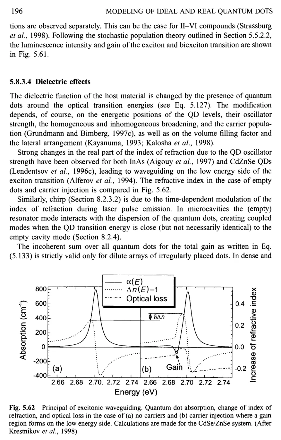
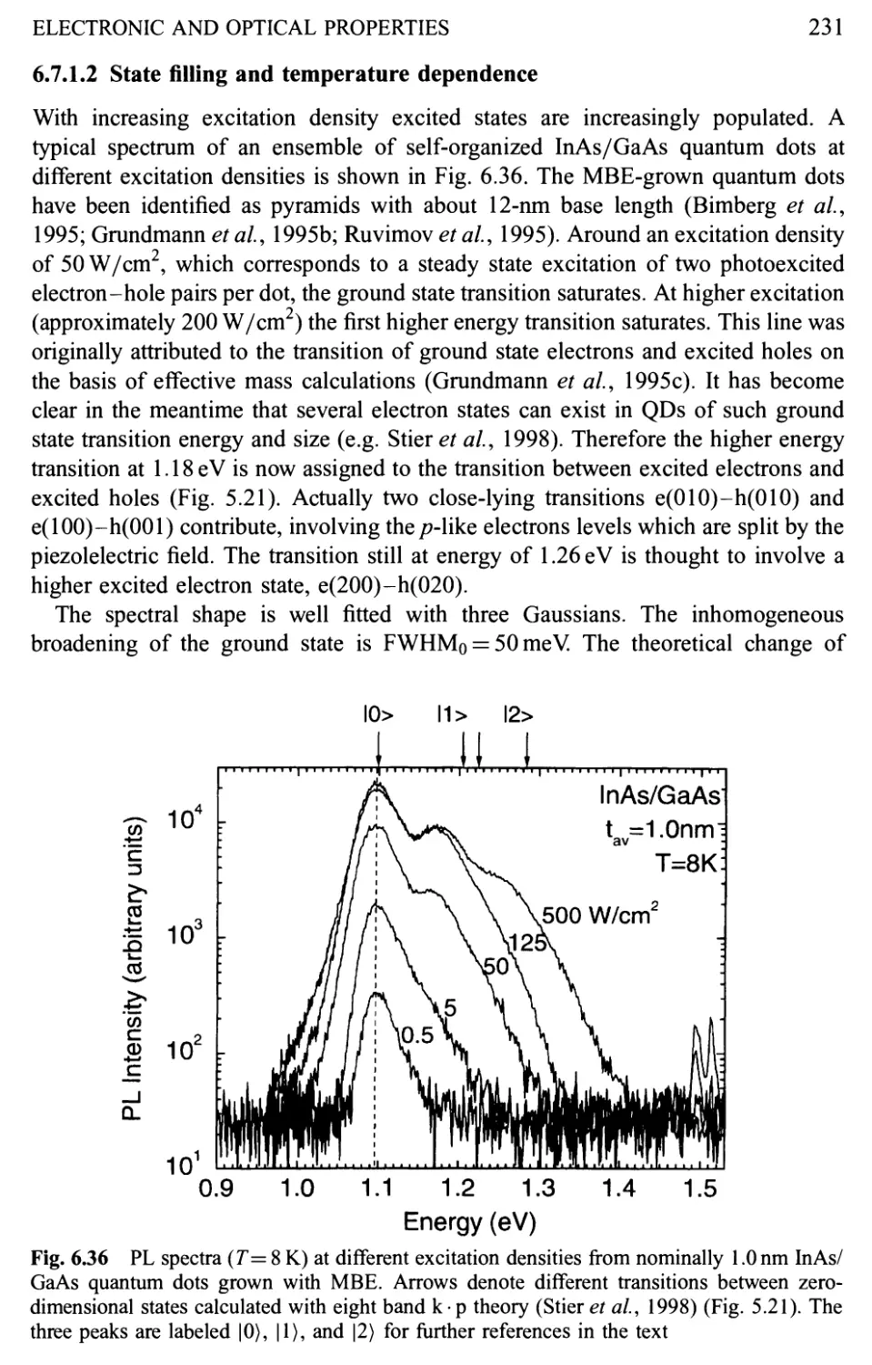
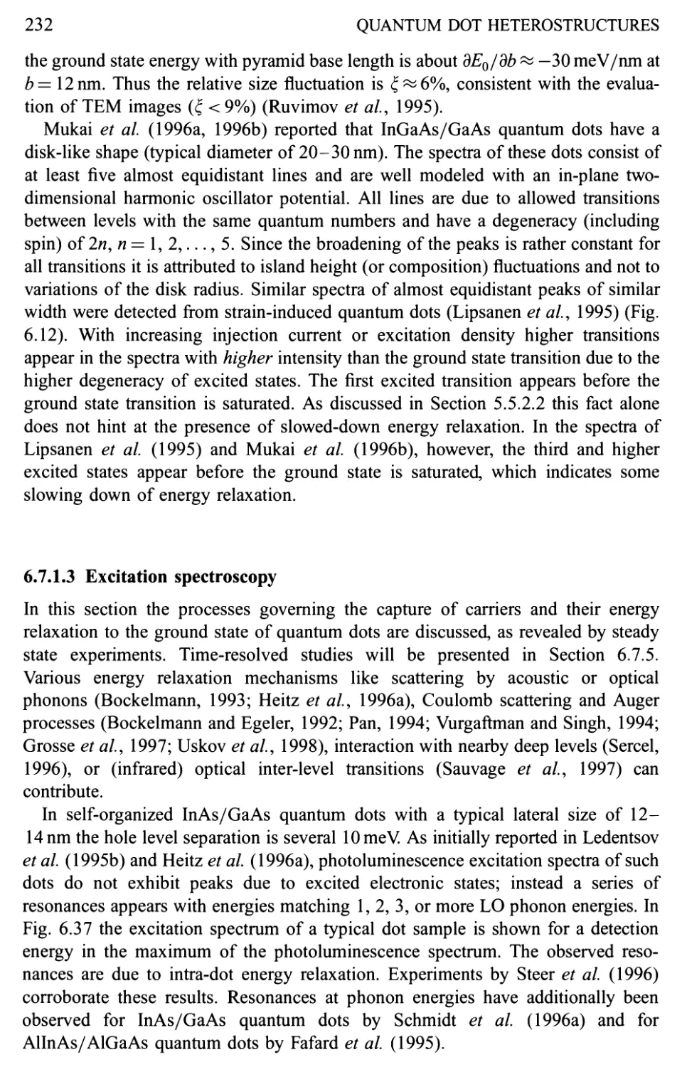
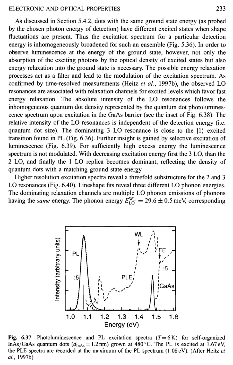
/
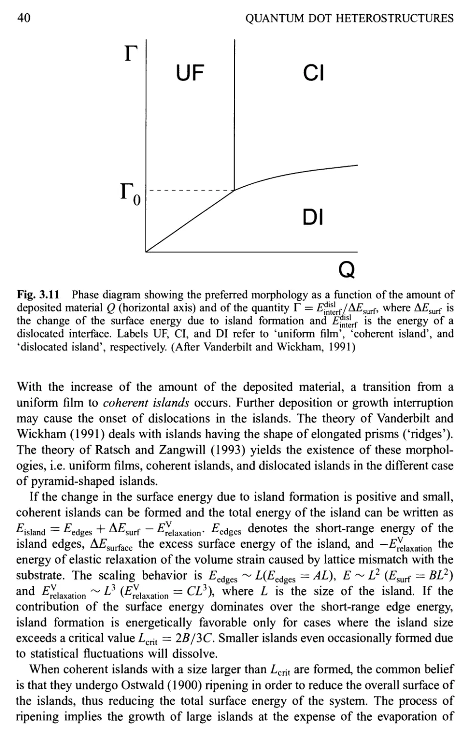


Автор: Bimberg D. Grundmann M. Ledentsov N.N.
Теги: physics solid state physics
ISBN: 0-471-97388-2
Год: 1999


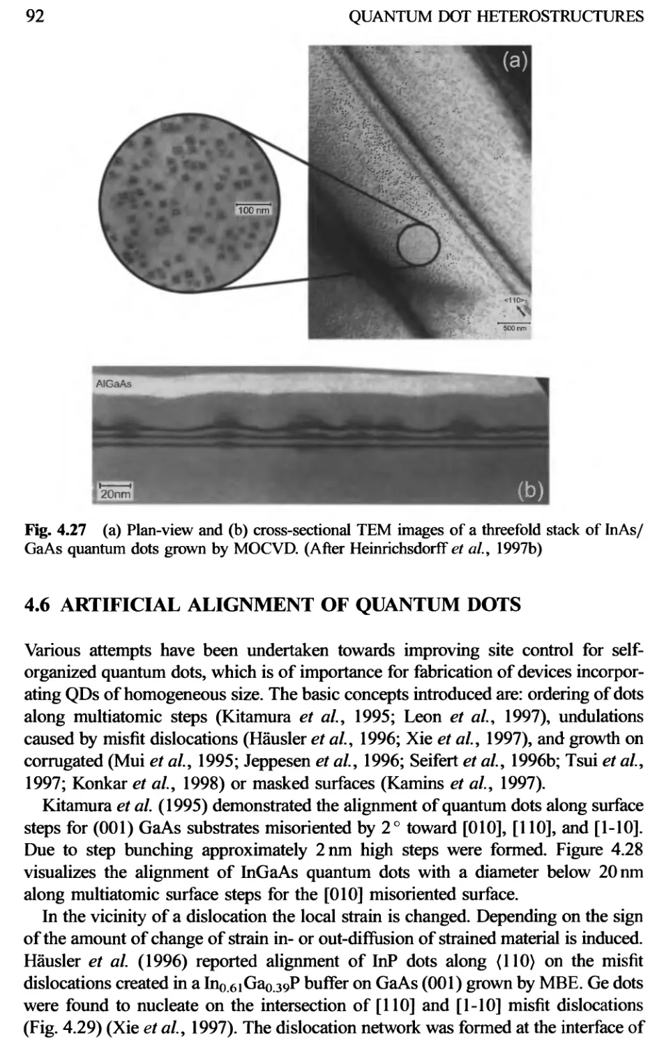
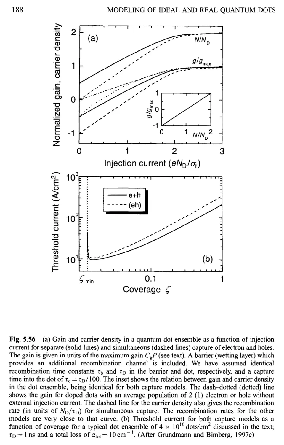
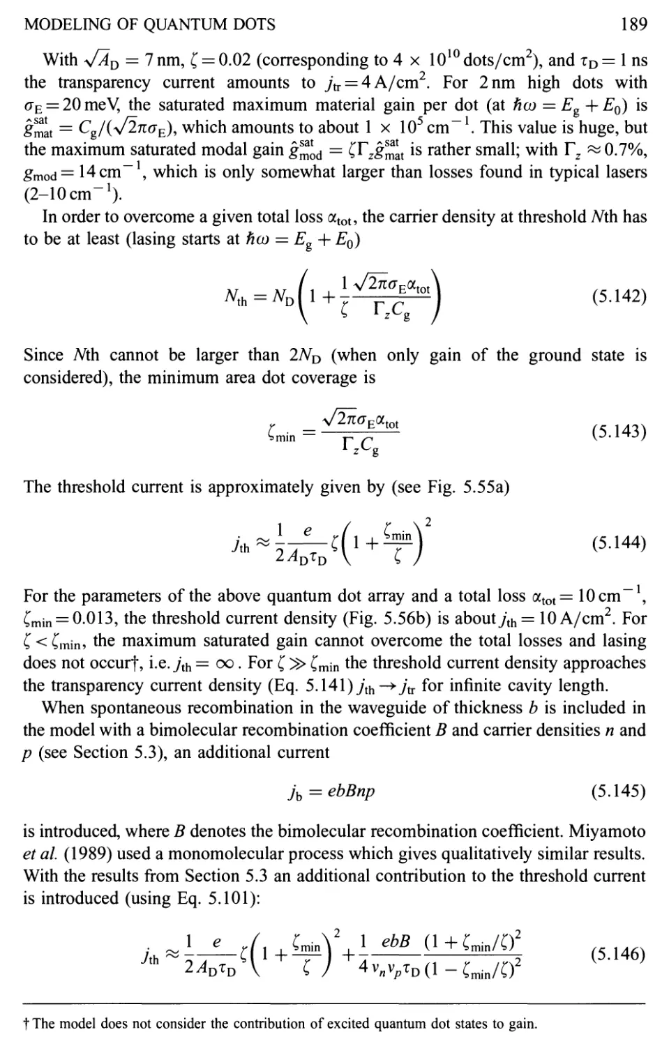
Текст
WILEY
Quantum Dor
Heterostructures
\
D. BlMBERG
M. Grundmann
N. N. Ledentsov
Quantum Dot Heterostructures
Quantum Dot
Hetero structures
Dieter Bimberg
Marius Grundmann
Nikolai N. Ledentsov
Institute of Solid State Physics,
Technische Universitdt Berlin,
Germany
) JOHN WILEY & SONS
Chichester • New York • Weinheim • Brisbane • Singapore • Toronto
Copyright © 1999 John Wiley & Sons Ltd,
Baffins Lane, Chichester,
West Sussex PO 19 1UD, England
National 01243 779777
International ( + 44) 1243 779777
e-mail (for orders and customer service enquiries): cs-books@wileyco.uk
Visit our Home Page on http://www.wiley.co.uk
or http://www.wiley.com
All Rights Reserved. No part of this publication may be reproduced, stored in a retrieval system, or
transmitted, in any form or by any means, electronic, mechanical, photocopying, recording, scanning or
otherwise, except under the terms of the 'Copyright Designs and Patents Act 1988 or under the terms of a
licence issued by the Copyright Licensing Agency, 90 Tottenham Court Road, London W1P 9HE, UK,
without the permission in writing of the Publisher
Other Wiley Editorial Offices
John Wiley & Sons, Inc., 605 Third Avenue,
New York, NY 10158-0012, USA
WILEY-VCH Verlag GmbH, Pappelallee 3,
D-69469 Weinheim, Germany
Jacaranda Wiley Ltd, 33 Park Road Milton,
Queensland 4064, Australia
John Wiley & Sons (Asia) Pte Ltd, Clementi Loop #02-01,
Jim Xing Distripark, Singapore 129809
John Wiley & Sons (Canada) Ltd, 22 Worcester Road,
Rexdale, Ontario M9W 1L1, Canada
Library of Congress Cataloging-in-Publication Data
Bimberg, Dieter.
Quantum dot heterostrucrures / Dieter Bimberg, Marius Grundmann,
Nikolai N. Ledentsov.
p. cm.
Includes bibliographical references and index.
ISBN 0-471-97388-2 (alk. paper)
1. Quantum dots. 2. Heterostrucrures. I. Grundmann, Marius.
II. Ledentsov, Nikolai N. III. Title.
TK7874.88.B55 1988
621.3815,2—dc21 98-7734
CIP
British Library Cataloguing-in-Publication Data
A catalogue record for this book is available from the British Library
ISBN 0 471 97388 2
Typeset in lOpt Times by Techset Composition Ltd., Salisbury, Wiltshire, England
Printed and bound in Great Britain by Biddies Ltd, Guildford, Surrey
This book is printed on acid-free paper responsible manufactured from sustainable forestry, in which at
least two trees are planted for each one used for paper production.
Contents
Preface ix
1 Introduction 1
1.1 Historical Development 1
1.1.1 From atoms to solids 1
1.1.2 From solids to 2D heterostructures 1
1.1.3 From 2D heterostructures to quantum dots 3
1.2 Basic Requirements for QDs in Room Temperature Devices 6
1.2.1 Size 6
1.2.2 Uniformity 7
1.2.3 Material quality 8
2 Fabrication Techniques for Quantum Dots 9
2.1 Quantum Dots Fabricated by Lithographic Techniques 9
2.1.1 Overview 9
2.1.2 Free-standing quantum dots 12
2.1.3 Selective intermixing based on ion implantation 15
2.1.4 Selective intermixing based on laser annealing 16
2.1.5 Strain-induced lateral confinement 16
2.1.6 Quantum dots grown on patterned substrates 17
2.1.7 Cleaved edge overgrowth 19
2.2 Quantum Dots Formed by Interface Fluctuations 19
2.3 Self-Organized Quantum Dots 19
3 Self-Organization Concepts on Crystal Surfaces 22
3.1 Introduction 22
3.2 Spontaneous Faceting of Crystal Surfaces 24
3.2.1 The problem of equilibrium crystal.shape 24
3.2.2 The concept of intrinsic surface stress of a crystal surface 26
3.2.3 Force monopoles at crystal edges 28
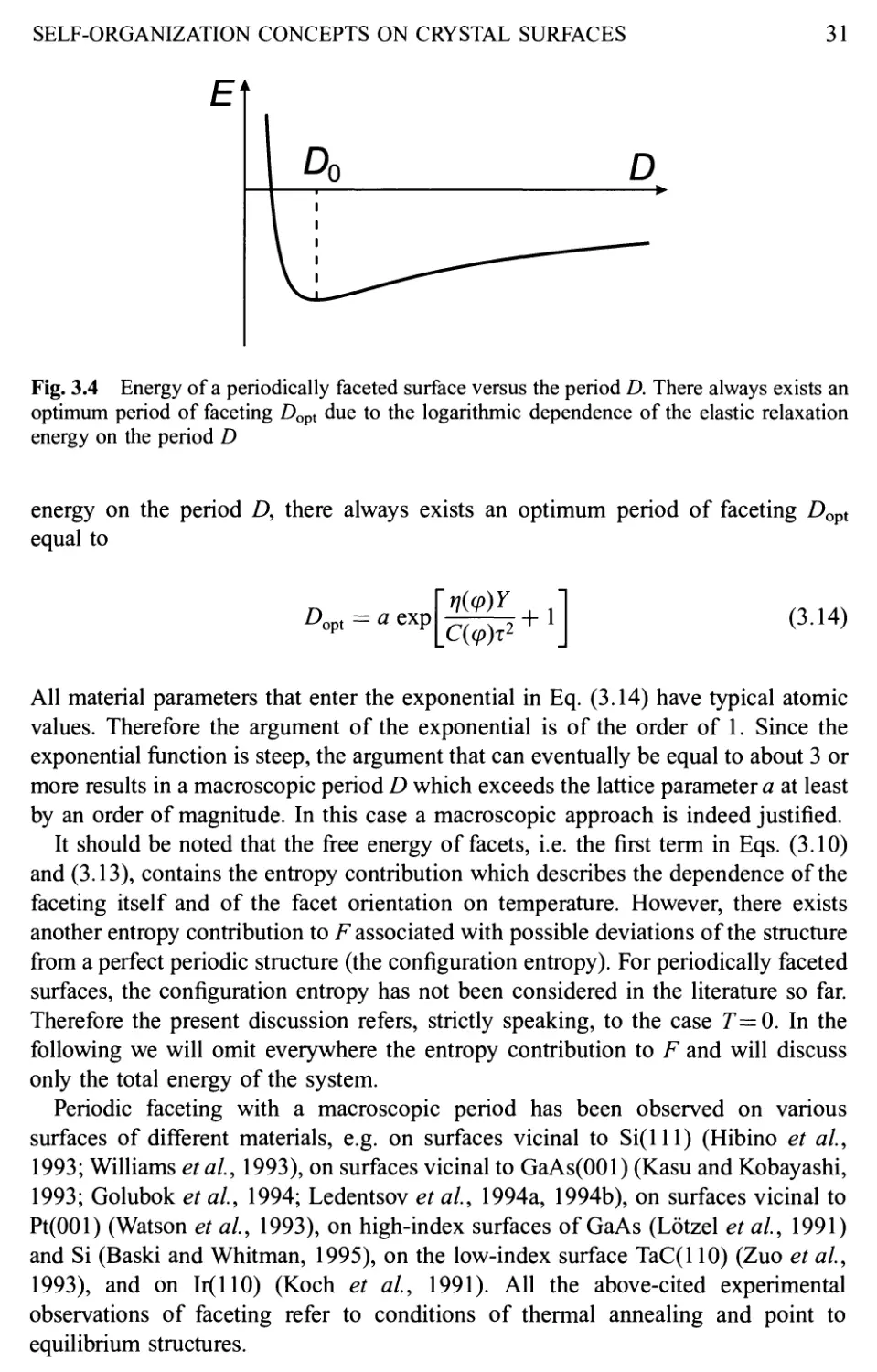
3.2.4 Spontaneous formation of periodically faceted surfaces 29
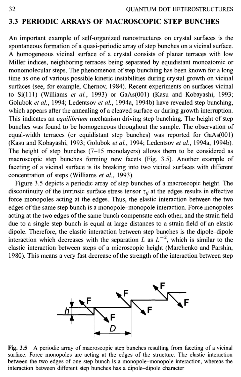
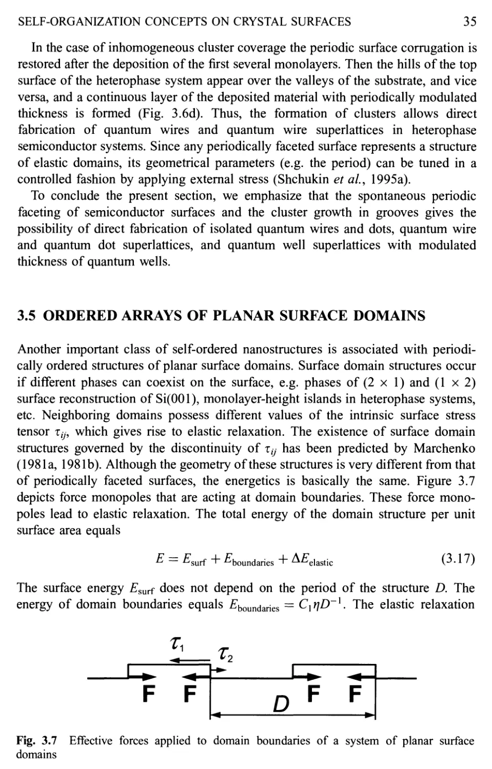
3.3 Periodic Arrays of Macroscopic Step Bunches 32
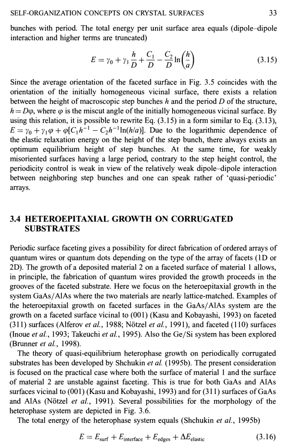
3.4 Heteroepitaxial Growth on Corrugated Substrates 33
3.5 Ordered Arrays of Planar Surface Domains 35
3.6 Ordered Arrays of Three-Dimensional Coherently Strained
Islands 37
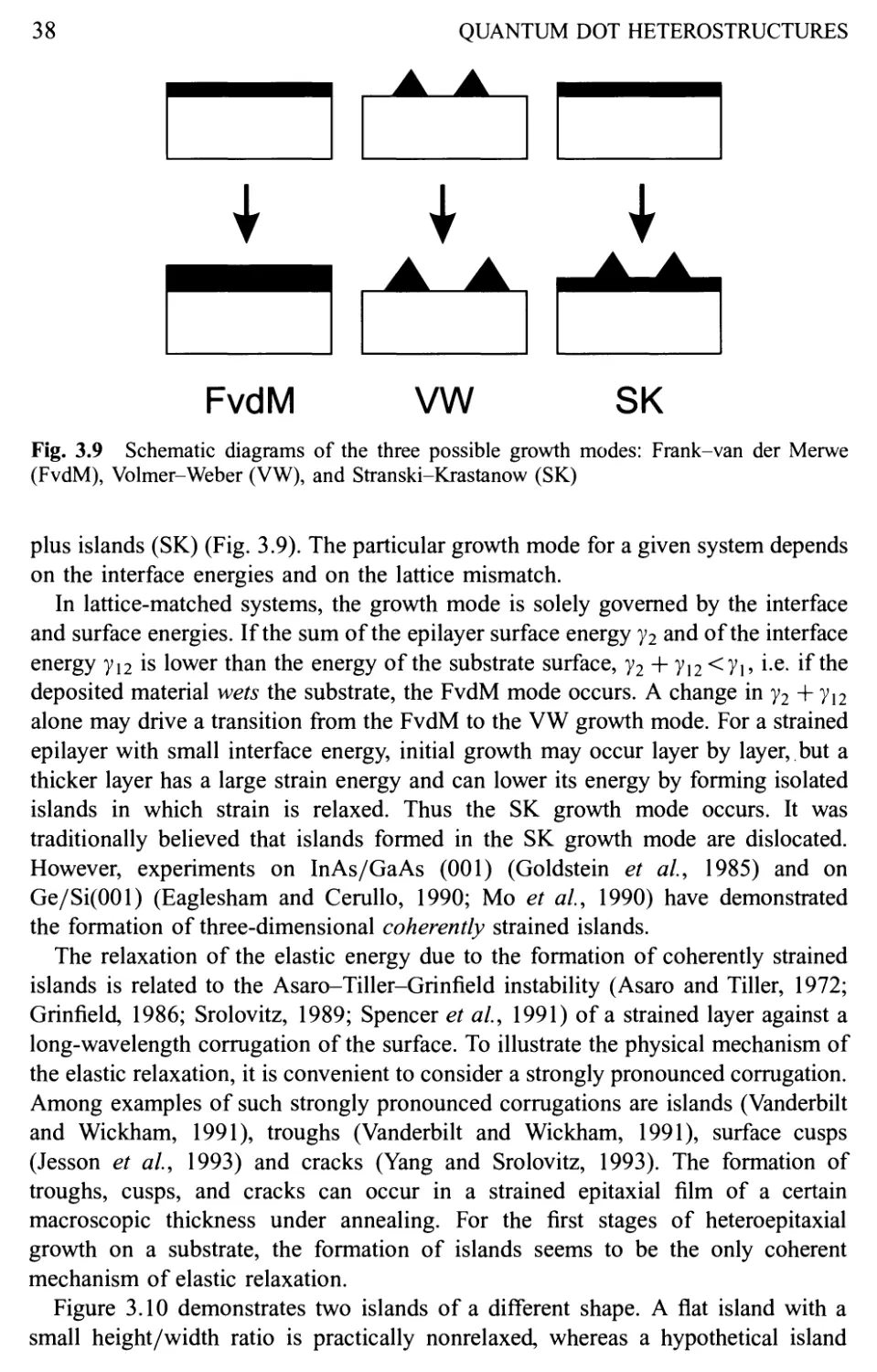
3.6.1 Heteroepitaxial growth in lattice-mismatched systems 37
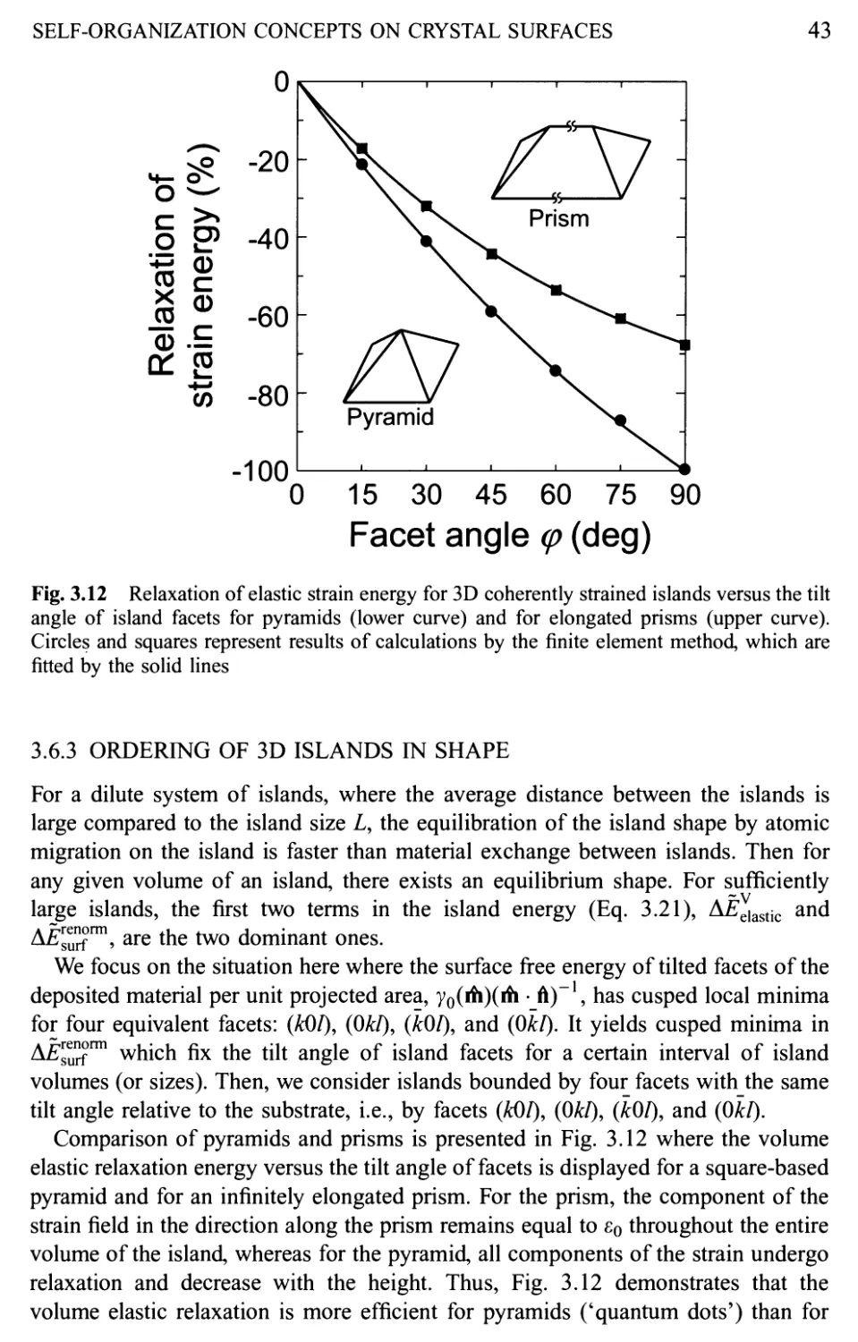
3.6.2 Energetics of a dilute array of 3D islands 41
CONTENTS
3.6.3 Ordering of 3D islands in shape 43
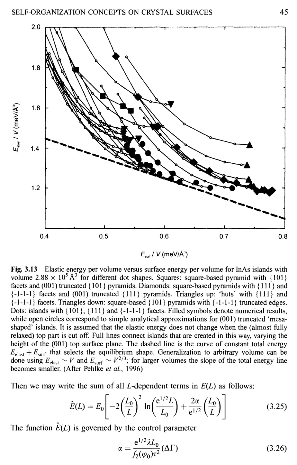
3.6.4 Ordering of 3D islands in size versus Ostwald ripening 44
3.6.5 Lateral ordering of 3D islands 48
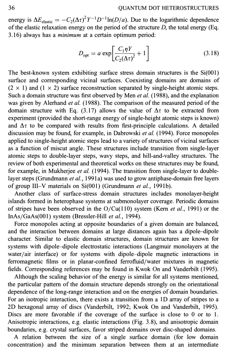
3.6.6 Phase diagram of a two-dimensional array of 3D islands 49
3.6.7 Ordering-to-ripening phase transition for 3D islands 51
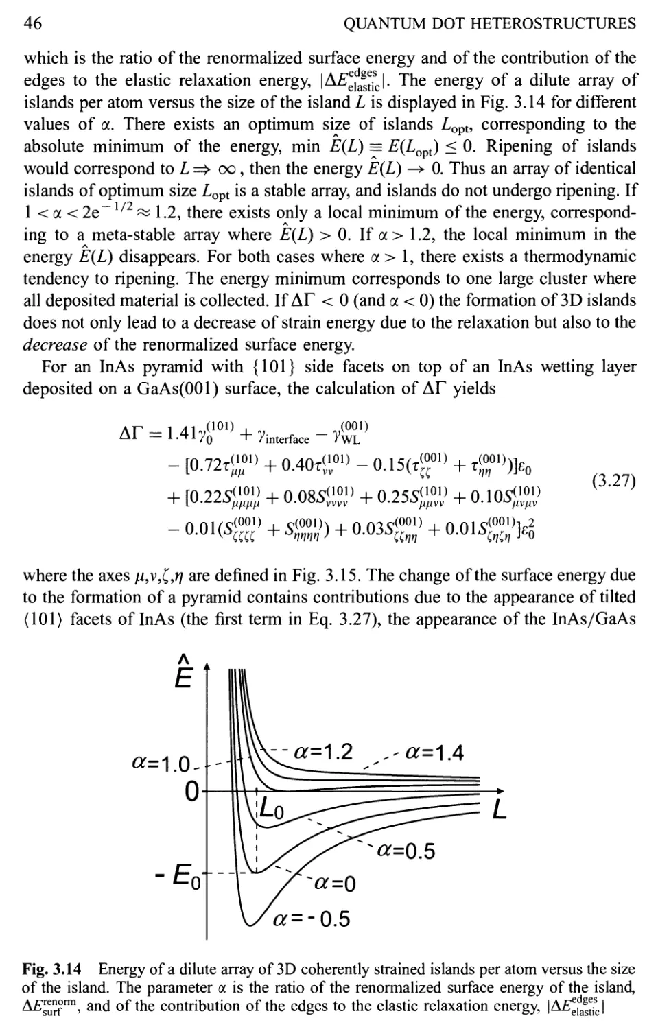
3.6.8 Kinetic theories of ordering 51
3.6.9 Equilibrium ordering versus kinetic-controlled ordering of 3D
islands 52
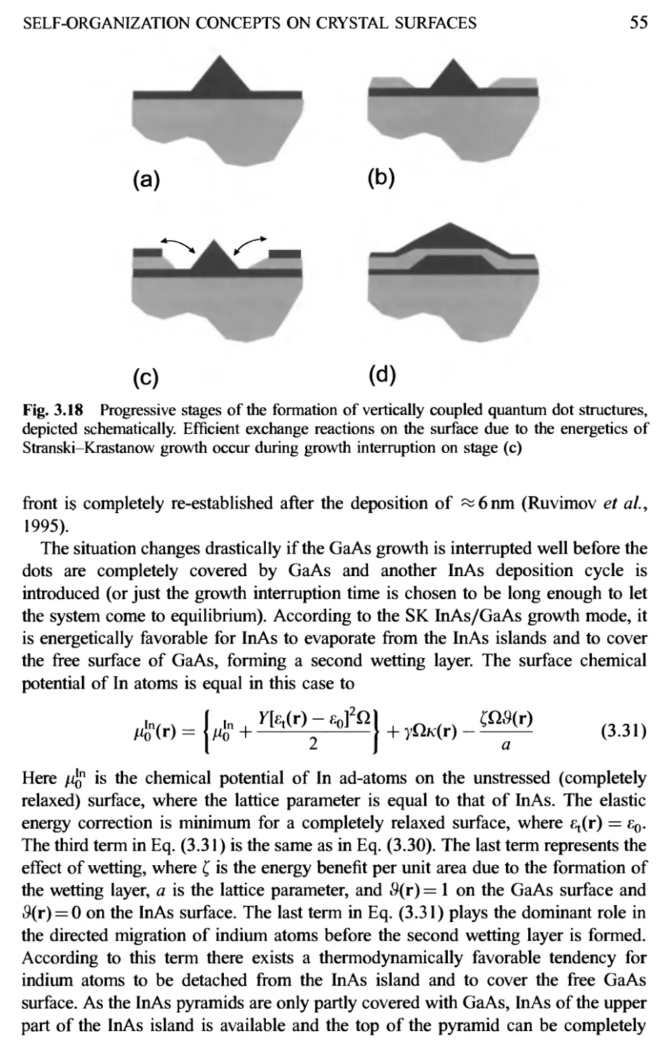
3.7 Vertically Correlated Growth of Nanostructures 53
3.7.1 Vertically correlated growth of nanostructures due to a modulated
strain field 53
3.7.2 Energetics of Stranski-Krastanow growth for subsequent InAs and
GaAs deposition cycles 54
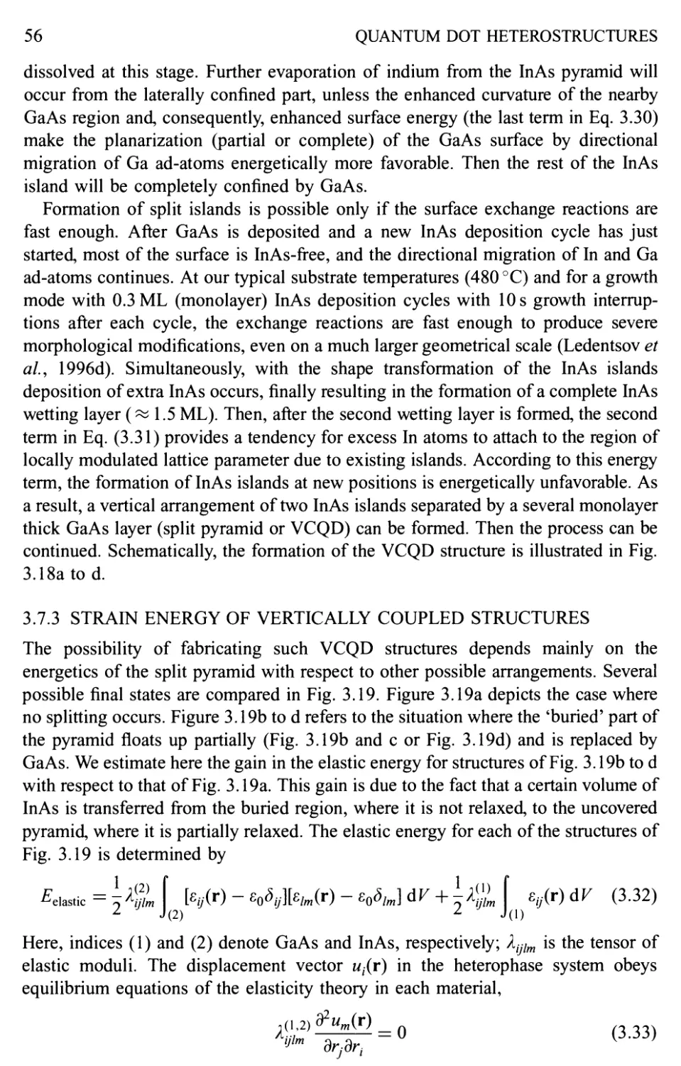
3.7.3 Strain energy of vertically coupled structures 56
Growth and Structural Characterization of Self-Organized Quantum
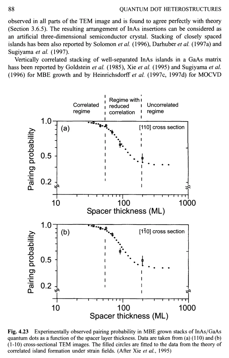
Dots 59
4.1 Introduction 59
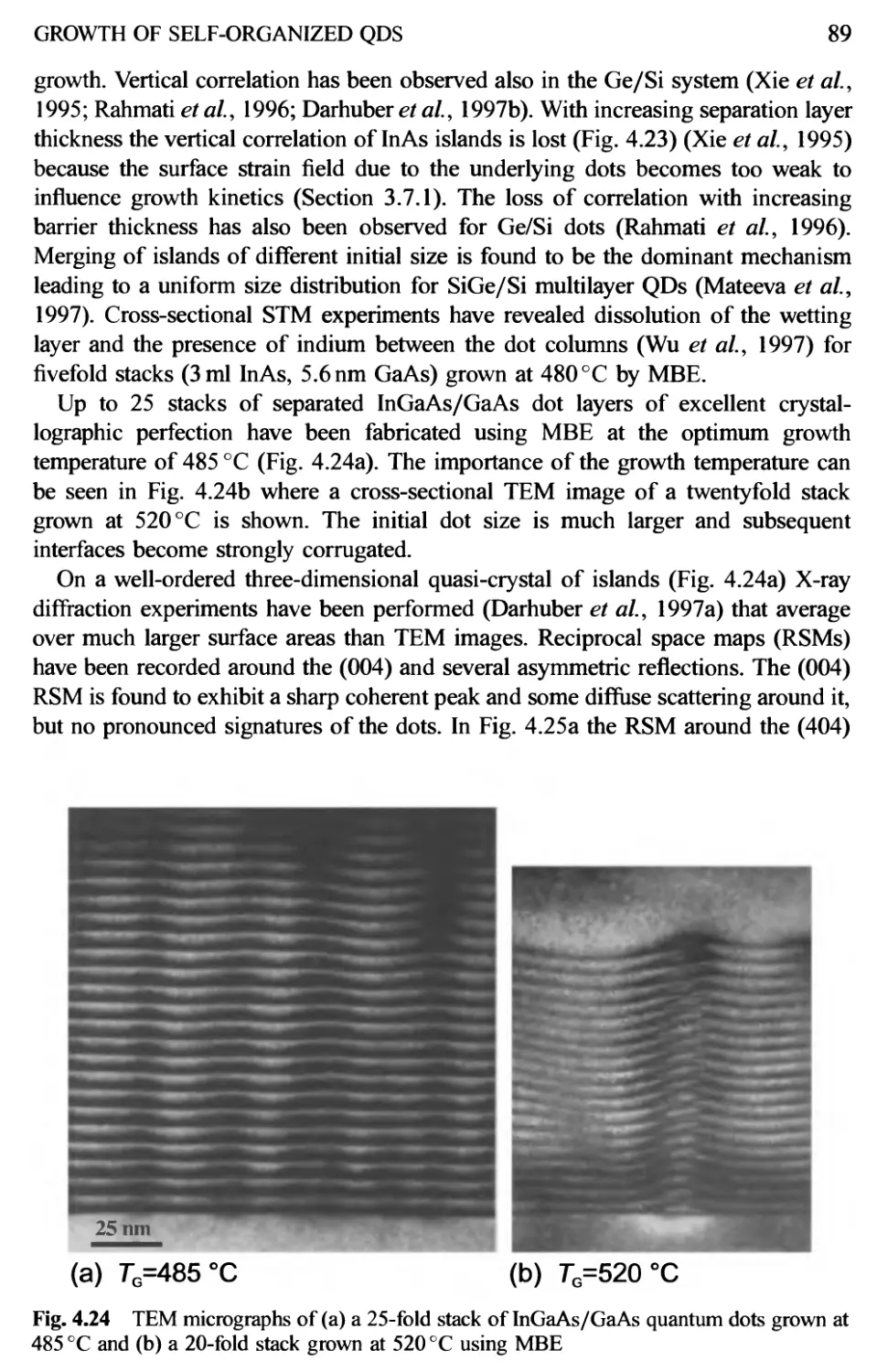
4.2 MBE of InGaAs/GaAs Quantum Dots 61
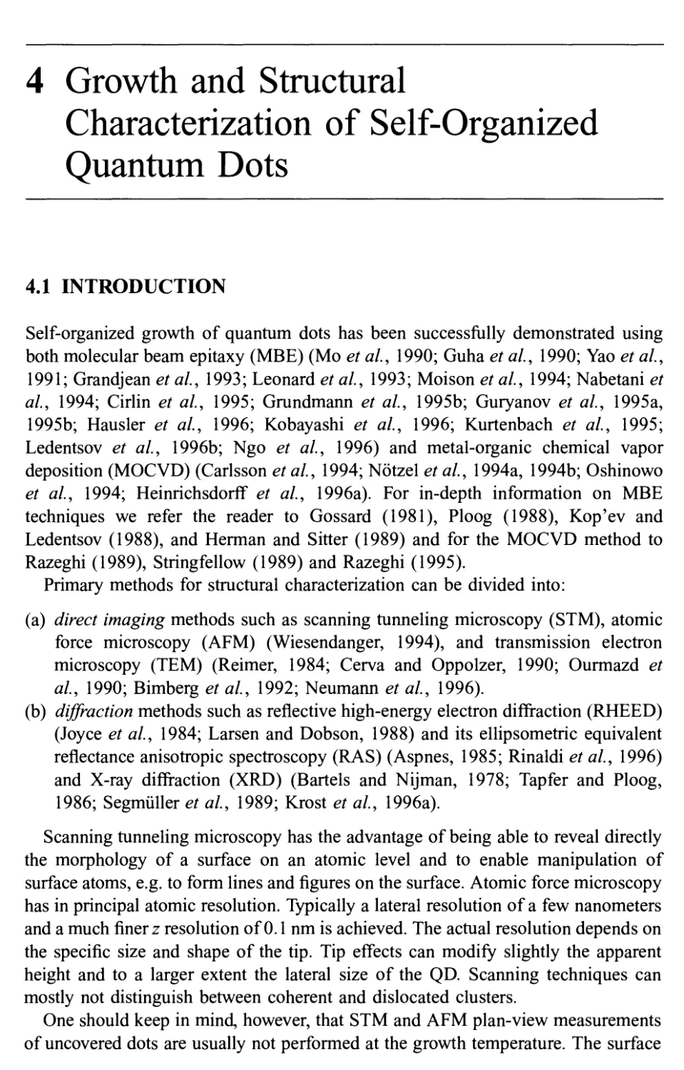
4.2.1 Deposition below the 2D-3D transition 61
4.2.2 2D-3D transition 63
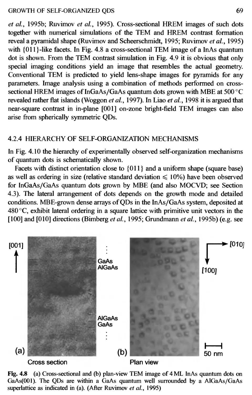
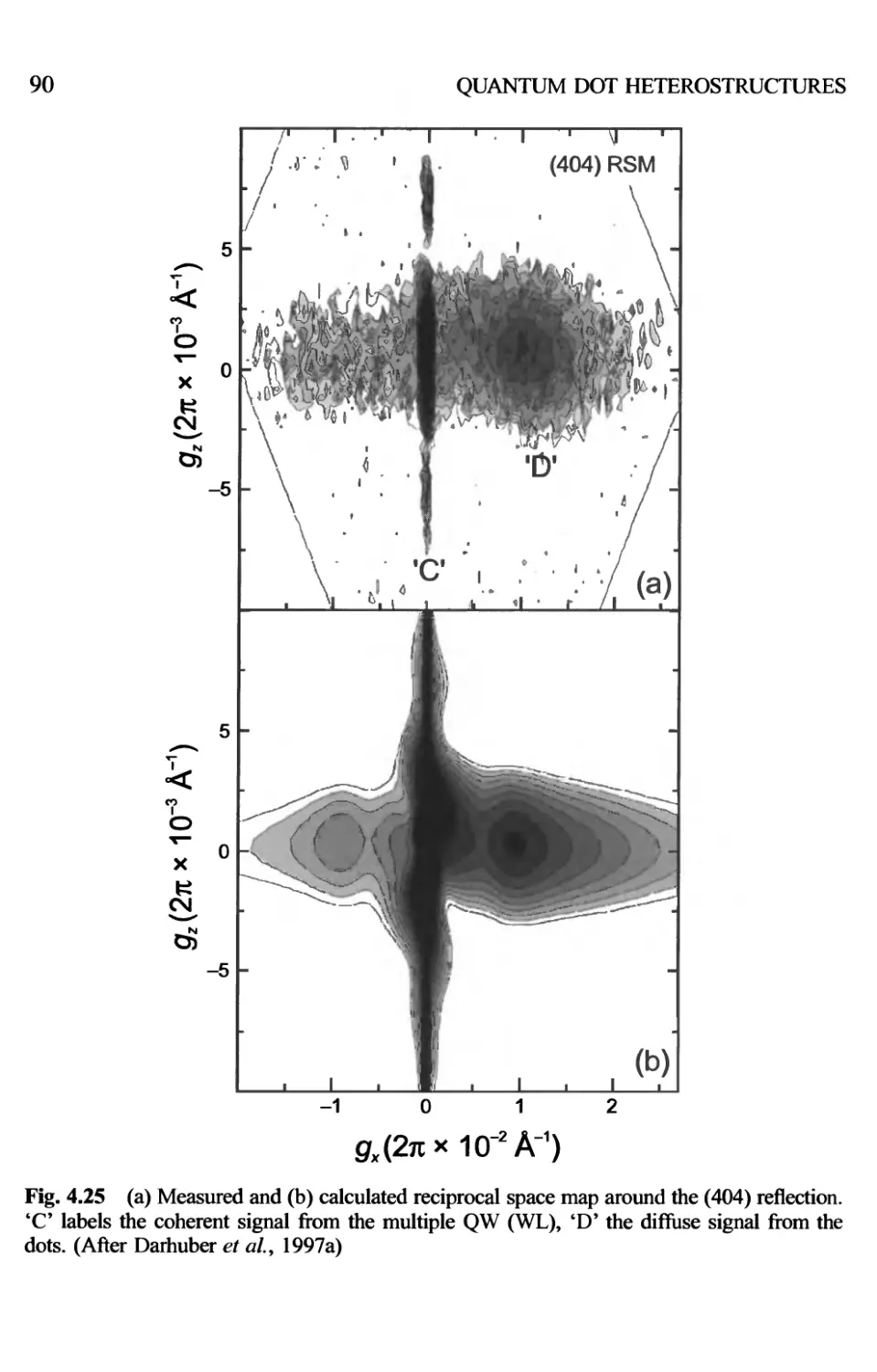
4.2.3 Quantum dot structure 64
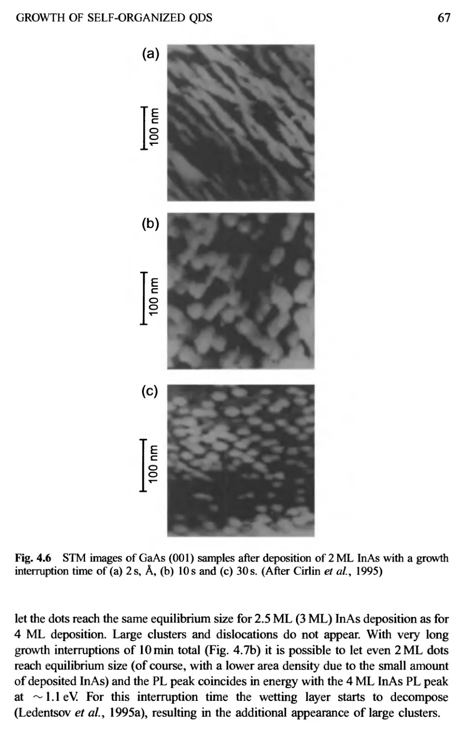
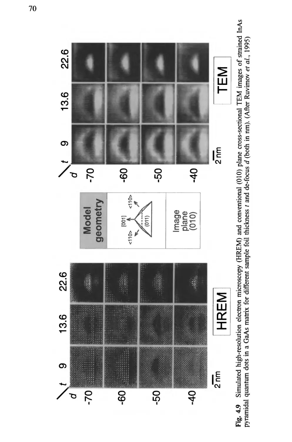
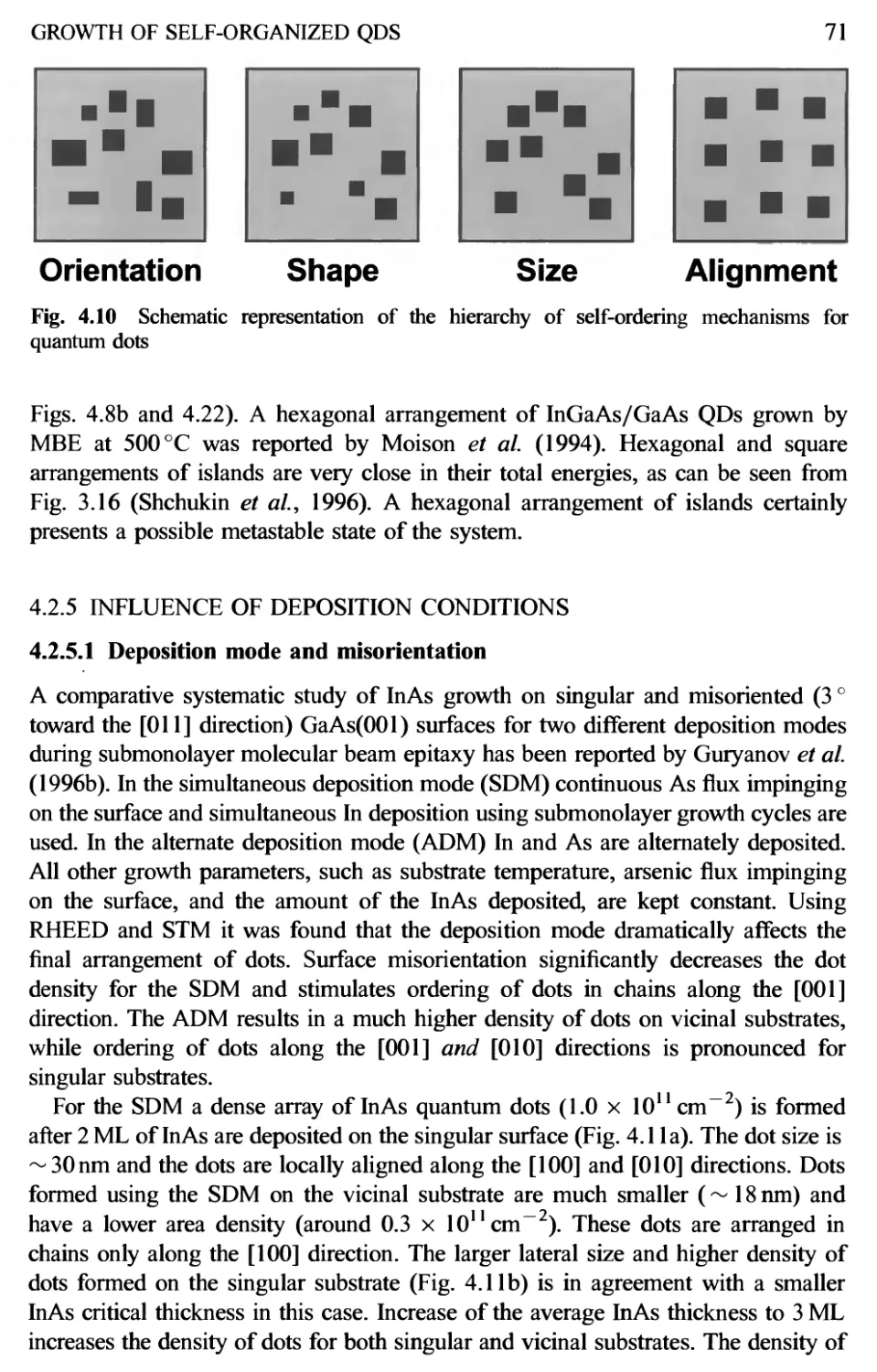
4.2.4 Hierarchy of self-organization mechanisms 69
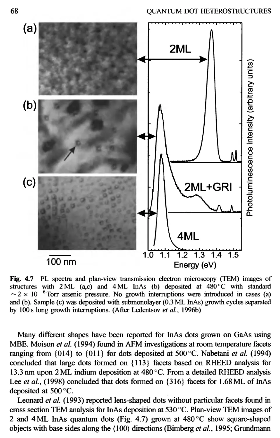
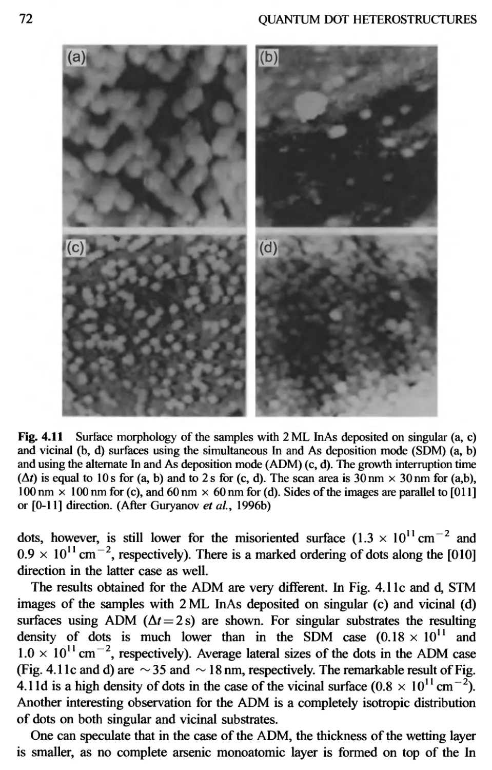
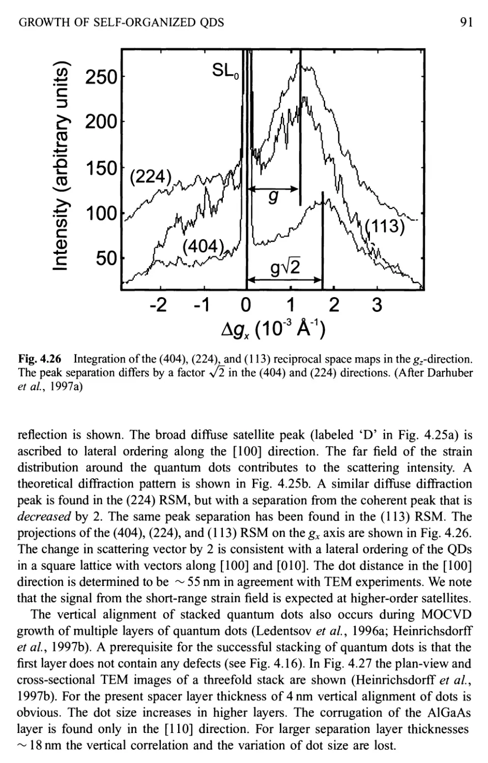
4.2.5 Influence of deposition conditions 71
4.3 MOCVD Growth of InGaAs/GaAs Quantum Dots 76
4.3.1 2D-3D transition 76
4.3.2 Quantum dots 78
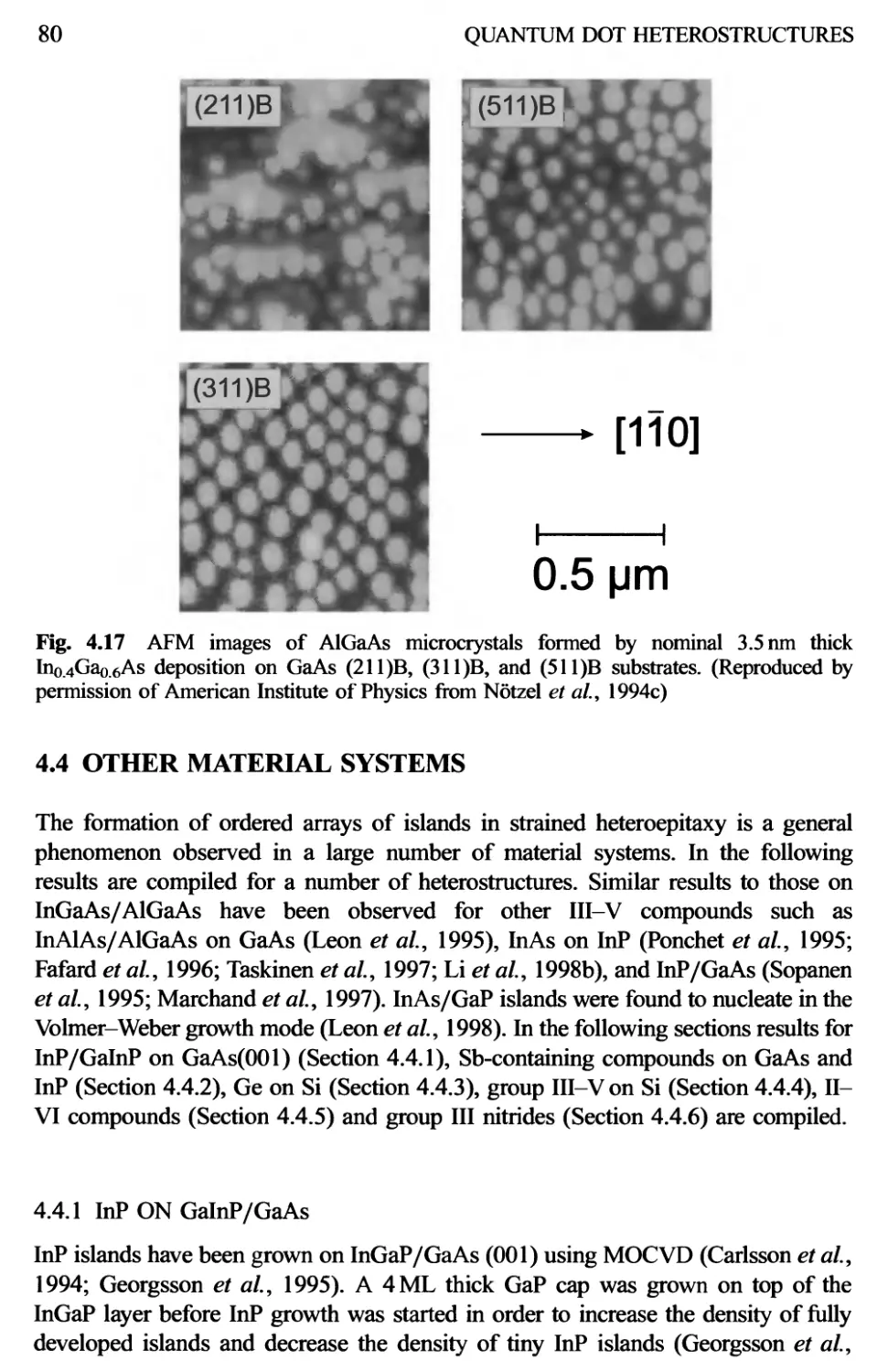
4.3.3 High index substrates 79
4.4 Other Material Systems 80
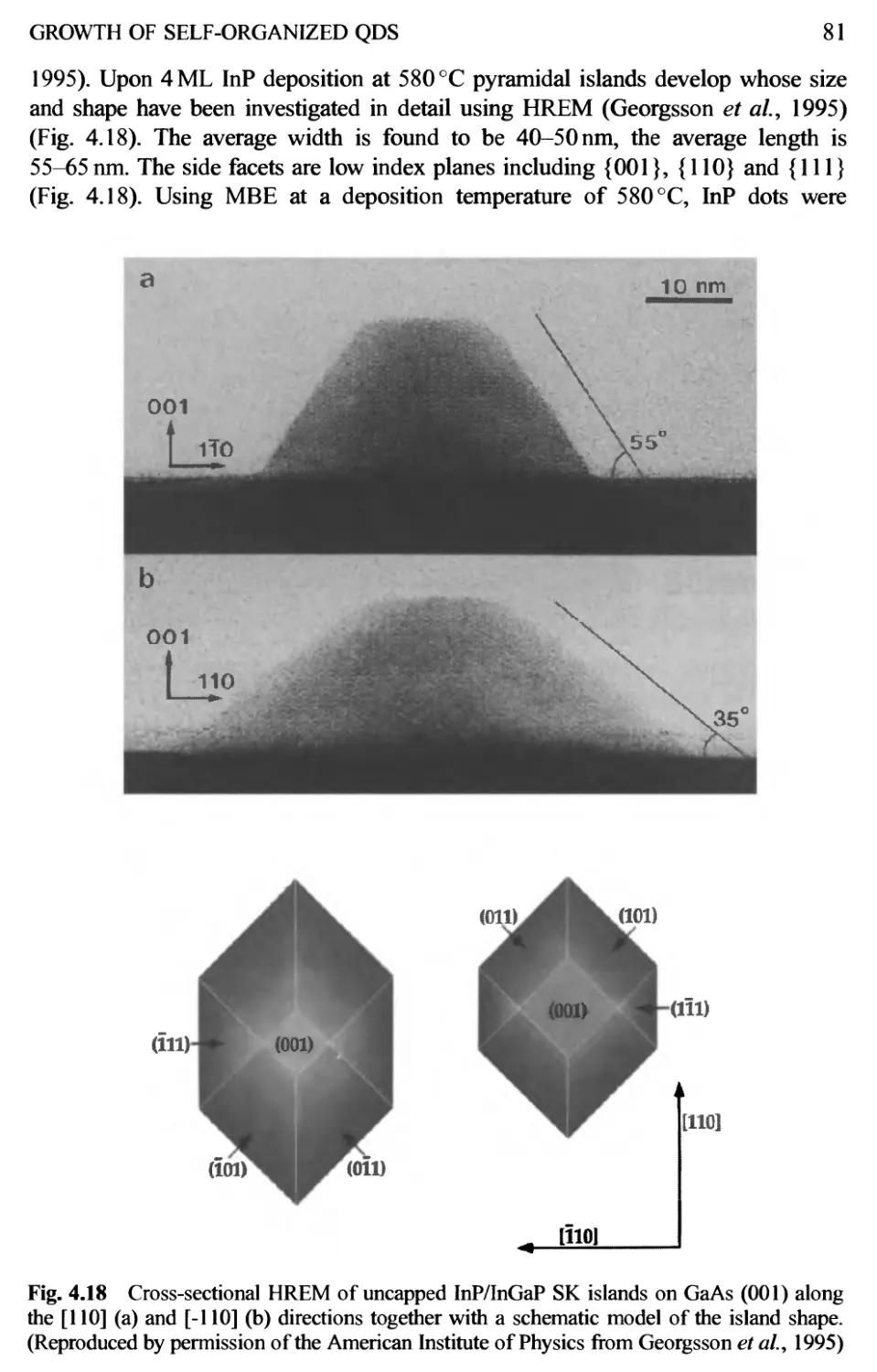
4.4.1 InP on GalnP/GaAs 80
4.4.2 Sb compounds 82
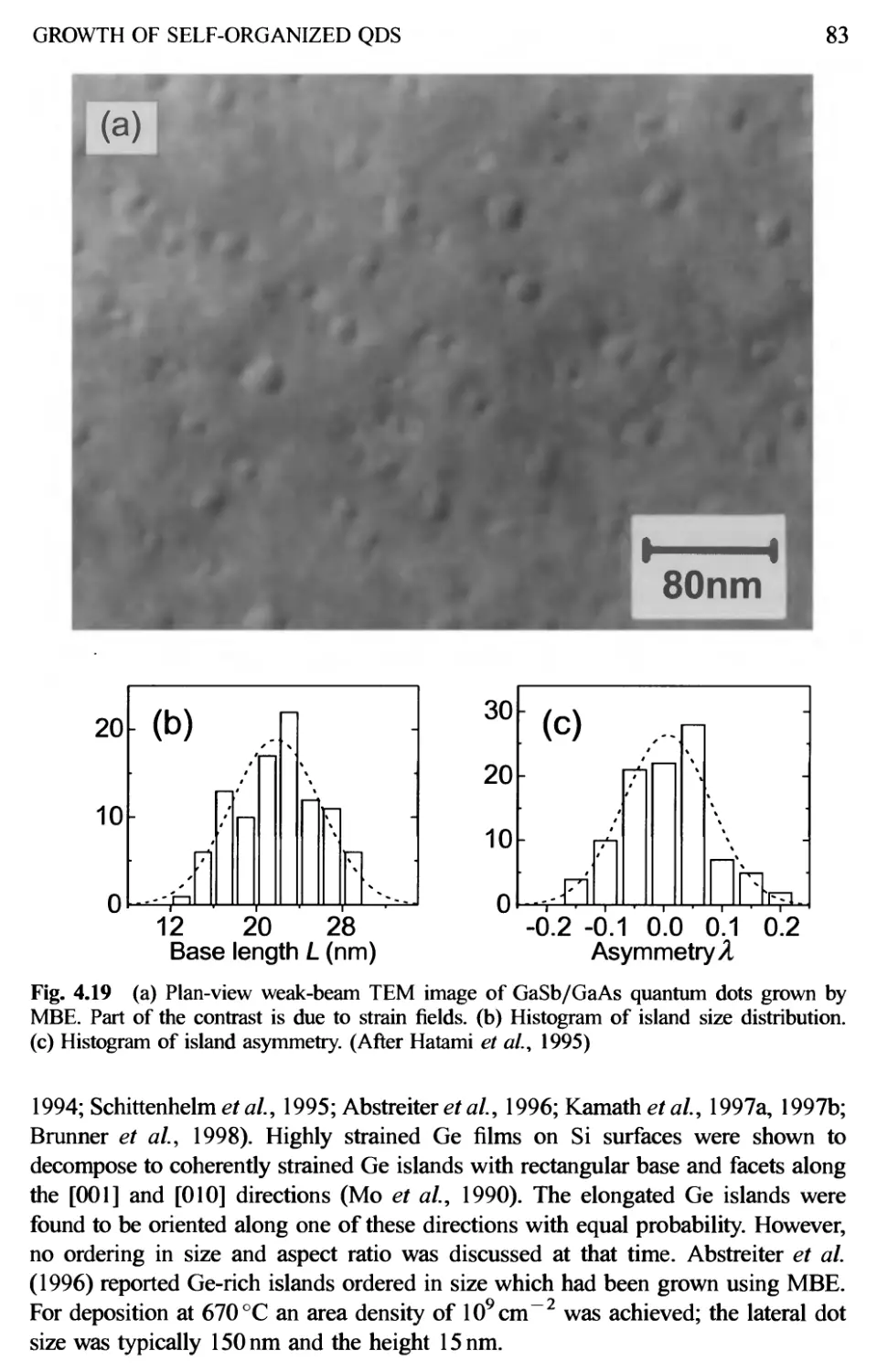
4.4.3 Ge on Si 82
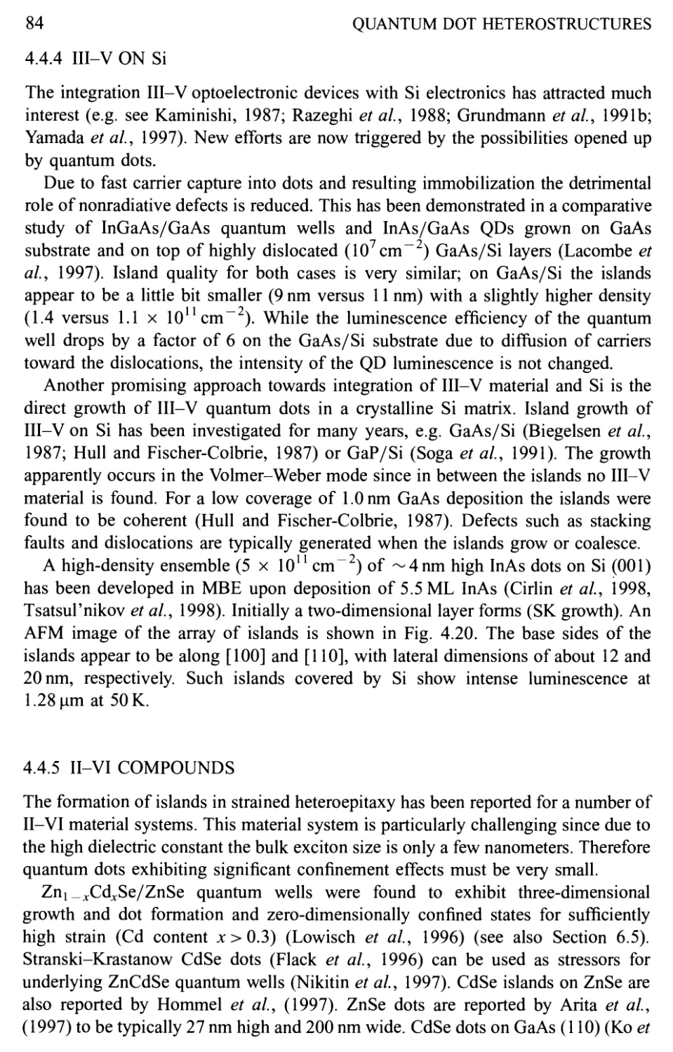
4.4.4 III-V on Si 84
4.4.5 II—VI compounds 84
4.4.6 Group III nitrides 85
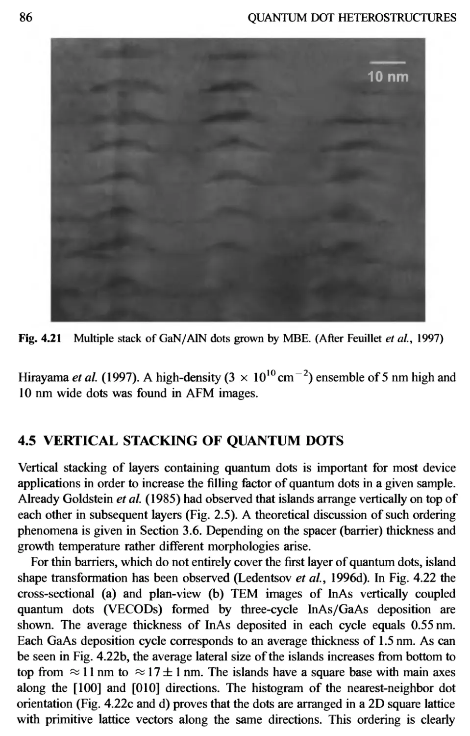
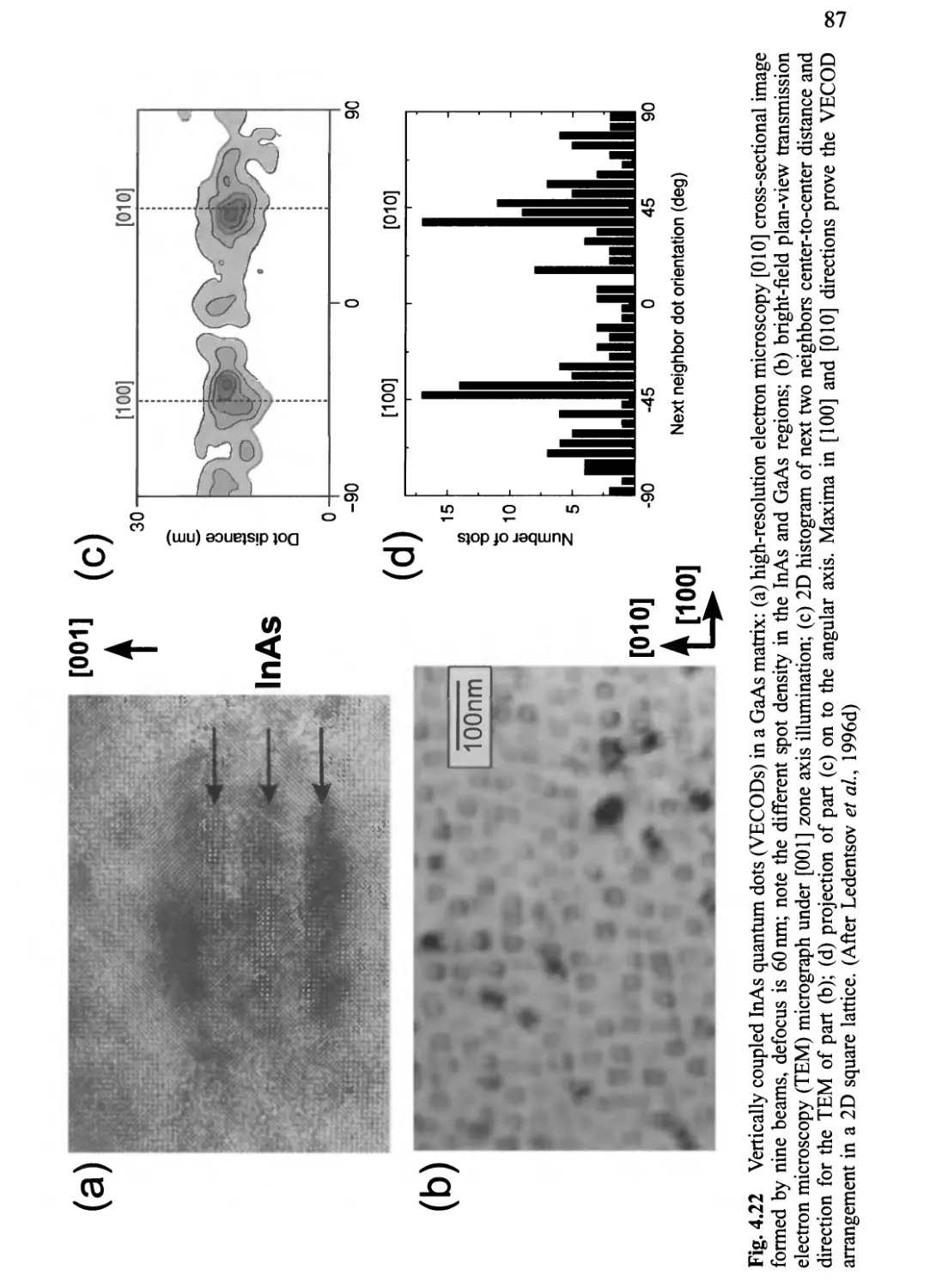
4.5 Vertical Stacking of Quantum Dots 86
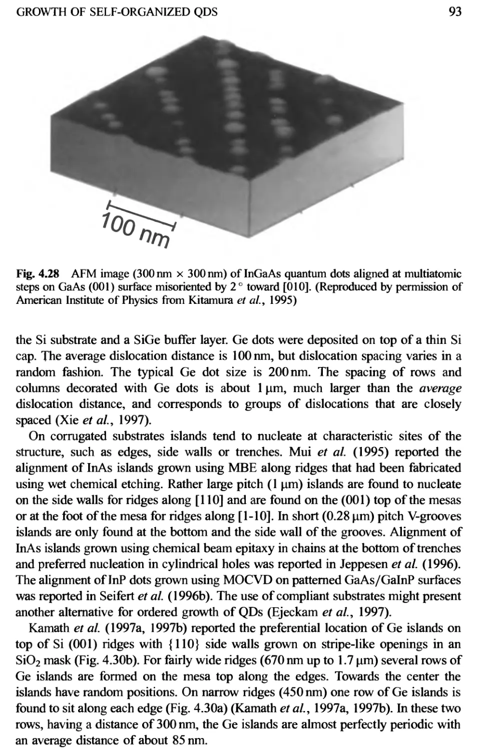
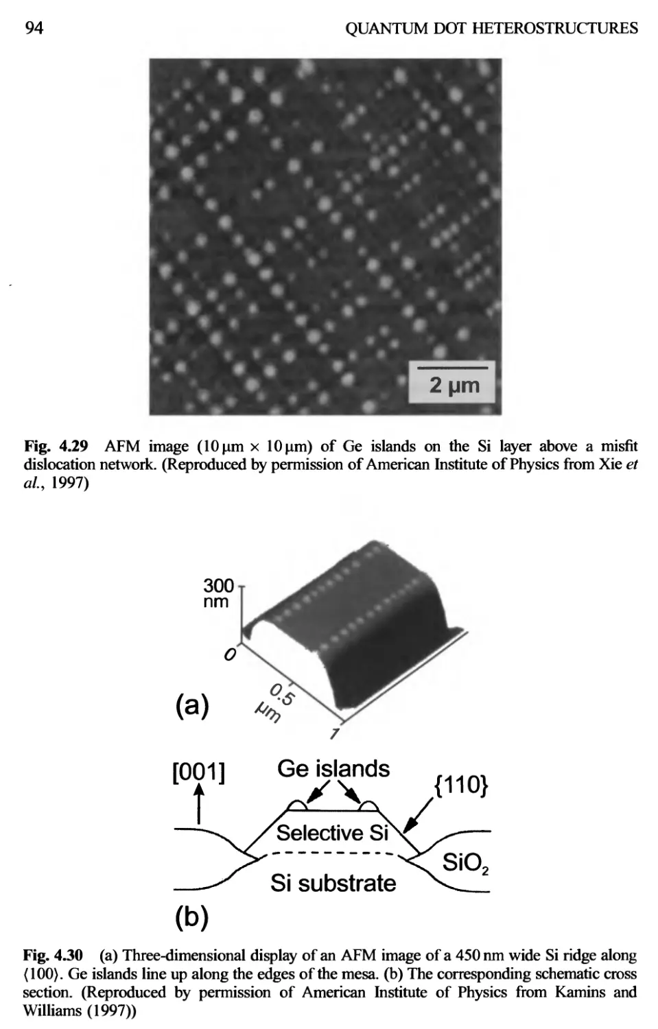
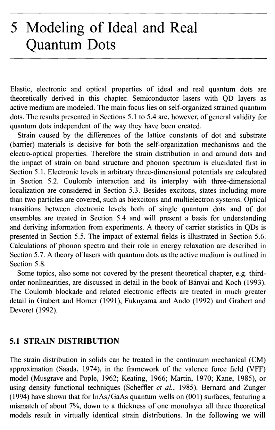
4.6 Artificial Alignment of Quantum Dots 92
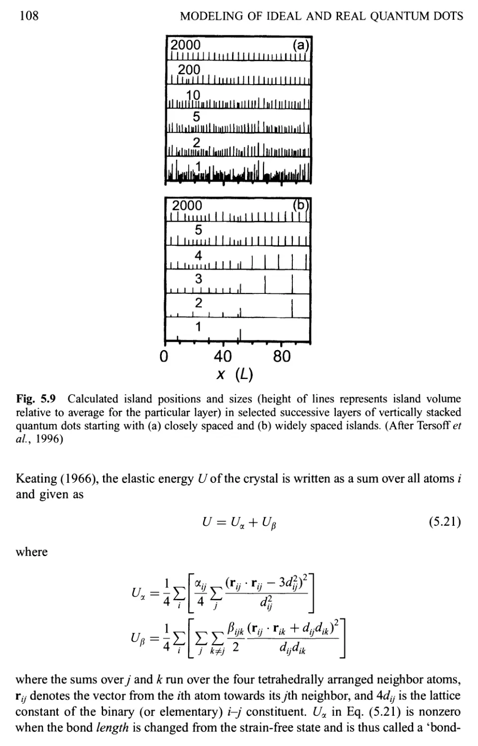
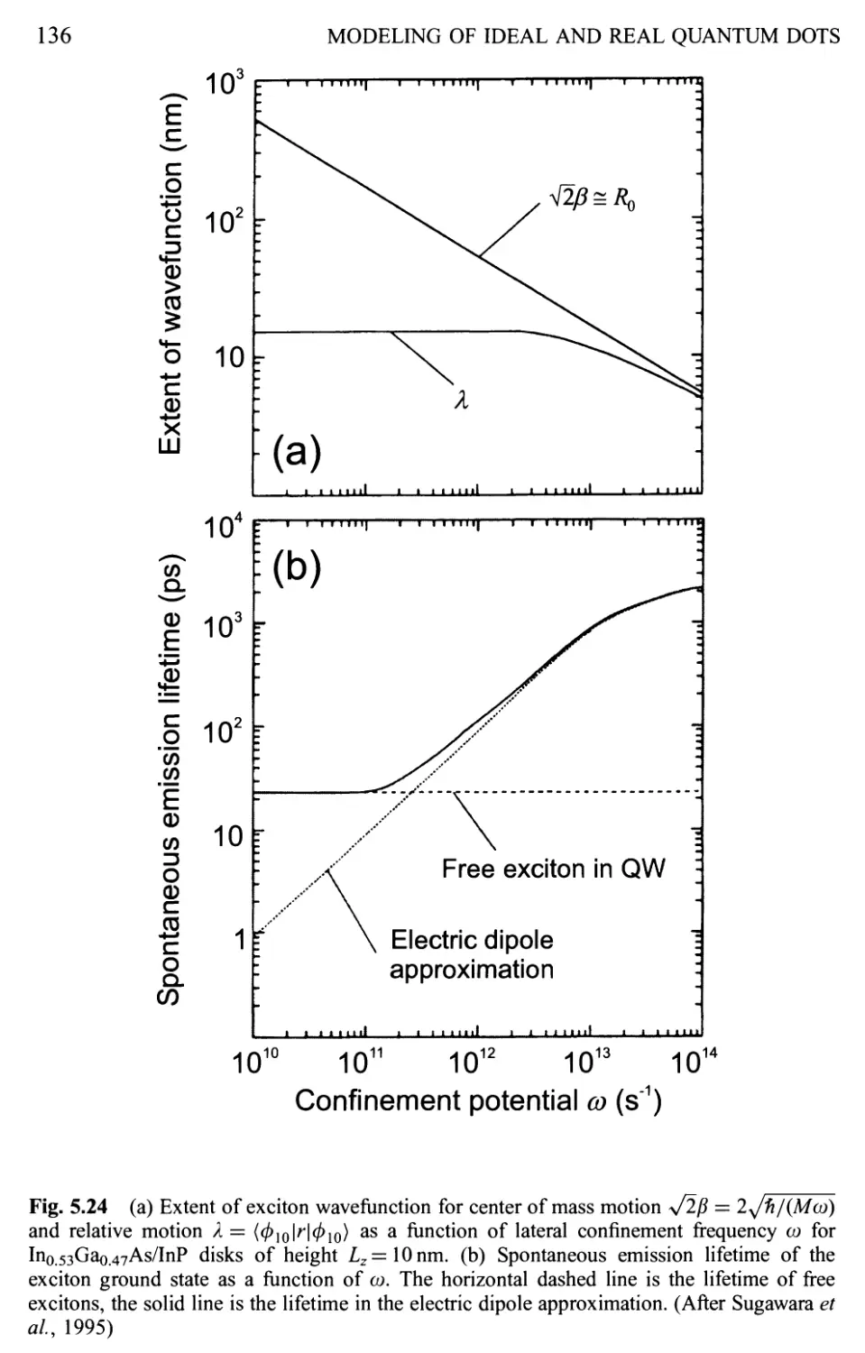
Modeling of Ideal and Real Quantum Dots 95
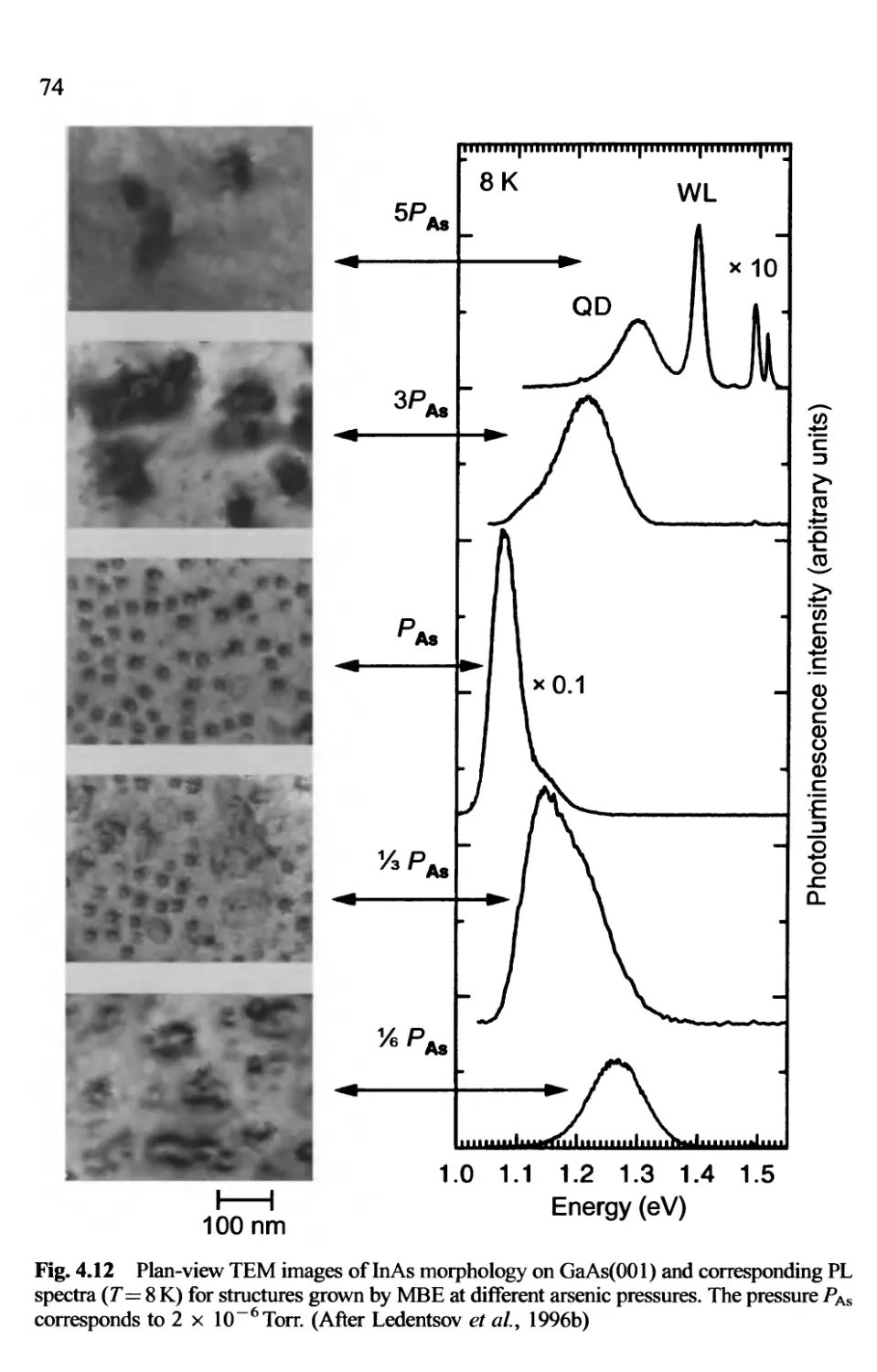
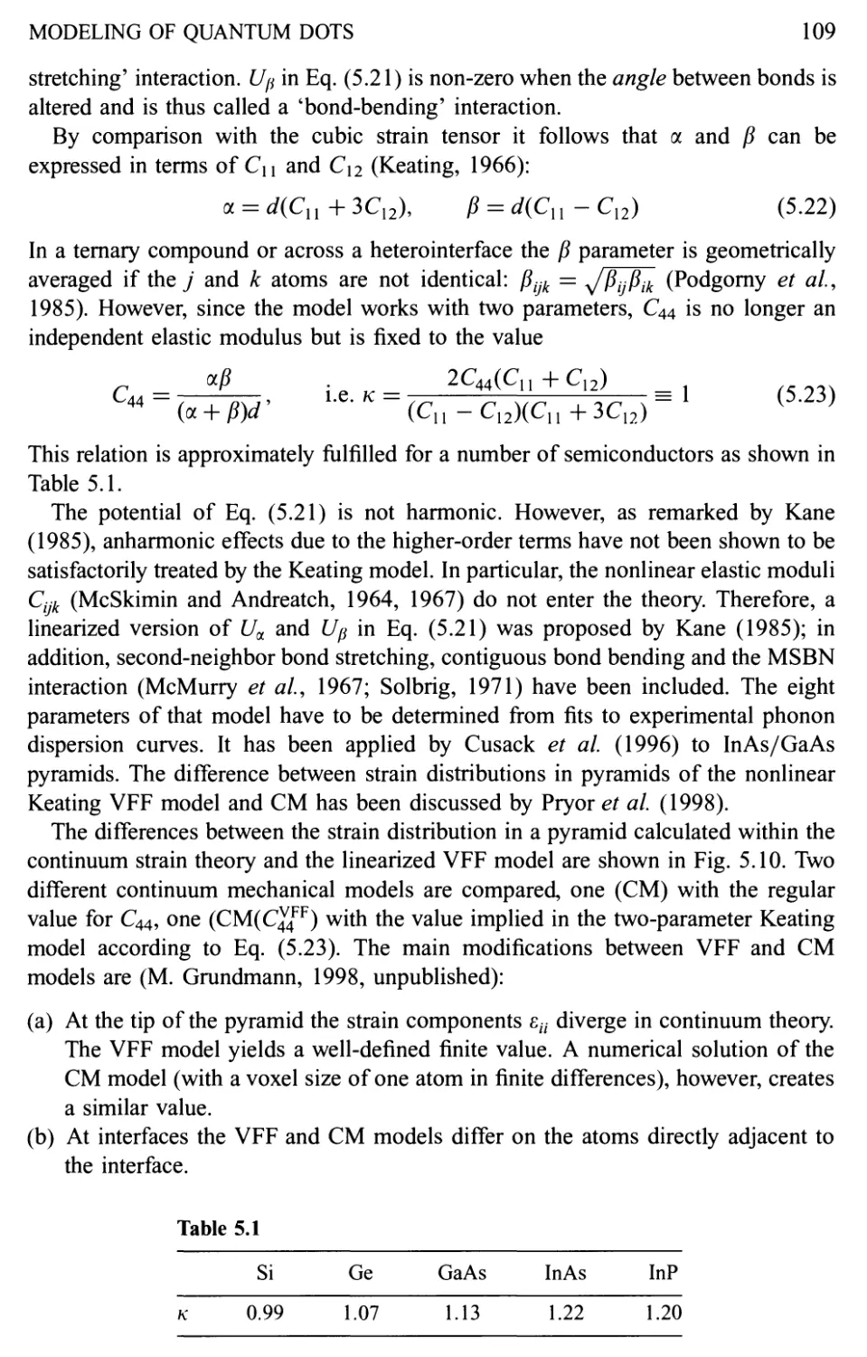
5.1 Strain Distribution 95
5.1.1 Stress-strain relations 96
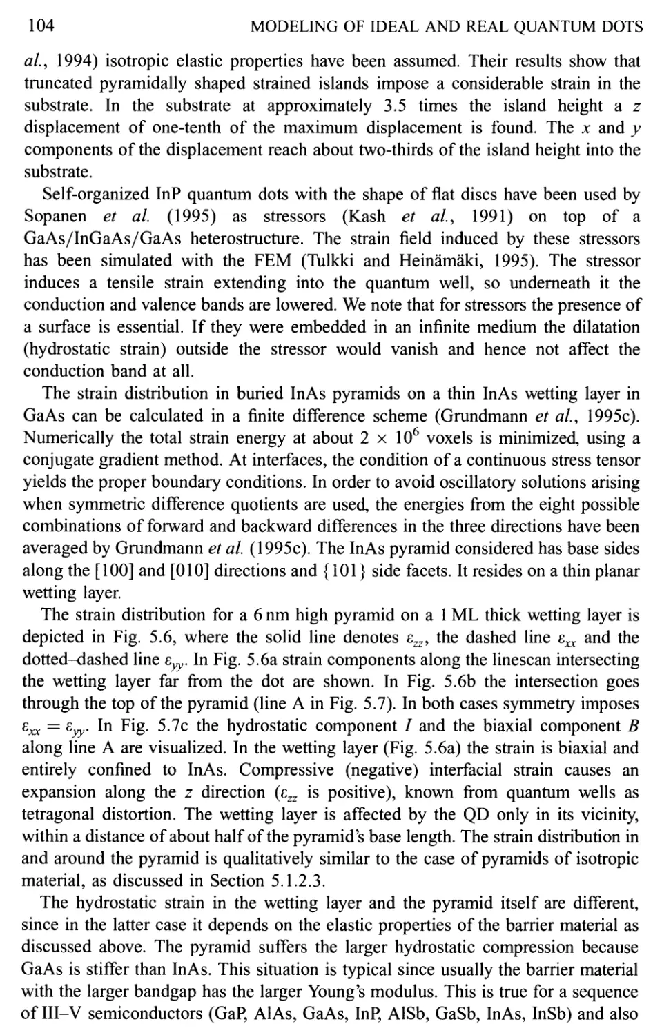
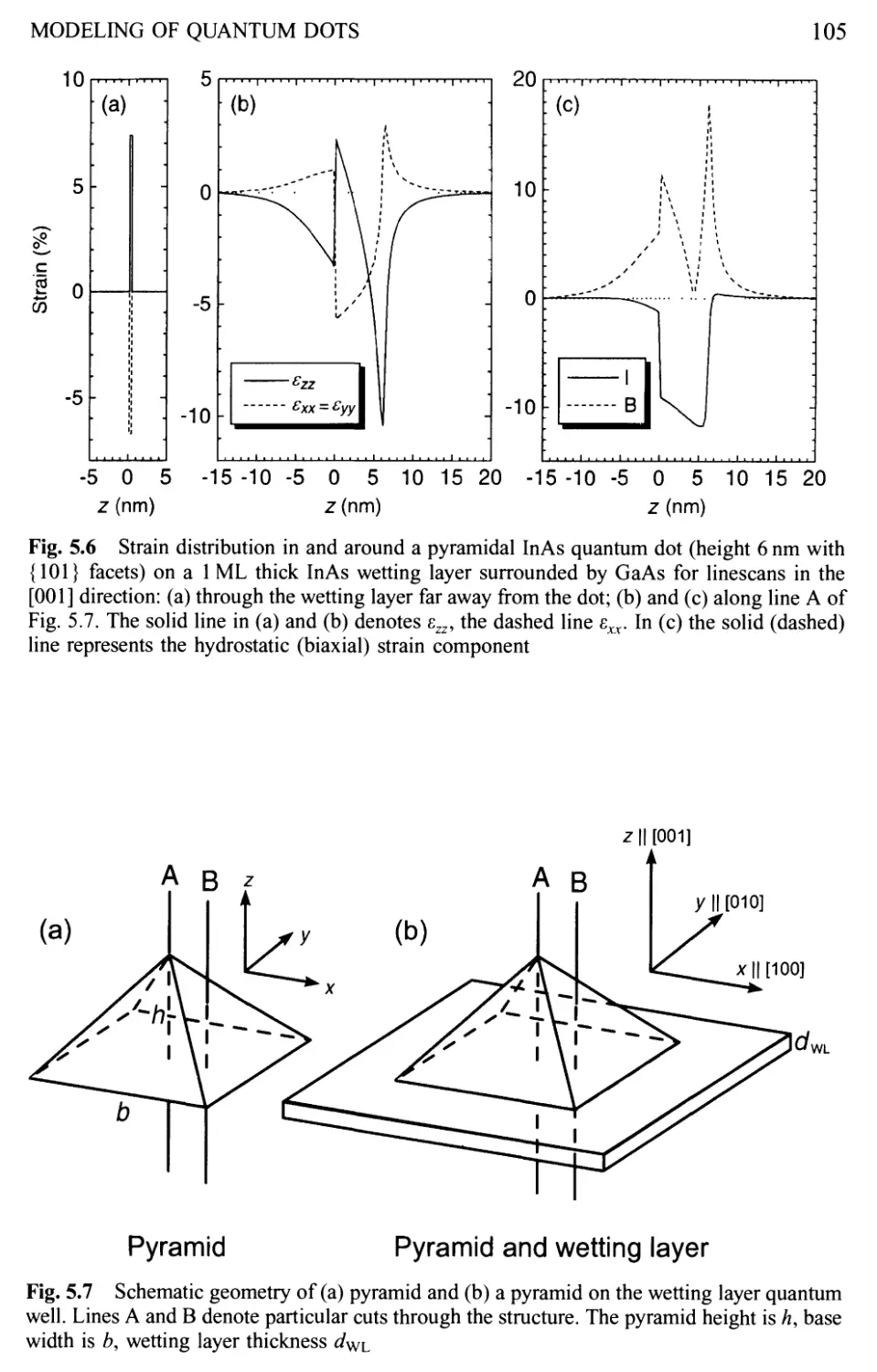
5.1.2 Strain in dots 96
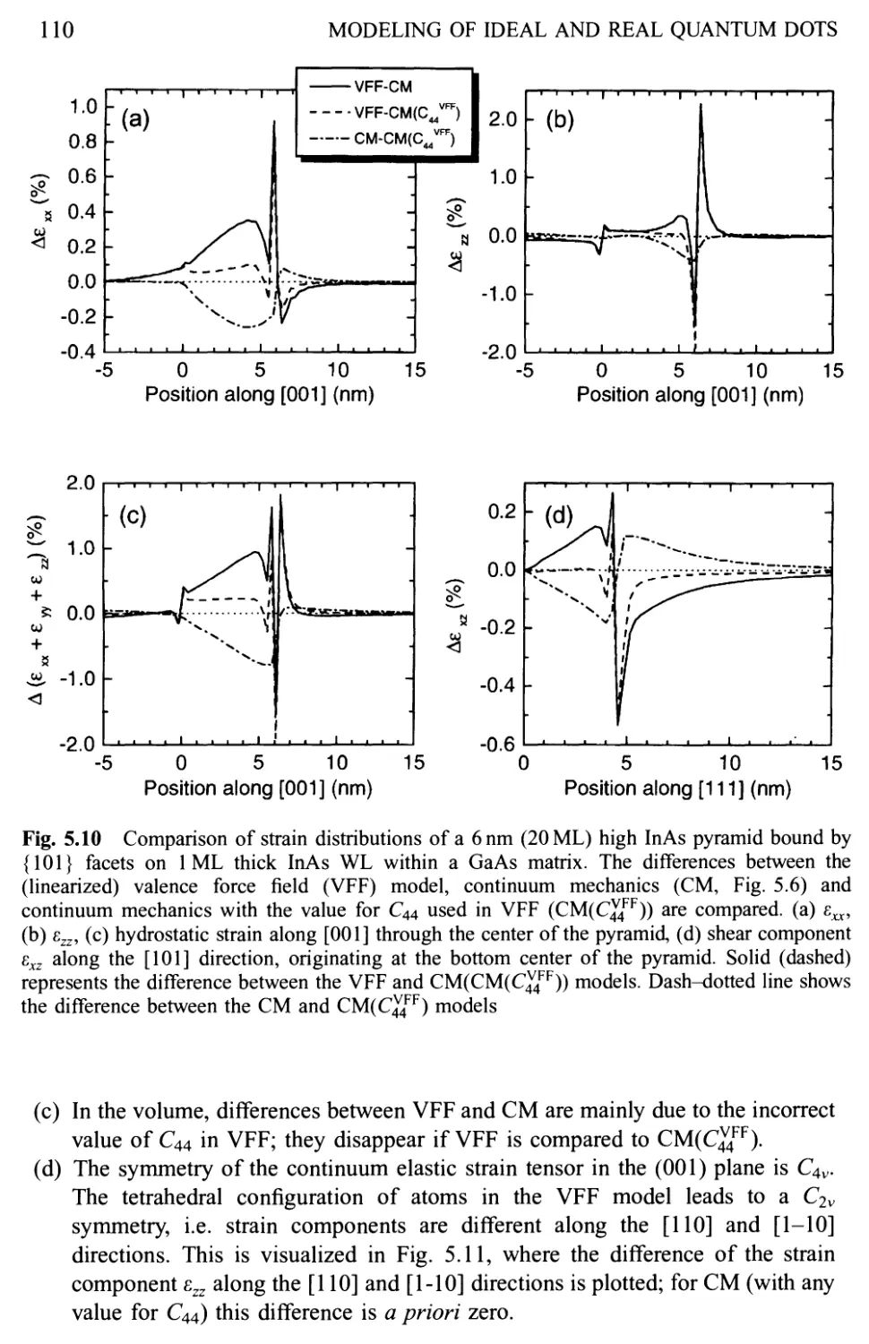
5.1.3 Valence force field model 107
5.1.4 Impact on band structure 111
5.1.5 Impact on phonon spectrum 113
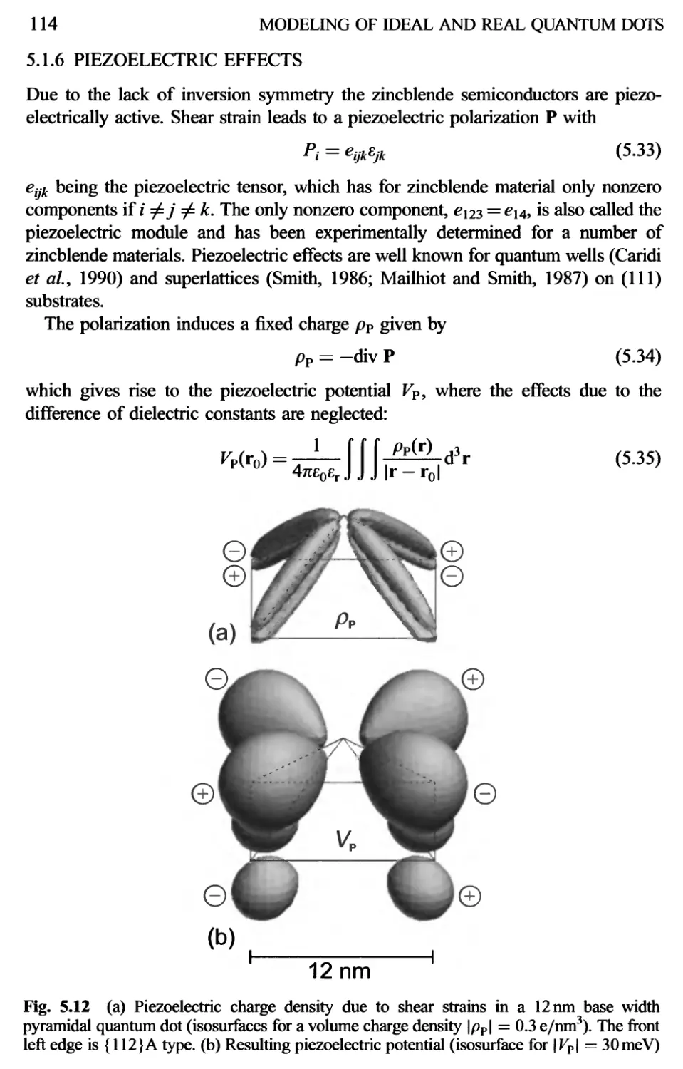
5.1.6 Piezoelectric effects 114
CONTENTS
vn
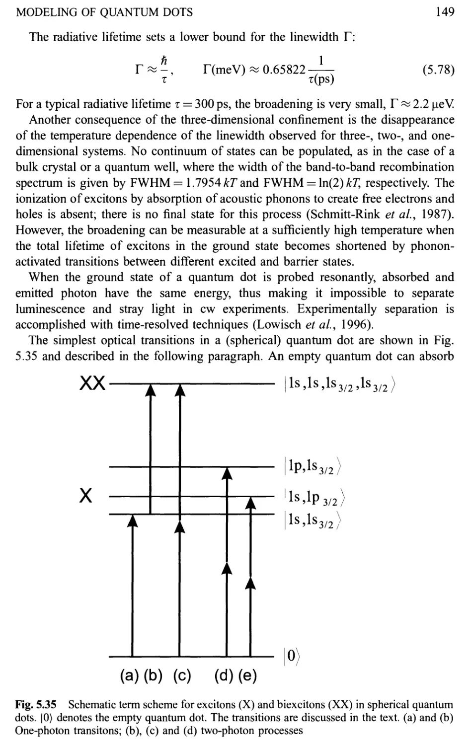
5.2 Quantum Confinement 115
5.2.1 Particle in a harmonic potential 115
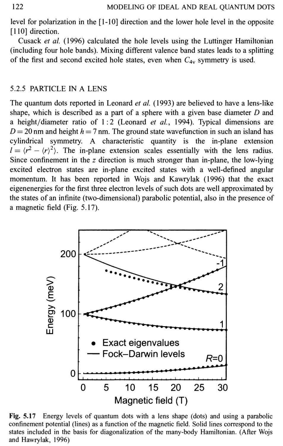
5.2.2 Particle in a sphere 116
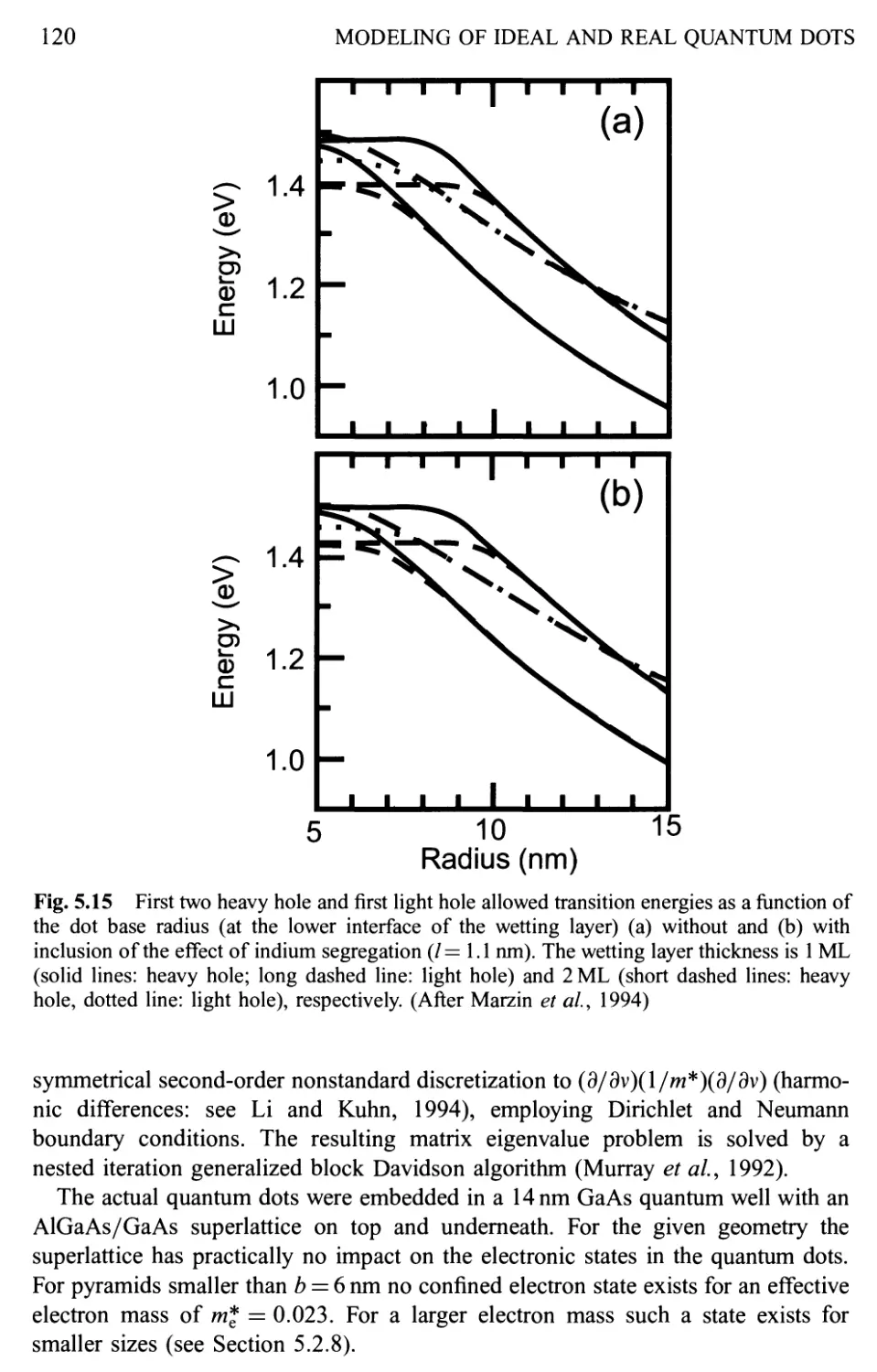
5.2.3 Particle in a cone 118
5.2.4 Particle in a pyramid 119
5.2.5 Particle in a lens 122
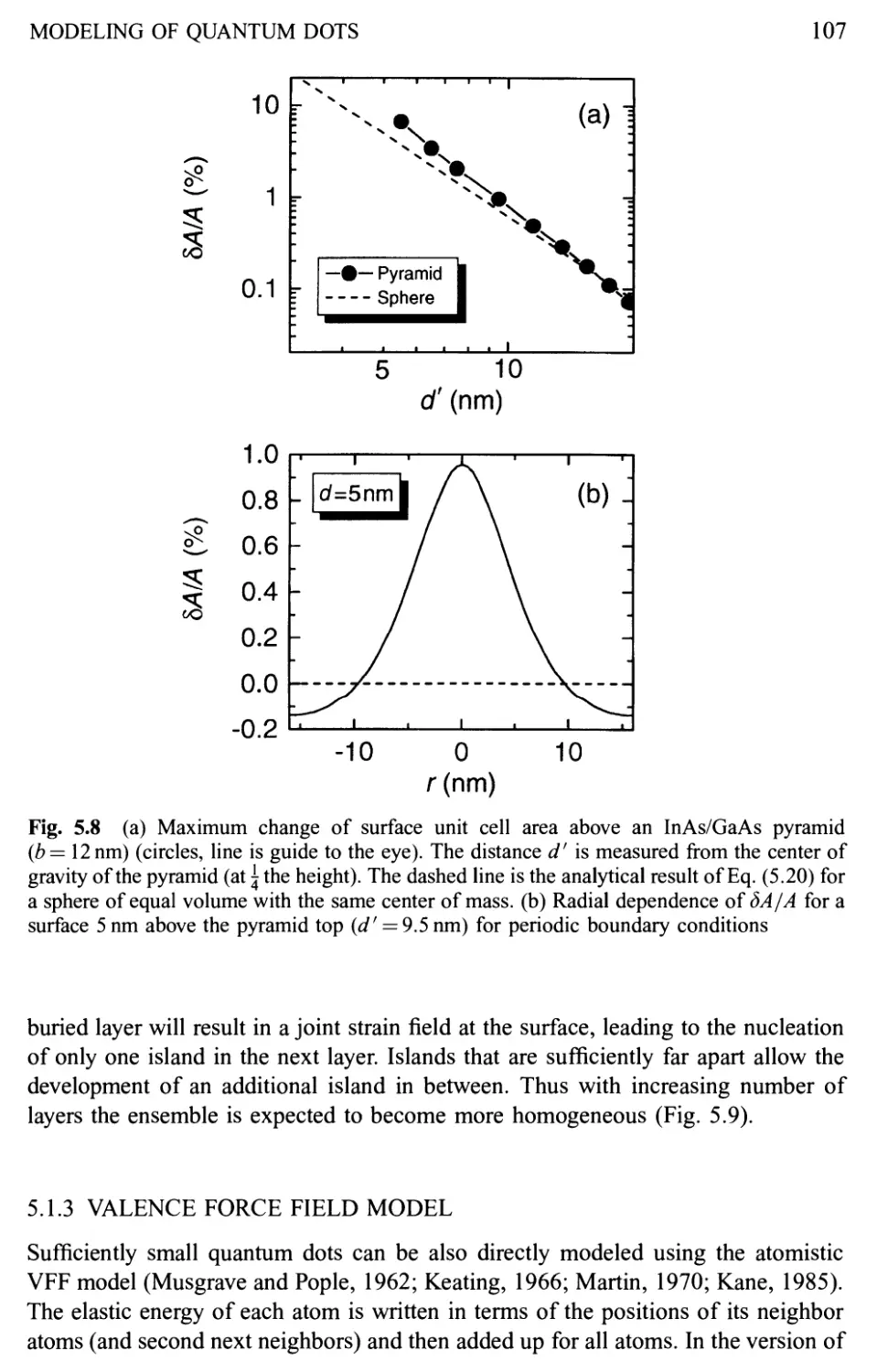
5.2.6 Stress-induced quantum dots 122
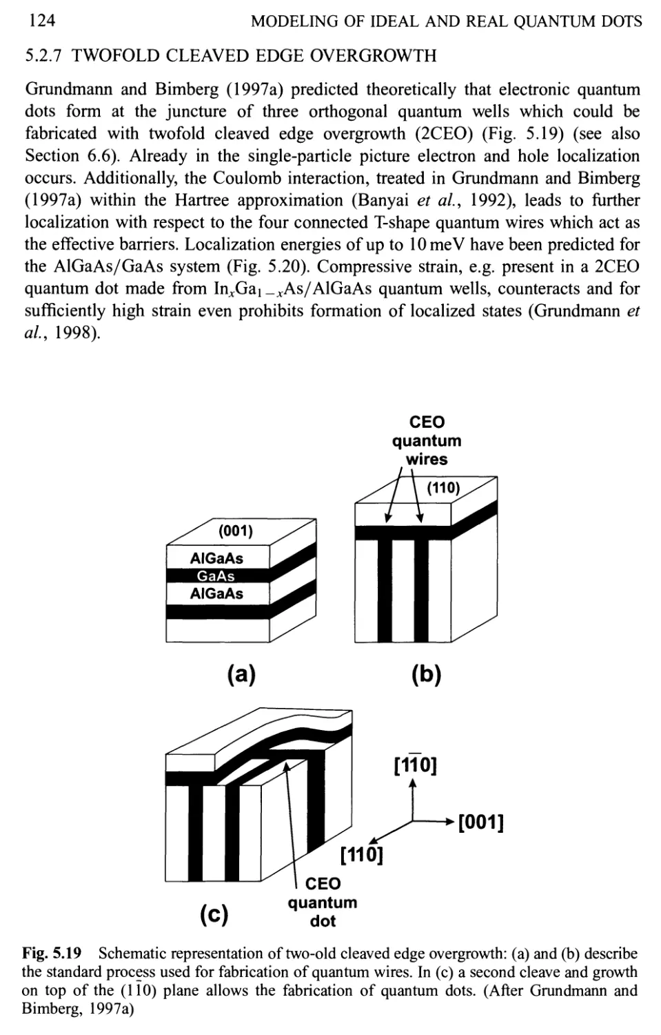
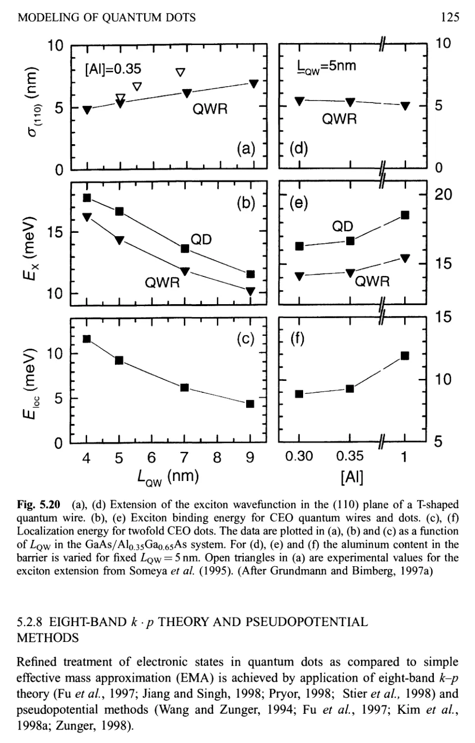
5.2.7 Twofold cleaved edge overgrowth 124
5.2.8 Eight-band kp theory and pseudopotential methods 125
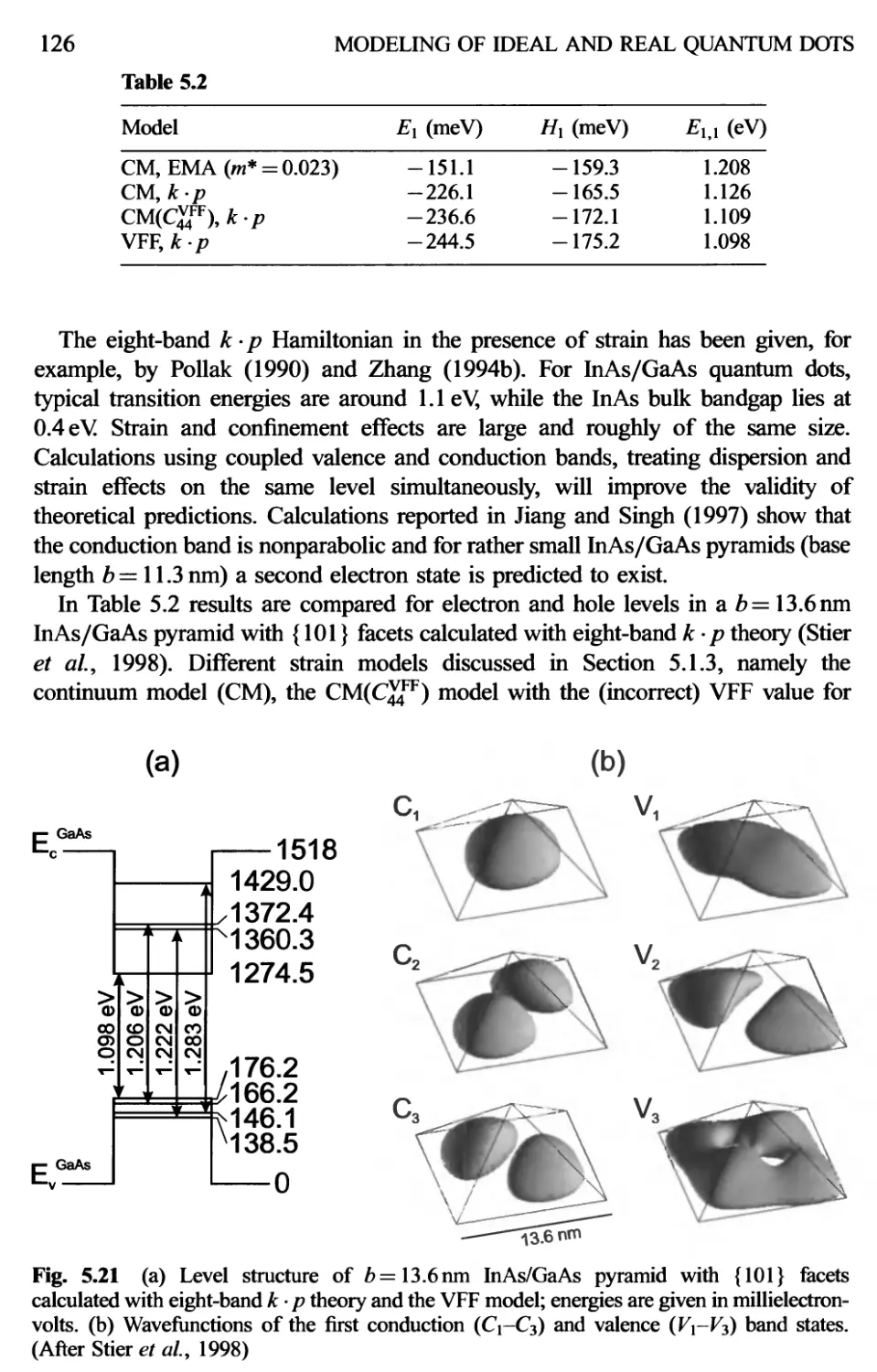
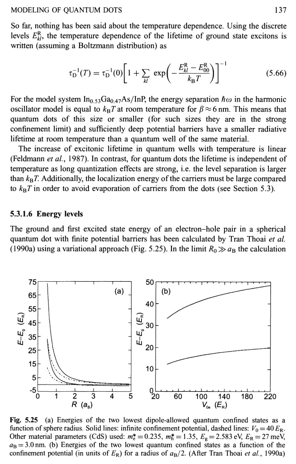
5.3 Coulomb Interaction 128
5.3.1 Excitons 128
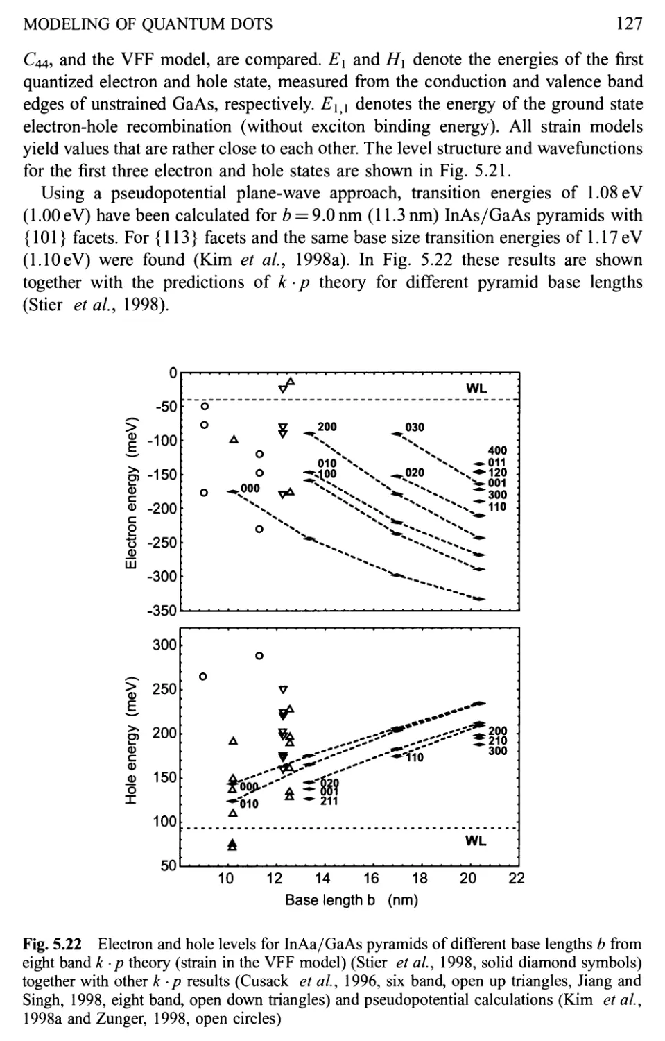
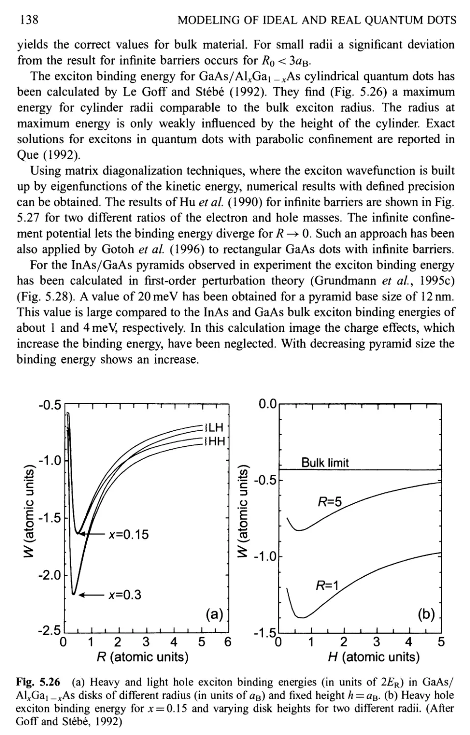
5.3.2 Type-II excitons 143
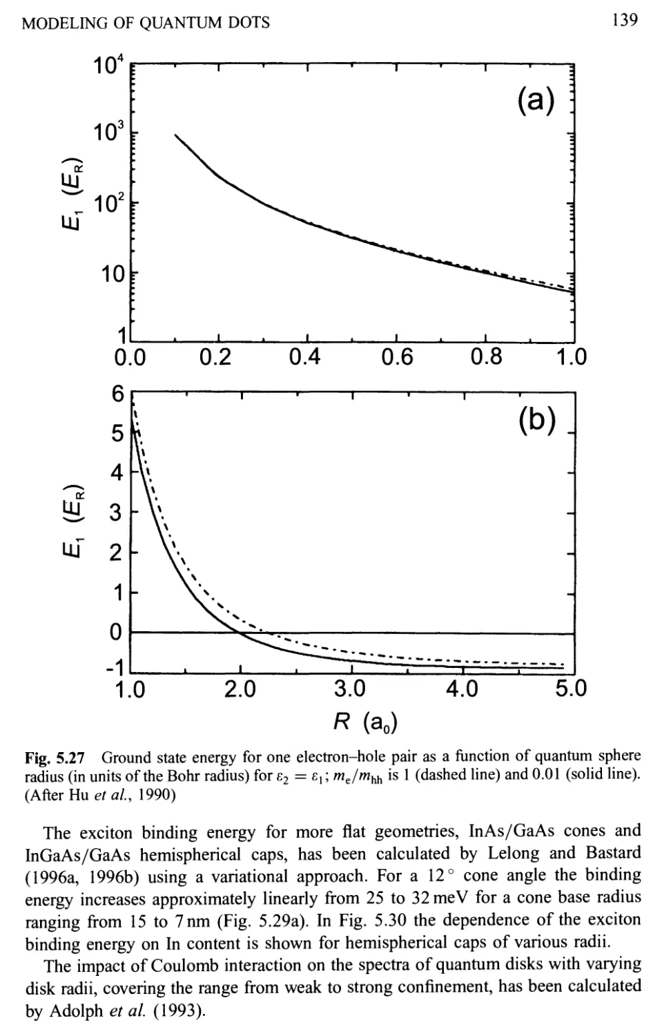
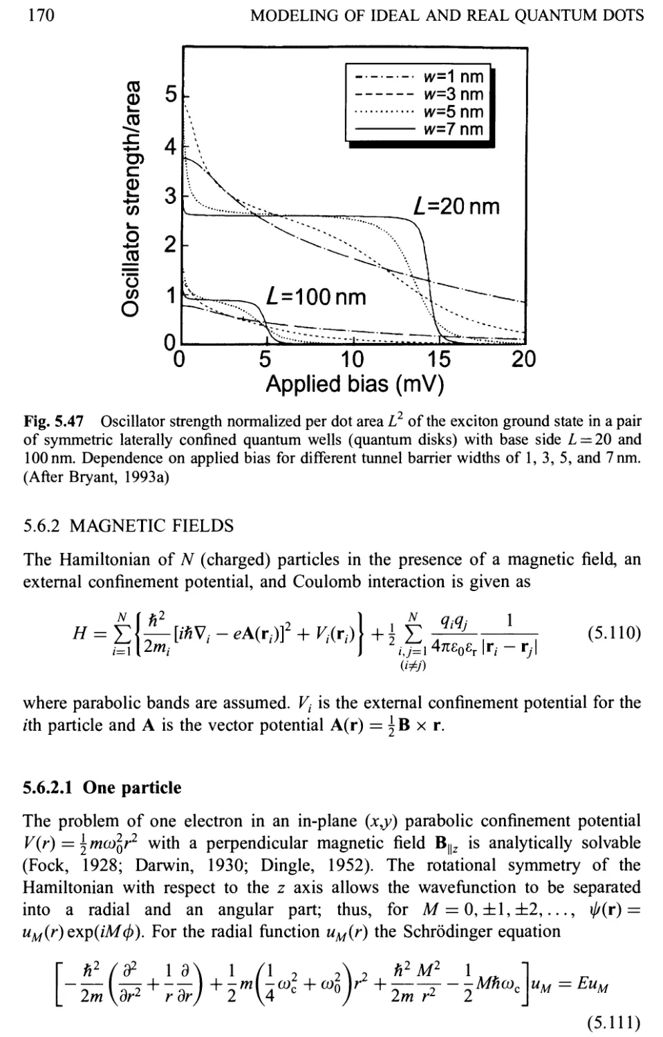
5.3.3 Electronically coupled quantum dots 145
5.3.4 Coulomb blockade 146
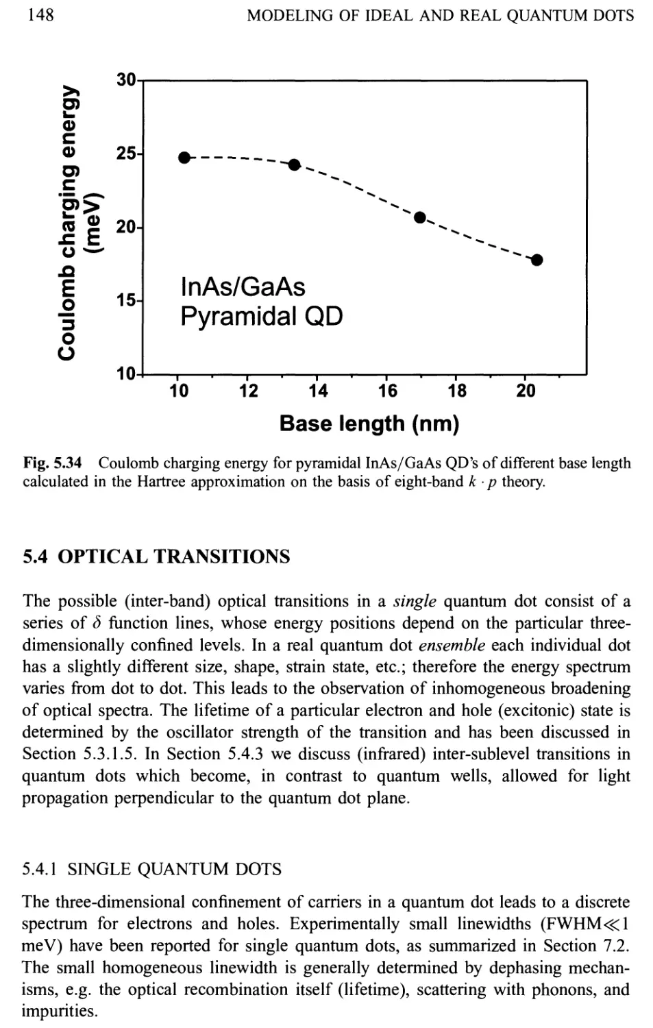
5.4 Optical Transitions 148
5.4.1 Single quantum dots 148
5.4.2 Quantum dot ensembles 150
5.4.3 Inter-sublevel transitions 154
5.5 Population of Levels 155
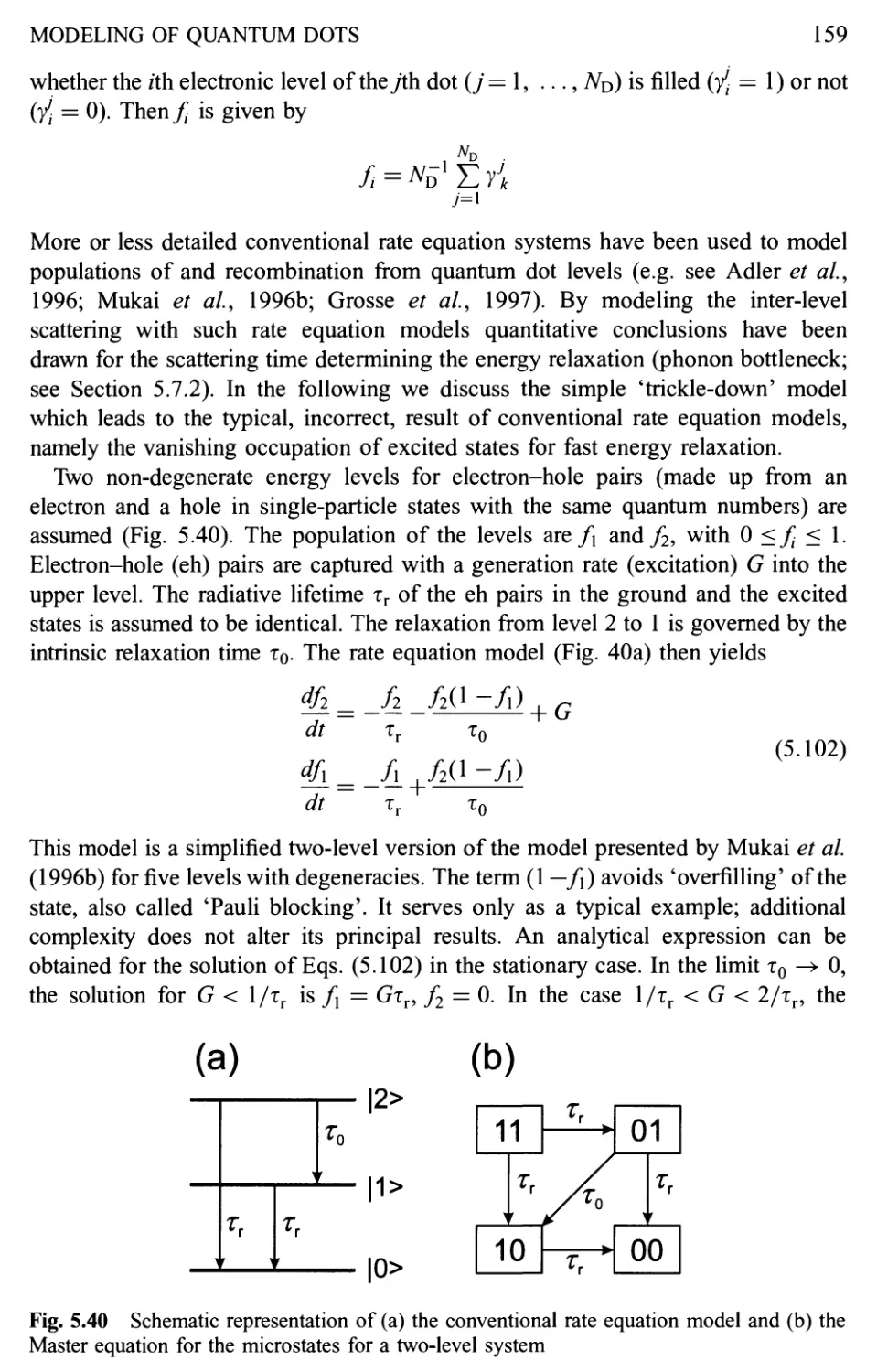
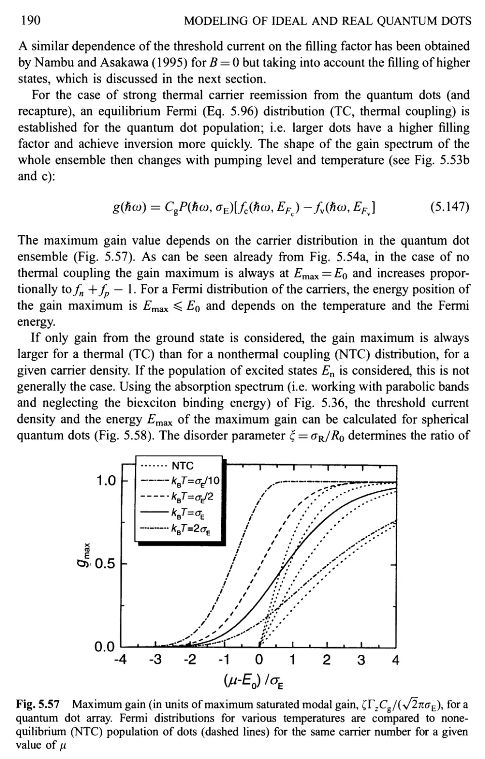
5.5.1 Thermal versus nonthermal distribution 155
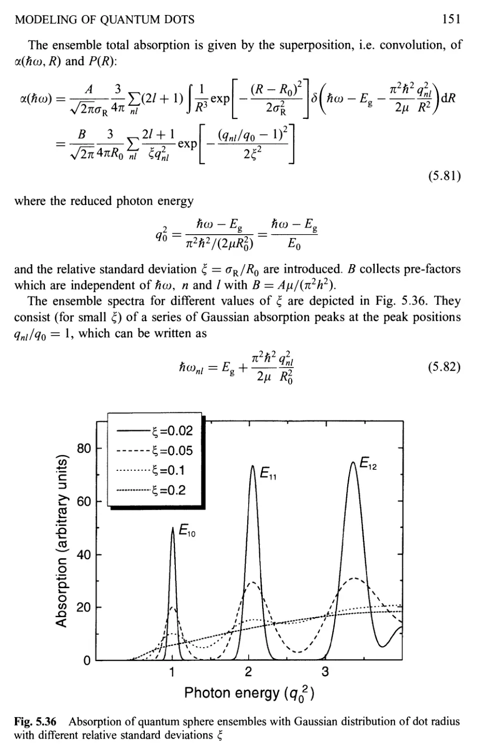
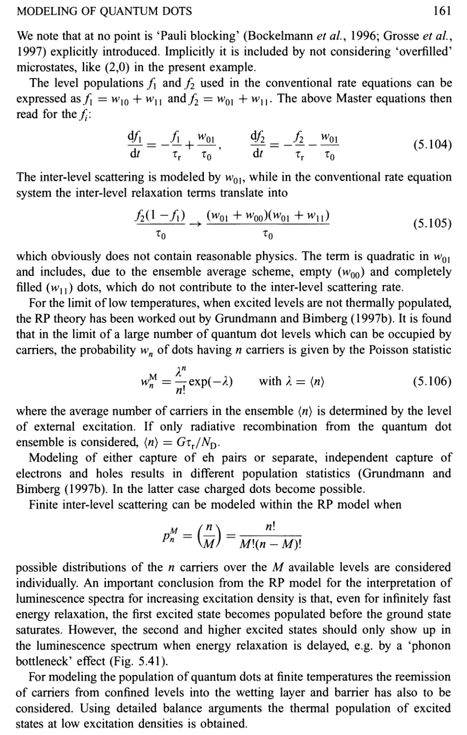
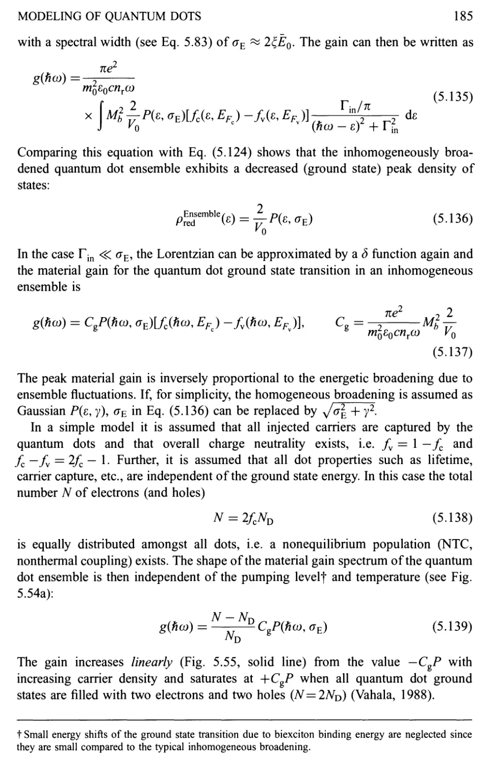
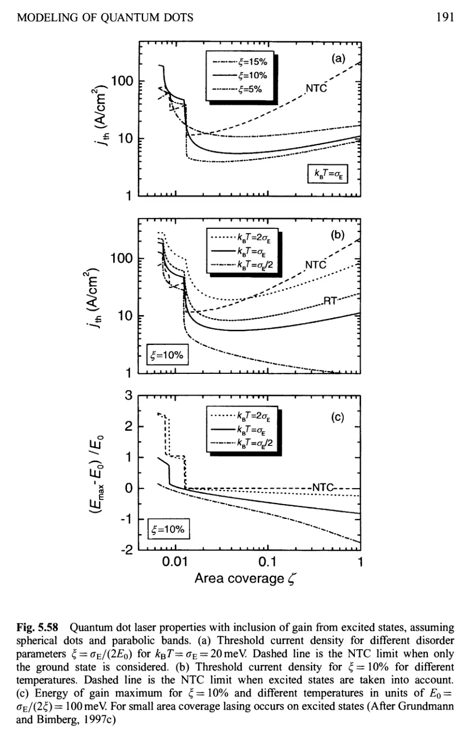
5.5.2 Population statistics 158
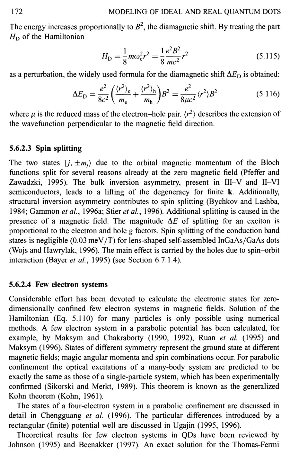
5.5.3 Auger effect 165
5.6 Static External Fields 165
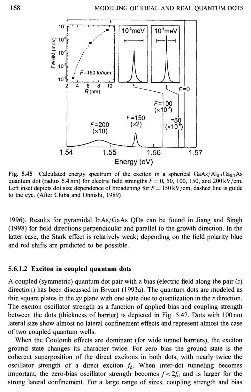
5.6.1 Electric fields 167
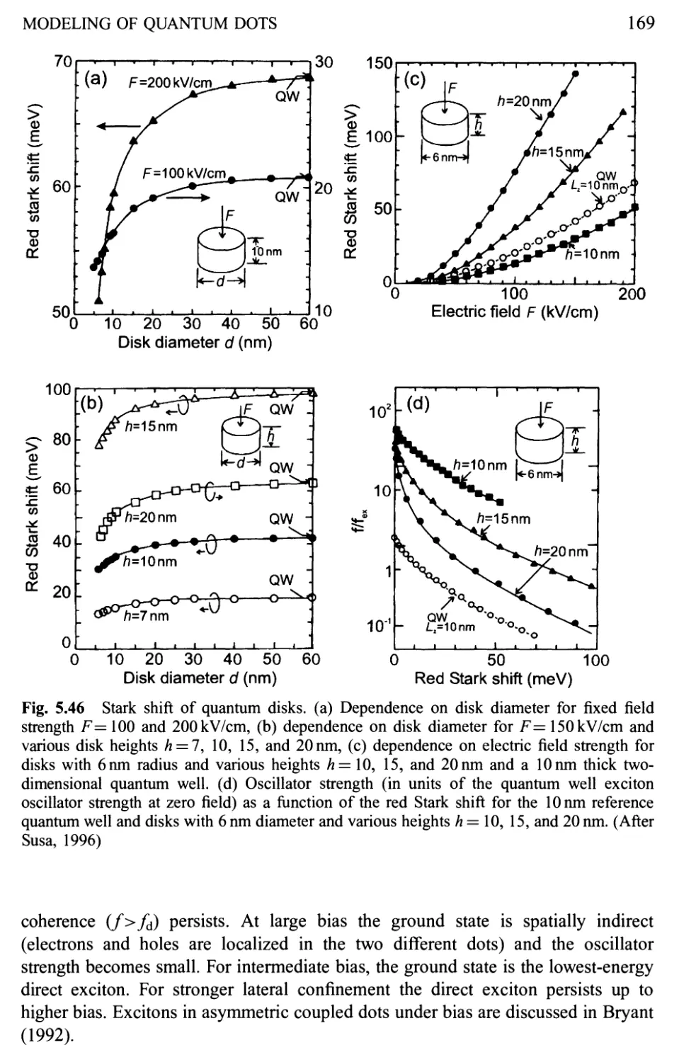
5.6.2 Magnetic fields 170
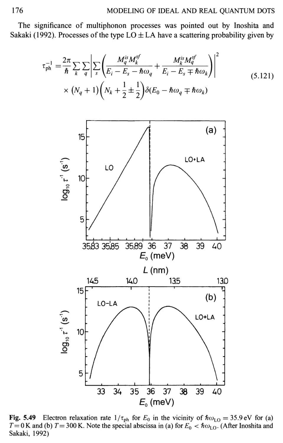
5.7 Phonons 174
5.7.1 Phonon spectrum 174
5.7.2 Electron-phonon interaction 174
5.8 Quantum Dot Laser 177
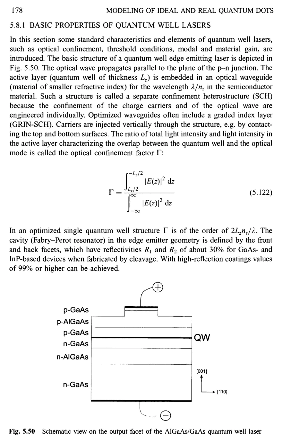
5.8.1 Basic properties of quantum well lasers 178
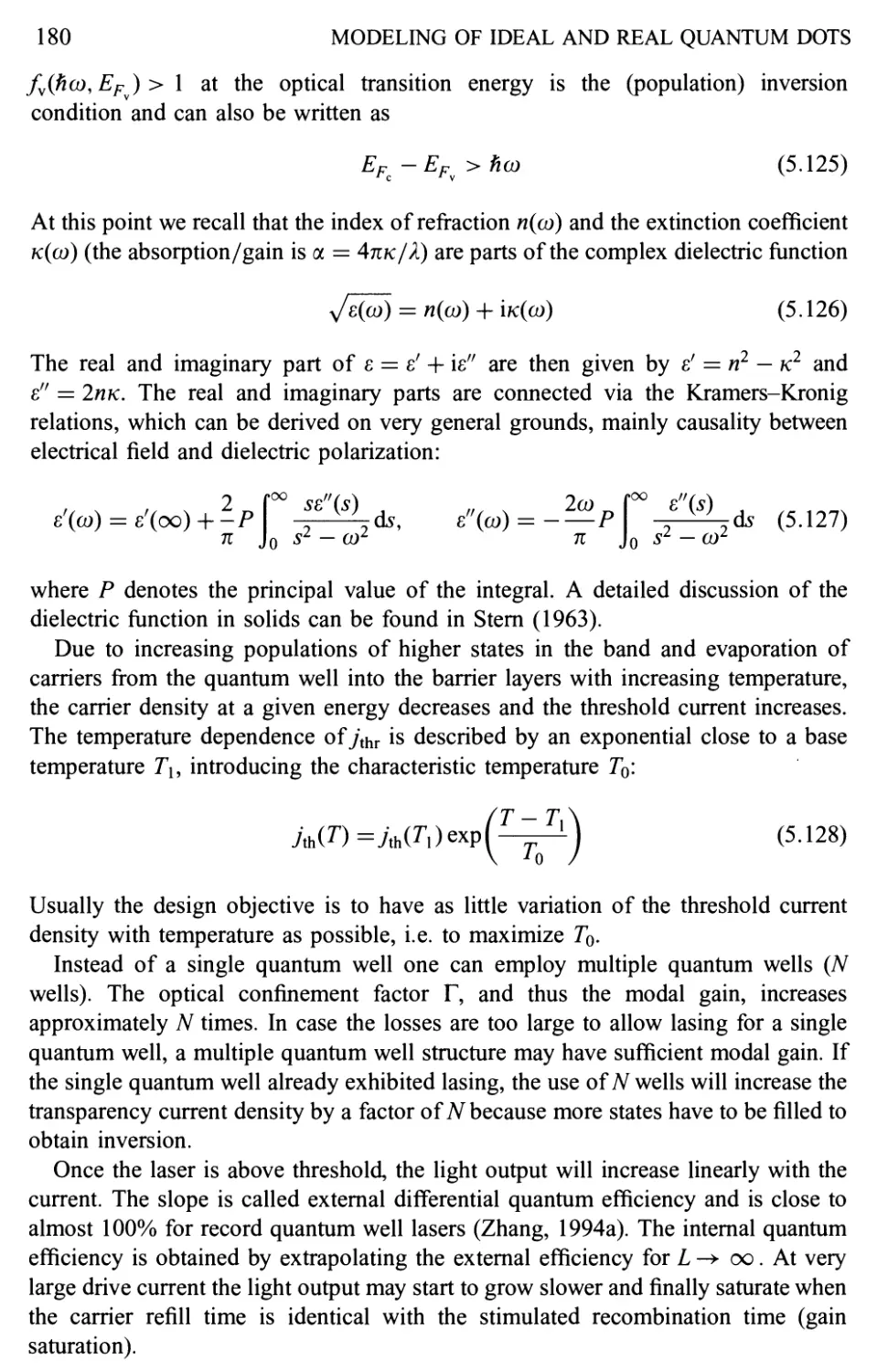
5.8.2 The ideal quantum dot laser 181 .
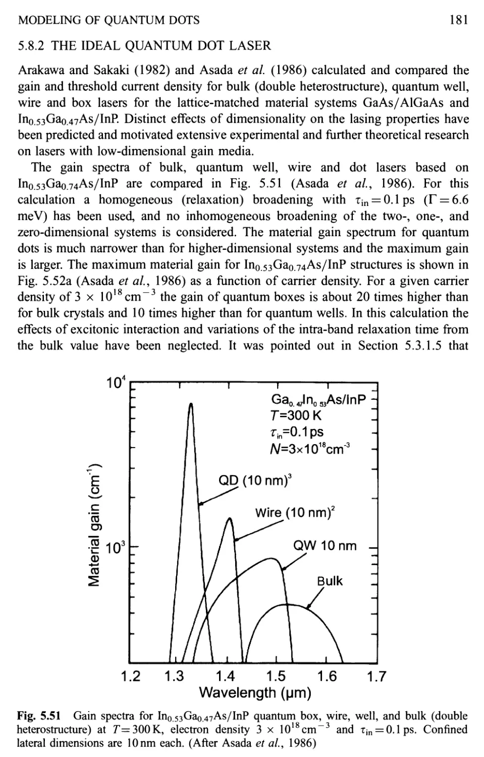
5.8.3 The real quantum dot laser 182
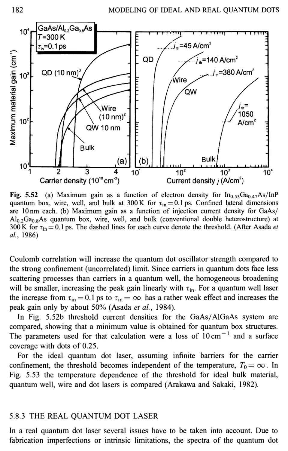
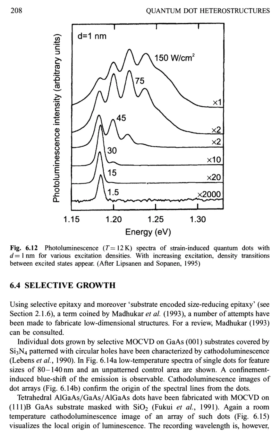
6 Electronic and Optical Properties 198
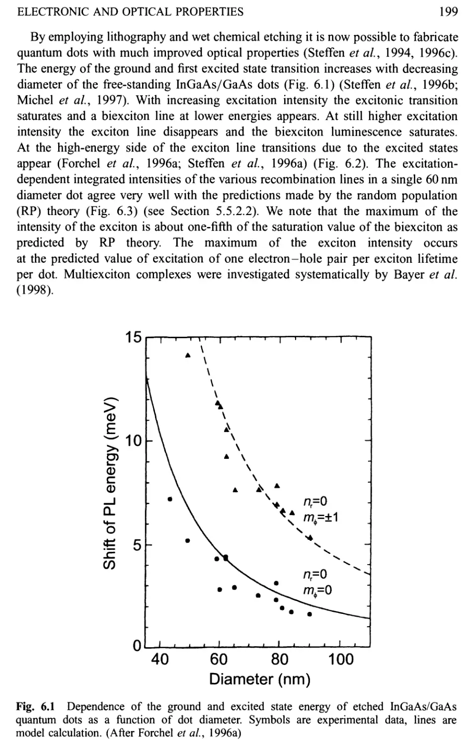
6.1 Etched Structures 198
6.2 Local Intermixing of Quantum Wells 201
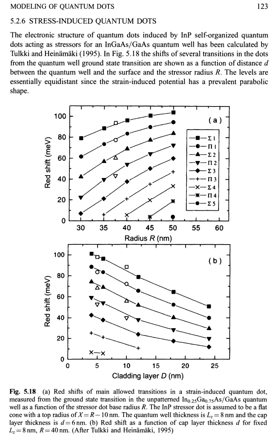
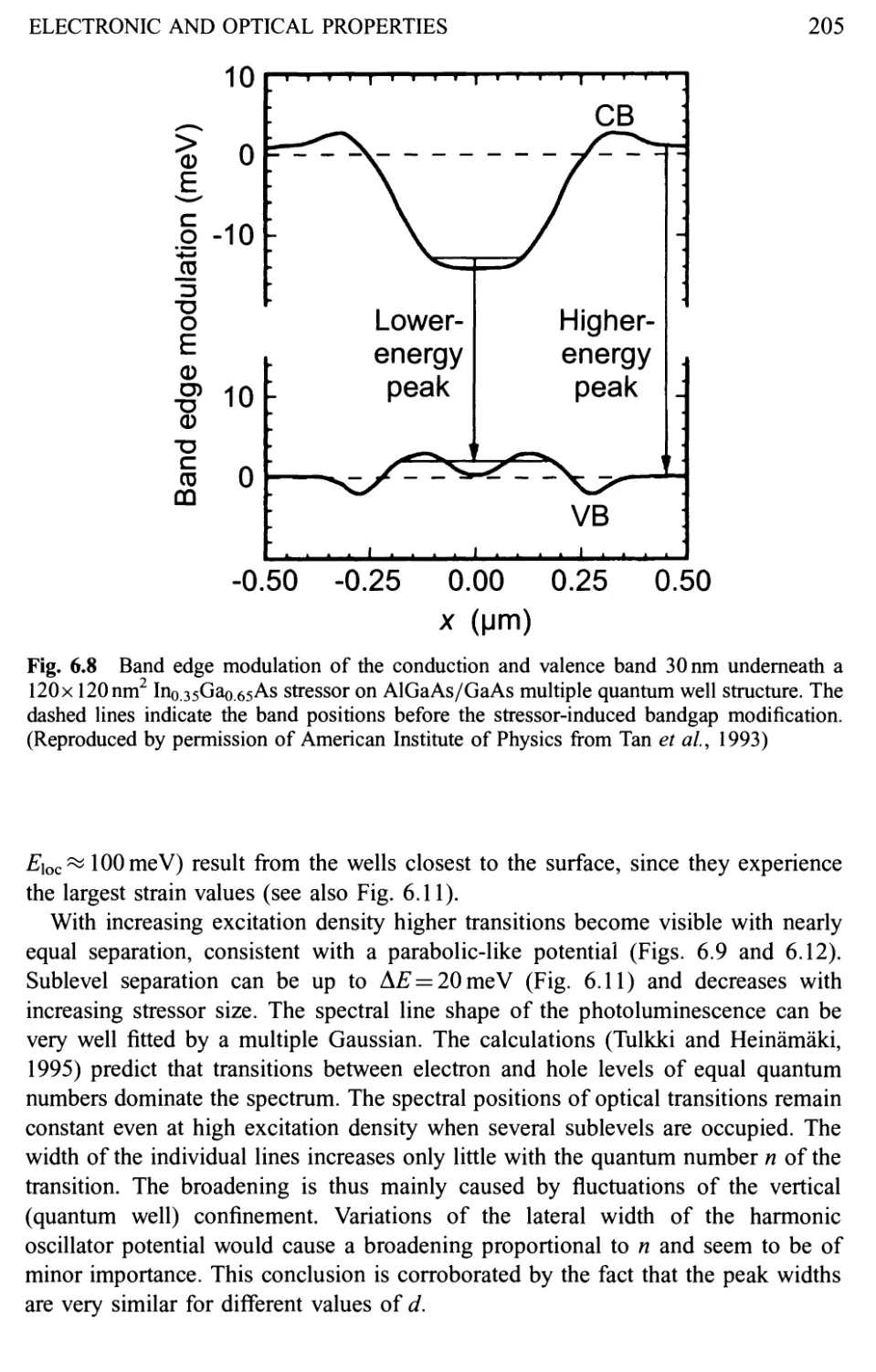
6.3 Stressors 202
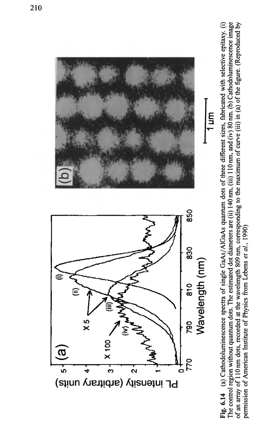
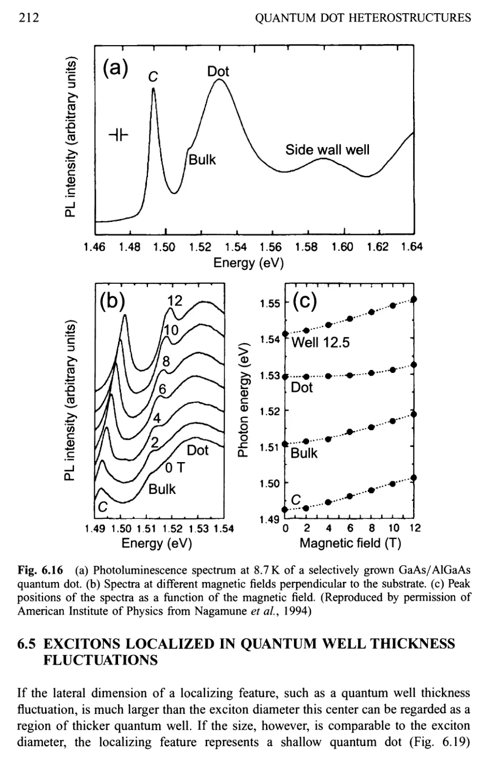
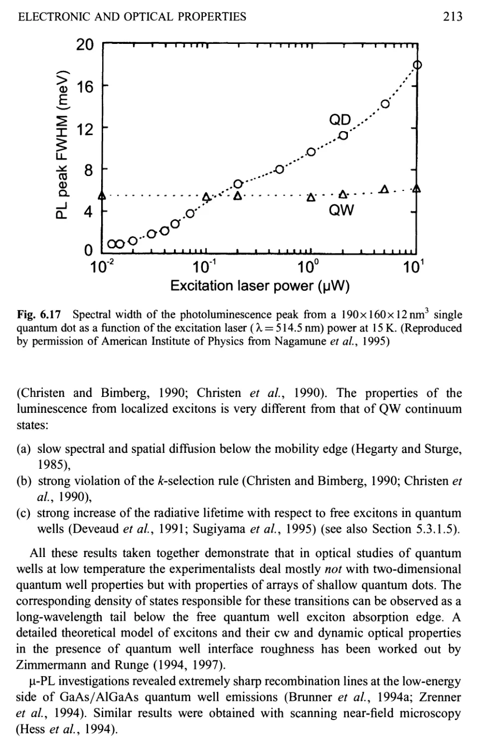
6.4 Selective Growth 208
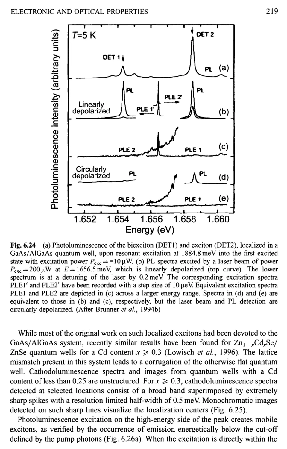
6.5 Excitons Localized in Quantum Well Thickness Fluctuations
212
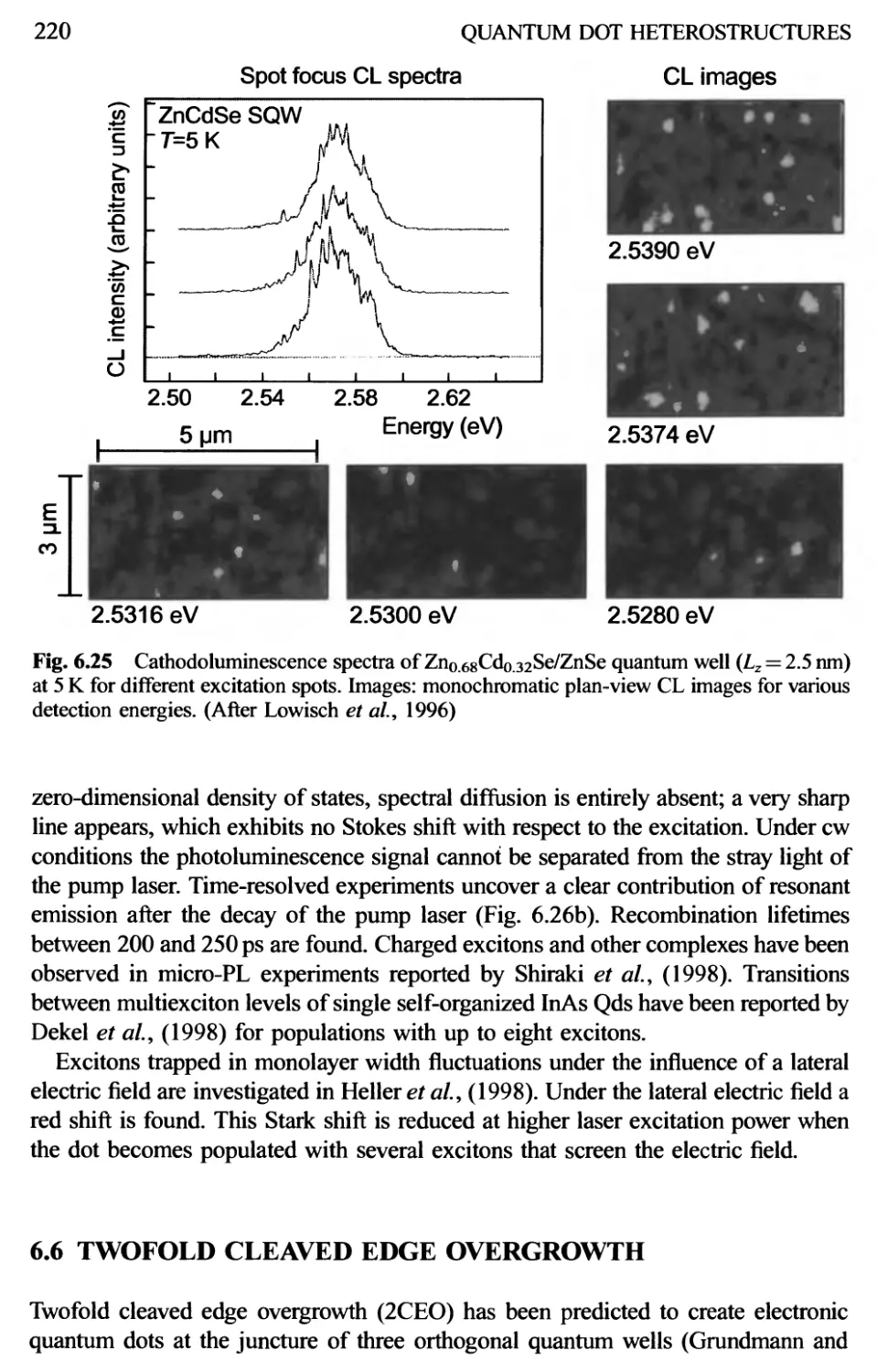
6.6 Twofold Cleaved Edge Overgrowth 220
6.7 Self-Organized Type-I Quantum Dots 222
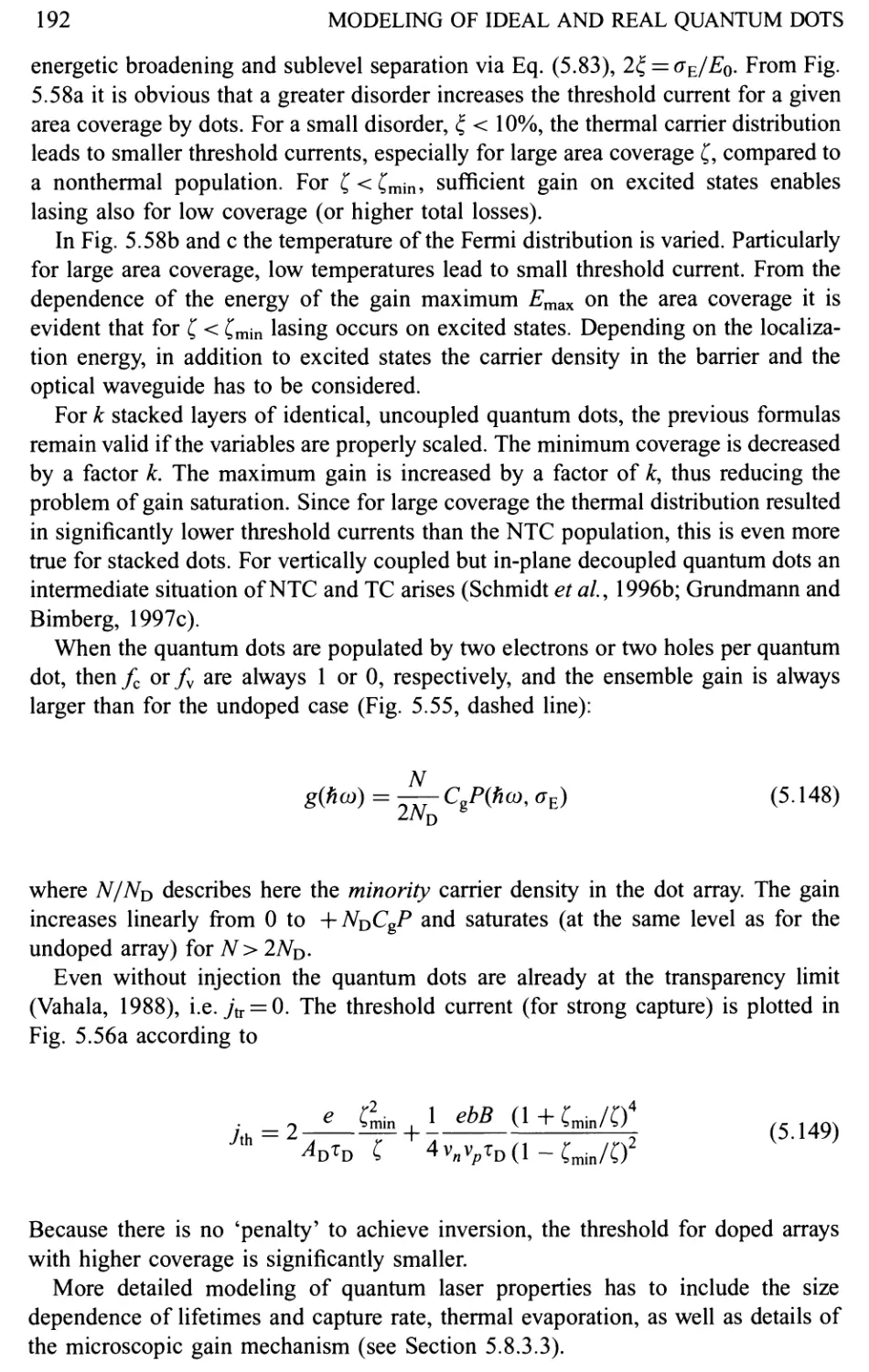
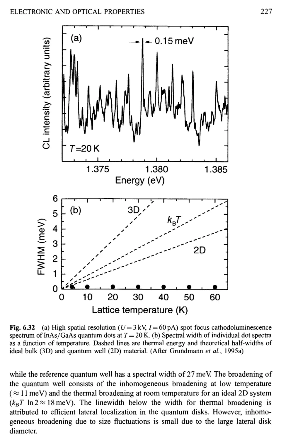
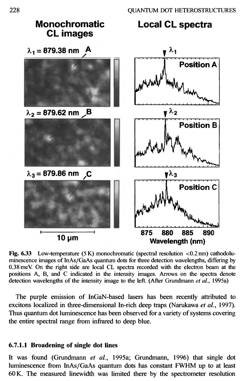
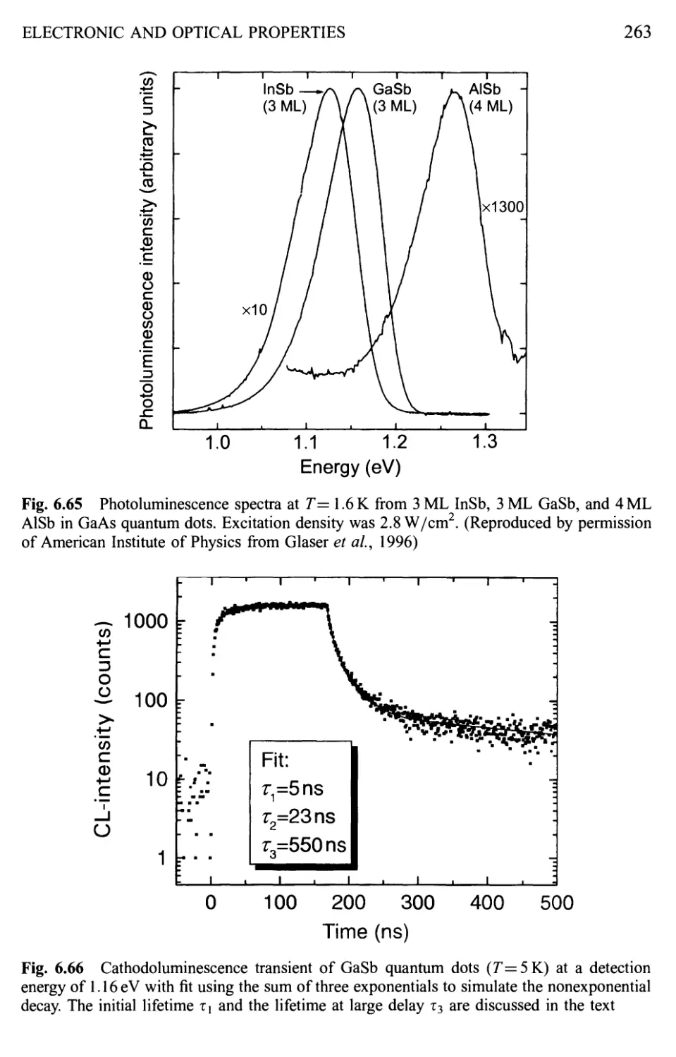
6.7.1 Luminescence 223
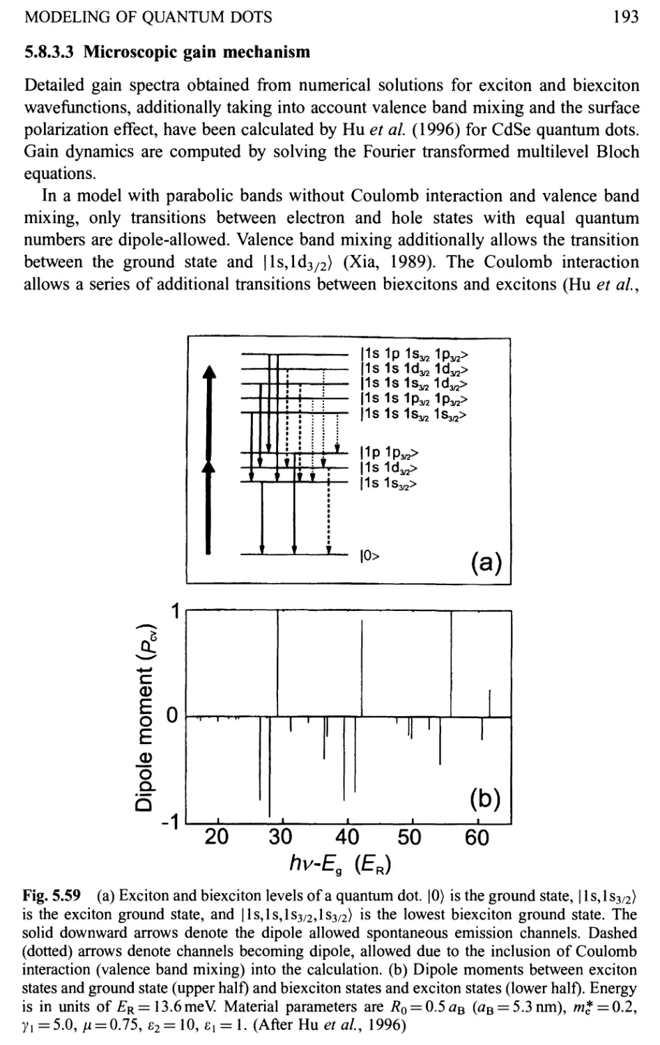
6.7.2 Absorption 239
6.7.3 Electroreflectance 241
Vlll
CONTENTS
6.7.4 Fourier spectroscopy of inter-sublevel transitions 243
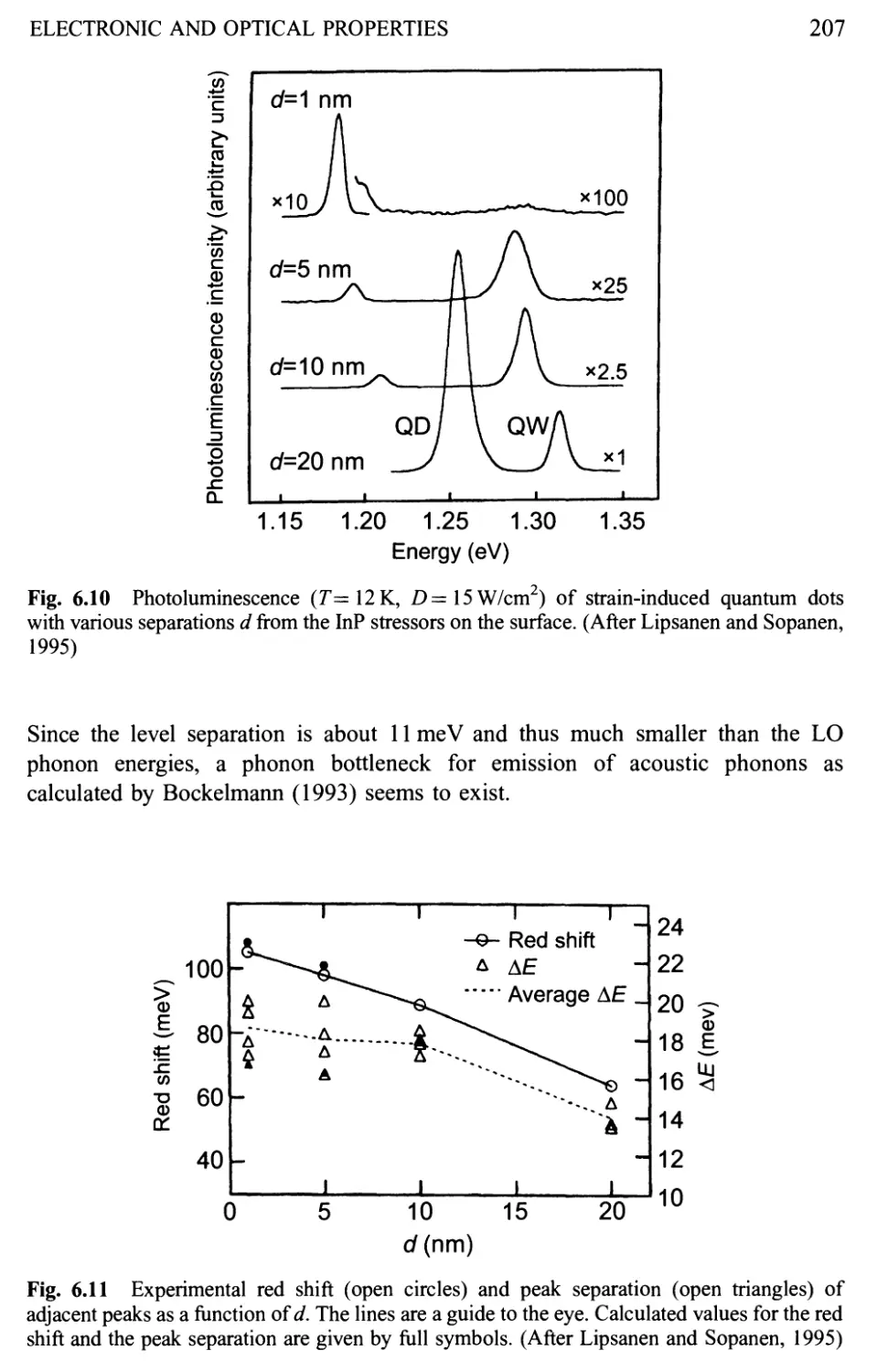
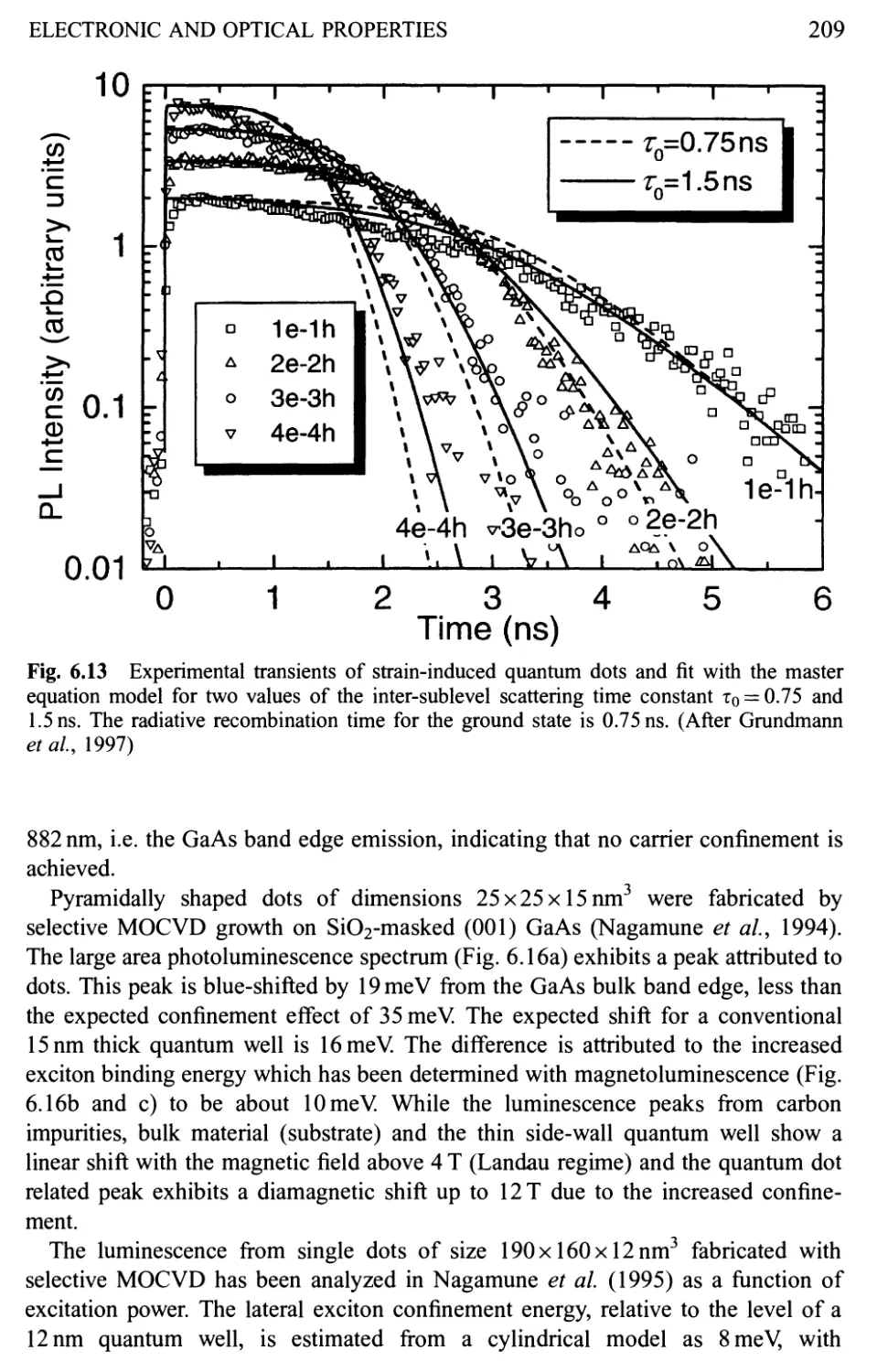
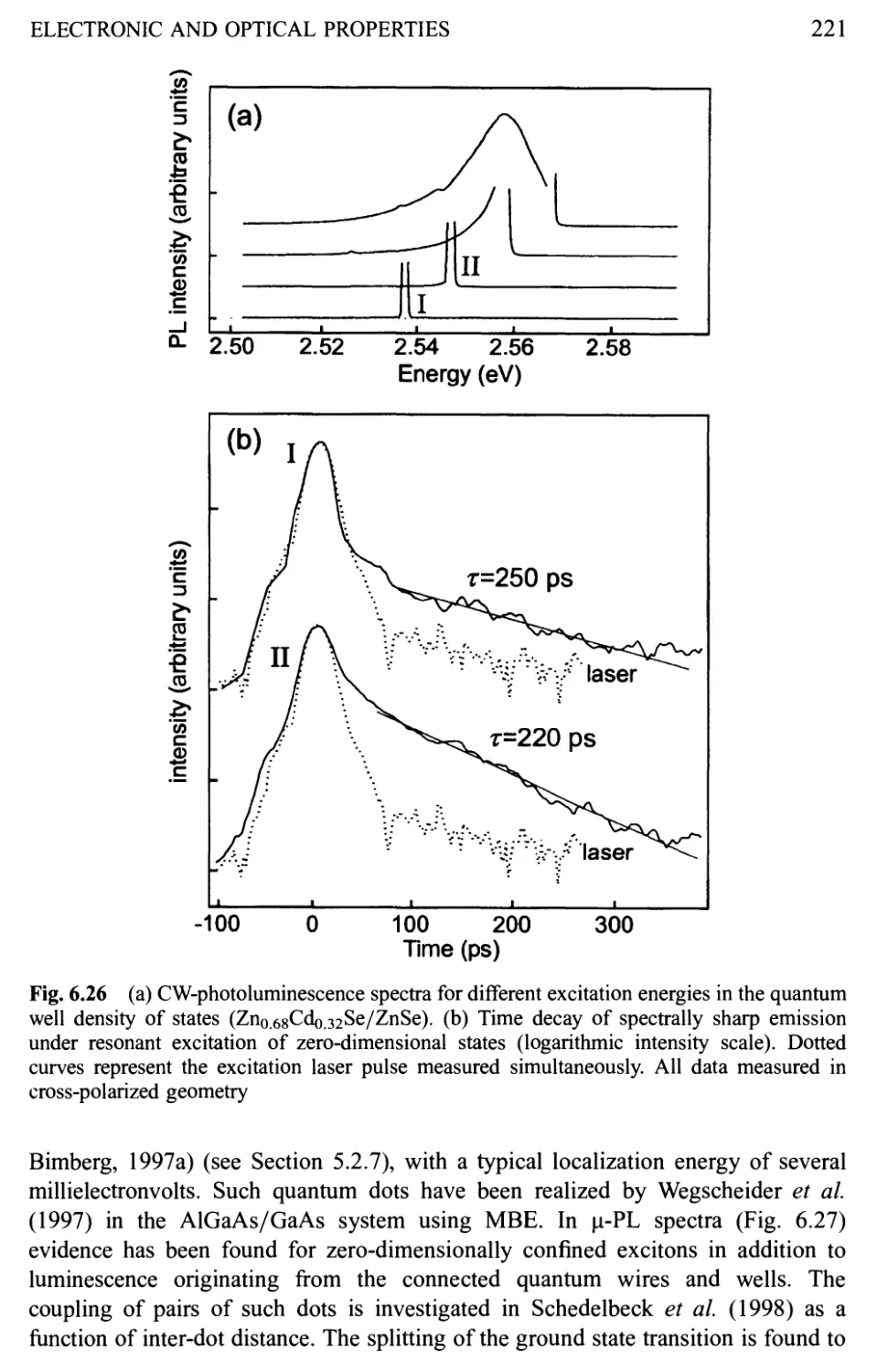
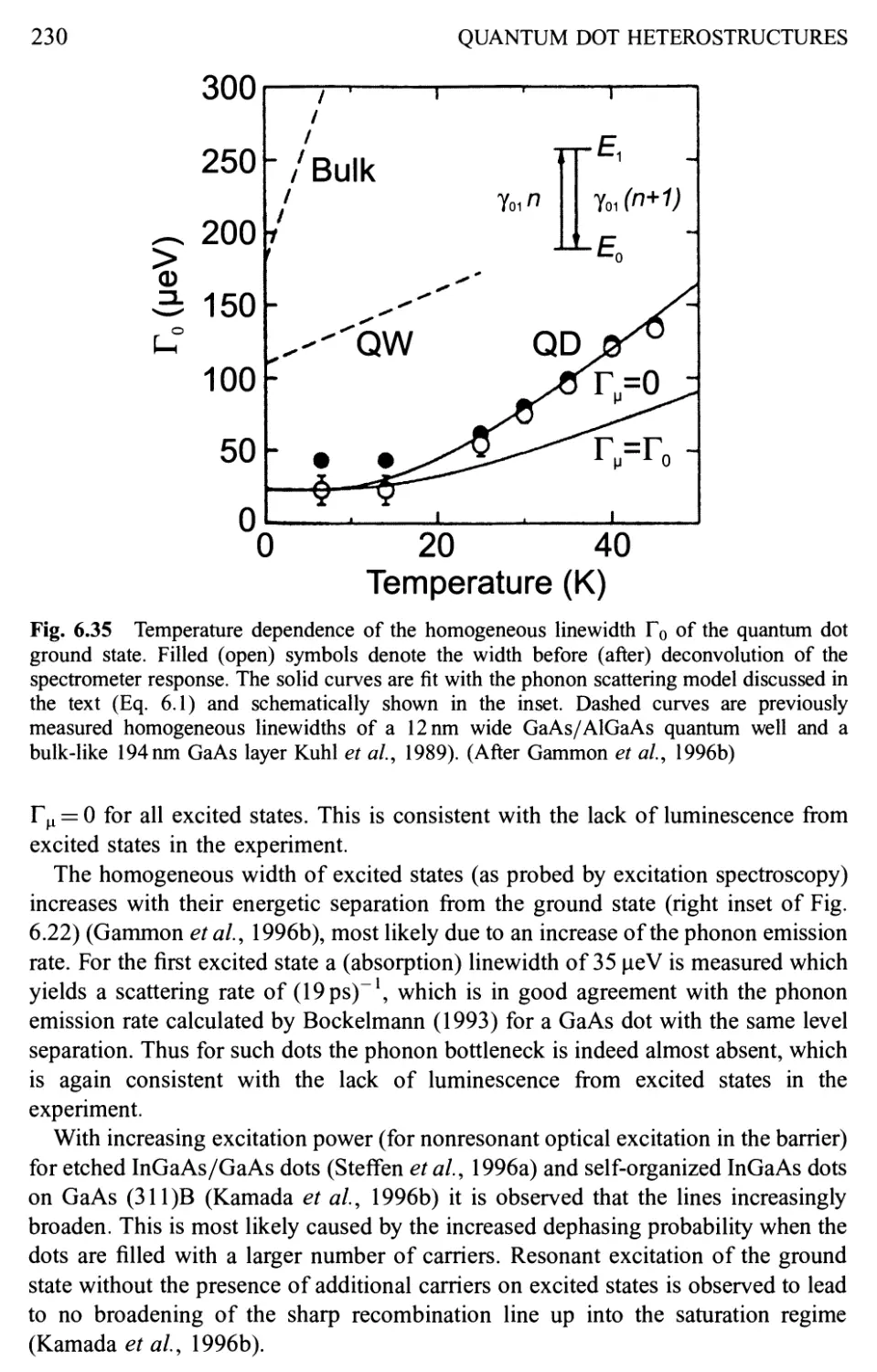
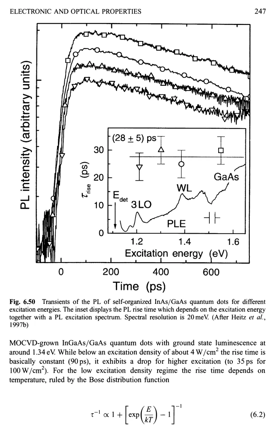
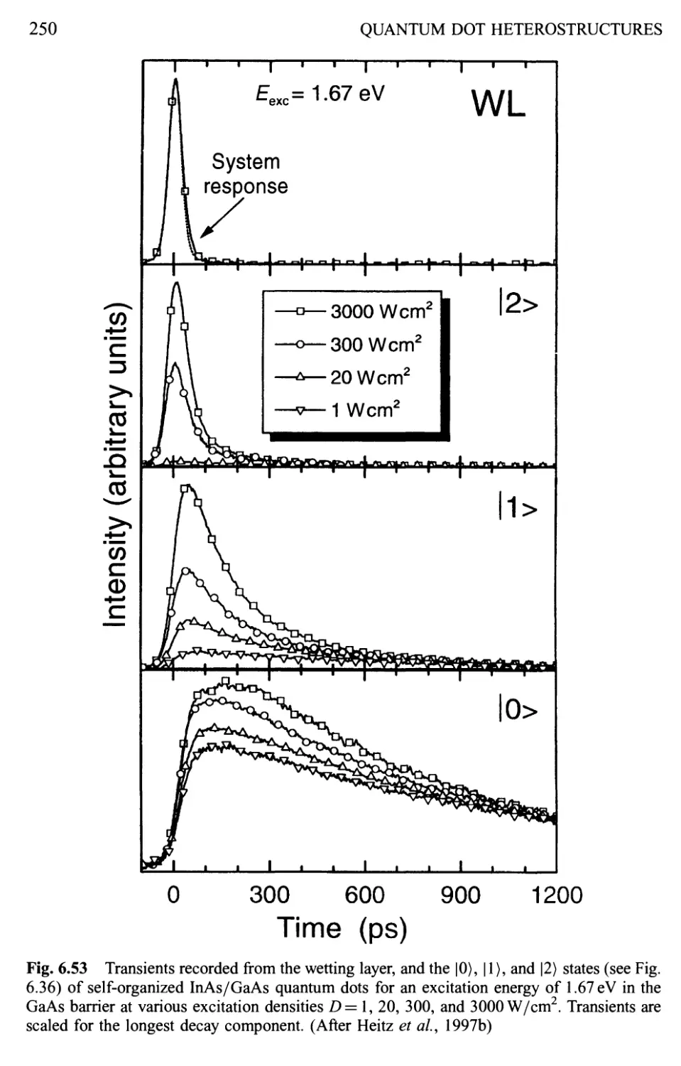
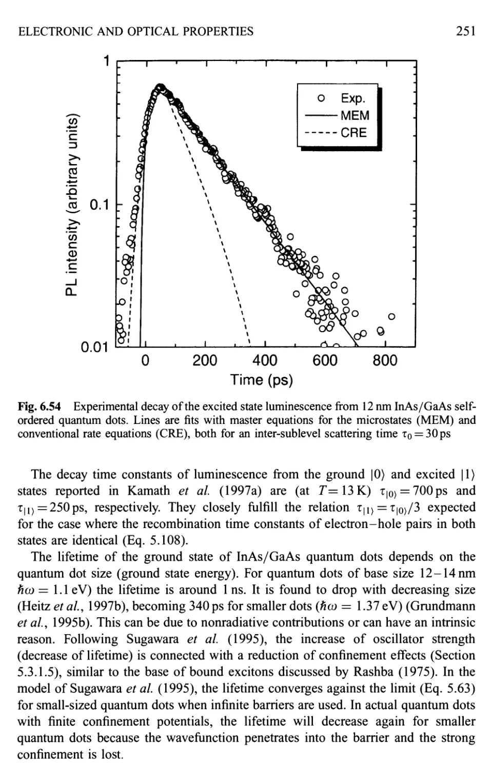
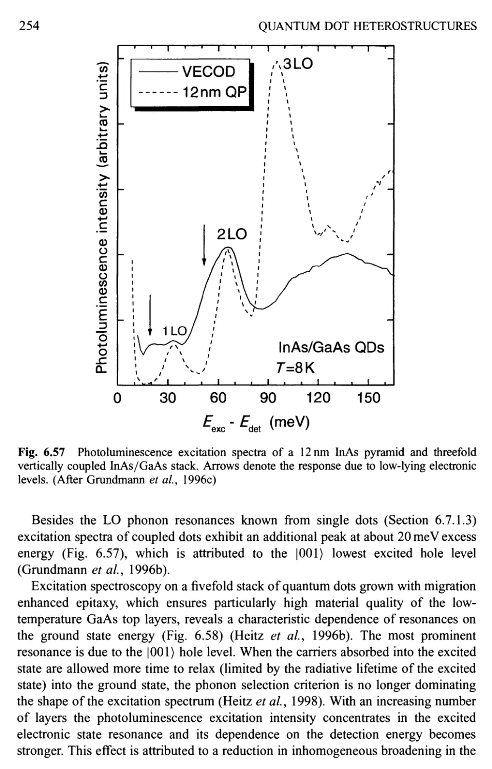
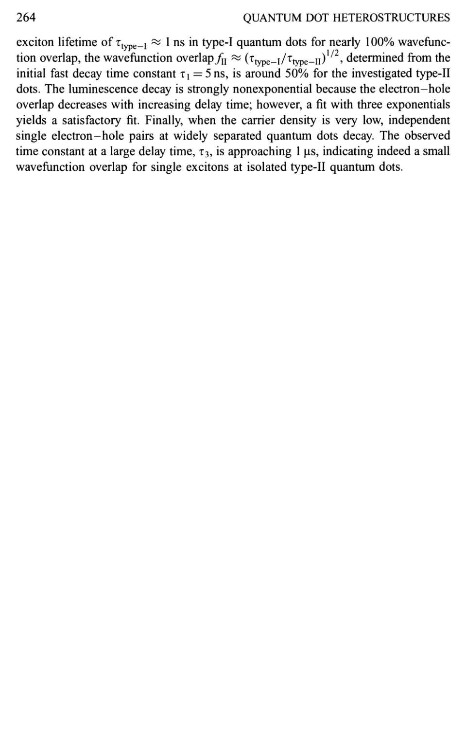
6.7.5 Carrier dynamics 246
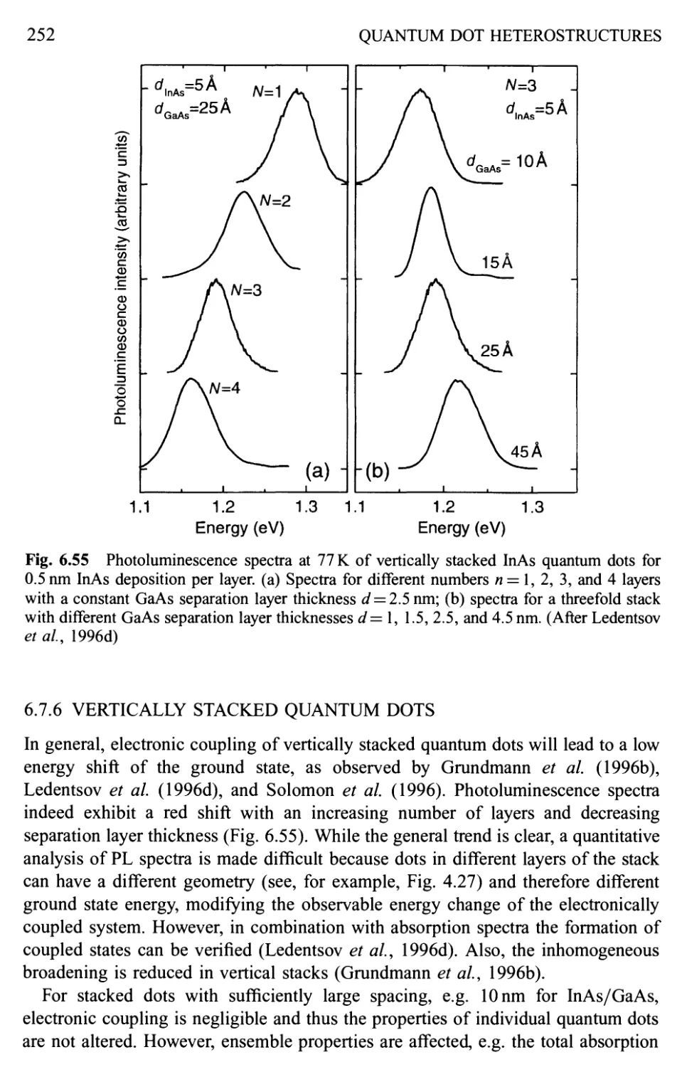
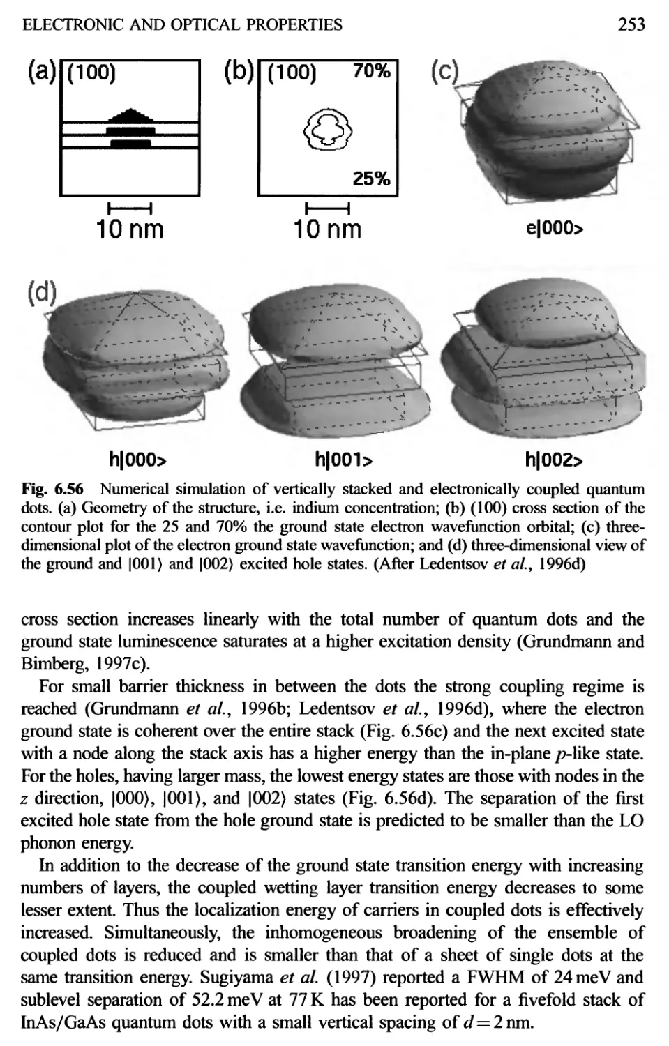
6.7.6 Vertically stacked quantum dots 252
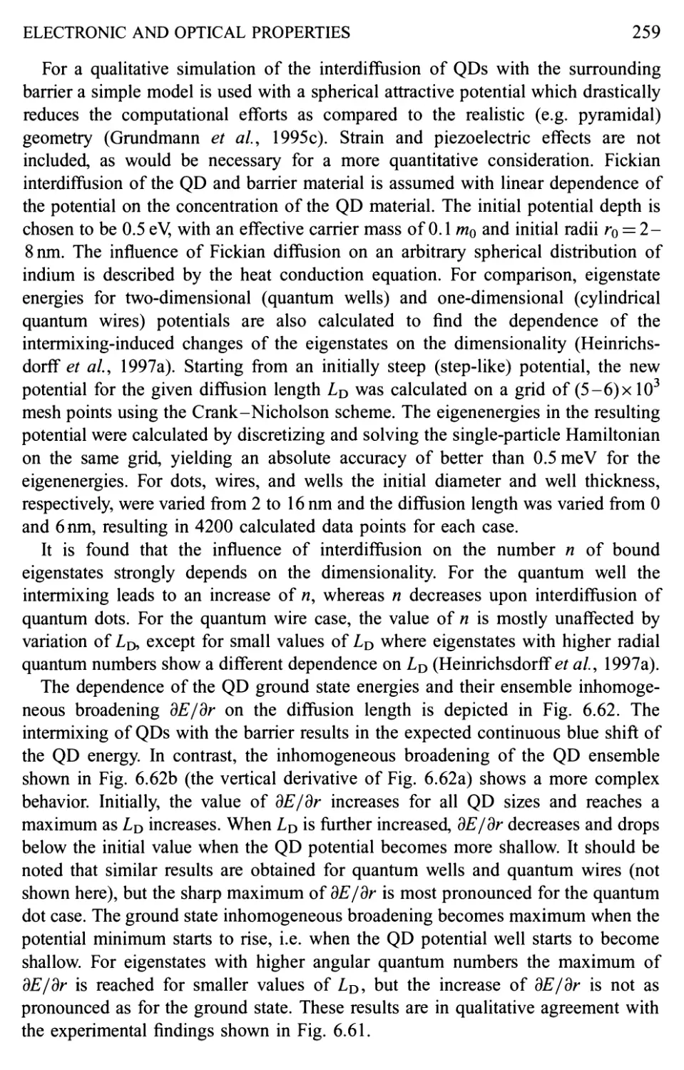
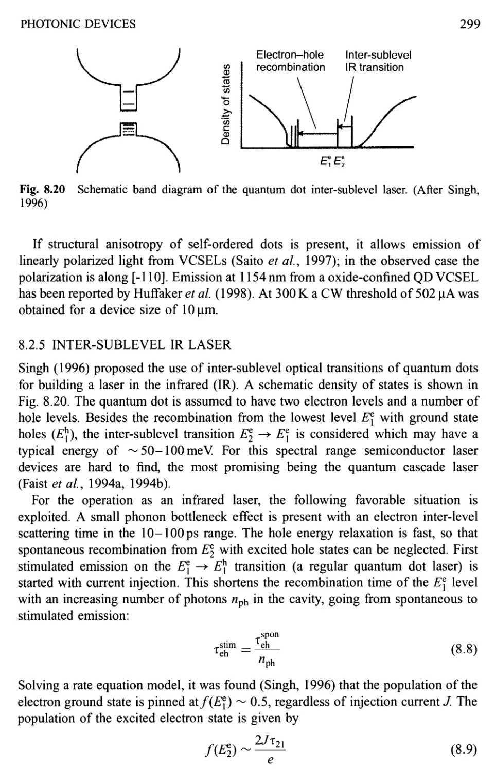
6.7.7 Annealing of quantum dots 255
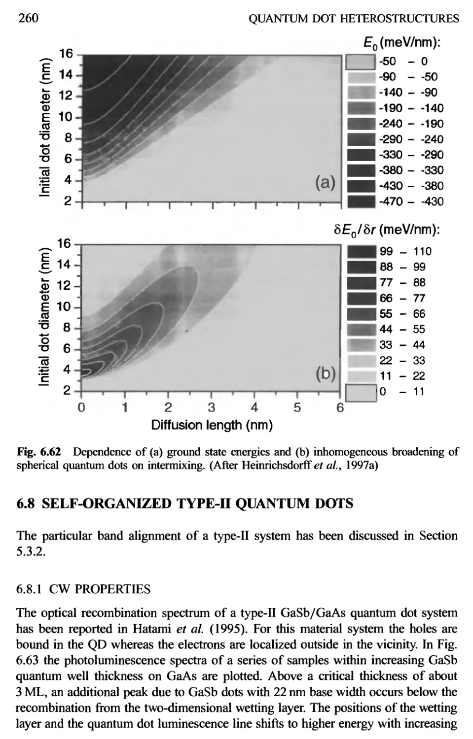
6.8 Self-Organized Type-II Quantum Dots 260
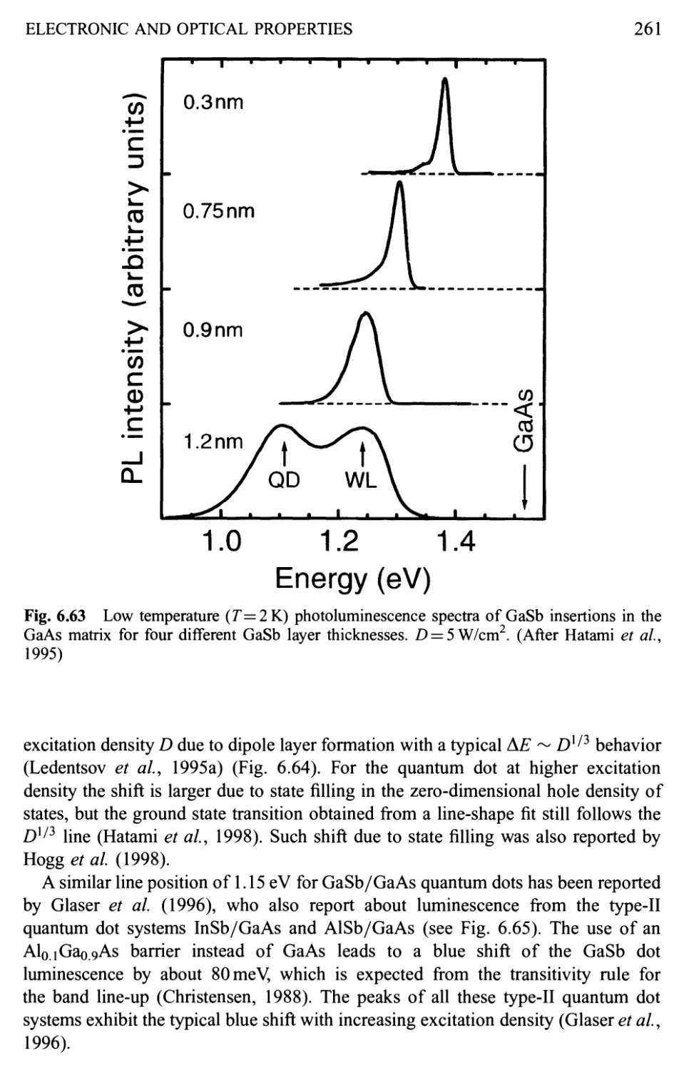
6.8.1 CW properties 260
6.8.2 Time-resolved experiments 262
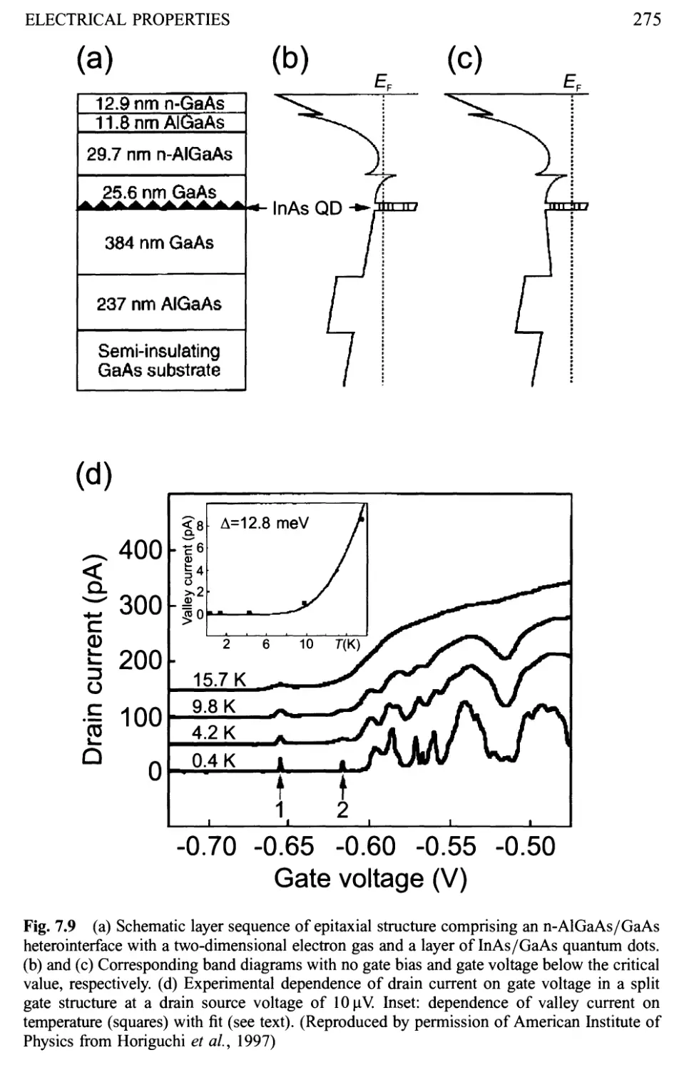
7 Electrical Properties 265
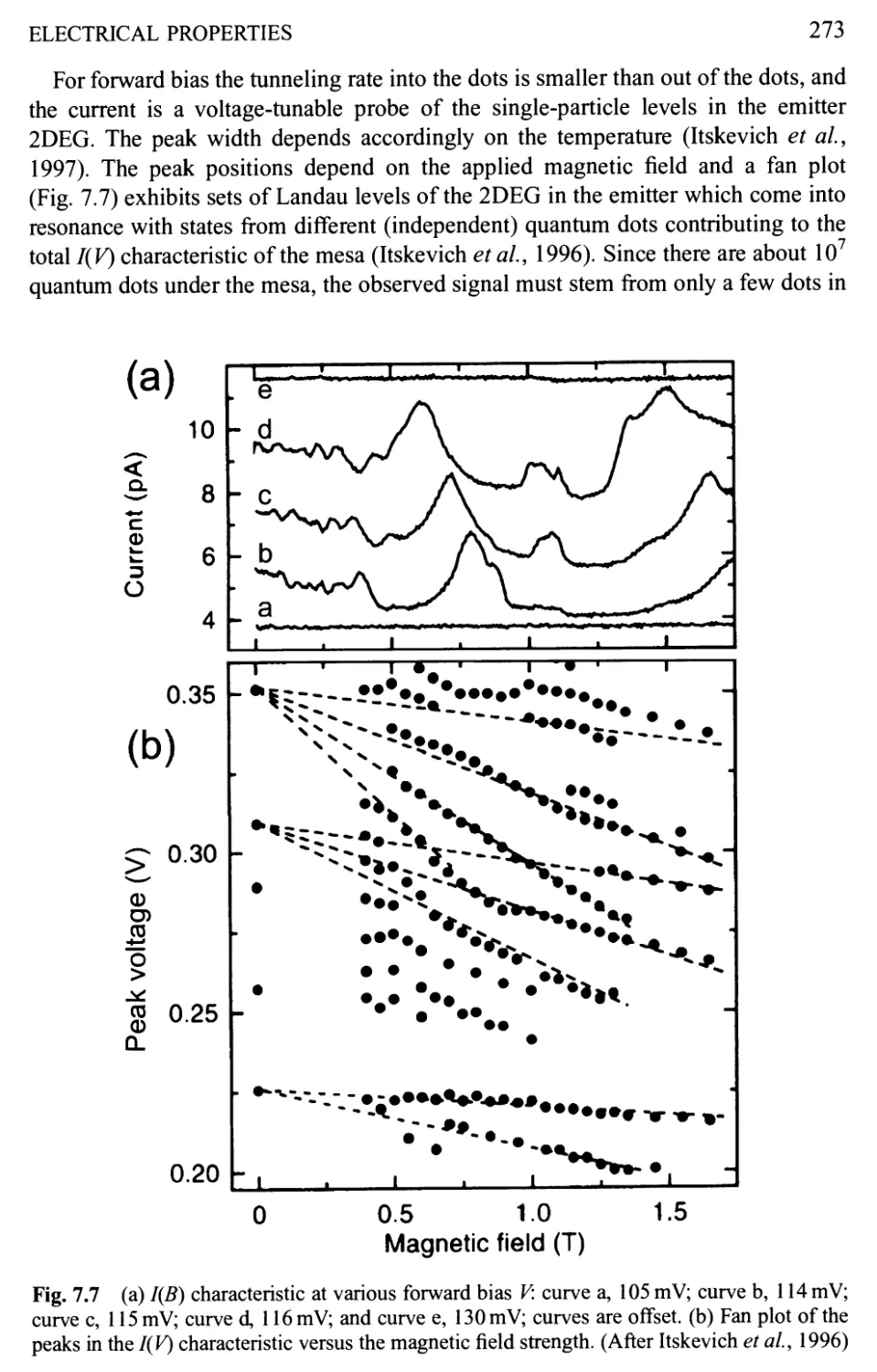
7.1 CV SPECTROSCOPY 265
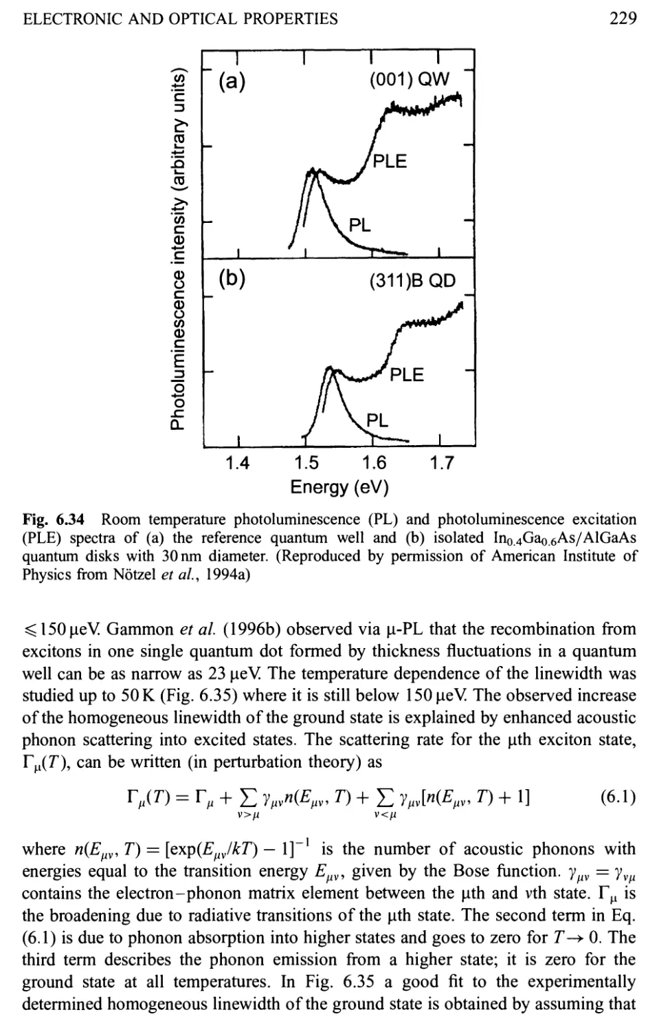
7.2 DLTS 269
7.3 Vertical Tunneling 270
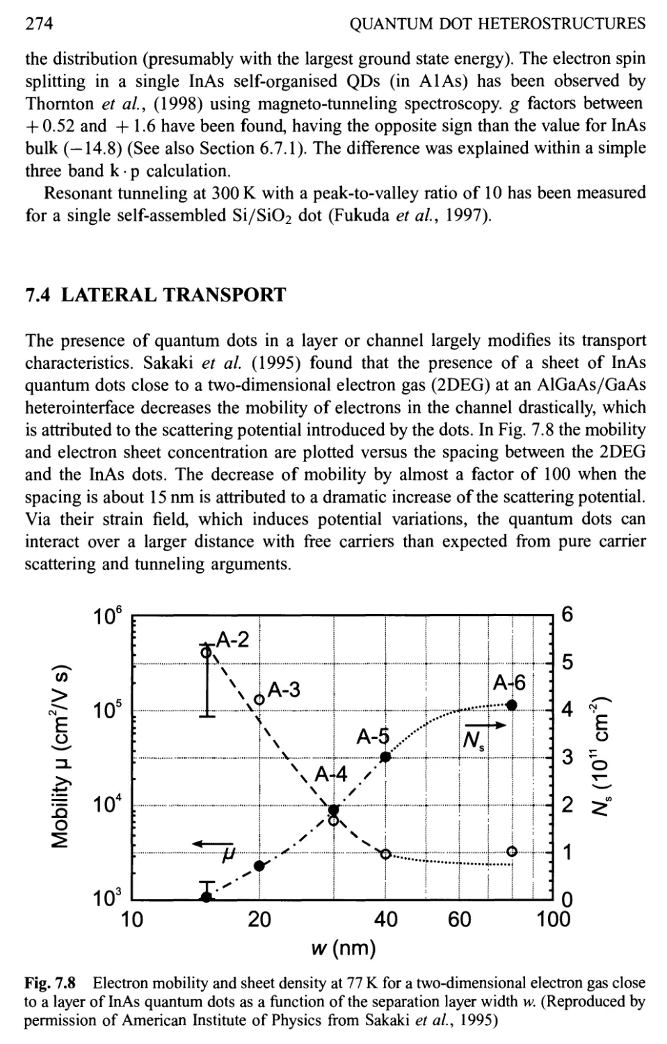
7.4 Lateral Transport 274
8 Photonic Devices 277
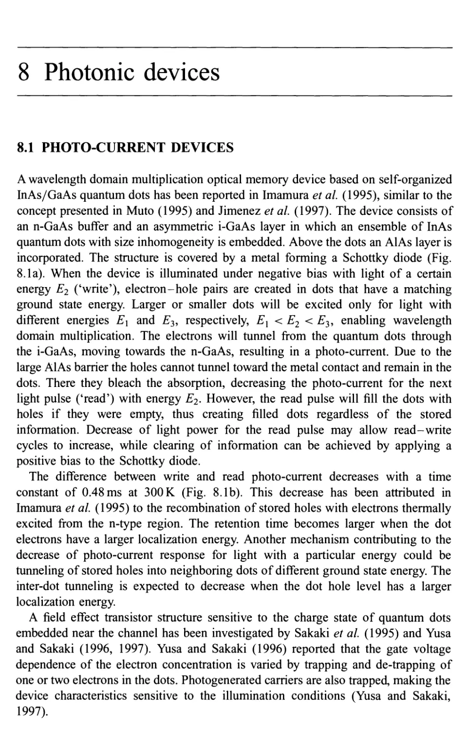
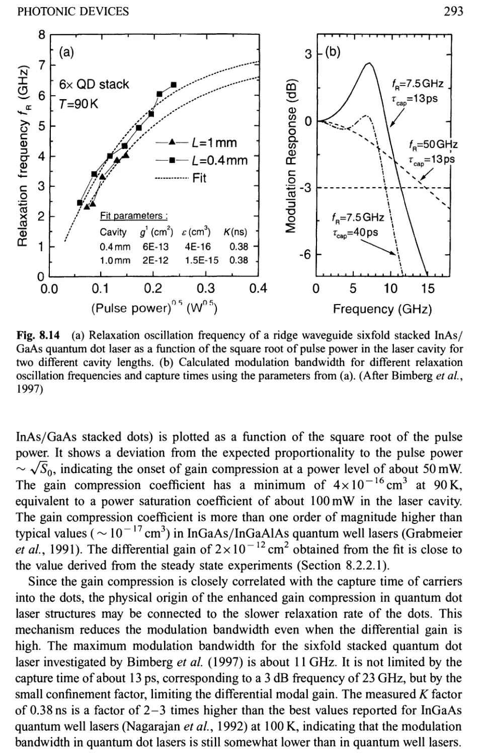
8.1 Photo-Current Devices 277
8.2 Quantum Dot Laser 279
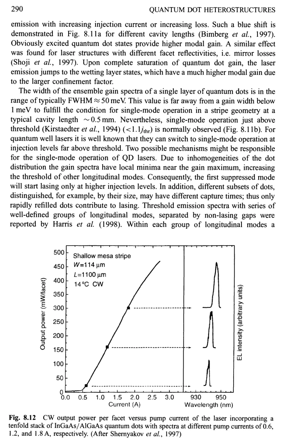
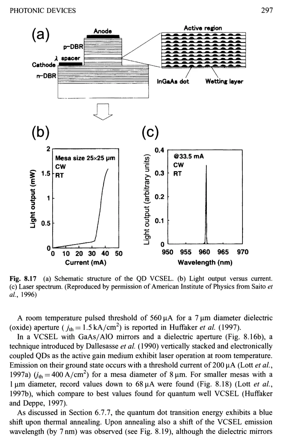
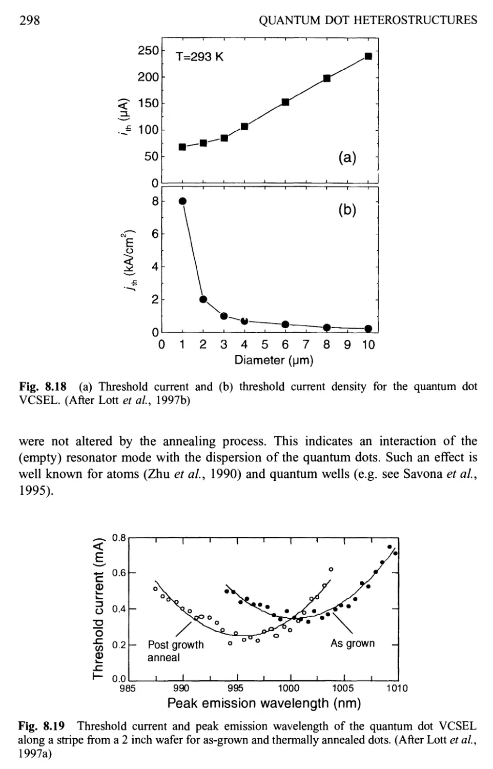
8.2.1 History 279
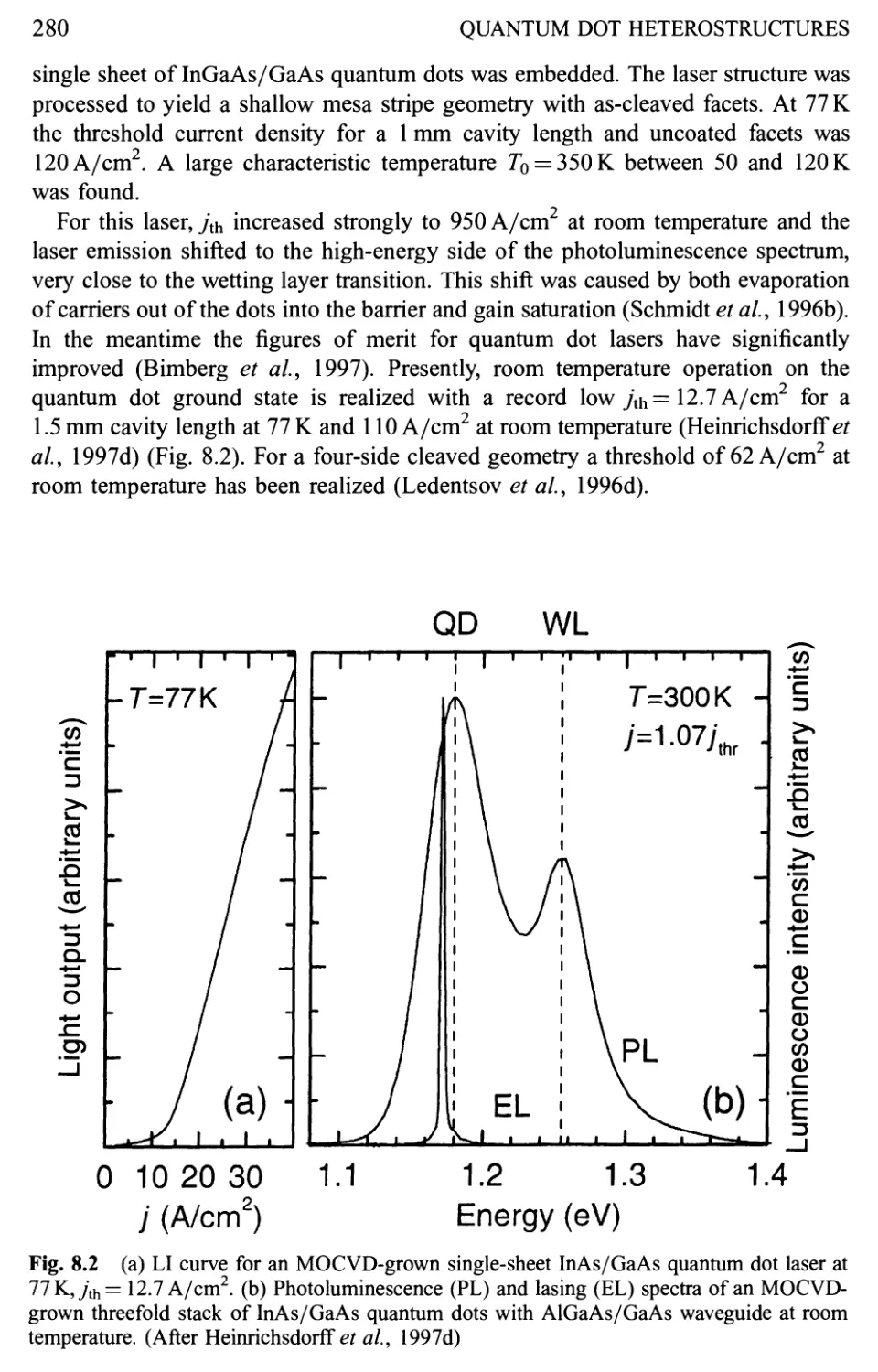
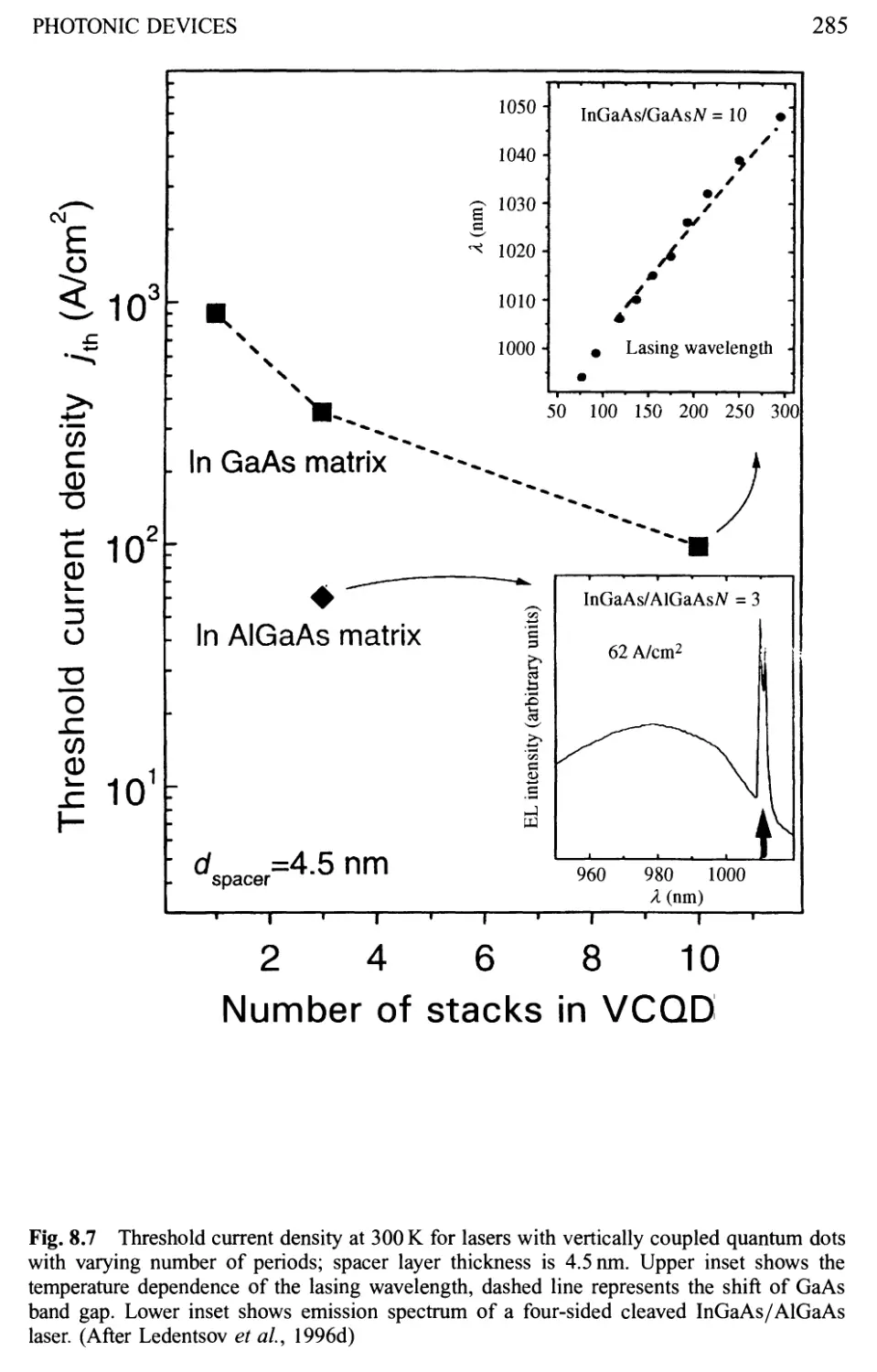
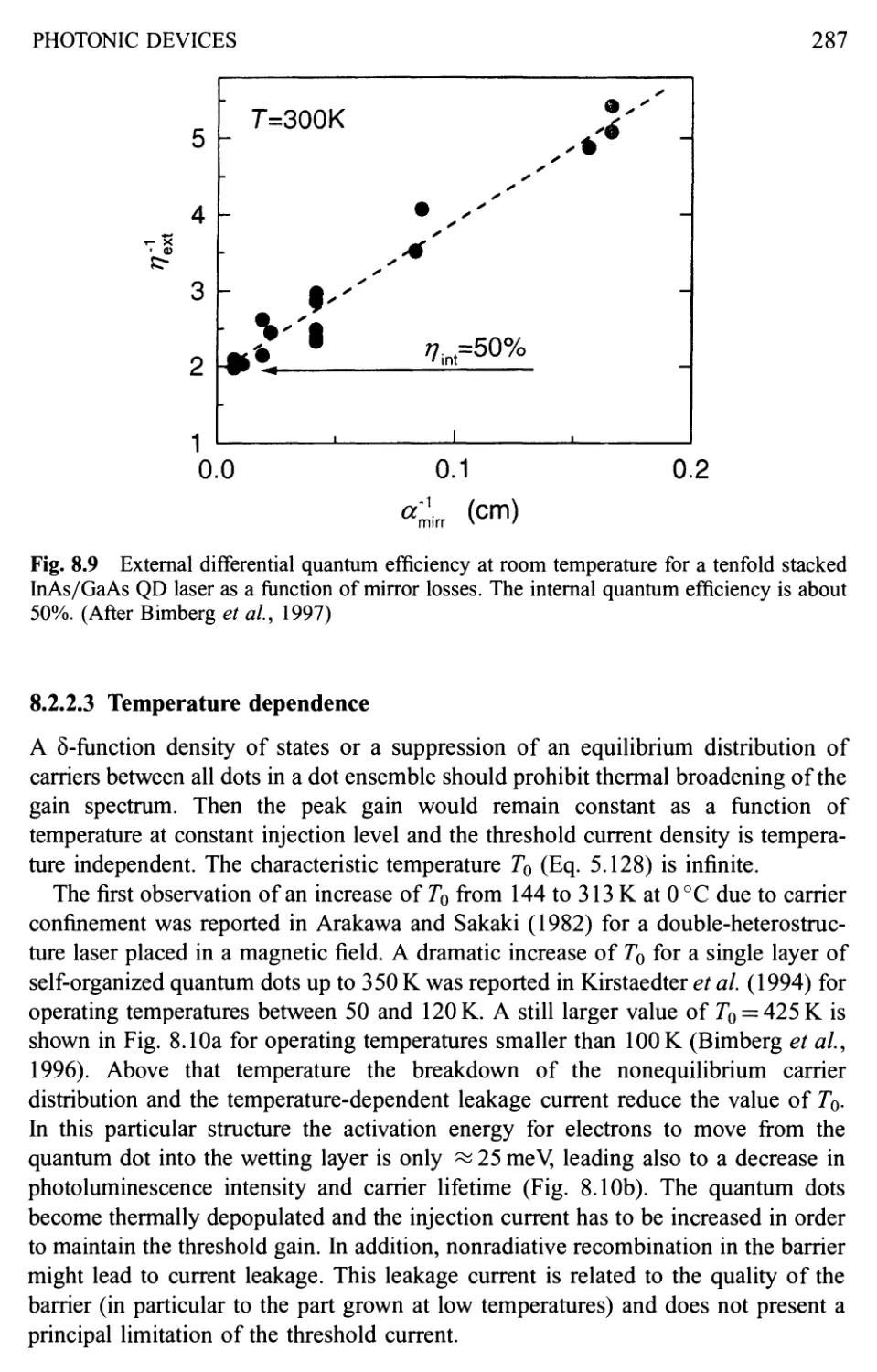
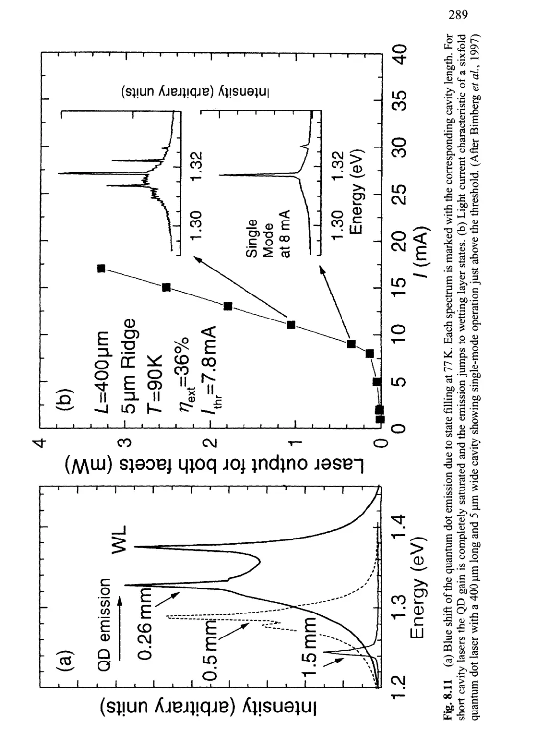
8.2.2 Static laser properties 281
8.2.3 Dynamic laser properties 291
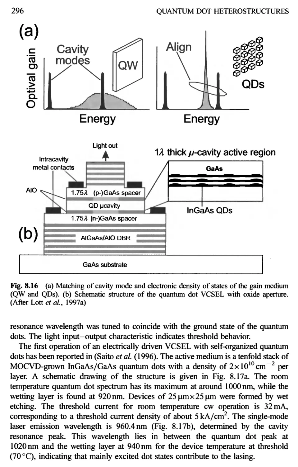
8.2.4 VCSEL 295
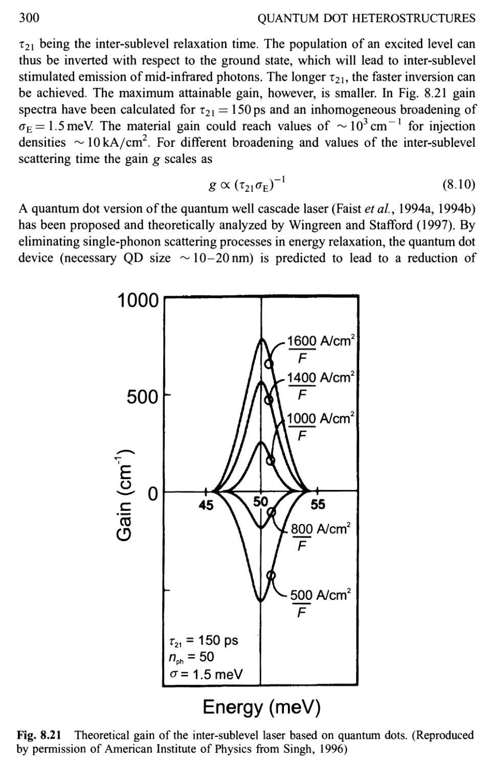
8.2.5 Inter-sublevel IR laser 299
References 303
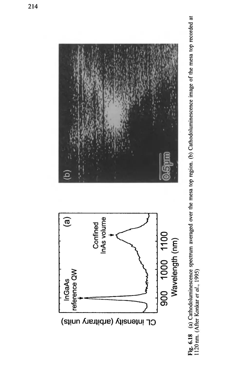
Index 325
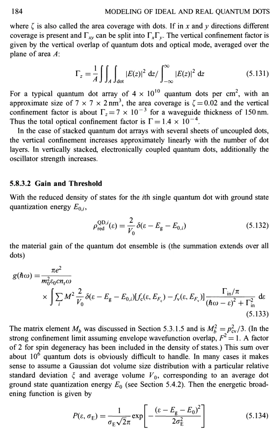
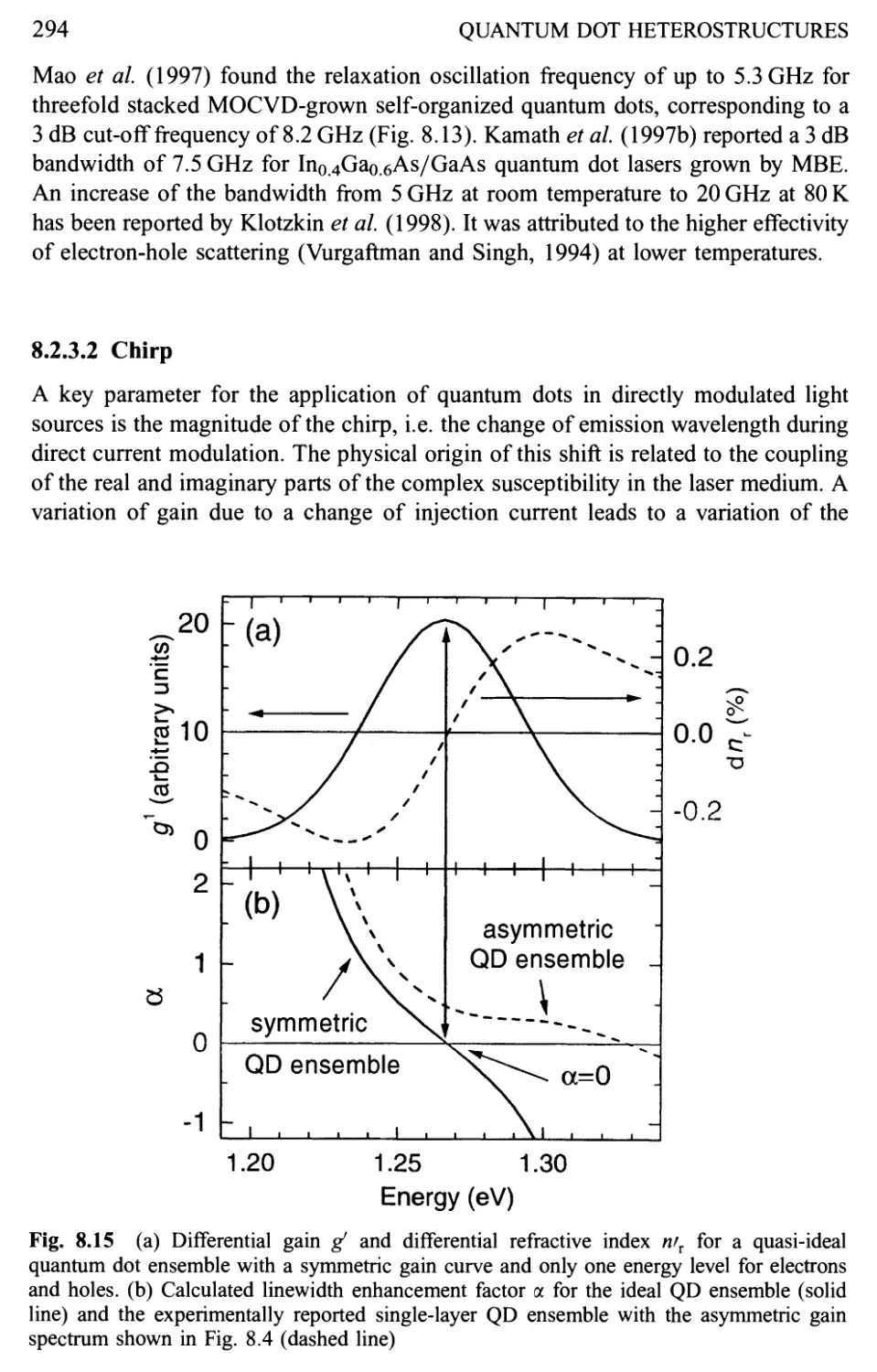
Preface
Quantum dots, coherent inclusions in a semiconductor matrix with truely zero-
dimensional electronic properties, present the utmost challenge and point of
culmination of semiconductor physics. Their properties resemble those of atoms
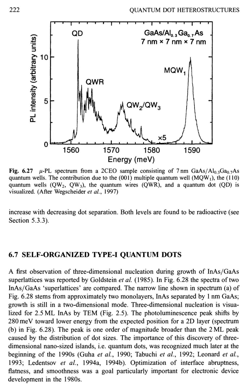
in an electromagnetic cage, rendering possible fascinating novel devices.
It was at the beginning of the 1990s that a modified Stranski-Krastanow growth
mechanism driven by self-organization phenomena at the surface of strongly strained
heterostructures was realized for the fabrication of such dots. This process presents a
sound way to fabricate easily and fast large densities of quantum dots. A rapidly
increasing number of leading laboratories around the world embarked on the
investigation and modeling of the growth, the physical properties, and device
applications of the numerous possible material combinations.
Many fundamental facts and phenomena are now at least qualitatively understood,
but no comprehensive survey exists to guide newcomers to the field. This book tries
to fill this gap. It focuses on phenomena and principles. With regard to collecting all
existing experimental material it is as incomplete as such a work in a rapidly
progressing field necessarily must be.
In Chapter 1 a brief account of the history of quantum dots is given and basic
requirements on their properties for making them useful in devices operating at room
temperature are formulated. Chapter 2 surveys various alternative techniques used in
the past decade to fabricate quantum dots. The chapter ends by introducing the
concept of self-organized growth. The following chapter extends this subject and
presents a broad review of thermodynamically driven self-organization phenomena
at surfaces of crystals.
Results on growth for a number of different quantum dot structures and on their
structural characterization are presented in Chapter 4. Knowledge of the geometric
structure and chemical composition of dots is a prerequisite for numerically
modeling the electronic and optical properties of real dots. Such modeling is
presented in Chapter 5, together with general theoretical considerations on carrier
capture, relaxation and properties of quantum dot lasers.
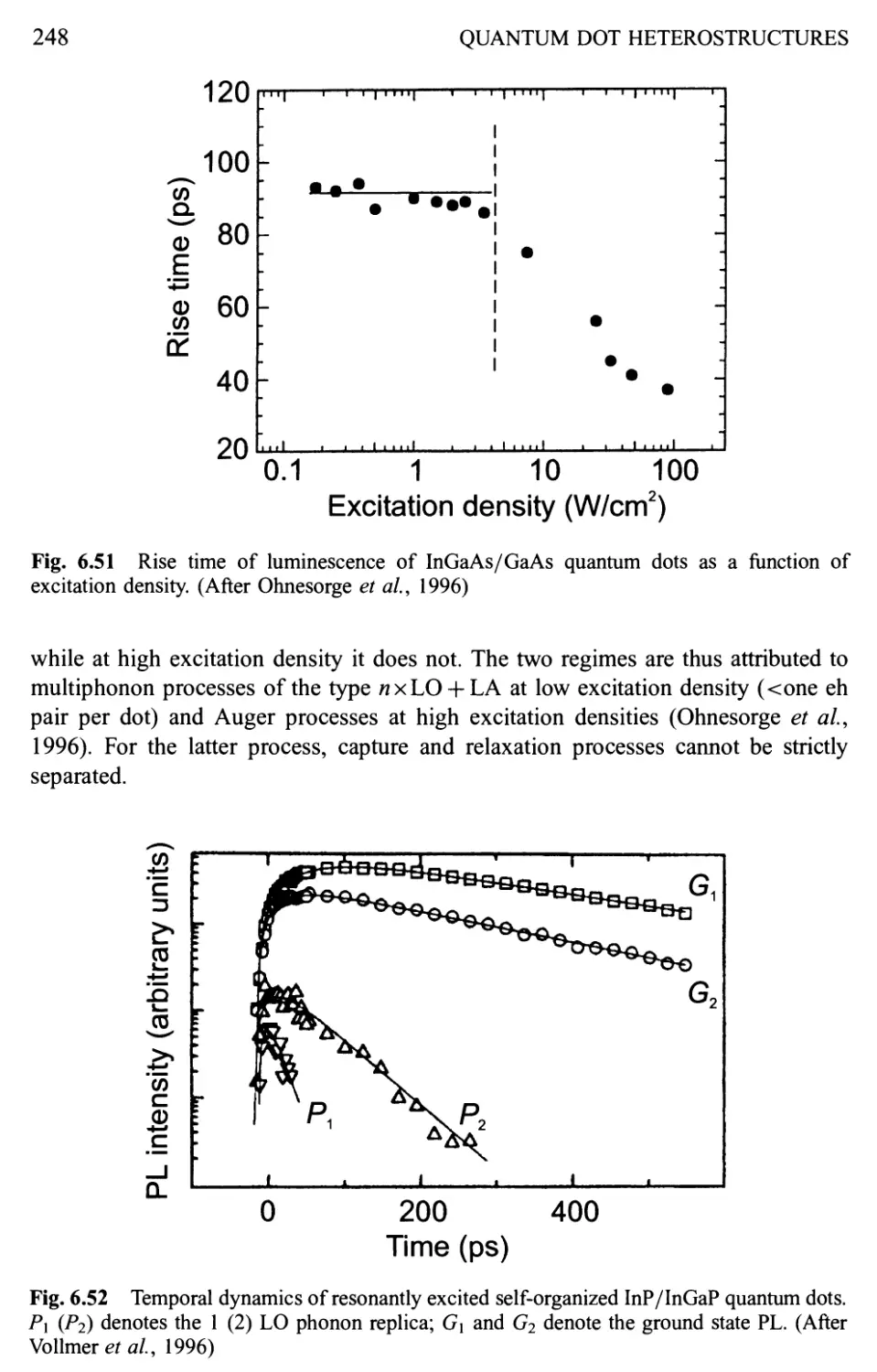
Experimental results on electronic and optical properties are summarized in
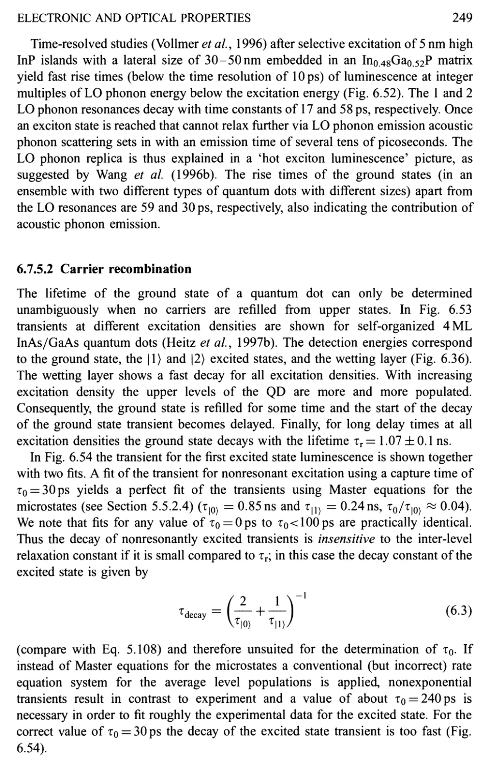
Chapter 6, followed by a rather brief Chapter 7 on electrical properties. The final
chapter, Chapter 8, presents results on quantum dot based photonic devices, mainly
quantum dot lasers.
X
PREFACE
ACKNOWLEDGMENTS
The work of the TU Berlin and Ioffe Institute, St Petersburg, teams, which presents
one backbone of this book, would not have been possible without the generous
support from the Deutsche Forschungsgemeinschaft and the Russian Foundation for
Basic Research. The cooperation and exchange of scientists of the teams were
particularly supported by the Volkswagen Stiftung, the governments of Germany and
Russia in the framework of their general science cooperation agreement, Alexander
von Humboldt Foundation and INTAS. We could not have done our research or
written this book without their help and we are very grateful to the respective
administrations and many anonymous approving project referees.
Many individuals lent us their personal advice. We are particularly grateful to
Zh.I. Alferov, A. Madhukar and M.S. Skolnick. Others contributed by their work as
members of our teams to this book. Particular thanks to V Shchukin for his
contribution to Chapter 3, to J. Bohrer, J. Christen, F. Hatami, F. HeinrichsdorfF,
R. Heitz, A. Hoffmann, C.M.A. Kapteyn, N. Kirstaedter, A. Krost, M.-H. Mao, O.G.
Schmidt, O. Stier, V Tiirck, and M. Veit of TU Berlin, to N.A. Bert, P.N. Brounkov,
A.Yu. Egorov, N.Yu. Gordeev, S.I. Ivanov, I.V Kochnev, VI. Kopchatov, PS. Kop'ev,
A.R. Kovsh, I.L. Krestnikov, A.V Lunev, M.V Maximov, B.Ya. Mel'tser, A.V
Sakharov, Yu.M. Shernyakov, LP. Soshnikov, A.A. Suvurova, A.F. Tsatsul'nikov,
VM. Ustinov, B.V Volovik, S.V Zaitsev, and A.E.Zhukov of the Ioffe Institute, to
G.E. Cirlin, A.O. Golubok, G.M. Guryanov, N.I. Komyak, VN. Petrov of the
Institute for Analytical Instrumentation. St Petersburg, and to U Gosele, J.
Heydenreich, A.O. Kosogov, S.S. Ruvimov, and P. Werner of the Max-Planck
Institut fur Mikrostrukturphysik, Halle/Saale.
D.B.
M.G.
N.N.L.
Berlin, March 1998
1 Introduction
1.1 HISTORICAL DEVELOPMENT
1.1.1 FROM ATOMS TO SOLIDS
By introducing the concept of an electronic 'bandstructure' for an ideal crystalline
solid Bloch (1928) (see the textbooks of Kittel, 1963, and Ibach and Liith, 1991)
presented in the late 1920s a revolution in the world of physics dominated by
research on atoms. In atoms the energies of bound electrons are discrete and
precisely defined within the limit of Heisenberg's uncertainty relation. In solids the
electron energy is a multivalued function of momentum resulting in energy bands,
continuous densities of states, and gaps. The wavefunctions became completely
delocalized in real space. Central in Bloch's theory is an infinite extension of the
regular array of lattice points in all three dimensions of space. The restriction of the
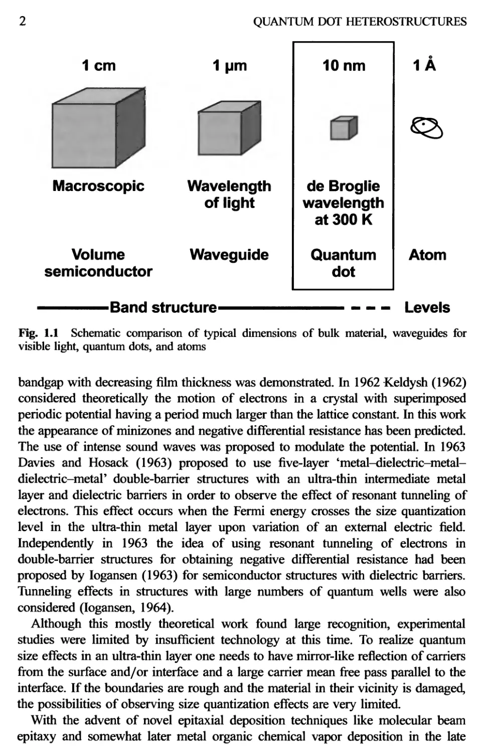
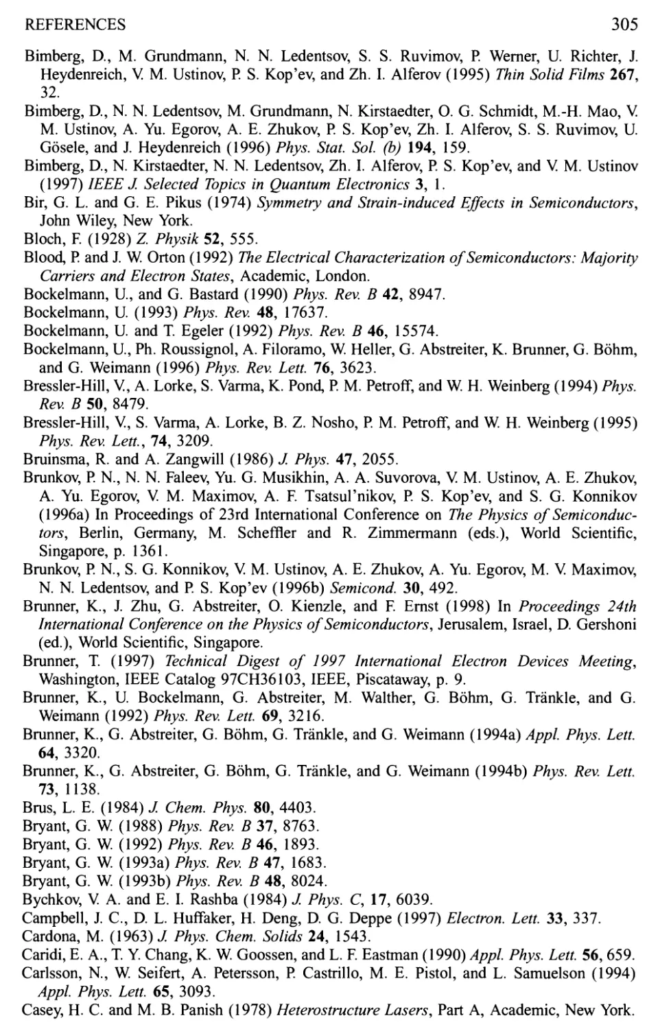
theory to infinite bodies (Fig. 1.1) was regarded as being meaningless from any
practical point of view, except next to surfaces. Still small crystallites of a few
micrometers in size are very large compared to next-neighbor distances. No
observable deviations from the predictions for an infinitely extended crystal were
expected, even for small objects.
1.1.2 FROM SOLIDS TO 2D HETEROSTRUCTURES
If the carrier motion in a solid is limited in a layer of a thickness of the order of the
carrier de Broglie wavelength (or mean free pass, if this number is smaller), one will
observe effects of size quantization. The de Broglie wavelength X depends on the
effective mass m^ of the carrier and on temperature T:
h h 1.22 nm
= P = A^ffkT) = ^(Ekin/[eV]) (,)
The mass of charged carriers entering Eq. (1.1) is not the free electron mass but the
effective mass of the electron (or hole) in the crystal. As this mass can be much
smaller than the free electron mass, size quantization effects can be already
pronounced at a thickness ten to a hundred times larger than the lattice constant.
The idea of using ultra-thin layers for studies of size quantization effects was
already popular by the late 1950s and early 1960s (see the review by Lutskii, 1970).
The main object of research at this time were thin films of semimetals (e.g. Bi) on
mica substrates obtained by vacuum deposition. However, thin films of metals and
semiconductors were also studied. For these films of Bi (Lutskii and Kulik, 1968)
and InSb (Filatov and Karpovich, 1968) the effect of the increase of the effective
2
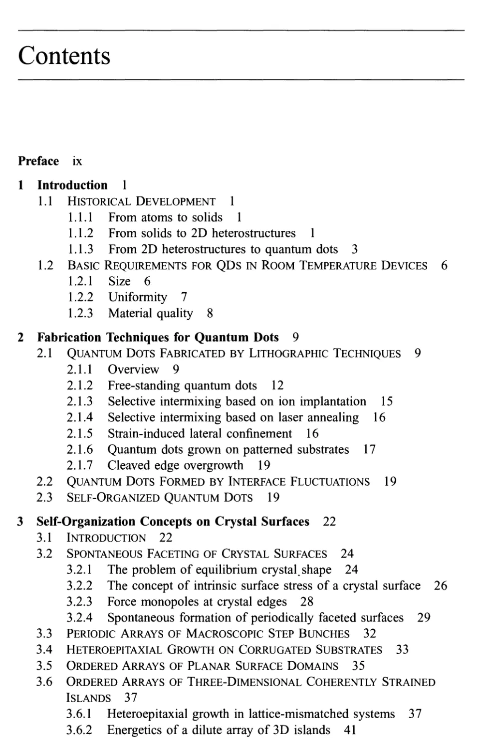
QUANTUM DOT HETEROSTRUCTURES
10 nm I 1A
Q>
de Broglie
wavelength
at 300 K
Quantum Atom
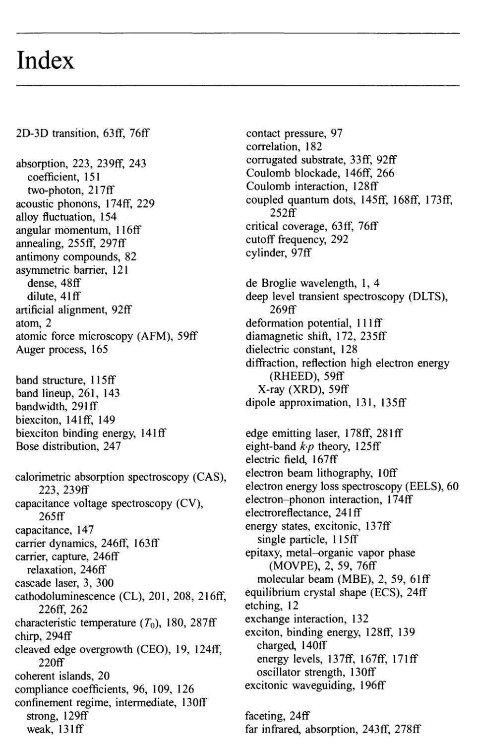
dot
Band structure - - - Levels
Fig. 1.1 Schematic comparison of typical dimensions of bulk material, waveguides for
visible light, quantum dots, and atoms
bandgap with decreasing film thickness was demonstrated. In 1962 Keldysh (1962)
considered theoretically the motion of electrons in a crystal with superimposed
periodic potential having a period much larger than the lattice constant. In this work
the appearance of minizones and negative differential resistance has been predicted.
The use of intense sound waves was proposed to modulate the potential. In 1963
Davies and Hosack (1963) proposed to use five-layer 'metal-dielectric-metal-
dielectric-metaF double-barrier structures with an ultra-thin intermediate metal
layer and dielectric barriers in order to observe the effect of resonant tunneling of
electrons. This effect occurs when the Fermi energy crosses the size quantization
level in the ultra-thin metal layer upon variation of an external electric field.
Independently in 1963 the idea of using resonant tunneling of electrons in
double-barrier structures for obtaining negative differential resistance had been
proposed by Iogansen (1963) for semiconductor structures with dielectric barriers.
Tunneling effects in structures with large numbers of quantum wells were also
considered (Iogansen, 1964).
Although this mostly theoretical work found large recognition, experimental
studies were limited by insufficient technology at this time. To realize quantum
size effects in an ultra-thin layer one needs to have mirror-like reflection of carriers
from the surface and/or interface and a large carrier mean free pass parallel to the
interface. If the boundaries are rough and the material in their vicinity is damaged,
the possibilities of observing size quantization effects are very limited.
With the advent of novel epitaxial deposition techniques like molecular beam
epitaxy and somewhat later metal organic chemical vapor deposition in the late
1 cm
1 |jm
Macroscopic Wavelength
of light
Volume Waveguide
semiconductor
INTRODUCTION
3
1960s the counter-revolution started. Suddenly it was possible to insert coherent
layers, a few lattice constants thick, of a semiconductor of lower bandgap in a matrix
with a larger bandgap, restricting carrier movement to only two dimensions. In
1969-70 Esaki and Tsu proposed the use of multilayer periodic semiconductor
heterostructures (superlattices) for the creation of artificial materials with controlled
width of minizones for carrier transport along the superlattice axis (Esaki and Tsu,
1970). They also proposed formation of delocalized states and negative differential
resistance for high-speed electrons reaching the minizone boundary in nipi super-
lattices and quantum wells. Another important effect regarding device applications is
sequential tunneling in superlattices that was considered first by Kazarinov and Suris
in 1970 (Kazarinov and Suris, 1971, 1972). One of the first of these superlattices was
grown, also in 1970, by Alferov in the GaPojAso^/GaAs material system (Alferov
etal, 1971). A clear demonstration of size quantization effects became possible only
after lattice-matched GaAs/AlGaAs structures with planar interfaces were realized
by molecular beam epitaxy. In 1974 Chang et al (1974) observed the effect of
resonant tunneling, proving the application of quantum mechanics to describe
transport phenomena in ultra-thin semiconductor heterostructures. The possibility
of creating unipolar long-wavelength laser using radiative transitions between
electron size quantization subbands was also considered at that time (Kazarinov
and Suris, 1971). Such lasers, so-called 'cascade' lasers, have been realized one
quarter of a century later (Faist et al, 1994a, 1994b). The extended possibilities for
bandgap engineering by using strained quantum wells were described in Osbourn
(1982).
Particularly impressive results have arisen from optical studies of quantum wells
and superlattices. In 1974 Dingle et al. (1974) directly observed the step-like
character of the absorption spectrum related to the two-dimensional character of
the density of states in quantum wells (Fig. 1.2). A decrease in the GaAs layer
thickness resulted in a shift of the steps toward higher photon energies. Optical
studies also underlined the tremendously increased role of excitonic effects (Christen
and Bimberg, 1990; Christen et al, 1990) and demonstrated zero-dimensional
properties of excitons localized in potential fluctuations of quantum wells. Much
increased exciton binding energies, oscillator strengths and temperature stability of
excitons were demonstrated. Excitonic effects were found to be of supreme
importance for some device applications, such as optical modulators or optical
bistable elements (Miller et al, 1984; Miller, 1990).
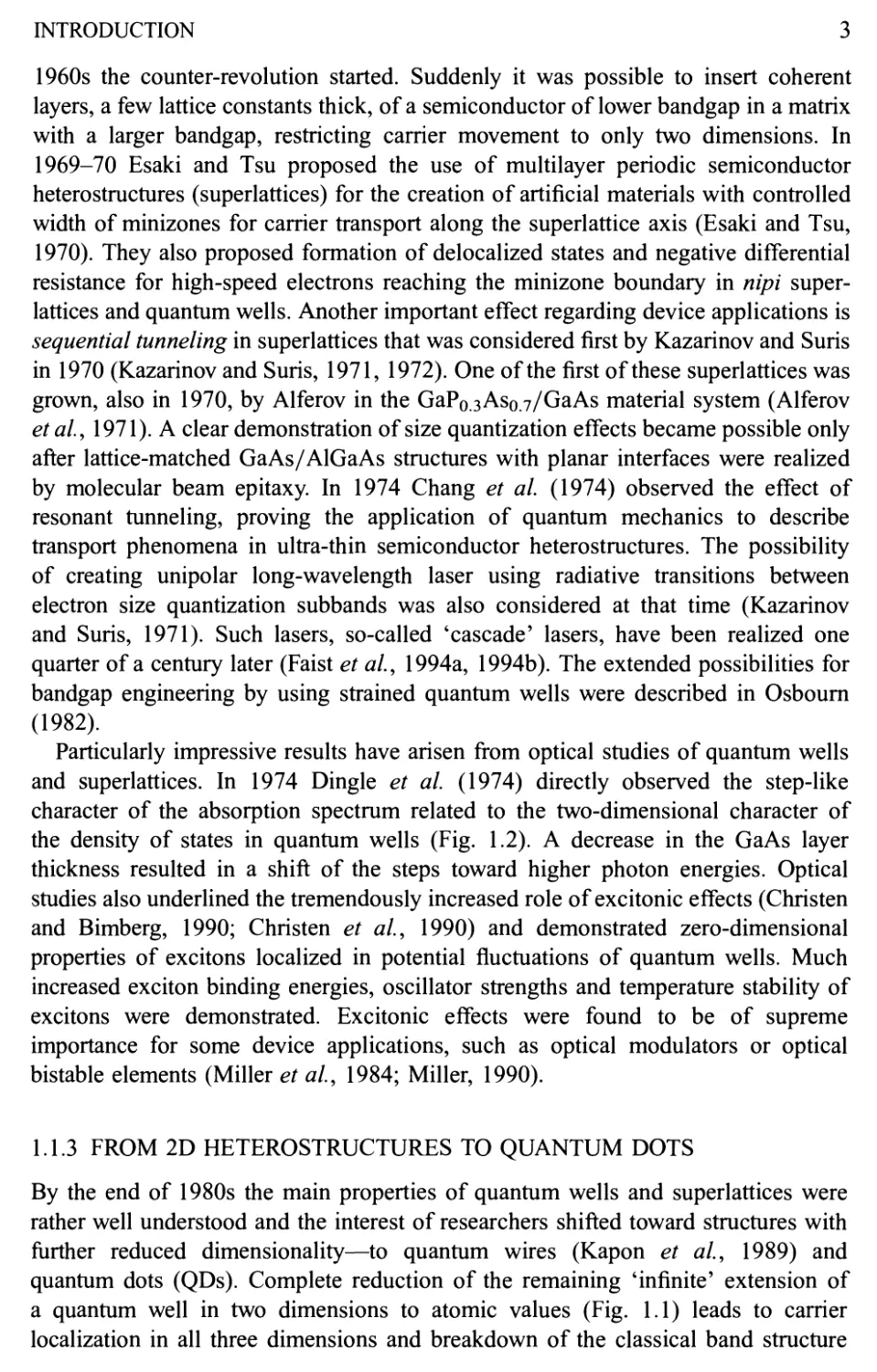
1.1.3 FROM 2D HETEROSTRUCTURES TO QUANTUM DOTS
By the end of 1980s the main properties of quantum wells and superlattices were
rather well understood and the interest of researchers shifted toward structures with
further reduced dimensionality—to quantum wires (Kapon et al, 1989) and
quantum dots (QDs). Complete reduction of the remaining 'infinite' extension of
a quantum well in two dimensions to atomic values (Fig. 1.1) leads to carrier
localization in all three dimensions and breakdown of the classical band structure
4
QUANTUM DOT HETEROSTRUCTURES
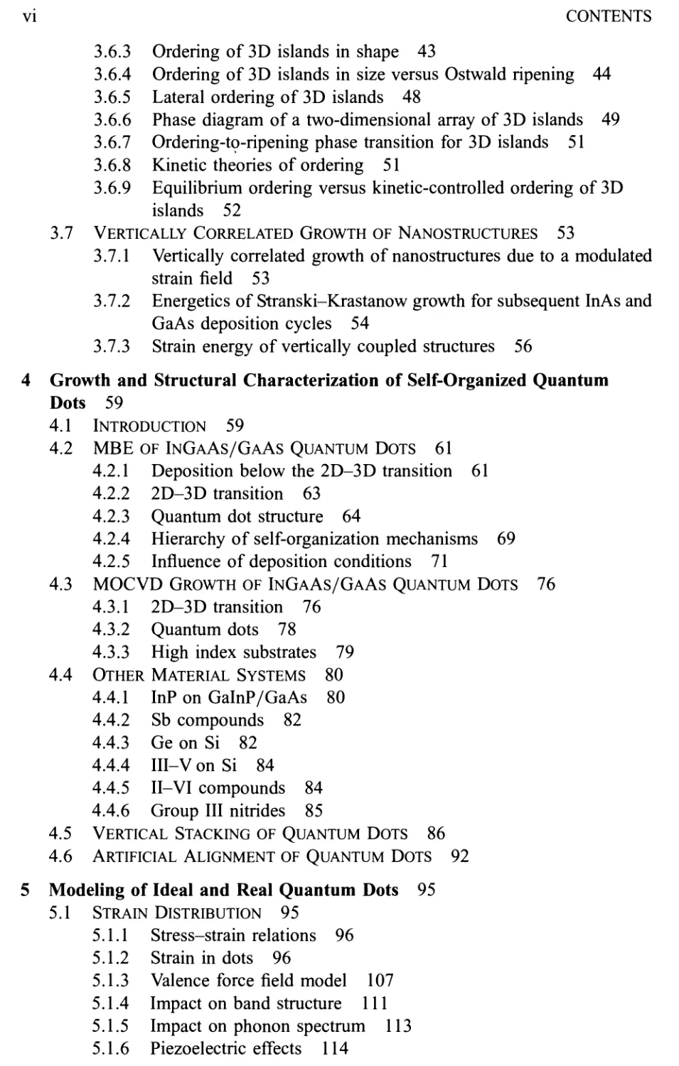
Bulk
^
X
/
Film
y
Dot
^
b
s\
-J
E
D(E)
4
D(E)
4
-►E
D(E)
►E
/
■^►E
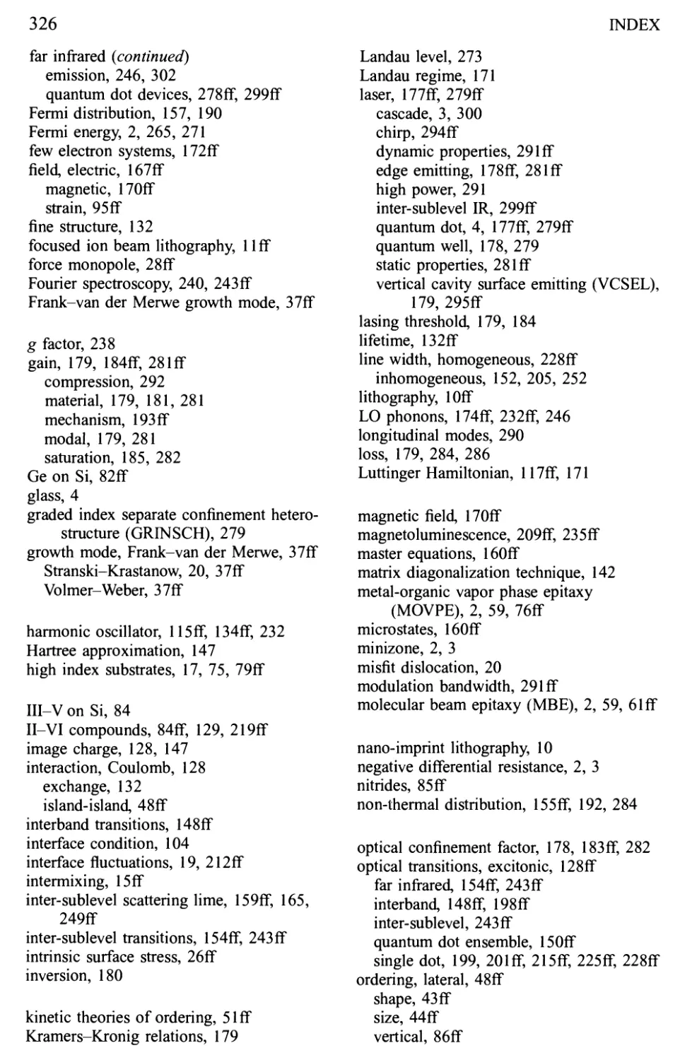
Fig. 1.2 Nature of electronic states in bulk material, quantum wells, and quantum dots. Top
row: schematic morphology, center row: quantized electronic states, bottom row: density of
electronic states
model of a continuous dispersion of energy as a function of momentum. The
resulting energy level structure of quantum dots is discrete (Fig. 1.2), like in atomic
physics, and the physical properties of quantum dots in many, although not all,
respects resemble those of an atom in a cage. A profound size-dependent change of
all macroscopic material properties as compared to the bulk occurs. A qualitative
measure when size quantization effects are important and energy separation of
sublevels is sufficiently large is again the de Broglie wavelength (Eq. 1.1), now
restricting geometry in all three dimensions. A typical size of such a dot is lOnm
and it may still contain 104 or more atoms.
The study of single quantum dots and ensembles of quantum dots presents a new
chapter in fundamental physics. Moreover, many applications of QDs for novel
devices have been predicted, such as single electron transistors or quantum dot
lasers. Such devices have exciting novel properties enabling new concepts and
systems for many different fields of our society, ranging from information
technology to environmental protection.
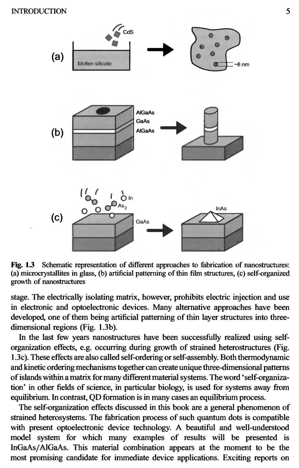
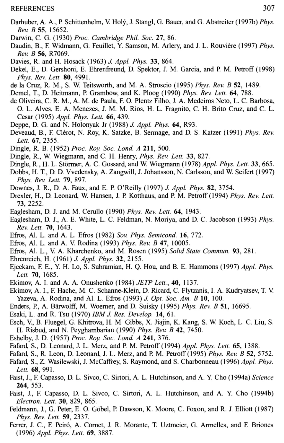
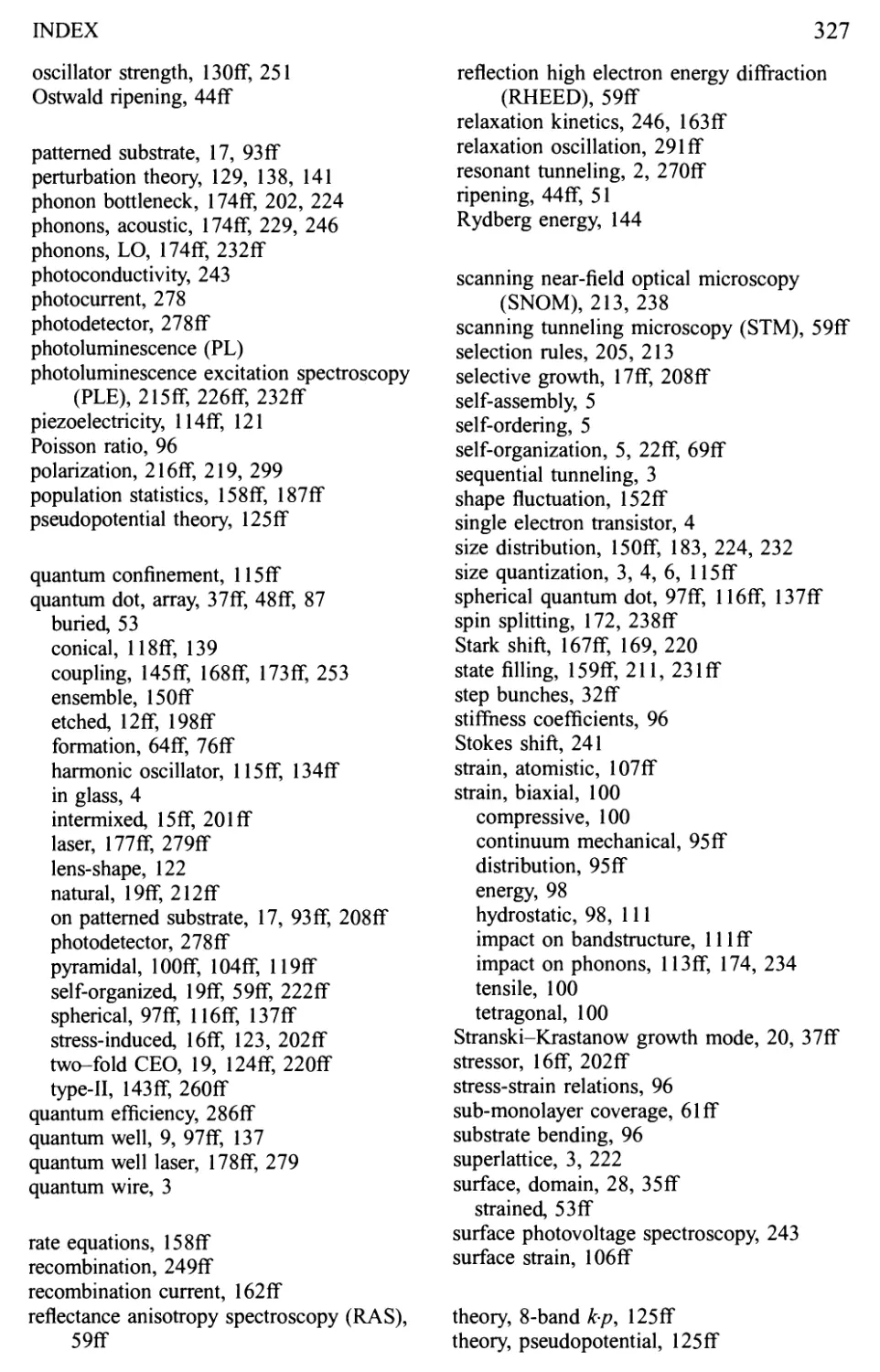
The road to develop quantum dots useful for devices has been full of detours and
obstacles. The first realization of quantum dots were nano-size semiconductor
inclusions (e.g. CdSe) in glass (Rocksby, 1932), which have been commercially
available as color filters for decades (Fig. 1.3a). Quantum confinement effects in
such a system were confirmed experimentally by Ekimov and Onushenko (1984).
The usefulness of such color glasses for switches was investigated at a very early
INTRODUCTION
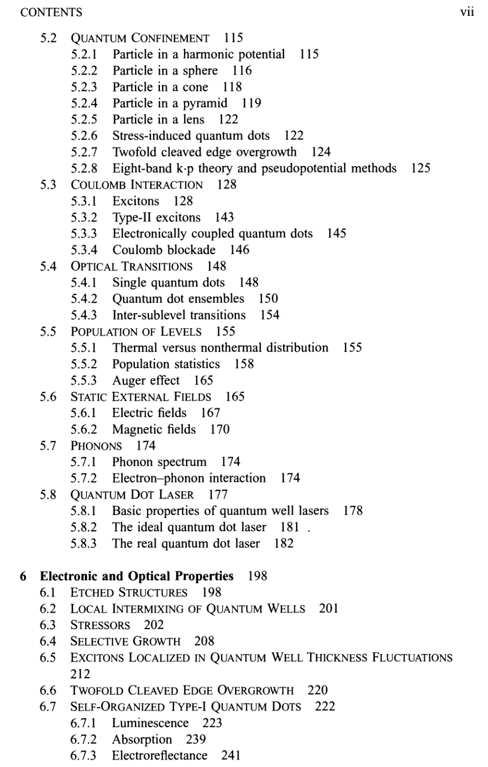
rrr
CdS
(a)
Molten silicate
~8nm
(b)
PI
(c)
[i r . \
°n U°ln
InAs
GaAs
,^s>^i
Fig. 1.3 Schematic representation of different approaches to fabrication of nanostructures:
(a) microcrystallites in glass, (b) artificial patterning of thin film structures, (c) self-organized
growth of nanostructures
stage. The electrically isolating matrix, however, prohibits electric injection and use
in electronic and optoelectronic devices. Many alternative approaches have been
developed, one of them being artificial patterning of thin layer structures into three-
dimensional regions (Fig. 1.3b).
In the last few years nanostructures have been successfully realized using self-
organization effects, e.g. occurring during growth of strained heterostrucrures (Fig.
1.3c). These effects are also called self-ordering or self-assembly. Both thermodynamic
and kinetic ordering mechanisms together can create unique three-dimensional patterns
of islands within a matrix for many different material systems. The word
'self-organization' in other fields of science, in particular biology, is used for systems away from
equilibrium. In contrast, QD formation is in many cases an equilibrium process.
The self-organization effects discussed in this book are a general phenomenon of
strained heterosystems. The fabrication process of such quantum dots is compatible
with present optoelectronic device technology. A beautiful and well-understood
model system for which many examples of results will be presented is
InGaAs/AlGaAs. This material combination appears at the moment to be the
most promising candidate for immediate device applications. Exciting reports on
6
QUANTUM DOT HETEROSTRUCTURES
self-organized quantum dots fabricated in other III—V systems like InP/InGaP, Sb-
containing systems such as (In,Ga)Sb/GaAs, structures based on group III nitrides
like (In,Ga,Al)N, Ge/Si, Si02/Si, and II—VI heterostructures emerge rapidly. In
order to concentrate on the most important physics, unfortunately not all of this work
can be covered here in detail.
1.2 BASIC REQUIREMENTS FOR QDs IN ROOM
TEMPERATURE DEVICES
Quantum dots should fulfill the following requirements in order to make them useful
for devices at room temperature:
(a) Sufficiently deep localizing potential and small QD size is a prerequisite for
observation and utilization of zero-dimensional confinement effects.
(b) QD ensembles should show high uniformity and a high volume filling factor.
(c) The material should be coherent without defects like dislocations.
1.2.1 SIZE
The lower size limit of a QD is given by the condition that at least one energy level
of an electron or hole or both is present. The critical diameter (for a spherical QD)
Anin depends strongly on the band offset of the corresponding bands in the material
system used. An electron level exists in a spherical quantum dot if the confinement
potential, defined by the conduction band offset (in a type-I heterostructure) AEC (see
Eq. 5.41), exceeds the value:
nh
Dmin = V(2< A£c) (L2)
where m* is the effective electron mass. Assuming a conduction band offset value of
~0.3 eV for GaAs/Al0.4Ga0.6As heterostructures, the diameter of the quantum dot
should be larger than 4 nm. This is the lower limit of the QD size. In quantum dots of
this or slightly larger size the separation between the electron level and the barrier
energy is very small, and at finite temperatures thermal evaporation of carriers from
QDs will result in their depletion. For the InAs/AlGaAs system the conduction band
offset is much larger while the electron effective mass is smaller, so the product of
AEcm* is comparable and the critical size is also about 3-5 nm depending on the
nonparabolicity effects in the InAs conduction band.
There also exists a limit for the maximum size of a QD. A thermal population of
higher-lying energy levels is undesirable for particular devices like, for example,
lasers. The condition to limit thermal population of higher-lying levels to 5%^e~3
can be written as
W< Ue$d-E?d) (1.3)
INTRODUCTION
7
Here £f and £2 are me energies of the first and the second levels in the QD,
respectively. This equation establishes an upper limit at room temperature for the
size of GaAs/AlGaAs QDs of M2nm, and of ~20nm for InAs/AlGaAs QDs if
electron levels are considered. This maximum size is, of course, a function of
operating temperature.
Consideration of hole quantization in QDs leads to size limits quite different from
those derived for electrons above. The maximum dot size to achieve sufficient
separation between hole sublevels at room temperature according to Eq. (1.3) should
be 5-6 nm for both material systems discussed above. This means that quantum dots
with sufficient sublevel separation for both electrons and holes (at room
temperature) are difficult to realize in most III—V material systems like GaAs/AlGaAs and
InAs/AlGaAs because of the large electron/hole mass ratio. For electrical
applications, where confinement has to be realized only for one sort of carrier, the problem
of different size requirements for simultaneous efficient hole and electron
confinement does not exist. In group III nitride and II-VI materials, having more similar
electron and hole masses, strong localization of both carrier types seems to be
possible.
1.2.2 UNIFORMITY
If a single device is based on more than one quantum dot, the issue of uniformity
arises. Even if an individual device is based on one single quantum dot, uniformity is
important in order to attain similar characteristics for different devices. In principle,
all structural parameters of a QD such as size, shape, and chemical composition are
subject to random fluctuations, even in the presence of ordering mechanisms. In
most cases a dense array of equisized and equishaped quantum dots is desired.
The main impact of size fluctuations is a variation in the energy position of
electronic levels. Such variation is typically Gaussian (Section 5.4.2). For a device
that relies on the integrated gain in a narrow energy range, such as a quantum dot
laser (Sections 5.4 and 8.2), the inhomogeneous energetic broadening should be as
small as possible. This means that for a given average size of the QDs one needs to
ensure the smallest possible size and shape dispersion values. If wavelength
multiplexing is attempted, a certain width of the distribution of energetic levels is desired
(e.g. see Section 8.1). In order to realize a reasonable width of a QD ensemble
luminescence spectrum, comparable to that of a quantum well (QW) at room
temperature (20-30 meV) for a GaAs QD size of about lOnm, one needs to have
a size dispersion lower than 1 nm.
If device operation is based on many quantum dots, typically a minimum number
of dots is necessary to obtain a given performance, e.g. a QD laser needs a certain
minimum number of QDs to overcome the losses. Those dots have to be packed into
a given volume, making it a prerequisite to achieve a minimum packing density or
volume filling factor.
8 QUANTUM DOT HETEROSTRUCTURES
1.2.3 MATERIAL QUALITY
The density of defects in a QD material and its interface to the surrounding matrix
should be as low as possible, on the level of in situ grown quantum wells and
interfaces used in state-of-the-art devices. QD fabrication using self-organized
growth seems to be predestined to achieve this goal since all interfaces are
formed in situ during crystal growth.
2 Fabrication Techniques for Quantum
Dots
Since the 1980s considerable efforts have been devoted to the realization of
semiconductor heterostructures that provide carrier confinement in all three
directions and behave as electronic quantum dots. Initially, mainly techniques like
lithographic patterning and etching of quantum well structures (Section 2.1.2)
have been employed. Technologically related techniques include selective
intermixing of quantum wells (Sections 2.1.3 and 2.1.4) and the use of stressors (Section
2.1.5). Substrate encoded epitaxy, which allows the fabrication of small nanostruc-
tures from a much larger template, is discussed in Section 2.1.6.
Interface fluctuations in quantum wells can also cause three-dimensional
confinement, similar to quantum dots, when 2D excitons become completely localized in
space at low temperatures (Section 2.2). Self-organized formation of quantum dots
without any artificial patterning is the main focus of this book, which is historically
the most recent technique and discussed in Section 2.3.
2.1 QUANTUM DOTS FABRICATED BY LITHOGRAPHIC
TECHNIQUES
2.1.1 OVERVIEW
By the end of the 1980s the fabrication of QDs by patterning of quantum wells was
considered to be the most straightforward way of QD fabrication. Patterning has
several advantages and still attracts much attention because:
(a) QDs of almost arbitrary lateral shape, size and arrangement can be realized
depending on the resolution of the particular lithographic technique used.
(b) A variety of processing techniques, like dry and wet etching, that are
continuously improved are at the researcher's disposal.
(c) It is generally compatible with modern VLSI (very large scale integrated)
semiconductor technology.
Lithographic techniques comprise (Forchel et al.9 1988; Beaumount, 1991;
Sotomayor Torres et al.9 1994):
(a) optical lithography and holography,
(b) X-ray lithography,
(c) electron and focused ion beam lithography (EBL, FIBL),
(d) scanning tunneling microscopy (STM).
10
QUANTUM DOT HETEROSTRUCTURES
Optical lithography, e.g. based on excimer lasers, presently provides resolution
below 0.2 um. Improvements of resolution below the lOOnm range have been
predicted (Brunner, 1997). Current developments concentrate on UV optics and
resists with steep photosensitivity curve and exposure close to the photosensitivity
threshold. Overdeveloping a resist can also reduce the size of a confining potential.
Subsequent photoresist deposition steps, where the mask is shifted laterally, also
reduce the characteristic dimensions of the resulting pattern. Resolution of optical
lithography based methods will nevertheless not be sufficient in the foreseeable
future to fabricate structures of lateral dimensions of 20 nm or less. A maximum size
of ~20nm is required such that carriers are still sufficiently confined at room
temperature in typical semiconductors. Optical lithography, however, can be applied
for fabrication of structures investigated only at low temperatures where confinement
is easily reached and for fabrication of patterned substrates that can be used
subsequently, e.g. for 'substrate encoded growth' of quantum dots.
X-ray lithography (Warren et al, 1986; IBM, 1993) has the advantage of much
shorter wavelengths and can be used for nanostructure fabrication. X-ray lithography
represents a contact printing process, since high-resolution X-ray lenses are
presently not available. An additional process is required to fabricate the mask. A
big advantage of X-ray lithography is in its potential to mass produce nanoscale
structures.
For direct lateral patterning the most developed approaches are electron beam
lithography (Howard et al, 1985; Beaumount, 1991), focused ion beam lithography
(Komuro et al, 1983), as discussed below, and contact imprinting (Krauss, 1997).
Scanning tunneling microscope techniques present novel approaches for creating
nanoscopic patterns and structures (Snow et al, 1993; Snow and Campbell, 1994).
The lack of parallelism is yet a problem remaining to be solved.
2.1.1.1 Electron beam lithography
The electron beam is usually emitted from a high-brightness cathode (e.g. LaB6) or a
field emission gun (cold emission) and focused on the substrate by a multilens
system. To define a focus in the nanometer range a short working distance between
the final lens and the substrate is required. Resolution in the 10-20nm range has
been already demonstrated at the beginning of the 1980s (Craighead et al, 1983;
Stern et al, 1984).
Computer control is employed to scan the beam over the surface and to define the
image. To minimize the working distance and to obtain large scanning fields the
deflection system is usually placed in the final lens. Typical deflection fields for high
resolution lithography machines are about lOOum x 100 um when addressed in
reasonable time. For beam currents in the lOpA range a focus diameter of 8nm can
be maintained throughout this field at an accelerating voltage of 50 kV. The address
grid resolution in a high-resolution field is 2.5 nm or even smaller. In order to
minimize distortion effects which occur in the electron beam exposure over large
fields all modern systems are equipped with appropriate software correction
FABRICATION TECHNIQUES FOR QUANTUM DOTS
11
algorithms. Laser-controlled interferometers can stitch adjacent fields with an
accuracy of a few nanometers. The final resolution of the process of around
lOnm is limited by the resists due to finite length of the organic molecules and
the grain size.
A novel way to improved resolution is 'mask' formation without resists. Ultrathin
layers of a material having high-temperature stability (e.g. 1 ML thick AlAs film on
GaAs) is sufficient to suppress the thermal evaporation of the underlying material.
Local formation of such 'masks' can be realized by using electron-stimulated
adsorption or desorption processes. Similar protective layers can also be used for
selective gas etching of structures and for electron-beam-stimulated epitaxy. These
techniques, however, are not sufficiently developed at present and there is still a long
way to go before the full potential of electron beam lithography can be realized in
practice.
Periodic nanostructures can also be fabricated using an electron beam interference
technique (Fujita et ai, 1995), which is particularly advantageous for mass-scale
fabrication of quantum wires and dots.
2.1.1.2 Focused ion beam lithography
Focused ion beam lithography has a number of properties advantageous for the
fabrication of nanostructures, although the present minimum beam diameter of
^30nm is somewhat larger than that of an electron beam. FIBL can be used for:
(a) maskless etching (ion beam sputtering or stimulated chemical etching),
(b) maskless implantation of dopants,
(c) deposition of metallic structures,
(d) patterning of resists with strongly reduced proximity effect
Ion beam lithography is conceptually very similar to electron beam lithography.
Its success is based on the realization of bright liquid metal ion sources. Such a
source typically consists of a tungsten needle emerged in a reservoir with liquid
metal and wetted by it. Due to capillary effects a very uniform and sharp metal tip is
formed. Metal sources are either elemental (e.g. Ga) or alloy (e.g. Au/Be/Si)
materials. The electric field applied to the tip extracts an intense beam of ions which
is focused by a series of lenses. The extracted particles have a large mass/charge
ratio, requiring magnetic fields for focusing that are larger than those generated by
conventional magnetic lenses. Instead, electrostatic lenses are used. The minimum
diameter of the beam of ~ 30 nm is limited by the ion energy spread and by
chromatic aberration of the lenses. A focused ion beam system usually includes a
mass separator to select single charged and multiple charged ions, or to switch
between different elements in alloy sources. If the lateral resolution further improves,
focused ion beams might become a basis for fabrication of quantum dot arrays, e.g.
by focused implantation of In ions in GaAs/AlGaAs quantum wells.
Applications of such structures for devices depend also on further improvements
of their crystallographic properties. The point defect concentration caused by the
12
QUANTUM DOT HETEROSTRUCTURES
implantation process has to be reduced by high-temperature annealing. Otherwise a
giant increase in the diffusion coefficient of constituent or doping atoms might
result.
2.1.2 FREE-STANDING QUANTUM DOTS
Free-standing quantum dots have now been fabricated for a decade from quantum
wells and were studied by many groups (Scherer and Craighead, 1986; Forchel et aL,
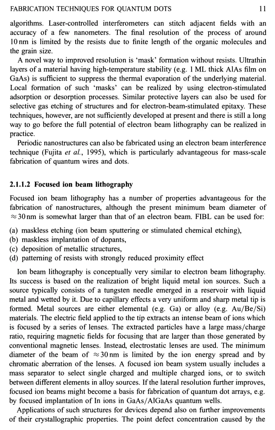
1988; Beaumount, 1991; Sotomayer Torres et ai, 1994). In Fig. 2.1 a regular array
of columns is shown that has been etched from an AlGaAs/GaAs superlattice. The
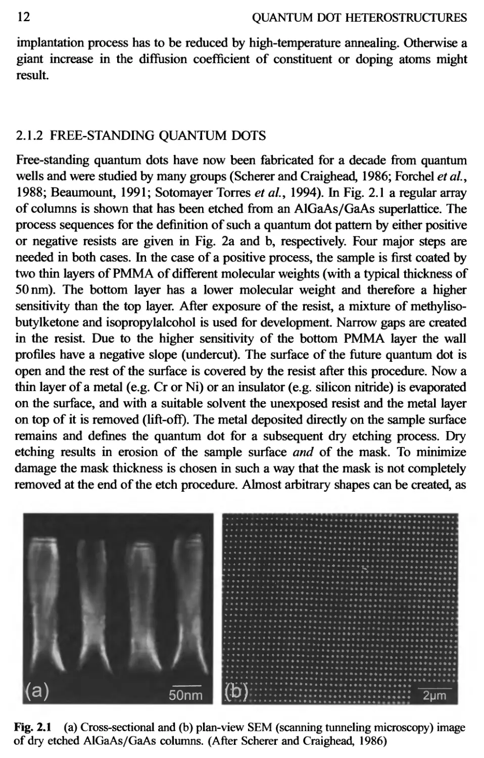
process sequences for the definition of such a quantum dot pattern by either positive
or negative resists are given in Fig. 2a and b, respectively. Four major steps are
needed in both cases. In the case of a positive process, the sample is first coated by
two thin layers of PMMA of different molecular weights (with a typical thickness of
50 nm). The bottom layer has a lower molecular weight and therefore a higher
sensitivity than the top layer. After exposure of the resist, a mixture of methyliso-
butylketone and isopropylalcohol is used for development. Narrow gaps are created
in the resist. Due to the higher sensitivity of the bottom PMMA layer the wall
profiles have a negative slope (undercut). The surface of the future quantum dot is
open and the rest of the surface is covered by the resist after this procedure. Now a
thin layer of a metal (e.g. Cr or Ni) or an insulator (e.g. silicon nitride) is evaporated
on the surface, and with a suitable solvent the unexposed resist and the metal layer
on top of it is removed (lift-off). The metal deposited directly on the sample surface
remains and defines the quantum dot for a subsequent dry etching process. Dry
etching results in erosion of the sample surface and of the mask. To minimize
damage the mask thickness is chosen in such a way that the mask is not completely
removed at the end of the etch procedure. Almost arbitrary shapes can be created, as
(a) §0nm j$}:
2um
Fig. 2.1 (a) Cross-sectional and (b) plan-view SEM (scanning tunneling microscopy) image
of dry etched AlGaAs/GaAs columns. (After Scherer and Craighead, 1986)
FABRICATION TECHNIQUES FOR QUANTUM DOTS
13
Positive resist
PMMA
AIGaAs
GaAs
AIGaAs
Negative
CMS
AIGaAs
GaAs
AIGaAs
Expose and develop
|B PMMA
AIGaAs
GaAs
AIGaAs
Metal lift-off
■ ^
AIGaAs i
GaAs
AIGaAs
Dry etchinc
Cr
1 AIGaAs
GaAs
AIGaAs
CMS
AIGaAs
GaAs
AIGaAs
I
■I CMS
MAIGaAs
JH GaAs
AIGaAs
(a) (b)
Fig. 2.2 Sequence of the definition procedures for fabrication of a free-standing quantum dot
using (a) positive or (b) negative resists. (After Forchel et al, 1988)
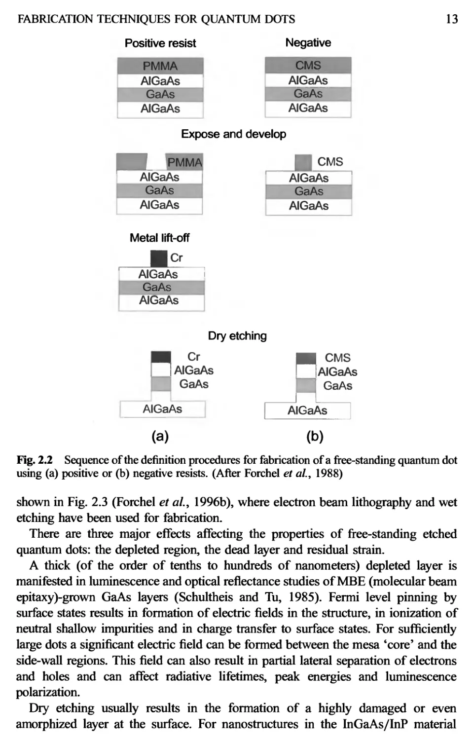
shown in Fig. 2.3 (Forchel et al.9 1996b), where electron beam lithography and wet
etching have been used for fabrication.
There are three major effects affecting the properties of free-standing etched
quantum dots: the depleted region, the dead layer and residual strain.
A thick (of the order of tenths to hundreds of nanometers) depleted layer is
manifested in luminescence and optical reflectance studies of MBE (molecular beam
epitaxy)-grown GaAs layers (Schultheis and Tu, 1985). Fermi level pinning by
surface states results in formation of electric fields in the structure, in ionization of
neutral shallow impurities and in charge transfer to surface states. For sufficiently
large dots a significant electric field can be formed between the mesa 'core' and the
side-wall regions. This field can also result in partial lateral separation of electrons
and holes and can affect radiative lifetimes, peak energies and luminescence
polarization.
Dry etching usually results in the formation of a highly damaged or even
amorphized layer at the surface. For nanostructures in the InGaAs/InP material
14
QUANTUM DOT HETEROSTRUCTURES
(a) (b)
4 k * * 9. 13 '.kV X29.K ' ikfcn
(d)
Fig. 2.3 SEM images of quantum dot structures of different shapes defined by electron beam
lithography and wet etching: (a) cone-shaped InGaAs quantum dot (diameter ~ 50 nm), (b)
rectangular cross section (central area: 83 x 47 nm2), (c) coupled dot structure (molecule,
~ 80 nm), and (d) ring structure (outer diameter ~ 75 nm, inner diameter ~ 30 nm). (After
Forchel et al, 1996b)
system subjected to Ar/02 reactive ion beam etching (RIE) the width of this layer
was estimated to be about 19nm independent of the lattice temperature. In such a
layer nonradiative recombination is predominant and the effective size of the binding
potential of the electronic quantum dot is reduced. The concept of the 'dead' layer
was introduced to explain the lateral size dependence of luminescence efficiency of
etched quantum dots (Forchel et al, 1988). The effective thickness of this layer
seems to depend strongly on etching parameters. Reactive ion etching of quantum
dots with BC13 was also claimed to result in formation of the dead layer, but of much
smaller thickness (Clausen et al, 1989). Using SiCl4 (Kohl et al, 1989) reduces the
luminescence efficiency of 70 nm GaAs/AlGaAs quantum wires at low temperatures
compared to unpatterned material by a factor of 30. Particularly strong degradation
of properties appears for etched II-VI nanostructures (Sotomayor Torres et al,
1992). Significant recovery was observed, however, after annealing of the structures.
Reactive ion etching is also known to result in a loss of stoichiometry at the
surface (Cho and Arthur, 1975), with a tendency of depletion of the more volatile
element (As in the case of GaAs). This effect can result in a significant deviation
from stochiometry and in a pronounced strain in etched structures. One possibility
for compensation is annealing in a group V gas atmosphere. A compressive uniaxial
strain of about 7 x 10⁻⁴ along the growth direction was observed for
GaAs/AlGaAs QDs (Sotomayor Torres et al, 1994). A large spread of confinement
c)
FABRICATION TECHNIQUES FOR QUANTUM DOTS
15
energies in the range from 0 to 11 meV was reported for 40 nm wide InGaAs/InP
wires. Annealing and wet etching steps carried out after dry etching were shown to
remarkably alter the blue shift (MacLeod et al, 1993). The observed variation of
experimental results demonstrates the large influence of extrinsic factors.
The surface recombination velocity for the free GaAs surface is very high and
close to the thermal velocity of nonequilibrium carriers (-107cm/s at 300 K)
(Bimberg and Queisser, 1972). For small mesas this value is not dramatically
smaller, even at low temperatures, as the nonresonantly created carriers can be
trapped by the surface well before they are thermalized with the lattice. For the
InGaAsP material system the surface recombination velocity is much smaller, being
around 1 x 104cm/s (Forchel et al, 1988) at 300 K, and the emission from etched
quantum dots can be observed in mesas having relatively small lateral sizes. By
studying the luminescence efficiency versus mesa size at different temperatures, it
was found (Maile et al, 1989) that the surface recombination velocity of InGaAs
increases from 1.6 x 103cm/s at 4 K to 5.9 x 103cm/s at 77 K and to 1.2 x 10⁴
cm/sat 300 K.
Comparison of the experimental results on luminescence intensity versus lateral
size (Forchel et al, 1988; Andrews et al, 1990; Beaumount, 1991; Sotomayor
Torres et al, 1994) demonstrates significant scatter of the experimental data of
different groups which is related to different degrees of damage introduced by
etching, different material purity and different interface or alloy structure of the
precursor QW. High concentrations of localization centers, such as impurities or
interface fluctuations, can suppress carrier lateral mobility and result in a relative
increase in luminescence intensity, at least at low temperatures. This is particularly
true for alloy quantum wells, where alloy scattering further reduces exciton mobility.
As a general trend, a strong decrease in integrated photoluminescence (PL) intensity
(by orders of magnitude) is manifested when the lateral size of the etched
GaAs/AlGaAs QD is reduced to about or slightly below lOOnm at low
temperatures. At high temperatures degradation of PL starts from the micrometer-range for
the InGaAs/InP system and from dozens of micrometers for the AlGaAs/GaAs one
(high purity samples). Lower surface recombination velocity still permits physical
studies of etched InGaAs/GaAs QDs at low temperatures down to lateral sizes of
50nm (Bayer et al, 1995).
In view of the above discussion one can conclude that it is possible to fabricate
free-standing etched quantum dots having a size down to ~ lOnm. It seems to be
difficult, however, to obtain bright luminescence from such small structures. Thus
the present usefulness of such structures for devices is limited.
2.1.3 SELECTIVE INTERMIXING BASED ON ION IMPLANTATION
Selective intermixing of quantum wells has been used for fabrication of laterally
buried heterostructures for many years (Werner et al, 1989). Diffusion-induced
disordering (Zahari and Tuck, 1985; Harrison et al, 1989), intermixing under pulsed
laser irradiation (Ralston et al, 1987) (see Section 2.1.4), and implantation-induced
16
QUANTUM DOT HETEROSTRUCTURES
disordering (Cibert et al, 1986; Venkateson et al, 1986; Kuttler et al, 1997) are
some of the techniques used. Submicrometer lateral variations in the local
composition were realized by intermixing superlattices using a scanned focused beam of Ga
ions (Hirayama et al, 1985).
Selective intermixing by ion implantation and subsequent annealing is caused by a
remarkable enhancement of diffusion coefficients by defects like vacancies or
interstitials (Cibert et al, 1986; Kuttler et al, 1997) after a high concentration of
impurities and point defects was created. Both impurities and point defects are
ionized at elevated temperatures, leading to a large increase in the concentration of
charge carriers. This increase changes the point defect equilibrium in the crystal
(Kroger, 1964; Hurle, 1979). It results in a drastic increase in the concentration of
more mobile species, such as, for example, charged interstitials (Tuck, 1985; Zahari
and Tuck, 1985), causing an effective intermixing of superlattices. The unimplanted
areas remain more or less unaffected.
2.1.4 SELECTIVE INTERMIXING BASED ON LASER ANNEALING
Laser-induced local interdiffusion of a GaAs/AlGaAs quantum well structure has
been proposed to define QDs (Ralston et al, 1987; Brunner et al, 1992). Pulsed
laser irradiation, e.g. of GaAs/AlGaAs superlattices, results in melting of the
annealed area followed by subsequent ultrafast recrystallization. After recrystalliza-
tion the composition of the superlattice is averaged. This method has been shown to
provide very sharp interfaces between intermixed and nonintermixed regions of less
than 5nm (Ralston et al, 1987). Using an Ar laser beam with 500nm focus,
selective intermixing of a single 3 nm thick GaAs/AlGaAs quantum well (Brunner ef
al, 1992) has been demonstrated. A high-energy shift of the luminescence line by
several tens of millielectronvolts has been observed. Due to the high activation
energy of the interdiffusion process the resulting lateral potential barriers were five
times steeper than the laser intensity profile (Schlesinger and Kuech, 1986).
A disadvantage of this method for applications is related to the quality of the
material after laser annealing. Melting and subsequent fast recrystallization of the
material results in a high concentration of nonequilibrium point defects and,
correspondingly, the luminescence efficiency of the treated areas strongly degrades.
It was shown (Brunner et al, 1992) that a reduction in the size of the unintermixed
region from 1000 to 450 nm resulted in a drop in PL intensity by a factor of 20, and a
further decrease in the size down to 300 nm resulted in an additional drop of one
order of magnitude. Luminescence efficiency of uniformly intermixed areas was
reported to be more than 300 times smaller than the luminescence of the untreated
quantum well at low temperature. Another problem relates to the microscale
uniformity of the recrystallized material.
2.1.5 STRAIN-INDUCED LATERAL CONFINEMENT
Formation of lateral confinement by strain gradients has been proposed for quantum
wires and quantum dot fabrication to overcome problems of interface damage in
FABRICATION TECHNIQUES FOR QUANTUM DOTS
17
free-standing quantum wires and dots (Kash, 1988, 1991). Here a highly strained
film is deposited on top of a quantum well structure buried closely underneath the
surface. If the film is not patterned, the strain is concentrated in the film and the
quantum well is not affected, except for a slight bending of the substrate as a whole.
If the film is patterned, the film strain partly relaxes at the expense of some strain in
the substrate and quantum well. The lateral resolution of the method is only limited
by the possibilities of electron lithography and very small mesas of stressors can be
potentially formed. Recently, self-organized stressed islands have also been used as
stressors (Lipsanen et al.9 1995) (see also Section 6.3). An initially biaxially
compressed film induces in the substrate regions of compression in the vicinity of
the stressor edges and regions of expansion under the stressor center (see Section
5.2.6). No problems with surface states on mesa side walls and related surface
recombination exist in this case. The confinement potentials for carriers, however,
are comparatively small.
2.1.6 QUANTUM DOTS GROWN ON PATTERNED SUBSTRATES
Growth of nanostructures on patterned substrates was originally initiated to avoid
some of the problems characteristic of free-standing quantum wires and dots. The
growth occurs on patterned surfaces, V-grooves or inverted pyramids with
dimensions significantly larger than the nanostructure itself (Kapon et al, 1987; Lebens et
al9 1990; Fukui et al.9 1991; Rajkumar et al9 1992; Madhukar, 1993; Madhukar ef
al9 1993; Sugawara, 1995; Hartmann et al9 1997; Ishida et al9 1998). The growth
on patterned, sometimes higher-index substrates, is complex and several instabilities,
such as spontaneous tilting of facets, spontaneous corrugation of facet surfaces, and
non-uniformity of the growth rate in the vicinity of edges can prevent the realization
of perfect structures. A high level of understanding of the growth process with
complex surface and interfacet kinetics and energetics is required.
Three steps are required to fabricate QDs using this approach (see, for example,
Rajkumar et al9 1992):
(a) definition of lateral masks using lithographic techniques,
(b) wet chemical etching to produce the desired geometrical relief and an atomically
clean surface suitable for growth,
(c) growth on the patterned or corrugated substrate.
Rajkumar et al. (1992) reported the fabrication of an array of mesas on an As
terminated GaAs (111)B substrate. By photolithography, an array of 5 urn size resist
patterns aligned along a (1-10) direction was defined, followed by wet chemical
etching. Growth was stopped when each mesa consisted of a truncated triangular
pyramid. The mesa top was an (111)B face and the three side facets were of the
{100} type. The size of the mesa top can be decreased from the initial pattern
defined size, eventually down to practically zero depending on the duration of
etching. Even if the size of the mesa top is not sufficient to provide efficient lateral
confinement one can reduce it further by overgrowth, due to lateral shrinkage of the
18
QUANTUM DOT HETEROSTRUCTURES
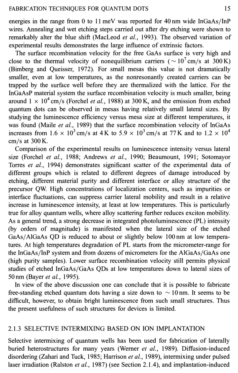
mesa top. Figure 2.4 illustrates this process. Precondition of the shrinkage process is
a higher growth rate on the mesa top rather than on the side walls. This condition is
fulfilled if, for example, upward diffusion takes place.
Optimization of the growth temperature (Rajkumar et ai, 1992) allows monotone
dependence (shrinkage) to be obtained and reproducibility to be improved. At the
same time, as growth continues, new facets emerge. A new facet was identified to be
of the {211} type, contiguous to the (lll)B mesa top. Using this or similar
approaches QD structures with lateral dimensions down to 50 nm can be created
(Rajkumar et ai, 1992). A similar approach has been used by Nagamune et al.
(1995).
Growth on patterned substrates and selective epitaxy in local openings of a
dielectric mask gave qualitatively similar results. In the latter case, no further
patterning of the substrate was required, as the growth was governed by the size and
the shape of the opening in the dielectric mask. Moreover, as the size of the opening
was defined by the resolution of the lithographic process, potentially very small
(~ lOnm) openings are possible. Such a formation of three-dimensional structures
using selective metal-organic chemical vapor phase epitaxy in openings in a Si3N4
Fig. 2.4 Schematic diagram and cross-sectional TEM image of a growth profile resulting in
quantum box mesas. (After Rajkumar et ai, 1992)
FABRICATION TECHNIQUES FOR QUANTUM DOTS
19
mask was demonstrated, for example, by Lebens et al (1990). The minimum GaAs
dot diameter was 80 nm.
In a recent alternative approach selective electron beam exposure was used to
define a pattern directly on to the GaAs surface, which can subsequently be used for
selective nucleation of clusters (Sleight et al, 1995). Also, contact printing (Krauss
and Chou, 1997) presents a novel way of pattern formation.
When conventional lithographic techniques are used, the lateral density of QDs is
defined by the pattern. The dot-to-dot distance is usually large (~ 0.3-3 urn),
preventing the realization of dense arrays of quantum dots. A general problem of
growth on patterned substrates is its limited compatibility with the planar technology
of double-heterostructure lasers. The mesoscopic size of the mesa opposes the
possibility of formation of perfect waveguides. On the other hand, it might ease
fabrication of distributed feedback lasers. In the case of growth in openings the
existence of a dielectric mask limits certain applications.
2.1.7 CLEAVED EDGE OVERGROWTH
Twofold growth on the cleaved edge of a quantum well or superlattice (2CEO) had
been predicted to lead to the formation of electronic quantum dots at the juncture of
three orthogonal quantum wells (see Fig. 5.19 (Grundmann and Bimberg, 1997a).
Such dots have been realized in the AlGaAs/GaAs system using MBE (Wegscheider
et al, 1997; Schedelbeck et al, 1998).
2.2 QUANTUM DOTS FORMED BY INTERFACE FLUCTUATIONS
Interface fluctuations cause potential fluctuations in a quantum well which form
efficient localization centers for excitons (Christen and Bimberg, 1990; Christen et
al, 1990). Optical properties of excitons localized at interface fluctuations are
reviewed in Section 6.5. Such 'natural' quantum dots are characterized by small
localization energy of the carriers and by inhomogeneity of lateral sizes and
relatively small density of states. This causes quick saturation of the luminescence
of localized excitons with increasing excitation density and depopulation of
localized states due to thermal evaporation of excitons already at moderate excitation
densities and observation temperatures, respectively (Kop'ev et al, 1986).
2.3 SELF-ORGANIZED QUANTUM DOTS
The evolution of an initially two-dimensional growth into a three-dimensional
corrugated growth front is a well-known phenomenon and has been observed for
an abundance of systems. A comprehensive discussion of such growth modes, in
particular in the presence of strain, is given in Section 3.6.1.
20 QUANTUM DOT HETEROSTRUCTURES
In a paper by Stranski| and Krastanow (1937) (SK) the possibility of island
formation on an initially flat heteroepitaxial surface was proposed; actually, for the
growth of lattice matched ionic crystals that had different charges. In the following
years the term 'SK growth' was used in heteroepitaxy for the formation of islands on
an initially two-dimensional layer (see Fig. 3.9), including growth of islands relaxed
by misfit dislocations in strained heteroepitaxy (Bauer, 1958).
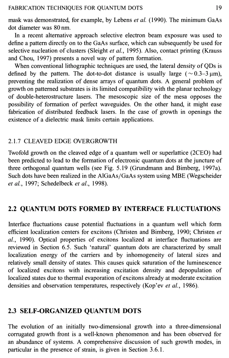
The formation of coherent, i.e. defect-free, islands as a result of SK growth of
strained heterostructures is a fairly new concept and is now systematically exploited
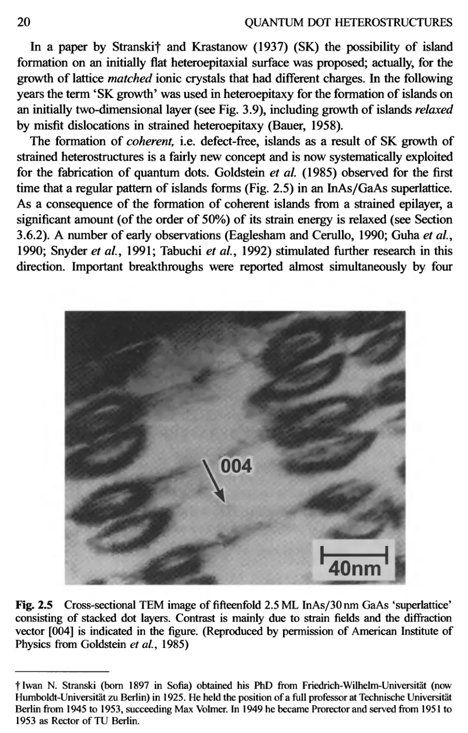
for the fabrication of quantum dots. Goldstein et ah (1985) observed for the first
time that a regular pattern of islands forms (Fig. 2.5) in an InAs/GaAs superlattice.
As a consequence of the formation of coherent islands from a strained epilayer, a
significant amount (of the order of 50%) of its strain energy is relaxed (see Section
3.6.2). A number of early observations (Eaglesham and Cerullo, 1990; Guha et ah,
1990; Snyder et ah, 1991; Tabuchi et ah, 1992) stimulated further research in this
direction. Important breakthroughs were reported almost simultaneously by four
004
40nm
Fig. 2.5 Cross-sectional TEM image of fifteenfold 2.5 ML InAs/30nm GaAs 'superlattice'
consisting of stacked dot layers. Contrast is mainly due to strain fields and the diffraction
vector [004] is indicated in the figure. (Reproduced by permission of American Institute of
Physics from Goldstein et ah, 1985)
flwan N. Stranski (born 1897 in Sofia) obtained his PhD from Friedrich-Wilhelm-Universitat (now
Humboldt-Universitat zu Berlin) in 1925. He held the position of a full professor at Technische Universitat
Berlin from 1945 to 1953, succeeding Max Volmer. In 1949 he became Prorector and served from 1951 to
1953 as Rector of TU Berlin.
FABRICATION TECHNIQUES FOR QUANTUM DOTS
21
^^
^
©^
**-^
5
CO
o
t_
CL
O
c
<D
i_
3
O
o
O
5
4
3
2
1
0
|j , '
0
oflnAs=2.35 ML
□ Height ■ Half-base
1
5 10 15 20 25
Dot size (nm)
Fig. 2.6 Histogram of height and lateral size for MBE-grown InAs/GaAs quantum dots.
(Reproduced by permission of American Institute of Physics from Moison et al.9 1994)
groups (Leonard et al.9 1993; Bimberg, 1994; Madhukar et al.9 1994; Moison et ai,
1994) where a narrow distribution of the island size was manifested (Fig. 2.6).
Structural and optical properties of self-organized quantum dots are the focus of
the remainder of this book. As discussed in detail in Chapter 4, using suitable growth
conditions in MBE or MOCVD, it is now possible to fabricate arrays and stacks of
small QDs (~10nm), ordered in size and shape, with high area density
(> 1011 cm~2) and high optical quality. Such dot ensembles are suitable for creating
devices such as low threshold lasers (see Section 8.2).
3 Self-Organization Concepts on
Crystal Surfaces
3.1 INTRODUCTION
Self-organization of ordered nanostructures on crystal surfaces represents a unique
phenomenon which opens exciting new possibilities both in fundamental research of
low-dimensional objects and in their device applications. There is a variety of effects
that can be used for fabrication of QDs:
(a) periodic surface faceting with subsequent heteroepitaxial growth on the faceted
surface,
(b) formation of arrays of step bunches of equal height on vicinal surfaces,
(c) formation of ordered nanoscale two-dimensional islands, e.g. having mono- or
bilayer height upon submonolayer deposition,
(d) formation of ordered arrays of three-dimensional coherently strained QDs.
In this section we consider theoretical concepts and their relation to experimental
results on self-ordering phenomena on semiconductor surfaces and on formation
mechanisms of self-ordered nanostructures (Shchukin and Bimberg, 1998).
Thermodynamic arguments will mainly be considered for the various classes of self-
organized semiconductor nanostructures. All of these structures are described as
equilibrium structures of elastic domains. Despite the fact that the driving forces of
the instability of a homogeneous phase are different in each case, the common
driving force for the long-range ordering of the inhomogeneous phase is the elastic
interaction. Also, kinetic theories of single-layer dot formation are reviewed and
compared with the thermodynamic approach. A kinetic theory of the formation of
multiple-sheet structures of QDs is considered. It includes equilibrium ordering of
coherently strained islands in the first sheet and the strain-driven kinetic stacking of
islands in the next sheets or strain-driven shape transformation effects induced by
complex growth modes.
Spontaneous formation of periodically ordered domain structures in solids with
the periodicity much larger than the lattice parameter is a general phenomenon
which is at the origin of a large variety of different domain structures. This process,
also called self-ordering, can occur if the homogeneous state of the system is
thermodynamically unstable and the system undergoes a phase transition into an
inhomogeneous state. In an inhomogeneous state, generally a coordinate-dependent
order parameter is the source of a long-range field (electric, magnetic, strain).
Therefore, a multidomain state of the solid is energetically more favorable than the
single-domain state, since the former provides compensation of the long-range field
SELF-ORGANIZATION CONCEPTS ON CRYSTAL SURFACES
23
at large distances outside the domain structure. The long-range field is responsible
for the periodic ordering of the equilibrium domain structure that meets the
conditions of the total Helmholtz free energy minimum. The free energy can be
written as a sum of three distinct contributions:
Motal ^domains ' ^boundaries ' -^long-range V^-U
Here ^domains is the free energy of domains, ^boundaries is the free energy of domain
boundaries, and £iong-range is the energy of a long-range field, which includes
interaction between domains.
The conventional classification of domain structures is based upon the physical
nature of the order parameter. An elastic strain field is of major importance for
consideration since it exists in nearly all domain structures. The reason is that
any phase transformation in solids is typically accompanied by a crystal lattice
rearrangement. In most cases, neighboring domains have different lattice parameters
of the bulk or surface unit cells. For the case of ferroelectric or ferromagnetic
domain structures this phenomenon is well known as electrostriction or
magnetostriction, respectively (Landau and Lifshits, 1960).
The focus of our consideration here will be given to so-called elastic domain
structures where the elastic strain field is the major or only long-range field. Elastic
domain structures only recently became the subject of monographs. The first
systematic theoretical approach to elastic domain structures in bulk materials is
given in the monographs by Khachaturyan (1974, 1983). Both composition-
modulated structures in phase-separating metal alloys and domain structures induced
by martensite transformation are treated and a review of experimental data is
presented. The theory of elastic domain structures in epitaxial films of macroscopic
thickness has been developed by Roitburd (1976) and Bruinsma and Zangwill
(1986) for martensite-type domains and by Ipatova et al (1993) for composition-
modulated structures in alloys.
In recent years, due to its high importance for fabrication of semiconductor
heterostructures with reduced dimensionality (quantum wires and quantum dots),
self-ordering phenomena on crystal surfaces has become a subject of intense
experimental and theoretical studies. The three classes of self-ordered surface
structures displayed in Fig. 3.1 will be discussed here. These are periodically
faceted surfaces of pure crystals, surface domain structures (e.g. ordered arrays of
monolayer-height islands in heterophase systems at submonolayer coverage), and
ordered arrays of three-dimensional coherently strained islands on lattice-
mismatched substrates. Since typical linear dimensions of all these structures are
of a nanometer length scale, they are commonly termed 'nanostructures'.
In Section 3.2 we consider the general problem of the equilibrium crystal shape in
relation to surface faceting. In Section 3.3 periodic arrays of macroscopic step
bunches are discussed. Section 3.4 focuses on the heteroepitaxial growth on
corrugated surfaces. In Section 3.5 the formation of ordered arrays of planar surface
domains is treated. The main section (3.6) is on ordered arrays of three-dimensional
24
QUANTUM DOT HETEROSTRUCTURES
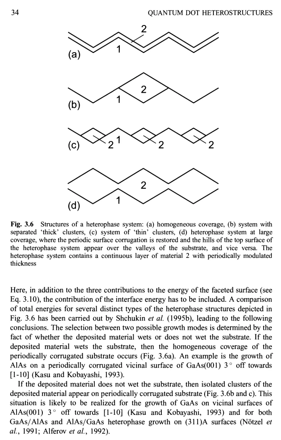
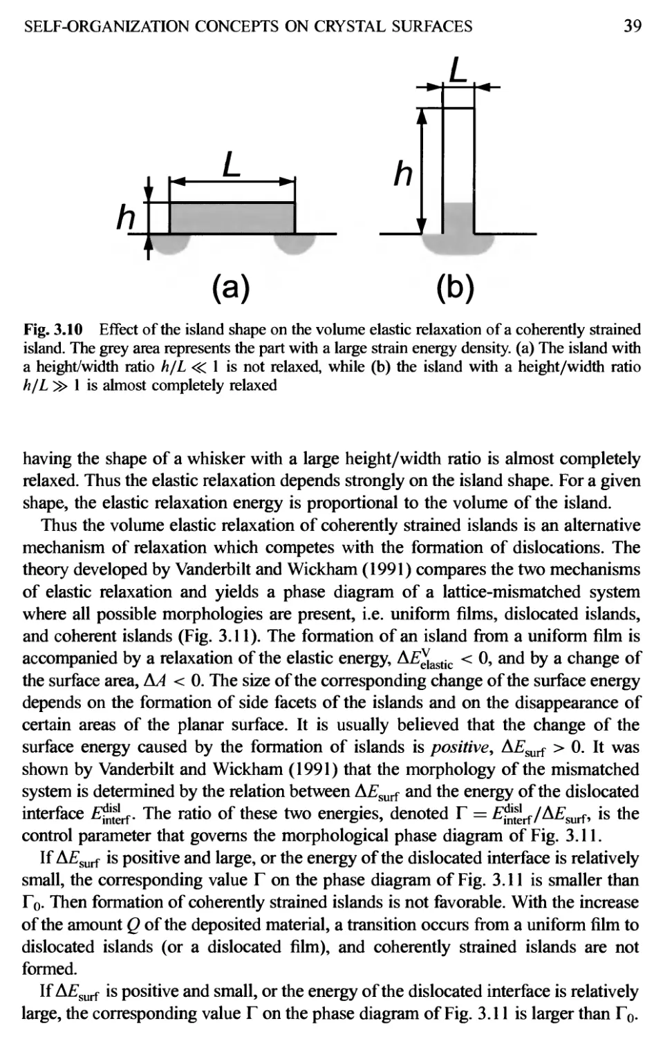
Fig. 3.1 Various classes of spontaneously ordered nanostructures: (a) periodically faceted
surfaces, (b) surface domain structures, (c) ordered arrays of coherently strained islands
(material 2) on a lattice-mismatched substrate (material 1)
islands. Finally, vertically correlated growth of nanostructures is discussed in Section
3.7.
3.2 SPONTANEOUS FACETING OF CRYSTAL SURFACES
3.2.1 THE PROBLEM OF EQUILIBRIUM CRYSTAL SHAPE
The phenomenon of equilibrium faceting plays the key role in the definition of the
equilibrium crystal shape (ECS). Two problems are related to the ECS that
correspond to two different physical situations. The first problem is the ECS of a
single crystal which dates back at least to Wulff (1901); further developments of
ECS theory can be found in Herring (1951a), Chernov (1961) and Mullins (1963).
The exact thermodynamic formulation may be found, for example, in the review by
Rottman and Wortis (1984), who discussed the shape of a single solid inclusion of a
SELF-ORGANIZATION CONCEPTS ON CRYSTAL SURFACES
25
fixed volume a> which is in equilibrium with the liquid or with the gas phase. The
surface free energy of the inclusion is the integral over the surface of cd\
Fsurf(7\ co) = | y(A;T)dA (3.2)
J da)
Here y(iti; T) is the surface free energy per unit surface area dependent on the
orientation rfi of the surface element dA relative to the crystal axes. Thermodynamic
theory of the ECS states that a macroscopic inclusion of a fixed volume
V(co) = [ dV (3.3)
JOJ
takes at equilibrium the shape that minimizes the surface free energy (Eq. 3.2)
subject to the constraint (Eq. 3.3).
The dependence of the surface free energy y(iti; T) on orientation is expected to
have cusps in symmetry directions, leading to facets in the crystal shape at
sufficiently low temperatures. These cusps represent discontinuities in the angular
derivatives of the surface free energies, the discontinuities being associated with the
free energy of the steps on a given facet. With a temperature increase, the step free
energies decrease, cusps blunt, and the corresponding facets shrink. Facets finally
disappear at the roughening transition temperature TR (which can be different for
different directions) of the corresponding infinite planar surface. Above TR the
corresponding region of the ECS becomes smoothly rounded.
References to experimental data on equilibrium crystal shapes of micrometer-
scale metal clusters are presented in Rottman and Wortis (1984). Transmission
electron microscopy (TEM) measurements of the equilibrium shape of voids in Si
enabled the orientation dependence of the surface free energy of Si to be revealed
(Eaglesham et al.9 1993). Statistical mechanics is the tool used for microscopic
evaluation of the dependence of the surface free energy y(iti; T) on orientation and
for the determination of the ECS; an overview of the theoretical results may be found
in Rottman and Wortis (1984).
The important issue of ECS theory is that there exist surface orientations that are
not present in the crystal shape at a given temperature. At T=0 only a few high-
symmetry surface orientations are present. All others are passive in the sense that
they do not contribute to the ECS. With increasing temperature the domain of
passive orientations shrinks as the crystal becomes more rounded.
The importance of this issue becomes even more visible as one considers the
second problem of the ECS. This concerns a crystal in equilibrium with the liquid or
with the gas phase and with the volume and all but the top surface fixed. This
formulation of the problem is relevant to an experimental situation where only the
top crystal surface is studied, e.g. thermal annealing of a crystal or growth
interruptions introduced in crystal growth experiments.
The top crystal surface is not fixed and is allowed to rearrange into a hill-and-
valley structure. Can rearranging the atoms into hills and valleys lower the free
energy of a plane surface? When hills and valleys have a size large compared to the
26
QUANTUM DOT HETEROSTRUCTURES
lattice parameter, new tilt facets can be defined, and the free energy of the hill-and-
valley structure can be written as a surface integral over tilted facets:
Here rfi is the coordinate-dependent unit vector locally normal to the surface at each
point and A is the constant unit vector normal to the initially planar surface. Fixed
side surfaces of the crystal imply that the average normal to the top surface coincides
with the normal to the nominally planar surface, i.e.
Mihd4 = A (3.5)
A being the total area of the nominally planar surface.
The theorem proved exactly by Herring (1951b) reads:
If a given macroscopic surface of a crystal does not coincide in orientation with some
portion of the boundary of the equilibrium shape, there will always exist a hill-and-
valley structure which has a lower free energy than a flat surface, while if the given
surface does occur in the equilibrium shape, no hill-and-valley structure can be more
stable.
If the planar surface is unstable, the resulting hill-and-valley structure is
determined by the minimum of the surface free energy (Eq. 3.4) subject to the
constraint (Eq. 3.5). This minimization will yield the orientation of tilt facets as well
as the fraction of the nominal planar surface on to which each facet is projected.
Microscopic theory based on statistical mechanics can yield the orientational
dependence of the surface free energy y(iti; T) and thus allow the ECS to be
determined. Recent developments in this area have been made by Williams et al.
(1993) for surfaces vicinal to Si(ll 1) and by Mukherjee et al. (1994) for surfaces
vicinal to Si(OOl).
The theory formulated by Eqs. (3.4) and (3.5) does not yield, however, the facet
size. This problem requires additional concepts of the intrinsic surface stress and of
capillary effects on solid surfaces, which are addressed in the next two sections.
3.2.2 THE CONCEPT OF INTRINSIC SURFACE STRESS OF A CRYSTAL
SURFACE
Since atoms in the surface layer are in a different environment than in the bulk, the
surface layer energetically favors a lattice parameter different from the bulk value in
the directions parallel to the surface. The surface layer is intrinsically stretched or
compressed and therefore characterized by intrinsic surface stress.
The intrinsic surface stress of a solid is an analogue to the surface tension of a
liquid (Fig. 3.2). However, there exists a fundamental difference in thermodynamic
properties of a liquid surface and of a solid surface, pointed out long ago by Gibbs
(1928); an explanation may also be found in Marschenko and Parshin (1980) and
Needs (1987). The basic reason is that any liquid is incompressible. When a liquid
SELF-ORGANIZATION CONCEPTS ON CRYSTAL SURFACES
27
(a)
(b)
Fig. 3.2 Capillary effects on liquid and on solid surfaces, (a) Balance of forces acting on an
element of the curved surface layer of a liquid. Forces caused by the surface tension t are
balanced by the force G acting from the bulk of the liquid. According to the third Newton law,
the opposite force F = — G is acting from the surface layer on the bulk of the liquid. This
force results in the excess Laplace pressure AP = P2—Px below the curved surface of the
liquid, P\ and P2 being the values of the pressure below and above the curved liquid surface,
(b) The balance of forces acting on a crystal edge. Forces caused by the intrinsic surface stress
t are balanced by the force G acting from the bulk of the crystal. The reaction F = — G is
acting from the surface layer on the bulk of the crystal, resulting in the strain field. The inset in
the center depicts the force balance, which is similar for a liquid and for a crystal (all forces
are per unit length in the direction perpendicular to the figure)
film is stretched, atoms or molecules move out from the bulk to form a new surface
that is structurally identical to the existing surface. Thus, an attempt to stretch a
liquid film by 1% results in a 1% increase in the number of surface atoms or
molecules, whereas the spacing between surface atoms remains unchanged.
Thus the processes of the creation and deformation of a liquid surface are identical
and are described by the single parameter y, the energy required to create a unit area
of the surface. However, when a crystal surface is stretched, the distance between
atoms increases and the nature of the surface itself changes. The energy to create a
unit area of the surface of a given orientation is characterized by two parameters: the
scalar quantity y, termed the surface energy, and the energy change due to
deformation of the crystal surface, described by the intrinsic surface stress tensor
Tap. The concept of the intrinsic surface stress tensor has been proposed by Gibbs
(1928) and discussed later by Shuttleworth (1950), Herring (1951a) and Marchenko
and Parshin (1980). The linearized change of the surface energy is written as the
following integral over the surface:
*ap(foKp <M
(3.6)
where Tap has nonvanishing components only in the surface plane, a,)S=l,2
(Marchenko and Parshin, 1980). The values of the intrinsic surface stress tensor
can be either positive (tensile) or negative (compressive); a tensile surface stress is
associated with the surface that favors contraction while a compressive surface stress
favors expansion.
Values of the intrinsic surface stress for solids are known either from first-
principle calculations or from comparison with indirect experimental data on
28
QUANTUM DOT HETEROSTRUCTURES
parameters of surface domain structures. No direct experimental method for
determining the intrinsic surface stress of a solid has been proposed so far. For
most solid surfaces, the intrinsic surface stress is tensile (see, for example, Needs,
1987; Fiorentini et al.9 1993) whereas a compressive surface stress is known for
Si(OOl) surfaces in the direction perpendicular to dimers (Garcia and Northrup,
1993). Results on the (2 x 4) GaAs(OOl) surface indicate tensile surface stress
(Moll, 1998a). The order of magnitude oft is 10-100 meV/A2.
Since the liquid surface is characterized by a single quantity y which is both the
energy for creation of a unit surface area (i.e. the surface energy) and the quantity
responsible for capillary effects of the Laplace-pressure type, the term 'surface
tension' is widely used for the surface energy y. Mainly for historical reasons, usage
of this term has been extended to surfaces and interfaces of solids. However, the use
of 'surface tension' for solids turns out to be ambiguous since it may produce a
confusion between the surface energy y and the intrinsic surface stress Tap.
Therefore, we intend to distinguish 'surface energy' and 'intrinsic surface stress' and will
not use the term 'surface tension' for solids.
The change in surface energy due to strain (Eq. 3.6) indicates the interconnection
between surface effects and strain-related phenomena. Within the framework of the
linear theory of elasticity, where the bulk strain energy is a quadratic function of the
strain, it is possible to expand the surface energy up to second-order terms in strain.
The thermodynamics of solid surfaces and interfaces up to second-order terms in
strain has been studied by Andreev (1981) and further developments have been made
by Nozieres and Wolf (1988). The dependence of the surface or interface free energy
on strain is written as
y(rfi; ea/?) = y0(rfi) + Ta/,(A)ea/, + 5^0(A)e^e^ + ±/^ifye^/w,. (3.7)
Here, rfi is the normal to the surface or interface, Greek characters label two-
dimensional indices in the surface plane whereas Latin indices are three-dimensional
ones. Quadratic coefficients S^ ^ and ha^ have the meaning of surface excess
elastic moduli and can be either positive or negative; o^ is the bulk elastic stress
tensor, and the fourth term in Eq. (3.7) exists on solid-solid interfaces and vanishes
on stress-free surfaces where the bulk stress tensor obeys the boundary conditions
Gijirij = 0.
Following the conventional approach of elasticity theory (Landau and Lifshits,
1959), we define all surface quantities defined per unit area of the undeformed
surface. The dependence of the surface free energy on the strain (Eq. 3.7) can be
interpreted as the strain-induced renormalization of the surface free energy.
3.2.3 FORCE MONOPOLES AT CRYSTAL EDGES
Both liquid and solid surfaces are intrinsically stressed. Solid surfaces exhibit
capillary (or surface stress-induced) phenomena similar to the familiar Laplace
capillary pressure near a curved liquid surface, and a strain field is generated at a
curved surface of a solid. The existence of a surface stress-induced strain field was
SELF-ORGANIZATION CONCEPTS ON CRYSTAL SURFACES
29
pointed out by Marchenko and Parshin (1980) who considered the elastic energy of a
solid including both bulk and surface contributions:
^elastic = 2 klrn^lm dV + *aj?(Aktf <*A (3-8)
The elastic strain field in the crystal is created by the force
Fi = -T-- (3-9)
The ultimate case of a curved solid surface is a sharp edge between neighboring
facets. Figure 3.2 depicts the force balance on the curved surface of a liquid and at
the crystal edge and thus demonstrates the similarity between capillary effects in
liquids and solids. The surface tension on a curved liquid surface results in an excess
pressure below the curved surface, and, similarly, the intrinsic surface stress of
crystal surfaces causes an effective force applied to the edge of the crystal. This force
monopole generates the strain field that affects significantly the energetics of faceted
surfaces and promotes the formation of a periodic structure of facets.
2.3.4 SPONTANEOUS FORMATION OF PERIODICALLY FACETED
SURFACES
If a planar crystal surface is unstable and breaks up into a system of tilt facets, the
conservation of the. average orientation of the normal to the surface (Eq. 3.5) implies
the coexistence of alternating facets (Fig. 3.1a). At the intersection of neighboring
facets there appear either sharp crystal edges or narrow rounded parts of the surface.
Both types of intersection may be described as linear defects at the surface. These
linear defects give a short-range contribution into the surface free energy and a long-
range contribution due to elastic strain energy.
If the order parameter related to the phase transition at the surface is linearly
coupled to the strain field, i.e. if a linear striction effect exists, formation of a
periodic structure, whose period can be macroscopically large, is favored (Andreev,
1980). For the faceting phase transition the possibility of the formation of a faceted
surface with a macroscopic period has been pointed out by Andreev and Kosevich
(1981).
The theory of a periodically faceted surface has been developed in Marchenko
(1981a, 1981b), predicting the period of equilibrium structures. Following
Marchenko (1981a, 1981b), we consider the faceted surface with a one-dimensional
periodic saw-tooth profile depicted in Fig. 3.3. The free energy per unit projected
area equals
F = ^surf + hedges + ^elastic (3.10)
Here Fsurf is the free energy of tilted facets, £edges is the short-range energy of the
edges, and A£eiastic is the elastic energy due to the discontinuity of the surface stress
tensor xy at the crystal edges.
30
QUANTUM DOT HETEROSTRUCTURES
hedges =7^ = ^ PAU
Fig. 3.3 Saw-tooth profile of the faceted surface. Effective forces of alternating sign are
applied to neighboring edges
The free energy of tilted facets per unit projected area depends only on the
orientation of the facets, £surf = y(cp)sec((p\ and does not depend on the period of
the structure D. The short-range energy of the edges per unit projected area equals
D~ D
where f]+((p) is the short-range energy of the convex edge per unit length of the edge
and f]~((p) denotes the same energy for the concave edge. The short-range energy
can be roughly considered as a contribution of additional dangling bonds due to the
edge formation. This term becomes dominant for a very small facet period.
^elastic is given by Eq. (3.8), which contains both linear and quadratic terms as a
function of strain and yields zero energy in the absence of strain. Therefore, the
elastic strain energy in the equilibrium is negative, which corresponds to the
relaxation of the surface stress at crystal edges. This negative elastic energy will
be termed below the elastic relaxation energy due to crystal edges. The effective
elastic forces acting at the edges are displayed in Fig. 3.3. Force monopoles are
acting at each edge and forces applied to neighboring edges are balanced, so that the
total force applied to the system vanishes. Elastic strains generated by linear crystal
edges propagate into the crystal across a distance of the order of D and decay at
larger distances from the surface. Since the strain field is generated at linear defects
at the surface, namely at the linear crystal edges, the elastic relaxation energy
depends logarithmically on the period D of the structure:
Here t is the characteristic value of the intrinsic surface stress tensor, Y is Young's
modulus, a is the lattice parameter, C(cp) is the geometric factor which accounts for
the particular symmetry of the tensor T,y, the elastic anisotropy of the crystal, etc.
By substituting Eqs. (3.11) and (3.12) into Eq. (3.10), one obtains the following
expression for the free energy of the faceted surface per unit projected area:
coscp D YD \a) v
The dependence of the free energy versus the period of the faceted surface D is
displayed in Fig. 3.4. Due to the logarithmic dependence of the elastic relaxation
SELF-ORGANIZATION CONCEPTS ON CRYSTAL SURFACES
31
Fig. 3.4 Energy of a periodically faceted surface versus the period D. There always exists an
optimum period of faceting Dopi due to the logarithmic dependence of the elastic relaxation
energy on the period D
energy on the period Z), there always exists an optimum period of faceting Dopt
equal to
Dopt = a exp
r](cp)Y
C(cp)T2
+ 1
(3.14)
All material parameters that enter the exponential in Eq. (3.14) have typical atomic
values. Therefore the argument of the exponential is of the order of 1. Since the
exponential function is steep, the argument that can eventually be equal to about 3 or
more results in a macroscopic period D which exceeds the lattice parameter a at least
by an order of magnitude. In this case a macroscopic approach is indeed justified.
It should be noted that the free energy of facets, i.e. the first term in Eqs. (3.10)
and (3.13), contains the entropy contribution which describes the dependence of the
faceting itself and of the facet orientation on temperature. However, there exists
another entropy contribution to F associated with possible deviations of the structure
from a perfect periodic structure (the configuration entropy). For periodically faceted
surfaces, the configuration entropy has not been considered in the literature so far.
Therefore the present discussion refers, strictly speaking, to the case T=0. In the
following we will omit everywhere the entropy contribution to F and will discuss
only the total energy of the system.
Periodic faceting with a macroscopic period has been observed on various
surfaces of different materials, e.g. on surfaces vicinal to Si(lll) (Hibino et al,
1993; Williams etal., 1993), on surfaces vicinal to GaAs(OOl) (Kasu and Kobayashi,
1993; Golubok et al, 1994; Ledentsov et al, 1994a, 1994b), on surfaces vicinal to
Pt(001) (Watson et al, 1993), on high-index surfaces of GaAs (Lotzel et al, 1991)
and Si (Baski and Whitman, 1995), on the low-index surface TaC(l 10) (Zuo et al,
1993), and on Ir( 110) (Koch et al, 1991). All the above-cited experimental
observations of faceting refer to conditions of thermal annealing and point to
equilibrium structures.
32 QUANTUM DOT HETEROSTRUCTURES
3.3 PERIODIC ARRAYS OF MACROSCOPIC STEP BUNCHES
An important example of self-organized nanostructures on crystal surfaces is the
spontaneous formation of a quasi-periodic array of step bunches on a vicinal surface.
A homogeneous vicinal surface of a crystal consists of planar terraces with low
Miller indices, neighboring terraces being separated by equidistant monoatomic or
monomolecular steps. The phenomenon of step bunching has been known for a long
time as one of various possible kinetic instabilities during crystal growth on vicinal
surfaces (see, for example, Chernov, 1984). Recent experiments on surfaces vicinal
to Si(lll) (Williams et al.9 1993) or GaAs(OOl) (Kasu and Kobayashi, 1993;
Golubok et al, 1994; Ledentsov et al, 1994a, 1994b) have revealed step bunching,
which appears after the annealing of a cleaved surface or during growth interruption.
This indicates an equilibrium mechanism driving step bunching. The height of step
bunches was found to be homogeneous throughout the sample. The observation of
equal-width terraces (or equidistant step bunches) was reported for GaAs(OOl)
(Kasu and Kobayashi, 1993; Golubok et al., 1994; Ledentsov et aL, 1994a, 1994b).
The height of step bunches (7-15 monolayers) allows them to be considered as
macroscopic step bunches forming new facets (Fig. 3.5). Another example of
faceting of a vicinal surface is its breaking into two vicinal surfaces with different
concentration of steps (Williams et ai, 1993).
Figure 3.5 depicts a periodic array of step bunches of a macroscopic height. The
discontinuity of the intrinsic surface stress tensor xtj at the edges results in effective
force monopoles acting at the edges. Thus, the elastic interaction between the two
edges of the same step bunch is a monopole-monopole interaction. Force monopoles
acting at the two edges of the same bunch compensate each other, and the strain field
due to a single step bunch is equal at large distances to a strain field of an elastic
dipole. Therefore, the elastic interaction between step bunches is the dipole-dipole
interaction which decreases with the separation L as L-2, which is similar to the
elastic interaction between steps of a microscopic height (Marchenko and Parshin,
1980). This means a very fast decrease of the strength of the interaction between step
L d J
Fig. 3.5 A periodic array of macroscopic step bunches resulting from faceting of a vicinal
surface. Force monopoles are acting at the edges of the structure. The elastic interaction
between the two edges of one step bunch is a monopole-monopole interaction, whereas the
interaction between different step bunches has a dipole-dipole character
SELF-ORGANIZATION CONCEPTS ON CRYSTAL SURFACES
33
bunches with period. The total energy per unit surface area equals (dipole-dipole
interaction and higher terms are truncated)
Since the average orientation of the faceted surface in Fig. 3.5 coincides with the
orientation of the initially homogeneous vicinal surface, there exists a relation
between the height of macroscopic step bunches h and the period D of the structure,
h = Dcp, where cp is the miscut angle of the initially homogeneous vicinal surface. By
using this relation, it is possible to rewrite Eq. (3.15) in a form similar to Eq. (3.13),
E = y0 + yxcp + cp[Cxh~x — C2h~x\n(hla)]. Due to the logarithmic dependence of
the elastic relaxation energy on the height of the step bunch, there always exists an
optimum equilibrium height of step bunches. At the same time, for weakly
misoriented surfaces having a large period, contrary to the step height control, the
periodicity control is weak in view of the relatively weak dipole-dipole interaction
between neighboring step bunches and one can speak rather of 'quasi-periodic'
arrays.
3.4 HETEROEPITAXIAL GROWTH ON CORRUGATED
SUBSTRATES
Periodic surface faceting gives a possibility for direct fabrication of ordered arrays of
quantum wires or quantum dots depending on the type of the array of facets (ID or
2D). The growth of a deposited material 2 on a faceted surface of material 1 allows,
in principle, the fabrication of quantum wires provided the growth proceeds in the
grooves of the faceted substrate. Here we focus on the heteroepitaxial growth in the
system GaAs/AlAs where the two materials are nearly lattice-matched. Examples of
the heteroepitaxial growth on faceted surfaces in the GaAs/AlAs system are the
growth on a faceted surface vicinal to (001) (Kasu and Kobayashi, 1993) on faceted
(311) surfaces (Alferov et al, 1988; Notzel et al, 1991), and faceted (110) surfaces
(Inoue et al, 1993; Takeuchi et al, 1995). Also the Ge/Si system has been explored
(Bmrmeret al, 1998).
The theory of quasi-equilibrium heterophase growth on periodically corrugated
substrates has been developed by Shchukin et al (1995b). The present consideration
is focused on the practical case where both the surface of material 1 and the surface
of material 2 are unstable against faceting. This is true for both GaAs and AlAs
surfaces vicinal to (001) (Kasu and Kobayashi, 1993) and for (311) surfaces of GaAs
and AlAs (Notzel et al, 1991). Several possibilities for the morphology of the
heterophase system are depicted in Fig. 3.6.
The total energy of the heterophase system equals (Shchukin et al, 1995b)
^ — ^surf ' ^interface ' ^edges ' ^^elastic
(3.16)
34
QUANTUM DOT HETEROSTRUCTURES
^H^%^
Fig. 3.6 Structures of a heterophase system: (a) homogeneous coverage, (b) system with
separated 'thick' clusters, (c) system of 'thin' clusters, (d) heterophase system at large
coverage, where the periodic surface corrugation is restored and the hills of the top surface of
the heterophase system appear over the valleys of the substrate, and vice versa. The
heterophase system contains a continuous layer of material 2 with periodically modulated
thickness
Here, in addition to the three contributions to the energy of the faceted surface (see
Eq. 3.10), the contribution of the interface energy has to be included. A comparison
of total energies for several distinct types of the heterophase structures depicted in
Fig. 3.6 has been carried out by Shchukin et al (1995b), leading to the following
conclusions. The selection between two possible growth modes is determined by the
fact of whether the deposited material wets or does not wet the substrate. If the
deposited material wets the substrate, then the homogeneous coverage of the
periodically corrugated substrate occurs (Fig. 3.6a). An example is the growth of
AlAs on a periodically corrugated vicinal surface of GaAs(OOl) 3° off towards
[1-10] (Kasu and Kobayashi, 1993).
If the deposited material does not wet the substrate, then isolated clusters of the
deposited material appear on periodically corrugated substrate (Fig. 3.6b and c). This
situation is likely to be realized for the growth of GaAs on vicinal surfaces of
AlAs(OOl) 3° off towards [1-10] (Kasu and Kobayashi, 1993) and for both
GaAs/AlAs and AlAs/GaAs heterophase growth on (311)A surfaces (Notzel et
al, 1991; Alferov et al, 1992).
SELF-ORGANIZATION CONCEPTS ON CRYSTAL SURFACES 35
In the case of inhomogeneous cluster coverage the periodic surface corrugation is
restored after the deposition of the first several monolayers. Then the hills of the top
surface of the heterophase system appear over the valleys of the substrate, and vice
versa, and a continuous layer of the deposited material with periodically modulated
thickness is formed (Fig. 3.6d). Thus, the formation of clusters allows direct
fabrication of quantum wires and quantum wire superlattices in heterophase
semiconductor systems. Since any periodically faceted surface represents a structure
of elastic domains, its geometrical parameters (e.g. the period) can be tuned in a
controlled fashion by applying external stress (Shchukin et ai, 1995a).
To conclude the present section, we emphasize that the spontaneous periodic
faceting of semiconductor surfaces and the cluster growth in grooves gives the
possibility of direct fabrication of isolated quantum wires and dots, quantum wire
and quantum dot superlattices, and quantum well superlattices with modulated
thickness of quantum wells.
3.5 ORDERED ARRAYS OF PLANAR SURFACE DOMAINS
Another important class of self-ordered nanostructures is associated with
periodically ordered structures of planar surface domains. Surface domain structures occur
if different phases can coexist on the surface, e.g. phases of (2 x 1) and (1x2)
surface reconstruction of Si(OOl), monolayer-height islands in heterophase systems,
etc. Neighboring domains possess different values of the intrinsic surface stress
tensor T,y, which gives rise to elastic relaxation. The existence of surface domain
structures governed by the discontinuity of T,y has been predicted by Marchenko
(1981a, 1981b). Although the geometry of these structures is very different from that
of periodically faceted surfaces, the energetics is basically the same. Figure 3.7
depicts force monopoles that are acting at domain boundaries. These force mono-
poles lead to elastic relaxation. The total energy of the domain structure per unit
surface area equals
E — ^surf + ^boundaries + ^elastic (3.17)
The surface energy £surf does not depend on the period of the structure D. The
energy of domain boundaries equals boundaries — Cxt]D~x. The elastic relaxation
-^
F F
h T—71
Fig. 3.7 Effective forces applied to domain boundaries of a system of planar surface
domains
36
QUANTUM DOT HETEROSTRUCTURES
energy is A£elastic = —C2(^T)2Y~xD~x\n{D/a). Due to the logarithmic dependence
of the elastic relaxation energy on the period of the structure D, the total energy (Eq.
3.16) always has a minimum at a certain optimum period:
Z)opt = aexPr-^^+ll (3.18)
LC2(At) J
The best-known system exhibiting surface stress domain structures is the Si(OOl)
surface and corresponding vicinal surfaces. Coexisting domains are domains of
(2x1) and (1x2) surface reconstruction separated by single-height atomic steps.
Such a domain structure was first observed by Men et al (1988), and the explanation
was given by Alerhand et al (1988). The comparison of the measured period of the
domain structure with Eq. (3.17) allows the value of At to be extracted from
experiment (provided the short-range energy of single-height atomic steps is known)
and At to be compared with results from first-principle calculations. A detailed
discussion may be found, for example, in Dabrowski et al (1994). Force monopoles
applied to single-height atomic steps lead to a variety of structures of vicinal surfaces
as a function of miscut angle. These structures include transition from single-layer
atomic steps to double-layer steps, wavy steps, and hill-and-valley structures. The
review of both experimental and theoretical works on these structures may be found,
for example, in Mukherjee et al (1994). The transition from single-layer to double-
layer steps (Grundmann et al, 1991a) was used to grow antiphase-domain free layers
of group III—V materials on Si(OOl) (Grundmann et al, 1991b).
Another class of surface-stress domain structures includes monolayer-height
islands formed in heterophase systems at submonolayer coverage. Periodic domains
of stripes have been observed in the O/Cu(110) system (Kern et al, 1991) or the
InAs/GaAs(001) system (Bressler-Hill et al, 1994).
Force monopoles acting at opposite boundaries of a given domain are balanced,
and the interaction between domains at large distances again has a dipole-dipole
character. Similar to elastic domain structures, domain structures are known for
systems with dipole-dipole electrostatic interactions (Langmuir monolayers at the
water/air interface) or for systems with dipole-dipole magnetic interactions in
ferromagnetic films or in planar-confined ferrofluid/water mixtures in magnetic
fields. Corresponding references may be found in Kwok On and Vanderbilt (1995).
Although the scaling behavior of the energy is similar for all systems mentioned,
the particular pattern of the domain structure depends strongly on the orientational
dependence of the long-range interaction and on the energies of domain boundaries.
For an isotropic interaction, there exists a transition from a 1D array of stripes to a
2D hexagonal array of discs (Vanderbilt, 1992; Kwok On and Vanderbilt, 1995).
Discs are more favorable if the coverage of the surface is close to 0 or to 1.
Anisotropic interactions, e.g. elastic interactions (Fig. 3.8), and anisotropic domain
boundaries, e.g. crystal surfaces, favor striped domains over disc-shaped domains.
A relation between the size of a single surface domain (for low domain
concentration) and the minimum separation between them at an intermediate
SELF-ORGANIZATION CONCEPTS ON CRYSTAL SURFACES
[001]
I
[100] [010]
Fig. 3.8 \/Y, Y being Young's modulus for different directions in GaAs, visualizing the
anisotropy of elastic properties in zincblende crystals
concentration has been established by Zeppenfeld et al. (1994). In the particular case
of monolayer-height islands, this result means that there exists an optimum island
size for a dilute array of islands. The existence of an optimum size of islands implies
that two-dimensional strained islands in the heterophase system do not undergo
Ostwald (1900) ripening.
Similar results are valid for a dilute array of strained islands of macroscopic height
for the case where islands have a planar top surface, and the height of the islands is
kinetically limited to a value considerably smaller than the lateral size (TersofFef al.,
1993). The global geometry of such islands is similar to the geometry of two-
dimensional islands. The important result is that there exists an optimum size in a
system of planar strained islands and no Ostwald ripening occurs.
3.6 ORDERED ARRAYS OF THREE-DIMENSIONAL
COHERENTLY STRAINED ISLANDS
3.6.1 HETEROEPITAXIAL GROWTH IN LATTICE-MISMATCHED
SYSTEMS
There are three well-known modes of heteroepitaxial growth: Frank-van der Merwe
(1949), Volmer-Weber (1926) and Stranski-Krastanow (1937). They represent
layer-by-layer growth (FvdM, 2D), island growth (VW, 3D), and layer-by-layer
38
QUANTUM DOT HETEROSTRUCTURES
ill
FvdM VW SK
Fig. 3.9 Schematic diagrams of the three possible growth modes: Frank-van der Merwe
(FvdM), Volmer-Weber (VW), and Stranski-Krastanow (SK)
plus islands (SK) (Fig. 3.9). The particular growth mode for a given system depends
on the interface energies and on the lattice mismatch.
In lattice-matched systems, the growth mode is solely governed by the interface
and surface energies. If the sum of the epilayer surface energy y2 and of the interface
energy yX2 is lower than the energy of the substrate surface, y2 + 7i2 <7i> i-e- iftne
deposited material wets the substrate, the FvdM mode occurs. A change in y2 + 712
alone may drive a transition from the FvdM to the VW growth mode. For a strained
epilayer with small interface energy, initial growth may occur layer by layer, but a
thicker layer has a large strain energy and can lower its energy by forming isolated
islands in which strain is relaxed. Thus the SK growth mode occurs. It was
traditionally believed that islands formed in the SK growth mode are dislocated.
However, experiments on InAs/GaAs (001) (Goldstein et al, 1985) and on
Ge/Si(001) (Eaglesham and Cerullo, 1990; Mo et al, 1990) have demonstrated
the formation of three-dimensional coherently strained islands.
The relaxation of the elastic energy due to the formation of coherently strained
islands is related to the Asaro-Tiller-Grinfield instability (Asaro and Tiller, 1972;
Grinfield, 1986; Srolovitz, 1989; Spencer et al, 1991) of a strained layer against a
long-wavelength corrugation of the surface. To illustrate the physical mechanism of
the elastic relaxation, it is convenient to consider a strongly pronounced corrugation.
Among examples of such strongly pronounced corrugations are islands (Vanderbilt
and Wickham, 1991), troughs (Vanderbilt and Wickham, 1991), surface cusps
(Jesson et al, 1993) and cracks (Yang and Srolovitz, 1993). The formation of
troughs, cusps, and cracks can occur in a strained epitaxial film of a certain
macroscopic thickness under annealing. For the first stages of heteroepitaxial
growth on a substrate, the formation of islands seems to be the only coherent
mechanism of elastic relaxation.
Figure 3.10 demonstrates two islands of a different shape. A flat island with a
small height/width ratio is practically nonrelaxed, whereas a hypothetical island
SELF-ORGANIZATION CONCEPTS ON CRYSTAL SURFACES
39
(a)
(b)
Fig. 3.10 Effect of the island shape on the volume elastic relaxation of a coherently strained
island. The grey area represents the part with a large strain energy density, (a) The island with
a height/width ratio h/L <$C 1 is not relaxed, while (b) the island with a height/width ratio
h/L y> 1 is almost completely relaxed
having the shape of a whisker with a large height/width ratio is almost completely
relaxed. Thus the elastic relaxation depends strongly on the island shape. For a given
shape, the elastic relaxation energy is proportional to the volume of the island.
Thus the volume elastic relaxation of coherently strained islands is an alternative
mechanism of relaxation which competes with the formation of dislocations. The
theory developed by Vanderbilt and Wickham (1991) compares the two mechanisms
of elastic relaxation and yields a phase diagram of a lattice-mismatched system
where all possible morphologies are present, i.e. uniform films, dislocated islands,
and coherent islands (Fig. 3.11). The formation of an island from a uniform film is
accompanied by a relaxation of the elastic energy, Ais^astic < 0, and by a change of
the surface area, AA < 0. The size of the corresponding change of the surface energy
depends on the formation of side facets of the islands and on the disappearance of
certain areas of the planar surface. It is usually believed that the change of the
surface energy caused by the formation of islands is positive, AEsurf > 0. It was
shown by Vanderbilt and Wickham (1991) that the morphology of the mismatched
system is determined by the relation between AEsurf and the energy of the dislocated
interface Ef^. The ratio of these two energies, denoted V = £j^rf/A£surf, is the
control parameter that governs the morphological phase diagram of Fig. 3.11.
If A£surf is positive and large, or the energy of the dislocated interface is relatively
small, the corresponding value T on the phase diagram of Fig. 3.11 is smaller than
r0. Then formation of coherently strained islands is not favorable. With the increase
of the amount Q of the deposited material, a transition occurs from a uniform film to
dislocated islands (or a dislocated film), and coherently strained islands are not
formed.
If AEsurf is positive and small, or the energy of the dislocated interface is relatively
large, the corresponding value V on the phase diagram of Fig. 3.11 is larger than r0.
40
QUANTUM DOT HETEROSTRUCTURES
r
r0
Q
Fig. 3.11 Phase diagram showing the preferred morphology as a function of the amount of
deposited material Q (horizontal axis) and of the quantity T = Ef^/AE^^, where AEsurf is
the change of the surface energy due to island formation and Ef^ is the energy of a
dislocated interface. Labels UF, CI, and DI refer to 'uniform film', 'coherent island', and
'dislocated island', respectively (After Vanderbilt and Wickham, 1991)
With the increase of the amount of the deposited material, a transition from a
uniform film to coherent islands occurs. Further deposition or growth interruption
may cause the onset of dislocations in the islands. The theory of Vanderbilt and
Wickham (1991) deals with islands having the shape of elongated prisms ('ridges').
The theory of Ratsch and Zangwill (1993) yields the existence of these
morphologies, i.e. uniform films, coherent islands, and dislocated islands in the different case
of pyramid-shaped islands.
If the change in the surface energy due to island formation is positive and small,
coherent islands can be formed and the total energy of the island can be written as
^island ^edges ""^relaxation- ^edges denotes the short-range energy of the
island edges, A£surface the excess surface energy of the island, and -^relaxation me
energy of elastic relaxation of the volume strain caused by lattice mismatch with the
substrate. The scaling behavior is £edges ~ A^edges = ^)» E ^ L2 (Esurf = BL2)
and ^relaxation ~ L?> (^relaxation = CL^ where L is the size °f the island- If the
contribution of the surface energy dominates over the short-range edge energy,
island formation is energetically favorable only for cases where the island size
exceeds a critical value Lcrit = 25/3C. Smaller islands even occasionally formed due
to statistical fluctuations will dissolve.
When coherent islands with a size larger than Z,crit are formed, the common belief
is that they undergo Ostwald (1900) ripening in order to reduce the overall surface of
the islands, thus reducing the total surface energy of the system. The process of
ripening implies the growth of large islands at the expense of the evaporation of
UF
CI
SELF-ORGANIZATION CONCEPTS ON CRYSTAL SURFACES
41
small islands. Thus islands undergoing ripening should become dislocated at some
point.
We note that in the case A£surf < 0 a critical island size exists, but is defined
mostly by the interplay between the short-range edge energy term and the negative
surface energy term (Z,crit & A/B)). The critical island size is generally much smaller
in this case. After islands exceed a critical size they undergo ripening to reduce the
short-range edge energy. However, if the total amount of the deposited material is
fixed, at some point ripening becomes energetically unfavorable as the growth of the
size of an island will reduce the total area of the wetting layer not covered by islands
and having a higher surface energy. Therefore at some characteristic island size,
defined by the balance of short-range edge energy of all islands and the total
negative surface energy, ripening stops.
Experimental studies of coherent islands of InGaAs/GaAs(001) and
InAs/GaAs(001) systems have revealed a surprisingly narrow size distribution of
the islands (Leonard et al, 1993; Ledentsov et al, 1994a, 1994b; Moison et al,
1994; Grundmann et al, 1995b), which does not follow from the SK growth mode
itself. Besides that, in Ledentsov et al (1994a), Bimberg et al (1995), Cirlin et al
(1995) and Grundmann et al (1995b) have reported that coherent islands of In As
form, under certain conditions, a quasi-periodic square lattice on the GaAs(OOl)
surface. The periodicity and the island size do not change with time upon growth
interruptions. A new class of self-ordered nanostructures, namely ordered arrays of
coherently strained three-dimensional islands, was discovered.
3.6.2 ENERGETICS OF A DILUTE ARRAY OF 3D ISLANDS
The energetics is considered of an array of three-dimensional coherent strained
islands under the constraint of a fixed amount of deposited material Q assembled in
all islands, where Q is defined in numbers of monolayers. Both the substrate and the
deposited material are treated as elastically anisotropic cubic media with equal
elastic moduli h^, and the lattice mismatch between the two materials being equal,
e0 = Aa/a, where a is the lattice spacing. The energy of the uniformly strained film
of the thickness (Qa) on the (001) substrate is given by E^l — AelA(Qa), where the
elastic modulus X is X — (CXX +2C12)(Cn — C12)/Cn, C\\ and CJ2 are elastic
compliances (see Section 5.1.1), and A is the surface area.
The energy of the heterophase lattice-mismatched system with islands is equal:
^total ~ -^elastic ' ^surf ' -^edges (^-19)
where
Elastic = 2 W£//W " £oV(r)][£/W(r) - e0Slm9(r)]dV
42
QUANTUM DOT HETEROSTRUCTURES
8jj(r) being the strain tensor, S(r) = 1 in the deposited material, and #(r) = 0 in the
substrate. The surface energy per unit area y is renormalized in the strain field:
y(£a/?) — 70 + Ta/?(£a/? ~ £(A/?#) + X ^a^v(£a^ ~ £(A/^)(£/xv _ £0^v^) "I
where 0=1 for the surface of the deposited material and 6 = 0 for the substrate
surface, Tap is the intrinsic surface stress tensor, Sa^v is the tensor of the surface
excess elastic moduli (Andreev, 1981), and a,/?,/i,v are 2D indices in the local facet
plane. The total renormalized surface energy of the heterophase system equals
^surf = J yo^) + M"h)[£a/?(r) " fi<A/*0(r)]
+ ^v(rti)[ea/,(r) - s0KpO(r)][s,v(r) - fi0M(r)](A ' ^ ^ (3-20)
Here rfi = iti(r) is the local normal to the facet, h = (0, 0, 1) is the normal to the flat
surface, and the integration in Eq. (3.20) is carried out over the reference flat surface.
The surface energy y0(fii) usually has cusped local minima for low-index facets
(Herring, 1951a). We consider here the situation where the quantity y0(ih)(ih • A)-1
has, besides the cusped absolute minimum for the (001) surface, also cusped local
minima for four equivalent facets: (£0/), (Okl), (kOl), and (Okl). Then, under a range
of conditions, the island will be bounded by (£0/), (Okl), (kOl), and (Okl) facets, e.g. it
will have the shape of a pyramid or of a prism, which are shown in the inset of Fig.
3.12. The third term in Eq. (3.19) is the short-range energy of edges.
For lattice-mismatched systems with edges, the total strain field is the sum of two
contributions, one due to the lattice mismatch and the other due to the discontinuity
of the intrinsic surface stress tensor Tap at the edges. By evaluating the change of the
energy of the heterophase system due to the formation of a single island of a
characteristic size L, one obtains (Shchukin et at., 1995c)
E(L) =
-M<p0)*4L3 + (Ar)I2 -M^LL ln( JL. ) +fi((Po) nL
h(=)
(3.21)
Here cp0 = tan"1 (k/l) is the tilt angle of island facets. The first term in Eq. (3.21) is
the energy of the volume elastic relaxation A£elastic; it is always negative. The second
term is the change of the renormalized surface energy of the system due to island
formation, AE^m = (AT)L2, where (AO = y0(<Po)sec <Po " 7o(°) " £i(<Po)T£o
—g2(<Po)^£o- Tne bare difference of the surface energies of the tilted facet and the
planar surface, y0(cp0)sec cp0 — y0(0) > 0, indicates that an unstrained planar surface
is stable against faceting. Due to the renormalization terms, (Ar) can be of either
sign. The third term in Eq. (3.21) is the contribution of the edges of the island to the
elastic relaxation energy, A£^la8s^c ~ — L In L\ it is always negative. The fourth term
in Eq. (3.21) is the short-range energy of edges, where n is the characteristic energy
per unit length of the edge. The coefficients/j,^,^ depend only on the tilt angle of
facets cp0.
SELF-ORGANIZATION CONCEPTS ON CRYSTAL SURFACES
43
c >»
o E>
CO
■100
0 15 30 45 60 75 90
Facet angle q> (deg)
Fig. 3.12 Relaxation of elastic strain energy for 3D coherently strained islands versus the tilt
angle of island facets for pyramids (lower curve) and for elongated prisms (upper curve).
Circles and squares represent results of calculations by the finite element method, which are
fitted by the solid lines
3.6.3 ORDERING OF 3D ISLANDS IN SHAPE
For a dilute system of islands, where the average distance between the islands is
large compared to the island size Z,, the equilibration of the island shape by atomic
migration on the island is faster than material exchange between islands. Then for
any given volume of an island, there exists an equilibrium shape. For sufficiently
large islands, the first two terms in the island energy (Eq. 3.21), A£elastic and
^surf1™* are me two dominant ones.
We focus on the situation here where the surface free energy of tilted facets of the
deposited material per unit projected area, y0(ih)(ih _A)~\ has cusped local minima
for four equivalent facets: (£0/), (0&/), (&0/), and (0 k I). It yields cusped minima in
^surf1™ which fix the tilt angle of island facets for a certain interval of island
volumes (or sizes). Then, we consider islands bounded by four facets withthe same
tilt angle relative to the substrate, i.e., by facets (£0/), (Okl), (&0/), and (Okl).
Comparison of pyramids and prisms is presented in Fig. 3.12 where the volume
elastic relaxation energy versus the tilt angle of facets is displayed for a square-based
pyramid and for an infinitely elongated prism. For the prism, the component of the
strain field in the direction along the prism remains equal to e0 throughout the entire
volume of the island, whereas for the pyramid, all components of the strain undergo
relaxation and decrease with the height. Thus, Fig. 3.12 demonstrates that the
volume elastic relaxation is more efficient for pyramids ('quantum dots') than for
44
QUANTUM DOT HETEROSTRUCTURES
infinitely elongated prisms ('quantum wires'), which explains the preferred
pyramidlike shape of the islands. In a more detailed treatment, if the surface energy y(iti)
does not have cusped local minima, then the tilt angle of facets cp will vary with the
size of the island.
The dependence of the island shape on the island volume has been studied by
Pehlke et al (1996, 1997). Using calculated ab initio surface energies of different
InAs facets and elastic relaxation energies for different shapes of islands, the
equilibrium shape for InAs/GaAs(001) is revealed to be strongly dependent on
the volume. In Fig. 3.13 the elastic energy of the islands is shown for different
shapes. Within the configuration space the optimum shape has been found to be a
mesa-type hill bounded by {101} and {111} facets and a (001) surface on the top.
However, the strain-induced renormalization of surface energies was not taken into
account. If the shape of the islands is a function of their volume, then the scaling
analysis of the total energy of island arrays is no longer possible. However, ordering
of islands in size generally occurs if formation of the islands leads to the decrease of
the renormalized surface energy.
3.6.4 ORDERING OF 3D ISLANDS IN SIZE VERSUS OSTWALD
RIPENING
The equilibrium in the array of islands can be reached by material exchange between
islands which occurs via'surface migration. For a dilute system of islands, the elastic
interaction between islands via the strained substrate may be neglected. Then the
energy of the array is the sum of contributions of single islands (Eq. 3.21). Here we
consider a dilute array of identical pyramid-shaped islands with the base length L.
The equilibrium is defined by the condition of the total energy minimum under the
constraint of a fixed amount of the deposited material. Then, instead of minimization
of the total energy, it is possible to use an equivalent procedure and to minimize the
energy per atom in the island E(L). Dividing E(L) from Eq. (3.21) by the volume of a
single island £ tan cp0L3 and multiplying by the atomic volume Q, one obtains
(Shchukin et al, 1995c)
E(L) = 6 cot cp0Q
f(,n Up* + (AF) ^(<?o)?2 J L \ f3(cp0)rj-
XL1 \2na L2
(3.22)
~v
The volume elastic relaxation energy A£elastic (the first term in Eq. 3.22) does not
depend on the island size L. To search the minimum of E(L) from Eq. (3.22), we
introduce the characteristic length
L0 — 2na exp
~MnW l"
and the characteristic energy per one atom
1 Qf2((po)r
(3.23)
t2
E»=i~nr (124)
SELF-ORGANIZATION CONCEPTS ON CRYSTAL SURFACES
2.0
45
<
>
UJ
Esurf/\/(meV/A3)
Fig. 3.13 Elastic energy per volume versus surface energy per volume for InAs islands with
volume 2.88 x 10⁵A3 for different dot shapes. Squares: square-based pyramid with {101}
facets and (001) truncated {101} pyramids. Diamonds: square-based pyramids with {111} and
{-1-1-1} facets and (001) truncated {111} pyramids. Triangles up: 'huts' with {111} and
{-1-1-1} facets. Triangles down: square-based {101} pyramids with {-1-1-1} truncated edges.
Dots: islands with {101}, {111} and {-1-1-1} facets. Filled symbols denote numerical results,
while open circles correspond to simple analytical approximations for (001) truncated 'mesa-
shaped' islands. It is assumed that the elastic energy does not change when the (almost fully
relaxed) top part is cut off. Full lines connect islands that are created in this way, varying the
height of the (001) top surface plane. The dashed line is the curve of constant total energy
^eiast + ^surf tnat selects the equilibrium shape. Generalization to arbitrary volume can be
done using £dast ~ V and £surf ~ V2/3; for larger volumes the slope of the total energy line
becomes smaller. (After Pehlke et al, 1996)
Then we may write the sum of all /.-dependent terms in E(L) as follows:
E(L).
-iv^ym
The function E(L) is governed by the control parameter
ex'2XL
a = ■
fi(n)x
^(AO
(3.25)
(3.26)
46
QUANTUM DOT HETEROSTRUCTURES
which is the ratio of the renormalized surface energy and of the contribution of the
edges to the elastic relaxation energy, \AEl^c\. The energy of a dilute array of
islands per atom versus the size of the island L is displayed in Fig. 3.14 for different
values of a. There exists an optimum size of islands Z,opt, corresponding to the
absolute minimum of the energy, min E(L) = E(Lopt) < 0. Ripening of islands
would correspond to L => oo, then the energy E(L) —► 0. Thus an array of identical
islands of optimum size Lopt is a stable array, and islands do not undergo ripening. If
1 < a < 2e~1/2 as 1.2, there exists only a local minimum of the energy,
corresponding to a meta-stable array where E(L) > 0. If a > 1.2, the local minimum in the
energy E(L) disappears. For both cases where a > 1, there exists a thermodynamic
tendency to ripening. The energy minimum corresponds to one large cluster where
all deposited material is collected. If Ar < 0 (and a < 0) the formation of 3D islands
does not only lead to a decrease of strain energy due to the relaxation but also to the
decrease of the renormalized surface energy.
For an In As pyramid with {101} side facets on top of an In As wetting layer
deposited on a GaAs(OOl) surface, the calculation of Ar yields
+ C1)*o
(3.27)
Ar = i.4iyri, + Wace-y(rL1)
-[0.72C + 0.40Tr)-0.15(Tfc01>, .„ ,„,
+ [0.22S<J°J> + 0.08S^> + 0.255^ + O.IOS^
- 0.01(Sgg> + O + COttg" + 0.0lO§
where the axes /i,v,C,7/ are defined in Fig. 3.15. The change of the surface energy due
to the formation of a pyramid contains contributions due to the appearance of tilted
(101) facets of InAs (the first term in Eq. 3.27), the appearance of the InAs/GaAs
Fig. 3.14 Energy of a dilute array of 3D coherently strained islands per atom versus the size
of the island. The parameter a is the ratio of the renormalized surface energy of the island,
A^surf1™' anc* of the contribution of the edges to the elastic relaxation energy, |AZ^,da^c|
SELF-ORGANIZATION CONCEPTS ON CRYSTAL SURFACES
47
interface under the pyramid (the second term in Eq. 3.27), the disappearance of the
L2 area of the wetting layer (the third term in Eq. 3.27), linear renormalization terms
(the second line of Eq. 3.27), and quadratic renormalization terms (the third and
fourth line in Eq. 3.27).
The change of the surface energy due to the formation of an island is governed
mainly by the interplay of two major contributions in Ar from Eq. 3.27, the one due
to the creation of the side facets of InAs and the other due to disappearance of a
certain area of the wetting layer, all other terms in Eq. 3.27 being small corrections.
It should be noted that a decrease of the surface energy in the InAs/GaAs(001)
system (Ar <0) may occur in spite of the fact, that the (001) surface of the bulk
InAs is stable against faceting. The reason is that the appearance of the tilted {101}
facets of InAs competes with the disappearance of a certain area of the wetting layer.
The wetting layer of InAs having a microscopic thickness of one or two monolayers,
should be regarded as a surface with its own surface energy, the latter has not to be
equal to the surface energy of InAs(001)
The quantity Ar could be evaluated if all quantities entering Eq. 3.27 were known
from ab initio calculations. By using so far known values for 7/^=41 meV/A2
(Pehlke et al, 1996), for the interface energy, for the intrinsic surface stress ray?, and
for the excess surface elastic moduli S^O^ from Moll et al, (1998b), it was shown
that the criterion Ar < 0 is equivalent to Y(0^> 55 meV/A2. Whether this condition
holds could be established by ab initio calculations.
However, one should be very careful while applying ab initio surface energies to
evaluate crucial quantities entering the macroscopic theory. Firstly, preferred surface
reconstructions and corresponding values of surface energies have been obtained in
above cited papers only for temperatures T=0 while typical growth temperatures are
450 °C and higher. It is known, however, that the surface reconstruction can change
and does change with temperature, and so does the surface energy. Secondly,
calculated surface energies refer to infinitely large surfaces while the reconstruction
a [001]
Fig. 3.15 Geometry of an InAs pyramid on an InAs wetting layer deposited on a GaAs(OOl)
surface
48
QUANTUM DOT HETEROSTRUCTURES
on nanometer-scale facets could be different from that on a plane. Thirdly, to apply
the macroscopic theory to finite temperatures, one has to take into account entropy
contribution to the free energy which was so far neglected. Thus, substantial efforts
from both ab initio and macroscopic theories are required in order to get an ultimate
theoretical answer on the nature of ordering in a given particular system.
3.6.5 LATERAL ORDERING OF 3D ISLANDS
For a dense system of islands, elastic interaction between islands via the strained
substrate becomes essential. The system of interacting islands can then be
considered as a system of elastic domains where the minimum of the strain energy
corresponds to a periodic domain structure Khachaturyan, 1974; Marchenko, 1981a,
1981b; Vanderbilt, 1992; Ipatova et ai, 1993; Zeppenfeld et aL, 1994). In the
approximation of a small tilt angle cp0 of the facets, the sum of the energy per unit
surface area A£^stic for isolated islands and the interaction energy per unit surface
area interaction equals Afifi^. + £interaction = (0fl)^g%[-ftfe)]-
Here X = (Cn + 2C12)2(Cn - CnfC^(Cu + C12)_1 and £ is the fraction of the
surface covered by islands. The functions — gf(g) for different arrays of islands are
displayed in Fig. 3.16.
Among different 2D arrays of pyramid-shaped islands on the (001) surface of an
elastically anisotropic cubic medium, the minimum energy corresponds to a 2D
square lattice of islands with primitive lattice vectors along the 'soft' directions [100]
and [010] (see Fig. 3.8). There exist two factors that favor the square lattice. First is
-1.5
-ffl
-2.0
-2.5
Area coverage ^
Fig. 3.16 The functions —gt(Q (see Section 3.6.5) for different arrays of coherently strained
islands versus the fraction f of the surface covered by islands. Different curves are for different
Bravais lattices: (1) 2D square lattice of pyramids with primitive lattice vectors (1,0,0) and
(0,1,0); (2) 2D hexagonal lattice of pyramids with primitive lattice vectors (—1/2, — \/3/2,0)
and (1,0,0); (3) 2D 'checkerboard' square lattice of pyramids with primitive lattice vectors
(1, — 1,0) and (1,1,0). Curves 2 and 3 terminate at the maximum possible coverage for given
arrays
SELF-ORGANIZATION CONCEPTS ON CRYSTAL SURFACES
49
the cubic anisotropy of elastic moduli of the medium and second is the square shape
of the base of a single island.
In the approximation of small tilt angles used in deriving A£^astic + interaction m
Fig. 3.16, significant elastic relaxation energy has already been obtained in
agreement with Vanderbilt and Wickham (1991). For large values of cp0, this
approximation overestimates the elastic relaxation energy. However, the difference
between the exact and the approximate values of A£^astic is small, even for the angle
cp0 = 45 °. In the approximation of small tilt angles the energy of the volume elastic
relaxation is found to be —64% of the total strain energy of the flat film.
Calculations using finite element methods yield an elastic relaxation energy of
-60%.
The close similarity between the approximation for small tilt angles and the exact
numerical solution remains for arrays of interacting islands. An evaluation of the
elastic energy of interacting arrays of islands by the finite element method for a tilt
angle cp0 = 45° shows that the cubic anisotropy of the elastic moduli in this case also
favors a 2D square lattice of islands with primitive lattice vectors along the 'soft'
directions [100] and [010].
3.6.6 PHASE DIAGRAM OF TWO-DIMENSIONAL ARRAY OF
3D ISLANDS
The main part of the interaction energy is the energy of dipole-dipole elastic
repulsion between islands, interaction — (Qa) x 6 cotcp0f5(cp0)X£l^3/2, where £
denotes again the surface area coverage by islands. Thus, the curve —g\(0 in Fig.
3.16 in the region 0 ^ C ^ 0.5 can be approximated by -gx(0 = -2.87 + 0.61C3/2
with an accuracy of 1%. To express £ in terms of Q and Z,, the volume of the pyramid
is set equal to the volume of the initially uniform film per unit period D x D of the
square lattice: ^L3 tancp0 = D2(Qa). Hence, £ = L2/D2 = 6Qa cotcp0/L. Now,
adding interaction ~ C / ~ L~3/2 to the energy of Eq. (3.22), we obtain the energy
of the array of interacting islands. To consider /.-dependent terms in the energy per
one atom Ef(L) = Edllute(L) + interaction(^) m detail, we introduce the characteristic
length L0 from Eq. (3.23) and the characteristic energy E0 from Eq. (3.24). Then the
sum of all /.-dependent terms in E(L) may be written as the function of the
dimensionless length L/L0:
E'(L) = E0
(3.28)
This function is governed by two control parameters, where a is defined in Eq.
(3.26), and
^4f5(cp0)(6cotcp0)3/2(Xs0)2Ll0/2
P = {Qa)3/2 - j^»,^~-™ v~u/-u (329)
The parameter f$ is the ratio interaction/1 A^iaSI' wmcn increases with the amount of
the deposited material as Q3/2.
50
QUANTUM DOT HETEROSTRUCTURES
Searching the minima of the energy E(L) from Eq. (3.28) for different a and /?, we
obtain the phase diagram of Fig. 3.17. For region 1 of the phase diagram, there exists
an optimum size of islands LopU corresponding to the absolute minimum of the
energy, min E(L) = E(Lopt) < 0. On the other hand, the ripening of islands would
correspond to L —► oo where the energy E(L) —► 0. Thus a 2D periodic square lattice
of islands of the optimum size Lopt is a stable array, and islands do not undergo
ripening. For region 2 of the phase diagram, there exists only a local minimum of the
energy, corresponding to a metastable array where E(L) > 0. For region 3, the local
minimum in the energy E'(L) disappears. In both regions 2 and 3, there exists a
thermodynamic tendency to ripening. If the system initially corresponds to the
region 1 and the amount of the deposited material Q increases, then the point in the
phase diagram moves to regions 2 and 3, and islands undergo ripening.
If a ^ 0, there exists an absolute minimum of the energy E(L) for an arbitrary
value of /?, and min E(L) = E(Lopi) < 0. Besides the absolute minimum of E(L),
a a
1 Stable
Stable
Fig. 3.17 Schematic phase diagram of the stability of a square lattice of coherently strained
islands in the plane of control parameters a, /?. Here a and /? are defined in Eqs. (3.26) and
(3.29). In the lower part of the figure, the energy of the interacting array of islands versus
the size of the islands is plotted. Plots labeled 1 to 6 correspond to different regions of the
phase diagram. In regions 1, 4, 5, and 6, stable arrays of islands exist that do not undergo
ripening. In regions 2 and 3, all arrays of islands undergo ripening.
2e~]/2^ 1.213, ft)=fe-
•/4 :
1.038
SELF-ORGANIZATION CONCEPTS ON CRYSTAL SURFACES
51
there may also exist a local minimum with an energy < 0 in region 4 and > 0 in
region 5. No metastable state exists in region 6.
In order to estimate characteristic values a and /?, t ~ 100 meV/A2,
A^500meV/A3, Z,0^100A, and a = 2.8 A were substituted in Eq. (3.29). This
gives fizz 1 for |e0| % 1% and g = 0.5 monolayers. Therefore, if a > 0, the array of
islands corresponds to region 1 of the phase diagram only for low coverage Q. On
the other hand, the typical difference in the surface energy between facets of different
orientation is of the order of ^5-10meV/A2 (Eaglesham et al, 1993). It follows
then from Eq. (3.26) that the parameter a for a strongly mismatched system may
become negative due to mismatch-induced renormalization of the surface energy of
island facets. If a<0, then the increase of |e0|, e.g. by the increase of x for the
heterophase system InxGai_xAs/GaAs(001), results in a decrease of Lopt.
3.6.7 ORDERING-TO-RIPENING PHASE TRANSITION FOR
3D ISLANDS
The key difference between arrays of three-dimensional coherently strained islands
and periodically faceted surfaces or periodic structures of surface domains is the
existence of both an ordering regime and a ripening regime in the island case. The
possible transition between these two regimes is governed by the surface energy of
the island facets. A remarkable fact is that such a phase transition driven by the As
pressure has been observed experimentally (Ledentsov et al, 1996b).
The MBE growth of four monolayers of InAs at a substrate temperature
r=480°C and an As pressure Pf] = (1.5-3) x 10"6Torr results in an array of
140 A pyramid-shaped QDs arranged in a 2D square lattice with principal axes along
the [100] and [010] directions. This array is stable and does not undergo ripening
upon growth interruption.
Significant changes of MBE growth conditions (T= 480 °C and P*® = 10"5 Torr)
lead to a ripening regime which results in the formation of large macroscopic islands
(Ledentsov et al, 1996b). This shows that kinetics is sufficient to drive the system to
a state with lower energy, i.e. to a stable array for the ordering regime or to
macroscopic clusters for the ripening regime. The shift from the ordering regime to
the ripening regime might be caused by the As pressure induced change of the
surface reconstruction and the consequent change of the surface energy (Qian et al,
1988).
3.6.8 KINETIC THEORIES OF ORDERING
Several kinetic models of island formation and ordering have been proposed (e.g.
Chen et al, 1995; Chen and Washburn, 1996; Jesson et al, 1996b; Barabasi, 1997;
Dobbs et al, 1997). Such models take into account microscopic processes of ad-
atoms on the crystal surface, such as deposition, diffusion, and attachment and
detachment to islands.
52
QUANTUM DOT HETEROSTRUCTURES
In Barabasi (1997) a one-dimensional model has been established using a Monte
Carlo method including strain relaxation of the lattice at each step. The strain
distribution around an island has an important impact on the kinetics (Chen and
Washburn 1996; Barabasi, 1997). The decrease of strain energy with increasing
distance from a 3D island biases the random motion of ad-atoms away from the
island. For large islands the bonding energy of an ad-atom at its edge becomes
comparable to the strain energy at the edge, enhancing its detachment. These effects
slow the growth rate of larger islands and increase the ad-atom density away from
them, thus enhancing the nucleation of new islands. This eventually leads to a
narrow size distribution for sufficiently large strain (^5%) (Barabasi, 1997).
Increasing deposition leads mainly to a higher density of islands of the same size.
In Dobbs et al. (1997) a mean field theory for the densities of ad-atoms, 2D and
3D islands has been formulated, attempting to explain data from Seifert et al.
(1996a). As soon as they nucleate, 3D islands act as traps for ad-atoms and atoms
detaching from (flat) 2D islands. The increase of the density of 3D islands with
increasing coverage is steep and saturates quickly. Additional material leads to no
further increase of the island density, but an increase of the 3D islands. This model,
however, does not predict the development of a particular island size.
3.6.9 EQUILIBRIUM ORDERING VERSUS KINETIC-CONTROLLED
ORDERING OF 3D ISLANDS
Discussing the ordering phenomena in a system of coherently strained islands on a
lattice-mismatched substrate, one faces inevitably the question of whether the
ordering is an equilibrium phenomenon or a kinetic-controlled one. It should be
remembered that thermodynamic equilibrium of course relies microscopically on
kinetic processes in a detailed balance. One way to investigate kinetic effects on dot
formation is rapid freezing of a certain configuration, e.g. by cooling or burying the
structure underneath a cap layer before it can reach thermodynamic equilibrium.
'True' kinetic effects in dot formation and ordering are only those that do not lead to
the thermodynamically preferred state with lowest free energy This can occur by
inhibiting the thermodynamic equilibrium structure or by creating shapes, sizes, and
ordering dynamically (Ruggerone et al, 1997).
Some experimental results discussed in Section 4.2.3 are in favor of equilibrium
ordering, at least in the system of InAs/GaAs or InGaAs/GaAs strained islands in
certain precisely defined growth windows. In particular, the evolution of a particular
dot size up to an equilibrium value upon growth interruption probably indicates that
the dominating ordering effects for the system in question are of a thermodynamic
nature.
From a theoretical point of view, the possibility of equilibrium ordering of islands
in size depends dramatically on the effect of strain-induced renormalization of the
surface energies of the wetting layer and the island facets. We note here that Ar from
Eq. (3.22) is very sensitive to the orientation of island facets. First, the bare surface
energy is expected to be lower for low-index facets (e.g. (101)) and, second, the
SELF-ORGANIZATION CONCEPTS ON CRYSTAL SURFACES
53
renormalization terms, which are governed by the volume elastic relaxation, strongly
depend on the tilt angle of island facets. For example, calculations of Priester and
Lannoo (1995) based on the VFF model (see Section 5.1.3) were performed for
islands in the InAs/GaAs(001) system, which have (104)-type side facets. These
calculations did not reveal any minimum in the total energy versus the size of the
island L.
So far, the thermodynamic approach has focused on the calculation of the total
energy and did not consider the entropy term in the free energy. This entropy term,
first, will lead to a finite concentration of the residual gas of ad-atoms on the surface
and to a reduction of the total amount of material assembled in islands. Second, it is
known for stepped vicinal surfaces (see, for example, Joos et al., 1991) that the
entropy term prevents the 'collision' of steps and results in an effective repulsion
between steps. Similarly, one might expect that for an array of islands, the entropy
term will also lead to an effective repulsion between islands.
3.7 VERTICALLY CORRELATED GROWTH OF
NANOSTRUCTURES
3.7.1 VERTICALLY CORRELATED GROWTH OF NANOSTRUCTURES
DUE TO A MODULATED STRAIN FIELD
An array of coherently strained islands (e.g. InAs), being again covered, creates a
strain field in the surrounding matrix. If the thickness of the deposited material
exceeds the height of the islands, the islands are typically completely buried. When
the next layer of InAs is grown, the growth proceeds in a completely new growth
mode, i.e. growth on a surface with a modulated surface unit cell size, similar to the
case of artificial stressors discussed in Section 2.1.5.
The modulated strain field on the surface leads to modulation of the chemical
potentials of surface ad-atoms (Srolovitz, 1989). The modulation of the chemical
potential makes a large impact on the growth mode. The migration of ad-atoms on
the surface consists of diffusion and drift in the strain field (sometimes the term
'directional migration' is used for the drift of ad-atoms). This drift is a driving force
of the kinetic self-ordering in this complex growth mode. Such a kinetic mechanism
is responsible for the instability of the epitaxial growth of the homogeneous alloy
and may result in the formation of composition-modulated structures (Malyshkin
and Shchukin, 1993; Ipatova et al., 1996).
The strain field on the surface generated by buried islands can be calculated using
an analytical approximation of continuum elasticity theory (Maradudin and Wallis,
1980) or numerically (Grundmann et al, 1996d) (see Section 5.1.2.5). For In ad-
atoms migrating on the GaAs surface, the minimum of the chemical potential
corresponds to the maximum of the tensile strain that is achieved, directly above
buried islands (Eq. 5.19). Therefore, In ad-atoms are attracted to buried islands of
InAs, resulting in vertical stacking of InAs islands in multisheet structures, a
54
QUANTUM DOT HETEROSTRUCTURES
theoretical consideration first used by Xie et al (1995). The theory by Tersoff et al
(1996) considers preferential nucleation of islands at the surface position of
maximum strain, thus explaining vertical stacking in the Ge/Si(001) system.
Experimental data and theoretical modeling (Tersoff ef al, 1996) show that lateral
ordering in subsequent sheets of islands is better pronounced than in the first sheet.
Self-ordering effects, which are likely to be purely equilibrium ones for the first
sheet of islands, become more pronounced for the growth of multisheet structures. In
the latter case, self-ordering effects are controlled both by energetics and by kinetics.
Since such vertically stacked islands (quantum dots) are essentially separated,
both electron and hole wave functions are effectively localized inside each individual
island. Therefore the regularity of the above arrangement does not result in a
modification of the basic electronic properties of the structures, such as radiative
lifetime, energy spectrum, carrier capture and relaxation mechanisms or material
gain. This fact initiated attempts to fabricate electronically coupled QDs (Ledentsov
et al, 1996d; Solomon et al, 1996; Heinrichsdorff et al, 1997d) with smaller
vertical separation.
3.7.2 ENERGETICS OF STRANSKI-KRASTANOW GROWTH FOR
SUBSEQUENT INAS AND GAAS DEPOSITION CYCLES
Single-cycle deposition of InAs on the GaAs (001) surface above the critical
thickness (% 0.45 nm) leads to the formation of pyramid-shaped InAs islands on
the InAs wetting layer. Further growth of GaAs on a surface with a wetting layer and
locally formed islands is affected by the inhomogeneous strain field due to the
pyramids (Srolovitz, 1989; Xie et al, 1994). The strain field modulates the surface
chemical potential for Ga ad-atoms as follows (see, for example, Srolovitz, 1989):
f\r)
+ yQ>c(r) (3.30)
Here /iGa is the chemical potential of Ga ad-atoms on the reference flat surface with
the lattice parameter equal to that of bulk GaAs. The second term in the brackets is
the elastic energy correction to $*, where et(r) is the tangential component of the
local strain defined with respect to unstrained GaAs, Y is Young's modulus, and Q is
the atomic volume. The third term is the surface energy contribution to the chemical
potential, where y is the surface energy and *c(r) is the local curvature of the surface.
Due to the elastic energy correction to /i^3, the incorporation of GaAs on the facets
of elastically relaxed InAs pyramids is energetically unfavorable. The gradient of the
surface chemical potential leads to a locally directional migration of Ga ad-atoms
away from the InAs islands (Fig. 3.18a to d). The latter results in a reduction of the
growth rate and in a curved growth front in the vicinity of the islands (Xie et al,
1994). When the InAs islarids are partly covered by GaAs, the effect of the strain
inhomogeneity on the profile of the growing surface decreases, and a planar growth
SELF-ORGANIZATION CONCEPTS ON CRYSTAL SURFACES
55
(a) (b)
(c) (d)
Fig. 3.18 Progressive stages of the formation of vertically coupled quantum dot structures,
depicted schematically. Efficient exchange reactions on the surface due to the energetics of
Stranski-Krastanow growth occur during growth interruption on stage (c)
front is completely re-established after the deposition of ~6nm (Ruvimov et ai,
1995).
The situation changes drastically if the GaAs growth is interrupted well before the
dots are completely covered by GaAs and another InAs deposition cycle is
introduced (or just the growth interruption time is chosen to be long enough to let
the system come to equilibrium). According to the SK InAs/GaAs growth mode, it
is energetically favorable for InAs to evaporate from the InAs islands and to cover
the free surface of GaAs, forming a second wetting layer. The surface chemical
potential of In atoms is equal in this case to
. f ln , Y[8x(r)-80]2Q] , ^ /x CQS(r)
M> M = j /4> + 2 1 yQK(r) ~— <3-31)
Here jJq is the chemical potential of In ad-atoms on the unstressed (completely
relaxed) surface, where the lattice parameter is equal to that of InAs. The elastic
energy correction is minimum for a completely relaxed surface, where £t(r) = £0.
The third term in Eq. (3.31) is the same as in Eq. (3.30). The last term represents the
effect of wetting, where £ is the energy benefit per unit area due to the formation of
the wetting layer, a is the lattice parameter, and #(r) =1 on the GaAs surface and
#(r) = 0 on the InAs surface. The last term in Eq. (3.31) plays the dominant role in
the directed migration of indium atoms before the second wetting layer is formed.
According to this term there exists a thermodynamically favorable tendency for
indium atoms to be detached from the InAs island and to cover the free GaAs
surface. As the InAs pyramids are only partly covered with GaAs, InAs of the upper
part of the InAs island is available and the top of the pyramid can be completely
56
QUANTUM DOT HETEROSTRUCTURES
dissolved at this stage. Further evaporation of indium from the InAs pyramid will
occur from the laterally confined part, unless the enhanced curvature of the nearby
GaAs region and, consequently, enhanced surface energy (the last term in Eq. 3.30)
make the planarization (partial or complete) of the GaAs surface by directional
migration of Ga ad-atoms energetically more favorable. Then the rest of the InAs
island will be completely confined by GaAs.
Formation of split islands is possible only if the surface exchange reactions are
fast enough. After GaAs is deposited and a new InAs deposition cycle has just
started, most of the surface is InAs-free, and the directional migration of In and Ga
ad-atoms continues. At our typical substrate temperatures (480 °C) and for a growth
mode with 0.3 ML (monolayer) InAs deposition cycles with 10 s growth
interruptions after each cycle, the exchange reactions are fast enough to produce severe
morphological modifications, even on a much larger geometrical scale (Ledentsov et
ah, 1996d). Simultaneously, with the shape transformation of the InAs islands
deposition of extra InAs occurs, finally resulting in the formation of a complete InAs
wetting layer (% 1.5 ML). Then, after the second wetting layer is formed, the second
term in Eq. (3.31) provides a tendency for excess In atoms to attach to the region of
locally modulated lattice parameter due to existing islands. According to this energy
term, the formation of InAs islands at new positions is energetically unfavorable. As
a result, a vertical arrangement of two InAs islands separated by a several monolayer
thick GaAs layer (split pyramid or VCQD) can be formed. Then the process can be
continued. Schematically, the formation of the VCQD structure is illustrated in Fig.
3.18a tod.
3.7.3 STRAIN ENERGY OF VERTICALLY COUPLED STRUCTURES
The possibility of fabricating such VCQD structures depends mainly on the
energetics of the split pyramid with respect to other possible arrangements. Several
possible final states are compared in Fig. 3.19. Figure 3.19a depicts the case where
no splitting occurs. Figure 3.19b to d refers to the situation where the 'buried' part of
the pyramid floats up partially (Fig. 3.19b and c or Fig. 3.19d) and is replaced by
GaAs. We estimate here the gain in the elastic energy for structures of Fig. 3.19b to d
with respect to that of Fig. 3.19a. This gain is due to the fact that a certain volume of
InAs is transferred from the buried region, where it is not relaxed, to the uncovered
pyramid, where it is partially relaxed. The elastic energy for each of the structures of
Fig. 3.19 is determined by
Mastic =\tfl\ Mr)-fio^[^(r)-fi0«/m]dK + i4^f Ey(r)dV (3.32)
1 J (2) l J(l)
Here, indices (1) and (2) denote GaAs and InAs, respectively; ktjlm is the tensor of
elastic moduli. The displacement vector w,(r) in the heterophase system obeys
equilibrium equations of the elasticity theory in each material,
42)S^ = 0 0.33)
SELF-ORGANIZATION CONCEPTS ON CRYSTAL SURFACES
57
E=£n
£=0.91 En
d$
(a)
d/3:
(b)
E=0.76£0
E=0.61En
2d/3
i
-f;
w
(c)
(d)
Fig. 3.19 Different possible final states for multilayer InAs (black) and GaAs (grey)
deposition. Relative dimensions used in calculations of the elastic energy are as follows:
d = 3W, L = 24W. The tilt angle of the pyramid facets is 45°. We show that a reduction
occurs in the elastic energy for structures (b to d) with respect to that of (a) caused by the InAs
transfer from the buried part to the uncovered part of the pyramid. No total energy reduction is
induced by simple splitting without InAs transfer
obeys boundary conditions at the interface and at the free surface and vanishes deep
in the substrate. The boundary conditions at the InAs/GaAs interface are as follows
(Khachaturyan, 1974):
;(2)
Aijlm"
^[^-^f-^WT <3M)
where ^(r) is the outer normal to the InAs region at the interface. The boundary
conditions at the free surface of InAs are as follows (Ipatova et al., 1993):
^(r)^-^]
(2)
= 0
(3.35)
where mj(r) is the outer normal to the free surface. We solve Eq. (3.32) subject to
boundary conditions Eqs. (3.33) and (3.34) by the finite element method, calculate
the strain tensor £;y(r), evaluate the elastic energy of the two wetting layers, and thus
obtain the net elastic energy of each of the islands displayed in Fig. 3.19.
58
QUANTUM DOT HETEROSTRUCTURES
If the net energy of the non-split pyramid of Fig. 3.19a is denoted as E0, the net
energies of split pyramids are as follows: 0.89£0 f°r 0>), 0.76£0 for (c), and 0.61£0
for (d). To analyze other possible shape transformations of the pyramid, we have
calculated Elastic for several split structures, where InAs from the buried part of the
pyramid is transferred, not to the uncovered part of the pyramid, but is redistributed
between two planar wetting layers. Such a splitting does not lead to a reduction in the
elastic energy, but, to the contrary, results in an increase in the elastic energy up to
1.20£0.
If the process described is repeated in a multicycle deposition mode, the volume
of each island progressively increases with successive deposition cycles of InAs due
to the transfer of InAs from the buried part of the structure to the uncovered part.
The elastic energy for structures like those of Fig. 3.19b to d is relaxed with respect
to that of Fig. 3.19a when at the final stage a certain volume of InAs is transferred
from the buried region (where it is not relaxed) to the uncovered pyramid (where it is
partially elastically relaxed). This general conclusion is not affected by possible
deviations of the real shape of islands from the simplified shapes of Fig. 3.19.
Although the maximum energy gain would correspond to a complete transfer of the
buried InAs to the uncovered part of the pyramid, the actual resulting shape of the
island strongly depends on the kinetics of the growth process involved. Thus the
strain energy calculations also support the total energy reduction due to kinetically
induced splitting of the pyramids, in addition to the energetics of the Stranski-
Krastanow growth itself. On the other hand, the splitting can be suppressed because
of the slower kinetics of surface exchange reactions for high deposition rates and low
substrate temperatures.
4 Growth and Structural
Characterization of Self-Organized
Quantum Dots
4.1 INTRODUCTION
Self-organized growth of quantum dots has been successfully demonstrated using
both molecular beam epitaxy (MBE) (Mo et aL, 1990; Guha et aL, 1990; Yao et aL,
1991; Grandjean et aL, 1993; Leonard et aL, 1993; Moison et aL, 1994; Nabetani et
aL, 1994; Cirlin et aL, 1995; Grundmann et aL, 1995b; Guryanov et aL, 1995a,
1995b; Hausler et aL, 1996; Kobayashi et aL, 1996; Kurtenbach et aL, 1995;
Ledentsov et aL, 1996b; Ngo et aL, 1996) and metal-organic chemical vapor
deposition (MOCVD) (Carlsson et aL, 1994; Notzel et aL, 1994a, 1994b; Oshinowo
et aL, 1994; HeinrichsdorfT et aL, 1996a). For in-depth information on MBE
techniques we refer the reader to Gossard (1981), Ploog (1988), Kop'ev and
Ledentsov (1988), and Herman and Sitter (1989) and for the MOCVD method to
Razeghi (1989), Stringfellow (1989) and Razeghi (1995).
Primary methods for structural characterization can be divided into:
(a) direct imaging methods such as scanning tunneling microscopy (STM), atomic
force microscopy (AFM) (Wiesendanger, 1994), and transmission electron
microscopy (TEM) (Reimer, 1984; Cerva and Oppolzer, 1990; Ourmazd et
aL, 1990; Bimberg et aL, 1992; Neumann et aL, 1996).
(b) diffraction methods such as reflective high-energy electron diffraction (RHEED)
(Joyce et aL, 1984; Larsen and Dobson, 1988) and its ellipsometric equivalent
reflectance anisotropic spectroscopy (RAS) (Aspnes, 1985; Rinaldi et aL, 1996)
and X-ray diffraction (XRD) (Bartels and Nijman, 1978; Tapfer and Ploog,
1986; Segmuller et aL, 1989; Krost et aL, 1996a).
Scanning tunneling microscopy has the advantage of being able to reveal directly
the morphology of a surface on an atomic level and to enable manipulation of
surface atoms, e.g. to form lines and figures on the surface. Atomic force microscopy
has in principal atomic resolution. Typically a lateral resolution of a few nanometers
and a much finer z resolution of 0.1 nm is achieved. The actual resolution depends on
the specific size and shape of the tip. Tip effects can modify slightly the apparent
height and to a larger extent the lateral size of the QD. Scanning techniques can
mostly not distinguish between coherent and dislocated clusters.
One should keep in mind, however, that STM and AFM plan-view measurements
of uncovered dots are usually not performed at the growth temperature. The surface
60
QUANTUM DOT HETEROSTRUCTURES
morphology actually investigated can thus be completely different from that directly
after growth. For example, QD size, facet angle, and density have all been shown to
be a function of the details of the growth conditions like the deposition temperature
(Ledentsov et al, 1996b). At the same time, the disappearance of InAs QDs due to
switching off the arsenic flux and depositing only 0.15 ML of pure indium has been
reported (Ledentsov et al, 1996b), to mention another example. These problems are
not encountered if STM cross-sectional experiments are performed on covered
samples (Wu et al, 1997; Legrand et al, 1998).
The problems mentioned can be avoided by using transmission electron
microscopic techniques like high-resolution electron microscopy (HREM) or electron
energy loss spectroscopy (EELS), which provide information on quantum dot
morphology which is frozen-in by direct coverage (Ruvimov et al, 1995a; Kosogov
et al, 1996). These techniques are, however, very time consuming and the apparent
shape of the dots is affected by strain fields. Further mathematical modeling of the
HREM and TEM images is necessary to understand contrast generation (Androussi
et al, 1994; Ruvimov and Scheerschmidt, 1995).
RHEED is a highly surface-sensitive ultra-high vacuum technique used to monitor
growth in MBE systems. Upon transformation of an initially two-dimensional
ordered surface with monolayer high islands into a corrugated structure the
RHEED pattern changes from streaky to spotty (e.g. see Nabetani et al, 1994;
Guryanov et al, 1996b). RHEED is thus a very valuable tool for in situ monitoring
of the dot formation.
RAS allows the asymmetry of the dielectric properties of the surface to be
monitored. Surface reconstructions (Kamiya et al, 1992) and oscillations due to
monolayer growth (Reinhardt et al, 1993) can be identified. The formation of larger
objects can be found in scattered (stray) light intensity (Olson and Kibbler, 1986).
RAS has been applied to the in-situ monitoring of MOCVD growth of self-organized
QDs by Steimetz et al (1996).
X-ray diffraction techniques are useful for structural investigation after growth.
Results for single dot layers (Krost, 1996b) and stacks (Darhuber et al, 1997a,
1997b) have been reported for the InAs/GaAs and Ge/Si systems. The diffraction
signal due to dots is rather weak since the dots are much larger (~ 10 nm) than the
probing wavelength (~ 0.1 nm). Thus high-brightness X-ray sources and
experimental set-ups yielding a large dynamic range like double-, triple- or four-crystal
spectrometers are of importance.
In the following we will discuss first MBE (Section 4.2) and MOCVD (Section
4.3) growth of quantum dots in the InGaAs/GaAs material system. Most work has
been devoted to this model system. In Section 4.4 other material systems such as
Ge/Si, InP/GalnP, Sb compounds, group III nitrides, and II-VI heterostructures are
presented for which similar and exciting results on dot formation have been found.
In Section 4.5 the vertical ordering of dots in stacks is discussed. Attempts to
achieve artificial alignment of self-organized dots are compiled in Section 4.6.
GROWTH OF SELF-ORGANIZED QDS
61
4.2 MBE OF InGaAs/GaAs QUANTUM DOTS
4.2.1 DEPOSITION BELOW THE 2D-3D TRANSITION
Submonolayer InAs deposition on GaAs results in the formation of wire-like one-
monolayer high islands, as proposed from optical anisotropy data by Wang et al.
(1994). Islands oriented along the [0-11] direction having a uniform width of
~4nm were visualized using STM (Fig. 4.1) (Bressler-Hill et al., 1994, 1995). The
island length/width ratio increases with the increase of the total amount of InAs
deposited. Such arrays of islands may be considered as broken quantum wires or
quantum dot arrays depending on the coverage with InAs (Ledentsov et al, 1996b).
These submonolayer structures show no ripening. There exists an optimal width of
the islands. Very uniform arrays yielding narrow luminescence linewidths (down to
FWHM (full width at half-maximum) = 0.15 meV) were reported (Belousov et al,
1995). The orientation of islands is a function of the surface symmetry defined by
the surface reconstruction and by the anisotropy of ad-atom diffusion. Typically the
diffusion length in [1-10] is larger than along [110]. Ordering of two-dimensional
islands in size leads to a reduction of total energy due to elastic relaxation of
intrinsic surface stress as predicted by Marchenko (1981a, 1981b) (see Section 3.2.2).
For the intermediate stage of InAs growth (1-1.5 ML deposition), before the
2D-3D transition starts, the RHEED pattern is still streaky, indicating a flat character
of the surface features, similar to the submonolayer deposition stage. This range of
depositions was studied using STM by Cirlin et al. (1995) and Guryanov et al.
?[110]
20 nm L^70/
Fig. 4.1 STM image of a 1 ° A-type GaAs(OOl) (2 x 4) surface after an InAs deposition of
0.75 ML. (After Bressler-Hill et al., 1994)
62
QUANTUM DOT HETEROSTRUCTURES
(1996a, 1996b). It was shown that an InAs monolayer on the (001) GaAs surface is
stable for short growth interruptions At of ~ 10 s, but decomposes under ultra-long
(~ 1000 s) growth interruptions to multilayer InAs islands having an anisotropic
shape and uniform 'submonolayer' InAs coverage (Ledentsov et ai, 1994b).
In Fig. 4.2a to c, STM images of the surface morphology of InAs on singular
GaAs (001) are shown (Guryanov et al.9 1996a). For 1 ML deposition and
subsequent growth interruption (GRI) of 30 s (Fig. 4.2a) a dense array of InAs
quantum wires directed along the [100] direction with a characteristic period of
30 nm is found. Increase in the mean thickness up to 1.5 ML InAs (Fig. 4.2b and c)
results in a complex parquet structure with quasi-periodic modulation of the
thickness in both [001] and [010], already for a 2s growth interruption time. In
these cases the characteristic period is increased to 40-50 nm. Such parquet
structures were predicted theoretically (Marchenko, 1981a, 1981b) where complex
structures of surface domains are considered. For clarification, a simple model of a
parquet structure is depicted in Fig. 4.2d. With increasing GRI the parquet
[(a) (b)
200 nm 300 nm
(c)
200 nm x x „ , [11Q]
Fig. 4.2 STM images of GaAs(100) singular surface after InAs deposition: (a) 1 ML InAs
with a growth interruption time of 30 s, scan area of 900 x 900 nm2; (b) 1.5 ML InAs with a
growth interruption time of 30 s, scan area of 550 x 550 nm2; (c) 1.5 ML InAs with a growth
interruption time of 2 s, scan area 900 x 900 nm2; (d) two-dimensional model of parquet
structure. Sides of the images are parallel to the [110] and [1-10] directions. (After Guryanov
et ai, 1996a)
GROWTH OF SELF-ORGANIZED QDS
63
structure becomes more pronounced (Fig. 4.2b and c). These observations indicate
the dependence of the pre-transformational morphology of InAs on minor growth
details and demonstrate that ordering and formation of nanostructures occurs at very
early stages of growth.
As shown by Marchenko (1981a, 1981b), the 2D domain structure on surfaces is
caused by the discontinuity of the intrinsic surface stress tensor ztj on the boundary
between neighboring domains (Section 3.2.2). The orientation of these boundaries is
determined by the direction of the main axes of the tensor zy, which are [110] and
[1-10] directions on the (001) surface of zincblende semiconductors. On the other
hand, the bulk anisotropy of elastic moduli of these semiconductors (see Fig. 3.8)
favors domain structures in the directions of the lowest stiffness, i.e. in [100] and
[010] directions. The interplay of these two factors may explain the different
orientations of ordering observed by Bressler-Hill et al (1994, 1995) and Cirlin
et al (1995) and may cause, under certain conditions, the complex 'parquet'
structures. Additional stress due to steps on vicinal surfaces may also affect the
domain structures and drastically change the surface morphology.
4.2.2 2D-3D TRANSITION
In a simplified scenario, three-dimensional islands start to develop on top of a two-
dimensional wetting layer above a critical thickness dc. As is clear from the previous
section, the structure of the 2D layer can be rather complex; however, the
corrugation is only in the monolayer (ML) range. Leonard et al (1994) determined
the area density of 3D islands pD from AFM images versus the amount d of InAs
deposited (Fig. 4.3). The samples were prepared using MBE at a deposition
1011
3, 101%
C/)
c
~o
U
c
C/)
Q
CO
109k
<* 108
107
t » , . 1 1 1
a=1.76
[ 0C=1.5OML
-
r No dots
I
i . . . i
1 ' ' ! ' ' ' 1 ' ' ' :
/^^ 1
. o A
]
. L I ... 1
1.2 1.4 1.6 1.8
InAs coverage (ML)
Fig. 4.3 Area density of 3D InAs quantum dots as a function of average thickness of
deposited InAs at 530 °C by MBE. Line is fit curve described in the text. (After Leonard et al,
1994)
64
QUANTUM DOT HETEROSTRUCTURES
temperature of 530 °C. The dependence can be described by a relation similar to that
of a first-order phase transition:
PD = Po(d-dcy (4.i)
where dc is the critical InAs coverage, a the exponent and p0 the normalization
density. The fit parameters from Fig. 4.3 are a =1.76, p0 = 2 x 10ncm-2, and
dc= 1.5 ML.
A much more complicated picture has been reported in Heitz et al (1997a) for the
2D-3D morphology transition during MBE at a temperature of 500 °C. InAs
features up to 5 ML high appear at ~ 1.25 ML deposition, disappear, and reappear
prior to the onset of well-developed 3D islands at 1.57 ML. In Fig. 4.4 the
morphology for InAs coverage increasing from 0.87 to 1.61 ML is shown. In Fig.
4.5 the area density of small and large 2D clusters, small and large 3D clusters, and
3D islands as determined from such STM images are plotted versus the deposited
amount of InAs. The dependence of the density of 3D islands on InAs coverage is
similar to Fig. 4.3.
A comparative STM study of InAs grown on exactly oriented GaAs (001) and
vicinal (001) surfaces (3° toward [1-10]) during submonolayer molecular beam
epitaxy in the vicinity of the 2D-3D transition has been reported in Cirlin et al
(1995). The evolution of a dense array of closely packed InAs 'wires', similar to that
observed for 1-1.5 ML deposition, is observed (Fig. 4.6a). An increase of GRI to
10 s (Fig. 4.6b) results in the formation of 3D islands, closely packed in chains along
the [100] and also [010] directions. For longer annealing time (30 s, Fig. 4.6c) the
dots are well separated from each other in both lateral directions and aligned on a
statistically distorted square lattice (Cirlin et al, 1995). For 2 ML InAs deposition on
the vicinal surface, the parquet structure is more stable and a longer GRI (~ 60 s) is
required for transformation into dots. A similar transformation of extended wire-like
segments in dots has been reported for Ge islands on Si(001), indicating that the
phenomenon is of quite general origin (Cullis, 1996; Jesson et al, 1996a).
The absence of a critical thickness for quantum dot formation has been reported
by Polimeni et al (1996) for InAs deposited at 420 °C using MBE.
4.2.3 QUANTUM DOT STRUCTURE
In Fig. 4.7 plan-view TEM images and PL spectra of samples with 2 ML (a, c) and
4ML InAs (b) deposited at 480°C with ^2x 10~6Torr arsenic pressure (PAs) are
shown. No growth interruptions were introduced in cases (a) and (b). Sample (c) was
deposited with submonolayer (0.3 ML InAs) growth cycles separated by 100 s long
growth interruptions. The dots formed after the critical layer thickness is just
exceeded (Fig. 4.7a) are small, mostly do not show well-resolved crystalline
shape, and exhibit large size dispersion. TEM contrast modulation with stripes
along the [100] direction resembles the pre-transformational InAs layer morphology
(Section 4.2.1) and indicates that the wetting layer is modulated in thickness. Similar
effects have been reported for InGaAs/GaAs growth, while the stripes were oriented
GROWTH OF SELF-ORGANIZED QDS
65
. .8
w
j r\
i.'»A
it»M 1 ML ^s
H
y
B 2000A
( ) . 5ML v
H
\ C C"
^A
2000A
(c2)1.25ML
c
mo] r
A V-'
110] 5QQA
(d)1.30ML
A. H
>C'
c
2000A
(e)1.35ML
S
B
2000A
(01.4SML
B
CX.
2000A
g)1.6l jL
to c'
^ r
«&
^
A*
B^
H
JL A
D
1Mb- 8-r r
Fig. 4.4 STM images showing the evolution of InAs morphology on GaAs(OOl) for different
thicknesses: (a) 0.87ML, (b) 1.15ML, (cl, c2) 1.25ML, (d) 1.30ML, (e) 1.35ML, (f)
1.45 ML, and (g) 1.61 ML. The labels in the figure denote small clusters (A), large 2D clusters
(B), small quasi-3D cluster (C), large quasi-3D clusters (C), 3D islands (D), 1 ML high steps
(S) and 1 ML deep holes (H). (After Heitz et ai, 1997a)
66
QUANTUM DOT HETEROSTRUCTURES
E
o
00
o
CO
c
CD
Q
10
10
10
10
TT^
■L 2D clusters
10"h
L ° Small
V Large
•D—03O-Q H
Detection
limit
\- Q3D clusters
L o Small
x Large
0 (ML)
Fig. 4.5 Area density of 2D and quasi-3D clusters as well as 3D InAs islands on GaAs(OOl),
determined from the STM images like those in Fig. 4.4, as a function of average deposition
thickness. (After Heitz et aL, 1997a)
along the [1-10] direction (Ming et al.9 1995; Ruvimov et ai, 1995). An increase to
4 ML InAs (Fig. 4.7c) results in a dense array of well-developed dots having a size
of ~ 14 nm. The sides of the square-shaped base of the dot are aligned parallel to the
[100] and [010] directions. The larger size of the dots in the case of the 4 ML sample
agrees well with a strong shift of the corresponding PL line toward smaller photon
energies.
Since the shape of the dots is quite different for 2 ML and for 4 ML InAs
deposition one might question the existence of an equilibrium shape of the dots. The
introduction of growth interruption of 40 s (10 s) after InAs deposition is enough to
GROWTH OF SELF-ORGANIZED QDS 67
(a)
II
(b)
E
c
o
o
(C)
E
c
o
o
Fig. 4.6 STM images of GaAs (001) samples after deposition of 2 ML InAs with a growth
interruption time of (a) 2 s, A, (b) 10 s and (c) 30 s. (After Cirlin et al., 1995)
let the dots reach the same equilibrium size for 2.5 ML (3 ML) InAs deposition as for
4 ML deposition. Large clusters and dislocations do not appear. With very long
growth interruptions of lOmin total (Fig. 4.7b) it is possible to let even 2 ML dots
reach equilibrium size (of course, with a lower area density due to the small amount
of deposited InAs) and the PL peak coincides in energy with the 4 ML InAs PL peak
at ~ 1.1 eV For this interruption time the wetting layer starts to decompose
(Ledentsov et ai, 1995a), resulting in the additional appearance of large clusters.
68
QUANTUM DOT HETEROSTRUCTURES
(a)
(b)
(c)
1 ■ ■ i ■ ■ ■ ' i ■ ■ ■ ■ i ■ ' ■ ' i ■
100 nm
1.1 1.2 1.3 1.4 1.5
Energy (eV)
Fig. 4.7 PL spectra and plan-view transmission electron microscopy (TEM) images of
structures with 2 ML (a,c) and 4 ML InAs (b) deposited at 480 °C with standard
~2 x 10_6Torr arsenic pressure. No growth interruptions were introduced in cases (a)
and (b). Sample (c) was deposited with submonolayer (0.3 ML InAs) growth cycles separated
by 100 s long growth interruptions. (After Ledentsov et al, 1996b)
Many different shapes have been reported for InAs dots grown on GaAs using
MBE. Moison et al (1994) found in AFM investigations at room temperature facets
ranging from {014} to {011} for dots deposited at 500 °C. Nabetani et al (1994)
concluded that large dots formed on {113} facets based on RHEED analysis for
13.3 nm upon 2 ML indium deposition at 480 °C. From a detailed RHEED analysis
Lee et al, (1998) concluded that dots formed on {316} facets for 1.68 ML of InAs
deposited at 500 °C.
Leonard et al. (1993) reported lens-shaped dots without particular facets found in
cross section TEM analysis for InAs deposition at 530 °C. Plan-view TEM images of
2 and 4 ML InAs quantum dots (Fig. 4.7) grown at 480 °C show square-shaped
objects with base sides along the (100) directions (Bimberg et al, 1995; Grundmann
GROWTH OF SELF-ORGANIZED QDS
69
et al, 1995b; Ruvimov et al, 1995). Cross-sectional HREM images of such dots
together with numerical simulations of the TEM and HREM contrast formation
reveal a pyramidal shape (Ruvimov and Scheerschmidt, 1995; Ruvimov et al, 1995)
with {011}-like facets. In Fig. 4.8 a cross-sectional TEM image of a InAs quantum
dot is shown. From the TEM contrast simulation in Fig. 4.9 it is obvious that only
special imaging conditions yield an image that resembles the actual geometry.
Conventional TEM is predicted to yield lens-shape images for pyramids for any
parameters. Image analysis using a combination of methods performed on cross-
sectional HREM images of InGaAs/GaAs quantum dots grown with MBE at 500 °C
revealed rather flat islands (Woggon et al, 1997). In Liao et al, 1998 it is argued that
near-square contrast in in-plane [001] on-zone bright-field TEM images can also
arise from spherically symmetric QDs.
4.2.4 HIERARCHY OF SELF-ORGANIZATION MECHANISMS
In Fig. 4.10 the hierarchy of experimentally observed self-organization mechanisms
of quantum dots is schematically shown.
Facets with distinct orientation close to {011} and a uniform shape (square base)
as well as ordering in size (relative standard deviation < 10%) have been observed
for InGaAs/GaAs quantum dots grown by MBE (and also MOCVD; see Section
4.3). The lateral arrangement of dots depends on the growth mode and detailed
conditions. MBE-grown dense arrays of QDs in the InAs/GaAs system, deposited at
480 °C, exhibit lateral ordering in a square lattice with primitive unit vectors in the
[100] and [010] directions (Bimberg et al, 1995; Grundmann et al, 1995b) (e.g. see
[001]
T ^ GaAs
AIGaAs
- %
AIGaAs
GaAs
(a) < (b)
Cross section Plan view
Fig. 4.8 (a) Cross-sectional and (b) plan-view TEM image of 4 ML InAs quantum dots on
GaAs(OOl). The QDs are within a GaAs quantum well surrounded by a AlGaAs/GaAs
superlattice as indicated in (a). (After Ruvimov et al, 1995)
I ►[010J
nooj
i—i
50 nm
o
>LL
-70 mm
13.6
■5013l,
-40
::i§
'#
22.6
:!::£>*#i&:
;;$^:&£:
*!$SJfe,-.
Model
geometry
[001]
<110> f <110>
yMoiiTx
Image
plane
(010)
>(
-70
-60
-50
-40
13.6 22.6
2nm
HREM
2nm
TEM
Fig. 4.9 Simulated high-resolution electron microscopy (HREM) and conventional (010) plane cross-sectional TEM images of strained InAs
pyramidal quantum dots in a GaAs matrix for different sample foil thickness t and de-focus d (both in nm). (After Ruvimov et ai, 1995)
GROWTH OF SELF-ORGANIZED QDS 71
-"■
a ■
- ■■
Orientation Shape Size Alignment
Fig. 4.10 Schematic representation of the hierarchy of self-ordering mechanisms for
quantum dots
Figs. 4.8b and 4.22). A hexagonal arrangement of InGaAs/GaAs QDs grown by
MBE at 500 °C was reported by Moison et al (1994). Hexagonal and square
arrangements of islands are very close in their total energies, as can be seen from
Fig. 3.16 (Shchukin et al, 1996). A hexagonal arrangement of islands certainly
presents a possible metastable state of the system.
4.2.5 INFLUENCE OF DEPOSITION CONDITIONS
4.2.5.1 Deposition mode and misorientation
A comparative systematic study of InAs growth on singular and misoriented (3 °
toward the [Oil] direction) GaAs(OOl) surfaces for two different deposition modes
during submonolayer molecular beam epitaxy has been reported by Guryanov et al
(1996b). In the simultaneous deposition mode (SDM) continuous As flux impinging
on the surface and simultaneous In deposition using submonolayer growth cycles are
used. In the alternate deposition mode (ADM) In and As are alternately deposited.
All other growth parameters, such as substrate temperature, arsenic flux impinging
on the surface, and the amount of the InAs deposited, are kept constant. Using
RHEED and STM it was found that the deposition mode dramatically affects the
final arrangement of dots. Surface misorientation significantly decreases the dot
density for the SDM and stimulates ordering of dots in chains along the [001]
direction. The ADM results in a much higher density of dots on vicinal substrates,
while ordering of dots along the [001] and [010] directions is pronounced for
singular substrates.
For the SDM a dense array of InAs quantum dots (1.0 x 1011 cm-2) is formed
after 2 ML of InAs are deposited on the singular surface (Fig. 4.1 la). The dot size is
~30nm and the dots are locally aligned along the [100] and [010] directions. Dots
formed using the SDM on the vicinal substrate are much smaller (~ 18 run) and
have a lower area density (around 0.3 x 10ncm-2). These dots are arranged in
chains only along the [100] direction. The larger lateral size and higher density of
dots formed on the singular substrate (Fig. 4.11b) is in agreement with a smaller
InAs critical thickness in this case. Increase of the average InAs thickness to 3 ML
increases the density of dots for both singular and vicinal substrates. The density of
72
QUANTUM DOT HETEROSTRUCTURES
(a) (b)
(c) * (d)
Fig. 4.11 Surface morphology of the samples with 2 ML InAs deposited on singular (a, c)
and vicinal (b, d) surfaces using the simultaneous In and As deposition mode (SDM) (a, b)
and using the alternate In and As deposition mode (ADM) (c, d). The growth interruption time
(At) is equal to 10 s for (a, b) and to 2 s for (c, d). The scan area is 30 nm x 30 nm for (a,b),
100 nm x 100 nm for (c), and 60 nm x 60 nm for (d). Sides of the images are parallel to [011]
or [0-11] direction. (After Guryanov et aL, 1996b)
dots, however, is still lower for the misoriented surface (1.3 x 10ncm-2 and
0.9 x 1011 cm-2, respectively). There is a marked ordering of dots along the [010]
direction in the latter case as well.
The results obtained for the ADM are very different. In Fig. 4.1 lc and d, STM
images of the samples with 2 ML InAs deposited on singular (c) and vicinal (d)
surfaces using ADM (At = 2s) are shown. For singular substrates the resulting
density of dots is much lower than in the SDM case (0.18 x 10¹¹ and
1.0 x 1011 cm-2, respectively). Average lateral sizes of the dots in the ADM case
(Fig. 4.1 lc and d) are ~ 35 and ~ 18 nm, respectively. The remarkable result of Fig.
4.1 Id is a high density of dots in the case of the vicinal surface (0.8 x 1011 cm-2).
Another interesting observation for the ADM is a completely isotropic distribution
of dots on both singular and vicinal substrates.
One can speculate that in the case of the ADM, the thickness of the wetting layer
is smaller, as no complete arsenic monoatomic layer is formed on top of the In
GROWTH OF SELF-ORGANIZED QDS
73
atomic layer. This results in a smaller driving force for corrugations of the InAs
wetting layer before the 2D-3D transformation starts. After the As4 flux is switched
on, a fast transformation to dots starts and the resulting dot distribution is laterally
isotropic. On the other hand, if the InAs layer is formed by the SDM, layer
corrugation and deformation of the substrate are pronounced as the 'effective'
wetting layer thickness is higher in this case by at least an As monoatomic layer.
Intentional substrate misorientation provides in this case an additional source for
elastic strain relaxation via monolayer InAs/GaAs interface steps of high density.
The dot formation starts at a larger critical thickness and the dot density is smaller.
The high density of dots observed for the ADM growth on the vicinal substrate is in
agreement with the relatively small elastic relaxation via interface steps due to a
much 'softer' wetting layer This is also in agreement with RHEED studies
indicating no delay in the dot formation for vicinal substrates in this case. On the
other hand, the increased concentration of interface steps along the [Oil] direction
can suppress the long-wavelength corrugation along the [010] direction and increase
the dot density.
4.2.5.2 As pressure
The stability of an array of InAs dots depends largely on the arsenic pressure
(Ledentsov et al, 1996b). In Fig. 4.12 samples are compared that have been grown
at a number of different arsenic pressures, varied around the standard MBE arsenic
pressure P{°]s « 2 x 10"6 Torr, for otherwise identical conditions (TG = 480 °C). For
growth at P^j, the typical equilibrium array of dots of high density (5 x 1010cm-2)
develops. This type of dot array is stable upon variation of the As pressure by about
50%. An increase in As pressure by a factor of 3 (3PAs) results in a dramatic change
in the morphology. The size of dots reduces, and a large concentration of dislocated
InAs clusters ~ 50-100 nm in size appears. A reduction of the arsenic pressure
affects the dots in a different way. At an arsenic pressure ^PAl, the dots completely
disappear in favor of macroscopic two-dimensional InAs islands (~ 100 nm). The
transition from 3D islands to 2D islands with a decrease in the arsenic pressure is
reversible whereas the ordering-to-ripening transition found for an increase in As
pressure is accompanied by the onset of misfit dislocations and is irreversible. A
similar reversible transition between an InGaAs dot structure and an InGaAsP flat
surface in chemical beam epitaxy was reported by Ozawa et al (1997). Supply of
phosphorus induces the morphology change from dots to a flat InGaAsP surface.
When the arsine beam is reapplied, a return to InGaAs dots is observed.
The stoichiometry of (001) surfaces of group III—V semiconductors that are in
equilibrium with the gas is known to depend strongly on the partial pressure of the
group V element. Thus a change in As pressure leads to a change in the surface
energy of a GaAs(OOl) surface and to a change in the surface reconstruction (Qian et
al, 1988). The wetting layer of InAs on a GaAs (001) surface is expected to exhibit a
similar behavior with arsenic pressure. A decrease in the surface energy results in an
increase in the control parameter a in Eq. (3.26) and favors a transition from the
74
5P
As
y3p.
YeP*
nniiin|iiiniin|nnnni{i
8K
fmjmj
WL
IiiiiiiiiiIh*
JiiiiiiuJiiii
100 nm
1.0 1.1 1.2 1.3 1.4 1.5
Energy (eV)
Fig. 4.12 Plan-view TEM images of InAs morphology on GaAs(OOl) and corresponding PL
spectra (T= 8 K) for structures grown by MBE at different arsenic pressures. The pressure PAs
corresponds to 2 x 10_6Torr. (After Ledentsov et al., 1996b)
GROWTH OF SELF-ORGANIZED QDS
75
ordering regime to the ripening regime. This is likely to be the case when the arsenic
pressure increases from P\l to 3P^S\ At a lower As pressure, on the other hand, In is
known to segregate on the surface. Such an In layer can be regarded as a quasi-liquid
phase (Ivanov et al, 1990) that shows no strain-induced renormalization of the
surface energy, since a liquid is incompressible. Therefore, an increase in the surface
area due to As pressure reduction induced island formation may lead to a large
increase in the surface energy making the formation of 3D islands unfavorable.
The growth regime of cation-rich conditions has been explored by Tournie and
Ploog (1993), Trampert et al (1994) and Tournie et al (1995), who find that two-
dimensional nucleation occurs and no 3D islands are formed, in agreement with the
above general discussion.
4.2.5.3 High index substrates
All parameters governing quantum dot formation, like strain energy, surface energy,
etc., depend on the substrate orientation in the systems discussed here. Quantum dot
formation on high index substrates is thus different from formation on (001)
substrates and has been investigated by various groups. Yamaguchi et al (1996)
observed that the MBE growth front remains two-dimensional on a (11 l)A-oriented
substrate. Large strain relaxation is found from RHEED patterns after 2 ML
deposition of InAs and 3D island formation is inhibited. A possible explanation is
given by the high surface energy or the small lifetime of arsenic molecules on the
(lll)A surface corresponding to cation-rich conditions favoring 2D nucleation (see
the previous section).
Formation of Ino.3Gao.7As dots on GaAs (311)B substrates during hydrogen-
assisted MBE was reported by Chun et al (1996). On GaAs (311)B substrates
ordered islands have also been fabricated using gas source MBE by Nishi et al
(1997). A typical base diameter of the dots was about 120nm. The height varied
from 3 to 13 nm for an increase in the nominal thickness of the Ino.25Gao.75 As layer
from 4 to 8nm. Ordering of islands along lines inclined about 60° from the [110]
direction was observed.
Arrays of GaAs/AlGaAs quantum dots formed at atomic hydrogen induced step
bunches on [011] oriented mesas on (311) substrates have been observed by Ploog
(1988).
Fabrication of InGaAs/GaAs quantum dots on (lll)B GaAs substrate was
claimed by Tsai and Lee (1998). The optimum growth temperature was found to
be 480 °C. The lateral extension of the QDs was estimated smaller than 50 nm, the
height around 5 nm. The island formation was attributed to 3D growth mode rather
than strain relaxation.
76
(a)
QUANTUM DOT HETEROSTRUCTURES
FWHM (meV): 5.1 ML
300 K
50 W/cm2
60T~ " ^
(b
(c)
30nm
(d)
[110]
I [no]
0.1 (jm
(•)
0.9 1.0 1.1 1.2 1.3
Energy (eV)
Fig. 4.13 Dependence of PL spectra (a) on deposited Ino.4Gao.6As thickness during
MOCVD growth (rG = 450°C) and corresponding TEM cross-sectional (b, d) and plan-
view (c, e) images. (After Heinrichsdorff et ai, 1996b)
4.3 MOCVD GROWTH OF InGaAs/GaAs QUANTUM DOTS
4.3.1 2D-3D TRANSITION
The 2D-3D transition of InGaAs on GaAs(OOl) during MOCVD has been
investigated for different In concentrations by Heinrichsdorff et al. (1996b).
GROWTH OF SELF-ORGANIZED QDS
77
Typically observed morphologies and corresponding PL spectra are shown in Fig.
4.13 for Ino.4Gao.6As of different thicknesses deposited on GaAs. For deposition up
to 3.6 ML the spectra consist of a triplet assigned to luminescence from the QD
ground and two excited states. With increasing thickness this triplet gradually shifts
to a higher energy and disappears. Instead, one broader peak at 1.05 eV comes up
and dominates the spectrum for 3.9 ML deposition. The corresponding TEM images
show that the dot density increases with layer thickness (Fig. 4.13e and c), whereas
the dot height decreases (Fig. 4.13d and b), as deduced from the reduced corrugation
of the AlGaAs cap layer. Figure 4.14 summarizes the types of PL spectra obtained
for samples with varying In content and layer thickness. Below 33% In
concentration no dot formation is observed. For higher concentrations the 2D-3D transition
(QW to triplet spectra) occurs for increasing In content at decreasing thickness. The
data are not explained by a curve of constant strain energy, as one might suspect, but
by the total amount of deposited indium (Heinrichsdorff et al., 1996b). These results
allow the conclusion for In segregation toward the surface and subsequent formation
of QDs (Fig. 4.13d and e), underlining the importance of kinetic effects in MOCVD.
Upon formation of QDs a decrease of indium content from 55 to 45% in the
wetting layer was found (Krost et al.9 1996b). Since strain relaxation is most efficient
in the 3D islands, the driving force behind this process can be understood in terms of
minimization of strain energy.
</)
CO
0
c
o
CO
c
E
o
20-
15-
10-
5-
i , , ,
Mo j i
\i 0
O QW
■ Triplet
♦ Transition
A Single peak
Id ^'l i i ':
: O "->*- Constant strain energy
;^ frj
: Constant In amount (1.75 ML InAs) :
1 1 1 1 1 1 1 1 1 1 1 1 1 1 1 | 1 1 1 1 1 1 1 1 1 | 1 1 1 1 1 1 1 1 1 | 1 > 1 1 |
-n
30
40 50 60 70
Nominal indium concentration (%)
80
Fig. 4.14 Phase diagram of dot formation as a function of In content and deposited
thickness, deducted from PL spectra according to Fig. 4.13a. (After Heinrichsdorff^ al,
1996b)
78
QUANTUM DOT HETEROSTRUCTURES
4.3.2 QUANTUM DOTS
The growth of self-organized InGaAs quantum dots on GaAs using MOCVD has
been reported by Mukai et al. (1994, 1996a), Oshinowo et al. (1994), Heinrichsdorff
et al. (1996a, 1996b, 1997c, 1997d), Ledentsov et al. (1996a) and Geiger et al
(1997). Using cross-sectional SEM, Oshinowo et al. (1994) observed a triangular
shape. An in-plane square shape of the QD base was visualized in plan-view TEM
images (Fig. 4.15a) (Heinrichsdorff efal, 1996b). The growth of binary InAs dots
had limited success initially due to occurrence of large three-dimensional dislocated
In-rich clusters (see Fig. 4.15b), which coexisted with the quantum dots
(Heinrichsdorff ef al, 1996a; Geiger et al, 1997) at standard growth conditions.
Formation of clusters, which also act as nonradiative defects, can be completely
avoided by switching off arsine flux during growth interruption (Heinrichsdorff et
al, 1997d). Defect-free and dense arrays of InAs QDs can now be fabricated (Fig.
4.16) (Heinrichsdorff ef al, 1997d). The local arrangement of these QDs in short
chains along (110)-type directions (Heinrichsdorff ef al, 1996b) might indicate the
dominance of kinetic ordering effects such as anisotropic diffusion of ad-atoms. A
further degree of freedom to tune the emission wavelength and a further increase of
quantum efficiency was achieved by deposition of a thin InGaAs layer on top of the
InAs QDs (Heinrichsdorff ef al, 1997d). Room temperature emission at wavelengths
up to 1.4 urn has been reported (Heinrichsdorff, 1998).
(a) (b)
m
[010]
T [100] •
* %
m *
100 nm * 500 nm
Fig. 4.15 Plan-view TEM image of InGaAs/GaAs quantum dots grown by MOCVD at
475 °C in two different magnifications: (a) reveals square-shaped dot base, (b) shows quantum
dots and coexistent dislocated In-rich clusters. (After Heinrichsdorff ef al, 1996a)
GROWTH OF SELF-ORGANIZED QDS
79
100 nm
Fig. 4.16 Large area plan-view image of defect-free single layer of InAs quantum dots on
GaAs grown by MOCVD
4.3.3 HIGH INDEX SUBSTRATES
The MOCVD growth of InGaAs islands on GaAs (nil) substrates has been
investigated by Notzel et al. (1994b) and Temmyo et al. (1996). On A-type surfaces
step bunching was observed, leading to the formation of wire-like structures for the
(311 )A substrate orientation. On B-type surfaces the InGaAs film deposited on top
of an AlGaAs layer transforms during growth interruption into disks that are directly
buried within AlGaAs microcrystals (Notzel et al.9 1994b). In Fig. 4.17 the
morphologies of AlGaAs microcrystals containing Ino.4Gao.6As islands on GaAs
(211)B, (311)B, and (511)B are compared (Notzel etal., 1994c). The uniformity and
ordering of the disks are apparently largest on the (311)B surface. The direction of
the alignment is about 45° off the [1-10] azimuth. The size of the microcrystals
depends strongly on growth temperature, where a 200 nm base width is found for
growth at 800 °C and 70 nm for deposition at 720 °C. The base width of the 70 nm
microcrystals is almost independent of the InGaAs coverage between 2 and 3.5 nm.
With increasing coverage the island density increases.
Similar results have been reported for MOCVD growth of GalnAs/AlInAs and
GalnAs/InP heterostrucrures on InP (311)B (Notzel et al., 1995). InP islands on
GalnP (311)B were fabricated by Reaves et al. (1996).
QUANTUM DOT HETEROSTRUCTURES
(211)B (511)B,
(311JB
"'■" ► [110]
I 1
0.5 |jm
Fig. 4.17 AFM images of AlGaAs microcrystals formed by nominal 3.5 nm thick
Ino.4Gao.6As deposition on GaAs (211)B, (311)B, and (511)B substrates. (Reproduced by
permission of American Institute of Physics from Notzel et al, 1994c)
4.4 OTHER MATERIAL SYSTEMS
The formation of ordered arrays of islands in strained heteroepitaxy is a general
phenomenon observed in a large number of material systems. In the following
results are compiled for a number of heterostructures. Similar results to those on
InGaAs/AlGaAs have been observed for other III-V compounds such as
InAlAs/AlGaAs on GaAs (Leon et al, 1995), InAs on InP (Ponchet et al, 1995;
Fafard et al, 1996; Taskinen et al, 1997; Li et al, 1998b), and InP/GaAs (Sopanen
et al, 1995; Marchand et al, 1997). InAs/GaP islands were found to nucleate in the
Volmer-Weber growth mode (Leon et al, 1998). In the following sections results for
InP/GalnP on GaAs(OOl) (Section 4.4.1), Sb-containing compounds on GaAs and
InP (Section 4.4.2), Ge on Si (Section 4.4.3), group III-V on Si (Section 4.4.4), II-
VI compounds (Section 4.4.5) and group III nitrides (Section 4.4.6) are compiled.
4.4.1 InP ON GalnP/GaAs
InP islands have been grown on InGaP/GaAs (001) using MOCVD (Carlsson et al,
1994; Georgsson et al, 1995). A 4ML thick GaP cap was grown on top of the
InGaP layer before InP growth was started in order to increase the density of fully
developed islands and decrease the density of tiny InP islands (Georgsson et al,
GROWTH OF SELF-ORGANIZED QDS
81
1995). Upon 4 ML InP deposition at 580 °C pyramidal islands develop whose size
and shape have been investigated in detail using HREM (Georgsson et ai, 1995)
(Fig. 4.18). The average width is found to be 40-50 nm, the average length is
55-65 nm. The side facets are low index planes including {001}, {110} and {111}
(Fig. 4.18). Using MBE at a deposition temperature of 580 °C, InP dots were
10 nm
001
Ljip
b
001
Ljio
.35*
(Oil)
(101)
fflOl)
(111)
(111)
(001)
(101)
(01D
[1101
[110]
Fig. 4.18 Cross-sectional HREM of uncapped InP/InGaP SK islands on GaAs (001) along
the [110] (a) and [-110] (b) directions together with a schematic model of the island shape.
(Reproduced by permission of the American Institute of Physics from Georgsson et ai, 1995)
82
QUANTUM DOT HETEROSTRUCTURES
fabricated on GalnP/GaAs (001) by Kurtenbach et al (1995). A diameter of 30-
50 nm and a height of about 5 nm were found. The luminescence transition of such
islands is close to 1.7 eV
4.4.2 Sb COMPOUNDS
It is expected that the incorporation of antimony compounds will lead to usable QD
luminescence in the wavelength range well above 1.1 urn on GaAs substrates. The
growth of pseudomorphic GaSb films on GaAs using metal-organic vapor
deposition was reported by Chidley et al (1989); above a critical thickness of 1.5 nm large
( > 100 nm) elastically relaxed islands were observed. Formation of coherent dots in
molecular beam epitaxy (MBE) was first reported by Hatami et al (1995) and
evidenced by transmission electron microscopy (TEM) images (Fig. 4.19a). The in-
plane projection of the quantum dot shape appears rectangular with rounded edges.
Some additional contrast can be seen in TEM images due to the two-dimensional
wetting layer resolved in between the GaSb dots. A statistical analysis of the size and
shape of about 102 dots is shown in Fig. 4.19b. The density of the dots is
approximately 4 x 1010cm-2. Most of the dots have a slightly asymmetric base
shape. The dots exhibit an average lateral size Z = \fab of 22 nm with a standard
deviation aL of 4.2 nm, a and b being the axes of the dots in the (100) and
(010) directions, respectively (Figure 4.19b). The relative standard deviation <jl/L
is 19%. The asymmetry I = (a - b)/(a + b) has an average value of \l\ ^0.07
(Fig. 4.19c/
Growth of GaSb/GaAs QDs was also reported by Thibado et al. (1996); in
scanning tunneling microscopy (STM) a dot height of 9 nm was found. Reported
lateral QD sizes are 22nm (Hatami et al, 1995), 28nm (Bennett et al, 1996) and
40-60nm (Glaser et al, 1996) for GaSb, 50nm diameter for InSb and 56nm
diameter for AlSb (Bennett et al, 1996) quantum dots on GaAs. InSb dots were also
fabricated on InP substrates (Ferrer et al, 1996; Uztmeier et al, 1996). Ferrer et al
(1996) observed a typical dot size of 15 nm. Part of the mismatch between dot
material and substrate was found here to be accommodated by misfit dislocations.
We note that (In,Ga,Al)Sb/GaAs heterostructures exhibit a type-II (staggered) band
line-up featuring recombination from spatially indirect excitons and are thus
electronically fundamentally different from their well-known As-containing type-I
counterparts (see Section 6.8).
4.4.3 Ge ON Si
Ge islands in Si are particular interesting, given the prominence of Si technology for
electronic device technology. Optoelectronic applications are also of interest, e.g. the
extension of the spectral range of Si-based detectors toward larger wavelengths and
the design of novel light emitting devices.
Formation of Ge or Ge-rich islands upon deposition on Si(001) has been found in
a number of works (Eaglesham and Cerullo, 1990; Mo et al, 1990; Hansson et al,
GROWTH OF SELF-ORGANIZED QDS
83
(a)
h
80nm
■*
30
20
10
n
■ (C) ,"\
-
pA
-Jd
r^i
-
i i
nnm •
12 20 28
Base length L (nm)
-0.2 -0.1 0.0 0.1
AsymmetryA
0.2
Fig. 4.19 (a) Plan-view weak-beam TEM image of GaSb/GaAs quantum dots grown by
MBE. Part of the contrast is due to strain fields, (b) Histogram of island size distribution,
(c) Histogram of island asymmetry. (After Hatami et al., 1995)
1994;Schittenhelmeftf/., 1995; Abstreiterefa/., 1996; KamaOietaL, 1997a, 1997b;
Brunner et ai, 1998). Highly strained Ge films on Si surfaces were shown to
decompose to coherently strained Ge islands with rectangular base and facets along
the [001] and [010] directions (Mo et al.9 1990). The elongated Ge islands were
found to be oriented along one of these directions with equal probability. However,
no ordering in size and aspect ratio was discussed at that time. Abstreiter et al.
(1996) reported Ge-rich islands ordered in size which had been grown using MBE.
For deposition at 670 °C an area density of 109cm-2 was achieved; the lateral dot
size was typically 150nm and the height 15nm.
84
QUANTUM DOT HETEROSTRUCTURES
4.4.4 III-V ON Si
The integration III-V optoelectronic devices with Si electronics has attracted much
interest (e.g. see Kaminishi, 1987; Razeghi et ai, 1988; Grundmann et ah, 1991b;
Yamada et ai, 1997). New efforts are now triggered by the possibilities opened up
by quantum dots.
Due to fast carrier capture into dots and resulting immobilization the detrimental
role of nonradiative defects is reduced. This has been demonstrated in a comparative
study of InGaAs/GaAs quantum wells and InAs/GaAs QDs grown on GaAs
substrate and on top of highly dislocated (107cm-2) GaAs/Si layers (Lacombe et
ai, 1997). Island quality for both cases is very similar; on GaAs/Si the islands
appear to be a little bit smaller (9 nm versus 11 nm) with a slightly higher density
(1.4 versus 1.1 x 10ncm-2). While the luminescence efficiency of the quantum
well drops by a factor of 6 on the GaAs/Si substrate due to diffusion of carriers
toward the dislocations, the intensity of the QD luminescence is not changed.
Another promising approach towards integration of III-V material and Si is the
direct growth of III-V quantum dots in a crystalline Si matrix. Island growth of
III-V on Si has been investigated for many years, e.g. GaAs/Si (Biegelsen et ai,
1987; Hull and Fischer-Colbrie, 1987) or GaP/Si (Soga et ai, 1991). The growth
apparently occurs in the Volmer-Weber mode since in between the islands no III-V
material is found. For a low coverage of 1.0 nm GaAs deposition the islands were
found to be coherent (Hull and Fischer-Colbrie, 1987). Defects such as stacking
faults and dislocations are typically generated when the islands grow or coalesce.
A high-density ensemble (5 x 1011 cm-2) of ~4nm high In As dots on Si (001)
has been developed in MBE upon deposition of 5.5 ML InAs (Cirlin et al.9 1998,
Tsatsul'nikov et al.9 1998). Initially a two-dimensional layer forms (SK growth). An
AFM image of the array of islands is shown in Fig. 4.20. The base sides of the
islands appear to be along [100] and [110], with lateral dimensions of about 12 and
20 nm, respectively. Such islands covered by Si show intense luminescence at
1.28 nm at 50 K.
4.4.5 II-VI COMPOUNDS
The formation of islands in strained heteroepitaxy has been reported for a number of
II-VI material systems. This material system is particularly challenging since due to
the high dielectric constant the bulk exciton size is only a few nanometers. Therefore
quantum dots exhibiting significant confinement effects must be very small.
Zn!_xCdxSe/ZnSe quantum wells were found to exhibit three-dimensional
growth and dot formation and zero-dimensionally confined states for sufficiently
high strain (Cd content x> 0.3) (Lowisch et ai, 1996) (see also Section 6.5).
Stranski-Krastanow CdSe dots (Flack et ai, 1996) can be used as stressors for
underlying ZnCdSe quantum wells (Nikitin et al.9 1997). CdSe islands on ZnSe are
also reported by Hommel et ai, (1997). ZnSe dots are reported by Arita et ai,
(1997) to be typically 27 nm high and 200 nm wide. CdSe dots on GaAs (110) (Ko et
GROWTH OF SELF-ORGANIZED QDS
100 nm
i 1
Fig. 4.20 AFM image of InAs islands on Si(001) grown by MBE. (After Cirlin et al., 1998)
al., 1997) were found to be lOnm high and 47nm wide. Three-dimensional
nucleation of ZnCdSe on ZnSe (110) has been reported by Zhang et al. (1997a).
ZnSe dots on GaAs (110) were reported to be 3nm high and about 50 nm wide
(Zhang et al. 1997a). Stacks of flat 5nm wide (Cd,Zn)Se islands in a ZnSe matrix
have been reported by Strassburg et al. (1998). Volmer-Weber growth of ZnSe QDs
during MOCVD on ZnS/Si and ZnS/GaAs layers was reported by Harris Liao et al,
(1997)
4.4.6 GROUP HI NITRIDES
Quantum dot formation has been also observed in the (In,Al,Ga)N system.
Narukawa et al. (1997) reported that InGaN layers decompose into regions of
laterally increased and decreased In concentration. The regions of higher In content
represent localizing potentials for carriers from which optical recombination is
observed.
Stranski-Krastanow growth of GaN on AlxGa! _XN surfaces has been reported by
Tanaka et al. (1996). Typical GaN dots grown on Al0.2Gao.8As using MOCVD
exhibited an average width of ~ 40 nm and a height of ~ 6 nm, as determined from
AFM images. The dot density was 3 x 109 cm-2. The GaN dot structures were only
observed when the AlGaN surface was exposed to tetraethylsilane (TESi) prior to
GaN deposition, which is attributed to an 'antisurfactant' effect, enabling 3D growth
(Tanaka et al, 1996). Daudin et al. (1997) fabricated lOnm wide and 2nm high
GaN dots on AIN. Vertical stacks of GaN QDs with AIN barriers (for stacking of
QDs see Section 4.5) were reported by Feuillet et al. (1997) (Fig. 4.21) grown by
MOCVD at 710 °C. The growth of InGaN QDs on AlGaN was reported by
86
QUANTUM DOT HETEROSTRUCTURES
10 nm
Fig. 4.21 Multiple stack of GaN/AIN dots grown by MBE. (After Feuillet et al9 1997)
Hirayama et al. (1997). A high-density (3 x 1010cm-2) ensemble of 5 nm high and
10 nm wide dots was found in AFM images.
4.5 VERTICAL STACKING OF QUANTUM DOTS
Vertical stacking of layers containing quantum dots is important for most device
applications in order to increase the filling factor of quantum dots in a given sample.
Already Goldstein et al. (1985) had observed that islands arrange vertically on top of
each other in subsequent layers (Fig. 2.5). A theoretical discussion of such ordering
phenomena is given in Section 3.6. Depending on the spacer (barrier) thickness and
growth temperature rather different morphologies arise.
For thin barriers, which do not entirely cover the first layer of quantum dots, island
shape transformation has been observed (Ledentsov et al.9 1996d). In Fig. 4.22 the
cross-sectional (a) and plan-view (b) TEM images of InAs vertically coupled
quantum dots (VECODs) formed by three-cycle InAs/GaAs deposition are
shown. The average thickness of InAs deposited in each cycle equals 0.55 nm.
Each GaAs deposition cycle corresponds to an average thickness of 1.5 nm. As can
be seen in Fig. 4.22b, the average lateral size of the islands increases from bottom to
top from ~ 11 nm to % 17 ± 1 nm. The islands have a square base with main axes
along the [100] and [010] directions. The histogram of the nearest-neighbor dot
orientation (Fig. 4.22c and d) proves that the dots are arranged in a 2D square lattice
with primitive lattice vectors along the same directions. This ordering is clearly
(a)
r::*V-:;*;;%:-ii .&,
InAs
(b)
100nm
s]
\
)
15
£
o
V 10
(1)
E
D
* 5
[100]
1 1
[010]
' 1 '
1 '
1
[010]
I [100]
-45 0 45
Next neighbor dot orientation (deg)
Fig. 4.22 Vertically coupled InAs quantum dots (VECODs) in a GaAs matrix: (a) high-resolution electron microscopy [010] cross-sectional image
formed by nine beams, defocus is 60 nm; note the different spot density in the InAs and GaAs regions; (b) bright-field plan-view transmission
electron microscopy (TEM) micrograph under [001] zone axis illumination; (c) 2D histogram of next two neighbors center-to-center distance and
direction for the TEM of part (b); (d) projection of part (c) on to the angular axis. Maxima in [100] and [010] directions prove the VECOD
arrangement in a 2D square lattice. (After Ledentsov et ai, 1996d)
88 QUANTUM DOT HETEROSTRUCTURES
observed in all parts of the TEM image and is found to agree perfectly with theory
(Section 3.6.5). The resulting arrangement of InAs insertions can be considered as
an artificial three-dimensional semiconductor crystal. Stacking of closely spaced
islands has been also reported by Solomon et al (1996), Darhuber et al (1997a) and
Sugiyama^tf/. (1997).
Vertically correlated stacking of well-separated InAs islands in a GaAs matrix
hass been reported by Goldstein et al (1985), Xie et al (1995) and Sugiyama et al
(1996) for MBE growth and by HeinrichsdorfF et al (1997c, 1997d) for MOCVD
_Q
CO
_Q
O
c
"as
0.
i Regime with i
Correlated , reduced i Uncorrelated
regime , correlation ■ regime
1.0-
0.5
0.2
(a)
^
w
i
[110] cross section
-i 1—i—i—i i i 11 1 1—i—i—iim
10 100 1000
Spacer thickness (ML)
-Q
CO
-Q
o
I.U .
0.5 -
0.2 -
(b)
*«B«
••••4
\
i f\
i
[110] cross section
-i. i
• • • i
1
1
1 -J
^
10
I I I I I I I I I I I I I I I I I I
100 1000
Spacer thickness (ML)
Fig. 4.23 Experimentally observed pairing probability in MBE grown stacks of InAs/GaAs
quantum dots as a function of the spacer layer thickness. Data are taken from (a) (110) and (b)
(1-10) cross-sectional TEM images. The filled circles are fitted to the data from the theory of
correlated island formation under strain fields. (After Xie et al., 1995)
GROWTH OF SELF-ORGANIZED QDS
89
growth. Vertical correlation has been observed also in the Ge/Si system (Xie et al,
1995; Rahmati et al, 1996; Darhuber et al, 1997b). With increasing separation layer
thickness the vertical correlation of InAs islands is lost (Fig. 4.23) (Xie et al, 1995)
because the surface strain field due to the underlying dots becomes too weak to
influence growth kinetics (Section 3.7.1). The loss of correlation with increasing
barrier thickness has also been observed for Ge/Si dots (Rahmati et al, 1996).
Merging of islands of different initial size is found to be the dominant mechanism
leading to a uniform size distribution for SiGe/Si multilayer QDs (Mateeva et al,
1997). Cross-sectional STM experiments have revealed dissolution of the wetting
layer and the presence of indium between the dot columns (Wu et al, 1997) for
fivefold stacks (3 ml InAs, 5.6 nm GaAs) grown at 480 °C by MBE.
Up to 25 stacks of separated InGaAs/GaAs dot layers of excellent crystal-
lographic perfection have been fabricated using MBE at the optimum growth
temperature of 485 °C (Fig. 4.24a). The importance of the growth temperature can
be seen in Fig. 4.24b where a cross-sectional TEM image of a twentyfold stack
grown at 520 °C is shown. The initial dot size is much larger and subsequent
interfaces become strongly corrugated.
On a well-ordered three-dimensional quasi-crystal of islands (Fig. 4.24a) X-ray
diffraction experiments have been performed (Darhuber et al, 1997a) that average
over much larger surface areas than TEM images. Reciprocal space maps (RSMs)
have been recorded around the (004) and several asymmetric reflections. The (004)
RSM is found to exhibit a sharp coherent peak and some diffuse scattering around it,
but no pronounced signatures of the dots. In Fig. 4.25a the RSM around the (404)
25 nm
(a) 7G=485°C (b) 7G=520 °C
Fig. 4.24 TEM micrographs of (a) a 25-fold stack of InGaAs/GaAs quantum dots grown at
485 °C and (b) a 20-fold stack grown at 520 °C using MBE
90 QUANTUM DOT HETEROSTRUCTURES
Srx(2rcxi(r2A-1)
Fig. 4.25 (a) Measured and (b) calculated reciprocal space map around the (404) reflection.
'C labels the coherent signal from the multiple QW (WL), 'D' the diffuse signal from the
dots. (After Darhuber et al, 1997a)
GROWTH OF SELF-ORGANIZED QDS
91
0 1 2
Agx(10"3A-1)
Fig. 4.26 Integration of the (404), (224), and (113) reciprocal space maps in the gz-direction.
The peak separation differs by a factor v2 in the (404) and (224) directions. (After Darhuber
etal., 1997a)
reflection is shown. The broad diffuse satellite peak (labeled 4D' in Fig. 4.25a) is
ascribed to lateral ordering along the [100] direction. The far field of the strain
distribution around the quantum dots contributes to the scattering intensity. A
theoretical diffraction pattern is shown in Fig. 4.25b. A similar diffuse diffraction
peak is found in the (224) RSM, but with a separation from the coherent peak that is
decreased by 2. The same peak separation has been found in the (113) RSM. The
projections of the (404), (224), and (113) RSM on the gx axis are shown in Fig. 4.26.
The change in scattering vector by 2 is consistent with a lateral ordering of the QDs
in a square lattice with vectors along [100] and [010]. The dot distance in the [100]
direction is determined to be ^55 nm in agreement with TEM experiments. We note
that the signal from the short-range strain field is expected at higher-order satellites.
The vertical alignment of stacked quantum dots also occurs during MOCVD
growth of multiple layers of quantum dots (Ledentsov et ai, 1996a; Heinrichsdorff
et ai, 1997b). A prerequisite for the successful stacking of quantum dots is that the
first layer does not contain any defects (see Fig. 4.16). In Fig. 4.27 the plan-view and
cross-sectional TEM images of a threefold stack are shown (Heinrichsdorff et al.,
1997b). For the present spacer layer thickness of 4 nm vertical alignment of dots is
obvious. The dot size increases in higher layers. The corrugation of the AlGaAs
layer is found only in the [110] direction. For larger separation layer thicknesses
~ 18 nm the vertical correlation and the variation of dot size are lost.
92
QUANTUM DOT HETEROSTRUCTURES
AIGaAs
20nrn (b)
Fig. 4.27 (a) Plan-view and (b) cross-sectional TEM images of a threefold stack of InAs/
GaAs quantum dots grown by MOCVD. (After Heinrichsdorff et al, 1997b)
4.6 ARTIFICIAL ALIGNMENT OF QUANTUM DOTS
Various attempts have been undertaken towards improving site control for self-
organized quantum dots, which is of importance for fabrication of devices
incorporating QDs of homogeneous size. The basic concepts introduced are: ordering of dots
along multiatomic steps (Kitamura et al, 1995; Leon et al, 1997), undulations
caused by misfit dislocations (Hausler et al, 1996; Xie et al, 1997), and growth on
corrugated (Mui et al, 1995; Jeppesen et al, 1996; Seifert et al, 1996b; Tsui et al,
1997; Konkar et al, 1998) or masked surfaces (Kamins et al, 1997).
Kitamura et al (1995) demonstrated the alignment of quantum dots along surface
steps for (001) GaAs substrates misoriented by 2° toward [010], [110], and [1-10].
Due to step bunching approximately 2nm high steps were formed. Figure 4.28
visualizes the alignment of InGaAs quantum dots with a diameter below 20 nm
along multiatomic surface steps for the [010] misoriented surface.
In the vicinity of a dislocation the local strain is changed. Depending on the sign
of the amount of change of strain in- or out-diffusion of strained material is induced.
Hausler et al (1996) reported alignment of InP dots along (110) on the misfit
dislocations created in a In0 61Gao.39P buffer on GaAs (001) grown by MBE. Ge dots
were found to nucleate on the intersection of [110] and [1-10] misfit dislocations
(Fig. 4.29) (Xie et al, 1997). The dislocation network was formed at the interface of
GROWTH OF SELF-ORGANIZED QDS
93
7o<^
Fig. 4.28 AFM image (300 nm x 300 nm) of InGaAs quantum dots aligned at multiatomic
steps on GaAs (001) surface misoriented by 2 c toward [010]. (Reproduced by permission of
American Institute of Physics from Kitamura et al, 1995)
the Si substrate and a SiGe buffer layer. Ge dots were deposited on top of a thin Si
cap. The average dislocation distance is lOOnm, but dislocation spacing varies in a
random fashion. The typical Ge dot size is 200 nm. The spacing of rows and
columns decorated with Ge dots is about 1 urn, much larger than the average
dislocation distance, and corresponds to groups of dislocations that are closely
spaced (Xie et al, 1997).
On corrugated substrates islands tend to nucleate at characteristic sites of the
structure, such as edges, side walls or trenches. Mui et al. (1995) reported the
alignment of InAs islands grown using MBE along ridges that had been fabricated
using wet chemical etching. Rather large pitch (1 urn) islands are found to nucleate
on the side walls for ridges along [110] and are found on the (001) top of the mesas
or at the foot of the mesa for ridges along [1-10]. In short (0.28 urn) pitch V-grooves
islands are only found at the bottom and the side wall of the grooves. Alignment of
InAs islands grown using chemical beam epitaxy in chains at the bottom of trenches
and preferred nucleation in cylindrical holes was reported in Jeppesen et al (1996).
The alignment of InP dots grown using MOCVD on patterned GaAs/GalnP surfaces
was reported in Seifert et al (1996b). The use of compliant substrates might present
another alternative for ordered growth of QDs (Ejeckam et al, 1997).
Kamath et al (1997a, 1997b) reported the preferential location of Ge islands on
top of Si (001) ridges with {110} side walls grown on stripe-like openings in an
Si02 mask (Fig. 4.30b). For fairly wide ridges (670 nm up to 1.7 um) several rows of
Ge islands are formed on the mesa top along the edges. Towards the center the
islands have random positions. On narrow ridges (450 nm) one row of Ge islands is
found to sit along each edge (Fig. 4.30a) (Kamath et al, 1997a, 1997b). In these two
rows, having a distance of 300 nm, the Ge islands are almost perfectly periodic with
an average distance of about 85 nm.
94
QUANTUM DOT HETEROSTRUCTURES
2 pm
Fig. 4.29 AFM image (10 um x lOum) of Ge islands on the Si layer above a misfit
dislocation network. (Reproduced by permission of American Institute of Physics from Xie et
al, 1997)
300
nm
(a)
[001] Gejslands {m}
Selective Si
Si substrate
(b)
Fig. 4.30 (a) Three-dimensional display of an AFM image of a 450 nm wide Si ridge along
(100). Ge islands line up along the edges of the mesa, (b) The corresponding schematic cross
section. (Reproduced by permission of American Institute of Physics from Kamins and
Williams (1997))
5 Modeling of Ideal and Real
Quantum Dots
Elastic, electronic and optical properties of ideal and real quantum dots are
theoretically derived in this chapter. Semiconductor lasers with QD layers as
active medium are modeled. The main focus lies on self-organized strained quantum
dots. The results presented in Sections 5.1 to 5.4 are, however, of general validity for
quantum dots independent of the way they have been created.
Strain caused by the differences of the lattice constants of dot and substrate
(barrier) materials is decisive for both the self-organization mechanisms and the
electro-optical properties. Therefore the strain distribution in and around dots and
the impact of strain on band structure and phonon spectrum is elucidated first in
Section 5.1. Electronic levels in arbitrary three-dimensional potentials are calculated
in Section 5.2. Coulomb interaction and its interplay with three-dimensional
localization are considered in Section 5.3. Besides excitons, states including more
than two particles are covered, such as biexcitons and multielectron systems. Optical
transitions between electronic levels both of single quantum dots and of dot
ensembles are treated in Section 5.4 and will present a basis for understanding
and deriving information from experiments. A theory of carrier statistics in QDs is
presented in Section 5.5. The impact of external fields is illustrated in Section 5.6.
Calculations of phonon spectra and their role in energy relaxation are described in
Section 5.7. A theory of lasers with quantum dots as the active medium is outlined in
Section 5.8.
Some topics, also some not covered by the present theoretical chapter, e.g. third-
order nonlinearities, are discussed in detail in the book of Banyai and Koch (1993).
The Coulomb blockade and related electronic effects are treated in much greater
detail in Grabert and Horner (1991), Fukuyama and Ando (1992) and Grabert and
Devoret(1992).
5.1 STRAIN DISTRIBUTION
The strain distribution in solids can be treated in the continuum mechanical (CM)
approximation (Saada, 1974), in the framework of the valence force field (VFF)
model (Musgrave and Pople, 1962; Keating, 1966; Martin, 1970; Kane, 1985), or
using density functional techniques (Scheffler et al.9 1985). Bernard and Zunger
(1994) have shown that for InAs/GaAs quantum wells on (001) surfaces, featuring a
mismatch of about 7%, down to a thickness of one monolayer all three theoretical
models result in virtually identical strain distributions. In the following we will
96
MODELING OF IDEAL AND REAL QUANTUM DOTS
mainly discuss continuum theoretical approaches since most insight of the nature of
strain can be derived from them. In Section 5.1.3 we will discuss the VFF model and
compared it to the CM approximation. Substrate bending will be generally neglected
since the strained layers are assumed to be much thinner than the substrate
(Chaudhari, 1969).
The strain distribution of a three-dimensional dot of arbitrary shape and elastic
properties in a matrix cannot be calculated in closed form but has to be solved
numerically with finite element or finite difference methods. Simplification to
isotropic materials allows a solution for spheres (Section 5.1.2.1). An extension to
arbitrarily shaped dots can be made for the case of identical elastic properties of dot
and matrix (Section 5.1.2.2).
5.1.1 STRESS-STRAIN RELATIONS
The relations between the stress components otj and the strains ey for arbitrary
materials are
Gkl — Cklmn8mn
and (5.1)
£kl — SklmnGmn
where Ckimn are the compliances and Skimn the stiffiiess coefficients. For materials
with cubic symmetry only three of the 81 components are independent. These are
Ql — Qlll — Q222 — Q3333> Q2 — Ql22 — Q233> etC> an(* Q4 = Q212 = ^2323>
etc., and accordingly S]h S]2 and S44. Other components are zero. For many
semiconductors Poisson ratio (Eq. 5.3) is in the vicinity of 1/3.
In isotropic materials there exist only two independent elastic coefficients and the
anisotropy constant C0 = 2C44 — Cn + C12 is zero. The stress-strain relation can
then be written in terms of Young's modulus E and Poisson's ratio v only:
1 (Cn-Cn)(C]]+2C]2)
s~ = r +r ( '
on cn -t- u]2
v = -ES12 = C]2 (5.3)
Thus
E vE 1
*y = T^rv£iJ + (i + v)(i-2v)3ijEm' £iJ =E[(l + v)GiJ "vdijGnn] {5A)
5.1.2 STRAIN IN DOTS
5.1.2.1 Spherical dot, isotropic materials
The case of an elliptical dot and isotropic materials was treated in Eshelby (1957). In
order to obtain some general insight about solutions of three-dimensional strain
MODELING OF QUANTUM DOTS
97
problems it is more lucid to treat a spherically symmetric problem. A solution for the
simple case of a spherical (homogeneous) dot of a lattice constant different to that of
the matrix with different (isotropic) elastic properties was given in Grundmann et al
(1995c). The dot has a radius p0 and volume V0 = (4n/3)pl; the relative lattice
mismatch is called e0-
Spherical coordinates (p, 6, <\>) are introduced. The solution is based on the radial
displacement for a spherical shell with inner and outer radii px and pa, subjected to
inner and outer pressures Px and Pa, given by (Saada, 1974).
"P(P) =
P(l+v)
-2v \_
1 +v +2
(tf
fc)
+p»
. -2v j_
1 +v +2
®"
1
©
-1
(5.5)
When a sphere (quantum dot) and a hollow matrix are brought into contact, a
procedure known as shrink fit, the mismatch of the lattice constants of the inner and
outer materials, imposes the following condition for the radial displacement up\
(«™ - u°;%=N = £oPo (5.6)
The contact pressure P depends on the elastic constants of the inner and outer
material (the ambient pressure on the system is neglected):
1 , IE
P=-s0
1 + vout 1
2£out +_
2vir
P' =
-fio
3(1-v)
(5.7)
The prime denotes, and also in the following, the case where the elastic constants in
the inner and outer materials are identical. This assumption allows algebraic
simplifications of the following formulas. The strains are (Grundmann et al, 1995c)
2 1 -2v
£pp _ 3 £o j
— 800 — 8(b
In the case of v =
displacements are
1/3, we find elpp=^e0 and e'
8pp ~ 3 ° i
(5.8)
o out
.out
pp
\£o(Po/P) ■ The radial
2 1 -2v
"P =3£o
1 -v
and
1 1+v , 1
"3e°T^
Pop2
(5.9)
We note that, starting with Eq. (5.5), results can be obtained in a similar fashion for
spherical dots with concentric caps of finite thickness, as outlined in Rockenberger et
al (1998).
A comparison of the strain distribution for a pseudomorphic sphere (dot), a
cylinder (quantum wire) of radius r, and a slab (quantum well) shows that around a
slab the barrier is completely unstrained, for the cylinder the strain in the barrier
98
MODELING OF IDEAL AND REAL QUANTUM DOTS
decays like r~2 and for a sphere the strain decays like p~3. The distribution of the
distortion energy between the inner and outer materials is fundamentally different for
the three geometries. The total strain energy E0 of the inner material and the barrier
per unit volume of the inner material of all three structures are identical and given by
£n=-
Esi
1
(5.10)
As depicted in Fig. 5.1 (for v= 1/3 and identical elastic constants of the inner and
outer materials), the energy of dilatation Es = E0/3, due to the isotropic part I of the
strain:
£yy £z<
= 3eJl +
l+v°
1 - 2vin 2£out
2en
l-2v
1
(5.11)
(5.12)
is also identical and completely stored in the inner material for all three cases. This is
also true for the case of anisotropic material parameters (Eshelby, 1957).
In the case of a slab the energy of distortion (due to the anisotropic component of
the strain) is fully stored in the slab. For a cylinder, the barrier becomes strained and
stores three-quarters of the energy of distortion. For the spherical geometry the entire
energy of distortion resides in the outer material. The strain in a planar geometry
(slab) does not depend on the elastic constants of the barrier material, while it does
depend on them in the case of a cylinder and a sphere.
These fundamental differences become important when in realistic structures dots
coexist with a quantum well (wetting layer) and exhibit different hydrostatic strain.
For vin = vout = 1 /3 the hydrostatic part / of the strain in the quantum well is given
UJ
&
CD
c
CD
c
E
GO
Slab Cylinder Sphere
Fig. 5.1 Energy of dilatation (solid black) and energy of distortion in the inner (hatched) and
outer (cross-hatched) materials (with identical isotropic elastic constants and v = ^ for three
different geometries. E0 is the total strain energy according to Eq. (5.10)
MODELING OF QUANTUM DOTS
99
W 4iab = eo> but for the sphere by 7sph = 3e0(2Em/Eoui + 1) . This difference
reflects the intuitive result that a stiffer barrier (£out > Em) leads to a larger
hydrostatic strain in the dot.
For arbitrary distributions of £o(p) a numerical solution of a one-dimensional
differential equation resulting, for example, from the equilibrium condition for the
strain energy density U, dU/dp = 0, can be found. In Fig. 5.2 the strain distribution
for spherical geometry is shown for v= 1/3 for the case of a homogeneous sphere.
5.1.2.2 Arbitrary shape, isotropic material
From the solution for a sphere a solution for an arbitrarily shaped dot of volume V
can be obtained. Dividing the displacements (5.9) by V0, we obtain the displacement
per unit volume of the dot. From the displacements we can derive the stress <r^ per
unit volume, where the xt denote the coordinates:
1 Ee0 2xj - x)
471 1 — V P5
and
4 =
3 1 Es0 xtXj
24nl - v p5
(5.13)
if
to
1.5
1.0
0.5 \-
0.0 h
-0.5 \-
-1.0
0
I—■—'—'—I
I
L
I
r— f - I ■
\
\
\
\
\
\
\
-i j r ,
1
^0
£pp
""*•<• ^,
. i • ■ 1 • ■
..._.i......i- i . 1
i_j i :
P/PQ
Fig. 5.2 Strain distribution for spherically symmetric geometry (with identical isotropic
elastic constants and v = \ throughout the structure). Within the sphere of radius p0 the lattice
mismatch £0 is constant
100
MODELING OF IDEAL AND REAL QUANTUM DOTS
with / ^j ^ k. Due to the linear superposition of stresses, the stress distribution o]j
for an arbitrary dot of volume V can be obtained by integrating over V:
^•(r0) = JJj4(r-r0)d3r (5.14)
v
From the stress the strain can be calculated from Eq. (5.1). This scheme can only be
applied when the material constants of the dot and the matrix are identical.
Otherwise the solution for the infinitesimal 4(5-dot' depends on the position within
the dot. As a generalization of Eq. (5.14), e0 can be taken as f,0(r) in Eq. (5.13).
In the case that e0 is constant within V, the volume integral can be readily
transformed into an integral over the surface d V using Gauss' theorem. With the
'potentials' A{- we fulfill div Atj = a^.
A __±J^JW and A _ 1 1 Ee0 xfij + *,e,
A"~ 4;il-vp3 and AU~ 2 4ti1 -v p3 <5-15)
for / 7^/, ez being the unit vector in the i direction.
Special care must be taken at the singularity r = r0 if r0 lies within V, because the
stress within the 'S inclusion' is not singular (in contrast to the electrostatic analog of
a S charge). Thus we find
°Uro) = §BVAU& + SVY^\
S(r-r0)d3r (5.16)
A similar scheme has been independently developed in Downes et al. (1997);
5.1.2.3 Pyramid, isotropic material
For self-organized growth quantum dots of pyramidal shape are observed (Bimberg
et al, 1995). Using Eq. (5.16), numerical integration over the facets of such a dot
can be readily achieved. First a pyramid with a 45 ° facet angle, i.e. b = 2h,b being
the base width and h being the height, is considered (Fig. 5.3a) assuming v = 1/3. In
Fig. 5.3a the strains exx, eyy, and ezz are shown along the z direction for a line through
the pyramid top. Additionally the isotropic (hydrostatic) part / of the strain (Eq.
5.11) and the biaxial part
B2 = (s^ - eyy)2 + (Eyy - szz)2 + (czz - O2 (5.17)
are depicted in Fig. 5.3b. At the tip of the pyramid the strain components diverge
within the continuum theory. The hydrostatic part of the strain is confined to the
inner material. The anisotropic part is shared between the dot and the barrier. In Fig.
5.3c the tetragonal strain
T = 2ezz ~ F'xx ~ *yy (5-18)
is shown. For e0 < 0 (as is the case for InAs in GaAs) the strain has a biaxial
compressive character for T< 0; for T> 0 the strain is biaxial tensile. In Fig. 5.4 the
MODELING OF QUANTUM DOTS
101
1 h
"2j
-1
2
1 h
i i L. . . ll
I
1 r ' '"H
1
czz
£xx~£yy ,
i 1 i ,J
i « j 1 r
nr
/ \
/ l'
»'
i
i
. i . .
i... .. .... i . .
J
0
(b)J
l\
/ \
1--,—
• c-£Zz £xx ^yyM
3\-
^ o
-3
Fig. 5.3 Strain distribution for a pyramid with 45 ° facet angle, i.e. b = 2h, where b is the
base width and h the height, along the line through the pyramid top (line A in Fig. 5.7).
Identical isotropic elastic constants and v = \ are taken throughout the structure: (a) displays
the strain components £zz and e^ = £ , the latter relation imposed by symmetry only for this
specific cut; (b) shows the hydrostatic part /and anisotropic part B of the strain defined in Eqs.
(5.11) and (5.17). In (c) the tetragonal strain Tas defined in Eq. (5.18) is depicted
102
MODELING OF IDEAL AND REAL QUANTUM DOTS
strain distribution in the (x,z) plane through the pyramid center is shown. For the
present case of v= 1/3, the iso-strain lines go continuously through the side facets
for e^ and ezz; for e^ and £xz they have a discontinuity of % Symmetry requires that
s^ and e are zero in this plane.
In Fig. 5.5 the strain for a truncated pyramid (with a flat top) with a 45° facet
angle and h = \{b/2) is shown. No divergence exists in this case.
5.1.2.4 Pyramid, realistic materials
Numerical methods like finite element (FE) or finite difference (FD) schemes are
required if realistic elastic material properties, i.e. anisotropy and different elastic
constants for different parts of the structure, are to be accounted for. For finite
element method (FEM) calculations of uncovered GeSi islands on Si (Christiansen et
x/(b/2) x/(b/2)
Fig. 5.4 Strain distribution for a pyramid with a 45 ° facet angle in the (xz) plane through the
pyramid top. Identical isotropic elastic constants and v = ^ are taken throughout the structure.
bxx, Cyy, 8ZZ and exz are shown; due to symmetry in this plane, cxv and cvz are zero
MODELING OF QUANTUM DOTS
103
0.5 h
2
* 1
I 1
[ (a)
I
I '
'
1 N
<• X
X
1 1 1
/r\
V
1
—1
—i | 1 -n
k 1
■
•
i/ J
1.0
0.5
0.0 |srn^.».:
o
[ ■ "I '
I >
1
L(b) ;
l\
U r
~I
;\ : \
I / v
r /
/
/
h •
•
V
\
\ /
**
i ,_
.
\
\
\
\
X
'
-i |n
- b|
^^^J -
I
J
-2
-3
~&77 £)tV ^1
yy|
-2-10 1 2 3
z/(b/2)
Fig. 5.5 Strain distribution for a truncated pyramid with 45 ° facet angle, with h = 36/8,
where b is the base width and h the height, along the line through the pyramid top (line A in
Fig. 5.7). Identical isotropic elastic constants and v = | are taken throughout the structure: (a)
displays the strain components ezz and e^ = £yy, the latter relation imposed by symmetry only
for this specific cut; (b) shows the hydrostatic part / and anisotropic part B of the strain,
respectively. In (c) the tetragonal strain T is depicted
104
MODELING OF IDEAL AND REAL QUANTUM DOTS
al, 1994) isotropic elastic properties have been assumed. Their results show that
truncated pyramidally shaped strained islands impose a considerable strain in the
substrate. In the substrate at approximately 3.5 times the island height a z
displacement of one-tenth of the maximum displacement is found. The x and y
components of the displacement reach about two-thirds of the island height into the
substrate.
Self-organized InP quantum dots with the shape of flat discs have been used by
Sopanen et al (1995) as stressors (Kash et al, 1991) on top of a
GaAs/InGaAs/GaAs heterostructure. The strain field induced by these stressors
has been simulated with the FEM (Tulkki and Heinamaki, 1995). The stressor
induces a tensile strain extending into the quantum well, so underneath it the
conduction and valence bands are lowered. We note that for stressors the presence of
a surface is essential. If they were embedded in an infinite medium the dilatation
(hydrostatic strain) outside the stressor would vanish and hence not affect the
conduction band at all.
The strain distribution in buried InAs pyramids on a thin InAs wetting layer in
GaAs can be calculated in a finite difference scheme (Grundmann et al, 1995c).
Numerically the total strain energy at about 2 x 10⁶ voxels is minimized, using a
conjugate gradient method. At interfaces, the condition of a continuous stress tensor
yields the proper boundary conditions. In order to avoid oscillatory solutions arising
when symmetric difference quotients are used, the energies from the eight possible
combinations of forward and backward differences in the three directions have been
averaged by Grundmann et al (1995c). The InAs pyramid considered has base sides
along the [100] and [010] directions and {101} side facets. It resides on a thin planar
wetting layer.
The strain distribution for a 6 nm high pyramid on a 1 ML thick wetting layer is
depicted in Fig. 5.6, where the solid line denotes ezz, the dashed line e^. and the
dotted-dashed line e^. In Fig. 5.6a strain components along the linescan intersecting
the wetting layer far from the dot are shown. In Fig. 5.6b the intersection goes
through the top of the pyramid (line A in Fig. 5.7). In both cases symmetry imposes
e^ = Syy. In Fig. 5.7c the hydrostatic component / and the biaxial component B
along line A are visualized. In the wetting layer (Fig. 5.6a) the strain is biaxial and
entirely confined to InAs. Compressive (negative) interfacial strain causes an
expansion along the z direction (ezz is positive), known from quantum wells as
tetragonal distortion. The wetting layer is affected by the QD only in its vicinity,
within a distance of about half of the pyramid's base length. The strain distribution in
and around the pyramid is qualitatively similar to the case of pyramids of isotropic
material, as discussed in Section 5.1.2.3.
The hydrostatic strain in the wetting layer and the pyramid itself are different,
since in the latter case it depends on the elastic properties of the barrier material as
discussed above. The pyramid suffers the larger hydrostatic compression because
GaAs is stiffer than InAs. This situation is typical since usually the barrier material
with the larger bandgap has the larger Young's modulus. This is true for a sequence
of III—V semiconductors (GaP, Al As, GaAs, InP, AlSb, GaSb, InAs, InSb) and also
MODELING OF QUANTUM DOTS
105
IU
5
(%)
Strain
o
-5
;(a) ;
-
"
: | :
; |;
20
10
-10
:(c)
'-
TTi-r-.Tr
I 1
1 1
b|
I i i i i , i
K I
i :
I *
\\ i
-5 0 5 -15 -10 -5 0 5 10 15 20
z (nm) z(nm)
-15 -10 -5 0 5 10 15 20
z (nm)
Fig. 5.6 Strain distribution in and around a pyramidal InAs quantum dot (height 6 nm with
{101} facets) on a 1 ML thick InAs wetting layer surrounded by GaAs for linescans in the
[001] direction: (a) through the wetting layer far away from the dot; (b) and (c) along line A of
Fig. 5.7. The solid line in (a) and (b) denotes £zz, the dashed line exx. In (c) the solid (dashed)
line represents the hydrostatic (biaxial) strain component
y II [010]
x || [100]
Pyramid
Pyramid and wetting layer
Fig. 5.7 Schematic geometry of (a) pyramid and (b) a pyramid on the wetting layer quantum
well. Lines A and B denote particular cuts through the structure. The pyramid height is h, base
width is b, wetting layer thickness dWL
106
MODELING OF IDEAL AND REAL QUANTUM DOTS
for the pair (Si, Ge). However, the two covalent crystals may not be ranged directly
in the III—V series. A comparison with results of the atomistic valence force field
model can be found in Section 5.1.3.
5.1.2.5 Induced surface strain
After coverage by a thin layer, which in the following is assumed to be planar, the
buried dot induces a surface strain field. If the lattice constant of the material of the
dot is larger than that of the surrounding matrix the surface lattice constant directly
above the dot will be increased, while further away it becomes smaller. This variation
of the surface lattice constant acts as the driving force for the vertical alignment of
islands (see Section 3.7).
The strain on the (x,y) surface at z = 0 above a spherical dot at x9y = 0 and z= —h
can be obtained from the superposition of stresses of that sphere in an infinite
medium and an image sphere! at z = + h. Using identical isotropic elastic properties
for the dot and the (semi-infinite) matrix, the change of surface unit cell area is given
by
where r = y/x2 +y2 is the distance from the center of the dot. For r < r0, r0 = \flh,
the surface unit cell is enlarged (for e0 < 0), for r > r0 it is shrunk, and for r —> oo
it is unchanged. We note that r0, the position of the change in sign, depends on h, but
is independent of the size p0 of the underlying dot. The maximum change in surface
area (at r = 0),
^1 - \PI ,520)
~A\ ~~3°P (5*2U)
A Imax J n
is reached directly above the dot.
The change of surface unit cell area above an InAs/GaAs pyramid was calculated
by Grundmann et al (1996d) and is shown in Fig. 5.8. The maximum change
directly above the pyramid is compared in Fig. 5.8a with the result for an isotropic
sphere (Eq. 5.20) of equal volume positioned at the center of gravity of the pyramid.
The d~3 decay is obvious, and such a sphere turns out to be a good approximation.
We conclude that the strain on top of the barrier is rather weakly dependent on the
detailed shape of the dot. In Fig. 5.8 the radial distribution of the change in surface
unit cell area is depicted for a surface 5nm above the pyramid's top. For this
calculation periodic in-plane boundary conditions at ±16nm have been used
(Grundmann et al, 1995c).
The induced surface strain is predicted to lead to self-organization in the vertical
direction (Ledentsov et al, 1996d; Tersoff et al, 1996). Close-by islands in the
t The concept of image islands is problematic: It ensures that <r2, at the surface is zero. However, the
tangential stresses, oX2 and ovz are not zero.
MODELING OF QUANTUM DOTS
107
5
s
10
1
0.1
■s, 1 1 I I I I | 1
r "V
[—•—Pyramid | ^ml
f 1 Sphere | xj
—i _i—i—i—i—a—i 1
5 10
d' (nm)
Fig. 5.8 (a) Maximum change of surface unit cell area above an InAs/GaAs pyramid
(b= 12 nm) (circles, line is guide to the eye). The distance d' is measured from the center of
gravity of the pyramid (at \ the height). The dashed line is the analytical result of Eq. (5.20) for
a sphere of equal volume with the same center of mass, (b) Radial dependence of SA/A for a
surface 5 nm above the pyramid top (d' = 9.5 nm) for periodic boundary conditions
buried layer will result in a joint strain field at the surface, leading to the nucleation
of only one island in the next layer. Islands that are sufficiently far apart allow the
development of an additional island in between. Thus with increasing number of
layers the ensemble is expected to become more homogeneous (Fig. 5.9).
5.1.3 VALENCE FORCE FIELD MODEL
Sufficiently small quantum dots can be also directly modeled using the atomistic
VFF model (Musgrave and Pople, 1962; Keating, 1966; Martin, 1970; Kane, 1985).
The elastic energy of each atom is written in terms of the positions of its neighbor
atoms (and second next neighbors) and then added up for all atoms. In the version of
108
MODELING OF IDEAL AND REAL QUANTUM DOTS
12000
ll MINI 1 llilllllllliill
I 200 ,
II IihIII 1 liimlllllliiil
lllillililiillltlliilliilllllliilln
1 5
lllllllullllillll.llllllllllllllllllll
1 o
llldliilniylnlUllllliiilllllllillill
LlLlikJ JLhUUblJLui
15)1
Mil
11111
Mil III
illillll
ji mil n il
2000
llliiiiillllnilllllllll
ii "I mum
4
I I liniil I I I
< < <>
2
_i i i i_
-T—t-
0
T^U-^.
40
x (L)
80
Fig. 5.9 Calculated island positions and sizes (height of lines represents island volume
relative to average for the particular layer) in selected successive layers of vertically stacked
quantum dots starting with (a) closely spaced and (b) widely spaced islands. (After Tersoff et
al, 1996)
Keating (1966), the elastic energy U of the crystal is written as a sum over all atoms i
and given as
where
u,=\E
"' = i?
u = ua + up
ay (r,j ■ ry - M}j)2
4 ^ d2-
y y Pijk (ry ■ rik + dijdik)2~\
j kft 2 djjdik
(5.21)
where the sums overy and k run over the four tetrahedrally arranged neighbor atoms,
r,y denotes the vector from the rth atom towards its/th neighbor, and Ady is the lattice
constant of the binary (or elementary) i-j constituent. Ua in Eq. (5.21) is nonzero
when the bond length is changed from the strain-free state and is thus called a 'bond-
MODELING OF QUANTUM DOTS
109
stretching' interaction. Up in Eq. (5.21) is non-zero when the angle between bonds is
altered and is thus called a 'bond-bending' interaction.
By comparison with the cubic strain tensor it follows that a and /? can be
expressed in terms of Cn and C\2 (Keating, 1966):
a = d(Cn + 3C12), P = d(Cn - C12) (5.22)
In a ternary compound or across a heterointerface the fi parameter is geometrically
averaged if the j and k atoms are not identical: f$ijk = y/PijPik (Podgorny et al,
1985). However, since the model works with two parameters, C44 is no longer an
independent elastic modulus but is fixed to the value
r ^ \ p „ 2C44(C11+C12)
(a + /*)« (Q! - Q2XQ! + 3C12)
This relation is approximately fulfilled for a number of semiconductors as shown in
Table 5.1.
The potential of Eq. (5.21) is not harmonic. However, as remarked by Kane
(1985), anharmonic effects due to the higher-order terms have not been shown to be
satisfactorily treated by the Keating model. In particular, the nonlinear elastic moduli
Ctjk (McSkimin and Andreatch, 1964, 1967) do not enter the theory. Therefore, a
linearized version of Ua and Up in Eq. (5.21) was proposed by Kane (1985); in
addition, second-neighbor bond stretching, contiguous bond bending and the MSBN
interaction (McMurry et al, 1967; Solbrig, 1971) have been included. The eight
parameters of that model have to be determined from fits to experimental phonon
dispersion curves. It has been applied by Cusack et al (1996) to InAs/GaAs
pyramids. The difference between strain distributions in pyramids of the nonlinear
Keating VFF model and CM has been discussed by Pryor et al (1998).
The differences between the strain distribution in a pyramid calculated within the
continuum strain theory and the linearized VFF model are shown in Fig. 5.10. Two
different continuum mechanical models are compared, one (CM) with the regular
value for C44, one (CM(C44FF) with the value implied in the two-parameter Keating
model according to Eq. (5.23). The main modifications between VFF and CM
models are (M. Grundmann, 1998, unpublished):
(a) At the tip of the pyramid the strain components eu diverge in continuum theory.
The VFF model yields a well-defined finite value. A numerical solution of the
CM model (with a voxel size of one atom in finite differences), however, creates
a similar value.
(b) At interfaces the VFF and CM models differ on the atoms directly adjacent to
the interface.
Table 5.1
Si Ge GaAs InAs InP
k 0.99 1.07 1.13 1.22 1.20
110
MODELING OF IDEAL AND REAL QUANTUM DOTS
VFF-CM
VFF-CM(C44VFF)
CM-CM(C44VFF)
-5 0 5 10 15
Position along [001] (nm)
%
2.0
1.0
0 0
-1.0
.9 n
i i i i | r i t-i-i-t
-(b)
" t-4
—V^-n|
—i—i i | i i i r
u
/■
1
lll.il ....• 1 1 1 1 I 4 1 1 . 1 1 1 -
0 5 10 15
Position along [001] (nm)
* 0.0 k»
^ -1.0
<
-2.0
t—i—i—|—i—i—i—r-
-5 0 5 10
Position along [001] (nm)
15
0.2
0.0
0.2
0.4
"(d) J
^C. \.
si
1 • -i f
/ ^*^
1 y^
If
if
If
if
1 i i i
i | i 1 1 1
;^ES2£=J
_1 1 1 1 L 1 J
5 10 15
Position along [111] (nm)
Fig. 5.10 Comparison of strain distributions of a 6nm (20 ML) high In As pyramid bound by
{101} facets on 1 ML thick InAs WL within a GaAs matrix. The differences between the
(linearized) valence force field (VFF) model, continuum mechanics (CM, Fig. 5.6) and
continuum mechanics with the value for C44 used in VFF (CMtC^)) are compared, (a) e^,
(b) £zz, (c) hydrostatic strain along [001] through the center of the pyramid, (d) shear component
bxz along the [101] direction, originating at the bottom center of the pyramid. Solid (dashed)
represents the difference between the VFF and CM(CM(C4V4FF)) models. Dash-dotted line shows
the difference between the CM and CMtCj/17) models
(c) In the volume, differences between VFF and CM are mainly due to the incorrect
value of C44 in VFF; they disappear if VFF is compared to CM(C^JF).
(d) The symmetry of the continuum elastic strain tensor in the (001) plane is C4v.
The tetrahedral configuration of atoms in the VFF model leads to a C2v
symmetry, i.e. strain components are different along the [110] and [1-10]
directions. This is visualized in Fig. 5.11, where the difference of the strain
component ezz along the [110] and [1-10] directions is plotted; for CM (with any
value for C44) this difference is a priori zero.
MODELING OF QUANTUM DOTS
111
0.8
« 0.6
o
4 °-4
~ 0.2
o
S o.o
-0.2
-20 -10 0 10 20
Position along [110] (nm)
Fig. 5.11 Difference of £zz along the [110] and [1-10] directions through the center (position
0) of the InAs/GaAs pyramid
5.1.4 IMPACT ON BAND STRUCTURE
The band structure of a material is altered by the presence of strain, which changes
the lattice constant and reduces the symmetry of the crystal. Strain modifies energy
gaps and lifts degeneracies. For a discussion of electronic properties a
decomposition into isotropic (hydrostatic) and anisotropic parts is suitable again.
For zincblende-type semiconductors the effects of strain can be treated within the
k-p perturbation theory (Bahder, 1990; Zhang, 1994b; Enders et ai, 1995),
originally developed by Kane (1957). In the eight-band model the conduction
band, the heavy and light holes valence bands, and the spin-orbit interaction split-off
valence band are considered for both spin directions. A group theoretical treatment
has been worked out by Bir and Pikus (1974). The case of homogeneous strain has
been reviewed by Pollak (1990). Strained pyramids actually represent a case of
inhomogeneous strain. The inclusion of terms containing the gradient of the strain
into the Hamiltonian has been treated (Zhang, 1994b). However, this Hamiltonian
has not yet been applied to actual structures. The general form of the strain-induced
modification of the band structure is described by a product of strain components
times a deformation potential. The values of typical deformation potentials are
between 1 and 10 eV; they determine the amount of band structure modification and
enter the calculations as basic material properties.
At the r point (k = 0) the conduction bands are decoupled from the valence bands
(when additionally the small coupling of the conduction band to shear deformations
due to the lack of inversion symmetry in zincblende material is neglected). The
conduction band is modified by the hydrostatic shift
1 1 1 1 1 1 1 1 1 1
^\_y u
■ i '
w
1 1 1 1 1 1 1 1 1 1 1
1 ]
<^H = «c(£« + £yy + £zz) = aJ
(5.24)
112
MODELING OF IDEAL AND REAL QUANTUM DOTS
where ac is the conduction band hydrostatic deformation potential. The effect on the
hole levels depends largely on the symmetry of the strain and can be obtained from
the remaining 6x6 Hamiltonian. A simple case is biaxial strain in the (001) plane:
the heavy and light hole bands exhibit a shift
SEyH = av(ex
+ £yy + £zz) = aJ
(5.25)
and a splitting
SE\
v(001)
b(2ezz - e^ - Eyy) = bT
(5.26)
where av is the hydrostatic deformation potential of the valence band and b a shear
deformation potential. The change of the bandgap due to hydrostatic strain scales
.v(001)
with the total hydrostatic deformation potential a = ac + ay. The sign of SE$ is
such that for compressive in-plane strain the \\,|) (heavy hole) band becomes the
top valence band. The splitting is modified in second order by the inclusion of a
finite split-off energy. For biaxial strain in the (111) plane the splitting is given by
SEfu) = 2V3d\sx
(5.27)
where d is another shear deformation potential.
A theoretical analysis of the impact of strain on the masses in tetrahedral
semiconductors was carried out by Aspnes (1978), performing a third-order
expansion of the Pikus-Bir Hamiltonian (Bir and Pikus, 1974). The value of the
conduction band mass w* in the presence of hydrostatic strain I is given by
m*
where
3m0 \E
mz
+
1
£p + A,
-5'
</
1 3 r^ + Ao/3^
2 +
3a
Eg + A0)
(5.28)
where m0 is the free electron mass and m® denotes the conduction band mass in the
strain-free case; /?cv is the momentum matrix element between the conduction band
and the valence band states. For a number of III-V and II-VI materials p2cv/m0 has a
value of around lOeV (Ehrenreich, 1961; Cardona, 1963). A0 denotes the split-off
energy. Compression leads to an increase of the electron mass.
Aspnes and Cardona (1978) have given expressions for tetragonal (uniaxial stress
along (100)) and shear strains (uniaxial stress along (111>). In these cases, the mass
becomes anisotropic and has different values parallel and perpendicular to the stress
axis.
MODELING OF QUANTUM DOTS
113
5.1.5 IMPACT ON PHONON SPECTRUM
In diamond-type materials the optical phonons at k = 0 are triple degenerate while
for zincblende-type material an LO phonon and twofold degenerate TO phonons
exist. The strain impacts these vibrational modes due to a change in the spring
constant. The shift of frequencies of the optical phonons is given by the eigenvalues
a = Q2 - col, Q « o)0 + k/{2(o0) of the matrix (Cerdeira et al, 1972):
/ P£xx + <l(£yy + £zz) 2r£xy ^ \
2rsxy pzyy + q(zzz + zxx) 2reyz (5.29)
\ 2r£XZ 2™yz PZZZ + q(Zxx + Zyy) /
where p = Kuojq, q = K12o)q, r = Kaaoj\, and Ktj are the dimensionless phonon
deformation potentials (Jusserand and Cardona, 1989) and co0 is the phonon
frequency in the strain-free case.
The hydrostatic component of the stress leads to a shift AQH of the phonon
frequencies. A uniaxial stress Xalong [001] or [111] lifts the cubic symmetry and
splits (AQ) the triplet in diamond-type material into a singlet (Qs) and a doublet (Qd).
For zincblende-type material one of the doublet components is the LO phonon (with
a different cd0); in this case a different set of Ktj exists for the TO and LO phonons.
For strain in the [001] or [111] direction the phonon frequencies are (Cerdeira et al,
1972)
LO phonon : Qd = a)L0 + AQH — ^ AQ
i
TO phonon :
with
Qd = coTO + AQH - j AQ (5.30)
Qs = a;T0 + AQH +| AQ
AQ,
X P + 2qt
lasH ■
AQ:
O)0
= &s-
6
-Qd
Wll -r
= —1
2co0 \
^^\2)
\(p-
i
■MSn-
-sl2)
,X\\[00\)
,^ll[lll]
(5.31)
For a biaxially strained quantum well with (001) interfaces one obtains
AilH=-^-(p + 2q)I and AQ = -i-^^7' (5.32)
2co0 2co0 2
The above results are valid in the case of homogeneous strain. For slowly varying
strain the phonon spectrum can be calculated as the average over the entire structure.
In heterostructures the elastic properties of the constituents are usually different.
This leads to novel effects of phonon quantization like interface modes (Sood et al,
1985) and zone folding (Colvard et al, 1980) when the structural dimensions are of
the order of only a few lattice constants.
114
MODELING OF IDEAL AND REAL QUANTUM DOTS
5.1.6 PIEZOELECTRIC EFFECTS
Due to the lack of inversion symmetry the zincblende semiconductors are piezo-
electrically active. Shear strain leads to a piezoelectric polarization P with
Pi = etjktjk (5-33)
etjk being the piezoelectric tensor, which has for zincblende material only nonzero
components if i /y / k. The only nonzero component, e123 = ^14, is also called the
piezoelectric module and has been experimentally determined for a number of
zincblende materials. Piezoelectric effects are well known for quantum wells (Caridi
et ai, 1990) and superlattices (Smith, 1986; Mailhiot and Smith, 1987) on (111)
substrates.
The polarization induces a fixed charge pP given by
pP = -div P (5.34)
which gives rise to the piezoelectric potential FP, where the effects due to the
difference of dielectric constants are neglected:
1 f f f Pp(r> ^3.
Fp(r°) = 4^JJJ^^dr (535)
0
©
(a)
0 ©
© ":" '" ©
© ©
<b), ,
12 nm
Fig. 5.12 (a) Piezoelectric charge density due to shear strains in a 12nm base width
pyramidal quantum dot (isosurfaces for a volume charge density |pP| = 0.3 e/nm3). The front
left edge is {112}A type, (b) Resulting piezoelectric potential (isosurface for | VP\ = 30meV)
MODELING OF QUANTUM DOTS
115
Since the polarization is connected with the shear strain, effects are mainly expected
in the (111) directions of quantum dot heterostructures. The charge distribution and
the resulting piezoelectric potential for a strained InAs pyramid in GaAs (Grund-
mann et ai9 1995c) are depicted in Fig. 5.12. The charge is mainly concentrated
along the {112}-like pyramid edges and has opposite sign for adjacent edges. The
resulting potential VP has a quadrupole-like character and reduces the C4v symmetry
of the potential of the pyramid to C2v.
5.2 QUANTUM CONFINEMENT
For the calculation of electronic states in quantum dots several schemes have been
used with different levels of sophistication. The simplest models are the effective
mass particle-in-a-sphere calculations for infinite barriers, refined by finite barriers
and different masses for the inner and outer material. Those will be treated in Section
5.2.2. For the large class of close to spherical quantum dots (e.g. II—VI dots in a glass
matrix, which are discussed in detail by Hennberger et al.9 1992, and Woggon, 1997)
this treatment is mostly already sufficient. For quantum dots of a different shape the
potential is nonseparable and the Schrodinger equation has usually to be solved
numerically. A semianalytical approach has been given by Marzin and Bastard
(1994) for conical quantum dots. For spherical dots a multiband envelope-function
theory has been presented by Sercel and Vahala (Sercel and Vahala, 1990a; Vahala
and Sercel, 1990).
Other more atomistic theoretical approaches are tight-binding calculations (e.g.
see Lippens and Lannoo, 1990) and the pseudopotential method (Wang and Zunger,
1994). The latter has been carried out for Si (Wang and Zunger, 1994) and II—VI
(CdSe) (Wang and Zunger, 1996a) quantum dots with 103 atoms and has been
extended to systems with several 105 atoms using a pseudopotential-based multi-
band k •/? method (Wang and Zunger, 1996b).
The presence of Coulomb interaction between the localized carriers modifies the
single-particle picture depending on the strength of the confinement in comparison
to the electrostatic energy and will be treated in the next section, Section 5.3.
5.2.1 PARTICLE IN A HARMONIC POTENTIAL
The solutions for the d-dimensional harmonic oscillator, i.e. the eigenenergies for
the Hamiltonian
d2 d 1
H = ^- +X>ww2)r2, d =1,2 and 3 (5.36)
2m i=\ 2
are given by
En = (n+-\hco0, n = 0,1,2,... (5.37)
116
MODELING OF IDEAL AND REAL QUANTUM DOTS
The energy levels of one- and two-hole states in GaAs/AlojGao.yAs QDs with
parabolic in-plane confinement have been calculated by Pedersen and Chang (1996)
on the basis on a multi-band effective mass theory. It was found that for sufficiently
large confinement potential both the single hole and the two-hole ground states are
changed from primarily heavy-hole character to light-hole character.
More detailed treatments can be found in most quantum mechanics textbooks.
5.2.2 PARTICLE IN A SPHERE
The problem of a particle in a centrosymmetric finite potential well with different
masses mj in the dot and m2 in the barrier has been treated in Tran Thoai et al
(1990a). The Hamiltonian and the potential are given by
HW(r)=U/~W+V(r)\w(r) and V(r)=hV°' ^ *° (5.38)
The wavefunction can be separated in radial and angular components ^(r) =
Rnlm(r)Ylm(S, 0), where Ylm are the spherical harmonic functions. For the ground
state (n = 1) the angular momentum / is zero and the solution for the wavefunction
(being regular at r = 0) is given by
R(r) =
kr
sin(kR0)
r<R0
sin(kr)
exp[-K(r - R0)l r>R0
(5.39)
kR0
where
k " ^2 and K ~ h2
From the boundary conditions that both R(r) and (l/m)[dR(r)/dr] are continuous
across the interface at r = R0, the transcendent equation
kR0 cot(kR0) = l - ^t (l + KR0) (5.40)
m2
is obtained. From this formula the energy of the single particle ground state in a
spherical quantum dot can be determined. For a given radius the potential needs a
certain strength Vo^m-in to confine at least one bound state; this condition can be
written as
n2h2
^<8^ (5-41)
for Wj = m2 = m*. For a general angular momentum /, the wavefunctions are given
by spherical Bessel functions j) in the dot and spherical Hankel functions ht in the
MODELING OF QUANTUM DOTS 117
barrier. Tran Thoai et al (1990a) gave the transcendent equation for the energy of
the first excited level:
kR0 cot(kR0) = 1 + kR° (5.42)
mx 2 + 2kR0 + kzRq
m2 1 + kR0
In the case of infinite barriers (Vo= oo), the wavefunction vanishes outside the dot
and is given by (normalized)
^_ Ji(Kir)
JR30Ji+i(knlR + 0)
Rnlm(r) = J-;* .. -ViJ n ■ nx (SA3)
where knl is the «th zero of the Bessel function jh e.g. kn0 = nn. With two-digit
precision the lowest levels are determined from the following:
knl 1 = 0 l=\ 1 = 2 1 = 3 1 = 4 1 = 5
8.18 9.36
n = 0
n=\
n = 2
3.14
6.28
9.42
4.49
7.73
5.76
9.10
6.99
10.42
The (2/+ 1) degenerate energy levels Enl are (Vo= oo, m = m\)
Enl=—% (5.44)
nl 2m Rl V }
The Is, lp, and Id states have smaller eigenenergies than the 2s state. For a cubic dot
of side length a0 and infinite potential barriers one finds the levels Enn „z :
n2h2 n2x + n2v+ n\
2m
EnYnvn7 = ~^T ~ \ ~"» nx* ny,nz=\,2, ... (5.45)
For a sphere the separation between the ground and the first excited state is
Ex — E0^ E0; for a cube and a two-dimensional harmonic oscillator it is exactly
Eq. For a three-dimensional harmonic oscillator this quantity is Ex — E0 = |£0.
The valence band structure near the F point has been described by the Luttinger
Hamiltonian (Luttinger, 1956) for spherical quantum dots with infinite (Xia, 1989)
and finite (Sercel and Vahala, 1990a; Vahala and Sercel, 1990) confinement
potentials. The split-off bands have been additionally taken into account in
Ekimov et al (1993). In the spherical approximation it is assumed that y2 — 73 >
and the Hamiltonian for the hole quantization can be reduced to the form
(Baldereschi and Lipari, 1973)
H=ir0[pl~l(p")j(2))\ + Vhirh) (546)
118
MODELING OF IDEAL AND REAL QUANTUM DOTS
2.5 5.0 7.5
Radius (nm)
Fig. 5.13 Comparison of one-band effective mass and multiband calculations for spherical
quantum dots. Left axis: difference between the ground state energies for type-I GaAs/
AlGaAs and type-II GaSb/GaAs quantum dots. Right axis: confinement energy for the two
lowest energy valence band states in the GaAs quantum dot. (After Vahala and Sercel, 1990)
which is irreducible under the full rotation group. Here m0 denotes the free electron
mass, ix = 2y2/y\, and yx, y2 — 73 are the Luttinger parameters, and/?^' and J(2) are
the spherical rank 2 tensors for the momentum operator ph and the angular
momentum operator J= 3/2 (Baldereschi and Lipari, 1973). The Hamiltonian for
the electrons remains of the form in Eq. (5.38). In Fig. 5.13 one-band effective mass
theory is compared with calculations taking into account the valence band coupling
between heavy and light holes. The most pronounced differences are found for
the type-II system (see Section 5.3.2) InAs/GaSb in the regime of strong hole
confinement (Vahala and Sercel, 1990).
5.2.3 PARTICLE IN A CONE
For the case of InAs islands and an InAs wetting layer on a GaAs substrate a
semianalytical approach was carried out by Marzin and Bastard (1994). The shape of
pyramids with {104} side facets, as derived from AFM experiments (Moison et al.9
1994), is approximated by 12° facet angle cones. For this rather flat geometry they
assume the strain state of the InAs island to be the same, namely biaxial, as in the 2D
layer. In the calculation the same electron mass, me = 0.067 (GaAs value), is used for
the dot, quantum well, and barrier. The confinement energies of the first two electron
levels are shown as a function of the cone base radius in Fig. 5.14 for two different
MODELING OF QUANTUM DOTS
119
S0-*^
>
3,
>>
&
0
C
LU
1 ' ' 1
(|ftOOOOO„
0.6
0.4
J
~0
■ + *
L
n—i—i—i—
o g(wl=i ml!
+ cywi=2ML|
MWL «-■»■■-■
• ••
• •
•« •
1 1 1 1 1 1 1 1 1
10 11
Radius
(nm)
Fig. 5.14 Confinement energies of the first two electron levels as a function of cone base
radius for two wetting layer thicknesses: 1 ML (O) and 2 ML (+). (After Marzin et al, 1994)
wetting layer thicknesses d equal to one and two monolayers. As expected for small
radii, the levels converge toward the ground state of the respective InAs quantum
well. For large radii the quantum dot states practically do not depend on the wetting
layer thickness because the states are well confined and do not overlap with the 2D
layer. The energy separation between the first and second electron level (if a second
one exists) is around lOOmeV for a cone base radius up to 15nm. The transition
energies for the first two electrons to heavy hole transitions and the first electron to
light hole transitions are shown in Fig. 5.15a. In Fig. 5.15b additionally an indium
concentration with a profile
a0 / z-z0\
«z) = Texp(——)
(5.47)
has been considered. Such an In concentration distribution leads to an increase of
transition energy compared to a homogeneous indium distribution.
5.2.4 PARTICLE IN A PYRAMID
Ruvimov et al. (1995) identified self-organized arrays of MBE-grown InAs
pyramids with {101} facets (45° facet angle) on a thin InAs wetting layer by
comparing cross-sectional HRTEM and image simulation. A similar shape was also
found by Oshinowo et al. (1994) for MOCVD-grown quantum dots. A numerical
solution of the effective mass Schrodinger equation for this geometry was carried
out by Grundmann et al. (1995c). The equation was discretized on an isotropic
cubic cell grid with about 106 voxels (lateral resolution^0.5nm) by applying a
120 MODELING OF IDEAL AND REAL QUANTUM DOTS
I—I—I I I I I—I—I—I—I
L (a) I
&
CD
C
LU
D)
i_
C
LU
5 10 15
Radius (nm)
Fig. 5.15 First two heavy hole and first light hole allowed transition energies as a function of
the dot base radius (at the lower interface of the wetting layer) (a) without and (b) with
inclusion of the effect of indium segregation (/= 1.1 nm). The wetting layer thickness is 1 ML
(solid lines: heavy hole; long dashed line: light hole) and 2 ML (short dashed lines: heavy
hole, dotted line: light hole), respectively. (After Marzin et ai, 1994)
symmetrical second-order nonstandard discretization to (d/dv)(l/w*)(d/dv)
(harmonic differences: see Li and Kuhn, 1994), employing Dirichlet and Neumann
boundary conditions. The resulting matrix eigenvalue problem is solved by a
nested iteration generalized block Davidson algorithm (Murray et al, 1992).
The actual quantum dots were embedded in a 14nm GaAs quantum well with an
AlGaAs/GaAs superlattice on top and underneath. For the given geometry the
superlattice has practically no impact on the electronic states in the quantum dots.
For pyramids smaller than b = 6 nm no confined electron state exists for an effective
electron mass of w* = 0.023. For a larger electron mass such a state exists for
smaller sizes (see Section 5.2.8).
1.4
1.2
1.0
-^
' ■
1 ■ * ■ ■
^^fc* 1
■ ■ 1
MODELING OF QUANTUM DOTS
121
Choosing a higher bandgap material as the barrier can significantly increase the
confinement effects. If the upper barrier is replaced by AlAs or Irio.5Gao.5P, the
asymmetric potential well of the wetting layer has a 'ground state' above the level for
unstrained GaAs for electrons and holes and is no longer bound. The quantum dot
ground state, however, remains localized, i.e. the quantized electron level lies below
the GaAs conduction band, for b ^ 9 nm. By comparing luminescence from InAs
quantum dot structures, grown on the same GaAs substrate and buffer layers but
with a different upper barrier (GaAs or AlAs), the role of the wetting layer for carrier
capture and relaxation could be identified and separated from that of the GaAs
barrier. When the upper and lower barriers consist of AlAs, the ground state energies
are further increased.
Due to the larger hole masses several hole states are localized in the pyramids.
Due to the strain-induced potential the hole ground state is squeezed to the bottom of
the QD. The degeneracy of the first (/?-like) excited level is lifted (at zero magnetic
field) by the piezoelectric effect. Due to the opposite charge, electron and hole levels
of the same symmetry exhibit energy shifts of different sign. Another reason for
lifting the degeneracy could be an anisotropy of the quantum dot shape, e.g. a
different base width in the [001] and [010] directions. In this case, electron and hole
levels would exhibit energy shifts of equal sign. Lifting of the degeneracy by a
random potential has been proposed by Tsiper (1996) and will be illustrated in
Section 5.4.2. Figure 5.16 illustrates that the expected polarization of luminescence
for the different mechanisms is quite different: for the random potential no
polarization is expected. In the case of a shape anisotropy, electrons and holes
will exhibit the energetically lower /?-like level for polarization parallel to the
elongated direction of the dot. The piezoelectric field indicates the lower electron
Random
. 0
__ j
h O
[110] \_^J
\iio]
e, h have no
Piezoelectricity
_ j
Lower Upper
e, h have different
Shape anisotropy
0©
L
Lower Upper
e, h have the same
polarization dependence
Fig. 5.16 Mechanisms for lifting of the degeneracy of the first excited p-like state. Each
mechanism leads to a different, characteristic polarization dependence
122
MODELING OF IDEAL AND REAL QUANTUM DOTS
level for polarization in the [1-10] direction and the lower hole level in the opposite
[110] direction.
Cusack et al (1996) calculated the hole levels using the Luttinger Hamiltonian
(including four hole bands). Mixing different valence band states leads to a splitting
of the first and second excited hole states, even when C4v symmetry is used.
5.2.5 PARTICLE IN A LENS
The quantum dots reported in Leonard et al (1993) are believed to have a lens-like
shape, which is described as a part of a sphere with a given base diameter D and
a height/diameter ratio of 1:2 (Leonard et al, 1994). Typical dimensions are
D = 20 nm and height h = 1 nm. The ground state wavefunction in such an island has
cylindrical symmetry. A characteristic quantity is the in-plane extension
/ = (r2 — (r)2). The in-plane extension scales essentially with the lens radius.
Since confinement in the z direction is much stronger than in-plane, the low-lying
excited electron states are in-plane excited states with a well-defined angular
momentum. It has been reported in Wojs and Kawrylak (1996) that the exact
eigenenergies for the first three electron levels of such dots are well approximated by
the states of an infinite (two-dimensional) parabolic potential, also in the presence of
a magnetic field (Fig. 5.17).
200
& 100
CD
c
LU
0
0 5 10 15 20 25 30
Magnetic field (T)
Fig. 5.17 Energy levels of quantum dots with a lens shape (dots) and using a parabolic
confinement potential (lines) as a function of the magnetic field. Solid lines correspond to the
states included in the basis for diagonalization of the many-body Hamiltonian. (After Wojs
and Hawrylak, 1996)
• Exact eigenvalues
— Fock-Darwin levels
R=0
MODELING OF QUANTUM DOTS
123
5.2.6 STRESS-INDUCED QUANTUM DOTS
The electronic structure of quantum dots induced by InP self-organized quantum
dots acting as stressors for an InGaAs/GaAs quantum well has been calculated by
Tulkki and Heinamaki (1995). In Fig. 5.18 the shifts of several transitions in the dots
from the quantum well ground state transition are shown as a function of distance d
between the quantum well and the surface and the stressor radius R. The levels are
essentially equidistant since the strain-induced potential has a prevalent parabolic
shape.
t—»—i—»—i—■—i—•—i—•—i—■—r
0 5 10 15 20 25
Cladding layer D (nm)
Fig. 5.18 (a) Red shifts of main allowed transitions in a strain-induced quantum dot,
measured from the ground state transition in the unpatterned Ino.25Gao.75As/GaAs quantum
well as a function of the stressor dot base radius R. The InP stressor dot is assumed to be a flat
cone with a top radius ofX=R— 10 nm. The quantum well thickness is Lz = 8 nm and the cap
layer thickness is d=6nm. (b) Red shift as a function of cap layer thickness d for fixed
Lz = 8nm, fl = 40nm. (After Tulkki and Heinamaki, 1995)
124
MODELING OF IDEAL AND REAL QUANTUM DOTS
5.2.7 TWOFOLD CLEAVED EDGE OVERGROWTH
Grundmann and Bimberg (1997a) predicted theoretically that electronic quantum
dots form at the juncture of three orthogonal quantum wells which could be
fabricated with twofold cleaved edge overgrowth (2CEO) (Fig. 5.19) (see also
Section 6.6). Already in the single-particle picture electron and hole localization
occurs. Additionally, the Coulomb interaction, treated in Grundmann and Bimberg
(1997a) within the Hartree approximation (Banyai et al.9 1992), leads to further
localization with respect to the four connected T-shape quantum wires which act as
the effective barriers. Localization energies of up to lOmeV have been predicted for
the AlGaAs/GaAs system (Fig. 5.20). Compressive strain, e.g. present in a 2CEO
quantum dot made from In^Gai _xAs/AlGaAs quantum wells, counteracts and for
sufficiently high strain even prohibits formation of localized states (Grundmann et
al, 1998).
CEO
quantum
wires
Fig. 5.19 Schematic representation of two-old cleaved edge overgrowth: (a) and (b) describe
the standard process used for fabrication of quantum wires. In (c) a second cleave and growth
on top of the (110) plane allows the fabrication of quantum dots. (After Grundmann and
Bimberg, 1997a)
MODELING OF QUANTUM DOTS
10
Fig. 5.20 (a), (d) Extension of the exciton wavefunction in the (110) plane of a T-shaped
quantum wire, (b), (e) Exciton binding energy for CEO quantum wires and dots, (c), (f)
Localization energy for twofold CEO dots. The data are plotted in (a), (b) and (c) as a function
of IQW in the GaAs/Al0.35Gao.65As system. For (d), (e) and (f) the aluminum content in the
barrier is varied for fixed IQW = 5 nm. Open triangles in (a) are experimental values for the
exciton extension from Someya et al (1995). (After Grundmann and Bimberg, 1997a)
5.2.8 EIGHT-BAND k p THEORY AND PSEUDOPOTENTIAL
METHODS
Refined treatment of electronic states in quantum dots as compared to simple
effective mass approximation (EMA) is achieved by application of eight-band k-p
theory (Fu et al, 1997; Jiang and Singh, 1998; Pryor, 1998; Stier et al, 1998) and
pseudopotential methods (Wang and Zunger, 1994; Fu et al, 1997; Kim et al,
1998a; Zunger, 1998).
126 MODELING OF IDEAL AND REAL QUANTUM DOTS
Table 5.2
Model
Ex (meV) Hx (meV)
Ei,i (eV)
CM, EMA(m* = 0.023) -151.1 -159.3 1.208
CM, kp -226.1 -165.5 1.126
CM(CXF),k-p -236.6 -172.1 1.109
VFF, kp -244.5 -175.2 1.098
The eight-band k p Hamiltonian in the presence of strain has been given, for
example, by Pollak (1990) and Zhang (1994b). For InAs/GaAs quantum dots,
typical transition energies are around 1.1 eV, while the In As bulk bandgap lies at
0.4 eV Strain and confinement effects are large and roughly of the same size.
Calculations using coupled valence and conduction bands, treating dispersion and
strain effects on the same level simultaneously, will improve the validity of
theoretical predictions. Calculations reported in Jiang and Singh (1997) show that
the conduction band is nonparabolic and for rather small InAs/GaAs pyramids (base
length b = 11.3 nm) a second electron state is predicted to exist.
In Table 5.2 results are compared for electron and hole levels in a b= 13.6nm
InAs/GaAs pyramid with {101} facets calculated with eight-band k p theory (Stier
et aL, 1998). Different strain models discussed in Section 5.1.3, namely the
continuum model (CM), the CN^CjJ17) model with the (incorrect) VFF value for
(a)
GaAs
— 1518
J 1429.0
1372.4
1360.3
1274.5
■ ,176.2
1/166.2
146.1
138.5
—0
C,
(b)
V,
-7V^--v
'A
.^
V,
^
Fig. 5.21 (a) Level structure of 6=13.6nm InAs/GaAs pyramid with {101} facets
calculated with eight-band k ■ p theory and the VFF model; energies are given in millielectron-
volts. (b) Wavefunctions of the first conduction (C1-C3) and valence (Vi-V3) band states.
(After Stier et al, 1998)
MODELING OF QUANTUM DOTS
127
C44, and the VFF model, are compared. Ex and Hx denote the energies of the first
quantized electron and hole state, measured from the conduction and valence band
edges of unstrained GaAs, respectively. £"1,1 denotes the energy of the ground state
electron-hole recombination (without exciton binding energy). All strain models
yield values that are rather close to each other. The level structure and wavefunctions
for the first three electron and hole states are shown in Fig. 5.21.
Using a pseudopotential plane-wave approach, transition energies of 1.08 eV
(1.00 eV) have been calculated for b = 9.0 nm (11.3 nm) InAs/GaAs pyramids with
{101} facets. For {113} facets and the same base size transition energies of 1.17 eV
(1.10 eV) were found (Kim et al, 1998a). In Fig. 5.22 these results are shown
together with the predictions of k • p theory for different pyramid base lengths
(Stier etal., 1998).
Electron energy (meV)
>
E,
Hole energy
0
-50
-100
-150
-200
-250
-300
-350
300
250
200
150
100
> WL |
■ O
O
O
O
A
O
O
^000
0
0
A
£bo>-
A
A
j
Z ^200 ^030
**\ 400
010 X X —011
-^100 X —020 Vv^120
V* *<\ **^ v*^ 300
W \ \^no
\\ \ —
****— i
V
* ^"""Z
n ♦ 211
WL
10 12 14 16 18 20 22
Base length b (nm)
Fig. 5.22 Electron and hole levels for InAa/GaAs pyramids of different base lengths b from
eight band k -p theory (strain in the VFF model) (Stier et ai, 1998, solid diamond symbols)
together with other k • p results (Cusack et ai, 1996, six band, open up triangles, Jiang and
Singh, 1998, eight band, open down triangles) and pseudopotential calculations (Kim et ai,
1998a and Zunger, 1998, open circles)
128 MODELING OF IDEAL AND REAL QUANTUM DOTS
5.3 COULOMB INTERACTION
Confined charge carriers, electrons and holes interact via the Coulomb interaction.
Each pair (ij) of particles with charge q at position r contributes the Coulomb
interaction energy Wtj to the system:
J J Aueve0 |rf- - ry|
where e0 denotes here the vacuum dielectric constant (and not the relative lattice
mismatch as used before). For qt = qj the particles suffer a repulsion, which
increases the total energy of the system; for qt = -qj (electron and hole) the
energy of the system is lowered and an exciton is formed. The correlation of carrier
motion by the Coulomb interaction not only changes the energy spectrum of the
system but also alters the oscillator strength of transitions, i.e. their lifetime, which is
of particular importance for optoelectronic applications.
For Eq. (5.48) a uniform relative dielectric constant er has been assumed
throughout the structure. For a non-uniform dielectric constant the surface
polarization and images charges have to be taken into account. This can be done analytically
for spherical quantum dots with dielectric constant £j embedded in an infinite
medium with dielectric constant e2 (Brus, 1984). The correction of Wtj for e2 / e{ is
caused by the electric field extending generally much further into the barrier than the
wavefunctions. Since in semiconductor heterostructures the barrier material with the
larger bandgap has usually the smaller dielectric constant (e2 < fij, e = e{/e2 > 1),
the electrostatic interaction is increased by the surface polarization compared to a
calculation with the same dielectric constant for the barrier and the dot region. A
similar, more extreme situation arises for semiconductor quantum dots in glass or
solution, where 1 ~ e2 <£ £j. The effect of image charges is enhanced for strongly
anisotropic structures (the extreme case being a quantum well; see Tran Thoai et al.,
1990b), because then a larger fraction of the field lines penetrates the barrier.
In the following we will discuss first the properties of excitons and biexcitons in
quantum dots. Then we will review results for multielectron systems in quantum
dots. The electron-electron interaction in quantum dots populated with few electrons
has drastic consequences for static and dynamic transport properties, the most
prominent feature being the so-called Coulomb blockade (Grabert and Horner,
1991).
5.3.1 EXCITONS
When the ground states for electrons and holes in a quantum dot are populated by
one carrier each automatically an exciton is formed. In a bulk crystal an exciton can
dissociate into a pair of free carriers in the conduction and valence bands, and in
principle the exciton binding energy is measurable. The definition of an exciton
binding energy in a quantum dot as the difference of the eigenenergies of a
MODELING OF QUANTUM DOTS
129
Hamiltonian with and without Coulomb interaction is mainly a theoretical concept
since an uncorrelated ground state is nonexistent. The exciton binding energy could
be measured in principle if the single-particle energies of electrons and holes are
determined independently, e.g. by inter-subband transitions in n- and p-doped
quantum dots, respectively.
Three regimes can be defined to compare the importance and role of Coulomb
effects with the effects due to the quantization of the kinetic energy (Efros and Efros,
1982):
(a) In the strong confinement regime the Coulomb effects are only a small
correction to the dominating quantization of the kinetic energy, i.e. A£e > Ec
and A£h ^> £c, where A£e and AEh are the electron and hole sublevel
separations and Ec is the Coulomb interaction energy (Hanamura, 1988).
Electron and hole wavefunctions are largely uncorrelated. An example is a
small quantum dot, where the dot radius is smaller than the bulk exciton radius
(Section 5.3.1.1).
(b) The opposite is true for the weak confinement regime, where the exciton radius
is smaller than the dot radius. In this case the electrons and holes form pairs
whose center of mass motion is quantized by the confinement potential. A£e and
A£h are comparable to or larger than Ec (Section 5.3.1.3).
(c) The intermediate confinement regime is introduced for the case when AEe ^> Ec
and AEh <£ Ec. This situation can arise due to the different masses of electrons
and holes. The hole energy is then quantized by the electrostatic potential of the
electron orbital (Section 5.3.1.2).
Since the Coulomb energy depends largely on the value of the dielectric constant,
dots of the same size can belong to different regimes in different materials. Typically,
in III—V compounds, due to the rather small dielectric constants, the bulk exciton
radius is > lOnm, causing a structural quantum dot of similar dimension and
sufficiently deep potential to be in the strong confinement regime. However, in II—VI
compounds the bulk exciton radius is smaller and typically only a few nanometers,
making it much harder to obtain strong confinement in structural quantum dots.
5.3.1.1 Strong confinement regime
For small dot radii, R0 <£ aB, the kinetic energy due to size quantization is the
dominant energy contribution. For both electrons and holes the Coulomb interaction
energy is small compared to the separation of ground and excited states. The exciton
binding energy Ex can then be calculated using perturbation theory. In first order it is
given by the Coulomb interaction matrix element as
£x = (0(Weh|oo>
■J
V0(re)V0(rh)Weh(re, rh)T0(re)n(rh)d3re d3rh (5.49)
For Ro^-0 and infinite barriers the exciton binding energy diverges like l/^o-
The wavefunctions are to first order not modified by inclusion of the Coulomb
130
MODELING OF IDEAL AND REAL QUANTUM DOTS
interaction. The transition dipole moment between an electron in state m and a hole
in state n to the ground state g is given, independently of R0, by
{x*mn\p\x¥g)=p^mn (5.50)
where pcy is the interband matrix element for the Bloch functions. The ^-function
describes the selection rules for the envelope function. If electron and hole masses
are different and the confinement potential is finite, this number (wavefunction
overlap) is close to 1 for low-lying allowed transitions. The oscillator strength per
quantum dot of the transition of an electron and a hole in the state n (Stern, 1963) in
the strong confinement regime f*c is
^=?»pyw (5.51)
where m0 denotes the free electron mass and hojn the transition energy. If/fc is
compared to the exciton oscillator strength fn per unit surface area in a quantum
well (Shinada and Sugano, 1966)
QW 2m0con 2 8
/n =—fTp^ (5-52)
it follows that only an ensemble of quantum dots with an average center-to-center
distance, day = aBy/n/8 ^ 2aB/3, possesses the same oscillator strength per unit
surface area. Thus the area coverage with quantum dots has to be rather high to
surpass the oscillator strength per unit area of a quantum well (e.g. aB is 14 nm for
GaAs and 50 nm for InAs). The reflectivity of quantum wells and quantum dot arrays
has been theoretically compared by Ivchenko and Kavokin (1992) and Ivchenko et
al (1992).
5.3.1.2 Intermediate confinement regime
In this regime A£e ^> Ec ^> A£h, which can be met if the electron mass is much
smaller than the hole mass (me/mh <3C 1). The electron is quantized by the
confinement potential and the hole moves (adiabatically) in the attractive
electrostatic potential build-up by the electron orbital. The hole potential is that of a
three-dimensional harmonic oscillator with the respective energy levels.
The oscillator strength/i for the n = 1 excitonic recombination in a sphere is (with
minor approximations):
t.^^r^J-fegf*
(5.53)
with ah = (47rere0/e2)(^2/wh). The electron hole wavefunction is of the separated
form <Ae(re),Ah(rh)- The transition dipole (p) (Efros and Efros, 1982; Hanamura,
1988) is (p) ^ /?cv and accordingly/j </jsc. Within this model the oscillator strength
is not enhanced compared to the strong confinement case and the previous
MODELING OF QUANTUM DOTS
131
conclusion for an enhancement of the oscillator strength (Hanamura, 1988) does not
hold. In Efros and Efros (1982) only the (invalid) approximation made in their
equation (20) leads to high values for (p) larger than pcy.
Variational calculations over a continuous range of dot radii (Takagahara, 1987,
1993; Bryant, 1988; Kayanuma, 1988) taking into account the correlation of carrier
motion show a monotonous increase of oscillator strength with increasing dot radius.
For dot radii typically larger than 4aB the regime of weak confinement is reached,
which will be discussed in the next section.
5.3.1.3 Weak confinement regime
When both A£e and AEh <£ £c, i.e. ae, ah <& R0, the center of mass motion of the
exciton is quantized by the confinement potential and the relative carrier motion is
dominated by the Coulomb interaction. The relative carrier motion is described by
the function
♦-"- *>-(4)'" ap(JI^r) (554)
The increase of exciton binding energy Ex due to confinement is marginal and the
exciton binding energy is given by the bulk Rydberg valuet E\ = ER:
*=M^J (555)
where /i = memh/(me + mh) is the reduced mass. In the electric dipole
approximation exp (iqR0) ^ 1, where q is the wave vector of the radiation field (with typical
values such as con= 1 eV and the refractive index nr = 3.5 and q~x ~57nm), the
exciton oscillator strength per (spherical) quantum dot for the ground state transition
is (Hanamura, 1988)
2wo^n 2 8 fR0\3 1
f*=—TP™lfi\^J#> 1=1,2,... (5.56)
The oscillator strength decreases for higher transitions. It increases with increasing
quantum dot size. However, this is true only as long as the electric dipole
approximation holds, which breaks down for large R0. The proper connection
with the bulk material oscillator strength for R0 —> oo has to be made by properly
including the selection rule K = q for the wave vectors of the radiation field and the
center of mass motion. Such an analysis has been carried out for disk-shaped
quantum dots (Sugawara et al.9 1995) and will be discussed in the Section 5.3.1.5.
fin the definition of the Rydberg energy sT is the dielectric constant 8, of the dot material.
132
MODELING OF IDEAL AND REAL QUANTUM DOTS
5.3.1.4 Fine structure
For spherical dots the lowest state |ls1/2 ls3/2) is eightfold degenerate in the
spherical band approximation (Ekimov et al., 1993). Several mechanisms can lift
this degeneracy, like anisotropy of the internal crystal structure or the quantum dot
shape (Efros and Rodina, 1993) and the electron-hole exchange interaction, which is
proportional to the spatial overlap of the electron and hole wavefunctions (Onodera
and Toyozawa, 1967; Takagahara, 1993).
The exchange interaction is sometimes split into a short- and a long-range part.
The short-range part is an analog to the singlet-triplet splitting in a two-electron
system caused by the Pauli principle. The states of the exciton are described by the
total angular momentum N = F + s and its projection Nm, where F= 3/2 is the hole
momentum with the projections mF = ± 3/2, ± 1/2 and s = 1/2 is the electron spin
with ms= ± 1/2. The resulting states are |1,1) and |1,— 1) (also labeled ± lu; see
Nirmal et al, 1995), |1,0) (0U), |2,1) and |2,- 1) (± 1L), |2,0) (0L), as well as |2,2)
and |2, —2) (also labeled ±2); the superscripts U and L denote the upper and lower
states with the same angular momentum projection, respectively.
A detailed discussion of the fine structure and the impact of spin flip dynamics on
the spectra from CdS quantum dots in a glass matrix can be found in Nirmal et al
(1995). In Fig. 5.23 the calculated band edge exciton structure in CdSe quantum dots
is shown for spherical and elliptical shapes. Radiative recombination from both the
± 2 and 0L levels, one of them typically being the energetically lowest level, is
optically forbidden within the electrical dipole approximation; therefore they are also
called dark states.
5.3.1.5 Exciton lifetime in quantum disks
In this section the radiative lifetime of (the optically allowed states of) excitons in
quantum dots is discussed. It has already been shown in the previous sections that
the oscillator strength depends on the quantum dot size. Thus we expect a similar
behavior for the lifetime. Additionally the dependence of the lifetime on temperature
is discussed.
Sugawara et al (1995) presented a theory for quantum disks of fixed height and
varying radius which connect continuously the cases of
(a) strong confinement (lifetime is independent of dot size, x & 1 ns),
(b) weak confinement (lifetime decreases proportionally to the volume, t-1 oc V),
(c) ideal quantum well (lifetime of free excitons, t^ lOps).
The numerical values chosen by Sugawara et al (1995) are approximate values for
Ino.53Gao.47As/InR Gotoh et al (1997) calculated exciton radiative lifetimes in
rectangular thin GaAs quantum boxes with infinite confinement potential and spatial
dimensions between 2D and OD confinement.
MODELING OF QUANTUM DOTS
133
Radius (A) Radius (A)
30 18 15 13 12 11 10 30 18 15 13 12 11 10
a3x104(A3) a3x104(A3)
Fig. 5.23 Calculated energies of band edge excitons in CdSe quantum dots for different dot
radii a for dots with (a) spherical, (b) elliptical, and (c) size-dependent elliptical shape (from
TEM data); for level labels see text, (d) Oscillator strength relative to the 0U level for the
optically active states of (c). (After Nirmal et al, 1995)
For increasingly weaker confinement, the lifetime does not decrease any more
because the expression yielding x ~x oc V is obtained using the electric dipole
approximation, which starts to break down for disk radii of several tens of
nanometers. The 2D limit of the quantum well exciton has to be compared with
experimental determinations of the lifetime of a true free quantum well exciton (e.g.
Deveaud et al, 1991). Low-temperature experiments on quantum wells mostly
investigate excitons that are more or less weakly bound to lateral potential
fluctuations, which results in radiative lifetimes in the range of several hundreds
of picoseconds (Sugawara et al, 1995).
For calculating the radiative lifetime of Wannier excitons in quantum disks, the
height of the islands is assumed to be so small that only the first subband is
populated (e.g. Lz= lOnm) due to large vertical quantization. The in-plane lateral
confinement is modeled as a two-dimensional harmonic oscillator of frequency co,
allowing the relative and center of mass carrier quantization to be separated.
134
MODELING OF IDEAL AND REAL QUANTUM DOTS
As a result of the center of mass motion we obtain the energy levels E^ and
wavefunctions ^/W of the two-dimensional harmonic oscillator, &=0, 1,2,...,
/ = 0, ± 1,..., ± k. The ground state ^ooW °f me center of mass motion is a
Gaussian:
^(r)=©'/2M-/f)
r-\ rr -VMco (5-57)
Since the center of mass motion covers an area 27r/?2, >/2/J = 2y/h/M(D, is a
measure for the disk radius. The selection rule for the in-plane wave vectors q of the
radiation field and K of the center of mass motion is for all radii K = q. This
supposes that only excitons with a wave vector
<7 <<7c
wPV«r
(5.58)
can recombine, nr being the index of refraction. For ground state excitons in a disk,
the lifetime td for arbitrary disk radius is (Sugawara et al, 1995)
U\Mq)+hri2(q)]q*q (5-59)
m^cn,
where
1\(<l) =
2-i 1/2 i-
\qj \qJ
1-V2
nib)
-©■
f\\/±- —
MQW,||/±
(^)Mb2F2|(/>10(0)|2
-1/2
MQW,||/±
m0ti(Dex
is the polarization factor in quantum wells for polarization parallel or
perpendicular to the quantum well plane (Yamanishi and Suemuno, 1984). For the
electron heavy hole transition one obtains for TE polarization:
3 1 + cos29
2 2
Mqw.n =:
(5.60)
& being 0 for emission perpendicular to the quantum well plane. However, as pointed
out in Yan et al (1990), for spontaneous emission the quantum well induced
enhancement of absorption by 3/2 (due to averaging the electron k vector over a
restricted set) has to be omitted from the matrix element. The momentum matrix
elements in bulk materials M,2 is correctly (Yan et al, 1990)
Ml
m0
3 w0
(5-0
£g(£g + A0)
Eg + 2A0/3
(5.61)
MODELING OF QUANTUM DOTS
135
The value used in Sugawara et al (1995) is a factor of two too small. Thus the
numerical results for emission rates have to be corrected by a factor of 4/3.
F2 is the overlap of the single particle states in the z direction; F2 ^ 1 will be taken
as equal to 1 in the following. (j)nm{r) denotes the radial envelope function for the
relative motion of the electron and hole; for the quantum well this function is
4>]0(r) = tfg1 exp(-r/aB). The numerical results for Ino.53Gao.47As/InP disks from
Sugawara et al (1995) are shown in Fig. 5.24 to illustrate the following points.
The equation for the ground state exciton lifetime can be written for the electric
dipole approximation, i.e. when exp(zqR)^ 1, as
-1 e-nrco;x 2M2/3 2 2
td = — 271/* |01O(O)| (5.62)
nm0e0c3 m0ha)e]
For a) —> 00, i.e. fi —> 0, the wavefunction of the relative carrier motion is not
affected by the Coulomb attraction and is given by a Gaussian. In this limit of strong
confinement the lifetime Td,sc is
-1 e2nra)lx 2M2/3 4memh
TD sc — 7 1 1 (y.OJ)
nm0e0c3 ™o^ex (me + mhy
The last factor equals the square of the overlap integral of the single particle
wavefunctions and is equal to 1 if me = mh- In this case the strong confinement limit
yields x ~ 2 ns. Since Mb is very similar for most III—V materials this value is typical
and reached for disk radii smaller than about 5 nm.
As mentioned previously, Eq. (5.62) leads to td^0 for co^O, i.e. /J—> 00.
However, the dipole approximation already starts to break down for disk radii larger
than about 15 nm and is entirely inapplicable for disk radii larger than about 100 nm.
Instead, using the selection rule K = q, the free exciton lifetime tf in a quantum well
(for /J —> 00) is obtained:
t?!=— ^l<M0)|2 (5.64)
Essentially the same formula was derived by Andreani et al (1991). The effect of
localization on the exciton lifetime in quantum wells was also treated by Citrin
(1993) and Kavokin (1994). For our system the (Z,z=10nm) quantum well free
exciton lifetime is td % 20 ps. This value is actually reached for disk radii larger than
about 150nm. The lifetime in large disks approaches tf like
lD — Tp
(5.65)
136
MODELING OF IDEAL AND REAL QUANTUM DOTS
E
c
o
c
a
CD
>
CO
c
CD
X
LU
CO
a.
CD
E
+-»
.CD
c
g
"co
CO
E
CD
CO
o
CD
c
CO
c
o
104P
103 k
102l
ior
t ir
£ 1—f f f t Ml}
(b)
[
F
h
L y'\
1 i i t mid
—r -r-rrTTTn r t■■ ttttttj 1 i i 11 ttv
s \
// J
~/~~\ j
\ j
Free exciton in QW j
Electric dipole |
approximation ]
1010 1011 1012 1013 1014
Confinement potential co (s~1)
Fig. 5.24 (a) Extent of exciton wavefunction for center of mass motion yflfi = 2y/fi/(Mco)
and relative motion A = (c/>i0|r|c/>10) as a function of lateral confinement frequency co for
Ino.53Gao.47As/InP disks of height Z,z=10nm. (b) Spontaneous emission lifetime of the
exciton ground state as a function of co. The horizontal dashed line is the lifetime of free
excitons, the solid line is the lifetime in the electric dipole approximation. (After Sugawara et
al.9 1995)
MODELING OF QUANTUM DOTS
137
So far, nothing has been said about the temperature dependence. Using the discrete
levels Efh the temperature dependence of the lifetime of ground state excitons is
written (assuming a Boltzmann distribution) as
\T)
'(0)
kl
( El-E*\-\
(5.66)
For the model system Ino.53Gao.47As/InP, the energy separation haj in the harmonic
oscillator model is equal to kBTat room temperature for /?^6nm. This means that
quantum dots of this size or smaller (for such sizes they are in the strong
confinement limit) and sufficiently deep potential barriers have a smaller radiative
lifetime at room temperature than a quantum well of the same material.
The increase of excitonic lifetime in quantum wells with temperature is linear
(Feldmann et al, 1987). In contrast, for quantum dots the lifetime is independent of
temperature as long quantization effects are strong, i.e. the level separation is larger
than kBT. Additionally, the localization energy of the carriers must be large compared
to A:BTin order to avoid evaporation of carriers from the dots (see Section 5.3).
5.3.1.6 Energy levels
The ground and first excited state energy of an electron-hole pair in a spherical
quantum dot with finite potential barriers has been calculated by Tran Thoai et al
(1990a) using a variational approach (Fig. 5.25). In the limit R0 > aB the calculation
75
65
_ 55
Hi 45
1 35
UJ
25
15
5
-5
(
I—i—' ' '
;l
- ,\\
- '^^-~___
I
(a) .
-
-
-
till
) 1 2 3
"(a.)
4 t
50
40
U?
^30
uf
20
10
0
> 2
—1 1 1 | r—
(b)
. . . I .
0 60
-t—t—r—r—1—r-r-T—
. , 1 , , , 1 ,
100 140
Voe (ER)
• ' 1 ' vjj
-
_
180 22
Fig. 5.25 (a) Energies of the two lowest dipole-allowed quantum confined states as a
function of sphere radius. Solid lines: infinite confinement potential, dashed lines: V0 = 40ER.
Other material parameters (CdS) used: m% = 0.235, wjf = 1.35, Eg = 2.583 eV, ER = 27 meV,
0B = 3.Onm. (b) Energies of the two lowest quantum confined states as a function of the
confinement potential (in units of ER) for a radius of aB/2. (After Tran Thoai et al, 1990a)
138
MODELING OF IDEAL AND REAL QUANTUM DOTS
yields the correct values for bulk material. For small radii a significant deviation
from the result for infinite barriers occurs for R0 < 3aB.
The exciton binding energy for GaAs/Al^Ga! _xAs cylindrical quantum dots has
been calculated by Le Goff and Stebe (1992). They find (Fig. 5.26) a maximum
energy for cylinder radii comparable to the bulk exciton radius. The radius at
maximum energy is only weakly influenced by the height of the cylinder. Exact
solutions for excitons in quantum dots with parabolic confinement are reported in
Que (1992).
Using matrix diagonalization techniques, where the exciton wavefunction is built
up by eigenfunctions of the kinetic energy, numerical results with defined precision
can be obtained. The results of Hu et al (1990) for infinite barriers are shown in Fig.
5.27 for two different ratios of the electron and hole masses. The infinite
confinement potential lets the binding energy diverge for R —> 0. Such an approach has been
also applied by Gotoh et al (1996) to rectangular GaAs dots with infinite barriers.
For the InAs/GaAs pyramids observed in experiment the exciton binding energy
has been calculated in first-order perturbation theory (Grundmann et al, 1995c)
(Fig. 5.28). A value of 20meV has been obtained for a pyramid base size of 12 run.
This value is large compared to the InAs and GaAs bulk exciton binding energies of
about 1 and 4 meV, respectively. In this calculation image the charge effects, which
increase the binding energy, have been neglected. With decreasing pyramid size the
binding energy shows an increase.
0.0
LH
HH
■
units)
atomic
-0.5
-1.0
12 3 4 5 6
R (atomic units)
-1.5.
I 1 I 1 I 1 1
Bulk limit
I
R=5^"
\ R=y^
i i i i i i
i i i
■
=
-
..
i i i
12 3 4
H (atomic units)
Fig. 5.26 (a) Heavy and light hole exciton binding energies (in units of 2ER) in GaAs/
Al^-Gaj _xAs disks of different radius (in units of aB) and fixed height h = aB. (b) Heavy hole
exciton binding energy for x = 0.15 and varying disk heights for two different radii. (After
Goff and Stebe, 1992)
MODELING OF QUANTUM DOTS
io4r
139
a:
lu
up
D
5
4
3
2
1
0
-1
1.
—, , , ,
V
- \\
^^ * ^
T |
Ibjl
-]
J
J
4
0 2.0 3.0
1 1
4.0
5.0
R (a0)
Fig. 5.27 Ground state energy for one electron-hole pair as a function of quantum sphere
radius (in units of the Bohr radius) for e2 = ex\ me/mhh is 1 (dashed line) and 0.01 (solid line).
(After Uuet al.9 1990)
The exciton binding energy for more flat geometries, InAs/GaAs cones and
InGaAs/GaAs hemispherical caps, has been calculated by Lelong and Bastard
(1996a, 1996b) using a variational approach. For a 12° cone angle the binding
energy increases approximately linearly from 25 to 32 meV for a cone base radius
ranging from 15 to 7nm (Fig. 5.29a). In Fig. 5.30 the dependence of the exciton
binding energy on In content is shown for hemispherical caps of various radii.
The impact of Coulomb interaction on the spectra of quantum disks with varying
disk radii, covering the range from weak to strong confinement, has been calculated
by Adolph etal. (1993).
140 MODELING OF IDEAL AND REAL QUANTUM DOTS
0i—.—.—.—i—.—.—.—.—i—.—.—.—.—r <-r
10 15 20
Pyramid base length (nm)
Fig. 5.28 Exciton binding energy as a function of InAs/GaAs pyramid base length. (After
Grundmann et al., 1995c)
5.3.1.7 Charged excitons
Lelong and Bastard (1996b) calculated the binding energy of charged excitons,
defined for X+ as the energy difference between the uncorrelated complex formed
by two holes and one electron and an exciton plus a single hole in the ground state.
For flat InAs/GaAs cones the X+ binding energy is 2 meV for a radius of 12 nm and
drops to zero for a radius of 7nm (Fig. 5.29). The X~ complex for the same radius
range is found to be unbound. For hemispherical InGaAs/GaAs caps the situation is
opposite, with the X~ being the bound complex.
**—i—•—i—■—i—■—i—«—I -1 I » \ » i ■ i ' i » i » I
5 10 15 6 9 12 15
ft(nm) ft(nm)
Fig. 5.29 Binding energy of (a) single excitons and (b) exciton complexes versus the basis
radius of an InAs/GaAs cone with base angle 12°. (After Lelong and Bastard, 1996b)
MODELING OF QUANTUM DOTS 141
i » ' ' ' i ' ' ' * j
r=7 nm
r=10 nm
r=13 nm
r=15 nm
0.0 0.1 0.2 0^3 0A ' (15
x
Fig. 5.30 Exciton binding energy in In^Gaj _xAs/GaAs hemispherical caps for several
values of the cap base radius r. The cap height is fixed to h = 1.5 nm, the wetting layer
thickness is d = 0.566 nm. (After Lelong and Bastard, 1996b)
5.3.1.8 Biexcitons
When the (single-particle) ground states for electrons and holes in a quantum dot are
filled by two carriers each, like in a photoluminescence experiment with suitable
excitation density, a biexciton is formed instead of two excitons. The biexciton
energy Exx differs from the energy of two excitons 2EX by the additional molecular
binding energy or biexciton binding energy defined as
Emol=2Ex-Exx (5.67)
In a bulk crystal, the two excitons forming the biexciton can dissociate, i.e. the two
excitons can spatially separate so far from each other that the interaction practically
vanishes. This is not possible in a quantum dot, where the carriers remain localized
in the dot.| The molecular binding energy is not a purely theoretical quantity but of
practical interest because it can be experimentally observed, e.g. in recombination
spectra or two-photon absorption experiments.
Biexcitons are of special importance for the gain mechanism in quantum dot
lasers. The ground state of the dots has to be filled by one electron-hole pair to reach
inversion. Stimulated emission occurs between biexciton and exciton energy levels,
as will be discussed in Section 5.8.3.3.
Emo\ vanishes in first-order perturbation theory and has a positive value Zs^ in
second-order perturbation theory (Banyai, 1989), which represents the limit for Emo]
t A single exciton is not an eigenstate of the four-particle Hamiltonian.
20
^ 15
>
I 10
uf 5
0
[ girt*
• o
- 8o
g°
: go
■X
. . . . I . . . . 1 . * .
C
c
<
X
142
MODELING OF IDEAL AND REAL QUANTUM DOTS
for R/aB -> 0. Upper and lower bounds for E^oX are dependent on the ratio of
dielectric constants e = £\/z2 (Banyai, 1989):
Q(e)<^(2 + ^^)_1<CU(£) (5.68)
with the following values:
10
C„(e)
CiE)
0.55
0.052
0.79
0.076
0.71
0.104
For III—V compounds e = 1 is a realistic approximation.
The matrix diagonalization technique delivers values for Emo\ that are not only in
the asymptotic limit (Fig. 5.31) (Hu et al.9 1990). Independently of the ratio of
electron and hole masses the molecular binding energy is positive and increases with
decreasing dot radius. For R/aB ^ 1 it takes values around one to two times the bulk
exciton binding energy.
Heller et al (1997) calculated the binding energy of biexcitons bound to
islandlike interface defects using a variational approach. For a 1 ML deep island with a
20 nm radius in an AlGaAs/GaAs quantum well the typical binding energy is
predicted to lie between 1.3 and 1.6 meV for a QW thickness between 2 and 5nm.
Fig. 5.31 Biexciton binding energy as a function of quantum sphere radius for three different
electron to hole mass ratios and b2 — £i- Solid lines are the result of numerical matrix
diagonalization for me/mhh = 0A (curve 1), 0.2 (curve 2), and 1 (curve 3). The dashed curves
are computed using third-order perturbation theory, respectively. (After Hu et ai, 1990)
MODELING OF QUANTUM DOTS
143
The variational calculations presented in Lelong and Bastard (1996b) for flat
InAs/GaAs cones predict biexciton binding energies in the range of 1.5 meV for
typical radii larger than 8nm (Fig. 5.29). This value is comparable to the bulk
exciton binding energy of InAs.
Many-body states of up to four excitons have been studied for small quantum dots
by Barenco and Dupertuis (1995). The solution is largely analytical. Also non-
neutral states, i.e. charged excitons, are discussed in this work.
In the strong confinement limit the biexciton can be viewed as two excitons that
can recombine independently In this case the lifetime tXx of the biexciton state is
given in terms of the exciton lifetime tx as
Txx —"
(5.69)
If Coulomb correlation plays a significant role, the oscillator strength is increased
and the lifetime is shortened.
5.3.2 TYPE-II EXCITONS
In type-II quantum dots one charge carrier is localized inside the dot and the other
one in the barrier. The barrier heights are given by Ve and Vh (Fig. 5.32). Due to
Coulomb attraction the carrier in the barrier becomes bound to the quantum dot
(similar to an 'extended' impurity); the carrier inside the quantum dot modifies its
orbital to increase the probability close to the dot boundary. Similar to the situation
in type-I dots, a strong and a weak confinement limit exists.
For dot radii much larger than the bulk exciton Bohr radius, the electron and hole
are strongly correlated and localized near the dot boundary. For dot radii much
smaller than the bulk exciton Bohr radius the 'inside' particle is in its ground state
units
(arbitrary
inergy
LU
- Type 1
"(a)
1 1
O >
i_J
0
1
I Type II
L
"(b)
i q
cbJ
vb
,|
Fig. 5
2 0 1 2
Radius {r/R0) Radius {r/R0)
.32 Schematic (a) type-I and (b) type-II band alignment for spherical quantum dot
144
MODELING OF IDEAL AND REAL QUANTUM DOTS
and hardly affected by the Coulomb interaction. The 'outside' particle sees a
potential similar to a bare Coulomb potential. In the limit of the vanishing dot
radius the barrier Rydberg energy is recovered.
Calculations for excitons in type-II quantum dots have been presented in Rorison
(1993) and Laheld et al (1995), where spherical quantum dots with finite potential
barriers are considered. The previous assumption of infinite barriers (Laheld et al,
1993) leads to a complete spatial separation of electron and hole, i.e. the
wavefunction overlap vanishes.
The exciton binding energy as a function of barrier Rydberg energy R in the limit
of a small dot radius is given by (assuming, without limiting the universality, that the
electron is bound in the dot and the hole is localized in the barrier)
EX = \-4R- SR2 In R (5.70)
for Ve,Vh = oo (Laheld et al, 1993) and
** = x-{$-£)* (5-71)
for Ve = oo, Vh = 0 (Laheld et al, 1995). The energy is in units of the hole Rydberg
energy
Eh = "*h / e2 \2
R 2/z2 VWo/
and the radius in units of the hole Bohr radius is
4nere0 h2
ah — 2
e mh
Results for finite band offsets are shown in Fig. 5.33a (Laheld et al, 1995), where
identical offsets and effective masses for electrons and holes have been used. The
binding energy for infinite offsets is included as a dashed line. It turns out that the
binding energy is insensitive to the mass ratio.
The wavefunction overlap is naturally smaller than for a type-I system. In Fig.
5.33b the overlap factor is plotted as a function of the band offset (for R = 3) and as
a function of the radius (for Ve, Vh = 1, Ve/h = Ve/h/R). For a typical band line-up
in III—V semiconductor quantum dots, when R % 1 and V ^> 1, small oscillator
strength and long recombination lifetimes are expected.
However, experimental quantum dot geometries may be very different from the
idealized case of a sphere in an infinite medium. In a layer of quantum dots a high
density of quantum dots can exist in the plane. At moderate carrier density a sheet
density of carriers bound in the dots attracts the outside carriers, making the situation
much more two-dimensional in character. Additional potential barriers may exist in
the growth direction, limiting the extension of the outside particle in that direction
(Zimmermann and Bimberg, 1993). Both effects tend to increase the oscillator
strength as experimentally confirmed (Hatami et al, 1998).
MODELING OF QUANTUM DOTS
145
<Uj
0.8
0.6
0.4
0.2
0.0
1 1 T
1
••oo
-i
IW
\\
\\\5
*\\ \
A\ \
1 1 1
(a)
0 12 4 5 6
R
Fig. 5.33 (a) Type-II exciton binding energy (in units of ER) for equal effective masses and
band offsets as a function of quantum sphere radius R (in units of the aB) for different values
of the offset. The dashed line is for Ve=Vh= oo. Wavefunction overlap as a function of
confinement potential (b) for R = 3 and dot radius (c) for me = mh and Ve=Vh=\. (After
Laheldef a/., 1995)
In a broken gap configuration, as, for example, is present for InAs/GaSb, self-
doping of quantum dots is expected (Sercel and Vahala, 1990b).
5.3.3 ELECTRONICALLY COUPLED QUANTUM DOTS
So far only isolated quantum dots have been discussed. In Section 5.4.2 the
properties of quantum dot ensembles will be treated for the case where each
quantum dot keeps its properties because they are isolated. Here, the case is
considered where quantum dots are so close in real space that electronic coupling
arises. The interaction between dots can originate from wavefunction overlap or
Coulomb interaction, the latter remaining even for infinite barriers.
The fundamental properties of coupled dots, their spectrum and oscillator
strength, are different from those of isolated dots. The fundamental effects due to
electronic coupling of two quantum dots have been calculated by Bryant (1992,
1993a, 1993b) for flat islands (laterally confined quantum wells). Without Coulomb
interaction, the coupling of two identical quantum dots leads to a splitting of the
single particle ground state into a symmetric and an antisymmetric state. The
magnitude of the splitting depends on the height and width of the barrier, very
146
MODELING OF IDEAL AND REAL QUANTUM DOTS
similar to the case of double quantum wells. Extensions of this approach can be
made for chains (one-dimensional dot superlattice) and arrays (two-dimensional dot
superlattice) of dots leading to formation of subbands.
If Coulomb interaction is important, the exciton ground state is the coherent state
|c)ex of the excitons in both dots (Bryant, 1993a):
i \ lA/ex ' l^/ex i:„„\ lA/ex — K/ex /r ^j^\
= Jl ' X = Jl
The incoherent state |inc)ex has higher energy. The coherent exciton has the sum of
the oscillator strengths of the excitons in both dots, while the optical dipole moment
of the incoherent exciton vanishes (see also Fig. 5.47).
A tremendous change in excitonic properties can be achieved by applying an
electric field along the dot-dot axis, e.g. in a p-i-n structure, which will eventually
break the coherence of the excitons and localize electrons and holes in different dots
(indirect exciton). These effects are presented in Section 5.6.1.2.
Three-dimensional arrays of disk-like InAs quantum dots in GaAs have been
calculated by Li et ah (1996). However, only constant biaxial strain in the InAs has
been considered, leaving the GaAs unstrained. With decreasing disk radius and
height the wavefunction delocalizes as expected. Heavy and light hole mixing exists
at the r point.
5.3.4 COULOMB BLOCKADE
The classical electrostatic energy of a quantum dot with capacity C which is
capacitively coupled to a gate at a bias voltage Vg is given by
E = ^-QaVg (5.73)
where a is a dimensionless factor relating the gate voltage to the potential of the
island and Q is the charge. Mathematically, minimum energy is reached for a charge
(?min — ocCVg. However, the charge has to be an integer multiple of e, i.e. Q = Ne. If
V% has a value, such that Qm[n/e = Nm[n is an integer, the charge cannot fluctuate as
long as the temperature is low enough, i.e.
^«— (5.74)
Tunneling in or out of the dot is suppressed by the Coulomb barrier e2/(2Q, and the
conductance is very low. Analogously, the differential capacitance is small. This
effect is called the 'Coulomb blockade' and has been discussed extensively in the
literature (e.g. see Grabert and Horner, 1991; Fukuyama and Ando, 1992; Grabert
and Devoret, 1992; Kastner, 1993). Peaks in the tunneling current or the capacitance
MODELING OF QUANTUM DOTS
147
occur when the gate voltage is such that the energies for N and N+ 1 electrons are
degenerate, i.e. Nmin = N + £. The expected level spacing is
e2
eaAVg= — + Ae7V (5.75)
where AeN denotes the change in lateral (kinetic) quantization energy for the added
electron; e2/C will be called the charging energy in the following.
Most research so far has been performed on lithographically defined systems
where the lateral quantization energies are small and smaller than the Coulomb
charging energy. In this case periodic oscillations are observed, especially for large
N. A deviation from periodic oscillations for small N and a characteristic shell
structure (at A^= 2,6,12) consistent with a harmonic oscillator model {hco0 ^ 3 meV)
has been reported by Tarucha et al (1996) for % 500 nm large mesas.
In small self-organized dots single-particle level separations can be larger than or
similar to the Coulomb charging energy. Classically the capacity for a metal sphere
of radius Rq is given as
C0 = 4nere0R0 (5.76)
e.g. Co ~ 6 aF for R0 = 4 nm in GaAs, resulting in a charging energy of 26 meV.
Quantum-mechanically the charging energy is given (compare with Eq. 5.49) in
first-order perturbation theory by
E2l = <0(Wee|00> = j JV0(r^eh(ii iMtf) d3r^ d3r^ (5.77)
where Wee denotes the Coulomb interaction of the two electrons and ^o the ground
state (single-particle) electron wavefunction. The matrix element gives an upper
bound for the charging energy since the wavefunctions will rearrange to lower their
overlap and the repulsive Coulomb interaction. For lens-shaped InAs/GaAs
quantum dots with a radius of 25 nm a charging energy of about 30meV has been
predicted (Wojs and Hawrylak, 1996). The Coulomb charging energy for
InAs/GaAs pyramids is shown in Fig. 5.34. It has been calculated, taking into
account image charge effects, in the Hartree approximation (Stier et al, 1998). In the
present dot system the Coulomb charging energy reaches values equal to kBT at
room temperature.
The impact of electronic coupling of dots on the Coulomb blockade of an array of
quantum dots has been analyzed by Stafford and Das Sarma (1994). Three zero-
temperature phases were identified depending on the strength of inter-dot tunneling:
Coulomb blockade of individual dots (regime of small coupling), collective
Coulomb blockade (intermediate coupling where at least separate minibands
exist), and the breakdown of Coulomb blockade (strong coupling regime).
148
MODELING OF IDEAL AND REAL QUANTUM DOTS
<D
C
<D
O)
C
30
25 * ^_
<0
o
Jz E
o ^
E
3
O
o
2<H
15
10
InAs/GaAs
Pyramidal QD
10 12 14 16 18
Base length (nm)
20
Fig. 5.34 Coulomb charging energy for pyramidal InAs/GaAs QD's of different base length
calculated in the Hartree approximation on the basis of eight-band k • p theory.
5.4 OPTICAL TRANSITIONS
The possible (inter-band) optical transitions in a single quantum dot consist of a
series of S function lines, whose energy positions depend on the particular three-
dimensionally confined levels. In a real quantum dot ensemble each individual dot
has a slightly different size, shape, strain state, etc.; therefore the energy spectrum
varies from dot to dot. This leads to the observation of inhomogeneous broadening
of optical spectra. The lifetime of a particular electron and hole (excitonic) state is
determined by the oscillator strength of the transition and has been discussed in
Section 5.3.1.5. In Section 5.4.3 we discuss (infrared) inter-sublevel transitions in
quantum dots which become, in contrast to quantum wells, allowed for light
propagation perpendicular to the quantum dot plane.
5.4.1 SINGLE QUANTUM DOTS
The three-dimensional confinement of carriers in a quantum dot leads to a discrete
spectrum for electrons and holes. Experimentally small linewidths (FWHM^Cl
meV) have been reported for single quantum dots, as summarized in Section 7.2.
The small homogeneous linewidth is generally determined by dephasing
mechanisms, e.g. the optical recombination itself (lifetime), scattering with phonons, and
impurities.
MODELING OF QUANTUM DOTS
149
The radiative lifetime sets a lower bound for the linewidth T:
T(meV) « 0.65822
zips)
(5.78)
For a typical radiative lifetime t = 300 ps, the broadening is very small, F & 2.2 jieV.
Another consequence of the three-dimensional confinement is the disappearance
of the temperature dependence of the linewidth observed for three-, two-, and one-
dimensional systems. No continuum of states can be populated, as in the case of a
bulk crystal or a quantum well, where the width of the band-to-band recombination
spectrum is given by FWHM= 1.7954 kT and FWHM = ln(2) kT9 respectively. The
ionization of excitons by absorption of acoustic phonons to create free electrons and
holes is absent; there is no final state for this process (Schmitt-Rink et al, 1987).
However, the broadening can be measurable at a sufficiently high temperature when
the total lifetime of excitons in the ground state becomes shortened by phonon-
activated transitions between different excited and barrier states.
When the ground state of a quantum dot is probed resonantly, absorbed and
emitted photon have the same energy, thus making it impossible to separate
luminescence and stray light in cw experiments. Experimentally separation is
accomplished with time-resolved techniques (Lowisch et al.9 1996).
The simplest optical transitions in a (spherical) quantum dot are shown in Fig.
5.35 and described in the following paragraph. An empty quantum dot can absorb
XX
X
f f
| I I A
if M
A
I A
| Is ,1s ,ls3/2,1s
'3/2,
|lp,ls
'ls,lp
3/2,
3/2,
|ls,ls3/2)
(a)(b) (c) (d)(e)
Fig. 5.35 Schematic term scheme for excitons (X) and biexcitons (XX) in spherical quantum
dots. |0) denotes the empty quantum dot. The transitions are discussed in the text, (a) and (b)
One-photon transitons; (b), (c) and (d) two-photon processes
150
MODELING OF IDEAL AND REAL QUANTUM DOTS
one photon of energy Ex to create an exciton (a). After being populated with this
exciton the quantum dot cannot absorb another photon of this energy Ex but a
photon of energy Exx — Ex (b) and is then populated with a biexciton. In reverse, the
biexciton state can decay into a photon of energy and an exciton, which
subsequently decays into a photon of energy Ex. The electrons and holes making up the
biexciton have opposite spins. With a nonlinear two-photon absorption process a
biexciton can be created by absorbing two photons of energy (Ex + Exx)/2 (c).
Since two-photon transitions involve changes of the total angular momentum of 0
and 2, the creation of a |lp, ls3/2) (d) or | Is, lp3/2) exciton (e) is possible.
5.4.2 QUANTUM DOT ENSEMBLES
In a quantum dot ensemble, as probed by nonspatially resolved experimental
techniques, each individual dot has slightly different properties induced by
fluctuations in size, shape, strain, etc., leading to a variation of energy levels and
subsequently to an inhomogeneous broadening of the ensemble properties, e.g.
the spectrum. The impact of size disorder on the spectrum is discussed in Section
5.4.2.1. Typical inhomogeneously broadened linewidths of quantum dot ensemble
spectra are 10-100meV
The main effect of inhomogeneous broadening results from the distribution of dot
sizes (volumes). It is reasonable to assume a Gaussian distribution function P with
an average volume V0 and a standard deviation (7V. The spectrum of an ensemble of
quantum cubes whose side length has a Gaussian distribution has been calculated by
Wu et al (1987). In their spirit we derive here the spectrum for an ensemble of
spherical quantum dots with a Gaussian distribution P(R) of radius with an average
radius R0 and a standard deviation aR = {(R — R0)2)~x/2\
P(R) = —=-Qxp
V27T(7R
(R-Ro)2
2c\
(5.79)
When infinite barriers are assumed for simplicity, the optical absorption coefficient
of a single dot with radius R is given by (neglecting the small homogeneous
broadening)
«(«(»,/?) = 1 ^(2/+l)^«,-£g-^_^ (5.80)
where knl = nqnl is the «th zero of the Bessel function j) (see Eq. 5.44). A collects
numerical constants:
nr2 ~2
A =
nef /?cv
mle0cnra) 3
assuming the envelope wavefunction overlaps F2 = 1. Since E0<^Eg, A can be taken
to be the same for all transitions.
MODELING OF QUANTUM DOTS
151
The ensemble total absorption is given by the superposition, i.e. convolution, of
a(ftco, R) and P(R):
_B 3 2/+1
2^4nR0Jt tfnl ^
(<?„//<7o ~ 1)
(5.81)
where the reduced photon energy
dl
hto — E0
hen — Ea
nW/QixF® E0
and the relative standard deviation £ = vR/Ro are introduced. B collects pre-factors
which are independent of hco, n and / with B = Afi/(n2h2).
The ensemble spectra for different values of £ are depicted in Fig. 5.36. They
consist (for small £) of a series of Gaussian absorption peaks at the peak positions
qnl/q0 = 1, which can be written as
hconl = E +
2li Rl
(5.82)
Photon energy (g02)
Fig. 5.36 Absorption of quantum sphere ensembles with Gaussian distribution of dot radius
with different relative standard deviations £
152
MODELING OF IDEAL AND REAL QUANTUM DOTS
where Eg is the bulk gap energy. Thus the peak positions of the ensemble spectrum
are determined solely by the average dot size R0. When the broadening parameter £
becomes larger than 0.05, the peaks exhibit a red shift relative to the positions given
in Eq. (5.82) and become markedly asymmetric because of the nonlinear dependence
of the confinement energy on the dot size. For small values of £ the absorption peaks
are Gaussian with a linewidth FWHM = 2V2 In 2 onh where oni of the («, /)
absorption peaks (generally defined as the one-sided exp(—^) decay from the
maximum) is given by
<x„, * 2£ ^-g = 2a*co„, - Eg) (5.83)
and increases for higher transitions. For £ —> 0 the linewidth approaches zero, since
in this model the homogeneous broadening is neglected. Equation (5.83) also holds
true for volume fluctuations of cubic quantum dots. If fluctuations of only one or two
sides of the cube are considered, the pre-factor 2 has to be replaced by 2/3 or 4/3,
respectively.
In the previous discussion the inhomogeneous broadening of the ground and
excited states was assumed to be due to fluctuations of the radius, i.e. volume, of the
quantum dot. Another possibility for broadening of the ground state is a variation in
bandgap Eg with constant radius, e.g. due to fluctuations of the composition. If the
energetic broadening of the ground state is described by a standard deviation oE , the
excited states have the same broadening, anl = oE , for all n, /. This consideration is
easily illustrated for the harmonic oscillator. Including the potential offset E& the
energy levels En of a three-dimensional harmonic potential are given by (compare
with Eq. 5.37)
En=Eg+(n + -\tia)0, /i = 0, 1, 2,... (5.84)
A fluctuation of a)0 (the 'width' of the potential) leads to a broadening a^n =
(n + 1)0-^0 proportional to (n + 1). In contrast, a fluctuation oE of Eg rigidly shifts
up and down the complete level system independently of n. When both effects are
present and independent, the inhomogeneous broadening oE of the energy level En
is given by the convoluted widths:
^„=y4g + ("+l)2<0 (5-85)
Although excited states suffer larger inhomogeneous broadening, the absorption and
subsequently the gain on excited transitions can be higher than for the ground state
due to larger degeneracies.
How does the absorption spectrum aEo(hco) of dots with a fixed ground state
energy E0 look above resonance? This question arises, for example, in photolumi-
nescence excitation spectra where the detection wavelength is fixed to a certain
energy and the energy of the exciting light is varied. If the quantum dot ensemble has
only one disorder parameter, like the quantum dot volume, aE (ftco) is a series of
sharp lines at the energy positions of the excited levels for the given ground state E0.
If there are at least two disorder parameters, e.g. island radius and height, quantum
MODELING OF QUANTUM DOTS
153
dots with different structural parameters can have the same ground state energy but
different excited energy levels. This leads to a 'broadening' of the peaks in ole (fico).
In the following the impact of the disorder on aE (hco) is modeled (for the case of
insufficient spectral resolution to resolve single excited states or in the limit of an
infinite number of quantum dots) for a rectangular quantum box with infinite
barriers, for which the base sides ax = ay and az vary independently. Both have
Gaussian distributions P(ax)9 P(az) with average values a^.a^, standard deviations
ax9 az, and relative standard deviations £x9 £z, respectively.
The energy levels Ennn are given by
_n2h2 (n2x + n2y n2\
W* 2n \ a2 +a\Y
nY, n„, n7,= 1, 2,
If dots with a ground state energy E0 are considered, the condition
1
2/J
K2h2
E.-1
(5.86)
(5.87)
is imposed on the base sides, which are no longer independent of each other. Thus
the absorption for a fixed ground state energy can be written as
2 i 2
aEo(ftw)=A J2
^nax)P(az)5
» F n2h2(n2x + n2y n2z\\A
8 2/i V a\ a2)\
(5.88)
For E in the vicinity of
2*2
E0 =
n2h
2/i \a.
2 1
the expression reads (using m2 = n2 + n
earlier)
2n \^nzU>2\\-
1
2n2, y = ax /az , and B as defined
ctEo(h(o)
1
exp
exp
2g
2{
n2z){2 + y2)
m
2(x2 - n2)/m2
- 1
(5.89)
m2y2
■ 2(x2 - n2)}(2 + y2)
Absorption spectra for a fixed ground state energy are shown in Fig. 5.37 for two
different quantum dot shapes as a function of reduced photon energy (ha) — Eg)/E0.
The inhomogeneous broadening parameters have been chosen as £ = £x = £z = 0.1
and y= 1 represents a cube. In the case of y = 2, the island height is half the lateral
base side. In the first case degeneracies let the spectrum appear sharper. In the latter
case predominantly the lower lying in-plane levels contribute to the resonances.
154
MODELING OF IDEAL AND REAL QUANTUM DOTS
"E
^.5001
v.
c
o
o
_Q
<
L
£=0.1 |
L
r
i
'
f\
! i
• i
i
y 1 I
— l
r=2\
■ ' f i
i ' ii
i i
. !
! ■ / \ ''\ -'
7 1 / \
y i ^—s i
k "" H
^Xl
Photon energy (g^)
Fig. 5.37 Absorption spectra aE of ensemble of rectangular quantum dots for fixed ground
state energy. The in-plane and vertical extensions, ax = ay and az, respectively, vary
independently with relative standard deviations £,x = \z = £, = 0.1. y=\ means cubic
geometry, for y = 2 the island height is half the lateral base side
A random potential, as, for example, caused by alloy fluctuations in
semiconductor alloys, leads to another broadening mechanism. The 'local' composition
varies from dot to dot and also inside one dot. The impact of the random potential
V(r) with the correlator,
{V(y)V(y')) =yS(r-r') (5.90)
is different for nondegenerate and degenerate levels. Without degeneracy the
distribution of energy levels Em is a Gaussian with standard deviation &„ given by
^ = yj^(r)d3r
(5.91)
A degenerate level is shifted and split by a random potential. For the simply
degenerate first excited state ^m±(r) = i^m(r)e±zm^ of an axially symmetric system
one finds (Tsiper, 1996) that the eigenenergies measured from the unperturbed level
are
SEm± = u± Jx2+h2,
u2 = ai
and
= y2 = a2J2 (5.92)
5.4.3 INTER-SUBLEVEL TRANSITIONS
In a two-dimensional quantum well inter-subband transitions are only allowed for
light propagation in the quantum well plane because only in this case is the electric
field vector parallel to the quantization direction (Bastard, 1988). Thus quantum wells
cannot absorb infrared radiation via inter-subband processes for vertical incidence. In
MODELING OF QUANTUM DOTS
155
quantum dots, however, the electronic wavefunctions are quantized in all three
dimensions and generally light of all polarization directions can be absorbed.
For the case of pyramidal InAs/GaAs quantum dots we have calculated the inter-
sublevel matrix elements from the hole wavefunctions (see Section 5.2.4) and find
(T
|100) \xI^lOOO)
> = <¥■
h
1010)
\y\V\m) = 3.45nm and (V\m)V
zWooo)>= 0.92 nm for
the inter-sublevel transitions between the hole ground state and the first excited hole
states. When the piezoelectric field is included, the main axes for in-plane
polarization are along the [110] and [1-10] directions. For the pyramidal geometry the
transition matrix element for in-plane polarization is larger than that for polarization
parallel to the growth direction.
5.5 POPULATION OF LEVELS
5.5.1 THERMAL VERSUS NONTHERMAL DISTRIBUTION
Due to the finite localization energies E\oc, i.e. the energy difference between
confined level and barrier, carriers can escape from the quantum dot (see Fig.
5.38). This process becomes increasingly important with increasing temperature and
decreasing localization energy. In the steady state the average recombination rate in
the quantum dots equals the net capture rate:
1
(fnfp) = V>0 - </,» -«,</,>] = VJ/7(1 - (fp)) -Pl(fp)]
(5.93)
Capture Escape
UJ
<
UJ
Uj
<
UJ
H(D=Eg+E+Eh
Capture Escape
Fig. 5.38 Schematic energy diagram for the quantum dot and barrier
156
MODELING OF IDEAL AND REAL QUANTUM DOTS
where fn and fp are the occupation probabilities for electrons and holes. (...)
denotes the average over all dots, n and/7 are the carrier densities in the barrier, nx
and p\ determine the rate of thermal escapes of electrons and holes from the
quantum dots into the barrier, vn and vp are the rates of carrier capture into the dots
from the barrier, which can be written as v = avih, a being the carrier capture cross
section and vth the thermal velocity of carriers. Actually, the recombination current
in the quantum dots cannot be properly expressed solely using electron and hole
densities, which is discussed in detail in Section 5.5.2.3. The characteristic times for
thermally induced escapes of an electron or a hole from the quantum dot into the
barrier is given by
v„*i P vpP\
respectively (Asryan and Suris, 1996), analogous to the physics of Shockley-Read
trapping centers.
The ratio of escape and recombination rates controls whether the dots have a
thermal equilibrium population:
(a) Obviously, if the carrier recombination is much faster than the escape a strong
nonequilibrium situation arises and the population does not depend on the
electron or hole energy; i.e. dots of different sizes have the same population. In
this case the dots are uncoupled and do not exchange carriers prior to
recombination.
(b) In the reverse case, when a carrier is scattered back into the barrier (with a
probability that depends on the localization energy) many times before it
recombines, a thermal equilibrium between the barrier and the quantum dot
ensemble is established. Larger quantum dots, providing greater localization,
become more strongly populated than smaller ones, allowing for easier escape.
Typical situations for real quantum dots are in between these two extreme cases.
In thermal equilibrium the thermal release time Te from a trap (for which no other
carrier loss mechanism exists) is given by (Lampert and Mark, 1970)
m
Te*10psexp^J (5.95)
when a typical three-dimensional density of states is used. The relation (Eq. 5.95) is
visualized in Fig. 5.39 for different temperatures and localization energies. At room
temperature a typical localization energy of 120 meV gives rise to Te = 1 ns, which is
also a typical radiative recombination lifetime. Thus for typical quantum dots, ie and
td can easily be the same for elevated temperatures.
The two limiting cases are now treated. If the characteristic escape time is small
compared to the radiative recombination in the quantum dot, Te„,Tep <^ td, the
carriers can redistribute between different quantum dots and thus establish a thermal
MODELING OF QUANTUM DOTS
157
100
S 10
CD
E
"■*= 1
CD
Q_
CO
% 0.1
0.01
Ma> / / / y
- ' ' y y
:- : / y y
■ < / / y
r l / y y
F •'' / /-'''
\ ' ' y •'
5 / / yy*
: / / yy
-/ / yy
IT . 1 - j L i L i-
77K
- 150K
400 K
1 i .._!.. . i
.3
■j
0 50 100 150 200 250 300
Localization energy (meV)
CO
c
100 rl
10 t
1 I
CD
5 0.11
CO
LU
0.01
50meV
100meV
150meV
- 200 meV
100 200 300
Temperature (K)
400
Fig. 5.39 Thermal equilibrium escape time from a trap (for which no other loss mechanism
exists) as a function of localization energy and temperature, illustrating Eq. (5.95)
distribution. In this case the population is given by Fermi-Dirac distribution
functions with quasi-Fermi levels EFc and EF^ respectively:
fn(Ee,EF) =
1 +exp
\ kBT )\
UEh,EF)
1 +exp
/Eh-EF\1
V kBT )\
(5.96)
Under these conditions the recombination rate in the quantum dots can be neglected
in Eq. (5.93) and the free carrier densities are expressed as
</„>
"1 1 - (fn)
and £ = ■ <*>
Px 1 - Up)
(5.97)
158
MODELING OF IDEAL AND REAL QUANTUM DOTS
The bulk electron density is given as
If the Boltzmann approximation holds (i.e. that the quasi-Fermi level EF is several
kB T below the barrier),
(EF -AEC\
n = Ncap[ F' cj (5.99)
Similar formulas hold for the holes. Therefore we get (E\oc < 0)
and (5.100)
The other extreme case is present when the radiative recombination is much faster
than the thermal reemission of carriers from the quantum dot, i.e. re „, re/, » td. In
this case the carrier density in the three-dimensional barrier is given by
1 1 f2f2
np = —- ^ (5.101)
The distribution functions^ represent nonequilibrium populations and do not (or
only weakly) depend on the dot energy and thus dot size.
The intermediate case, when both escape and recombination play a role, is much
harder to access. It has also to be considered that electrons and holes have different
localization energies. A further complication is introduced by excited states which
can serve as intermediate levels for escape and capture.
5.5.2 POPULATION STATISTICS
Upon external excitation, e.g. by an injection current or by carriers created from
photoabsorption, the quantum dot level(s) become populated. In the following
section an adequate theoretical description of cw and transient-level population is
discussed.
5.5.2.1 Conventional rate equation models
Conventional rate equation models are mean field theories in the sense that the
population of the zth (nondegenerate) electronic level is described with the ensemble
averaged population probabilities^. For an ensemble of ND quantum dots i{ denotes
MODELING OF QUANTUM DOTS
159
whether the zth electronic level of they'th dot (7 = 1,
(y1. = 0). Then/ is given by
..., ND) is filled (y( = 1) or not
More or less detailed conventional rate equation systems have been used to model
populations of and recombination from quantum dot levels (e.g. see Adler et al,
1996; Mukai et al., 1996b; Grosse et al, 1997). By modeling the inter-level
scattering with such rate equation models quantitative conclusions have been
drawn for the scattering time determining the energy relaxation (phonon bottleneck;
see Section 5.7.2). In the following we discuss the simple 'trickle-down' model
which leads to the typical, incorrect, result of conventional rate equation models,
namely the vanishing occupation of excited states for fast energy relaxation.
Two non-degenerate energy levels for electron-hole pairs (made up from an
electron and a hole in single-particle states with the same quantum numbers) are
assumed (Fig. 5.40). The population of the levels are/i and 72, with 0 <ft < 1.
Electron-hole (eh) pairs are captured with a generation rate (excitation) G into the
upper level. The radiative lifetime Tr of the eh pairs in the ground and the excited
states is assumed to be identical. The relaxation from level 2 to 1 is governed by the
intrinsic relaxation time t0. The rate equation model (Fig. 40a) then yields
dt
dA
dt
fi /2O-/1)
/l ,/2(l-/l)
+ G
(5.102)
This model is a simplified two-level version of the model presented by Mukai et al
(1996b) for five levels with degeneracies. The term (1 —f\) avoids 'overfilling' of the
state, also called Tauli blocking'. It serves only as a typical example; additional
complexity does not alter its principal results. An analytical expression can be
obtained for the solution of Eqs. (5.102) in the stationary case. In the limit t0 —> 0,
the solution for G < l/ir is fx = Gir, f2 = 0. In the case l/ir < G < 2/ir, the
(a)
(b)
0
I T
k k
w 4r
|2>
|0>
Fig. 5.40 Schematic representation of (a) the conventional rate equation model and (b) the
Master equation for the microstates for a two-level system
160
MODELING OF IDEAL AND REAL QUANTUM DOTS
solution is/j = 1, f2 = Grr - 1. We note that for an infinitely fast energy relaxation
(or inter-level scattering) rate equation models generally yield the unreasonable
result of vanishing population of excited levels as long as a lower level is not
completely filled. Let us look at a simple case and assume that the external excitation
is low, G < l/ir. The (large) total number of quantum dots is ND. Thus f\ND
quantum dots are filled with one electron-hole pair; the rest is empty. If now an
additional eh pair is captured from the reservoir by the quantum dot ensemble, two
things can happen. If it is captured by an empty dot,/ remains zero. However, there
is a finite chance that it is captured into one of the/A^ dots which are already filled
with one eh pair, making/ > 0. Thus conventional rate equation models cannot
describe correctly the occupation of excited states or simulate finite inter-level
scattering times.
5.5.2.2 Master equations for microstates
The alternative to conventional rate equation models are master equations
formulated for the microstates of the quantum dot ensemble. The ensemble is described by
the number of quantum dots Nk that have the same individual population k9 defined
by a particular set of yt (Grundmann and Bimberg, 1997b). The sum over all possible
different populations must then be the total number of quantum dots, J^k^k — ^d-
When a randomly occurring capture or recombination process causes one specific
dot to go from a configuration kx to another k2, the change of ensemble state is
exactly described by Nk -> Nk - 1 and Nk -> Nk + 1. If it is irrelevant what
particular dots have a particular configuration (e.g. for a nonspatially resolved
spectroscopic experiment), the only approximation in this random population (RP)
model is that eventually differential equations are used for the time evolution of the
N, which is valid for large ND.
The correct description of the above two-level system is achieved using the
microstates of the system (Fig. 5.40b). These are given by dots with the two levels
filled with (n,m) electron-hole pairs (made up from an electron and a hole in single-
particle states with the same quantum numbers), i.e. (0,0) for empty dots, (1,0) and
(0,1) for partially filled dots, and (1,1) for completely filled dots. The probability of
finding a dot with a specific microstate in the ensemble is given by w00, w10, w01,
and vvn, respectively, fulfilling w00 + w10 + w01 + vvn = 1. The Master equations
(without external excitation) are
dw00
dt
dw10
At
dw01
At
dwu
~dT
w0\
wpi
| w\\
+
-
wqi
*0
™01
To
(5.103)
■= -2
wn
MODELING OF QUANTUM DOTS
161
We note that at no point is 'Pauli blocking' (Bockelmann et ai, 1996; Grosse et al,
1997) explicitly introduced. Implicitly it is included by not considering 'overfilled'
microstates, like (2,0) in the present example.
The level populations f\ and f2 used in the conventional rate equations can be
expressed as/j = w10 + wn and^ = w01 + wn. The above Master equations then
read for the/:
4/j_=_/j_ + l%L ^2 = _4_:^oi (5 104)
dt Tr T0 ' dt Tr T0
The inter-level scattering is modeled by w01, while in the conventional rate equation
system the inter-level relaxation terms translate into
fi(\ ~f\) > (^oi + WqoXwqi + wu) (5 105)
which obviously does not contain reasonable physics. The term is quadratic in w01
and includes, due to the ensemble average scheme, empty (w00) and completely
filled (wn) dots, which do not contribute to the inter-level scattering rate.
For the limit of low temperatures, when excited levels are not thermally populated,
the RP theory has been worked out by Grundmann and Bimberg (1997b). It is found
that in the limit of a large number of quantum dot levels which can be occupied by
carriers, the probability wn of dots having n carriers is given by the Poisson statistic
w™ = — exp(-A) with X = (n) (5.106)
n\
where the average number of carriers in the ensemble (n) is determined by the level
of external excitation. If only radiative recombination from the quantum dot
ensemble is considered, (n) = Gtt/Nd.
Modeling of either capture of eh pairs or separate, independent capture of
electrons and holes results in different population statistics (Grundmann and
Bimberg (1997b). In the latter case charged dots become possible.
Finite inter-level scattering can be modeled within the RP model when
Pn \m) M\(n - M)\
possible distributions of the n carriers over the M available levels are considered
individually. An important conclusion from the RP model for the interpretation of
luminescence spectra for increasing excitation density is that, even for infinitely fast
energy relaxation, the first excited state becomes populated before the ground state
saturates. However, the second and higher excited states should only show up in
the luminescence spectrum when energy relaxation is delayed, e.g. by a 'phonon
bottleneck' effect (Fig. 5.41).
For modeling the population of quantum dots at finite temperatures the reemission
of carriers from confined levels into the wetting layer and barrier has also to be
considered. Using detailed balance arguments the thermal population of excited
states at low excitation densities is obtained.
162
MODELING OF IDEAL AND REAL QUANTUM DOTS
10 20
Excitation (NJr,)
Fig. 5.41 Intensity of luminescence from QD states (two-dimensional harmonic oscillator
model with four states, k = 0, 1, 2, 3 with degeneracies g = 2k + 2) as a function of excitation
for different inter-level scattering times (t0 = 0, t0 = tr). All quantum dot transitions and the
barrier (Res.) are modeled to have the same radiative lifetime tp The random population
causes the excited level to gain intensity before the first transition is saturated, even for
infinitely fast energy relaxation (t0 = 0). Finite inter-level scattering time causes the ground
state to saturate more slowly and excited states to gain intensity at lower excitation. The scatter
in the points for Tq^O is due to the Monte Carlo method used. (After Grundmann and
Bimberg, 1997b)
5.5.2.3 Recombination current
The recombination current in a quantum dot ensemble cannot be described using
only the average electron and hole densities. Throughout the literature the bulk
recombination rate (van Roosbroeck and Shockley, 1954) is used for the
recombination current which is essentially a bimolecular expression
2eND
fefh
having a maximum of j = 2eND/Tr for the fully occupied ground state, Tr being the
exciton lifetime.
We start with a simple example to show that this scheme does not hold for
quantum dots. Two quantum dot ensembles with ND = 2 dots which have the same
average carrier density (in units/dot)^ =fh =\ are compared (Fig. 5.41). The
associated recombination currents are extremely different, jT { = e/xx for ensemble /
andy'r n = 0 for ensemble II (Grundmann and Bimberg, 1997c). Obviously, charged
dots offer a lower recombination current per carrier. Therefore the precise distribu-
MODELING OF QUANTUM DOTS
Ensemble I
163
Ensemble I
Fig. 5.42 Comparison of two quantum dot ensembles (containing two quantum dots each).
Both ensembles exhibit the same carrier density, but different recombination current
tion of carriers over the dots has to be known in order to build the sum for the
recombination current jr properly:
+
Nx+ 2N:
+ -
(5.107)
where Nx denotes the number of dots filled with an exciton, Nx- and Nx+ the
number of dots with negatively or positively charged excitons, and Nxx those with
biexcitons. The lifetimes of X~, X+, and XX have been taken as in the strong
confinement limit, e.g. tXx = Tr/2 (see Section 5.3.1.1). If excited states are
populated with carriers additional terms enter Eq. (5.107).
5.5.2.4 Transients
Conventional rate equation models have been used for the interpretation and fit of
cw and time-resolved experiments on quantum dots by many authors (e.g. see Mukai
et al, 1996b; Grosse et al, 1997). For the simple two-level model, we compare in
Fig. 5.43 the results of the conventional rate equation model with the correct result
from the Master equations in order to explain the main flaw of the RE model. The
initial distribution ensures that both levels are completely filled, i.e./i = 1,^=1,
and wu = 1, respectively.
For t0 -> 0 the rate equation model yields an essentially nonexponential transient
for the excited state and a kink in the transient of the ground state (Grundmann et al,
1997). The rate equation model can generate transients with a somehow reasonable
shape only for T0/Tr > ^ In the RE model the decay of the excited state is always too
fast, requiring the artificial introduction of sufficiently large values of t0. The only
feature modeled correctly by the RE model is the asymptotic decay constant of the
ground state Tr. Only for t0 -> oo does the rate equation model give the same result
164
MODELING OF IDEAL AND REAL QUANTUM DOTS
Fig. 5.43 Transients for the conventional rate equation model and Master equation for
different values of To/Tr = 0, 0.1, 1, and 10 and initially a completely filled two-level system.
Upper (lower) curves in each plot are intensity of state |2) (|1))
as the Master equation model, namely two states independently decaying with the
time constant ir.
For To = 0 no inter-level scattering processes have to be considered and the
carriers in a dot are always in the energetically lowest possible states. The asymptotic
transient of the first excited state after complete initial filling, for example, is then
governed by dots in the (2,1,...) state. This microstate obviously decays with the
time constant 1/t(21) = 1/t2 + 2/t,, where t2 (ti) denotes the exciton
recombination time constant on the first excited (ground) state (Grundmann et al, 1997). If
MODELING OF QUANTUM DOTS
165
1
f 1 2
—+ —,
T2 Tj
1 2
—+ —,
I T2 T0
T0 <TX
*0 >*1
the exciton lifetimes on both levels are identical, the asymptotic behavior of the
first excited state is given by Ti/3.
For finite values of To, the asymptotic decay constant t^ of the first excited state is
given by the following equations in the MEM model, which is illustrated in Fig.
5.44a.
(5.108)
We reach the important conclusion that a finite value of t0 has only an impact on the
asymptotic transient of the excited state for t0>Ti, i.e. when the inter-level
scattering time is larger than the ground state exciton recombination lifetime. As
can be seen in Fig. 5.44b, for fast inter-level scattering (0 < t0 < Tj/3) the
(2,1,0,0,0) dots, having the ground state filled with the biexciton, govern the
decay. In an intermediate regime, tj/3 < t0 < 2tj/3, the (1,1,0,0,0) dots, having
a single exciton in the ground state, are most probable in the asymptotic distribution
of microstates for which the excited state is populated. For slow inter-level
scattering, t0 >2tj/3, the (0,1,0,0,0) microstate with an empty ground state is
most probable at large times. However, for Tq/tj % 1 the true asymptotic values are
only reached for large delay times. Within the typical dynamic range of 101—104 of
time-resolved luminescence experiments no simple formula can be given to obtain t0
directly from the observable slopes, which are depicted in Fig. 5.44a together with
the asymptotic values.
5.5.3 AUGER EFFECT
The carrier relaxation into quantum dots is largely controlled by phonon emission,
which is discussed in more detail in Section 5.7. The Auger effect also contributes to
the population dynamics of quantum dot levels. As pointed out by Efros et al.
(1995), Auger-like processes contribute to the relaxation of excitons into the low
quantum dot levels. A similar effect is provided by Coulomb scattering, discussed in
Bockelmann and Egeler (1992). Since energy is transferred to a carrier which leaves
the quantum dot the Auger effect is rather a 'depopulation' effect.
5.6 STATIC EXTERNAL FIELDS
The single-particle energies and the Coulomb interaction are modified in the
presence of external fields. An electric field leads to the quantum confined Stark
effect (QCSE), with the consequence of red shifts of the absorption peaks. A
magnetic field leads to shifts in the energy levels and lifts degeneracies. Apart from
zero-field magnetic quantum number degeneracies of excited states, the spin
degeneracy, also of the ground state, is lifted (spin splitting).
166
MODELING OF IDEAL AND REAL QUANTUM DOTS
^
2h
10'
Mill
03
_Q
O
i—
Q-
O
E
CO
<
10°
4r\l
10
-«/v2
-
~
-
•
—i 1—i i i 1111 1 r
X
>
•
/
/
s
/
/
/
/
1 i
/m \ W
(U,1,...J 1
(1,1,..) 1
(2,1,-) 1
—j 1—i r 1 1
,i i I ,i 111 r
*S~A
:\ /ix
• ♦ /• \
: /\ : l
!/ \: '.
1/ \. t
I i
! A 1
; J:
: : i J
: : ! i
: : j i
' ' 1 1 J III H L
—i—i i i i in
H
H
H
H
H
H
1
H
(b)
1 1 I.J-Li-L
10"
10"1
10L
101
T0/Tr
Fig. 5.44 (Local) exponential slope t2 of the transient of the first excited state as a function
of the inter-level relaxation constant. Solid line: asymptotic value at large delay times; other
lines: value at the time when the signal from the excited state has decayed from 2 (plateau
region) to \0~N in an experiment with finite dynamic range
MODELING OF QUANTUM DOTS
167
5.6.1 ELECTRIC FIELDS
5.6.1.1 Exciton in single quantum dot
Similar to the problem of the atomic Stark effect (Coulomb potential in an electric
field) the addition of a potential energy VF due to the electric field F to the
confinement potential
V¥(r) = -qF-r (5.109)
which takes arbitrarily large negative values in sufficient distance from the dot, leads
to nonstationary solutions. For low field strength the carrier loss from the inside of
the dot occurs very slowly. Technically, the density of states of the continuous
spectrum around the zero-field confined state has to be determined. A red shift and
broadening of the resonance are expected. (We note that the calculated red shift is
larger when the (attractive) Coulomb interaction is neglected (single-particle
energies). This may seem a paradox at first and is caused by the contribution of
excited states to the exciton.) Due to the reduced electron-hole overlap the oscillator
strength is expected to decrease with increasing electric field. The reduced symmetry
of the problem causes the angular momentum to be no longer a good quantum
number. However, the (z) component along the field direction is still conserved.
The problem has been treated with various approximations and methods for
different geometries. Chiba and Ohnishi (1988) neglected the center of mass motion
of the exciton, assuming that the center of mass is at all times identical to the center
of the sphere. The effective one-particle Hamiltonian is numerically solved with
further approximations. Figure 5.45 depicts the result for 6.4 nm radius spherical
GaAs/AlojGao.vAs dots in different electric fields (Chiba and Ohnishi, 1989).
The problem has also been solved by variational methods for infinite confinement
potentials, where the solutions remain stationary, for spheres (Nomura and Kobaya-
shi, 1990a, 1990b) and a parabolic potential (Jaziri, 1994). The matrix diagonaliza-
tion approach has also been used (Esch et al, 1990; Wen et al, 1995). It was found
that the results obtained for the ground state exciton with the matrix diagonalization
approach agree very well with the results of the variational calculation of Nomura
and Kobayashi (1990a). The Stark red shift decreases with decreasing sphere radius.
The excitonic absorption coefficient of a linear array of quantum dots with finite
square-well potential under the influence of a uniform electric field has been
calculated by Pacheco and Barticevic (1997).
The quantum confined Stark effect has been calculated by Susa (1996) for
quantum disks in an electric field along the cylinder axis with finite barriers and
variable size using a variational procedure based on that used by Le Goff and Stebe
(1992). The calculated spectral Stark red shift is shown in Fig. 5.45 for various disk
size parameters and field strengths. The red shift of a disk becomes smaller with
decreasing quantum disk diameter and is smaller than that of a quantum well of the
same thickness. However, the oscillator strength per area of a disk is much larger
than that of a quantum well. Thus for a large area or volume filling factor with disks
favorable operation of electro-optical devices is expected (Sahara et al, 1996; Susa,
168
MODELING OF IDEAL AND REAL QUANTUM DOTS
1.54 1.55 1.56
Energy (eV)
1.57
Fig. 5.45 Calculated energy spectrum of the exciton in a spherical GaAs/AlojGao.vAs
quantum dot (radius 6.4 nm) for electric field strengths F = 0, 50, 100, 150, and 200kV/cm.
Left inset depicts dot size dependence of broadening for F= 150kV/cm, dashed line is guide
to the eye. (After Chiba and Ohnishi, 1989)
1996). Results for pyramidal InAs/GaAs QDs can be found in Jiang and Singh
(1998) for field directions perpendicular and parallel to the growth direction. In the
latter case, the Stark effect is relatively weak; depending on the field polarity blue
and red shifts are predicted to be possible.
5.6.1.2 Exciton in coupled quantum dots
A coupled (symmetric) quantum dot pair with a bias (electric field along the pair (z)
direction) has been discussed in Bryant (1993a). The quantum dots are modeled as
thin square plates in the xy plane with one state due to quantization in the z direction.
The exciton oscillator strength as a function of applied bias and coupling strength
between the dots (thickness of barrier) is depicted in Fig. 5.47. Dots with 100 nm
lateral size show almost no lateral confinement effects and represent almost the case
of two coupled quantum wells.
When the Coulomb effects are dominant (for wide tunnel barriers), the exciton
ground state changes its character twice. For zero bias the ground state is the
coherent superposition of the direct excitons in both dots, with nearly twice the
oscillator strength of a direct exciton fd. When inter-dot tunneling becomes
important, the zero-bias oscillator strength becomes f< 2fd and is larger for the
strong lateral confinement. For a large range of sizes, coupling strength and bias
MODELING OF QUANTUM DOTS
169
70
>
CD
E
•D
CD
a:
60
50,
[(a)
[
L f
L / .
r Js
[ i ..j.
-—i—i—%—,—i—i—
F=200kV/cm^^-
I F=100kV/cm^_
j*^~*~l
' X,
&
.. J.-,. 1...J 1 1—J—
10 r
1 r ■ i
QW j
J
QWJ
J
lm H
30 150
5
E 100
20
a:
50
[<C> IF
^K
L P^
U l^ J*-
f |«-6nm-*|
L «
r V
m-m3tffi*
7 i
/7=20nm/ J
V wM
/* ./ ^
yA?=15nm/ i
/ 7 qw 1
J yr/.z=l0nmn.4
fs>3i
f<*£t'*\
q^m^n^Onm I
0 10 20 30 40 50 60
10
100 200
Electric field F (kV/cm)
Disk diameter d (nm)
100
20
0
c^7]=7nm ^
101h g^0nm*°^o
0 10 20 30 40 50 60
Disk diameter d (nm)
i l i i L
0 50 100
Red Stark shift (meV)
Fig. 5.46 Stark shift of quantum disks, (a) Dependence on disk diameter for fixed field
strength F= 100 and 200kV/cm, (b) dependence on disk diameter for F= 150kV/cm and
various disk heights h = 7, 10, 15, and 20 nm, (c) dependence on electric field strength for
disks with 6nm radius and various heights h= 10, 15, and 20 nm and a lOnm thick two-
dimensional quantum well, (d) Oscillator strength (in units of the quantum well exciton
oscillator strength at zero field) as a function of the red Stark shift for the lOnm reference
quantum well and disks with 6 nm diameter and various heights h = 10, 15, and 20 nm. (After
Susa, 1996)
coherence (f>fd) persists. At large bias the ground state is spatially indirect
(electrons and holes are localized in the two different dots) and the oscillator
strength becomes small. For intermediate bias, the ground state is the lowest-energy
direct exciton. For stronger lateral confinement the direct exciton persists up to
higher bias. Excitons in asymmetric coupled dots under bias are discussed in Bryant
(1992).
170
MODELING OF IDEAL AND REAL QUANTUM DOTS
05
0
L_
05
D)
C
(/)
i—
O
J5
cil
(A
o
5
4
3
?
1
Q
w=1 nm
w=3nm
w=5nm
w=7nm
\
V
Z.=20nm
Z.=100nm
0 5 10 15
Applied bias (mV)
20
Fig. 5.47 Oscillator strength normalized per dot area L2 of the exciton ground state in a pair
of symmetric laterally confined quantum wells (quantum disks) with base side L = 20 and
lOOnm. Dependence on applied bias for different tunnel barrier widths of 1, 3, 5, and 7nm.
(After Bryant, 1993a)
5.6.2 MAGNETIC FIELDS
The Hamiltonian of N (charged) particles in the presence of a magnetic field, an
external confinement potential, and Coulomb interaction is given as
— Y"J__ UfiV - -A/'-VI2 _L T//VU ±IV ^™J
"-SW"''-**"^™!^.^,-,!
(5.110)
(¥J)
where parabolic bands are assumed. V( is the external confinement potential for the
/th particle and A is the vector potential A(r) = |Bxr.
5.6.2.1 One particle
The problem of one electron in an in-plane (x,y) parabolic confinement potential
V(r) = \mco>lr2 with a perpendicular magnetic field Byz is analytically solvable
(Fock, 1928; Darwin, 1930; Dingle, 1952). The rotational symmetry of the
Hamiltonian with respect to the z axis allows the wavefunction to be separated
into a radial and an angular part; thus, for M = 0, ±1, ±2,..., ^(r) =
uM(r)Qxp(iM(f)). For the radial function uM(r) the Schrodinger equation
' _^_(l_
+ -
i a
2m V dr2 r dr
\ 1 /l 2 l\l hlMl X **>
uM — EuM
(5.111)
MODELING OF QUANTUM DOTS 171
has to be solved; coc = eB/(mc) denotes the cyclotron frequency. The solutions
involve Laguerre polynoms. The eigenenergies are, for n = 0, 1,2,...,
EnM = (2* + 1 + \M\)h(\wl + a^)1/2 -\Mhmz (5.112)
For coo -> 0, i.e. a vanishing confinement potential, or coc ^> co0, i.e. a large magnetic
field, the Landau solution is obtained. In this limit the energy is EnM -* {ri + ^)fto)c
with ri = n + (\M\ — m)/2. The essential impact of the confinement potential is that
the energy of states with positive M actually depends on M, while in the Landau case
it is independent of M.
The energies of single electron states in the presence of a perpendicular magnetic
field of lens-shaped self-assembled quantum dots have been calculated by Wojs and
Hawrylak (1996). A numerical solution for the actual shape of the dots is compared
to the states of the infinite parabolic potential discussed above with the same co0 in
Fig. 5.17. The parabolic potential seems to be a good approximation for the given
geometry.
The one- and two-hole states in parabolic (unstrained) QDs in the presence of a
perpendicular magnetic field have been calculated by Pedersen and Chang (1997) on
the basis of a four-band Luttinger Hamiltonian. The electron and hole states in
parabolic QDs with a finite square potential in vertical direction in the presence of an
axial magnetic field have been calculated by Li and Xia (1998). Conduction band
non-parabolicity is taken into account and the holes are treated within a four band
Luttinger approximation; apparently biaxial strain is assumed. Large strain and
strong magnetic field are found to decrease the effect of mixing between heavy hole
and light hole.
5.6.2.2 One exciton
The problem of a two-dimensional exciton in a magnetic field perpendicular to the
confinement plane is discussed in Akimoto and Hasegawa (1967). For M=0,
analytical solutions are obtained for low and high magnetic fields.
For strong magnetic fields the Landau regime is reached (E^ is the Rydberg
energy given in Eq. 5.55), y^3:
At low magnetic fields the energy in terms of £% is
^'-^7W + sV + 2){W+- <5114)
172 MODELING OF IDEAL AND REAL QUANTUM DOTS
The energy increases proportionally to B2, the diamagnetic shift. By treating the part
HD of the Hamiltonian
HD=\mc4r2=\e^r2 (5.115)
8 8 mcl
as a perturbation, the widely used formula for the diamagnetic shift AED is obtained:
AED=f2(^ + ^y=/-2(W (5.116)
where fi is the reduced mass of the electron-hole pair, (r2) describes the extension of
the wavefunction perpendicular to the magnetic field direction.
5.6.2.3 Spin splitting
The two states \j, ±my) due to the orbital magnetic momentum of the Bloch
functions split for several reasons already at the zero magnetic field (Pfeffer and
Zawadzki, 1995). The bulk inversion asymmetry, present in III—V and II—VI
semiconductors, leads to a lifting of the degeneracy for finite k. Additionally,
structural inversion asymmetry contributes to spin splitting (Bychkov and Lashba,
1984; Gammon et al, 1996a; Stier et al, 1996). Additional splitting is caused in the
presence of a magnetic field. The magnitude AE of splitting for an exciton is
proportional to the electron and hole g factors. Spin splitting of the conduction band
states is negligible (0.03 meV/T) for lens-shaped self-assembled InGaAs/GaAs dots
(Wojs and Hawrylak, 1996). The main effect is carried by the holes due to spin-orbit
interaction (Bayer et al, 1995) (see Section 6.7.1.4).
5.6.2.4 Few electron systems
Considerable effort has been devoted to calculate the electronic states for zero-
dimensionally confined few electron systems in magnetic fields. Solution of the
Hamiltonian (Eq. 5.110) for many particles is only possible using numerical
methods. A few electron system in a parabolic potential has been calculated, for
example, by Maksym and Chakraborty (1990, 1992), Ruan et al (1995) and
Maksym (1996). States of different symmetry represent the ground state at different
magnetic fields; magic angular momenta and spin combinations occur. For parabolic
confinement the optical excitations of a many-body system are predicted to be
exactly the same as those of a single-particle system, which has been experimentally
confirmed (Sikorski and Merkt, 1989). This theorem is known as the generalized
Kohn theorem (Kohn, 1961).
The states of a four-electron system in a parabolic confinement are discussed in
detail in Chengguang et al (1996). The particular differences introduced by a
rectangular (finite) potential well are discussed in Ugajin (1995, 1996).
Theoretical results for few electron systems in QDs have been reviewed by
Johnson (1995) and Beenakker (1997). An exact solution for the Thomas-Fermi
MODELING OF QUANTUM DOTS 173
>
^ 804
2> 606
CD
<d 424
" 269
C
ID
e
CD
130
50
0 5 10 15 20 25 30
Magnetic field (T)
Fig. 5.48 Many-electron system in a hemispherical quantum dot in the magnetic field.
Ground state energies for different number of electrons N. Curves are vertically shifted and
offset, at zero field is given on the left axis. Configurations of the states (total angular
momentum, total spin) are indicated. (After Wojs and Hawrylak, 1996)
approximation (for dots with many electrons) in a parabolic QD has been given by
Pino (1998).
For the many electron states in a lens-shape self-assembled dot it was found (Wojs
and Hawrylak, 1996) that for up to three electrons the ground states, also at magnetic
fields up to 30 T, are given by the lowest kinetic energy noninteracting states. A
transition induced by the magnetic field is predicted for N = 4 electrons (filled s shell
and half-filled p shell). At a zero or low (B < 2.8 T) magnetic field the ground state is
given by the state S= 1 with maximum spin according to Hund's rule in order to
lower the total energy. For increasing magnetic field the degeneracy of the/? states is
more and more removed, making it eventually energetically more favorable to pay a
price in exchange energy for the population of the lowest kinetic energy with S=0
(Fig. 5.48).
5.6.2.5 Coulomb coupling of dots
The coupling of two parabolic quantum dots via Coulomb interaction is treated in
Chakraborty et al (1991). Many-body effects due to the breaking of the circular
symmetry, namely anti-crossing behavior of magneto-optical transitions, are
calculated in agreement with experimental observations (Demel et al, 1990).
A model for an arbitrary number of colinear, two-dimensional parabolic dots filled
with two electrons each is reported in Benjamin and Johnson (1995). Intra-dot
■ ■ ■ ■ » ■. ■ i ■ i i ■ ■ ■ i i i ■ i i ■ -■- * ■ i ■ i ■ ■
174
MODELING OF IDEAL AND REAL QUANTUM DOTS
coupling leads to the occurrence of entangled ground states at finite magnetic fields.
The coupling of dots could be used for ultra-small logic gates and quantum cellular
automata (Lent and Tougaw, 1993; Lent et al, 1993a, 1993b; Paz and Mahler, 1993;
Chen and Porod, 1995).
5.7 PHONONS
5.7.1 PHONON SPECTRUM
The phonon spectrum of nanostructures is modified as compared to that of the bulk
material due to size quantization, the presence of interfaces and inhomogeneous
strain for the case of non-lattice-matched materials. In short-period superlattices
folded acoustical phonons were observed by Colvard et al (1980). Confined optical
(Jusserand et al, 1984) and interface optical (Sood et al, 1985) modes were also
discovered. The phonon quantization in ultra-small structures leads generally to a
decrease in the longitudinal-optical (LO) phonon energy. In a compressively strained
quantum well the phonon energy is shifted toward higher energies (see Section
5.1.4). In thin (Lz^ 1 ML) InAs/GaAs quantum wells both effects cancel (Wang et
al, 1996b).
In quantum dots with a typical size of several nanometers the quantization plays
no role for the phonon energy. Thus the energy shift due to strain is prevalent. For an
InAs/GaAs pyramid the shift of phonon energies has been calculated by Grundmann
et al (1995c) in the approximation of slowly varying strain; the LO phonon is
predicted to shift by +2.2 meV from the bulk value of 29.9 meV (Aoki et al, 1984),
mainly due to the hydrostatic strain.
The presence of interfaces leads to new phonon modes, which have been
calculated in Knipp and Reinecke (1992) in the dielectric continuum approximation
for different dot shapes. Calculations for GaAs spherical dots in AL^ai^As were
reported in de la Cruz et al (1995).
5.7.2 ELECTRON-PHONON INTERACTION
The carrier-phonon interaction and charge carrier relaxation are drastically modified
in quantum dots with respect to bulk material or even quantum wells:
(1) The inter-sublevel (inter-subband) relaxation process dominant in three-, two-,
and one-dimensional structures, LO phonon emission via Frohlich interaction, is
forbidden unless the sublevel separation matches hcoLO (at the zone center).
(b) Deformation potential scattering via longitudinal-acoustic (LA) phonons in bulk
material is weak compared to the Frohlich interaction and becomes even weaker
with decreasing dot size (Bockelmann and Bastard, 1990).
The consequences of such reduction of energy loss mechanisms (the 'phonon
bottleneck' effect) were thought to be frustrated or at least delayed population of
MODELING OF QUANTUM DOTS
175
quantum dot ground states if capture occurs only via localized excited states.
Subsequently, localized excited states have a longer occupation time, and thus can
be subject to nonradiative recombination or easier evaporation to barrier states at
higher temperatures. High-frequency device operation might be hindered by slow
capture.
However, this consideration does not include the increasing role of interface
phonons. Moreover, with decreasing structural size additional scattering mechanisms
arise. Knipp and Reinecke (1996) discussed the importance of the 'ripple'
mechanism, scattering due to the modification of confinement potential and spatially varying
mass by the displacement field of acoustic phonons. The scattering rate increases by
orders of magnitudes for decreasing quantum dot size and finally becomes stronger
than the contribution from deformation potential scattering. However, the absolute
scattering rates remain small.
Following the notation of Inoshita and Sakaki (1992), the phonon scattering
probability is evaluated using Fermi's golden rule and the Hamiltonians for the
Frohlich interaction or deformation potential scattering. In first order, i.e.
considering LO or LA emission, the phonon scattering time Tph is
n g
h(Dq)
(5.117)
where i and f denote the initial and final states, and Nq is the Bose distribution
function:
Nn
HW
(5.118)
The matrix elements can be written as
< = ('V'H/K
dn =
_ | Djhq/lpcCl
[M/qVQ
(LA mode)
(LO mode)
(5.119)
where Q is the system volume, D is the deformation potential, p is the density, and c
the sound velocity. The Frohlich coupling constant can be obtained from
M =
2ne2ha>
LO
(---)V
(5.120)
The q dependence of the matrix elements is such that for q —► 0 the behavior is
dominated by aq, while for large q the form factor governs, which decays quickly to
zero if q becomes larger than Q = n/R0. For a typical dot the size is still much larger
than the lattice constant, and therefore only phonons with small q contribute to the
transition probability. Together with the d function rapid energy relaxation is
expected only in a limited range around Eq.
176
MODELING OF IDEAL AND REAL QUANTUM DOTS
The significance of multiphonon processes was pointed out by Inoshita and
Sakaki (1992). Processes of the type LO ± LA have a scattering probability given by
2tt
ph > 1^1^
k q
Ei
M*M?
- + -
M[sMf
Es — hcoq Et — Es =p hcoki
1 V
2*2,
(Nq + 1) Uk + l- ± %(E0 - hojq T hmk)
(5.121)
w
O
15
10h
- L0 /
1 III
(a) j
U>LA J
'i i i i i ,"
35jfe 35!85 35.89 36 37 38 39 40
Eo(meV)
L(nm)
140 135
130
33 34 35 36 37 38 39 40
E0 (meV)
Fig. 5.49 Electron relaxation rate l/iph for E0 in the vicinity of ficoLO = 35.9 eV for (a)
T= 0 K and (b) T= 300 K. Note the special abscissa in (a) for E0 < ficoL0. (After Inoshita and
Sakaki, 1992)
MODELING OF QUANTUM DOTS
177
where the upper (lower) sign corresponds to LA emission (absorption). The
quantities q and k refer to LO and LA modes, respectively. The summation over s
excludes the states / and/
The numerical results of Inoshita and Sakaki (1992) are shown in Fig. 5.49 for
7=0 and 300 K. At low temperatures (Fig. 5.49a) the LO emission is the leading
relaxation mechanism, but only in a narrow energy window of about 38/ieV for
Tph < lOOps. The inclusion of the LO + LA mechanism yields a rather broad peak at
the high-energy side, with a maximum emission rate exceeding t"^ = lOps. In a
window of about 2.1 meV (1.3meV) the emission time is smaller than lOOps
(10ps). At room temperature (Fig. 5.49b) the LO peak is nearly the same as for 0 K
and thus is not shown in the plot. Now the LO — LA process gives rise to a peak on
the low-energy side of the LO phonon, which is almost perfectly mirror symmetric
to the LO + LA process because Nq % 102 ^> 1. The energy interval for which the
phonon emission time is smaller than lOOps (10ps) is increased to 5.1 meV
(2.5 me V).
Nakayama and Arakawa (1996) point out that Fermi's golden rule does not strictly
apply any more because the coupling between the electrons and the LO phonons is
strong. The direct solution of the time-dependent Schrodinger equation using
coupled mode equations yields larger capture rates. For a phonon lifetime Tph of
even 2.5ps a relaxation rate of 1010s_1 is realized in an energy range of about
50meV. For a phonon lifetime of lOfs the rate exceeds 10ns-1 for almost the
whole energy range, ps multi-phonon scattering processes are also predicted by Krai
and Khas (1998a, 1998b).
5.8 QUANTUM DOT LASER
A quantum dot laser built from ideal quantum dots, i.e. an ensemble having identical
electronic properties, where the carriers are strongly confined has very intriguing
properties, as has been predicted theoretically in the early 1980s (Arakawa and
Sakaki, 1982; Asada et ai, 1986). Particular advantages are ultra-low threshold
current density, independent of temperature, and high material and differential gain.
The traits of a real structure, like finite inhomogeneous broadening of the
ensemble properties, a particular volume coverage with dots, inhibited carrier
capture, and relaxation and re-evaporation due to finite localization, etc., partly
balance those advantages. In this section we will focus on the requirements for
realistic quantum dot arrays serving as the basis for lasers, which are superior to
quantum well lasers.
Since quantum dot lasers are fabricated very similarly to quantum well lasers, with
the main difference being that the optically active medium consists of quantum dots,
we start with an introductory section covering some standard properties of quantum
well lasers.
178
MODELING OF IDEAL AND REAL QUANTUM DOTS
5.8.1 BASIC PROPERTIES OF QUANTUM WELL LASERS
In this section some standard characteristics and elements of quantum well lasers,
such as optical confinement, threshold conditions, modal and material gain, are
introduced. The basic structure of a quantum well edge emitting laser is depicted in
Fig. 5.50. The optical wave propagates parallel to the plane of the p-n junction. The
active layer (quantum well of thickness Lz) is embedded in an optical waveguide
(material of smaller refractive index) for the wavelength X/nv in the semiconductor
material. Such a structure is called a separate confinement heterostructure (SCH)
because the confinement of the charge carriers and of the optical wave are
engineered individually. Optimized waveguides often include a graded index layer
(GRIN-SCH). Carriers are injected vertically through the structure, e.g. by
contacting the top and bottom surfaces. The ratio of total light intensity and light intensity in
the active layer characterizing the overlap between the quantum well and the optical
mode is called the optical confinement factor T:
r-LJ2
\E(z)\2 6z
r = -±£ (5.122)
\E(z)\2 dz
J— oo
In an optimized single quantum well structure F is of the order of 2LznJL The
cavity (Fabry-Perot resonator) in the edge emitter geometry is defined by the. front
and back facets, which have reflectivities R\ and R2 of about 30% for GaAs- and
InP-based devices when fabricated by cleavage. With high-reflection coatings values
of 99% or higher can be achieved.
p-GaAs
p-AIGaAs
p-GaAs
n-GaAs
n-AIGaAs
n-GaAs
Fig. 5.50 Schematic view on the output facet of the AlGaAs/GaAs quantum well laser
QW
[001]
• [HO]
MODELING OF QUANTUM DOTS
179
One decisive property of a laser is the current density jt necessary to obtain
transparency; i.e. total material gain and absorption and scattering losses in the
waveguide compensate. Obviously the threshold current, for which additionally the
losses at the mirrors have to be overcome, has to be at least that large. The gain at
threshold gthr is written in terms of the internal loss coefficient a, of the active layer
and the loss coefficient ac in the cladding layers:
rgthr = To, + (1 - I>c + -Lln(^y = at0, (5.123)
where 2L is the round trip length in the cavity and atot is called total loss. Vg is called
the modal gain. The modal gain has to overcome the waveguide and mirror losses.
The latter can be varied and decreased by facet coating and by using longer cavities.
Systematic variation of the cavity length is one of the important experimental means
to characterize lasers. Transparency current and gain are obtained by extrapolating to
L—► oo.
In vertical cavity surface emitting lasers (VCSELs) the optical wave is emitted
perpendicular to the surface. The structure consists of the active quantum well
between two high-reflectivity mirrors, realized by Bragg reflectors. Due to the short
cavity length of the device (< 1 urn) the optical losses at the facets are dominant;
thus the reflectivity has to be above 99%, requiring about 20 layers for the mirror
stacks in the AlAs/GaAs system.
The gain spectrum g(h(o) is obtained in a similar way as the recombination
lifetimes in Section 5.3.1.5. With the same notation we can note for one pair of two-
dimensional sub-levels (Yan et al, 1990; Chuang et al, 1995)
g(hco) = -^ f M2pred(s)[fc(s, EFc) -/v(e, EFy)] V'J" de (5.124)
m20s0cnr(o} c v (hco - e)2 + Tfn
The matrix element is M2 = MqWF2M^ and in the notation of Section 5.3.1.5
Tin = h/xm is the homogeneous broadening due to the intra-band relaxation time.
(As pointed out in Yan et al (1990) some authors use improperly normalized
Lorentzians, which are wrong by \/n.) For Tin —► oo, the last factor in Eq. (5.124)
can be replaced by difico — s). Typical intra-band relaxation times are 0.1 ps (Knox et
al, 1986). The populations of electrons (holes) in the conduction and valence band
are/^ =fn and/v = 1 —fp (Eq. 5.96), respectively, usually described by Fermi-Dirac
distributions. EF and EF denote the quasi Fermi levels and pred is the reduced
density of states. (Formula Eq. (5.124) assumes that a factor of 2 is included in the
density of states for spin degeneracy.)
From this formula the gain spectrum can be calculated. Handy analytical formulas
for gain and other properties of quantum well lasers can be found in Maksym
(1996). Equation (5.124) also holds for systems of other dimensionality when the
appropriate densities of states are utilized. The net gain condition fc(ho),EF) —
180
MODELING OF IDEAL AND REAL QUANTUM DOTS
fw(fi(jo,EF) > 1 at the optical transition energy is the (population) inversion
condition and can also be written as
EFe-EFy>h(o (5.125)
At this point we recall that the index of refraction n(co) and the extinction coefficient
k(co) (the absorption/gain is a = Auk/X) are parts of the complex dielectric function
y/e((o) = /i(cd) + i/c(oj) (5.126)
The real and imaginary part of s = e' + is" are then given by sf = n2 — k2 and
e" = 2hk. The real and imaginary parts are connected via the Kramers-Kronig
relations, which can be derived on very general grounds, mainly causality between
electrical field and dielectric polarization:
fi'(a)) = fi'(oo) + -Pr-^d5, e"(a>) = -— pf-^-ds (5.127)
n Jo s1 - coz n J0 sz - a>z
where P denotes the principal value of the integral. A detailed discussion of the
dielectric function in solids can be found in Stern (1963).
Due to increasing populations of higher states in the band and evaporation of
carriers from the quantum well into the barrier layers with increasing temperature,
the carrier density at a given energy decreases and the threshold current increases.
The temperature dependence of ythr is described by an exponential close to a base
temperature Tu introducing the characteristic temperature T0:
MT)=MTl)cxp(^p^j (5.128)
Usually the design objective is to have as little variation of the threshold current
density with temperature as possible, i.e. to maximize T0.
Instead of a single quantum well one can employ multiple quantum wells (N
wells). The optical confinement factor T, and thus the modal gain, increases
approximately TV times. In case the losses are too large to allow lasing for a single
quantum well, a multiple quantum well structure may have sufficient modal gain. If
the single quantum well already exhibited lasing, the use of TV wells will increase the
transparency current density by a factor of TV because more states have to be filled to
obtain inversion.
Once the laser is above threshold, the light output will increase linearly with the
current. The slope is called external differential quantum efficiency and is close to
almost 100% for record quantum well lasers (Zhang, 1994a). The internal quantum
efficiency is obtained by extrapolating the external efficiency for L -> oo. At very
large drive current the light output may start to grow slower and finally saturate when
the carrier refill time is identical with the stimulated recombination time (gain
saturation).
MODELING OF QUANTUM DOTS 181
5.8.2 THE IDEAL QUANTUM DOT LASER
Arakawa and Sakaki (1982) and Asada et al (1986) calculated and compared the
gain and threshold current density for bulk (double heterostructure), quantum well,
wire and box lasers for the lattice-matched material systems GaAs/AlGaAs and
Ino.53Gao.47As/InP. Distinct effects of dimensionality on the lasing properties have
been predicted and motivated extensive experimental and further theoretical research
on lasers with low-dimensional gain media.
The gain spectra of bulk, quantum well, wire and dot lasers based on
Ino.53Gao.74As/InP are compared in Fig. 5.51 (Asada et al, 1986). For this
calculation a homogeneous (relaxation) broadening with Tin = 0.1ps (r = 6.6
meV) has been used, and no inhomogeneous broadening of the two-, one-, and
zero-dimensional systems is considered. The material gain spectrum for quantum
dots is much narrower than for higher-dimensional systems and the maximum gain
is larger. The maximum material gain for Ino.53Gao.74As/InP structures is shown in
Fig. 5.52a (Asada et al, 1986) as a function of carrier density. For a given carrier
density of 3 x 1018cm-3 the gain of quantum boxes is about 20 times higher than
for bulk crystals and 10 times higher than for quantum wells. In this calculation the
effects of excitonic interaction and variations of the intra-band relaxation time from
the bulk value have been neglected. It was pointed out in Section 5.3.1.5 that
104
"E
c
'(0
D)
llO3
0
"(3
1.2 1.3 1.4 1.5 1.6 1.7
Wavelength (pm)
Fig. 5.51 Gain spectra for Ino.53Gao.47As/InP quantum box, wire, well, and bulk (double
heterostructure) at r=300K, electron density 3 x 1018cm~3 and Tin = 0.1ps. Confined
lateral dimensions are lOnm each. (After Asada et al, 1986)
T 1 T
182
MODELING OF IDEAL AND REAL QUANTUM DOTS
Carrier density (1018 cm"3) Current density j (A/cm2)
Fig. 5.52 (a) Maximum gain as a function of electron density for Ino.53Gao.47As/InP
quantum box, wire, well, and bulk at 300 K for iin = 0.1 ps. Confined lateral dimensions
are lOnm each, (b) Maximum gain as a function of injection current density for GaAs/
Alo.2Gao.8As quantum box, wire, well, and bulk (conventional double heterostructure) at
300 K for Tin = 0.1 ps. The dashed lines for each curve denote the threshold. (After Asada et
al, 1986)
Coulomb correlation will increase the quantum dot oscillator strength compared to
the strong confinement (uncorrected) limit. Since carriers in quantum dots face less
scattering processes than carriers in a quantum well, the homogeneous broadening
will be smaller, increasing the peak gain linearly with iin. For a quantum well laser
the increase from iin = 0.1 ps to iin =00 has a rather weak effect and increases the
peak gain only by about 50% (Asada et ai, 1984).
In Fig. 5.52b threshold current densities for the GaAs/AlGaAs system are
compared, showing that a minimum value is obtained for quantum box structures.
The parameters used for that calculation were a loss of 10cm-1 and a surface
coverage with dots of 0.25.
For the ideal quantum dot laser, assuming infinite barriers for the carrier
confinement, the threshold becomes independent of the temperature, T0 = 00. In
Fig. 5.53 the temperature dependence of the threshold for ideal bulk material,
quantum well, wire and dot lasers is compared (Arakawa and Sakaki, 1982).
5.8.3 THE REAL QUANTUM DOT LASER
In a real quantum dot laser several issues have to be taken into account. Due to
fabrication imperfections or intrinsic limitations, the spectra of the quantum dot
MODELING OF QUANTUM DOTS
183
"O
O
CD
r
T5
CD
N
CO
F
i-_
o
z
c
D
>*
i-_
cn
itr
_Q
CO
^—*"
.c
""~^
>,
CO
c
CD
T5
.^
c
CD
i_
i-_
3
O
2.0
1.5
1.0
0.5
-i 1 1 r-
Bulk, 70=104K
QWL, 70=285 K
QWR, 70=481 K
QD, 70=oo
/th(^)=/th(ooC)exp(r/r0)
-40 -20 0 20
Temperature (°C)
40
60
Fig. 5.53 Temperature dependence of threshold current for ideal lasers based on bulk
material, quantum well, wire, and dot. (After Arakawa and Sakaki, 1982)
ensemble are inhomogeneously broadened (see Section 5.4.2). Size fluctuations
especially will lead to a recombination spectrum with a width of the order of several
tens of millielectronvolts, orders of magnitude broader than the expected
homogeneous linewidth. For typical laser dimensions of several micrometers in stripe
width and several hundred micrometers in cavity length and quantum dot densities
of several 1010cm~2, there are about 106 quantum dots in the active zone.
Depending on the broadening, the peak material gain can be very high. However,
the optical confinement factor for quantum dot arrays is very small. The resulting
modal gain might be small. In real lasers all confinement potentials are finite,
making the escape of carriers into the barrier possible. Also, the energy separation of
a quantized state becomes finite, enabling a thermal population of excited states.
5.8.3.1 Optical confinement factor
For a quantum dot array the optical confinement factor is of the order of total dot
volume to total waveguide volume. It can be split into the in-plane and vertical
confinement factors Vxy and Tz, respectively:
r = rx>;rz (5A29)
The in-plane confinement factor is given by the number of quantum dots ND of
average in-plane size AD for an area A:
1 xy — A —^
(5.130)
184
MODELING OF IDEAL AND REAL QUANTUM DOTS
where £ is also called the area coverage with dots. If in x and y directions different
coverage is present and F^ can be split into rxTy. The vertical confinement factor is
given by the vertical overlap of quantum dots and optical mode, averaged over the
plane of area A:
rz=-U[ f |£(z)|2dz/f° \E(z)\2dz (5.131)
A J J A J dot J-oo
For a typical quantum dot array of 4 x 10¹⁰ quantum dots per cm2, with an
approximate size of 7 x 7 x 2nm3, the area coverage is £ = 0.02 and the vertical
confinement factor is about Tz~l x 10~3 for a waveguide thickness of 150nm.
Thus the total optical confinement factor is T = 1.4 x 10~4.
In the case of stacked quantum dot arrays with several sheets of uncoupled dots,
the vertical confinement increases approximately linearly with the number of dot
layers. In vertically stacked, electronically coupled quantum dots, additionally the
oscillator strength increases.
5.8.3.2 Gain and Threshold
With the reduced density of states for the z'th single quantum dot with ground state
quantization energy E0ti,
P^,'^) = ^-Et-E0J) (5.132)
the material gain of the quantum dot ensemble is (the summation extends over all
dots)
2
mQS0cnrco
x [ E M1 y *(£ ~ Eg - E0J)[fc(s, EFc) -/v(fi, EFJ] FJU ds
(5.133)
The matrix element Mb was discussed in Section 5.3.1.5 and is Ml =plw/3. (In the
strong confinement limit assuming envelope waveftinction overlap, F2 = 1. A factor
of 2 for spin degeneracy has been included in the density of states.) This sum over
about 106 quantum dots is obviously difficult to handle. In many cases it makes
sense to assume a Gaussian dot volume size distribution with a particular relative
standard deviation £ and average volume V0, corresponding to an average dot
ground state quantization energy E0 (see Section 5.4.2). Then the energetic
broadening function is given by
(7Ey/2n
(e-Eg-E0f
24
(5.134)
MODELING OF QUANTUM DOTS 185
with a spectral width (see Eq. 5.83) of ge % 2£E0. The gain can then be written as
g(haj>)=—2
x \Mi^P(s,cjE)[fc(s,EFc)-Ms,EFv)] FJn d£
Comparing this equation with Eq. (5.124) shows that the inhomogeneously
broadened quantum dot ensemble exhibits a decreased (ground state) peak density of
states:
p%™*%) = ±-P(e,iJf,) (5.136)
In the case Tin <£ ffE, the Lorentzian can be approximated by a d function again and
the material gain for the quantum dot ground state transition in an inhomogeneous
ensemble is
ne2 -> 2
g(hCD) = CgP(*G), <7E)[/C(*G>, EF) -/V(*G), Erf], Cg = -^ M2h —
(5.137)
The peak material gain is inversely proportional to the energetic broadening due to
ensemble fluctuations. If, for simplicity, the homogeneous broadening is assumed as
Gaussian P(e, y), oE in Eq. (5.136) can be replaced by y/o\ + y2.
In a simple model it is assumed that all injected carriers are captured by the
quantum dots and that overall charge neutrality exists, i.e. fw = 1 —fc and
fc —fw = 2fc— 1. Further, it is assumed that all dot properties such as lifetime,
carrier capture, etc., are independent of the ground state energy. In this case the total
number TV of electrons (and holes)
N = 2fcND (5.138)
is equally distributed amongst all dots, i.e. a nonequilibrium population (NTC,
nonthermal coupling) exists. The shape of the material gain spectrum of the quantum
dot ensemble is then independent of the pumping level| and temperature (see Fig.
5.54a):
g(*G>) = ^^CgP(?lCD, (TE) (5.139)
The gain increases linearly (Fig. 5.55, solid line) from the value — CgP with
increasing carrier density and saturates at +CgP when all quantum dot ground
states are filled with two electrons and two holes (N=2ND) (Vahala, 1988).
t Small energy shifts of the ground state transition due to biexciton binding energy are neglected since
they are small compared to the typical inhomogeneous broadening.
MODELING OF IDEAL AND REAL
QUANTUM DOTS
Fig. 5.54 Gain spectra (in units of maximum saturated modal gain, l,YzCJ{\/2noE\ for a
quantum dot array, (a) for vanishing thermal escape from the dots (NTC, nonequilibrium
population) and different inversion levels, (b) and (c) for the equilibrium dot population (TC,
Fermi statistic), (b) Gain as a function of chemical potential (^ = ^e + ^h, ^e = ^h) for
kBT = <te, where the inset depicts carrier number as a function of chemical potential, (c) Gain
as a function of temperature for \i = <7E, where the inset depicts carrier number as a function of
temperature for \i = aE- Dashed line in all graphs is the spectrum of saturated gain (After
Grundmann and Bimberg, 1997c)
MODELING OF QUANTUM DOTS
187
1
ST
w o
c
CD
-1
0 1 2
A/(A/D)
Fig. 5.55 Gain of quantum dots (in units of CgP, see text) as a function of carrier density N
in units of quantum number ND. Strictly, for undoped dots N is the averaged electron and hole
density (ne + nh)/2, for the doped case N represents the minority carrier density. (After
Vahala, 1988)
As pointed out in Grundmann and Bimberg (1997b), it is nontrivial to obtain the
correct relation between the gain and the injection current. The same gain value can
be obtained for different populations that have the same carrier density but different
(recombination) current (as detailed in Section 5.5.2.3). For example, dots filled with
two electrons (20) and dots filled with an exciton (11) both provide zero gain. The
(20) dots, however, show no recombination current, whereas the (11) dots have a
recombination rate of 1/td, i.e. one electron-hole pair per exciton lifetime td.
In the mean field spirit of conventional rate equation models the transparency
current /tr and transparency current density j^ are (NtT = ND)
j -2eN°m f,_leND(N*\2_leND
ytr — „. Jc\l J\) — 0 „. I w I — ~ „.
TD 2 TD \NDJ 2 TD
i =/|r=1 e :(NA2=l e r
7tr A 2ADTD\NDJ 2Adtd^
A more detailed theory, taking into account the random character of carrier capture
and recombination (Grundmann and Bimberg, 1997c), yields a factor of 5/8 instead
of 1/2 in Eq. (5.140), when independent electron and hole capture is assumed (see
Fig. 5.56a). For capture of electron-hole pairs (only neutral dots exist) the pre-factor
is 1. In the following we will use the pre-factor 5/8, being aware of the fact that,
depending on the carrier capture processes, the threshold current may be (by less
than a factor of two) larger. The case of dots that have an initial occupation with
carriers without injection, e.g. due to doping, is discussed further below.
(5.140)
(5.141)
188
MODELING OF IDEAL AND REAL QUANTUM DOTS
c
CD
■o
CD
03
O
03
■o
CD
N
E
o
CM
E
o
<^
"c
CD
i_
i_
O
O
CO
CD
2
1
0
1
i i
"(a)
r s
s
s
s
i ! r- i —
t y
s
'y^'' 1
a
-1
(
i
"***
-
)
j L
iii
^"nin0 1
1 ' S
-
J
1 NIN02 ~
1 1 t , J
0 12 3
Injection current (e/VD/o-r)
IU
102
101
-
"
-
i r- 1 1—i—i i i I | i
e+h |
(eh)|
I '1^^^^
1 1 1—i i j i i_l_ i —
t 1—r i i i ij
J]
^'VJ
j
(b) \
• ....."
r> min
0.1
Coverage C,
Fig. 5.56 (a) Gain and carrier density in a quantum dot ensemble as a function of injection
current for separate (solid lines) and simultaneous (dashed lines) capture of electron and holes.
The gain is given in units of the maximum gain CgP (see text). A barrier (wetting layer) which
provides an additional recombination channel is included. We have assumed identical
recombination time constants Tb and td in the barrier and dot, respectively, and a capture
time into the dot of tc = td/ 100. The inset shows the relation between gain and carrier density
in the dot ensemble, being identical for both capture models. The dash-dotted (dotted) line
shows the gain for doped dots with an average population of 2 (1) electron or hole without
external injection current. The dashed line for the carrier density also gives the recombination
rate (in units of Nd/td) for simultaneous capture. The recombination rates for the other
models are very close to that curve, (b) Threshold current for both capture models as a
function of coverage for a typical dot ensemble of 4 x 10¹⁰ dots/cm2 discussed in the text;
td= 1 ns and a total loss of atot= 10cm-1. (After Grundmann and Bimberg, 1997c)
MODELING OF QUANTUM DOTS
189
With \/ZD = 7 nm, £ = 0.02 (corresponding to 4 x 10¹⁰ dots/cm2), and td = 1 ns
the transparency current amounts to 7^ = 4 A/cm2. For 2nm high dots with
<7E = 20meV, the saturated maximum material gain per dot (at hco = Eg + E0) is
£mat — ^g/(V^7ro-E), which amounts to about 1 x 105 cm-1. This value is huge, but
the maximum saturated modal gain gs^od = C^zSSmatls rather small; with Tz & 0.7%,
gmod= 14 cm-1, which is only somewhat larger than losses found in typical lasers
(2-10 cm"1).
In order to overcome a given total loss atot, the carrier density at threshold Mh has
to be at least (lasing starts at hco = Eg + E0)
Since Mh cannot be larger than 2ND (when only gain of the ground state is
considered), the minimum area dot coverage is
Cmin=±f^ (5.143)
The threshold current is approximately given by (see Fig. 5.55a)
A^^j^Cll+^J (5-144)
For the parameters of the above quantum dot array and a total loss atot= 10 cm-1,
£min = 0.013, the threshold current density (Fig. 5.56b) is aboutjth= 10 A/cm2. For
C < Cmin» the maximum saturated gain cannot overcome the total losses and lasing
does not occurf, i.e.y'th = oo. For C ^> Cmin the threshold current density approaches
the transparency current density (Eq. 5.141)yth-*ytr for infinite cavity length.
When spontaneous recombination in the waveguide of thickness b is included in
the model with a bimolecular recombination coefficient B and carrier densities n and
p (see Section 5.3), an additional current
jh = ebBnp (5.145)
is introduced, where B denotes the bimolecular recombination coefficient. Miyamoto
et al (1989) used a monomolecular process which gives qualitatively similar results.
With the results from Section 5.3 an additional contribution to the threshold current
is introduced (using Eq. 5.101):
,• -1 e r(\J™\\x ebB V+^JO2 rc14fi.
t The model does not consider the contribution of excited quantum dot states to gain.
190
MODELING OF IDEAL AND REAL QUANTUM DOTS
A similar dependence of the threshold current on the filling factor has been obtained
by Nambu and Asakawa (1995) for B = 0 but taking into account the filling of higher
states, which is discussed in the next section.
For the case of strong thermal carrier reemission from the quantum dots (and
recapture), an equilibrium Fermi (Eq. 5.96) distribution (TC, thermal coupling) is
established for the quantum dot population; i.e. larger dots have a higher filling
factor and achieve inversion more quickly. The shape of the gain spectrum of the
whole ensemble then changes with pumping level and temperature (see Fig. 5.53b
and c):
g(hco) = CgP(fia>, oE)[fc(*<o,EF) -/V(*G),EFv]
(5.147)
The maximum gain value depends on the carrier distribution in the quantum dot
ensemble (Fig. 5.57). As can be seen already from Fig. 5.54a, in the case of no
thermal coupling the gain maximum is always at £max = E0 and increases
proportionally tofn +fp - 1. For a Fermi distribution of the carriers, the energy position of
the gain maximum is Emax ^ E0 and depends on the temperature and the Fermi
energy.
If only gain from the ground state is considered, the gain maximum is always
larger for a thermal (TC) than for a nonthermal coupling (NTC) distribution, for a
given carrier density. If the population of excited states En is considered, this is not
generally the case. Using the absorption spectrum (i.e. working with parabolic bands
and neglecting the biexciton binding energy) of Fig. 5.36, the threshold current
density and the energy Emax of the maximum gain can be calculated for spherical
quantum dots (Fig. 5.58). The disorder parameter £ = (TR/R0 determines the ratio of
1.0
3
Oy 0.5
n n
NTC 1
V^io
/
/
/
/
/ ,
y *
1 • i ■ i ■ 1 ■ 1 »
' •'-' -*" "^-"""T^ *1
/ //// A
/ ' /•' • S' 1
'/.4A
\'A $■'
-4-3-2-10 1 2 3 4
(^0)/°E
Fig. 5.57 Maximum gain (in units of maximum saturated modal gain, 1>TzCJ(\/2tioe\ for a
quantum dot array. Fermi distributions for various temperatures are compared to none-
quilibrium (NTC) population of dots (dashed lines) for the same carrier number for a given
value of \i
MODELING OF QUANTUM DOTS
191
_100
(A/ci
•4s 10
i
r
i i 11 f "
i i 111
'
• i i i i-rrr-
£=15%
£=10%
£=5%
-.-.-"
-
,
• i i • • i.i
'
i i i i i
"^
1 ia)A
NTC 1
'
r-^
t
^=^
V=°E
-J 1 1 1 .1
d
*a
11J
E
o
100
10
Uj
I
X
I l 1 1 t I I l|
I I I I 1 I I l
£=10%
j—'i i—*-* 111
T 1 I I I I I
0.01 0.1 1
Area coverage £
Fig. 5.58 Quantum dot laser properties with inclusion of gain from excited states, assuming
spherical dots and parabolic bands, (a) Threshold current density for different disorder
parameters £ = ge/(2E0) for ^Br=o-E = 20meV Dashed line is the NTC limit when only
the ground state is considered, (b) Threshold current density for £=10% for different
temperatures. Dashed line is the NTC limit when excited states are taken into account,
(c) Energy of gain maximum for £=10% and different temperatures in units of E0 =
<te/(2£)= lOOmeV. For small area coverage lasing occurs on excited states (After Grundmann
andBimberg, 1997c)
192
MODELING OF IDEAL AND REAL QUANTUM DOTS
energetic broadening and sublevel separation via Eq. (5.83), 2£ = (jE/E0. From Fig.
5.58a it is obvious that a greater disorder increases the threshold current for a given
area coverage by dots. For a small disorder, £ < 10%, the thermal carrier distribution
leads to smaller threshold currents, especially for large area coverage £, compared to
a nonthermal population. For C<Cmin, sufficient gain on excited states enables
lasing also for low coverage (or higher total losses).
In Fig. 5.58b and c the temperature of the Fermi distribution is varied. Particularly
for large area coverage, low temperatures lead to small threshold current. From the
dependence of the energy of the gain maximum Emax on the area coverage it is
evident that for £ < £min lasing occurs on excited states. Depending on the
localization energy, in addition to excited states the carrier density in the barrier and the
optical waveguide has to be considered.
For k stacked layers of identical, uncoupled quantum dots, the previous formulas
remain valid if the variables are properly scaled. The minimum coverage is decreased
by a factor k. The maximum gain is increased by a factor of k, thus reducing the
problem of gain saturation. Since for large coverage the thermal distribution resulted
in significantly lower threshold currents than the NTC population, this is even more
true for stacked dots. For vertically coupled but in-plane decoupled quantum dots an
intermediate situation of NTC and TC arises (Schmidt et al, 1996b; Grundmann and
Bimberg, 1997c).
When the quantum dots are populated by two electrons or two holes per quantum
dot, then fc or fy are always 1 or 0, respectively, and the ensemble gain is always
larger than for the undoped case (Fig. 5.55, dashed line):
g(hco) = ^rCgP(ticD,cjE) (5.148)
where N/ND describes here the minority carrier density in the dot array. The gain
increases linearly from 0 to +NDCgP and saturates (at the same level as for the
undoped array) for N>2ND.
Even without injection the quantum dots are already at the transparency limit
(Vahala, 1988), i.e. jtr = 0. The threshold current (for strong capture) is plotted in
Fig. 5.56a according to
e fL 1 ebB (l+Cmin/04 r5149,
J*-2^T + 4^^-Jtf (5'149)
Because there is no 'penalty' to achieve inversion, the threshold for doped arrays
with higher coverage is significantly smaller.
More detailed modeling of quantum laser properties has to include the size
dependence of lifetimes and capture rate, thermal evaporation, as well as details of
the microscopic gain mechanism (see Section 5.8.3.3).
MODELING OF QUANTUM DOTS
193
5.8.3.3 Microscopic gain mechanism
Detailed gain spectra obtained from numerical solutions for exciton and biexciton
wavefunctions, additionally taking into account valence band mixing and the surface
polarization effect, have been calculated by Hu et al (1996) for CdSe quantum dots.
Gain dynamics are computed by solving the Fourier transformed multilevel Bloch
equations.
In a model with parabolic bands without Coulomb interaction and valence band
mixing, only transitions between electron and hole states with equal quantum
numbers are dipole-allowed. Valence band mixing additionally allows the transition
between the ground state and |ls,ld3/2) (Xia, 1989). The Coulomb interaction
allows a series of additional transitions between biexcitons and excitons (Hu et al,
A
[ | f
► J
11 i
If! {
F 1 • •
?
f
i
i ! ?
»* i
!
1 T
1s1p1sM1pM>
1s 1s Id^ 1d^>
1s 1s Is^ 1d3/2>
1S 1S 1P3/21P3/2>
1S 1S IS^ 1S3/2>
1P1P3Z2>
1s 1d^>
1s 1s3/2>
(a)
0?
C
CD
E
o
E
O
Q-
Q
0
n ■ 1 1 II 1 ■
1 1
1 ■ II1
. J . J.
1 1 1
1 ..
1
(b)
i
20 30 40 50 60
hv-Eg (ER)
Fig. 5.59 (a) Exciton and biexciton levels of a quantum dot. |0) is the ground state, 11 s, 1 s3/2)
is the exciton ground state, and |Is,ls,ls3/2,ls3/2> is the lowest biexciton ground state. The
solid downward arrows denote the dipole allowed spontaneous emission channels. Dashed
(dotted) arrows denote channels becoming dipole, allowed due to the inclusion of Coulomb
interaction (valence band mixing) into the calculation, (b) Dipole moments between exciton
states and ground state (upper half) and biexciton states and exciton states (lower half). Energy
is in units of ER= 13.6meV. Material parameters are R0 = 0.5aB (tfB = 5.3nm), m* = 0.2,
V! =5.0, ^ = 0.75, e2= 10, ex = 1. (After Hu et al, 1996)
194
MODELING OF IDEAL AND REAL QUANTUM DOTS
1990). In Fig. 5.59 a simplified scheme of the allowed transitions and their dipole
matrix elements is shown. The allowed transitions can be obtained from symmetry
arguments; obtaining their relative strength requires a numerical calculation.
When initially biexciton states are populated, optical gain can be realized by
stimulated transitions from biexciton to exciton states. Due to the positive biexciton
binding energy (see Section 5.3.1.8), the stimulated emission from the ground state
biexciton |ls,ls,ls3/2) to the ground state exciton |ls,ls3/2) has a lower energy than
the linear absorption of the ground state. Other comparably weaker transitions from
biexciton to excited exciton states have even lower energy, e.g. the 11 s, 1 s, 1S3/2) to
|lp,lp3/2) transition (Hu et ai, 1996). The resulting linear absorption and gain
spectra are depicted in Fig. 5.60. The first three absorption resonances are due to
transitions between the ground state and |ls,ls3/2), |ls,ld3/2), and |lp,lp3/2). The
gain spectra, calculated for different initial biexciton populations, are dominated by
the biexciton to exciton transitions.
In the strong confinement regime the gain (in units of the maximum gain) and
recombination current (in Tx1) for the different populations of the ground state are
given by the values in Table 5.3 (Grundmann and Bimberg, 1997c).
In the previous chapter it was assumed that the biexciton binding energy is much
smaller than the inhomogeneous broadening. In the case where the biexciton binding
energy is larger than the inhomogeneous broadening, exciton and biexciton transi-
10 20 30 40 50 60
hv-Eg(EH)
Fig. 5.60 Linear absorption (solid) and bleached absorption/gain (dashed) with various
biexciton or exciton populations. Material parameters are the same as in Fig. 5.59. The
homogeneous dephasing time is chosen as lOfs. From top to bottom, dashed curves
correspond to increasing biexciton or exciton population. The arrow shows one-half of the
maximum biexciton energy that was populated in the calculation. (After Hu et ah, 1996)
MODELING OF QUANTUM DOTS
195
Table 5.3 Dependence of the carrier density nc = (n + m)/2 (so that a completely filled dot
has nc = 2), absorption coefficient a (scaled so that an empty dot has a = 1), gain g (in units of
the maximum gain, thus varying between — 1 and 1), and recombination rate R (in units of
l/ir, i.e. one electron-hole pair per lifetime) and the energy Eph of the emitted photon, for a
quantum dot ground state having different populations with n electrons and m holes. For all
populations g = nc — 1 is valid. X denotes the exciton and XX the biexciton. (After
Grundmann and Bimberg, 1997c)
m
0
0
1
1
0
2
1
2
2
nc
0
0.5
0.5
1
1
1
1.5
1.5
2
a
1
-0.5
0.5
0.5
0
0
0
0
0
g
-1
0
-0.5
0
0
0
0.5
0.5
1
R
0
0
1
0
0
1
1
2
£ph
—
—
—
X
—
—
X"
x+
XX
■ I 1 I I I I I
0 12 3
Injection current ( eh pairs / (dot rx ))
Fig. 5.61 Total, excitonic, and biexitonic luminescence intensities and gains of a quantum
dot ground state versus external injection current. A capture time from the barrier tc = tx/100
and a barrier recombination channel with rb = tx have been assumed
196
MODELING OF IDEAL AND REAL QUANTUM DOTS
tions are observed separately. This can be the case for II—VI compounds (Strassburg
et al, 1998). Following the stochastic population theory outlined in Section 5.5.2.2,
the luminescence intensity and gain of the exciton and biexciton transition are shown
in Fig. 5.61.
5.8.3.4 Dielectric effects
The dielectric function of the host material is changed by the presence of quantum
dots around the optical transition energies (see Eq. 5.127). The modification
depends, of course, on the energetic positions of the QD levels, their oscillator
strength, the homogeneous and inhomogeneous broadening, and the carrier
population (Grundmann and Bimberg, 1997c), as well as on the volume filling factor and
the lateral arrangement (Kayanuma, 1993; Kalosha et al, 1998).
Strong changes in the real part of the index of refraction due to the QD oscillator
strength have been observed for both InAs (Aigouy et al, 1997) and CdZnSe QDs
(Lendentsov et al, 1996c), leading to waveguiding on the low energy side of the
exciton transition (Alferov et al, 1994). The refractive index in the case of empty
dots and carrier injection is compared in Fig. 5.62.
Similarly, chirp (Section 8.2.3.2) is due to the time-dependent modulation of the
index of refraction during laser pulse emission. In microcavities the (empty)
resonator mode interacts with the dispersion of the quantum dots, creating coupled
modes when the QD transition energy is close (but not necessarily identical) to the
empty cavity mode (Section 8.2.4).
The incoherent sum over all quantum dots for the total gain as written in Eq.
(5.133) is strictly valid only for dilute arrays of irregularly placed dots. In dense and
E
c
o
o
CO
<
800
600
400
200
0
-200
-400 L
(a)
a(E)
An(E)-1
Optical loss
(b) Gain \U'„._.—
X
CD
"D
0.4 .£
CD
>
0.2
2.66 2.68 2.70. 2.72 2.74 2.66 2.68 2.70 2.72 2.74
Energy (eV)
o
03
P
0.0 o
CD
CO
03
-0.2 £
o
c
Fig. 5.62 Principal of excitonic waveguiding. Quantum dot absorption, change of index of
refraction, and optical loss in the case of (a) no carriers and (b) carrier injection where a gain
region forms on the low energy side. Calculations are made for the CdSe/ZnSe system. (After
Krestnikov et al, 1998)
MODELING OF QUANTUM DOTS
197
regular arrays electrodynamic coupling between dots arises, even when the size of
and distance between dots are smaller than the wavelength of the resonance energy
(Kayanuma, 1993; Kalosha et al, 1998). For dense and periodic arrays the polariton
becomes an eigenstate of the photon/material system (Hopfield, 1958), leading, for
example, to a forbidden gap around the resonance energy in which the reflection
coefficient is unity. Such effects are weakened and eventually destroyed by
inhomogeneous broadening and geometric disorder.
6 Electronic and Optical Properties
Optical experiments are particularly well suited to reveal the unique electronic
properties of zero-dimensional systems. The (5-function density of states manifests
itself in the occurrence of very narrow spectral lines emitted by single dots. The size
dependence of shift and splitting of the energy states are directly visualized by the
optical spectra; cw-luminescence, absorption, reflection and excitation spectroscopy
probe ground and excited zero-dimensional electronic states, state filling, and energy
relaxation amongst other properties. Carrier dynamics, namely capture, relaxation
and recombination, are experimentally accessed using time-resolved spectroscopy.
Local luminescence probe techniques prove to be particularly useful for the
investigation of single quantum dots (Gustafsson et al, 1998).
Sections 6.1 to 6.6 briefly review the results of such experiments on various zero-
dimensional systems fabricated with a number of different technologies, discussed in
Section 6.2. Most attention is, however, devoted to self-organized quantum dots. For
this class of quantum dots larger quantization effects, higher localization energies
and sublevel separations are observed than for any other class of dots. In addition,
their area density of up to several 10ncm-2 at which they can be reproducibly
produced with comparatively little effort makes them extremely attractive for many
different future photonic and electronic devices taking advantage of the unique
electronic properties. Optical properties of type-I self-organized quantum dots are
discussed in Section 6.7. Results on single layers of dots, and stacked, doped, and
annealed dots are presented. The properties of type-II quantum dots are discussed in
Section 6.8.
6.1 ETCHED STRUCTURES
The initial attempts towards fabrication of small nanostructures (<100nm) using
lithography and dry etching techniques were haunted by small quantum efficiencies.
Etching introduced surface damage which led to optically dead layers. The observed
decrease of luminescence efficiency from pseudo-wires with decreasing length by
Benisty et al. (1991) was originally attributed to an intrinsic slow-down of carrier
capture and energy relaxation, the so-called phonon bottleneck (see Section 5.7.2),
leading to vanishing quantum efficiency. In the meantime it has become clear that
nonradiative recombination related to process-induced defects is at its origin.
Optical spectra of quantum 'disks' dry etched from quantum well superlattices
were presented in Kash et al. (1986) and Reed et al. (1986). A slight modification of
the spectra but no clear evidence for zero-dimensional effects was reported.
ELECTRONIC AND OPTICAL PROPERTIES
199
By employing lithography and wet chemical etching it is now possible to fabricate
quantum dots with much improved optical properties (Steffen et al, 1994, 1996c).
The energy of the ground and first excited state transition increases with decreasing
diameter of the free-standing InGaAs/GaAs dots (Fig. 6.1) (Steffen et al, 1996b;
Michel et al, 1997). With increasing excitation intensity the excitonic transition
saturates and a biexciton line at lower energies appears. At still higher excitation
intensity the exciton line disappears and the biexciton luminescence saturates.
At the high-energy side of the exciton line transitions due to the excited states
appear (Forchel et al, 1996a; Steffen et al, 1996a) (Fig. 6.2). The excitation-
dependent integrated intensities of the various recombination lines in a single 60 nm
diameter dot agree very well with the predictions made by the random population
(RP) theory (Fig. 6.3) (see Section 5.5.2.2). We note that the maximum of the
intensity of the exciton is about one-fifth of the saturation value of the biexciton as
predicted by RP theory. The maximum of the exciton intensity occurs
at the predicted value of excitation of one electron-hole pair per exciton lifetime
per dot. Multiexciton complexes were investigated systematically by Bayer et al
(1998).
151—i—» » \ ■—i—i—■—•—i—«—i—i—i—r
Ql I j . . I I t | I . | I I L
40 60 80 100
Diameter (nm)
Fig. 6.1 Dependence of the ground and excited state energy of etched InGaAs/GaAs
quantum dots as a function of dot diameter. Symbols are experimental data, lines are
model calculation. (After Forchel et al, 1996a)
200
QUANTUM DOT HETEROSTRUCTURES
'c
CO
</)
c
0
0
o
c
0
o
</)
0
c
"E
o
o
1.42
1.43
Energy (eV)
1.44
Fig. 6.2 Photoluminescence spectra (T= 2 K) of a single-etched InGaAs/GaAs quantum dot
with 60 nm diameter for different excitation densities. (After Steffen et al, 1996a)
Excitation power (jjW)
Generation of e h pairs /rD
Fig. 6.3 Dependence of integrated exciton (X), biexciton (XX), excited state (n = 2) and
total (Int.) luminescence intensity of a single-etched InGaAs/GaAs quantum dot (after Forchel
et ai, 1996a) with theoretical prediction from random population theory in terms of carrier
generation rate per exciton lifetime (Grundmann and Bimberg, 1997b)
ELECTRONIC AND OPTICAL PROPERTIES
201
6.2 LOCAL INTERMIXING OF QUANTUM WELLS
'Quantum well boxes' have been made by local implantation-enhanced interdifiu-
sion of a 5 nm GaAs/Al0.35Gao.65As quantum well, among others by Cibert et al
(1986). After creating circular mesas in a metal mask, Ga+ ions were implanted
followed by subsequent rapid thermal annealing, resulting in enhanced interdifiusion
of Ga and Al atoms across the interface. The resulting lateral potential is governed
by the atom diffusion profile and described by a sum of error functions. In Fig. 6.4 a
cathodoluminescence image of an array of such boxes for 280 nm diameter metal
dots is shown together with a spectrum taken at the position of one of these boxes.
The lowest energy peak is blue-shifted from the quantum well position slightly
below 1.610 eV by 15meV to 1.625 eV and was attributed to the ground state
transition of a zero-dimensional system. At least part of that shift is, however, due to
aluminum diffusion underneath the masked area. The occurrence of peaks at higher
energies was attributed to excited states. However, the linewidth of the peaks from
individual boxes remained as broad as the original quantum well (% 9 meV). For this
ensit
y uni
int
itar
-1 _Q
QS
1 &■ f / \
* >?«?- •«► \ ]
„^* V]
1.6 Energy (eV) 1.69
',,■£* ■"'* x ^ ^* 5 **
•■' *£* "• ':"> ''" *■■--<* -.-" """^ ' »V ** %
v •> #- .. •< ;,,.. .- ,
**"V k t, * ■•■ ' .V' -" ■■• • •■'*' '*"r
• ^-. *J^ /■■" *f- <•' ;
.' v* ■• 4 # 4 /-^ | 2jjm / : -^ ";; *"
. ■,,- v <* «sk %-.4 ^ 'Hr*4; y$
fe ^ 19 ; ^ '- *' & &»-
■■■" *& ^ ■ '•! >■■ - /^/v
LiJ
=1.631eV .: -t ^ % t
Fig. 6.4 Low-temperature cathodoluminescence spectrum of a single GaAs/AlGaAs
quantum well box with mask size 280 nm and the monochromatic cathodoluminescence image at
E= 1.631 eV Arrows denote transitions in quantum boxes. (Reproduced by permission of
American Institute of Physics from Cibert et al, 1986)
202
QUANTUM DOT HETEROSTRUCTURES
structure the sum of electron and hole localization energy was claimed to be
E\oc ~ 45 meV with a sublevel separation of AE & 9 meV
A similar method was employed by Brunner et al (1992). Isolated single quantum
dots were fabricated by laser-induced local interdiffusion of a 3nm GaAs/
Alo.35Gao.65As quantum well. Square-shaped Si3N4 mesas of different base length
w were fabricated to locally protect the quantum well from interdiffusion produced
by local heating and subsequent thermal interdiffusion (Schlesinger and Kuech,
1986) caused by an Ar+ laser beam. The length w was varied between 1 urn and
250 nm. Using microscopic photoluminescence the spectra of single dots were
detected. Figure 6.5 visualizes mesa size-dependent peak shifts and the occurrence
of excited states. The linewidths found at low excitation power are below 0.5 meV
Figure 6.6 shows the Si3N4 mask size dependence of ground state transition energy
and the separation AE between the two peaks at lowest energies. A maximum
separation of A£=10meV was observed for a localization energy of about
£ioc ~ 55 meV The population of excited states, even at very low excitation density,
was interpreted as an indication of slowed-down energy relaxation in accordance
with theoretical predictions by Bockelmann (1993). Coulomb scattering has been
identified as the dominant relaxation mechanism, at least at moderate carrier
densities (several excitons per dot) (Bockelmann et al, 1996). The quantum dot
luminescence exhibits a short rise time (< 10 ps) independent of the excitation excess
energy, being below or above the LO phonon energy. At highest carrier densities the
spectra exhibit at short delay times after excitation-significant spectral broadening
(Fig. 6.7).
6.3 STRESSORS
Masks on a sample surface induce an attractive potential via the strain! extending
into the layers underneath (Kash et al, 1988, 1991) and are called 'stressors'.
Similar effects can also be achieved using buried stressors (Xu and Petroff, 1991).
For quantum wire structures induced by amorphous carbon stressors subband
separations of A£ = 2.4meV were obtained (Kash et al, 1991) for a localization
of about E\oc as 20 meV Using a laterally patterned Ino.35Gao.65As quantum well as
the stressor on top of a GaAs/AlGaAs multiquantum well structure, localization
energies of up to 12.3 meV were obtained (Tan et al, 1993). As expected, the strain-
induced localization decays rapidly with increasing distance from the stressor. A
typical stressor-induced potential is depicted in Fig. 6.8. The valence band has a
rather complex structure and provides only shallow confining potentials. The
conduction band is parabolic in the center and exhibits an energy barrier of a few
millielectronvolts around the edge. This barrier hinders carrier capture at very low
temperatures but can be overcome at higher temperatures (Zhang et al, 1995).
t In order to create an attractive potential in the conduction band the strain has to be tensile.
ELECTRONIC AND OPTICAL PROPERTIES
203
c
la
CO
CO
c
CD
CD
O
c
CD
O
CO
CD
c
"E
_g
o
o
1.68
1.70
1.72
Energy (eV)
1.74
1.76
Fig. 6.5 Microphotoluminescence spectra of single (interdifnised) GaAs/AlGaAs quantum
dots. Laser excitation was focused to a spot of 1.5 urn (1.96 eV, 1 uW). The inset shows a
schematic diagram of the structure. (After Brunner et ai, 1992)
Larger localization energies and stronger confinement effects have been obtained
using epitaxially grown dots as stressors for underlying quantum well structures
(Lipsanen et al.9 1995; Sopanen et al.9 1995). A schematic view is provided in Fig.
6.9 from Tulkki and Heinamaki (1995) where strain and band structure calculations
have been reported. Typical stressor size is lOOnm wide and 20nm high; the
204
QUANTUM DOT HETEROSTRUCTURES
1.76
^^
i.1,7S
§5 1.74
CD
§ 1.73
Q.
"3 1.72
§ 1.71
m
1.70
1.69
■ | i
J*
J—i—
1 ■ I ■ ■ «
\
■ « I i i i
' 1 ' ■ » 1 ' » ' I ' '
A-
■^m • -
• • ■
■ ' * * * ' * * * ' » '
' ' 1 '.
. . i .
15 —
>
CD
E
Cn C
splitting
03
o0-
200 400 600 800
Mask size w (nm)
1000
Fig. 6.6 Minimum photoluminescence peak energy and energy separation of the two lowest
dominant peaks as a function of geometrical dot size (GaAs/AlGaAs). Solid lines are a guide
to the eye. (After Brunner et al., 1992)
area stressor density is 2x10 cm-2. A systematic variation of the confinement
potential is obtained by growing structures with different distances d of the quantum
well from the surface with the stressors. Theoretical results for different distances d
and dot radius R are shown in Fig. 5.18.
Photoluminescence spectra at low excitation intensities of such strain-induced
quantum dots are shown in Fig. 6.10. The largest localization energies (up to
CO
1.69 1.72 1.75 1.69 1.72
1.75 1.69
Energy (eV)
1.72 1.75 1.69 1.72 1.75
0-50 ps
Fig. 6.7 Time-resolved photoluminescence spectra of single interdiffused quantum dot
(w = 450 nm) for various excitation powers P = 800 nW (a,b), 2 ^W (c), and 7 ^W (d) focused
on a 1.5 ^m spot. Excitation energy is (a) 30 or (b-d) 59meV above the lowest PL peak.
(After Bockelmann et al., 1996)
ELECTRONIC AND OPTICAL PROPERTIES
205
10
5 0
o -10
"D
O
E
-§> 10
0
■D
5 o
GQ
-0.50 -0.25 0.00 0.25 0.50
x (Mm)
Fig. 6.8 Band edge modulation of the conduction and valence band 30 nm underneath a
120x 120nm2 Ino.35Gao.65As stressor on AlGaAs/GaAs multiple quantum well structure. The
dashed lines indicate the band positions before the stressor-induced bandgap modification.
(Reproduced by permission of American Institute of Physics from Tan et al., 1993)
E\oc^ lOOmeV) result from the wells closest to the surface, since they experience
the largest strain values (see also Fig. 6.11).
With increasing excitation density higher transitions become visible with nearly
equal separation, consistent with a parabolic-like potential (Figs. 6.9 and 6.12).
Sublevel separation can be up to A£ = 20meV (Fig. 6.11) and decreases with
increasing stressor size. The spectral line shape of the photoluminescence can be
very well fitted by a multiple Gaussian. The calculations (Tulkki and Heinamaki,
1995) predict that transitions between electron and hole levels of equal quantum
numbers dominate the spectrum. The spectral positions of optical transitions remain
constant even at high excitation density when several sublevels are occupied. The
width of the individual lines increases only little with the quantum number n of the
transition. The broadening is thus mainly caused by fluctuations of the vertical
(quantum well) confinement. Variations of the lateral width of the harmonic
oscillator potential would cause a broadening proportional to n and seem to be of
minor importance. This conclusion is corroborated by the fact that the peak widths
are very similar for different values of d.
206
QUANTUM DOT HETEROSTRUCTURES
1.15 1.20 1.25 Energy (eV)
-HH1
GaAs
InGaAs
GaAs
nm
Fig. 6.9 Geometry of self-organized InP disk-like quantum dot on a GaAs/InGaAs/GaAs
heterostructure, and schematic strain-induced band structure together with an experimental
photoluminescence spectrum from Sopanen et al (1995) and assignment of optical
transitions. (After Tulkki and Heinamaki, 1995)
Small (<13ps) carrier capture times upon nonresonant excitation in the barrier
have been observed for such dots (Grosse et al, 1996, 1997) and are attributed to
Coulomb scattering for short times when a high carrier concentration is present. The
experimental luminescence transients from an ensemble of such dots agree well with
fits using master equations for the microstates (Grundmann et al, 1997) (Fig. 6.13).
The inter-sublevel scattering time t0 is determined to be similar to the radiative
electron-hole pair recombination time constant of tt = 0.75 ns. The slow inter-
sublevel relaxation is manifested in a slowed-down transient of the first excited state.
ELECTRONIC AND OPTICAL PROPERTIES
207
c
-I
.a
CO
V)
c
B
_c
0
o
c
0
o
(A
0
c
o
o
d=1 nm
x100
x25
d=10nm
d=20 nm
x2.5
1.15 1.20 1.25 1.30 1.35
Energy (eV)
Fig. 6.10 Photoluminescence (r=12K, D=15W/cm2) of strain-induced quantum dots
with various separations d from the InP stressors on the surface. (After Lipsanen and Sopanen,
1995)
Since the level separation is about 11 meV and thus much smaller than the LO
phonon energies, a phonon bottleneck for emission of acoustic phonons as
calculated by Bockelmann (1993) seems to exist.
(meV)
00 O
o o
Red shift
o
40
I "
A
A
A
1
—T
... £
1-
l_
1 n
-9- Red shift "1
^ AE "j
Average AE J
"* 1
1 1
10
d(nm)
15
20
24
22
20^
18 E,
16^
14
12
10
Fig. 6.11 Experimental red shift (open circles) and peak separation (open triangles) of
adjacent peaks as a function of d. The lines are a guide to the eye. Calculated values for the red
shift and the peak separation are given by full symbols. (After Lipsanen and Sopanen, 1995)
208
QUANTUM DOT HETEROSTRUCTURES
'c
+-*
t_
CO
c
0)
0)
o
c
0)
o
(/>
0
c
E
_3
s
o
_c
Q_
1.15 1.20 1.25
Energy (eV)
1.30
Fig. 6.12 Photoluminescence (r=12K) spectra of strain-induced quantum dots with
d=\um for various excitation densities. With increasing excitation, density transitions
between excited states appear. (After Lipsanen and Sopanen, 1995)
6.4 SELECTIVE GROWTH
Using selective epitaxy and moreover 'substrate encoded size-reducing epitaxy' (see
Section 2.1.6), a term coined by Madhukar et al (1993), a number of attempts have
been made to fabricate low-dimensional structures. For a review, Madhukar (1993)
can be consulted.
Individual dots grown by selective MOCVD on GaAs (001) substrates covered by
Si3N4 patterned with circular holes have been characterized by cathodoluminescence
(Lebens et al, 1990). In Fig. 6.14a low-temperature spectra of single dots for feature
sizes of 80-140nm and an unpatterned control area are shown. A confinement-
induced blue-shift of the emission is observable. Cathodoluminescence images of
dot arrays (Fig. 6.14b) confirm the origin of the spectral lines from the dots.
Tetrahedral AlGaAs/GaAs/AlGaAs dots have been fabricated with MOCVD on
(lll)B GaAs substrate masked with Si02 (Fukui et al, 1991). Again a room
temperature cathodoluminescence image of an array of such dots (Fig. 6.15)
visualizes the local origin of luminescence. The recording wavelength is, however,
ELECTRONIC AND OPTICAL PROPERTIES 209
Fig. 6.13 Experimental transients of strain-induced quantum dots and fit with the master
equation model for two values of the inter-sublevel scattering time constant t0 = 0.75 and
1.5 ns. The radiative recombination time for the ground state is 0.75 ns. (After Grundmann
etai, 1997)
882 nm, i.e. the GaAs band edge emission, indicating that no carrier confinement is
achieved.
Pyramidally shaped dots of dimensions 25x25xl5nm3 were fabricated by
selective MOCVD growth on Si02-masked (001) GaAs (Nagamune et al, 1994).
The large area photoluminescence spectrum (Fig. 6.16a) exhibits a peak attributed to
dots. This peak is blue-shifted by 19meV from the GaAs bulk band edge, less than
the expected confinement effect of 35 meV The expected shift for a conventional
15nm thick quantum well is 16meV The difference is attributed to the increased
exciton binding energy which has been determined with magnetoluminescence (Fig.
6.16b and c) to be about lOmeV. While the luminescence peaks from carbon
impurities, bulk material (substrate) and the thin side-wall quantum well show a
linear shift with the magnetic field above 4 T (Landau regime) and the quantum dot
related peak exhibits a diamagnetic shift up to 12 T due to the increased
confinement.
The luminescence from single dots of size 190xl60xl2nm3 fabricated with
selective MOCVD has been analyzed in Nagamune et al (1995) as a function of
excitation power. The lateral exciton confinement energy, relative to the level of a
12nm quantum well, is estimated from a cylindrical model as 8meV, with
units)
en
£» 4-
5 •
1 3-
i2-
CO
c
$
C 1 •
-J
a.
(a) «A
(H)/K \
X5_Y/W
X 100 . O'^V \\
(iv) JW\A U
T ■ 1 ' 1 ■ -—1
(b);
'* >'
rff'
770 790 810 830
Wavelength (nm)
850
V-
* 3*
1 um
Fig. 6.14 (a) Cathodoluminescence spectra of single GaAs/AlGaAs quantum dots of three different sizes, fabricated with selective epitaxy, (i)
The control region without quantum dots. The estimated dot diameters are (ii) 140 nm, (iii) 110 nm, and (iv) 80 nm. (b) Cathodoluminescence image
of an array of 1 lOnm dots, recorded at the wavelength 809 nm, corresponding to the maximum of curve (iii) in (a) of the figure. (Reproduced by
permission of American Institute of Physics from Lebens et al, 1990)
ELECTRONIC AND OPTICAL PROPERTIES 211
5|jm
(a (e)
h 1.5 um ■ i 0.5 um
(•) (c) (d)
AK3PAS ^aAs
(111)BGaAs
Fig. 6.15 (a) Plan-view SEM image and (e) cathodoluminescence image at room
temperature of an array of tetrahedral GaAs/AlGaAs quantum dots. Recording wavelength is 822 nm,
i.e. the GaAs bulk band edge, (b) and (c) Higher magnification plan-view and cross-sectional
SEM images, respectively, (d) Schematic drawing of cross-sectional geometry. (Reproduced
by permission of American Institute of Physics from Fukui et al.9 1991)
corresponding small sublevel separation. Due to state filling effects, the spectral
width of the recombination spectrum largely depends on the excitation density (Fig.
6.17). Only at the lowest excitation power of 15nW, for which the estimated
population of a quantum dot is one electron-hole pair on time average, does the
peak become narrow (0.9 meV). With increasing excitation power the peak broadens
continuously due to the contribution of excited states which do not appear as
separate lines.
The deposition of nominally 3.5 ML InAs on size-reduced GaAs (001) square
mesas results in 75 nm square base InAs dots. The apparent InAs thickness
determined from cross-sectional transmission electron microscopy is 8-9 nm.
Cathodoluminescence imaging of the top of one such mesa structure (Fig. 6.18)
revealed a peak due to confined InAs (Konkar et al.9 1995). The peak is about
60meV broad, which can be attributed to extreme state filling.
212
QUANTUM DOT HETEROSTRUCTURES
c
I
c
— -J 1
(a) c
""" 1
1 i i
,,.. , .. ,
Dot
/Bulk N
I 1
T T ~n 1 1
Side wall well /
i -i i. i
1.46 1.48 1.50 1.52 1.54 1.56 1.58 1.60 1.62 1.64
Energy (eV)
c
I
c
CD
1.49 1.50 1.51 152 1 53 1.54
Energy (eV)
1.49
i—i—i—r—r
0 2 4 6 8 10 12
Magnetic field (T)
Fig. 6.16 (a) Photoluminescence spectrum at 8.7 K of a selectively grown GaAs/AlGaAs
quantum dot. (b) Spectra at different magnetic fields perpendicular to the substrate, (c) Peak
positions of the spectra as a function of the magnetic field. (Reproduced by permission of
American Institute of Physics from Nagamune et al., 1994)
6.5 EXCITONS LOCALIZED IN QUANTUM WELL THICKNESS
FLUCTUATIONS
If the lateral dimension of a localizing feature, such as a quantum well thickness
fluctuation, is much larger than the exciton diameter this center can be regarded as a
region of thicker quantum well. If the size, however, is comparable to the exciton
diameter, the localizing feature represents a shallow quantum dot (Fig. 6.19)
ELECTRONIC AND OPTICAL PROPERTIES
20
£ 16
E
213
t 12
LL
8
CO
0
Q.
0
I 1 1 1 1 J 11II—
h
Y
1 -O'
1 1 1 1 1 1 1 HI
1 1
.O"
1 1
1—1 1 1
..-•o"
tttt r r-
QD/
QW
i i inn
6
o'
A
4
A- - X
i i i ml
10'
10
10°
Excitation laser power (pW)
101
Fig. 6.17 Spectral width of the photoluminescence peak from a 190xl60x 12nm3 single
quantum dot as a function of the excitation laser (X = 514.5 nm) power at 15 K. (Reproduced
by permission of American Institute of Physics from Nagamune et al., 1995)
(Christen and Bimberg, 1990; Christen et al, 1990). The properties of the
luminescence from localized excitons is very different from that of QW continuum
states:
(a) slow spectral and spatial diffusion below the mobility edge (Hegarty and Sturge,
1985),
(b) strong violation of the ^-selection rule (Christen and Bimberg, 1990; Christen et
al, 1990),
(c) strong increase of the radiative lifetime with respect to free excitons in quantum
wells (Deveaud et al, 1991; Sugiyama et al, 1995) (see also Section 5.3.1.5).
All these results taken together demonstrate that in optical studies of quantum
wells at low temperature the experimentalists deal mostly not with two-dimensional
quantum well properties but with properties of arrays of shallow quantum dots. The
corresponding density of states responsible for these transitions can be observed as a
long-wavelength tail below the free quantum well exciton absorption edge. A
detailed theoretical model of excitons and their cw and dynamic optical properties
in the presence of quantum well interface roughness has been worked out by
Zimmermann and Runge (1994, 1997).
u-PL investigations revealed extremely sharp recombination lines at the low-energy
side of GaAs/AlGaAs quantum well emissions (Brunner et al, 1994a; Zrenner
et al, 1994). Similar results were obtained with scanning near-field microscopy
(Hesse/a/., 1994).
InGaAs
[ reference QW
*
(a)
Confined
InAs volume
900 1000 1100
Wavelength (nm)
(b) - w
0.5pm
Fig. 6.18 (a) Cathodoluminescence spectrum averaged over the mesa top region, (b) Cathodoluminescence image of the mesa top recorded at
1120nm. (After Konkar et al., 1995)
ELECTRONIC AND OPTICAL PROPERTIES
215
►x.y
Fig. 6.19 Localization of the quantum well exciton in lateral energy fluctuations in the (xy)
interface plane for kT<SE. (After Christen and Bimberg, 1990)
In Fig. 6.20 a microscopic photoluminescence spectrum with about 1.5 um lateral
resolution is shown (Brunner et al, 1994a). Individual linewidths of single peaks are
as small as 0.07 meV The localization energy is of the order of £loc^ lOmeV. A
typical area density of such features is a few per square micrometer. Excited states
"c
-^
0)
i i I i i i rjT-i i i | i i i i | i
T
i i i i i 11 I i i i i i i i i i i i i
T
T
SQWwithGI
2re=1.5 pirn
7=5 K
PLE1
0 10 20 30 40 50
Defect size (nm)
ia
1650 1660 1670 1680 1690 1700 1710 1720 1730
Energy (meV)
Fig. 6.20 Microphotoluminescence spectrum (PL) of a growth-interrupted GaAs/AlGaAs
quantum well and photoluminescence excitation spectrum (PLE1) recorded with a spatial
resolution of 1.5 urn at 5K. PLE2 was measured several weeks later than PLE1 at half the
excitation power. Inset: calculated binding energy of a quantum well exciton bound to a
Gaussian shape protrusion of lateral radius and depth b. (Reproduced by permission of
American Institute of Physics from Brunner et al, 1994a)
216
QUANTUM DOT HETEROSTRUCTURES
are revealed in photoluminescence excitation spectra (Fig. 6.20); typical sublevel
separation is A£^6meV. Model calculations are consistent with one monolayer
high interface islands of a lateral extension of several tens of nanometers.
Coincidence of luminescence from the first excited state and the lowest energy
excitation spectroscopy peak was reported by Gammon et al (1995) (Fig. 6.21),
proving that objects with zero-dimensional density of states are indeed probed. In
linearly polarized excitation spectra the degeneracy of the ground and excited states
is observed to be lifted (Gammon et al, 1996a) (Fig. 6.22), which is attributed to the
impact of the asymmetries of the confining potential. In the same figure the
homogeneous broadening of different higher transitions is shown as a function of
energy separation from the ground state transition. The ground state transition has
the smallest width, probably since it is subject to the least amount of scattering
processes (for the temperature dependence see also Section 6.7.1.1).
Increasing the excitation density from 0.1 to 5 uW, a new sharp line appears about
5meV below the exciton line (X) (Fig. 6.23a). It is attributed to the biexciton
transition (XX) (Brunner et al, 1994b). The exciton intensity increases originally
CO
0)
0)
o
0)
o
0)
"E
1.688
1.692
Energy (eV)
1.696
Fig. 6.21 Top: low-temperature photoluminescence excitation spectrum recorded with the
detection energy on the ground state of the GaAs/AlAs quantum dot (E0). The bottom series of
photoluminescence spectra shows the luminescence (of ground state E0 and first excited state
Ex) upon scanning the excitation energy EL in small equidistant steps through the second
excited state E2. (Reproduced by permission of American Institute of Physics from Gammon
etal, 1995)
ELECTRONIC AND OPTICAL PROPERTIES
217
CO
"c
CD
CD
CO
c
0
(/)
c
0)
+-»
—I
0.
I i y f I r i t |
6of
I (**>]] \w>
100 0 100
AE (ueV)
£. IE,
^ 40
t?20t-
0
0
E,
L
4 8
£M-£0 (meV)
continuum
H4
in. 11
r'- i ' ■
1.684 1.688 1.692
Energy (eV)
Fig. 6.22 Photoluminescence line (E0) of the ground state of a single GaAs quantum dot
formed in a QW thickness fluctuation and the associated photoluminescence excitation
spectrum (measured with the (//) polarization configuration) showing excited states E^.
The arrow denotes the approximate onset of the 2D continuum. Each line actually consists of a
doublet, as shown for the first excited state in the left inset. The homogeneous linewidth
increases with energy separation £ — E0 from the ground state, as shown in the right inset.
(After Gammon et al., 1996b)
linearly with excitation power / (Fig. 6.23b) and eventually saturates. The biexciton
line increases proportionally to I2 and remains sharp. For still higher excitation
densities, a decrease of the exciton line and further increase and saturation of the
biexciton line is expected (Grundmann and Bimberg, 1997b).
An interesting experiment is two-photon absorption, as illustrated in Fig. 6.24.
Luminescence from the X and XX states is obtained when the sample is excited with
laser light of energy (Ex + £xx)/2 of sufficient intensity (200 uW). Via an
intermediate state a correlated biexciton is formed, which decays with a photon of energy
EXx and subsequently with a photon of energy Ex. The biexciton state can only be
excited by linearly polarized light in order to allow the creation of electron-hole
pairs of opposite spin orientation. The intensity dependence of X and XX
recombination for the two-photon resonance is shown in Fig. 6.23b by open
symbols. A linear and quadratic increase with excitation density is again observed.
218
QUANTUM DOT HETEROSTRUCTURES
2
"E
3
^
.«
(arbiti
tensity
PL in
111 j 11 11 11111 | 11 i i 11
OD-X
OD-XX
1
5mw Jk-Jk^
0.1 uW Jl J^
1 1 1 1 1 1 1 1 1 1 1 1 1 1 1 1 1 I 1
iiifiiiiyiiii
j\ 2D-X
m ImiiI > u i
i | i i 1
H
i 1 i i 1
1.65 1.66 1.67
Energy (eV)
1.68
MUiq I I UHI^ I lllfTWf I llllll] 1 I HHHJ
' ■'"-*
1Ail£.
OD-XX
lid I lllllld
10"2 10"1 10° 101 102 103
Laser power Pexc (pW)
Fig. 6.23 (a) Microscopic photoluminescence spectrum of the same area of a growth-
interrupted GaAs/AlGaAs quantum well at two different excitation powers 0.1 and 5 fiW as
indicated, (b) Excitation power dependence of the integrated photoluminescence intensity for
the broad quantum well line (2D-X), the sharp line of the localized exciton (OD-X) and the
biexciton line (OD-XX) from (a). Open symbols denote luminescence intensities on the X and
XX lines for resonant two-photon absorption of the biexciton state. T— 5 K, probe size is
1.5 /«n. (After Brunner et al, 1994b)
ELECTRONIC AND OPTICAL PROPERTIES
219
CO
"c
C/)
c
0)
_c
0)
o
c
0)
o
C/)
0)
c
E
o
o
0.
7=5 K
DET1|
Linearly
depolarized
plev
FUE2
Circularly
depolarized ^
PLE2
(c)
APL w
plei (e)
J i I i I i L.
1.652 1.654 1.656 1.658 1.660
Energy (eV)
Fig. 6.24 (a) Photoluminescence of the biexciton (DET1) and exciton (DET2), localized in a
GaAs/AlGaAs quantum well, upon resonant excitation at 1884.8 meV into the first excited
state with excitation power />exc = =10uW. (b) PL spectra excited by a laser beam of power
^exc = 200uW at E— 1656.5 meV, which is linearly depolarized (top curve). The lower
spectrum is at a detuning of the laser by 0.2 meV The corresponding excitation spectra
PLEl' and PLE2' have been recorded with a step size of 10 ueV Equivalent excitation spectra
PLEl and PLE2 are depicted in (c) across a larger energy range. Spectra in (d) and (e) are
equivalent to those in (b) and (c), respectively, but the laser beam and PL detection are
circularly depolarized. (After Brunner et al, 1994b)
While most of the original work on such localized excitons had been devoted to the
GaAs/AlGaAs system, recently similar results have been found for Zni^Cd^Se/
ZnSe quantum wells for a Cd content x ^ 0.3 (Lowisch et al, 1996). The lattice
mismatch present in this system leads to a corrugation of the otherwise flat quantum
well. Cathodoluminescence spectra and images from quantum wells with a Cd
content of less than 0.25 are unstructured. For jc ^ 0.3, cathodoluminescence spectra
detected at selected locations consist of a broad band superimposed by extremely
sharp spikes with a resolution limited half-width of 0.5 meV. Monochromatic images
detected on such sharp lines visualize the localization centers (Fig. 6.25).
Photoluminescence excitation on the high-energy side of the peak creates mobile
excitons, as verified by the occurrence of emission energetically below the cut-off
defined by the pump photons (Fig. 6.26a). When the excitation is directly within the
220
QUANTUM DOT HETEROSTRUCTURES
Spot focus CL spectra CL images
2.5390 eV
2.50 2.54
5 pm
2.58 2.62
Energy (e V)
2.5374 eV
E
ZL
CO
2.5316 eV
2.5300 eV
2.5280 eV
Fig. 6.25 Cathodoluminescence spectra of Zno.68Cdo.32Se/ZnSe quantum well (Lz = 2.5 nm)
at 5 K for different excitation spots. Images: monochromatic plan-view CL images for various
detection energies. (After Lowisch et ai, 1996)
zero-dimensional density of states, spectral diffusion is entirely absent; a very sharp
line appears, which exhibits no Stokes shift with respect to the excitation. Under cw
conditions the photoluminescence signal cannot be separated from the stray light of
the pump laser. Time-resolved experiments uncover a clear contribution of resonant
emission after the decay of the pump laser (Fig. 6.26b). Recombination lifetimes
between 200 and 250 ps are found. Charged excitons and other complexes have been
observed in micro-PL experiments reported by Shiraki et ai, (1998). Transitions
between multiexciton levels of single self-organized InAs Qds have been reported by
Dekel et ai, (1998) for populations with up to eight excitons.
Excitons trapped in monolayer width fluctuations under the influence of a lateral
electric field are investigated in Heller et ai, (1998). Under the lateral electric field a
red shift is found. This Stark shift is reduced at higher laser excitation power when
the dot becomes populated with several excitons that screen the electric field.
6.6 TWOFOLD CLEAVED EDGE OVERGROWTH
Twofold cleaved edge overgrowth (2CEO) has been predicted to create electronic
quantum dots at the juncture of three orthogonal quantum wells (Grundmann and
ELECTRONIC AND OPTICAL PROPERTIES
c
£
J
C/>
c
c
(a)
^
-A
p
'1 I
'
u
II
i i i i i_ 1
°- 2.50 2.52
2.54 2.56
Energy (eV)
2.58
c
(0
0)
c
(b) !A
/ ii/\
11 i
\^ r=250ps
'r *^'r?Y"'laser
^^, r=220 ps
v ": * vW"7\=--:,a: laser ^^
i i i . j
-100
100 200
Time (ps)
300
Fig. 6.26 (a) CW-photoluminescence spectra for different excitation energies in the quantum
well density of states (Zno.68Cdo.32Se/ZnSe). (b) Time decay of spectrally sharp emission
under resonant excitation of zero-dimensional states (logarithmic intensity scale). Dotted
curves represent the excitation laser pulse measured simultaneously. All data measured in
cross-polarized geometry
Bimberg, 1997a) (see Section 5.2.7), with a typical localization energy of several
millielectronvolts. Such quantum dots have been realized by Wegscheider et al
(1997) in the AlGaAs/GaAs system using MBE. In u-PL spectra (Fig. 6.27)
evidence has been found for zero-dimensionally confined excitons in addition to
luminescence originating from the connected quantum wires and wells. The
coupling of pairs of such dots is investigated in Schedelbeck et al (1998) as a
function of inter-dot distance. The splitting of the ground state transition is found to
222
QUANTUM DOT HETEROSTRUCTURES
jo
'c
^ 10
I
J
CO
<D 5
c
-|—i—i—i—i—|—i—i—i—i—|—i—i—i—i—|—i—r
Q D GaAs/AI0 3 Ga0.7 As
7 nm x 7 nm x 7 nm
Q Ut—T-*T I L
1560 1570 1580
Energy (meV)
1590
Fig. 6.27 ^-PL spectrum from a 2CEO sample consisting of 7nm GaAs/Alo.3Gao.7As
quantum wells. The contribution due to the (001) multiple quantum well (MQWi), the (110)
quantum wells (QW2, QW3), the quantum wires (QWR), and a quantum dot (QD) is
visualized. (After Wegscheider et al, 1997)
increase with decreasing dot separation. Both levels are found to be radioactive (see
Section 5.3.3).
6.7 SELF-ORGANIZED TYPE-I QUANTUM DOTS
A first observation of three-dimensional nucleation during growth of InAs/GaAs
superlattices was reported by Goldstein et al (1985). In Fig. 6.28 the spectra of two
InAs/GaAs 'superlattices' are compared. The narrow line shown in spectrum (a) of
Fig. 6.28 stems from approximately two monolayers, InAs separated by 1 nm GaAs;
growth is still in a two-dimensional mode. Three-dimensional nucleation is
visualized for 2.5 ML InAs by TEM (Fig. 2.5). The photoluminescence peak shifts by
280 meV toward lower energy from the expected position for a 2D layer (spectrum
(b) in Fig. 6.28). The peak is one order of magnitude broader than the 2 ML peak
caused by the distribution of dot sizes. The importance of this discovery of three-
dimensional nano-sized islands, i.e. quantum dots, was recognized much later at the
beginning of the 1990s (Guha et al, 1990; Tabuchi et al, 1992; Leonard et al,
1993; Ledentsov et al, 1994a, 1994b). Optimization of interface abruptness,
flatness, and smoothness was a goal particularly important for electronic device
development in the 1980s.
ELECTRONIC AND OPTICAL PROPERTIES
223
c
|
I—
CO
C/)
c
0
1.0
1.1
1.2 1.3
Energy (eV)
Fig. 6.28 Photoluminescence spectra at 77 K for (a) a two-dimensional superlattice of 1 ML
InAs with 5 ML GaAs barriers and (b) a three-dimensionally nucleated layer with islands upon
deposition of 2.5 ML InAs. (After Goldstein et al., 1985)
6.7.1 LUMINESCENCE
Figure 6.29 displays a typical low-temperature photoluminescence spectrum at
1.1 eV of a large number of self-organized quantum dots fabricated by deposition
of 4ML InAs on GaAs using MBE (Ledentsov et al, 1995b). MOCVD-grown
structures exhibit very similar properties. The localization energy with respect to the
CO
*^
"c
I
>?
"55
c
CD
30
20
10
n
.
CAS
"0.5 K
ry ' i
PLA
7k/:\
J ft \
w ' \
AT ' \
jff 1 \
VI 1 \
/ ' \
/ q'd V
l« i. ...Zl
■ 1
QD* ™1l
1.2nm InAs 1
on GaAs 1
. ,
' M 1
i
i
i |
i
i
i J
i 1
i
i
i J
i "I
■ i
WW f i Uh j
i '
i -\
i
i
i
WL 1
1.0
1.1
1.2 1.3
Energy (eV)
1.4
Fig. 6.29 Photoluminescence (PL) and calorimetric absorption spectrum (CAS) of InAs/
GaAs quantum dots. (After Grundmann et al, 1995a)
224
QUANTUM DOT HETEROSTRUCTURES
wetting layer (WL) is about £ioc~300meV (Grundmann et al, 1995b).
Luminescence from the WL appears only at higher excitation densities. With increasing
excitation density, transitions between excited states appear and giant (exciton)
sublevel separations of A£~ 80-90 meV are deduced (Grundmann et al, 1996d).
The luminescence efficiency obtained from such quantum dot arrays is similar to
that of the best quantum well samples. The predicted primary consequence of a
phonon bottleneck effect, a completely quenched luminescence efficiency (Benisty
et al, 1991) is not observed. The positions of ground and excited state transitions are
practically independent of the excitation density. A relative dot size fluctuation close
to £ = 0.1 can be deduced from line-shape fits using a series of Gaussians (for a
discussion of size fluctuation £ = Gr/R, see Section 5.4.2).
Similar spectra have been obtained for related material systems, such as
InGaAs/GaAs (Fafard et al, 1994; Mirin et al, 1995; Mukai et al, 1996b) or
InAlAs/AlGaAs (Fafard et al, 1995; Leon et al, 1995). InP/GalnP (2.4ML InP
deposition) emitting at 1.65 eV (Castrillo et al, 1995) exhibits a similarly large
localization energy £loc~280meV An excited state separation of A£"^23meV is
reported. Simultaneously, luminescence from smaller, not completely transformed,
islands is visible at around 1.8 eV (Fig. 6.30).
c/)
'c
CO
CO
c
0
0
o
c
0
o
(/)
0
c
o
*—»
o
CL
.6 1.7 1.8 1.9
Energy (eV)
Fig. 6.30 Photoluminescence spectra (T=5K) of InP/GalnP quantum dots at different
excitation densities (4, 40, 400 W/cm2 as indicated). (Reproduced by permission of American
Institute of Physics from Castrillo et al, 1995)
ELECTRONIC AND OPTICAL PROPERTIES
225
Mukai et al (1996a, 1996b) investigated in detail InGaAs/GaAs quantum dots
deposited using multiple InAs/GaAs cycles. With increasing cycle number the dot
diameter increases, as observed by plan-view TEM. Accordingly the ground state
energy and the sublevel separation decrease due to the reduction of confinement
effects.
Theory predicts (Section 5.4.1) the recombination spectrum of a quantum dot to
consist of a series of narrow lines independent of temperature. A true quantum dot
has sufficiently large sublevel separation that populated excited states give rise to
discrete transitions well separated from the ground state.
Indeed, in Marzin et al (1994) it could be confirmed that the luminescence from
ensembles of only a few quantum dots, prepared by etching small (several lOOnm
diameter) mesas into a sample containing a layer of self-organized InAs/GaAs
quantum dots, consists of a series of sharp lines (Fig. 6.31). The narrowest lines have
5T
CO
*—*
c
3
o
O^
&
CO
c
0
_c
0
1 1 1 1
-(c)
"
, T T
kill, m i
i II Via i
IHI HI 1
- imIMu
r
L i
.
i i
I i
wMWwwm
CO
"c
"ary u
bitr
i_
CO
CO
c
0
"D
i
Tra
i i r i i ■
(b) /
1 I
1 \
1 I
1 J
V T
' ll/l 1 1 1
1.25
,,,,,,,,
F\ j
|\| 1
1 \l \ 1
\J\ \
' \ \ 1
\ u 1
\ 1 1
v i 1
\ li _ I
i 1 i i i i -til
1.3 1.35
Energy (eV)
1.25 1.3 1.35
Energy (eV)
1.28 1.285 1.29 1.295
Energy (eV)
Fig. 6.31 Photoluminescence spectra (T=10K) of etched mesas with InAs/GaAs self-
organized quantum dots: (a) large (5 urn) mesa, (c) 500 nm mesa, (d) same as (c) with different
energy scale, (b) number of peaks per unit energy in spectrum (c), compared to Gaussian fit of
spectrum (a). (After Marzin et al, 1994)
226
QUANTUM DOT HETEROSTRUCTURES
a width of 0.1 meV limited by the experimental resolution. Model calculations
(Marzin and Bastard, 1994; Marzin et al, 1994) result in an energy separation
between the ground and first excited transitions of more than 80 meV. Thus all sharp
lines within an energy interval of 80 meV around the peak of the ground state
luminescence stem from ground states of different single quantum dots. The number
of peaks per energy interval resembles the large-area photoluminescence spectrum
(Fig. 6.31b).
Using spatially resolved cathodoluminescence, clearly resolved single-line spectra
(experimental resolution of 0.15 meV) were found in Grundmann et al (1995a) and
Ledentsov et al (1995b) for spot focus excitation (Fig. 6.32a). The lines do not
change their width with increasing temperature (Fig. 6.32b) up to at least 60 K,
where kBT is an order of magnitude larger than the observed spectral linewidth. This
absence of spectral broadening proves the zero-dimensionality of the density of
states and yields an upper limit for thermal broadening. Each quantum dot contains
here about (2-3)xl03 InAs molecules, which leads to a theoretically expected
change of transition energy of ~ 0.06 meV for the addition of one single InAs
molecule. Thus the minimal detectable energy separation for sharp lines in that
experiment corresponds to a dot size variation of a single InAs molecule. The typical
separation of the most prominent lines in Fig. 6.32a corresponds to about sixteen
InAs molecules. Monochromatic cathodoluminescence images recorded on single
quantum dot recombination lines reveal the local origin of these peaks (Fig. 6.33);
the virtual size of the quantum dot in the CL images is determined by carrier
diffusion. Obviously, quantum dots of identical ground state energy (within the
spectral resolution of the image, 0.3 meV) have an area density of less than 1 uirT2.
Conversely, local spectra at the position of particular quantum dots are dominated by
a sharp line at the detection wavelength. Minute changes of the recording
wavelength lead to completely different intensity distributions because completely
different quantum dots come under observation.
In single InP/GalnP quantum dots (Georgsson et al, 1995) of much larger size
than in the InAs/GaAs system (approximately 45x60xl5nm3) the ground state
luminescence appears as three discrete sharp lines which are separated by about
20meV and persist up to lowest excitation densities and to high temperatures
(Hessmann et al, 1996). This triplet ground state is attributed to distinct localization
sites for electrons and holes within one dot, separated by a considerable energy
barrier, suppressing energy relaxation between the sites (Pryor et al, 1997).
The luminescence spectrum from 30 nm InGaAs quantum disks formed during
spontaneous reorganization of a sequence of AlGaAs and strained Ino.4Gao.6As
epitaxial films on a GaAs (311)B substrate (Notzel et al, 1994a) is depicted in Fig.
6.34, together with the spectrum of a reference quantum well of nominally identical
composition grown on (001) GaAs. A small blue shift is observed in contrast to the
expected red shift, which may hint at indium segregation during the disk formation.
The photoluminescence excitation signals for quantum well and disks are rather
similar and continuous in both cases. Room temperature photoluminescence of an
array of coupled disks of 200 nm diameter reveals a linewidth of 13meV (<kBT),
ELECTRONIC AND OPTICAL PROPERTIES
227
7=20K
1.375 1.380
Energy (eV)
1.385
u
5
?4
e
-^ 3
S
I2
LJ- 1
0
—i— i « r ' i '• i ""'T— i ■ i""|
1 (b) 3Q/' *-'' 1
' k T *'" J
- s „' -" J
.-' ,,-' 2D I
-/''' J
L^y • . ft i ft i ft . ft i ft 1
0 10 20 30 40 50 60
Lattice temperature (K)
Fig. 6.32 (a) High spatial resolution (U= 3 kV, /= 60 pA) spot focus cathodoluminescence
spectrum of InAs/GaAs quantum dots at T= 20 K. (b) Spectral width of individual dot spectra
as a function of temperature. Dashed lines are thermal energy and theoretical half-widths of
ideal bulk (3D) and quantum well (2D) material. (After Grundmann et al., 1995a)
while the reference quantum well has a spectral width of 27 meV The broadening of
the quantum well consists of the inhomogeneous broadening at low temperature
(^11 meV) and the thermal broadening at room temperature for an ideal 2D system
(kBT ln2^18meV). The linewidth below the width for thermal broadening is
attributed to efficient lateral localization in the quantum disks. However,
inhomogeneous broadening due to size fluctuations is small due to the large lateral disk
diameter.
228
Monochromatic
CL images
X* = 879.38 nm A
1 z
QUANTUM DOT HETEROSTRUCTURES
Local CL spectra
T—I 1 I I I II | I
X2 = 879.62 nm ^B
A,3 = 879.86 nm JC
10 pm
875 880 885 890
Wavelength (nm)
Fig. 6.33 Low-temperature (5 K) monochromatic (spectral resolution <0.2 nm) cathodolu-
minescence images of InAs/GaAs quantum dots for three detection wavelengths, differing by
0.38 meV On the right side are local CL spectra recorded with the electron beam at the
positions A, B, and C indicated in the intensity images. Arrows on the spectra denote
detection wavelengths of the intensity image to the left. (After Grundmann et ai, 1995a)
The purple emission of InGaN-based lasers has been recently attributed to
excitons localized in three-dimensional In-rich deep traps (Narukawa et al.9 1997).
Thus quantum dot luminescence has been observed for a variety of systems covering
the entire spectral range from infrared to deep blue.
6.7.1.1 Broadening of single dot lines
It was found (Grundmann et al.9 1995a; Grundmann, 1996) that single dot
luminescence from InAs/GaAs quantum dots has constant FWHM up to at least
60 K. The measured linewidth was limited there by the spectrometer resolution
ELECTRONIC AND OPTICAL PROPERTIES
229
c
-^
03
(/)
C
CD
CD
O
C
CD
O
(/)
(1)
c
E
_g
"o
1 1
|(a)
, 1
1(b)
U
i i
1 1 II
(001 )QW 1
^
1 ^T-*-—. 1
(311)BQD J
rt^spiE -j
NL, \
1.4
1.5 1.6
Energy (eV)
1.7
Fig. 6.34 Room temperature photoluminescence (PL) and photoluminescence excitation
(PLE) spectra of (a) the reference quantum well and (b) isolated Ino.4Gao.6As/AlGaAs
quantum disks with 30 nm diameter. (Reproduced by permission of American Institute of
Physics from Notzel et al, 1994a)
^ 150 ueV Gammon et al (1996b) observed via u-PL that the recombination from
excitons in one single quantum dot formed by thickness fluctuations in a quantum
well can be as narrow as 23 ueV The temperature dependence of the linewidth was
studied up to 50 K (Fig. 6.35) where it is still below 150 ueV The observed increase
of the homogeneous linewidth of the ground state is explained by enhanced acoustic
phonon scattering into excited states. The scattering rate for the uth exciton state,
r^(T), can be written (in perturbation theory) as
r,(r) = r„ + £ v«(^v, t) + £ y,v[«(^v, T) +1] (6.1)
where n(E^, T) = [Qxp(E^v/kT) - l]"1 is the number of acoustic phonons with
energies equal to the transition energy E^ given by the Bose function. y = y
contains the electron-phonon matrix element between the uth and vth state. T^ is
the broadening due to radiative transitions of the uth state. The second term in Eq.
(6.1) is due to phonon absorption into higher states and goes to zero for T-> 0. The
third term describes the phonon emission from a higher state; it is zero for the
ground state at all temperatures. In Fig. 6.35 a good fit to the experimentally
determined homogeneous linewidth of the ground state is obtained by assuming that
230
QUANTUM DOT HETEROSTRUCTURES
>
0)
ouu
250
200
150
100
50
n
1— / ' —f-
/
/
"/Bulk
/
/
i
f
<**
^^Q\N
9 ^T
\ J ,1
r
T
Y01"
T" ]
° 1
QD &^
U^t^To^
__. .. .J J
0 20 40
Temperature (K)
Fig. 6.35 Temperature dependence of the homogeneous linewidth T0 of the quantum dot
ground state. Filled (open) symbols denote the width before (after) deconvolution of the
spectrometer response. The solid curves are fit with the phonon scattering model discussed in
the text (Eq. 6.1) and schematically shown in the inset. Dashed curves are previously
measured homogeneous linewidths of a 12nm wide GaAs/AlGaAs quantum well and a
bulk-like 194nm GaAs layer Kuhl et al, 1989). (After Gammon et ai9 1996b)
r^ = 0 for all excited states. This is consistent with the lack of luminescence from
excited states in the experiment.
The homogeneous width of excited states (as probed by excitation spectroscopy)
increases with their energetic separation from the ground state (right inset of Fig.
6.22) (Gammon etal, 1996b), most likely due to an increase of the phonon emission
rate. For the first excited state a (absorption) linewidth of 35 ueV is measured which
yields a scattering rate of (19 ps)-1, which is in good agreement with the phonon
emission rate calculated by Bockelmann (1993) for a GaAs dot with the same level
separation. Thus for such dots the phonon bottleneck is indeed almost absent, which
is again consistent with the lack of luminescence from excited states in the
experiment.
With increasing excitation power (for nonresonant optical excitation in the barrier)
for etched InGaAs/GaAs dots (Steffen etal, 1996a) and self-organized InGaAs dots
on GaAs (311 )B (Kamada et al, 1996b) it is observed that the lines increasingly
broaden. This is most likely caused by the increased dephasing probability when the
dots are filled with a larger number of carriers. Resonant excitation of the ground
state without the presence of additional carriers on excited states is observed to lead
to no broadening of the sharp recombination line up into the saturation regime
(Kamada et al, 1996b).
ELECTRONIC AND OPTICAL PROPERTIES
231
6.7.1.2 State filling and temperature dependence
With increasing excitation density excited states are increasingly populated. A
typical spectrum of an ensemble of self-organized InAs/GaAs quantum dots at
different excitation densities is shown in Fig. 6.36. The MBE-grown quantum dots
have been identified as pyramids with about 12-nm base length (Bimberg et al,
1995; Grundmann et al, 1995b; Ruvimov et al, 1995). Around an excitation density
of 50 W/cm2, which corresponds to a steady state excitation of two photoexcited
electron-hole pairs per dot, the ground state transition saturates. At higher excitation
(approximately 200 W/cm2) the first higher energy transition saturates. This line was
originally attributed to the transition of ground state electrons and excited holes on
the basis of effective mass calculations (Grundmann et al, 1995c). It has become
clear in the meantime that several electron states can exist in QDs of such ground
state transition energy and size (e.g. Stier et al, 1998). Therefore the higher energy
transition at 1.18 eV is now assigned to the transition between excited electrons and
excited holes (Fig. 5.21). Actually two close-lying transitions e(010)-h(010) and
e(100)-h(001) contribute, involving thep-like electrons levels which are split by the
piezolelectric field. The transition still at energy of 1.26 eV is thought to involve a
higher excited electron state, e(200)-h(020).
The spectral shape is well fitted with three Gaussians. The inhomogeneous
broadening of the ground state is FWHM0 = 50 meV. The theoretical change of
I0> 11 > I2>
0.9 1.0 1.1 1.2 1.3 1.4 1.5
Energy (eV)
Fig. 6.36 PL spectra (T= 8 K) at different excitation densities from nominally 1.0 nm In As/
GaAs quantum dots grown with MBE. Arrows denote different transitions between zero-
dimensional states calculated with eight band k • p theory (Stier et al, 1998) (Fig. 5.21). The
three peaks are labeled |0), |1), and |2) for further references in the text
232
QUANTUM DOT HETEROSTRUCTURES
the ground state energy with pyramid base length is about dE0/db ~ —30 meV/nm at
b= 12 nm. Thus the relative size fluctuation is £^6%, consistent with the
evaluation of TEM images (£ < 9%) (Ruvimov et al, 1995).
Mukai et al (1996a, 1996b) reported that InGaAs/GaAs quantum dots have a
disk-like shape (typical diameter of 20-30 nm). The spectra of these dots consist of
at least five almost equidistant lines and are well modeled with an in-plane two-
dimensional harmonic oscillator potential. All lines are due to allowed transitions
between levels with the same quantum numbers and have a degeneracy (including
spin) of 2w, w = 1, 2,..., 5. Since the broadening of the peaks is rather constant for
all transitions it is attributed to island height (or composition) fluctuations and not to
variations of the disk radius. Similar spectra of almost equidistant peaks of similar
width were detected from strain-induced quantum dots (Lipsanen et al, 1995) (Fig.
6.12). With increasing injection current or excitation density higher transitions
appear in the spectra with higher intensity than the ground state transition due to the
higher degeneracy of excited states. The first excited transition appears before the
ground state transition is saturated. As discussed in Section 5.5.2.2 this fact alone
does not hint at the presence of slowed-down energy relaxation. In the spectra of
Lipsanen et al (1995) and Mukai et al (1996b), however, the third and higher
excited states appear before the ground state is saturated, which indicates some
slowing down of energy relaxation.
6.7.1.3 Excitation spectroscopy
In this section the processes governing the capture of carriers and their energy
relaxation to the ground state of quantum dots are discussed, as revealed by steady
state experiments. Time-resolved studies will be presented in Section 6.7.5.
Various energy relaxation mechanisms like scattering by acoustic or optical
phonons (Bockelmann, 1993; Heitz et al, 1996a), Coulomb scattering and Auger
processes (Bockelmann and Egeler, 1992; Pan, 1994; Vurgaftman and Singh, 1994;
Grosse et al, 1997; Uskov et al, 1998), interaction with nearby deep levels (Sercel,
1996), or (infrared) optical inter-level transitions (Sauvage et al, 1997) can
contribute.
In self-organized InAs/GaAs quantum dots with a typical lateral size of 12-
14nm the hole level separation is several lOmeV. As initially reported in Ledentsov
et al (1995b) and Heitz et al (1996a), photoluminescence excitation spectra of such
dots do not exhibit peaks due to excited electronic states; instead a series of
resonances appears with energies matching 1, 2, 3, or more LO phonon energies. In
Fig. 6.37 the excitation spectrum of a typical dot sample is shown for a detection
energy in the maximum of the photoluminescence spectrum. The observed
resonances are due to intra-dot energy relaxation. Experiments by Steer et al (1996)
corroborate these results. Resonances at phonon energies have additionally been
observed for InAs/GaAs quantum dots by Schmidt et al (1996a) and for
AlInAs/AlGaAs quantum dots by Fafard et al (1995).
ELECTRONIC AND OPTICAL PROPERTIES
233
As discussed in Section 5.4.2, dots with the same ground state energy (as probed
by the chosen photon energy of detection) have different excited states when shape
fluctuations are present. Thus the excitation spectrum for a particular detection
energy is inhomogeneously broadened for such an ensemble (Fig. 5.36). In order to
observe luminescence at the energy of the ground state, however, not only the
absorption of the exciting photons by the optical density of excited states but also
energy relaxation into the ground state is necessary. The possible energy relaxation
processes act as a filter and lead to the modulation of the excitation spectrum. As
confirmed by time-resolved measurements (Heitz et al., 1997b), the observed LO
resonances are associated with relaxation channels for excited levels which favor fast
energy relaxation. The absolute intensity of the LO resonances follows the
inhomogeneous quantum dot density represented by the quantum dot photolumines-
cence spectrum upon excitation in the GaAs barrier (see the inset of Fig. 6.38). The
relative intensity of the LO resonances is independent of the detection energy (i.e.
quantum dot size). The dominating 3 LO resonance is close to the |1) excited
transition found in PL (Fig. 6.36). Further insight is gained by selective excitation of
luminescence (Fig. 6.39). For sufficiently high excess energy the luminescence
spectrum is not modulated. With decreasing excitation energy first the 3 LO, than the
2 LO, and finally the 1 LO replica becomes dominant, reflecting the density of
quantum dots with a matching ground state energy.
Higher resolution excitation spectra reveal a threefold substructure for the 2 and 3
LO resonances (Fig. 6.40). Lineshape fits reveal three different LO phonon energies.
The dominating relaxation channels are multiple LO phonon emissions of phonons
having the same energy. The phonon energy E™q = 29.6 ± 0.5 meV, corresponding
" PLI
L 1
-r5j
l_L-/.
WL A 1
,\ / 'ipp _
I,' i
i-5 J
ple; a .'
H
—1—-—v^^J U. , il
1.0 1.1 1.2 1.3 1.4 1.5 1.6
Energy (eV)
Fig. 6.37 Photoluminescence and PL excitation spectra (T=6K) for self-organized
InAs/GaAs quantum dots (dlnAs = 1.2 nm) grown at 480 °C. The PL is excited at 1.67eV,
the PLE spectra are recorded at the maximum of the PL spectrum (1.08 eV). (After Heitz et
al, 1997b)
234 QUANTUM DOT HETEROSTRUCTURES
1.1 1.2 1.3 1.4
Excitation energy (eV)
Fig. 6.38 PLE spectra of self-organized InAs/GaAs quantum dots for different detection
energies Edei marked with crosses. The spectra are shifted in the y direction for clarity. The
inset compares the PL intensity for excitation in the 1, 2, and 3 LO phonon resonances and
above the GaAs band gap. (After Heitz et al, 1997b)
to the InAs bulk LO phonon energy, is attributed to the InAs wetting layer, for which
strain-induced shift and phonon confinement cancel. The mode at E^q = 32.6 ± 0.5
meV is attributed to the InAs quantum dot LO phonon. This value agrees very well
with the value 32.1 meV predicted for strain calculations by Grundmann et al.
(1995c) and thus confirms the coherent nature of the dots. The third energy of
£|>arr — 37.6 meV is attributed to the GaAs barrier; the increase as compared to
GaAs bulk reflects the strain in the vicinity of the dot. A fourth phonon at 35 meV
was found in selective excitation spectra reported in Heitz et al. (1996a) and was
attributed to an interface mode.
The wetting layer and GaAs LO phonon resonances have an FWHM of about
7meV, with the quantum dot phonon 3 LO resonance even about 14meV. The large
ELECTRONIC AND OPTICAL PROPERTIES 235
T ' \ • 1 « r
_J . l i l i l
1.05 1.10 1.15 1.20
Detection energy (eV)
Fig. 6.39 PL spectra of self-organized InAs/GaAs quantum dots for different energies of
selective excitation energies Eexc marked with crosses. The spectra are shifted in the y
direction for clarity. (After Heitz et al., 1997b)
widths might be the result of weakened ^-selection rules, strain inhomogeneities
within single dots and within the ensemble, or higher-order processes involving LA
phonons (Inoshita and Sakaki, 1992). The dominating phonon is the quantum dot
LO phonon. For the 3 LO resonance the wetting layer and GaAs phonon replica
become stronger as compared to the 1 and 2 LO resonances. The coupling to those
modes is enhanced with increasing energy separation from the ground state and
consequently decreasing carrier localization in the excited state.
6.7.1.4 Magnetoluminescence
The effects of a static external magnetic field on the energy levels of quantum dot
excitons are twofold (and have been theoretically discussed in Section 5.6.2):
(a) diamagnetic shifts of the various states, dependent on the extension of the
wavefunction,
(b) Zeeman splitting of states due to orbital and spin degeneracy.
236 QUANTUM DOT HETEROSTRUCTURES
0 50 100 150 200
AE (meV)
Fig. 6.40 Line-shape fit of a PLE spectrum (T= 6 K) of self-organized InAs/GaAs quantum
dots at a low excitation density (£><0.02 W/cm2). The combined experimental resolution of
excitation and detection indicated in the figure is 3.6 meV. (After Heitz et al, 1997b)
Both effects have been experimentally investigated for various types of quantum
dots. The evolution of the recombination lines of strain-induced quantum dots
(Lipsanen et al, 1995) in magnetic fields parallel and perpendicular to the surface,
the (xy) plane, has been investigated by Rinaldi et al (1996). An in-plane field does
not lead to observable peak shifts because z is the direction of very strong
confinement. In addition no splitting is found. The two-dimensional in-plane
harmonic oscillator like states are, however, strongly affected by a magnetic field
parallel to the z direction, as shown in Fig. 6.41. The fan chart which approximately
describes the experimental results has been calculated using a harmonic in-plane
confinement. Transitions between states with rrij ^ 0 split, as expected, linearly with
increasing field; transitions between my = 0 states exhibit only a weak diamagnetic
shift.
The diamagnetic shift of small self-organized InAs/GaAs quantum dots has been
investigated by Itskevich et al (1997). For magnetic field direction parallel to the
growth direction the shift of the photoluminescence line (weighted line center) is
quadratic in B for fields up to 23 T (Fig. 6.42). From the magnitude of the shift a
spatial extension of the wavefunction in the (xy) plane of 6 nm is obtained. The
diamagnetic shift is strongly anisotropic: for fields parallel to the sample surface a
decrease of the energetic position of the line center with increasing field is observed
ELECTRONIC AND OPTICAL PROPERTIES
237
1.44 h
1.42 \-
a 1.40
| 1.38
Q.
1.36
1.34 h
['I'M
r qw
I o
I 3n
I D
31, 2A,
^£^
I 2n, i(t
i_
21, 1A
r ^^^
h m
r
11
i. Pv
O
D
ir
_■- -
>^
■▼- ■
•
J—L
"T^
O
□
-v -
•
J_±
~~T-
o
■
V
•
_I_J
o
//77
■ /
■
T
T
V
•
—1_
1 1 1
rT~r
O
=4
/■
'*'
T
T
V^
V. -
fr
O
_L-i
o
T
W
V
V
•
#
Q -
1 ■
» 1 ■ 1 ■ 1 '
O O H
/T7=2
/ y /77=3 J
/ m
„ /77 = 0
" T
▼ v' /T7=1 1
/ A7? = 2 J
^_F/T7=-2 I
*A77=-1 1
—^
^. m=0 J
.^ /77=1 J
m=-3 1
• • J
/77=-2 |
^ I
"^ •m=-1 -j
•-°--e/r7=0 -J
I i I i I i I
0123456789
Magnetic field (T)
Fig. 6.41 Fan plot of peaks in the magnetoluminescence of strain-induced quantum
dots. The magnetic field is along the growth axis, excitation density is 75 W/cm2. Curves
are theoretical calculations; dashed lines indicate nonsplitting transitions (\m\ = 0), solid lines
indicate split transition with nonvanishing magnetic momenta (\m\ ^0). Diamonds denote a
shift of the QW transition. (After Rinaldi et al, 1996)
for fields up to about 12 T. The subsequent blue shift is smaller than for the magnetic
field along the z direction due to the stronger confinement of carriers in the growth
direction and the contribution of the larger hole mass. The red shift by almost 2 meV
is not accounted for yet.
238
QUANTUM DOT HETEROSTRUCTURES
Magnetic field (T)
0 10 15 17.5 20 22.5
1.260
1.259
_ 1258
>
^ 1.257
E>
<D 1.256
c
LU
1.255
1.254
0 100 200 300 400 500
B2(T2)
Fig. 6.42 Magnetic field dependence of the energy position (weighted photoluminescence
line center) for self-organized InAs/GaAs quantum dots with a ground state energy of about
1.25 eV. Solid (open) squares are for the magnetic field normal (parallel) to the sample plane.
Solid line is the least squares fit. (Reproduced by pernission of American Institute of Physics
from Itskevich et al, 1997)
The energy splitting between states of angular momenta +1 and —1 in the
magnetic field has been investigated by Bayer et al (1996) for cylindrical, wet
chemically etched Ino.53Gao.47As/InP dots of different size. As expected from
theory, the Zeeman splitting AE = heB/ji, fi being the reduced mass, depends
linearly on the magnetic field and is independent of the dot diameter (Fig. 6.43).
An enhancement of spin splitting with decreasing quantum dot size has been
reported in Bayer et al (1995). Deep etched In0.iGa0.9As/GaAs quantum dots of
cylindrical disk shape were investigated. With increasing magnetic field the
difference in energy between the o+ and o~ polarized lines increases linearly
(Fig. 6.44a). The energy difference (at a fixed magnetic field) is shown in Fig. 6.44b
as a function of the dot diameter d. The experimental data points are best described
with a curve ~ d~2, which has theoretically been explained with the enhancement of
the hole g factor due to the admixture of higher dot levels to the ground state by the
spin-orbit interaction (Bayer et al., 1995). Near-field magneto-optical data from
self-organized InAs/GaAs QDs reported by Toda et al (1998) show that the spin
splitting scatters for different dots having the same or similar ground state transition
energy. No clear trend for the splitting for QDs with ground state energies between
1.25 and 1.37 eV is observable. The g factor varies between 1.21 and 1.73.
ELECTRONIC AND OPTICAL PROPERTIES
239
i j i i i I i > i I i i i I i i i I i i i I i i i I j
1 ■ ■ ■ i * ■ ■ * ' * » ' ■ ' ' ' j ' ' i ■ ■ ■ '
0 2 4 6 8 10 12
Magnetic field (T)
Fig. 6.43 Energy splitting between the transitions involving angular momenta +1 and —1 in
cylindrical Ino.53Gao.45As/InP dots as a function of the magnetic field for three different dot
diameters </=29 (A), 38 (•), and 47 (HJiim. (After Bayer et al, 1996)
GaAs/InAs/Alo.36GAo.64As QDs (an asymmetric barrier!) are found to exhibit a
smaller spin splitting, which is caused by the wavefunction being pushed out of the
QD, predicted earlier by Grundmann et al (1995c).
The spin splitting in single InAs self-assembled QDs (embedded in AlAs) has
been observed by Thornton et al (1998) using magneto-tunneling spectroscopy, g
factors between +0.52 and +1.6 have been found (see Section 7.3).
The magneto-optical properties of excitons localized at quantum well inhomo-
geneities (see Section 6.5) have been reported in Heller and Bockelmann (1997),
with the result that spin is largely conserved during relaxation processes from
excited states into the ground state. Spin relaxation of the ground state at zero field is
fast in the range of some tens of picoseconds. With an increasing field and
subsequent energy splitting of the ground state the spin relaxation is reduced
because energy exchange with the lattice is required.
6.7.2 ABSORPTION
In true quantum dots the oscillator strength of the material making up the dots is
concentrated in the zero-dimensional states. Accordingly these states give rise to a
reasonable absorption signal. A suitable technique is calorimetric absorption
spectroscopy (CAS) (Bimberg et al, 1991). In Fig. 6.29 the CAS signal and
240
2.0
1.5
>
£ 1.0
Uj
<
0.5
0.0
pTnr-r t r ' ' '■ F't-i—
!■*-<■
r B -
I 1 ►a
7,
2
T' ' ,T\
(a) J
••*
,-i" 1
r ..i'd=52 nm j
,•?"'
r/ x * ^=106 nm
..••J 1'" x \
\* \
[ill l_i_L.,l 1 1 1 1 1 I I l_l 1 .1
QUANTUM DOT HETEROSTRUCTURES
1.5r
0 2 4 6 8
Magnetic field B (T)
50 100 150 200
Dot diameter d (nm)
Fig. 6.44 (a) Energetic separation SE± between the a+ and o~ polarized lines of
Ino.1Gao.9As/GaAs deep-etched quantum dots with two different diameters d (d=52 and
106 nm) as a function of the magnetic field. Inset shows the schematic scheme of investigated
levels and transitions, (b) SE± at B = ST as a function of dot diameter d. Solid line is
proportional to d~2. Inset shows increase of energy of ground state luminescence (2? = 0T) as
a function of dot size due to confinement. (After Bayer et ai, 1995)
photoluminescence spectra of a typical MBE-grown InAs/GaAs quantum dot sheet
for nominal 4 ML InAs deposition were compared (Grundmann et al, 1995a). The
ground state absorption and luminescence are in close resonance. Additionally,
absorption due to excited levels (QD*) and the wetting layer appears. Their
transition energies correspond to luminescence lines found at high-excitation
photoluminescence (Grundmann et al, 1996d) (see also Section 6.7.1.2). An
almost identical situation is observed for MOCVD-grown quantum dots. The
absorption signal from a threefold stack (Fig. 6.45) of InAs/GaAs quantum dots
also shows the same transitions as the photoluminescence spectra. Transmission
spectra of MBE grown self-organized QDs have been measured using Fourier
spectroscopy by Warburton etal (1997). Several interband transitions were detected.
In a field effect structure additionally the population of the QDs with electrons could
be controlled, enabling the determination of transition energies of charged excitons
in good agreement with results from perturbation theory.
The important question of whether there is resonance between absorption and
emission can also be probed by excitation spectroscopy. When the excitation
wavelength is tuned into the ground state, the luminescence is emitted at the same
wavelength. It can usually only be separated from the unavoidable stray light of the
excitation source by time-resolved techniques (Lowisch et al, 1996) (see Section
6.7.5). We note that the resonance between emission and absorption typical for self-
ELECTRONIC AND OPTICAL PROPERTIES
2 107|
10
241
InAs/GaAs
3 x stack
GaAs H
1.2 1.4
Energy (eV)
Fig. 6.45 Photoluminescence (T= 8 K) and calorimetric absorption spectra of a triple stack
of InAs/GaAs quantum dots grown with MOCVD. The excited state at 1.3 eV apparent in the
absorption spectrum becomes populated at the higher PL excitation density
organized III-V quantum dots is different from typical absorption and luminescence
spectra of II-VI quantum dots in a glass matrix, as shown in Fig. 6.46 (de Oliveira et
al, 1995). In this system a large Stokes shift between luminescence and absorption
is usually observed, which occurs because absorption takes place in the II—VI dot
material, but the luminescence stems from interface traps to which the carriers
localize (Roussignol et al, 1989; Bawendi et al, 1990).
6.7.3 ELECTROREFLECTANCE
The contactless electroreflectance (CER) response from vertically coupled InAs/
GaAs quantum dots (tenfold stack) has been reported in Aigouy et al (1997a). The
242
QUANTUM DOT HETEROSTRUCTURES
units)
itrary
;arb
tensity (
_c
• , . 1
/ \PL
/ i Ar^^rr^__i
A
yS J
•^Absorption J
-I
^^?^*!*|~- * >
1.4 1.6 1.8 2.0
Energy (eV)
2.2
Fig. 6.46 Photoluminescence (PL) and absorption (ABS) spectra of CdTe quantum dots. The
PL has been measured at 2K. The room ABS spectrum has been shifted by 174meV to
account for the temperature change of the bandgap. (Reproduced by permission of American
Institute of Physics from de Oliveira et al, 1995)
1-5
o
5
oU
-5
Experiment
— Line-shape fit
300 K
1.1 1.2 1.3
Energy (eV)
Fig. 6.47 CER spectra (dots) with line-shape fit (solid line) of the sample with a tenfold
stack of InAs/GaAs quantum dots at two different temperatures, 300 and 20 K. The transitions
due to zero-dimensionally confined states in the QDs are labeled QD0, QDj and QD2. (After
Aigouy et al., 1997a)
ELECTRONIC AND OPTICAL PROPERTIES
243
energy positions of three QD transitions obtained from peaks in the CER spectra
taken at 20 K (Fig. 6.47) are in agreement with measurements using CAS (at 0.5 K)
(Ledentsov et al, 1996d). In addition, response is obtained from the wetting layer
and the GaAs barrier. Evidence for these states is also found in CER spectra
recorded at room temperature. All transitions have also been observed in surface
photovoltage spectroscopy (SPS) by Aigouy et al (1997b).
6.7.4 FOURIER SPECTROSCOPY OF INTER-SUBLEVEL TRANSITIONS
With far- or mid-infrared radiation the transitions between different sublevels in
quantum dots can be probed. Depending on the quantum dot size the energy of the
corresponding transitions is in the range of a few millielectronvolts below the
Reststrahlen regime or for small quantum dots much larger than typical phonon
energies.
Sauvage et al (1997) investigated the infrared absorption of small InAs/GaAs
self-organized quantum dots in the energy range 90-250 meV. The samples are
illuminated with a pump light source to optically populate the quantum dot ground
state. Then the infrared transmission is probed (Fig. 6.48). The transition between
the ground and excited state is observed at an energy of 115meV for a photo-
luminescence spectrum centered at 1.15 eV; an additional broad feature at 200 meV
is attributed to the transition of the confined electron to the continuum (wetting layer
or barrier). The two transitions possess different temperature dependences. With
increasing temperature smaller quantum dots, having smaller localization energy, are
preferentially depopulated. Thus the infrared absorption signal is increasingly caused
by larger dots having larger electron localization energy. Therefore the electron
confined-to-continuum transition exhibits a blue shift with increasing temperature.
On the contrary, the confined transition exhibits a small red shift because the
sublevel separation decreases with increasing dot size. It is found that the transition
between the confined levels saturates with increasing excitation density when all
final states are populated. Absorption peaks at 70 and 88 meV have been observed in
Si-doped InAs/GaAs and InAs/Alo.isGao.ssAs quantum dots, respectively (Phillips
et al, 1997b). Normal incidence absorption of a 20-period InGaAs/GaAs quantum
dot superlattice at 14-15/im (^86meV) with a linewidth of about llmeV has
been reported by Pan et al (1996). Mid-infrared photoconductivity (300-400 meV)
has been found for InAs QDs by Berryman et al (1997). FIR photoconductivity
with peak response at about 70meV has been reported by Phillips et al (1998a) for
Si-doped InAs/GaAs Qd's for normal incidence.
The far-infrared response of self-organized lens-shaped InGaAs quantum dots in a
GaAs/AlAs field-effect-type heterostructure, charged with electrons, has been
probed by Drexler et al (1994). A transition between the electron ground state
and first excited state was observed. Under increasing bias voltage the ground state
can be occupied by two electrons and a complex pattern of inter-sublevel transitions
in a magnetic field was observed (Fricke et al, 1996) (Fig. 6.49b). The splitting of
the p-like excited electron state could be followed (Fig. 6.49a). The cause of the
244
QUANTUM DOT HETEROSTRUCTURES
c
o
o
(/)
-Q
03
■o
CD
O
c
I
o
"o
I I I I I I I I I I I I I I I I I I I I
(a)
f,^^^^
150 K
120 K
l l | I I l I | I I I I | I I I I | I I
(b)
160 K
^^M^ 110K
100
200 300
Energy (meV)
400
Fig. 6.48 Photo-induced infrared absorption of self-organized InAs/GaAs quantum dots for
different temperatures, (a) For a sample with broad distribution of ground state energies
(approximately 1.05-1.35 eV), (b) for a sample with narrow energy distribution
(approximately 1.13-1.25 eV). (Reproduced by permission of American Institute of Physics from
Sauvage et al., 1997)
65
60
0 55
E,
|5 50
CD
lu 45
40
1 1 —
N S*—
L \ /
T^—^
1 • —^^^
1
rVg=-0.40V
1
T 1
_J 1 1 L
""># *-^i
(a)]
10
e,(T)
65
60
cd 55
E
&50*
CD <
lu 45
40
j.
•
L # #
> •
•
•
~
Vg=-0.30V
i
•
•
•
•
1 • 1
• 1
• • 4
• •
• • J
•
J
-i
• • • i
-#
(b)
10
e,(T)
Fig. 6.49 Positions of the far-infrared resonances of lens-shaped InGaAs/GaAs quantum dots filled with (a) two and (b) three electrons versus the
magnetic field. The partial filling of the/?-like states in (b) gives rise to additional resonances. Insets display schematically the observed resonances
in a simplified single-particle picture. (After Fricke et ai, 1996)
246
QUANTUM DOT HETEROSTRUCTURES
measured zero magnetic field splitting can be manifold (see Section 5.2.4).
Spontaneous emission of far infrared radiation in an InGaAs/AlGaAs quantum
dot laser has been reported by Vorob'ev et al (1998).
6.7.5 CARRIER DYNAMICS
In this section the dynamics of carrier capture, energy relaxation and radiative
recombination is discussed. An attempt is made to separate these three mechanisms,
although all three typically appear in the same time-resolved luminescence
experiment. Especially capture and energy relaxation are intrinsically connected. In a
restricted sense energy relaxation will be understood here as relaxation of energy
from carriers on confined levels within the quantum dot.
6.7.5.1 Carrier capture and relaxation
For device applications, generally, fast carrier capture is desirable. The capture
process consists of two essential parts:
(a) the transport of carriers towards the quantum dots from the barriers and within
the wetting layer plane;
(b) the actual quantum mechanical capture process of a carrier near the quantum
dot, involving real space transfer and energy relaxation, potentially into the
lowest energetic state.
For structures with a low density of quantum dots (^2x 109cm~2) (Wang et al,
1996a), the small volume filling factor is believed to be responsible for the observed
large capture time of Tc = 350ps due to the dominance of transport. Such limitation
is not expected in dense arrays of self-organized quantum dots with typical lateral
densities of 4x 10¹⁰ to 2x 1011 cm-2.
Time-resolved studies of the onset of ground state luminescence upon resonant and
nonresonant excitation in self-organized MBE-grown 4 ML InAs/GaAs quantum dots
reveal a time constant of 28 ± 5 ps, independent of excitation energy in a wide energy
range >400meV (Fig. 6.50) (Heitz et al, 1997b). These times are of the order of
relaxation times predicted for LO + LA scattering (Inoshita and Sakaki, 1992),
indicating that the multiphonon emission probability does not drastically decrease for
higher-order LO processes. The rise time of the excited state photoluminescence is
much faster (< 10 ps). Thus the observed rise time of the ground state luminescence is
mainly given by the relaxation time constant from the excited electronic state into the
ground state. The carrier capture itself occurs on a <10ps time scale.
In somewhat larger MOCVD-grown InAs/GaAs quantum dots reported in Adler
et al (1996), a much larger rise time of 156ps for the ground state luminescence at
1.036 eV was found. This is attributed to slow energy relaxation within the dot;
higher states show much smaller rise times in the 20 ps range, also indicating fast
capture from the barrier into the quantum dots. Ohnesorge et al (1996) reported the
dependence of the rise time on the excitation density (Fig. 6.51) for self-organized
ELECTRONIC AND OPTICAL PROPERTIES 247
CO
-I—»
c h
co
1—
CO
CO
c
0
(28 ± 5) ps
1.2 1.4 1.6
Excitation energy (eV)
0
200 400
Time (ps)
600
Fig. 6.50 Transients of the PL of self-organized InAs/GaAs quantum dots for different
excitation energies. The inset displays the PL rise time which depends on the excitation energy
together with a PL excitation spectrum. Spectral resolution is 20meV. (After Heitz et al.,
1997b)
MOCVD-grown InGaAs/GaAs quantum dots with ground state luminescence at
around 1.34 eV While below an excitation density of about 4 W/cm2 the rise time is
basically constant (90 ps), it exhibits a drop for higher excitation (to 35 ps for
100 W/cm2). For the low excitation density regime the rise time depends on
temperature, ruled by the Bose distribution function
oc 1 +
Ki)"
(6.2)
248
120
_100
CO
Q.
^T 80
E
1 60
40
20
TTT] I 1 I I IIH|
QUANTUM DOT HETEROSTRUCTURES
i i \ \ i 1111 i ? i | i i ii| r-
*^-
• "•••.!
I i ml i i i I i ml
0.1 1 10 100
Excitation density (W/cm2)
Fig. 6.51 Rise time of luminescence of InGaAs/GaAs quantum dots as a function of
excitation density. (After Ohnesorge et al, 1996)
while at high excitation density it does not. The two regimes are thus attributed to
multiphonon processes of the type hxLO + LA at low excitation density (<one eh
pair per dot) and Auger processes at high excitation densities (Ohnesorge et ai,
1996). For the latter process, capture and relaxation processes cannot be strictly
separated.
200 400
Time (ps)
Fig. 6.52 Temporal dynamics of resonantly excited self-organized InP/InGaP quantum dots.
Px (P2) denotes the 1 (2) LO phonon replica; Gx and G2 denote the ground state PL. (After
Vollmer etal., 1996)
ELECTRONIC AND OPTICAL PROPERTIES
249
Time-resolved studies (Vollmer et al, 1996) after selective excitation of 5 nm high
InP islands with a lateral size of 30-50 nm embedded in an Ino.4gGao.52P matrix
yield fast rise times (below the time resolution of lOps) of luminescence at integer
multiples of LO phonon energy below the excitation energy (Fig. 6.52). The 1 and 2
LO phonon resonances decay with time constants of 17 and 58 ps, respectively. Once
an exciton state is reached that cannot relax further via LO phonon emission acoustic
phonon scattering sets in with an emission time of several tens of picoseconds. The
LO phonon replica is thus explained in a 'hot exciton luminescence' picture, as
suggested by Wang et al (1996b). The rise times of the ground states (in an
ensemble with two different types of quantum dots with different sizes) apart from
the LO resonances are 59 and 30 ps, respectively, also indicating the contribution of
acoustic phonon emission.
6.7.5.2 Carrier recombination
The lifetime of the ground state of a quantum dot can only be determined
unambiguously when no carriers are refilled from upper states. In Fig. 6.53
transients at different excitation densities are shown for self-organized 4 ML
InAs/GaAs quantum dots (Heitz et al, 1997b). The detection energies correspond
to the ground state, the |1) and |2) excited states, and the wetting layer (Fig. 6.36).
The wetting layer shows a fast decay for all excitation densities. With increasing
excitation density the upper levels of the QD are more and more populated.
Consequently, the ground state is refilled for some time and the start of the decay
of the ground state transient becomes delayed. Finally, for long delay times at all
excitation densities the ground state decays with the lifetime Tr= 1.07 ±0.1 ns.
In Fig. 6.54 the transient for the first excited state luminescence is shown together
with two fits. A fit of the transient for nonresonant excitation using a capture time of
i0 = 30ps yields a perfect fit of the transients using Master equations for the
microstates (see Section 5.5.2.4) (t^ = 0.85 ns and t^ = 0.24 ns, To/T|o> ~ 0.04).
We note that fits for any value of i0 = 0ps to T0<100ps are practically identical.
Thus the decay of nonresonantly excited transients is insensitive to the inter-level
relaxation constant if it is small compared to Tr; in this case the decay constant of the
excited state is given by
^decay = (—+ —) (6-3)
\T|0> T|l)/
(compare with Eq. 5.108) and therefore unsuited for the determination of t0. If
instead of Master equations for the microstates a conventional (but incorrect) rate
equation system for the average level populations is applied, nonexponential
transients result in contrast to experiment and a value of about i0 = 240ps is
necessary in order to fit roughly the experimental data for the excited state. For the
correct value of t0 = 30 ps the decay of the excited state transient is too fast (Fig.
6.54).
250 QUANTUM DOT HETEROSTRUCTURES
I 1 ' ' 1 ' ' 1 ■ ' 1 ' ' 1
0 300 600 900 1200
Time (ps)
Fig. 6.53 Transients recorded from the wetting layer, and the |0), 11), and |2) states (see Fig.
6.36) of self-organized InAs/GaAs quantum dots for an excitation energy of 1.67 eV in the
GaAs barrier at various excitation densities D= 1, 20, 300, and 3000 W/cm2. Transients are
scaled for the longest decay component. (After Heitz et al., 1997b)
ELECTRONIC AND OPTICAL PROPERTIES
251
'E
S, 0.1
CO
c
CD
0.01
r i ■ i ■ i • i ' i ]
l j&b*
r ot ^«L
r )i * ^a
C
11 ■ 1
9
9
ro [
r»
b !
l!
t| \ y^An
o Exp.
MEM
CRE
1 H
J
\
i
\ <s& "3
^ TO ° 1
cgS&° J
^^S J
•^^fi0 °
V °
il i 1 l-J 1 1 <\ O \ 1
200 400 600 800
Time (ps)
Fig. 6.54 Experimental decay of the excited state luminescence from 12 nm InAs/GaAs self-
ordered quantum dots. Lines are fits with master equations for the microstates (MEM) and
conventional rate equations (CRE), both for an inter-sublevel scattering time T0 = 30ps
The decay time constants of luminescence from the ground |0) and excited |1)
states reported in Kamath et al (1997a) are (at T=13K) T|0> = 700ps and
T|1) = 250ps, respectively. They closely fulfill the relation T|i) = T|o>/3 expected
for the case where the recombination time constants of electron-hole pairs in both
states are identical (Eq. 5.108).
The lifetime of the ground state of InAs/GaAs quantum dots depends on the
quantum dot size (ground state energy). For quantum dots of base size 12-14nm
hco = 1.1 eV) the lifetime is around 1 ns. It is found to drop with decreasing size
(Heitz et al, 1997b), becoming 340 ps for smaller dots (ftco = 1.37 eV) (Grundmann
et al, 1995b). This can be due to nonradiative contributions or can have an intrinsic
reason. Following Sugawara et al (1995), the increase of oscillator strength
(decrease of lifetime) is connected with a reduction of confinement effects (Section
5.3.1.5), similar to the base of bound excitons discussed by Rashba (1975). In the
model of Sugawara et al (1995), the lifetime converges against the limit (Eq. 5.63)
for small-sized quantum dots when infinite barriers are used. In actual quantum dots
with finite confinement potentials, the lifetime will decrease again for smaller
quantum dots because the wavefunction penetrates into the barrier and the strong
confinement is lost.
252
-Q
CO
QUANTUM DOT HETEROSTRUCTURES
v
1.1
1.2 1.3
Energy (eV)
1.1 1.2 1.3
Energy (eV)
Fig. 6.55 Photoluminescence spectra at 77 K of vertically stacked InAs quantum dots for
0.5 nm InAs deposition per layer, (a) Spectra for different numbers n = 1, 2, 3, and 4 layers
with a constant GaAs separation layer thickness d = 2.5 nm; (b) spectra for a threefold stack
with different GaAs separation layer thicknesses d=\, 1.5, 2.5, and 4.5 nm. (After Ledentsov
etal, 1996d)
6.7.6 VERTICALLY STACKED QUANTUM DOTS
In general, electronic coupling of vertically stacked quantum dots will lead to a low
energy shift of the ground state, as observed by Grundmann et al (1996b),
Ledentsov et al (1996d), and Solomon et al (1996). Photoluminescence spectra
indeed exhibit a red shift with an increasing number of layers and decreasing
separation layer thickness (Fig. 6.55). While the general trend is clear, a quantitative
analysis of PL spectra is made difficult because dots in different layers of the stack
can have a different geometry (see, for example, Fig. 4.27) and therefore different
ground state energy, modifying the observable energy change of the electronically
coupled system. However, in combination with absorption spectra the formation of
coupled states can be verified (Ledentsov et al, 1996d). Also, the inhomogeneous
broadening is reduced in vertical stacks (Grundmann et al, 1996b).
For stacked dots with sufficiently large spacing, e.g. lOnm for InAs/GaAs,
electronic coupling is negligible and thus the properties of individual quantum dots
are not altered. However, ensemble properties are affected, e.g. the total absorption
ELECTRONIC AND OPTICAL PROPERTIES
253
(C)_
10 nm
10nm
e|000>
_ -"- - -*-•*-'■ v * _ » r - - " * " " , ^ - -s' - ^
w>* - — -* — '" • . ie^-JiwyBi^,-^. ~~'~' -*•*■■ "" \ I I
h|000> h|001> h|002>
Fig. 6.56 Numerical simulation of vertically stacked and electronically coupled quantum
dots, (a) Geometry of the structure, i.e. indium concentration; (b) (100) cross section of the
contour plot for the 25 and 70% the ground state electron wavefunction orbital; (c) three-
dimensional plot of the electron ground state wavefunction; and (d) three-dimensional view of
the ground and |001) and |002) excited hole states. (After Ledentsov et al.9 1996d)
cross section increases linearly with the total number of quantum dots and the
ground state luminescence saturates at a higher excitation density (Grundmann and
Bimberg, 1997c).
For small barrier thickness in between the dots the strong coupling regime is
reached (Grundmann et ai, 1996b; Ledentsov et al.9 1996d), where the electron
ground state is coherent over the entire stack (Fig. 6.56c) and the next excited state
with a node along the stack axis has a higher energy than the in-plane /?-like state.
For the holes, having larger mass, the lowest energy states are those with nodes in the
z direction, |000), |001), and |002) states (Fig. 6.56d). The separation of the first
excited hole state from the hole ground state is predicted to be smaller than the LO
phonon energy.
In addition to the decrease of the ground state transition energy with increasing
numbers of layers, the coupled wetting layer transition energy decreases to some
lesser extent. Thus the localization energy of carriers in coupled dots is effectively
increased. Simultaneously, the inhomogeneous broadening of the ensemble of
coupled dots is reduced and is smaller than that of a sheet of single dots at the
same transition energy. Sugiyama et al (1997) reported a FWHM of 24meV and
sublevel separation of 52.2 meV at 77 K has been reported for a fivefold stack of
InAs/GaAs quantum dots with a small vertical spacing of d=2nm.
254
QUANTUM DOT HETEROSTRUCTURES
its)
ry uni
CD
i—
+-»
!q
L.
3
>
+-'
CO
c
CD
+-'
c
CD
O
c
CD
O
CO
CD
C
E
otolu
Q.
i—i—,—.—i—|—i—
VECOD~|
12nmQP
i i
2LO
A\
- /' \\
/ ' * \
/ / * \
/ v \
/ ' > \
'
/ i ' \
/ v
/ ' N
' 1LO/ ;
iv^Y /
iI^iLj i i i i i
1—i—'—•—i—'—■—i—n
1 A3L0 1
i f i
lit
i »
* * *i
i i
i »
1 *
i \
• /' n
i * r J \
i \ i
i \ i
■ i '
. V v '
*"'\ /
1 «• V
1 ^-~^ "A
J
InAs/GaAs QDs
7=8 K
i i i i i i i i J
30
60
90
120 150
£™ - E^ (meV)
"det
Fig. 6.57 Photoluminescence excitation spectra of a 12 nm InAs pyramid and threefold
vertically coupled InAs/GaAs stack. Arrows denote the response due to low-lying electronic
levels. (After Grundmann et ai, 1996c)
Besides the LO phonon resonances known from single dots (Section 6.7.1.3)
excitation spectra of coupled dots exhibit an additional peak at about 20 meV excess
energy (Fig. 6.57), which is attributed to the |001) lowest excited hole level
(Grundmann et al, 1996b).
Excitation spectroscopy on a fivefold stack of quantum dots grown with migration
enhanced epitaxy, which ensures particularly high material quality of the low-
temperature GaAs top layers, reveals a characteristic dependence of resonances on
the ground state energy (Fig. 6.58) (Heitz et ai, 1996b). The most prominent
resonance is due to the |001) hole level. When the carriers absorbed into the excited
state are allowed more time to relax (limited by the radiative lifetime of the excited
state) into the ground state, the phonon selection criterion is no longer dominating
the shape of the excitation spectrum (Heitz et ai, 1998). With an increasing number
of layers the photoluminescence excitation intensity concentrates in the excited
electronic state resonance and its dependence on the detection energy becomes
stronger. This effect is attributed to a reduction in inhomogeneous broadening in the
ELECTRONIC AND OPTICAL PROPERTIES
255
1050 1100 1150 " 1.1 1.2 1.3
Detection wavelength (nm) Detection energy (eV)
Fig. 6.58 Low-temperature PL excitation spectroscopy of stacked self-organized InAs/GaAs
quantum dots, (a) Dependence of PL intensity on the detection wavelength and excess
excitation energy SE for a fivefold stack; (b) PLE resonances for different excitation energies
(i.e. dot sizes) for samples with 1, 2, and 5 stacked layers with a layer separation of lOnm
Arrow indicates PLE response due to electronic level. (After Heitz et al., 1996b)
vertically aligned quantum dots, causing a stronger correlation of ground state
energy and excited state separation in the ensemble.
Stacked quantum dots can be realized with varying degrees of coupling, which
modifies the oscillator strength. The decrease of spontaneous recombination lifetime
with increasing coupling (decreasing barrier width between stacks) is demonstrated
in Ledentsov et al (1996d). Lifetimes are found to be independent of excitation
density between 1 and 100 W/cm2 (Bimberg et al, 1997).
6.7.7 ANNEALING OF QUANTUM DOTS
One major problem for the growth of QD laser structures is a consequence of the
difference in growth temperatures for the deposition of the different layers
constituting the complete device. The optimum growth temperature TG for barriers,
waveguides and surrounding superlattices in the AlGaAs/GaAs system is very
high, 700 °C, as compared to TG of 475-530 °C, which is typically used for the
deposition of high-density QD arrays. Therefore, after growing the underlying layers
at high temperature, TG is decreased for the deposition of the dot layer and is
afterwards increased again for the growth of barriers, waveguide and contact layers
on top of the QDs.
For quantum wells the influence of thermally activated interdiffusion is well
understood (Deppe etal, 1988; Kuttler etal, 1996). Thermal annealing experiments
on QDs have been reported in Kosogov et al (1996), Leon et al (1996), Malik et al
(1997) and Heinrichsdorff et al (1997a). An increase in the effective QD size
together with a reduction of the In content in the QDs due to thermally activated
120
90
>
0)
£60
LU
<
30
256 QUANTUM DOT HETEROSTRUCTURES
(a)
*[100]
[oio]
—►
(b)
200 nm
< ►
Fig. 6.59 TEM plan-view image taken under [001] zone axis illumination of a threefold
stack of InAs/GaAs (0.5 nm/4.5 nm) quantum dots, annealed at rA = 700°C for (a) lOmin
and (b) 30min. (After Kosogov et al.9 1996)
intermixing of QD and barrier material has been reported (Kosogov et ai, 1996;
Leon et al.9 1996) and can be directly visualized by TEM images (Fig. 6.59). In these
reports relatively high annealing temperatures of TA = 700-950 °C have been
applied, leading to a strong blue shift of the QD emission energy together with a
reduction of the luminescence peak width (Leon et ai, 1995; Malik et ai, 1997,
Lobo etai, 1998).
Heinrichsdorff et al (1997a) investigated the influence of indium interdifiusion
for annealing temperatures between 580 and 700 °C. It was found that the
inhomogeneous broadening of ground state and excited state energies of the QD
ensemble increases for small diffusion lengths LD but decreases below that of the
ELECTRONIC AND OPTICAL PROPERTIES
257
201 k As grown
.9 1.0 1.1 1.2 1.3 1.4 1.5
Energy (eV)
Fig. 6.60 Low-temperature PL spectra of (a) as-grown and (b)-(e) annealed QD samples at
high excitation densities (500 W/cm2). (After Heinrichsdorff et aL, 1997a)
as-grown samples for large values of LD. The results qualitatively agree with
calculations for spherical dots assuming Fickian interdifrusion of the dot and barrier.
Low-temperature PL spectra of as-grown and annealed samples are shown in Fig.
6.60. For the as-grown sample the dot luminescence consists of four peaks between
1.0 and 1.3 eV (E0-E3) due to recombination of excitons in the QD ground and
excited states. Additionally, the wetting layer luminescence line at 1.35 eV and the
258
QUANTUM DOT HETEROSTRUCTURES
GaAs related luminescence at 1.52 eV can be seen. Obviously, the peak width is
smallest for the ground state luminescence and increases for the higher energy QD
peaks, as expected for a size distribution induced inhomogeneous sublevel
broadening (see Section 5.4.2). The PL spectra of the annealed samples show a continuous
shift of the QD luminescence lines to higher energy, together with a reduction of the
peak separations. The high-energy QD peak (E3) is shifted toward the wetting layer
energy; it can no longer be resolved for rA = 700°C. At the same time the wetting
layer peak is only slightly shifted from 1.355 eV for the as-grown sample to
1.367eVfor rA = 700°C.
The width of the peaks E0-E3 strongly depends on the thermal annealing
temperature. For TA being as low as 580-610 °C the peak width increases as
compared to the as-grown sample. A further increase of TA to 640 °C and eventually
700 °C, however, leads to a decrease of the sublevel broadening, even below the
half-width of the as-grown sample. The evolution of the peak positions and widths
for the first three sublevels as deduced from curve fits using multiple Gaussians are
summarized in Fig. 6.61. The width of the wetting layer line, partly due to band
filling effects, increases from 20.8 eV for the as-grown sample to 30.3 meV for
rA = 700°C.
—i . 1 . , 1 , 1 ,—
500 550 600 650 700
Annealing temperature (°C)
Fig. 6.61 Peak positions and broadening for the three low-energy QD PL peaks (E0-E2).
Values are deduced from curve fits using multiple Gaussians. rA = 485°C represents the
as-grown sample. (After Heinrichsdorff et ai, 1997a)
ELECTRONIC AND OPTICAL PROPERTIES
259
For a qualitative simulation of the interdifflision of QDs with the surrounding
barrier a simple model is used with a spherical attractive potential which drastically
reduces the computational efforts as compared to the realistic (e.g. pyramidal)
geometry (Grundmann et al, 1995c). Strain and piezoelectric effects are not
included, as would be necessary for a more quantitative consideration. Fickian
interdifflision of the QD and barrier material is assumed with linear dependence of
the potential on the concentration of the QD material. The initial potential depth is
chosen to be 0.5 eV, with an effective carrier mass of 0.1 m0 and initial radii r0 = 2-
8 nm. The influence of Fickian diffusion on an arbitrary spherical distribution of
indium is described by the heat conduction equation. For comparison, eigenstate
energies for two-dimensional (quantum wells) and one-dimensional (cylindrical
quantum wires) potentials are also calculated to find the dependence of the
intermixing-induced changes of the eigenstates on the dimensionality (Heinrichs-
dorff et al, 1997a). Starting from an initially steep (step-like) potential, the new
potential for the given diffusion length LD was calculated on a grid of (5-6)x 103
mesh points using the Crank-Nicholson scheme. The eigenenergies in the resulting
potential were calculated by discretizing and solving the single-particle Hamiltonian
on the same grid, yielding an absolute accuracy of better than 0.5 meV for the
eigenenergies. For dots, wires, and wells the initial diameter and well thickness,
respectively, were varied from 2 to 16 nm and the diffusion length was varied from 0
and 6nm, resulting in 4200 calculated data points for each case.
It is found that the influence of interdifflision on the number n of bound
eigenstates strongly depends on the dimensionality. For the quantum well the
intermixing leads to an increase of «, whereas n decreases upon interdifflision of
quantum dots. For the quantum wire case, the value of n is mostly unaffected by
variation of L& except for small values of LD where eigenstates with higher radial
quantum numbers show a different dependence on LD (Heinrichsdorff et al, 1997a).
The dependence of the QD ground state energies and their ensemble inhomoge-
neous broadening dE/dr on the diffusion length is depicted in Fig. 6.62. The
intermixing of QDs with the barrier results in the expected continuous blue shift of
the QD energy. In contrast, the inhomogeneous broadening of the QD ensemble
shown in Fig. 6.62b (the vertical derivative of Fig. 6.62a) shows a more complex
behavior. Initially, the value of dE/dr increases for all QD sizes and reaches a
maximum as LD increases. When LD is further increased, dE/dr decreases and drops
below the initial value when the QD potential becomes more shallow. It should be
noted that similar results are obtained for quantum wells and quantum wires (not
shown here), but the sharp maximum of dE/dr is most pronounced for the quantum
dot case. The ground state inhomogeneous broadening becomes maximum when the
potential minimum starts to rise, i.e. when the QD potential well starts to become
shallow. For eigenstates with higher angular quantum numbers the maximum of
dE/dr is reached for smaller values of ID, but the increase of dE/dr is not as
pronounced as for the ground state. These results are in qualitative agreement with
the experimental findings shown in Fig. 6.61.
260
QUANTUM DOT HETEROSTRUCTURES
_ 16
|14
© 12
"©
E 10-
=6 8
6-
4-|
2
o
o
i 14-|
© 12-
<D
E 10
T3 8
6
4
2
S « =>
(a)
E0(meV/nm):
^]-50 - o
-90 - -50
-140 - -90
-190 - -140
■ -240 - -190
■ -290 - -240
■ -330 - -290
■ -380 - -330
■ -430 - -380
-470 - -430
2 3 4
Diffusion length (nm)
8E0/8r(meV/nm):
99-110
■188 - 99
■|77 - 88
■ 66 - 77
■I 55 - 66
44 - 55
33 - 44
22 - 33
(b) 11 - 22
0 - 11
Fig. 6.62 Dependence of (a) ground state energies and (b) inhomogeneous broadening of
spherical quantum dots on intermixing. (After Heinrichsdorff et ai, 1997a)
6.8 SELF-ORGANIZED TYPE-II QUANTUM DOTS
The particular band alignment of a type-II system has been discussed in Section
5.3.2.
6.8.1 CW PROPERTIES
The optical recombination spectrum of a type-II GaSb/GaAs quantum dot system
has been reported in Hatami et al (1995). For this material system the holes are
bound in the QD whereas the electrons are localized outside in the vicinity. In Fig.
6.63 the photoluminescence spectra of a series of samples within increasing GaSb
quantum well thickness on GaAs are plotted. Above a critical thickness of about
3 ML, an additional peak due to GaSb dots with 22 nm base width occurs below the
recombination from the two-dimensional wetting layer. The positions of the wetting
layer and the quantum dot luminescence line shifts to higher energy with increasing
ELECTRONIC AND OPTICAL PROPERTIES
T
261
1.2 1.4
Energy (eV)
Fig. 6.63 Low temperature (T=2K) photoluminescence spectra of GaSb insertions in the
GaAs matrix for four different GaSb layer thicknesses. Z) = 5W/cm2. (After Hatami et al,
1995)
excitation density D due to dipole layer formation with a typical AE ~ D1/3 behavior
(Ledentsov et al, 1995a) (Fig. 6.64). For the quantum dot at higher excitation
density the shift is larger due to state filling in the zero-dimensional hole density of
states, but the ground state transition obtained from a line-shape fit still follows the
D1/3 line (Hatami et al, 1998). Such shift due to state filling was also reported by
Hogg et al (1998).
A similar line position of 1.15 eV for GaSb/GaAs quantum dots has been reported
by Glaser et al (1996), who also report about luminescence from the type-II
quantum dot systems InSb/GaAs and AlSb/GaAs (see Fig. 6.65). The use of an
Alo.1Gao.9As barrier instead of GaAs leads to a blue shift of the GaSb dot
luminescence by about 80meV, which is expected from the transitivity rule for
the band line-up (Christensen, 1988). The peaks of all these type-II quantum dot
systems exhibit the typical blue shift with increasing excitation density (Glaser et al,
1996).
262
QUANTUM DOT HETEROSTRUCTURES
CO
'c
CD
^_
CD p
>
'co
£ 1
0
500W/cm
1.0 1.2
Energy (eV)
Fig. 6.64 Dependence of the photoluminescence spectrum of a 1.2 nm GaSb/GaAs quantum
dot structure on the excitation density D. Low-energy line due to quantum dots dominates the
spectrum at a low excitation density. Inset: shift of peak maximum energy with excitation
density for 0.75 and 1.2 nm GaSb in GaAs. Dashed lines are a guide to the eye ~D1/3 line.
(After Hatami et aU 1995)
6.8.2 TIME-RESOLVED EXPERIMENTS
For type-II GaSb/GaAs quantum dots the (initial) recombination time constant x\ is
very similar to that of the wetting layer (~ 5 ns) (Hatami et al, 1998) (Fig. 6.66) and
is independent of the temperature up to 65 K. Above this temperature the intensity
starts to drop, probably due to exciton dissociation. Using a spherical quantum dot
model (Laheld et aL, 1995), a practically vanishing wavefunction overlap <10-3 is
predicted for the material parameters given. However, the geometric situation in a
typical sample geometry with self-organized quantum dots is very different from this
model:
(a) When dots are charged with holes and additional holes are in the wetting layer,
the electrons are attracted by a two-dimensional charge distribution.
(b) Along the growth direction the GaSb/GaAs layer is surrounded by AlGaAs
barriers, confining the electrons close to the dot plane.
At moderate or high excitation density ( ^ one eh pair per dot), it is thus
understandable that the wavefunction overlap between electrons and holes in the
wetting layer and the quantum dots is very similar and quite high. Using a typical
ELECTRONIC AND OPTICAL PROPERTIES
263
its)
c
3
^
CO
i_
■«-»
1q
u_
>s
CO
c
.8
"c
CD
O
c
8
CO
CD
c
E
3
o
■«-»
Pho
1 1 1
InSb -+ss
(3 ML) / \
If
xio/ /
i , i
T 1 1
A GaSb
1 \(3 ML)
, ,
i 1 '
A AlSb -
f \(4 ML)
1x1300
I -j
l H
\ n
, 1
1.0 1.1 1.2 1.3
Energy (eV)
Fig. 6.65 Photoluminescence spectra at T= 1.6 K from 3 ML InSb, 3 ML GaSb, and 4 ML
AlSb in GaAs quantum dots. Excitation density was 2.8 W/cm2. (Reproduced by permission
of American Institute of Physics from Glaser et al.9 1996)
c
D
O
o
CO
c
CD
O
000
100
10
1
1 '
: •
?/■
: i
i ■ I
Fit: 1
r^ns
r2=23ns
r3=550ns
i i i
• i ■ i •
■5
V.
1 " " ' ■■'■ *-
| -
100
200 300
Time (ns)
400 500
Fig. 6.66 Cathodoluminescence transient of GaSb quantum dots (T= 5 K) at a detection
energy of 1.16 eV with fit using the sum of three exponentials to simulate the nonexponential
decay. The initial lifetime xx and the lifetime at large delay t3 are discussed in the text
264
QUANTUM DOT HETEROSTRUCTURES
exciton lifetime of t^^ ~ 1 ns in type-I quantum dots for nearly 100% wavefunc-
tion overlap, the wavefunction overlap^ ^ (Ttype-i/Ttype-n)1/2> determined from the
initial fast decay time constant t{ = 5 ns, is around 50% for the investigated type-II
dots. The luminescence decay is strongly nonexponential because the electron-hole
overlap decreases with increasing delay time; however, a fit with three exponentials
yields a satisfactory fit. Finally, when the carrier density is very low, independent
single electron-hole pairs at widely separated quantum dots decay. The observed
time constant at a large delay time, t3, is approaching 1 us, indicating indeed a small
wavefunction overlap for single excitons at isolated type-II quantum dots.
7 Electrical Properties
Transport of charge occurs always in quanta of the elementary charge e. This
discreteness has in general no consequences for the current flow in bulk material,
except for the underlying microscopic scattering mechanisms. The number of
electrons involved in the operation of present-day transport devices is so large
that single-electron effects are not observed. Today's memory chips operate, for
example, with storage charges of about 104-105 electrons per bit. In order to lower
the power consumption of electronic circuits it is, however, highly desirable to
decrease the number of carriers involved in a switching or storage operation. The
goal is to reduce this number down to one single electron representing a bit using
quantum confinement effects (single-electron transistor).
The foremost modification of charge transport by the presence of a quantum dot in
the current path is that single electron effects become essential. When the change of
the energy of a quantum dot by adding a single electron is larger than £3^ and the
quantum dot is connected to reservoirs with appropriate Fermi levels, transport
through the dot can be altogether forbidden and no current may flow (Coulomb
blockade; Section 5.3.4). Excellent collections of papers cover this topic for
quantum dots induced by lithographically defined structures (e.g. see Grabert and
Horner, 1991; Fukuyama and Ando, 1992; Grabert and Devoret, 1992; Kastner,
1993; Kouwenhoven et al, 1997). In these structures, however, lateral confinement
energies are small and quantum effects are limited to the low-temperature regime,
T ^ 4 K. Ongoing research in this field is beyond the scope of this book. We will
focus here on the new field of transport via growth-induced self-organized quantum
dots. Experiments on charging of quantum dots will be discussed in Section 7.1 and
time-resolved capacitance spectroscopy (DLTS) in Section 7.2 Tunneling
experiments are reviewed in section 7.3. In Section 7.4 lateral transport is discussed.
7.1 CV SPECTROSCOPY
The charging of quantum dots with electrons or holes can be probed with
capacitance voltage (CV) spectroscopy. By moving the Fermi level EF through the
states of the quantum dot via the bias voltage, the differential capacitance is probed
with an additional (small) a.c. signal. (Note that the temperature, potential depth, and
measurement frequency are such that a thermal equilibrium is established.) The
sheet-like density of electrons in the quantum dots (for a «-doped structure) is
266
QUANTUM DOT HETEROSTRUCTURES
where En denotes the energy level of a quantum dot filled with n electrons, ND is the
area dot density, and M is the maximum number of electron levels in the quantum
dot. Taking into account the finite spread N(En) of energies within an inhomoge-
neous ensemble, Eq. (7.1) has to be extended to
m c r /r _r\
-l
d£„ (7.2)
with ND = j N(En) dEn for all n, and N(En) being typically a Gaussian distribution.
Assuming that a quantum dot is charged with one electron in the s-like ground state,
a second electron can fill the ground state but experiences an additional charging
energy Elx = E2 — Ex of the order e2 /C$, where C0 is the capacity of the dot (see
Section 5.3.4). Thus the Fermi level has to be increased in order to fill another
electron into the dot. This phenomenon is called Coulomb blockade and is discussed
in detail in, for example, Grabert and Horner (1991), Kastner (1993), and
Kouwenhoven et al (1997). Coulomb blockade is basically observable at
temperatures for which E2\ ^>kBT.
The double-peak structure of an s-like ground state due to the charging energy can
be washed out in experiments by the inhomogeneous broadening, high temperatures
and the magnitude of the a.c. signal used to probe the capacitance. Further electrons
have to be filled into excited states (if there are more bound states at all). The energy
difference £32 = E3 — E2 consists, apart from the next charging energy, also of the
energy difference between the single-particle ground and excited states.
The scenario described above has been experimentally investigated for MBE-
grown lens-shaped InGaAs self-organized quantum dots (Drexler et al, 1994; Fricke
et al, 1996). In Fig. 7.1 the CV characteristics of such dots is shown for different
magnetic fields, which furthermore lead to a splitting of the /?-like excited state. A
clear separation of the lowest two peaks is reported in Fricke et al (1996) (Fig. 7.2).
Miller et al (1997) observed a fine structure in the CV peaks for small gate electrode
areas. The CV spectrum consists of a superposition of similar subcurves with an
offset of integer multiples of 7 meV The origin of this effect remains speculative;
discrete island size variation by monolayer height fluctuation or Coulomb interaction
between nearest-neighbor dots could cause shifts of the observed magnitude.
Brunkov et al (1996a, 1996b) investigated the charging of self-organized
InAs/GaAs quantum dots (Fig. 7.3). The experimental data are fitted by a model
based on the numerical solution of the one-dimensional Poisson equation. The
localization energy £loc of the electron level, measured from the GaAs conduction
band, is used as a fit parameter. The capacitance is calculated in the quasi-static
approximation (Brunkov et al, 1996b). Inhomogeneous broadening of 2sloc is
considered, but finite charging energy is neglected. The best fit is clearly obtained
for 2sioc= 100 meV, confirming the predictions for the magnitude of the electron
localization and the existence of only one bound state for electrons in small InAs
dots (Grundmann et al, 1995c). At low temperatures «QD is found to be close to
twice the density of quantum dots, each dot being filled with two electrons. With
ELECTRICAL PROPERTIES
(a)
InGaAs quantum dot (rf» 20 nm)
Buffer
f 8
nm dope
GaAs
CL
=5 w
nm + 5
opedG
Q> ZJ
> 3
CO =*
5 o
*£L 3
ll
</> %
TJ CD
o
ZJ
mGaA
w
O
T3
S
etal ga
CD
(b)
Tunneling
barrier
eF
Blocking
J barrier
f = 37Hz,dl/ = 5mV
7 = 4.2K
-h h—tt»-t
0.3 0.4 0.5 0.6
Gate voltage Vg (V)
Fig. 7.1 (a) Schematic sample structure, (b) schematic band structure, and (c) measured
capacitance of the sample with self-organized InGaAs/GaAs quantum dots as a function of
gate voltage VE for different magnetic fields B perpendicular to the sample surface. Vertical
scale refers to the bottom trace (B = 0 T); to the other traces constant offsets were added for
clarity, (d) Calculated peak positions using a capacitance C0 = 9.2 aF for a single quantum dot,
and fia>0 = 41 meV and m* = 0.07 for the parabolic confinement used to model the magnetic
field dependence. Inhomogeneous Gaussian broadening with erE = 5 (25) meV is assumed for
the dashed (solid) lines. (After Drexler et al, 1994)
268
QUANTUM DOT HETEROSTRUCTURES
LL
C^
<D
O
C
■8
"o
03
Q.
03
O
2.3 \-
2.2
2.1
-0.4 0
Gate voltage (V)
Fig. 7.2 Capacitance-voltage characteristics of lens-shaped InGaAs/GaAs quantum dots at
different magnetic fields. (After Fricke et ai, 1996)
50
3
Capacity
o o
i * i
"(a)
^
* ■
'I'll 1
—1|
-:S
*3^\ 1
1 • * *^****
1018
|io17
>
<->
10H
[(b)
j
i » i » 1
•a
I 1
i a
i i
\ J
ii a 1
i t i i i i i
0.0 -1.0 -2.0
Reverse bias (V)
0.3 0.4 0.5
W (|jm)
Fig. 7.3 (a) Capacitance voltage and (b) carrier number versus depth characteristics of the
structure with self-organized InAs/GaAs quantum dots at T=200K. The experimental data
(1) are compared to model calculations with quantum dot electron localization energy
Eloc = 150, 100, and 75 meV for curves 2, 3, and 4, respectively, and fixed density of quantum
dots ND = 6 x 1010cm-2 as determined from TEM, and inhomogeneous broadening
<je = 25 meV. (After Brunkov et ai, 1996a)
increasing temperature the electron occupation of the dots decreases (Brunkov et ai,
1996a). Such evaporation of carriers from the dots has been observed in
luminescence on similar (undoped) structures (Grundmann et ai, 1996a; Xu et al, 1996).
ELECTRICAL PROPERTIES
269
A model taking into account the inter- and intra-dot Coulomb interaction by using
a Monte Carlo simulation of CV experiments has been reported in Medeiros-Ribeiro
et al (1997). From the dependence of the capacitance peak splitting and width (for
charging the s-like state) as a function of the dot-gate distance it has been deduced
that dot-dot interaction is important for the quantitative interpretation of the
experimental data.
Besides the charging of electronic levels, the charging of hole levels in InGaAs/GaAs
quantum dots has been demonstrated in Medeiros-Ribeiro et al (1995) using a/?-doped
structure. However, only the hole ground state could be revealed. Photocurrent and
photocapacitance measurements revealing absorption in QDs have been reported by
Petterssone/tf/.,(1996).
7.2 DLTS
Quantum dots can be considered as traps for charge carriers. Applying time-resolved
capacitance spectroscopy methods using data analysis methods known from deep
level transient spectroscopy (DLTS) (Lang et al, 1974; Blood and Orton, 1992)
allows investigation not only of the electronic level structure of the QDs, but also of
the dynamics of emission and capture processes. The QDs are usually placed close
to the space charge region of a pn-junction or Schottky contact at zero bias. First, the
junction is reverse-biased such that the QDs are inside the depletion region and
empty (Fig. 7.4a). Then a forward filling pulse is applied and carriers are captured
into the QDs (Fig. 7.4b). After re-establishing the reverse bias condition the carriers
are emitted from the QDs (Fig. 7.4c). Since the depletion width and therefore the
junction capacitance depends on the amount of charge inside the space charge
region, it is possible to measure the amount of charge in the QDs directly and its
change in time leads to capacitance transients which can be recorded. The DLTS
signal is taken as the change AC of the capacitance at a fixed reference emission rate
(boxcar method) for varying temperature.
Emission of electrons from self-organized InP QDs in a GalnP matrix was
observed using DLTS by Anand et al, (1995). In Fig. 7.5 the DLTS signal from
an ensemble of three layers of vertically coupled InAs QDs embedded in GaAs
grown by MOCVD is shown (Kapetyn et al, 1998). The peak at about 40 K is due
to thermal emission of electrons from the QDs, whereas the constant contribution
towards lower temperatures is due to tunnel emission from the QD ground state into
the conduction band of the barrier material. The activation energy of the thermal
peak as obtained from an Arrhenius plot (inset of Fig. 7.5) is 94meV and represents
the energy difference of the QD ground state and excited QD states. From the tunnel
emission rate an energy barrier height of AE= 162 meV is directly obtained, in good
agreement with the expected ground state electron localization energy obtained from
numerical simulations using eight-band k • p theory including strain effects (Stier et
al, 1998.
270
0)
c
0)
2
LU
QUANTUM DOT HETEROSTRUCTURES
(a)
>* 1
D)
L_
0)
c
0)
c
o
L_
Elec
V
w
V
X
\*
^"^
rf» ^
(b)
0)
c
2
LU
Fig. 7.4 Principle of DLTS measurement, where xd denotes the width of the depletion region
of a pn junction or Schottky contact, (a) Reverse detection bias applied, (b) during filling
pulse, (c) after filling pulse, for observation of carrier reemission
7.3 VERTICAL TUNNELING
When a quantum dot is sandwiched between two barriers current can flow (tunnel)
through the dot only at a bias voltage for which an occupied emitter state is resonant
with a quantum dot level. Resonant tunneling diodes containing self-organized
InAs/GaAs quantum dots have been investigated by Itskevich et al. (1996) and
Narihiro^a/. (1997).
ELECTRICAL PROPERTIES
— 50
O 40
<
a 30
c
.9> 20
0)
271
19 21 23 25
100OT(K~1) H
0 20 40 60 80 100 120 140
Temperature (K)
Fig. 7.5 DLTS signal of a strongly coupled threefold QD stack sample (•) and reference
samples with WL only and without InAs (O) at an emission rate of ev = 47.6 s~l. The diodes
were biased —3.5 V/—2.5 V during transient recording and the 10 us pulse, respectively. The
constant contribution in the DLTS signal below 30 K is due to tunnel emission; the peak at
about 40 K is due to thermal activation. Inset: Arrhenius plot of the thermal emission peak of
the QD sample; from the linear fit an activation energy of 94 meV is obtained. (After Kapteyn
etal, 1998)
A schematic band line-up (Itskevich et aL, 1996) is depicted in Fig. 7.6a. The I(V)
characteristics are shown in Fig. 7.6b. The control sample without quantum dots
exhibits only a continuously rising background current only (curve I). In the sample
containing quantum dots within the tunneling barrier additional features due to
tunneling through zero-dimensional quantum dot states are observed. In forward
bias, when electrons flow from the substrate to the mesa contact (diameter 100 um),
a number of peaks (with pA height) appears (curve IV). In reverse bias a set of
distinct steps is observed at 350 mK (curve III), which is almost completely smeared
out at 4.2 K (curve II).
This asymmetry is attributed to the asymmetric geometry of the tunneling barrier.
Although the quantum dots are nominally inserted into the center of a 10 nm AlAs
barrier, the pyramidal-like shape of the dots causes the barrier directly on top of the
dots to be thinner. Thus for reverse bias (electrons tunnel into the top of the dots) the
rate for tunneling into the dot, which may be dominated by inelastic processes, is
much larger than for tunneling out. As each dot moves below the emitter Fermi level,
the I(V) curve exhibits another step as an additional tunneling path is opened
(Itskevich et aL, 1996).
272
QUANTUM DOT HETEROSTRUCTURES
(b)
60
40
<
Q.
r 20
c
Q>
i_
i—
o
o h
20
1—i—•—i—•—i—'—r-—r' i—' ]
4t"' AAAJ / J
r 1'65T,-AArv^>^
12T~"yuJM^^
[ °,8T^— j^^A
05T-A—sSLs/\
6=0 yv-^' //
L —, ■-- j / J
^J J
\C---—^~^~^^
b •*•—*♦*"' ^^^^
I a --«- *"^^"" J
I I —i i t. i . i . i i 1
0.1
0.2 0.3
Voltage (V)
0.4
0.5
Fig. 7.6 (a) Schematic diagram of the conduction band edge of a quantum dot tunnel
structure under an applied (reverse) voltage V. (b) I(V) characteristic of 100 urn diameter mesa.
Curve I: control sample without dots; curves II (III) for B = 0 T at 4.2 K (350 mK) for reverse
bias. Curves IV are for forward bias at 4.2 K at various magnetic fields (parallel to the current).
Offsets have been added for clarity. (After Itskevich et al, 1996)
ELECTRICAL PROPERTIES
273
For forward bias the tunneling rate into the dots is smaller than out of the dots, and
the current is a voltage-tunable probe of the single-particle levels in the emitter
2DEG. The peak width depends accordingly on the temperature (Itskevich et ai,
1997). The peak positions depend on the applied magnetic field and a fan plot
(Fig. 7.7) exhibits sets of Landau levels of the 2DEG in the emitter which come into
resonance with states from different (independent) quantum dots contributing to the
total I(V) characteristic of the mesa (Itskevich etai, 1996). Since there are about 107
quantum dots under the mesa, the observed signal must stem from only a few dots in
(a)
<
c
CD
o
0
8
6
4
—i——i
. e
. ^^wv\ k
V
- b
a
i .
i - '
^\
A
X
J
~ T
~~r*
i
*~" *W
/\
r
J
-L J—
1
4
0.35 h
(b)
0.30
(D
U)
CO
o
>
1 o.
Q.
25 h
0.20 V
1 1 1
N
x ^ ^
i ** x ^
•
•
f—
1 1
1 4% ■ 1 "» •— "I 1
•..». *v *^^ J
?»-*A""">Si—-^ ^1
••;.. '.^ -.:
:.: •.. * • •*».... i
• •• H
••
•
-* * . m M ••••••# nr ^- ^-
0.5 1.0
Magnetic field (T)
1.5
Fig. 7.7 (a) 1(B) characteristic at various forward bias V: curve a, 105 mV; curve b, 114 mV;
curve c, 115 mV; curve d, 116mV; and curve e, 130mV; curves are offset, (b) Fan plot of the
peaks in the I(V) characteristic versus the magnetic field strength. (After Itskevich et ai, 1996)
274
QUANTUM DOT HETEROSTRUCTURES
the distribution (presumably with the largest ground state energy). The electron spin
splitting in a single InAs self-organised QDs (in AlAs) has been observed by
Thornton et al, (1998) using magneto-tunneling spectroscopy, g factors between
+ 0.52 and + 1.6 have been found, having the opposite sign than the value for InAs
bulk (—14.8) (See also Section 6.7.1). The difference was explained within a simple
three band k • p calculation.
Resonant tunneling at 300 K with a peak-to-valley ratio of 10 has been measured
for a single self-assembled Si/Si02 dot (Fukuda et al, 1997).
7.4 LATERAL TRANSPORT
The presence of quantum dots in a layer or channel largely modifies its transport
characteristics. Sakaki et al (1995) found that the presence of a sheet of InAs
quantum dots close to a two-dimensional electron gas (2DEG) at an AlGaAs/GaAs
heterointerface decreases the mobility of electrons in the channel drastically, which
is attributed to the scattering potential introduced by the dots. In Fig. 7.8 the mobility
and electron sheet concentration are plotted versus the spacing between the 2DEG
and the InAs dots. The decrease of mobility by almost a factor of 100 when the
spacing is about 15 nm is attributed to a dramatic increase of the scattering potential.
Via their strain field, which induces potential variations, the quantum dots can
interact over a larger distance with free carriers than expected from pure carrier
scattering and tunneling arguments.
C/>
>
E
o
S
o
106
105
1 10M
103
10
*A-2
P
A-3
\A
• 'On
A-5
4 /
.^_.T.:
20 40
w (nm)
• •• -3 5
A*6
N.
...&....
E
o
1
60
0
100
Fig. 7.8 Electron mobility and sheet density at 77 K for a two-dimensional electron gas close
to a layer of InAs quantum dots as a function of the separation layer width w. (Reproduced by
permission of American Institute of Physics from Sakaki et al, 1995)
ELECTRICAL PROPERTIES
(a)
12.9nmn-GaAs
275
11.8 nm AIGaAs
29.7 nm n-AIGaAs
25.6 nm GaAs
384 nm GaAs
237 nm AIGaAs
Semi-insulating
GaAs substrate
(d)
^400
<
r 300
c
§ 200
i 100
2
Q n
u
18
--E6
u
_ o
' §0
1!
A=12.8 meV /
■ ■ ■ *~*^
2 6 10 T(K)
5.7 K ^
9.8 K -„ ^/
4-2 K ^ _7
0.4 K i
t t
1 2
1 1
rWuj
1 I I 1
-0.70 -0.65 -0.60 -0.55
Gate voltage (V)
-0.50
Fig. 7.9 (a) Schematic layer sequence of epitaxial structure comprising an n-AlGaAs/GaAs
heterointerface with a two-dimensional electron gas and a layer of InAs/GaAs quantum dots,
(b) and (c) Corresponding band diagrams with no gate bias and gate voltage below the critical
value, respectively, (d) Experimental dependence of drain current on gate voltage in a split
gate structure at a drain source voltage of 10 uV. Inset: dependence of valley current on
temperature (squares) with fit (see text). (Reproduced by permission of American Institute of
Physics from Horiguchi et al., 1997)
276
QUANTUM DOT HETEROSTRUCTURES
The transport through single dots in a similar structure (Fig. 7.9a to c) has been
investigated by Horiguchi et al (1997). The number of quantum dots contributing to
transport has been largely reduced by defining a split gate structure with a depletion
zone such that only a few or possibly one dot is located in the channel. Up to 20 K
the drain source current exhibits a peak due to tunneling through the ground state of
a single quantum dot at a particular gate voltage (Fig. 7.9d). Below 10 K another
peak is observable at a lower gate voltage, which in most samples is separated from
the first one by a charging energy of about 14meV. A similar value of 12.8 meV is
obtained from fitting the valley current (inset in Fig. 7.9d). In a similar
InGaAs/AlGaAs modulation doped field effect transistor distinct steps and a
region of negative differential resistance were observed by Phillips et al (1998b)
in the current-voltage characteristics (up to room temperature).
8 Photonic devices
8.1 PHOTO-CURRENT DEVICES
A wavelength domain multiplication optical memory device based on self-organized
InAs/GaAs quantum dots has been reported in Imamura et al. (1995), similar to the
concept presented in Muto (1995) and Jimenez et al. (1997). The device consists of
an n-GaAs buffer and an asymmetric i-GaAs layer in which an ensemble of InAs
quantum dots with size inhomogeneity is embedded. Above the dots an AlAs layer is
incorporated. The structure is covered by a metal forming a Schottky diode (Fig.
8.1a). When the device is illuminated under negative bias with light of a certain
energy E2 ('write'), electron-hole pairs are created in dots that have a matching
ground state energy. Larger or smaller dots will be excited only for light with
different energies Ex and E3, respectively, Ex < E2 < E3, enabling wavelength
domain multiplication. The electrons will tunnel from the quantum dots through
the i-GaAs, moving towards the n-GaAs, resulting in a photo-current. Due to the
large AlAs barrier the holes cannot tunnel toward the metal contact and remain in the
dots. There they bleach the absorption, decreasing the photo-current for the next
light pulse ('read') with energy E2. However, the read pulse will fill the dots with
holes if they were empty, thus creating filled dots regardless of the stored
information. Decrease of light power for the read pulse may allow read-write
cycles to increase, while clearing of information can be achieved by applying a
positive bias to the Schottky diode.
The difference between write and read photo-current decreases with a time
constant of 0.48 ms at 300 K (Fig. 8.1b). This decrease has been attributed in
Imamura et al. (1995) to the recombination of stored holes with electrons thermally
excited from the n-type region. The retention time becomes larger when the dot
electrons have a larger localization energy. Another mechanism contributing to the
decrease of photo-current response for light with a particular energy could be
tunneling of stored holes into neighboring dots of different ground state energy. The
inter-dot tunneling is expected to decrease when the dot hole level has a larger
localization energy.
A field effect transistor structure sensitive to the charge state of quantum dots
embedded near the channel has been investigated by Sakaki et al. (1995) and Yusa
and Sakaki (1996, 1997). Yusa and Sakaki (1996) reported that the gate voltage
dependence of the electron concentration is varied by trapping and de-trapping of
one or two electrons in the dots. Photogenerated carriers are also trapped, making the
device characteristics sensitive to the illumination conditions (Yusa and Sakaki,
1997).
278
QUANTUM DOT HETEROSTRUCTURES
:=0.266 eV
0 0.2 0.4 0.6 0.8 1.0 1.2 1.4
Time (ms)
Fig. 8.1 (a) Estimated band alignment for InAs quantum dots embedded in a Schottky diode
structure under negative bias, (b) Time dependence of photocurrent difference. (Reproduced
by permission of American Institute of Physics from Imamura et al, 1995)
Electrical detection of charge storage in self-assembled QDs was reported by
Finley et al (1998a, 1998b). Charge storage times of 22min (8h) were found at
T=200K(140K).
A photodiode with a QD absorbing region has been reported in Campbell et al
(1997). Since the absorption coefficient (otd~3-4x 10~3) of the QD material is
quite low, a resonant cavity design was employed. Within a spectral bandwidth of
1.2 nm around 1267 nm, for a top mirror consisting of 4 MgF/ZnSe pairs, a peak
maximum external quantum efficiency of 49% has been achieved.
Nie et al (1998) reported a QD-based photodetector operating at 1.06 urn. The
absorption region consists of two five-layer stacks of 6 ML Ino.5Gao.5As/GaAs dots
in GaAs placed at the antinodes of a resonant cavity. The peak efficiency was 57%
within a spectral bandwidth of 1.3 nm.
A far-infrared response due to inter-sublevel transitions has been demonstrated for
a quantum dot absorber (Phillips et al, 1997a). A tenfold stack of InAs/GaAs
quantum dots has been placed in an intrinsic GaAs region between n-doped contact
PHOTONIC DEVICES
279
layers. A photocurrent response is found for normal incidence in the range of
10-21 urn with its peak at 17 urn (Phillips et al, 1998). A mid-infrared detector
based on a tenfold stack of self-organized InGaAs QDs with InGaP barriers on GaAs
substrate was reported by Kim et al (1998b). The 16nm large dots had an area
density of 3x 1010cm ~ 2. The photoconductivity signal peaking at 220 meV (with a
FWHM of 48 meV) was observed up to 130 K. At 77 K the maximum responsivity
was 0.13 A/W. The detectivity for vertical incidence was 4.74x10 cm Hz1/2/W.
8.2 QUANTUM DOT LASER
A quantum dot laser includes a laser host material; a plurality of quantum dots
disposed in the host material; and a pumping source for exciting and inducing a
population inversion in the quantum dots (US Patent, 1993).
8.2.1 HISTORY
Semiconductor laser diodes have a long history (Alferov, 1998). The most important
milestones after the initial observation of laser emission from GaAs p-n-homojunc-
tions at 4K were the introduction of the double heterostructure (Alferov and
Kazarinov, 1963; Kroemer, 1963; Alferov, 1967) and the separate confinement
(Casey and Panish, 1978; Tsang, 1981; Hersee et al, 1982) concepts. The evolution
went and still goes toward creating population inversion in increasingly constricted
geometric regions and energy ranges (quantum wells, wires, and dots). The lowest
threshold current densities (<50 A/cm2 at room temperature) are currently obtained
using compressively strained quantum wells as active medium (Chand et al, 1991).
The ultimate step forward for reducing jth and improving other decisive fundamental
parameters will be the introduction of equisized quantum dots as active medium,
concentrating the oscillator strength in a narrow energy range.
The first attempt to study the lasing properties of three-dimensionally quantized
carriers was to investigate quantum well lasers in strong magnetic fields (Arakawa
and Sakaki, 1982; Vahala et al, 1987; Berendschet et al, 1989). These experiments
demonstrated a reduction in the temperature dependence of jth but did not prove a
reduction iny'th. Berendschet et al (1989) actually observed an increase inyth.
The first light-emitting diode structure containing structural quantum dots was
realized from a MOCVD-grown GalnAsP/InP quantum well. It was twofold
patterned with a holographic process, etched and subsequently overgrown by
liquid phase epitaxy InP (Miyamoto et al, 1987). More recent approaches using
lithographic patterning yield a laser operation, but are still troubled by extremely
high threshold current densities (e.g. 7.6 kA/cm2 at 77 K; see Hirayama et al, 1994),
most probably due to the process-introduced damage.
In 1994 the first Fabry-Perot injection laser based on self-organized quantum dots
was presented (Kirstaedter et al, 1994). In an AlGaAs/GaAs GRIN-SCH structure a
280
QUANTUM DOT HETEROSTRUCTURES
single sheet of InGaAs/GaAs quantum dots was embedded. The laser structure was
processed to yield a shallow mesa stripe geometry with as-cleaved facets. At 77 K
the threshold current density for a 1 mm cavity length and uncoated facets was
120 A/cm2. A large characteristic temperature r0 = 350K between 50 and 120 K
was found.
For this laser, jth increased strongly to 950 A/cm2 at room temperature and the
laser emission shifted to the high-energy side of the photoluminescence spectrum,
very close to the wetting layer transition. This shift was caused by both evaporation
of carriers out of the dots into the barrier and gain saturation (Schmidt et aL, 1996b).
In the meantime the figures of merit for quantum dot lasers have significantly
improved (Bimberg et aL, 1997). Presently, room temperature operation on the
quantum dot ground state is realized with a record low j\h= 12.7 A/cm2 for a
1.5 mm cavity length at 77 K and 110 A/cm2 at room temperature (Heinrichsdorff e/1
aL, 1997d) (Fig. 8.2). For a four-side cleaved geometry a threshold of 62 A/cm2 at
room temperature has been realized (Ledentsov et aL, 1996d).
QD WL
nits)
d
rary
•*-*
!q
*—
3,
*-*
D
Q.
out
*-*
x:
Ll
r • i ■ i ■ i ■ ]
^7=77K A
\
J 1
" /1
/
/ 1
_ / H
/ 1
/ \
J 1
/ 1
/ 1
/ 1
/ 1
■ / (a)
*-fl 1 1 1 1 1
1 1 ■ ■ ■
i- 1
r J
1 /I
f /
/
1 1 1
1 II
1 / 1
r / '
1 / 1
i / 1
f /
1 / 1
r /
r J
! I ' ■
) EL
l i^/i /Ki i .I
;i i 1 i i i i
7=300K -
WW* 1
\ ""
\PL
Vjb>:
1 ■ > ' ■ r^-*
its
c
rary
■*™-
(arb
>»
*--
CO
c
CD
*—•
_c
nee
CD
o
CO
CD
UILU
L l
0 10 20 30 1.1
j (A/cm2)
1.2 1.3
Energy (eV)
1.4
Fig. 8.2 (a) LI curve for an MOCVD-grown single-sheet InAs/GaAs quantum dot laser at
77K,yth= 12.7 A/cm2, (b) Photoluminescence (PL) and lasing (EL) spectra of an MOCVD-
grown threefold stack of InAs/GaAs quantum dots with AlGaAs/GaAs waveguide at room
temperature. (After Heinrichsdorff ef aL, 1997d)
PHOTONIC DEVICES
281
8.2.2 STATIC LASER PROPERTIES
8.2.2.1 Gain and threshold
Laser operation relies on the fact that a quantum dot ensemble exhibits (positive)
gain for sufficiently high carrier injection levels. As outlined in Section 5.8.3.2, gain
occurs in a simple twofold degenerate energy level system when the ground state
population is inverted, i.e. when on average more than one electron and hole resides
in the quantum dot ground state. Laser operation starts at a current density jth where
the losses are overcome, i.e.
gmodO'th) = rg^O^) = aint + <*„
(8.1)
where gmod is the modal gain, T the optical confinement factor, and the total loss is
separated in the internal loss aint in the waveguide and the mirror loss amirr. Large
material gain is theoretically predicted (Asada et ai, 1986), and also for inhomo-
geneously broadened ensembles (Asryan and Suris, 1996; Grundmann and Bimberg,
1997b).
The gain of InGaAs/GaAs quantum dot structures has been measured (Kirstaedter
et al, 1996) using different methods. By converting photoluminescence spectra at
different excitation densities into material gain spectra (Fig. 8.3), a saturated material
gain of close to 105cm_1 is obtained for a single layer of dots. This value is more
than an order of magnitude larger than that for comparable quantum well lasers (e.g.
see Hue* a/., 1994).
Similar spectra of the modal gain are obtained using the 'stripe length method',
introduced by Shaklee et al (1985), where single-pass amplified spectra are
measured for different excitation lengths (Fig. 8.4). The modal gain is transformed
1
E
o
1
'Jf
. i ^ j i ™i_.
, -B-H
r±J
10
1.3 1.4
Energy (eV)
1 2 3
y(100A/cm2)
£
Fig. 8.3 (a) Material gain spectra of InAs/GaAs quantum dot laser, T= 11K as a function of
excitation density ranging from 20 to 250 A/cm . The WL is assumed to be a ^0.5 rim
quantum well, (b) Peak material gain at % 1.28 eV and differential gain as a function of
injection current density. (After Kirstaedter et al, 1996)
282
QUANTUM DOT HETEROSTRUCTURES
6h
E
■o 4
E
0>
1 1 1 1 1
1 D=200W/cm:
1 1 1 1 r
•-••.
\- • " *-
/
•
/
h /
•
/
\- P
•
V
/
- •
1 Ground
| state 1
1 1 1 L_
•
X
*
First and second
excited states
i i
i i
—'—n
—i
H
»•
x» J
\
\
•
\
\ 1
WL
1
I
\
<i
111
2 h •
1.2
1.3
Energy (eV)
1.4
Fig. 8.4 Modal gain spectrum for an InAs/GaAs quantum dot laser, T= 77 K derived from
single-pass amplification. The transition energies of the QD ground state and excited states
and the WL are marked. (After Kirstaedter et ai, 1996)
into the material gain using the optical confinement factor r= 1.2x10" of the
structure. The gain spectra are asymmetric on the high-energy side due to the
contributions of excited states. The modal gain of the dot ensemble was also
determined from the dependence of the threshold and differential external quantum
efficiency (Section 8.2.2.2) on the cavity length. This method yields values of the
modal gain close to those obtained with the stripe length method (Kirstaedter et al,
1996).
The increase and saturation of the gain with current density is shown in the inset
of Fig. 8.3 (Kirstaedter et al, 1996), together with the differential gain g^at:
&mat
dgmat(")
(8.2)
where n is the carrier density averaged over the SCH. The maximum observed
values next to the threshold for the differential gain in the 10-12cm-2 range are
orders of magnitude larger than those for quantum well lasers (e.g. see Hu et al,
1994). Further discussion of the impact of the differential gain on the modulation
properties can be found in Section 8.2.3.1.
For a single sheet of quantum dots the extrapolation of the threshold current for
zero mirror loss (Fig. 8.5) yields a very low value around 20 A/cm2. For high mirror
loss in short cavities the threshold increases strongly and the laser no longer operates
on the quantum dots but on the wetting layer (Fig. 8.6). This is attributed to gain
PHOTONIC DEVICES
283
16
8
E J
§ 2
WL
T=77K
A^ QD Laser
yth<20 A/cm2
10 20 30 40
«mirr (cm'1)
Fig. 8.5 Threshold current density of InAs/GaAs quantum dot lasers with different mirror
loss (cavity length). Extrapolation for amirr -> 0 yields a transparency current density of about
20 A/cm2. At short cavities gain saturation causes lasing on the wetting layer states. (After
Kirstaedtere/tf/., 1996)
•— 1 Layer
^— 6 Layers I
1 0.5
Cavity length (mm)
Fig. 8.6 Comparison of lasing characteristics of InAs/GaAs quantum dot lasers with single
sheets of dots and a sixfold stack for various cavity lengths, i.e. mirror losses. (After Schmidt
etal, 1996b)
284
QUANTUM DOT HETEROSTRUCTURES
saturation. For similar reasons, lasing on the excited transition has been observed in
Kamath et al. (1996a) for Ino.4Gao.6As/GaAs quantum dots in a 1mm cavity at
room temperature and jth = 650 A/cm2 in Mirin et al. (1996).
The maximum modal gain g™^ of a single sheet of quantum dots has a finite
value of about 10cm-1. Thus only cavities with sufficient length L
p-max _
amto + a,„,<Smod, le-L>in(i/V^j <8-3)
can show laser operation on the dots. R\ and R2 denote the mirror reflectivities.
For typical internal loss ajnt = 2.5cm-1 and uncoated as-cleaved facets with
Rl=R2^30% we find I ^ 1.6mm.
At least two schemes to prevent gain saturation are feasible:
(a) increase of the modal gain by stacking layers of quantum dots (Schmidt et al,
1996b);
(b) decrease of mirror loss by high reflection (HR) coating of the facets (Shoji et al,
1996).
As shown in Fig. 8.6, the linear gain regime is extended and shorter cavities
achieve lasing when a sixfold stack of InGaAs/GaAs quantum dots is used as the
gain medium (Schmidt et al, 1996b).
With increasing number of layers the threshold current density (at room
temperature) of InAs/GaAs and InGaAs/GaAs quantum dot lasers decreases (Fig. 8.7).
Numbers given in this figure are obtained for otherwise identical four-side cleaved
structures. For stripe lasers (1=1.5-2 mm) the threshold is typically 20-40%
larger. Current densities of 90 A/cm2 are achieved for a tenfold Ino.5Gao.5As/GaAs
stack and 62 A/cm2 for a threefold Ino.5Gao.5As/Alo.15Gao.72As stack (Ledentsov et
al, 1996d). For a threefold stack of MOCVD-grown InAs/GaAs quantum dots the
dots become transparent for a current density of 40 A/cm2 at room temperature
{MzoetaL, 1997).
The carrier distribution function and threshold also depend on barrier thickness
between individual layers. An intermediate case between thermal and nonthermal
carrier distribution has been found in Schmidt et al. (1996b) for slightly coupled
layers.
For single-sheet InAs/GaAs dot lasers investigated in Shoji et al. (1996) the laser
emission at room temperature for as-cleaved facets occurs close to the photon energy
of the wetting layer for a 0.9 mm cavity length. A threefold stack emits from the first
excited state of the dots. The decrease of mirror loss by using HR coated facets
(R = 95%) eventually leads to a shift of the laser emission to the ground state.
Alternatively, of course, a decrease in temperature, trapping carriers on the lower
states, results in a switching of the laser emission from the excited state back to the
ground state for uncoated facets (Shoji et al, 1997).
Optical gain has been also investigated for self-organized InP/GalnP quantum
dots (Moritz et al, 1996). As depicted in Fig. 8.8, the quantum dot ensemble
exhibits a positive modal gain around 1.75 eV for TE polarization with a maximum
PHOTONIC DEVICES
285
c\j
£
o
10'
c
0)
-G
i 10
O
O
CO
CD
L In GaAs matrix
10'
1050 H
1040
^ 1030-1
^ 1020
ioio H
1000
InGaAs/GaAsW = 10 •
•
/
Lasing wavelength -J
50 100 150 200 250 300
In AIGaAs matrix
j
w
d =4.5 nm
spacer
InGaAs/AlGaAsW = 3
62 A/cm2
1
M
960 980 1000
X (nm)
2 4 6 8 10
Number of stacks in VCQD
Fig. 8.7 Threshold current density at 300 K for lasers with vertically coupled quantum dots
with varying number of periods; spacer layer thickness is 4.5 nm. Upper inset shows the
temperature dependence of the lasing wavelength, dashed line represents the shift of GaAs
band gap. Lower inset shows emission spectrum of a four-sided cleaved InGaAs/AlGaAs
laser. (After Ledentsov et aL, 1996d)
286
E
o^
c
"(0
O)
+-»
Q.
o
100
50
0
■50 h
100h
QUANTUM DOT HETEROSTRUCTURES
_, j r—
1.7 1.8
Energy (eV)
Fig. 8.8 Optical gain (TE and TM polarization) of nominally 3 ML InP quantum dots in
GalnP at room temperature; excitation density was 30 kW/cm2. (Reproduced by permission of
American Institute of Physics from Moritz et al, 1996)
value of 25 cm-1, while for TM polarization only absorption is observed. A separate
peak at 1.85eV is due to a large gain of 75cm-1 in the wetting layer.
8.2.2.2 Quantum efficiency
An important parameter characterizing the laser quality is the internal differential
quantum efficiency r\mi. This value can be derived from the dependence of the
external differential quantum efficiency t]QXt on the mirror loss according to the
equation
1
>/ext
*/int \amirr /
(8.4)
where rjext can be directly determined from the slope of the light output versus
current characteristic. In Fig. 8.9 the 300 K inverse external quantum efficiency is
shown versus the inverse mirror loss for a tenfold InAs/GaAs QD stack. By
extrapolating for amirr -* oo, i.e. L -* 0, the internal quantum efficiency of 50%
is obtained (Bimberg et al, 1997; Zaitsev et al, 1997). From the slope of the line the
internal loss is determined to 11 cm-1, which is larger than the value of 2.5 cm-1
found for a single layer at 77 K (Kirstaedter et al, 1996). Recently, values of 70%
(Bimberg et al, 1997), 81% (Mirin et al, 1996), and 91% (Mao et al, 1997) have
been obtained for ternary InGaAs/GaAs quantum dot lasers grown by MBE or
MOCVD (Mao et al, 1997). These values are not much lower than the recently
reported record internal efficiency of 99% for a quantum well laser (Zhang, 1994a).
PHOTONIC DEVICES
287
T- X
5
4
3
2
1
7"=300K
-
%■'
\ y%
y
*
*
• '' A
*
*
H
^,=50% J
I . I
0.0
0.1
0.2
0L
(cm)
Fig. 8.9 External differential quantum efficiency at room temperature for a tenfold stacked
InAs/GaAs QD laser as a function of mirror losses. The internal quantum efficiency is about
50%. (After Bimberg et al., 1997)
8.2.2.3 Temperature dependence
A 8-function density of states or a suppression of an equilibrium distribution of
carriers between all dots in a dot ensemble should prohibit thermal broadening of the
gain spectrum. Then the peak gain would remain constant as a function of
temperature at constant injection level and the threshold current density is
temperature independent. The characteristic temperature T0 (Eq. 5.128) is infinite.
The first observation of an increase of T0 from 144 to 313 K at 0°C due to carrier
confinement was reported in Arakawa and Sakaki (1982) for a double-heterostruc-
ture laser placed in a magnetic field. A dramatic increase of T0 for a single layer of
self-organized quantum dots up to 350 K was reported in Kirstaedter et al. (1994) for
operating temperatures between 50 and 120 K. A still larger value of r0 = 425K is
shown in Fig. 8.10a for operating temperatures smaller than 100K (Bimberg et al,
1996). Above that temperature the breakdown of the nonequilibrium carrier
distribution and the temperature-dependent leakage current reduce the value of T0.
In this particular structure the activation energy for electrons to move from the
quantum dot into the wetting layer is only % 25 meV, leading also to a decrease in
photoluminescence intensity and carrier lifetime (Fig. 8.10b). The quantum dots
become thermally depopulated and the injection current has to be increased in order
to maintain the threshold gain. In addition, nonradiative recombination in the barrier
might lead to current leakage. This leakage current is related to the quality of the
barrier (in particular to the part grown at low temperatures) and does not present a
principal limitation of the threshold current.
288
QUANTUM DOT HETEROSTRUCTURES
0.1
0 100 200 300
Temperature (K)
Fig. 8.10 Temperature dependence of threshold current density and carrier decay constant
on temperature for single-layer InGaAs/GaAs quantum dots
Higher growth temperatures of the cladding layers and optimization of the dot size
with the goal of an increase of the activation energy shifts the onset of current
leakage to 220 K with an ultra-high T0 of 530 K between 80 and 220 K (Alferov et
al, 1996). Another way to decrease the leakage current is to place the dot layers in a
GaAs/AlGaAs quantum well, thus drastically reducing the escape probability of
carriers from the dot. With this approach the onset of current leakage has been
increased up to room temperature while maintaining a high T0 = 385 K between 80
and 330 K (Maximov et al, 1997a, 1997b). Large T0 values of up to 477 K at low
temperatures of 60-110K have been also reported (Shoji et al, 1997). At room
temperature, however, T0<50K and a decrease of luminescence efficiency are
found.
A negative characteristic temperature in the temperature range of about 60-130 K
has been found in Zhukov et al (1997). It has been attributed to the transition of a
nonthermal into a thermal carrier distribution with increasing temperature, as is
discussed in Grundmann and Bimberg (1997c) (see Section 5.8.3.2).
8.2.2.4 Spectra
The emission of a single-layer quantum dot laser consisting of a dot ensemble with
only one energy state for electrons and holes is expected to occur at the maximum of
the photoluminescence emission and should not show any energy shift with injection
current. In the case of real structures emission from both the ground state and excited
state(s) may be observed. Thus the line shape of the gain spectrum is no longer
independent of the injection level, generally causing a slight blue shift of the laser
IT | 1 1 1 1 | 1 1 1
"■
' \
V \
r \
r * /
1 T0=425Ky*^
~
> 1 i i i i 1 i i i
1 1 • ■ ■ ■ 1 ■
• "
/
/T0=63K i
, i , , . , i ,1
H2
CO
c
n
(a)
QD emission
1.2 1.3 1.4
Energy (eV)
1 £ 3
CD
O
o
Z3
CL
■*—>
o
CD
CO
05
0
[ (b)
/_=400um
5pm Ridge
7=90 K
7ext=36%
/thr=7.8mA
Single
Mode
at 8 mA
1.30 1.32
Energy (eV)
J i L__i L
0
10 15 20 25 30 35 40
/(mA)
Fig. 8.11 (a) Blue shift of the quantum dot emission due to state filling at 77 K. Each spectrum is marked with the corresponding cavity length. For ^
short cavity lasers the QD gain is completely saturated and the emission jumps to wetting layer states, (b) Light current characteristic of a sixfold ^
quantum dot laser with a 400 urn long and 5 um wide cavity showing single-mode operation just above the threshold. (After Bimberg et ai, 1997)
290
QUANTUM DOT HETEROSTRUCTURES
emission with increasing injection current or increasing loss. Such a blue shift is
demonstrated in Fig. 8.11a for different cavity lengths (Bimberg et al, 1997).
Obviously excited quantum dot states provide higher modal gain. A similar effect
was found for laser structures with different facet reflectivities, i.e. mirror losses
(Shoji et al, 1997). Upon complete saturation of quantum dot gain, the laser
emission jumps to the wetting layer states, which have a much higher modal gain due
to the larger confinement factor.
The width of the ensemble gain spectra of a single layer of quantum dots is in the
range of typically FWHM ^50 meV This value is far away from a gain width below
1 meV to fulfill the condition for single-mode operation in a stripe geometry at a
typical cavity length ~ 0.5 mm. Nevertheless, single-mode operation just above
threshold (Kirstaedter et al, 1994) (<l.l/thr) is normally observed (Fig. 8.1 lb). For
quantum well lasers it is well known that they can switch to single-mode operation at
injection levels far above threshold. Two possible mechanisms might be responsible
for the single-mode operation of QD lasers. Due to inhomogeneities of the dot
distribution the gain spectra have local minima near the gain maximum, increasing
the threshold of other longitudinal modes. Consequently, the first suppressed mode
will start lasing only at higher injection levels. In addition, different subsets of dots,
distinguished, for example, by their size, may have different capture times; thus only
rapidly refilled dots contribute to lasing. Threshold emission spectra with series of
well-defined groups of longitudinal modes, separated by non-lasing gaps were
reported by Harris et al (1998). Within each group of longitudinal modes a
500
450
? 400
I 350
~ 300
CD
§ 250
Q_
l 200
O 150
100
50
0
0
i | i ■ i • i • i ' i •
" Shallow mesa stripe
. W=114um /
■ /_=1100um /
" 14°C CW /
H
Y . i . i "" i . i . i .
0 0.5 1.0 1.5 2.0 2.5 3.0
Current (A)
A i
I
J
/
1
1
... JI
Jl
.. Jl ,
930 950
Wavelengt
h (nm)
Fig. 8.12 CW output power per facet versus pump current of the laser incorporating a
tenfold stack of InGaAs/AlGaAs quantum dots with spectra at different pump currents of 0.6,
1.2, and 1.8 A, respectively. (After Shernyakov et al, 1997)
PHOTONIC DEVICES
291
highly nonuniform intensity distribution is found. The spectrally separated groups of
longitudinal modes correspond to different lateral intensity profiles (far-field
patterns).
8.2.2.5 High power performance
Shernyakov et al (1997) reported total cw output power of up to 1 W at 14 °C heat
sink temperature for a tenfold stack of Ino.5Gao.5As with inter-layers of
Alo.15Gao.g5As (Fig. 8.12). The laser structure was a shallow mesa of width
114 urn. The differential efficiency was 40%; the threshold current density for a
1100 urn long device was 290 A/cm2. The maximum temperature of the heat sink
for which lasing could be obtained was ~ 70-75 °C. Advantages of QD lasers for
high-power operation are expected in the future due to reduced COD, relaxed
cooling requirements due to larger T0, and slightly improved wall plug efficiency due
to the reduced jth.
8.2.3 DYNAMIC LASER PROPERTIES
8.2.3.1 Modulation bandwidth
Part of the attraction of the quantum dot laser is the prediction of high differential
gain which might lead to a higher modulation bandwidth (Arakawa and Yariv, 1986).
The orders of magnitude of higher differential gain of quantum dot lasers should
lead to an increased modulation bandwidth. Small signal analysis of standard rate
equations yields an approximation of the modulation bandwidth defined as the
— 3 dB value of the ratio of photon density S and current density /(Nagaraj an et al,
1992):
1(d)
oc
1
1
CO
1 + i2ncoTcapJ An2co\ — 4n2co2 + i2ncoy
R=4^Tphot(l+e50)
y =*(»! +[(1+Z)tqd]"
(1+X)fi
(8.5)
K = 4nz
rphot
+
v*r
coR being the relaxation oscillation frequency, y the damping factor, and K the
proportionality factor between y and co|; co represents the modulation frequency,
Tcap the quantum dot capture time, tqd the carrier decay time, Tphot the photon round
trip time in the laser cavity, gf the differential material gain, F the confinement factor,
vg the group velocity in the laser, e the gain compression coefficient, S0 the photon
292
QUANTUM DOT HETEROSTRUCTURES
density in the laser cavity at the bias level, and x the ratio of quantum dot capture
and emission time (Kirstaedter et al, 1996).
The material gain depends on the carrier density (state filling), which is clamped
during laser operation close to the threshold carrier density, and the gain
compression factor e, which depends on the photon density. Various physical processes like
transport and carrier capture (Agrawal, 1990; Nagarajan et al, 1992), carrier
heating, spectral hole burning and two-photon absorption (Willatzen et al, 1991)
may contribute to gain compression. The form we use here for quantum dots is
Smat(", S) ■
, g\n - yi0)
1+£S
(8.6)
which exactly describes the gain compression for a homogeneously broadened two-
level system (Agrawal, 1990). The gain compression describes the fast reduction of
inversion by the photons. The coefficient e is inversely proportional to the saturation
photon density of the laser. From Eq. (8.5) it is clear that not only the differential
gain but also gain compression influences the high-frequency behavior of the laser.
The bandwidth is in any case limited by ~ t~{, .
For determining experimentally the cut-off frequency, relaxation oscillations (see
Fig. 8.13) have been measured as a function of the photon density (i.e. the power in
the laser cavity) (Bimberg et al., 1997). Using a fit, the differential gain g7 and the
gain compression coefficient e are determined and therefrom the K value. In Fig.
8.14 the relaxation oscillation frequency of a typical quantum dot laser (sixfold
c
c
CD
20
15
10
5
iii!
-(a)
m*imi**T . I
i
1 A P(mW)J
^*/^ 2.90 1
i\A^ 2.41
fyfif^98 i
/ \/v1 *49
i i . i .
1000
Time (ps)
2000
N
X
o
c
CD
o-
CD
o
4h
3h
2\-
(b)
^
*
7=293 K
L=265 pm
1 2 3
VPower (VmW)
Fig. 8.13 (a) Streak camera traces of relaxation oscillations (RO) of an MOCVD-grown
quantum dot laser with a threefold stack of InAs/GaAs quantum dots, (b) RO frequency versus
the square root of the output power per facet; dashed line is best fit of linear region with slope
1.8GHz/mWI/2. (After Mao et al, 1997)
PHOTONIC DEVICES
293
»7
I
S 6
o
c
0)
CX
0)
c
o
"5
X
_Cfl
0)
3h
1 • 1 « 1
[(a)
[ 6x QD stack ■.
[T=90K ./-'"..
\ fr-*-
Y / Fit parameters:
h / Cavity g (cm2)
V ' 0.4mm 6E-13
L 1.0mm 2E-12
I ' -]
,-'""' ^
-L=1mm j
-L=0.4mm 1
- Rt j
^(cm3) /C(ns) j
4E-16 0.38 H
1.5E-15 0.38 J
i • 1
0.1 0.2
(Pulse power)
'(W
0.3
rOfH
0.4
3
ST
^
Response
o
1-3
3
O
^
-6
i i i i i i i i i | i i i i | i i j
-(b) J
/ \ 'R=7.5GHz J
/ \ rcap=13ps j
■< ^ V \
^A \ ^R=50GH;
. /R=7.5GHz \ \ J
^caP=40ps \ \
^^\ \ "I
»■■'»■ . . . i .\. . .\ . . I
5 10 15
Frequency (GHz)
Fig. 8.14 (a) Relaxation oscillation frequency of a ridge waveguide sixfold stacked InAs/
GaAs quantum dot laser as a function of the square root of pulse power in the laser cavity for
two different cavity lengths, (b) Calculated modulation bandwidth for different relaxation
oscillation frequencies and capture times using the parameters from (a). (After Bimberg et ai,
1997)
InAs/GaAs stacked dots) is plotted as a function of the square root of the pulse
power. It shows a deviation from the expected proportionality to the pulse power
~ V^o* indicating the onset of gain compression at a power level of about 50 mW.
The gain compression coefficient has a minimum of 4xl0_16cm3 at 90K,
equivalent to a power saturation coefficient of about lOOmW in the laser cavity.
The gain compression coefficient is more than one order of magnitude higher than
typical values (~ 10"17 cm3) in InGaAs/InGaAlAs quantum well lasers (Grabmeier
et ai9 1991). The differential gain of 2x 10 ~ 12cm2 obtained from the fit is close to
the value derived from the steady state experiments (Section 8.2.2.1).
Since the gain compression is closely correlated with the capture time of carriers
into the dots, the physical origin of the enhanced gain compression in quantum dot
laser structures may be connected to the slower relaxation rate of the dots. This
mechanism reduces the modulation bandwidth even when the differential gain is
high. The maximum modulation bandwidth for the sixfold stacked quantum dot
laser investigated by Bimberg et al (1997) is about 11 GHz. It is not limited by the
capture time of about 13 ps, corresponding to a 3 dB frequency of 23 GHz, but by the
small confinement factor, limiting the differential modal gain. The measured K factor
of 0.38 ns is a factor of 2-3 times higher than the best values reported for InGaAs
quantum well lasers (Nagarajan et al, 1992) at 100 K, indicating that the modulation
bandwidth in quantum dot lasers is still somewhat lower than in quantum well lasers.
294 QUANTUM DOT HETEROSTRUCTURES
Mao et al (1997) found the relaxation oscillation frequency of up to 5.3 GHz for
threefold stacked MOCVD-grown self-organized quantum dots, corresponding to a
3 dB cut-off frequency of 8.2 GHz (Fig. 8.13). Kamath et al (1997b) reported a 3 dB
bandwidth of 7.5 GHz for In0.4Gao.6As/GaAs quantum dot lasers grown by MBE.
An increase of the bandwidth from 5 GHz at room temperature to 20 GHz at 80 K
has been reported by Klotzkin et al (1998). It was attributed to the higher effectivity
of electron-hole scattering (Vurgaftman and Singh, 1994) at lower temperatures.
8.2.3.2 Chirp
A key parameter for the application of quantum dots in directly modulated light
sources is the magnitude of the chirp, i.e. the change of emission wavelength during
direct current modulation. The physical origin of this shift is related to the coupling
of the real and imaginary parts of the complex susceptibility in the laser medium. A
variation of gain due to a change of injection current leads to a variation of the
_20
c/)
'c
f 10
!5
^ 0
2
1
0
-1
1.20 1.25 1.30
Energy (eV)
Fig. 8.15 (a) Differential gain g and differential refractive index n'r for a quasi-ideal
quantum dot ensemble with a symmetric gain curve and only one energy level for electrons
and holes, (b) Calculated linewidth enhancement factor a for the ideal QD ensemble (solid
line) and the experimentally reported single-layer QD ensemble with the asymmetric gain
spectrum shown in Fig. 8.4 (dashed line)
I ' '\'x ' I '
0.2
0.0
c
•o
-0.2
I'M
H h
asymmetric
QD ensemble
QD ensemble
a=0
PHOTONIC DEVICES
295
refractive index that modifies the phase of the optical mode in the laser cavity. The
coupling strength is defined by the linewidth enhancement factor a defined as
= d*r/dW= 2hc 8nT/8N = hcn'T
a dXi/8N E dgmJdN Eg' l • j
where nT is the real part of the complex refractive index, c is the light velocity in
vacuum, E is the photon energy, and gf is the differential material gain. The
linewidth enhancement factor can be calculated from the gain spectrum via the
Kramers-Kronig relation. In the case of a dot laser with a dot ensemble showing a
perfect Gaussian energy distribution and only one energy level for electrons and
holes, the gain spectrum and the differential gain are perfectly symmetric around the
peak gain energy. In this case the differential change of refractive index is exactly
zero at the lasing energy, i.e. the peak gain position. Thus a = 0, and the ideal
quantum dot laser operates chirp-free, as shown in Fig. 8.15. In the case of real
quantum dots the contribution of excited states causes an asymmetric gain curve,
which increases the linewidth enhancement factor depending on the excitation level
to about 0.5. This value is still considerably lower than values of a = 1 -2 (Raghura-
man et al, 1993), which are considered as being very good for quantum well lasers.
8.2.4 VCSEL
In vertical cavity surface emitting lasers (VCSELs) the active medium is embedded
in a short X cavity (e.g. see Iga et al, 1988; Geels and Coldren, 1990). In order to
keep the losses low, the mirrors have to be highly reflective and are usually realized
with stacks of A/4 distributed Bragg reflectors. Lateral mode shaping is achieved by
structuring mesas with diameters in the ~ lOum range.
The vertical cavity represents a (one-dimensional) microcavity. It has a stop band
of typically several lOmeV width and within the stop band a pass band of about
1 meV width. Using a narrow quantum dot ensemble whose ground state energy is
matched to the cavity pass band, optimum photon and electron control would be
achieved (Fig. 8.16a). Since the Fabry-Perot mode distance is large, due to the short
cavity single-mode operation is automatically realized. The laser wavelength is in
any case clamped to the pass band, i.e. if the quantum dot ensemble gain maximum
is not well matched to the pass band an increase in the threshold current will result.
In general, great epitaxial homogeneity and control are needed to reproducibly
fabricate a matching pass band and quantum dot ground state energy across a whole
wafer. Otherwise the emission wavelength and threshold current will vary
accordingly.
Optically pumped laser oscillation at T= 11K has been obtained for a single sheet
of quantum dots grown by MOVPE (Arakawa, 1996; Schur et al, 1997). The dots
were fabricated by spinodal decomposition. The width of the photoluminescence
spectrum of the dot ensemble in the vertical cavity is given by the width of the pass
band (1.8 meV) and not by the inhomogeneous distribution of the dot ensemble. The
296
QUANTUM DOT HETEROSTRUCTURES
Energy
Energy
Intracavity
metal contacts
Light out
AIO
(b)
U thick /y-cavity active region
1.75X (p-)GaAs spacer
QD pcavity
1.75A (n-)GaAs spacer
GaAs
InGaAs QDs
AIGaAs/AlO DBR
GaAs substrate
Fig. 8.16 (a) Matching of cavity mode and electronic density of states of the gain medium
(QW and QDs). (b) Schematic structure of the quantum dot VCSEL with oxide aperture.
(After Lott et al, 1997a)
resonance wavelength was tuned to coincide with the ground state of the quantum
dots. The light input-output characteristic indicates threshold behavior.
The first operation of an electrically driven VCSEL with self-organized quantum
dots has been reported in (Saito et al. (1996). The active medium is a tenfold stack of
MOCVD-grown InGaAs/GaAs quantum dots with a density of2xl010cm-2 per
layer. A schematic drawing of the structure is given in Fig. 8.17a. The room
temperature quantum dot spectrum has its maximum at around lOOOnm, while the
wetting layer is found at 920 nm. Devices of 25 urn x 25 urn were formed by wet
etching. The threshold current for room temperature cw operation is 32 mA,
corresponding to a threshold current density of about 5 kA/cm2. The single-mode
laser emission wavelength is 960.4 nm (Fig. 8.17b), determined by the cavity
resonance peak. This wavelength lies in between the quantum dot peak at
1020nm and the wetting layer at 940 nm for the device temperature at threshold
(70 °C), indicating that mainly excited dot states contribute to the lasing.
PHOTONIC DEVICES
297
Anode
Active region
Wetting layer
(c)
C
CO
0.4
0.3
I 0.2
3
a.
I 0.1
O)
@33.5mA
CW
^ RT
10 20 30 40 50
Current (mA)
950 955 960 965 970
Wavelength (nm)
Fig. 8.17 (a) Schematic structure of the QD VCSEL. (b) Light output versus current,
(c) Laser spectrum. (Reproduced by permission of American Institute of Physics from Saito et
al, 1996)
A room temperature pulsed threshold of 560 uA for a 7 um diameter dielectric
(oxide) aperture (y'th^ 1.5kA/cm2) is reported in Huffaker et al (1997).
In a VCSEL with GaAs/AlO mirrors and a dielectric aperture (Fig. 8.16b), a
technique introduced by Dallesasse et al (1990) vertically stacked and electronically
coupled QDs as the active gain medium exhibit laser operation at room temperature.
Emission on their ground state occurs with a threshold current of 200 uA (Lott et al,
1997a) (/th = 400 A/cm2) for a mesa diameter of 8um. For smaller mesas with a
1 um diameter, record values down to 68 uA were found (Fig. 8.18) (Lott et al,
1997b), which compare to best values found for quantum well VCSEL (Huffaker
and Deppe, 1997).
As discussed in Section 6.7.7, the quantum dot transition energy exhibits a blue
shift upon thermal annealing. Upon annealing also a shift of the VCSEL emission
wavelength (by 7nm) was observed (see Fig. 8.19), although the dielectric mirrors
298
QUANTUM DOT HETEROSTRUCTURES
01 23456789 10
Diameter (pm)
Fig. 8.18 (a) Threshold current and (b) threshold current density for the quantum dot
VCSEL. (After Lott et al, 1997b)
were not altered by the annealing process. This indicates an interaction of the
(empty) resonator mode with the dispersion of the quantum dots. Such an effect is
well known for atoms (Zhu et al, 1990) and quantum wells (e.g. see Savona et al,
1995).
^ 0.8
<
CD
i—
O 0.4
O
0.2
0.01—
985
Post growth
anneal
i i i i i i
As grown
_i l i_
990 995 1000 1005
Peak emissJon wavelength (nm)
1010
Fig. 8.19 Threshold current and peak emission wavelength of the quantum dot VCSEL
along a stripe from a 2 inch wafer for as-grown and thermally annealed dots. (After Lott et al,
1997a)
PHOTONIC DEVICES
299
Electron-hole
recombination
Inter-sublevel
IR transition
E]Ee2
Fig. 8.20 Schematic band diagram of the quantum dot inter-sublevel laser. (After Singh,
1996)
If structural anisotropy of self-ordered dots is present, it allows emission of
linearly polarized light from VCSELs (Saito et ai, 1997); in the observed case the
polarization is along [-110]. Emission at 1154 nm from a oxide-confined QD VCSEL
has been reported by Huffaker et al (1998). At 300 K a CW threshold of 502 uA was
obtained for a device size of 10 urn.
8.2.5 INTER-SUBLEVEL IR LASER
Singh (1996) proposed the use of inter-sublevel optical transitions of quantum dots
for building a laser in the infrared (IR). A schematic density of states is shown in
Fig. 8.20. The quantum dot is assumed to have two electron levels and a number of
hole levels. Besides the recombination from the lowest level E\ with ground state
holes {E\\ the inter-sublevel transition E\ -> E\ is considered which may have a
typical energy of ~ 50-100 me V For this spectral range semiconductor laser
devices are hard to find, the most promising being the quantum cascade laser
(Faist etal, 1994a, 1994b).
For the operation as an infrared laser, the following favorable situation is
exploited. A small phonon bottleneck effect is present with an electron inter-level
scattering time in the 10-100ps range. The hole energy relaxation is fast, so that
spontaneous recombination from E\ with excited hole states can be neglected. First
stimulated emission on the E\ -> E\ transition (a regular quantum dot laser) is
started with current injection. This shortens the recombination time of the E\ level
with an increasing number of photons nph in the cavity, going from spontaneous to
stimulated emission:
Teh —
spon
reh
"ph
(8.8)
Solving a rate equation model, it was found (Singh, 1996) that the population of the
electron ground state is pinned at/(£f) ~ 0.5, regardless of injection current J. The
population of the excited electron state is given by
2Jt21
/(£!)
(8.9)
300
QUANTUM DOT HETEROSTRUCTURES
t2i being the inter-sublevel relaxation time. The population of an excited level can
thus be inverted with respect to the ground state, which will lead to inter-sublevel
stimulated emission of mid-infrared photons. The longer t2i, the faster inversion can
be achieved. The maximum attainable gain, however, is smaller. In Fig. 8.21 gain
spectra have been calculated for r2\ = 150ps and an inhomogeneous broadening of
erE=1.5meV The material gain could reach values of ~103cm_1 for injection
densities ~10kA/cm2. For different broadening and values of the inter-sublevel
scattering time the gain g scales as
g (* (r2l(TErl (8.10)
A quantum dot version of the quantum well cascade laser (Faist et al., 1994a, 1994b)
has been proposed and theoretically analyzed by Wingreen and Stafford (1997). By
eliminating single-phonon scattering processes in energy relaxation, the quantum dot
device (necessary QD size ~10-20nm) is predicted to lead to a reduction of
10001 1 1
500
E
c
O
Energy (meV)
Fig. 8.21 Theoretical gain of the inter-sublevel laser based on quantum dots. (Reproduced
by permission of American Institute of Physics from Singh, 1996)
r //
1 I !^^L
1 *5>\\5
r V
r21 = 150 ps
"* = 50
|q-=1,5meV
\X F
[i^ 1400 A/cm2
W\ F
Al 1000 A/cm2
\f\F
0//^55 1
At 800 A/cm2
/ F
/^- 500 A/cm2
F
PHOTONIC DEVICES
301
(a)
State 4
Absorption
(b)
© yfjL-E.-v,,
5S
0\2
«1.1
Fig. 8.22 (a) Absorption and emission processes in an asymmetric pair of coupled quantum
dots, (b) Representation of electronic states in terms of the image charge distribution function.
(After Lee and Khurgin, 1996)
threshold by several orders of magnitude compared to QW devices, even when
nonuniformity typically found in current dot arrays is taken into account. However,
the rate of multiphonon processes was treated as negligible (except in narrow energy
bands; see Inoshita and Sakaki, 1992), an assumption not supported by experiments
(Heitz et al, 1996a) (see Section 6.7.5.1).
Lee and Khurgin (1996) proposed the use of an asymmetrically coupled pair of
quantum dots for an inter-sublevel laser. The laser operates between the 11) + |2> and
|1> — |2> electron states of the coupled system, where |1> and |2> denote the
uncoupled eigenstates of the two dots. The main idea is that a redistribution of image
charges below and on top of the quantum dot pair leads to a relative shift of
absorption and emission energies (Fig. 8.22). The purely dielectric effect for
302
QUANTUM DOT HETEROSTRUCTURES
AlAs/GaAs yields a shift of about 2 meV, which can be enhanced to 5 meV using
high-doped or metallic layers close to the dots.
Another scheme to separate emission and absorption based on the quantum
confined Stark effect in biased quantum dots is reported in Yamanishi et al (1990)
and Yamanishi and Yamamoto (1991).
The strong enhancement of spontaneous far infrared emission in a near infrared
quantum dot laser (A = 940nm) as compared to a quantum cell laser has been
reported by Vorob'ev et al (1998).
References
Abstreiter, G., P. Schittenhelm, C. Engel, E. Silveira, A. Zrenner, D. Meertens, and W. Jager
(1996) Semicond. Sci. Technol. 11, 1521.
Adler, K, M. Geiger, A. Bauknecht, F. Scholz, H. Schweizer, M. H. Pilkuhn, B. Ohnesorge,
and A. Forchel (1996) J. Appl. Phys. 80, 4019.
Adolph, B., S. Glutsch, and F Bechstedt (1993) Phys. Rev. B 48, 15077.
Agrawal, G. P. (1990) Appl. Phys. Lett. 57, 1.
Aigouy, L., T. Holden, F H. Pollak, N. N. Ledentsov, V M. Ustinov, P. S. Kop'ev, and D.
Bimberg (1997a) Appl. Phys. Lett. 70, 3329.
Aigouy, L., T. Holden, F H. Pollak, N. N. Ledentsov, V M. Ustinov, P. S. Kop'ev, and D.
Bimberg (1997b) In Proceedings of the 4th Int. Symp. on Quantum Confinement, The
Electrochemical Society, Pennington, USA, Vol. 97-11, p. 146.
Akimoto, O and H. Hasegawa (1967) J. Phys. Soc. Jap. 22, 181.
Alerhand, O. L., D. Vanderbilt, R. D. Meade and J. D. Joannopoulos (1988) Phys. Rev. Lett.
61, 1973.
Alferov, Zh. I. (1967) Fiz. Tekh. Poluprovodn. 1, 436 (Sov. Phys. Semicond. 1, 358).
Alferov, Zh. I. (1998) Semicond. 32, 1.
Alferov, Zh. I. and R. F Kazarinov (1963) Semiconductor laser with electric pumping.
Author's Certificate N181737.
Alferov, Zh. I., Yu. V Zhiljaev, and Yu. V Shmartsev (1971) Fiz. Tekh. Polyprovodn. 5, 196
(Sov. Phys. Semicond. 5, 174).
Alferov, Zh. I., A. Yu. Egorov, A. E. Zhukov, S. V Ivanov, P. S. Kop'ev, N. N. Ledentsov, B.
Ya. Mel'tser, and V M. Ustinov (1992) Fiz. Tekh. Poluprovodn. 26, 1715 (Sov. Phys.
Semicond 26, 959).
Alferov, Zh. I., S. V. Ivanov, P. S. Kop'ev, A. V Lebedev, N. N. Ledentsov, M. V Maximov, I.
V. Sedova, T. V Shubina, and A. A. Toropov (1994) Superlattices and Microstructs 15, 65.
Alferov, Zh. I., N. Yu. Gordeev, S. V Zaitsev, P. S. Kop'ev, I. V Kochnev, V V Komin, I. L.
Krestnikov, N. N. Ledentsov, A. V Lunev, M. V Maximov, S. S. Ruvimov, A. V Sakharov,
A. F Tsapul'nikov, Yu. M. Shernyakov, and D. Bimberg (1996) Semicond. 30, 197.
Anand, S., N. Carlsson, M.-E. Pistol, L. Samuelson, and W. Seifert (1995) Appl. Phys. Lett.
67, 3016.
Ando, T., A. B. Fowler, and F Stern (1982) Rev Mod. Phys. 54, 437.
Andreani, L. C, F Tassone, and F Bassani (1991) Solid State Commun. 11, 641.
Andreev, A. F (1980) Pis'ma Zh. Eksp. Teor. Fiz. 32, 654 (JETP Lett. 32, 640).
Andreev, A. F (1981) Zh. Eksp. Teor. Fiz. 80, 2042 (Sov. Phys. JETP 53, 1063).
Andreev, A. F and Yu. A. Kosevich (1981) Zh. Eksp. Teor Fiz. 81, 1435 (Sov. Phys. JETP 54,
761).
Andrews, S. R, H. Arnot, R. K. Rees, T. M. Kerr, and S. P. Beaumont (1990) J. Appl. Phys.
67, 3472.
Androussi, Y, A. Lefebvre, B. Courboules, N. Grandjean, J. Massies, T. Bouhacina, and J. P.
Aime (1994) Appl. Phys. Lett. 65, 1162.
Aoki, K., E. Anastassakis, and M. Cardona (1984) Phys. Rev. B 30, 681.
Arakawa, Y (1996) In Proceedings of 23rd International Conference on The Physics of
Semiconductors, Berlin, Germany, M. Scheffler and R. Zimmermann (eds.), World
Scientific, Singapore, p. 1349.
Arakawa, Y and H. Sakaki (1982) Appl. Phys. Lett. 40, 939.
Arakawa, Y and A. Yariv (1985) IEEE J. Quantum Electron. QE-21, 1666.
304
QUANTUM DOT HETEROSTRUCTURES
Arakawa, Y. and A. Yariv (1986) IEEE J. Quantum Electron. QE-22, 1887.
Arita, M., A. Avramescu, K. Uesugi, I. Suemune, T Numai, H. Machida, and N. Shimoyama
(1997) Jpn J. Appl. Phys. 36, 4097.
Asada, M., A. Kameyama, and Y. Suematsu (1984) IEEE J. Quantum Electron. QE-20, 745.
Asada, M., Y Miyamoto, and Y Suematsu (1986) IEEE J. Quantum Electron. QE-22, 1915.
Asaro, R. J. and W. A. Tiller (1982) Metall. Trans. 3, 1789.
Aspnes, D. E. (1985) J. Vac. Sci. Technol. B 3, 1498.
Aspnes, D. E. and M. Cardona (1978) Phys. Rev. B 17, 726.
Asryan, L. V and R. A. Suns (1996) Semicond. Sci. Technol. 11, 1.
Bahder, Th. B. (1990) Phys. Rev. 41, 11992.
Baldereschi, A. and N. O. Lipari (1973) Phys. Rev. B 8, 2697.
Banyai, L. (1989) Phys. Rev. B 39, 8022.
Banyai, L. and S. W. Koch (1993) Semiconductor Quantum Dots, World Scientific Series on
Atomic, Molecular and Optical Properties, Vol. 2, World Scientific, Singapore.
Banyai, L., P. Gilliot, Y Z. Hu, and S. W Koch (1992) Phys. Rev. B 45, 14136.
Barabasi, A.-L. (\997) Appl. Phys. Lett. 1997, 2565.
Barenco, A. and M. A. Dupertuis (1995) Phys. Rev B 52, 2766.
Bartels, W J. and W Nijman (1978) J. Cryst. Growth 44, 518.
Baski, A. A. and L. J. Whitman (1995) Phys. Rev Lett. 74, 956.
Bastard, G. (1988) Wave Mechanics Applied to Semiconductor Heterostructures, Les editions
de Physique, Les Ulis.
Bauer, E. (1958) Z. Kristallogr. 110, 372.
Bawendi, M. G., W L. Wilson, L. Rothberg, P. J. Carrol, T. M. Jedju, M. L. Steigerwald, and
L. E. Brus (1990) Phys. Rev Lett. 65, 1623.
Bayer, M., T Gutbrod, A. Forchel, V D. Kulakovskii, A. Gorbunov, M. Michel, R. Steffen and
K. H. Wang (1998) Phys. Rev. B 58, 5740.
Bayer, M, V B. Timofeev, T. Gutbrod, A. Forchel, R. Steffen, and J. Oshinowo (1995) Phys.
Rev. 5 52, R11623.
Bayer, M., O. Schilling, A. Forchel, T. L. Reinecke, P. A. Knipp, Ph. Pagnod-Rossiaux, and L.
Goldstein (1996) Phys. Rev B 53, 15810.
Beaumount, S. P. (1991) In Low-Dimensional Structures in Semiconductors, A. R. Peaker and
H. G. Grimmeiss (eds.), Plenum Press, New York, p. 109.
Beenakker, C. W J. (1997) Rev. Mod. Phys. 69, 731.
Belousov, M. V, N. N. Ledentsov, M. V Maximov, P. D. Wang, I. N. Yassievitch, N. N. Faleev,
I. A. Kozin, V M. Ustinov, P. S. Kop'ev, and C. M. Sotomayor Torres (1995) Phys. Rev. B
51, 14346.
Benisty, H., C. M. Sotomayor-Torres, and C. Weisbuch (1991) Phys. Rev. B 44, 10945.
Benjamin, S. C. and N. F Johnson (1995) Phys. Rev. B 51, 14733.
Bennett, B. R., R. Magno, and B. V Shanabrook (1996) Appl. Phys. Lett. 68, 505.
Berendschet, T T. J. M., H. A. J. M. Reinen, H. A. Bluyssen, C. Harder, and H. P. Meier
(\9S9) Appl. Phys. Lett. 54, 1827.
Bernard, J. and A. Zunger (1994) Appl. Phys. Lett. 65, 165.
Berryman, K. W, S. A. Lyon, and M. Segev (1997) Appl. Phys. Lett. 70, 1861.
Biegelsen, D. K., F A. Ponce, A. J. Smith, and J. C. Tramontana (1987) J. Appl. Phys. 61,
1856.
Bimberg, D. (1994) QUEST Workshop on Quantum Structures, Colloquium Abstracts, Santa
Barbara, p. 15.
Bimberg, D. and H. J. Queisser (1972) In Proceedings of 11th International Conference on
The Physics of Semiconductors, Polish Scientific Publishers, Warsaw, p. 157.
Bimberg, D., T. Wolf, and J. Bohrer (1991) In Advances in Nonradiative Processes in Solids,
B. di Bartolo (ed.), Plenum Press, New York, p. 577.
Bimberg, D., F Heinrichsdorff, R. K. Bauer, D. Gerthsen, D. Stenkamp, D. E. Mars, and J. N.
Miller (1992)./ Vac. Sci. Technol. B 10, 1793.
REFERENCES
305
Bimberg, D., M. Grundmann, N. N. Ledentsov, S. S. Ruvimov, P. Werner, U. Richter, J.
Heydenreich, V M. Ustinov, P. S. Kop'ev, and Zh. I. Alferov (1995) Thin Solid Films 267,
32.
Bimberg, D., N. N. Ledentsov, M. Grundmann, N. Kirstaedter, O. G. Schmidt, M.-H. Mao, V
M. Ustinov, A. Yu. Egorov, A. E. Zhukov, P. S. Kop'ev, Zh. I. Alferov, S. S. Ruvimov, U.
Gosele, and J. Heydenreich (1996) Phys. Stat. Sol (b) 194, 159.
Bimberg, D., N. Kirstaedter, N. N. Ledentsov, Zh. I. Alferov, P. S. Kop'ev, and V M. Ustinov
(1997) IEEE J. Selected Topics in Quantum Electronics 3, 1.
Bir, G. L. and G. E. Pikus (1974) Symmetry and Strain-induced Effects in Semiconductors,
John Wiley, New York.
Bloch, F. (1928) Z. Physik 52, 555.
Blood, P. and J. W Orton (1992) The Electrical Characterization of Semiconductors: Majority
Carriers and Electron States, Academic, London.
Bockelmann, U, and G. Bastard (1990) Phys. Rev. B 42, 8947.
Bockelmann, U (1993) Phys. Rev. 48, 17637.
Bockelmann, U. and T. Egeler (1992) Phys. Rev. B 46, 15574.
Bockelmann, U, Ph. Roussignol, A. Filoramo, W Heller, G. Abstreiter, K. Brunner, G. Bohm,
and G. Weimann (1996) Phys. Rev. Lett. 76, 3623.
Bressler-Hill, V, A. Lorke, S. Varma, K. Pond, P. M. Petroff, and W H. Weinberg (1994) Phys.
Rev. B 50, 8479.
Bressler-Hill, V, S. Varma, A. Lorke, B. Z. Nosho, P. M. Petroff, and W H. Weinberg (1995)
Phys. Rev. Lett., 74, 3209.
Bruinsma, R. and A. Zangwill (1986) J. Phys. 47, 2055.
Brunkov, P. N., N. N. Faleev, Yu. G. Musikhin, A. A. Suvorova, V M. Ustinov, A. E. Zhukov,
A. Yu. Egorov, V M. Maximov, A. F Tsatsul'nikov, P. S. Kop'ev, and S. G. Konnikov
(1996a) In Proceedings of 23rd International Conference on The Physics of
Semiconductors, Berlin, Germany, M. Scheffler and R. Zimmermann (eds.), World Scientific,
Singapore, p. 1361.
Brunkov, P. N., S. G. Konnikov, V M. Ustinov, A. E. Zhukov, A. Yu. Egorov, M. V Maximov,
N. N. Ledentsov, and P. S. Kop'ev (1996b) Semicond. 30, 492.
Brunner, K., J. Zhu, G. Abstreiter, O. Kienzle, and F Ernst (1998) In Proceedings 24th
International Conference on the Physics of Semiconductors, Jerusalem, Israel, D. Gershoni
(ed.), World Scientific, Singapore.
Brunner, T. (1997) Technical Digest of 1997 International Electron Devices Meeting,
Washington, IEEE Catalog 97CH36103, IEEE, Piscataway, p. 9.
Brunner, K., U Bockelmann, G. Abstreiter, M. Walther, G. Bohm, G. Trankle, and G.
Weimann (1992) Phys. Rev. Lett. 69, 3216.
Brunner, K., G. Abstreiter, G. Bohm, G. Trankle, and G. Weimann (1994a) Appl. Phys. Lett.
64, 3320.
Brunner, K., G. Abstreiter, G. Bohm, G. Trankle, and G. Weimann (1994b) Phys. Rev. Lett
73, 1138.
Brus, L. E. (1984) J. Chem. Phys. 80, 4403.
Bryant, G. W (1988) Phys. Rev. B 37, 8763.
Bryant, G. W (1992) Phys. Rev. B 46, 1893.
Bryant, G. W (1993a) Phys. Rev B 47, 1683.
Bryant, G. W (1993b) Phys. Rev. B 48, 8024.
Bychkov, V A. and E. I. Rashba (1984) J. Phys. C, 17, 6039.
Campbell, J. C, D. L. Huffaker, H. Deng, D. G. Deppe (1997) Electron. Lett. 33, 337.
Cardona, M. (1963) J. Phys. Chem. Solids 24, 1543.
Caridi, E. A., T Y Chang, K. W Goossen, and L. F Eastman (1990) Appl. Phys. Lett. 56, 659.
Carlsson, R, W Seifert, A. Petersson, P. Castrillo, M. E. Pistol, and L. Samuelson (1994)
Appl. Phys. Lett. 65, 3093.
Casey, H. C. and M. B. Panish (1978) Heterostructure Lasers, Part A, Academic, New York.
306
QUANTUM DOT HETEROSTRUCTURES
Castrillo, P, D. Hessmann, M.-E. Pistol, S. Anand, N. Carlsson, W. Seifert, and L. Samuelson
(1995) Appl. Phys. Lett. 67, 1905.
Cerdeira, R, C. J. Buchenauer, F. H. Pollak, and M. Cardona (1972) Phys. Rev B 5, 580.
Cerva, H. and H. Oppolzer (1990) Prog. Crystal Growth and Charact. 20, 231.
Chakraborty, T, V Halonen, and P. Pietilainen (1991) Phys. Rev. B 43, 14289.
Chand, N., E. E. Becker, J. P. van der Ziel, S. N. G. Chu, and N. K. Dutta (1991) Appl. Phys.
Lett. 1991, 1704.
Chang, L. L., L. Esaki, and R. Tsu (1974) Appl. Phys. Lett. 24, 593.
Chaudhari, P. (1969) IBM J. Res. Develop. 13, 197.
Chen, M. and W. Porod (1995) J. Appl. Phys. 78, 1050.
Chen, Y. and J. Washburn (1996) Phys. Rev. Lett. 11, 4046.
Chen, A.-B., A. Sher, and W T. Yost (1992) Semicond. Semimetals 37, 1.
Chen, K. M., D. E. Jesson, S. J. Pennycook, T Thundat, and R. J. Warmack (1995) Proc.
Mater. Res. Soc. Symp. 399, 271.
Chengguan, G., R. Wenying, and L. Youyang (1996) Phys. Rev. B 53, 10820.
Chepic, D. I., Al. L. Efros, A. I. Ekimov, M. G. Ivanov, V A. Kharchenko, I. A. Kudriavtsev,
and T. V Yazeva (1990) J. Luminescence 47, 113.
Chernov, A. A. (1961) Uspekhi Fiz. Nauk 73, 277 (Sov. Phys. Uspekhi 4, 116).
Chernov, A. A. (1984) Modern Crystallography, Vol. Ill, Springer-Verlag, Berlin.
Chiba, Y and S. Ohnishi (1988) Phys. Rev. B 38, 12988.
Chiba, Y and S. Ohnishi (1989) Superlattices and Microstructs 6, 23.
Chidley, E. T. R., S. K. Haywood, R. E. Mallard, N. J. Mason, R. J. Nicholas, P. J. Walker, and
R. J. Warburton (1989) Appl. Phys. Lett. 54, 1241.
Cho, A. Y and J. R. Arthur Jr (1975) Prog, in Solid State Chem. 10, 157.
Christen, J. and D. Bimberg (1990) Phys. Rev. B 42, 7213.
Christen, J., M. Krahl, and D. Bimberg (1990) Superlattices and Microstructs 7, 1.
Christensen, N. E. (1988) Phys. Rev. B 38, 12687.
Christiansen, S., M. Albrecht, H. P. Strunk, and H. J. Maier (1994) Appl. Phys. Lett. 64,
3617.
Chuang, S. L. (1995) Physics of Optoelectronic Devices John Wiley, New York.
Chun, Y J., S. Nakajima, and M. Kawabe (1996) Jpn. J. Appl. Phys. 2, Lett. 35, L 1075.
Cibert, J., P. M. Petroff, G. J. Dolan, S. J. Pearton, A. C. Gossard, and J. H. English (1986)
Appl. Phys. Lett. 49, 1275.
Cirlin, G. E., G. M. Guryanov, A. O. Golubok, S. Ya. Tipissev, N. N. Ledentsov, P. S. Kop'ev,
M. Grundmann, and D. Bimberg (1995) Appl. Phys. Lett. 67, 97.
Cirlin, G. E., V G. Dubrovskii, V N. Petrov, N. K. Polyakov, N. P. Korneeva, V N. Demidov,
A. O. Golubok, S. A. Masalov, D. V. Kurochkin, O. M. Gorbenko, N. I. Komyak, V M.
Ustinov, A. F. Tsatsul'nikov, Zh. I. Alferov, N. N. Ledentsov, M. Grundmann, and D.
Bimberg (1998) Semicond. Sci. Technol. 13, October.
Citrin, D. S. (1993) Phys. Rev. B 47, 3832.
Clausen, E. M., H. G. Craighead, J. M. Worlock, J. P. Harbison, L. M. Schiavone, L. Florez,
and B. van der Gaag (1989) Appl. Phys. Lett. 55, 1427.
Colvard, C, R. Merlin, M. V Klein, and A. C. Gossard (1980) Phys. Rev. Lett. 43, 298.
Craighead, H. G., R. E. Howard, L. D. Jackel, and P. M. Mankievich (1983) Appl. Phys. Lett.
42, 38.
Cullis, A. G. (1996) MRS Bull. 21, 31.
Cusack, M. A., P. R. Briddon, and M. Jaros (1996) Phys. Rev B 54, R2300.
Dabrowski, J., E. Pehlke, and M. Scheffler (1994) Phys. Rev. B 49, 4790.
Dallesasse, J. M., N. Holonyak Jr, A. R. Sugg, T A. Richard, and N. El-Zein (1990) Appl.
Phys. Lett. 57, 2844.
Darhuber, A. A., V Holy, J. Stangl, G. Bauer, A. Krost, F HeinrichsdorfF, M. Grundmann, D.
Bimberg, V M. Ustinov, P. S. Kop'ev, A. O. Kosogov, and P. Werner (1997a) Appl. Phys.
Lett. 70, 955.
REFERENCES
307
Darhuber, A. A., P. Schittenhelm, V Holy, J. Stangl, G. Bauer, and G. Abstreiter (1997b) Phys.
Rev. £55, 15652.
Darwin, C. G. (1930) Proc. Cambridge Phil. Soc. 11, 86.
Daudin, B., F Widmann, G. Feuillet, Y. Samson, M. Arlery, and J. L. Rouviere (1997) Phys.
Rev. B 56, R7069.
Davies, R. and H. Hosack (1963) J. Appl. Phys. 33, 864.
Dekel, E., D. Gershoni, E. Ehrenfreund, D. Spektor, J. M. Garcia, and P. M. Petroff (1998)
Phys. Rev. Lett. 80,4991.
de la Cruz, R. M, S. W. Teitsworth, and M. A. Stroscio (1995) Phys. Rev. B 52, 1489.
Demel, T, D. Heitmann, P. Grambow, and K. Ploog (1990) Phys. Rev. Lett. 64, 788.
de Oliveira, C. R. M, A. M. de Paula, F O. Plentz Filho, J. A. Medeiros Neto, L. C. Barbosa,
O. L. Alves, E. A. Menezes, J. M. M. Rios, H. L. Fragnito, C. H. Brito Cruz, and C. L.
Cesar (1995) Appl. Phys. Lett. 66, 439.
Deppe, D. G. and N. Holonyak Jr (1988) J. Appl. Phys. 64, R93.
Deveaud, B., F Clerot, N. Roy, K. Satzke, B. Sermage, and D. S. Katzer (1991) Phys. Rev.
Lett. 67, 2355.
Dingle, R. B. (1952) Proc. Roy. Soc. Lond. A 1\\, 500.
Dingle, R., W. Wiegmann, and C. H. Henry, Phys. Rev Lett. 33, 827.
Dingle, R., H. L. Stormer, A. C. Gossard, and W. Wiegmann (1978) Appl. Phys. Lett. 33, 665.
Dobbs, H. T., D. D. Vvedensky, A. Zangwill, J. Johansson, N. Carlsson, and W. Seifert (1997)
Phys. Rev Lett. 79, 897.
Downes, J. R, D. A. Faux, and E. P. O'Reilly (1997) J. Appl. Phys. 82, 3754.
Drexler, H., D. Leonard, W. Hansen, J. P. Kotthaus, and P. M. Petroff (1994) Phys. Rev. Lett.
73, 2252.
Eaglesham, D. J. and M. Cerullo (1990) Phys. Rev. Lett. 64, 1943.
Eaglesham, D. J., A. E. White, L. C. Feldman, N. Moriya, and D. C. Jacobson (1993) Phys.
Rev. Lett. 70, 1643.
Efros, Al. L. and A. L. Efros (1982) Sov Phys. Semicond. 16, 772.
Efros, Al. L. and A. V Rodina (1993) Phys. Rev. B 47, 10005.
Efros, Al. L., V A. Kharchenko, and M. Rosen (1995) Solid State Commun. 93, 281.
Ehrenreich, H. (1961) J. Appl. Phys. 32, 2155.
Ejeckam, F E., Y. H. Lo, S. Subramian, H. Q. Hou, and B. E. Hammons (1997) Appl. Phys.
Lett. 70, 1685.
Ekimov, A. I. and A. A. Onushenko (1984) JETP Lett., 40, 1137.
Ekimov, A. I., F Hache, M. C. Schanne-Klein, D. Ricard, C. Flytzanis, I. A. Kudryatsev, T. V
Yazeva, A. Rodina, and Al. L. Efros (1993) J. Opt. Soc. Am. B 10, 100.
Enders, P., A. Barwolff, M. Woerner, and D. Suisky (1995) Phys. Rev. B 51, 16695.
Esaki, L. and R. Tsu (1970) IBM J. Res. Develop. 14, 61.
Esch, V, B. Fluegel, G. Khitrova, H. M. Gibbs, X. Jiajin, K. Kang, S. W Koch, L. C. Liu, S.
H. Risbud, and N. Peyghambarian (1990) Phys. Rev. B 42, 7450.
Eshelby, J. D. (1957) Proc. Roy. Soc. Lond. A 241, 376.
Fafard, S., D. Leonard, J. L. Merz, and P. M. Petroff (1994) Appl. Phys. Lett. 65, 1388.
Fafard, S., R. Leon, D. Leonard, J. L. Merz, and P. M. Petroff (1995) Phys. Rev. B 52, 5752.
Fafard, S., Z. Wasilewski, J. McCaffrey, S. Raymond, and S. Charbonneau (1996) Appl. Phys.
Lett. 68,991.
Faist, J., F Capasso, D. L. Sivco, C. Sirtori, A. L. Hutchinson, and A. Y Cho (1994a) Science
264, 553.
Faist, J., F Capasso, D. L. Sivco, C. Sirtori, A. L. Hutchinson, and A. Y Cho (1994b)
Electron. Lett. 30, 829, 865.
Feldmann, J., G. Peter, E. O. Gobel, P. Dawson, K. Moore, C. Foxon, and R. J. Elliott (1987)
Phys. Rev Lett. 59, 2337.
Ferrer, J. C, F Peiro, A. Cornet, J. R. Morante, T. Uztmeier, G. Armelles, and F Briones
(1996) Appl Phys. Lett. 69, 3887.
308
QUANTUM DOT HETEROSTRUCTURES
Feuillet, G., B. Daudin, F. Widmann, J. L. Rouviere, M. Arlery (1997) In Proceedings
of 2nd International Conference on Nitride Semiconductors (ICNS'97), Tokushima, Japan,
p. 498.
Filatov, O. N. and I. A. Karpovich (1968) Fiz. I Tekh. Poluprovodn. (Sov. Phys. Semicond.)
10,9.
Finley, J. J., M. Skalitz, D. Heinrich, M. Arzberger, A. Zrenner, G. Bohm, and G. Abstreiter
(1998a) In Proceedings 24th International Conference on The Physics of Semiconductors,
Jerusalem, Israel, D. Gershoni (ed.), World Scientific, Singapore.
Fiorentini, V, M. Methfessel, and M. Scheffler (1993) Phys. Rev. Lett. 71, 1051.
Flack. F, N. Samarth, V Nikitin, P. A. Crowell, J. Shi, J. Levy, and D. D. Awschalom (1996)
Phys. Rev. B 54, R17312.
Fock, V (1928) Z Phys. 47, 446.
Forchel, A., H. Leier, B. E. Maile, and R. Germann (1988) Festkorperprobleme (Advances in
Solid State Physics) 28, 99.
Forchel, A., R. Steffen, T Koch, M. Michel, M. Albrecht, and T L. Reinecke (1996a)
Semicond. Sci. Technol. 11, 1529.
Forchel, A., R. Steffen, M. Michel, A. Pecher, and T. L. Reinecke (1996b) In Proceedings of
23rd International Conference on The Physics of Semiconductors, Berlin, Germany, M.
Scheffler and R. Zimmerman (eds.), World Scientific, Singapore, p. 1285.
Frank, F C. and J. H. van der Merwe (1949) Proc. Roy. Soc. Lond. A 198, 205.
Fricke, M., A. Lorke, J. P. Kotthaus, G. Medeiros-Ribeiro, and P. M. PetrofF (1996) Europhys.
Lett. 36, 197.
Fu, H., L.-W Wang, and A. Zunger (1997) Appl. Phys. Lett. 71, 3433.
Fujita, S., S. Maruno, H. Watanabe, Y. Kusumi, and M. Ichikawa (1995) Appl Phys. Lett. 66,
2754.
Fukuda, M., K. Nakagawa, S. Miyazaki, and M. Hirose (1997) Appl Phys. Lett 70, 2291.
Fukui, T., S. Ando, Y. Tokura, and T Toriyama (1991) Appl. Phys. Lett. 58, 2018.
Fukuyama, H. and T Ando (1992) Transport Phenomena in Mesoscopic Systems, Springer,
Berlin.
Gammon, D., E. S. Snow, and D. S. Katzer (1995) Appl Phys. Lett 67, 2391.
Gammon, D., E. S. Snow, B. V Shanabrook, D. S. Katzer, and D. Park (1996a) Phys. Rev. Lett.
76, 3005.
Gammon, D., E. S. Snow, B. V Shanabrook, D. S. Katzer, and D. Park (1996b) Science 273,
87.
Garcia, A. and J. E. Northrup (1993) Phys. Rev B 48, 17350.
Gavnlovic, P., D. G. Deppe, K. Meehan, N. Holonyak Jr, J. J. Coleman, and R. D Burnham
(1985) Appl. Phys. Lett. 47, 130.
Geels, R. S. and L. A. Coldren (1990) Appl. Phys. Lett. 57, 1605.
Geiger, M., A. Bauknecht, F Adler, H. Schweizer, and F Scholz (1997) J. Crystal Growth
170, 558.
Georgsson, K., N. Carlsson, L. Samuelson, W Seifert, and L. R. Wallenberg (1995) Appl
Phys. Lett. 67,2981.
Gibbs, J. W (1928) Collected Works, Vol. 1, Thermodynamics, Longmans, London.
Glaser, E. R., B. R. Bennett, B. V Shanabrook, and R. Magno (1996) Appl. Phys. Lett. 68,
3614.
Le Goff, S. and B. Stebe (1992) Solid State Commun. 83, 555.
Goldstein, L., F Glas, J. Y Marzin, M. N. Charasse, and G. Le Roux (1985) Appl Phys. Lett.
47, 1099.
Golubok, A. O., G. M. Guryanov, V N. Petrov, Yu. B. Samsonenko, S. Ya. Tipisev, G. E.
Cirlin, and N. N. Ledentsov (1994) Fiz. Tekh. Poluprovodn. 28, 516 (Semiconductors 28,
317).
Gossard, A. C. (1981) Treat. Mater. Sci. Technol. 24, 13.
Gotoh, H., H. Ando, and H. Kanbe (1996) Appl Phys. Lett 68, 2132.
REFERENCES
309
Gotoh, H., H. Ando, and T. Takagahara (1997) J. Appl. Phys. 81, 1785.
Grabert, H. and M. H. Devoret (eds.) (1992) Single Charge Tunneling—Coulomb Blockade
Phenomena in Nanostructures, Plenum Press, New York.
Grabert, H. and H. Horner (eds.) (1991) Z Phys. B 85, 317 (Special Issue on Single Charge
Tunneling).
Grabmeier, A., A. Hangleiter, G. Fuchs, J. E. A. Whiteaway, and R. W. Glew (1991) Appl.
Phys. Lett. 59, 3024.
Grandjean, N., J. Massies, C. Delamarre, L. P. Wang, A. Dubon, and J. Y. Laval (1993) Appl.
Phys. Lett. 63, 66.
Griesinger, U. A., H. Schweizer, S.. Kronmuller, M. Geiger, D. Ottenwalder, F Stolz, and M.
Pilkuhn (1996) IEEE Photon. Technol. Lett. 8, 587.
Grinfield, M. A. (1986) Dokl. Akad. Nauk SSSR 290, 1358 (Sov. Phys. Dokl 31, 831).
Grosse, S., J. H. H. Sandmann, G. von Plessen, J. Feldmann, H. Lipsanen, M. Sopanen, J.
Tulkki, and J. Ahopelto (1996) In Proceedings of 23rd International Conference on The
Physics of Semiconductors, Berlin, Germany, M. Scheffler and R. Zimmermann (eds.),
World Scientific, Singapore, p. 1401.
Grosse, S., J. H. H. Sandmann, G. von Plessen, J. Feldmann, H. Lipsanen, M. Sopanen, J.
Tullki, and J. Ahopelto (1997) Phys. Rev. B 55, 4473.
Grundmann, M. (1996) Festkorperprobleme (Advances in Solid State Physics) 35, 123.
Grundmann, M, A. Krost, and D. Bimberg (1991a) J. Vac. Sci. Technol. B 9, 2159.
Grundmann, M, A. Krost, and D. Bimberg (1991b) Appl. Phys. Lett. 58, 284.
Grundmann, M, J. Christen, N. N. Ledentsov, J. Bohrer, D. Bimberg, S. S. Ruvimov, P.
Werner, U. Richter, U. Gosele, J. Heydenreich, V. M. Ustinov, A. Yu. Egorov, A. E. Zhukov,
P. S. Kop'ev, and Zh. I. Alferov (1995a) Phys. Rev. Lett. 74, 4043.
Grundmann, M, N. N. Ledentsov, J. Christen, J. Bohrer, D. Bimberg, S. S. Ruvimov, P.
Werner, U. Richter, U. Gosele, J. Heydenreich, V M. Ustinov, A. Yu. Egorov, A. E. Zhukov,
P. S. Kop'ev, and Zh. I. Alferov (1995b) Phys. Stat. Sol. (b) 188, 249.
Grundmann, M., O. Stier, and D. Bimberg (1995c) Phys. Rev. B 52, 11969.
Grundmann, M, R. Heitz, N. Ledentsov, O. Stier, D. Bimberg, V M. Ustinov, P. S. Kop'ev, Zh.
I. Alferov, S. S. Ruvimov, P. Werner, U. Gosele, and J. Heydenreich (1996a) Superlattices
and Microstructs 19, 81.
Grundmann, M., N. N. Ledentsov, R. Heitz, D. Bimberg, V M. Ustinov, A. Yu. Egorov, M. V
Maximov, P. S. Kop'ev, Zh. I. Alferov, A. O. Kosogov, P. Werner, J. Heydenreich, and U.
Gosele (1996b) In Proceedings of 8th International Conference on Indium Phosphide and
Related Materials (IPRM-8), IEEE Catalog 96CH35930, Library of Congress 96-75713,
p. 738.
Grundmann, M., N. N. Ledentsov, R. Heitz, O. Stier, N. Kirstaedter, D. Bimberg, S. Ruvimov,
A. O. Kosogov, P. Werner, J. Heydenreich, U Gosele, V M. Ustinov, M. Maximov, A. Yu.
Egorov, P. S. Kop'ev, and Zh. I. Alferov (1996c) In Proceedings of 3rd International
Symposium on Quantum Confinement (ECS-188), Chicago, Illinois, PV 75-17, The
Electrochemical Society, Pennington, p. 80.
Grundmann, M., N. N. Ledentsov, O. Stier, D. Bimberg, V M. Ustinov, P. S. Kop'ev, and Zh. I.
Alferov (1996d) Appl Phys. Lett. 68, 979.
Grundmann, M, N. N. Ledentsov, O. Stier, J. Bohrer, D. Bimberg, V M. Ustinov, P. S. Kop'ev,
and Zh. I. Alferov (1996e) Phys. Rev. B 53, R10509.
Grundmann, M. and D. Bimberg (1997a) Phys. Rev. B 55, 4054.
Grundmann, M. and D. Bimberg (1997b) Phys. Rev. B 55, 9740.
Grundmann, M. and D. Bimberg (1997c) Jpn. J. Appl. Phys. 36, 4181.
Grundmann, M, R. Heitz, D. Bimberg, J. H. H. Sandmann, and J. Feldman (1997) Phys. Stat.
Sol fe)203, 121.
Grundmann, M, O. Stier, and D. Bimberg (1998) Phys. Rev B 58 (in press).
Guha, S., A. Madhukar, and K. C. Rajkumar (1990) Appl Phys. Lett. 57, 2110.
310
QUANTUM DOT HETEROSTRUCTURES
Guryanov, G. M, G. E. Cirlin, V N. Petrov, N. K. Polyakov, A. O. Golubok, S. Ya. Tipissev, E.
P. Misikhina, V. B. Gubanov, Yu. B. Samsonenko, and N. N. Ledentsov (1995a) Surf. Set
331-333, 414.
Guryanov, G. M., G. E. Cirlin, V N. Petrov, Yu. B. Samsonenko, V B. Gubanov, N. K.
Polyakov, A. O. Golubok, S. Ya. Tipisev, E. P. Musikhina, and N. N. Ledentsov (1995b) Fiz.
Tekh. Poluprovodn. 29, 1642 (Semiconductors 29, 854).
Guryanov, G. M., G. E. Cirlin, A. O. Golubok, S. Ya. Tipisev, N. N. Ledentsov, V A.
Shchukin, M. Grundmann, and D. Bimberg (1996a) Surf. Sci. 352-354, 646.
Guryanov, G. M., G. E. Cirlin, V. N. Petrov, N. K. Polyakov, A. O. Golubok, S. Ya. Tipisev, V
B. Gubanov, Yu. B. Samsonenko, N. N. Ledentsov, V. A. Shchukin, M. Grundmann, D.
Bimberg, and Zh. I. Alferov (1996b) Surf. ScL 352-354, 651.
Gustafsson, A., M.-E. Pistol, L. Montelius, and L. Samuelson (1998)./ Appl. Phys. 84, 1715.
Hanamura, E. (1988) Phys. Rev. B 37, 1273.
Hansson, P. O., M. Albrecht, W Dorsch, H. P. Strunk, and E. Bauser (1994) Phys. Rev. Lett.
73, 444.
Harison, I., H. P. Hot, B. Tuck, M. Henini, and O. H. Hughes (1989) Semicond. Sci. Technol.
4, 841.
Harris, L., D. J. Mowbray, M. S. Skolnick, M. Hopkinson, and G. Hill (\99$) Appl. Phys. Lett.
73, 969.
Harris Liao, M. C, Y H. Chang, Y F. Chen, J. W Hsu, J. M. Linm, and W C. Chou (1997)
Appl Phys. Lett. 70, 2256.
Hartmann, A., L. Loubies, F. Reinhardt, and E. Kapon (1997) Appl Phys. Lett. 71, 1314.
Hatami, F, N. N. Ledentsov, M. Grundmann, J. Bohrer, F Heinrichsdorff, M. Beer, D.
Bimberg, S. S. Ruvimov, P. Werner, U Gosele, J. Heydenreich, U. Richter, S. V Ivanov, B.
Ya. Meltser, P. S. Kop'ev, and Zh. I. Alferov (1995) Appl. Phys. Lett. 67, 656.
Hatami, F, M. Grundmann, N. N. Ledentsov, R. Heitz, J. Bohrer, D. Bimberg, S. V. Ivanov, B.
Ya. Meltser, V. M. Ustinov, P. S. Kop'ev, and Zh. I. Alferov (1998) Phys. Rev. B 57, 4635.
Hausler, K., K. Eberl, F Noll, and A. Trampert (1996) Phys. Rev. B 54, 4913.
Hegarty, J. and M. D. Sturge (1985) J. Opt. Soc. Am. B 2, 1143.
Heinrichsdorff, F (1998) PhD thesis, TU Berlin.
Heinrichsdorff, A., A. Krost, M. Grundmann, D. Bimberg, A. O. Kosogov, and P. Werner
(1996a) Appl. Phys. Lett. 68, 3284.
Heinrichsdorff, F, A. Krost, M. Grundmann, R. Heitz, D Bimberg, A. Kosogov, P. Werner, F
Bertram, and J. Christen (1996b) In Proceedings of 23rd International Conference on The
Physics of Semiconductors, Berlin, Germany, M. Scheffler and R. Zimmermann (eds.),
World Scientific, Singapore, p. 1321.
Heinrichsdorff, F, M. Grundmann, O. Stier, A. Krost, and D Bimberg (1997a) (in press).
Heinrichsdorff, F, A. Krost, D. Bimberg, A. O. Kosogov, and P. Werner (1997b) Appl Surf.
Sci. (in press).
Heinrichsdorff, F, A. Krost, M. Grundmann, D Bimberg, F Bertram, J. Christen, A. Kosogov,
and P. Werner (1997c) J. Cryst. Growth 170, 569.
Heinrichsdorff, F, M.-H. Mao, N. Kirstaedter, A. Krost, D. Bimberg, A. O. Kosogov, and P.
Werner (1997d) Appl. Phys. Lett. 71, 22.
Heitz, R., M. Grundmann, N. N. Ledentsov, L. Eckey, M. Veit, D. Bimberg, V. M. Ustinov,
A. Yu. Egorov, A. E. Zhukov, P. S. Kop'ev, and Zh. I. Alferov (1996a) Appl Phys. Lett. 68,
361.
Heitz, R., A. Kalburge, Q. Xie, M. Veit, M. Grundmann, P. Chen, A. Madhukar, and D.
Bimberg (1996b) In Proceedings of 23rd International Conference on The Physics of
Semiconductors, Berlin, Germany, M. Scheffler and R. Zimmermann (eds.), World
Scientific, Singapore, p. 1425.
Heitz, R., T. R. Ramachandran, A. Kalburge, Q. Xie, I. Mukhametzhanov, P. Chen, and A.
Madhukar (1997a) Phys. Rev. Lett. 1997, 4071.
REFERENCES
311
Heitz, R., M. Veit, N. N. Ledentsov, A. Hoffmann, D. Bimberg, V. M. Ustinov, P. S. Kop'ev,
and Zh. I. Alferov (1997b) Phys. Rev. B 56, 10435.
Heitz, R., A. Kalburge, Q. Xie, M. Grundmann, P. Chen, A. Hoffmann, A. Madhukar, and D.
Bimberg (1998) Phys. Rev. B, 57, 9050.
Heller, O., Ph. Lelong, and G. Bastard (1997) Phys. Rev B 56, 4702.
Heller, W. and U. Bockelmann (1997) Phys. Rev. B 55, R4871.
Heller, W, U. Bockelmann, and G. Abstreiter (1998) Phys. Rev. B 57, 6270.
Henneberger, E, J. Puis, A. Schiilzgen, V. Jungnickel, and Ch. Spiegelberg (1992) Festkor-
perprobleme {Advances in Solid State Physics) 32, 279.
Herman, M. A. and H. Sitter (1989) Molecular Beam Epitaxy: Fundamentals and Current
Status, Springer, Berlin.
Herring, C. (1951a) In The Physics of the Powder Metallurgy, W. E. Kingston (ed.), McGraw-
Hill, New York.
Herring, C. (1951b) Phys. Rev. 82, 87.
Hersee, S. D., M. Baldy, P. Assenat, B. de Cremoux, and J. P. Duchemin (1982) Electron. Lett.
18, 870.
Hess, H. E, E. Betzig, T. D. Harris, L. N. Pfeiffer, and K. W. West (1994) Science 264, 1740.
Hessmann, D., P. Castrillo, M.-E. Pistol, C. Pryor, and L. Samuelson (1996) Appl. Phys. Lett.
69, 749.
Hibino, H., T. Fukuda, M. Suzuki, Y Hommo, T. Sato, M. Iwatsuki, K. Miki, and H.
Tokumoto (1993) Phys. Rev. B 47, 13027.
Hirayama, Y, Y Suzuki, S. Tarucha, and K. Okamoto (1985) Jpn. J. Appl. Phys. 24,
516.
Hirayama, H., K. Matsunaga, M. Asada, and Y Suematsu (1994) Electron. Lett. 30, 142.
Hirayama, H., S. Tanaka, P. Ramvall, and Y Aoyagi (1997) In Proceedings of 2nd
International Conference on Nitride Semiconductors (ICNS'97), Tokushima, Japan, p. 472.
Hogg, R. A., K. Suzuki, K. Tachibana, L. Finger, K. Hirakawa, and Y Arakawa (1998) Appl.
Phys. Lett. 72, 2856.
Hommel, D., K. Leonardi, H. Heineke, H. Selke, K. Ohkawa, F. Gindele, and U. Woggon
(1997) Phys. Stat. Sol. (b) 202, 835.
Hopfield, J. J. (1958) Phys. Rev. 112, 1555.
Horiguchi, N., T. Futatsugi, Y Nakata, and N. Yokoyama (1997) Appl. Phys. Lett. 70,
2294.
Howard, R. E., L. D. Jackel, and W. J. Skocpol (1985) Microelectronic Engineering 3, 3.
Hu, Y Z., M. Lindberg, and S. W. Koch (1990) Phys. Rev. B 42, 1713.
Hu, S. Y, B. Young, S. W. Corzine, A. C. Gossard, and L. A. Coldren (1994) J. Appl. Phys. 76,
3932.
Hu, Y Z., H. Gieen, N. Peyghambarian, and S. W. Koch (1996) Phys. Rev. B 53, 4814.
Huffaker, D. L. and D. G. Deppe (1997) Appl. Phys. Lett. 70, 1781.
Huffaker, D., H. Deng, and D. G. Deppe (1998) IEEE Photon. Technol. Lett. 10, 185.
Huffaker, D. L., O. Baklenov, L. A. Graham, B. G. Sreetman, and D. G. Deppe (1997) Appl.
Phys. Lett. 70, 2356.
Hull, R. and A. Fischer-Colbrie (1987) Appl. Phys. Lett. 50, 853.
Hurle, D. T. J. (1979) J. Phys. Chem. Solids 40, 613.
Ibach, H. and H. Liith (1991) Solid-State Physics Springer, Berlin.
IBM (1993) IBM J. Res. Develop. 37, 288 (Special Issue on X-ray Lithography).
Ide, T., A. Yamashida, and T. Mizutani (1992) Phys. Rev. B 46, 1950.
Iga, K., F Koyama, and S. Kinoshita (1988) IEEE J. Quantum Electron. QE-24, 1845.
Imamura, K., Y Sugiyama, Y Nakata, Sh. Muto, and N. Yokoyama (1995) Jpn. J. Appl. Phys.
34, L1445.
Inoshita, T. and H. Sakaki (1992) Phys. Rev. B 46, 7260.
Inoue, K., K. Kimura, K. Maehashi, S. Hasegawa, H. Nakashima, O. Matsuda, and K. Murase
(1993) J. Crystal Growth 111, 1041.
312
QUANTUM DOT HETEROSTRUCTURES
Iogansen, L. V (1963) Zh. Exp. i Teor Fiziki {Sov. Phys. JETP) 45, 207.
Iogansen, L. V. (1964) Zh. Exp. i Teor Fiziki (Sov. Phys. JETP) 47, 270.
Ipatova, I. P., V. G. Malyshkin, and V. A. Shchukin (1993) J Appl. Phys. 74, 7198.
Ipatova, I. P., V. G. Malyshkin, and V. A. Shchukin (1994) Phil. Mag B 70, 557.
Ipatova, I. P., V. G. Malyshkin, A. A. Maradudin, V. A. Shchukin, and R. F. Wallis (1996) in
Proceedings of International Symposium on Compound Semiconductors, St Petersburg (in
press).
Ishida, S., Y. Arakawa, and K. Wada (1998) Appl. Phys. Lett. 72, 800.
Itskevich, I. E., T mn, A. Thornton, M. Henini, T J. Foster, P. Moriarty, A. Nogaret, P. H.
Beton, L. Eaves, and P. C. Main (1996) Phys. Rev. B 54, 16401.
Itskevich, I. E., T mn, A. Thornton, M. Henini, H. de Andrade Carmona, L. Eaves, P. C.
Main, D. K. Maude, and J.-C. Portal (1997a) Jpn. J Appl. Phys. 36, 4037.
Itskevich, I.E., M. Henini, H. A. Carmona, L. Eaves, P. C. Main, D. K. Maude, and J. C. Portal
(1997b) Appl. Phys. Lett. 70, 505.
Ivanov, S. V, P. S. Kop'ev, and N. N. Ledentsov (1990) J Cryst. Growth 104, 345.
Ivchenko, E. L. and A. V. Kavokin (1992) Sov. Phys. Solid State 34, 968.
Ivchenko, E. L., A. V. Kavokin, V. P. Kochereshko, P. S. Kop'ev, and N. N. Ledenstov (1992)
Superlattices and Microstructures 12, 317.
Jaziri, S. (1994) Solid State Commun. 91, 171.
Jeppesen, S., M. S. Miller, D. Hessman, B. Kowalski, I. Maximov, and L. Samuelson (1996)
Appl. Phys. Lett. 68, 2228.
Jesson, D. E., S. J. Pennycook, J.-M. Baribeau, and D. C. Houghton (1993) Phys. Rev. Lett. 71,
1744.
Jesson, D. E., K. M. Chen, and S. J. Pennycook (1996a) MRS Bull. 21, 31.
Jesson, D. E., K. M. Chen, S. J. Pennycook, T Thundat, and R. J. Warmack (1996b) Phys. Rev.
Lett. 11, 1330.
Jiang, H., and J. Singh (1997a) Phys. Rev. B 56, 4696.
Jiang, H., and J. Singh (1998) IEEE J. Quantum Electronics 34, 1188.
Jimenez, J. L., L. R. C. Fonseca, D. J. Brady, J. P. Leburton, D. E. Wohlert, and K. Y. Cheng
(1997) Appl. Phys. Lett. 71, 3558.
Johnson, N. F. (1995) J Phys.'.Condens. Matter 7, 965.
Joos, B., T L. Einstein, and N. C. Bartelt (1991) Phys. Rev B 43, 8153.
Joyce, B. A., J. H. Neave, P. J. Dobson, and P. K. Larsen (1984) Phys. Rev. B 29, 814.
Jusserand, B. and M. Cardona (1989) Light Scattering in Solids V: Superlattices and Other
Micros true ture, Topics in Applied Physics, Vol. 66, Springer, Berlin, p. 49.
Jusserand, B., D. Paquet, and A. Regreny (1984) Phys. Rev. B 30, 6245.
Kalosha, V. P., G. Ya. Slepyan, S. A. Maksimenko, O. Stier, M. Grundmann, N. N. Ledentsov,
and D. Bimberg (1998) In Proceedings 24th International Conference on The Physics of
Semiconductors, Jerusalem, Israel, D. Gershoni (ed.), World Scientific, Singapore.
Kamada, H., J. Temmyo, M. Notomi, T Furuta, and T Tamamura (1996b) Jpn. J. Appl. Phys.
36, 4194.
Kamath, K., P. Bhattacharya, T Sosnowski, T. Norris, and J. Phillips (1996a) Electron. Lett.
32, 1374.
Kamath, K., N. Chervela, K. K. Linder, T Sosnowski, H.-T Jiang, T. Norris, J. Singh, and P.
Battacharya (1997a) Appl. Phys. Lett. 71, 927.
Kamath, K., J. Philips, H. Jiang, J. Singh, and P. Bhattacharya (1997b) Appl. Phys. Lett. 70,
2952.
Kaminishi, K. (1987) Solid State Technol. 9, 91.
Kamins, T I. and R. S. Williams (1997) Appl. Phys. Lett. 71, 1201.
Kamiya, I., D. E. Aspnes, H. Tanaka, L. T. Florez, J. P. Harbison, and R. Bhat (1992) Phys.
Rev. Lett. 68, 627.
Kane, E. O. (1957) Phys. Chem. Solids 1, 249.
Kane, E. O. (1985) Phys. Rev. B 31, 7865.
REFERENCES
313
Kapon, E., M. C. Tamargo, and D. M. Hwang (1987) Appl. Phys. Lett. 50, 347.
Kapon, E., D. M. Hwang, and R. Bhat (1989) Phys. Rev. Lett. 63, 430.
Kapteyn, C. M. A., F. Heinrichsdorff, O. Stier, M. Grundmann, and D. Bimberg (1998) In
Proceedings 24th International Conference on The Physics of Semiconductors, Jerusalem,
Israel, D. Gershoni (ed.), World Scientific, Singapore.
Kash, K., J. M. Worlock, M. D. Sturge, P. Grabbe, J. P. Harbison, A. Scherer, and P. S. D. Lin
(1988) Appl Phys. Lett. 53, 782.
Kash, K., B. P. Van der Gaag, D. D. Mahoney, A. S. Gozdz, L. T. Florez, J. P. Harbison, M. D.
Sturge (1991) Phys. Rev. Lett. 67, 1326.
Kastner, M. A. (1993) Physics Today 1, 25.
Kasu, M. and N. Kobayashi (1993) Appl. Phys. Lett. 62, 1262.
Kavokin, A. V. (1994) Phys. Rev. B 50, 8000.
Kayanuma, Y. (1988) Phys. Rev. B 38, 9797.
Kayanuma, Y. (1993) J. Phys. Soc. Jap. 62, 346.
Kazarinov, R. F. and R. A. Suns (1971) Fiz. I Tekh. Poluprovodn. (Sov. Phys. Semicond.) 5
797.
Kazarinov, R. F. and R. A. Suris (1972) Fiz. I Tekh. Poluprovodn. (Sov. Phys. Semicond.) 6,
148.
Keating, P. N. (1966) Phys. Rev. 145, 637.
Keldysh, L. V. (1962) Fizika Tverdogo Tela (Sov. Phys. Solid State) 4, 2265.
Kern, K., H. Niehus, A. Schatz, P. Zeppenfeld, J. George, and G. Comsa (1991) Phys. Rev.
Lett. 67, 855.
Khachaturyan, A. G. (1974) Theory of Phase Transformations and the Structure of Solid
Solution (in Russian), Moscow, Nauka.
Khachaturyan, A. G. (1983) Theory of Structural Transformations in Solids, John Wiley, New
York.
Kim, J., L.-W Wang, and A. Zunger (1998a) Phys. Rev. B 57, R9408.
Kim, S., H. Mohseni, M. Erdtmann, E. Michel, C. Jelen, and M. Razeghi (1998b) Appl. Phys.
Lett. 73, 963.
Kirstaedter, N., N. N. Ledentsov, M. Grundmann, D. Bimberg, V. M. Ustinov, S. S. Ruvimov,
M. V. Maximov, P. S. Kop'ev, Zh. I. Alferov, U. Richter, P. Werner, U. Gosele, and J.
Heydenreich (1994) Electron. Lett. 30, 1416.
Kirstaedter, N., O. Schmidt, N. N. Ledentsov, D. Bimberg, V. M. Ustinov, A. Yu. Egorov, A. E.
Zhukov, M. V. Maximov, P. S. Kop'ev, and Zh. I Alferov (1996) Appl. Phys. Lett. 69, 1226.
Kitamura, M., M. Nishioka, J. Oshinowo, and Y. Arakawa (1995) Appl. Phys. Lett. 66, 3663.
Kittel, C. (1959) Introduction to Solid State Physics, John Wiley, New York.
Kittel, C. (1963) Quantum Theory of Solids, John Wiley, New York.
Klitzing, K. v., G. Dorda, and M. Pepper (1980) Phys. Rev. Lett. 45, 494.
Klotzin, D., K. Kamath, K. Vineberg, P. Bhattacharya, R. Murty, and J. Laskar (1998) IEEE
Photon. Technol. Lett. 10, 932.
Knipp, P. A. and T. L. Reinecke (1992) Phys. Rev. B 46, 10310.
Knipp, P. A. and T. L. Reinecke (1996) Solid State Electron. 40, 343.
Knox, W H., C. Hirlimann, D. A. Miller, J. Shah, D. S. Chemla, and C. V Shank (1986) Phys.
Rev. Lett. 56, 1191.
Ko, H.-C, D.-C. Park, Y. Kawakami, S. Fujita, and S. Fujita (1997) Appl Phys. Lett. 70, 3278.
Kobayashi, N. P., T. R. Ramachandran, P. Chen, and A. Madhukar (1996) Appl. Phys. Lett. 68,
3299.
Koch, R., M. Borbonus, O. Haase, and K. H. Rieder (1991) Phys. Rev. Lett. 67, 3416.
Kohn, M., D. Heitman, P. Grambow and K. Ploog (1989) Phys. Rev. Lett. 63, 2124.
Kohn, W (1961) Phys. Rev. 123, 1242.
Komuro, M., H. Hiroshima, H. Tanoue, and T. Kanayama (1983) J. Vac. Sci. Technol. B 4, 985.
Konkar, A., K. C. Rajkumar, Q. Xie, P. Chen, A. Madhukar, H. T. Lin, and D. H. Rich (1995)
J. Cryst. Growth 150, 311.
314
QUANTUM DOT HETEROSTRUCTURES
Konkar, A., A. Madhukar, and P. Chen (1998) Appl Phys. Lett. 72, 220.
Kop'ev, P. S., N. N. Ledentsov, B. Ya. Meltser, I. N. Uraltsev, Al. L. Efros, and D. R. Yakovlev
(1986) in Proceedings of 18th International Conference on The Physics of Semiconductors,
O. Engstrom (ed.), World Scientific, Singapore, p. 219.
Kop'ev, P. S. and N. N. Ledentsov (1988) Soviet Physics — Semiconductors 22, 1093.
Kosogov, A. O., P. Werner, U. Gosele, N. N. Ledentsov, D. Bimberg, V M. Ustinov, A. Yu.
Egorov, A. E. Zhukov, P. S. Kop'ev, and Zh. I. Alferov (1996) Appl. Phys. Lett. 69, 3072.
Kouwenhoven, L. P., Ch. M. Marcus, P. L. McEuen, S. Tarucha, R. M. Westervelt, and N. S.
Wingreen (1997) In Proceedings of the Advanced Study Institute on Mesoscopic Electron
Transport, L. L. Sohn and L. P. Kouwenhoven (eds.), Kluwer, Dordrecht.
Krai, K, and Z. Khas (1998a) Phys. Rev. B 57, R2061.
Krai, K., and Z. Khas (1998b) Phys. Stat. Sol. (b) 208, R5.
Krestnikov, I. L., M. V Maximov,A.V. Sakharov.,P.S. Kop'ev, etal.(\998)J. Crystal Growth 184.
Krauss, P. R. and S. Y. Chou (1997) Appl. Phys. Lett. 71, 3174.
Kroemer, H. (1963) Proc. IEEE 51, 1782.
Kroger, F. A. (1964) The Chemistry of Imperfect Crystals, North-Holland, Amsterdam.
Krost, A., G. Bauer, and J. Woitok (1996a) In Optical Characterization of Epitaxial
Semiconductor Layers, G. Bauer and W Richter (eds.), Springer, Berlin, p. 287.
Krost, A., F. Heinrichsdorff, D. Bimberg, A. Darhuber, and G. Bauer (1996b) Appl. Phys. Lett.
68, 785.
Kuhl, J., A. Honold, L. Schultheis, and C. W. Tu (1989) Festkorperprobleme (Advances in
Solid State Physics) 29, 157.
Kurtenbach, A., K. Eberl, and T. Shitara (1995) Appl. Phys. Lett. 66, 361.
Kuttler, M., M. Strassburg, V. Tiirck, R. Heitz, U. W Pohl, D Bimberg, E. Kurtz, G.
Landwehr, and D. Hommel (1996) Appl. Phys. Lett. 69, 2647.
Kuttler, M., M. Strassburg, O. Stier, U. W Pohl, D Bimberg, E. Kurtz, J. Niirnberger, G.
Landwehr, M. Behringer, and D. Hommel (1997) Appl. Phys. Lett. 71, 243.
Kwok On, N. and D. Vanderbilt (1995) Phys. Rev. B 52, 2177.
Lacombe, D, A. Ponchet, J.-M. Gerard, and O. Cabrol (1997) Appl. Phys. Lett. 70, 2398.
Laheld, U. E. H., F. B. Pedersen, and P. C. Hemmer (1993) Phys. Rev. B 48, 4659.
Laheld, U. E. H., F B. Pedersen, and P. C. Hemmer (1995) Phys. Rev. B 52, 2697.
Lampert, M. A. and P. Mark (1970) Current injection in Solids, Academic Press, New York.
Landau, L. D. and E. M. Lifshits (1959) Theory of Elasticity, Pergamon, New York.
Landau, L. D. and E. M. Lifshits (1960) Electrodynamics of Continuous Media, Pergamon,
New York.
Lang, D. V. (1974) J. Appl. Phys. 45, 3023.
Larsen, P. K. and P. J. Dobson (eds.) (1988) Reflection High Energy Electron Diffraction and
Reflection Electron Imaging of Surfaces, NATO ASI Series B: Physics Vol. 188, Plenum
Press, New York.
Lebens, J. A, Ch. S. Tsai, K. J. Vahala, and T. F. Kuech (1990) Appl. Phys. Lett. 56, 2642.
Ledentsov, N. N., R. Notzel, P. S. Kop'ev, and K. Ploog (1992) Appl. Phys. A 55, 533.
Ledentsov, N. N., G. M. Guryanov, G. E. Cirlin, V. N. Petrov, Yu. B. Samsonenko, A. O.
Golubok, and S. Ya. Tipisev (1994a) Fiz. Tekh. Poluprovodn. 28, 903 (Semicond 28, 526).
Ledentsov, N. N., P. D. Wang, C. M. Sotomayor Torres, A. Yu. Egorov, M. V Maximov, V M.
Ustinov, A. E. Zhukov, and P. S. Kop'ev (1994b) Phys. Rev. B 50, 12171.
Ledentsov, N. N., J. Bohrer, M. Beer, F Heinrichsdorff, M. Grundmann, D. Bimberg, S. V
Ivanov, B. Ya. Meltser, S. V Shaposhnikov, I. N. Yassievich, N. N. Faleev, P. S. Kop'ev, and
Zh. I. Alferov (1995a) Phys. Rev. B 52, 14058.
Ledentsov, N. N., M. Grundmann, N. Kirstaedter, J. Christen, R. Heitz, J. Bohrer, F
Heinrichsdorff, D Bimberg, S. S. Ruvimov, P. Werner, U. Richter, U. Gosele, J. Heydenreich, V M.
Ustinov, A. Yu. Egorov, M. V. Maximov, P. S. Kop'ev, and Zh. I. Alferov (1995b) In Proceedings
of 22nd International Conference on The Physics of Semiconductors, Vancouver, Canada, D. J.
Lockwood (ed.), Vol. 3, World Scientific, Singapore, p. 1855.
REFERENCES
315
Ledentsov, N. N., M. V Maximov, P. S. Kop'ev, V. M. Ustinov, M. V Belousov, B. Ya. Meltser,
S. V Ivanov, V A. Shchukin, Zh. I. Alferov, M. Grundmann, D. Bimberg, S. S. Ruvimov, W.
Richter, P. Werner, U Gosele, J. Heydenreich, P. D. Wang, and CM. Sotomayor Torres
(1995c) Microelectron. J. 26, 871.
Ledentsov, N. N., J. Bohrer, D. Bimberg, I. V Kochnev, M. V Maximov, P. S. Kop'ev, Zh. I.
Alferov, A. O. Kosogov, S. S. Ruvimov, P. Werner, and U. Gosele (1996a) Appl. Phys. Lett.
69, 1095.
Ledentsov, N. N., M. Grundmann, N. Kirstaedter, O. Schmidt, R. Heitz, J. Bohrer, D. Bimberg,
V. M. Ustinov, V A. Shchukin, P. S. Kop'ev, Zh. I. Alferov, S. S. Ruvimov, A. O. Kosogov,
P. Werner, U. Richter, U Gosele, J. Heydenreich (1996b) Solid State Electron. 40, 875.
Ledentsov, N. N., I. L. Krestnikov, M. V Maximov, S. V Ivanov, S. L. Sorokin, P. S. Kop'ev,
Zh. I. Alferov, D. Bimberg, and C. M. Sotomayor Torres (1996c) Appl Phys. Lett. 69, 1343.
Ledentsov, N. N., V. A. Shchukin, M. Grundmann, N. Kirstaedter, J. Bohrer, O. Schmidt, D.
Bimberg, V M. Ustinov, A. Yu. Egorov, A. E. Zhukov, P. S. Kop'ev, S. V Zaitsev, N. Yu.
Gordeev, Zh. I. Alferov, A. I. Borovkov, A. O. Kosogov, S. S. Ruvimov, P. Werner, U.
Gosele, and J. Heydenreich (1996d) Phys. Rev. B 54, 8743.
Lee, H., R. Lowe-Webb, W Yang, and P. C. Sercel (1998) Appl. Phys. Lett. 72, 812.
Lee, S. J. and J. B. Khurgin (1996) Appl. Phys. Lett. 69, 1038.
Legrand, B., B. Grandidier, J. P. Nys, D. Stievenard, J. M. Gerard, and V Thierry-Mieg (1998)
Appl. Phys. Lett. 73, 96.
Lelong, Ph. and G. Bastard (1996a) Solid State Commun. 98, 819.
Lelong, Ph. and G. Bastard (1996b) In Proceedings of 23rd International Conference on The
Physics of Semiconductors, Berlin, Germany, M. Scheffler and R. Zimmermann (eds.),
World Scientific, Singapore, p. 1377.
Lent, C. S. and P. D. Tougaw (1993) J. Appl. Phys. 74, 6227.
Lent, C. S., P. D. Tougaw, and W Porod (1993a) Appl. Phys. Lett. 62, 714.
Lent, C. S., P. D. Tougaw, W Porod, and G. H. Bernstein (1993b) Nanotechnol 4, 49.
Leon, R., S. Fafard, D. Leonard, J. L. Merz, and P. M. Petroff(1995) Appl. Phys. Lett. 67, 521.
Leon, R., Y Kim, C. Jagadish, M. Gal, J. Zou, and D. J. H. Cockayne (1996) Appl. Phys. Lett.
69, 1888.
Leon, R., T. J. Senden, Y Kim, C. Jagadish, and A. Clark (1997) Phys. Rev. Lett., 4942.
Leon, R., C. Lobo, T. P. Chin, J. M. Woodall, S. Fafard, S. Ruvimov, Z. Liliental-Weber, and
M. A. Stevens Kalceff(1998) Appl Phys. Lett. 72, 1356.
Leonard, D., M. Krishnamurthy, C. M. Reaves, S. P. DenBaars, and P. M. Petroff (1993) Appl
Phys. Lett. 63, 3203.
Leonard, D., K. Pond, and P. M. Petroff (1994) Phys. Rev. B 50, 11687.
Li, H., J. Wu, B. Xu, J. Liang, and Z. Wang (1998) Appl Phys. Lett. 72, 2123.
Li, S.-S., and J.-B. Xia (1998) Phys. Rev. B 58, 3561.
Li, T. S. and K. J. Kuhn (1994) J. Comp. Phys. 110, 292.
Li, Sh.-Sh., J.-B. Xia, Z. L. Yuan, Z. Y Xu, W. Ge, X. R. Wang, Y Wang, J. Wang, and L. L.
Chang (1996) Phys. Rev. B 54, 11575.
Liao, X. Z., J. Zou, X. F Duan, D. J. H. Cockayne, R. Leon, and C. Lobo (1998) Phys. Rev. B
58, R4235.
Lippens, P. E. and M. Lannoo (1990) Phys. Rev. B 41, 6079.
Lipsanen, H., M. Sopanen, and J. Ahopelto (1995) Phys. Rev. B 51, 13868.
Lobo, C, R. Leon, S. Fafard, and P. G. Piva (1998) Appl. Phys. Lett. 72, 2850.
Lott, J. A., N. N. Ledentsov, V M. Ustinov, A. Yu. Egorov, A. E. Zhukov, P. S. Kop'ev, Zh. I.
Alferov, and D. Bimberg (1997a) Electron. Lett. 33, 1150.
Lott, J. A., et al (1997b) (in press).
Lowisch, M., M. Rabe, B. Stegemann, F Henneberger, M. Grundmann, V Tiirck, and D.
Bimberg (1996) Phys. Rev B 54, R11074.
Luttinger, J. M. (1956) Phys. Rev, 102, 1030.
Lutskii, V N. and L. A. Kulik (1968) Pis'ma v Zh. Eksp. And Teor Fiz (JETP Lett.) 8, 3.
316
QUANTUM DOT HETEROSTRUCTURES
Lutskii, V N. (1970) Phys. Stat Sol. (a) 1, 199.
MacLeod, R. W, C. M. Sotomayor Torres, Y-S. Tang, and A. Kohl (1993) J de Physique IK
Colloque 5 3, 335.
McMurry, H. L., A. W. Solbrig Jr, J. K. Boyter, and C. Noble (1967) J. Phys. Chem. Solids 28,
2359.
McSkimin, H. J. and P. Andreatch (1964) J Appl. Phys. 35, 3312.
McSkimin, H. J. and P. Andreatch (1967) J Appl. Phys. 38, 2610.
Madhukar, A. (1993) Thin Solid Films 231, 8.
Madhukar, A., K. C. Rajkumar, and P. Chen (1993) Appl. Phys. Lett. 62, 1547.
Madhukar, A., Q. Xie, P. Chen, and A. Konkar (1994) Appl. Phys. Lett. 64, 2727.
Maile, B. E., A. Forchel, R. Germann, and D. Grutzmacher (1989) Appl. Phys. Lett. 54, 1552.
Mailhiot, C. and D. L. Smith (1987) Phys. Rev. B 35, 1242.
Maksym, P. A. (1996) Phys. Rev. B 53, 10871.
Maksym, P. A. and T. Chakraborty (1990) Phys. Rev. Lett. 65, 108.
Maksym, P. A. and T. Chakraborty (1992) Phys. Rev. B 45, 1947.
Makino, T (1996) IEEE J. Quantum Electron. QE-32, 493.
Malik, S., Ch. Roberts, R. Murray, and M. Pate (1997) Appl. Phys. Lett., 71, 1987.
Malyshkin, V. G. and V. A. Shchukin (1993) Fiz. Tekh. Poluprovodn. 27, 1932 (Semicond. 27,
1062).
Mansfield, M. and R. J. Needs (1990) J Phys. Condens. Matter 2, 2361.
Mao, M.-H., F. Heinrichsdorff, A. Krost, and D. Bimberg (1997) Electron. Lett. 33, 1641.
Maradudin, A. A. and R. F Wallis (1980) Surf. Sci. 91, 423.
Marchand, H., P. Desjardins, S. Guillon, J.-E. Paultre, Z. Bougrioua, Y.-F Yip, and R. A.
Masut ((1997) Appl. Phys. Lett. 71, 527.
Marchenko, V. I. (1981a) Zh. Eksp. Teor. Fiz. 81, 1141 (Sov. Phys. JETP 54, 605).
Marchenko, V. I. (1981b) Pis ma Zh. Eksp. Teor. Fiz. 33, 397 (JETP Lett. 33, 381).
Marchenko, V. I. and A. Ya. Parshin (1980) Zh. Eksp. Teor. Fiz. 79, 257 (Sov Phys. JETP 52,
129).
Martin, R. M. (1970) Phys. Rev. B 1, 4005.
Marzin, J.-Y and G. Bastard (1994) Solid State Commun. 92, 437.
Marzin, J.-Y, J.-M. Gerard, A. Izrael, D. Barrier, and G. Bastard (1994) Phys. Rev Lett. 73,
716.
Mateeva, E., P. Sutter, J. C. Bean, and M. G. Lagally (1997) Appl. Phys. Lett. 71, 3233.
Matthews, J. W. and A. E. Blakeslee (1976) J Cryst. Growth 32, 265.
Maximov, M. V, N. Yu. Gordeev, S. V Zaitsev, P. S. Kop'ev, I. V Kochnev, N. N. Ledentsov,
A. V Lunev, S. S. Ruvimov, A. V. Sakharov, A. F Tsatsul'nikov, Yu. M. Shernyakov, Zh. I.
Alferov, and D. Bimberg (1997a) Semicond. 31, 124.
Maximov, M. V, I. V. Kochnev, Yu. M. Shernakov, S. V Zaitsev, N. Yu. Gordeev, A. F
Tsatsulnikov, A. V. Sakharov, I. L. Krestnikov, P. S. Kop'ev, Zh. I. Alferov, N. N. Ledentsov,
D. Bimberg, A. O. Kosogov, P. Werner, and U Gosele (1997b) Jpn. J Appl. Phys. 36, 4221.
Medeiros-Ribeiro, G., D. Leonard, and P. M. Petroff (1995) Appl. Phys. Lett. 66, 1767.
Medeiros-Ribeiro, G., F G. Pikus, P. M. Petroff, and A. L. Efros (1997) Phys. Rev. B 55, 1568.
Men, F K., W. E. Packard, and M. B. Webb (1988) Phys. Rev. Lett. 61, 2469.
Michel, M., A. Forchel, and F Faller (1997) Appl. Phys. Lett. 70, 393.
Miller, D. A. B. (1990) Optics and Photonics News 2, 7.
Miller, D. A. B., D. S. Chemla, T. C. Damen, A. C. Gossard, W Wiegmann, T. Wood, and C.
A. Burus (1984) Appl. Phys. Lett. 45, 13.
Miller, B. T, W Hansen, S. Manus, A. Lorke, J. P. Kotthaus, G. Medeiros-Ribeiro, and P. M.
Petroff (1997) Phys. Rev. B 56, 6764.
Ming, Z. H., Y L. Soo, S. Huang, Y H. Kao, K. Stair, G. Devane, and C. Choi-Feng (1995)
Appl. Phys. Lett. 66, 165.
Mirin, R., J. P. Ibbetson, K. Nishi, A. C. Gossard, and J. E. Bowers (1995) Appl. Phys. Lett. 67,
3795.
REFERENCES
317
Minn, R., A. Gossard, and J. Bowers (1996) Electron. Lett. 32, 1732.
Miyamoto, Y, M. Cao, Y Shinagi, K. Furuya, Y Suematsu, K. G. Ravikumar, and S. Arai
(1987) Jpn. J Appl Phys. 26, L225.
Miyamoto, Y, Y Miyake, M. Asada, and Y Suematsu (1989) IEEE J. Quantum Electron.
QE-25, 2001.
Mo, Y.-W, B. S. Swartzentruber, R. Kariotis, M. B. Webb, and M. G. Lagally (1989) Phys.
Rev. Lett. 63, 2393.
Mo, Y.-W, D. E. Savage, B. S. Swartzentruber, and M. G. Lagally (1990) Phys. Rev. Lett. 65,
1020.
Moison, J. M., F Houzay, F Barthe, L. Leprince, E. Andre, and O. Vatel (1994) Appl. Phys.
Lett. 64, 196.
Moll, N. (1998a) PhD Thesis, TU Berlin, Wissenschaft und Technik Verlag, Berlin.
Moll, N., M. Scheffler, and E. Pehlke (1998b) Phys. Rev B 58, 4566.
Moritz, A., R. Wirth, A. Hangleiter, A. Kurtenbach, and K. Eberl (1996) Appl. Phys. Lett. 69,
212.
Mui, D. S., D. Leonard, L. A. Coldren, and P. M. PetrorT(1995) Appl. Phys. Lett. 66, 1620.
Mukai, K., N. Ohtsuka, M. Sugawara, and S. Yamazaki (1994) Jpn. J Appl. Phys. 33,
L1710.
Mukai, K., N. Ohtsuka, H. Shoji, and M. Sugawara (1996a) Appl Phys. Lett. 68, 3013.
Mukai, K., N. Ohtsuka, and M. Sugawara (1996b) Jpn. J Appl Phys. 35, L262.
Mukherjee, S., E. Pehlke, and J. Tersoff (1994) Phys. Rev B 49, 1919.
Mullins, W W (1963) In Metal Surfaces: Structure, Energetics and Kinetics, American
Society for Metals, Metals Park, Ohio, p. 17.
Murray, C. W, S. C. Racine, and E. R. Davidson (1992) J Comp. Phys. 103, 382.
Musgrave, M. J. P. and J. A. Pople (1962) Proc. Roy. Soc. Lond. A 268, 474.
Muto, S. (1995) Jpn. J Appl. Phys. 34, L210.
Nabetani, Y, T. Ishikawa, S. Noda, and A. Sasaki (1994) J Appl. Phys. 76, 347.
Nagarajan, R., I. Ishikawa, T. Fukushima, R. Geels, and J. E. Bowers (1992) IEEE J. Quantum
Electron. 28, 1990.
Nagamune, Y, M. Nishioka, S. Tsukamoto, and Y Arakawa (1994) Appl. Phys. Lett. 64,
2495.
Nagamune, Y, H. Watabe, M. Nishioka, and Y Arakawa (1995) Appl Phys. Lett. 67, 3257.
Nakayama, H. and Y Arakawa (1996) In Proceedings of 15th IEEE International Conference
on Semiconductor Lasers, Haifa, IEEE Catalog 96CH35896, p. 41.
Nambu, Y and K. Asakawa (1995) Appl. Phys. Lett. 67, 1509.
Narasimhan, S. and D Vanderbilt (1992) Phys. Rev. Lett. 69, 1564.
Narihiro, M., G. Yusa, Y Nakamura, T. Noda, and H. Sakaki (1997) Appl. Phys. Lett. 70, 105.
Narukawa, Y, Y Kawakami, M. Funato, Sh. Fujita, Sh. Fujita, and Sh. Nakamura (1997)
Appl Phys. Lett. 70, 981.
Needs, R. J. (1987) Phys. Rev Lett. 58, 53.
Neumann, W, H. Hofmeister, D Conrad, K. Scheerschmidt, and S. Ruvimov (1996) Z.
Kristallogr. 211, 147.
Ngo, T. T., P. M. Petroff, H. Sakaki, and J. L. Merz (1996) Phys. Rev B 53, 9618.
Nie, H., O. Baklenov, P. Yuan, C. Lenox, B. G. Streetman, and J. C. Campbell (1998) IEEE
Photon. Technol Lett. 10, 1009.
Nikitin, V, P. A. Crowell, J. A. Gupta, D D. Awschalom, F Flack, and N. Samarth (1997)
Appl. Phys. Lett. 71, 1213.
Nirmal, M., D. J. Norris, M. Kuno, M. G. Bawendi, Al. L. Efros, and M. Rosen (1995) Phys.
Rev Lett. 75, 3728.
Nishi, K., T. Anan, A. Gomyo, S. Kohmoto, and S. Sugou (1997) Appl Phys. Lett. 70, 3579.
Nomura, S. and T. Kobayashi (1990a) Solid State Commun. 73, 425.
Nomura, S. and T. Kobayashi (1990b) Solid State Commun. 74, 1153.
Notzel, R. (1996) Semicond. Sci. Technol 11, 1365.
318
QUANTUM DOT HETEROSTRUCTURES
Notzel, R., T. Fukui, H. Hasegawa, J. Temmyo, and T. Tamamura (1994c) Appl Phys. Lett. 65,
2854.
Notzel, R., N. N. Ledentsov, L. Daweritz, M. Hohenstein, and K. Ploog (1991) Phys. Rev. Lett.
67, 3812.
Notzel, R., J. Temmyo, H. Kamada, T. Furuta, and T. Tamamura (1994a) Appl. Phys. Lett. 65,
457.
Notzel, R., J. Temmyo, and T Tamamura (1994b) Nature 369, 131.
Notzel, R., J. Temmyo, A. Kozen, T. Tamamura, T. Fukui, and H. Hasegawa (1995) Appl.
Phys. Lett. 66, 2525.
Nozieres, P. and D. E. Wolf (1988) Z Phys. B 70, 399, 507.
Ohnesorge, B., M. Albrecht, J. Oshinowo, A. Forchel, and Y. Arakawa, Phys. Rev. B 54,
11532.
Olson, J. M. and A. Kibbler (1986) J. Cryst. Growth 77, 182.
Onodera, Y, and Y Toyozawa (1967) J. Phys. Soc. Jpn. 22, 833.
Osbourn, G. C. (1982) J. Appl. Phys. 53, 1586.
Oshinowo, J., M. Nishioka, S. Ishida, and Y. Arakawa (1994) Appl Phys. Lett. 65, 1421.
Ostwald, W. (1900) Z. Phys. Chem. 34, 495.
Ourmazd, A., F H. Baumann, M. Bode, and Y Kim (1990) Ultramicrosc. 34, 237.
Ozawa, K., Y Aoyagi, Y J. Park, and L. Samuelson (1997) Appl. Phys. Lett. 71, 797.
Pacheco, M., and Z. Barticevic (1997) Phys. Rev. B 55, 10688.
Pan, D., Y P. Zeng, M. Y Kong, J. Wu, Y Q. Zhu, C. H. Zhang, J. M. Li, and C. Y Wang
(1996) Electron. Lett. 32, 1726.
Pan, J. L. (1994) Phys. Rev. B 49, 2536.
Paz, J. P. and G. Mahler (1993) Phys. Rev. Lett. 71, 3235.
Pedersen, F B., and Y.-C. Chang (1996) Phys. Rev. B 53, 1507.
Pedersen, F B., and Y.-C. Chang (1997) Phys. Rev. B 55, 4580.
Pehlke, E., N. Moll, and M. Scheffler (1996) In Proceedings of 23rd International Conference
on The Physics of Semiconductors, Berlin, Germany, M. Scheffler and R. Zimmerman
(eds.), World Scientific, Singapore, p. 1301.
Pehlke, E., N. Moll, A. Kley, and M. Scheffler (1997) Appl. Phys. A 65, 525.
Petroff, P. M. and G. Medeiros-Ribeiro (1996) MRS Bull. 21, 50.
Petroff, P. M., A. C. Gossard, R. A. Logan, and W Wiegmann (1982) Appl Phys. Lett. 41,
635.
Pettersson, H., S. Anand, H. G. Grimmeiss, and L. Samuelson (1996) Phys. Rev. B 53, R10497.
Pfeffer, P. and W Zawadzki (1995) Phys. Rev. B 52, R14332.
Phillips, J., K. Kamath, and P. Bhattacharya (1997a) Electron. Lett.
Phillips, J., K. Kamath, X. Zhou, N. Chervela, and P. Bhattacharya (1997b) Appl Phys. Lett.
71, 2079.
Phillips, J., K. Kamath, and P. Bhattacharya (1998a) Appl. Phys. Lett. 72, 2020.
Phillips, J., K. Kamath, T. Brock, and P. Bhattacharya (1998b) Appl Phys. Lett. 72, 3509.
Pino, R. (1998) Phys. Rev.B 58, 4644.
Ploog, K. (1988) Angew. Chem. Int. Ed. Engng 27, 593.
Ploog, K. H. and R. Notzel (1998) Physica E (in press).
Podgorny, M., M. T. Czyzyk, A. Balzarotti, P. Letardi, N. Motta, A. Kisiel, and M. Zimnal-
Starnawska (1985) Solid State Commun. 55, 413.
Polimeni, A., A. Patane, M. Capizzi, F Martelli, L. Nasi, and G. Salviati (1996) Phys. Rev. B
53, R4213.
Pollak, F H. (1990) Semicond. Semimetals 32, 17.
Ponchet, A., A. Le Corre, H. LHaridon, B. Lambert, and S. Salaun (1995) Appl. Phys. Lett.
67, 1850.
Priester, C. and M. Lannoo (1995) Phys. Rev. Lett. 75, 93.
Prins, F E., G. Lehr, H. Schweizer, M. H. Pilkuhn, and G. W Smith (1993) Appl. Phys. Lett.
62, 1365.
REFERENCES
319
Pryor, C. (1998) Phys. Rev. B 57, 7190.
Pryor, C, M.-E. Pistol, and L. Samuelson (1997) Phys. Rev. B 56, 10404.
Pryor, C, J. Kim, L. W. Wang, A. Williamson, and A. Zunger (1998) J. Appl Phys. 83, 2548.
Qian, G.-X., R. M. Martin, and D. J. Chadi (1988) Phys. Rev. B 38, 7649.
Que, W (1992) Solid State Commun. 81, 721.
Raghuraman, R., N. Yu, R. Engelmann, H. Lee and C. L. Shieh (1993) IEEE J. Quantum
Electron. 29, 69.
Rahmati, B., W Jager, H. Trinkaus, R. Loo, L. Vescan, and H. Liith (1996) Appl. Phys. A 62, 575.
Rajkumar, K. C, K. Kaviani, J. Chen, P. Chen, A. Madhukar, and D. Rich (1992) Mater. Res.
Soc. Symp. Proc. 263, 163.
Ralston, J., A. L. Moretti, R. K. Jain, and F. A. Chambers (1987) Appl. Phys. Lett. 50,
1817.
Rashba, E. I. (1975) Sov. Phys. Semicond. 8, 807.
Ratsch, C. and A. Zangwill (1993) Surf. Sci. 293, 123.
Razeghi, M. (1989) The MOCVD Challenge, Vol. 1, Adam Hilger, Bristol.
Razeghi, M. (1995) The MOCVD Challenge, Vol. 2, Adam Hilger, Bristol.
Razeghi, M, F Omnes, M. Defour, and P. Maurel (1988) Appl. Phys. Lett. 52, 209.
Reaves, C. M., R. I. Pelzel, G. C. Hsueh, W. H. Weinberg, and S. P. DenBaars (1996) Appl.
Phys. Lett. 69, 3878.
Reed, M, R. T. Bate, K. Bradshaw, W M. Duncan, W R. Frensley, J. W Lee, and H. D. Smith
(1986) J. Vac. Sci. Technol. B 4, 358.
Reimer, L. (1984) Transmission Electron Microscopy, Springer Series in Optical Sciences,
Vol. 36, Springer, Berlin.
Reinhardt, F, W Richter, A. B. Miiller, D. Gutsche, P. Kurpas, K. Ploska, K. C. Rose, and M.
Zorn (1993) J Vac. Sci. Technol. B 11, 1427.
Richter, W and D. R. T. Zahn (1996) In Optical Characterization of Epitaxial Semiconductor
Layers, G. Bauer and W Richter (eds.), Springer, Berlin, p. 12.
Rinaldi, R., P. V. Giugno, R. Cingolani, H. Lipsanen, M. Sopanen, J. Tulkki, and J. Ahopelto
(1996) Phys. Rev. Lett. 11, 342.
Rockenberger, J., A. Rogach, L. Troger, M. Tischer, M. Grundmann, A. Eychmiiller, and H.
Weller(1998)J Chem. Phys. 108, 7807.
Rocksby, H. P. (1932) J Soc. Glass Technol 16, 171.
Roitburd, A. L. (1976) Phys. Stat. Sol. (a) 37, 329.
Rorison, J. M. (1993) Phys. Rev. B 48, 4643.
Rottman, C. and M. Wortis (1984) Phys. Rep. 103, 59.
Roussignol, P., D. Ricard, C. Flytzanis, and N. Neuroth (1989) Phys. Rev. Lett. 62, 312.
Ruan, W Y, Y Y Liu, C. G. Bao, and Z. Q. Zhang (1995) Phys. Rev. B 51, 7942.
Ruggerone, P., C. Ratsch, and M. Scheffler (1997) In Growth and Properties of Ultrathin
Epitaxial Layers, D. A. King and D. P. Woodruff (eds.), The Chemical Physics of Solid
Surfaces, Vol. 8, Elsevier Science, Amsterdam, p. 490.
Ruvimov, S. and K. Scheerschmidt (1995) Phys. Stat. Sol. (a) 150, 471.
Ruvimov, S., P. Werner, K. Scheerschmidt, J. Heydenreich, U. Richter, N. N. Ledentsov, M.
Grundmann, D. Bimberg, V M. Ustinov, A. Yu. Egorov, P. S. Kop'ev, and Zh. I. Alferov
(1995) Phys. Rev. B 51, 14766.
Saada, A. S. (1974) Elasticity Theory and Applications, Pergamon, New York.
Sahara, R., M. Matsuda, H. Shoji, K. Morito, and H. Soda (1996) IEEE Phot. Technol. Lett. 8,
1477.
Saito, H., K. Nishi, I. Ogura, S. Sugou, and Y Sugimoto (1996) Appl. Phys. Lett. 69, 3140.
Saito, H., K. Nishi, Sh. Sugou, and Y Sugimoto (1997) Appl. Phys. Lett. 71, 590.
Sakaki, H., G. Yusa, T. Someya, Y Ohno, T Noda, H. Akiyama, Y Kadoya, and H. Noge
(1995) Appl. Phys. Lett. 67, 3444.
Sauvage, S., P. Boucaud, F H. Julien, J.-M. Gerard, and J.-Y Marzin (1997) J. Appl. Phys. 82,
3396.
320
QUANTUM DOT HETEROSTRUCTURES
Savona, V, L. C. Andreani, P. Schwendimann, and A. Quattropani (1995) Solid State
Commun. 93, 733.
Schedelbeck, G., W. Wegscheider, M. Bichler, and G. Abstreiter (1998) Science 278, 1792.
Scheffler, M., J. P. Vigneron, and G. B. Bachelet (1985) Phys. Rev. Lett. 49, 1765.
Scherer, A. and H. G. Craighead (1986) Appl. Phys. Lett. 49, 1284.
Schittenhelm, P, M. Gail, J. Brunner, J. F. Nutzel, and G. Abstreiter (1995) Appl. Phys. Lett.
67, 1292.
Schlesinger, T. E. and T. Kuech (1986) Appl. Phys. Lett. 49, 519.
Schmidt, K. H., G. Medeiros-Ribeiro, M. Oesterreich, P. M. Petroff, and G. H. Dohler (1996a)
Phys. Rev. 5 54, 11346.
Schmidt, O. G., N. Kirstaedter, N. N. Ledentsov, M.-H. Mao, D. Bimberg, V M. Ustinov, A.
Yu. Egorov, A. E. Zhukov, M. V Maximov, P. S. Kop'ev, and Zh. I. Alferov (1996b)
Electron. Lett. 32, 1302.
Schmitt-Rink, S., D. A. B. Miller, and D. S. Chemla (1987) Phys. Rev. B 35, 8113.
Schultheis, L. and C. W. Tu (1985) Phys. Rev. B 32, 6978.
Schur, R., F. Sogawa, M. Nishioka, S. Ishida, Y Arakawa (\997) Jpn. J. Appl. Phys. 36, L357.
Segmiiller, A., I. C. Noyan, and V S. Speriosu (1989) Prog. Cryst. Growth and Charact. 18,
21.
Seifert, W., N. Carlsson, M. Miller, M.-E. Pistol, L. Samuelson, and L. R. Wallenberg (1996a)
Proc. Cryst. Growth Charact. Mater. 33, 423.
Seifert, W., N. Carlsson, A. Petersson, L.-E. Wernersson, and L. Samuelson (1996b) Appl.
Phys. Lett. 68, 1684.
Sercel, P. C. (1996) Phys. Rev B 53, 14532.
Sercel, P. C. and K. J. Vahala (1990a) Phys. Rev. B 42, 3690.
Sercel, P. C. and K. J. Vahala (1990b) Appl. Phys. Lett. 57, 1569.
Shaklee, K. L., R. E. Nahory, and R. F. Laheny (1985) J. Lumin. 7, 284.
Shchukin, V A. and D. Bimberg (1998) Rev Modern Physics (in press).
Shchukin, V A., A. I. Borovkov, N. N. Ledentsov, and D. Bimberg (1995a) Phys. Rev B 51,
10104.
Shchukin, V A., A. I. Borovkov, N. N. Ledentsov, and P. S. Kop'ev (1995b) Phys. Rev. B 51,
17767.
Shchukin, V A., N. N. Ledentsov, P. S. Kop'ev, and D. Bimberg (1995c) Phys. Rev Lett. 75,
2968.
Shchukin, V A., N. N. Ledentsov, M. Grundmann, P. S. Kop'ev, and D. Bimberg (1996) Surf.
Sci. 352-354, 117.
Shernyakov, Yu. M., A. Yu. Egorov, A. E. Zhukov, A. V Zaitsev, A. R. Kovsh, I. L. Krestnikov,
A. V Lunev, N. N. Ledentsov, M. V Maximov, A. V Sakharov, V M. Ustinov, Zhao Zhen, P.
S. Kop'ev, Zh. I. Alferov, and D. Bimberg (1997) Pis'ma vZh. Tekhn. Fiz. 23(1), 51 {Tech.
Phys. Lett. 23).
Shinada, M. and S. Sugano (1966) J. Phys. Soc. Jpn. 21, 1936.
Shiraki, Y, Ota, K. and Usami, N. 1998) In Proceedings 24th International Conference on
The Physics of Semiconductors, Jerusalem, Israel, D. Gershoni (ed.), World Scientific,
Singapore.
Shoji, H., Y Nakata, M. Mukai, Y Sugiyama, M. Sugawara, N. Yokoyama, and H. Ishikawa
(1996) Electron. Lett. 32, 2032.
Shoji, H., Y Nakata, K. Mukai, Y Sugiyama, M. Sugawara, N. Yokoyama, and H. Ishikawa
(1997) Appl. Phys. Lett. 71, 193.
Shuttleworth, R. (1950) Proc. Phys. Soc. Lond. A 63, 444.
Sikorski, Ch. and U. Merkt (1989) Phys. Rev. Lett. 62, 2164.
Singh, J. (1996) IEEE Photon. Technol. Lett. 8, 488.
Sleight, J. W, R. E. Welser, L. J. Guido, M. Amman, and M. A. Reed (1995) Appl. Phys. Lett.
66, 1343.
Smith, D. L. (1986) Solid State Commun. 57, 919.
REFERENCES
321
Snyder, C. W., B. G. Orr, D. Kessler, and L. M. Sander (1991) Phys. Rev. Lett. 66, 3032.
Snow, E. S. and P. M. Campbell (1994) Appl. Phys. Lett. 64, 1932.
Snow, E. S., P. M. Campbell, and P. J. McMarr (1993) Appl. Phys. Lett. 63, 749.
Soga, T., T. George, T. Suzuki, T. Jimbo, M. Umeno, and E. R. Weber (1991) Appl Phys. Lett.
58, 2108.
Solbrig Jr, A. W. (1971) J. Phys. Chem. Solids 32, 1761.
Solomon, G. S., J. A. Trezza, A. F Marshall, and J. S. Harris Jr (1996) Phys. Rev. Lett. 76,
952.
Someya, T., H. Akiyama, and H. Sakaki (1995) Phys. Rev. Lett. 74, 3664.
Sood, A. K., J. Menendez, M. Cardona, and K. Ploog (1985) Phys. Rev. Lett. 54, 2115.
Sopanen, M., H. Lipsanen, and J. Ahopelto (1995) Appl. Phys. Lett. 65, 1662.
Sotomayor Torres, C. M., A. P. Smart, M. A. Foad, and C. D. W. Wilkinson (1992)
Festkorperprobleme {Advances in Solid State Physics) 32, 265.
Sotomayor Torres, C. M., P. D. Wang, N. N. Ledentsov, and Y.-S. Tang (1994) In
Spectroscopic Characterization Techniques for Semiconductor Technology V, O. Glembocki (ed.),
SPIE Vol. 2141, p. 2.
Spencer, B. J., P. W Voorhees, and S. H. Davis (1991) Phys. Rev. Lett. 67, 3696.
Srolovitz, D. (1989) Acta Metall 37, 621.
Stafford, C. A. and S. Das Sarma (1994) Phys. Rev. Lett. 11, 3590.
Steer, M. J., D. J. Mowbray, W R. Tribe, M. S. Skolnick, M. D. Sturge, M. Hopkinson, A. G.
Cullis, C. R. Whitehoue, and R. Murray (1996) Phys. Rev. B 54, 17738.
Steffen, R., F. Faller, and A. Forchel (1994) J. Vac. Sci. Technol B 12, 3653.
Steffen, R., A. Forchel, T. Reinecke, T. Koch, M. Albrecht, J. Oshinowo, and F Faller (1996a)
Phys. Rev. B 54, 1510.
Steffen, R., Th. Koch, J. Oshinowo, F Faller, and A. Forchel (1996b) Surf. Sci. 361/362, 805.
Steffen, R., Th. Koch, J. Oshinowo, and A. Forchel (1996c) Appl. Phys. Lett. 68, 225.
Steimetz, E., J.-T. Zettler, F Schienle, T. Trepk, T. Wethkamp, W Richter, and I. Sieber (1996)
Appl Surf. Sci. 107, 203.
Stern, F (1963) Solid State Physics 15, 299.
Stern, M. B., H. G. Craighead, P. F Liao, and P. M. Mankievich (1984) Appl. Phys. Lett. 45,
410.
Stier, O., M. Grundmann, and D. Bimberg (1996) In Proceedings of 23rd International
Conference on The Physics of Semiconductors, Berlin, Germany, M. Scheffler, and R.
Zimmermann (eds.), World Scientific, Singapore, p. 1177.
Stier, O., M. Grundmann, and D. Bimberg (1998) In Proceedings 24th International
Conference on The Physics of Semiconductors, Jerusalem, Israel, D. Gershoni (ed.),
World Scientific, Singapore.
fStranski, I. N. and L. Krastanow (1937) Sitzungsberichte d. Akad. d. Wissenschaften in
Wien, Abt. lib, Band 146, p. 797.
Strassburg, M., V. Kutzer, U. W Pohl, A. Hoffmann, I. Broser, N. N. Ledenstov, D. Bimberg,
A. Rosenauer, U. Fischer, D. Gerthsen, I. L. Krestnikov, M. V. Maximov, P. S. Kop'ev, and
Zh. I. Alferov (1998) Appl. Phys. Lett. 11, 942.
Stringfellow, G. B. (1989) Organometallic Vapor Phase Epitaxy: Theory and Practice,
Academic Press, San Diego.
Sugawara, M. (1995) Phys. Rev. B 51, 10743.
Sugiyama, Y., Y. Sakuma, S. Muto, and N. Yokoyama (1995) Appl Phys. Lett. 67, 256.
Sugiyama, Y, Y Nakata, K. Imamura, Sh. Muto, and N. Yokoyama (1996) Jpn. J. Appl Phys.
35, 1320.
Sugiyama, Y, Y Nakata, T Futatsugi, M. Sugawara, Y Awano, and N. Yokoyama (1997) Jpn.
J. Appl. Phys. 36, LI58.
t Note that the frequently used similar reference involving the Akademie in Mainz is incorrect.
322
QUANTUM DOT HETEROSTRUCTURES
Susa, N. (1996) IEEE J. Quantum Electron. QE-32, 1760.
Tabuchi, M., S. Noda, and A. Sasaki (1992) In Science and Technology of Mesoscopic
Structures, S. Namba, C. Hamaguchi, and T. Ando (eds.), Springer, Tokyo, p. 379.
Takagahara, T. (1987) Phys. Rev. B 36, 9293.
Takagahara, T (1993) Phys. Rev. B 47, 4569.
Takeuchi, M., K. Shiba, K. Sato, H. K. Hung, K. Inoue, and H. Nakashima (1995) J. Appl.
Phys. 34,4411.
Tan, I.-H., Y.-L. Chang, R. Mirin, E. Hu, J. Merz, T Yasuda, and Y Segawa (1993) Appl.
Phys. Lett. 62, 1376.
Tanaka, S., S. Iwai, and Y Aoyagi (1996) Appl Phys. Lett. 69, 4096.
Tapfer, L. and K. Ploog (1986) Phys. Rev. 533, 5565.
Tarucha, S., D. G. Austing, T. Honda, R. J. van der Hage, and L. P. Kouwenhoven (1996)
Phys. Rev. Lett. 11, 3613.
Taskinen, M., M. Sopanen, H. Lipsanen, J. Tulkki, T Tuomi, J. Ahopelto (1997) J. Cryst.
Growth 170, 60.
Temmyo, J., A. Kozen, T. Tamamura, R. Notzel, T. Fukui, and H. Hasegawa (1996) J.
Electron. Mater. 25, 431.
Tersoff, J. and R. M. Tromp (1993) Phys. Rev. Lett. 70, 2782.
Tersoff, J., C. Teichert, and M. G. Lagally (1996) Phys. Rev. Lett. 76, 1675.
Thibado, P. M., B. R. Bennett, M. E. Twigg, B. V Shanabrook, and L. J. Whitman (1996) J.
Vac. Sci. Technol. A 14, 885.
Thornton, A. S. G., T Ihn, P. C. Main, L. Eaves, and M. Henini (1998) Appl. Phys. Lett. 73,
354.
Tournie, E. and K. Ploog (1993) Appl. Phys. Lett. 62, 858.
Tournie, E., N. Grandjean, A. Trampert, J. Massies, and K. H. Ploog (1995)./ Cryst. Growth
150, 460.
Toyozawa, Y (1959) Prog. Theor Phys., Suppl. 12, 111.
Trampert, A., E. Tournie, and K. H. Ploog (1994) Phys. Stat. Sol. (b) 145, 481.
Tran Thoai, D. B., Y Z. Hu, and S. W. Koch (1990a) Phys. Rev. B 42, 11261.
Tran Thoai, D. B., R. Zimmermann, M. Grundmann, and D. Bimberg (1990b) Phys. Rev. B 42,
5906.
Tsai, F.-Y, and C. P. Lee (1998) J. Appl Phys. 84, 2624.
Tsang, W. T. (1981) Appl Phys. Lett. 38, 835.
Tsatsul'nikov, A. E, G. E. Cirlin, A. Yu. Egorov, A. O. Golubok, P. S. Kop'ev, A. R. Kovsh,
N. N. Ledentsov, S. A. Masalov, M. V Maximov, V N. Petrov, V M. Ustinov, B. V Volovik,
A. E. Zhukov, R. Heitz, P. Werner, M. Grundmann, D. Bimberg, and Zh. I. Alferov (1998)
In Proceedings 24th International Conference on The Physics of Semiconductors,
Jerusalem, Israel, D. Gershoni (ed.), World Scientific, Singapore.
Tsiper, E. V (1996) Phys. Rev. B 54, 1959.
Tsui, D. C, H. L. Stormer, and A. C. Gossard (1982) Phys. Rev Lett. 48, 1559.
Tsui, R., R. Zhang, K. Shiralagi, and H. Goronkin (1997) Appl Phys. Lett. 71, 3254.
Tuck, B. (1985) J. Phys. D: Appl Phys. 18, 557.
Tulkki, J. and A. Heinamaki (1995) Phys. Rev B 52, 8239.
Ugajin, R. (1995) Phys. Rev B 51, 10714.
Ugajin, R. (1996) Phys. Rev B 53, 6963.
Uskov, A. V, J. Mclnerney, F. Adler, H. Schweizer, and M. H. Pilkuhn (1998) Appl Phys. Lett.
72, 58.
US Patent 5,260,957, 9 November 1993.
Uztmeier, T, P. A. Postigo, J. Tamayo, R. Garcia, and F Briones (1996) Appl Phys. Lett. 69,
2674.
Vahala, K. J. (1988) IEEE J. Quantum Electron. QE-24, 523.
Vahala, K. J. and P. C. Sercel (1990) Phys. Rev Lett. 65, 239.
Vahala, K. J., Y Arakawa, and A. Yariv (1987) Appl Phys. Lett. 51, 365.
REFERENCES
323
Vanderbilt, D. (1992) Surf. Sci. 268, L300.
Vanderbilt, D. and L. K. Wickham (1991) Proc. Mater. Res. Soc. Symp. 202, 555.
van Roosbroeck, W. and W. Shockley (1954) Phys. Rev. 94, 1558.
Venkatesan, T., S. A. Schwarz, D. M. Hwang, R. Bhat, M. Koza, H. W. Yoon, P. Mei, Y.
Arakawa, and A. Yariv (1986) Appl. Phys. Lett. 49, 701.
Volmer, M. and A. Weber (1926) Z. Phys. Chem. 119, 277.
Vollmer, M, E. J. Mayer, W W Riihle, A. Kurtenbach, and K. Eberl (1996) Phys. Rev. B 54,
R17292.
Vorob'ev, L. E., D. A. Firsov, V A. Shalygin, V N. Tulupenko et al. (1998) Technical Phys.
Lett. 24, 590.
Vurgaftman, I. and J. Singh (1994) Appl. Phys. Lett. 64, 232.
Wang, P. D. and C. M. Sotomayor Torres (1993) J. Appl. Phys. 74, 5047.
Wang, L.-W and A. Zunger (1994) J. Phys. Chem. 98, 2158.
Wang, L.-W. and A. Zunger (1996a) Phys. Rev. B 53, 9579.
Wang, L.-W. and A. Zunger (1996b) Phys. Rev B 54, 11417.
Wang, P. D., N. N. Ledentsov, C. M. Sotomayor Torres, P. S. Kop'ev, and V M. Ustinov (1994)
Appl. Phys. Lett. 64, 1526.
Wang, J., U. A. Griesinger, M. Geiger, D. Ottenwaelder, F Scholz, and H. Schweizer (1996a)
IEEE Photon. Technol. Lett. 8, 1585.
Warburton, R. J., C. S. Diirr, K. Karrai, J. P. Kotthaus, G. Medeiros-Ribeiro, and P. M. Petroff
(1997) Phys. Rev Lett. 79, 5282.
Warren, A. C, I. Plotnik, E. H. Anderson, M. L. Schattenburg, D. A. Antoniadis, and H. I.
Smith (1986) J. Vac. Sci. Technol. B 4, 365.
Watson, G. M., D. Gibbs, D. M. Zehner, M. Yoon, and S. G. J. Mochrie (1993) Phys. Rev. Lett.
71, 3166.
Wegscheider, W, G. Schedelbeck, G. Abstreiter, M. Rother, and M. Bichler (1997) Phys. Rev.
Lett. 79, 1917.
Wen, G., J. Y. Lin, H. X. Jiang, and Z. Chen (1995) Phys. Rev. B 52, 5913.
Werner, J., E. Kapon, N. G. Stoffel, E. Colas, S. A. Schwarz, and N. Andreadakis (1989) Appl.
Phys. Lett. 55, 540.
Wiesendanger, R. (1994) Scanning Probe Microscopy and Spectroscopy, Cambridge
University Press, Cambridge.
Wiesner, P. and U. Heim (1975) Phys. Rev. B 11, 3071.
Willatzen, M., A. Uskov, J. Mork, H. Olesen, B. Tromborg, and A. P. Jauho (1991) Photon.
Technol. Lett. 3, 606.
Williams, E. D., R. J. Phaneuf, J. Wei, N. C. Bartelt, and T. L. Einstein (1993) Surf. Sci. 294, 219.
Wingreen, N. S. and Ch. A. Stafford (1997) IEEE J. Quantum Electron. QE-33, 1170.
Woggon, U. (1997) Optical Properties of Semiconductor Quantum Dots, Springer Tracts in
Modern Physics 136, Springer, Berlin.
Woggon, U, W. Langbein, J. M. Hvam, A. Rosenauer, T. Remmele, and D. Gerthsen (1997)
Appl. Phys. Lett. 71, 377.
Wojs, A. and P. Hawrylak (1996) Phys. Rev. B 53, 10841.
Wolf, D. (1993) Phys. Rev. Lett., 70, 627.
Wu, W.-Y, J. N. Schulman, T. Y Hsu, and U. Efron (1987) Appl. Phys. Lett. 51, 710.
Wu, W, J. R. Tucker, G. S. Solomon, and J. S. Harris Jr, (1997) Appl. Phys. Lett. 71, 1083.
Wulff, G. (1901) Kristallogr. Mineral. 34, 449.
Xia, J.-B. (1989) Phys. Rev. B 40, 8500.
Xie, Q., P. Chen, and A. Madhukar (1994) Appl. Phys. Lett. 65, 2051.
Xie, Q., A. Madhukar, P. Chen, and N. Kobayashi (1995) Phys. Rev Lett. 75, 2542.
Xie, Q., A. Kalburge, P. Chen, and A. Madhukar (1996) IEEE Photon. Technol. Lett. 8, 965.
Xie, Y H., S. B. Samavedam, M. Bulsara, T. A. Langdo, and E. A. Fitzgerald (1997) Appl.
Phys. Lett. 71, 3567.
Xu, Z. and P. M. Petroff (1991) J. Appl. Phys. 69, 6564.
324
QUANTUM DOT HETEROSTRUCTURES
Xu, Z. Y, Z. D. Lu, X. P. Yang, Z. L. Yuan, B. Z. Zheng, J. Z. Xu, W. K. Ge, Y Wang, J.
Wang, and L. L. Chang (1996) Phys. Rev. B 54, 11528.
Yamada, T, M. Tachikawa, T. Sasaki, H. Mori, and Y Kadota (1997) Appl. Phys. Lett. 70,
1614.
Yamaguchi, H., M. R. Fahy, and B. A. Joyce (1996) Appl. Phys. Lett. 69, 776.
Yamanishi, M. and I. Suemune (1984) Jpn. J. Appl. Phys. 23, L35.
Yamanishi, M. and Y Yamamoto (1991) Jpn. J. Appl. Phys. 30, L60.
Yamanishi, M., Y Osaka, and M. Kurosaki (1990) Jpn. J. Appl. Phys. 29, L308.
Yan, R. H., S. W Corzine, L. A. Coldren, and I. Suemune (1990) IEEE J. Quantum Electron.
QE-26, 213.
Yang, W H. and D. J. Srolovitz (1993) Phys. Rev. Lett. 71, 1593.
Yao, J. Y, T. G. Andersson, and G. L. Dunlop (1991) J. Appl. Phys. 69, 2224.
Yusa, G. and H. Sakaki (1996) Electron. Lett. 32, 491.
Yusa, G. and H. Sakaki (1997) Appl. Phys. Lett. 70, 345.
Zahari, M. D. and B. Tuck (1985) J. Phys. D: Appl. Phys. 18, 1585.
Zaitsev, S., N. Yu. Gordeev, V I. Kopchatov, V M. Ustinov, A. E. Zhukov, A. Yu. Egorov, N.
N. Ledentsov, M. V Maximov, P. S. Kop'ev, A. O. Kosogov, and Zh. I. Alferov (1997) Jpn.
J. Appl. Phys. 36, 4219.
Zeppenfeld, P., M. Krzyzowski, C. Romainczuk, G. Comsa, and M. G. Lagally (1994) Phys.
Rev Lett. 72, 2737.
Zhang, B. P., T. Yasuda, Y Segawa, H. Yaguchi, K. Onabe, E. Edamatsu, and T. Itoh (1997a)
Appl. Phys. Lett. 70, 2413.
Zhang, B. P., W X. Wang, T. Yasuda, Y Segawa, K. Edamatsu, and T. Itho (1997b) Appl.
Phys. Lett. 71, 3370.
Zhang, G. (1994a) Electron. Lett. 21, 1230.
Zhang, Y (1994b) Phys. Rev B 49, 14352.
Zhang, Y, M. D. Sturge, K. Kash, B. P. Van der Gaag, A. S. Gozdz, L. T. Florez, and J. P.
Harbison (1995) Phys. Rev B 51, 1303.
Zhu, Y, D. J. Gauthier, S. E. Morin, Q. Wu, H. J. Carmichael, and T W Mossberg (1990)
Phys. Rev Lett. 64, 2499.
Zhukov, A. E., V M. Ustino, A. Yu. Egorov, A. R. Kovsh, A. F Tsatsulnikov, N. N. Ledentsov,
S. V Zaitsev, N. Yu. Gordeev, P. S. Kop'ev, and Zh. I. Alferov (1997) Jpn. J. Appl. Phys. 36,
4216.
Zimmermann, R. and D. Bimberg (1993) J. de Physique IV 3, C261.
Zimmermann, R. and E. Runge (1994) J. Luminescence 60, 61, 320.
Zimmermann, R. and E. Runge (1997) Phys. Stat. Sol. (a) 164, 511.
Zrenner, A., L. V Butov, M. Hagn, G. Abstreiter, G. Bohm, and G. Weimann (1994) Phys.
Rev Lett. 72, 3382.
Zunger, A. (1998) MRS Bull. 23(2), 35.
Zuo, J.-K., R. J. Warmack, D. M. Zehner, and J. F Wendelken (1993) Phys. Rev 47, 10743.
Index
2D-3D transition, 63ff, 76ff
absorption, 223, 239ff, 243
coefficient, 151
two-photon, 217ff
acoustic phonons, 174ff, 229
alloy fluctuation, 154
angular momentum, 116ff
annealing, 255ff, 297ff
antimony compounds, 82
asymmetric barrier, 121
dense, 48ff
dilute, 4Iff
artificial alignment, 92ff
atom, 2
atomic force microscopy (AFM), 59ff
Auger process, 165
band structure, 115ff
band lineup, 261, 143
bandwidth, 29Iff
biexciton, 141 ff, 149
biexciton binding energy, 14Iff
Bose distribution, 247
calorimetric absorption spectroscopy (CAS),
223, 239ff
capacitance voltage spectroscopy (CV),
265ff
capacitance, 147
carrier dynamics, 246ff, 163ff
carrier, capture, 246ff
relaxation, 246ff
cascade laser, 3, 300
cathodoluminescence (CL), 201, 208, 216ff,
226ff, 262
characteristic temperature (To), 180, 287ff
chirp, 294ff
cleaved edge overgrowth (CEO), 19, 124ff,
220ff
coherent islands, 20
compliance coefficients, 96, 109, 126
confinement regime, intermediate, 130ff
strong, 129ff
weak, 13 Iff
contact pressure, 97
correlation, 182
corrugated substrate, 33ff, 92ff
Coulomb blockade, 146ff, 266
Coulomb interaction, 128ff
coupled quantum dots, 145ff, 168ff, 173ff,
252ff
critical coverage, 63 ff, 76ff
cutoff frequency, 292
cylinder, 97ff
de Broglie wavelength, 1, 4
deep level transient spectroscopy (DLTS),
269ff
deformation potential, 111 ff
diamagnetic shift, 172, 235ff
dielectric constant, 128
diffraction, reflection high electron energy
(RHEED), 59ff
X-ray (XRD), 59ff
dipole approximation, 131, 135ff
edge emitting laser, 178ff, 28Iff
eight-band hp theory, 125ff
electric field, 167ff
electron beam lithography, lOff
electron energy loss spectroscopy (EELS), 60
electron-phonon interaction, 174ff
electroreflectance, 24Iff
energy states, excitonic, 137ff
single particle, 115ff
epitaxy, metal-organic vapor phase
(MOVPE), 2, 59, 76ff
molecular beam (MBE), 2, 59, 6Iff
equilibrium crystal shape (ECS), 24ff
etching, 12
exchange interaction, 132
exciton, binding energy, 128ff, 139
charged, 140ff
energy levels, 137ff, 167ff, 171ff
oscillator strength, 130ff
excitonic waveguiding, 196ff
faceting, 24ff
far infrared, absorption, 243ff, 278ff
326
INDEX
far infrared (continued)
emission, 246, 302
quantum dot devices, 278ff, 299ff
Fermi distribution, 157, 190
Fermi energy, 2, 265, 271
few electron systems, 172ff
field, electric, 167ff
magnetic, 170ff
strain, 95ff
fine structure, 132
focused ion beam lithography, 11 ff
force monopole, 28ff
Fourier spectroscopy, 240, 243 ff
Frank-van der Merwe growth mode, 37ff
g factor, 238
gain, 179, 184ff, 28Iff
compression, 292
material, 179, 181, 281
mechanism, 193ff
modal, 179, 281
saturation, 185, 282
Ge on Si, 82ff
glass, 4
graded index separate confinement hetero-
structure (GRINSCH), 279
growth mode, Frank-van der Merwe, 37ff
Stranski-Krastanow, 20, 37ff
Volmer-Weber, 37ff
harmonic oscillator, 115ff, 134ff, 232
Hartree approximation, 147
high index substrates, 17, 75, 79ff
III-V on Si, 84
II-VI compounds, 84ff, 129, 219ff
image charge, 128, 147
interaction, Coulomb, 128
exchange, 132
island-island, 48ff
interband transitions, 148ff
interface condition, 104
interface fluctuations, 19, 212ff
intermixing, 15ff
inter-sublevel scattering lime, 159ff, 165,
249ff
inter-sublevel transitions, 154ff, 243ff
intrinsic surface stress, 26ff
inversion, 180
kinetic theories of ordering, 51 ff
Kramers-Kronig relations, 179
Landau level, 273
Landau regime, 171
laser, 177ff, 279ff
cascade, 3, 300
chirp, 294ff
dynamic properties, 29Iff
edge emitting, 178ff, 28Iff
high power, 291
inter-sublevel IR, 299ff
quantum dot, 4, 177ff, 279ff
quantum well, 178, 279
static properties, 28Iff
vertical cavity surface emitting (VCSEL),
179, 295ff
lasing threshold, 179, 184
lifetime, 132ff
line width, homogeneous, 228ff
inhomogeneous, 152, 205, 252
lithography, lOff
LO phonons, 174ff, 232ff, 246
longitudinal modes, 290
loss, 179, 284, 286
Luttinger Hamiltonian, 117ff, 171
magnetic field, 170ff
magnetoluminescence, 209ff, 235ff
master equations, 160ff
matrix diagonalization technique, 142
metal-organic vapor phase epitaxy
(MOVPE), 2, 59, 76ff
microstates, 160ff
minizone, 2, 3
misfit dislocation, 20
modulation bandwidth, 291 ff
molecular beam epitaxy (MBE), 2, 59, 6Iff
nano-imprint lithography, 10
negative differential resistance, 2, 3
nitrides, 85ff
non-thermal distribution, 155ff, 192, 284
optical confinement factor, 178, 183ff, 282
optical transitions, excitonic, 128ff
far infrared, 154ff, 243ff
interband, 148ff, 198ff
inter-sublevel, 243ff
quantum dot ensemble, 150ff
single dot, 199, 20Iff, 215ff, 225ff, 228ff
ordering, lateral, 48ff
shape, 43 ff
size, 44ff
vertical, 86ff
INDEX
327
oscillator strength, 130ff, 251
Ostwald ripening, 44ff
patterned substrate, 17, 93 ff
perturbation theory, 129, 138, 141
phonon bottleneck, 174ff, 202, 224
phonons, acoustic, 174ff, 229, 246
phonons, LO, 174ff, 232ff
photoconductivity, 243
photocurrent, 278
photodetector, 278ff
photoluminescence (PL)
photoluminescence excitation spectroscopy
(PLE), 215ff, 226ff, 232ff
piezoelectricity, 114ff, 121
Poisson ratio, 96
polarization, 216ff, 219,299
population statistics, 158ff, 187ff
pseudopotential theory, 125ff
quantum confinement, 115ff
quantum dot, array, 37ff, 48ff, 87
buried, 53
conical, 118ff, 139
coupling, 145ff, 168ff, 173ff, 253
ensemble, 150ff
etched, 12ff, 198ff
formation, 64ff, 76ff
harmonic oscillator, 115ff, 134ff
in glass, 4
intermixed, 15ff, 20Iff
laser, 177ff, 279ff
lens-shape, 122
natural, 19ff, 212ff
on patterned substrate, 17, 93ff, 208ff
photodetector, 278ff
pyramidal, lOOff, 104ff, 119ff
self-organized, 19ff, 59ff, 222ff
spherical, 97ff, 116ff, 137ff
stress-induced, 16ff, 123, 202ff
two-fold CEO, 19, 124ff, 220ff
type-II, 143ff, 260ff
quantum efficiency, 286ff
quantum well, 9, 97ff, 137
quantum well laser, 178ff, 279
quantum wire, 3
rate equations, 158ff
recombination, 249ff
recombination current, 162ff
reflectance anisotropy spectroscopy (RAS),
59ff
reflection high electron energy diffraction
(RHEED), 59ff
relaxation kinetics, 246, 163ff
relaxation oscillation, 29Iff
resonant tunneling, 2, 270ff
ripening, 44ff, 51
Rydberg energy, 144
scanning near-field optical microscopy
(SNOM), 213, 238
scanning tunneling microscopy (STM), 59ff
selection rules, 205, 213
selective growth, 17ff, 208ff
self-assembly, 5
self-ordering, 5
self-organization, 5, 22ff, 69ff
sequential tunneling, 3
shape fluctuation, 152ff
single electron transistor, 4
size distribution, 150ff, 183, 224, 232
size quantization, 3, 4, 6, 115ff
spherical quantum dot, 97ff, 116ff, 137ff
spin splitting, 172, 238ff
Stark shift, 167ff, 169, 220
state filling, 159ff, 211, 23Iff
step bunches, 32ff
stiffness coefficients, 96
Stokes shift, 241
strain, atomistic, 107ff
strain, biaxial, 100
compressive, 100
continuum mechanical, 95ff
distribution, 95 ff
energy, 98
hydrostatic, 98, 111
impact on bandstructure, 111 ff
impact on phonons, 113ff, 174, 234
tensile, 100
tetragonal, 100
Stranski-Krastanow growth mode, 20, 37ff
stressor, 16ff, 202ff
stress-strain relations, 96
sub-monolayer coverage, 6Iff
substrate bending, 96
superlattice, 3, 222
surface, domain, 28, 35ff
strained, 53ff
surface photovoltage spectroscopy, 243
surface strain, 106ff
theory, 8-band hp, 125ff
theory, pseudopotential, 125ff
328
INDEX
thermal distribution, 155ff
thermal evaporation, 6, 268
threshold current, 28Iff
time-resolved luminescence, 202, 206, 220,
233, 246ff, 262ff
transients, 163ff
transmission electron microscopy (TEM),
59ff, 70
transparency current, 179
transport, lateral, 274ff
vertical, 270ff
tunneling, 270ff
type-I structure, 143, 222ff
type-II structure, 143ff, 260ff
uniformity, 6, 7
valence force field model, 107ff
variational calculation, 131, 139
vector potential, 170
vertical cavity surface emitting laser
(VCSEL), 179, 295ff
vertically correlated growth, 53ff, 88ff, 106ff
vertically coupled quantum dots (VCQD),
56ff, 86ff, 252ff
Volmer-Weber growth mode, 37ff
volume filling factor, 6, 7
waveguide, 180
X-ray diffraction (XRD), 59ff, 89ff
X-ray lithography, 9
Young's modulus, 37, 96, 104
Zeeman splitting, 235ff
Quantum Dot
Hemostructures
Dieter Bimberg, Marius Grundmann and Nikolai N. Ledentsov
Institute of Solid State Physics, Technische Universitat Berlin,
Germany
Quantum dots are nanometer-size semiconductor structures, and
represent one of the most rapidly developing areas of current
semiconductor research as increases in the speed and decreases
in the size of semiconductor devices become more important. They
present the utmost challenge to semiconductor technology, making
possible fascinating novel devices.
This important new reference book focuses on the key phenomena
and principles. Chapter 1 provides a brief account of the history of
quantum dots, whilst the second chapter surveys the various
fabrication techniques used in the past two decades, and
introduces the concept of self-organized growth. This topic is
expanded in the following chapter, which presents a broad review
of self-organization phenomena at surfaces of crystals.
Experimental results on growth of quantum dot structures in many
different systems and on their structural characterization are
presented in Chapter 4.
Basic properties of the dots relate to their geometric structure and
chemical composition. Numerical modeling of the electronic and
optical properties of real dots «s presented in Chapter 5, together
with general theoretical considerations on carrier capture,
relaxation, recombination and properties of quantum dot lasers.
Chapter^ 6 and 7 summarize experimental results on electronic,
optica and electrical properties. The book concludes by
dis ssing highly topical results on quantum-dot-based photonic
• vices — mainly quantum dot lasers.
Quantum Dot Heterostructures is written by s»« e of the key
researchers who have contributed significantly to th- development
of the field, and have pioneered both the theoretical understanding
o quant ut relaxed phenomena and quantum aot asefS. It is of
great interest to graduate and postgraduate students, and to
researchers in semiconductor physics and technology and
optoelectronics.
ISBN 0-471-97388-2
JOHN WILEY & SONS
Chichester ■ New York ■ Weinheim ■ Brisbane ■ Singapore ■ Toronto